Baron Services XDD-1000C C-BAND DOPPLER WEATHER RADAR User Manual
Baron Services Inc C-BAND DOPPLER WEATHER RADAR
Contents
- 1. Modulator Manual
- 2. Users Manual Part 1
- 3. Users Manual Part 2
- 4. Users Manual Part 3
- 5. S10 OPERATION AND MAINTENANCE MANUAL
- 6. S10 FAST TRAC MILLENIUM USERS GUIDE
- 7. S10 TECHNICAL MANUAL
- 8. S10 RECEIVER AND PROCESSOR USERS MANUAL PART 1
- 9. S10 RECEIVER AND PROCESSOR USERS MANUAL PART 2
- 10. S10 RECEIVER AND PROCESSOR USERS MANUAL PART 3
S10 RECEIVER AND PROCESSOR USERS MANUAL PART 1

![Introduction and SpecificationsRVP8 User’s ManualMay 20031–27Time (azimuth) AveragingThe autocorrelations are based on input “I” and “Q” values over a selectable number of pulsesbetween 8, 9, 10, ...,256. Any integer number of pulses in this interval may be used includingDFT/FFT and random phase modes.Selectable angle synchronization using the input AZ and EL tag lines assures that all possiblepulses are used during averaging for each, say, 1 degree interval. This minimizes the number of“wasted” pulses for maximum sensitivity. Azimuth angle synchronization also assures theaccurate vertical alignment of radial data from different elevation angles in a volume scan (seebelow).TAG Angle Samples of Azimuth and Elevation During data acquisition and processing it is usually necessary to associate each output ray withan antenna position. To make this task simpler the RVP8 samples 32 digital input “TAG” lines,once at the beginning and once at the end of each data acquisition period. These samples areoutput in a four-word header of each processed ray. When connected to antenna azimuth andelevation, the TAG samples provide starting and ending angles for the ray, from which themidpoint could easily be deduced. Since the bits are merely passed on to the user, any anglecoding scheme may be used. The processor also supports an angle synchronization mode, inwhich data rays are automatically aligned with a user-defined table of positions. For thatapplication, angles may be input either in binary or BCD.Range Averaging and Clutter Microsuppression To improve the accuracy of the reflectivity measurements, the RVP8 can perform rangeaveraging. When this is done, autocorrelations from consecutive range bins are averaged, andthe result is treated as if it were a single bin. This type of averaging is useful to lower thenumber of range bins that the host computer must process.Range averaging of the autocorrelations may be performed over 2, 3, 4, ..., 16 bins. Prior torange averaging, any bins that exceed the selectable clutter-to-signal threshold are discarded.This prevents isolated strong clutter targets from corrupting the range average, which improvesthe sub-clutter visibility.Moment ExtractionThe autocorrelations serve as the basis for the Doppler moment calculations,Mean velocity – from Arg [ R1 ]Spectrum width – from |R1| and |R2| assuming Gaussian spectrumdBZ – from R0 with correction for ground clutter, system noise and gaseousattenuation. Uses calibration information supplied by host computer.dBT – identical to dBZ except without ground clutter.These are the standard parameters that are output to the host computer on the high-speedEthernet interface.](https://usermanual.wiki/Baron-Services/XDD-1000C.S10-RECEIVER-AND-PROCESSOR-USERS-MANUAL-PART-1/User-Guide-374022-Page-40.png)
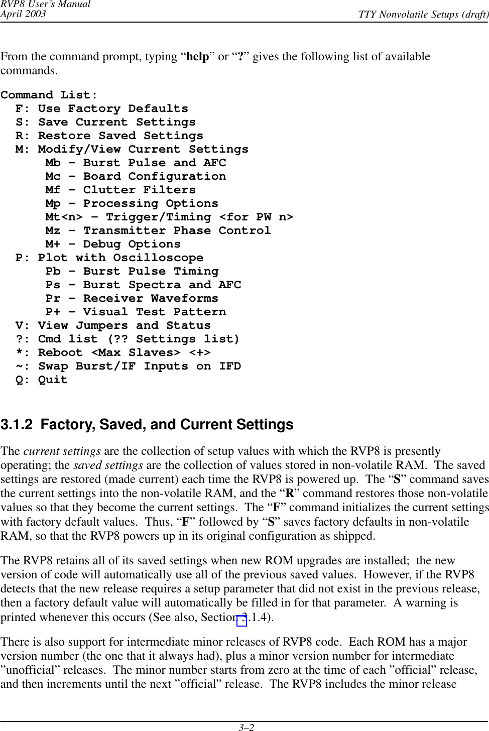
![Hardware InstallationRVP8 User’s ManualMay 20032–312.4.2 Example Hookup to a MITEQ “MFS-xxx” STALO The electrical interface for this STALO uses a 25-pin “D” connector with the following pinassignmentsGROUND on pins 1 and 2.Four BCD digits of 1KHz, 10KHz, 100KHz, and 1MHz frequency steps, usingPins <25:22>, <21:18>, <17:14>, <13:10>.Seven binary bits of representing 10MHz steps, Bits<0:6> on Pins<9:3>.First configure the IFD pins themselves. Pins 1 and 2 are ground, and are connected withwirewrap wire to the nearby ground posts. Pins 3 through 25 all are signal pins, so we plug in ajumper for each of these 23 pins. We will use pinmap uplink protocol, so H3 and H4 areremoved; and a x1 on-board crystal, so H2 is also removed.In this example we will assume that we wish to control the STALO in 20KHz steps from1.350GHz to 1.365GHz. This can be done with the following setups from the Mb section: AFC span– [–100%,+100%] maps into [ 1350000 , 1365000 ] AFC format– 0:Bin, 1:BCD, 2:8B4D: 2, ActLow: NO AFC uplink protocol– 0:Off, 1:Normal, 2:PinMap : 2 PinMap Table (Type ’31’ for GND, ’30’ for +5) ––––––––––––––––––––––––––––––––––––––––––––– Pin01:GND Pin02:GND Pin03:22 Pin04:21 Pin05:20 Pin06:19 Pin07:18 Pin08:17 Pin09:16 Pin10:15 Pin11:14 Pin12:13 Pin13:12 Pin14:11 Pin15:10 Pin16:09 Pin17:08 Pin18:07 Pin19:06 Pin20:05 Pin21:GND Pin22:GND Pin23:GND Pin24:GND Pin25:GND FAULT status pin (0:None): 0, ActLow: NOWe map the AFC interval into a numeric span from 1350000 to 1365000, and choose the“8B4D” mixed-radix encoding format. The STALO itself has 1KHz frequency steps, but theAFC servo will be easier to tune if we intentionally degrade this to 20KHz. This is done simplyby grounding all four of the 1KHz BCD input lines, plus the LSB of the 10KHz BCD digit. Amore creative use for one of these unused pins would be to remove the pin 25 jumper, wirewrappin 25 to ground (so the STALO sill reads it a logic low), and assign pin 25 as a fault statusinput. That pin could then be connected to an external fault line, if the STALO has one.](https://usermanual.wiki/Baron-Services/XDD-1000C.S10-RECEIVER-AND-PROCESSOR-USERS-MANUAL-PART-1/User-Guide-374022-Page-57.png)


![Hardware InstallationRVP8 User’s ManualMay 20032–312.4.2 Example Hookup to a MITEQ “MFS-xxx” STALO The electrical interface for this STALO uses a 25-pin “D” connector with the following pinassignmentsGROUND on pins 1 and 2.Four BCD digits of 1KHz, 10KHz, 100KHz, and 1MHz frequency steps, usingPins <25:22>, <21:18>, <17:14>, <13:10>.Seven binary bits of representing 10MHz steps, Bits<0:6> on Pins<9:3>.First configure the IFD pins themselves. Pins 1 and 2 are ground, and are connected withwirewrap wire to the nearby ground posts. Pins 3 through 25 all are signal pins, so we plug in ajumper for each of these 23 pins. We will use pinmap uplink protocol, so H3 and H4 areremoved; and a x1 on-board crystal, so H2 is also removed.In this example we will assume that we wish to control the STALO in 20KHz steps from1.350GHz to 1.365GHz. This can be done with the following setups from the Mb section: AFC span– [–100%,+100%] maps into [ 1350000 , 1365000 ] AFC format– 0:Bin, 1:BCD, 2:8B4D: 2, ActLow: NO AFC uplink protocol– 0:Off, 1:Normal, 2:PinMap : 2 PinMap Table (Type ’31’ for GND, ’30’ for +5) ––––––––––––––––––––––––––––––––––––––––––––– Pin01:GND Pin02:GND Pin03:22 Pin04:21 Pin05:20 Pin06:19 Pin07:18 Pin08:17 Pin09:16 Pin10:15 Pin11:14 Pin12:13 Pin13:12 Pin14:11 Pin15:10 Pin16:09 Pin17:08 Pin18:07 Pin19:06 Pin20:05 Pin21:GND Pin22:GND Pin23:GND Pin24:GND Pin25:GND FAULT status pin (0:None): 0, ActLow: NOWe map the AFC interval into a numeric span from 1350000 to 1365000, and choose the“8B4D” mixed-radix encoding format. The STALO itself has 1KHz frequency steps, but theAFC servo will be easier to tune if we intentionally degrade this to 20KHz. This is done simplyby grounding all four of the 1KHz BCD input lines, plus the LSB of the 10KHz BCD digit. Amore creative use for one of these unused pins would be to remove the pin 25 jumper, wirewrappin 25 to ground (so the STALO sill reads it a logic low), and assign pin 25 as a fault statusinput. That pin could then be connected to an external fault line, if the STALO has one.](https://usermanual.wiki/Baron-Services/XDD-1000C.S10-RECEIVER-AND-PROCESSOR-USERS-MANUAL-PART-1/User-Guide-374022-Page-64.png)


![Hardware InstallationRVP8 User’s ManualMay 20032–312.4.2 Example Hookup to a MITEQ “MFS-xxx” STALO The electrical interface for this STALO uses a 25-pin “D” connector with the following pinassignmentsGROUND on pins 1 and 2.Four BCD digits of 1KHz, 10KHz, 100KHz, and 1MHz frequency steps, usingPins <25:22>, <21:18>, <17:14>, <13:10>.Seven binary bits of representing 10MHz steps, Bits<0:6> on Pins<9:3>.First configure the IFD pins themselves. Pins 1 and 2 are ground, and are connected withwirewrap wire to the nearby ground posts. Pins 3 through 25 all are signal pins, so we plug in ajumper for each of these 23 pins. We will use pinmap uplink protocol, so H3 and H4 areremoved; and a x1 on-board crystal, so H2 is also removed.In this example we will assume that we wish to control the STALO in 20KHz steps from1.350GHz to 1.365GHz. This can be done with the following setups from the Mb section: AFC span– [–100%,+100%] maps into [ 1350000 , 1365000 ] AFC format– 0:Bin, 1:BCD, 2:8B4D: 2, ActLow: NO AFC uplink protocol– 0:Off, 1:Normal, 2:PinMap : 2 PinMap Table (Type ’31’ for GND, ’30’ for +5) ––––––––––––––––––––––––––––––––––––––––––––– Pin01:GND Pin02:GND Pin03:22 Pin04:21 Pin05:20 Pin06:19 Pin07:18 Pin08:17 Pin09:16 Pin10:15 Pin11:14 Pin12:13 Pin13:12 Pin14:11 Pin15:10 Pin16:09 Pin17:08 Pin18:07 Pin19:06 Pin20:05 Pin21:GND Pin22:GND Pin23:GND Pin24:GND Pin25:GND FAULT status pin (0:None): 0, ActLow: NOWe map the AFC interval into a numeric span from 1350000 to 1365000, and choose the“8B4D” mixed-radix encoding format. The STALO itself has 1KHz frequency steps, but theAFC servo will be easier to tune if we intentionally degrade this to 20KHz. This is done simplyby grounding all four of the 1KHz BCD input lines, plus the LSB of the 10KHz BCD digit. Amore creative use for one of these unused pins would be to remove the pin 25 jumper, wirewrappin 25 to ground (so the STALO sill reads it a logic low), and assign pin 25 as a fault statusinput. That pin could then be connected to an external fault line, if the STALO has one.](https://usermanual.wiki/Baron-Services/XDD-1000C.S10-RECEIVER-AND-PROCESSOR-USERS-MANUAL-PART-1/User-Guide-374022-Page-71.png)


![RVP8 User’s ManualApril 2003 TTY Nonvolatile Setups (draft)3–25Output control 4–bit pattern: 0001These are the hardware control bits for this pulsewidth. The bits are the 4-bit binarypattern that is output on PWBW0:3Bit Limits: 0 to 15 (input must be typed in decimal)Current noise level: –75.00 dBmPowerup noise level: –75.00 dBm –or–Current noise levels – PriRx: –75.00 dBm, SecRx: –75.00 dBmPowerup noise levels – PriRx: –75.00 dBm, SecRx: –75.00 dBmThese questions allow you to set the current value and the power-up value of thereceiver noise level for either a single or dual receiver system. The noise level(s) areshown in dBm, and you may alter either one from the TTY. The power-up level(s)are assigned by default when the RVP8 first starts up, and whenever the RESETopcode is issued with Bit #8 set. Likewise, the current noise level is revisedwhenever the SNOISE opcode is issued. These setup questions are intended forapplications in which the RVP8 must operate with a reasonable default value, up untilthe time that an SNOISE command is actually received. They may also be used tocompare the receiver noise levels during normal operation, which serves as a checkthat each FIR filter is behaving as expected when presented with thermal noise.Transmitter phase switch point: –1.00 usecThis is the transition time of the RVP8’s phase control output lines during randomphase processing modes. The switch point should be selected so that there isadequate settling time prior to the burst/COHO phase measurement on each pulse.This question only appears if the PHOUT[0:7] lines are actually configured for phasecontrol (See Section 3.3.1).Limits: –500 to 500 sec.Polarization switch point for POLAR0: –1.00 usecPolarization switch point for POLAR1: 1.00 usecThe RVP8’s POLAR0 and POLAR1 digital output lines control the polarizationswitch in a dual-polarization radar. During data processing modes in which thepolarization alternates from pulse to pulse, the transition points of these controlsignals are set by these two questions. The values are in microseconds relative torange zero; the same units used to define the start times of the six user triggers. Thelogical sense of POLAR0 and POLAR1 is set by questions described in Section 3.3.4.Limits: –500 to 500 sec.3.3.6 Mb — Burst Pulse and AFCThese questions are accessed by typing “Mb”. They set the parameters that influence the phaseand frequency analysis of the burst pulse, and the operation of the AFC feedback loop.Receiver Intermediate Frequency: 30.0000 MHzThis is the center frequency of the IF receiver and burst pulse waveform. The RVP8can operate at an intermediate frequency from any of the three alias bands22–32MHz, 40–50MHz, and 58–68MHz. These bands are delineated by 4MHz](https://usermanual.wiki/Baron-Services/XDD-1000C.S10-RECEIVER-AND-PROCESSOR-USERS-MANUAL-PART-1/User-Guide-374022-Page-102.png)
![RVP8 User’s ManualApril 2003 TTY Nonvolatile Setups (draft)3–29arbitrary units ranging from –100 to +100 corresponding to the complete span of theD/A converter. Since the D–Unit corresponds in a natural way to a percentage scale,the shorter “%” symbol is sometimes used.AFC feedback will be applied in proportion to the frequency error that the algorithmis attempting to correct. The feedback slope determines the sensitivity and timeconstant of the loop by establishing the AFC’s rate of change in (D-Units / sec) perthousand Hertz of frequency error. For example, a slope of 0.01 and a frequencyerror of 30KHz would result in a control voltage slew of 0.3 D-Units per second. Atthat rate it would take approximately 67 seconds for the output voltage to slew onetenth of its total span (20 D-Units / (0.3 D-Units / sec) = 67 sec). AFC is intended totrack very slow drifts in the radar system, so response times of this magnitude arereasonable.Keep in mind that the feedback slew is based on a frequency error which itself isderived from a time averaging process (see Burst Frequency Estimator Settling Timedescribed above) . The AFC loop will become unstable if a large feedback slope isused together with a long settling time constant, due to the phase lag introduced bythe averaging process. Keep the loop stable by choosing a small enough slope thatthe loop easily comes to a stop within the inner hysteresis zone.See Section 3.3.6.1 for more information about these slope and slew rate parameters. AFC span– [–100%,+100%] maps into [ –32768 , 32767 ] AFC format– 0:Bin, 1:BCD, 2:8B4D: 0, ActLow: NO AFC uplink protocol– 0:Off, 1:Normal, 2:PinMap : 1The RVP8’s implementation of AFC has been generalized so that there is nodifference between configuring an analog loop and a digital loop. The AFC feedbackloop parameters are setup the same way in each case; the only difference being themodel for how the AFC information is made available to the outside world. Manytypes of interfaces and protocols thus become possible according to how these threequestions are answered. AFC output follows these three steps:The internal feedback loop uses a conceptual [–100%,+100%] range of values.However, this range may be mapped into an arbitrary numeric span for eventualoutput. For example, choosing the span from –32768 to +32767 would result in16-bit AFC, and 0 to 999 might be appropriate for 3-digit BCD; but any otherspan could also be selected from the full 32-bit integer range.Next, an encoding format is chosen for the specified numeric span. The result ofthe encoding step is another 32-bit pattern which represents the above numericvalue. SIGMET will make an effort to include in the list of supported formats allcustom encodings that our customers encounter from their vendors.Available formats include straight binary, BCD, and mixed-radix formats thatmight be required by a specialized piece of equipment. The “8B4D” formatencodes the low four decimal digits as four BCD digits, and the remaining upperbits in binary. For example, 659999 base-10 would encode into 0x00419999Hex.Finally, an output protocol is selected for the bit pattern that was produced byencoding the numeric value. The bits may be written to the eight RVP8/Main](https://usermanual.wiki/Baron-Services/XDD-1000C.S10-RECEIVER-AND-PROCESSOR-USERS-MANUAL-PART-1/User-Guide-374022-Page-106.png)
![Hardware InstallationRVP8 User’s ManualMay 20032–30Table 2–8: Pinout for the CTI “MVSR-xxx” STALO Ribbon Pin “D” Pin Function Ribbon Pin “D” Pin Function 1 1 Ground 2 14 –– 3 2 +5V 4 15 –– 5 3 +24V 6 16 –– 7 4 Alarm 8 17 –– 9 5 –– 10 18 Bit–0 11 6 Bit–2 12 19 Bit–1 13 7 Bit–3 14 20 Bit–10 15 8 Bit–11 16 21 Bit–4 17 9 Bit–9 18 22 Bit–5 19 10 Bit–8 20 23 Bit–6 21 11 Bit–7 22 24 Ground 23 12 Bit–12 24 25 Bit–13 25 13 Inhb 26 –– ––First configure the IFD pins themselves. Pins 1 and 24 are power supply grounds, and areconnected with wirewrap wire to the nearby ground posts. Pins 2 and 3 supply +5V and +24Vto the STALO, and should be wire wrapped to the internal power posts. The STALO power, aswell as the DAFC power, is then supplied externally via the terminal block on the DAFC itself.Sixteen jumpers should be installed to connect the Control and Status lines, i.e., pins 4, 6–13,18–23, and 25. We will use pinmap uplink protocol, so H3 and H4 are removed; and a x1on-board crystal, so H2 is also removed.The STALO has an output frequency range from 5200–6020MHz in 100KHz steps. In thisexample we will assume that we need an AFC frequency span of 5580–5600MHz. This can bedone with the following setups from the Mb section: AFC span– [–100%,+100%] maps into [ 3800 , 4000 ] AFC format– 0:Bin, 1:BCD, 2:8B4D: 0, ActLow: NO AFC uplink protocol– 0:Off, 1:Normal, 2:PinMap : 2 PinMap Table (Type ’31’ for GND, ’30’ for +5) ––––––––––––––––––––––––––––––––––––––––––––– Pin01:GND Pin02:GND Pin03:GND Pin04:GND Pin05:GND Pin06:02 Pin07:03 Pin08:11 Pin09:09 Pin10:08 Pin11:07 Pin12:12 Pin13:GND Pin14:GND Pin15:GND Pin16:GND Pin17:GND Pin18:00 Pin19:01 Pin20:10 Pin21:04 Pin22:05 Pin23:06 Pin24:GND Pin25:13 FAULT status pin (0:None): 4, ActLow: NOWe map the AFC interval into the numeric span 3800–4000, and choose the “Bin” (simplebinary) encoding format. The actual frequency limits therefore match the desired values:5200MHz + ( 3800 x 100KHz ) = 5580MHz5200MHz + (4000 x 100KHz ) = 5600MHzThe “Inhb” line is held low, and fault status is input on Pin 4. Note that all pins that are notdirectly controlled by the software uplink (e.g., power pins, and unused pins) are merely set to“GND” in the setup table.](https://usermanual.wiki/Baron-Services/XDD-1000C.S10-RECEIVER-AND-PROCESSOR-USERS-MANUAL-PART-1/User-Guide-374022-Page-143.png)
![Hardware InstallationRVP8 User’s ManualMay 20032–312.4.2 Example Hookup to a MITEQ “MFS-xxx” STALO The electrical interface for this STALO uses a 25-pin “D” connector with the following pinassignmentsSGROUND on pins 1 and 2.SFour BCD digits of 1KHz, 10KHz, 100KHz, and 1MHz frequency steps, usingPins <25:22>, <21:18>, <17:14>, <13:10>.SSeven binary bits of representing 10MHz steps, Bits<0:6> on Pins<9:3>.First configure the IFD pins themselves. Pins 1 and 2 are ground, and are connected withwirewrap wire to the nearby ground posts. Pins 3 through 25 all are signal pins, so we plug in ajumper for each of these 23 pins. We will use pinmap uplink protocol, so H3 and H4 areremoved; and a x1 on-board crystal, so H2 is also removed.In this example we will assume that we wish to control the STALO in 20KHz steps from1.350GHz to 1.365GHz. This can be done with the following setups from the Mb section: AFC span– [–100%,+100%] maps into [ 1350000 , 1365000 ] AFC format– 0:Bin, 1:BCD, 2:8B4D: 2, ActLow: NO AFC uplink protocol– 0:Off, 1:Normal, 2:PinMap : 2 PinMap Table (Type ’31’ for GND, ’30’ for +5) ––––––––––––––––––––––––––––––––––––––––––––– Pin01:GND Pin02:GND Pin03:22 Pin04:21 Pin05:20 Pin06:19 Pin07:18 Pin08:17 Pin09:16 Pin10:15 Pin11:14 Pin12:13 Pin13:12 Pin14:11 Pin15:10 Pin16:09 Pin17:08 Pin18:07 Pin19:06 Pin20:05 Pin21:GND Pin22:GND Pin23:GND Pin24:GND Pin25:GND FAULT status pin (0:None): 0, ActLow: NOWe map the AFC interval into a numeric span from 1350000 to 1365000, and choose the“8B4D” mixed-radix encoding format. The STALO itself has 1KHz frequency steps, but theAFC servo will be easier to tune if we intentionally degrade this to 20KHz. This is done simplyby grounding all four of the 1KHz BCD input lines, plus the LSB of the 10KHz BCD digit. Amore creative use for one of these unused pins would be to remove the pin 25 jumper, wirewrappin 25 to ground (so the STALO sill reads it a logic low), and assign pin 25 as a fault statusinput. That pin could then be connected to an external fault line, if the STALO has one.](https://usermanual.wiki/Baron-Services/XDD-1000C.S10-RECEIVER-AND-PROCESSOR-USERS-MANUAL-PART-1/User-Guide-374022-Page-144.png)