Bilian Electronic R8801MS1 IEEE 802.11b/g/n WLAN SDIO Module User Manual
Shenzhen Bilian Electronic Co., Ltd. IEEE 802.11b/g/n WLAN SDIO Module
User Manual
0
BL-R8801MS1
Product Specification
IEEE 802.11b/g/n WLAN SDIO Module
Version: 1.0
Customer
Date
Model Name BL-R8801MS1
Part NO.
Blink Approve Field
ENGINEER QC SALES
Customer Approve Field
ENGINEER QC MANUFACTORY PURCHASING

B-LINK ELECTRONIC CO., LTD in shenzhen
1
Content
Content................................................................................................................................................................. 1
0. Revision History................................................................................................................................................1
1. General Description......................................................................................................................................... 2
2. The range of applying.......................................................................................................................................2
3. Product Specification....................................................................................................................................... 2
3.1 Function Block diagram.............................................................................................................................. 3
3.2 Electrical and Performance Specification................................................................................................... 3
3.3 Product Photo............................................................................................................................................. 4
3.4 Mechanical Specification............................................................................................................................ 5
3.5 Product Pin Definition.................................................................................................................................5
4. Supported platform..........................................................................................................................................6
4.1 DC characteristics........................................................................................................................................6
4.2 RF Characteristic......................................................................................................................................... 7
5. Typical Solder Reflow Profile........................................................................................................................... 8
6. Precautions for use.......................................................................................................................................... 9
0. Revision History

B-LINK ELECTRONIC CO., LTD in shenzhen
2
Date Document
revision
Product
revision
Change Description
2015/05/11 1.0 V1.0 Draft initial release
1. General Description
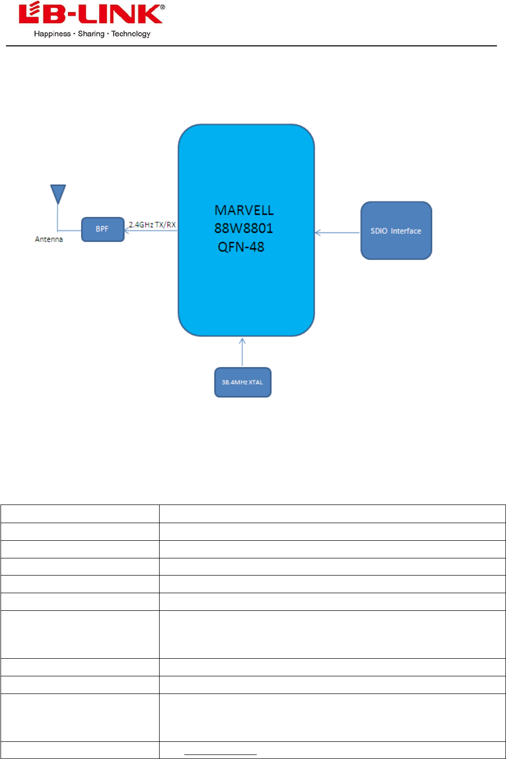
BL-R8801MS1 product is designed base on MARVELL 88W8801 chipset .It is a highly integrated
single-band (2.4GHz) IEEE 802.11n 1X1 System-on-Chip (SoC), specifically designed to support High
Throughput data rates for next generation WLAN products. It supports IEEE802.11i safety protocol,
along with IEEE 802.11e standard service quality. It supports the new data encryption on 64/128 bit
WEP and safety mechanism on WPA-PSK/WPA2-PSK, WPA/WPA2. It can implement the wireless
network function on the laptop/desktop/MID and other wireless devices easily .
2. The range of applying
MID, networking camera, STB GPS, E-book, Hard disk player, Network Radios, PSP and other device
which need be supported by wireless networking.
3. Product Specification
B-LINK ELECTRONIC CO., LTD in shenzhen
3
3.1 Function Block diagram
3.2 Electrical and Performance Specification
Item Description
Product Name BL-R8801MS1
Major Chipset MARVELL 88W8801
Host Interface SDIO
Standard IEEE 802.11b, IEEE 802.11g,IEEE 802.11n,
Frequency Range
Modulation Type
802.11b: CCK, DQPSK, DBPSK
802.11g: 64-QAM,16-QAM, QPSK, BPSK
802.11n: 64-QAM,16-QAM, QPSK, BPSK
Working Mode Infrastructure, Ad-Hoc
Data Transfer Rate 1,2,5.5,6,11,12,18,22,24,30,36,48,54,and maximum of 72.2Mbps
Spread Spectrum
IEEE 802.11b: DSSS (Direct Sequence Spread Spectrum)
IEEE 802.11g/n:OFDM (Orthogonal Frequency Division
Multiplexing)
Sensitivity @PER 1M: -92dBm@8%PER
2412MHz~2462MHz
B-LINK ELECTRONIC CO., LTD in shenzhen
4
6M: -88dBm@10%PER
11M:-86dBm@8%PER
54M:-72dBm@10%PER
72.2M:- 68dBm@10%PER
RF Power
Antenna type
Dimension(L*W*H) 13 x 13.5 x 1.46mm (LxWxH) ;Tolerance: +-0.15mm
Power supply 3.3V +/-0.2V
Power Consumption standby mode 70mA@3.3V ,
TX mode 150mA@3.3V
Clock source 38.4MHz
Working Temperature -20°C to +70°C
Storage temperature -40°C ~ +105°C
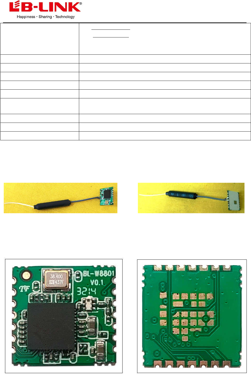
3.3 Product Photo
15dBm @802.11b/g/n
Internal Antenna
Antenna Gain 2.11dBi
Module TOP Module BOTTOM
TOP BOTTOM
B-LINK ELECTRONIC CO., LTD in shenzhen
5
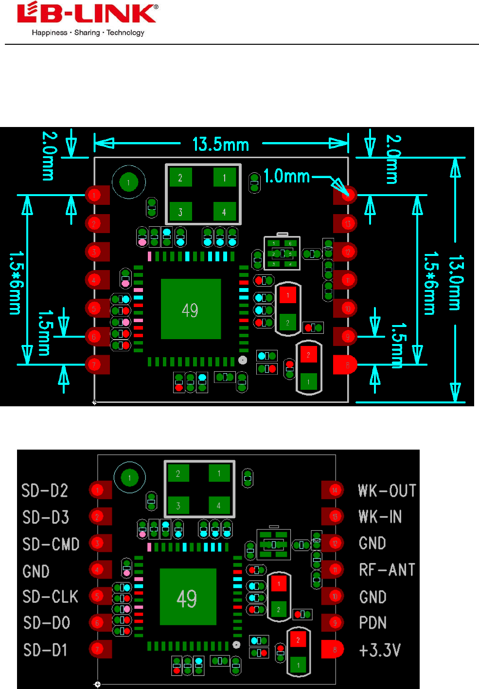
3.4 Mechanical Specification
Module dimension: Typical (W x L x H): 13mmx13.5mmx1.46mm Tolerance : +/-0.15mm
3.5 Product Pin Definition
B-LINK ELECTRONIC CO., LTD in shenzhen
6
4. Supported platform
Support Linux platform.
4.1 DC characteristics
Terms Contents
Specification : IEEE802.11b
Mode DSSS / CCK
Frequency
Data rate 1, 2, 5.5, 11Mbps
DC Characteristics min Typ. max. unit
TX mode 140 151 160 mA
Rx mode 70 72 75 mA
Sleep mode 65 66 68 mA
Specification : IEEE802.11g
Mode OFDM
Frequency
Data rate 6, 9, 12, 18, 24, 36, 48, 54Mbps
DC Characteristics min Typ. max. unit
Function Description
SD _2 SDIO data 2 1
SD _3 SDIO data 3 /GSPI chip select 2
SD _CMD SDIO command/GSPI data input 3
GND Ground 4
SD _CLK SDIO clock /GSPI clock 5
SD _D0 SDIO data 0 /GSPI data output 6
SD _D1 SDIO data 1 /GSPI data out 7
VCC3 3.3V power supply 8
PD_n Power down (active low) 9
GND Ground 10
ANT_RF WLAN RF pad 11
GND Ground 12
WK_IN Wake/Suspend input control 13
WK_OUT Wake/Suspend output control 14
2412MHz - 2462MHz
2412MHz - 2462MHz
B-LINK ELECTRONIC CO., LTD in shenzhen
7
TX mode 90 95 150 mA
Rx mode 72 73 75 mA
Sleep mode 65 66 68 mA
Specification : IEEE802.11n
Mode OFDM
Frequency
Data rate 6.5, 13, 19.5, 26, 39, 52, 58.5, 72.2Mbps
DC Characteristics min Typ. max. unit
TX mode 72 75 140 mA
Rx mode 70 73 78 mA
Sleep mode 65 66 68 mA
4.2 RF Characteristic
Mode Rate(Mbps) Power(dBm) EVM(dB) Sensitivity(dBm)
CH1 CH7 CH13 CH1 CH7 CH13 CH1 CH7 CH13
11b 1 17.02 17.37 16.85 -39.37 -37.29 -38.79 -93 -93 -93
11 16.98 17.41 16.61 -39.49 -39.06 -39.57 -88 -88 -88
11g 6 15.97 16.04 15.71 -23.36 -20.66 -20.34 -89 -89 -89
54 15.28 15.07 14.49 -32.51 -31.98 -32.75 -73 -73 -73
11n
HT20
MCS0 13.88 13.68 13.16 -26.61 -24.31 -24.90 -86 -86 -86
MCS7 13.65 14.00 13.38 -34.66 -31.8 -32.96 -70 -70 -70
2412MHz - 2462MHz
B-LINK ELECTRONIC CO., LTD in shenzhen
8
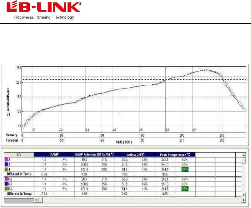
5. Typical Solder Reflow Profile

B-LINK ELECTRONIC CO., LTD in shenzhen
9
6. Precautions for use
1. Pls handle the module under ESD protection.
2. Reflow soldering shall be done according to the solder reflow profile. Peak temperature
245℃.
3. Products require baking before mounting if humidity indicator cards reads >30% temp <30 degree C,
humidity < 70% RH, over 96 hours.
Baking condition: 125 degree C, 12 hours
Baking times: 1 time
4. Storage Condition: Moisture barrier bag must be stored under 30 degree C, humidity under 85% RH. The
calculated shelf life for the dry packed product shall be a 12 months from the bag seal date. Humidity
indicator cards must be blue, <30%.
FCC Statement:
This equipment has been tested and found to comply with the limits for a Class B
digital device, pursuant to part 15 of the FCC Rules. These limits are designed to
provide reasonable protection against harmful interference in a residential installation.
This equipment generates uses and can radiate radio frequency energy and, if not
installed and used in accordance with the instructions, may cause harmful interference
to radio communications. However, there is no guarantee that interference will not
occur in a particular installation. If this equipment does cause harmful interference to
radio or television reception, which can be determined by turning the equipment off
and on, the user is encouraged to try to correct the interference by one or more of the
following measures:
-Reorient or relocate the receiving antenna.
-Increase the separation between the equipment and receiver.
-Connect the equipment into an outlet on a circuit different from that to which the
receiver is connected.
-Consult the dealer or an experienced radio/TV technician for help.
This device complies with part 15 of the FCC Rules. Operation is subject to the
following two conditions: (1) This device may not cause harmful interference, and (2)
this device must accept any interference received, including interference that may
cause undesired operation.
Any Changes or modifications not expressly approved by the party responsible for
compliance could void the user's authority to operate the equipment.
The device complies with RF specifications when the device used at 20cm form your
body.