Billion Electric BIL-SIM7100C 4G/LTE PCIE module User Manual
Billion Electric Co., Ltd. 4G/LTE PCIE module Users Manual
UserManual.wiki
>
Billion Electric
>
BIL SIM7100C User Manual
Users Manual
Navigation menu
Upload a User Manual
Namespaces
Wiki Guide
HTML
PDF
Info
Views
User Manual
Discussion / Help
Navigation
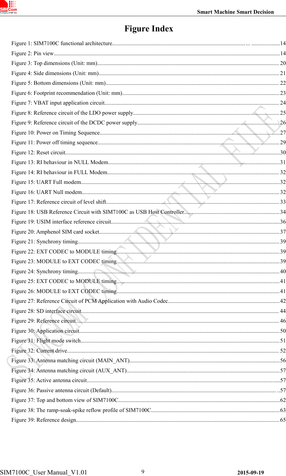
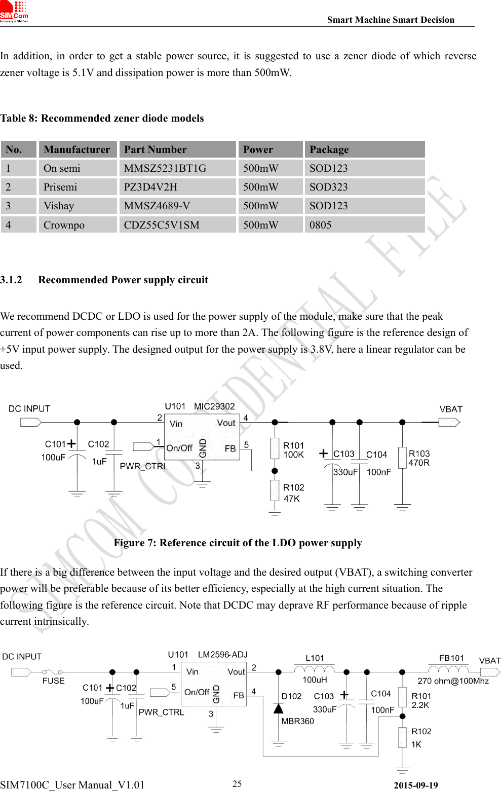
![Smart Machine Smart DecisionSIM7100C_User Manual_V1.01 2015-09-1926Figure 8: Reference circuit of the DCDC power supply3.1.3 Voltage monitorTo monitor the power supply voltage, user can use the AT command “AT+CBC”, this command has twoparameters: the battery status and the voltage value (mV). It will return the capacity percentage and actualvalue of battery (at the VBAT pin). The voltage is continuously measured at intervals, whenever themeasured battery voltage is lower than a specific value set by the AT command “AT+CVALARM”. Forexample, if the voltage value is set to be 3.4V, the following URC will be presented: “warning! voltage islow: 3.3v”.If the voltage is lower than a specific value which is set by the AT command “AT+CPMVT”, the modulewill be powered off automatically and AT commands cannot be executed any more.Note: Under-voltage warning function and under-voltage power-off function are disabled by default.For more information about these AT command, please refer to Document [1].3.2 Power on/Power off/Reset Time Sequence3.2.1 Power on SequenceSIM7100C can be powered on by PWRKEY pin, which starts normal operating mode.PWRKEY pin is pulled up with a 200k ohm resistor to 1.8V in module. User can power on the SIM7100Cby pulling the PWRKEY pin down for a short time. The power-on scenarios are illustrated in the followingfigures.](https://usermanual.wiki/Billion-Electric/BIL-SIM7100C/User-Guide-2877050-Page-26.png)
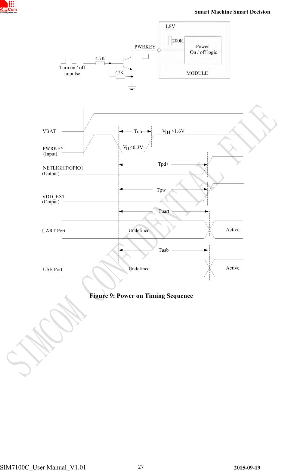
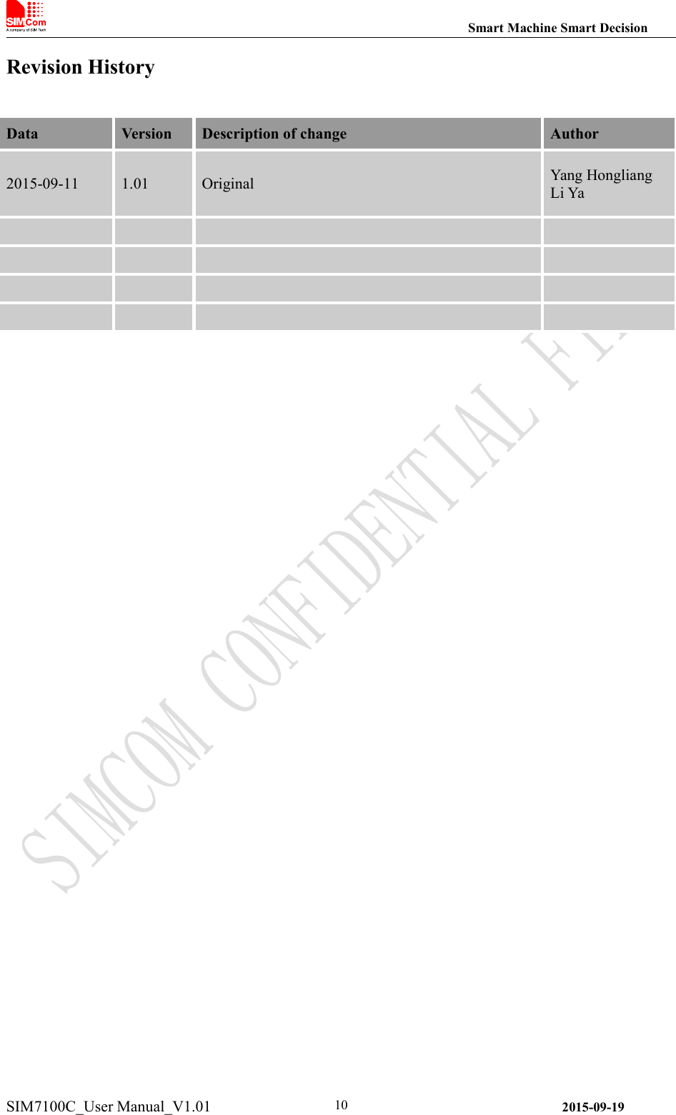
![Smart Machine Smart DecisionSIM7100C_User Manual_V1.01 2015-09-1928Table 9: Power on timingSymbolParameterTime valueUnitMin.Typ.Max.TonThe time to pull PWRKEY down to power on180500-msTpD+The time to indicate connecting with the network--5sTpw+The time to indicate the module is powered oncompletely--0.5sTuartThe time to enable UART--8sTusbThe time to enable USB--10sNote: Module could be automatically power on by connecting PWRKEY pin to Low level directly.Before designing, please refer to Document [27] for more detail.3.2.2 Power off SequenceThe following methods can be used to power down SIM7100C. These procedures will make moduledisconnect from the network and allow the software to enter a safe state, and then save data beforecompletely powering the module off.●Method 1: Power off SIM7100C by pulling the PWRKEY pin down●Method 2: Power off SIM7100C by AT commandUser can power off the SIM7100C by pulling PWRKEY down for a specific time. The power off scenariois illustrated in the following figure.](https://usermanual.wiki/Billion-Electric/BIL-SIM7100C/User-Guide-2877050-Page-28.png)
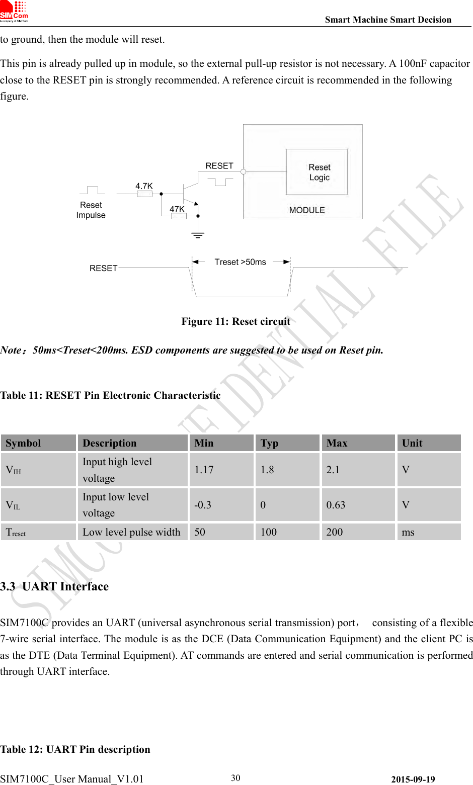
![Smart Machine Smart DecisionSIM7100C_User Manual_V1.01 2015-09-1929Figure 10: Power off timing sequenceTable 10: Power off timingSymbolParameterTime valueMin.Typ.Max.UnitToffThe time pulling PWRKEY down to power off0.5-5sTpD-The time to indicate disconnecting from the network--2sTpw-The time to indicate the module power off completely--2sTuartThe time to disable UART--3sTusbThe time to disable USB--2sTrestartThe time to power on again after Tpw-0--sUser can also use the AT command “AT+CPOF”to power down the module. After that, the ATcommands cannot be executed any longer. The module enters the POWER DOWN mode.VDD_EXT pin can be used to detect whether module is powered on or not. When module is poweredon and firmware goes ready, VDD_EXT will be high level.Note: For details about “AT+CPOF”, please refer to Document [1].3.2.3 Reset FunctionSIM7100C also have a RESET pin (PIN4) to reset the module. This function is used as an emergency resetonly when AT command “AT+CPOF” and the PWRKEY pin has no effect. User can pull the RESET pin](https://usermanual.wiki/Billion-Electric/BIL-SIM7100C/User-Guide-2877050-Page-29.png)
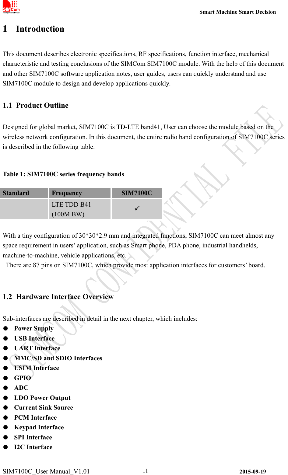
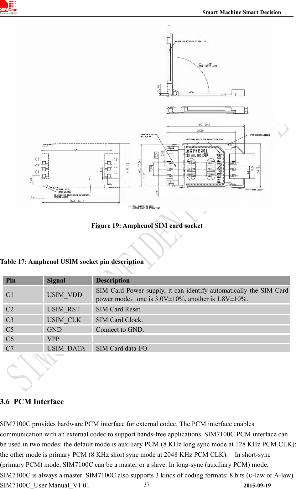
![Smart Machine Smart DecisionSIM7100C_User Manual_V1.01 2015-09-1936SEMI (www.onsemi.com ) SMF05C. Note that the SIM peripheral circuit should be close to the SIM cardsocket. The reference circuit of the 6-pin SIM card holder is illustrated in the following figure.Figure 18: USIM interface reference circuitNote: USIM_DATA has been pulled up with a 15kohm resistor to USIM_VDD in module. A 220nF shutcapacitor on USIM_VDD is used to reduce interference. Use AT Commands to get information inUSIM card. For more detail, please refer to document [1].3.5.3 Recommend Components of USIM holderFor 6 pins USIM socket, SIMCom recommend to use Amphenol C707 10M006 512. User can visithttp://www.amphenol.com for more information about the holder.](https://usermanual.wiki/Billion-Electric/BIL-SIM7100C/User-Guide-2877050-Page-36.png)
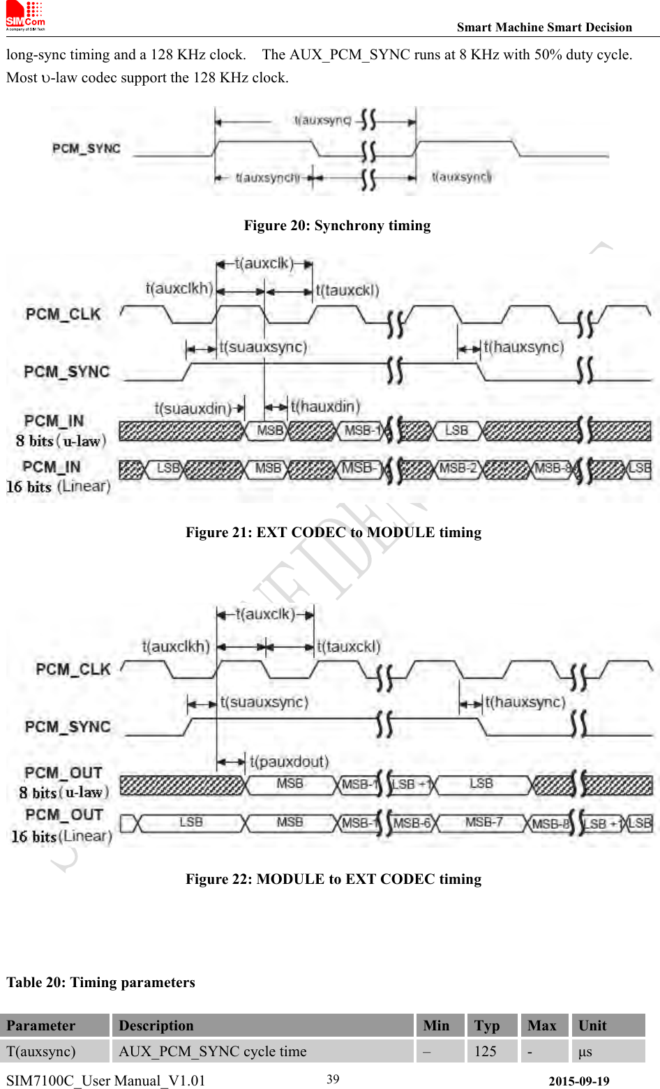
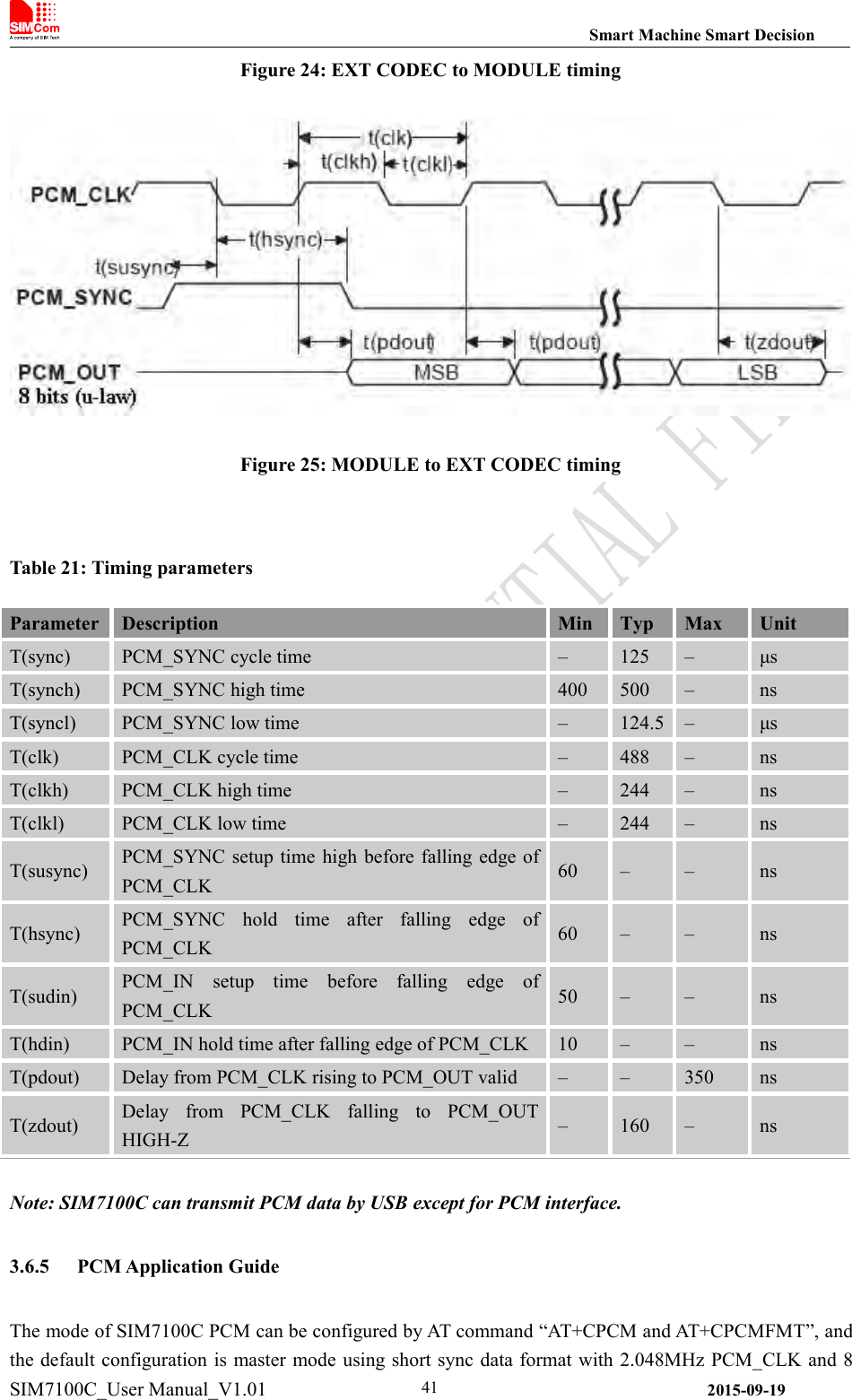
![Smart Machine Smart DecisionSIM7100C_User Manual_V1.01 2015-09-1938and 16 bits (linear).Note: PCM interface is multiplexed from GPIO (default setting). The AT command “AT+CPCM” isused to switch between PCM and GPIO functions. Please refer to document [21] and document [1] fordetails.3.6.1 PCM Pin DescriptionTable 18: PCM Pin descriptionPinsPin No.DescriptionPCM_OUT73PCM data outputPCM_IN74PCM data inputPCM_SYNC75PCM data synchronyPCM_CLK76PCM data clockTable 19: PCM Electronic characteristicSymbolParameterMinTypMaxUnitVIHHigh-level input voltage1.261.82.1VVILLow-level input voltage-0.300.63VVOHHigh-level output voltage1.35-1.8VVOLLow-level output voltage000.45V3.6.2 PCM Signal DescriptionThe default PCM interface in SIM7100C is the auxiliary PCM interface. The data changes on the highlevel of PCM_CLK and is sampled at the falling edge of PCM_CLK in one period. Primary PCM isdisabled after every power-on or every reset event. So user must use AT command to enable the primaryPCM mode after powering on or resetting the module every time if user wants to use PrimaryPCM.SIM7100C PCM Interface can be operated in Master or Slave mode if it is configured to primaryPCM. In Master Mode, the Module drives the clock and sync signals that are sent to the external codec.When it is in Slave Mode, the external codec drives the clock and sync signals which are sent to themodule. Both PCM modes are discussed in this section followed by additional PCM topics.3.6.3 Auxiliary PCM (128 KHz PCM clock)-law coding is supported by the auxiliary PCM. The auxiliary codec port operates with standard](https://usermanual.wiki/Billion-Electric/BIL-SIM7100C/User-Guide-2877050-Page-38.png)
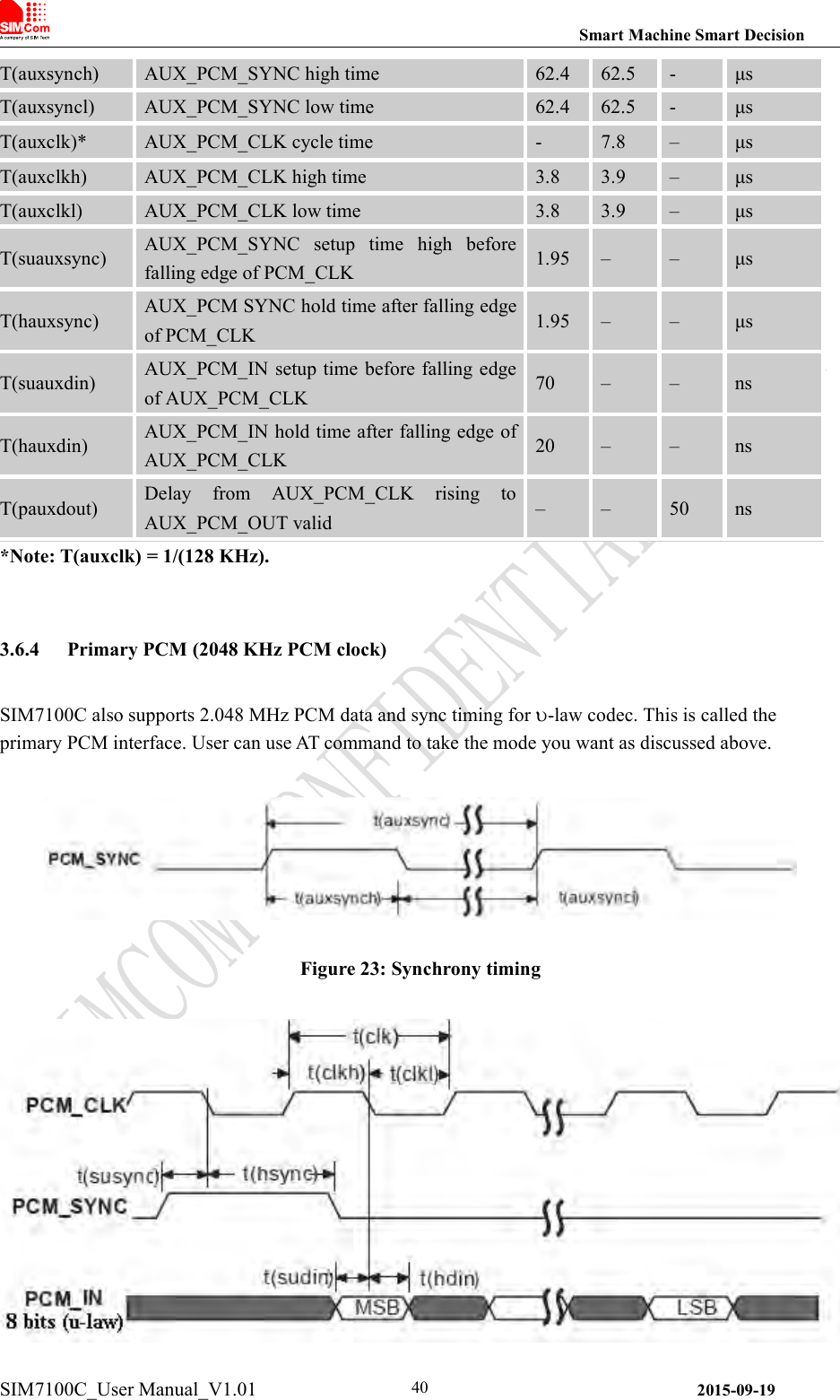
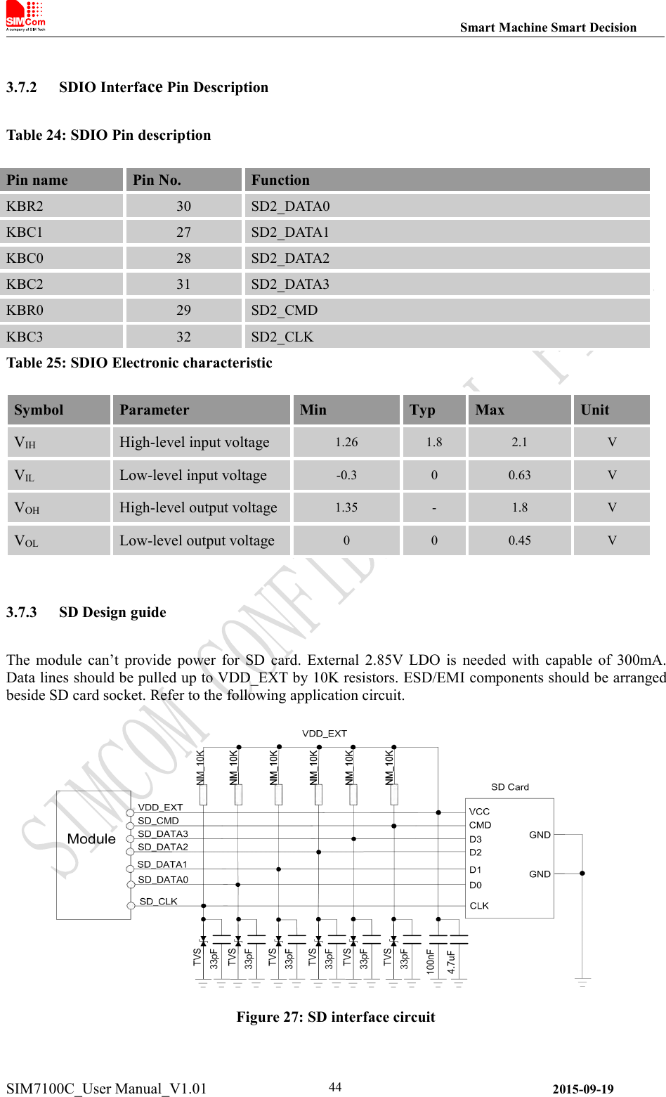
![Smart Machine Smart DecisionSIM7100C_User Manual_V1.01 2015-09-1942kHz PCM_SYNC. Please refer to document [21] and document [1] for details.In addition, the firmware of SIM7100C has integrated the configuration on WM8960GEFL/RV codecprovided by WOLFSON MICROELECTRONICS with I2C interface.The reference circuit of the reference design of PCM interfaces with external codec IC in the followingfigure. It is recommended to use a 26MHz CXO component such as TXC CORPORATION(www.txccorp.com) 8W26000011.Figure 26: Reference Circuit of PCM Application with Audio Codec3.7 MMC/SD and SDIO InterfaceSIM7100C provides one 4-bit SD/MMC interface and one SDIO interface with clock rate up to 52 MHz.3.7.1 MMC/SD Interface Pin DescriptionThe operation voltage of MMC/SD interface is 2.85V. It supports 1-bit SD/MMC or 4-bit SD datatransmission mode. Though the same hardware controller is used, the initialization procession for SD orMMC cards is different.Note: Interface with SD/MMC memory cards up to 32GBTable 22: MMC/SD Pin descriptionPin namePin No.FunctionSD_DATA022SD/MMC card data0SD_DATA123SD card data1SD_DATA224SD card data2](https://usermanual.wiki/Billion-Electric/BIL-SIM7100C/User-Guide-2877050-Page-42.png)
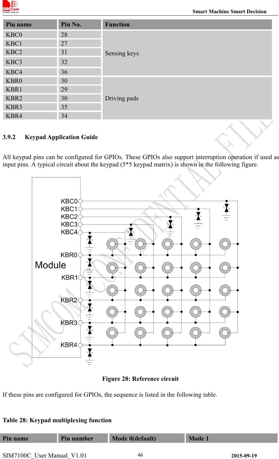
![Smart Machine Smart DecisionSIM7100C_User Manual_V1.01 2015-09-1947KBR434KBR4GPIO6KBR335KBR3GPIO7KBR230KBR2GPIO8KBR133KBR1GPIO9KBR029KBR0GPIO10KBC436KBC4GPIO11KBC332KBC3GPIO12KBC231KBC2GPIO13KBC127KBC1GPIO14KBC028KBC0GPIO15Note: Refer to document [23] for detailed information of Keypad Application Note.3.10 SPI InterfaceSPI interface of SIM7100C is master only. It provides a duplex, synchronous, serial communication linkwith peripheral devices. Its operation voltage is 1.8V, with clock rates up to 26 MHz.3.10.1 SPI Pin DescriptionTable 29: SPI Pin descriptionTable 30: SPI Electronic characteristicSymbolParameterMinTypMaxUnitVIHHigh-level input voltage1.261.82.1VVILLow-level input voltage-0.300.63VVOHHigh-level output voltage1.35-1.8VVOLLow-level output voltage000.45VPin namePin No.FunctionSPI_CS9SPI chip-select; not mandatory in a point-to-point connectionSPI_MISO7SPI master in/slave out dataSPI_CLK6SPI clockSPI_MOSI8SPI master out/slave in data](https://usermanual.wiki/Billion-Electric/BIL-SIM7100C/User-Guide-2877050-Page-47.png)
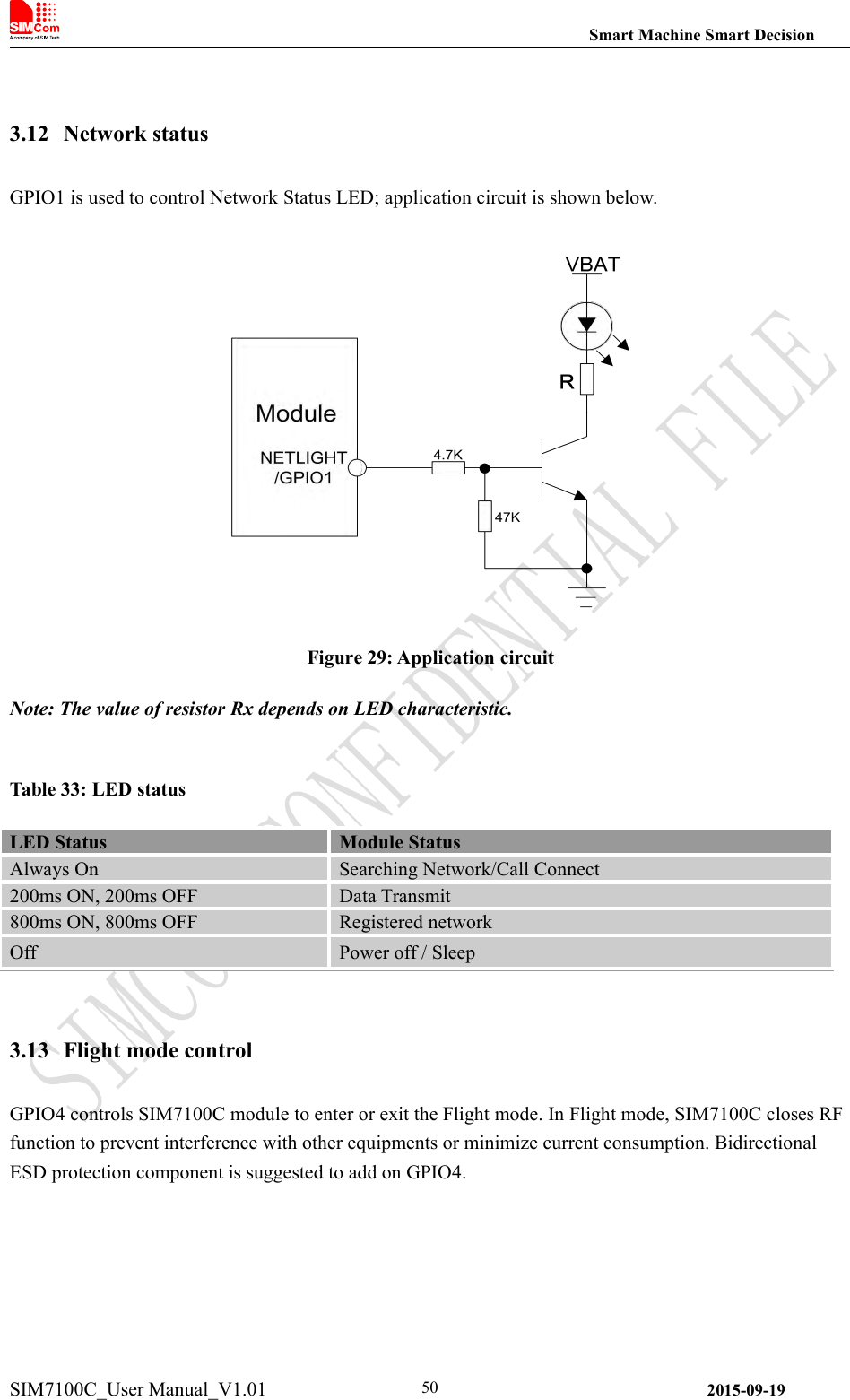
![Smart Machine Smart DecisionSIM7100C_User Manual_V1.01 2015-09-1951Figure 30: Flight mode switchTable 34: Flight mode statusGPIO4 StatusModule operationLow LevelFlight Mode: RF is closed.High LevelNormal Mode: RF is working.Note:1. For SIM7100C, GPIO0, GPIO2, GPIO3 and GPIO5 have multiplex function, user can usethem as PCM interface to connect extend codec. Refer to section 3.11 and document [1] for details.2. When the module is powered off, make sure all digital interfaces (PCM UART, etc) connected withperipheral devices have no voltage higher than 0.3V. If users’ design cannot meet above conditions,high level voltages maybe occur in GPIO pins because current leakage from above digital interfacesmay occur.3.14 Multi-functional interfaceSIM7100C merges functions for various applications. It can enrich users’ design and lower the cost ofusers’ hardware.3.14.1 Sink Current SourceThe dedicated pin (ISINK) is intended for driving passive devices ,such as LCD backlight, thisimplementation is VBAT tolerant and suitable for driving white LEDs. The high-current driver canmaintain a constant current which is set by the AT command “AT+ CLEDITST”, capable of up to 40 mA.Table 35: Sink Current Electronic characteristic](https://usermanual.wiki/Billion-Electric/BIL-SIM7100C/User-Guide-2877050-Page-51.png)
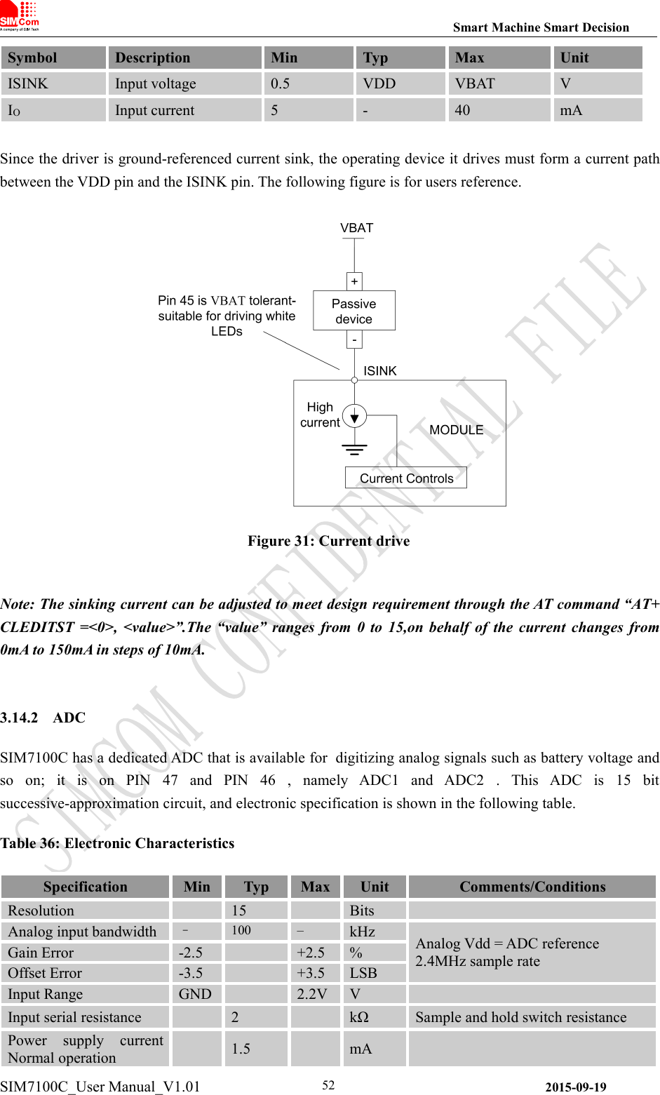
![Smart Machine Smart DecisionSIM7100C_User Manual_V1.01 2015-09-1953Power supply currentOff50200nAUser can introduce a signal in the ADC pin directly and use the AT command “AT+CADC” to get the rawdata which is between 0 and 32768. The data can be transformed to any type such as voltage, temperatureetc. Please refer to document [1].Note: The input signal voltage value in ADC must not be higher than 2.2V.3.14.3 LDOSIM7100C has a LDO power output, namely VDD_EXT. The LDO is available and output voltage is2.85v by default, rated for 150mA. User can switch the LDO on or off by the AT command“AT+CVAUXS” and configure its output voltage by the AT command “AT+CVAUXV”.Table 37: Electronic characteristicSymbolDescriptionMinTypMaxUnitVDD_EXTOutput voltage1.72.853.05VIOOutput current--50mA](https://usermanual.wiki/Billion-Electric/BIL-SIM7100C/User-Guide-2877050-Page-53.png)
![Smart Machine Smart DecisionSIM7100C_User Manual_V1.01 2015-09-1960ModeStatusFunctionNormaloperationSleepLTEModule will automatically go into sleep mode if theconditions of sleep mode are enabling and there is no on airand no hardware interrupt (such as USB wake-up operation ordata on serial port).In this case, the current consumption of module will bereduced to the minimal level.In sleep mode, the module can still receive paging messageand SMS.IdleLTESoftware is active. Module is registered to the LTE network,and the module is ready to communicate.StandbyLTEModule is ready for EDGE/HSPA+ /LTE data transfer, but nodata is currently sent or received. In this case, powerconsumption depends on network settings and EDGE/HSPA+/LTE configuration.DatatransferLTEThere is EDGE/HSPA+/LTE data transfer in progress. In thiscase, power consumption is related to network settings (e.g.power control level); uplink/downlink data rates and GPRSconfiguration (e.g. used multi-slot settings).Minimumfunctionality modeAT command “AT+CFUN” can be used to set the module to a minimumfunctionality mode without removing the power supply. In this mode, the RFpart of the module will not work or the USIM card will not be accessible, orboth RF part and USIM card will be closed, and the serial port is stillaccessible. The power consumption in this mode is lower than normal mode.5.2.2 Minimize Power ConsumptionThere are two modes that SIM7100C achieves low power consumption.5.2.3 Sleep modeIf peripheral equipments stops working, and there is no on air or hardware interrupts (such as GPIOinterrupts or data on UART), SIM7100C will enter sleep mode automatically. In this mode, SIM7100C canstill receive paging,voice call or SMS from network. If USB interface of SIM7100C is connected to hostCPU, but host CPU does not support USB suspending, then SIM7100C will not enter sleep mode. AfterUSB is disconnected, SIM7100C will enter sleep mode.Note: When UART interface is connected with host CPU, SIM7100C cannot enter sleep mode untilRXD is pulled down by the host CPU. If the module is in the idle mode, make sure to pull the RXD tolow level by host CPU. SIMCom recommends using GPIO43 or DTR to wake up the module from hostCPU and to use GPIO41 or RI to wake up the host CPU. Before designing, pay attention to how torealize waking function and refer to Document[24] and Document[25] for more detail.](https://usermanual.wiki/Billion-Electric/BIL-SIM7100C/User-Guide-2877050-Page-60.png)
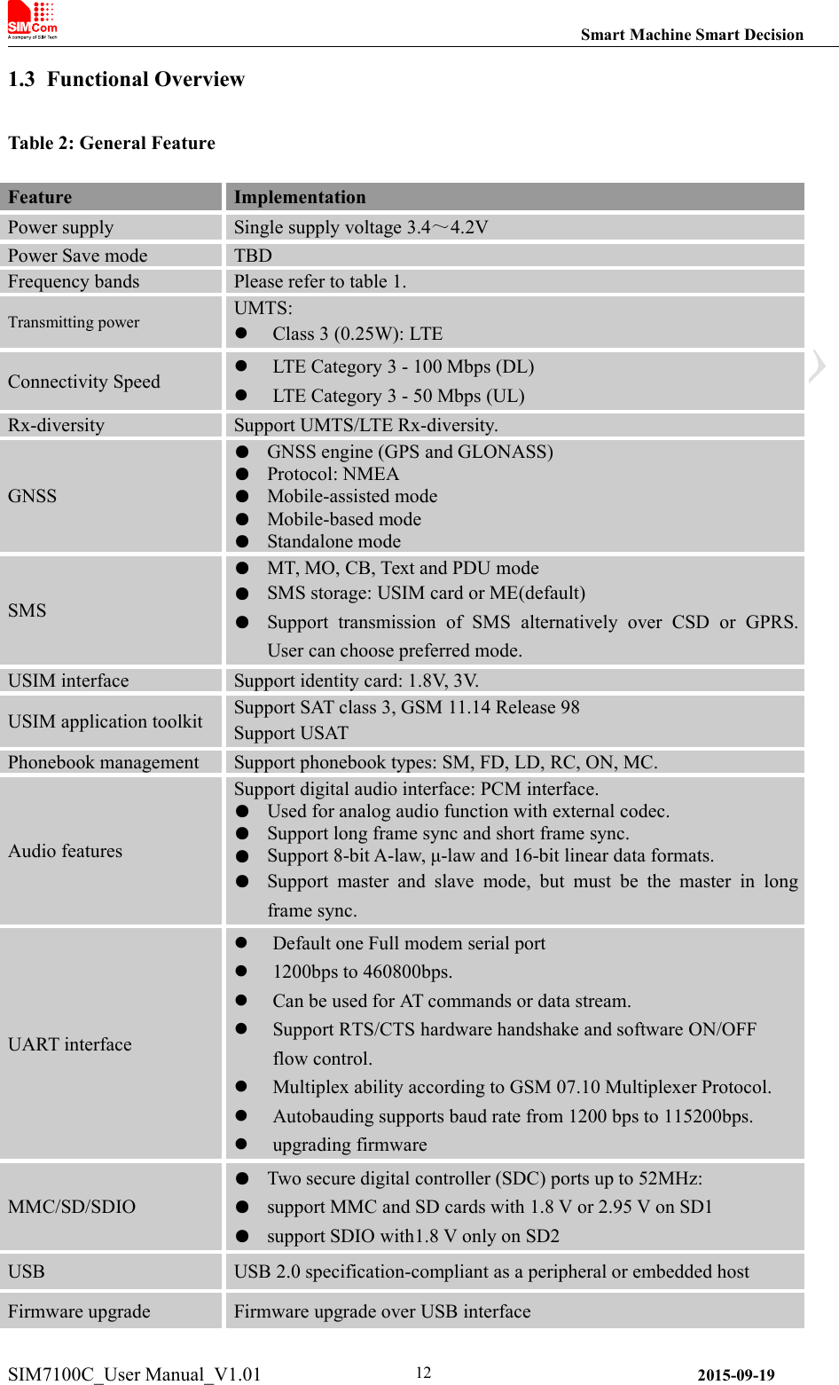
![Smart Machine Smart DecisionSIM7100C_User Manual_V1.01 2015-09-1963Figure 35: The ramp-soak-spike reflow profile of SIM7100CFor details about secondary SMT, please refer to document [26].6.3 Moisture Sensitivity Level (MSL)SIM7100C is qualified to Moisture Sensitivity Level (MSL) 5 in accordance with JEDEC J-STD-033.After the prescribed time limit exceeded, users should bake modules for 192 hours in drying equipment(<5% RH) at 40° C +5° C/-0° C, or 72 hours at 85° C +5° C/-5° C. Note that plastic tray is notheat-resistant, users must not use the tray to bake at 85° C or the tray may be damaged.Table 48: Moisture sensitivity level and floor lifeMoisture Sensitivity Level(MSL)Floor Life (out of bag) at factory ambient≤30°C/60% RH or asstated1Unlimited at ≦30℃/85% RH21 year2a4 weeks3168 hours472 hours548 hours5a24 hours6Mandatory bake before use. After bake, it must be reflowed within thetime limit specified on the label.NOTE: For product handling, storage, processing, IPC / JEDEC J-STD-033 must be followed.](https://usermanual.wiki/Billion-Electric/BIL-SIM7100C/User-Guide-2877050-Page-63.png)
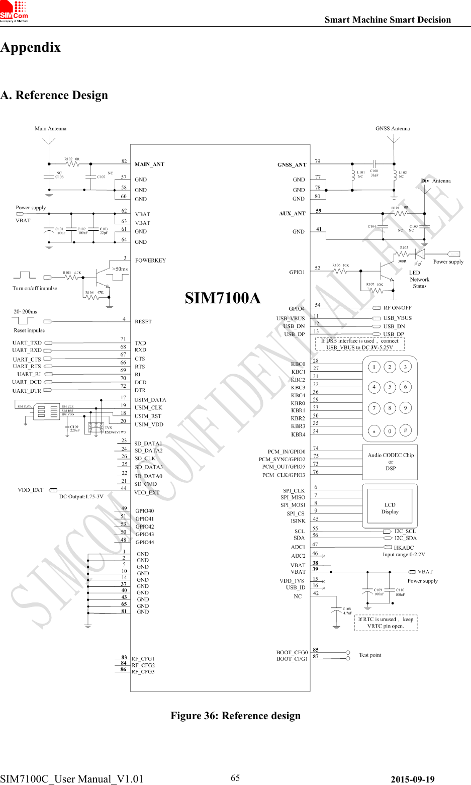
![Smart Machine Smart DecisionSIM7100C_User Manual_V1.01 2015-09-1966B. SIM7100C GPIOs ListTable 49: SIM7100C GPIOs listNameGPIO IndexDefault FunctionAlternate FunctionPCM_IN0GPIO Interrupt [LEVEL/LOW]PCM_INSTATUS_LED1Status ledGPIO1PCM_SYNC2GPIO [IN]PCM_SYNCPCM_CLK3GPIO [OUT/LOW]PCM_CLKRF_SWITCH4RF SwitchGPIO4PCM_OUT5GPIO [OUT/LOW]PCM_OUTKBR46KeypadGPIOKBR37KeypadGPIOKBR28KeypadGPIOKBR19KeypadGPIOKBR010KeypadGPIOKBC411KeypadGPIOKBC312KeypadGPIOKBC213KeypadGPIOKBC114KeypadGPIOKBC015KeypadGPIOCTS33CTSGPIORTS34RTSGPIODTR35DTR wake up moduleGPIODCD36DCDGPIORI37RI wake up hostGPIOGPIO4040Module power up statusGPIOGPIO4141Wake up hostGPIOGPIO4242GPIO[OUT/LOW]GPIOGPIO4343Wake up moduleGPIOGPIO4444GPIO[OUT/LOW]GPIOC. Digital I/O CharacteristicsTable 50: Digital I/O characteristicsParameterDescription1.8V Digital I/OUnitMinTypMaxVIHHigh-level inputvoltage1.261.82.1VVILLow-level inputvoltage-0.300.63VVOHHigh-level outputvoltage1.35-1.8V](https://usermanual.wiki/Billion-Electric/BIL-SIM7100C/User-Guide-2877050-Page-66.png)
![Smart Machine Smart DecisionSIM7100C_User Manual_V1.01 2015-09-1967VOLLow-level outputvoltage000.45VIOHHigh-level outputcurrent-1-mAIOLLow-level outputcurrent--1-mAIIHInput high leakagecurrent--1uAIILInput low leakagecurrent-1--uACINInput capacitance--7pFNote: These parameters are for digital interface pins, such as keypad, GPIO, I2C, UART, SPI. DigitalI/O specifications under both conditions are presented in the above tables.D. Related DocumentsTable 51: Related documentsSNDocument nameRemark[1]SIM7100C_ATC_V1.00SIM7100C_ATC_V1.00[2]ITU-T Draft newrecommendationV.25terSerial asynchronous automatic dialing and control[3]3GPP TS 51.010-1Digital cellular telecommunications system (Release 5); MobileStation (MS) conformance specification[4]3GPP TS 34.124Electromagnetic Compatibility (EMC) for mobile terminals andancillary equipment.[5]3GPP TS 34.121Electromagnetic Compatibility (EMC) for mobile terminals andancillary equipment.[6]3GPP TS 34.123-1Technical Specification Group Radio Access Network; Terminalconformance specification; Radio transmission and reception(FDD)[7]3GPP TS 34.123-3User Equipment (UE) conformance specification; Part 3: AbstractTest Suites.[8]EN 301 908-02 V2.2.1Electromagnetic compatibility and Radio spectrum Matters(ERM); Base Stations (BS) and User Equipment (UE) forIMT-2000. Third Generation cellular networks; Part 2:Harmonized EN for IMT-2000, CDMA Direct Spread(UTRA FDD) (UE) covering essential requirements of article3.2 of the R&TTE Directive[9]EN 301 489-24 V1.2.1Electromagnetic compatibility and Radio Spectrum Matters (ERM);Electromagnetic Compatibility (EMC) standard for radioequipment and services; Part 24: Specific conditions for IMT-2000CDMA Direct Spread (UTRA) for Mobile and portable (UE) radioand ancillary equipment](https://usermanual.wiki/Billion-Electric/BIL-SIM7100C/User-Guide-2877050-Page-67.png)
![Smart Machine Smart DecisionSIM7100C_User Manual_V1.01 2015-09-1968[10]IEC/EN60950-1(2001)Safety of information technology equipment (2000)[11]3GPP TS 51.010-1Digital cellular telecommunications system (Release 5); MobileStation (MS) conformance specification[12]GCF-CC V3.23.1Global Certification Forum - Certification Criteria[13]2002/95/ECDirective of the European Parliament and of the Council of 27January 2003 on the restriction of the use of certain hazardoussubstances in electrical and electronic equipment (RoHS)[14]Audio Application NoteV1.01Audio Application Note V1.01[15]ReservedReserved[16]Keypad ApplicationNote V1.01Keypad Application Note V1.01[17]Sleep_Application_NoteSleep_Application_Note[18]Waking_up_Application_NoteWaking_up_Application_Note[19]Modulesecondary-SMT-UGDSMT Note[20]SIM5xxx_Automatic_POWER_ON_Application_NoteSIM5xxx_Automatic_POWER_ON_Application_NoteE. Terms and AbbreviationsTable 52: Terms and AbbreviationsAbbreviationDescriptionADCAnalog-to-Digital ConverterARPAntenna Reference PointBERBit Error RateBTSBase Transceiver StationCSCoding SchemeCSDCircuit Switched Data](https://usermanual.wiki/Billion-Electric/BIL-SIM7100C/User-Guide-2877050-Page-68.png)