Billion Electric BIL-SIM7100C 4G/LTE PCIE module User Manual
Billion Electric Co., Ltd. 4G/LTE PCIE module Users Manual
Users Manual
SIM7100C_User Manual_V1.01

Smart Machine Smart Decision
Document Title
SIM7100C_User Manual_V1.01
Version
1.01
Date
2015-09-19
Status
Draft
Document Control ID
SIM7100C_User Manual_V1.01
General Notes
SIMCom offers this information as a service to its customers, to support application and engineering
efforts that use the products designed by SIMCom. The information provided is based upon requirements
specifically provided to SIMCom by the customers. SIMCom has not undertaken any independent search
for additional relevant information, including any information that may be in the customer’s possession.
Furthermore, system validation of this product designed by SIMCom within a larger electronic system
remains the responsibility of the customer or the customer’s system integrator. All specifications supplied
herein are subject to change.
RF exposure statements:
Information to OEM integrator
The OEM integrator has to be aware not to provide information to the end user regarding how to install or
remove this RF module in the user manual of the end product.
The user manual which is provided by OEM integrators for end users must include the following
information in a prominent location.
1. To comply with FCC RF exposure compliance requirements, the antenna used for this transmitter must
be installed to provide a separation distance of at least 20 cm from all persons and must not be co-located
or operating in conjunction with any other antenna or transmitter, except in accordance with FCC
multi-transmitter product procedures.
2. Only those antennas with same type and lesser gain filed under this FCC ID number can be used with
this device.
3. The regulatory label on the final system must include the statement: “Contains FCC ID: xxxx or using
electronic labeling method as documented in KDB 784748.
4. The final system integrator must ensure there is no instruction provided in the user manual or customer
documentation indicating how to install or remove the transmitter module except such device has
implemented two ways authentication between module and the host system.
This module can't be used on radio system and operation individually. Using others antenna must be
re-testing and certification.
Copyright
This document contains proprietary technical information which is the property of SIMCom Limited,
copying of this document and giving it to others and the using or communication of the contents thereof,
are forbidden without express authority. Offenders are liable to the payment of damages. All rights
reserved in the event of grant of a patent or the registration of a utility model or design. All specification
supplied herein are subject to change without notice at any time.
Copyright © Shanghai SIMCom Wireless Solutions Ltd. 2014

Smart Machine Smart Decision
SIM7100C_User Manual_V1.01 2015-09-19
3

Smart Machine Smart Decision
SIM7100C_User Manual_V1.01 2015-09-19
4
Contents
SIM7100C_User Manual_V1.01................................................................................................................... 1
Contents...........................................................................................................................................................4
Table Index...................................................................................................................................................... 7
Figure Index.................................................................................................................................................... 9
Revision History............................................................................................................................................10
1 Introduction............................................................................................................................................11
1.1 Product Outline................................................................................................................................. 11
1.2 Hardware Interface Overview.......................................................................................................... 11
1.3 Hardware Diagram............................................................................................................................11
1.4 Functional Overview........................................................................................................................ 12
2 Package Information............................................................................................................................. 13
2.1 Pin Configuration............................................................................................................................. 13
2.2 Pin description.................................................................................................................................. 16
2.3 Package Dimensions.........................................................................................................................20
2.4 Footprint Recommendation.............................................................................................................. 23
3 Application Interface Specification..................................................................................................... 24
3.1 Power Supply....................................................................................................................................24
3.1.1 Design Guide............................................................................................................................. 24
3.1.2 Recommended Power supply circuit.........................................................................................25
3.1.3 Voltage monitor..........................................................................................................................26
3.2 Power on/Power off/Reset Time Sequence...................................................................................... 26
3.2.1 Power on Sequence....................................................................................................................26
3.2.2 Power off Sequence................................................................................................................... 28
3.2.3 Reset Function........................................................................................................................... 29
3.3 UART Interface................................................................................................................................ 30
3.3.1 RI Behavior................................................................................................................................31
3.3.2 Design Guide............................................................................................................................. 32
3.4 USB Interface................................................................................................................................... 33
3.4.1 USB Application Guide............................................................................................................. 33
3.5 USIM Interface................................................................................................................................. 35
3.5.1 USIM Pin description................................................................................................................ 35
3.5.2 USIM Application Guide...........................................................................................................35
3.5.3 Recommend Components of USIM holder...............................................................................36
3.6 PCM Interface...................................................................................................................................37
3.6.1 PCM Pin Description.................................................................................................................38
3.6.2 PCM Signal Description............................................................................................................38
3.6.3 Auxiliary PCM (128 KHz PCM clock).....................................................................................38
3.6.4 Primary PCM (2048 KHz PCM clock)..................................................................................... 40
3.6.5 PCM Application Guide............................................................................................................ 41
3.7 MMC/SD and SDIO Interface..........................................................................................................42

Smart Machine Smart Decision
SIM7100C_User Manual_V1.01 2015-09-19
5
3.7.1 MMC/SD Interface Pin Description..........................................................................................42
3.7.2 SDIO Interface Pin Description.................................................................................................44
3.7.3 SD Design guide........................................................................................................................ 44
3.8 I2C Interface..................................................................................................................................... 45
3.8.1 I2C Pin Description................................................................................................................... 45
3.8.2 I2C Signal Description.............................................................................................................. 45
3.8.3 I2C Design Guide...................................................................................................................... 45
3.9 Keypad Interface...............................................................................................................................45
3.9.1 Keypad Pin Description.............................................................................................................45
3.9.2 Keypad Application Guide........................................................................................................ 46
3.10 SPI Interface..................................................................................................................................47
3.10.1 SPI Pin Description................................................................................................................ 47
3.11 GPIO Interface.............................................................................................................................. 48
3.11.1 GPIO Pin Description............................................................................................................ 48
3.12 Network status...............................................................................................................................50
3.13 Flight mode control.......................................................................................................................50
3.14 Multi-functional interface............................................................................................................. 51
3.14.1 Sink Current Source............................................................................................................... 51
3.14.2 ADC........................................................................................................................................52
3.14.3 LDO........................................................................................................................................53
4 RF Specification..................................................................................................................................... 54
4.1 RF Specification............................................................................................................................... 54
4.2 Antenna Design Guide......................................................................................................................56
5 Reliability and Operating Characteristics..........................................................................................59
5.1 Electronic Characteristics.................................................................................................................59
5.2 Operating Mode................................................................................................................................59
5.2.1 Operating Mode......................................................................................................................... 59
5.2.2 Minimize Power Consumption..................................................................................................60
5.2.3 Sleep mode.................................................................................................................................60
5.2.4 Minimum functionality mode....................................................................................................61
5.3 Current Consumption....................................................................................................................... 61
5.4 EMC and ESD Notes........................................................................................................................61
6 Guide for Production.............................................................................................................................62
6.1 Top and Bottom View of SIM7100C...............................................................................................62
6.2 Typical Solder Reflow Profile..........................................................................................................62
6.3 Moisture Sensitivity Level (MSL)................................................................................................... 63
6.4 Stencil Foil Design Recommendation..............................................................................................64
Appendix........................................................................................................................................................65
A. Reference Design................................................................................................................................... 65
B. SIM7100C GPIOs List...........................................................................................................................66
C. Digital I/O Characteristics......................................................................................................................66
D. Related Documents................................................................................................................................ 67

Smart Machine Smart Decision
SIM7100C_User Manual_V1.01 2015-09-19
6
E. Terms and Abbreviations....................................................................................................................... 68
F. Safety Caution.........................................................................................................................................70
Contact us:.....................................................................................................................................................72
Shanghai SIMCom Wireless Solutions Ltd............................................................................................... 72

Smart Machine Smart Decision
SIM7100C_User Manual_V1.01 2015-09-19
7
Table Index
Table 1: SIM7100C series frequency bands...................................................................................................................... 11
Table 2: General Feature....................................................................................................................................................12
Table 3: Coding schemes and maximum net data rates over air interface.........................................................................13
Table 4: Pin definition....................................................................................................................................................... 15
Table 5: IO Parameters Definition.....................................................................................................................................16
Table 6: Pin description..................................................................................................................................................... 16
Table 7: VBAT Pin description.......................................................................................................................................... 24
Table 8: Recommended zener diode models..................................................................................................................... 25
Table 9: Power on timing...................................................................................................................................................28
Table 10: Power off timing................................................................................................................................................ 29
Table 11: RESET Pin Electronic Characteristic................................................................................................................ 30
Table 12: UART Pin description........................................................................................................................................30
Table 13: UART Pin Logic level....................................................................................................................................... 31
Table 14: USB Pin description.......................................................................................................................................... 33
Table 15: USIM Pin description........................................................................................................................................ 35
Table 16: USIM Electronic characteristic..........................................................................................................................35
Table 17: Amphenol USIM socket pin description............................................................................................................37
Table 18: PCM Pin description..........................................................................................................................................38
Table 19: PCM Electronic characteristic........................................................................................................................... 38
Table 20: Timing parameters............................................................................................................................................. 39
Table 21: Timing parameters............................................................................................................................................. 41
Table 22: MMC/SD Pin description.................................................................................................................................. 42
Table 23: MMC/SD Electronic characteristic*..................................................................................................................43
Table 24: SDIO Pin description......................................................................................................................................... 44
Table 25: SDIO Electronic characteristic.......................................................................................................................... 44
Table 26: I2C Pin description............................................................................................................................................ 45
Table 27: Keypad Pin description......................................................................................................................................45
Table 28: Keypad multiplexing function........................................................................................................................... 46
Table 29: SPI Pin description............................................................................................................................................ 47
Table 30: SPI Electronic characteristic..............................................................................................................................47
Table 31: GPIO Pin description......................................................................................................................................... 48
Table 32: GPIO Electronic characteristic.......................................................................................................................... 48
Table 23: LED status......................................................................................................................................................... 50
Table 34: Flight mode status..............................................................................................................................................51
Table 35: Sink Current Electronic characteristic............................................................................................................... 51
Table 36: Electronic Characteristics.................................................................................................................................. 52
Table 37: Electronic characteristic.....................................................................................................................................53
Table 38: Conducted transmission power..........................................................................................................................54
Table 39: Operating frequencies........................................................................................................................................54
Table 40: E-UTRA operating bands.................................................................................................................................. 54
Table 41: Conducted receive sensitivity............................................................................................................................ 55
Table 42: Reference sensitivity (QPSK)............................................................................................................................57
Table 43: Absolute maximum ratings................................................................................................................................ 59

Smart Machine Smart Decision
SIM7100C_User Manual_V1.01 2015-09-19
8
Table 44: Recommended operating ratings....................................................................................................................... 59
Table 45: Operating temperature....................................................................................................................................... 59
Table 46: Operating mode................................................................................................................................................. 59
Table 47: Current consumption......................................................................................................................................... 61
Table 48: The ESD performance measurement table (Temperature: 25℃, Humidity: 45%)............................................61
Table 49: Moisture sensitivity level and floor life.............................................................................................................63
Table 50: SIM7100C GPIOs list........................................................................................................................................66
Table 51: Digital I/O characteristics.................................................................................................................................. 66
Table 52: Related documents.............................................................................................................................................67
Table 53: Terms and Abbreviations................................................................................................................................... 68
Table 54: Safety caution.................................................................................................................................................... 70

Smart Machine Smart Decision
SIM7100C_User Manual_V1.01 2015-09-19
9
Figure Index
Figure 1: SIM7100C functional architecture................................................................................................ ....................14
Figure 2: Pin view..............................................................................................................................................................14
Figure 3: Top dimensions (Unit: mm)............................................................................................................................... 20
Figure 4: Side dimensions (Unit: mm).............................................................................................................................. 21
Figure 5: Bottom dimensions (Unit: mm)......................................................................................................................... 22
Figure 6: Footprint recommendation (Unit: mm)..............................................................................................................23
Figure 7: VBAT input application circuit.......................................................................................................................... 24
Figure 8: Reference circuit of the LDO power supply...................................................................................................... 25
Figure 9: Reference circuit of the DCDC power supply................................................................................................... 26
Figure 10: Power on Timing Sequence..............................................................................................................................27
Figure 11: Power off timing sequence............................................................................................................................... 29
Figure 12: Reset circuit......................................................................................................................................................30
Figure 13: RI behaviour in NULL Modem........................................................................................................................31
Figure 14: RI behaviour in FULL Modem........................................................................................................................ 32
Figure 15: UART Full modem...........................................................................................................................................32
Figure 16: UART Null modem.......................................................................................................................................... 32
Figure 17: Reference circuit of level shift......................................................................................................................... 33
Figure 18: USB Reference Circuit with SIM7100C as USB Host Controller...................................................................34
Figure 19: USIM interface reference circuit......................................................................................................................36
Figure 20: Amphenol SIM card socket..............................................................................................................................37
Figure 21: Synchrony timing............................................................................................................................................. 39
Figure 22: EXT CODEC to MODULE timing..................................................................................................................39
Figure 23: MODULE to EXT CODEC timing..................................................................................................................39
Figure 24: Synchrony timing............................................................................................................................................. 40
Figure 25: EXT CODEC to MODULE timing..................................................................................................................41
Figure 26: MODULE to EXT CODEC timing..................................................................................................................41
Figure 27: Reference Circuit of PCM Application with Audio Codec..............................................................................42
Figure 28: SD interface circuit.......................................................................................................................................... 44
Figure 29: Reference circuit.............................................................................................................................................. 46
Figure 30: Application circuit............................................................................................................................................50
Figure 31: Flight mode switch........................................................................................................................................... 51
Figure 32: Current drive.................................................................................................................................................... 52
Figure 33: Antenna matching circuit (MAIN_ANT).........................................................................................................56
Figure 34: Antenna matching circuit (AUX_ANT)...........................................................................................................57
Figure 35: Active antenna circuit.......................................................................................................................................57
Figure 36: Passive antenna circuit (Default)................................................................................................................... ..57
Figure 37: Top and bottom view of SIM7100C.................................................................................................................62
Figure 38: The ramp-soak-spike reflow profile of SIM7100C..........................................................................................63
Figure 39: Reference design.............................................................................................................................................. 65

Smart Machine Smart Decision
SIM7100C_User Manual_V1.01 2015-09-19
10
Revision History
Data
Version
Description of change
Author
2015-09-11
1.01
Original
Yang Hongliang
Li Ya

Smart Machine Smart Decision
SIM7100C_User Manual_V1.01 2015-09-19
11
1Introduction
This document describes electronic specifications, RF specifications, function interface, mechanical
characteristic and testing conclusions of the SIMCom SIM7100C module. With the help of this document
and other SIM7100C software application notes, user guides, users can quickly understand and use
SIM7100C module to design and develop applications quickly.
1.1 Product Outline
Designed for global market, SIM7100C is TD-LTE band41, User can choose the module based on the
wireless network configuration. In this document, the entire radio band configuration of SIM7100C series
is described in the following table.
Table 1: SIM7100C series frequency bands
Standard
Frequency
SIM7100C
LTE TDD B41
(100M BW)
With a tiny configuration of 30*30*2.9 mm and integrated functions, SIM7100C can meet almost any
space requirement in users’ application, such as Smart phone, PDA phone, industrial handhelds,
machine-to-machine, vehicle applications, etc.
There are 87 pins on SIM7100C, which provide most application interfaces for customers’ board.
1.2 Hardware Interface Overview
Sub-interfaces are described in detail in the next chapter, which includes:
●Power Supply
●USB Interface
●UART Interface
●MMC/SD and SDIO Interfaces
●USIM Interface
●GPIO
●ADC
●LDO Power Output
●Current Sink Source
●PCM Interface
●Keypad Interface
●SPI Interface
●I2C Interface

Smart Machine Smart Decision
SIM7100C_User Manual_V1.01 2015-09-19
12
1.3 Functional Overview
Table 2: General Feature
Feature
Implementation
Power supply
Single supply voltage 3.4~4.2V
Power Save mode
TBD
Frequency bands
Please refer to table 1.
Transmitting power
UMTS:
Class 3 (0.25W): LTE
Connectivity Speed
LTE Category 3 - 100 Mbps (DL)
LTE Category 3 - 50 Mbps (UL)
Rx-diversity
Support UMTS/LTE Rx-diversity.
GNSS
●GNSS engine (GPS and GLONASS)
●Protocol: NMEA
●Mobile-assisted mode
●Mobile-based mode
●Standalone mode
SMS
●MT, MO, CB, Text and PDU mode
●SMS storage: USIM card or ME(default)
●Support transmission of SMS alternatively over CSD or GPRS.
User can choose preferred mode.
USIM interface
Support identity card: 1.8V, 3V.
USIM application toolkit
Support SAT class 3, GSM 11.14 Release 98
Support USAT
Phonebook management
Support phonebook types: SM, FD, LD, RC, ON, MC.
Audio features
Support digital audio interface: PCM interface.
●Used for analog audio function with external codec.
●Support long frame sync and short frame sync.
●Support 8-bit A-law, μ-law and 16-bit linear data formats.
●Support master and slave mode, but must be the master in long
frame sync.
UART interface
Default one Full modem serial port
1200bps to 460800bps.
Can be used for AT commands or data stream.
Support RTS/CTS hardware handshake and software ON/OFF
flow control.
Multiplex ability according to GSM 07.10 Multiplexer Protocol.
Autobauding supports baud rate from 1200 bps to 115200bps.
upgrading firmware
MMC/SD/SDIO
●Two secure digital controller (SDC) ports up to 52MHz:
●support MMC and SD cards with 1.8 V or 2.95 V on SD1
●support SDIO with1.8 V only on SD2
USB
USB 2.0 specification-compliant as a peripheral or embedded host
Firmware upgrade
Firmware upgrade over USB interface
Smart Machine Smart Decision
SIM7100C_User Manual_V1.01 2015-09-19
13
Physical characteristics
Size:30*30*2.9mm
Weight:5.7 g
Temperature range
●Normal operation temperature: -30°C to +80°C
●Extended operation temperature: -40°C to +85°C
●Storage temperature -45°C to +90°C
Table 3: Coding schemes and maximum net data rates over air interface
LTE-FDD device category
(Downlink)
Max data rate(peak)
Modulation type
Category 1
10Mbps
QPSK/16QAM/64QA
M
Category 2
50Mbps
QPSK/16QAM/64QA
M
Category 3
100Mbps
QPSK/16QAM/64QA
M
Category 4
150Mbps
QPSK/16QAM/64QA
M
LTE-TDD device category
(Uplink)
Max data rate(peak)
Modulation type
Category 1
5Mbps
QPSK/16QAM
Category 2
25Mbps
QPSK/16QAM
Category 3
50Mbps
QPSK/16QAM
Category 4
50Mbps
QPSK/16QAM
2Package Information
2.1 Pin Configuration
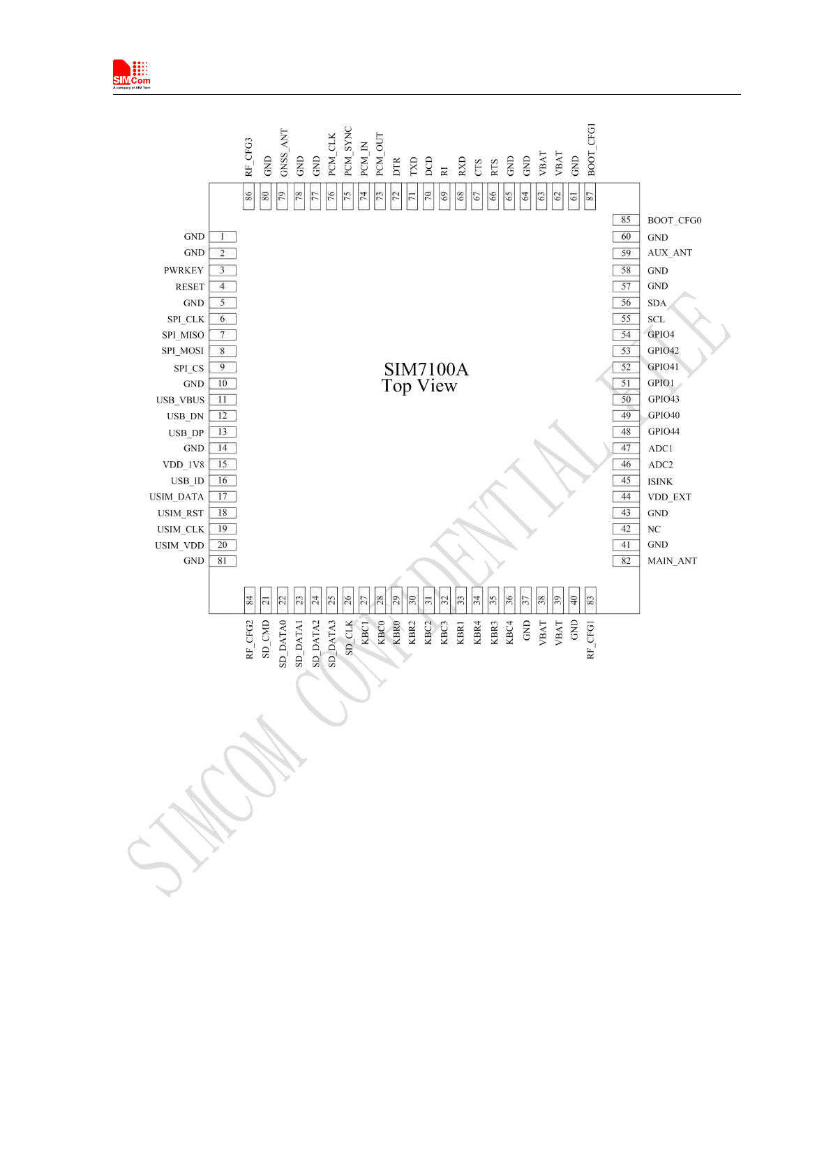
All hardware interfaces which connect SIM7100C to customers’ application platform are through 87 pins
pads (Metal half hole). Figure 2 is SIM7100C outline diagram.
Smart Machine Smart Decision
SIM7100C_User Manual_V1.01 2015-09-19
14
Figure 1: Pin view
Smart Machine Smart Decision
SIM7100C_User Manual_V1.01 2015-09-19
15
Table 4: Pin definition
Pin No.
Define
Pin No.
Define
1
GND
2
GND
3
PWRKEY
4
RESET
5
GND
6
SPI_CLK
7
SPI_MISO
8
SPI_MOSI
9
SPI_CS
10
GND
11
USB_VBUS
12
USB_DN
13
USB_DP
14
GND
15
VDD_1V8
16
USB_ID
17
USIM_DATA
18
USIM_RST
19
USIM_CLK
20
USIM_VDD
21
SD_CMD
22
SD_DATA0
23
SD_DATA1
24
SD_DATA2
25
SD_DATA3
26
SD_CLK
27
KBC1
28
KBC0
29
KBR0
30
KBR2
31
KBC2
32
KBC3
33
KBR1
34
KBR4
35
KBR3
36
KBC4
37
GND
38
VBAT
39
VBAT
40
GND
41
GND
42
NC
43
GND
44
VDD_EXT
45
ISINK
46
ADC2
47
ADC1
48
GPIO44
49
GPIO40
50
GPIO43
51
GPIO1
52
GPIO41
53
GPIO42
54
GPIO4
55
SCL
56
SDA
57
GND
58
GND
59
AUX_ANT
60
GND
61
GND
62
VBAT
63
VBAT
64
GND
65
GND
66
RTS
67
CTS
68
RXD

Smart Machine Smart Decision
SIM7100C_User Manual_V1.01 2015-09-19
16
69
RI
70
DCD
71
TXD
72
DTR
73
PCM_OUT
74
PCM_IN
75
PCM_SYNC
76
PCM_CLK
77
GND
78
GND
79
GNSS_ANT
80
GND
81
GND
82
MAIN_ANT
83
RF_CFG1
84
RF_CFG2
85
BOOT_CFG0
86
RF_CFG3
87
BOOT_CFG1
2.2 Pin description
Table 5: IO Parameters Definition
Pin Type
Description
PI
Power input
PO
Power output
IO
Bidirectional input / output
DI
Digital input
DO
Digital output
AI
Analog input
Table 6: Pin description
Pin name
Pin No.
I/O
Description
Comment
Power Supply
VBAT
38,39,
62,63
PI
Power supply voltage
NC
42
No connection
Please keep open
VDD_EXT
44
PO
LDO power output for SD card
circuit or other external circuit
with MAX. 150mA output. This
LDO output voltage can be
changed by the AT command
“AT+CVAUXV”.
If unused, please keep
open.
VDD_1V8
15
PO
1.8V SMPS output for external
circuit, such as level shift circuit.
Recommend placing a
10uF and 100nF
capacitors to improve
the stability of the
internal 1.8V SMPS
circuit.
GND
1,2,5,10
Ground

Smart Machine Smart Decision
SIM7100C_User Manual_V1.01 2015-09-19
17
,14,37,4
0,41,43,
57,58,6
0,61,64,
65,77,7
8,80,81
Power on/off
PWRKEY
3
DI
PWRKEY should be pulled low
at least 180ms to power on or
500ms to power off the module.
PWRKEY has been
pulled up to 1.8V in
the module.
SD interface
SD_CMD
21
I/O
SDIO command
If unused, please keep
open.
SD_DATA0
22
I/O
SDIO data
SD_DATA1
23
I/O
SDIO data
SD_DATA2
24
I/O
SDIO data
SD_DATA3
25
I/O
SDIO data
SD_CLK
26
DO
SDIO clock
USIM interface
USIM_DATA
17
I/O
SIM Data Output/Input
All signals of SIM
interface should be
protected against
ESD/EMC.
USIM_RST
18
DO
SIM Reset
USIM_CLK
19
DO
SIM Clock
USIM_VDD
20
PO
Voltage Supply for SIM card
Support 1.8V or 3V SIM card
SPI interface
SPI_CLK
6
DO
SPI clock
If unused, please keep
open.
SPI_MISO
7
DI
SPI (master only) master in/slave
out data
SPI_MOSI
8
DO
SPI(master only) master out/slave
in data
SPI_CS
9
DO
SPI chip-select
USB
USB_VBUS
11
DI
Valid USB detection input
USB_DN
12
I/O
Negative line of the differential,
bi-directional USB signal to/from
the peripheral device.
USB_DP
13
I/O
Positive line of the differential,
bi-directional USB signal to/from
the peripheral device.

Smart Machine Smart Decision
SIM7100C_User Manual_V1.01 2015-09-19
18
USB_ID
16
DI
High-speed USB ID
If SIM7100C is
peripheral (USB
device), please keep it
open. If SIM7100C is
USB host, please
connect to GND
directly.
UART interface
RTS
66
DO
Request to send
CTS
67
DI
Clear to Send
RXD
68
DI
Receive Data
RI
69
DO
Ring Indicator
DCD
70
DO
Carrier detects
TXD
71
DO
Transmit Data
DTR
72
DI
DTE get ready
I2C interface
SCL
55
DO
I2C clock output
Please place 2
external Pull-up 2.2kR
resistors to VDD_1V8
for using I2C bus.
If unused, keep open.
SDA
56
I/O
I2C data
Keypad interface
KBR0
29
DO
Bit 0 drive to the pad matrix
All Keypad pins can
be configured as
GPIOs.
KBC0, KBC1, KBC2,
KBC3, KBR0 and
KBR2 can be
configured as SD2,
please refer to SDIO
description for more
details.
If unused, please keep
open.
KBR1
33
DO
Bit 1 drive to the pad matrix
KBR2
30
DO
Bit 2 drive to the pad matrix
KBR3
35
DO
Bit 3 drive to the pad matrix
KBR4
34
DO
Bit 4 drive to the pad matrix
KBC0
28
DI
Bit 0 for sensing key press on pad
matrix
KBC1
27
DI
Bit 1 for sensing key press on pad
matrix
KBC2
31
DI
Bit 2 for sensing key press on pad
matrix
KBC3
32
DI
Bit 3 for sensing key press on pad
matrix
KBC4
36
DI
Bit 4 for sensing key press on pad
matrix
PCM interface
PCM_OUT
73
DO
PCM data output. It also can be
multiplexed as GPIO5.
If unused, please keep
open.
PCM_IN
74
DI
PCM data input. It also can be
multiplexed as GPIO0 with
module wake/interrupt.
PCM_SYNC
75
DO
PCM data frame sync signal. It

Smart Machine Smart Decision
SIM7100C_User Manual_V1.01 2015-09-19
19
also can be multiplexed as
GPIO2.
PCM_CLK
76
DO
PCM data bit clock. It also can be
multiplexed as GPIO3.
GPIOs
GPIO1
51
DO
Output as LED control for
network status.
If unused, keep open.
GPIO4
54
DI
Input as RF operating control.
GPIO40
49
DO
Output as operating status
indicating of module.
It also can output a clock signal
for PCM clock source.
GPIO41
52
DO
General input/output. It can be
used as wake/interrupt signal to
host from module
GPIO43
50
DI
General input/output. It can be
used as wake/interrupt signal to
module from host.
GPIO44
48
I/O
General input/output.
It can be configured as SD
detecting.
GPIO42
53
I/O
General input/output.
It can be configured as USIM
card detecting.
RF interface
MAIN _ANT
82
MAIN antenna soldering pad
GNSS_ANT
79
AI
GNSS antenna soldering pad
AUX_ANT
59
AI
Diversity antenna soldering pad
Other interface
RESET
4
DI
System reset input, active low.
ISINK
45
DI
Current source of
ground-referenced current sink
If unused, please keep
open.
ADC1
47
AI
Analog Digital Converter Input
ADC2
46
AI
Analog Digital Converter Input
RF_CFG1
83
I/O
RF control
They are used to
control RF when
SDIO function is
used.
If unused, keep open.
RF_CFG2
84
I/O
RF_CFG3
86
I/O
BOO_CFG0
85
DI
Boot configure
Recommend placing 2
test points for
debugging. Module
will be forced to go
into USB download
mode by connect 85
and 87 pins to
VDD_1V8 during
power up.
BOO_CFG1
87
DI
Smart Machine Smart Decision
SIM7100C_User Manual_V1.01 2015-09-19
20
2.3 Package Dimensions
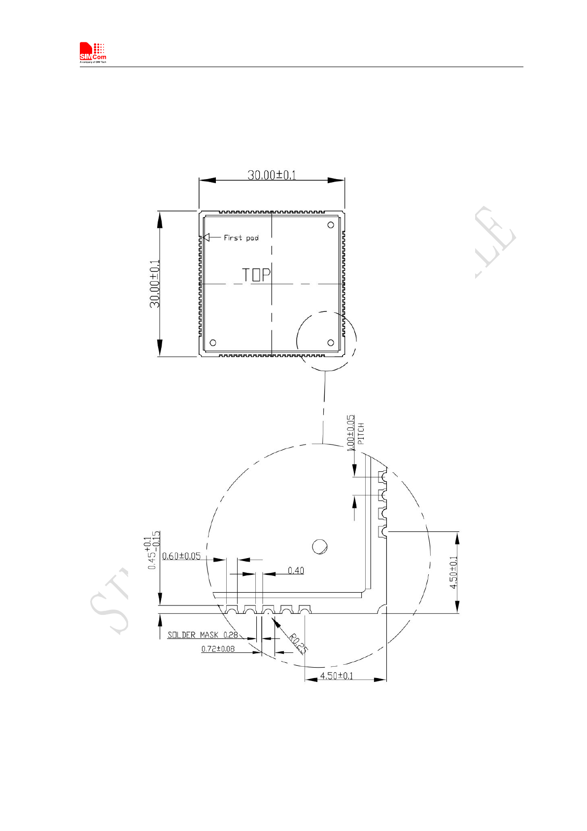
The following figure shows mechanical dimensions of SIM7100C.
Figure 2: Top dimensions (Unit: mm)
Smart Machine Smart Decision
SIM7100C_User Manual_V1.01 2015-09-19
21
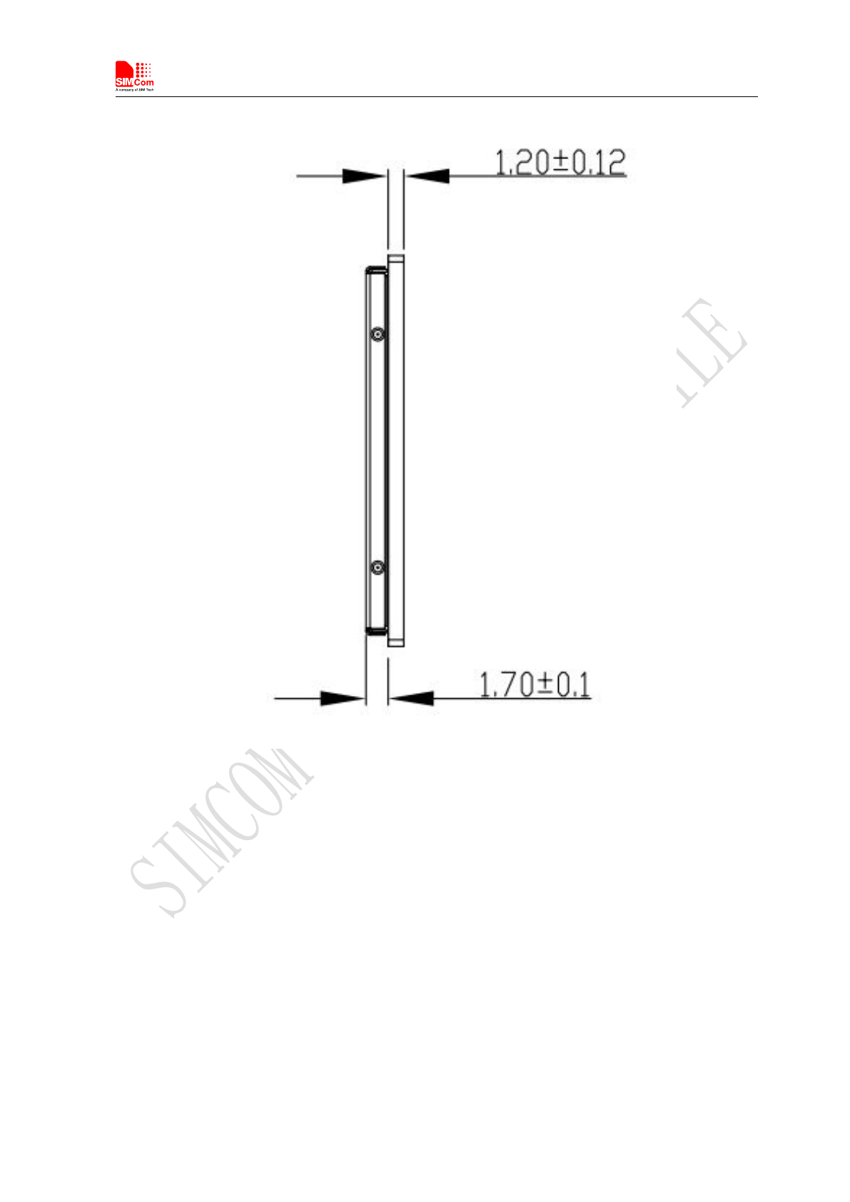
Figure 3: Side dimensions (Unit: mm)
Smart Machine Smart Decision
SIM7100C_User Manual_V1.01 2015-09-19
22
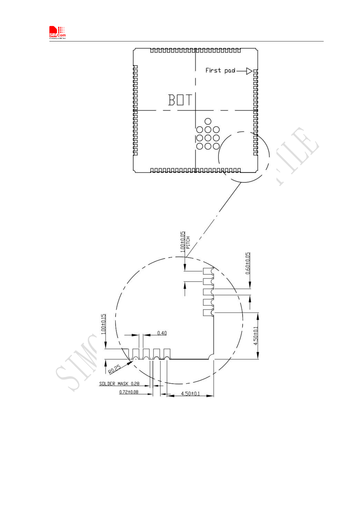
Figure 4: Bottom dimensions (Unit: mm)
Smart Machine Smart Decision
SIM7100C_User Manual_V1.01 2015-09-19
23
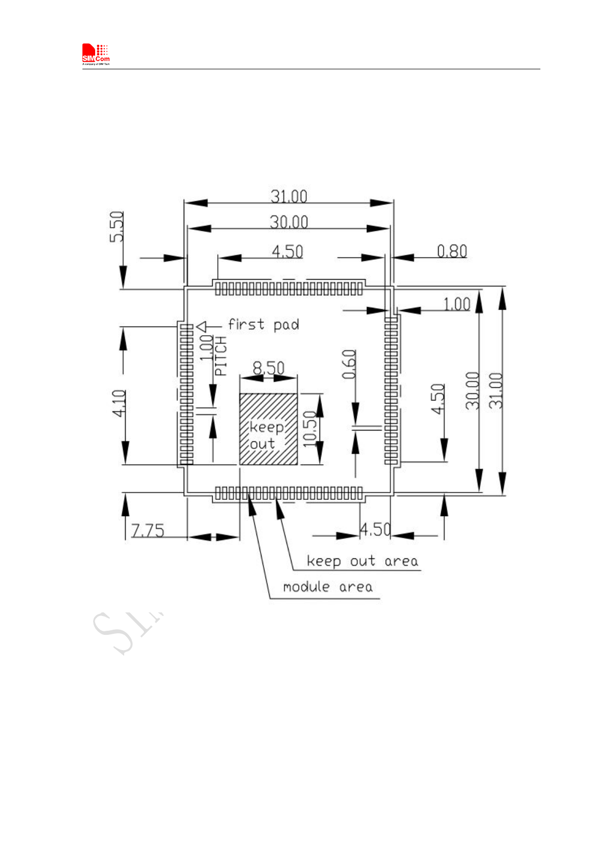
2.4 Footprint Recommendation
Figure 5: Footprint recommendation (Unit: mm)
Smart Machine Smart Decision
SIM7100C_User Manual_V1.01 2015-09-19
24
3Application Interface Specification
3.1 Power Supply
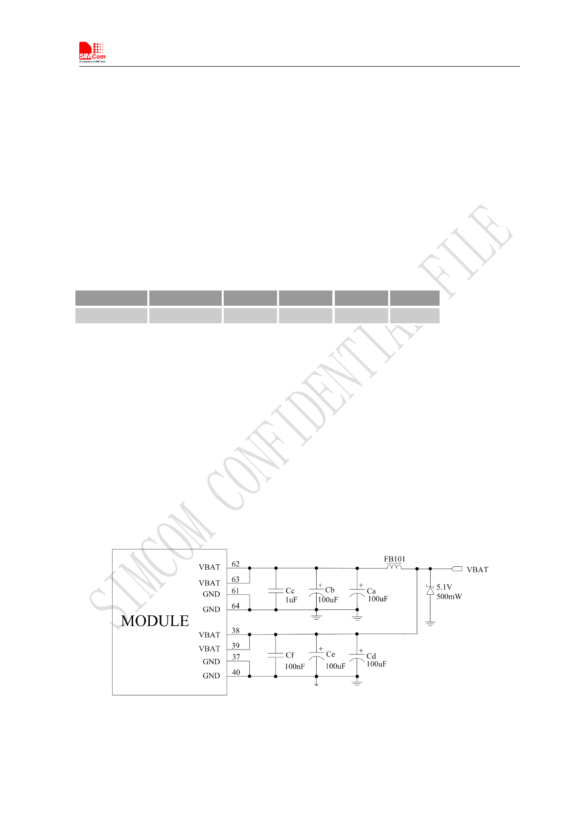
The power supply pins of SIM7100C include four VBAT pins (pin 62&63, pin 38&39). VBAT directly
supplies the power to RF and baseband circuit. VBAT directly supplies the power to RF PA and baseband
system. Power Supply Pin
4 VBAT pins are dedicated to connect the supply voltage.
Table 7: VBAT Pin description
Pin type
Pin name
Min
Typ
Max
Unit
POWER
VBAT
3.15
3.8
4.2
V
3.1.1 Design Guide
Make sure that the input voltage at the VBAT pin will never drop below 3.15V even during a transmit
when the current consumption up to more than 700mA. If the power voltage drops below 3.15V, the
module may be shut down automatically. Using large tantalum capacitors (above 300uF) will be the best
way to reduce the voltage drops.
For the consideration of RF performance and system stability, some multi-layer ceramic chip (MLCC)
capacitors (0.1/1uF) need to be used for EMC because of their low ESR in high frequencies. Note that
capacitors should be put beside VBAT pins as close as possible. Also User should minimize the PCB trace
impedance from the power supply to the VBAT pins through widening the trace to 80 mil or more on the
board. The following figure is the recommended circuit.
Figure 6: VBAT input application circuit
Note: The Cd, Ce, Cb, Cc and Cf must be mounted for SIM7100C.
Smart Machine Smart Decision
SIM7100C_User Manual_V1.01 2015-09-19
25
In addition, in order to get a stable power source, it is suggested to use a zener diode of which reverse
zener voltage is 5.1V and dissipation power is more than 500mW.
Table 8: Recommended zener diode models
No.
Manufacturer
Part Number
Power
Package
1
On semi
MMSZ5231BT1G
500mW
SOD123
2
Prisemi
PZ3D4V2H
500mW
SOD323
3
Vishay
MMSZ4689-V
500mW
SOD123
4
Crownpo
CDZ55C5V1SM
500mW
0805
3.1.2 Recommended Power supply circuit
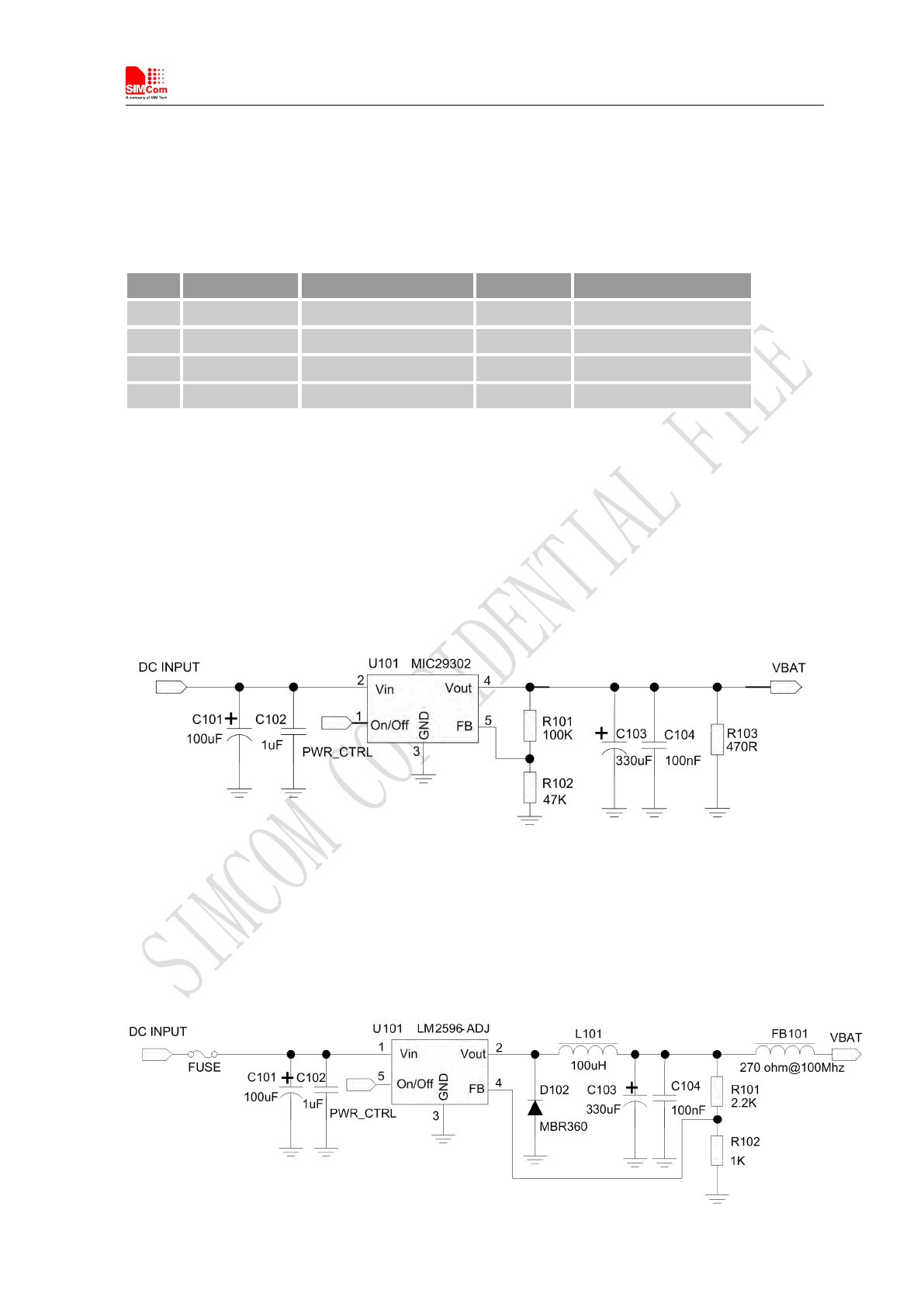
We recommend DCDC or LDO is used for the power supply of the module, make sure that the peak
current of power components can rise up to more than 2A. The following figure is the reference design of
+5V input power supply. The designed output for the power supply is 3.8V, here a linear regulator can be
used.
Figure 7: Reference circuit of the LDO power supply
If there is a big difference between the input voltage and the desired output (VBAT), a switching converter
power will be preferable because of its better efficiency, especially at the high current situation. The
following figure is the reference circuit. Note that DCDC may deprave RF performance because of ripple
current intrinsically.

Smart Machine Smart Decision
SIM7100C_User Manual_V1.01 2015-09-19
26
Figure 8: Reference circuit of the DCDC power supply
3.1.3 Voltage monitor
To monitor the power supply voltage, user can use the AT command “AT+CBC”, this command has two
parameters: the battery status and the voltage value (mV). It will return the capacity percentage and actual
value of battery (at the VBAT pin). The voltage is continuously measured at intervals, whenever the
measured battery voltage is lower than a specific value set by the AT command “AT+CVALARM”. For
example, if the voltage value is set to be 3.4V, the following URC will be presented: “warning! voltage is
low: 3.3v”.
If the voltage is lower than a specific value which is set by the AT command “AT+CPMVT”, the module
will be powered off automatically and AT commands cannot be executed any more.
Note: Under-voltage warning function and under-voltage power-off function are disabled by default.
For more information about these AT command, please refer to Document [1].
3.2 Power on/Power off/Reset Time Sequence
3.2.1 Power on Sequence
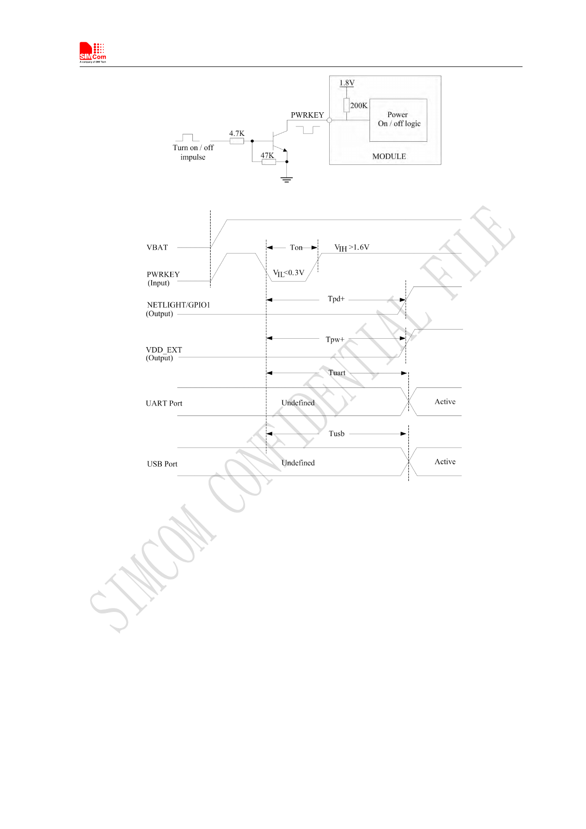
SIM7100C can be powered on by PWRKEY pin, which starts normal operating mode.
PWRKEY pin is pulled up with a 200k ohm resistor to 1.8V in module. User can power on the SIM7100C
by pulling the PWRKEY pin down for a short time. The power-on scenarios are illustrated in the following
figures.
Smart Machine Smart Decision
SIM7100C_User Manual_V1.01 2015-09-19
27
Figure 9: Power on Timing Sequence

Smart Machine Smart Decision
SIM7100C_User Manual_V1.01 2015-09-19
28
Table 9: Power on timing
Symbol
Parameter
Time value
Unit
Min.
Typ.
Max.
Ton
The time to pull PWRKEY down to power on
180
500
-
ms
TpD+
The time to indicate connecting with the network
-
-
5
s
Tpw+
The time to indicate the module is powered on
completely
-
-
0.5
s
Tuart
The time to enable UART
-
-
8
s
Tusb
The time to enable USB
-
-
10
s
Note: Module could be automatically power on by connecting PWRKEY pin to Low level directly.
Before designing, please refer to Document [27] for more detail.
3.2.2 Power off Sequence
The following methods can be used to power down SIM7100C. These procedures will make module
disconnect from the network and allow the software to enter a safe state, and then save data before
completely powering the module off.
●Method 1: Power off SIM7100C by pulling the PWRKEY pin down
●Method 2: Power off SIM7100C by AT command
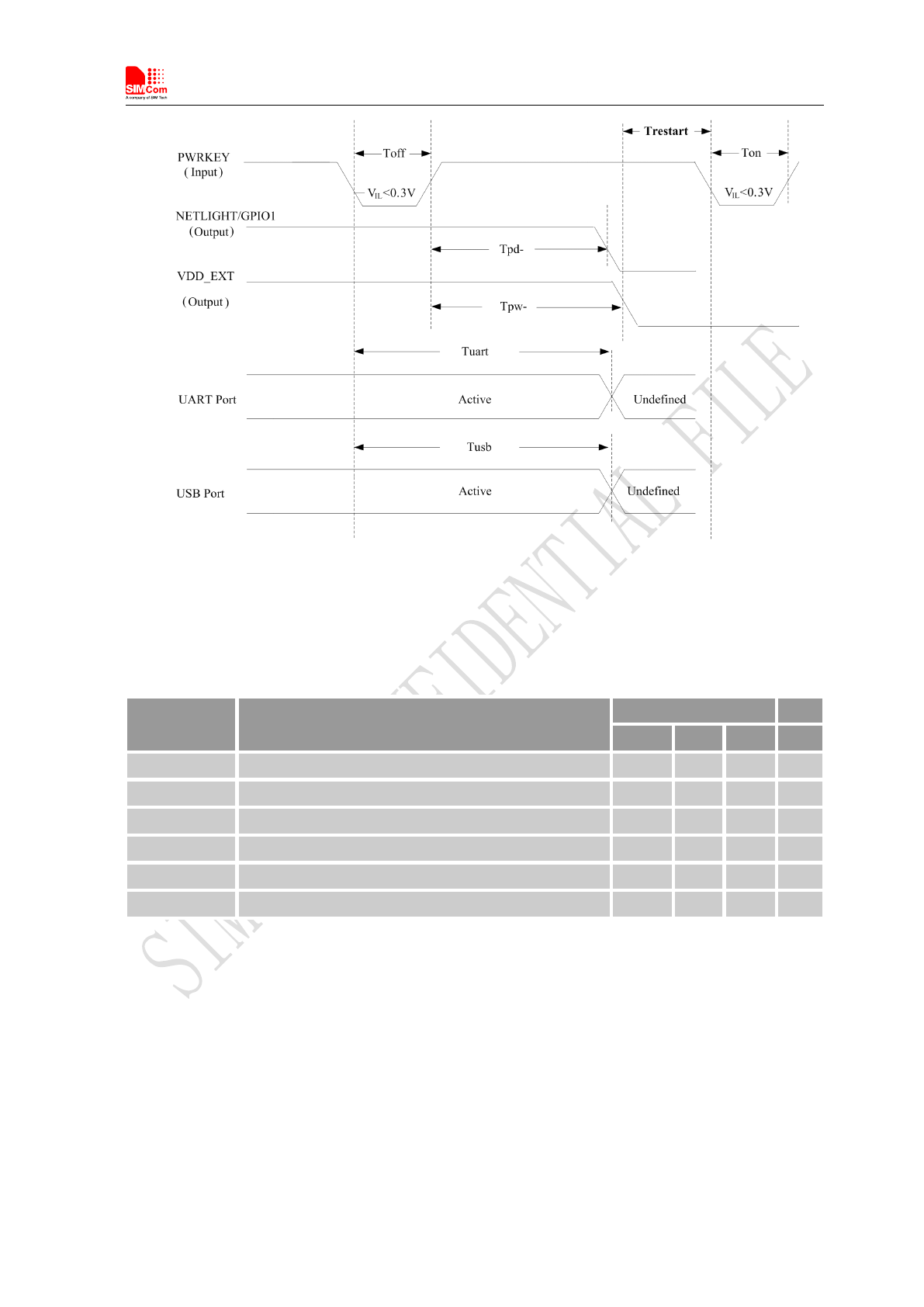
User can power off the SIM7100C by pulling PWRKEY down for a specific time. The power off scenario
is illustrated in the following figure.
Smart Machine Smart Decision
SIM7100C_User Manual_V1.01 2015-09-19
29
Figure 10: Power off timing sequence
Table 10: Power off timing
Symbol
Parameter
Time value
Min.
Typ.
Max.
Unit
Toff
The time pulling PWRKEY down to power off
0.5
-
5
s
TpD-
The time to indicate disconnecting from the network
-
-
2
s
Tpw-
The time to indicate the module power off completely
-
-
2
s
Tuart
The time to disable UART
-
-
3
s
Tusb
The time to disable USB
-
-
2
s
Trestart
The time to power on again after Tpw-
0
-
-
s
User can also use the AT command “AT+CPOF”to power down the module. After that, the AT
commands cannot be executed any longer. The module enters the POWER DOWN mode.
VDD_EXT pin can be used to detect whether module is powered on or not. When module is powered
on and firmware goes ready, VDD_EXT will be high level.
Note: For details about “AT+CPOF”, please refer to Document [1].
3.2.3 Reset Function
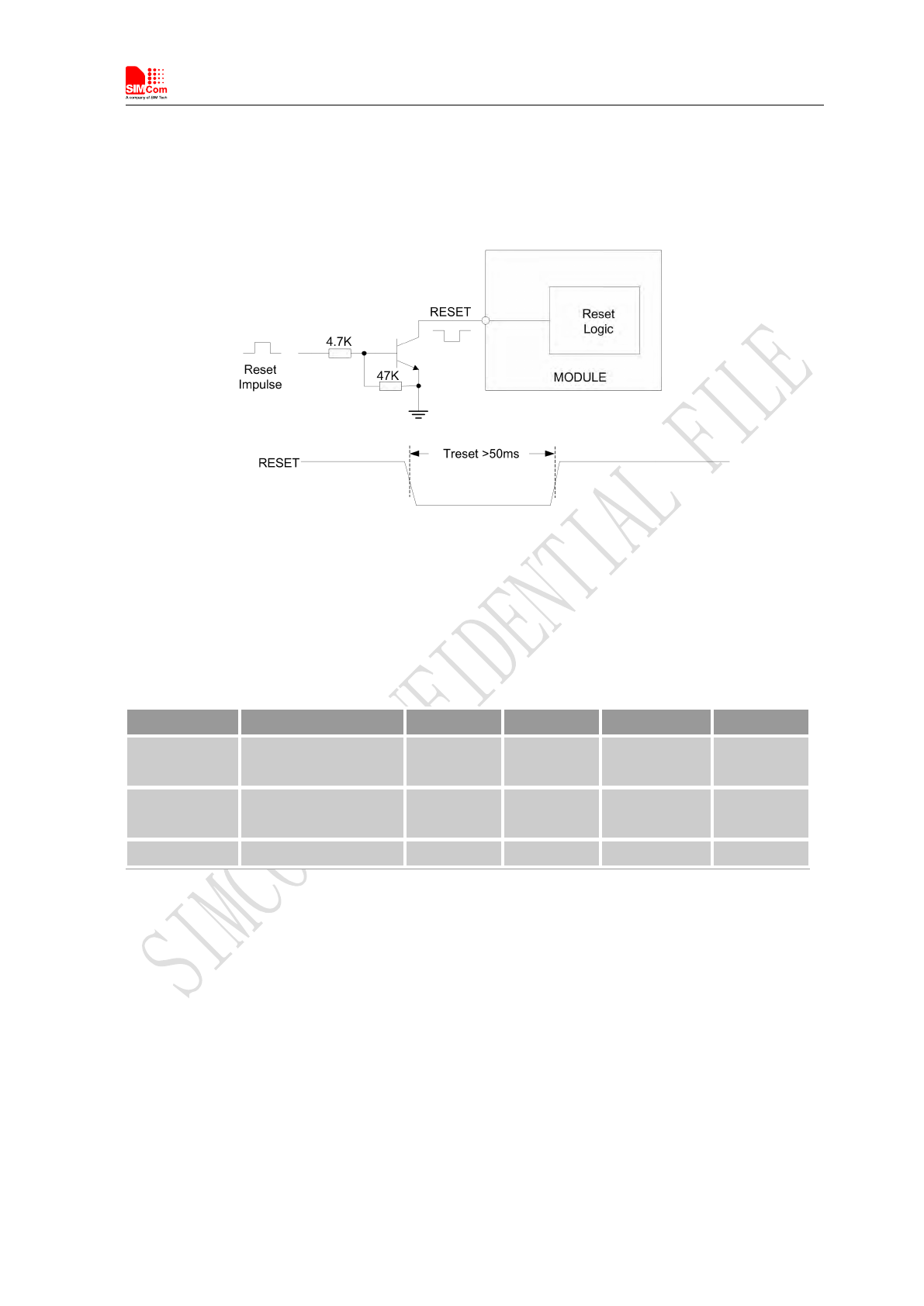
SIM7100C also have a RESET pin (PIN4) to reset the module. This function is used as an emergency reset
only when AT command “AT+CPOF” and the PWRKEY pin has no effect. User can pull the RESET pin
Smart Machine Smart Decision
SIM7100C_User Manual_V1.01 2015-09-19
30
to ground, then the module will reset.
This pin is already pulled up in module, so the external pull-up resistor is not necessary. A 100nF capacitor
close to the RESET pin is strongly recommended. A reference circuit is recommended in the following
figure.
Figure 11: Reset circuit
Note
:
50ms<Treset<200ms. ESD components are suggested to be used on Reset pin.
Table 11: RESET Pin Electronic Characteristic
Symbol
Description
Min
Typ
Max
Unit
VIH
Input high level
voltage
1.17
1.8
2.1
V
VIL
Input low level
voltage
-0.3
0
0.63
V
Treset
Low level pulse width
50
100
200
ms
3.3 UART Interface
SIM7100C provides an UART (universal asynchronous serial transmission) port,consisting of a flexible
7-wire serial interface. The module is as the DCE (Data Communication Equipment) and the client PC is
as the DTE (Data Terminal Equipment). AT commands are entered and serial communication is performed
through UART interface.
Table 12: UART Pin description
Smart Machine Smart Decision
SIM7100C_User Manual_V1.01 2015-09-19
31
Pin type
Pin name
Pin No.
I/O
Default Status
UART1
RXD
68
I
Pull-Down
TXD
71
O
Pull-Up
RTS
66
O
Pull-Up
CTS
67
I
Pull-Down
DTR
72
I
Pull-Up
DCD
70
O
Pull-Up
RI
69
O
Pull-Up
More pin information refers to chapter 2.2.
Table 13: UART Pin Logic level
Symbol
Parameter
Min
Typ
Max
Unit
VIH
High-level input voltage
1.26
1.8
2.1
V
VIL
Low-level input voltage
-0.3
0
0.63
V
VOH
High-level output voltage
1.35
-
1.8
V
VOL
Low-level output voltage
0
0
0.45
V
3.3.1 RI Behavior
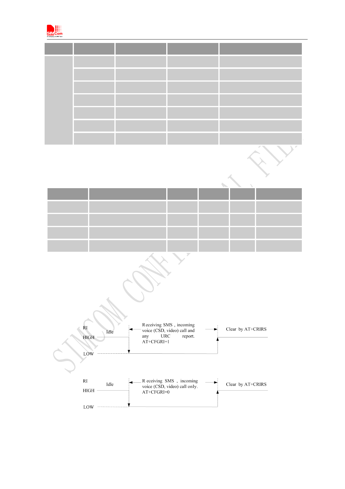
If UART port is used in Null Modem, the pin “RI” can be used as an interrupt signal to HOST. Normally it
will keep high logic level until certain condition such as receiving SMS, voice call (CSD, video) or URC
reporting, then “RI” will change to low logic level to inform the master (client PC). It will stay low until
the master clears the interrupt event with AT command.
Figure 12: RI behaviour in NULL Modem
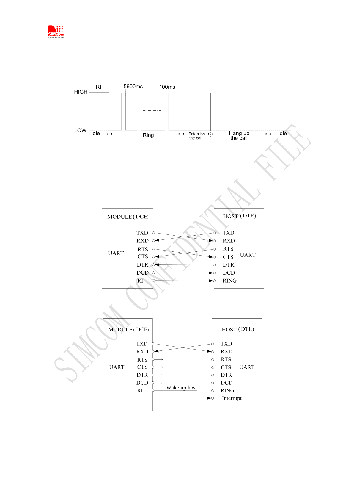
If Full Modem is used to establish communication between devices, the pin “RI” is another operation
Smart Machine Smart Decision
SIM7100C_User Manual_V1.01 2015-09-19
32
status. Initially it keeps high, when a voice call or CSD call comes, the pin “RI” will change to low for
about 5900ms, then it will return to high level for 100ms. It will repeat this procedure until this call is
answered or hung up.
Figure 13: RI behaviour in FULL Modem
3.3.2 Design Guide
The application circuit is in the following figures.
Figure 14: UART Full modem
Figure 15: UART Null modem
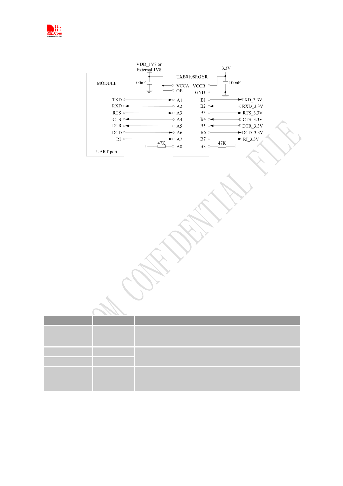
The SIM7100C UART is 1.8V interface. A level shifter should be used if user’s application is equipped
with a 3.3V UART interface. The level shifter TXB0108RGYR provided by Texas Instruments is
Smart Machine Smart Decision
SIM7100C_User Manual_V1.01 2015-09-19
33
recommended. The reference design of the TXB0108RGYR is in the following figures.
Figure 16: Reference circuit of level shift
To comply with RS-232-C protocol, the RS-232-C level shifter chip should be used to connect SIM7100C
to the RS-232-C interface. In this connection, the TTL level and RS-232-C level are converted mutually.
SIMCom recommends that user uses the SP3238ECA chip with a full modem. For more information
please refers to the RS-232-C chip datasheet.
Note: SIM7100C supports the baud rate: 300, 600, 1200, 2400, 4800, 9600, 19200, 38400, 57600,
115200, 230400, 460800, 921600, 3200000, 3686400, 4000000bps. Default rate is 115200bps.
3.4 USB Interface
SIM7100C module contains a USB interface. This interface is compliant with the USB2.0 specification as
a peripheral or embedded host. USB charging is not supported.
Table 14: USB Pin description
Pin name
Pin No.
Description
USB_VBUS
11
Valid USB detection input ,Valid USB detection voltage is
3.0-5.25V.
USB_DP
13
USB 2.0 specification-compliant as a peripheral or embedded
host
USB_DN
12
USB_ID
16
High-speed USB ID input. If keep USB_ID pin open, SIM7100C
will be a USB device. If tie USB_ID pin to ground, SIM7100C
will be a USB host controller.
3.4.1 USB Application Guide
Normally, SIM7100C is a USB device. SIM7100C supports the USB suspend and resume mechanism
which can help to save power. If no transaction is on USB bus, SIM7100C will enter suspend mode.

Smart Machine Smart Decision
SIM7100C_User Manual_V1.01 2015-09-19
34
When some events such as voice call or receiving SMS happen, SIM7100C will resume normal mode
automatically.
SIM7100C is a USB host controller.
Figure 17: USB Reference Circuit with SIM7100C as USB Host Controller.
Because of high bit rate on USB bus, please pay attention to influence of junction capacitance of ESD
component on USB data lines. Typically, the capacitance should be less than 1pF ,It is recommended to
use an ESD protection component such as ON SEMI (www.onsemi.com ) ESD9L5.0ST5G.
Note
:
The SIM7100C has two kinds of interface (UART and USB) to connect to host CPU. USB
interface is mapped to five virtual ports: “SIMTECH HS-USB Modem 9001”, “SIMTECH HS-USB
NMEA 9001”, “SIMTECH HS-USB AT port 9001”, “SIMTECH HS-USB Diagnostics 9001” and
“SIMTECH Wireless HS-USB Ethernet Adapter 9001”.

Smart Machine Smart Decision
SIM7100C_User Manual_V1.01 2015-09-19
35
3.5 USIM Interface
The USIM provides the required subscription verification information to allow the mobile equipment to
attach to a GSM or UMTS network. Both 1.8V and 3.0V SIM Cards are supported.
3.5.1 USIM Pin description
Table 15: USIM Pin description
Table 16: USIM Electronic characteristic
Symbol
Parameter
3.0V mode
1.8V mode
Unit
Min
Typ
Max
Min
Typ
Max
USIM_VDD
LDO power
output
2.71
2.85
3.05
1.7
1.8
1.9
V
VIH
High-level
input
voltage
0.65·USI
M_VDD
-
USIM_V
DD +0.3
0.65·USI
M_VDD
-
USIM_VDD
+0.3
V
VIL
Low-level
input
voltage
-0.3
0
0.3·USI
M_VDD
-0.3
0
0.3·USIM_V
DD
V
VOH
High-level
output
voltage
2.71
2.85
3.05
1.7
1.8
1.9
V
VOL
Low-level
output
voltage
0
0
0.45
0
0
0.45
V
3.5.2 USIM Application Guide
It is recommended to use an ESD protection component such as ST (www.st.com ) ESDA6V1W5 or ON
Pin name
Pin
Description
USIM_CLK
19
USIM Card Clock
USIM_RST
18
USIM Card Reset
USIM_DATA
17
USIM Card data I/O, which has been pulled up with a 22kR resistor to
USIM_VDD in module. Do not pull up or pull down in users’ application
circuit.
USIM_VDD
20
USIM Card Power output depends automatically on USIM mode,one is
3.0V±10%, another is 1.8V±10%. Current is less than 50mA.
Smart Machine Smart Decision
SIM7100C_User Manual_V1.01 2015-09-19
36
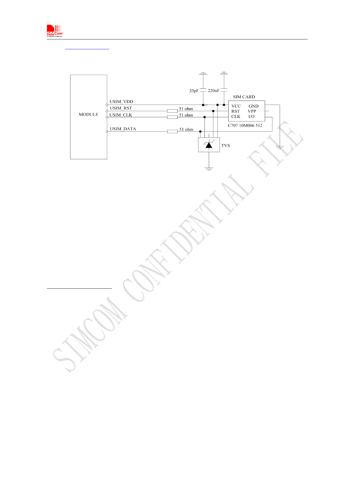
SEMI (www.onsemi.com ) SMF05C. Note that the SIM peripheral circuit should be close to the SIM card
socket. The reference circuit of the 6-pin SIM card holder is illustrated in the following figure.
Figure 18: USIM interface reference circuit
Note: USIM_DATA has been pulled up with a 15kohm resistor to USIM_VDD in module. A 220nF shut
capacitor on USIM_VDD is used to reduce interference. Use AT Commands to get information in
USIM card. For more detail, please refer to document [1].
3.5.3 Recommend Components of USIM holder
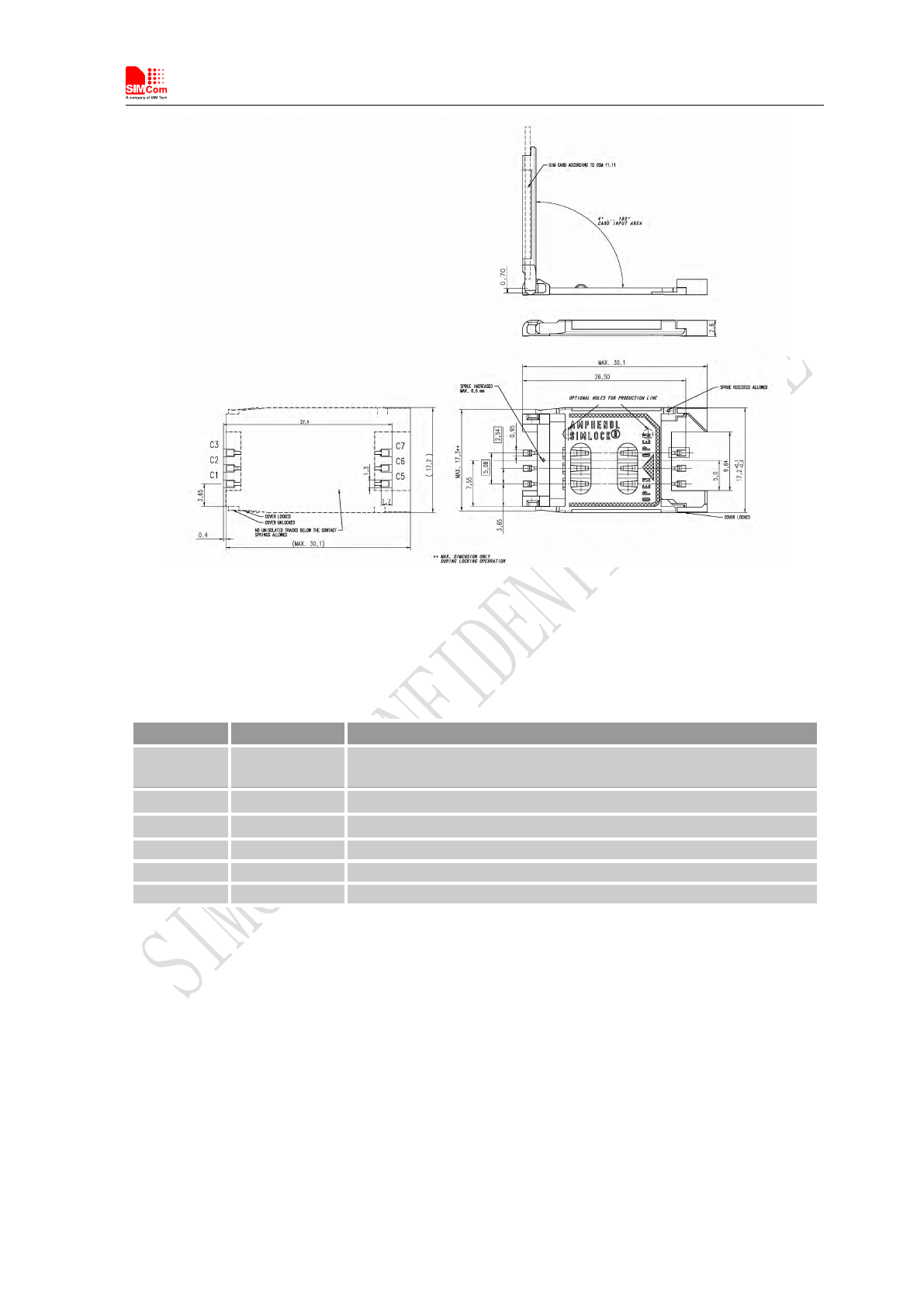
For 6 pins USIM socket, SIMCom recommend to use Amphenol C707 10M006 512. User can visit
http://www.amphenol.com for more information about the holder.
Smart Machine Smart Decision
SIM7100C_User Manual_V1.01 2015-09-19
37
Figure 19: Amphenol SIM card socket
Table 17: Amphenol USIM socket pin description
Pin
Signal
Description
C1
USIM_VDD
SIM Card Power supply, it can identify automatically the SIM Card
power mode,one is 3.0V±10%, another is 1.8V±10%.
C2
USIM_RST
SIM Card Reset.
C3
USIM_CLK
SIM Card Clock.
C5
GND
Connect to GND.
C6
VPP
C7
USIM_DATA
SIM Card data I/O.
3.6 PCM Interface
SIM7100C provides hardware PCM interface for external codec. The PCM interface enables
communication with an external codec to support hands-free applications. SIM7100C PCM interface can
be used in two modes: the default mode is auxiliary PCM (8 KHz long sync mode at 128 KHz PCM CLK);
the other mode is primary PCM (8 KHz short sync mode at 2048 KHz PCM CLK). In short-sync
(primary PCM) mode, SIM7100C can be a master or a slave. In long-sync (auxiliary PCM) mode,
SIM7100C is always a master. SIM7100C also supports 3 kinds of coding formats: 8 bits (-law or A-law)
Smart Machine Smart Decision
SIM7100C_User Manual_V1.01 2015-09-19
38
and 16 bits (linear).
Note: PCM interface is multiplexed from GPIO (default setting). The AT command “AT+CPCM” is
used to switch between PCM and GPIO functions. Please refer to document [21] and document [1] for
details.
3.6.1 PCM Pin Description
Table 18: PCM Pin description
Pins
Pin No.
Description
PCM_OUT
73
PCM data output
PCM_IN
74
PCM data input
PCM_SYNC
75
PCM data synchrony
PCM_CLK
76
PCM data clock
Table 19: PCM Electronic characteristic
Symbol
Parameter
Min
Typ
Max
Unit
VIH
High-level input voltage
1.26
1.8
2.1
V
VIL
Low-level input voltage
-0.3
0
0.63
V
VOH
High-level output voltage
1.35
-
1.8
V
VOL
Low-level output voltage
0
0
0.45
V
3.6.2 PCM Signal Description
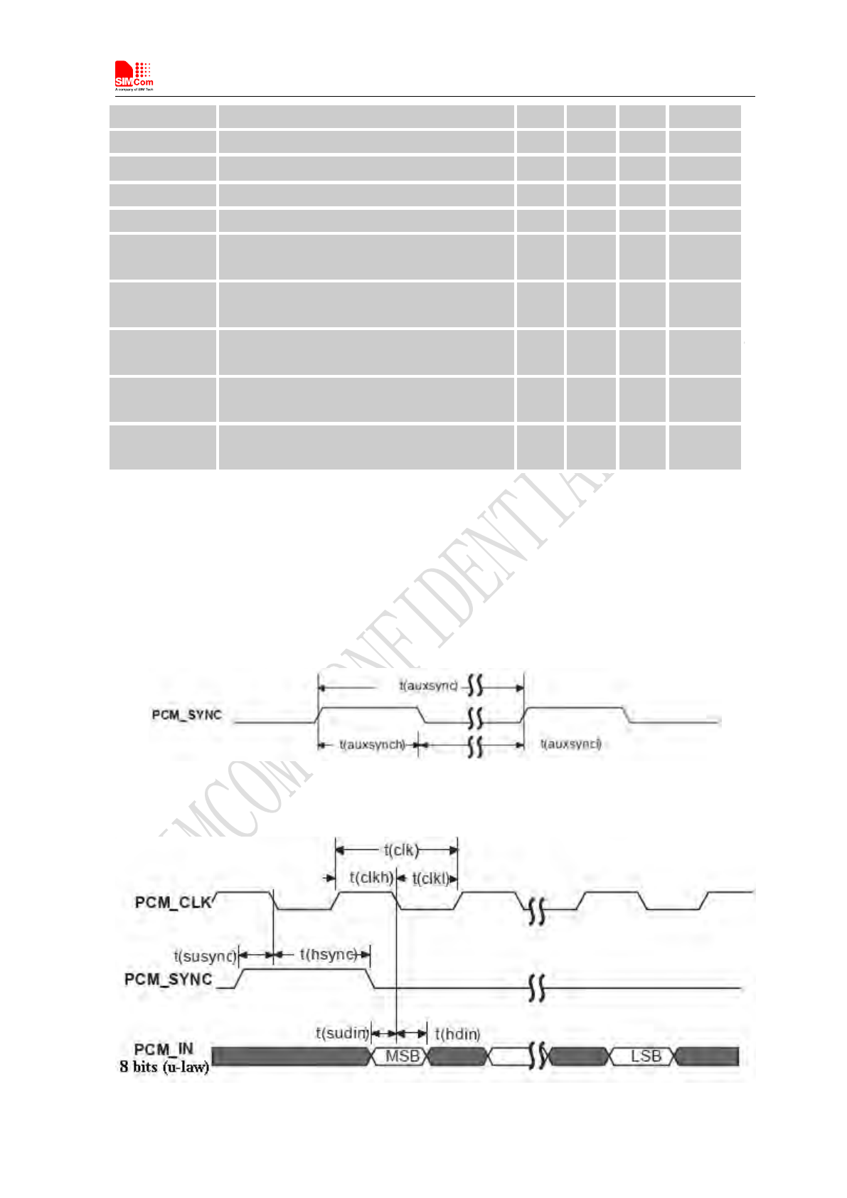
The default PCM interface in SIM7100C is the auxiliary PCM interface. The data changes on the high
level of PCM_CLK and is sampled at the falling edge of PCM_CLK in one period. Primary PCM is
disabled after every power-on or every reset event. So user must use AT command to enable the primary
PCM mode after powering on or resetting the module every time if user wants to use Primary
PCM.SIM7100C PCM Interface can be operated in Master or Slave mode if it is configured to primary
PCM. In Master Mode, the Module drives the clock and sync signals that are sent to the external codec.
When it is in Slave Mode, the external codec drives the clock and sync signals which are sent to the
module. Both PCM modes are discussed in this section followed by additional PCM topics.
3.6.3 Auxiliary PCM (128 KHz PCM clock)
-law coding is supported by the auxiliary PCM. The auxiliary codec port operates with standard
Smart Machine Smart Decision
SIM7100C_User Manual_V1.01 2015-09-19
39
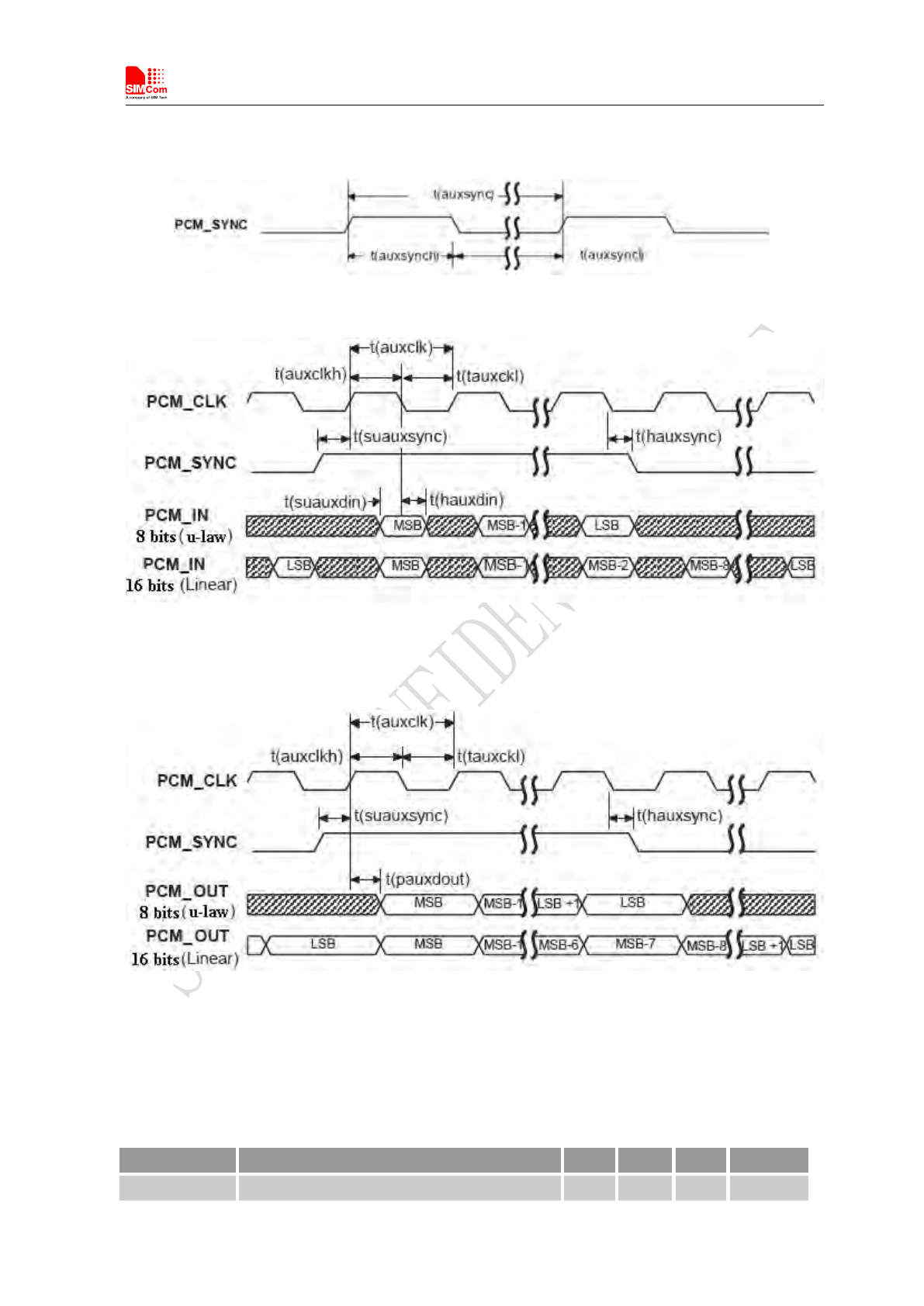
long-sync timing and a 128 KHz clock. The AUX_PCM_SYNC runs at 8 KHz with 50% duty cycle.
Most -law codec support the 128 KHz clock.
Figure 20: Synchrony timing
Figure 21: EXT CODEC to MODULE timing
Figure 22: MODULE to EXT CODEC timing
Table 20: Timing parameters
Parameter
Description
Min
Typ
Max
Unit
T(auxsync)
AUX_PCM_SYNC cycle time
–
125
-
μs
Smart Machine Smart Decision
SIM7100C_User Manual_V1.01 2015-09-19
40
T(auxsynch)
AUX_PCM_SYNC high time
62.4
62.5
-
μs
T(auxsyncl)
AUX_PCM_SYNC low time
62.4
62.5
-
μs
T(auxclk)*
AUX_PCM_CLK cycle time
-
7.8
–
μs
T(auxclkh)
AUX_PCM_CLK high time
3.8
3.9
–
μs
T(auxclkl)
AUX_PCM_CLK low time
3.8
3.9
–
μs
T(suauxsync)
AUX_PCM_SYNC setup time high before
falling edge of PCM_CLK
1.95
–
–
μs
T(hauxsync)
AUX_PCM SYNC hold time after falling edge
of PCM_CLK
1.95
–
–
μs
T(suauxdin)
AUX_PCM_IN setup time before falling edge
of AUX_PCM_CLK
70
–
–
ns
T(hauxdin)
AUX_PCM_IN hold time after falling edge of
AUX_PCM_CLK
20
–
–
ns
T(pauxdout)
Delay from AUX_PCM_CLK rising to
AUX_PCM_OUT valid
–
–
50
ns
*Note: T(auxclk) = 1/(128 KHz).
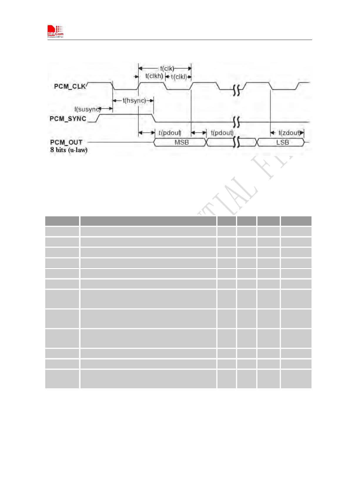
3.6.4 Primary PCM (2048 KHz PCM clock)
SIM7100C also supports 2.048 MHz PCM data and sync timing for -law codec. This is called the
primary PCM interface. User can use AT command to take the mode you want as discussed above.
Figure 23: Synchrony timing
Smart Machine Smart Decision
SIM7100C_User Manual_V1.01 2015-09-19
41
Figure 24: EXT CODEC to MODULE timing
Figure 25: MODULE to EXT CODEC timing
Table 21: Timing parameters
Parameter
Description
Min
Typ
Max
Unit
T(sync)
PCM_SYNC cycle time
–
125
–
μs
T(synch)
PCM_SYNC high time
400
500
–
ns
T(syncl)
PCM_SYNC low time
–
124.5
–
μs
T(clk)
PCM_CLK cycle time
–
488
–
ns
T(clkh)
PCM_CLK high time
–
244
–
ns
T(clkl)
PCM_CLK low time
–
244
–
ns
T(susync)
PCM_SYNC setup time high before falling edge of
PCM_CLK
60
–
–
ns
T(hsync)
PCM_SYNC hold time after falling edge of
PCM_CLK
60
–
–
ns
T(sudin)
PCM_IN setup time before falling edge of
PCM_CLK
50
–
–
ns
T(hdin)
PCM_IN hold time after falling edge of PCM_CLK
10
–
–
ns
T(pdout)
Delay from PCM_CLK rising to PCM_OUT valid
–
–
350
ns
T(zdout)
Delay from PCM_CLK falling to PCM_OUT
HIGH-Z
–
160
–
ns
Note: SIM7100C can transmit PCM data by USB except for PCM interface.
3.6.5 PCM Application Guide
The mode of SIM7100C PCM can be configured by AT command “AT+CPCM and AT+CPCMFMT”, and
the default configuration is master mode using short sync data format with 2.048MHz PCM_CLK and 8
Smart Machine Smart Decision
SIM7100C_User Manual_V1.01 2015-09-19
42
kHz PCM_SYNC. Please refer to document [21] and document [1] for details.
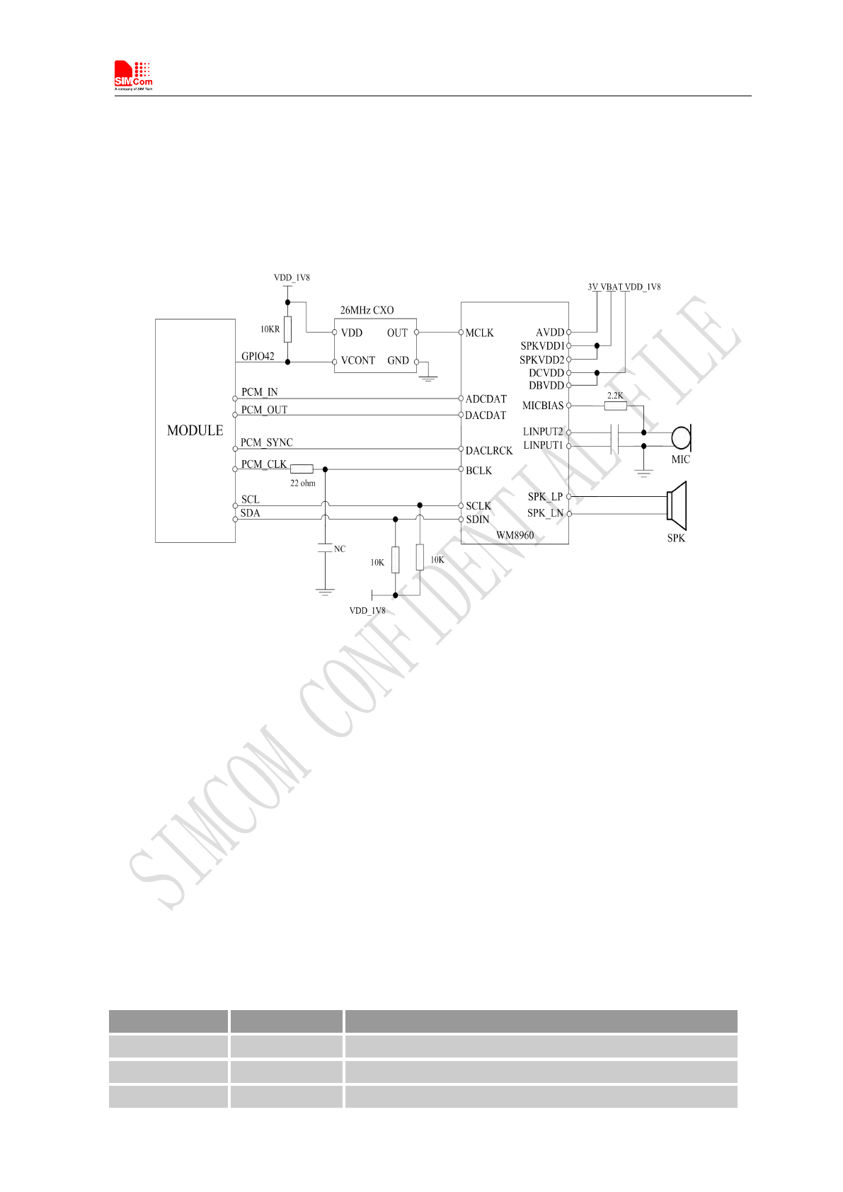
In addition, the firmware of SIM7100C has integrated the configuration on WM8960GEFL/RV codec
provided by WOLFSON MICROELECTRONICS with I2C interface.
The reference circuit of the reference design of PCM interfaces with external codec IC in the following
figure. It is recommended to use a 26MHz CXO component such as TXC CORPORATION
(www.txccorp.com) 8W26000011.
Figure 26: Reference Circuit of PCM Application with Audio Codec
3.7 MMC/SD and SDIO Interface
SIM7100C provides one 4-bit SD/MMC interface and one SDIO interface with clock rate up to 52 MHz.
3.7.1 MMC/SD Interface Pin Description
The operation voltage of MMC/SD interface is 2.85V. It supports 1-bit SD/MMC or 4-bit SD data
transmission mode. Though the same hardware controller is used, the initialization procession for SD or
MMC cards is different.
Note: Interface with SD/MMC memory cards up to 32GB
Table 22: MMC/SD Pin description
Pin name
Pin No.
Function
SD_DATA0
22
SD/MMC card data0
SD_DATA1
23
SD card data1
SD_DATA2
24
SD card data2
Smart Machine Smart Decision
SIM7100C_User Manual_V1.01 2015-09-19
43
Table 23: MMC/SD Electronic characteristic*
Symbol
Parameter
Min
Typ
Max
Unit
VDD_EXT**
LDO power output
2.71
2.85
2.99
V
VIH
High-level input voltage
0.65·VDD_EXT
-
VDD_EXT+0.3
V
VIL
Low-level input voltage
-0.3
0
0.3·VDD_EXT
V
VOH
High-level output voltage
2.71
2.85
2.99
V
VOL
Low-level output voltage
0
0
0.45
V
Note:
*For SD_DATA0-SD_DATA3
,
SD_CLK and SD_CMD
,
GPIO44 is 1.8V operation voltage.
**VDD_EXT must be set with 2.85V output.
SD_DATA3
25
SD card data3
SD_CLK
26
SD card clock
SD_CMD
21
SD card command
GPIO44
48
SD card detecting
Smart Machine Smart Decision
SIM7100C_User Manual_V1.01 2015-09-19
44
3.7.2 SDIO Interface Pin Description
Table 24: SDIO Pin description
Table 25: SDIO Electronic characteristic
Symbol
Parameter
Min
Typ
Max
Unit
VIH
High-level input voltage
1.26
1.8
2.1
V
VIL
Low-level input voltage
-0.3
0
0.63
V
VOH
High-level output voltage
1.35
-
1.8
V
VOL
Low-level output voltage
0
0
0.45
V
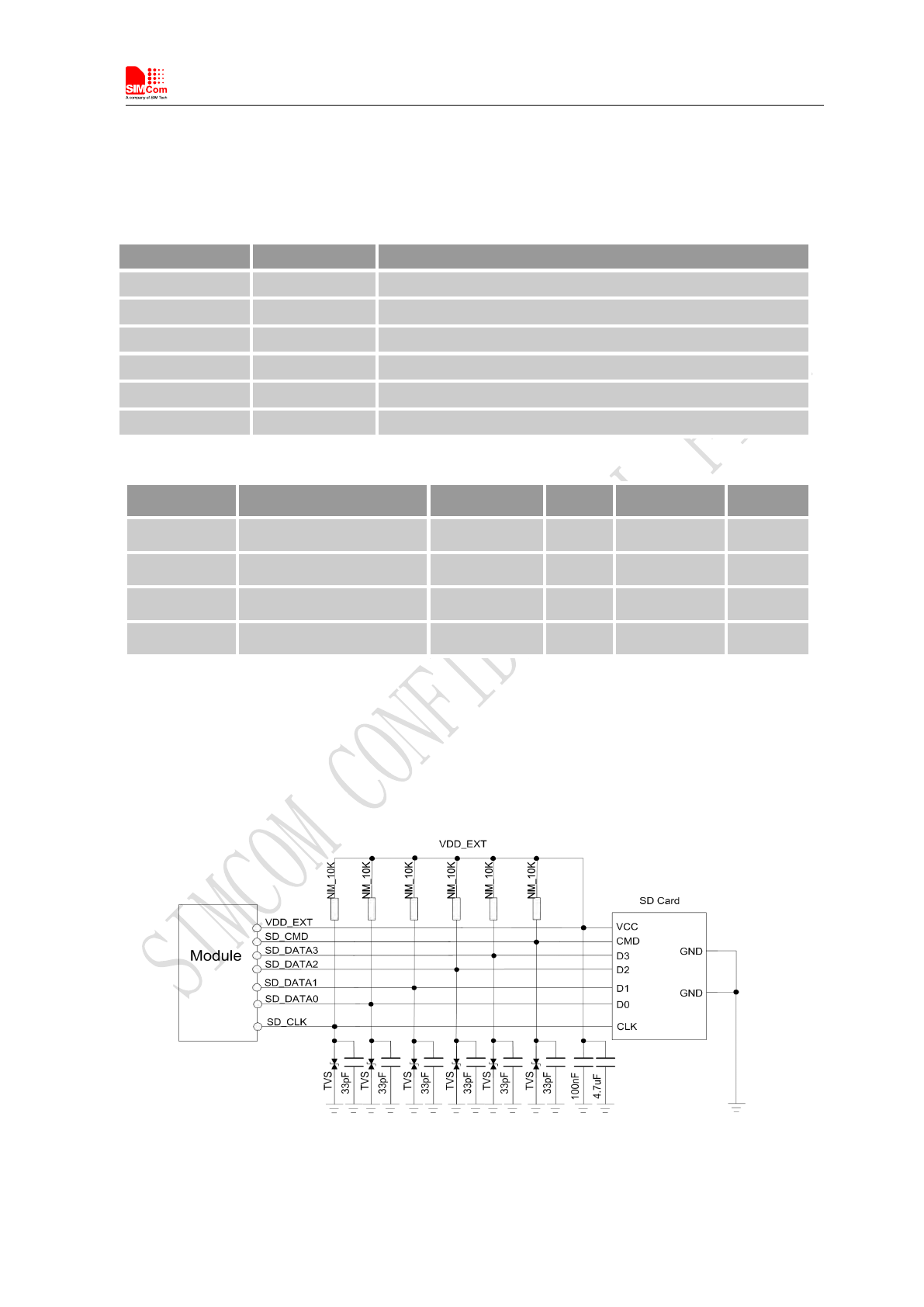
3.7.3 SD Design guide
The module can’t provide power for SD card. External 2.85V LDO is needed with capable of 300mA.
Data lines should be pulled up to VDD_EXT by 10K resistors. ESD/EMI components should be arranged
beside SD card socket. Refer to the following application circuit.
Figure 27: SD interface circuit
Pin name
Pin No.
Function
KBR2
30
SD2_DATA0
KBC1
27
SD2_DATA1
KBC0
28
SD2_DATA2
KBC2
31
SD2_DATA3
KBR0
29
SD2_CMD
KBC3
32
SD2_CLK

Smart Machine Smart Decision
SIM7100C_User Manual_V1.01 2015-09-19
45
3.8 I2C Interface
I2C is used to communicate with peripheral equipments and can be operated as either a transmitter or
receiver, depending on the device function. Use AT Commands “AT+CRIIC and AT+CWIIC” to read/write
register values of related peripheral equipments connected with I2C interface. Its operation voltage is
1.8V.
3.8.1 I2C Pin Description
Table 26: I2C Pin description
3.8.2 I2C Signal Description
Both SDA and SCL are bidirectional lines, connected to a positive supply via a pull-up resistor
respectively. When the bus is free, both lines are high.
3.8.3 I2C Design Guide
For SIM7100C, the data on the I2C bus can be transferred at rates up to 400kbps. The number of
peripheral devices connected to the bus is solely dependent on the bus capacitance limit of 400pF. Note
that PCB traces length and bending are in users’ control to minimize load capacitance.
Note
:
SDA and SCL have none pulled up resistors in module. So there is need to pull them up in users’
application circuit.
3.9 Keypad Interface
SIM7100C module provides a keypad interface that supports five sense lines, or columns, and five keypad
rows. The interface generates an interrupt when any key is pressed. Its operation voltage is 1.8V.
3.9.1 Keypad Pin Description
Table 27: Keypad Pin description
Pin name
Pin No.
Function
SDA
56
Serial interface data input and output
SCL
55
Serial interface clock input
Smart Machine Smart Decision
SIM7100C_User Manual_V1.01 2015-09-19
46
Pin name
Pin No.
Function
KBC0
28
Sensing keys
KBC1
27
KBC2
31
KBC3
32
KBC4
36
KBR0
30
Driving pads
KBR1
29
KBR2
30
KBR3
35
KBR4
34
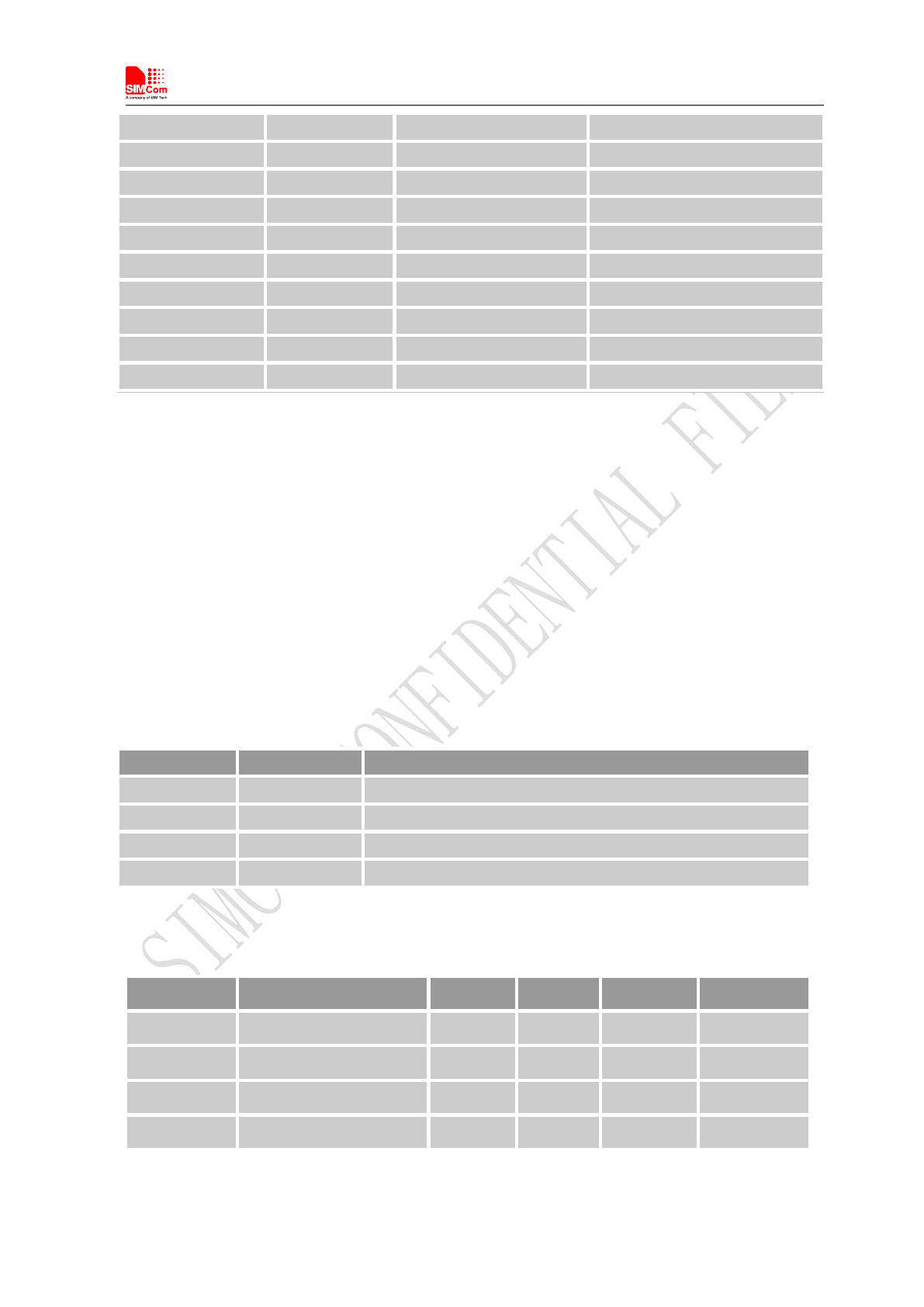
3.9.2 Keypad Application Guide
All keypad pins can be configured for GPIOs. These GPIOs also support interruption operation if used as
input pins. A typical circuit about the keypad (5*5 keypad matrix) is shown in the following figure.
Figure 28: Reference circuit
If these pins are configured for GPIOs, the sequence is listed in the following table.
Table 28: Keypad multiplexing function
Pin name
Pin number
Mode 0(default)
Mode 1
Smart Machine Smart Decision
SIM7100C_User Manual_V1.01 2015-09-19
47
KBR4
34
KBR4
GPIO6
KBR3
35
KBR3
GPIO7
KBR2
30
KBR2
GPIO8
KBR1
33
KBR1
GPIO9
KBR0
29
KBR0
GPIO10
KBC4
36
KBC4
GPIO11
KBC3
32
KBC3
GPIO12
KBC2
31
KBC2
GPIO13
KBC1
27
KBC1
GPIO14
KBC0
28
KBC0
GPIO15
Note: Refer to document [23] for detailed information of Keypad Application Note.
3.10 SPI Interface
SPI interface of SIM7100C is master only. It provides a duplex, synchronous, serial communication link
with peripheral devices. Its operation voltage is 1.8V, with clock rates up to 26 MHz.
3.10.1 SPI Pin Description
Table 29: SPI Pin description
Table 30: SPI Electronic characteristic
Symbol
Parameter
Min
Typ
Max
Unit
VIH
High-level input voltage
1.26
1.8
2.1
V
VIL
Low-level input voltage
-0.3
0
0.63
V
VOH
High-level output voltage
1.35
-
1.8
V
VOL
Low-level output voltage
0
0
0.45
V
Pin name
Pin No.
Function
SPI_CS
9
SPI chip-select; not mandatory in a point-to-point connection
SPI_MISO
7
SPI master in/slave out data
SPI_CLK
6
SPI clock
SPI_MOSI
8
SPI master out/slave in data
Smart Machine Smart Decision
SIM7100C_User Manual_V1.01 2015-09-19
48
3.11GPIO Interface
SIM7100C provides a limited number of GPIO pins. All GPIOs can be configured as inputs or outputs.
User can use AT Commands to read or write GPIOs status. Refer to ATC document for details.
3.11.1 GPIO Pin Description
Table 31: GPIO Pin description
Note: If more GPIOs need to be used, users can configure GPIO on other multiple function interfaces,
such as PCM. Please refer to GPIO list.
Table 32: GPIO Electronic characteristic
Symbol
Parameter
Min
Typ
Max
Unit
VIH
High-level input voltage
1.26
1.8
2.1
V
VIL
Low-level input voltage
-0.3
0
0.63
V
Pin name
Pin No.
I/O
Function
GPIO1
51
O
Output PIN as LED control for network status. If
unused, please keep open.
GPIO4
54
I
Input PIN as RF operating control.
H: Normal Mode L:Flight Mode
If unused, please keep open .
GPIO40
49
O
Output PIN as operating status indicating of module.
H: Power on L: Power off
It also can output a clock signal for PCM clock source.
If unused, left open.
GPIO41
52
I/O
General input/output PIN. It can be used as
wake/interrupt signal to host from module If unused,
left open.
GPIO42
53
I/O
General Purpose Input/Output Port.
It can be configured as USIM card detecting.
GPIO43
50
I/O
General Purpose Input/Output Port. It can be used as
wake/interrupt signal to module from host. If unused,
left open.
GPIO44
48
I/O
General Purpose Input/Output Port.
It can be configured as SD detecting.

Smart Machine Smart Decision
SIM7100C_User Manual_V1.01 2015-09-19
49
VOH
High-level output voltage
1.35
-
1.8
V
VOL
Low-level output voltage
0
0
0.45
V
Note: The output driver current of GPIOs is 2mA.
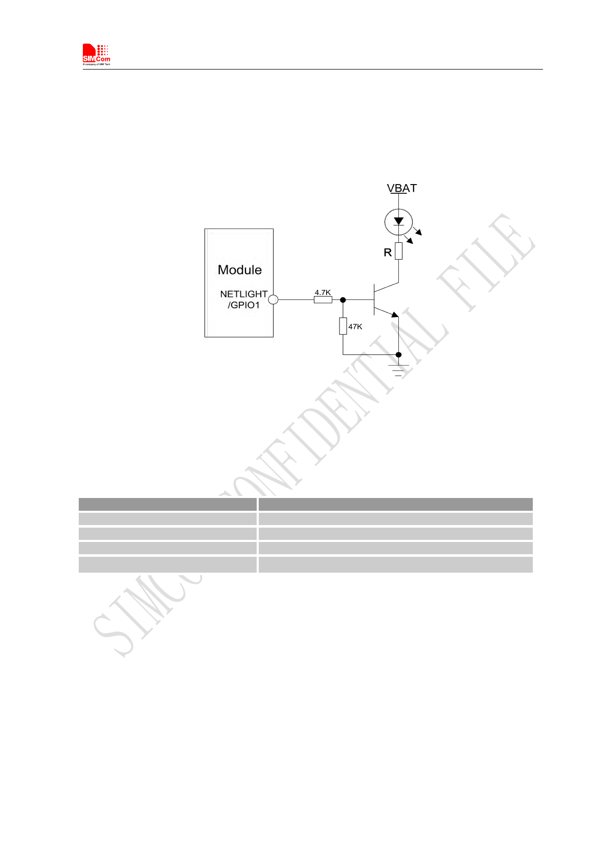
Smart Machine Smart Decision
SIM7100C_User Manual_V1.01 2015-09-19
50
3.12 Network status
GPIO1 is used to control Network Status LED; application circuit is shown below.
Figure 29: Application circuit
Note: The value of resistor Rx depends on LED characteristic.
Table 33: LED status
LED Status
Module Status
Always On
Searching Network/Call Connect
200ms ON, 200ms OFF
Data Transmit
800ms ON, 800ms OFF
Registered network
Off
Power off / Sleep
3.13 Flight mode control
GPIO4 controls SIM7100C module to enter or exit the Flight mode. In Flight mode, SIM7100C closes RF
function to prevent interference with other equipments or minimize current consumption. Bidirectional
ESD protection component is suggested to add on GPIO4.
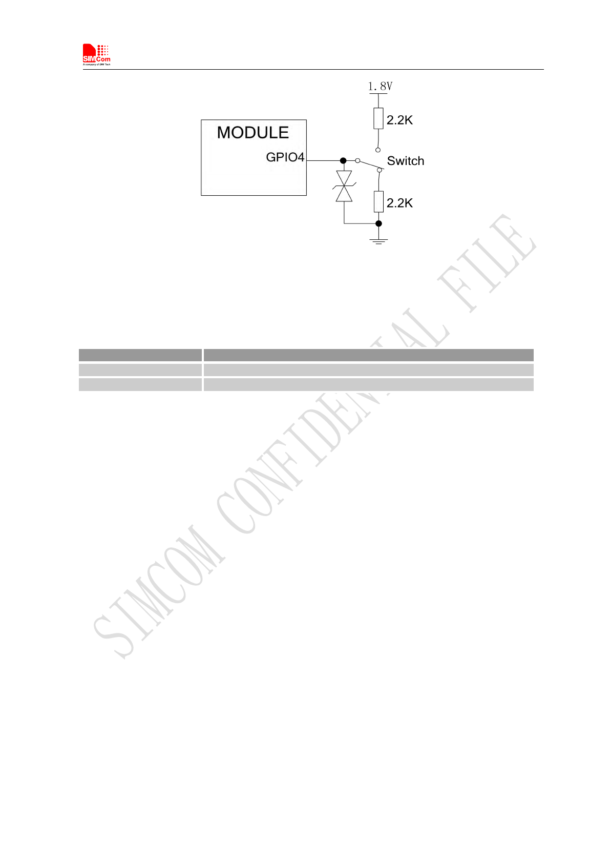
Smart Machine Smart Decision
SIM7100C_User Manual_V1.01 2015-09-19
51
Figure 30: Flight mode switch
Table 34: Flight mode status
GPIO4 Status
Module operation
Low Level
Flight Mode: RF is closed.
High Level
Normal Mode: RF is working.
Note
:
1. For SIM7100C, GPIO0, GPIO2, GPIO3 and GPIO5 have multiplex function, user can use
them as PCM interface to connect extend codec. Refer to section 3.11 and document [1] for details.
2. When the module is powered off, make sure all digital interfaces (PCM UART, etc) connected with
peripheral devices have no voltage higher than 0.3V. If users’ design cannot meet above conditions,
high level voltages maybe occur in GPIO pins because current leakage from above digital interfaces
may occur.
3.14 Multi-functional interface
SIM7100C merges functions for various applications. It can enrich users’ design and lower the cost of
users’ hardware.
3.14.1 Sink Current Source
The dedicated pin (ISINK) is intended for driving passive devices ,such as LCD backlight, this
implementation is VBAT tolerant and suitable for driving white LEDs. The high-current driver can
maintain a constant current which is set by the AT command “AT+ CLEDITST”, capable of up to 40 mA.
Table 35: Sink Current Electronic characteristic
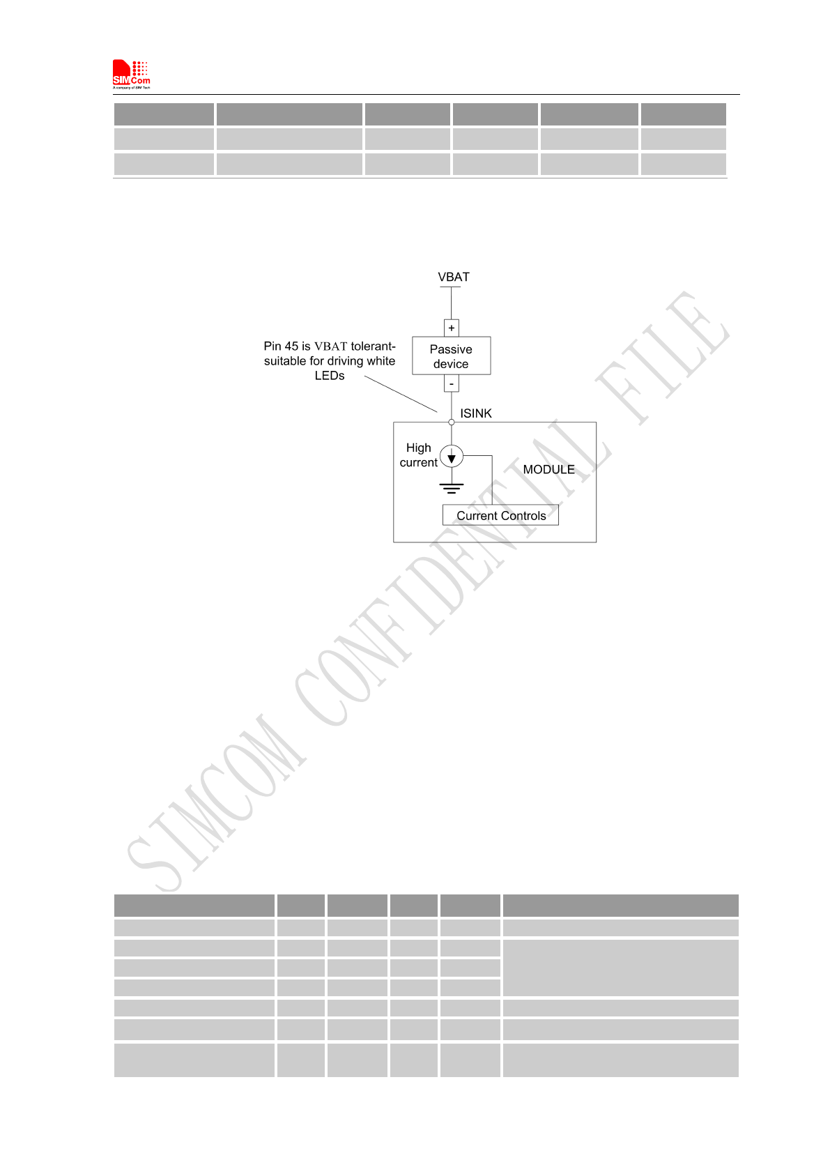
Smart Machine Smart Decision
SIM7100C_User Manual_V1.01 2015-09-19
52
Symbol
Description
Min
Typ
Max
Unit
ISINK
Input voltage
0.5
VDD
VBAT
V
IO
Input current
5
-
40
mA
Since the driver is ground-referenced current sink, the operating device it drives must form a current path
between the VDD pin and the ISINK pin. The following figure is for users reference.
Figure 31: Current drive
Note: The sinking current can be adjusted to meet design requirement through the AT command “AT+
CLEDITST =<0>, <value>”.The “value” ranges from 0 to 15,on behalf of the current changes from
0mA to 150mA in steps of 10mA.
3.14.2 ADC
SIM7100C has a dedicated ADC that is available for digitizing analog signals such as battery voltage and
so on; it is on PIN 47 and PIN 46 , namely ADC1 and ADC2 . This ADC is 15 bit
successive-approximation circuit, and electronic specification is shown in the following table.
Table 36: Electronic Characteristics
Specification
Min
Typ
Max
Unit
Comments/Conditions
Resolution
15
Bits
Analog input bandwidth
–
100
–
kHz
Analog Vdd = ADC reference
2.4MHz sample rate
Gain Error
-2.5
+2.5
%
Offset Error
-3.5
+3.5
LSB
Input Range
GND
2.2V
V
Input serial resistance
2
kΩ
Sample and hold switch resistance
Power supply current
Normal operation
1.5
mA

Smart Machine Smart Decision
SIM7100C_User Manual_V1.01 2015-09-19
53
Power supply current
Off
50
200
nA
User can introduce a signal in the ADC pin directly and use the AT command “AT+CADC” to get the raw
data which is between 0 and 32768. The data can be transformed to any type such as voltage, temperature
etc. Please refer to document [1].
Note: The input signal voltage value in ADC must not be higher than 2.2V.
3.14.3 LDO
SIM7100C has a LDO power output, namely VDD_EXT. The LDO is available and output voltage is
2.85v by default, rated for 150mA. User can switch the LDO on or off by the AT command
“AT+CVAUXS” and configure its output voltage by the AT command “AT+CVAUXV”.
Table 37: Electronic characteristic
Symbol
Description
Min
Typ
Max
Unit
VDD_EXT
Output voltage
1.7
2.85
3.05
V
IO
Output current
-
-
50
mA

Smart Machine Smart Decision
SIM7100C_User Manual_V1.01 2015-09-19
54
4 RF Specification
4.1 RF Specification
Table 38: Conducted transmission power
Frequency
Max
Min
LTE-TDD B41
23dBm +2.7dB
-50dBm ±5dB
Table 39: Operating frequencies
Frequency
Receiving
Transmission
LTE Operating frequencies are shown in following table 34.
Note: Operating frequencies of LTE TDD B41 for SIM7100C is 100MHz BW, 2555 ~2655
MHz
Table 40: E-UTRA operating bands
E-UTRA
Operating
Band
Uplink (UL) operating band
Downlink (DL) operating
band
Duplex
Mode
BS receive / UE transmit(UL)
BS transmit / UE receive(DL)
1
1920 MHz~1980 MHz
2110 MHz~2170 MHz
FDD
2
1850 MHz~1910 MHz
1930 MHz~1990 MHz
FDD
3
1710 MHz~1785 MHz
1805 MHz~1880 MHz
FDD
4
1710 MHz~1755 MHz
2110 MHz~2155 MHz
FDD
5
824 MHz~849 MHz
869 MHz~894MHz
FDD
61
830 MHz~840 MHz
875 MHz~885 MHz
FDD
7
2500 MHz~2570 MHz
2620 MHz~2690 MHz
FDD
8
880 MHz~915 MHz
925 MHz~960 MHz
FDD
9
1749.9 MHz~1784.9 MHz
1844.9 MHz~1879.9 MHz
FDD
10
1710 MHz~1770 MHz
2110 MHz~2170 MHz
FDD
11
1427.9 MHz~1447.9 MHz
1475.9 MHz~1495.9 MHz
FDD
12
699 MHz~716 MHz
729 MHz~746 MHz
FDD
13
777 MHz~787 MHz
746 MHz~756 MHz
FDD
14
788 MHz~798 MHz
758 MHz~768 MHz
FDD
17
704 MHz~716 MHz
734 MHz~746 MHz
FDD
18
815 MHz~830 MHz
860 MHz~875 MHz
FDD
19
830 MHz~845 MHz
875 MHz~890 MHz
FDD
20
832 MHz~862 MHz
791 MHz~821 MHz
FDD
Smart Machine Smart Decision
SIM7100C_User Manual_V1.01 2015-09-19
55
21
1447.9 MHz~1462.9 MHz
1495.9 MHz~1510.9 MHz
FDD
22
3410 MHz~3490 MHz
3510 MHz~3590 MHz
FDD
23
2000 MHz~2020 MHz
2180 MHz~2200 MHz
FDD
24
1626.5 MHz~1660.5 MHz
1525 MHz~1559 MHz
FDD
25
1850 MHz~1915 MHz
1930 MHz~1995 MHz
FDD
26
814 MHz~849 MHz
859 MHz~894 MHz
FDD
27
807 MHz~824 MHz
852 MHz~869 MHz
FDD
28
703 MHz~748 MHz
758 MHz~803 MHz
FDD
31
452.5 MHz~457.5 MHz
462.5 MHz~467.5 MHz
FDD
33
1900 MHz~1920 MHz
1900 MHz~1920 MHz
TDD
34
2010 MHz~2025 MHz
2010 MHz~2025 MHz
TDD
35
1850 MHz~1910 MHz
1850 MHz~1910 MHz
TDD
36
1930 MHz~1990 MHz
1930 MHz~1990 MHz
TDD
37
1910 MHz~1930 MHz
1910 MHz~1930 MHz
TDD
38
2570 MHz~2620 MHz
2570 MHz~2620 MHz
TDD
39
1880 MHz~1920 MHz
1880 MHz~1920 MHz
TDD
40
2300 MHz~2400 MHz
2300 MHz~2400 MHz
TDD
41
2496 MHz~2690 MHz
2496 MHz~2690 MHz
TDD
42
3400 MHz~3600 MHz
3400 MHz~3600 MHz
TDD
43
3600 MHz~3800 MHz
3600 MHz~3800 MHz
TDD
44
703 MHz~803 MHz
703 MHz~803 MHz
TDD
Table 41: Conducted receive sensitivity
Frequency
Receive sensitivity
LTE TDD
See table 36.
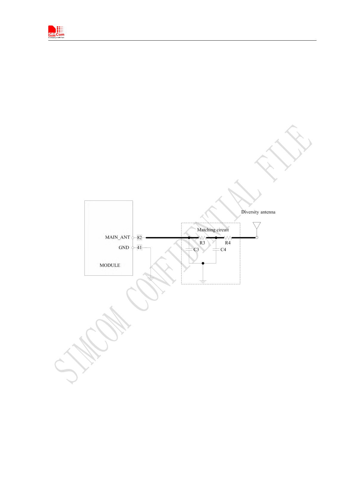
Smart Machine Smart Decision
SIM7100C_User Manual_V1.01 2015-09-19
56
4.2 Antenna Design Guide
SIM7100C provides RF antenna interface. Customer’s antenna should be located in the host board and
connected to module’s antenna pad through micro-strip line or other types of RF trace and the trace
impedance must be controlled in 50Ω. SIMCom recommends that the total insertion loss between the
antenna pad and antenna should meet the following requirements:
●LTE (F<1GHz) <0.5dB
●LTE (1GHz<F<2GHz) <0.9dB
●LTE (2GHz<F) <1.2dB
To facilitate the antenna tuning and certification test, a RF connector and an antenna matching circuit
should be added. The following figure is the recommended circuit.
Figure 32: Antenna matching circuit (MAIN_ANT)
In this figure, the components R4,C3,C4 and R4 is used for antenna matching, the value of components
can only be got after the antenna tuning, usually, they are provided by antenna vendor. By default, the R3,
R4 are 0 Ohm resistors, and the C3, C4 are reserved for tuning.
The RF test connector in the figure is used for the conducted RF performance test, and should be placed as
close as to the module’s antenna pin. The traces impedance between components must be controlled in
50ohm.
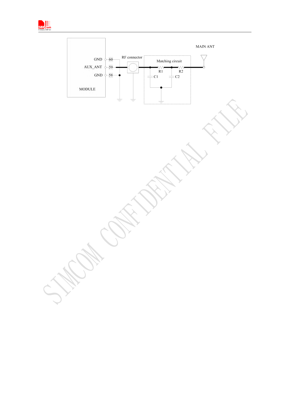
Smart Machine Smart Decision
SIM7100C_User Manual_V1.01 2015-09-19
57
Figure 33: Antenna matching circuit (AUX_ANT)
In above figure, R1, C1, C2 and R2 are used for diversity antenna matching. By default, the R1, R2 are 0
Ohm resistors, and the C1, C2 are reserved for tuning.
4.3 GNSS (GPS and GLONASS)
SIM7100C merges GNSS (GPS/GLONASS) satellite and network information to provide a
high-availability solution that offers industry-leading accuracy and performance. This solution performs
well, even in very challenging environmental conditions where conventional GNSS receivers fail, and
provides a platform to enable wireless operators to address both location-based services and emergency
mandates.
4.3.1 GNSS Technical specification
Tracking sensitivity -159 dBm(GPS)-158 dBm(GLONASS)
Cold-start sensitivity -148 dBm
Accuracy (Open Sky) 2.5m (CEP50)
TTFF (Open Sky) Hot start <1s Cold start 35s
Receiver Type 16-channel, C/A Code
GPS L1 Frequency (1575.42±1.023MHz),
GLONASS: 1597.5~1605.8 MHz
Update rate Default 1 Hz
Note: Performance will vary depending on the environment, antenna type and signal conditions and so
on.
4.3.2 GNSS Operate Mode
SIM7100C supports both A-GPS and S-GPS, and then provides three operating modes: mobile-assisted
mode, mobile-based mode and standalone mode. A-GPS includes mobile-assisted and mobile-based mode.

Smart Machine Smart Decision
SIM7100C_User Manual_V1.01 2015-09-19
58
In mobile-assisted mode, when a request for position location is issued, available network information is
provided to the location server (e.g. Cell-ID) and assistance is requested from the location server. The
location server sends the assistance information to the handset. The handset/mobile unit measures the
GNSS observables and provides the GNSS measurements along with available network data (that is
appropriate for the given air interface technology) to the location server. The location server then
calculates the position location and returns results to the requesting entity.
In mobile-based mode, the assistant data provided by the location server encompasses not only the
information required to assist the handset in measuring the satellite signals, but also the information
required to calculate the handset’s position. Therefore, rather than provide the GNSS measurements and
available network data back to the location server, the mobile calculates the location on the handset and
passes the result to the requesting entity.
In standalone (autonomous) mode, the handset demodulates the data directly from the GNSS satellites.
This mode has some reduced cold-start sensitivity, and a longer time to first fix as compared to the assisted
modes. However, it requires no server interaction and works out of network coverage.
This combination of GNSS measurements and available network information provides:
●High-sensitivity solution that works in all terrains: Indoor, outdoor, urban, and rural
●High availability that is enabled by using both satellite and network information
Therefore, while network solutions typically perform poorly in rural areas and areas of poor cell
geometry/density, and while unassisted, GNSS-only solutions typically perform poorly indoors. The
SIM7100C GNSS solution provides optimal time to fix, accuracy, sensitivity, availability, and reduced
network utilization in both of these environments, depending on the given condition.
Smart Machine Smart Decision
SIM7100C_User Manual_V1.01 2015-09-19
59
5Reliability and Operating Characteristics
5.1 Electronic Characteristics
Absolute maximum rating for digital and analog pins of SIM7100C are listed in the following table:
Table 42: Absolute maximum ratings
Parameter
Min
Max
Unit
Voltage at digital pins (1.8v digital I/O)
-0.3
2.1
V
Voltage at VBAT
-0.5
6.0
V
Voltage at VRTC
2
3.25
V
Voltage at USB_VBUS
-0.5
6.0
V
Table 43: Recommended operating ratings
Parameter
Min
Typ
Max
Unit
Voltage at digital pins (1.8v digital I/O)
0
1.8
1.95
V
Voltage at VBAT
3.4
3.8
4.2
V
Voltage at VRTC
2
-
3.2
V
Voltage at USB_VBUS
3
5
5.25
V
The operating temperature and power specification is listed in the following table.
Table 44: Operating temperature
Parameter
Min
Typ
Max
Unit
Normal operation temperature
-30
25
80
℃
Extended operation temperature
-40
25
85
℃
Storage temperature
-45
25
+90
℃
Note: The module is fully functional in all the temperature range. Temperatures outside of the range
-30℃~ +80℃might slightly deviate from ETSI specifications.
5.2 Operating Mode
5.2.1 Operating Mode
The table below summarizes the various operating modes of SIM7100Cx.
Table 45: Operating mode

Smart Machine Smart Decision
SIM7100C_User Manual_V1.01 2015-09-19
60
Mode
Status
Function
Normal
operati
on
Sleep
LTE
Module will automatically go into sleep mode if the
conditions of sleep mode are enabling and there is no on air
and no hardware interrupt (such as USB wake-up operation or
data on serial port).
In this case, the current consumption of module will be
reduced to the minimal level.
In sleep mode, the module can still receive paging message
and SMS.
Idle
LTE
Software is active. Module is registered to the LTE network,
and the module is ready to communicate.
Standby
LTE
Module is ready for EDGE/HSPA+ /LTE data transfer, but no
data is currently sent or received. In this case, power
consumption depends on network settings and EDGE/HSPA+
/LTE configuration.
Data
transfer
LTE
There is EDGE/HSPA+/LTE data transfer in progress. In this
case, power consumption is related to network settings (e.g.
power control level); uplink/downlink data rates and GPRS
configuration (e.g. used multi-slot settings).
Minimum
functionality mode
AT command “AT+CFUN” can be used to set the module to a minimum
functionality mode without removing the power supply. In this mode, the RF
part of the module will not work or the USIM card will not be accessible, or
both RF part and USIM card will be closed, and the serial port is still
accessible. The power consumption in this mode is lower than normal mode.
5.2.2 Minimize Power Consumption
There are two modes that SIM7100C achieves low power consumption.
5.2.3 Sleep mode
If peripheral equipments stops working, and there is no on air or hardware interrupts (such as GPIO
interrupts or data on UART), SIM7100C will enter sleep mode automatically. In this mode, SIM7100C can
still receive paging,voice call or SMS from network. If USB interface of SIM7100C is connected to host
CPU, but host CPU does not support USB suspending, then SIM7100C will not enter sleep mode. After
USB is disconnected, SIM7100C will enter sleep mode.
Note: When UART interface is connected with host CPU, SIM7100C cannot enter sleep mode until
RXD is pulled down by the host CPU. If the module is in the idle mode, make sure to pull the RXD to
low level by host CPU. SIMCom recommends using GPIO43 or DTR to wake up the module from host
CPU and to use GPIO41 or RI to wake up the host CPU. Before designing, pay attention to how to
realize waking function and refer to Document[24] and Document[25] for more detail.

Smart Machine Smart Decision
SIM7100C_User Manual_V1.01 2015-09-19
61
5.2.4 Minimum functionality mode
Minimum functionality mode ceases a majority function of module, thus minimizing the power
consumption. This mode is set by the AT command which provides a choice of the functionality levels.
●AT+CFUN=0: Minimum functionality
●AT+CFUN=1: Full functionality (Default)
●AT+CFUN=4: Disable RF function of the module (Flight mode)
If SIM7100C has been set to minimum functionality mode, the module will firstly enter sleep mode, then
the RF function and SIM card function will be closed. In this case, the serial port is still accessible, but RF
function or SIM card will be unavailable. When SIM7100C is in minimum functionality or flight mode, it
can return to full functionality by the AT command “AT+CFUN=1”.
5.3 Current Consumption
The current consumption in suspended mode and without USB connection is listed in the table below.
Here, “suspended mode” means that SIM7100C is connected to USB bus, but it does not transfer data.
Table 46: Current consumption
OFF state
OFF state supply current
Power down 10uA
5.4 EMC and ESD Notes
EMC tests should be performed to detect any potential problems. Possible harmful emissions radiate by
the application to the RF receiver in the receiver band. RF emissions interfere with audio input/output. It is
recommended to shield the sensitive components and trace with common ground and user can add beads
where necessary.
Normally SIM7100C is mounted on customer host board. Although some ESD components have been
added in SIM7100C, to prevent ESD, user should put some ESD components on customers’ board. The
ESD components should be placed beside the connectors which human body might touch, such as SIM
card holder, audio jacks, switches, keys, etc. The following table is the SIM7100C ESD measurement
performance; the results are from SIMCom EVB test.
Table 47: The ESD performance measurement table (Temperature: 25℃, Humidity: 45%)
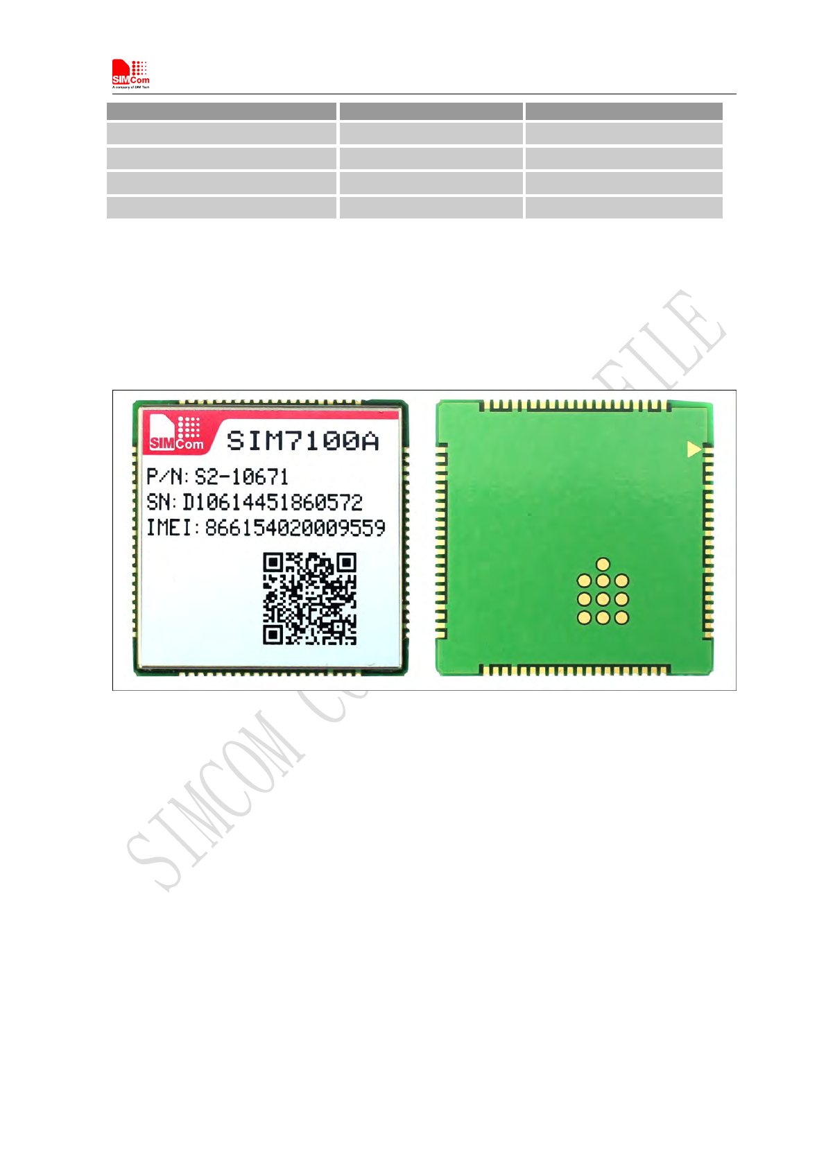
Smart Machine Smart Decision
SIM7100C_User Manual_V1.01 2015-09-19
62
Part
Contact discharge
Air discharge
VBAT,GND
TBD
TBD
UART,USB
TBD
TBD
Antenna port
TBD
TBD
Other PADs
TBD
TBD
6Guide for Production
6.1 Top and Bottom View of SIM7100C
Figure 34: Top and bottom view of SIM7100C
These test points are only used for module manufacturing and testing. They are not for customer’s
application.
6.2 Typical Solder Reflow Profile
For customer convenience, SIMCom provides a typical example for a commonly used soldering profile. In
final board assembly, the typical solder reflow profile will be determined by the largest component on the
board, as well as the type of solder/flux used and PCB stack-up. Therefore the soldering profile shown
below is only a generic recommendation and should be adjusted to the specific application and
manufacturing constraints.
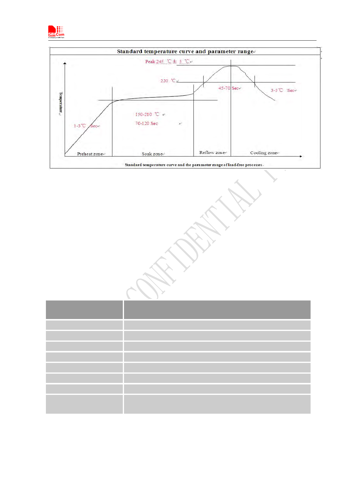
Smart Machine Smart Decision
SIM7100C_User Manual_V1.01 2015-09-19
63
Figure 35: The ramp-soak-spike reflow profile of SIM7100C
For details about secondary SMT, please refer to document [26].
6.3 Moisture Sensitivity Level (MSL)
SIM7100C is qualified to Moisture Sensitivity Level (MSL) 5 in accordance with JEDEC J-STD-033.
After the prescribed time limit exceeded, users should bake modules for 192 hours in drying equipment
(<5% RH) at 40° C +5° C/-0° C, or 72 hours at 85° C +5° C/-5° C. Note that plastic tray is not
heat-resistant, users must not use the tray to bake at 85° C or the tray may be damaged.
Table 48: Moisture sensitivity level and floor life
Moisture Sensitivity Level
(MSL)
Floor Life (out of bag) at factory ambient≤30°C/60% RH or as
stated
1
Unlimited at ≦30℃/85% RH
2
1 year
2a
4 weeks
3
168 hours
4
72 hours
5
48 hours
5a
24 hours
6
Mandatory bake before use. After bake, it must be reflowed within the
time limit specified on the label.
NOTE: For product handling, storage, processing, IPC / JEDEC J-STD-033 must be followed.

Smart Machine Smart Decision
SIM7100C_User Manual_V1.01 2015-09-19
64
6.4 Stencil Foil Design Recommendation
The recommended thickness of stencil foil is more than 0.15mm.
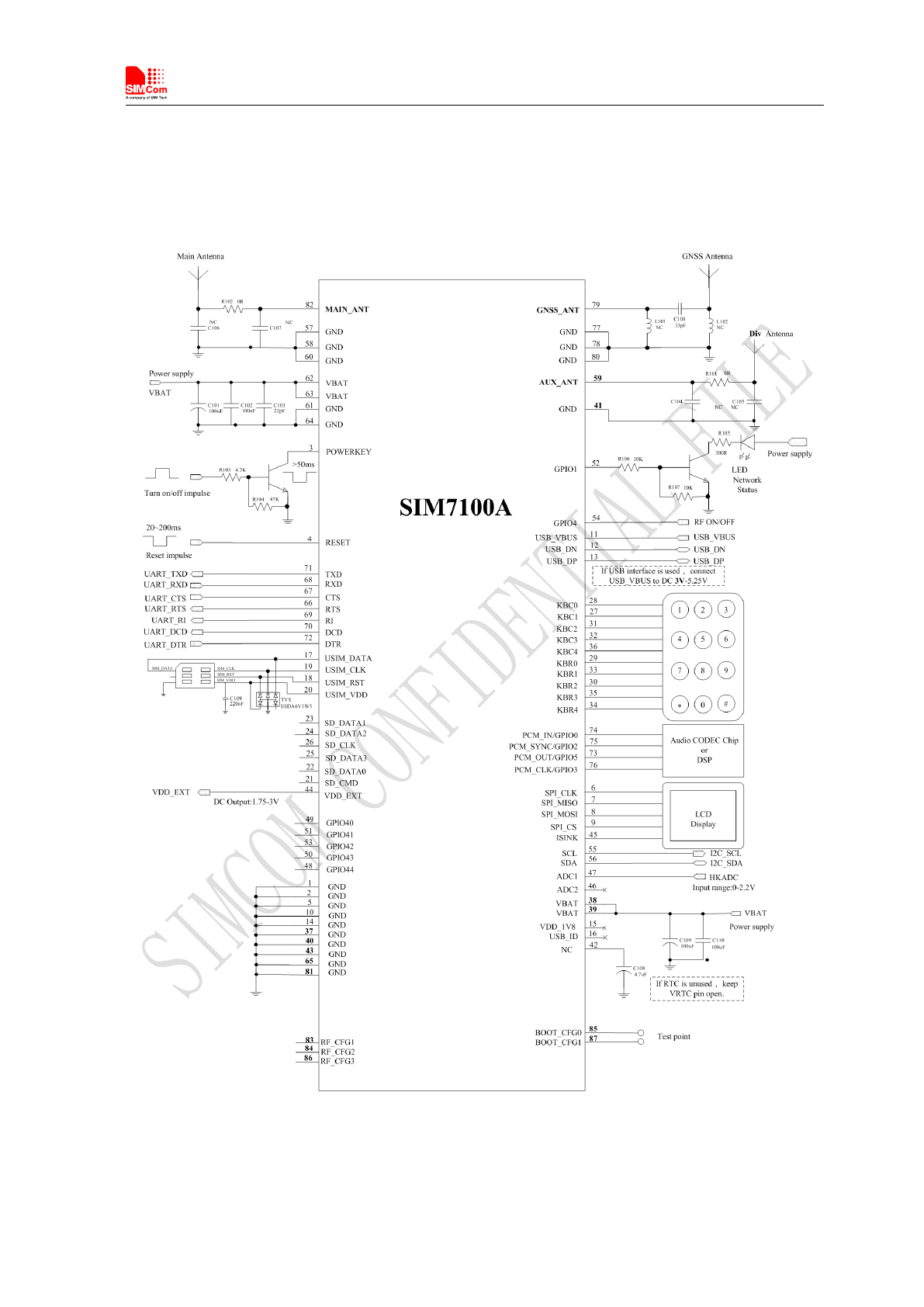
Smart Machine Smart Decision
SIM7100C_User Manual_V1.01 2015-09-19
65
Appendix
A. Reference Design
Figure 36: Reference design
Smart Machine Smart Decision
SIM7100C_User Manual_V1.01 2015-09-19
66
B. SIM7100C GPIOs List
Table 49: SIM7100C GPIOs list
Name
GPIO Index
Default Function
Alternate Function
PCM_IN
0
GPIO Interrupt [LEVEL/LOW]
PCM_IN
STATUS_LED
1
Status led
GPIO1
PCM_SYNC
2
GPIO [IN]
PCM_SYNC
PCM_CLK
3
GPIO [OUT/LOW]
PCM_CLK
RF_SWITCH
4
RF Switch
GPIO4
PCM_OUT
5
GPIO [OUT/LOW]
PCM_OUT
KBR4
6
Keypad
GPIO
KBR3
7
Keypad
GPIO
KBR2
8
Keypad
GPIO
KBR1
9
Keypad
GPIO
KBR0
10
Keypad
GPIO
KBC4
11
Keypad
GPIO
KBC3
12
Keypad
GPIO
KBC2
13
Keypad
GPIO
KBC1
14
Keypad
GPIO
KBC0
15
Keypad
GPIO
CTS
33
CTS
GPIO
RTS
34
RTS
GPIO
DTR
35
DTR wake up module
GPIO
DCD
36
DCD
GPIO
RI
37
RI wake up host
GPIO
GPIO40
40
Module power up status
GPIO
GPIO41
41
Wake up host
GPIO
GPIO42
42
GPIO[OUT/LOW]
GPIO
GPIO43
43
Wake up module
GPIO
GPIO44
44
GPIO[OUT/LOW]
GPIO
C. Digital I/O Characteristics
Table 50: Digital I/O characteristics
Parameter
Description
1.8V Digital I/O
Unit
Min
Typ
Max
VIH
High-level input
voltage
1.26
1.8
2.1
V
VIL
Low-level input
voltage
-0.3
0
0.63
V
VOH
High-level output
voltage
1.35
-
1.8
V

Smart Machine Smart Decision
SIM7100C_User Manual_V1.01 2015-09-19
67
VOL
Low-level output
voltage
0
0
0.45
V
IOH
High-level output
current
-
1
-
mA
IOL
Low-level output
current
-
-1
-
mA
IIH
Input high leakage
current
-
-
1
uA
IIL
Input low leakage
current
-1
-
-
uA
CIN
Input capacitance
-
-
7
pF
Note: These parameters are for digital interface pins, such as keypad, GPIO, I2C, UART, SPI. Digital
I/O specifications under both conditions are presented in the above tables.
D. Related Documents
Table 51: Related documents
SN
Document name
Remark
[1]
SIM7100C_ATC_V1.00
SIM7100C_ATC_V1.00
[2]
ITU-T Draft new
recommendationV.25ter
Serial asynchronous automatic dialing and control
[3]
3GPP TS 51.010-1
Digital cellular telecommunications system (Release 5); Mobile
Station (MS) conformance specification
[4]
3GPP TS 34.124
Electromagnetic Compatibility (EMC) for mobile terminals and
ancillary equipment.
[5]
3GPP TS 34.121
Electromagnetic Compatibility (EMC) for mobile terminals and
ancillary equipment.
[6]
3GPP TS 34.123-1
Technical Specification Group Radio Access Network; Terminal
conformance specification; Radio transmission and reception
(FDD)
[7]
3GPP TS 34.123-3
User Equipment (UE) conformance specification; Part 3: Abstract
Test Suites.
[8]
EN 301 908-02 V2.2.1
Electromagnetic compatibility and Radio spectrum Matters
(ERM); Base Stations (BS) and User Equipment (UE) for
IMT-2000. Third Generation cellular networks; Part 2:
Harmonized EN for IMT-2000, CDMA Direct Spread
(UTRA FDD) (UE) covering essential requirements of article
3.2 of the R&TTE Directive
[9]
EN 301 489-24 V1.2.1
Electromagnetic compatibility and Radio Spectrum Matters (ERM);
Electromagnetic Compatibility (EMC) standard for radio
equipment and services; Part 24: Specific conditions for IMT-2000
CDMA Direct Spread (UTRA) for Mobile and portable (UE) radio
and ancillary equipment

Smart Machine Smart Decision
SIM7100C_User Manual_V1.01 2015-09-19
68
[10]
IEC/EN60950-1(2001)
Safety of information technology equipment (2000)
[11]
3GPP TS 51.010-1
Digital cellular telecommunications system (Release 5); Mobile
Station (MS) conformance specification
[12]
GCF-CC V3.23.1
Global Certification Forum - Certification Criteria
[13]
2002/95/EC
Directive of the European Parliament and of the Council of 27
January 2003 on the restriction of the use of certain hazardous
substances in electrical and electronic equipment (RoHS)
[14]
Audio Application Note
V1.01
Audio Application Note V1.01
[15]
Reserved
Reserved
[16]
Keypad Application
Note V1.01
Keypad Application Note V1.01
[17]
Sleep_Application_Note
Sleep_Application_Note
[18]
Waking_up_Applicatio
n_Note
Waking_up_Application_Note
[19]
Module
secondary-SMT-UGD
SMT Note
[20]
SIM5xxx_Automatic_PO
WER_ON_Application_No
te
SIM5xxx_Automatic_POWER_ON_Application_Note
E. Terms and Abbreviations
Table 52: Terms and Abbreviations
Abbreviation
Description
ADC
Analog-to-Digital Converter
ARP
Antenna Reference Point
BER
Bit Error Rate
BTS
Base Transceiver Station
CS
Coding Scheme
CSD
Circuit Switched Data

Smart Machine Smart Decision
SIM7100C_User Manual_V1.01 2015-09-19
69
CTS
Clear to Send
DAC
Digital-to-Analog Converter
DRX
Discontinuous Reception
DSP
Digital Signal Processor
DTE
Data Terminal Equipment (typically computer, terminal, printer)
DTR
Data Terminal Ready
DTX
Discontinuous Transmission
EFR
Enhanced Full Rate
EGSM
Enhanced GSM
EMC
Electromagnetic Compatibility
ESD
Electrostatic Discharge
ETS
European Telecommunication Standard
FCC
Federal Communications Commission (U.S.)
FD
SIM fix dialing phonebook
FDMA
Frequency Division Multiple Access
FR
Full Rate
GMSK
Gaussian Minimum Shift Keying
GPRS
General Packet Radio Service
GSM
Global Standard for Mobile Communications
HR
Half Rate
I2C
Inter-Integrated Circuit
IMEI
International Mobile Equipment Identity
Inorm
Normal Current
Imax
Maximum Load Current
kbps
Kilo bits per second
Li-Ion
Lithium-Ion
MO
Mobile Originated
MS
Mobile Station (GSM engine), also referred to as TE
MT
Mobile Terminated
PAP
Password Authentication Protocol
PBCCH
Packet Switched Broadcast Control Channel
PCB
Printed Circuit Board
PCS
Personal Communication System, also referred to as GSM 1900
RF
Radio Frequency
RMS
Root Mean Square (value)
RTC
Real Time Clock
Rx
Receive Direction
SIM
Subscriber Identification Module
SMS
Short Message Service
SPI
serial peripheral interface
TDMA
Time Division Multiple Access
TE
Terminal Equipment, also referred to as DTE
TX
Transmit Direction
UART
Universal Asynchronous Receiver & Transmitter
VSWR
Voltage Standing Wave Ratio
Vmax
Maximum Voltage Value
Vnorm
Normal Voltage Value
Vmin
Minimum Voltage Value
VIHmax
Maximum Input High Level Voltage Value

Smart Machine Smart Decision
SIM7100C_User Manual_V1.01 2015-09-19
70
VIHmin
Minimum Input High Level Voltage Value
VILmax
Maximum Input Low Level Voltage Value
VILmin
Minimum Input Low Level Voltage Value
VImax
Absolute Maximum Input Voltage Value
VImin
Absolute Minimum Input Voltage Value
VOHmax
Maximum Output High Level Voltage Value
VOHmin
Minimum Output High Level Voltage Value
VOLmax
Maximum Output Low Level Voltage Value
VOLmin
Minimum Output Low Level Voltage Value
SM
SIM phonebook
NC
Not connect
EDGE
Enhanced data rates for GSM evolution
HSDPA
High Speed Downlink Packet Access
HSUPA
High Speed Uplink Packet Access
ZIF
Zero intermediate frequency
WCDMA
Wideband Code Division Multiple Access
VCTCXO
Voltage control temperature-compensated crystal oscillator
USIM
Universal subscriber identity module
UMTS
Universal mobile telecommunications system
UART
Universal asynchronous receiver transmitter
F. Safety Caution
Table 53: Safety caution
Marks
Requirements
When in a hospital or other health care facility, observe the restrictions about the use
of mobiles. Switch the cellular terminal or mobile off, medical equipment may be
sensitive to not operate normally for RF energy interference.
Switch off the cellular terminal or mobile before boarding an aircraft. Make sure it is
switched off. The operation of wireless appliances in an aircraft is forbidden to
prevent interference with communication systems. Forget to think much of these
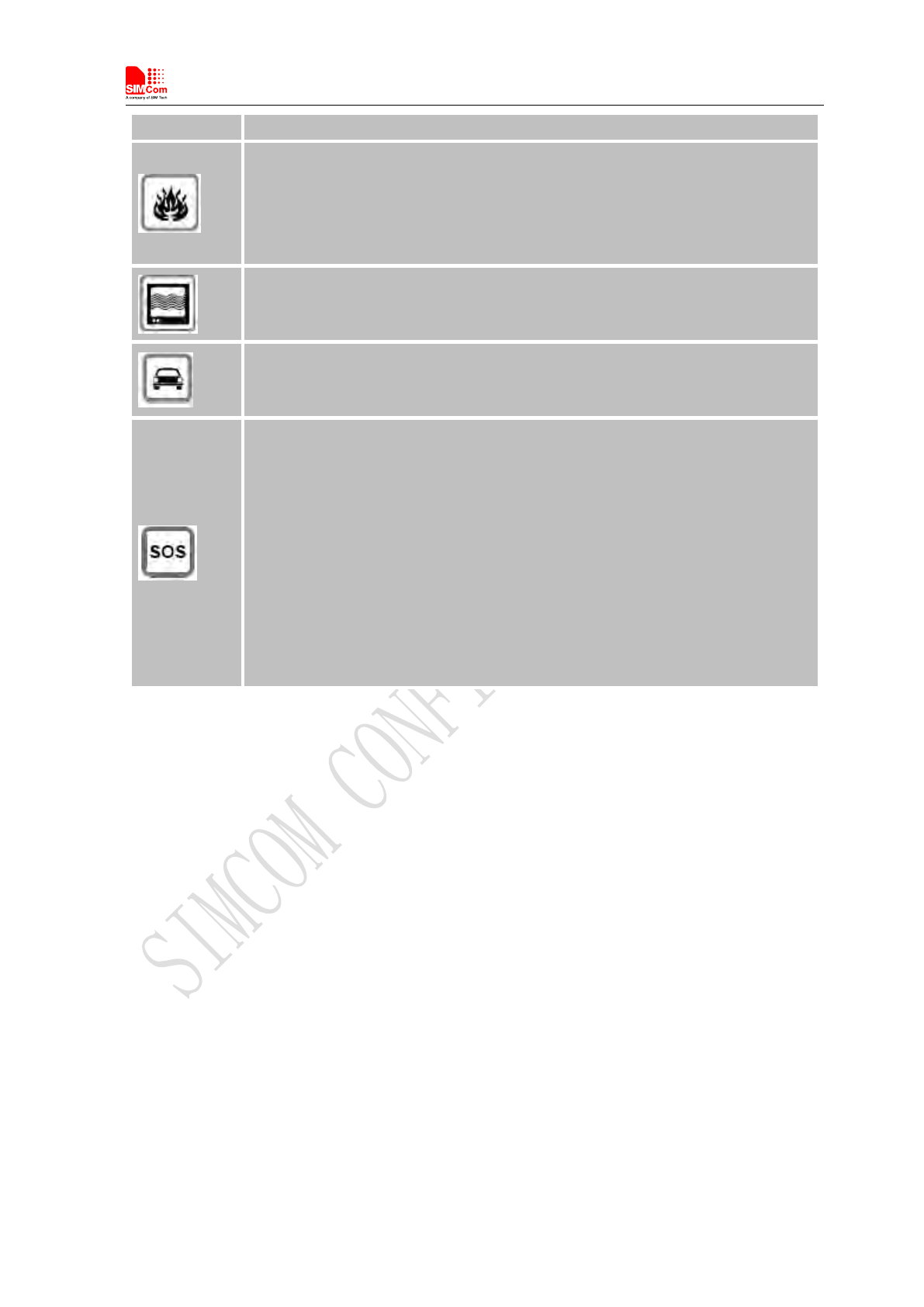
Smart Machine Smart Decision
SIM7100C_User Manual_V1.01 2015-09-19
71
instructions may lead to the flight safety or offend against local legal action, or both.
Do not operate the cellular terminal or mobile in the presence of flammable gases or
fumes. Switch off the cellular terminal when you are near petrol stations, fuel depots,
chemical plants or where blasting operations are in progress. Operation of any
electrical equipment in potentially explosive atmospheres can constitute a safety
hazard.
Your cellular terminal or mobile receives and transmits radio frequency energy while
switched on. RF interference can occur if it is used close to TV sets, radios,
computers or other electric equipment.
Road safety comes first! Do not use a hand-held cellular terminal or mobile when
driving a vehicle, unless it is securely mounted in a holder for hands free operation.
Before making a call with a hand-held terminal or mobile, park the vehicle.
GSM cellular terminals or mobiles operate over radio frequency signals and cellular
networks and cannot be guaranteed to connect in all conditions, for example no
mobile fee or a invalid SIM card. While you are in this condition and need emergent
help, please remember using emergency calls. In order to make or receive calls, the
cellular terminal or mobile must be switched on and in a service area with adequate
cellular signal strength.
Some networks do not allow for emergency call if certain network services or phone
features are in use (e.g. lock functions, fixed dialing etc.). You may have to
deactivate those features before you can make an emergency call.
Also, some networks require that a valid SIM card be properly inserted in the cellular
terminal or mobile.

Smart Machine Smart Decision
SIM7100C_User Manual_V1.01 2015-09-19
72
Contact us:
Shanghai SIMCom Wireless Solutions Ltd.
Add: SIM Technology Building, No.633, Jinzhong Road, Changning District, Shanghai P.R. China
200335
Tel: +86 21 3235 3300
Fax: +86 21 3235 3301
URL: www.sim.com/wm