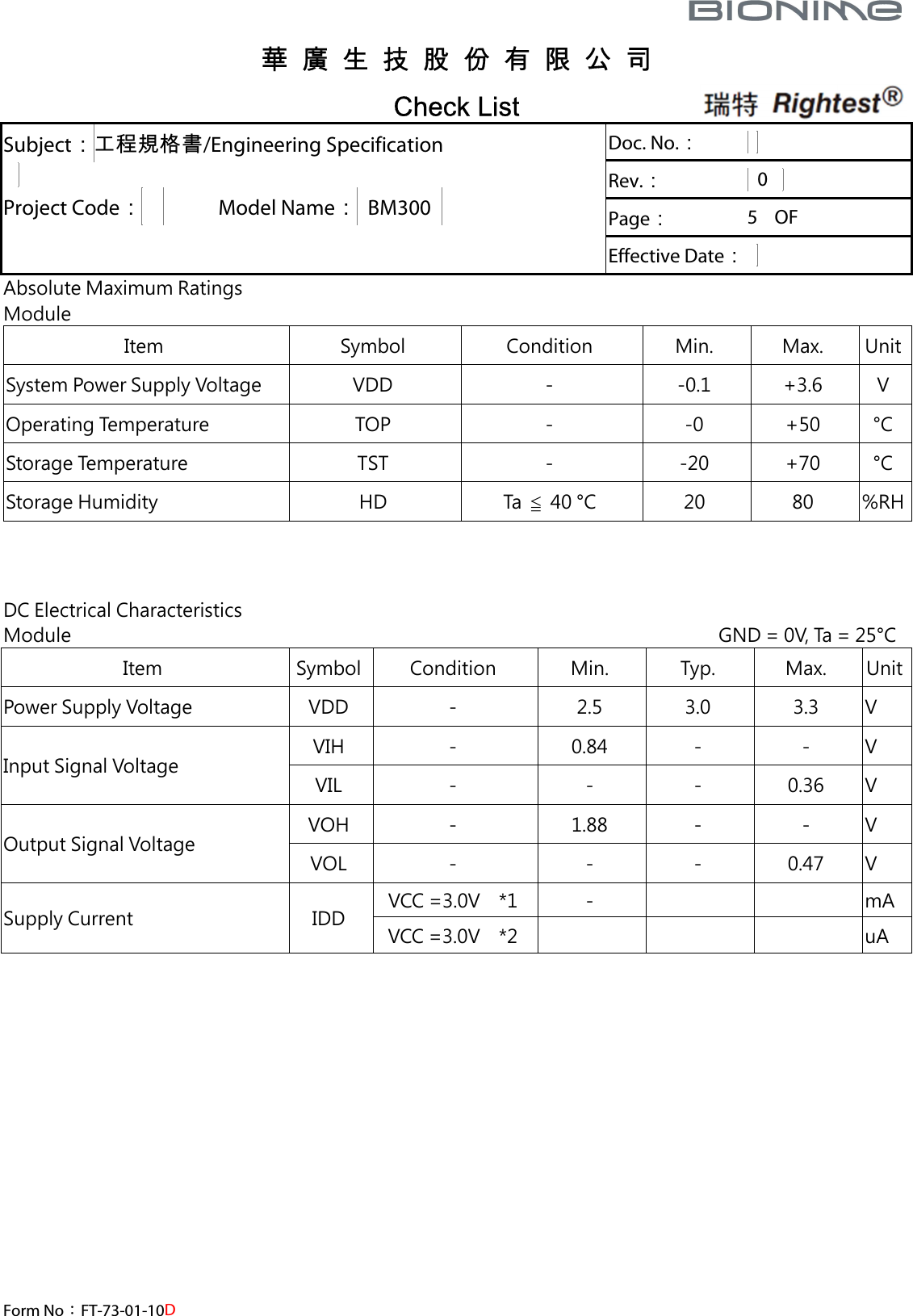
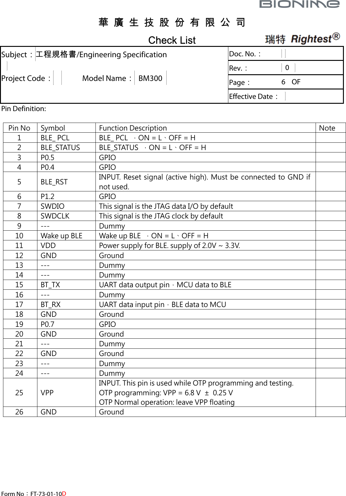
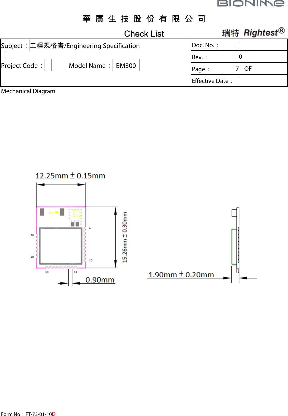
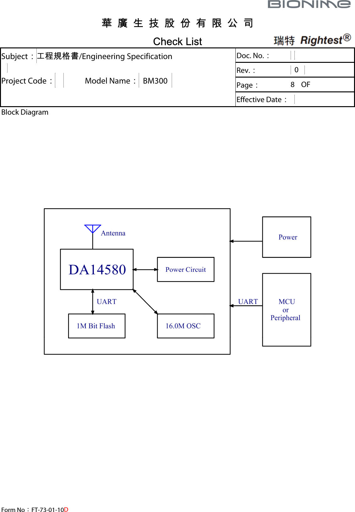
Bionime BM300 BLE module User Manual BT SPEC
Bionime Corporation BLE module BT SPEC
UserManual.wiki
>
Bionime
>
BM300 User Manual
OEM Installation Manual
Navigation menu
Upload a User Manual
Namespaces
Wiki Guide
HTML
PDF
Info
Views
User Manual
Discussion / Help
Navigation
![華 廣 生 技 股 份 有 限 公 司 Check List Form No:FT-73-01-10D Subject:工程規格書/Engineering Specification Project Code: Model Name: BM300 Doc. No.: Rev.: 0 Page: 3 OF Effective Date: FCC Statement: This device complies with part 15 of the FCC Rules. Operation is subject to the following two conditions: (1) This device may not cause harmful interference, and (2) this device must accept any interference received, including interference that may cause undesired operation. NOTE: This equipment has been tested and found to comply with the limits for a Class B digital device, pursuant to part 15 of the FCC Rules. These limits are designed to provide reasonable protection against harmful interference in a residential installation. This equipment generates, uses and can radiate radio frequency energy and, if not installed and used in accordance with the instructions, may cause harmful interference to radio communications. However, there is no guarantee that interference will not occur in a particular installation. If this equipment does cause harmful interference to radio or television reception, which can be determined by turning the equipment off and on, the user is encouraged to try to correct the interference by one or more of the following measures: —Reorient or relocate the receiving antenna. —Increase the separation between the equipment and receiver. —Connect the equipment into an outlet on a circuit different from that to which the receiver is connected. —Consult the dealer or an experienced radio/TV technician for help. Changes or modifications not expressly approved by the party responsible for compliance could void the user’s authority to operate the equipment. FCC Label Instructions: The outside of final products that contains this module device must display a label referring to the enclosed module. This exterior label can use wording such as the following: “Contains Transmitter Module FCC ID: [put FCC ID here]” or “Contains FCC ID: [put FCC ID here].” Any similar wording that expresses the same meaning may be used.](https://usermanual.wiki/Bionime/BM300/User-Guide-3187957-Page-3.png)
![華 廣 生 技 股 份 有 限 公 司 Check List Form No:FT-73-01-10D Subject:工程規格書/Engineering Specification Project Code: Model Name: BM300 Doc. No.: Rev.: 0 Page: 12 OF Effective Date: Instruction Set Function Instruction Set BGM Device ID Command “ {“ LEN ID-1 ID-2 … ID-n CS “ } ” LEN ID-1 ID-2 … ID-n CS Pairing [ 0x27 White List CS ] 0xD8 Status Byte CS Pair Completion [ 0x28 CS ] 0xD7 CS White List Full [ 0x29 CS ] 0xD6 CS Check BLE ] 0x5F CS [ 0xA0 CS Clear White List ] 0x5B CS [ 0xA4 Status Byte CS Read BLE Flash ] 0x5A indexL indexH CS [ 0xA5 indexL indexH data0 … data9 CS Write BLE Flash ] 0x59 indexL indexH data0 … data9 CS [ 0xA6 indexL indexH data0 … data9 CS BLE Flash writing area setting ] 0x58 Section Index CS [ 0xA7 Section Index CS Write BLE Flash End ] 0x57 CS [ 0xA8 CS](https://usermanual.wiki/Bionime/BM300/User-Guide-3187957-Page-12.png)
![華 廣 生 技 股 份 有 限 公 司 Check List Form No:FT-73-01-10D Subject:工程規格書/Engineering Specification Project Code: Model Name: BM300 Doc. No.: Rev.: 0 Page: 13 OF Effective Date: Set BGM Device ID Command: Byte Index 0 1 2 3 … LEN+1 LEN+2 MCU to BLE Command ‘ } ’ LEN ID-1 ID-2 … ID-n CS BLE to MCU Return Data ‘ { ’ LEN ID-1 ID-2 … ID-n CS ‘ } ’ : Header of MCU set command, ASCII Format. ‘ { ’ : Header of BLE return data. ASCII Format. LEN : Length of BGM ID. HEX value. ID-1 ~ ID-n : Unique ID of BGM. ASCII format. Range 0x01 ~ 0x14 (1~20) CS : Checksum. Checksum Byte = (Byte[0] + byte[1] + …. Byte[n]) & 0xFF Pairing: Byte Index 0 1 2 3 BLE to MCU Command ‘ [ ’ 0x27 White List CS MCU to BLE Return Data ‘ ] ’ 0xD8 Status Byte CS ‘ [ ’: Header of BLE set command, ASCII Format. ‘ ] ’: Header of MCU return data. ASCII Format. White List : paired quantity Status Byte: 0x00:Agree 0x01:Deny 0x02:Wait Pair Completion Byte Index 0 1 2 BLE to MCU Command ‘ [ ’ 0x28 CS MCU to BLE Return Data ‘ ] ’ 0xD7 CS BLE module pairing is completed White List Full Byte Index 0 1 2 BLE to MCU Command ‘ [ ’ 0x29 CS MCU to BLE Return Data ‘ ] ’ 0xD6 CS Whitelist is full and can no longer new pairing](https://usermanual.wiki/Bionime/BM300/User-Guide-3187957-Page-13.png)
![華 廣 生 技 股 份 有 限 公 司 Check List Form No:FT-73-01-10D Subject:工程規格書/Engineering Specification Project Code: Model Name: BM300 Doc. No.: Rev.: 0 Page: 14 OF Effective Date: Check BLE Byte Index 0 1 2 MCU to BLE Command ‘ ] ’ 0x5F CS BLE to MCU Return Data ‘ [ ’ 0xA0 CS MCU tested for BLE module function test BLE normal operation, reply to 0xA0 Clear White List Byte Index 0 1 2 3 MCU to BLE Command ‘ ] ’ 0x5B CS BLE to MCU Return Data ‘ [ ’ 0xA4 Status Byte CS MCU command BLE clear Whitelist Status Byte: 0x00:BLE reply, Whitelist Clear Completed 0x01:BLE reply, Whitelist Cleanup failed Read BLE Flash Byte Index 0 1 2 3 4 … 13 14 MCU to BLE Command ‘ ] ’ 0x5A indexL indexH CS … BLE to MCU Return Data ‘ [ ’ 0xA5 indexL indexH data0 … Data9 CS Read BLE Flash BLE 模組內可儲存資料 1200 筆 Flash 可存 1200 筆資料,每筆 10byte,index 範圍 0x0000~0x04AF Write BLE Flash Byte Index 0 1 2 3 4 … 13 14 MCU to BLE Command ‘ ] ’ 0x59 indexL indexH data0 … Data9 CS BLE to MCU Return Data ‘ [ ’ 0xA6 indexL indexH data0 … Data9 CS BLE Flash writing area setting Byte Index 0 1 2 3 MCU to BLE Command ‘ ] ’ 0x58 Section Index CS BLE to MCU Return Data ‘ [ ’ 0xA7 Section Index CS](https://usermanual.wiki/Bionime/BM300/User-Guide-3187957-Page-14.png)
![華 廣 生 技 股 份 有 限 公 司 Check List Form No:FT-73-01-10D Subject:工程規格書/Engineering Specification Project Code: Model Name: BM300 Doc. No.: Rev.: 0 Page: 15 OF Effective Date: Section Index: 0: 1: 2: Write BLE Flash End Byte Index 0 1 2 3 MCU to BLE Command ‘ ] ’ 0x57 CS BLE to MCU Return Data ‘ [ ’ 0xA8 CS](https://usermanual.wiki/Bionime/BM300/User-Guide-3187957-Page-15.png)