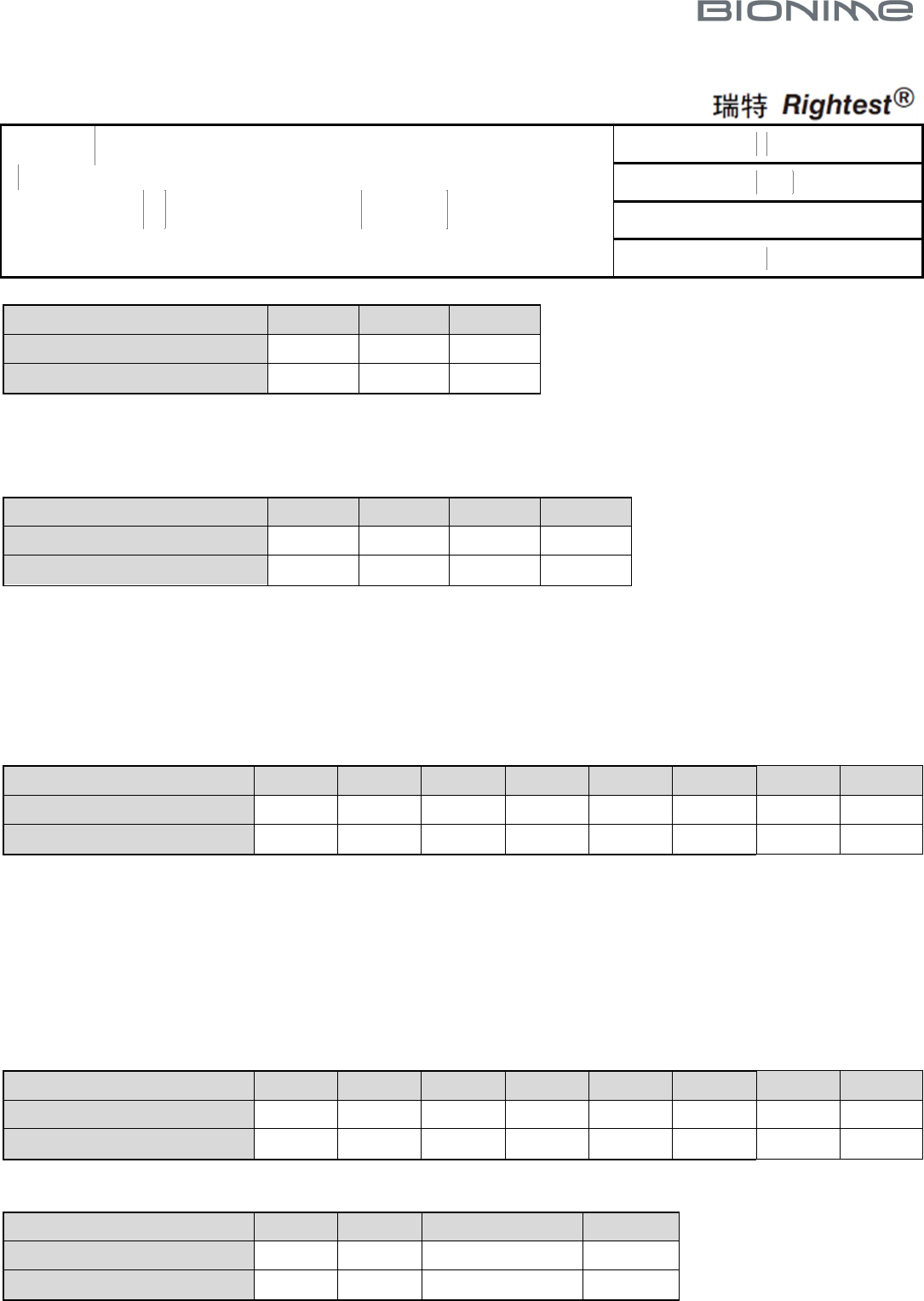
OEM Installation Manual
華 廣 生 技 股 份 有 限 公 司
Check List
Form No:FT-73-01-10D
Subject:工程規格書/Engineering Specification
Project Code: Model Name: BM300
Doc. No.:
Rev.: 0
Page: 1
OF
Effective Date:
Change History
CICN NO#
Page
Rev.
Effective
Date
Reason For Release
0 First Released
Copy to (all contents):
Copy to(cover sheet):
Reviewed By
Dep.
Manager Executor Dep.
Manager Executor
Approved By :
□
SL
□
QA
□
MK
□
LM
□
CT ■PO
■PD
□
AU
Prepare By: □PM
□
RO
■PE
■QC
□TW
□
華 廣 生 技 股 份 有 限 公 司
Check List
Form No:FT-73-01-10D
Subject:工程規格書/Engineering Specification
Project Code: Model Name: BM300
Doc. No.:
Rev.: 0
Page: 2
OF
Effective Date:
NCC 警語
「減少電磁波影響,請妥善使用」。
依據低功率電波輻射性電機管理辦法
第十二條 經型式認證合格之低功率射頻電機,非經許可,公司、商號或使用者均 不得擅自變更頻率、加大功率
或變更原設計之特性及功能。
第十四條 低功率射頻電機之使用不得影響飛航安全及干擾合法通信;經發現有干 擾現象時,應立即停用,並改
善至無干擾時方得繼續使用。
前項合法通信,指依電信法規定作業之無線電通信。 低功率射頻電機須忍受合法通信或工業、科學
及醫療用電波輻射性電機 設備之干擾。」

華 廣 生 技 股 份 有 限 公 司
Check List
Form No:FT-73-01-10D
Subject:工程規格書/Engineering Specification
Project Code: Model Name: BM300
Doc. No.:
Rev.: 0
Page: 3
OF
Effective Date:
FCC Statement:
This device complies with part 15 of the FCC Rules. Operation is subject to the following two conditions:
(1) This device may not cause harmful interference, and
(2) this device must accept any interference received, including interference that may cause undesired
operation.
NOTE: This equipment has been tested and found to comply with the limits for a Class B digital device,
pursuant to part 15 of the FCC Rules. These limits are designed to provide reasonable protection against
harmful interference in a residential installation.
This equipment generates, uses and can radiate radio frequency energy and, if not installed and used in
accordance with the instructions, may cause harmful interference to radio communications. However,
there is no guarantee that interference will not occur in a particular installation.
If this equipment does cause harmful interference to radio or television reception, which can be
determined by turning the equipment off and on, the user is encouraged to try to correct the
interference by one or more of the following measures:
—Reorient or relocate the receiving antenna.
—Increase the separation between the equipment and receiver.
—Connect the equipment into an outlet on a circuit different from that to which the receiver is
connected.
—Consult the dealer or an experienced radio/TV technician for help.
Changes or modifications not expressly approved by the party responsible for compliance could void
the user’s authority to operate the equipment.
FCC Label Instructions:
The outside of final products that contains this module device must display a label referring to the
enclosed module. This exterior label can use wording such as the following: “Contains Transmitter
Module FCC ID: [put FCC ID here]” or “Contains FCC ID: [put FCC ID here].” Any similar wording that
expresses the same meaning may be used.
華 廣 生 技 股 份 有 限 公 司
Check List
Form No:FT-73-01-10D
Subject:工程規格書/Engineering Specification
Project Code: Model Name: BM300
Doc. No.:
Rev.: 0
Page: 4
OF
Effective Date:
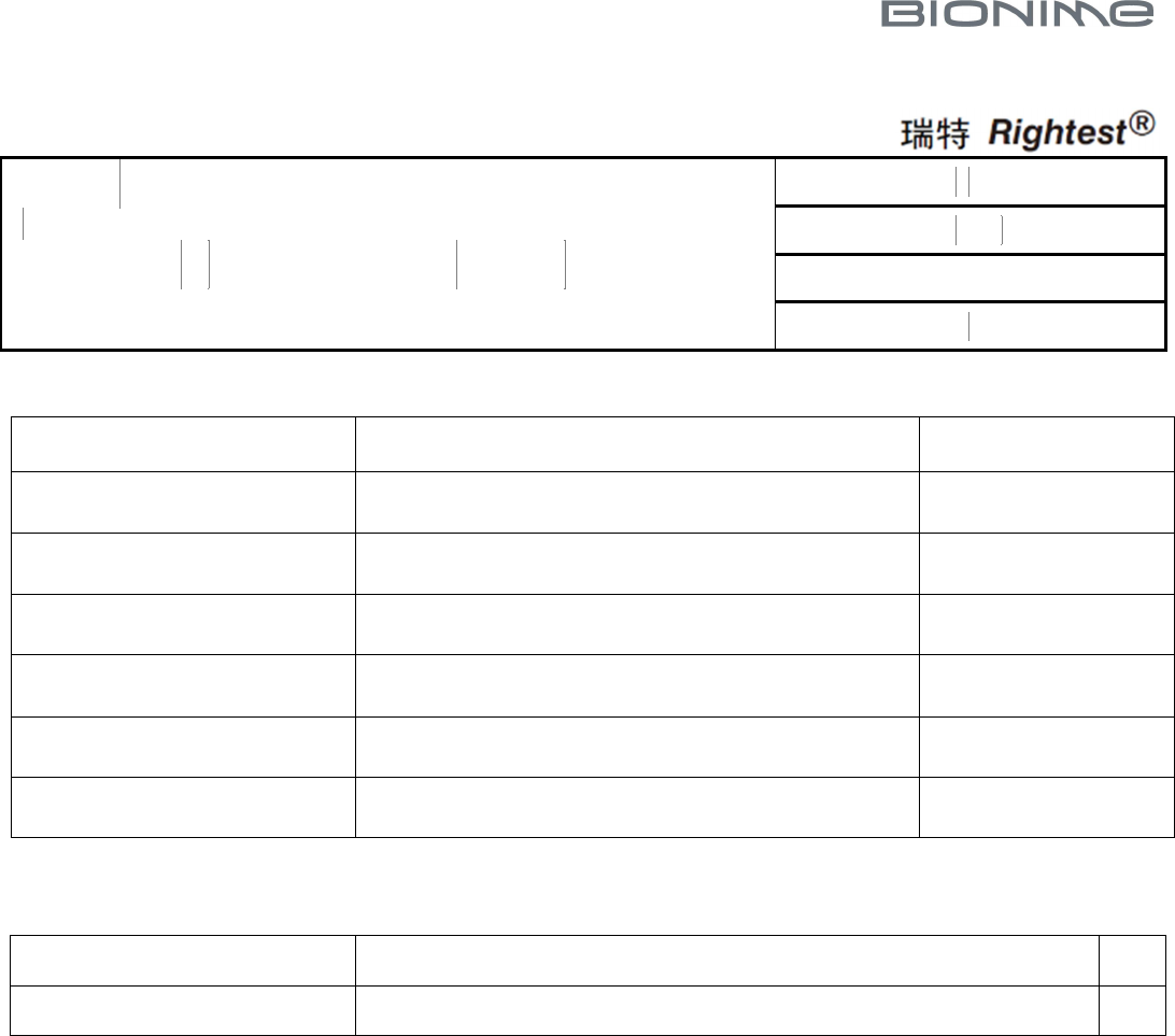
Feature:
Item Specification Remark
Chip DA14580
Standard Bluetooth V4.1
RF band 2402 ~ 2480MHz ISM band
Interface UART
RF Output Power -20dBm ~0 dBm
Sensitivity >-93 dBm
Mechanical Specifications
Item Standard Value Unit
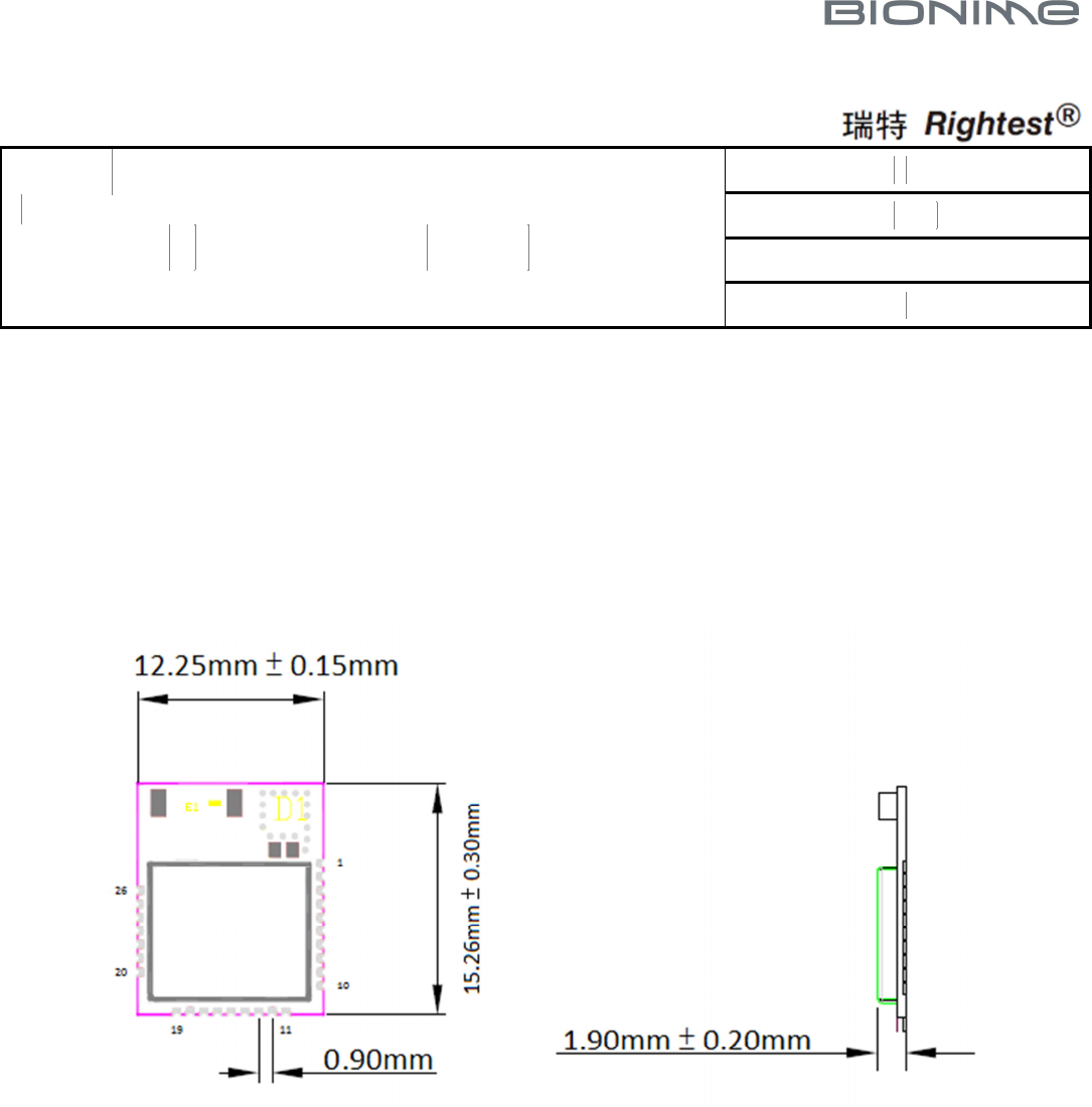
Outline Dimension 12.25 (W) * 15.26 (L) * 1.9 (H) mm
華 廣 生 技 股 份 有 限 公 司
Check List
Form No:FT-73-01-10D
Subject:工程規格書/Engineering Specification
Project Code: Model Name: BM300
Doc. No.:
Rev.: 0
Page: 5
OF
Effective Date:
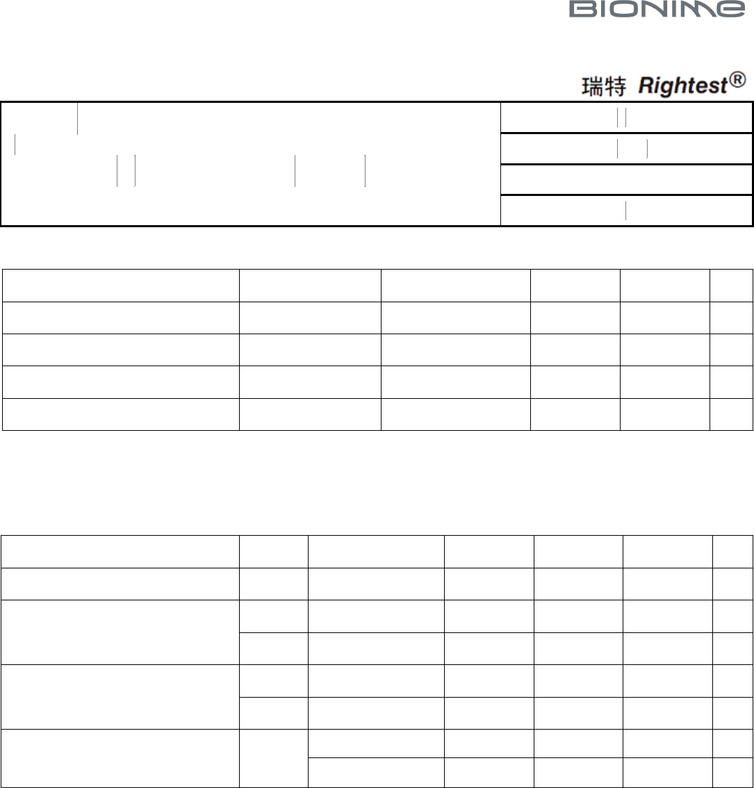
Absolute Maximum Ratings
Module
Item Symbol Condition Min. Max. Unit
System Power Supply Voltage VDD - -0.1 +3.6 V
Operating Temperature TOP - -0 +50 °C
Storage Temperature TST - -20 +70 °C
Storage Humidity HD Ta ≦ 40 °C 20 80 %RH
DC Electrical Characteristics
Module GND = 0V, Ta = 25°C
Item Symbol
Condition Min. Typ. Max. Unit
Power Supply Voltage VDD - 2.5 3.0 3.3 V
Input Signal Voltage VIH - 0.84 - - V
VIL - - - 0.36 V
Output Signal Voltage VOH - 1.88 - - V
VOL - - - 0.47 V
Supply Current IDD VCC =3.0V *1 - mA
VCC =3.0V *2 uA
華 廣 生 技 股 份 有 限 公 司
Check List
Form No:FT-73-01-10D
Subject:工程規格書/Engineering Specification
Project Code: Model Name: BM300
Doc. No.:
Rev.: 0
Page: 6
OF
Effective Date:
Pin Definition:
Pin No Symbol Function Description Note
1 BLE_ PCL BLE_ PCL ,ON = L、OFF = H
2 BLE_STATUS BLE_STATUS ,ON = L、OFF = H
3 P0.5 GPIO
4 P0.4 GPIO
5 BLE_RST INPUT. Reset signal (active high). Must be connected to GND if
not used.
6 P1.2 GPIO
7 SWDIO This signal is the JTAG data I/O by default
8 SWDCLK This signal is the JTAG clock by default
9 --- Dummy
10 Wake up BLE Wake up BLE ,ON = L、OFF = H
11 VDD Power supply for BLE. supply of 2.0V ~ 3.3V.
12 GND Ground
13 --- Dummy
14 --- Dummy
15 BT_TX UART data output pin,MCU data to BLE
16 --- Dummy
17 BT_RX UART data input pin,BLE data to MCU
18 GND Ground
19 P0.7 GPIO
20 GND Ground
21 --- Dummy
22 GND Ground
23 --- Dummy
24 --- Dummy
25 VPP
INPUT. This pin is used while OTP programming and testing.
OTP programming: VPP = 6.8 V ± 0.25 V
OTP Normal operation: leave VPP floating
26 GND Ground
華 廣 生 技 股 份 有 限 公 司
Check List
Form No:FT-73-01-10D
Subject:工程規格書/Engineering Specification
Project Code: Model Name: BM300
Doc. No.:
Rev.: 0
Page: 7
OF
Effective Date:
Mechanical Diagram
華 廣 生 技 股 份 有 限 公 司
Check List
Form No:FT-73-01-10D
Subject:工程規格書/Engineering Specification
Project Code: Model Name: BM300
Doc. No.:
Rev.: 0
Page: 8
OF
Effective Date:
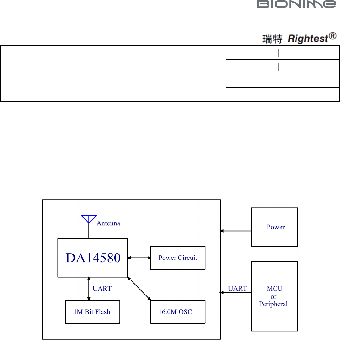
Block Diagram
華 廣 生 技 股 份 有 限 公 司
Check List
Form No:FT-73-01-10D
Subject:工程規格書/Engineering Specification
Project Code: Model Name: BM300
Doc. No.:
Rev.: 0
Page: 9
OF
Effective Date:
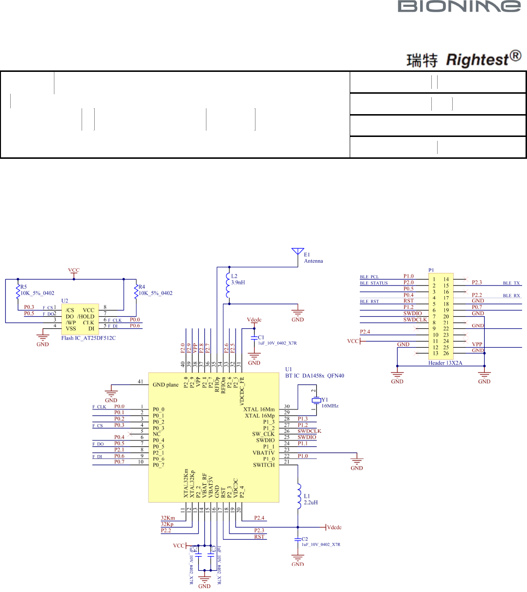
Module Application Circuit:
華 廣 生 技 股 份 有 限 公 司
Check List
Form No:FT-73-01-10D
Subject:工程規格書/Engineering Specification
Project Code: Model Name: BM300
Doc. No.:
Rev.: 0
Page: 10
OF
Effective Date:
Module Bill of Material:
Item Part No. Designator Comment
1 503-040000-0P0 U1 DA14580 / QFN 40
2 503-040000-0Q0 U2 MX25V1006E / USON 8L
3 502-021057-010 C1,C2,C3,C4 1uF / 10V / X5R /±10% / 0402
4 501-011032-020 R4, R5 10KΩ / ±5% / 0402
5 505-040000-2K0 L1 2.2uH±10%-1608
6 505-040000-2L0 L2 3.9nH±0.3nH-1005
7 505-020000-0B0 Y1 16 MHz/ FA-128
8 505-040000-0E0 E1 AT5020-B2R8HAA
9
華 廣 生 技 股 份 有 限 公 司
Check List
Form No:FT-73-01-10D
Subject:工程規格書/Engineering Specification
Project Code: Model Name: BM300
Doc. No.:
Rev.: 0
Page: 11
OF
Effective Date:
Software & Operation Mode
UART Configuration
Baud Rate
9600 bps
Start Bit
1
Data Bits
8
Stop Bits
1
Parity Bit
None
Timeout : 500 ms
華 廣 生 技 股 份 有 限 公 司
Check List
Form No:FT-73-01-10D
Subject:工程規格書/Engineering Specification
Project Code: Model Name: BM300
Doc. No.:
Rev.: 0
Page: 12
OF
Effective Date:
Instruction Set
Function Instruction
Set BGM Device ID
Command
“ {“ LEN ID-1 ID-2
…
ID-n CS
“ } ” LEN ID-1 ID-2
…
ID-n CS
Pairing
[ 0x27 White List CS
] 0xD8 Status Byte CS
Pair Completion
[ 0x28 CS
] 0xD7 CS
White List Full
[ 0x29 CS
] 0xD6 CS
Check BLE
] 0x5F CS
[ 0xA0 CS
Clear White List
] 0x5B CS
[ 0xA4 Status Byte CS
Read BLE Flash
] 0x5A indexL indexH CS
[ 0xA5 indexL indexH data0
…
data9 CS
Write BLE Flash
] 0x59 indexL indexH data0
…
data9 CS
[ 0xA6 indexL indexH data0
…
data9 CS
BLE Flash writing
area setting
] 0x58 Section Index
CS
[ 0xA7 Section Index
CS
Write BLE Flash End
] 0x57 CS
[ 0xA8 CS
華 廣 生 技 股 份 有 限 公 司
Check List
Form No:FT-73-01-10D
Subject:工程規格書/Engineering Specification
Project Code: Model Name: BM300
Doc. No.:
Rev.: 0
Page: 13
OF
Effective Date:
Set BGM Device ID Command:
Byte Index 0 1 2 3 … LEN+1
LEN+2
MCU to BLE Command ‘ } ’ LEN ID-1 ID-2 … ID-n CS
BLE to MCU Return Data ‘ { ’ LEN ID-1 ID-2 … ID-n CS
‘ } ’ : Header of MCU set command, ASCII Format.
‘ { ’ : Header of BLE return data. ASCII Format.
LEN : Length of BGM ID. HEX value.
ID-1 ~ ID-n : Unique ID of BGM. ASCII format.
Range 0x01 ~ 0x14 (1~20)
CS : Checksum.
Checksum Byte = (Byte[0] + byte[1] + …. Byte[n]) & 0xFF
Pairing:
Byte Index 0 1 2 3
BLE to MCU Command ‘ [ ’
0x27
White List
CS
MCU to BLE Return Data ‘ ] ’
0xD8
Status Byte
CS
‘ [ ’: Header of BLE set command, ASCII Format.
‘ ] ’: Header of MCU return data. ASCII Format.
White List : paired quantity
Status Byte: 0x00:Agree
0x01:Deny
0x02:Wait
Pair Completion
Byte Index 0 1 2
BLE to MCU Command ‘ [ ’
0x28
CS
MCU to BLE Return Data ‘ ] ’
0xD7
CS
BLE module pairing is completed
White List Full
Byte Index 0 1 2
BLE to MCU Command ‘ [ ’
0x29
CS
MCU to BLE Return Data ‘ ] ’
0xD6
CS
Whitelist is full and can no longer new pairing
華 廣 生 技 股 份 有 限 公 司
Check List
Form No:FT-73-01-10D
Subject:工程規格書/Engineering Specification
Project Code: Model Name: BM300
Doc. No.:
Rev.: 0
Page: 14
OF
Effective Date:
Check BLE
Byte Index 0 1 2
MCU to BLE Command ‘ ] ’
0x5F
CS
BLE to MCU Return Data ‘ [ ’
0xA0
CS
MCU tested for BLE module function test
BLE normal operation, reply to 0xA0
Clear White List
Byte Index 0 1 2 3
MCU to BLE Command ‘ ] ’
0x5B
CS
BLE to MCU Return Data ‘ [ ’
0xA4 Status Byte
CS
MCU command BLE clear Whitelist
Status Byte: 0x00:BLE reply, Whitelist Clear Completed
0x01:BLE reply, Whitelist Cleanup failed
Read BLE Flash
Byte Index 0 1 2 3 4 … 13 14
MCU to BLE Command ‘ ] ’
0x5A
indexL
indexH
CS …
BLE to MCU Return Data
‘ [ ’
0xA5
indexL
indexH
data0 … Data9 CS
Read BLE Flash
BLE 模組內可儲存資料 1200 筆
Flash 可存 1200 筆資料,每筆 10byte,index 範圍 0x0000~0x04AF
Write BLE Flash
Byte Index 0 1 2 3 4 … 13 14
MCU to BLE Command ‘ ] ’
0x59
indexL
indexH
data0 … Data9 CS
BLE to MCU Return Data
‘ [ ’
0xA6
indexL
indexH
data0 … Data9 CS
BLE Flash writing area setting
Byte Index 0 1 2 3
MCU to BLE Command ‘ ] ’
0x58
Section Index
CS
BLE to MCU Return Data
‘ [ ’
0xA7
Section Index
CS
華 廣 生 技 股 份 有 限 公 司
Check List
Form No:FT-73-01-10D
Subject:工程規格書/Engineering Specification
Project Code: Model Name: BM300
Doc. No.:
Rev.: 0
Page: 15
OF
Effective Date:
Section Index: 0:
1:
2:
Write BLE Flash End
Byte Index 0 1 2 3
MCU to BLE Command ‘ ] ’
0x57
CS
BLE to MCU Return Data ‘ [ ’
0xA8
CS

華 廣 生 技 股 份 有 限 公 司
Check List
Form No:FT-73-01-10D
Subject:工程規格書/Engineering Specification
Project Code: Model Name: BM300
Doc. No.:
Rev.: 0
Page: 16
OF
Effective Date: