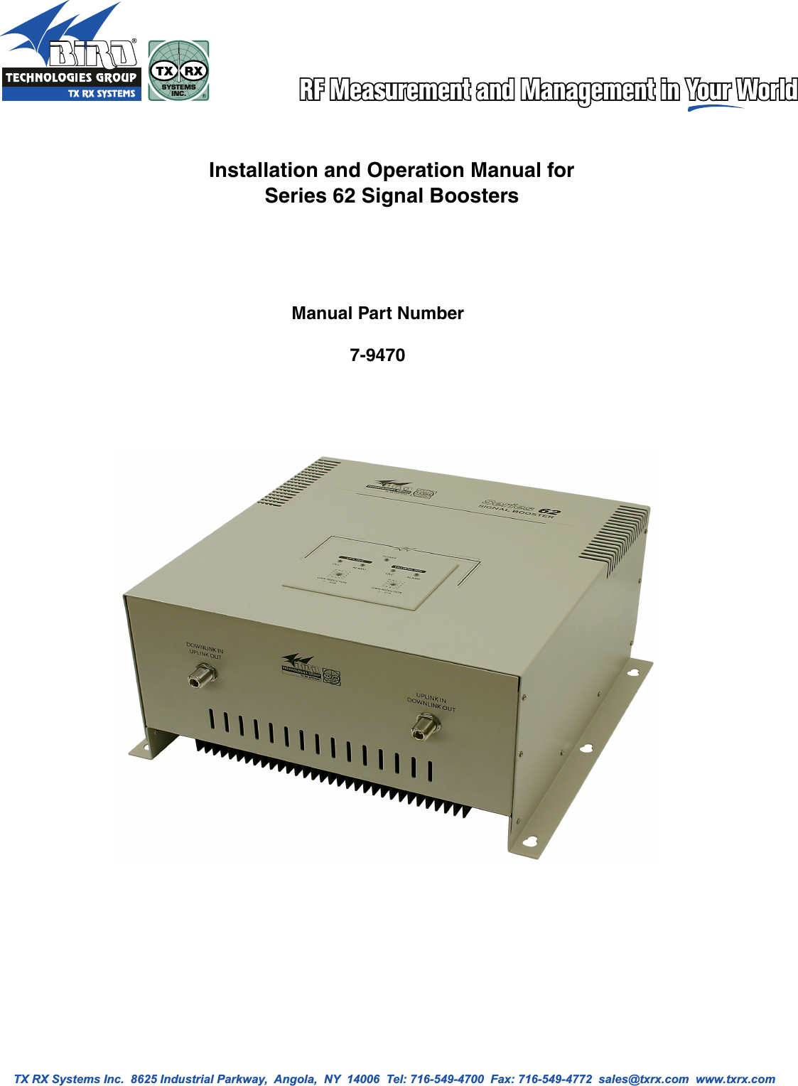
Bird Technologies Group 5PI62 Signal Booster (Bi-directional Amplifier) User Manual

Bird Technologies Group Signal Booster (Bi-directional Amplifier) Users Manual

Users Manual

TX RX Systems Inc.  8625 Industrial Parkway,  Angola,  NY  14006  Tel: 716-549-4700  Fax: 716-549-4772  sales@txrx.com  www.txrx.com SYSTEMSINC.SYSTEMSINC.Installation and Operation Manual forSeries 62 Signal BoostersManual Part Number7-9470
WarrantyThis warranty applies for one year from shipping date.TX RX Systems Inc. warrants its products to be free from defect in material and workmanship at the time of shipment.Our obligation under warranty is limited to replacement or repair, at our option, of any such products that shall havebeen defective at the time of manufacture. TX RX Systems Inc. reserves the right to replace with merchandise ofequal performance although not identical in every way to that originally sold. TX RX Systems Inc. is not liable for dam-age caused by lightning or other natural disasters. No product will be accepted for repair or replacement without ourprior written approval. The purchaser must prepay all shipping charges on returned products. TX RX Systems Inc.shall in no event be liable for consequential damages, installation costs or expense of any nature resulting from thepurchase or use of products, whether or not they are used in accordance with instructions. This warranty is in lieu of allother warranties, either expressed or implied, including any implied warranty or merchantability of fitness. No repre-sentative is authorized to assume for TX RX Systems Inc. any other liability or warranty than set forth above in con-nection with our products or services.TERMS AND CONDITIONS OF SALE PRICES AND TERMS:Prices are FOB seller’s plant in Angola, NY domestic packaging only, and are subject to change without notice. Fed-eral, State and local sales or excise taxes are not included in prices. When Net 30 terms are applicable, payment isdue within 30 days of invoice date. All orders are subject to a $100.00 net minimum.QUOTATIONS:Only written quotations are valid.ACCEPTANCE OF ORDERS:Acceptance of orders is valid only when so acknowledged in writing by the seller.SHIPPING:Unless otherwise agreed at the time the order is placed, seller reserves the right to make partial shipments for whichpayment shall be made in accordance with seller’s stated terms. Shipments are made with transportation charges col-lect unless otherwise specified by the buyer. Seller’s best judgement will be used in routing, except that buyer’s routingis used where practicable. The seller is not responsible for selection of most economical or timeliest routing.CLAIMS:All claims for damage or loss in transit must be made promptly by the buyer against the carrier. All claims for shortagesmust be made within 30 days after date of shipment of material from the seller’s plant.SPECIFICATION CHANGES OR MODIFICATIONS:All designs and specifications of seller’s products are subject to change without notice provided the changes or modifi-cations do not affect performance.RETURN MATERIAL:Product or material may be returned for credit only after written authorization from the seller, as to which seller shallhave sole discretion. In the event of such authorization, credit given shall not exceed 80 percent of the original pur-chase. In no case will Seller authorize return of material more than 90 days after shipment from Seller’s plant. Creditfor returned material is issued by the Seller only to the original purchaser.ORDER CANCELLATION OR ALTERATION:Cancellation or alteration of acknowledged orders by the buyer will be accepted only on terms that protect the selleragainst loss.NON WARRANTY REPAIRS AND RETURN WORK:Consult seller’s plant for pricing. Buyer must prepay all transportation charges to seller’s plant. Standard shipping pol-icy set forth above shall apply with respect to return shipment from TX RX Systems Inc. to buyer.DISCLAIMER Product part numbering in photographs and drawings is accurate at time of printing. Part number labels on TX RXproducts supersede part numbers given within this manual. Information is subject to change without notice. Bird Technologies Group                                                                                TX RX Systems Inc.
Symbols Commonly UsedWARNING                ESD Electrostatic DischargeHot SurfaceElectrical Shock HazardImportant InformationCAUTION or ATTENTIONHigh VoltageHeavy LiftingBird Technologies Group TX RX Systems Inc.NOTEManual Part Number 7-9470Copyright © 2008 TX RX Systems, Inc.First Printing: February 2009Version Number Version Date1 02/14/091.1 04/27/09
For Class A Unintentional RadiatorsThis equipment has been tested  and found to comply with the limits for a Class A digital device, pursuantto Part 15 of the FCC rules. These limits are designed to provide resonable protection against harmfulinterference when the equipment is operated in a commercial environment. This equipment generates,uses, and can radiate radio frequency energy and, if not installed and used in accordance with the instruc-tion manual, may cause harmful interference to radio communications. Operation of this equipment in aresidential area is likely to cause harmful interference in which the user will be required to correct the inter-ference at his own expense.WARNING: Changes or modifications which are not expressly approved by TXRXSystems Inc. could void the user’s authority to operate the equipment.ATTENTION: This device complies with Part 15 of the FCC rules. Operation is subject to thefollowing two conditions: (1) this device may not cause harmful interference and (2) thisdevice must accept any interference received, including interference that may cause undes-ired operation.
  Table of Contents                                                           Manual 7-9470-1.1                                                                  04/27/09     Table of ContentsOverview............................................................................................................... 1Unpacking ............................................................................................................ 3Block Diagram Description................................................................................. 4  Front-End Module................................................................................................ 4  Power Amplifier Module....................................................................................... 5  Front Panel Module ............................................................................................. 6  Power Entry/Supply ............................................................................................. 7Connections......................................................................................................... 8Alarm Conditions.................................................................................................8Installation............................................................................................................ 9   Location  ............................................................................................................. 9Mounting .......................................................................................................... 10Antenna Isolation  ............................................................................................. 10  Required Equipment ....................................................................................... 10  Measurement Procedure ................................................................................ 10Installation Procedure  ...................................................................................... 11Operation............................................................................................................11Variable Step Attenuator ..................................................................................11OLC (Automatic Level Control) ......................................................................... 12RF Exposure ...................................................................................................... 12Diagnostic Guide ...............................................................................................13  Gain Reduction.................................................................................................. 13  Excessive Intermodulation or Spurious ............................................................. 13  Occasional Drop-out of Some channels ............................................................ 13  Optional Sampler Ports ..................................................................................... 13Figures and TablesFigure 1A: Front View of the Unit  ........................................................................ 2Figure 1B: Rear View of the Unit ......................................................................... 2Figure 2: System Interconnect Diagram ............................................................... 4Figure 3: Front-End Module Block Diagram ......................................................... 5Figure 4: Power Amplifier Module Block Diagram ................................................ 6Figure 5: Front Panel Module Block Diagram....................................................... 7Figure 6: Power Entry/Supply............................................................................... 7Figure 7: Remote Alarm Sensing Connector ........................................................ 8Figure 8: Mechanical Dimensions  ....................................................................... 9Figure 9: Measuring Antenna Isolation...............................................................10Figure 10: Front Panel ........................................................................................ 12Table 1: Series 62 Models..................................................................................... 1Table 2: Specifications .......................................................................................... 3
  Table of Contents                                                           Manual 7-9470-1.1                                                                  04/27/09     Contact Information  Changes to this Manual                  Bird Technologies Group TX RX Systems Inc.Sales Support at 716-549-4700 extension 5043Customer Service at 716-549-4700 extension 5044Technical Publications at 716-549-4700 extension 5019We have made every effort to ensure this manual is accurate. If you discover any errors, or if you have suggestions for improving this manual, please send your comments to our Angola, New York facility to the attention of the Technical Publications Department. This manual may be periodically updated. When inquiring about updates to this manual refer to the manual part number and revision number on the revision page following the front cover.
TX RX Systems Inc.                               Manual 7-9470-1.1                               04/27/09                                  Page 1 OVERVIEWSignal Boosters extend radio coverage into areaswhere abrupt RF propagation losses prevent reli-able communication. No frequency translation(conversion) occurs with this device. The Series 62signal booster is a broadband, bi-directional signalbooster that has dual RF paths (uplink and down-link) to extend coverage in RF shielded environ-ments. The signal boosters have either a 1 Watt or10 Watt downlink output level @ 1dB compressionfor single band models and either a 2 Watt or 10Watt downlink output level @ 1 db compression fordual band models. Table 1 lists all of the modelsavailable as well as their uplink / downlink pass-bands and downlink output power.The Series 62 signal booster couples a low noisefigure with a wide dynamic range to provide excel-lent selectivity for operation in a shared frequencyband. The signal booster is based on a duplexedModelNumberUplinkBandDownlinkBandDownlinkOutput Power62-89-A15-01-T3 806 - 821 851 - 866 1 W62-89-A15-03-T3 806 - 821 851 - 866 10 W62-90A-A03-01-T3 821 - 824 866 - 869 1 W62-90A-A03-03-T3 821 - 824 866 - 869 10 W62-89B-A03-01-T3 806 - 809 851 - 854 1 W62-89B-A03-03-T3 806 - 809 851 - 854 10 W62-89A-A18-01-T3 806 - 824 851 - 869 1 W62-89A-A18-03-T3 806 - 824 851 - 869 10 W62-88A-A06-01-T3 896 - 902 935 - 941 1 W62-88A-A06-03-T3 896 - 902 935 - 941 10 W62-91A-A25-01-T3 824 - 849 869 - 894 1 W62-91A-A25-03-T3 824 - 849 869 - 894 10 W62-83E-ADB-02-T3 806 - 824 851 - 869 2 W62-83E-ADB-04-T3 806 - 824 851 - 869 10 W62 - 89A - A18 - 03 - T3(Example)TYPEFREQUENCYBANDDOWNLINKOUTPUTPOWERBANDWIDTHENCLOSURESTYLE62 01  =02  =03  =04  =1 Watt2 Watt10 Watt10 WattA03  =A06  =A15  =A18  =A25  =3 MHz6 MHz15 MHz18 MHz25 MHzT3  =  Painted83E88A8989A89B90A91A764 - 869 MHz896 - 941 MHz806 - 866 MHz806 - 869 MHz806 - 854 MHz821 - 869 MHz824 - 894 MHz=======Table 1 : Series 62 signal booster models.
TX RX Systems Inc.                               Manual 7-9470-1.1                               04/27/09                                  Page 2Figure 1A: Front view of the Series 62 signal booster.Downlink InUplink OutUplink InDownlink OutFigure 1B: Rear view of the Series 62 signal booster.FuseON / OFFSwitchAC CordConnectsHere
TX RX Systems Inc.                               Manual 7-9470-1.1                               04/27/09                                  Page 3path configuration with sharp out of band attenua-tion assuring isolation between the receiving andtransmitting paths. A front and rear view of the unitare shown in Figures 1A and 1B respectively.Electrical, mechanical, and environmental specifi-cations are listed in Table 2.UNPACKINGIt is important to report any visible damage to thecarrier immediately. It is the customer’s responsi-bility to file damage claims with the carrier within ashort period of time after delivery (1 to 5 days).Care should be taken when removing the unit fromthe packing box to avoid damage to the unit. Usecaution because the heat sink fins can have some-what sharp corners.BLOCK DIAGRAM DESCRIPTIONThe Series 62 single-band signal booster is abroadband, bidirectional, dual branch (uplink anddownlink) system. Linear RF active amplifiers, fil-ters, and DC power sources are used to ade-quately boost and re-radiate the passband signals.Signal flow through the system is illustrated usingthe system interconnect diagram shown in Figure2.The signal booster system is composed of twosymmetrical branches, uplink and downlink. Theonly difference between the two branches is thetuning of their duplexer passbands. The duplexersisolate the uplink and downlink paths from eachothers allowing common connectors to be used forElectrical SpecificationsPassband Gain 80 dB Min (at max output power)50 db Min (at min output power)Manual Attenuation Range 0 to 30 dB in 2 dB stepsPassband Ripple +/- 1.5 dB (typical)Noise Figure 5 dB Max (at 25°C and max gain)3rd Order Output Intercept Point  Uplink  +40 dBm MinDownlink  +52 dBm MinInput / Output Impedance 50 ohms NominalInput / Output VSWR 1.5 : 1.0 (max)Input Power 80 to 240 VAC at 50 / 60 HzSignal Test Ports Optional -50 dB sample signal / additional BNC portsAlarm Capability Optional Form-C contacts (DB-9 connector)Mechanical SpecificationsPaint Gray Powder-CoatDimensions 15.0” x 14.6” x 8.1”(381 mm x 371 mm x 206 mm)RF Connectors N-type FemaleWeight 30 lBs.  (13.63 kg)Environmental ConditionsThis unit is designed for indoor applicationsOperating Temperature -30 to +50 °CTable 2: Series 62 signal booster specifications.
TX RX Systems Inc.                               Manual 7-9470-1.1                               04/27/09                                  Page 4both input and output signals. The downlink pathreceives RF signals from the base station andamplifies and transmits them to the subscriber. Theuplink path receives RF signals from the subscriberand amplifies and transmits them to the base sta-tion.FRONT-END MODULEThe block diagram for the Front-End Module isshown in Figure 3. Received RF signals leave theduplexer and are routed to the Front-End Modulewhich provides amplification, variable attenuation,and filtering. U3 is the first stage of amplification onthe Front-End Module and is an LNA with ultra-lownoise figure and high linearity. Following the firststage LNA is a Digital Attenuator U4. The positivecontrol inputs for this device are provided by theuser adjustable rotary dip switch located on thefront panel module. The rotary switch allows theuser to adjust system gain for the uplink and down-link paths individually during the installation of thebooster.The next functional device on the front-end moduleis the voltage variable attenuator U5. The controlvoltage for this attenuator is designated“VVA_CTL” and its source is the RF Detector cir-cuit on the power amplifier module. The detectorcircuit produces an analog voltage proportional tothe RF signal strength. This is an OLC (OutputLevel Control) feedback which is incorporated intothe systems design for output power limiting and tominimize intermodulation products from exces-sively strong input signal levels. The OLC circuitrylocated on the power amplifier module senses theoutput power and automatically limits it by adjust-ing the variable attenuator U5. An LED located onthe front panel module for both the uplink anddownlink channels will illuminate whenever outputpower meets or exceeds the OLC factory presetlevel for that channel.The next amplifier stage U1 following the variableattenuator is a broadband design that incorporateslow noise as well as high IP3. The output from theamplifier is passed thru the low pass filter FL1which provides harmonic rejection. Further amplifi-ULFrontEndModuleULPowerAmplifierModuleDLFrontEndModuleDLPowerAmplifierModuleFrontPanelModuleACToUplinkAntennaToDownlinkAntennaDuplexerDuplexerPower EntryPower SupplyRFOutRFInRFOutRFInRFOutRFInRFOutRFInTXRXRXTXFigure 2: System interconnect diagram.
TX RX Systems Inc.                               Manual 7-9470-1.1                               04/27/09                                  Page 5cation and filtering is provided by amplifier U2 andlow pass filter FL2. RF signals then exit the Front-End module at the RF output connector and areapplied to the Power Amplifier Module.The front-end module also contains a TemperatureSensing and Current Sensing circuit, U11 and U8respectively. These circuits are used to detect anexcessive temperature or current draw condition.The output from the sensors are fed back to theMicrocontroller on the Front Panel Module and areused to determine an alarm condition. There arefour voltage regulators on the Front-End Module(U9, U6, U7, and U10) which are used to createbias voltages from the 9 VDC source voltage sup-plied to the module through the ribbon cable.POWER AMPLIFIER MODULEThe block diagram for the Power Amplifier Moduleis shown in Figure 4. The first stage of the PowerAmplifier Module is the driver amplifier U2. This isa medium power high linearity amplifier whichserves as a preamp for the high power amplifier.U4 is the final output high power amplifier. This isan integrated multi-stage power amplifier with on-chip impedance matching. The output of the poweramplifier is applied to the directional coupler U3which is used to sample the OLC feedback signal.RF signals leave the Power Amplifier Module at theRF output connector and are then applied to aduplexer which routes the signals to the appropri-ate antenna.The power amplifier module also contains a Tem-perature sensing circuit U1 and two Current sens-ing circuits U8 and U9 for the driver amplifier andpower amplifier respectively. These circuits areused to detect an excessive temperature or currentdraw condition. The output from the sensors arefed back to the Microcontroller on the Front PanelModule and used to determine an alarm condition.In addition, the temperature sensor and PA currentsensor are used by the on-board MicrocontrollerU7 to turn off the power amplifier via the “PA OFF”control signal. This will protect the power amplifierunder conditions of excessive current draw or tem-perature. There are two voltage regulators on theFront-End Module (U10 and U11) which are usedto create bias voltages from the 28 VDC sourcevoltage supplied to the module through the ribboncable. The regulator U10 is the source of the 9VDC used by the front-end module. A malfunctionVolt Var AttenRegRegTempSenseAmp A Amp B Amp CRFAttenU4CurrSenseU5 U1FL1U2FL2U11U8U6U7U10U99VV V A ControlTempCurr5VA5VB5VC3.3VAtten Control5VBRFIN5VC5VA 3.3VRFOUTU3UL Front End Module 3-22620Figure 3: Front-End Module block diagram. Uplink shown as an example.Ribbon Cable toFront Panel Module
TX RX Systems Inc.                               Manual 7-9470-1.1                               04/27/09                                  Page 6of regulator U11 on the power amplifier module willshut down the front-end module.FRONT PANEL MODULEThe block diagram for the Front Panel Module isshown in Figure 5. The Microcontroller U1 moni-tors the temperature and current control inputsfrom the front-end and power amplifier modulesand will respond with an alarm whenever a controlline is active. During an alarm the micro will illumi-nate the appropriate alarm LED (uplink or down-link).The uplink and downlink “VVA_CTL” control signalis passed through the front panel module via ribboncable J1 and J2. The microcontroller monitorsthese control lines and illuminates either the uplinkor downlink OLC LED whenever the respectivesignal is active. The OLC LED will remain lit whileoutput leveling is taking place. The Output LevelControl (OLC) allows for output power limiting. Avariable step attenuator gives 0 to 30 dB of attenu-ation in 2 dB steps. The use of these controls arecovered in the “OPERATION” section, later in thisdocument.Voltage regulator U10 is used to create bias volt-ages from the 9 VDC source voltage supplied tothe module through the ribbon cable. The poweramplifier module is the source of the 9 VDC usedby the front panel module. So a malfunction of reg-ulator U11 on the power amplifier module will shutdown the front panel module. There are two useradjustable rotary switches located on the frontpanel module, S1 for uplink and S2 for downlink.The rotary switch allows the user to adjust systemgain for the uplink and downlink paths individuallyduring the installation of the booster.POWER ENTRY/SUPPLYThe booster is designed to operate between 80and 240 VAC. Figure 6 shows the block diagramfor the Power Entry Module as well as the PowerSupply. The power entry module has a dual poleswitch for the incoming AC which is followed by apair of inline fuses. When operating the booster at110 VAC one fuse can be replaced by a jumper.Operation at 220 VAC will require both fuses to beused. RF interference is reduced by the EMI filter-ing. The power supply is a switching design thatwill operate at either 110 or 220 VAC and is pro-grammed by jumpers. There is a green LED on theRFINRFOUT-50dBPortPAU49V5V-20dBDirectionalCoupler  U39V5V RegU10DriverU228VV V A ControlOLC AdjPA TempPA CurrRFDetU5Driver CurrTempSenseRegU11CurrSenseCurrSense PICU7PA Off9VPA OffUL Power Amplifier Module 3-2262130dBPadU1U8 U9 U6Figure 4: Power Amplifier Module block diagram. Uplink shown as an example.Ribbon Cable toFront Panel Module
TX RX Systems Inc.                               Manual 7-9470-1.1                               04/27/09                                  Page 7supply which is illuminated whenever the supply ison. The output of the supply is 28 VDC which isapplied to J7 on the front panel module.CONNECTIONSAC power is accepted through a standard 3-wiremale plug (IEC-320) with phase, neutral andground leads. The AC power is wired to a high effi-ciency DC switching power supply which is CE andUL approved. The power supply runs all of themodules within the cabinet and the Power On LEDon the front panel module. This LED provides anindication to the user that the system is powered.The metal enclosure of the signal booster is con-nected to ground.RF connections are made via two type “N” femaleconnectors. The RF connector labeled “Uplink OutPICU1DIPSWDIPSWULGain Adj9V5VV V A  CrlDLGain AdjUL TempUL CurrDL Curr9VV V A  CrlUL PA TempDL PA TempUL PA CurrDL PA CurrUL Driver CurrDL Driver Curr DL TempReg5VUL OLCUL ALMDL ALMDL OLC28V28VPwrPRG28VDCFront Panel Module 3-22636S1S2J1J2J4J5J7U10Figure 5: Front Panel Module block diagram.To ULFront-EndTo DLFront-EndTo DLPower AmpTo ULPower AmpSwitchingPowerSupplyPower Entry Module80-240VAC 28VDC80-240VAC EMI FilterFigure 6: Power Entry / Supply.ToFrontPanelModule
TX RX Systems Inc.                               Manual 7-9470-1.1                               04/27/09                                  Page 8/ Downlink In” must be connected to the antennapointing towards the base station. The RF connec-tion labeled “Uplink In / Downlink Out” must beconnected to the antenna facing the area to becovered by the signal booster. RF connectionsmust be made through cables with characteristicimpedance of 50 ohms.Isolation between the two antennas should be atleast 15 dB higher than the signal booster gain.Isolation less than this value can cause gain rippleacross the band. Isolation equal to or less than thesignal booster gain will give rise to oscillationswhich will saturate the amplifiers and possiblycause damage to the signal booster.ALARMS CONDITIONSThe alarm circuit monitors the current and temper-ature of both the Uplink and Downlink amplifiers.An alarm condition will occur if either the Uplink orDownlink amplifiers are over or under their currenttolerance. The respective front panel alarm LEDwill blink to indicate the alarm condition. An OLCover-range error which causes the booster to shutdown for 10 minutes will be indicated by a continu-ousely illuminated alarm LED.An option is available for the booster that allowsremote alarm sensing through a DB-9 connectorwhich is added to the back of the unit in the lowerright. Customers should connect their remotealarm sensing cables to this plug. Refer to Figure7.Normally Open, Common, and Normally Closedrelay contacts are available at pins 1, 2, and 3respectively of the DB9 connector. Refer to thepinout diagram in figure 7. In a Non-Alarm condi-tion there will be continuity between the NormallyOpen and Common pins. During an Alarm condi-tion continuity will switch to the Common and Nor-mally Closed pins.INSTALLATIONThe following sub-sections of the manual discussgeneral considerations for installing the booster. Allwork should be performed by qualified personnel inaccordance with local codes.LocationThe layout of the signal distribution system will bethe prime factor in determining the mounting loca-tion of this unit. However safety and serviceabilityare also key considerations. The unit should belocated where it can not be tampered with by thegeneral public, yet is easily accessible to servicepersonnel. Also, consider the weight of the unit andthe possibility for injury if it should becomedetached from its mounting surface for any reason.987241356N.O.COM.N.C.GND+12V(250mA)Figure 7: Remote alarm sensing connector.
TX RX Systems Inc.                               Manual 7-9470-1.1                               04/27/09                                  Page 9The signal booster uses external heat sinks andneeds to be mounted such that there can be unob-structed air flow over the heat sink fins. The cabi-net will stay warm during normal operation so inthe interest of equipment longevity, avoid locationsthat carry hot exhaust air or are continually hot.MountingFigure 8 shows mounting hole dimensions andlayout for the cabinet. Because TX RX Systems,Inc. cannot anticipate all the possible mountinglocations and structure types where these deviceswill be located, we recommend consulting localbuilding inspectors, engineering consultants orarchitects for advice on how to properly mountobjects of this type, size and weight in your particu-lar situation. It is the customers responsibility tomake sure these devices are mounted safely andin compliance with local building codes.Antenna IsolationAntenna isolation between uplink and downlinkshould be measured before connecting the signalbooster to the antenna system. This step is neces-GAIN REDUCTION0 . . . 30 dBGAIN REDUCTION0 . . . 30 dBOLC ALARM OLCPOWERALARM030 21646282620 1822241214108030 21646282620 1822241214108DOWNLINK INUPLINK OUTUPLINK INDOWNLINK OUT3.062 3.06214.62415.437 0.5310.7507.25013.75015.0005.2018.075Figure 8: Mechanical dimensions.
TX RX Systems Inc.                               Manual 7-9470-1.1                               04/27/09                                  Page 10sary to insure that no conditions exist that couldpossibly damage the signal booster and should notbe skipped for even the most thoroughly designedsystem.Just like the feedback squeal that can occur whenthe microphone and speaker get too close togetherin a public address system, a signal booster canstart to self oscillate. This can occur when the iso-lation between the Uplink and Downlink antennasdoes not exceed the signal boosters gain by atleast 15 dB. Oscillation will reduce the effective-ness of the system and may possibly damageamplifier stages. Isolation values are relativelyeasy to measure with a spectrum analyzer and sig-nal generator.REQUIRED EQUIPMENTThe following equipment is required in order to per-form the antenna isolation measurements.1) Signal generator for the frequencies of interestcapable of a 0 dBm output level. Modulation isnot necessary.2) Spectrum analyzer that covers the frequenciesof interest and is capable of observing signallevels down to -100 dBm or better.3) Double shielded coaxial test cables made fromRG142, RG55 or RG223 coaxial cable.MEASUREMENT PROCEDURETo measure the antenna isolation perform the fol-lowing in a step-by-step fashion.1) Set the signal generator for a 0 dBm outputlevel at the center frequency of one of theboosters passbands.2) Set the spectrum analyzer for the same centerfrequency and a sweep width equal to or justslightly greater than the passband chosen ear-lier in step 1.3) Temporarily connect the test leads of the signalgenerator and spectrum analyzer togetherusing a female barrel connector, see Figure 9.Observe the signal on the analyzer and adjustthe input attenuator of the spectrum analyzerfor a signal level that just reaches the 0 dBmlevel at the top of the graticule.4) Referring to figure 9, connect the generator testlead to one side of the antenna system and thespectrum analyzer to the other then observe thesignal level. The difference between thisobserved level and 0 dBm is the isolationbetween the sections. If the signal is too weakto observe, the spectrum analyzer’s bandwidthmay have to be narrowed and its input attenua-tion reduced. The isolation value measuredSignal GeneratorExternalAntenna(YAGI)Spectrum AnalyzerIsolation (dB)Zero LossReferenceInternalSignal DistributionSystem(Omni-directionalAntennas)Figure 9: Typical test equipment interconnection for measuring antenna isolation.
TX RX Systems Inc.                               Manual 7-9470-1.1                               04/27/09                                  Page 11should exceed the signal booster’s gain fig-ure by at least 15 dB.5) Repeat step 4 again with the signal generatorset to frequencies at the passbands edges inorder to see if the isolation is remaining rela-tively constant over the complete width of thepassband.6) Repeat the isolation measurements at the othersystem passbands to determine the overall min-imum isolation value for the system. Physicalmodification of the antenna system mayberequired in order to reach an acceptable mini-mum value.Installation ProcedureTo install the signal booster perform the followingin a step-by-step fashion.CAUTION: DO NOT APPLY A.C.POWER TO THE SIGNALBOOSTER UNTIL CABLES ARECONNECTED TO BOTH PORTS OFTHE SIGNAL BOOSTER AND THEANTENNAS.1. Mount the signal booster on the wall with the RFconnectors pointing DOWN. Using appropriatescrews and anchors, attach the signal boosterto the wall at the six mounting holes on the sideflanges. Refer to figure 8.2. Ensure that the isolation between the donorantenna and the service antenna is at least 15dB greater than the signal booster gain. (Usethe higher of the Uplink and Downlink gainsreported on the test data sheet).3. Connect the cable from the donor antenna to thesignal booster connector labeled “Uplink Out /Downlink In” and the cable from the serviceantennas to the signal booster connectorlabeled “Downlink Out / Uplink In”.4. Review the attenuator positions on the front ofthe signal booster and verify that both of theattenuator’s are positioned to their maximumsetting (30 dB).5. Connect the AC power cord to the signal boosterand then to the power source. Move the ON/OFF switch to the ON position and verify thatthe “Power ON” LED is illuminated.Installation of the signal booster is now complete.To adjust the gain controls to suit the specific sig-nal environment, refer to the next section of themanual.For repeat installations of existingequipment, make sure the attenuationsetting is positioned to its maximumsetting (30 dB). After verification ofthe attenuation, follow the abovesteps starting with step 1.OPERATIONPower is applied to the unit by turning ON the ACpower switch located on the upper rear of the cabi-net. The front panel Power Indicator LED shouldilluminate. Refer to Figure 10 which is a view of thefront panel.Variable Step AttenuatorThe signal booster gain can be reduced by up to30 dB in 2 dB steps using the variable step attenu-ator. Gain adjustments are made with rotaryswitches on the front of the unit. The attenuatorsare labeled for Uplink and Downlink. Arrows on theshafts of these switches point to the value of atten-uation selected. Gain can be determined by sub-tracting the attenuation value from the gainreported on the Test Data Sheet for that side of theunit. A small screwdriver should be used for mak-ing attenuator adjustments. OLC (Output Level Control) To minimize intermodulation products, eachbranch in the signal booster contains an OLC feed-back loop. The OLC circuit senses the outputpower and limits it to a factory preset level on theUplink and the Downlink. Red indicator LEDs located on the front panel forboth the uplink and downlink will illuminate whenoutput power meets or exceeds the OLC factorypreset level.To establish proper operating gain on the Uplinkand Downlink sides, start with the Downlink.Observe the downlink OLC indicator LED. Unitsare shipped with maximum attenuation. Decreasethe downlink variable attenuator one step at a timeuntil the downlink OLC lamp is lit. Then increasethe step attenuation until the lamp goes off. Repeatthe process for the Uplink. The OLC indicator LEDis accurate to within +/- 0.4 dB of the OLC factorypreset level.NOTE
TX RX Systems Inc.                               Manual 7-9470-1.1                               04/27/09                                  Page 12CAUTION: Operation of the signalbooster at maximum gain withgreater than -20 dBm average powerincident on either of the RF Inputconnectors can cause damage to thesignal booster.RF EXPOSUREIn order to satisfy the FCC RF exposure require-ments, the signal booster/antenna installation mustcomply with the following:The outdoor antenna (Yagi type or similar direc-tional antenna) must be installed so as to provide aminimum separation distance of 1.0 Meters (100cm or 40 inches) between the antenna and per-sons within the area. (This assumes a typicalantenna with gain of 10.1 dBi, VSWR < or = 1.5 : 1,Zo= 50 ohms, and a cable attenuation of between1-10 dB).The indoor antenna (omni directional) must beinstalled so as to provide a minimum separationdistance of 0.4 Meters (40 cm or 16 inches)between the antenna and persons within the area.(This assumes a typical wide-beam type antennawith gain of 0-2 dBi, VSWR < or = 2 : 1, Zo= 50ohms, and a cable attenuation of between 1-10dB).DIAGNOSTIC GUIDEThe signal booster provides long term, care-freeoperation and requires no periodic maintenance.There are no user-serviceable components insidethe signal booster. This section covers possibleproblems that may be related to the installation oroperating environment.Gain ReductionPossible causes: bad RF cables, bad RF connec-tions to antennas or damaged antennas.Excessive Intermodulation or SpuriousPossible causes: Amplifier oscillation caused byinsufficient isolation. The isolation between twoantennas is given by the equation:Isolation = 92.5 + 20 Log (F x D) – Gt – GrF = frequency (GHz)Gt = transmit antenna gain (in the direction of thereceive antenna)D = separation (Km)Gr = receive antenna gain (in the direction of thetransmit antenna)For example, at the SMR frequencies, the antennaisolation at 100 m separation is about 71 dB foromni-directional antennas (0 dB gain). To increaseisolation, the antennas should have higher directiv-ity and must be pointed away from each other.Occasional Drop-out of Some ChannelsPossible causes: One channel with very strongpower dominates the RF output of the amplifier.Optional Sampler PortsAn option is available for the booster that bringsthe -50 db sampler ports on the power amplifierassembly out to the side panel near the RF con-nectors. This option provides a convenience fortechnicians installing or servicing the signalbooster.Figure 10: The Front Panel.Power  ONLEDUplinkAlarmRotaryAttenuatorDownlinkAlarmDownlinkOLCUplinkOLCRotaryAttenuator
TX RX Systems Inc.                               Manual 7-9470-1.1                               04/27/09                                  Page 13Return Loss vs. VSWRReturn Loss VSWR30 1.0625 1.1120 1.2019 1.2518 1.2817 1.3316 1.3715 1.4314 1.5013 1.5712 1.6711 1.7810 1.9292.10Watts to dBmWatts dBm300 54.8250 54.0200 53.0150 51.8100 50.075 48.850 47.025 44.020 43.015 41.810 40.0537.0436.0334.8233.0130.0dBm = 10log P/1mWWhere P = power (Watt)Insertion LossInput Power (Watts)50 75 100 125 150 200 250 300325 38 50 63 75 100 125 1502.5 28 42 56 70 84 112 141 169232 47 63 79 95 126 158 1891.5 35 53 71 88 106 142 177 212140 60 79 99 119 159 199 238.5 45 67 89 111 134 178 223 267Output Power (Watts)Insertion LossFree Space LossDistance (miles).25 .50 .75 1 2 5 10 15150 68 74 78 80 86 94 100 104220 71 77 81 83 89 97 103 107460 78 84 87 90 96 104 110 113860 83 89 93 95 101 109 115 119940 84 90 94 96 102 110 116 1201920 90 96 100 102 108 116 122 126Free Space Loss (dB)Free space loss = 36.6 + 20log D + 20log FWhere D = distance in miles and F = frequency in MHzFrequency (MHz)
TX RX Systems Inc.                               Manual 7-9470-1.1                               04/27/09                                  Page 14TX RX Systems Inc.  8625 Industrial Parkway,  Angola,  NY  14006  Tel: 716-549-4700  Fax: 716-549-4772  sales@txrx.com  www.txrx.com SYSTEMSINC.SYSTEMSINC.

Navigation menu