Bird Technologies Group 5PI62 Signal Booster (Bi-directional Amplifier) User Manual
Bird Technologies Group Signal Booster (Bi-directional Amplifier) Users Manual
Users Manual
TX RX Systems Inc. 8625 Industrial Parkway, Angola, NY 14006 Tel: 716-549-4700 Fax: 716-549-4772 sales@txrx.com www.txrx.com
SYSTEMS
INC.
SYSTEMS
INC.
Installation and Operation Manual for
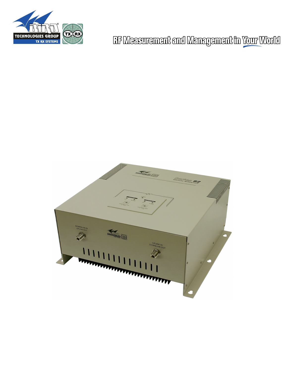
Series 62 Signal Boosters
Manual Part Number
7-9470

Warranty
This warranty applies for one year from shipping date.
TX RX Systems Inc. warrants its products to be free from defect in material and workmanship at the time of shipment.
Our obligation under warranty is limited to replacement or repair, at our option, of any such products that shall have
been defective at the time of manufacture. TX RX Systems Inc. reserves the right to replace with merchandise of
equal performance although not identical in every way to that originally sold. TX RX Systems Inc. is not liable for dam-
age caused by lightning or other natural disasters. No product will be accepted for repair or replacement without our
prior written approval. The purchaser must prepay all shipping charges on returned products. TX RX Systems Inc.
shall in no event be liable for consequential damages, installation costs or expense of any nature resulting from the
purchase or use of products, whether or not they are used in accordance with instructions. This warranty is in lieu of all
other warranties, either expressed or implied, including any implied warranty or merchantability of fitness. No repre-
sentative is authorized to assume for TX RX Systems Inc. any other liability or warranty than set forth above in con-
nection with our products or services.
TERMS AND CONDITIONS OF SALE
PRICES AND TERMS:
Prices are FOB seller’s plant in Angola, NY domestic packaging only, and are subject to change without notice. Fed-
eral, State and local sales or excise taxes are not included in prices. When Net 30 terms are applicable, payment is
due within 30 days of invoice date. All orders are subject to a $100.00 net minimum.
QUOTATIONS:
Only written quotations are valid.
ACCEPTANCE OF ORDERS:
Acceptance of orders is valid only when so acknowledged in writing by the seller.
SHIPPING:
Unless otherwise agreed at the time the order is placed, seller reserves the right to make partial shipments for which
payment shall be made in accordance with seller’s stated terms. Shipments are made with transportation charges col-
lect unless otherwise specified by the buyer. Seller’s best judgement will be used in routing, except that buyer’s routing
is used where practicable. The seller is not responsible for selection of most economical or timeliest routing.
CLAIMS:
All claims for damage or loss in transit must be made promptly by the buyer against the carrier. All claims for shortages
must be made within 30 days after date of shipment of material from the seller’s plant.
SPECIFICATION CHANGES OR MODIFICATIONS:
All designs and specifications of seller’s products are subject to change without notice provided the changes or modifi-
cations do not affect performance.
RETURN MATERIAL:
Product or material may be returned for credit only after written authorization from the seller, as to which seller shall
have sole discretion. In the event of such authorization, credit given shall not exceed 80 percent of the original pur-
chase. In no case will Seller authorize return of material more than 90 days after shipment from Seller’s plant. Credit
for returned material is issued by the Seller only to the original purchaser.
ORDER CANCELLATION OR ALTERATION:
Cancellation or alteration of acknowledged orders by the buyer will be accepted only on terms that protect the seller
against loss.
NON WARRANTY REPAIRS AND RETURN WORK:
Consult seller’s plant for pricing. Buyer must prepay all transportation charges to seller’s plant. Standard shipping pol-
icy set forth above shall apply with respect to return shipment from TX RX Systems Inc. to buyer.
DISCLAIMER
Product part numbering in photographs and drawings is accurate at time of printing. Part number labels on TX RX
products supersede part numbers given within this manual. Information is subject to change without notice.
Bird Technologies Group TX RX Systems Inc.
Symbols Commonly Used
WARNING
ESD Electrostatic Discharge
Hot Surface
Electrical Shock Hazard
Important Information
CAUTION or ATTENTION
High Voltage
Heavy Lifting
Bird Technologies Group TX RX Systems Inc.
NOTE
Manual Part Number 7-9470
Copyright © 2008 TX RX Systems, Inc.
First Printing: February 2009
Version Number Version Date
1 02/14/09
1.1 04/27/09

For Class A Unintentional Radiators
This equipment has been tested and found to comply with the limits for a Class A digital device, pursuant
to Part 15 of the FCC rules. These limits are designed to provide resonable protection against harmful
interference when the equipment is operated in a commercial environment. This equipment generates,
uses, and can radiate radio frequency energy and, if not installed and used in accordance with the instruc-
tion manual, may cause harmful interference to radio communications. Operation of this equipment in a
residential area is likely to cause harmful interference in which the user will be required to correct the inter-
ference at his own expense.
WARNING: Changes or modifications which are not expressly approved by TXRX
Systems Inc. could void the user’s authority to operate the equipment.
ATTENTION: This device complies with Part 15 of the FCC rules. Operation is subject to the
following two conditions: (1) this device may not cause harmful interference and (2) this
device must accept any interference received, including interference that may cause undes-
ired operation.
Table of Contents Manual 7-9470-1.1 04/27/09
Table of Contents
Overview............................................................................................................... 1
Unpacking ............................................................................................................ 3
Block Diagram Description................................................................................. 4
Front-End Module................................................................................................ 4
Power Amplifier Module....................................................................................... 5
Front Panel Module ............................................................................................. 6
Power Entry/Supply ............................................................................................. 7
Connections......................................................................................................... 8
Alarm Conditions.................................................................................................8
Installation............................................................................................................ 9
Location ............................................................................................................. 9
Mounting .......................................................................................................... 10
Antenna Isolation ............................................................................................. 10
Required Equipment ....................................................................................... 10
Measurement Procedure ................................................................................ 10
Installation Procedure ...................................................................................... 11
Operation............................................................................................................11
Variable Step Attenuator ..................................................................................11
OLC (Automatic Level Control) ......................................................................... 12
RF Exposure ...................................................................................................... 12
Diagnostic Guide ...............................................................................................13
Gain Reduction.................................................................................................. 13
Excessive Intermodulation or Spurious ............................................................. 13
Occasional Drop-out of Some channels ............................................................ 13
Optional Sampler Ports ..................................................................................... 13
Figures and Tables
Figure 1A: Front View of the Unit ........................................................................ 2
Figure 1B: Rear View of the Unit ......................................................................... 2
Figure 2: System Interconnect Diagram ............................................................... 4
Figure 3: Front-End Module Block Diagram ......................................................... 5
Figure 4: Power Amplifier Module Block Diagram ................................................ 6
Figure 5: Front Panel Module Block Diagram....................................................... 7
Figure 6: Power Entry/Supply............................................................................... 7
Figure 7: Remote Alarm Sensing Connector ........................................................ 8
Figure 8: Mechanical Dimensions ....................................................................... 9
Figure 9: Measuring Antenna Isolation...............................................................10
Figure 10: Front Panel ........................................................................................ 12
Table 1: Series 62 Models..................................................................................... 1
Table 2: Specifications .......................................................................................... 3

Table of Contents Manual 7-9470-1.1 04/27/09
Contact Information
Changes to this Manual
Bird Technologies Group TX RX Systems Inc.
Sales Support at 716-549-4700 extension 5043
Customer Service at 716-549-4700 extension 5044
Technical Publications at 716-549-4700 extension 5019
We have made every effort to ensure this manual is accurate. If you discover any
errors, or if you have suggestions for improving this manual, please send your
comments to our Angola, New York facility to the attention of the Technical Publications
Department. This manual may be periodically updated. When inquiring about updates to
this manual refer to the manual part number and revision number on the revision page
following the front cover.
TX RX Systems Inc. Manual 7-9470-1.1 04/27/09 Page 1
OVERVIEW
Signal Boosters extend radio coverage into areas
where abrupt RF propagation losses prevent reli-
able communication. No frequency translation
(conversion) occurs with this device. The Series 62
signal booster is a broadband, bi-directional signal
booster that has dual RF paths (uplink and down-
link) to extend coverage in RF shielded environ-
ments. The signal boosters have either a 1 Watt or
10 Watt downlink output level @ 1dB compression
for single band models and either a 2 Watt or 10
Watt downlink output level @ 1 db compression for
dual band models. Table 1 lists all of the models
available as well as their uplink / downlink pass-
bands and downlink output power.
The Series 62 signal booster couples a low noise
figure with a wide dynamic range to provide excel-
lent selectivity for operation in a shared frequency
band. The signal booster is based on a duplexed
Model
Number
Uplink
Band
Downlink
Band
Downlink
Output Power
62-89-A15-01-T3 806 - 821 851 - 866 1 W
62-89-A15-03-T3 806 - 821 851 - 866 10 W
62-90A-A03-01-T3 821 - 824 866 - 869 1 W
62-90A-A03-03-T3 821 - 824 866 - 869 10 W
62-89B-A03-01-T3 806 - 809 851 - 854 1 W
62-89B-A03-03-T3 806 - 809 851 - 854 10 W
62-89A-A18-01-T3 806 - 824 851 - 869 1 W
62-89A-A18-03-T3 806 - 824 851 - 869 10 W
62-88A-A06-01-T3 896 - 902 935 - 941 1 W
62-88A-A06-03-T3 896 - 902 935 - 941 10 W
62-91A-A25-01-T3 824 - 849 869 - 894 1 W
62-91A-A25-03-T3 824 - 849 869 - 894 10 W
62-83E-ADB-02-T3 806 - 824 851 - 869 2 W
62-83E-ADB-04-T3 806 - 824 851 - 869 10 W
62 - 89A - A18 - 03 - T3
(Example)
TYPE
FREQUENCY
BAND
DOWNLINK
OUTPUT
POWERBANDWIDTH
ENCLOSURE
STYLE
62 01 =
02 =
03 =
04 =
1 Watt
2 Watt
10 Watt
10 Watt
A03 =
A06 =
A15 =
A18 =
A25 =
3 MHz
6 MHz
15 MHz
18 MHz
25 MHz
T3 = Painted
83E
88A
89
89A
89B
90A
91A
764 - 869 MHz
896 - 941 MHz
806 - 866 MHz
806 - 869 MHz
806 - 854 MHz
821 - 869 MHz
824 - 894 MHz
=
=
=
=
=
=
=
Table 1 : Series 62 signal booster models.
TX RX Systems Inc. Manual 7-9470-1.1 04/27/09 Page 2
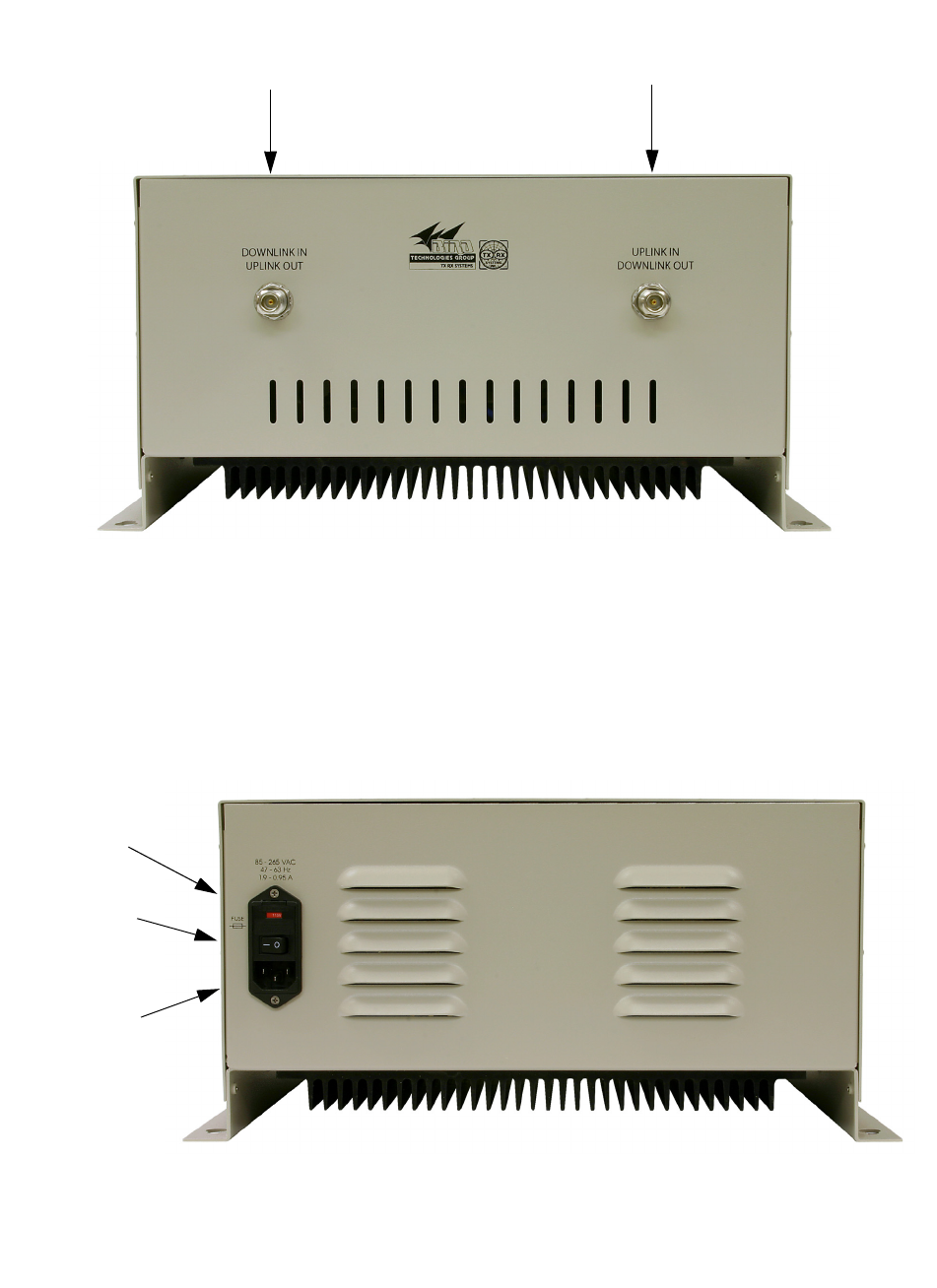
Figure 1A: Front view of the Series 62 signal booster.
Downlink In
Uplink Out
Uplink In
Downlink Out
Figure 1B: Rear view of the Series 62 signal booster.
Fuse
ON / OFF
Switch
AC Cord
Connects
Here

TX RX Systems Inc. Manual 7-9470-1.1 04/27/09 Page 3
path configuration with sharp out of band attenua-
tion assuring isolation between the receiving and
transmitting paths. A front and rear view of the unit
are shown in Figures 1A and 1B respectively.
Electrical, mechanical, and environmental specifi-
cations are listed in Table 2.
UNPACKING
It is important to report any visible damage to the
carrier immediately. It is the customer’s responsi-
bility to file damage claims with the carrier within a
short period of time after delivery (1 to 5 days).
Care should be taken when removing the unit from
the packing box to avoid damage to the unit. Use
caution because the heat sink fins can have some-
what sharp corners.
BLOCK DIAGRAM DESCRIPTION
The Series 62 single-band signal booster is a
broadband, bidirectional, dual branch (uplink and
downlink) system. Linear RF active amplifiers, fil-
ters, and DC power sources are used to ade-
quately boost and re-radiate the passband signals.
Signal flow through the system is illustrated using
the system interconnect diagram shown in Figure
2.
The signal booster system is composed of two
symmetrical branches, uplink and downlink. The
only difference between the two branches is the
tuning of their duplexer passbands. The duplexers
isolate the uplink and downlink paths from each
others allowing common connectors to be used for
Electrical Specifications
Passband Gain 80 dB Min (at max output power)
50 db Min (at min output power)
Manual Attenuation Range 0 to 30 dB in 2 dB steps
Passband Ripple +/- 1.5 dB (typical)
Noise Figure 5 dB Max (at 25°C and max gain)
3rd Order Output Intercept Point Uplink +40 dBm Min
Downlink +52 dBm Min
Input / Output Impedance 50 ohms Nominal
Input / Output VSWR 1.5 : 1.0 (max)
Input Power 80 to 240 VAC at 50 / 60 Hz
Signal Test Ports Optional -50 dB sample signal / additional BNC ports
Alarm Capability Optional Form-C contacts (DB-9 connector)
Mechanical Specifications
Paint Gray Powder-Coat
Dimensions 15.0” x 14.6” x 8.1”
(381 mm x 371 mm x 206 mm)
RF Connectors N-type Female
Weight 30 lBs. (13.63 kg)
Environmental Conditions
This unit is designed for indoor applications
Operating Temperature -30 to +50 °C
Table 2: Series 62 signal booster specifications.
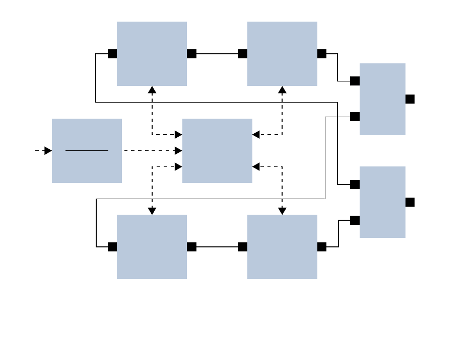
TX RX Systems Inc. Manual 7-9470-1.1 04/27/09 Page 4
both input and output signals. The downlink path
receives RF signals from the base station and
amplifies and transmits them to the subscriber. The
uplink path receives RF signals from the subscriber
and amplifies and transmits them to the base sta-
tion.
FRONT-END MODULE
The block diagram for the Front-End Module is
shown in Figure 3. Received RF signals leave the
duplexer and are routed to the Front-End Module
which provides amplification, variable attenuation,
and filtering. U3 is the first stage of amplification on
the Front-End Module and is an LNA with ultra-low
noise figure and high linearity. Following the first
stage LNA is a Digital Attenuator U4. The positive
control inputs for this device are provided by the
user adjustable rotary dip switch located on the
front panel module. The rotary switch allows the
user to adjust system gain for the uplink and down-
link paths individually during the installation of the
booster.
The next functional device on the front-end module
is the voltage variable attenuator U5. The control
voltage for this attenuator is designated
“VVA_CTL” and its source is the RF Detector cir-
cuit on the power amplifier module. The detector
circuit produces an analog voltage proportional to
the RF signal strength. This is an OLC (Output
Level Control) feedback which is incorporated into
the systems design for output power limiting and to
minimize intermodulation products from exces-
sively strong input signal levels. The OLC circuitry
located on the power amplifier module senses the
output power and automatically limits it by adjust-
ing the variable attenuator U5. An LED located on
the front panel module for both the uplink and
downlink channels will illuminate whenever output
power meets or exceeds the OLC factory preset
level for that channel.
The next amplifier stage U1 following the variable
attenuator is a broadband design that incorporates
low noise as well as high IP3. The output from the
amplifier is passed thru the low pass filter FL1
which provides harmonic rejection. Further amplifi-
UL
Front
End
Module
UL
Power
Amplifier
Module
DL
Front
End
Module
DL
Power
Amplifier
Module
Front
Panel
Module
AC
To
Uplink
Antenna
To
Downlink
Antenna
Duplexer
Duplexer
Power Entry
Power Supply
RF
Out
RF
In
RF
Out
RF
In
RF
Out
RF
In
RF
Out
RF
In
TX
RX
RX
TX
Figure 2: System interconnect diagram.
TX RX Systems Inc. Manual 7-9470-1.1 04/27/09 Page 5
cation and filtering is provided by amplifier U2 and
low pass filter FL2. RF signals then exit the Front-
End module at the RF output connector and are
applied to the Power Amplifier Module.
The front-end module also contains a Temperature
Sensing and Current Sensing circuit, U11 and U8
respectively. These circuits are used to detect an
excessive temperature or current draw condition.
The output from the sensors are fed back to the
Microcontroller on the Front Panel Module and are
used to determine an alarm condition. There are
four voltage regulators on the Front-End Module
(U9, U6, U7, and U10) which are used to create
bias voltages from the 9 VDC source voltage sup-
plied to the module through the ribbon cable.
POWER AMPLIFIER MODULE
The block diagram for the Power Amplifier Module
is shown in Figure 4. The first stage of the Power
Amplifier Module is the driver amplifier U2. This is
a medium power high linearity amplifier which
serves as a preamp for the high power amplifier.
U4 is the final output high power amplifier. This is
an integrated multi-stage power amplifier with on-
chip impedance matching. The output of the power
amplifier is applied to the directional coupler U3
which is used to sample the OLC feedback signal.
RF signals leave the Power Amplifier Module at the
RF output connector and are then applied to a
duplexer which routes the signals to the appropri-
ate antenna.
The power amplifier module also contains a Tem-
perature sensing circuit U1 and two Current sens-
ing circuits U8 and U9 for the driver amplifier and
power amplifier respectively. These circuits are
used to detect an excessive temperature or current
draw condition. The output from the sensors are
fed back to the Microcontroller on the Front Panel
Module and used to determine an alarm condition.
In addition, the temperature sensor and PA current
sensor are used by the on-board Microcontroller
U7 to turn off the power amplifier via the “PA OFF”
control signal. This will protect the power amplifier
under conditions of excessive current draw or tem-
perature. There are two voltage regulators on the
Front-End Module (U10 and U11) which are used
to create bias voltages from the 28 VDC source
voltage supplied to the module through the ribbon
cable. The regulator U10 is the source of the 9
VDC used by the front-end module. A malfunction
Volt Var Atten
Reg
Reg
Temp
Sense
Amp A Amp B Amp C
RF
Atten
U4
Curr
Sense
U5 U1
FL1
U2
FL2
U11
U8
U6
U7
U10
U9
9V
V V A Control
Temp
Curr
5VA
5VB
5VC
3.3V
Atten Control
5VB
RF
IN
5VC
5VA 3.3V
RF
OUT
U3
UL Front End Module 3-22620
Figure 3: Front-End Module block diagram. Uplink shown as an example.
Ribbon Cable to
Front Panel Module
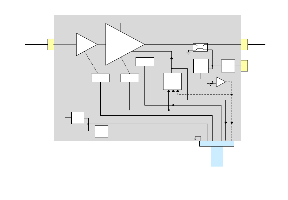
TX RX Systems Inc. Manual 7-9470-1.1 04/27/09 Page 6
of regulator U11 on the power amplifier module will
shut down the front-end module.
FRONT PANEL MODULE
The block diagram for the Front Panel Module is
shown in Figure 5. The Microcontroller U1 moni-
tors the temperature and current control inputs
from the front-end and power amplifier modules
and will respond with an alarm whenever a control
line is active. During an alarm the micro will illumi-
nate the appropriate alarm LED (uplink or down-
link).
The uplink and downlink “VVA_CTL” control signal
is passed through the front panel module via ribbon
cable J1 and J2. The microcontroller monitors
these control lines and illuminates either the uplink
or downlink OLC LED whenever the respective
signal is active. The OLC LED will remain lit while
output leveling is taking place. The Output Level
Control (OLC) allows for output power limiting. A
variable step attenuator gives 0 to 30 dB of attenu-
ation in 2 dB steps. The use of these controls are
covered in the “OPERATION” section, later in this
document.
Voltage regulator U10 is used to create bias volt-
ages from the 9 VDC source voltage supplied to
the module through the ribbon cable. The power
amplifier module is the source of the 9 VDC used
by the front panel module. So a malfunction of reg-
ulator U11 on the power amplifier module will shut
down the front panel module. There are two user
adjustable rotary switches located on the front
panel module, S1 for uplink and S2 for downlink.
The rotary switch allows the user to adjust system
gain for the uplink and downlink paths individually
during the installation of the booster.
POWER ENTRY/SUPPLY
The booster is designed to operate between 80
and 240 VAC. Figure 6 shows the block diagram
for the Power Entry Module as well as the Power
Supply. The power entry module has a dual pole
switch for the incoming AC which is followed by a
pair of inline fuses. When operating the booster at
110 VAC one fuse can be replaced by a jumper.
Operation at 220 VAC will require both fuses to be
used. RF interference is reduced by the EMI filter-
ing. The power supply is a switching design that
will operate at either 110 or 220 VAC and is pro-
grammed by jumpers. There is a green LED on the
RF
IN
RF
OUT
-50dB
Port
PA
U4
9V
5V
-20dB
Directional
Coupler U3
9V
5V Reg
U10
Driver
U2
28V
V V A Control
OLC
Adj
PA Temp
PA Curr
RF
Det
U5
Driver Curr
Temp
Sense
Reg
U11
Curr
Sense
Curr
Sense PIC
U7
PA Off
9V
PA Off
UL Power Amplifier Module 3-22621
30dB
Pad
U1
U8 U9 U6
Figure 4: Power Amplifier Module block diagram. Uplink shown as an example.
Ribbon Cable to
Front Panel Module
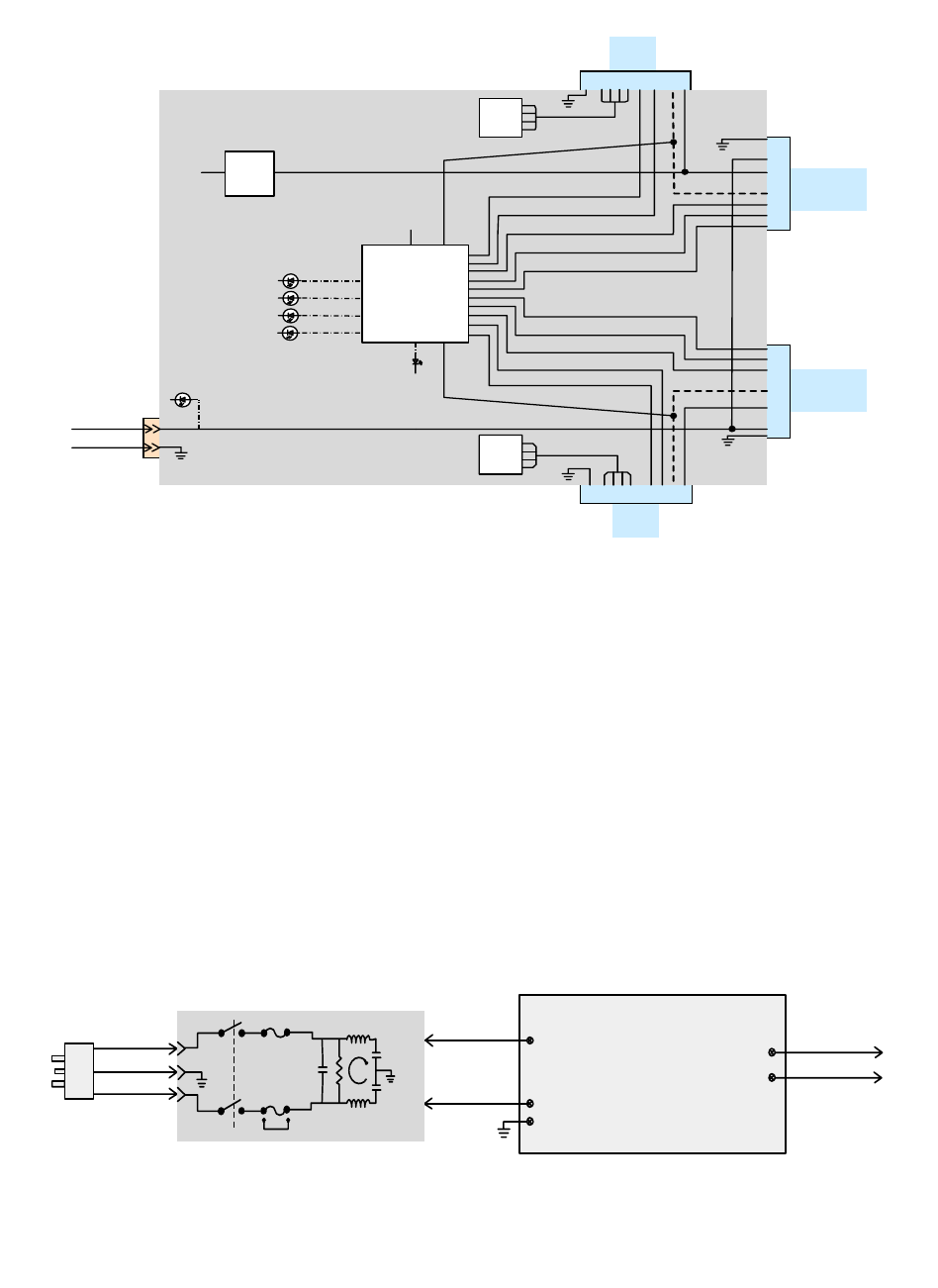
TX RX Systems Inc. Manual 7-9470-1.1 04/27/09 Page 7
supply which is illuminated whenever the supply is
on. The output of the supply is 28 VDC which is
applied to J7 on the front panel module.
CONNECTIONS
AC power is accepted through a standard 3-wire
male plug (IEC-320) with phase, neutral and
ground leads. The AC power is wired to a high effi-
ciency DC switching power supply which is CE and
UL approved. The power supply runs all of the
modules within the cabinet and the Power On LED
on the front panel module. This LED provides an
indication to the user that the system is powered.
The metal enclosure of the signal booster is con-
nected to ground.
RF connections are made via two type “N” female
connectors. The RF connector labeled “Uplink Out
PIC
U1
DIP
SW
DIP
SW
UL
Gain Adj
9V
5V
V V A Crl
DL
Gain Adj
UL Temp
UL Curr
DL Curr
9V
V V A Crl
UL PA Temp
DL PA Temp
UL PA Curr
DL PA Curr
UL Driver Curr
DL Driver Curr
DL Temp
Reg
5V
UL OLC
UL ALM
DL ALM
DL OLC
28V
28V
Pwr
PRG
28VDC
Front Panel Module 3-22636
S1
S2
J1
J2
J4
J5
J7
U10
Figure 5: Front Panel Module block diagram.
To UL
Front-End
To DL
Front-End
To DL
Power Amp
To UL
Power Amp
Switching
Power
Supply
Power Entry Module
80-240VAC 28VDC
80-240VAC EMI Filter
Figure 6: Power Entry / Supply.
To
Front
Panel
Module
TX RX Systems Inc. Manual 7-9470-1.1 04/27/09 Page 8
/ Downlink In” must be connected to the antenna
pointing towards the base station. The RF connec-
tion labeled “Uplink In / Downlink Out” must be
connected to the antenna facing the area to be
covered by the signal booster. RF connections
must be made through cables with characteristic
impedance of 50 ohms.
Isolation between the two antennas should be at
least 15 dB higher than the signal booster gain.
Isolation less than this value can cause gain ripple
across the band. Isolation equal to or less than the
signal booster gain will give rise to oscillations
which will saturate the amplifiers and possibly
cause damage to the signal booster.
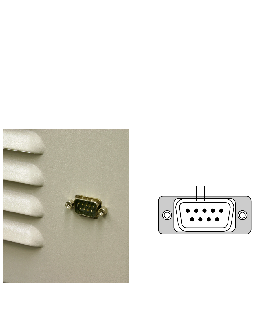
ALARMS CONDITIONS
The alarm circuit monitors the current and temper-
ature of both the Uplink and Downlink amplifiers.
An alarm condition will occur if either the Uplink or
Downlink amplifiers are over or under their current
tolerance. The respective front panel alarm LED
will blink to indicate the alarm condition. An OLC
over-range error which causes the booster to shut
down for 10 minutes will be indicated by a continu-
ousely illuminated alarm LED.
An option is available for the booster that allows
remote alarm sensing through a DB-9 connector
which is added to the back of the unit in the lower
right. Customers should connect their remote
alarm sensing cables to this plug. Refer to Figure
7.
Normally Open, Common, and Normally Closed
relay contacts are available at pins 1, 2, and 3
respectively of the DB9 connector. Refer to the
pinout diagram in figure 7. In a Non-Alarm condi-
tion there will be continuity between the Normally
Open and Common pins. During an Alarm condi-
tion continuity will switch to the Common and Nor-
mally Closed pins.
INSTALLATION
The following sub-sections of the manual discuss
general considerations for installing the booster. All
work should be performed by qualified personnel in
accordance with local codes.
Location
The layout of the signal distribution system will be
the prime factor in determining the mounting loca-
tion of this unit. However safety and serviceability
are also key considerations. The unit should be
located where it can not be tampered with by the
general public, yet is easily accessible to service
personnel. Also, consider the weight of the unit and
the possibility for injury if it should become
detached from its mounting surface for any reason.
987
24135
6
N.O.
COM.
N.C.
GND
+12V(250mA)
Figure 7: Remote alarm sensing connector.
TX RX Systems Inc. Manual 7-9470-1.1 04/27/09 Page 9
The signal booster uses external heat sinks and
needs to be mounted such that there can be unob-
structed air flow over the heat sink fins. The cabi-
net will stay warm during normal operation so in
the interest of equipment longevity, avoid locations
that carry hot exhaust air or are continually hot.
Mounting
Figure 8 shows mounting hole dimensions and
layout for the cabinet. Because TX RX Systems,
Inc. cannot anticipate all the possible mounting
locations and structure types where these devices
will be located, we recommend consulting local
building inspectors, engineering consultants or
architects for advice on how to properly mount
objects of this type, size and weight in your particu-
lar situation. It is the customers responsibility to
make sure these devices are mounted safely and
in compliance with local building codes.
Antenna Isolation
Antenna isolation between uplink and downlink
should be measured before connecting the signal
booster to the antenna system. This step is neces-
GAIN REDUCTION
0 . . . 30 dB
GAIN REDUCTION
0 . . . 30 dB
OLC ALARM OLC
POWER
ALARM
030 2
16
4
6
28
26
20 18
22
24
1214
10
8
030 2
16
4
6
28
26
20 18
22
24
1214
10
8
DOWNLINK IN
UPLINK OUT
UPLINK IN
DOWNLINK OUT
3.062 3.062
14.624
15.437 0.531
0.750
7.250
13.750
15.000
5.201
8.075
Figure 8: Mechanical dimensions.
TX RX Systems Inc. Manual 7-9470-1.1 04/27/09 Page 10
sary to insure that no conditions exist that could
possibly damage the signal booster and should not
be skipped for even the most thoroughly designed
system.
Just like the feedback squeal that can occur when
the microphone and speaker get too close together
in a public address system, a signal booster can
start to self oscillate. This can occur when the iso-
lation between the Uplink and Downlink antennas
does not exceed the signal boosters gain by at
least 15 dB. Oscillation will reduce the effective-
ness of the system and may possibly damage
amplifier stages. Isolation values are relatively
easy to measure with a spectrum analyzer and sig-
nal generator.
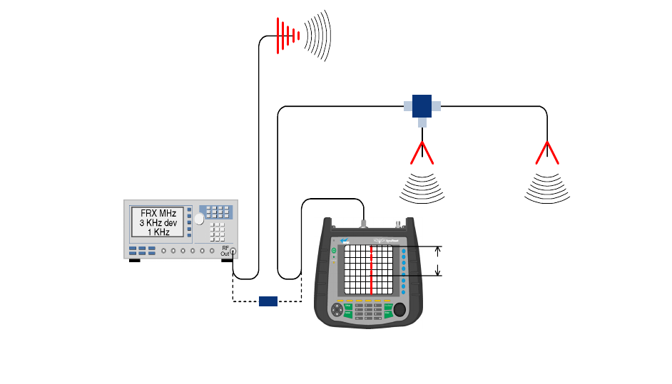
REQUIRED EQUIPMENT
The following equipment is required in order to per-
form the antenna isolation measurements.
1) Signal generator for the frequencies of interest
capable of a 0 dBm output level. Modulation is
not necessary.
2) Spectrum analyzer that covers the frequencies
of interest and is capable of observing signal
levels down to -100 dBm or better.
3) Double shielded coaxial test cables made from
RG142, RG55 or RG223 coaxial cable.
MEASUREMENT PROCEDURE
To measure the antenna isolation perform the fol-
lowing in a step-by-step fashion.
1) Set the signal generator for a 0 dBm output
level at the center frequency of one of the
boosters passbands.
2) Set the spectrum analyzer for the same center
frequency and a sweep width equal to or just
slightly greater than the passband chosen ear-
lier in step 1.
3) Temporarily connect the test leads of the signal
generator and spectrum analyzer together
using a female barrel connector, see Figure 9.
Observe the signal on the analyzer and adjust
the input attenuator of the spectrum analyzer
for a signal level that just reaches the 0 dBm
level at the top of the graticule.
4) Referring to figure 9, connect the generator test
lead to one side of the antenna system and the
spectrum analyzer to the other then observe the
signal level. The difference between this
observed level and 0 dBm is the isolation
between the sections. If the signal is too weak
to observe, the spectrum analyzer’s bandwidth
may have to be narrowed and its input attenua-
tion reduced. The isolation value measured
Signal Generator
External
Antenna
(YAGI)
Spectrum Analyzer
Isolation (dB)
Zero Loss
Reference
Internal
Signal Distribution
System
(Omni-directional
Antennas)
Figure 9: Typical test equipment interconnection for measuring antenna isolation.
TX RX Systems Inc. Manual 7-9470-1.1 04/27/09 Page 11
should exceed the signal booster’s gain fig-
ure by at least 15 dB.
5) Repeat step 4 again with the signal generator
set to frequencies at the passbands edges in
order to see if the isolation is remaining rela-
tively constant over the complete width of the
passband.
6) Repeat the isolation measurements at the other
system passbands to determine the overall min-
imum isolation value for the system. Physical
modification of the antenna system maybe
required in order to reach an acceptable mini-
mum value.
Installation Procedure
To install the signal booster perform the following
in a step-by-step fashion.
CAUTION: DO NOT APPLY A.C.
POWER TO THE SIGNAL
BOOSTER UNTIL CABLES ARE
CONNECTED TO BOTH PORTS OF
THE SIGNAL BOOSTER AND THE
ANTENNAS.
1. Mount the signal booster on the wall with the RF
connectors pointing DOWN. Using appropriate
screws and anchors, attach the signal booster
to the wall at the six mounting holes on the side
flanges. Refer to figure 8.
2. Ensure that the isolation between the donor
antenna and the service antenna is at least 15
dB greater than the signal booster gain. (Use
the higher of the Uplink and Downlink gains
reported on the test data sheet).
3. Connect the cable from the donor antenna to the
signal booster connector labeled “Uplink Out /
Downlink In” and the cable from the service
antennas to the signal booster connector
labeled “Downlink Out / Uplink In”.
4. Review the attenuator positions on the front of
the signal booster and verify that both of the
attenuator’s are positioned to their maximum
setting (30 dB).
5. Connect the AC power cord to the signal booster
and then to the power source. Move the ON/
OFF switch to the ON position and verify that
the “Power ON” LED is illuminated.
Installation of the signal booster is now complete.
To adjust the gain controls to suit the specific sig-
nal environment, refer to the next section of the
manual.
For repeat installations of existing
equipment, make sure the attenuation
setting is positioned to its maximum
setting (30 dB). After verification of
the attenuation, follow the above
steps starting with step 1.
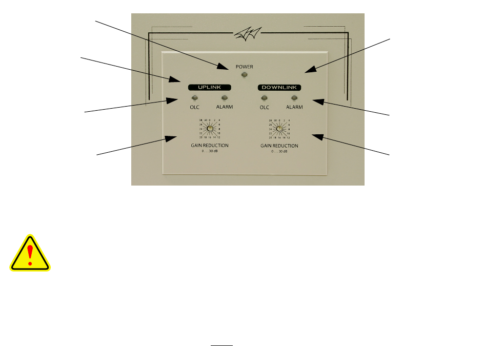
OPERATION
Power is applied to the unit by turning ON the AC
power switch located on the upper rear of the cabi-
net. The front panel Power Indicator LED should
illuminate. Refer to Figure 10 which is a view of the
front panel.
Variable Step Attenuator
The signal booster gain can be reduced by up to
30 dB in 2 dB steps using the variable step attenu-
ator. Gain adjustments are made with rotary
switches on the front of the unit. The attenuators
are labeled for Uplink and Downlink. Arrows on the
shafts of these switches point to the value of atten-
uation selected. Gain can be determined by sub-
tracting the attenuation value from the gain
reported on the Test Data Sheet for that side of the
unit. A small screwdriver should be used for mak-
ing attenuator adjustments.
OLC (Output Level Control)
To minimize intermodulation products, each
branch in the signal booster contains an OLC feed-
back loop. The OLC circuit senses the output
power and limits it to a factory preset level on the
Uplink and the Downlink.
Red indicator LEDs located on the front panel for
both the uplink and downlink will illuminate when
output power meets or exceeds the OLC factory
preset level.
To establish proper operating gain on the Uplink
and Downlink sides, start with the Downlink.
Observe the downlink OLC indicator LED. Units
are shipped with maximum attenuation. Decrease
the downlink variable attenuator one step at a time
until the downlink OLC lamp is lit. Then increase
the step attenuation until the lamp goes off. Repeat
the process for the Uplink. The OLC indicator LED
is accurate to within +/- 0.4 dB of the OLC factory
preset level.
NOTE
TX RX Systems Inc. Manual 7-9470-1.1 04/27/09 Page 12
CAUTION: Operation of the signal
booster at maximum gain with
greater than -20 dBm average power
incident on either of the RF Input
connectors can cause damage to the
signal booster.
RF EXPOSURE
In order to satisfy the FCC RF exposure require-
ments, the signal booster/antenna installation must
comply with the following:
The outdoor antenna (Yagi type or similar direc-
tional antenna) must be installed so as to provide a
minimum separation distance of 1.0 Meters (100
cm or 40 inches) between the antenna and per-
sons within the area. (This assumes a typical
antenna with gain of 10.1 dBi, VSWR < or = 1.5 : 1,
Zo= 50 ohms, and a cable attenuation of between
1-10 dB).
The indoor antenna (omni directional) must be
installed so as to provide a minimum separation
distance of 0.4 Meters (40 cm or 16 inches)
between the antenna and persons within the area.
(This assumes a typical wide-beam type antenna
with gain of 0-2 dBi, VSWR < or = 2 : 1, Zo= 50
ohms, and a cable attenuation of between 1-10
dB).
DIAGNOSTIC GUIDE
The signal booster provides long term, care-free
operation and requires no periodic maintenance.
There are no user-serviceable components inside
the signal booster. This section covers possible
problems that may be related to the installation or
operating environment.
Gain Reduction
Possible causes: bad RF cables, bad RF connec-
tions to antennas or damaged antennas.
Excessive Intermodulation or Spurious
Possible causes: Amplifier oscillation caused by
insufficient isolation. The isolation between two
antennas is given by the equation:
Isolation = 92.5 + 20 Log (F x D) – Gt – Gr
F = frequency (GHz)
Gt = transmit antenna gain (in the direction of the
receive antenna)
D = separation (Km)
Gr = receive antenna gain (in the direction of the
transmit antenna)
For example, at the SMR frequencies, the antenna
isolation at 100 m separation is about 71 dB for
omni-directional antennas (0 dB gain). To increase
isolation, the antennas should have higher directiv-
ity and must be pointed away from each other.
Occasional Drop-out of Some Channels
Possible causes: One channel with very strong
power dominates the RF output of the amplifier.
Optional Sampler Ports
An option is available for the booster that brings
the -50 db sampler ports on the power amplifier
assembly out to the side panel near the RF con-
nectors. This option provides a convenience for
technicians installing or servicing the signal
booster.
Figure 10: The Front Panel.
Power ON
LED
Uplink
Alarm
Rotary
Attenuator
Downlink
Alarm
Downlink
OLC
Uplink
OLC
Rotary
Attenuator

TX RX Systems Inc. Manual 7-9470-1.1 04/27/09 Page 13
Return Loss vs. VSWR
Return Loss VSWR
30 1.06
25 1.11
20 1.20
19 1.25
18 1.28
17 1.33
16 1.37
15 1.43
14 1.50
13 1.57
12 1.67
11 1.78
10 1.92
92.10
Watts to dBm
Watts dBm
300 54.8
250 54.0
200 53.0
150 51.8
100 50.0
75 48.8
50 47.0
25 44.0
20 43.0
15 41.8
10 40.0
537.0
436.0
334.8
233.0
130.0
dBm = 10log P/1mW
Where P = power (Watt)
Insertion Loss
Input Power (Watts)
50 75 100 125 150 200 250 300
325 38 50 63 75 100 125 150
2.5 28 42 56 70 84 112 141 169
232 47 63 79 95 126 158 189
1.5 35 53 71 88 106 142 177 212
140 60 79 99 119 159 199 238
.5 45 67 89 111 134 178 223 267
Output Power (Watts)
Insertion Loss
Free Space Loss
Distance (miles)
.25 .50 .75 1 2 5 10 15
150 68 74 78 80 86 94 100 104
220 71 77 81 83 89 97 103 107
460 78 84 87 90 96 104 110 113
860 83 89 93 95 101 109 115 119
940 84 90 94 96 102 110 116 120
1920 90 96 100 102 108 116 122 126
Free Space Loss (dB)
Free space loss = 36.6 + 20log D + 20log F
Where D = distance in miles and F = frequency in MHz
Frequency (MHz)

TX RX Systems Inc. Manual 7-9470-1.1 04/27/09 Page 14
TX RX Systems Inc. 8625 Industrial Parkway, Angola, NY 14006 Tel: 716-549-4700 Fax: 716-549-4772 sales@txrx.com www.txrx.com
SYSTEMS
INC.
SYSTEMS
INC.