Broadcom BRCM1067 802.11 abgn WLAN+Bluetooth Card User Manual
Broadcom Corporation 802.11 abgn WLAN+Bluetooth Card
UserManual.wiki
>
Broadcom
>
BRCM1067 User Manual
>
User Manual
Contents
1.
User Manual
2.
Users Manual Host
3.
Users Manual Module
4.
USERS MANUAL HOST
5.
USERS MANUAL MODULE
6.
Users Manual
7.
INP-110Q User Manual
User Manual
Navigation menu
Upload a User Manual
Namespaces
Wiki Guide
HTML
PDF
Info
Views
User Manual
Discussion / Help
Navigation
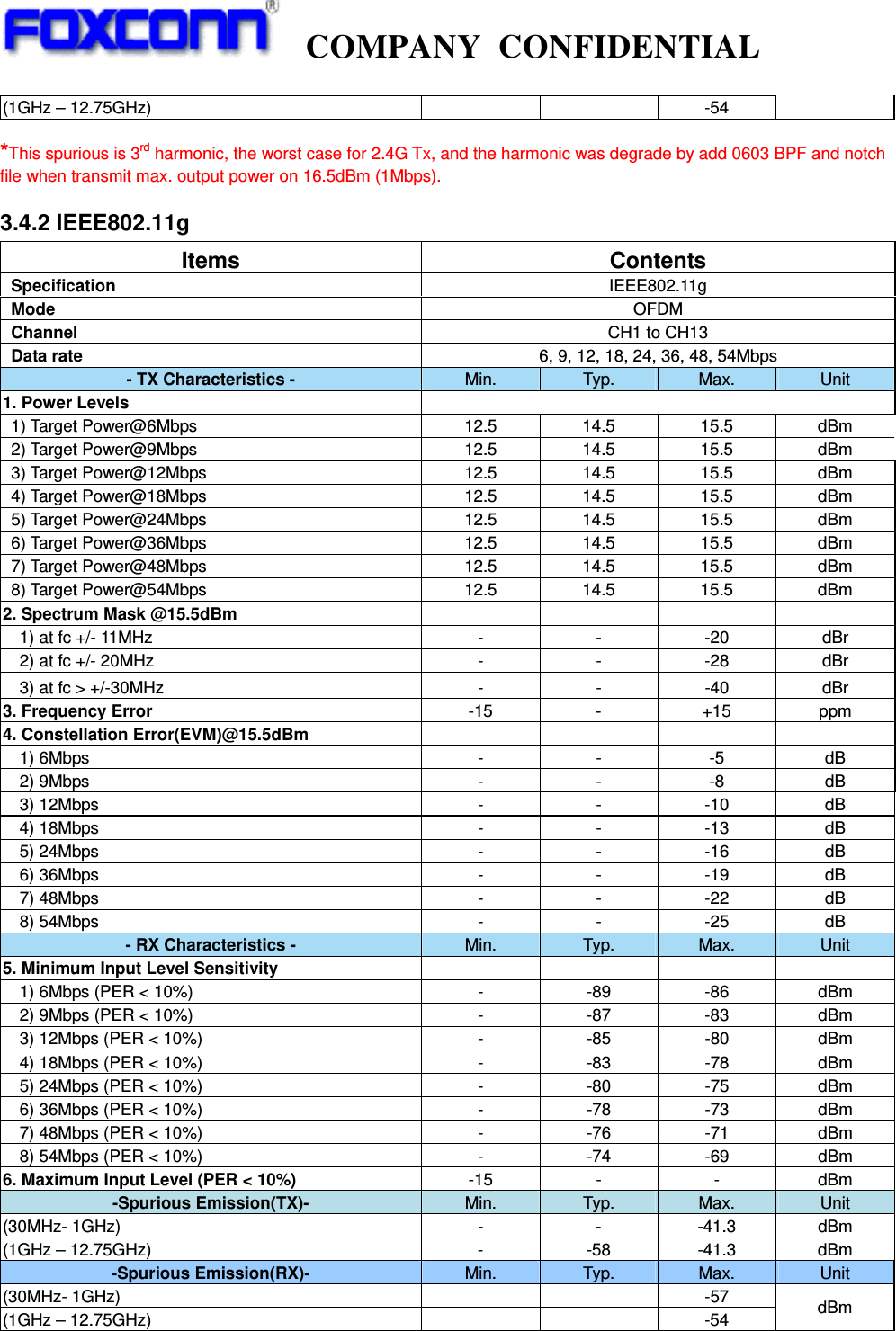
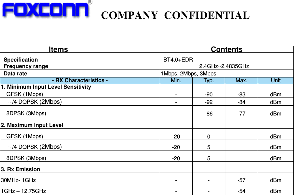
![COMPANY CONFIDENTIAL Enhanced data rate 3Mbps: 8DPSK Items Contents Specification BT4.0+EDR Frequency range 2.4GHz~2.4835GHz Data rate 1Mbps, 2Mbps, 3Mbps - TX Characteristics - Min. Typ. Max. Unit 1. Power Levels BT Output Power 4 7 10 dBm 2. Initial Carrier Frequency Tolerance Average Offset -75 6 75 kHz 3. Carrier Drift Drift Rate DH1 -20 3 20 kHz/50us DH3 -20 -3 20 kHz/50us DH5 -20 0 20 kHz/50us Average Drift DH1 -25 -1 25 kHz DH3 -40 0 40 kHz DH5 -40 0 40 kHz 4. Modulation Characteristic F1avg 140 153 175 kHz F2max 115 133 kHz F1/F2 Ratio 0.8 0.93 5. EDR Relative Transmit Power 2Mbps: P[DQPSK]-P[GFSK] -4 0.25 1 dB 3Mbps: P[8DPSK]-P[GFSK] -4 0.25 1 dB 6. EDR Carrier Frequency Stability and Modulation Accuracy 2Mbps: π/4 DQPSK Initial Frequency Error: ωi -75 5 75 kHz Frequency Error: ω0 -10 1 10 kHz Block Frequency Error: ωi + ω0 -75 6 75 kHz RMS DEVM - - 0.2 Peak DEVM - - 0.35 99% DEVM (% Symbols <=0.3) 99% 100% 3Mbps: 8DPSK Initial Frequency Error: ωi -75 6 75 kHz Frequency Error: ω0 -10 0.9 10 kHz Block Frequency Error: ωi + ω0 -75 6.3 75 kHz RMS DEVM - - 0.13 Peak DEVM - - 0.25 99% DEVM (% Symbols <=0.13) 99% 100% 7. Tx Spurious Emission 30MHz- 1GHz - - -41.3 dBm 1GHz – 12.75GHz - -51 -41.3 dBm](https://usermanual.wiki/Broadcom/BRCM1067.User-Manual/User-Guide-1756201-Page-12.png)