Broadcom BRCM1067 802.11 abgn WLAN+Bluetooth Card User Manual
Broadcom Corporation 802.11 abgn WLAN+Bluetooth Card
Broadcom >
Contents
User Manual

COMPANY CONFIDENTIAL
BCM4330 WLAN+BT Combo Module
(Foxconn T77H360.00)
Product Specification
Rev 1.9
Prepared by Reviewed by Approved by
Gallon Tao Robin-Xu Chang-Fu Lin

COMPANY CONFIDENTIAL
Index
1. REVISION HISTORY...................................................................................................................................................3
2. INTRODUCTION ..........................................................................................................................................................4
2.1 SCOPE ......................................................................................................................................................................4
2.2 FUNCTION.................................................................................................................................................................4
3. PRODUCT SPECIFICATION .....................................................................................................................................5
3.1 HARDWARE CHARACTERISTIC .................................................................................................................................5
3.2 HARDWARE ARCHITECTURE ....................................................................................................................................5
3.3 ELECTRICAL SPECIFICATION ....................................................................................................................................6
3.4 WLAN RF CHARACTERISTICS ................................................................................................................................7
3.4.1 IEEE802.11b..................................................................................................................................................7
3.4.2 IEEE802.11g..................................................................................................................................................8
3.4.3 IEEE802.11n HT20(2.4GHz) .......................................................................................................................9
3.4.4 IEEE802.11a ................................................................................................................................................10
3.4.5 IEEE802.11n HT20 (5GHz) .......................................................................................................................11
3.5 BLUETOOTH STANDARD SPECIFICATIONS .............................................................................................................11
3.6 LGA PIN DEFINITION .............................................................................................................................................14
4. MECHANICAL DRAWING .......................................................................................................................................16
5. PERIPHERAL SCHEMATIC REFERENCE DESIGN ..........................................................................................18
6. PCB LAYOUT.............................................................................................................................................................19
7. SOFTWARE REQUIREMENT .................................................................................................................................19
8. REGULATORY...........................................................................................................................................................19
9. ENVIRONMENTAL REQUIREMENTS AND SPECIFICATIONS.......................................................................19
9.1 TEMPERATURE .......................................................................................................................................................19
9.2 PCB BENDING ........................................................................................................................................................19
9.3 HANDLING ENVIRONMENT.......................................................................................................................................20
9.4 STORAGE CONDITION.............................................................................................................................................20
9.5 BAKING CONDITION ................................................................................................................................................20
9.6 SOLDERING AND REFLOW CONDITION....................................................................................................................20

COMPANY CONFIDENTIAL
1. Revision History
Date Change Note REV
Note
2011-10-12 Initial release 1.0
2011-10-13 Update module mechanical 2D drawing in section 5 1.1
2011-11-25
1. Update product specification
2. Add description for 5G enable and disable
3. FM is optional in this product.
1.2
2011-11-30
1. Update product specification to add product IDs
2. Add mother board and test jig reference schematic
3. Update Environmental Requirements and Specifications:
1) Add handling environment;
2) Add baking condition;
3) Add soldering and reflow condition
1.3
2011-12-14
1. Update mother board and test jig reference design schematic:
Add remark on the schematic.
1.4
2011-12-26 1. Update section 3: product specification 1.5
2012-02-11
1. Update section 3.3, Current consumption
2. Update section 3.4, 11bg Tx emission result for EVT3 modules
3. Update section 3.5, complete Bluetooth specification
4. Update section 4, module mechanical drawing since shielding
cover changed.
1.6
2012-03-16
1. Update section 3.4 for 2.4GHz TX emission for EVT4 modules
2. Update section 3.4 for add RX emission
3. Update section 3.4 for 11a/11an target power for middle and
high band
4. Update section 3.4 for 11a/11an power limit
1.7
2012-03-17
1. Update 5GHz LO leakage level and RX SEN
2. Update module dimension
3. Update module block-diagram
4. Update section 4 for mechanical drawing
1.8
2012-03-17
1. Update 5GHz LO leakage level and RX SEN
2. Update module dimension
3. Update module block-diagram
4. Update section 4 for mechanical drawing
1.8

COMPANY CONFIDENTIAL
2. Introduction
Project Name: 802.11abgn (1X1) + BT4.0 combo module
This documentation describes the product specification of the WLAN+BT combo Module. WLAN is Compliant
with IEEE Std. 802.11b-1999, IEEE Std. 802.11g-2003 and IEEE Std. 802.11n-2009, Bluetooth is compliant
with Bluetooth 4.0+HS. It is a confidential document of Foxconn.
* For b/g/n and a/b/g/n module, Foxconn HW/FW are the same, platform use different firmware and
driver to enable or disable 5GHz
2.1 Scope
This combo Module combines WLAN, Bluetooth in one module, the WLAN is available in the 2.4GHz
and 5GHz band, it is compatible with the IEEE 802.11 a/b/g standard and the 802.11n standard. It allow
user to switch to different vendors’ Access Points through the wireless networks and to prevent from
eavesdropping. The 802.11 a/g data rate provides for 54, 48, 36, 24, 18, 12, 9, 6Mbps, 802.11b data
rate provides for 11, 5.5, 2, 1 Mbps, it can also support 11n high data rate up to MCS7(HT20) with PHY
data rate to 72Mbps. Bluetooth is compliant to Core Specification version 4.0
2.2 Function
Single stream 802.11n support for 20MHz channels provide PHY layer rates up to 72Mbps.
Bluetooth supports Class 1.5 and Class 2 output power.
Provides a small form factor solution and ultra low power consumption to support low cost requirement.
Host interface supports:
WLAN: SDIO;
BT data: UART
BT digital audio: PCM
COMPANY CONFIDENTIAL
3. Product Specification
3.1 Hardware Characteristic
Form factor 14mmx13mm LGA
Host Interface WLAN: SDIO
BT: UART for data, PCM for Audio
FM: UART for data, I2S for Audio
PCB 6-layer HDI design
RF connector Two MHF RF connectors
3.2 Hardware Architecture
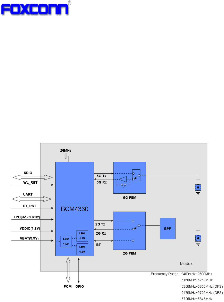
The WLAN+BT combo module is designed base on BROADCOM BCM4330 chip, the Broadcom
BCM4330 is a highly integrated single chip solution for single stream dual-band WLAN and BT4.0, use
two RF connector for 2.4GHz and 5GHz RF each, use a chip BPF for 2.4GHz and external LNA for
5GHz, a 26MHz crystal is used for reference clock generation, see the block diagram as below:
COMPANY CONFIDENTIAL
3.3 Electrical Specification
Absolute Maximum Ratings
These specification indicate levels where permanent damage to the device can occur. Functional
operation is not guaranteed under these conditions. Operation at absolute maximum conditions for
extended can adversely affect long-term reliability of the device.
Recommended Operating Condition
Value
Element Symbol
Minimum Typical Maximum
Unit
DC supply voltage for the device VBAT_3.
3V
2.3 3.3 4.8 V
VDDIO for WL_VDDIO and BT_VDDIO VIO_1.8V 1.2 1.8 2.9 V
Function operation is not guaranteed outside this limit, and operation outside this limit for extended
periods can adversely affect long-term reliability of the device.
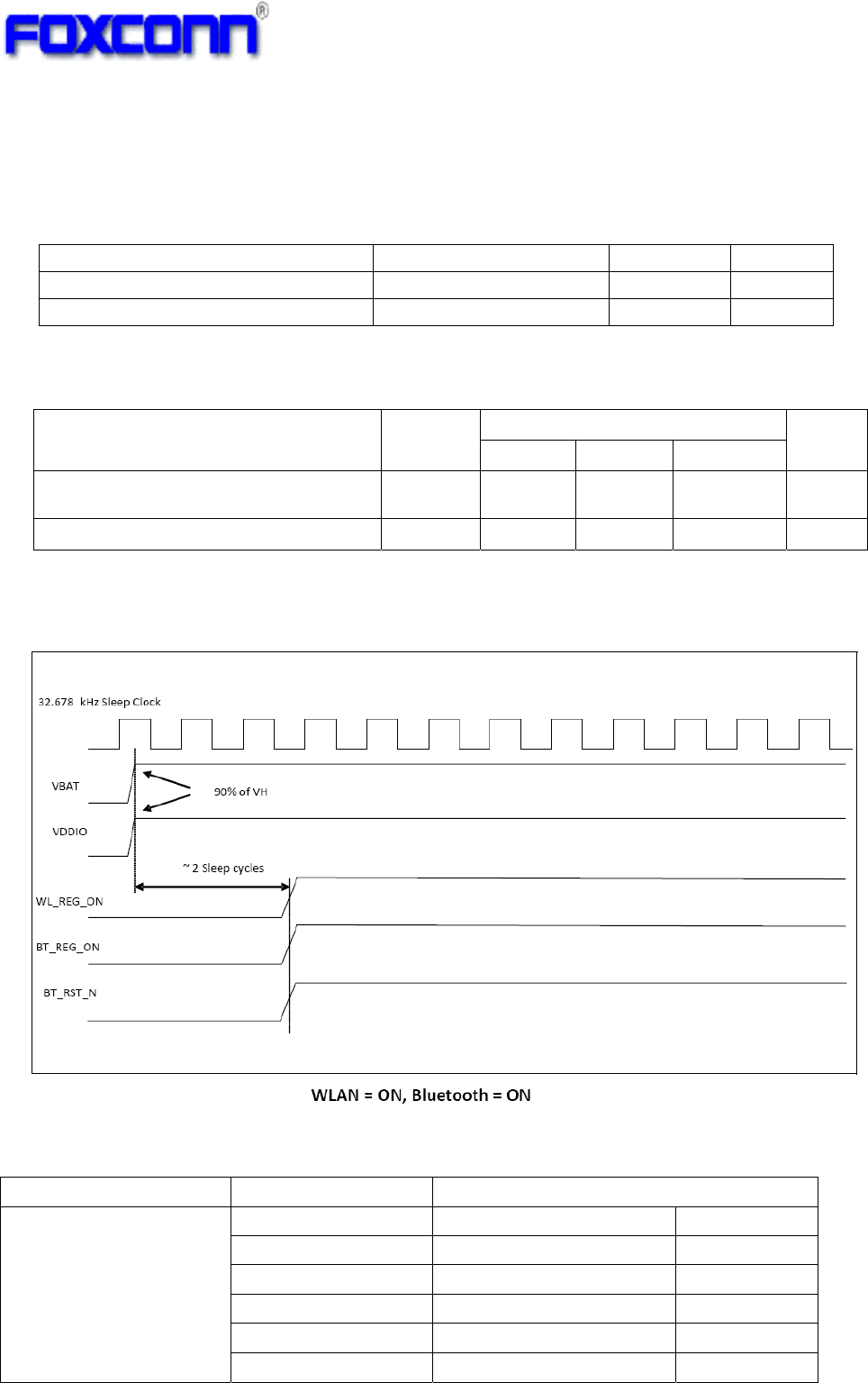
Power-Up Sequence Timing
Current Consumption
Typical Current@3.3V
WLAN:
Mode Tx Rx
11b@15.5dBm 180mA 105mA
11g @14.5dBm 150mA 100mA
11n(2.4G)@13.5dBm 160mA 100mA
Active
Rating Symbol Value Unit
DC supply voltage for the device VBAT_3.3V -0.5 to +6.0 V
VDDIO VIO -0.5 to 2.98 V
COMPANY CONFIDENTIAL
11a @13dBm 200mA 135mA
11n(5G) @12dBm 220mA 138mA
BT:
26mA @0dBm(CLASS II)
48mA @7dBm(CLASS1.5) 22mA
WiFi&BT Idle
(RF on,
WiFi no association;
BT no inquiry,
scan/page scan) 40mA
WiFi Associated with AP;
BT Idle 90mA
Product ID Definition
Vendor ID: 0x14e4
Device ID: 0x4360
3.4 WLAN RF Characteristics
3.4.1 IEEE802.11b
Items Contents
Specification IEEE802.11b
Mode DSSS / CCK
Channel CH1 to CH13,CH14
Data rate 1, 2, 5.5, 11Mbps
-TX Characteristics- Min. Typ. Max. Unit
1. Power Levels
Target Power 13.5 15.5 16.5 dBm
2. Spectrum Mask @16.5dBm (Max.)
1) fc-33MHz < f < fc-22MHz - - -50 dBr
2) fc-22MHz < f < fc-11MHz - - -30 dBr
3) fc+11MHz < f < fc+22MHz - - -30 dBr
4) fc+22MHz < f < fc+33MHz - - -50 dBr
3. Frequency Error -15 - +15 ppm
4 Modulation Accuracy(EVM)@16.5dBm (Max.)
1) 1Mbps - -10 dB
2) 2Mbps - -10 dB
3) 5.5Mbps - -10 dB
4) 11Mbps - -10 dB
-RX Characteristics- Min. Typ. Max. Unit
5. Minimum Input Level Sensitivity
1) 11Mbps (FER≦8%) - -86 -82 dBm
6. ≦
Maximum Input Level (FER 8%)
1) 1,2Mbps (FER≦8%) -4 - dBm
2) 5.5,11Mbps (FER≦8%) -10 - dBm
-Spurious Emission(TX)- Min. Typ. Max. Unit
(30MHz- 1GHz) - - -41.3
(1GHz – 12.75GHz) - -46.5 * -41.3 dBm
-Spurious Emission(RX)- Min. Typ. Max. Unit
(30MHz- 1GHz) -57 dBm

COMPANY CONFIDENTIAL
(1GHz – 12.75GHz) -54
*This spurious is 3rd harmonic, the worst case for 2.4G Tx, and the harmonic was degrade by add 0603 BPF and notch
file when transmit max. output power on 16.5dBm (1Mbps).
3.4.2 IEEE802.11g
Items Contents
Specification IEEE802.11g
Mode OFDM
Channel CH1 to CH13
Data rate 6, 9, 12, 18, 24, 36, 48, 54Mbps
- TX Characteristics - Min. Typ. Max. Unit
1. Power Levels
1) Target Power@6Mbps
12.5 14.5 15.5 dBm
2) Target Power@9Mbps
12.5 14.5 15.5 dBm
3) Target Power@12Mbps
12.5 14.5 15.5 dBm
4) Target Power@18Mbps
12.5 14.5 15.5 dBm
5) Target Power@24Mbps
12.5 14.5 15.5 dBm
6) Target Power@36Mbps
12.5 14.5 15.5 dBm
7) Target Power@48Mbps
12.5 14.5 15.5 dBm
8) Target Power@54Mbps
12.5 14.5 15.5 dBm
2. Spectrum Mask @15.5dBm
1) at fc +/- 11MHz - - -20 dBr
2) at fc +/- 20MHz - - -28 dBr
3) at fc > +/-30MHz - - -40 dBr
3. Frequency Error -15 - +15 ppm
4. Constellation Error(EVM)@15.5dBm
1) 6Mbps - - -5 dB
2) 9Mbps - - -8 dB
3) 12Mbps - - -10 dB
4) 18Mbps - - -13 dB
5) 24Mbps - - -16 dB
6) 36Mbps - - -19 dB
7) 48Mbps - - -22 dB
8) 54Mbps - - -25 dB
- RX Characteristics - Min. Typ. Max. Unit
5. Minimum Input Level Sensitivity
1) 6Mbps (PER < 10%) - -89 -86 dBm
2) 9Mbps (PER < 10%) - -87 -83 dBm
3) 12Mbps (PER < 10%) - -85 -80 dBm
4) 18Mbps (PER < 10%) - -83 -78 dBm
5) 24Mbps (PER < 10%) - -80 -75 dBm
6) 36Mbps (PER < 10%) - -78 -73 dBm
7) 48Mbps (PER < 10%) - -76 -71 dBm
8) 54Mbps (PER < 10%) - -74 -69 dBm
6. Maximum Input Level (PER < 10%) -15 - - dBm
-Spurious Emission(TX)- Min. Typ. Max. Unit
(30MHz- 1GHz) - - -41.3 dBm
(1GHz – 12.75GHz) - -58 -41.3 dBm
-Spurious Emission(RX)- Min. Typ. Max. Unit
(30MHz- 1GHz) -57
(1GHz – 12.75GHz) -54 dBm

COMPANY CONFIDENTIAL
3.4.3 IEEE802.11n HT20(2.4GHz)
-Spurious Emission(RX)- Min. Typ. Max. Unit
(30MHz- 1GHz) -57
(1GHz – 12.75GHz) -54 dBm
Items Contents
Specification IEEE802.11n HT20
Mode OFDM
Channel CH1 to CH13
Data rate (MCS index) MCS0~MCS7
- TX Characteristics - Min. Typ. Max. Unit
1. PowerLevels
1) Target Power@MCS0
11.5 13.5 14.5 dBm
2) Target Power@ MCS1
11.5 13.5 14.5 dBm
3) Target Power@ MCS2
11.5 13.5 14.5 dBm
4) Target Power@ MCS3
11.5 13.5 14.5 dBm
5) Target Power@ MCS4
11.5 13.5 14.5 dBm
6) Target Power@ MCS5
11.5 13.5 14.5 dBm
7) Target Power@ MCS6
11.5 13.5 14.5 dBm
8) Target Power@ MCS7
11.5 13.5 14.5 dBm
2. Spectrum Mask @14.5dBm
1) at fc +/- 11MHz - - -20 dBr
2) at fc +/- 20MHz - - -28 dBr
3) at fc > +/-30MHz - - -45 dBr
3. Frequency Error -15 - +15 ppm
4. Constellation Error(EVM)@14.5dBm
1) MCS0 - -
-5 dB
2) MCS1 - -
-10 dB
3) MCS2 - -
-13 dB
4) MCS3 - -
-16 dB
5) MCS4 - -
-19 dB
6) MCS5 - -
-22 dB
7) MCS6 - -
-25 dB
8) MCS7 - -
-28 dB
- RX Characteristics - Min. Typ. Max. Unit
5. Minimum Input Level Sensitivity
1) MCS0 (PER < 10%) - -88 -84 dBm
2) MCS1 (PER < 10%) - -85 -81 dBm
3) MCS2 (PER < 10%) - -83 -79 dBm
4) MCS3 (PER < 10%) - -80 -76 dBm
5) MCS4 (PER < 10%) - -78 -74 dBm
6) MCS5 (PER < 10%) - -76 -72 dBm
7) MCS6 (PER < 10%) - -74 -70 dBm
8) MCS7 (PER < 10%) - -71 -67 dBm
6. Maximum Input Level (PER < 10%) -15 - - dBm
-Spurious Emission(TX)- Min. Typ. Max. Unit
FCC(30MHz- 1GHz) - - -41.3
FCC Average(1GHz – 12.75GHz) - -60 -41.3 dBm
COMPANY CONFIDENTIAL
3.4.4 IEEE802.11a
Items Contents
Specification IEEE802.11a
Mode OFDM
Channel
lower band:5.15GHz~5.35GHz
middle band:5.500GHz~5.700GHz
upper band:5.745GHz~5.825GHz
Data rate 6, 9, 12, 18, 24, 36, 48, 54Mbps
- TX Characteristics - Min. Typ. Max. Unit
1. Power Levels
Low Band(5.15GHz~5.35GHz) 11 13 14 dBm
Middle Band(5.500GHz~5.700GHz) 11 13 14 dBm
Upper Band(5.745GHz~5.825GHz) 11 13 14 dBm
2. Spectrum Mask @ Type power@14dBm
1) at fc +/- 11MHz - - -20 dBr
2) at fc +/- 20MHz - - -28 dBr
3) at fc > +/-30MHz - - -40 dBr
3. Frequency Error -15 - +15 ppm
4. Constellation Error(EVM)@ Type power@14dBm
1) 6Mbps - - -5 dB
2) 9Mbps - - -8 dB
3) 12Mbps - - -10 dB
4) 18Mbps - - -13 dB
5) 24Mbps - - -16 dB
6) 36Mbps - - -19 dB
7) 48Mbps - - -22 dB
8) 54Mbps - - -25 dB
- RX Characteristics - Min. Typ. Max. Unit
5. Minimum Input Level Sensitivity
1) 6Mbps (PER < 10%) - -91 -87 dBm
2) 9Mbps (PER < 10%) - -89 -85 dBm
3) 12Mbps (PER < 10%) - -87 -83 dBm
4) 18Mbps (PER < 10%) - -85 -81 dBm
5) 24Mbps (PER < 10%) - -82 -78 dBm
6) 36Mbps (PER < 10%) - -80 -76 dBm
7) 48Mbps (PER < 10%) - -78 -74 dBm
8) 54Mbps (PER < 10%) - -76 -72 dBm
6. Maximum Input Level (PER < 10%) -15 - - dBm
-Spurious Emission(TX)- Min. Typ. Max. Unit
FCC(30MHz- 1GHz) - - -41.3 dBm
FCC Average(1GHz – 12.75GHz) - - -41.3 dBm
-Spurious Emission(RX)- Min. Typ. Max. Unit
(30MHz- 1GHz) -57
(1GHz – 12.75GHz)* -58 -54 dBm
* the LO leakage is decreased to under -54dBm since adding eLNA, can meet KCC regulatory limit.

COMPANY CONFIDENTIAL
3.4.5 IEEE802.11n HT20 (5GHz)
7) MCS6 (PER < 10%) - -75 -71 dBm
8) MCS7 (PER < 10%) - -73 -69 dBm
6. Maximum Input Level (PER < 10%) -20 - - dBm
-Spurious Emission(TX)- Min. Typ. Max. Unit
FCC(30MHz- 1GHz) - - -41.3 dBm
FCC Average(1GHz – 12.75GHz) - - -41.3 dBm
-Spurious Emission(RX)- Min. Typ. Max. Unit
(30MHz- 1GHz) -57
(1GHz – 12.75GHz)* -58 -54 dBm
* the LO leakage is decreased to under -54dBm since adding eLNA, can meet KCC regulatory limit.
3.5 Bluetooth Standard Specifications
Bluetooth Core Specification version 4.0:
Host interface: UART, baud rates up to 4Mbps
Support all Bluetooth 4.0+HS packet types.
Operating frequency range: 2400MHz ~2483.5MHz
Modulation type:
Basic rate 1Mbps: GFSK,
Enhanced data rate 2Mbps: DQPSK
Items Contents
Specification IEEE802.11n HT20
Mode OFDM
Channel
lower band:5.15GHz~5.35GHz
middle band:5.500GHz~5.700GHz
upper band:5.745GHz~5.825GHz
Data rate (MCS index) MCS0~MCS7
- TX Characteristics - Min. Typ. Max. Unit
1. Power Levels
Low Band(5.15GHz~5.35GHz) 10 12 13 dBm
Middle Band(5.500GHz~5.700GHz) 10 12 13 dBm
Upper Band(5.745GHz~5.825GHz) 10 12 13 dBm
2. Spectrum Mask @Type power@13dBm
1) at fc +/- 11MHz - - -20 dBr
2) at fc +/- 20MHz - - -28 dBr
3) at fc > +/-30MHz - - -45 dBr
3. Frequency Error -15 - +15 ppm
4. Constellation Error(EVM)@Type power@13dBm
1) MCS0 - -
-5 dB
2) MCS1 - -
-10 dB
3) MCS2 - -
-13 dB
4) MCS3 - -
-16 dB
5) MCS4 - -
-19 dB
6) MCS5 - -
-22 dB
7) MCS6 - -
-25 dB
8) MCS7 - -
-28 dB
- RX Characteristics - Min. Typ. Max. Unit
5. Minimum Input Level Sensitivity
1) MCS0 (PER < 10%) - -91 -87 dBm
2) MCS1 (PER < 10%) - -88 -84 dBm
3) MCS2 (PER < 10%) - -85 -81 dBm
4) MCS3 (PER < 10%) - -82 -78 dBm
5) MCS4 (PER < 10%) - -79 -75 dBm
6) MCS5 (PER < 10%) - -77 -73 dBm

COMPANY CONFIDENTIAL
Enhanced data rate 3Mbps: 8DPSK
Items Contents
Specification BT4.0+EDR
Frequency range 2.4GHz~2.4835GHz
Data rate 1Mbps, 2Mbps, 3Mbps
- TX Characteristics - Min. Typ. Max. Unit
1. Power Levels
BT Output Power 4 7 10 dBm
2. Initial Carrier Frequency Tolerance
Average Offset -75 6 75 kHz
3. Carrier Drift
Drift Rate
DH1 -20 3 20 kHz/50us
DH3 -20 -3 20 kHz/50us
DH5 -20 0 20 kHz/50us
Average Drift
DH1 -25 -1 25 kHz
DH3 -40 0 40
kHz
DH5 -40 0 40
kHz
4. Modulation Characteristic
F1avg 140 153 175 kHz
F2max 115 133 kHz
F1/F2 Ratio 0.8 0.93
5. EDR Relative Transmit Power
2Mbps: P[DQPSK]-P[GFSK] -4 0.25 1 dB
3Mbps: P[8DPSK]-P[GFSK] -4 0.25 1 dB
6. EDR Carrier Frequency Stability and Modulation Accuracy
2Mbps: π/4 DQPSK
Initial Frequency Error: ωi -75 5 75
kHz
Frequency Error: ω0 -10 1 10
kHz
Block Frequency Error: ωi + ω0 -75 6 75
kHz
RMS DEVM - - 0.2
Peak DEVM - - 0.35
99% DEVM (% Symbols <=0.3) 99% 100%
3Mbps: 8DPSK
Initial Frequency Error: ωi -75 6 75
kHz
Frequency Error: ω0 -10 0.9 10 kHz
Block Frequency Error: ωi + ω0 -75 6.3 75
kHz
RMS DEVM - - 0.13
Peak DEVM - - 0.25
99% DEVM (% Symbols <=0.13) 99% 100%
7. Tx Spurious Emission
30MHz- 1GHz - - -41.3 dBm
1GHz – 12.75GHz - -51 -41.3 dBm

COMPANY CONFIDENTIAL
Items Contents
Specification BT4.0+EDR
Frequency range 2.4GHz~2.4835GHz
Data rate 1Mbps, 2Mbps, 3Mbps
- RX Characteristics - Min. Typ. Max. Unit
1. Minimum Input Level Sensitivity
GFSK (1Mbps) - -90 -83 dBm
π/4 DQPSK (2Mbps) - -92 -84 dBm
8DPSK (3Mbps) - -86 -77 dBm
2. Maximum Input Level
GFSK (1Mbps) -20 0 dBm
π/4 DQPSK (2Mbps) -20 5 dBm
8DPSK (3Mbps) -20 5 dBm
3. Rx Emission
30MHz- 1GHz - - -57 dBm
1GHz – 12.75GHz - - -54 dBm
COMPANY CONFIDENTIAL
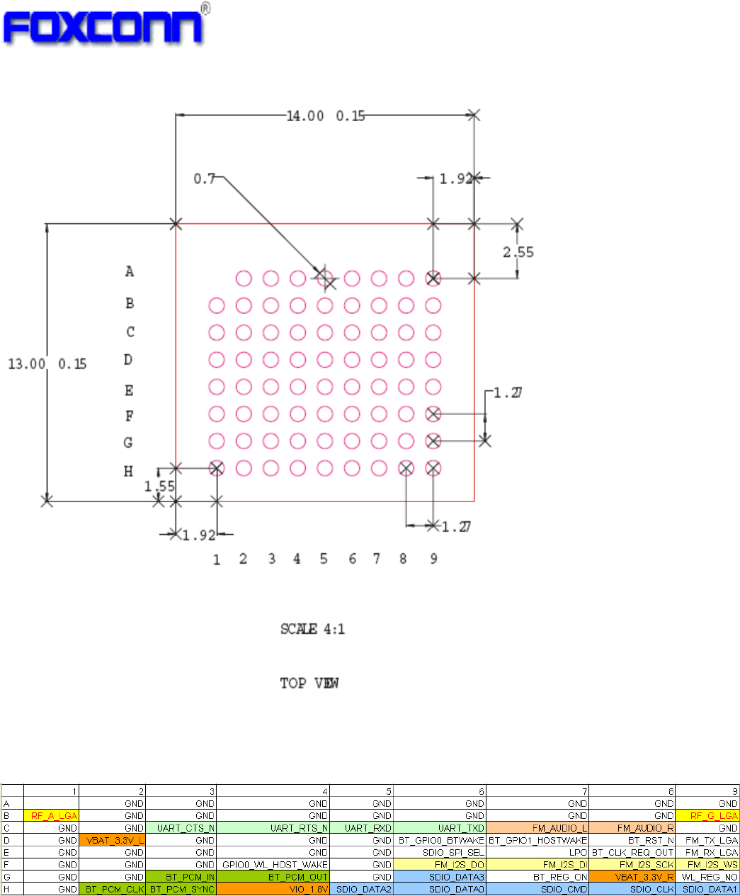
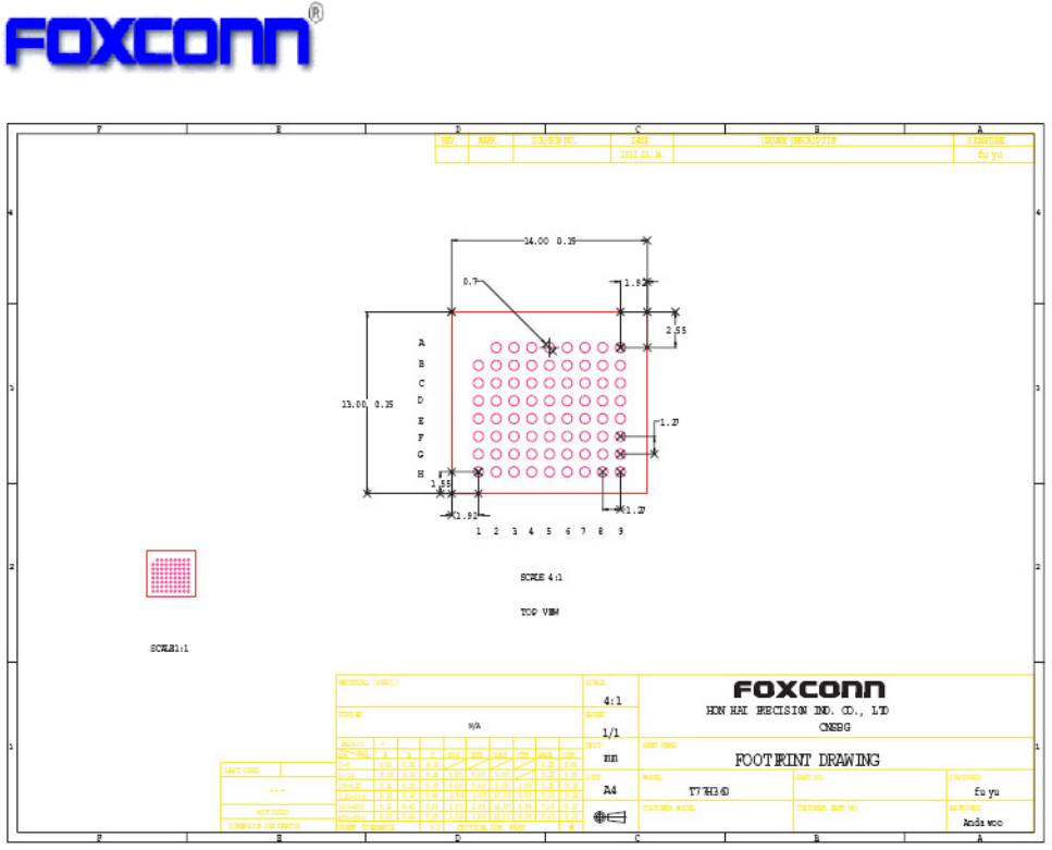
3.6 LGA Pin Definition
TOP View

COMPANY CONFIDENTIAL
Pin
No.
Pin Name Type Description
B1 RF_A_LGA I/O 5GHz RF pin (WLAN 5GHz Tx/Rx)
B9 RF_G_LGA I/O 2.4GHz RF pin (for WLAN2.4GHz Tx/Rx and BT Tx/Rx)
C3 UART_CTS_N I UART clear to Send, active low (for BT data)
C4 UART_RTS_N O UART request to Send, active low (for BT data)
C5 UART_RXD I UART signal input
C6 UART_TXD O UART signal output
C7 FM_AUDIO_L O FM analog audio output channel L (Not used)
C8 FM_AUDIO_R O FM analog audio output channel R (Not used)
D2 VBAT_3.3V_L I Main power supply for the module, (3.3V+/-10%, together with pin
G8 to supply the module), please consider reserve for 300mA
current consumption, need place a 4.7uF decoupling CAP close to
this pin on main board.
G8 VBAT_3.3V_R I Main power supply for the module, (3.3V+/-10%, together with pin
D2 to supply the module ), please consider reserve for 300mA
current consumption, need place a 4.7uF decoupling CAP close to
this pin on main board.
D6 BT_GPIO0_BTWAKE I BT wake up, signal from the host to module to require BT device
wake-up or remain awake
D7 BT_GPIO1_HOSTWAKE O Signal from module to host to require Host wake up
D8 BT_RST_N I External reset for BT, active low, please pull-up on host side (not left
floating)
D9 FM_TX_LGA O FM Radio output (Not used)
E9 FM_RX_LGA I FM Radio input (Not used)
E6 SDIO_SPI_SEL I Host interface mode selection, internal pull down, work with
SDIO_DATA_1 and SDIO_DATA_2 together to select the host
interface
E7 LPO I 32.768kHz LPO clock, need for device auto frequency detection
E8 BT_CLK_REQ_OUT O BT/WLAN reference clock request out, active high, need an
external 100kohm pull-down resistor to ensure the signal is
deasserted when BCM43330 powers up.
F4 GPIO0_WL_HOST_WAKE O Signal from WLAN device to awake the host.
F6 FM_I2S_DO I/O I2S data output
F7 FM_I2S_DI I/O I2S data input
F8 FM_I2S_SCK I I2S reference clock
F9 FM_I2S_WS I/O I2S word select
G3 BT_PCM_IN I/O PCM data input
COMPANY CONFIDENTIAL
G4 BT_PCM_OUT I/O PCM data output
H2 BT_PCM_CLK I PCM Clock
H3 BT_PCM_SYNC I/O PCM sync signal
G6 SDIO_DATA3 I/O SDIO data line 3
H5 SDIO_DATA2 I/O SDIO data line 2
H6 SDIO_DATA0 I/O SDIO data line 0
H7 SDIO_CMD I/O SDIO command line
H8 SDIO_CLK I SDIO clock
G7 BT_REG_ON I Power up or power down BCM4330 internal regulators used for BT,
Logic high level: 1.08V~3.6V
Need pull-up via a 10Kohm resistor or less (internal 200K
pull-down)
G9 WL_REG_ON I Power up or power down BCm4330 internal regulators used for
WLAN, this pin is also a low active reset for WLAN only (not for BT)
Logic high level: 1.08V~3.6V
Need pull-up via a 10Kohm resistor or less (inertnal 200K
pull-down)
H4 VIO_1.8V I VDDIO for BCM4330 I/O supply, range from 1.2V~2.9V, select 1.8V
here, please consider reserve for 100mA current consumption
A2,A3,A4,A5,A6,
A7,A8,A9,B2,B3,
B4,B5,B6,B7,B8,
C1,C2,C9,D1,D3
,D4,D5,E1,E2,E3
,E4,E5,F1,F2,F3,
F5,G1,G2,G5,H1
GND Ground
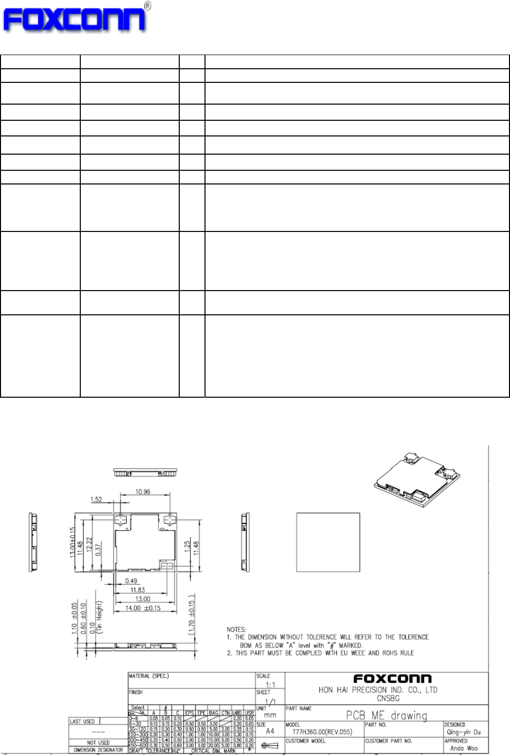
4. Mechanical Drawing
* The on board RF connector and plug mating height would be 1.2mm max.
COMPANY CONFIDENTIAL
* The holes represent the LGA pins on bottom side of the module.
COMPANY CONFIDENTIAL
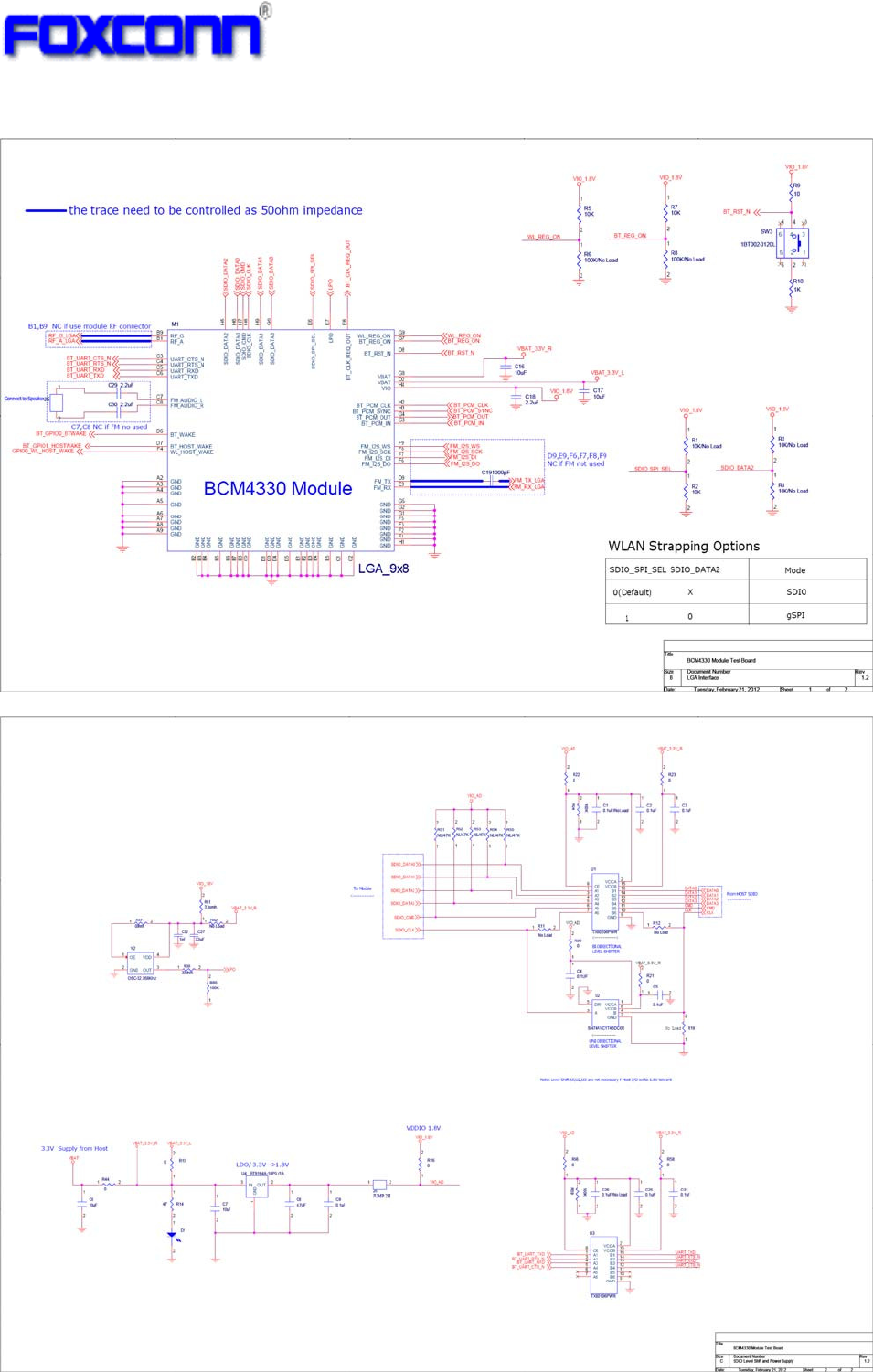
5. Peripheral Schematic Reference Design
COMPANY CONFIDENTIAL
6. PCB Layout
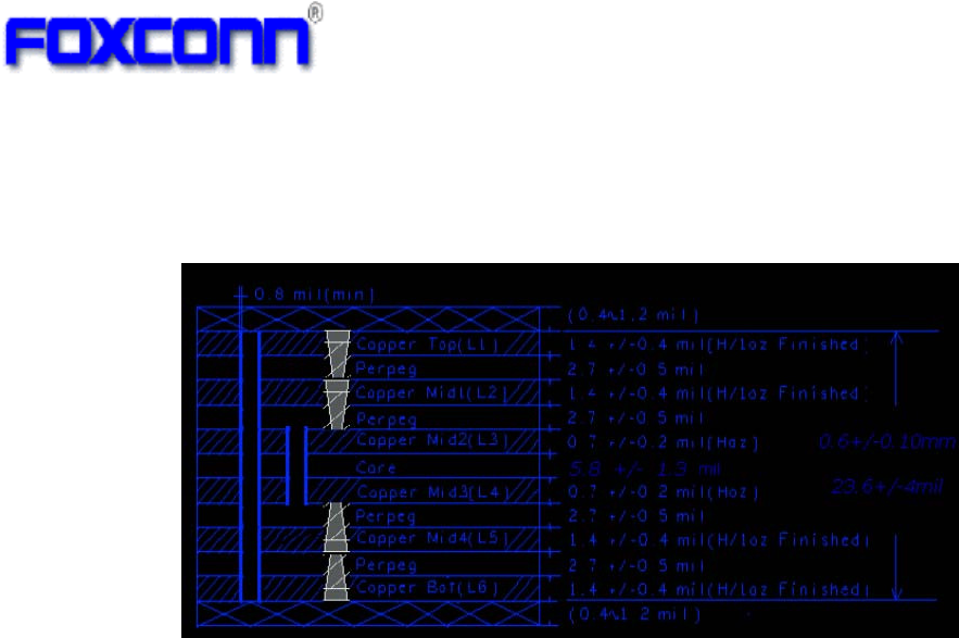
6-layer, 2 order HDI FR-4 (Halogen Free) design, total thickness 0.6+/-0.1mm
Stack-up
7. Software Requirement
Nvram file for RF parameters configuration.
If use dual-band WLAN, platform need to load dual-band firmware and install dual-band driver.
If use single-band WLAN, platform need to load single-band firmware and install single-band driver.
8. Regulatory
TBD
9. Environmental Requirements and Specifications
9.1 Temperature
9.1.1 Operating Temperature Conditions
The product shall be capable of continuous reliable operation when operating in ambient temperature of
0 to +℃70 .℃
9.1.2 Non-Operating Temperature Conditions
Neither subassemblies shall be damaged nor shall the operational performance be degraded when
restored to the operating temperature when exposed to storage temperature in the range of -10 t℃o +85 .℃
9.2 PCB bending
The PCB bending spec shall be keep planeness under 0.1mm for both Foxconn and end assembly
customer.

COMPANY CONFIDENTIAL
9.3 Handling environment
9.3.1. ESD
The product ESD immunity is HBM>= +/- 450 (V), MM >= +/- 100 (V). Please handle it under ESD protection
environment.
Note: HBM: Human Body Model/MM: Mechanical Model
This device is ESD sensitive device, it must be protected at all times from ESD, industry-standard ESD
precautions should be used at all times.
9.3.2. Terminals
The product is mounted with motherboard through Land Grid Array. In order to prevent poor soldering,
please do not touch LGA portion by hand.
9.3.3. Falling
It will cause damage on the mounted components when the product is falling or receiving drop shock. It may
cause the product mal-function.
9.4 Storage Condition
9.4.1 Moisture barrier bag before opened
Moisture barrier bag must be stored under 30 degree C, humidity under 85% RH. The calculated shelf life for
the dry packed product shall be a 12 months from the bag seal date.
9.4.2. Moisture barrier bag open
Humidity indicator cards must be blue, <30%.
9.5 Baking Condition
Products require baking before mounting if
a) humidity indicator cards reads >30%
b) temp <30 degree C, humidity < 70% RH, over 96 hours
Baking condition: 90 degree C, 12-22 hours
Baking times: 1 time
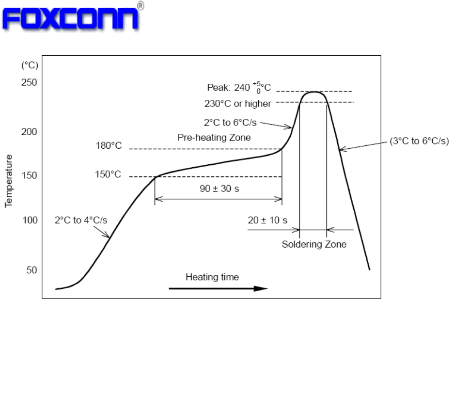
9.6 Soldering and reflow condition
1) Heating method
Conventional Convection or IR/convection
2) Temperature measurement
Thermocouple d=0.1mm ~ 0.2mm CA (K) or CC (T) at soldering portion or equivalent method.
3) Solder paste composition
Sn/3.0Ag/0.5Cu
4) Allowable reflow soldering times: 2 times based on the below reflow soldering profile
5) Temperature profile
Reflow soldering shall be done according to the below temperature profile.
6) Peak temp: 245 degree C
COMPANY CONFIDENTIAL
Temperature profile for evaluation of solder heat resistance of a
component (at solder joint)