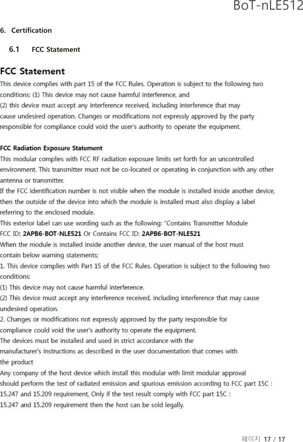
CHIPSEN BOT-NLE521 BLE Module User Manual BoT nLE512

CHIPSEN. Co., Ltd BLE Module BoT nLE512

User Manual

 페이지 1 / 17  BoT-nLE521 Ver 1.0  2018/03/06
 페이지 2 / 17  BoT-nLE521 List of Contents  1. General ............................................................................................................................................. 3 1.1  Overview ...................................................................................................................................................................3 1.2  Block Diagram ........................................................................................................................................................3 1.3  Features .....................................................................................................................................................................4 1.4  Application ...............................................................................................................................................................4 1.5  Pin Configuration ..................................................................................................................................................5 1.6  PIN Description ......................................................................................................................................................6 1.7  Dimensions ..............................................................................................................................................................7 1.8  Land Pattern ............................................................................................................................................................8 2. Characteristics ................................................................................................................................ 9 2.1  Electrical Characteristics .....................................................................................................................................9 2.2  RF Characteristics ............................................................................................................................................... 11 3.1  Regulator ............................................................................................................................................................... 12 3.2  32.768KHz Crystal Oscillator .......................................................................................................................... 13 4. Application Schematic ............................................................................................................... 15 5. Antenna ......................................................................................................................................... 16 5.1  Antenna Layout Guide ..................................................................................................................................... 16 6. Certification .................................................................................................................................. 17 6.1  FCC Statement ..................................................................................................................................................... 17
 페이지 3 / 17  BoT-nLE521 1. General   1.1 Overview The  BoT-nLE521  module  is  a  cost-effective,  low-power,  true  system-on-chip  (SoC)  for Bluetooth Smart (Bluetooth low energy) applications. It enables robust BLE master or slave nodes  to  be  built  with  very  low  total  bill-of-material  costs.  BoT-nLE521  combines  an excellent  RF  transceiver  with  an  industry-standard  enhanced  Cortec-M4  CPU,  in-system programmable flash memory,  24kB RAM,  and many other powerful  supporting  features and peripherals. The BoT-nLE521 is suitable for systems where very low power Consumption is required. Very low-power sleep modes are available. Short transition times between operating modes further enable low power consumption.    1.2 Block Diagram FilterRadioMultiprotocol2.4GHzBalunProcessor64 MHz ARMCortex-M4 CPU192kB Flash with cache24kB RAMAHB Lite busAPB busTimers / CountersAnalog I/ODigital I/OSystem PeripheralsOscillators PowersupplyGPIO32 MHzCrystalInternal Antenna&Matching NetworkPIO SWDCLKSWDIODCCDEC4VDDRFINT_ANT BoT-nLE521 Block Diagram
 페이지 4 / 17  BoT-nLE521 1.3 Features ■  Built in Antenna Bluetooth Smart (Bluetooth Low Energy) Module. ■ ARM® Cortex®-M4 32-bit processor with FPU, 64 MHz ■  Memory: 192 kB Flash / 24 kB RAM ■  RF Output Power: MAX +4 dBm (-20 ~ 4 dBm) ■  RF Receive Sensitivity: -96 dBm ■  Type 2 near field communication (NFC-A) tag with wakeup-on-field and touch to-pair capabilities ■ Fully automatic LDO and DC/DC regulator system (Used LDO by Default) ■  Temperature Sensor ■  UART (CTS/RTS) with EasyDMA, SPI, and I2C data interfaces. ■ 12-Bit 200 ksps ADC with - 8 configurable channels with programmable gain   ■  Size: 15 mm x 8 mm x 1.8 mm ■  Operating Voltage: 1.7V to 3.6V ■  Operating Temperature: -40 to +85℃ ■  RoHS compliant  1.4 Application ■·  Computer peripherals and I/O devices  ·  Mouse  · Keyboard  · Multi-touch trackpad ·■  Interactive entertainment devices  ·■ Remote control  ·  Gaming controller ·■ Beacons ·■ Personal Area Networks  ·  Health/fitness sensor and monitor devices  · Medical devices  · Key-fobs + wrist watches ■·  Remote control toys
 페이지 5 / 17  BoT-nLE521 1.5 Pin Configuration         112123456789101613 17 1918 203029282726252423222131323314 151    GND    GND    GND    GND    P0.28/AIN4    P0.25    P0.30/AIN6    DCC    DEC4    VDD_nRFSWDIOGNDGNDSWDCLKP0.20P0.21/RESETP0.18P0.15P0.16P0.14    GND    P0.00/XL1    P0.01/XL2    P0.04/AIN2    P0.05/AIN3    P0.06    P0.09    P0.10    P0.12    GND    ANT     RFGND   TOP VIEW
 페이지 6 / 17  BoT-nLE521 1.6 PIN Description Pin No. Pin Name Pin Function Description 01 GND GROUND Ground Pin. 02 GND GROUND Ground Pin. 03 GND GROUND Ground Pin. 04 GND GROUND Ground Pin. 05 P0.25 DIGITAL I/O General purpose I/O pin. 06 P0.28 DIGITAL I/O General purpose I/O pin. AIN4 ANALOG INPUT SAADC/COMP input 07 P0.30 DIGITAL I/O General purpose I/O pin. AIN6 ANALOG INPUT COMP input 08 DEC4 POWER 1.3 V regulator supply decoupling Input from DC/DC converter. Output from 1.3 V LDO 09 DCC POWER DC/DC regulator output 10 VDD_nRF POWER Power supply pin. 11 GND GROUND Ground Pin. 12 P0.00 DIGITAL I/O General purpose I/O pin. XL1 ANALOG INPUT Connection for 32.768 kHz crystal (LFXO) 13 P0.01 DIGITAL I/O General purpose I/O pin. XL2 ANALOG INPUT Connection for 32.768 kHz crystal (LFXO) 14 P0.04 DIGITAL I/O General purpose I/O pin. AIN2 ANALOG INPUT SAADC/COMP input 15 P0.05 DIGITAL I/O General purpose I/O pin. AIN3 ANALOG INPUT SAADC/COMP input 16 P0.06 DIGITAL I/O General purpose I/O pin. RXD DIGITAL INPUT UART RXD 17 P0.09 DIGITAL I/O General purpose I/O pin. TXD DIGITAL OUTPUT UART TXD 18 P0.10 DIGITAL I/O General purpose I/O pin. CTS DIGITAL OUTPUT UART CTS 19 P0.12 DIGITAL I/O General purpose I/O pin. RTS DIGITAL INPUT UART RTS 20 GND GROUND Ground Pin. 21 P0.14 DIGITAL I/O General purpose I/O pin. 22 P0.15 DIGITAL I/O General purpose I/O pin. 23 P0.16 DIGITAL I/O General purpose I/O pin. 24 P0.18 DIGITAL I/O General purpose I/O pin. 25 P0.20 DIGITAL I/O General purpose I/O pin. 26 P0.21 DIGITAL I/O General purpose I/O pin. RESET nRESET Configurable as system RESET pin. 27 SWDCLK DIGITAL INPUT Serial Wire Debug clock input for debug and programming 28 SWDIO DIGITAL I/O Serial Wire Debug I/O for debug and programming 29 GND GROUND Ground Pin. 30 GND GROUND Ground Pin. 31 RF RF IN / OUT PORT Bluetooth 50Ω transmitter output / receiver input 32 ANT INTERNAL ANTENNA IN / OUT Internal antenna. It should be connected to Pin 32 RF for normal operation. 33 GND GROUND Ground Pin.
 페이지 7 / 17  BoT-nLE521 1.7 Dimensions  112128.0mm4.03456789100.81613 17 1918 203029282726252423222131320.80.3511.7mm333.450.63.0 3.00.80.60.5 0.814 150.350.3 0.3 0.3 0.30.8250.50.43.3mm0.8 0.510.50.50.50.50.52.02.00.20.2015.0mm0.3 TOP VIEW
 페이지 8 / 17  BoT-nLE521 2124.034567890.81613 17 1918 203029282726252423222131320.811.7mm3.450.43.0 3.00.80.40.5 0.814 150.350.3 0.3 0.3 0.30.8250.500.43.3mm0.8 0.510.50.70.50.91.2332.02.00.20.28.0mm15.0mm0.30.35100.31.2110.36.24.00.31.8 Land Pattern                     Land Pattern (TOP VIEW)
 페이지 9 / 17  BoT-nLE521 2. Characteristics 2.1 Electrical Characteristics   Absolute Maximum Ratings Symbol Parameter Min. Max. Units VDD  -0.3 +3.9 V GND   0 V VI/O, VDD≤3.6V  -0.3 VDD + 0.3 V VI/O, VDD >3.6V  -0.3 +3.9 V Storage temperature  -40 +125 °C  Radio ra   RF Input Level  10 dBm MSL Moisture Sensitivity Level 2  ESD HBM Human Body Model  4 kV ESD CDM Charged Device Model  1000 V Endurance Flash Memory Endurance 10000  write/erase cycles Retention Flash Memory Retention 10 years  At 40 °C    Recommended Operating Conditions Symbol Parameter Min. Typ. Max. Units VDD LDO Regulator Operation (Default Mode) 1.7 3.0 3.6 V VDD DC/DC Regulator Oprtation 2.1 3.0 3.6 V tR_VDD Supply rise time (0V to 1.7V)   60 ms TA Operation temperature -40 25 85 °C    DC Characteristics Symbol Parameter (condition) Min. Typ. Max. Units VIH Input high voltage 0.7 X VDD  VDD V VIL Input low voltage VSS  0.3 X VDD V VOH,SD Output high voltage, standard drive, 0.5 mA, VDD ≥1.7 VDD-0.4  VDD V VOH,HDH Output high voltage, high drive, 5 mA, VDD ≥ 2.7 V VDD-0.4  VDD V VOH,HDL Output high voltage, high drive, 3 mA, VDD ≥ 1.7 V VDD-0.4  VDD V VOL,SD Output low voltage, standard drive, 0.5 mA, VDD ≥1.7 VSS  VSS +0.4 V VOL,HDH Output low voltage, high drive, 5 mA, VDD ≥ 2.7 V VSS  VSS +0.4 V
 페이지 10 / 17  BoT-nLE521 VOL,HDL Output low voltage, high drive, 3 mA, VDD ≥ 1.7 V VSS  VSS +0.4 V RPU Pull-up resistance 11 13 16 kΩ RPD Pull-down resistance 11 13 16 kΩ ITX,+4dBm,DCDC TX only run current (DCDC, 3V) PRF=+4 dBm  7.0  mA ITX,+4dBm TX only run current PRF=+4 dBm  15.4  mA IRX,1M,DCDC RX only run current (DCDC, 3V) 1Msps    4.6  mA IRX,1M RX only run current 1Msps    10.0  mA IRX,2M,DCDC RX only run current (DCDC, 3V) 2Msps    5.2  mA IRX,2M RX only run current 2Msps    11.2  mA ION_RAMOFF_EVENT System ON, No RAM retention, Wake on any event  0.6  μA ION_RAMON_EVENT System ON, Full 24 kB RAM retention, Wake on any event  0.8  μA ION_RAMON_POF System ON, Full 24 kB RAM retention, Wake on any event, Power fail comparator enabled  0.8  μA ION_RAMON_GPIOTE System ON, Full 24 kB RAM retention, Wake on GPIOTE input (Event mode)  3.3  μA ION_RAMON_GPIOTEPORT System ON, Full 24 kB RAM retention, Wake on GPIOTE PORT event  0.8  μA ION_RAMON_RTC System ON, Full 24 kB RAM retention, Wake on RTC (running from LFRC clock)  1.5  μA IOFF_RAMOFF_RESET System OFF, No RAM retention, Wake on reset  0.3  μA IOFF_RAMON_RESET System OFF, Full 24 kB RAM retention, Wake on reset  0.5  μA
 페이지 11 / 17  BoT-nLE521 2.2 RF Characteristics Symbol Description Min. Typ. Max. Units fOP Operating frequencies 2402  2480 MHz fPLL,PROG,RES PLL programming resolution  2  kHz fPLL,CH,SP PLL channel spacing  1  MHz fDELTA,BLE,1M Frequency deviation @ BLE 1Msps  ±250  kHz fDELTA,BLE,2M Frequency deviation @ BLE 2Msps  ±500  kHz PRF Maximum output power  0 4 dBm PRFC RF power control range  24  dB PRFCR RF power accuracy   ±4 dB PRF1,1 1st Adjacent Channel Transmit Power 1 MHz (1 Msps)  -25  dBc PRF2,1 2nd Adjacent Channel Transmit Power 2 MHz (1 Msps)  -50  dBc PRF1,2 1st Adjacent Channel Transmit Power 2 MHz (2 Msps)  -25  dBc PRF2,2 2nd Adjacent Channel Transmit Power 4 MHz (2 Msps)  -50  dBc PRX,MAX Maximum received signal strength at < 0.1% PER  0  dBm PSENS,IT,SP,1M,BLE Sensitivity, 1Msps BLE ideal transmitter, <=37 bytes BER=1E-3  -96  dBm PSENS,IT,SP,2M,BLE Sensitivity, 2Msps BLE ideal transmitter, <=37 bytes    -93  dBm RSSIACC RSSI Accuracy Valid range -90 to -20 dBm  ±2  dB RSSIRESOLUTION RSSI resolution  1  dB RSSIPERIOD Sample period  8  us
 페이지 12 / 17  BoT-nLE521 3. Terminal Description   3.1 Regulator The following internal power regulator alternatives are supported: •  Internal LDO regulator •  Internal DC/DC regulator The LDO is the default regulator. Using the DC/DC regulator will reduce current consumption compared to when using the LDO regulator, but the DC/DC regulator requires an external LC filter to be connected, as shown in Figure.              LDO Regulator Setup                 DC/DC Regulator Setup
 페이지 13 / 17  BoT-nLE521 3.2 32.768KHz Crystal Oscillator The BoT-nLE521 external 32.768KHz Crystal does not required for BLE mode If you choose to use an internal 32.768kHz oscillator, an average of 10uA of current is consumed compared to an external crystal. The ANT specification requires ± 50ppm accuracy for a 32.768kHz clock. The internal 32.768kHz oscillator may not meet specifications. BoT-nLE521 F/W does not yet support ANT Mode.                  Clock control   Circuit diagram of the 32.768 kHz crystal oscillator The load capacitance (CL) is the total capacitance seen by the crystal across its terminals and is given by:  C1 and C2 are ceramic SMD capacitors connected between each crystal terminal and ground. Cpcb1 and Cpcb2 are stray capacitances on the PCB.
 페이지 14 / 17  BoT-nLE521  32.768 kHz RC oscillator (LFRC) Symbol Description Min. Typ. Max. Units fNOM_LFRC Nominal frequency  32.768  kHz fTOL_LFRC Frequency tolerance  ±2  % fTOL_CAL_LFRC Frequency tolerance for LFRC after calibration  ±500  ppm   32.768 kHz crystal oscillator (LFXO) Symbol Description Min. Typ. Max. Units fNOM_LFXO Crystal frequency  32.768  kHz fTOL_LFXO_BLE Frequency tolerance requirement for BLE stack  ±250  ppm fTOL_LFXO_ANT Frequency tolerance requirement for ANT stack  ±50  ppm CL_LFXO Load capacitance   12.5 pF C0_LFXO Shunt capacitance   2 pF RS_LFXO Equivalent series resistance   100 kohm PD_LFXO Drive level   1 uW Cpin Input capacitance on XL1 and XL2 pads  4  pF
   페이지 15 / 17  BoT-nLE512 4. Application Schematic
   페이지 16 / 17  BoT-nLE512 5. Antenna 5.1 Antenna Layout Guide 21234567891613 17 1918 2030292827262524232221313214 1513310115.0 5.0In order to use the built-in antenna on the module, please connect PAD31 and PAD32 as short as possible. 3.10PCB OUTLINE0.30Clearance Area8.0mm
   페이지 17 / 17  BoT-nLE512 6. Certification   6.1 FCC Statement FCC Statement  This device complies with part 15 of the FCC Rules. Operation is subject to the following two conditions:   (1) This device may not cause harmful interference, and (2) this device must accept any interference received, including interference that may cause undesired operation. Changes or modifications not expressly approved by the party responsible for compliance could void the user's authority to operate the equipment.  FCC Radiation Exposure Statement  This modular complies with FCC RF radiation exposure limits set forth for an uncontrolled environment. This transmitter must not be co-located or operating in conjunction with any other antenna or transmitter. If the FCC identification number is not visible when the module is installed inside another device, then the outside of the device into which the module is installed must also display a label referring to the enclosed module.   This exterior label can use wording such as the following: “Contains Transmitter Module   FCC ID: 2APB6-BoT-nLE521 Or Contains FCC ID: 2APB6-BoT-nLE521 When the module is installed inside another device, the user manual of the host must contain below warning statements; 1. This device complies with Part 15 of the FCC Rules. Operation is subject to the following two conditions: (1) This device may not cause harmful interference. (2) This device must accept any interference received, including interference that may cause   undesired operation. 2. Changes or modifications not expressly approved by the party responsible for compliance could void the user's authority to operate the equipment. The devices must be installed and used in strict accordance with the manufacturer's instructions as described in the user documentation that comes with the product Any company of the host device which install this modular with limit modular approval should perform the test of radiated emission and spurious emission according to FCC part 15C : 15.247 and 15.209 requirement, Only if the test result comply with FCC part 15C : 15.247 and 15.209 requirement then the host can be sold legally.

Navigation menu