CalAmp Wireless Networks 2424096-001 T-96SR 900MHz Transceiver/Modem User Manual Cover
CalAmp Wireless Networks Corporation T-96SR 900MHz Transceiver/Modem Cover
UserManual.wiki
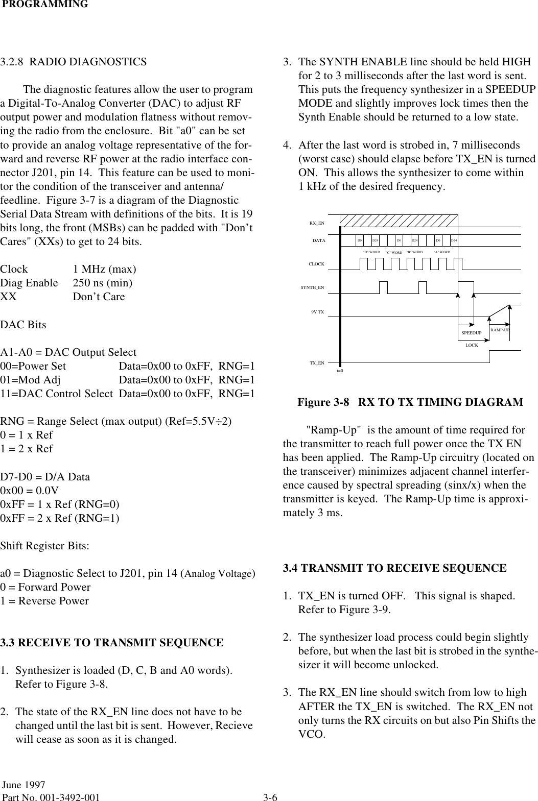
>
CalAmp Wireless Networks
>
2424096-001 User Manual
>
Transceiver Manual
Contents
1.
Transceiver Manual
2.
Modem Manual
Transceiver Manual
Navigation menu
Upload a User Manual
Namespaces
Wiki Guide
HTML
PDF
Info
Views
User Manual
Discussion / Help
Navigation

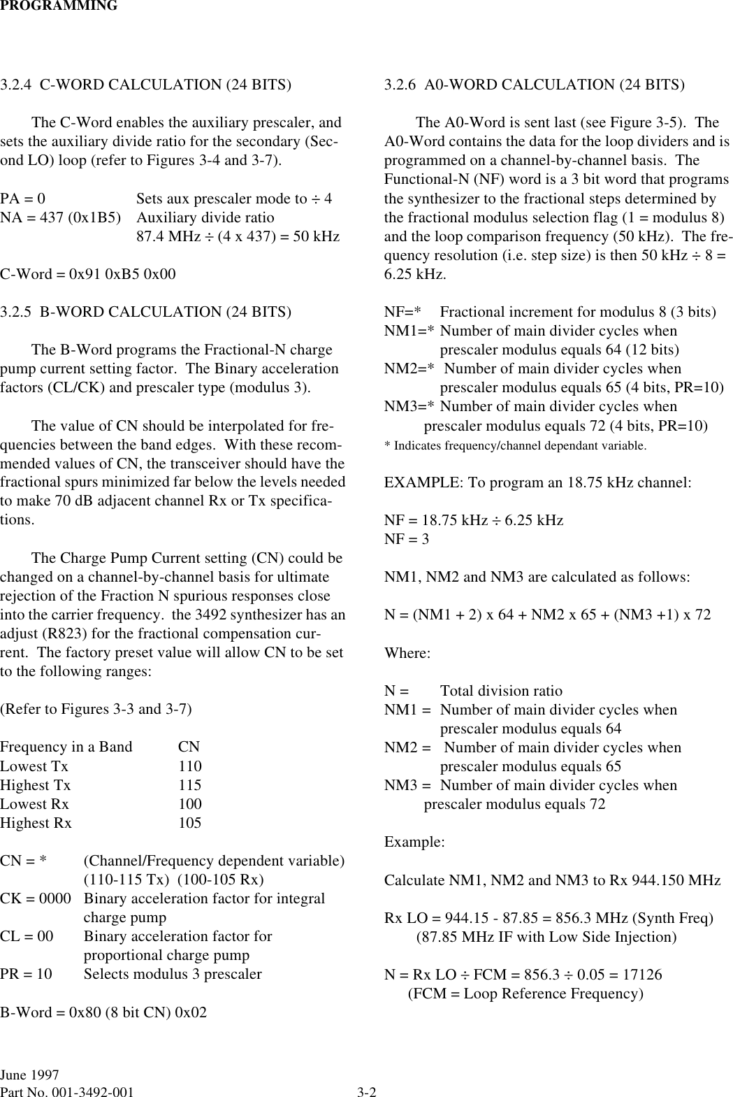
![PROGRAMMING3-3June 1997 Part No. 001-3492-001NM3 = (INT(64 x FRAC [N ÷ 64]) ÷ 8) - 1 = (INT(64 x 0.59375) ÷ 8) - 1= (INT(38 ÷ 8)) - 1= 4 - 1= 3NM2 = 8 x FRAC [N ÷ 8] = 8 x 0.75= 6NM1 = INTEGER [N ÷ 64] - NM2 - NM3 - 3= 267 - 6 - 3 - 3= 2553.2.7 TX / RX FREQUENCY SHIFT AND BAND SELECTIONAs mentioned in 3.2.2, in order to implement the band selection and Rx/Rx an additional 8 bits of data are added to each of the synthesizer load words (D/C/B/AO) (see Figure 3-1). The frequency bands and Transmit/Receive Bits are defined as follows:Low Band 928-944 MHzHigh Band >944 MHz to 960 MHzxx Don’t careLow+ Low Band Select (1=lowband, 0=highband)Low- Low Band Select (0=lowband, 1=highband)Tx+ Transmit Select (1=Tx mode, 0=Rx mode)Tx- Transmit Select (0=Tx mode, 1=Rx mode)Figure 3-2 D-WORD4321 141312111098765 2019181715 16 242322211 1 1 1 1 1 1 1 00/110000000000000ADDRESSBITS= 350 FOR 50 kHz REFERENCE EA (ALWAYS 1)FMOD (1 = MODULUS 8)SA (ALWAYS 00)EM (ALWAYS 1)SM (ALWAYS 00)LONG (0=24 BIT WORD)NR (REFERENCE DIVIDE)](https://usermanual.wiki/CalAmp-Wireless-Networks/2424096-001.Transceiver-Manual/User-Guide-6868-Page-16.png)

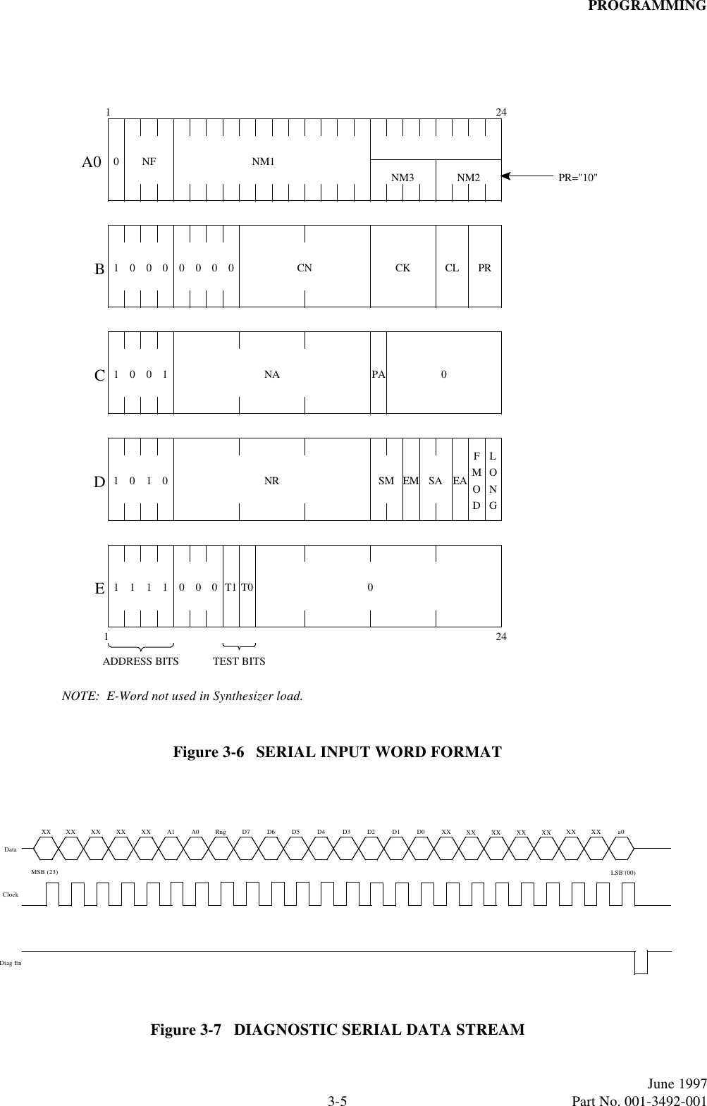

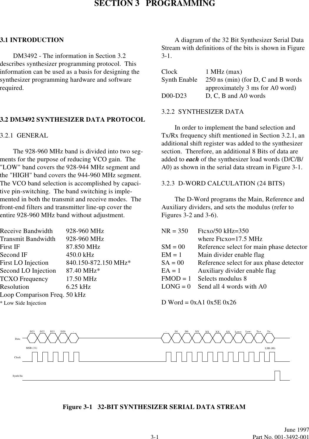

![PROGRAMMING3-3June 1997 Part No. 001-3492-001NM3 = (INT(64 x FRAC [N ÷ 64]) ÷ 8) - 1 = (INT(64 x 0.59375) ÷ 8) - 1= (INT(38 ÷ 8)) - 1= 4 - 1= 3NM2 = 8 x FRAC [N ÷ 8] = 8 x 0.75= 6NM1 = INTEGER [N ÷ 64] - NM2 - NM3 - 3= 267 - 6 - 3 - 3= 2553.2.7 TX / RX FREQUENCY SHIFT AND BAND SELECTIONAs mentioned in 3.2.2, in order to implement the band selection and Rx/Rx an additional 8 bits of data are added to each of the synthesizer load words (D/C/B/AO) (see Figure 3-1). The frequency bands and Transmit/Receive Bits are defined as follows:Low Band 928-944 MHzHigh Band >944 MHz to 960 MHzxx Don’t careLow+ Low Band Select (1=lowband, 0=highband)Low- Low Band Select (0=lowband, 1=highband)Tx+ Transmit Select (1=Tx mode, 0=Rx mode)Tx- Transmit Select (0=Tx mode, 1=Rx mode)Figure 3-2 D-WORD4321 141312111098765 2019181715 16 242322211 1 1 1 1 1 1 1 00/110000000000000ADDRESSBITS= 350 FOR 50 kHz REFERENCE EA (ALWAYS 1)FMOD (1 = MODULUS 8)SA (ALWAYS 00)EM (ALWAYS 1)SM (ALWAYS 00)LONG (0=24 BIT WORD)NR (REFERENCE DIVIDE)](https://usermanual.wiki/CalAmp-Wireless-Networks/2424096-001.Transceiver-Manual/User-Guide-6868-Page-24.png)