California Eastern Laboratories FSTARPRO FreeStar Pro Transceiver Module User Manual manual
California Eastern Laboratories FreeStar Pro Transceiver Module manual
UserManual.wiki
>
California Eastern Laboratories
>
FSTARPRO User Manual
>
manual
Contents
1.
Manual
2.
manual
manual
Navigation menu
Upload a User Manual
Namespaces
Wiki Guide
HTML
PDF
Info
Views
User Manual
Discussion / Help
Navigation
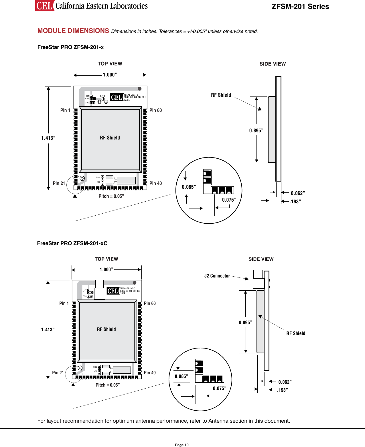
![ZFSM-201 SeriesPage 11MODULE LAND FOOTPRINT NOTE: Dimensions in inches. Tolerances = +/-0.005” unless otherwise noted.1.100 [27.93]0.308 [7.82]0.050 [1.26]0.050 [1.27]60 X 0.040 [1.02]60 X 0.100 [2.54]1.155 [29.34]1.040 [26.42]0.890 [22.61]0.104 [2.65]1.000 [25.40]COPPER KEEPOUT AREAFigure 2](https://usermanual.wiki/California-Eastern-Laboratories/FSTARPRO.manual/User-Guide-1702463-Page-11.png)