California Eastern Laboratories FSTARPRO FreeStar Pro Transceiver Module User Manual manual
California Eastern Laboratories FreeStar Pro Transceiver Module manual
Contents
- 1. Manual
- 2. manual
manual
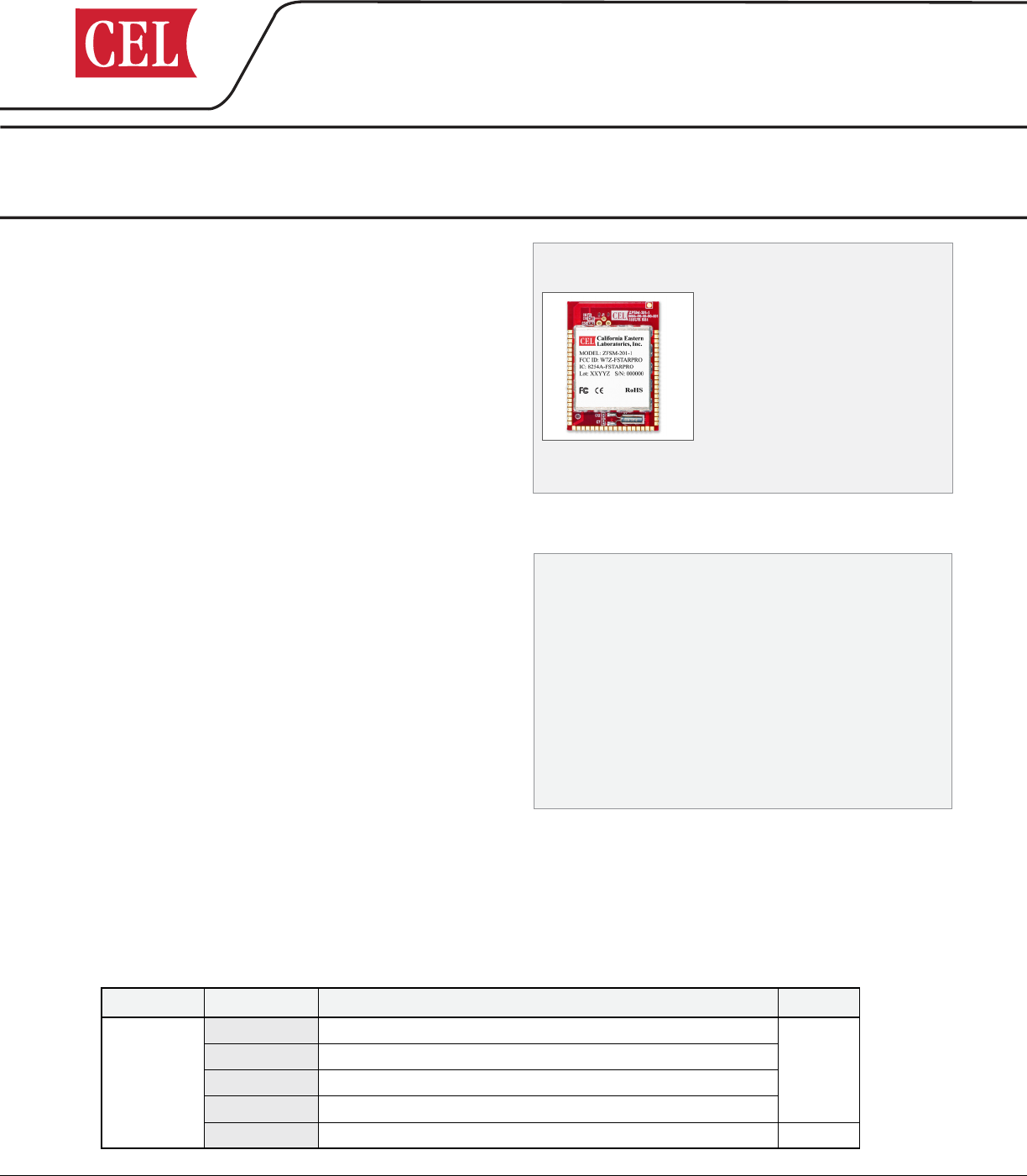
ZFSM-201-1
ZFSM-201-2
FREESTAR PRO SERIES TRANSCEIVER MODULES
DESCRIPTION
CEL’s FreeStar Pro module provides a high performance and cost
effective RF transceiver solution for 2.4 GHz IEEE 802.15.4, ZigBee,
and Zigbee PRO wireless networks.
The FreeStar Pro module is based on the Freescale™ MC13224V
(ZFSM-201-1) or MC13226V (ZFSM-201-2) transceiver platforms. It
combines Freescale’s transceiver IC with an onboard 100mW Power
Amplier. Ideal for remote sensing, AMR/AMI, home and building
automation, industrial control, and security applications, FreeStar Pro
combines extensive processing capability with high output power and
low power consumption.
The processing power of the MC1322xV enables the FreeStar Pro to
provide a level of integration unprecedented in a ZigBee module. The
32-bit ARM7TDMI processor and expansive on-chip memory enable
designers to eliminate the peripheral host processors often required
by 8- and 16-bit transceiver solutions. This high level of integration
reduces component count, lower power consumption and overall
system costs.
Integrated Transceiver Modules for ZigBee/IEEE 802.15.4
Evaluation Kit available: ZFSM-201-KIT-1
The information in this document is subject to change without notice, please conrm data is current
Document No: 0006-00-07-00-000 (Issue B)
Date Published: May 17, 2012
DATA SHEET
• Transmit Power: 100 mW
• Receive Sensitivity: -94 dBm
• Freescale MC1322xV platform
• 128 kB Serial Flash Memory
• 96 kB SRAM
• 80 kB ROM
• 32-bit ARM7TDMI-based MCU
• 46 GPIO Pins
• 12-bit ADC
FREESTAR PRO
ZFSM-201-x
APPLICATIONS
• Powerful 32-bit ARM7TDMI based microprocessor
• Extensive on-board memory resources
• Up to 100 mW output power
• Miniature footprint: 1” x 1.4” (25.4 mm x 36.5 mm)
• Integrated PCB trace antenna
• Optional MMCX connector for external antenna
• 15 RF channels
• Over 4000 feet of range
• AES 128-bit encryption
• Low power consumption
• FCC, CE and IC certied
• RoHS compliant
FEATURES
Home &
Building Automation
• Security
• HVAC control
• Lighting control
• Thermostats
Industrial Controls
• Food processing controls
• Trafc Management
• Sensor Networks
• Asset Management
• Barcode reader
• Patient Monitoring
• Glucose monitor
Automated Meter
Reading
• In meter applications
• Thermostats
• In-home display units
ORDERING INFORMATION
Part Number Order Number Description Mins/Mults
FreeStar Pro
ZFSM-201
ZFSM-201-1 FreestarPro MC13224 100mW transceiver module PCB Trace Antenna
5,040 pcs /
140 pcs
ZFSM-201-1C FreestarPro MC13224 100mW transceiver module with MMCX connector
ZFSM-201-2 FreestarPro MC13226 100mW transceiver module PCB Trace Antenna
ZFSM-201-2C FreestarPro MC13226 100mW transceiver module with MMCX connector
ZFSM-201-KIT-1 FreeStar Pro Module Kit 1
ZFSM-201 Series
Page 2
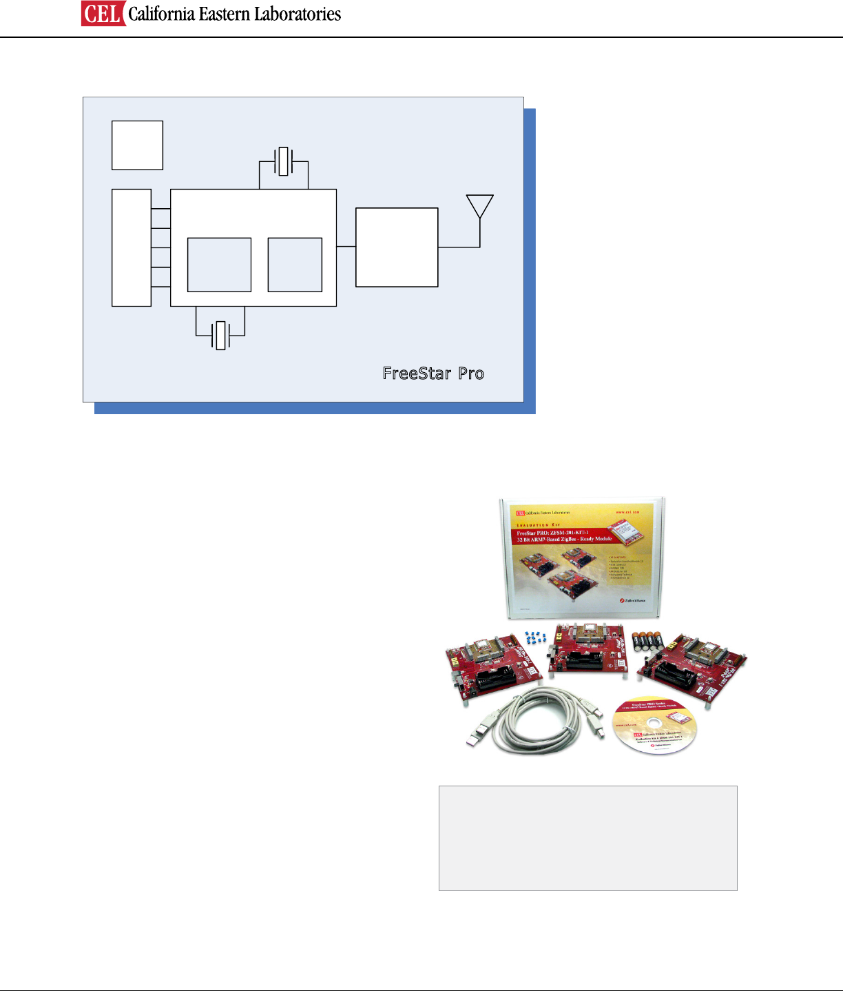
FREESTAR PRO MODULE BLOCK DIAGRAM
EVALUATION KIT
The FreeStar Pro Kits assists users in both evaluation and
development. As a stand alone radio system, the kit allows users
to place the modules into the target environment and evaluate
performance. The FreeStar Pro kit also serves as an invaluable
aid in application development. Through the many headers on
the interface board, the user has access to all pins on the
ZFSM-201-1 enabling easy connection to the target system for
application development.
The FreeStar Pro module contains the Freescale™ MC1322xV
transceiver IC, an NEC high gain Power Amplier, XTALs, Power
Regulator, and an integrated PCB antenna.
The interface board features a serial communication interface, a
power management module, peripherals such as potentiometer
LEDs, and GPIO headers. The Evaluation Kit also contains four
AA batteries and two USB cables.
For more detailed information regarding FreeStar Pro Evaluation
Kit, refer to the FreeStar Pro Evaluation Kit User Guide docu-
ment. (Available at CEL’s website http://www.cel.com)
Kit Contents:
32.768 kHz XTAL (optional)
32.768 kHz XTAL
Castellation Edge
Connector
24 MHz
XTAL
PWR
Reg
Radio
ANT
Micro
processor
Freescale
MC1322xV
RF Front End
(NEC PA and
NEC Switch)
FreeStar Pro
• Three Evaluation Boards with ZFSM-201-1 Modules
• Two USB A/B Cables
• Ten Jumpers (Spares)
• Four AA Batteries
• Software & Technical Information CD

ZFSM-201 Series
Page 3
Introduction and Overview
Description.............................................................................................................................................................................................. 1
Features.................................................................................................................................................................................................. 1
Applications............................................................................................................................................................................................ 1
Ordering Information............................................................................................................................................................................. 1
Module Block Diagram........................................................................................................................................................................... 2
Evaluation Kit......................................................................................................................................................................................... 2
System Level Function
Module Microprocessor......................................................................................................................................................................... 4
Modes of Operation (TX, RX, Sleep)...................................................................................................................................................... 5
Power Amplier....................................................................................................................................................................................... 6
Power Amplier Control Line................................................................................................................................................................. 6
Interface.................................................................................................................................................................................................. 6
Host Protocol Interface Commands...................................................................................................................................................... 6
Electrical Specication
Absolute Maximum Ratings................................................................................................................................................................... 7
Recommended (Operating Conditions)................................................................................................................................................ 7
DC Characteristics.................................................................................................................................................................................. 7
RF Characteristics.................................................................................................................................................................................. 7
Pin Signal & Interfaces
Pin Signals I/O Conguration................................................................................................................................................................ 7
I/O Pin Assignments............................................................................................................................................................................... 8
Module Dimensions................................................................................................................................................................................ 10
Processing......................................................................................................................................................................................... 12
Agency Certications................................................................................................................................................................... 13
Shipment, Storage & Handling................................................................................................................................................. 15
References & Revision History................................................................................................................................................. 16
TABLE OF CONTENTS

ZFSM-201 Series
Page 4
mICROPROCESSOR
The primary component of the FreeStar Pro module is Freescale’s third generation ZigBee platform. It incorporates
a complete, low power, 2.4 GHz radio frequency transceiver, 32-bit ARM7TDMI-based microprocessor, hardware
acceleration for both IEEE 802.15.4 MAC and AES security plus a full suite of processor peripherals.
The MC1322xV architecture offers superior processing power for ZigBee applications. The core operates up to 26 MHz.
An 80 kByte ROM is utilized for the low level IEEE 802.15.4 MAC and PHYsical layer commands. This off loads the Flash
memory, leaving more space for the end user application. The MC1322xV supports 128 kBytes of Flash memory. The
program code is mirrored in 96 kBytes of RAM for faster execution by the processor core. A full set of peripherals and
Direct Memory Access (DMA) capability for transceiver packet data are also included.
In addition, the MC1322xV provides extensive power savings options, including low current sleep modes allowing for
maximum operating life when battery-powered.
The MC1322x family is available as two part numbers. These device types differ only in their ROM contents, all other
device hardware, performance, and specications are identical:
• mC13224V - this is the original version and is the generic part type.
- The MC13224V is intended for most IEEE 802.15.4 applications including MAC-based,
ZigBee-2007 Prole 1, and ZigBee RF4CE targets.
- It has a more complete set of peripheral drivers in ROM.
• mC13226V - this is a more recent version and is provided specically for ZigBee-2007 Prole 2 (Pro)
applications. Only the onboard ROM image has been changed to optimize ROM usage for the ZigBee Pro
prole and maximize the amount of available RAM for application use.
- The IEEE MAC/PHY functionality has been streamlined to include only that functionality
required by the ZigBee specication. The MAC functionality is 802.15.4 compatible.
- For a typical application, up to 20 kbytes more of RAM is available versus the M13224V
- Some drivers present in the MC13224 ROM have been removed and these include the ADC,
LCD font, and SSI drivers. These drivers are still available as library functions, but now compile into the
RAM space.
- The Low Level Component (LLC) functionality has also been streamlined for the ZigBee Specication.
ANTENNA
FreeStar Pro modules include an integrated PCB trace antenna. An optional MMCX connector can be specied, enabling
connection to a 50-ohm external antenna of the user’s choice. See Ordering Information on page 1.
The PCB antenna employs an F-Antenna topology that is compact and supports an omni-directional radiation pattern.
To maximize antenna efciency, an adequate ground plane must be provided on the host PCB. Correctly positioned, the
ground plane on the host board under the module will contribute signicantly to antenna performance.
The position of the module on the host board and overall design of the product enclosure contribute to antenna perfor-
mance. Poor design affects radiation patterns and can result in reection, diffraction, and/or scattering of the transmitted
signal.
Here are some design guidelines to help ensure antenna performance:
• Never place the ground plane or route copper traces directly underneath the antenna portion of the module.
• Never place the antenna close to metallic objects.
• In the overall design, ensure that wiring and other components are not placed near the antenna.
• Do not place the antenna in a metallic or metallized plastic enclosure.
• Keep plastic enclosures 1cm or more from the antenna in any direction.

ZFSM-201 Series
Page 5
MODES OF OPERATION
FreeStar Pro power management is controlled through the Freescale MC1322xV’s Clock and Reset Module (CRM). The
CRM is a dedicated module to handle clock, reset, and power management functions including control of the power regu-
lators. All these functions have direct impact on attaining the lowest power.
The FreeStar Pro module supports three modes of operation: Active, Doze and Hibernation. The latter two modes are the
low-power sleep modes.
Active Mode
In this mode all functions / features are operating normally.
Doze Mode
Doze mode provides signicant reduction in power consumption while still maintaining a high degree of sleep timing ac-
curacy. In Doze mode, the reference oscillator of the processor continues to operate normally.
Hibernation Mode
Hibernation mode provides the greatest reduction in power consumption however the sleep timing accuracy is not as
precise as in Doze mode.
The CRM manages the recovery from the low-power modes, similar to power-up from reset, providing regulator and clock
management.
The module can be awoken from the low-power modes in 3 ways, wake-up can occur:
• On external interrupts through any of the 4 Keyboard Interface inputs
• From internal interrupts
• On the Real Time (wake-up) timer interrupt
For more detail information on modes of operation refer to Freescale’s MC1322xV datasheet available at
Freescale’s website (www.freescale.com)
ZFSM-201 Series
Page 6
POWER AMPLIFIER
The FreeStar Pro module incorporates a high performance Power Amplier from Renesas Electronics.
Power Amplier Control Line
FreeStar Pro modules include a separate 1.8V regulator supplying a bias that enables consistent module output performance
over the wide operating range. To prevent excessive sleep current draw, this regulator should be disabled when the module is
placed into sleep mode.The voltage regulator is controlled by GPIO42 (ANT1), setting GPIO42 high enables the regulator while
setting GPIO42 low disables the regulator. See the table below for the Turn on Time requirements for the voltage regulator.
SPECIFICATIONS — GPIO42
Parameter Min Typ Max Unit
Regulator enable voltage 0.95 V
Regulator disable voltage 0.40 V
Turn on Time for VOUT=1.8V (Default) 105 200 µsec
For the TX_ON and RX_ON pins, the function table is as follows:
Parameter TX Mode RX Mode
TX_ON High Low
RX_ON Low High
Other Notes:
• The GPIO43 (ANT2) pin is not used and is left unconnected.
• Due to the long turn on time (105µs) of the regulator, the regulator is enabled or ON all the time with the
execption of sleep mode.
• The RF switch uses both the TX_ON and RX_ON outputs as control inputs.
• The PA uses the TX_ON line as the control input.
INTERFACE
The FreeStar Pro module has all major pins routed to the castellation connectors, this includes, but is not limited, to the pins for
JTAG, serial communication, A/D, etc.
HOST PROTOCOL INTERFACE COMMANDS
CEL provides the Host Serial and RF Protocols document which details the protocols and commands between the Host
processor (i.e. an external microprocessor, a PC, etc.) and the FreeStar Pro module. An example of the commands, but
not limited to, included in the host protocol interface are as follows:
• Query Version (MAC version)
• Set RF Channel
• Set RF Power
• Transmit Packet Error Test
For more detail refer to Host Serial and RF Protocols document listed on our website at http://www.cel.com
(FreeStar Pro Host & RF Protocol)
ZFSM-201 Series
Page 7
ABSOLUTE MAXIMUM RATINGS
Description Min Max Unit
Power Supply Voltage -0.3 3.6 VDC
Voltage on Any Digital Pin -0.3 VCC + 0.2 VDC
RF Input Power 10 dBm
Storage Temperature Range -45 125 °C
Reow Soldering Temperature 260 °C
Note: Exceeding the maximum ratings may cause permanent damage to the module.
RECOMMENDED OPERATING CONDITIONS
Description Min Typ Max Unit
Power Supply Voltage (VCC) 2.1 3.6 VDC
Ambient Temperature Range -40 25 85 °C
Crystal Reference Oscillator 24 MHz
DC CHARACTERISTICS (@ 25°C, VCC = 3.3V unless otherwise noted)
Description Typ Max Unit
Transmit Mode Current
(at +20 dBm Output Power) 193 mA
Receive Mode Current 30 mA
Hibernate or Doze Mode Current 5 µA
RF CHARACTERISTICS (@ 25°C, VCC = 3.3V unless otherwise noted)
Parameter Min Typ Max Unit
General Charcteristics
RF Frequency Range 2400 2483.5 MHz
RF Data Rate 250 kbps
Transmitter
Nominal Output Power 20 dBm
Programmable Output Power Range 18 dB
Error Vector Magnitude 8 35 %
Receiver
Receiver Sensitivity (1% PER) -92 -94 dBm
Saturation (Maximum Input Level) (1% PER) 0 dBm
802.15.4 Adjacent Channel Rejection (±5 MHz) 35 40 dB
802.15.4 Alternate Channel Rejection (±10 MHz) 50 dB
PIN SIGNALS I/O PORT CONFIGURATION
The FreeStar Pro module has 60 edge I/O interfaces for connection to the user’s host board. Figure 1 shows the layout of
the 60 edge castellations.
ZFSM-201 Series
Page 8
FREESTAR PRO I/O PIN ASSIGNMENTS
Pin # Name Type Description IC
Pin #
1 GND GND GND 85
2 GND GND GND 84
3 GND GND GND 75
4ADC2_VREFL Analog Input or
Digital I/O
GPIO39
Alternate function: Low reference voltage for ADC2 61
5ADC1_VREFL Analog Input or
Digital I/O
GPIO41
Alternate function: Low reference voltage for ADC1 62
6ADC1_VREFH Analog Input or
Digital I/O
GPIO40
Alternate function: High reference voltage for ADC1 63
7ADC2_VREFH Analog Input or
Digital I/O
GPIO38
Alternate function: Low reference voltage for ADC2 64
8 ADC0 Analog Input or
Digital I/O
GPIO30
Alternate function: ADC analog input Channel 0 1
9 ADC1 Analog Input or
Digital I/O
GPIO31
Alternate function: ADC analog input Channel 1 2
10 ADC2 Analog Input or
Digital I/O
GPIO32
Alternate function: ADC analog input Channel 2 3
11 ADC3 Analog Input or
Digital I/O
GPIO33
Alternate function: ADC analog input Channel 3 4
12 VCC Power Input High side supply voltage to buck regulator switching MOSFET & IO
buffers 45
13 ADC4 Analog Input or
Digital I/O
GPIO34
Alternate function: ADC analog input Channel 4 5
14 ADC5 Analog Input or
Digital I/O
GPI035
Alternate function: ADC analog input Channel 5 6
15 ADC6 Analog Input or
Digital I/O
GPIO036
Alternate function: ADC analog input Channel 6 7
16 ADC7_RTCK Analog Input or
Digital I/O
GPI037
Alternate function: ADC analog input Channel 7 / Return ClocK 8
17 TDO Digital I/O GPI049
Alternate function: JTAG Test Data Output 9
18 TDI Digital I/O GPI048
Alternate function: JTAG Test Data Input 10
19 TCK Digital I/O GPIO47
Alternate function: JTAG Test Clock Input 11
20 TMS Digital I/O GPIO46
Alternate function: JTAG Test Mode Select Input 12
21 UART2_RTS Digital I/O GPIO21
Alternate function: UART2 Request to Send input 13
22 GND GND GND 76
23 UART2_CTS Digital I/O GPI020
Alternate function: UART2 Clear to Send output 14
24 UART2_RX Digital I/O GPIO19
Alternate function: UART2 RX data input 15
25 UART2_TX Digital I/O GPIO18
Alternate function: GPIO18UART2 TX data output 16
26 UART1_RTS Digital I/O GPI017
Alternate function: UART1 Request to Send input 17
27 UART1_CTS Digital I/O GIO016
Alternate function: UART1 Clear to Send output 18
28 I2C_SDA Digital I/O GPIO13
Alternate function: I2C Bus data 21
ZFSM-201 Series
Page 9
FREESTAR PRO I/O PIN ASSIGNMENTS (Continued)
Pin # Name Type Description IC
Pin #
29 I2C_SCL Digital I/O GPIO12
Alternate function: I2C Bus clock 22
30 TMR3 Digital I/O GPIO11
Alternate function: Timer 3 IO signal 23
31 VCC Power Input High side supply voltage to buck regulator switching MOSFET & IO buffers 45
32 TMR2 Digital I/O GPIO10
Alternate function: Timer 2 IO signal 24
33 TMR1 Digital I/O GPIO9
Alternate function: Timer 1 IO signal 25
34 TMR0 Digital I/O GPIO8
Alternate function: Timer 0 IO signal 26
35 SPI_SCK Digital I/O GPIO7
Alternate function: SPI Port clock 27
36 UART1_TX Digital I/O GPIO14
Alternate function: UART1 TX data output 20
37 UART1_RX Digital I/O GPIO15
Alternate function: UART1 RX data input 19
38 GND GND GND 77
39 SPI_MOSI Digital I/O GPIO6
Alternate function: SPI Port MOSI 28
40 SPI_MISO Digital I/O GPIO5
Alternate function: SPI Port MISO 29
41 SPI_SS Digital I/O GPIO4
Alternate function: SPI Port SS 30
42 SSI_BITCK Digital I/O GPIO3
Alternate function: SSI Bit Clock 31
43 SSI_FSYN Digital I/O GPIO2
Alternate function: SSI Frame Sync 32
44 SSI_RX Digital I/O GPIO1
Alternate function: SSI RX data input 33
45 SSI_TX Digital I/O SSI TX data output / GPIO0 34
46 KBI_7 Digital I/O GPIO29
Alternate function: Keyboard Interface Bit 7 35
47 COIL_BK Power Switch
Output Buck Converter coil drive output 43
48 KBI_6 Digital I/O GPIO28
Alternate function: Keyboard Interface Bit 6 36
49 RESETB Digital Input System reset input 51
50 LREG_BK_FB Power Input Voltage input to onboard regulators, buck regulator feedback
voltage 44
51 GND GND GND 78
52 KBI_5 Digital I/O GPIO27
Alternate function: Keyboard Interface Bit 5 37
53 KBI_4 Digital I/O GPIO26
Alternate function: Keyboard Interface Bit 4 38
54 KBI_3 Digital I/O GPIO25
Alternate function: Keyboard Interface Bit 3 39
55 KBI_2 Digital I/O GPIO24
Alternate function: Keyboard Interface Bit 2 40
56 KBI_1 Digital I/O GPIO23
Alternate function: Keyboard Interface Bit 1 41
57 KBI_0_HST
_WK Digital I/O GPIO22
Alternate function: Keyboard Interface Bit 0 / Host Walk-up output 42
58 GND GND GND 79
59 GND GND GND 86
60 GND GND GND 87
ZFSM-201 Series
Page 10
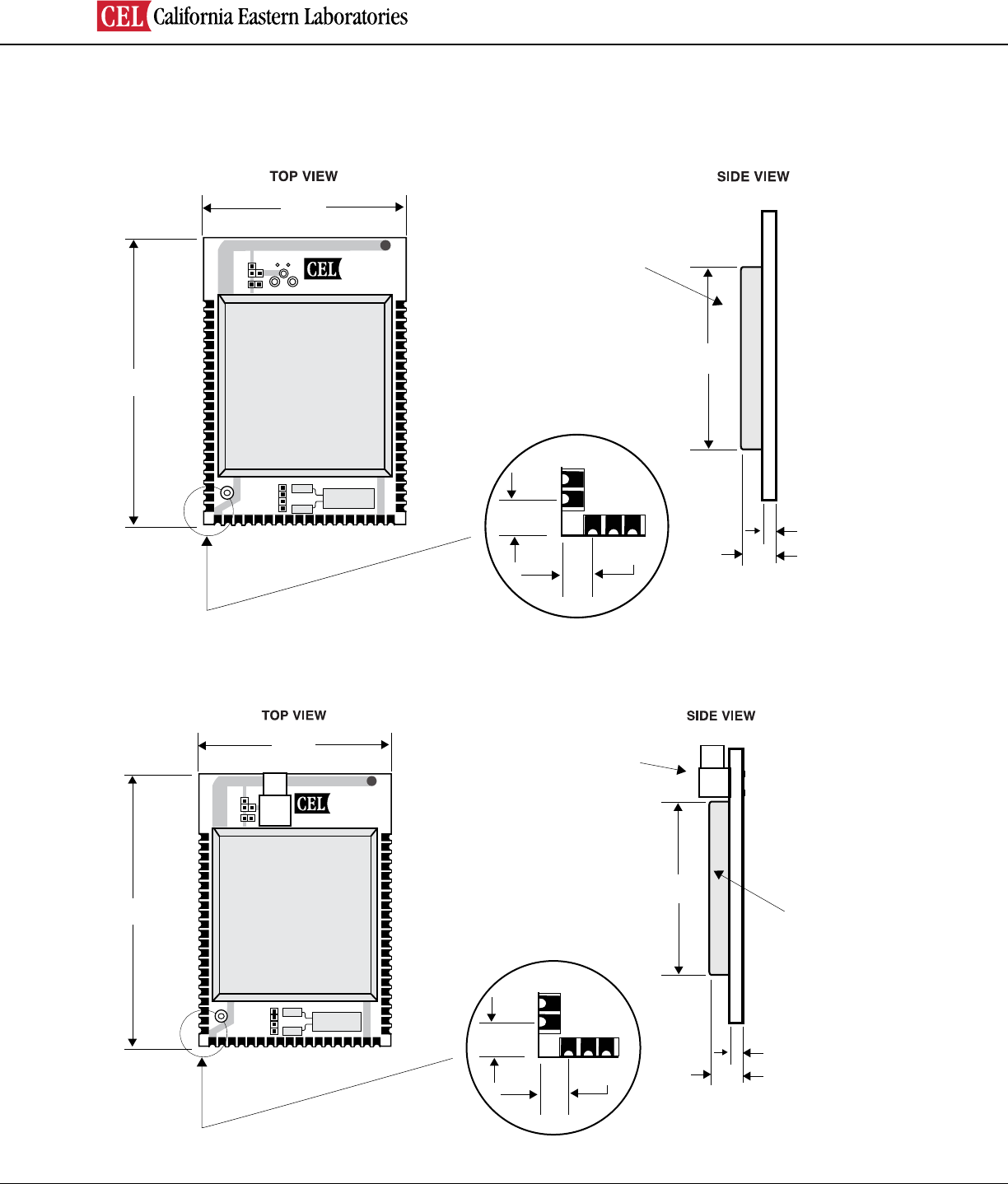
MODULE DIMENSIONS Dimensions in inches. Tolerances = +/-0.005” unless otherwise noted.
For layout recommendation for optimum antenna performance, refer to Antenna section in this document.
FreeStar PRO ZFSM-201-xC
FreeStar PRO ZFSM-201-x
RF Shield
0.895”
1.413”
Pitch = 0.05”
1.000”
0.062”
.193”
0.085”
0.075”
Pin 1
Pin 21 Pin 40
Pin 60
RF Shield
ZFSM-201-1
C6 J1
C12
C7
C11
C30
0006-00-00-00-001
ISSUE
RF Shield
J2 Connector
0.895”
1.413”
Pitch = 0.05”
1.000”
0.062”
.193”
0.085”
0.075”
Pin 1
Pin 21 Pin 40
Pin 60
RF Shield
ZFSM-201-1C
C6
C12
C7
C11
C30
0006-00-00-00-001
ISSUE
ZFSM-201 Series
Page 11
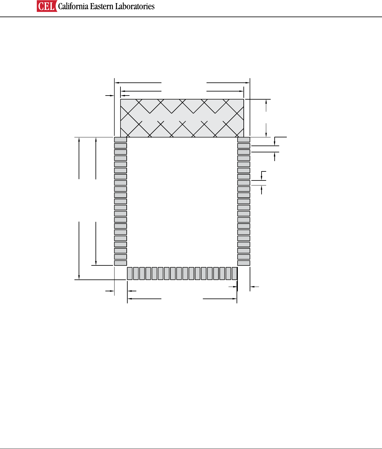
MODULE LAND FOOTPRINT
NOTE: Dimensions in inches. Tolerances = +/-0.005” unless otherwise noted.
1.100 [27.93]
0.308 [7.82]
0.050 [1.26]
0.050 [1.27]
60 X 0.040 [1.02]
60 X 0.100 [2.54]
1.155 [29.34]
1.040 [26.42]
0.890 [22.61]
0.104 [2.65]
1.000 [25.40]
COPPER KEEPOUT AREA
Figure 2

ZFSM-201 Series
Page 12
PROCESSING
Recommended Reow Prole
Parameters Values
Ramp up rate (from Tsoakmax to Tpeak) 3º/sec max
Minimum Soak Temperature 150ºC
Maximum Soak Temperature 200ºC
Soak Time 60-120 sec
TLiquidus 217ºC
Time above TL 60-150 sec
Tpeak 250ºC
Time within 5º of Tpeak 20-30 sec
Time from 25º to Tpeak 8 min max
Ramp down rate 6ºC/sec max
Achieve the brightest possible solder llets with a good shape and low contact angle.
Pb-Free Soldering Paste
Use of “No Clean” soldering paste is strongly recommended, as it does not require cleaning after the soldering process.
Note: The quality of solder joints on the castellations (‘half vias’) where they contact the host board should meet the appropriate IPC
Specication. See IPC-A-610 Acceptability of Electronic Assemblies, section 8.2.4 Castellated Terminations.”
Cleaning
In general, cleaning the populated modules is strongly discouraged. Residuals under the module cannot be easily re-
moved with any cleaning process.
• Cleaning with water can lead to capillary effects where water is absorbed into the gap between the host board and
the module. The combination of soldering ux residuals and encapsulated water could lead to short circuits between
neighboring pads. Water could also damage any stickers or labels.
• Cleaning with alcohol or a similar organic solvent will likely ood soldering ux residuals into the two housings, which is
not accessible for post-washing inspection. The solvent could also damage any stickers or labels.
• Ultrasonic cleaning could damage the module permanently.
The best approach is to consider using a “no clean” soldering paste and eliminate the post-soldering cleaning step.
Optical Inspection
After soldering the Module to the host board, consider optical inspection to check the following:
• Proper alignment and centering of the module over the pads.
• Proper solder joints on all pads.
• Excessive solder or contacts to neighboring pads, or vias.
Repeating Reow Soldering
Only a single reow soldering process is encouraged for host boards.
Wave Soldering
If a wave soldering process is required on the host boards due to the presence of leaded components, only a single wave
soldering process is encouraged.
Hand Soldering
Hand soldering is possible. Use a soldering iron temperature setting equivalent to 350°C, follow IPC recommendations/
reference document IPC-7711.
ZFSM-201 Series
Page 13
AGENCY CERTIFICATIONS
FCC Part 15.247 Module Certied (Mobile)
The Freestar Pro modules comply with Part 15 of the Federal Communications Commission rules and regulations and with
Industry Canada license exempt RSS standards.
To meet the Certication requirements, the user must meet these regulations:
• The text on the FCC ID label provided with the module must be placed on the outside of the nal product.
• The modules may only use the antennas that have been tested and approved with these modules:
— The on-board PCB trace antenna
— Nearson S181AH-2450S antenna.
Per Section 2.109, the Freestar Pro module has been certied by the FCC for use with other products without additional
certication. Any modications to this product may violate the rules of the Federal Communications Commission and
make operation of the product unlawful.
Per Sections 15.107 and 15.109, the user’s end product must be tested for unintentional radiators compliance.
RF Output Power Setting
In order to comply with FCC and Industry Canada emissions requirements,the Freestar Pro module has the following
power shaping requirements implemented:
• Model ZFSM-201-x” which uses the integrated PCB antenna is limited to power step 4 for channels 11 & 12 with
channel 26 being disabled.
• Model ZFSM-201-xC” which has the MMCX connector has rmware that limits the power to CEL Test Tool setting 4
on channels 11-25, with channel 26 being disabled.
In addition to restricting power, the rmware also limits the maximum data payload to 106 bytes for any transmitted
packet. The rmware also limits the transmission rate such that a maximum duty cylce of 32 percent is allowed.
RF Output Power
Certication RF Channel CEL Test Tool Typical Max
Output Power
ZFSM-201-x FCC/IC 11,12 4 10 dBm
13-25 6 20dBm
ETSI 11-25 4 10dBm
ZFSM-201-xC FCC/IC 11-25 4 10dBm
ETSI 11-25 4 10dBm
PROCESSING (Continued)
Rework
The FreeStar Pro Module can be unsoldered from the host board. Use of a hot air rework tool and hot plate for pre-heating
from underneath is recommended. Avoid overheating.
Warning
Never attempt a rework on the module itself, e.g. replacing individual components. Such actions will terminate warranty
coverage.
Additional Grounding
Attempts to improve module or system grounding by soldering braids, wires, or cables onto the module RF shield cover
is done at the customers own risk. The numerous ground pins at the module perimeter should be sufcient for optimum
immunity to external RF interference.

ZFSM-201 Series
Page 14
AGENCY CERTIFICATIONS (Continued)
FCC Compliance Statement (Part 15.19) Section 7.15 of RSS-GEN
This device complies with Part 15 of the FCC Rules and with Industry Canada license exempt RSS Standards. Operation
is subject to the following two conditions:
1. This device may not cause harmful interference.
2. This device must accept any interference received, including interference that may cause undesired operation.
Le présent appareil est conforme aux CNR d’Industrie Canada applicables aux appareils radio exempts de licence.
L’exploitation est autorisée aux deux conditions suivantes:
1. l’appareil ne doit pas produire de brouillage, et
2. l’utilisateur de l’appareil doit accepter tout brouillage radioélectrique subi, même si le brouillage est susceptible
d’en compromettre le fonctionnement.
Warning (Part 15.21)
Changes or modications not expressly approved by CEL could void the user’s authority to operate the equipment.
20 cm Separation Distance
To comply with FCC/IC RF exposure limits for general population / uncontrolled exposure, the antenna(s) used for this
transmitter must be installed to provide a separation distance of at least 20 cm from all persons and must not be co-locat-
ed or operating in conjunction with any other antenna or transmitter.
OEM Responsibility to the FCC Rules and Regulations
The FreeStar Pro Module has been certied per FCC Part 15 rules and to Industry Canada license-exempt RSS Standards
for integration into products without further testing or certication. To fulll the FCC and IC certication requirements, the
OEM using the FreeStar Pro Module must ensure that the information provided on the FreeStar Pro Label is placed on
the outside of the nal product. The FreeStar Pro Module is labeled with its own FCC ID Number and IC ID Number. IF
the FCC ID is not visible when the module is installed inside another device, then the outside of the device into which the
module is installed must also display a label referring to the enclosed module. This exterior label can use wording such as
the following: “Contains Transmitter Module FCC ID: W7Z-FSTARPRO” or “Contains FCC ID: W7Z-FSTARPRO”
The OEM using the FreeStar Pro Module must only use the approved antennas, (PCB Trace Antenna or Nearson Whip
Antenna Model S181AH-2450S) that has been certied with this module. The OEM using the FreeStar Pro Module must
test their nal product conguration to comply with Unintentional Radiator Limits before declaring FCC compliance per Part 15
of the FCC rules.
IC Certication — Industry Canada Statement
The term "IC" before the certication / registration number only signies that the Industry Canada technical specications
were met.
Certication IC - Déclaration d’Industrie Canada
Le terme “IC” devant le numéro de certication / d’enregistrement signie seulement que les spécications techniques
Industrie Canada ont été respectées.
Section 14 of RSS-210
The installer of this radio equipment must ensure that the antenna is located or pointed such that it does not emit RF eld
in excess of Health Canada limits for the general population. Consult Safety Code 6, obtainable from Health Canada's
website: http://www.hc-sc.gc.ca/ewh-semt/pubs/radiation/99ehd-dhm237/index-eng.php
L’article 14 du CNR-210
Le programme d’installation de cet équipement radio doit s’assurer que l’antenne est située ou orientée de telle sorte qu’il
ne pas émettre de champ RF au-delà des limites de Santé Canada pour la population générale. Consulter le Code de
sécurité 6, disponible sur le site Web de Santé Canada: http://www.hc-sc.gc.ca/ewh-semt/pubs/radiation/99ehd-dhm237/
index-eng.php
ZFSM-201 Series
Page 15
CE Certication — Europe
The FreeStar Pro RF module has been tested and certied for use in the European Union.
OEM Responsibility to the European Union Compliance Rules
If the FreeStar Pro module is to be incorporated into a product, the OEM must verify compliance of the nal product to the
European Harmonized EMC and Low-Voltage / Safety Standards. A Declaration of Conformity must be issued for each of
these standards and kept on le as described in Annex II of the R&TTE Directive.
The manufacturer must maintain the user's guide and adhere to the settings described in the manual for maintaining
European Union Compliance. If any of the specications are exceeded in the nal product, the OEM is required to
make a submission to the notied body for compliance testing.
OEM Labeling Requirements
The `CE' mark must be placed on the OEM product in a visible location.
The CE mark shall consist of the initials “CE” with the following form:
· If the CE marking is reduced or enlarged, the proportions given in the above graduated
drawing must be adhered to.
· The CE mark must be a minimum of 5mm in height
· The CE marking must be afxed visibly, legibly, and indelibly Since the 2400 - 2483.5 MHz
band is not harmonized by a few countries throughout Europe, the Restriction sign must be
placed to the right of the `CE' marking as shown in the picture
SHIPMENT, HANDLING, AND STORAGE
Shipment
The FreeStar Pro Modules are delivered in trays of TBD.
Handling
The FreeStar Pro Modules are designed and packaged to be processed in an automated assembly line.
Warning
The FreeStar Pro Modules contain a highly sensitive electronic circuitry. Handling without proper ESD protection may
destroy or damage the module permanently.
Warning
According to JEDEC ISP, the FreeStar Pro Modules are moisture sensitive devices. Appropriate handling instructions and
precautions are summarized in Section 2.1. Read carefully to prevent permanent damage due to moisture intake.
Moisture Sensitivity Level (MSL)
MSL 3, per J-STD-033
Storage
Storage/shelf life in sealed bags is 12 months at <40°C and <90% relative humidity.
AGENCY CERTIFICATIONS (Continued)
ZFSM-201 Series
Page 16
REFERENCES & REVISION HISTORY
References
Reference Documents
FreeStar Pro Module Evaluation Kit User Guide
FreeScale MC1322xV Datasheet
Freescale Semiconductor MC1322x Reference Manual MC1322xRM
Freescale Semiconductor BeeKit™ User Guide BKWCTKUG
Freescale Semiconductor Software Driver Reference Manual 22XDRVRRM
Freescale Semiconductor MC1322x Simple Media Access Controller (SMAC) Reference Manual 22xSMACRM
Freescale Semiconductor Simple Media Access Controller (SMAC) User’s Guide SMACRM
IAR J-Link and IAR J-Trace user Guide J-Link_J-TraceARM-1
ARM® IAR Embedded Workbench® IDE User Guide UARM-13
Revision History
Previous Versions Changes to Current Version Page
0006-00-07-00-000
(Preliminary) October 28, 2008 Initial advance datasheet. N/A
0006-00-07-00-000
(Preliminary) May 20, 2009 Updated to current revisions to the Freescale Silicon IC N/A
0006-00-07-00-000
(Preliminary) June 11, 2009 Updated FCC and IC Agency Statements 14-15
0006-00-07-00-000
August 17, 2009 Updated RF Output Power Setting 6
0006-00-07-00-000
(Issue A) December 10, 2010 Added the MC13226 (ZFMS-201-2) Transceiver platform Option All
0006-00-07-00-000
(Issue B) May 17, 2012
Updated FCC and Agency Statements (added French translation), updated RF
Output Power information, reformatted and repaginated document 13-15
Disclaimer
• The information in this document is current as of December, 2010. The information is subject to change without
notice. For actual design-in, refer to the latest publications of CEL data sheets or data books, etc., for the most
up-to-date specications of CEL products. Not all products and/or types are available in every country. Please
check with an CEL sales representative for availability and additional information.
• No part of this document may be copied or reproduced in any form or by any means without the prior written
consent of CEL. CEL assumes no responsibility for any errors that may appear in this document.
• CEL does not assume any liability for infringement of patents, copyrights or other intellectual property rights of
third parties by or arising from the use of CEL products listed in this document or any other liability arising from
the use of such products. No license, express, implied or otherwise, is granted under any patents, copyrights or
other intellectual property rights of CEL or others.
• Descriptions of circuits, software and other related information in this document are provided for illustrative
purposes in semiconductor product operation and application examples. The incorporation of these circuits,
software and information in the design of a customer’s •equipment shall be done under the full responsibility of
the customer. CEL assumes no responsibility for any losses incurred by customers or third parties arising from
the use of these circuits, software and information.
• While CEL endeavors to enhance the quality, reliability and safety of CEL products, customers agree and
acknowledge that the possibility of defects thereof cannot be eliminated entirely. To minimize risks of damage to
property or injury (including death) to persons arising from defects in CEL products, customers must incorporate
sufcient safety measures in their design, such as redundancy, re-containment and anti-failure features.