California Eastern Laboratories ZIC2410P0 MeshConnect Module User Manual Revised
California Eastern Laboratories MeshConnect Module Users Manual Revised
UserManual.wiki
>
California Eastern Laboratories
>
ZIC2410P0 User Manual
Users Manual Revised
Navigation menu
Upload a User Manual
Namespaces
Wiki Guide
HTML
PDF
Info
Views
User Manual
Discussion / Help
Navigation
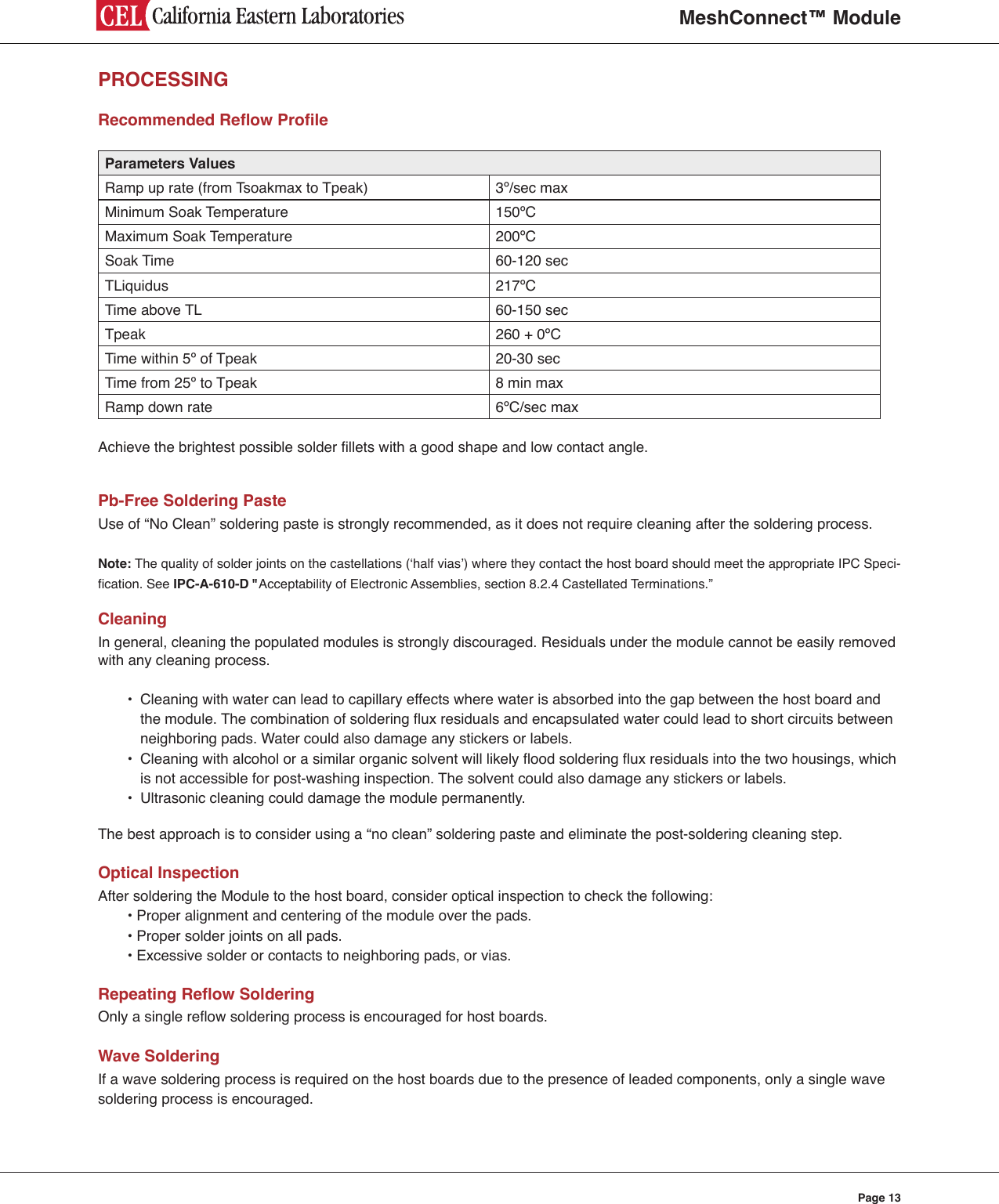
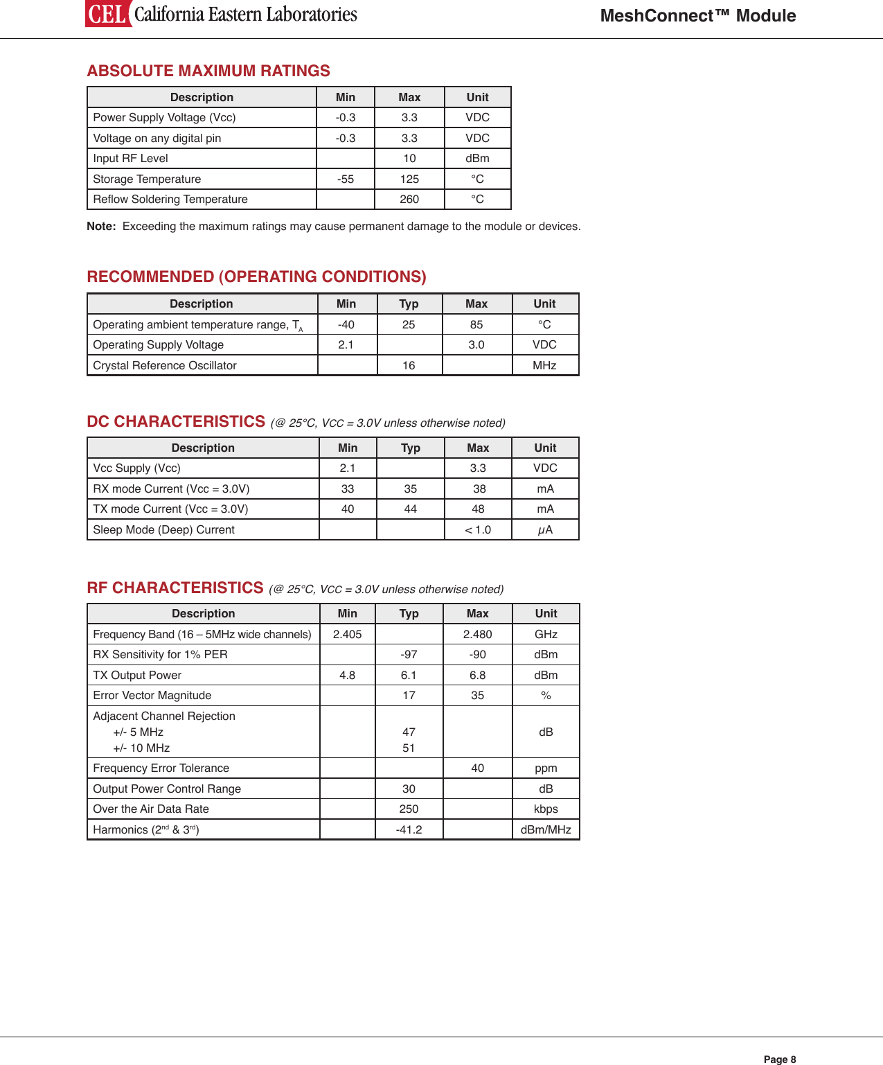
![MeshConnect™ ModulePage 5CEL's MeshConnect modules include an integrated Printed Circuit Board (PCB) trace antenna. An optional u.FL connector can be specied, providing connection to a 50-ohm external antenna of the user’s choice. See Ordering Information on page 1. The PCB antenna employs an F-Antenna topology that is compact and supports an omni-directional radiation pattern. To maximize antenna efciency, an adequate ground plane must be provided on the host PCB. Correctly positioned, the ground plane on the host PCB (but not directly under the F-Antenna). Correctly positioned, the ground plane on the host PCB board under the module will contribute signicantly to the antenna performance. The position of the module on the host board and overall design of the product enclosure contribute to antenna perfor mance. Poor design affects radiation patterns and can result in reection, diffraction, and/or scattering of the transmitted signal. Here are some design guidelines to help ensure antenna performance: • Never place the ground plane or route copper traces directly underneath the antenna portion of the module. • Never place the antenna close to metallic objects. • In the overall design, ensure that wiring and other components are not placed near the antenna. • Do not place the antenna in a metallic or metalized plastic enclosure. • Keep plastic enclosures 1cm or more from the antenna in any direction.For optimum antenna performance, the MeshConnect modules should be mounted with the PCB trace antenna overhanging the edge of the host board. To further improve performance, a ground plane may be placed on the host board under the module, up to the antenna. The installation of an uninterrupted ground plane on a layer directly beneath the module will also allow you to run traces under this layer. CEL can provide assistance with your PCB layout.There are three power down modes in the ZIC2410. Each mode can be set using the PDMODE [1:0] bits in the PDCON register and power down modes can be started by setting the PDSTART bit to 1. Each mode has a different current consumption and wake-up sources, please refer to the ZIC2410 datasheet for further information on the available power down modes.. Table 8 describes the three power down modes. Table 8 – Power Down Modes PDMODE [1:0] Description Wake-Up Source Regulator for Digital block0 Active (Normal Operation) - - 1 PM1 mode Hardware Reset, Sleep Timer interrupt, External interrupt ON 2 PM2 mode Hardware Reset, Sleep Timer interrupt, External interrupt OFF (After wake-up, register conguration is required) 3 PM3 mode Hardware Reset, External interrupt OFF (After wake-up, register conguration is required) ANTENNAMODES OF OPERATION](https://usermanual.wiki/California-Eastern-Laboratories/ZIC2410P0/User-Guide-1124090-Page-5.png)

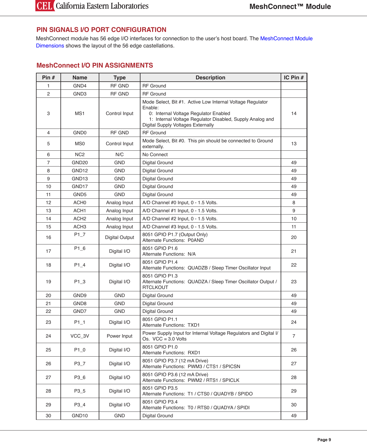
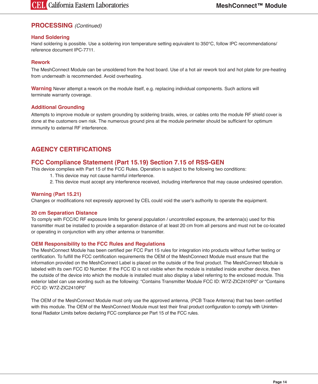
![MeshConnect™ ModulePage 12MODULE LAND FOOTPRINTNote: Unless otherwise specied. Dimensions are in Inches [mm].1.100 [27.94]1.000 [25.41]0.990 [22.61]0.105 [2.67]0.050 [1.27]COPPER KEEPOUT 0.298 [27.94]0.940 [23.88]1.055 [26.80]0.050 [1.27] Pitch56 x 0.040 [1.02]56 x 0.100 [2.54]](https://usermanual.wiki/California-Eastern-Laboratories/ZIC2410P0/User-Guide-1124090-Page-12.png)