California Eastern Laboratories ZIC2410P0 MeshConnect Module User Manual Revised
California Eastern Laboratories MeshConnect Module Users Manual Revised
Users Manual Revised
Page 1
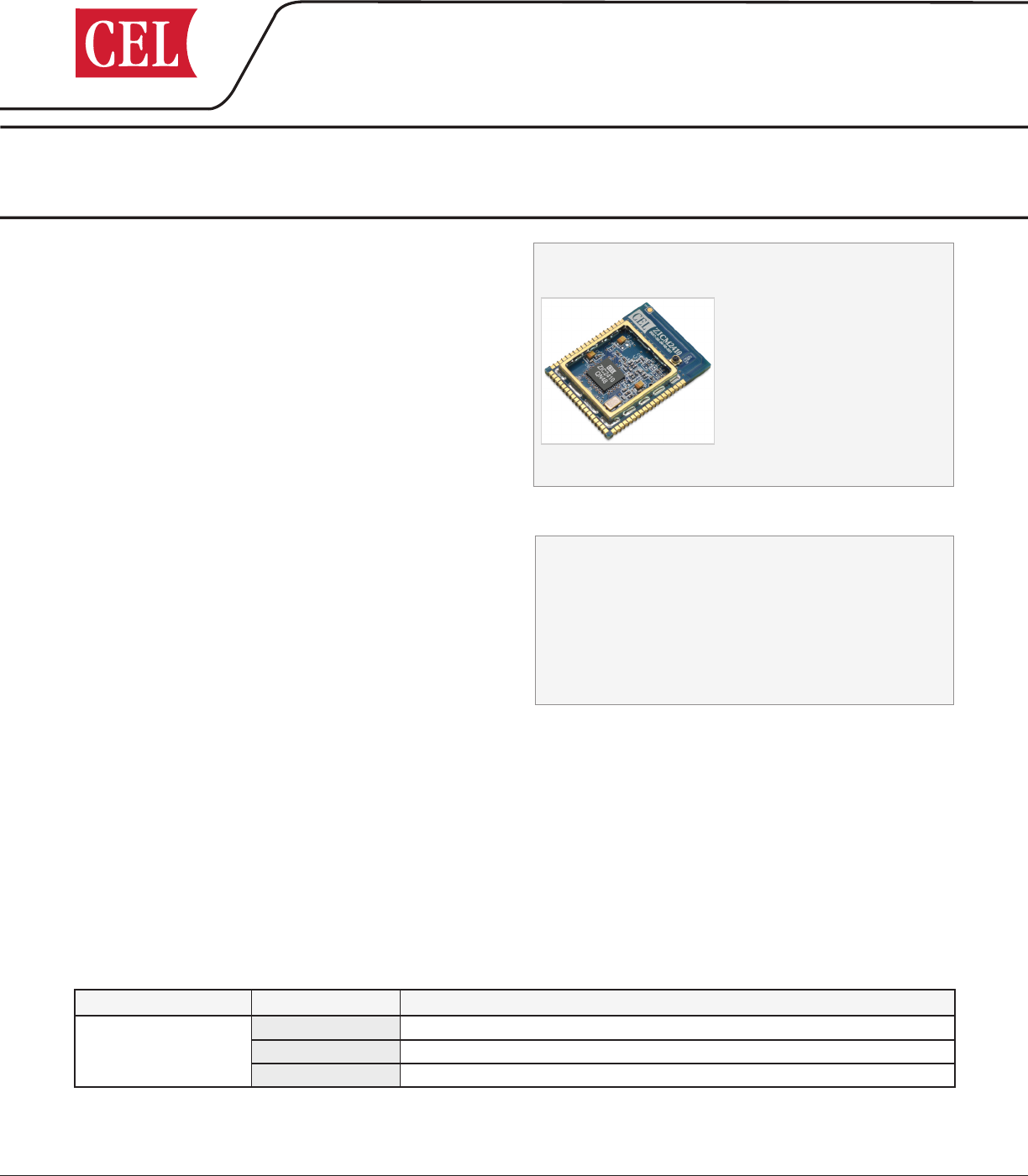
ZICM2410P0
MeshConnect™ Module
DESCRIPTION
CEL's MeshConnect™ modules provide a high performance
and low cost RF transceiver solution for 2.4 GHz IEEE
802.15.4 / ZigBee data links and wireless networks.
CEL's MeshConnect radio module leverages the advanced
features of CEL’s ZIC2410 transceiver platform. The ZIC2410
is a true single-chip solution, compliant with ZigBee specica-
tions and IEEE 802.15.4, a complete wireless solution for all
ZigBee applications. The ZIC2410 consists of an RF transceiv-
er with baseband modem, a hardwired MAC and an embed-
ded 8051 microcontroller with internal Flash memory. The
device provides numerous general-purpose I/O pins, periph-
eral functions such as timers and UART and is one of the rst
devices to provide an embedded Voice CODEC. This device is
also ideal for low power applications.
Unique in the market, the ZIC2410 offers extended data rates,
supporting 500 kbps and 1 Mbps modes of operation. When
combined with the voice codec the ZICM2410’s high speed
modes offers an excellent voice platform. The high level of
integration reduces component count, lowers power consump-
tion, and reduces overall system costs.
Integrated Transceiver Modules for ZigBee / IEEE 802.15.4
Evaluation Kit available: ZICM2410P0-KIT1-1
The information in this document is subject to change without notice, please conrm data is current
Document No: 0007-00-07-00-000 (Issue B)
Date Published: May 14, 2009
PRELIMINARY DATA SHEET
CEL's MeshConnect™ Module Platform
APPLICATIONS
ORDERING INFORMATION
Part Number Order Number Supplying Form
ZICM2410P0 Series
MeshConnect™ Module
ZICM2410P0-1 4 mW Output power, PCB Trace Antenna
ZICM2410P0-1C 4 mW Output power, with U.FL Connector for external antenna
ZICM2410P0-KIT1-1 Engineering Development Kit
• High RF performance
- 103dB RF Link Budget
- RX Sensitivity: -97 dBm @1.5V
- RF TX Power: +6dBm @1.5V
• Scalable Data Rate: 250kbps for ZigBee, 500kbps and 1Mbps
• Miniature footprint: 1” x 1.350” (25.4 mm x 34.3 mm)
• Voice Codec Support: µ-law/a-law/ADPCM
FEATURES
Home &
Building Automation
• Security
• HVAC control
• Lighting control
• Thermostats
Industrial Controls
• Food processing controls
• Trafc Management
• Sensor Networks
• Asset Management
• Barcode reader
• Patient Monitoring
• Glucose monitor
• 4 Level Power Management Scheme w/ Deep Sleep Mode (0.3µA)
• Integrated PCB trace antenna
• 16 RF channels
• Over 3000 feet of range
• AES 128-bit encryption
• FCC, CE and IC certications (pending)
• ROHS compliant
• 96 kB FLASH Memory
• 8 kB SRAM
• 8051 compatible single-cycle
microcontroller core
• 22 GPIO Ports
• SPI (Master/Slave) + UART
• I2S/PCM Interface with two
128-byte FIFOs
• µ-law/a-law/ADPCM Voice Codec
• 4-channel 8-bit ADC
MeshConnect™ Module
Page 2
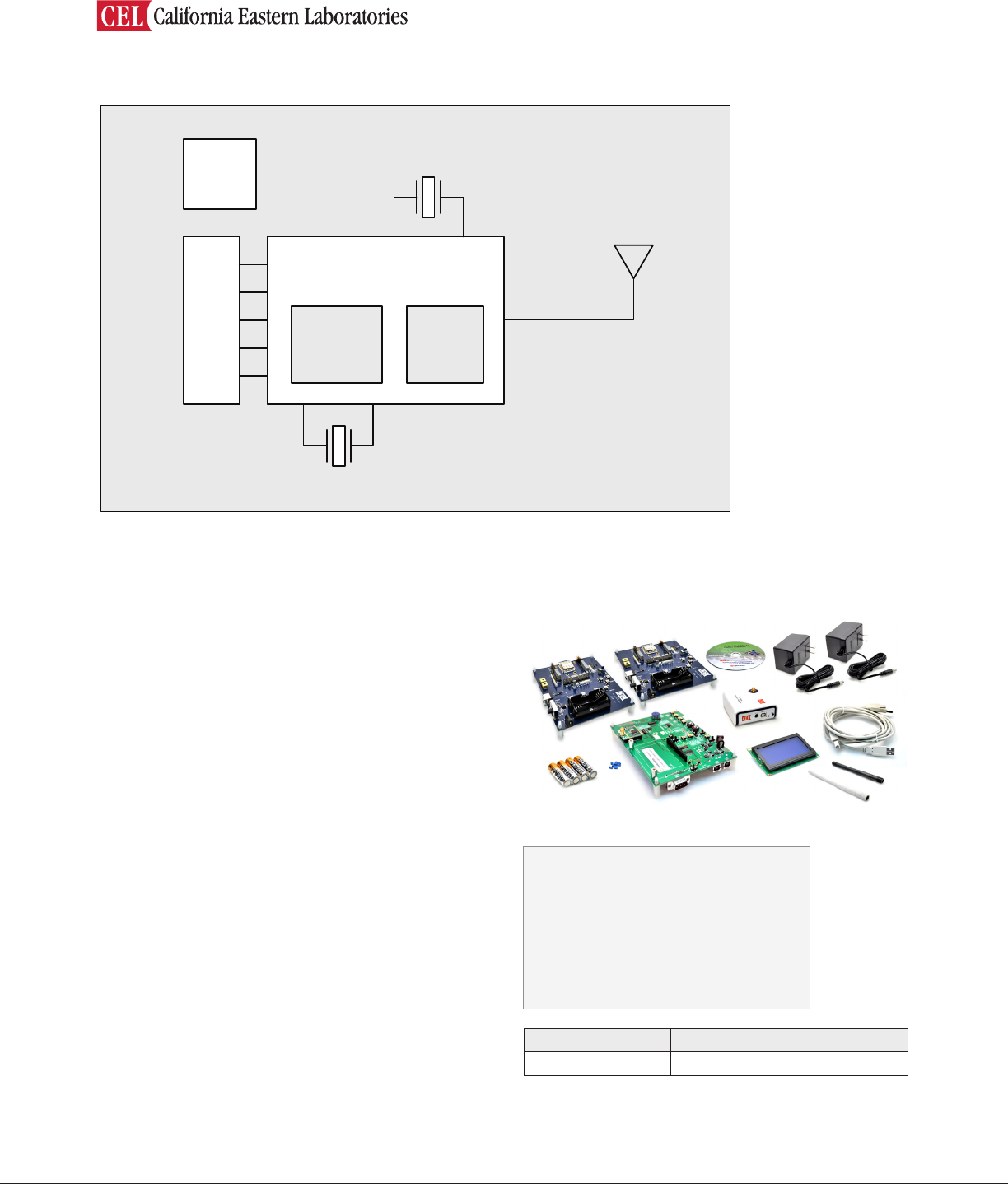
MODULE BLOCK DIAGRAM
16 MHz
32.768 kHz XTAL
XTAL
Radio
Micro
processor
MeshConnect ZIC2410
ANT
Castellation Edge
Connector
PWR
Reg
MeshConnect™ Module
DEVELOPMENT KIT
CEL's MeshConnect Development Kit (ZICM2410P0-KIT1-1)
assist users in both evaluation and development. As a
stand-alone radio system, the kit allows users to place
the modules in to the target environment and evaluate
performance on-site. The MeshConnect Development Kit
also serves as an invaluable aid in application develop-
ment. Through the many interface headers on the board,
the user has access to all the MeshConnect module pins
enabling easy connection to target systems for application
development. The key components of the MeshConnect
Development Kits are the CEL’s MeshConnect radio mod-
ule and the interface board.
The MeshConnect module contains the CEL ZIC2410
transceiver IC, XTALs, Power Regulator and an integrated
PCB antenna and connectors for an external antenna
(optional). The interface board features a serial com-
munication interface, a power management module, and
peripherals such as potentiometers, LEDs, and GPIO
headers. The Development Kit also contains four AA
batteries and two USB cables.
For more detail information regarding MeshConnect
Development Kit, refer to the ZICM2410P0-KIT1-1
Development Kit User Guide document. (Available at
CEL’s website http://www.cel.com)
Kit Contents:
• Evaluation Boards w/Module (3)
• Network Analyzer (1)
• USB Cables (2)
• Jumpers (10)
• AA Batteries (4)
• AC Adapter (2)
• Technical Information CD (1)
Order Number Description
ZICM2410P0-KIT1-1 Engineering Development Kit

MeshConnect™ Module
Page 3
Introduction and Overview
Description.............................................................................................................................................................................................. 1
Features.................................................................................................................................................................................................. 1
Applications............................................................................................................................................................................................ 1
Ordering Information............................................................................................................................................................................. 1
Module Block Diagram........................................................................................................................................................................... 2
Development Kit..................................................................................................................................................................................... 2
System Level Function
Transceiver IC......................................................................................................................................................................................... 4
Modes of Operation (TX, RX, Sleep)...................................................................................................................................................... 5
Power Amplier....................................................................................................................................................................................... 6
Interface.................................................................................................................................................................................................. 6
Software Tools........................................................................................................................................................................................ 6
Electrical Specication
Absolute Maximum Ratings................................................................................................................................................................... 8
Recommended (Operating Condition).................................................................................................................................................. 8
DC Characteristics.................................................................................................................................................................................. 8
RF Characteristics.................................................................................................................................................................................. 8
Pin Signal & Interfaces
Pin Signals I/O Conguration................................................................................................................................................................ 9
I/O Pin Assignment................................................................................................................................................................................. 9
Module Dimensions................................................................................................................................................................................ 11
Processing 13
Agency Certications 14
Shipment, Storage & Handling 15
References & Revision History 16
TABLE OF CONTENTS
MeshConnect™ Module
Page 4
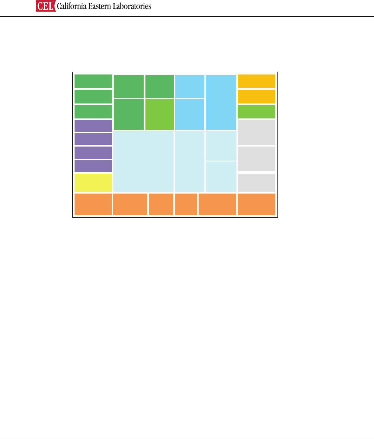
TRANSCEIVER IC
A true monolithic solution, the CEL ZIC2410 IEEE 802.15.4/ZigBee IC incorporates the RF transceiver with baseband
modem, a hardwired MAC, and an embedded 8051 microcontroller, offering an excellent low cost high performance solution
for all IEEE 802.15.4 / ZigBee applications.
With an industry best +6 dBm output power, the ZIC2410 will support a wide a variety of applications without the need for
external amplication. Combined with a highly sensitive -97 dBm receiver the ZICM2410P0 leads the industry with 103 dB
link budget.
In addition to excellent RF performance at ZigBee (250 kbps) data rates, the ZIC2410 adds high speed modes, Turbo
(500 kbps) and Premium (1 Mbps), for networks looking for increased throughput. The device provides numerous general-
purpose I/O pins, peripheral functions such as timers and UART and is one of the rst devices to provide an embedded
Voice CODEC.
CEL provides its customers with the CEL ZigBee Stack as part of the software library. Also available are the hardware &
software tools required to develop custom applications.
The combination of industry leading link budget, high speed RF, and integrate voice CODEC make the ZIC2410 a truly
distinct single chip solution.
PS/2
UART/2
SPI
WDT
GPIO/24
Timer/4
PWM/2
Quad
Key Scan
Digital
Regulator
RC
Oscillator
Clock
PLL POR
RF TX
RF RX
PLL
Temp.
Sensor
Bat
Monitor
ADC
(4CH)
Analog
Regulator
3V
Ciruitry
MCU
(8051) FLASH
96KB
MODEM
MAC
DMA
ADPCM Voice
FIFFO
AES
Engine
a-law
μ-law
DATA
8KB
ROM
MeshConnect™ Module
Page 5
CEL's MeshConnect modules include an integrated Printed Circuit Board (PCB) trace antenna. An optional u.FL connector
can be specied, providing connection to a 50-ohm external antenna of the user’s choice. See Ordering Information on
page 1.
The PCB antenna employs an F-Antenna topology that is compact and supports an omni-directional radiation pattern.
To maximize antenna efciency, an adequate ground plane must be provided on the host PCB. Correctly positioned, the
ground plane on the host PCB (but not directly under the F-Antenna). Correctly positioned, the ground plane on the host
PCB board under the module will contribute signicantly to the antenna performance. The position of the module on the
host board and overall design of the product enclosure contribute to antenna perfor mance. Poor design affects radiation
patterns and can result in reection, diffraction, and/or scattering of the transmitted signal.
Here are some design guidelines to help ensure antenna performance:
• Never place the ground plane or route copper traces directly underneath the antenna portion of the module.
• Never place the antenna close to metallic objects.
• In the overall design, ensure that wiring and other components are not placed near the antenna.
• Do not place the antenna in a metallic or metalized plastic enclosure.
• Keep plastic enclosures 1cm or more from the antenna in any direction.
For optimum antenna performance, the MeshConnect modules should be mounted with the PCB trace antenna
overhanging the edge of the host board. To further improve performance, a ground plane may be placed on the host board
under the module, up to the antenna. The installation of an uninterrupted ground plane on a layer directly beneath the
module will also allow you to run traces under this layer. CEL can provide assistance with your PCB layout.
There are three power down modes in the ZIC2410. Each mode can be set using the PDMODE [1:0] bits in the PDCON
register and power down modes can be started by setting the PDSTART bit to 1. Each mode has a different current
consumption and wake-up sources, please refer to the ZIC2410 datasheet for further information on the available power
down modes.. Table 8 describes the three power down modes.
Table 8 – Power Down Modes
PDMODE [1:0] Description Wake-Up Source Regulator for Digital
block
0 Active (Normal Operation) - -
1 PM1 mode
Hardware Reset,
Sleep Timer interrupt,
External interrupt
ON
2 PM2 mode
Hardware Reset,
Sleep Timer interrupt,
External interrupt
OFF
(After wake-up, register
conguration is required)
3 PM3 mode Hardware Reset,
External interrupt
OFF
(After wake-up, register
conguration is required)
ANTENNA
MODES OF OPERATION

MeshConnect™ Module
Page 6
POWER AMPLIFIER
VOICE CODEC
SOFTWARE TOOLS
The MeshConnect module does not incorporate an external Power Amplier and therefore the RF output port is connected
directly (through matching components) to the RF antenna. As CEL’s ZIC2410 IEEE 802.15.4 / ZigBee transceiver already
offers the industry’s best link budget at 106 dB, even without an external PA the MeshConnect can maintain wireless
connection over long distance (3000 ft line-of-sight).
INTERFACE
The MeshConnect has all major communication interfaces routed from the ZIC2410 to the module edge connectors:
• UART1 & UART 2
• I2S
• SPI
ZIC2410 includes three voice codec algorithms: μ-law, a-law and ADPCM.
The μ-law algorithm is a companding algorithm primarily used in the digital telecommunication systems of North America
and Japan. As with other companding algorithms, its purpose is to reduce the dynamic range of an audio signal. In the
analog domain this can increase the signal-to-noise ratio (SNR) achieved during transmission and in the digital domain, it
can reduce the quantization error (hence increasing signal to quantization noise ratio). These SNR improvements can be
traded for reduced bandwidth and equivalent SNR instead. The a-law algorithm is a standard companding algorithm used in
European digital communications systems to optimize/modify the dynamic range of an analog signal for digitizing.
The a-law algorithm provides a slightly larger dynamic range than the μ-law at the cost of worse proportional distortion for
small signals.
Adaptive DPCM (ADPCM) is a variant of DPCM (Differential (or Delta) pulse-code modulation) that varies the size of the
quantization step, to allow further reduction of the required bandwidth for a given signal-to-noise ratio. DPCM encodes the
PCM values as differences between the current and the previous value. For audio this type of encoding reduces the num-
ber of bits required per sample by about 25% compared to PCM.
CEL offers complete SW tools for MeshConnect that customers need to create their ZigBee application.
PROFILE BUILDER
• Prole Builder allows for easy creation of custom ZigBee proles for use in end-user applications.
• Uses the input requirements to modify a set of ‘C’ source les which include the necessary ZigBee functions.
• Output les will contain the ZigBee Device Object (ZDO) descriptors and the ZigBee Device Prole (ZDP) descriptors.
• The ZDO and ZDP dene the ZigBee node and functionality.
The output les can be seamlessly integrated with the CEL ZigBee stack libraries.

MeshConnect™ Module
Page 7
SOFTWARE TOOLS (Continued)
DEVICE PROGRAMMER
• Device Programmer is used to program the application rmware to the on-chip Flash program memory of the
ZIC2410 device.
• Device Programmer supports:
• ISP Mode: Download the rmware from the host PC via serial communication through the ZIC2410’s
UART1 interface.
• The evaluation boards utilize a USB -> Serial converter
• OTA Mode: Download the rmware from the host PC using wireless communication (Over-The-Air)
• Requires two nodes, the host (connected to a PC) and the target device to be programmed
Device Programmer can read / write hardware information (i.e. IEEE Address, Channel #, etc) directly via the
aforementioned communication modes.
PROFILE SIMULATOR
• Prole Simulator is used to simulate and test a ZigBee network consisting of a coordinator, router and / or end devices.
• Prole Simulator includes:
• Device Manager: Setting parameters of a ZigBee node.
• Bind Manager: Managing “bindings” in a ZigBee network.
• ZStack manager: Setting parameters of a ZigBee network.
• ZigBee Device Wizard: Selects network conguration during ZigBee network formation.
Can be used to generate ZigBee standard primitive functions for MAC, NWK and APS layers and the ZDO and APP.
PACKET ANALYZER AND WIRELESS NETWORK ANALYZER
• Packet Analyzer monitors trafc over a wireless network channel by capturing RF packet data in real-time.
• Packet Analyzer requires the Wireless Network Analyzer to “sniff” the RF packets.
• Also includes diagnostic tools:
• Energy Scan: Evaluates the received signal power within the bandwidth of an IEEE 802.15.4 channel
yielding available channels.
• Active Scan: Scanning for active Coordinators and Routers broadcasting a Beacon frame.
• Packet Analyzer is capable of displaying network conguration (i.e. tree vs. star), network nodes, packet details, etc.
• Can be used in conjunction with any IEEE 802.15.4 or ZigBee network.
KEIL 8051 DEVELOPMENT TOOLS (Evaluation version provided in development kit).
• Supports all 8051 derivatives and variants.
• Easy-to-Use µVision Integrated Development Environment (IDE) supports the complete development cycle.
• Supports memory banking for CODE and variables beyond the 64 kbyte threshold.
Numerous optimization levels yield the ability to place more features into less memory providing the utmost code density.
MeshConnect™ Module
Page 8
ABSOLUTE MAXIMUM RATINGS
Description Min Max Unit
Power Supply Voltage (Vcc) -0.3 3.3 VDC
Voltage on any digital pin -0.3 3.3 VDC
Input RF Level 10 dBm
Storage Temperature -55 125 °C
Reow Soldering Temperature 260 °C
Note: Exceeding the maximum ratings may cause permanent damage to the module or devices.
RECOMMENDED (OPERATING CONDITIONS)
Description Min Typ Max Unit
Operating ambient temperature range, TA-40 25 85 °C
Operating Supply Voltage 2.1 3.0 VDC
Crystal Reference Oscillator 16 MHz
DC CHARACTERISTICS (@ 25°C, VCC = 3.0V unless otherwise noted)
Description Min Typ Max Unit
Vcc Supply (Vcc) 2.1 3.3 VDC
RX mode Current (Vcc = 3.0V) 33 35 38 mA
TX mode Current (Vcc = 3.0V) 40 44 48 mA
Sleep Mode (Deep) Current < 1.0 µA
RF CHARACTERISTICS (@ 25°C, VCC = 3.0V unless otherwise noted)
Description Min Typ Max Unit
Frequency Band (16 – 5MHz wide channels) 2.405 2.480 GHz
RX Sensitivity for 1% PER -97 -90 dBm
TX Output Power 4.8 6.1 6.8 dBm
Error Vector Magnitude 17 35 %
Adjacent Channel Rejection
+/- 5 MHz
+/- 10 MHz
47
51
dB
Frequency Error Tolerance 40 ppm
Output Power Control Range 30 dB
Over the Air Data Rate 250 kbps
Harmonics (2nd & 3rd) -41.2 dBm/MHz
MeshConnect™ Module
Page 9
PIN SIGNALS I/O PORT CONFIGURATION
MeshConnect I/O PIN ASSIGNMENTS
MeshConnect module has 56 edge I/O interfaces for connection to the user’s host board. The MeshConnect Module
Dimensions shows the layout of the 56 edge castellations.
Pin # Name Type Description IC Pin #
1 GND4 RF GND RF Ground
2 GND3 RF GND RF Ground
3 MS1 Control Input
Mode Select, Bit #1. Active Low Internal Voltage Regulator
Enable:
0: Internal Voltage Regulator Enabled
1: Internal Voltage Regulator Disabled, Supply Analog and
Digital Supply Voltages Externally
14
4 GND0 RF GND RF Ground
5 MS0 Control Input Mode Select, Bit #0. This pin should be connected to Ground
externally. 13
6 NC2 N/C No Connect
7 GND20 GND Digital Ground 49
8 GND12 GND Digital Ground 49
9 GND13 GND Digital Ground 49
10 GND17 GND Digital Ground 49
11 GND5 GND Digital Ground 49
12 ACH0 Analog Input A/D Channel #0 Input, 0 - 1.5 Volts. 8
13 ACH1 Analog Input A/D Channel #1 Input, 0 - 1.5 Volts. 9
14 ACH2 Analog Input A/D Channel #2 Input, 0 - 1.5 Volts. 10
15 ACH3 Analog Input A/D Channel #3 Input, 0 - 1.5 Volts. 11
16 P1_7 Digital Output 8051 GPIO P1.7 (Output Only)
Alternate Functions: P0AND 20
17 P1_6 Digital I/O 8051 GPIO P1.6
Alternate Functions: N/A 21
18 P1_4 Digital I/O 8051 GPIO P1.4
Alternate Functions: QUADZB / Sleep Timer Oscillator Input 22
19 P1_3 Digital I/O
8051 GPIO P1.3
Alternate Functions: QUADZA / Sleep Timer Oscillator Output /
RTCLKOUT
23
20 GND9 GND Digital Ground 49
21 GND8 GND Digital Ground 49
22 GND7 GND Digital Ground 49
23 P1_1 Digital I/O 8051 GPIO P1.1
Alternate Functions: TXD1 24
24 VCC_3V Power Input Power Supply Input for Internal Voltage Regulators and Digital I/
Os. VCC = 3.0 Volts 7
25 P1_0 Digital I/O 8051 GPIO P1.0
Alternate Functions: RXD1 26
26 P3_7 Digital I/O 8051 GPIO P3.7 (12 mA Drive)
Alternate Functions: PWM3 / CTS1 / SPICSN 27
27 P3_6 Digital I/O 8051 GPIO P3.6 (12 mA Drive)
Alternate Functions: PWM2 / RTS1 / SPICLK 28
28 P3_5 Digital I/O 8051 GPIO P3.5
Alternate Functions: T1 / CTS0 / QUADYB / SPIDO 29
29 P3_4 Digital I/O 8051 GPIO P3.4
Alternate Functions: T0 / RTS0 / QUADYA / SPIDI 30
30 GND10 GND Digital Ground 49
MeshConnect™ Module
Page 10
MeshConnect I/O PIN ASSIGNMENTS (Continued)
Pin # Name Type Description IC Pin #
31 P3_3 Digital I/O 8051 GPIO P3.3
Alternate Functions: INT1 (Active Low) 31
32 P3_2 Digital I/O 8051 GPIO P3.2
Alternate Functions: INT0 (Active Low) 32
33 GND11 GND Digital Ground 49
34 P3_1 Digital I/O 8051 GPIO P3.1
Alternate Functions: TXD0 / QUADXB 33
35 P3_0 Digital I/O 8051 GPIO P3.0
Alternate Functions: RXD0 / QUADXA 35
36 GND6 GND Digital Ground 49
37 P0_7 Digital I/O 8051 GPIO P0.7
Alternate Functions: I2STX_MCLK 36
38 P0_6 Digital I/O 8051 GPIO P0.6
Alternate Functions: I2STX_BCLK 37
39 P0_5 Digital I/O 8051 GPIO P0.5
Alternate Functions: I2STX_LRCLK 38
40 P0_4 Digital I/O 8051 GPIO P0.4
Alternate Functions: I2STX_DO 39
41 P0_3 Digital I/O 8051 GPIO P0.3
Alternate Functions: I2SRX_MCLK 40
42 P0_2 Digital I/O 8051 GPIO P0.2
Alternate Functions: I2SRX_BCLK 41
43 P0_1 Digital I/O 8051 GPIO P0.1
Alternate Functions: I2SRX_LRCLK 42
44 P0_0 Digital I/O 8051 GPIO P0.0
Alternate Functions: I2SRX_DI 43
45 DVDD_1_5 Power I/O
Digital Power Supply I/O
Input: When the Mode Select Bit #1 (MS1, Module Pin #3) is
tied high this pin functions as the 1.5 Volt power supply input for
the Digital Core.
Output: When the Mode Select Bit #1 (MS1, Module Pin #3)
is tied low this pin functions as the output of the Internal Digital
Voltage Regulator (1.5 Volts).
19
46 ISP Control Input
Mode Select, Bit #2. Active High In-System Programming (ISP)
Input:
0: Normal Mode
1: ISP Mode
15
47 RESET# Control Reset (Active Low) 17
48 AVDD_1_5 Power I/O
Analog Power Supply I/O
Input: When the Mode Select Bit #1 (MS1, Module Pin #3) is
tied high this pin functions as the 1.5 Volt power supply input for
the Mixer, VGA and LPF.
Output: When the Mode Select Bit #1 (MS1, Module Pin #3)
is tied low this pin functions as the output of the Internal Analog
Voltage Regulator (1.5 Volts).
6
49 GND14 GND Digital Ground 49
50 GND15 GND Digital Ground 49
51 GND16 GND Digital Ground 49
52 GND18 GND Digital Ground 49
53 GND19 GND Digital Ground 49
54 NC1 N/C No Connect
55 GND1 RF GND RF Ground
56 GND2 RF GND RF Ground
MeshConnect™ Module
Page 11
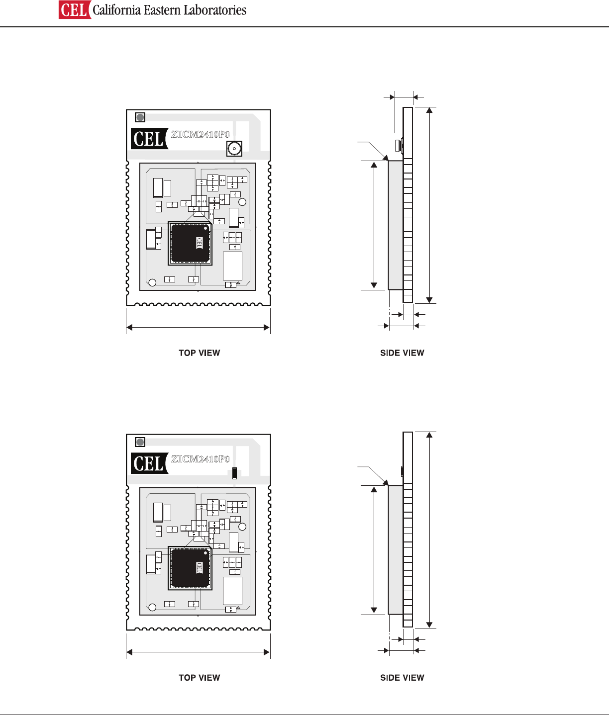
MODULE DIMENSIONS
1.000” 0.193”
0.895”
1.350”
0.062”
0.111”
RF Shield
R6
R7
U1
R1
C7 C7B
L4
L3
C11
R10
C21
C20
L5
R11 C23
C22
R8
C5B
C24
C13
C6A C1
C2
R5
L6
C6B
C6
L2
C14
C10
C9 R2
R9
C15
C16
R4
C17
C4A
XTAL1
ZICM2410P0
0007000000001
J2
Pin 1
Pin 19 Pin 38
Pin 56
0R
C25
ZIC2410
QN48
1.000” 0.193”
0.895”
1.350”
0.062”
RF Shield
R6
R7
U1
R1
C7 C7B
L4
L3
C11
R10
C21
C20
L5
R11 C23
C22
R8
C5B
C24
C13
C6A C1
C2
R5
L6
C6B
C6
L2
C14
C10
C9 R2
R9
C15
C16
R4
C17
C4A
XTAL1
ZICM2410P0
0007000000001
J2
Pin 1
Pin 19 Pin 38
Pin 56
0R
C25
ZIC2410
QN48
For layout recommendation for optimum antenna performance, refer to Antenna section in this document.
MeshConnect ZICM2410P0-1
MeshConnect ZICM2410P0-1C
MeshConnect™ Module
Page 12
MODULE LAND FOOTPRINT
Note: Unless otherwise specied. Dimensions are in Inches [mm].
1.100 [27.94]
1.000 [25.41]
0.990 [22.61]
0.105 [2.67]
0.050 [1.27]
COPPER KEEPOUT 0.298 [27.94]
0.940 [23.88]
1.055 [26.80]
0.050 [1.27] Pitch
56 x 0.040 [1.02]
56 x 0.100 [2.54]
MeshConnect™ Module
Page 13
PROCESSING
Recommended Reow Prole
Parameters Values
Ramp up rate (from Tsoakmax to Tpeak) 3º/sec max
Minimum Soak Temperature 150ºC
Maximum Soak Temperature 200ºC
Soak Time 60-120 sec
TLiquidus 217ºC
Time above TL 60-150 sec
Tpeak 260 + 0ºC
Time within 5º of Tpeak 20-30 sec
Time from 25º to Tpeak 8 min max
Ramp down rate 6ºC/sec max
Achieve the brightest possible solder llets with a good shape and low contact angle.
Pb-Free Soldering Paste
Use of “No Clean” soldering paste is strongly recommended, as it does not require cleaning after the soldering process.
Note: The quality of solder joints on the castellations (‘half vias’) where they contact the host board should meet the appropriate IPC Speci-
cation. See IPC-A-610-D "Acceptability of Electronic Assemblies, section 8.2.4 Castellated Terminations.”
Cleaning
In general, cleaning the populated modules is strongly discouraged. Residuals under the module cannot be easily removed
with any cleaning process.
• Cleaning with water can lead to capillary effects where water is absorbed into the gap between the host board and
the module. The combination of soldering ux residuals and encapsulated water could lead to short circuits between
neighboring pads. Water could also damage any stickers or labels.
• Cleaning with alcohol or a similar organic solvent will likely ood soldering ux residuals into the two housings, which
is not accessible for post-washing inspection. The solvent could also damage any stickers or labels.
• Ultrasonic cleaning could damage the module permanently.
The best approach is to consider using a “no clean” soldering paste and eliminate the post-soldering cleaning step.
Optical Inspection
After soldering the Module to the host board, consider optical inspection to check the following:
• Proper alignment and centering of the module over the pads.
• Proper solder joints on all pads.
• Excessive solder or contacts to neighboring pads, or vias.
Repeating Reow Soldering
Only a single reow soldering process is encouraged for host boards.
Wave Soldering
If a wave soldering process is required on the host boards due to the presence of leaded components, only a single wave
soldering process is encouraged.

MeshConnect™ Module
Page 14
PROCESSING (Continued)
AGENCY CERTIFICATIONS
Hand Soldering
Hand soldering is possible. Use a soldering iron temperature setting equivalent to 350°C, follow IPC recommendations/
reference document IPC-7711.
Rework
The MeshConnect Module can be unsoldered from the host board. Use of a hot air rework tool and hot plate for pre-heating
from underneath is recommended. Avoid overheating.
Warning Never attempt a rework on the module itself, e.g. replacing individual components. Such actions will
terminate warranty coverage.
Additional Grounding
Attempts to improve module or system grounding by soldering braids, wires, or cables onto the module RF shield cover is
done at the customers own risk. The numerous ground pins at the module perimeter should be sufcient for optimum
immunity to external RF interference.
FCC Compliance Statement (Part 15.19) Section 7.15 of RSS-GEN
This device complies with Part 15 of the FCC Rules. Operation is subject to the following two conditions:
1. This device may not cause harmful interference.
2. This device must accept any interference received, including interference that may cause undesired operation.
Warning (Part 15.21)
Changes or modications not expressly approved by CEL could void the user's authority to operate the equipment.
20 cm Separation Distance
To comply with FCC/IC RF exposure limits for general population / uncontrolled exposure, the antenna(s) used for this
transmitter must be installed to provide a separation distance of at least 20 cm from all persons and must not be co-located
or operating in conjunction with any other antenna or transmitter.
OEM Responsibility to the FCC Rules and Regulations
The MeshConnect Module has been certied per FCC Part 15 rules for integration into products without further testing or
certication. To fulll the FCC certication requirements the OEM of the MeshConnect Module must ensure that the
information provided on the MeshConnect Label is placed on the outside of the nal product. The MeshConnect Module is
labeled with its own FCC ID Number. If the FCC ID is not visible when the module is installed inside another device, then
the outside of the device into which the module is installed must also display a label referring to the enclosed module. This
exterior label can use wording such as the following: “Contains Transmitter Module FCC ID: W7Z-ZIC2410P0” or “Contains
FCC ID: W7Z-ZIC2410P0”
The OEM of the MeshConnect Module must only use the approved antenna, (PCB Trace Antenna) that has been certied
with this module. The OEM of the MeshConnect Module must test their nal product conguration to comply with Uninten-
tional Radiator Limits before declaring FCC compliance per Part 15 of the FCC rules.
MeshConnect™ Module
Page 15
AGENCY CERTIFICATIONS (Continued)
SHIPMENT, HANDLING, AND STORAGE
Shipment
The MeshConnect Modules are delivered in trays of 28.
Handling
The MeshConnect Modules are designed and packaged to be processed in an automated assembly line.
Warning The MeshConnect Modules contain highly sensitive electronic circuitry. Handling without proper ESD
protection may destroy or damage the module permanently.
Warning According to JEDEC ISP, the MeshConnect Modules are moisture sensitive devices. Appropriate handling instruc-
tions and precautions are summarized in Section 2.1. Read carefully to prevent permanent damage due to moisture intake.
Moisture Sensitivity Level (MSL)
MSL 3, per J-STD-033
Storage
Storage/shelf life in sealed bags is 12 months at <40°C and <90% relative humidity.
IC Certication — Industry Canada Statement
The term "IC" before the certication / registration number only signies that the Industry Canada technical specications
were met.
Section 14 of RSS-210
The installer of this radio equipment must ensure that the antenna is located or pointed such that it does not emit RF eld in
excess of Health Canada limits for the general population. Consult Safety Code 6, obtainable from Health Canada's
website: http://www.hc-sc.gc.ca/ewh-semt/pubs/radiation/99ehd-dhm237/index-eng.php
CE Certication — Europe
The MeshConnect RF module has been tested and certied for use in the European Union.
OEM Responsibility to the European Union Compliance Rules
If the MeshConnect module is to be incorporated into a product, the OEM must verify compliance of the nal product to the
European Harmonized EMC and Low-Voltage / Safety Standards. A Declaration of Conformity must be issued for each of
these standards and kept on le as described in Annex II of the R&TTE Directive.
The manufacturer must maintain the user's guide and adhere to the settings described in the manual for maintaining
European Union Compliance. If any of the specications are exceeded in the nal product, the OEM is required to
make a submission to the notied body for compliance testing.
OEM Labeling Requirements
The `CE' mark must be placed on the OEM product in a visible location.
The CE mark shall consist of the initials “CE” with the following form:
· If the CE marking is reduced or enlarged, the proportions given in the above graduated
drawing must be adhered to.
· The CE mark must be a minimum of 5mm in height
· The CE marking must be afxed visibly, legibly, and indelibly Since the 2400 - 2483.5 MHz
band is not harmonized by a few countries throughout Europe, the Restriction sign must be
placed to the right of the `CE' marking as shown in the picture
MeshConnect™ Module
Page 16
REFERENCES & REVISION HISTORY
Previous Versions Changes to Current Version Page(s)
0007-00-07-00-000
(Issue A) February 05, 2009 Initial preliminary datasheet. N/A
0007-00-07-00-000
(Issue B) May 14, 2009 Agency Certication 14, 15
Disclaimer
• The information in this document is current as of May, 2009. The information is subject to change without
notice. For actual design-in, refer to the latest publications of CEL data sheets or data books, etc., for the most
up-to-date specications of CEL products. Not all products and/or types are available in every country. Please
check with an CEL sales representative for availability and additional information.
• No part of this document may be copied or reproduced in any form or by any means without the prior written
consent of CEL. CEL assumes no responsibility for any errors that may appear in this document.
• CEL does not assume any liability for infringement of patents, copyrights or other intellectual property rights of
third parties by or arising from the use of CEL products listed in this document or any other liability arising from the
use of such products. No license, express, implied or otherwise, is granted under any patents, copyrights or other
intellectual property rights of CEL or others.
• Descriptions of circuits, software and other related information in this document are provided for illustrative
purposes in semiconductor product operation and application examples. The incorporation of these circuits,
software and information in the design of a customer’s equipment shall be done under the full responsibility of the
customer. CEL assumes no responsibility for any losses incurred by customers or third parties arising from the use
of these circuits, software and information.
• While CEL endeavors to enhance the quality, reliability and safety of CEL products, customers agree and
acknowledge that the possibility of defects thereof cannot be eliminated entirely. To minimize risks of damage to
property or injury (including death) to persons arising from defects in CEL products, customers must incorporate
sufcient safety measures in their design, such as redundancy, re-containment and anti-failure features.