California Eastern Laboratories ZIC2410P2 MeshConnect Extended Range ZigBee Module User Manual Exhibit D Users Manual per 2 1033 b3
California Eastern Laboratories MeshConnect Extended Range ZigBee Module Exhibit D Users Manual per 2 1033 b3
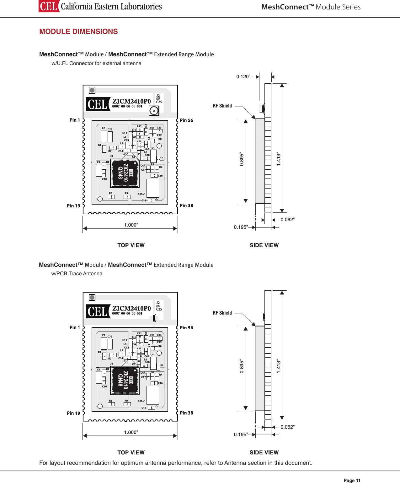
Exhibit D Users Manual per 2 1033 b3
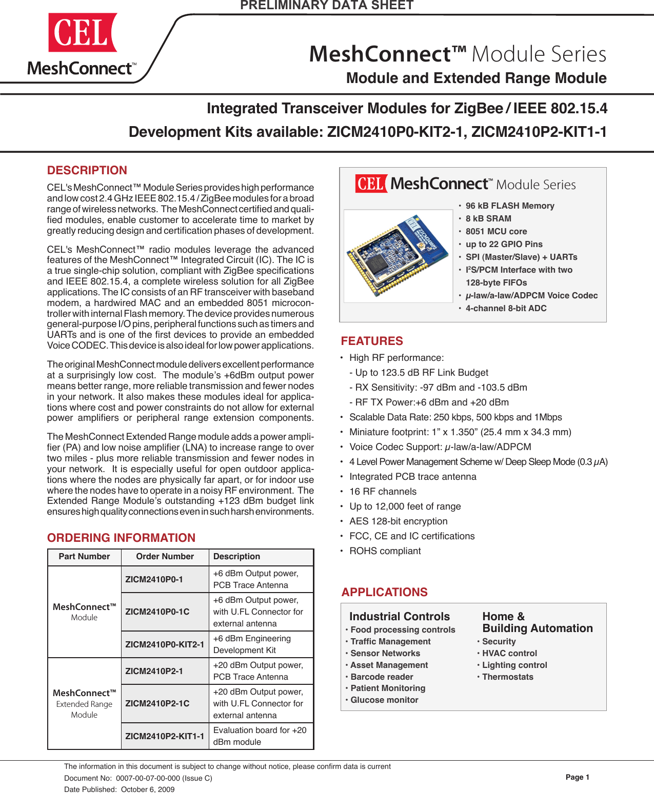
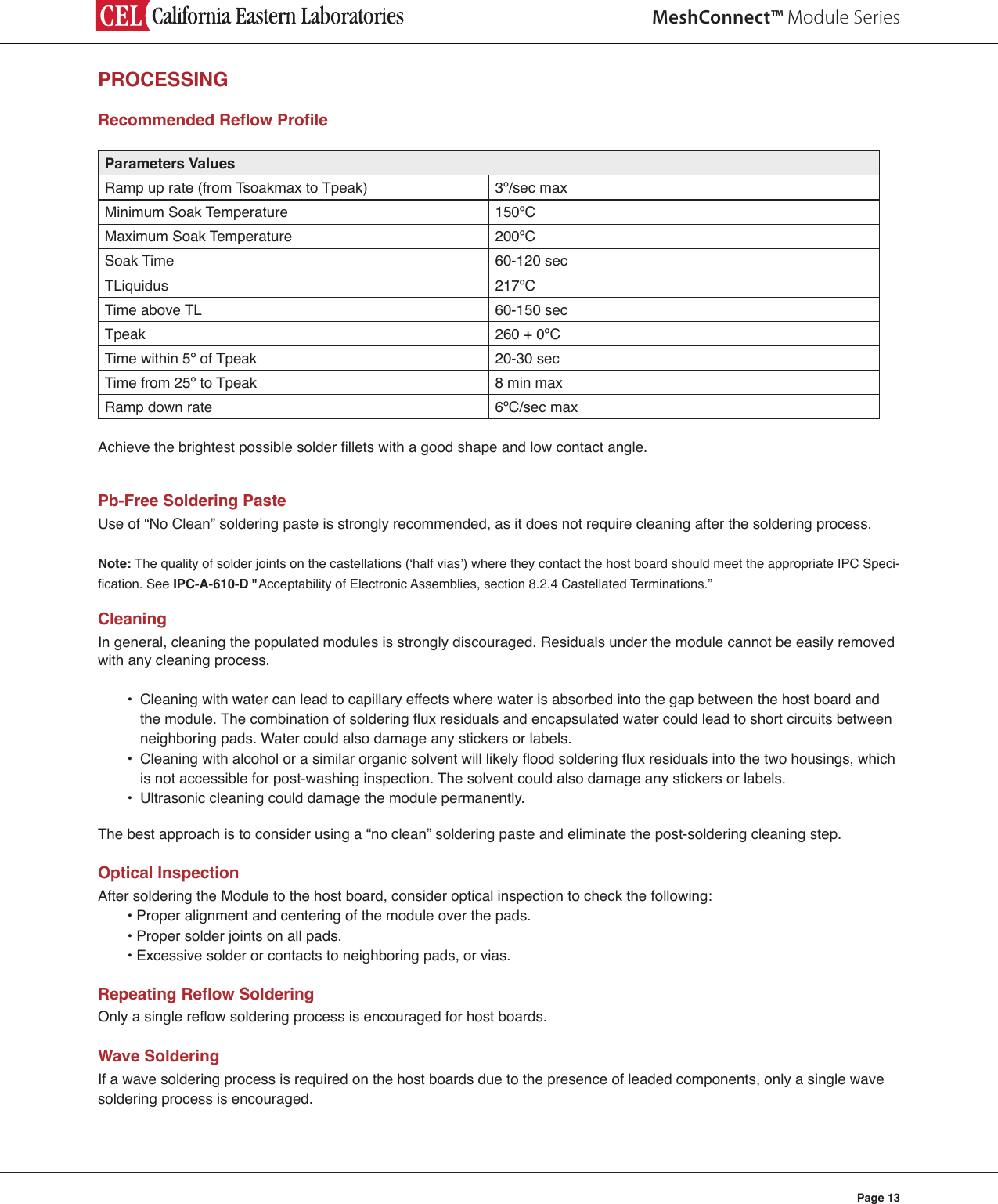
![MeshConnect™ Module SeriesPage 5CEL's MeshConnect modules include an integrated Printed Circuit Board (PCB) trace antenna. An optional u.FL connector can be specied, providing connection to a 50-ohm external antenna of the user’s choice. See Ordering Information on page 1. The PCB antenna employs an F-Antenna topology that is compact and supports an omni-directional radiation pattern. To maximize antenna efciency, an adequate ground plane must be provided on the host PCB. Correctly positioned, the ground plane on the host PCB will contribute signicantly to the antenna performance (it should not be directly under the F-Antenna). The position of the module on the host board and overall design of the product enclosure contribute to antenna perfor mance. Poor design affects radiation patterns and can result in reection, diffraction, and/or scattering of the transmitted signal. Here are some design guidelines to help ensure antenna performance: • Never place the ground plane or route copper traces directly underneath the antenna portion of the module. • Never place the antenna close to metallic objects. • In the overall design, ensure that wiring and other components are not placed near the antenna. • Do not place the antenna in a metallic or metalized plastic enclosure. • Keep plastic enclosures 1cm or more from the antenna in any direction.For optimum antenna performance, the MeshConnect modules should be mounted with the PCB trace antenna overhanging the edge of the host board. To further improve performance, a ground plane may be placed on the host board under the module, up to the antenna. The installation of an uninterrupted ground plane on a layer directly beneath the module will also allow you to run traces under this layer. CEL can provide assistance with your PCB layout.There are three power down modes in the IC. Each mode can be set using the PDMODE [1:0] bits in the PDCON register and power down modes can be started by setting the PDSTART bit to 1. Each mode has a different current consumption and wake-up sources, please refer to the IC datasheet for further information on the available power down modes. Table 8 describes the three power down modes. Table 8 – Power Down Modes PDMODE [1:0] Description Wake-Up Source Regulator for Digital block0 Active (Normal Operation) - - 1 PM1 mode Hardware Reset, Sleep Timer interrupt, External interrupt ON 2 PM2 mode Hardware Reset, Sleep Timer interrupt, External interrupt OFF (After wake-up, register conguration is required) 3 PM3 mode Hardware Reset, External interrupt OFF (After wake-up, register conguration is required) ANTENNAMODES OF OPERATION](https://usermanual.wiki/California-Eastern-Laboratories/ZIC2410P2/User-Guide-1200125-Page-5.png)
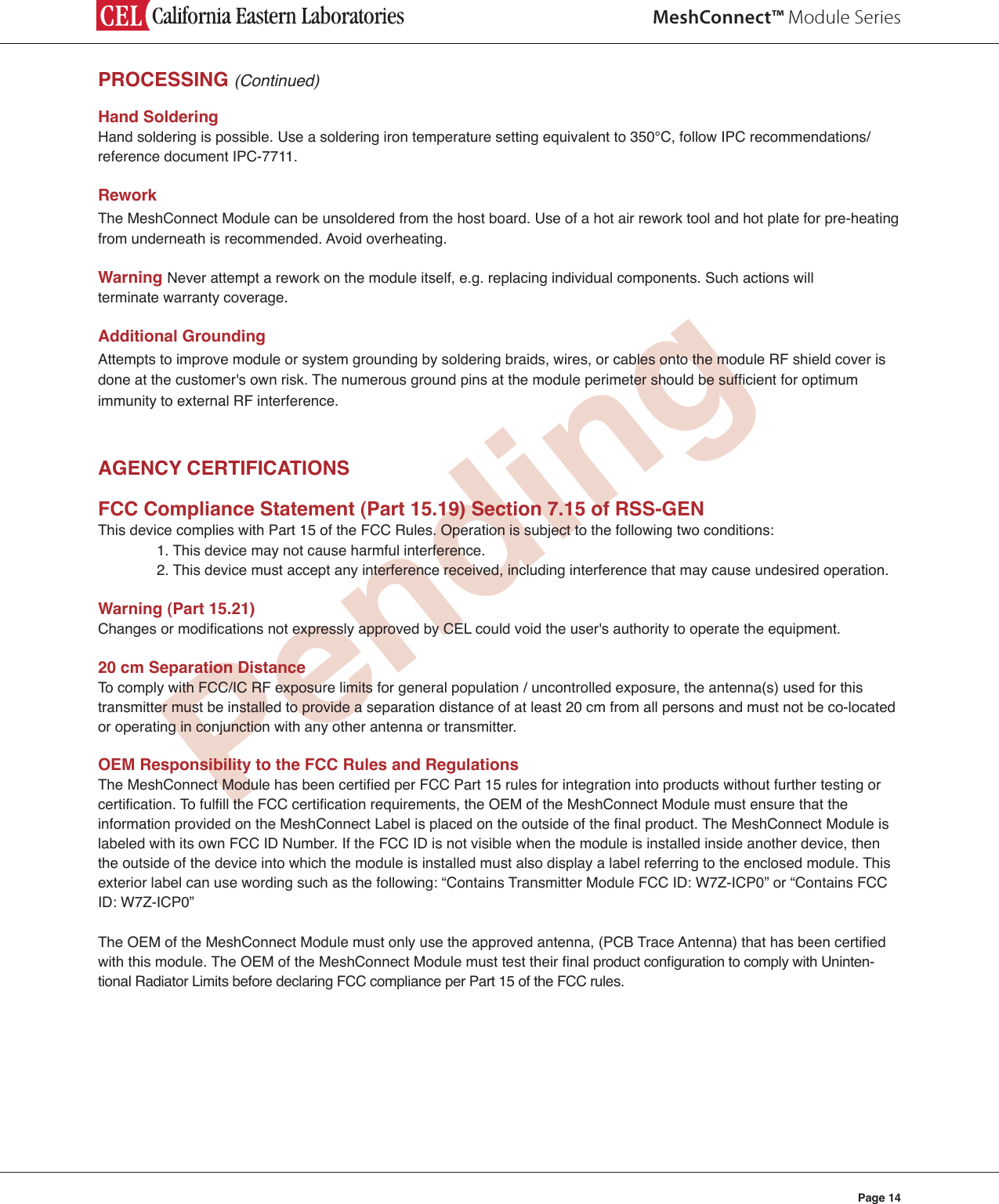
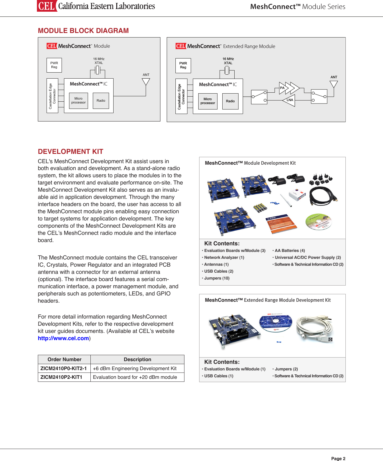
![MeshConnect™ Module SeriesPage 6POWER AMPLIFIERVOICE CODECSOFTWARE TOOLSThe orginal MeshConnect module does not incorporate an external Power Amplier and therefore the RF output port is connected directly (through matching components) to the RF antenna. As CEL’s IC IEEE 802.15.4 / ZigBee transceiver already offers the industry’s best link budget at 106 dB, even without an external PA the MeshConnect can maintain wireless connection over long distance (3,000 ft line-of-sight).The Extended Range module adds both an PA and LNA to optimize RF performance. The NEC uPG2250 PA enable the Extended Range module to output up to +20 dBm transmit power. In the receive path the addition of the UPC8233 LNA boosts the already sensitive receiver up to -103.5 dBm. The Extended Range link budget boasts a very robust 123.5 dBm enabling a line of sight range over 2 miles. INTERFACEThe MeshConnect has all major communication interfaces routed from the IC to the module edge connectors: • UART1 & UART 2 • I2S • SPI The MeshConnect IC includes three voice codec algorithms: μ-law, a-law and ADPCM.The μ-law algorithm is a companding algorithm primarily used in the digital telecommunication systems of North America and Japan. As with other companding algorithms, its purpose is to reduce the dynamic range of an audio signal. In the analog domain this can increase the signal-to-noise ratio (SNR) achieved during transmission and in the digital domain, it can reduce the quantization error (hence increasing signal to quantization noise ratio). These SNR improvements can be traded for reduced bandwidth and equivalent SNR instead. The a-law algorithm is a standard companding algorithm used in European digital communications systems to optimize/modify the dynamic range of an analog signal for digitizing. The a-law algorithm provides a slightly larger dynamic range than the μ-law at the cost of worse proportional distortion for small signals. Adaptive DPCM (ADPCM) is a variant of DPCM [Differential (or Delta) pulse-code modulation] that varies the size of the quantization step, allowing further reduction of the required bandwidth for a given signal-to-noise ratio. DPCM encodes the PCM values as differences between the current and the previous value. For audio applications this type of encoding reduces the number of bits required per sample by about 25% compared to PCM.CEL offers complete SW tools for MeshConnect that customers need to create their ZigBee application. PROFILE BUILDER • Prole Builder allows for easy creation of custom ZigBee proles for use in end-user applications. • Uses the input requirements to modify a set of ‘C’ source les which include the necessary ZigBee functions. • Output les will contain the ZigBee Device Object (ZDO) descriptors and the ZigBee Device Prole (ZDP) descriptors. • The ZDO and ZDP dene the ZigBee node and functionality.The output les can be seamlessly integrated with the CEL ZigBee stack libraries.](https://usermanual.wiki/California-Eastern-Laboratories/ZIC2410P2/User-Guide-1200125-Page-6.png)
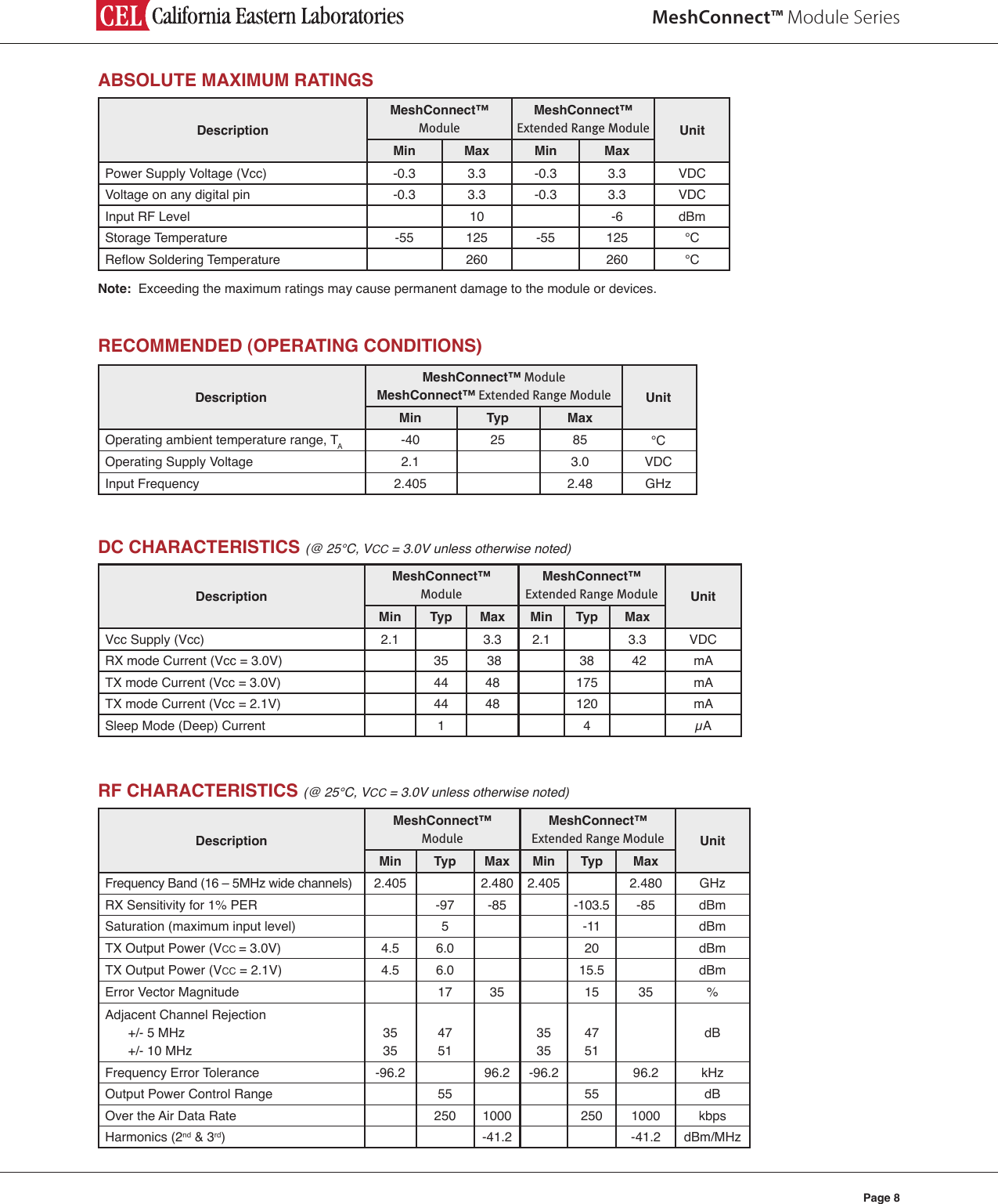
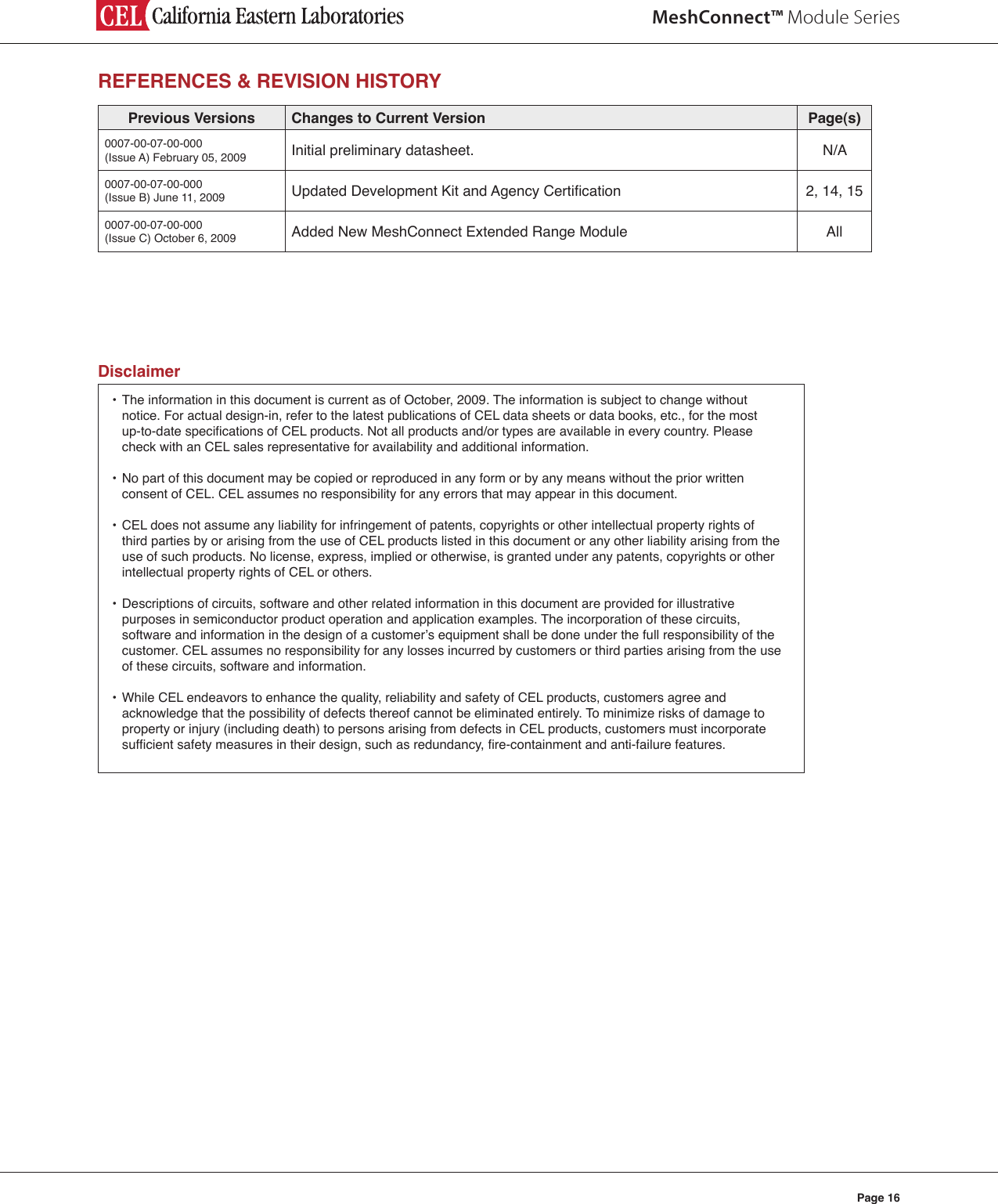
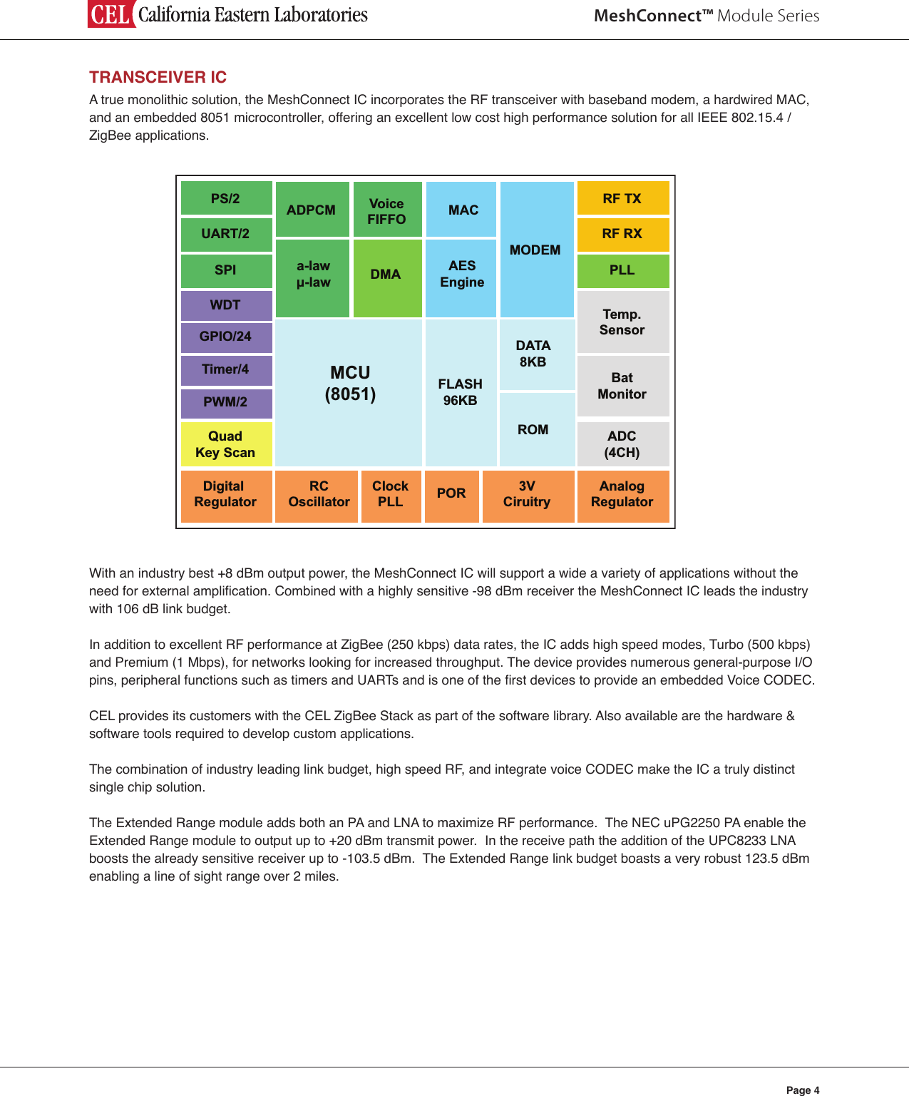
![MeshConnect™ Module SeriesPage 12MODULE LAND FOOTPRINTNote: Unless otherwise specied. Dimensions are in Inches [mm].1.100 [27.94]1.000 [25.41]0.990 [22.61]0.105 [2.67]0.050 [1.27]COPPER KEEPOUT 0.361 [9.17]0.940 [23.88]1.055 [26.80]0.050 [1.27] Pitch56 x 0.040 [1.02]56 x 0.100 [2.54]](https://usermanual.wiki/California-Eastern-Laboratories/ZIC2410P2/User-Guide-1200125-Page-12.png)