California Eastern Laboratories ZICM357SP0 MeshConnect ZICM357SP0-1C Zigbee Module User Manual External Antenna Manual V3
California Eastern Laboratories MeshConnect ZICM357SP0-1C Zigbee Module External Antenna Manual V3
Contents
- 1. Users Manual
- 2. External Antenna Manual V3
- 3. Users Manual V2
External Antenna Manual V3
0011-00-16-11-000
Mini Module External Antenna Implementation
INTRODUCTION
This Technical Note describes the host board layout
requirements for using an external antenna with the
MeshConnect™ ZigBee and Thread
Mini Modules from
California Eastern Laboratories (CEL). The ZigBee and
Thread ZICM35x Mini Modules have been certified for
use with an external antenna through the use of the
Mini Module castellation pin, a U.FL connector, a U.FL
cable assembly and the specified external antenna. For
the B1010SPx Mini Modules please refer to the
datasheet for latest regulatory certification. This
document deta ils the implementation required to
be compliant with the regulatory certification. In order
to preserve the Modular Radio certification, the
integrator of the module must abide by these
layout recommendations outlined in this
document. Any divergence from these
recommendations will invalidate the modular
radio certifications and require the integrator to
re-certify the module and/or end-product.
Technical Note
This document is subject to change without notice.
Document No: 0011-00-16-11-000 (Issue C)
Date Published: July 21, 2016
Page 1
Document No:
0011-00-16-11-000 (Issue C)

Mini Module External
A
ntenna Implementation
This document is subject to change without notice.
Document No: 0011-00-16-11-000 (Issue C) Page 2
TABLE OF CONTENTS
Introduction......................................................................................................................................................................................... 1
Coplanar Waveguide
.......................................................................................................................................................................
1
Components Used in the Implementation............................................................................................................................ 3
Design Verification Test Procedure......................................................................................................................................... 5
Production Test Procedure for Ensuring Compliance ................................................................................................. 5
References.......................................................................................................................................................................................... 6
Revision History
...............................................................................................................................................................................
6
Mini Module External
A
ntenna Implementation
This document is subject to change without notice.
Document No: 0011-00-16-11-000 (Issue C) Page 3
COPLANAR WAVEGUIDE
An RF coplanar waveguide with ground plane structure consists of an RF trace on the topside of the printed circuit board
with adjacent ground planes spaced close to the RF transmission line. A ground plane under the RF trace should also
exist directly below the transmission line. Since the module castellation pad is 40 mils wide on the bottom of the module,
an RF trace width of 40 mils, along with a gap of 8 mils separation from the ground plane, will result in a 50 Ω
transmission line on a standard two layer FR4 printed circuit board with a thickness of 0.062 inches. Using the
transmission line width equal to the castellation pad width eliminates any RF discontinuity which could degrade the return
loss.
PCB Implementation Requirements
The ZICM35xSP0-1C was certified with two external antennas and the ZICM35xSP2-1C was certified with one external
antenna. The first implementation uses a U.FL non-standard connector to interface to an external antenna with its own
coaxial cable. The second configuration for the ZICM35xSP0-1C uses the non-standard reverse polarity SMA (RP-SMA)
end launch connector to interface to a 3" cable and external antenna.
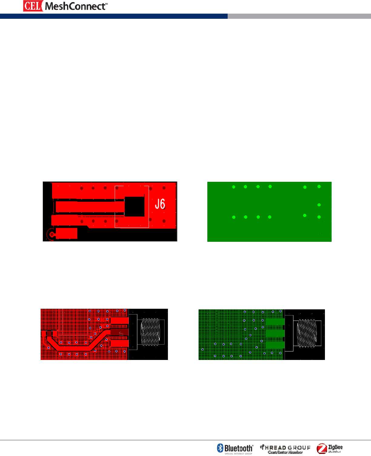
The figures below detail the Gerber layout for the using a U.FL connector for both the ZICM35xSP0-1C and the
ZICM35xSP2-1C. The transmission line is 40 mils wide with an 8 mil gap to the ground. The length of the transmission
line is 200 mils long from the castellation pad to the edge of the U.FL connector. Figure 1 below represents the top layer,
while Figure 2 is the bottom layer on the two layer FR4 printed circuit board.
Figure 1. Top Layer Figure 2. Bottom Layer
The second configuration is detailed below and pertains only to the ZICM35xSP0-1C. Once again a 400mil wide trace
with an 8 mil gap to the adjacent ground planes. It extends from the module footprint to the edge launch RP-SMA
connector which has been placed 200 mils from the top edge of the module. The RF trace is 590 mils in length between
the pad of the module and the RPSMA center pin. A continuous ground plane must be present under the RF trace once
again.
Mini Module External
A
ntenna Implementation
This document is subject to change without notice.
Document No: 0011-00-16-11-000 (Issue C) Page 4
COMPONENTS USED IN THE IMPLEMENTATION
The following components specify the requirements for this implementation:
• CEL Module Part Number: ZICM35xSP0-1C is certified with external Antennas "E-2820-CA" & LSR 001-0100"
• CEL Module Part Number: ZICM35xSP2-1C is certified with external antenna "Nearson S181AH-2450S"
• U.FL Connector Part Number: U.FL-R-SMT(10) from Hirose Electric Co. Ltd.
• RP-SMA end launch Part Number: Amphenol 132255RP
• Host Board: FR4 two layer, 0.062” thick with dielectric constant of 4.2 typical. The transmission line between the
module and the U.FL connector should be a straight line with a width of 40 mils, and ground plane spaced 8 mils apart
on the top layer. The bottom layer should be a continuous ground plane under the transmission line. Ground vias
should be included between the module castellation pins and the U.FL connector ground pads to provide a good
RF ground connection.
• Connectors, Cable assemblies, and antennas must be as specified in photos below or equivalent.
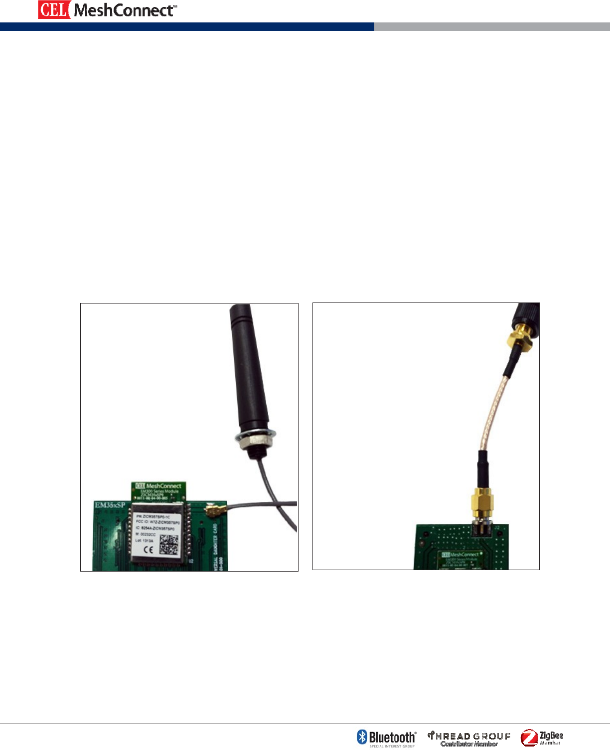
Figure 3 and 4 below illustrates the implementation.
Part Number ZICM35xSP1-1C
External Antenna Implementation
Figure 3. Implementation using connector, cable and external antenna
Antenna: 001-0100
Cable: 095D1ASMARG316
Edge Mount Reverse Polarity SMA Connector
Antenna + Cable Assembly
E-2820-CA
Mini Module External
A
ntenna Implementation
This document is subject to change without notice.
Document No: 0011-00-16-11-000 (Issue C) Page 5
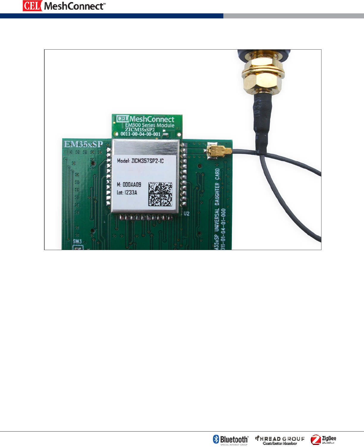
Part Number ZICM35xSP2-1C
External Antenna Implementation
Figure 4. Implementation using connector, cable and external antenna
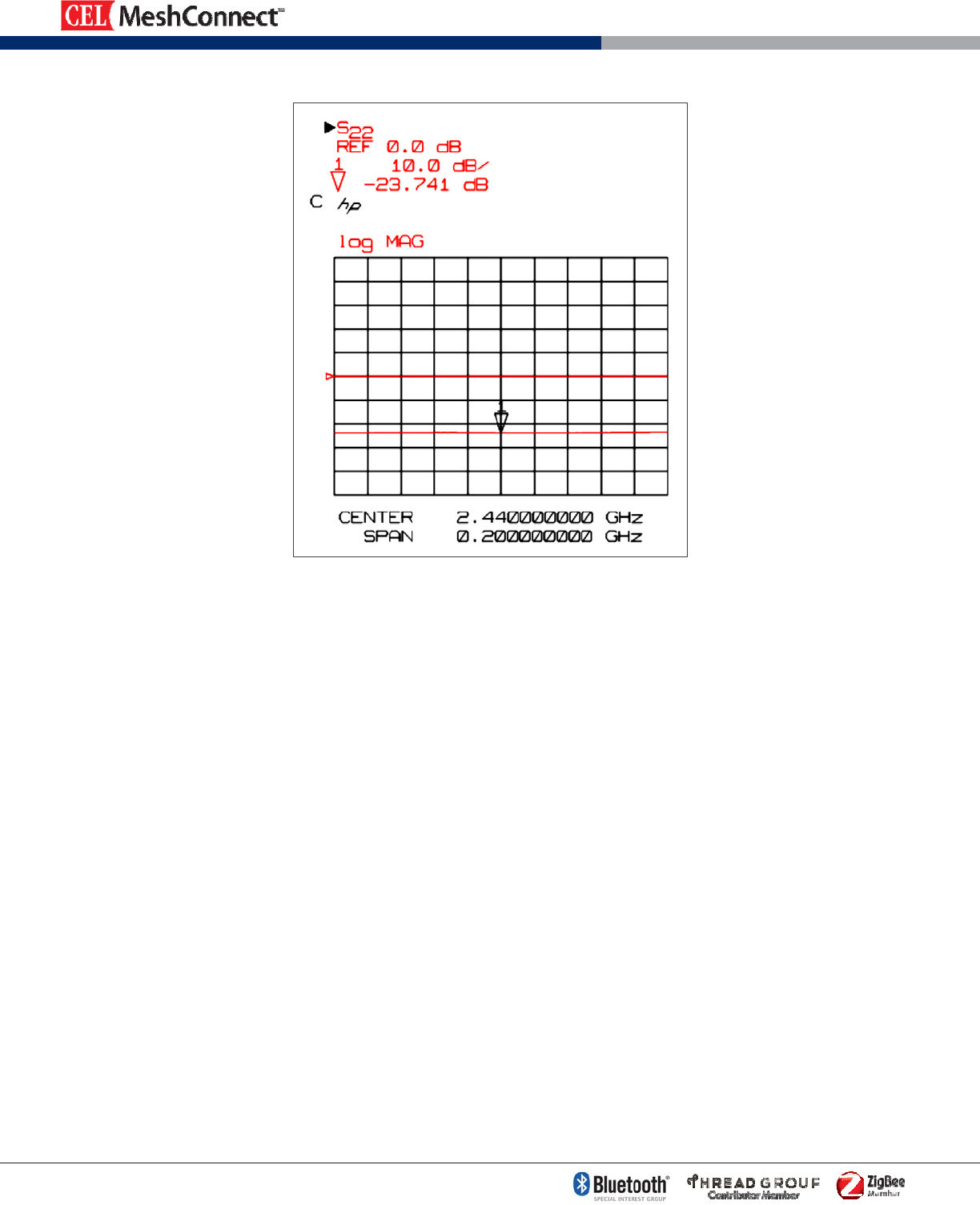
DESIGN VERIFICATION TEST PROCEDURE
Any manufacturer that chooses to implement the external antenna on their host board should verify that the implementation
was done properly. To assist with this, the following Test Procedure can be used. The procedure uses a Network Analyzer
capable of making return loss measurements at 2.4 GHz.
1.
Calibrate the network analyzer for a one port measurement with a center frequency of 2.44 GHz and a span of 200 MHz.
2.
Take a blank host board and solder a 100 Ω resistor between castellation Pin 31 and 32.
3.
Solder a second 100 Ω resistor between castellation Pin 32 and 33.
4.
Solder the U.FL connector on the host board.
5.
Using the appropriate U.FL to SMA adapter for your network analyzer, measure the Return Loss of the trace,
(either S11 or S22 depending on which port was chosen during the 1-port calibration).
6.
A return loss of -15 dB or lower indicates an acceptable implementation (PASS).
Antenna: S181AH-2450S
Cable: 336320-12-0100
U.FL-R-SMT connector
Mini Module External
A
ntenna Implementation
This document is subject to change without notice.
Document No: 0011-00-16-11-000 (Issue C) Page 6
Figure 5. displays the measurement where Port 2 was used as the measurement Port.
Figure 5. Measured Return Loss of RF trace
PRODUCTION TEST PROCEDURE FOR ENSURING COMPLIANCE
During production, host boards should be tested to ensure compliance. CEL recommends that when the host board is
manufactured, the requirement of “Electrical Testing” is specified with the PCB order to guarantee that no short is present
anywhere on the host board (which includes the trace between the U.FL connector location and the module RF castellation
pad). This greatly simplifies the production test requirements down to verifying that a solder short did not occur during
the component placement and reflow of the host board assembly. Verifying no solder short has occurred can be done by
measuring an open circuit between castellation pins 32 and 33 using a DC multi-meter.
Mini Module External
A
ntenna Implementation
This document is subject to change without notice.
Document No: 0011-00-16-11-000 (Issue C) Page 7
REFERENCES
Reference Documents Download
California Eastern Laboratories
0011-00-07-00-000 CEL – EM357 Mini Modules Datasheet Link
0019-00-07-00-000 CEL – B1010SP0 Mini Modules Datasheet Link
REVISION HISTORY
Previous Versions Changes to Current Version Page(s)
0011-00-16-11-000
(Issue A) August 26, 2013
Initial Technical Note
N/A
0011-00-16-11-000
(Issue B) September 4, 2015
Update to include all Mini Modules
ALL
0011-00-16-11-000
(Issue C) July 21, 2016
Added external antenna certification information for ZICM35xSPx-1C.
Added new photos under Components Used in the Implementation section
1,3
Mini Module External
A
ntenna Implementation
This document is subject to change without notice.
Document No: 0011-00-16-11-000 (Issue C) Page 8
Disclaimer
For More Information
For more information about CEL MeshConnect products and solutions, visit our website at: www.cel.com/MeshConnect.
Technical Assistance
For Technical Assistance, visit www.cel.com/MeshConnectHelp.
The information in this document is current as of the published date. The information is subject to change without notice. For actual
design-in, refer to the latest publications of CEL Data Sheets or Data Books, etc., for the most up-to-date specifications of CEL
products. Not all products and/or types are available in every country. Please check with an CEL sales representative for availability and
additional information.
No part of this document may be copied or reproduced in any form or by any means without the prior written consent of CEL.
CEL assumes no responsibility for any errors that may appear in this document.
CEL does not assume any liability for infringement of patents, copyrights or other intellectual property rights of third parties by or arising
from the use of CEL products listed in this document or any other liability arising from the use of such products. No license, express,
implied or otherwise, is granted under any patents, copyrights or other intellectual property rights of CEL or others.
Descriptions of circuits, software and other related information in this document are provided for illustrative purposes in semiconductor
product operation and application examples. The incorporation of these circuits, software and information in the design of a customer’s
equipment shall be done under the full responsibility of the customer. CEL assumes no responsibility for any losses incurred by
customers or third parties arising from the use of these circuits, software and information.
While CEL endeavors to enhance the quality, reliability and safety of CEL products, customers agree and acknowledge that the
possibility of defects thereof cannot be eliminated entirely. To minimize risks of damage to property or injury (including death) to persons
arising from defects in CEL products, customers must incorporate sufficient safety measures in their design, such as redundancy,
fire-containment and anti-failure features.