California Eastern Laboratories ZICM357SP0 MeshConnect ZICM357SP0-1C Zigbee Module User Manual V2

California Eastern Laboratories MeshConnect ZICM357SP0-1C Zigbee Module Users Manual V2
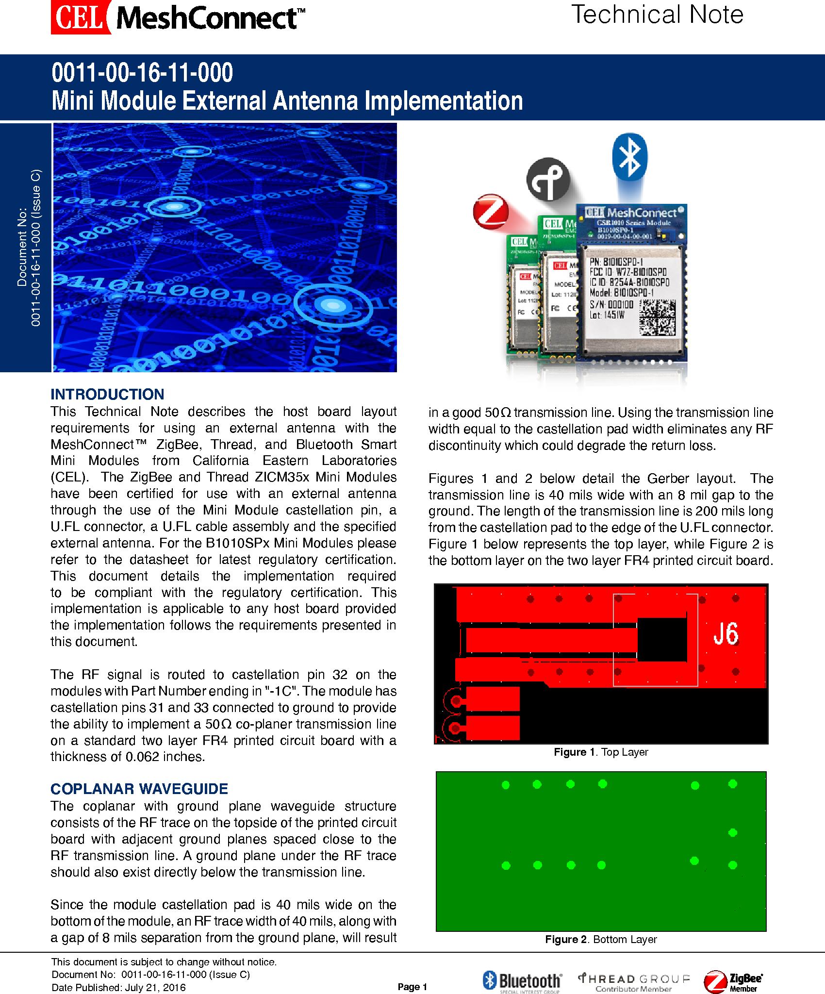
Users Manual V2

Page 1Document No:0011-00-16-11-000 (Issue C)Technical NoteThis document is subject to change without notice.Document No:  0011-00-16-11-000 (Issue C)Date Published: July 21, 20160011-00-16-11-000Mini Module External Antenna ImplementationINTRODUCTION This Technical Note describes the host board layout requirements for using an external antenna with the MeshConnect™ ZigBee, Thread, and Bluetooth Smart Mini Modules from California Eastern Laboratories (CEL).  The ZigBee and Thread ZICM35x Mini Modules have  been  certied  for  use  with  an  external  antenna through the use of the Mini Module castellation pin, a U.FL connector, a U.FL cable assembly and the specied external antenna. For the B1010SPx Mini Modules please refer  to  the  datasheet  for  latest  regulatory  certication. This document details the implementation required to  be  compliant  with  the  regulatory  certication.  This implementation is applicable to any host board provided the implementation follows the requirements presented in  this document.The RF signal is routed to castellation pin 32 on the modules with Part Number ending in "-1C". The module has castellation pins 31 and 33 connected to ground to provide the ability to implement a 50 Ω co-planer transmission line on a standard two layer FR4 printed circuit board with a thickness of 0.062 inches.COPLANAR WAVEGUIDEThe coplanar with ground plane waveguide structure consists of the RF trace on the topside of the printed circuit board with adjacent ground planes spaced close to the RF transmission line. A ground plane under the RF trace should also exist directly below the transmission line.Since the module castellation pad is 40 mils wide on the bottom of the module, an RF trace width of 40 mils, along with a gap of 8 mils separation from the ground plane, will result in a good 50Ω transmission line. Using the transmission line width equal to the castellation pad width eliminates any RF discontinuity which could degrade the return loss. Figures 1 and 2 below detail the Gerber layout.  The transmission line is 40 mils wide with an 8 mil gap to the ground. The length of the transmission line is 200 mils long from the castellation pad to the edge of the U.FL connector. Figure 1 below represents the top layer, while Figure 2 is the bottom layer on the two layer FR4 printed circuit board.Figure 1. Top LayerFigure 2. Bottom Layer

Navigation menu