California Eastern Laboratories ZICM900P2 MeshConnect Sub-G Extended Range Module User Manual Exhibit D Users Manual per 2 1033 b3
California Eastern Laboratories MeshConnect Sub-G Extended Range Module Exhibit D Users Manual per 2 1033 b3
Exhibit D Users Manual per 2 1033 b3
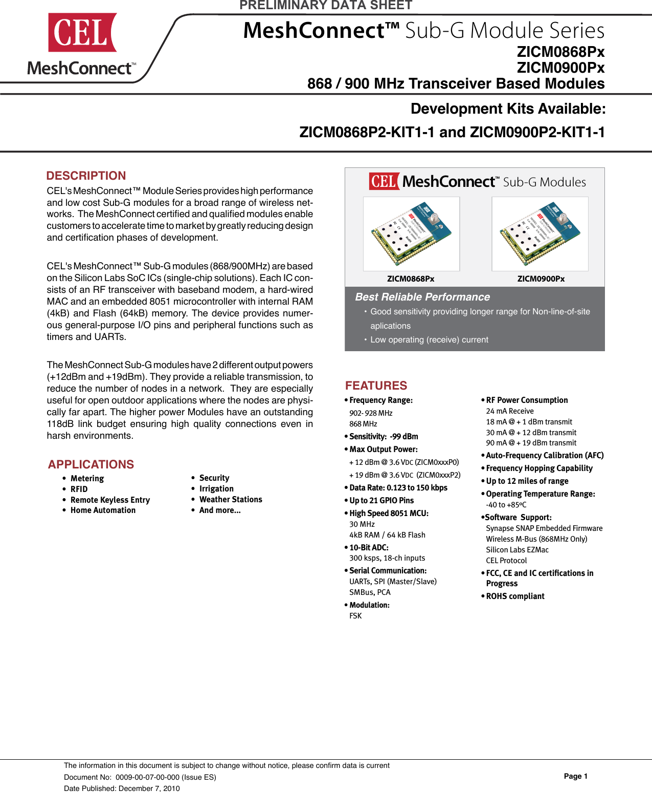
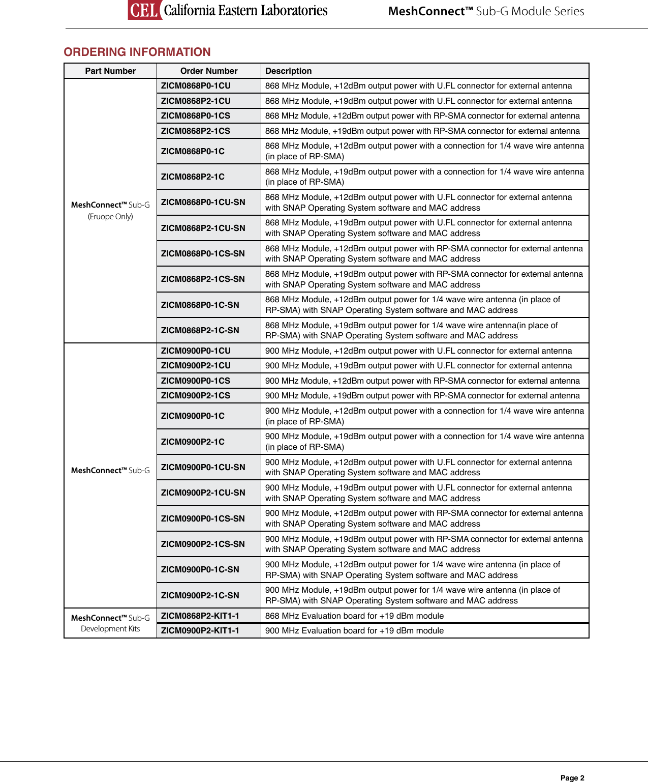
![MeshConnect™ Sub-G Module SeriesPage 11MODULE LAND FOOTPRINTNote: Unless otherwise specied. Dimensions are in Inches [mm].EVALUATION BOARD CEL provides an Evaluation board to allow easy testing of the Module. The Evaluation board provides power via: • AA cell batteries • USB • AC Adapter regulated down to 3.3VDC • External Lab Power Supply (A jumper is also provided for the purposes of monitoring the DC current of the module under various modes of operation). Also included on the evaluation board are four momentary push button switches and four LEDs, a piezo buzzer, a potenti-ometer, and a SPI memory IC. The peripherals are connected to GPIO of the module (see notes in Pin denitions) through slide switches. If the user would wants to connect user specic circuits to the GPIO, slide switches can be used to discon-nect the evaluation board peripherals. The purpose of the evaluation board is to demonstrate simple applications of using GPIO, communicating with the device and also allow exibility for user specic needs.](https://usermanual.wiki/California-Eastern-Laboratories/ZICM900P2/User-Guide-1492467-Page-11.png)