California Eastern Laboratories ZICM900P2 MeshConnect Sub-G Extended Range Module User Manual Exhibit D Users Manual per 2 1033 b3
California Eastern Laboratories MeshConnect Sub-G Extended Range Module Exhibit D Users Manual per 2 1033 b3
Exhibit D Users Manual per 2 1033 b3
Page 1
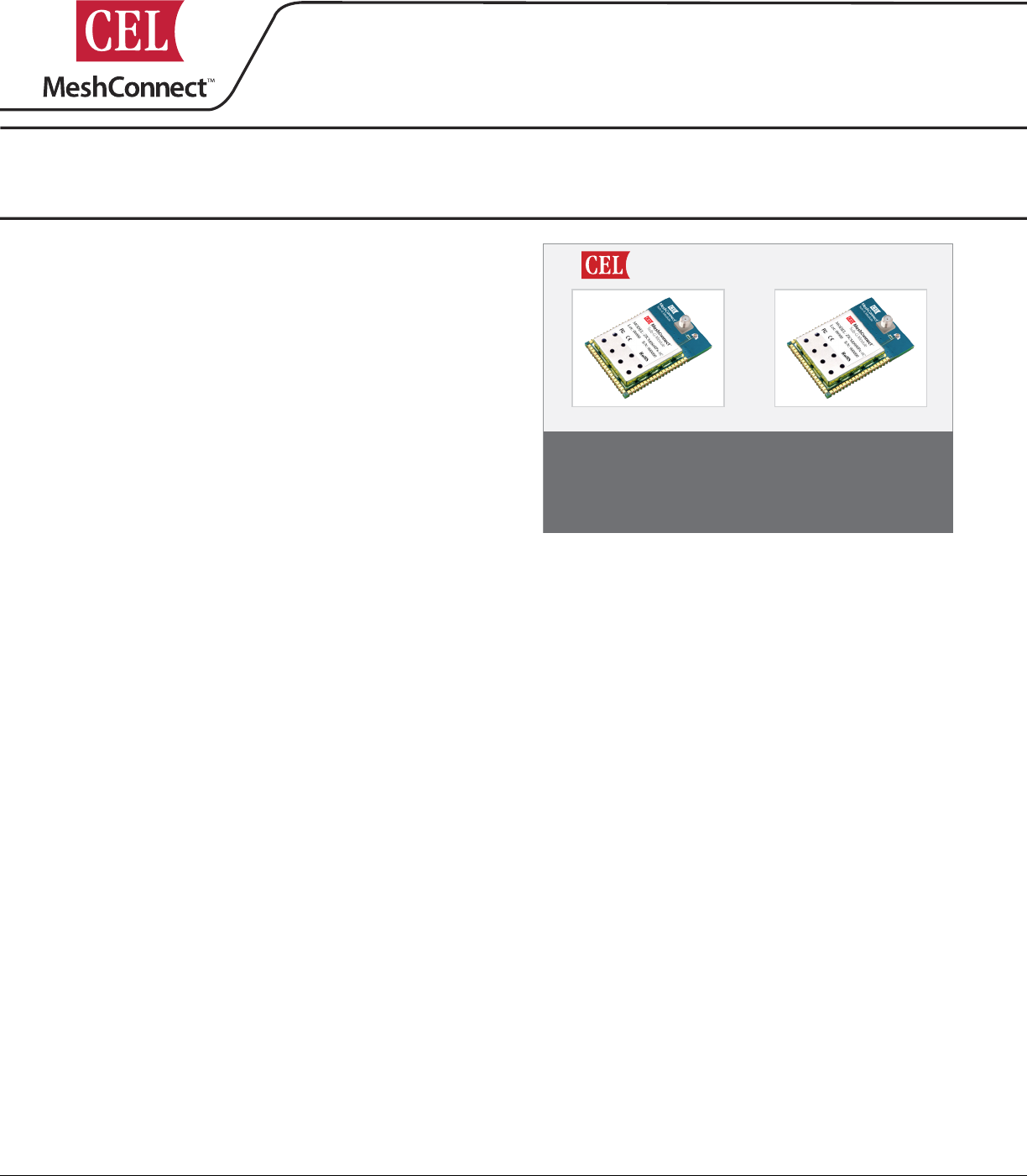
MeshConnect™ Sub-G Module Series
CEL's MeshConnect™ Module Series provides high performance
and low cost Sub-G modules for a broad range of wireless net-
works. The MeshConnect certied and qualied modules enable
customers to accelerate time to market by greatly reducing design
and certication phases of development.
CEL's MeshConnect™ Sub-G modules (868/900MHz) are based
on the Silicon Labs SoC ICs (single-chip solutions). Each IC con-
sists of an RF transceiver with baseband modem, a hard-wired
MAC and an embedded 8051 microcontroller with internal RAM
(4kB) and Flash (64kB) memory. The device provides numer-
ous general-purpose I/O pins and peripheral functions such as
timers and UARTs.
The MeshConnect Sub-G modules have 2 different output powers
(+12dBm and +19dBm). They provide a reliable transmission, to
reduce the number of nodes in a network. They are especially
useful for open outdoor applications where the nodes are physi-
cally far apart. The higher power Modules have an outstanding
118dB link budget ensuring high quality connections even in
harsh environments.
Development Kits Available:
ZICM0868P2-KIT1-1 and ZICM0900P2-KIT1-1
The information in this document is subject to change without notice, please conrm data is current
Document No: 0009-00-07-00-000 (Issue ES)
Date Published: December 7, 2010
PRELIMINARY DATA SHEET
DESCRIPTION
ZICM0868Px
ZICM0900Px
868 / 900 MHz Transceiver Based Modules
•FrequencyRange:
902- 928 MHz
868 MHz
•Sensitivity:-99dBm
•MaxOutputPower:
+ 12 dBm @ 3.6 VDC (ZICM0xxxP0)
+ 19 dBm @ 3.6 VDC (ZICM0xxxP2)
•DataRate:0.123to150kbps
•Upto21GPIOPins
•HighSpeed8051MCU:
30 MHz
4kB RAM / 64 kB Flash
•10-BitADC:
300 ksps, 18-ch inputs
•SerialCommunication:
UARTs, SPI (Master/Slave)
SMBus, PCA
•Modulation:
FSK
FEATURES
•RFPowerConsumption
24 mA Receive
18 mA @ + 1 dBm transmit
30 mA @ + 12 dBm transmit
90 mA @ + 19 dBm transmit
•Auto-FrequencyCalibration(AFC)
•FrequencyHoppingCapability
•Upto12milesofrange
•OperatingTemperatureRange:
-40 to +85ºC
•SoftwareSupport:
Synapse SNAP Embedded Firmware
Wireless M-Bus (868MHz Only)
Silicon Labs EZMac
CEL Protocol
•FCC,CEandICcerticationsin
Progress
•ROHScompliant
MeshConnect™ Sub-G Modules
ZICM0868Px ZICM0900Px
APPLICATIONS
• Metering
• RFID
• RemoteKeylessEntry
• HomeAutomation
• Security
• Irrigation
• WeatherStations
• Andmore...
Best Reliable Performance
• Good sensitivity providing longer range for Non-line-of-site
aplications
• Low operating (receive) current
MeshConnect™ Sub-G Module Series
Page 2
ORDERING INFORMATION
Part Number Order Number Description
MeshConnect™ Sub-G
(Eruope Only)
ZICM0868P0-1CU 868 MHz Module, +12dBm output power with U.FL connector for external antenna
ZICM0868P2-1CU 868 MHz Module, +19dBm output power with U.FL connector for external antenna
ZICM0868P0-1CS 868 MHz Module, +12dBm output power with RP-SMA connector for external antenna
ZICM0868P2-1CS 868 MHz Module, +19dBm output power with RP-SMA connector for external antenna
ZICM0868P0-1C 868 MHz Module, +12dBm output power with a connection for 1/4 wave wire antenna
(in place of RP-SMA)
ZICM0868P2-1C 868 MHz Module, +19dBm output power with a connection for 1/4 wave wire antenna
(in place of RP-SMA)
ZICM0868P0-1CU-SN 868 MHz Module, +12dBm output power with U.FL connector for external antenna
with SNAP Operating System software and MAC address
ZICM0868P2-1CU-SN 868 MHz Module, +19dBm output power with U.FL connector for external antenna
with SNAP Operating System software and MAC address
ZICM0868P0-1CS-SN 868 MHz Module, +12dBm output power with RP-SMA connector for external antenna
with SNAP Operating System software and MAC address
ZICM0868P2-1CS-SN 868 MHz Module, +19dBm output power with RP-SMA connector for external antenna
with SNAP Operating System software and MAC address
ZICM0868P0-1C-SN 868 MHz Module, +12dBm output power for 1/4 wave wire antenna (in place of
RP-SMA) with SNAP Operating System software and MAC address
ZICM0868P2-1C-SN 868 MHz Module, +19dBm output power for 1/4 wave wire antenna(in place of
RP-SMA) with SNAP Operating System software and MAC address
MeshConnect™ Sub-G
ZICM0900P0-1CU 900 MHz Module, +12dBm output power with U.FL connector for external antenna
ZICM0900P2-1CU 900 MHz Module, +19dBm output power with U.FL connector for external antenna
ZICM0900P0-1CS 900 MHz Module, +12dBm output power with RP-SMA connector for external antenna
ZICM0900P2-1CS 900 MHz Module, +19dBm output power with RP-SMA connector for external antenna
ZICM0900P0-1C 900 MHz Module, +12dBm output power with a connection for 1/4 wave wire antenna
(in place of RP-SMA)
ZICM0900P2-1C 900 MHz Module, +19dBm output power with a connection for 1/4 wave wire antenna
(in place of RP-SMA)
ZICM0900P0-1CU-SN 900 MHz Module, +12dBm output power with U.FL connector for external antenna
with SNAP Operating System software and MAC address
ZICM0900P2-1CU-SN 900 MHz Module, +19dBm output power with U.FL connector for external antenna
with SNAP Operating System software and MAC address
ZICM0900P0-1CS-SN 900 MHz Module, +12dBm output power with RP-SMA connector for external antenna
with SNAP Operating System software and MAC address
ZICM0900P2-1CS-SN 900 MHz Module, +19dBm output power with RP-SMA connector for external antenna
with SNAP Operating System software and MAC address
ZICM0900P0-1C-SN 900 MHz Module, +12dBm output power for 1/4 wave wire antenna (in place of
RP-SMA) with SNAP Operating System software and MAC address
ZICM0900P2-1C-SN 900 MHz Module, +19dBm output power for 1/4 wave wire antenna (in place of
RP-SMA) with SNAP Operating System software and MAC address
MeshConnect™ Sub-G
Development Kits
ZICM0868P2-KIT1-1 868 MHz Evaluation board for +19 dBm module
ZICM0900P2-KIT1-1 900 MHz Evaluation board for +19 dBm module
MeshConnect™ Sub-G Module Series
Page 3
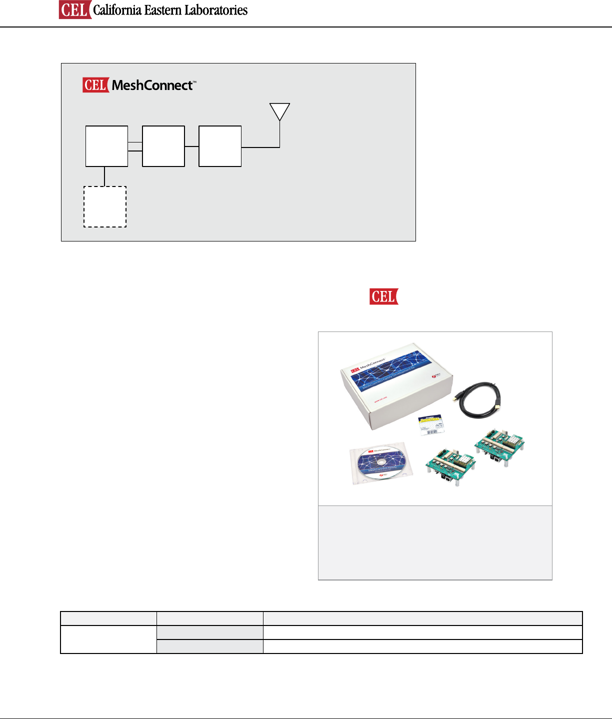
MODULE BLOCK DIAGRAM
ANT
SI100x
T/R
Switch
External
Memory
Low Pass
Filter
Sub-G
Optional
DEVELOPMENT KIT
CEL's Development Kit assist users in both evaluation and
development. As a stand-alone radio system, the kit allows
users to place the modules into the target environment
and evaluate performance on-site. The Development Kit
also serves as an invaluable aid in application develop-
ment. Through the many interface headers on the board,
the user has access to all of the MeshConnect module
pins, enabling easy connection to target systems for ap-
plication development.
The interface board features a serial communication
interface, a power management module, and peripherals
such as a buzzer, push-button switches, LEDs, and GPIO
headers.
For more detail information regarding MeshConnect
Development Kits, refer to the respective development
kit user guides documents. (Available at CEL’s website
http://www.cel.com)Kit Contents:
• Evaluation Boards w/Module (2)
• USB Cables (1)
• AA Batteries (4)
• Software & Technical Information CD (1)
MeshConnect™
Sub-G Module Development Kit
DEVELOPMENT KIT ORDERING INFORMATION
Part Number Order Number Description
MeshConnect™ Sub-G
Development Kits
ZICM0868P2-KIT1-1 868 MHz Evaluation board for +19dBm module
ZICM0900P2-KIT1-1 900 MHz Evaluation board for +19dBm module

MeshConnect™ Sub-G Module Series
Page 4
Introduction and Overview
Description.............................................................................................................................................................................................. 1
Features.................................................................................................................................................................................................. 1
Applications............................................................................................................................................................................................ 1
Ordering Information............................................................................................................................................................................. 2
Module Block Diagram........................................................................................................................................................................... 3
Development Kit..................................................................................................................................................................................... 3
System Level Function
Transceiver IC......................................................................................................................................................................................... 5
Antenna.................................................................................................................................................................................... 5
Additional Flash Memory....................................................................................................................................................................... 5
Electrical Specication
Absolute Maximum Ratings................................................................................................................................................................... 6
Recommended (Operating Condition).................................................................................................................................................. 6
DC Characteristics.................................................................................................................................................................................. 6
RF Characteristics.................................................................................................................................................................................. 7
Pin Signal & Interfaces
Pin Signals I/O Conguration................................................................................................................................................................ 8
I/O Pin Assignment................................................................................................................................................................................. 8
Software/Firmware.................................................................................................................................................................................. 9
Module Dimensions................................................................................................................................................................................ 10
Module Footprint.................................................................................................................................................................................... 11
Processing......................................................................................................................................................................................... 12
Agency Certications................................................................................................................................................................... 13
Shipment, Storage & Handling................................................................................................................................................. 14
References & Revision History................................................................................................................................................. 15
TABLE OF CONTENTS

MeshConnect™ Sub-G Module Series
Page 5
TRANSCEIVER IC
The MeshConnect Sub-G modules are based on the Silicon Labs Si1000 and Si1002 SOC transceiver ICs. These ICs
incorporate the RF transceiver with the baseband modem, a hardwired MAC, and an embedded 8051 microcontroller,
offering a high performance solution for all Sub-G applications.
For more information about the Silicon Labs ICs, visit http://www.silabs.com.
ANTENNA
The MeshConnect Sub-G modules include RF connectors for external antenna options only (There is no trace antenna
option). The following options are supported by CEL:
• U.FL connector
• RP-SMA connector
• A Connection for 1/4 wave wire antenna in place of RP-SMA
Here are some design guidelines to help ensure antenna performance:
• Never place the antenna close to metallic objects.
• In the overall design, ensure that wiring and other components are not placed near the antenna.
• Do not place the antenna in a metallic or metalized plastic enclosure.
• Keep plastic enclosures 1cm or more from the antenna in any direction.
ADDITIONAL FLASH MEMORY (Optional)
The Silicon Labs Transceiver ICs (Si1000 and Si1002) have an embedded 64kB of ash. Additional memory (1MB) can be
mounted on the module (as an option) to enable Over The Air (OTA) programming capability.
This is a custom solution as an option for all part numbers.
MeshConnect™ Sub-G Module Series
Page 6
ABSOLUTE MAXIMUM RATINGS
Description MeshConnect™ Sub-G Module Unit
Min Max
Power Supply Voltage (VDD) -0.3 3.6 VDC
Voltage on any I/O Line -0.3 VDD + 0.3 VDC
RF Input Power – 10 dBm
Storage Temperature Range -40 125 °C
Reow Soldering Temperature – 260 °C
Note: Exceeding the maximum ratings may cause permanent damage to the module or devices.
RECOMMENDED (OPERATING CONDITIONS)
Description MeshConnect™ Sub-G Module Unit
Min Typ Max
Power Supply Voltage (VDD)1.8/2.7* 3.3 3.6 V
Input Frequency 863 –870 MHz
Input Frequency 902 – 928 MHz
Ambient Temperature Range -40 25 85 °C
Note: * 2.7v is the min voltage if an additional memory IC was placed on the module.
DC CHARACTERISTICS (@ 25°C, VDD = 3.6V, ZICM0xxxP2 TX power max)
Description MeshConnect™ Sub-G Module Unit
Min Typ Max
Transmit Mode Current – 90 – mA
Receive Mode Current – 24 – mA
Sleep Mode Current – TBD – µA
DC CHARACTERISTICS (@ 25°C, VDD = 3.6V, ZICM0xxxP0 TX power max)
Description MeshConnect™ Sub-G Module Unit
Min Typ Max
Transmit Mode Current – 35 – mA
Receive Mode Current – 24 – mA
Sleep Mode Current – TBD – µA
MeshConnect™ Sub-G Module Series
Page 7
RF CHARACTERISTICS (@ 25°C, VDD = 3.6V, ZICM0xxxP2)
Description MeshConnect™ Sub-G Module Unit
Min Typ Max
General Characteristics
RF Frequency Range 863 –928 MHz
Transmitter
Maximum Output Power – 19 – dBm
Minimum Output Power – -5 – dBm
FSK Error TBD – TBD %
Carrier Offset TBD – TBD KHz
Deviation – 75 – KHz
Receiver
Sensitivity (1% PER, 156kbps) –-99 TBD dBm
Saturation (maximum input level) ––10 dBm
RF CHARACTERISTICS (@ 25°C, VDD = 3.6V, ZICM0xxxP0)
Description MeshConnect™ Sub-G Module Unit
Min Typ Max
General Characteristics
RF Frequency Range 863 – 928 MHz
Transmitter
Maximum Output Power – 12 – dBm
Minimum Output Power – -12 – dBm
FSK Error TBD – TBD %
Carrier Offset TBD – TBD KHz
Deviation – 75 – KHz
Receiver
Sensitivity (1% PER, 156kbps) – -99 TBD dBm
Saturation (maximum input level) – – 10 dBm
MeshConnect™ Sub-G Module Series
Page 8
PIN SIGNALS I/O PORT CONFIGURATION
MeshConnect module has 56 edge I/O interfaces for connection to the user’s host board. The MeshConnect Module Dimensions
shows the layout of the 56 edge castellations.
MeshConnect I/O PIN ASSIGNMENTS
Number Name Notes
1 GND
2 GND
3 GND
4 GND
5 GND
6 GND
7 GND
8 NC
9 ANTA Available: Not used for any module funconality
10 GPIO0 Available: Not used for any module funconality
11 GPIO2 Available: Not used for any module funconality
12 P0.7/IREF Must be connected to SDN for SNAP rmware
13
P0.6/
CNVSTR Used as Chip Select for Memory on CEL Eval. Board
14 P0.5/RXD UART TXD
15 P0.4/TXD UART RXD
16 WP Write Protect Pin of Memory Chip on Module
17 NC
18 GND
19 GND
20 NC
21 NC
22 NC
23 P0.3 Used as Chip Select for Memory IC on the CEL Module
24 P0.2 Memory IC MISO signal pin
25 P0.1 Must be connected to NIRQ for SNAP rmware
26 P0.0 Memory IC Clock Signal
27 GND
28 VCC
29 RST/C2CK Debug Clock
30 P2.7/C2D Debug Data
31 P2.6 GPIO connected to Buzzer on CEL Eval Board
32 P2.5 GPIO connected to Switch 3 on CEL Eval board
33 P2.4 GPIO connected to LED3 on CEL Eval board
34 P2.3 GPIO connected to Switch 2 on CEL Eval Board
MeshConnect™ Sub-G Module Series
Page 9
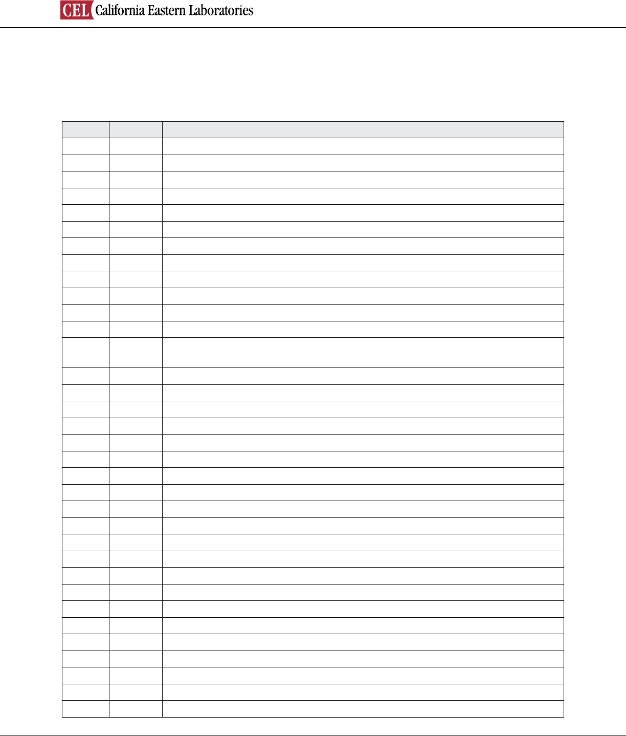
35 NC
36 NC
37 GND
38 GND
39 GND
40 GND
41 GND
42 P2.2 GPIO connected to LED2 on CEL Eval board
43 P2.1 GPIO connected to Switch 1 on CEL Eval Board
44 P2.0 GPIO connected to LED1 on CEL Eval board
45 P1.7 GPIO connected to Switch 0 on CEL Eval Board
46 P1.6 GPIO connected to LED0 on CEL Eval board
47 P1.5 Memory IC MOSI
48 NIRQ External Interrupt Request
49 SDN Radio Shutdown (Acve High)
50 GND
51 GND
52 GND
53 GND
54 GND
55 GND
56 GND
MeshConnect I/O PIN ASSIGNMENTS (Continued)
Number Name Notes
SOFTWARE/FIRMWARE
The Sub-G modules support the following software:
• SynapseSNAPEmbeddedFirmware
• WirelessM-Bus(868MHzOnly)
• SiliconLabsEZMac
• CELProtocol
The MeshConnect Sub-G Development Kit provides a guide on how to access the Si100x IC and utilize the Silicon Labs
software development environment. It also provides a set of demo applications to conduct several tests. Below is the list of
the demo software features:
MeshConnect™ Sub-G Module Series
Page 10
SOFTWARE/FIRMWARE (Continued)
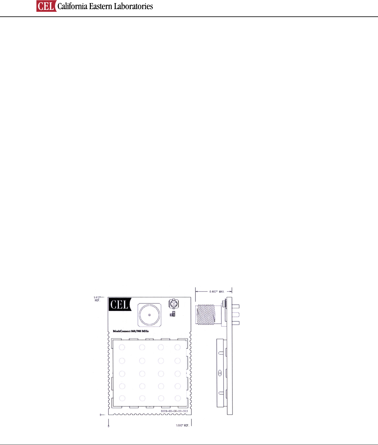
MODULE DIMENSIONS
MeshConnect™ Sub-G Module with U.FL Connector for external antenna
MeshConnect™ Sub-G Module with RPSMA Connector for external Antenna
• Self Healing (Orphan handling)
• Point-to-Point network formation
• Point-to-Multipoint (Star) network formation
• Self Healing (Orphan handling)
• Point-to-Point network formation
• Point-to-Multipoint (Star) network formation
• ACK
• Wakeup Modes (Si100X) – most likely software will just use one of the wakeup modes
• Frequency Hopping
• Unicast Addressing using 16-bit device IDs
• Broadcast Addressing
• Packet Forwarding (Master node only)
• Forwarding Table Aging (Master node only)
• Promiscuous Mode (TBD – later release)
• Listen Before Talk (LBT)
• RSSI
• Packet Filtering
• Pairing/Joining
• Network Synchronization through beacon messages to coordinate sleep/wake cycles
- Master node needs to send out beacon as well as gure out when to go to sleep and when to wake up
- End node wakes up and looks for beacon to gure out when to go to sleep and wake up
• Command line interface for debug/testing/conguration
• Push buttons for Range or PER packet test on a Eval board
• Save conguration to ash
• Save conguration to external ash
• Over-the-air programming of the image to another device (TBD – later release)
• Low Battery detection
For layout recommendation for optimum antenna performance, refer to Antenna section in this document.
MeshConnect™ Sub-G Module Series
Page 11
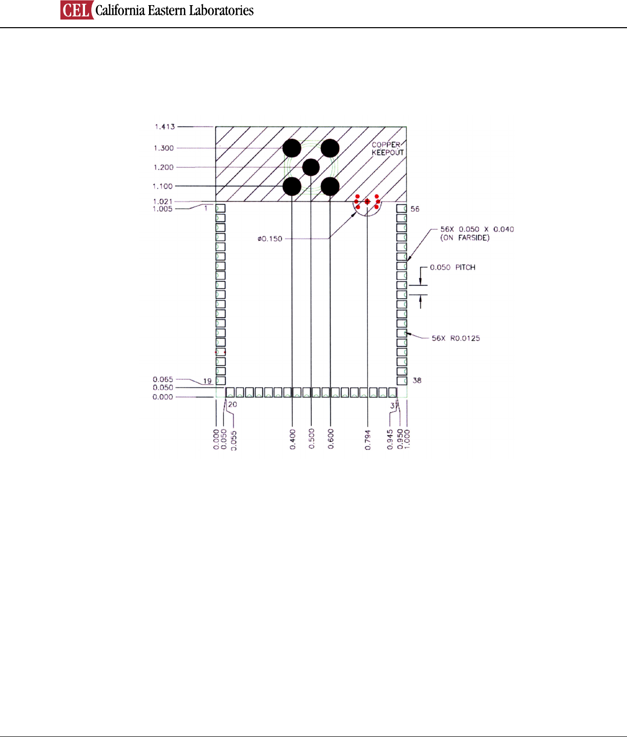
MODULE LAND FOOTPRINT
Note: Unless otherwise specied. Dimensions are in Inches [mm].
EVALUATION BOARD
CEL provides an Evaluation board to allow easy testing of the Module. The Evaluation board provides power via:
• AA cell batteries
• USB
• AC Adapter regulated down to 3.3VDC
• External Lab Power Supply (A jumper is also provided for the purposes of monitoring the DC current of
the module under various modes of operation).
Also included on the evaluation board are four momentary push button switches and four LEDs, a piezo buzzer, a potenti-
ometer, and a SPI memory IC. The peripherals are connected to GPIO of the module (see notes in Pin denitions) through
slide switches. If the user would wants to connect user specic circuits to the GPIO, slide switches can be used to discon-
nect the evaluation board peripherals.
The purpose of the evaluation board is to demonstrate simple applications of using GPIO, communicating with the device
and also allow exibility for user specic needs.
MeshConnect™ Sub-G Module Series
Page 12
PROCESSING
Recommended Reow Prole
Parameters Values
Ramp up rate (from Tsoakmax to Tpeak) 3º/sec max
Minimum Soak Temperature 150ºC
Maximum Soak Temperature 200ºC
Soak Time 60-120 sec
TLiquidus 217ºC
Time above TL 60-150 sec
Tpeak 250ºC
Time within 5º of Tpeak 20-30 sec
Time from 25º to Tpeak 8 min max
Ramp down rate 6ºC/sec max
Achieve the brightest possible solder llets with a good shape and low contact angle.
Pb-Free Soldering Paste
Use of “No Clean” soldering paste is strongly recommended, as it does not require cleaning after the soldering process.
Note: The quality of solder joints on the castellations (‘half vias’) where they contact the host board should meet the appropriate IPC Speci-
cation. See the latest IPC-A-610 "Acceptability of Electronic Assemblies, section 8.2.4 Castellated Terminations.”
Cleaning
In general, cleaning the populated modules is strongly discouraged. Residuals under the module cannot be easily removed
with any cleaning process.
• Cleaning with water can lead to capillary effects where water is absorbed into the gap between the host board and
the module. The combination of soldering ux residuals and encapsulated water could lead to short circuits between
neighboring pads. Water could also damage any stickers or labels.
• Cleaning with alcohol or a similar organic solvent will likely ood soldering ux residuals into the two housings, which
is not accessible for post-washing inspection. The solvent could also damage any stickers or labels.
• Ultrasonic cleaning could damage the module permanently.
The best approach is to consider using a “no clean” soldering paste and eliminate the post-soldering cleaning step.
Optical Inspection
After soldering the Module to the host board, consider optical inspection to check the following:
• Proper alignment and centering of the module over the pads.
• Proper solder joints on all pads.
• Excessive solder or contacts to neighboring pads, or vias.
Repeating Reow Soldering
Only a single reow soldering process is encouraged for host boards.
Wave Soldering
If a wave soldering process is required on the host boards due to the presence of leaded components, only a single wave
soldering process is encouraged.

MeshConnect™ Sub-G Module Series
Page 13
PROCESSING (Continued)
AGENCY CERTIFICATIONS
Hand Soldering
Hand soldering is possible. Use a soldering iron temperature setting equivalent to 350°C, follow IPC recommendations/
reference document IPC-7711.
Rework
The MeshConnect Module can be unsoldered from the host board. Use of a hot air rework tool and hot plate for pre-heating
from underneath is recommended. Avoid overheating.
Warning Never attempt a rework on the module itself, e.g. replacing individual components. Such actions will
terminate warranty coverage.
Additional Grounding
Attempts to improve module or system grounding by soldering braids, wires, or cables onto the module RF shield cover is
done at the customer's own risk. The numerous ground pins at the module perimeter should be sufcient for optimum
immunity to external RF interference.
FCC Compliance Statement (Part 15.19) Section 7.15 of RSS-GEN
This device complies with Part 15 of the FCC Rules. Operation is subject to the following two conditions:
1. This device may not cause harmful interference.
2. This device must accept any interference received, including interference that may cause undesired operation.
Warning (Part 15.21)
Changes or modications not expressly approved by CEL could void the user's authority to operate the equipment.
20 cm Separation Distance
To comply with FCC/IC RF exposure limits for general population / uncontrolled exposure, the antenna(s) used for this
transmitter must be installed to provide a separation distance of at least 20 cm from all persons and must not be co-located
or operating in conjunction with any other antenna or transmitter.
OEM Responsibility to the FCC Rules and Regulations
The MeshConnect Module has been certied per FCC Part 15 rules for integration into products without further testing or
certication. To fulll the FCC certication requirements, the OEM of the MeshConnect Module must ensure that the
information provided on the MeshConnect Label is placed on the outside of the nal product. The MeshConnect Module is
labeled with its own FCC ID Number. If the FCC ID is not visible when the module is installed inside another device, then
the outside of the device into which the module is installed must also display a label referring to the enclosed module. This
exterior label can use wording such as the following: “Contains Transmitter Module FCC ID: W7Z-ICP0” or “Contains FCC
ID: W7Z-ICP0”
The OEM of the MeshConnect Module must only use the approved antenna, (PCB Trace Antenna) that has been certied
with this module. The OEM of the MeshConnect Module must test their nal product conguration to comply with Uninten-
tional Radiator Limits before declaring FCC compliance per Part 15 of the FCC rules.
MeshConnect™ Sub-G Module Series
Page 14
AGENCY CERTIFICATIONS (Continued)
SHIPMENT, HANDLING, AND STORAGE
Shipment
The MeshConnect Modules are delivered in trays of 28.
Handling
The MeshConnect Modules are designed and packaged to be processed in an automated assembly line.
Warning The MeshConnect Modules contain highly sensitive electronic circuitry. Handling without proper ESD
protection may destroy or damage the module permanently.
Warning According to JEDEC ISP, the MeshConnect Modules are moisture-sensitive devices. Appropriate handling instruc-
tions and precautions are summarized in Section 2.1. Read carefully to prevent permanent damage due to moisture intake.
Moisture Sensitivity Level (MSL)
MSL 3, per J-STD-033
Storage
Storage/shelf life in sealed bags is 12 months at <40°C and <90% relative humidity.
IC Certication — Industry Canada Statement
The term "IC" before the certication / registration number only signies that the Industry Canada technical specications
were met.
Section 14 of RSS-210
The installer of this radio equipment must ensure that the antenna is located or pointed such that it does not emit RF eld in
excess of Health Canada limits for the general population. Consult Safety Code 6, obtainable from Health Canada's
website: http://www.hc-sc.gc.ca/ewh-semt/pubs/radiation/99ehd-dhm237/index-eng.php
CE Certication — Europe
The MeshConnect 868MHz RF modules has been tested and certied for use in the European Union.
OEM Responsibility to the European Union Compliance Rules
If the MeshConnect module is to be incorporated into a product, the OEM must verify compliance of the nal product to the
European Harmonized EMC and Low-Voltage / Safety Standards. A Declaration of Conformity must be issued for each of
these standards and kept on le as described in Annex II of the R&TTE Directive.
The manufacturer must maintain the user's guide and adhere to the settings described in the manual for maintaining
European Union Compliance. If any of the specications are exceeded in the nal product, the OEM is required to
make a submission to the notied body for compliance testing.
OEM Labeling Requirements
The `CE' mark must be placed on the OEM product in a visible location.
The CE mark shall consist of the initials “CE” with the following form:
· If the CE marking is reduced or enlarged, the proportions given in the above graduated
drawing must be adhered to.
· The CE mark must be a minimum of 5mm in height
· The CE marking must be afxed visibly, legibly, and indelibly. Since the 2400 - 2483.5 MHz
band is not harmonized by a few countries throughout Europe, the Restriction sign must be
placed to the right of the “CE” marking as shown in the picture
MeshConnect™ Sub-G Module Series
Page 15
REFERENCES & REVISION HISTORY
Previous Versions Changes to Current Version Page(s)
0008-00-07-00-000
(Issue ES) December 7, 2010 Initial preliminary datasheet. N/A
Disclaimer
• The information in this document is current as of the published date. The information is subject to change without
notice. For actual design-in, refer to the latest publications of CEL data sheets or data books, etc., for the most
up-to-date specications of CEL products. Not all products and/or types are available in every country. Please
check with an CEL sales representative for availability and additional information.
• No part of this document may be copied or reproduced in any form or by any means without the prior written
consent of CEL. CEL assumes no responsibility for any errors that may appear in this document.
• CEL does not assume any liability for infringement of patents, copyrights or other intellectual property rights of
third parties by or arising from the use of CEL products listed in this document or any other liability arising from the
use of such products. No license, express, implied or otherwise, is granted under any patents, copyrights or other
intellectual property rights of CEL or others.
• Descriptions of circuits, software and other related information in this document are provided for illustrative
purposes in semiconductor product operation and application examples. The incorporation of these circuits,
software and information in the design of a customer’s equipment shall be done under the full responsibility of the
customer. CEL assumes no responsibility for any losses incurred by customers or third parties arising from the use
of these circuits, software and information.
• While CEL endeavors to enhance the quality, reliability and safety of CEL products, customers agree and
acknowledge that the possibility of defects thereof cannot be eliminated entirely. To minimize risks of damage to
property or injury (including death) to persons arising from defects in CEL products, customers must incorporate
sufcient safety measures in their design, such as redundancy, re-containment and anti-failure features.