Christie Digital Systems Canada CRMX100 ASSY PCB RF Module User Manual 020 100489 02 LIT TECH REF RFModule
Christie Digital Systems Canada, Inc. ASSY PCB RF Module 020 100489 02 LIT TECH REF RFModule
user manual

RF Module Datasheet Technical Reference Information 1 of 8
020-100489-02 Rev. 01 (11-2009)
RF Module
Technical Reference Information
DESCRIPTION
The CRMX-100 RF module is a 2.4GHz IEEE 802.15.4 transceiver designed for proprietary, Zigbee
or RF4CE application. The module is based on Texas Instruments CC2530 that combines the excellent
performance of a RF transceiver with industry–standard enhanced 8051 microcontroller unit, 128 KB
in-system programmable flash memory, 8-KB RAM, and many other features. The RF module
incorporates Texas Instrument CC2590 RF Front End power amplifier (PA) and low-noise amplifier
(LNA) for increased output power, and improved receiver sensitivity respectively. The module has an
option to either be populated with a chip antenna or reverse-polarity SMA connector to be used with an
external antenna. The RF module has various operating modes, making it highly suited for systems
where ultralow power consumption is required.
FEATURES
• 2.4GHz IEEE 802.15.4 Compliant RF Transceiver
•High Performance and Low-Power 8051 Microcontroller
• Two Serial Unart Interface
• 2.4GHz Front End Amplifier
• Supports RemoTI stack from Texas Instruments
• 16 General Purpose I/O ports
• Chip antenna or RP-SMA connector for external antenna
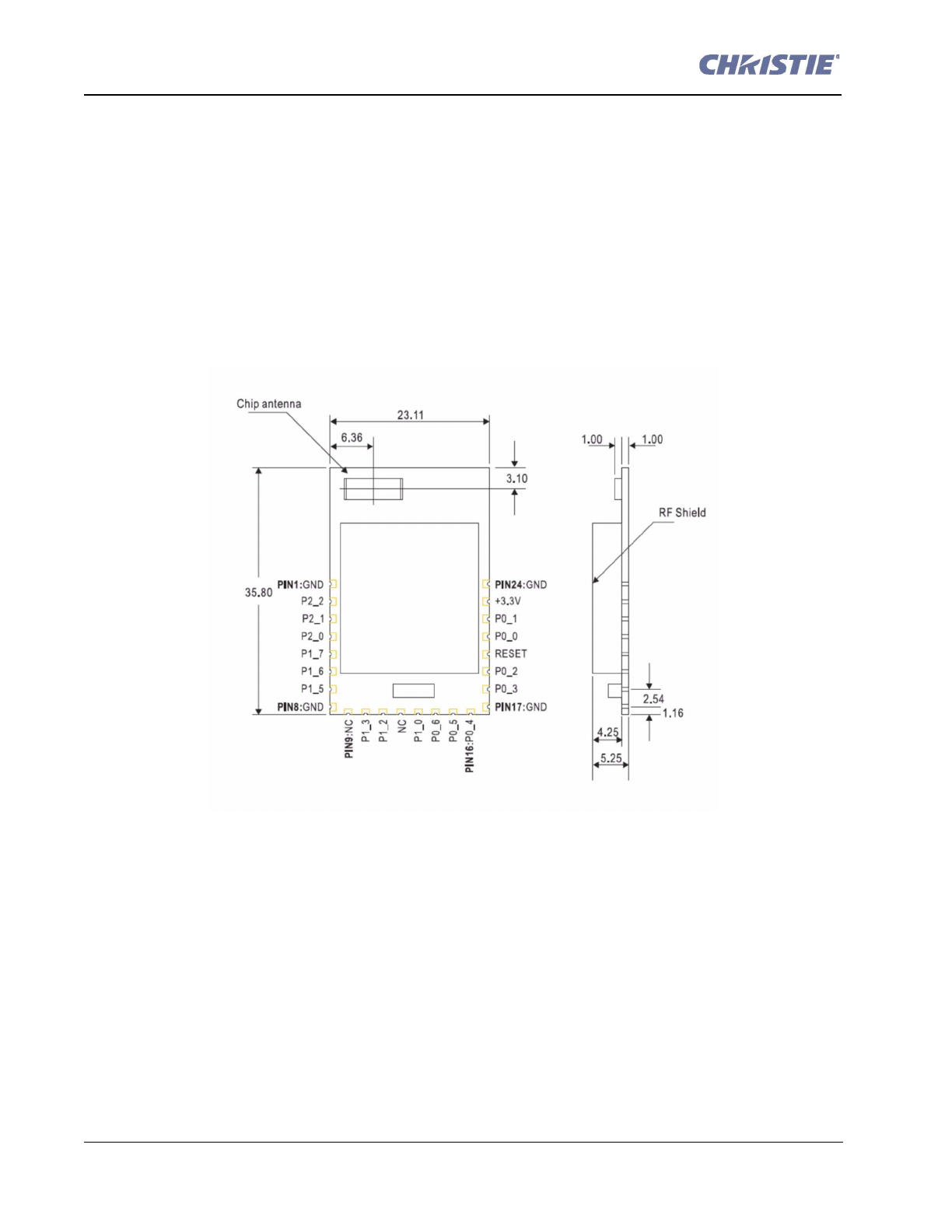
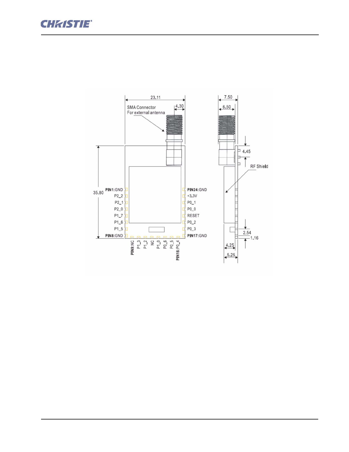
• Miniature Footprint 35.80 x 23.11 mm
• Long Range up to 225 meter
• Max 10 mW output power
• RoHS compliant
OFFICIALLY RELEASED
Document Control
Dec 1, 2009
2 of 8 RF Module Datasheet Technical Reference Information
020-100489-02 Rev. 01 (11-2009)
ABSOLUTE MAXIMUM RATINGS (1)
1) Stress beyond those listed under the Absolute Maximum Ratings may cause permanent damage to
device. These are stress ratings only, and functional operation of the device at these or any other
conditions beyond those indicated under Recommended Operating Conditions is not implied.
Exposure to absolute-maximum-rated conditions for extended periods may affect device reliabil-
ity.
2) CAUTION! ESD sensitive device. Precaution should be used when handling the device in
order to prevent permanent damage.
RECOMMENDED OPERATING CONDITIONS
PIN DESCRIPTIONS
The RF module has 24 edge I/O pins for connecting to a host board. The following table enumerates
and defines the RF module pinout.
Rating MIN MAX UNIT
Supply voltage All supply pins must have the same
voltage
-0.3 3.9 V
DC
Voltage on any digital pin -0.3 VDD + 0.3,
Max 3.9
V
DC
Input RF level +10 dBm
Storage Temperature Range -40 125 °C
Reflow soldering temperature According to IPC/JEDEC J-STD-020C 260 °C
ESD
(2)
All pads, according to human-body
model, JEDEC STD 22, method A114
2 kV
According to charged-device model
JEDEC STD 22, method C101
500 V
Rating Min Max Unit
Power Supply Voltage (VDD) 2 3.6 VDC
Input Frequency 2405 2480 MHz
Ambient Temperature Range -40 85 °C
OFFICIALLY RELEASED
Document Control
Dec 1, 2009
RF Module Datasheet Technical Reference Information 3 of 8
020-100489-02 Rev. 01 (11-2009)
DI= Digital Input
DO= Digital Output
AI= Analog Input
AO=Analog Output
PI = Power Input
GND = Ground
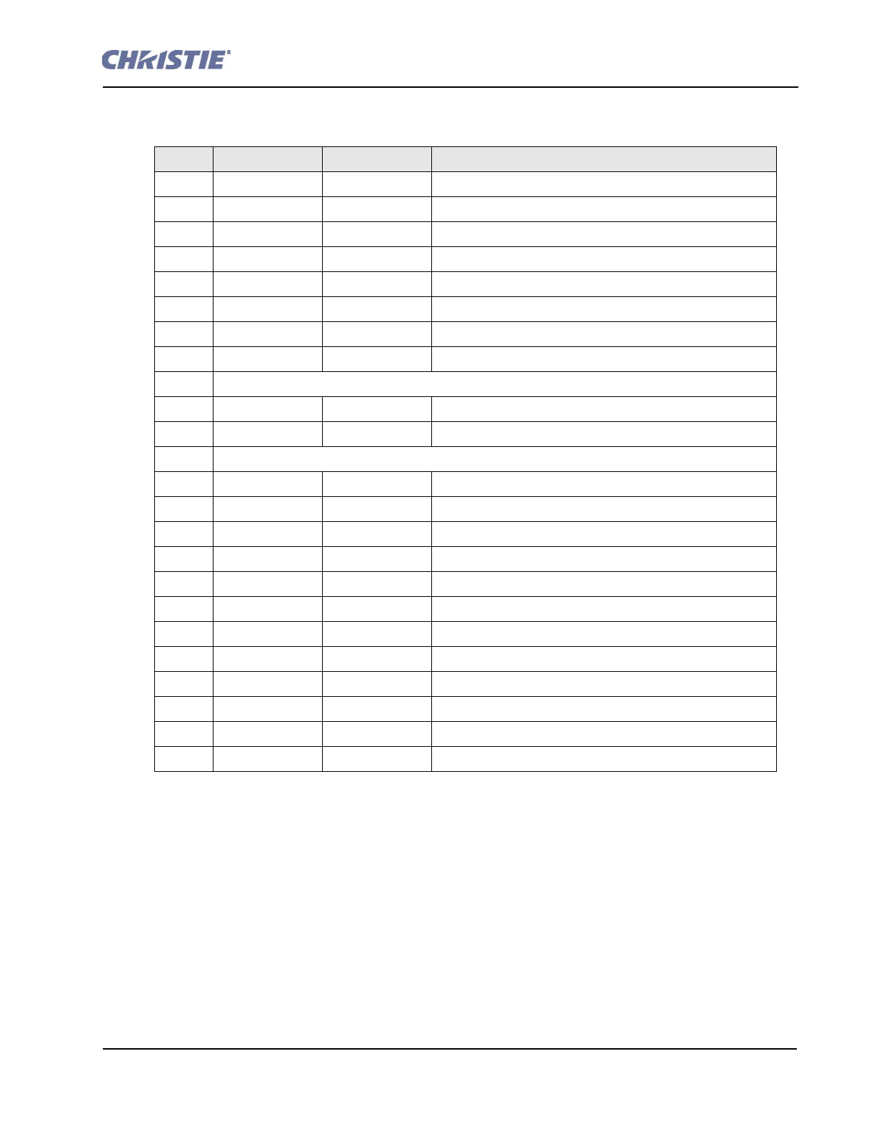
PIN PIN NAME PIN TYPE PIN DESCRIPTION
1 GROUND GND Ground
2 P2_2 DI/DO/AI General Purpose Digital I/O Port 2_2
3 P2_1 DI/DO/AI General Purpose Digital I/O Port 2_1
4 P2_0 DI/DO/AI General Purpose Digital I/O Port 2_0
5 P1_7 DI/DO/AI General Purpose Digital I/O Port 1_7
6 P1_6 DI/DO/AI General Purpose Digital I/O Port 1_6
7 P1_5 DI/DO/AI General Purpose Digital I/O Port 1_5
8 GROUND GND Ground
9 Not Connected
10 P1_3 DI/DO General Purpose Digital I/O Port 1_3
11 P1_2 DI/DO General Purpose Digital I/O Port 1_2
12 Not Connected
13 P1_0 DI/DO General Purpose Digital I/O Port 1_0
14 P0_6 DI/DO General Purpose Digital I/O Port 0_6
15 P0_5 DI/DO General Purpose Digital I/O Port 0_5
16 P0_4 DI/DO General Purpose Digital I/O Port 0_4
17 GROUND GND Ground
18 P0_3 DI/DO General Purpose Digital I/O Port 0_3
19 P0_2 DI/DO General Purpose Digital I/O Port 0_2
20 RESET DI Reset, active low
21 P0_1 DI/DO General Purpose Digital I/O Port 0_1
22 P0_0 DI/DO General Purpose Digital I/O Port 0_0
23 VDD PI Power Supply Input
24 GROUND GND Ground
OFFICIALLY RELEASED
Document Control
Dec 1, 2009
4 of 8 RF Module Datasheet Technical Reference Information
020-100489-02 Rev. 01 (11-2009)
ANTENNA
The RF module can either be populated with a chip antenna or Reverse-Polarity SMA connector for an
external whip antenna. The regulatory certification will be completed with Yageo Corporation’s 5320
ceramic chip antenna (part# CAN4311153002501K) and also with the PRO-CELL CO., LTD’s dipole
antenna (part# RA-A01) with Reverse-Polarity SMA connector.
DIMENSIONS: CRMX-100 RF MODULE WITH CHIP ANTENNA
All dimensions are in millimeters, unless otherwise noted.
OFFICIALLY RELEASED
Document Control
Dec 1, 2009
RF Module Datasheet Technical Reference Information 5 of 8
020-100489-02 Rev. 01 (11-2009)
DIMENSIONS: CRMX-100 RF MODULE WITH RP-SMA
CONNECTOR
All dimensions are in millimeters, unless otherwise noted.
OFFICIALLY RELEASED
Document Control
Dec 1, 2009
6 of 8 RF Module Datasheet Technical Reference Information
020-100489-02 Rev. 01 (11-2009)
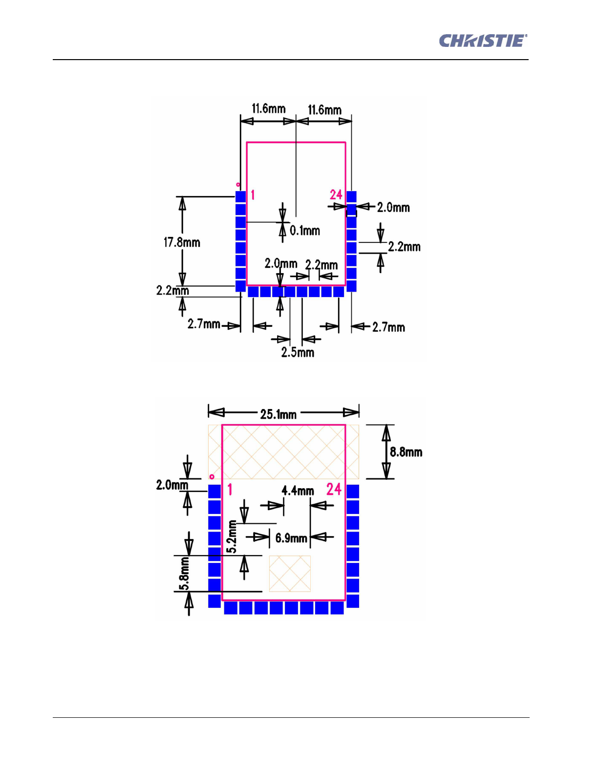
PCB PAD LAYOUT
PCB KEEP-OUT AREAS
OFFICIALLY RELEASED
Document Control
Dec 1, 2009

RF Module Datasheet Technical Reference Information 7 of 8
020-100489-02 Rev. 01 (11-2009)
NOTICE
You are cautioned that changes or modifications not expressly approved by the part responsible for
compliance could void the user's authority to operate the equipment.
This equipment has been tested and found to comply with the limits for a Class B digital device,
pursuant to part 15 of the FCC/IC rules. These limits are designed to provide reasonable protection
against harmful interference in a residential installation. This equipment generates, uses and can
radiate radio frequency energy and, if not installed and used in accordance with the instructions, may
cause harmful interference to radio communications. However, there is no guarantee that interference
will not occur in a particular installation. If this equipment does cause harmful interference to radio or
television reception, which can be determined by turning the equipment off and on, the user is
encouraged to try to correct the interference by one or more of the following measures:
• Reorient or relocate the receiving antenna.
• Increase the separation between the equipment and receiver.
• Connect the equipment into an outlet on a circuit different from that to which the receiver is con-
nected.
• Consult the dealer or an experienced radio/TV technician for help.
This device complies with Part 15 of the FCC/IC Rules.Operation is subject to the following two
conditions:
1) this device may not cause interference and
2) this device must accept any interference received, including interference that may cause undesired
operation of the device.
FCC/IC RF Radiation Exposure Statement:
This equipment complies with FCC/IC radiation exposure limits set forth for an uncontrolled
environment. End users must follow the specific operating instructions for satisfying RF exposure
compliance. This transmitter must not be co-located or operating in conjunction with any other antenna
or transmitter.
Contains FCC ID: XU6-CRMX100
Contains IC: 8691A-CRMX100
OFFICIALLY RELEASED
Document Control
Dec 1, 2009

8 of 8 RF Module Datasheet Technical Reference Information
020-100489-02 Rev. 01 (11-2009)
OFFICIALLY RELEASED
Document Control
Dec 1, 2009