Computime CTLB357 ZigBee-Ready RF Transceiver User Manual CTLA357 CTLB357 General Product specifications R1
Computime Ltd. ZigBee-Ready RF Transceiver CTLA357 CTLB357 General Product specifications R1
User manual

Copyright © 2015 Computime L
i
Zig
B
The reproduction of this datasheet is
N
contained in this datasheet are subje
c
previously supplied. Computime has
n
document.
i
mited. All rights reserved.
B
ee-Ready RF Transc
e
(IE
E
CTLA3
5
N
OT allowed without approval of Computime Limited.
c
t to change without notice. This publication supersede
n
o responsibility to the consequence of using the infor
m
Rev.1
e
iver Module
E
E 802.15.4)
5
7/CTLB357
All information and data
s and replaces all information
m
ation described in this

ZigBee- Ready RF Transceiver M
o
Copyright © 2015 Computime L
i
Revision
Rev. Date
(DD-MM-YYYY)
1 21-1-2015
First Re
o
dule CTLA357/CTLB357
i
mited. All rights reserved.
History
leased
Rev. 1

ZigBee- Ready RF Transceiver M
o
Copyright © 2015 Computime L
i
Table of Contents
1.
General Description ...........
2.
Applications ........................
3.
Features .............................
4.
A
bsolute Maximum Rating
s
5.
Recommended Operating
C
6.
Electrical Specifications .....
7.
Typical application block ....
8.
Pin Assignment ..................
9.
Pin Description ...................
10.
Block Diagram ....................
11.
RF Frequency Detail ..........
12.
PCB Layout Recommenda
t
13.
Mechanical Dimensions .....
o
dule CTLA357/CTLB357
i
mited. All rights reserved.
..............................................................................
..............................................................................
..............................................................................
s
.............................................................................
C
onditions..............................................................
..............................................................................
..............................................................................
..............................................................................
..............................................................................
..............................................................................
..............................................................................
t
ions .......................................................................
..............................................................................
Rev.1
......................................... 1
......................................... 1
......................................... 1
......................................... 2
......................................... 2
......................................... 2
......................................... 3
......................................... 4
......................................... 5
....................................... 10
....................................... 11
....................................... 12
....................................... 13

ZigBee- Ready RF Transceiver M
o
Copyright © 2015 Computime L
i
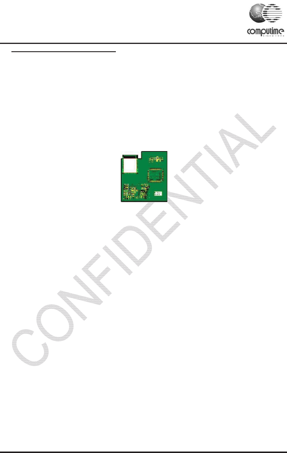
1. General Description
The CTLA357 and CTLB357
a
Module specially designed f
o
based on IEEE 802.15.4
s
CTLA357/CTLB357 is 32.4 x
2
transceiver with a 32-bit net
w
contains embedded FLASH a
n
intrusive SIF module for power
f
2. Applications
Home
automation &
building control
Home
appliances
&
alarms
3. Features
Complete ZigBee-ready m
o
Integrated IEEE 802.15.4
P
Non-intrusive debug interfa
SPI interface for communic
(EZSP)
Internal RC oscillator for ti
m
High performance direct se
16 channels in the 2.4 GH
z
On-chip regulator for 2.1-3.
Three deep low power mo
d
32-bit ARM® Cortex™-M3
192KB FLASH ROM and 1
2
8Mb off chip FLASH memo
+20dBm Max. transmission
-100dBm sensitivity
Small footprint: 32.4 x 25.4
Extremely low Deep Sleep
o
dule CTLA357/CTLB357
i
mited. All rights reserved.
a
re compact surface mounted High Power
W
o
r Ember ZigBee™ protocol stack for wirele
s
s
tandard in the 2.4GHz world-wide IS
M
2
5.4 x 4.1 mm. It integrated a 2.4GHz, IEEE
w
ork processor (ARM Corte
x
-M3 Process
o
n
d integrated RAM for program and data st
o
f
ul software debugging and programming of
t
&
Monitoring of
remote
systems
Security
systems &
lighting
controls
Se
n
ca
e
m
n
e
o
dule with integrated PCB antenna
P
HY and MAC layer
ce (SIF)
ation and controlled by the Host using the E
m
m
er
quence spread spectrum (DSSS) RF transc
e
z
ISM band
6V operation.
d
es
processor
2
KB RAM(EM357 internal)
ry (CTLB357)
power
x 4.1 mm
Current.
Rev. 1
W
ireless RF Transceiver
s
s networks, EmberZNet,
M
band. The size of
802.15.4-2003 compliant
o
r) to run EmberZNet. It
o
rage. It utilizes the non-
t
he network processor.
n
sor data
pture in
m
bedded
e
tworks
m
berZNet Serial Protocol
e
iver
+18dBm+/-1dBm Max. transmission power
ZigBee- Ready RF Transceiver M
o
Copyright © 2015 Computime L
i
4. Absolute Maximum Ra
t
Parameter
Regulator input voltage (VDD_PADS)
Voltage on any GPIO (PA[7:0], PB[7:0],
PC[7:0]), SWCLK, nRESET,
VREG_OUT
Voltage on any GPIO pin (PA4, PA5
PB6, PB7, PC1), when used as an inpu
t
general purpose ADC with the low
v
range selected
Voltage on OSCA, OSCB, NC
Storage temperature
5. Recommended Operati
n
Parameter
Regulator input voltage (VDD_PADS)
Operating temperature range
Moisture Sensitivity Level(MSL)
6. Electrical Specification
s
T=25ć, VCC = 3.0V, Fo =2450MHz,
i
Parameter
RF Operating frequency
Number of channels
Channel spacing
Frequency stability
Transmit power
Sensitivity
Adjacent channel rejection +/-5 MHz
Adjacent channel rejection +/-10 MHz
o
dule CTLA357/CTLB357
i
mited. All rights reserved.
t
ings
Test Conditions Mi
n
-0.3
-0.3
, PB5,
t
to the
v
oltage
-0.3
-0.3
-40
n
g Conditions
Test Conditions Min
.
2.1
-40
s
i
f nothing else stated.
Condition / Note Min
Programmable in 5MHz steps, 5 MHz
steps for IEEE 802.15.4 compliance 2.4
For IEEE 802.15.4 compliance
For IEEE 802.15.4 compliance
Programmable from firmware
PER = 1% PER, 20byte packet
defined by IEEE 802.15.4 Boost
mode
IEEE 802.15.4 compliance at -82
dBm
IEEE 802.15.4 compliance at -82
dBm
Rev. 1
n
.Max. Unit
+3.6 V
VDD_PADS
+0.3
V
2.0 V
VDD_PADSA
+0.3
V
+85 °C
.
Typ. Max. Unit
3.6 V
+85 °C
MSL3
Typ. Max Unit
2.5 GHz
16
5 MHz
+/-40 ppm
+20 dBm
-100 dBm
35/35 dB
40/40 dB
+18+/-1
2.405
2.480
ZigBee- Ready RF Transceiver M
o
Copyright © 2015 Computime L
i
Parameter
Supply voltage
Current consumption,
RX mode
Current
consumption,
TX mode
CTLA357, CTL
B
Deep sleep current
CTLA357
CTLB357
Flash Memory CTLA357, CTL
B
CTLB357
RAM
MCU clock frequency
MCU Low Speed Clock
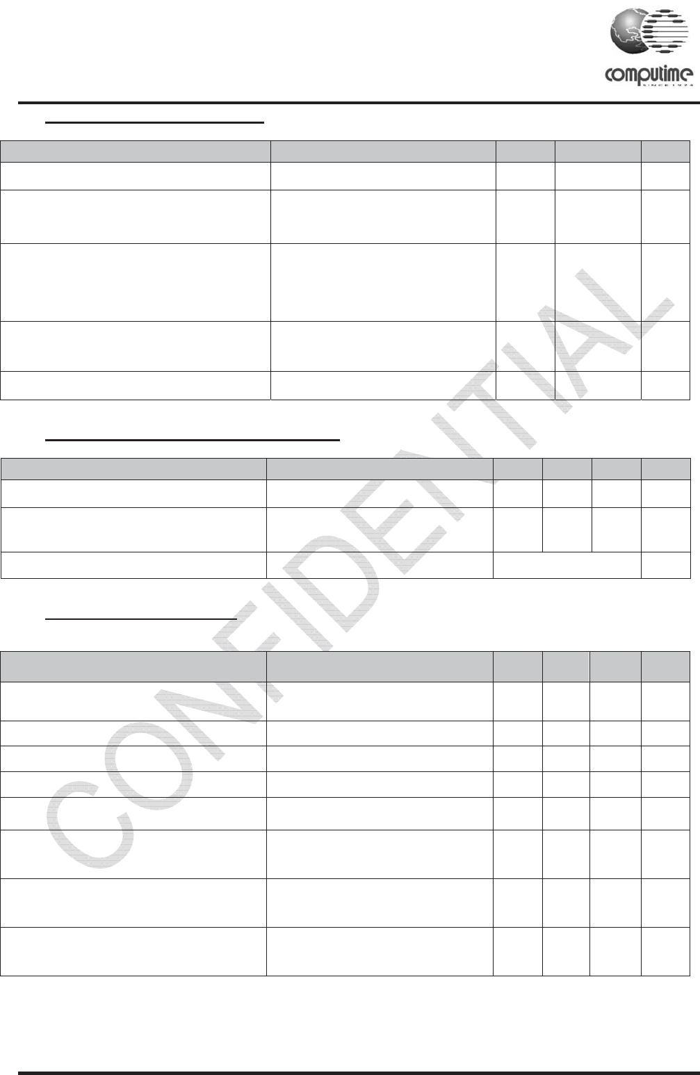
7. Typical application blo
c
Fi
Debug and
programming
interface
HOST
MCU
NRE
PTI_
PTI-D
A
SIF_
C
SIF-
M
SIF-
M
NSIF_
L
SD
B
o
dule CTLA357/CTLB357
i
mited. All rights reserved.
Condition / Note Min
2.1
Max RX sensitivity (normal mode)
Max RX sensitivity (boost mode)
B
357
B
357 FLASH memory in EM357
Off chip Serial FLASH
Internal RAM in EM357
c
k
gure 1: Example of application circuit
CTLA/B357
RF Module
VDD_PADS=2.1- 3.6
V
LINK_ACTIVITY
ST
EN
A
TA
C
LK
M
ISO
M
OSI
L
OAD
B
G
Rev. 1
Typ. Max Unit
3.6 V
28 mA
30 mA
150 mA
2.8 uA
8 12 uA
192 KB
8 Mb
12 KB
24 MHz
32.768 KHz
V
N+]&/ S)
ZigBee- Ready RF Transceiver M
o
Copyright © 2015 Computime L
i
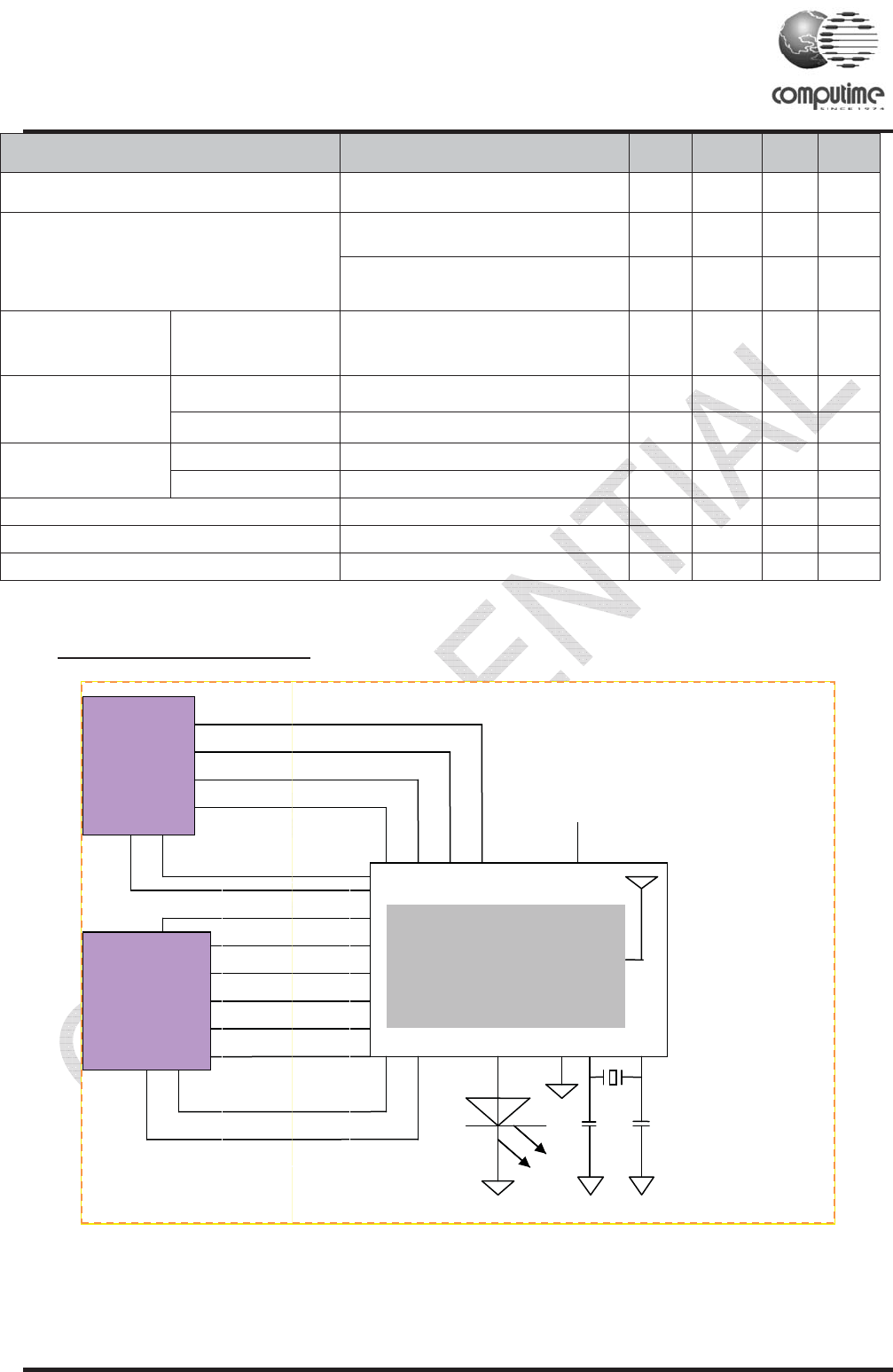
8. Pin Assignment
F
o
dule CTLA357/CTLB357
i
mited. All rights reserved.
F
igure 2: CTLA357/CTLB357 pin assignm
e
Rev. 1
e
nt

ZigBee- Ready RF Transceiver M
o
Copyright © 2015 Computime L
i
9. Pin Description
Pin# CTLA35
7
1
JTCK
SWCLK
2
PC2
JTDO
SWO
3
PC3
JTDI
4
PC4
JTMS
SWDIO
5
PC0
JRST
IRQD
TRACEDATA1
6
PB7
ADC2
IRQC
TIM1C2
TIM1C2
7
PB6
ADC1
IRQB
TIM1C1
TIM1C1
o
dule CTLA357/CTLB357
i
mited. All rights reserved.
7
CTLB357 Direction Descriptio
n
JTCK I JTAG clock input from debugg
SWCLK I/O Serial Wire Clock input/output
w
PC2 I/O Digital I/O Enable with GPIO_
D
JTDO O JTAG data out to debugger
SWO O
Serial Wire Output async
h
output to debugger
PC3 I/O Digital I/O Enable with GPIO_
D
JTDI I JTAG data in from debugger
PC4 I/O
Digital I/O Either
E
GPIO_DBGCFG[5]
JTMS I JTAG mode select from debu
g
SWDIO I/O
Serial Wire bidirectional
debugger
PC0 I/O High
current
Digital I/O Either
E
GPIO_DBGCFG[5]
JRST I JTAG reset input from debugg
e
IRQD I Default external interrupt sour
c
TRACEDATA1 O Synchronous CPU trace data
b
PB7 I/OHigh current Digital I/O
ADC2 Analog ADC input 2
IRQC I Default external interrupt sour
c
TIM1C2 O Timer 1 channel 2 output
TIM1C2 1 Timer 1 channel 2 input
PB6 I/O High
current Digital I/O
ADC1 Analog ADC input 1
IRQB I External interrupt source B
TIM1C1 O Timer 1 channel 1 output
TIM1C1 I Timer 1 channel 1 input
Rev. 1
n
er
w
ith debugger
D
BGCFG[5]
h
ronous trace
D
BGCFG[5]
E
nable with
g
ger
data to/from
E
nable with
e
r
c
e D
b
it 1
c
e C

ZigBee- Ready RF Transceiver M
o
Copyright © 2015 Computime L
i
Pin# CTLA35
7
8
PA7
TIM1C4
TIM1C4
REG_EN
9 PC1
10 GND
11
PB3
TIM2C3
TIM2C3
SC1nCTS
SC1SCLK
SC1SCLK
12 GND
13
PC6
NTX_ACTIVE
14
PC7
OSC32_EXT
15 GND
16 VDD_PADS
17 nRESET
o
dule CTLA357/CTLB357
i
mited. All rights reserved.
7
CTLB357 Direction Descriptio
n
PA7 I/O High current Digital I/O Disable R
E
GPIO_DBGCFG [4]
TIM1C4 O Timer 1 channel 4 output
TIM1C4 I Timer 1 channel 4 input
REG_EN O External regulator open drain
o
PC1 O RX Enable: High RX Disa
b
GND
PB3 I/O Digital I/O
TIM2C3 O Timer 2 channel 3 output
TIM2C3 I Timer 2 channel 3 input
SC1nCTS I UART CTS handshake of Seri
a
SC1SCLK O SPI master clock of serial Con
SC1SCLK I SPI slave clock of serial Contr
o
GND
PC6 I/O Digital I/O
I/O
32.768KHz crystal oscillator.
used for oscillation, then can
n
other purposes, such as gene
r
NTX_ACTIVE O Inverted TX_ACTIVE signal
PC7 I/O Digital I/O
I/O
32.768KHz crystal oscillator.
used for oscillation, then can
n
other purposes, such as gene
r
OSC32_EXT I Digital 32.768KHz clock input
s
GND
VDD_PADS Power Pads supply(2.1-3.6V)
nRESET I
A
ctive low chip reset(internal
p
Rev. 1
n
E
G_EN with
o
utput
b
le: Low
a
l Controller 1
troller 1
o
ller 1
If this pin is
n
ot be use for
r
al I/O port.
If this pin is
n
ot be use for
r
al I/O port.
s
ource
p
ull-up)

ZigBee- Ready RF Transceiver M
o
Copyright © 2015 Computime L
i
Pin# CTLA35
7
18
PA0
TIM2C1
TIM2C1
SC2MOSI
SC2MOSI
19
PA1
TIM2C3
TIM2C3
SC2SDA
SC2MISO
SC2MISO
20
PA2
TIM2C4
TIM2C4
SC2SCL
SC2SCLK
SC2SCLK
21
PA6
TIM1C3
TIM1C3
o
dule CTLA357/CTLB357
i
mited. All rights reserved.
7
CTLB357 Direction Descriptio
n
PA0 I/O Digital I/O
TIM2C1 O Timer 2 channel 1 output
TIM2C1 I Timer 2 channel 1 input
SC2MOSI O SPI master data out of serial
c
SC2MOSI I SPI slave data in of serial con
t
SI I
Serial data in for off-chip
connected to AT25DF081A.S
used for other purposes.
PA1 I/O Digital I/O
TIM2C3 O Timer 2 channel 3 output
TIM2C3 I Timer 2 channel 3 input
SC2SDA I/O TWI data of serial controller 2
SC2MISO O SPI slave data out of serial co
n
SC2MISO I SPI master data in of serial co
SO O
Serial data out for off-chip
connected to AT25DF081A.S
used for other purposes.
PA2 I/O Digital I/O
TIM2C4 O Timer 2 channel 4 output
TIM2C4 I Timer 2 channel 4 input
SC2SCL I/O TWI clock of serial controller 2
SC2SCLK O SPI master clock of serial con
t
SC2SCLK I SPI slave clock of serial contr
o
SCK I
Clock in for 8Mb flash. It
AT25DF081A.So it cannot be
purposes.
PA6 I/O High current Digital I/O
TIM1C3 O Timer 1 channel 3 output
TIM1C3 I Timer 1 channel 3 input
Rev. 1
n
c
ontroller 2
t
roller 2
8Mb flash. It
o it cannot be
n
troller 2
ntroller 2
8Mb flash. It
o it cannot be
t
roller 2
o
ller 2
connected to
used for other

ZigBee- Ready RF Transceiver M
o
Copyright © 2015 Computime L
i
Pin# CTLA35
7
22
PB4
TIM2C4
TIM2C4
SC1nRTS
SC1nSSEL
23
PA3
SC2Nssel
TRACECLK
TIM2C2
TIM2C2
24
PA4
ADC4
PTI_EN
TRACEDATA2
25
PA5
ADC5
PTI_DATA
NBOOTMODE
TRACEDATA3
26
PB1
SC1MISO
SC1MOSI
SC1SDA
SC1TXD
TIM2C1
TIM2C1
o
dule CTLA357/CTLB357
i
mited. All rights reserved.
7
CTLB357 Direction Descriptio
n
PB4 I/O Digital I/O
TIM2C4 O Timer 2 channel 4 output
TIM2C4 i Timer 2 channel 4 input
SC1nRTS O UART RTS handshake of seri
a
SC1nSSEL I SPI slave select of serial cont
r
PA3 I/O Digital I/O
SC2Nssel I SPI slave select of serial cont
r
TRACECLK O Synchronous CPU trace clock
TIM2C2 O Timer 2 channel 2 output
TIM2C2 I Timer 2 channel 2 input
CE# I
Chip Enable of 8Mb falsh. It c
o
AT25DF081A.So it cannot be
u
purposes, such as general I/O
PA4 I/O Digital I/O
ADC4 Analog ADC input 4
PTI_EN O Frame signal of packet trace i
n
TRACEDATA2 O Synchronous CPU trace data
b
PA5 I/O Digital I/O
ADC5 Analog ADC input 5
PTI_DATA O Data signal of packet trace int
e
NBOOTMODE I Embedded serial bootloader
a
reset
TRACEDATA3 O Synchronous CPU trace data
b
PB1 I/O Digital I/O
SC1MISO O SPI slave data out of serial co
n
SC1MOSI O SPI master data out of serial
c
SC1SDA I/O TWI data of serial controller 1
SC1TXD O UART transmit data of serial c
o
TIM2C1 O Timer 2 channel 1 output
TIM2C1 I Timer 2 channel 1 input
Rev. 1
n
a
l controller 1
r
oller 1
r
oller 2
o
nnected to
u
sed for other
port.
n
terface
b
it 2
e
rface
a
ctivation out of
b
it 3
n
troller 1
c
ontroller 1
o
ntroller 1

ZigBee- Ready RF Transceiver M
o
Copyright © 2015 Computime L
i
Pin# CTLA35
7
27
PB2
SC1MISO
SC1MOSI
SC1SCL
SC1RXD
TIM2C2
TIM2C2
28
PB5
ADC0
TIM2CLK
TIM1CLK
29
PB0
VREF
VREF
IRQA
TRACECLK
TIM1CLK
TIM2MSK
o
dule CTLA357/CTLB357
i
mited. All rights reserved.
7
CTLB357 Direction Description
PB2 I/O Digital I/O
SC1MISO I SPI master data in of serial co
n
SC1MOSI I SPI slave data in of serial cont
SC1SCL I/O TWI clock of serial controller 1
SC1RXD I UART receive data of serial c
o
TIM2C2 O Timer 2 channel 2 output
TIM2C2 I Timer 2 channel 2 input
PB5 I/O Digital I/O
ADC0 Analog ADC input 0
TIM2CLK I Timer 2 external clock input
TIM1CLK I Timer 1 external clock mask in
PB0 I/O Digital I/O
VREF Analog O ADC reference output
VREF Analog I ADC reference input
IRQA I External interrupt source A
TRACECLK O Synchronous CPU trace clock
TIM1CLK I Timer 1 external clock input
TIM2MSK I Timer 2 external clock mask in
Rev. 1
n
troller 1
roller 1
o
ntroller 1
put
put
ZigBee- Ready RF Transceiver M
o
Copyright © 2015 Computime L
i
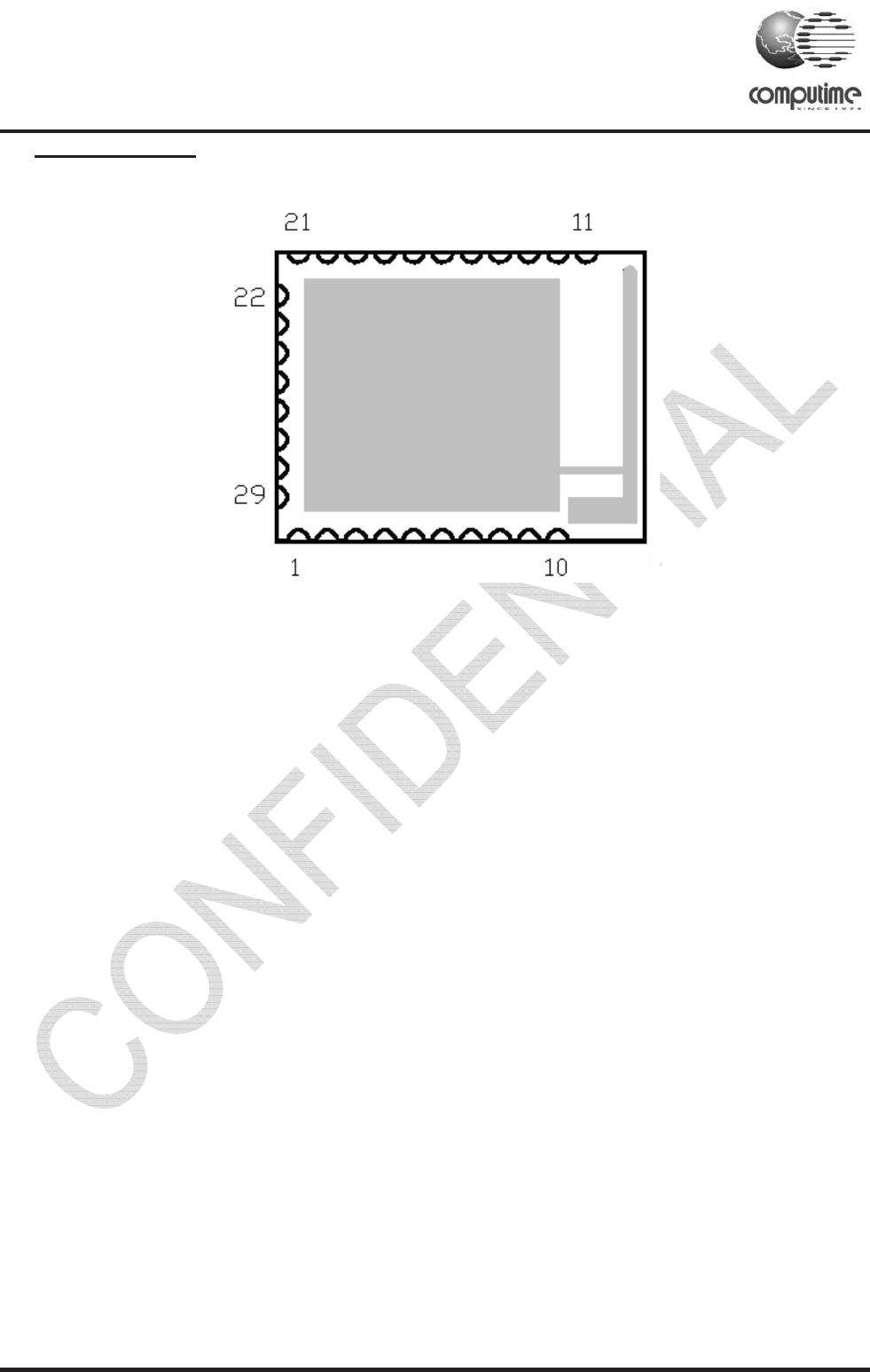
10. Block Diagram
UART/SPI/I2C
Communication
Ap
Z
i
N
IEE
E
32 Bit
A
UART/SPI/I2C
Communication
Ap
Z
i
N
IEE
E
32 Bit
A
o
dule CTLA357/CTLB357
i
mited. All rights reserved.
Figure 3: CTLA357 Block Diagram
Figure 4: CTLB357 Block Diagram
User
p
plication
i
gbee
TM
N
etwork
E
802.15.4
MAC
IEEE 802.15.4
RF Transceiver
2.1 – 3.6V
FE
M
A
RM Processor
24MHz
P
User
p
plication
i
gbee
TM
N
etwork
E
802.15.4
MAC
IEEE 802.15.4
RF Transceiver
2.1 – 3.6V
FE
M
A
RM Processor
24MHz
P
8Mb flash
Rev. 1
M
P
CB antenna
M
P
CB antenna

ZigBee- Ready RF Transceiver M
o
Copyright © 2015 Computime L
i
11. RF Frequency Detail
The following table shows the
R
R
Note: The output power of
C
2480M channel to Comply F
C
The use of RF frequencies an
d
regulations. The CTLA357/C
T
wide 2.4GHz ISM band.
The following table is the settin
Channel
Freq(MHz)
Ember setting
o
dule CTLA357/CTLB357
i
mited. All rights reserved.
R
F channels as defined by the IEEE 802.15.
4
R
F channel Frequency
11 2405MHz
12 2410MHz
13 2415MHz
14 2420MHz
15 2425MHz
16 2430MHz
17 2435MHz
18 2440MHz
19 2445MHz
20 2450MHz
21 2455MHz
22 2460MHz
23 2465MHz
24 2470MHz
25 2475MHz
26 2480MHz
C
TLA357/CTLB357 should be configured
C
C requirement.
d
maximum allowed RF power should acco
r
T
LB357 are complying with the applicable
r
g for the CTLA357/CTLB357 to US market:
FCC
CH11~25
2405~2475
-4dBm +Non boost -2
4
t
e
Rev. 1
4
standard.
lower than -24dBm for
r
ding to different national
r
egulations for the world
CH26
2480
4
dBm ( base on FCC
e
st result to adjust )
-3.5dBm for
+18+/-1dBm
-3+/-1dBm
ZigBee- Ready RF Transceiver M
o
Copyright © 2015 Computime L
i
12. PCB Layout Recomme
n
Please reference Mechanical
D
The area underneath the mod
u
circuit on the test pads on the
b
preferred.
As the module integrated with
o
have great impact on the RF p
e
part underneath or nearby the
a
example how the module posit
i
Figure 4: A rec
o
o
dule CTLA357/CTLB357
i
mited. All rights reserved.
n
dations
D
imensions shown in next section for PCB la
y
u
le should be covered with solder mask in or
d
b
ack side of the module. A solid ground plan
e
o
nboard PCB trace antenna, the mounting p
o
e
rformance. There should not be any trace,
g
a
rea of the onboard PCB trace antenna. The
i
oned on the mother PCB.
o
mmended placement of the module on a
Rev. 1
y
out.
d
er to prevent short
e
under the module is
o
sition of the module will
g
round plane or metal
figure below shows an
main PCB
ZigBee- Ready RF Transceiver M
o
Copyright © 2015 Computime L
i
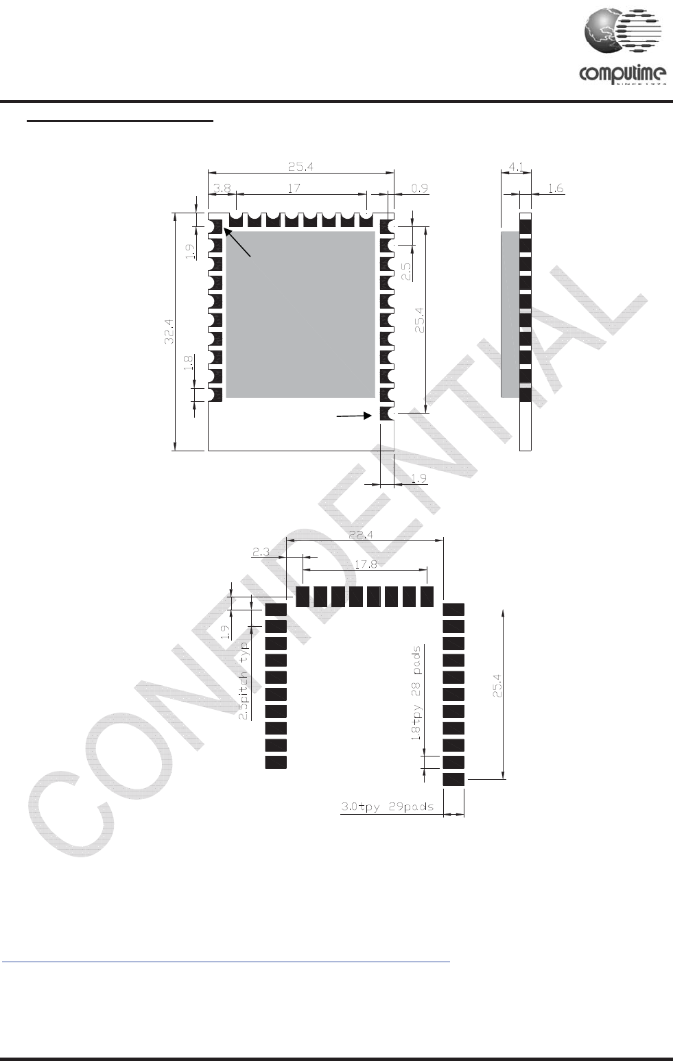
13. Mechanical Dimension
s
Figure 5:
M
For further details on the S
o
http://www.silabs.com/product
s
o
dule CTLA357/CTLB357
i
mited. All rights reserved.
s
M
echanical Dimensions of CTLA357/CTL
B
o
C transceiver (Ember EM357), please c
o
s
/wireless/zigbee/Pages/default.asp
x
Pin 1
Pin 11
Rev. 1
B
357
o
nsult the data sheet at

ZigBee- Ready RF Transceiver M
o
Copyright © 2015 Computime L
i
About Computime
Founded in 1974, Computi
m
providing innovative automa
t
and consumer markets.
The Company provides tech
lives more productive and c
o
o
dule CTLA357/CTLB357
i
mited. All rights reserved.
Co
n
C
9/F To
w
e-ma
m
eis a global technology, brand and ma
n
t
ion and control solutions to customers i
n
nologies and products that save energy
a
o
mfortable.
Rev. 1
n
tact information
C
OMPUTIME LIMITED
w
er One, Lippo Centre,
89 Queensway,
Hong Kong
Tel: +852.2260.0300
Fax: +852.2790.3996
il: hq@computime.com
n
ufacturing company
n
commercial, industrial
a
nd make people's
FCC Statement
Thisdevicecomplieswithpart15oftheFCCRules.Operationissubjecttothefollowingtwoconditions:(1)Thisdevicemaynotcauseharmful
interference,and(2)thisdevicemustacceptanyinterferencereceived,includinginterferencethatmaycauseundesiredoperation.
Changes or modifications not expressly approved by the party responsible for compliance could void the user's authority to operate the
equipment.
NOTE:ThisequipmenthasbeentestedandfoundtocomplywiththelimitsforaClassBdigitaldevice,pursuanttoPart15oftheFCCRules.
Theselimitsaredesignedtoprovidereasonableprotectionagainstharmfulinterferenceinaresidentialinstallation.Thisequipmentgenerates,
usesandcanradiateradiofrequencyenergyand,ifnotinstalledandusedinaccordancewiththeinstructions,maycauseharmfulinterference
toradiocommunications. However, there is noguaranteethat interferencewill notoccurin a particularinstallation.If this equipment does
cause harmful interference to radio or television reception, which can be determined by turning the equipment off and on, the user is
encouragedtotrytocorrecttheinterferencebyoneormoreofthefollowing
measures:
ͲͲReorientorrelocatethereceivingantenna.
ͲͲIncreasetheseparationbetweentheequipmentandreceiver.
ͲͲConnecttheequipmentintoanoutletonacircuitdifferentfromthattowhichthereceiverisconnected.
ͲͲConsultthedealeroranexperiencedradio/TVtechnicianforhelp.
FCCRadiationExposureStatement
Themodularcanbeinstalledorintegratedinmobileorfixdevicesonly.Thismodularcannotbeinstalledinanyportabledevice,forexample,
USBdongleliketransmittersisforbidden.
ThismodularcomplieswithFCCRFradiationexposurelimitssetforthforanuncontrolledenvironment.ThistransmittermustnotbecoͲlocated
oroperatinginconjunctionwithanyotherantennaortransmitter.Thismodularmustbeinstalledandoperatedwithaminimumdistanceof20
cmbetweentheradiatoranduserbody.
IftheFCCidentificationnumberisnotvisiblewhenthemoduleisinstalledinsideanotherdevice,thentheoutsideofthedeviceintowhichthe
module is installed must also display a label referring to the enclosed module. This exterior label can use wording such as the following:
“ContainsTransmitterModuleFCCID:2AAUQͲCTLB357OrContainsFCCID:2AAUQͲCTLB357 ā
whenthemoduleisinstalledinsideanotherdevice,theusermanualofthisdevicemustcontainbelowwarningstatements;
1.ThisdevicecomplieswithPart15oftheFCCRules.Operationissubjecttothefollowingtwoconditions:
(1)Thisdevicemaynotcauseharmfulinterference.
(2)Thisdevicemustacceptanyinterferencereceived,includinginterferencethatmaycauseundesiredoperation.
2. Changes or modifications not expressly approved by the party responsible for compliance could void the user's authority to operate the
equipment.
Thedevicesmustbeinstalledandusedinstrictaccordancewiththemanufacturer'sinstructionsasdescribedintheuserdocumentationthat
comeswiththeproduct
IC STATEMENT
ThisdevicecomplieswithIndustryCanada’slicenceͲexemptRSSs.Operationissubjecttothefollowingtwoconditions:
(1)Thisdevicemaynotcauseinterference;and
(2)Thisdevicemustacceptanyinterference,includinginterferencethatmaycauseundesiredoperationofthedevice.
CetappareilestconformeauxCNRexemptesdelicenced'IndustrieCanada.Sonfonctionnementestsoumisauxdeuxconditionssuivantes:
(1)Cedispositifnepeutcauserd'interférences;et
(2)Cedispositifdoitacceptertouteinterférence,ycomprislesinterférencesquipeuventcauserunmauvaisfonctionnementdel'appareil.
ICRadiationExposureStatement
Themodularcanbeinstalledorintegratedinmobileorfixdevicesonly.Thismodularcannotbeinstalledinanyportabledevice,forexample,
USBdongleliketransmittersisforbidden.
ThismodularcomplieswithICRFradiationexposurelimitssetforthforanuncontrolledenvironment.ThistransmittermustnotbecoͲlocated
oroperatinginconjunctionwithanyotherantennaortransmitter.Thismodularmustbeinstalledandoperatedwithaminimumdistanceof20
cmbetweentheradiatoranduserbody.Cettemodulairedoitêtreinstalléetutiliséàunedistanceminimumde20cmentreleradiateuretle
corpsdel'utilisateur.
If the IC number is not visiblewhen the module is installed inside another device, then the outside of the device intowhich the moduleis
installedmustalsodisplayalabelreferringtotheenclosedmodule.Thisexteriorlabelcanusewordingsuchasthefollowing:
“ContainsIC:1700DͲCTLB357ā
whenthemoduleisinstalledinsideanotherdevice,theusermanualofthisdevicemustcontainbelowwarningstatements;
1.ThisdevicecomplieswithIndustryCanada’slicenceͲexemptRSSs.Operationissubjecttothefollowingtwoconditions:
(1)Thisdevicemaynotcauseinterference;and
(2)Thisdevicemustacceptanyinterference,includinginterferencethatmaycauseundesiredoperationofthedevice.
2.CetappareilestconformeauxCNRexemptesdelicenced'IndustrieCanada.Sonfonctionnementestsoumisauxdeuxconditionssuivantes:
(1)Cedispositifnepeutcauserd'interférences;et
(2)Cedispositifdoitacceptertouteinterférence,ycomprislesinterférencesquipeuventcauserunmauvaisfonctionnementdel'appareil.
Thedevicesmustbeinstalledandusedinstrictaccordancewiththemanufacturer'sinstructionsasdescribedintheuserdocumentationthat
comeswiththeproduct