Connect One MDLWMGMR09 C1 Wireless b/g baseband User Manual Product specification of WM G MR 09
Connect One Ltd. C1 Wireless b/g baseband Product specification of WM G MR 09
UserManual.wiki
>
Connect One
>
MDLWMGMR09 User Manual
User manual
Navigation menu
Upload a User Manual
Namespaces
Wiki Guide
HTML
PDF
Info
Views
User Manual
Discussion / Help
Navigation
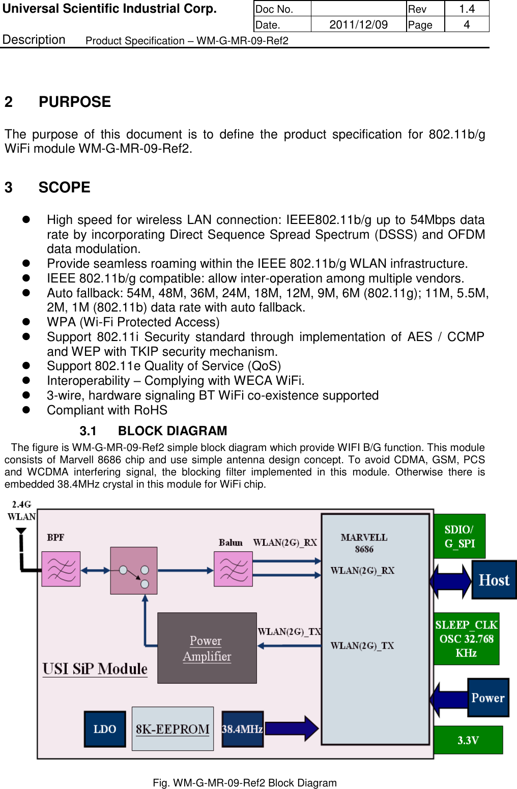
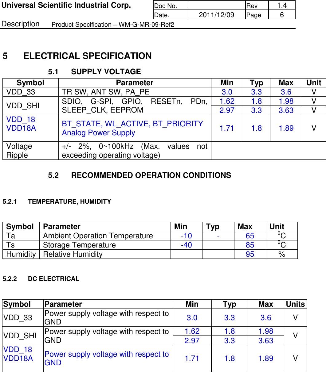
![Universal Scientific Industrial Corp. Doc No. Rev 1.4 Date. 2011/12/09 Page 9 Description Product Specification – WM-G-MR-09-Ref2 6 INTERFACE 6.1 PIN DEFINITION No Pin Name Type Description 1 GND GND Ground 2 RF PORT O Antenna Port (50ohm) 3 GND GND Ground 4 NC O NC 5 SD_D1 I/O SDIO 4-bit Mode: Data Line Bit [1] G-SPI Mode: G-SPI Data Output 6 SCLK I NC This is for Boot setting of ROM. 7 ECSn O Boot from SPI EEPROM: Pull down by 100kohm Boot from host Interface: NC 8 GND GND Ground 9 VDD_SHI I Host I/F Voltage: 3.3V Connect to 3.3V power supply Host I/F Voltage: 1.8V Connect to 1.8V power supply Not need to prepare external 1.8V power supply by connecting #9 and #17 (1.8V terminal) 10 GPIO_6 I/O General I/O Port , leave open if no use. 11 GPIO_5 I/O General I/O Port , leave open if no use. 12 SD_D3 I/O SDIO 4-bit Mode: Data Line Bit [3] 13 GPIO_2 I/O General I/O Port , leave open if no use. 14 SD_CLK I/O SDIO 4-bit Mode: Clock Input G-SPI Mode: G-SPI Clock Input 15 GPIO_4 I/O General I/O Port , leave open if no use. 16 GPIO_1 I/O General I/O Port t , leave open if no use. Default function : LED indicate. 17 VDD_18 POWER 1.8V DC monitor terminal , need 1uF decoupling capacitor 18 VDD_12 POWER 1.2V DC monitor terminal , need 1uF decoupling capacitor 19 GND GND Ground 20 SD_CMD I/O SDIO 4-bit Mode: Command / Response G-SPI Mode: G-SPI Data Input 21 SD_D0 I SDIO 4-bit Mode: Data Line Bit [0] G-SPI Mode: G-SPI Chip Select Input (Active Low) 22 SD_D2 I/O SDIO 4-bit Mode: Data Line Bit [2] G-SPI Mode: G-SPI Interrupt Output (Active Low)](https://usermanual.wiki/Connect-One/MDLWMGMR09/User-Guide-2202657-Page-9.png)
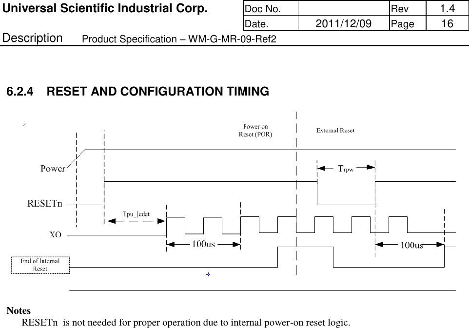
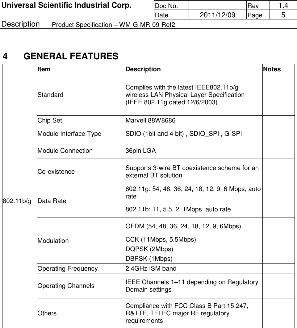
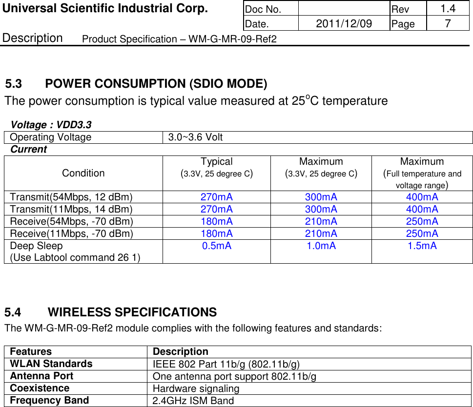
![Universal Scientific Industrial Corp. Doc No. Rev 1.4 Date. 2011/12/09 Page 18 Description Product Specification – WM-G-MR-09-Ref2 6.2.5 LED INTERFACE Pin No. Pin description Function description 16 GPIO_1 WLAN status LED (Tx power or Rx ready LED NOTE: Over full range of values specified in the Recommended Operating Conditions unless otherwise specified. Symbol Parameter Condition Typ Units LOH Switching current high Tristate on pad (requires pull-up on board) Tristate when driving high mA IOL Switching current low @0.4V 10 mA 6.2.6 ANTENNA INTERFACE Antenna diversity is not supported on the Wireless Module. The output impedance of the antenna port is 50 Ohms. 7 REGULATORY The WM-G-MR-09-Ref2 module is tested on module level to comply with following standards (pre-test): • US/CAN: FCC CFR47 Part 15.247 • Europe: ETS 300-328 V1.6.1 Test setup: laptop plus adaptor card with Marvell Lab tool in SDIO mode Final certification should be completed on system level. Antenna Part No. :W1030 Gain [dBi] :2.0 Impedance [Nom]:50 Ω VSWR<=2.0 Electrical Length :1/4, dipole Radiation: Omni Connector Options-Reverse SMA Trade mark: Pulse Manufacture: A TECHNITROL COMPANYINFORMATION](https://usermanual.wiki/Connect-One/MDLWMGMR09/User-Guide-2202657-Page-17.png)