Connect One MDLWMGMR09 C1 Wireless b/g baseband User Manual Product specification of WM G MR 09
Connect One Ltd. C1 Wireless b/g baseband Product specification of WM G MR 09
User manual

Communication Products BU
Product Specification
of WM-G-MR-09-Ref2
Wireless LAN Module
SOURCE ORGANIZATION: USI WP/RD/WM/HW1
Document No. Rev. 1.4
Product Code WM-G-MR-09-Ref2
Product No.
HW Prepared by︰
Ven
Date: 2010/04/16
Checked by︰ Erico Yang Date: 2010/04/16
Approved by︰ Date:
Concurrence (MD): Date:
Concurrence (PM): Date:

Universal Scientific Industrial Corp. Doc No. Rev 1.4
Date. 2011/12/09 Page 2
Description Product Specification – WM-G-MR-09-Ref2
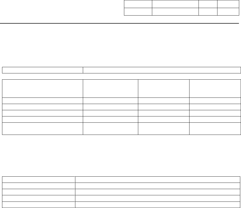
1 REVISION HISTORY
Version
No. Revised
Date Revised by Description Notes
1.0 2009-09-28 Camus Chen First released
1.1 2009-11-4 Ven Chen 10.1.3 orderable P/N
1.2 2010-01-07 Ven Chen Add 3.1 block diagram(page 4)
Change 8 Mechanical Specification(page 19)
Change 10.1.2 Laser mark(page 22)
1.3 2010-04-16 Ven Chen Change 8 Mechanical Specification(page 19)
Change 10.1.2 Laser mark(page 22)
1.4 2011-12-09 Robert CHANG Model Name Correction
Universal Scientific Industrial Corp. Doc No. Rev 1.4
Date. 2011/12/09 Page 3
Description Product Specification – WM-G-MR-09-Ref2
INDEX
1 REVISION HISTORY ................................................................................................................................... 2
2 PURPOSE ..................................................................................................................................................... 4
3 SCOPE .......................................................................................................................................................... 4
3.1 BLOCK DIAGRAM ......................................................................................................................................... 4
4 GENERAL FEATURES .............................................................................................................................. 5
5 ELECTRICAL SPECIFICATION................................................................................................................ 6
5.1 SUPPLY VOLTAGE ....................................................................................................................................... 6
5.2 RECOMMENDED OPERATION CONDITIONS ................................................................................................. 6
5.2.1 Temperature, humidity ................................................................................................................. 6
5.2.2 DC Electrical .................................................................................................................................. 6
5.3 POWER CONSUMPTION (SDIO MODE) ...................................................................................................... 7
5.4 WIRELESS SPECIFICATIONS ....................................................................................................................... 7
5.5 RADIO SPECIFICATION ................................................................................................................................. 8
6 INTERFACE .................................................................................................................................................. 9
6.1 PIN DEFINITION ........................................................................................................................................... 9
6.1.1 RECOMMENDED FOOTPRINT ............................................................................................................ 12
6.2 SPEIFICATIONS AND TIMING DIAGRAM ........................................................................................................13
6.2.1 External sleep clock specification ............................................................................................ 13
6.2.2 SDIO protocol timing .................................................................................................................. 13
6.2.3 G-SPI protocol timing ................................................................................................................. 15
6.2.4 Networking Coexistence ............................................................................................................ 16
6.2.5 Reset and configuration timing ................................................................................................. 16
6.2.6 LED Interface .............................................................................................................................. 18
6.2.7 Antenna Interface ....................................................................................................................... 18
7 REGULATORY ........................................................................................................................................... 18
8 MECHANICAL SPECIFICATION ............................................................................................................ 19
9 RECOMMENDED REFLOW PROFILE .................................................................................................. 20
10 PACKAGE AND STORAGE CONDITION ............................................................................................. 21
10.1.1 Package Dimension ................................................................................................................... 21
10.1.2 Laser Mark ................................................................................................................................... 22
10.1.3 Part Order Numbering................................................................................................................ 22
10.1.4 ESD Level .................................................................................................................................... 22
Universal Scientific Industrial Corp. Doc No. Rev 1.4
Date. 2011/12/09 Page 4
Description Product Specification – WM-G-MR-09-Ref2
2 PURPOSE
The purpose of this document is to define the product specification for 802.11b/g
WiFi module WM-G-MR-09-Ref2.
3 SCOPE
High speed for wireless LAN connection: IEEE802.11b/g up to 54Mbps data
rate by incorporating Direct Sequence Spread Spectrum (DSSS) and OFDM
data modulation.
Provide seamless roaming within the IEEE 802.11b/g WLAN infrastructure.
IEEE 802.11b/g compatible: allow inter-operation among multiple vendors.
Auto fallback: 54M, 48M, 36M, 24M, 18M, 12M, 9M, 6M (802.11g); 11M, 5.5M,
2M, 1M (802.11b) data rate with auto fallback.
WPA (Wi-Fi Protected Access)
Support 802.11i Security standard through implementation of AES / CCMP
and WEP with TKIP security mechanism.
Support 802.11e Quality of Service (QoS)
Interoperability – Complying with WECA WiFi.
3-wire, hardware signaling BT WiFi co-existence supported
Compliant with RoHS
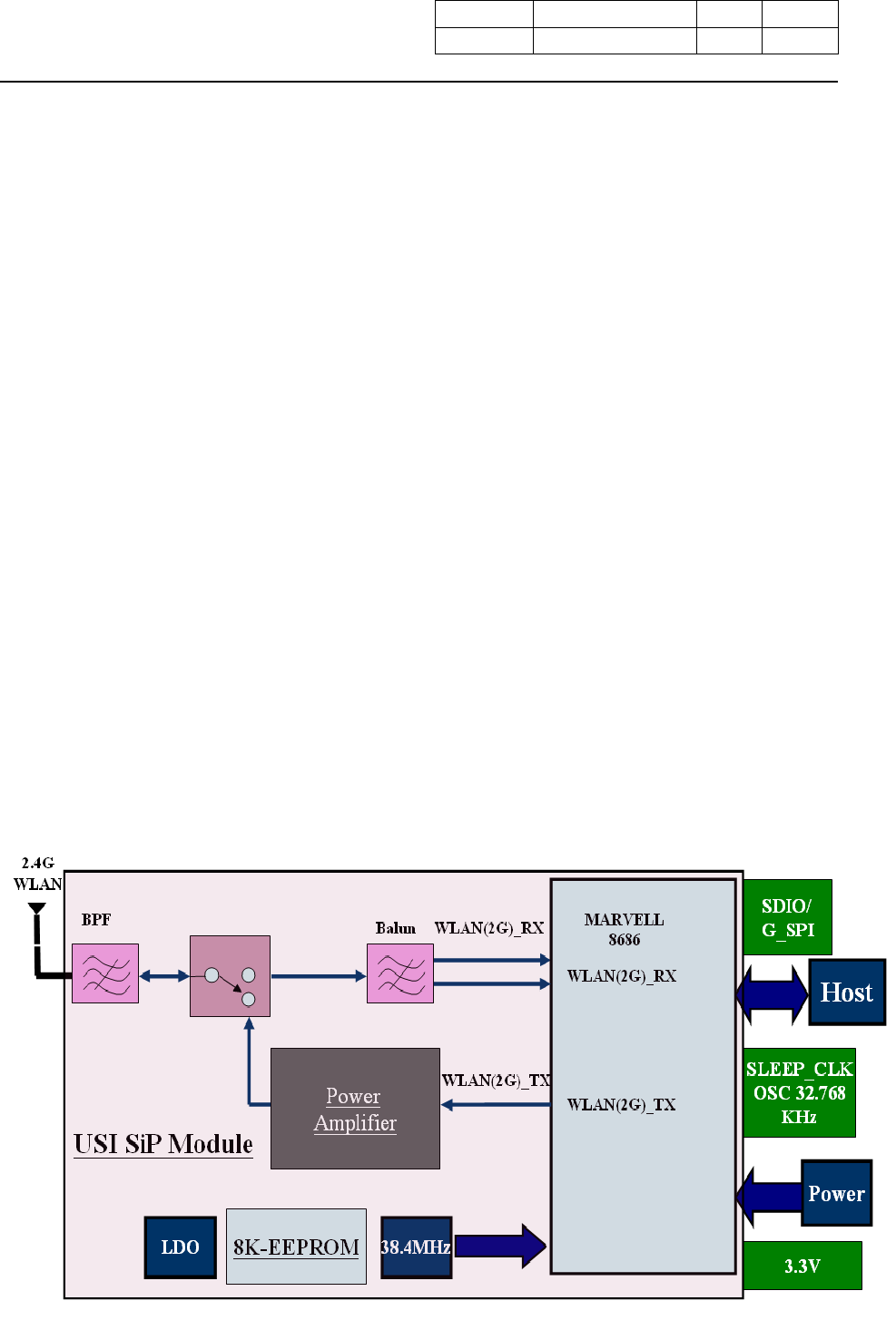
3.1 BLOCK DIAGRAM
The figure is WM-G-MR-09-Ref2 simple block diagram which provide WIFI B/G function. This module
consists of Marvell 8686 chip and use simple antenna design concept. To avoid CDMA, GSM, PCS
and WCDMA interfering signal, the blocking filter implemented in this module. Otherwise there is
embedded 38.4MHz crystal in this module for WiFi chip.
Fig. WM-G-MR-09-Ref2 Block Diagram
Universal Scientific Industrial Corp. Doc No. Rev 1.4
Date. 2011/12/09 Page 5
Description Product Specification – WM-G-MR-09-Ref2
4 GENERAL FEATURES
Item Description Notes
802.11b/g
Standard Complies with the latest IEEE802.11b/g
wireless LAN Physical Layer Specification
(IEEE 802.11g dated 12/6/2003)
Chip Set Marvell 88W8686
Module Interface Type SDIO (1bit and 4 bit) , SDIO_SPI , G-SPI
Module Connection 36pin LGA
Co-existence Supports 3-wire BT coexistence scheme for an
external BT solution
Data Rate
802.11g: 54, 48, 36, 24, 18, 12, 9, 6 Mbps, auto
rate
802.11b: 11, 5.5, 2, 1Mbps, auto rate
Modulation
OFDM (54, 48, 36, 24, 18, 12, 9, 6Mbps)
CCK (11Mbps, 5.5Mbps)
DQPSK (2Mbps)
DBPSK (1Mbps)
Operating Frequency 2.4GHz ISM band
Operating Channels IEEE Channels 1–11 depending on Regulatory
Domain settings
Others Compliance with FCC Class B Part 15.247,
R&TTE, TELEC major RF regulatory
requirements
Universal Scientific Industrial Corp. Doc No. Rev 1.4
Date. 2011/12/09 Page 6
Description Product Specification – WM-G-MR-09-Ref2
5 ELECTRICAL SPECIFICATION
5.1 SUPPLY VOLTAGE
Symbol Parameter Min Typ Max Unit
VDD_33 TR SW, ANT SW, PA_PE 3.0 3.3 3.6 V
VDD_SHI SDIO, G-SPI, GPIO, RESETn, PDn,
SLEEP_CLK, EEPROM 1.62 1.8 1.98 V
2.97 3.3 3.63 V
VDD_18
VDD18A BT_STATE, WL_ACTIVE, BT_PRIORITY
Analog Power Supply 1.71 1.8 1.89 V
Voltage
Ripple +/- 2%, 0~100kHz (Max. values not
exceeding operating voltage)
5.2 RECOMMENDED OPERATION CONDITIONS
5.2.1 TEMPERATURE, HUMIDITY
Symbol Parameter Min Typ Max Unit
Ta Ambient Operation Temperature -10 - 65
0
C
Ts Storage Temperature -40 85
0
C
Humidity Relative Humidity 95 %
5.2.2 DC ELECTRICAL
Symbol Parameter Min Typ Max Units
VDD_33 Power supply voltage with respect to
GND 3.0 3.3 3.6 V
VDD_SHI Power supply voltage with respect to
GND 1.62 1.8 1.98 V
2.97 3.3 3.63
VDD_18
VDD18A Power supply voltage with respect to
GND 1.71 1.8 1.89 V
Universal Scientific Industrial Corp. Doc No. Rev 1.4
Date. 2011/12/09 Page 7
Description Product Specification – WM-G-MR-09-Ref2
5.3 POWER CONSUMPTION (SDIO MODE)
The power consumption is typical value measured at 25oC temperature
Voltage : VDD3.3
Operating Voltage 3.0~3.6 Volt
Current
Condition Typical
(3.3V, 25 degree C) Maximum
(3.3V, 25 degree C) Maximum
(Full temperature and
voltage range)
Transmit(54Mbps, 12 dBm) 270mA 300mA 400mA
Transmit(11Mbps, 14 dBm) 270mA 300mA 400mA
Receive(54Mbps, -70 dBm) 180mA 210mA 250mA
Receive(11Mbps, -70 dBm) 180mA 210mA 250mA
Deep Sleep
(Use Labtool command 26 1) 0.5mA 1.0mA 1.5mA
5.4 WIRELESS SPECIFICATIONS
The WM-G-MR-09-Ref2 module complies with the following features and standards:
Features Description
WLAN Standards IEEE 802 Part 11b/g (802.11b/g)
Antenna Port One antenna port support 802.11b/g
Coexistence Hardware signaling
Frequency Band 2.4GHz ISM Band
Universal Scientific Industrial Corp. Doc No. Rev 1.4
Date. 2011/12/09 Page 8
Description Product Specification – WM-G-MR-09-Ref2
5.5 RADIO SPECIFICATION
Over full range of values specified in the “Recommended Operation Condition” unless specified
otherwise.
Features Description
Frequency Band 2.4 GHz ISM Band
Number of selectable Sub
channels 11 channels
Modulation OFDM, DSSS (Direct Sequence Spread Spectrum), DBPSK,
DQPSK, CCK , 16QAM, 64QAM
Supported rates 1, 2, 5.5, 11, 6, 9, 12, 18, 24, 36, 48, 54 Mbps
Maximum receive level - 10dBm (with PER < 8%)
Carrier Frequency Accuracy +/- 25ppm
(crystal: 38.4MHz +/-5ppm in 250C)
Output Power
Data Rate
Typical (3.3V, 25
degree C) Maximum (3.3V, 25
degree C) Maximum (Full temperature and
voltage range)
1, 2, 5.5, 11Mbps 12 dBm 12 dBm +1.0 /-2.0
6, 9 and >12Mbps 12 dBm 12 dBm +1.0 /-2.0
802.11g EVM Requirement
Item Data Rate (Mbps) Relative Constellation Error (dB) EVM (%RMS)
1 6 (BPSK) -5 56.2
2 9 (BPSK) -8 39.8
3 12 (QPSK) -10 31.6
4 18 (QPSK) -13 22.4
5 24 (16-QAM) -16 15.8
6 36 (16-QAM) -19 11.2
7 48 (64-QAM) -22 7.9
8 54 (64-QAM) -25 5.6
802.11b EVM
Item Data Rate (Mbps) EVM (%RMS)
1 1 (BPSK) 35%
2 2 (QPSK) 35%
3 5.5 (QPSK) 35%
4 11 (QPSK) 35%
Sensitivity
Receiver Characteristics
( 3.3V, 25 degree C ) Typical
(3.3V, 25
degree C)
Maximum
(3.3V, 25
degree C)
Maximum (Full
temperature and
voltage range)
Unit
PER <8%, Rx Sensitivity @ 11 Mbps -85 -83 -81 dBm
PER <8%, Rx Sensitivity @ 1 Mbps -91 -89 -87 dBm
PER <10%, Rx Sensitivity @ 6 Mbps -86 -84 -82 dBm
PER <10%, Rx Sensitivity @ 54 Mbps -70 -68 -66 dBm
12 dBm +1.0 /-2.0
12 dBm +1.0 /-2.0

Universal Scientific Industrial Corp. Doc No. Rev 1.4
Date. 2011/12/09 Page 9
Description Product Specification – WM-G-MR-09-Ref2
6 INTERFACE
6.1 PIN DEFINITION
No Pin Name Type Description
1 GND GND Ground
2 RF PORT O Antenna Port (50ohm)
3 GND GND Ground
4 NC O NC
5 SD_D1 I/O SDIO 4-bit Mode: Data Line Bit [1]
G-SPI Mode: G-SPI Data Output
6 SCLK I NC
This is for Boot setting of ROM.
7 ECSn O Boot from SPI EEPROM: Pull down by
100kohm
Boot from host Interface: NC
8 GND GND Ground
9 VDD_SHI I
Host I/F Voltage: 3.3V
Connect to 3.3V power supply
Host I/F Voltage: 1.8V
Connect to 1.8V power supply
Not need to prepare external 1.8V power supply
by connecting #9 and #17 (1.8V terminal)
10 GPIO_6 I/O General I/O Port , leave open if no use.
11 GPIO_5 I/O General I/O Port , leave open if no use.
12 SD_D3 I/O SDIO 4-bit Mode: Data Line Bit [3]
13 GPIO_2 I/O General I/O Port , leave open if no use.
14 SD_CLK I/O SDIO 4-bit Mode: Clock Input
G-SPI Mode: G-SPI Clock Input
15 GPIO_4 I/O General I/O Port , leave open if no use.
16 GPIO_1 I/O General I/O Port t , leave open if no use.
Default function : LED indicate.
17 VDD_18 POWER 1.8V DC monitor terminal , need 1uF
decoupling capacitor
18 VDD_12 POWER 1.2V DC monitor terminal , need 1uF
decoupling capacitor
19 GND GND Ground
20 SD_CMD I/O SDIO 4-bit Mode: Command / Response
G-SPI Mode: G-SPI Data Input
21 SD_D0 I SDIO 4-bit Mode: Data Line Bit [0]
G-SPI Mode: G-SPI Chip Select Input (Active
Low)
22 SD_D2 I/O SDIO 4-bit Mode: Data Line Bit [2]
G-SPI Mode: G-SPI Interrupt Output (Active
Low)
Universal Scientific Industrial Corp. Doc No. Rev 1.4
Date. 2011/12/09 Page 10
Description Product Specification – WM-G-MR-09-Ref2
23 IF_SEL_1 O Select Interface Mode Pin
SDIO Mode: No Connect
G-SPI Mode: Pull Down by 100kohm
24 IF_SEL_2 O Select Interface Mode Pin
SDIO Mode: No Connect
G-SPI Mode: Pull Down by 100kohm
25 VDD18A POWER 1.8V Analog DC monitor terminal , need 1uF
decoupling capacitor
26 GND GND Ground
27 VDD_33 POWER Connect to 3.3V DC supply
28 VDD_33 POWER Connect to 3.3V DC supply
29 WL_ACTIVE O
WLAN Active (Active Low)
2-Wire BCA Mode
When high, WLAN is transmitting or receiving
packets.
3-Wire BCA Mode
0 = Bluetooth device is allowed to transmit
1 = Bluetooth device is not allowed to transmit
Internal 50kohm pull-down. This pin drives low
when PDn
is asserted. In WLAN Sleep mode, all I/O Pads
are
powered down. This Pad must stay at a low
state even in
power down mode.
Please make it open when do not use it.
30 PDn I Pull up by 100kohm, Full Power Down (Active
Low)
31 RESETn I Reset (Active Low) , leave open if no use.

Universal Scientific Industrial Corp. Doc No. Rev 1.4
Date. 2011/12/09 Page 11
Description Product Specification – WM-G-MR-09-Ref2
32 GPIO_0 I/O General I/O Port , leave open if no use.
33 SLEEP_CLK I Clock Input for External Sleep Clock , leave
open if no use.
34 PW_SEL O NC
Universal Scientific Industrial Corp. Doc No. Rev 1.4
Date. 2011/12/09 Page 13
Description Product Specification – WM-G-MR-09-Ref2
6.2 SPEIFICATIONS AND TIMING DIAGRAM
6.2.1 EXTERNAL SLEEP CLOCK SPECIFICATION
The WM-G-MR-09-Ref2 external sleep clock pin (SLEEP_CLK) is powered from VDD_SHI Voltage
Supply.
Protocol Timing
Symbol Parameter Condition Min Typ Max Units
CLK Clock Frequency
Range -- 10 100 1000 KHz
THIGH Clock high time -- 40 -- -- ns
TLOW Clock low time -- 40 -- -- ns
TRISE Clock rise time -- -- -- 5 ns
TFALL Clock fall time -- -- -- 5 ns
NOTE: Over full range of values specified in the Recommended Operating Conditions unless
otherwise specified.
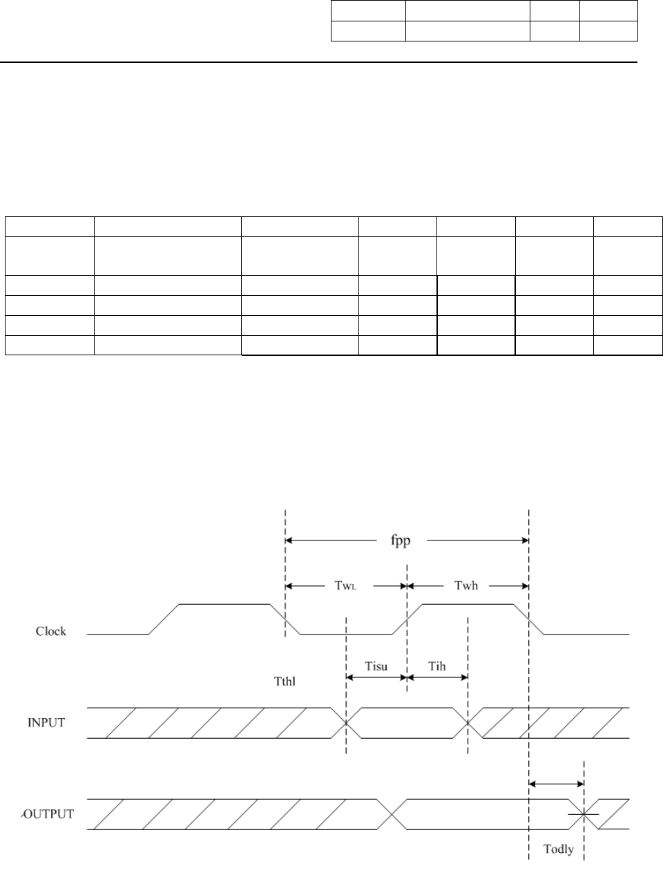
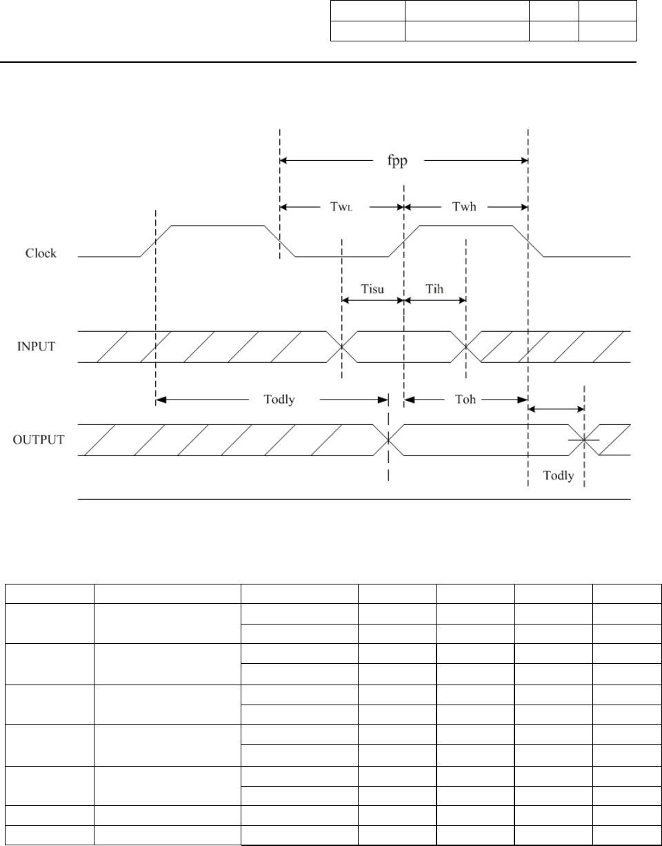
6.2.2 SDIO PROTOCOL TIMING
SDIO Protocol Timing Diagram
Universal Scientific Industrial Corp. Doc No. Rev 1.4
Date. 2011/12/09 Page 14
Description Product Specification – WM-G-MR-09-Ref2
SDIO Protocol Timing Diagram – High Speed Mode
SDIO Timing Data
Symbol Parameter Condition Min Typ Max Units
Fpp Clock Frequency Normal 0 -- 25 MHz
High Speed 0 -- 50 MHz
TWL Clock Low Time Normal 10 -- -- ns
High Speed 7 -- -- ns
TWH Clock High Time Normal 10 -- -- ns
High Speed 7 -- -- ns
TISU Input Setup Time Normal 5 -- -- ns
High Speed 6 -- --
TIH Input Hold Time Normal 5 -- -- ns
High Speed 2 -- --
TODLY Output Delay Time -- 0 -- 14 ns
TOH Output Hold Time Normal 2.5 -- -- ns
NOTE: Over full range of values specified in the Recommended Operating Condition unless
Otherwise specified.
Universal Scientific Industrial Corp. Doc No. Rev 1.4
Date. 2011/12/09 Page 15
Description Product Specification – WM-G-MR-09-Ref2
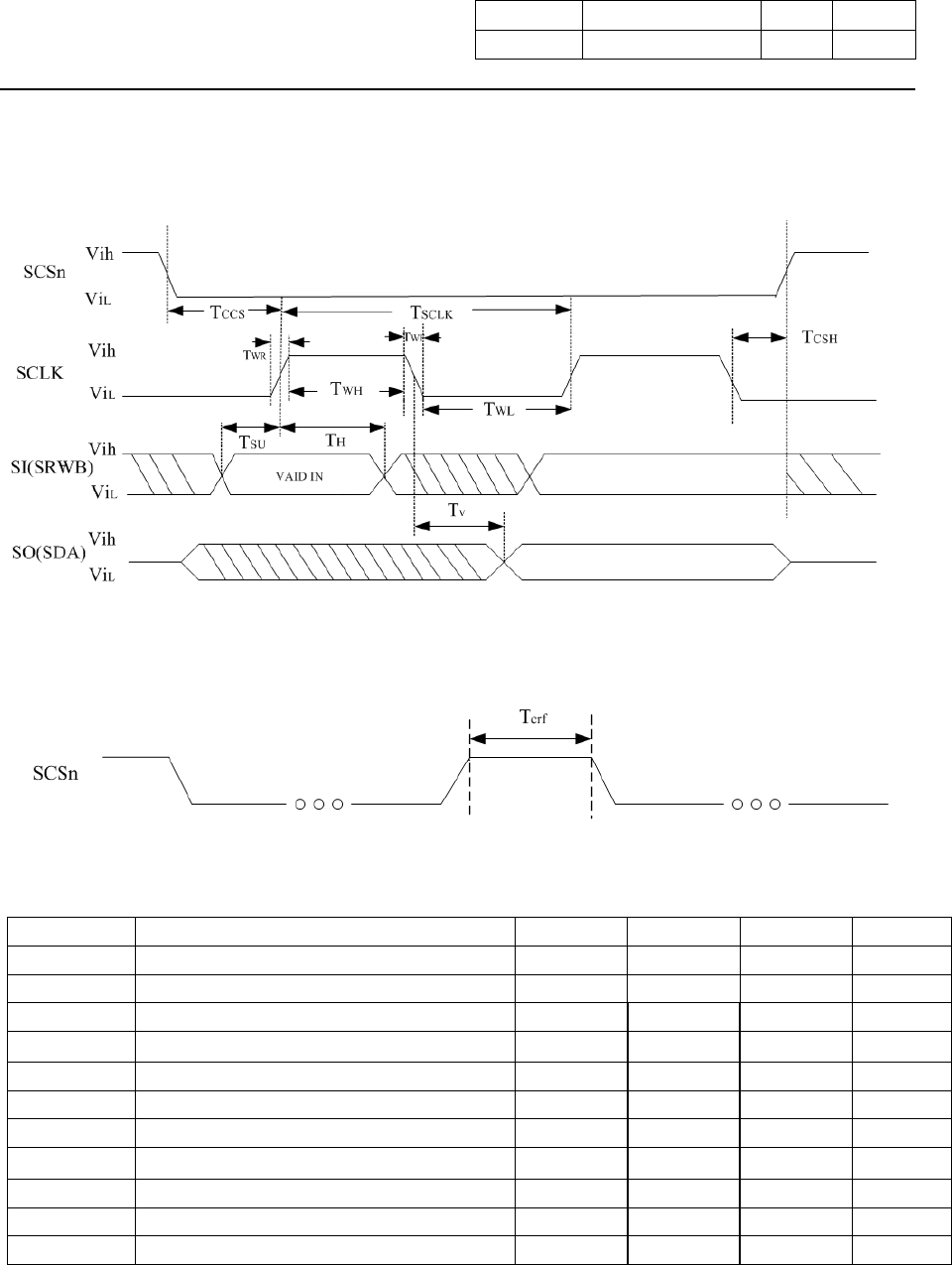
6.2.3 G-SPI PROTOCOL TIMING
G-SPI Host Interface Transaction Timing
G-SPI Host Interface Inter-Transaction Timing
SPI Interface Timing Data
Symbol Parameter Min Typ Max Units
TSCLK Clock Period 20 -- -- ns
TWH Clock High 5 -- -- ns
TWL Clock Low 9 -- -- ns
TWR Clock Rise Time -- -- 1 ns
TWF Clock Fall Time -- -- 1 ns
TH SDI Hold Time 2.5 -- -- ns
TSU SDI Setup Time 2.5 -- -- ns
TV SDO Hold Time 5 -- -- ns
TCSS SCSn Fall to Clock 5 -- -- ns
TCSH Clock to SCSn Rise 0 -- -- ns
TCRF SCSn Rise to SCSn Fall 400 -- -- ns
NOTE: Over full range of values specified in the Recommended Operating Condition unless
Otherwise specified.
Universal Scientific Industrial Corp. Doc No. Rev 1.4
Date. 2011/12/09 Page 16
Description Product Specification – WM-G-MR-09-Ref2
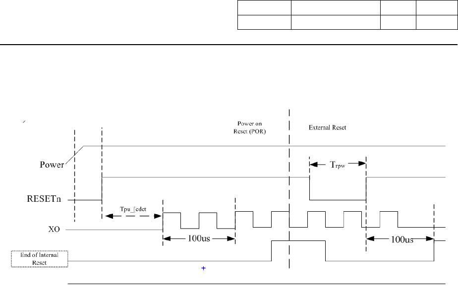
6.2.4 RESET AND CONFIGURATION TIMING
Notes
RESETn is not needed for proper operation due to internal power-on reset logic.

Universal Scientific Industrial Corp. Doc No. Rev 1.4
Date. 2011/12/09 Page 17
Description Product Specification – WM-G-MR-09-Ref2
External Timing Requirement (RESETn Pin)
Symbol Parameter Condition Min Typ Max Units
TPU-RESET Valid power to RESETn
de-asserted -- 0 -- -- ms
TRPW1 RESETn pulse width -- 10^2 100 -- ns
NOTE: Over full range of values specified in the Recommended Operating Conditions unless otherwise
specified.
1. For external reset, the device reset time is TRPW +300μs
2. Minimum value guaranteed for a valid reset smaller values may trigger the reset circuit.
Internal Reset Timing
Symbol Parameter Condition Min Typ Max Units
-- Negative internal reset pulse width -- 100 100 -- μs
NOTE: Over full range of values specified in the Recommended Operating Conditions unless otherwise
specified.

Universal Scientific Industrial Corp. Doc No. Rev 1.4
Date. 2011/12/09 Page 18
Description Product Specification – WM-G-MR-09-Ref2
6.2.5 LED INTERFACE
Pin No. Pin description Function description
16 GPIO_1 WLAN status LED (Tx power or Rx ready LED
NOTE: Over full range of values specified in the Recommended Operating Conditions unless
otherwise specified.
Symbol Parameter Condition Typ Units
LOH Switching current high Tristate on pad (requires
pull-up on board) Tristate when driving high mA
IOL Switching current low @0.4V 10 mA
6.2.6 ANTENNA INTERFACE
Antenna diversity is not supported on the Wireless Module.
The output impedance of the antenna port is 50 Ohms.
7 REGULATORY
The WM-G-MR-09-Ref2 module is tested on module level to comply with following
standards (pre-test):
• US/CAN: FCC CFR47 Part 15.247
• Europe: ETS 300-328 V1.6.1
Test setup: laptop plus adaptor card with Marvell Lab tool in SDIO mode
Final certification should be completed on system level.
Antenna Part No. :W1030
Gain [dBi] :2.0
Impedance [Nom]:50 Ω
VSWR<=2.0
Electrical Length :1/4, dipole
Radiation: Omni
Connector Options-Reverse SMA
Trade mark: Pulse
Manufacture: A TECHNITROL COMPANY
INFORMATION
Universal Scientific Industrial Corp. Doc No. Rev 1.4
Date. 2011/12/09 Page 20
Description Product Specification – WM-G-MR-09-Ref2
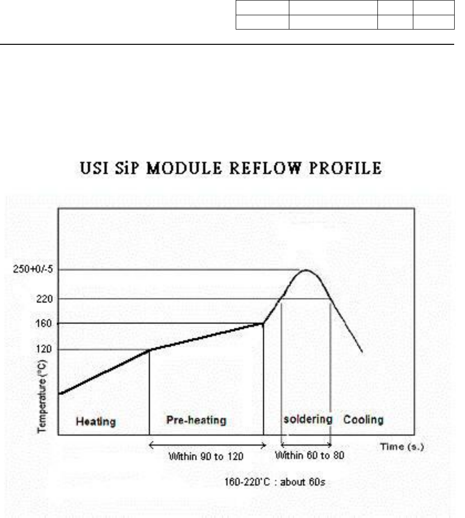
9 RECOMMENDED REFLOW PROFILE
Universal Scientific Industrial Corp. Doc No. Rev 1.4
Date. 2011/12/09 Page 21
Description Product Specification – WM-G-MR-09-Ref2
10 PACKAGE AND STORAGE CONDITION
10.1.1 PACKAGE DIMENSION
This device complies with part 15 of the FCC Rules. Operation is subject to the following two
conditions: (1) This device may not cause harmful interference, and (2) this device must accept
any interference received, including interference that may cause undesired operation.
Changes or modifications not expressly approved by the party responsible for compliance could
void the user's authority to operate the equipment.
FCC Radiation Exposure Statement
The modular can be installed or integrated in mobile or fix devices only. This modular cannot be
installed in any portable device, for example, USB dongle like transmitters is forbidden.
This modular complies with FCC RF radiation exposure limits set forth for an uncontrolled
environment. This transmitter must not be co-located or operating in conjunction with any other
antenna or transmitter. This modular must be installed and operated with a minimum distance of
20 cm between the radiator and user body.
If the FCC identification number is not visible when the module is installed inside another device,
then the outside of the device into which the module is installed must also display a label
referring to the enclosed module. This exterior label can use wording such as the following:
“Contains Transmitter Module FCC ID: XM5-MDLWMGMR09
when the module is installed inside another device, the user manual of this device must contain
below warning statements;
1. This device complies with Part 15 of the FCC Rules. Operation is subject to the following two
conditions:
(1) This device may not cause harmful interference.
(2) This device must accept any interference received, including interference that may cause
undesired operation.
2. Changes or modifications not expressly approved by the party responsible for compliance
could void the user's authority to operate the equipment.
The devices must be installed and used in strict accordance with the manufacturer's instructions
as describe