Crossbow Technology 005MPR1000 902-928MHz, Frequency Hopping, Wireless Network User Manual
Crossbow Technology, Inc. 902-928MHz, Frequency Hopping, Wireless Network
manual

MPR-MIB Users Manual
Revision B, June 2006
PN: 7430-0021-07
© 2002-2006 Crossbow Technology, Inc. All rights reserved.
Information in this document is subject to change without notice.
Crossbow, MoteWorks, MICA, TrueMesh and XMesh are registered trademarks of Crossbow
Technology, Inc. Other product and trade names are trademarks or registered trademarks of their
respective holders.

MPR/MIB User’s Manual
Doc. # 7430-0021-07 Rev. B Page 1
Table of Contents
1 Introduction.............................................................................................................................1
2 MPR2400 (MICAz).................................................................................................................2
2.1 Product Summary .......................................................................................................... 2
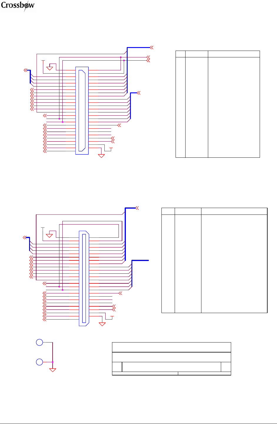
2.2 Block Diagram and Schematics for the MPR2400 / MICAz......................................... 2
3 MPR400/MPR410/MPR420 (MICA2)..................................................................................6
3.1 Product Summary .......................................................................................................... 6
3.2 Block Diagram and Schematics: MPR400/410/420 ...................................................... 6
4 MPR500/MPR510/MPR520 (MICA2DOT) .......................................................................11
4.1 Product Summary ........................................................................................................ 11
4.2 On-board Thermistor ................................................................................................... 11
4.3 Block Diagram and Schematics for the MPR500/510/520 MICA2DOT .................... 12
5 MPR300/MPR310 (MICA) ..................................................................................................16
5.1 Schematic..................................................................................................................... 16
6 MPR1000 (MICA3) ..............................................................................................................17
6.1 Block Diagram............................................................................................................. 17
6.2 Schematic..................................................................................................................... 17
6.3 Regulatory Compliance ............................................................................................... 18
7 Power .....................................................................................................................................19
7.1 Battery Power .............................................................................................................. 19
7.2 External Power............................................................................................................. 20
7.3 MICAz Battery Voltage Monitor................................................................................. 21
7.4 MICA2 Battery Voltage Monitor................................................................................. 21
7.5 MICA2DOT Battery Voltage Monitor ........................................................................ 22
8 Radios.....................................................................................................................................23
8.1 MICA2 and MICA2DOT............................................................................................. 23
8.2 MICAz ......................................................................................................................... 25
9 Antennas..............................................................................................................................28
9.1 Radio/Antenna Considerations .................................................................................... 28
9.2 Connectors for the MICA2 and MICAz and Whip Antennas...................................... 29
10 Flash Data Logger and Serial ID Chip ............................................................................30
11 Atmega128 Fuses................................................................................................................31
12 Sensor Boards & Expansion Connectors.........................................................................32
12.1 Sensor Board Compatibility..................................................................................... 32
12.2 MICAz and MICA2 Expansion Connector.............................................................. 32

MPR/MIB User’s Manual
Page 2 Doc. # 7430-0021-07 Rev. B
12.3 MICA2DOT Expansion Connector.......................................................................... 34
13 MIB300 / MIB500 Interface Boards.................................................................................36
13.1 Programming the Mote ............................................................................................ 36
13.2 RS-232 Interface ...................................................................................................... 36
14 MIB510 Serial Interface Boards.......................................................................................37
14.1 Product Summary..................................................................................................... 37
14.2 ISP............................................................................................................................ 37
14.3 Mote Programming Using the MIB510 ................................................................... 37
14.4 Interfaces to MICAz, MICA2, and MICA2DOT ..................................................... 38
15 MIB520 USB Interface Board...........................................................................................42
15.1 ISP............................................................................................................................ 42
15.2 Mote Programming Using the MIB520 ................................................................... 42
15.3 MIB520 Use............................................................................................................. 43
15.4 Reset......................................................................................................................... 43
15.5 JTAG........................................................................................................................ 43
15.6 Power........................................................................................................................ 43
15.7 USB Interface........................................................................................................... 43
15.8 51-Pin Mote Connector Interface............................................................................. 44
16 MIB600 Ethernet Interface Board...................................................................................46
16.1 Introduction .............................................................................................................. 46
16.2 Setup / Installation.................................................................................................... 46
16.3 Host Software........................................................................................................... 48
16.4 MIB600 Use............................................................................................................. 48
16.5 JTAG........................................................................................................................ 49
17 Appendix A: 10/100 Base-T Cabling tandards................................................................51
18 Appendix B. Warranty and Support Information..........................................................52
18.1 Customer Service ..................................................................................................... 52
18.2 Contact Directory ..................................................................................................... 52
18.3 Return Procedure...................................................................................................... 52
18.4 Warranty................................................................................................................... 53
MPR/MIB User’s Manual
Doc. # 7430-0021-07 Rev. B Page 3
About This Document
The following annotations have been used to provide additional information.
; NOTE
Note provides additional information about the topic.
; EXAMPLE
Examples are given throughout the manual to help the reader understand the terminology.
3 IMPORTANT
This symbol defines items that have significant meaning to the user
0 WARNING
The user should pay particular attention to this symbol. It means there is a chance that physical
harm could happen to either the person or the equipment.
The following paragraph heading formatting is used in this manual:
1 Heading 1
1.1 Heading 2
1.1.1 Heading 3
This document also uses different body text fonts (listed in Table 0-1) to help you distinguish
between names of files, commands to be typed, and output coming from the computer.
Table 0-1. Font types used in this document.
Font Type Usage
Courier New Normal Sample code and screen output
Courier New Bold Commands to be typed by the user
Times New Roman Italic TinyOS files names, directory names
Franklin Medium Condensed Text labels in GUIs
MPR/MIB User’s Manual
Doc. # 7430-0021-07 Rev. B Page 1
1 Introduction
This User’s Manual describes the hardware features of the Mote Processor Radio (MPR)
platforms and Mote Interface Boards (MIB) for network base stations and programming
interfaces. It is intended for understanding and leveraging Crossbow’s Smart Dust hardware
design in real-world sensor network, smart RFID, and ubiquitous computing applications. Table
1-1 below lists the models in this Manual.
Table 1-1. This User’s Manual covers these MPR and MIB models.
MPR 2400
(MICAz)
400/410/420
(MICA2)
500/510/520
(MICA2DOT)
300/310
(MICA)
MIB 600 510 500 300
The Table 1-2 below summarizes the main features of each Mote.
Table 1-2. Mote Product Summary.
Mote Hardware Platform MICAz MICA2 MICA2DOT MICA
Models (as of April 2005) MPR2400 MPR400/410/420 MPR500/510/520 MPR300/310
Chip ATMega128L ATMega103L
Type 7.37 MHz, 8 bit 4 MHz, 8 bit 4 MHz, 8 bit
MCU Program Memory
(kB) 128
SRAM (kB) 4
Type 51 pin 18 pin 51 pin
10-Bit ADC 7, 0 V to 3 V input 6, 0 V to 3 V input 7, 0 V to 3 V input
UART 2 1 2
Sensor Board
Interface
Other interfaces DIO, I2C DIO DIO, I2C
Chip CC2420 CC1000 TR1000
Radio Frequency
(MHz) 2400 315/433/915 433/915
Max. Data Rate
(kbits/sec) 250 38.4 40
RF
Transceiver
(Radio)
Antenna Connector MMCX PCB solder hole
Chip AT45DB014B
Connection Type SPI
Flash Data
Logger
Memory Size (kB) 512
Type AA, 2× Coin (CR2354) AA, 2×
Typical capacity
(mA-hr) 2000 560 2000
Default power
source
3.3 V booster N/A 9
This Manual is not a software guide to programming the motes in TinyOS/nesC, nor is it a guide
to pre-built software packages that run on top of the Motes. The following two resources are
available regarding software:
TinyOS Getting Started Guide by Crossbow Technology, Inc. available on the TinyOS
Support Tools CDROM or the Crossbow web site at www.xbow.com under Support>User’s
Manuals.
The TinyOS web site at http://webs.cs.berkeley.edu/tos
MPR/MIB User’s Manual
Page 2 Doc. # 7430-0021-07 Rev. B
2 MPR2400 (MICAz)
2.1 Product Summary
The MICAz is the latest generation of Motes from Crossbow Technology. The MPR2400 (2400
MHz to 2483.5 MHz band) uses the Chipcon CC2420, IEEE 802.15.4 compliant, ZigBee ready
radio frequency transceiver integrated with an Atmega128L micro-controller. The same MICA2,
51 pin I/O connector, and serial flash memory is used; all MICA2 application software and
sensor boards are compatible with the MPR2400.
Figure 2-1. Photo of the MPR2400—MICAz with standard antenna. For the dimensions of the
board and locations of the mounting holes, see Figure 2-2.
2.2 Block Diagram and Schematics for the MPR2400 / MICAz
Feature Chapter
Batteries 6
Radio 7
Antenna 8
Data Flash Lo
gg
er 9
Atme
g
a128 10
Expansion Connector 11
Logger
Flash
ATMega128L
µcontroller
Analog I/O
Digital I/O
CC2420 DSSS
Radio
51-Pin Expansion Connector
Antenna
MMCX connector
LEDs
Logger
Flash
ATMega128L
µcontroller
Analog I/O
Digital I/O
CC2420 DSSS
Radio
51-Pin Expansion Connector
Antenna
MMCX connector
LEDs
MPR/MIB User’s Manual
Doc. # 7430-0021-07 Rev. B Page 3
Figure 2-1. Block diagram of the MICA2 and listing of Chapters that discuss the components in
greater detail.
2.2.1 51-pin Expansion Connector
MPR/MIB User’s Manual
Page 4 Doc. # 7430-0021-07 Rev. B
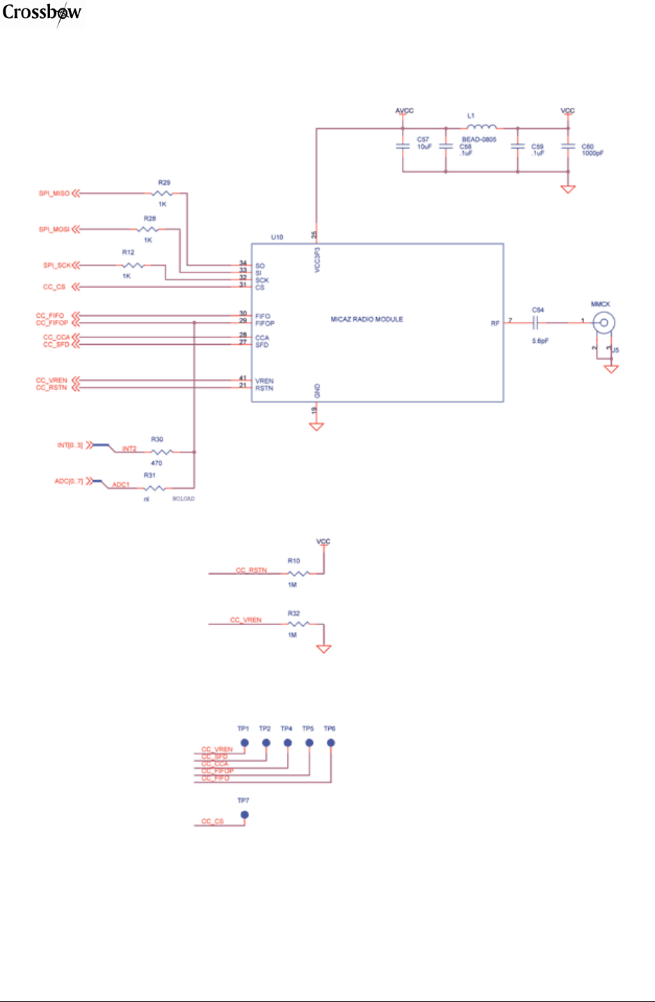
2.2.2 CC2420 Radio
MPR/MIB User’s Manual
Doc. # 7430-0021-07 Rev. B Page 5
2.2.3 Battery, ADC1
MPR/MIB User’s Manual
Page 6 Doc. # 7430-0021-07 Rev. B
3 MPR400/MPR410/MPR420 (MICA2)
3.1 Product Summary
The MICA2 Motes come in three models according to their RF frequency band: the MPR400
(915 MHz), MPR410 (433 MHz), and MPR420 (315 MHz). The Motes use the Chipcon
CC1000, FSK modulated radio. All models utilize a powerful Atmega128L micro-controller and
a frequency tunable radio with extended range. The MPR4x0 and MPR5x0 radios are compatible
and can communicate with each other. (The x = 0, 1, or 2 depending on the model / frequency
band.)
Figure 3-1. Left: Photo of a MICA2 (MPR4x0) without an antenna. Right: Top and plan views
showing the dimensions and hole locations of the MICA2 PCB without the battery pack.
3.2 Block Diagram and Schematics: MPR400/410/420
Feature Chapte
r
Batter
y
/ Ext. Powe
r
6
Radio 7
Antenna 8
Data Flash Lo
gg
er 9
Atme
g
a128 10
Expansion Connecto
r
11
Figure 3-2. Block diagram of the MICA2 and listing of Chapters that discuss the components in
greater detail.
MMCX connector
(female)
51-pin Hirose connector
(male)
On/Off Switch
External power
connector
Atmel
®
ATMega128
Logger
Flash
ATMega128L
µcontroller
Analog I/O
Digital I/O
CC1000 FSK
51-Pin Expansion Connector
Antenna
MMCX connector
LEDs
Power
Connector
Logger
Flash
ATMega128L
µcontroller
Analog I/O
Digital I/O
CC1000 FSK
51-Pin Expansion Connector
Antenna
MMCX connector
LEDs
Power
Connector
MPR/MIB User’s Manual
Doc. # 7430-0021-07 Rev. B Page 7
3.2.1 Battery, Power, and ADC1
VSNS
INSTALL
NOT INSTALLED
NOT INSTALLED
NOT INSTALLED
NOT INSTALLED
J4
CONN
1
2
1
2
SW2
SPDT
12
3
R8
10K
U2
LM4041-1.2
1
23
R1
0 OHM
TP3
R1
R2
R4
R8
RT1
D1
BAT54C
BAT_MON
BOARD OPTIONS
R2
0 OHM
R4
0 OHM
ADC7
R5
1K
VCC
C2
.1uF C1
.1u
F
BT1
BATTERY_2AA
1
2
V-
V+
R6
10K
ADC1
R3
0 OHM
VSNSR
THERM_PWR
ADC[0..7]
RT1
10.0K
R7
18.2K
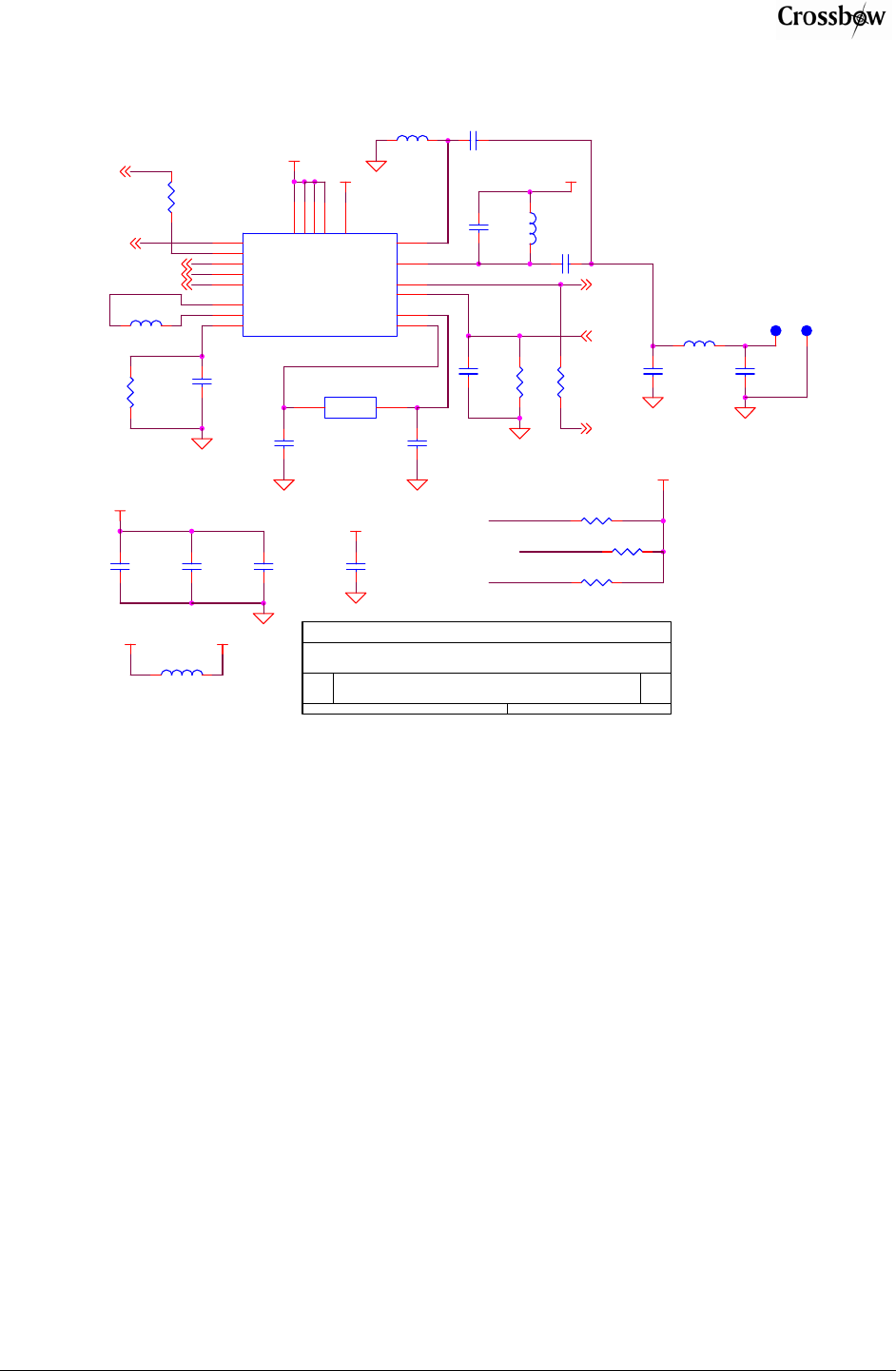
3.2.2 CC1000
AVCC
R12
10K
L5
R11
1M
CHP_OUT
6310-0306-01 A
MICA2 MPR410CB-433MHZ
B
26Friday, March 21, 2003
Title
Size Document Number Rev
Date: Sheet of
AVCC
R10
1M
L2
C18
4.7pF
RADIO DATA
L4
C14
Y4
14.7456MHZ
21 21
C19
13pF
C13
R9
1M
C6
.001uF
PDATA
L1
BEAD-0805
C11
.001uF
L3
J
5
MMCX
1
2
3
VCC
R13
27.4K
C16
.001uF
AVCC
J3
HDR 2 X 1 X .1
1
21
2
U3
CC1000
21
1
5
9
15
3
4
10
11
12
13 18
17
23
24
25
26
27 28
VCC
AVCC
AVCC
AVCC
AVCC
RF_IN
RF_OUT
L1
L2
CHP_OUT
R_BIAS XOSC1
XOSC2
DIO
DCLK
PCLK
PDATA
PALE RSSI
C12
C7
.001uF
C17
RADIO CONTROL
VCC
C15
AVCC
PALE
PDATA
C10
0.033uF
C5
0.033uF
DCLK
PCLK
SPI_SCK
SPI_MOSI
SPI_MISO
CHP_OUT
ADC0 (RSSI)
C9
220PF
PALE
SPI_MISO
PCLK
PDATA
PALE
R14
82.5K
ADC0
C20
13pF
SPI_SCK
VCC
VCCC8
220PF
DCLK
MPR/MIB User’s Manual
Page 8 Doc. # 7430-0021-07 Rev. B
3.2.3 51-pin Expansion Connector: Location J21
ADC4
AC+
SPI_SCK
UART_RXD0
USART1_RXD
DESCRIPTION
ADC3
PW2
ALE
PWM1A
ADC2
BAT_MON
GND
VSNSR
INT3
INT2
INT1
INT0
BAT_MON
LED3
LED2
LED1
RD
WR
ALE
PW7
USART1_CLK
PROG_MOSI
PROG_MISO
SPI_SCK
USART1_RXD
USART1_TXD
I2C_CLK
I2C_DATA
PWM0
PWM1A
AC+
AC-
NAME
ADC7
PW5
INT1
ADC1
PIN
THRU3
LED3
LED1
ADC[0..7]
I2C_CLK
PWM1B
AC-
PWM0 RSTN
UART_TXD0
RD
INT2
ADC5
INT3
THERM_PWR
PW4
UART_RXD0
THRU1
USART1_CLK
PROG_MISO
ADC6
PW1
T
[0..3]
1
2
3
4
5
6
7
8
9
10
11
12
13
14
15
16
17
18
19
20
21
22
23
24
25
26
VCC
HIROSE PLUG
J21
DF9-51P-1V(54)
1
2
3
4
5
6
7
8
9
10
11
12
13
14
15
16
17
18
19
20
21
22
23
24
25
26
27
28
29
30
31
32
33
34
35
36
37
38
39
40
41
42
43
44
45
46
47
48
49
50
51
WR
PROG_MOSI
THRU2
LED2
PW0
PW6
ADC0
VSNSR
I2C_DATA
PW7
INT0 PW3
UART_TXD0
USART1_TXD
GROUND
SENSOR SUPPLY
GPIO
GPIO
GPIO
GPIO
BATTERY VOLTAGE MONITOR ENABLE
LED3
LED2
LED1
GPIO
GPIO
GPIO
POWER CONTROL 7
USART1 CLOCK
SERIAL PROGRAM MOSI
SERIAL PROGRAM MISO
SPI SERIAL CLOCK
USART1 RX DATA
USART1 TX DATA
I2C BUS CLOCK
I2C BUS DATA
GPIO/PWM0
GPIO/PWM1A
GPIO/AC+
GPIO/AC-
PW[0..7]
3.2.4 51-pin Expansion Pads: Location J22
THRU1
PW4
AC+
ALE
THRU2
PROG_MISO
UART_TXD0
PWM0
I2C_DATA
ADC[0..7]
PW1
PW[0..7]
I2C_CLK
ADC6
THRU3
PW2
USART1_RXD
SPI_SCK
BAT_MON
6310-0306-01 A
MICA2 MPR410CB-433MHZ
CROSSBOW TECHNOLOGY. INC.
B
46Friday, March 21, 2003
Title
Size Document Number Rev
Date: Sheet of
PW6
INT0
UART_RXD0
UART_TXD0
PW0
PW1
PW2
PW3
PW4
PW5
PW6
ADC7
ADC6
ADC5
ADC4
ADC3
ADC2
ADC1
ADC0
THERM_PWR
THRU1
THRU2
THRU3
RSTN
PWM1B
VCC
GND
ADC5
PWM1B
AC-
ADC3
PWM1A
INT1
LED1
ADC0
USART1_CLK ADC1
THERM_PWR
NAME DESCRIPTION
ADC7
USART1_TXD
M20
MTG128
1
1
VSNSR
INT3
PROG_MOSI
ADC4
HIROSE SOCKET
J22
DF9B-51S-1V
1
2
3
4
5
6
7
8
9
10
11
12
13
14
15
16
17
18
19
20
21
22
23
24
25
26
27
28
29
30
31
32
33
34
35
36
37
38
39
40
41
42
43
44
45
46
47
48
49
50
51
M18
MTG128
1
1
INT[0..3]
WR
PW3
RSTN
PW7
UART_0 RECEIVE
UART_0 TRANSMIT
POWER CONTROL 0
POWER CONTROL 1
POWER CONTROL 2
POWER CONTROL 3
POWER CONTROL 4
POWER CONTROL 5
POWER CONTROL 6
ADC INPUT 7 - BATTERY MONITOR/JTAG TDI
ADC INPUT 6 / JTAG TDO
ADC INPUT 5 / JTAG TMS
ADC INPUT 4 / JTAG TCK
ADC INPUT 3
ADC INPUT 2
ADC INPUT 1
ADC INPUT 0 / RSSI MONITOR
TEMP SENSOR ENABLE
THRU CONNECT 1
THRU CONNECT 2
THRU CONNECT3
RESET (NEG)
GPIO/PWM1B
DIGITAL SUPPLY
GROUND
LED2
VCC
UART_RXD0
PIN
PW5
PW0
ADC2
INT2
LED3
RD
27
28
29
30
31
32
33
34
35
36
37
38
39
40
41
42
43
44
45
46
47
48
49
50
51
MPR/MIB User’s Manual
Doc. # 7430-0021-07 Rev. B Page 9
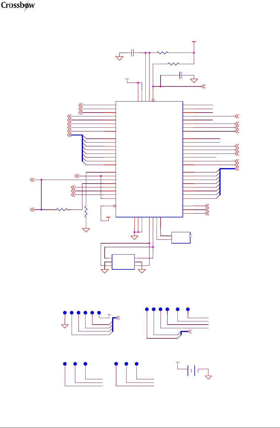
3.2.5 ATMega128L
VCC
BAT_MON
C23
.1uF
SPI_MISO
INT0
PW6
RD
INT3
ADC7
PWM1A
C36
13pF
R20
10K
VSNSR
ADC5
LED3
PW0
Y3
32.768KHZ
4
3 2
1
X2
GND GND
X1
UART_TXD0
I2C_CLK
LED1
AC+
PW5
R16
10K
PW3
C22
.1uF
U7
ATMEGA128L
51
50
49
48
47
46
45
44
10
11
12
13
14
15
16
17
35
36
37
38
39
40
41
42
25
26
27
28
29
30
31
32
2
3
4
5
6
7
8
9
61
60
59
58
57
56
55
54
64
62
1
20
24
23
33
34
43
18
19
PA0/AD0
PA1/AD1
PA2/AD2
PA3/AD3
PA4/AD4
PA5/AD5
PA6/AD6
PA7/AD7
PB0/SS
PB1/SCK
PB2/MOSI
PB3/MISO
PB4/OC0
PB5/OC1A
PB6/OC1B
PB7/OC1C
PC0/A8
PC1/A9
PC2/A10
PC3/A11
PC4/A12
PC5/A13
PC6/A14
PC7/A15
PD0/I2C_CLK
PD1/I2C_DATA
PD2/RXD1
PD3/TXD1
PD4/IC1
PD5/XCK1
PD6/T1
PD7/T2
PE0/RXD0
PE1/TXD0
PE2/XCK0
PE3/OC3A
PE4/OC3B
PE5/OC3C
PE6/T3
PE7/IC3
PF0/ADC0
PF1/ADC1
PF2/ADC2
PF3/ADC3
PF4/TCK
PF5/TMS
PF6/TDO
PF7/TDI
AVCC
AREF
PEN
RST
XTAL1
XTAL2
PG0/WR
PG1/RD
PG2/ALE
PG3/TOSC2
PG4/TOSC1
USART1_CLK
C21
.1uF
FLASH_CS
WR
SPI_SCK ADC2
ADC3
R21
10K
PW1
CHP_OUT
THERM_PWR
PWM1B
RSTN
ADC4
VCC
PALE
AC-
INT2
LED2
ADC1
PWM0
USART1_RXD
PW4
R18
0 OHM
SERIAL_ID
R15
470
UART_RXD0
INT[0..3]
C35
13pF
I2C_DATA
PW[0..7]
6310-0306-01 A
MICA2 MPR410CB-433MHZ
CROSSBOW TECHNOLOGY. INC.
B
56Friday, March 21, 2003
Title
Size Document Number Rev
Date: Sheet of
ADC0
ADC6
ALE
PDATA
PCLK
Y2
7.3728MHZ
2
34
1X2
X2X1
X1
PW7
ADC[0..7]
SPI_MOSI
USART1_TXD
PW2
INT1
MPR/MIB User’s Manual
Page 10 Doc. # 7430-0021-07 Rev. B
3.2.6 Flash Memory, Serial ID, LEDs, USART
SERIAL_ID
VCC
PCLK
PDATA
PALE
D2
RED
12
6310-0306-01 A
MICA2 MPR410CB-433MHZ
CROSSBOW TECHNOLOGY. INC.
B
66Friday, March 21, 2003
Title
Size Document Number Rev
Date: Sheet of
C27
.01uF
FLASH INTERFACE
USART1_CLK
C28
.01uF
RADIO CONTROL
C32
1000pF
R23
4.7K
VCC
C30
.01uF
USART1_TXD
U5
AT45DB041
1
2
3
4 5
8
SI
SCK
RST
CS WP
SO
UART INTERFACE
UART_RXD0
UART_TXD0
CONTROL INTERFACE
R19
1M
LED2
U6
DS2401P
2DQ
D4
YELLOW
12
USART1_RXD
+
C24
10uF
10V
R27
470
I2C_CLK
I2C_DATA
SPI_SCK
SPI_MOSI
SPI_MISO
CHP_OUT
ADC0
(RSSI)
RADIO DATA
LED1
ADC7
C29
.01uF
C25
.01uF
R25
470
R22
1M
VCC
C33
1000pF
LED3
FLASH_CS
FLASH_CS
VCC
D3
GREEN
12
FLASH_SI
FLASH_SO
FLASH_CLK
SERIAL_ID
SENSOR INTERFACE
R26
470
PW[0..7]
ADC[1..6]
USART1_RXD
VCC
VCC MONITOR
UART_TXD0
C31
1000pF C34
1000pF
C26
.01uF
MPR/MIB User’s Manual
Doc. # 7430-0021-07 Rev. B Page 11
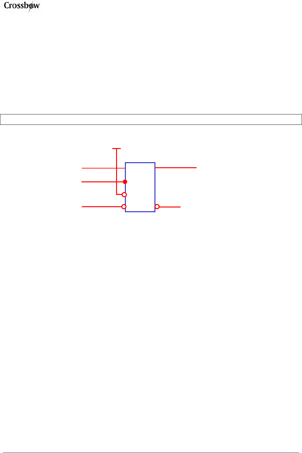
4 MPR500/MPR510/MPR520 (MICA2DOT)
4.1 Product Summary
The MICA2DOT is a Mote designed for applications where physical size is important. Like the
MICA2, these are available in three models according to the frequency of the RF transceiver: the
MPR500 (915 MHz), MPR510 (433 MHz), and MPR520 (315 MHz). The Motes use the
Chipcon CC1000 FSK-modulated radio. All models utilize a powerful ATMega128L micro-
controller and a frequency tunable radio with extended range. The MPR4x0 and MPR5x0 radios
are compatible and can communicate with each other as long as the “x” is the same number.
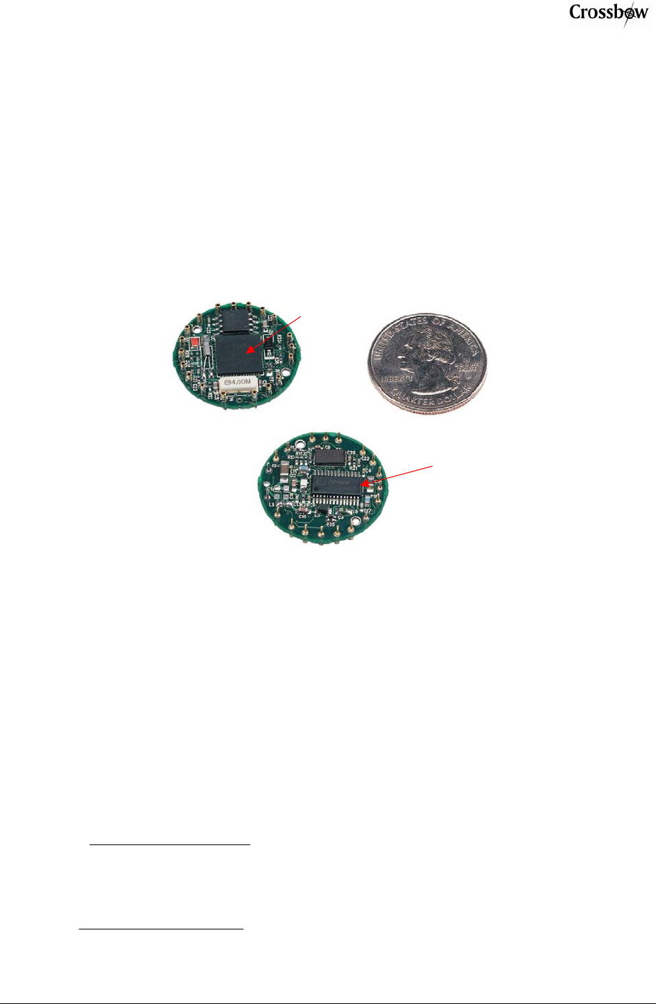
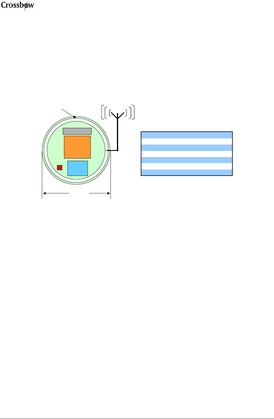
Figure 4-1. Photos of the MICA2DOT shown next to a US quarter: a) Top-side and b) Bottom-
side. Typically the MICA2DOT has a 3 V coin-cell battery holder attached to the bottom-side,
but it has been removed to show the details.
4.2 On-board Thermistor
The MICA2DOT Mote has an on-board thermistor (Panasonic ERT-J1VR103J) which is a
surface mount component. It is on the ATMega128 side of the board at the location labeled
“RT1.” Its output is at ADC1 and is enabled by setting PW6 (PC6/A14) to “LO” and PW7
(PC7/A15) to “HI.”
The Mote’s ADC output can be converted to degrees kelvin in the 273.15 K to 323.15 K (0°C to
50 °C) range using the Steinhart-Hart equation, which is a widely used third-order
approximation.
3
)(lnln
1
)(
thrthr RcRba
KT ++
=
where:
()
ADC
ADCFSADCR
Rthr
−×
=_
1
and a, b and c are called the Steinhart-Hart parameters with the following values:
(a) Top-side
(b) Bottom-side
Atmel
®
ATMega128
Chipcon
®
CC1000
MPR/MIB User’s Manual
Page 12 Doc. # 7430-0021-07 Rev. B
a = 0.00130705
b = 0.000214381
c = 0.000000093
R1 = 10 kΩ
ADC_FS = 1023
ADC = output value from the Mote’s ADC measurement.
4.3 Block Diagram and Schematics for the MPR500/510/520 MICA2DOT
Feature Chapter
Battery / Ext. Power 6
Radio 7
Antenna 8
Data Flash Lo
gg
er 9
Atme
g
a128 10
Expansion Connector 11
Figure 4-2. Block diagram of the MICA2DOT and listing of Chapters that discuss the
components in greater detail.
ATMega128L
µcontroller
Analog I/O
Digital I/O
Freq.
Tunable
Radio
Logger Flash
AntennaAntenna
25 mm
19 peripheral pins
MPR/MIB User’s Manual
Doc. # 7430-0021-07 Rev. B Page 13
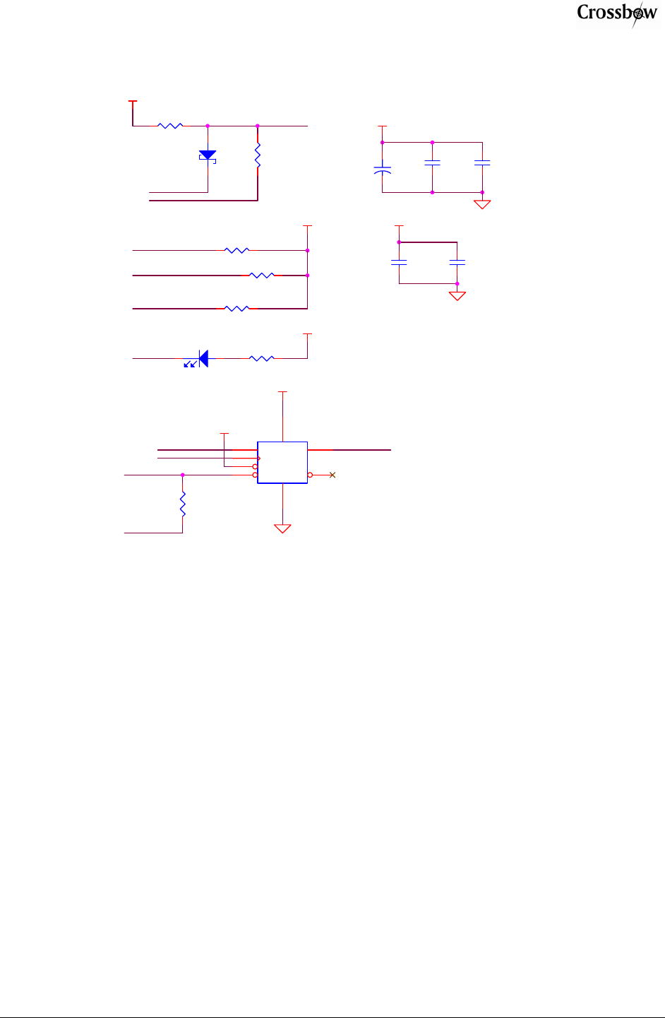
4.3.1 MICA2DOT CC1000 Radio Side
R13
10K
R17
27.4K
L3
R11
1M
VCCA
C12
AVCC
L4
TP18
PDATA
VCCA
C6
220PF
PDATA
C4
.001uF
PALE
C9
.001uF
AVCC
6310-0300-01 A
MICA DOT2 RADIO SIDE
B
13Wednesday, March 26, 2003
Title
Size Document Number Rev
Date: Sheet of
DCLK
L2
BEAD-0805
C3
0.033uF
R12
1M
AVCC
C10
DCLK
C20
13pF
AVCC
U3
CC1000
21
1
5
9
15
3
4
10
11
12
13 18
17
23
24
25
26
27 28
VCC
AVCC
AVCC
AVCC
AVCC
RF_IN
RF_OUT
L1
L2
CHP_OUT
R_BIAS XOSC1
XOSC2
DIO
DCLK
PCLK
PDATA
PALE RSSI
POT_PWR
SPI_MISO
SPI_SCK
L9
VCCA
C18C16
.001uF
C17
4.7pF
R18
82.5K
PALE
TP17
Y1
14.7456MHZ
21 X2X1
C19
C13
PCLK
VCCA
INT3
ADC0
L8
R10
1M
C21
13pF
R35
10K
MPR/MIB User’s Manual
Page 14 Doc. # 7430-0021-07 Rev. B
4.3.2 MIC2DOT ATMega128L, ADC Interfaces, Battery
PW5
Y5
32.768KHZ
32
1NCX2
X1
SPI_MOSI
INT0
SPI_SCK
PDATA
VCCA
R22
10K
PWM1B
PW[0..7]
R21
470
ADC1
POT_PWR
LED2
UART_RXD0
INT1
ALE
ADC6
ADC5
AC+
LED3
VCCA
DC_BOOST_SHD
N
PW7
PWM0
SERIAL_ID
SPI_MISO
ADC3
PWM1A
INT2
Y4
4.000MHZ
6
52
1
3 4
X1
GNDGND
X1
X2 X2
PW2
ADC4
RSTN
U6
ATMEGA128LMLF
21
52
22
53
63
51
50
49
48
47
46
45
44
10
11
12
13
14
15
16
17
35
36
37
38
39
40
41
42
25
26
27
28
29
30
31
32
2
3
4
5
6
7
8
9
61
60
59
58
57
56
55
54
64
62
1
20
24
23
33
34
43
18
19
VCC
VCC
GND
GND
GND
PA0/AD0
PA1/AD1
PA2/AD2
PA3/AD3
PA4/AD4
PA5/AD5
PA6/AD6
PA7/AD7
PB0/SS
PB1/SCK
PB2/MOSI
PB3/MISO
PB4/OC0
PB5/OC1A
PB6/OC1B
PB7/OC1C
PC0/A8
PC1/A9
PC2/A10
PC3/A11
PC4/A12
PC5/A13
PC6/A14
PC7/A15
PD0/INT0
PD1/INT1
PD2/RXD1
PD3/TXD1
PD4/IC1
PD5/XCK1
PD6/T1
PD7/T2
PE0/RXD0
PE1/TXD0
PE2/XCK0
PE3/OC3A
PE4/OC3B
PE5/OC3C
PE6/T3
PE7/IC3
PF0/ADC0
PF1/ADC1
PF2/ADC2
PF3/ADC3
PF4/TCK
PF5/TMS
PF6/TDO
PF7/TDI
AVCC
AREF
PEN
RST
XTAL1
XTAL2
PG0/WR
PG1/RD
PG2/ALE
PG3/TOSC2
PG4/TOSC1
ADC7
C23
.1uF
R28
10K
PALE
ADC2
GPS_ENA
C22
.1uF
PW3 AC-
PCLK
LED1
PW6
RD
VCCA
PW0
ADC[0..7]
SPI_MOSI
I2C1_DATA
FLASH_SI
FLASH_SO
R27
10K
PW1
ADC0
FLASH_CLK
UART_TXD0
PW4
I2C1_CLK
WR
INT3
INT0
TP8
TP19
ADC[0..7]
TP10TP7
PW1
SPI_SCK
RSTN
ADC3
TP6 TP11
TP13
PW0
TP20
ADC5
TP4
VCCA
ADC2
PWM1B
TP15
BT1
BATTERY
1 2
TP2
VCCA
TP9
TP1
ADC7
ADC6
TP21
GPS_ENA
PW[0..7]
ADC4
TP5TP3 TP12
TP14
INT1
UART_TXD0
UART_RXD0
MPR/MIB User’s Manual
Doc. # 7430-0021-07 Rev. B Page 15
4.3.3 Data Flash Logger/Serial ID, On-board Thermistor, LED
UART_TXD0
FLASH_SI
VCCA
VCCA
R36
10K
ADC1
C31
1000pF
C25
.01uF
R29
1M
D2
RED
12
R25
100K
VCCA
SERIAL_ID
LED1
RT1
10.0K
PW6
FLASH_SO
FLASH_CLK
D5
SD103AW C26
.01uF
PW7
+
C24
10uF
10V
R30
4.7K
VCCA
R31
470
C32
1000pF
U7
AT45DB041
1
2
3
4 5
67
8
SI
SCK
RST
CS WP
VCCGND
SO
RSTN
VCCA
R26
1M
VCCA
VCCA
SERIAL_ID
FLASH_SO

MPR/MIB User’s Manual
Page 16 Doc. # 7430-0021-07 Rev. B
5 MPR300/MPR310 (MICA)
; NOTE: The MICA Mote has been discontinued by Crossbow since December 2003.
The MICA Mote was the second generation Mote module used in many ground breaking
research and development efforts. The MPR300/310 includes a powerful Atmel ATMega128L. It
used an amplitude shift keying radio—the TR1000—by RF Monolithics, Inc.
5.1 Schematic
Schematics for the MPR300/310 Mote can be found at:
http://www.tinyos.net/scoop/special/hardware
MPR/MIB User’s Manual
Doc. # 7430-0021-07 Rev. B Page 17
6 MPR1000 (MICA3)
The MPR1000 is a 1 watt high power mote with Frequency Hopping feature that enables it to
transmit over a very high range.
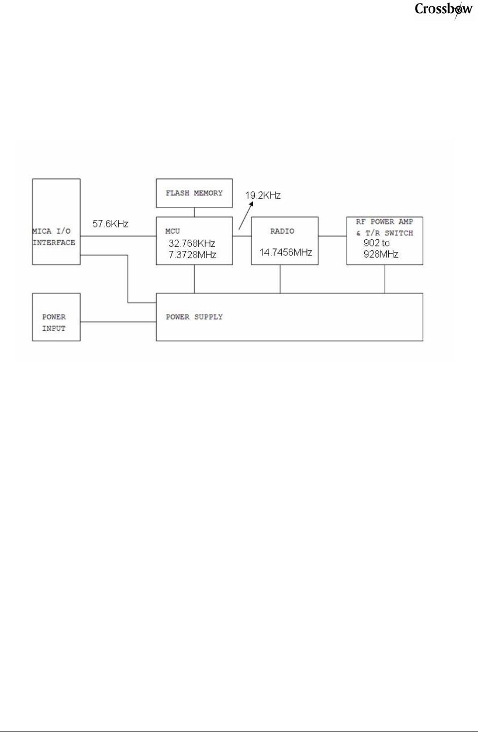
6.1 Block Diagram
Power Supply: Input power regulator which accepts 3.6 to 4.5VDC.
MCU: it includes ATMega128 processor and its’ peripherals.
Flash Memory: 4Kbit flash memory for storing firmware.
Radio: it is purposed for transmitting and receiving at 902MHz to 928MHz band using
Frequency Hopping modulation. The maximum output power of the radio is 5dBm
RF Power Amplifier: is used to boost up the output RF power of the radio to 30dBm or 1
Watt.
Note: RF circuitary including radio and RF power amplifier are covered by an RF shield.
Mica I/O interface: is the mote standard 51 pin connector which enables MPR1000 module to
connect to other modules for data transmission.
6.2 Schematic
MPR1000 Schematic will be released in future version of the manual.

MPR/MIB User’s Manual
Page 18 Doc. # 7430-0021-07 Rev. B
6.3 Regulatory Compliance
This device has been designed, constructed, and tested for compliance with FCC Rules that
regulate intentional and unintentional radiators. The user is not permitted to make any
modifications to this equipment without express approval from Crossbow Technology Inc. Doing
so will void the user’s authority to operate this equipment.
This device complies with Part 15 of the FCC Rules. Operation is subject to the following two
conditions: (1) this device may not cause harmful interference, and (2) this device must accept
any interference received, including interference that may cause undesired operation
This equipment has been tested and found to comply with the limits for a Class A digital device,
pursuant to part 15 of the FCC Rules. These limits are designed to provide reasonable protection
against harmful interference when the equipment is operated in a commercial environment. This
equipment generates, uses, and can radiate radio frequency energy and, if not installed and used
in accordance with the instruction manual, may cause harmful interference to radio
communications. Operation of this equipment in a residential area is likely to cause harmful
interference in which case the user will be required to correct the interference at his own
expense.
This device has been designed to operate with the antennas listed below, and having a maximum
gain of 2.0 dBi. Antennas not included in this list or having a gain greater than 2.0 dBi are
strictly prohibited for use with this device. The required antenna impedance is 50 ohms.
- Internal PCBA Antenna which has been developed on the board
- External Antenna with a gain of 2.0 dBi or less
To reduce potential radio interference to other users, the antenna type and its gain should be so
chosen that the equivalent isotropically radiated power (e.i.r.p.) is not more than that permitted
for successful communication.
MPR/MIB User’s Manual
Doc. # 7430-0021-07 Rev. B Page 19
7 Power
7.1 Battery Power
All motes are designed for battery power. The MICA2 and MICAz form factors are designed to
match up with two AA batteries; however any battery combination (AAA, C, D, etc., cells) can
be used provided that the output is between 2.7 VDC to 3.6 VDC.
The MPR500 (915 MHz band), MPR510 (433 MHz band), and MPR520 (315 MHz band, Japan
specific) MICA2DOT form factor is designed to match up with a single coin cell battery;
however any battery combination (AAA, C, D, etc., cells) can be used provided that the output is
between 2.7–3.6VDC.
Table 7-1. Batteries for the Mote Platforms.
Mote Hardware
Platform Standard Battery (#
required) Typical Battery Capacity
(mA-hr) Practical Operating Voltage
Range (V)
MICAz AA (2) 2000, Alkaline 3.6 to 2.7
MICA2 AA (2) 2000, Alkaline 3.6 to 2.7
MICA2DOT Coin 560, Li-ion 3.6 to 2.7
Care should be used in selecting the battery and its capacity to match the energy needs of the
motes and their required operating span. Also make sure that the temperature range and
associated capacity degradation are looked at prior to deployment. Table 6-2 below provides
some useful guidance on current consumption of various system components.
Table 7-2. Current Requirements for the Motes in Various Operation.
Operating Current (mA) MICAz MICA2 MICA2DOT
ATMega128L, full operation 12 (7.37 MHz) 12 (7.37 MHz) 6 (4MHz)
ATMega128L, sleep 0.010 0.010 0.010
Radio, receive 19.7 7 7
Radio, transmit (1 mW power) 17 10 10
Radio, sleep 0.001 0.001 0.001
Serial flash memory, write 15
Serial flash memory, read 4
Serial flash memory, sleep 0.002
Table 7-3 below provides some useful guidance on how to predict battery life. The spreadsheet
can be found at http://www.xbow.com under the Support section.
MPR/MIB User’s Manual
Page 20 Doc. # 7430-0021-07 Rev. B
Table 7-3. Estimate of battery life operation for a Mote.
SYSTEM SPECIFICATIONS
Currents
Processor Example Duty
Cycle
Current (full operation) 8 mA 1
Current sleep 8 µA99
Radio
Current in receive 8 mA 0.75
Current transmit 12 mA 0.25
Current sleep 2 µA99
Logger Memory
Write 15 mA 0
Read 4 mA 0
Sleep 2 µA100
Sensor Board
Current (full operation) 5 mA 1
Current sleep 5 µA99
Computed mA-hr used each hour
Processo
r
0.0879
Radio 0.0920
Logger Memory 0.0020
Sensor Board 0.0550
Total current (mA-hr) used 0.2369
Computed battery life vs. battery size
Battery Capacity (mA-hr) Battery Life
(months)
250 1.45
1000 5.78
3000 17.35
; NOTE: In most Mote applications, the processor and radio run for a brief period of time, followed by a
sleep cycle. During sleep, current consumption is in the micro-amps as opposed to milli-amps. This
results in very low-current draw the majority of the time, and short duration spikes while processing,
receiving, and transmitting data. This method extends battery life; however, due to the current surges, it
reduces specified battery capacity. Battery capacity is typically specified by the manufacturer for a
constant nominal current drawn.
7.2 External Power
The MICA2 and MICAz can be externally powered through either:
1. The 51-pin connector will supply power and ground to the unit. Refer to connector
description.
MPR/MIB User’s Manual
Doc. # 7430-0021-07 Rev. B Page 21
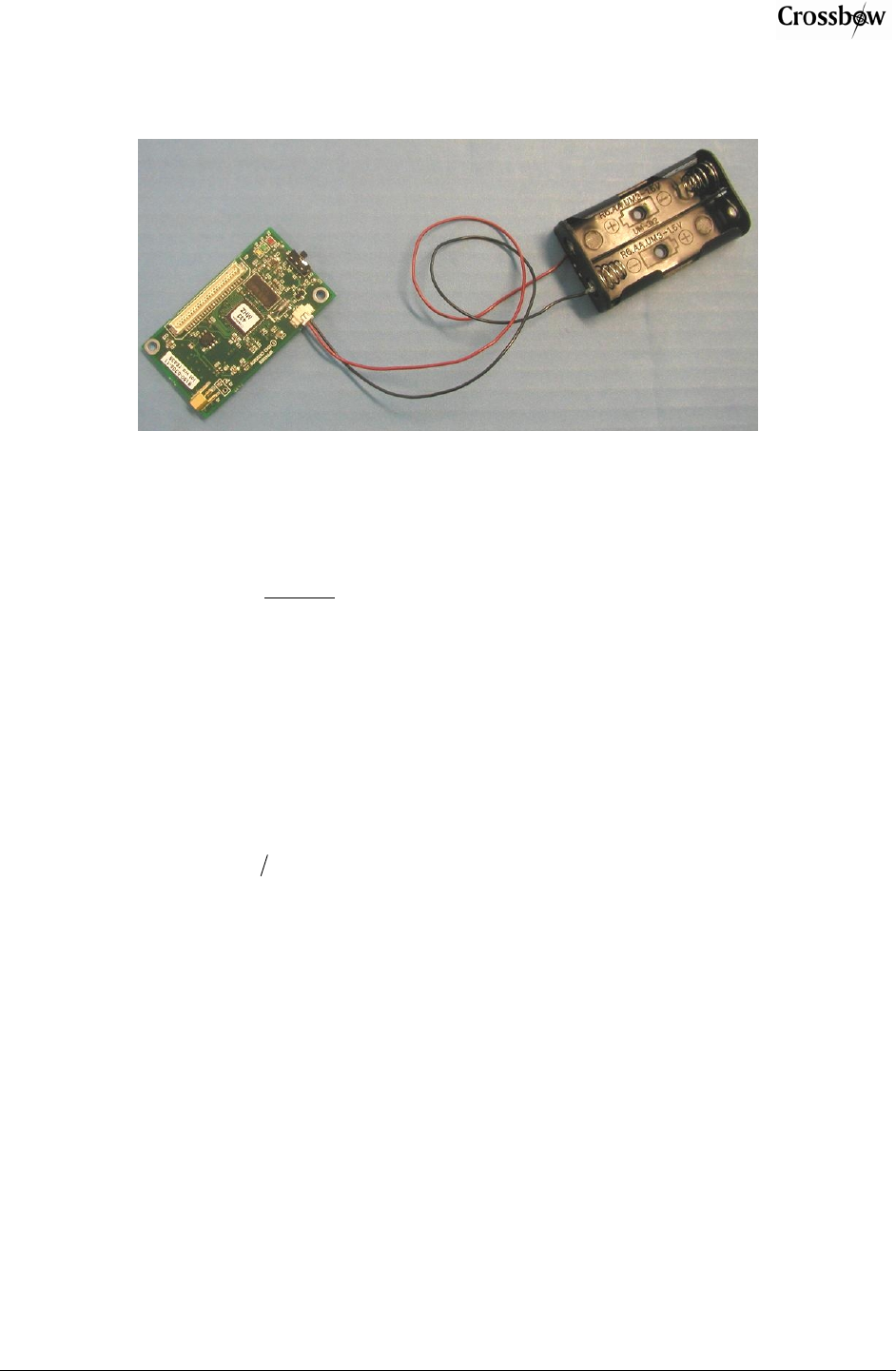
2. The 2-pin Molex connector. Molex part number 53261-0290, Digi-Key part number
WM1753-ND. (See Figure 7-4 below.)
Figure 7-4. Photo of using the Molex connector to attach the AA battery pack. Photo courtesy of
Nick Sitar, UC Berkeley, 2004.
7.3 MICAz Battery Voltage Monitor
The MICAz has an accurate internal voltage reference that can be used to measure battery
voltage (Vbatt). Since the eight-channel ADC on the ATMega128L uses the battery voltage as a
full scale reference, the ADC full scale voltage value changes as the battery voltage changes. In
order to track the battery voltage, the precision voltage reference (band gap reference) is
monitored to determine the ADC full-scale (ADC_FS) voltage span which corresponds to Vbatt.
To compute the battery voltage:
1. Program the application code to measure ADC channel 30 – the Internal Bandgap
Voltage reference.
2. Compute battery voltage, Vbatt, from ADC reading (ADC_Count) by:
CountADCFSADCVV refbatt __×=
where:
Vbatt = Battery voltage
ADC_FS = 1024
Vref = Internal voltage reference = 1.223 volts
ADC_Count = Data from the ADC measurement of Internal Voltage reference
The TinyOS component VoltageM.nc can be wired into an application to provide this
measurement capability. The reserved keyword TOS_ADC_VOLTAGE_PORT is mapped to ADC
Channel 30 in the MICAz.
7.4 MICA2 Battery Voltage Monitor
The MICA2 units have an accurate voltage reference that can be used to measure battery voltage
(Vbatt). Since the eight-channel, ATMega128L ADC uses the battery voltage as a full scale
reference, the ADC full scale voltage value changes as the battery voltage changes. In order to

MPR/MIB User’s Manual
Page 22 Doc. # 7430-0021-07 Rev. B
calibrate the battery voltage a precision external voltage reference is required. The MICA2 uses
an LM4041 (Mfg: National Semiconductor) 1.223 V reference (Vref) attached to ADC channel 7.
; NOTE: ADC channel 7 is also used for JTAG debugging on the Atmega128 processor. MICA2s and
MICA2DOTs ship with the JTAG fuse enabled. When this fuse is enabled the input impedance of channel
7 is lowered which affects the voltage reference measurement. The fuse must be disabled if ADC channel
7 is used. See below for information on setting ATMega128L fuses.
To compute the battery voltage:
1. Set the BAT_MON processor pin (PA5/AD5) to HI.
2. Program the application code to measure ADC Channel 7.
3. Compute battery voltage, Vbatt, from Channel 7’s data by:
CountADCFSADCVV refbatt __×=
where:
Vbatt = Battery voltage
ADC_FS = 1024
Vref = External voltage reference = 1.223 V
ADC_Count = Data from the ADC measurement of Channel 7
7.5 MICA2DOT Battery Voltage Monitor
Unlike the MICAz and the MICA2, the MICA2DOT uses a Schottky reference diode (S103AW)
as a voltage reference that can be used to measure battery voltage (Vbatt). Since the eight-channel,
ATMega128L ADC uses the battery voltage as a full-scale reference, the ADC full scale
(ADC_FS) voltage value changes as the battery voltage changes. In order to calibrate the battery
voltage an external voltage reference (Vref) is required.
To compute the battery voltage:
1. Set processor pins PW7 (PC7/A15) to LO and PW6 (PC6/A14) to HI.
2. Program the application code to measure ADC Channel 1 (ADC1).
3. Compute battery voltage, Vbatt, from channel 1’s data by:
CountADCFSADCVV refbatt __×=
where:
Vbatt = Battery voltage
ADC_FS = 1024
Vref = External voltage reference = 0.6 volts
ADC_Count = Data from the ADC measurement of Channel 1

MPR/MIB User’s Manual
Doc. # 7430-0021-07 Rev. B Page 23
8 Radios
8.1 MICA2 and MICA2DOT
8.1.1 Radio Considerations
The radio on the MICA2 and MICA2DOT is capable of multiple channel operation, within the
intended band of operation. The MPR420/MPR520 can span up to 4 channels of operation in the
315 MHz band, the MPR410/MPR510 can span up to 4 channels of operation in the 433 MHz
band (433.05–434.79 MHz). The MPR400/MPR500 can operate in two frequency regions: 868–
870 MHz (up to 4 channels) and 902–928 MHz (up to 54 channels). The actual number of
possible channels is higher for all the MICA2/MICA2DOT motes. However, it is recommended
that the adjacent channel spacing should be at least 500 kHz to avoid adjacent channel
interference thereby reducing the number of available channels. A tutorial on how to change
frequency is available at http://www.tinyos.net/tinyos-1.x/doc/mica2radio/CC1000.html.
8.1.2 Radio Transmission Power
The radio on the MICA2/MICA2DOT can be adjusted for a range of output power levels. The
register in the radio that controls the RF power level is designated PA_POW at address 0x0B,
and the values and their corresponding RF outputs are provided on Error! Reference source not
found. below. It shows the closest programmable value for output powers in steps of 1 dBm. For
power down mode the Chipcon datasheet says, “the PA_POW should be set to 00h [0x00] for
minimum leakage current.”

MPR/MIB User’s Manual
Page 24 Doc. # 7430-0021-07 Rev. B
Table 8-1. Chipcon® CC1000 Ouput Power (PA_POW) Settings and Typical Current
Consumption. From Smart RF® CC1000 Preliminary Datasheet (rev. 2.1), 2002-04-19, p. 29 of
48.
Pout (dBm) PA_POW (hex)
433/315 MHz
Current
Consumption,
typ.
(mA)
PA_POW
(hex)
915 MHz
Current
Consumption,
typ.
(mA)
-20 0x01 5.3 0x02 8.6
-19 0x01 6.9 0x02 8.8
-18 0x02 7.1 0x03 9.0
-17 0x02 7.1 0x03 9.0
-16 0x02 7.1 0x04 9.1
-15 0x03 7.4 0x05 9.3
-14 0x03 7.4 0x05 9.3
-13 0x03 7.4 0x06 9.5
-12 0x04 7.6 0x07 9.7
-11 0x04 7.6 0x08 9.9
-10 0x05 7.9 0x09 10.1
-9 0x05 7.9 0x0b 10.4
-8 0x06 8.2 0x0c 10.6
-7 0x07 8.4 0x0d 10.8
-6 0x08 8.7 0x0f 11.1
-5 0x09 8.9 0x40 13.8
-4 0x0a 9.4 0x50 14.5
-3 0x0b 9.6 0x50 14.5
-2 0x0c 9.7 0x60 15.1
-1 0x0e 10.2 0x70 15.8
0 0x0f 10.4 0x80 16.8
1 0x40 11.8 0x90 17.2
2 0x50 12.8 0xb0 18.5
3 0x50 12.8 0xc0 19.2
4 0x60 13.8 0xf0 21.3
5 0x70 14.8 0xff 25.4
6 0x80 15.8
7 0x90 16.8
8 0xc0 20.0
9 0xe0 22.1
10 0xff 26.7
; NOTE:
In order to comply with "Biyjacku" (Japanese standard), the Radio Transmit power for the MICA2 must
have a PA_POW set to lowest value, 0x01.
The radio on the MICA2/MICA2DOT also provides a measurement of the received signal
strength, referred to as RSSI. This output is measured on ADC channel 0 and is available to the
software. Some versions of TinyOS provide this measurement automatically, and others must be
enabled by the user. The conversion from ADC counts to RSSI in dBm is given by:
MPR/MIB User’s Manual
Doc. # 7430-0021-07 Rev. B Page 25
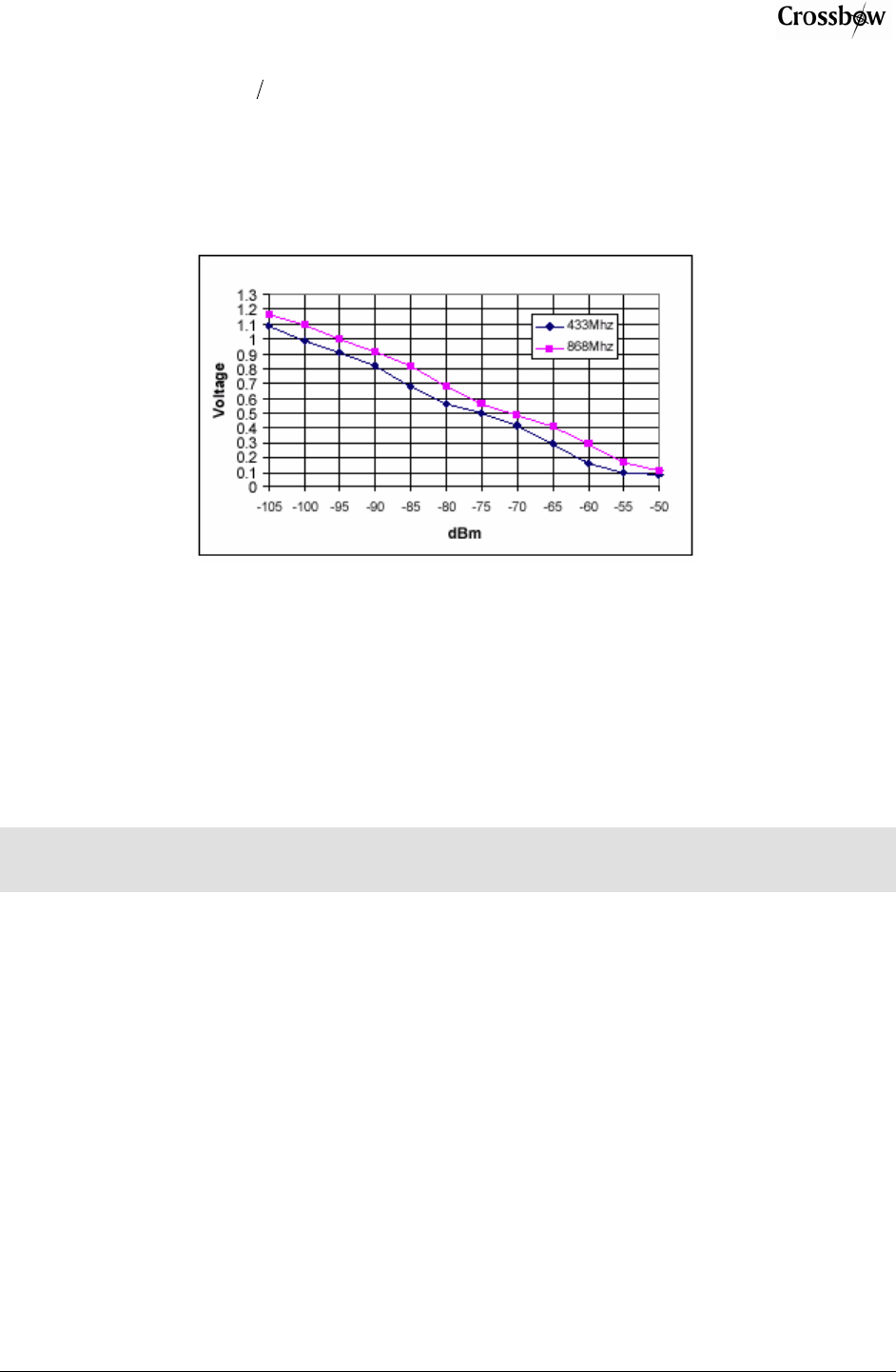
1024_ CountsADCVV battRSSI ×=
2.493.51)( −×−= RSSI
VdBmRSSI for 433 and 315 MHz Motes
5.450.50)( −×−= RSSI
VdBmRSSI for 915 MHz Motes
Figure 8-2. Graph showing VRSSI versus the received signal strength indicator (dBm). From the
ChipCon’s SmartRF® CC1000 PRELIMINARY Datasheet (rev. 2.1), p. 30. 2002.
Care should be taken to provide an antenna that provides proper coverage for the environment
expected. Range and performance are strongly affected by choice of antenna and antenna
placement within the environment. In addition, care must be taken to ensure compliance with
FCC article 15 regulations for intentional radiators. An omni directional antenna such as a
quarter wavelength whip should be sufficient to meet most user requirements.
0 WARNING: The radio on the MICA2 has an extremely sensitive receiver, which can be interfered with
by an adjacent local oscillator from another MICA2. A distance of at least 2 feet should be maintained
between MICA2 units to avoid local oscillator interference.
8.2 MICAz
8.2.1 Radio RF Channel Selection
The MICAz’s CC2420 radio can be tuned within the IEEE 802.15.4 channels that are numbered
from 11 (2.405 GHz) to 26 (2.480 GHz) each separated by 5 MHz. The channel can be selected
at run-time with the TOS CC2420Radio library call
CC2420Control.TunePreset(uint8_t chnl). By default channel 11 (2480 MHz) is
selected.
8.2.2 Radio Transmission Power
RF transmission power is programmable from 0 dBm (1 mW) to –25dBm. Lower transmission
power can be advantageous by reducing interference and dropping radio power consumption
from 17.5 mA at full power to 8.5 mA at lowest power. RF transmit power is controlled using
the TOS CC2420Radio library call CC2420Control.SetRFPower(uint8_t power)
where power is an 8-bit code selected from the following:
MPR/MIB User’s Manual
Page 26 Doc. # 7430-0021-07 Rev. B
Power Register (code) MICAz TX RF Power (dBm)
31 0
27 -1
23 -3
19 -5
15 -7
11 -10
7 -15
3 -25
3 IMPORTANT
For MPR2400J, the power is constant at 0dBm and any questions be directed to Crossbow,
Japan. http://www.xbow.com/jp/index.html
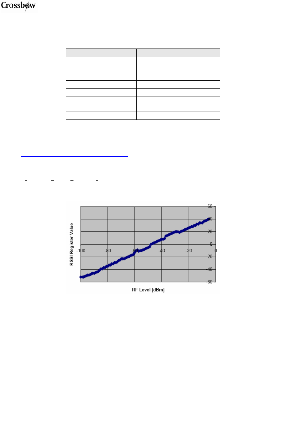
The RF received signal strength indication (RSSI) is read directly from the CC2420 Radio. In
TinyOS the RSSI is automatically returned in the TOSMsg->strength field with every radio
packet received. Typical RSSI values for a given RF input level are shown in Figure 7-1 below.
Figure 8-1. Typical RSSI value versus input RF level in dBm.
8.2.3 Known MICAz and TinyOS Compatibility Issues
1. #define PLATFORM_MICAZ
In general this #define should be added to various applications/libraries wherever
the text PLATFORM_MICA2 is found.
2. ATMega128L Timer2 Use
Timer2 is used for high resolution (32uSec) timing in the CC2420Radio stack. The
module HPLTimer2.nc located under the tinyos-1.x/tos/platform/micaz/ directory
provides the Timer2 resources to AsyncTimerJiffy component for this service.
Applications that use Timer2 will have to be modified to avoid conflicts with its use
for the MICAz platform radio stack.

MPR/MIB User’s Manual
Doc. # 7430-0021-07 Rev. B Page 27
3. INT2 GPIO Line
MICA I/O signal INT2 (Port E, pin 6 on ATMega128 or 51-pin Hirose connector pin
4) is used internally to the MICAz for the CC2420 Radio Receiver FIFO Ready
interrupt. Use of INT2 for any other purpose must be done with care. Specifically, the
Port configuration (input, active low) must be restored following use in other
software modules.
; NOTE: Programmers should be cautioned that the MICAz receiver radio stack
(CC2420RadioM.nc) will be disabled if the INT2 pin is reprogrammed/re-tasked by another TOS
component.
4. MTS300/310 (a.k.a., micasb) Temperature Sensor
• INT2 control line is used on the MTS300/310 (micasb) for enabling the
thermistor. During temperature measurement, interrupts from the MICAz radio
receiver are inhibited. MICAz radio received packets are buffered in the CC2420
RX FIFO. If the MTS300/310’s thermistor is enabled for too long the receiver
buffer may overflow. During temperature measurements dropout in data reading.
This is due to receipt of a radio packet which will strobe the INT2 and thus affect
the thermistor voltage. Following temperature measurement, the MTS300/310
driver must restore the INT2 port to configuration used for handling interrupts
from the CC2420 radio. Symptom of not restoring the INT2 port correctly is all
that radio reception stops.
• A fix the temperature sensor issue:
• INT2 Control
A modified PhotoTempM.nc module is provided in tinyos-
1.x/tos/platform/micaz/. This module restores INT2 port following each
measurement.
• Temperature data drop out
Software can be added to exclude/reject a temperature reading differentials
that exceed what is physically possible from one sample to the next.
• Hardware can be modified to buffer/overdrive CC2420 Radio’s packet
received flag during temperature measurements. The following two changes
are suggested.
a. MTS300/310 Sensor Board Module: Remove capacitor C1 (located near
RT1 thermistor)
b. MICAz Module: Change resistor at location R31 to 10 kΩ.
MPR/MIB User’s Manual
Page 28 Doc. # 7430-0021-07 Rev. B
9 Antennas
9.1 Radio/Antenna Considerations
Care should be taken to provide an antenna that provides proper coverage for the environment
expected. Range and performance are strongly affected by choice of antenna and antenna
placement within the environment. In addition, care must be taken to ensure compliance with
FCC article 15 regulations for intentional radiators. Because of its small physical size, the usual
antenna chosen is a length of insulated wire one-quarter wavelength long for the frequency of
interest. This type of antenna is often called a monopole antenna, and its gain is ground plane
dependent.
Antenna lengths for the different radio frequencies are provided in Table 9-1.
Table 9-1. Antenna lengths for quarter wavelength whip antennas. The part number’s for the
connectorized antennas are listed.
Name Model Whip Antenna Length
(inches) Crossbow Part
No.
MICA2/MICA2DOT MPR400 (916 MHz) 3.2 8060-0011-01
MICA2/MICA2DOT MPR410 (433 MHz) 6.8 8060-0011-02
MICA2/MICA2DOT MPR420 (315 MHz) 9.4 8060-0011-03
MICAZ MPR2400 (2400 MHz) 1.2 8060-0011-04
Antennas are also available from Linx Technologies, such as part number ANT-433-PW-QW for
433 MHz and ANT-916-PW-QW for 916 MHz. These antennas are terminated in a coax pigtail,
and must have an MMCX connector installed. They also function best with a ground plane
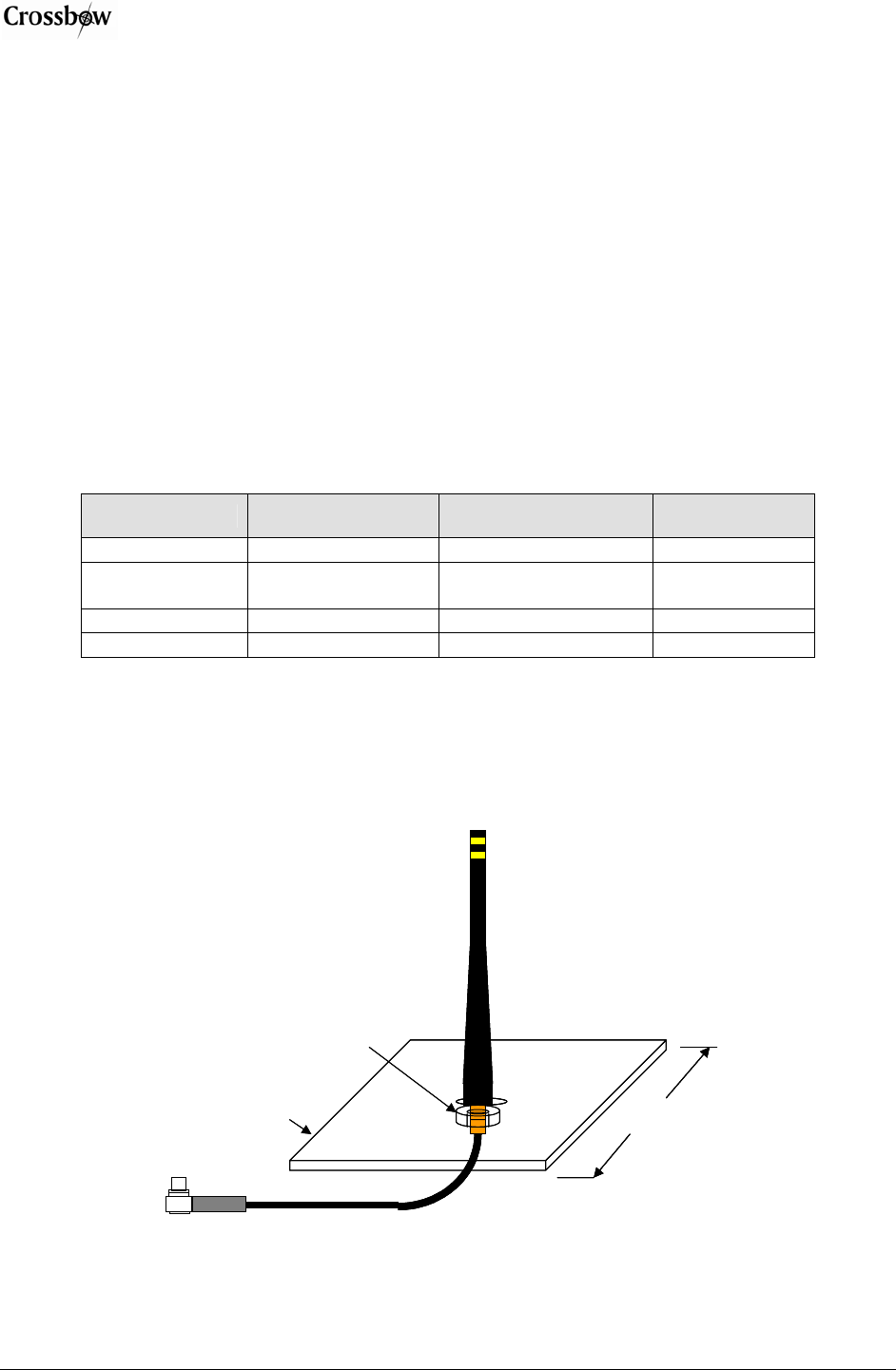
installed, as shown in Figure 9-2. The ground plane can be a layer of aluminum or copper tape
attached to the lid of a plastic enclosure, or the lid of a metal enclosure.
Figure 9-2. Illustration of an antenna option for the motes using a Linx antenna and ground
plane.
1/2 WAVELENGTH
RECOMMENDED
METALLIC
GROUND
PLANE
NUT MAKES
CONTACT WITH
GROUND PLANE
1/2 WAVELENGTH
RECOMMENDED
1/2 WAVELENGTH
RECOMMENDED
METALLIC
GROUND
PLANE
NUT MAKES
CONTACT WITH
GROUND PLANE
MPR/MIB User’s Manual
Doc. # 7430-0021-07 Rev. B Page 29
9.2 Connectors for the MICA2 and MICAz and Whip Antennas
The MICA2 and MICAz have an MMCX connector for attaching an external antenna. These
mating connectors can be purchased from Digi-Key. There are two manufacturers—Johnson
Components and Hirose Electric Ltd. The mating connectors come in straight and right angle.
They also support two different standard varieties of Coaxial cable—RG178 /U and RG 316/U.
There are also other vendors who sell MMCX to SMA conversion cables.
Table 9-3. Johnson Components’ MMCX mating connectors*
Type Coax Digi-Key PN Johnson PN
Straight Plug RG178/U J589-ND 135-3402-001
Straight Plug RG316/U J590-ND 135-3403-001
Right Angle RG178/U J593-ND 135-3402-101
Right Angle RG316/U J594-ND 135-3403-101
Right Angle RG 316 DS J595-ND 135-3404-101
*These connectors require the following hand crimp and die set (Digi-Key part # / Johnson part #):
a) Hand crimp (J572-ND / 140-0000-952), b) Die (JD604-ND / 140-0000-953).
Table 9-4. Hirose MMCX connectors.
Type Coax Digi-Key PN Hirose PN
Straight Plug RG178/U H3224-ND MMCX-J-178B/U
Right Angle RG178/U H3221-ND MMCX-LP-178B/U
Right Angle RG316/U H3222-ND MMCX-LP-316/U
MPR/MIB User’s Manual
Page 30 Doc. # 7430-0021-07 Rev. B
10 Flash Data Logger and Serial ID Chip
All Motes feature a 4-Mbit serial flash (Atmel AT45DB041) for storing data, measurements, and
other user-defined information. It is connected to one of the USART on the ATMega128L. This
chip is supported in TinyOS which uses this chip as micro file system. The serial flash device
supports over 100,000 measurement readings. This chip is also used for over-the-air
reprogramming services available in TinyOS.
Also on the MICA2 is a 64-bit serial ID chip.
; NOTE: This device consumes 15 mA of current when writing data.
FLASH_CS
VCC
USART_CLK
USART1_TXD SI
SCK
RST
CS WP
SO
1
2
3
4
USART1_RXD
8
x
5
Atmega AT45DB041
FLASH_CS
VCC
USART_CLK
USART1_TXD SI
SCK
RST
CS WP
SO
1
2
3
4
USART1_RXD
8
x
5
Atmega AT45DB041
MPR/MIB User’s Manual
Doc. # 7430-0021-07 Rev. B Page 31
11 Atmega128 Fuses
The ATMega128L processor on the Motes has many programmable fuses to control various
parameters. Refer to Atmel’s technical information for the ATMega128L for a complete
discussion of the fuses (http://www.atmel.com/dyn/resources/prod_documents/2467s.pdf). There
are two fuses that TinyOS users should be aware of as setting these fuses incorrectly will cause
the unit to not operate correctly.
11.1.1 Atmega103 compatibility mode fuse
This fuse put the ATMega128 in the ATMega103 compatible mode. This fuse was set for the
older generation MICA units. It must be disabled for MICA2 and MICA2DOTs.
11.1.2 JTAG fuse
This fuse enables users to use the Atmel JTAG pod for in-circuit code debugging. Units are
shipped with JTAG enabled. As discussed in the previous section on battery voltage monitoring,
if JTAG is enabled, it will cause inaccurate measurements on ADC channel 7.
11.1.3 Using UISP to set fuses
The UISP utility used to download code to the MICAz, MICA2, or MICA2DOT on a
programming board can also be used to set and unset fuses of the Atmel® ATMega128.
Table 11-1. UISP Commands for Setting the ATMega128’s Fuses.
Action Command
Disable JTAG fuse uisp -dprog=<programmer> --wr_fuse_h=0xD9
Enable JTAG fuse uisp -dprog=<programmer> --wr_fuse_h=0x19
Enable native 128 mode uisp -dprog=<programmer> --wr_fuse_e=ff
<programmer> is the device you are using to interface to the Mote from a computer. The current options
are dapa (for an MIB500), mib510 for a MIB510; and EPRB for a MIB600.
Users can also edit the file called profile in the cygwin/etc/ directory and enter an alias. One
example is this alias to disable the JTAG fuse:
alias fuse_dis="uisp -dprog=<programmer> --wr_fuse_h=0xD9"
Therefore, when fuse_dis and is entered into a Cygwin command line, the script will be
executed.
MPR/MIB User’s Manual
Page 32 Doc. # 7430-0021-07 Rev. B
12 Sensor Boards & Expansion Connectors
Crossbow supplies a variety of sensor and data acquisition boards for the Motes. This Chapter
describes the connectors and the functions of the pins for the MICAz, MICA2, MICA, and
MICA2DOT.
Information for customized sensor board design is available on the Crossbow web site.
12.1 Sensor Board Compatibility
Table 12-1. Sensor board compatibility.
Mote Platform Mote Interface Connector Hardware Compatibility with: Section
MICA2 Use 51 pin connector MICAz, MICA2 sensor boards 11.2
MICAz Use 51 pin connector MICAz, MICA2 sensor boards 11.2
MICA2DOT Use circular, 19 pin connector MICA2DOT sensor boards 11.3
12.2 MICAz and MICA2 Expansion Connector
Connection to the MICAz and MICA2 Motes is by a 51-pin connector (see Table 12-1 below).
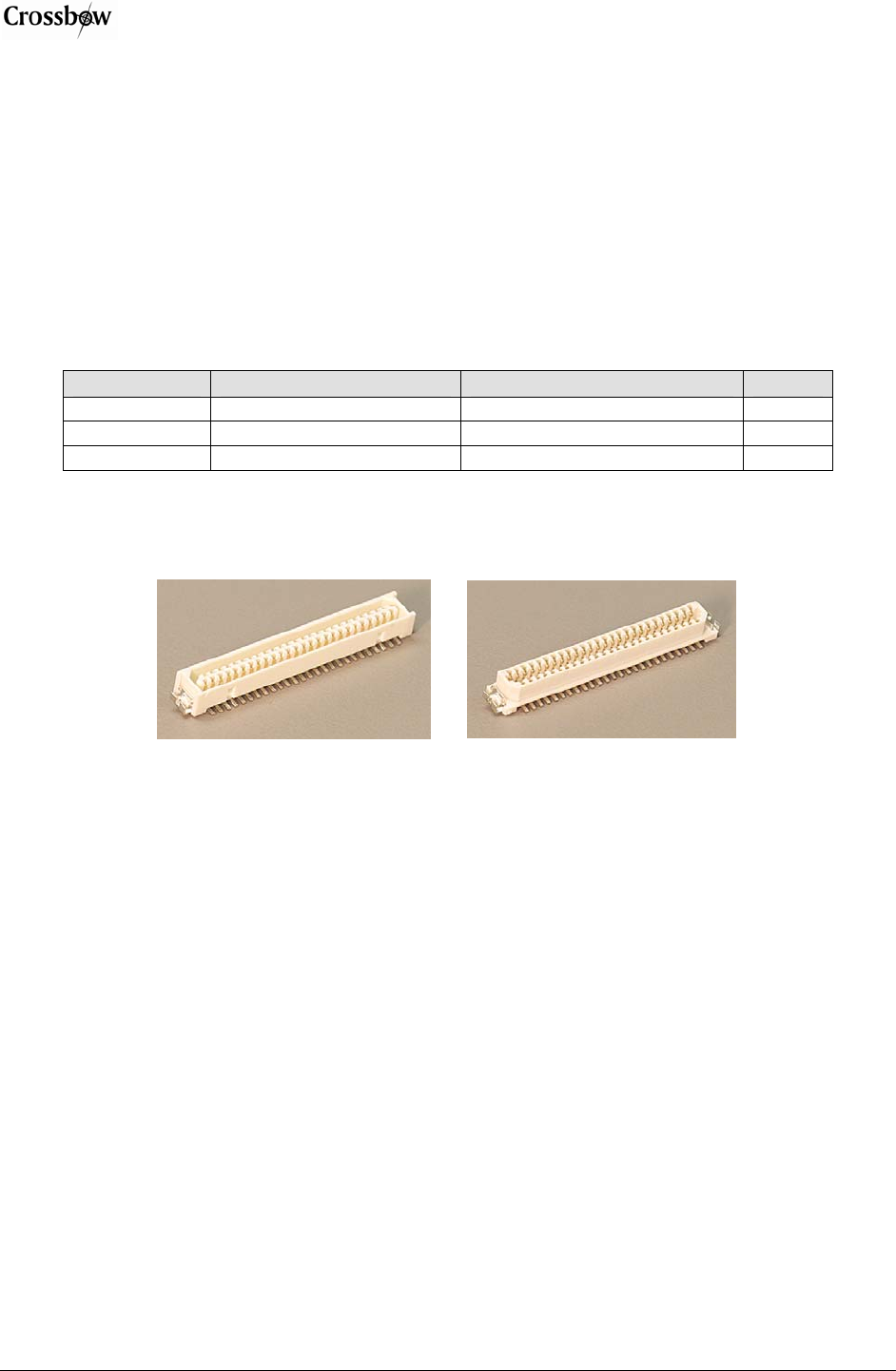
Figure 12-1. Hirose DF-51P-1V(54)—Digi-Key part no. H2175-ND—on left is used on the
MICAz, MICA2, and MICA Motes boards. The Hirose DF9-51S-1V(54)—Digi-Key part no.
H2163-ND—on right is the corresponding connector used on the MIB Interface Boards and
Stargate Gateways.
The expansion connector provides a user interface for sensor boards and base stations. The
connector includes interfaces for power and ground, power control of peripheral sensors, ADC
inputs for reading sensor outputs, UART interfaces, and I2C interface, general-purpose digital
IO, and others.

MPR/MIB User’s Manual
Doc. # 7430-0021-07 Rev. B Page 33
12.2.1 MICAz and MICA2 Sensor Interface.
Table 12-2. MICAz Sensor Interface.
Pin Name Description Pin Name Description
1 GND Ground 27g UART_RXDO UART_0 Receive
2 VSNR Sensor Supply 28g UART_TXDO UART_0 Transmit
3 INT3 GPIO 29 PWO GPIO/PWM
4 INT2 GPIO 30 PW1 GPIO/PWM
5 INT1 GPIO 31 PW2 GPIO/PWM
6 INT0 GPIO 32 PW3 GPIO/PWM
7gg CC_CCA Radio Signal 33 PW4 GPIO/PWM
8g LED3 Green LED 34 PW5 GPIO/PWM
9g LED2 Yellow LED 35 PW6 GPIO/PWM
10g LED1 Red LED 36g ADC7 ADC CH7, JTAG TDI
11 RD GPIO 37g ADC6 ADC CH6, JTAG TDO
12 WR GPIO 38g ADC5 ADC CH5, JTAG
13 ALE GPIO 39g ADC4 ADC CH4, JTAG
14 PW7 GPIO 40 ADC3 GPIO/ADC CH3
15 USART1_CLK USART1 Clock 41 ADC2 GPIO/ADC CH2
16gg PROG_MOSI Serial Program MOSI 42 ADC1 GPIO/ADC CH1
17gg PROG_MISO Serial Program MISO 43 ADC0 GPIO/ADC CH0
18gg SPI_CLK SPI Serial Clock 44 THERM_PWR Temp Sensor Enable
19 USART1_RXD USART1 Receive 45 THRU1 Thru Connect 1
20 USART1_TXD USART1 Transmit 46 THRU2 Thru Connect 2
21 I2C_CLK I2C Bus Clock 47 THRU3 Thru Connect 3
22 I2C_DATA I2C Bus Data 48gg RSTN Reset (Neg.)
23 PWM0 GPIO/PWM0 49 PWM1B GPIO/PWM1B
24 PWMIA GPIO/PWM1A 50 VCC Digital Supply
25 AC+ GPIO/AC+ 51 GND Ground
26 AC- GPIO/AC-
(gOK to use but has shared functionality. ggDo not use)
Table 12-3. MICA2 Sensor Interface.
Pin Name Description Pin Name Description
1 GND Ground 27g UART_RXDO UART Receive
2 VSNR Voltage (battery 28g UART_TXDO UART Transmit
3 INT3 GPIO 29 PWO GPIO/PWM
4 INT2 GPIO 30 PW1 GPIO/PWM
5 INT1 GPIO 31 PW2 GPIO/PWM
6 INT0 GPIO 32 PW3 GPIO/PWM
7g BAT_MON Battery Voltage Monitor 33 PW4 GPIO/PWM

MPR/MIB User’s Manual
Page 34 Doc. # 7430-0021-07 Rev. B
8g LED3 Green LED 34 PW5 GPIO/PWM
9g LED2 Yellow LED 35 PW6 GPIO/PWM
10g LED1 Red LED 36g ADC7 GPIO/ADC CH7, JTAG
11 RD GPIO 37g ADC6 GPIO/ADC CH6, JTAG
12 WR GPIO 38g ADC5 GPIO/ACD CH5, JTAG
13 ALE GPIO 39g ADC4 GPIO/ADC CH4, JTAG
14 PW7 GPIO 40 ADC3 GPIO/ADC CH3
15 USART_CLK USART Clock 41 ADC2 GPIO/ADC CH2
16gg PROG_MOSI Programmer Pin 42 ADC1 GPIO/ADC CH1
17gg PROG_MISO Programmer Pin 43 ADC0 GPIO/ADC CH0
18gg SPI_CLK Radio Clock 44 THERM_PWR GPIO
19 USART1_RXD USART1 Receive 45 THRU1 Thru User Connect
20 USART1_TXD USART1 Transmit 46 THRU2 Thru User Connect
21 I2C_CLK I2C Bus Clock 47 THRU3 Thru User Connect
22 I2C_DATA I2C Bus Data 48gg RSTN Micro Processor Reset
23 PWMIO GPIO 49 PWM1B GPIO
24 PWMIA GPIO 50 VCC Voltage (battery)
25 AC+ GPIO 51 GND Ground
26 AC- GPIO
(gOK to use but has shared functionality. ggDo not use)
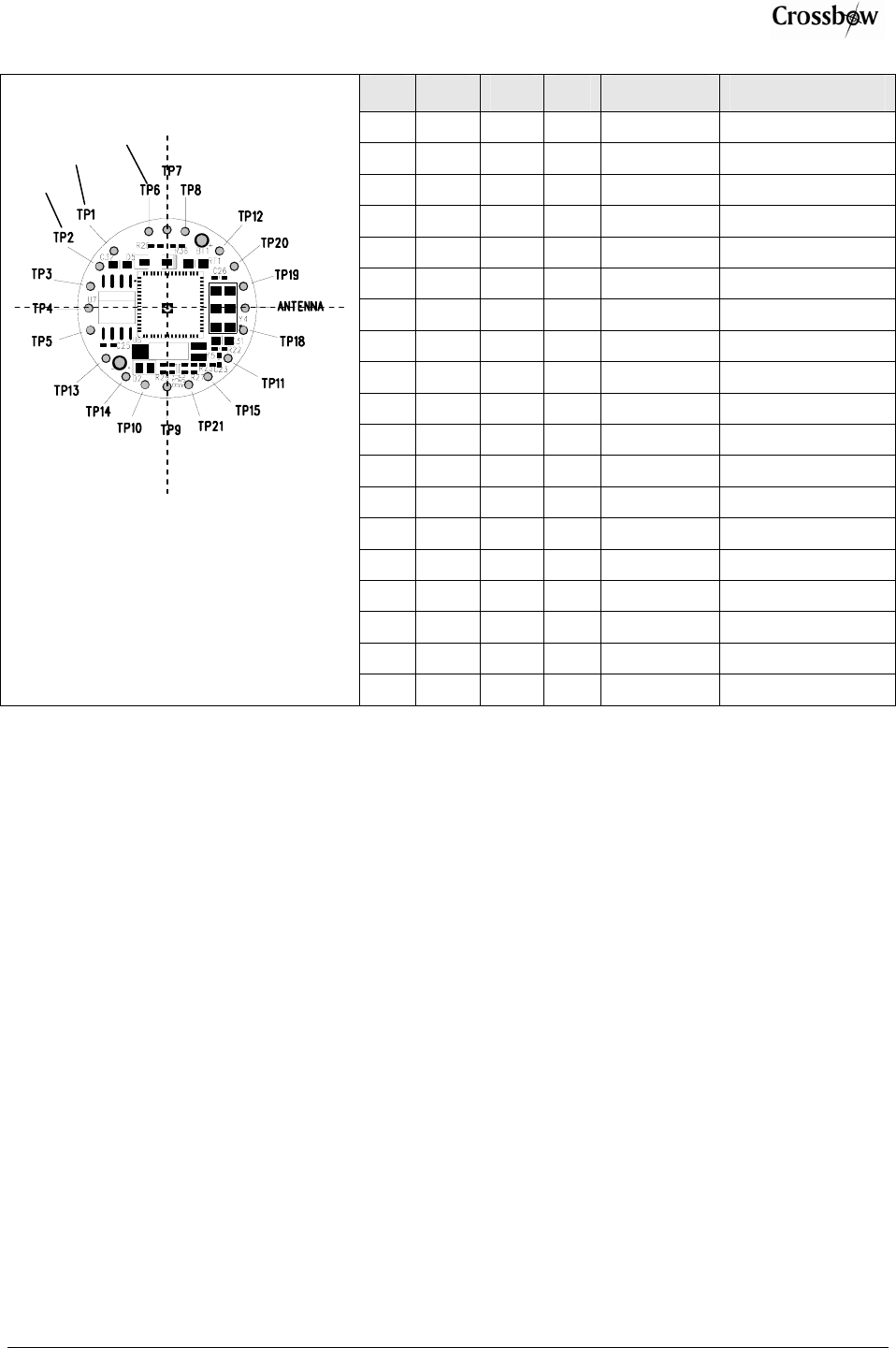
12.3 MICA2DOT Expansion Connector
The interface to the MPR500 is through a series of 19 pins Elpacko spaced around the
circumference of the MPR5x0 Mote. (They represent a subset of the pins available on the
MPR5x0.) They include a set of power control pins, ADC channels, power, ground, some
general purpose digital IO, and the serial programming port. For applications with more digital
IO, the ADC pins can be reconfigured as digital input/output but not both.
0 WARNING: The TP12 (SPI_CK) pin is controlled by the Radio. In the majority of applications it
should not be used. It is also used for programming the processor.
MPR/MIB User’s Manual
Doc. # 7430-0021-07 Rev. B Page 35
Loc. x y Pin Name Description
1 -0.290 0.315 TP1 GND Ground
2 -0.370 0.230 TP2 ADC7 ADC Channel 7
3 -0.420 0.120 TP3 ADC6 ADC Channel 6
4 -0.430 0.000 TP4 ADC5 ADC Channel 5
5 -0.420 -0.120 TP5 ADC4 ADC Channel 4
6 -0.335 -0.275 TP13 ADC3 ADC Channel 3
7 -0.225 -0.375 TP14 ADC2 ADC Channel 2
8 -0.120 -0.420 TP10 UART_RX UART Receive
9 0.000 -0.430 TP9 UART_TX UART Transmit
10 0.120 -0.420
TP21 THERM_PWR GPIO
11 0.225 -0.375
TP15 PWM1B GPIO
12 0.335 -0.275
TP11 RESETN MCU Reset
13 0.420 -0.120
TP18 GND Ground (Battery –term)
14 0.420 0.120
TP19 INT0 GPIO
15 0.370 0.230
TP20 INT1 GPIO
16 0.290 0.315
TP12 SPI_CLK Radio Clock
17 0.100 0.420 TP8 PW0 GPIO/PWM
18 0.000 0.430 TP7 PW1 GPIO/PWM
19 -0.100 0.420 TP6 VCC Voltage (Battery +term)
Figure 12-2. MICA2DOT pin locations and sensor interface description. The locations of the
pins are taken relative to the geometric center of the board. The board has a diameter of 0.988
inches. Note the “TP” under the “Pin” column means “test point.”
y
x
Loc. 1
Loc.
2
Loc. 19

MPR/MIB User’s Manual
Page 36 Doc. # 7430-0021-07 Rev. B
13 MIB300 / MIB500 Interface Boards
; NOTE: The MIB300 and MIB500 have been discontinued by Crossbow. The MIB500 has been
replaced by the MIB510.
0 WARNING: When programming a MICA2 with the MIB500, turn off the battery switch. For a
MICA2DOT, remove the battery before inserting into the MIB500. The MICA2s and MICA2DOTs do not
have switching diodes to switch between external and battery power.
13.1 Programming the Mote
The MIB300/MIB500 interface boards are multi-purpose interface boards used in conjunction
with the MICA Family of products. They supply power to the devices through an external power
adapter option, and provide interfaces for an RS232 serial port and reprogramming port (using
the parallel printer interface). The MIB300 can only be used with an external 3 VDC supply, or it
can take advantage of the battery power supplied from the mote.
The MIB500 has an on-board regulator that will accept 5 to 7 VDC, and supplies a regulated 3
VDC to the MICA The MIB500 is delivered with a wall power supply. It also has monitor LEDs
that mirror the LEDs on the MICA.
There is a built-in low voltage monitor that disables reprogramming if the power supply voltage
is dangerously low. When the proper programming voltage exists—the Green LED adjacent the
parallel port is lit—D6. If the voltage goes below 2.95V, the Green LED D6 will turn off,
programming is disabled.
The MIB500 also has an interface connector for reprogramming the MICA2DOT. Programming
the mote is accomplished by connecting the MIB300/MIB500 to the parallel port of the
computer, and executing the required programming software—UISP—supplied with the TinyOS
install.
; NOTE: There have been numerous reported difficulties with programming motes through the
MIB500CA. These include program failure, flash verification errors, and dead Motes. The root cause of
these problems is almost always one of two issues: 1) low programming voltage or 2) UISP problems on
the Host PC. A detailed application note is posted at http://www.xbow.com under Support. Please review
this application note, if you have trouble programming. Programming the Motes improperly or with a bad
UISP install can result in permanent damage to the Mote CPU.
13.2 RS-232 Interface
The RS-232 interface is a standard single channel bi-directional interface with a DB9 connector
to interface to an external computer. It uses transmit and receive lines only.
MPR/MIB User’s Manual
Doc. # 7430-0021-07 Rev. B Page 37
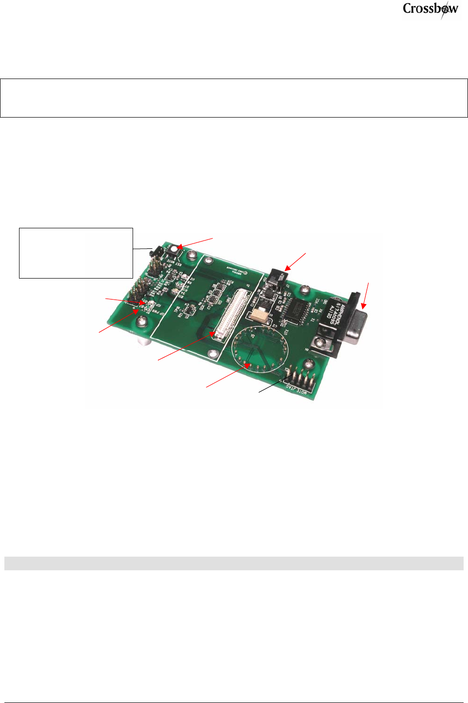
14 MIB510 Serial Interface Boards
; NOTE: The MIB510 will only work with ATMega128 processors used on the MICA2 and MICA2DOT.
It will work for older Mica units that have the ATMega128 processor but not earlier processors such as the
ATMega103.
14.1 Product Summary
The MIB510 interface board is a multi-purpose interface board used with the MICAz, MICA2,
MICA, and MICA2DOT family of products. The board is supplied with all MOTE-KITs. It
supplies power to the devices through an external power adapter option, and provides an
interface for a RS-232 Mote serial port and reprogramming port.
Figure 14-1. Photo of top view of an MIB510CA.
14.2 ISP
The MIB510 has an on-board in-system processor (ISP)—an Atmega16L located at U14—to
program the Motes. Code is downloaded to the ISP through the RS-232 serial port. Next the ISP
programs the code into the mote. The ISP and Mote share the same serial port. The ISP runs at a
fixed baud rate of 115.2 kbaud. The ISP continually monitors incoming serial packets for a
special multi-byte pattern. Once this pattern is detected it disables the Mote’s serial RX and TX,
then takes control of the serial port.
0 WARNING: Some USB to DB9 serial port adapters cannot run at 115 kbaud.
The ISP processor is connected to two LEDs, a green LED labeled “SP PWR” (at D3) and a red
LED labeled “ISP” (at D5). SP PWR is used to indicate the power state of the MIB510 (see
below). If the ISP LED is on, the MIB510 has control of the serial port. It will also blink once
when the RESET (SW1) button is pushed and released.
14.3 Mote Programming Using the MIB510
Programming the Motes requires having TinyOS installed in your host PC. Instructions for
installing TinyOS can be found in Crossbow’s Getting Started Guide or on-line at
ISP LED (red)
MICAx-series
connecto
r
MICA2DOT connector on
bottom side Mote JTAG connector
RS-232 Serial Port
(DB9 female)
Reset Switch (SW1)
; NOTE: Enable/Disable
Mote TX switch (“SW2”).
This should normally be
in the “OFF” position.
AC Wall-Power
Connector
Power OK LED
(green)

MPR/MIB User’s Manual
Page 38 Doc. # 7430-0021-07 Rev. B
http://www.tinyos.net/download.html. The commands for downloading build (compiled) code
depend on the Mote platform you are programming. Instructions can also be found in the Getting
Started Guide.
0 WARNING: Under Cygwin the ISP may not get control of the serial port if the Mote is continually
sending packets over the serial TX line at a high rate. If this happens, the UISP will hang. This can be
fixed by:
1. Type Ctrl C in the Cygwin window and try again.
2. Turn SW2 to the “ON” position. This turns on a circuit to disable the Mote’s TX line. Be sure to set
SW2 to ‘OFF’ after programming the mote if you are using the Mote as a base station (e.g., a
MICAz or MICA2 Mote programmed with Surge_Reliable as node “0” or with TOSBase).
14.4 Interfaces to MICAz, MICA2, and MICA2DOT
The MIB510 has connectors for the MICAz, MICA2 and MICA2DOT. For the MICAz and
MICA2 there is another connector on the bottom side of the MIB510 to allow the simultaneous
attachment of a sensor board. MICA2DOTs with battery connectors can be mounted, also, to the
bottom side of the board.
14.4.1 Reset
The “RST MOTE” push button switch resets both the ISP and Mote processors. RST resets the
ISP; after the ISP powers-up it resets the Mote’s processor.
14.4.2 JTAG
The MIB510 has a connector, J3 (“MOTE JTAG”) which connects to an Atmel JTAG pod for
in-circuit debugging. This connector will supply power to the JTAG pod; no external power
supply is required for the pod.
0 WARNING: The MIB510 also has JTAG and ISP connectors for the ISP processor. These are for
factory use only.
14.4.3 Power
The MIB510 has an on-board regulator that will accept 5 to 7 VDC, and supply a regulated 3
VDC to the MICAz, MICA2, and MICA Motes. The MIB510 is delivered with a wall power
supply.
0 WARNING: Applying more than 7 VDC will damage the on-board linear regulator.
There is a built-in low voltage monitor that disables reprogramming if the power supply voltage
is dangerously low. When the proper programming voltage exists the “ISP PWR” LED is on. If
the voltage goes below 2.9 V, the green “ISP PWR” LED will blink and disable the Mote from
any code downloads. If the voltage is too low to power the ISP then the “ISP PWR” LED will be
off.
0 WARNING: When programming a MICA2/MICAz with the MIB510, turn off the battery switch. For
a MICA2DOT, remove the battery before inserting into the MIB510. The MICA2s and MICA2DOTs do not
have switching diodes to switch between external and battery power.
14.4.4 RS-232 Interface
The RS-232 interface is a standard single channel bi-directional interface with a DB9 connector
to interface to an external computer. It uses the transmit and receive lines only.
MPR/MIB User’s Manual
Doc. # 7430-0021-07 Rev. B Page 39
14.4.5 Schematics
HIROSE SOCKET
J1
DF9B-51S-1V
1
2
3
4
5
6
7
8
9
10
11
12
13
14
15
16
17
18
19
20
21
22
23
24
25
26
27
28
29
30
31
32
33
34
35
36
37
38
39
40
41
42
43
44
45
46
47
48
49
50
51
PROG_MISO
ADC4
INT0
PW2
PW7
PW1
ADC4
PROG_MOSI
INT0
USART1_RXD
PW[0..7]
INT2
AC+
VCC
THERM_PWR
VSNSR
PWM0
VCC
PW5
M1
MTG128
1
1
ADC[0..7]
INT3
PWM1B
AC+
LED1
THRU1
USART1_TXD
LED3
ALE
PW1
VSNSR
AC-
ADC6
USART1_CLK
AC-
PWM1B
HIROSE PLUG
J2
DF9-51P-1V(54)
1
2
3
4
5
6
7
8
9
10
11
12
13
14
15
16
17
18
19
20
21
22
23
24
25
26
27
28
29
30
31
32
33
34
35
36
37
38
39
40
41
42
43
44
45
46
47
48
49
50
51
ADC5
USART1_RXD THRU2
PROG_MISO
LED2
PW3
PW6
WR
ADC3
RSTN
PROG_MOSI
INT[0..3]
THERM_PWR
PW7
PWM0
THRU2
INT[0..3]
INT2
ADC2
UART_TXD0
PW0
THRU3
LED3
INT1
BAT_MON
ADC7
PW4
PW5
THRU3
ADC1
LED1
USART1_CLK
I2C_CLK
ADC3
I2C_DATA
I2C_CLK
PWM1A
ADC1
UART_RXD0
ADC0
UART_RXD0
PW[0..7]
INT1
PW3
SPI_SCK
UART_RXD0
ADC7
ADC5
BAT_MON
LED2
RD
I2C_DATA
SPI_SCK
UART_TXD0
RD
ALE
PW0INT3
PWM1A
UART_TXD0
THRU1
RSTN
USART1_TXD
ADC[0..7]
PW2
PW4
PW6
ADC6
ADC0 M2
MTG128
1
1
ADC2
WR

MPR/MIB User’s Manual
Page 40 Doc. # 7430-0021-07 Rev. B
PIN NAME
GND
VSNSR
INT3
INT2
INT1
INT0
BAT_MON
LED3
LED2
LED1
RD
WR
ALE
PW7
USART1_CLK
PROG_MOSI
PROG_MISO
SPI_SCK
USART1_RXD
USART1_TXD
I2C_CLK
I2C_DATA
PWM0
PWM1A
AC+
AC-
DESCRIPTIONPIN
UART_RXD0
UART_TXD0
PW0
PW1
PW2
PW3
PW4
PW5
PW6
ADC7
ADC6
ADC5
ADC4
ADC3
ADC2
ADC1
ADC0
THERM_PWR
THRU1
THRU2
THRU3
RSTN
PWM1B
VCC
GND
UART_0 RECEIVE
UART_0 TRANSMIT
POWER CONTROL 0
POWER CONTROL 1
POWER CONTROL 2
POWER CONTROL 3
POWER CONTROL 4
POWER CONTROL 5
POWER CONTROL 6
ADC INPUT 7 - BATTERY MONITOR/JTAG TDI
ADC INPUT 6 / JTAG TDO
ADC INPUT 5 / JTAG TMS
ADC INPUT 4 / JTAG TCK
ADC INPUT 3
ADC INPUT 2
ADC INPUT 1
ADC INPUT 0 / RSSI MONITOR
TEMP SENSOR ENABLE
THRU CONNECT 1
THRU CONNECT 2
THRU CONNECT3
RESET (NEG)
GPIO/PWM1B
DIGITAL SUPPLY
GROUND
GROUND
SENSOR SUPPLY
GPIO
GPIO
GPIO
GPIO
BATTERY VOLTAGE MONITOR ENABLE
LED3
LED2
LED1
GPIO
GPIO
GPIO
POWER CONTROL 7
USART1 CLOCK
SERIAL PROGRAM MOSI
SERIAL PROGRAM MISO
SPI SERIAL CLOCK
USART1 RX DATA
USART1 TX DATA
I2C BUS CLOCK
I2C BUS DATA
GPIO/PWM0
GPIO/PWM1A
GPIO/AC+
GPIO/AC-
27
28
29
30
31
32
33
34
35
36
37
38
39
40
41
42
43
44
45
46
47
48
49
50
51
NAME
DESCRIPTION
1
2
3
4
5
6
7
8
9
10
11
12
13
14
15
16
17
18
19
20
21
22
23
24
25
26
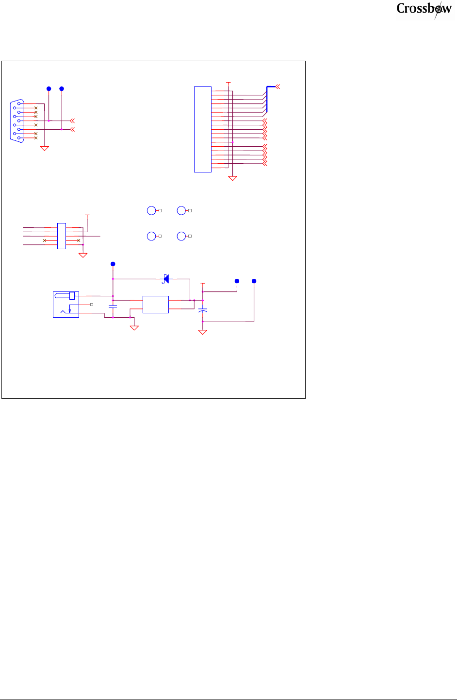
MPR/MIB User’s Manual
Doc. # 7430-0021-07 Rev. B Page 41
14.4.6 RS-232, MICA2DOT, and Ext. Power Interface.
M4
MTG128
1
1
LPT1_MISO
J4
DB25-M-RA
5
17
4
16
3
15
2
14
1
20
7
19
6
18
10
22
9
21
8
23
11
24
12
25
13
A
DC5
VCC
INT1
J3
HDR2X5
1 2
3 4
5 6
7 8
910
VCC
A
DC[0..7]
RSTN
RS232_TX
M6
MTG128
1
1
C1
.1uF
50V
THERM_PWR
A
DC6
RSTN
RS232_RX
TP6
J6
DB9-F-RA
5
9
4
8
3
7
2
6
1
SPI_SC
K
A
DC6
INT0
TP5
PWM1B
TP7
PIN
OUTER
J7
PJ-014D
2
3
1
UART_TXD0
U1
LMS8117-3.3
3
1 2
4
VIN
A
DJ
VOUT
GND
PW1
M3
MTG128
1
1
D1
B2100
+
C2
10uF
35V
TDI
TP9
TCK
TDO
TMS
PW0
J5
DOT2
1
2
3
4
5
6
7
8
9
10
11
12
13
14
15
16
17
18
19
1
2
3
4
5
6
7
8
9
10
11
12
13
14
15
16
17
18
19
A
DC4
A
DC2
6310-0304-01
A
MIB500CA MICA PROG BOARD
CROSSBOW TECHNOLOGY. INC.
B
23Wednesday, March 26, 2003
Title
Size Document Numbe
r
Rev
Date: Sheet o
f
LPT1_MOSI
A
DC3
A
DC4
VCC
LPT1_RST
UART_RXD0
TP8
A
DC7
A
DC7
M5
MTG128
1
1
A
DC5
LPT1_SCK
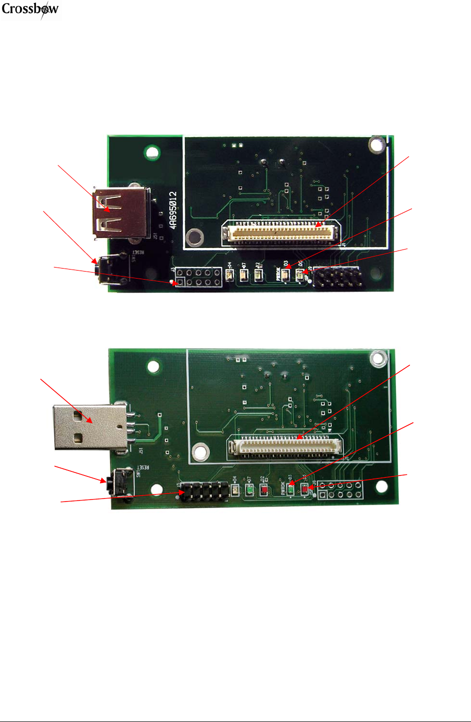
MPR/MIB User’s Manual
Page 42 Doc. # 7430-0021-07 Rev. B
15 MIB520 USB Interface Board
The MIB520 provides USB connectivity to the MICA family of Motes for communication and
in-system programming. It supplies power to the devices through USB bus. MIB520CB has a
male connector while MIB520CA has female connector.
Figure 15-1a. Photo of top view of an MIB520CA.
Figure 15-2b. Photo of top view of an MIB520CB.
15.1 ISP
The MIB520 has an on-board in-system processor (ISP)—an Atmega16L located at U14—to
program the Motes. Code is downloaded to the ISP through the USB port. Next the ISP programs
the code into the Mote.
15.2 Mote Programming Using the MIB520
Programming the Motes requires having TinyOS installed in your host PC. The MICAz and
MICA2 Motes connect to the MIB520 for UISP programming from USB connected host PC.
MICAx-series
connector
Power OK LED
(green)
ISP LED (red)
USB Serial Port
(A-type female)
Reset Switch
(SW1)
Mote JTAG
connector
(unmounted)
Mote JTAG
connector
USB Serial Port
(B-type Male)
Reset Switch
(SW1)
MICA-series
connecto
r
Power OK LED
(green)
ISP LED (red)

MPR/MIB User’s Manual
Doc. # 7430-0021-07 Rev. B Page 43
15.3 MIB520 Use
15.3.1 Install FTDI USB Virtual COM Port Drivers
MIB520 uses FTDI FT2232C to use USB port as virtual COM port. Hence you need to install
FT2232C VCP drivers.
• When you plug a MIB520 into your PC for the first time, the Windows detects and
reports it as a new hardware. Please select “Install from a list or specific location
(Advanced)” and browse to “MIB520 Drivers” folder of the TinyOS Support Tools
CDROM. Install shield wizard will guide you through the installation process.
• When the drivers are installed, you will see two serial ports added under the Control
PanelÆSystemÆHardwareÆDevice ManagerÆPort. Make a note of the assigned
COM port numbers.
• The two virtual serial ports for MIB520 are comn and com(n+1); comn is for Mote
programming and com(n+1) is for Mote communication.
15.4 Reset
The “RESET” push button switch resets both the ISP and Mote processors. It also resets the
monitoring software which runs on the host PC.
15.5 JTAG
The MIB520 has a connector, J3 which connects to an Atmel JTAG pod for in-circuit debugging.
This connector will supply power to the JTAG pod; no external power supply is required for the
pod.
0 WARNING: The MIB520 also has JTAG and ISP connectors for the ISP processor. These
are for factory use only.
15.6 Power
The MIB520 is powered by the USB bus of the host.
0 WARNING: When programming a MICA2/MICAz with the MIB520, turn off the battery
switch.
15.7 USB Interface
The MIB520CA offers two separate ports: one dedicated to in-system Mote programming and a
second for data communication over USB.
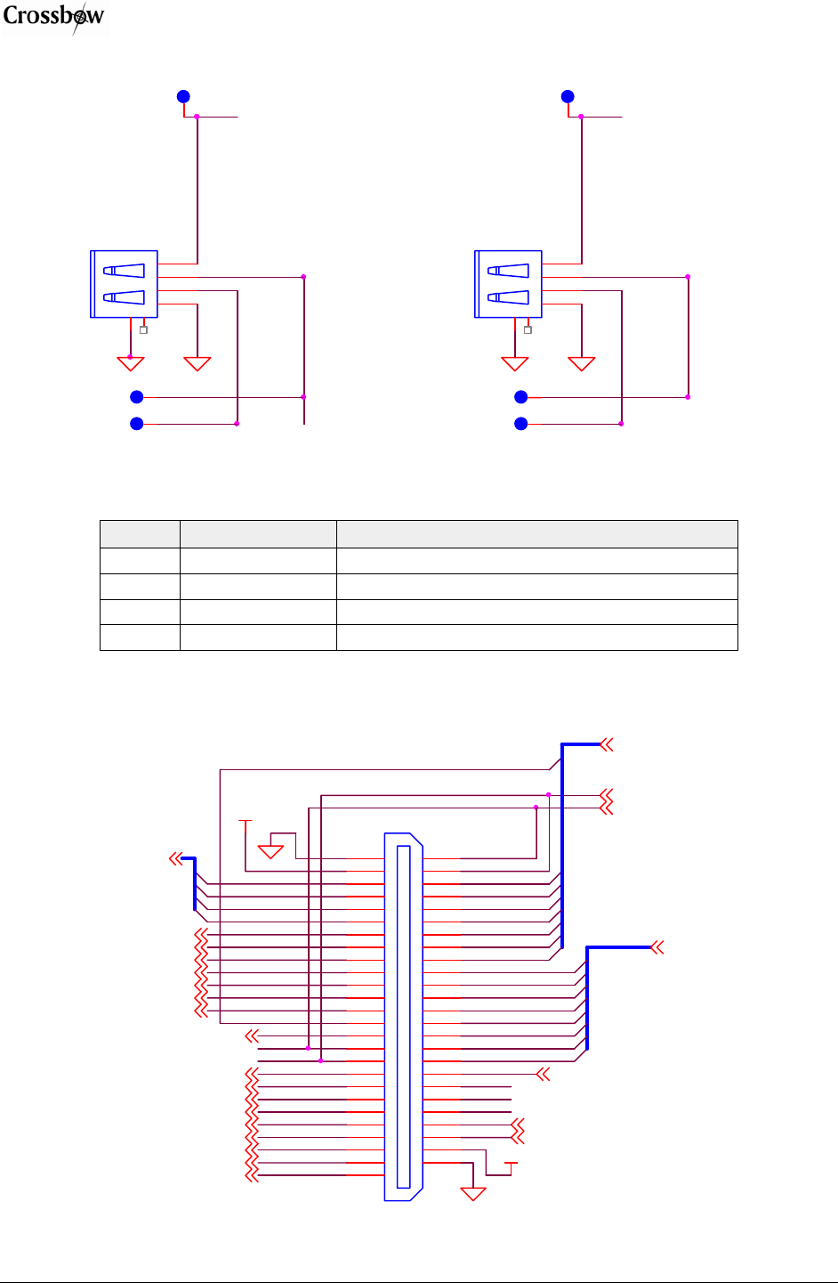
MPR/MIB User’s Manual
Page 44 Doc. # 7430-0021-07 Rev. B
DP
TP6
VIN
DM
TP5
J51 USB-A
1
2
3
4
5
6
TP7
TP7
DM
DP
TP5
J51
A-USB-A-LP/SMT
1
2
3
4
5
6
VIN
TP6
MIB520CA MIB520CB
Table 15-3. Pin Outs for a USB Connection
Pin No. Name Description
1 VBUS Powered Supply Pin
2 USBDM USB Data Signal Minus
3 USBDP USB Data Signal Plus
4 GND Ground Supply Pin
15.8 51-Pin Mote Connector Interface
PW7
PWM1A
LED2
THRU2
PW6
USART1_CLK
UART_RXD0
VCC
LED3
PW0
PW1
I2C_CLK
PW5
ADC7
AC-
INT3
AC+
RSTN
INT1
ALE
THERM_PWR
INT0
PWM0
ADC5
HIROSE SOCKET
J1
DF9B-51S-1V
1
2
3
4
5
6
7
8
9
10
11
12
13
14
15
16
17
18
19
20
21
22
23
24
25
26
27
28
29
30
31
32
33
34
35
36
37
38
39
40
41
42
43
44
45
46
47
48
49
50
51
RD
VSNSR
PW4
WR
UART_TXD0
ADC3
USART1_TXD
PROG_MOSI
PW2
I2C_DATA
ADC6
PROG_MISO
USART1_RXD
LED1
THRU3
INT[0..3]
ADC[0..7]
SPI_SCK
ADC[0..7]
PW3
ADC4
INT2
UART_RXD0
ADC0
THRU1
BAT_MON
PWM1B
PW[0..7]
ADC1
UART_TXD0
ADC2

MPR/MIB User’s Manual
Doc. # 7430-0021-07 Rev. B Page 45
DESCRIPTION
UART_0 RECEIVE
UART_0 TRANSMIT
POWER CONTROL 0
POWER CONTROL 1
POWER CONTROL 2
POWER CONTROL 3
POWER CONTROL 4
POWER CONTROL 5
POWER CONTROL 6
ADC INPUT 7 - BATTERY MONITOR/JTAG TDI
ADC INPUT 6 / JTAG TDO
ADC INPUT 5 / JTAG TMS
ADC INPUT 4 / JTAG TCK
ADC INPUT 3
ADC INPUT 2
ADC INPUT 1
ADC INPUT 0 / RSSI MONITOR
TEMP SENSOR ENABLE
THRU CONNECT 1
THRU CONNECT 2
THRU CONNECT3
RESET (NEG)
GPIO/PWM1B
DIGITAL SUPPLY
GROUND
NAME
GROUND
SENSOR SUPPLY
GPIO
GPIO
GPIO
GPIO
BATTERY VOLTAGE MONITOR ENABLE
LED3
LED2
LED1
GPIO
GPIO
GPIO
POWER CONTROL 7
USART1 CLOCK
SERIAL PROGRAM MOSI
SERIAL PROGRAM MISO
SPI SERIAL CLOCK
USART1 RX DATA
USART1 TX DATA
I2C BUS CLOCK
I2C BUS DATA
GPIO/PWM0
GPIO/PWM1A
GPIO/AC+
GPIO/AC-
1
2
3
4
5
6
7
8
9
10
11
12
13
14
15
16
17
18
19
20
21
22
23
24
25
26
UART_RXD0
UART_TXD0
PW0
PW1
PW2
PW3
PW4
PW5
PW6
ADC7
ADC6
ADC5
ADC4
ADC3
ADC2
ADC1
ADC0
THERM_PWR
THRU1
THRU2
THRU3
RSTN
PWM1B
VCC
GND
NAME PINDESCRIPTION
GND
VSNSR
INT3
INT2
INT1
INT0
BAT_MON
LED3
LED2
LED1
RD
WR
ALE
PW7
USART1_CLK
PROG_MOSI
PROG_MISO
SPI_SCK
USART1_RXD
USART1_TXD
I2C_CLK
I2C_DATA
PWM0
PWM1A
AC+
AC-
27
28
29
30
31
32
33
34
35
36
37
38
39
40
41
42
43
44
45
46
47
48
49
50
51
PIN
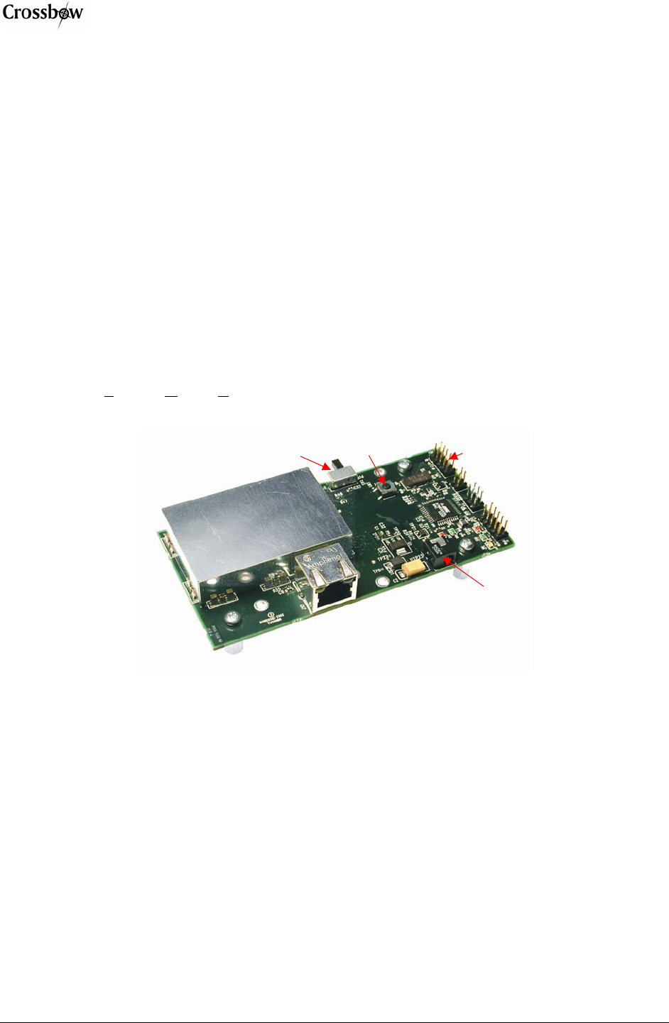
MPR/MIB User’s Manual
Page 46 Doc. # 7430-0021-07 Rev. B
16 MIB600 Ethernet Interface Board
16.1 Introduction
The MIB600 provides Ethernet (10/100 Base-T) connectivity to MICA2 family Motes for
communication and in-system programming. Its two standard configurations are (a) an Ethernet
Gateway for a Mote network and (b) a Mote network programming and out-band diagnostic
channel.
The MIB600CA device contains, on a 4.5” × 2.25” platform a
MICA2 mote 54-pin connector (J1),
Mote target JTAG port (J12),
TCP/IP serial server,
In-system programmer compatible with UISP STK500,
On-board power regulation and monitor, and a
Power Over Ethernet (POE) power supply
Figure 16-1. Photo of top side of an MIB600CA.
16.1.1 Mote Network – Ethernet Gateway
A MICAz or MICA2 Mote running TOSBase or GenericBase is permanently installed on the
MIB600. This forms a Mote RF to Ethernet bridge.
16.1.2 Mote Network Programming and Out-Band Diagnostic Channel
The MICAz and MICA2 Motes connect to the MIB600 for UISP programming from LAN
connected host computers. Out band (non-RF) diagnostics can be forwarded from the Mote via
its UART port over the LAN to host monitor/control computers.
16.2 Setup / Installation
This section describes MIB600 installation and configuration for use in a TinyOS v1.1
environment.
Ext 5V / POE Power
Select
MIB600 &
Mote Reset
External 5V
DC Power
J12: Mote
JTAG
p
ort

MPR/MIB User’s Manual
Doc. # 7430-0021-07 Rev. B Page 47
16.2.1 Physical
For other than temporary installations, the MIB600 should be installed in a ground isolated
enclosure.
16.2.2 MICA Mote Connection
MICAz and MICA2 Motes connect to the MIB600 directly via the standard mote 51-pin
HIROSE connector at J1. Two mounting holes are provided for securing the MICA2 Mote when
installed at J1. It is recommended that these mounting points be used for longer term installations
to ensure a reliable mechanical and electrical connection to the MIB600.
16.2.3 Power
Two power supply sources are available with the MIB600
External 5VDC from AC wall-power adaptor
Power Over Ethernet
External 5VDC Power Supply
Connect the external 5VDC power supply to an AC 110-240V power source.
Place the MIB600 SW2 in the POE position
Connect the DC plug to J7 of the MIB600
; NOTE: Turn-on the MIB by placing the SW2 in the 5V position. Turn-off by placing the SW2 in the POE
position.
Power Over Ethernet / IEEE802.3af (POE).
0 WARNING! The Mote “ground” is at POE potential (-48 V). Do not connect MIB600 to facility/building
ground when using POE.
An IEEE 802.3af compliant power supply is provided for POE equipped facilities. Ethernet
appliance power (-48 V) is supplied at pins 4/5 and 7/8 of the 10/100 Base-T RJ45 plug. Refer
to Appendix A for Base-T wiring information.
The MIB600 POE circuit contains IEEE 802.13f compliant power sequencing and classification
circuitry. Reversed and over-voltage protection is provided.
; NOTE: The MIB600 only supports POE over the “spare wires” 4/5 and 7/8. It does not support POE
shared on the Base-T signaling lines.
Connect the MIB600 to a POE-equipped LAN port.
Turn-On the MIB600 by placing the MIB600 SW2 in the POE position
Turn-Off by placing SW2 in 5V position (with External 5VDC supply
disconnected)
16.2.4 MIB600–LAN Connection
The MIB600 Serial Server connects directly to a 10 Base-T LAN as any other network device.
Straight cables are used to connect to a hub or switch. If your connection is an MIB600 to PC
you must use a crossed cable. Refer to Appendix A for LAN wiring information.
MPR/MIB User’s Manual
Page 48 Doc. # 7430-0021-07 Rev. B
Table 16-2. Pin Outs for a LAN Connection
Pin No. Strand Color Name
1 White and orange TX+
2 Orange TX-
3 White and green RX+
4 Blue 0V POE
5 White and blue 0V POE
6 Green RX-
7 Brown and white -48V POE
8 Brown -48V POE
16.3 Host Software
16.3.1 UISP
UISP version 20030820tinyos or newer is required. This version is included in the TinyOS 1.1.0
September 2003 release package. Verify your system is using a compatible UISP version by
entering uisp -–version in a Cygwin window (see the example below in Figure 16-3).
Figure 16-3. Screen shot of the output after typing in uisp --version.
16.4 MIB600 Use
16.4.1 Controls and Indicators
Power. MIB600 power (and power to attached mote) is controlled by the switch labeled
“SW2.”
0 WARNING! Always turn-off the MIB600’s power before installing/removing a mote.
Table 16-4. SW2 Switch Settings.
Position Function
5V External 5V DC power supply selected
POE Power Over Ethernet supply selected
When valid power is detected, the green LED at D5 is ON.
LAN Activity Indicators (RJ45). Green indicates a network connection is present. Yellow
indicates Active ISP serial port traffic is present.
RESET. Pressing the RESET pushbutton (SW1) causes the MIB600 and any
installed/attached MOTE to reset. Note the Serial Server is NOT reset.

MPR/MIB User’s Manual
Doc. # 7430-0021-07 Rev. B Page 49
Serial Server RESET. Pressing the S1 switch on the server sub-module (U15) manually
resets the Ethernet serial server.
;NOTE The MIB600 and attached Mote are not reset. The serial server can also be reset via Telnet at
Port 9999.
ISP LED. During in-system programming of a Mote the ISP LED (D3) is ON.
Mote LEDs. Three LEDs (red, green, yellow) correspond to the attached Mote’s
indicators.
16.4.2 Mote UART (Serial Port)
The Mote’s serial port can be accessed via Telnet using Port# 10002.
Factory default serial rate on the Serial Server is 57.6 kbaud for compatibility with the standard
TinyOS v1.1 release of TOSBase & GenericBase.
If other baud rates or communication parameters are used in your Mote application, the serial
server configuration must be changed.
16.4.3 In-System Programming
The MIB600 ISP micro-controller is attached to Port#10002. UISP assumes this port assignment
by default. Programming using MIB600 requires assigning an IP address to the device first
followed by commands via Cygwin. Instructions can be found in Crossbow’s Getting Started
Guide.
16.5 JTAG
JTAG connection to the attached MICAz/MICA2 Mote is via J12. Note PIN1 orientation (square
pad) is indicated by the J12 legend. Power for the JTAG pod is provided by the MIB600 at J12
pin 4. Please use the tables in this section as references when using the JTAG connection. Table
16-5 has information about the controls, indicators, and connector summary; Table 16-6 has
information on the JT12 Mote JTAG pins.
MPR/MIB User’s Manual
Page 50 Doc. # 7430-0021-07 Rev. B
Table 16-5. Controls, Indicators, and Connector Summary.
ID NAME DESCRIPTION
CONTROLS
SW1 RESET MIB600 Manual RESET pushbutton. Resets MIB600 ISP controller and attached MOTE.
SW2 POWER
SELECT
5V Selects External 5VDC power source at J7
POE Selects Power Over Ethernet provided at RJ45/J10
Serial Server
Reset Reset Serial Server. Located on Server sub module U15
CONNECTORS
J1 MOTE I/O 51 Standard 51 Position MICAx-series Mote interface
J7 External 5VDC
Input Connects to external 5VDC +/-20% power supply
J9 JTAG-ISP JTAG connection to MIB600 ISP Controller. For Factory Test only
J10 RJ45 / LAN Ethernet 10Base-T connection (w/ IEEE 802.3af option)
J11 MOTE Umbilical
Umbilical connection to Mote Adapter PCB. Used for connection to MICA2 and
MICA2DOT motes.
J12 JTAG-MOTE JTAG connection to attached MICA2/MICA2DOT Mote. Provides JTAG connectivity
between external JTAG pod and Mote.
COM1 Factory use only. Do not use
INDICATORS
D2 MOTE-YELLOW Corresponds to attached Mote’s Yellow LED
D4 MOTE-RED Corresponds to attached Mote’s Red LED
D7 MOTE-GREEN Corresponds to attached Mote’s Green LED
D3 ISP Active Indicates MIB600 in PROGRAMMING mode – RED
D5 Power OK Indicated MIB600 input power is OK
Table 16-6. J12 Mote JTAG
PIN NAME DESCRIPTION
1 TCK/ADC4 MICA2(DOT) JTAG Clock
2 GND Ground
3 TDO MICA2(DOT) JTAG Data Out
4 VCC 3.3V Power
5 TMS MICA2 (DOT) JTAG Sync
6 RSTN MICA2 (DOT) Reset
7 VCC 3.3V Power to JTAG Pod
8 N/C Not connected
9 TDI MICA2(DOT) JTAG Data In
10 GND Ground
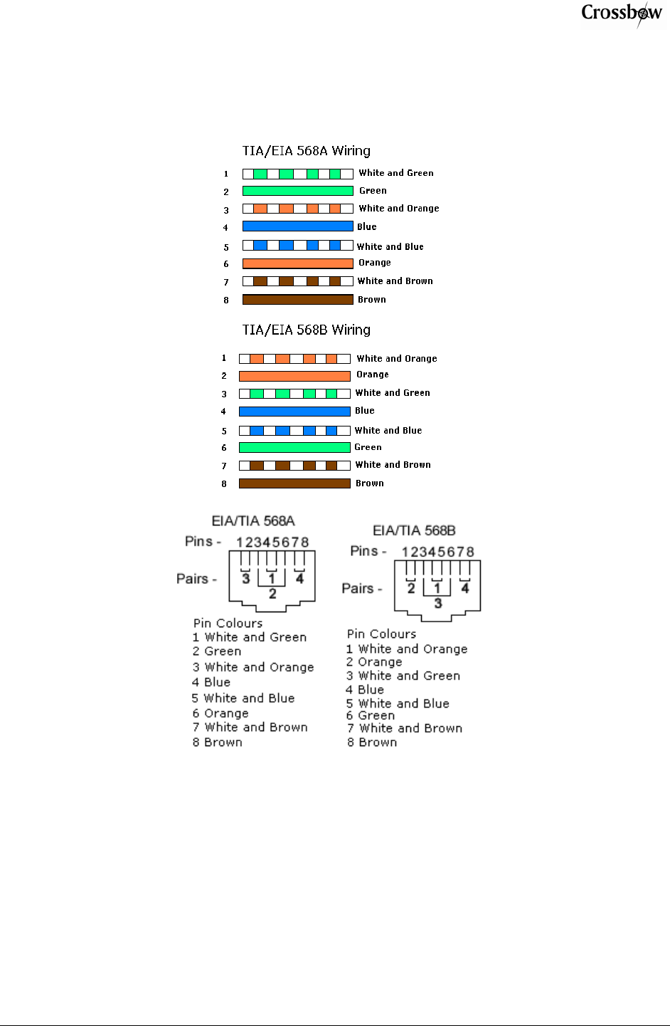
MPR/MIB User’s Manual
Doc. # 7430-0021-07 Rev. B Page 51
17 Appendix A: 10/100 Base-T Cabling tandards
Category 5(e) (UTP) color coding table

MPR/MIB User’s Manual
Page 52 Doc. # 7430-0021-07 Rev. B
18 Appendix B. Warranty and Support Information
18.1 Customer Service
As a Crossbow Technology customer you have access to product support services, which
include:
• Single-point return service
• Web-based support service
• Same day troubleshooting assistance
• Worldwide Crossbow representation
• Onsite and factory training available
• Preventative maintenance and repair programs
• Installation assistance available
18.2 Contact Directory
United States: Phone: 1-408-965-3300 (8 AM to 5 PM PST)
Fax: 1-408-324-4840 (24 hours)
Email: techsupport@xbow.com
Non-U.S.: refer to website www.xbow.com
18.3 Return Procedure
18.3.1 Authorization
Before returning any equipment, please contact Crossbow to obtain a Returned Material
Authorization number (RMA).
Be ready to provide the following information when requesting a RMA:
• Name
• Address
• Telephone, Fax, Email
• Equipment Model Number
• Equipment Serial Number
• Installation Date
• Failure Date
• Fault Description

MPR/MIB User’s Manual
Doc. # 7430-0021-07 Rev. B Page 53
18.3.2 Identification and Protection
If the equipment is to be shipped to Crossbow for service or repair, please attach a tag TO THE
EQUIPMENT, as well as the shipping container(s), identifying the owner. Also indicate the
service or repair required, the problems encountered and other information considered valuable
to the service facility such as the list of information provided to request the RMA number.
Place the equipment in the original shipping container(s), making sure there is adequate packing
around all sides of the equipment. If the original shipping containers were discarded, use heavy
boxes with adequate padding and protection.
18.3.3 Sealing the Container
Seal the shipping container(s) with heavy tape or metal bands strong enough to handle the weight
of the equipment and the container.
18.3.4 Marking
Please write the words, “FRAGILE, DELICATE INSTRUMENT” in several places on the
outside of the shipping container(s). In all correspondence, please refer to the equipment by the
model number, the serial number, and the RMA number.
18.3.5 Return Shipping Address
Use the following address for all returned products:
Crossbow Technology, Inc.
4145 N. First Street
San Jose, CA 95134
Attn: RMA Number (XXXXXX)
18.4 Warranty
The Crossbow product warranty is one year from date of shipment.

Crossbow Technology, Inc.
4145 N. First Street
San Jose, CA 95134
Phone: 408.965.3300
Fax: 408.324.4840