Cypress Semiconductor 2006 Bluetooth Module User Manual
Cypress Semiconductor Bluetooth Module
User Manual

Document Number: 002-15631 Rev.PRELIMINARY Page 2 of 38
PRELIMINARY
CYBLE-212006-01
CYBLE-202007-01
CYBLE-202013-11
More Information
Cypress provides a wealth of data at www.cypress.com to help you to select the right module for your design, and to help you to
quickly and effectively integrate the module into your design.
nOverview: EZ-BLE Module Portfolio, Module Roadmap
nEZ-BLE PRoC Product Overview
nPRoC BLE Silicon Datasheet
nApplication notes: Cypress offers a number of BLE application
notes covering a broad range of topics, from basic to advanced
level. Recommended application notes for getting started with
EZ-BLE modules are:
pAN96841 - Getting Started with EZ-BLE Module
pAN94020 - Getting Started with PRoC BLE
pAN97060 - PSoC® 4 BLE and PRoC™ BLE - Over-The-Air
(OTA) Device Firmware Upgrade (DFU) Guide
pAN91162 - Creating a BLE Custom Profile
pAN91184 - PSoC 4 BLE - Designing BLE Applications
pAN92584 - Designing for Low Power and Estimating Battery
Life for BLE Applications
pAN85951 - PSoC® 4 CapSense® Design Guide
pAN95089 - PSoC® 4/PRoC™ BLE Crystal Oscillator Selec-
tion and Tuning Techniques
pAN91445 - Antenna Design and RF Layout Guidelines
nKnowledge Base Articles
pKBA97095 - EZ-BLE™ Module Placement
nTechnical Reference Manual (TRM):
pPRoC® BLE Technical Reference Manual
nDevelopment Kits:
pCYBLE-212006-EVAL, CYBLE-212006-01 Evaluation Board
pCYBLE-202007-EVAL, CYBLE-202007-01 Evaluation Board
pCYBLE-202013-EVAL, CYBLE-202013-11 Evaluation Board
pCY8CKIT-042-BLE, Bluetooth® Low Energy (BLE) Pioneer
Kit
pCY8CKIT-002, PSoC® MiniProg3 Program and Debug Kit
nTest and Debug Tools:
pCYSmart, Bluetooth® LE Test and Debug Tool (Windows)
pCYSmart Mobile, Bluetooth® LE Test and Debug Tool
(Android/iOS Mobile App)
PSoC® Creator™ Integrated Design Environment (IDE)
PSoC Creator is an Integrated Design Environment (IDE) that enables concurrent hardware and firmware editing, compiling and
debugging of PSoC 3, PSoC 4, PSoC 5LP, PSoC 4 BLE, PRoC BLE and EZ-BLE module systems with no code size limitations. PSoC
peripherals are designed using schematic capture and simple graphical user interface (GUI) with over 120 pre-verified,
production-ready PSoC Components™.
PSoC Components are analog and digital “virtual chips,” represented by an icon that users can drag-and-drop into a design and
configure to suit a broad array of application requirements.
Bluetooth Low Energy Component
The Bluetooth Low Energy Component inside PSoC Creator provides a comprehensive GUI-based configuration window that lets you
quickly design BLE applications. The Component incorporates a Bluetooth Core Specification v4.1 compliant BLE protocol stack and
provides API functions to enable user applications to interface with the underlying Bluetooth Low Energy Sub-System (BLESS)
hardware via the stack.
Technical Support
nFrequently Asked Questions (FAQs): Learn more about our BLE ECO System.
nForum: See if your question is already answered by fellow developers on the PSoC 4 BLE and PRoC BLE forums.
nVisit our support page and create a technical support case or contact a local sales representatives. If you are in the United States,
you can talk to our technical support team by calling our toll-free number: +1-800-541-4736. Select option 2 at the prompt.

Document Number: 002-15631 Rev.PRELIMINARY Page 3 of 38
PRELIMINARY
CYBLE-212006-01
CYBLE-202007-01
CYBLE-202013-11
Contents
Overview............................................................................ 4
Module Description...................................................... 4
Pad Connection Interface ................................................ 6
Recommended Host PCB Layout ................................... 7
Power Supply Connections and Recommended External
Components.................................................................... 10
Connection Options................................................... 10
External Component Recommendation .................... 10
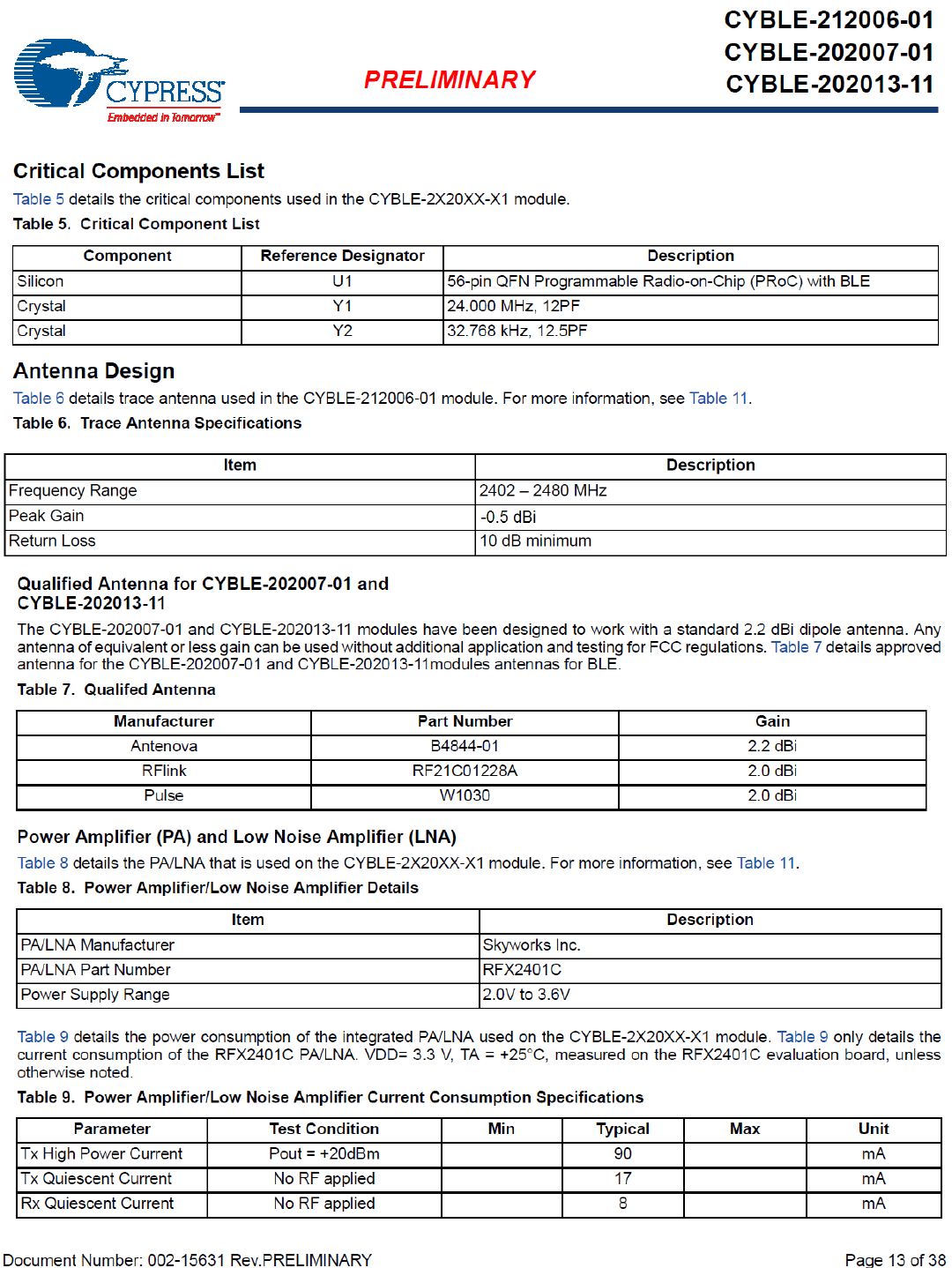
Critical Components List ........................................... 13
Antenna Design......................................................... 13
Qualified Antenna for CYBLE-202007-01 and CY .........
BLE-202013-11 ................................................................ 13
Power Amplifier (PA) and Low Noise Amplifier (LNA) 13
Electrical Specification .................................................. 14
GPIO ......................................................................... 16
XRES......................................................................... 17
Digital Peripherals ..................................................... 20
Serial Communication ............................................... 22
Memory ..................................................................... 23
System Resources .................................................... 23
Environmental Specifications ....................................... 29
Environmental Compliance ....................................... 29
RF Certification.......................................................... 29
Safety Certification .................................................... 29
Environmental Conditions ......................................... 29
ESD and EMI Protection ........................................... 29
Regulatory Information .................................................. 30
FCC........................................................................... 30
Industry Canada (IC) Certification ............................. 31
European R&TTE Declaration of Conformity ............ 31
MIC Japan................................................................. 32
KC Korea................................................................... 32
Packaging........................................................................ 33
Ordering Information...................................................... 35
Part Numbering Convention...................................... 35
Acronyms........................................................................ 36
Document Conventions ................................................. 36
Units of Measure ....................................................... 36
Document History Page ................................................. 37
Sales, Solutions, and Legal Information ...................... 38
Worldwide Sales and Design Support....................... 38
Products .................................................................... 38
PSoC® Solutions ...................................................... 38
Cypress Developer Community................................. 38
Technical Support ..................................................... 38
Document Number: 002-15631 Rev.PRELIMINARY Page 4 of 38
PRELIMINARY
CYBLE-212006-01
CYBLE-202007-01
CYBLE-202013-11
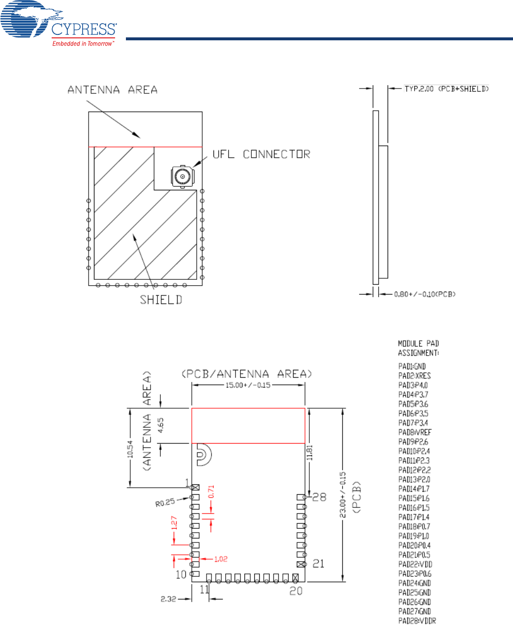
Overview
Module Description
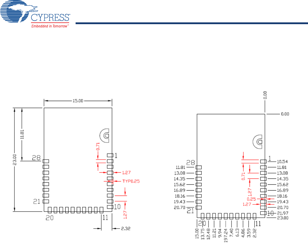
The CYBLE-2X20XX-X1 module is a complete module designed to be soldered to the applications main board.
Module Dimensions and Drawing
Cypress reserves the right to select components (including the appropriate BLE device) from various vendors to achieve the BLE
module functionality. Such selections will still guarantee that all height restrictions of the component area are maintained. Designs
should be held within the physical dimensions shown in the mechanical drawings in Figure 1. All dimensions are in millimeters (mm).
Table 1. Module Design Dimensions
See Figure 1 on page 5 for the mechanical reference drawing for CYBLE-2X20XX-X1.
Dimension Item Specification
Module dimensions Length (X) 15.00 ± 0.15 mm
Width (Y) 23.00 ± 0.15 mm
Antenna location dimensions Length (X) 15.00 ± 0.15 mm
Width (Y) 4.65 ± 0.15 mm
PCB thickness Height (H) 0.80 ± 0.10 mm
Shield height Height (H) 1.20 ± 0.10 mm
Maximum component height Height (H)
1.20 mm typical (shield) - CYBLE-212006-01
1.25 mm typical (connector) - CYBLE-202007-01
0.75mm typical (crystal) - CYBLE-202013-11
Total module thickness (bottom of module to highest component) Height (H)
2.00 mm typical - CYBLE-212006-01
2.05 mm typical - CYBLE-202007-01
1.55 mm typical - CYBLE-202013-11
Document Number: 002-15631 Rev.PRELIMINARY Page 5 of 38
PRELIMINARY
CYBLE-212006-01
CYBLE-202007-01
CYBLE-202013-11
Figure 1. Module Mechanical Drawing
Top View (View from Top)
Bottom View (Seen from Bottom)
Side View
Note
1. No metal should be located beneath or above the antenna area. Only bare PCB material should be located beneath the antenna area. For more information on
recommended host PCB layout, see Figure 3, Figure 4, Figure 5, and Figure 6 and Ta ble 3.
Document Number: 002-15631 Rev.PRELIMINARY Page 6 of 38
PRELIMINARY
CYBLE-212006-01
CYBLE-202007-01
CYBLE-202013-11
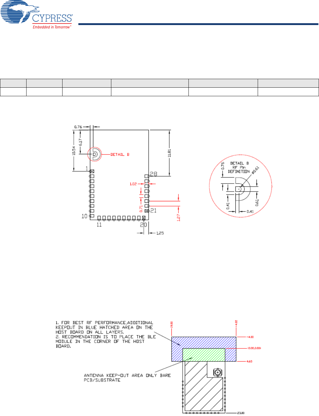
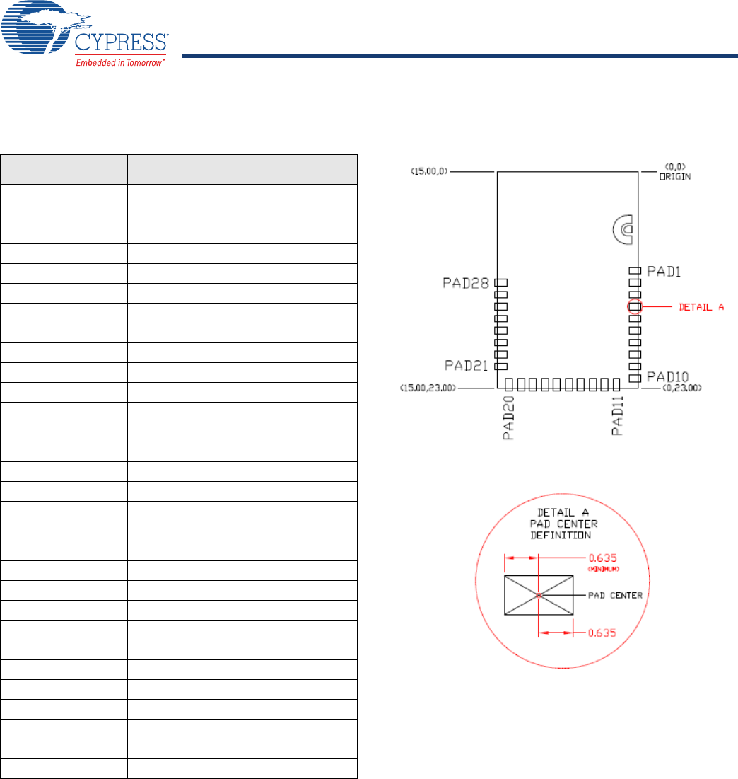
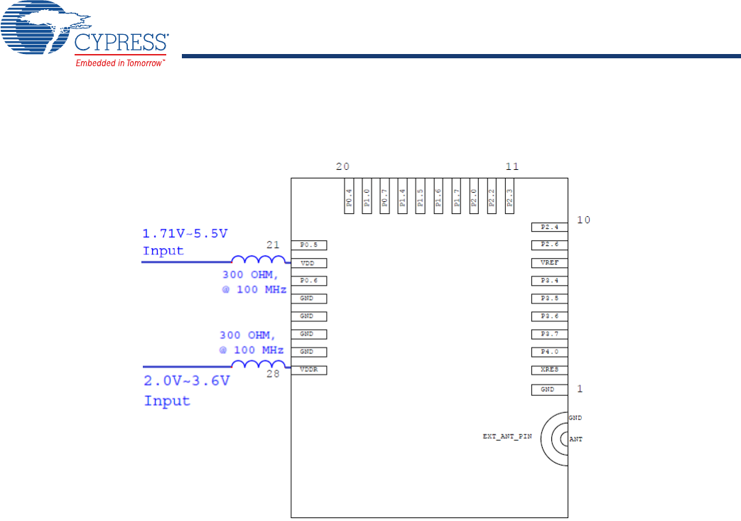
Pad Connection Interface
As shown in the bottom view of Figure 1 on page 5, the CYBLE-2X20XX-X1 connects to the host board via solder pads on the backside
of the module. Tab le 2 and Figure 2 detail the solder pad length, width, and pitch dimensions of the CYBLE-2X20XX-X1 module.
Figure 2. Solder Pad Dimensions (Seen from Bottom)
To maximize RF performance, the host layout should follow these recommendations:
1. The ideal placement of the Cypress BLE module is in a corner of the host board with the trace antenna located at the far corner.
This placement minimizes the additional recommended keep out area stated in item 2. Please refer to AN96841 for module
placement best practices.
2. To maximize RF performance, the area immediately around the Cypress BLE module trace antenna should contain an additional
keep out area, where no grounding or signal trace are contained. The keep out area applies to all layers of the host board. The
recommended dimensions of the host PCB keep out area are shown in Figure 3 (dimensions are in mm).
Figure 3. Recommended Host PCB Keep Out Area Around the CYBLE-2X20XX-X1 Antenna
Table 2. Solder Pad Connection Description
Name Connections Connection Type Pad Length Dimension Pad Width Dimension Pad Pitch
SP 30 Solder Pads 1.02 mm 0.71 mm 1.27 mm
Host PCB Keep Out Area Around Trace Antenna
Document Number: 002-15631 Rev.PRELIMINARY Page 7 of 38
PRELIMINARY
CYBLE-212006-01
CYBLE-202007-01
CYBLE-202013-11
Recommended Host PCB Layout
Figure 4, Figure 5, Figure 6, and Table 3 provide details that can be used for the recommended host PCB layout pattern for the
CYBLE-212006-01. Dimensions are in millimeters unless otherwise noted. Pad length of 1.27 mm (0.635 mm from center of the pad
on either side) shown in Figure 6 is the minimum recommended host pad length. The host PCB layout pattern can be completed using
either Figure 4, Figure 5, or Figure 6. It is not necessary to use all figures to complete the host PCB layout pattern.
Figure 4. Host Layout Pattern for CYBLE-2X20XX-X1 Figure 5. Module Pad Location from Origin
Top View (On Host PCB)
Top View (On Host PCB)
Document Number: 002-15631 Rev.PRELIMINARY Page 8 of 38
PRELIMINARY
CYBLE-212006-01
CYBLE-202007-01
CYBLE-202013-11
Table 3 provides the center location for each solder pad on the CYBLE-2X20XX-X1. All dimensions reference the to the center of the
solder pad. Refer to Figure 6 for the location of each module solder pad.
Table 3. Module Solder Pad Location Figure 6. Solder Pad Reference Location
Solder Pad
(Center of Pad)
Location (X,Y) from
Orign (mm)
Dimension from
Orign (mils)
1 (0.38, 10.54) (14.96, 414.96)
2 (0.38, 11.81) (14.96, 464.96)
3 (0.38, 13.08) (14.96, 514.96)
4 (0.38, 14.35) (14.96, 564.96)
5 (0.38, 15.62) (14.96, 614.96)
6 (0.38, 16.89) (14.96, 664.96)
7 (0.38, 18.16) (14.96, 714.96)
8 (0.38, 19.43) (14.96, 764.96)
9 (0.38, 20.70) (14.96, 814.96)
10 (0.38, 21.97) (14.96, 864.96)
11 (2.32, 22.62) (91.34, 890.55)
12 (3.59, 22.62) (141.34, 890.55)
13 (4.86, 22.62) (191.34, 890.55)
14 (6.13, 22.62) (241.34, 890.55)
15 (7.40, 22.62) (291.34, 890.55)
16 (8.67, 22.62) (341.34, 890.55)
17 (9.94, 22.62) (391.34,8 90.55)
18 (11.21, 22.62) (441.34, 890.55)
19 (12.48, 22.62) (491.34, 890.55)
20 (13.75, 22.62) (541.34, 890.55
21 (14.62, 20.70) (575.59, 814.96)
22 (14.62, 19.43) (575.59, 764.96)
23 (14.62, 18.16) (575.59, 714.96)
24 (14.62, 16.89) (575.59, 664.96)
25 (14.62, 15.62) (575.59, 614.96)
26 (14.62, 14.35) (575.59, 564.96)
27 (14.62, 13.08) (575.59, 514.96)
28 (14.62, 11.81) (575.59, 464.96)
29 See Figure 2 See Figure 2
30 See Figure 2 See Figure 2
Document Number: 002-15631 Rev.PRELIMINARY Page 9 of 38
PRELIMINARY
CYBLE-212006-01
CYBLE-202007-01
CYBLE-202013-11
Table 4 details the solder pad connection definitions and available functions for each connection pad. Ta ble 4 lists the solder pads on
CYBLE-2X20XX-X1, the BLE device port-pin, and denotes whether the function shown is available for each solder pad. Each
connection is configurable for a single option shown with a 3.
Table 4. Solder Pad Connection Definitions
Solder Pad
Number
Device
Port Pin UART SPI I2CTCPWM[2] Cap-
Sense
WCO
Out
ECO
Out LCD SWD GPIO
1 GND Ground Connection
2 XRES External Reset Hardware Connection Input
3P4.0
[3] 3(SCB1_RTS) 3(SCB1_MOSI) 3(TCPWM0_P) 3(CMOD)33
4P3.73(SCB1_CTS) 3(TCPWM3_N) 3(Sensor) 33 3
5P3.63(SCB1_RTS) 3(TCPWM3_P) 3(Sensor) 33
6P3.53(SCB1_TX) 3(SCB1_SCL) 3(TCPWM2_N) 3(Sensor) 33
7P3.43(SCB1_RX) 3(SCB1_SDA) 3(TCPWM2_P) 3(Sensor) 33
8 VREF Reference Voltage Input (Optional)
9P2.6 3(Sensor) 33
10 P2.4 3(Sensor) 33
11 P2.3 3(Sensor) 33 3
12 P2.2 3(SCB0_SS3) 3(Sensor) 33
13 P2.0 3(SCB0_SS1) 3(Sensor) 33
14 P1.7 3(SCB0_CTS) 3(SCB0_SCLK 3(TCPWM3_N) 3(Sensor) 33
15 P1.6 3(SCB0_RTS)3(SCB0_SS0) 3(TCPWM3_P) 3(Sensor) 33
16 P1.5 3(SCB0_TX) 3(SCB0_MISO) 3(SCB0_SCL) 3(TCPWM2_N) 3(Sensor) 33
17 P1.4 3(SCB0_RX) 3(SCB0_MOSI) 3(SCB0_SDA) 3(TCPWM2_P) 3(Sensor) 33
18 P0.7 3(SCB0_CTS) 3(SCB0_SCLK 3(TCPWM2_N) 3(Sensor) 33(SWDCLK) 3
19 P1.0 3(TCPWM0_P) 3(Sensor) 33
20 P0.4 3(SCB0_RX) 3(SCB0_MOSI) 3(SCB0_SDA) 3(TCPWM1_P) 3(Sensor) 33 3
21 P0.5 3(SCB0_TX) 3(SCB0_MISO) 3(SCB0_SCL) 3(TCPWM1_N) 3(Sensor) 33
22 VDD Digital Power Supply Input (1.8 to 5.5V)
23 P0.6 3(SCB0_RTS) 3(SCB0_SS0) 3(TCPWM2_P) 3(Sensor) 33(SWDIO) 3
24 GND[4] Ground Connection
25 GND Ground Connection
26 GND Ground Connection
27 GND Ground Connection
28 VDDR Radio Power Supply (2V to 3.6V)
29 ANT RF Pin to External Antenna
30 GND Ground Connection
Notes
2. TCPWM: Timer, Counter, and Pulse Width Modulator. If supported, the pad can be configured to any of these peripheral functions.
3. When using the capacitive sensing functionality, Pad 3 (P4.0) must be connected to a CMOD capacitor (located off of Cypress BLE Module). The value of this
capacitor is 2.2 nF and should be placed as close to the module as possible.
4. The main board needs to connect all GND connections (Pad 24/25/26/27) on the module to the common ground of the system.
5. If the I2S feature is used in the design, the I2S pins shall be dynamically routed to the appropriate available GPIO by PSoC Creator.
Document Number: 002-15631 Rev.PRELIMINARY Page 10 of 38
PRELIMINARY
CYBLE-212006-01
CYBLE-202007-01
CYBLE-202013-11
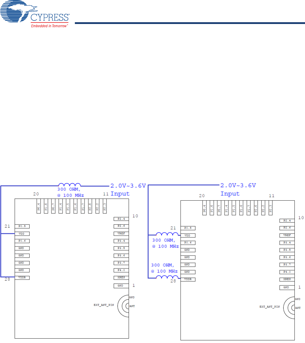
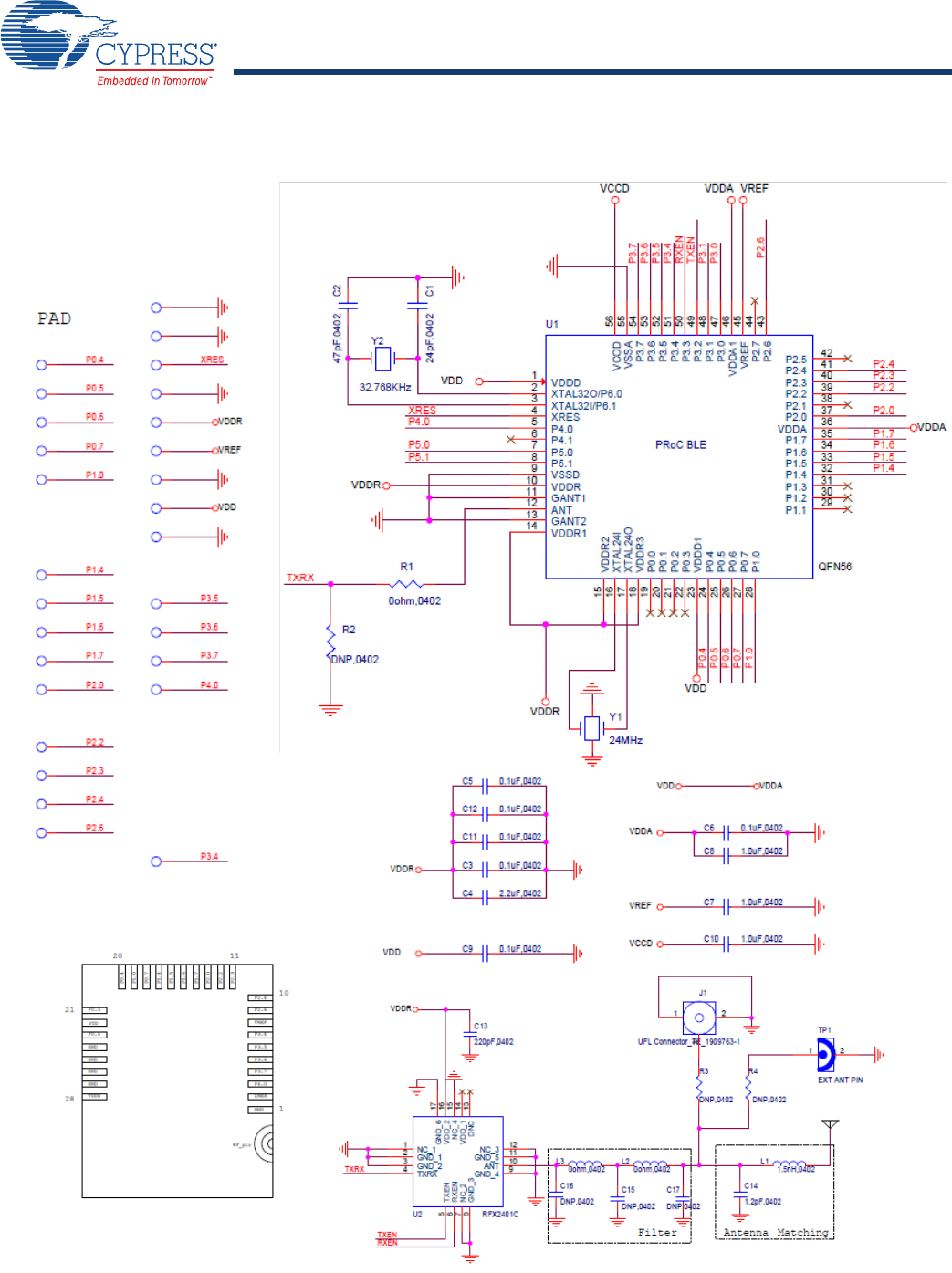
Power Supply Connections and Recommended External Components
Power Connections
The CYBLE-2X20XX-X1 contains two power supply connec-
tions, VDD and VDDR. The VDD connection supplies power for
both digital and analog device operation. The VDDR connection
supplies power for the device radio.
VDD accepts a supply range of 1.71 V to 5.5 V. VDDR accepts
a supply range of 2.0V to 3.6V. These specifications can be
found in Table 12 . The maximum power supply ripple for both
power connections on the module is 100 mV, as shown in
Table 10.
The power supply ramp rate of VDD must be equal to or greater
than that of VDDR.
Connection Options
Two connection options are available for any application:
1. Single supply: Connect VDD and VDDR to the same supply.
2. Independent supply: Power VDD and VDDR separately.
External Component Recommendation
In either connection scenario, it is recommended to place an
external ferrite bead between the supply and the module
connection. The ferrite bead should be positioned as close as
possible to the module pin connection.
Figure 7 details the recommended host schematic options for a
single supply scenario. The use of one or two ferrite beads will
depend on the specific application and configuration of the
CYBLE-2X20XX-X1.
Figure 8 details the recommended host schematic for an
independent supply scenario.
The recommended ferrite bead value is 330 Ω, 100 MHz. (Murata
BLM21PG331SN1D).
Figure 7. Recommended Host Schematic Options for a Single Supply Option
Two Ferrite Bead Option
Single Ferrite Bead Option
Document Number: 002-15631 Rev.PRELIMINARY Page 11 of 38
PRELIMINARY
CYBLE-212006-01
CYBLE-202007-01
CYBLE-202013-11
Figure 8. Recommended Host Schematic for an Independent Supply Option
Document Number: 002-15631 Rev.PRELIMINARY Page 14 of 38
PRELIMINARY
CYBLE-212006-01
CYBLE-202007-01
CYBLE-202013-11
Electrical Specification
Table 10 details the absolute maximum electrical characteristics for the Cypress BLE module.
Table 10. CYBLE-2X20XX-X1 Absolute Maximum Ratings
Table 11 details the RF characteristics for the Cypress BLE module.
Table 11. CYBLE-2X20XX-X1 RF Performance Characteristics
Table 12 through Table 51 list the module level electrical characteristics for the CYBLE-2X20XX-X1. All specifications are valid for
–40 °C ≤ TA ≤ 85 °C and TJ ≤ 100 °C, except where noted. Specifications are valid for 1.71 V to 5.5 V, except where noted.
Parameter Description Min Typ Max Units Details/Conditions
VDDD_ABS Analog, digital, or radio supply relative to VSS
(VSSD = VSSA)–0.5 – 6 V Absolute maximum
VCCD_ABS Direct digital core voltage input relative to VSSD –0.5 – 1.95 V Absolute maximum
VDD_RIPPLE Maximum power supply ripple for VDD and VDDR
input voltage – – 100 mV
3.0V supply
Ripple frequency of 100 kHz
to 750 kHz
VGPIO_ABS GPIO voltage –0.5 – VDD +0.5 V Absolute maximum
IGPIO_ABS Maximum current per GPIO –25 – 25 mA Absolute maximum
IGPIO_injection GPIO injection current: Maximum for VIH > VDD
and minimum for VIL < VSS –0.5 – 0.5 mA Absolute maximum current
injected per pin
LU Pin current for latch up –200 200 mA –
Parameter Description Min Typ Max Units Details/Conditions
RFO RF output power on ANT 1 7.5 dBm Configurable via register
settings (CYBLE-212006-01)
RXSRF receive sensitivity on ANT – –93 – dBm Measured value
(CYBLE-212006-01)
FRModule frequency range 2402 – 2480 MHz –
GPPeak gain – –0.5 – dBi –
RL Return loss – –10 – dB –
Table 12. CYBLE-2X20XX-X1 DC Specifications
Parameter Description Min Typ Max Units Details/Conditions
VDD1 Power supply input voltage 1.8 – 5.5 V With regulator enabled
VDD2 Power supply input voltage unregulated 1.71 1.8 1.89 V Internally unregulated
supply
VDDR1 Radio supply voltage (radio on) 2.0 – 3.6 V Restricted by RFX2401C
VDDR2 Radio supply voltage (radio off) 2.0 – 3.6 V –
Active Mode, VDD = 1.71 V to 5.5 V
IDD3 Execute from flash; CPU at 3 MHz – 1.7 – mA T = 25 °C,
VDD = 3.3 V
IDD4 Execute from flash; CPU at 3 MHz – – – mA T = –40 °C to 85 °C
IDD5 Execute from flash; CPU at 6 MHz – 2.5 – mA T = 25 °C,
VDD = 3.3 V
IDD6 Execute from flash; CPU at 6 MHz – – – mA T = –40 °C to 85 °C
IDD7 Execute from flash; CPU at 12 MHz – 4 – mA T = 25 °C,
VDD = 3.3 V
IDD8 Execute from flash; CPU at 12 MHz – – – mA T = –40 °C to 85 °C
Document Number: 002-15631 Rev.PRELIMINARY Page 15 of 38
PRELIMINARY
CYBLE-212006-01
CYBLE-202007-01
CYBLE-202013-11
IDD9 Execute from flash; CPU at 24 MHz – 7.1 – mA T = 25 °C,
VDD = 3.3 V
IDD10 Execute from flash; CPU at 24 MHz – – – mA T = –40 °C to 85 °C
IDD11 Execute from flash; CPU at 48 MHz – 13.4 – mA T = 25 °C,
VDD = 3.3 V
IDD12 Execute from flash; CPU at 48 MHz – – – mA T = –40 °C to 85 °C
Sleep Mode, VDD = 1.8 to 5.5 V
IDD13 IMO on – – – mA T = 25 °C, VDD = 3.3 V,
SYSCLK = 3 MHz
Sleep Mode, VDD and VDDR = 1.9 to 5.5 V
IDD14 ECO on – – – mA T = 25 °C, VDD = 3.3 V,
SYSCLK = 3 MHz
Deep-Sleep Mode, VDD = 1.8 to 3.6 V
IDD15 WDT with WCO on – 1.5 – μAT = 25 °C,
VDD = 3.3 V
IDD16 WDT with WCO on – – – μA T = –40 °C to 85 °C
IDD17 WDT with WCO on – – – μAT = 25 °C,
VDD = 5 V
IDD18 WDT with WCO on – – – μA T = –40 °C to 85 °C
Deep-Sleep Mode, VDD = 1.71 to 1.89 V (Regulator Bypassed)
IDD19 WDT with WCO on – – – μA T = 25 °C
IDD20 WDT with WCO on – – – μA T = –40 °C to 85 °C
Hibernate Mode, VDD = 1.8 to 3.6 V
IDD27 GPIO and reset active – 150 – nA T = 25 °C,
VDD = 3.3 V
IDD28 GPIO and reset active – – – nA T = –40 °C to 85 °C
Hibernate Mode, VDD = 3.6 to 5.5 V
IDD29 GPIO and reset active – – – nA T = 25 °C,
VDD = 5 V
IDD30 GPIO and reset active – – – nA T = –40 °C to 85 °C
Stop Mode, VDD = 1.8 to 3.6 V
IDD33 Stop-mode current (VDD)–20–nA
T = 25 °C,
VDD = 3.3 V
IDD34 Stop-mode current (VDDR)–40–- nA
T = 25 °C,
VDDR = 3.3 V
IDD35 Stop-mode current (VDD) – – – nA T = –40 °C to 85 °C
IDD36 Stop-mode current (VDDR)–––nA
T = –40 °C to 85 °C,
VDDR = 1.9 V to 3.6 V
Stop Mode, VDD = 3.6 to 5.5 V
IDD37 Stop-mode current (VDD)–––nA
T = 25 °C,
VDD = 5 V
IDD38 Stop-mode current (VDDR)–––nA
T = 25 °C,
VDDR = 5 V
IDD39 Stop-mode current (VDD) – – – nA T = –40 °C to 85 °C
IDD40 Stop-mode current (VDDR) – – – nA T = –40 °C to 85 °C
Table 12. CYBLE-2X20XX-X1 DC Specifications (continued)
Parameter Description Min Typ Max Units Details/Conditions
Document Number: 002-15631 Rev.PRELIMINARY Page 16 of 38
PRELIMINARY
CYBLE-212006-01
CYBLE-202007-01
CYBLE-202013-11
Table 13. AC Specifications
GPIO
Parameter Description Min Typ Max Units Details/Conditions
FCPU CPU frequency DC – 48 MHz 1.71 V ≤ VDD ≤ 5.5 V
TSLEEP Wakeup from Sleep mode – 0 – μs Guaranteed by characterization
TDEEPSLEEP Wakeup from Deep-Sleep mode – – 25 μs24-MHz IMO. Guaranteed by
characterization
THIBERNATE Wakeup from Hibernate mode – – 2 ms Guaranteed by characterization
TSTOP Wakeup from Stop mode – – 2 ms XRES wakeup
Table 14. GPIO DC Specifications
Parameter Description Min Typ Max Units Details/Conditions
VIH[6]
Input voltage HIGH threshold 0.7 × VDD – – V CMOS input
LVTTL input, VDD < 2.7 V 0.7 × VDD – – V –
LVTTL input, VDD ≥ 2.7 V 2.0 – – V –
VIL
Input voltage LOW threshold – – 0.3 × VDD VCMOS input
LVTTL input, VDD < 2.7 V – – 0.3 × VDD V–
LVTTL input, VDD ≥ 2.7 V – – 0.8 V –
VOH
Output voltage HIGH level VDD –0.6 – – V IOH = 4 mA at 3.3-V VDD
Output voltage HIGH level VDD –0.5 – – V IOH = 1 mA at 1.8-V VDD
VOL
Output voltage LOW level – – 0.6 V IOL = 8 mA at 3.3-V VDD
Output voltage LOW level – – 0.6 V IOL = 4 mA at 1.8-V VDD
Output voltage LOW level – – 0.4 V IOL = 3 mA at 3.3-V VDD
RPULLUP Pull-up resistor 3.5 5.6 8.5 kΩ–
RPULLDOWN Pull-down resistor 3.5 5.6 8.5 kΩ–
IIL Input leakage current (absolute value) – – 2 nA 25 °C, VDD = 3.3 V
IIL_CTBM Input leakage on CTBm input pins – – 4 nA –
CIN Input capacitance – – 7 pF –
VHYSTTL Input hysteresis LVTTL 25 40 – mV VDD > 2.7 V
VHYSCMOS Input hysteresis CMOS 0.05 × VDD – – 1 –
IDIODE Current through protection diode to
VDD/VSS – – 100 μA–
ITOT_GPIO Maximum total source or sink chip
current – – 200 mA –
Note
6. VIH must not exceed VDD + 0.2 V.
Document Number: 002-15631 Rev.PRELIMINARY Page 17 of 38
PRELIMINARY
CYBLE-212006-01
CYBLE-202007-01
CYBLE-202013-11
Table 15. GPIO AC Specifications
XRES
Parameter Description Min Typ Max Units Details/Conditions
TRISEF Rise time in Fast-Strong mode 2 – 12 ns 3.3-V VDDD, CLOAD = 25 pF
TFALLF Fall time in Fast-Strong mode 2 – 12 ns 3.3-V VDDD, CLOAD = 25 pF
TRISES Rise time in Slow-Strong mode 10 – 60 ns 3.3-V VDDD, CLOAD = 25 pF
TFALLS Fall time in Slow-Strong mode 10 – 60 ns 3.3-V VDDD, CLOAD = 25 pF
FGPIOUT1 GPIO Fout; 3.3 V ≤ VDD ≤ 5.5 V
Fast-Strong mode ––33MHz
90/10%, 25 pF load, 60/40 duty
cycle
FGPIOUT2 GPIO Fout; 1.7 V≤ VDD ≤ 3.3 V
Fast-Strong mode – – 16.7 MHz 90/10%, 25 pF load, 60/40 duty
cycle
FGPIOUT3 GPIO Fout; 3.3 V ≤ VDD ≤ 5.5 V
Slow-Strong mode –– 7 MHz
90/10%, 25 pF load, 60/40 duty
cycle
FGPIOUT4 GPIO Fout; 1.7 V ≤ VDD ≤ 3.3 V
Slow-Strong mode ––3.5MHz
90/10%, 25 pF load, 60/40 duty
cycle
FGPIOIN GPIO input operating frequency
1.71 V ≤ VDD ≤ 5.5 V – – 48 MHz 90/10% VIO
Table 16. OVT GPIO DC Specifications (P5_0 and P5_1 Only)
Parameter Description Min Typ Max Units Details/Conditions
IIL Input leakage (absolute value).
VIH > VDD ––10 μA 25°C, VDD = 0 V, VIH = 3.0 V
VOL Output voltage LOW level – – 0.4 V IOL = 20 mA, VDD > 2.9 V
Table 17. OVT GPIO AC Specifications (P5_0 and P5_1 Only)
Parameter Description Min Typ Max Units Details/Conditions
TRISE_OVFS Output rise time in Fast-Strong mode 1.5 – 12 ns 25-pF load, 10%–90%, VDD = 3.3 V
TFALL_OVFS Output fall time in Fast-Strong mode 1.5 – 12 ns 25-pF load, 10%–90%, VDD = 3.3 V
TRISESS Output rise time in Slow-Strong mode 10 – 60 ns 25 pF load, 10%-90%,
VDD = 3.3 V
TFALLSS Output fall time in Slow-Strong mode 10 – 60 ns 25 pF load, 10%-90%,
VDD = 3.3 V
FGPIOUT1 GPIO FOUT
; 3.3 V ≤ VDD ≤ 5.5 V
Fast-Strong mode ––24MHz
90/10%, 25 pF load, 60/40 duty
cycle
FGPIOUT2 GPIO FOUT
; 1.71 V ≤ VDD ≤ 3.3 V
Fast-Strong mode ––16MHz
90/10%, 25 pF load, 60/40 duty
cycle
Table 18. XRES DC Specifications
Parameter Description Min Typ Max Units Details/Conditions
VIH Input voltage HIGH threshold 0.7 × VDDD – – V CMOS input
VIL Input voltage LOW threshold – – 0.3 × VDDD V CMOS input
RPULLUP Pull-up resistor 3.5 5.6 8.5 kΩ–
CIN Input capacitance – 3 – pF –
VHYSXRES Input voltage hysteresis – 100 – mV –
IDIODE Current through protection diode to
VDD/VSS – – 100 μA–
Document Number: 002-15631 Rev.PRELIMINARY Page 18 of 38
PRELIMINARY
CYBLE-212006-01
CYBLE-202007-01
CYBLE-202013-11
Temperature Sensor
SAR ADC
Table 19. XRES AC Specifications
Parameter Description Min Typ Max Units Details/Conditions
TRESETWIDTH Reset pulse width 1 – – μs–
Table 20. Temperature Sensor Specifications
Parameter Description Min Typ Max Units Details/Conditions
TSENSACC Temperature-sensor accuracy –5 ±1 5 °C –40 °C to +85 °C
Table 21. SAR ADC DC Specifications
Parameter Description Min Typ Max Units Details/Conditions
A_RES Resolution – – 12 bits
A_CHNIS_S Number of channels - single-ended – – 8 8 full-speed
A-CHNKS_D Number of channels - differential – – 4 Diff inputs use
neighboring I/O
A-MONO Monotonicity – – – Yes
A_GAINERR Gain error – – ±0.1 % With external
reference
A_OFFSET Input offset voltage – – 2 mV Measured with 1-V
VREF
A_ISAR Current consumption – – 1 mA
A_VINS Input voltage range - single-ended VSS –V
DDA V
A_VIND Input voltage range - differential VSS – VDDA V
A_INRES Input resistance – – 2.2 kΩ
A_INCAP Input capacitance – – 10 pF
VREFSAR Trimmed internal reference to SAR –1 – 1 % Percentage of Vbg
(1.024 V)
Table 22. SAR ADC AC Specifications
Parameter Description Min Typ Max Units Details/Conditions
A_PSRR Power-supply rejection ratio 70 – – dB Measured at 1-V
reference
A_CMRR Common-mode rejection ratio 66 – – dB
A_SAMP Sample rate – – 1 Msps
Fsarintref SAR operating speed without external ref.
bypass – – 100 Ksps 12-bit resolution
A_SNR Signal-to-noise ratio (SNR) 65 – – dB FIN = 10 kHz
A_BW Input bandwidth without aliasing – – A_SAMP/2 kHz
A_INL Integral nonlinearity. VDD = 1.71 V to 5.5 V,
1 Msps –1.7 – 2 LSB VREF = 1 V to VDD
A_INL Integral nonlinearity. VDDD = 1.71 V to 3.6 V,
1 Msps –1.5 – 1.7 LSB VREF = 1.71 V to VDD
A_INL Integral nonlinearity. VDD = 1.71 V to 5.5 V,
500 Ksps –1.5 – 1.7 LSB VREF = 1 V to VDD
A_dnl Differential nonlinearity. VDD = 1.71 V to
5.5 V, 1 Msps –1 – 2.2 LSB VREF = 1 V to VDD
Document Number: 002-15631 Rev.PRELIMINARY Page 19 of 38
PRELIMINARY
CYBLE-212006-01
CYBLE-202007-01
CYBLE-202013-11
CSD
A_DNL Differential nonlinearity. VDD = 1.71 V to
3.6 V, 1 Msps –1 – 2 LSB VREF = 1.71 V to VDD
A_DNL Differential nonlinearity. VDD = 1.71 V to
5.5 V, 500 Ksps –1 – 2.2 LSB VREF = 1 V to VDD
A_THD Total harmonic distortion – – –65 dB FIN = 10 kHz
Table 22. SAR ADC AC Specifications (continued)
Parameter Description Min Typ Max Units Details/Conditions
CSD Block Specifications
Parameter Description Min Typ Max Units Details/Conditions
VCSD Voltage range of operation 1.71 – 5.5 V –
IDAC1 DNL for 8-bit resolution –1 – 1 LSB –
IDAC1 INL for 8-bit resolution –3 – 3 LSB –
IDAC2 DNL for 7-bit resolution –1 – 1 LSB –
IDAC2 INL for 7-bit resolution –3 – 3 LSB –
SNR Ratio of counts of finger to noise 5 – – Ratio
Capacitance range of
9 pF to 35 pF, 0.1-pF
sensitivity. Radio is not
operating during the
scan
IDAC1_CRT1 Output current of IDAC1 (8 bits) in High
range –612 – μA–
IDAC1_CRT2 Output current of IDAC1 (8 bits) in Low
range –306 – μA–
IDAC2_CRT1 Output current of IDAC2 (7 bits) in High
range –305 – μA–
IDAC2_CRT2 Output current of IDAC2 (7 bits) in Low
range –153 – μA–
Document Number: 002-15631 Rev.PRELIMINARY Page 20 of 38
PRELIMINARY
CYBLE-212006-01
CYBLE-202007-01
CYBLE-202013-11
Digital Peripherals
Timer
Counter
Table 23. Timer DC Specifications
Parameter Description Min Typ Max Units Details/Conditions
ITIM1 Block current consumption at 3 MHz – – 42 μA 16-bit timer
ITIM2 Block current consumption at 12 MHz – – 130 μA 16-bit timer
ITIM3 Block current consumption at 48 MHz – – 535 μA 16-bit timer
Table 24. Timer AC Specifications
Parameter Description Min Typ Max Units Details/Conditions
TTIMFREQ Operating frequency FCLK –48MHz
TCAPWINT Capture pulse width (internal) 2 × TCLK ––ns
TCAPWEXT Capture pulse width (external) 2 × TCLK ––ns
TTIMRES Timer resolution TCLK ––ns
TTENWIDINT Enable pulse width (internal) 2 × TCLK ––ns
TTENWIDEXT Enable pulse width (external) 2 × TCLK ––ns
TTIMRESWINT Reset pulse width (internal) 2 × TCLK ––ns
TTIMRESEXT Reset pulse width (external) 2 × TCLK ––ns
Table 25. Counter DC Specifications
Parameter Description Min Typ Max Units Details/Conditions
ICTR1 Block current consumption at 3 MHz – – 42 μA 16-bit counter
ICTR2 Block current consumption at 12 MHz – – 130 μA 16-bit counter
ICTR3 Block current consumption at 48 MHz – – 535 μA 16-bit counter
Table 26. Counter AC Specifications
Parameter Description Min Typ Max Units Details/Conditions
TCTRFREQ Operating frequency FCLK –48MHz –
TCTRPWINT Capture pulse width (internal) 2 × TCLK ––ns –
TCTRPWEXT Capture pulse width (external) 2 × TCLK ––ns –
TCTRES Counter Resolution TCLK ––ns –
TCENWIDINT Enable pulse width (internal) 2 × TCLK ––ns –
TCENWIDEXT Enable pulse width (external) 2 × TCLK ––ns –
TCTRRESWINT Reset pulse width (internal) 2 × TCLK ––ns –
TCTRRESWEXT Reset pulse width (external) 2 × TCLK –– ns –
Document Number: 002-15631 Rev.PRELIMINARY Page 21 of 38
PRELIMINARY
CYBLE-212006-01
CYBLE-202007-01
CYBLE-202013-11
Pulse Width Modulation (PWM)
LCD Direct Drive
Table 27. PWM DC Specifications
Parameter Description Min Typ Max Units Details/Conditions
IPWM1 Block current consumption at 3 MHz – – 42 μA 16-bit PWM
IPWM2 Block current consumption at 12 MHz – – 130 μA 16-bit PWM
IPWM3 Block current consumption at 48 MHz – – 535 μA 16-bit PWM
Table 28. PWM AC Specifications
Parameter Description Min Typ Max Units Details/Conditions
TPWMFREQ Operating frequency FCLK –48MHz –
TPWMPWINT Pulse width (internal) 2 × TCLK ––ns –
TPWMEXT Pulse width (external) 2 × TCLK ––ns –
TPWMKILLINT Kill pulse width (internal) 2 × TCLK ––ns –
TPWMKILLEXT Kill pulse width (external) 2 × TCLK ––ns –
TPWMEINT Enable pulse width (internal) 2 × TCLK ––ns –
TPWMENEXT Enable pulse width (external) 2 × TCLK ––ns –
TPWMRESWINT Reset pulse width (internal) 2 × TCLK ––ns –
TPWMRESWEXT Reset pulse width (external) 2 × TCLK ––ns –
Table 29. LCD Direct Drive DC Specifications
Parameter Description Min Typ Max Units Details/Conditions
ILCDLOW Operating current in low-power mode – 17.5 – μA16 × 4 small segment
display at 50 Hz
CLCDCAP LCD capacitance per segment/common
driver – 500 5000 pF –
LCDOFFSET Long-term segment offset – 20 – mV –
ILCDOP1 LCD system operating current, VBIAS = 5 V – 2 – mA 3 2 × 4 se gm en ts . 5 0 H z a t
25 °C
ILCDOP2 LCD system operating current, VBIAS = 3.3 V – 2 – mA 32 × 4 segments
50 Hz at 25 °C
Table 30. LCD Direct Drive AC Specifications
Parameter Description Min Typ Max Units Details/Conditions
FLCD LCD frame rate 10 50 150 Hz –
Document Number: 002-15631 Rev.PRELIMINARY Page 22 of 38
PRELIMINARY
CYBLE-212006-01
CYBLE-202007-01
CYBLE-202013-11
Serial Communication
Table 31. Fixed I2C DC Specifications
Table 33. Fixed UART DC Specifications
Table 34. Fixed UART AC Specifications
Parameter Description Min Typ Max Units Details/Conditions
II2C1 Block current consumption at 100 kHz – – 50 μA–
II2C2 Block current consumption at 400 kHz – – 155 μA–
II2C3 Block current consumption at 1 Mbps – – 390 μA–
II2C4 I2C enabled in Deep-Sleep mode – – 1.4 μA–
Table 32. Fixed I2C AC Specifications
Parameter Description Min Typ Max Units Details/Conditions
FI2C1 Bit rate – – 400 kHz
Parameter Description Min Typ Max Units Details/Conditions
IUART1 Block current consumption at 100 kbps – – 55 μA–
IUART2 Block current consumption at 1000 kbps – – 312 μA–
Parameter Description Min Typ Max Units Details/Conditions
FUART Bit rate – – 1 Mbps –
Table 35. Fixed SPI DC Specifications
Parameter Description Min Typ Max Units Details/Conditions
ISPI1 Block current consumption at 1 Mbps – – 360 μA–
ISPI2 Block current consumption at 4 Mbps – – 560 μA–
ISPI3 Block current consumption at 8 Mbps – – 600 μA–
Table 36. Fixed SPI AC Specifications
Parameter Description Min Typ Max Units Details/Conditions
FSPI SPI operating frequency (master; 6x over sampling) – – 8 MHz –
Table 37. Fixed SPI Master Mode AC Specifications
Parameter Description Min Typ Max Units Details/Conditions
TDMO MOSI valid after SCLK driving edge – – 18 ns –
TDSI MISO valid before SCLK capturing edge
Full clock, late MISO sampling used 20 – – ns Full clock, late MISO sampling
THMO Previous MOSI data hold time 0 – – ns Referred to Slave capturing edge
Table 38. Fixed SPI Slave Mode AC Specifications
Parameter Description Min Typ Max Units
TDMI MOSI valid before SCLK capturing edge 40 – – ns
TDSO MISO valid after SCLK driving edge – – 42 + 3 × TCPU ns
TDSO_ext MISO Valid after SCLK driving edge in
external clock mode. VDD < 3.0 V – – 50 ns
THSO Previous MISO data hold time 0 – – ns
TSSELSCK SSEL valid to first SCK valid edge 100 – – ns
Document Number: 002-15631 Rev.PRELIMINARY Page 23 of 38
PRELIMINARY
CYBLE-212006-01
CYBLE-202007-01
CYBLE-202013-11
Memory
System Resources
Power-on-Reset (POR)
Table 39. Flash DC Specifications
Parameter Description Min Typ Max Units Details/Conditions
VPE Erase and program voltage 1.71 – 5.5 V –
TWS48 Number of Wait states at 32–48 MHz 2 – – CPU execution from flash
TWS32 Number of Wait states at 16–32 MHz 1 – – CPU execution from flash
TWS16 Number of Wait states for 0–16 MHz 0 – – CPU execution from flash
Table 40. Flash AC Specifications
Parameter Description Min Typ Max Units Details/Conditions
TROWWRITE[7] Row (block) write time (erase and program) – – 20 ms Row (block) = 256 bytes
TROWERASE[7] Row erase time – – 13 ms –
TROWPROGRAM[7] Row program time after erase – – 7 ms –
TBULKERASE[7] Bulk erase time (256 KB) – – 35 ms –
TDEVPROG[7] Total device program time – – 25 seconds –
FEND Flash endurance 100 K – – cycles –
FRET Flash retention. TA ≤ 55 °C, 100 K P/E cycles 20 – – years –
FRET2 Flash retention. TA ≤ 85 °C, 10 K P/E cycles 10 – – years –
Note
7. It can take as much as 20 ms to write to flash. During this time, the device should not be reset, or flash operations will be interrupted and cannot be relied on to have
completed. Reset sources include the XRES pin, software resets, CPU lockup states and privilege violations, improper power supply levels, and watchdogs. Make
certain that these are not inadvertently activated.
Table 41. POR DC Specifications
Parameter Description Min Typ Max Units Details/Conditions
VRISEIPOR Rising trip voltage 0.80 – 1.45 V –
VFALLIPOR Falling trip voltage 0.75 – 1.40 V –
VIPORHYST Hysteresis 15 – 200 mV –
Table 42. POR AC Specifications
Parameter Description Min Typ Max Units Details/Conditions
TPPOR_TR Precision power-on reset (PPOR) response
time in Active and Sleep modes ––1
μs–
Table 43. Brown-Out Detect
Parameter Description Min Typ Max Units Details/Conditions
VFALLPPOR BOD trip voltage in Active and Sleep modes 1.64 – – V –
VFALLDPSLP BOD trip voltage in Deep Sleep 1.4 – – V –
Table 44. Hibernate Reset
Parameter Description Min Typ Max Units Details/Conditions
VHBRTRIP BOD trip voltage in Hibernate 1.1 – – V –
Document Number: 002-15631 Rev.PRELIMINARY Page 24 of 38
PRELIMINARY
CYBLE-212006-01
CYBLE-202007-01
CYBLE-202013-11
Voltage Monitors (LVD)
SWD Interface
Table 45. Voltage Monitor DC Specifications
Parameter Description Min Typ Max Units Details/Conditions
VLVI1 LVI_A/D_SEL[3:0] = 0000b 1.71 1.75 1.79 V –
VLVI2 LVI_A/D_SEL[3:0] = 0001b 1.76 1.80 1.85 V –
VLVI3 LVI_A/D_SEL[3:0] = 0010b 1.85 1.90 1.95 V –
VLVI4 LVI_A/D_SEL[3:0] = 0011b 1.95 2.00 2.05 V –
VLVI5 LVI_A/D_SEL[3:0] = 0100b 2.05 2.10 2.15 V –
VLVI6 LVI_A/D_SEL[3:0] = 0101b 2.15 2.20 2.26 V –
VLVI7 LVI_A/D_SEL[3:0] = 0110b 2.24 2.30 2.36 V –
VLVI8 LVI_A/D_SEL[3:0] = 0111b 2.34 2.40 2.46 V –
VLVI9 LVI_A/D_SEL[3:0] = 1000b 2.44 2.50 2.56 V –
VLVI10 LVI_A/D_SEL[3:0] = 1001b 2.54 2.60 2.67 V –
VLVI11 LVI_A/D_SEL[3:0] = 1010b 2.63 2.70 2.77 V –
VLVI12 LVI_A/D_SEL[3:0] = 1011b 2.73 2.80 2.87 V –
VLVI13 LVI_A/D_SEL[3:0] = 1100b 2.83 2.90 2.97 V –
VLVI14 LVI_A/D_SEL[3:0] = 1101b 2.93 3.00 3.08 V –
VLVI15 LVI_A/D_SEL[3:0] = 1110b 3.12 3.20 3.28 V –
VLVI16 LVI_A/D_SEL[3:0] = 1111b 4.39 4.50 4.61 V –
LVI_IDD Block current – – 100 μA–
Table 46. Voltage Monitor AC Specifications
Parameter Description Min Typ Max Units Details/Conditions
TMONTRIP Voltage monitor trip time – – 1 μs–
Table 47. SWD Interface Specifications
Parameter Description Min Typ Max Units Details/Conditions
F_SWDCLK1 3.3 V ≤ VDD ≤ 5.5 V – – 14 MHz SWDCLK ≤ 1/3 CPU clock frequency
F_SWDCLK2 1.71 V ≤ VDD ≤ 3.3 V – – 7 MHz SWDCLK ≤ 1/3 CPU clock frequency
T_SWDI_SETUP T = 1/f SWDCLK 0.25 × T – – ns –
T_SWDI_HOLD T = 1/f SWDCLK 0.25 × T – – ns –
T_SWDO_VALID T = 1/f SWDCLK – – 0.5 × T ns –
T_SWDO_HOLD T = 1/f SWDCLK 1 – – ns –
Document Number: 002-15631 Rev.PRELIMINARY Page 25 of 38
PRELIMINARY
CYBLE-212006-01
CYBLE-202007-01
CYBLE-202013-11
Internal Main Oscillator
Internal Low-Speed Oscillator
Table 52. ECO Trim Value Specification
BLE Subsystem
Table 48. IMO DC Specifications
Parameter Description Min Typ Max Units Details/Conditions
IIMO1 IMO operating current at 48 MHz – – 1000 μA–
IIMO2 IMO operating current at 24 MHz – – 325 μA–
IIMO3 IMO operating current at 12 MHz – – 225 μA–
IIMO4 IMO operating current at 6 MHz – – 180 μA–
IIMO5 IMO operating current at 3 MHz – – 150 μA–
Table 49. IMO AC Specifications
Parameter Description Min Typ Max Units Details/Conditions
FIMOTOL3 Frequency variation from 3 to 48 MHz – – ±2 % With API-called calibration
FIMOTOL3 IMO startup time – 12 – μs–
Table 50. ILO DC Specifications
Parameter Description Min Typ Max Units Details/Conditions
IILO2 ILO operating current at 32 kHz – 0.3 1.05 μA–
Table 51. ILO AC Specifications
Parameter Description Min Typ Max Units Details/Conditions
TSTARTILO1 ILO startup time – – 2 ms –
FILOTRIM1 32-kHz trimmed frequency 15 32 50 kHz –
Parameter Description Value Details/Conditions
ECOTRIM 24-MHz trim value
(firmware configuration) 0x00007FDC Optimum trim value that needs to be loaded to register
CY_SYS_XTAL_BLERD_BB_XO_CAPTRIM_REG
Table 53. BLE Subsystem
Parameter Description Min Typ Max Units Details/Conditions
RF Receiver Specification
RXS, IDLE RX sensitivity with idle transmitter – –89 – dBm –
RX sensitivity with idle transmitter
excluding Balun loss – –91 – dBm Guaranteed by design
simulation
RXS, DIRTY RX sensitivity with dirty transmitter – –87 –70 dBm RF-PHY Specification
(RCV-LE/CA/01/C)
RXS, HIGHGAIN RX sensitivity in high-gain mode with idle
transmitter – –91 – dBm –
PRXMAX Maximum input power –10 –1 – dBm RF-PHY Specification
(RCV-LE/CA/06/C)
CI1
Cochannel interference,
Wanted signal at –67 dBm and Interferer
at FRX
– 9 21 dB RF-PHY Specification
(RCV-LE/CA/03/C)

Document Number: 002-15631 Rev.PRELIMINARY Page 26 of 38
PRELIMINARY
CYBLE-212006-01
CYBLE-202007-01
CYBLE-202013-11
CI2
Adjacent channel interference
Wanted signal at –67 dBm and Interferer
at FRX ±1 MHz
– 3 15 dB RF-PHY Specification
(RCV-LE/CA/03/C)
CI3
Adjacent channel interference
Wanted signal at –67 dBm and Interferer
at FRX ±2 MHz
– –29 – dB RF-PHY Specification
(RCV-LE/CA/03/C)
CI4
Adjacent channel interference
Wanted signal at –67 dBm and Interferer
at ≥FRX ±3 MHz
– –39 – dB RF-PHY Specification
(RCV-LE/CA/03/C)
CI5
Adjacent channel interference
Wanted Signal at –67 dBm and Interferer
at Image frequency (FIMAGE)
– –20 – dB RF-PHY Specification
(RCV-LE/CA/03/C)
CI3
Adjacent channel interference
Wanted signal at –67 dBm and Interferer
at Image frequency (FIMAGE ± 1 MHz)
– –30 – dB RF-PHY Specification
(RCV-LE/CA/03/C)
OBB1
Out-of-band blocking,
Wanted signal at –67 dBm and Interferer
at F = 30–2000 MHz
–30 –27 – dBm RF-PHY Specification
(RCV-LE/CA/04/C)
OBB2
Out-of-band blocking,
Wanted signal at –67 dBm and Interferer
at F = 2003–2399 MHz
–35 –27 – dBm RF-PHY Specification
(RCV-LE/CA/04/C)
OBB3
Out-of-band blocking,
Wanted signal at –67 dBm and Interferer
at F = 2484–2997 MHz
–35 –27 – dBm RF-PHY Specification
(RCV-LE/CA/04/C)
OBB4
Out-of-band blocking,
Wanted signal a –67 dBm and Interferer
at F = 3000–12750 MHz
–30 –27 – dBm RF-PHY Specification
(RCV-LE/CA/04/C)
IMD
Inter modulation performance
Wanted signal at –64 dBm and 1-Mbps
BLE, third, fourth, and fifth offset channel
–50 – – dBm RF-PHY Specification
(RCV-LE/CA/05/C)
RXSE1 Receiver spurious emission
30 MHz to 1.0 GHz –––57dBm
100-kHz measurement
bandwidth
ETSI EN300 328 V1.8.1
RXSE2 Receiver spurious emission
1.0 GHz to 12.75 GHz –––47dBm
1-MHz measurement
bandwidth
ETSI EN300 328 V1.8.1
RF Transmitter Specifications
TXP, ACC RF power accuracy – ±1 – dB –
TXP, RANGE RF power control range – 20 – dB –
TXP, 0dBm Output power, 0-dB Gain setting (PA7) – 0 – dBm –
TXP, MAX Output power, maximum power setting
(PA10) –3 – dBm –
TXP, MIN Output power, minimum power setting
(PA1) – –18 – dBm –
F2AVG Average frequency deviation for
10101010 pattern 185 – – kHz RF-PHY Specification
(TRM-LE/CA/05/C)
F1AVG Average frequency deviation for
11110000 pattern 225 250 275 kHz RF-PHY Specification
(TRM-LE/CA/05/C)
Table 53. BLE Subsystem (continued)
Parameter Description Min Typ Max Units Details/Conditions
Document Number: 002-15631 Rev.PRELIMINARY Page 27 of 38
PRELIMINARY
CYBLE-212006-01
CYBLE-202007-01
CYBLE-202013-11
EO Eye opening = ΔF2AVG/ΔF1AVG 0.8 – – RF-PHY Specification
(TRM-LE/CA/05/C)
FTX, ACC Frequency accuracy –150 – 150 kHz RF-PHY Specification
(TRM-LE/CA/06/C)
FTX, MAXDR Maximum frequency drift –50 – 50 kHz RF-PHY Specification
(TRM-LE/CA/06/C)
FTX, INITDR Initial frequency drift –20 – 20 kHz RF-PHY Specification
(TRM-LE/CA/06/C)
FTX, DR Maximum drift rate –20 – 20 kHz/
50 μs
RF-PHY Specification
(TRM-LE/CA/06/C)
IBSE1 In-band spurious emission at 2-MHz
offset –––20dBm
RF-PHY Specification
(TRM-LE/CA/03/C)
IBSE2 In-band spurious emission at ≥3-MHz
offset ––-30dBm
RF-PHY Specification
(TRM-LE/CA/03/C)
TXSE1 Transmitter spurious emissions
(average), <1.0 GHz – – -55.5 dBm FCC-15.247
TXSE2 Transmitter spurious emissions
(average), >1.0 GHz – – -41.5 dBm FCC-15.247
RF Current Specifications
IRX Receive current in normal mode – 18.7 – mA –
IRX_RF Radio receive current in normal mode – 16.4 – mA Measured at VDDR
IRX, HIGHGAIN Receive current in high-gain mode – 21.5 – mA –
ITX, 3dBm TX current at 3-dBm setting (PA10) – 20 – mA –
ITX, 0dBm TX current at 0-dBm setting (PA7) – 16.5 – mA –
ITX_RF, 0dBm Radio TX current at 0 dBm setting (PA7) – 15.6 – mA Measured at VDDR
ITX_RF, 0dBm Radio TX current at 0 dBm excluding
Balun loss – 14.2 – mA Guaranteed by design
simulation
ITX,-3dBm TX current at –3-dBm setting (PA4) – 15.5 – mA –
ITX,-6dBm TX current at –6-dBm setting (PA3) – 14.5 – mA –
ITX,-12dBm TX current at –12-dBm setting (PA2) – 13.2 – mA –
ITX,-18dBm TX current at –18-dBm setting (PA1) – 12.5 – mA –
Iavg_1sec, 0dBm Average current at 1-second BLE
connection interval – 17.1 – μA
TXP: 0 dBm; ±20-ppm
master and slave clock
accuracy.
For empty PDU exchange
Iavg_4sec, 0dBm Average current at 4-second BLE
connection interval –6.1 – μA
TXP: 0 dBm; ±20-ppm
master and slave clock
accuracy.
For empty PDU exchange
General RF Specifications
FREQ RF operating frequency 2400 – 2482 MHz –
CHBW Channel spacing – 2 – MHz –
DR On-air data rate – 1000 – kbps –
Table 53. BLE Subsystem (continued)
Parameter Description Min Typ Max Units Details/Conditions
Document Number: 002-15631 Rev.PRELIMINARY Page 28 of 38
PRELIMINARY
CYBLE-212006-01
CYBLE-202007-01
CYBLE-202013-11
IDLE2TX BLE.IDLE to BLE. TX transition time – 120 140 μs–
IDLE2RX BLE.IDLE to BLE. RX transition time – 75 120 μs–
RSSI Specifications
RSSI, ACC RSSI accuracy – ±5 – dB –
RSSI, RES RSSI resolution – 1 – dB –
RSSI, PER RSSI sample period – 6 – μs–
Table 53. BLE Subsystem (continued)
Parameter Description Min Typ Max Units Details/Conditions
Document Number: 002-15631 Rev.PRELIMINARY Page 29 of 38
PRELIMINARY
CYBLE-212006-01
CYBLE-202007-01
CYBLE-202013-11
Environmental Specifications
Environmental Compliance
This Cypress BLE module is built in compliance with the Restriction of Hazardous Substances (RoHS) and Halogen Free (HF)
directives. The Cypress module and components used to produce this module are RoHS and HF compliant.
RF Certification
The CYBLE-212006-01 and CYBLE-202007-01 modules will be certified under the following RF certification standards at production
release.
nFCC: WAP2006
nCE
nIC: 7922A-2006
nMIC: TBD
nKC: TBD
Safety Certification
The CYBLE-212006-01 and CYBLE-202007-01 modules comply with the following regulations:
nUnderwriters Laboratories, Inc. (UL) - Filing E331901
nCSA
nTUV
Environmental Conditions
Table 54 describes the operating and storage conditions for the Cypress BLE module.
Table 54. Environmental Conditions for CYBLE-2X20XX-X1
ESD and EMI Protection
Exposed components require special attention to ESD and electromagnetic interference (EMI).
A grounded conductive layer inside the device enclosure is suggested for EMI and ESD performance. Any openings in the enclosure
near the module should be surrounded by a grounded conductive layer to provide ESD protection and a low-impedance path to ground.
Device Handling: Proper ESD protocol must be followed in manufacturing to ensure component reliability.
Description Minimum Specification Maximum Specification
Operating temperature –40 °C 85 °C
Operating humidity (relative, non-condensation) 5% 85%
Thermal ramp rate – 3 °C/minute
Storage temperature –40 °C 85 °C
Storage temperature and humidity – 85 ° C at 85%
ESD: Module integrated into system Components[8] –15 kV Air
2.2 kV Contact
Note
8. This does not apply to the RF pins (ANT, XTALI, and XTALO). RF pins (ANT, XTALI, and XTALO) are tested for 500-V HBM.

Document Number: 002-15631 Rev.PRELIMINARY Page 32 of 38
PRELIMINARY
CYBLE-212006-01
CYBLE-202007-01
CYBLE-202013-11
MIC Japan
CYBLE-212006-01 and CYBLE-202007-01 are certified as a module with type certification number TBD. End products that integrate
CYBLE-212006-01 and CYBLE-202007-01 do not need additional MIC Japan certification for the end product.
End product can display the certification label of the embedded module.
KC Korea
CYBLE-212006-01 and CYBLE-202007-01 are certified for use in Korea with certificate number TBD.
Document Number: 002-15631 Rev.PRELIMINARY Page 33 of 38
PRELIMINARY
CYBLE-212006-01
CYBLE-202007-01
CYBLE-202013-11
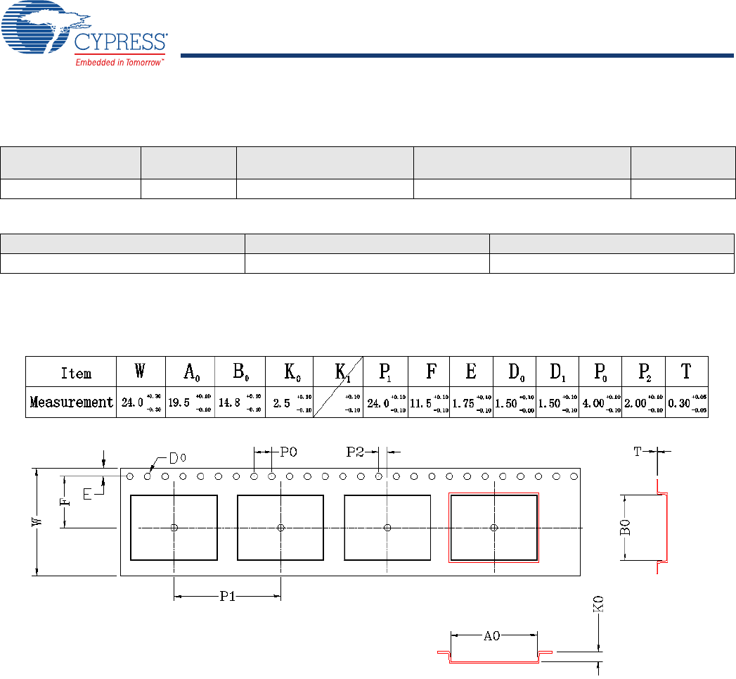
Packaging
The CYBLE-2X20XX-X1 is offered in tape and reel packaging. Figure 10 details the tape dimensions used for the CYBLE-2X20XX-X1.
Figure 10. CYBLE-2X20XX-X1 Tape Dimensions
Figure 11 details the orientation of the CYBLE-2X20XX-X1 in the tape as well as the direction for unreeling.
Figure 11. Component Orientation in Tape and Unreeling Direction (Illustration Only) - TBD
Table 55. Solder Reflow Peak Temperature
Module Part Number Package Maximum Peak Temperature Maximum Time at Peak
Temperature No. of Cycles
CYBLE-2X20XX-X1 30-pad SMT 260 °C 30 seconds 2
Table 56. Package Moisture Sensitivity Level (MSL), IPC/JEDEC J-STD-2
Module Part Number Package MSL
CYBLE-2X20XX-X1 30-pad SMT MSL 3
Document Number: 002-15631 Rev.PRELIMINARY Page 34 of 38
PRELIMINARY
CYBLE-212006-01
CYBLE-202007-01
CYBLE-202013-11
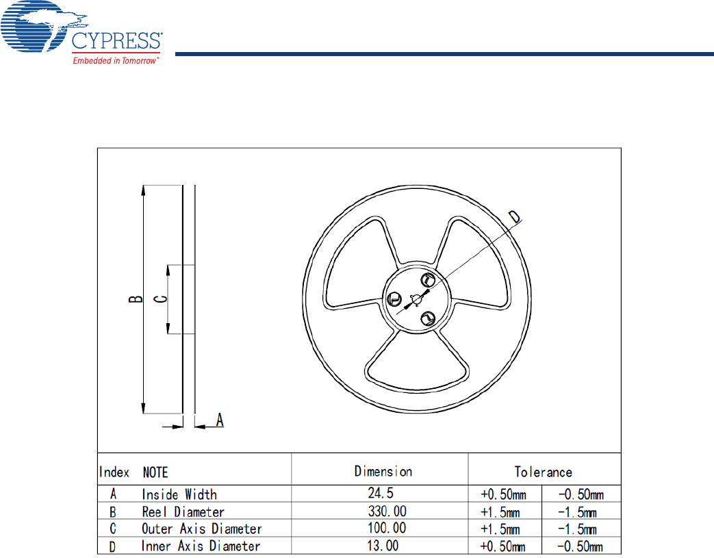
Figure 12 details reel dimensions used for the CYBLE-2X20XX-X1.
Figure 12. Reel Dimensions
The CYBLE-2X20XX-X1 is designed to be used with pick-and-place equipment in an SMT manufacturing environment. The
center-of-mass for the CYBLE-2X20XX-X1 is detailed in Figure 13.
Figure 13. CYBLE-2X20XX-X1 Center of Mass (Seen from Top) - TBD
Document Number: 002-15631 Rev.PRELIMINARY Page 35 of 38
PRELIMINARY
CYBLE-212006-01
CYBLE-202007-01
CYBLE-202013-11
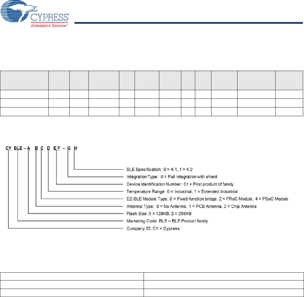
Ordering Information
Table 57 lists the CYBLE-2X20XX-X1 part numbers and features.
Part Numbering Convention
The part numbers are of the form CYBLE-ABCDEF-GH where the fields are defined as follows.
For additional information and a complete list of Cypress Semiconductor BLE products, contact your local Cypress sales
representative. To locate the nearest Cypress office, visit our website.
Table 57. Ordering Information
Part Number
CPU
Speed
(MHz)
Flash
Size
(KB)
CapSense SCB TCPWM
12-Bit
SAR
ADC
I2SLCD Package Packing Certified
CYBLE-212006-01 48 256 Yes 2 4 1 Msps Yes Yes 30-SMT Tape and Reel Yes
CYBLE-202007-01 48 256 Yes 2 4 1 Msps Yes Yes 30-SMT Tape and Reel Yes
CYBLE-202013-11 48 256 Yes 2 4 1 Msps Yes Yes 30-SMT Tape and Reel No
U.S. Cypress Headquarters Address 198 Champion Court, San Jose, CA 95134
U.S. Cypress Headquarter Contact Info (408) 943-2600
Cypress website address http://www.cypress.com
Document Number: 002-15631 Rev.PRELIMINARY Page 36 of 38
PRELIMINARY
CYBLE-212006-01
CYBLE-202007-01
CYBLE-202013-11
Acronyms Document Conventions
Units of Measure
Table 58. Acronyms Used in this Document
Acronym Description
BLE Bluetooth Low Energy
Bluetooth
SIG Bluetooth Special Interest Group
CE European Conformity
CSA Canadian Standards Association
EMI electromagnetic interference
ESD electrostatic discharge
FCC Federal Communications Commission
GPIO general-purpose input/output
IC Industry Canada
IDE integrated design environment
KC Korea Certification
MIC Ministry of Internal Affairs and Communications
(Japan)
PCB printed circuit board
RX receive
QDID qualification design ID
SMT
surface-mount technology; a method for producing
electronic circuitry in which the components are
placed directly onto the surface of PCBs
TCPWM timer, counter, pulse width modulator (PWM)
TUV Germany: Technischer Überwachungs-Verein
(Technical Inspection Association)
TX transmit
Table 59. Units of Measure
Symbol Unit of Measure
°C degree Celsius
kV kilovolt
mA milliamperes
mm millimeters
mV millivolt
μA microamperes
μm micrometers
MHz megahertz
GHz gigahertz
Vvolt
Document Number: 002-15631 Rev.PRELIMINARY Page 37 of 38
PRELIMINARY
CYBLE-212006-01
CYBLE-202007-01
CYBLE-202013-11
Document History Page
Document Title: CYBLE-212006-01, CYBLE-202007-01, CYBLE-202013-11 EZ-BLE™ PRoC™ 4.2 XR Module
Document Number: 002-09764
Revision ECN Orig. of
Change
Submission
Date Description of Change
** PRELIM-
INARY MINS PRELIM-
INARY
Preliminary datasheet for CYBLE-212006-01, CYBLE-202007-01 and
CYBLE-202013-11module.

Document Number: 002-15631 Rev.PRELIMINARY Revised July 28, 2016 Page 38 of 38
PRELIMINARY
CYBLE-212006-01
CYBLE-202007-01
CYBLE-202013-11
© Cypress Semiconductor Corporation, 2016. This document is the property of Cypress Semiconductor Corporation and its subsidiaries, including Spansion LLC ("Cypress"). This document, including
any software or firmware included or referenced in this document ("Software"), is owned by Cypress under the intellectual property laws and treaties of the United States and other countries worldwide.
Cypress reserves all rights under such laws and treaties and does not, except as specifically stated in this paragraph, grant any license under its patents, copyrights, trademarks, or other intellectual
property rights. If the Software is not accompanied by a license agreement and you do not otherwise have a written agreement with Cypress governing the use of the Software, then Cypress hereby
grants you a personal, non-exclusive, nontransferable license (without the right to sublicense) (1) under its copyright rights in the Software (a) for Software provided in source code form, to modify and
reproduce the Software solely for use with Cypress hardware products, only internally within your organization, and (b) to distribute the Software in binary code form externally to end users (either
directly or indirectly through resellers and distributors), solely for use on Cypress hardware product units, and (2) under those claims of Cypress's patents that are infringed by the Software (as provided
by Cypress, unmodified) to make, use, distribute, and import the Software solely for use with Cypress hardware products. Any other use, reproduction, modification, translation, or compilation of the
Software is prohibited.
TO THE EXTENT PERMITTED BY APPLICABLE LAW, CYPRESS MAKES NO WARRANTY OF ANY KIND, EXPRESS OR IMPLIED, WITH REGARD TO THIS DOCUMENT OR ANY SOFTWARE
OR ACCOMPANYING HARDWARE, INCLUDING, BUT NOT LIMITED TO, THE IMPLIED WARRANTIES OF MERCHANTABILITY AND FITNESS FOR A PARTICULAR PURPOSE. To the extent
permitted by applicable law, Cypress reserves the right to make changes to this document without further notice. Cypress does not assume any liability arising out of the application or use of any
product or circuit described in this document. Any information provided in this document, including any sample design information or programming code, is provided only for reference purposes. It is
the responsibility of the user of this document to properly design, program, and test the functionality and safety of any application made of this information and any resulting product. Cypress products
are not designed, intended, or authorized for use as critical components in systems designed or intended for the operation of weapons, weapons systems, nuclear installations, life-support devices or
systems, other medical devices or systems (including resuscitation equipment and surgical implants), pollution control or hazardous substances management, or other uses where the failure of the
device or system could cause personal injury, death, or property damage ("Unintended Uses"). A critical component is any component of a device or system whose failure to perform can be reasonably
expected to cause the failure of the device or system, or to affect its safety or effectiveness. Cypress is not liable, in whole or in part, and you shall and hereby do release Cypress from any claim,
damage, or other liability arising from or related to all Unintended Uses of Cypress products. You shall indemnify and hold Cypress harmless from and against all claims, costs, damages, and other
liabilities, including claims for personal injury or death, arising from or related to any Unintended Uses of Cypress products.
Cypress, the Cypress logo, Spansion, the Spansion logo, and combinations thereof, PSoC, CapSense, EZ-USB, F-RAM, and Traveo are trademarks or registered trademarks of Cypress in the United
States and other countries. For a more complete list of Cypress trademarks, visit cypress.com. Other names and brands may be claimed as property of their respective owners.
Sales, Solutions, and Legal Information
Worldwide Sales and Design Support
Cypress maintains a worldwide network of offices, solution centers, manufacturer’s representatives, and distributors. To find the office
closest to you, visit us at Cypress Locations.
Products
ARM® Cortex® Microcontrollers cypress.com/arm
Automotive cypress.com/automotive
Clocks & Buffers cypress.com/clocks
Interface cypress.com/interface
Lighting & Power Control cypress.com/powerpsoc
Memory cypress.com/memory
PSoC cypress.com/psoc
Touch Sensing cypress.com/touch
USB Controllers cypress.com/usb
Wireless/RF cypress.com/wireless
PSoC® Solutions
PSoC 1 | PSoC 3 | PSoC 4 | PSoC 5LP
Cypress Developer Community
Forums | Projects | Video | Blogs | Training | Components
Technical Support
cypress.com/support