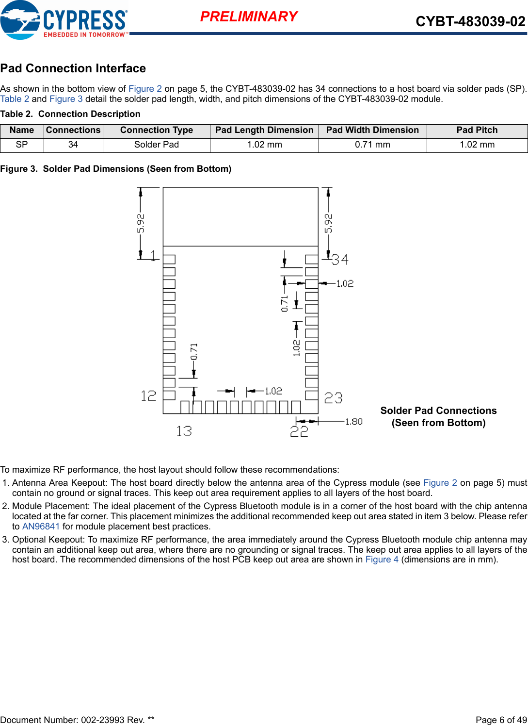
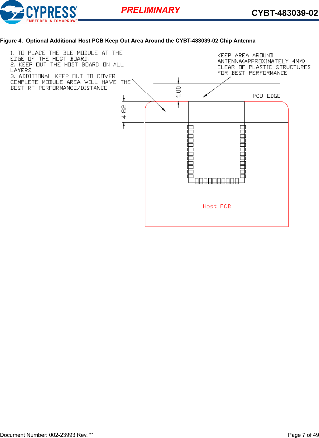
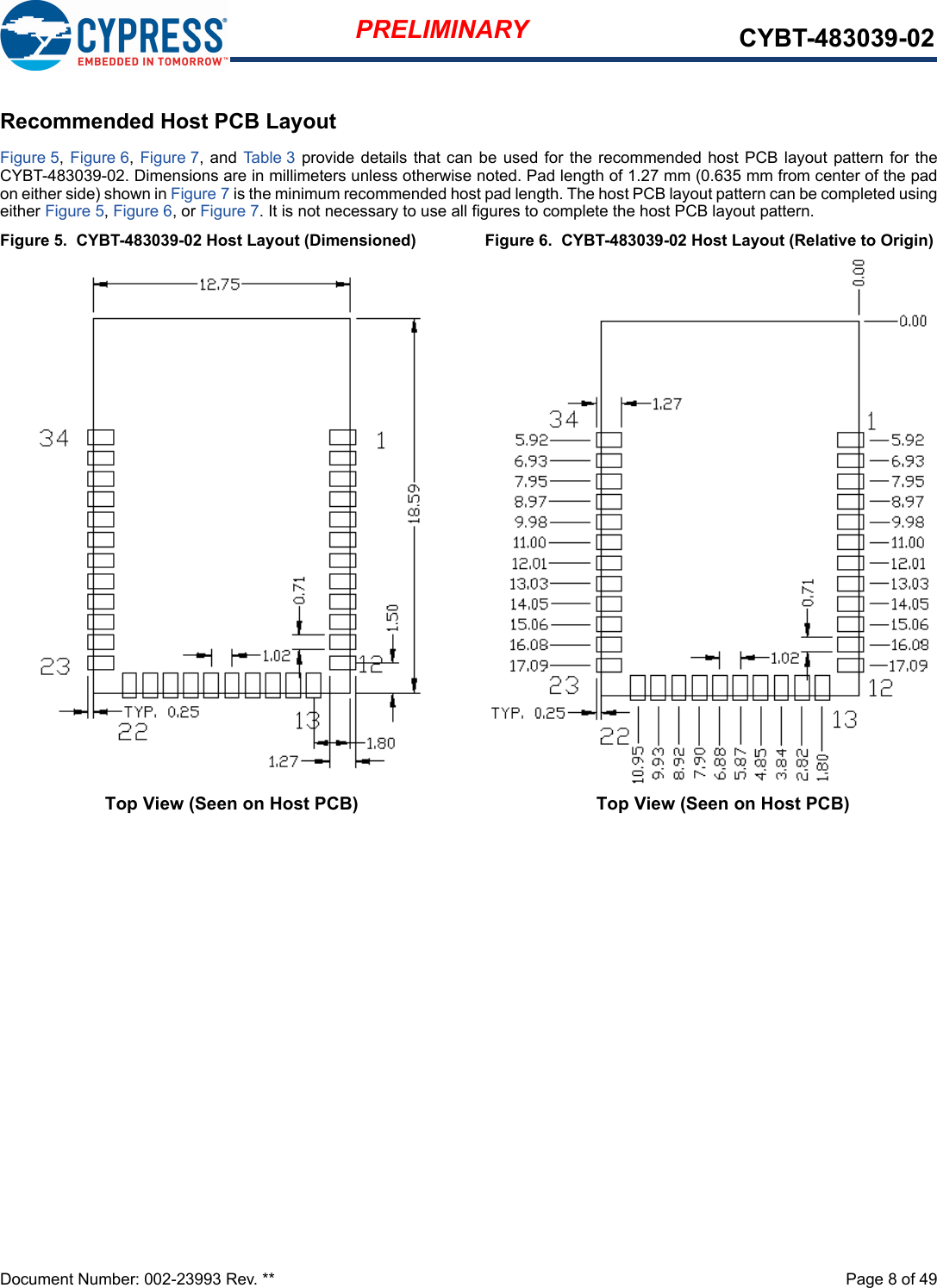
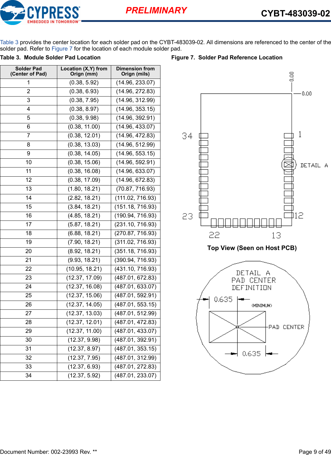
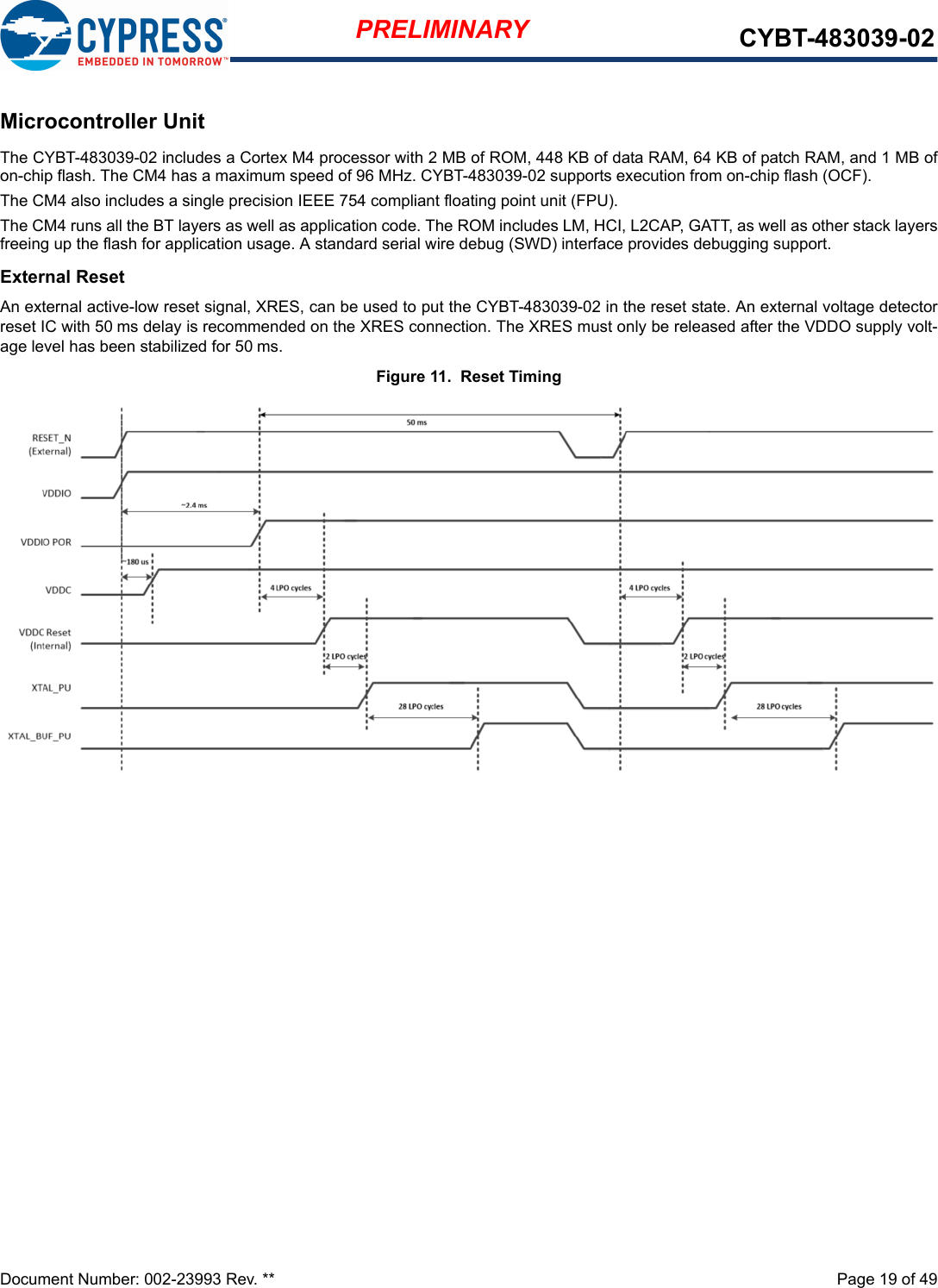
Cypress Semiconductor 3039 This product is a Bluetooth wireless EZ-BT WICED XR Module with Mesh User Manual CYBT 013033 01 EZ BT Module
Cypress Semiconductor This product is a Bluetooth wireless EZ-BT WICED XR Module with Mesh CYBT 013033 01 EZ BT Module
User Manual
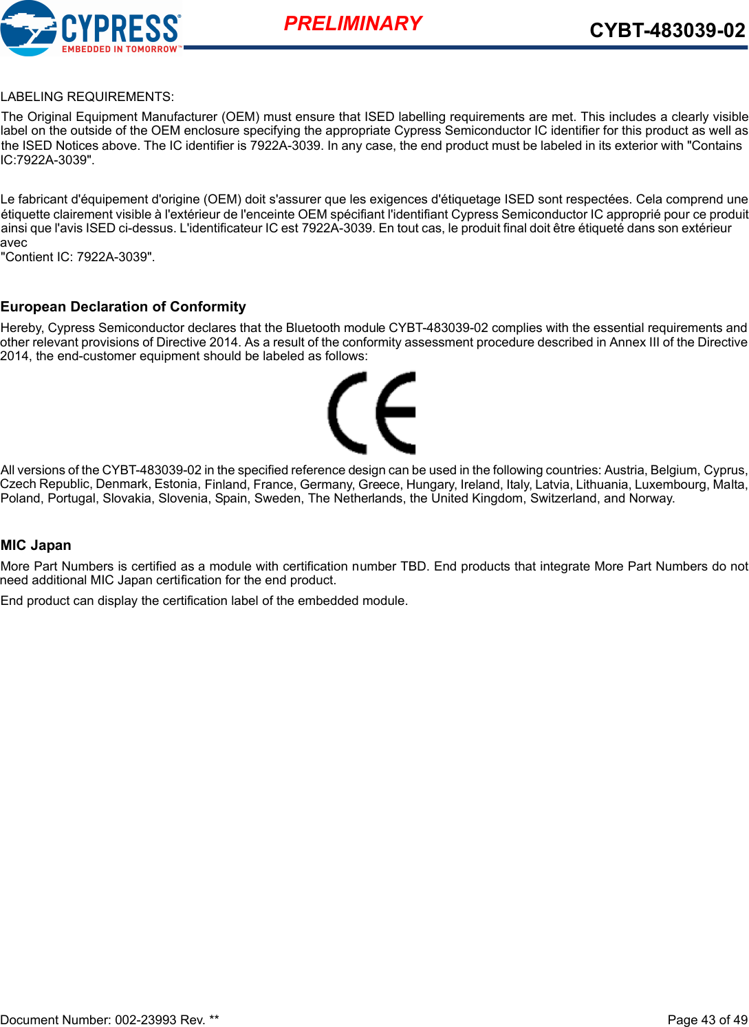
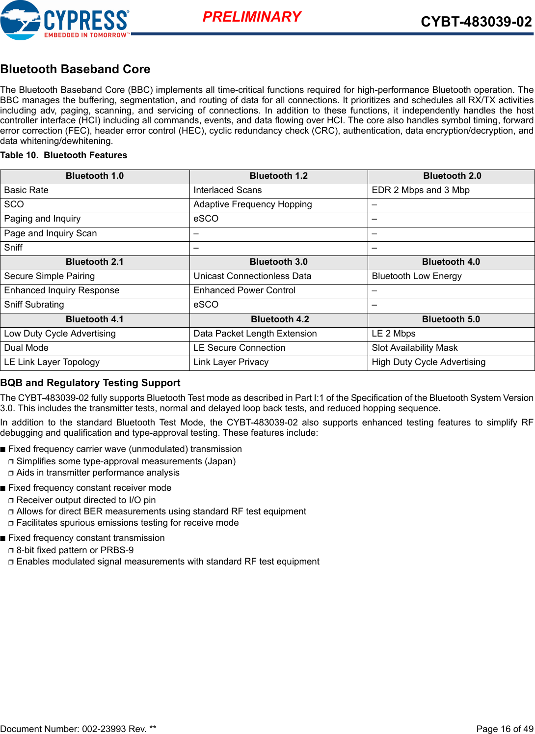
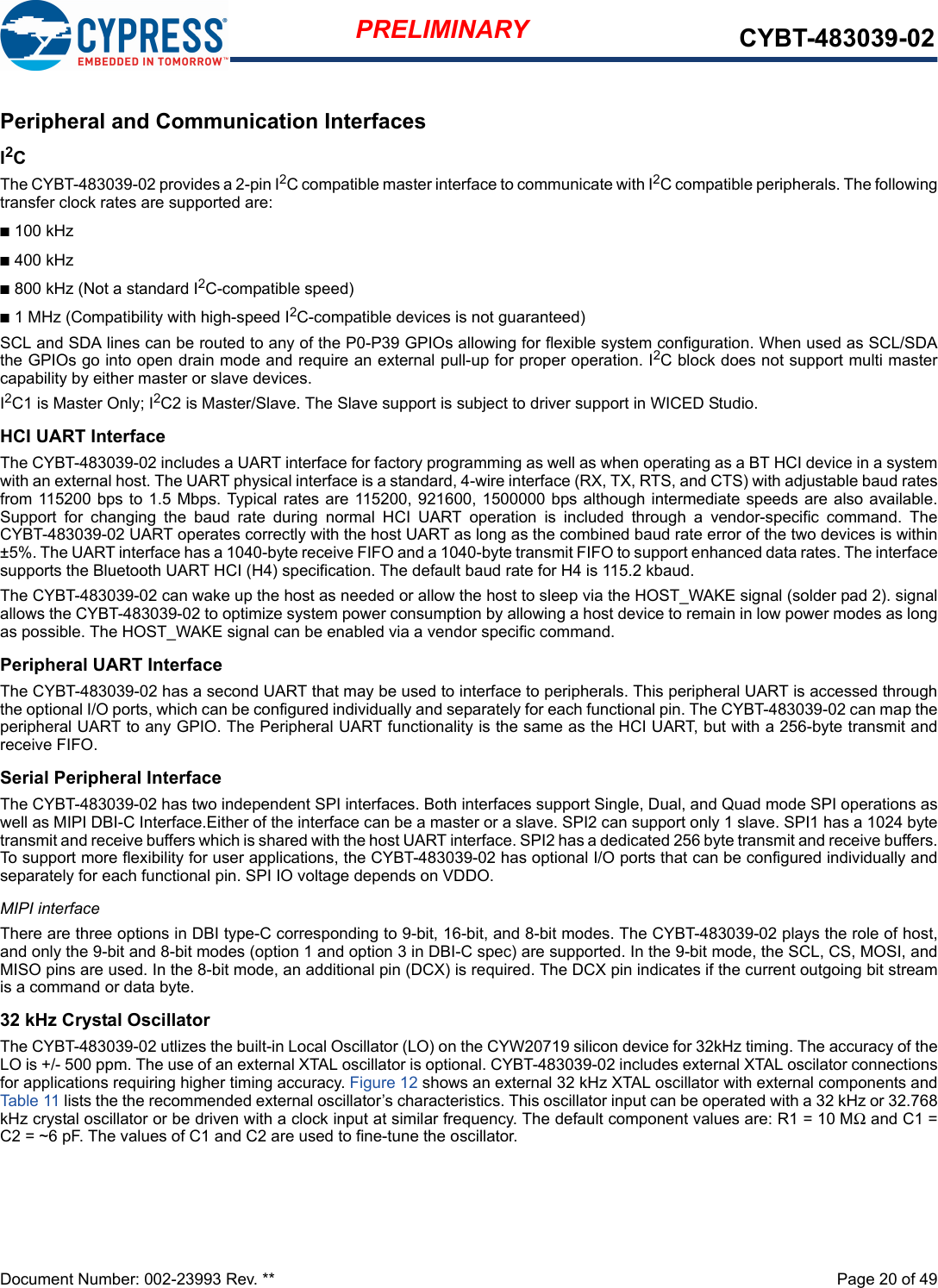
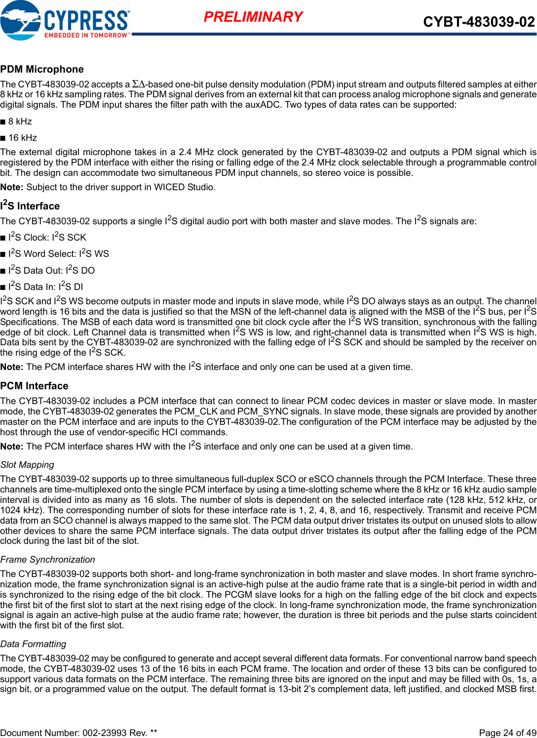
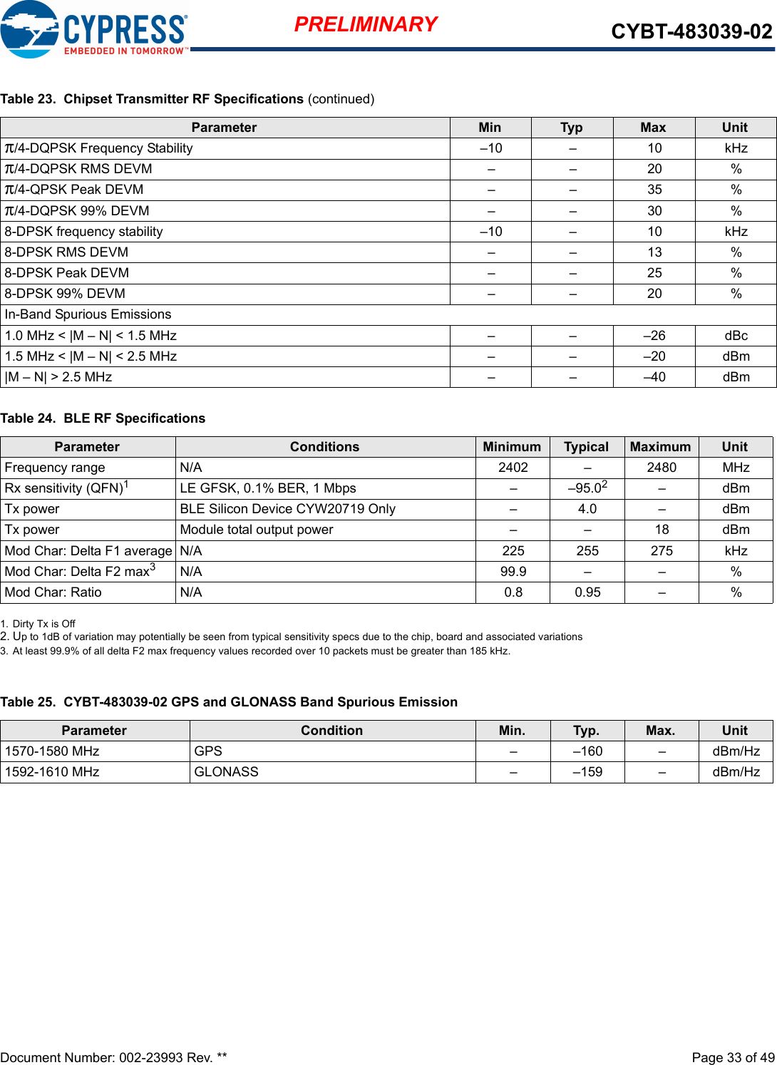
![PRELIMINARY CYBT-483039-02EZ-BT™ XR WICED® ModuleCypress Semiconductor Corporation • 198 Champion Court • San Jose,CA 95134-1709 • 408-943-2600Document Number: 002-23993 Rev. ** Revised May 22, 2018General DescriptionThe CYBT-483039-02 is a dual-mode Bluetooth BR/EDR andLow Energy (BLE) wireless module solution. TheCYBT-483039-02 includes onboard crystal oscillators, passivecomponents, PA/LNA, and the Cypress CYW20719 silicondevice. The CYBT-483039-02 supports a number of peripheral functions(ADC, PWM), as well as multiple serial communication protocols(UART, SPI, I2C, I2S/PCM). The CYBT-483039-02 includes aroyalty-free stack compatible with Bluetooth 5.0 in a 12.75 ×18.59 × 1.80 mm module form-factor.The CYBT-483039-02 includes an integrated chip antenna,on-board external power/low noise amplifier, qulaified byBluetooth SIG, and includes regulatory certification approval forFCC, ISED, MIC, and CE. Module DescriptionnModule size: 12.75 mm × 18.59 mm × 1.80 mm nComplies with Bluetooth Core Specification version 5.0supporting BR, EDR 2/3 Mbps, eSCO, BLE, and LE 2 Mbps . pQDID: TBDpDeclaration ID: TBDnTrue Extended Range:pUp to 1 kilometer bidirectional communication[1, 2]nCertified to FCC, ISED, MIC, and CE standardsnUp to 15 GPIOsn1024-KB flash memory, 512-KB SRAM memorynIndustrial temperature range: –30 °C to +85 °CnIntegrated ARM Cortex-M4 microprocessor core with floating point unit (FPU)RF CharacteristicsnAntenna peak gain: 2.3 dBinBLE RX Receive Sensitivity: –95.0 dbmnReceived signal strength indicator (RSSI) with 1-dB resolutionPower ConsumptionnTX current consumptionpBLE silicon: 5.6 mA (MCU + radio only, 0 dbm)pRFX2401C: 100 mA peak (PA/LNA only, +17.5 dBm Pout)pRFX2401C: 27 mA peak (PA/LNA only, +7.5 dBm Pout)nRX current consumptionpBluetooth silicon: 5.9 mA (MCU + radio only)pRFX2401C: 8.0 mA (PA/LNA only)nCypress CYW20719 silicon low power mode supportpPDS: 61 μA with 512 KB SRAM retentionpSDS: 1.6 uApHIDOFF (External Interrupt): 400 nA Functional Capabilitiesn1x ADC with (12-bit ENoB for DC measurement and 13-bitENoB for Audio measurement) with 10 channels.n1x HCI UART for programming and HCIn1x peripheral UART (PUART)n2x SPI (master or slave) blocks (SPI, Quad SPI, MIPI DBI-C)n1x I2C master/slave and 1x I2C master onlynI2S/PCM audio interfacesnUp to 6 16-bit PWMsnWatchdog TimernBluetooth Basic Rate (BR) and Enhanced Data Rate (EDR)SupportnBLE protocol stack supporting generic access profile (GAP)Central, Peripheral, or Broadcaster rolesnHardware Security EngineBenefitsCYBT-483039-02 is fully integrated and certified solution thatprovides all necessary components required to operateBluetooth communication standards. nProven hardware design ready to usenUltra-flexible supermux I/O designs allows maximum flexibilityfor GPIO function assignmentnLarge non-volatile memory for complex application devel-opmentnOver-the-air update capable for development or field updatesnBluetooth SIG qualified with QDID and Declaration ID nWICED™ Studio provides an easy-to-use integrated designenvironment (IDE) to configure, develop, program, and testyour Bluetooth applicationNotes1. Connection range tested module-to-module in full line-of-sight environment, free of obstacles or interference sources with output power of +18 dBm POUT.2. Specified as EZ-BT XT module to module range. Mobile phone connection will decrease based on the PA/LNA performance of the mobile phone used. nMaximum TX output power(EIRP): +20.0 dBmnConducted output power: p+17.6dBm for BT3.0, +16.8dBm for BT4.0](https://usermanual.wiki/Cypress-Semiconductor/3039/User-Guide-3880529-Page-1.png)
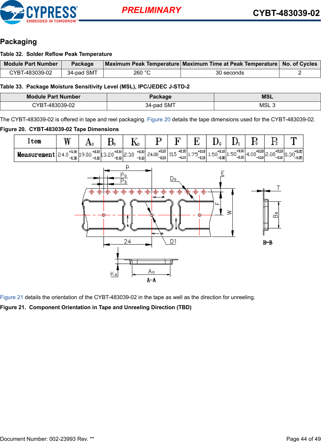
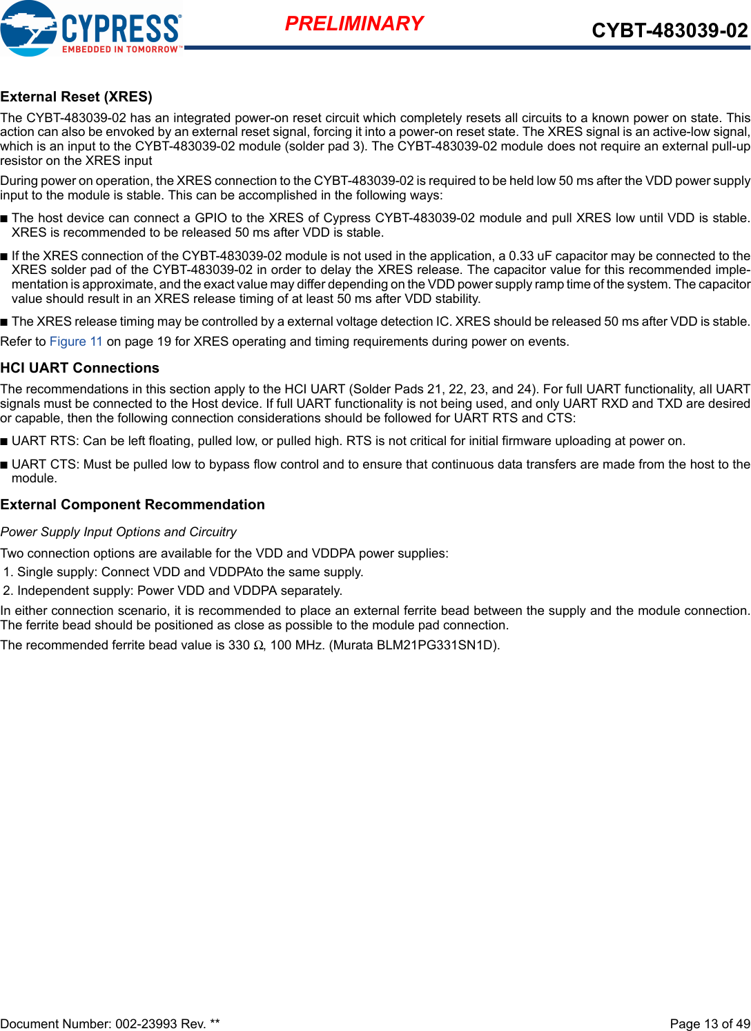
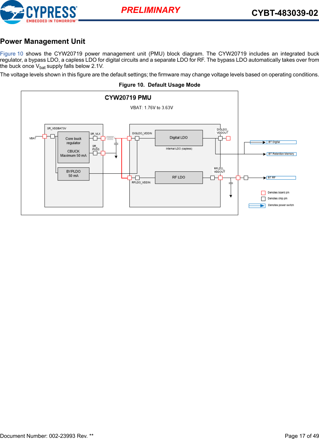
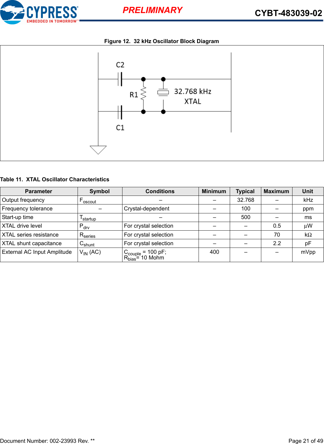
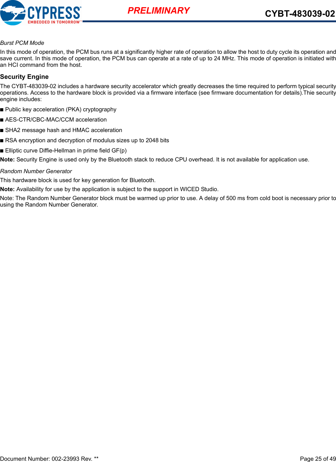
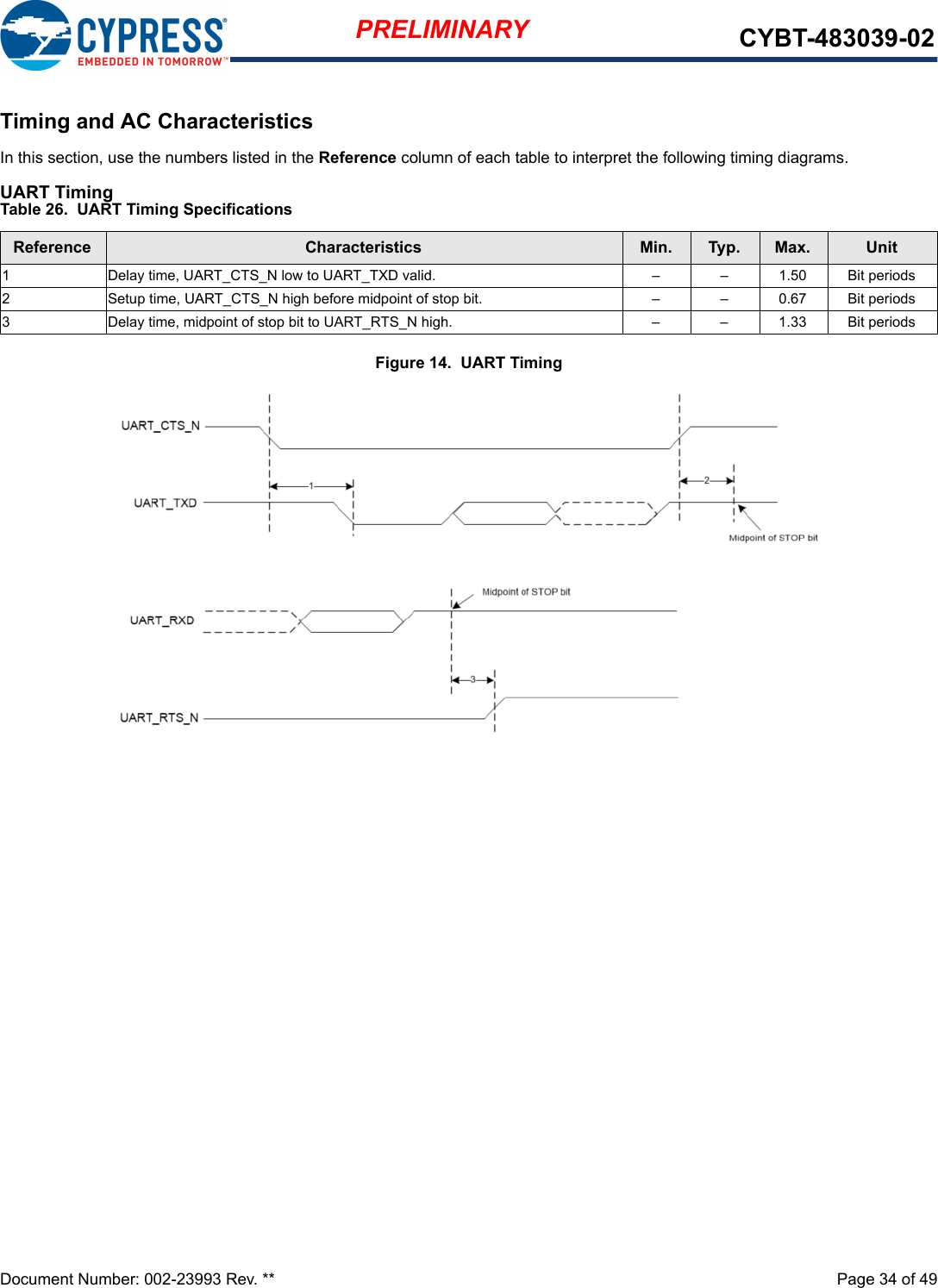
![Document Number: 002-23993 Rev. ** Page 10 of 49PRELIMINARY CYBT-483039-02Module ConnectionsTable 4 details the solder pad connection definitions and available functions for each connection pad. The GPIO connections availableon the CYBT-483039-02 can be configured to any of the input or output funcitons listed in Table 5. Table 4 specifies any function thatis required to be used on a specific solder pad, and also identifies GPIOs that can be configured using the SuperMux. Table 4. CYBT-483039-02 Solder Pad Connection Definitions Pad Pad Name Silicon Pin Name XTALI/O ADC GPIO SuperMux Capable[4]1 VDD VDDIO Silicon Power Supply Input (2.0V ~ 3.6V)2 GND GND Ground3 XRES RST_N External Reset (Active Low)4P33 P33 - IN6 33 see Table 55P25 P25 - - 33 see Table 56P26 P26 - - 33 see Table 57P38 P38 - IN1 33 see Table 58 P34/P35/P36 P34P35P36 -IN5 (P34)IN4 (P35)IN3 (P36)3 (P34/P35/P36) 3 see Table 59P1 P1 - IN28 33 see Table 510 P0 P0 - IN29 33 see Table 511 P29 P29 - IN10 33 see Table 512 P13/P23/P28 P13P23P28 -IN22 (P13)IN12 (P23)IN11 (P28)3(P13/P23/P28) 3 see Table 513 GND GND Ground14 P10/P11 P10P11 -IN25 (P10)IN24 (P11) 3 (P10/P11) 3 see Table 515 P17 P17 - IN18 33 see Table 516 P7 P7 - - 3-17 P6 P6 - - 33 see Table 518 P4 P4 - - 3-19 XTALO_32K XTALO_32K External Oscillator Output (32KHz) -- -20 XTALI_32K/P15[5] XTALI_32KP15 External Oscillator Input (32KHz) IN20 (P15) 3(P15) 3(P15), see Ta b le 521 UART_CTS_N BT_UART_CTS_N UART (HCI UART) Clear To Send Input Only22 UART_RTS_N BT_UART_RTS_N UART (HCI UART) Request To Send Output Only23 UART_TXD BT_UART_TXD UART (HCI UART) Transmit Data Only24 UART_RXD BT_UART_RXD UART (HCI UART) Receive Data Only25 HOST_WAKE BT_HOST_WAKE A signal from the CYBT-483039-02 module to the host indicating that the Bluetooth device requires attention.26 GND GND Ground27 GND GND Ground28 GND GND Ground29 GND GND Ground30 GND GND Ground31 GND GND Ground32 VDDPA N/A PA/LNA Power Supply Voltage (2.0 ~ 3.6V)33 GND GND Ground34 GND GND GroundNote4. The CYBT-483039-02 can configure GPIO connections to any Input/Output function described in Table 5. 5. P15 should not be driven high externally while the part is held in reset (it can be floating or driven low). Failure to do so may cause some current to flow through P15 until the device comes out of reset.](https://usermanual.wiki/Cypress-Semiconductor/3039/User-Guide-3880529-Page-10.png)
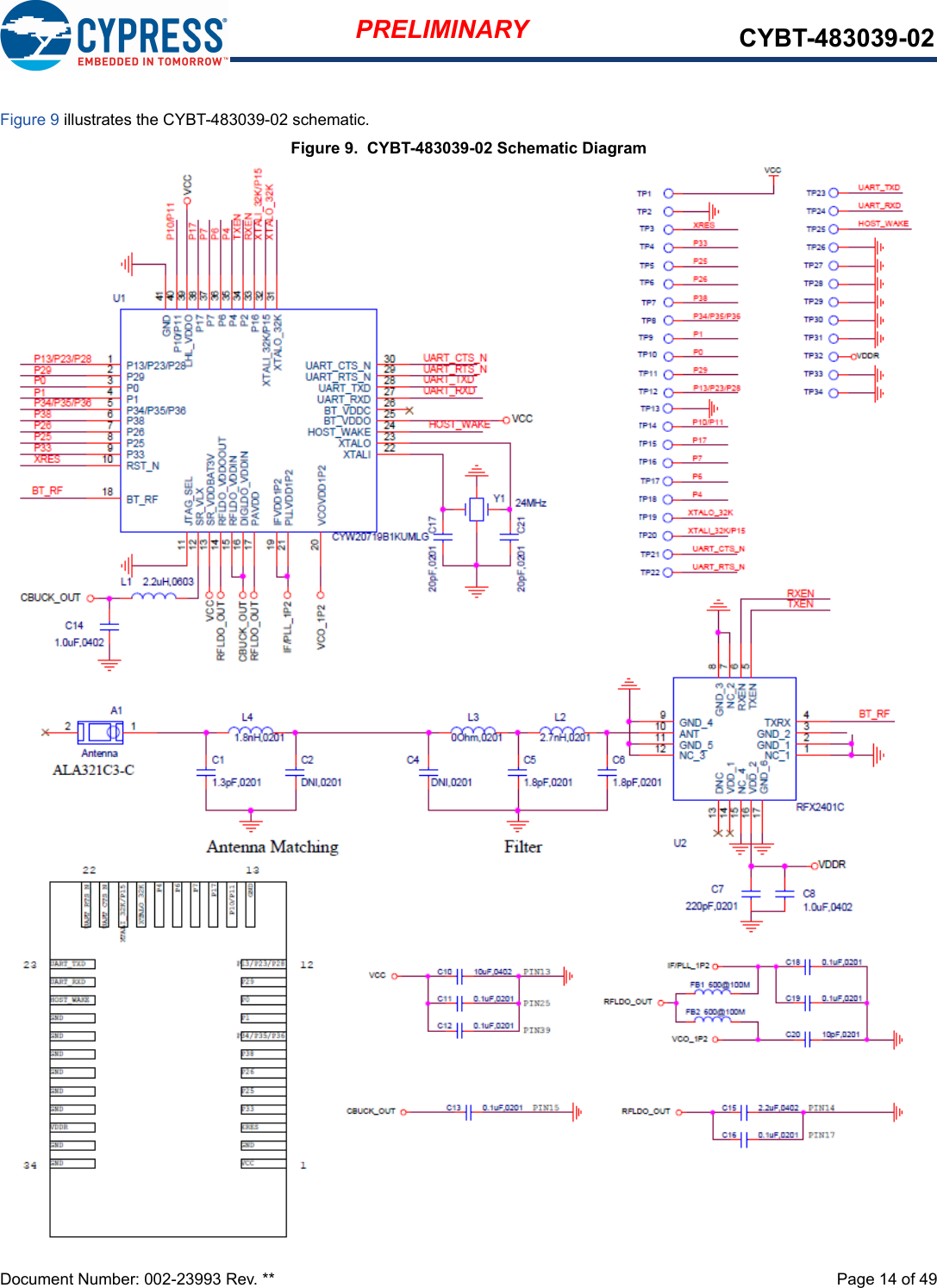
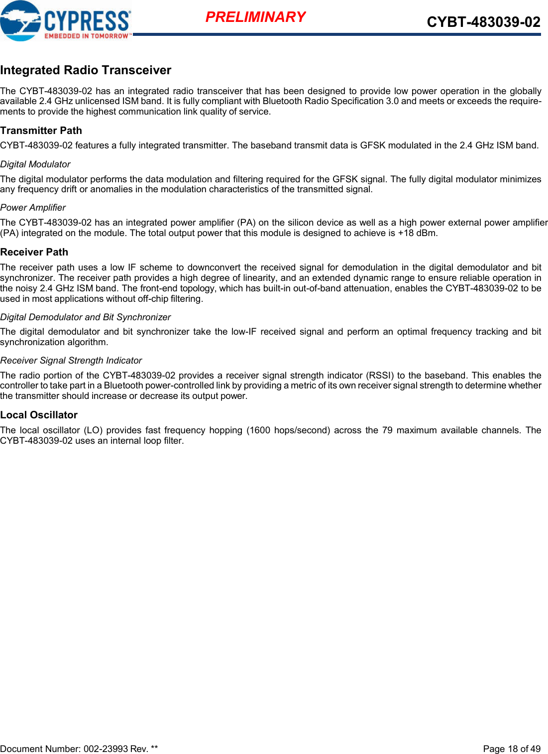
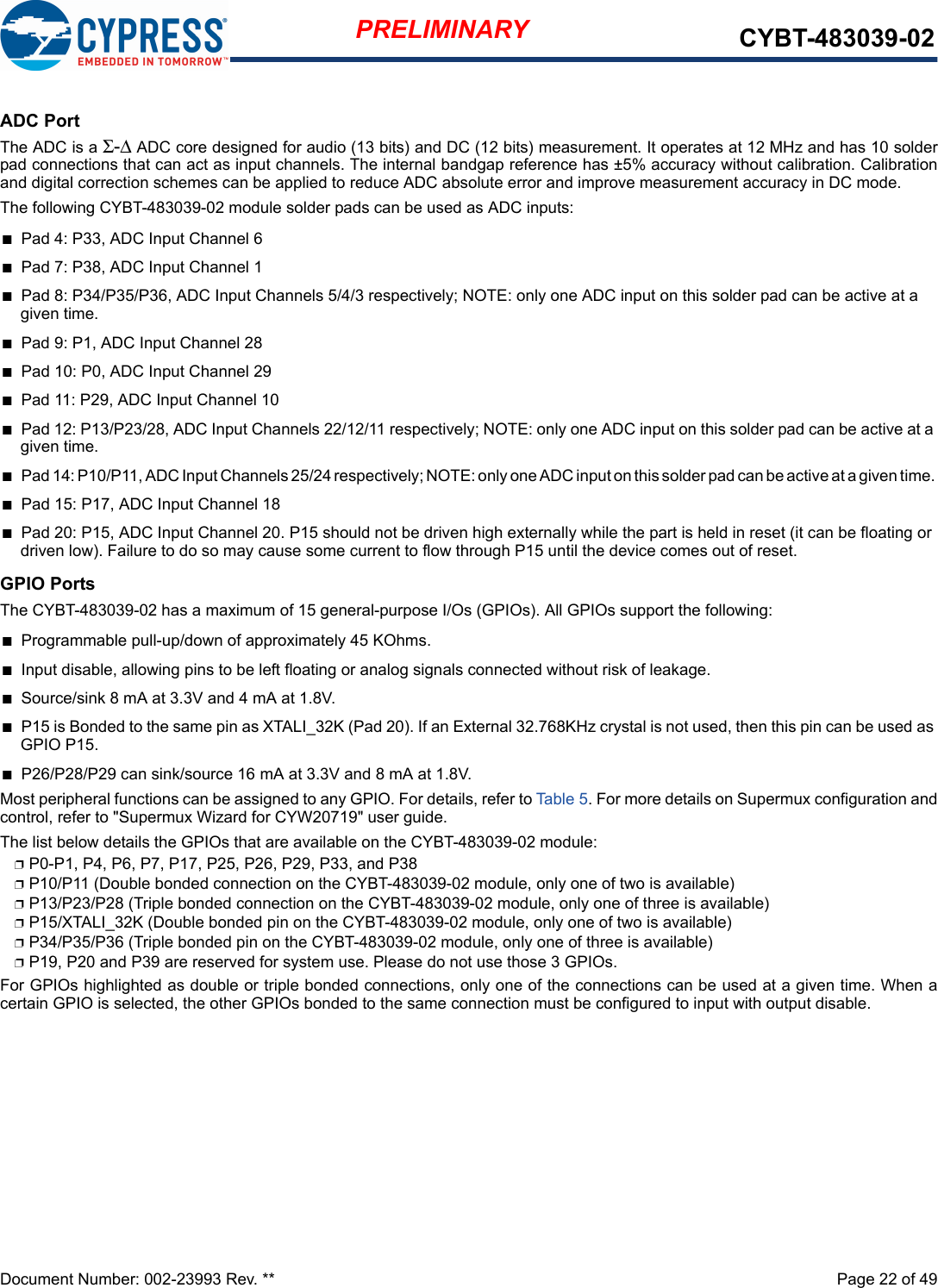
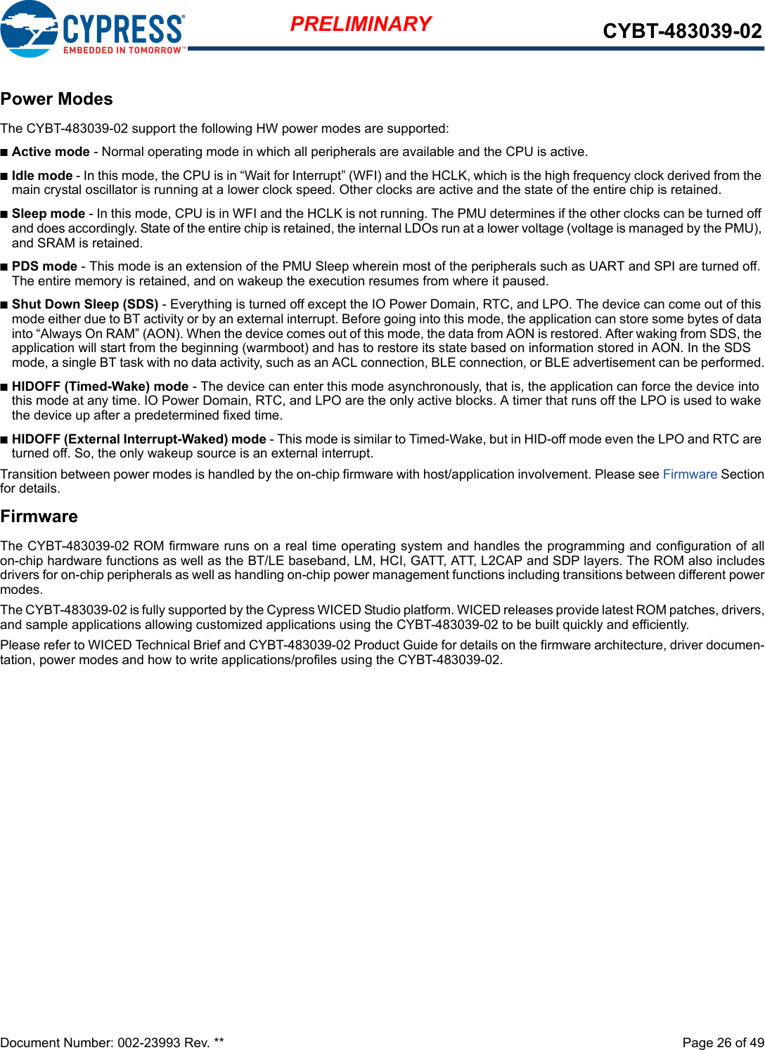

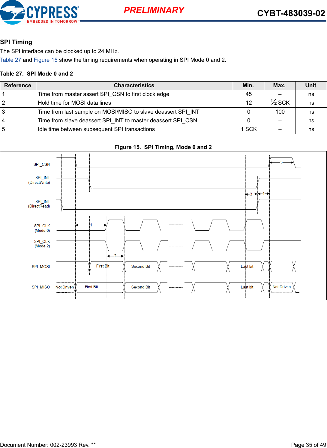
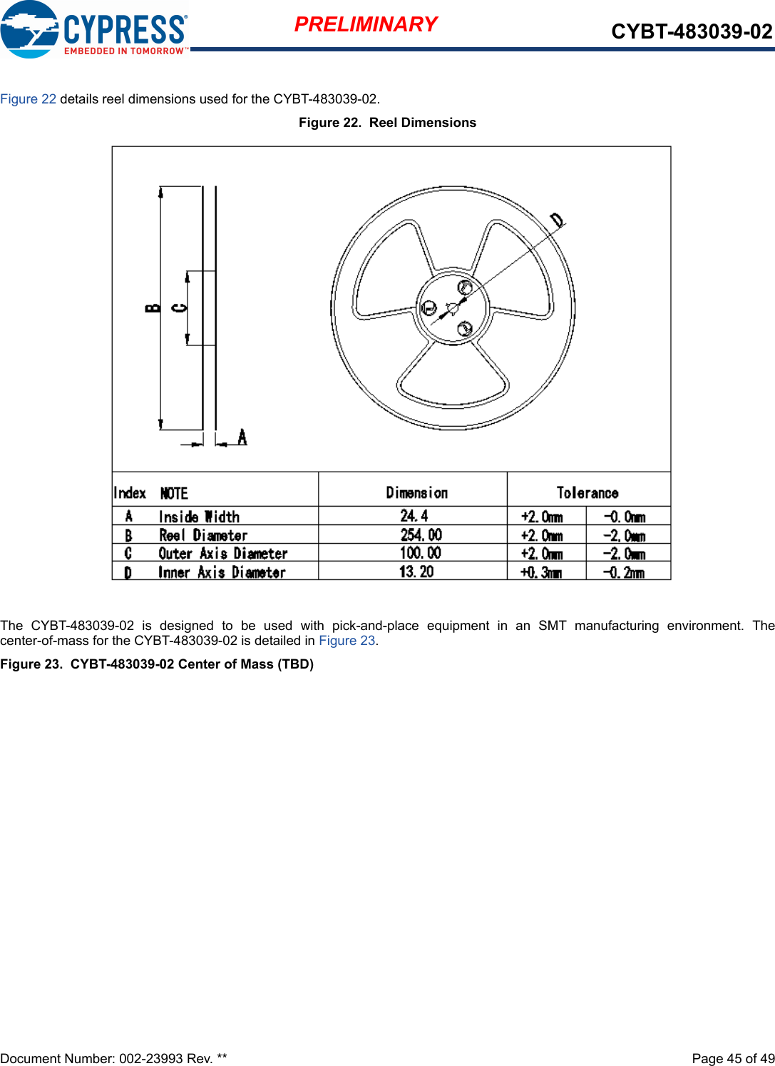
![Document Number: 002-23993 Rev. ** Page 40 of 49PRELIMINARY CYBT-483039-02Environmental SpecificationsEnvironmental ComplianceThis Cypress BLE module is produced in compliance with the Restriction of Hazardous Substances (RoHS) and Halogen-Free (HF)directives. The Cypress module and components used to produce this module are RoHS and HF compliant.RF CertificationThe CYBT-483039-02 module is certified under the following RF certification standards:nFCC: WAP3039nIC: 7922A-3039nMIC: TBDnCESafety CertificationThe CYBT-483039-02 module complies with the following safety regulations:nUnderwriters Laboratories, Inc. (UL): Filing E331901nCSAnTUVEnvironmental ConditionsTable 31 describes the operating and storage conditions for the Cypress BLE module.ESD and EMI ProtectionExposed components require special attention to ESD and electromagnetic interference (EMI).A grounded conductive layer inside the device enclosure is suggested for EMI and ESD performance. Any openings in the enclosurenear the module should be surrounded by a grounded conductive layer to provide ESD protection and a low-impedance path to ground. Device Handling: Proper ESD protocol must be followed in manufacturing to ensure component reliability.Table 31. Environmental Conditions for CYBT-483039-02Description Minimum Specification Maximum SpecificationOperating temperature −30 °C 85 °COperating humidity (relative, non-condensation) 5% 85%Thermal ramp rate – 10 °C/minuteStorage temperature –40 °C 85 °CStorage temperature and humidity – 85 °C at 85%ESD: Module integrated into system Components[6] –15 kV Air2.0 kV ContactNote6. This does not apply to the RF pins (ANT).](https://usermanual.wiki/Cypress-Semiconductor/3039/User-Guide-3880529-Page-40.png)