Cypress Semiconductor 3039 This product is a Bluetooth wireless EZ-BT WICED XR Module with Mesh User Manual CYBT 013033 01 EZ BT Module
Cypress Semiconductor This product is a Bluetooth wireless EZ-BT WICED XR Module with Mesh CYBT 013033 01 EZ BT Module
User Manual

PRELIMINARY CYBT-483039-02
EZ-BT™ XR WICED® Module
Cypress Semiconductor Corporation • 198 Champion Court • San Jose,CA 95134-1709 • 408-943-2600
Document Number: 002-23993 Rev. ** Revised May 22, 2018
General Description
The CYBT-483039-02 is a dual-mode Bluetooth BR/EDR and
Low Energy (BLE) wireless module solution. The
CYBT-483039-02 includes onboard crystal oscillators, passive
components, PA/LNA, and the Cypress CYW20719 silicon
device.
The CYBT-483039-02 supports a number of peripheral functions
(ADC, PWM), as well as multiple serial communication protocols
(UART, SPI, I2C, I2S/PCM). The CYBT-483039-02 includes a
royalty-free stack compatible with Bluetooth 5.0 in a 12.75 ×
18.59 × 1.80 mm module form-factor.
The CYBT-483039-02 includes an integrated chip antenna,
on-board external power/low noise amplifier, qulaified by
Bluetooth SIG, and includes regulatory certification approval for
FCC, ISED, MIC, and CE.
Module Description
nModule size: 12.75 mm × 18.59 mm × 1.80 mm
nComplies with Bluetooth Core Specification version 5.0
supporting BR, EDR 2/3 Mbps, eSCO, BLE, and LE 2 Mbps .
pQDID: TBD
pDeclaration ID: TBD
nTrue Extended Range:
pUp to 1 kilometer bidirectional communication[1, 2]
nCertified to FCC, ISED, MIC, and CE standards
nUp to 15 GPIOs
n1024-KB flash memory, 512-KB SRAM memory
nIndustrial temperature range: –30 °C to +85 °C
nIntegrated ARM Cortex-M4 microprocessor core with
floating point unit (FPU)
RF Characteristics
nAntenna peak gain: 2.3 dBi
nBLE RX Receive Sensitivity: –95.0 dbm
nReceived signal strength indicator (RSSI) with 1-dB resolution
Power Consumption
nTX current consumption
pBLE silicon: 5.6 mA (MCU + radio only, 0 dbm)
pRFX2401C: 100 mA peak (PA/LNA only, +17.5 dBm Pout)
pRFX2401C: 27 mA peak (PA/LNA only, +7.5 dBm Pout)
nRX current consumption
pBluetooth silicon: 5.9 mA (MCU + radio only)
pRFX2401C: 8.0 mA (PA/LNA only)
nCypress CYW20719 silicon low power mode support
pPDS: 61 μA with 512 KB SRAM retention
pSDS: 1.6 uA
pHIDOFF (External Interrupt): 400 nA
Functional Capabilities
n1x ADC with (12-bit ENoB for DC measurement and 13-bit
ENoB for Audio measurement) with 10 channels.
n1x HCI UART for programming and HCI
n1x peripheral UART (PUART)
n2x SPI (master or slave) blocks (SPI, Quad SPI, MIPI DBI-C)
n1x I2C master/slave and 1x I2C master only
nI2S/PCM audio interfaces
nUp to 6 16-bit PWMs
nWatchdog Timer
nBluetooth Basic Rate (BR) and Enhanced Data Rate (EDR)
Support
nBLE protocol stack supporting generic access profile (GAP)
Central, Peripheral, or Broadcaster roles
nHardware Security Engine
Benefits
CYBT-483039-02 is fully integrated and certified solution that
provides all necessary components required to operate
Bluetooth communication standards.
nProven hardware design ready to use
nUltra-flexible supermux I/O designs allows maximum flexibility
for GPIO function assignment
nLarge non-volatile memory for complex application devel-
opment
nOver-the-air update capable for development or field updates
nBluetooth SIG qualified with QDID and Declaration ID
nWICED™ Studio provides an easy-to-use integrated design
environment (IDE) to configure, develop, program, and test
your Bluetooth application
Notes
1. Connection range tested module-to-module in full line-of-sight environment, free of obstacles or interference sources with o
utput power of +18 dBm POUT.
2. Specified as EZ-BT XT module to module range. Mobile phone connection will decrease based on the PA/LNA performance of the mobile phone used.
nMaximum TX output power(EIRP): +20.0 dBm
nConducted output power:
p+17.6dBm for BT3.0, +16.8dBm for BT4.0

Document Number: 002-23993 Rev. ** Page 2 of 49
PRELIMINARY CYBT-483039-02
More Information
Cypress provides a wealth of data at www.cypress.com to help you to select the right module for your design, and to help you to
quickly and effectively integrate the module into your design.
References
nOverview: EZ-BLE/EZ-BT Module Portfolio, Module Roadmap
nDevelopment Kits:
pCYBT-483039-EVAL, CYBT-483039-02 Evaluation Board
pCYW920719Q40EVB-01, Evaluation Kit for CYW20719
silicon device
nTest and Debug Tools:
pCYSmart, Bluetooth® LE Test and Debug Tool (Windows)
pCYSmart Mobile, Bluetooth® LE Test and Debug Tool
(Android/iOS Mobile App)
nKnowledge Base Article
pKBA97095 - EZ-BLE™ Module Placement
pKBA213976 - FAQ for BLE and Regulatory Certifications with
EZ-BLE modules
pKBA210802 - Queries on BLE Qualification and Declaration
Processes
pKBA218122 - 3D Model Files for EZ-BLE/EZ-BT Modules
pKBA223428- Programming an EZ-BT WICED Module
Development Environments
Wireless Connectivity for Embedded Devices (WICED) Studio Software Development Kit (SDK)
Cypress' WICED® (Wireless Connectivity for Embedded Devices) is a full-featured platform with proven Software Development Kits
(SDKs) and turnkey hardware solutions from partners to readily enable Wi-Fi and Bluetooth® connectivity in system design.
WICED Studio is the only SDK for the Internet of Things (ioT) that combines Wi-Fi and Bluetooth into a single integrated development
environment. In addition to providing WICED APIs and an application framework designed to abstract complexity, WICED Studio also
leverages many common industry standards.
Technical Support
nCypress Community: Whether you’re a customer, partner or a developer interested in the latest Cypress innovations, the Cypress
Developer Community offers you a place to learn, share and engage with both Cypress experts and other embedded engineers
around the world.
nFrequently Asked Questions (FAQs): Learn more about our Bluetooth ECO System.
nVisit our support page and create a technical support case or contact a local sales representatives. If you are in the United States,
you can talk to our technical support team by calling our toll-free number: +1-800-541-4736. Select option 2 at the prompt.

Document Number: 002-23993 Rev. ** Page 3 of 49
PRELIMINARY CYBT-483039-02
Contents
Overview............................................................................ 4
Functional Block Diagram ........................................... 4
Module Description...................................................... 4
Pad Connection Interface ................................................ 6
Recommended Host PCB Layout ................................... 8
Module Connections ...................................................... 10
Connections and Optional External Components ..... 12
Power Connections (VDD and VDDPA).................... 12
External Reset (XRES).............................................. 13
HCI UART Connections ............................................ 13
External Component Recommendation .................... 13
Critical Components List ........................................... 15
Antenna Design......................................................... 15
Power Amplifier (PA) and Low Noise Amplifier (LNA) 15
Bluetooth Baseband Core ............................................. 16
BQB and Regulatory Testing Support....................... 16
Power Management Unit................................................ 17
Integrated Radio Transceiver ........................................ 18
Transmitter Path........................................................ 18
Receiver Path............................................................ 18
Local Oscillator.......................................................... 18
Microcontroller Unit ....................................................... 19
External Reset........................................................... 19
Peripheral and Communication Interfaces .................. 20
I2C............................................................................. 20
HCI UART Interface .................................................. 20
Peripheral UART Interface ........................................ 20
Serial Peripheral Interface......................................... 20
32 kHz Crystal Oscillator........................................... 20
ADC Port ................................................................... 22
GPIO Ports................................................................ 22
PWM.......................................................................... 23
PDM Microphone....................................................... 24
I2S Interface.............................................................. 24
PCM Interface ........................................................... 24
Security Engine ......................................................... 25
Power Modes .................................................................. 26
Firmware.......................................................................... 26
Electrical Characteristics............................................... 27
Core Buck Regulator................................................. 27
Digital LDO................................................................ 29
Digital I/O Characteristics.......................................... 29
ADC Electrical Characteristics .................................. 29
Bluetooth Silicon Current Consumption .................... 30
Chipset RF Specifications ............................................. 31
Timing and AC Characteristics ..................................... 34
UART Timing............................................................. 34
SPI Timing................................................................. 35
I2C Compatible Interface Timing............................... 37
I2S Interface Timing .................................................. 38
Environmental Specifications ....................................... 40
Environmental Compliance ....................................... 40
RF Certification.......................................................... 40
Safety Certification .................................................... 40
Environmental Conditions ......................................... 40
ESD and EMI Protection ........................................... 40
Regulatory Information .................................................. 41
FCC........................................................................... 41
ISED.......................................................................... 42
European Declaration of Conformity ......................... 43
MIC Japan................................................................. 43
Packaging........................................................................ 44
Ordering Information...................................................... 46
Acronyms........................................................................ 47
Document Conventions ................................................. 47
Units of Measure ....................................................... 47
Document History Page................................................. 48
Sales, Solutions, and Legal Information ...................... 49
Worldwide Sales and Design Support....................... 49
Products .................................................................... 49
PSoC® Solutions ...................................................... 49
Cypress Developer Community................................. 49
Technical Support ..................................................... 49
Document Number: 002-23993 Rev. ** Page 4 of 49
PRELIMINARY CYBT-483039-02
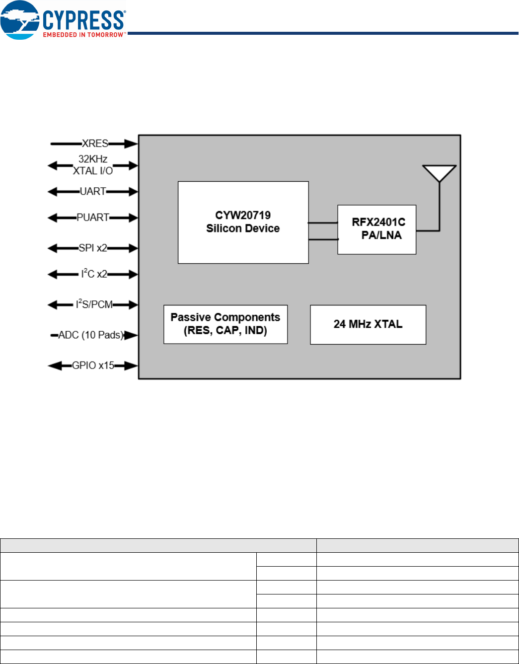
Overview
Functional Block Diagram
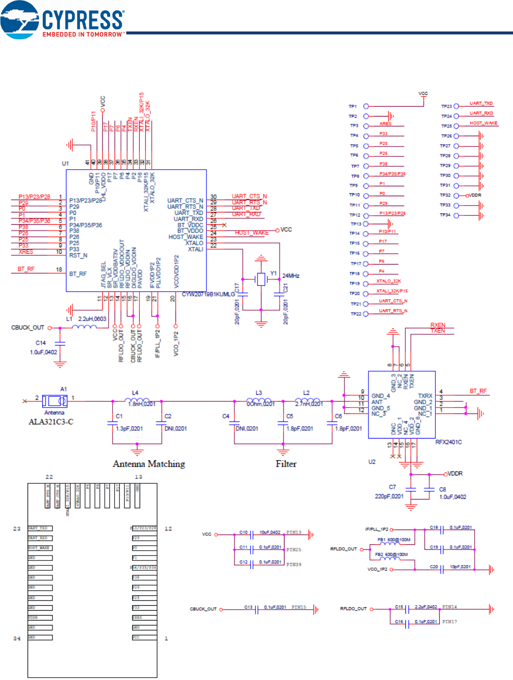
Figure 1 illustrates the CYBT-483039-02 functional block diagram.
Figure 1. Functional Block Diagram
Note: General Purpose Input/Output pins shown in Figure 1 are configuratble to any specified input or output function in the SuperMux table detailed in Table 5 in the Module
Connections section.
Note: Connections shown in the above block diagram are maximum number of connections per function. The total number of GPIOs available on the CYBT-483039-02 is 15.
Module Description
The CYBT-483039-02 module is a complete module designed to be soldered to the applications main board.
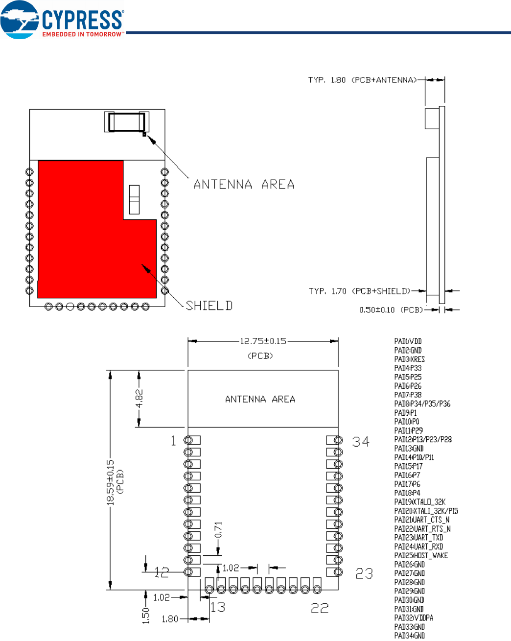
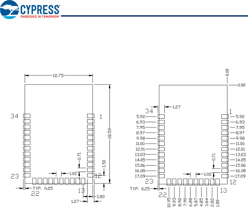
Module Dimensions and Drawing
Cypress reserves the right to select components from various vendors to achieve the Bluetooth module functionality. Such selections
will still guarantee that all mechanical specifications and module certifications are maintained. Any changes to the current BOM for
the CYBT-483039-02 will not be made until approval is provided by the end customer for this product. The CYBT-483039-02 will be
held within the physical dimensions shown in the mechanical drawings in Figure 2 on page 5. All dimensions are in millimeters (mm).
Table 1. Module Design Dimensions
See Figure 2 for the mechanical reference drawing for CYBT-483039-02.
Dimension Item Specification
Module dimensions Length (X) 12.75 ± 0.15 mm
Width (Y) 18.59 ± 0.15 mm
Antenna location dimensions Length (X) 12.75 mm
Width (Y) 4.82 mm
PCB thickness Height (H) 0.50 ± 0.10 mm
Shield height Height (H) 1.20 mm
Maximum component height Height (H) 1.30 mm typical (Chip Antenna)
Total module thickness (bottom of module to top of shield) Height (H) 1.80 mm typical
Document Number: 002-23993 Rev. ** Page 5 of 49
PRELIMINARY CYBT-483039-02
Figure 2. Module Mechanical Drawing
Bottom View (Seen from Bottom)
Side View
Top View (Seen from Top)
Notes
3. No metal should be located beneath or above the antenna area. Only bare PCB material should be located beneath the antenna area. For more information on
recommended host PCB layout, see “Recommended Host PCB Layout” on page 8.
Document Number: 002-23993 Rev. ** Page 6 of 49
PRELIMINARY CYBT-483039-02
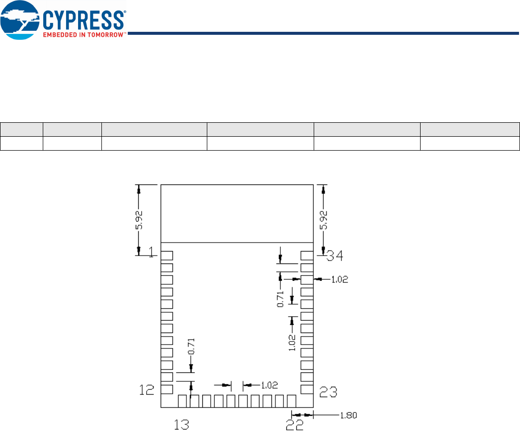
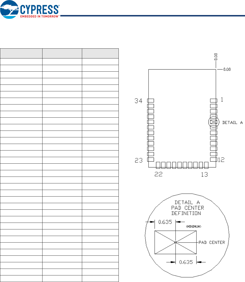
Pad Connection Interface
As shown in the bottom view of Figure 2 on page 5, the CYBT-483039-02 has 34 connections to a host board via solder pads (SP).
Table 2 and Figure 3 detail the solder pad length, width, and pitch dimensions of the CYBT-483039-02 module.
Figure 3. Solder Pad Dimensions (Seen from Bottom)
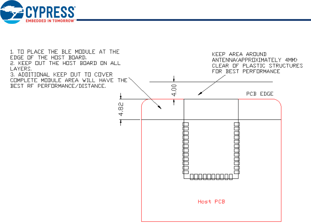
To maximize RF performance, the host layout should follow these recommendations:
1. Antenna Area Keepout: The host board directly below the antenna area of the Cypress module (see Figure 2 on page 5) must
contain no ground or signal traces. This keep out area requirement applies to all layers of the host board.
2. Module Placement: The ideal placement of the Cypress Bluetooth module is in a corner of the host board with the chip antenna
located at the far corner. This placement minimizes the additional recommended keep out area stated in item 3 below. Please refer
to AN96841 for module placement best practices.
3. Optional Keepout: To maximize RF performance, the area immediately around the Cypress Bluetooth module chip antenna may
contain an additional keep out area, where there are no grounding or signal traces. The keep out area applies to all layers of the
host board. The recommended dimensions of the host PCB keep out area are shown in Figure 4 (dimensions are in mm).
Table 2. Connection Description
Name Connections Connection Type Pad Length Dimension Pad Width Dimension Pad Pitch
SP 34 Solder Pad 1.02 mm 0.71 mm 1.02 mm
Solder Pad Connections
(Seen from Bottom)
Document Number: 002-23993 Rev. ** Page 7 of 49
PRELIMINARY CYBT-483039-02
Figure 4. Optional Additional Host PCB Keep Out Area Around the CYBT-483039-02 Chip Antenna
Document Number: 002-23993 Rev. ** Page 8 of 49
PRELIMINARY CYBT-483039-02
Recommended Host PCB Layout
Figure 5, Figure 6, Figure 7, and Ta ble 3 provide details that can be used for the recommended host PCB layout pattern for the
CYBT-483039-02. Dimensions are in millimeters unless otherwise noted. Pad length of 1.27 mm (0.635 mm from center of the pad
on either side) shown in Figure 7 is the minimum recommended host pad length. The host PCB layout pattern can be completed using
either Figure 5, Figure 6, or Figure 7. It is not necessary to use all figures to complete the host PCB layout pattern.
Figure 5. CYBT-483039-02 Host Layout (Dimensioned) Figure 6. CYBT-483039-02 Host Layout (Relative to Origin)
Top View (Seen on Host PCB)
Top View (Seen on Host PCB)
Document Number: 002-23993 Rev. ** Page 9 of 49
PRELIMINARY CYBT-483039-02
Table 3 provides the center location for each solder pad on the CYBT-483039-02. All dimensions are referenced to the center of the
solder pad. Refer to Figure 7 for the location of each module solder pad.
Table 3. Module Solder Pad Location Figure 7. Solder Pad Reference Location
Solder Pad
(Center of Pad)
Location (X,Y) from
Orign (mm)
Dimension from
Orign (mils)
1 (0.38, 5.92) (14.96, 233.07)
2 (0.38, 6.93) (14.96, 272.83)
3 (0.38, 7.95) (14.96, 312.99)
4 (0.38, 8.97) (14.96, 353.15)
5 (0.38, 9.98) (14.96, 392.91)
6 (0.38, 11.00) (14.96, 433.07)
7 (0.38, 12.01) (14.96, 472.83)
8 (0.38, 13.03) (14.96, 512.99)
9 (0.38, 14.05) (14.96, 553.15)
10 (0.38, 15.06) (14.96, 592.91)
11 (0.38, 16.08) (14.96, 633.07)
12 (0.38, 17.09) (14.96, 672.83)
13 (1.80, 18.21) (70.87, 716.93)
14 (2.82, 18.21) (111.02, 716.93)
15 (3.84, 18.21) (151.18, 716.93)
16 (4.85, 18.21) (190.94, 716.93)
17 (5.87, 18.21) (231.10, 716.93)
18 (6.88, 18.21) (270.87, 716.93)
19 (7.90, 18.21) (311.02, 716.93)
20 (8.92, 18.21) (351.18, 716.93)
21 (9.93, 18.21) (390.94, 716.93)
22 (10.95, 18.21) (431.10, 716.93)
23 (12.37, 17.09) (487.01, 672.83)
24 (12.37, 16.08) (487.01, 633.07)
25 (12.37, 15.06) (487.01, 592.91)
26 (12.37, 14.05) (487.01, 553.15)
27 (12.37, 13.03) (487.01, 512.99)
28 (12.37, 12.01) (487.01, 472.83)
29 (12.37, 11.00) (487.01, 433.07)
30 (12.37, 9.98) (487.01, 392.91)
31 (12.37, 8.97) (487.01, 353.15)
32 (12.37, 7.95) (487.01, 312.99)
33 (12.37, 6.93) (487.01, 272.83)
34 (12.37, 5.92) (487.01, 233.07)
Top View (Seen on Host PCB)

Document Number: 002-23993 Rev. ** Page 10 of 49
PRELIMINARY CYBT-483039-02
Module Connections
Table 4 details the solder pad connection definitions and available functions for each connection pad. The GPIO connections available
on the CYBT-483039-02 can be configured to any of the input or output funcitons listed in Table 5. Table 4 specifies any function that
is required to be used on a specific solder pad, and also identifies GPIOs that can be configured using the SuperMux.
Table 4. CYBT-483039-02 Solder Pad Connection Definitions
Pad Pad Name Silicon Pin Name XTALI/O ADC GPIO SuperMux Capable[4]
1 VDD VDDIO Silicon Power Supply Input (2.0V ~ 3.6V)
2 GND GND Ground
3 XRES RST_N External Reset (Active Low)
4P33 P33 - IN6 33 see Table 5
5P25 P25 - - 33 see Table 5
6P26 P26 - - 33 see Table 5
7P38 P38 - IN1 33 see Table 5
8 P34/P35/P36 P34
P35
P36 -IN5 (P34)
IN4 (P35)
IN3 (P36)
3 (P34/P35/P36) 3 see Table 5
9P1 P1 - IN28 33 see Table 5
10 P0 P0 - IN29 33 see Table 5
11 P29 P29 - IN10 33 see Table 5
12 P13/P23/P28 P13
P23
P28 -IN22 (P13)
IN12 (P23)
IN11 (P28)
3(P13/P23/P28) 3 see Table 5
13 GND GND Ground
14 P10/P11 P10
P11 -IN25 (P10)
IN24 (P11) 3 (P10/P11) 3 see Table 5
15 P17 P17 - IN18 33 see Table 5
16 P7 P7 - - 3-
17 P6 P6 - - 33 see Table 5
18 P4 P4 - - 3-
19 XTALO_32K XTALO_32K External Oscillator
Output (32KHz) -- -
20 XTALI_32K/
P15[5] XTALI_32K
P15 External Oscillator Input
(32KHz) IN20 (P15) 3(P15) 3(P15), see Ta b le 5
21 UART_CTS_N BT_UART_CTS_N UART (HCI UART) Clear To Send Input Only
22 UART_RTS_N BT_UART_RTS_N UART (HCI UART) Request To Send Output Only
23 UART_TXD BT_UART_TXD UART (HCI UART) Transmit Data Only
24 UART_RXD BT_UART_RXD UART (HCI UART) Receive Data Only
25 HOST_WAKE BT_HOST_WAKE A signal from the CYBT-483039-02 module to the host indicating that the Bluetooth device requires
attention.
26 GND GND Ground
27 GND GND Ground
28 GND GND Ground
29 GND GND Ground
30 GND GND Ground
31 GND GND Ground
32 VDDPA N/A PA/LNA Power Supply Voltage (2.0 ~ 3.6V)
33 GND GND Ground
34 GND GND Ground
Note
4. The CYBT-483039-02 can configure GPIO connections to any Input/Output function described in Table 5.
5. P15 should not be driven high externally while the part is held in reset (it can be floating or driven low). Failure to do so may cause some current to flow through P15
until the device comes out of reset.

Document Number: 002-23993 Rev. ** Page 11 of 49
PRELIMINARY CYBT-483039-02
Table 5 details the available Input and Ouput functions that are configurable to any sodler pad in Table 4 that are marked as SuperMux
capable.
Table 5. GPIO SuperMux Input and Output Functions
Function Input or Output Function Type GPIOs Required Function Connection Description
SWD Input Serial Communication and
Debug 2SWDCK, Serial Wire Debugger Clock
Input/Output SWDIO, Serial Wire Debugger I/O
SPI 1 Input/Output Serial Communication
(Master or Slave) 4 ~ 8
SPI 1 Clock
SPI 1 Chip Select
SPI 1 MOSI
SPI 1 MISO
SPI 1 I/O 2 (Quad SPI)
SPI 1 I/O 3 (Quad SPI)
SPI 1 Interrupt
Output SPI 1 DCX (DBI-C DCX 8-bit mode)
SPI 2 Input/Output Serial Communication
(Master or Slave) 4 ~ 8
SPI 2 Clock
SPI 2 Chip Select
SPI 2 MOSI
SPI 2 MISO
SPI 2 I/O 2 (Quad SPI)
SPI 2 I/O 3 (Quad SPI)
SPI 2 Interrupt
Output SPI 2 DCX (DBI-C DCX 8-bit mode)
PUART
Input Serial Communication Input
4
Periperal UART RX
Peripheral UART CTS
Output Serial Communication Output Peripheral UART TX
Peripheral UART RTS
I2C Input/Output Serial Communication
(Master or Slave) 2I2C Clock
I2C Data
I2C 2 Input/Output Serial Communication
(Master or Slave) 2I2C 2 Clock
I2C 2 Data
PCM In Input Audio Input Communication 3
PCM Input
PCM Clock
PCM Sync
PCM Out Output Audio Output Communication 3
PCM Output
PCM Clock
PCM Sync
I2S In Input Audio Input Communication 3
I2S DI, Data Input
I2S WS, Word Select
I2S Clock
I2S Out Ouput Audio Output Communication 3
I2S DO, Data Output
I2S WS, Word Select
I2S Clock
PDM Input Microphone 1 ~ 2 PDM Input Channel 1
PDM Input Channel 2
Document Number: 002-23993 Rev. ** Page 12 of 49
PRELIMINARY CYBT-483039-02
Connections and Optional External Components
Power Connections (VDD and VDDPA)
The CYBT-483039-02 contains two power supply connections, VDD and VDDPA.
VDD is the power supply connection for the Cypress CYW20719 silicon device. VDD accepts a supply input of 1.76 V to 3.63 V.
Table 14 provides this specification. The maximum power supply ripple for this power connection is 100 mV, as shown in Ta ble 1 4 .
VDDPA is the power supply connection for the on-module power amplifier/low-noise amplifier. VDDPA accepts a supply input of 2.00 V
to 3.60 V. Table 14 provides this specification. The maximum power supply ripple for this power connection is 100 mV, as shown in
Table 14.
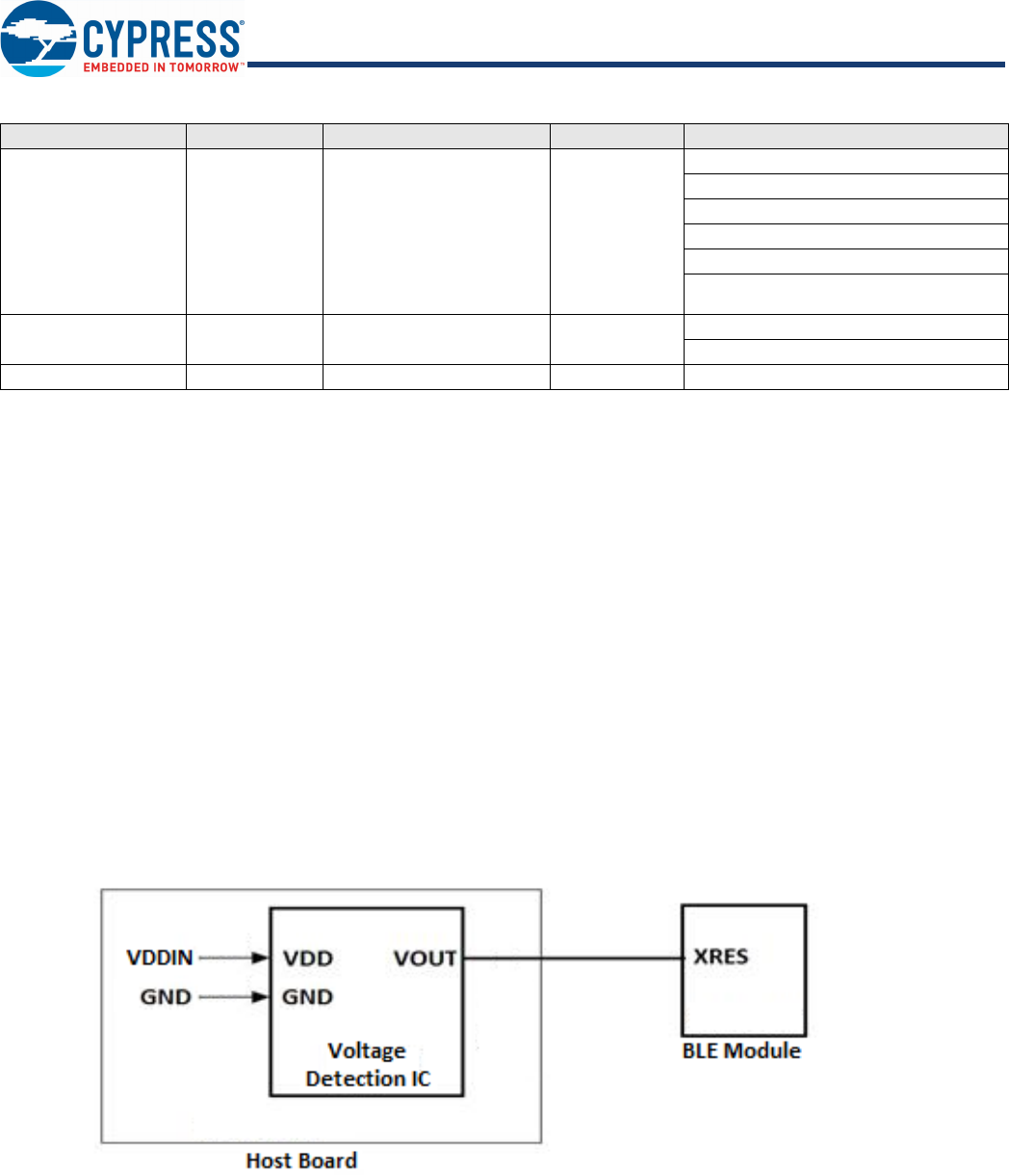
Considerations and Optional Components for Brown Out (BO) Conditions
Power supply design must be completed to ensure that the CYBT-483039-02 module does not encounter a Brown Out condition,
which can lead to unexpected funcitonality, or module lock up. A Brown Out condition may be met if power supply provided to the
module during power up or reset is in the range shown below:
VIL ≤ VDD ≤ VIH
Refer to Table 18 for the VIL and VIH specifications.
System design should ensure that the condition above is not encountered when power is removed from the system. In the event that
this cannot be guaranteed (i.e. battery installation, high value power capacitors with slow discharge), it is recommended that an
external voltage detection device be used to prevent the Brown Out voltage range from occuring during power removal. Please refer
to Figure 8 for the recommended circuit design when using an external voltage detection IC.
Figure 8. Reference Circuit Block Diagram for External Voltage Detection IC
In the event that the module does encounter a Brown Out condition, and is operating erratically or not responsive, power cycling the
module will correct this issue and once reset, the module should operate correctly. Brown Out conditions can potentially cause issues
that cannot be corrected, but in general, a power-on-reset operation will correct a Brown Out condition.
Function Input or Output Function Type GPIOs Required Function Connection Description
PWM Output Pulse Width Modulator 1 ~ 6
PWM Channel 0
PWM Channel 1
PWM Channel 2
PWM Channel 3
PWM Channel 4
PWM Channel 5
ACLK Output Auxiliary Clock 1 ~ 2 Auxiliary Clock 0 (ACLK0)
Auxiliary Clock 1 (ACLK1)
HIDOFF Output HID-OFF Indicator 1 HID-OFF Indicator to host

Document Number: 002-23993 Rev. ** Page 13 of 49
PRELIMINARY CYBT-483039-02
External Reset (XRES)
The CYBT-483039-02 has an integrated power-on reset circuit which completely resets all circuits to a known power on state. This
action can also be envoked by an external reset signal, forcing it into a power-on reset state. The XRES signal is an active-low signal,
which is an input to the CYBT-483039-02 module (solder pad 3). The CYBT-483039-02 module does not require an external pull-up
resistor on the XRES input
During power on operation, the XRES connection to the CYBT-483039-02 is required to be held low 50 ms after the VDD power supply
input to the module is stable. This can be accomplished in the following ways:
nThe host device can connect a GPIO to the XRES of Cypress CYBT-483039-02 module and pull XRES low until VDD is stable.
XRES is recommended to be released 50 ms after VDD is stable.
nIf the XRES connection of the CYBT-483039-02 module is not used in the application, a 0.33 uF capacitor may be connected to the
XRES solder pad of the CYBT-483039-02 in order to delay the XRES release. The capacitor value for this recommended imple-
mentation is approximate, and the exact value may differ depending on the VDD power supply ramp time of the system. The capacitor
value should result in an XRES release timing of at least 50 ms after VDD stability.
nThe XRES release timing may be controlled by a external voltage detection IC. XRES should be released 50 ms after VDD is stable.
Refer to Figure 11 on page 19 for XRES operating and timing requirements during power on events.
HCI UART Connections
The recommendations in this section apply to the HCI UART (Solder Pads 21, 22, 23, and 24). For full UART functionality, all UART
signals must be connected to the Host device. If full UART functionality is not being used, and only UART RXD and TXD are desired
or capable, then the following connection considerations should be followed for UART RTS and CTS:
nUART RTS: Can be left floating, pulled low, or pulled high. RTS is not critical for initial firmware uploading at power on.
nUART CTS: Must be pulled low to bypass flow control and to ensure that continuous data transfers are made from the host to the
module.
External Component Recommendation
Power Supply Input Options and Circuitry
Two connection options are available for the VDD and VDDPA power supplies:
1. Single supply: Connect VDD and VDDPAto the same supply.
2. Independent supply: Power VDD and VDDPA separately.
In either connection scenario, it is recommended to place an external ferrite bead between the supply and the module connection.
The ferrite bead should be positioned as close as possible to the module pad connection.
The recommended ferrite bead value is 330 Ω, 100 MHz. (Murata BLM21PG331SN1D).
Document Number: 002-23993 Rev. ** Page 15 of 49
PRELIMINARY CYBT-483039-02
Critical Components List
Table 6 details the critical components used in the CYBT-483039-02 module.
Table 6. Critical Component List
Antenna Design
Table 7 details the chip antenna used in the CYBT-483039-02 module.
Table 7. Chip Antenna Specifications
Power Amplifier (PA) and Low Noise Amplifier (LNA)
Table 8 details the PA/LNA that is used on the CYBT-483039-02 module. For more information, see Table 8.
Table 8. Power Amplifier/Low Noise Amplifier Details
Table 9 details the power consumption of the integrated PA/LNA used on the More Part Numbers module. Table 9 only details the
current consumption of the RFX2401C PA/LNA. VDD= 3.3 V, TA = +25°C, measured on the RFX2401C evaluation board, unless
otherwise noted.
Table 9. Power Amplifier/Low Noise Amplifier Current Consumption Specifications
Component Reference Designator Description
40-pin QFU2Silicon N Bluetooth Silicon Device - CYW20719
Antenna, 2.4 GHz, ALA321C3-CA1Chip Antenna
PA/LNA, RFX2401CU2PA/LNA
24.000 MHz, 12PFY1Crystal
Item Description
2400 – 2500 MHzFrequency Range
2.3 dBi typicalPeak Gain
10.0 dB typicalReturn Loss
Item Description
Skyworks Inc.PA/LNA Manufacturer
RFX2401CPA/LNA Part Number
Power Supply R 2.0V to 3.6Vange
Parameter Test Condition Min Typical Max Unit
mA100Pout = +18dBmTx High Power Current
mA17No RF appliedTx Quiescent Current
mA8No RF appliedRx Quiescent Current

Document Number: 002-23993 Rev. ** Page 16 of 49
PRELIMINARY CYBT-483039-02
Bluetooth Baseband Core
The Bluetooth Baseband Core (BBC) implements all time-critical functions required for high-performance Bluetooth operation. The
BBC manages the buffering, segmentation, and routing of data for all connections. It prioritizes and schedules all RX/TX activities
including adv, paging, scanning, and servicing of connections. In addition to these functions, it independently handles the host
controller interface (HCI) including all commands, events, and data flowing over HCI. The core also handles symbol timing, forward
error correction (FEC), header error control (HEC), cyclic redundancy check (CRC), authentication, data encryption/decryption, and
data whitening/dewhitening.
Table 10. Bluetooth Features
BQB and Regulatory Testing Support
The CYBT-483039-02 fully supports Bluetooth Test mode as described in Part I:1 of the Specification of the Bluetooth System Version
3.0. This includes the transmitter tests, normal and delayed loop back tests, and reduced hopping sequence.
In addition to the standard Bluetooth Test Mode, the CYBT-483039-02 also supports enhanced testing features to simplify RF
debugging and qualification and type-approval testing. These features include:
nFixed frequency carrier wave (unmodulated) transmission
pSimplifies some type-approval measurements (Japan)
pAids in transmitter performance analysis
nFixed frequency constant receiver mode
pReceiver output directed to I/O pin
pAllows for direct BER measurements using standard RF test equipment
pFacilitates spurious emissions testing for receive mode
nFixed frequency constant transmission
p8-bit fixed pattern or PRBS-9
pEnables modulated signal measurements with standard RF test equipment
Bluetooth 1.0 Bluetooth 1.2 Bluetooth 2.0
Basic Rate Interlaced Scans EDR 2 Mbps and 3 Mbp
SCO Adaptive Frequency Hopping –
Paging and Inquiry eSCO –
Page and Inquiry Scan – –
Sniff – –
Bluetooth 2.1 Bluetooth 3.0 Bluetooth 4.0
Secure Simple Pairing Unicast Connectionless Data Bluetooth Low Energy
Enhanced Inquiry Response Enhanced Power Control –
Sniff Subrating eSCO –
Bluetooth 4.1 Bluetooth 4.2 Bluetooth 5.0
Low Duty Cycle Advertising Data Packet Length Extension LE 2 Mbps
Dual Mode LE Secure Connection Slot Availability Mask
LE Link Layer Topology Link Layer Privacy High Duty Cycle Advertising
Document Number: 002-23993 Rev. ** Page 17 of 49
PRELIMINARY CYBT-483039-02
Power Management Unit
Figure 10 shows the CYW20719 power management unit (PMU) block diagram. The CYW20719 includes an integrated buck
regulator, a bypass LDO, a capless LDO for digital circuits and a separate LDO for RF. The bypass LDO automatically takes over from
the buck once Vbat supply falls below 2.1V.
The voltage levels shown in this figure are the default settings; the firmware may change voltage levels based on operating conditions.
Figure 10. Default Usage Mode

Integrated Radio Transceiver
The CYBT-483039-02 has an integrated radio transceiver that has been designed to provide low power operation in the globally
available 2.4 GHz unlicensed ISM band. It is fully compliant with Bluetooth Radio Specification 3.0 and meets or exceeds the require-
ments to provide the highest communication link quality of service.
Transmitter Path
CYBT-483039-02 features a fully integrated transmitter. The baseband transmit data is GFSK modulated in the 2.4 GHz ISM band.
Digital Modulator
The digital modulator performs the data modulation and filtering required for the GFSK signal. The fully digital modulator minimizes
any frequency drift or anomalies in the modulation characteristics of the transmitted signal.
Power Amplifier
The CYBT-483039-02 has an integrated power amplifier (PA) on the silicon device as well as a high power external power amplifier
(PA) integrated on the module. The total output power that this module is designed to achieve is +18 dBm.
Receiver Path
The receiver path uses a low IF scheme to downconvert the received signal for demodulation in the digital demodulator and bit
synchronizer. The receiver path provides a high degree of linearity, and an extended dynamic range to ensure reliable operation in
the noisy 2.4 GHz ISM band. The front-end topology, which has built-in out-of-band attenuation, enables the CYBT-483039-02 to be
used in most applications without off-chip filtering.
Digital Demodulator and Bit Synchronizer
The digital demodulator and bit synchronizer take the low-IF received signal and perform an optimal frequency tracking and bit
synchronization algorithm.
Receiver Signal Strength Indicator
The radio portion of the CYBT-483039-02 provides a receiver signal strength indicator (RSSI) to the baseband. This enables the
controller to take part in a Bluetooth power-controlled link by providing a metric of its own receiver signal strength to determine whether
the transmitter should increase or decrease its output power.
Local Oscillator
The local oscillator (LO) provides fast frequency hopping (1600 hops/second) across the 79 maximum available channels. The
CYBT-483039-02 uses an internal loop filter.
Document Number: 002-23993 Rev. ** Page 18 of 49
PRELIMINARY
CYBT-483039-02
Document Number: 002-23993 Rev. ** Page 19 of 49
PRELIMINARY CYBT-483039-02
Microcontroller Unit
The CYBT-483039-02 includes a Cortex M4 processor with 2 MB of ROM, 448 KB of data RAM, 64 KB of patch RAM, and 1 MB of
on-chip flash. The CM4 has a maximum speed of 96 MHz. CYBT-483039-02 supports execution from on-chip flash (OCF).
The CM4 also includes a single precision IEEE 754 compliant floating point unit (FPU).
The CM4 runs all the BT layers as well as application code. The ROM includes LM, HCI, L2CAP, GATT, as well as other stack layers
freeing up the flash for application usage. A standard serial wire debug (SWD) interface provides debugging support.
External Reset
An external active-low reset signal, XRES, can be used to put the CYBT-483039-02 in the reset state. An external voltage detector
reset IC with 50 ms delay is recommended on the XRES connection. The XRES must only be released after the VDDO supply volt-
age level has been stabilized for 50 ms.
Figure 11. Reset Timing

Document Number: 002-23993 Rev. ** Page 20 of 49
PRELIMINARY CYBT-483039-02
Peripheral and Communication Interfaces
I2C
The CYBT-483039-02 provides a 2-pin I2C compatible master interface to communicate with I2C compatible peripherals. The following
transfer clock rates are supported are:
n100 kHz
n400 kHz
n800 kHz (Not a standard I2C-compatible speed)
n1 MHz (Compatibility with high-speed I2C-compatible devices is not guaranteed)
SCL and SDA lines can be routed to any of the P0-P39 GPIOs allowing for flexible system configuration. When used as SCL/SDA
the GPIOs go into open drain mode and require an external pull-up for proper operation. I2C block does not support multi master
capability by either master or slave devices.
I2C1 is Master Only; I2C2 is Master/Slave. The Slave support is subject to driver support in WICED Studio.
HCI UART Interface
The CYBT-483039-02 includes a UART interface for factory programming as well as when operating as a BT HCI device in a system
with an external host. The UART physical interface is a standard, 4-wire interface (RX, TX, RTS, and CTS) with adjustable baud rates
from 115200 bps to 1.5 Mbps. Typical rates are 115200, 921600, 1500000 bps although intermediate speeds are also available.
Support for changing the baud rate during normal HCI UART operation is included through a vendor-specific command. The
CYBT-483039-02 UART operates correctly with the host UART as long as the combined baud rate error of the two devices is within
±5%. The UART interface has a 1040-byte receive FIFO and a 1040-byte transmit FIFO to support enhanced data rates. The interface
supports the Bluetooth UART HCI (H4) specification. The default baud rate for H4 is 115.2 kbaud.
The CYBT-483039-02 can wake up the host as needed or allow the host to sleep via the HOST_WAKE signal (solder pad 2). signal
allows the CYBT-483039-02 to optimize system power consumption by allowing a host device to remain in low power modes as long
as possible. The HOST_WAKE signal can be enabled via a vendor specific command.
Peripheral UART Interface
The CYBT-483039-02 has a second UART that may be used to interface to peripherals. This peripheral UART is accessed through
the optional I/O ports, which can be configured individually and separately for each functional pin. The CYBT-483039-02 can map the
peripheral UART to any GPIO. The Peripheral UART functionality is the same as the HCI UART, but with a 256-byte transmit and
receive FIFO.
Serial Peripheral Interface
The CYBT-483039-02 has two independent SPI interfaces. Both interfaces support Single, Dual, and Quad mode SPI operations as
well as MIPI DBI-C Interface.Either of the interface can be a master or a slave. SPI2 can support only 1 slave. SPI1 has a 1024 byte
transmit and receive buffers which is shared with the host UART interface. SPI2 has a dedicated 256 byte transmit and receive buffers.
To support more flexibility for user applications, the CYBT-483039-02 has optional I/O ports that can be configured individually and
separately for each functional pin. SPI IO voltage depends on VDDO.
MIPI interface
There are three options in DBI type-C corresponding to 9-bit, 16-bit, and 8-bit modes. The CYBT-483039-02 plays the role of host,
and only the 9-bit and 8-bit modes (option 1 and option 3 in DBI-C spec) are supported. In the 9-bit mode, the SCL, CS, MOSI, and
MISO pins are used. In the 8-bit mode, an additional pin (DCX) is required. The DCX pin indicates if the current outgoing bit stream
is a command or data byte.
32 kHz Crystal Oscillator
The CYBT-483039-02 utlizes the built-in Local Oscillator (LO) on the CYW20719 silicon device for 32kHz timing. The accuracy of the
LO is +/- 500 ppm. The use of an external XTAL oscillator is optional. CYBT-483039-02 includes external XTAL oscilator connections
for applications requiring higher timing accuracy. Figure 12 shows an external 32 kHz XTAL oscillator with external components and
Table 11 lists the the recommended external oscillator’s characteristics. This oscillator input can be operated with a 32 kHz or 32.768
kHz crystal oscillator or be driven with a clock input at similar frequency. The default component values are: R1 = 10 MΩ and C1 =
C2 = ~6 pF. The values of C1 and C2 are used to fine-tune the oscillator.
Document Number: 002-23993 Rev. ** Page 21 of 49
PRELIMINARY CYBT-483039-02
Figure 12. 32 kHz Oscillator Block Diagram
Table 11. XTAL Oscillator Characteristics
Parameter Symbol Conditions Minimum Typical Maximum Unit
Output frequency Foscout – – 32.768 – kHz
Frequency tolerance – Crystal-dependent – 100 – ppm
Start-up time Tstartup – – 500 – ms
XTAL drive level Pdrv For crystal selection – – 0.5 μW
XTAL series resistance Rseries For crystal selection – – 70 kΩ
XTAL shunt capacitance Cshunt For crystal selection – – 2.2 pF
External AC Input Amplitude VIN (AC) Ccouple = 100 pF;
Rbias= 10 Mohm 400 – – mVpp

Document Number: 002-23993 Rev. ** Page 22 of 49
PRELIMINARY CYBT-483039-02
ADC Port
The ADC is a Σ-Δ ADC core designed for audio (13 bits) and DC (12 bits) measurement. It operates at 12 MHz and has 10 solder
pad connections that can act as input channels. The internal bandgap reference has ±5% accuracy without calibration. Calibration
and digital correction schemes can be applied to reduce ADC absolute error and improve measurement accuracy in DC mode.
The following CYBT-483039-02 module solder pads can be used as ADC inputs:
nPad 4: P33, ADC Input Channel 6
nPad 7: P38, ADC Input Channel 1
nPad 8: P34/P35/P36, ADC Input Channels 5/4/3 respectively; NOTE: only one ADC input on this solder pad can be active at a
given time.
nPad 9: P1, ADC Input Channel 28
nPad 10: P0, ADC Input Channel 29
nPad 11: P29, ADC Input Channel 10
nPad 12: P13/P23/28, ADC Input Channels 22/12/11 respectively; NOTE: only one ADC input on this solder pad can be active at a
given time.
nPad 14: P10/P11, ADC Input Channels 25/24 respectively; NOTE: only one ADC input on this solder pad can be active at a given time.
nPad 15: P17, ADC Input Channel 18
nPad 20: P15, ADC Input Channel 20. P15 should not be driven high externally while the part is held in reset (it can be floating or
driven low). Failure to do so may cause some current to flow through P15 until the device comes out of reset.
GPIO Ports
The CYBT-483039-02 has a maximum of 15 general-purpose I/Os (GPIOs). All GPIOs support the following:
nProgrammable pull-up/down of approximately 45 KOhms.
nInput disable, allowing pins to be left floating or analog signals connected without risk of leakage.
nSource/sink 8 mA at 3.3V and 4 mA at 1.8V.
nP15 is Bonded to the same pin as XTALI_32K (Pad 20). If an External 32.768KHz crystal is not used, then this pin can be used as
GPIO P15.
nP26/P28/P29 can sink/source 16 mA at 3.3V and 8 mA at 1.8V.
Most peripheral functions can be assigned to any GPIO. For details, refer to Tabl e 5 . For more details on Supermux configuration and
control, refer to "Supermux Wizard for CYW20719" user guide.
The list below details the GPIOs that are available on the CYBT-483039-02 module:
pP0-P1, P4, P6, P7, P17, P25, P26, P29, P33, and P38
pP10/P11 (Double bonded connection on the CYBT-483039-02 module, only one of two is available)
pP13/P23/P28 (Triple bonded connection on the CYBT-483039-02 module, only one of three is available)
pP15/XTALI_32K (Double bonded pin on the CYBT-483039-02 module, only one of two is available)
pP34/P35/P36 (Triple bonded pin on the CYBT-483039-02 module, only one of three is available)
pP19, P20 and P39 are reserved for system use. Please do not use those 3 GPIOs.
For GPIOs highlighted as double or triple bonded connections, only one of the connections can be used at a given time. When a
certain GPIO is selected, the other GPIOs bonded to the same connection must be configured to input with output disable.
Document Number: 002-23993 Rev. ** Page 23 of 49
PRELIMINARY CYBT-483039-02
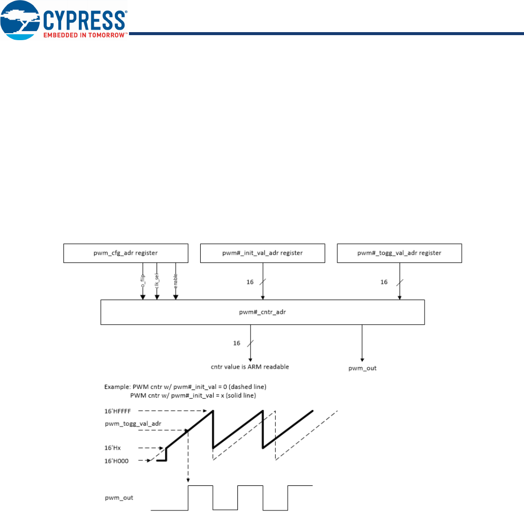
PWM
The CYBT-483039-02 has six internal PWMs, labeled PWM0-5. The PWM module consists of the following:
nEach of the six PWM channels contains the following registers:
p16-bit initial value register (read/write)
p16-bit toggle register (read/write)
p16-bit PWM counter value register (read)
nPWM configuration register shared among PWM0–5 (read/write). This 18-bit register is used:
pTo configure each PWM channel
pTo select the clock of each PWM channel
pTo change the phase of each PWM channel
The application can access the PWM module through the FW driver.
Figure 13 shows the structure of one PWM channel.
Figure 13. PWM Block Diagram

Document Number: 002-23993 Rev. ** Page 24 of 49
PRELIMINARY CYBT-483039-02
PDM Microphone
The CYBT-483039-02 accepts a ΣΔ-based one-bit pulse density modulation (PDM) input stream and outputs filtered samples at either
8 kHz or 16 kHz sampling rates. The PDM signal derives from an external kit that can process analog microphone signals and generate
digital signals. The PDM input shares the filter path with the auxADC. Two types of data rates can be supported:
n8 kHz
n16 kHz
The external digital microphone takes in a 2.4 MHz clock generated by the CYBT-483039-02 and outputs a PDM signal which is
registered by the PDM interface with either the rising or falling edge of the 2.4 MHz clock selectable through a programmable control
bit. The design can accommodate two simultaneous PDM input channels, so stereo voice is possible.
Note: Subject to the driver support in WICED Studio.
I2S Interface
The CYBT-483039-02 supports a single I2S digital audio port with both master and slave modes. The I2S signals are:
nI2S Clock: I2S SCK
nI2S Word Select: I2S WS
nI2S Data Out: I2S DO
nI2S Data In: I2S DI
I2S SCK and I2S WS become outputs in master mode and inputs in slave mode, while I2S DO always stays as an output. The channel
word length is 16 bits and the data is justified so that the MSN of the left-channel data is aligned with the MSB of the I2S bus, per I2S
Specifications. The MSB of each data word is transmitted one bit clock cycle after the I2S WS transition, synchronous with the falling
edge of bit clock. Left Channel data is transmitted when I2S WS is low, and right-channel data is transmitted when I2S WS is high.
Data bits sent by the CYBT-483039-02 are synchronized with the falling edge of I2S SCK and should be sampled by the receiver on
the rising edge of the I2S SCK.
Note: The PCM interface shares HW with the I2S interface and only one can be used at a given time.
PCM Interface
The CYBT-483039-02 includes a PCM interface that can connect to linear PCM codec devices in master or slave mode. In master
mode, the CYBT-483039-02 generates the PCM_CLK and PCM_SYNC signals. In slave mode, these signals are provided by another
master on the PCM interface and are inputs to the CYBT-483039-02.The configuration of the PCM interface may be adjusted by the
host through the use of vendor-specific HCI commands.
Note: The PCM interface shares HW with the I2S interface and only one can be used at a given time.
Slot Mapping
The CYBT-483039-02 supports up to three simultaneous full-duplex SCO or eSCO channels through the PCM Interface. These three
channels are time-multiplexed onto the single PCM interface by using a time-slotting scheme where the 8 kHz or 16 kHz audio sample
interval is divided into as many as 16 slots. The number of slots is dependent on the selected interface rate (128 kHz, 512 kHz, or
1024 kHz). The corresponding number of slots for these interface rate is 1, 2, 4, 8, and 16, respectively. Transmit and receive PCM
data from an SCO channel is always mapped to the same slot. The PCM data output driver tristates its output on unused slots to allow
other devices to share the same PCM interface signals. The data output driver tristates its output after the falling edge of the PCM
clock during the last bit of the slot.
Frame Synchronization
The CYBT-483039-02 supports both short- and long-frame synchronization in both master and slave modes. In short frame synchro-
nization mode, the frame synchronization signal is an active-high pulse at the audio frame rate that is a single-bit period in width and
is synchronized to the rising edge of the bit clock. The PCGM slave looks for a high on the falling edge of the bit clock and expects
the first bit of the first slot to start at the next rising edge of the clock. In long-frame synchronization mode, the frame synchronization
signal is again an active-high pulse at the audio frame rate; however, the duration is three bit periods and the pulse starts coincident
with the first bit of the first slot.
Data Formatting
The CYBT-483039-02 may be configured to generate and accept several different data formats. For conventional narrow band speech
mode, the CYBT-483039-02 uses 13 of the 16 bits in each PCM frame. The location and order of these 13 bits can be configured to
support various data formats on the PCM interface. The remaining three bits are ignored on the input and may be filled with 0s, 1s, a
sign bit, or a programmed value on the output. The default format is 13-bit 2’s complement data, left justified, and clocked MSB first.

Document Number: 002-23993 Rev. ** Page 25 of 49
PRELIMINARY CYBT-483039-02
Burst PCM Mode
In this mode of operation, the PCM bus runs at a significantly higher rate of operation to allow the host to duty cycle its operation and
save current. In this mode of operation, the PCM bus can operate at a rate of up to 24 MHz. This mode of operation is initiated with
an HCI command from the host.
Security Engine
The CYBT-483039-02 includes a hardware security accelerator which greatly decreases the time required to perform typical security
operations. Access to the hardware block is provided via a firmware interface (see firmware documentation for details).Thie security
engine includes:
nPublic key acceleration (PKA) cryptography
nAES-CTR/CBC-MAC/CCM acceleration
nSHA2 message hash and HMAC acceleration
nRSA encryption and decryption of modulus sizes up to 2048 bits
nElliptic curve Diffie-Hellman in prime field GF(p)
Note: Security Engine is used only by the Bluetooth stack to reduce CPU overhead. It is not available for application use.
Random Number Generator
This hardware block is used for key generation for Bluetooth.
Note: Availability for use by the application is subject to the support in WICED Studio.
Note: The Random Number Generator block must be warmed up prior to use. A delay of 500 ms from cold boot is necessary prior to
using the Random Number Generator.

Document Number: 002-23993 Rev. ** Page 26 of 49
PRELIMINARY CYBT-483039-02
Power Modes
The CYBT-483039-02 support the following HW power modes are supported:
nActive mode - Normal operating mode in which all peripherals are available and the CPU is active.
nIdle mode - In this mode, the CPU is in “Wait for Interrupt” (WFI) and the HCLK, which is the high frequency clock derived from the
main crystal oscillator is running at a lower clock speed. Other clocks are active and the state of the entire chip is retained.
nSleep mode - In this mode, CPU is in WFI and the HCLK is not running. The PMU determines if the other clocks can be turned off
and does accordingly. State of the entire chip is retained, the internal LDOs run at a lower voltage (voltage is managed by the PMU),
and SRAM is retained.
nPDS mode - This mode is an extension of the PMU Sleep wherein most of the peripherals such as UART and SPI are turned off.
The entire memory is retained, and on wakeup the execution resumes from where it paused.
nShut Down Sleep (SDS) - Everything is turned off except the IO Power Domain, RTC, and LPO. The device can come out of this
mode either due to BT activity or by an external interrupt. Before going into this mode, the application can store some bytes of data
into “Always On RAM” (AON). When the device comes out of this mode, the data from AON is restored. After waking from SDS, the
application will start from the beginning (warmboot) and has to restore its state based on information stored in AON. In the SDS
mode, a single BT task with no data activity, such as an ACL connection, BLE connection, or BLE advertisement can be performed.
nHIDOFF (Timed-Wake) mode - The device can enter this mode asynchronously, that is, the application can force the device into
this mode at any time. IO Power Domain, RTC, and LPO are the only active blocks. A timer that runs off the LPO is used to wake
the device up after a predetermined fixed time.
nHIDOFF (External Interrupt-Waked) mode - This mode is similar to Timed-Wake, but in HID-off mode even the LPO and RTC are
turned off. So, the only wakeup source is an external interrupt.
Transition between power modes is handled by the on-chip firmware with host/application involvement. Please see Firmware Section
for details.
Firmware
The CYBT-483039-02 ROM firmware runs on a real time operating system and handles the programming and configuration of all
on-chip hardware functions as well as the BT/LE baseband, LM, HCI, GATT, ATT, L2CAP and SDP layers. The ROM also includes
drivers for on-chip peripherals as well as handling on-chip power management functions including transitions between different power
modes.
The CYBT-483039-02 is fully supported by the Cypress WICED Studio platform. WICED releases provide latest ROM patches, drivers,
and sample applications allowing customized applications using the CYBT-483039-02 to be built quickly and efficiently.
Please refer to WICED Technical Brief and CYBT-483039-02 Product Guide for details on the firmware architecture, driver documen-
tation, power modes and how to write applications/profiles using the CYBT-483039-02.
Document Number: 002-23993 Rev. ** Page 27 of 49
PRELIMINARY CYBT-483039-02
Electrical Characteristics
The absolute maximum ratings in the following table indicate levels where permanent damage to the device can occur, even if these
limits are exceeded for only a brief duration. Functional operation is not guaranteed under these conditions. Operation at absolute
maximum conditions for extended periods can adversely affect long-term reliability of the device.
The CYBT-483039-02 uses an onboard low voltage detector to shut down the part when supply voltage (VDD) drops below operating
range.
Table 15. Power Supply Shut Down Specifications
Core Buck Regulator
Table 12. Silicon Absolute Maximum Ratings
Requirement Parameter Specification Unit
Min. Nom. Max.
Maximum Junction Temperature – – 125 °C
VDD IO –0.5 – 3.795 V
VDD RF –0.5 – 1.38 V
VDDBAT3V –0.5 – 3.795 V
DIGLDO_VDDIN1P5 –0.5 – 1.65 V
RFLDO_VDDIN1P5 –0.5 – 1.65 V
PALDO_VDDIN_5V –0.5 – 3.795 V
MIC_AVDD –0.5 – 3.795 V
Table 13. ESD/Latchup
Requirement Parameter Specification Unit
Min. Nom. Max.
ESD Tolerance HBM (Silicon) –2000 – 2000 V
ESD Tolerance CDM (Silicon) –500 – 500 V
Latch-up – 200 – mA
Table 14. Power Supply Specifications
Parameter Conditions Min. Typical Max. Unit
VDD input Module Chipset Input 2.0 3.0 3.60 V
VDDPA input Module PA/LNA Input 2.0 3.0 3.60 V
VDD Ripple Module Input Ripple (VDDPA, VDD) – – 100 mV
VBAT Input Internal to Module (not accessible) 1.90 3.0 3.6 V
PMU turn-on time VBAT is ready. – – 300 μs
Parameter Min. Typical Max. Unit
VSHUT 1.625 1.7 1.76 V
Table 16. Silicon Core Buck Regulator
Parameter Conditions Min. Typ. Max. Unit
Input supply voltage DC, VBAT DC voltage range inclusive of disturbances 1.90 3.0 3.63 V
CBUCK output current LPOM only – – 65 mA

Document Number: 002-23993 Rev. ** Page 28 of 49
PRELIMINARY CYBT-483039-02
nMinimum capacitor value refers to residual capacitor value after taking into account part-to-part tolerance, DC-bias, temperature,
and aging.
nMaximum capacitor value refers to the total capacitance seen at a node where the capacitor is connected. This also includes any
decoupling capacitors connected at the load side, if any.
Output voltage range Programmable, 30mV/step
default = 1.2V (bits=0000) 1.21.261.5 V
Output voltage DC accuracy Includes load and line regulation –4 – +4%
LPOM efficiency (high load) – 85 – %
LPOM efficiency (low load) – 80 – %
Input supply voltage ramp-up time 0 to 3.3V 40 – – μs
Table 16. Silicon Core Buck Regulator (continued)
Parameter Conditions Min. Typ. Max. Unit
Document Number: 002-23993 Rev. ** Page 29 of 49
PRELIMINARY CYBT-483039-02
Digital LDO
Digital I/O Characteristics
ADC Electrical Characteristics
Table 17. Digital LDO
Parameter Conditions Min. Typ. Max. Unit
Input supply voltage, Vin Minimum Vin=Vo+0.12V requirement must be
met under maximum load. 1.2 1.2 1.6 V
Nominal output voltage,Vo Internal default setting – 1.1 – V
Dropout voltage At maximum load – – 120 mV
Table 18. Digital I/O Characteristics
Characteristics Symbol Minimum Typical Maximum Unit
Input low voltage (VDD = 3V) VIL ––0.8V
Input high voltage (VDD = 3V) VIH 2.4 – – V
Input low voltage (VDD = 1.8V) VIL ––0.4V
Input high voltage (VDD = 1.8V) VIH 1.4 – – V
Output low voltage VOL – – 0.45 V
Output high voltage VOH VDDO – 0.45V – – V
Input low current IIL ––1.0μA
Input high current IIH ––1.0μA
Output low current (VDD = 3V, VOL = 0.5V) IOL ––8.0mA
Output low current (VDD = 1.8V, VOL = 0.5V) IOL ––4.0mA
Output high current (VDD = 3V, VOH = 2.55V) IOH ––8.0mA
Output high current (VDD = 1.8V, VOH = 1.35V) IOH ––4.0mA
Input capacitance CIN ––0.4pF
UART_TXD VOL (0.5mA) UART_TXD VOL ––TBDmA
UART_TXD VOH (0.5mA) UART_TXD VOH TBD – – mA
Table 19. Electrical Characteristics
Parameter Symbol Conditions/Comments Min. Typ. Max. Unit
Current consumption ITOT ––23mA
Power down current – At room temperature – 1 – μA
ADC Core Specification
ADC reference voltage VREF From BG with ±3% accuracy – 0.85 – V
ADC sampling clock – – – 12 – MHz
Absolute error – Includes gain error, offset and
distortion. Without factory calibration. ––5%
Includes gain error, offset and
distortion. After factory calibration. ––2%
ENOB –For audio application 12 13 –Bit
For static measurement 10 – –
ADC input full scale FS For audio application –1.6 –
For static measurement 1.8 –3.6
Conversion rate –For audio application 816 –kHz
For static measurement 50 100 –
Document Number: 002-23993 Rev. ** Page 30 of 49
PRELIMINARY CYBT-483039-02
Bluetooth Silicon Current Consumption
In Table 20, current consumption measurements are taken at module input VDD = 3.0V.
Signal bandwidth –For audio application 20 –8K Hz
For static measurement –DC –
Input impedance RIN For audio application 10 – – KW
For static measurement 500 – –
Startup time –For audio application –10 –ms
For static measurement –20 –μs
MIC PGA Specifications
MIC PGA gain range – – 0 – 42 dB
MIC PGA gain step – – – 1 – dB
MIC PGA gain error – Includes part-to-part gain variation –1 – 1 dB
PGA input referred noise – At 42 dB PGA gain A-weighted – – 4 μV
Passband gain flatness – PGA and ADC, 100 Hz–4 kHz –0.5 – 0.5 dB
MIC Bias Specifications
MIC bias output voltage – At 2.5V supply – 2.1 – V
MIC bias loading current – – – – 3 mA
MIC bias noise – Refers to PGA input 20 Hz to
8 kHz, A-weighted ––3μV
MIC bias PSRR – at 1 kHz 40 – – dB
ADC SNR – A-weighted 0 dB PGA gain 78 – – dB
ADC THD + N – –3 dBFS input 0 dB PGA gain 74 – – dB
GPIO input voltage Always lower than avddBAT – – 3.6 V
GPIO source impedance1– Resistance – – 1 kΩ
Capacitance – – 10 pF
1. Conditional requirement for the measurement time of 10 μs. Relaxed with longer measurement time for each GPIO input channel.
Table 20. SIlicon Current Consumption BT/LE
Operational Mode Conditions Typical Unit
HCI 48 MHz with Pause 1.1 mA
48 MHz Without Pause 2.2 mA
RX Continuous RX 5.9 mA
TX Continuous TX - 0 dBm 5.6 mA
PDS 61 μA
HID-Off (SDS) 32 KHz xtal and 16 KB Retention RAM on 1.6 μA
Advertising Unconnectable - 1 sec 14 μA
Connectable Undirected - 1 sec 17 μA
LE Connection - SDS Master - 1 sec TBD μA
Slave - 1 sec TBD μA
Page Scan - PDS Interlaced - R1 122 μA
Sniff - PDS 500 ms Sniff, 1 attempt, 0 timeout - Master 132 μA
500 ms Sniff, 1 attempt, 0 timeout - Slave 138 μA
Table 19. Electrical Characteristics (continued)
Parameter Symbol Conditions/Comments Min. Typ. Max. Unit
Document Number: 002-23993 Rev. ** Page 31 of 49
PRELIMINARY CYBT-483039-02
Table 21. Power Amplifier/Low Noise Amplifier Current Consumption Specifications
Chipset RF Specifications
Table 22 and Table 23 apply to single-ended industrial temperatures. Unused inputs are left open.
Continuous DM5 or DH5 packets - MasBi-Directional Data Exchange mA6.9ter or Slave
Parameter Test Condition Min Typical Max Unit
mA100
Pout = +18dBm
Tx High Power Current
mA17No RF appliedTx Quiescent Current
mA8No RF appliedRx Quiescent Current
Table 22. Chipset Receiver RF Specifications
Parameter Mode and Conditions Min Typ Max Unit
MHz2480–2402–Frequency range
RX sensitivity1–92.0–GFSK, 0.1% BER, 1 Mbps 2dBm–
π–94.0–/4-DQPSK, 0.01% BER, 2 Mbps 2dBm–
8-DPSK, 0.01% BER –88.0–, 3 Mbps 2dBm–
dBm–20––All data ratesMaximum input
GFSK Modulation
GFSK, 0.1% BERC/I cochannel 3dB11.0––
GFSK, 0.1% BERC/I 1 MHz adjacent channel 4dB0––
GFSK, 0.1% BERC/I 2 MHz adjacent channel 3dB–30.0––
C/I ≥ GFSK, 0.1% BER3 MHz adjacent channel 5dB–40.0––
GFSK, 0.1% BERC/I image channel 3dB–9.0––
GFSK, 0.1% BERC/I 1 MHz adjacent to image channel 3dB–20.0––
QPSK Modulation
C/I cochannel π/4-DQPSK, 0.1% BER3dB13.0––
C/I 1 MHz adjacent channel π/4-DQPSK, 0.1% BER4dB0––
C/I 2 MHz adjacent channel π/4-DQPSK, 0.1% BER3dB–30.0––
C/I ≥ 3 MHz adjacent channel π/4-DQPSK, 0.1% BER5dB–40.0––
C/I image channel π/4-DQPSK, 0.1% BER3dB–9.0––
C/I 1 MHz adjacent to image channel π/4-DQPSK, 0.1% BER3dB–20.0––
8PSK Modulation
8-DPSK, 0.1% BERC/I cochannel 3dB21.0––
8-DPSK, 0.1% BERC/I 1 MHz adjacent channel 3dB5.0––
8-DPSK, 0.1% BERC/I 2 MHz adjacent channel 3dB–25.0––
C/I ≥ 8-DPSK, 0.1% BER3 MHz adjacent channel 5dB–33.0––
8-DPSK, 0.1% BERC/I image channel 3dB0––
C/I 1 MHz adjacen 8-DPSK, 0.1% BERt to image channel 3dB13––
Out-of-Band Blocking Performance (CW)4
dBm––10.0–BDR GFSK 0.1% BER30 MHz to 2000 MHz
Table 20. SIlicon Current Consumption BT/LE
Operational Mode Conditions Typical Unit
Document Number: 002-23993 Rev. ** Page 32 of 49
PRELIMINARY CYBT-483039-02
2000 MHz to 2399 MHz BDR GFSK 0.1% BER – –27.0 – dBm
2498 MHz to 3000 MHz BDR GFSK 0.1% BER – –27.0 – dBm
3000 MHz to 12.75 GHz BDR GFSK 0.1% BER – –10.0 – dBm
Inter-modulation Performance6
BT, interferer signal level BDR GFSK 0.1% BER – – –39.0 dBm
Spurious Emissions
30 MHz to 1 GHz – – – –57.0 dBm
1 GHz to 12.75 GHz – – – –55.0 dBm
1. Dirty TX is off
2. Up to 1dB of variation may potentially be seen from typical sensitivity specs due to the chip, board and associated variations
3. The receiver sensitivity is measured at BER of 0.1% on the device interface.
4. Desired signal is 10 dB above the reference sensitivity level (defined as –70 dBm).
5. Desired signal is 3 dB above the reference sensitivity level (defined as –70 dBm).
6. Desired signal is -64 dBm Bluetooth-modulated signal, interferer 1 is –39 dBm sine wave at frequency f1, interferer 2 is –39 dBm Bluetooth modulated signal at
frequency f2, f0 = 2*f1 – f2, and |f2 – f1| = n*1 MHz, where n is 3, 4, or 5. For the typical case, n = 4.
Table 23. Chipset Transmitter RF Specifications
Parameter Min Typ Max Unit
Transmitter Section
Frequency range 2402 – 2480 MHz
Class 2: GFSK Tx power – 4.0 – dBm
Class 2: EDR Tx Power – 0 – dBm
20 dB bandwidth – 930 1000 kHz
Adjacent Channel Power
|M – N| = 2 – – –20 dBm
|M – N| ≥ 3 – – –40 dBm
Out-of-Band Spurious Emission
30 MHz to 1 GHz – – –36.0 dBm
1 GHz to 12.75 GHz – – –30.0 dBm
1.8 GHz to 1.9 GHz – – –47.0 dBm
5.15 GHz to 5.3 GHz – – –47.0 dBm
LO Performance
Initial carrier frequency tolerance –75 – +75 kHz
Frequency Drift
DH1 packet –25 – +25 kHz
DH3 packet –40 – +40 kHz
DH5 packet –40 – +40 kHz
Drift rate –20 20 kHz/50 µs
Frequency Deviation
Average deviation in payload
(sequence used is 00001111) 140 – 175 kHz
Maximum deviation in payload
(sequence used is 10101010) 115 – – kHz
Channel spacing – 1 – MHz
Modulation Accuracy
Table 22. Chipset Receiver RF Specifications (continued)
Parameter Mode and Conditions Min Typ Max Unit
Document Number: 002-23993 Rev. ** Page 33 of 49
PRELIMINARY CYBT-483039-02
πkHz10––10/4-DQPSK Frequency Stability
π%20––/4-DQPSK RMS DEVM
π%35––/4-QPSK Peak DEVM
π%30––/4-DQPSK 99% DEVM
kHz10––108-DPSK frequency stability
%13––8-DPSK RMS DEVM
%25––8-DPSK Peak DEVM
%20––8-DPSK 99% DEVM
In-Band Spurious Emissions
1.0 MHz < |M – N| < dBc–26––1.5 MHz
1.5 MHz < |M – N| < dBm–20––2.5 MHz
dBm–40––|M – N| > 2.5 MHz
Table 24. BLE RF Specifications
Parameter Conditions Minimum Typical Maximum Unit
MHz2480–2402N/AFrequency range
Rx sensitivity (QFN)1–95.0–LE GFSK, 0.1% BER, 1 Mbps 2dBm–
dBm–4.0–BLE Silicon Device CYW20719 OnlyTx power
dBm
18
––Module total output powerTx power
kHz275255225N/AMod Char: Delta F1 average
Mod Char: Delta F2 max3%––99.9N/A
%–0.950.8N/AMod Char: Ratio
1. Dirty Tx is Off
2. Up to 1dB of variation may potentially be seen from typical sensitivity specs due to the chip, board and associated variations
3. At least 99.9% of all delta F2 max frequency values recorded over 10 packets must be greater than 185 kHz.
Table 25. CYBT-483039-02 GPS and GLONASS Band Spurious Emission
Parameter Condition Min. Typ. Max. Unit
dBm/Hz––160–GPS1570-1580 MHz
dBm/Hz––159–GLONASS1592-1610 MHz
Table 23. Chipset Transmitter RF Specifications (continued)
Parameter Min Typ Max Unit
Document Number: 002-23993 Rev. ** Page 34 of 49
PRELIMINARY CYBT-483039-02
Timing and AC Characteristics
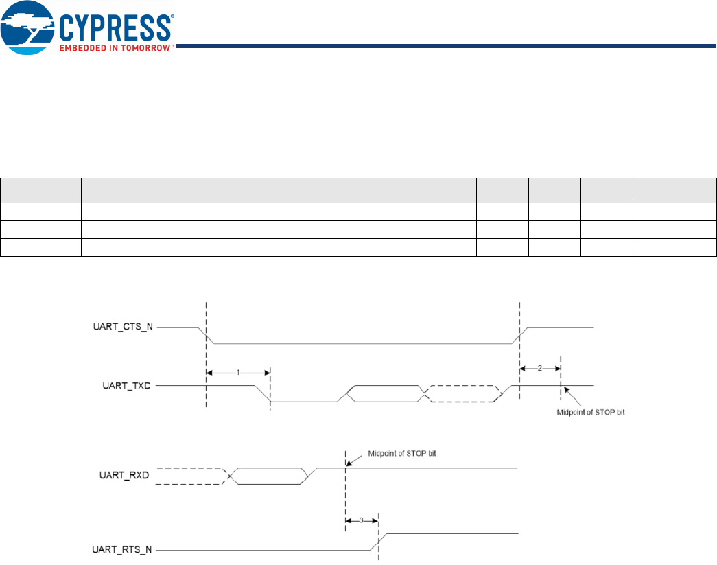
In this section, use the numbers listed in the Reference column of each table to interpret the following timing diagrams.
UART Timing
Figure 14. UART Timing
Table 26. UART Timing Specifications
Reference Characteristics Min. Typ. Max. Unit
1 Delay time, UART_CTS_N low to UART_TXD valid. – – 1.50 Bit periods
2 Setup time, UART_CTS_N high before midpoint of stop bit. – – 0.67 Bit periods
3 Delay time, midpoint of stop bit to UART_RTS_N high. – – 1.33 Bit periods
Document Number: 002-23993 Rev. ** Page 35 of 49
PRELIMINARY CYBT-483039-02
SPI Timing
The SPI interface can be clocked up to 24 MHz.
Table 27 and Figure 15 show the timing requirements when operating in SPI Mode 0 and 2.
Figure 15. SPI Timing, Mode 0 and 2
Table 27. SPI Mode 0 and 2
Reference Characteristics Min. Max. Unit
1 Time from master assert SPI_CSN to first clock edge 45 – ns
2 Hold time for MOSI data lines 12 ½ SCK ns
3 Time from last sample on MOSI/MISO to slave deassert SPI_INT 0 100 ns
4 Time from slave deassert SPI_INT to master deassert SPI_CSN 0 – ns
5 Idle time between subsequent SPI transactions 1 SCK – ns
Document Number: 002-23993 Rev. ** Page 36 of 49
PRELIMINARY CYBT-483039-02
Table 28 and Figure 16 show the timing requirements when operating in SPI Mode 1 and 3.
Figure 16. SPI Timing, Mode 1 and 3
Table 28. SPI Mode 1 and 3
Reference Characteristics Min. Max. Unit
1 Time from master assert SPI_CSN to first clock edge 45 – ns
2 Hold time for MOSI data lines 12 ½ SCK ns
3 Time from last sample on MOSI/MISO to slave deassert SPI_INT 0 100 ns
4 Time from slave deassert SPI_INT to master deassert SPI_CSN 0 – ns
5 Idle time between subsequent SPI transactions 1 SCK – ns
Document Number: 002-23993 Rev. ** Page 37 of 49
PRELIMINARY CYBT-483039-02
I2C Compatible Interface Timing
The specifications in Table 29 references Figure 17.
Figure 17. I2C Interface Timing Diagram
Table 29. I2C Compatible Interface Timing Specifications (up to 1 MHz)
Reference Characteristics Minimum Maximum Unit
1 Clock frequency – 100 kHz
400
800
1000
2 START condition setup time 650 – ns
3 START condition hold time 280 – ns
4 Clock low time 650 – ns
5 Clock high time 280 – ns
6 Data input hold time1
1. As a transmitter, 125 ns of delay is provided to bridge the undefined region of the falling edge of SCL to avoid unintended generation
of START or STOP conditions.
0 – ns
7 Data input setup time 100 – ns
8 STOP condition setup time 280 – ns
9 Output valid from clock – 400 ns
10 Bus free time2
2. Time that the CBUS must be free before a new transaction can start.
650 – ns

Document Number: 002-23993 Rev. ** Page 38 of 49
PRELIMINARY CYBT-483039-02
I2S Interface Timing
I2S timing is shown below in Table 30, Figure 18, and Figure 19.
Table 30. Timing for I2S Transmitters and Receivers
Transmitter Receiver
NotesLower LImit Upper Limit Lower Limit Upper Limit
Min Max Min Max Min Max Min Max
Clock Period T Ttr –––T
r–––1
Master Mode: Clock generated by transmitter or receiver
HIGH tHC 0.35Ttr – – – 0.35Ttr –––2
LOWtLC 0.35Ttr – – – 0.35Ttr –––2
Slave Mode: Clock accepted by transmitter or receiver
HIGH tHC –0.35T
tr –––0.35T
tr ––3
LOW tLC –0.35T
tr –––0.35T
tr ––3
Rise time tRC – – 0.15Ttr ––– – 4
Transmitter
Delay tdtr –––0.8T––––5
Hold time thtr 0–––––––4
Receiver
Setup time tsr ––––0.2T
tr –––6
Hold time thr ––––0.2T
tr –––6
1. The system clock period T must be greater than Ttr and Tr because both the transmitter and receiver have to be able to handle the data transfer
rate.
2.At all data rates in master mode, the transmitter or receiver generates a clock signal with a fixed mark/space ratio. For this reason, tHC and
tLC are specified with respect to T.
3.In slave mode, the transmitter and receiver need a clock signal with minimum HIGH and LOW periods so that they can detect the signal. So
long as the minimum periods are greater than 0.35Tr, any clock that meets the requirements can be used.
4.Because the delay (tdtr) and the maximum transmitter speed (defined by Ttr) are related, a fast transmitter driven by a slow clock edge can
result in tdtr not exceeding tRC which means thtr becomes zero or negative. Therefore, the transmitter has to guarantee that thtr is greater than
or equal to zero, so long as the clock rise-time tRC is not more than tRCmax, where tRCmax is not less than 0.15Ttr.
5. To allow data to be clocked out on a falling edge, the delay is specified with respect to the rising edge of the clock signal and T, always giving
the receiver sufficient setup time.
6. The data setup and hold time must not be less than the specified receiver setup and hold time.
Document Number: 002-23993 Rev. ** Page 39 of 49
PRELIMINARY CYBT-483039-02
Figure 18. I2S Transmitter Timing
Figure 19. I2S Receiver Timing
Document Number: 002-23993 Rev. ** Page 40 of 49
PRELIMINARY CYBT-483039-02
Environmental Specifications
Environmental Compliance
This Cypress BLE module is produced in compliance with the Restriction of Hazardous Substances (RoHS) and Halogen-Free (HF)
directives. The Cypress module and components used to produce this module are RoHS and HF compliant.
RF Certification
The CYBT-483039-02 module is certified under the following RF certification standards:
nFCC: WAP3039
nIC: 7922A-3039
nMIC: TBD
nCE
Safety Certification
The CYBT-483039-02 module complies with the following safety regulations:
nUnderwriters Laboratories, Inc. (UL): Filing E331901
nCSA
nTUV
Environmental Conditions
Table 31 describes the operating and storage conditions for the Cypress BLE module.
ESD and EMI Protection
Exposed components require special attention to ESD and electromagnetic interference (EMI).
A grounded conductive layer inside the device enclosure is suggested for EMI and ESD performance. Any openings in the enclosure
near the module should be surrounded by a grounded conductive layer to provide ESD protection and a low-impedance path to ground.
Device Handling: Proper ESD protocol must be followed in manufacturing to ensure component reliability.
Table 31. Environmental Conditions for CYBT-483039-02
Description Minimum Specification Maximum Specification
Operating temperature −30 °C 85 °C
Operating humidity (relative, non-condensation) 5% 85%
Thermal ramp rate – 10 °C/minute
Storage temperature –40 °C 85 °C
Storage temperature and humidity – 85 °C at 85%
ESD: Module integrated into system Components[6] –15 kV Air
2.0 kV Contact
Note
6. This does not apply to the RF pins (ANT).

Document Number: 002-23993 Rev. ** Page 41 of 49
PRELIMINARY CYBT-483039-02
Regulatory Information
FCC
FCC NOTICE:
The device CYBT-483039-02 complies with Part 15 of the FCC Rules. The device meets the requirements for modular transmitter
approval as detailed in FCC public Notice DA00-1407.transmitter
Operation is subject to the following two conditions: (1) This
device
may not cause harmful interference, and (2) This device must accept any interference received,
including interference that may
cause
undesired operation.
CAUTION:
The FCC requires the user to be notified that any changes or modifications made to this device that are not expressly approved
by
Cypress Semiconductor may void
the user's authority to operate
the equipment.
This equipment has been tested
and found to comply with the limits for a Class B digital device, pursuant to Part 15 of the FCC Rules.
These limits are designed to provide reasonable protection against harmful interference in a residential installation. This equipment
generates uses and can radiate radio frequency energy and, if not installed and used in accordance with the instructions,ê may
cause
harmful interference to radio communications. However, there is
no guarantee that interference will not occur in a particular
installation.
If this equipment does cause harmful interference to radio or television reception, which can be determined by turning the equipment
off and on, the user is encouraged to try to
correct the interference by one or more of
the following measures:
n
Reorient or relocate the receiving antenna.
n
Increase the separation between
the equipment and receiver.
n
Connect the equipment into an outlet on a circuit different from that to which the receiver is connected.
n
Consult the dealer or an experienced radio/TV technician for help
LABELING REQUIREMENTS:
The Original Equipment Manufacturer (OEM) must ensure that FCC
labelling requirements are met. This includes a clearly visible
label on the outside of the OEM enclosure specifying the appropriate Cypress Semiconductor FCC identifier for this product as
well
as the FCC Notice above. The FCC
identifier is FCC ID: WAP3039.
In any case the end product must be labeled exterior with “Contains FCC ID: WAP3039”.
ANTENNA WARNING:
This device is tested with a standard SMA connector and with the antenna listed in
Table 7
on page 15. When integrated in the OEMs
product, this fixed antenna requires installation preventing end-users from replacing them with
non-approved antennas. Any antenna
not in
Table 7
on page 15 must be tested to comply with FCC Section 15.203 for unique antenna connectors
and Section 15.247 for
emissions.
RF EXPOSURE:
To comply with FCC RF Exposure requirements, the Original Equipment Manufacturer (OEM) must ensure to install the approved
antenna in the previous.
The preceding statement must be included as a CAUTION statement
in manuals, for products operating with the approved antennas
in
Table 7
on page 15, to alert users on FCC RF Exposure compliance. Any
notification to the end user of installation or removal
instructions about the integrated radio module is not allowed.
SAR is not required for this module as long as the distance is higher than 33mm away from user.
End
users
may
not
be
provided
with
the
module
installation
instructions.
OEM
integrators
and
end
users
must
be
provided
with
transmitter operating conditions
for satisfying RF exposure compliance.

Document Number: 002-23993 Rev. ** Page 42 of 49
PRELIMINARY CYBT-483039-02
ISED
Innovation, Science and Economic Development (ISED) Canada Certification
CYBT-483039-02 is licensed to meet the regulatory requirements
of Innovation, Science and Economic Development (ISED) Canada.
License: IC: 7922A-3039
Manufacturers of mobile, fixed or portable devices incorporating this module are advised to clarify any regulatory questions and ensure
compliance
for
SAR
and/or
RF
exposure
limits.
Users
can
obtain
Canadian
information
on
RF
exposure
and
compliance
from
www.ic.gc.ca.
This device has been designed to operate with the antennas listed in
Table 7
on page 15, having a maximum gain of 2.3 dBi. Antennas
not included in
Table 7
on page 15 or having a gain greater than 2.3 dBi are strictly
prohibited for use with this device. The required
antenna impedance is 50 ohms. The antenna used for this transmitter must not be co-located or operating in conjunction with any
other antenna or transmitter.
ISED NOTICE:
The
device
CYBT-483039-02 including
the
built-in
trace
antenna
complies
with
Canada
RSS-GEN
Rules.
The
device
meets
the
requirements for modular transmitter approval as detailed in RSS-GEN. Operation is subject to
the following two conditions: (1) This
device may not cause harmful interference, and (2) This device
must accept any interference received, including interference that
may cause undesired operation.
L'appareil CYBT-483039-02, y compris l'antenne intégrée, est conforme aux Règles RSS-GEN de Canada. L'appareil répond aux
exigences
d'approbation
de
l'émetteur
modulaire
tel
que
décrit
dans
RSS-GEN.
L'opération
est
soumise
aux
deux
conditions
suivantes: (1) Cet appareil ne doit pas causer d'interférences
nuisibles, et (2) Cet appareil
doit accepter toute interférence
reçue, y
compris les interférences pouvant entraîner un fonctionnement indésirable.
ISED INTERFERENCE STATEMENT FOR CANADA
This
device
complies
with
Innovation,
Science
and
Economic
Development
(ISED)
Canada
licence-exempt
RSS
standard(s).
Operation is subject to the following two conditions: (1) this
device may not cause interference, and (2) this device must accept any
interference, including interference that may cause undesired operation of the device.
Cet appareil est conforme à la norme sur l'innovation, la science et le développement économique (ISED) norme RSS exempte de
licence. L'exploitation est autorisée aux deux conditions suivantes : (1) l'appareil ne doit pas produire de brouillage, et (2) l'utilisateur
de l'appareil doit accepter tout brouillage radioélectrique subi, même si le brouillage est susceptible d'en compromettre le fonction-
nement.
ISED RADIATION EXPOSURE STATEMENT FOR CANADA
L'antenne de cet émetteur doit fournir une distance de séparation d'au moins 35 mm par rapport à toutes les personnes. Les
installateurs et les utilisateurs finaux doivent recevoir les instructions d'installation de l'antenne ainsi que les conditions d'utilisation
de l'émetteur et les instructions pour satisfaire à la conformité à l'exposition aux radiofréquences.
The antenna of this transmitter must provide a separation distance of at least 35 mm from all persons. Installers and end-users
must be provided with antenna installation instructions and transmitter operating conditions and instructions for satisfying RF
exposure compliance.
Compliance of this device in all final product configurations is the responsibility of the Grantee.
Installation of this device into specific final products may require the submission of a Class II permissive change application,
containing data pertinent to RF Exposure, emissions and host/module authentication, or new application if appropriate. The final
product operating with this transmitter must include operating instructions and antenna installation instructions, for end-users and
installers to satisfy RF exposure compliance requirements.
La conformité de cet appareil dans toutes les configurations de produit final est la responsabilité du bénéficiaire.
L'installation de cet appareil dans des produits finaux spécifiques peut nécessiter la soumission d'une demande de modification
permissive de classe II, contenant des données pertinentes sur l'exposition RF, les émissions et l'authentification hôte / module,
ou une nouvelle application, le cas échéant. Le produit final fonctionnant avec cet émetteur doit inclure des instructions d'utilisation
et des instructions d'installation de l'antenne, pour les utilisateurs finaux et les installateurs afin de satisfaire aux exigences de
conformité en matière d'exposition aux RF.
Document Number: 002-23993 Rev. ** Page 43 of 49
PRELIMINARY CYBT-483039-02
European Declaration of Conformity
Hereby, Cypress Semiconductor declares that the Bluetooth module CYBT-483039-02 complies with the essential requirements and
other relevant provisions of Directive 2014. As a result of the conformity assessment procedure described in Annex III of the Directive
2014, the end-customer equipment should be labeled as follows:
All versions of the CYBT-483039-02 in the specified reference design can be used in the following countries: Austria, Belgium, Cyprus,
Czech Republic, Denmark, Estonia, Finland, France, Germany, Greece, Hungary, Ireland, Italy, Latvia, Lithuania, Luxembourg, Malta,
Poland, Portugal, Slovakia, Slovenia, Spain, Sweden, The Netherlands, the United Kingdom, Switzerland, and Norway.
MIC Japan
More Part Numbers is certified as a module with certification number TBD. End products that integrate More Part Numbers do not
need additional MIC Japan certification for the end product.
End product can display the certification label of the embedded module.
LABELING REQUIREMENTS:
The Original Equipment Manufacturer (OEM) must ensure that ISED labelling requirements are met. This includes a clearly visible
label on the outside of the OEM enclosure specifying the appropriate Cypress Semiconductor IC identifier for this product as well as
the ISED Notices above. The IC identifier is 7922A-3039. In any case, the end product must be labeled in its exterior with "Contains
IC:7922A-3039".
Le fabricant d'équipement d'origine (OEM) doit s'assurer que les exigences d'étiquetage ISED sont respectées. Cela comprend une
étiquette clairement visible à l'extérieur de l'enceinte OEM spécifiant l'identifiant Cypress Semiconductor IC approprié pour ce produit
ainsi que l'avis ISED ci-dessus. L'identificateur IC est 7922A-3039. En tout cas, le produit final doit être étiqueté dans son extérieur
avec
"Contient IC: 7922A-3039".
Document Number: 002-23993 Rev. ** Page 44 of 49
PRELIMINARY CYBT-483039-02
Packaging
The CYBT-483039-02 is offered in tape and reel packaging. Figure 20 details the tape dimensions used for the CYBT-483039-02.
Figure 20. CYBT-483039-02 Tape Dimensions
Figure 21 details the orientation of the CYBT-483039-02 in the tape as well as the direction for unreeling.
Figure 21. Component Orientation in Tape and Unreeling Direction (TBD)
Table 32. Solder Reflow Peak Temperature
Module Part Number Package Maximum Peak Temperature Maximum Time at Peak Temperature No. of Cycles
CYBT-483039-02 34-pad SMT 260 °C 30 seconds 2
Table 33. Package Moisture Sensitivity Level (MSL), IPC/JEDEC J-STD-2
Module Part Number Package MSL
CYBT-483039-02 34-pad SMT MSL 3
Document Number: 002-23993 Rev. ** Page 45 of 49
PRELIMINARY CYBT-483039-02
Figure 22 details reel dimensions used for the CYBT-483039-02.
Figure 22. Reel Dimensions
The CYBT-483039-02 is designed to be used with pick-and-place equipment in an SMT manufacturing environment. The
center-of-mass for the CYBT-483039-02 is detailed in Figure 23.
Figure 23. CYBT-483039-02 Center of Mass (TBD)
Document Number: 002-23993 Rev. ** Page 46 of 49
PRELIMINARY CYBT-483039-02
Ordering Information
Table 34 lists the CYBT-483039-02 part number and features. Table 34 also lists the target program for the respective module ordering
codes. Table 35 lists the reel shipment quantities for the CYBT-483039-02.
The CYBT-483039-02 is offered in tape and reel packaging. The CYBT-483039-02 ships in a reel size of 500 units.
For additional information and a complete list of Cypress Semiconductor Bluetooth products, contact your local Cypress sales
representative. To locate the nearest Cypress office, visit our website.
Table 34. Ordering Information
Ordering Part
Number
Max CPU
Speed
(MHz)
Flash
Size
(KB)
RAM
Size
(KB)
UART I2CSPI I2SPCM PWM ADC
Inputs GPIOs Package Packaging
CYBT-483039-02 96 1024 512 Yes Yes Yes Yes Yes 6 10 15 34-SMT Tape and Reel
Table 35. Tape and Reel Package Quantity and Minimum Order Amount
Description Minimum Reel Quantity Maximum Reel Quantity Comments
Reel Quantity 500 500 Ships in 500 unit reel quantities.
Minimum Order Quantity (MOQ) 500 – –
Order Increment (OI) 500 – –
U.S. Cypress Headquarters Address 198 Champion Court, San Jose, CA 95134
U.S. Cypress Headquarter Contact Info (408) 943-2600
Cypress website address http://www.cypress.com
Document Number: 002-23993 Rev. ** Page 47 of 49
PRELIMINARY CYBT-483039-02
Acronyms Document Conventions
Units of Measure
Table 36. Acronyms Used in this Document
Acronym Description
BLE Bluetooth Low Energy
Bluetooth SIG Bluetooth Special Interest Group
CE European Conformity
CSA Canadian Standards Association
EMI electromagnetic interference
ESD electrostatic discharge
FCC Federal Communications Commission
GPIO general-purpose input/output
ISED Innovation, Science and Economic Devel-
opment (Canada)
IDE integrated design environment
KC Korea Certification
MIC Ministry of Internal Affairs and Communications
(Japan)
PCB printed circuit board
RX receive
QDID qualification design ID
SMT
surface-mount technology; a method for
producing electronic circuitry in which the
components are placed directly onto the surface
of PCBs
TCPWM timer, counter, pulse width modulator (PWM)
TUV Germany: Technischer Überwachungs-Verein
(Technical Inspection Association)
TX transmit
Table 37. Units of Measure
Symbol Unit of Measure
°C degree Celsius
kV kilovolt
mA milliamperes
mm millimeters
mV millivolt
μA microamperes
μm micrometers
MHz megahertz
GHz gigahertz
Vvolt

Document Number: 002-23993 Rev. ** Page 48 of 49
PRELIMINARY CYBT-483039-02
Document History Page
Document Title: CYBT-483039-02 EZ-BT™ XR WICED® Module
Document Number: 002-23993
Revision ECN Orig. of
Change
Submission
Date Description of Change
** DSO 05/17/2018 Preliminary datasheet for CYBT-483039-02 module.

Document Number: 002-23993 Rev. ** Revised May 22, 2018 Page 49 of 49
PRELIMINARY CYBT-483039-02
© Cypress Semiconductor Corporation, 2018. This document is the property of Cypress Semiconductor Corporation and its subsidiaries, including Spansion LLC ("Cypress"). This document, including
any software or firmware included or referenced in this document ("Software"), is owned by Cypress under the intellectual property laws and treaties of the United States and other countries worldwide.
Cypress reserves all rights under such laws and treaties and does not, except as specifically stated in this paragraph, grant any license under its patents, copyrights, trademarks, or other intellectual
property rights. If the Software is not accompanied by a license agreement and you do not otherwise have a written agreement with Cypress governing the use of the Software, then Cypress hereby
grants you a personal, non-exclusive, nontransferable license (without the right to sublicense) (1) under its copyright rights in the Software (a) for Software provided in source code form, to modify and
reproduce the Software solely for use with Cypress hardware products, only internally within your organization, and (b) to distribute the Software in binary code form externally to end users (either
directly or indirectly through resellers and distributors), solely for use on Cypress hardware product units, and (2) under those claims of Cypress's patents that are infringed by the Software (as provided
by Cypress, unmodified) to make, use, distribute, and import the Software solely for use with Cypress hardware products. Any other use, reproduction, modification, translation, or compilation of the
Software is prohibited.
TO THE EXTENT PERMITTED BY APPLICABLE LAW, CYPRESS MAKES NO WARRANTY OF ANY KIND, EXPRESS OR IMPLIED, WITH REGARD TO THIS DOCUMENT OR ANY SOFTWARE
OR ACCOMPANYING HARDWARE, INCLUDING, BUT NOT LIMITED TO, THE IMPLIED WARRANTIES OF MERCHANTABILITY AND FITNESS FOR A PARTICULAR PURPOSE. To the extent
permitted by applicable law, Cypress reserves the right to make changes to this document without further notice. Cypress does not assume any liability arising out of the application or use of any
product or circuit described in this document. Any information provided in this document, including any sample design information or programming code, is provided only for reference purposes. It is
the responsibility of the user of this document to properly design, program, and test the functionality and safety of any application made of this information and any resulting product. Cypress products
are not designed, intended, or authorized for use as critical components in systems designed or intended for the operation of weapons, weapons systems, nuclear installations, life-support devices or
systems, other medical devices or systems (including resuscitation equipment and surgical implants), pollution control or hazardous substances management, or other uses where the failure of the
device or system could cause personal injury, death, or property damage ("Unintended Uses"). A critical component is any component of a device or system whose failure to perform can be reasonably
expected to cause the failure of the device or system, or to affect its safety or effectiveness. Cypress is not liable, in whole or in part, and you shall and hereby do release Cypress from any claim,
damage, or other liability arising from or related to all Unintended Uses of Cypress products. You shall indemnify and hold Cypress harmless from and against all claims, costs, damages, and other
liabilities, including claims for personal injury or death, arising from or related to any Unintended Uses of Cypress products.
Cypress, the Cypress logo, Spansion, the Spansion logo, and combinations thereof, WICED, PSoC, CapSense, EZ-USB, F-RAM, and Traveo are trademarks or registered trademarks of Cypress in
the United States and other countries. For a more complete list of Cypress trademarks, visit cypress.com. Other names and brands may be claimed as property of their respective owners.
Sales, Solutions, and Legal Information
Worldwide Sales and Design Support
Cypress maintains a worldwide network of offices, solution centers, manufacturer’s representatives, and distributors. To find the office
closest to you, visit us at Cypress Locations.
Products
ARM® Cortex® Microcontrollers cypress.com/arm
Automotive cypress.com/automotive
Clocks & Buffers cypress.com/clocks
Interface cypress.com/interface
Internet of Things cypress.com/iot
Memory cypress.com/memory
Microcontrollers cypress.com/mcu
PSoC cypress.com/psoc
Power Management ICs cypress.com/pmic
Touch Sensing cypress.com/touch
USB Controllers cypress.com/usb
Wireless Connectivity cypress.com/wireless
PSoC® Solutions
PSoC 1 | PSoC 3 | PSoC 4 | PSoC 5LP | PSoC 6
Cypress Developer Community
Forums | WICED IOT Forums | Projects | Video | Blogs |
Training | Components
Technical Support
cypress.com/support