DETECTION MONITORING TECHNOLOGIES AIMSFS-05X AIMS FAST SCAN RADAR SYSTEM (AIMSFS-05X) User Manual MSM855 Detailed
DETECTION MONITORING TECHNOLOGIES, LLC (dba DMT, LLC) AIMS FAST SCAN RADAR SYSTEM (AIMSFS-05X) MSM855 Detailed
UserManual.wiki
>
DETECTION MONITORING TECHNOLOGIES
>
AIMSFS-05X User Manual
>
User Manual 1B
Contents
1.
User Manual 1A
2.
User Manual 1B
3.
User Manual 2
4.
Installation Guide 1
5.
Installation Guide 2
6.
Installation Guide 3
User Manual 1B
Navigation menu
Upload a User Manual
Namespaces
Wiki Guide
HTML
PDF
Info
Views
User Manual
Discussion / Help
Navigation
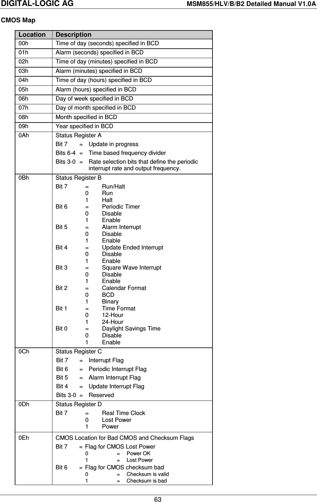
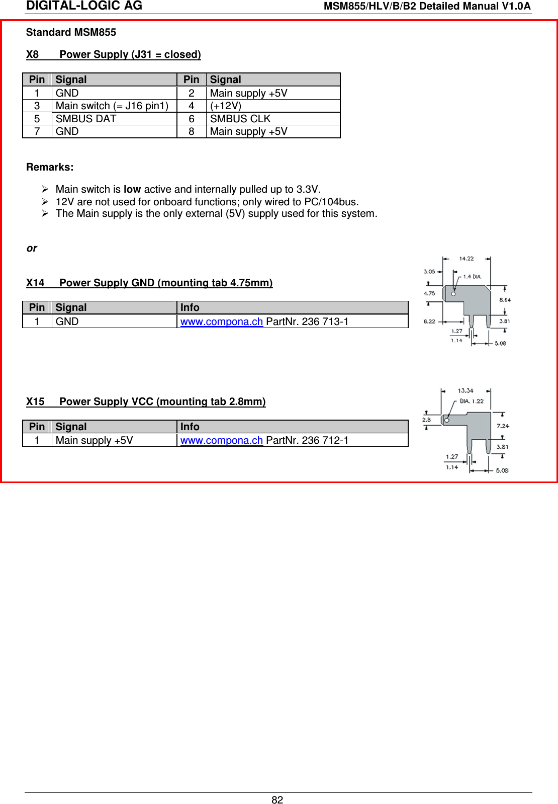
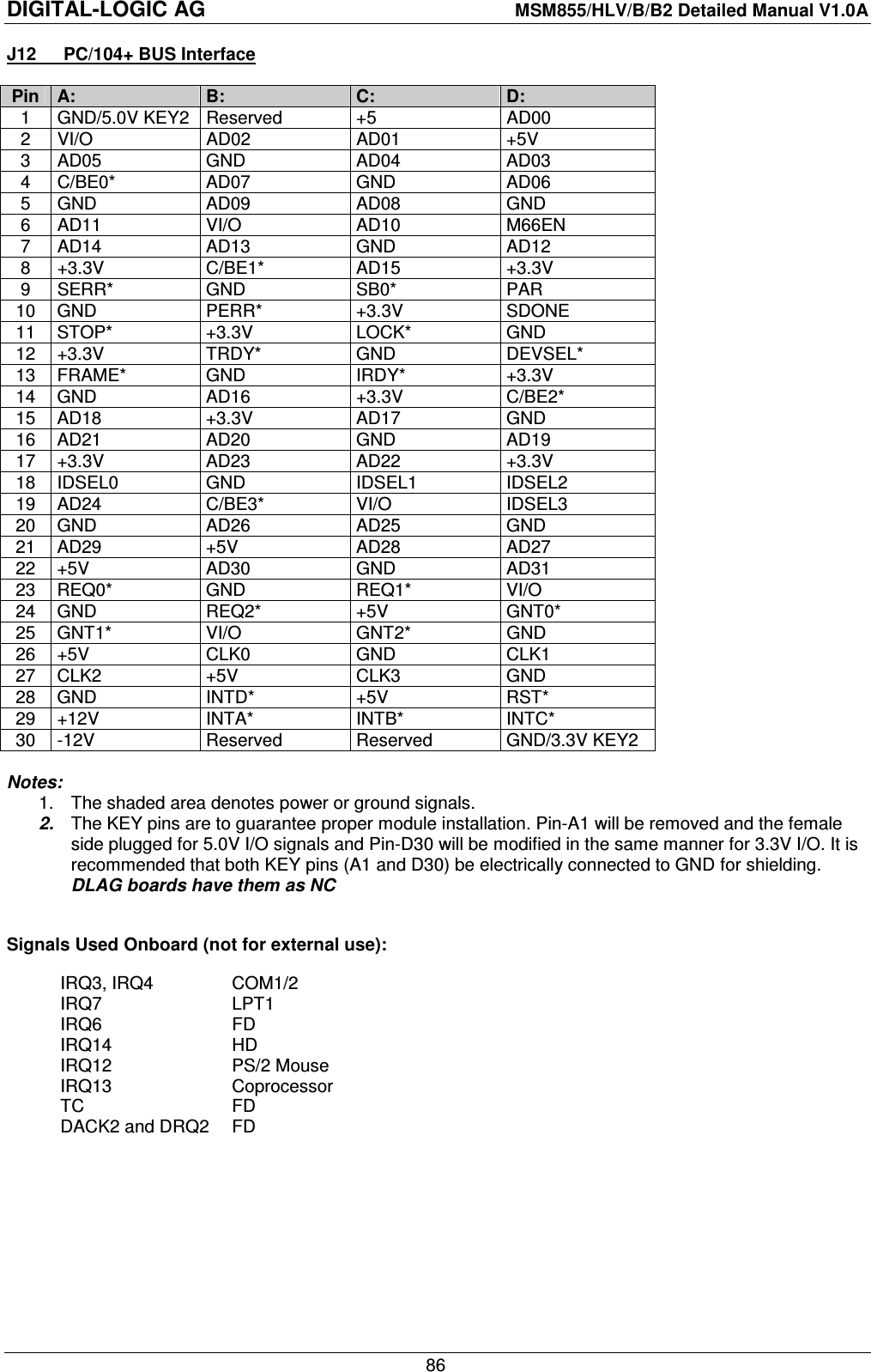
![DIGITAL-LOGIC AG MSM855/HLV/B/B2 Detailed Manual V1.0A 67 5.8. EEPROM Saved CMOS Setup The EEPROM has different functions, as listed below: Backup of the CMOS-Setup values. Storing system informations like: version, production date, customisation of the board, CPU type. Storing user/application values. The EEPROM will be updated automatically after exiting the BIOS setup menu. The system will also operate without a CMOS battery. While booting up, the CMOS is automatically updated with the EEPROM values. Press the ESC-key while powering on the system before the video shows the BIOS message and the CMOS will not be updated. This is helpful if incorrect parameters are stored in the EEPROM and the setup of the BIOS does not start. If the system hangs or a problem appears, the following steps must be performed: 1. Reset the CMOS-Setup (to reset the CMOS, disconnect the battery for at least 10 minutes). 2. Press ESC until the system starts up. 3. Enter the BIOS Setup: a. load DEFAULT values (F9) b. enter the settings for the environment c. exit the setup (F10) 4. Restart the system. The user may access the EEPROM through the INT15 special functions. The system information is read-only and uses the SFI functions. Please refer to the driver/software/BIOS manual 855_BIOS, the chapter on Special Peripherals / Configurations, the Special Function Interface (SFI). 5.8.1. EEPROM Memory for Setup The EEPROM is used for setup and configuration data, stored as an alternative to the CMOS-RTC. Optionally, the EEPROM setup driver may update the CMOS RTC, if the battery is running down and the checksum error would appear and stop the system. The capacity of the EEPROM is 2 kByte. Organization of the 2048Byte EEPROMs: Address MAP Function 0000h CMOS-Setup valid (01=valid) 0001h Reserved 0003h Flag for DLAG-Message (FF=no message) 0010h-007Fh Copy of CMOS-Setup data 0080h-00FFh Reserved for AUX-CMOS-Setup 0100h-010Fh Serial-Number 0110h-0113h Production date (year/day/month) 0114h-0117h 1. Service date (year/day/month) 0118h-011Bh 2. Service date (year/day/month) 011Ch-011Fh 3. Service date (year/day/month) 0120h-0122h Boot errors (Auto incremented if any boot error occurs) 0123h-0125h Setup Entries (Auto incremented on every Setup entry) 0126h-0128h Low Battery (Auto incremented every time the battery is low, EEPROM -> CMOS) 0129h-012Bh Startup (Auto incremented on every power-on start) 0130h Reserved 0131h Reserved 0132h/0133h BIOS Version (V1.4 => [0132h]:= 4, [0133h]:=1) 0134h/0135h BOARD Version (V1.5 => [0124h]:=5, [0125h]:=1) 0136h BOARD TYPE (‘M’=PC/104, ‘E’=Euro, ‘W’=MSWS, ‘S’=Slot, ‘C’=Custom, ‘X’= smartCore or smartModule) 0137h CPU TYPE: (01h=ELAN300/310, 02h=ELAN400, 05h=P5, 08h=P3, 09h=ELAN520, 10h=P-M). 0200h-03FFh Reserved 0200h-027Fh Reserved 0400h-07FFh Free for Customer use](https://usermanual.wiki/DETECTION-MONITORING-TECHNOLOGIES/AIMSFS-05X.User-Manual-1B/User-Guide-1532462-Page-6.png)
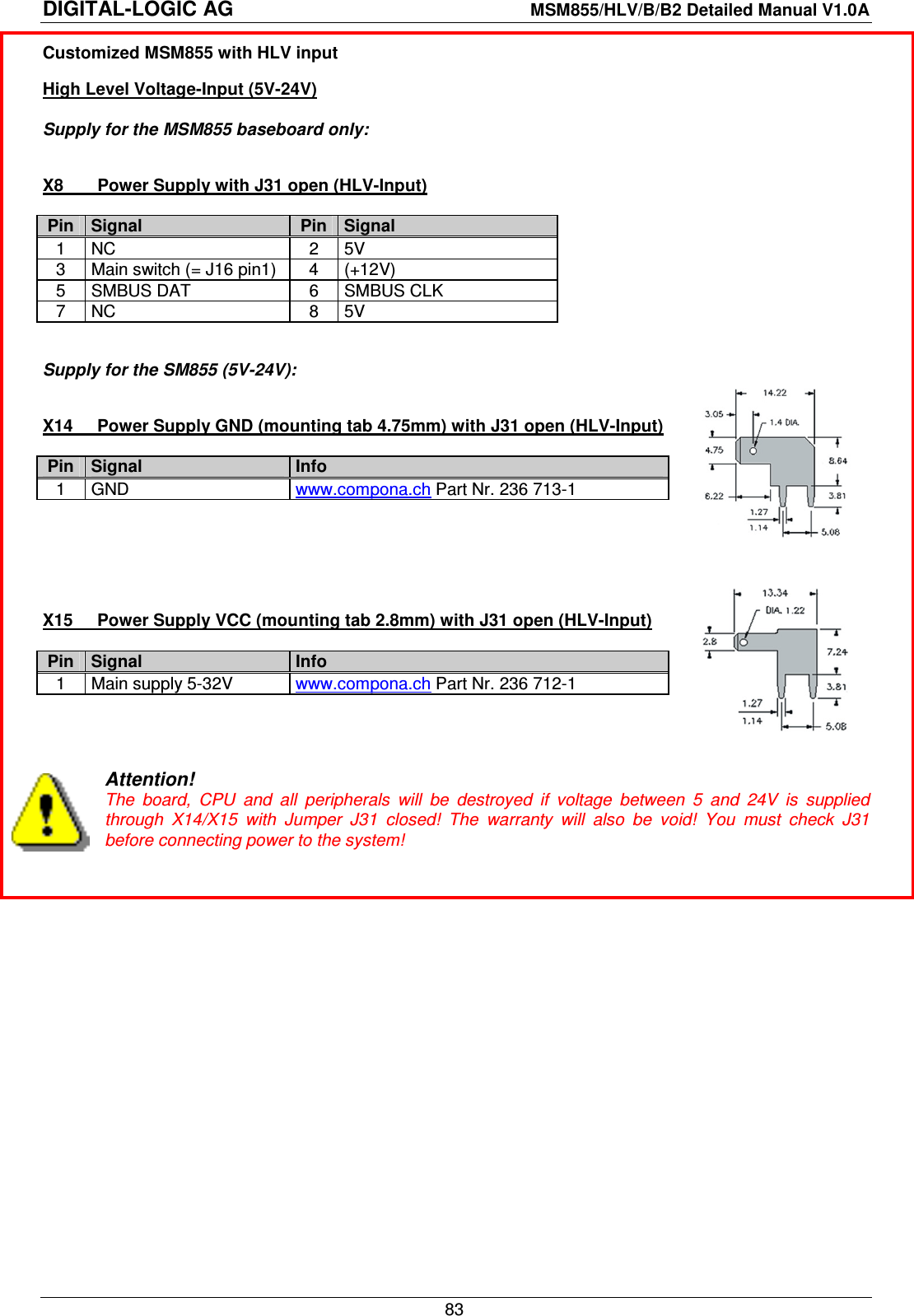
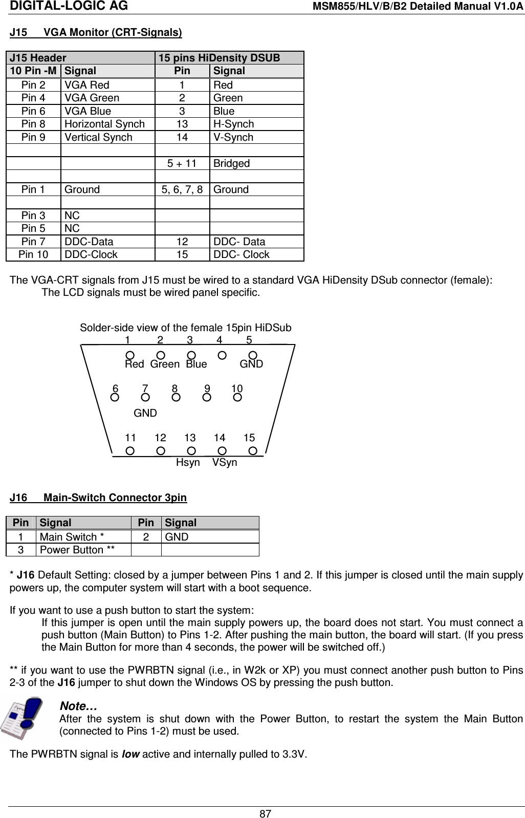
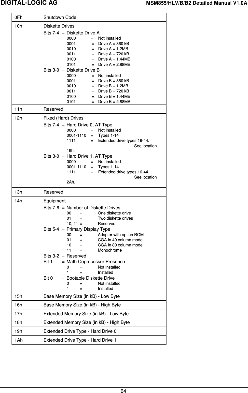
![DIGITAL-LOGIC AG MSM855/HLV/B/B2 Detailed Manual V1.0A 90 X11 LVDS / DVO on board version V1.0 Pin Signal Pin Signal 1 DVO_C_CLK 2 DVO_C_CLK# 3 GND 4 DVO_C_BLANK# 5 DVO_C_D0 6 DVO_C_D1 7 DVO_C_D10 8 DVO_C_D11 9 DVO_C_D2 10 DVO_C_D3 11 DVO_C_D4 12 DVO_C_D5 13 DVO_C_D6 14 DVO_C_D7 15 DVO_C_D8 16 DVO_C_D9 17 DVO_C_FLDSTL 18 DVO_C_HSYNC 19 DVO_C_VSYNC 20 DVO_BC_CLKINT 21 DVO_DVIC 22 DVO_DVID 23 GND 24 DVO_MI2C 25 DVO_MI2D 26 DVI_REF 27 VCC15 28 VCC15 29 VCC3S 30 VCC3S 31 DVO_detect 32 DVO_reset# 33 VCC5S 34 VCC5S 35 VCC12 36 LVDS_BKLC 37 LVDS_BKLEN 38 LVDS_VDDEN 39 GND 40 LVDS_CLKAM 41 LVDS_CLKAP 42 GND 43 LVDS_YAM 44 LVDS_YAP0 45 LVDS_YAM1 46 LVDS_YAP1 47 LVDS_YAM2 48 LVDS_YAP2 49 LVDS_YAM3 50 LVDS_YAP3 Detailed signal description: Signal LVDS_CLKAM [ICLKAM] Description Output, LVDS, voltage: 1.25V±225mV Channel A differential clock pair output (compliment): 245-800 MHz. Signal LVDS_CLKAP [ICLKAP] Description Output, LVDS, voltage: 1.25V±225mV Channel A differential clock pair output (true): 245-800 MHz. Signal LVDS_BKLC [PANELBKLTCTL] Description Output, CMOS LVDS LCD Flat Panel Backlight Brightness Control: This signal is used as the Pulse Width Modulated (PWM) control signal to control the backlight inverter. Signal LVDS_BKLEN [PANELBKLTEN] Description Output, CMOS LVDS LCD Flat Panel Backlight Enable: This signal is used to enable the backlight inverter (BLI). Signal LVDS_VDDEN [PANELVDDEN] Description Output, CMOS LVDS LCD Flat Panel Power Control: This signal is used enable power to the panel interface. Signal LVDS_YAP0..3 [IYAP[3:0]] Description Output, LVDS, voltage: 1.25V±225mV Channel A differential data pair 3:0 output (true): 245-800MHz. Signal LVDS_YAM0..3 [IYAM[3:0]] Description Output, LVDS, 1.25V±225mV Channel A differential data pair 3:0 output (compliment): 245-800 MHz.](https://usermanual.wiki/DETECTION-MONITORING-TECHNOLOGIES/AIMSFS-05X.User-Manual-1B/User-Guide-1532462-Page-29.png)