DETECTION MONITORING TECHNOLOGIES AIMSFS-05X AIMS FAST SCAN RADAR SYSTEM (AIMSFS-05X) User Manual MSM855 Detailed
DETECTION MONITORING TECHNOLOGIES, LLC (dba DMT, LLC) AIMS FAST SCAN RADAR SYSTEM (AIMSFS-05X) MSM855 Detailed
Contents
User Manual 1B
DIGITAL-LOGIC AG MSM855/HLV/B/B2 Detailed Manual V1.0A
62
5.6.3. ROM-BIOS Sockets
An EPROM socket with 8bit wide data access normally contains the board's AT compatible ROM-BIOS. The
socket takes an E82802AC8 EPROM (or equivalent) device. The board's wait-state control logic
automatically inserts four memory wait-states in all CPU accesses to this socket. The ROM-BIOS sockets
occupy the memory area from C0000H through FFFFFh; however, the board's ASIC logic reserves the entire
area from C0000h through FFFFFh for onboard devices, so that this area is already usable for ROM-DOS
and BIOS expansion modules. Consult the appropriate address map for the MICROSPACE MSM855 ROM-
BIOS sockets.
5.7. CMOS RAM Map
Systems based on the industry-standard specification include a battery backed Real Time Clock chip. This
clock contains at least 64Bytes of non-volatile RAM. The system BIOS uses this area to store information
including system configuration and initialization parameters, system diagnostics, and the time and date. This
information remains intact even when the system is powered down.
The BIOS supports 128Bytes of CMOS RAM. This information is accessible through I/O ports 70h and 71h.
CMOS RAM can be divided into several segments:
Locations 00h - 0Fh contain real time clock (RTC) and status information
Locations 10h - 2Fh contain system configuration data
Locations 30h - 3Fh contain System BIOS-specific configuration data as well as chipset-specific
information
Locations 40h - 7Fh contain chipset-specific information as well as power management configuration
parameters
The following table provides a summary of how these areas may be further divided.
Beginning
Ending Checksum Description
00h 0Fh No RTC and Checksum
10h 2Dh Yes System Configuration
2Eh 2Fh No Checksum Value of 10h - 2Dh
30h 33h No Standard CMOS
34h 3Fh No Standard CMOS - SystemSoft Reserved
40h 5Bh Yes Extended CMOS - Chipset Specific
5Ch 5Dh No Checksum Value of 40h - 5Bh
5Eh 6Eh No Extended CMOS - Chipset Specific
6Fh 7Dh Yes Extended CMOS - Power Management
7Eh 7Fh No Checksum Value of 6Fh - 7Dh
DIGITAL-LOGIC AG MSM855/HLV/B/B2 Detailed Manual V1.0A
63
CMOS Map
Location Description
00h Time of day (seconds) specified in BCD
01h Alarm (seconds) specified in BCD
02h Time of day (minutes) specified in BCD
03h Alarm (minutes) specified in BCD
04h Time of day (hours) specified in BCD
05h Alarm (hours) specified in BCD
06h Day of week specified in BCD
07h Day of month specified in BCD
08h Month specified in BCD
09h Year specified in BCD
0Ah Status Register A
Bit 7 = Update in progress
Bits 6-4 = Time based frequency divider
Bits 3-0 = Rate selection bits that define the periodic
interrupt rate and output frequency.
0Bh Status Register B
Bit 7 = Run/Halt
0 Run
1 Halt
Bit 6 = Periodic Timer
0 Disable
1 Enable
Bit 5 = Alarm Interrupt
0 Disable
1 Enable
Bit 4 = Update Ended Interrupt
0 Disable
1 Enable
Bit 3 = Square Wave Interrupt
0 Disable
1 Enable
Bit 2 = Calendar Format
0 BCD
1 Binary
Bit 1 = Time Format
0 12-Hour
1 24-Hour
Bit 0 = Daylight Savings Time
0 Disable
1 Enable
0Ch Status Register C
Bit 7 = Interrupt Flag
Bit 6 = Periodic Interrupt Flag
Bit 5 = Alarm Interrupt Flag
Bit 4 = Update Interrupt Flag
Bits 3-0 = Reserved
0Dh Status Register D
Bit 7 = Real Time Clock
0 Lost Power
1 Power
0Eh CMOS Location for Bad CMOS and Checksum Flags
Bit 7 = Flag for CMOS Lost Power
0 = Power OK
1 = Lost Power
Bit 6 = Flag for CMOS checksum bad
0 = Checksum is valid
1 = Checksum is bad
DIGITAL-LOGIC AG MSM855/HLV/B/B2 Detailed Manual V1.0A
64
0Fh Shutdown Code
10h Diskette Drives
Bits 7-4 = Diskette Drive A
0000 = Not installed
0001 = Drive A = 360 kB
0010 = Drive A = 1.2MB
0011 = Drive A = 720 kB
0100 = Drive A = 1.44MB
0101 = Drive A = 2.88MB
Bits 3-0 = Diskette Drive B
0000 = Not installed
0001 = Drive B = 360 kB
0010 = Drive B = 1.2MB
0011 = Drive B = 720 kB
0100 = Drive B = 1.44MB
0101 = Drive B = 2.88MB
11h Reserved
12h Fixed (Hard) Drives
Bits 7-4 = Hard Drive 0, AT Type
0000 = Not installed
0001-1110 = Types 1-14
1111 = Extended drive types 16-44.
See location
19h.
Bits 3-0 = Hard Drive 1, AT Type
0000 = Not installed
0001-1110 = Types 1-14
1111 = Extended drive types 16-44.
See location
2Ah.
13h Reserved
14h Equipment
Bits 7-6 = Number of Diskette Drives
00 = One diskette drive
01 = Two diskette drives
10, 11 = Reserved
Bits 5-4 = Primary Display Type
00 = Adapter with option ROM
01 = CGA in 40 column mode
10 = CGA in 80 column mode
11 = Monochrome
Bits 3-2 = Reserved
Bit 1 = Math Coprocessor Presence
0 = Not installed
1 = Installed
Bit 0 = Bootable Diskette Drive
0 = Not installed
1 = Installed
15h Base Memory Size (in kB) - Low Byte
16h Base Memory Size (in kB) - High Byte
17h Extended Memory Size (in kB) - Low Byte
18h Extended Memory Size (in kB) - High Byte
19h Extended Drive Type - Hard Drive 0
1Ah Extended Drive Type - Hard Drive 1
DIGITAL-LOGIC AG MSM855/HLV/B/B2 Detailed Manual V1.0A
65
1Bh Custom and Fixed (Hard) Drive Flags
Bits 7-6 = Reserved
Bit 5 = Internal Floppy Disk Controller
0 = Disabled
1 = Enabled
Bit 4 = Internal IDE Controller
0 = Disabled
1 = Enabled
Bit 3 = Hard Drive 0 Custom Flag
0 = Disabled
1 = Enabled
Bit 2 = Hard Drive 0 IDE Flag
0 = Disabled
1 = Enabled
Bit 1 = Hard Drive 1 Custom Flag
0 = Disabled
1 = Enabled
Bit 0 = Hard Drive 1 IDE Flag
0 = Disabled
1 = Enabled
1Ch Reserved
1Dh EMS Memory Size Low Byte
1Eh EMS Memory Size High Byte
1Fh - 24h Custom Drive Table 0
These 6 Bytes (48 bits) contain the following data:
Cylinders 10bits range 0-1023
Landing Zone 10bits range 0-1023
Write Precompensation 10bits range 0-1023
Heads 08bits range 0-15
Sectors/Track 08bits range 0-254
1Fh Byte 0
Bits 7-0 = Lower 8 bits of Cylinders
20h Byte 1
Bits 7-2 = Lower 6 bits of Landing Zone
Bits 1-0 = Upper 2 bits of Cylinders
21h Byte 2
Bits 7-4 = Lower 4 bits of Write Precompensation
Bits 3-0 = Upper 4 bits of Landing Zone
22h Byte 3
Bits 7-6 = Reserved
Bits 5-0 = Upper 6 bits of Write Precompensation
23h Byte 4
Bits 7-0 = Number of Heads
24h Byte 5
Bits 7-0 = Sectors Per Track
25h - 2Ah Custom Drive Table 1
These 6 Bytes (48 bits) contain the following data:
Cylinders 10bits range 0-1023
Landing Zone 10bits range 0-1023
Write Precompensation 10bits range 0-1023
Heads 08bits range 0-15
Sectors/Track 08bits range 0-254
25h Byte 0
Bits 7-0 = Lower 8 bits of Cylinders
DIGITAL-LOGIC AG MSM855/HLV/B/B2 Detailed Manual V1.0A
66
26h Byte 1
Bits 7-2 = Lower 6 bits of Landing Zone
Bits 1-0 = Upper 2 bits of Cylinders
27h Byte 2
Bits 7-4 = Lower 4 bits of Write Precompensation
Bits 3-0 = Upper 4 bits of Landing Zone
28h Byte 3
Bits 7-6 = Reserved
Bits 5-0 = Upper 6 bits of Write Precompensation
29h Byte 4
Bits 7-0 = Number of Heads
2Ah Byte 5
Bits 7-0 = Sectors Per Track
2Bh Boot Password
Bit 7 = Enable/Disable Password
0 = Disable Password
1 = Enable Password
Bits 6-0 = Calculated Password
2Ch SCU Password
Bit 7 = Enable/Disable Password
0 = Disable Password
1 = Enable Password
Bits 6-0 = Calculated Password
2Dh Reserved
2Eh High Byte of Checksum - Locations 10h to 2Dh
2Fh Low Byte of Checksum - Locations 10h to 2Dh
30h Extended RAM (kB) detected by POST - Low Byte
31h Extended RAM (kB) detected by POST - High Byte
32h BCD Value for Century
33h Base Memory Installed
Bit 7 = Flag for Memory Size
0 = 640kB
1 = 512kB
Bits 6-0 = Reserved
34h Minor CPU Revision
Differentiates CPUs within a CPU type (i.e., 486SX vs 486
DX, vs 486 DX/2). This is crucial for correctly determining
CPU input clock frequency. During a power-on reset, Reg DL
holds minor CPU revision.
35h Major CPU Revision
Differentiates between different CPUs (i.e., 386, 486,
Pentium). This is crucial for correctly determining CPU input
clock frequency. During a power-on reset, Reg DH holds
major CPU revision.
36h Hotkey Usage
Bits 7-6 = Reserved
Bit 5 = Semaphore for Completed POST
Bit 4 = Semaphore for 0 Volt POST (not currently used)
Bit 3 = Semaphore for already in SCU menu
Bit 2 = Semaphore for already in PM menu
Bit 1 = Semaphore for SCU menu call pending
Bit 0 = Semaphore for PM menu call pending
40h-7Fh Definitions for these locations vary depending on the chipset.

DIGITAL-LOGIC AG MSM855/HLV/B/B2 Detailed Manual V1.0A
67
5.8. EEPROM Saved CMOS Setup
The EEPROM has different functions, as listed below:
Backup of the CMOS-Setup values.
Storing system informations like: version, production date, customisation of the board, CPU type.
Storing user/application values.
The EEPROM will be updated automatically after exiting the BIOS setup menu. The system will also operate
without a CMOS battery. While booting up, the CMOS is automatically updated with the EEPROM values.
Press the ESC-key while powering on the system before the video shows the BIOS message and the CMOS
will not be updated. This is helpful if incorrect parameters are stored in the EEPROM and the setup of the
BIOS does not start.
If the system hangs or a problem appears, the following steps must be performed:
1. Reset the CMOS-Setup (to reset the CMOS, disconnect the battery for at least 10 minutes).
2. Press ESC until the system starts up.
3. Enter the BIOS Setup:
a. load DEFAULT values (F9)
b. enter the settings for the environment
c. exit the setup (F10)
4. Restart the system.
The user may access the EEPROM through the INT15 special functions. The system information is read-only
and uses the SFI functions. Please refer to the driver/software/BIOS manual 855_BIOS, the chapter on
Special Peripherals / Configurations, the Special Function Interface (SFI).
5.8.1. EEPROM Memory for Setup
The EEPROM is used for setup and configuration data, stored as an alternative to the CMOS-RTC.
Optionally, the EEPROM setup driver may update the CMOS RTC, if the battery is running down and the
checksum error would appear and stop the system. The capacity of the EEPROM is 2 kByte.
Organization of the 2048Byte EEPROMs:
Address MAP Function
0000h CMOS-Setup valid (01=valid)
0001h Reserved
0003h Flag for DLAG-Message (FF=no message)
0010h-007Fh Copy of CMOS-Setup data
0080h-00FFh Reserved for AUX-CMOS-Setup
0100h-010Fh Serial-Number
0110h-0113h Production date (year/day/month)
0114h-0117h 1. Service date (year/day/month)
0118h-011Bh 2. Service date (year/day/month)
011Ch-011Fh 3. Service date (year/day/month)
0120h-0122h Boot errors (Auto incremented if any boot error occurs)
0123h-0125h Setup Entries (Auto incremented on every Setup entry)
0126h-0128h Low Battery (Auto incremented every time the battery is low, EEPROM -> CMOS)
0129h-012Bh Startup (Auto incremented on every power-on start)
0130h Reserved
0131h Reserved
0132h/0133h BIOS Version (V1.4 => [0132h]:= 4, [0133h]:=1)
0134h/0135h BOARD Version (V1.5 => [0124h]:=5, [0125h]:=1)
0136h BOARD TYPE (‘M’=PC/104, ‘E’=Euro, ‘W’=MSWS, ‘S’=Slot, ‘C’=Custom,
‘X’= smartCore or smartModule)
0137h CPU TYPE: (01h=ELAN300/310, 02h=ELAN400, 05h=P5, 08h=P3, 09h=ELAN520, 10h=P-M).
0200h-03FFh Reserved
0200h-027Fh Reserved
0400h-07FFh Free for Customer use
DIGITAL-LOGIC AG MSM855/HLV/B/B2 Detailed Manual V1.0A
68
5.9. Memory & I/O Map
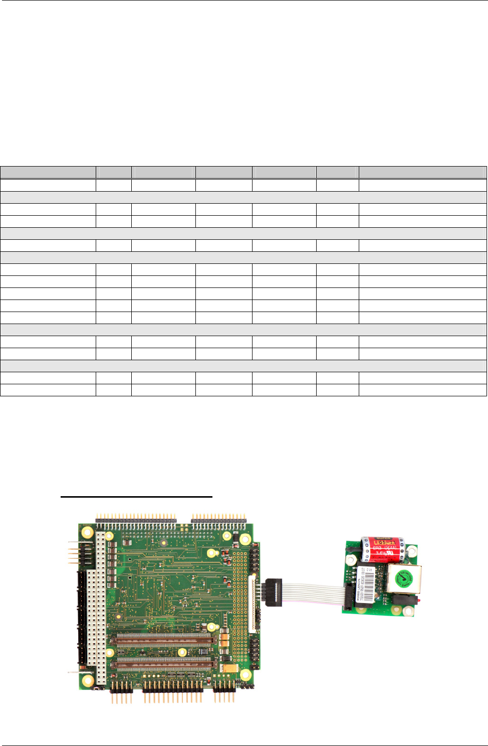
5.9.1. Replacement of the SODIMM-DDRAM
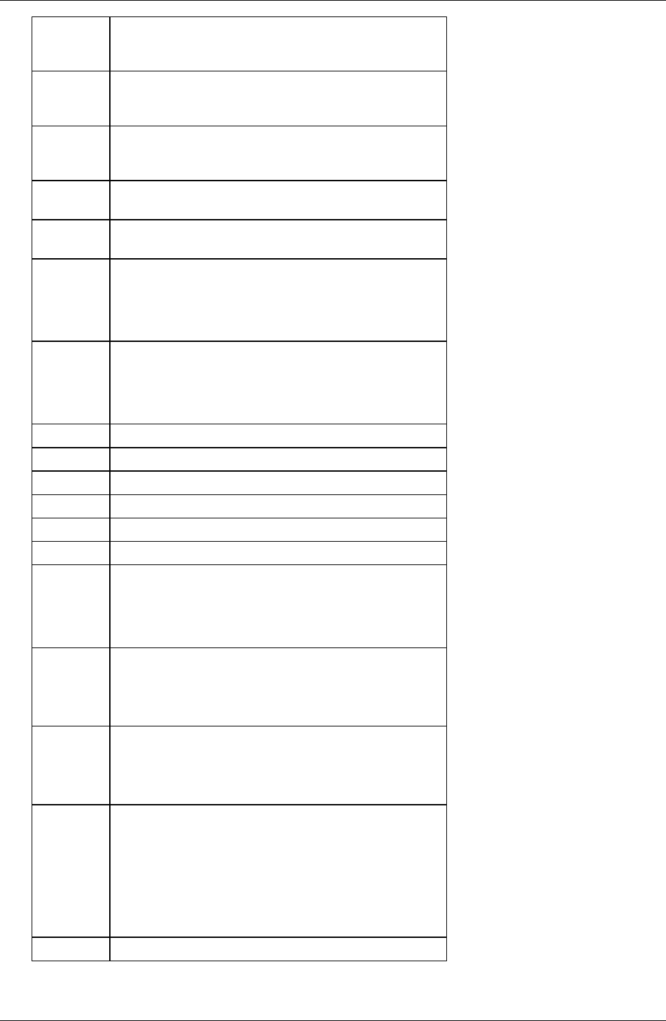
MSM855 and SM855 with heat sink
Step 1:
Remove the fan connection x12 on the MSEBX855.
Remove the 3 screws from heat sink and dismantle
the heatsink.
Screw Type:
Cylinder hexagon socket type screw
M2x6mm /BN7 DIN912 ISO 4762
Tool: Hexagon head socket wrench no. 1.5
Step 2:
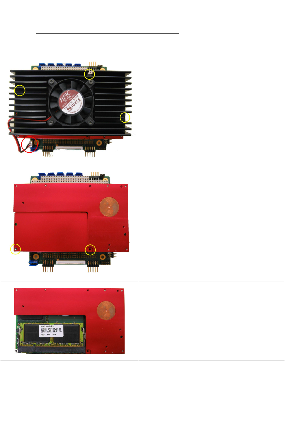
Remove the 2 screws from the SODIMM cover and
dismantle the cover very carefully. Slide the cover to
the side and gently lift it away from the casing.
Screw Type:
Cylinder hexagon socket type screw
M2x4mm /BN11 DIN912 ISO 4762
Tool: Hexagon head socket wrench no. 1.5
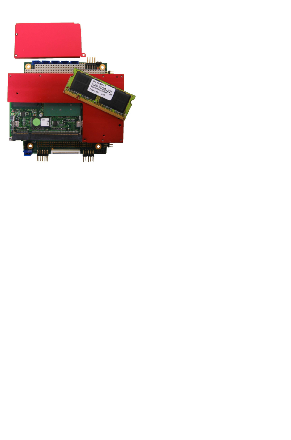
Step 3:
Press the memory holder sideways and click the
module out.
DIGITAL-LOGIC AG MSM855/HLV/B/B2 Detailed Manual V1.0A
69
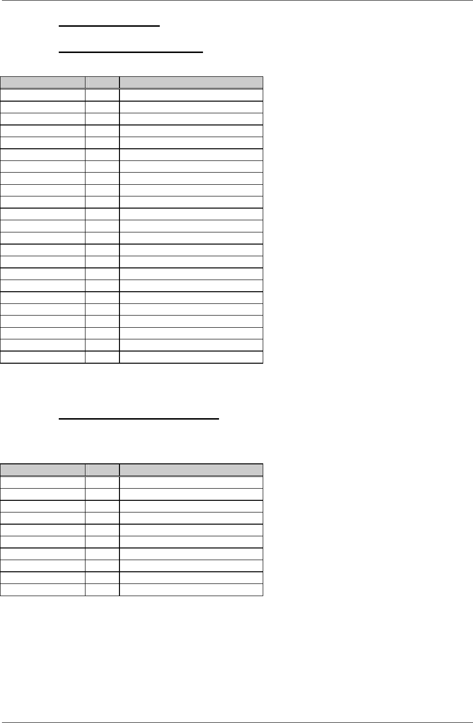
Completely dismantled parts.
DIGITAL-LOGIC AG MSM855/HLV/B/B2 Detailed Manual V1.0A
70
5.9.2. System I/O Map
5.9.2.1. Fixed IO Address Space
IO Address Size Target
00h-1Fh 32 DMA controller
20h-2Dh 14 Interrupt controller
2Eh-2Fh 2 LPC SIO
30h-3Dh 14 Interrupt controller
40h-43h 4 8254 compatible timer
4Eh-4Fh 2 LPC SIO
50h-53h 4 8254 compatible timer
60h-66h (even) 4 8254 compatible timer
61h-67h (odd) 4 NMI controller
70h-77h 8 RTC controller
80h-91h 18 DMA controller
92h 1 Reset controller
93h-9Fh 13 DMA controller
A0h-B1h 18 Interrupt controller
B2h-B3h 2 Power management
B4h-BDh 10 Interrupt controller
C0h-DFh 32 DMA controller
F0h 1 Depends on configuration
F8h-FFh 8 Reserved
170h-177h 8 IDE controller
1F0h-1F7h 8 IDE controller
376h 1 IDE controller
3F6h 1 IDE controller
5.9.2.2. Variable IO Address Space
The variable IO address space depends on the BIOS settings. The following ranges are with default setup
values loaded.
IO Address Size Target
000h-0FFh 256 Fixed IO address space
274h-277h 4 ISAPNP
279h-279h 1 ISAPNP
295h-296h 2 SuperIO
2F8h-2FFh 8 Serial port (COM2)
378h-37Fh 8 Printer port (LPT1)
3B0h-3BBh 12 Graphic controller
3C0h-3DFh 32 Graphic controller
3F0h-3F7h 8 Floppy controller
3F8h-3FFh 8 Serial port (COM1)
DIGITAL-LOGIC AG MSM855/HLV/B/B2 Detailed Manual V1.0A
71
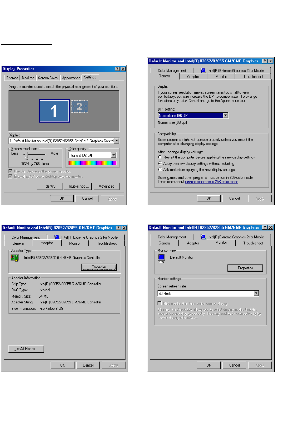
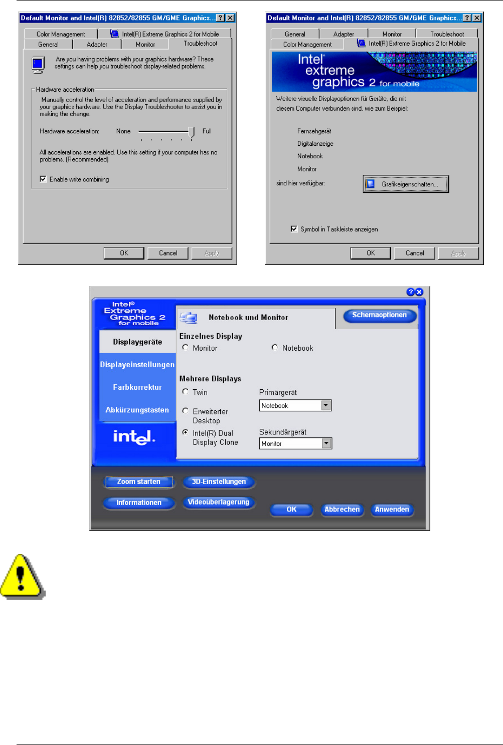
5.10. VGA / LCD
Start / Control Panel / Appearance and Themes / Display
Register Settings:
DIGITAL-LOGIC AG MSM855/HLV/B/B2 Detailed Manual V1.0A
72
Attention!
If there is no picture after changing the values in the menu "DISPLAY PROPERTIES Settings" or
if the system was started without a monitor connected:
Press the following key combination to get a picture again:
CTRL+ALT+ Fx
Where Fx is:
F1 = VGA
F2 or F3 = SVIDEO
F4 = DVI
We recommend changing the settings in the Intel graphics menu.
DIGITAL-LOGIC AG MSM855/HLV/B/B2 Detailed Manual V1.0A
73
5.11. LVDS-Display
There are various LCD-panels available with a 6bit-LVDS interface which can be directly adapted to the
LVDS-interface of the 855GME video controller.
The LVDS interface is composed of:
3x2 LVDS Datalines (differential)
1x2 LVDS Clockline (differential)
Backlight Power = 5V / DCMain
LCD Power = 3.3V / 5V
Here is a list of LVDS-Panels:
Display Part No. Size Resolution Colors Luminance Power Remarks
LVDS 18bit
Toshiba
LTM06C310 6.3” 1024x768 262k 150 cd/m3 3W Tested, limited availability
LTM10C306L 10.4” 1024x768 262k 200cd/m3 3W Tested
SIEMENS I-SFT
G23916-B65-H068 10.4” 1024x768 262k 1000cd/m3 20W
NEC 1)
NL10276BC24-13 12.1” 1024x768 262k/16M 400cd/m3 8/6bit LCD 1)
NL8060BC31-28D 12.1” 800x600 262k 350cd/m3 1)
NL10276BC26-17 10.4” 1024x768 262k 1)
NL10276BC16-01 8.4” 1024x768 262k/16M 8/6bit LCD 1)
NL10276BC12-02 6.3” 1024x768 262k/16M 8/6bit LCD 1)
SANYO-TORISAN
TM121XG-02L01 12.1” 1024x768 262k 150cd/m3
TM100SV-02L02 10” 800x600 262k 170cd/m3
LG-Philips LCD
LP104S5 10.4” 800x600 262k 170cd/m3 -T with 300cd/m3
LB150X06 15.0” 1024x768 262k 250cd/m3
To use NEC Panels, please ask the manufacturer for any application notes.
5.12. LAN / Ethernet
5.12.1. LAN Cable Connection
DIGITAL-LOGIC AG MSM855/HLV/B/B2 Detailed Manual V1.0A
74
RJ45 connector 10BaseT (IEEE 802.3i), 100BaseTX (IEEE 802.3u):
MDI-Pin EIA/TIA 568A
colors (wire/line)
Pin Twisted
Pair
TX+ White / Green 1 3
TX- Green 2 3
RX+ White / Orange 3 2
GND .. 4 1
GND .. 5 1
RX- Orange 6 2
GND .. 7 4
GND .. 8 4
Cabling: Do not exceed 100 meters (328 feet)
Has a quality of at least CAT5, though S/FTP or STP CAT6 would be better
Be sure to have a well balanced shield/ground concept
5.12.2. Boot from LAN
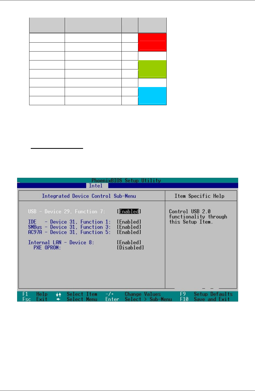
The integrated LAN boot option in the BIOS supports only the PXE LAN boot.
Enable the PXE OPROM function in the BIOS setup:
After enabling this feature, Save, Exit and Reboot. To boot from LAN, re-enter the BIOS setup and select
the “IBA FE Slot 0240” as the first boot device in the boot order.
DIGITAL-LOGIC AG MSM855/HLV/B/B2 Detailed Manual V1.0A
75
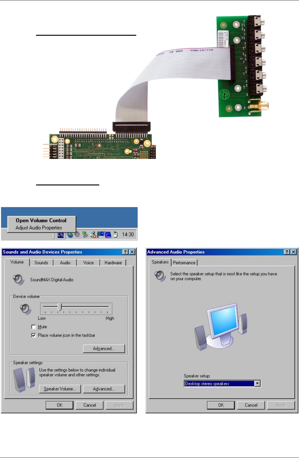
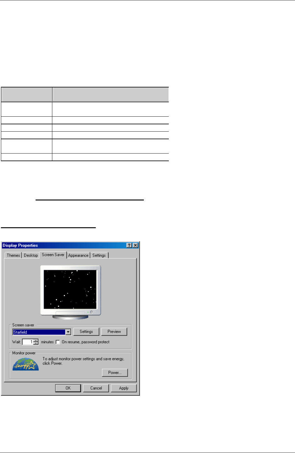
5.13. AC97 Sound
5.13.1. Audio Cable Connection
5.13.2. Sound Settings
DIGITAL-LOGIC AG MSM855/HLV/B/B2 Detailed Manual V1.0A
76
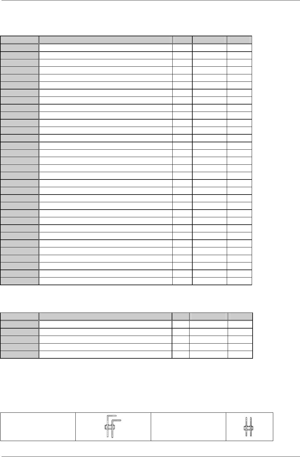
5.14. SpeedStep Performance Control
The Pentium-M improved the SpeedStep mechanism by adding a third power scheme in addition to the low-
power and the full-performance modes. This new mode is called adaptive mode, and allows the frequency
and voltage to switch according to the CPU activity. The CPU uses a low-power mode by default, but when
its activity increases, it switches itself very quicky into full-performance mode. This new power scheme is
very pleasant to use, because it allows full CPU speed only when needed. Of course, power consumption
depends on the CPU activity, and the more the CPU is used, the more it consumes power.
Windows XP
Power Schemes
AC Power
(Frequency example: mobile Pentium-M 1.6 GHz)
Battery DC
(Frequency example: mobile Pentium-M 1.6 GHz)
Home/Office
Desktop
None (1.6 GHz Always) Adaptive (600 MHz <...>1.6 GHz)
Portable /Laptop Adaptive (600 MHz <...> 1.6 GHz) Adaptive (600 MHz <...>1.6 GHz)
Presentation Adaptive (600 MHz <...> 1.6 GHz) Degrade (600 MHz)
Always On None (1.6 GHz Always) None (1.6 GHz Always)
Minimal Power
Management
Adaptive (600 MHz <...> 1.6 GHz) Adaptive (600 MHz <...>1.6 GHz)
Maximum Battery
Adaptive (600 MHz <...> 1.6 GHz) Degrade (600 MHz)
CPU performance is heavily dependent on the choice of power scheme in the system control
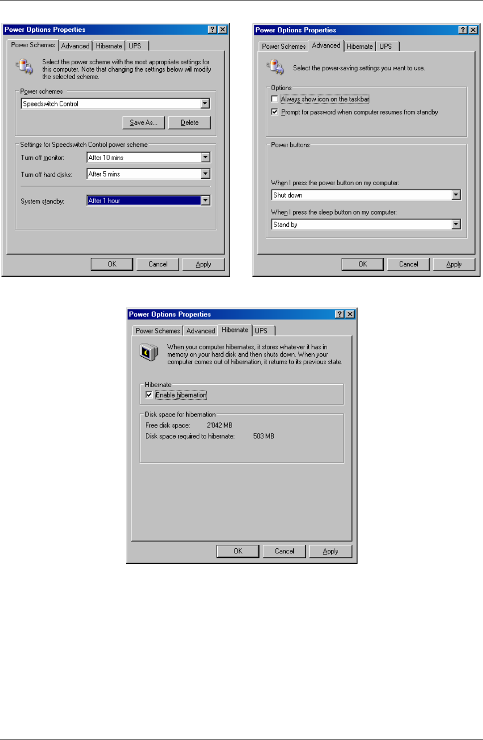
5.14.1. Set up Power Management
Start / Control Panel / Appearance and Themes / Display
Go to the Register Screen Saver:
Press the Power Button
DIGITAL-LOGIC AG MSM855/HLV/B/B2 Detailed Manual V1.0A
77
DIGITAL-LOGIC AG MSM855/HLV/B/B2 Detailed Manual V1.0A
78
6. DESCRIPTION & LOCATION OF THE CONNECTORS
Connector Structure Pin Grid Angle
J1 USB Port1 4 RM2.54 180°
J2 USB Port0 (preparation for Wakeup from USB) 4 RM2.54 180°
J4 Floppy disk 26 FFC 180°
J5 COM2 RS232C 10 RM2.54 90°
J6 COM1 RS232C 10 RM2.54 180°
J7 LPT1 Printer port 26 RM2.54 90°
J8 Utility (KB,MS,Battery,Reset,Sp.) 10 RM2.54 90°
J9 IrDA 4 RM2.54
J10 Ext.Temp. Sensor (manufacturer's use only) 2
J11 Ext.Temp. Sensor (manufacturer's use only) 2
J12 PCI-Bus PC/104+ 120
J15 VGA interface (RGB,H&V-Synch,I2C) 10 RM2.54 180°
J16 ATX-Mainswitch (toggle) 3 RM2.54 180°
J21 ATA-IDE primary 44 RM2.00 90°
J22 ISA-Bus PC/104 104
J23 USB Port3 4 RM2.54 180°
J24 USB Port2 4 RM2.54 180°
J25 USB Port5 4 RM2.54 180°
J26 USB Port4 4 RM2.54 180°
J27 POD (manufacturer's use only) 14 RM2.00 180°
J29 LAN (LAN, LED, Battery) 10 RM2.00 90°
J30 Sound (3xStereo, MIC, Line) 30 RM2.00 90°
J33 LAN (LAN, LED) 10 RM2.00 180°
J34 Factory test 14 RM2.00
X7 Optional CompactFlash 50 CF
X8 Power input (Main Input) 8 RM2.54 90°
X11 LVDS, DVO channel B, DVO channel C 50 RM2.00 180°
X12 FAN-Power Output (5V/GND) 2 RM2.54 180°
X13 FAN-Power Output 1 (5V/FANPWM/GND) 3 RM2.54 180°
X14 Power Input GND 90°
X15 Power Input VCC 5V 90°
X16 FAN-Power Output 2 (5V/FANPWM/GND) 3 RM2.54 180°
only available on the MSM855B2
Different connectors on board version 0.4
Connector Structure Pin Remarks Angle
J16 ATX-Mainswitch (toggle) 2 RM2.54
X8 Power Input (Main Input) 8 RM2.54
X9 LVDS Interface 20 RM2.00
X10 DVO channel B 26 RM2.00
X11 DVO channel C 26 RM2.00
Also refer to Chapter 13, Previous Product Versions
Remarks:
J16 is used to start up the computer system.
90° angle =
180° angle (straight) =
DIGITAL-LOGIC AG MSM855/HLV/B/B2 Detailed Manual V1.0A
79
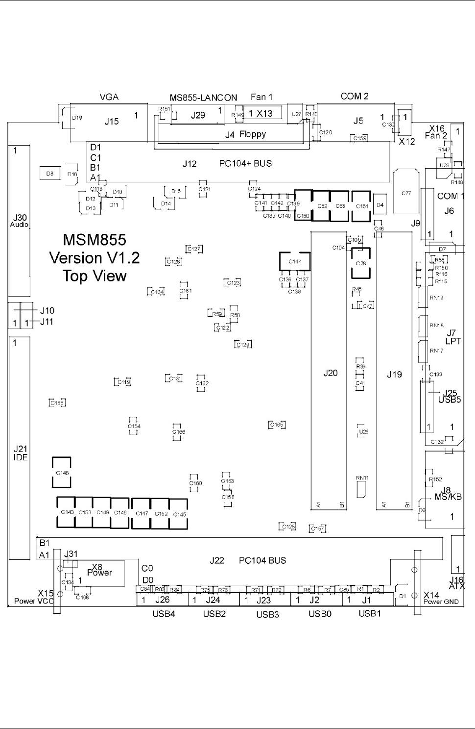
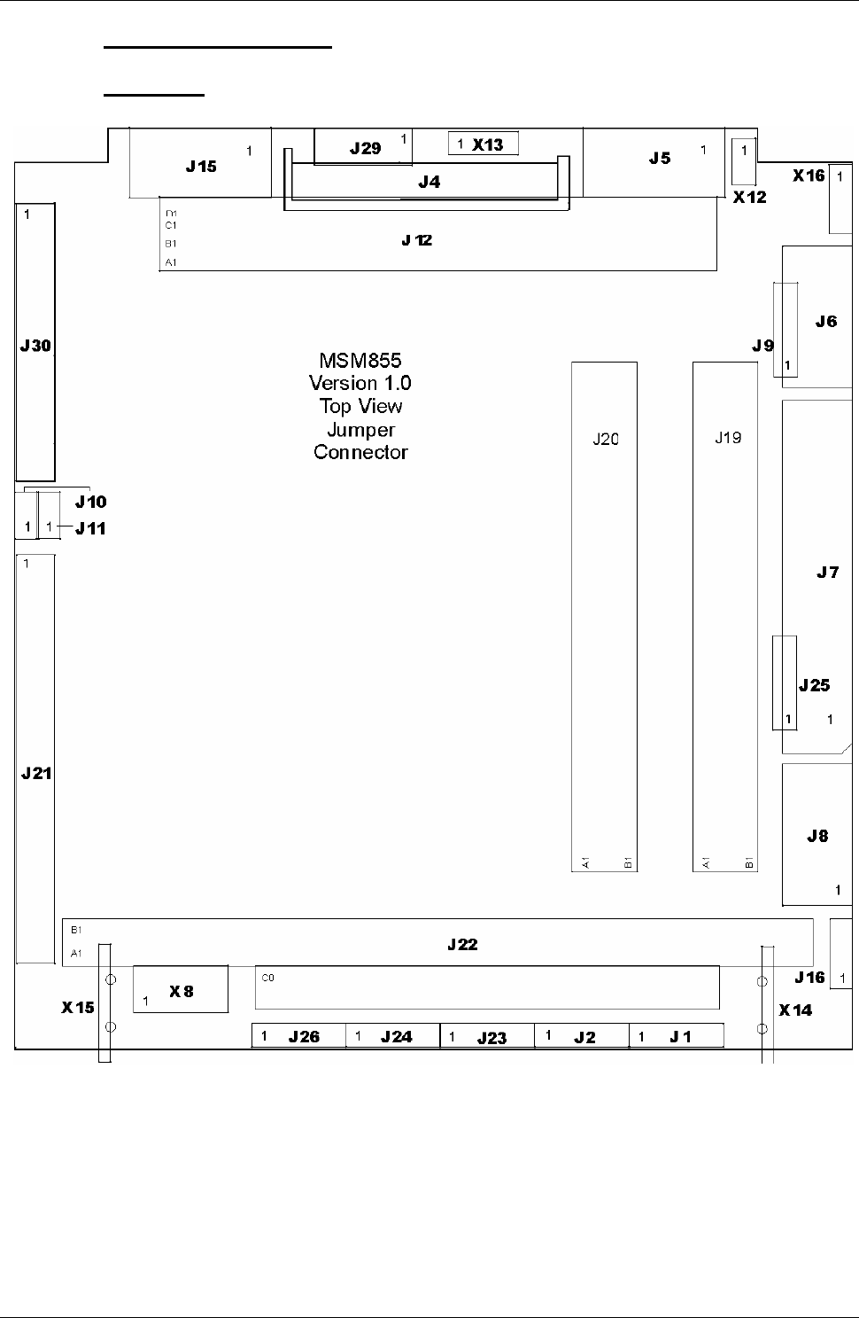
6.1. Top Side of the MSM855 V1.2/V1.3
DIGITAL-LOGIC AG MSM855/HLV/B/B2 Detailed Manual V1.0A
80
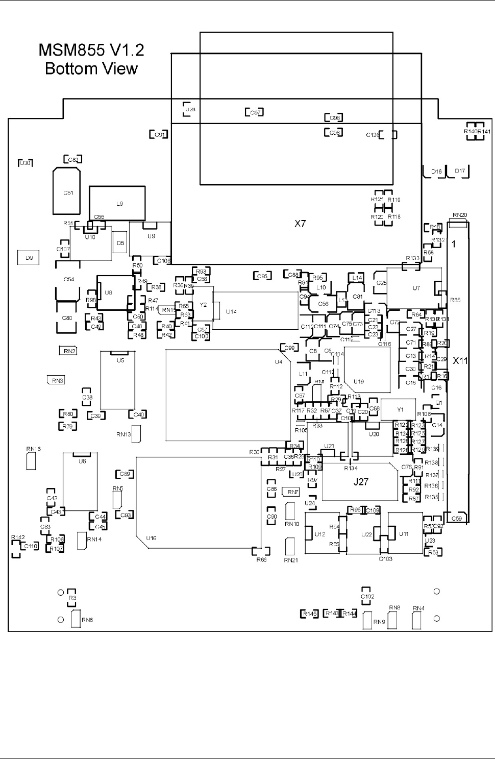
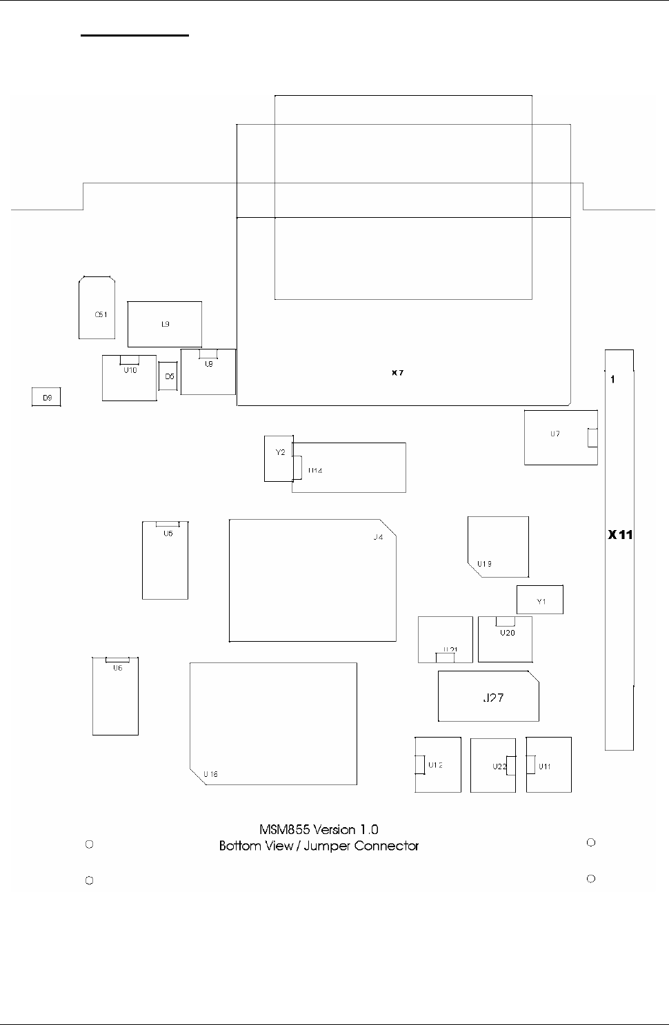
6.2. Bottom Side of the MSM855 V1.2/V1.3
DIGITAL-LOGIC AG MSM855/HLV/B/B2 Detailed Manual V1.0A
81
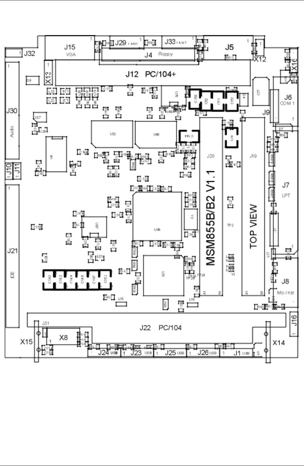
6.3. Top Side of the MSM855B/B2 V1.1
6.4. Top Side of the MSM855B/B2 V1.1
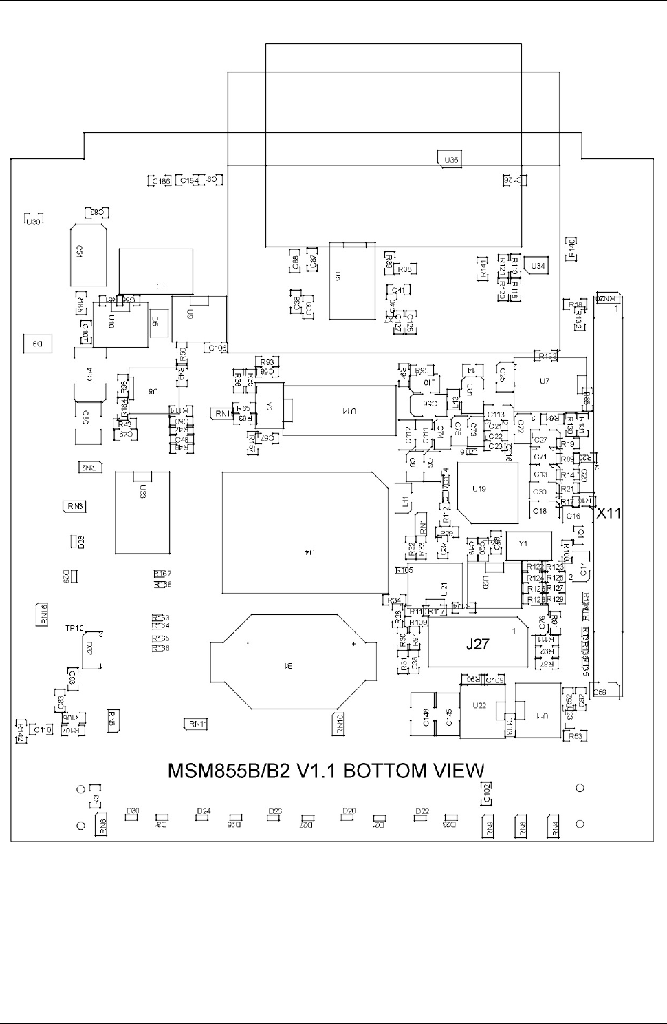
The bottom of the MSM855B/B2 is indentical to the bottom side of the MSM855 V1.3.
DIGITAL-LOGIC AG MSM855/HLV/B/B2 Detailed Manual V1.0A
82
Standard MSM855
X8 Power Supply (J31 = closed)
Pin Signal Pin Signal
1 GND 2 Main supply +5V
3 Main switch (= J16 pin1) 4 (+12V)
5 SMBUS DAT 6 SMBUS CLK
7 GND 8 Main supply +5V
Remarks:
Main switch is low active and internally pulled up to 3.3V.
12V are not used for onboard functions; only wired to PC/104bus.
The Main supply is the only external (5V) supply used for this system.
or
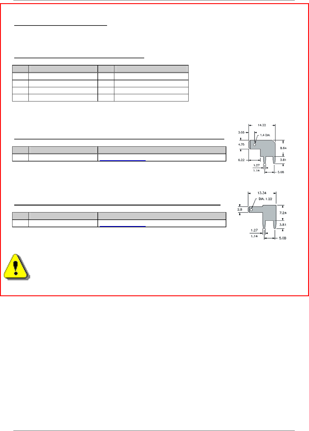
X14 Power Supply GND (mounting tab 4.75mm)
Pin Signal Info
1 GND www.compona.ch PartNr. 236 713-1
X15 Power Supply VCC (mounting tab 2.8mm)
Pin Signal Info
1 Main supply +5V www.compona.ch PartNr. 236 712-1
DIGITAL-LOGIC AG MSM855/HLV/B/B2 Detailed Manual V1.0A
83
Customized MSM855 with HLV input
High Level Voltage-Input (5V-24V)
Supply for the MSM855 baseboard only:
X8 Power Supply with J31 open (HLV-Input)
Pin Signal Pin Signal
1 NC 2 5V
3 Main switch (= J16 pin1) 4 (+12V)
5 SMBUS DAT 6 SMBUS CLK
7 NC 8 5V
Supply for the SM855 (5V-24V):
X14 Power Supply GND (mounting tab 4.75mm) with J31 open (HLV-Input)
Pin Signal Info
1 GND www.compona.ch Part Nr. 236 713-1
X15 Power Supply VCC (mounting tab 2.8mm) with J31 open (HLV-Input)
Pin Signal Info
1 Main supply 5-32V www.compona.ch Part Nr. 236 712-1
Attention!
The board, CPU and all peripherals will be destroyed if voltage between 5 and 24V is supplied
through X14/X15 with Jumper J31 closed! The warranty will also be void! You must check J31
before connecting power to the system!
DIGITAL-LOGIC AG MSM855/HLV/B/B2 Detailed Manual V1.0A
84
J1 USB 1 Connector
J2 USB 0 Connector (not assembled on the MSM855)
J23 USB 3 Connector
J24 USB 2 Connector
J25 USB 5 Connector (not assembled on the MSM855B/B2)
J26 USB 4 Connector
Pin Signal
1 VCC5
2 USB-Px-
3 USB-Px+
4 GND
Remarks:
Use twisted pair USB cables for USB V2.0 compatibility.
Components assembled on MSM855 Dubox 4 pole Nr. 246 562
Cable Dubox 4 pole Nr. 246 552
Crimp Contacts Dubox Nr. 246 513
Contact: www.compona.ch
J4 Floppy Disk Interface Connector
FD26:
Pin
Signal
Function
in/out
1 VCC +5V
2 IDX Index Pulse in
3 VCC +5V
4 DS2 Drive Select 2 out
5 VCC +5V
6 DCHG Disk Change in
10 M02 Motor On 2 out
12 DIRC Direction Select out
14 STEP Step out
16 WD Write Data out
17 GND Signal grounds
18 WE Write Enable out
19 GND Signal grounds
20 TRKO Track 0 in
21 GND Signal grounds
22 WP Write Protect in
23 GND Signal grounds
24 RDD Read Data in
25 GND Signal grounds
26 HS Head Select out
J5 Serial Port COM2
Header onboard D-SUB connector Signal
Pin 1 Pin 1 DCD
Pin 2 Pin 6 DSR
Pin 3 Pin 2 RxD
Pin 4 Pin 7 RTS
Pin 5 Pin 3 TxD
Pin 6 Pin 8 CTS
Pin 7 Pin 4 DTR
Pin 8 Pin 9 RI
Pin 9 Pin 5 GND
Pin10 open
DIGITAL-LOGIC AG MSM855/HLV/B/B2 Detailed Manual V1.0A
85
J6 Serial Port COM1
Header onboard D-SUB connector Signal
Pin 1 Pin 1 DCD
Pin 2 Pin 6 DSR
Pin 3 Pin 2 RxD
Pin 4 Pin 7 RTS
Pin 5 Pin 3 TxD
Pin 6 Pin 8 CTS
Pin 7 Pin 4 DTR
Pin 8 Pin 9 RI
Pin 9 Pin 5 GND
Pin10 open
J7 Printer Port (Centronics)
The printer connector provides an interface for 8bit Centronics printers.
Header onboard D-SUB connector Signal
Pin 1 Pin 1 Strobe
Pin 3 Pin 2 Data 0
Pin 5 Pin 3 Data 1
Pin 7 Pin 4 Data 2
Pin 9 Pin 5 Data 3
Pin 11 Pin 6 Data 4
Pin 13 Pin 7 Data 5
Pin 15 Pin 8 Data 6
Pin 17 Pin 9 Data 7
Pin 19 Pin 10 Acknowledge
Pin 21 Pin 11 Busy
Pin 23 Pin 12 Paper end
Pin 25 Pin 13 Select
Pin 2 Pin 14 Autofeed
Pin 4 Pin 15 Error
Pin 6 Pin 16 Init printer
Pin 8 Pin 17 Shift in (SI)
Pins 10, 12, 14, 16, 18 Pins 18-22 Left open
Pins 20, 22, 24 Pin 23-25 GND
J8 Keyboard PS/2/-Mouse Utility Connector
Attention: The speaker must be connected to VCC, to have a low inactive current in the speaker !
Pin Signal Pin Signal
1 Speaker Out 2 Ground
3 Reset In 4 VCC
5 Keyboard Data 6 Keyboard Clock
7 Ground 8 Ext. 3.6V Lithium Battery
9 PS/2 Mouse Clock 10 PS/2 Mouse Data
J9 IrDA Connector
Pin Signal
1 VCC
2 IRTX
3 IRRX
4 GND
DIGITAL-LOGIC AG MSM855/HLV/B/B2 Detailed Manual V1.0A
86
J12 PC/104+ BUS Interface
Pin A: B: C: D:
1 GND/5.0V KEY2 Reserved +5 AD00
2 VI/O AD02 AD01 +5V
3 AD05 GND AD04 AD03
4 C/BE0* AD07 GND AD06
5 GND AD09 AD08 GND
6 AD11 VI/O AD10 M66EN
7 AD14 AD13 GND AD12
8 +3.3V C/BE1* AD15 +3.3V
9 SERR* GND SB0* PAR
10 GND PERR* +3.3V SDONE
11 STOP* +3.3V LOCK* GND
12 +3.3V TRDY* GND DEVSEL*
13 FRAME* GND IRDY* +3.3V
14 GND AD16 +3.3V C/BE2*
15 AD18 +3.3V AD17 GND
16 AD21 AD20 GND AD19
17 +3.3V AD23 AD22 +3.3V
18 IDSEL0 GND IDSEL1 IDSEL2
19 AD24 C/BE3* VI/O IDSEL3
20 GND AD26 AD25 GND
21 AD29 +5V AD28 AD27
22 +5V AD30 GND AD31
23 REQ0* GND REQ1* VI/O
24 GND REQ2* +5V GNT0*
25 GNT1* VI/O GNT2* GND
26 +5V CLK0 GND CLK1
27 CLK2 +5V CLK3 GND
28 GND INTD* +5V RST*
29 +12V INTA* INTB* INTC*
30 -12V Reserved Reserved GND/3.3V KEY2
Notes:
1. The shaded area denotes power or ground signals.
2. The KEY pins are to guarantee proper module installation. Pin-A1 will be removed and the female
side plugged for 5.0V I/O signals and Pin-D30 will be modified in the same manner for 3.3V I/O. It is
recommended that both KEY pins (A1 and D30) be electrically connected to GND for shielding.
DLAG boards have them as NC
Signals Used Onboard (not for external use):
IRQ3, IRQ4 COM1/2
IRQ7 LPT1
IRQ6 FD
IRQ14 HD
IRQ12 PS/2 Mouse
IRQ13 Coprocessor
TC FD
DACK2 and DRQ2 FD
DIGITAL-LOGIC AG MSM855/HLV/B/B2 Detailed Manual V1.0A
87
J15 VGA Monitor (CRT-Signals)
J15 Header 15 pins HiDensity DSUB
10 Pin -M
Signal Pin Signal
Pin 2 VGA Red 1 Red
Pin 4 VGA Green 2 Green
Pin 6 VGA Blue 3 Blue
Pin 8 Horizontal Synch 13 H-Synch
Pin 9 Vertical Synch 14 V-Synch
5 + 11 Bridged
Pin 1 Ground 5, 6, 7, 8 Ground
Pin 3 NC
Pin 5 NC
Pin 7 DDC-Data 12 DDC- Data
Pin 10 DDC-Clock 15 DDC- Clock
The VGA-CRT signals from J15 must be wired to a standard VGA HiDensity DSub connector (female):
The LCD signals must be wired panel specific.
Solder-side view of the female 15pin HiDSub
1 2 3 4 5
Red Green Blue GND
6 7 8 9 10
GND
11 12 13 14 15
Hsyn VSyn
J16 Main-Switch Connector 3pin
Pin Signal Pin Signal
1 Main Switch * 2 GND
3 Power Button **
* J16 Default Setting: closed by a jumper between Pins 1 and 2. If this jumper is closed until the main supply
powers up, the computer system will start with a boot sequence.
If you want to use a push button to start the system:
If this jumper is open until the main supply powers up, the board does not start. You must connect a
push button (Main Button) to Pins 1-2. After pushing the main button, the board will start. (If you press
the Main Button for more than 4 seconds, the power will be switched off.)
** if you want to use the PWRBTN signal (i.e., in W2k or XP) you must connect another push button to Pins
2-3 of the J16 jumper to shut down the Windows OS by pressing the push button.
Note…
After the system is shut down with the Power Button, to restart the system the Main Button
(connected to Pins 1-2) must be used.
The PWRBTN signal is low active and internally pulled to 3.3V.
DIGITAL-LOGIC AG MSM855/HLV/B/B2 Detailed Manual V1.0A
88
J21 IDE Interface
Pin Signal Pin Signal
1 Reset (active low) 2 GND
3 D7 4 D8
5 D6 6 D9
7 D5 8 D10
9 D4 10 D11
11 D3 12 D12
13 D2 14 D13
15 D1 16 D14
17 D0 18 D15
19 GND 20 (keypin) NC
21 NC 22 GND
23 IOW (active low) 24 GND
25 IOR (active low) 26 GND
27 IORDY 28 ALE / Master-Slave
29 DACK 30 GND
31 IRQ14 32 IOCS16 (active low) NC
33 ADR1 34 NC
35 ADR0 36 ADR2
37 CS0 (active low) 38 CS1 (active low)
39 LED (active low) 40 GND
41 VCC Logic 42 VCC Motor
43 GND 44 NC
J22 PC/104 BUS Interface
Pin A: B: C: D:
0 Ground Ground
1 IOCHCK Ground SBHE MEMCS16
2 SD7 RESET LA23 IOCS16
3 SD6 +5V LA22 IRQ10
4 SD5 IRQ9 LA21 IRQ11
5 SD4 NC LA20 IRQ12
6 SD3 DRQ2 LA19 IRQ15
7 SD2 (-12V) LA18 IRQ14
8 SD1 0WS LA17 DACK0
9 SD0 +12V MEMR DRQ0
10 IOCHRDY Ground NC MEMW DACK5
11 AEN SMEMW SD8 DRQ5
12 SA19 SMEMR SD9 DACK6
13 SA18 SIOW SD10 DRQ6
14 SA17 SIOR SD11 DACK7
15 SA16 DACK3 SD12 DRQ7
16 SA15 DRQ3 SD13 +5 Volt
17 SA14 DACK1 SD14 MASTER
18 SA13 DRQ1 SD15 Ground
19 SA12 REF Ground Ground
20 SA11 SYSCLK
21 SA10 IRQ7
22 SA9 IRQ6
23 SA8 IRQ5
24 SA7 IRQ4
25 SA6 IRQ3
26 SA5 DACK2
27 SA4 TC
28 SA3 ALE
29 SA2 +5V
30 SA1 OSC
31 SA0 Ground
32 Ground Ground
DIGITAL-LOGIC AG MSM855/HLV/B/B2 Detailed Manual V1.0A
89
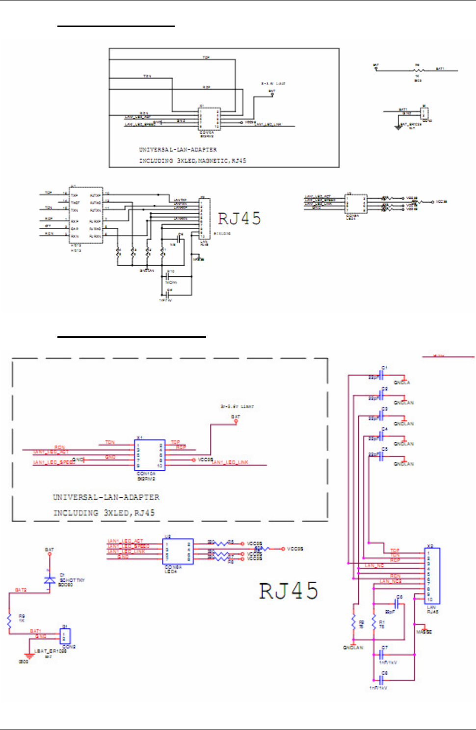
J29 LAN Interface Connector
MSM855:
Pin Signal Pin Signal
1 TDN (LAN TX-) 2 TDP (LAN TX+)
3 RDN (LAN RX-) 4 RDP (LAN RX+)
5 LAN-LED Activity 6 3.6V-RTC Lithium Battery Input
7 GND 8 VCC3 (+3.3V)
9 LAN-LED Speed 10 LAN-LED Link
Remarks:
Pins 1-4 must be connected to a 100/10-BASE-T transformation for isolation.
Pins 5, 8, 9 and 10 are used to connect 3pc LAN LED’s.
Each LAN-LED-signal must be terminated with a 330 Ohm resistor.
Pins 6 & 7 are used to connect the RTC-Battery.
MSM855B/B2:
Pin Signal Pin Signal
1 LAN TX- 2 LAN TX+
3 LAN RX- 4 LAN RX+
5 LAN-LED Activity 6 NC
7 GND 8 VCC3 (+3.3V)
9 LAN-LED Speed 10 LAN-LED Link
J30 Sound Interface Connector
Pin Signal Pin Signal
1 CD Input Left 2 GND for CD
3 CD Input Right 4 AUX-Line Input Left
5 GND for AUX 6 AUX-Line Input Right
7 LINE Input Left 8 GND for LINE
9 LINE Input Right 10 GND for MIC1
11 MIC1 Input 12 GND for MIC2
13 MIC2 Input 14 MONO Input
15 Output Suround Left 16 GND
17 Output Suround Right 18 GND
19 Output Front Left 20 GND
21 Output Front Right 22 GND
23 Output Center 24 GND
25 Output Subwoofer 26 GND
27 SPDIF Output 28 Jack-sense 0 (Front-sense)
29 Jack-sense 2 LineIn) 30 Jack-sense 3 (MIC-sense)
J33 LAN Interface Connector
Only on the MSM855B2:
Pin Signal Pin Signal
1 LAN TX- 2 LAN TX+
3 LAN RX- 4 LAN RX+
5 LAN-LED Activity 6 NC
7 GND 8 VCC3 (+3.3V)
9 LAN-LED Speed 10 LAN-LED Link
DIGITAL-LOGIC AG MSM855/HLV/B/B2 Detailed Manual V1.0A
90
X11 LVDS / DVO on board version V1.0
Pin Signal Pin Signal
1 DVO_C_CLK 2 DVO_C_CLK#
3 GND 4 DVO_C_BLANK#
5 DVO_C_D0 6 DVO_C_D1
7 DVO_C_D10 8 DVO_C_D11
9 DVO_C_D2 10 DVO_C_D3
11 DVO_C_D4 12 DVO_C_D5
13 DVO_C_D6 14 DVO_C_D7
15 DVO_C_D8 16 DVO_C_D9
17 DVO_C_FLDSTL 18 DVO_C_HSYNC
19 DVO_C_VSYNC 20 DVO_BC_CLKINT
21 DVO_DVIC 22 DVO_DVID
23 GND 24 DVO_MI2C
25 DVO_MI2D 26 DVI_REF
27 VCC15 28 VCC15
29 VCC3S 30 VCC3S
31 DVO_detect 32 DVO_reset#
33 VCC5S 34 VCC5S
35 VCC12 36 LVDS_BKLC
37 LVDS_BKLEN 38 LVDS_VDDEN
39 GND 40 LVDS_CLKAM
41 LVDS_CLKAP 42 GND
43 LVDS_YAM 44 LVDS_YAP0
45 LVDS_YAM1 46 LVDS_YAP1
47 LVDS_YAM2 48 LVDS_YAP2
49 LVDS_YAM3 50 LVDS_YAP3
Detailed signal description:
Signal LVDS_CLKAM [ICLKAM]
Description Output, LVDS, voltage: 1.25V±225mV
Channel A differential clock pair output (compliment): 245-800 MHz.
Signal LVDS_CLKAP [ICLKAP]
Description Output, LVDS, voltage: 1.25V±225mV
Channel A differential clock pair output (true): 245-800 MHz.
Signal LVDS_BKLC [PANELBKLTCTL]
Description Output, CMOS LVDS LCD Flat Panel Backlight Brightness Control: This signal is used as the
Pulse Width Modulated (PWM) control signal to control the backlight inverter.
Signal LVDS_BKLEN [PANELBKLTEN]
Description Output, CMOS LVDS LCD Flat Panel Backlight Enable: This signal is used to enable the
backlight inverter (BLI).
Signal LVDS_VDDEN [PANELVDDEN]
Description Output, CMOS LVDS LCD Flat Panel Power Control: This signal is used enable power to the
panel interface.
Signal LVDS_YAP0..3 [IYAP[3:0]]
Description Output, LVDS, voltage: 1.25V±225mV
Channel A differential data pair 3:0 output (true): 245-800MHz.
Signal LVDS_YAM0..3 [IYAM[3:0]]
Description Output, LVDS, 1.25V±225mV
Channel A differential data pair 3:0 output (compliment): 245-800 MHz.
DIGITAL-LOGIC AG MSM855/HLV/B/B2 Detailed Manual V1.0A
91
X12 FAN-Power Supply, 2pin
Pin Signal Pin Signal
1 VCC5 2 GND
X13 FAN-Power Supply 1, 3pin
Pin Signal Pin Signal
1 GND P2 VCC12V **
3 FAN1IN* * for future use / ** only if 12V on X8 pin 4
X16 FAN-Power Supply 2, 3pin
Pin Signal Pin Signal
1 GND 2 VCC12V **
3 FAN2IN* * for future use / ** only if 12V on X8 pin 4
7. JUMPER LOCATIONS ON THE BOARD
The following figures show the location of all jumper blocks on the MSM855 board. The numbers shown in
the figures are silk screened on the board so that the pins can easily be located. This chapter refers to the
individual pins for these jumpers. The default jumper settings are written in bold.
Be careful: some jumpers are soldering bridges; you will need a miniature soldering station with a vacuum
pump.
Settings written in bold are defaults!
Jumper Structure 1-2 / open 2-3 / closed Remarks
J16 Main switch manually set 1-2 = Automatic
power on
2-3 = ATX-Switch (push button)
must be connected to GND
(press button for boot up)
J10 Only for manufacturer's use
J11 Only for manufacturer's use
J32
LAN onboard function Enabled Disabled
only available on the MSM855B/B2
For the jumpers of board Version 0.4 please refer to Chapter 13, Previous Product Versions.
DIGITAL-LOGIC AG MSM855/HLV/B/B2 Detailed Manual V1.0A
92
7.1. The Jumpers on the MSM855
MSM855 V1.2 / V1.3 – Top View
DIGITAL-LOGIC AG MSM855/HLV/B/B2 Detailed Manual V1.0A
93
7.2. The Jumpers on the MSM855/B2
MSM855B/B2 V1.1 – Top View
DIGITAL-LOGIC AG MSM855/HLV/B/B2 Detailed Manual V1.0A
94
8. LED CRITERIA
LED Color Function
L1 Green Run OK located in the SM855 cover
L2 Red Hard disk activity located near the power supply connector
L3 Green SM855 waiting for start (led blinks)
LED Color Function
L1 Red Power
L2 Red LAN Link
L3 Red LAN Speed (100MB = lights / 10MB = no light)
L4 Red LAN Activity
L1
L2
L3
L1
L2
L3
L4
DIGITAL-LOGIC AG MSM855/HLV/B/B2 Detailed Manual V1.0A
95
9. CABLE INTERFACES
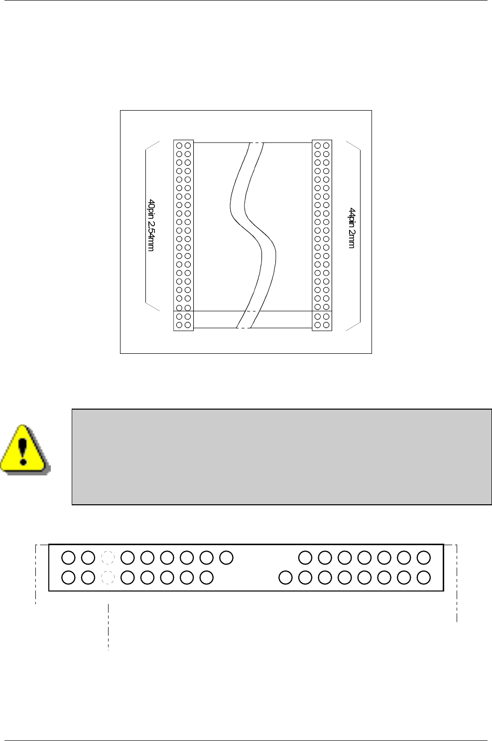
9.1. The Hard Disk Cable 44pin
IDT Terminal for Dual Row (2.00mm grid) and 1.00mm flat cable; 44pins = 40pins signal and 4pins power.
1 1 2
4343
44
44
39 39
40 40
2
Maximum length for the IDE cable is 30cm.
Attention!
Check the Pin 1 marker of the cable and the connector before you power-on. Refer to the
technical manual of the installed drives because a wrong cable will immediately destroy the
drive and/or the MICROSPACE MSM945 board. In this case the warranty is void! Without
the technical manual you may not connect this type of drive.
The 44pin IDE connector on the drives is normally composed of the 44 pins, 2 open pins and
4 test pins, 50 pins in total. Leave the 4 test pins unconnected.
1 3 43a b
c d
Testpin
open pin
44pin IDE Interface with integrated power lines
DIGITAL-LOGIC AG MSM855/HLV/B/B2 Detailed Manual V1.0A
96
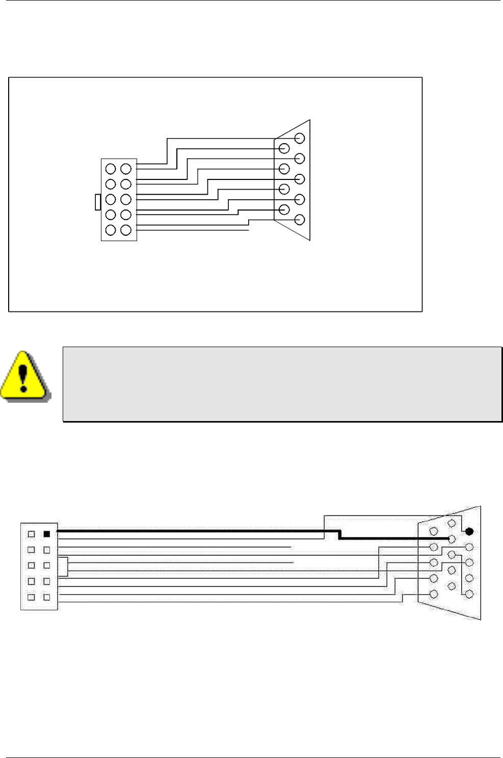
9.2. The COM 1/2 Serial Cable
DT terminal for dual row 0.1" (2.54 mm grid) and 1.27 mm flat cable.
2 1
COM1
9pin D-Sub
male
COM1/2
1
6 2
3
4
5
7
8
9
Line of pin 1
9 10
Attention!
Do not short circuit these signal lines.
Never connect any pins on the same plug or to any other plug on the MICROSPACE
MSM945. The +/- 10Volts will destroy the MICROSPACE core logic immediately. In this
case the warranty is void!
Do not overload the output; the maximum output current converters: 10mA
9.3. VGA Cable
DIGITAL-LOGIC AG MSM855/HLV/B/B2 Detailed Manual V1.0A
97
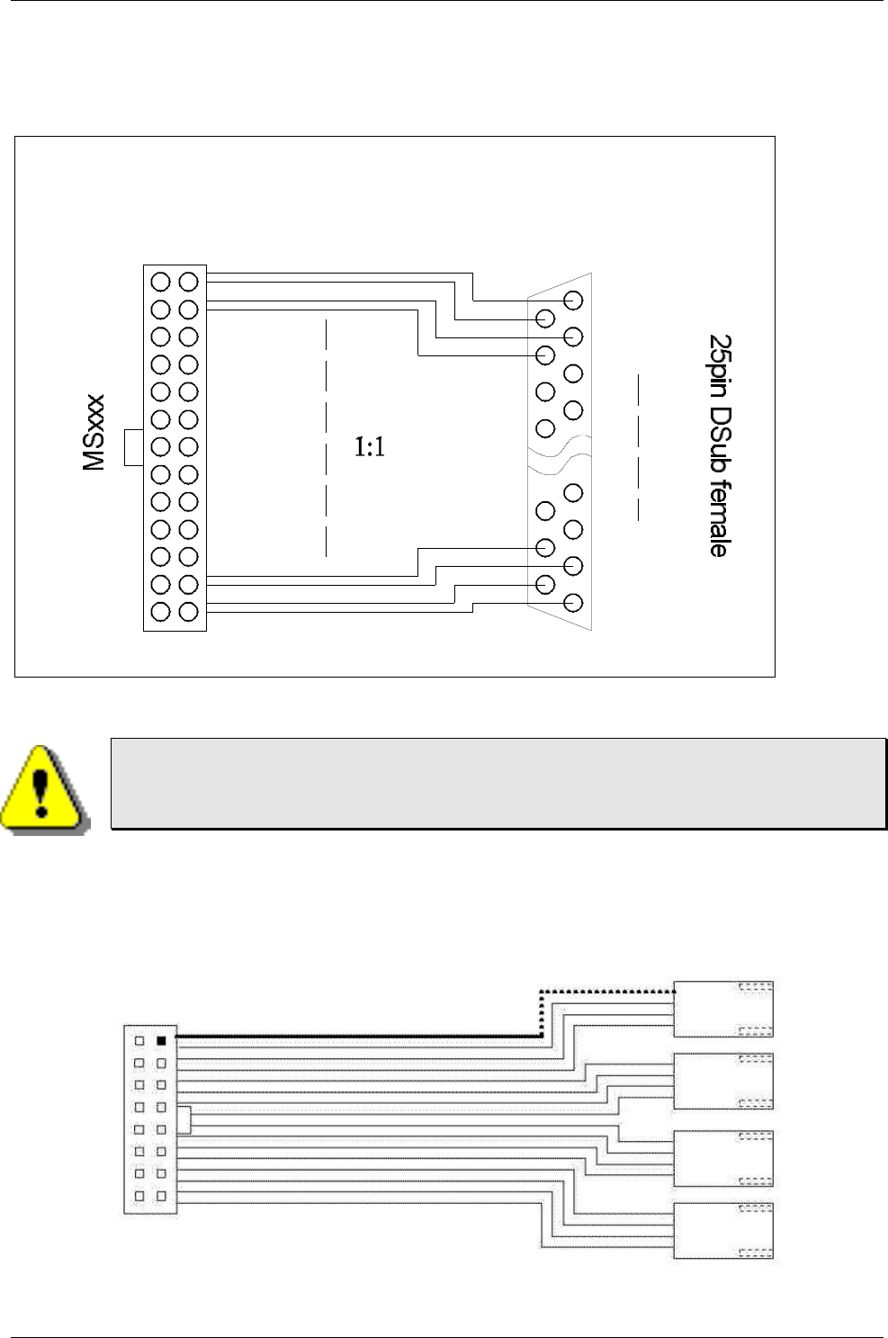
9.4. The Printer Cable (P4)
IDT terminal for dual row 0.1" (2.54mm grid) and 1.27 mm flat cable
14
2
15
1
24
25 12
13
Parallelport Cable LPT1
Attention!
Maximum length of this cable is 6 meters.
Prevent short-circuits.
Never apply power to these signals, the MICROSPACE MSM945 will be destroyed.
9.5. USB Cable
DIGITAL-LOGIC AG MSM855/HLV/B/B2 Detailed Manual V1.0A
98
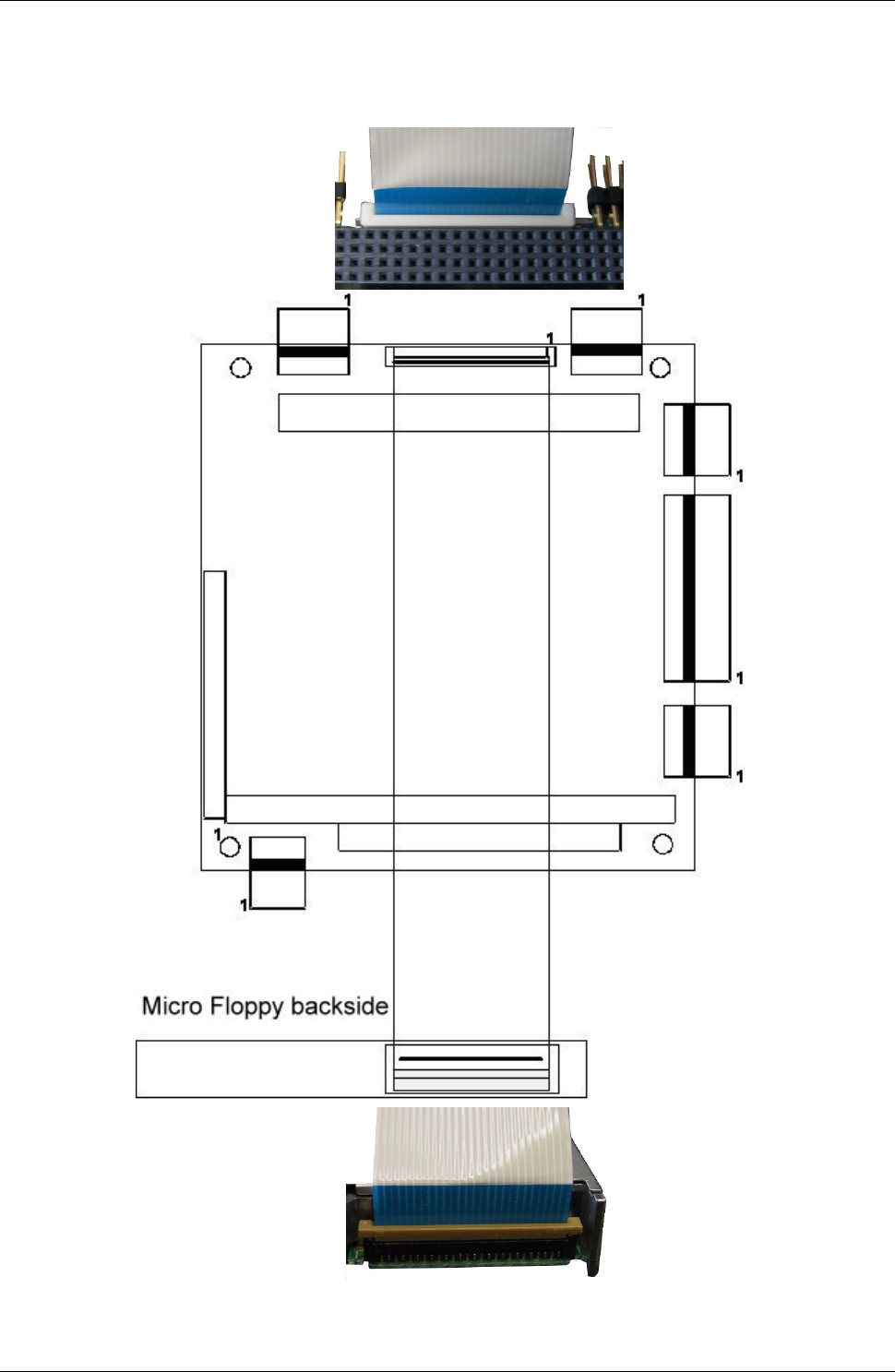
9.6. The Micro Floppy Cable
DIGITAL-LOGIC AG MSM855/HLV/B/B2 Detailed Manual V1.0A
99
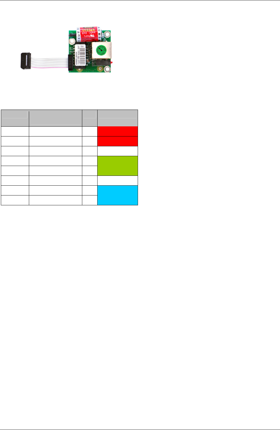
9.7. The LAN Interface Cable (RJ45)
This picture shows the MSM855-LANCON.
RJ45 connector 10BaseT (IEEE 802.3i), 100BaseTX (IEEE 802.3u):
MDI-Pin EIA/TIA 568A
Colors (wire/line)
Pin
Twisted Pair
TX+ White / Green 1 3
TX- Green 2 3
RX+ White / Orange 3 2
GND .. 4 1
GND .. 5 1
RX- Orange 6 2
GND .. 7 4
GND .. 8 4
Cabling: Do not exceed 100 meters (328 feet)
Has a minimum quality of CAT5, preferably S/FTP or STP CAT6
Be sure to have a well balanced shield/ground concept
DIGITAL-LOGIC AG MSM855/HLV/B/B2 Detailed Manual V1.0A
100
9.7.1. MSM855 LANCON
9.7.2. MSM855B/B2 LANCON

DIGITAL-LOGIC AG MSM855/HLV/B/B2 Detailed Manual V1.0A
101
10. THERMAL SPECIFICATIONS
10.1. Thermal Analysis for Case Integration
Since the integrated heat sink is uni-directional, the airflow must be exactly in the direction of the heat rails. If
possible, mount the board vertically, so that the heat rails are up/down. In this case, the self produced airflow
is about 3m/sec.
Pay particular attention when mounting the PC-product in a fully enclosed case/box. The thermal energy will
be stored in the inner room of this environment.
If the case has a fan:
The hot air must be exchanged with cool air from outside using a filtered fan.
The hot air must be cooled with a heat exchanger.
If the case has no fan or opening to exchange the hot air:
The heat sink of the CPU must be mounted directly to a heat sink integrated in the case. The thermal
energy does not go through the air; the heat will be conducted directly through the alloy of the heat
sink to the outside.
Diminish the thermal energy production by reducing the CPU performance, i.e. by using the 600MHz
clock only.
DIGITAL-LOGIC AG MSM855/HLV/B/B2 Detailed Manual V1.0A
102
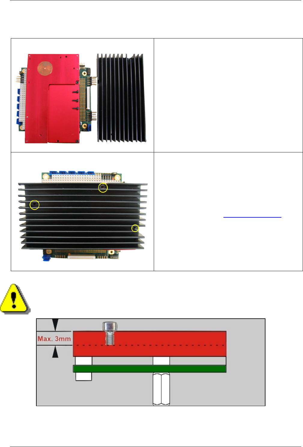
10.2. Assembly of the Passive Heat Sink
Photo of basic SM855 with passive heat sink and 3
screws.
Step 1:
Put the passive heat sink onto the SM855.
Step 2:
Attach the heat sink with 3 screws.
Screw Type:
Cylinder hexagon socket type screw M2x6mm
BN7 DIN 912 ISO 4762 / www.sfsunimarket.biz
Tool: Hexagon head socket wrench no. 1.5
Attention!
When using an active/passive heat sink that is not from DLAG, be very careful!
The maximum depth the screws can go into the product is 3mm or the smartModule will be
destroyed!
DIGITAL-LOGIC AG MSM855/HLV/B/B2 Detailed Manual V1.0A
103
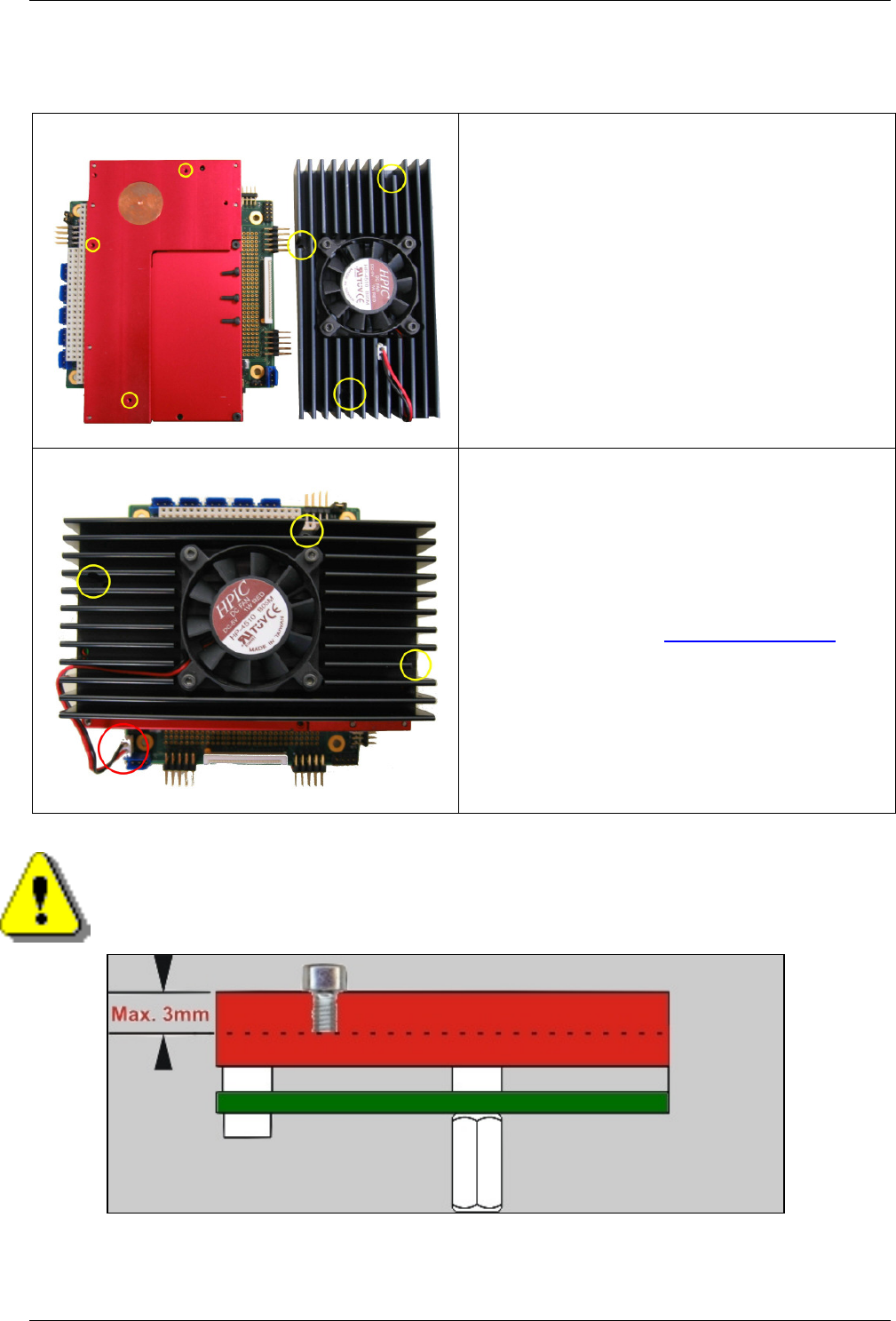
10.3. Assembly of the Active Heat Sink
Photo of basic SM855 with active heat sink and 3
screws.
Step 1:
Put the heat sink onto the SM855.
Step 2:
Attach the heat sink with 3 screws.
Screw Type:
Cylinder hexagon socket type screw M2x6mm
BN7 DIN 912 ISO 4762 / www.sfsunimarket.biz
Tool: Hexagon head socket wrench no. 1.5
Step 3:
Plug the fan into the electrical connection.
Attention!
When using an active/passive heat sink that is not from DLAG, be very careful!
The maximum depth the screws can go into the product is 3mm or the smartModule will be
destroyed!
DIGITAL-LOGIC AG MSM855/HLV/B/B2 Detailed Manual V1.0A
104
11. ASSEMBLY VIEWS
11.1. MSM855 V1.2 / V1.3
DIGITAL-LOGIC AG MSM855/HLV/B/B2 Detailed Manual V1.0A
105
DIGITAL-LOGIC AG MSM855/HLV/B/B2 Detailed Manual V1.0A
106
11.2. MSM855B/B2
DIGITAL-LOGIC AG MSM855/HLV/B/B2 Detailed Manual V1.0A
107
DIGITAL-LOGIC AG MSM855/HLV/B/B2 Detailed Manual V1.0A
108
12. Q&A – QUESTIONS & ANSWERS
Problem Solution
There is no picture after changing values in the
menu "DISPLAY PROPERTIES Settings".
You must press the following key combination to get a
picture again:
CTRL+ALT+ Fx
Fx:
F1 = VGA
F2 or F3 = SVIDEO
F4 = DVI
We recommend changing the settings in the Intel graphics
menu:
"DISPLAY PROPERTIES Settings Advanced Intel
Device Properties"
Strange behavior of the system during the boot-
up of the OS or while using the system.
Enter the BIOS setup and set the primary IDE channel to
“user” (instead “auto”).
Change the value “Ultra DMA Mode” = “2”
After changing the hardware to a newer revision
or version with the IHC4, Windows gives a blue
screen during the boot-up.
You must install Windows again (a new installation of the
OS).
Note…
To have better sound quality configure the “Sound” as
follows:
1. Enter the Menu Settings
2. Enable the “AUX” input in the playback device area
3. Mute the following inputs:
AUX, CD-Player, Phone, Line IN
DIGITAL-LOGIC AG MSM855/HLV/B/B2 Detailed Manual V1.0A
109
13. PREVIOUS PRODUCT VERSIONS
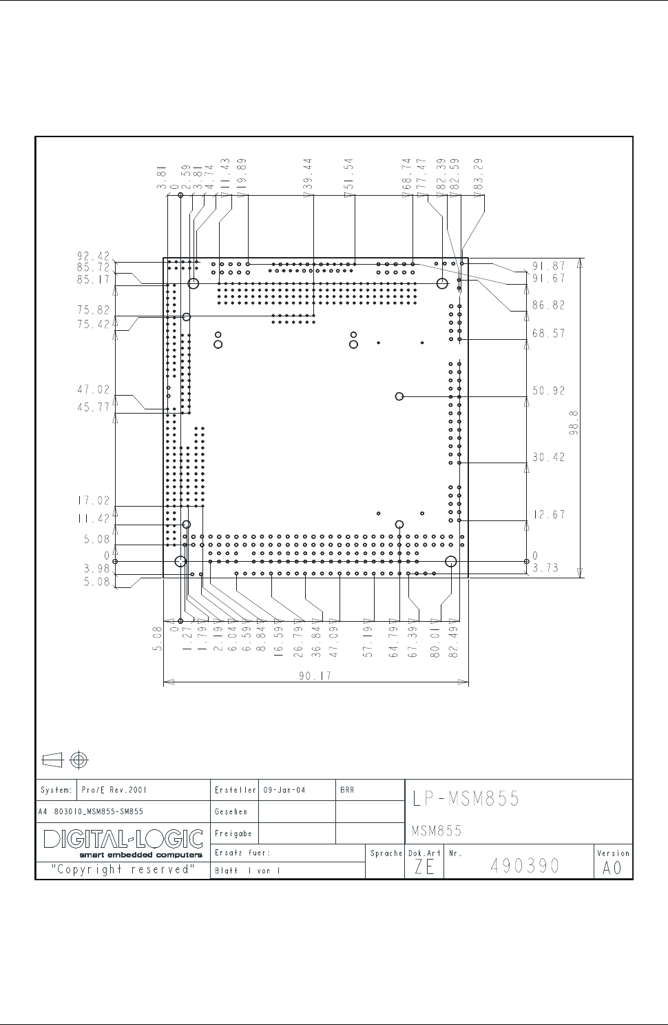
13.1. Mechanical Drawing V0.3/V0.4

DIGITAL-LOGIC AG MSM855/HLV/B/B2 Detailed Manual V1.0A
110
13.2. Assembly Views
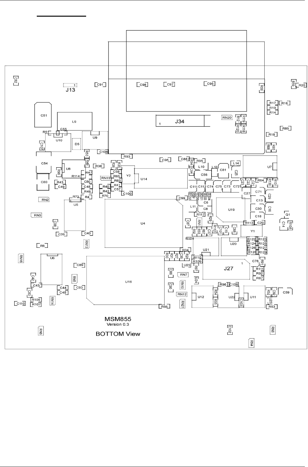
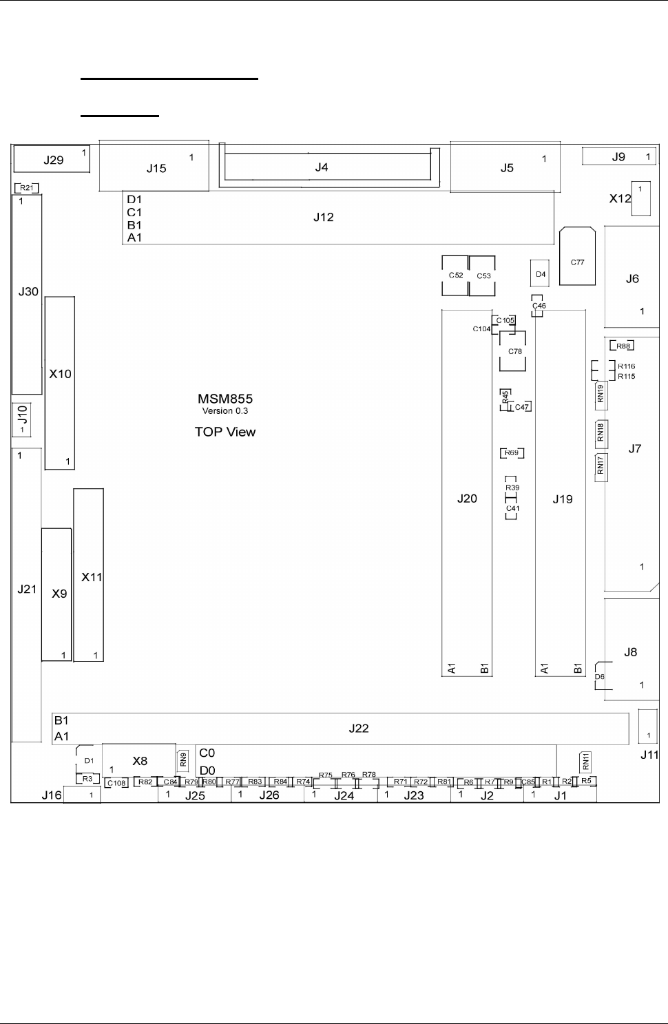
13.2.1. MSM855 V0.3 / V0.4
13.2.1.1. Top View
DIGITAL-LOGIC AG MSM855/HLV/B/B2 Detailed Manual V1.0A
111
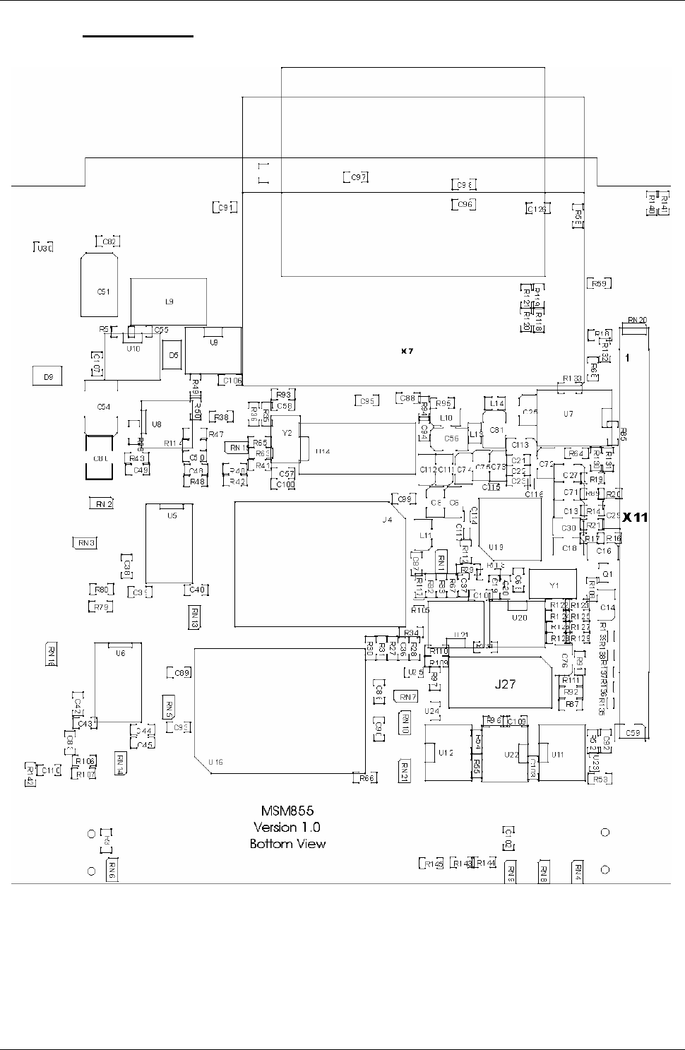
13.2.1.2. Bottom View
DIGITAL-LOGIC AG MSM855/HLV/B/B2 Detailed Manual V1.0A
112
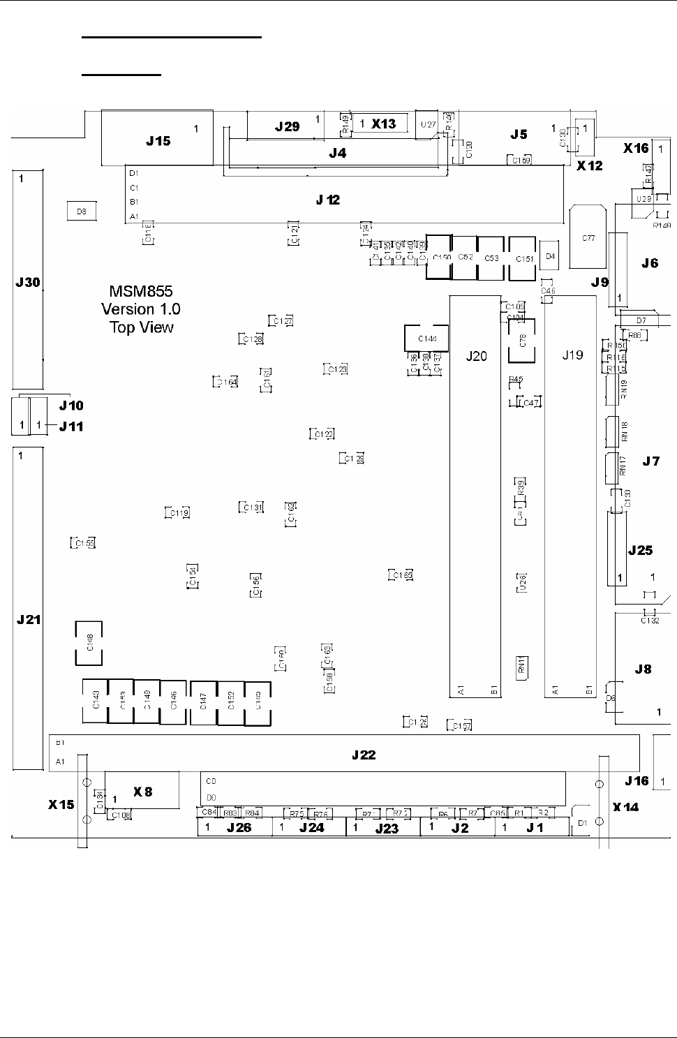
13.2.2. MSM855 V1.0 / V1.1
13.2.2.1. Top View
DIGITAL-LOGIC AG MSM855/HLV/B/B2 Detailed Manual V1.0A
113
13.2.2.2. Bottom View
DIGITAL-LOGIC AG MSM855/HLV/B/B2 Detailed Manual V1.0A
114
13.3. Connectors & Jumpers
13.3.1. MSM855 V0.3 / V0.4
13.3.1.1. Top View

DIGITAL-LOGIC AG MSM855/HLV/B/B2 Detailed Manual V1.0A
115
13.3.1.2. Bottom View
DIGITAL-LOGIC AG MSM855/HLV/B/B2 Detailed Manual V1.0A
116
13.3.2. MSM855 V0.3 / V0.4 – Jumpers only
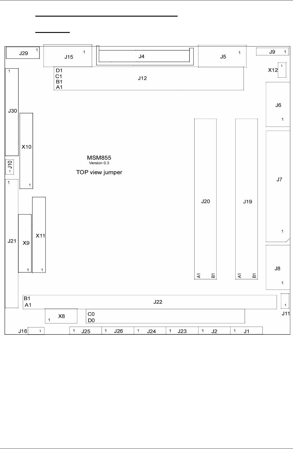
13.3.2.1. Top View
DIGITAL-LOGIC AG MSM855/HLV/B/B2 Detailed Manual V1.0A
117
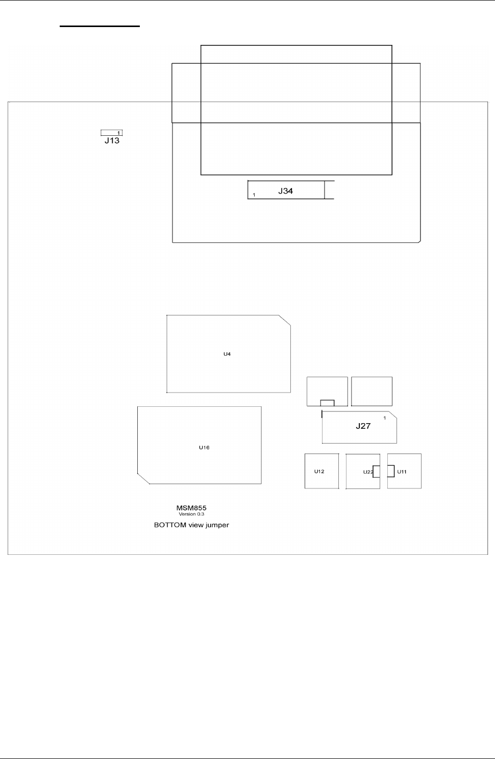
13.3.2.2. Bottom View
DIGITAL-LOGIC AG MSM855/HLV/B/B2 Detailed Manual V1.0A
118
13.3.3. MSM855 V1.0 / V1.1
13.3.3.1. Top View
DIGITAL-LOGIC AG MSM855/HLV/B/B2 Detailed Manual V1.0A
119
13.3.3.2. Bottom View
DIGITAL-LOGIC AG MSM855/HLV/B/B2 Detailed Manual V1.0A
120
13.4. Description of the Connectors for V0.4
Note…
Only the following connectors are different to the newer board version. All other connectors are
the same. Therefore, please refer to Chapter 6 for the other connectors.
J16 Main Switch Connector, 2pin
Pin Signal Pin Signal
1 Main Switch 2 GND
Used for connecting the ATX–compatible toggle switch (momentary close between Pins 1 and 2).
If this jumper is closed until the main supply powers up, the computer system starts by booting.
If this jumper is open until the main supply power up, then Pin1 (ATX-switch) must be tied to the
ground (Pin 2) to start the computer system (this is the ATX-function).
X8 Power Supply
Pin Signal Pin Signal
1 GND 2 Main supply +5Vo
3 Main switch (=J16 Pin1) 4 +12V
5 Reserved for AC-Present
6 Reserved for PWRBTN
7 GND 8 Main supply +5V
Remarks:
The Main Switch is low active and internally pulled up to 3.3V.
PWRBTN signal is low active and internally pulled up to 3.3V.
12V are not used for onboard functions, only wired to the PC/104bus.
The Main Supply is the only external (5V) supply used for this system.
X9 LVDS Interface
Pin Signal Pin Signal
1 LVDS_CLKAM 2 LVDS_CLKAP
3 NC 4 NC
5 LVDS_BKLC 6 LVDS_BKLEN
7 LVDS_VDDEN 8 NC
9 LVDS_YAM0 10 LVDS_YAM1
11 LVDS_YAM2 12 LVDS_YAM3
13 LVDS_YAP0 14 LVDS_YAP1
15 LVDS_YAP2 16 LVDS_YAP3
17 NC 18 NC
19 VCC3S 20 GND
DIGITAL-LOGIC AG MSM855/HLV/B/B2 Detailed Manual V1.0A
121
X10 DVO Channel B
Pin Signal Pin Signal
1 DVO_B_CLK 2 DVO_B_CLK#
3 DVO_B_BLANK# 4 DVO_B_D0
5 DVO_B_D1 6 DVO_B_D10
7 DVO_B_D11 8 DVO_B_D2
9 DVO_B_D3 10 DVO_B_D4
11 DVO_B_D5 12 DVO_B_D6
13 DVO_B_D7 14 DVO_B_D8
15 DVO_B_D9 16 VCC3S
17 DVO_B_FLDSTL 18 DVO_B_HSYNC
19 DVO_B_VSYNC 20 DVO_BC_CLKINT
21 DVO_DDC 22 DVO_DDD
23 GND 24 DVI_REV
25 NC 26 DVO_Detect
X11 DVO Channel C
Pin Signal Pin Signal
1 DVO_C_CLK 2 DVO_C_CLK#
3 DVO_C_BLANK# 4 DVO_C_D0
5 DVO_C_D1 6 DVO_C_D10
7 DVO_C_D11 8 DVO_C_D2
9 DVO_C_D3 10 DVO_C_D4
11 DVO_C_D5 12 DVO_C_D6
13 DVO_C_D7 14 DVO_C_D8
15 DVO_C_D9 16 VCC3S
17 DVO_C_FLDSTL 18 DVO_C_HSYNC
19 DVO_C_VSYNC 20 DVO_BC_INTR#
21 DVO_DVIC 22 DVO_DVID
23 GND 24 DVI_REF
25 NC 26 DVO_Detect
13.5. Description of the Jumpers for V0.4
Note…
Only the following connectors are different to the newer board version. All other connectors are
the same. Therefore, please refer to Chapter 7 for the other jumpers.
Settings written in bold are defaults!
Jumper Structure open closed Remarks
J13 PCI-IO voltage select 1-2 = 5V 2-3 = 3.3V
J16 Main switch set manually ATX-Switch (on X8 Pin6) must
be closed for boot-up
Automatic power-on
DIGITAL-LOGIC AG MSM855/HLV/B/B2 Detailed Manual V1.0A
122
14. INDEX
1
10/100 BASE-T Interface ........................................... 89
A
AC97 Sound............................................................... 75
Active Heat Sink....................................................... 103
Addressing PCI Devices............................................. 48
Assembly Views ....................................................... 104
B
Block Diagrams.......................................................... 14
Boot from LAN............................................................ 74
Bus Currents .............................................................. 47
Bus Signals ................................................................ 45
C
Cable Interfaces......................................................... 95
CMOS Setup.............................................................. 67
COM 1/2 Serial Cable ................................................ 96
Connectors................................................................. 78
Core BIOS Download................................................. 61
D
Disclaimer .................................................................... 6
E
EEPROM Memory for Setup ...................................... 67
Environmental Protection Statement............................ 6
Ethernet...................................................................... 73
External Battery Assembly ......................................... 37
F
Features, Standard .................................................... 13
Features, Unique........................................................ 13
Floppy Disk Interface............................................ 55, 84
Floppy Disk Interface Connector ................................ 56
H
Hard Disk Cable......................................................... 95
I
IDE Interface .............................................................. 88
IO Address ................................................................. 70
IrDA............................................................................ 85
ISO 9001:2000........................................................... 12
J
Jumper Locations ....................................................... 91
K
Keyboard.............................................................. 54, 85
L
LAN ............................................................................ 73
LAN boot .................................................................... 74
LAN Interface Cable ................................................... 99
LED Criteria................................................................ 94
LPT1........................................................................... 54
LVDS Interface ......................................................... 120
M
Main Switch Connector............................................. 120
Manual, How to Use It .................................................. 2
Micro Floppy Cable..................................................... 98
Mouse Utility Connector ............................................. 85
P
Passive Heat Sink .................................................... 102
PC/104 BUS Interface ................................................ 88
PC/104+ BUS Interface .............................................. 86
PC104 Bus ................................................................. 45
Power Supply ............................................... 87, 91, 120
Previous Product Versions ....................................... 109
Printer......................................................................... 54
Printer Cable .............................................................. 97
Printer Interface Cable................................................ 97
Printer Port ................................................................. 85
Q
Q&A.......................................................................... 108
Questions & Answers ............................................... 108
R
Recycling Information................................................... 7
Remote Function ........................................................ 58
RoHS Commitment..................................................... 10
ROM-BIOS ................................................................. 62
RTC Battery Lifetime .................................................. 36
S
Safety Precautions ..................................................... 10
Security ...................................................................... 17
Serial Cable................................................................ 96
Serial Ports........................................................... 55, 85
Speaker...................................................................... 56
Specifications ............................................................. 16

DIGITAL-LOGIC AG MSM855/HLV/B/B2 Detailed Manual V1.0A
123
SQS............................................................................ 12
Standards............................................................... 9, 13
Swiss Association for Quality and Management
Systems................................................................. 12
Swiss Quality.............................................................. 12
Symbols ....................................................................... 8
System I/O Map ......................................................... 70
T
Technical Support ........................................................ 7
Thermal Specifications............................................. 101
Trademarks.................................................................. 6
U
USB............................................................................ 84
USB Interface Protection............................................ 57
V
VGA Cable ................................................................. 96
VGA Monitor............................................... 87, 120, 121
W
Warranty....................................................................... 7
Watchdog ................................................................... 59