Delta Electronics orporated DFBM-NW726 Bluetooth Low Energy Module User Manual Preliminary
Delta Electronics Incorporated Bluetooth Low Energy Module Preliminary
UserManual.wiki
>
Delta Electronics orporated
>
DFBM NW726 User Manual
Users Manual
Navigation menu
Upload a User Manual
Namespaces
Wiki Guide
HTML
PDF
Info
Views
User Manual
Discussion / Help
Navigation
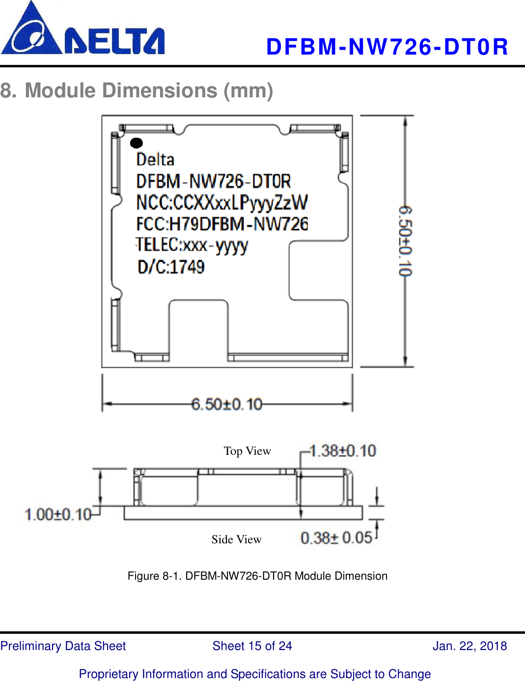
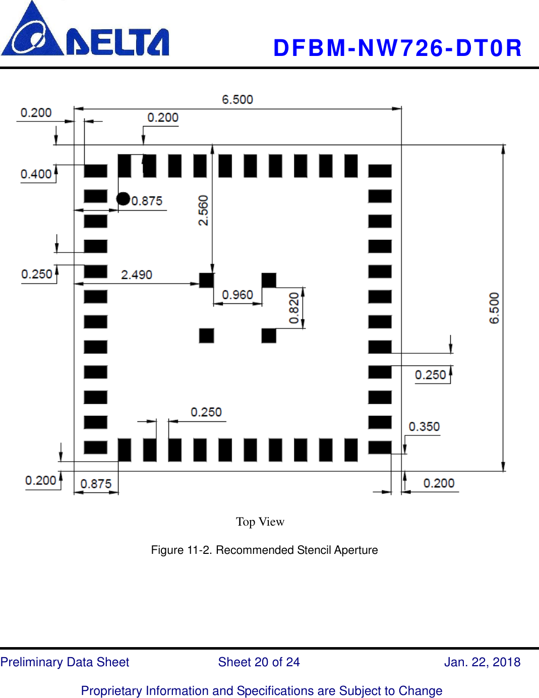
![DFBM-NW726-DT0R Preliminary Data Sheet Sheet 4 of 24 Jan. 22, 2018 Proprietary Information and Specifications are Subject to Change Revision History Rev. Date Reason of change Maker Approval S01 2018/01/22 Update FCC / NCC / TELEC Certification Number Ryan Josh 0.6 2018/01/10 1. Modify description in 6.Pin Description section Pin3 P0.20 / TRACECLK Pin5 P0.18 / TRACEDATA[0] / SWO Pin11 P0.16 / TRACEDATA[1] Pin13 P0.15 / TRACEDATA[2] Pin15 SWDIO, remove reset description Pin16 P0.14 / TRACEDATA[3] 2.Update detail dimension of footprint in 11.Recommended Stencil Aperture section 3.Modify C3 from 10UF to NC in 7.Reference Design section Ryan Josh 0.5 2017/12/14 Certification based on BT4.2 Ryan Josh 0.4 2017/12/08 Modify Laser marking information Ryan Josh 0.3 2017/11/07 Update Package information Ryan Josh 0.2 2017/10/20 Modify ESD (HBM/CDM) specification Ryan Josh 0.1 2017/07/03 Initial release Ryan Josh](https://usermanual.wiki/Delta-Electronics-orporated/DFBM-NW726/User-Guide-3722056-Page-4.png)


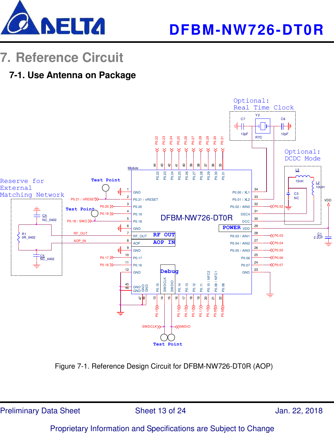
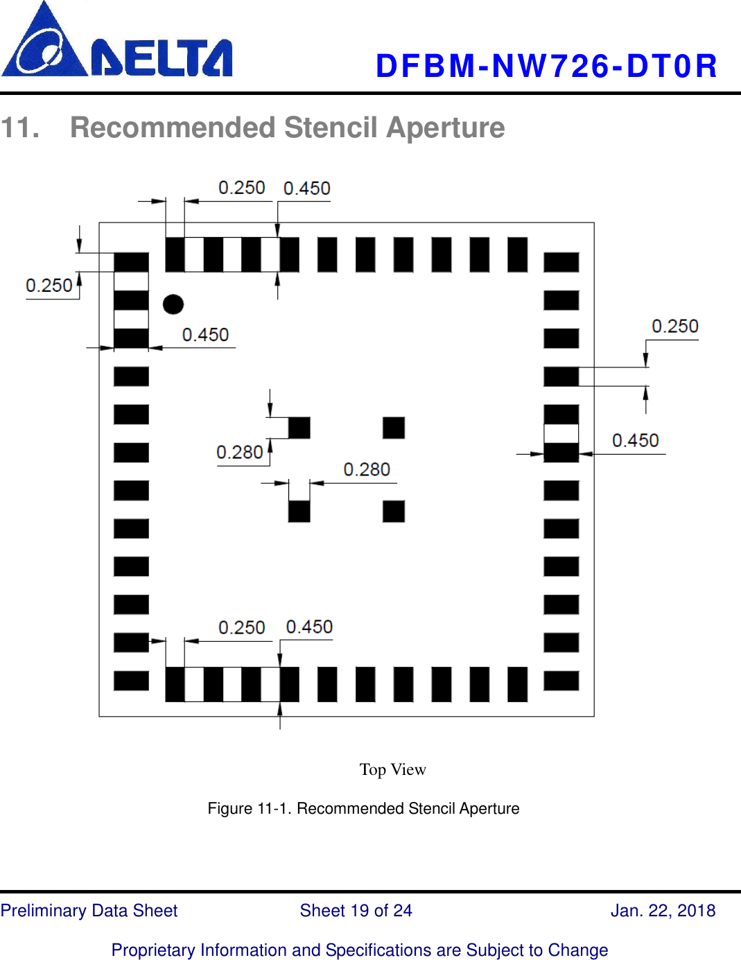
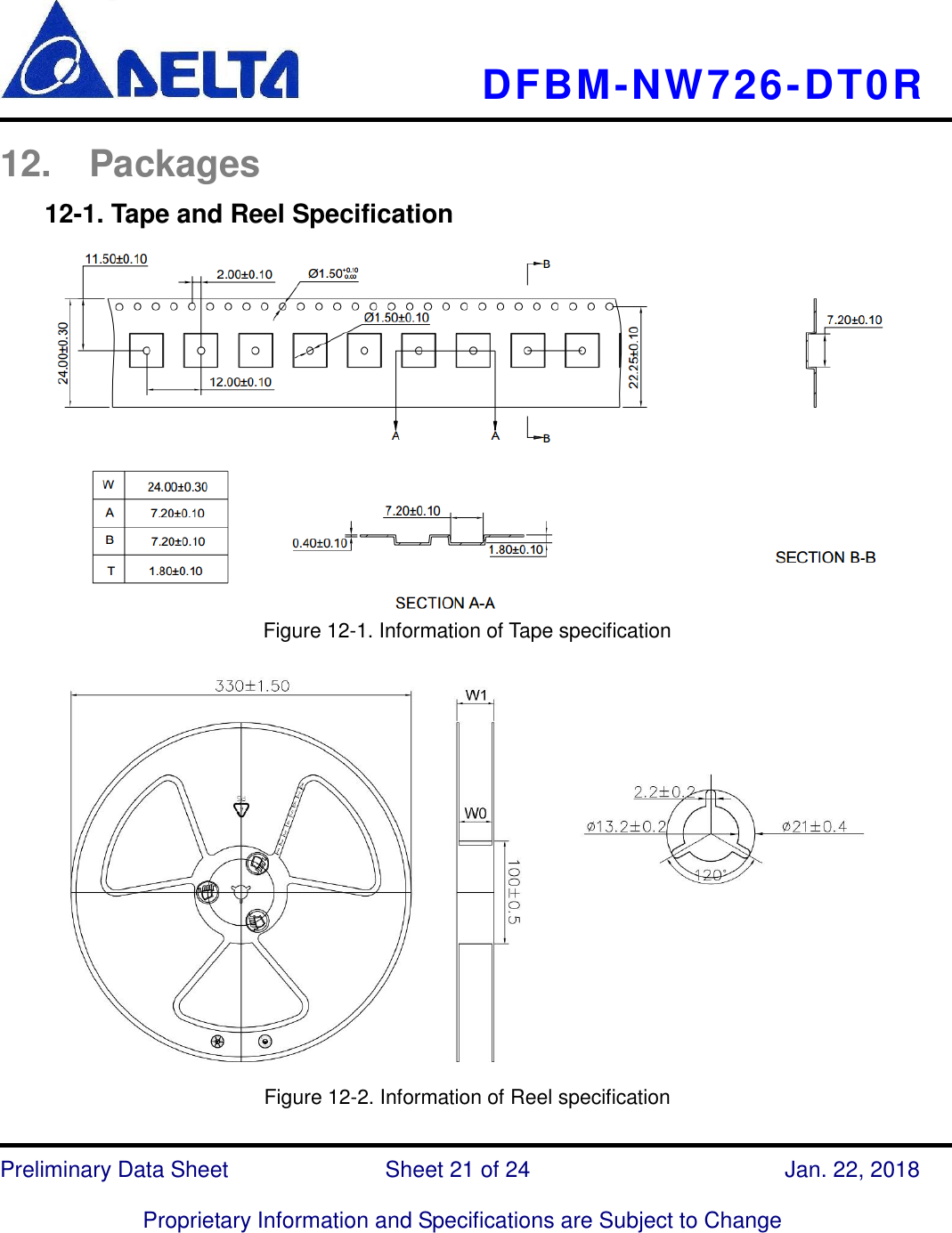
![DFBM-NW726-DT0R Preliminary Data Sheet Sheet 10 of 24 Jan. 22, 2018 Proprietary Information and Specifications are Subject to Change 6. Pin Description Pin Definition Function Description 1 GND Gnd Ground 2 P0.21 nRESET Digital I/O Bluetooth general purpose I/O pin Configurable as pin reset 3 P0.20 TRACECLK Digital I/O Bluetooth general purpose I/O pin Trace port clock output 4 P0.19 Digital I/O Bluetooth general purpose I/O pin 5 P0.18 TRACEDATA[0] / SWO Digital I/O Bluetooth general purpose I/O pin Single wire output Trace port output 6 GND Gnd Ground 7 RF_OUT RF_OUT Bluetooth RF input/output from IC 8 AOP AOP_IN Bluetooth RF input/output to antenna on package 9 GND Gnd Ground 10 P0.17 Digital I/O Bluetooth general purpose I/O pin 11 P0.16 TRACEDATA[1] Digital I/O Bluetooth general purpose I/O pin Trace port output 12 GND Gnd Ground 13 P0.15 TRACEDATA[2] Digital I/O Bluetooth general purpose I/O pin Trace port output 14 SWDCLK Digital input Serial wire debug clock input for debug and programming 15 SWDIO Digital I/O Serial wire debug I/O for debug and programming 16 P0.14 TRACEDATA[3] Digital I/O Bluetooth general purpose I/O pin Trace port output 17 P0.13 Digital I/O Bluetooth general purpose I/O pin](https://usermanual.wiki/Delta-Electronics-orporated/DFBM-NW726/User-Guide-3722056-Page-10.png)