Delta Electronics orporated DFBM-NW726 Bluetooth Low Energy Module User Manual Preliminary
Delta Electronics Incorporated Bluetooth Low Energy Module Preliminary
Users Manual

DFBM-NW726-DT0R
Preliminary Data Sheet Sheet 1 of 24 Jan. 22, 2018
Proprietary Information and Specifications are Subject to Change
Data sheet
BLE Module
DFBM-NW726-DT0R
A Bluetooth Low Energy module with Antenna
on Package.

DFBM-NW726-DT0R
Preliminary Data Sheet Sheet 2 of 24 Jan. 22, 2018
Proprietary Information and Specifications are Subject to Change
Contents
1. Features ........................................................................................................................................... 5
1-1. General ......................................................................................................................................... 5
1-2. Bluetooth...................................................................................................................................... 5
2. Block Diagram ................................................................................................................................ 6
2-1. Use Antenna on Package ............................................................................................................. 6
2-2. Use RF connector or External Antenna ....................................................................................... 6
3. General Specification ...................................................................................................................... 7
4. Electrical Characteristics ................................................................................................................. 8
4-1. Absolute Maximum Rating .......................................................................................................... 8
4-2. Recommended Operating Conditions & Power Consumption .................................................... 8
5. RF Characteristics ........................................................................................................................... 9
5-1. Bluetooth RF characteristics ........................................................................................................ 9
5-2. Antenna characteristics ................................................................................................................ 9
6. Pin Description .............................................................................................................................. 10
7. Reference Circuit .......................................................................................................................... 13
7-1. Use Antenna on Package ........................................................................................................... 13
7-2. Use RF connector or External Antenna ..................................................................................... 14
8. Module Dimensions (mm) ............................................................................................................ 15
9. Recommend Soldering Conditions ............................................................................................... 17
10. Layout Guide (mm) ....................................................................................................................... 18
10-1. Use Antenna on Package ......................................................................................................... 18
10-2. Use RF connector or External Antenna ................................................................................... 18
11. Recommended Stencil Aperture .................................................................................................... 19
12. Packages ........................................................................................................................................ 21
12-1. Tape and Reel Specification .................................................................................................... 21
12-2. Storage Specification ............................................................................................................... 22
13. Required End Product Labeling .................................................................................................... 23

DFBM-NW726-DT0R
Preliminary Data Sheet Sheet 3 of 24 Jan. 22, 2018
Proprietary Information and Specifications are Subject to Change
14. Manual Information to the End User ............................................................................................ 23
15. Federal Communications Commission (FCC) Statement ............................................................. 23
DFBM-NW726-DT0R
Preliminary Data Sheet Sheet 4 of 24 Jan. 22, 2018
Proprietary Information and Specifications are Subject to Change
Revision History
Rev.
Date
Reason of change
Maker
Approval
S01
2018/01/22
Update FCC / NCC / TELEC Certification Number
Ryan
Josh
0.6
2018/01/10
1. Modify description in 6.Pin Description section
Pin3 P0.20 / TRACECLK
Pin5 P0.18 / TRACEDATA[0] / SWO
Pin11 P0.16 / TRACEDATA[1]
Pin13 P0.15 / TRACEDATA[2]
Pin15 SWDIO, remove reset description
Pin16 P0.14 / TRACEDATA[3]
2.Update detail dimension of footprint in 11.Recommended
Stencil Aperture section
3.Modify C3 from 10UF to NC in 7.Reference Design section
Ryan
Josh
0.5
2017/12/14
Certification based on BT4.2
Ryan
Josh
0.4
2017/12/08
Modify Laser marking information
Ryan
Josh
0.3
2017/11/07
Update Package information
Ryan
Josh
0.2
2017/10/20
Modify ESD (HBM/CDM) specification
Ryan
Josh
0.1
2017/07/03
Initial release
Ryan
Josh

DFBM-NW726-DT0R
Preliminary Data Sheet Sheet 5 of 24 Jan. 22, 2018
Proprietary Information and Specifications are Subject to Change
DFBM-NW726-DT0R
BLE Module with Antenna on Package
his document describes the DFBM-NW726-DT0R wireless BLE module hardware specification. The
modules provide cost effective, low power, and flexible platform to add BLE for embedded devices for
a variety of applications, such as wireless sensors and thermostats. It uses BLE SoC, which integrating the
2.4GHz transceiver, a 32 bit ARM® Cortex M4F CPU, flash memory, and analog and digital peripherals.
1. Features
1-1. General
BLE chip with a single chip antenna or an external RF connector
Integrate a 32 bit ARM® Cortex M4F CPU,512KB flash memory and 64KB RAM
12-bit 200kspc ADC - 8 configurable channels with programmable gain
30 General Purpose I/O Pins
Two-wire Master (I2C compatible) support 100K bps and 400K bps
UART baud rate up to 921600 bps
SPI bit rate up to 4M bps
Quadrature Decoder (QDEC)
LGA 48 pin package
Dimension 6.5mm(L) x 6.5mm(W) x 1.5 mm(H)
RoHS compliant
1-2. Bluetooth
Bluetooth 4.2 specification compliant
AES HW encryption
T
DFBM-NW726-DT0R
Preliminary Data Sheet Sheet 6 of 24 Jan. 22, 2018
Proprietary Information and Specifications are Subject to Change
2. Block Diagram
2-1. Use Antenna on Package
Figure 2-1. DFBM-NW726-DT0R Block Diagram (AOP)
2-2. Use RF connector or External Antenna
Figure 2-2. DFBM-NW726-DT0R Block Diagram (External RF)
ADC
Bluetooth ANT
On Package
UART/SPI/I2C
GPIO
VDD: 1.7V ~ 3.6V
32MHz Crystal
Bluetooth
SOC
Matching
Network
(Optional)
ADC
External Antenna
UART/SPI/I2C
GPIO
VDD: 1.7V ~ 3.6V
32MHz Crystal
Bluetooth
SOC
Matching
Network
(Optional)
Bluetooth ANT
On Package
DFBM-NW726-DT0R
Preliminary Data Sheet Sheet 7 of 24 Jan. 22, 2018
Proprietary Information and Specifications are Subject to Change
3. General Specification
MCU
ARM® Cortex® -M4 32-bit processor with FPU, 64MHz
Standard
Bluetooth: V4.2
Frequency
2.402 ~ 2.48 GHz
Modulation
GFSK
Data Rate
BLE: 0.25, 1, 2 Mbps
Operating Temperature
-40℃ ~ +85 ℃
Storage Temperature
-40℃ ~ +85 ℃
Antenna Impedance
50 ohm
Package Size
6.5 x 6.5 x 1.5 mm3
Host Interface
UART, SPI, I2C, ADC
Certification
FCC: H79DFBM-NW726
CE Compliant
NCC: CCAM18LP0130T8
TELEC: 201-180008
Table 3-1. General Specification
DFBM-NW726-DT0R
Preliminary Data Sheet Sheet 8 of 24 Jan. 22, 2018
Proprietary Information and Specifications are Subject to Change
4. Electrical Characteristics
4-1. Absolute Maximum Rating
Symbol
Min.
Max.
Units
VDD_3V3
-0.3
3.9
V
VGPIO
-0.3
3.9
V
ESD-HBM
2
KV
ESD-CDM
500
V
Table 4-1. Absolute Maximum Rating
4-2. Recommended Operating Conditions & Power Consumption
Symbol
Parameter
Min.
Typ.
Max.
Unit
VDD_3V3
Supply Voltage
1.7
3.3
3.6
V
System On, Standby mode
50
uA
TX Current at POUT = +0 dBm (LDO)
11.6
mA
TX Current at POUT = +0 dBm (DCDC)
5.3
mA
RX Current (LDO)
12.9
mA
RX Current (DCDC)
5.8
mA
Current in SYSTEM OFF, no RAM retention.
0.7
1.2
1.9
uA
Current in SYSTEM OFF mode 32 kB RAM retention.
1.0
uA
SYSTEM-ON base current with 32 kB RAM enabled.
1.5
uA
Table 4-2. Bluetooth Power Consumption
DFBM-NW726-DT0R
Preliminary Data Sheet Sheet 9 of 24 Jan. 22, 2018
Proprietary Information and Specifications are Subject to Change
5. RF Characteristics
5-1. Bluetooth RF characteristics
Condition: VDD_3V3=VIO=3.3V, T=25℃
Item
Condition
Min.
Typ.
Max.
Unit
RF Characteristics
Output Power
-20
0
4
dBm
Initial Frequency Offset
-75
75
KHz
Carrier Frequency Offset and Drift
CFOD
-150
150
KHz
Modulation Characteristics
Modulation Index (F1 / F2)
0.8
N/A
F1 Average
225
275
KHz
F2 Maximum
185
KHz
Sensitivity
PER < 30.8%
-96
dBm
Maximum Input Level
PER < 30.8%
-10
dBm
Table 5-1. Bluetooth RF Characteristics
5-2. Antenna characteristics
There is no antenna on module. Only RF pad is used for antenna. Below table shows antenna list used
for certification testing.
Antenna Designation for
Certification
1. Dipole Antenna, Gain: 2.23dBi
Part No.:RFDPA8780900SMAB801, Supplier: Walsin
2. Chip Antenna, Gain: 2.12dBi
Part No.:RFANT3216120A5T, Supplier: Walsin
3. PCB Antenna, Gain: 2dBi
Part No.:DFAM-NW726-DT0R, Supplier: Delta
DFBM-NW726-DT0R
Preliminary Data Sheet Sheet 10 of 24 Jan. 22, 2018
Proprietary Information and Specifications are Subject to Change
6. Pin Description
Pin
Definition
Function
Description
1
GND
Gnd
Ground
2
P0.21
nRESET
Digital I/O
Bluetooth general purpose I/O pin
Configurable as pin reset
3
P0.20
TRACECLK
Digital I/O
Bluetooth general purpose I/O pin
Trace port clock output
4
P0.19
Digital I/O
Bluetooth general purpose I/O pin
5
P0.18
TRACEDATA[0] /
SWO
Digital I/O
Bluetooth general purpose I/O pin
Single wire output
Trace port output
6
GND
Gnd
Ground
7
RF_OUT
RF_OUT
Bluetooth RF input/output from IC
8
AOP
AOP_IN
Bluetooth RF input/output to antenna on package
9
GND
Gnd
Ground
10
P0.17
Digital I/O
Bluetooth general purpose I/O pin
11
P0.16
TRACEDATA[1]
Digital I/O
Bluetooth general purpose I/O pin
Trace port output
12
GND
Gnd
Ground
13
P0.15
TRACEDATA[2]
Digital I/O
Bluetooth general purpose I/O pin
Trace port output
14
SWDCLK
Digital input
Serial wire debug clock input for debug and programming
15
SWDIO
Digital I/O
Serial wire debug I/O for debug and programming
16
P0.14
TRACEDATA[3]
Digital I/O
Bluetooth general purpose I/O pin
Trace port output
17
P0.13
Digital I/O
Bluetooth general purpose I/O pin

DFBM-NW726-DT0R
Preliminary Data Sheet Sheet 11 of 24 Jan. 22, 2018
Proprietary Information and Specifications are Subject to Change
Pin
Definition
Function
Description
18
P0.12
Digital I/O
Bluetooth general purpose I/O pin
19
P0.11
Digital I/O
Bluetooth general purpose I/O pin
20
P0.10
NFC2
Digital I/O
NFC input
Bluetooth general purpose I/O pin
NFC antenna connection
21
P0.09
NFC1
D Digital I/O
NFC input
Bluetooth general purpose I/O pin
NFC antenna connection
22
P0.08
Digital I/O
Bluetooth general purpose I/O pin
23
GND
Gnd
Ground
24
P0.07
Digital I/O
Bluetooth general purpose I/O pin
25
P0.06
Digital I/O
Bluetooth general purpose I/O pin
26
P0.05
AIN3
Digital I/O
Analog input
Bluetooth general purpose I/O pin
SAADC/COMP/LPCOMP input
27
P0.04
AIN2
Digital I/O
Analog input
Bluetooth general purpose I/O pin
SAADC/COMP/LPCOMP input
28
P0.03
AIN1
Digital I/O
Analog input
Bluetooth general purpose I/O pin
SAADC/COMP/LPCOMP input
29
VDD
Power
Power supply input
30
DCC
Power
DC/DC regulator output
31
DEC4
Power
1.3 V regulator supply decoupling Input from DC/DC
regulator Output from 1.3 V LDO
32
P0.02
AIN0
Digital I/O
Analog input
Bluetooth general purpose I/O pin
SAADC/COMP/LPCOMP input
33
P0.01
XL2
Digital I/O
Analog input
Bluetooth general purpose I/O pin
Connection for 32.768 kHz crystal (LFXO)
34
P0.00
XL1
Digital I/O
Analog input
Bluetooth general purpose I/O pin
Connection for 32.768 kHz crystal (LFXO)
35
P0.31
Digital I/O
Bluetooth general purpose I/O pin
36
P0.30
Digital I/O
Bluetooth general purpose I/O pin
DFBM-NW726-DT0R
Preliminary Data Sheet Sheet 12 of 24 Jan. 22, 2018
Proprietary Information and Specifications are Subject to Change
Pin
Definition
Function
Description
37
P0.29
Digital I/O
Bluetooth general purpose I/O pin
38
P0.28
Digital I/O
Bluetooth general purpose I/O pin
39
P0.27
Digital I/O
Bluetooth general purpose I/O pin
40
P0.26
Digital I/O
Bluetooth general purpose I/O pin
41
P0.25
Digital I/O
Bluetooth general purpose I/O pin
42
P0.24
Digital I/O
Bluetooth general purpose I/O pin
43
P0.23
Digital I/O
Bluetooth general purpose I/O pin
44
P0.22
Digital I/O
Bluetooth general purpose I/O pin
45
GND
Gnd
Ground
46
GND
Gnd
Ground
47
GND
Gnd
Ground
48
GND
Gnd
Ground
DFBM-NW726-DT0R
Preliminary Data Sheet Sheet 13 of 24 Jan. 22, 2018
Proprietary Information and Specifications are Subject to Change
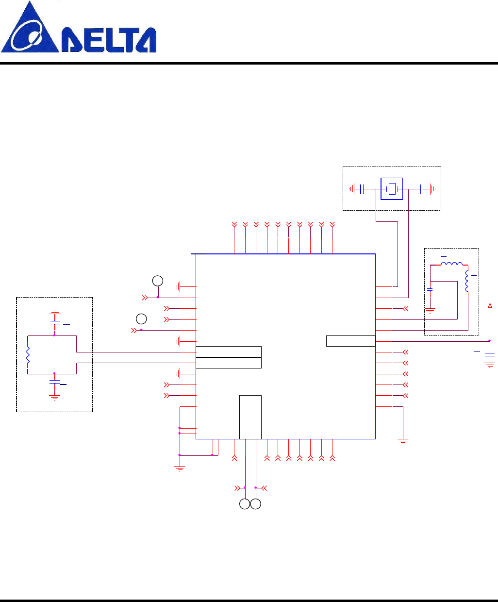
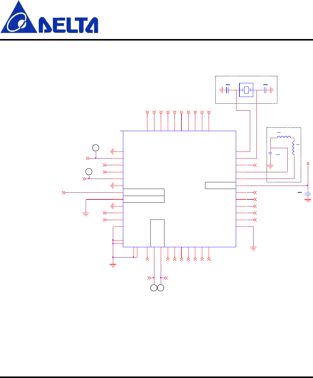
7. Reference Circuit
7-1. Use Antenna on Package
C3
NC
L2
10UH
L3
15nH
Optional:
DCDC Mode
Test Point
P0.21 / nRESET
Test Point
SWDIOSWDCLK
Test Point
RF_OUT
AOP_IN
C5
NC_0402
R1
0R_0402
Module
DFBM-NW726-DT0R
GND
1
P0.21 / nRESET
2
P0.20
3
P0.19
4
P0.18
5
GND
6
RF_OUT
7
AOP
8
GND
9
P0.17
10
GND
12
P0.10 / NFC2
20
P0.09 / NFC1
21
P0.08
22
GND 23
P0.31 35
P0.00 / XL1 34
DEC4 31
DCC 30
VDD 29
P0.03 / AIN1 28
P0.04 / AIN2 27
P0.07 24
P0.30 36
P0.02 / AIN0 32
P0.01 / XL2 33
P0.14
16
P0.13
17
P0.06 25
P0.05 / AIN3 26
P0.12
18
P0.11
19
P0.15
13
SWDCLK
14
SWDIO
15
P0.16
11
P0.29 37
P0.28 38
P0.27 39
P0.26 40
P0.25 41
P0.24 42
P0.23 43
P0.22 44
GND
45
GND
46
GND
47
GND
48
C1
2.2UF
C4
NC_0402
VDD
P0.29
P0.28
P0.23
P0.31
P0.30
P0.22
P0.25
P0.24
P0.06
P0.05
P0.04
P0.15
P0.07
P0.13
P0.14
P0.09
P0.10
P0.11
P0.12
P0.16
P0.17
P0.08
P0.20
P0.18 / SWO
P0.19
AOP IN
Optional:
Real Time Clock
RF OUT
Debug
POWER
Reserve for
External
Matching Network
P0.02
P0.03
P0.27
P0.26
C6
12pF
Y2
RTC
C7
12pF
Figure 7-1. Reference Design Circuit for DFBM-NW726-DT0R (AOP)
DFBM-NW726-DT0R
Preliminary Data Sheet Sheet 14 of 24 Jan. 22, 2018
Proprietary Information and Specifications are Subject to Change
7-2. Use RF connector or External Antenna
L3
15nH
C3
NC
L2
10UH
Optional:
DCDC Mode
C1
2.2UF
VDD
Debug
Test Point
Test Point
AOP IN
P0.18 / SWO
Test Point
P0.04
P0.05
P0.06
P0.07
P0.15
SWDCLK
P0.14
SWDIO
P0.13
P0.12
P0.11
P0.10
P0.09
P0.08
POWER
RF OUT
Connect to
RF connector or
Antenna
AOP_IN
RF_OUT
P0.17
P0.16
P0.19
P0.20
P0.21 / nRESET
RF_OUT
P0.02
P0.03
Module
DFBM-NW726-DT0R
GND
1
P0.21 / nRESET
2
P0.20
3
P0.19
4
P0.18
5
GND
6
RF_OUT
7
AOP
8
GND
9
P0.17
10
GND
12
P0.10 / NFC2
20
P0.09 / NFC1
21
P0.08
22
GND 23
P0.31 35
P0.00 / XL1 34
DEC4 31
DCC 30
VDD 29
P0.03 / AIN1 28
P0.04 / AIN2 27
P0.07 24
P0.30 36
P0.02 / AIN0 32
P0.01 / XL2 33
P0.14
16
P0.13
17
P0.06 25
P0.05 / AIN3 26
P0.12
18
P0.11
19
P0.15
13
SWDCLK
14
SWDIO
15
P0.16
11
P0.29 37
P0.28 38
P0.27 39
P0.26 40
P0.25 41
P0.24 42
P0.23 43
P0.22 44
GND
45
GND
46
GND
47
GND
48
P0.28
P0.29
P0.30
P0.31
P0.23
P0.24
P0.25
P0.22
P0.26
Optional:
Real Time Clock
P0.27
C6
12pF
Y3
RTC
C7
12pF
Figure 7-2. Reference Design Circuit for DFBM-NW726-DT0R (External Antenna)
DFBM-NW726-DT0R
Preliminary Data Sheet Sheet 15 of 24 Jan. 22, 2018
Proprietary Information and Specifications are Subject to Change
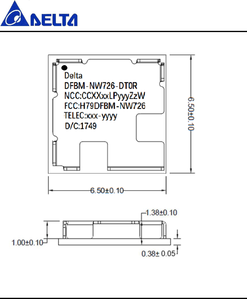
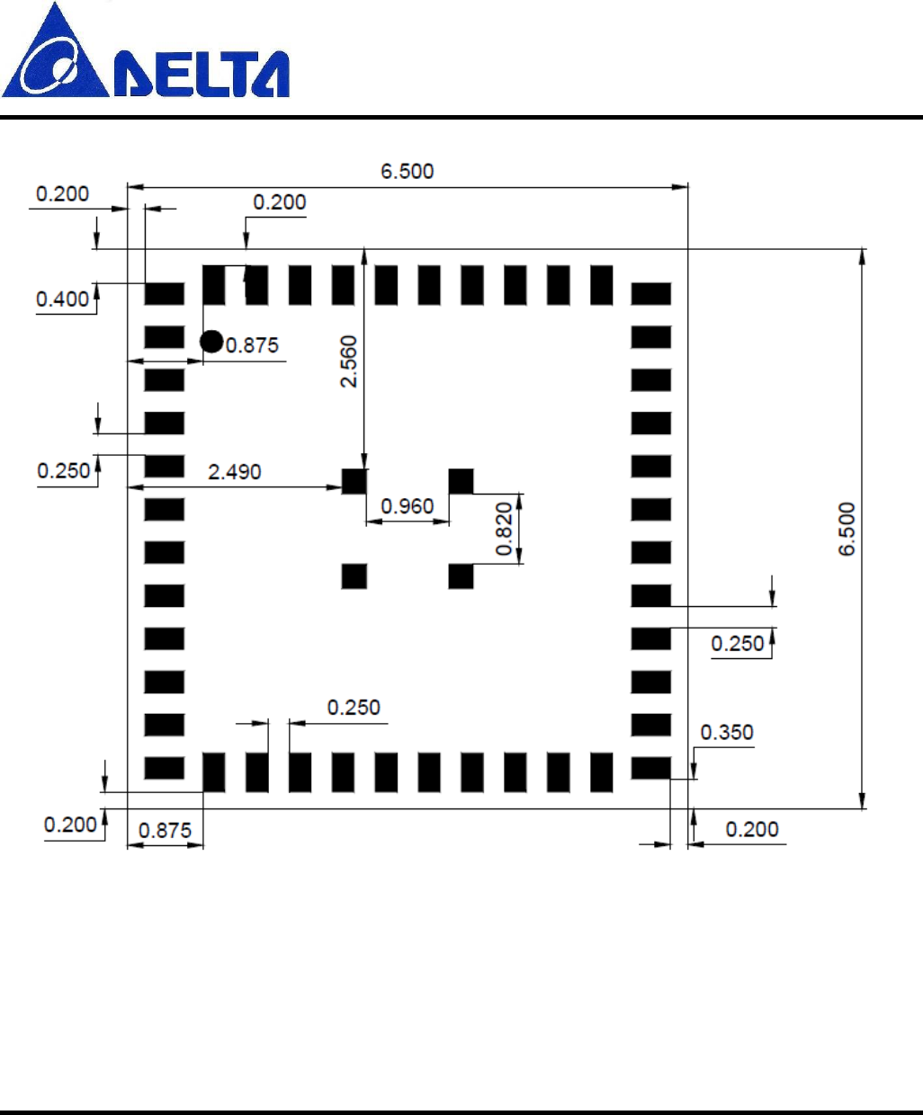
8. Module Dimensions (mm)
Figure 8-1. DFBM-NW726-DT0R Module Dimension
Top View
Side View
DFBM-NW726-DT0R
Preliminary Data Sheet Sheet 16 of 24 Jan. 22, 2018
Proprietary Information and Specifications are Subject to Change
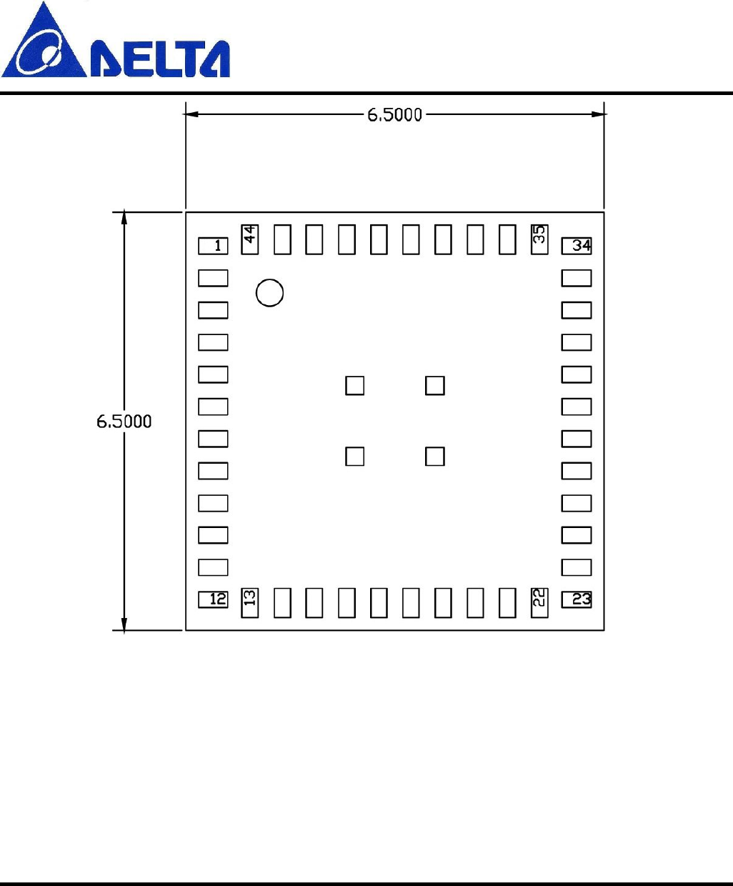
Figure 8-2. DFBM-NW726-DT0R Module Pin Number
Top View
DFBM-NW726-DT0R
Preliminary Data Sheet Sheet 17 of 24 Jan. 22, 2018
Proprietary Information and Specifications are Subject to Change
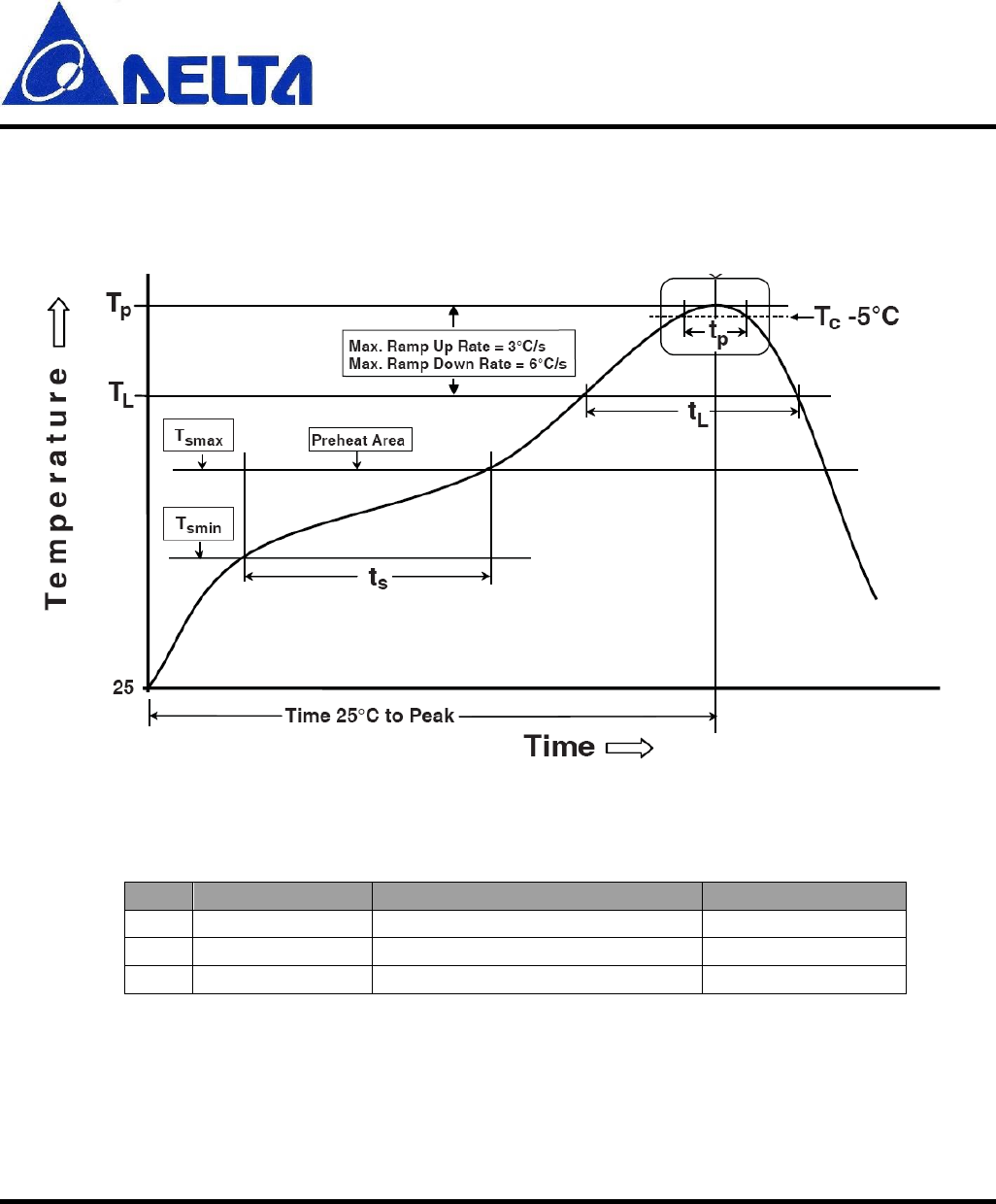
9. Recommend Soldering Conditions
Figure 9-1. Reflow temperature Profile
No.
Item
Temperature (°C)
Time (sec)
1
Pre-heat
Tsmin: 150 °C ~ Tsmax: 200°C
ts: 60 ~ 120
2
Soldering
TL: >= 217°C
tL: 60~150
3
Peak-Temp.
Tp: 260 °C
tp: 30
Table 9-1. Reflow temperature Profile Parameters
DFBM-NW726-DT0R
Preliminary Data Sheet Sheet 18 of 24 Jan. 22, 2018
Proprietary Information and Specifications are Subject to Change
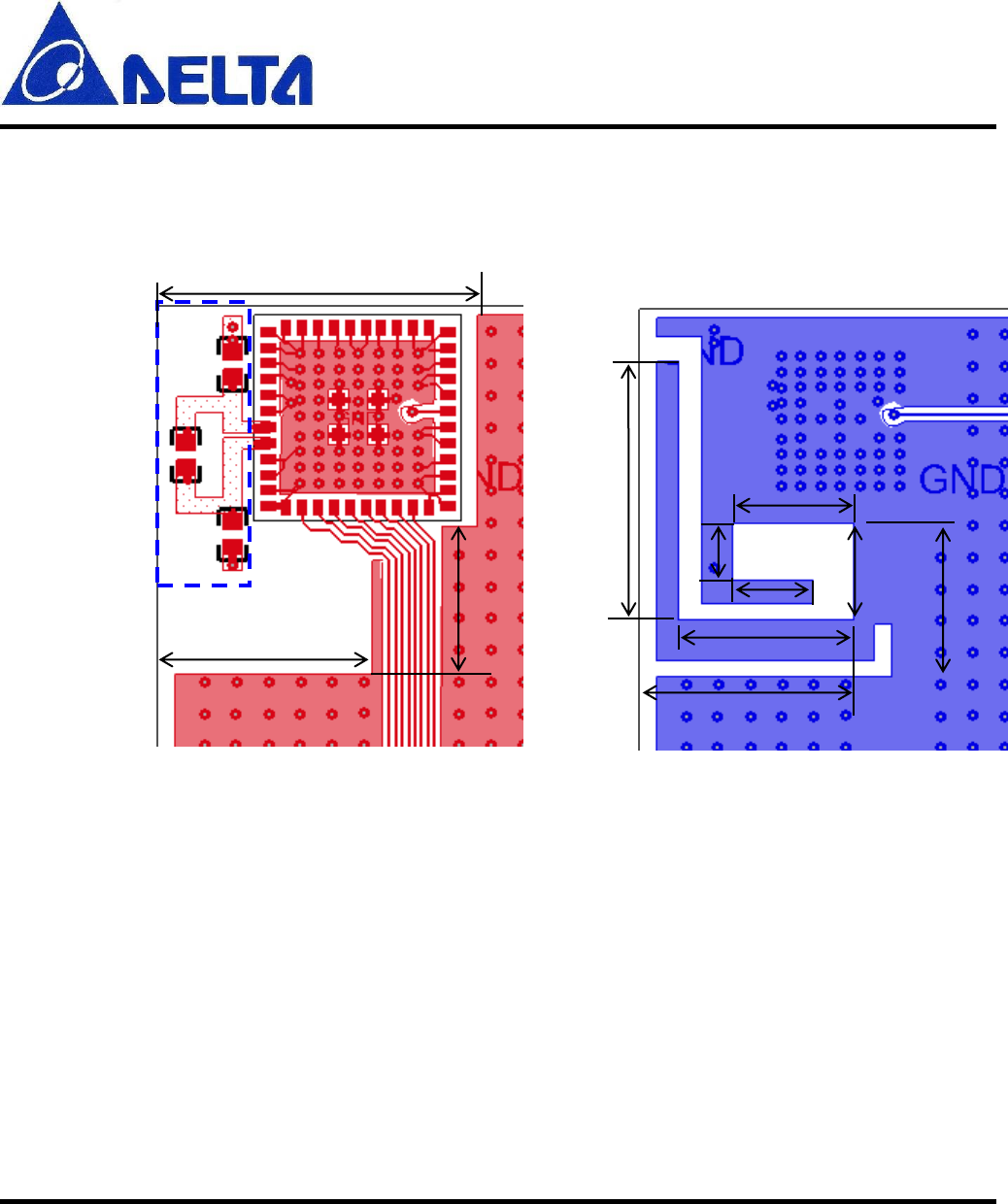
10. Layout Guide (mm)
10-1. Use Antenna on Package
Figure 10-1. Layout Guide
10-2. Use RF connector or External Antenna
Trace of RF_OUT should be controlled as 50 Ohm stripline or mirco-stripline design.
6.7mm
5.5mm
4.8mm
4.8mm
3mm
3.8mm
1.8mm
2.5mm
6.7mm
8.1mm
Matching
Circuit
Top Layer
Bottom Layer
10mm
DFBM-NW726-DT0R
Preliminary Data Sheet Sheet 19 of 24 Jan. 22, 2018
Proprietary Information and Specifications are Subject to Change
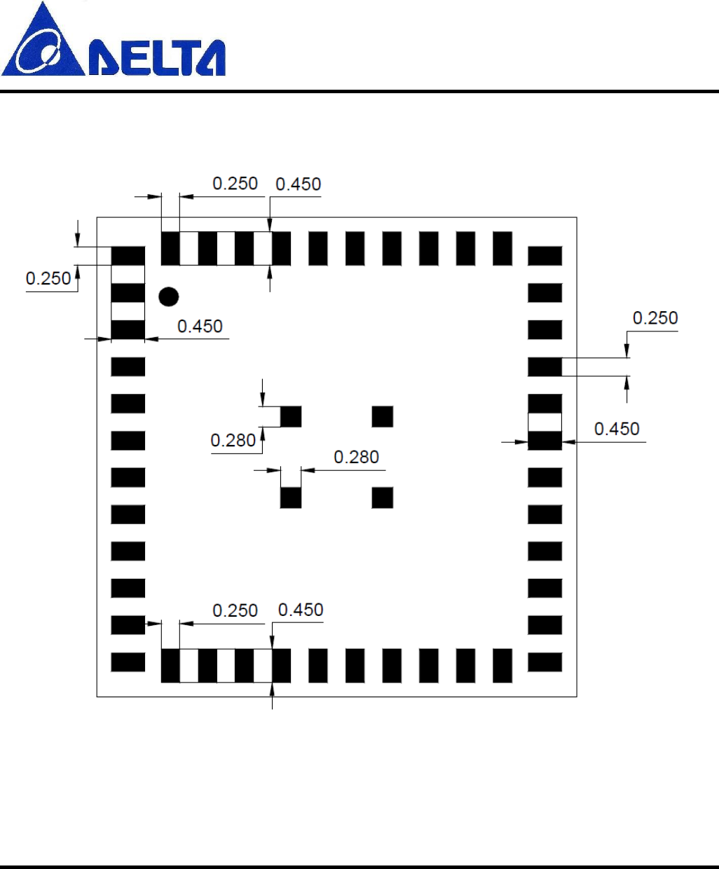
11. Recommended Stencil Aperture
Figure 11-1. Recommended Stencil Aperture
Top View
DFBM-NW726-DT0R
Preliminary Data Sheet Sheet 20 of 24 Jan. 22, 2018
Proprietary Information and Specifications are Subject to Change
Figure 11-2. Recommended Stencil Aperture
Top View
DFBM-NW726-DT0R
Preliminary Data Sheet Sheet 21 of 24 Jan. 22, 2018
Proprietary Information and Specifications are Subject to Change
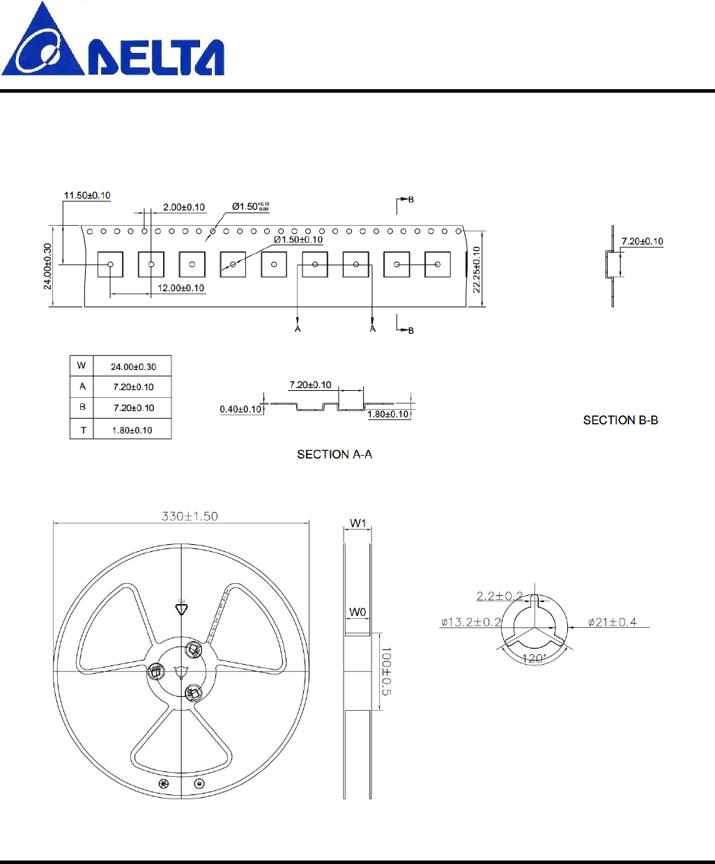
12. Packages
12-1. Tape and Reel Specification
Figure 12-1. Information of Tape specification
Figure 12-2. Information of Reel specification
DFBM-NW726-DT0R
Preliminary Data Sheet Sheet 22 of 24 Jan. 22, 2018
Proprietary Information and Specifications are Subject to Change
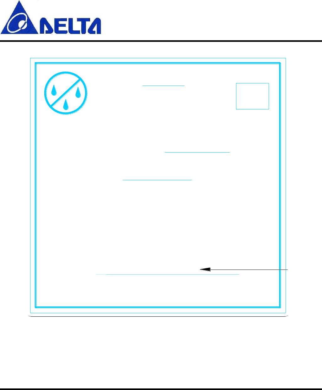
12-2. Storage Specification
LEVEL
3
CAUTION
This bag contains
MOISTURE-SENSITIVE DEVICES
1. Calculated shelf life in sealed bag: 12 months at < 40 °C and< 90 %
relative humidity (RH)
2. Peak package body temperature: 260 °C
3. After bag is opened, devices that will be subjected to reflow solder
or other high temperature process must
a) Mounted within: 168 hours of factory
conditions ? 30°C/60 % RH .OR
b) Stored at <10% RH
4. Devices require bake, before mounting, if:
a) Humidity Indicator Card is > 10% when read at 23±5°C
b) 3a or 3b not met.
5. If baking is required, devices may be baked for 48 hours at 125± 5°C
Note: If device containers cannot be subjected to high temperature
or shorter bake times are desired,
reference IPC/JEDEC J-STD-033 for bake procedure
Bag Seal Date: .
If Blank, see adjacent bar code label
Note: Level and body temperature defined by IPC/JEDEC J-STD-020
20121204 Note 7
Figure 12-4. MSL3 definition

DFBM-NW726-DT0R
Preliminary Data Sheet Sheet 23 of 24 Jan. 22, 2018
Proprietary Information and Specifications are Subject to Change
13. Required End Product Labeling
Any device incorporating this module must include an external, visible, permanent marking or label
which states: “Contains FCC ID: H79DFBM-NW726.”
14. Manual Information to the End User
The OEM integrator has to be aware not to provide information to the end user regarding how to
install or remove this RF module in the user’s manual of the end product which integrates this
module. The end user manual shall include all required regulatory information/warming as shown in
this manual.
15. Federal Communications Commission (FCC)
Statement
15.21
You are cautioned that changes or modifications not expressly approved by the part responsible for
compliance could void the user’s authority to operate the equipment.
15.105(b)
This equipment has been tested and found to comply with the limits for a Class B digital device,
pursuant to part 15 of the FCC rules. These limits are designed to provide reasonable protection
against harmful interference in a residential installation.
This equipment generates uses and can radiate radio frequency energy and, if not installed and
used in accordance with the instructions, may cause harmful interference to radio communications.
However, there is no guarantee that interference will not occur in a particular installation. If this
equipment does cause harmful interference to radio or television reception, which can be
determined by turning the equipment off and on, the user is encouraged to try to correct the
interference by one or more of the following measures:

DFBM-NW726-DT0R
Preliminary Data Sheet Sheet 24 of 24 Jan. 22, 2018
Proprietary Information and Specifications are Subject to Change
-Reorient or relocate the receiving antenna.
-Increase the separation between the equipment and receiver.
-Connect the equipment into an outlet on a circuit different from that to which the receiver is
connected.
-Consult the dealer or an experienced radio/TV technician for help.
This device complies with part 15 of the FCC Rules. Operation is subject to the following two
conditions:
1) this device may not cause interference and
2) this device must accept any interference, including interference that may cause undesired
operation of the device.
RF Radiation Exposure Statement:
This Transmitter must not be co-located or operating in conjunction with any other antenna or
transmitter.
This equipment complies with FCC RF radiation exposure limits set forth for an uncontrolled
environment. This equipment should be installed and operated with a minimum distance of 20
centimeters between the radiator and your body.