Digi 50M880 802.11b Wireless Module User Manual DC ME HWR
Digi International Inc 802.11b Wireless Module DC ME HWR
UserManual.wiki
>
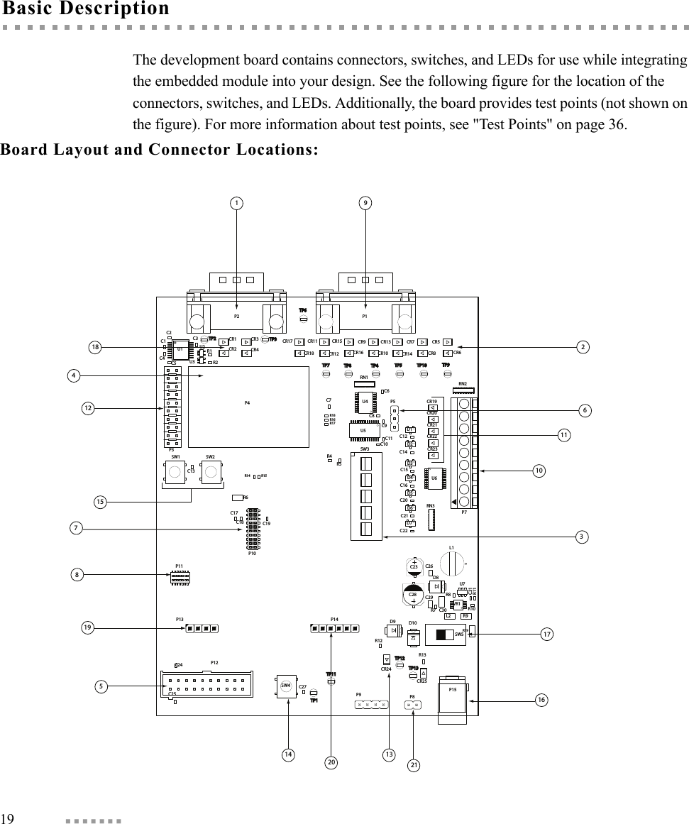
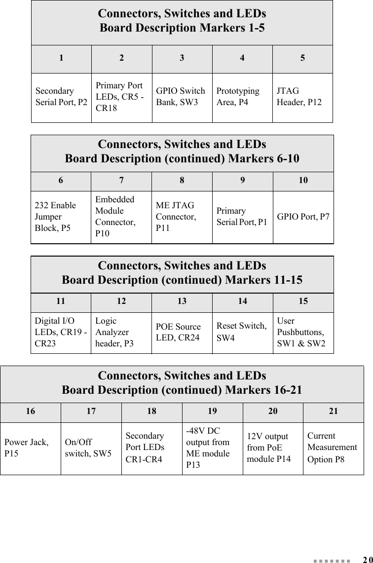
Digi
>
50M880 User Manual
>
user manual
Contents
1.
manual
2.
user manual
user manual
Navigation menu
Upload a User Manual
Namespaces
Wiki Guide
HTML
PDF
Info
Views
User Manual
Discussion / Help
Navigation
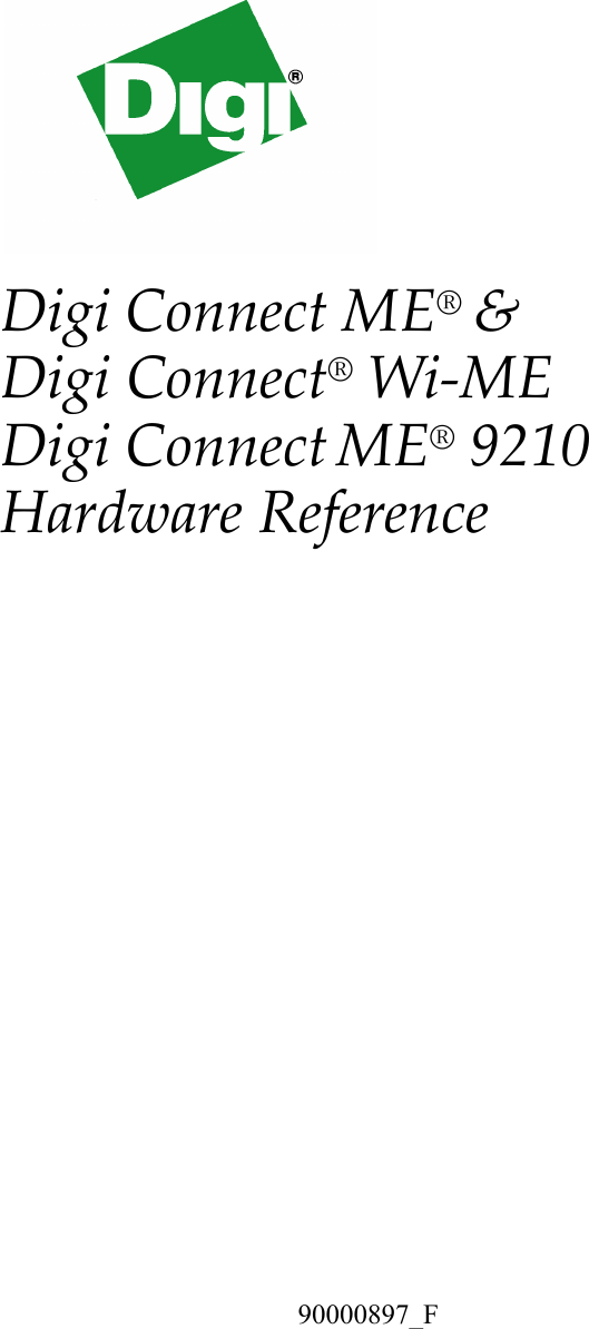
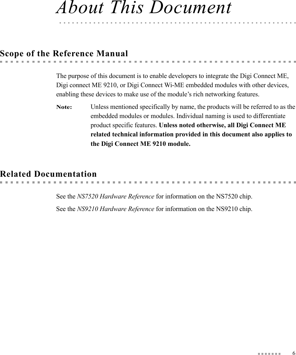
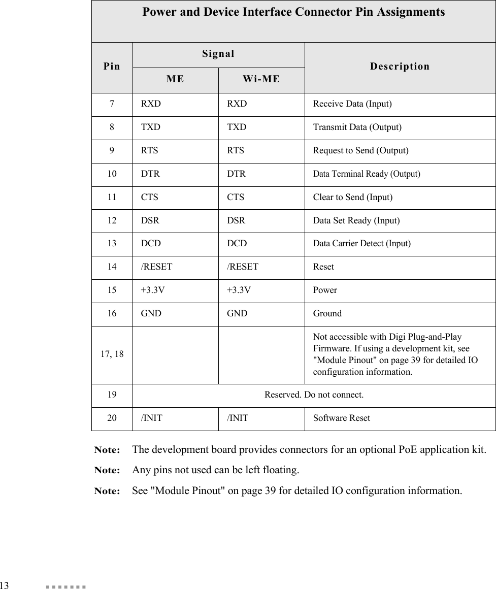
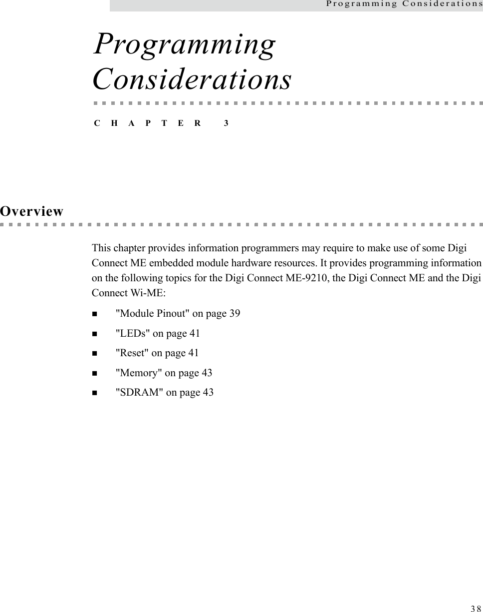
![40Programming ConsiderationsNote:A special model of the Digi Connect ME 9210 is required for CAN bus 2.0 support. The CAN bus model does not support the 12C interface. Instead, it makes GPIO[14] / PIC[0]_CAN_RXD available on pin 17, and GPIO [15]/PIC[0]_CA_TXD on pin 18. Please contact Digi for availabilty information.Note:The Digi Connect Wi-ME module does not provide pins 1-6.Pin UART[All]GPIO[ME/Wi-ME]GPIO [ME 9210]Ext IRQ[ME/Wi-ME]Ext IRQ[ME 9210]I2C[ME 9210]SPI[ME 9210]FIM[ME 9210]Timer[ME 9210]Other[All]1VETH+2VETH-3-6 Positions Removed7RXD A3 GPIO[3] DATA IN PIC [3]8TXD A7 GPIO[7] DATA OUT Timer Out 7Timer In 89RTS A5 GPIO[5] 3CLK Timer Out 610 DTR A6 GPIO[6] Timer In 711 CTS A1 GPIO[1] 0PIC[1]12 DSR A2 GPIO[2] 1PIC[2]13 DCD A0 GPIO[0] EN PIC[0]14 /RST15 3.3V16 GND17 C4 GPIO[12] SDA CLK RESET_DONE18 C1 GPIO[9] 1 0 SCL19 Reserved20 C5 GPIO [13] CLK Timer Out 9 /INIT](https://usermanual.wiki/Digi/50M880.user-manual/User-Guide-1116232-Page-40.png)
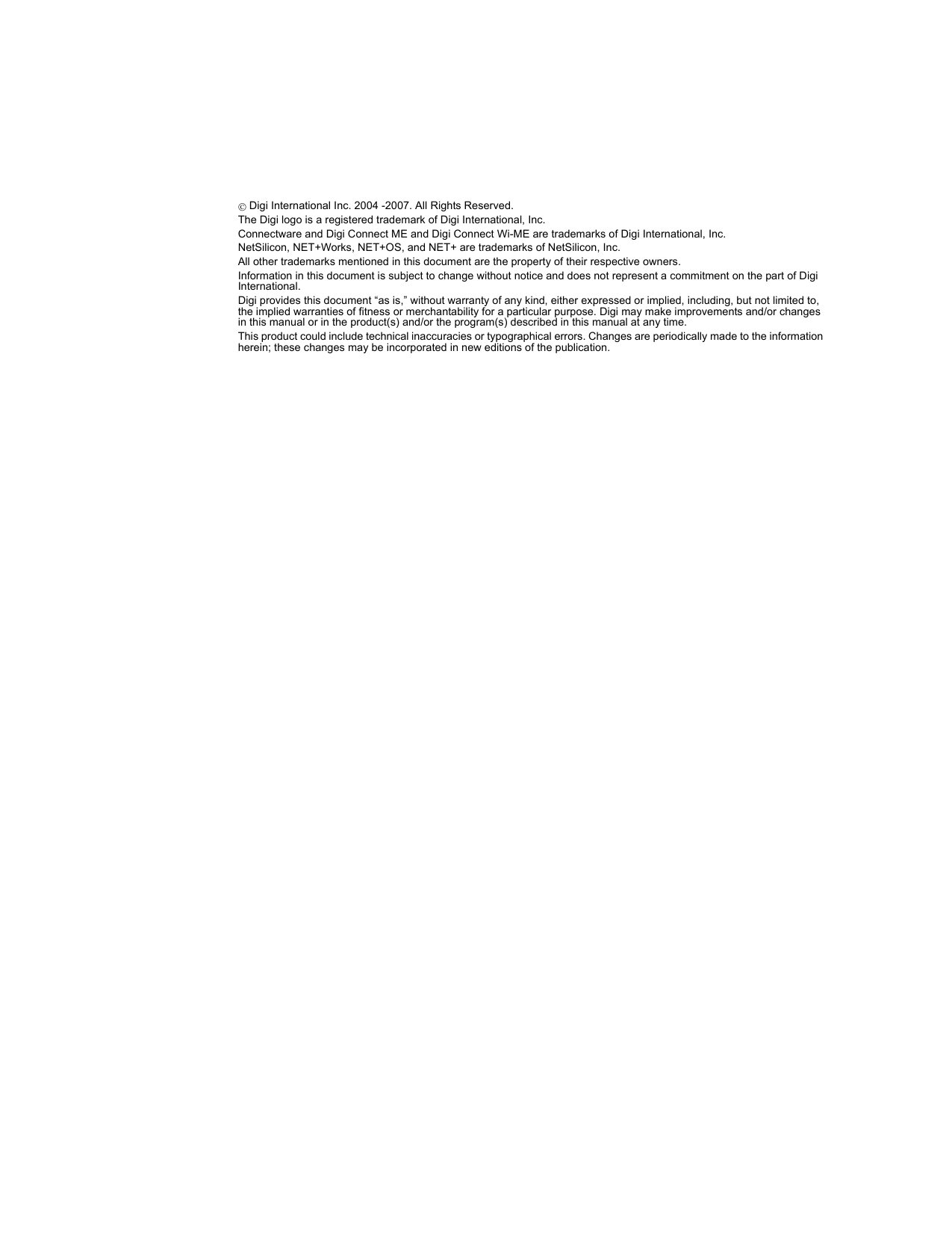
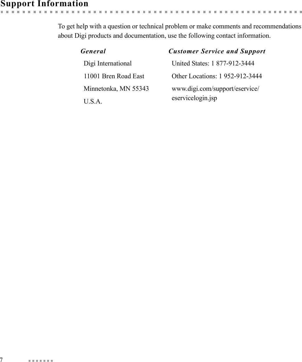
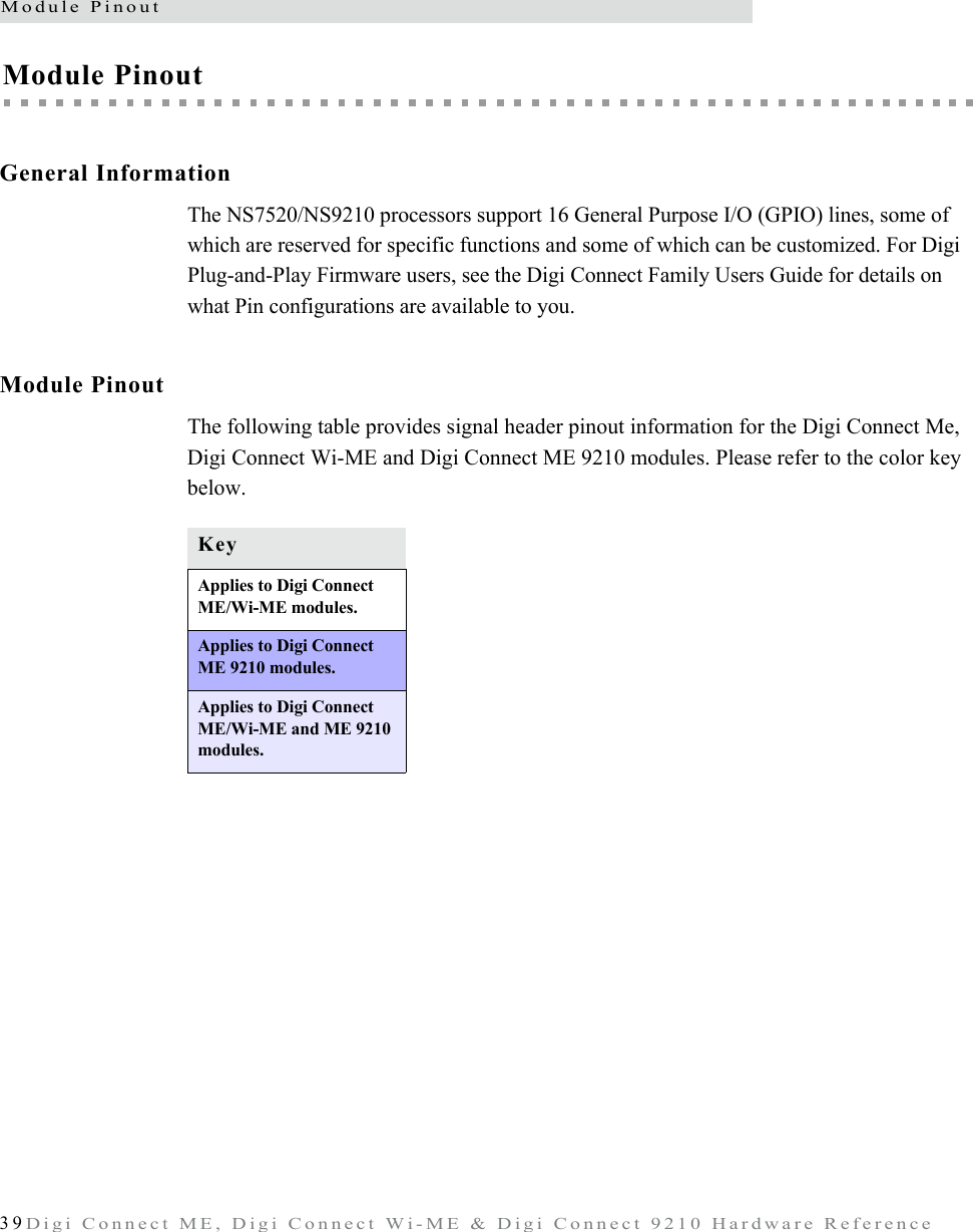
![LEDs41Digi Connect ME, Digi Connect Wi-ME & Digi Connect 9210 Hardware ReferenceLEDsGeneral InformationThe embedded modules have two types of LEDs: An LED connected directly to GPIO pins on the processor and controlled directly in softwareAn LED connected to other hardware components (normally the Ethernet hardware) and not directly programmable by the operating systemThe development kit, by default, correctly configures the GPIO connected to the LED as an output and then uses this LED to represent Ethernet activity. Reset Hard ResetThe embedded module supports a hardware reset via pin 14 of the 20-pin header. The unit is forced into a hard reset when pulling the pin to ground, or less than 2.88v, for one microsecond. When plugged into a development board, this pin is wired to the push button at SW3. As a result, this switch acts as a hard reset button.LED DescriptionYellow This is wired directly to Ethernet hardware and provides an indication of link.GreenThis software-programmable LED is wired to processor GPIO register bit C6/GPIO[14] and is wired to be lit when low. The default behavior is to blink on Ethernet activity.Reset CharacteristicsCharacteristic SpecificationDelay 250 milliseconds (typical)Threshold 2.88 V](https://usermanual.wiki/Digi/50M880.user-manual/User-Guide-1116232-Page-41.png)
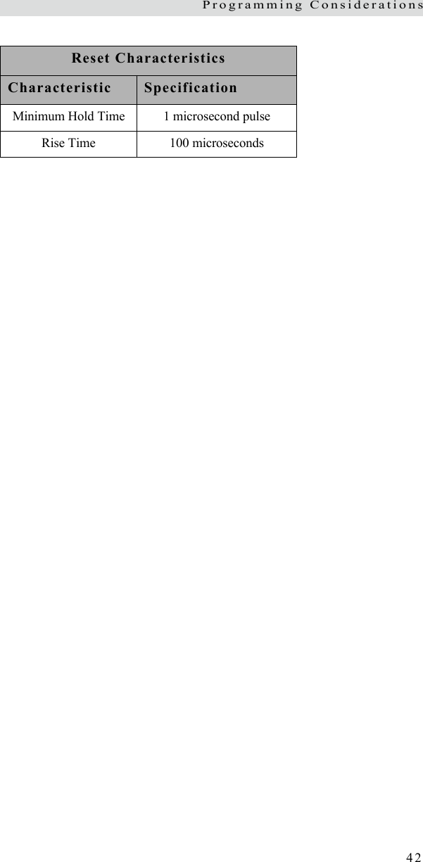
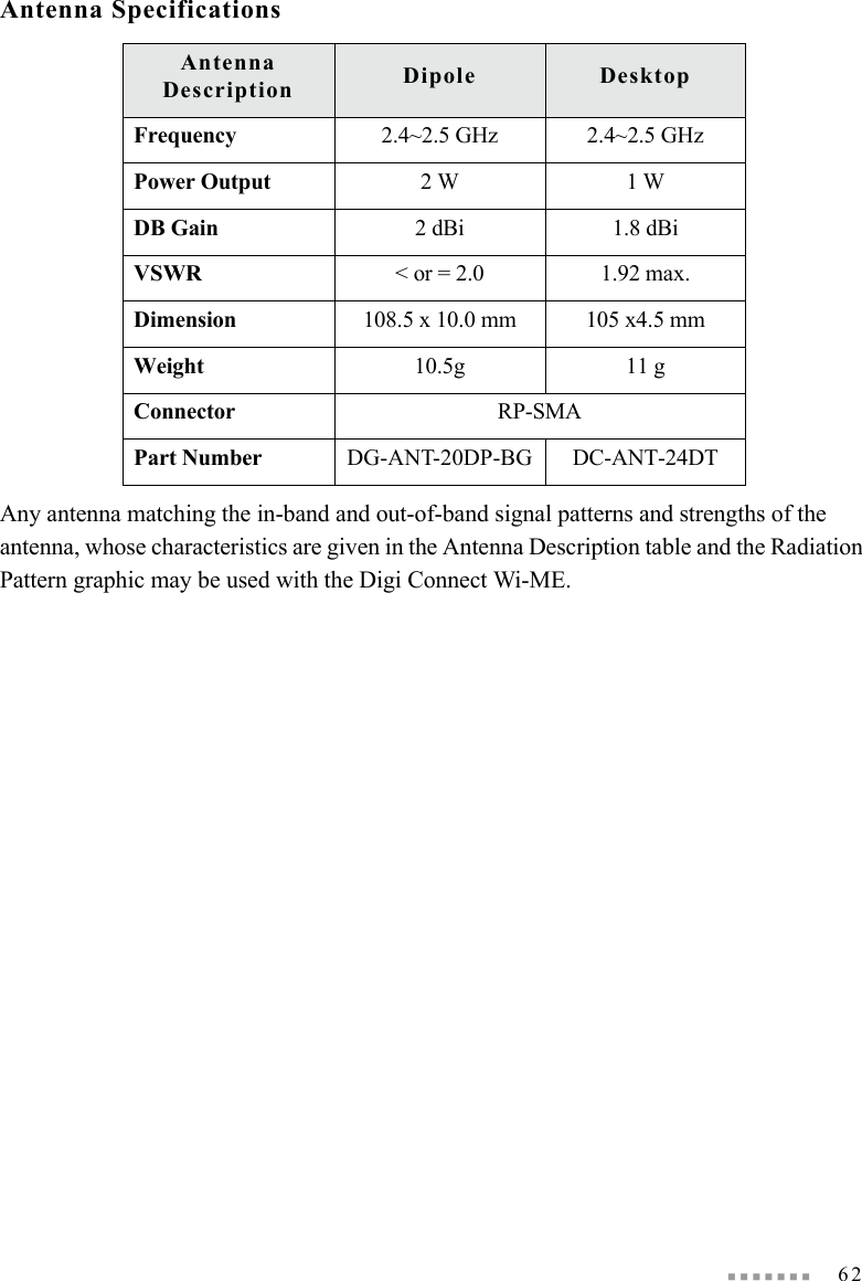

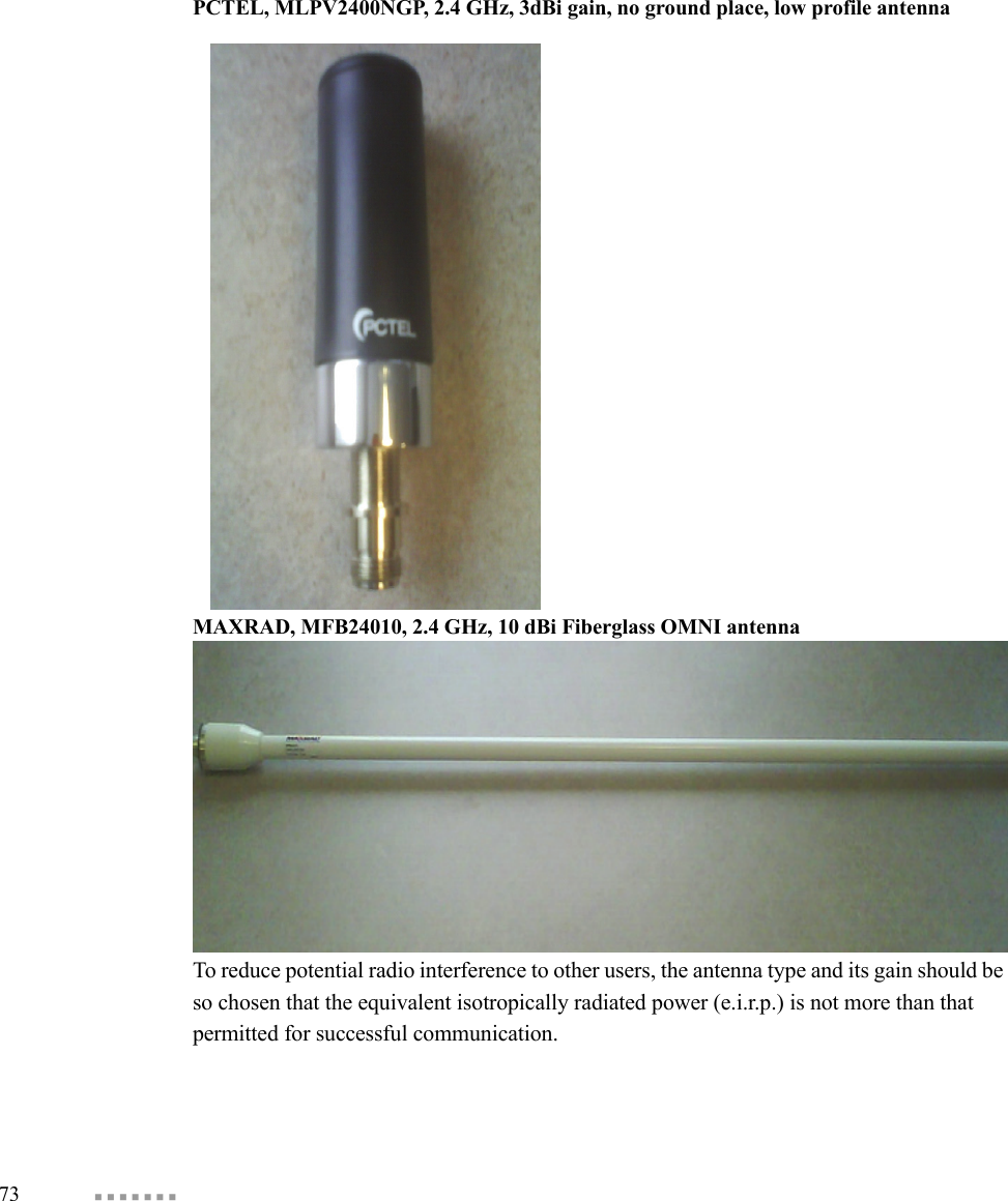
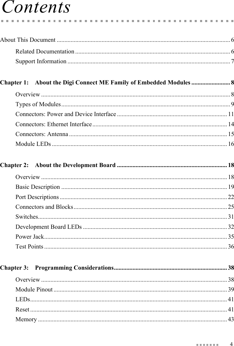
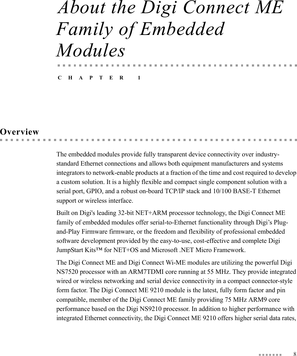
![ 72Antenna configurationsThis device has been designed to operate with the antennas listed below, and having a maximum gain of [10] dBi. Antennas not included in this list or having a gain greater than [10] dBi are strictly prohibited for use with this device. The required antenna impedance is [50] ohms The following antenna configurations that were tested with the Connect Wi-ME 802.11 b module. Digi 29000095, Bobbintron SA-006-1, +2 dBi dipole antenna (RP-SMA)](https://usermanual.wiki/Digi/50M880.user-manual/User-Guide-1116232-Page-72.png)