Digi XBEE3 XBEE3 User Manual XBee Micro Hardware Reference Manual
Digi International Inc XBEE3 XBee Micro Hardware Reference Manual
UserManual.wiki
>
Digi
>
XBEE3 User Manual
>
User Manual
Contents
1.
User Manual
2.
Module User Manual
3.
XBee3 USB Adapter User Manual
4.
XBee 3 USB Adapter User Manual
User Manual
Navigation menu
Upload a User Manual
Namespaces
Wiki Guide
HTML
PDF
Info
Views
User Manual
Discussion / Help
Navigation

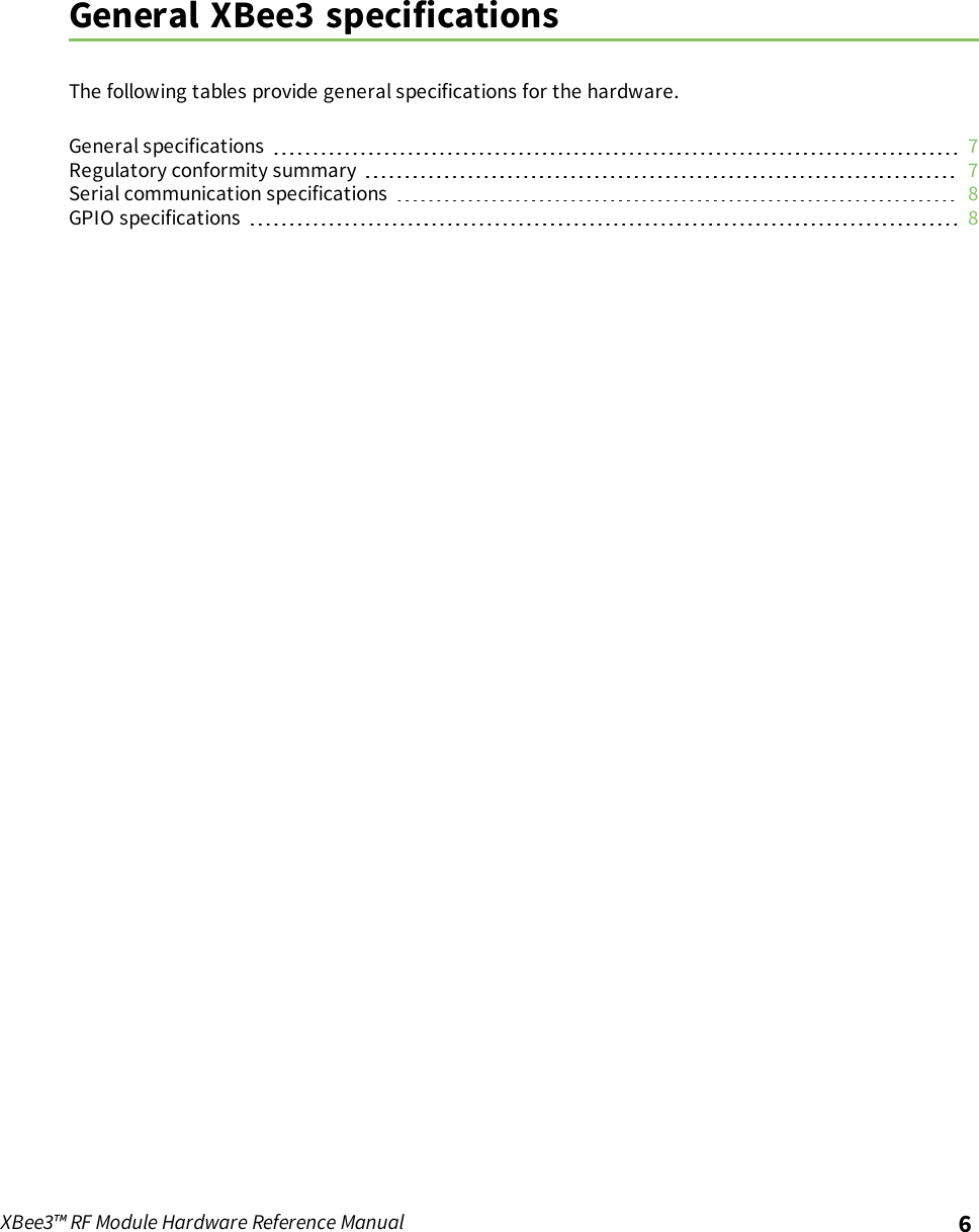
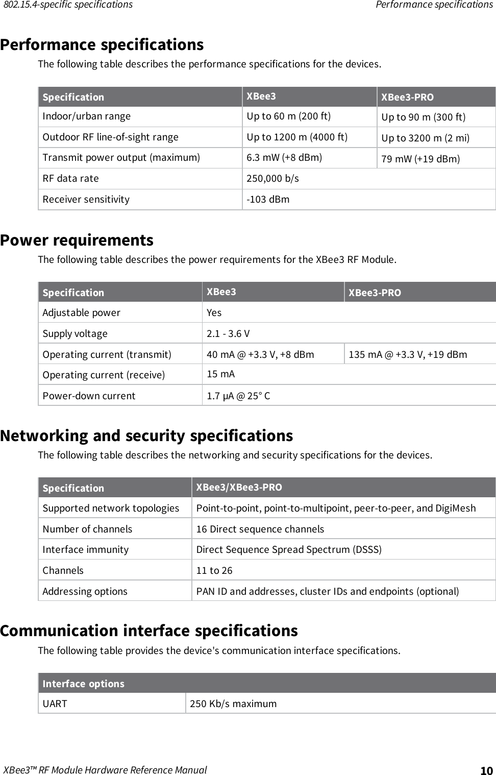
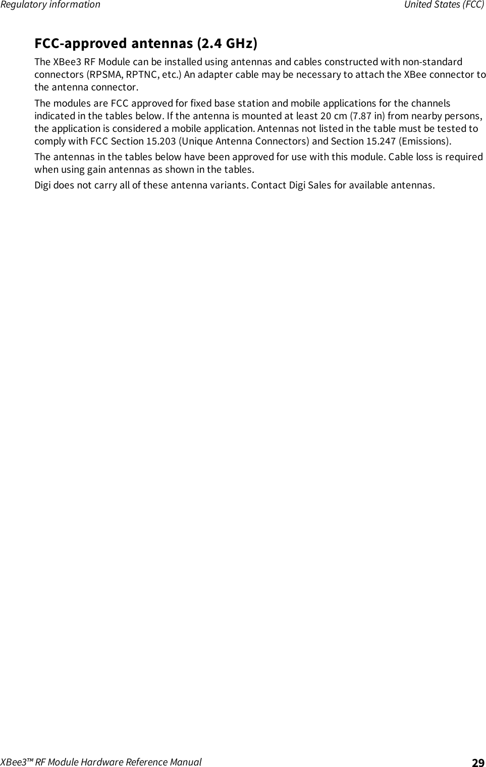
![Hardware Pin signals for the XBee3 surface-mount moduleXBee3™ RF Module Hardware Reference Manual 16The following table shows the pin signals and their descriptions for the surface-mount device.Pin# Name DirectionDefaultstate Description1 GND - - Ground.2 VCC - - Power supply.3 DOUT /DIO13 Both Output UART data out/GPIO.4 DIN / CONFIG /DIO14 Both Input UART data in/GPIO.5 DIO12 Both GPIO.6 RESET Input Device reset.7 RSSI PWM/DIO10 Both Output RX signalstrengthIndicator /GPIO.8 PWM1/DIO11 Both Disabled Pulse widthmodulator/GPIO.9 [reserved] - Disabled Do not connect.](https://usermanual.wiki/Digi/XBEE3.User-Manual/User-Guide-3642957-Page-16.png)
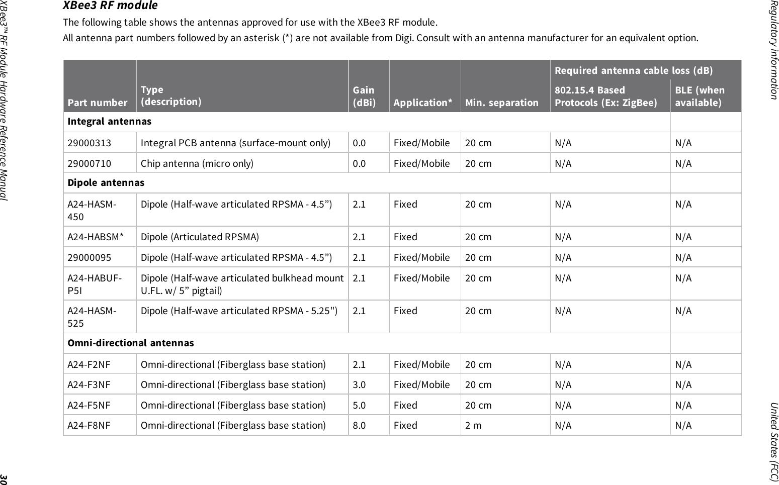
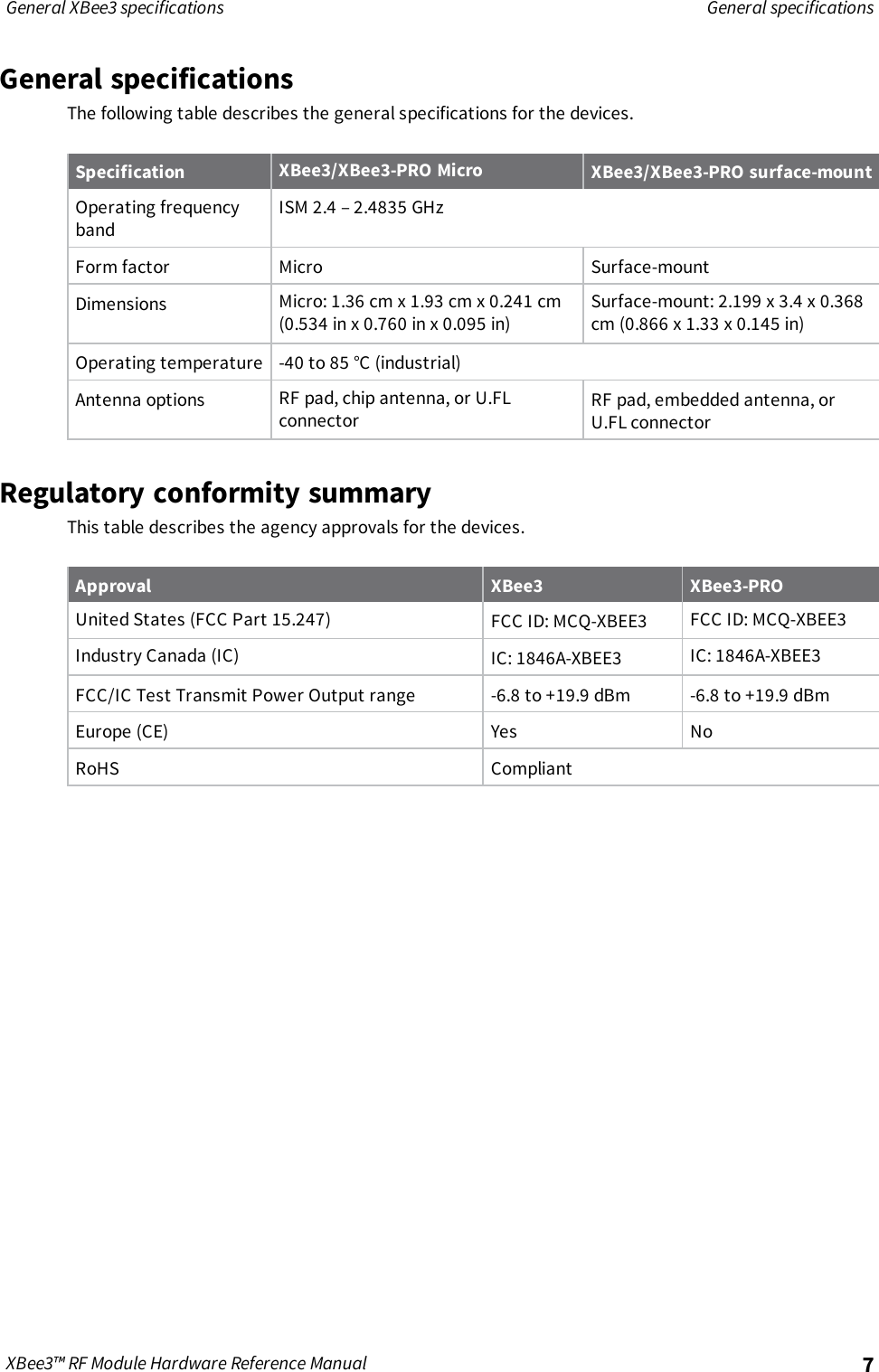
![Hardware Pin signals for the XBee3 surface-mount moduleXBee3™ RF Module Hardware Reference Manual 17Pin# Name DirectionDefaultstate Description10 DTR/SLEEP_RQ /DIO8 Both Input Pin sleep controlLine/GPIO.11 GND - - Ground.12 SPI_ATTN/ BOOTMODE/DIO19 Output OutputSerial peripheralinterfaceattention .Do not tie low onreset.13 GND - - Ground.14 SPI_CLK /DIO18 Input Input Serial peripheralinterfaceclock/GPIO.15 SPI_SSEL/DIO17 Input Input Serial peripheralinterface notselect/GPIO.16 SPI_MOSI/DIO16 Input Input Serial peripheralinterface datain/GPIO.17 SPI_MISO/DIO15 Output Output Serial peripheralinterface dataout/GPIO.18 [reserved]* - Disabled Do not connect.19 [reserved]* - Disabled Do not connect.20 [reserved]* - Disabled Do not connect.21 [reserved]* - Disabled Do not connect.22 GND - - Ground.23 [reserved] - Disabled Do not connect.24 DIO4 Both Disabled GPIO.25 CTS/DIO7 Both Output Clear to sendflowcontrol/GPIO.26 ON/SLEEP/DIO9 Both Output Device statusindicator/GPIO](https://usermanual.wiki/Digi/XBEE3.User-Manual/User-Guide-3642957-Page-17.png)
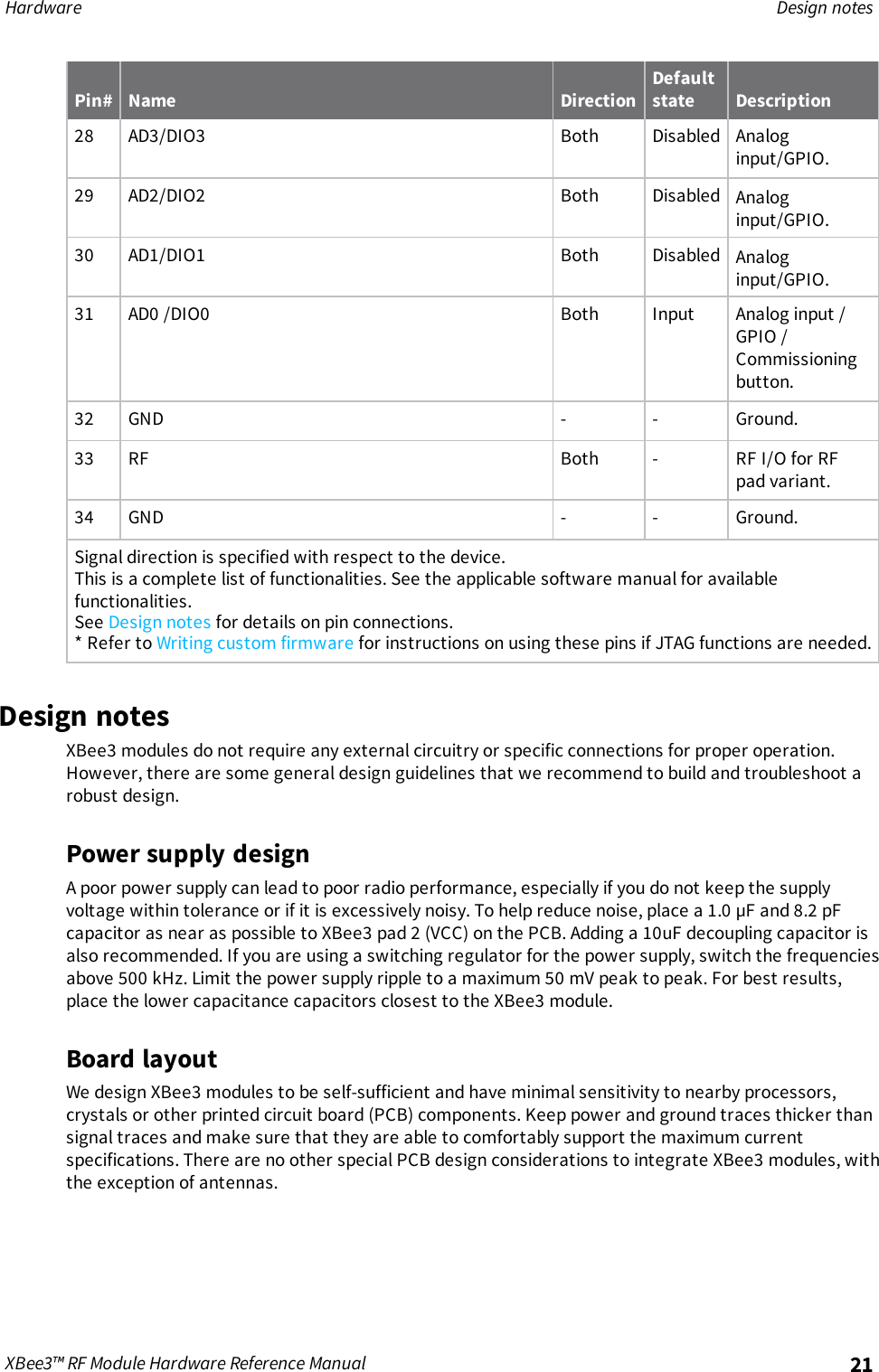
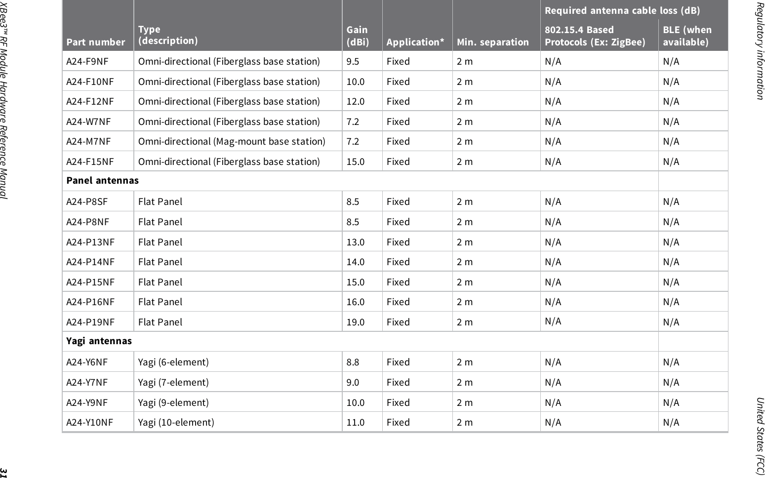
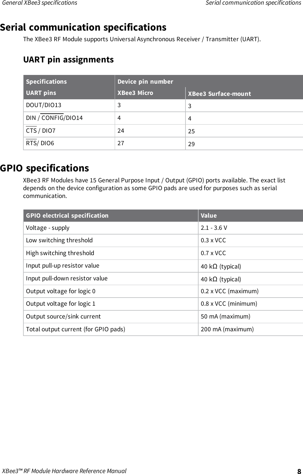
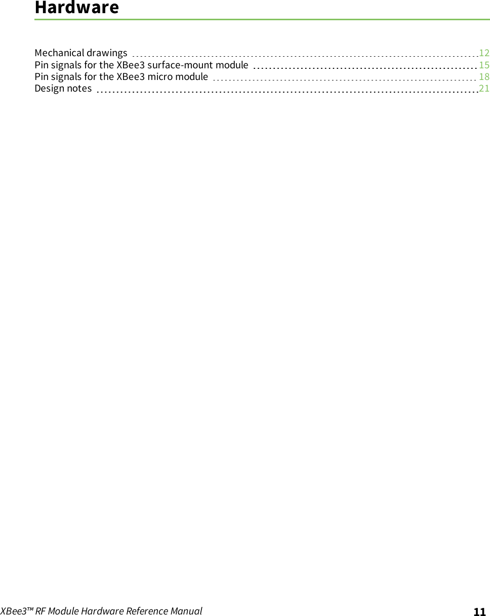
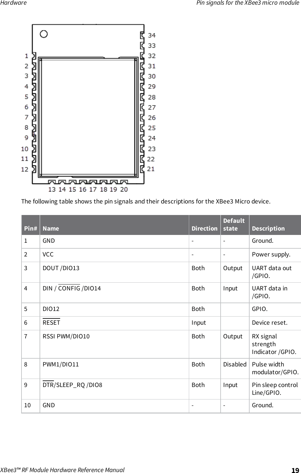
![Hardware Pin signals for the XBee3 micro moduleXBee3™ RF Module Hardware Reference Manual 18Pin# Name DirectionDefaultstate Description27 [reserved] - DisabledDo not connector connect toGround.28 ASSOCIATE/DIO5 Both Output AssociateIndicator/GPIO.29 RTS/DIO6 Both Input Request to sendflow control/GPIO.30 AD3/DIO3 Both Disabled Analoginput/GPIO.31 AD2/DIO2 Both Disabled Analoginput/GPIO32 AD1/DIO1 Both Disabled Analoginput/GPIO.33 AD0 /DIO0 Both Input Analog input /GPIO /Commissioningbutton.34 [reserved] - Disabled Do not connect.35 GND - - Ground.36 RF Both - RF I/O for RFpad variant.37 [reserved] - Disabled Do not connect.Signal direction is specified with respect to the device.This is a complete list of functionalities. See the applicable software manual for availablefunctionalities.See Design notes for details on pin connections.* Refer to Writing custom firmware for instructions on using these pins if JTAG functions are needed.Pin signals for the XBee3 micro moduleThe following drawing shows the micro pin locations.](https://usermanual.wiki/Digi/XBEE3.User-Manual/User-Guide-3642957-Page-18.png)
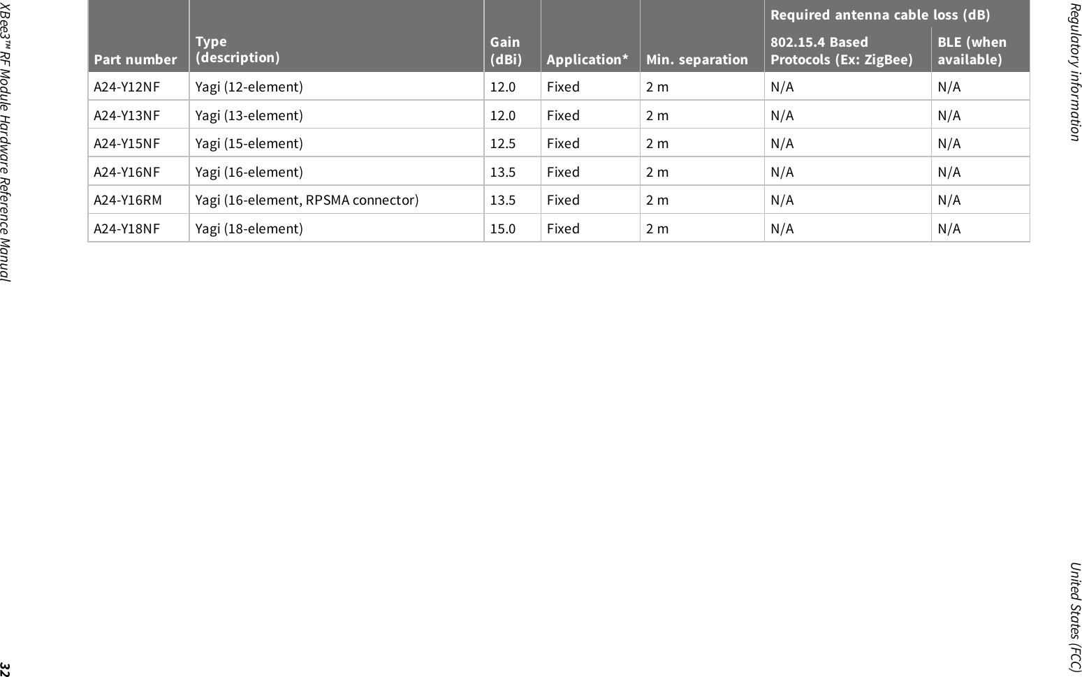
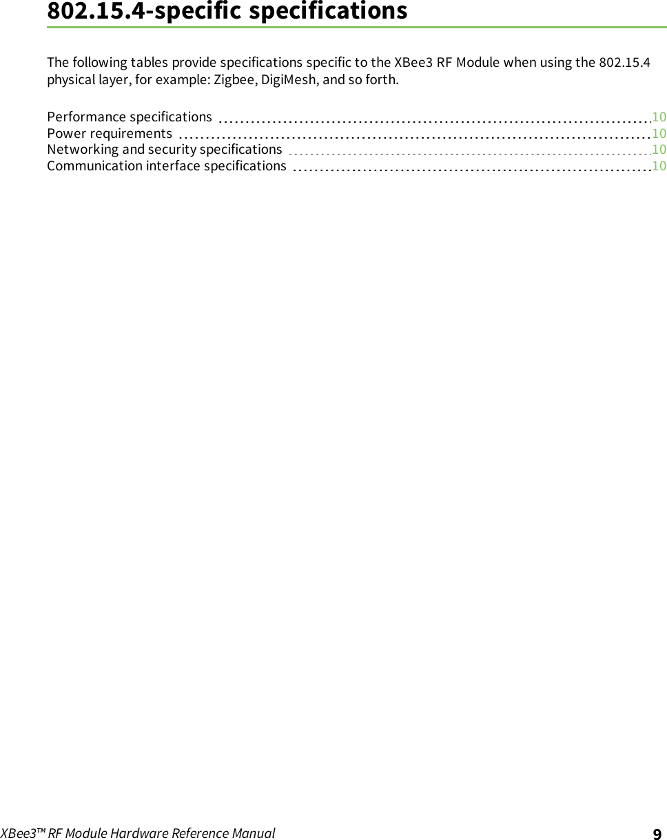
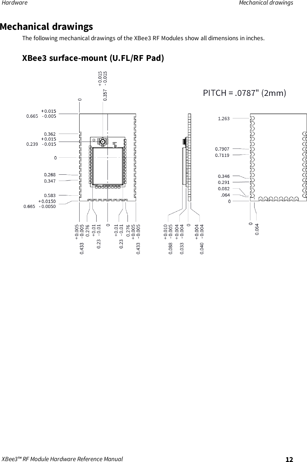
![Hardware Pin signals for the XBee3 micro moduleXBee3™ RF Module Hardware Reference Manual 20Pin# Name DirectionDefaultstate Description11 SPI_ATTN/ BOOTMODE/DIO19 Output OutputSerial peripheralinterfaceattentionDo not tie low onreset.12 GND - - Ground.13 SPI_CLK /DIO18 Input Input Serial peripheralinterfaceclock/GPIO.14 SPI_SSEL/DIO17 Input Input Serial peripheralinterface notselect/GPIO.15 SPI_MOSI/DIO16 Input Input Serial peripheralinterface datain/GPIO.16 SPI_MISO/DIO15 Output Output Serial peripheralinterface dataout/GPIO.17 [reserved]* - Disabled Do not connect.18 [reserved]* - Disabled Do not connect.19 [reserved]* - Disabled Do not connect.20 [reserved]* - Disabled Do not connect.21 GND - - Ground.22 [reserved] - Disabled Do not connect.23 DIO4 Both Disabled GPIO.24 CTS/DIO7 Both Output Clear to sendflowcontrol/GPIO.25 ON/SLEEP/DIO9 Both Output Device statusindicator/GPIO.26 ASSOCIATE/DIO5 Both Output AssociateIndicator/GPIO.27 RTS/DIO6 Both Input Request to sendflow control/GPIO.](https://usermanual.wiki/Digi/XBEE3.User-Manual/User-Guide-3642957-Page-20.png)