Digi XBEE3 XBEE3 User Manual XBee Micro Hardware Reference Manual
Digi International Inc XBEE3 XBee Micro Hardware Reference Manual
Digi >
Contents
User Manual

XBee3™
RF Module
Hardware Reference Manual

Revision history—900001543
Revision Date Description
A October 2017 Initial release.
Trademarks and copyright
Digi, Digi International, and the Digi logo are trademarks or registered trademarks in the United
States and other countries worldwide. All other trademarks mentioned in this document are the
property of their respective owners.
© 2017 Digi International Inc. All rights reserved.
Disclaimers
Information in this document is subject to change without notice and does not represent a
commitment on the part of Digi International. Digi provides this document “as is,” without warranty of
any kind, expressed or implied, including, but not limited to, the implied warranties of fitness or
merchantability for a particular purpose. Digi may make improvements and/or changes in this manual
or in the product(s) and/or the program(s) described in this manual at any time.
Warranty
To view product warranty information, go to the following website:
www.digi.com/howtobuy/terms
Send comments
Documentation feedback: To provide feedback on this document, send your comments to
techcomm@digi.com.
Customer support
Digi Technical Support: Digi offers multiple technical support plans and service packages to help our
customers get the most out of their Digi product. For information on Technical Support plans and
pricing, contact us at +1 952.912.3444 or visit us at www.digi.com/support.
XBee3™ RF Module Hardware Reference Manual 2

Contents
XBee3™ RF Module Hardware Reference Manual
General XBee3 specifications
General specifications 7
Regulatory conformity summary 7
Serial communication specifications 8
UART pin assignments 8
GPIO specifications 8
802.15.4-specific specifications
Performance specifications 10
Power requirements 10
Networking and security specifications 10
Communication interface specifications 10
Hardware
Mechanical drawings 12
XBee3 surface-mount (U.FL/RF Pad) 12
XBee3 surface-mount (embedded antenna) 13
XBee3 micro (U.FL/RF Pad) 14
XBee3 micro (chip antenna) 15
Pin signals for the XBee3 surface-mount module 15
Pin signals for the XBee3 micro module 18
Design notes 21
Power supply design 21
Board layout 21
Antenna performance 22
Recommended pin connections 22
Design notes for surface mount PCB antenna and micro footprint chip antenna devices 22
Design notes for RF pad devices 24
Regulatory information
United States (FCC) 28
OEM labeling requirements 28
FCC notices 28
XBee3™ RF Module Hardware Reference Manual 3

XBee3™ RF Module Hardware Reference Manual 4
FCC-approved antennas (2.4 GHz) 29
RF exposure 35
Europe (CE) 35
Maximum power and frequency specifications 36
OEM labeling requirements 36
Declarations of conformity 37
Antennas 37
IC (Industry Canada) 37
Labeling requirements 37
For XBee3: 37
RF Exposure 38
Manufacturing information
Recommended solder reflow cycle 40
Handling and storage 40
Recommended footprint 41
Flux and cleaning 44
Reworking 44

XBee3™ RF Module Hardware Reference Manual
This manual provides information for the XBee3 RF Module hardware. The XBee3 RF Module can be
either the micro or the surface-mount form factor.
For more information about the operation and programming functions of the device, see the XBee3®
Zigbee® User Guide.
XBee3™ RF Module Hardware Reference Manual 5


General XBee3 specifications General specifications
XBee3™ RF Module Hardware Reference Manual 7
General specifications
The following table describes the general specifications for the devices.
Specification XBee3/XBee3-PRO Micro XBee3/XBee3-PRO surface-mount
Operating frequency
band
ISM 2.4 – 2.4835 GHz
Form factor Micro Surface-mount
Dimensions Micro: 1.36 cm x 1.93 cm x 0.241 cm
(0.534 in x 0.760 in x 0.095 in)
Surface-mount: 2.199 x 3.4 x 0.368
cm (0.866 x 1.33 x 0.145 in)
Operatingtemperature -40 to 85 °C (industrial)
Antenna options RF pad, chip antenna, or U.FL
connector
RF pad, embedded antenna, or
U.FL connector
Regulatory conformity summary
This table describes the agency approvals for the devices.
Approval XBee3 XBee3-PRO
United States (FCC Part 15.247) FCC ID: MCQ-XBEE3 FCC ID: MCQ-XBEE3
Industry Canada (IC) IC: 1846A-XBEE3 IC: 1846A-XBEE3
FCC/IC Test Transmit Power Output range -6.8 to +19.9 dBm -6.8 to +19.9 dBm
Europe (CE) Yes No
RoHS Compliant
General XBee3 specifications Serial communication specifications
XBee3™ RF Module Hardware Reference Manual 8
Serial communication specifications
The XBee3 RF Module supports Universal Asynchronous Receiver / Transmitter (UART).
UART pin assignments
Specifications Device pin number
UART pins XBee3 Micro XBee3 Surface-mount
DOUT/DIO13 3 3
DIN / CONFIG/DIO14 4 4
CTS / DIO7 24 25
RTS/ DIO6 27 29
GPIO specifications
XBee3 RF Modules have 15 General Purpose Input / Output (GPIO) ports available. The exact list
depends on the device configuration as some GPIO pads are used for purposes such as serial
communication.
GPIO electrical specification Value
Voltage - supply 2.1 - 3.6 V
Low switching threshold 0.3 x VCC
High switching threshold 0.7 x VCC
Input pull-up resistor value 40 kΩ(typical)
Input pull-down resistor value 40 kΩ(typical)
Output voltage for logic 0 0.2 x VCC (maximum)
Output voltage for logic 1 0.8 x VCC (minimum)
Output source/sink current 50 mA (maximum)
Total output current (for GPIO pads) 200 mA (maximum)

802.15.4-specific specifications
The following tables provide specifications specific to the XBee3 RF Module when using the 802.15.4
physical layer, for example: Zigbee, DigiMesh, and so forth.
Performance specifications 10
Power requirements 10
Networking and security specifications 10
Communication interface specifications 10
XBee3™ RF Module Hardware Reference Manual 9
802.15.4-specific specifications Performance specifications
XBee3™ RF Module Hardware Reference Manual 10
Performance specifications
The following table describes the performance specifications for the devices.
Specification XBee3 XBee3-PRO
Indoor/urban range Up to 60 m (200 ft) Up to 90 m (300 ft)
Outdoor RF line-of-sight range Up to 1200 m (4000 ft) Up to 3200 m (2 mi)
Transmit power output (maximum) 6.3 mW (+8 dBm) 79 mW (+19 dBm)
RF data rate 250,000 b/s
Receiver sensitivity -103 dBm
Power requirements
The following table describes the power requirements for the XBee3 RF Module.
Specification XBee3 XBee3-PRO
Adjustable power Yes
Supply voltage 2.1 - 3.6 V
Operating current (transmit) 40 mA @ +3.3 V, +8 dBm 135 mA @ +3.3 V, +19 dBm
Operating current (receive) 15 mA
Power-down current 1.7 µA @ 25° C
Networking and security specifications
The following table describes the networking and security specifications for the devices.
Specification XBee3/XBee3-PRO
Supported network topologies Point-to-point, point-to-multipoint, peer-to-peer, and DigiMesh
Number of channels 16 Direct sequence channels
Interface immunity Direct Sequence Spread Spectrum (DSSS)
Channels 11 to 26
Addressing options PAN ID and addresses, cluster IDs and endpoints (optional)
Communication interface specifications
The following table provides the device's communication interface specifications.
Interface options
UART 250 Kb/s maximum

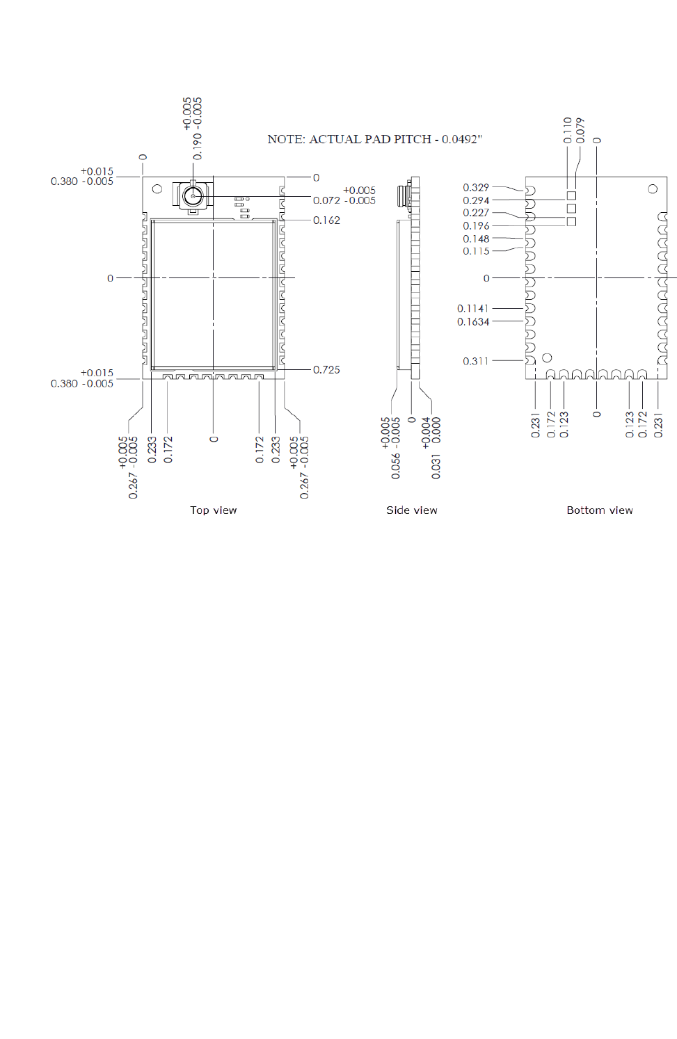
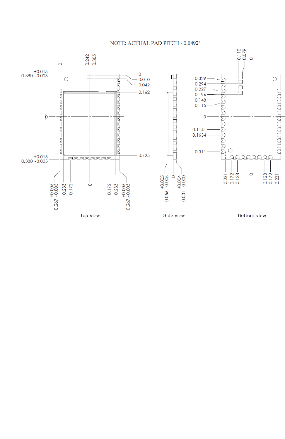
Hardware Mechanical drawings
XBee3™ RF Module Hardware Reference Manual 12
Mechanical drawings
The following mechanical drawings of the XBee3 RF Modules show all dimensions in inches.
XBee3 surface-mount (U.FL/RF Pad)
Hardware Mechanical drawings
XBee3™ RF Module Hardware Reference Manual 13
XBee3 surface-mount (embedded antenna)
Hardware Mechanical drawings
XBee3™ RF Module Hardware Reference Manual 14
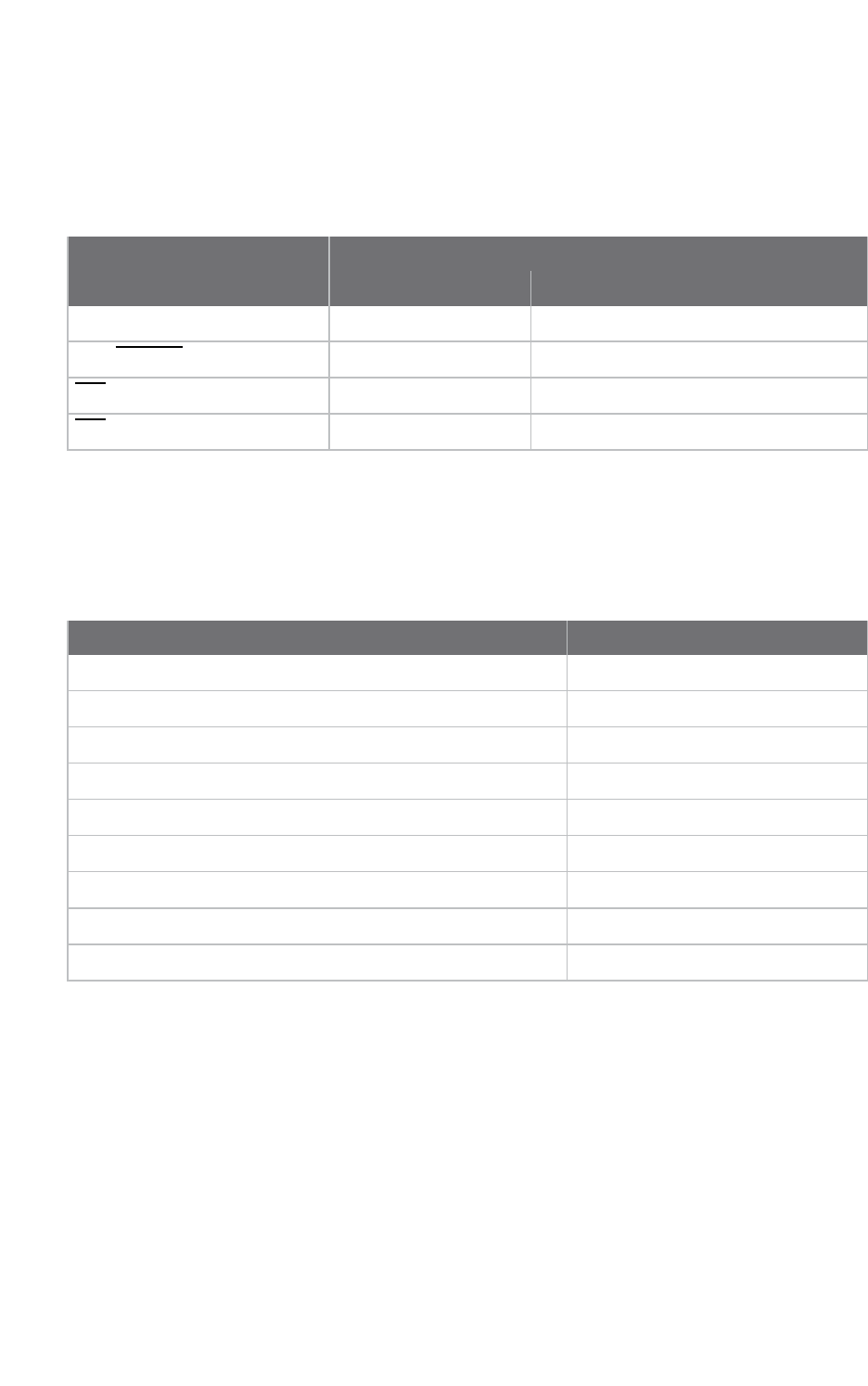
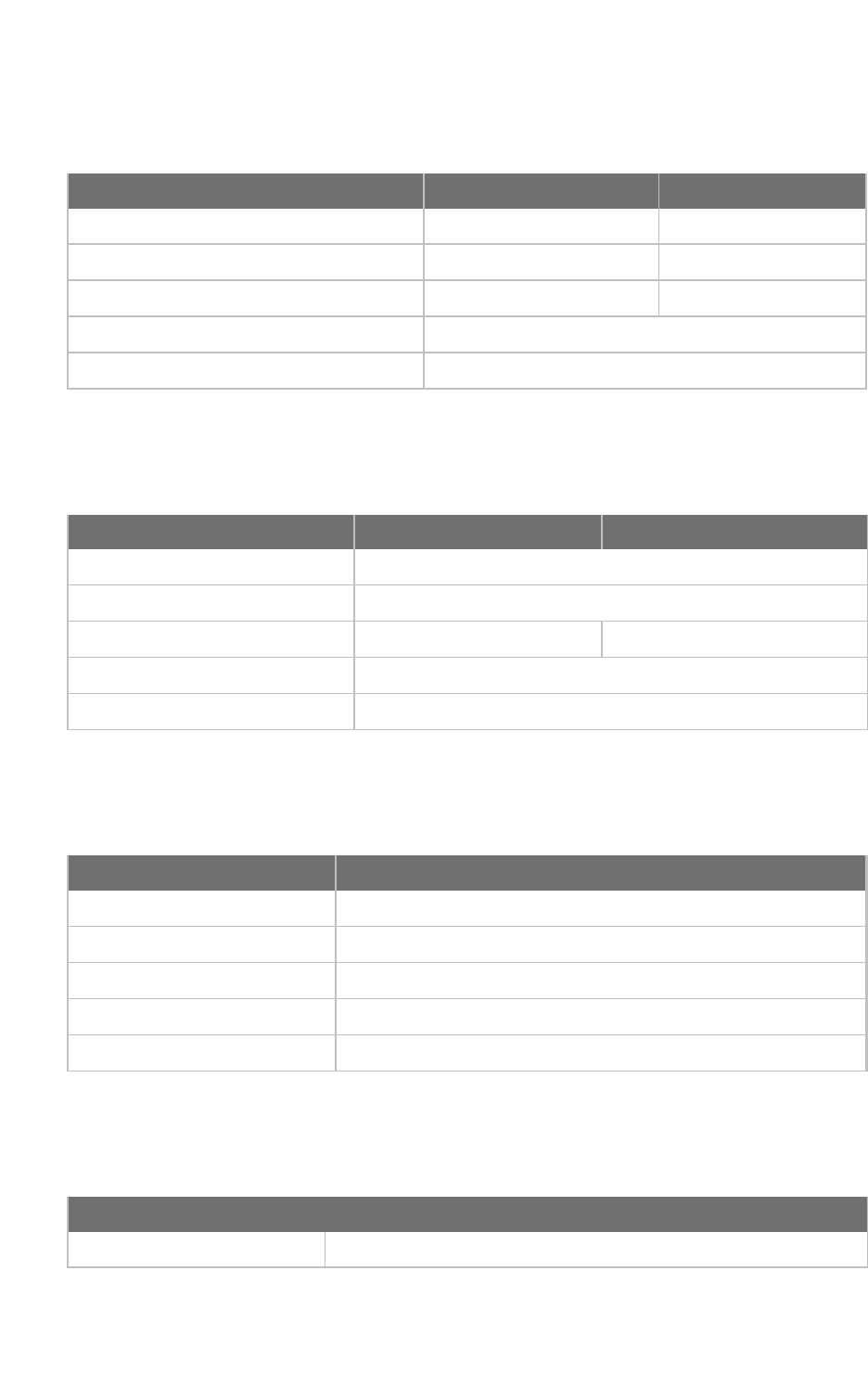
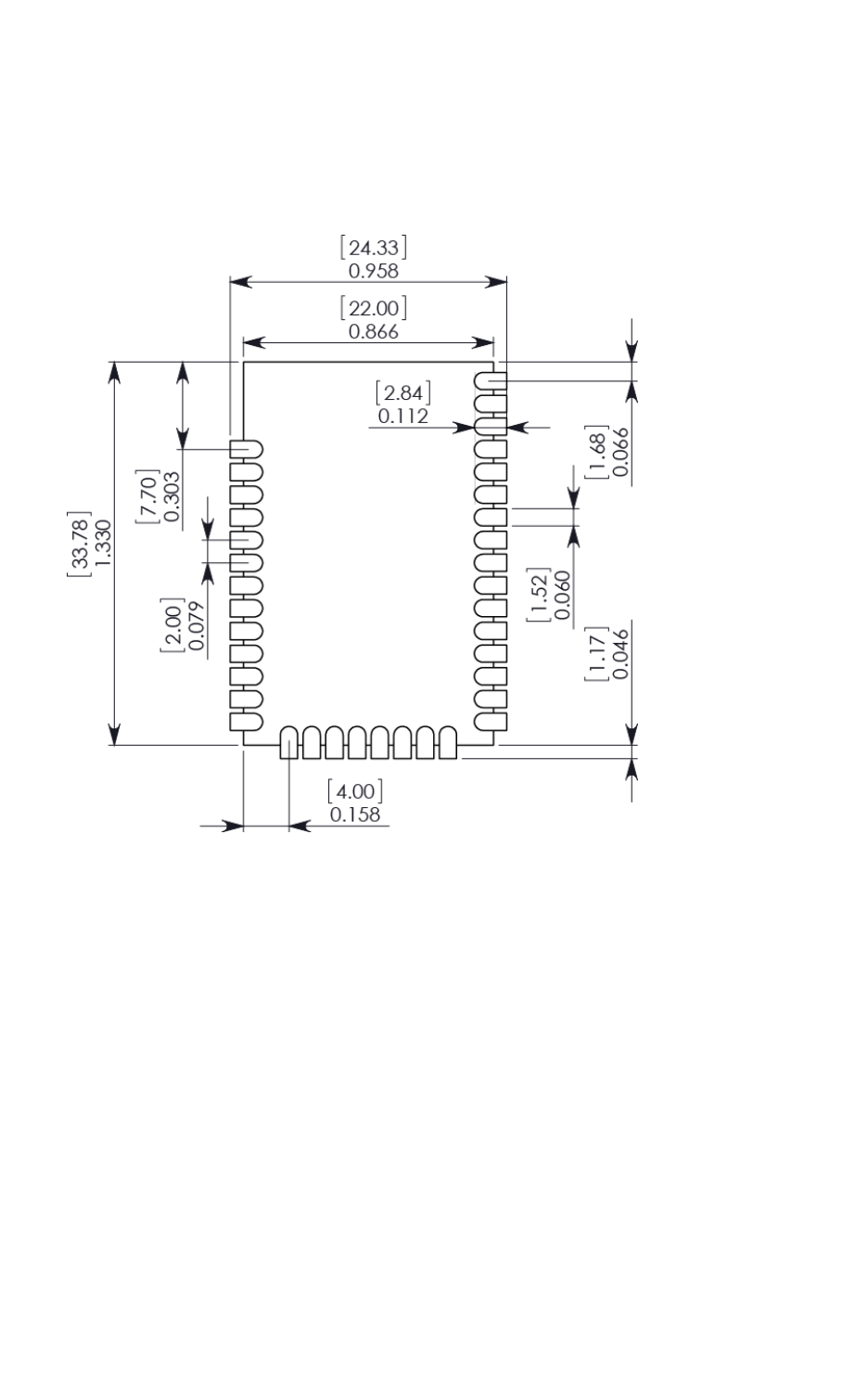
XBee3 micro (U.FL/RF Pad)
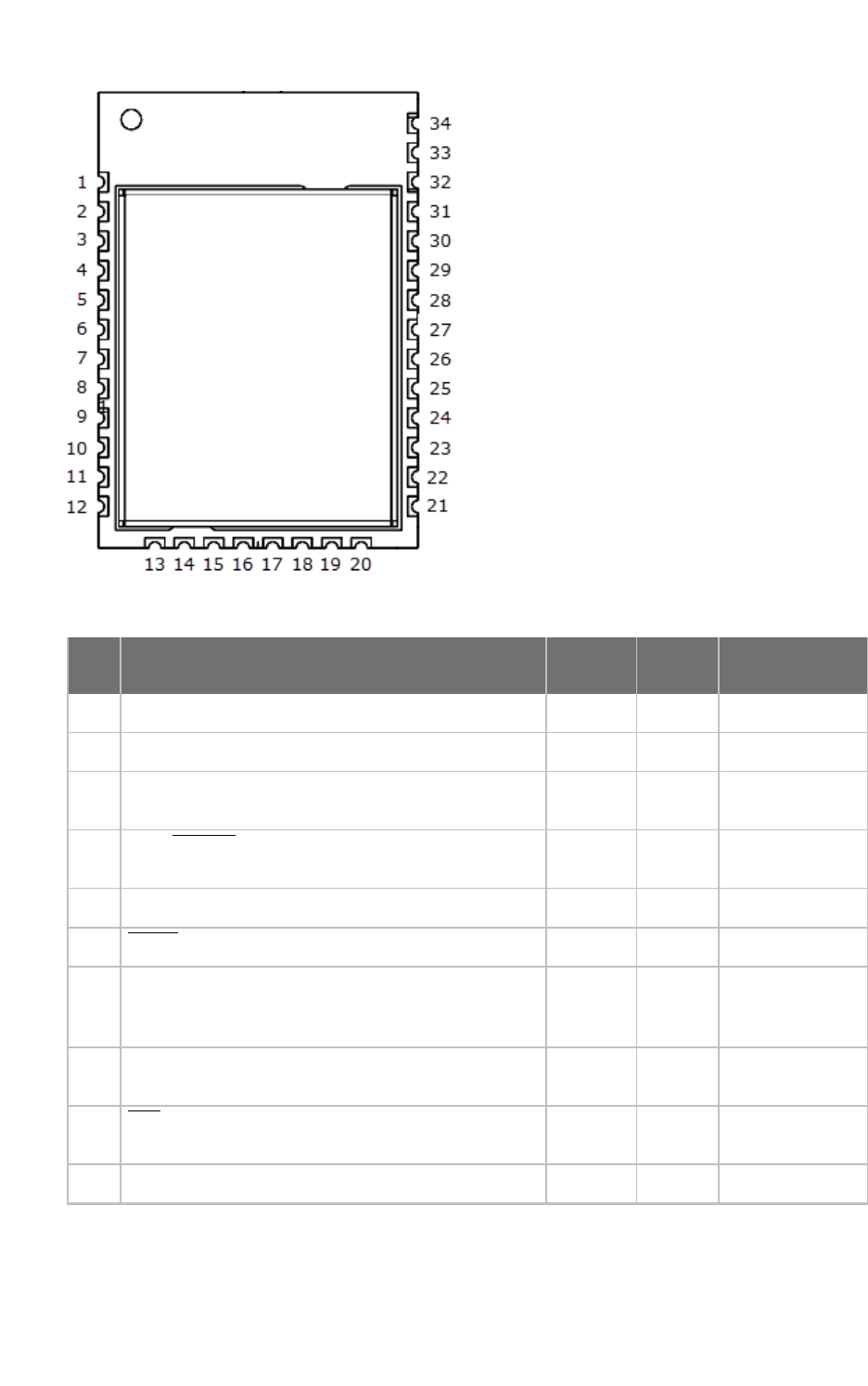
Hardware Pin signals for the XBee3 surface-mount module
XBee3™ RF Module Hardware Reference Manual 15
XBee3 micro (chip antenna)
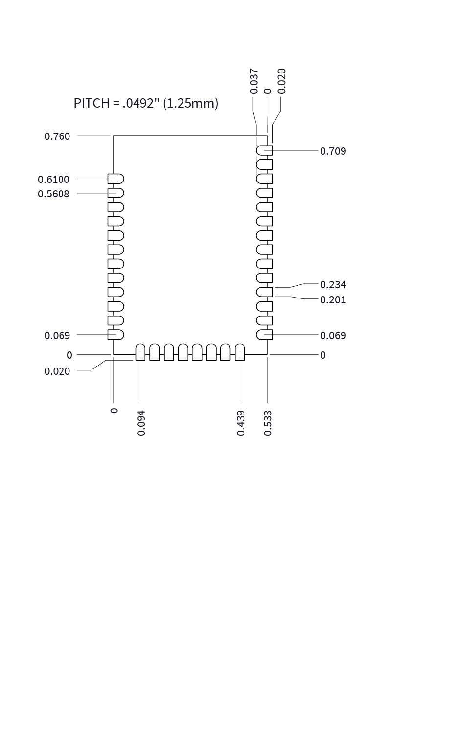
Pin signals for the XBee3 surface-mount module
The following drawing shows the surface-mount (SMT) pin locations.
Hardware Pin signals for the XBee3 surface-mount module
XBee3™ RF Module Hardware Reference Manual 16
The following table shows the pin signals and their descriptions for the surface-mount device.
Pin# Name Direction
Default
state Description
1 GND - - Ground.
2 VCC - - Power supply.
3 DOUT /DIO13 Both Output UART data out
/GPIO.
4 DIN / CONFIG /DIO14 Both Input UART data in
/GPIO.
5 DIO12 Both GPIO.
6 RESET Input Device reset.
7 RSSI PWM/DIO10 Both Output RX signal
strength
Indicator /GPIO.
8 PWM1/DIO11 Both Disabled Pulse width
modulator/GPIO.
9 [reserved] - Disabled Do not connect.

Hardware Pin signals for the XBee3 surface-mount module
XBee3™ RF Module Hardware Reference Manual 17
Pin# Name Direction
Default
state Description
10 DTR/SLEEP_RQ /DIO8 Both Input Pin sleep control
Line/GPIO.
11 GND - - Ground.
12 SPI_ATTN/ BOOTMODE/DIO19 Output Output
Serial peripheral
interface
attention .
Do not tie low on
reset.
13 GND - - Ground.
14 SPI_CLK /DIO18 Input Input Serial peripheral
interface
clock/GPIO.
15 SPI_SSEL/DIO17 Input Input Serial peripheral
interface not
select/GPIO.
16 SPI_MOSI/DIO16 Input Input Serial peripheral
interface data
in/GPIO.
17 SPI_MISO/DIO15 Output Output Serial peripheral
interface data
out/GPIO.
18 [reserved]* - Disabled Do not connect.
19 [reserved]* - Disabled Do not connect.
20 [reserved]* - Disabled Do not connect.
21 [reserved]* - Disabled Do not connect.
22 GND - - Ground.
23 [reserved] - Disabled Do not connect.
24 DIO4 Both Disabled GPIO.
25 CTS/DIO7 Both Output Clear to send
flow
control/GPIO.
26 ON/SLEEP/DIO9 Both Output Device status
indicator/GPIO

Hardware Pin signals for the XBee3 micro module
XBee3™ RF Module Hardware Reference Manual 18
Pin# Name Direction
Default
state Description
27 [reserved] - Disabled
Do not connect
or connect to
Ground.
28 ASSOCIATE/DIO5 Both Output Associate
Indicator/GPIO.
29 RTS/DIO6 Both Input Request to send
flow control
/GPIO.
30 AD3/DIO3 Both Disabled Analog
input/GPIO.
31 AD2/DIO2 Both Disabled Analog
input/GPIO
32 AD1/DIO1 Both Disabled Analog
input/GPIO.
33 AD0 /DIO0 Both Input Analog input /
GPIO /
Commissioning
button.
34 [reserved] - Disabled Do not connect.
35 GND - - Ground.
36 RF Both - RF I/O for RF
pad variant.
37 [reserved] - Disabled Do not connect.
Signal direction is specified with respect to the device.
This is a complete list of functionalities. See the applicable software manual for available
functionalities.
See Design notes for details on pin connections.
* Refer to Writing custom firmware for instructions on using these pins if JTAG functions are needed.
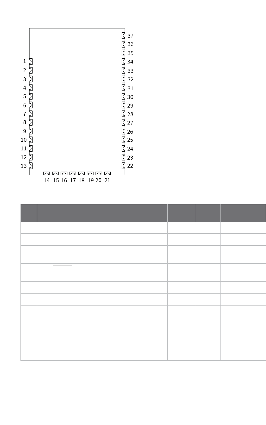
Pin signals for the XBee3 micro module
The following drawing shows the micro pin locations.
Hardware Pin signals for the XBee3 micro module
XBee3™ RF Module Hardware Reference Manual 19
The following table shows the pin signals and their descriptions for the XBee3 Micro device.
Pin# Name Direction
Default
state Description
1 GND - - Ground.
2 VCC - - Power supply.
3 DOUT /DIO13 Both Output UART data out
/GPIO.
4 DIN / CONFIG /DIO14 Both Input UART data in
/GPIO.
5 DIO12 Both GPIO.
6 RESET Input Device reset.
7 RSSI PWM/DIO10 Both Output RX signal
strength
Indicator /GPIO.
8 PWM1/DIO11 Both Disabled Pulse width
modulator/GPIO.
9 DTR/SLEEP_RQ /DIO8 Both Input Pin sleep control
Line/GPIO.
10 GND - - Ground.
Hardware Pin signals for the XBee3 micro module
XBee3™ RF Module Hardware Reference Manual 20
Pin# Name Direction
Default
state Description
11 SPI_ATTN/ BOOTMODE/DIO19 Output Output
Serial peripheral
interface
attention
Do not tie low on
reset.
12 GND - - Ground.
13 SPI_CLK /DIO18 Input Input Serial peripheral
interface
clock/GPIO.
14 SPI_SSEL/DIO17 Input Input Serial peripheral
interface not
select/GPIO.
15 SPI_MOSI/DIO16 Input Input Serial peripheral
interface data
in/GPIO.
16 SPI_MISO/DIO15 Output Output Serial peripheral
interface data
out/GPIO.
17 [reserved]* - Disabled Do not connect.
18 [reserved]* - Disabled Do not connect.
19 [reserved]* - Disabled Do not connect.
20 [reserved]* - Disabled Do not connect.
21 GND - - Ground.
22 [reserved] - Disabled Do not connect.
23 DIO4 Both Disabled GPIO.
24 CTS/DIO7 Both Output Clear to send
flow
control/GPIO.
25 ON/SLEEP/DIO9 Both Output Device status
indicator/GPIO.
26 ASSOCIATE/DIO5 Both Output Associate
Indicator/GPIO.
27 RTS/DIO6 Both Input Request to send
flow control
/GPIO.

Hardware Design notes
XBee3™ RF Module Hardware Reference Manual 21
Pin# Name Direction
Default
state Description
28 AD3/DIO3 Both Disabled Analog
input/GPIO.
29 AD2/DIO2 Both Disabled Analog
input/GPIO.
30 AD1/DIO1 Both Disabled Analog
input/GPIO.
31 AD0 /DIO0 Both Input Analog input /
GPIO /
Commissioning
button.
32 GND - - Ground.
33 RF Both - RF I/O for RF
pad variant.
34 GND - - Ground.
Signal direction is specified with respect to the device.
This is a complete list of functionalities. See the applicable software manual for available
functionalities.
See Design notes for details on pin connections.
* Refer to Writing custom firmware for instructions on using these pins if JTAG functions are needed.
Design notes
XBee3 modules do not require any external circuitry or specific connections for proper operation.
However, there are some general design guidelines that we recommend to build and troubleshoot a
robust design.
Power supply design
A poor power supply can lead to poor radio performance, especially if you do not keep the supply
voltage within tolerance or if it is excessively noisy. To help reduce noise, place a 1.0 µF and 8.2 pF
capacitor as near as possible to XBee3 pad 2 (VCC) on the PCB. Adding a 10uF decoupling capacitor is
also recommended. If you are using a switching regulator for the power supply, switch the frequencies
above 500 kHz. Limit the power supply ripple to a maximum 50 mV peak to peak. For best results,
place the lower capacitance capacitors closest to the XBee3 module.
Board layout
We design XBee3 modules to be self-sufficient and have minimal sensitivity to nearby processors,
crystals or other printed circuit board (PCB) components. Keep power and ground traces thicker than
signal traces and make sure that they are able to comfortably support the maximum current
specifications. There are no other special PCB design considerations to integrate XBee3 modules, with
the exception of antennas.

Hardware Design notes
XBee3™ RF Module Hardware Reference Manual 22
Antenna performance
Antenna location is important for optimal performance. The following suggestions help you achieve
optimal antenna performance. Point the antenna up vertically (upright). Antennas radiate and receive
the best signal perpendicular to the direction they point, so a vertical antenna's omnidirectional
radiation pattern is strongest across the horizon.
Position the antennas away from metal objects whenever possible. Metal objects between the
transmitter and receiver can block the radiation path or reduce the transmission distance. Objects
that are often overlooked include:
nMetal poles
nMetal studs
nStructure beams
nConcrete, which is usually reinforced with metal rods
If you place the device inside a metal enclosure, use an external antenna. Common objects that have
metal enclosures include:
nVehicles
nElevators
nVentilation ducts
nRefrigerators
nMicrowave ovens
nBatteries
nTall electrolytic capacitors
Use the following additional guidelines for optimal antenna performance:
nDo not place XBee3 modules with the chip antenna or the embedded antenna inside a metal
enclosure.
nDo not place any ground planes or metal objects above or below the antenna.
nFor the best results, mount the device at the edge of the host PCB. Ensure that the ground,
power, and signal planes are vacant immediately below the antenna section.
Recommended pin connections
The only required pin connections for two-way communication are VCC, GND, DOUT and DIN. To
support serial firmware updates, you must connect VCC, GND, DOUT, DIN, RTS, and DTR.
For applications that need to ensure the lowest sleep current, never leave unconnected inputs
floating. Use internal or external pull-up or pull-down resistors, or set the unused I/O lines to outputs.
Design notes for surface mount PCB antenna and micro footprint
chip antenna devices
Position PCB/chip antenna devices so there are no ground planes or metal objects above or below the
antenna. For best results, do not place the device in a metal enclosure, as this may greatly reduce the
range. Place the device at the edge of the PCB on which it is mounted. Make sure the ground, power
and signal planes are vacant immediately below the antenna section.
Hardware Design notes
XBee3™ RF Module Hardware Reference Manual 23
The following drawings illustrate important recommendations when you are designing with PCB/chip
antenna devices. For optimal performance, do not mount the device on the RF pad footprint described
in the next section, because the footprint requires a ground plane within the PCB antenna keep out
area.
Surface-mount embedded antenna keepout area
Notes
1. We recommend non-metal enclosures. For metal enclosures, use an external antenna.
2. Keep metal chassis or mounting structures in the keepout area at least 2.54 cm (1 in) from the
antenna.
3. Maximize the distance between the antenna and metal objects that might be mounted in the
keepout area.
4. These keepout area guidelines do not apply for chip antennas or external RF connectors.
Hardware Design notes
XBee3™ RF Module Hardware Reference Manual 24
XBee3 Micro keepout area
Notes
1. We recommend non-metal enclosures. For metal enclosures, use an external antenna.
2. Keep metal chassis or mounting structures in the keepout area at least 2.54 cm (1 in) from the
antenna.
3. Maximize the distance between the antenna and metal objects that might be mounted in the
keepout area.
4. These keepout area guidelines do not apply for surface-mount embedded antennas or external
RFconnectors.
Design notes for RF pad devices
The RF pad is a soldered antenna connection. The RF signal travels from the RF pad connection (pad
33 on micro modules and pad 36 on surface-mount modules) on the device to the antenna through an
RF trace transmission line on the PCB. Any additional components between the device and antenna
violates modular certification. The controlled impedance for the RF trace is 50 Ω.
We recommend using a microstrip trace, although you can also use a coplanar waveguide if you need
more isolation. A microstrip generally requires less area on the PCB than a coplanar waveguide. We do
not recommend using a stripline because sending the signal to different PCB layers can introduce
matching and performance problems.
Following good design practices is essential when implementing the RF trace on a PCB. Consider the
following points:
nMinimize the length of the trace by placing the RPSMA jack close to the device.
nConnect all of the grounds on the jack and the device to the ground planes directly or through
closely placed vias.
Hardware Design notes
XBee3™ RF Module Hardware Reference Manual 25
nSpace any ground fill on the top layer at least twice the distance d, for Micro modules at least
0.028" and for surface mount modules at least 0.050".
Additional considerations:
nThe top two layers of the PCB have a controlled thickness dielectric material in between.
nThe second layer has a ground plane which runs underneath the entire RF pad area. This
ground plane is a distance d, the thickness of the dielectric, below the top layer.
nThe RF trace width determines the impedance of the transmission line with relation to the
ground plane. Many online tools can estimate this value, although you should consult the PCB
manufacturer for the exact width.
Implementing these design suggestions helps ensure that the RF pad device performs to its
specifications.
The following figures show a layout example of a host PCB that connects an RF pad device to a right
angle, through-hole RPSMA jack.
Number Description
1Maintain a distance of at least 2 d between microstrip and ground fill.
Hardware Design notes
XBee3™ RF Module Hardware Reference Manual 26
Number Description
2 RF pad pin.
3 50 Ω microstrip trace.
4 RF connection of RPSMA jack.
This example is on a surface-mount device. The width in this example is approximately 0.045" for a 50
Ωtrace, assuming d=0.025”, and that the dielectric has a relative permittivity of 4.4. This trace width
is a good fit with the device footprint's 0.060" pad width.
Note We do not recommend using a trace wider than the pad width, and using a very narrow trace
(under 0.010") can cause unwanted RF loss.
The following illustration shows PCB layer 2 of an example RF layout.
Number Description
1Use multiple vias to help eliminate ground variations.
2 Put a solid ground plane under RF trace to achieve the desired impedance.


Regulatory information United States (FCC)
XBee3™ RF Module Hardware Reference Manual 28
United States (FCC)
XBee3 RF Modules comply with Part 15 of the FCC rules and regulations. Compliance with the labeling
requirements, FCC notices and antenna usage guidelines is required.
To fulfill FCC Certification, the OEM must comply with the following regulations:
1. The system integrator must ensure that the text on the external label provided with this
device is placed on the outside of the final product.
2. RF Modules may only be used with antennas that have been tested and approved for use with
the modules.
OEM labeling requirements
WARNING! As an Original Equipment Manufacturer (OEM) you must ensure that FCC
labeling requirements are met. You must include a clearly visible label on the outside of
the final product enclosure that displays the following content:
Required FCC Label for OEM products containing the XBee3 RF Module
Contains FCC ID: MCQ-XBEE3
This device complies with Part 15 of the FCC Rules. Operation is subject to the following two
conditions: (1.) this device may not cause harmful interference and (2.) this device must accept any
interference received, including interference that may cause undesired operation.
FCC notices
IMPORTANT: XBee3 RF Modules have been certified by the FCC for use with other products without
any further certification (as per FCC section 2.1091). Modifications not expressly approved by Digi
could void the user's authority to operate the equipment.
IMPORTANT: OEMs must test final product to comply with unintentional radiators (FCC section 15.107
& 15.109) before declaring compliance of their final product to Part 15 of the FCC Rules.
IMPORTANT: The RF module has been certified for remote and base radio applications. If the module
will be used for portable applications, the device must undergo SAR testing.
This equipment has been tested and found to comply with the limits for a Class B digital device,
pursuant to Part 15 of the FCC Rules. These limits are designed to provide reasonable protection
against harmful interference in a residential installation. This equipment generates, uses and can
radiate radio frequency energy and, if not installed and used in accordance with the instructions, may
cause harmful interference to radio communications. However, there is no guarantee that
interference will not occur in a particular installation.
If this equipment does cause harmful interference to radio or television reception, which can be
determined by turning the equipment off and on, the user is encouraged to try to correct the
interference by one or more of the following measures: Re-orient or relocate the receiving antenna,
Increase the separation between the equipment and receiver, Connect equipment and receiver to
outlets on different circuits, or Consult the dealer or an experienced radio/TV technician for help.

Regulatory information United States (FCC)
XBee3™ RF Module Hardware Reference Manual 29
FCC-approved antennas (2.4 GHz)
The XBee3 RF Module can be installed using antennas and cables constructed with non-standard
connectors (RPSMA, RPTNC, etc.) An adapter cable may be necessary to attach the XBee connector to
the antenna connector.
The modules are FCC approved for fixed base station and mobile applications for the channels
indicated in the tables below. If the antenna is mounted at least 20 cm (7.87 in) from nearby persons,
the application is considered a mobile application. Antennas not listed in the table must be tested to
comply with FCC Section 15.203 (Unique Antenna Connectors) and Section 15.247 (Emissions).
The antennas in the tables below have been approved for use with this module. Cable loss is required
when using gain antennas as shown in the tables.
Digi does not carry all of these antenna variants. Contact Digi Sales for available antennas.

Regulatory information United States (FCC)
XBee3™ RF Module Hardware Reference Manual 30
XBee3 RF module
The following table shows the antennas approved for use with the XBee3 RF module.
All antenna part numbers followed by an asterisk (*) are not available from Digi. Consult with an antenna manufacturer for an equivalent option.
Partnumber
Type
(description)
Gain
(dBi) Application* Min. separation
Required antenna cable loss (dB)
802.15.4 Based
Protocols (Ex: ZigBee)
BLE (when
available)
Integral antennas
29000313 Integral PCB antenna (surface-mount only) 0.0 Fixed/Mobile 20 cm N/A N/A
29000710 Chip antenna (micro only) 0.0 Fixed/Mobile 20 cm N/A N/A
Dipole antennas
A24-HASM-
450
Dipole (Half-wave articulated RPSMA - 4.5”) 2.1 Fixed 20 cm N/A N/A
A24-HABSM* Dipole (Articulated RPSMA) 2.1 Fixed 20 cm N/A N/A
29000095 Dipole (Half-wave articulated RPSMA - 4.5”) 2.1 Fixed/Mobile 20 cm N/A N/A
A24-HABUF-
P5I
Dipole (Half-wave articulated bulkhead mount
U.FL. w/ 5” pigtail)
2.1 Fixed/Mobile 20 cm N/A N/A
A24-HASM-
525
Dipole (Half-wave articulated RPSMA - 5.25") 2.1 Fixed 20 cm N/A N/A
Omni-directional antennas
A24-F2NF Omni-directional (Fiberglass base station) 2.1 Fixed/Mobile 20 cm N/A N/A
A24-F3NF Omni-directional (Fiberglass base station) 3.0 Fixed/Mobile 20 cm N/A N/A
A24-F5NF Omni-directional (Fiberglass base station) 5.0 Fixed 20 cm N/A N/A
A24-F8NF Omni-directional (Fiberglass base station) 8.0 Fixed 2 m N/A N/A

Regulatory information United States (FCC)
XBee3™ RF Module Hardware Reference Manual 31
Partnumber
Type
(description)
Gain
(dBi) Application* Min. separation
Required antenna cable loss (dB)
802.15.4 Based
Protocols (Ex: ZigBee)
BLE (when
available)
A24-F9NF Omni-directional (Fiberglass base station) 9.5 Fixed 2 m N/A N/A
A24-F10NF Omni-directional (Fiberglass base station) 10.0 Fixed 2 m N/A N/A
A24-F12NF Omni-directional (Fiberglass base station) 12.0 Fixed 2 m N/A N/A
A24-W7NF Omni-directional (Fiberglass base station) 7.2 Fixed 2 m N/A N/A
A24-M7NF Omni-directional (Mag-mount base station) 7.2 Fixed 2 m N/A N/A
A24-F15NF Omni-directional (Fiberglass base station) 15.0 Fixed 2 m N/A N/A
Panel antennas
A24-P8SF Flat Panel 8.5 Fixed 2 m N/A N/A
A24-P8NF Flat Panel 8.5 Fixed 2 m N/A N/A
A24-P13NF Flat Panel 13.0 Fixed 2 m N/A N/A
A24-P14NF Flat Panel 14.0 Fixed 2 m N/A N/A
A24-P15NF Flat Panel 15.0 Fixed 2 m N/A N/A
A24-P16NF Flat Panel 16.0 Fixed 2 m N/A N/A
A24-P19NF Flat Panel 19.0 Fixed 2 m N/A N/A
Yagi antennas
A24-Y6NF Yagi (6-element) 8.8 Fixed 2 m N/A N/A
A24-Y7NF Yagi (7-element) 9.0 Fixed 2 m N/A N/A
A24-Y9NF Yagi (9-element) 10.0 Fixed 2 m N/A N/A
A24-Y10NF Yagi (10-element) 11.0 Fixed 2 m N/A N/A

Regulatory information United States (FCC)
XBee3™ RF Module Hardware Reference Manual 32
Partnumber
Type
(description)
Gain
(dBi) Application* Min. separation
Required antenna cable loss (dB)
802.15.4 Based
Protocols (Ex: ZigBee)
BLE (when
available)
A24-Y12NF Yagi (12-element) 12.0 Fixed 2 m N/A N/A
A24-Y13NF Yagi (13-element) 12.0 Fixed 2 m N/A N/A
A24-Y15NF Yagi (15-element) 12.5 Fixed 2 m N/A N/A
A24-Y16NF Yagi (16-element) 13.5 Fixed 2 m N/A N/A
A24-Y16RM Yagi (16-element, RPSMA connector) 13.5 Fixed 2 m N/A N/A
A24-Y18NF Yagi (18-element) 15.0 Fixed 2 m N/A N/A

Regulatory information United States (FCC)
XBee3™ RF Module Hardware Reference Manual 33
XBee3-PRO RF module
The following table shows the antennas approved for use with the XBee3-PRO RF Module.
All antenna part numbers followed by an asterisk (*) are not available from Digi. Consult with an antenna manufacturer for an equivalent option.
Partnumber Type (description)
Gain
(dBi) Application*
Min
separation
Required antenna cable loss (dB)
802.15.4 Based Protocols
(Ex: ZigBee)
BLE (when
available)
Internal antennas
29000313 Integral PCB antenna (surface mount only) 0.0 Fixed/Mobile 20 cm N/A N/A
29000710 Chip antenna (micro only) 0.0 Fixed/Mobile 20 cm N/A N/A
Dipole antennas
A24-HASM-
450
Dipole (Half-wave articulated RPSMA - 4.5”) 2.1 Fixed 20 cm N/A N/A
A24-HABSM* Dipole (Articulated RPSMA) 2.1 Fixed 20 cm N/A N/A
29000095 Dipole (Half-wave articulated RPSMA - 4.5”) 2.1 Fixed/Mobile 20 cm N/A N/A
A24-HABUF-
P5I
Dipole (Half-wave articulated bulkhead mount
U.FL. w/ 5” pigtail)
2.1 Fixed/Mobile 20 cm N/A N/A
A24-HASM-
525
Dipole (Half-wave articulated RPSMA - 5.25") 2.1 Fixed 20 cm N/A N/A
Omni-directional antennas
A24-F2NF Omni-directional (Fiberglass base station) 2.1 Fixed/Mobile 20 cm N/A N/A
A24-F3NF Omni-directional (Fiberglass base station) 3.0 Fixed/Mobile 20 cm N/A N/A
A24-F5NF Omni-directional (Fiberglass base station) 5.0 Fixed 20 cm N/A N/A
A24-F8NF Omni-directional (Fiberglass base station) 8.0 Fixed 2 m N/A N/A

Regulatory information United States (FCC)
XBee3™ RF Module Hardware Reference Manual 34
Partnumber Type (description)
Gain
(dBi) Application*
Min
separation
Required antenna cable loss (dB)
802.15.4 Based Protocols
(Ex: ZigBee)
BLE (when
available)
A24-F9NF Omni-directional (Fiberglass base station) 9.5 Fixed 2 m N/A N/A
A24-F10NF Omni-directional (Fiberglass base station) 10 Fixed 2 m N/A N/A
A24-F12NF Omni-directional (Fiberglass base station) 12 Fixed 2 m N/A N/A
A24-W7NF Omni-directional (Fiberglass base station) 7.2 Fixed 2 m N/A N/A
A24-M7NF Omni-directional (Mag-mount base station) 7.2 Fixed 2 m N/A N/A
A24-F15NF Omni-directional (Fiberglass base station) 15.0 Fixed 2 m N/A 2.0
Panel antennas
A24-P8SF Flat Panel 8.5 Fixed 2 m N/A N/A
A24-P8NF Flat Panel 8.5 Fixed 2 m N/A N/A
A24-P13NF Flat Panel 13.0 Fixed 2 m N/A N/A
A24-P14NF Flat Panel 14.0 Fixed 2 m N/A 1.0
A24-P15NF Flat Panel 15.0 Fixed 2 m N/A 2.0
A24-P16NF Flat Panel 16.0 Fixed 2 m N/A 3.0
A24-P19NF Flat Panel 19.0 Fixed 2 m 3.0 6.0
Yagi antennas
A24-Y6NF Yagi (6-element) 8.8 Fixed 2 m N/A N/A
A24-Y7NF Yagi (7-element) 9.0 Fixed 2 m N/A N/A
A24-Y9NF Yagi (9-element) 10.0 Fixed 2 m N/A N/A
A24-Y10NF Yagi (10-element) 11.0 Fixed 2 m N/A N/A
Regulatory information Europe (CE)
XBee3™ RF Module Hardware Reference Manual 35
Partnumber Type (description)
Gain
(dBi) Application*
Min
separation
Required antenna cable loss (dB)
802.15.4 Based Protocols
(Ex: ZigBee)
BLE (when
available)
A24-Y12NF Yagi (12-element) 12.0 Fixed 2 m N/A N/A
A24-Y13NF Yagi (13-element) 12.0 Fixed 2 m N/A N/A
A24-Y15NF Yagi (15-element) 12.5 Fixed 2 m N/A N/A
A24-Y16NF Yagi (16-element) 13.5 Fixed 2 m N/A 0.5
A24-Y16RM Yagi (16-element, RPSMA connector) 13.5 Fixed 2 m N/A 0.5
A24-Y18NF Yagi (18-element) 15.0 Fixed 2 m N/A 2.0
RF exposure
If you are an integrating the XBee3 into another product, you must include the following Caution statement in OEMproduct manuals to alert users of FCC
RF exposure compliance:
CAUTION! To satisfy FCC RF exposure requirements for mobile transmitting devices, a separation distance of 20 cm or more should be
maintained between the antenna of this device and persons during device operation. To ensure compliance, operations at closer than this
distance are not recommended. The antenna used for this transmitter must not be co-located in conjunction with any other antenna or
transmitter.
Europe (CE)
The XBee3 RF Module has been tested for use in several European countries. For a complete list, refer to www.digi.com/resources/certifications.
If XBee3 RF Modules are incorporated into a product, the manufacturer must ensure compliance of the final product with articles 3.1a and 3.1b of the
Radio Equipment Directive. A Declaration of Conformity must be issued for each of these standards and kept on file as described in the Radio Equipment
Directive.
Furthermore, the manufacturer must maintain a copy of the XBee3 RF Module user guide documentation and ensure the final product does not exceed
the specified power ratings, antenna specifications, and/or installation requirements as specified in the user guide.
Regulatory information Europe (CE)
XBee3™ RF Module Hardware Reference Manual 36
Maximum power and frequency specifications
For the XBee3 device:
When using 802.15.4 RF physical layer:
nMaximum power: 8.61mW (9.35 dBm) Equivalent Isotropically Radiated Power (EIRP).
nFrequencies: 5 MHz channel spacing, beginning at 2405 MHz and ending at 2480 MHz.
When using BLE RF physical layer:
nMaximum power: 9.02mW (9.55 dBm) Equivalent Isotropically Radiated Power (EIRP).
nFrequencies: 2 MHz channel spacing, beginning at 2402 MHz and ending at 2480 MHz.
OEM labeling requirements
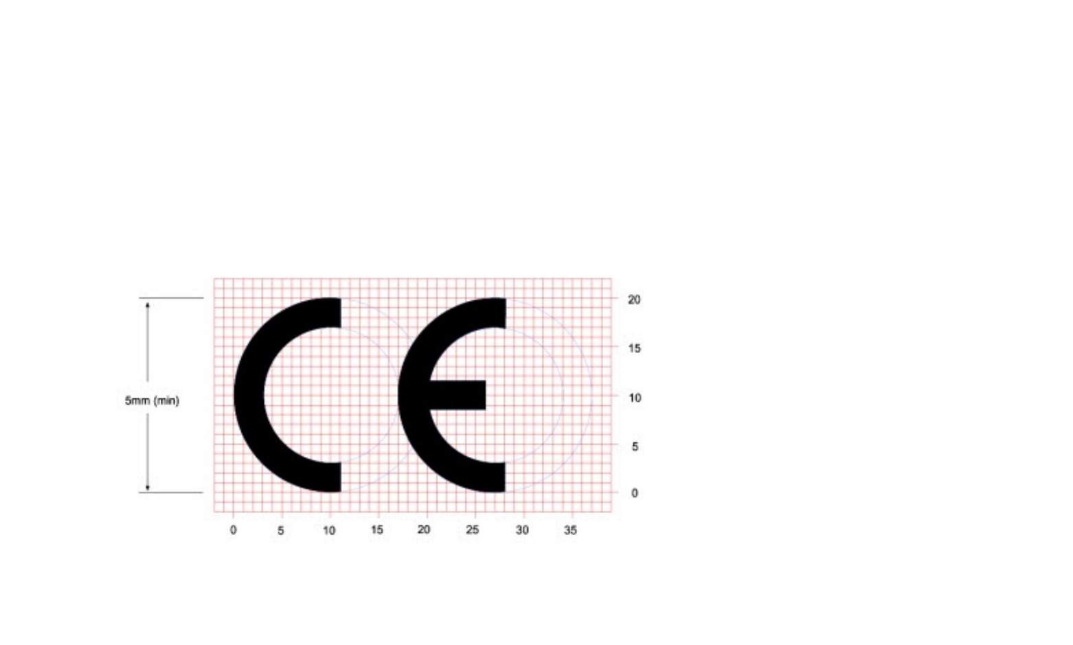
The “CE” marking must be affixed to a visible location on the OEM product. The following figure shows CE labeling requirements.
The CE mark shall consist of the initials “CE” taking the following form:

Regulatory information IC (Industry Canada)
XBee3™ RF Module Hardware Reference Manual 37
nIf the CE marking is reduced or enlarged, the proportions given in the above graduated drawing must be respected.
nThe CE marking must have a height of at least 5 mm except where this is not possible on account of the nature of the apparatus.
nThe CE marking must be affixed visibly, legibly, and indelibly.
Digi customers assume full responsibility for learning and meeting the required guidelines for each country in their distribution market. Refer to the radio
regulatory agency in the desired countries of operation for more information.
Declarations of conformity
Digi has issued Declarations of Conformity for the XBee3 RF Modules concerning emissions, EMC, and safety. For more information, see
www.digi.com/resources/certifications.
Antennas
The following antennas have been tested and approved for use with the XBee3 RF Module:
All antenna part numbers followed by an asterisk (*) are not available from Digi. Consult with an antenna manufacturer for an equivalent option.
nDipole (2.1 dBi, Omni-directional, Articulated RPSMA, Digi part number A24-HABSM)
nPCB antenna (surface mount boards only) (0.0 dBi)
nChip antenna (micro form factor only) (0.0 dBi)
IC (Industry Canada)
Labeling requirements
Labeling requirements for Industry Canada are similar to those of the FCC. A clearly visible label on the outside of the final product enclosure must display
the following text.
For XBee3:
Contains Model XBEE3, IC: 1846A-XBEE3
The integrator is responsible for its product to comply with IC ICES-003 & FCC Part 15, Sub. B -Unintentional Radiators. ICES-003 is the same as FCC Part
15 Sub. B and Industry Canada accepts FCC test report or CISPR 22 test report for compliance with ICES-003.
This device complies with Industry Canada licence-exempt RSS standard(s). Operation is subject to the following two conditions: (1) this device may not
cause interference, and (2) this device must accept any interference, including interference that may cause undesired operation of the device.
Regulatory information IC (Industry Canada)
XBee3™ RF Module Hardware Reference Manual 38
Le présent appareil est conforme aux CNR d'Industrie Canada applicables aux appareils radio exempts de licence. L'exploitation est autorisée aux deux
conditions suivantes: (1) l'appareil ne doit pas produire de brouillage, et (2) l'utilisateur de l'appareil doit accepter tout brouillage radioélectrique subi,
même si le brouillage est susceptible d'en compromettre le fonctionnement.
RF Exposure
CAUTION! This equipment is approved for mobile and base station transmitting devices only. Antenna(s) used for this transmitter must be
installed to provide a separation distance of at least 20 cm from all persons and must not be co-located or operating in conjunction with any
other antenna or transmitter.
ATTENTION! Cet équipement est approuvé pour la mobile et la station base dispositifs d'émission seulement. Antenne(s) utilisé pour cet
émetteur doit être installé pour fournir une distance de séparation d'au moins 20 cm à partir de toutes les personnes et ne doit pas être
situé ou fonctionner en conjonction avec tout autre antenne ou émetteur.
Transmitters with Detachable Antennas
This radio transmitter (IC: 1846A-XBEE3) has been approved by Industry Canada to operate with the antenna types listed in FCC-approved antennas (2.4
GHz) with the maximum permissible gain and required antenna impedance for each antenna type indicated. Antenna types not included in this list, having
a gain greater than the maximum gain indicated for that type, are strictly prohibited for use with this device.
Le présent émetteur radio (IC: 1846A-XBEE3) a été approuvé par Industrie Canada pour fonctionner avec les types d'antenne énumérés ci-dessous et
ayant un gain admissible maximal et l'impédance requise pour chaque type d'antenne. Les types d'antenne non inclus dans cette liste, ou dont le gain est
supérieur au gain maximal indiqué, sont strictement interdits pour l'exploitation de l'émetteur.
Detachable Antenna
Under Industry Canada regulations, this radio transmitter may operate using only an antenna of a type and maximum (or lesser) gain approved for the
transmitter by Industry Canada. To reduce potential radio interference to other users, the antenna type and its gain should be so chosen that the
equivalent isotropically radiated power (EIRP) is not more than that necessary for successful communication.
Conformément à la réglementation d'Industrie Canada, le présent émetteur radio peutfonctionner avec une antenne d'un type et d'un gain maximal (ou
inférieur) approuvépour l'émetteur par Industrie Canada. Dans le but de réduire les risques de brouillageradioélectrique à l'intention des autres
utilisateurs, il faut choisir le type d'antenne etson gain de sorte que la puissance isotrope rayonnée équivalente (p.i.r.e.) ne dépassepas l'intensité
nécessaire àl'établissement d'une communication satisfaisante.

Manufacturing information
XBee3™ RF Module Hardware Reference Manual 39
Manufacturing information
The XBee3 RF Module (both surface-mount and micro)is designed for surface-mounting on the OEM
PCB. It has castellated pads to allow for easy solder attaching and inspection. The pads are all located
on the edge of the device so there are no hidden solder joints on these devices.
Recommended solder reflow cycle 40
Handling and storage 40
Recommended footprint 41
Flux and cleaning 44
Reworking 44
Manufacturing information Recommended solder reflow cycle
XBee3™ RF Module Hardware Reference Manual 40
Recommended solder reflow cycle
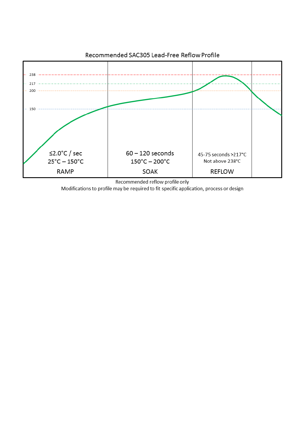
The following diagram shows the recommended solder reflow cycle.
The device reflows during this cycle, and must not be reflowed upside down. Be careful not to jar the
device while the solder is molten, as parts inside the device can be removed from their required
locations.
Hand soldering is possible and should be done in accordance with approved standards.
Handling and storage
The XBee3 RF Modules are level 3 Moisture Sensitive Devices. When using this kind of device, consider
the relative requirements in accordance with standard IPC/JEDEC J-STD-020.
In addition, note the following conditions:
a. Calculated shelf life in sealed bag: 12 months at <40 °C and <90% relative humidity (RH).
b. Environmental condition during the production: 30 °C /60% RH according to IPC/JEDEC J-STD -
033C, paragraphs 5 through 7.
c. The time between the opening of the sealed bag and the start of the reflow process cannot
exceed 168 hours if condition b) is met.
d. Baking is required if conditions b) or c) are not met.
e. Baking is required if the humidity indicator inside the bag indicates a RH of 10% more.
f. If baking is required, bake modules in trays stacked no more than 10 high for 4-6 hours at 125
°C.
Manufacturing information Recommended footprint
XBee3™ RF Module Hardware Reference Manual 41
Recommended footprint
We recommend that you use the following PCB footprints for surface-mounting. The dimensions
without brackets are in inches, and those in brackets are in millimeters.
XBee3 surface-mount recommended footprint
Manufacturing information Recommended footprint
XBee3™ RF Module Hardware Reference Manual 42
XBee3 Micro recommended footprint
Match the solder footprint to the copper pads, but may need to be adjusted depending on the specific
needs of assembly and product standards. Recommended stencil thickness is 0.15 mm/0.005”. Place
the component last and set the placement speed to the slowest setting.
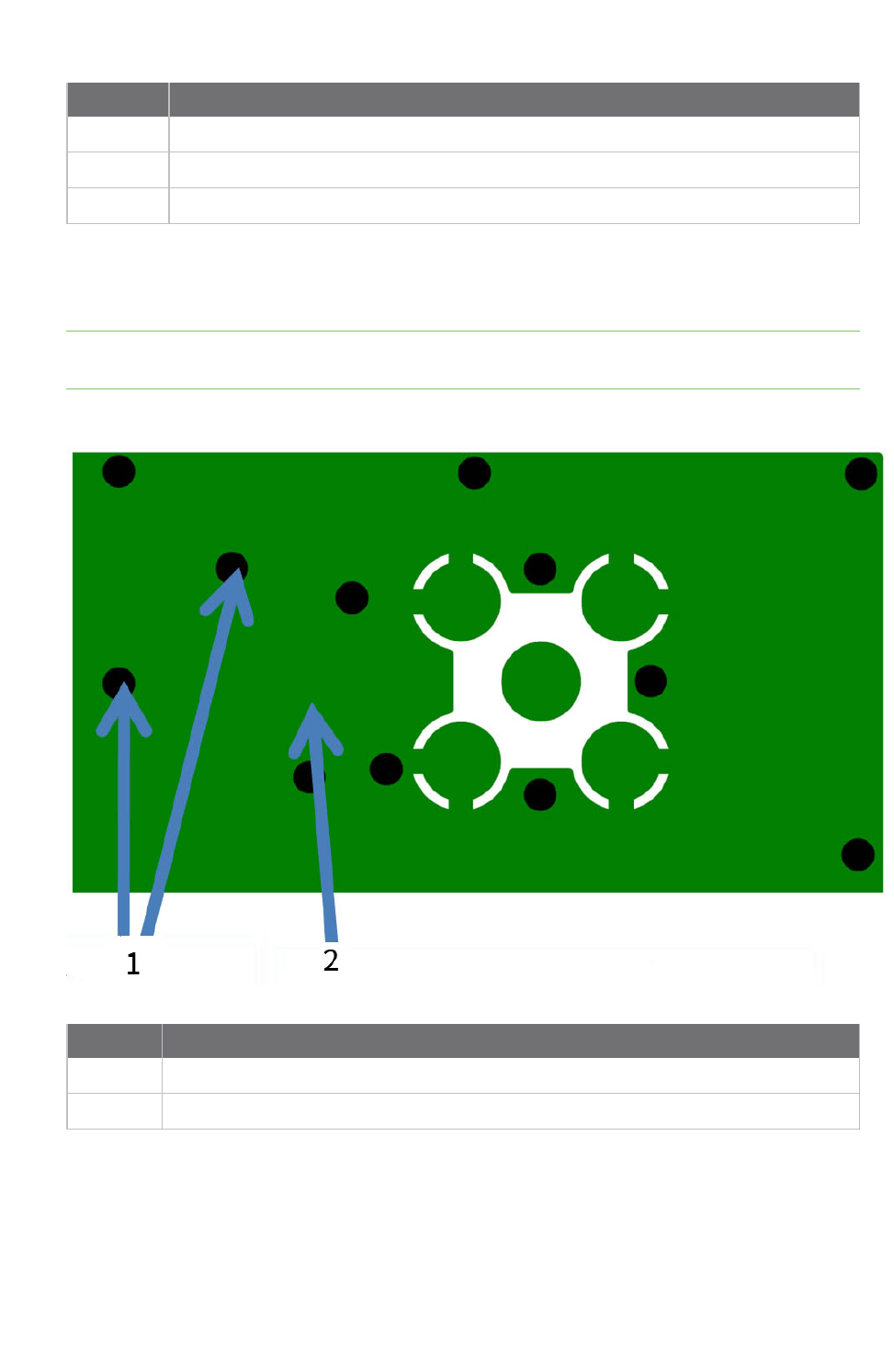
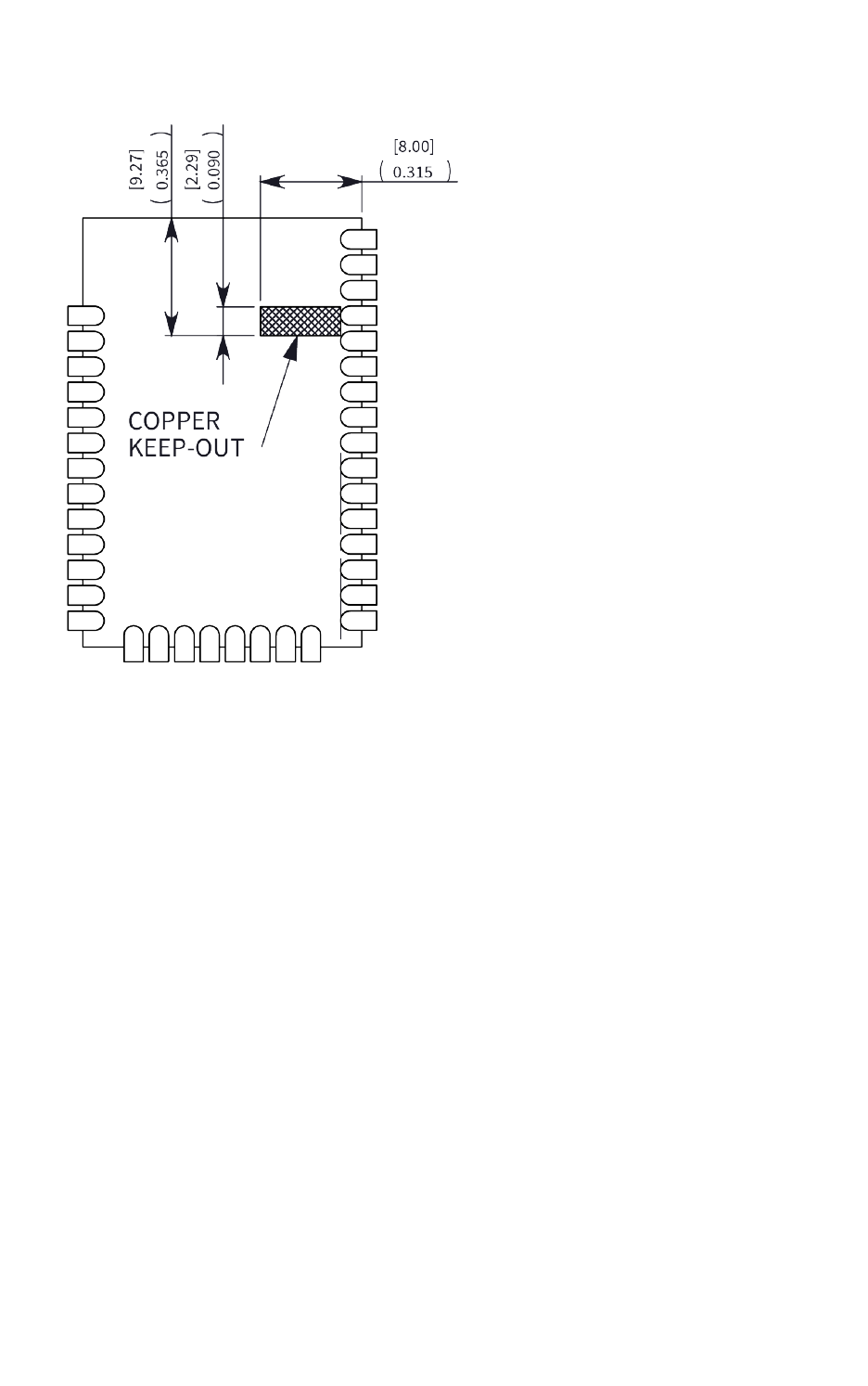
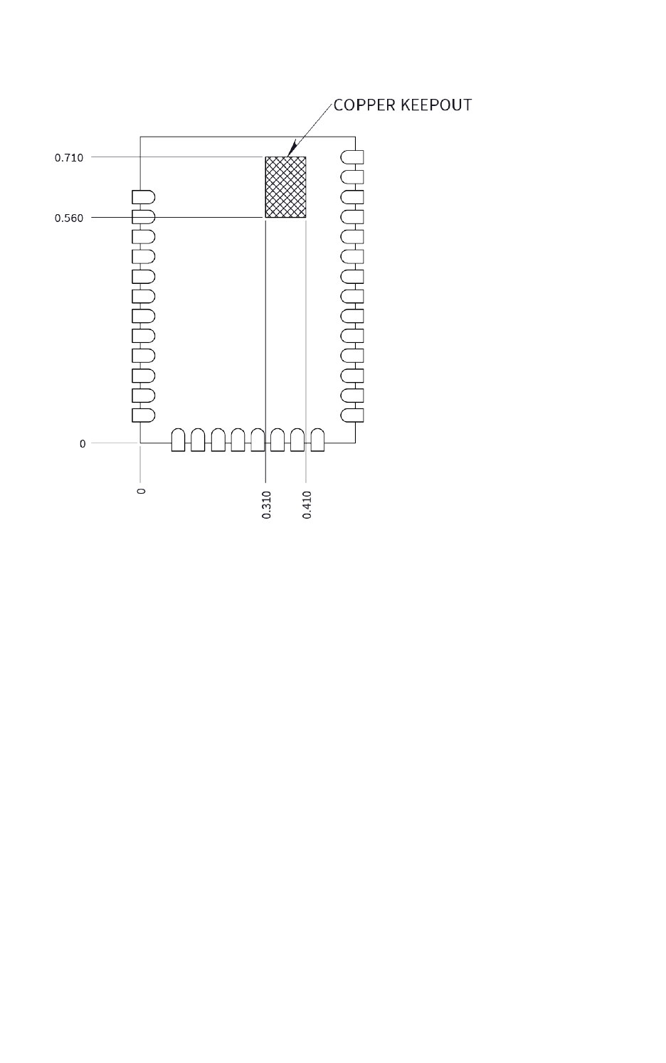
While the underside of the device is mostly coated with solder resist, we recommended the copper
layer directly below the device be left open to avoid unintended contacts. Copper or vias must not
interfere with the three exposed RF test points on the bottom of the device as shown in the following
diagrams. These devices have a ground plane in the middle on the back side for shielding purposes,
which can be affected by copper traces directly below the device.
Manufacturing information Recommended footprint
XBee3™ RF Module Hardware Reference Manual 43
Copper keepout for the XBee3 surface-mount
Manufacturing information Flux and cleaning
XBee3™ RF Module Hardware Reference Manual 44
Copper keepout for the XBee3 Micro
Flux and cleaning
Digi recommends that a “no clean” solder paste be used in assembling these devices. This eliminates
the clean step and ensures unwanted residual flux is not left under the device where it is difficult to
remove.
In addition the following issues can occur:
nCleaning with liquids can result in liquid remaining under the shield or in the gap between the
device and the OEM PCB. This can lead to unintended connections between pads on the device.
nThe residual moisture and flux residue under the device are not easily seen during an
inspection process.
Factory recommended best practice is to use a “no clean” solder paste to avoid these issues and
ensure proper device operation.
Reworking
Never perform rework on the device itself. The device has been optimized to give the best possible
performance, and reworking the device itself will void warranty coverage and certifications. We
recognize that some customers choose to rework and void the warranty. The following information
serves as a guideline in such cases to increase the chances of success during rework, though the
warranty is still voided.
The device may be removed from the OEM PCB by the use of a hot air rework station, or hot plate. Be
careful not to overheat the device. During rework, the device temperature may rise above its internal

Manufacturing information Reworking
XBee3™ RF Module Hardware Reference Manual 45
solder melting point and care should be taken not to dislodge internal components from their
intended positions.