ARM1176JZF S Technical Reference Manual S+Technical+Reference+Manual
User Manual:
Open the PDF directly: View PDF ![]() .
.
Page Count: 759 [warning: Documents this large are best viewed by clicking the View PDF Link!]
- ARM1176JZF-S Technical Reference Manual
- Contents
- List of Tables
- List of Figures
- Preface
- Introduction
- 1.1 About the processor
- 1.2 Extensions to ARMv6
- 1.3 TrustZone security extensions
- 1.4 ARM1176JZF-S architecture with Jazelle technology
- 1.5 Components of the processor
- 1.6 Power management
- 1.7 Configurable options
- 1.8 Pipeline stages
- 1.9 Typical pipeline operations
- 1.10 ARM1176JZF-S instruction set summary
- 1.11 Product revisions
- Programmer’s Model
- 2.1 About the programmer’s model
- 2.2 Secure world and Non-secure world operation with TrustZone
- 2.3 Processor operating states
- 2.4 Instruction length
- 2.5 Data types
- 2.6 Memory formats
- 2.7 Addresses in a processor system
- 2.8 Operating modes
- 2.9 Registers
- 2.10 The program status registers
- 2.11 Additional instructions
- 2.12 Exceptions
- 2.12.1 New instructions for exception handling
- 2.12.2 Exception entry and exit summary
- 2.12.3 Entering an ARM exception
- 2.12.4 Leaving an ARM exception
- 2.12.5 Reset
- 2.12.6 Fast interrupt request
- 2.12.7 Interrupt request
- 2.12.8 Low interrupt latency configuration
- 2.12.9 Interrupt latency example
- 2.12.10 Aborts
- 2.12.11 Imprecise Data Abort mask in the CPSR/SPSR
- 2.12.12 Supervisor call instruction
- 2.12.13 Secure Monitor Call (SMC)
- 2.12.14 Undefined instruction
- 2.12.15 Breakpoint instruction (BKPT)
- 2.12.16 Exception vectors
- 2.12.17 Exception priorities
- 2.13 Software considerations
- System Control Coprocessor
- 3.1 About the system control coprocessor
- 3.1.1 System control coprocessor functional groups
- 3.1.2 System control and configuration
- 3.1.3 MMU control and configuration
- 3.1.4 Cache control and configuration
- 3.1.5 TCM control and configuration
- 3.1.6 Cache Master Valid Registers
- 3.1.7 DMA control
- 3.1.8 System performance monitor
- 3.1.9 System validation
- 3.1.10 Use of the system control coprocessor
- 3.2 System control processor registers
- 3.2.1 Register allocation
- 3.2.2 c0, Main ID Register
- 3.2.3 c0, Cache Type Register
- 3.2.4 c0, TCM Status Register
- 3.2.5 c0, TLB Type Register
- 3.2.6 c0, CPUID registers
- 3.2.7 c1, Control Register
- 3.2.8 c1, Auxiliary Control Register
- 3.2.9 c1, Coprocessor Access Control Register
- 3.2.10 c1, Secure Configuration Register
- 3.2.11 c1, Secure Debug Enable Register
- 3.2.12 c1, Non-Secure Access Control Register
- 3.2.13 c2, Translation Table Base Register 0
- 3.2.14 c2, Translation Table Base Register 1
- 3.2.15 c2, Translation Table Base Control Register
- 3.2.16 c3, Domain Access Control Register
- 3.2.17 c5, Data Fault Status Register
- 3.2.18 c5, Instruction Fault Status Register
- 3.2.19 c6, Fault Address Register
- 3.2.20 c6, Watchpoint Fault Address Register
- 3.2.21 c6, Instruction Fault Address Register
- 3.2.22 c7, Cache operations
- 3.2.23 c8, TLB Operations Register
- 3.2.24 c9, Data and instruction cache lockdown registers
- 3.2.25 c9, Data TCM Region Register
- 3.2.26 c9, Instruction TCM Region Register
- 3.2.27 c9, Data TCM Non-secure Control Access Register
- 3.2.28 c9, Instruction TCM Non-secure Control Access Register
- 3.2.29 c9, TCM Selection Register
- 3.2.30 c9, Cache Behavior Override Register
- 3.2.31 c10, TLB Lockdown Register
- 3.2.32 c10, Memory region remap registers
- 3.2.33 c11, DMA identification and status registers
- 3.2.34 c11, DMA User Accessibility Register
- 3.2.35 c11, DMA Channel Number Register
- 3.2.36 c11, DMA enable registers
- 3.2.37 c11, DMA Control Register
- 3.2.38 c11, DMA Internal Start Address Register
- 3.2.39 c11, DMA External Start Address Register
- 3.2.40 c11, DMA Internal End Address Register
- 3.2.41 c11, DMA Channel Status Register
- 3.2.42 c11, DMA Context ID Register
- 3.2.43 c12, Secure or Non-secure Vector Base Address Register
- 3.2.44 c12, Monitor Vector Base Address Register
- 3.2.45 c12, Interrupt Status Register
- 3.2.46 c13, FCSE PID Register
- 3.2.47 c13, Context ID Register
- 3.2.48 c13, Thread and process ID registers
- 3.2.49 c15, Peripheral Port Memory Remap Register
- 3.2.50 c15, Secure User and Non-secure Access Validation Control Register
- 3.2.51 c15, Performance Monitor Control Register
- 3.2.52 c15, Cycle Counter Register
- 3.2.53 c15, Count Register 0
- 3.2.54 c15, Count Register 1
- 3.2.55 c15, System Validation Counter Register
- 3.2.56 c15, System Validation Operations Register
- 3.2.57 c15, System Validation Cache Size Mask Register
- 3.2.58 c15, Instruction Cache Master Valid Register
- 3.2.59 c15, Data Cache Master Valid Register
- 3.2.60 c15, TLB lockdown access registers
- 3.1 About the system control coprocessor
- Unaligned and Mixed-endian Data Access Support
- 4.1 About unaligned and mixed-endian support
- 4.2 Unaligned access support
- 4.3 Endian support
- 4.3.1 Load unsigned byte, endian independent
- 4.3.2 Load signed byte, endian independent
- 4.3.3 Store byte, endian independent
- 4.3.4 Load unsigned halfword, little-endian
- 4.3.5 Load unsigned halfword, big-endian
- 4.3.6 Load signed halfword, little-endian
- 4.3.7 Load signed halfword, big-endian
- 4.3.8 Store halfword, little-endian
- 4.3.9 Store halfword, big-endian
- 4.3.10 Load word, little-endian
- 4.3.11 Load word, big-endian
- 4.3.12 Store word, little-endian
- 4.3.13 Store word, big-endian
- 4.3.14 Load double, load multiple, load coprocessor (little-endian, E = 0)
- 4.3.15 Load double, load multiple, load coprocessor (big-endian, E=1)
- 4.3.16 Store double, store multiple, store coprocessor (little-endian, E=0)
- 4.3.17 Store double, store multiple, store coprocessor (big-endian, E=1)
- 4.4 Operation of unaligned accesses
- 4.5 Mixed-endian access support
- 4.6 Instructions to reverse bytes in a general-purpose register
- 4.7 Instructions to change the CPSR E bit
- Program Flow Prediction
- Memory Management Unit
- 6.1 About the MMU
- 6.2 TLB organization
- 6.3 Memory access sequence
- 6.4 Enabling and disabling the MMU
- 6.5 Memory access control
- 6.6 Memory region attributes
- 6.7 Memory attributes and types
- 6.8 MMU aborts
- 6.9 MMU fault checking
- 6.10 Fault status and address
- 6.11 Hardware page table translation
- 6.12 MMU descriptors
- 6.13 MMU software-accessible registers
- Level One Memory System
- Level Two Interface
- 8.1 About the level two interface
- 8.2 Synchronization primitives
- 8.3 AXI control signals in the processor
- 8.4 Instruction Fetch Interface transfers
- 8.5 Data Read/Write Interface transfers
- 8.5.1 Linefills
- 8.5.2 Noncacheable LDRB
- 8.5.3 Noncacheable LDRH
- 8.5.4 Noncacheable LDR or LDM1
- 8.5.5 Noncacheable LDRD or LDM2
- 8.5.6 Noncacheable LDM3
- 8.5.7 Noncacheable LDM4
- 8.5.8 Noncacheable LDM5
- 8.5.9 Noncacheable LDM6
- 8.5.10 Noncacheable LDM7
- 8.5.11 Noncacheable LDM8
- 8.5.12 Noncacheable LDM9
- 8.5.13 Noncacheable LDM10
- 8.5.14 Noncacheable LDM11
- 8.5.15 Noncacheable LDM12
- 8.5.16 Noncacheable LDM13
- 8.5.17 Noncacheable LDM14
- 8.5.18 Noncacheable LDM15
- 8.5.19 Noncacheable LDM16
- 8.5.20 Half-line Write-Back
- 8.5.21 Full-line Write-Back
- 8.5.22 Cacheable Write-Through or Noncacheable STRB
- 8.5.23 Cacheable Write-Through or Noncacheable STRH
- 8.5.24 Cacheable Write-Through or Noncacheable STR or STM1
- 8.5.25 Cacheable Write-Through or Noncacheable STRD or STM2
- 8.5.26 Cacheable Write-Through or Noncacheable STM3
- 8.5.27 Cacheable Write-Through or Noncacheable STM4
- 8.5.28 Cacheable Write-Through or Noncacheable STM5
- 8.5.29 Cacheable Write-Through or Noncacheable STM6
- 8.5.30 Cacheable Write-Through or Noncacheable STM7
- 8.5.31 Cacheable Write-Through or Noncacheable STM8
- 8.5.32 Cacheable Write-Through or Noncacheable STM9
- 8.5.33 Cacheable Write-Through or Noncacheable STM10
- 8.5.34 Cacheable Write-Through or Noncacheable STM11
- 8.5.35 Cacheable Write-Through or Noncacheable STM12
- 8.5.36 Cacheable Write-Through or Noncacheable STM13
- 8.5.37 Cacheable Write-Through or Noncacheable STM14
- 8.5.38 Cacheable Write-Through or Noncacheable STM15
- 8.5.39 Cacheable Write-Through or Noncacheable STM16
- 8.6 Peripheral Interface transfers
- 8.7 Endianness
- 8.8 Locked access
- Clocking and Resets
- Power Control
- Coprocessor Interface
- Vectored Interrupt Controller Port
- Debug
- 13.1 Debug systems
- 13.2 About the debug unit
- 13.3 Debug registers
- 13.3.1 Accessing debug registers
- 13.3.2 CP14 c0, Debug ID Register (DIDR)
- 13.3.3 CP14 c1, Debug Status and Control Register (DSCR)
- 13.3.4 CP14 c5, Data Transfer Registers (DTR)
- 13.3.5 CP14 c6, Watchpoint Fault Address Register (WFAR)
- 13.3.6 CP14 c7, Vector Catch Register (VCR)
- 13.3.7 CP14 c64-c69, Breakpoint Value Registers (BVR)
- 13.3.8 CP14 c80-c85, Breakpoint Control Registers (BCR)
- 13.3.9 CP14 c96-c97, Watchpoint Value Registers (WVR)
- 13.3.10 CP14 c112-c113, Watchpoint Control Registers (WCR)
- 13.3.11 CP14 c10, Debug State Cache Control Register
- 13.3.12 CP14 c11, Debug State MMU Control Register
- 13.4 CP14 registers reset
- 13.5 CP14 debug instructions
- 13.6 External debug interface
- 13.7 Changing the debug enable signals
- 13.8 Debug events
- 13.9 Debug exception
- 13.10 Debug state
- 13.11 Debug communications channel
- 13.12 Debugging in a cached system
- 13.13 Debugging in a system with TLBs
- 13.14 Monitor debug-mode debugging
- 13.15 Halting debug-mode debugging
- 13.16 External signals
- Debug Test Access Port
- 14.1 Debug Test Access Port and Debug state
- 14.2 Synchronizing RealView ICE
- 14.3 Entering Debug state
- 14.4 Exiting Debug state
- 14.5 The DBGTAP port and debug registers
- 14.6 Debug registers
- 14.7 Using the Debug Test Access Port
- 14.7.1 Entering and leaving Debug state
- 14.7.2 Executing instructions in Debug state
- 14.7.3 Using the ITRsel IR instruction
- 14.7.4 Transferring data between the host and the core
- 14.7.5 Using the debug communications channel
- 14.7.6 Target to host debug communications channel sequence
- 14.7.7 Host to target debug communications channel
- 14.7.8 Transferring data in Debug state
- 14.7.9 Example sequences
- 14.8 Debug sequences
- 14.8.1 Debug macros
- 14.8.2 General setup
- 14.8.3 Forcing the processor to halt
- 14.8.4 Entering Debug state
- 14.8.5 Leaving Debug state
- 14.8.6 Reading a current mode ARM register in the range R0-R14
- 14.8.7 Writing a current mode ARM register in the range R0-R14
- 14.8.8 Reading the CPSR/SPSR
- 14.8.9 Writing the CPSR/SPSR
- 14.8.10 Reading the PC
- 14.8.11 Writing the PC
- 14.8.12 General notes about reading and writing memory
- 14.8.13 Reading memory as words
- 14.8.14 Writing memory as words
- 14.8.15 Reading memory as halfwords or bytes
- 14.8.16 Writing memory as halfwords/bytes
- 14.8.17 Coprocessor register reads and writes
- 14.8.18 Reading coprocessor registers
- 14.8.19 Writing coprocessor registers
- 14.9 Programming debug events
- 14.10 Monitor debug-mode debugging
- Trace Interface Port
- Cycle Timings and Interlock Behavior
- 16.1 About cycle timings and interlock behavior
- 16.2 Register interlock examples
- 16.3 Data processing instructions
- 16.4 QADD, QDADD, QSUB, and QDSUB instructions
- 16.5 ARMv6 media data-processing
- 16.6 ARMv6 Sum of Absolute Differences (SAD)
- 16.7 Multiplies
- 16.8 Branches
- 16.9 Processor state updating instructions
- 16.10 Single load and store instructions
- 16.11 Load and Store Double instructions
- 16.12 Load and Store Multiple Instructions
- 16.13 RFE and SRS instructions
- 16.14 Synchronization instructions
- 16.15 Coprocessor instructions
- 16.16 SVC, SMC, BKPT, Undefined, and Prefetch Aborted instructions
- 16.17 No operation
- 16.18 Thumb instructions
- AC Characteristics
- Introduction to the VFP coprocessor
- 18.1 About the VFP11 coprocessor
- 18.2 Applications
- 18.3 Coprocessor interface
- 18.4 VFP11 coprocessor pipelines
- 18.5 Modes of operation
- 18.6 Short vector instructions
- 18.7 Parallel execution of instructions
- 18.8 VFP11 treatment of branch instructions
- 18.9 Writing optimal VFP11 code
- 18.10 VFP11 revision information
- The VFP Register File
- VFP Programmer’s Model
- VFP Instruction Execution
- 21.1 About instruction execution
- 21.2 Serializing instructions
- 21.3 Interrupting the VFP11 coprocessor
- 21.4 Forwarding
- 21.5 Hazards
- 21.6 Operation of the scoreboards
- 21.7 Data hazards in full-compliance mode
- 21.8 Data hazards in RunFast mode
- 21.9 Resource hazards
- 21.10 Parallel execution
- 21.11 Execution timing
- VFP Exception Handling
- 22.1 About exception processing
- 22.2 Bounced instructions
- 22.3 Support code
- 22.4 Exception processing
- 22.5 Input Subnormal exception
- 22.6 Invalid Operation exception
- 22.7 Division by Zero exception
- 22.8 Overflow exception
- 22.9 Underflow exception
- 22.10 Inexact exception
- 22.11 Input exceptions
- 22.12 Arithmetic exceptions
- Signal Descriptions
- Summary of ARM1136JF-S and ARM1176JZF-S Processor Differences
- B.1 About the differences between the ARM1136JF-S and ARM1176JZF-S processors
- B.2 Summary of differences
- B.2.1 TrustZone
- B.2.2 ARMv6k extensions support
- B.2.3 Power management
- B.2.4 SmartCache
- B.2.5 CPU ID
- B.2.6 Block transfer operations
- B.2.7 Tightly-Coupled Memories
- B.2.8 Fault Address Register
- B.2.9 Fault Status Register
- B.2.10 Prefetch Unit
- B.2.11 System control coprocessor operations
- B.2.12 DMA
- B.2.13 Debug
- B.2.14 Level two interface
- B.2.15 Memory BIST
- Revisions
- Glossary

Copyright © 2004-2009 ARM Limited. All rights reserved.
ARM DDI 0301H (ID012310)
ARM1176JZF-S™
Revision: r0p7
Technical Reference Manual

ARM DDI 0301H Copyright © 2004-2009 ARM Limited. All rights reserved. ii
ID012310 Non-Confidential, Unrestricted Access
ARM1176JZF-S
Technical Reference Manual
Copyright © 2004-2009 ARM Limited. All rights reserved.
Release Information
The following changes have been made to this book.
Proprietary Notice
Words and logos marked with ® or ™ are registered trademarks or trademarks of ARM® Limited in the EU and other
countries, except as otherwise stated below in this proprietary notice. Other brands and names mentioned herein may
be the trademarks of their respective owners.
Neither the whole nor any part of the information contained in, or the product described in, this document may be
adapted or reproduced in any material form except with the prior written permission of the copyright holder.
The product described in this document is subject to continuous developments and improvements. All particulars of the
product and its use contained in this document are given by ARM in good faith. However, all warranties implied or
expressed, including but not limited to implied warranties of merchantability, or fitness for purpose, are excluded.
This document is intended only to assist the reader in the use of the product. ARM Limited shall not be liable for any
loss or damage arising from the use of any information in this document, or any error or omission in such information,
or any incorrect use of the product.
Where the term ARM is used it means “ARM or any of its subsidiaries as appropriate”.
Figure 14-1 on page 14-2 reprinted with permission from IEEE Std. 1149.1-2001, IEEE Standard Test Access Port and
Boundary-Scan Architecture by IEEE Std. The IEEE disclaims any responsibility or liability resulting from the
placement and use in the described manner.
Some material in this document is based on IEEE Standard for Binary Floating-Point Arithmetic, ANSI/IEEE Std
754-1985. The IEEE disclaims any responsibility or liability resulting from the placement and use in the described
manner
Confidentiality Status
This document is Non-Confidential. The right to use, copy and disclose this document may be subject to license
restrictions in accordance with the terms of the agreement entered into by ARM and the party that ARM delivered this
document to.
Unrestricted Access is an ARM internal classification.
Change history
Date Issue Confidentiality Change
19 July 2004 A Non-Confidential First release.
18 April 2005 B Non-Confidential Minor corrections and enhancements.
29 June 2005 C Non-Confidential r0p1 changes, addition of CPUCLAMP
Figure 10-1 updated.
Section 10.4.3 updated.
Table 23-1 updated.
Minor corrections and enhancements.
22 March 2006 D Non-Confidential Update for r0p2. Minor corrections and enhancements.
19 July 2006 E Non-Confidential Patch update for r0p4.
19 April 2007 F Non-Confidential Update for r0p6 release. Minor corrections and enhancements.
15 February 2008 G Non-Confidential Update for r0p7 release. Minor corrections and enhancements.
27 November 2009 H Non-Confidential Update for r0p7 maintenance release. Minor corrections and enhancements.

ARM DDI 0301H Copyright © 2004-2009 ARM Limited. All rights reserved. iii
ID012310 Non-Confidential, Unrestricted Access
Product Status
The information in this document is final, that is for a developed product.
Web Address
http://www.arm.com

ARM DDI 0301H Copyright © 2004-2009 ARM Limited. All rights reserved. iv
ID012310 Non-Confidential, Unrestricted Access
Contents
ARM1176JZF-S Technical Reference Manual
Preface
About this book ........................................................................................................ xxii
Feedback ................................................................................................................ xxvi
Chapter 1 Introduction
1.1 About the processor ................................................................................................. 1-2
1.2 Extensions to ARMv6 .............................................................................................. 1-3
1.3 TrustZone security extensions ................................................................................. 1-4
1.4 ARM1176JZF-S architecture with Jazelle technology ............................................. 1-6
1.5 Components of the processor .................................................................................. 1-8
1.6 Power management ............................................................................................... 1-23
1.7 Configurable options .............................................................................................. 1-25
1.8 Pipeline stages ...................................................................................................... 1-26
1.9 Typical pipeline operations .................................................................................... 1-28
1.10 ARM1176JZF-S instruction set summary .............................................................. 1-32
1.11 Product revisions ................................................................................................... 1-47
Chapter 2 Programmer’s Model
2.1 About the programmer’s model ............................................................................... 2-2
2.2 Secure world and Non-secure world operation with TrustZone ............................... 2-3
2.3 Processor operating states .................................................................................... 2-12
2.4 Instruction length ................................................................................................... 2-13
2.5 Data types .............................................................................................................. 2-14
2.6 Memory formats ..................................................................................................... 2-15
2.7 Addresses in a processor system .......................................................................... 2-16
2.8 Operating modes ................................................................................................... 2-17
2.9 Registers ................................................................................................................ 2-18
2.10 The program status registers ................................................................................. 2-24
2.11 Additional instructions ............................................................................................ 2-30

Contents
ARM DDI 0301H Copyright © 2004-2009 ARM Limited. All rights reserved. v
ID012310 Non-Confidential, Unrestricted Access
2.12 Exceptions ............................................................................................................. 2-36
2.13 Software considerations ........................................................................................ 2-59
Chapter 3 System Control Coprocessor
3.1 About the system control coprocessor ..................................................................... 3-2
3.2 System control processor registers ....................................................................... 3-13
Chapter 4 Unaligned and Mixed-endian Data Access Support
4.1 About unaligned and mixed-endian support ............................................................ 4-2
4.2 Unaligned access support ....................................................................................... 4-3
4.3 Endian support ......................................................................................................... 4-6
4.4 Operation of unaligned accesses .......................................................................... 4-13
4.5 Mixed-endian access support ................................................................................ 4-17
4.6 Instructions to reverse bytes in a general-purpose register ................................... 4-20
4.7 Instructions to change the CPSR E bit .................................................................. 4-21
Chapter 5 Program Flow Prediction
5.1 About program flow prediction ................................................................................. 5-2
5.2 Branch prediction ..................................................................................................... 5-4
5.3 Return stack ............................................................................................................. 5-7
5.4 Memory Barriers ...................................................................................................... 5-8
5.5 ARM1176JZF-S IMB implementation .................................................................... 5-10
Chapter 6 Memory Management Unit
6.1 About the MMU ........................................................................................................ 6-2
6.2 TLB organization ...................................................................................................... 6-4
6.3 Memory access sequence ....................................................................................... 6-7
6.4 Enabling and disabling the MMU ............................................................................. 6-9
6.5 Memory access control .......................................................................................... 6-11
6.6 Memory region attributes ....................................................................................... 6-14
6.7 Memory attributes and types ................................................................................. 6-20
6.8 MMU aborts ........................................................................................................... 6-27
6.9 MMU fault checking ............................................................................................... 6-29
6.10 Fault status and address ....................................................................................... 6-34
6.11 Hardware page table translation ............................................................................ 6-36
6.12 MMU descriptors .................................................................................................... 6-43
6.13 MMU software-accessible registers ....................................................................... 6-53
Chapter 7 Level One Memory System
7.1 About the level one memory system ........................................................................ 7-2
7.2 Cache organization .................................................................................................. 7-3
7.3 Tightly-coupled memory .......................................................................................... 7-7
7.4 DMA ....................................................................................................................... 7-10
7.5 TCM and cache interactions .................................................................................. 7-12
7.6 Write buffer ............................................................................................................ 7-16
Chapter 8 Level Two Interface
8.1 About the level two interface .................................................................................... 8-2
8.2 Synchronization primitives ....................................................................................... 8-6
8.3 AXI control signals in the processor ........................................................................ 8-8
8.4 Instruction Fetch Interface transfers ...................................................................... 8-14
8.5 Data Read/Write Interface transfers ...................................................................... 8-15
8.6 Peripheral Interface transfers ................................................................................ 8-37
8.7 Endianness ............................................................................................................ 8-38
8.8 Locked access ....................................................................................................... 8-39
Chapter 9 Clocking and Resets
9.1 About clocking and resets ........................................................................................ 9-2

Contents
ARM DDI 0301H Copyright © 2004-2009 ARM Limited. All rights reserved. vi
ID012310 Non-Confidential, Unrestricted Access
9.2 Clocking and resets with no IEM ............................................................................. 9-3
9.3 Clocking and resets with IEM .................................................................................. 9-5
9.4 Reset modes .......................................................................................................... 9-10
Chapter 10 Power Control
10.1 About power control ............................................................................................... 10-2
10.2 Power management ............................................................................................... 10-3
10.3 VFP shutdown ....................................................................................................... 10-6
10.4 Intelligent Energy Management ............................................................................. 10-7
Chapter 11 Coprocessor Interface
11.1 About the coprocessor interface ............................................................................ 11-2
11.2 Coprocessor pipeline ............................................................................................. 11-3
11.3 Token queue management .................................................................................... 11-9
11.4 Token queues ...................................................................................................... 11-12
11.5 Data transfer ........................................................................................................ 11-15
11.6 Operations ........................................................................................................... 11-19
11.7 Multiple coprocessors .......................................................................................... 11-22
Chapter 12 Vectored Interrupt Controller Port
12.1 About the PL192 Vectored Interrupt Controller ...................................................... 12-2
12.2 About the processor VIC port ................................................................................ 12-3
12.3 Timing of the VIC port ............................................................................................ 12-5
12.4 Interrupt entry flowchart ......................................................................................... 12-7
Chapter 13 Debug
13.1 Debug systems ...................................................................................................... 13-2
13.2 About the debug unit .............................................................................................. 13-3
13.3 Debug registers ..................................................................................................... 13-5
13.4 CP14 registers reset ............................................................................................ 13-25
13.5 CP14 debug instructions ...................................................................................... 13-26
13.6 External debug interface ...................................................................................... 13-28
13.7 Changing the debug enable signals .................................................................... 13-31
13.8 Debug events ....................................................................................................... 13-32
13.9 Debug exception .................................................................................................. 13-35
13.10 Debug state ......................................................................................................... 13-37
13.11 Debug communications channel .......................................................................... 13-42
13.12 Debugging in a cached system ............................................................................ 13-43
13.13 Debugging in a system with TLBs ....................................................................... 13-44
13.14 Monitor debug-mode debugging .......................................................................... 13-45
13.15 Halting debug-mode debugging ........................................................................... 13-50
13.16 External signals ................................................................................................... 13-52
Chapter 14 Debug Test Access Port
14.1 Debug Test Access Port and Debug state ............................................................. 14-2
14.2 Synchronizing RealView ICE ................................................................................. 14-3
14.3 Entering Debug state ............................................................................................. 14-4
14.4 Exiting Debug state ................................................................................................ 14-5
14.5 The DBGTAP port and debug registers ................................................................. 14-6
14.6 Debug registers ..................................................................................................... 14-8
14.7 Using the Debug Test Access Port ...................................................................... 14-21
14.8 Debug sequences ................................................................................................ 14-29
14.9 Programming debug events ................................................................................. 14-40
14.10 Monitor debug-mode debugging .......................................................................... 14-42
Chapter 15 Trace Interface Port
15.1 About the ETM interface ........................................................................................ 15-2

Contents
ARM DDI 0301H Copyright © 2004-2009 ARM Limited. All rights reserved. vii
ID012310 Non-Confidential, Unrestricted Access
Chapter 16 Cycle Timings and Interlock Behavior
16.1 About cycle timings and interlock behavior ............................................................ 16-2
16.2 Register interlock examples ................................................................................... 16-6
16.3 Data processing instructions .................................................................................. 16-7
16.4 QADD, QDADD, QSUB, and QDSUB instructions ................................................ 16-9
16.5 ARMv6 media data-processing ............................................................................ 16-10
16.6 ARMv6 Sum of Absolute Differences (SAD) ........................................................ 16-11
16.7 Multiplies .............................................................................................................. 16-12
16.8 Branches .............................................................................................................. 16-14
16.9 Processor state updating instructions .................................................................. 16-15
16.10 Single load and store instructions ........................................................................ 16-16
16.11 Load and Store Double instructions ..................................................................... 16-19
16.12 Load and Store Multiple Instructions ................................................................... 16-21
16.13 RFE and SRS instructions ................................................................................... 16-23
16.14 Synchronization instructions ................................................................................ 16-24
16.15 Coprocessor instructions ..................................................................................... 16-25
16.16 SVC, SMC, BKPT, Undefined, and Prefetch Aborted instructions ...................... 16-26
16.17 No operation ........................................................................................................ 16-27
16.18 Thumb instructions .............................................................................................. 16-28
Chapter 17 AC Characteristics
17.1 Processor timing diagrams .................................................................................... 17-2
17.2 Processor timing parameters ................................................................................. 17-3
Chapter 18 Introduction to the VFP coprocessor
18.1 About the VFP11 coprocessor ............................................................................... 18-2
18.2 Applications ........................................................................................................... 18-3
18.3 Coprocessor interface ............................................................................................ 18-4
18.4 VFP11 coprocessor pipelines ................................................................................ 18-5
18.5 Modes of operation .............................................................................................. 18-11
18.6 Short vector instructions ...................................................................................... 18-13
18.7 Parallel execution of instructions ......................................................................... 18-14
18.8 VFP11 treatment of branch instructions .............................................................. 18-15
18.9 Writing optimal VFP11 code ................................................................................ 18-16
18.10 VFP11 revision information .................................................................................. 18-17
Chapter 19 The VFP Register File
19.1 About the register file ............................................................................................. 19-2
19.2 Register file internal formats .................................................................................. 19-3
19.3 Decoding the register file ....................................................................................... 19-5
19.4 Loading operands from ARM11 registers .............................................................. 19-6
19.5 Maintaining consistency in register precision ........................................................ 19-8
19.6 Data transfer between memory and VFP11 registers ............................................ 19-9
19.7 Access to register banks in CDP operations ....................................................... 19-10
Chapter 20 VFP Programmer’s Model
20.1 About the programmer’s model ............................................................................. 20-2
20.2 Compliance with the IEEE 754 standard ............................................................... 20-3
20.3 ARMv5TE coprocessor extensions ........................................................................ 20-8
20.4 VFP11 system registers ....................................................................................... 20-12
Chapter 21 VFP Instruction Execution
21.1 About instruction execution .................................................................................... 21-2
21.2 Serializing instructions ........................................................................................... 21-3
21.3 Interrupting the VFP11 coprocessor ...................................................................... 21-4
21.4 Forwarding ............................................................................................................. 21-5
21.5 Hazards ................................................................................................................. 21-6
21.6 Operation of the scoreboards ................................................................................ 21-7
21.7 Data hazards in full-compliance mode ................................................................. 21-13

Contents
ARM DDI 0301H Copyright © 2004-2009 ARM Limited. All rights reserved. viii
ID012310 Non-Confidential, Unrestricted Access
21.8 Data hazards in RunFast mode ........................................................................... 21-16
21.9 Resource hazards ................................................................................................ 21-17
21.10 Parallel execution ................................................................................................ 21-20
21.11 Execution timing .................................................................................................. 21-22
Chapter 22 VFP Exception Handling
22.1 About exception processing ................................................................................... 22-2
22.2 Bounced instructions ............................................................................................. 22-3
22.3 Support code ......................................................................................................... 22-5
22.4 Exception processing ............................................................................................. 22-8
22.5 Input Subnormal exception .................................................................................. 22-12
22.6 Invalid Operation exception ................................................................................. 22-13
22.7 Division by Zero exception ................................................................................... 22-15
22.8 Overflow exception .............................................................................................. 22-16
22.9 Underflow exception ............................................................................................ 22-17
22.10 Inexact exception ................................................................................................. 22-18
22.11 Input exceptions ................................................................................................... 22-19
22.12 Arithmetic exceptions ........................................................................................... 22-20
Appendix A Signal Descriptions
A.1 Global signals .......................................................................................................... A-2
A.2 Static configuration signals ...................................................................................... A-4
A.3 TrustZone internal signals ....................................................................................... A-5
A.4 Interrupt signals, including VIC interface ................................................................. A-6
A.5 AXI interface signals ................................................................................................ A-7
A.6 Coprocessor interface signals ............................................................................... A-12
A.7 Debug interface signals, including JTAG ............................................................... A-14
A.8 ETM interface signals ............................................................................................ A-15
A.9 Test signals ............................................................................................................ A-16
Appendix B Summary of ARM1136JF-S and ARM1176JZF-S Processor Differences
B.1 About the differences between the ARM1136JF-S and ARM1176JZF-S processors ....
B-2
B.2 Summary of differences ........................................................................................... B-3
Appendix C Revisions
Glossary

ARM DDI 0301H Copyright © 2004-2009 ARM Limited. All rights reserved. ix
ID012310 Non-Confidential, Unrestricted Access
List of Tables
ARM1176JZF-S Technical Reference Manual
Change history ................................................................................................................................ ii
Table 1-1 TCM configurations ................................................................................................................... 1-13
Table 1-2 Double-precision VFP operations ............................................................................................. 1-20
Table 1-3 Flush-to-zero mode ................................................................................................................... 1-20
Table 1-4 Configurable options ................................................................................................................. 1-25
Table 1-5 ARM1176JZF-S processor default configurations .................................................................... 1-25
Table 1-6 Key to instruction set tables ...................................................................................................... 1-32
Table 1-7 ARM instruction set summary ................................................................................................... 1-33
Table 1-8 Addressing mode 2 ................................................................................................................... 1-40
Table 1-9 Addressing mode 2P, post-indexed only .................................................................................. 1-41
Table 1-10 Addressing mode 3 ................................................................................................................... 1-42
Table 1-11 Addressing mode 4 ................................................................................................................... 1-42
Table 1-12 Addressing mode 5 ................................................................................................................... 1-42
Table 1-13 Operand2 .................................................................................................................................. 1-43
Table 1-14 Fields ........................................................................................................................................ 1-43
Table 1-15 Condition codes ........................................................................................................................ 1-43
Table 1-16 Thumb instruction set summary ................................................................................................ 1-44
Table 2-1 Write access behavior for system control processor registers .................................................... 2-9
Table 2-2 Secure Monitor bus signals ....................................................................................................... 2-11
Table 2-3 Address types in the processor system .................................................................................... 2-16
Table 2-4 Mode structure .......................................................................................................................... 2-17
Table 2-5 Register mode identifiers .......................................................................................................... 2-19
Table 2-6 GE[3:0] settings ........................................................................................................................ 2-26
Table 2-7 PSR mode bit values ................................................................................................................ 2-28
Table 2-8 Exception entry and exit ............................................................................................................ 2-37
Table 2-9 Exception priorities .................................................................................................................... 2-57
Table 3-1 System control coprocessor register functions ........................................................................... 3-3
Table 3-2 Summary of CP15 registers and operations ............................................................................. 3-14
Table 3-3 Summary of CP15 MCRR operations ....................................................................................... 3-19
Table 3-4 Main ID Register bit functions ................................................................................................... 3-20

List of Tables
ARM DDI 0301H Copyright © 2004-2009 ARM Limited. All rights reserved. x
ID012310 Non-Confidential, Unrestricted Access
Table 3-5 Results of access to the Main ID Register ................................................................................ 3-20
Table 3-6 Cache Type Register bit functions ............................................................................................ 3-21
Table 3-7 Results of access to the Cache Type Register ......................................................................... 3-23
Table 3-8 Example Cache Type Register format ...................................................................................... 3-23
Table 3-9 TCM Status Register bit functions ............................................................................................ 3-24
Table 3-10 TLB Type Register bit functions ................................................................................................ 3-25
Table 3-11 Results of access to the TLB Type Register ............................................................................. 3-25
Table 3-12 Processor Feature Register 0 bit functions ............................................................................... 3-26
Table 3-13 Results of access to the Processor Feature Register 0 ............................................................ 3-27
Table 3-14 Processor Feature Register 1 bit functions ............................................................................... 3-28
Table 3-15 Results of access to the Processor Feature Register 1 ............................................................ 3-28
Table 3-16 Debug Feature Register 0 bit functions .................................................................................... 3-29
Table 3-17 Results of access to the Debug Feature Register 0 ................................................................. 3-29
Table 3-18 Auxiliary Feature Register 0 bit functions ................................................................................. 3-30
Table 3-19 Results of access to the Auxiliary Feature Register 0 .............................................................. 3-30
Table 3-20 Memory Model Feature Register 0 bit functions ....................................................................... 3-31
Table 3-21 Results of access to the Memory Model Feature Register 0 .................................................... 3-31
Table 3-22 Memory Model Feature Register 1 bit functions ....................................................................... 3-32
Table 3-23 Results of access to the Memory Model Feature Register 1 .................................................... 3-33
Table 3-24 Memory Model Feature Register 2 bit functions ....................................................................... 3-34
Table 3-25 Results of access to the Memory Model Feature Register 2 .................................................... 3-35
Table 3-26 Memory Model Feature Register 3 bit functions ....................................................................... 3-35
Table 3-27 Results of access to the Memory Model Feature Register 3 .................................................... 3-36
Table 3-28 Instruction Set Attributes Register 0 bit functions ..................................................................... 3-36
Table 3-29 Results of access to the Instruction Set Attributes Register 0 .................................................. 3-37
Table 3-30 Instruction Set Attributes Register 1 bit functions ..................................................................... 3-38
Table 3-31 Results of access to the Instruction Set Attributes Register 1 .................................................. 3-38
Table 3-32 Instruction Set Attributes Register 2 bit functions ..................................................................... 3-39
Table 3-33 Results of access to the Instruction Set Attributes Register 2 .................................................. 3-40
Table 3-34 Instruction Set Attributes Register 3 bit functions ..................................................................... 3-41
Table 3-35 Results of access to the Instruction Set Attributes Register 3 .................................................. 3-41
Table 3-36 Instruction Set Attributes Register 4 bit functions ..................................................................... 3-42
Table 3-37 Results of access to the Instruction Set Attributes Register 4 .................................................. 3-43
Table 3-38 Results of access to the Instruction Set Attributes Register 5 .................................................. 3-43
Table 3-39 Control Register bit functions .................................................................................................... 3-45
Table 3-40 Results of access to the Control Register ................................................................................. 3-47
Table 3-41 Resultant B bit, U bit, and EE bit values ................................................................................... 3-48
Table 3-42 Auxiliary Control Register bit functions ..................................................................................... 3-49
Table 3-43 Results of access to the Auxiliary Control Register .................................................................. 3-50
Table 3-44 Coprocessor Access Control Register bit functions .................................................................. 3-51
Table 3-45 Results of access to the Coprocessor Access Control Register ............................................... 3-51
Table 3-46 Secure Configuration Register bit functions .............................................................................. 3-52
Table 3-47 Operation of the FW and FIQ bits ............................................................................................. 3-53
Table 3-48 Operation of the AW and EA bits .............................................................................................. 3-53
Table 3-49 Secure Debug Enable Register bit functions ............................................................................ 3-54
Table 3-50 Results of access to the Coprocessor Access Control Register ............................................... 3-55
Table 3-51 Non-Secure Access Control Register bit functions ................................................................... 3-56
Table 3-52 Results of access to the Auxiliary Control Register .................................................................. 3-57
Table 3-53 Translation Table Base Register 0 bit functions ....................................................................... 3-58
Table 3-54 Results of access to the Translation Table Base Register 0 .................................................... 3-58
Table 3-55 Translation Table Base Register 1 bit functions ....................................................................... 3-59
Table 3-56 Results of access to the Translation Table Base Register 1 .................................................... 3-60
Table 3-57 Translation Table Base Control Register bit functions .............................................................. 3-61
Table 3-58 Results of access to the Translation Table Base Control Register ........................................... 3-62
Table 3-59 Domain Access Control Register bit functions .......................................................................... 3-63
Table 3-60 Results of access to the Domain Access Control Register ....................................................... 3-63
Table 3-61 Data Fault Status Register bit functions .................................................................................... 3-64
Table 3-62 Results of access to the Data Fault Status Register ................................................................. 3-66
Table 3-63 Instruction Fault Status Register bit functions ........................................................................... 3-67
Table 3-64 Results of access to the Instruction Fault Status Register ........................................................ 3-67

List of Tables
ARM DDI 0301H Copyright © 2004-2009 ARM Limited. All rights reserved. xi
ID012310 Non-Confidential, Unrestricted Access
Table 3-65 Results of access to the Fault Address Register ...................................................................... 3-68
Table 3-66 Results of access to the Instruction Fault Address Register ..................................................... 3-69
Table 3-67 Functional bits of c7 for Set and Index ...................................................................................... 3-72
Table 3-68 Cache size and S parameter dependency ................................................................................ 3-72
Table 3-69 Functional bits of c7 for MVA .................................................................................................... 3-73
Table 3-70 Functional bits of c7 for VA format ............................................................................................ 3-74
Table 3-71 Cache operations for entire cache ............................................................................................ 3-74
Table 3-72 Cache operations for single lines .............................................................................................. 3-75
Table 3-73 Cache operations for address ranges ....................................................................................... 3-76
Table 3-74 Cache Dirty Status Register bit functions ................................................................................. 3-78
Table 3-75 Cache operations flush functions .............................................................................................. 3-79
Table 3-76 Flush Branch Target Entry using MVA bit functions ................................................................. 3-79
Table 3-77 PA Register for successful translation bit functions .................................................................. 3-80
Table 3-78 PA Register for unsuccessful translation bit functions .............................................................. 3-81
Table 3-79 Results of access to the Data Synchronization Barrier operation ............................................. 3-84
Table 3-80 Results of access to the Data Memory Barrier operation ......................................................... 3-85
Table 3-81 Results of access to the Wait For Interrupt operation ............................................................... 3-85
Table 3-82 Results of access to the TLB Operations Register ................................................................... 3-86
Table 3-83 Instruction and data cache lockdown register bit functions ....................................................... 3-88
Table 3-84 Results of access to the Instruction and Data Cache Lockdown Register ................................ 3-88
Table 3-85 Data TCM Region Register bit functions ................................................................................... 3-90
Table 3-86 Results of access to the Data TCM Region Register ................................................................ 3-91
Table 3-87 Instruction TCM Region Register bit functions .......................................................................... 3-92
Table 3-88 Results of access to the Instruction TCM Region Register ....................................................... 3-93
Table 3-89 Data TCM Non-secure Control Access Register bit functions .................................................. 3-94
Table 3-90 Effects of NS items for data TCM operation ............................................................................. 3-94
Table 3-91 Instruction TCM Non-secure Control Access Register bit functions ......................................... 3-95
Table 3-92 Effects of NS items for instruction TCM operation .................................................................... 3-95
Table 3-93 TCM Selection Register bit functions ........................................................................................ 3-96
Table 3-94 Results of access to the TCM Selection Register ..................................................................... 3-97
Table 3-95 Cache Behavior Override Register bit functions ....................................................................... 3-98
Table 3-96 Results of access to the Cache Behavior Override Register .................................................... 3-98
Table 3-97 TLB Lockdown Register bit functions ...................................................................................... 3-100
Table 3-98 Results of access to the TLB Lockdown Register ................................................................... 3-100
Table 3-99 Primary Region Remap Register bit functions ........................................................................ 3-102
Table 3-100 Encoding for the remapping of the primary memory type ....................................................... 3-103
Table 3-101 Normal Memory Remap Register bit functions ....................................................................... 3-103
Table 3-102 Remap encoding for Inner or Outer cacheable attributes ....................................................... 3-104
Table 3-103 Results of access to the memory region remap registers ....................................................... 3-104
Table 3-104 DMA identification and status register bit functions ................................................................ 3-106
Table 3-105 DMA Identification and Status Register functions ................................................................... 3-106
Table 3-106 Results of access to the DMA identification and status registers ........................................... 3-107
Table 3-107 DMA User Accessibility Register bit functions ........................................................................ 3-108
Table 3-108 Results of access to the DMA User Accessibility Register ..................................................... 3-108
Table 3-109 DMA Channel Number Register bit functions ......................................................................... 3-109
Table 3-110 Results of access to the DMA Channel Number Register ...................................................... 3-109
Table 3-111 Results of access to the DMA enable registers ...................................................................... 3-111
Table 3-112 DMA Control Register bit functions ......................................................................................... 3-112
Table 3-113 Results of access to the DMA Control Register ...................................................................... 3-113
Table 3-114 Results of access to the DMA Internal Start Address Register ............................................... 3-114
Table 3-115 Results of access to the DMA External Start Address Register ............................................. 3-115
Table 3-116 Results of access to the DMA Internal End Address Register ................................................ 3-116
Table 3-117 DMA Channel Status Register bit functions ............................................................................ 3-117
Table 3-118 Results of access to the DMA Channel Status Register ......................................................... 3-119
Table 3-119 DMA Context ID Register bit functions ................................................................................... 3-120
Table 3-120 Results of access to the DMA Context ID Register ................................................................ 3-120
Table 3-121 Secure or Non-secure Vector Base Address Register bit functions ....................................... 3-121
Table 3-122 Results of access to the Secure or Non-secure Vector Base Address Register .................... 3-122
Table 3-123 Monitor Vector Base Address Register bit functions ............................................................... 3-123
Table 3-124 Results of access to the Monitor Vector Base Address Register ............................................ 3-123

List of Tables
ARM DDI 0301H Copyright © 2004-2009 ARM Limited. All rights reserved. xii
ID012310 Non-Confidential, Unrestricted Access
Table 3-125 Interrupt Status Register bit functions ..................................................................................... 3-124
Table 3-126 Results of access to the Interrupt Status Register .................................................................. 3-124
Table 3-127 FCSE PID Register bit functions ............................................................................................. 3-126
Table 3-128 Results of access to the FCSE PID Register .......................................................................... 3-126
Table 3-129 Context ID Register bit functions ............................................................................................ 3-128
Table 3-130 Results of access to the Context ID Register ......................................................................... 3-128
Table 3-131 Results of access to the thread and process ID registers ....................................................... 3-129
Table 3-132 Peripheral Port Memory Remap Register bit functions ........................................................... 3-131
Table 3-133 Results of access to the Peripheral Port Remap Register ...................................................... 3-131
Table 3-134 Secure User and Non-secure Access Validation Control Register bit functions ..................... 3-132
Table 3-135 Results of access to the Secure User and Non-secure Access Validation Control Register .. 3-133
Table 3-136 Performance Monitor Control Register bit functions ............................................................... 3-134
Table 3-137 Performance monitoring events .............................................................................................. 3-135
Table 3-138 Results of access to the Performance Monitor Control Register ............................................ 3-137
Table 3-139 Results of access to the Cycle Counter Register .................................................................... 3-138
Table 3-140 Results of access to the Count Register 0 .............................................................................. 3-139
Table 3-141 Results of access to the Count Register 1 .............................................................................. 3-140
Table 3-142 System validation counter register operations ........................................................................ 3-140
Table 3-143 Results of access to the System Validation Counter Register ................................................ 3-141
Table 3-144 System Validation Operations Register functions ................................................................... 3-142
Table 3-145 Results of access to the System Validation Operations Register ........................................... 3-143
Table 3-146 System Validation Cache Size Mask Register bit functions .................................................... 3-145
Table 3-147 Results of access to the System Validation Cache Size Mask Register ................................. 3-146
Table 3-148 TLB Lockdown Index Register bit functions ............................................................................ 3-149
Table 3-149 TLB Lockdown VA Register bit functions ................................................................................ 3-150
Table 3-150 TLB Lockdown PA Register bit functions ................................................................................ 3-150
Table 3-151 Access permissions APX and AP bit fields encoding ............................................................. 3-151
Table 3-152 TLB Lockdown Attributes Register bit functions ..................................................................... 3-151
Table 3-153 Results of access to the TLB lockdown access registers ....................................................... 3-152
Table 4-1 Unaligned access handling ......................................................................................................... 4-4
Table 4-2 Memory access types ............................................................................................................... 4-13
Table 4-3 Unalignment fault occurrence when access behavior is architecturally unpredictable ............. 4-14
Table 4-4 Legacy endianness using CP15 c1 ........................................................................................... 4-17
Table 4-5 Mixed-endian configuration ....................................................................................................... 4-19
Table 4-6 B bit, U bit, and EE bit settings ................................................................................................. 4-19
Table 6-1 Access permission bit encoding ................................................................................................ 6-12
Table 6-2 TEX field, and C and B bit encodings used in page table formats ............................................ 6-15
Table 6-3 Cache policy bits ....................................................................................................................... 6-16
Table 6-4 Inner and Outer cache policy implementation options .............................................................. 6-16
Table 6-5 Effect of remapping memory with TEX remap = 1 .................................................................... 6-17
Table 6-6 Values that remap the shareable attribute ................................................................................ 6-18
Table 6-7 Primary region type encoding ................................................................................................... 6-18
Table 6-8 Inner and outer region remap encoding .................................................................................... 6-18
Table 6-9 Memory attributes ..................................................................................................................... 6-20
Table 6-10 Memory region backwards compatibility ................................................................................... 6-26
Table 6-11 Fault Status Register encoding ................................................................................................. 6-34
Table 6-12 Summary of aborts .................................................................................................................... 6-35
Table 6-13 Translation table size ................................................................................................................ 6-43
Table 6-14 Access types from first-level descriptor bit values .................................................................... 6-45
Table 6-15 Access types from second-level descriptor bit values .............................................................. 6-47
Table 6-16 CP15 register functions ............................................................................................................. 6-53
Table 6-17 CP14 register functions ............................................................................................................. 6-54
Table 7-1 TCM configurations ..................................................................................................................... 7-7
Table 7-2 Access to Non-secure TCM ........................................................................................................ 7-8
Table 7-3 Access to Secure TCM ............................................................................................................... 7-8
Table 7-4 Summary of data accesses to TCM and caches ...................................................................... 7-14
Table 7-5 Summary of instruction accesses to TCM and caches ............................................................. 7-15
Table 8-1 AXI parameters for the level 2 interconnect interfaces ............................................................... 8-3
Table 8-2 AxLEN[3:0] encoding ................................................................................................................ 8-10
Table 8-3 AxSIZE[2:0] encoding ............................................................................................................... 8-11

List of Tables
ARM DDI 0301H Copyright © 2004-2009 ARM Limited. All rights reserved. xiii
ID012310 Non-Confidential, Unrestricted Access
Table 8-4 AxBURST[1:0] encoding ........................................................................................................... 8-11
Table 8-5 AxLOCK[1:0] encoding ............................................................................................................. 8-11
Table 8-6 AxCACHE[3:0] encoding ........................................................................................................... 8-12
Table 8-7 AxPROT[2:0] encoding ............................................................................................................. 8-12
Table 8-8 AxSIDEBAND[4:1] encoding ..................................................................................................... 8-13
Table 8-9 ARSIDEBANDI[4:1] encoding ................................................................................................... 8-13
Table 8-10 AXI signals for Cacheable fetches ............................................................................................ 8-14
Table 8-11 AXI signals for Noncacheable fetches ...................................................................................... 8-14
Table 8-12 Linefill behavior on the AXI interface ........................................................................................ 8-15
Table 8-13 Noncacheable LDRB ................................................................................................................ 8-16
Table 8-14 Noncacheable LDRH ................................................................................................................ 8-16
Table 8-15 Noncacheable LDR or LDM1 .................................................................................................... 8-17
Table 8-16 Noncacheable LDRD or LDM2 ................................................................................................. 8-17
Table 8-17 Noncacheable LDRD or LDM2 from word 7 ............................................................................. 8-18
Table 8-18 Noncacheable LDM3, Strongly Ordered or Device memory ..................................................... 8-18
Table 8-19 Noncacheable LDM3, Noncacheable memory or cache disabled ............................................ 8-18
Table 8-20 Noncacheable LDM3 from word 6, or 7 .................................................................................... 8-18
Table 8-21 Noncacheable LDM4, Strongly Ordered or Device memory ..................................................... 8-19
Table 8-22 Noncacheable LDM4, Noncacheable memory or cache disabled ............................................ 8-19
Table 8-23 Noncacheable LDM4 from word 5, 6, or 7 ................................................................................ 8-19
Table 8-24 Noncacheable LDM5, Strongly Ordered or Device memory ..................................................... 8-20
Table 8-25 Noncacheable LDM5, Noncacheable memory or cache disabled ............................................ 8-20
Table 8-26 Noncacheable LDM5 from word 4, 5, 6, or 7 ............................................................................ 8-20
Table 8-27 Noncacheable LDM6, Strongly Ordered or Device memory ..................................................... 8-20
Table 8-28 Noncacheable LDM6, Noncacheable memory or cache disabled ............................................ 8-21
Table 8-29 Noncacheable LDM6 from word 3, 4, 5, 6, or 7 ........................................................................ 8-21
Table 8-30 Noncacheable LDM7, Strongly Ordered or Device memory ..................................................... 8-21
Table 8-31 Noncacheable LDM7, Noncacheable memory or cache disabled ............................................ 8-21
Table 8-32 Noncacheable LDM7 from word 2, 3, 4, 5, 6, or 7 .................................................................... 8-21
Table 8-33 Noncacheable LDM8 from word 0 ............................................................................................ 8-22
Table 8-34 Noncacheable LDM8 from word 1, 2, 3, 4, 5, 6, or 7 ................................................................ 8-22
Table 8-35 Noncacheable LDM9 ................................................................................................................ 8-22
Table 8-36 Noncacheable LDM10 .............................................................................................................. 8-23
Table 8-37 Noncacheable LDM11 .............................................................................................................. 8-23
Table 8-38 Noncacheable LDM12 .............................................................................................................. 8-24
Table 8-39 Noncacheable LDM13 .............................................................................................................. 8-24
Table 8-40 Noncacheable LDM14 .............................................................................................................. 8-24
Table 8-41 Noncacheable LDM15 .............................................................................................................. 8-25
Table 8-42 Noncacheable LDM16 .............................................................................................................. 8-25
Table 8-43 Half-line Write-Back .................................................................................................................. 8-26
Table 8-44 Full-line Write-Back ................................................................................................................... 8-26
Table 8-45 Cacheable Write-Through or Noncacheable STRB .................................................................. 8-27
Table 8-46 Cacheable Write-Through or Noncacheable STRH .................................................................. 8-27
Table 8-47 Cacheable Write-Through or Noncacheable STR or STM1 ...................................................... 8-28
Table 8-48 Cacheable Write-Through or Noncacheable STRD or STM2 to words 0, 1, 2, 3, 4, 5, or 6 ..... 8-29
Table 8-49 Cacheable Write-Through or Noncacheable STM2 to word 7 .................................................. 8-29
Table 8-50 Cacheable Write-Through or Noncacheable STM3 to words 0, 1, 2, 3, 4, or 5 ........................ 8-29
Table 8-51 Cacheable Write-Through or Noncacheable STM3 to words 6 or 7 ......................................... 8-29
Table 8-52 Cacheable Write-Through or Noncacheable STM4 to word 0, 1, 2, 3, or 4 .............................. 8-30
Table 8-53 Cacheable Write-Through or Noncacheable STM4 to word 5, 6, or 7 ...................................... 8-30
Table 8-54 Cacheable Write-Through or Noncacheable STM5 to word 0, 1, 2, or 3 .................................. 8-30
Table 8-55 Cacheable Write-Through or Noncacheable STM5 to word 4, 5, 6, or 7 .................................. 8-30
Table 8-56 Cacheable Write-Through or Noncacheable STM6 to word 0, 1, or 2 ...................................... 8-31
Table 8-57 Cacheable Write-Through or Noncacheable STM6 to word 3, 4, 5, 6, or 7 .............................. 8-31
Table 8-58 Cacheable Write-Through or Noncacheable STM7 to word 0 or 1 ........................................... 8-31
Table 8-59 Cacheable Write-Through or Noncacheable STM7 to word 2, 3, 4, 5, 6 or 7 ........................... 8-32
Table 8-60 Cacheable Write-Through or Noncacheable STM8 to word 0 .................................................. 8-32
Table 8-61 Cacheable Write-Through or Noncacheable STM8 to word 1, 2, 3, 4, 5, 6, or 7 ...................... 8-32
Table 8-62 Cacheable Write-Through or Noncacheable STM9 .................................................................. 8-32
Table 8-63 Cacheable Write-Through or Noncacheable STM10 ................................................................ 8-33

List of Tables
ARM DDI 0301H Copyright © 2004-2009 ARM Limited. All rights reserved. xiv
ID012310 Non-Confidential, Unrestricted Access
Table 8-64 Cacheable Write-Through or Noncacheable STM11 ................................................................ 8-33
Table 8-65 Cacheable Write-Through or Noncacheable STM12 ................................................................ 8-34
Table 8-66 Cacheable Write-Through or Noncacheable STM13 ................................................................ 8-34
Table 8-67 Cacheable Write-Through or Noncacheable STM14 ................................................................ 8-35
Table 8-68 Cacheable Write-Through or Noncacheable STM15 ................................................................ 8-35
Table 8-69 Cacheable Write-Through or Noncacheable STM16 ................................................................ 8-36
Table 8-70 Example Peripheral Interface reads and writes ........................................................................ 8-37
Table 9-1 Reset modes ............................................................................................................................. 9-10
Table 11-1 Coprocessor instructions .......................................................................................................... 11-3
Table 11-2 Coprocessor control signals ...................................................................................................... 11-4
Table 11-3 Pipeline stage update ............................................................................................................... 11-7
Table 11-4 Addressing of queue buffers ................................................................................................... 11-10
Table 11-5 Retirement conditions ............................................................................................................. 11-20
Table 12-1 VIC port signals ......................................................................................................................... 12-3
Table 13-1 Terms used in register descriptions .......................................................................................... 13-5
Table 13-2 CP14 debug register map ......................................................................................................... 13-5
Table 13-3 Debug ID Register bit field definition ......................................................................................... 13-7
Table 13-4 Debug Status and Control Register bit field definitions ............................................................. 13-8
Table 13-5 Data Transfer Register bit field definitions .............................................................................. 13-12
Table 13-6 Vector Catch Register bit field definitions ............................................................................... 13-14
Table 13-7 Summary of debug entry and exception conditions ................................................................ 13-14
Table 13-8 Processor breakpoint and watchpoint registers ...................................................................... 13-16
Table 13-9 Breakpoint Value Registers, bit field definition ........................................................................ 13-17
Table 13-10 Processor Breakpoint Control Registers ................................................................................. 13-17
Table 13-11 Breakpoint Control Registers, bit field definitions ................................................................... 13-18
Table 13-12 Meaning of BCR[22:20] bits .................................................................................................... 13-19
Table 13-13 Processor Watchpoint Value Registers .................................................................................. 13-20
Table 13-14 Watchpoint Value Registers, bit field definitions ..................................................................... 13-21
Table 13-15 Processor Watchpoint Control Registers ................................................................................ 13-21
Table 13-16 Watchpoint Control Registers, bit field definitions ................................................................... 13-21
Table 13-17 Debug State Cache Control Register bit functions ................................................................. 13-23
Table 13-18 Debug State MMU Control Register bit functions ................................................................... 13-24
Table 13-19 CP14 debug instructions ......................................................................................................... 13-26
Table 13-20 Debug instruction execution .................................................................................................... 13-27
Table 13-21 Secure debug behavior ........................................................................................................... 13-28
Table 13-22 Behavior of the processor on debug events ........................................................................... 13-33
Table 13-23 Setting of CP15 registers on debug events ............................................................................ 13-34
Table 13-24 Values in the link register after exceptions ............................................................................. 13-36
Table 13-25 Read PC value after Debug state entry .................................................................................. 13-39
Table 13-26 Example memory operation sequence ................................................................................... 13-41
Table 14-1 Supported public instructions .................................................................................................... 14-6
Table 14-2 Scan chain 7 register map ...................................................................................................... 14-19
Table 15-1 Instruction interface signals ...................................................................................................... 15-2
Table 15-2 ETMIACTL[17:0] ....................................................................................................................... 15-3
Table 15-3 ETMIASECCTL[1:0] .................................................................................................................. 15-4
Table 15-4 Data address interface signals .................................................................................................. 15-4
Table 15-5 ETMDACTL[17:0] ...................................................................................................................... 15-5
Table 15-6 Data value interface signals ...................................................................................................... 15-6
Table 15-7 ETMDDCTL[3:0] ....................................................................................................................... 15-6
Table 15-8 ETMPADV[2:0] .......................................................................................................................... 15-6
Table 15-9 Coprocessor interface signals ................................................................................................... 15-7
Table 15-10 ETMCPSECCTL[1:0] format ..................................................................................................... 15-7
Table 15-11 Other connections ..................................................................................................................... 15-8
Table 16-1 Pipeline stages .......................................................................................................................... 16-3
Table 16-2 Definition of cycle timing terms ................................................................................................. 16-5
Table 16-3 Register interlock examples ...................................................................................................... 16-6
Table 16-4 Data Processing Instruction cycle timing behavior if destination is not PC ............................... 16-7
Table 16-5 Data Processing Instruction cycle timing behavior if destination is the PC ............................... 16-7
Table 16-6 QADD, QDADD, QSUB, and QDSUB instruction cycle timing behavior ................................... 16-9
Table 16-7 ARMv6 media data-processing instructions cycle timing behavior ......................................... 16-10

List of Tables
ARM DDI 0301H Copyright © 2004-2009 ARM Limited. All rights reserved. xv
ID012310 Non-Confidential, Unrestricted Access
Table 16-8 ARMv6 sum of absolute differences instruction timing behavior ............................................ 16-11
Table 16-9 Example interlocks .................................................................................................................. 16-11
Table 16-10 Example multiply instruction cycle timing behavior ................................................................. 16-12
Table 16-11 Branch instruction cycle timing behavior ................................................................................. 16-14
Table 16-12 Processor state updating instructions cycle timing behavior .................................................. 16-15
Table 16-13 Cycle timing behavior for stores and loads, other than loads to the PC ................................. 16-16
Table 16-14 Cycle timing behavior for loads to the PC ............................................................................... 16-17
Table 16-15 <addr_md_1cycle> and <addr_md_2cycle> LDR example instruction explanation ............... 16-17
Table 16-16 Load and Store Double instructions cycle timing behavior ..................................................... 16-19
Table 16-17 <addr_md_1cycle> and <addr_md_2cycle> LDRD example instruction explanation ............. 16-19
Table 16-18 Cycle timing behavior of Load and Store Multiples, other than load multiples including the PC .......
16-21
Table 16-19 Cycle timing behavior of Load Multiples, where the PC is in the register list .......................... 16-22
Table 16-20 RFE and SRS instructions cycle timing behavior .................................................................... 16-23
Table 16-21 Synchronization Instructions cycle timing behavior ................................................................ 16-24
Table 16-22 Coprocessor Instructions cycle timing behavior ...................................................................... 16-25
Table 16-23 SVC, BKPT, undefined, prefetch aborted instructions cycle timing behavior ......................... 16-26
Table 17-1 Global signals ........................................................................................................................... 17-3
Table 17-2 AXI signals ................................................................................................................................ 17-3
Table 17-3 Coprocessor signals ................................................................................................................. 17-5
Table 17-4 ETM interface signals ............................................................................................................... 17-5
Table 17-5 Interrupt signals ........................................................................................................................ 17-5
Table 17-6 Debug interface signals ............................................................................................................ 17-6
Table 17-7 Test signals ............................................................................................................................... 17-6
Table 17-8 Static configuration signals ....................................................................................................... 17-6
Table 17-9 TrustZone internal signals ......................................................................................................... 17-7
Table 19-1 VFP11 MCR instructions ........................................................................................................... 19-6
Table 19-2 VFP11 MRC instructions ........................................................................................................... 19-6
Table 19-3 VFP11 MCRR instructions ........................................................................................................ 19-6
Table 19-4 VFP11 MRRC instructions ........................................................................................................ 19-7
Table 19-5 Single-precision data memory images and byte addresses ..................................................... 19-9
Table 19-6 Double-precision data memory images and byte addresses .................................................... 19-9
Table 19-7 Single-precision three-operand register usage ....................................................................... 19-13
Table 19-8 Single-precision two-operand register usage .......................................................................... 19-13
Table 19-9 Double-precision three-operand register usage ...................................................................... 19-13
Table 19-10 Double-precision two-operand register usage ........................................................................ 19-13
Table 20-1 Default NaN values ................................................................................................................... 20-4
Table 20-2 QNaN and SNaN handling ........................................................................................................ 20-5
Table 20-3 VFP11 system registers .......................................................................................................... 20-12
Table 20-4 Accessing VFP11 system registers ........................................................................................ 20-13
Table 20-5 FPSID bit fields ....................................................................................................................... 20-14
Table 20-6 Encoding of the Floating-Point Status and Control Register ................................................... 20-15
Table 20-7 Vector length and stride combinations .................................................................................... 20-16
Table 20-8 Encoding of the Floating-Point Exception Register ................................................................. 20-17
Table 20-9 Media and VFP Feature Register 0 bit functions .................................................................... 20-19
Table 20-10 Media and VFP Feature Register 1 bit functions .................................................................... 20-20
Table 21-1 Single-precision source register locking ................................................................................... 21-8
Table 21-2 Single-precision source register clearing .................................................................................. 21-9
Table 21-3 Double-precision source register locking ................................................................................ 21-10
Table 21-4 Double-precision source register clearing for one-cycle instructions ...................................... 21-11
Table 21-5 Double-precision source register clearing for two-cycle instructions ...................................... 21-11
Table 21-6 FCMPS-FMSTAT RAW hazard .............................................................................................. 21-13
Table 21-7 FLDM-FADDS RAW hazard ................................................................................................... 21-14
Table 21-8 FLDM-short vector FADDS RAW hazard ................................................................................ 21-14
Table 21-9 FMULS-FADDS RAW hazard ................................................................................................. 21-15
Table 21-10 Short vector FMULS-FLDMS WAR hazard ............................................................................. 21-15
Table 21-11 Short vector FMULS-FLDMS WAR hazard in RunFast mode ................................................ 21-16
Table 21-12 FLDM-FLDS-FADDS resource hazard ................................................................................... 21-18
Table 21-13 FLDM-short vector FMULS resource hazard .......................................................................... 21-18
Table 21-14 Short vector FDIVS-FADDS resource hazard ......................................................................... 21-19

List of Tables
ARM DDI 0301H Copyright © 2004-2009 ARM Limited. All rights reserved. xvi
ID012310 Non-Confidential, Unrestricted Access
Table 21-15 Parallel execution in all three pipelines ................................................................................... 21-21
Table 21-16 Throughput and latency cycle counts for VFP11 instructions ................................................. 21-22
Table 22-1 Exceptional short vector FMULD followed by load/store instructions ....................................... 22-9
Table 22-2 Exceptional short vector FADDS with a FADDS in the pretrigger slot .................................... 22-10
Table 22-3 Exceptional short vector FADDD with an FMACS trigger instruction ...................................... 22-11
Table 22-4 Possible Invalid Operation exceptions .................................................................................... 22-13
Table 22-5 Default results for invalid conversion inputs ............................................................................ 22-14
Table 22-6 Rounding mode overflow results ............................................................................................. 22-16
Table 22-7 LSA and USA determination ................................................................................................... 22-20
Table 22-8 FADD family bounce thresholds ............................................................................................. 22-21
Table 22-9 FMUL family bounce thresholds ............................................................................................. 22-22
Table 22-10 FDIV bounce thresholds ......................................................................................................... 22-23
Table 22-11 FCVTSD bounce thresholds ................................................................................................... 22-24
Table 22-12 Single-precision float-to-integer bounce thresholds and stored results .................................. 22-25
Table 22-13 Double-precision float-to-integer bounce thresholds and stored results ................................. 22-26
Table A-1 Global signals ............................................................................................................................. A-2
Table A-2 Static configuration signals ......................................................................................................... A-4
Table A-3 TrustZone internal signals ........................................................................................................... A-5
Table A-4 Interrupt signals .......................................................................................................................... A-6
Table A-5 Port signal name suffixes ............................................................................................................ A-7
Table A-6 Instruction read port AXI signal implementation ......................................................................... A-8
Table A-7 Data port AXI signal implementation ........................................................................................... A-9
Table A-8 Peripheral port AXI signal implementation ................................................................................ A-10
Table A-9 DMA port signals ....................................................................................................................... A-11
Table A-10 Core to coprocessor signals ..................................................................................................... A-12
Table A-11 Coprocessor to core signals ..................................................................................................... A-12
Table A-12 Debug interface signals ............................................................................................................ A-14
Table A-13 ETM interface signals ............................................................................................................... A-15
Table A-14 Test signals ............................................................................................................................... A-16
Table B-1 TCM for ARM1176JZF-S processors .......................................................................................... B-6
Table B-2 CP15 c15 features common to ARM1136JF-S and ARM1176JZF-S processors ...................... B-8
Table B-3 CP15 c15 only found in ARM1136JF-S processors .................................................................... B-9
Table C-1 Differences between issue G and issue H .................................................................................. C-1

ARM DDI 0301H Copyright © 2004-2009 ARM Limited. All rights reserved. xvii
ID012310 Non-Confidential, Unrestricted Access
List of Figures
ARM1176JZF-S Technical Reference Manual
Key to timing diagram conventions ............................................................................................ xxiv
Figure 1-1 ARM1176JZF-S processor block diagram .................................................................................. 1-8
Figure 1-2 ARM1176JZF-S pipeline stages ............................................................................................... 1-26
Figure 1-3 Typical operations in pipeline stages ........................................................................................ 1-28
Figure 1-4 Typical ALU operation ............................................................................................................... 1-28
Figure 1-5 Typical multiply operation ......................................................................................................... 1-29
Figure 1-6 Progression of an LDR/STR operation ..................................................................................... 1-30
Figure 1-7 Progression of an LDM/STM operation ..................................................................................... 1-30
Figure 1-8 Progression of an LDR that misses .......................................................................................... 1-31
Figure 2-1 Secure and Non-secure worlds ................................................................................................... 2-3
Figure 2-2 Memory in the Secure and Non-secure worlds ........................................................................... 2-6
Figure 2-3 Memory partition in the Secure and Non-secure worlds ............................................................. 2-7
Figure 2-4 Big-endian addresses of bytes within words ............................................................................. 2-15
Figure 2-5 Little-endian addresses of bytes within words .......................................................................... 2-15
Figure 2-6 Register organization in ARM state .......................................................................................... 2-20
Figure 2-7 Processor core register set showing banked registers ............................................................. 2-21
Figure 2-8 Register organization in Thumb state ....................................................................................... 2-22
Figure 2-9 ARM state and Thumb state registers relationship ................................................................... 2-23
Figure 2-10 Program status register ............................................................................................................. 2-24
Figure 2-11 LDREXB instruction .................................................................................................................. 2-30
Figure 2-12 STREXB instructions ................................................................................................................ 2-30
Figure 2-13 LDREXH instruction .................................................................................................................. 2-31
Figure 2-14 STREXH instruction .................................................................................................................. 2-32
Figure 2-15 LDREXD instruction .................................................................................................................. 2-33
Figure 2-16 STREXD instruction .................................................................................................................. 2-33
Figure 2-17 CLREX instruction ..................................................................................................................... 2-34
Figure 2-18 NOP-compatible hint instruction ............................................................................................... 2-34
Figure 3-1 System control and configuration registers ................................................................................. 3-5
Figure 3-2 MMU control and configuration registers .................................................................................... 3-7
Figure 3-3 Cache control and configuration registers .................................................................................. 3-8

List of Figures
ARM DDI 0301H Copyright © 2004-2009 ARM Limited. All rights reserved. xviii
ID012310 Non-Confidential, Unrestricted Access
Figure 3-4 TCM control and configuration registers ..................................................................................... 3-8
Figure 3-5 Cache Master Valid Registers .................................................................................................... 3-9
Figure 3-6 DMA control and configuration registers ..................................................................................... 3-9
Figure 3-7 System performance monitor registers ..................................................................................... 3-10
Figure 3-8 System validation registers ....................................................................................................... 3-11
Figure 3-9 CP15 MRC and MCR bit pattern ............................................................................................... 3-12
Figure 3-10 Main ID Register format ............................................................................................................ 3-20
Figure 3-11 Cache Type Register format ..................................................................................................... 3-21
Figure 3-12 TCM Status Register format ..................................................................................................... 3-24
Figure 3-13 TLB Type Register format ......................................................................................................... 3-25
Figure 3-14 Processor Feature Register 0 format ........................................................................................ 3-26
Figure 3-15 Processor Feature Register 1 format ........................................................................................ 3-28
Figure 3-16 Debug Feature Register 0 format ............................................................................................. 3-29
Figure 3-17 Memory Model Feature Register 0 format ................................................................................ 3-31
Figure 3-18 Memory Model Feature Register 1 format ................................................................................ 3-32
Figure 3-19 Memory Model Feature Register 2 format ................................................................................ 3-34
Figure 3-20 Memory Model Feature Register 3 format ................................................................................ 3-35
Figure 3-21 Instruction Set Attributes Register 0 format .............................................................................. 3-36
Figure 3-22 Instruction Set Attributes Register 1 format .............................................................................. 3-38
Figure 3-23 Instruction Set Attributes Register 2 format .............................................................................. 3-39
Figure 3-24 Instruction Set Attributes Register 3 format .............................................................................. 3-40
Figure 3-25 Instruction Set Attributes Register 4 format .............................................................................. 3-42
Figure 3-26 Control Register format ............................................................................................................. 3-44
Figure 3-27 Auxiliary Control Register format .............................................................................................. 3-49
Figure 3-28 Coprocessor Access Control Register format ........................................................................... 3-51
Figure 3-29 Secure Configuration Register format ....................................................................................... 3-52
Figure 3-30 Secure Debug Enable Register format ..................................................................................... 3-54
Figure 3-31 Non-Secure Access Control Register format ............................................................................ 3-56
Figure 3-32 Translation Table Base Register 0 format ................................................................................ 3-57
Figure 3-33 Translation Table Base Register 1 format ................................................................................ 3-59
Figure 3-34 Translation Table Base Control Register format ....................................................................... 3-61
Figure 3-35 Domain Access Control Register format ................................................................................... 3-63
Figure 3-36 Data Fault Status Register format ............................................................................................. 3-64
Figure 3-37 Instruction Fault Status Register format .................................................................................... 3-66
Figure 3-38 Cache operations ...................................................................................................................... 3-70
Figure 3-39 Cache operations with MCRR instructions ............................................................................... 3-71
Figure 3-40 c7 format for Set and Index ....................................................................................................... 3-72
Figure 3-41 c7 format for MVA ..................................................................................................................... 3-73
Figure 3-42 Format of c7 for VA ................................................................................................................... 3-73
Figure 3-43 Cache Dirty Status Register format .......................................................................................... 3-78
Figure 3-44 c7 format for Flush Branch Target Entry using MVA ................................................................ 3-79
Figure 3-45 PA Register format for successful translation ........................................................................... 3-80
Figure 3-46 PA Register format for aborted translation ................................................................................ 3-80
Figure 3-47 TLB Operations Register MVA and ASID format ...................................................................... 3-87
Figure 3-48 TLB Operations Register ASID format ...................................................................................... 3-87
Figure 3-49 Instruction and data cache lockdown register formats .............................................................. 3-88
Figure 3-50 Data TCM Region Register format ............................................................................................ 3-90
Figure 3-51 Instruction TCM Region Register format ................................................................................... 3-91
Figure 3-52 Data TCM Non-secure Control Access Register format ........................................................... 3-93
Figure 3-53 Instruction TCM Non-secure Control Access Register format .................................................. 3-95
Figure 3-54 TCM Selection Register format ................................................................................................. 3-96
Figure 3-55 Cache Behavior Override Register format ................................................................................ 3-97
Figure 3-56 TLB Lockdown Register format ............................................................................................... 3-100
Figure 3-57 Primary Region Remap Register format ................................................................................. 3-102
Figure 3-58 Normal Memory Remap Register format ................................................................................ 3-103
Figure 3-59 DMA identification and status registers format ....................................................................... 3-106
Figure 3-60 DMA User Accessibility Register format ................................................................................. 3-108
Figure 3-61 DMA Channel Number Register format .................................................................................. 3-109
Figure 3-62 DMA Control Register format .................................................................................................. 3-112
Figure 3-63 DMA Channel Status Register format ..................................................................................... 3-117

List of Figures
ARM DDI 0301H Copyright © 2004-2009 ARM Limited. All rights reserved. xix
ID012310 Non-Confidential, Unrestricted Access
Figure 3-64 DMA Context ID Register format ............................................................................................ 3-120
Figure 3-65 Secure or Non-secure Vector Base Address Register format ................................................ 3-121
Figure 3-66 Monitor Vector Base Address Register format ........................................................................ 3-122
Figure 3-67 Interrupt Status Register format .............................................................................................. 3-124
Figure 3-68 FCSE PID Register format ...................................................................................................... 3-126
Figure 3-69 Address mapping with the FCSE PID Register ....................................................................... 3-127
Figure 3-70 Context ID Register format ..................................................................................................... 3-128
Figure 3-71 Peripheral Port Memory Remap Register format .................................................................... 3-130
Figure 3-72 Secure User and Non-secure Access Validation Control Register format .............................. 3-132
Figure 3-73 Performance Monitor Control Register format ........................................................................ 3-133
Figure 3-74 System Validation Counter Register format for external debug request counter .................... 3-141
Figure 3-75 System Validation Cache Size Mask Register format ............................................................. 3-145
Figure 3-76 TLB Lockdown Index Register format ..................................................................................... 3-149
Figure 3-77 TLB Lockdown VA Register format ......................................................................................... 3-149
Figure 3-78 TLB Lockdown PA Register format ......................................................................................... 3-150
Figure 3-79 TLB Lockdown Attributes Register format .............................................................................. 3-151
Figure 4-1 Load unsigned byte ..................................................................................................................... 4-6
Figure 4-2 Load signed byte ......................................................................................................................... 4-6
Figure 4-3 Store byte .................................................................................................................................... 4-7
Figure 4-4 Load unsigned halfword, little-endian ......................................................................................... 4-7
Figure 4-5 Load unsigned halfword, big-endian ........................................................................................... 4-8
Figure 4-6 Load signed halfword, little-endian ............................................................................................. 4-8
Figure 4-7 Load signed halfword, big-endian ............................................................................................... 4-9
Figure 4-8 Store halfword, little-endian ........................................................................................................ 4-9
Figure 4-9 Store halfword, big-endian ........................................................................................................ 4-10
Figure 4-10 Load word, little-endian ............................................................................................................. 4-10
Figure 4-11 Load word, big-endian .............................................................................................................. 4-11
Figure 4-12 Store word, little-endian ............................................................................................................ 4-11
Figure 4-13 Store word, big-endian .............................................................................................................. 4-12
Figure 6-1 Memory ordering restrictions .................................................................................................... 6-24
Figure 6-2 Translation table managed TLB fault checking sequence part 1 .............................................. 6-30
Figure 6-3 Translation table managed TLB fault checking sequence part 2 .............................................. 6-31
Figure 6-4 Backwards-compatible first-level descriptor format .................................................................. 6-37
Figure 6-5 Backwards-compatible second-level descriptor format ............................................................. 6-38
Figure 6-6 Backwards-compatible section, supersection, and page translation ........................................ 6-38
Figure 6-7 ARMv6 first-level descriptor formats with subpages disabled ................................................... 6-39
Figure 6-8 ARMv6 second-level descriptor format ..................................................................................... 6-40
Figure 6-9 ARMv6 section, supersection, and page translation ................................................................. 6-41
Figure 6-10 Creating a first-level descriptor address ................................................................................... 6-44
Figure 6-11 Translation for a 1MB section, ARMv6 format .......................................................................... 6-46
Figure 6-12 Translation for a 1MB section, backwards-compatible format .................................................. 6-46
Figure 6-13 Generating a second-level page table address ........................................................................ 6-47
Figure 6-14 Large page table walk, ARMv6 format ...................................................................................... 6-48
Figure 6-15 Large page table walk, backwards-compatible format .............................................................. 6-49
Figure 6-16 4KB small page or 1KB small subpage translations, backwards-compatible format ................ 6-50
Figure 6-17 4KB extended small page translations, ARMv6 format ............................................................. 6-51
Figure 6-18 4KB extended small page or 1KB extended small subpage translations,
backwards-compatible format ................................................................................................... 6-52
Figure 7-1 Level one cache block diagram .................................................................................................. 7-4
Figure 8-1 Level two interconnect interfaces ................................................................................................ 8-2
Figure 8-2 Channel architecture of reads ..................................................................................................... 8-8
Figure 8-3 Channel architecture of writes .................................................................................................... 8-8
Figure 8-4 Swizzling of data and strobes in BE-32 big-endian configuration ............................................. 8-38
Figure 9-1 Processor clocks with no IEM ..................................................................................................... 9-3
Figure 9-2 Read latency with no IEM ........................................................................................................... 9-4
Figure 9-3 Processor clocks with IEM .......................................................................................................... 9-6
Figure 9-4 Processor synchronization with IEM ........................................................................................... 9-6
Figure 9-5 Read latency with IEM ................................................................................................................ 9-8
Figure 9-6 Power-on reset .......................................................................................................................... 9-10
Figure 10-1 IEM structure ............................................................................................................................. 10-8

List of Figures
ARM DDI 0301H Copyright © 2004-2009 ARM Limited. All rights reserved. xx
ID012310 Non-Confidential, Unrestricted Access
Figure 11-1 Core and coprocessor pipelines ............................................................................................... 11-5
Figure 11-2 Coprocessor pipeline and queues ............................................................................................ 11-5
Figure 11-3 Coprocessor pipeline ................................................................................................................ 11-6
Figure 11-4 Token queue buffers ................................................................................................................. 11-9
Figure 11-5 Queue reading and writing ...................................................................................................... 11-10
Figure 11-6 Queue flushing ........................................................................................................................ 11-11
Figure 11-7 Instruction queue .................................................................................................................... 11-12
Figure 11-8 Coprocessor data transfer ...................................................................................................... 11-15
Figure 11-9 Instruction iteration for loads ................................................................................................... 11-16
Figure 11-10 Load data buffering ................................................................................................................. 11-17
Figure 12-1 Connection of a VIC to the processor ....................................................................................... 12-3
Figure 12-2 VIC port timing example ............................................................................................................ 12-5
Figure 12-3 Interrupt entry sequence ........................................................................................................... 12-7
Figure 13-1 Typical debug system ............................................................................................................... 13-2
Figure 13-2 Debug ID Register format ......................................................................................................... 13-6
Figure 13-3 Debug Status and Control Register format ............................................................................... 13-8
Figure 13-4 DTR format ............................................................................................................................. 13-12
Figure 13-5 Vector Catch Register format .................................................................................................. 13-13
Figure 13-6 Breakpoint Control Registers, format ...................................................................................... 13-17
Figure 13-7 Watchpoint Control Registers, format ..................................................................................... 13-21
Figure 14-1 JTAG DBGTAP state machine diagram .................................................................................... 14-2
Figure 14-2 RealView ICE clock synchronization ......................................................................................... 14-3
Figure 14-3 Bypass register bit order ........................................................................................................... 14-8
Figure 14-4 Device ID code register bit order .............................................................................................. 14-9
Figure 14-5 Instruction register bit order ...................................................................................................... 14-9
Figure 14-6 Scan chain select register bit order ......................................................................................... 14-10
Figure 14-7 Scan chain 0 bit order ............................................................................................................. 14-11
Figure 14-8 Scan chain 1 bit order ............................................................................................................. 14-11
Figure 14-9 Scan chain 4 bit order ............................................................................................................. 14-13
Figure 14-10 Scan chain 5 bit order, EXTEST selected ............................................................................... 14-15
Figure 14-11 Scan chain 5 bit order, INTEST selected ................................................................................ 14-15
Figure 14-12 Scan chain 6 bit order ............................................................................................................. 14-17
Figure 14-13 Scan chain 7 bit order ............................................................................................................. 14-18
Figure 14-14 Behavior of the ITRsel IR instruction ...................................................................................... 14-22
Figure 15-1 ETMCPADDRESS format ......................................................................................................... 15-7
Figure 18-1 FMAC pipeline .......................................................................................................................... 18-6
Figure 18-2 DS pipeline ................................................................................................................................ 18-8
Figure 18-3 LS pipeline ................................................................................................................................ 18-9
Figure 19-1 Single-precision data format ..................................................................................................... 19-3
Figure 19-2 Double-precision data format .................................................................................................... 19-4
Figure 19-3 Register file access ................................................................................................................... 19-5
Figure 19-4 Register banks ........................................................................................................................ 19-10
Figure 20-1 FMDRR instruction format ........................................................................................................ 20-8
Figure 20-2 FMRRD instruction format ........................................................................................................ 20-9
Figure 20-3 FMSRR instruction format ....................................................................................................... 20-10
Figure 20-4 FMRRS instruction format ....................................................................................................... 20-11
Figure 20-5 Floating-Point System ID Register .......................................................................................... 20-13
Figure 20-6 Floating-Point Status and Control Register ............................................................................. 20-14
Figure 20-7 Floating-Point Exception Register ........................................................................................... 20-17
Figure 20-8 Media and VFP Feature Register 0 format ............................................................................. 20-19
Figure 20-9 Media and VFP Feature Register 1 format ............................................................................. 20-20


Preface
ARM DDI 0301H Copyright © 2004-2009 ARM Limited. All rights reserved. xxii
ID012310 Non-Confidential, Unrestricted Access
About this book
This book is for ARM1176JZF-S processor. In this manual the generic term processor means
the ARM1176JZF-S processor.
Product revision status
The rnpn identifier indicates the revision status of the product described in this book, where:
rn Identifies the major revision of the product.
pn Identifies the minor revision or modification status of the product.
Intended audience
This document has been written for hardware and software engineers implementing the
processor system designs. It provides information to enable designers to integrate the processor
into a target system as quickly as possible.
Using this book
This book is organized into the following chapters:
Chapter 1 Introduction
Read this for an introduction to the processor and descriptions of the major
functional blocks.
Chapter 2 Programmer’s Model
Read this for a description of the processor registers and programming details.
Chapter 3 System Control Coprocessor
Read this for a description of the processor’s system control coprocessor CP15
registers and programming details.
Chapter 4 Unaligned and Mixed-endian Data Access Support
Read this for a description of the processor support for unaligned and
mixed-endian data accesses.
Chapter 5 Program Flow Prediction
Read this for a description of the functions of the processor’s Prefetch Unit,
including static and dynamic branch prediction and the return stack.
Chapter 6 Memory Management Unit
Read this for a description of the processor’s Memory Management Unit (MMU)
and the address translation process.
Chapter 7 Level One Memory System
Read this for a description of the processor’s level one memory system, including
caches, TCM, DMA, TLBs, and write buffer.
Chapter 8 Level Two Interface
Read this for a description of the processor’s level two memory interface and the
peripheral port.
Chapter 9 Clocking and Resets
Read this for a description of the processor’s clocking modes and the reset
signals.

Preface
ARM DDI 0301H Copyright © 2004-2009 ARM Limited. All rights reserved. xxiii
ID012310 Non-Confidential, Unrestricted Access
Chapter 10 Power Control
Read this for a description of the processor’s power control facilities.
Chapter 11 Coprocessor Interface
Read this for details of the processor’s coprocessor interface.
Chapter 12 Vectored Interrupt Controller Port
Read this for a description of the processor’s Vectored Interrupt Controller
interface.
Chapter 13 Debug
Read this for a description of the processor’s debug support.
Chapter 14 Debug Test Access Port
Read this for a description of the JTAG-based processor Debug Test Access Port.
Chapter 15 Trace Interface Port
Read this for a description of the trace interface port.
Chapter 16 Cycle Timings and Interlock Behavior
Read this for a description of the processor’s instruction cycle timing and for
details of the interlocks.
Chapter 17 AC Characteristics
Read this for a description of the timing parameters applicable to the processor.
Chapter 18 Introduction to the VFP coprocessor
Read this to get an overview of the VFP11 coprocessor.
Chapter 19 The VFP Register File
Read this to learn about the structure and operation of the VFP11 register file.
Chapter 20 VFP Programmer’s Model
Read this to learn about the VFPv2 programmer’s model, including the
ARMv5TE coprocessor extension instructions and the architecture compliance of
VFPv2 with the IEEE 754 standard.
Chapter 21 VFP Instruction Execution
Read this to learn about forwarding, hazards, and parallel execution in the VFP11
instruction pipelines.
Chapter 22 VFP Exception Handling
Read this to learn about VFP11 exceptional conditions and how they are handled
in hardware and software.
Appendix A Signal Descriptions
Read this for a description of the processor signals.
Appendix B Summary of ARM1136JF-S and ARM1176JZF-S Processor Differences
Read this for a summary of the differences between the ARM1136JF-S™ and
ARM1176JZF-S processors.
Appendix C Revisions
Read this for a description of the technical changes between released issues of this
book.

Preface
ARM DDI 0301H Copyright © 2004-2009 ARM Limited. All rights reserved. xxiv
ID012310 Non-Confidential, Unrestricted Access
Glossary Read this for definitions of terms used in this book.
Conventions
Conventions that this book can use are described in:
•Typographical
•Timing diagrams
•Signals on page xxv.
Typographical
The typographical conventions are:
italic Highlights important notes, introduces special terminology, denotes
internal cross-references, and citations.
bold Highlights interface elements, such as menu names. Denotes signal
names. Also used for terms in descriptive lists, where appropriate.
monospace
Denotes text that you can enter at the keyboard, such as commands, file
and program names, and source code.
monospace
Denotes a permitted abbreviation for a command or option. You can enter
the underlined text instead of the full command or option name.
monospace
italic
Denotes arguments to monospace text where the argument is to be
replaced by a specific value.
monospace
bold
Denotes language keywords when used outside example code.
< and > Enclose replaceable terms for assembler syntax where they appear in code
or code fragments. For example:
MRC p15, 0 <Rd>, <CRn>, <CRm>, <Opcode_2>
Timing diagrams
The figure named Key to timing diagram conventions explains the components used in timing
diagrams. Variations, when they occur, have clear labels. You must not assume any timing
information that is not explicit in the diagrams.
Shaded bus and signal areas are undefined, so the bus or signal can assume any value within the
shaded area at that time. The actual level is unimportant and does not affect normal operation.
Key to timing diagram conventions
Clock
HIGH to LOW
Transient
HIGH/LOW to HIGH
Bus stable
Bus to high impedance
Bus change
High impedance to stable bus

Preface
ARM DDI 0301H Copyright © 2004-2009 ARM Limited. All rights reserved. xxv
ID012310 Non-Confidential, Unrestricted Access
Signals
The signal conventions are:
Signal level The level of an asserted signal depends on whether the signal is
active-HIGH or active-LOW. Asserted means:
• HIGH for active-HIGH signals
• LOW for active-LOW signals.
Lower-case n At the start or end of a signal name denotes an active-LOW signal.
Additional reading
This section lists publications by ARM and by third parties.
See Infocenter,
http://infocenter.arm.com
, for access to ARM documentation.
ARM publications
This book contains information that is specific to this product. See the following documents for
other relevant information:
•ARM Architecture Reference Manual (ARM DDI 0406)
Note
The ARM DDI 0406 edition of the ARM Architecture Reference Manual (the ARM ARM)
incorporates the supplements to the previous ARM ARM, including the Security
Extensions supplement.
•Jazelle® V1 Architecture Reference Manual (ARM DDI 0225)
•AMBA® AXI Protocol V1.0 Specification (ARM IHI 0022)
•Embedded Trace Macrocell Architecture Specification (ARM IHI 0014)
•ARM1136J-S Technical Reference Manual (ARM DDI 0211)
•ARM11 Memory Built-In Self Test Controller Technical Reference Manual
(ARM DDI 0289)
•ARM1176JZF-S™ and ARM1176JZ-S™ Implementation Guide (ARM DII 0081)
•CoreSight ETM11™ Technical Reference Manual (ARM DDI 0318)
•RealView™ Compilation Tools Developer Guide (ARM DUI 0203)
•ARM PrimeCell® Vectored Interrupt Controller (PL192) Technical Reference Manual
(ARM DDI 0273).
•Intelligent Energy Controller Technical Overview (ARM DTO 0005).
Other publications
This section lists relevant documents published by third parties:
•IEEE Standard Test Access Port and Boundary-Scan Architecture specification, IEEE Std.
1149.1-1990 (JTAG).
•IEEE Standard for Binary Floating-Point Arithmetic, ANSI/IEEE Std 754-1985.
Figure 14-1 on page 14-2 is printed with permission IEEE Std. 1149.1-1990, IEEE Standard
Test Access Port and Boundary-Scan Architecture Copyright 2001, by IEEE. The IEEE
disclaims any responsibility or liability resulting from the placement and use in the described
manner.

Preface
ARM DDI 0301H Copyright © 2004-2009 ARM Limited. All rights reserved. xxvi
ID012310 Non-Confidential, Unrestricted Access
Feedback
ARM welcomes feedback on this product and its documentation.
Feedback on this product
If you have any comments or suggestions about this product, contact your supplier and give:
• The product name.
• The product revision or version.
• An explanation with as much information as you can provide. Include symptoms and
diagnostic procedures if appropriate.
Feedback on content
If you have comments on content then send an e-mail to
errata@arm.com
. Give:
• the title
• the number, ARM DDI 0301H
• the page numbers to which your comments apply
• a concise explanation of your comments.
ARM also welcomes general suggestions for additions and improvements.

ARM DDI 0301H Copyright © 2004-2009 ARM Limited. All rights reserved. 1-1
ID012310 Non-Confidential, Unrestricted Access
Chapter 1
Introduction
This chapter introduces the ARM1176JZF-S processor and its features. It contains the following
sections:
•About the processor on page 1-2
•Extensions to ARMv6 on page 1-3
•TrustZone security extensions on page 1-4
•ARM1176JZF-S architecture with Jazelle technology on page 1-6
•Components of the processor on page 1-8
•Power managemen t on page 1-23
•Configurable options on page 1-25
•Pipeline stages on page 1-26
•Typical pipeline operations on page 1-28
•ARM1176JZF-S instruction set summary on page 1-32
•Product revisions on page 1-47.

Introduction
ARM DDI 0301H Copyright © 2004-2009 ARM Limited. All rights reserved. 1-2
ID012310 Non-Confidential, Unrestricted Access
1.1 About the processor
The ARM1176JZF-S processor incorporates an integer core that implements the ARM11 ARM
architecture v6. It supports the ARM and Thumb™ instruction sets, Jazelle technology to enable
direct execution of Java bytecodes, and a range of SIMD DSP instructions that operate on 16-bit
or 8-bit data values in 32-bit registers.
The ARM1176JZF-S processor features:
•TrustZone
™ security extensions
• provision for Intelligent Energy Management (IEM™)
• high-speed Advanced Microprocessor Bus Architecture (AMBA) Advanced Extensible
Interface (AXI) level two interfaces supporting prioritized multiprocessor
implementations.
• an integer core with integral EmbeddedICE-RT logic
• an eight-stage pipeline
• branch prediction with return stack
• low interrupt latency configuration
• internal coprocessors CP14 and CP15
•Vector Floating-Point (VFP) coprocessor support
• external coprocessor interface
• Instruction and Data Memory Management Units (MMUs), managed using MicroTLB
structures backed by a unified Main TLB
• Instruction and data caches, including a non-blocking data cache with Hit-Under-Miss
(HUM)
• virtually indexed and physically addressed caches
• 64-bit interface to both caches
• level one Tightly-Coupled Memory (TCM) that you can use as a local RAM with DMA
• trace support
• JTAG-based debug.
Note
The only functional difference between the ARM1176JZ-S and ARM1176JZF-S processor is
that the ARM1176JZF-S processor includes a Vector Floating-Point (VFP) coprocessor.

Introduction
ARM DDI 0301H Copyright © 2004-2009 ARM Limited. All rights reserved. 1-3
ID012310 Non-Confidential, Unrestricted Access
1.2 Extensions to ARMv6
The ARM1176JZF-S processor provides support for extensions to ARMv6 that include:
• Store and Load Exclusive instructions for bytes, halfwords and doublewords and a new
Clear Exclusive instruction.
• A true no-operation instruction and yield instruction.
• Architectural remap registers.
• Cache size restriction through CP15 c1. You can restrict cache size to 16KB for Operating
Systems (OSs) that do not support page coloring.
• Revised use of TEX remap bits. The ARMv6 MMU page table descriptors use a large
number of bits to describe all of the options for inner and outer cachability. In reality, it is
believed that no application requires all of these options simultaneously. Therefore, it is
possible to configure the ARM1176JZF-S processor to support only a small number of
options by means of the TEX remap mechanism. This implies a level of indirection in the
page table mappings.
The TEX CB encoding table provides two OS managed page table bits. For binary
compatibility with existing ARMv6 ports of OSs, this gives a separate mode of operation
of the MMU. This is called the TEX Remap configuration and is controlled by bit [28] TR
in CP15 Register 1.
• Revised use of AP bits. In the ARM1176JZF-S processor the APX and AP[1:0] encoding
b111 is Privileged or User mode read only access. AP[0] indicates an abort type, Access
Bit fault, when CP15 c1[29] is 1.

Introduction
ARM DDI 0301H Copyright © 2004-2009 ARM Limited. All rights reserved. 1-4
ID012310 Non-Confidential, Unrestricted Access
1.3 TrustZone security extensions
Caution
TrustZone security extensions enable a Secure software environment. The technology does not
protect the processor from hardware attacks and the implementor must take appropriate steps to
secure the hardware and protect trusted code.
The ARM1176JZF-S processor supports TrustZone security extensions to provide a secure
environment for software. This section summarizes processor elements that TrustZone uses. For
details of TrustZone, see the ARM Architecture Reference Manual.
The TrustZone approach to integrated system security depends on an established trusted code
base. The trusted code is a relatively small block that runs in the Secure world in the processor
and provides the foundation for security throughout the system. This security applies from
system boot and enforces a level of trust at each stage of a transaction.
The processor has:
• seven operating modes that can be either Secure or Non-secure
• Secure Monitor mode, that is always Secure.
Except when the processor is in Secure Monitor mode, the NS bit in the Secure Configuration
Register determines whether the processor runs code in the Secure or Non-secure worlds. The
Secure Configuration Register is in CP15 register c1, see c1, Secure Configuration Register on
page 3-52.
Secure Monitor mode is used to switch operation between the Secure and Non-secure worlds.
Secure Monitor mode uses these banked registers:
R13_mon Stack Pointer
R14_mon Link Register
SPSR_mon Saved Program Status Register
The processor implements this instruction to enter Secure Monitor mode:
SMC Secure Monitor Call, switches from one of the privileged modes to the Secure
Monitor mode.
The processor implements these TrustZone related signals:
nDMASIRQ Secure DMA transfer request, see c11, DMA Channel Status Register on
page 3-117.
nDMAEXTERRIR
Not maskable error DMA interrupt, see c11, DMA Channel Status Register on
page 3-117.
SPIDEN Secure privileged invasive debug enable, see Secure Monitor mode and debug on
page 13-4.
SPNIDEN Secure privileged non-invasive debug enable, see Secure Monitor mode and
debug on page 13-4.
Note
Do not confuse Secure Monitor mode with the Monitor debug-mode.

Introduction
ARM DDI 0301H Copyright © 2004-2009 ARM Limited. All rights reserved. 1-5
ID012310 Non-Confidential, Unrestricted Access
AXI supports trusted peripherals through these signals:
AxPROT[1]
Protection type signal, see AxPROT[2:0] on page 8-12.
RRESP[1:0]
Read response signal, see AXI interface signals on page A-7.
BRESP[1:0]
Write response signal, see AXI interface signals on page A-7.
ETMIASECCTL[1:0] and ETMCPSECCTL[1:0]
TrustZone information for tracing, see Secure control bus on page 15-4.

Introduction
ARM DDI 0301H Copyright © 2004-2009 ARM Limited. All rights reserved. 1-6
ID012310 Non-Confidential, Unrestricted Access
1.4 ARM1176JZF-S architecture with Jazelle technology
The ARM1176JZF-S processor has three instruction sets:
• the 32-bit ARM instruction set used in ARM state, with media instructions
• the 16-bit Thumb instruction set used in Thumb state
• the 8-bit Java bytecodes used in Jazelle state.
For details of both the ARM and Thumb instruction sets, see the ARM Architecture Reference
Manual. For full details of the ARM1176JZF-S Java instruction set, see the Jazelle V1
Architecture Reference Manual.
1.4.1 Instruction compression
A typical 32-bit architecture can manipulate 32-bit integers with single instructions, and address
a large address space much more efficiently than a 16-bit architecture. When processing 32-bit
data, a 16-bit architecture takes at least two instructions to perform the same task as a single
32-bit instruction.
When a 16-bit architecture has only 16-bit instructions, and a 32-bit architecture has only 32-bit
instructions, overall the 16-bit architecture has higher code density, and greater than half the
performance of the 32-bit architecture.
Thumb implements a 16-bit instruction set on a 32-bit architecture, giving higher performance
than on a 16-bit architecture, with higher code density than a 32-bit architecture.
The ARM1176JZ-S processor can easily switch between running in ARM state and running in
Thumb state. This enables you to optimize both code density and performance to best suit your
application requirements.
1.4.2 The Thumb instruction set
The Thumb instruction set is a subset of the most commonly used 32-bit ARM instructions.
Thumb instructions are 16 bits long, and have a corresponding 32-bit ARM instruction that has
the same effect on the processor model. Thumb instructions operate with the standard ARM
register configuration, enabling excellent interoperability between ARM and Thumb states.
Thumb has all the advantages of a 32-bit core:
• 32-bit address space
• 32-bit registers
• 32-bit shifter and Arithmetic Logic Unit (ALU)
• 32-bit memory transfer.
Thumb therefore offers a long branch range, powerful arithmetic operations, and a large address
space.
The availability of both 16-bit Thumb and 32-bit ARM instruction sets, gives you the flexibility
to emphasize performance or code size on a subroutine level, according to the requirements of
their applications. For example, you can code critical loops for applications such as fast
interrupts and DSP algorithms using the full ARM instruction set, and linked with Thumb code.
1.4.3 Java bytecodes
ARM architecture v6 with Jazelle technology executes variable length Java bytecodes. Java
bytecodes fall into two classes:
Hardware execution
Bytecodes that perform stack-based operations.

Introduction
ARM DDI 0301H Copyright © 2004-2009 ARM Limited. All rights reserved. 1-7
ID012310 Non-Confidential, Unrestricted Access
Software execution
Bytecodes that are too complex to execute directly in hardware are executed in
software. An ARM register is used to access a table of exception handlers to
handle these particular bytecodes.
A complete list of the ARM1176JZF-S processor-supported Java bytecodes and their
corresponding hardware or software instructions is in the Jazelle V1 Architecture Reference
Manual.
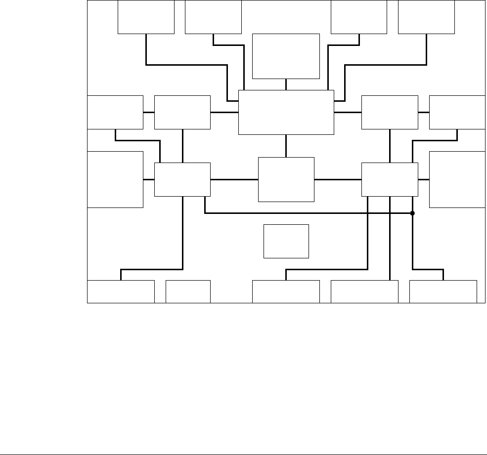
Introduction
ARM DDI 0301H Copyright © 2004-2009 ARM Limited. All rights reserved. 1-8
ID012310 Non-Confidential, Unrestricted Access
1.5 Components of the processor
The main components of the ARM1176JZF-S processor are:
•Integer core
•Load Store Unit (LSU) on page 1-11
•Prefetch unit on page 1-11
•Memory system on page 1-12
•AMBA AXI interface on page 1-16
•Coprocessor interface on page 1-17
•Debug on page 1-17
•Instruction cycle summary and interlocks on page 1-19
•Vector Floating-Point (VFP) on page 1-19
•System control on page 1-21
•Interrupt handling on page 1-21.
Figure 1-1 shows the structure of the ARM1176JZF-S processor.
Figure 1-1 ARM1176JZF-S processor block diagram
1.5.1 Integer core
The ARM1176JZF-S processor is built around the ARM11 integer core. It is an implementation
of the ARMv6 architecture, that runs the ARM, Thumb, and Java instruction sets. The processor
contains EmbeddedICE-RT™ logic and a JTAG debug interface to enable hardware debuggers to
communicate with the processor. The following sections describe the core in more detail:
•Instruction set categories on page 1-9
•Conditional execution on page 1-9
ARM1176JZF-S
L2 instruction
interface
Vector Floating
Point Coprocessor
Instruction
Cache
ETM interface
Memory
management
unit
Load Store
Unit
Data
Cache
Prefetch
Unit
Integer
core
L1 data side
controller
Power
control
L2 data
interface
L2 DMA
interface
Peripheral
port
JTAG interface Coprocessor
interface VIC interface
Data
TCM
Instruction
TCM
L1 instruction
side controller
System
metrics

Introduction
ARM DDI 0301H Copyright © 2004-2009 ARM Limited. All rights reserved. 1-9
ID012310 Non-Confidential, Unrestricted Access
•Registers
•Modes and exceptions
•Thumb instruction set on page 1-10
•DSP instructions on page 1-10
•Media extensions on page 1-10
•Datapath on page 1-10
•Branch prediction on page 1-11
•Return stack on page 1-11.
Instruction set categories
The main instruction set categories are:
• branch instructions
• data processing instructions
• status register transfer instructions
• load and store instructions
• coprocessor instructions.
• exception-generating instructions.
Note
Only load, store, and swap instructions can access data from memory.
Conditional execution
The processor conditionally executes nearly all ARM instructions. You can decide if the
condition code flags, Negative, Zero, Carry, and Overflow, are updated according to their result.
Registers
The ARM1176JZF-S core contains:
• 33 general-purpose 32-bit registers
• 7 dedicated 32-bit registers.
Note
At any one time, 16 general-purpose registers are visible. The remainder are banked registers
used to speed up exception processing.
Modes and exceptions
The core provides a set of operating and exception modes, to support systems combining
complex operating systems, user applications, and real-time demands. There are eight operating
modes, six of them are exception processing modes:
•User
• Supervisor
• fast interrupt
• normal interrupt
•abort
•system
• Undefined

Introduction
ARM DDI 0301H Copyright © 2004-2009 ARM Limited. All rights reserved. 1-10
ID012310 Non-Confidential, Unrestricted Access
• Secure Monitor.
Thumb instruction set
The Thumb instruction set contains a subset of the most commonly-used 32-bit ARM
instructions encoded into 16-bit wide opcodes. This reduces the amount of memory required for
instruction storage.
DSP instructions
The DSP extensions to the ARM instruction set provide:
• 16-bit data operations
• saturating arithmetic
• MAC operations.
The processor executes multiply instructions using a single-cycle 32x16 implementation. The
processor can perform 32x32, 32x16, and 16x16 multiply instructions (MAC).
Media extensions
The ARMv6 instruction set provides media instructions to complement the DSP instructions.
There are four media instruction groups:
• Multiplication instructions for handling 16-bit and 32-bit data, including
dual-multiplication instructions that operate on both 16-bit halves of their source registers.
This group includes an instruction that improves the performance and size of code for
multi-word unsigned multiplications.
•Single Instruction Multiple Data (SIMD) Instructions to perform operations on pairs of
16-bit values held in a single register, or on sets of four 8-bit values held in a single
register. The main operations supplied are addition and subtraction, selection, pack, and
saturation.
• Instructions to extract bytes and halfwords from registers and zero-extend or sign-extend
them. These include a parallel extraction of two bytes followed by extension of each byte
to a halfword.
• Unsigned Sum-of-Absolute-Differences (SAD) instructions. This is used in MPEG motion
estimation.
Datapath
The datapath consists of three pipelines:
• ALU, shift and Sat pipeline
• MAC pipeline
• load or store pipeline, see Load Store Unit (LSU) on page 1-11.
ALU, shift or Sat pipe
The ALU, shift and Sat pipeline executes most of the ALU operations, and includes a 32-bit
barrel shifter. It consists of three pipeline stages:
Shift The Shift stage contains the full barrel shifter. This stage performs all shifts,
including those required by the LSU.
The Shift stage implements saturating left shift that doubles the value of an
operand and saturates it.

Introduction
ARM DDI 0301H Copyright © 2004-2009 ARM Limited. All rights reserved. 1-11
ID012310 Non-Confidential, Unrestricted Access
ALU The ALU stage performs all arithmetic and logic operations, and generates the
condition codes for instructions that set these flags.
The ALU stage consists of a logic unit, an arithmetic unit, and a flag generator.
The pipeline logic evaluates the flag settings in parallel with the main adder in the
ALU. The flag generator is enabled only on flag-setting operations.
The ALU stage separates the carry chains of the main adder for 8-bit and 16-bit
SIMD instructions.
Sat The Sat stage implements the saturation logic required by the various classes of
DSP instructions.
MAC pipe
The MAC pipeline executes all of the enhanced multiply, and multiply-accumulate instructions.
The MAC unit consists of a 32x16 multiplier and an accumulate unit that is configured to
calculate the sum of two 16x16 multiplies. The accumulate unit has its own dedicated single
register read port for the accumulate operand.
To minimize power consumption, the processor only clocks each of the MAC and ALU stages
when required.
Return stack
The processor includes a three-entry return stack to accelerate returns from procedure calls. For
each procedure call, the processor pushes the return address onto a hardware stack. When the
processor recognizes a procedure return, the processor pops the address held in the return stack
that the prefetch unit uses as the predicted return address.
Note
See Pipeline stages on page 1-26 for details of the pipeline stages and instruction progression.
See Chapter 3 System Control Coprocessor for system control coprocessor programming
information.
1.5.2 Load Store Unit (LSU)
The Load Store Unit (LSU) manages all load and store operations. The load-store pipeline
decouples loads and stores from the MAC and ALU pipelines.
When the processor issues LDM and STM instructions to the LSU pipeline, other instructions
run concurrently, subject to the requirements of supporting precise exceptions.
1.5.3 Prefetch unit
The prefetch unit fetches instructions from the instruction cache, Instruction TCM, or from
external memory and predicts the outcome of branches in the instruction stream.
See Chapter 5 Program Flow Prediction for more details.
Branch prediction
The core uses both static and dynamic branch prediction. All branches are predicted where the
target address is an immediate address, or fixed-offset PC-relative address.

Introduction
ARM DDI 0301H Copyright © 2004-2009 ARM Limited. All rights reserved. 1-12
ID012310 Non-Confidential, Unrestricted Access
The first level of branch prediction is dynamic, through a 128-entry Branch Target Address
Cache (BTAC). If the PC of a branch matches an entry in the BTAC, the processor uses the
branch history and the target address to fetch the new instruction stream.
The processor might remove dynamically predicted branches from the instruction stream, and
might execute such branches in zero cycles.
If the address mappings are changed, the BTAC must be flushed. A BTAC flush instruction is
provided in the CP15 coprocessor.
The processor uses static branch prediction to manage branches not matched in the BTAC. The
static branch predictor makes a prediction based on the direction of the branches.
1.5.4 Memory system
The level-one memory system provides the core with:
• separate instruction and data caches
• separate instruction and data Tightly-Coupled Memories
• 64-bit datapaths throughout the memory system
• virtually indexed, physically tagged caches
• memory access controls and virtual memory management
• support for four sizes of memory page
• two-channel DMA into TCMs
• I-fetch, D-read/write interface, compatible with multi-layer AMBA AXI
• 32-bit dedicated peripheral interface
• export of memory attributes for second-level memory system.
The following sections describe the memory system in more detail:
•Instruction and data caches
•Cache power management on page 1-13
•Instruction and data TCM on page 1-13
•TCM DMA engine on page 1-14
•DMA features on page 1-14
•Memory Management Unit on page 1-14.
Instruction and data caches
The core provides separate instruction and data caches. The cache has the following features:
• Independent configuration of the instruction and data cache during synthesis to sizes
between 4KB and 64KB.
• 4-way set-associative instruction and data caches. You can lock each way independently.
• Pseudo-random or round-robin replacement.
• Eight word cache line length.
• The MicroTLB entry determines whether cache lines are write-back or write-through.
• Ability to disable each cache independently, using the system control coprocessor.
• Data cache misses that are non-blocking. The processor supports up to three outstanding
data cache misses.
• Streaming of sequential data from LDM and LDRD operations, and sequential instruction
fetches.

Introduction
ARM DDI 0301H Copyright © 2004-2009 ARM Limited. All rights reserved. 1-13
ID012310 Non-Confidential, Unrestricted Access
• Critical word first filling of the cache on a cache-miss.
• You can implement all the cache RAM blocks, and the associated tag and valid RAM
blocks using standard ASIC RAM compilers. This ensures optimum area and
performance of your design.
• Each cache line is marked with a Secure or Non-secure tag that defines if the line contains
Secure or Non-secure data.
Cache power management
To reduce power consumption, the core uses sequential cache operations to reduce the number
of full cache reads. If a cache read is sequential to the previous cache read, and the read is within
the same cache line, only the data RAM set that was previously read is accessed. The core does
not access tag RAM during sequential cache operations.
To reduce unnecessary power consumption additionally, the core only reads the addressed
words within a cache line at any time.
Instruction and data TCM
Because some applications might not respond well to caching, configurable memory blocks are
provided for Instruction and Data Tightly Coupled Memories (TCMs). These ensure high-speed
access to code or data.
An Instruction TCM typically holds an interrupt or exception code that the processor must
access at high speed, without any potential delay resulting from a cache miss.
A Data TCM typically holds a block of data for intensive processing, such as audio or video
processing.
You can configure each TCM to be Secure or Non-secure.
Level one memory system
You can separately configure the size of the Instruction TCM (ITCM) and the size of the Data
TCM (DTCM) to be 0KB, 4KB. 8KB, 16KB, 32KB or 64KB. For each side (ITCM and DTCM):
• If you configure the TCM size to be 4KB you get one TCM, of 4KB, on this side.
• If you configure the TCM size to be larger than 4KB you get two TCMs on this side, each
of half the configured size. So, for example, if you configure an ITCM size of 16KB you
get two ITCMs, each of size 8KB.
Table 1-1 lists all possible TCM configurations. See Configurable options on page 1-25 for
more information about configuring your ARM1176JZF-S implementation.
Table 1-1 TCM configurations
Configured TCM size Number of TCMs Size of each TCM
0KB 0 0
4KB 1 4KB
8KB 2 4KB

Introduction
ARM DDI 0301H Copyright © 2004-2009 ARM Limited. All rights reserved. 1-14
ID012310 Non-Confidential, Unrestricted Access
The TCM can be anywhere in the memory map. The INITRAM pin enables booting from the
ITCM.
See Chapter 7 Level One Memory System for more details.
TCM DMA engine
To support use of the TCMs by data-intensive applications, the core provides two DMA
channels to transfer data to or from the Instruction or Data TCM blocks. DMA can proceed in
parallel with CPU accesses to the TCM blocks. Arbitration is on a cycle-by-cycle basis. The
DMA channels connect with the System-on-Chip (SoC) backplane through a dedicated 64-bit
AMBA AXI port.
The DMA controller is programmed using the CP15 system-control coprocessor. DMA accesses
can only be to or from the TCM, and an external memory. There is no coherency support with
the caches.
Note
Only one of the two DMA channels can be active at any time.
DMA features
The DMA controller has the following features:
• runs in background of CPU operations
• enables CPU priority access to TCM during DMA
• programmed with Virtual Addresses
• controls DMA to either the instruction or data TCM
• allocated by a privileged process (OS)
• software can check and monitor DMA progress
• interrupts on DMA event
• ability to configure each channel to transfer data between Secure TCM and Secure
external memory.
Memory Management Unit
The Memory Management Unit (MMU) has a unified Translation Lookaside Buffer (TLB) for
both instructions and data. The MMU includes a 4KB page mapping size to enable a smaller
RAM and ROM footprint for embedded systems and operating systems such as WindowsCE
that have many small mapped objects. The ARM1176JZF-S processor implements the Fast
Context Switch Extension (FCSE) and high vectors extension that are required to run Microsoft
WindowsCE. See Chapter 6 Memory Management Unit for more details.
16KB 2 8KB
32KB 2 16KB
64KB 2 32KB
Table 1-1 TCM configurations (continued)
Configured TCM size Number of TCMs Size of each TCM

Introduction
ARM DDI 0301H Copyright © 2004-2009 ARM Limited. All rights reserved. 1-15
ID012310 Non-Confidential, Unrestricted Access
The MMU is responsible for protection checking, address translation, and memory attributes,
and some of these can be passed to an external level two memory system. The memory
translations are cached in MicroTLBs for each of the instruction and data caches, with a single
Main TLB backing the MicroTLBs.
The MMU has the following features:
• matches Virtual Address, ASID, and NSTID
• each TLB entry is marked with the NSTID
• checks domain access permissions
• checks memory attributes
• translates virtual-to-physical address
• supports four memory page sizes
• maps accesses to cache, TCM, peripheral port, or external memory
• hardware handles TLB misses
• software control of TLB.
Paging
Four page sizes are supported:
• 16MB super sections
• 1MB sections
• 64KB large pages
• 4KB small pages.
Domains
Sixteen access domains are supported.
TLB
A two-level TLB structure is implemented. Eight entries in the main TLB are lockable.
Hardware TLB loading is supported, and is backwards compatible with previous versions of the
ARM architecture.
ASIDs
TLB entries can be global, or can be associated with particular processes or applications using
Application Space IDentifiers (ASIDs). ASIDs enable TLB entries to remain resident during
context switches to avoid subsequent reload of TLB entries and also enable task-aware
debugging.
NSTID
TrustZone extensions enable the system to mark each entry in the TLB as Secure or Non-secure
with the Non-secure Table IDentifier (NSTID).
System control coprocessor
Cache, TCM, and DMA operations are controlled through a dedicated coprocessor, CP15,
integrated within the core. This coprocessor provides a standard mechanism for configuring the
level one memory system, and also provides functions such as memory barrier instructions. See
System control on page 1-21 for more details.

Introduction
ARM DDI 0301H Copyright © 2004-2009 ARM Limited. All rights reserved. 1-16
ID012310 Non-Confidential, Unrestricted Access
1.5.5 AMBA AXI interface
The bus interface provides high bandwidth connections between the processor, second level
caches, on-chip RAM, peripherals, and interfaces to external memory.
There are separate bus interfaces for:
• instruction fetch, 64-bit data
• data read/write, 64-bit data
• peripheral access, 32-bit data
• DMA, 64-bit data.
All interfaces are AMBA AXI compatible. This enables them to be merged in smaller systems.
Additional signals are provided on each port to support second-level cache.
The ports support the following bus transactions:
Instruction fetch
Servicing instruction cache misses and noncacheable instruction fetches.
Data read/write
Servicing data cache misses, hardware handled TLB misses, cache eviction and
noncacheable data reads and writes.
DMA Servicing the DMA engine for writing and reading the TCMs. This behaves as a
single bidirectional port.
These ports enable several simultaneous outstanding transactions, providing:
• high performance from second-level memory systems that support parallelism
• high use of pipelined and multi-page memories such as SDRAM.
The following sections describe the AMBA AXI interface in more detail:
•Bus clock speeds
•Unaligned accesses
•Mixed-endian support
•Write buffer on page 1-17
•Peripheral port on page 1-17.
Bus clock speeds
The bus interface ports operate synchronously to the CPU clock if IEM is not implemented.
Unaligned accesses
The core supports unaligned data access. Words and halfwords can align to any byte boundary.
This enables access to compacted data structures with no software overhead. This is useful for
multi-processor applications and reducing memory space requirements.
The Bus Interface Unit (BIU) automatically generates multiple bus cycles for unaligned
accesses.
Mixed-endian support
The core provides the option of switching between little-endian and byte invariant big endian
data access modes. This means the core can share data with big-endian systems, and improves
the way the core manages certain types of data.

Introduction
ARM DDI 0301H Copyright © 2004-2009 ARM Limited. All rights reserved. 1-17
ID012310 Non-Confidential, Unrestricted Access
Write buffer
All memory writes take place through the write buffer. The write buffer decouples the CPU
pipeline from the system bus for external memory writes. Memory reads are checked for
dependency against the write buffer contents.
Peripheral port
The peripheral port is a 32-bit AMBA AXI interface that provides direct access to local,
Non-shared devices separately. The peripheral port does not use the main bus system. The
memory regions that these non-shared devices use are marked as Device and Non-Shared.
Accesses to these memory regions are routed to the peripheral port instead of to the data
read-write ports.
See Chapter 8 Level Two Interface for more details.
1.5.6 Coprocessor interface
The ARM1176JZF-S processor connects to external coprocessors through the coprocessor
interface. This interface supports all ARM coprocessor instructions:
•LDC
•LDCL
•STC
•STCL
•MRC
• MRRC
•MCR
• MCRR
•CDP.
The memory system returns data for all loads to coprocessors in the order of the accesses in the
program. The processor suppresses HUM operation of the cache for coprocessor instructions.
The external coprocessor interface relies on the coprocessor executing all its instructions in
order.
Externally-connected coprocessors follow the early stages of the core pipeline to permit the
exchange of instructions and data between the two pipelines. The coprocessor runs one pipeline
stage behind the core pipeline.
To prevent the coprocessor interface introducing critical paths, wait states can be inserted in
external coprocessor operations. These wait states enable critical signals to be retimed.
The VFP unit connects to the internal coprocessor interface that has different timings and
behavior, using controlled delays for internal interconnections.
Chapter 11 Coprocessor Interface describes the interface for on-chip coprocessors such as
floating-point or other application-specific hardware acceleration units.
1.5.7 Debug
The ARM1176JZF-S core implements the ARMv6.1 Debug architecture that includes
extensions of the ARMv6 Debug architecture to support TrustZone. It introduces three levels of
debug:
• debug everywhere
• debug in Non-secure privileged and user, and Secure user

Introduction
ARM DDI 0301H Copyright © 2004-2009 ARM Limited. All rights reserved. 1-18
ID012310 Non-Confidential, Unrestricted Access
• debug in Non-secure only.
The debug coprocessor, CP14, implements a full range of debug features that Chapter 13 Debug
and Chapter 14 Debug Test Access Port describe.
The core provides extensive support for real-time debug and performance profiling.
The following sections describe debug in more detail:
•System performance monitoring
•ETM interface
•ETM trace buffer
•Software access to trace buffer
•Real-time debug facilities on page 1-19
•Debug and trace Environment on page 1-19.
System performance monitoring
This is a group of counters that you can configure to monitor the operation of the processor and
memory system. See System performance monitor on page 3-10 for more details.
ETM interface
You can connect an external Embedded Trace Macrocell (ETM) unit to the processor for
real-time code tracing of the core in an embedded system.
The ETM interface collects various processor signals and drives these signals from the core. The
interface is unidirectional and runs at the full speed of the core. The ETM interface connects
directly to the external ETM unit without any additional glue logic. You can disable the ETM
interface for power saving.
For more information see:
• the Embedded Trace Macrocell Architecture Specification
• Chapter 15 Trace Interface Port
• Appendix A Signal Descriptions, for details of ETM-related signals.
ETM trace buffer
You can extend the functionality of the ETM by adding an on-chip trace buffer. The trace buffer
is an on-chip memory area. The trace buffer stores trace information during capture that
otherwise passes immediately through the trace port at the operating frequency of the core.
When capture is complete the stored information can be read out at a reduced clock rate from
the trace buffer using the JTAG port of the SoC, instead of through a dedicated trace port.
This is a two-step process that avoids you implementing a wide trace port that has many
high-speed device pins. In effect, a zero-pin trace port is created where the device already has a
JTAG port and associated pins.
Software access to trace buffer
You can access buffered trace information through an APB slave-based memory-mapped
peripheral included as part of the trace buffer. You can perform internal diagnostics on a closed
system where a JTAG port is not normally brought out.

Introduction
ARM DDI 0301H Copyright © 2004-2009 ARM Limited. All rights reserved. 1-19
ID012310 Non-Confidential, Unrestricted Access
Real-time debug facilities
The ARM1176JZF-S processor contains an EmbeddedICE-RT logic unit that provides the
following real-time debug facilities:
• up to six breakpoints
• thread-aware breakpoints
• up to two watchpoints
•Debug Communications Channel (DCC).
The EmbeddedICE-RT logic connects directly to the core and monitors the internal address and
data buses. You can access the EmbeddedICE-RT logic in one of two ways:
• executing CP14 instructions
• through a JTAG-style interface and associated TAP controller.
The EmbeddedICE-RT logic supports two modes of debug operation:
Halting debug-mode
On a debug event, such as a breakpoint or watchpoint, the debug logic stops the
core and forces the core into Debug state. This enables you to examine the internal
state of the core, and the external state of the system, independently from other
system activity. When the debugging process completes, the core and system state
is restored, and normal program execution resumes.
Monitor debug-mode
On a debug event, the core generates a debug exception instead of entering Debug
state, as in Halting debug-mode. The exception entry activates a debug monitor
program that performs critical interrupt service routines to debug the processor.
The debug monitor program communicates with the debug host over the DCC.
Debug and trace Environment
Several external hardware and software tools are available for you to enable:
• real-time debugging using the EmbeddedICE-RT logic
• execution trace using the ETM.
1.5.8 Instruction cycle summary and interlocks
Chapter 16 Cycle Timings and Interlock Behavior describes instruction cycles and gives
examples of interlock timing.
1.5.9 Vector Floating-Point (VFP)
The VFP coprocessor supports floating point arithmetic operations and is a functional block
within the ARM1176JZF-S processor. The VFP coprocessor is mapped as coprocessor numbers
10 and 11. Software can determine whether the VFP is present by the use of the Coprocessor
Access Control Register. See c1, Coprocessor Access Control Register on page 3-51 for more
details.
The VFP implements the ARM VFPv2 floating point coprocessor instruction set. It supports
single and double-precision arithmetic on vector-vector, vector-scalar, and scalar-scalar data
sets. Vectors can consist of up to eight single-precision, or four double-precision elements.
The VFP has its own bank of 32 registers for single-precision operands that you can:
• use in pairs for double-precision operands
• operate loads and stores of VFP registers in parallel with arithmetic operations.

Introduction
ARM DDI 0301H Copyright © 2004-2009 ARM Limited. All rights reserved. 1-20
ID012310 Non-Confidential, Unrestricted Access
The VFP supports a wide range of single and double precision operations, including ABS, NEG,
COPY, MUL, MAC, DIV, and SQRT. The VFP effectively executes most of these in a single
cycle. Table 1-2 lists the exceptions. These issue latencies also apply to individual elements in
a vector operation.
Compliance with the IEEE 754 standard
The VFP supports all five floating point exceptions defined by the IEEE 754 standard:
• invalid operation
• divide by zero
•overflow
• underflow
• inexact.
You can individually enable or disable these exception traps. If disabled, the default results
defined by IEEE 754 are returned. All rounding modes are supported, and basic single and basic
double formats are used.
For full compliance, the VFP requires support code to handle arithmetic where operands or
results are de-norms. This support code is normally installed on the Undefined instruction
exception handler.
Flush-to-zero mode
A flush-to-zero mode is provided where a default treatment of de-norms is applied. Table 1-3
lists the default behavior in flush-to-zero mode.
Operations not supported
The following operations are not directly supported by the VFP:
• remainder
• binary (decimal) conversions
• direct comparisons between single and double-precision values.
These are normally implemented as C library functions.
Table 1-2 Double-precision VFP operations
Instruction types Issue latency
DP MUL and MAC 2 cycle
SP DIV, SQRT 14 cycles
DP DIV, SQRT 28 cycles
All other instructions 1 cycle
Table 1-3 Flush-to-zero mode
Operation Flush-to-zero
De-norm operand(s) Treated as 0+. Inexact flag set.
De-norm result Returned as 0+. Inexact Flag set.

Introduction
ARM DDI 0301H Copyright © 2004-2009 ARM Limited. All rights reserved. 1-21
ID012310 Non-Confidential, Unrestricted Access
1.5.10 System control
The control of the memory system and its associated functionality, and other system-wide
control attributes are managed through a dedicated system control coprocessor, CP15. See
System control and configuration on page 3-5 for more details.
1.5.11 Interrupt handling
Interrupt handling in the ARM1176JZF-S processor is compatible with previous ARM
architectures, but has several additional features to improve interrupt performance for real-time
applications.
The following sections describe interrupt handling in more detail:
•Vectored Interrupt Controller port
•Low interrupt latency configuration
•Configuration on page 1-22
•Exception processing enhancements on page 1-22.
Note
The nIRQ and nFIQ signals are level-sensitive and must be held LOW until a suitable interrupt
response is received from the processor.
Vectored Interrupt Controller port
The core has a dedicated port that enables an external interrupt controller, such as the ARM
Vectored Interrupt Controller (VIC), to supply a vector address along with an interrupt request
(IRQ) signal. This provides faster interrupt entry but you can disable it for compatibility with
earlier interrupt controllers.
Low interrupt latency configuration
This mode minimizes the worst-case interrupt latency of the processor, with a small reduction
in peak performance, or instructions-per-cycle. You can tune the behavior of the core to suit the
requirements of the application.
The low interrupt latency configuration disables HUM operation of the cache. In low interrupt
latency configuration, on receipt of an interrupt, the ARM1176JZF-S processor:
• abandons any pending restartable memory operations
• restarts memory operations on return from the interrupt.
To obtain maximum benefit from the low interrupt latency configuration, software must only use
multi-word load or store instructions that are fully restartable. The software must not use
multi-word load or store instructions on memory locations that produce side-effects for the type
of access concerned. This applies to:
ARM LDC, all forms of LDM, LDRD, and STC, and all forms of STM and STRD.
Thumb LDMIA, STMIA, PUSH, and POP.
To achieve optimum interrupt latency, memory locations accessed with these instructions must
not have large numbers of wait-states associated with them. To minimize the interrupt latency,
the following is recommended:
• multiple accesses to areas of memory marked as Device or Strongly Ordered must not be
performed

Introduction
ARM DDI 0301H Copyright © 2004-2009 ARM Limited. All rights reserved. 1-22
ID012310 Non-Confidential, Unrestricted Access
• access to slow areas of memory marked as Device or Strongly Ordered must not be
performed. That is, those that take many cycles in generating a response
• SWP operations must not be performed to slow areas of memory.
Configuration
You configure the processor for low interrupt latency mode by use of the system control
coprocessor. To ensure that a change between normal and low interrupt latency configurations
is synchronized correctly, you must use software systems that only change the configuration
while interrupts are disabled.
Exception processing enhancements
The ARMv6 architecture contains several enhancements to exception processing, to reduce
interrupt handler entry and exit time:
SRS Save return state to a specified stack frame.
RFE Return from exception.
CPS Directly modify the CPSR.
Note
With TrustZone, in Non-secure state, specifying Secure Monitor mode in the
<mode>
field of the
SRS
instruction causes the processor to take the Undefined exception.

Introduction
ARM DDI 0301H Copyright © 2004-2009 ARM Limited. All rights reserved. 1-23
ID012310 Non-Confidential, Unrestricted Access
1.6 Power management
The ARM1176JZF-S processor includes several micro-architectural features to reduce energy
consumption:
• Accurate branch and return prediction, reducing the number of incorrect instruction fetch
and decode operations.
• Use of physically tagged caches that reduce the number of cache flushes and refills, to
save energy in the system.
• The use of MicroTLBs reduces the power consumed in translation and protection
look-ups for each memory access.
• The caches use sequential access information to reduce the number of accesses to the Tag
RAMs and to unmatched data RAMs.
• Extensive use of gated clocks and gates to disable inputs to unused functional blocks.
Because of this, only the logic actively in use to perform a calculation consumes any
dynamic power.
• Optionally supports IEM. The ARM1176JZF-S is separated into three different blocks to
support three different power domains:
—all the RAMS
— the core logic that is clocked by CLKIN and FREECLKIN
— four optional IEM Register Slices to have an asynchronous interface between the
Level 2 ports powered by VCore and clocked by CLKIN, and the AXI system
powered by VSoc and clocked by ACLK clocks, one for each port.
The ARM1176JZF-S processor support four levels of power management:
Run mode This mode is the normal mode of operation when the processor can use all its
functions.
Standby mode
This mode disables most of the processor clocks of the device, while processor
remains powered up. This reduces the power drawn to the static leakage current,
plus a tiny clock power overhead required to enable the processor to wake up from
the standby state. One of the following events cause a transition from the standby
mode to the run mode:
• an interrupt, either masked or unmasked
• a debug request, regardless of whether debug is enabled
• reset.
Shutdown mode
This mode powers down the entire processor. The processor must save all states,
including cache and TCM state, externally. The processor is returned to the run
state by the assertion of reset. The processor saves the states with interrupts
disabled, and finishes with a Data Synchronization Barrier operation. The
ARM1176JZF-S processor then communicates with the power controller that it is
ready to be powered down.

Introduction
ARM DDI 0301H Copyright © 2004-2009 ARM Limited. All rights reserved. 1-24
ID012310 Non-Confidential, Unrestricted Access
Dormant mode
This mode powers down the processor and leaves the caches and the TCM
powered up and maintaining their state. The valid bits remain visible to software
to enable you to implement dormant mode. For full implementation of dormant
mode you must:
• modify the RAM blocks to include an input clamp
• implement separate power domains.
For full implementation of dormant mode see ARM1176JZF-S and ARM1176JZ-S
Implementation Guide.
For more details of power management features see Chapter 10 Power Control.

Introduction
ARM DDI 0301H Copyright © 2004-2009 ARM Limited. All rights reserved. 1-25
ID012310 Non-Confidential, Unrestricted Access
1.7 Configurable options
Note
These options are configurable features of your ARM1176JZF-S processor implementation.
They are not programmable options of the implemented device.
Table 1-4 lists the ARM1176JZF-S processor configurable options.
In addition, the form of the BIST solution for the RAM blocks in the ARM1176JZF-S design is
determined when the processor is implemented. For details, see the ARM11 Memory Built-In
Self Test Controller Technical Reference Manual.
Table 1-5 lists the default configuration of ARM1176JZF-S processor.
Table 1-4 Configurable options
Feature Range of options
IEM support Yes or No
Cache way size 1KB, 2KB, 4KB, 8KB, or 16KB
Number of cache ways 4, not configurable
TCM block size 4KB, 8KB, 16KB, or 32KB
Number of TCM blocks 0, or auto-configuresa to 1, or 2
a. Number of TCM blocks depends only on the size of the
TCM RAM.
Table 1-5 ARM1176JZF-S processor default configurations
Feature Default value
IEM support No
Cache way size 4KB
Number of cache ways 4
TCM block size 8KB
Number of TCM blocks 2

Introduction
ARM DDI 0301H Copyright © 2004-2009 ARM Limited. All rights reserved. 1-26
ID012310 Non-Confidential, Unrestricted Access
1.8 Pipeline stages
Figure 1-2 shows:
• the two Fetch stages
• a Decode stage
• an Issue stage
• the four stages of the ARM1176JZF-S integer execution pipeline.
These eight stages make up the processor pipeline.
Figure 1-2 ARM1176JZF-S pipeline stages
From Figure 1-2, the pipeline operations are:
Fe1 First stage of instruction fetch where address is issued to memory and data returns
from memory
Fe2 Second stage of instruction fetch and branch prediction.
De Instruction decode.
Iss Register read and instruction issue.
Sh Shifter stage.
ALU Main integer operation calculation.
Sat Pipeline stage to enable saturation of integer results.
WBex Write back of data from the multiply or main execution pipelines.
MAC1 First stage of the multiply-accumulate pipeline.
MAC2 Second stage of the multiply-accumulate pipeline.
MAC3 Third stage of the multiply-accumulate pipeline.
ADD Address generation stage.
DC1 First stage of data cache access.
DC2 Second stage of data cache access.
WBls Write back of data from the Load Store Unit.
By overlapping the various stages of operation, the ARM1176JZF-S processor maximizes the
clock rate achievable to execute each instruction. It delivers a throughput approaching one
instruction for each cycle.
1st fetch
stage
2nd fetch
stage
Instruction
decode
Reg. read
and issue
Shifter
stage
ALU
operation
Saturation
stage
Writeback
Mul/ALU
Fe1 Fe2 De Iss Sh ALU Sat WBex
1st multiply
acc. stage
2nd multiply
acc. stage
MAC1 MAC2 MAC3
Address
generation
Data
cache 1
Data
cache 2
Writeback
from LSU
ADD DC1 DC2 WBls
3rd multiply
acc. stage

Introduction
ARM DDI 0301H Copyright © 2004-2009 ARM Limited. All rights reserved. 1-27
ID012310 Non-Confidential, Unrestricted Access
The Fetch stages can hold up to four instructions, where branch prediction is performed on
instructions ahead of execution of earlier instructions.
The Issue and Decode stages can contain any instruction in parallel with a predicted branch.
The Execute, Memory, and Write stages can contain a predicted branch, an ALU or multiply
instruction, a load/store multiple instruction, and a coprocessor instruction in parallel execution.
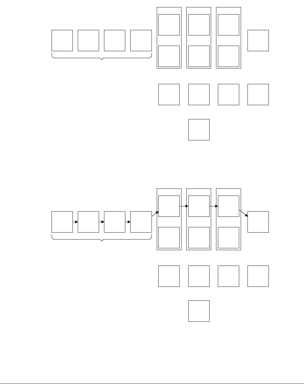
Introduction
ARM DDI 0301H Copyright © 2004-2009 ARM Limited. All rights reserved. 1-28
ID012310 Non-Confidential, Unrestricted Access
1.9 Typical pipeline operations
Figure 1-3 shows all the operations in each of the pipeline stages in the ALU pipeline, the
load/store pipeline, and the HUM buffers.
Figure 1-3 Typical operations in pipeline stages
Figure 1-4 shows a typical ALU data processing instruction. The processor does not use the
load/store pipeline or the HUM buffer.
Figure 1-4 Typical ALU operation
Figure 1-5 on page 1-29 shows a typical multiply operation. The MUL instruction can loop in
the MAC1 stage until it has passed through the first part of the multiplier array enough times.
The MUL instruction progresses to MAC2 and MAC3 where it passes through the second half
of the array once to produce the final result.
MAC1
1st
multiply
stage
Sh
Shifter
operation
Ex1
1st fetch
stage
Fe1 Fe2 De Iss WBex
DC1 DC2
2nd fetch
stage
Instruction
decode
Register
read and
instruction
issue
Base
register
writeback
Data
address
calculation
First stage
of data
cache
access
Second
stage of
data cache
access
Writeback
from LSU
Load miss
waits
ADD WBls
Common decode pipeline
MAC2
2nd
multiply
stage
ALU
Calculate
writeback
value
Ex2
MAC3
3rd
multiply
stage
Sat
Saturation
Ex3
ALU
pipeline
Load/store
pipeline
Hit under
miss
Multiply
pipeline
MAC3
Not used
Sat
Saturation
Ex3
MAC2
Not used
ALU
Calculate
writeback
value
Ex2
MAC1
Not used
Sh
Shifter
operation
Ex1
1st fetch
stage
Fe1 Fe2 De Iss WBex
2nd fetch
stage
Instruction
decode
Register
read and
instruction
issue
Base
register
writeback
Not used
Common decode pipeline
Not used
ADD DC1
Not used
DC2
Not used Not used
WBls
ALU
pipeline
Load/store
pipeline
Hit under
miss
Multiply
pipeline
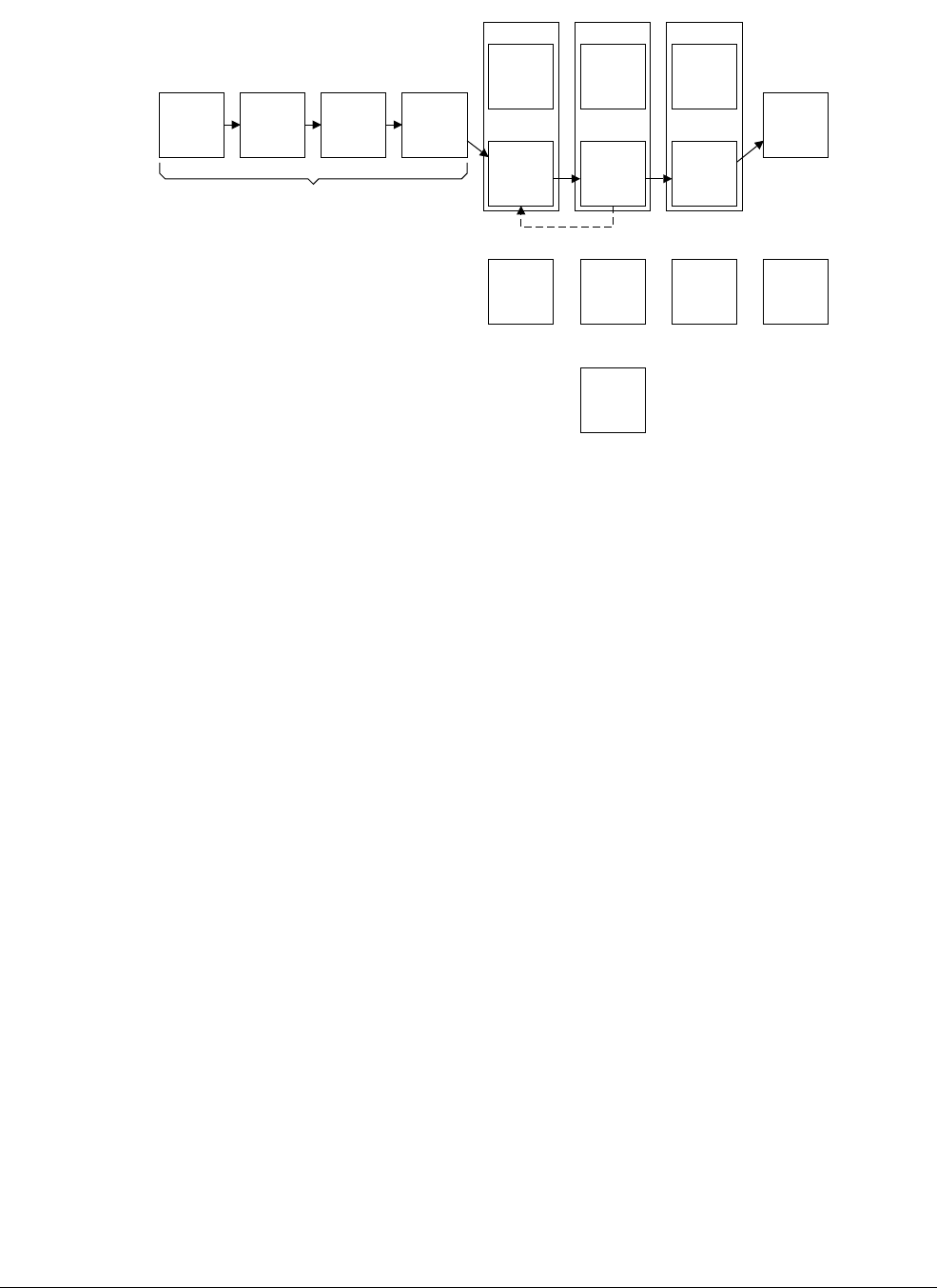
Introduction
ARM DDI 0301H Copyright © 2004-2009 ARM Limited. All rights reserved. 1-29
ID012310 Non-Confidential, Unrestricted Access
Figure 1-5 Typical multiply operation
MAC3
3rd
multiply
stage
Sat
Not used
Ex3
MAC2
2nd
multiply
stage
ALU
Not used
Ex2
MAC1
1st
multiply
stage
Sh
Not used
Ex1
1st fetch
stage
Fe1 Fe2 De Iss
2nd fetch
stage
Instruction
decode
Register
read and
instruction
issue
Not used
Common decode pipeline
WBex
Base
register
writeback
Not used
ADD DC1
Not used
DC2
Not used Not used
WBls
ALU
pipeline
Load/store
pipeline
Hit under
miss
Multiply
pipeline
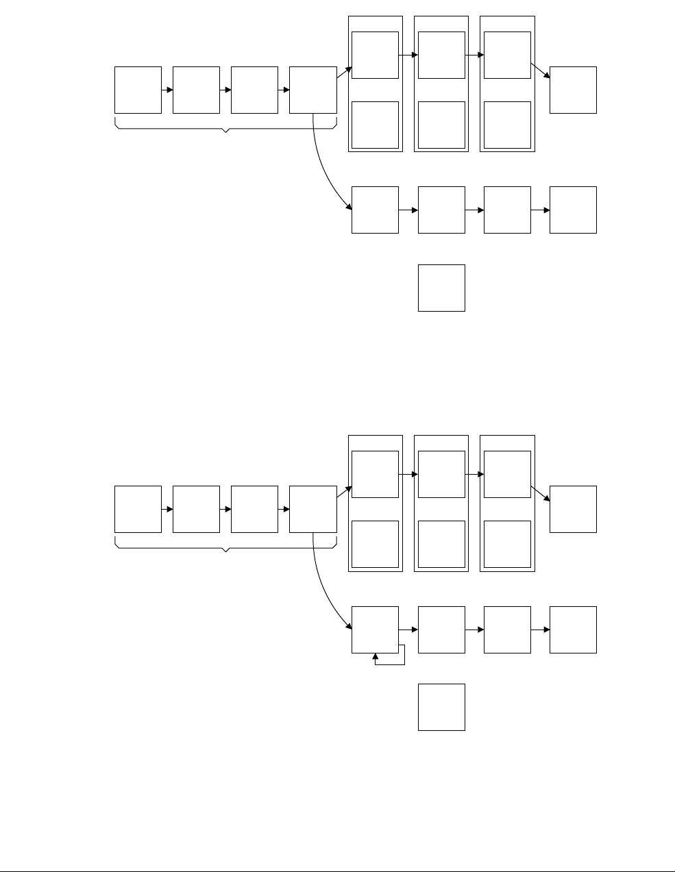
Introduction
ARM DDI 0301H Copyright © 2004-2009 ARM Limited. All rights reserved. 1-30
ID012310 Non-Confidential, Unrestricted Access
1.9.1 Instruction progression
Figure 1-6 shows an LDR/STR operation that hits in the data cache.
Figure 1-6 Progression of an LDR/STR operation
Figure 1-7 shows the progression of an LDM/STM operation that completes by use of the
load/store pipeline. Other instructions can use the ALU pipeline at the same time as the
LDM/STM completes in the load/store pipeline.
Figure 1-7 Progression of an LDM/STM operation
Figure 1-8 on page 1-31 shows the progression of an LDR that misses. When the LDR is in the
HUM buffers, other instructions, including independent loads that hit in the cache, can run under
it.
MAC3
Not used
Sat
Saturation
Ex3
MAC2
Not used
ALU
Calculate
writeback
value
Ex2
MAC1
Not used
Sh
Shifter
operation
Ex1
1st fetch
stage
Fe1 Fe2 De Iss
2nd fetch
stage
Instruction
decode
Register
read and
instruction
issue
Not used
Common decode pipeline
Data
address
calculation
ADD DC1
First stage
of data
cache
access
DC2
Second
stage of
data cache
access
Writeback
from LSU
WBls
WBex
Base
register
writeback
ALU
pipeline
Load/store
pipeline
Hit under
miss
Multiply
pipeline
MAC3
Not used
Sat
Saturation
Ex3
MAC2
Not used
ALU
Calculate
writeback
value
Ex2
MAC1
Not used
Sh
Shifter
operation
Ex1
1st fetch
stage
Fe1 Fe2 De Iss
2nd fetch
stage
Instruction
decode
Register
read and
instruction
issue
Not used
unless a
miss
occurs
Common decode pipeline
WBex
Base
register
writeback
Data
address
calculation
ADD DC1
First stage
of data
cache
access
DC2
Second
stage of
data cache
access
Writeback
from LSU
WBls
ALU
pipeline
Load/store
pipeline
Hit under
miss
Multiply
pipeline
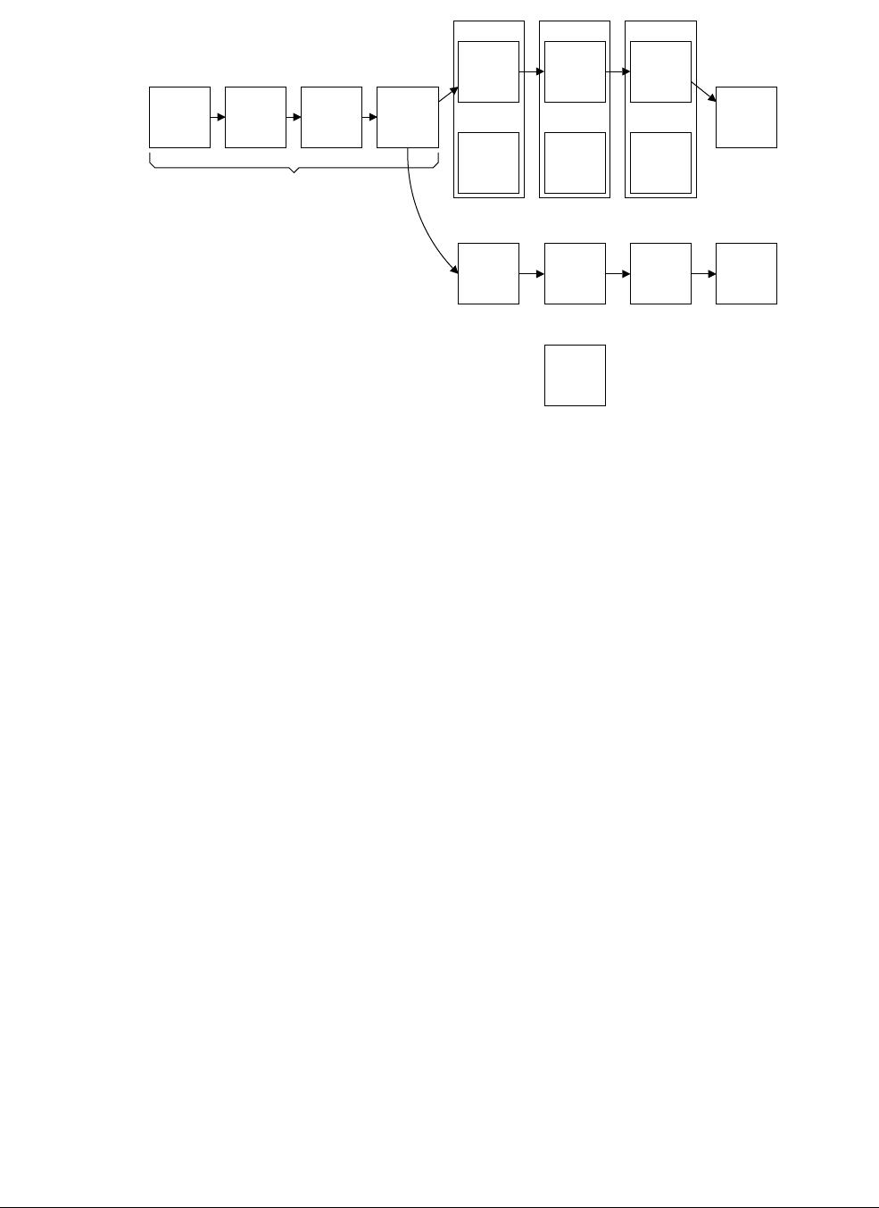
Introduction
ARM DDI 0301H Copyright © 2004-2009 ARM Limited. All rights reserved. 1-31
ID012310 Non-Confidential, Unrestricted Access
Figure 1-8 Progression of an LDR that misses
See Chapter 16 Cycle Timings and Interlock Behavior for details of instruction cycle timings.
MAC3
Not used
Sat
Saturation
Ex3
MAC2
Not used
ALU
Calculate
writeback
value
Ex2
MAC1
Not used
Sh
Shifter
operation
Ex1
1st fetch
stage
Fe1 Fe2 De Iss WBex
DC1 DC2
2nd fetch
stage
Instruction
decode
Register
read and
instruction
issue
Base
register
writeback
Data
address
calculation
Writeback
from LSU
ADD WBls
ALU
pipeline
Load/store
pipeline
Hit under
miss
Common decode pipeline
Multiply
pipeline
First stage
of data
cache
access
Second
stage of
data cache
access
Load
9,10
1234
567
8
561112

Introduction
ARM DDI 0301H Copyright © 2004-2009 ARM Limited. All rights reserved. 1-32
ID012310 Non-Confidential, Unrestricted Access
1.10 ARM1176JZF-S instruction set summary
This section provides:
•an Extended ARM instruction set summary on page 1-33
•a Thumb instruction set summary on page 1-44.
Table 1-6 lists a key to the ARM and Thumb instruction set tables.
The ARM1176JZF-S processor implements the ARM architecture v6 with ARM Jazelle
technology. For a description of the ARM and Thumb instruction sets, see the ARM Architecture
Reference Manual. Contact ARM Limited for complete descriptions of all instruction sets.
Table 1-6 Key to instruction set tables
Symbol Description
{!}
Update base register after operation if ! present.
{^}
For all STMs and LDMs that do not load the PC, stores or restores the User mode banked registers
instead of the current mode registers if ^ present, and sets the S bit. For LDMs that load the PC,
indicates that the CPSR is loaded from the SPSR.
B
Byte operation.
H
Halfword operation.
T
Forces execution to be handled as having User mode privilege. Cannot be used with pre-indexed
addresses.
x Selects HIGH or LOW 16 bits of register Rm. T selects the HIGH 16 bits,
T = top, and B selects the LOW 16 bits, B = bottom.
y Selects HIGH or LOW 16 bits of register Rs. T selects the HIGH 16 bits,
T = top, and B selects the LOW 16 bits, B = bottom.
{cond}
Updates condition flags if cond present. See Table 1-15 on page 1-43.
{field}
See Table 1-14 on page 1-43.
{S}
Sets condition codes, optional.
<a_mode2>
See Table 1-8 on page 1-40.
<a_mode2P>
See Table 1-9 on page 1-41.
<a_mode3>
See Table 1-10 on page 1-42.
<a_mode4>
See Table 1-11 on page 1-42.
<a_mode5>
See Table 1-12 on page 1-42.
<cp_num>
One of the coprocessors p0 to p15.
<effect>
Specifies the effect required on the interrupt disable bits, A, I, and F in the CPSR:
IE = Interrupt enable
ID = Interrupt disable.
<
iflags
> specifies the bits affected if
<effect>
is specified.
<endian_specifier>
BE = Set E bit in instruction, set CPSR E bit.
LE = Reset E bit in instruction, clear CPSR E bit.
<HighReg>
Specifies a register in the range R8 to R15.

Introduction
ARM DDI 0301H Copyright © 2004-2009 ARM Limited. All rights reserved. 1-33
ID012310 Non-Confidential, Unrestricted Access
1.10.1 Extended ARM instruction set summary
Table 1-7 summarizes the extended ARM instruction set.
<iflags>
A sequence of one or more of the following:
a = Set A bit.
i = Set I bit.
f = Set F bit.
If
<effect>
is specified, the sequence determines the interrupt flags that are affected.
<immed_8*4>
A 10-bit constant, formed by left-shifting an 8-bit value by two bits.
<immed_8>
An 8-bit constant.
<immed_8r>
A 32-bit constant, formed by right-rotating an 8-bit value by an even number of bits.
<label>
The target address to branch to.
<LowReg>
Specifies a register in the range R0 to R7.
<mode>
The new mode number for a mode change. See Mode bits on page 2-28.
<op1>
,
<op2>
Specify, in a coprocessor-specific manner, the coprocessor operation to perform.
<operand2>
See Table 1-13 on page 1-43.
<option>
Specifies additional instruction options to the coprocessor. An integer in the range 0 to 255
surrounded by { and }.
<reglist>
A comma-separated list of registers, enclosed in braces {and}.
<rotation>
One of
ROR
#8,
ROR
#16, or
ROR
#24.
<Rm>
Specifies the register, the value of which is the instruction operand.
<Rn>
Specifies the address of the base register.
<shift>
Specifies the optional shift. If present, it must be one of:
•
LSL #N
.
N
must be in the range 0 to 31.
•
ASR #N
.
N
must be in the range 1 to 32.
Table 1-6 Key to instruction set tables (continued)
Symbol Description
Table 1-7 ARM instruction set summary
Operation Assembler
Arithmetic Add
ADD{cond}{S} <Rd>, <Rn>, <operand2>
Add with carry
ADC{cond}{S} <Rd>, <Rn>, <operand2>
Subtract
SUB{cond}{S} <Rd>, <Rn>, <operand2>
Subtract with carry
SBC{cond}{S} <Rd>, <Rn>, <operand2>
Reverse subtract
RSB{cond}{S} <Rd>, <Rn>, <operand2>
Reverse subtract with carry
RSC{cond}{S} <Rd>, <Rn>, <operand2>
Multiply
MUL{cond}{S} <Rd>, <Rm>, <Rs>
Multiply-accumulate
MLA{cond}{S} <Rd>, <Rm>, <Rs>, <Rn>

Introduction
ARM DDI 0301H Copyright © 2004-2009 ARM Limited. All rights reserved. 1-34
ID012310 Non-Confidential, Unrestricted Access
Multiply unsigned long
UMULL{cond}{S} <RdLo>, <RdHi>, <Rm>, <Rs>
Multiply unsigned accumulate long
UMLAL{cond}{S} <RdLo>, <RdHi>, <Rm>, <Rs>
Multiply signed long
SMULL{cond}{S} <RdLo>, <RdHi>, <Rm>, <Rs>
Multiply signed accumulate long
SMLAL{cond}{S} <RdLo>, <RdHi>, <Rm>, <Rs>
Saturating add
QADD{cond} <Rd>, <Rm>, <Rn>
Saturating add with double
QDADD{cond} <Rd>, <Rm>, <Rn>
Saturating subtract
QSUB{cond} <Rd>, <Rm>, <Rn>
Saturating subtract with double
QDSUB{cond} <Rd>, <Rm>, <Rn>
Multiply 16x16
SMULxy{cond} <Rd>, <Rm>, <Rs>
Multiply-accumulate 16x16+32
SMLAxy{cond} <Rd>, <Rm>, <Rs>, <Rn>
Multiply 32x16
SMULWy{cond} <Rd>, <Rm>, <Rs>
Multiply-accumulate 32x16+32
SMLAWy{cond} <Rd>, <Rm>, <Rs>, <Rn>
Multiply signed
accumulate long 16x16+64
SMLALxy{cond} <RdLo>, <RdHi>, <Rm>, <Rs>
Count leading zeros
CLZ{cond} <Rd>, <Rm>
Compare Compare
CMP{cond} <Rn>, <operand2>
Compare negative
CMN{cond} <Rn>, <operand2>
Logical Move
MOV{cond}{S} <Rd>, <operand2>
Move NOT
MVN{cond}{S} <Rd>, <operand2>
Test
TST{cond} <Rn>, <operand2>
Test equivalence
TEQ{cond} <Rn>, <operand2>
AND
AND{cond}{S} <Rd>, <Rn>, <operand2>
XOR
EOR{cond}{S} <Rd>, <Rn>, <operand2>
OR
ORR{cond}{S} <Rd>, <Rn>, <operand2>
Bit clear
BIC{cond}{S} <Rd>, <Rn>, <operand2>
Copy
CPY{<cond>} <Rd>, <Rm>
Branch Branch
B{cond} <label>
Branch with link
BL{cond} <label>
Branch and exchange
BX{cond} <Rm>
Branch, link and exchange
BLX <label>
Branch, link and exchange
BLX{cond} <Rm>
Branch and exchange to Jazelle
state
BXJ{cond} <Rm>
Table 1-7 ARM instruction set summary (continued)
Operation Assembler

Introduction
ARM DDI 0301H Copyright © 2004-2009 ARM Limited. All rights reserved. 1-35
ID012310 Non-Confidential, Unrestricted Access
Status register
handling
Move SPSR to register
MRS{cond} <Rd>, SPSR
Move CPSR to register
MRS{cond} <Rd>, CPSR
Move register to SPSR
MSR{cond} SPSR_{field}, <Rm>
Move register to CPSR
MSR{cond} CPSR_{field}, <Rm>
Move immediate to SPSR flags
MSR{cond} SPSR_{field}, #<immed_8r>
Move immediate to CPSR flags
MSR{cond} CPSR_{field}, #<immed_8r>
Load Word
LDR{cond} <Rd>, <a_mode2>
Word with User mode privilege
LDR{cond}T <Rd>, <a_mode2P>
PC as destination, branch and
exchange
LDR{cond} R15, <a_mode2P>
Byte
LDR{cond}B <Rd>, <a_mode2>
Byte with User mode privilege
LDR{cond}BT <Rd>, <a_mode2P>
Byte signed
LDR{cond}SB <Rd>, <a_mode3>
Halfword
LDR{cond}H <Rd>, <a_mode3>
Halfword signed
LDR{cond}SH <Rd>, <a_mode3>
Doubleword
LDR{cond}D <Rd>, <a_mode3>
Return from exception
RFE<a_mode4> <Rn>{!}
Load multiple Stack operations
LDM{cond}<a_mode4L> <Rn>{!}, <reglist>
Increment before
LDM{cond}IB <Rn>{!}, <reglist>{^}
Increment after
LDM{cond}IA <Rn>{!}, <reglist>{^}
Decrement before
LDM{cond}DB <Rn>{!}, <reglist>{^}
Decrement after
LDM{cond}DA <Rn>{!}, <reglist>{^}
Stack operations and restore CPSR
LDM{cond}<a_mode4> <Rn>{!}, <reglist+pc>^
User registers
LDM{cond}<a_mode4> <Rn>{!}, <reglist>^
Soft preload Memory system hint
In Non-secure this instruction
behaves like a
NOP
PLD <a_mode2>
Store Word
STR{cond} <Rd>, <a_mode2>
Word with User mode privilege
STR{cond}T <Rd>, <a_mode2P>
Byte
STR{cond}B <Rd>, <a_mode2>
Byte with User mode privilege
STR{cond}BT <Rd>, <a_mode2P>
Halfword
STR{cond}H <Rd>, <a_mode3>
Doubleword
STR{cond}D <Rd>, <a_mode3>
Store return state
SRS<a_mode4> <mode>{!}
Table 1-7 ARM instruction set summary (continued)
Operation Assembler

Introduction
ARM DDI 0301H Copyright © 2004-2009 ARM Limited. All rights reserved. 1-36
ID012310 Non-Confidential, Unrestricted Access
Store multiple Stack operations
STM{cond}<a_mode4S> <Rn>{!}, <reglist>
User registers
STM{cond}<a_mode4S> <Rn>, <reglist>^
Increment before
STM{cond}IB, <Rn>{!}, <reglist>{^}
Increment after
STM{cond}IA, <Rn>{!}, <reglist>{^}
Decrement before
STM{cond}DB, <Rn>{!}, <reglist>{^}
Decrement after
STM{cond}DA, <Rn>{!}, <reglist>{^}
Swap Word
SWP{cond} <Rd>, <Rm>, [<Rn>]
Byte
SWP{cond}B <Rd>, <Rm>, [<Rn>]
Change state Change processor state
CPS<effect> <iflags>{, <mode>}
Change processor mode
CPS <mode>
Change endianness
SETEND <endian_specifier>
NOP-compatible
hints
No Operation
NOP{<cond>}
YIELD{<cond>}
Byte-reverse Byte-reverse word
REV{cond} <Rd>, <Rm>
Byte-reverse halfword
REV16{cond} <Rd>, <Rm>
Byte-reverse signed halfword
REVSH{cond} <Rd>, <Rm>
Synchronization
primitives
Load exclusive
LDREX{cond} <Rd>, [<Rn>
]
Store exclusive
STREX{cond} <Rd>, <Rm>, [<Rn>]
Load Byte Exclusive
LDREXB{cond} <Rxf>, [<Rbase>]
Load Halfword Exclusive
LDREXH{cond} <Rd>, [<Rn>]
Load Doubleword Exclusive
LDREXD{cond} <Rd>, [<Rn>]
Store Byte Exclusive
STREXB{cond} <Rd>, <Rm>, [<Rn>]
Store Halfword Exclusive
STREXH{cond} <Rd>, <Rm>, [<Rn>]
Store Doubleword Exclusive
STREXD{cond} <Rd>, <Rm>, [<Rn>]
Clear Exclusive
CLREX
Coprocessor Data operations
CDP{cond} <cp_num>, <op1>, <CRd>, <CRn>, <CRm>{, <op2>}
Move to ARM reg from coproc
MRC{cond} <cp_num>, <op1>, <Rd>, <CRn>, <CRm>{, <op2>}
Move to coproc from ARM reg
MCR{cond} <cp_num>, <op1>, <Rd>, <CRn>, <CRm>{, <op2>}
Move double to ARM reg
from coproc
MRRC{cond} <cp_num>, <op1>, <Rd>, <Rn>, <CRm>
Move double to coproc
from ARM reg
MCRR{cond} <cp_num>, <op1>, <Rd>, <Rn>, <CRm>
Load
LDC{cond} <cp_num>, <CRd>, <a_mode5>
Store
STC{cond} <cp_num>, <CRd>, <a_mode5>
Table 1-7 ARM instruction set summary (continued)
Operation Assembler

Introduction
ARM DDI 0301H Copyright © 2004-2009 ARM Limited. All rights reserved. 1-37
ID012310 Non-Confidential, Unrestricted Access
Alternative
coprocessor
Data operations
CDP2 <cp_num>, <op1>, <CRd>, <CRn>, <CRm>{, <op2>}
Move to ARM reg from coproc
MRC2 <cp_num>, <op1>, <Rd>, <CRn>, <CRm>{, <op2>}
Move to coproc from ARM reg
MCR2 <cp_num>, <op1>, <Rd>, <CRn>, <CRm>{, <op2>}
Move double to ARM reg
from coproc
MRRC2 <cp_num>, <op1>, <Rd>, <Rn>, <CRm>
Move double to coproc
from ARM reg
MCRR2 <cp_num>, <op1>, <Rd>, <Rn>, <CRm>
Load
LDC2 <cp_num>, <CRd>, <a_mode5>
Store
STC2 <cp_num>, <CRd>, <a_mode5>
Supervisor call
SVC{cond} <immed_24>
Secure Monitor call
SMC{cond} <immed_16>
Software breakpoint
BKPT <immed_16>
Parallel add
/subtract
Signed add high 16 + 16,
low 16 + 16, set GE flags
SADD16{cond} <Rd>, <Rn>, <Rm>
Saturated add high 16 + 16,
low 16 + 16
QADD16{cond} <Rd>, <Rn>, <Rm>
Signed high 16 + 16, low 16 + 16,
halved
SHADD16{cond} <Rd>, <Rn>, <Rm>
Unsigned high 16 + 16, low 16 +
16, set GE flags
UADD16{cond} <Rd>, <Rn>, <Rm>
Saturated unsigned high 16 + 16,
low 16 + 16
UQADD16{cond} <Rd>, <Rn>, <Rm>
Unsigned high 16 + 16,
low 16 + 16, halved
UHADD16{cond} <Rd>, <Rn>, <Rm>
Signed high 16 + low 16,
low 16 - high 16, set GE flags
SADDSUBX{cond} <Rd>, <Rn>, <Rm>
Saturated high 16 + low 16,
low 16 - high 16
QADDSUBX{cond} <Rd>, <Rn>, <Rm>
Signed high 16 + low 16,
low 16 - high 16, halved
SHADDSUBX{cond} <Rd>, <Rn>, <Rm>
Unsigned high 16 + low 16,
low 16 - high 16, set GE flags
UADDSUBX{cond} <Rd>, <Rn>, <Rm>
Saturated unsigned
high 16 + low 16, low 16 - high 16
UQADDSUBX{cond} <Rd>, <Rn>, <Rm>
Unsigned high 16 + low 16,
low 16 - high 16, halved
UHADDSUBX{cond} <Rd>, <Rn>, <Rm>
Signed high 16 - low 16,
low 16 + high 16, set GE flags
SSUBADDX{cond} <Rd>, <Rn>, <Rm>
Table 1-7 ARM instruction set summary (continued)
Operation Assembler

Introduction
ARM DDI 0301H Copyright © 2004-2009 ARM Limited. All rights reserved. 1-38
ID012310 Non-Confidential, Unrestricted Access
Saturated high 16 - low 16,
low 16 + high 16
QSUBADDX{cond} <Rd>, <Rn>, <Rm>
Signed high 16 - low 16,
low 16 + high 16, halved
SHSUBADDX{cond} <Rd>, <Rn>, <Rm>
Unsigned high 16 - low 16,
low 16 + high 16, set GE flags
USUBADDX{cond} <Rd>, <Rn>, <Rm>
Saturated unsigned
high 16 - low 16, low 16 + high 16
UQSUBADDX{cond} <Rd>, <Rn>, <Rm>
Unsigned high 16 - low 16,
low 16 + high 16, halved
UHSUBADDX{cond} <Rd>, <Rn>, <Rm>
Signed high 16-16, low 16-16,
set GE flags
SSUB16{cond} <Rd>, <Rn>, <Rm>
Saturated high 16 - 16, low 16 - 16
QSUB16{cond} <Rd>, <Rn>, <Rm>
Signed high 16 - 16, low 16 - 16,
halved
SHSUB16{cond} <Rd>, <Rn>, <Rm>
Unsigned high 16 - 16, low 16 - 16,
set GE flags
USUB16{cond} <Rd>, <Rn>, <Rm>
Saturated unsigned high 16 - 16,
low 16 - 16
UQSUB16{cond} <Rd>, <Rn>, <Rm>
Unsigned high 16 - 16, low 16 - 16,
halved
UHSUB16{cond} <Rd>, <Rn>, <Rm>
Four signed 8 + 8, set GE flags
SADD8{cond} <Rd>, <Rn>, <Rm>
Four saturated 8 + 8
QADD8{cond} <Rd>, <Rn>, <Rm>
Four signed 8 + 8, halved
SHADD8{cond} <Rd>, <Rn>, <Rm>
Four unsigned 8 + 8, set GE flags
UADD8{cond} <Rd>, <Rn>, <Rm>
Four saturated unsigned 8 + 8
UQADD8{cond} <Rd>, <Rn>, <Rm>
Four unsigned 8 + 8, halved
UHADD8{cond} <Rd>, <Rn>, <Rm>
Four signed 8 - 8, set GE flags
SSUB8{cond} <Rd>, <Rn>, <Rm>
Four saturated 8 - 8
QSUB8{cond} <Rd>, <Rn>, <Rm>
Four signed 8 - 8, halved
SHSUB8{cond} <Rd>, <Rn>, <Rm>
Four unsigned 8 - 8
USUB8{cond} <Rd>, <Rn>, <Rm>
Four saturated unsigned 8 - 8
UQSUB8{cond} <Rd>, <Rn>, <Rm>
Four unsigned 8 - 8, halved
UHSUB8{cond} <Rd>, <Rn>, <Rm>
Sum of absolute differences
USAD8{cond} <Rd>, <Rm>, <Rs>
Sum of absolute differences and
accumulate
USADA8{cond} <Rd>, <Rm>, <Rs>, <Rn>
Table 1-7 ARM instruction set summary (continued)
Operation Assembler

Introduction
ARM DDI 0301H Copyright © 2004-2009 ARM Limited. All rights reserved. 1-39
ID012310 Non-Confidential, Unrestricted Access
Sign/zero extend
and add
Two low 8/16, sign extend to 16 +
16
SXTAB16{cond} <Rd>, <Rn>, <Rm>{, <rotation>}
Low 8/32, sign extend to 32, + 32
SXTAB{cond} <Rd>, <Rn>, <Rm>{, <rotation>}
Low 16/32, sign extend to 32, + 32
SXTAH{cond} <Rd>, <Rn>, <Rm>{, <rotation>}
Two low 8/16, zero extend
to 16, + 16
UXTAB16{cond} <Rd>, <Rn>, <Rm>{, <rotation>}
Low 8/32, zero extend to 32, + 32
UXTAB{cond} <Rd>, <Rn>, <Rm>{, <rotation>}
Low 16/32, zero extend to 32, + 32
UXTAH{cond} <Rd>, <Rn>, <Rm>{, <rotation>}
Two low 8, sign extend to 16,
packed 32
SXTB16{cond} <Rd>, <Rm>{, <rotation>}
Low 8, sign extend to 32
SXTB{cond} <Rd>, <Rm>{, <rotation>}
Low 16, sign extend to 32
SXTH{cond} <Rd>, <Rm>{, <rotation>}
Two low 8, zero extend to 16,
packed 32
UXTB16{cond} <Rd>, <Rm>,{, <rotation>}
Low 8, zero extend to 32
UXTB{cond} <Rd>, <Rm>{, <rotation>}
Low 16, zero extend to 32
UXTH{cond} <Rd>, <Rm>{, <rotation>}
Signed multiply
and multiply,
accumulate
Signed
(high 16 x 16) + (low 16 x 16) + 32,
and set Q flag.
SMLAD{cond} <Rd>, <Rm>, <Rs>, <Rn>
As
SMLAD
, but high x low,
low x high, and set Q flag
SMLADX{cond} <Rd>, <Rm>, <Rs>, <Rn>
Signed
(high 16 x 16) - (low 16 x 16) + 32
SMLSD{cond} <Rd>, <Rm>, <Rs>, <Rn>
As
SMLSD
, but high x low,
low x high
SMLSDX{cond} <Rd>, <Rm>, <Rs>, <Rn>
Signed
(high 16 x 16) + (low 16 x 16) + 64
SMLALD{cond} <RdLo>, <RdHi>, <Rm>, <Rs>
As
SMLALD
, but high x low,
low x high
SMLALDX{cond} <RdLo>, <RdHi>, <Rm>, <Rs>
Signed
(high 16 x 16) - (low 16 x 16) + 64
SMLSLD{cond} <RdLo>, <RdHi>, <Rm>, <Rs>
As
SMLSLD
, but high x low,
low x high
SMLSLDX{cond} <RdLo>, <RdHi>, <Rm>, <Rs>
32 + truncated high 16 (32 x 32)
SMMLA{cond} <Rd>, <Rm>, <Rs>, <Rn>
32 + rounded high 16 (32 x 32)
SMMLAR{cond} <Rd>, <Rm>, <Rs>, <Rn>
32 - truncated high 16 (32 x 32)
SMMLS{cond} <Rd>, <Rm>, <Rs>, <Rn>
32 -rounded high 16 (32 x 32)
SMMLSR{cond} <Rd>, <Rm>, <Rs>, <Rn>
Table 1-7 ARM instruction set summary (continued)
Operation Assembler

Introduction
ARM DDI 0301H Copyright © 2004-2009 ARM Limited. All rights reserved. 1-40
ID012310 Non-Confidential, Unrestricted Access
Table 1-8 summarizes addressing mode 2.
Signed (high 16 x 16) +
(low 16 x 16), and set Q flag
SMUAD{cond} <Rd>, <Rm>, <Rs>
As
SMUAD
, but high x low,
low x high, and set Q flag
SMUADX{cond} <Rd>, <Rm>, <Rs>
Signed (high 16 x 16) -
(low 16 x 16)
SMUSD{cond} <Rd>, <Rm>, <Rs>
As
SMUSD
, but high x low,
low x high
SMUSDX{cond} <Rd>, <Rm>, <Rs>
Truncated high 16 (32 x 32)
SMMUL{cond} <Rd>, <Rm>, <Rs>
Rounded high 16 (32 x 32)
SMMULR{cond} <Rd>, <Rm>, <Rs>
Unsigned 32 x 32, + two 32, to 64
UMAAL{cond} <RdLo>, <RdHi>, <Rm>, <Rs>
Saturate, select,
and pack
Signed saturation at
bit position n
SSAT{cond} <Rd>, #<immed_5>, <Rm>{, <shift>}
Unsigned saturation at
bit position n
USAT{cond} <Rd>, #<immed_5>, <Rm>{, <shift>}
Two 16 signed saturation at
bit position n
SSAT16{cond} <Rd>, #<immed_4>, <Rm>
Two 16 unsigned saturation at
bit position n
USAT16{cond} <Rd>, #<immed_4>, <Rm>
Select bytes from
Rn
/
Rm
based
on GE flags
SEL{cond} <Rd>, <Rn>, <Rm>
Pack low 16/32, high 16/32
PKHBT{cond} <Rd>, <Rn>, <Rm>{, LSL #<immed_5>}
Pack high 16/32, low 16/32
PKHTB{cond} <Rd>, <Rn>, <Rm>{, ASR #<immed_5>}
Table 1-7 ARM instruction set summary (continued)
Operation Assembler
Table 1-8 Addressing mode 2
Addressing mode Assembler
Offset -
Immediate offset
[<Rn>, #+/<immed_12>]
Zero offset
[<Rn>]
Register offset
[<Rn>, +/-<Rm>]
Scaled register offset
[<Rn>, +/-<Rm>, LSL #<immed_5>]
[<Rn>, +/-<Rm>, LSR #<immed_5>]
[<Rn>, +/-<Rm>, ASR #<immed_5>]
[<Rn>, +/-<Rm>, ROR #<immed_5>]
[<Rn>, +/-<Rm>, RRX]

Introduction
ARM DDI 0301H Copyright © 2004-2009 ARM Limited. All rights reserved. 1-41
ID012310 Non-Confidential, Unrestricted Access
Table 1-9 summarizes addressing mode 2P, post-indexed only.
Pre-indexed offset -
Immediate offset
[<Rn>], #+/<immed_12>
Zero offset
[<Rn>]
Register offset
[<Rn>, +/-<Rm>]
!
Scaled register offset
[<Rn>, +/-<Rm>, LSL #<immed_5>]
!
[<Rn>, +/-<Rm>, LSR #<immed_5>]
!
[<Rn>, +/-<Rm>, ASR #<immed_5>]
!
[<Rn>, +/-<Rm>, ROR #<immed_5>]
!
[<Rn>, +/-<Rm>, RRX]
!
Post-indexed offset -
Immediate
[<Rn>], #+/-<immed_12>
Zero offset
[<Rn>]
Register offset
[<Rn>], +/-<Rm>
Scaled register offset
[<Rn>], +/-<Rm>, LSL #<immed_5>
[<Rn>], +/-<Rm>, LSR #<immed_5>
[<Rn>], +/-<Rm>, ASR #<immed_5>
[<Rn>], +/-<Rm>, ROR #<immed_5>
[<Rn>], +/-<Rm>, RRX
Table 1-9 Addressing mode 2P, post-indexed only
Addressing mode Assembler
Post-indexed offset -
Immediate offset
[<Rn>], #+/-<immed_12>
Zero offset
[<Rn>]
Register offset
[<Rn>], +/-<Rm>
Scaled register offset
[<Rn>], +/-<Rm>, LSL #<immed_5>
[<Rn>], +/-<Rm>, LSR #<immed_5>
[<Rn>], +/-<Rm>, ASR #<immed_5>
[<Rn>], +/-<Rm>, ROR #<immed_5>
[<Rn>], +/-<Rm>, RRX
Table 1-8 Addressing mode 2 (continued)
Addressing mode Assembler

Introduction
ARM DDI 0301H Copyright © 2004-2009 ARM Limited. All rights reserved. 1-42
ID012310 Non-Confidential, Unrestricted Access
Table 1-10 summarizes addressing mode 3.
Table 1-11 summarizes addressing mode 4.
Table 1-12 summarizes addressing mode 5.
Table 1-10 Addressing mode 3
Addressing mode Assembler
Immediate offset
[<Rn>, #+/-<immed_8>]
Pre-indexed
[<Rn>, #+/-<immed_8>]!
Post-indexed
[<Rn>], #+/-<immed_8>
Register offset
[<Rn>, +/- <Rm>]
Pre-indexed
[<Rn>, +/- <Rm>]!
Post-indexed
[<Rn>], +/- <Rm>
Table 1-11 Addressing mode 4
Addressing mode Stack type
Block load Stack pop (LDM, RFE)
IA Increment after FD Full descending
IB Increment before E
D
Empty descending
DA Decrement after FA Full ascending
DB Decrement before E
A
Empty ascending
Block store Stack push (STM, SRS)
IA IA Increment after E
A
Empty ascending
IB IB Increment before FA Full ascending
DA DA Decrement after E
D
Empty descending
DB DB Decrement before FD Full descending
Table 1-12 Addressing mode 5
Addressing mode Assembler
Immediate offset
[<Rn>, #+/-<immed_8*4>]
Immediate pre-indexed
[<Rn>, #+/-<immed_8*4>]!
Immediate pre-indexed
[<Rn>], #+/-<immed_8*4>
Unindexed
[<Rn>], <option>

Introduction
ARM DDI 0301H Copyright © 2004-2009 ARM Limited. All rights reserved. 1-43
ID012310 Non-Confidential, Unrestricted Access
Table 1-13 summarizes Operand2 assembler.
Table 1-14 summarizes the MSR instruction fields.
Table 1-15 summarizes condition codes.
Table 1-13 Operand2
Operation Assembler
Immediate value
#<immed_8r>
Logical shift left
<Rm> LSL #<immed_5>
Logical shift right
<Rm> LSR #<immed_5>
Arithmetic shift right
<Rm> ASR #<immed_5>
Rotate right
<Rm> ROR #<immed_5>
Register
<Rm>
Logical shift left
<Rm> LSL <Rs>
Logical shift right
<Rm> LSR <Rs>
Arithmetic shift right
<Rm> ASR <Rs>
Rotate right
<Rm> ROR <Rs>
Rotate right extended
<Rm> RRX
Table 1-14 Fields
Suffix Sets this bit in the MSR field_mask MSR instruction bit number
c
Control field mask bit, bit 0 16
x
Extension field mask bit, bit 1 17
s
Status field mask bit, bit 2 18
f
Flags field mask bit, bit 3 19
Table 1-15 Condition codes
Suffix Description
EQ
Equal
NE
Not equal
HS/CS
Unsigned higher or same, carry set
LO/CC
Unsigned lower, carry clear
MI
Negative, minus
PL
Positive or zero, plus
VS
Overflow
VC
No overflow
HI
Unsigned higher

Introduction
ARM DDI 0301H Copyright © 2004-2009 ARM Limited. All rights reserved. 1-44
ID012310 Non-Confidential, Unrestricted Access
1.10.2 Thumb instruction set summary
Table 1-16 summarizes the Thumb instruction set.
LS
Unsigned lower or same
GE
Signed greater or equal
LT
Signed less than
GT
Signed greater than
LE
Signed less than or equal
AL
Always
Table 1-15 Condition codes (continued)
Suffix Description
Table 1-16 Thumb instruction set summary
Operation Assembler
Move Immediate, update flags
MOV <Rd>, #<immed_8>
LowReg to LowReg, update flags
MOV <Rd>, <Rm>
HighReg to LowReg
MOV <Rd>, <Rm>
LowReg to HighReg
MOV <Rd>, <Rm>
HighReg to HighReg
MOV <Rd>, <Rm>
Copy
CPY <Rd>, <Rm>
Arithmetic Add
ADD <Rd>, <Rn>, #<immed_3>
Add immediate
ADD <Rd>, #<immed_8>
Add LowReg and LowReg, update flags
ADD <Rd>, <Rn>, <Rm>
Add HighReg to LowReg
ADD <Rd>, <Rm>
Add LowReg to HighReg
ADD <Rd>, <Rm>
Add HighReg to HighReg
ADD <Rd>, <Rm>
Add immediate to PC
ADD <Rd>, PC, #<immed_8*4>
Add immediate to SP
ADD <Rd>, SP, #<immed_8*4>
Add immediate to SP
ADD SP, #<immed_7*4>
ADD SP, SP, #<immed_7*4>
Add with carry
ADC <Rd>, <Rs>
Subtract immediate
SUB <Rd>, <Rn>, #<immed_3>
Subtract immediate
SUB <Rd>, #<immed_8>
Subtract
SUB <Rd>, <Rn>, <Rm>
Subtract immediate from SP
SUB SP, #<immed_7*4>
Subtract with carry
SBC <Rd>, <Rm>

Introduction
ARM DDI 0301H Copyright © 2004-2009 ARM Limited. All rights reserved. 1-45
ID012310 Non-Confidential, Unrestricted Access
Negate
NEG <Rd>, <Rm>
Multiply
MUL <Rd>, <Rm>
Compare Compare immediate
CMP <Rn>, #<immed_8>
Compare LowReg and LowReg, update flags
CMP <Rn>, <Rm>
Compare LowReg and HighReg, update flags
CMP <Rn>, <Rm>
Compare HighReg and LowReg, update flags
CMP <Rn>, <Rm>
Compare HighReg and HighReg, update flags
CMP <Rn>, <Rm>
Compare negative
CMN <Rn>, <Rm>
Logical AND
AND <Rd>, <Rm>
XOR
EOR <Rd>, <Rm>
OR
ORR <Rd>, <Rm>
Bit clear
BIC <Rd>, <Rm>
Move NOT
MVN <Rd>, <Rm>
Test bits
TST <Rd>, <Rm>
Shift/Rotate Logical shift left
LSL <Rd>, <Rm>, #<immed_5>
LSL <Rd>, <Rs>
Logical shift right
LSR <Rd>, <Rm>, #<immed_5>
LSR <Rd>, <Rs>
Arithmetic shift right
ASR <Rd>, <Rm>, #<immed_5>
ASR <Rd>, <Rs>
Rotate right
ROR <Rd>, <Rs>
Branch Conditional
B{cond} <label>
Unconditional
B <label>
Branch with link
BL <label>
Branch, link and exchange
BLX <label>
Branch, link and exchange
BLX <Rm>
Branch and exchange
BX <Rm>
Load With immediate offset -
Word
LDR <Rd>, [<Rn>, #<immed_5*4>]
Halfword
LDRH <Rd>, [<Rn>, #<immed_5*2>]
Byte
LDRB <Rd>, [<Rn>, #<immed_5>]
With register offset -
Word
LDR <Rd>, [<Rn>, <Rm>]
Halfword
LDRH <Rd>, [<Rn>, <Rm>]
Table 1-16 Thumb instruction set summary (continued)
Operation Assembler

Introduction
ARM DDI 0301H Copyright © 2004-2009 ARM Limited. All rights reserved. 1-46
ID012310 Non-Confidential, Unrestricted Access
Signed halfword
LDRSH <Rd>, [<Rn>, <Rm>]
Byte
LDRB <Rd>, [<Rn>, <Rm>]
Signed byte
LDRSB <Rd>, [<Rn>, <Rm>]
PC-relative
LDR <Rd>, [PC, #<immed_8*4>]
SP-relative
LDR <Rd>, [SP, #<immed_8*4>]
Multiple
LDMIA <Rn>!, <reglist>
Store With immediate offset -
Word
STR <Rd>, [<Rn>, #<immed_5*4>]
Halfword
STRH <Rd>, [<Rn>, #<immed_5*2>]
Byte
STRB <Rd>, [<Rn>, #<immed_5>]
With register offset -
Word
STR <Rd>, [<Rn>, <Rm>]
Halfword
STRH <Rd>, [<Rn>, <Rm>]
Byte
STRB <Rd>, [<Rn>, <Rm>]
SP-relative
STR <Rd>, [SP, #<immed_8*4>]
Multiple
STMIA <Rn>!, <reglist>
Push/Pop Push registers onto stack
PUSH <reglist>
Push LR and registers onto stack
PUSH <reglist, LR>
Pop registers from stack
POP <reglist>
Pop registers and PC from stack
POP <reglist, PC>
Change state Change processor state
CPS <effect> <iflags>
Change endianness
SETEND <endian_specifier>
Byte-reverse Byte-reverse word
REV <Rd>, <Rm>
Byte-reverse halfword
REV16 <Rd>, <Rm>
Byte-reverse signed halfword
REVSH <Rd>, <Rm>
Supervisor call
SVC <immed_8>
Software breakpoint
BKPT <immed_8>
Sign or zero extend Sign extend 16 to 32
SXTH<Rd>, <Rm>
Sign extend 8 to 32
SXTB<Rd>, <Rm>
Zero extend 16 to 32
UXTH<Rd>, <Rm>
Zero extend 8 to 32
UXTB<Rd>, <Rm>
Table 1-16 Thumb instruction set summary (continued)
Operation Assembler

Introduction
ARM DDI 0301H Copyright © 2004-2009 ARM Limited. All rights reserved. 1-47
ID012310 Non-Confidential, Unrestricted Access
1.11 Product revisions
This section describes differences in functionality between product revisions of the
ARM1176JZF-S processor:
r0p0-r0p1 Contains the following differences:
• The addition of the CPUCLAMP input in r0p1 to better support IEM. See
Intelligent Energy Management on page 10-7.
• The top level RTL hierarchy has been changed in r0p1 to better support
IEM. See Intelligent Energy Management on page 10-7.
• The architectural clock gating scheme for the generation of clock dedicated
to the RAMs has been changed. For more information see the description
of the RAM interface implementation in the ARM1176JZF-S™ and
ARM1176JZ-S™ Implementation Guide.
r0p1-r0p2 There are no functional differences between r0p1 and r0p2.
r0p2-r0p4 There are no functional differences between r0p2 and r0p4.
r0p4-r0p6 Between r0p4 and r0p6 there are no differences in the functionality described in
this Technical Reference Manual. However, r0p6 introduces optional top-level
latches, for implementing Dormant mode or IEM with cell libraries that do not
provide retention latches. For more information see the description of Dormant
mode implementation in the ARM1176JZF-S™ and ARM1176JZ-S™
Implementation Guide.
r0p6-r0p7 There are no functional differences between r0p6 and r0p7.
Note
Product revisions r0p3 and r0p5 were not generally available.

ARM DDI 0301H Copyright © 2004-2009 ARM Limited. All rights reserved. 2-1
ID012310 Non-Confidential, Unrestricted Access
Chapter 2
Programmer’s Model
This chapter describes the processor registers and provides information for programming the
microprocessor. It contains the following sections:
•About the programmer’s model on page 2-2
•Secure world and Non-secure world operation with TrustZone on page 2-3
•Processor operating states on page 2-12
•Instruction length on page 2-13
•Data types on page 2-14
•Memory formats on page 2-15
•Addresses in a processor system on page 2-16
•Operating modes on page 2-17
•Registers on page 2-18
•The program status registers on page 2-24
•Additional instructions on page 2-30
•Exceptions on page 2-36
•Software considerations on page 2-59.

Programmer’s Model
ARM DDI 0301H Copyright © 2004-2009 ARM Limited. All rights reserved. 2-2
ID012310 Non-Confidential, Unrestricted Access
2.1 About the programmer’s model
The ARM1176JZF-S processors implement ARM architecture v6 with Java extensions and
TrustZone™ security extensions.
The architecture includes the 32-bit ARM instruction set, 16-bit Thumb instruction set, and the
8-bit Java instruction set. For details of both the ARM and Thumb instruction sets, see the ARM
Architecture Reference Manual. For the Java instruction set see the Jazelle V1 Architecture
Reference Manual.
TrustZone provides Secure and Non-secure worlds for software to operate in. For more details
see Secure world and Non-secure world operation with TrustZone on page 2-3 and the ARM
Architecture Reference Manual.
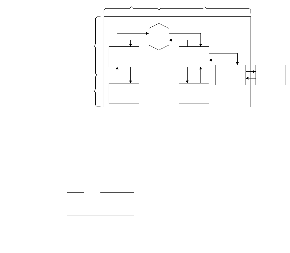
Programmer’s Model
ARM DDI 0301H Copyright © 2004-2009 ARM Limited. All rights reserved. 2-3
ID012310 Non-Confidential, Unrestricted Access
2.2 Secure world and Non-secure world operation with TrustZone
This section describes;
•TrustZone model
•How the Secure model works on page 2-4.
For more details on TrustZone and the ARM architecture, see the ARM Architecture Reference
Manual.
2.2.1 TrustZone model
The basis of the TrustZone model is that the computing environment splits into two isolated
worlds, the Secure world and the Non-secure world, with no leakage of Secure data to the
Non-secure world. Software Secure Monitor code, running in the Secure Monitor Mode, links
the two worlds and acts as a gatekeeper to manage program flow. The system can have both
Secure and Non-secure peripherals that suitable Secure and Non-secure device drivers control.
Figure 2-1 shows the relationship between the Secure and Non-secure worlds. The Operating
System (OS) splits into the Secure OS, that includes the Secure kernel, and the Non-secure OS,
that includes the Non-secure kernel. For details on modes of operation, see Operating modes on
page 2-17.
Figure 2-1 Secure and Non-secure worlds
In normal Non-secure operation the OS runs tasks in the usual way. When a User process
requires Secure execution it makes a request to the Non-secure kernel, that operates in privileged
mode, and this calls the Secure Monitor to transfer execution to the Secure world.
This approach to secure systems means that the platform OS, that works in the Non-secure
world, has only a few fixed entry points into the Secure world through the Secure Monitor. The
trusted code base for the Secure world, that includes the Secure kernel and Secure device
drivers, is small and therefore much easier to maintain and verify.
Note
Software that runs in User mode cannot directly switch the world that it operates in. Changes
from one world to the other can only occur through the Secure Monitor mode.
Non-secure
kernel
Secure
kernel
Non-secure
application
Secure
tasks
Secure
device driver
Secure
device
Non-secure Secure
Privileged modesUser mode
Fixed entry
points
Fixed entry
points
Monitor

Programmer’s Model
ARM DDI 0301H Copyright © 2004-2009 ARM Limited. All rights reserved. 2-4
ID012310 Non-Confidential, Unrestricted Access
2.2.2 How the Secure model works
This section describes how the Secure model works from a program perspective and includes:
•The NS bit and Secure Monitor mode
•Secure memory management on page 2-5
•System boot sequence on page 2-8
•Secure interrupts on page 2-8
•Secure peripherals on page 2-8
•Secure debug on page 2-9.
The NS bit and Secure Monitor mode
The Non-secure (NS) bit determines if the program execution is in the Secure or Non-secure
world. The NS bit is in the Secure Configuration Register (SCR) in coprocessor CP15, see c1,
Secure Configuration Register on page 3-52. All the modes of the core, except the Secure
Monitor, can operate in either the Secure or Non-secure worlds, so there are both Secure and
Non-secure User modes and Secure and Non-secure privileged modes, see Operating modes on
page 2-17 and Registers on page 2-18.
Note
An attempt to access the SCR directly in User modes, Secure or Non-secure, or in Non-secure
privileged modes, makes the processor enter the Undefined exception trap. SCR can only be
accessed in Secure privileged modes.
Secure Monitor mode is a privileged mode and is always Secure regardless of the state of the
NS bit. The Secure Monitor is code that runs in Secure Monitor mode and processes switches
to and from the Secure world. The overall security of the software relies on the security of this
code along with the Secure boot code.
When the Secure Monitor transfers control from one world to the other it must save the
processor context, that includes register banks, from one world and restore those for the other
world. The processor hardware automatically shadows and changes context information in
CP15 registers appropriately.
If the Secure Monitor determines that a change from one world to the other is valid it writes to
the NS bit to change the world in operation. Although all Secure privileged modes can access
the NS bit, it is strongly recommended that you only use the Secure Monitor to change the NS
bit. See the ARM Architecture Reference Manual for more information.
A Secure Monitor Call (SMC) is used to enter the Secure Monitor mode and perform a Secure
Monitor kernel service call. This instruction can only be executed in privileged modes, so when
a User process wants to request a change from one world to the other it must first execute a SVC
instruction. This changes the processor to a privileged mode where the Supervisor call handler
processes the SVC and executes a SMC, see Exceptions on page 2-36.
Note
An attempt by a User process to execute an SMC makes the processor enter the Undefined
exception trap.
The Secure Monitor mode is responsible for the switch from one world to the other. You must
only modify the SCR in Secure Monitor mode.
The recommended way to return to the Non-secure world is to:
1. Set the NS bit in the SCR.

Programmer’s Model
ARM DDI 0301H Copyright © 2004-2009 ARM Limited. All rights reserved. 2-5
ID012310 Non-Confidential, Unrestricted Access
2. Execute a MOVS, SUBS or RFE.
All ARM implementations ensure that the processor can not execute the prefetched instructions
that follow MOVS, SUBS, or equivalents, with Secure access permissions.
It is strongly recommended that you do not use an MSR instruction to switch from the Secure
to the Non-secure world. There is no guarantee that, after the NS bit is set in Secure Monitor
mode, an MSR instruction avoids execution of prefetched instructions with Secure access
permission. This is because the processor prefetches the instructions that follow the MSR with
Secure privileged permissions and this might form a security hole in the system if the prefetched
instructions then execute in the Non-secure world.
If the prefetched instructions are in Non-secure memory, with the MSR at the boundary between
Secure and Non-secure memory, they might be corrupted to give Secure information to the
Non-secure world.
To avoid this problem with the MSR instruction, you can use an IMB sequence shortly after the
MSR. If you use the IMB sequence you must ensure that the instructions that execute after the
MSR and before the IMB do not leak any information to the Non-secure world and do not rely
on the Secure permission level.
It is strongly recommended that you do not set the NS bit in Privileged modes other than in
Secure Monitor mode. If you do so you face the same problem as a return to the Non-secure
world with the MSR instruction.
Note
To avoid leakage after an MSR instruction use an IMB sequence.
To enter the Secure Monitor the processor executes:
SMC {<cond>} <imm16>
Where:
<cond>
Is the condition when the processor executes the SMC
<imm16>
The processor ignores this 16-bit immediate value, but the Secure Monitor can
use it to determine the service to provide.
To return from the Secure Monitor the processor executes:
MOVS PC, R14_mon
Secure memory management
The principle of TrustZone memory management is to partition the physical memory into
Secure and Non-secure regions. The Secure protection is ensured by checking all physical
access to memory or peripherals. There are various means to split the global physical memory
into Secure and Non-secure regions. This can be done at each slave level, in the memory
controller, or in a global module, for example. The partition can be hard-wired or configurable.
All systems can have specific requirements, but the partitioning must be done so that any
Non-secure access to Secure memory or device causes an external abort to the core, a security
violation. An AXI signal AxPROT[1] indicates whether the current access is Secure or not and
is used to check the access.
The Secure information exists at any stage of the memory management to guarantee the integrity
of data:
• at L2 stage, you can split the memory mapping into Secure and Non-secure regions
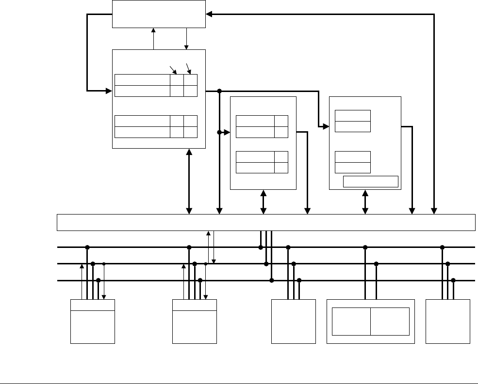
Programmer’s Model
ARM DDI 0301H Copyright © 2004-2009 ARM Limited. All rights reserved. 2-6
ID012310 Non-Confidential, Unrestricted Access
• in the MMU, Secure and Non-secure descriptors can coexist and they are differentiated
by the NSTID.
In the descriptors the NS attribute indicates whether the corresponding physical memory is
Secure or Non-secure.
For Non-secure descriptors, marked with NSTID=Non-secure, NS attribute is forced to
Non-secure value. The Non-secure world can only target Non-secure memory.
For Secure descriptor, marked with NSTID=Secure, NS attribute indicates if the physical
memory targets Secure or Non-secure memory:
In the caches, instruction and data, each line is tagged as Secure or Non-secure, so that Secure
and Non-secure data can coexist in the cache. Each time a cache line fill is performed, the NS
tag is updated appropriately.
For external accesses, AxPROT[1] indicates whether the access is Secure or Non-secure.
The TrustZone security extensions are completely compatible with existing software. This
means that existing applications and operating systems access memory without change. Where
a system employs Secure functionality the Non-secure world is effectively blind to Secure
memory. This means that Secure and Non-secure memory can co-exist with no affect on
Non-secure code.
Figure 2-2 shows the basic connection of the Secure and Non-secure memory.
Figure 2-2 Memory in the Secure and Non-secure worlds
Core
MMU
AXI interface
External
memory
Secure
slave
Non-
secure
slave
Arbiter Master
peripheral
Decoder
NSTID
Core world
state
Address
Abort
Cache
Line (n) S
Line(n-1) NS
Line 2 NS
Line 1 S
TCM
Line(n-1)
Line 1
Line(n)
Line 2
NS access bit
Data Data
Data
Page
table
walk
Address
Control
Data
S prot
Abort
AxPROT[1]
Abort
AxPROT[1]
S prot
Abort
AxPROT[1]
NS attribute
NS
SS
NS
NS
S
NS
NS
Descriptor (n-1)
Descriptor 1
Descriptor 2
Descriptor (n)
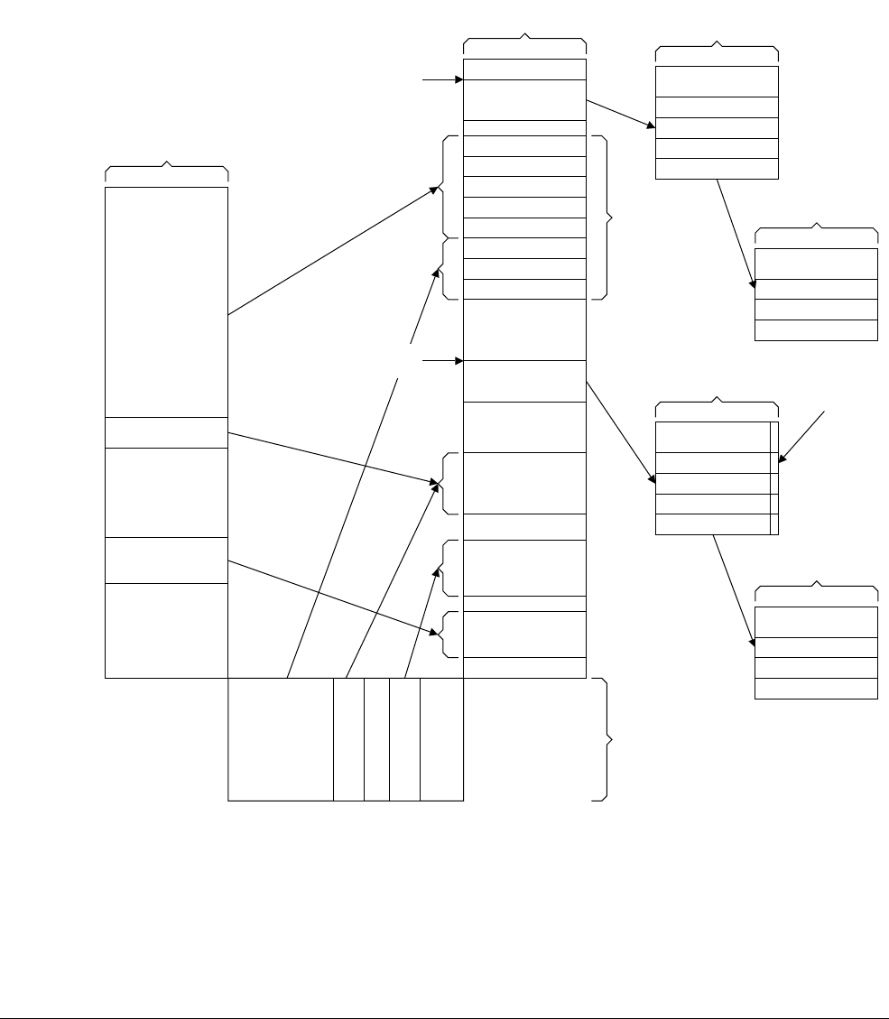
Programmer’s Model
ARM DDI 0301H Copyright © 2004-2009 ARM Limited. All rights reserved. 2-7
ID012310 Non-Confidential, Unrestricted Access
The virtual memory address map for the Secure and Non-secure worlds appear as separate
blocks. Figure 2-3 shows how the Secure and Non-secure virtual address spaces might map onto
the physical address space. In this example:
• Non-secure descriptors are stored in Non-secure memory and can only target Non-secure
memory
• Secure descriptors are stored in Secure memory and can target both Secure and
Non-secure memory.
Figure 2-3 Memory partition in the Secure and Non-secure worlds
Non-secure
Virtual memory
32KB on-chip RAM
Non-secure translation
table base address
NS
attribute
Secure
Virtual memory
Physical memory
Non-secure level
1 descriptors
4KB non-secure
4KB non-secure
4KB non-secure
4KB non-secure
4KB non-secure
4KB secure
4KB secure
4KB secure
Secure level 1
descriptors
Non-secure
SDRAM
Secure
peripherals
Non-secure
peripherals
1MB sections
Non-secure level 1
descriptors
1MB sections
Secure level 1
descriptors
4KB small pages
Secure level 2
descriptors
4KB small pages
Non-secure level 2
descriptors
Secure translation
table base address

Programmer’s Model
ARM DDI 0301H Copyright © 2004-2009 ARM Limited. All rights reserved. 2-8
ID012310 Non-Confidential, Unrestricted Access
System boot sequence
Caution
TrustZone security extensions enable a Secure software environment. The technology does not
protect the processor from hardware attacks and the implementor must make sure that the
hardware that contains the boot code is appropriately secure.
The processor always boots in the privileged Supervisor mode in the Secure world, that is the
NS bit is 0. This means that code not written for TrustZone always runs in the Secure world, but
has no way to switch to the Non-secure world. Because the Secure and Non-secure worlds
mirror each other this Secure operation does not affect the functionality of code not written for
TrustZone. The processor is therefore compatible with other ARMv6 architectures. Peripherals
boot in their most Secure state.
The Secure OS code at the reset vector must:
1. Initialize the Secure OS. This includes normal boot actions such as:
a. Generate page tables and switch on the MMU if the design uses caches or memory
protection.
b. Switch on the stack.
c. Set up the run time environment and program stacks for each processor mode.
2. Initialize the Secure Monitor. This includes such actions as:
a. Allocate TCM memory for the Secure Monitor code.
b. Allocate scratch work space.
c. Set up the Secure Monitor stack pointer and initialize its state block.
3. Program the partition checker to allocate physical memory available to the Non-secure
OS.
4. Yield control to the Non-secure OS. The Non-secure OS boots after this.
The overall security of the software relies on the security of the boot code along with the code
for the Secure Monitor.
Secure interrupts
There are no new pins to deal with Secure interrupts. However the IRQ and FIQ bits in the SCR
can be set to 1, so that the core branches to Secure Monitor mode, instead of IRQ or FIQ mode,
when an interrupt occurs. For more information see c1, Secure Configuration Register on
page 3-52.
FIQ can be used to enter the Secure world in a deterministic way, if it is configured as NMI when
the core is in the Non-secure world,. This configuration is done using the FW and FIQ bits in
SCR. The nIRQ pin can also be used as Secure interrupt and can enter directly monitor mode,
if the IRQ bit in the SCR is set to 1. But it might be masked in the Non-secure world if the I bit
in the CPSR is set to 1.
Secure peripherals
You can protect a Secure peripheral by mapping it to a Secure memory region. In addition, you
can protect Secure peripherals by checking the AxPROT[1] signal and generating an error
response if a Non-secure access attempts to read or write a Secure register.

Programmer’s Model
ARM DDI 0301H Copyright © 2004-2009 ARM Limited. All rights reserved. 2-9
ID012310 Non-Confidential, Unrestricted Access
Secure peripherals require Secure device drivers to supervise them. To minimize the effects of
drivers on system security it is recommended that the Secure device drivers run in the Secure
User mode so that they cannot change the NS bit directly.
Secure debug
For details of software debug in Secure systems see, Chapter 13 Debug. Because the processor
boots in Secure mode you might have to make special arrangements to debug code not written
for TrustZone.
2.2.3 TrustZone write access disable
The processor pin CP15SDISABLE disables write access to certain registers in the system
control coprocessor. Table 2-1 lists the registers affected by this pin.
Attempts to write to the registers in Table 2-1 when CP15SDISABLE is HIGH result in an
Undefined exception. Reads from the registers are still permitted. For more information about
the registers, see Chapter 3 System Control Coprocessor.
A change to the CP15SDISABLE pin takes effect on the instructions decoded by the processor
as quickly as practically possible. Software must perform a Prefetch Flush CP15 operation, after
a change to this pin on the boundary of the macrocell, to ensure that its effect is recognized for
following instructions. It it is expected that:
• control of the CP15SDISABLE pin remains within the SoC that embodies the macrocell
• the CP15SDISABLE pin is set to logic 0 by the SoC hardware at reset.
You can use the CP15SDISABLE pin to disable subsequent access to system control processor
registers after the Secure boot code runs and protect the configuration that the Secure boot code
applies.
Note
With the exception of the TCM Region Registers, the registers in Table 2-1 are only accessible
in Secure Privileged modes.
Table 2-1 Write access behavior for system control processor registers
Register Instruction that is Undefined
when CP15SDISABLE=1 Security Condition
Secure Control Register
MCR p15, 0, Rd, c1, c0, 0
Secure Monitor or Privileged when NS=0
Secure Translation Table Base
Register 0
MCR p15, 0, Rd, c2, c0, 0
Secure Monitor or Privileged when NS=0
Secure Translation Table Control
Register
MCR p15, 0, Rd, c2, c0, 2
Secure Monitor or Privileged when NS=0
Secure Domain Access Control
Register
MCR p15, 0, Rd, c3, c0, 0
Secure Monitor or Privileged when NS=0
Data TCM Non-secure Control
Access Register
MCR p15, 0, Rd, c9, c1, 2
Secure Monitor or Privileged when NS=0

Programmer’s Model
ARM DDI 0301H Copyright © 2004-2009 ARM Limited. All rights reserved. 2-10
ID012310 Non-Confidential, Unrestricted Access
2.2.4 Secure Monitor bus
The SECMONBUS exports a set of signals from the core for use in a monitoring block inside
the chip.
Caution
Implementors must ensure that the SECMONBUS signals do not compromise the security of
the processor. The signals provide information for a security monitoring block, that is inside the
SoC, and must not appear outside the chip.
Table 2-2 on page 2-11 lists the signals that appear on the Secure Monitor bus SECMONBUS.
Instruction/Unified TCM
Non-secure Control Access
Register
MCR p15, 0, Rd, c9, c1, 3
Secure Monitor or Privileged when NS=0
Data TCM Region Registers
MCR p15, 0, Rd, c9, c1, 0
All TCM Base Registers for which the
Data TCM Non-secure Control Access
Register = 0
Instruction/Unified TCM Region
Registers
MCR p15, 0, Rd, c9, c1, 1
All TCM Base Registers for which the
Instruction/Unified TCM Non-secure
Control Access Register = 0
Secure Primary Region Remap
Register
MCR p15, 0, Rd, c10, c2, 0
Secure Monitor or Privileged when NS=0
Secure Normal Memory Remap
Register
MCR p15, 0, Rd, c10, c2, 1
Secure Monitor or Privileged when NS=0
Secure Vector Base Register
MCR p15, 0, Rd, c12, c0, 0
Secure Monitor or Privileged when NS=0
Monitor Vector Base Register
MCR p15, 0, Rd, c12, c0, 1
Secure Monitor or Privileged when NS=0
Secure FCSE Register
MCR p15, 0, Rd, c13, c0, 0
Secure Monitor or Privileged when NS=0
Peripheral Port remap Register
MCR p15, 0, Rd, c15, c2, 4
Secure Monitor or Privileged when NS=0
Instruction Cache master valid
register
MCR p15, 3, Rd, c15, c8, {0-7}
Secure Monitor or Privileged when NS=0
Data Cache master valid register
MCR p15, 3, Rd, c15, c12, {0-7}
Secure Monitor or Privileged when NS=0
TLB lockdown Index register
MCR p15, 5, Rd, c15, c4, 2
Secure Monitor or Privileged when NS=0
TLB lockdown VA register
MCR p15, 5, Rd, c15, c5, 2
Secure Monitor or Privileged when NS=0
TLB lockdown PA register
MCR p15, 5, Rd, c15, c6, 2
Secure Monitor or Privileged when NS=0
TLB lockdown Attribute register
MCR p15, 5, Rd, c15, c7, 2
Secure Monitor or Privileged when NS=0
Validation registers
MCR p15, 0, Rd, c15, c9, 0
MCR p15, 0, Rd, c15, c12, {4-7}
MCR p15, 0, Rd, c15, c14, 0
MCR p15, {0-7}, Rd, c15, c13, {0-7}
Secure Monitor or Privileged when NS=0
Table 2-1 Write access behavior for system control processor registers (continued)
Register Instruction that is Undefined
when CP15SDISABLE=1 Security Condition

Programmer’s Model
ARM DDI 0301H Copyright © 2004-2009 ARM Limited. All rights reserved. 2-11
ID012310 Non-Confidential, Unrestricted Access
Table 2-2 Secure Monitor bus signals
Bits Description
[24]aETMIACTL[11] unmodified by Non-invasive security enable masking.
This signal is disabled when ETMPWRUP = 0 and the Performance Monitoring counters are disabled.
[23]aETMIACTL[9] unmodified by Non-invasive security enable masking.
This signal is disabled when ETMPWRUP = 0 and the Performance Monitoring counters are disabled.
[22] Signal that indicates, for duration of operation, the execution of a DMB or DSB operation.
[21] Signal that indicates, for 1 cycle, the execution of a Prefetch Flush operation.
[20:19] Instruction/Unified TCM Region Register bit[0], entries [1:0].
[18:17] Data TCM Region Register bit [0], entries [1:0].
[16] Non-secure Access Control register bit [18].
[15] Secure Control Register I bit, bit [12].
[14] Secure Control Register C bit, bit [2].
[13] Secure Control Register M bit, bit [0].
[12] Secure Configuration Register NS bit, bit [0].
[11] CPSR A bit, bit [8], taken from the core pipeline writeback stage.
[10] CPSR I bit, bit [7], taken from the core pipeline writeback stage.
[9] CPSR F bit, bit [6], taken from the core pipeline writeback stage.
[8:5] CPSR mode bits, bits [3:0], taken from the core pipeline writeback stage.
[4:3] ETMDDCTL[1:0] unmodified by Non-invasive security enable masking.
This signal is disabled when ETMPWRUP = 0 and the Performance Monitoring counters are disabled.
[2:1]aETMDACTL[1:0] unmodified by Non-invasive security enable masking.
This signal is disabled when ETMPWRUP = 0 and the Performance Monitoring counters are disabled.
[0]aETMIACTL[0] unmodified by Non-invasive security enable masking.
This signal is disabled when ETMPWRUP = 0 and the Performance Monitoring counters are disabled.
a. nRESETIN resets all SECMONBUS output pins except bits [24:23] and bits [2:0].
nPORESETIN resets the output pins for bits [24:23] and bits [2:0].

Programmer’s Model
ARM DDI 0301H Copyright © 2004-2009 ARM Limited. All rights reserved. 2-12
ID012310 Non-Confidential, Unrestricted Access
2.3 Processor operating states
The processor has these operating states:
ARM state 32-bit, word-aligned ARM instructions are executed in this state.
Thumb state 16-bit, halfword-aligned Thumb instructions.
Jazelle state Variable length, byte-aligned Java instructions.
In Thumb state, the Program Counter (PC) uses bit 1 to select between alternate halfwords. In
Jazelle state, all instruction fetches are in words.
Note
Transition between ARM and Thumb states does not affect the processor mode or the register
contents. For details on entering and exiting Jazelle state see Jazelle V1 Architecture Reference
Manual.
2.3.1 Switching state
You can switch the operating state of the processor between:
• ARM state and Thumb state using the BX and BLX instructions, and loads to the PC. The
ARM Architecture Reference Manual describes the switching state.
• ARM state and Jazelle state using the BXJ instruction.
All exceptions are entered, handled, and exited in ARM state. If an exception occurs in Thumb
state or Jazelle state, the processor reverts to ARM state. Exception return instructions restore
the SPSR to the CPSR, that can also cause a transition back to Thumb state or Jazelle state.
2.3.2 Interworking ARM and Thumb state
The processor enables you to mix ARM and Thumb code. For details see the chapter about
interworking ARM and Thumb in the RealView Compilation Tools Developer Guide.

Programmer’s Model
ARM DDI 0301H Copyright © 2004-2009 ARM Limited. All rights reserved. 2-13
ID012310 Non-Confidential, Unrestricted Access
2.4 Instruction length
Instructions are one of:
• 32 bits long, in ARM state
• 16 bits long, in Thumb state
• variable length, multiples of 8 bits, in Jazelle state.

Programmer’s Model
ARM DDI 0301H Copyright © 2004-2009 ARM Limited. All rights reserved. 2-14
ID012310 Non-Confidential, Unrestricted Access
2.5 Data types
The processor supports the following data types:
• word, 32-bit
• halfword, 16-bit
• byte, 8-bit.
Note
• When any of these types are described as unsigned, the N-bit data value represents a
non-negative integer in the range 0 to +2N-1, using normal binary format.
• When any of these types are described as signed, the N-bit data value represents an integer
in the range -2N-1 to +2N-1-1, using two’s complement format.
For best performance you must align these as follows:
• word quantities must be aligned to four-byte boundaries
• halfword quantities must be aligned to two-byte boundaries
• byte quantities can be placed on any byte boundary.
The processor provides mixed-endian and unaligned access support. For details see Chapter 4
Unaligned and Mixed-endian Data Access Support.
Note
You cannot use LDRD, LDM, LDC, STRD, STM, or STC instructions to access 32-bit
quantities if they are unaligned.

Programmer’s Model
ARM DDI 0301H Copyright © 2004-2009 ARM Limited. All rights reserved. 2-15
ID012310 Non-Confidential, Unrestricted Access
2.6 Memory formats
The processor views memory as a linear collection of bytes numbered in ascending order from
zero. Bytes 0-3 hold the first stored word, and bytes 4-7 hold the second stored word, for
example.
The processor can treat words in memory as being stored in either:
•Legacy big-endian format
•Little-endian format.
Additionally, the processor supports mixed-endian and unaligned data accesses. For details see
Chapter 4 Unaligned and Mixed-endian Data Access Support.
2.6.1 Legacy big-endian format
In legacy big-endian format, the processor stores the most significant byte of a word at the
lowest-numbered byte, and the least significant byte at the highest-numbered byte. Therefore,
byte 0 of the memory system connects to data lines 31-24. Figure 2-4 shows this.
Figure 2-4 Big-endian addresses of bytes within words
2.6.2 Little-endian format
In little-endian format, the lowest-numbered byte in a word is the least significant byte of the
word and the highest-numbered byte is the most significant. Therefore, byte 0 of the memory
system connects to data lines 7-0. Figure 2-5 shows this.
Figure 2-5 Little-endian addresses of bytes within words
31 24 23 16 15 8 7 Word address0
4
0
8Higher address
Lower address
• Most significant byte is at lowest address
• Word is addressed by byte address of most significant byte
Bit
111098
7654
3210
31 24 23 16 15 8 7 Word address0
4
0
8Higher address
Lower address
• Least significant byte is at lowest address
• Word is addressed by byte address of least significant byte
Bit
891011
4567
0123

Programmer’s Model
ARM DDI 0301H Copyright © 2004-2009 ARM Limited. All rights reserved. 2-16
ID012310 Non-Confidential, Unrestricted Access
2.7 Addresses in a processor system
Three distinct types of address exist in the processor system:
•Virtual Address (VA)
•Modified Virtual Address (MVA)
•Physical Address (PA).
When the core is in the Secure world the VA is Secure, and when the core is in the Non-secure
world the VA is Non-secure. To get the VA to PA translation, the core uses Secure pages tables
while it is in Secure world. Otherwise it uses the Non-secure page tables.
Table 2-3 lists the address types in the processor system.
This is an example of the address manipulation that occurs when the processor requests an
instruction, see Figure 1-1 on page 1-8:
1. The VA of the instruction is issued by the processor, Secure or Non-secure VA according
to the world where the core is.
2. The Instruction Cache is indexed by the lower bits of the VA. The VA is translated using
the ProcID, Secure or Non-secure one, to the MVA, and then to PA in the Translation
Lookaside Buffer (TLB). The TLB performs the translation in parallel with the Cache
lookup. The translation uses Secure descriptors if the core is in Secure world. Otherwise
it uses the Non-secure ones.
3. If the protection check carried out by the TLB on the MVA does not abort and the PA tag
is in the Instruction Cache, the instruction data is returned to the processor.
4. The PA is passed to the AXI bus interface to perform an external access, in the event of a
cache miss. The external access is always Non-secure when the core is in Non-secure
world. In Secure world, the external access is Secure or Non-secure according to the NS
attribute value in the selected descriptor.
Table 2-3 Address types in the processor system
Processor Caches TLBs AXI bus
Virtual Address Virtual index Physical tag Translates Virtual Address to Physical Address Physical Address

Programmer’s Model
ARM DDI 0301H Copyright © 2004-2009 ARM Limited. All rights reserved. 2-17
ID012310 Non-Confidential, Unrestricted Access
2.8 Operating modes
In all states there are eight modes of operation:
• User mode is the usual ARM program execution state, and is used for executing most
application programs
•Fast interrupt (FIQ) mode is used for handling fast interrupts
•Interrupt (IRQ) mode is used for general-purpose interrupt handling
• Supervisor mode is a protected mode for the OS
• Abort mode is entered after a data abort or prefetch abort
• System mode is a privileged user mode for the OS
• Undefined mode is entered when an undefined instruction exception occurs.
• Secure Monitor mode is a Secure mode for the TrustZone Secure Monitor code.
Note
Secure Monitor mode is not the same as monitor debug mode.
Modes other than User mode are collectively known as privileged modes. Privileged modes are
used to service interrupts or exceptions, or to access protected resources. Table 2-4 lists the
mode structure for the processor.
Table 2-4 Mode structure
Modes Mode type
State of core
NS bit = 1 NS bit = 0
User User Non-secure Secure
FIQ privileged Non-secure Secure
IRQ privileged Non-secure Secure
Supervisor privileged Non-secure Secure
Abort privileged Non-secure Secure
Undefined privileged Non-secure Secure
System privileged Non-secure Secure
Secure Monitor privileged Secure Secure

Programmer’s Model
ARM DDI 0301H Copyright © 2004-2009 ARM Limited. All rights reserved. 2-18
ID012310 Non-Confidential, Unrestricted Access
2.9 Registers
The processor has a total of 40 registers:
• 33 general-purpose 32-bit registers
• seven 32-bit status registers.
These registers are not all accessible at the same time. The processor state and operating mode
determine the registers that are available to the programmer.
2.9.1 The ARM state core register set
In ARM state, 16 general registers and one or two status registers are accessible at any time. In
privileged modes, mode-specific banked registers become available. Figure 2-6 on page 2-20
shows the registers that are available in each mode.
The ARM state core register set contains 16 directly-accessible registers, R0-R15. Another
register, the Current Program Status Register (CPSR), contains condition code flags, status bits,
and current mode bits. Registers R0-R12 are general-purpose registers used to hold either data
or address values. Registers R13, R14, R15, and the Saved Program Status Register (SPSR)
have the following special functions:
Stack Pointer Register R13 is used as the Stack Pointer (SP).
R13 is banked for the exception modes. This means that an exception
handler can use a different stack to the one in use when the exception
occurred.
In many instructions, you can use R13 as a general-purpose register, but
the architecture deprecates this use of R13 in most instructions. For more
information see the ARM Architecture Reference Manual.
Link Register Register R14 is used as the subroutine Link Register (LR).
Register R14 receives the return address when a Branch with Link (BL or
BLX) instruction is executed.
You can treat R14 as a general-purpose register at all other times. The
corresponding banked registers R14_mon, R14_svc, R14_irq, R14_fiq,
R14_abt, and R14_und are similarly used to hold the return values when
interrupts and exceptions arise, or when BL or BLX instructions are
executed within interrupt or exception routines.
Program Counter Register R15 holds the PC:
• in ARM state this is word-aligned
• in Thumb state this is halfword-aligned
• in Jazelle state this is byte-aligned.
Saved Program Status Register
In privileged modes, another register, the SPSR, is accessible. This
contains the condition code flags, status bits, and current mode bits saved
as a result of the exception that caused entry to the current mode.

Programmer’s Model
ARM DDI 0301H Copyright © 2004-2009 ARM Limited. All rights reserved. 2-19
ID012310 Non-Confidential, Unrestricted Access
Banked registers have a mode identifier that indicates the mode that they relate to. Table 2-5 lists
these mode identifiers.
FIQ mode has seven banked registers mapped to R8–R14 (R8_fiq–R14_fiq). As a result many
FIQ handlers do not have to save any registers.
The Secure Monitor, Supervisor, Abort, IRQ, and Undefined modes each have alternative
mode-specific registers mapped to R13 and R14, permitting a private stack pointer and link
register for each mode.
Figure 2-6 on page 2-20 shows the ARM state registers.
Table 2-5 Register mode identifiers
Mode Mode identifier
User usra
a. The
usr
identifier is usually omitted from
register names. It is only used in descriptions
where the User or System mode register is
specifically accessed from another operating
mode.
Fast interrupt fiq
Interrupt irq
Supervisor svc
Abort abt
System usra
Undefined und
Secure Monitor mon
Programmer’s Model
ARM DDI 0301H Copyright © 2004-2009 ARM Limited. All rights reserved. 2-20
ID012310 Non-Confidential, Unrestricted Access
Figure 2-6 Register organization in ARM state
Figure 2-7 on page 2-21 shows an alternative view of the ARM registers.
ARM state general registers and program counter
System and
User
ARM state program status registers
= banked register
Supervisor Abort IRQ Undefined
R0
R1
R2
R3
R4
R5
R6
R7
R8
R9
R10
R11
R12
R13
R14
R15
FIQ
R0
R1
R2
R3
R4
R5
R6
R7
R8_fiq
R9_fiq
R10_fiq
R11_fiq
R12_fiq
R13_fiq
R14_fiq
R15 (PC)
R0
R1
R2
R3
R4
R5
R6
R7
R8
R9
R10
R11
R12
R13_svc
R14_svc
R0
R1
R2
R3
R4
R5
R6
R7
R8
R9
R10
R11
R12
R13_abt
R14_abt
R0
R1
R2
R3
R4
R5
R6
R7
R8
R9
R10
R11
R12
R13_irq
R14_irq
R0
R1
R2
R3
R4
R5
R6
R7
R8
R9
R10
R11
R12
R13_und
R14_und
CPSR CPSR CPSR CPSR CPSR CPSR
SPSR_fiq SPSR_svc SPSR_abt SPSR_irq SPSR_und
R15 (PC) R15 (PC) R15 (PC) R15 (PC)
Secure
monitor
R0
R1
R2
R3
R4
R5
R6
R7
R8
R9
R10
R11
R12
R13_mon
R14_mon
CPSR
SPSR_mon
R15 (PC)
Programmer’s Model
ARM DDI 0301H Copyright © 2004-2009 ARM Limited. All rights reserved. 2-21
ID012310 Non-Confidential, Unrestricted Access
Figure 2-7 Processor core register set showing banked registers
2.9.2 The Thumb state core register set
The Thumb state core register set is a subset of the ARM state set. The programmer has direct
access to:
• eight general registers, R0–R7. For details of high register access in Thumb state see
Accessing high registers in Thumb state on page 2-22
•the PC
• a stack pointer, SP, ARM R13
•an LR, ARM R14
• the CPSR.
There are banked SPs, LRs, and SPSRs for each privileged mode. Figure 2-8 on page 2-22
shows the Thumb state core register set.
R0
R1
R2
R3
R4
R5
R6
R7
R8
R9
R10
R11
R12
R13
R14
R15 (PC)
R8_fiq
R9_fiq
R10_fiq
R11_fiq
R12_fiq
R13_fiq
R14_fiq
R13_svc
R14_svc
R13_abt
R14_abt
R13_irq
R14_irq
R13_und
R14_und
CPSR SPSR_fiq SPSR_svc SPSR_abt SPSR_irq SPSR_und
R13_mon
R14_mon
SPSR_mon
23 mode-specific registers (banked registers)
17 banked general-purpose registers + 6 banked status registers
33 general purpose registers7 status registers
16 general
purpose
registers + 1
status register
Programmer’s Model
ARM DDI 0301H Copyright © 2004-2009 ARM Limited. All rights reserved. 2-22
ID012310 Non-Confidential, Unrestricted Access
Figure 2-8 Register organization in Thumb state
2.9.3 Accessing high registers in Thumb state
In Thumb state, the high registers, R8–R15, are not part of the standard core register set. You
can use special variants of the MOV instruction to transfer a value from a low register, in the
range R0–R7, to a high register, and from a high register to a low register. The CMP instruction
enables you to compare high register values with low register values. The ADD instruction
enables you to add high register values to low register values. For more details, see the ARM
Architecture Reference Manual.
2.9.4 ARM state and Thumb state registers relationship
Figure 2-9 on page 2-23 shows the relationships between the Thumb state and ARM state
registers. See the Jazelle V1 Architecture Reference Manual for details of Jazelle state registers.
Thumb state general registers and program counter
System and
User
Thumb state program status registers
= banked register
Supervisor Abort IRQ Undefined
R0
R1
R2
R3
R4
R5
R6
R7
SP
LR
PC
FIQ
R0
R1
R2
R3
R4
R5
R6
R7
SP_fiq
LR_fiq
PC
R0
R1
R2
R3
R4
R5
R6
R7
SP_svc
LR_svc
R0
R1
R2
R3
R4
R5
R6
R7
SP_abt
LR_abt
R0
R1
R2
R3
R4
R5
R6
R7
SP_irq
LR_irq
R0
R1
R2
R3
R4
R5
R6
R7
SP_und
LR_und
CPSR CPSR CPSR CPSR CPSR CPSR
SPSR_fiq SPSR_svc SPSR_abt SPSR_irq SPSR_und
PC PC PC PC
Secure
monitor
R0
R1
R2
R3
R4
R5
R6
R7
SP_mon
LR_mon
CPSR
SPSR_mon
PC

Programmer’s Model
ARM DDI 0301H Copyright © 2004-2009 ARM Limited. All rights reserved. 2-23
ID012310 Non-Confidential, Unrestricted Access
Figure 2-9 ARM state and Thumb state registers relationship
Note
Registers R0–R7 are known as the low registers. Registers R8–R15 are known as the high
registers.
Thumb state ARM State
R0
R1
R2
R3
R4
R5
R6
R7
R8
R9
R10
R11
R12
Stack Pointer (R13)
Link Register (R14)
Program Counter (R15)
CPSR
SPSR
Stack pointer (SP)
Link register (LR)
Program counter (PC)
CPSR
SPSR
R0
R1
R2
R3
R4
R5
R6
R7
Low registersHigh registers
Programmer’s Model
ARM DDI 0301H Copyright © 2004-2009 ARM Limited. All rights reserved. 2-24
ID012310 Non-Confidential, Unrestricted Access
2.10 The program status registers
The processor contains one CPSR, and six SPSRs for exception handlers to use. The program
status registers:
• hold information about the most recently performed ALU operation
• control the enabling and disabling of interrupts
• set the processor operating mode.
Figure 2-10 shows the arrangement of bits in the status registers, and the sections from The
condition code flags to Reserved bits on page 2-29 inclusive describe it.
Figure 2-10 Program status register
Note
The bits that Figure 2-10 identifies as Do Not Modify (DNM), Read As Zero (RAZ), must not be
modified by software. These bits are:
• Readable, to enable the processor state to be preserved, for example, during process
context switches
• Writable, to enable the processor state to be restored. To maintain compatibility with
future ARM processors, and as good practice, you are strongly advised to use a
read-modify-write strategy when changing the CPSR.
2.10.1 The condition code flags
The N, Z, C, and V bits are the condition code flags. You can set them by arithmetic and logical
operations, and also by MSR and LDM instructions. The processor tests these flags to determine
whether to execute an instruction.
In ARM state, most instructions can execute conditionally on the state of the N, Z, C, and V bits.
The exceptions are:
•BKPT
•CDP2
•CPS
•LDC2
• MCR2
• MCRR2
• MRC2
• MRRC2
•PLD
N
31 30 29 28 27 26 25 24 23 20 19 16 15 10 9 8 7 6 5 4 0
Z C V Q DNM
(RAZ) JDNM
(RAZ) GE[3:0] DNM
(RAZ) E A I F T M[4:0]
Greater than
or equal to
Jazelle state bit
Sticky overflow
Overflow
Carry/Borrow/Extend
Zero
Negative/Less than
Mode bits
Thumb state bit
FIQ disable
IRQ disable
Imprecise abort
disable bit
Data endianness bit

Programmer’s Model
ARM DDI 0301H Copyright © 2004-2009 ARM Limited. All rights reserved. 2-25
ID012310 Non-Confidential, Unrestricted Access
• SETEND
•RFE
•SRS
•STC2.
In Thumb state, only the Branch instruction can be executed conditionally. For more
information about conditional execution, see the ARM Architecture Reference Manual.
2.10.2 The Q flag
The Sticky Overflow (Q) flag can be set by certain multiply and fractional arithmetic
instructions:
• QADD
•QDADD
•QSUB
• QDSUB
•SMLAD
•SMLAxy
•SMLAWy
•SMLSD
•SMUAD
•SSAT
•SSAT16
•USAT
•USAT16.
The Q flag is sticky in that, when set by an instruction, it remains set until explicitly cleared by
an MSR instruction writing to the CPSR. Instructions cannot execute conditionally on the status
of the Q flag.
To determine the status of the Q flag you must read the PSR into a register and extract the Q flag
from this. For details of how the Q flag is set and cleared, see individual instruction definitions
in the ARM Architecture Reference Manual.
2.10.3 The J bit
The J bit in the CPSR indicates when the processor is in Jazelle state.
When:
J = 0 The processor is in ARM or Thumb state, depending on the T bit.
J = 1 The processor is in Jazelle state.
Note
• The combination of J = 1 and T = 1 causes similar effects to setting T=1 on a non
Thumb-aware processor. That is, the next instruction executed causes entry to the
Undefined Instruction exception. Entry to the exception handler causes the processor to
re-enter ARM state, and the handler can detect that this was the cause of the exception
because J and T are both set in SPSR_und.
• MSR cannot be used to change the J bit in the CPSR.

Programmer’s Model
ARM DDI 0301H Copyright © 2004-2009 ARM Limited. All rights reserved. 2-26
ID012310 Non-Confidential, Unrestricted Access
• The placement of the J bit avoids the status or extension bytes in code running on
ARMv5TE or earlier processors. This ensures that OS code written using the deprecated
CPSR, SPSR, CPSR_all, or SPSR_all syntax for the destination of an MSR instruction
continues to work.
2.10.4 The GE[3:0] bits
Some of the SIMD instructions set GE[3:0] as greater-than-or-equal bits for individual
halfwords or bytes of the result. Table 2-6 lists these.
Note
GE bit is 1 if A op B ≥ C, otherwise 0.
The SEL instruction uses GE[3:0] to select the source register that supplies each byte of its
result.
Note
• For unsigned operations, the GE bits are determined by the usual ARM rules for carries
out of unsigned additions and subtractions, and so are carry-out bits.
• For signed operations, the rules for setting the GE bits are chosen so that they have the
same sort of greater than or equal functionality as for unsigned operations.
Table 2-6 GE[3:0] settings
GE[3] GE[2] GE[1] GE[0]
Instruction A op B >= C A op B >= C A op B >= C A op B >= C
Signed
SADD16 [31:16] + [31:16] ≥ 0 [31:16] + [31:16] ≥ 0 [15:0] + [15:0] ≥ 0 [15:0] + [15:0] ≥ 0
SSUB16 [31:16] - [31:16] ≥ 0 [31:16] - [31:16] ≥ 0 [15:0] - [15:0] ≥ 0 [15:0] - [15:0] ≥ 0
SADDSUBX [31:16] + [15:0] ≥ 0 [31:16] + [15:0] ≥ 0 [15:0] - [31:16] ≥ 0 [15:0] - [31:16] ≥ 0
SSUBADDX [31:16] - [15:0] ≥ 0 [31:16] - [15:0] ≥ 0 [15:0] + [31:16] ≥ 0 [15:0] + [31:16] ≥ 0
SADD8 [31:24] + [31:24] ≥ 0 [23:16] + [23:16] ≥ 0 [15:8] + [15:8] ≥ 0 [7:0] + [7:0] ≥ 0
SSUB8 [31:24] - [31:24] ≥ 0 [23:16] - [23:16] ≥ 0 [15:8] - [15:8] ≥ 0 [7:0] - [7:0] ≥ 0
Unsigned
UADD16 [31:16] + [31:16] ≥ 216 [31:16] + [31:16] ≥ 216 [15:0] + [15:0] ≥ 216 [15:0] + [15:0] ≥ 216
USUB16 [31:16] - [31:16] ≥ 0 [31:16] - [31:16] ≥ 0 [15:0] - [15:0] ≥ 0 [15:0] - [15:0] ≥ 0
UADDSUBX [31:16] + [15:0] ≥ 216 [31:16] + [15:0] ≥ 216 [15:0] - [31:16] ≥ 0 [15:0] - [31:16] ≥ 0
USUBADDX [31:16] - [15:0] ≥ 0 [31:16] - [15:0] ≥ 0[15:0] + [31:16] ≥ 216 [15:0] + [31:16] ≥216
UADD8 [31:24] + [31:24] ≥ 28[23:16] + [23:16] ≥ 28[15:8] + [15:8] ≥ 28[7:0] + [7:0] ≥ 28
USUB8 [31:24] - [31:24] ≥ 0 [23:16] - [23:16] ≥ 0 [15:8] - [15:8] ≥ 0 [7:0] - [7:0] ≥ 0

Programmer’s Model
ARM DDI 0301H Copyright © 2004-2009 ARM Limited. All rights reserved. 2-27
ID012310 Non-Confidential, Unrestricted Access
2.10.5 The E bit
ARM and Thumb instructions are provided to set and clear the E-bit. The E bit controls
load/store endianness. For details of where the E bit is used see Chapter 4 Unaligned and
Mixed-endian Data Access Support.
Architecture versions prior to ARMv6 specify this bit as SBZ. This ensures no endianness
reversal on loads or stores.
2.10.6 The A bit
The A bit is set automatically. It is used to disable imprecise Data Aborts. It might be not
writable in the Non-secure world if the AW bit in the SCR register is reset. For details of how
to use the A bit see Imprecise Data Abort mask in the CPSR/SPSR on page 2-47.
2.10.7 The control bits
The bottom eight bits of a PSR are known collectively as the control bits. They are the:
•Interrupt disable bits
•T bit
•Mode bits on page 2-28.
The control bits change when an exception occurs. When the processor is operating in a
privileged mode, software can manipulate these bits.
Interrupt disable bits
The I and F bits are the interrupt disable bits:
• When the I bit is set, IRQ interrupts are disabled.
• When the F bit is set, FIQ interrupts are disabled. FIQ can be non-maskable in the
Non-secure world if the FW bit in SCR register is reset
Note
You can change the SPSR F bit in the Non-secure world but this does not update the CPSR if
the SCR bit 4 (FW) does not permit it.
T bit
The T bit reflects the operating state:
• when the T bit is set, the processor is executing in Thumb state
• when the T bit is clear, the processor is executing in ARM state, or Jazelle state depending
on the J bit.
Note
Never use an MSR instruction to force a change to the state of the T bit in the CPSR. If an MSR
instruction does try to modify this bit the result is architecturally Unpredictable. In the
ARM1176JZF-S processor this bit is not affected.

Programmer’s Model
ARM DDI 0301H Copyright © 2004-2009 ARM Limited. All rights reserved. 2-28
ID012310 Non-Confidential, Unrestricted Access
Mode bits
M[4:0] are the mode bits. Table 2-7 lists how these bits determine the processor operating mode.
2.10.8 Modification of PSR bits by MSR instructions
In previous architecture versions, MSR instructions can modify the flags byte, bits [31:24], of
the CPSR in any mode, but the other three bytes are only modifiable in privileged modes.
After the introduction of ARM architecture v6, however, each CPSR bit falls into one of the
following categories:
• Bits that are freely modifiable from any mode, either directly by MSR instructions or by
other instructions whose side-effects include writing the specific bit or writing the entire
CPSR.
Bits in Figure 2-10 on page 2-24 that are in this category are N, Z, C, V, Q, GE[3:0], and E.
• Bits that must never be modified by an MSR instruction, and so must only be written as a
side-effect of another instruction. If an MSR instruction does try to modify these bits the
results are architecturally Unpredictable. In the processor these bits are not affected.
Bits in Figure 2-10 on page 2-24 that are in this category are J and T.
• Bits that can only be modified from privileged modes, and that are completely protected
from modification by instructions while the processor is in User mode. The only way that
these bits can be modified while the processor is in User mode is by entering a processor
exception, as Exceptions on page 2-36 describes.
Bits in Figure 2-10 on page 2-24 that are in this category are A, I, F, and M[4:0].
Table 2-7 PSR mode bit values
M[4:0] Mode
Visible state registers
Thumb ARM
b10000 User R0–R7, R8-R12a, SP, LR, PC, CPSR R0–R14, PC, CPSR
b10001 FIQ R0–R7, R8_fiq-R12_fiqa, SP_fiq, LR_fiq PC,
CPSR, SPSR_fiq
R0–R7, R8_fiq–R14_fiq, PC, CPSR,
SPSR_fiq
b10010 IRQ R0–R7, R8-R12a, SP_irq, LR_irq, PC, CPSR,
SPSR_irq
R0–R12, R13_irq, R14_irq, PC, CPSR,
SPSR_irq
b10011 Supervisor R0–R7, R8-R12a, SP_svc, LR_svc, PC, CPSR,
SPSR_svc
R0–R12, R13_svc, R14_svc, PC, CPSR,
SPSR_svc
b10111 Abort R0–R7, R8-R12a, SP_abt, LR_abt,
PC, CPSR, SPSR_abt
R0–R12, R13_abt, R14_abt, PC, CPSR,
SPSR_abt
b11011 Undefined R0–R7, R8-R12a, SP_und,
LR_und, PC, CPSR, SPSR_und
R0–R12, R13_und, R14_und,
PC, CPSR, SPSR_und
b11111 System R0–R7, R8-R12a, SP, LR, PC, CPSR R0–R14, PC, CPSR
b10110 Secure
Monitor
R0-R7, R8-R12a, SP_mon, LR_mon, PC, CPSR,
SPSR_mon
R0-R12, PC,CPSR, SPSR_mon,
R13_mon,R14_mon
a. Access to these registers is limited in Thumb state.

Programmer’s Model
ARM DDI 0301H Copyright © 2004-2009 ARM Limited. All rights reserved. 2-29
ID012310 Non-Confidential, Unrestricted Access
Only Secure privileged modes can write directly to the CPSR mode bits to enter Secure
Monitor mode. If the core is in Secure User mode, Non-secure User mode, or Non-secure
privileged modes it ignores changes to the CPSR to enter the Secure Monitor. The core
does not copy mode bits in the SPSR, changed in the Non-secure world, across to the
CPSR.
2.10.9 Reserved bits
The remaining bits in the PSRs are unused, but are reserved. When changing a PSR flag or
control bits, make sure that these reserved bits are not altered. You must ensure that your
program does not rely on reserved bits containing specific values because future processors
might use some or all of the reserved bits.

Programmer’s Model
ARM DDI 0301H Copyright © 2004-2009 ARM Limited. All rights reserved. 2-30
ID012310 Non-Confidential, Unrestricted Access
2.11 Additional instructions
To support extensions to ARMv6, the ARM1176JZF-S processor includes these instructions in
addition to those in the ARMv6 and TrustZone architectures:
• Load Register Exclusive instructions, see LDREXB, LDREXH on page 2-31, and
LDREXD on page 2-33
• Store Register Exclusive instructions, see STREXB, STREXH on page 2-32, and STREXH
on page 2-32
• Clear Register Exclusive instruction, see CLREX on page 2-34
• Yield instruction, see NOP-compatible hints on page 2-34.
2.11.1 Load or Store Byte Exclusive
These instruction operate on unsigned data of size byte.
No alignment restrictions apply to the addresses of these instructions.
The LDREXB and STREXB instructions share the same data monitors as the LDREX and
STREX instructions, a local and a global monitor for each processor, for shared memory
support.
LDREXB
Figure 2-11 shows the format of the Load Register Byte Exclusive, LDREXB, instruction.
Figure 2-11 LDREXB instruction
Syntax
LDREXB{<cond>} <Rxf>, [<Rbase>]
Operation
if ConditionPassed(cond) then
processor_id = ExecutingProcessor()
Rd = Memory[Rn,1]
if Shared(Rn) ==1 then
physical_address=TLB(Rn)
MarkExclusiveGlobal(physical_address,processor_id,1)
MarkExclusiveLocal(processor_id)
STREXB
Figure 2-12 shows the format of the Store Register Byte Exclusive, STREXB, instruction.
Figure 2-12 STREXB instructions
Syntax
STREXB{<cond>} <Rd>, <Rm>, [<Rn>]]
SBOCond
31 28 27 21 20 19 15 12 11 7 4 3 0
0 0 0 1 1 1 0 1 Rn Rd SBO 1 0 0 1
16 8
RmCond
31 28 27 21 20 19 15 12 11 7 4 3 0
0 0 0 1 1 1 0 0 Rn Rd SBO 1 0 0 1
16 8

Programmer’s Model
ARM DDI 0301H Copyright © 2004-2009 ARM Limited. All rights reserved. 2-31
ID012310 Non-Confidential, Unrestricted Access
Operation
if ConditionPassed(cond) then
processor_id = ExecutingProcessor()
if IsExclusiveLocal(processor_id) then
if Shared(Rn)==1 then
physical_address=TLB(Rn)
if IsExclusiveGlobal(physical_address,processor_id,1) then
Memory[Rn,1] = Rm
Rd = 0
ClearByAddress(physical_address,1)
else
Rd =1
else
Memory[Rn,1] = Rm
Rd = 0
else
Rd = 1
ClearExclusiveLocal(processor_id)
2.11.2 Load or Store Halfword Exclusive
These instructions operate on naturally aligned, unsigned data of size halfword:
• The address in memory must be 16-bit aligned, address[0] == b0
When (A,U) == (0,1), (1,0) or (1,1) in CP15 register 1, the instruction generates alignment
faults if this condition is not met.
For more information, see Operation of unaligned accesses on page 4-13.
• The transaction must be a single access or indivisible burst on bus widths < 16 bits
For AXI based systems, the exclusive access signal, AxPROT[4], must remain asserted
throughout the burst where AxSIZE <
0x1
.
The LDREXH and STREXH instructions share the same data monitors as the LDREX and
STREX instructions, a local and a global monitor for each processor, for shared memory
support.
LDREXH
Figure 2-13 shows the format of the Load Register Halfword Exclusive, LDREXH, instruction.
Figure 2-13 LDREXH instruction
Syntax
LDREXH{<cond>} <Rd>, [<Rn>]
Operation
if ConditionPassed(cond) then
processor_id = ExecutingProcessor()
Rd = Memory[Rn,2]
if Shared(Rn) ==1 then
physical_address=TLB(Rn)
MarkExclusiveGlobal(physical_address,processor_id,2)
MarkExclusiveLocal(processor_id)
SBOCond
31 28 27 21 20 19 15 12 11 7 4 3 0
0 0 0 1 1 1 1 1 Rn Rd SBO 1 0 0 1
16 8

Programmer’s Model
ARM DDI 0301H Copyright © 2004-2009 ARM Limited. All rights reserved. 2-32
ID012310 Non-Confidential, Unrestricted Access
STREXH
Figure 2-14 shows the format of the Store Register Halfword Exclusive, STREXH, instruction.
Figure 2-14 STREXH instruction
Syntax
STREXH{<cond>} <Rd>, <Rm>, [<Rn>]
Operation
if ConditionPassed(cond) then
processor_id = ExecutingProcessor()
if IsExclusiveLocal(processor_id) then
if Shared(Rn)==1 then
physical_address=TLB(Rn)
if IsExclusiveGlobal(physical_address,processor_id,2) then
Memory[Rn,2] = Rm
Rd = 0
ClearByAddress(physical_address,2)
else
Rd =1
else
Memory[Rn,2] = Rm
Rd = 0
else
Rd = 1
ClearExclusiveLocal(processor_id)
2.11.3 Load or Store Doubleword
The LDREXD and STREXD instructions behave as follows:
• The operands are considered as two words, that load or store to consecutive
word-addressed locations in memory.
• Register restrictions are the same as LDRD and STRD. For STRD in ARM state, the
registers Rm and R(m+1) provide the value that is stored, where m is an even number.
• The address in memory must be 64-bit aligned, address[2:0] == b000
When (A,U) == (0,1), (1,0) or (1,1) in CP15 register 1, the instruction generates alignment
faults if this condition is not met.
For more information, see Operation of unaligned accesses on page 4-13.
• The transaction must be a single access or indivisible burst on bus widths < 64 bits
For AXI based systems, the exclusive access signal, AxPROT[4], must remain asserted
throughout the burst where AxSIZE < 0x3.
The LDREXD and STREXD instructions share the same data monitors as the LDREX and
STREX instructions, a local and a global monitor for each processor, for shared memory
support.
RmCond
31 28 27 21 20 19 15 12 11 7 4 3 0
0 0 0 1 1 1 1 0 Rn Rd SBO 1 0 0 1
16 8

Programmer’s Model
ARM DDI 0301H Copyright © 2004-2009 ARM Limited. All rights reserved. 2-33
ID012310 Non-Confidential, Unrestricted Access
LDREXD
Figure 2-15 shows the format of the Load Register Doubleword Exclusive, LDREXD,
instruction.
Figure 2-15 LDREXD instruction
Syntax
LDREXD{<cond>} <Rd>, [<Rn>]
Operation
if ConditionPassed(cond) then
processor_id = ExecutingProcessor()
Rd = Memory[Rn,4]
R(d+1) = Memory[Rn+4,4]
if Shared(Rn) ==1 then
physical_address=TLB(Rn)
MarkExclusiveGlobal(physical_address,processor_id,8)
MarkExclusiveLocal(processor_id)
STREXD
Figure 2-16 shows the format of the Store Register Doubleword Exclusive, STREXD,
instruction.
Figure 2-16 STREXD instruction
Syntax
STREXD{<cond>} <Rd>, <Rm>, [<Rn>]
Operation
if ConditionPassed(cond) then
processor_id = ExecutingProcessor()
if IsExclusiveLocal(processor_id) then
if Shared(Rn)==1 then
physical_address=TLB(Rn)
if IsExclusiveGlobal(physical_address,processor_id,8) then
Memory[Rn,4] = Rm
Memory[Rn+4,4] = R(m+1)
Rd = 0
ClearByAddress(physical_address,8)
else
Rd =1
else
Memory[Rn,4] = Rm
Memory[Rn+4,4] = R(m+1)
Rd = 0
else
Rd = 1
SBOCond
31 28 27 21 20 19 15 12 11 7 4 3 0
0 0 0 1 1 0 1 1 Rn Rd SBO 1 0 0 1
16 8
RmCond
31 28 27 21 20 19 15 12 11 7 4 3 0
0 0 0 1 1 0 1 0 Rn Rd SBO 1 0 0 1
16 8

Programmer’s Model
ARM DDI 0301H Copyright © 2004-2009 ARM Limited. All rights reserved. 2-34
ID012310 Non-Confidential, Unrestricted Access
ClearExclusiveLocal(processor_id)
2.11.4 CLREX
Figure 2-17 shows the format of the Clear Exclusive, CLREX, instruction.
Figure 2-17 CLREX instruction
The dummy STREX construct specified in ARMv6 is required for correct system behavior. The
CLREX instruction replaces the dummy STREX instruction.
This operation in unconditional in the ARM instruction set.
Syntax
CLREX
Operation
ClearExclusiveLocal(processor_id)
2.11.5 NOP-compatible hints
Figure 2-18 shows the format of the NOP-compatible hint instruction.
Figure 2-18 NOP-compatible hint instruction
Syntax
<cond>
Is the condition when the instruction executes. It produces no useful change in
functionality, but is provided to ensure disassembly followed by reassembly
always regenerates the original code.
<hint>
defaults to zero
hint == 0x0: the instruction is NOP
hint == 0x1: the instruction is YIELD
For all other values, RESERVED, the instruction behaves like NOP.
The true NOP for ARM state is equivalent to an MSR to the CPSR with the
immed_value
redefined as the hint field and no bytes selected. The instruction is fully architecturally defined,
with all encodings assigned.
Note
True NOPs are architected for alignment reasons and do not have any timing guarantees with
respect to their neighboring instructions.
01010 11111
31 28 27 21 20 19 16 15 12 11 8 7 4 3 0
1 1 SBO SBO SBZ 0 0 0 1 SBO
HintCond
31 28 27 23 22 21 20 19 16 15 12 11 8 7 0
0 0 1 1 0 0 1 0 0 0 0 0 SBO 0 0 0 0

Programmer’s Model
ARM DDI 0301H Copyright © 2004-2009 ARM Limited. All rights reserved. 2-35
ID012310 Non-Confidential, Unrestricted Access
In an Symmetric Multi-Threading (SMT) design, a yield instruction enables a thread to generate
a hint to the processor that runs it. The hint indicates that the current activity of the thread is not
important, for example sitting in a spin-lock, and so can yield. On a uniprocessor system, this
instruction behaves as a NOP. OSs can use the yielding NOP in those places that require the
yield hint, and the non-yielding NOP in other cases.
Operation
The instruction acts as a NOP irrespective of whether the condition passes or fails, effectively
the ALWAYS condition. Do not use RESERVED values in software.

Programmer’s Model
ARM DDI 0301H Copyright © 2004-2009 ARM Limited. All rights reserved. 2-36
ID012310 Non-Confidential, Unrestricted Access
2.12 Exceptions
Exceptions occur whenever the normal flow of a program has to be halted temporarily. For
example, to service an interrupt from a peripheral. Before attempting to handle an exception, the
processor preserves the current processor state so that the original program can resume when the
handler routine has finished.
If two or more exceptions occur simultaneously, the exceptions are dealt with in the fixed order
given in Exception priorities on page 2-57.
This section provides details of the processor exception handling:
•Exception entry and exit summary on page 2-37
•Entering an ARM exception on page 2-38
•Leaving an ARM exception on page 2-38.
Several enhancements are made in ARM architecture v6 to the exception model, mostly to
improve interrupt latency, as follows:
• New instructions are added to give a choice of stack to use for storing the exception return
state after exception entry, and to simplify changes of processor mode and the disabling
and enabling of interrupts.
• The interrupt vector definitions on ARMv6 are changed to support the addition of
hardware to prioritize the interrupt sources and to look up the start vector for the related
interrupt handling routine.
• A low interrupt latency configuration is added in ARMv6. In terms of the instruction set
architecture, it specifies that multi-access load/store instructions, ARM LDC, LDM,
LDRD, STC, STM, and STRD, and Thumb LDMIA, POP, PUSH, and STMIA, can be
interrupted and then restarted after the interrupt has been processed.
• Support for an imprecise Data Abort that behaves as an interrupt rather than as an abort,
in that it occurs asynchronously relative to the instruction execution. Support involves the
masking of a pending imprecise Data Abort at times when entry into Abort mode is
deemed unrecoverable.
2.12.1 New instructions for exception handling
This section describes the instructions added to accelerate the handling of exceptions. Full
details of these instructions are given in the ARM Architecture Reference Manual.
Store Return State (SRS)
This instruction stores R14_<current_mode> and SPSR_<current_mode> to sequential
addresses, using the banked version of R13 for a specified mode to supply the base address, and
to be written back to if base register Write-Back is specified. This enables an exception handler
to store its return state on a stack other than the one automatically selected by its exception entry
sequence.
The addressing mode used is a version of an ARM addressing mode, modified to assume a
{R14,SPSR} register list rather than using a list specified by a bit mask in the instruction. For
more information see the ARM Architecture Reference Manual. This enables the SRS
instruction to access stacks in a manner compatible with the normal use of STM instructions for
stack accesses.
When in Non-secure state, specifying Secure Monitor mode in <mode> parameter field causes
the SRS to be an Undefined exception. The behavior prevents the Secure Monitor stack values
being altered.

Programmer’s Model
ARM DDI 0301H Copyright © 2004-2009 ARM Limited. All rights reserved. 2-37
ID012310 Non-Confidential, Unrestricted Access
Return From Exception (RFE)
This instruction loads the PC and CPSR from sequential addresses. This is used to return from
an exception that has had its return state saved using the SRS instruction, see Store Return State
(SRS) on page 2-36, and again uses a version of an ARM addressing mode, modified to assume
a {PC,CPSR} register list.
Change Processor State (CPS)
This instruction provides new values for the CPSR interrupt masks, mode bits, or both, and is
designed to shorten and speed up the read/modify/write instruction sequence used in ARMv5 to
perform such tasks. Together with the SRS instruction, it enables an exception handler to save
its return information on the stack of another mode and then switch to that other mode, without
modifying the stack belonging to the original mode or any registers other than the new mode
stack pointer.
This instruction also streamlines interrupt mask handling and mode switches in other code. In
particular it enables short code sequences to be made atomic efficiently in a uniprocessor system
by disabling interrupts at their start and re-enabling interrupts at their end. A similar Thumb
instruction is also provided. However, the Thumb instruction can only change the interrupt
masks, not the processor mode as well, to avoid using too much instruction set space.
2.12.2 Exception entry and exit summary
Table 2-8 summarizes the PC value preserved in the relevant R14 on exception entry, and the
recommended instruction for exiting the exception handler. Full details of Jazelle state
exceptions are provided in the Jazelle V1 Architecture Reference Manual.
Table 2-8 Exception entry and exit
Exception
or entry Return instruction
Previous state
Notes
ARM R14_x Thumb
R14_x
Jazelle
R14_x
SVC
MOVS PC, R14_svc
PC + 4 PC+2 - Where the PC is the address
of the SVC, SMC, or
undefined instruction. Not
used in Jazelle state.
SMC
MOVS PC, R14_mon
PC + 4 - -
UNDEF
MOVS PC, R14_und
PC + 4 PC+2 -
PAB T
SUBS PC, R14_abt, #4
PC + 4 PC+4 PC+4 Where the PC is the address
of instruction that had the
Prefetch Abort.
FIQ
SUBS PC, R14_fiq, #4
PC + 4 PC+4 PC+4 Where the PC is the address
of the instruction that was
not executed because the
FIQ or IRQ took priority.
IRQ
SUBS PC, R14_irq, #4
PC + 4 PC+4 PC+4
DABT
SUBS PC, R14_abt, #8
PC + 8 PC+8 PC+8 Where the PC is the address
of the Load or Store
instruction that generated
the Data Abort.
RESET
NA
- - - The value saved in R14_svc
on reset is Unpredictable.
BKPT
SUBS PC, R14_abt, #4
PC + 4 PC+4 PC+4 Software breakpoint.

Programmer’s Model
ARM DDI 0301H Copyright © 2004-2009 ARM Limited. All rights reserved. 2-38
ID012310 Non-Confidential, Unrestricted Access
2.12.3 Entering an ARM exception
SCR[3:1] determine the mode that the processor enters on an FIQ, IRQ, or external abort
exception, see System control and configuration on page 3-5.
When handling an ARM exception the processor:
1. Preserves the address of the next instruction in the appropriate LR. When the exception
entry is from:
ARM and Jazelle states:
The processor writes the value of the PC into the LR, offset by a value, current
PC + 4 or PC + 8 depending on the exception, that causes the program to
resume from the correct place on return.
Thumb state:
The processor writes the value of the PC into the LR, offset by a value, current
PC + 2, PC + 4 or PC + 8 depending on the exception, that causes the program
to resume from the correct place on return.
The exception handler does not have to determine the state when entering an exception.
For example, in the case of a SVC,
MOVS PC, R14_svc
always returns to the next instruction
regardless of whether the SVC was executed in ARM or Thumb state.
2. Copies the CPSR into the appropriate SPSR.
3. Forces the CPSR mode bits to a value that depends on the exception.
4. Forces the PC to fetch the next instruction from the relevant exception vector.
The processor can also set the interrupt and imprecise abort disable flags to prevent otherwise
unmanageable nesting of exceptions.
Note
Exceptions are always entered, handled, and exited in ARM state. When the processor is in
Thumb state or Jazelle state and an exception occurs, the switch to ARM state takes place
automatically when the exception vector address is loaded into the PC.
2.12.4 Leaving an ARM exception
When an exception has completed, the exception handler must move the LR, minus an offset to
the PC. The offset varies according to the type of exception, as Table 2-8 on page 2-37 lists.
Typically the return instruction is an arithmetic or logical operation with the S bit set and rd =
R15, so the core copies the SPSR back to the CPSR.
Note
The action of restoring the CPSR from the SPSR automatically resets the T bit and J bit to the
values held immediately prior to the exception. The A, I, and F bits are also automatically
restored to the value they held immediately prior to the exception.
2.12.5 Reset
When the nRESETIN and nVFPRESETIN signals are driven LOW a reset occurs, and the
processor abandons the executing instruction.

Programmer’s Model
ARM DDI 0301H Copyright © 2004-2009 ARM Limited. All rights reserved. 2-39
ID012310 Non-Confidential, Unrestricted Access
When nRESETIN and nVFPRESETIN are driven HIGH again the processor:
1. Forces NS bit in SCR to 0, Secure, CPSR M[4:0] to b10011, Secure Supervisor mode, sets
the A, I, and F bits in the CPSR, and clears the CPSR T bit and J bit. The E bit is set based
on the state of the BIGENDINIT and UBITINIT pins. Other bits in the CPSR are
indeterminate.
2. Forces the PC to fetch the next instruction from the reset vector address.
3. Reverts to ARM state, and resumes execution.
After reset, all register values except the PC and CPSR are indeterminate.
See Chapter 9 Clocking and Resets for more details of the reset behavior for the processor.
2.12.6 Fast interrupt request
The Fast Interrupt Request (FIQ) exception supports fast interrupts. In ARM state, FIQ mode
has eight private registers to reduce, or even remove the requirement for register saving,
minimizing the overhead of context switching.
An FIQ is externally generated by taking the nFIQ signal input LOW. The nFIQ input is
registered internally to the processor. It is the output of this register that is used by the processor
control logic.
Irrespective of whether exception entry is from ARM state, Thumb state, or Jazelle state, an FIQ
handler returns from the interrupt by executing:
SUBS PC,R14_fiq,#4
You can disable FIQ exceptions within a privileged mode by setting the CPSR F flag. When the
F flag is clear, the processor checks for a LOW level on the output of the nFIQ register at the
end of each instruction.
The FW bit and FIQ bit in the SCR register configure the FIQ as:
• non maskable in Non-secure world, FW bit in SCR
• branch to either current FIQ mode or Secure Monitor mode, FIQ bit in SCR.
FIQs and IRQs are disabled when an FIQ occurs. You can use nested interrupts but it is up to
you to save any corruptible registers and to re-enable FIQs and interrupts.
2.12.7 Interrupt request
The IRQ exception is a normal interrupt caused by a LOW level on the nIRQ input. IRQ has a
lower priority than FIQ, and is masked on entry to an FIQ sequence.
Irrespective of whether exception entry is from ARM state, Thumb state, or Jazelle state, an IRQ
handler returns from the interrupt by executing:
SUBS PC,R14_irq,#4
You can disable IRQ exceptions within a privileged mode by setting the CPSR I flag. When the
I flag is clear, the processor checks for a LOW level on the output of the nIRQ register at the end
of each instruction.
IRQs are disabled when an IRQ occurs. You can use nested interrupts but it is up to you to save
any corruptible registers and to re-enable IRQs.
The IRQ bit in the SCR register configures the IRQ to branch to either the current IRQ mode or
to the Secure Monitor mode.

Programmer’s Model
ARM DDI 0301H Copyright © 2004-2009 ARM Limited. All rights reserved. 2-40
ID012310 Non-Confidential, Unrestricted Access
2.12.8 Low interrupt latency configuration
The FI bit, bit 21, in CP15 register 1 enables a low interrupt latency configuration. This bit is
not duplicated in both worlds, and can only be modified in Secure state. It applies to both worlds.
This mode reduces the interrupt latency of the processor. This is achieved by:
• disabling Hit-Under-Miss (HUM) functionality
• abandoning restartable external accesses so that the core can react to a pending interrupt
faster than is normally the case
• recognizing low-latency interrupts as early as possible in the main pipeline.
To ensure that a change between normal and low interrupt latency configurations is
synchronized correctly, the FI bit must only be changed in using the sequence:
1. Data Synchronization Barrier.
2. Change FI Bit.
3. Data Synchronization Barrier with interrupt disabled.
You must disable interrupts during this complete sequence of operations.
You must ensure that software systems only change the FI bit shortly after Reset, while
interrupts are disabled. In low interrupt latency configuration, software must only use
multi-word load/store instructions in ways that are fully restartable. In particular, they must not
be used on memory locations that produce non-idempotent side-effects for the type of memory
access concerned.
This enables, but does not require, implementations to make these instructions interruptible
when in low interrupt latency configuration. If the instruction is interrupted before it is
complete, the result might be that one or more of the words are accessed twice, but the
idempotency of the side-effects, if any, of the memory accesses ensures that this does not matter.
Note
There is a similar existing requirement with unaligned and multi-word load/store instructions
that access memory locations that can abort in a recoverable way. An abort on one of the words
accessed can cause a previously-accessed word to be accessed twice, once before the abort, and
once again after the abort handler has returned. The requirement in this case is either:
• all side-effects are idempotent
• the abort must either occur on the first word accessed or not at all.
The instructions that this rule currently applies to are:
• ARM instructions LDC, all forms of LDM, LDRD, STC, all forms of STM, STRD, and
unaligned LDR, STR, LDRH, and STRH
• Thumb instructions LDMIA, PUSH, POP, and STMIA, and unaligned LDR, STR, LDRH,
and STRH.
System designers are also advised that memory locations accessed with these instructions must
not have large numbers of wait-states associated with them if the best possible interrupt latency
is to be achieved.

Programmer’s Model
ARM DDI 0301H Copyright © 2004-2009 ARM Limited. All rights reserved. 2-41
ID012310 Non-Confidential, Unrestricted Access
2.12.9 Interrupt latency example
This section gives an extended example to show how the combination of new facilities improves
interrupt latency. The example is not necessarily entirely realistic, but illustrates the main points.
To be simpler, this example applies for legacy code, that is for code that does not use any
TrustZone features. You can therefore assume the core only runs code in either Secure or
Non-secure world.
The assumptions made are:
1. Vector Interrupt Controller (VIC) hardware exists to prioritize interrupts and to supply the
address of the highest priority interrupt to the processor core on demand. In the ARMv5
system, the address is supplied in a memory-mapped I/O location, and loading the address
acts as an entering interrupt handler acknowledgement to the VIC. In the ARMv6 system,
the address is loaded and the acknowledgement given automatically, as part of the
interrupt entry sequence. In both systems, a store to a memory-mapped I/O location is
used to send a finishing interrupt handler acknowledgement to the VIC.
2. The system has the following layers:
Real-time layer Contains handlers for a number of high-priority interrupts. These
interrupts can be prioritized, and are assumed to be signaled to the
processor core by means of the FIQ interrupt. Their handlers do not
use the facilities supplied by the other two layers. This means that
all memory they use must be locked down in the TLBs and caches.
It is possible to use additional code to make access to nonlocked
memory possible, but this example does not describe this.
Architectural completion layer
Contains Prefetch Abort, Data Abort and Undefined instruction
handlers whose purpose is to give the illusion that the hardware is
handling all memory requests and instructions on its own, without
requiring software to handle TLB misses, virtual memory misses,
and near-exceptional floating-point operations, for example. This
illusion is not available to the real-time layer, because the software
handlers concerned take a significant number of cycles, and it is not
reasonable to have every memory access to take large numbers of
cycles. Instead, the memory concerned has to be locked down.
Non real-time layer
Provides interrupt handlers for low-priority interrupts. These
interrupts can also be prioritized, and are assumed to be signaled to
the processor core using the IRQ interrupt.
3. The corresponding exception priority structure is as follows, from highest to lowest
priority:
a. FIQ1, highest priority FIQ
b. FIQ2
c. ...
d. FIQm, lowest priority FIQ
e. Data Abort
f. Prefetch Abort
g. Undefined instruction
h. SVC
i. IRQ1, highest priority IRQ
j. IRQ2
k. ...

Programmer’s Model
ARM DDI 0301H Copyright © 2004-2009 ARM Limited. All rights reserved. 2-42
ID012310 Non-Confidential, Unrestricted Access
l. IRQn, lowest priority IRQ
The processor core prioritization handles most of the priority structure, but the VIC
handles the priorities within each group of interrupts.
Note
This list reflects the priorities that the handlers are subject to, and differs from the
priorities that the exception entry sequences are subject to. The difference occurs because
simultaneous Data Abort and FIQ exceptions result in the sequence:
a. Data Abort entry sequence executed, updating R14_abt, SPSR_abt, PC, and CPSR.
b. FIQ entry sequence executed, updating R14_fiq, SPSR_fiq, PC, and CPSR.
c. FIQ handler executes to completion and returns.
d. Data Abort handler executes to completion and returns.
For more information see the ARM Architecture Reference Manual.
4. Stack and register usage is:
• The FIQ1 interrupt handler has exclusive use of R8_fiq to R12_fiq. In ARMv5,
R13_fiq points to a memory area, that is mainly for use by the FIQ1 handler.
However, a few words are used during entry for other FIQ handlers. In ARMv6, the
FIQ1 interrupt handler has exclusive use of R13_fiq.
• The Undefined instruction, Prefetch Abort, Data Abort, and non-FIQ1 FIQ handlers
use the stack pointed to by R13_abt. This stack is locked down in memory, and
therefore of known, limited depth.
• All IRQ and SVC handlers use the stack pointed to by R13_svc. This stack does not
have to be locked down in memory.
• The stack pointed to by R13_usr is used by the current process. This process can be
privileged or unprivileged, and uses System or User mode accordingly.
5. Timings are roughly consistent with ARM10 timings, with the pipeline reload penalty
being three cycles. It is assumed that pipeline reloads are combined to execute as quickly
as reasonably possible, and in particular that:
• If an interrupt is detected during an instruction that has set a new value for the PC,
after that value has been determined and written to the PC but before the resulting
pipeline refill is completed, the pipeline refill is abandoned and the interrupt entry
sequence started as soon as possible.
• Similarly, if an FIQ is detected during an exception entry sequence that does not
disable FIQs, after the updates to R14, the SPSR, the CPSR, and the PC but before
the pipeline refill has completed, the pipeline refill is abandoned and the FIQ entry
sequence started as soon as possible.
FIQs in the example system in ARMv5
In ARMv5, all FIQ interrupts come through the same vector, at address
0x0000001C
or
0xFFFF001C
. To implement the above system, the code at this vector must get the address of the
correct handler from the VIC, branch to it, and transfer to using R13_abt and the Abort mode
stack if it is not the FIQ1 handler. The following code does, assuming that R8_fiq holds the
address of the VIC:
FIQhandler
LDR PC, [R8,#HandlerAddress]
...
FIQ1handler
... Include code to process the interrupt ...

Programmer’s Model
ARM DDI 0301H Copyright © 2004-2009 ARM Limited. All rights reserved. 2-43
ID012310 Non-Confidential, Unrestricted Access
STR R0, [R8,#AckFinished]
SUBS PC, R14, #4
...
FIQ2handler
STMIA R13, {R0-R3}
MOV R0, LR
MRS R1, SPSR
ADD R2, R13, #8
MRS R3, CPSR
BIC R3, R3, #0x1F
ORR R3, R3, #0x1B ; = Abort mode number
MSR CPSR_c, R3
STMFD R13!, {R0, R1}
LDMIA R2, {R0, R1}
STMFD R13!, {R0, R1}
LDMDB R2, {R0, R1}
BIC R3, R3, #0x40 ; = F bit
MSR CPSR_c, R3
... FIQs are now re-enabled, with original R2, R3, R14, SPSR on stack
... Include code to stack any more registers required, process the interrupt
... and unstack extra registers
ADR R2, #VICaddress
MRS R3, CPSR
ORR R3, R3, #0x40 ; = F bit
MSR CPSR_c, R3
STR R0, [R2,#AckFinished]
LDR R14, [R13,#12] ; Original SPSR value
MSR SPSR_fsxc, R14
LDMFD R13!, {R2,R3,R14}
ADD R13, R13, #4
SUBS PC, R14, #4
...
The major problem with this is the length of time that FIQs are disabled at the start of the lower
priority FIQs. The worst-case interrupt latency for the FIQ1 interrupt occurs if a lower priority
FIQ2 has fetched its handler address, and is approximately:
• 3 cycles for the pipeline refill after the LDR PC instruction fetches the handler address
• + 24 cycles to get to and execute the MSR instruction that re-enables FIQs
• + 3 cycles to re-enter the FIQ exception
• + 5 cycles for the LDR PC instruction at FIQhandler
• = 35 cycles.
Note
FIQs must be disabled for the final store to acknowledge the end of the handler to the VIC.
Otherwise, more badly timed FIQs, each occurring close to the end of the previous handler, can
cause unlimited growth of the locked-down stack.
FIQs in the example system in ARMv6
Using the VIC and the new instructions, there is no longer any requirement for everything to go
through the single FIQ vector, and the changeover to a different stack occurs much more
smoothly. The code is:
FIQ1handler
... Include code to process the interrupt ...

Programmer’s Model
ARM DDI 0301H Copyright © 2004-2009 ARM Limited. All rights reserved. 2-44
ID012310 Non-Confidential, Unrestricted Access
STR R0, [R8,#AckFinished]
SUBS PC, R14, #4
...
FIQ2handler
SUB R14, R14, #4
SRSFD R13_abt!
CPSIE f, #0x1B ; = Abort mode
STMFD R13!, {R2, R3}
... FIQs are now re-enabled, with original R2, R3, R14, SPSR on stack
... Include code to stack any more registers required, process the interrupt
... and unstack extra registers
LDMFD R13!, {R2, R3}
ADR R14, #VICaddress
CPSID f
STR R0, [R14,#AckFinished]
RFEFD R13!
...
The worst-case interrupt latency for a FIQ1 now occurs if the FIQ1 occurs during an FIQ2
interrupt entry sequence, after it disables FIQs, and is approximately:
• 3 cycles for the pipeline refill for the FIQ2 exception entry sequence
• + 5 cycles to get to and execute the CPSIE instruction that re-enables FIQs
• + 3 cycles to re-enter the FIQ exception
• = 11 cycles.
Note
In the ARMv5 system, the potential additional interrupt latency caused by a long LDM or STM
being in progress when the FIQ is detected was only significant because the memory system was
able to stretch its cycles considerably. Otherwise, it was dwarfed by the number of cycles lost
because of FIQs being disabled at the start of a lower-priority interrupt handler. In ARMv6, this
is still the case, but it is a lot closer.
Alternatives to the example system
Two alternatives to the design in FIQs in the example system in ARMv6 on page 2-43 are:
• The first alternative is not to reserve the FIQ registers for the FIQ1 interrupt, but instead
either to:
— share them out among the various FIQ handlers
The first restricts the registers available to the FIQ1 handler and adds the software
complication of managing a global allocation of FIQ registers to FIQ handlers.
Also, because of the shortage of FIQ registers, it is not likely to be very effective if
there are many FIQ handlers.
— require the FIQ handlers to treat them as normal callee-save registers.
The second adds a number of cycles of loading important addresses and variable
values into the registers to each FIQ handler before it can do any useful work. That
is, it increases the effective FIQ latency by a similar number of cycles.

Programmer’s Model
ARM DDI 0301H Copyright © 2004-2009 ARM Limited. All rights reserved. 2-45
ID012310 Non-Confidential, Unrestricted Access
• The second alternative is to use IRQs for all but the highest priority interrupt, so that there
is only one level of FIQ interrupt. This achieves very fast FIQ latency, 5-8 cycles, but at a
cost to all the lower-priority interrupts that every exception entry sequence now disables
them. You then have the following possibilities:
— None of the exception handlers in the architectural completion layer re-enable
IRQs. In this case, all IRQs suffer from additional possible interrupt latency caused
by those handlers, and so effectively are in the non real-time layer. In other words,
this results in there only being one priority for interrupts in the real-time layer.
— All of the exception handlers in the architectural completion layer re-enable IRQs
to permit IRQs to have real-time behavior. The problem in this case is that all IRQs
can then occur during the processing of an exception in the architectural completion
layer, and so they are all effectively in the real-time layer. In other words, this
effectively means that there are no interrupts in the non real-time layer.
— All of the exception handlers in the architectural completion layer re-enable IRQs,
but they also use additional VIC facilities to place a lower limit on the priority of
IRQs that is taken. This permits IRQs at that priority or higher to be treated as being
in the real-time layer, and IRQs at lower priorities to be treated as being in the non
real-time layer. The price paid is some additional complexity in the software and in
the VIC hardware.
Note
For either of the last two options, the new instructions speed up the IRQ re-enabling and
the stack changes that are likely to be required.
2.12.10 Aborts
An abort can be caused by either:
• the MMU signalling an internal abort
• an external abort being raised from the AXI interfaces, by an AXI error response.
There are two types of abort:
•Prefetch Abort
•Data Abort on page 2-46.
IRQs are disabled when an abort occurs. When the aborts are configured to branch to Secure
Monitor mode, the FIQ is also disabled.
Note
The Interrupt Status Register shows at any time if there is a pending IRQ, FIQ, or External
Abort. For more information, see c12, Interrupt Status Register on page 3-123.
All aborts from the TLB are internal except for aborts from page table walks that are external
precise aborts. If the EA bit is 1 for translation aborts, see c1, Secure Configuration Register on
page 3-52, the core branches to Secure Monitor mode in the same way as it does for all other
external aborts.
Prefetch Abort
This is signaled with the Instruction as it enters the pipeline Decode stage.

Programmer’s Model
ARM DDI 0301H Copyright © 2004-2009 ARM Limited. All rights reserved. 2-46
ID012310 Non-Confidential, Unrestricted Access
When a Prefetch Abort occurs, the processor marks the prefetched instruction as invalid, but
does not take the exception until the instruction is to be executed. If the instruction is not
executed, for example because a branch occurs while it is in the pipeline, the abort does not take
place.
After dealing with the cause of the abort, the handler executes the following instruction
irrespective of the processor operating state:
SUBS PC,R14_abt,#4
This action restores both the PC and the CPSR, and retries the aborted instruction.
Data Abort
Data Abort on the processor can be precise or imprecise. Precise Data Aborts are those
generated after performing an instruction side CP15 operation, and all those generated by the
MMU:
• alignment faults
• translation faults
• access bit faults
• domain faults
• permission faults.
Data Aborts that occur because of watchpoints are imprecise in that the processor and system
state presented to the abort handler is the processor and system state at the boundary of an
instruction shortly after the instruction that caused the watchpoint, but before any following
load/store instruction. Because the state that is presented is consistent with an instruction
boundary, these aborts are restartable, even though they are imprecise.
Errors that cause externally generated Data Aborts might be precise or imprecise. Two separate
FSR encodings indicate if the external abort is precise or imprecise:
• all external aborts to loads when the CP15 Register 1 FI bit, bit 21, is set are precise
• all external aborts to loads or stores to Strongly Ordered memory are precise
• all external aborts to loads to the Program Counter or the CSPR are precise
• all external aborts on the load part of a SWP are precise
• all other external aborts are imprecise.
External aborts are supported on cacheable locations. The abort is transmitted to the processor
only if a word requested by the processor had an external abort.
Precise Data Aborts
A precise Data Abort is signaled when the abort exception enables the processor and system
state presented to the abort handler to be consistent with the processor and system state when
the aborting instruction was executed. With precise Data Aborts, the restarting of the processor
after the cause of the abort has been rectified is straightforward.
The ARM1176JZF-S processor implements the base restored Data Abort model, that differs
from the base updated Data Abort model implemented by the ARM7TDMI-S processor.
With the base restored Data Abort model, when a Data Abort exception occurs during the
execution of a memory access instruction, the base register is always restored by the processor
hardware to the value it contained before the instruction was executed. This removes the
requirement for the Data Abort handler to unwind any base register update, that might have been
specified by the aborted instruction. This simplifies the software Data Abort handler. See ARM
Architecture Reference Manual for more details.

Programmer’s Model
ARM DDI 0301H Copyright © 2004-2009 ARM Limited. All rights reserved. 2-47
ID012310 Non-Confidential, Unrestricted Access
After dealing with the cause of the abort, the handler executes the following return instruction
irrespective of the processor operating state at the point of entry:
SUBS PC,R14_abt,#8
This restores both the PC and the CPSR, and retries the aborted instruction.
Imprecise Data Aborts
An imprecise Data Abort is signaled when the processor and system state presented to the abort
handler cannot be guaranteed to be consistent with the processor and system state when the
aborting instruction was issued.
2.12.11 Imprecise Data Abort mask in the CPSR/SPSR
An imprecise Data Abort caused, for example, by an External Error on a write that has been held
in a Write Buffer, is asynchronous to the execution of the causing instruction and can occur
many cycles after the instruction that caused the memory access has retired. For this reason, the
imprecise Data Abort can occur at a time that the processor is in Abort mode because of a
precise Data Abort, or can have live state in Abort mode, but be handling an interrupt.
To avoid the loss of the Abort mode state, R14_abt and SPSR_abt, in these cases, that leads to
the processor entering an unrecoverable state, the existence of a pending imprecise Data Abort
must be held by the system until a time when the Abort mode can safely be entered.
A mask is added into the CPSR to indicate that an imprecise Data Abort can be accepted. This
bit is referred to as the A bit. The imprecise Data Abort causes a Data Abort to be taken when
imprecise Data Aborts are not masked. When imprecise Data Aborts are masked, then the
implementation is responsible for holding the presence of a pending imprecise Data Abort until
the mask is cleared and the abort is taken. The A bit is set automatically on entry into Abort
Mode, IRQ, and FIQ Modes, and on Reset.
Note
You cannot change the CPSR A bit in the Non-secure world if the SCR bit 5 is reset. You can
change the SPSR A bit in the Non-secure world but this does not update the CPSR if the SCR
bit 5 does not permit it.
2.12.12 Supervisor call instruction
You can use the Supervisor call instruction (SVC) to enter Supervisor mode, usually to request
a particular supervisor function. The SVC handler reads the opcode to extract the SVC function
number. A SVC handler returns by executing the following instruction, irrespective of the
processor operating state:
MOVS PC, R14_svc
This action restores the PC and CPSR, and returns to the instruction following the SVC.
IRQs are disabled when a Supervisor call occurs.
2.12.13 Secure Monitor Call (SMC)
When the processor executes the Secure Monitor Call (SMC) the core enters Secure Monitor
mode to execute the Secure Monitor code. For more details on SMC and the Secure Monitor,
see The NS bit and Secure Monitor mode on page 2-4.

Programmer’s Model
ARM DDI 0301H Copyright © 2004-2009 ARM Limited. All rights reserved. 2-48
ID012310 Non-Confidential, Unrestricted Access
Note
An attempt by a User process to execute an SMC makes the processor enter the Undefined
exception trap.
2.12.14 Undefined instruction
When an instruction is encountered that neither the processor, nor any coprocessor in the
system, can handle the processor takes the undefined instruction trap. Software can use this
mechanism to extend the ARM instruction set by emulating undefined coprocessor instructions.
After emulating the failed instruction, the trap handler executes the following instruction,
irrespective of the processor operating state:
MOVS PC,R14_und
This action restores the CPSR and returns to the next instruction after the undefined instruction.
IRQs are disabled when an undefined instruction trap occurs. For more information about
undefined instructions, see the ARM Architecture Reference Manual.
2.12.15 Breakpoint instruction (BKPT)
A breakpoint (BKPT) instruction operates as though the instruction causes a Prefetch Abort.
A breakpoint instruction does not cause the processor to take the Prefetch Abort exception until
the instruction reaches the Execute stage of the pipeline. If the instruction is not executed, for
example because a branch occurs while it is in the pipeline, the breakpoint does not take place.
After dealing with the breakpoint, the handler executes the following instruction irrespective of
the processor operating state:
SUBS PC,R14_abt,#4
This action restores both the PC and the CPSR, and retries the breakpointed instruction.
Note
If the EmbeddedICE-RT logic is configured into Halting debug-mode, a breakpoint instruction
causes the processor to enter Debug state. See Halting debug-mode debugging on page 13-50.
2.12.16 Exception vectors
The Secure Configuration Register bits [3:1] determine the mode that is entered when an IRQ,
a FIQ, or an external abort exception occur.
Three CP15 registers define the base address of the following vector tables:
• Non-secure, Non_Secure_Base_Address
• Secure, Secure_Base_Address
• Secure Monitor, Monitor_Base_Address.
If high vectors are enabled, Non_Secure_Base_Address and Secure_Base_Address registers are
treated as being
0xFFFF0000
, regardless of the value of these registers.
Exceptions occurring in Non-secure world
The following exceptions occur in the Non-secure world:
•Reset on page 2-49

Programmer’s Model
ARM DDI 0301H Copyright © 2004-2009 ARM Limited. All rights reserved. 2-49
ID012310 Non-Confidential, Unrestricted Access
•Undefined instruction
•Software Interrupt exception
•External Prefetch Abort on page 2-50
•Internal Prefetch Abort on page 2-50
•External Data Abort on page 2-50
•Internal Data Abort on page 2-51
•Interrupt request (IRQ) exception on page 2-51
•Fast Interrupt Request (FIQ) exception on page 2-52
•Secure Monitor Call Exception on page 2-52.
Reset
When Reset is de-asserted:
/* Enter secure state */
R14_svc = UNPREDICTABLE value
SPSR_svc = UNPREDICTABLE value
CPSR [4:0] = 0b10011 /* Enter supervisor mode */
CPSR [5] = 0 /* Execute in ARM state */
CPSR [6] = 1 /* Disable fast interrupts */
CPSR [7] = 1 /* Disable interrupts */
CPSR [8] = 1 /* Disable imprecise aborts */
CPSR [9] = Secure EE-bit /* store value of Secure Control Register bit[25] */
CPSR[24] = 0 /* Clear J bit */
if high vectors configured then
PC = 0xFFFF0000
else
PC = 0x00000000
Undefined instruction
On an undefined instruction:
/* Non-secure state is unchanged */
R14_und = address of the next instruction after the undefined instruction
SPSR_und = CPSR
CPSR [4:0] = 0b11011 /* Enter undefined Instruction mode */
CPSR [5] = 0 /* Execute in ARM state */
CPSR [7] = 1 /* Disable interrupts */
CPSR [9] = Non-secure EE-bit /* store value of NS Control Reg[25] */
CPSR[24] = 0 /* Clear J bit */
if high vectors configured then
PC = 0xFFFF0004
else
PC = Non_Secure_Base_Address + 0x00000004
Software Interrupt exception
On an SVC:
/* Non-secure state is unchanged */
R14_svc = address of the next instruction after the SVC instruction
SPSR_svc = CPSR
CPSR [4:0] = 0b10011 /* Enter supervisor mode */
CPSR [5] = 0 /* Execute in ARM state */
CPSR [7] = 1 /* Disable interrupts */
CPSR [9] = Non-secure EE-bit /* store value of NS Control Reg[25] */
CPSR[24] = 0 /* Clear J bit */
if high vectors configured then
PC = 0xFFFF0008
else

Programmer’s Model
ARM DDI 0301H Copyright © 2004-2009 ARM Limited. All rights reserved. 2-50
ID012310 Non-Confidential, Unrestricted Access
PC = Non_Secure_Base_Address + 0x00000008
External Prefetch Abort
On an external prefetch abort:
if SCR[3]=1 /* external prefetch aborts trapped to Secure Monitor mode */
R14_mon = address of the aborted instruction + 4
SPSR_mon = CPSR
CPSR [4:0] = 0b10110 /* Enter Secure Monitor mode */
CPSR [5] = 0 /* Execute in ARM state */
CPSR [6] = 1 /* Disable fast interrupts */
CPSR [7] = 1 /* Disable interrupts */
CPSR [8] = 1 /* Disable imprecise aborts */
CPSR [9] = Secure EE-bit /* store value of Secure Ctrl Reg bit[25] */
CPSR[24] = 0 /* Clear J bit */
PC = Monitor_Base_Address + 0x0000000C
Else
R14_abt = address of the aborted instruction + 4
SPSR_abt = CPSR
CPSR [4:0] = 0b10111 /* Enter abort mode */
CPSR [5] = 0 /* Execute in ARM state */
CPSR [7] = 1 /* Disable interrupts */
If SCR[5]=1 (bit AW)
CPSR [8] = 1 /* Disable imprecise aborts */
Else
CPSR [8] = UNCHANGED
CPSR [9] = Non-secure EE-bit /* store value of NS Control Reg[25] */
CPSR[24] = 0 /* Clear J bit */
if high vectors configured then
PC = 0xFFFF000C
else
PC = Non_Secure_Base_Address + 0x0000000C
Internal Prefetch Abort
On an internal prefetch abort:
/* Non-secure state is unchanged */
R14_abt = address of the aborted instruction + 4
SPSR_abt = CPSR
CPSR [4:0] = 0b10111 /* Enter abort mode */
CPSR [5] = 0 /* Execute in ARM state */
CPSR [7] = 1 /* Disable interrupts */
If SCR[5]=1 (bit AW)
CPSR [8] = 1 /* Disable imprecise aborts */
Else
CPSR [8] = UNCHANGED
CPSR [9] = Non-secure EE-bit /* store value of NS Control Reg[25] */
CPSR[24] = 0 /* Clear J bit */
if high vectors configured then
PC = 0xFFFF000C
else
PC = Non_Secure_Base_Address + 0x0000000C
External Data Abort
On an External Precise Data Abort or on an External Imprecise Abort with CPSR[8]=0 (A bit):
/* Non-secure state is unchanged */
if SCR[3]=1 /* external aborts trapped to Secure Monitor mode */
R14_mon = address of the aborted instruction + 8
SPSR_mon = CPSR
CPSR [4:0] = 0b10110 /* Enter Secure Monitor mode */

Programmer’s Model
ARM DDI 0301H Copyright © 2004-2009 ARM Limited. All rights reserved. 2-51
ID012310 Non-Confidential, Unrestricted Access
CPSR [5] = 0 /* Execute in ARM state */
CPSR [6] = 1 /* Disable fast interrupts */
CPSR [7] = 1 /* Disable interrupts */
CPSR [8] = 1 /* Disable imprecise aborts */
CPSR [9] = Secure EE-bit /* store value of secure Ctrl Reg bit[25] */
CPSR[24] = 0 /* Clear J bit */
Else /* external Aborts trapped in abort mode */
R14_abt = address of the aborted instruction + 8
SPSR_abt = CPSR
CPSR [4:0] = 0b10111 /* Enter abort mode */
CPSR [5] = 0 /* Execute in ARM state */
CPSR [7] = 1 /* Disable interrupts */
If SCR[5]=1 (bit AW)
CPSR [8] = 1 /* Disable imprecise aborts */
Else
CPSR [8] = UNCHANGED
CPSR [9] = Non-secure EE-bit /* store value of NS Control Reg[25] */
CPSR[24] = 0 /* Clear J bit */
if high vectors configured then
PC = 0xFFFF0010
else
PC = Non_Secure_Base_Address + 0x00000010
Internal Data Abort
On an Internal Data Abort. All aborts that are not external aborts, that is data aborts on L1
memory management occurring when a fault is detected in MMU:
/* Non-secure state is unchanged */
R14_abt = address of the aborted instruction + 8
SPSR_abt = CPSR
CPSR [4:0] = 0b10111 /* Enter abort mode */
CPSR [5] = 0 /* Execute in ARM state */
CPSR [7] = 1 /* Disable interrupts */
If SCR[5]=1 (bit AW)
CPSR [8] = 1 /* Disable imprecise aborts */
Else
CPSR [8] = UNCHANGED
CPSR [9] = Non-secure EE-bit /* store value of NS Control Reg[25] */
CPSR[24] = 0 /* Clear J bit */
if high vectors configured then
PC = 0xFFFF0010
else
PC = Non_Secure_Base_Address + 0x00000010
Interrupt request (IRQ) exception
On an Interrupt Request, and CPSR[7]=0, I bit:
/* Non-secure state is unchanged */
if SCR[1]=1 /* IRQ trapped in Secure Monitor mode */
R14_mon = address of the next instruction to be executed + 4
SPSR_mon = CPSR
CPSR [4:0] = 0b10110 /* Enter Secure Monitor mode */
CPSR [5] = 0 /* Execute in ARM state */
CPSR [6] = 1 /* Disable fast interrupts */
CPSR [7] = 1 /* Disable interrupts */
CPSR [8] = 1 /* Disable imprecise aborts */
CPSR [9] = Secure EE-bit /* store value of secure Ctrl Reg bit[25] */
CPSR[24] = 0 /* Clear J bit */
PC = Monitor_Base_Address + 0x00000018
else
R14_irq = address of the next instruction to be executed + 4
SPSR_irq = CPSR

Programmer’s Model
ARM DDI 0301H Copyright © 2004-2009 ARM Limited. All rights reserved. 2-52
ID012310 Non-Confidential, Unrestricted Access
CPSR [4:0] = 0b10010 /* Enter IRQ mode */
CPSR [5] = 0 /* Execute in ARM state */
CPSR [7] = 1 /* Disable interrupts */
If SCR[5]=1 (bit AW)
CPSR [8] = 1 /* Disable imprecise aborts */
Else
CPSR [8] = UNCHANGED
CPSR [9] = Non-secure EE-bit /* store value of NS Control Reg[25] */
CPSR[24] = 0 /* Clear J bit */
if VE == 0 /* Core with VIC port only */
if high vectors configured then
PC = 0xFFFF0018
else
PC = Non_Secure_Base_Address + 0x00000018
else
PC = IRQADDR
Fast Interrupt Request (FIQ) exception
On a Fast Interrupt Request, and CPSR[6]=0, F bit:
/* Non-secure state is unchanged */
if SCR[2]=1 /* FIQ trapped in Secure Monitor mode */
R14_mon = address of the next instruction to be executed + 4
SPSR_mon = CPSR
CPSR [4:0] = 0b10001 /* Enter Secure Monitor mode */
CPSR [5] = 0 /* Execute in ARM state */
CPSR [6] = 1 /* Disable fast interrupts */
CPSR [7] = 1 /* Disable interrupts */
CPSR [8] = 1 /* Disable imprecise aborts */
CPSR [9] = Secure EE-bit /* store value of secure Ctrl Reg bit[25] */
CPSR[24] = 0 /* Clear J bit */
PC = Monitor_Base_Address + 0x0000001C
Else
/* SCR[4] (bit FW) must be set to avoid infinite loop until FIQ is asserted */
R14_fiq = address of the next instruction to be executed + 4
SPSR_fiq = CPSR
CPSR [4:0] = 0b10001 /* Enter FIQ mode */
CPSR [5] = 0 /* Execute in ARM state */
CPSR [6] = 1 /* Disable fast interrupts */
CPSR [7] = 1 /* Disable interrupts */
If SCR[5]=1 (bit AW)
CPSR [8] = 1 /* Disable imprecise aborts */
Else
CPSR [8] = UNCHANGED
CPSR [9] = Non-secure EE-bit /* store value of NS Control Reg[25] */
CPSR[24] = 0 /* Clear J bit */
if high vectors configured then
PC = 0xFFFF001C
else
PC = Non_Secure_Base_Address + 0x0000001C
Secure Monitor Call Exception
On a
SMC
:
If (UserMode) /* undefined instruction */
R14_und = address of the next instruction after the SMC instruction
SPSR_und = CPSR
CPSR [4:0] = 0b11011 /* Enter undefined instruction mode */
CPSR [5] = 0 /* Execute in ARM state */
CPSR [7] = 1 /* Disable interrupts */
CPSR [9] = Non-secure EE-bit /* store value of NS Control Reg[25] */
CPSR[24] = 0 /* Clear J bit */

Programmer’s Model
ARM DDI 0301H Copyright © 2004-2009 ARM Limited. All rights reserved. 2-53
ID012310 Non-Confidential, Unrestricted Access
If high vectors configured then
PC = 0xFFFF0004
else
PC = Non_Secure_Base_Address + 0x00000004
else
R14_mon = address of the next instruction after the SMC instruction
SPSR_mon = CPSR
CPSR [4:0] = 0b10110 /* Enter Secure Monitor mode */
CPSR [5] = 0 /* Execute in ARM state */
CPSR [6] = 1 /* Disable fast interrupts */
CPSR [7] = 1 /* Disable interrupts */
CPSR [8] = 1 /* Disable imprecise aborts */
CPSR [9] = Secure EE-bit /* store value of secure Ctrl Reg bit[25] */
CPSR[24] = 0 /* Clear J bit */
PC = Monitor_Base_Address + 0x00000008 /* SMC vectored to the */
/*conventional SVC vector */
Exceptions occurring in Secure world
The behavior in Secure state is identical to that in Non-secure state, except that
Secure_Base_Address is used instead of Non_Secure_Base_Address and that CPSR[6], F bit,
and CPSR[8], A bit, are updated regardless the bits [5:4] of the Secure Configuration Register.
Except Reset, the software model does not expect any other exception to occur in Secure
Monitor mode. However, if an exception occurs in Secure Monitor mode, the NS bit in SCR
register is automatically reset and the core branches either to the exception handler in Secure
world or in Secure Monitor mode, Secure Monitor mode for IRQ, FIQ or external aborts with
the corresponding bit set in SCR[3:1].
The following exceptions occur in the Secure world:
•Reset
•Undefined instruction on page 2-54
•Software Interrupt exception on page 2-54
•External Prefetch Abort on page 2-54
•Internal Prefetch Abort on page 2-55
•External Data Abort on page 2-50
•Internal Data Abort on page 2-55
•Interrupt request (IRQ) exception on page 2-56
•Fast Interrupt Request (FIQ) exception on page 2-56
•Secure Monitor Call Exception on page 2-57.
Reset
When Reset is de-asserted:
/* Stay in secure state */
R14_svc = UNPREDICTABLE value
SPSR_svc = UNPREDICTABLE value
CPSR [4:0] = 0b10011 /* Enter supervisor mode */
CPSR [5] = 0 /* Execute in ARM state */
CPSR [6] = 1 /* Disable fast interrupts */
CPSR [7] = 1 /* Disable interrupts */
CPSR [8] = 1 /* Disable imprecise aborts */
CPSR [9] = Secure EE-bit /* store value of Secure Control Register bit[25] */
CPSR[24] = 0 /* Clear J bit */
if high vectors configured then
PC = 0xFFFF0000
else
PC = 0x00000000

Programmer’s Model
ARM DDI 0301H Copyright © 2004-2009 ARM Limited. All rights reserved. 2-54
ID012310 Non-Confidential, Unrestricted Access
Undefined instruction
On an undefined instruction:
/* secure state is unchanged */
R14_und = address of the next instruction after the undefined instruction
SPSR_und = CPSR
CPSR [4:0] = 0b11011 /* Enter undefined Instruction mode */
CPSR [5] = 0 /* Execute in ARM state */
CPSR [7] = 1 /* Disable interrupts */
CPSR [9] = Secure EE-bit /* store value of secure Control Reg[25] */
CPSR[24] = 0 /* Clear J bit */
if high vectors configured then
PC = 0xFFFF0004
else
PC = Secure_Base_Address + 0x00000004
Software Interrupt exception
On a
SVC
:
/* secure state is unchanged */
R14_svc = address of the next instruction after the SVC instruction
SPSR_svc = CPSR
CPSR [4:0] = 0b10011 /* Enter supervisor mode */
CPSR [5] = 0 /* Execute in ARM state */
CPSR [7] = 1 /* Disable interrupts */
CPSR [9] = Secure EE-bit /* store value of secure Control Reg[25] */
CPSR[24] = 0 /* Clear J bit */
if high vectors configured then
PC = 0xFFFF0008
else
PC = Secure_Base_Address + 0x00000008
External Prefetch Abort
On an external prefetch abort:
/* secure state is unchanged */
if SCR[3]=1 /* external prefetch aborts trapped to Secure Monitor mode */
R14_mon = address of the aborted instruction + 4
SPSR_mon = CPSR
CPSR [4:0] = 0b10110 /* Enter Secure Monitor mode */
CPSR [5] = 0 /* Execute in ARM state */
CPSR [6] = 1 /* Disable fast interrupts */
CPSR [7] = 1 /* Disable interrupts */
CPSR [8] = 1 /* Disable imprecise aborts */
CPSR [9] = Secure EE-bit /* store value of secure Control Reg[25] */
CPSR[24] = 0 /* Clear J bit */
PC = Monitor_Base_Address + 0x0000000C
Else
R14_abt = address of the aborted instruction + 4
SPSR_abt = CPSR
CPSR [4:0] = 0b10111 /* Enter abort mode */
CPSR [5] = 0 /* Execute in ARM state */
CPSR [7] = 1 /* Disable interrupts */
CPSR [8] = 1 /* Disable imprecise aborts */
CPSR [9] = Secure EE-bit /* store value of secure Control Reg[25] */
CPSR[24] = 0 /* Clear J bit */
if high vectors configured then
PC = 0xFFFF000C
else
PC = Secure_Base_Address + 0x0000000C

Programmer’s Model
ARM DDI 0301H Copyright © 2004-2009 ARM Limited. All rights reserved. 2-55
ID012310 Non-Confidential, Unrestricted Access
Internal Prefetch Abort
On an internal prefetch abort:
/* secure state is unchanged */
R14_abt = address of the aborted instruction + 4
SPSR_abt = CPSR
CPSR [4:0] = 0b10111 /* Enter abort mode */
CPSR [5] = 0 /* Execute in ARM state */
CPSR [7] = 1 /* Disable interrupts */
CPSR [8] = 1 /* Disable imprecise aborts */
CPSR [9] = Secure EE-bit /* store value of secure Control Reg[25] */
CPSR[24] = 0 /* Clear J bit */
if high vectors configured then
PC = 0xFFFF000C
else
PC = Secure_Base_Address + 0x0000000C
External Data Abort
On an External Precise Data Abort or on an External Imprecise Abort with CPSR[8]=0 (A bit):
/* secure state is unchanged */
if SCR[3]=1 /* external aborts trapped to Secure Monitor mode */
R14_mon = address of the aborted instruction + 8
SPSR_mon = CPSR
CPSR [4:0] = 0b10110 /* Enter Secure Monitor mode */
CPSR [5] = 0 /* Execute in ARM state */
CPSR [6] = 1 /* Disable fast interrupts */
CPSR [7] = 1 /* Disable interrupts */
CPSR [8] = 1 /* Disable imprecise aborts */
CPSR [9] = Secure EE-bit /* store value of secure Control Reg[25] */
CPSR[24] = 0 /* Clear J bit */
PC = Monitor_Base_Address + 0x00000010
Else /* external Aborts trapped in abort mode */
R14_abt = address of the aborted instruction + 8
SPSR_abt = CPSR
CPSR [4:0] = 0b10111 /* Enter abort mode */
CPSR [5] = 0 /* Execute in ARM state */
CPSR [7] = 1 /* Disable interrupts */
CPSR [8] = 1 /* Disable imprecise aborts */
CPSR [9] = Secure EE-bit /* store value of secure Control Reg[25] */
CPSR[24] = 0 /* Clear J bit */
if high vectors configured then
PC = 0xFFFF0010
else
PC = Secure_Base_Address + 0x00000010
Internal Data Abort
On an Internal Data Abort. All aborts that are not external aborts, i.e. data aborts on L1 memory
management occurring when a fault is detected in MMU:
/* secure state is unchanged */
R14_abt = address of the aborted instruction + 8
SPSR_abt = CPSR
CPSR [4:0] = 0b10111 /* Enter abort mode */
CPSR [5] = 0 /* Execute in ARM state */
CPSR [7] = 1 /* Disable interrupts */
CPSR [8] = 1 /* Disable imprecise aborts */
CPSR [9] = Secure EE-bit /* store value of secure Control Reg[25] */
CPSR[24] = 0 /* Clear J bit */
if high vectors configured then

Programmer’s Model
ARM DDI 0301H Copyright © 2004-2009 ARM Limited. All rights reserved. 2-56
ID012310 Non-Confidential, Unrestricted Access
PC = 0xFFFF0010
else
PC = Secure_Base_Address + 0x00000010
Interrupt request (IRQ) exception
On an Interrupt Request, and CPSR[7]=0, I bit:
/* secure state is unchanged */
if SCR[1]=1 /* IRQ trapped in Secure Monitor mode */
R14_mon = address of the next instruction to be executed + 4
SPSR_mon = CPSR
CPSR [4:0] = 0b10110 /* Enter Secure Monitor mode */
CPSR [5] = 0 /* Execute in ARM state */
CPSR [6] = 1 /* Disable fast interrupts */
CPSR [7] = 1 /* Disable interrupts */
CPSR [8] = 1 /* Disable imprecise aborts */
CPSR [9] = Secure EE-bit /* store value of secure Control Reg[25] */
CPSR[24] = 0 /* Clear J bit */
PC = Monitor_Base_Address + 0x00000018
else
R14_irq = address of the next instruction to be executed + 4
SPSR_irq = CPSR
CPSR [4:0] = 0b10010 /* Enter IRQ mode */
CPSR [5] = 0 /* Execute in ARM state */
CPSR [7] = 1 /* Disable interrupts */
CPSR [8] = 1 /* Disable imprecise aborts */
CPSR [9] = Secure EE-bit /* store value of secure Control Reg[25] */
CPSR[24] = 0 /* Clear J bit */
if VE == 0 /* Core with VIC port only */
if high vectors configured then
PC = 0xFFFF0018
else
PC = Secure_Base_Address + 0x00000018
else
PC = IRQADDR
Fast Interrupt Request (FIQ) exception
On a Fast Interrupt Request, and CPSR[6]=0, F bit:
/* secure state is unchanged */
if SCR[2]=1 /* FIQ trapped in Secure Monitor mode */
R14_mon = address of the next instruction to be executed + 4
SPSR_mon = CPSR
CPSR [4:0] = 0b10110 /* Enter Secure Monitor mode */
CPSR [5] = 0 /* Execute in ARM state */
CPSR [6] = 1 /* Disable fast interrupts */
CPSR [7] = 1 /* Disable interrupts */
CPSR [8] = 1 /* Disable imprecise aborts */
CPSR [9] = Secure EE-bit /* store value of secure Control Reg[25] */
CPSR[24] = 0 /* Clear J bit */
PC = Monitor_Base_Address + 0x0000001C
else
R14_fiq = address of the next instruction to be executed + 4
SPSR_fiq = CPSR
CPSR [4:0] = 0b10001 /* Enter FIQ mode */
CPSR [5] = 0 /* Execute in ARM state */
CPSR [6] = 1 /* Disable fast interrupts */
CPSR [7] = 1 /* Disable interrupts */
CPSR [8] = 1 /* Disable imprecise aborts */
CPSR [9] = Secure EE-bit /* store value of secure Control Reg[25] */
CPSR[24] = 0 /* Clear J bit */
if high vectors configured then

Programmer’s Model
ARM DDI 0301H Copyright © 2004-2009 ARM Limited. All rights reserved. 2-57
ID012310 Non-Confidential, Unrestricted Access
PC = 0xFFFF001C
else
PC = Non_Secure_Base_Address + 0x0000001C
Secure Monitor Call Exception
On a SMC:
If (UserMode) /* undefined instruction */
R14_und = address of the next instruction after the SMC instruction
SPSR_und = CPSR
CPSR [4:0] = 0b11011 /* Enter undefined instruction mode */
CPSR [5] = 0 /* Execute in ARM state */
CPSR [7] = 1 /* Disable interrupts */
CPSR [9] = Secure EE-bit /* store value of secure Control Reg[25] */
CPSR[24] = 0 /* Clear J bit */
If high vectors configured then
PC = 0xFFFF0004
else
PC = Secure_Base_Address + 0x00000004
else
R14_mon = address of the next instruction after the SMC instruction
SPSR_mon = CPSR
CPSR [4:0] = 0b10110 /* Enter Secure Monitor mode */
CPSR [5] = 0 /* Execute in ARM state */
CPSR [6] = 1 /* Disable fast interrupts */
CPSR [7] = 1 /* Disable interrupts */
CPSR [8] = 1 /* Disable imprecise aborts */
CPSR [9] = Secure EE-bit /* store value of secure Control Reg[25] */
CPSR[24] = 0 /* Clear J bit */
PC = Monitor_Base_Address + 0x00000008 /* SMC vectored to the */
/*conventional SVC vector */
2.12.17 Exception priorities
When multiple exceptions arise at the same time, a fixed priority system determines the order
that they are handled. Table 2-9 lists the order of exception priorities.
Some exceptions cannot occur together:
• The BKPT, undefined instruction, SMC, and SVC exceptions are mutually exclusive.
Each corresponds to a particular, non-overlapping, decoding of the current instruction.
Table 2-9 Exception priorities
Priority Exception
Highest 1 Reset
2 Precise Data Abort
3FIQ
4IRQ
5 Prefetch Abort
6 Imprecise Data Abort
Lowest 7 BKPT
Undefined Instruction
SVC
SMC

Programmer’s Model
ARM DDI 0301H Copyright © 2004-2009 ARM Limited. All rights reserved. 2-58
ID012310 Non-Confidential, Unrestricted Access
• When FIQs are enabled, and a precise Data Abort occurs at the same time as an FIQ, the
processor enters the Data Abort handler, and proceeds immediately to the FIQ vector.
A normal return from the FIQ causes the Data Abort handler to resume execution.
Precise Data Aborts must have higher priority than FIQs to ensure that the transfer error
does not escape detection. You must add the time for this exception entry to the worst-case
FIQ latency calculations in a system that uses aborts to support virtual memory.
The FIQ handler must not access any memory that can generate a Data Abort, because the
initial Data Abort exception condition is lost if this happens.
Note
If the data abort is a precise external abort and bit 3 (EA) of SCR is set, the processor enters
Secure Monitor mode where aborts and FIQs are disabled automatically. Therefore, the
processor does not proceed to FIQ vector immediately afterwards.

Programmer’s Model
ARM DDI 0301H Copyright © 2004-2009 ARM Limited. All rights reserved. 2-59
ID012310 Non-Confidential, Unrestricted Access
2.13 Software considerations
When using the processor you must consider the following software issues:
•Branch Target Address Cache flush
•Waiting for DMA to complete.
2.13.1 Branch Target Address Cache flush
When the processor switches from the Secure to the Non-secure state the Secure Monitor code
is responsible for flushing the BTAC if necessary. See About program flow prediction on
page 5-2 for more information.
2.13.2 Waiting for DMA to complete
When it is necessary to wait for the generation of an interrupt by the DMA indicating the
completion of a transfer between external memory and an Instruction TCM, the prioritization
between core requests from a tight-loop and the DMA can mean the DMA is locked out from
writing the TCM, so freezing the system. To avoid this, two mechanisms are recommended:
1. The use of the WFI operation in the wait-loop to freeze core execution while permitting
the DMA to continue. Standby mode is not entered in this case as the DMA keeps on
running and prevents this entry. See Standby mode on page 10-3 for more details.
2. Including at least five instructions, including NOP instructions, in the wait loop.
For details of the WFI operation see c7, Cache operations on page 3-69.
Note
In the ARM1176 instruction set,
WFI
is a valid instruction but is treated as a NOP.

ARM DDI 0301H Copyright © 2004-2009 ARM Limited. All rights reserved. 3-1
ID012310 Non-Confidential, Unrestricted Access
Chapter 3
System Control Coprocessor
This chapter describes the purpose of the system control coprocessor, its structure, operation, and
how to use it. It contains the following sections:
•About the system control coprocessor on page 3-2
•System control processor registers on page 3-13.

System Control Coprocessor
ARM DDI 0301H Copyright © 2004-2009 ARM Limited. All rights reserved. 3-2
ID012310 Non-Confidential, Unrestricted Access
3.1 About the system control coprocessor
The section gives an overall view of the system control coprocessor. For detail of the registers
in the system control coprocessor, see System control processor registers on page 3-13.
The purpose of the system control coprocessor, CP15, is to control and provide status
information for the functions implemented in the ARM1176JZF-S processor. The main
functions of the system control coprocessor are:
• overall system control and configuration
• cache configuration and management
•Tightly-Coupled Memory (TCM) configuration and management
•Memory Management Unit (MMU) configuration and management
• DMA control
• system performance monitoring.
The system control coprocessor does not exist in a distinct physical block of logic.
3.1.1 System control coprocessor functional groups
The system control coprocessor appears as a set of 32-bit registers that you can write to and read
from. Some of the registers permit more than one type of operation. The functional groups for
the registers are:
•System control and configuration on page 3-5
•MMU control and configuration on page 3-6
•Cache control and configuration on page 3-7
•TCM control and configuration on page 3-8
•Cache Master Valid Registers on page 3-8
•DMA control on page 3-9
•System performance monitor on page 3-10
•System validation on page 3-10.
The system control coprocessor controls the TrustZone operation of the processor:
• some of the registers are only accessible in the Secure world
• some of the registers are banked for Secure and Non-secure worlds
• some of the registers are common to both worlds.
Note
When Secure Monitor mode is active the core is in the Secure world. The processor treats all
accesses as Secure and the system control coprocessor behaves as if it operates in the Secure
world regardless of the value of the NS bit, see c1, Secure Configuration Register on page 3-52.
In Secure Monitor mode, the NS bit defines the copies of the banked registers in the system
control coprocessor that the processor can access:
NS = 0 Access to Secure world CP15 registers
NS = 1 Access to Non-secure world CP15 registers.
Registers that are only accessible in the Secure world are always accessible in Secure Monitor
mode, regardless of the value of the NS bit.
Table 3-1 on page 3-3 lists the overall functionality for the system control coprocessor as it
relates to its registers.

System Control Coprocessor
ARM DDI 0301H Copyright © 2004-2009 ARM Limited. All rights reserved. 3-3
ID012310 Non-Confidential, Unrestricted Access
Table 3-2 on page 3-14 lists the registers in the system control processor in register order and
gives their reset values.
Table 3-1 System control coprocessor register functions
Function Register/operation Reference to description
System control
and configuration
Control c1, Control Register on page 3-44
Auxiliary control c1, Auxiliary Control Register on page 3-48
Secure Configuration c1, Secure Configuration Register on page 3-52
Secure Debug Enable c1, Secure Debug Enable Register on page 3-54
Non-Secure Access Control c1, Non-Secure Access Control Register on page 3-55
Coprocessor Access Control c1, Coprocessor Access Control Register on page 3-51
Secure or Non-secure Vector Base
Address
c12, Secure or Non-secure Vector Base Address Register on
page 3-121
Monitor Vector Base Address c12, Monitor Vector Base Address Register on page 3-122
ID codeac0, Main ID Register on page 3-20
Feature ID, CPUID scheme c0, CPUID registers on page 3-26
MMU control and
configuration
TLB Type c0, TLB Type Register on page 3-25
Translation Table Base 0 c2, Translation Table Base Register 0 on page 3-57
Translation Table Base 1 c2, Translation Table Base Register 1 on page 3-59
Translation Table Base Control c2, Translation Table Base Control Register on page 3-60
Domain Access Control c3, Domain Access Control Register on page 3-63
Data Fault Status c5, Data Fault Status Register on page 3-64
Instruction Fault Status c5, Instruction Fault Status Register on page 3-66
Fault Address c6, Fault Address Register on page 3-68
Instruction Fault Address c6, Instruction Fault Address Register on page 3-69
Watchpoint Fault Address c6, Watchpoint Fault Address Register on page 3-69
TLB Operations c8, TLB Operations Register on page 3-86
TLB Lockdown c10, TLB Lockdown Register on page 3-100
Memory Region Remap c10, Memory region remap registers on page 3-101
Peripheral Port Memory Remap c15, Peripheral Port Memory Remap Register on
page 3-130
Context ID c13, Context ID Register on page 3-128
FCSE PID c13, FCSE PID Register on page 3-126
Thread And Process ID c13, Thread and process ID registers on page 3-129
TLB Lockdown Access c15, TLB lockdown access registers on page 3-149

System Control Coprocessor
ARM DDI 0301H Copyright © 2004-2009 ARM Limited. All rights reserved. 3-4
ID012310 Non-Confidential, Unrestricted Access
Cache control and
configuration
Cache Type c0, Cache Type Register on page 3-21
Cache Operations c7, Cache operations on page 3-69
Data Cache Lockdown c9, Data and instruction cache lockdown registers on
page 3-87
Instruction Cache Lockdown c9, Data and instruction cache lockdown registers on
page 3-87
Cache Behavior Override c9, Cache Behavior Override Register on page 3-97
TCM control and
configuration
TCM Status c0, TCM Status Register on page 3-24
Data TCM Region c9, Data TCM Region Register on page 3-89
Instruction TCM Region c9, Instruction TCM Region Register on page 3-91
Data TCM Non-secure Access
Control
c9, Data TCM Non-secure Control Access Register on
page 3-93
Instruction TCM Non-secure Access
Control
c9, Instruction TCM Non-secure Control Access Register on
page 3-94
TCM Selection c9, TCM Selection Register on page 3-96
Cache Master
Va l i d
Instruction Cache Master Valid c15, Instruction Cache Master Valid Register on page 3-147
Data Cache Master Valid c15, Data Cache Master Valid Register on page 3-148
DMA control DMA Identification and Status c11, DMA identification and status registers on page 3-106
DMA User Accessibility c11, DMA User Accessibility Register on page 3-107
DMA Channel Number c11, DMA Channel Number Register on page 3-109
DMA enable c11, DMA enable registers on page 3-110
DMA Control c11, DMA Control Register on page 3-112
DMA Internal Start Address c11, DMA Internal Start Address Register on page 3-114
DMA External Start Address c11, DMA External Start Address Register on page 3-115
DMA Internal End Address c11, DMA Internal End Address Register on page 3-116
DMA Channel Status c11, DMA Channel Status Register on page 3-117
DMA Context ID c11, DMA Context ID Register on page 3-120
System
performance
monitor
Performance Monitor Control c15, Performance Monitor Control Register on page 3-133
Cycle Counter c15, Cycle Counter Register on page 3-137
Count Register 0 c15, Count Register 0 on page 3-138
Count Register 1 c15, Count Register 1 on page 3-139
Table 3-1 System control coprocessor register functions (continued)
Function Register/operation Reference to description
System Control Coprocessor
ARM DDI 0301H Copyright © 2004-2009 ARM Limited. All rights reserved. 3-5
ID012310 Non-Confidential, Unrestricted Access
3.1.2 System control and configuration
The purpose of the system control and configuration registers is to provide overall management
of:
• TrustZone behavior
• memory functionality
• interrupt behavior
• exception handling
• program flow prediction
• coprocessor access rights for CP0-CP13.
The system control and configuration registers also provide the processor ID.
The system control and configuration registers consist of three 32-bit read only registers and
eight 32-bit read/write registers. Figure 3-1 shows the arrangement of registers in this functional
group.
Figure 3-1 System control and configuration registers
To use the system control and configuration registers you read or write individual registers that
make up the group, see Use of the system control coprocessor on page 3-12.
System validation Secure User and Non-secure Access
Validation Control
c15, Secure User and Non-secure Access Validation Control
Register on page 3-132
System Validation Counter c15, System Validation Counter Register on page 3-140
System Validation Operations c15, System Validation Operations Register on page 3-142
System Validation Cache Size Mask c15, System Validation Cache Size Mask Register on
page 3-145
a. Returns device ID code.
Table 3-1 System control coprocessor register functions (continued)
Function Register/operation Reference to description
CRn
c1
Coprocessor Access Control Register
Auxiliary Control Register
Control Register
1
2
0
c00
Opcode_2CRmOpcode_1
c0 ID Code Register
0c00
Write-only Accessible in User modeRead-only Read/write
2
Secure Configuration Register
Non-secure Access Control Register
CPUID Registers
CPUID Registers
CPUID Registers
CPUID Registers
CPUID Registers
CPUID Registers
CPUID Registers
Secure Debug Enable Register
1
c12
Monitor Vector Base Address Register
Non-secure or Secure Vector Base Address Register
1
0c00
Interrupt Status Register
2
c1
{0-7}
c1
{0-7}
{0-7}
{0-7}
{0-7}
{0-7}
{0-7}
c2
c3
c4
c5
c6
c7
0
c1

System Control Coprocessor
ARM DDI 0301H Copyright © 2004-2009 ARM Limited. All rights reserved. 3-6
ID012310 Non-Confidential, Unrestricted Access
Some of the functionality depends on how you set external signals at reset.
System control and configuration behaves in three ways:
• as a set of flags or enables for specific functionality
• as a set of numbers, values that indicate system functionality
• as a set of addresses for processes in memory.
3.1.3 MMU control and configuration
The purpose of the MMU control and configuration registers is to:
• allocate physical address locations from the Virtual Addresses (VAs) that the processor
generates.
• control program access to memory.
• designate areas of memory as either:
— noncacheable
— unbufferable
— noncacheable and unbufferable.
• detect MMU faults and external aborts
• hold thread and process IDs
• provide direct access to the TLB lockdown entries.
The MMU control and configuration registers consist of one 32-bit read-only register, one 32-bit
write-only register, and 22 32-bit read/write registers. Figure 3-2 on page 3-7 shows the
arrangement of registers in this functional group.
System Control Coprocessor
ARM DDI 0301H Copyright © 2004-2009 ARM Limited. All rights reserved. 3-7
ID012310 Non-Confidential, Unrestricted Access
Figure 3-2 MMU control and configuration registers
To use the MMU control and configuration registers you read or write individual registers that
make up the group, see Use of the system control coprocessor on page 3-12.
MMU control and configuration behaves in three ways:
• as a set of numbers, values that describe aspects of the MMU or indicate its current state
• as a set of addresses for tables in memory
• as a set of operations that act on the MMU.
3.1.4 Cache control and configuration
The purpose of the cache control and configuration registers is to:
• provide information on the size and architecture of the instruction and data caches
• control instruction and data cache lockdown
• control cache maintenance operations that include clean and invalidate caches, drain and
flush buffers, and address translation
• override cache behavior during debug or interruptible cache operations.
The cache control and configuration registers consist of one 32-bit read only register and four
32-bit read/write registers. Figure 3-3 on page 3-8 shows the arrangement of the registers in this
functional group.
c0 3
c00
c2
1
2
0
c00
c5
1
0
c00
c6
1
0
c00
c8 0
c10
c3 0
c00
0
c15
2
4
0 c2
c0
TLB Type Register
Translation Table Base Control Register
Translation Table Base Register 1
Translation Table Base Register 0
Instruction Fault Status Register
Data Fault Status Register
Watchpoint Fault Address Register
Fault Address Register
TLB Operations Register
TLB Lockdown Register
Domain Access Control Register
TLB Lockdown Index Register
Peripheral Port Memory Remap Register
Write-onlyRead-only Read/write
CRn CRmOpcode_1 Opcode_2
c13 0
4
c0 FCSE PID Register
Context ID Register
0
2Instruction Fault Address Register
1Normal Memory Remap Register
0
c2 Primary Region Remap Register
3
2
1
User Read/Write Thread and Process ID Register
User Read Only Thread and Process ID Register
Privileged Only Thread and Process ID Register
2
5 c4
c5 TLB Lockdown VA Register
2
c6 TLB Lockdown PA Register
2
c7 TLB Lockdown Attributes Register
Memory region
remap registers
Thread and
process ID
registers
TLB lockdown
access registers
Accessible in User mode
System Control Coprocessor
ARM DDI 0301H Copyright © 2004-2009 ARM Limited. All rights reserved. 3-8
ID012310 Non-Confidential, Unrestricted Access
Figure 3-3 Cache control and configuration registers
To use the system control and configuration registers you read or write individual registers that
make up the group, see Use of the system control coprocessor on page 3-12.
Cache control and configuration registers behave as:
• a set of numbers, values that describe aspects of the caches
• a set of bits that enable specific cache functionality
• a set of operations that act on the caches.
3.1.5 TCM control and configuration
The purpose of the TCM control and configuration registers is to:
• inform the processor about the status of the TCM regions
• define TCM regions.
The TCM control and configuration registers consist of one 32-bit read-only register and five
32-bit read/write registers. Figure 3-4 shows the arrangement of registers.
Figure 3-4 TCM control and configuration registers
To use the system control and configuration registers you read or write individual registers that
make up the group, see Use of the system control coprocessor on page 3-12.
TCM control and configuration behaves in three ways:
• as a set of numbers, values that describe aspects of the TCMs
• as a set of bits that enable specific TCM functionality
• as a set of addresses that define the memory locations of data stored in the TCMs.
3.1.6 Cache Master Valid Registers
The purpose of the Cache Master Valid Registers is to hold the state of the Master Valid bits of
the instruction and data caches.
The cache debug registers consist of two 32-bit read/write registers. Figure 3-5 on page 3-9
shows the arrangement of registers in this functional group.
Read-only Read/write Write only
c9 c0
1
0 0
Opcode_2CRmOpcode_1
c7 0
1
c0 0 c0
Instruction Cache Lockdown Register
Data Cache Lockdown Register
Cache Operations Register
Cache Type Register
CRn
Cache Behavior Override Register
c8 0
Accessible in User mode
Instruction TCM Region Register
1
c9 c1
c0 2
0
0
0
c0
Data TCM Region Register
TCM Status Register
Read-only Read/write Write-only
CRn CRmOpcode_1 Opcode_2
Data TCM Non-secure Access Control Register
Instruction TCM Non-secure Access Control Register
TCM Selection Register
2
c2 0
3
Accessible in User mode
System Control Coprocessor
ARM DDI 0301H Copyright © 2004-2009 ARM Limited. All rights reserved. 3-9
ID012310 Non-Confidential, Unrestricted Access
Figure 3-5 Cache Master Valid Registers
To use the Cache Master Valid Registers you read or write the individual registers that make up
the group, see Use of the system control coprocessor on page 3-12.
The Cache Master Valid Registers behave as a set of bits that define the cache contents as valid
or invalid. The number of bits is a function of the cache size.
3.1.7 DMA control
The purpose of the DMA control registers is to:
• enable software to control DMA
• transfer large blocks of data between the TCM and an external memory
• determine accessibility
• select DMA channel.
The Enable, Control, Internal Start Address, External Start Address, Internal End Address,
Channel Status, and Context ID Registers are multiple registers with one register of each for
each channel that is implemented.
The DMA control registers consist of five 32-bit read-only registers, three 32-bit write-only
registers and seven 32-bit read/write registers. Figure 3-6 shows the arrangement of registers.
Figure 3-6 DMA control and configuration registers
To use the DMA control and configuration registers you read or write the individual registers
that make up the group, see Use of the system control coprocessor on page 3-12.
Code can execute several DMA operations while in User mode if these operations are enabled
by the DMA User Accessibility Register.
If DMA control registers attempt to execute a privileged operation in User mode the processor
takes an Undefined instruction trap.
c15
Data Cache Master Valid Register
Instruction Cache Master Valid Registerc8
c12
Read-only Read/write
3
CRn CRmOpcode_1 Opcode_2
Write-only Accessible in User mode
Write-onlyRead-only Read/write
DMA Context ID Register
One register per channel selected
by DMA Channel Number Register
c11 c0
DMA Internal End Address Register
DMA Channel Status Register
DMA External Start Address Register
DMA Internal Start Address Register
DMA Enable
Registers
Present
DMA User Accessibility Register
DMA Channel Number Register
DMA Control Register
DMA Identification
and Status Registers
Queued
Running
Interrupting
Stop
Start
Clear
c3
c2
c1
c4
c5
c6
c7
c8
3
1
2
2
1
0
0
0
0
0
0
0
0
0
0
c15
0
Opcode_2Opcode_1 CRmCRn
Accessible in User mode

System Control Coprocessor
ARM DDI 0301H Copyright © 2004-2009 ARM Limited. All rights reserved. 3-10
ID012310 Non-Confidential, Unrestricted Access
The DMA control registers operation specifies the block of data for transfer, the location of
where the transfer is to, and the direction of the DMA. For more details on the operation see
DMA on page 7-10.
DMA control behaves in four ways:
• as a set of numbers, values that describe aspects of the DMA channels or indicate their
current state
• as a set of bits that enable specific DMA functionality
• as a set of addresses that define the memory locations of data for transfer
• as a set of operations that act on the DMA channels.
3.1.8 System performance monitor
The purpose of the performance monitor registers is to:
• control the monitoring operation
• count events.
The system performance monitor consist of four 32-bit read/write registers. Figure 3-7 shows
the arrangement of registers in this functional group.
Figure 3-7 System performance monitor registers
To use the system performance monitor registers you read or write individual registers that make
up the group, see Use of the system control coprocessor on page 3-12.
Note
The counters are only enabled when the SPNIDEN input and the SUNIDEN bit, see c1, Secure
Debug Enable Register on page 3-54, are appropriately set. When the core is in a mode where
non-invasive debug is not permitted, events are not counted but the cycle count register, CCNT,
continues to count.
You can not use the system performance monitor registers at the same time as the system
validation registers, because both sets of registers use the same physical counters. You must
disable one set of registers before you start to use the other set. See System validation.
System performance monitoring counts system events, such as cache misses, TLB misses,
pipeline stalls, and other related features to enable system developers to profile the performance
of their systems. It can generate interrupts when the number of events reaches a given value.
3.1.9 System validation
The system validation registers extend the use of the system performance monitor registers to
provide some functions for validation and must not be used for other purposes. The system
validation registers schedule and clear:
• resets
Opcode_2CRmCRn Opcode_1
c15
3
1
2
0 c12 0
Count Register 1
Cycle Counter Register
Count Register 0
Performance Monitor Control Register
Read-only Read/write Write-only Accessible in User mode
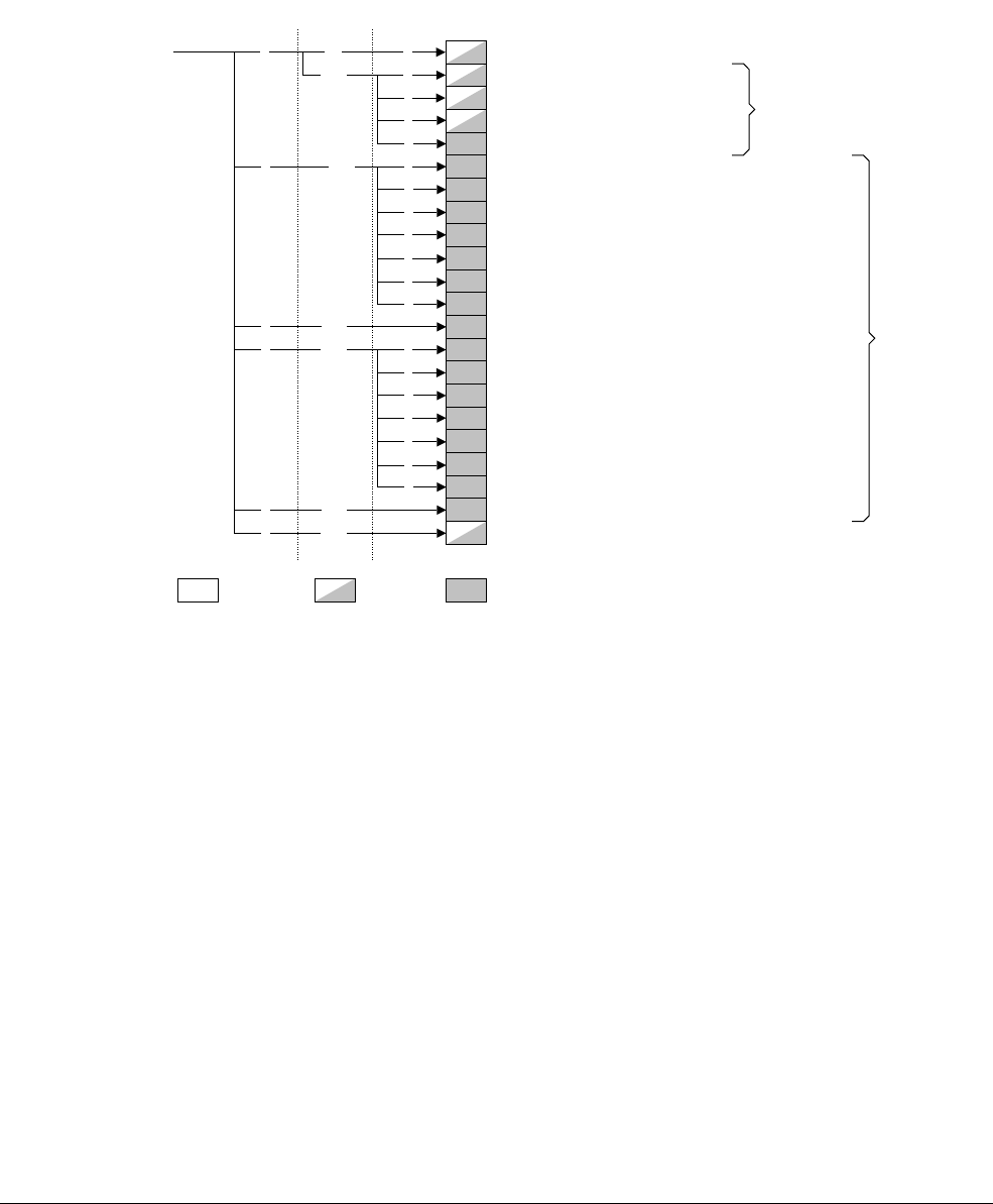
System Control Coprocessor
ARM DDI 0301H Copyright © 2004-2009 ARM Limited. All rights reserved. 3-11
ID012310 Non-Confidential, Unrestricted Access
• interrupts
• fast interrupts
• external debug requests.
The system validation registers consist of four 32-bit read/write registers. Figure 3-8 shows the
arrangement of registers.
Figure 3-8 System validation registers
The System Validation Counter Register and System Validation Operations Register reuse the
Cycle Counter Register, Count Register 0, and Count Register 1, see System performance
monitor on page 3-10, to schedule resets, interrupts and fast interrupts respectively. External
debug requests are scheduled using an additional 6 bit counter that is not used by the System
performance monitor registers.
Each of the four counters counts upwards, and when the counter overflows, the corresponding
event occurs. To the core, the events are indistinguishable from ordinary external events. The
System Validation Registers provide functions for loading the counter registers with the
required number of clock cycles before the event occurs, and starting, stopping and clearing the
counters, to return them to their System performance monitor functionality.
The System Validation Registers are usually only accessible from Secure privileged modes, but
a Secure User and Non-secure Access Validation Control Register is provided to permit access
to the System Validation Registers from User modes and Non-secure modes.
The System Validation Cache Size Mask Register masks the physical size of the caches and
TCMs to make their size appear different to the processor. You can use this in validation by
simulation, but you must not use it in a manufactured device because it can corrupt correct
operation of the processor.
Read-only Read/write
c12 4
c13
c15
Write-only
Secure User and Non-secure Access Validation Control Register
System Validation
Counter Registers
System
Validation
Operations
Registers
0
c90
Opcode_2Opcode_1 CRmCRn
System Validation Cache Size Mask Register
5
6
7
Reset counter
Interrupt counter
Fast interrupt counter
External debug request counter
0
c13
1
c13
2
c13
3
2
3
4
5
1
6
7
2
3
4
5
1
6
7
Start reset counter
Start interrupt counter
Start reset and interrupt counters
Start fast interrupt counter
Start reset and fast interrupt counters
Start interrupt and fast interrupt counters
Start reset, interrupt and fast interrupt counters
Start external debug request counter
Stop reset counter
Stop interrupt counter
Stop reset and interrupt counters
Stop fast interrupt counter
Stop reset and fast interrupt counters
Stop interrupt and fast interrupt counters
Stop reset, interrupt and fast interrupt counters
Stop external debug request counter
Accessible in User mode
c14
0

System Control Coprocessor
ARM DDI 0301H Copyright © 2004-2009 ARM Limited. All rights reserved. 3-12
ID012310 Non-Confidential, Unrestricted Access
To use the system validation registers you read or write individual registers that make up the
group, see Use of the system control coprocessor.
You cannot use the System Validation Registers at the same time as the System Performance
Monitor Registers, because both sets of registers use the same physical counters. You must
disable one set of registers before starting to use the other set. See System performance monitor
on page 3-10.
System validation behaves in three ways:
• as a set of bits that enable specific system validation functionality
• as a set of operations that schedule and clear system validation events
• as a set of numbers, values that describe aspects of the caches and TCMs for system
validation.
3.1.10 Use of the system control coprocessor
This section describes the general method for use of the system control coprocessor.
You can access system control coprocessor CP15 registers with MRC and MCR instructions.
MCR{cond} P15,<Opcode_1>,<Rd>,<CRn>,<CRm>,<Opcode_2>
MRC{cond} P15,<Opcode_1>,<Rd>,<CRn>,<CRm>,<Opcode_2>
Figure 3-9 shows the instruction bit pattern of MRC and MCR instructions.
Figure 3-9 CP15 MRC and MCR bit pattern
The CRn field of MRC and MCR instructions specifies the coprocessor register to access. The
CRm field and Opcode_2 fields specify a particular operation when addressing registers. The L
bit distinguishes between an MRC (L=1) and an MCR (L=0).
Instructions CDP, LDC, and STC, together with unprivileged MRC and MCR instructions to
privileged-only CP15 registers, and Non-secure accesses to Secure registers, cause the
processor to take the Undefined instruction trap.
Note
Attempting to read from a nonreadable register, or to write to a nonwriteable register causes
Undefined exceptions.
The Opcode_1, Opcode_2, and CRm fields Should Be Zero in all instructions that access CP15,
except when the values specified are used to select required operations. Using other values
results in Undefined exceptions.
In all cases, reading from or writing any data values to any CP15 registers, including those fields
specified as Unpredictable (UNP), Should Be One (SBO), or Should Be Zero (SBZ), does not
cause any physical damage to the chip.
Cond
31 28 27 24 23 21 20 19 16 15 12 11 8 7 5 4 3 0
1 1 1 0
Opcode_1
L CRn Rd 1 1 1 1
Opcode_2
1 CRm

System Control Coprocessor
ARM DDI 0301H Copyright © 2004-2009 ARM Limited. All rights reserved. 3-13
ID012310 Non-Confidential, Unrestricted Access
3.2 System control processor registers
This section gives details of all the registers in the system control coprocessor. The section
presents a summary of the registers and detailed descriptions in register order of CRn,
Opcode_1, CRm, Opcode_2.
You can access CP15 registers with MRC and MCR instructions:
MCR{cond} P15,<Opcode_1>,<Rd>,<CRn>,<CRm>,<Opcode_2>
MRC{cond} P15,<Opcode_1>,<Rd>,<CRn>,<CRm>,<Opcode_2>
3.2.1 Register allocation
Table 3-2 on page 3-14 lists the allocation and reset values of the registers of the system control
coprocessor where:
• CRn is the register number within CP15
• Op1 is the Opcode_1 value for the register
• CRm is the operational register
• Op2 is the Opcode_2 value for the register.
• Type applies to the Secure, S, or the Non-secure, NS, world and is:
— B, registers banked in Secure and Non-secure worlds. If the registers are not banked
then they are common to both worlds or only accessible in one world.
— NA, no access
—RO, read-only access
— RO, read-only access in privileged modes only
—R/W, read/write access
— R/W, read/write access in privileged modes only
—WO, write-only access
— WO, write-only access in privileged modes only
— X, access depends on another register or external signal.

System Control Coprocessor
ARM DDI 0301H Copyright © 2004-2009 ARM Limited. All rights reserved. 3-14
ID012310 Non-Confidential, Unrestricted Access
Table 3-2 Summary of CP15 registers and operations
CRn Op1 CRm Op2 Register or operation S type NS
type
Reset
value Page
c0 0 c0 0 Main ID RO RO
0x41xFB76x
apage 3-20
1 Cache Type RO RO
0x10152152
bpage 3-21
2 TCM Status RO RO
0x00020002
cpage 3-24
3 TLB Type RO RO
0x00000800
page 3-25
c1 0 Processor Feature 0 RO RO
0x00000111
page 3-26
1 Processor Feature 1 RO RO
0x00000011
page 3-27
2 Debug Feature 0 RO RO
0x00000033
page 3-29
3 Auxiliary Feature 0 RO RO
0x00000000
page 3-30
4 Memory Model Feature 0 RO RO
0x01130003
page 3-31
5 Memory Model Feature 1 RO RO
0x10030302
page 3-32
6 Memory Model Feature 2 RO RO
0x01222100
page 3-33
7 Memory Model Feature 3 RO RO
0x00000000
page 3-35
c2 0 Instruction Set Feature
Attribute 0
RO RO
0x00140011
page 3-36
1 Instruction Set Feature
Attribute 1
RO RO
0x12002111
page 3-37
2 Instruction Set Feature
Attribute 2
RO RO
0x11231121
page 3-39
3 Instruction Set Feature
Attribute 3
RO RO
0x01102131
page 3-40
4 Instruction Set Feature
Attribute 4
RO RO
0x00001141
page 3-42
5 Instruction Set Feature
Attribute 5
RO RO
0x00000000
page 3-43
6-7 Reserved - - - -
c3-c7 - Reserved - - - -
c1 0 c0 0 Control R/W, Bd, X R/W
0x00050078
epage 3-44
1 Auxiliary Control R/W RO
0x00000007
page 3-48
2 Coprocessor Access Control R/W R/W
0x00000000
page 3-51
c1 0 Secure Configuration R/W NA
0x00000000
page 3-52
1 Secure Debug Enable R/W NA
0x00000000
page 3-54
2 Non-Secure Access Control R/W RO
0x00000000
page 3-55

System Control Coprocessor
ARM DDI 0301H Copyright © 2004-2009 ARM Limited. All rights reserved. 3-15
ID012310 Non-Confidential, Unrestricted Access
c2 0 c0 0 Translation Table Base 0 R/W, B, X R/W
0x00000000
page 3-57
1 Translation Table Base 1 R/W, B R/W
0x00000000
page 3-59
2 Translation Table Base Control R/W, B, X R/W
0x00000000
page 3-60
c3 0 c0 0 Domain Access Control R/W, B, X R/W
0x00000000
page 3-63
c4 Not used
c5 0 c0 0 Data Fault Status R/W, B R/W
0x00000000
page 3-64
1 Instruction Fault Status R/W, B R/W
0x00000000
page 3-66
c6 0 c0 0 Fault Address R/W, B R/W
0x00000000
page 3-68
1 Watchpoint Fault Address R/W NA
0x00000000
page 3-69
2 Instruction Fault Address R/W, B R/W
0x00000000
page 3-69
c7 0 c0 4 Wait For Interrupt WO WO - page 3-85
c4 0 PA R/W, B R/W
0x00000000
page 3-80
c5 0 Invalidate Entire Instruction
Cache
WO WO, X - page 3-71
1 Invalidate Instruction Cache
Line by MVA
WO WO - page 3-71
2 Invalidate Instruction Cache
Line by Index
WO WO - page 3-71
4 Flush Prefetch Buffer WO WO -page3-79
6 Flush Entire Branch Target
Cache
WO WO - page 3-79
7 Flush Branch Target Cache
Entry by MVA
WO WO - page 3-79
c6 0 Invalidate Entire Data Cache WO NA - page 3-71
1 Invalidate Data Cache Line by
MVA
WO WO - page 3-71
2 Invalidate Data Cache Line by
Index
WO WO - page 3-71
c7 0 Invalidate Both Caches WO NA - page 3-71
c8 0-3 VA to PA translation in the
current world
WO WO - page 3-82
4-7 VA to PA translation in the
other world
WO NA - page 3-83
Table 3-2 Summary of CP15 registers and operations (continued)
CRn Op1 CRm Op2 Register or operation S type NS
type
Reset
value Page

System Control Coprocessor
ARM DDI 0301H Copyright © 2004-2009 ARM Limited. All rights reserved. 3-16
ID012310 Non-Confidential, Unrestricted Access
c7 0 c10 0 Clean Entire Data Cache WO, X WO, X - page 3-71
1 Clean Data Cache Line by
MVA
WO WO - page 3-71
2 Clean Data Cache Line by
Index
WO WO - page 3-71
4 Data Synchronization Barrier WO WO -page3-83
5 Data Memory Barrier WO WO -page3-84
6 Cache Dirty Status RO, B RO
0x00000000
page 3-78
c13 1 Prefetch Instruction Cache
Line
WO WO - page 3-71
c14 0 Clean and Invalidate Entire
Data Cache
WO, X WO, X - page 3-71
1 Clean and Invalidate Data
Cache Line by MVA
WO WO - page 3-71
2 Clean and Invalidate Data
Cache Line by Index
WO WO - page 3-71
c8 0 c5 0 Invalidate Instruction TLB
unlocked entries
WO, B WO - page 3-86
1 Invalidate Instruction TLB
entry by MVA
WO, B WO - page 3-86
2 Invalidate Instruction TLB
entry on ASID match
WO, B WO - page 3-86
c8 0 c6 0 Invalidate Data TLB unlocked
entries
WO, B WO - page 3-86
1 Invalidate Data TLB entry by
MVA
WO, B WO - page 3-86
2 Invalidate Data TLB entry on
ASID match
WO, B WO - page 3-86
c7 0 Invalidate unified TLB
unlocked entries
WO, B WO - page 3-86
1 Invalidate unified TLB entry
by MVA
WO, B WO - page 3-86
2 Invalidate unified TLB entry
on ASID match
WO, B WO - page 3-86
Table 3-2 Summary of CP15 registers and operations (continued)
CRn Op1 CRm Op2 Register or operation S type NS
type
Reset
value Page

System Control Coprocessor
ARM DDI 0301H Copyright © 2004-2009 ARM Limited. All rights reserved. 3-17
ID012310 Non-Confidential, Unrestricted Access
c9 0 c0 0 Data Cache Lockdown R/W R/W, X
0xFFFFFFF0
page 3-87
1 Instruction Cache Lockdown R/W R/W, X
0xFFFFFFF0
page 3-87
c1 0 Data TCM Region R/W, X R/W, X
0x00000014
fpage 3-89
1 Instruction TCM Region R/W, X R/W, X
0x00000014
gpage 3-91
2 Data TCM Non-secure Control
Access
R/W, X NA
0x00000000
page 3-93
3 Instruction TCM Non-secure
Control Access
R/W, X NA
0x00000000
page 3-94
c2 0 TCM Selection R/W, B R/W
0x00000000
page 3-96
c8 0 Cache Behavior Override R/WhR/W
0x00000000
page 3-97
c10 0 c0 0 TLB Lockdown R/W, X R/W, X
0x00000000
page 3-100
c2 0 Primary Region Memory
Remap Register
R/W, B, X R/W
0x00098AA4
page 3-101
1 Normal Memory Region
Remap Register
R/W, B, X R/W
0x44E048E0
page 3-101
c11 0 c0 0-3 DMA identification and status RO RO, X
0x0000000B
ipage 3-106
c1 0 DMA User Accessibility R/W R/W, X
0x00000000
page 3-107
c2 0 DMA Channel Number R/W, X R/W, X
0x00000000
page 3-109
c3 0-2 DMA enable WO, X WO, X - page 3-110
c4 0 DMA Control R/W, X R/W, X
0x08000000
page 3-112
c5 0 DMA Internal Start Address R/W, X R/W, X - page 3-114
c6 0 DMA External Start Address R/W, X R/W, X - page 3-115
c7 0 DMA Internal End Address R/W, X R/W, X - page 3-116
c8 0 DMA Channel Status RO, X RO, X
0x00000000
page 3-117
c15 0 DMA Context ID R/W R/W, X - page 3-120
c12 0 c0 0 Secure or Non-secure Vector
Base Address
R/W, B, X R/W
0x00000000
page 3-121
1 Monitor Vector Base Address R/W, X NA
0x00000000
page 3-122
c1 0 Interrupt Status RO RO
0x00000000
jpage 3-123
Table 3-2 Summary of CP15 registers and operations (continued)
CRn Op1 CRm Op2 Register or operation S type NS
type
Reset
value Page

System Control Coprocessor
ARM DDI 0301H Copyright © 2004-2009 ARM Limited. All rights reserved. 3-18
ID012310 Non-Confidential, Unrestricted Access
c13 0 c0 0 FCSE PID R/W, B, X R/W
0x00000000
page 3-126
1 Context ID R/W, B R/W
0x00000000
page 3-128
2 User Read/Write Thread and
Process ID
R/W, B R/W
0x00000000
page 3-129
3 User Read-only Thread and
Process ID
R/W, RO,
Bk
R/W,
RO
0x00000000
page 3-129
4 Privileged Only Thread and
Process ID
R/W, B R/W
0x00000000
page 3-129
c14 Not used
c15 0 c2 4 Peripheral Port Memory
Remap
R/W, B, X R/W
0x00000000
page 3-130
c9 0 Secure User and Non-secure
Access Validation Control
R/W, X NA
0x00000000
page 3-132
c12 0 Performance Monitor Control R/W, X R/W, X
0x00000000
page 3-133
1 Cycle Counter R/W, X R/W, X
0x00000000
page 3-137
2 Count 0 R/W, X R/W, X
0x00000000
page 3-138
3 Count 1 R/W, X R/W, X
0x00000000
page 3-139
4-7 System Validation Counter R/W, X R/W, X
0x00000000
page 3-140
c13 1-7 System Validation Operations R/W, X R/W, X
0x00000000
page 3-142
c14 0 System Validation Cache Size
Mask
R/W, X R/W, X
0x00006655
lpage 3-145
c15 1 c13 0-7 System Validation Operations R/W, X R/W, X
0x00000000
page 3-142
c15 2 c13 1-7 System Validation Operations R/W, X R/W, X
0x00000000
page 3-142
c15 3 c8 0-7 Instruction Cache Master Valid R/W, X NA
0x00000000
page 3-147
c12 0-7 Data Cache Master Valid R/W, X NA
0x00000000
page 3-148
c13 0-7 System Validation Operations R/W, X R/W, X
0x00000000
page 3-142
c15 4 c13 0-7 System Validation Operations R/W, X R/W, X
0x00000000
page 3-142
c15 5 c4 2 TLB Lockdown Index R/W, X NA
0x00000000
page 3-149
c5 2 TLB Lockdown VA R/W, X NA - page 3-149
c6 2 TLB Lockdown PA R/W, X NA - page 3-149
c7 2 TLB Lockdown Attributes R/W, X NA - page 3-149
c13 0-7 System Validation Operations R/W, X R/W, X
0x00000000
page 3-142
c15 6 c13 0-7 System Validation Operations R/W, X R/W, X
0x00000000
page 3-142
c15 7 c13 0-7 System Validation Operations R/W, X R/W, X
0x00000000
page 3-142
a. See c0, Main ID Register on page 3-20 for the values of bits [23:20] and bits [3:0].
Table 3-2 Summary of CP15 registers and operations (continued)
CRn Op1 CRm Op2 Register or operation S type NS
type
Reset
value Page

System Control Coprocessor
ARM DDI 0301H Copyright © 2004-2009 ARM Limited. All rights reserved. 3-19
ID012310 Non-Confidential, Unrestricted Access
Table 3-3 lists the operations available with MCRR operations:
MCRR{cond} P15,<Opcode_1>,<End Address>,<Start Address>,<CRm>
b. Reset value depends on the cache size implemented. The value here is for 16KB instruction and data caches.
c. Reset value depends on the number of TCM banks implemented. The value here is for 2 data TCM and 2 instruction TCM
banks.
d. Some bits in this register are banked and some Secure modify only.
e. Reset value depends on external signals.
f. Reset value depends on the TCM sizes implemented. The value here is for 16KB TCM banks.
g. Reset value depends on the TCM sizes implemented, and on the value of the INITRAM static configuration signal. The value
here is for 16KB TCM banks, with INITRAM tied LOW.
h. Some bits in this register are common and some Secure modify only.
i. Reset value depends on the number of DMA channels implemented and the presence of TCMs.
j. Reset value depends on external signals.
k. This register is read/write in Privileged modes and read-only on User mode.
l. Reset value depends on the cache and TCM sizes implemented. The value here is for 2 banks of 16KB instruction and data
TCMs and 16KB instruction and data caches.
Table 3-3 Summary of CP15 MCRR operations
Op1 CRm Register or operation S type NS type Reset value Page
0 c5 Invalidate instruction cache range WO WO - page 3-69
c6 Invalidate data cache range WO WO - page 3-69
c12 Clean data cache range WO WO -page3-69
c14 Clean and invalidate data cache range WO WO - page 3-69

System Control Coprocessor
ARM DDI 0301H Copyright © 2004-2009 ARM Limited. All rights reserved. 3-20
ID012310 Non-Confidential, Unrestricted Access
3.2.2 c0, Main ID Register
The purpose of the Main ID Register is to return the device ID code that contains information
about the processor.
The Main ID Register is:
•in CP15 c0
• a 32 bit read-only register common to the Secure and Non-secure worlds
• accessible in privileged modes only.
Figure 3-10 shows the arrangement of bits in the register.
Figure 3-10 Main ID Register format
The contents of the Main ID Register depend on the specific implementation. Table 3-4 lists
how the bit values correspond with the Main ID Register functions.
Note
If an Opcode_2 value corresponding to an unimplemented or reserved ID register with CRm
equal to c0 and Opcode_1 = 0 is encountered, the system control coprocessor returns the value
of the main ID register.
Table 3-5 lists the results of attempted access for each mode.
Variant
number
Implementor
31 24 23 20 19 16 15 4 3 0
Architecture Primary part number Revision
Table 3-4 Main ID Register bit functions
Bits Field name Function
[31:24] Implementor Indicates implementor, ARM Limited:
0x41
[23:20] Variant number The major revision number n in the rn part of the rnpn revision status.
0x0
[19:16] Architecture Indicates that the architecture is given in the CPUID registers:
0xF
[15:4] Primary part number Indicates part number, ARM1176JZF-S:
0xB76
[3:0] Revision The minor revision number n in the pn part of the rnpn revision status. For example:
for release r0p0:
0x0
for release r0p7:
0x7
Table 3-5 Results of access to the Main ID Register
Secure Privileged Non-secure Privileged
User
Read Write Read Write
Data Undefined exception Data Undefined exception Undefined exception
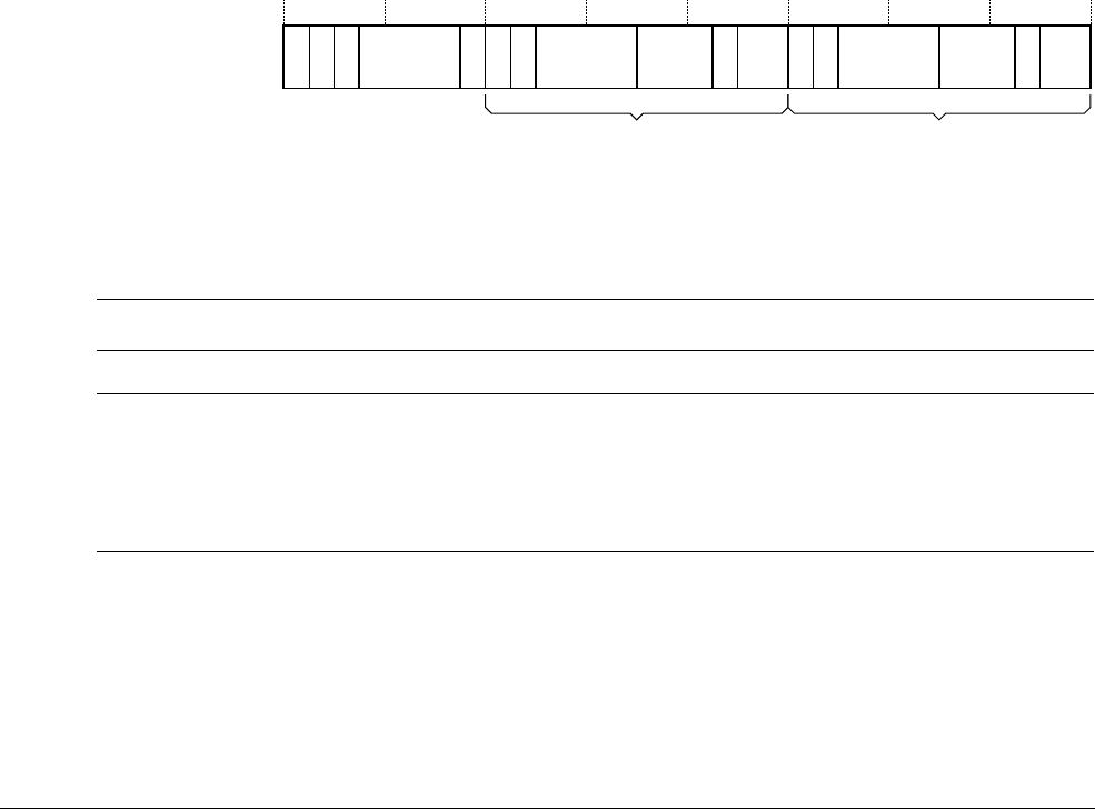
System Control Coprocessor
ARM DDI 0301H Copyright © 2004-2009 ARM Limited. All rights reserved. 3-21
ID012310 Non-Confidential, Unrestricted Access
To use the Main ID Register read CP15 with:
• Opcode_1 set to 0
• CRn set to c0
• CRm set to c0
• Opcode_2 set to 0.
For example:
MRC p15,0,<Rd>,c0,c0,0 ;Read Main ID Register
For more information on the processor features, see c0, CPUID registers on page 3-26.
3.2.3 c0, Cache Type Register
The purpose of the Cache Type Register is to provide information about the size and architecture
of the cache for the operating system. This enables the operating system to establish how to
clean the cache and how to lock it down. Inclusion of this register enables RTOS vendors to
produce future-proof versions of their operating systems.
The Cache Type Register is:
•in CP15 c0
• a 32-bit read only register, common to Secure and Non-secure worlds
• accessible in privileged modes only.
All ARMv4T and later cached processors contain this register. Figure 3-11 shows the
arrangement of bits in the Cache Type Register.
Figure 3-11 Cache Type Register format
Table 3-6 lists how the bit values correspond with the Cache Type Register functions.
0
31 30 29 28 25 24 23 12 11 0
0 0 Ctype S P 0 Size Assoc M LenP 0 Size Assoc M Len
Dsize Isize
22 21 18 17 15 14 13 10 9 6 5 3 2 1
Table 3-6 Cache Type Register bit functions
Bits Field name Function
[31:29] - 0
[28:25] Ctype The Cache type and Separate bits provide information about the cache architecture.
b1110, indicates that the ARM1176JZF-S processor supports:
• write back cache
• Format C cache lockdown
• Register 7 cache cleaning operations.
[24] S bit S = 1, indicates that the processor has separate instruction and data caches and not a unified
cache.

System Control Coprocessor
ARM DDI 0301H Copyright © 2004-2009 ARM Limited. All rights reserved. 3-22
ID012310 Non-Confidential, Unrestricted Access
[23:12] Dsize Provides information about the size and construction of the Data cache.
Note
The ARM1176JZF-S processor does not support cache sizes of less than 4KB.
[23] P bit The P, Page, bit indicates restrictions on page allocation for bits [13:12] of the VA
For ARM1176JZF-S processors, the P bit is set if the cache size is greater than 16KB. For
more details see Restrictions on page table mappings page coloring on page 6-41.
0 = no restriction on page allocation.
1 = restriction applies to page allocation.
[22] - 0
[21:18] Size The Size field indicates the cache size in conjunction with the M bit.
b0000 = 0.5KB cache, not supported
b0001 = 1KB cache, not supported
b0010 = 2KB cache, not supported
b0011 = 4KB cache
b0100 = 8KB cache
b0101 = 16KB cache
b0110 = 32KB cache
b0111 = 64KB cache
b1000 = 128KB cache, not supported.
[17:15] Assoc b010, indicates that the ARM1176JZF-S processor has 4-way associativity. All other values
for Assoc are reserved.
[14] M bit Indicates the cache size and cache associativity values in conjunction with the Size and Assoc
fields.
In the ARM1176JZF-S processor the M bit is set to 0, for the Data and Instruction Caches.
[13:12] Len b10, indicates that ARM1176JZF-S processor has a cache line length of 8 words, that is 32
bytes. All other values for Len are reserved.
[11:0] Isize Provides information about the size and construction of the Instruction cache.
[11] P The functions of the Isize bit fields are the same as the equivalent Dsize bit fields and the Isize
values have the corresponding meanings.
[10] -
[9:6] Size
[5:3] Assoc
[2] M
[1:0] Len
Table 3-6 Cache Type Register bit functions (continued)
Bits Field name Function

System Control Coprocessor
ARM DDI 0301H Copyright © 2004-2009 ARM Limited. All rights reserved. 3-23
ID012310 Non-Confidential, Unrestricted Access
Table 3-7 lists the results of attempted access for each mode.
To use the Cache Type Register read CP15 with:
• Opcode_1 set to 0
• CRn set to c0
• CRm set to c0
• Opcode_2 set to 1.
For example:
MRC p15,0,<Rd>,c0,c0,1; returns cache details
Table 3-8, for example, lists the Cache Type Register values for an ARM1176JZF-S processor
with:
• separate instruction and data caches
• cache size = 16KB
• associativity = 4-way
• line length = eight words
• caches use write-back, CP15 c7 for cache cleaning, and Format C for cache lockdown.
Table 3-7 Results of access to the Cache Type Register
Secure Privileged Non-secure Privileged
User
Read Write Read Write
Data Undefined exception Data Undefined exception Undefined exception
Table 3-8 Example Cache Type Register format
Bits Field name Value Behavior
[31:29] Reserved b000
[28:25] Ctype b1110
[24] S b1 Harvard cache
[23] Dsize P b0
[22] Reserved b0
[21:18] Size b0101 16KB
[17:15] Assoc b010 4-way
[14] M b0
[13:12] Len b10 8 words per line, 32 bytes
[11] Isize P b0
[10] Reserved b0
[9:6] Size b0101 16KB
[5:3] Assoc b010 4-way
[2] M b0
[1:0] Len b10 8 words per line, 32 bytes

System Control Coprocessor
ARM DDI 0301H Copyright © 2004-2009 ARM Limited. All rights reserved. 3-24
ID012310 Non-Confidential, Unrestricted Access
3.2.4 c0, TCM Status Register
The purpose of the TCM Status Register is to inform the system about the number of Instruction
and Data TCMs available in the processor.
Table 3-9 lists the purposes of the individual bits in the TCM Status Register.
Note
In the ARM1176JZF-S processor there is a maximum of two Instruction TCMs and two Data
TCMs.
The TCM Status Register is:
•in CP15 c0
• a 32-bit read-only register common to Secure and Non-secure worlds
• accessible in privileged modes only.
Figure 3-12 shows the bit arrangement for the TCM Status Register.
Figure 3-12 TCM Status Register format
Table 3-9 lists how the bit values correspond with the TCM Status Register functions.
Attempts to write the TCM Status Register or read it in User modes result in Undefined
exceptions.
To use the TCM Status Register read CP15 with:
• Opcode_1 set to 0
• CRn set to c0
• CRm set to c0
• Opcode_2 set to 2.
0
31 30 29 28 19 18 16 15 3 2 0
0 0 SBZ/UNP DTCM SBZ/UNP ITCM
Table 3-9 TCM Status Register bit functions
Bits Field name Function
[31:29] - Always b000.
[28:19] - UNP/SBZ
[18:16] DTCM Indicates the number of Data TCM banks implemented.
b000 = 0 Data TCMs
b001 = 1 Data TCM
b010 = 2 Data TCMs
All other values reserved
[15:3] - UNP/SBZ
[2:0] ITCM Indicates the number of Instruction TCM banks implemented.
b000 = 0 Instruction TCMs
b001 = 1 Instruction TCM
b010 = 2 Instruction TCMs
All other values reserved

System Control Coprocessor
ARM DDI 0301H Copyright © 2004-2009 ARM Limited. All rights reserved. 3-25
ID012310 Non-Confidential, Unrestricted Access
For example:
MRC p15,0,<Rd>,c0,c0,2 ; returns TCM status register
3.2.5 c0, TLB Type Register
The purpose of the TLB Type Register is to return the number of lockable entries for the TLB.
The TLB has 64 entries organized as a unified two-way set associative TLB. In addition, it has
eight lockable entries that the read-only TLB Type Register specifies.
The TLB Type Register is:
•in CP15 c0
• a 32-bit read only register common to the Secure and Non-secure worlds
• accessible in privileged modes only.
Figure 3-13 shows the bit arrangement for the TLB Type Register.
Figure 3-13 TLB Type Register format
Table 3-10 lists how the bit values correspond with the TLB Type Register functions.
Table 3-11 lists the results of attempted access for each mode.
To use the TLB Type Register read CP15 with:
• Opcode_1 set to 0
• CRn set to c0
• CRm set to c0
• Opcode_2 set to 3.
USBZ/UNP
31 24 23 16 15 8 7 1 0
ILsize DLsize SBZ/UNP
Table 3-10 TLB Type Register bit functions
Bits Field name Function
[31:24] - UNP/SBZ
[23:16] ILsize Instruction lockable size specifies the number of instruction TLB lockable entries
0, indicates that the ARM1176JZF-S processor has a unified TLB
[15:8] DLsize Data lockable size specifies the number of unified or data TLB lockable entries
0x08
, indicates the ARM1176JZF-S processors has 8 unified TLB lockable entries
[7:1] - UNP/SBZ
[0] U Unified specifies if the TLB is unified, 0, or if there are separate instruction and data TLBs, 1.
0, indicates that the ARM1176JZF-S processor has a unified TLB
Table 3-11 Results of access to the TLB Type Register
Secure Privileged Non-secure Privileged
User
Read Write Read Write
Data Undefined exception Data Undefined exception Undefined exception

System Control Coprocessor
ARM DDI 0301H Copyright © 2004-2009 ARM Limited. All rights reserved. 3-26
ID012310 Non-Confidential, Unrestricted Access
For example:
MRC p15,0,<Rd>,c0,c0,3 ; returns TLB details
3.2.6 c0, CPUID registers
The section describes the CPUIID registers:
•c0, Processor Feature Register 0
•c0, Processor Feature Register 1 on page 3-27
•c0, Debug Feature Register 0 on page 3-29
•c0, Auxiliary Feature Register 0 on page 3-30
•c0, Memory Model Feature Register 0 on page 3-31
•c0, Memory Model Feature Register 1 on page 3-32
•c0, Memory Model Feature Register 2 on page 3-33
•c0, Memory Model Feature Register 3 on page 3-35
•c0, Instruction Set Attributes Register 0 on page 3-36
•c0, Instruction Set Attributes Register 1 on page 3-37
•c0, Instruction Set Attributes Register 2 on page 3-39
•c0, Instruction Set Attributes Register 3 on page 3-40
•c0, Instruction Set Attributes Register 4 on page 3-42
•c0, Instruction Set Attributes Register 5 on page 3-43.
Note
The CPUID registers are sometimes described as the Core Feature ID registers.
c0, Processor Feature Register 0
The purpose of the Processor Feature Register 0 is to provide information about the execution
state support and programmer’s model for the processor.
Processor Feature Register 0 is:
•in CP15 c0
• a 32-bit read-only register common to the Secure and Non-secure worlds
• accessible in privileged modes only.
Table 3-12 lists how the bit values correspond with the Processor Feature Register 0 functions.
Figure 3-14 shows the bit arrangement for Processor Feature Register 0.
Figure 3-14 Processor Feature Register 0 format
Table 3-12 Processor Feature Register 0 bit functions
Bits Field name Function
[31:28] - Reserved. RAZ.
[27:24] - Reserved. RAZ.
[23:20] - Reserved. RAZ.
ReservedReservedReserved State3 State2 State1 State0Reserved
31 16 15 12 11 8 7 4 3 0
28 27 24 23 20 19

System Control Coprocessor
ARM DDI 0301H Copyright © 2004-2009 ARM Limited. All rights reserved. 3-27
ID012310 Non-Confidential, Unrestricted Access
Table 3-13 lists the results of attempted access for each mode.
To use the Processor Feature Register 0 read CP15 with:
• Opcode_1 set to 0
• CRn set to c0
• CRm set to c1
• Opcode_2 set to 0.
For example:
MRC p15, 0, <Rd>, c0, c1, 0 ;Read Processor Feature Register 0
c0, Processor Feature Register 1
The purpose of the Processor Feature Register 1 is to provide information about the execution
state support and programmer’s model for the processor.
Processor Feature Register 1 is:
•in CP15 c0
• a 32-bit read-only register common to the Secure and Non-secure worlds
• accessible in privileged modes only.
Figure 3-15 on page 3-28 shows the bit arrangement for Processor Feature Register 1.
[19:16] - Reserved. RAZ.
[15:12] State3 Indicates support for Thumb-2™ execution environment.
0x0
, ARM1176JZF-S processors do not support Thumb-2.
[11:8] State2 Indicates support for Java extension interface.
0x1
, ARM1176JZF-S processors support Java.
[7:4] State1 Indicates type of Thumb encoding that the processor supports.
0x1
, ARM1176JZF-S processors support Thumb-1 but do not support Thumb-2.
[3:0] State0 Indicates support for 32-bit ARM instruction set.
0x1
, ARM1176JZF-S processors support 32-bit ARM instructions.
Table 3-12 Processor Feature Register 0 bit functions (continued)
Bits Field name Function
Table 3-13 Results of access to the Processor Feature Register 0
Secure Privileged Non-secure Privileged
User
Read Write Read Write
Data Undefined exception Data Undefined exception Undefined exception

System Control Coprocessor
ARM DDI 0301H Copyright © 2004-2009 ARM Limited. All rights reserved. 3-28
ID012310 Non-Confidential, Unrestricted Access
Figure 3-15 Processor Feature Register 1 format
Table 3-14 lists how the bit values correspond with the Processor Feature Register 1 functions.
Table 3-15 lists the results of attempted access for each mode.
To use the Processor Feature Register 1 read CP15 with:
• Opcode_1 set to 0
• CRn set to c0
• CRm set to c1
• Opcode_2 set to 1.
For example:
MRC p15, 0, <Rd>, c0, c1, 1 ;Read Processor Feature Register 1
ReservedReservedReservedReservedReserved
31 8 7 4 3 016 15 12 1128 27 24 23 20 19
Microcontroller programmer's model
Security extension
Programmer's model
Table 3-14 Processor Feature Register 1 bit functions
Bits Field name Function
[31:28] - Reserved. RAZ
[27:24] - Reserved. RAZ.
[23:20] - Reserved. RAZ.
[19:16] - Reserved. RAZ.
[15:12] - Reserved. RAZ.
[11:8] Microcontroller programmer’s model Indicates support for the ARM microcontroller programmer’s model.
0x0
, Not supported by ARM1176JZF-S processors.
[7:4] Security extension Indicates support for Security Extensions Architecture v1.
0x1
, ARM1176JZF-S processors support Security Extensions
Architecture v1, TrustZone.
[3:0] Programmer’s model Indicates support for standard ARMv4 programmer’s model.
0x1
, ARM1176JZF-S processors support the ARMv4 model.
Table 3-15 Results of access to the Processor Feature Register 1
Secure Privileged Non-secure Privileged
User
Read Write Read Write
Data Undefined exception Data Undefined exception Undefined exception

System Control Coprocessor
ARM DDI 0301H Copyright © 2004-2009 ARM Limited. All rights reserved. 3-29
ID012310 Non-Confidential, Unrestricted Access
c0, Debug Feature Register 0
The purpose of the Debug Feature Register 0 is to provide information about the debug system
for the processor.
Debug Feature Register 0 is:
•in CP15 c0
• a 32-bit read-only register common to the Secure and Non-secure worlds
• accessible in privileged modes only.
Figure 3-16 shows the bit arrangement for Debug Feature Register 0.
Figure 3-16 Debug Feature Register 0 format
Table 3-16 lists how the bit values correspond with the Debug Feature Register 0 functions.
Table 3-17 lists the results of attempted access for each mode.
To use the Debug Feature Register 0 read CP15 with:
• Opcode_1 set to 0
Reserved ---Reserved
31 12 11 8 7 4 3 0
---
24 23 20 19 16 1528 27
Table 3-16 Debug Feature Register 0 bit functions
Bits Field name Function
[31:28] - Reserved. RAZ.
[27:24] - Reserved. RAZ.
[23:20] - Indicates the type of memory-mapped microcontroller debug model that the processor
supports.
0x0
, ARM1176JZF-S processors do not support this debug model.
[19:16] - Indicates the type of memory-mapped Trace debug model that the processor supports.
0x0
, ARM1176JZF-S processors do not support this debug model.
[15:12] - Indicates the type of coprocessor-based Trace debug model that the processor supports.
0x0
, ARM1176JZF-S processors do not support this debug model.
[11:8] - Indicates the type of embedded processor debug model that the processor supports.
0x0
, ARM1176JZF-S processors do not support this debug model.
[7:4] - Indicates the type of Secure debug model that the processor supports.
0x3
, ARM1176JZF-S processors support the v6.1 Secure debug architecture based model.
[3:0] - Indicates the type of applications processor debug model that the processor supports.
0x3
, ARM1176JZF-S processors support the v6.1 debug model.
Table 3-17 Results of access to the Debug Feature Register 0
Secure Privileged Non-secure Privileged
User
Read Write Read Write
Data Undefined exception Data Undefined exception Undefined exception

System Control Coprocessor
ARM DDI 0301H Copyright © 2004-2009 ARM Limited. All rights reserved. 3-30
ID012310 Non-Confidential, Unrestricted Access
• CRn set to c0
• CRm set to c1
• Opcode_2 set to 2.
For example:
MRC p15, 0, <Rd>, c0, c1, 2 ;Read Debug Feature Register 0
c0, Auxiliary Feature Register 0
The purpose of the Auxiliary Feature Register 0 is to provide additional information about the
features of the processor.
The Auxiliary Feature Register 0 is:
•in CP15 c0
• a 32-bit read-only register common to the Secure and Non-secure worlds
• accessible in privileged modes only.
Table 3-18 lists how the bit values correspond with the Auxiliary Feature Register 0 functions.
The contents of the Auxiliary Feature Register 0 [31:16] are Reserved. The contents of the
Auxiliary Feature Register 0 [15:0] are Implementation Defined. In the ARM1176JZF-S
processor, the Auxiliary Feature Register 0 reads as
0x00000000
.
Table 3-19 lists the results of attempted access for each mode.
To use the Auxiliary Feature Register 0 read CP15 with:
• Opcode_1 set to 0
• CRn set to c0
• CRm set to c1
• Opcode_2 set to 3.
For example:
MRC p15, 0, <Rd>, c0, c1, 3 ;Read Auxiliary Feature Register 0.
Table 3-18 Auxiliary Feature Register 0 bit functions
Bits Field name Function
[31:16] - Reserved. RAZ.
[15:12] - Implementation Defined.
[11:8] - Implementation Defined.
[7:4] - Implementation Defined.
[3:0] - Implementation Defined.
Table 3-19 Results of access to the Auxiliary Feature Register 0
Secure Privileged Non-secure Privileged
User
Read Write Read Write
Data Undefined exception Data Undefined exception Undefined exception

System Control Coprocessor
ARM DDI 0301H Copyright © 2004-2009 ARM Limited. All rights reserved. 3-31
ID012310 Non-Confidential, Unrestricted Access
c0, Memory Model Feature Register 0
The purpose of the Memory Model Feature Register 0 is to provide information about the
memory model, memory management, cache support, and TLB operations of the processor.
The Memory Model Feature Register 0 is:
•in CP15 c0
• a 32-bit read-only register common to the Secure and Non-secure worlds
• accessible in privileged modes only.
Figure 3-17 shows the bit arrangement for Memory Model Feature Register 0.
Figure 3-17 Memory Model Feature Register 0 format
Table 3-20 lists how the bit values correspond with the Memory Model Feature Register 0
functions.
Table 3-21 lists the results of attempted access for each mode.
- - - - - -Reserved
31 28 27 24 23 20 19 16 15 12 11 8 7 4 3 0
-
Table 3-20 Memory Model Feature Register 0 bit functions
Bits Field name Function
[31:28] - Reserved. RAZ.
[27:24] - Indicates support for FCSE.
0x1
, ARM1176JZF-S processors support FCSE.
[23:20] - Indicates support for the ARMv6 Auxiliary Control Register.
0x1
, ARM1176JZF-S processors support the Auxiliary Control Register.
[19:16] - Indicates support for TCM and associated DMA.
0x3
, ARM1176JZF-S processors support ARMv6 TCM and DMA.
[15:12] - Indicates support for cache coherency with DMA agent, shared memory.
0x0
, ARM1176JZF-S processors do not support this model.
[11:8] - Indicates support for cache coherency support with CPU agent, shared memory.
0x0
, ARM1176JZF-S processors do not support this model.
[7:4] - Indicates support for Protected Memory System Architecture (PMSA).
0x0
, ARM1176JZF-S processors do not support PMSA
[3:0] - Indicates support for Virtual Memory System Architecture (VMSA).
0x3
, ARM1176JZF-S processors support:
• VMSA v7 remapping and access flag.
Table 3-21 Results of access to the Memory Model Feature Register 0
Secure Privileged Non-secure Privileged
User
Read Write Read Write
Data Undefined exception Data Undefined exception Undefined exception

System Control Coprocessor
ARM DDI 0301H Copyright © 2004-2009 ARM Limited. All rights reserved. 3-32
ID012310 Non-Confidential, Unrestricted Access
To use the Memory Model Feature Register 0 read CP15 with:
• Opcode_1 set to 0
• CRn set to c0
• CRm set to c1
• Opcode_2 set to 4.
For example:
MRC p15, 0, <Rd>, c0, c1, 4 ;Read Memory Model Feature Register 0.
c0, Memory Model Feature Register 1
The purpose of the Memory Model Feature Register 1 is to provide information about the
memory model, memory management, cache support, and TLB operations of the processor.
The Memory Model Feature Register 1 is:
•in CP15 c0
• a 32-bit read-only register common to the Secure and Non-secure worlds
• accessible in privileged modes only.
Figure 3-18 shows the bit arrangement for Memory Model Feature Register 1.
Figure 3-18 Memory Model Feature Register 1 format
Table 3-22 lists how the bit values correspond with the Memory Model Feature Register 1
functions.
-------
31 28 27 24 23 20 19 16 15 12 11 8 7 4 3 0
-
Table 3-22 Memory Model Feature Register 1 bit functions
Bits Field
name Function
[31:28] - Indicates support for branch target buffer.
0x1
, ARM1176JZF-S processors require flushing of branch predictor on VA change.
[27:24] - Indicates support for test and clean operations on data cache, Harvard or unified architecture.
0x0
, no support in ARM1176JZF-S processors.
[23:20] - Indicates support for level one cache, all maintenance operations, unified architecture.
0x0
, no support in ARM1176JZF-S processors.
[19:16] - Indicates support for level one cache, all maintenance operations, Harvard architecture.
0x3
, ARM1176JZF-S processors support:
• invalidate instruction cache including branch prediction
• invalidate data cache
• invalidate instruction and data cache including branch prediction
• clean data cache, recursive model using cache dirty status bit
• clean and invalidate data cache, recursive model using cache dirty status bit.
[15:12] - Indicates support for level one cache line maintenance operations by Set/Way, unified architecture.
0x0
, no support in ARM1176JZF-S processors.

System Control Coprocessor
ARM DDI 0301H Copyright © 2004-2009 ARM Limited. All rights reserved. 3-33
ID012310 Non-Confidential, Unrestricted Access
Table 3-23 lists the results of attempted access for each mode.
To use the Memory Model Feature Register 1 read CP15 with:
• Opcode_1 set to 0
• CRn set to c0
• CRm set to c1
• Opcode_2 set to 5.
For example:
MRC p15, 0, <Rd>, c0, c1, 5 ;Read Memory Model Feature Register 1.
c0, Memory Model Feature Register 2
The purpose of the Memory Model Feature Register 2 is to provide information about the
memory model, memory management, cache support, and TLB operations of the processor.
The Memory Model Feature Register 2 is:
•in CP15 c0
• a 32-bit read-only register common to the Secure and Non-secure worlds
• accessible in privileged modes only.
Figure 3-19 on page 3-34 shows the bit arrangement for Memory Model Feature Register 2.
[11:8] - Indicates support for level one cache line maintenance operations by Set/Way, Harvard architecture.
0x3
, ARM1176JZF-S processors support:
• clean data cache line by Set/Way
• clean and invalidate data cache line by Set/Way
• invalidate data cache line by Set/Way
• invalidate instruction cache line by Set/Way.
[7:4] - Indicates support for level one cache line maintenance operations by MVA, unified architecture.
0, no support in ARM1176JZF-S processors.
[3:0] - Indicates support for level one cache line maintenance operations by MVA, Harvard architecture.
0x2
, ARM1176JZF-S processors support:
• clean data cache line by MVA
• invalidate data cache line by MVA
• invalidate instruction cache line by MVA
• clean and invalidate data cache line by MVA
• invalidation of branch target buffer by MVA.
Table 3-22 Memory Model Feature Register 1 bit functions (continued)
Bits Field
name Function
Table 3-23 Results of access to the Memory Model Feature Register 1
Secure Privileged Non-secure Privileged
User
Read Write Read Write
Data Undefined exception Data Undefined exception Undefined exception

System Control Coprocessor
ARM DDI 0301H Copyright © 2004-2009 ARM Limited. All rights reserved. 3-34
ID012310 Non-Confidential, Unrestricted Access
Figure 3-19 Memory Model Feature Register 2 format
Table 3-24 lists how the bit values correspond with the Memory Model Feature Register 2
functions.
- ------
31 28 27 24 23 20 19 16 15 12 11 8 7 4 3 0
-
Table 3-24 Memory Model Feature Register 2 bit functions
Bits Field name Function
[31:28] - Indicates support for a Hardware access flag.
0x0
, no support in ARM1176JZF-S processors.
[27:24] - Indicates support for Wait For Interrupt stalling.
0x1
, ARM1176JZF-S processors support Wait For Interrupt.
[23:20] - Indicates support for memory barrier operations.
0x2
, ARM1176JZF-S processors support:
• Data Synchronization Barrier
• Prefetch Flush
• Data Memory Barrier.
[19:16] - Indicates support for TLB maintenance operations, unified architecture.
0x2
, ARM1176JZF-S processors support:
• invalidate all entries
• invalidate TLB entry by MVA
• invalidate TLB entries by ASID match.
[15:12] - Indicates support for TLB maintenance operations, Harvard architecture.
0x2
, ARM1176JZF-S processors support:
• invalidate instruction and data TLB, all entries
• invalidate instruction TLB, all entries
• invalidate data TLB, all entries
• invalidate instruction TLB by MVA
• invalidate data TLB by MVA
• invalidate instruction and data TLB entries by ASID match
• invalidate instruction TLB entries by ASID match
• invalidate data TLB entries by ASID match.
[11:8] - Indicates support for cache maintenance range operations, Harvard architecture.
0x1
, ARM1176JZF-S processors support:
• invalidate data cache range by VA
• invalidate instruction cache range by VA
• clean data cache range by VA
• clean and invalidate data cache range by VA.
[7:4] - Indicates support for background prefetch cache range operations, Harvard architecture.
0x0
, no support in ARM1176JZF-S processors.
[3:0] - Indicates support for foreground prefetch cache range operations, Harvard architecture.
0x0
, no support in ARM1176JZF-S processors.

System Control Coprocessor
ARM DDI 0301H Copyright © 2004-2009 ARM Limited. All rights reserved. 3-35
ID012310 Non-Confidential, Unrestricted Access
Table 3-25 lists the results of attempted access for each mode.
To use the Memory Model Feature Register 2 read CP15 with:
• Opcode_1 set to 0
• CRn set to c0
• CRm set to c1
• Opcode_2 set to 6.
For example:
MRC p15, 0, <Rd>, c0, c1, 6 ;Read Memory Model Feature Register 2.
c0, Memory Model Feature Register 3
The purpose of the Memory Model Feature Register 3 is to provide information about the
memory model, memory management, cache support, and TLB operations of the processor.
The Memory Model Feature Register 3 is:
•in CP15 c0
• a 32-bit read-only register common to the Secure and Non-secure worlds
• accessible in privileged modes only.
Figure 3-20 shows the bit arrangement for Memory Model Feature Register 3.
Figure 3-20 Memory Model Feature Register 3 format
Table 3-26 lists how the bit values correspond with the Memory Model Feature Register 3
functions.
Table 3-25 Results of access to the Memory Model Feature Register 2
Secure Privileged Non-secure Privileged
User
Read Write Read Write
Data Undefined exception Data Undefined exception Undefined exception
ReservedReservedReservedReservedReserved - -Reserved
31 8 7 4 3 0
16 15 12 1128 27 24 23 20 19
Table 3-26 Memory Model Feature Register 3 bit functions
Bits Field name Function
[31:8] - Reserved. RAZ.
[7:4] - Support for hierarchical cache maintenance by MVA, all architectures
0x0
, no support in ARM1176JZF-S processors.
[3:0] - Support for hierarchical cache maintenance by Set/Way, all architectures.
0x0
, no support in ARM1176JZF-S processors.

System Control Coprocessor
ARM DDI 0301H Copyright © 2004-2009 ARM Limited. All rights reserved. 3-36
ID012310 Non-Confidential, Unrestricted Access
Table 3-27 lists the results of attempted access for each mode.
To use the Memory Model Feature Register 3 read CP15 with:
• Opcode_1 set to 0
• CRn set to c0
• CRm set to c1
• Opcode_2 set to 7.
For example:
MRC p15, 0, <Rd>, c0, c1, 7 ;Read Memory Model Feature Register 3.
c0, Instruction Set Attributes Register 0
The purpose of the Instruction Set Attributes Register 0 is to provide information about the
instruction set that the processor supports beyond the basic set.
The Instruction Set Attributes Register 0 is:
•in CP15 c0
• a 32-bit read-only register common to the Secure and Non-secure worlds
• accessible in privileged modes only.
Figure 3-21 shows the bit arrangement for Instruction Set Attributes Register 0.
Figure 3-21 Instruction Set Attributes Register 0 format
Table 3-28 lists how the bit values correspond with the Instruction Set Attributes Register 0
functions.
Table 3-27 Results of access to the Memory Model Feature Register 3
Secure Privileged Non-secure Privileged
User
Read Write Read Write
Data Undefined exception Data Undefined exception Undefined exception
- - - - - -Reserved
31 28 27 24 23 20 19 16 15 12 11 8 7 4 3 0
-
Table 3-28 Instruction Set Attributes Register 0 bit functions
Bits Field name Function
[31:28] - Reserved. RAZ.
[27:24] - Indicates support for divide instructions.
0x0
, no support in ARM1176JZF-S processors.
[23:20] - Indicates support for debug instructions.
0x1
, ARM1176JZF-S processors support BKPT.

System Control Coprocessor
ARM DDI 0301H Copyright © 2004-2009 ARM Limited. All rights reserved. 3-37
ID012310 Non-Confidential, Unrestricted Access
Table 3-29 lists the results of attempted access for each mode.
To use the Instruction Set Attributes Register 0 read CP15 with:
• Opcode_1 set to 0
• CRn set to c0
• CRm set to c2
• Opcode_2 set to 0.
For example:
MRC p15, 0, <Rd>, c0, c2, 0 ;Read Instruction Set Attributes Register 0
c0, Instruction Set Attributes Register 1
The purpose of the Instruction Set Attributes Register 1 is to provide information about the
instruction set that the processor supports beyond the basic set.
The Instruction Set Attributes Register 1 is:
•in CP15 c0
• a 32-bit read-only register common to the Secure and Non-secure worlds
• accessible in privileged modes only.
Figure 3-22 on page 3-38 shows the bit arrangement for Instruction Set Attributes Register 1.
[19:16] - Indicates support for coprocessor instructions.
0x4
, ARM1176JZF-S processors support:
• CDP, LDC, MCR, MRC, STC
• CDP2, LDC2, MCR2, MRC2, STC2
• MCRR, MRRC
• MCRR2, MRRC2.
[15:12] - Indicates support for combined compare and branch instructions.
0x0
, no support in ARM1176JZF-S processors.
[11:8] - Indicates support for bitfield instructions.
0x0
, no support in ARM1176JZF-S processors.
[7:4] - Indicates support for bit counting instructions.
0x1
, ARM1176JZF-S processors support CLZ.
[3:0] - Indicates support for atomic load and store instructions.
0x1
, ARM1176JZF-S processors support SWP and SWPB.
Table 3-29 Results of access to the Instruction Set Attributes Register 0
Secure Privileged Non-secure Privileged
User
Read Write Read Write
Data Undefined exception Data Undefined exception Undefined exception
Table 3-28 Instruction Set Attributes Register 0 bit functions (continued)
Bits Field name Function

System Control Coprocessor
ARM DDI 0301H Copyright © 2004-2009 ARM Limited. All rights reserved. 3-38
ID012310 Non-Confidential, Unrestricted Access
Figure 3-22 Instruction Set Attributes Register 1 format
Table 3-30 lists how the bit values correspond with the Instruction Set Attributes Register 1
functions.
Table 3-31 lists the results of attempted access for each mode.
To use the Instruction Set Attributes Register 1 read CP15 with:
• Opcode_1 set to 0
• CRn set to c0
• CRm set to c2
• Opcode_2 set to 1.
-------
31 28 27 24 23 20 19 16 15 12 11 8 7 4 3 0
-
Table 3-30 Instruction Set Attributes Register 1 bit functions
Bits Field name Function
[31:28] - Indicates support for Java instructions.
0x1
, ARM1176JZF-S processors support BXJ and J bit in PSRs.
[27:24] - Indicates support for interworking instructions.
0x2
, ARM1176JZF-S processors support:
• BX, and T bit in PSRs
• BLX, and PC loads have BX behavior.
[23:20] - Indicates support for immediate instructions.
0x0
, no support in ARM1176JZF-S processors.
[19:16] - Indicates support for if then instructions.
0x0
, no support in ARM1176JZF-S processors.
[15:12] - Indicates support for sign or zero extend instructions.
0x2
, ARM1176JZF-S processors support:
• SXTB, SXTB16, SXTH, UXTB, UXTB16, and UXTH
• SXTAB, SXTAB16, SXTAH, UXTAB, UXTAB16, and UXTAH.
[11:8] - Indicates support for exception 2 instructions.
0x1
, ARM1176JZF-S processors support SRS, RFE, and CPS.
[7:4] - Indicates support for exception 1 instructions.
0x1
, ARM1176JZF-S processors support LDM(2), LDM(3) and STM(2).
[3:0] - Indicates support for endianness control instructions.
0x1
, ARM1176JZF-S processors support SETEND and E bit in PSRs.
Table 3-31 Results of access to the Instruction Set Attributes Register 1
Secure Privileged Non-secure Privileged
User
Read Write Read Write
Data Undefined exception Data Undefined exception Undefined exception

System Control Coprocessor
ARM DDI 0301H Copyright © 2004-2009 ARM Limited. All rights reserved. 3-39
ID012310 Non-Confidential, Unrestricted Access
For example:
MRC p15, 0, <Rd>, c0, c2, 1 ;Read Instruction Set Attributes Register 1
c0, Instruction Set Attributes Register 2
The purpose of the Instruction Set Attributes Register 2 is to provide information about the
instruction set that the processor supports beyond the basic set.
The Instruction Set Attributes Register 2 is:
•in CP15 c0
• a 32-bit read-only register common to the Secure and Non-secure worlds
• accessible in privileged modes only.
Figure 3-23 shows the bit arrangement for Instruction Set Attributes Register 2.
Figure 3-23 Instruction Set Attributes Register 2 format
Table 3-32 lists how the bit values correspond with the Instruction Set Attributes Register 2
functions.
-------
31 28 27 24 23 20 19 16 15 12 11 8 7 4 3 0
-
Table 3-32 Instruction Set Attributes Register 2 bit functions
Bits Field
name Function
[31:28] - Indicates support for reversal instructions.
0x1
, ARM1176JZF-S processors support REV, REV16, and REVSH.
[27:24] - Indicates support for PSR instructions.
0x1
, ARM1176JZF-S processors support MRS and MSR exception return instructions for
data-processing.
[23:20] - Indicates support for advanced unsigned multiply instructions.
0x2
, ARM1176JZF-S processors support:
• UMULL and UMLAL
• UMAAL.
[19:16] - Indicates support for advanced signed multiply instructions.
0x3
, ARM1176JZF-S processors support:
• SMULL and SMLAL
• SMLABB, SMLABT, SMLALBB,SMLALBT, SMLALTB, SMLALTT, SMLATB,
SMLATT, SMLAWB, SMLAWT, SMULBB, SMULBT, SMULTB, SMULTT, SMULWB,
SMULWT, and Q flag in PSRs
• SMLAD, SMLADX, SMLALD, SMLALDX, SMLSD, SMLSDX, SMLSLD, SMLSLDX,
SMMLA, SMMLAR, SMMLS, SMMLSR, SMMUL, SMMULR, SMUAD, SMUADX,
SMUSD, and SMUSDX.
[15:12] - Indicates support for multiply instructions.
0x1
, ARM1176JZF-S processors support MLA.

System Control Coprocessor
ARM DDI 0301H Copyright © 2004-2009 ARM Limited. All rights reserved. 3-40
ID012310 Non-Confidential, Unrestricted Access
Table 3-33 lists the results of attempted access for each mode.
To use the Instruction Set Attributes Register 2 read CP15 with:
• Opcode_1 set to 0
• CRn set to c0
• CRm set to c2
• Opcode_2 set to 2.
For example:
MRC p15, 0, <Rd>, c0, c2, 2 ;Read Instruction Set Attributes Register 2
c0, Instruction Set Attributes Register 3
The purpose of the Instruction Set Attributes Register 3 is to provide information about the
instruction set that the processor supports beyond the basic set.
The Instruction Set Attributes Register 3 is:
•in CP15 c0
• a 32-bit read-only registers common to the Secure and Non-secure worlds
• accessible in privileged modes only.
Figure 3-24 shows the bit arrangement for Instruction Set Attributes Register 3.
Figure 3-24 Instruction Set Attributes Register 3 format
[11:8] - Indicates support for multi-access interruptible instructions.
0x1
, ARM1176JZF-S processors support restartable LDM and STM.
[7:4] - Indicates support for memory hint instructions.
0x2
, ARM1176JZF-S processors support PLD.
[3:0] - Indicates support for load and store instructions.
0x1
, ARM1176JZF-S processors support LDRD and STRD.
Table 3-32 Instruction Set Attributes Register 2 bit functions (continued)
Bits Field
name Function
Table 3-33 Results of access to the Instruction Set Attributes Register 2
Secure Privileged Non-secure Privileged
User
Read Write Read Write
Data Undefined exception Data Undefined exception Undefined exception
-------
31 28 27 24 23 20 19 16 15 12 11 8 7 4 3 0
-

System Control Coprocessor
ARM DDI 0301H Copyright © 2004-2009 ARM Limited. All rights reserved. 3-41
ID012310 Non-Confidential, Unrestricted Access
Table 3-34 lists how the bit values correspond with the Instruction Set Attributes Register 3
functions.
Table 3-35 lists the results of attempted access for each mode.
To use the Instruction Set Attributes Register 3 read CP15 with:
• Opcode_1 set to 0
• CRn set to c0
• CRm set to c2
• Opcode_2 set to 3.
Table 3-34 Instruction Set Attributes Register 3 bit functions
Bits Field
name Function
[31:28] - Indicates support for Thumb-2 extensions.
0x0
, no support in ARM1176JZF-S processors.
[27:24] - Indicates support for true NOP instructions.
0x1
, ARM1176JZF-S processors support NOP and the capability for additional NOP compatible
hints. ARM1176JZF-S processors do not support NOP16.
[23:20] - Indicates support for Thumb copy instructions.
0x1
, ARM1176JZF-S processors support Thumb MOV(3) low register ⇒ low register, and the CPY
alias for Thumb MOV(3).
[19:16] - Indicates support for table branch instructions.
0x0
, no support in ARM1176JZF-S processors.
[15:12] - Indicates support for synchronization primitive instructions.
0x2
, ARM1176JZF-S processors support:
• LDREX and STREX
• LDREXB, LDREXH, LDREXD, STREXB, STREXH, STREXD, and CLREX
[11:8] - Indicates support for SVC instructions.
0x1
, ARM1176JZF-S processors support SVC.
[7:4] - Indicates support for Single Instruction Multiple Data (SIMD) instructions.
0x3
, ARM1176JZF-S processors support:
PKHBT, PKHTB, QADD16, QADD8, QADDSUBX, QSUB16, QSUB8, QSUBADDX, SADD16,
SADD8, SADDSUBX, SEL, SHADD16, SHADD8, SHADDSUBX, SHSUB16, SHSUB8,
SHSUBADDX, SSAT, SSAT16, SSUB16, SSUB8, SSUBADDX, SXTAB16, SXTB16, UADD16,
UADD8, UADDSUBX, UHADD16, UHADD8, UHADDSUBX, UHSUB16, UHSUB8,
UHSUBADDX, UQADD16, UQADD8, UQADDSUBX, UQSUB16, UQSUB8, UQSUBADDX,
USAD8, USADA8, USAT, USAT16, USUB16, USUB8, USUBADDX, UXTAB16, UXTB16, and
the GE[3:0] bits in the PSRs.
[3:0] - Indicates support for saturate instructions.
0x1
, ARM1176JZF-S processors support QADD, QDADD, QDSUB, QSUB and Q flag in PSRs.
Table 3-35 Results of access to the Instruction Set Attributes Register 3
Secure Privileged Non-secure Privileged
User
Read Write Read Write
Data Undefined exception Data Undefined exception Undefined exception

System Control Coprocessor
ARM DDI 0301H Copyright © 2004-2009 ARM Limited. All rights reserved. 3-42
ID012310 Non-Confidential, Unrestricted Access
For example:
MRC p15, 0, <Rd>, c0, c2, 3 ;Read Instruction Set Attributes Register 3
c0, Instruction Set Attributes Register 4
The purpose of the Instruction Set Attributes Register 4 is to provide information about the
instruction set that the processor supports beyond the basic set.
The Instruction Set Attributes Register 4 is:
•in CP15 c0
• a 32-bit read-only register common to the Secure and Non-secure worlds
• accessible in privileged modes only.
Figure 3-25 shows the bit arrangement for Instruction Set Attributes Register 4.
Figure 3-25 Instruction Set Attributes Register 4 format
Table 3-36 lists how the bit values correspond with the Instruction Set Attributes Register 4
functions.
Reserved - - - - - -Reserved
31 16 15 12 11 8 7 4 3 0
20 1928 27 24 23
Table 3-36 Instruction Set Attributes Register 4 bit functions
Bits Field name Function
[31:28] - Reserved. RAZ.
[27:24] - Reserved. RAZ.
[23:20] - Indicates fractional support for synchronization primitive instructions.
0x0
, ARM1176JZF-S processors support all synchronization primitive instructions.
See Table 3-34 on page 3-41.
[19:16] - Indicates support for barrier instructions.
0x0
, None. ARM1176JZF-S processors support only the CP15 barrier operations.
[15:12] - Indicates support for SMC instructions.
0x1
, ARM1176JZF-S processors support SMC.
[11:8] - Indicates support for writeback instructions.
0x1
, ARM1176JZF-S processors support all defined writeback addressing modes.
[7:4] - Indicates support for with shift instructions.
0x4
, ARM1176JZF-S processors support:
• shifts of loads and stores over the range LSL 0-3
• constant shift options
• register controlled shift options.
[3:0] - Indicates support for Unprivileged instructions.
0x1
, ARM1176JZF-S processors support LDRBT, LDRT, STRBT, and STRT.

System Control Coprocessor
ARM DDI 0301H Copyright © 2004-2009 ARM Limited. All rights reserved. 3-43
ID012310 Non-Confidential, Unrestricted Access
Table 3-37 lists the results of attempted access for each mode.
To use the Instruction Set Attributes Register 4 read CP15 with:
• Opcode_1 set to 0
• CRn set to c0
• CRm set to c2
• Opcode_2 set to 4.
For example:
MRC p15, 0, <Rd>, c0, c2, 4 ;Read Instruction Set Attributes Register 4
c0, Instruction Set Attributes Register 5
The purpose of the Instruction Set Attributes Register 5 is to provide additional information
about the properties of the processor.
The Instruction Set Attributes Register 5 is:
•in CP15 c0
• a 32-bit read-only registers common to the Secure and Non-secure worlds
• accessible in privileged modes only.
The contents of the Instruction Set Attributes Register 5 are implementation defined. In the
ARM1176JZF-S processor, Instruction Set Attributes Register 5 is read as
0x00000000
.
Table 3-38 lists the results of attempted access for each mode.
To use the Instruction Set Attributes Register 5 read CP15 with:
• Opcode_1 set to 0
• CRn set to c0
• CRm set toc2
• Opcode_2 set to 5.
For example:
MRC p15, 0, <Rd>, c0, c2, 5 ;Read Instruction Set Attribute Register 5.
Table 3-37 Results of access to the Instruction Set Attributes Register 4
Secure Privileged Non-secure Privileged
User
Read Write Read Write
Data Undefined exception Data Undefined exception Undefined exception
Table 3-38 Results of access to the Instruction Set Attributes Register 5
Secure Privileged Non-secure Privileged
User
Read Write Read Write
Data Undefined exception Data Undefined exception Undefined exception
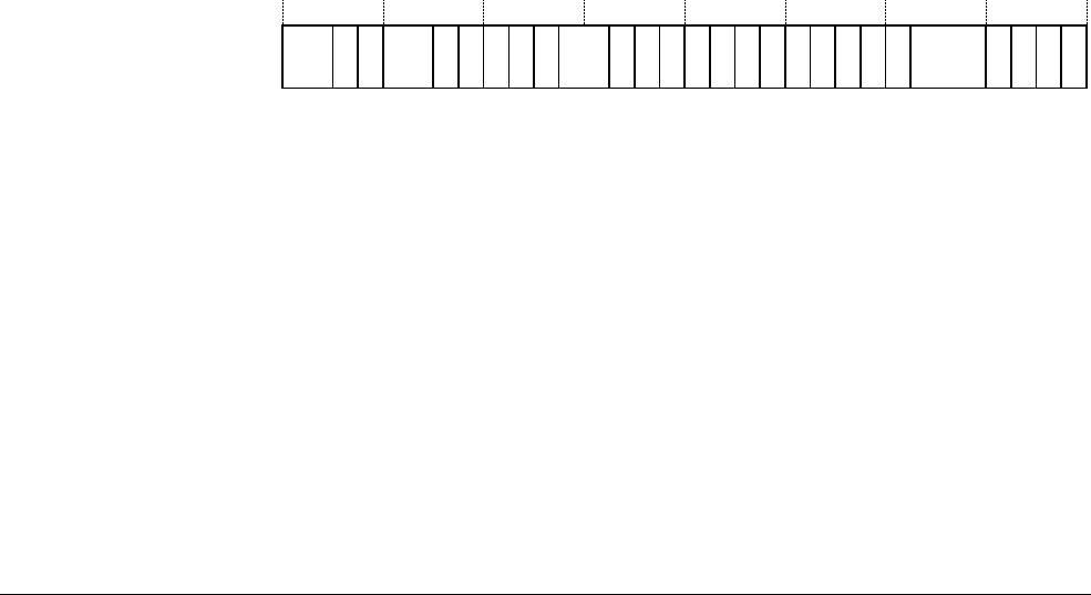
System Control Coprocessor
ARM DDI 0301H Copyright © 2004-2009 ARM Limited. All rights reserved. 3-44
ID012310 Non-Confidential, Unrestricted Access
3.2.7 c1, Control Register
This section contains information on:
•Purpose of the Control Register
•Structure of the Control Register
•Operation of the Control Register on page 3-45
•Use of the Control Register on page 3-47
•Behavior of the Control Register on page 3-48.
Purpose of the Control Register
The purpose of the Control Register is to provide control and configuration of:
• memory alignment, endianness, protection, and fault behavior
• MMU and cache enables and cache replacement strategy
• interrupts and the behavior of interrupt latency
• the location for exception vectors
• program flow prediction.
Table 3-39 on page 3-45 lists the purposes of the individual bits in the Control Register.
Structure of the Control Register
The Control Register is:
•in CP15 c1
• a 32 bit register, Table 3-39 on page 3-45 lists read and write access to individual bits for
the Secure and Non-secure worlds
• accessible in privileged modes only
• partially banked, Table 3-39 on page 3-45 lists banked and Secure modify only bits.
Figure 3-26 shows the arrangement of bits in the register.
Figure 3-26 Control Register format
F
A
T
RSBZ MSBZ
31 25 24 23 22 21 20 19 18 17 16 15 14 13 12 11 10 9 8 7 6 4 3 2 1 0
V
E
X
PU FI SBZ IT
S
B
Z
D
TL4 R
RV I Z F R S B SBO W C A
E
E
26272830 29

System Control Coprocessor
ARM DDI 0301H Copyright © 2004-2009 ARM Limited. All rights reserved. 3-45
ID012310 Non-Confidential, Unrestricted Access
Operation of the Control Register
Table 3-39 lists how the bit values correspond with the Control Register functions.
Table 3-39 Control Register bit functions
Bits Field
name Access Function
[31:30] - - This field is UNP when read. Write as the existing value.
[29] FA Banked This bit controls the Force AP functionality in the MMU that generates Access Bit
faults, see Access permissions on page 6-11
0 = Force AP is disabled, reset value.
1 = Force AP is enabled.
[28] TR Banked This bit controls the TEX remap functionality in the MMU, see Memory region
attributes on page 6-14.
0 = TEX remap disabled. Normal ARMv6 behavior, reset value
1 = TEX remap enabled. TEX[2:1] become page table bits for OS.
[27:26] - - This field is UNP when read. Write as the existing value.
[25] EE bit Banked Determines how the E bit in the CPSR bit is set on an exception. The reset value
depends on external signals.
0 = CPSR E bit is set to 0 on an exception, reset value.
1 = CPSR E bit is set to 1 on an exception.
[24] VE bit Banked Enables the VIC interface to determine interrupt vectors.
See the description of the V bit, bit [13].
0 = Interrupt vectors are fixed, reset value.
1 = Interrupt vectors are defined by the VIC interface.
[23] XP bit Banked Enables the extended page tables to be configured for the hardware page translation
mechanism.
0 = Subpage AP bits enabled, reset value.
1 = Subpage AP bits disabled.
[22] U bit Banked Enables unaligned data access operations, including support for mixed little-endian and
big-endian operation. The A bit has priority over the U bit. The reset value of the U bit
depends on external signals.
0 = Unaligned data access support disabled, reset value. The processor treats unaligned
loads as rotated aligned data accesses.
1 = Unaligned data access support enabled. The processor permits unaligned loads and
stores and support for mixed endian data is enabled.
[21] FI bit Secure
modify
only
Configures low latency features for fast interrupts. This bit is overridden by the FIO bit,
see c1, Auxiliary Control Register on page 3-48.
0 = All performance features enabled, reset value.
1 = Low interrupt latency configuration enabled. See Low interrupt latency
configuration on page 2-40.
[20:19] - - UNP/SBZ
[18] IT bit - Deprecated. Global enable for instruction TCM.
Function redundant in ARMv6.
SBO
[17] - - UNP/SBZ

System Control Coprocessor
ARM DDI 0301H Copyright © 2004-2009 ARM Limited. All rights reserved. 3-46
ID012310 Non-Confidential, Unrestricted Access
[16] DT bit - Deprecated. Global enable for data TCM.
Function redundant in ARMv6.
SBO
[15] L4 bit Secure
modify
only
Determines if the T bit is set for PC load instructions. For more details see the ARM
Architecture Reference Manual.
0 = Loads to PC set the T bit, reset value.
1 = Loads to PC do not set the T bit, ARMv4 behavior.
[14] RR bit Secure
modify
only
Determines the replacement strategy for the cache.
0 = Normal replacement strategy by random replacement, reset value.
1 = Predictable replacement strategy by round-robin replacement.
[13] V bit Banked Determines the location of exception vectors, see c12, Secure or Non-secure Vector
Base Address Register on page 3-121 and c12, Monitor Vector Base Address Register
on page 3-122. The reset value of the V bit depends on an external signal.
0 = Normal exception vectors selected, the Vector Base Address Registers determine
the address range, reset value.
1 = High exception vectors selected, address range =
0xFFFF0000-0xFFFF001C
.
[12] I bit Banked Enables level one instruction cache.
0 = Instruction Cache disabled, reset value.
1 = Instruction Cache enabled.
[11] Z bit Banked Enables branch prediction.
0 = Program flow prediction disabled, reset value.
1 = Program flow prediction enabled.
[10] F bit - Should Be Zero
[9] R bit Banked Deprecated. Enables ROM protection. If you modify the R bit this does not affect the
access permissions of entries already in the TLB. See MMU software-accessible
registers on page 6-53.
0 = ROM protection disabled, reset value.
1 = ROM protection enabled.
[8] S bit Banked Deprecated. Enables MMU protection. If you modify the S bit this does not affect the
access permissions of entries already in TLB.
0 = MMU protection disabled, reset value.
1 = MMU protection enabled.
[7] B bit Secure
modify
only
Determines operation as little-endian or big-endian word invariant memory system and
the names of the low four-byte addresses within a 32-bit word. The reset value of the B
bit depends on the BIGENDINIT external signal.
0 = Little-endian memory system, reset value.
1 = Big-endian word-invariant memory system.
[6:4] - - This field returns 1 when read.
Should Be One.
[3] W bit - Not implemented in the processor.
Read As One
Write Ignore.
Table 3-39 Control Register bit functions (continued)
Bits Field
name Access Function

System Control Coprocessor
ARM DDI 0301H Copyright © 2004-2009 ARM Limited. All rights reserved. 3-47
ID012310 Non-Confidential, Unrestricted Access
Attempts to read or write the Control Register from Secure or Non-secure User modes results
in an Undefined exception.
Attempts to write to this register in Secure Privileged mode when CP15SDISABLE is HIGH
result in an Undefined exception, see TrustZone write access disable on page 2-9.
Attempts to write Secure modify only bit in Non-secure privileged modes are ignored.
Attempts to read Secure modify only bits return the Secure bit value. Table 3-40 lists the actions
that result from attempted access for each mode.
Use of the Control Register
To use the Control Register it is recommended that you use a read modify write technique. To
use the Control Register read or write CP15 with:
• Opcode_1 set to 0
• CRn set to c1
• CRm set to c0
• Opcode_2 set to 0.
For example:
MRC p15, 0, <Rd>, c1, c0, 0 ; Read Control Register configuration data
MCR p15, 0, <Rd>, c1, c0, 0 ; Write Control Register configuration data
Normally, to set the V bit and the B, EE, and U bits you configure signals at reset.
The V bit depends on VINITHI at reset:
•VINITHI LOW sets V to 0
•VINITHI HIGH sets V to 1.
[2] C bit Banked Enables level one data cache.
0 = Data cache disabled, reset value.
1 = Data cache enabled.
[1] A bit Banked Enables strict alignment of data to detect alignment faults in data accesses. The A bit
setting takes priority over the U bit.
0 = Strict alignment fault checking disabled, reset value.
1 = Strict alignment fault checking enabled.
[0] M bit Banked Enables the MMU.
0 = MMU disabled, reset value.
1 = MMU enabled.
Table 3-39 Control Register bit functions (continued)
Bits Field
name Access Function
Table 3-40 Results of access to the Control Register
Access type Secure Privileged
Non-secure Privileged
User
Read Write
Secure modify only Secure bit Secure bit Ignored Undefined exception
Banked Secure bit Non-secure bit Non-secure bit Undefined exception

System Control Coprocessor
ARM DDI 0301H Copyright © 2004-2009 ARM Limited. All rights reserved. 3-48
ID012310 Non-Confidential, Unrestricted Access
The B, EE, and U bits depend on how you set BIGENDINIT and UBITINIT at reset.
Table 3-41 lists the values of the B, EE, and U bits that result for the reset values of these signals.
See Reset values of the U, B, and EE bits on page 4-19.
Behavior of the Control Register
These bits in the Control Register exhibit specific behavior:
A bit The A bit setting takes priority over the U bit. The Data Abort trap is taken if strict
alignment is enabled and the data access is not aligned to the width of the
accessed data item.
DT bit This bit is used in ARM946 and ARM966 processors to enable the Data TCM.
In ARMv6, the TCM blocks have individual enables that apply to each block. As
a result, this bit is now redundant and Should Be One. See c9, Data TCM Region
Register on page 3-89 for a description of the ARM1176JZF-S TCM enables.
IT bit This bit is used in ARM946 and ARM966 processors to enable the Instruction
TCM.
In ARMv6, the TCM blocks have individual enables that apply to each block. As
a result, this bit is now redundant and Should Be One. See c9, Instruction TCM
Region Register on page 3-91 for a description of the ARM1176JZF-S TCM
enables.
R bit Modifying the R bit does not affect the access permissions of entries already in
the TLB. See MMU software-accessible registers on page 6-53.
S bit Modifying the S bit does not affect the access permissions of entries already in
the TLB. See MMU software-accessible registers on page 6-53.
W bit The ARM1176JZF-S processor does not implement the write buffer enable
because all memory writes take place through the Write Buffer.
3.2.8 c1, Auxiliary Control Register
The purpose of the Auxiliary Control Register is to control:
• program flow
• low interrupt latency
• cache cleaning
• MicroTLB cache strategy
• cache size restriction.
For more information on how the system control coprocessor operates with caches, see Cache
control and configuration on page 3-7.
Table 3-42 lists the purposes of the individual bits in the Auxiliary Control Register.
Table 3-41 Resultant B bit, U bit, and EE bit values
UBITINIT BIGENDINIT EE U B
00 000
01 001
10 010
11 110

System Control Coprocessor
ARM DDI 0301H Copyright © 2004-2009 ARM Limited. All rights reserved. 3-49
ID012310 Non-Confidential, Unrestricted Access
The Auxiliary Control Register is:
•in CP15 c1
• a 32-bit:
— read/write register in the Secure world
— read only register in the Non-secure world
• accessible in privileged modes only.
Figure 3-27 shows the arrangement of bits in the register.
Figure 3-27 Auxiliary Control Register format
Table 3-42 lists how the bit values correspond with the Auxiliary Control Register functions.
P
H
D
C
Z
T
R
R
V
R
A
F
S
D
B
F
D
F
I
O
R
S
SBZ/UNP
31 3210
S
B
D
B
456730 29 28 27
Table 3-42 Auxiliary Control Register bit functions
Bits Field
name Function
[31] FIO Provides additional level of control for low interrupt latency configuration. This bit overrides the FI
bit, see FI bit in c1, Control Register on page 3-44:
0 = Normal operation for low interrupt latency configuration, reset value
1 = Low interrupt latency configuration overridden. This feature:
• disables the fast interrupt response introduced by setting the FI bit
• disables Hit-Under-Miss (HUM) functionality
• abandons restartable external accesses so that all external aborts to loads are precise.
[30] FSD Provides additional level of control for speculative operations, see c1, Control Register on page 3-44.
Force speculative operations force the PC to a new value because of static, speculative, branch
prediction:
0 = Enable force speculative operations, reset value
1 = Disable force speculative operations.
[29] BFD Disables branch folding. This behavior also depends on the SB and DB bits, [2:1] in this register, and
the Z bit, see c1, Control Register on page 3-44:
0 = Branch folding is enabled, when branch prediction is enabled, reset value
1 = Branch folding is disabled.
[28] PHD Disables instruction prefetch halting on unconditional, unpredictable instructions that later result in a
prefetch buffer flush. This prefetch halting is a power saving technique:
0 = Prefetch halting is enabled, reset value
1 = Prefetch halting is disabled.
[27:7] - UNP/SBZ
[6] CZ Controls the restriction of cache size to 16KB. This enables the processor to run software that does not
support ARMv6 page coloring. When set the CZ bit does not effect the Cache Type Register. See
Restrictions on page table mappings page coloring on page 6-41 for more information:
0 = Normal ARMv6 cache behavior, reset value
1 = Cache size limited to 16KB.
[5] RV Disables block transfer cache operations:
0 = Block transfer cache operations enabled, reset value
1 = Block transfer cache operations disabled.

System Control Coprocessor
ARM DDI 0301H Copyright © 2004-2009 ARM Limited. All rights reserved. 3-50
ID012310 Non-Confidential, Unrestricted Access
Table 3-43 lists the results of attempted access for each mode.
To use the Auxiliary Control Register you must use a read modify write technique. To access
the Auxiliary Control Register read or write CP15 with:
• Opcode_1 set to 0
• CRn set to c1
• CRm set to c0
• Opcode_2 set to 1.
For example:
MRC p15, 0, <Rd>, c1, c0, 1 ; Read Auxiliary Control Register
MCR p15, 0, <Rd>, c1, c0, 1 ; Write Auxiliary Control Register
[4] RA Disables clean entire data cache:
0 = Clean entire data cache enabled, reset value
1 = Clean entire data cache disabled.
[3] TR Enables MicroTLB random replacement strategy. This depends on the cache replacement strategy that
the RR bit controls, see c1, Control Register on page 3-44. The MicroTLB strategy is only random
when the cache strategy is random:
0 = MicroTLB replacement is Round Robin, reset value
1 = MicroTLB replacement is Random if cache replacement is also Random.
[2] SB Enables static branch prediction. This depends on program flow prediction that the Z bit enables, see
c1, Control Register on page 3-44:
0 = Static branch prediction disabled
1 = Static branch prediction enabled, if the Z bit is set. The reset value is 1.
[1] DB Enables dynamic branch prediction. This depends on program flow prediction that the Z bit enables,
see c1, Control Register on page 3-44:
0 = Dynamic branch prediction disabled
1 = Dynamic branch prediction enabled, if the Z bit is set. The reset value is 1.
[0] RS Enables the return stack. This depends on program flow prediction that the Z bit enables, see c1,
Control Register on page 3-44:
0 = Return stack is disabled
1 = Return stack is enabled, if the Z bit is set. The reset value is 1.
Table 3-42 Auxiliary Control Register bit functions (continued)
Bits Field
name Function
Table 3-43 Results of access to the Auxiliary Control Register
Secure Privileged Non-secure Privileged
User
Read Write Read Write
Data Data Data Undefined exception Undefined exception

System Control Coprocessor
ARM DDI 0301H Copyright © 2004-2009 ARM Limited. All rights reserved. 3-51
ID012310 Non-Confidential, Unrestricted Access
3.2.9 c1, Coprocessor Access Control Register
The purpose of the Coprocessor Access Control Register is to set access rights for the
coprocessors CP0 through CP13. This register has no effect on access to CP14, the debug
control coprocessor, or CP15, the system control coprocessor. This register also provides a
means for software to determine if any particular coprocessor, CP0-CP13, exists in the system.
The Coprocessor Access Control Register is:
•in CP15 c1
• a 32-bit read/write register common to Secure and Non-secure worlds
• accessible in privileged modes only.
Figure 3-28 shows the arrangement of bits in the register.
Figure 3-28 Coprocessor Access Control Register format
Table 3-44 lists how the bit values correspond with the Coprocessor Access Control Register
functions.
Access to coprocessors in the Non-secure world depends on the permissions set in the c1,
Non-Secure Access Control Register on page 3-55.
Attempts to read or write the Coprocessor Access Control Register access bits depend on the
corresponding bit for each coprocessor in c1, Non-Secure Access Control Register on page 3-55.
Table 3-45 lists the results of attempted access to coprocessor access bits for each mode.
To use the Coprocessor Access Control Register read or write CP15 with:
• Opcode_1 set to 0
SBZ/UNP
31 28 27 26 25 24 23 22 21 20 19 18 17 16 15 14 13 12 11 10 9 8 7 6 5 4 3 2 1 0
cp13 cp12 cp11 cp10 cp9 cp8 cp7 cp6 cp5 cp4 cp3 cp2 cp1 cp0
Table 3-44 Coprocessor Access Control Register bit functions
Bits Field name Function
[31:28] - UNP/SBZ.
-cp<n>aDefines access permissions for each coprocessor.
Access denied is the reset condition.
Access denied is the behavior for non-existent coprocessors:
b00 = Access denied, reset value. Attempted access generates an Undefined exception
b01 = Privileged mode access only
b10 = Reserved.
b11 = Privileged and User mode access.
a. n is the coprocessor number between 0 and 13.
Table 3-45 Results of access to the Coprocessor Access Control Register
Corresponding bit in Non-Secure
Access Control Register
Secure Privileged Non-secure Privileged
User
Read Write Read Write
0 Data Data b00 Ignored Undefined exception
1 Data Data Data Data Undefined exception

System Control Coprocessor
ARM DDI 0301H Copyright © 2004-2009 ARM Limited. All rights reserved. 3-52
ID012310 Non-Confidential, Unrestricted Access
• CRn set to c1
• CRm set to c0
• Opcode_2 set to 2.
For example:
MRC p15, 0, <Rd>, c1, c0, 2 ; Read Coprocessor Access Control Register
MCR p15, 0, <Rd>, c1, c0, 2 ; Write Coprocessor Access Control Register
You must perform an Instruction Memory Barrier (IMB) sequence immediately after an update
of the Coprocessor Access Control Register, see Memory Barriers on page 5-8. You must not
attempt to execute any instructions that are affected by the change of access rights between the
IMB sequence and the register update.
To determine if any particular coprocessor exists in the system write the access bits for the
coprocessor of interest with a value other than b00. If the coprocessor does not exist in the
system the access rights remain set to b00.
3.2.10 c1, Secure Configuration Register
The purpose of the Secure Configuration Register is to define:
• the current world as Secure or Non-secure
• the world in which the core executes exceptions
• the ability to modify the A and I bits in the CPSR in the Non-secure world.
The Secure Configuration Register is:
•in CP15 c1
• a 32 bit read/write register
• accessible in Secure privileged modes only.
Figure 3-29 shows the arrangement of bits in the register.
Figure 3-29 Secure Configuration Register format
Table 3-46 lists how the bit values correspond with the Secure Configuration Register functions.
SBZ
n
E
T
N
S
31 6543210
A
W
F
W
E
A
F
I
Q
IR
Q
7
Table 3-46 Secure Configuration Register bit functions
Bits Field name Function
[31:7] - UNP/SBZ.
[6] nET The Early Termination bit is not implemented in ARM1176JZF-S processors.
UNP/SBZ.
[5] AW Determines if the A bit in the CPSR can be modified when in the Non-secure world:
0 = Disable modification of the A bit in the CPSR in the Non-secure world, reset value
1 = Enable modification of the A bit in the CPSR in the Non-secure world.
[4] FW Determines if the F bit in the CPSR can be modified when in the Non-secure world:
0 = Disable modification of the F bit in the CPSR in the Non-secure world, reset value
1 = Enable modification of the F bit in the CPSR in the Non-secure world.

System Control Coprocessor
ARM DDI 0301H Copyright © 2004-2009 ARM Limited. All rights reserved. 3-53
ID012310 Non-Confidential, Unrestricted Access
Note
When the core runs in Secure Monitor mode the state is considered Secure regardless of the state
of the NS bit. However, Monitor mode code can access nonsecure banked copies of registers if
the NS bit is set to 1. See the ARM Architecture Reference Manual for information on the effect
of the Security Extensions on the CP15 registers.
The permutations of the bits in the Secure Configuration Register have certain security
implications. Table 3-47 lists the results for combinations of the FW and FIQ bits.
Table 3-48 lists the results for combinations of the AW and EA bits.
For more details on the use of Secure Monitor mode, see The NS bit and Secure Monitor mode
on page 2-4.
[3] EA Determines External Abort behavior for Secure and Non-secure worlds:
0 = Branch to abort mode on an External Abort exception, reset value
1 = Branch to Secure Monitor mode on an External Abort exception.
[2] FIQ Determines FIQ behavior for Secure and Non-secure worlds:
0 = Branch to FIQ mode on an FIQ exception, reset value
1 = Branch to Secure Monitor mode on an FIQ exception.
[1] IRQ Determines IRQ behavior for Secure and Non-secure worlds:
0 = Branch to IRQ mode on an IRQ exception, reset value
1 = Branch to Secure Monitor mode on an IRQ exception.
[0] NS bit Defines the world for the processor:
0 = Secure, reset value
1 = Non-secure.
Table 3-46 Secure Configuration Register bit functions (continued)
Bits Field name Function
Table 3-47 Operation of the FW and FIQ bits
FW FIQ Function
1 0 FIQs handled locally.
0 1 FIQs can be configured to give deterministic Secure interrupts.
1 1 Non-secure world able to make denial of service attack, avoid use of this function.
0 0 Avoid because the core might enter an infinite loop for Non-secure FIQ.
Table 3-48 Operation of the AW and EA bits
AW EA Function
1 0 Aborts handled locally.
0 1 All external aborts trapped to Secure Monitor.
1 1 All external imprecise data aborts trapped to Secure Monitor but the Non-secure world can hide Secure
aborts from the Secure Monitor, avoid use of this function.
0 0 Avoid because the core can unexpectedly enter an abort mode in the Non-secure world.

System Control Coprocessor
ARM DDI 0301H Copyright © 2004-2009 ARM Limited. All rights reserved. 3-54
ID012310 Non-Confidential, Unrestricted Access
To use the Secure Configuration Register read or write CP15 with:
• Opcode_1 set to 0
• CRn set to c1
• CRm set to c1
• Opcode_2 set to 0.
For example:
MRC p15, 0, <Rd>, c1, c1, 0 ; Read Secure Configuration Register data
MCR p15, 0, <Rd>, c1, c1, 0 ; Write Secure Configuration Register data
An attempt to access the Secure Configuration Register from any state other than Secure
privileged results in an Undefined exception.
3.2.11 c1, Secure Debug Enable Register
The purpose of the Secure Debug Enable Register is to provide control of permissions for debug
in Secure User mode, see Chapter 13 Debug.
Table 3-49 lists the purposes of the individual bits in the Secure Debug Enable Register.
The Secure Debug Enable Register is:
•in CP15 c1
• a 32 bit register in the Secure world only
• accessible in Secure privileged modes only.
Figure 3-30 shows the arrangement of bits in the register.
Figure 3-30 Secure Debug Enable Register format
Table 3-49 lists how the bit values correspond with the Secure Debug Enable Register functions.
SBZ
31 10
2
SUNIDEN
SUIDEN
Table 3-49 Secure Debug Enable Register bit functions
Bits Field name Function
[31:2] - This field is UNP when read. Write as the existing value.
[1] SUNIDEN Enables Secure User non-invasive debug:
0 = Non-invasive debug is not permitted in Secure User mode, reset value
1 = Non-invasive debug is permitted in Secure User mode.
[0] SUIDEN Enables Secure User invasive debug:
0 = Invasive debug is not permitted in Secure User mode, reset value
1 = Invasive debug is permitted in Secure User mode.

System Control Coprocessor
ARM DDI 0301H Copyright © 2004-2009 ARM Limited. All rights reserved. 3-55
ID012310 Non-Confidential, Unrestricted Access
Table 3-50 lists the results of attempted access for each mode.
To use the Secure Debug Enable Register read or write CP15 with:
• Opcode_1 set to 0
• CRn set to c1
• CRm set to c1
• Opcode_2 set to 1.
For example:
MRC p15, 0, <Rd>, c1, c1, 1 ; Read Secure Debug Enable Register
MCR p15, 0, <Rd>, c1, c1, 1 ; Write Secure Debug Enable Register
3.2.12 c1, Non-Secure Access Control Register
The purpose of the Non-Secure Access Control Register is to define the Non-secure access
permission for:
• coprocessors
• cache lockdown registers
• TLB lockdown registers
• internal DMA.
Note
This register has no effect on Non-secure access permissions for the debug control coprocessor,
CP14, or the system control coprocessor, CP15.
The Non-Secure Access Control Register is:
•in CP15 c1
• a 32 bit register:
— read/write in the Secure world
— read only in the Non-secure world
• only accessible in privileged modes.
Figure 3-31 on page 3-56 shows the arrangement of bits in the register.
Table 3-50 Results of access to the Coprocessor Access Control Register
Secure Privileged
Non-secure Privileged User
Read Write
Data Data Undefined exception Undefined exception

System Control Coprocessor
ARM DDI 0301H Copyright © 2004-2009 ARM Limited. All rights reserved. 3-56
ID012310 Non-Confidential, Unrestricted Access
Figure 3-31 Non-Secure Access Control Register format
Table 3-51 lists how the bit values correspond with the Non-Secure Access Control Register
functions.
31 19 18 17 16 15 14 13 12 11 10 9 8 7 6 5 4 3 2 1 0
SBZ
D
M
A
TL C
LSBZ
CP13
CP12
CP11
CP10
CP9
CP8
CP7
CP6
CP5
CP4
CP3
CP2
CP1
CP0
Table 3-51 Non-Secure Access Control Register bit functions
Bits Field
name Function
[31:19] - Reserved.
UNP/SBZ.
[18] DMA Reserves the DMA channels and registers for the Secure world and determines the page tables, Secure
or Non-secure, to use for DMA transfers. For details, see DMA on page 7-10:
0 = DMA reserved for the Secure world only and the Secure page tables are used for DMA transfers,
reset value
1 = DMA can be used by the Non-secure world and the Non-secure page tables are used for DMA
transfers.
[17] TL Prevents operations in the Non-secure world from locking page tables in TLB lockdown entries.
The Invalidate Single Entry or Invalidate ASID match operations can match a TLB lockdown entry
but an Invalidate All operation only applies to unlocked entries:
0 = Reserve TLB Lockdown registers for Secure operation only, reset value
1 = TLB Lockdown registers available for Secure and Non-secure operation.
[16] CL Prevents operations in the Non-secure world from changing cache lockdown entries:
0 = Reserve cache lockdown registers for Secure operation only, reset value
1 = Cache lockdown registers available for Secure and Non-secure operation.
[15:14] - Reserved.
UNP/SBZ.
[13:0] CPnaDetermines permission to access the given coprocessor in the Non-secure world:
0 = Secure access only, reset value
1 = Secure or Non-secure access.
a. n is the coprocessor number from 0 to 13.
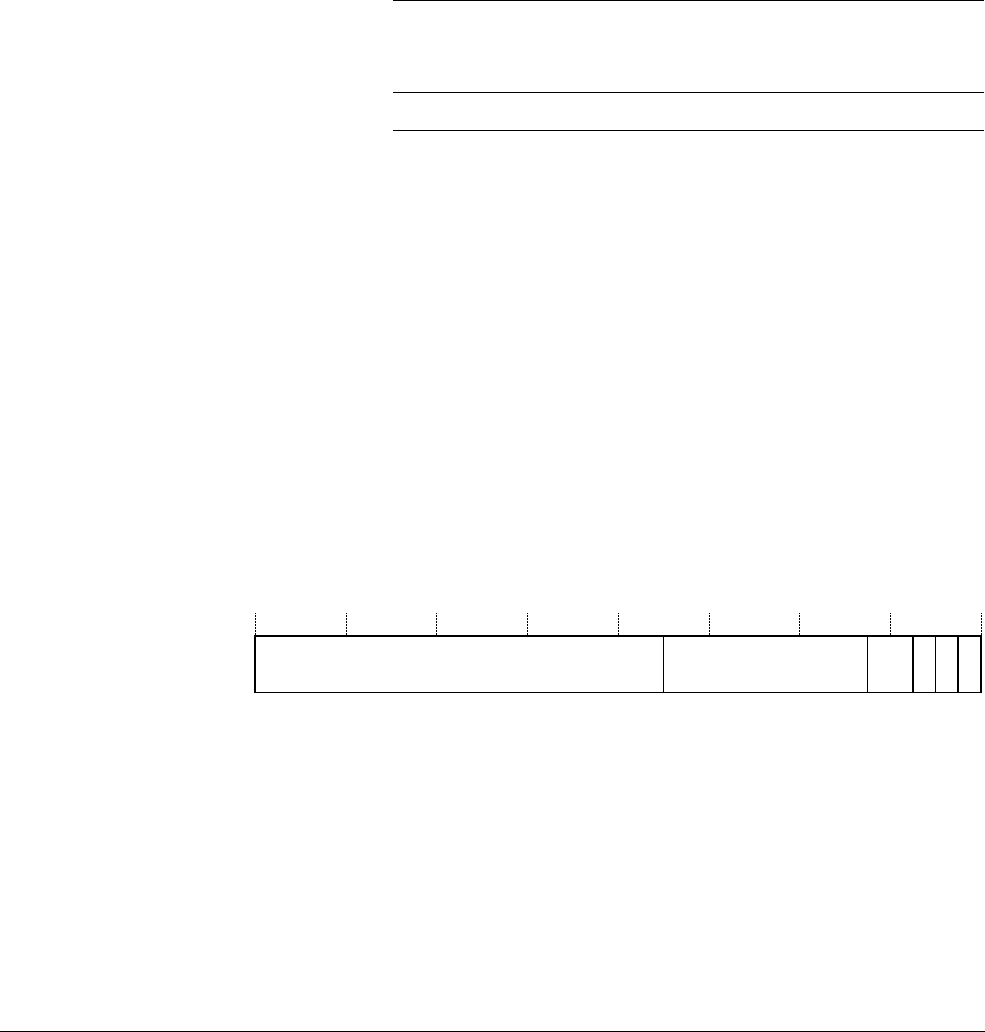
System Control Coprocessor
ARM DDI 0301H Copyright © 2004-2009 ARM Limited. All rights reserved. 3-57
ID012310 Non-Confidential, Unrestricted Access
To use the Non-Secure Access Control Register read or write CP15 with:
• Opcode_1 set to 0
• CRn set to c1
• CRm set to c1
• Opcode_2 set to 2.
For example:
MRC p15, 0, <Rd>, c1, c1, 2 ; Read Non-Secure Access Control Register data
MCR p15, 0, <Rd>, c1, c1, 2 ; Write Non-Secure Access Control Register data
Table 3-52 lists the results of attempted access for each mode.
3.2.13 c2, Translation Table Base Register 0
The purpose of the Translation Table Base Register 0 is to hold the physical address of the
first-level translation table.
You use Translation Table Base Register 0 for process-specific addresses, where each process
maintains a separate first-level page table. On a context switch you must modify both
Translation Table Base Register 0 and the Translation Table Base Control Register, if
appropriate.
Table 3-53 on page 3-58 lists the purposes of the individual bits in the Translation Table Base
Register 0.
The Translation Table Base Register 0 is:
•in CP15 c2
• a 32 bit read/write register banked for Secure and Non-secure worlds
• accessible in privileged modes only.
Figure 3-32 shows the bit arrangement for the Translation Table Base Register 0.
Figure 3-32 Translation Table Base Register 0 format
Table 3-52 Results of access to the Auxiliary Control Register
Secure Privileged Non-secure Privileged
User
Read Write Read Write
Data Data Data Undefined exception Undefined exception
SC
Translation table base 0 UNP/SBZ RGN
31 14-N 13-N 0
P
1
2
34
5

System Control Coprocessor
ARM DDI 0301H Copyright © 2004-2009 ARM Limited. All rights reserved. 3-58
ID012310 Non-Confidential, Unrestricted Access
Table 3-53 lists how the bit values correspond with the Translation Table Base Register 0
functions.
Attempts to write to this register in Secure Privileged mode when CP15SDISABLE is HIGH
result in an Undefined exception, see TrustZone write access disable on page 2-9.
Table 3-54 lists the results of attempted access for each mode.
A write to the Translation Table Base Register 0 updates the address of the first level translation
table from the value in bits [31:7] of the written value, to account for the maximum value of 7
for N. The number of bits of this address that the processor uses, and therefore, the required
alignment of the first level translation table, depends on the value of N, see c2, Translation Table
Base Control Register on page 3-60.
A read from the Translation Table Base Register 0 returns the complete address of the first level
translation table in bits [31:7] of the read value, regardless of the value of N.
To use the Translation Table Base Register 0 read or write CP15 c2 with:
• Opcode_1 set to 0
• CRn set to c2
• CRm set to c0
Table 3-53 Translation Table Base Register 0 bit functions
Bits Field name Function
[31:14-N]aTranslation table base 0 Holds the translation table base address, the physical address of the first level
translation table. The reset value is 0.
[13-N:5]a-UNP/SBZ.
[4:3] RGN Indicates the Outer cacheable attributes for page table walking:
b00 = Outer Noncacheable, reset value
b01 = Write-back, Write Allocate
b10 = Write-through, No Allocate on Write
b11 = Write-back, No Allocate on Write.
[2] P If the processor supports ECC, it indicates to the memory controller it is enabled
or disabled. For ARM1176JZF-S processors this is 0:
0 = Error-Correcting Code (ECC) is disabled, reset value
1 = ECC is enabled.
[1] S Indicates the page table walk is to Non-Shared or to Shared memory:
0 = Non-Shared, reset value
1 = Shared.
[0] C Indicates the page table walk is Inner Cacheable or Inner Noncacheable:
0 = Inner noncacheable, reset value
1 = Inner cacheable.
a. For an explanation of N see c2, Translation Table Base Control Register on page 3-60.
Table 3-54 Results of access to the Translation Table Base Register 0
Secure Privileged Non-secure Privileged
User
Read Write Read Write
Secure data Secure data Non-secure data Non-secure data Undefined exception

System Control Coprocessor
ARM DDI 0301H Copyright © 2004-2009 ARM Limited. All rights reserved. 3-59
ID012310 Non-Confidential, Unrestricted Access
• Opcode_2 set to 0.
For example:
MRC p15, 0, <Rd>, c2, c0, 0 ; Read Translation Table Base Register 0
MCR p15, 0, <Rd>, c2, c0, 0 ; Write Translation Table Base Register 0
Note
The ARM1176JZF-S processor cannot page table walk from level one cache. Therefore, if C is
set to 1, to ensure coherency, you must either store page tables in Inner write-through memory
or, if in Inner write-back, you must clean the appropriate cache entries after modification so that
the mechanism for the hardware page table walks sees them.
3.2.14 c2, Translation Table Base Register 1
The purpose of the Translation Table Base Register 1 is to hold the physical address of the
first-level table. The expected use of the Translation Table Base Register 1 is for OS and I/O
addresses.
Table 3-55 lists the purposes of the individual bits in the Translation Table Base Register 1.
The Translation Table Base Register 1 is:
•in CP15 c2
• a 32 bit read/write register banked for Secure and Non-secure worlds
• accessible in privileged modes only.
Figure 3-33 shows the bit arrangement for the Translation Table Base Register 1.
Figure 3-33 Translation Table Base Register 1 format
Table 3-55 lists how the bit values correspond with the Translation Table Base Register 1
functions.
Translation table base 1
31 14 13
SCP
0
UNP/SBZ
1
2
3
RGN
4
5
Table 3-55 Translation Table Base Register 1 bit functions
Bits Field name Function
[31:14] Translation table base 1 Holds the translation table base address, the physical address of the first level
translation table. The reset value is 0.
[13:5] - UNP/SBZ.
[4:3] RGN Indicates the Outer cacheable attributes for page table walking:
b00 = Outer Noncacheable, reset value
b01 = Write-back, Write Allocate
b10 = Write-through, No Allocate on Write
b11 = Write-back, No Allocate on Write.

System Control Coprocessor
ARM DDI 0301H Copyright © 2004-2009 ARM Limited. All rights reserved. 3-60
ID012310 Non-Confidential, Unrestricted Access
Table 3-56 lists the results of attempted access for each mode.
A write to the Translation Table Base Register 1 updates the address of the first level translation
table from the value in bits [31:14] of the written value. Bits [13:5] Should Be Zero. The
Translation Table Base Register 1 must reside on a 16KB page boundary.
To use the Translation Table Base Register 1 read or write CP15 with:
• Opcode_1 set to 0
• CRn set to c2
• CRm set to c0
• Opcode_2 set to 1.
For example:
MRC p15, 0, <Rd>, c2, c0, 1 ; Read Translation Table Base Register 1
MCR p15, 0, <Rd>, c2, c0, 1 ; Write Translation Table Base Register 1
Note
The ARM1176JZF-S processor cannot page table walk from level one cache. Therefore, if C is
set to 1, to ensure coherency, you must either store page tables in Inner write-through memory
or, if in Inner write-back, you must clean the appropriate cache entries after modification so that
the mechanism for the hardware page table walks sees them.
3.2.15 c2, Translation Table Base Control Register
The purpose of the Translation Table Base Control Register is to determine if a page table miss
for a specific VA uses, for its page table walk, either:
• Translation Table Base Register 0. The recommended use is for task-specific addresses
• Translation Table Base Register 1. The recommended use is for operating system and I/O
addresses.
[2] P If the processor supports ECC, it indicates to the memory controller it is enabled or
disabled. For ARM1176JZF-S processors this is 0:
0 = Error-Correcting Code (ECC) is disabled, reset value
1 = ECC is enabled.
[1] S Indicates the page table walk is to Non-Shared or to Shared memory:
0 = Non-Shared, reset value
1 = Shared.
[0] C Indicates the page table walk is Inner Cacheable or Inner Non Cacheable:
0 = Inner Noncacheable, reset value
1 = Inner Cacheable.
Table 3-55 Translation Table Base Register 1 bit functions (continued)
Bits Field name Function
Table 3-56 Results of access to the Translation Table Base Register 1
Secure Privileged Non-secure Privileged
User
Read Write Read Write
Secure data Secure data Non-secure data Non-secure data Undefined exception

System Control Coprocessor
ARM DDI 0301H Copyright © 2004-2009 ARM Limited. All rights reserved. 3-61
ID012310 Non-Confidential, Unrestricted Access
Table 3-57 lists the purposes of the individual bits in the Translation Table Base Control
Register.
The Translation Table Base Control Register is:
•in CP15 c2
• a 32 bit read/write register banked for Secure and Non-secure worlds
• accessible in privileged modes only.
Figure 3-34 shows the bit arrangement for the Translation Table Base Register 1.
Figure 3-34 Translation Table Base Control Register format
Table 3-57 lists how the bit values correspond with the Translation Table Base Register 0
functions.
Attempts to write to this register in Secure Privileged mode when CP15SDISABLE is HIGH
result in an Undefined exception, see TrustZone write access disable on page 2-9.
P
D
1
P
D
0
S
B
Z
UNP/SBZ
31 32 0
N
456
Table 3-57 Translation Table Base Control Register bit functions
Bits Field name Function
[31:6] - UNP/SBZ.
[5] PD1 Specifies occurrence of a page table walk on a TLB miss when using Translation Table Base
Register 1. When page table walk is disabled, a Section Fault occurs instead on a TLB miss:
0 = The processor performs a page table walk on a TLB miss, with Secure or Non-secure
privilege appropriate to the current world. This is the reset value
1 = The processor does not perform a page table walk. If a TLB miss occurs with Translation
Table Base Register 1 in use, the processor returns a Section Translation Fault.
[4] PD0 Specifies occurrence of a page table walk on a TLB miss when using Translation Table Base
Register 0. When page table walk is disabled, a Section Fault occurs instead on a TLB miss:
0 = The processor performs a page table walk on a TLB miss, with Secure or Non-secure
privilege appropriate to the current world. This is the reset value
1 = The processor does not perform a page table walk. If a TLB miss occurs with Translation
Table Base Register 0 in use, the processor returns a Section Translation Fault.
[3] - UNP/SBZ.
[2:0] N Specifies the boundary size of Translation Table Base Register 0:
b000 = 16KB, reset value
b001 = 8KB
b010 = 4KB
b011 = 2KB
b100 = 1KB
b101 = 512-byte
b110 = 256-byte
b111 = 128-byte.

System Control Coprocessor
ARM DDI 0301H Copyright © 2004-2009 ARM Limited. All rights reserved. 3-62
ID012310 Non-Confidential, Unrestricted Access
Table 3-58 lists the results of attempted access for each mode.
To use the Translation Table Base Control Register read or write CP15 with:
• Opcode_1 set to 0
• CRn set to c2
• CRm set to c0
• Opcode_2 set to 2.
For example:
MRC p15, 0, <Rd>, c2, c0, 2 ; Read Translation Table Base Control Register
MCR p15, 0, <Rd>, c2, c0, 2 ; Write Translation Table Base Control Register
A translation table base register is selected like this:
• If N is set to 0, always use Translation Table Base Register 0. This is the default case at
reset. It is backwards compatible with ARMv5 and earlier processors.
• If N is set greater than 0, and bits [31:32-N] of the VA are all 0, use Translation Table Base
Register 0, otherwise use Translation Table Base Register 1. N must be in the range 0-7.
Note
The ARM1176JZF-S processor cannot page table walk from level one cache. Therefore, if C is
set to 1, to ensure coherency, you must either store page tables in Inner write-through memory
or, if in Inner write-back, you must clean the appropriate cache entries after modification so that
the mechanism for the hardware page table walks sees them.
Table 3-58 Results of access to the Translation Table Base Control Register
Secure Privileged Non-secure Privileged
User
Read Write Read Write
Secure data Secure data Non-secure data Non-secure data Undefined exception

System Control Coprocessor
ARM DDI 0301H Copyright © 2004-2009 ARM Limited. All rights reserved. 3-63
ID012310 Non-Confidential, Unrestricted Access
3.2.16 c3, Domain Access Control Register
The purpose of the Domain Access Control Register is to hold the access permissions for a
maximum of 16 domains.
Table 3-59 lists the purposes of the individual bits in the Domain Access Control Register.
The Domain Access Control Register is:
•in CP15 c3
• a 32-bit read/write register banked for Secure and Non-secure worlds
• accessible in privileged modes only.
Figure 3-35 shows the bit arrangement of the Domain Access Control Register.
Figure 3-35 Domain Access Control Register format
Table 3-59 lists how the bit values correspond with the Domain Access Control Register
functions.
Attempts to write to this register in Secure Privileged mode when CP15SDISABLE is HIGH
result in an Undefined exception, see TrustZone write access disable on page 2-9.
Table 3-60 lists the results of attempted access for each mode.
To use the Domain Access Control Register read or write CP15 c3 with:
• Opcode_1 set to 0
• CRn set to c3
• CRm set to c0
• Opcode_2 set to 0.
For example:
D15
31 30 29 28 27 26 25 24 23 22 21 20 19 18 17 16 15 14 13 12 11 10 9 8 7 6 5 4 3 2 1 0
D14 D13 D12 D11 D10 D9 D8 D7 D6 D5 D4 D3 D2 D1 D0
Table 3-59 Domain Access Control Register bit functions
Bits Field
name Function
-D<n>aThe purpose of the fields D15-D0 in the register is to define the access permissions for each one of
the 16 domains. These domains can be either sections, large pages or small pages of memory:
b00 = No access, reset value. Any access generates a domain fault.
b01 = Client. Accesses are checked against the access permission bits in the TLB entry.
b10 = Reserved. Any access generates a domain fault.
b11 = Manager. Accesses are not checked against the access permission bits in the TLB entry, so a
permission fault cannot be generated.
a. n is the Domain number in the range between 0 and 15
Table 3-60 Results of access to the Domain Access Control Register
Secure Privileged Non-secure Privileged
User
Read Write Read Write
Secure data Secure data Non-secure data Non-secure data Undefined exception

System Control Coprocessor
ARM DDI 0301H Copyright © 2004-2009 ARM Limited. All rights reserved. 3-64
ID012310 Non-Confidential, Unrestricted Access
MRC p15, 0, <Rd>, c3, c0, 0 ; Read Domain Access Control Register
MCR p15, 0, <Rd>, c3, c0, 0 ; Write Domain Access Control Register
3.2.17 c5, Data Fault Status Register
The purpose of the Data Fault Status Register is to hold the source of the last data fault.
Table 3-61 lists the purposes of the individual bits in the Data Fault Status Register.
The Data Fault Status Register is:
•in CP15 c5
• a 32-bit read/write register banked for Secure and Non-secure worlds
• accessible in privileged modes only.
Figure 3-36 shows the bit arrangement in the Data Fault Status Register.
Figure 3-36 Data Fault Status Register format
Table 3-61 shows how the bit values correspond with the Data Fault Status Register functions.
S
D0
UNP/SBZ
31 8 7 4 3 0
Domain Status
9
0S
1011
R
W
1213
Table 3-61 Data Fault Status Register bit functions
Bits Field
name Function
[31:13] - UNP/SBZ.
[12] SD Indicates if an AXI Decode or Slave error caused an abort. This is only valid for external
aborts. For all other aborts this Should Be Zero. See Fault status and address on
page 6-34:
0 = AXI Decode error caused the abort, reset value
1 = AXI Slave error caused the abort.
[11] RW Indicates whether a read or write access caused an abort:
0 = Read access caused the abort, reset value
1 = Write access caused the abort.
[10] S Part of the Status field. See Bits [3:0] in this table. The reset value is 0.
[9:8] - Always read as 0. Writes ignored.

System Control Coprocessor
ARM DDI 0301H Copyright © 2004-2009 ARM Limited. All rights reserved. 3-65
ID012310 Non-Confidential, Unrestricted Access
[7:4] Domain Indicates the domain from the 16 domains, D15-D0, is accessed when a data fault occurs.
Takes values 0-15. The reset value is 0.
[3:0]
with bit[10] = 0
Status Indicates type of fault generated. See Fault status and address on page 6-34 for full
details of Domain and FAR validity, and priorities:
b0000 = no function, reset value
b0001 = Alignment fault
b0010 = Instruction debug event fault
b0011 = Access Bit fault on Section
b0100 = Instruction cache maintenance operation fault
b0101 = Translation Section fault
b0110 = Access Bit fault on Page
b0111 = Translation Page fault
b1000 = Precise external abort
b1001 = Domain Section fault
b1010 = no function
b1011 = Domain Page fault
b1100 = External abort on translation, first level
b1101 = Permission Section fault
b1110 = External abort on translation, second level
b1111 = Permission Page fault.
[3:0]
with bit[10] = 1
Status Indicates type of fault generated. See Fault status and address on page 6-34 for full
details of Domain and FAR validity, and priorities:
b0000 = no function, reset value
b0001 = no function
b0010 = no function
b0011 = no function
b0100 = no function
b0101 = no function
b0110 = Imprecise external abort
b0111 = no function
b1000 = no function
b1001 = no function
b1010 = no function
b1011 = no function
b1100 = no function
b1101 = no function
b1110 = no function
b1111 = no function.
Table 3-61 Data Fault Status Register bit functions (continued)
Bits Field
name Function

System Control Coprocessor
ARM DDI 0301H Copyright © 2004-2009 ARM Limited. All rights reserved. 3-66
ID012310 Non-Confidential, Unrestricted Access
Table 3-62 lists the results of attempted access for each mode.
Note
When the SCR EA bit is set, see c1, Secure Configuration Register on page 3-52, the processor
writes to the Secure Data Fault Status Register on a Secure Monitor entry caused by an external
abort.
To use the Data Fault Status Register read or write CP15 with:
• Opcode_1 set to 0
• CRn set to c5
• CRm set to c0
• Opcode_2 set to 0.
For example:
MRC p15, 0, <Rd>, c5, c0, 0 ; Read Data Fault Status Register
MCR p15, 0, <Rd>, c5, c0, 0 ; Write Data Fault Status Register
3.2.18 c5, Instruction Fault Status Register
The purpose of the Instruction Fault Status Register (IFSR) is to hold the source of the last
instruction fault.
Table 3-63 on page 3-67 lists the purposes of the individual bits in IFSR.
The Instruction Fault Status Register is:
•in CP15 c5
• a 32-bit read/write register banked for Secure and Non-secure worlds
• accessible in privileged modes only.
Figure 3-37 shows the bit arrangement of the Instruction Fault Status Register.
Figure 3-37 Instruction Fault Status Register format
Table 3-62 Results of access to the Data Fault Status Register
Secure Privileged Non-secure Privileged
User
Read Write Read Write
Secure data Secure data Non-secure data Non-secure data Undefined exception
0
S
B
Z
S
D
UNP/SBZ
31 30
StatusUNP/SBZ
4
910111213

System Control Coprocessor
ARM DDI 0301H Copyright © 2004-2009 ARM Limited. All rights reserved. 3-67
ID012310 Non-Confidential, Unrestricted Access
Table 3-63 lists how the bit values correspond with the Instruction Fault Status Register
functions.
Table 3-64 lists the results of attempted access for each mode.
Table 3-63 Instruction Fault Status Register bit functions
Bits Field
name Function
[31:13] - UNP/SBZ.
[12] SD Indicates whether an AXI Decode or Slave error caused an abort. This bit is only valid for
external aborts. For all other aborts this bit Should Be Zero. See Fault status and address on
page 6-34:
0 = AXI Decode error caused the abort, reset value
1 = AXI Slave error caused the abort.
[11] - UNP/SBZ.
[10] - Part of the Status field, see bits [3:0] in this table.
Always 0.
[9:4] - UNP/SBZ.
[3:0] with
bit[10] = 0
Status Indicates type of fault generated.
See Fault status and address on page 6-34 for full details of Domain and FAR validity, and
priorities:
b0000 = no function, reset value
b0001= Alignment fault
b0010 = Instruction debug event fault
b0011 = Access Bit fault on Section
b0100 = no function
b0101 = Translation Section fault
b0110 = Access Bit fault on Page
b0111 = Translation Page fault
b1000 = Precise external abort
b1001 = Domain Section fault
b1010 = no function
b1011 = Domain Page fault
b1100 = External abort on translation, first level
b1101 = Permission Section fault
b1110 = External abort on translation, second level
b1111 = Permission Page fault.
Table 3-64 Results of access to the Instruction Fault Status Register
Secure Privileged Non-secure Privileged
User
Read Write Read Write
Secure data Secure data Non-secure data Non-secure data Undefined exception

System Control Coprocessor
ARM DDI 0301H Copyright © 2004-2009 ARM Limited. All rights reserved. 3-68
ID012310 Non-Confidential, Unrestricted Access
Note
When the SCR EA bit is set, see c1, Secure Configuration Register on page 3-52, the processor
writes to the Secure Instruction Fault Status Register on a Secure Monitor entry caused by an
external abort.
To use the IFSR read or write CP15 with:
• Opcode_1 set to 0
• CRn set to c5
• CRm set to c0
• Opcode_2 set to 1.
For example:
MRC p15, 0, <Rd>, c5, c0, 1 ; Read Instruction Fault Status Register
MCR p15, 0, <Rd>, c5, c0, 1 ; Write Instruction Fault Status Register
3.2.19 c6, Fault Address Register
The purpose of the Fault Address Register (FAR) is to hold the Modified Virtual Address (MVA)
of the fault when a precise abort occurs.
The FAR is:
•in CP15 c6
• a 32-bit read/write register banked for Secure and Non-secure worlds
• accessible in privileged modes only.
The Fault Address Register bits [31:0] contain the MVA that the precise abort occurred on. The
reset value is 0.
Table 3-65 lists the results of attempted access for each mode.
To use the FAR read or write CP15 with:
• Opcode_1 set to 0
• CRn set to c6
• CRm set to c0
• Opcode_2 set to 0.
For example:
MRC p15, 0, <Rd>, c6, c0, 0 ; Read Fault Address Register
MCR p15, 0, <Rd>, c6, c0, 0 ; Write Fault Address Register
A write to this register sets the FAR to the value of the data written. This is useful for a debugger
to restore the value of the FAR.
The ARM1176JZF-S processor also updates the FAR on debug exception entry because of
watchpoints, see Effect of a debug event on CP15 registers on page 13-34 for more details.
Table 3-65 Results of access to the Fault Address Register
Secure Privileged Non-secure Privileged
User
Read Write Read Write
Secure data Secure data Non-secure data Non-secure data Undefined exception

System Control Coprocessor
ARM DDI 0301H Copyright © 2004-2009 ARM Limited. All rights reserved. 3-69
ID012310 Non-Confidential, Unrestricted Access
3.2.20 c6, Watchpoint Fault Address Register
Access to the Watchpoint Fault Address register through the system control coprocessor is
deprecated, see CP14 c6, Watchpoint Fault Address Register (WFAR) on page 13-12.
3.2.21 c6, Instruction Fault Address Register
The purpose of the Instruction Fault Address Register (IFAR) is to hold the address of
instructions that cause a prefetch abort.
The IFAR is:
•in CP15 c6
• a 32-bit read/write register banked for Secure and Non-secure worlds
• accessible in privileged modes only.
The Instruction Fault Address Register bits [31:0] contain the Instruction Fault MVA. The reset
value is 0.
Table 3-66 lists the results of attempted access for each mode.
To use the IFAR read or write CP15 with:
• Opcode_1 set to 0
• CRn set to c6
• CRm set to c0
• Opcode_2 set to 2.
For example:
MRC p15, 0, <Rd>, c6, c0, 2 ; Read Instruction Fault Address Register
MCR p15, 0, <Rd>, c6, c0, 2 ; Write Instruction Fault Address Register
A write to this register sets the IFAR to the value of the data written. This is useful for a debugger
to restore the value of the IFAR.
3.2.22 c7, Cache operations
The purpose of c7 is to:
• control these operations:
— clean and invalidate instruction and data caches, including range operations
— prefetch instruction cache line
— Flush Prefetch Buffer
— flush branch target address cache
— virtual to physical address translation.
• implement the Data Synchronization Barrier (DSB) operation
• implement the Data Memory Barrier (DMB) operation
Table 3-66 Results of access to the Instruction Fault Address Register
Secure Privileged Non-secure Privileged
User
Read Write Read Write
Secure data Secure data Non-secure data Non-secure data Undefined exception
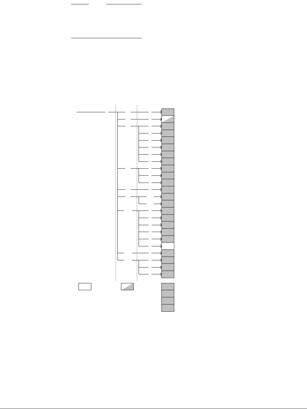
System Control Coprocessor
ARM DDI 0301H Copyright © 2004-2009 ARM Limited. All rights reserved. 3-70
ID012310 Non-Confidential, Unrestricted Access
• implement the Wait For Interrupt clock control function.
Note
Cache operations also depend on:
• the C, W, I and RR bits, see c1, Control Register on page 3-44.
• the RA and RV bits, see c1, Auxiliary Control Register on page 3-48.
The following cache operations globally flush the BTAC:
• Invalidate Entire Instruction Cache
• Invalidate Both Caches.
c7 consists of one 32-bit register that performs 28 functions. Figure 3-38 shows the arrangement
of the 24 functions in this group that operate with the MCR and MRC instructions.
Figure 3-38 Cache operations
Figure 3-39 on page 3-71 shows the arrangement of the 4 functions in this group that operate
with the MCRR instruction.
SBZ
Read-only Read/write
Should Be Zero
MVA
Index
Using MVA
Using Set and Index
Write only
c7
c6
c7
c0 4
c5 0
1
2
4
6
7
0
1
2
0
c10
c13
c14
0
1
2
4
5
6
1
0
1
2
SBZ
SBZ
MVA
Index
SBZ
SBZ
MVA
SBZ
MVA
Index
SBZ
SBZ
MVA
Index
SBZ
SBZ
MVA
SBZ
MVA
Index
0
Invalidate Data Cache Line (using Index)
Invalidate Both Caches
Invalidate Data Cache Line (using MVA)
Invalidate Entire Data Cache
Flush Entire Branch Target Cache
Wait For Interrupt (WFI)
Flush Prefetch Buffer
Flush Branch Target Cache Entry
Invalidate Entire Instruction Cache
Invalidate Instruction Cache Line (using MVA)
Invalidate Instruction Cache Line (using Index)
Cache Dirty Status Register
Clean Entire Data Cache
Clean Data Cache Line (using MVA)
Clean Data Cache Line (using Index)
Data Synchronization Barrier (DSB)
Data Memory Barrier (DMB)
Clean and Invalidate Entire Data Cache
Prefetch Instruction Cache Line
Clean and Invalidate Data Cache Line (using MVA)
Clean and Invalidate Data Cache Line (using Index)
Opcode_2CRmCRn Opcode_1
PA Register
c4 0
VA to PA Translation in the current world
VA to PA Translation in the other world
c8 0-3
4-7
Accessible in User mode

System Control Coprocessor
ARM DDI 0301H Copyright © 2004-2009 ARM Limited. All rights reserved. 3-71
ID012310 Non-Confidential, Unrestricted Access
Figure 3-39 Cache operations with MCRR instructions
Note
• Writing c7 with a combination of CRm and Opcode_2 not listed in Figure 3-38 on
page 3-70 or CRm not listed in Figure 3-39 results in an Undefined exception apart from
the following operations, that are architecturally defined as unified cache operations and
have no effect:
—
MCR p15,0,<Rd>,c7,c7,{1-7}
—
MCR p15,0,<Rd>,c7,c11,{0-7}
—
MCR p15,0,<Rd>,c7,c15,{0-7}
.
• In the ARM1176JZF-S processor, reading from c7, except for reads from the Cache Dirty
Status Register or PA Register, causes an Undefined instruction trap.
• Writes to the Cache Dirty Status Register cause an Undefined exception.
• If Opcode_1 = 0, these instructions are applied to a level one cache system. All other
Opcode_1 values are reserved.
• All accesses to c7 can only be executed in a privileged mode of operation, except Data
Synchronization Barrier, Flush Prefetch Buffer, Data Memory Barrier, and Clean Data
Cache Range. These can be operated in User mode. Attempting to execute a privileged
instruction in User mode results in the Undefined instruction trap being taken.
There are three ways to use c7:
• For the Cache Dirty Status Register, read c7 with the MRC instruction.
• For range operations use the MCRR instruction with the value of CRm to select the
required operation.
• For all other operations use the MCR instruction to write to c7 with the combination of
CRm and Opcode_2 to select the required operation.
Depending on the operation you require set <Rd> for MCR instructions or <Rd> and
<Rn> for MCRR instructions to:
—Virtual Address (VA)
—Modified Virtual Address (MVA)
— Set and Index
— Should Be Zero.
Invalidate, Clean, and Prefetch operations
The purposes of the invalidate, clean, and prefetch operations that c7 provides are to:
• Invalidate part or all of the Data or Instruction caches
• Clean part or all of the Data cache
• Clean and Invalidate part or all of the Data cache
Read-only Read/write VA Using VA
c14
c5
c12
VA
0Invalidate Instruction Cache Range
CRmOpcode_1
c6 VA
VA
VA
Invalidate Data Cache Range
Clean Data Cache Range
Clean and Invalidate Data Cache Range
Accessible in User mode

System Control Coprocessor
ARM DDI 0301H Copyright © 2004-2009 ARM Limited. All rights reserved. 3-72
ID012310 Non-Confidential, Unrestricted Access
• Prefetch code into the Instruction cache.
The terms used to describe the invalidate, clean, and prefetch operations are as defined in the
Caches and Write Buffers chapter of the ARM Architecture Reference Manual.
For details of the behavior of c7 in the Secure and Non-secure worlds, see TrustZone behavior
on page 3-77.
When it controls invalidate, clean, and prefetch operations c7 appears as a 32-bit write only
register. There are four possible formats for the data that you write to the register that depend on
the specific operation:
• Set and Index format
•MVA
•VA
•SBZ.
Set and Index format
Figure 3-40 shows the Set and Index format for invalidate and clean operations.
Figure 3-40 c7 format for Set and Index
Table 3-67 lists how the bit values correspond with the Cache Operation functions
for Set and Index format operations.
The value of S in Table 3-68 depends on the cache size. Table 3-68 lists the
relationship of cache sizes and S.
0Set
31 30 29 S+5 1 0
SBZ/UNP Index SBZ/UNP
45S+4
Table 3-67 Functional bits of c7 for Set and Index
Bits Field name Function
[31:30] Set Selects the cache set to operate on, from the four cache sets.
Value is the cache set number.
[29:S+5] - UNP/SBZ.
[S+4:5] Index Selects the cache line to operate on.
Value is the index number.
[4:1] - SBZ.
[0] 0 For the ARM1176JZF-S, this Should Be Zero.
Table 3-68 Cache size and S parameter dependency
Cache size S
4KB 5
8KB 6
16KB 7
32KB 8
64KB 9

System Control Coprocessor
ARM DDI 0301H Copyright © 2004-2009 ARM Limited. All rights reserved. 3-73
ID012310 Non-Confidential, Unrestricted Access
The value of S is given by:
See c0, Cache Type Register on page 3-21 for details of instruction and data cache
size.
Note
If the data is stated to be Set and Index format, see Figure 3-40 on page 3-72, it
identifies the cache line that the operation applies to by specifying the cache Set
that it belongs to and what its Index is within the Set. The Set corresponds to the
number of the cache way, and the Index number corresponds to the line number
within a cache way.
MVA format
Figure 3-41 shows the MVA format for invalidate, clean, and prefetch operations.
Figure 3-41 c7 format for MVA
Table 3-69 lists how the bit values correspond with the Cache Operation functions
for MVA format operations.
Note
• Invalidation and cleaning operations have no effect if they miss in the
cache.
• If the corresponding entry is not in the TLB, these instructions can cause a
TLB miss exception or hardware page table walk, depending on the miss
handling mechanism.
• For the cache control operations, the MVAs that are passed to the cache are
not translated by the FCSE extension.
VA format
Figure 3-42 shows the VA format for invalidate and clean operations. All VA
format operations use the MCRR instruction.
Figure 3-42 Format of c7 for VA
Associativity x line length in bytes
cache size
S = log
2
Modified virtual address
31 54 0
SBZ
Table 3-69 Functional bits of c7 for MVA
Bits Field name Function
[31:5] MVA Specifies address to invalidate, clean, or prefetch.
Holds the MVA of the cache line.
[4:0] - Ignored. This means that the lower 5 bits of MVA are ignored and these bits are not used for the
cache operations. Only the top bits are necessary to determine whether or not the cache line is
present in the cache. Even if the MVA is not aligned to the cache line, the cache operation is
performed by ignoring the lower 5 bits.
Virtual address
31 40
SBZ
5

System Control Coprocessor
ARM DDI 0301H Copyright © 2004-2009 ARM Limited. All rights reserved. 3-74
ID012310 Non-Confidential, Unrestricted Access
Table 3-70 lists how the bit values correspond with the Cache Operation functions
for VA format operations.
You can perform invalidate, clean, and prefetch operations on:
• single cache lines
• entire caches
• address ranges in cache.
Note
• Clean, invalidate, and clean and invalidate operations apply regardless of the lock applied
to entries.
• An explicit flush of the relevant lines in the branch target cache must be performed after
invalidation of Instruction Cache lines or the results are Unpredictable. There is no impact
on security. This is not required after an entire Instruction Cache invalidation because the
entire branch target cache is flushed automatically.
• A small number of CP15 c7 operations can be executed by code while in User mode.
Attempting to execute a privileged operation in User mode using CP15 c7 results in an
Undefined instruction trap being taken.
To determine if the cache is dirty use the Cache Dirty Status Register, see Cache Dirty Status
Register on page 3-78.
Entire cache
Table 3-71 lists the instructions and operations that you can use to clean and
invalidate the entire cache.
Register c7 specifies operations for cleaning the entire Data Cache, and also for
performing a clean and invalidate of the entire Data Cache. These are blocking
operations that can be interrupted. If they are interrupted, the R14 value that is
Table 3-70 Functional bits of c7 for VA format
Bits Field name Function
[31:5] Virtual address Specifies the start or end address to invalidate or clean.
Holds the true VA of the start or end of a memory block before any modification by FCSE.
[4:0] - SBZ.
Table 3-71 Cache operations for entire cache
Instruction Data Function
MCR p15, 0, <Rd>, c7, c5, 0
SBZ Invalidate Entire Instruction Cache.
Also flushes the branch target cache and globally flushes the BTAC.
MCR p15, 0, <Rd>, c7, c6, 0
SBZ Invalidate Entire Data Cache.
MCR p15, 0, <Rd>, c7, c7, 0
SBZ Invalidate Both Caches.
Also flushes the branch target cache and globally flushes the BTAC.
MCR p15, 0, <Rd>, c7, c10, 0
SBZ Clean Entire Data Cache.
MCR p15, 0, <Rd>, c7, c14, 0
SBZ Clean and Invalidate Entire Data Cache.

System Control Coprocessor
ARM DDI 0301H Copyright © 2004-2009 ARM Limited. All rights reserved. 3-75
ID012310 Non-Confidential, Unrestricted Access
captured on the interrupt is the address of the instruction that launched the cache
clean operation + 4. This enables the standard return mechanism for interrupts to
restart the operation.
If it is essential that the cache is clean, or clean and invalid, for a particular
operation, the sequence of instructions for cleaning, or cleaning and invalidating,
the cache for that operation must handle the arrival of an interrupt at any time
when interrupts are not disabled. This is because interrupts can write to a
previously clean cache. For this reason, the Cache Dirty Status Register indicates
if the cache has been written to since the last clean of the cache was started, see
Cache Dirty Status Register on page 3-78. You can interrogate the Cache Dirty
Status Register to determine if the cache is clean, and if this is done while
interrupts are disabled, the following operations can rely on having a clean cache.
The following sequence shows this approach:
; interrupts are assumed to be enabled at this point
Loop1 MOV R1, #0
MCR CP15, 0, R1, C7, C10, 0 ; Clean (or Clean & Invalidate) Cache
MRS R2, CPSR
CPSID iaf ; Disable interrupts
MRC CP15, 0, R1, C7, C10, 6 ; Read Cache Dirty Status Register
ANDS R1, R1, #1 ; Check if it is clean
BEQ UseClean
MSR CPSR, R2 ; Re-enable interrupts
B Loop1 ; - clean the cache again
UseClean Do_Clean_Operations ; Perform whatever operation relies on
; the cache being clean/invalid.
; To reduce impact on interrupt
; latency, this sequence should be
; short
MSR CPSR, R2 ; Re-enable interrupts
The long cache clean operation is performed with interrupts enabled throughout
this routine.
Single cache lines
There are two ways to perform invalidate or clean operations on cache lines:
• by use of Set and Index format
• by use of MVA format.
Table 3-72 lists the instructions and operations that you can use for single cache
lines.
Table 3-72 Cache operations for single lines
Instruction Data Function
MCR p15, 0, <Rd>, c7, c5, 1
MVA Invalidate Instruction Cache Line, using MVA
MCR p15, 0, <Rd>, c7, c5, 2
Set/Index Invalidate Instruction Cache Line, using Index
MCR p15, 0, <Rd>, c7, c6, 1
MVA Invalidate Data Cache Line, using MVA
MCR p15, 0, <Rd>, c7, c6, 2
Set/Index Invalidate Data Cache Line, using Index
MCR p15, 0, <Rd>, c7, c10, 1
MVA Clean Data Cache Line, using MVA
MCR p15, 0, <Rd>, c7, c10, 2
Set/Index Clean Data Cache Line, using Index

System Control Coprocessor
ARM DDI 0301H Copyright © 2004-2009 ARM Limited. All rights reserved. 3-76
ID012310 Non-Confidential, Unrestricted Access
Example 3-1 shows how to use Clean and Invalidate Data Cache Line with Set
and Index to clean and invalidate one whole cache way, in this example, way 3.
The example works with any cache size because it reads the cache size from the
Cache Type Register.
Example 3-1 Clean and Invalidate Data Cache Line with Set and Index
MRC p15,0,R0,c0,c0,1 ; Read cache type reg
AND R0,R0,#0x1C0000 ; Extract D cache size
MOV R0,R0, LSR #18 ; Move to bottom bits
ADD R0,R0,#7 ; Get Index loop max
MOV r1,#3:SHL:30 ; Set up Set = 3
MOV R2,#0 ; Set up Index counter
MOV R3,#1
MOV R3,R3, LSL R0 ; Set up Index loop max
index_loop
ORR R4,R2,r1 ; Set and Index format
MCR p15,0,R4,c7,c14,2 ; Clean&inval D cache line
ADD R2,R2,#1:SHL:5 ; Increment Index
CMP R2,R3 ; Done all index values?
BNE index_loop ; Loop until done
Address ranges
Table 3-73 lists the instructions and operations that you can use to clean and
invalidate the address ranges in cache.
The operations in Table 3-73 can only be performed using an MCRR or MCRR2
instruction, and all other operations to these registers are ignored.
The
End Address
and
Start Address
in Table 3-73 is the true VA before any
modification by the Fast Context Switch Extension (FCSE). This address is
translated by the FCSE logic. Each of the range operations operates between
cache lines containing the
Start Address
and the
End Address
, inclusive of
Start
Address
and
End Address
.
MCR p15, 0, <Rd>, c7, c13, 1
MVA Prefetch Instruction Cache Line
MCR p15, 0, <Rd>, c7, c14, 1
MVA Clean and Invalidate Data Cache Line, using MVA
MCR p15, 0, <Rd>, c7, c14, 2
Set/Index Clean and Invalidate Data Cache Line, using Index
Table 3-73 Cache operations for address ranges
Instruction Data Function
MCRR p15,0,<End Address>,<Start Address>,c5
VA Invalidate Instruction Cache Range
MCRR p15,0,<End Address>,<Start Address>,c6
VA Invalidate Data Cache Range
MCRR p15,0,<End Address>,<Start Address>,c12
VA Clean Data Cache Rangea
a. This operation is accessible in both User and privileged modes of operation. All other operations listed
here are only accessible in privileged modes of operation.
MCRR p15,0,<End Address>,<Start Address>,c14
VA Clean and Invalidate Data Cache Range
Table 3-72 Cache operations for single lines (continued)
Instruction Data Function

System Control Coprocessor
ARM DDI 0301H Copyright © 2004-2009 ARM Limited. All rights reserved. 3-77
ID012310 Non-Confidential, Unrestricted Access
Because the least significant address bits are ignored, the transfer automatically
adjusts to a line length multiple spanning the programmed addresses.
The
Start Address
is the first VA of the block transfer. It uses the VA bits [31:5].
The
End Address
is the VA where the block transfer stops. This address is at the
start of the line containing the last address to be handled by the block transfer. It
uses the VA bits [31:5].
If the Start Address is greater than the End Address the effect is architecturally Unpredictable.
The ARM1176JZF-S processor does not perform cache operations in this case. All block
transfers are interruptible. When Block transfers are interrupted, the R14 value that is captured
is the address of the instruction that launched the block operation + 4. This enables the standard
return mechanism for interrupts to restart the operation.
Exception behavior
The blocking block transfers cause a Data Abort on a translation fault if a valid page table entry
cannot be fetched. The FAR indicates the address that caused the fault, and the DFSR indicates
the reason for the fault.
TrustZone behavior
TrustZone affects cache operations as follows:
Secure world operations
In the Secure world cache operations can affect both Secure and Non-secure
cache lines:
• Clean, invalidate, and clean and invalidate operations affect all cache lines
regardless of their status as locked or unlocked.
• For clean, invalidate, and clean and invalidate operations with the Set and
Index format, the selected cache line is affected regardless of the Secure
tag.
• For MVA operations clean, invalidate, and clean and invalidate:
— when the MVA is marked as Non-secure in the page table, only
Non-secure entries are affected
— when the MVA is marked as Secure in the page table, only Secure
entries are affected.
Non-secure world operations
In the Non-secure world:
• Clean, invalidate, and clean and invalidate operations only affect
Non-secure cache lines regardless of the method used.
• Any attempt to access Secure cache lines is ignored.
• Invalidate Entire Data Cache and Invalidate Both Caches operations cause
an Undefined exception. This prevents invalidating lockdown entries that
might be configured as Secure.
— the Invalidate Both Caches operation globally flushes the BTAC.
• Invalidate Entire Instruction Cache operations:
— cause an Undefined exception if lockdown entries are reserved for the
Secure world
— affect all Secure and Non-secure cache entries if the lockdown entries
are not reserved for the Secure world
— globally flush the BTAC.

System Control Coprocessor
ARM DDI 0301H Copyright © 2004-2009 ARM Limited. All rights reserved. 3-78
ID012310 Non-Confidential, Unrestricted Access
Cache Dirty Status Register
The purpose of the Cache Dirty Status Register is to indicate when the Cache is dirty.
The Cache Dirty Status Register is:
•in CP15 c7
• a 32-bit read only register, banked for Secure and Non-secure worlds
• accessible in privileged modes only.
Figure 3-43 shows the arrangement of bits in the Cache Dirty Status Register.
Figure 3-43 Cache Dirty Status Register format
Table 3-74 lists how the bit value corresponds with the Cache Dirty Status Register function.
The Cache Dirty Status Register behaves in this way with regard to the Secure and Non-secure
cache:
• clean, invalidate, and clean and invalidate operations of the whole cache in the Non-secure
world clear the Non-secure Cache Dirty Status Register
• clear, invalidate, and clean and invalidate operations of the whole cache in the Secure
world clear both the Secure and Non-secure Cache Dirty Status Registers
• if the core is in the Non-secure world or targets Non-secure data from the Secure world,
stores that write a dirty bit in the cache set both the Secure and the Non-secure Cache Dirty
Status Register
• all stores that write a dirty bit in the cache set the Secure Cache Dirty Status Register.
All writes and User mode reads of the Cache Dirty Status Register cause an Undefined
exception.
To use the Cache Dirty Status Register read CP15 with:
• Opcode_1 set to 0
• CRn set to c7
• CRm set to c10
• Opcode_2 set to 6.
For example:
MRC p15, 0, <Rd>, c7, c10, 6 ; Read Cache Dirty Status Register.
CUNP/SBZ
31 10
Table 3-74 Cache Dirty Status Register bit functions
Bits Field name Function
[31:1] - UNP/SBZ.
[0] C The C bit indicates if the cache is dirty.
0 = indicates that no write has hit the cache since the last cache clean, clean and invalidate, or
invalidate all operation, or reset, successfully left the cache clean. This is the reset value.
1 = indicates that the cache might contain dirty data.

System Control Coprocessor
ARM DDI 0301H Copyright © 2004-2009 ARM Limited. All rights reserved. 3-79
ID012310 Non-Confidential, Unrestricted Access
Flush operations
Table 3-75 lists the flush operations and instructions available through c7.
The Flush Branch Target Entry using MVA operation uses a different MVA format to that used
by Clean and Invalidate operations. Figure 3-44 shows the MVA format for the Flush Branch
Target Entry operation.
Figure 3-44 c7 format for Flush Branch Target Entry using MVA
Table 3-76 lists how the bit values correspond with the Flush Branch Target Entry using MVA
functions.
Note
The MVA does not have to be cache line aligned.
Flushing the prefetch buffer has the effect that all instructions occurring in program order after
this instruction are fetched from the memory system after the execution of this instruction,
including the level one cache or TCM. This operation is useful for ensuring the correct execution
of self-modifying code. See Explicit Memory Barriers on page 6-25.
VA to PA translation operations
The purpose of the VA to PA translation operations is to provide a Secure means to determine
address translation in the Secure and Non-secure worlds and for address translation between the
Secure and Non-secure worlds. VA to PA translations operate through:
•PA Reg ist er on page 3-80
Table 3-75 Cache operations flush functions
Instruction Data Function
MCR p15, 0, <Rd>, c7, c5, 4
SBZ Flush Prefetch Buffera.
a. These operations are accessible in both User and privileged modes of operation. All
other operations are only accessible in privileged modes of operation.
MCR p15, 0, <Rd>, c7, c5, 6
SBZ Flush Entire Branch Target Cacheb.
b. This operation is accessible in both Privileged and User modes of operation when in
Debug state.
MCR p15, 0, <Rd>, c7, c5, 7
MVAc
c. The range of MVA bits used in this function is different to the range of bits used in other
functions that have MVA data.
Flush Branch Target Cache Entry with MVA.
MVA
31 32 0
SBZ
Table 3-76 Flush Branch Target Entry using MVA bit functions
Bits Field name Function
[31:3] MVA Specifies address to flush.
Holds the MVA of the Branch Target Cache line.
[2:0] - SBZ.

System Control Coprocessor
ARM DDI 0301H Copyright © 2004-2009 ARM Limited. All rights reserved. 3-80
ID012310 Non-Confidential, Unrestricted Access
•VA to PA translation in the current world on page 3-82
•VA to PA translation in the other world on page 3-83.
PA Register
The purpose of the PA Register is to hold:
• the PA after a successful translation
• the source of the abort for an unsuccessful translation.
Table 3-77 lists the purpose of the bits of the PA Register for successful translations and
Table 3-78 on page 3-81 lists the purpose of the bits of the PA Register for unsuccessful
translations.
The PA Register is:
•in CP15 c7
• a 32 bit read/write register banked in Secure and Non-secure worlds
• accessible in privileged modes only.
Figure 3-45 shows the format of the PA Register for successful translations.
Figure 3-45 PA Register format for successful translation
Figure 3-46 shows the format of the PA register for aborted translations.
Figure 3-46 PA Register format for aborted translation
Table 3-77 lists the functional bits of the PA Register for successful translation.
0PA
31 109876543210
N
SPS
H-
OUTERINNER
1UNP / SBZ
31 6710
FSR[12,10,3:0]
Table 3-77 PA Register for successful translation bit functions
Bits Field name Function
[31:10] PA PA Translated physical address.
[9] NS Indicates the state of the NS Attribute bit in the page table:
0 = Secure memory
1 = Non-secure memory.
[8] P Not used in the ARM1176JZF-S processor.
UNP/SBZ.
[7] SH Indicates shareable memory:
0 = Non-shared
1 = Shared.

System Control Coprocessor
ARM DDI 0301H Copyright © 2004-2009 ARM Limited. All rights reserved. 3-81
ID012310 Non-Confidential, Unrestricted Access
Table 3-78 lists the functional bits of the PA Register for aborted translation.
Attempts to access the PA Register in User mode results in an Undefined exception.
Note
The VA to PA translation can only generate an abort to the core if the operation failed because
an external abort occurred on the possible page table request. In this case, the processor updates
the Secure or Non-secure version of the PA register, depending on the Secure or Non-secure
state of the core when the operation was issued. The processor also updates the Data Fault Status
Register and the Fault Address Register:
• if the EA bit in the Secure Configuration Register is set, the Secure versions of the two
registers are updated and the processor traps the abort into Secure Monitor mode
• if the EA bit in the Secure Configuration Register is not set, the processor updates the
Secure or Non-secure versions of the two registers, depending on the Secure or
Non-secure state of the core when the operation was issued.
[6:4] INNER Indicates the inner attributes from the page table:
b000 = Noncacheable
b001 = Strongly Ordered
b010 = Reserved
b011 = Device
b100 = Reserved
b101 = Reserved
b110 = Inner Write-through, no allocate on write
b111 = Inner Write-back, no allocate on write.
[3:2] OUTER Indicates the outer attributes from the page table:
b00 = Noncacheable
b01 = Write-back, allocate on write
b10 = Write-through, no allocate on write
b11 = Write-back, no allocate on write.
[1] - Reserved.
UNP/SBZ.
[0] - Indicates that the translation succeeded:
0 = Translation successful.
Table 3-77 PA Register for successful translation bit functions (continued)
Bits Field name Function
Table 3-78 PA Register for unsuccessful translation bit functions
Bits Field name Function
[31:7] - UNP/SBZ.
[6:1] FSR[12,10,3:0] Holds the FSR bits for the aborted address, see c5, Data Fault Status Register on page 3-64
and c5, Instruction Fault Status Register on page 3-66.
FSR bits [12], [10], and [3:0].
[0] - Indicates that the translation aborted:
1 = Translation aborted.

System Control Coprocessor
ARM DDI 0301H Copyright © 2004-2009 ARM Limited. All rights reserved. 3-82
ID012310 Non-Confidential, Unrestricted Access
For all other cases when the VA to PA operation fails, the processor only updates the PA register,
Secure or Non-secure version, depending on the Secure or Non-secure state of the core when
the operation was issued, with the Fault Status Register encoding and bit[0] set. The Data Fault
Status Register and Fault Address Register remain unchanged and the processor does not send
an abort to the core.
To use the PA Register read or write CP15 c7 with:
• Opcode_1 set to 0
• CRn set to c7
• CRm set to c4
• Opcode_2 set to 0.
For example:
MRC p15, 0, <Rd>, c7, c4, 0 ; Read PA Register
MCR p15, 0, <Rd>, c7, c4, 0 ; Write PA Register
VA to PA translation in the current world
The purpose of the VA to PA translation in the current world is to translate the address with the
current virtual mapping for either Secure or Non-secure worlds.
The VA to PA translation in the current world operations use:
•CP15 c7
• four, 32-bit write-only operations common to the Secure and Non-secure worlds
• operations accessible in privileged modes only
The operations work for privileged or User access permissions and returns information in the
PA Register for aborts, when the translation is unsuccessful, or page table information, when the
translation succeeds.
Attempts to access the VA to PA translation operations in the current world in User mode result
in an Undefined exception.
To use the VA to PA translation in the current world write CP15 c7 with:
• Opcode_1 set to 0
• CRn set to c7
• CRm set to c8
• Opcode_2 set to:
— 0 for privileged read permission
— 1 for privileged write permission
— 2 for User read permission
— 3 for User write permission.
General register <Rn> contains the VA for translation. The result returns in the PA Register, for
example:
MCR p15,0,<Rn>,c7,c8,3 ;get VA = <Rn> and run VA-to-PA translation
;with User write permission.
;if the selected page table has the
;User write permission, the PA is loaded
;in PA register, otherwise abort information is
;loaded in PA Register
MRC p15,0,<Rd>,c7,c4,0 ;read in <Rd> the PA value

System Control Coprocessor
ARM DDI 0301H Copyright © 2004-2009 ARM Limited. All rights reserved. 3-83
ID012310 Non-Confidential, Unrestricted Access
Note
The VA that this operation uses is the true VA not the MVA.
VA to PA translation in the other world
The purpose of the VA to PA translation in the other world is to translate the address with the
current virtual mapping in the Non-secure world while the core is in the Secure world.
The VA to PA translation in the other world operations use:
•CP15 c7
• four, 32-bit write-only operations in the Secure world only
• operations accessible in privileged modes only.
The operations work in the Secure world for Non-secure privileged or Non-secure User access
permissions and returns information in the PA Register for aborts, when the translation is
unsuccessful, or page table information, when the translation succeeds.
Attempts to access the VA to PA translation operations in the other world in any Non-secure or
User mode result in an Undefined exception.
To use the VA to PA translation in the other world write CP15 c7 with:
• Opcode_1 set to 0
• CRn set to c7
• CRm set to c8
• Opcode_2 set to:
— 4 for privileged read permission
— 5 for privileged write permission
— 6 for User read permission
— 7 for User write permission.
General register <Rn> contains the VA for translation. The result returns in the PA Register, for
example:
MCR p15,0,<Rn>,c7,c8,4 ;get VA = <Rn> and run Non-secure translation
;with Non-secure privileged read permission.
;if the selected page table has the
;privileged read permission, the PA is loaded
;in PA register, otherwise abort information is
;loaded in PA Register
MRC p15,0,<Rd>,c7,c4,0 ;read in <Rd> the PA value
Data Synchronization Barrier operation
The purpose of the Data Synchronization Barrier operation is to ensure that all outstanding
explicit memory transactions complete before any following instructions begin. This ensures
that data in memory is up to date before the processor executes any more instructions.
Note
The Data Synchronization Barrier operation is synonymous with Drain Write Buffer and Data
Write Barrier in earlier versions of the architecture.
The Data Synchronization Barrier operation is:
•in CP15 c7
• 32-bit write-only access, common to both Secure and Non-secure worlds

System Control Coprocessor
ARM DDI 0301H Copyright © 2004-2009 ARM Limited. All rights reserved. 3-84
ID012310 Non-Confidential, Unrestricted Access
• accessible in both User and Privileged modes.
Table 3-79 lists the results of attempted access for each mode.
To use the Data Memory Barrier operation write CP15 with <Rd> SBZ and:
• Opcode_1 set to 0
• CRn set to c7
• CRm set to c10
• Opcode_2 set to 4.
For example:
MCR p15,0,<Rd>,c7,c10,4 ; Data Synchronization Barrier operation.
For more details, see Explicit Memory Barriers on page 6-25.
Note
The W bit that usually enables the Write Buffer is not implemented in ARM1176JZF-S
processors, see c1, Control Register on page 3-44.
This instruction acts as an explicit memory barrier. This instruction completes when all explicit
memory transactions occurring in program order before this instruction are completed. No
instructions occurring in program order after this instruction are executed until this instruction
completes. Therefore, no explicit memory transactions occurring in program order after this
instruction are started until this instruction completes. See Explicit Memory Barriers on
page 6-25.
It can be used instead of Strongly Ordered memory when the timing of specific stores to the
memory system has to be controlled. For example, when a store to an interrupt acknowledge
location must be completed before interrupts are enabled.
The Data Synchronization Barrier operation can be performed in both privileged and User
modes of operation.
Data Memory Barrier operation
The purpose of the Data Memory Barrier operation is to ensure that all outstanding explicit
memory transactions complete before any following explicit memory transactions begin. This
ensures that data in memory is up to date before any memory transaction that depends on it.
The Data Memory Barrier operation is:
•in CP15 c7
• a 32-bit write only operation, common to the Secure and Non-secure worlds
• accessible in User and Privileged mode.
Table 3-79 Results of access to the Data Synchronization Barrier operation
Read Write
Undefined exception Data

System Control Coprocessor
ARM DDI 0301H Copyright © 2004-2009 ARM Limited. All rights reserved. 3-85
ID012310 Non-Confidential, Unrestricted Access
Table 3-80 lists the results of attempted access for each mode.
To use the Data Memory Barrier operation write CP15 with <Rd> SBZ and:
• Opcode_1 set to 0
• CRn set to c7
• CRm set to c10
• Opcode_2 set to 5.
For example:
MCR p15,0,<Rd>,c7,c10,5 ; Data Memory Barrier Operation.
For more details, see Explicit Memory Barriers on page 6-25.
Wait For Interrupt operation
The purpose of the Wait For Interrupt operation is to put the processor in to a low power state,
see Standby mode on page 10-3.
The Wait For Interrupt operation is:
•in CP15 c7
• 32-bit write only access, common to Secure and Non-secure worlds
• accessible in privileged modes only.
Table 3-81 lists the results of attempted access for each mode.
To use the Wait For Interrupt operation write CP15 with <Rd> SBZ and:
• Opcode_1 set to 0
• CRn set to c7
• CRm set to c0
• Opcode_2 set to 4.
For example:
MCR p15,0,<Rd>,c7,c0,4 ; Wait For Interrupt.
This puts the processor into a low-power state and stops it executing following instructions until
an interrupt, an imprecise external abort, or a debug request occurs, regardless of whether the
interrupts or external imprecise aborts are disabled by the masks in the CPSR. When an interrupt
does occur, the MCR instruction completes. If interrupts are enabled, the IRQ or FIQ handler is
entered as normal. The return link in R14_irq or R14_fiq contains the address of the MCR
instruction plus 8, so that the normal instruction used for interrupt return (
SUBS PC,R14,#4
)
returns to the instruction following the MCR.
Table 3-80 Results of access to the Data Memory Barrier operation
Read Write
Undefined exception Data
Table 3-81 Results of access to the Wait For Interrupt operation
Secure Privileged Non-secure Privileged
User
Read Write Read Write
Undefined exception Wait For Interrupt Undefined exception Wait For Interrupt Undefined exception

System Control Coprocessor
ARM DDI 0301H Copyright © 2004-2009 ARM Limited. All rights reserved. 3-86
ID012310 Non-Confidential, Unrestricted Access
3.2.23 c8, TLB Operations Register
The purpose of the TLB Operations Register is to either:
• invalidate all the unlocked entries in the TLB
• invalidate all TLB entries for an area of memory before the MMU remaps it
• invalidate all TLB entries that match an ASID value.
These operations can be performed on either:
• Instruction TLB
• Data TLB
•Unified TLB.
Note
The ARM1176JZF-S processor has a unified TLB. Any TLB operations specified for the
Instruction or Data TLB perform the equivalent operation on the unified TLB.
The TLB Operations Register is:
•in CP15 c8
• a 32-bit write-only register banked for Secure and Non-secure world operations
• accessible in privileged modes only.
Table 3-82 lists the results of attempted access for each mode.
To access the TLB Operations Register write CP15 with:
• Opcode_1 set to 0
• CRn set to c8
• CRm set to:
— c5, Instruction TLB
— c6, Data TLB
— c7, Unified TLB
• Opcode_2 set to:
— 0, Invalidate TLB unlocked entries
— 1, Invalidate TLB Entry by MVA
— 2, Invalidate TLB Entry on ASID Match.
For example, to invalidate all the unlocked entries in the Instruction TLB:
MCR p15,0,<Rd>,c8, c5,0 ; Write TLB Operations Register
Functions that update the contents of the TLB occur in program order. Therefore, an explicit
data access before the TLB function uses the old TLB contents, and an explicit data access after
the TLB function uses the new TLB contents. For instruction accesses, TLB updates are
guaranteed to have taken effect before the next pipeline flush. This includes Flush Prefetch
Buffer operations and exception return sequences.
Table 3-82 Results of access to the TLB Operations Register
Secure Privileged Non-secure Privileged
User
Read Write Read Write
Undefined exception Secure data Undefined exception Non-secure data Undefined exception

System Control Coprocessor
ARM DDI 0301H Copyright © 2004-2009 ARM Limited. All rights reserved. 3-87
ID012310 Non-Confidential, Unrestricted Access
Invalidate TLB unlocked entries
Invalidate TLB unlocked entries invalidates all the unlocked entries in the TLB. This function
causes a flush of the prefetch buffer. Therefore, all instructions that follow are fetched after the
TLB invalidation.
Invalidate TLB Entry by MVA
You can use Invalidate TLB Entry by MVA to invalidate all TLB entries for an area of memory
before you remap.
You must perform an Invalidate TLB Entry by MVA of an MVA in each area you want to remap,
section, small page, or large page.
This function invalidates a TLB entry that matches the provided MVA and ASID, or a global
TLB entry that matches the provided MVA.
This function invalidates a matching locked entry.
The Invalidate TLB Entry by MVA operation uses an MVA and ASID as an argument.
Figure 3-47 shows the format of this.
Figure 3-47 TLB Operations Register MVA and ASID format
Invalidate TLB Entry on ASID Match
This is a single interruptible operation that invalidates all TLB entries that match the provided
ASID value.
This function invalidates locked entries but does not invalidate entries marked as global.
In this processor this operation takes several cycles to complete and the instruction is
interruptible. When interrupted the R14 state is set to indicate that the MCR instruction has not
executed. Therefore, R14 points to the address of the MCR + 4. The interrupt routine then
automatically restarts at the MCR instruction. If the processor interrupts and later restarts this
operation, any entries fetched into the TLB by the interrupt that uses the provided ASID are
invalidated by the restarted invalidation.
The Invalidate TLB Entry on ASID Match function requires an ASID as an argument.
Figure 3-48 shows the format of this.
Figure 3-48 TLB Operations Register ASID format
3.2.24 c9, Data and instruction cache lockdown registers
The purpose of the data and instruction cache lockdown registers is to provide a means to lock
down the caches and therefore provide some control over pollution that applications might
cause. With these registers you can lock down each cache way independently.
Modified virtual address
31 8 7 0
SBZ ASID
1112
31 8 7 0
SBZ ASID

System Control Coprocessor
ARM DDI 0301H Copyright © 2004-2009 ARM Limited. All rights reserved. 3-88
ID012310 Non-Confidential, Unrestricted Access
There are two cache lockdown registers:
• one Data Cache Lockdown Register
• one Instruction Cache Lockdown Register.
The cache lockdown registers are:
•in CP15 c9
• two 32-bit read/write registers, common to the Secure and Non-secure worlds
• accessible in privileged modes only.
Figure 3-49 shows the bit arrangement of the cache lockdown registers.
Figure 3-49 Instruction and data cache lockdown register formats
Table 3-83 lists how the bit values correspond with the cache lockdown registers functions.
The lockdown behavior depends on the CL bit, see c1, Non-Secure Access Control Register on
page 3-55. If the CL bit is not set, the Lockdown entries are reserved for the Secure world.
Table 3-84 lists the results of attempted access for each mode.
The Data Cache Lockdown Register only supports the Format C method of lockdown. This
method is a cache way based scheme that gives a traditional lockdown function to lock critical
regions in the cache.
A locking bit for each cache way determines if the normal cache allocation mechanisms,
Random or Round-Robin, can access that cache way. For details of the RR bit, that controls the
selection of Random or Round-Robin cache policy, see c1, Control Register on page 3-44.
ARM1176JZF-S processors have an associativity of 4. With all ways locked, the
ARM1176JZF-S processor behaves as if only ways 3 to 1 are locked and way 0 is unlocked.
SBO
31 43 0
L bit for
each cache
way
Table 3-83 Instruction and data cache lockdown register bit functions
Bits Field name Function
[31:4] SBO UNP on reads, SBO on writes.
[3:0] L bit for each
cache way
Locks each cache way individually. The L bits for cache ways 3 to 0 are bits [3:0] respectively.
On a line fill to the cache, data is allocated to unlocked cache ways as determined by the
standard replacement algorithm. Data is not allocated to locked cache ways. If a cache way is
not implemented, then the L bit for that way is hardwired to 1, and writes to that bit are ignored.
0 indicates that this cache way is not locked. Allocation to this cache way is determined by the
standard replacement algorithm. This is the reset state.
1 indicates that this cache way is locked. No allocation is performed to this cache way.
Table 3-84 Results of access to the Instruction and Data Cache Lockdown Register
CL bit value
Secure Privileged Non-secure Privileged
User
Read Write Read Write
0 Data Data Undefined exception Undefined exception Undefined exception
1 Data Data Data Data Undefined exception

System Control Coprocessor
ARM DDI 0301H Copyright © 2004-2009 ARM Limited. All rights reserved. 3-89
ID012310 Non-Confidential, Unrestricted Access
To use the Instruction and Data Cache Lockdown Registers read or write CP15 with:
• Opcode_1 set to 0
• CRn set to c9
• CRm set to c0
• Opcode_2 set to:
— 0, for Data Cache
— 1, for Instruction Cache.
For example:
MRC p15, 0, <Rd>, c9, c0, 0 ; Read Data Cache Lockdown Register
MCR p15, 0, <Rd>, c9, c0, 0 ; Write Data Cache Lockdown Register
MRC p15, 0, <Rd>, c9, c0, 1 ; Read Instruction Cache Lockdown Register
MCR p15, 0, <Rd>, c9, c0, 1 ; Write Instruction Cache Lockdown Register
The system must only change a cache lockdown register when it is certain that all outstanding
accesses that might cause a cache line fill are complete. For this reason, the processor must
perform a Data Synchronization Barrier operation before the cache lockdown register changes,
see Data Synchronization Barrier operation on page 3-83.
The following procedure for lock down into a data or instruction cache way i, with N cache
ways, using Format C, ensures that only the target cache way i is locked down.
This is the architecturally defined method for locking data or instructions into caches:
1. Ensure that no processor exceptions can occur during the execution of this procedure, by
disabling interrupts. If this is not possible, all code and data or instructions used by any
exception handlers that can be called must meet the conditions specified in step 2.
2. Ensure that all data or instructions used by the following code, apart from the data or
instructions that are to be locked down, are either:
• in an noncacheable area of memory, including the TCM
• in an already locked cache way.
3. Ensure that the data or instructions to be locked down are in a Cacheable area of memory.
4. Ensure that the data or instructions to be locked down are not already in the cache, using
cache Clean and/or Invalidate instructions as appropriate, see c7, Cache operations on
page 3-69.
5. Enable allocation to the target cache way by writing to the Instruction or Data Cache
Lockdown Register, with the CRm field set to 0, setting L equal to 0 for bit i and L equal
to 1 for all other ways.
6. Ensure that the memory cache line is loaded into the cache by using an LDR instruction
to load a word from the memory cache line, for each of the cache lines to be locked down
in cache way i.
To lock down an instruction cache use the c7 Prefetch Instruction Cache Line operation
to fetch the memory cache line, see Invalidate, Clean, and Prefetch operations on
page 3-71.
7. Write to the Instruction or Data Cache Lockdown Register, setting L to 1 for bit i and
restore all the other bits to the values they had before this routine was started.
3.2.25 c9, Data TCM Region Register
The purpose of the Data TCM Region Register is to describe the physical base address and size
of the Data TCM region and to provide a mechanism to enable it.

System Control Coprocessor
ARM DDI 0301H Copyright © 2004-2009 ARM Limited. All rights reserved. 3-90
ID012310 Non-Confidential, Unrestricted Access
The Data TCM Region Register is:
•in CP15 c9
• a 32-bit read/write register common to Secure and Non-secure worlds
• accessible in privileged modes only.
If the processor is configured to have 2 Data TCMs, each TCM has a separate Data TCM Region
Register. The TCM Selection Register determines the register in use.
Figure 3-50 shows the bit arrangement for the Data TCM Region Register.
Figure 3-50 Data TCM Region Register format
Table 3-85 lists how the bit values correspond with the Data TCM Region Register functions.
Attempts to write to this register in Secure Privileged mode when CP15SDISABLE is HIGH
result in an Undefined exception, see TrustZone write access disable on page 2-9.
Note
When the NS access bit is 0 for Data TCM, see c9, Data TCM Non-secure Control Access
Register on page 3-93, attempts to access the Data TCM Region Register from the Non-secure
world cause an Undefined exception.
E
n
Base address (physical address)
31 12 11 7 6 2 1 0
SBZ/UNP Size
S
B
Z
Table 3-85 Data TCM Region Register bit functions
Bits Field name Function
[31:12] Base address Contains the physical base address of the TCM.
The base address must be aligned to the size of the TCM.
Any bits in the range [(log2(RAMSize)-1):12] are ignored. The base address is 0 at Reset.
[11:7] - UNP/SBZ.
[6:2] Size Indicates the size of the TCM on readsa. All other values are reserved:
b00000 = 0KB
b00011 = 4KB
b00100 = 8KB
b00101 = 16KB
b00110 = 32KB.
[1] - UNP/SBZ.
[0] En Indicates if the TCM is enabled.
0 = TCM disabled, reset value
1 = TCM enabled.
a. On writes this field is ignored. For more details see Tightly-coupled memory on page 7-7.

System Control Coprocessor
ARM DDI 0301H Copyright © 2004-2009 ARM Limited. All rights reserved. 3-91
ID012310 Non-Confidential, Unrestricted Access
Table 3-86 lists the results of attempted access for each mode.
To use the Data TCM Region Register read or write CP15 with:
• Opcode_1 set to 0
• CRn set to c9
• CRm set to c1
• Opcode_2 set to 0.
For example:
MRC p15, 0, <Rd>, c9, c1, 0 ; Read Data TCM Region Register
MCR p15, 0, <Rd>, c9, c1, 0 ; Write Data TCM Region Register
Attempting to change the Data TCM Region Register while a DMA operation is running has
Unpredictable effects but there is no impact on security.
3.2.26 c9, Instruction TCM Region Register
The purpose of the Instruction TCM Region Register is to describe the physical base address
and size of the Instruction TCM region and to provide a mechanism to enable it.
Table 3-87 on page 3-92 lists the purposes of the individuals bits of the Instruction TCM Region
Register.
The Instruction TCM Region Register is:
•in CP15 c9
• a 32-bit read/write register common to Secure and Non-secure worlds
• accessible in privileged modes only.
If the processor is configured to have 2 Instruction TCMs, each TCM has a separate Instruction
TCM Region Register. The TCM Selection Register determines the register in use.
Figure 3-51 shows the bit arrangement for the Instruction TCM Region Register.
Figure 3-51 Instruction TCM Region Register format
Table 3-86 Results of access to the Data TCM Region Register
NS access bit value
Secure Privileged Non-secure Privileged
User
Read Write Read Write
0 Data Data Undefined exception Undefined exception Undefined exception
1 Data Data Data Data Undefined exception
E
n
Base address (physical address)
31 12 11 7 6 2 1 0
SBZ/UNP Size
S
B
Z

System Control Coprocessor
ARM DDI 0301H Copyright © 2004-2009 ARM Limited. All rights reserved. 3-92
ID012310 Non-Confidential, Unrestricted Access
Table 3-87 lists how the bit values correspond with the Instruction TCM Region Register
functions.
Attempts to write to this register in Secure Privileged mode when CP15SDISABLE is HIGH
result in an Undefined exception, see TrustZone write access disable on page 2-9.
The value of the En bit at Reset depends on the INITRAM signal:
•INITRAM LOW sets En to 0
•INITRAM HIGH sets En to 1.
When INITRAM is HIGH this enables the Instruction TCM directly from reset, with a Base
address of
0x00000
. When the processor comes out of reset, it executes the instructions in the
Instruction TCM instead of fetching instructions from external memory, except when the
processor uses high vectors.
Note
When the NS access bit is 0 for Instruction TCM, see c9, Instruction TCM Non-secure Control
Access Register on page 3-94, attempts to access the Instruction TCM Region Register from the
Non-secure world cause an Undefined exception.
Table 3-87 Instruction TCM Region Register bit functions
Bits Field
name Function
[31:12] Base
address
Contains the physical base address of the TCM. The base address must be aligned to the size of the
TCM. Any bits in the range [(log2(RAMSize)-1):12] are ignored.
The base address is 0 at Reset.
[11:7] - UNP/SBZ.
[6:2] Size Indicates the size of the TCM on readsa. All other values are reserved:
b00000 = 0KB
b00011 = 4KB
b00100 = 8KB
b00101 = 16KB
b00110 = 32KB.
[1] - UNP/SBZ.
[0] En Indicates if the TCM is enabled:
0 = TCM disabled.
1 = TCM enabled.
The reset value of this bit depends on the value of the INITRAM static configuration signal. If
INITRAM is HIGH then this bit resets to 1. If INITRAM is LOW then this bit resets to 0. For more
information see Static configuration signals on page A-4.
a. On writes this field is ignored. For more details see Tightly-coupled memory on page 7-7.

System Control Coprocessor
ARM DDI 0301H Copyright © 2004-2009 ARM Limited. All rights reserved. 3-93
ID012310 Non-Confidential, Unrestricted Access
Table 3-88 lists the results of attempted access for each mode.
To use the Instruction TCM Region Register read or write CP15 with:
• Opcode_1 set to 0
• CRn set to c9
• CRm set to c1
• Opcode_2 set to 1.
For example:
MRC p15, 0, <Rd>, c9, c1, 1 ; Read Instruction TCM Region Register
MCR p15, 0, <Rd>, c9, c1, 1 ; Write Instruction TCM Region Register
Attempts to change the Instruction TCM Region Register while a DMA operation is running has
Unpredictable effects but there is no impact on security.
3.2.27 c9, Data TCM Non-secure Control Access Register
The purpose of the Data TCM Non-secure Access Register is to:
• set access permission to the Data TCM Region Register
• define data in the Data TCM as Secure or Non-secure.
The Data TCM Non-secure Control Access Register is:
•in CP15 c9
• a 32-bit read/write register in the Secure world only
• accessible in privileged modes only.
If the processor is configured to have 2 Data TCMs, each TCM has a separate Data TCM
Non-secure Control Access Register. The TCM Selection Register determines the register in
use.
Figure 3-52 shows the bit arrangement for the Data TCM Non-secure Control Access Register.
Figure 3-52 Data TCM Non-secure Control Access Register format
Table 3-88 Results of access to the Instruction TCM Region Register
NS access bit value
Secure Privileged Non-secure Privileged
User
Read Write Read Write
0 Data Data Undefined exception Undefined exception Undefined exception
1 Data Data Data Data Undefined exception
31 10
SBZ
NS access

System Control Coprocessor
ARM DDI 0301H Copyright © 2004-2009 ARM Limited. All rights reserved. 3-94
ID012310 Non-Confidential, Unrestricted Access
Table 3-89 lists how the bit values correspond with the register functions.
Table 3-90 lists the effect on TCM operations for different combinations of operating world and
NS bits.
Attempts to write to this register in Secure Privileged mode when CP15SDISABLE is HIGH
result in an Undefined exception, see TrustZone write access disable on page 2-9.
Attempts to access the Data TCM Non-secure Control Access Register in modes other than
Secure privileged result in an Undefined exception.
To use the Data TCM Non-secure Control Access Register read or write CP15 with:
• Opcode_1 set to 0
• CRn set to c9
• CRm set to c1
• Opcode_2 set to 2.
For example:
MRC p15,0,<Rd>,c9,c1,2 ; Read Data TCM Non-secure Control Access Register
MCR p15,0,<Rd>,c9,c1,2 ; Write Data TCM Non-secure Control Access Register
3.2.28 c9, Instruction TCM Non-secure Control Access Register
The purpose of the Instruction TCM Non-secure Control Access Register is to:
• set access permission to the Instruction TCM Region Register
• define instructions in the Instruction TCM as Secure or Non-secure.
Table 3-89 Data TCM Non-secure Control Access Register bit functions
Bits Field name Function
[31:1] - UNP/SBZ.
[0] NS access Makes Data TCM invisible to the Non-secure world and makes TCM data Secure.
0 = Data TCM Region Register only accessible in the Secure world. Data TCM only visible in
the Secure world and only when the NS Attribute in the page table is 0. The reset value is 0.
1 = Data TCM Region Register accessible in the Secure and Non-secure worlds. Data TCM is
visible in the Non-secure world, and also in the Secure world if the NS Attribute in the page table
is 1.
Table 3-90 Effects of NS items for data TCM operation
World
NS
acces
s
NS page
table
Region
visible Control Data
Secure 0 1 No - -
10 No- -
0 0 Yes Secure privileged only Secure only
1 1 Yes Secure and Non-secure privileged Non-secure only
Non-secure 1 X Yes Secure and Non-secure privileged Non-secure only
0X No- -

System Control Coprocessor
ARM DDI 0301H Copyright © 2004-2009 ARM Limited. All rights reserved. 3-95
ID012310 Non-Confidential, Unrestricted Access
The Instruction TCM Non-secure Control Access Register is:
•in CP15 c9
• a 32-bit read/write register in the Secure world only
• accessible in privileged modes only.
If the processor is configured to have 2 Instruction TCMs, each TCM has a separate Instruction
TCM Non-secure Control Access Register. The TCM Selection Register determines the register
in use.
Figure 3-53 shows the bit arrangement for the Instruction TCM Non-secure Control Access
Register.
Figure 3-53 Instruction TCM Non-secure Control Access Register format
Table 3-91 lists how the bit values correspond with the register functions.
Table 3-92 lists the effect on TCM operations for different combinations of operating world, and
NS bits.
Attempts to write to this register in Secure Privileged mode when CP15SDISABLE is HIGH
result in an Undefined exception, see TrustZone write access disable on page 2-9.
31 10
SBZ
NS access
Table 3-91 Instruction TCM Non-secure Control Access Register bit functions
Bits Field name Function
[31:1] - UNP/SBZ.
[0] NS access Makes Instruction TCM invisible to the Non-secure world and makes TCM data Secure.
0 = Instruction TCM Region Register only accessible in the Secure world. Instruction TCM only
visible in the Secure world and only when the NS Attribute in the page table is 0. The reset value
is 0.
1 = Instruction TCM Region Register accessible in the Secure and Non-secure worlds.
Instruction TCM is visible in the Non-secure world, and also in the Secure world if the NS
Attribute in the page table is 1.
Table 3-92 Effects of NS items for instruction TCM operation
World
NS
acces
s
NS page
table
Region
visible Control Data
Secure 0 1 No - -
10 No- -
0 0 Yes Secure privileged only Secure only
1 1 Yes Secure and Non-secure privileged Non-secure only
Non-secure 1 X Yes Secure and Non-secure privileged Non-secure only
0X No- -

System Control Coprocessor
ARM DDI 0301H Copyright © 2004-2009 ARM Limited. All rights reserved. 3-96
ID012310 Non-Confidential, Unrestricted Access
Attempts to access the Instruction TCM Non-secure Control Access Register in modes other
than Secure Privileged result in an Undefined exception.
To use the Instruction TCM Non-secure Control Access Register read or write CP15 with:
• Opcode_1 set to 0
• CRn set to c9
• CRm set to c1
• Opcode_2 set to 3.
For example:
MRC p15,0,<Rd>,c9,c1,3 ;Read Instruction TCM Non-secure Control Access Register
MCR p15,0,<Rd>,c9,c1,3 ;Write Instruction TCM Non-secure Control Access Register
3.2.29 c9, TCM Selection Register
The purpose of the TCM Selection Register is to determine the bank of CP15 registers related
to TCM configuration in use. These banks consist of:
•c9, Data TCM Region Register on page 3-89
•c9, Instruction TCM Region Register on page 3-91
•c9, Data TCM Non-secure Control Access Register on page 3-93
•c9, Instruction TCM Non-secure Control Access Register on page 3-94.
The TCM Selection Register is:
•in CP15 c9
• a 32-bit read/write register banked in the Secure and Non-secure worlds
• accessible in privileged modes only.
Figure 3-54 shows the bit arrangement for the TCM Selection Register.
Figure 3-54 TCM Selection Register format
Table 3-93 lists how the bit values correspond with the TCM Selection Register functions.
SBZ
31 210
TCM number
Table 3-93 TCM Selection Register bit functions
Bits Field name Function
[31:2] - UNP/SBZ.
[1:0] TCM number Selects the bank of CP15 registers related to TCM configuration. Attempts to select a bank
related to a TCM that does not exist are ignored:
b00 = TCM 0, reset value.
b01 = TCM 1. When there is only one TCM on both Instruction and Data sides, write access is
ignored.
b10 = Write access ignored.
b11 = Write access ignored.
System Control Coprocessor
ARM DDI 0301H Copyright © 2004-2009 ARM Limited. All rights reserved. 3-97
ID012310 Non-Confidential, Unrestricted Access
Accesses to the TCM Region Registers and TCM Non-secure Control Access Registers in the
Secure world, access the bank of CP15 registers related to TCM configuration selected by the
Secure TCM Selection Register. Accesses to the TCM Region Registers in the Non-secure
world, access the bank of CP15 registers related to TCM configuration selected by the
Non-secure TCM Selection Register.
Table 3-94 lists the results of attempted access for each mode.
To use the TCM Selection Register read or write CP15 c9 with:
• Opcode_1 set to 0
• CRn set to c9
• CRm set to c2
• Opcode_2 set to 0.
For example:
MRC p15,0,<Rd>,c9,c2,0 ; Read TCM Selection register
MCR p15,0,<Rd>,c9,c2,0 ; Write TCM Selection register
3.2.30 c9, Cache Behavior Override Register
The purpose of the Cache Behavior Override Register is to control cache write through and line
fill behavior for interruptible cache operations, or during debug. The register enables you to
ensure that the contents of caches do not change, for example in debug.
The Cache Behavior Override Register is:
•in CP15 c9
• a 32 bit read/write register, Table 3-95 on page 3-98 lists the access for each bit in Secure
and Non-secure worlds
• accessible in privileged modes only.
Figure 3-55 shows the bit arrangement for the Cache Behavior Override Register.
Figure 3-55 Cache Behavior Override Register format
Table 3-94 Results of access to the TCM Selection Register
Secure Privileged Non-secure Privileged
User
Read Write Read Write
Secure data Secure data Non-secure data Non-secure data Undefined exception
31 6543210
SBZ
S_WT
S_IL
S_DL
NS_WT
NS_IL
NS_DL

System Control Coprocessor
ARM DDI 0301H Copyright © 2004-2009 ARM Limited. All rights reserved. 3-98
ID012310 Non-Confidential, Unrestricted Access
Table 3-95 lists how the bit values correspond to the Cache Behavior Override Register.
Table 3-96 lists the actions that result from attempted access for each mode.
To use the Cache Behavior Override Register read or write CP15 with:
• Opcode_1 to 0
• CRn set to c9
• CRm set to c8
• Opcode_2 set to 0.
For example:
MRC p15, 0, <Rd>, c9, c8, 0 ; Read Cache Behavior Override Register
MCR p15, 0, <Rd>, c9, c8, 0 ; Write Cache Behavior Override Register
You might use the Cache Behavior Override Register during, for example, clean or clean and
invalidate all operations in Non-secure world that might not prevent fast interrupts to the Secure
world if the FW bit is clear, see c1, Secure Configuration Register on page 3-52. In this case, the
Secure world can read or write the Non-secure locations in the cache, so potentially causing the
Table 3-95 Cache Behavior Override Register bit functions
Bits Field name Access Function
[31:6] - - UNP/SBZ.
[5] S_WT Secure only Defines write-through behavior for regions marked as Secure write-back:
0 = Do not force write-through, normal operation, reset value
1 = Force write-through.
[4] S_IL Secure only Defines Instruction Cache linefill behavior for Secure regions:
0 = Instruction Cache linefill enabled, normal operation, reset value
1 = Instruction Cache linefill disabled.
[3] S_DL Secure only Defines Data Cache linefill behavior for Secure regions:
0 = Data Cache linefill enabled, normal operation, reset value
1 = Data Cache linefill disabled.
[2] NS_WT Common Defines write-through behavior for regions marked as Non-secure write-back:
0 = Do not force write-through, normal operation, reset value
1 = Force write-through.
[1] NS_IL Common Defines Instruction Cache linefill behavior for Non-secure regions:
0 = Instruction Cache linefill enabled, normal operation, reset value
1 = Instruction Cache linefill disabled.
[0] NS_DL Common Defines Data Cache linefill behavior for Non-secure regions:
0 = Data Cache linefill enabled, normal operation, reset value
1 = Data Cache linefill disabled.
Table 3-96 Results of access to the Cache Behavior Override Register
Bits Secure Privileged access
Non-secure Privileged access
User access
Read Write
Secure only [5:3] Data Read As Zero Ignored Undefined exception
Common [2:0] Data Data Data Undefined exception

System Control Coprocessor
ARM DDI 0301H Copyright © 2004-2009 ARM Limited. All rights reserved. 3-99
ID012310 Non-Confidential, Unrestricted Access
cache to contain valid or dirty Non-secure entries when the Non-secure clean or clean and
invalidate all operation completes. To avoid this kind of problem, the Secure side must not
allocate Non-secure entries into the cache and must treat all writes to Non-secure regions that
hit in the cache as write-though.
Note
Three bits, nWT, nIL and nDL, are also defined for Debug state in CP14, see CP14 c10, Debug
State Cache Control Register on page 13-23, and apply to all Secure and Non-secure regions.
The CP14 register has precedence over the CP15 register when the core is in Debug state, and
the CP15 register has precedence over the CP14 register in functional states.
For more information on cache debug, see Chapter 13 Debug.

System Control Coprocessor
ARM DDI 0301H Copyright © 2004-2009 ARM Limited. All rights reserved. 3-100
ID012310 Non-Confidential, Unrestricted Access
3.2.31 c10, TLB Lockdown Register
The purpose of the TLB Lockdown Register is to control where hardware page table walks place
the TLB entry in either:
• the set associative region of the TLB
• the lockdown region of the TLB, and if in the lockdown region, the entry to write.
Table 3-97 lists the purposes of the individual bits in the TLB Lockdown Register.
The TLB Lockdown Register is:
• in CP15 c10
• 32-bit read/write register common to Secure and Non-secure worlds
• accessible in privileged modes only.
Figure 3-56 shows the bit arrangement of the TLB Lockdown Register.
Figure 3-56 TLB Lockdown Register format
Table 3-97 lists how the bit values correspond with the TLB Lockdown Register functions.
The TLB lockdown behavior depends on the TL bit, see c1, Non-Secure Access Control Register
on page 3-55. If the TL bit is not set, the Lockdown entries are reserved for the Secure world.
Table 3-98 lists the results of attempted access for each mode.
The lockdown region of the TLB contains eight entries. TLB organization on page 6-4 describes
the structure of the TLB.
PSBZ
31 29 28 26 25 10
Victim SBZ/UNP
Table 3-97 TLB Lockdown Register bit functions
Bits Field name Function
[31:29] - UNP/SBZ.
[28:26] Victim Specifies the entry in the lockdown region where a subsequent hardware page table walk can
place a TLB entry. The reset value is 0.
0-7, defines the Lockdown region for the TLB entry.
[25:1] - UNP/SBZ.
[0] P Determines if subsequent hardware page table walks place a TLB entry in the lockdown region
or in the set associative region of the TLB:
0 = Place the TLB entry in the set associative region of the TLB, reset value.
1 = Place the TLB entry in the lockdown region of the TLB as defined by the Victim bits
[28:26].
Table 3-98 Results of access to the TLB Lockdown Register
TL bit value
Secure Privileged Non-secure Privileged
User
Read Write Read Write
0 Data Data Undefined exception Undefined exception Undefined exception
1 Data Data Data Data Undefined exception

System Control Coprocessor
ARM DDI 0301H Copyright © 2004-2009 ARM Limited. All rights reserved. 3-101
ID012310 Non-Confidential, Unrestricted Access
The Invalidate TLB unlocked entries operation does not invalidate TLB entries in the lockdown
region.
Invalidate TLB Entry by MVA and Invalidate TLB Entry on ASID Match operations invalidate
any TLB entries that correspond to the MVA or ASID given in Rd, if they are in the lockdown
region or if they are in the set-associative region of the TLB. See c8, TLB Operations Register
on page 3-86 for a description of the TLB invalidate operations.
The victim automatically increments after any page table walk that results in a write puts an
entry into the lockdown part of the TLB.
To use the TLB Lockdown Register read or write CP15 with:
• Opcode_1 set to 0
• CRn set to c10
• CRm set to c0
• Opcode_2 set to 0.
For example:
MRC p15, 0, <Rd>, c10, c0, 0 ; Read TLB Lockdown Register
MCR p15, 0, <Rd>, c10, c0, 0 ; Write TLB Lockdown Register.
Example 3-2 is a code sequence that locks down an entry to the current victim.
Example 3-2 Lock down an entry to the current victim
ADR r1,LockAddr ; set r1 to the value of the address to be locked down
MCR p15,0,r1,c8,c7,1 ; invalidate TLB single entry to ensure that
; LockAddr is not already in the TLB
MRC p15,0,R0,c10,c0,0 ; read the lockdown register
ORR R0,R0,#1 ; set the preserve bit
MCR p15,0,R0,c10,c0,0 ; write to the lockdown register
LDR r1,[r1] ; TLB misses, and entry is loaded
MRC p15,0,R0,c10,c0,0 ; read the lockdown register (victim
; increments)
BIC R0,R0,#1 ; clear preserve bit
MCR p15,0,R0,c10,c0,0 ; write to the lockdown register
3.2.32 c10, Memory region remap registers
The purpose of the memory region remap registers is to remap memory region attributes
encoded by the TEX[2:0], C, and B bits in the page tables that the Data side, Instruction side,
and DMA use. For details of memory remap, see Memory region attributes on page 6-14.
The memory region remap registers are:
• in CP15 c10
• two 32-bit read/write registers banked for the Secure and Non-secure worlds:
— the Primary Region Remap Register
— the Normal Memory Remap Register.
• accessible in privileged modes only.
These registers apply to all memory accesses and this includes accesses from the Data side,
Instruction side, and DMA. Table 3-99 on page 3-102 lists the purposes of the individual bits in
the Primary Region Remap Register. Table 3-101 on page 3-103 lists the purposes of the
individual bits in the Normal Memory Remap Register.

System Control Coprocessor
ARM DDI 0301H Copyright © 2004-2009 ARM Limited. All rights reserved. 3-102
ID012310 Non-Confidential, Unrestricted Access
Note
The behavior of the memory region remap registers depends on the TEX remap bit, see c1,
Control Register on page 3-44.
Figure 3-57 shows the arrangement of the bits in the Primary Region Remap Register.
Figure 3-57 Primary Region Remap Register format
Table 3-99 lists the functional bits of the Primary Region Remap Register.
-
31 20 19 18 17 16 15 14 13 12 11 10 9 8 7 6 5 4 3 2 1 0
UNP/SBZ - - - - - - - - - - -
Table 3-99 Primary Region Remap Register bit functions
Bits Field name Functiona
a. The reset values ensure that no remapping occurs at reset
[31:20] - UNP/SBZ
[19] - Remaps shareable attribute when S=1 for Normal regionsb
1 = reset value
[18] - Remaps shareable attribute when S=0 for Normal regionsb
0 = reset value
[17] - Remaps shareable attribute when S=1 for Device regionsb
0 = reset value
[16] - Remaps shareable attribute when S= 0 for Device regionsb
1= reset value
[15:14] - Remaps {TEX[0],C,B} = b111
b10 = reset value
[13:12] - Remaps {TEX[0],C,B} = b110
b00 = reset value
[11:10] - Remaps {TEX[0],C,B} = b101
b10 = reset value
[9:8] - Remaps {TEX[0],C,B} = b100
b10 = reset value
[7:6] - Remaps {TEX[0],C,B} = b011
b10 = reset value
[5:4] - Remaps {TEX[0],C,B} = b010
b10 = reset value
[3:2] - Remaps {TEX[0],C,B} = b001
b01 = reset value
[1:0] - Remaps {TEX[0],C,B} = b000
b00 = reset value

System Control Coprocessor
ARM DDI 0301H Copyright © 2004-2009 ARM Limited. All rights reserved. 3-103
ID012310 Non-Confidential, Unrestricted Access
Table 3-100 lists the encoding of the remapping for the primary memory type.
Figure 3-58 shows the arrangement of the bits in the Normal Memory Remap Register.
Figure 3-58 Normal Memory Remap Register format
Table 3-101 lists how the bit values correspond with the Normal Memory Remap Register
functions.
b. Shareable attributes can map for both shared and non-shared memory. If the Shared bit
read from the TLB or page tables is 0, then the bit remaps to the Not Shared attributes
in this register. If the Shared bit read from the TLB or page tables is 1, then the bit
remaps to the Shared attributes of this register.
Table 3-100 Encoding for the remapping of the primary memory type
Encoding Memory type
b00 Strongly ordered
b01 Device
b10 Normal
b11 UNP, normal
-
31 30 29 28 27 26 25 24 23 22 21 20 19 18 17 16 15 14 13 12 11 10 9 8 7 6 5 4 3 2 1 0
---------------
Table 3-101 Normal Memory Remap Register bit functions
Bits Field name Functiona
[31:30] - Remaps Outer attribute for {TEX[0],C,B} = b111
b01 = reset value
[29:28] - Remaps Outer attribute for {TEX[0],C,B} = b110
b00 = reset value
[27:26] - Remaps Outer attribute for {TEX[0],C,B} = b101
b01 = reset value
[25:24] - Remaps Outer attribute for {TEX[0],C,B} = b100
b00 = reset value
[23:22] - Remaps Outer attribute for {TEX[0],C,B} = b011
b11 = reset value
[21:20] - Remaps Outer attribute for {TEX[0],C,B} = b010
b10 = reset value
[19:18] - Remaps Outer attribute for {TEX[0],C,B} = b001
b00 = reset value
[17:16] - Remaps Outer attribute for {TEX[0],C,B} = b000
b00 = reset value
[15:14] - Remaps Inner attribute for {TEX[0],C,B} = b111
b01 = reset value

System Control Coprocessor
ARM DDI 0301H Copyright © 2004-2009 ARM Limited. All rights reserved. 3-104
ID012310 Non-Confidential, Unrestricted Access
Table 3-102 lists the encoding for the Inner or Outer cacheable attribute bit fields I0 to I7 and
O0 to O7.
Attempts to write to this register in Secure Privileged mode when CP15SDISABLE is HIGH
result in an Undefined exception, see TrustZone write access disable on page 2-9.
Table 3-103 lists the results of attempted access for each mode.
To use the memory region remap registers read or write CP15 with:
• Opcode_1 set to 0
• CRn set to c10
• CRm set to c2
[13:12] - Remaps Inner attribute for {TEX[0],C,B} = b110
b00 = reset value
[11:10] - Remaps Inner attribute for {TEX[0],C,B} = b101
b10 = reset value
[9:8] - Remaps Inner attribute for {TEX[0],C,B} = b100
b00 = reset value
[7:6] - Remaps Inner attribute for {TEX[0],C,B} = b011
b11 = reset value
[5:4] - Remaps Inner attribute for {TEX[0],C,B} = b010
b10 = reset value
[3:2] - Remaps Inner attribute for {TEX[0],C,B} = b001
b00 = reset value
[1:0] - Remaps Inner attribute for {TEX[0],C,B} = b000
b00 = reset value
a. The reset values ensure that no remapping occurs at reset.
Table 3-102 Remap encoding for Inner or Outer cacheable attributes
Encoding Cacheable attribute
b00 Noncacheable
b01 Write-back, allocate on write
b10 Write-through, no allocate on write
b11 Write-back, no allocate on write
Table 3-103 Results of access to the memory region remap registers
Secure Privileged Non-secure Privileged
User
Read Write Read Write
Secure data Secure data Non-secure data Non-secure data Undefined exception
Table 3-101 Normal Memory Remap Register bit functions (continued)
Bits Field name Functiona

System Control Coprocessor
ARM DDI 0301H Copyright © 2004-2009 ARM Limited. All rights reserved. 3-105
ID012310 Non-Confidential, Unrestricted Access
• Opcode_2 set to:
— 0, Primary Region Remap Register
— 1, Normal Memory Remap Register.
For example:
MRC p15, 0, <Rd>, c10, c2, 0 ;Read Primary Region Remap Register
MCR p15, 0, <Rd>, c10, c2, 0 ;Write Primary Region Remap Register
MRC p15, 0, <Rd>, c10, c2, 1 ;Read Normal Memory Remap Register
MCR p15, 0, <Rd>, c10, c2, 1 ;Write Normal Memory Remap Register
Memory remap occurs in two stages:
1. The processor uses the Primary Region Remap Register to remap the primary memory
type, Normal, Device, or Strongly Ordered, and the shareable attribute.
2. For memory regions that the Primary Region Remap Register defines as Normal memory,
the processor uses the Normal Memory Remap Register to remap the inner and outer
cacheable attributes.
The behavior of the memory region remap registers depends on the TEX remap bit, see c1,
Control Register on page 3-44. If the TEX remap bit is set, the entries in the memory region
remap registers remap each possible value of the TEX[0], C and B bits in the page tables. You
can therefore set your own definitions for these values. If the TEX remap bit is clear, the memory
region remap registers are not used and no memory remapping takes place. For more
information see Memory region attributes on page 6-14.
The memory region remap registers are expected to remain static during normal operation.
When you write to the memory region remap registers, you must invalidate the TLB and perform
an IMB operation before you can rely on the new written values. You must also stop the DMA
if it is running or queued.
Note
You cannot remap the NS bit. This is for security reasons.

System Control Coprocessor
ARM DDI 0301H Copyright © 2004-2009 ARM Limited. All rights reserved. 3-106
ID012310 Non-Confidential, Unrestricted Access
3.2.33 c11, DMA identification and status registers
The purpose of the DMA identification and status registers is to define:
• the DMA channels that are physically implemented on the particular device
• the current status of the DMA channels.
Processes that handle DMA can read this register to determine the physical resources
implemented and their availability.
The DMA Identification and Status Register is:
• in CP15 c11
• four 32-bit read-only registers common to Secure and Non-secure worlds
• accessible only in privileged modes.
Figure 3-59 shows the format of DMA identification and status registers 0-3.
Figure 3-59 DMA identification and status registers format
Table 3-104 lists how the bit values correspond with the DMA identification and status registers.
Table 3-105 lists the Opcode_2 values used to select the DMA channel function.
C
H
0
UNP
31 210
C
H
1
Table 3-104 DMA identification and status register bit functions
Bits Field name Function
[31:2] - UNP/SBZ
[1] CH1 Provides information on DMA Channel 1 functions:
0 = DMA Channel 1 functiona disabled
1 = DMA Channel 1 functiona enabled.
a. See Table 3-105 for the function of the channel that Opcode_2 of the MRC
instruction determines.
[0] CH0 Provides information on DMA Channel 0 functions:
0 = DMA Channel 0 functiona disabled
1 = DMA Channel 0 functiona enabled.
Table 3-105 DMA Identification and Status Register functions
Opcode_2 Function
0 Indicates channel present:
0 = the channel is not Present
1 = the channel is Present.
1 Indicates channel queued:
0 = the channel is not Queued
1 = the channel is Queued.

System Control Coprocessor
ARM DDI 0301H Copyright © 2004-2009 ARM Limited. All rights reserved. 3-107
ID012310 Non-Confidential, Unrestricted Access
Access in the Non-secure world depends on the DMA bit, see c1, Non-Secure Access Control
Register on page 3-55. The processor can only access these registers in Privileged modes.
Table 3-106 lists the results of attempted access for each mode.
To access the DMA identification and status registers in a privileged mode read CP15 with:
• Opcode_1 set to 0
• CRn set to c11
• CRm set to c0
• Opcode_2 set to:
— 0, Present
— 1, Queued
— 2, Running
— 3, Interrupting.
For example:
MRC p15, 0, <Rd>, c11, c0, 0 ; Read DMA Identification and Status Register present
MRC p15, 0, <Rd>, c11, c0, 1 ; Read DMA Identification and Status Register queued
MRC p15, 0, <Rd>, c11, c0, 2 ; Read DMA Identification and Status Register running
MRC p15, 0, <Rd>, c11, c0, 3 ; Read DMA Identification and Status Register interrupting.
3.2.34 c11, DMA User Accessibility Register
The purpose of the DMA User Accessibility Register is to determine if a User mode process can
access the registers for each channel.
The DMA User Accessibility Register is:
• in CP15 c11
• a 32-bit read/write register common to the Secure and Non-secure worlds
• accessible in privileged modes only.
Figure 3-60 on page 3-108 shows the bit arrangement for the DMA User Accessibility Register.
2 Indicates channel running:
0 = the channel is not Running
1 = the channel is Running.
3 Indicates channel interrupting:
0 = the channel is not Interrupting
1 = the channel is Interrupting, through completion or an error.
4-7 Reserved. Results in an Undefined exception.
Table 3-105 DMA Identification and Status Register functions (continued)
Opcode_2 Function
Table 3-106 Results of access to the DMA identification and status registers
DMA bit
Secure Privileged Non-secure Privileged
User
Read Write Read Write
0 Data Undefined exception Undefined exception Undefined exception Undefined exception
1 Data Undefined exception Data Undefined exception Undefined exception

System Control Coprocessor
ARM DDI 0301H Copyright © 2004-2009 ARM Limited. All rights reserved. 3-108
ID012310 Non-Confidential, Unrestricted Access
Figure 3-60 DMA User Accessibility Register format
Table 3-107 lists how the bit values correspond with the DMA User Accessibility Register.
Access in the Non-secure world depends on the DMA bit, see c1, Non-Secure Access Control
Register on page 3-55. The processor can only access this register in Privileged modes.
Table 3-108 lists the results of attempted access for each mode.
To access the DMA User Accessibility Register read or write CP15 with:
• Opcode_1 set to 0
• CRn set to c11
• CRm set to c1
• Opcode_2 set to0.
For example:
MRC p15, 0, <Rd>, c11, c1, 0 ; Read DMA User Accessibility Register
MCR p15, 0, <Rd>, c11, c1, 0 ; Write DMA User Accessibility Register
The registers that you can access in User mode when the U bit = 1 for the current channel are:
•c11, DMA enable registers on page 3-110
•c11, DMA Control Register on page 3-112
•c11, DMA Internal Start Address Register on page 3-114
•c11, DMA External Start Address Register on page 3-115
•c11, DMA Internal End Address Register on page 3-116
•c11, DMA Channel Status Register on page 3-117.
U
0
SBZ/UNP
31 210
U
1
Table 3-107 DMA User Accessibility Register bit functions
Bits Field name Function
[31:2] - UNP/SBZ.
[1] U1 Indicates if a User mode process can access the registers for channel 1:
0 = User mode cannot access channel 1. User mode accesses cause an Undefined exception.
This is the reset value.
1 = User mode can access channel 1.
[0] U0 Indicates if a User mode process can access the registers for channel 0:
0 = User mode cannot access channel 0. User mode accesses cause an Undefined exception.
This is the reset value.
1 = User mode can access channel 0.
Table 3-108 Results of access to the DMA User Accessibility Register
DMA bit
Secure Privileged Non-secure Privileged
User
Read Write Read Write
0 Data Data Undefined exception Undefined exception Undefined exception
1 Data Data Data Data Undefined exception

System Control Coprocessor
ARM DDI 0301H Copyright © 2004-2009 ARM Limited. All rights reserved. 3-109
ID012310 Non-Confidential, Unrestricted Access
You can access the DMA channel Number Register, see c11, DMA Channel Number Register,
in User mode when the U bit for any channel is 1.
The contents of these registers must be preserved on a task switch if the registers are
User-accessible.
If the U bit for the currently selected channel is set to 0, and a User process attempts to access
any of these registers the processor takes an Undefined instruction trap.
3.2.35 c11, DMA Channel Number Register
The purpose of the DMA Channel Number Register is to select a DMA channel.
Table 3-109 lists the purposes of the individual bits in the DMA Channel Number Register.
The DMA Channel Number Register is:
• in CP15 c11
• a 32-bit read/write register common to Secure and Non-secure worlds
• accessible in user and privileged modes.
Figure 3-61 shows the bit arrangement for the DMA Channel Number Register.
Figure 3-61 DMA Channel Number Register format
Table 3-109 lists how the bit values correspond with the DMA Channel Number Register.
Access in the Non-secure world depends on the DMA bit, see c1, Non-Secure Access Control
Register on page 3-55. The processor can access this register in User mode if the U bit, see c11,
DMA User Accessibility Register on page 3-107, for any channel is set to 1. Table 3-110 lists the
results of attempted access for each mode.
SBZ/UNP
31 10
C
N
Table 3-109 DMA Channel Number Register bit functions
Bits Field name Function
[31:1] - UNP/SBZ.
[0] CN Indicates DMA Channel selected:
0 = DMA Channel 0 selected, reset value
1 = DMA Channel 1 selected.
Table 3-110 Results of access to the DMA Channel Number Register
U1 and
U0 bits
DMA
bit
Secure
Privileged
Read or Write
Non-secure
Privileged
Read or Write
Secure User
Read or Write
Non-secure
User
Read or Write
Both 0 0 Data Undefined exception Undefined exception Undefined exception
1 Data Data Undefined exception Undefined exception
Either or both 1 0 Data Undefined exception Data Undefined exception
1 Data Data Data Data

System Control Coprocessor
ARM DDI 0301H Copyright © 2004-2009 ARM Limited. All rights reserved. 3-110
ID012310 Non-Confidential, Unrestricted Access
To access the DMA Channel Number Register read or write CP15 with:
• Opcode_1 set to 0
• CRn set to c11
• CRm set to c2
• Opcode_2 set to 0.
For example:
MRC p15, 0, <Rd>, c11, c2, 0 ; Read DMA Channel Number Register
MCR p15, 0, <Rd>, c11, c2, 0 ; Write DMA Channel Number Register
3.2.36 c11, DMA enable registers
The purpose of the DMA enable registers is to start, stop or clear DMA transfers for each
channel implemented.
The DMA enable registers are:
• in CP15 c11
• three 32-bit write only registers for each DMA channel common to Secure and
Non-secure worlds
• accessible in user and privileged modes.
The commands that operate through the registers are:
Stop The DMA channel ceases to do memory accesses as soon as possible after the
level one DMA issues the instruction. This acceleration approach cannot be used
for DMA transactions to or from memory regions marked as Device. The DMA
can issue a Stop command when the channel status is Running. The DMA channel
can take several cycles to stop after the DMA issues a Stop instruction. The
channel status remains at Running until the DMA channel stops. The channel
status is set to Complete or Error at the point that all outstanding memory accesses
complete. The Start Address Registers contain the addresses the DMA requires to
restart the operation when the channel stops.
If the Stop command occurs when the channel status is Queued, the channel status
changes to Idle. The Stop command has no effect if the channel status is not
Running or Queued.
c11, DMA Channel Status Register on page 3-117 describes the DMA channel
status.
Start The Start command causes the channel to start DMA transfers. If the other DMA
channel is not in operation the channel status is set to Running on the execution
of a Start command. If the other DMA channel is in operation the channel status
is set to Queued.
A channel is in operation if either:
• its channel status is Queued
• its channel status is Running
• its channel status is Complete or Error, with either the Internal or External
Address Error Status indicating an Error.
c11, DMA Channel Status Register on page 3-117 describes DMA channel status.
Clear The Clear command causes the channel status to change from Complete or Error
to Idle. It also clears:
• all the Error bits for that DMA channel

System Control Coprocessor
ARM DDI 0301H Copyright © 2004-2009 ARM Limited. All rights reserved. 3-111
ID012310 Non-Confidential, Unrestricted Access
• the interrupt that is set by the DMA channel as a result of an error or
completion, see c11, DMA Control Register on page 3-112 for more details.
The Clear command does not change the contents of the Internal and External
Start Address Registers. A Clear command has no effect when the channel status
is Running or Queued.
Access in the Non-secure world depends on the DMA bit, see c1, Non-Secure Access Control
Register on page 3-55. The processor can access these registers in User mode if the U bit, see
c11, DMA User Accessibility Register on page 3-107, for the currently selected channel is set to
1. Table 3-111 lists the results of attempted access for each mode.
To access a DMA Enable Register set the DMA Channel Number Register to the appropriate
DMA channel and write CP15 with:
• Opcode_1 set to 3
• CRn set to c11
• CRm set to c3
• Opcode_2 set to:
—0, Stop
—1, Start
—2, Clear.
For example:
MCR p15, 0, <Rd>, c11, c3, 0 ; Stop DMA Enable Register
MCR p15, 0, <Rd>, c11, c3, 1 ; Start DMA Enable Register
MCR p15, 0, <Rd>, c11, c3, 2 ; Clear DMA Enable Register
Debug implications for the DMA
The level one DMA behaves as a separate engine from the processor core, and when started,
works autonomously. When the level one DMA has channels with the status of Running or
Queued, these channels continue to run, or start running, even if a debug mechanism stops the
processor. This can cause the contents of the TCM to change while the processor stops in debug.
To avoid this situation you must ensure the level one DMA issues a Stop command to stop
Running or Queued channels when entering debug.
Table 3-111 Results of access to the DMA enable registers
U
bit
DMA
bit
Secure
Privileged
Non-secure
Privileged Secure User Non-secure User
Read Write Read Write Read Write Read Write
0 0 Undefined
exception
Data Undefined
exception
Undefined
exception
Undefined
exception
Undefined
exception
Undefined
exception
Undefined
exception
1 Undefined
exception
Data Undefined
exception
Data Undefined
exception
Undefined
exception
Undefined
exception
Undefined
exception
1 0 Undefined
exception
Data Undefined
exception
Undefined
exception
Undefined
exception
Data Undefined
exception
Undefined
exception
1 Undefined
exception
Data Undefined
exception
Data Undefined
exception
Data Undefined
exception
Data

System Control Coprocessor
ARM DDI 0301H Copyright © 2004-2009 ARM Limited. All rights reserved. 3-112
ID012310 Non-Confidential, Unrestricted Access
3.2.37 c11, DMA Control Register
The purpose of the DMA Control Register for each channel is to control the operations of that
DMA channel. Table 3-112 lists the purposes of the individual bits in the DMA Control
Register.
The DMA Control Register is:
• in CP15 c11
• one 32-bit read/write register for each DMA channel common to Secure and Non-secure
worlds
• accessible in user and privileged modes.
Figure 3-62 shows the bit arrangement for the DMA Control Register.
Figure 3-62 DMA Control Register format
Table 3-112 lists how the bit values correspond with the DMA Control Register.
T
R
31 30 29 28 27 26 25 20 19 8 7 2 1 0
D
T
I
C
I
E
F
T
U
MUNP/SBZ ST UNP/SBZ TS
Table 3-112 DMA Control Register bit functions
Bits Field name Function
[31] TR Indicates target TCM:
0 = Data TCM, reset value
1 = Instruction TCM.
[30] DT Indicates direction of transfer:
0 = Transfer from level two memory to the TCM, reset value
1 = Transfer from the TCM to the level two memory.
[29] IC Indicates whether the DMA channel must assert an interrupt on completion of the DMA
transfer, or if the DMA is stopped by a Stop command, see c11, DMA enable registers on
page 3-110.
The interrupt is deasserted, from this source, if the processor performs a Clear operation on the
channel that caused the interrupt. For more details see c11, DMA enable registers on
page 3-110.
The U bita has no effect on whether an interrupt is generated on completion:
0 = No Interrupt on Completion, reset value
1 = Interrupt on Completion.
[28] IE Indicates that the DMA channel must assert an interrupt on an error.
The interrupt is deasserted, from this source, when the channel is set to Idle with a Clear
operation, see c11, DMA enable registers on page 3-110:
0 = No Interrupt on Error, if the U bit is 0, reset value
1 = Interrupt on Error, regardless of the U bita. All DMA transactions on channels that have the
U bit set to 1 Interrupt on Error regardless of the value written to this bit.
[27] FT Read As One, Write ignored
In the ARM1176JZF-S this bit has no effect.

System Control Coprocessor
ARM DDI 0301H Copyright © 2004-2009 ARM Limited. All rights reserved. 3-113
ID012310 Non-Confidential, Unrestricted Access
Access in the Non-secure world depends on the DMA bit, see c1, Non-Secure Access Control
Register on page 3-55. The processor can access this register in User mode if the U bit, see c11,
DMA User Accessibility Register on page 3-107, for the currently selected channel is set to 1.
Table 3-113 lists the results of attempted access for each mode.
To access the DMA Control Register set the DMA Channel Number Register to the appropriate
DMA channel and read or write CP15 with:
• Opcode_1 set to 0
• CRn set to c11
• CRm set to c4
• Opcode_2 set to 0.
For example:
[26] UM Indicates that the permission checks are based on the DMA being in User or privileged mode.
The UM bit is provided so that the User mode can be emulated by a privileged mode process.
For a User mode process the setting of the UM bit is irrelevant and behaves as if set to 1:
0 = Transfer is a privileged transfer, reset value
1 = Transfer is a User mode transfer.
[25:20] - UNP/SBZ.
[19:8] ST Indicates the increment on the external address between each consecutive access of the DMA.
A Stride of zero, reset value, indicates that the external address is not to be incremented. This
is designed to facilitate the accessing of volatile locations such as a FIFO.
The Stride is interpreted as a positive number, or zero.
The internal address increment is not affected by the Stride, but is fixed at the transaction size.
The stride value is in bytes.
The value of the Stride must be aligned to the Transaction Size, otherwise this results in a bad
parameter error, see c11, DMA Channel Status Register on page 3-117.
[7:2] - UNP/SBZ.
[1:0] TS Indicates the size of the transactions that the DMA channel performs. This is particularly
important for Device or Strongly Ordered memory locations because it ensures that accesses
to such memory occur at their programmed size:
b00 = Byte, reset value
b01 = Halfword
b10 = Word
b11 = Doubleword, 8 bytes.
a. See c11, DMA User Accessibility Register on page 3-107.
Table 3-112 DMA Control Register bit functions (continued)
Bits Field name Function
Table 3-113 Results of access to the DMA Control Register
U bit DMA bit Secure Privileged
Read or Write
Non-secure Privileged
Read or Write
Secure User
Read or Write
Non-secure User
Read or Write
0 0 Data Undefined exception Undefined exception Undefined exception
1 Data Data Undefined exception Undefined exception
1 0 Data Undefined exception Data Undefined exception
1 Data Data Data Data

System Control Coprocessor
ARM DDI 0301H Copyright © 2004-2009 ARM Limited. All rights reserved. 3-114
ID012310 Non-Confidential, Unrestricted Access
MRC p15, 0, <Rd>, c11, c4, 0 ; Read DMA Control Register
MCR p15, 0, <Rd>, c11, c4, 0 ; Write DMA Control Register
While the channel has the status of Running or Queued, any attempt to write to the DMA
Control Register results in architecturally Unpredictable behavior. For ARM1176JZF-S
processors writes to the DMA Control Register have no effect when the DMA channel is
running or queued.
3.2.38 c11, DMA Internal Start Address Register
The purpose of the DMA Internal Start Address Register for each channel is to define the first
address in the TCM for that channel. That is, it defines the first address that data transfers go to
or from.
The DMA Internal Start Address Register is:
• in CP15 c11
• one 32-bit read/write register for each DMA channel common to Secure and Non-secure
worlds
• accessible in user and privileged modes.
The DMA Internal Start Address Register bits [31:0] contain the Internal Start VA.
Access in the Non-secure world depends on the DMA bit, see c1, Non-Secure Access Control
Register on page 3-55. The processor can access this register in User mode if the U bit, see c11,
DMA User Accessibility Register on page 3-107, for the currently selected channel is set to 1.
Table 3-114 lists the results of attempted access for each mode.
To access the DMA Internal Start Address Register set the DMA Channel Number Register to
the appropriate DMA channel and read or write CP15 c11 with:
• Opcode_1 set to 0
• CRn set to c11
• CRm set to c5
• Opcode_2 set to 0.
For example:
MRC p15, 0, <Rd>, c11, c5, 0 ; Read DMA Internal Start Address Register
MCR p15, 0, <Rd>, c11, c5, 0 ; Write DMA Internal Start Address Register
The Internal Start Address is a VA. Page tables describe the physical mapping of the VA when
the channel starts.
Table 3-114 Results of access to the DMA Internal Start Address Register
U bit DMA bit Secure Privileged
Read or Write
Non-secure Privileged
Read or Write
Secure User
Read or Write
Non-secure User
Read or Write
0 0 Data Undefined exception Undefined exception Undefined exception
1 Data Data Undefined exception Undefined exception
1 0 Data Undefined exception Data Undefined exception
1 Data Data Data Data

System Control Coprocessor
ARM DDI 0301H Copyright © 2004-2009 ARM Limited. All rights reserved. 3-115
ID012310 Non-Confidential, Unrestricted Access
The memory attributes for that VA are used in the transfer, so memory permission faults might
be generated. The Internal Start Address must lie within a TCM, otherwise an error is reported
in the DMA Channel Status Register. The marking of memory locations in the TCM as being
Device results in Unpredictable effects. The global system behavior, but not the security, can be
affected.
The contents of this register do not change while the DMA channel is Running. When the
channel is stopped because of a Stop command, or an error, it contains the address required to
restart the transaction. On completion, it contains the address equal to the Internal End Address.
The Internal Start Address must be aligned to the transaction size set in the DMA Control
Register or the processor generates a bad parameter error.
3.2.39 c11, DMA External Start Address Register
The purpose of the DMA External Start Address Register for each channel is to define the first
address in external memory for that DMA channel. That is, it defines the first address that data
transfers go to or from.
The DMA External Start Address Register is:
• in CP15 c11
• one 32-bit read/write register for each DMA channel common to Secure and Non-secure
worlds
• accessible in user and privileged modes.
The DMA External Start Address Register bits [31:0] contain the External Start VA.
Access in the Non-secure world depends on the DMA bit, see c1, Non-Secure Access Control
Register on page 3-55. The processor can access this register in User mode if the U bit, see c11,
DMA User Accessibility Register on page 3-107, for the currently selected channel is set to 1.
Table 3-115 lists the results of attempted access for each mode.
To access the DMA External Start Address Register set the DMA Channel Number Register to
the appropriate DMA channel and read or write CP15 with:
• Opcode_1 set to 0
• CRn set to c11
• CRm set to c6
• Opcode_2 set to 0.
For example:
MRC p15, 0, <Rd>, c11, c6, 0 ; Read DMA External Start Address Register
MCR p15, 0, <Rd>, c11, c6, 0 ; Write DMA External Start Address Register
Table 3-115 Results of access to the DMA External Start Address Register
U bit DMA bit Secure Privileged
Read or Write
Non-secure Privileged
Read or Write
Secure User
Read or Write
Non-secure User
Read or Write
0 0 Data Undefined exception Undefined exception Undefined exception
1 Data Data Undefined exception Undefined exception
1 0 Data Undefined exception Data Undefined exception
1 Data Data Data Data

System Control Coprocessor
ARM DDI 0301H Copyright © 2004-2009 ARM Limited. All rights reserved. 3-116
ID012310 Non-Confidential, Unrestricted Access
The External Start Address is a VA, the physical mapping that you must describe in the page
tables at the time that the channel is started. The memory attributes for that VA are used in the
transfer, so memory permission faults might be generated.
The External Start Address must lie in the external memory outside the level one memory
system otherwise the results are Unpredictable. The global system behavior, but not the security,
can be affected.
This register contents do not change while the DMA channel is Running. When the channel
stops because of a Stop command, or an error, it contains the address that the DMA requires to
restart the transaction. On completion, it contains the address equal to the final address of the
transfer accessed plus the Stride.
If the External Start Address does not align with the transaction size that is set in the Control
Register, the processor generates a bad parameter error.
3.2.40 c11, DMA Internal End Address Register
The purpose of the DMA Internal End Address Register for each channel is to define the final
internal address for that channel. This is, the end address of the data transfer.
The DMA Internal End Address Register is:
• in CP15 c11
• one 32-bit read/write register for each DMA channel common to Secure and Non-secure
worlds
• accessible in user and privileged modes.
The DMA Internal End Address Register bits [31:0] contain the Internal End VA.
Access in the Non-secure world depends on the DMA bit, see c1, Non-Secure Access Control
Register on page 3-55. The processor can access this register in User mode if the U bit, see c11,
DMA User Accessibility Register on page 3-107, for the currently selected channel is set to 1.
Table 3-116 lists the results of attempted access for each mode.
To access the DMA Internal End Address Register set the DMA Channel Number Register to
the appropriate DMA channel and read or write CP15 with:
• Opcode_1 set to 0
• CRn set to c11
• CRm set to c7
• Opcode_2 set to 0.
For example:
MRC p15, 0, <Rd>, c11, c7, 0 ; Read DMA Internal End Address Register
MCR p15, 0, <Rd>, c11, c7, 0 ; Write DMA Internal End Address Register
Table 3-116 Results of access to the DMA Internal End Address Register
U bit DMA bit Secure Privileged
Read or Write
Non-secure Privileged
Read or Write
Secure User
Read or Write
Non-secure User
Read or Write
0 0 Data Undefined exception Undefined exception Undefined exception
1 Data Data Undefined exception Undefined exception
1 0 Data Undefined exception Data Undefined exception
1 Data Data Data Data

System Control Coprocessor
ARM DDI 0301H Copyright © 2004-2009 ARM Limited. All rights reserved. 3-117
ID012310 Non-Confidential, Unrestricted Access
The Internal End Address is the final internal address, modulo the transaction size, that the
DMA is to access plus the transaction size. Therefore, the Internal End Address is the first,
incremented, address that the DMA does not access.
If the Internal End Address is the same of the Internal Start Address, the DMA transfer
completes immediately without performing transactions.
When the transaction associated with the final internal address has completed, the whole DMA
transfer is complete.
The Internal End Address is a VA. Page tables describe the physical mapping of the VA when
the channel starts.
The memory attributes for that VA are used in the transfer, so memory permission faults might
be generated. The Internal End Address must lie within a TCM, otherwise an error is reported
in the DMA Channel Status Register. The marking of memory locations in the TCM as being
Device results in Unpredictable effects. The global system behavior, but not the security, can be
affected.
The Internal End Address must be aligned to the transaction size set in the DMA Control
Register or the processor generates a bad parameter error.
3.2.41 c11, DMA Channel Status Register
The purpose of the DMA Channel Status Register for each channel is to define the status of the
most recently started DMA operation on that channel.
The DMA Channel Status Register is:
• in CP15 c11
• one 32-bit read-only register for each DMA channel common to Secure and Non-secure
worlds
• accessible in user and privileged modes.
Figure 3-63 shows the bit arrangement for the DMA Channel Status Register.
Figure 3-63 DMA Channel Status Register format
Table 3-117 lists the functions of the bits in the DMA Channel Status Register.
SBZ/
UNP
SBZ/UNP
31 13 12
ES IS
B
P
1114
15
16
17
ESX[0] ISX[0] Status
76 210
Table 3-117 DMA Channel Status Register bit functions
Bits Field name Function
[31:17] - UNP/SBZ.
[16] ESX[0] The ESX[0] bit adds a SLVERR or DECERR qualifier to the ES encoding. Only predictable
on ES encodings of b11010, b11100, and b1.1110, otherwise UNP/SBZ. For the predictable
encodings:0 = DECERR1 = SLVERR.
[15:14] - UNP/SBZ.
[13] ISX[0] The ISX[0] bit adds a SLVERR or DECERR qualifier to the IS encoding. Only predictable on
IS encodings of b11100 and b11110, otherwise UNP/SBZ. For the predictable encodings:0 =
DECERR1 = SLVERR.

System Control Coprocessor
ARM DDI 0301H Copyright © 2004-2009 ARM Limited. All rights reserved. 3-118
ID012310 Non-Confidential, Unrestricted Access
[12] BPaIndicates whether the DMA parameters are conditioned inappropriately or acceptable:
0 = DMA parameters are acceptable, reset value
1 = DMA parameters are conditioned inappropriately.
[11:7] ES Indicates the status of the External Address Error. All other encodings are Reserved:
b00000 = No error, reset value
b00xxx = No error
b01001 = Unshared data error
b11010 = External Abort, can be imprecise
b11100 = External Abort on translation of first-level page table
b11110 = External Abort on translation of second-level page table
b10011 = Access Bit fault on section
b10110 = Access Bit fault on page
b10101 = Translation fault, section
b10111 = Translation fault, page
b11001 = Domain fault, section
b11011 = Domain fault, page
b11101 = Permission fault, section
b11111 = Permission fault, page.
[6:2] IS Indicates the status of the Internal Address Error. All other encodings are Reserved:
b00000 = No error, reset value
b00xxx = No error
b01000 = TCM out of range
b11100 = External Abort on translation of first-level page table
b11110 = External Abort on translation of second-level page table
b10011 = Access Bit fault on section
b10110 = Access Bit fault on page
b10101 = Translation fault, section
b10111 = Translation fault, page
b11001 = Domain fault, section
b11011 = Domain fault, page
b11101 = Permission fault, section
b11111 = Permission fault, page.
[1:0] Status Indicates the status of the DMA channel:
b00 = Idle, reset value
b01 = Queued
b10 = Running
b11 = Complete or Error.
a. The external start and end addresses and the Stride must all be multiples of the transaction size. If this is not the case, the BP
bit is set to 1, and the DMA channel does not start.
Table 3-117 DMA Channel Status Register bit functions (continued)
Bits Field name Function

System Control Coprocessor
ARM DDI 0301H Copyright © 2004-2009 ARM Limited. All rights reserved. 3-119
ID012310 Non-Confidential, Unrestricted Access
Access in the Non-secure world depends on the DMA bit, see c1, Non-Secure Access Control
Register on page 3-55. These registers can be accessed in User mode if the U bit, see c11, DMA
User Accessibility Register on page 3-107, for the currently selected channel is set to 1.
Table 3-118 lists the results of attempted access for each mode.
To access the DMA Channel Status Register set DMA Channel Number Register to the
appropriate DMA channel and read CP15 with:
• Opcode_1 set to 0
• CRn set to c11
• CRm set to c8
• Opcode_2 set to 0.
MRC p15, 0, <Rd>, c11, c8, 0 ; Read DMA Channel Status Register
In the event of an error, the appropriate Start Address Register contains the address that faulted,
unless the error is an external error that is set to b11010 by bits [11:7].
A channel with the state of Queued changes to Running automatically if the other channel, if
implemented, changes to Idle, or Complete or Error, with no error.
When a channel completes all of the transfers of the DMA, so that all changes to memory
locations caused by those transfers are visible to other observers, its status is changed from
Running to Complete or Error. This change does not happen before the external accesses from
the transfer complete.
If the processor attempts to access memory locations that are not marked as shared, then the ES
bits signal an Unshared error for either:
• a DMA transfer in User mode
• a DMA transfer that has the UM bit set in the DMA Control Register.
A DMA transfer where the external address is within the range of the TCM also results in an
Unshared data error.
If the DMA channel is configured Secure, in the event of an error the processor asserts the
nDMASIRQ pin provided it is not masked. If the channel is configured Non-secure, in the event
of an error the processor asserts the nDMAIRQ pin, provided it is not masked. In the event of
an external abort on a page table walk caused by the DMA, the processor asserts the
nDMAEXTERRIRQ output.
Table 3-118 Results of access to the DMA Channel Status Register
U
bit
DMA
bit
Secure
Privileged
Non-secure
Privileged Secure User Non-secure User
Read Write Read Write Read Write Read Write
0 0 Data Undefined
exception
Undefined
exception
Undefined
exception
Undefined
exception
Undefined
exception
Undefined
exception
Undefined
exception
1 Data Undefined
exception
Data Undefined
exception
Undefined
exception
Undefined
exception
Undefined
exception
Undefined
exception
1 0 Data Undefined
exception
Undefined
exception
Undefined
exception
Data Undefined
exception
Undefined
exception
Undefined
exception
1 Data Undefined
exception
Data Undefined
exception
Data Undefined
exception
Data Undefined
exception

System Control Coprocessor
ARM DDI 0301H Copyright © 2004-2009 ARM Limited. All rights reserved. 3-120
ID012310 Non-Confidential, Unrestricted Access
3.2.42 c11, DMA Context ID Register
The DMA Context ID Register for each channel contains the processor 32-bit Context ID of the
process that uses that channel.
The DMA Context ID Register is:
• in CP15 c11
• a 32-bit read/write register for each DMA channel common to Secure and Non-secure
worlds
• accessible in privileged modes only.
Figure 3-64 shows the arrangement of bits in the DMA Context ID Register.
Figure 3-64 DMA Context ID Register format
Table 3-119 lists how the bit values correspond with the DMA Context ID Register functions.
Access in the Non-secure world depends on the DMA bit, see c1, Non-Secure Access Control
Register on page 3-55. Table 3-120 lists the results of attempted access for each mode.
To access the DMA Context ID register in a privileged mode set the DMA Channel Number
Register to the appropriate DMA channel and read or write CP15 with:
• Opcode_1 set to 0
• CRn set to c11
• CRm set to c15
• Opcode_2 set to 0.
MRC p15, 0, <Rd>, c11, c15, 0 ; Read DMA Context ID Register
MCR p15, 0, <Rd>, c11, c15, 0 ; Write DMA Context ID Register
PROCID
31 8 7 0
ASID
Table 3-119 DMA Context ID Register bit functions
Bits Field name Function
[31:8] PROCID Extends the ASID to form the process ID and identify the current process
Holds the process ID value
[8:0] ASID Holds the ASID of the current process and identifies the current ASID
Holds the ASID value
Table 3-120 Results of access to the DMA Context ID Register
DMA bit
Secure Privileged Non-secure Privileged
User
Read Write Read Write
0 Data Data Undefined exception Undefined exception Undefined exception
1 Data Data Data Data Undefined exception

System Control Coprocessor
ARM DDI 0301H Copyright © 2004-2009 ARM Limited. All rights reserved. 3-121
ID012310 Non-Confidential, Unrestricted Access
As part of the initialization of the DMA channel, the process that uses that channel writes the
processor Context ID to the DMA Context ID Register. Where the channel is designated as a
User-accessible channel, the privileged process, that initializes the channel for use in User
mode, must write the Context ID at the same time that the software writes to the U bit for the
channel.
The process that translates VAs to physical addresses uses the ASID stored in the bottom eight
bits of the Context ID register to enable different VA maps to co-exist. Attempts to write this
register while the DMA channel is Running or Queued has no effect.
Only privileged processes can read this register. This provides anonymity of the DMA channel
usage from User processes. On a context switch, where the state of the DMA is stacked and
restored, the saved state must include this register.
If a user process attempts to access this privileged register the processor takes an Undefined
instruction trap.
3.2.43 c12, Secure or Non-secure Vector Base Address Register
The purpose of the Secure or Non-secure Vector Base Address Register is to hold the base
address for exception vectors in the Secure and Non-secure worlds. For more information, see
Exceptions on page 2-36.
The Secure or Non-secure Vector Base Address Register is:
• in CP15 c12
• a 32-bit read/write register banked in Secure and Non-secure worlds
• accessible in privileged modes only.
Figure 3-65 shows the arrangement of bits in the register.
Figure 3-65 Secure or Non-secure Vector Base Address Register format
Table 3-121 lists how the bit values correspond with the Secure or Non-secure Vector Base
Address Register functions.
When an exception occurs in the Secure world, the core branches to address:
Secure Vector_Base_Address + Exception_Vector_Address.
When an exception occurs in the Non-secure world, the core branches to address:
Non-secure Vector_Base_Address + Exception_Vector_Address.
When high vectors are enabled, regardless of the value of the register the core branches to:
0xFFFF0000
+ Exception_Vector_Address
Vector base address
31 54 0
SBZ
Table 3-121 Secure or Non-secure Vector Base Address Register bit functions
Bits Field name Function
[31:5] Vector base address Determines the location that the core branches to on an exception
Holds the base address. The reset value is 0.
[4:0] SBZ UNP/SBZ.

System Control Coprocessor
ARM DDI 0301H Copyright © 2004-2009 ARM Limited. All rights reserved. 3-122
ID012310 Non-Confidential, Unrestricted Access
You can configure IRQ, FIQ, and External abort exceptions to branch to Secure Monitor mode,
see c1, Secure Configuration Register on page 3-52. In this case the processor uses the Monitor
Vector Base Address, see c12, Monitor Vector Base Address Register, to calculate the branch
address. The Reset exception always branches to
0x00000000
, regardless of the value of the
Vector Base Address except when the processor uses high vectors.
Attempts to write to this register in Secure Privileged mode when CP15SDISABLE is HIGH
result in an Undefined exception, see TrustZone write access disable on page 2-9.
Table 3-122 lists the results of attempted access for each mode.
To use the Secure or Non-secure Vector Base Address Register read or write CP15 with:
• Opcode_1 set to 0
• CRn set to c12
• CRm set to c0
• Opcode_2 set to 0.
For example:
MRC p15, 0, <Rd>, c12, c0, 0 ; Read Secure or Non-secure Vector Base Address Register
MCR p15, 0, <Rd>, c12, c0, 0 ; Write Secure or Non-secure Vector Base Address Register
3.2.44 c12, Monitor Vector Base Address Register
The purpose of the Monitor Vector Base Address Register is to hold the base address for the
Secure Monitor exception vector. For more information, see Exceptions on page 2-36.
The Monitor Vector Base Address Register is:
• in CP15 c12
• a 32-bit read/write register in the Secure world only
• accessible in Secure privileged modes only.
Figure 3-66 shows the arrangement of bits in the register.
Figure 3-66 Monitor Vector Base Address Register format
Table 3-122 Results of access to the Secure or Non-secure Vector Base Address Register
Secure Privileged Non-secure Privileged
User
Read Write Read Write
Secure data Secure data Non-secure data Non-secure data Undefined exception
Monitor vector base address
31 54 0
SBZ

System Control Coprocessor
ARM DDI 0301H Copyright © 2004-2009 ARM Limited. All rights reserved. 3-123
ID012310 Non-Confidential, Unrestricted Access
Table 3-123 lists how the bit values correspond with the Monitor Vector Base Address Register
functions.
When an exception branches to the Secure Monitor mode, the core branches to address:
Monitor_Base_Address + Exception_Vector_Address.
The Secure Monitor Call Exception caused by an SMC instruction branches to Secure Monitor
mode. You can configure IRQ, FIQ, and External abort exceptions to branch to Secure Monitor
mode, see c1, Secure Configuration Register on page 3-52. These are the only exceptions that
can branch to Secure Monitor mode and that use the Monitor Vector Base Address Register to
calculate the branch address. For more information about exceptions, see Exception vectors on
page 2-48.
Note
The Monitor Vector Base Address Register is
0x00000000
at reset. The Secure boot code must
program the register with an appropriate value for the Secure Monitor.
Attempts to write to this register in Secure Privileged mode when CP15SDISABLE is HIGH
result in an Undefined exception, see TrustZone write access disable on page 2-9.
Table 3-124 lists the results of attempted access for each mode.
To use the Monitor Vector Base Address Register read or write CP15 with:
• Opcode_1 set to 0
• CRn set to c12
• CRm set to c0
• Opcode_2 set to 1.
For example:
MRC p15, 0, <Rd>, c12, c0, 1 ; Read Monitor Vector Base Address Register
MCR p15, 0, <Rd>, c12, c0, 1 ; Write Monitor Vector Base Address Register
3.2.45 c12, Interrupt Status Register
The purpose of the Interrupt Status Register is to:
• reflect the state of the nFIQ and nIRQ pins on the processor
• to reflect the state of external aborts.
Table 3-123 Monitor Vector Base Address Register bit functions
Bits Field name Function
[31:5] Monitor vector base
address
Determines the location that the core branches to on a Secure Monitor mode exception.
Holds the base address. The reset value is 0.
[4:0] SBZ UNP/SBZ.
Table 3-124 Results of access to the Monitor Vector Base Address Register
Secure Privileged
Non-secure Privileged User
Read Write
Data Data Undefined exception Undefined exception

System Control Coprocessor
ARM DDI 0301H Copyright © 2004-2009 ARM Limited. All rights reserved. 3-124
ID012310 Non-Confidential, Unrestricted Access
The Interrupt Status Register is:
• in CP15 c12
• a 32-bit read-only register common to Secure and Non-secure worlds
• accessible in privileged modes only.
Figure 3-67 shows the arrangement of bits in the register.
Figure 3-67 Interrupt Status Register format
Table 3-125 lists how the bit values correspond with the Interrupt Status Register functions.
Note
• The F and I bits directly reflect the state of the nFIQ and nIRQ pins respectively, but are
the inverse state.
• The A bit is set when an external abort occurs and automatically clears when the abort is
taken.
Table 3-126 lists the results of attempted access for each mode.
The A, I, and F bits map to the same format as the CPSR so that you can use the same mask for
these bits.
SBZ
31 98765 0
A I F SBZ
Table 3-125 Interrupt Status Register bit functions
Bits Field name Functiona
a. The reset values depend on external signals.
[31:9] - SBZ.
[8] A Indicates when an external abort is pending:
0 = No abort, reset value
1 = Abort pending.
[7] I Indicates when an IRQ is pending:
0 = no IRQ, reset value
1 = IRQ pending.
[6] F Indicates when an FIQ is pending:
0 = no FIQ, reset value
1 = FIQ pending.
[5:0] - SBZ.
Table 3-126 Results of access to the Interrupt Status Register
Secure Privileged Non-secure Privileged
User
Read Write Read Write
Data Undefined exception Data Undefined exception Undefined exception

System Control Coprocessor
ARM DDI 0301H Copyright © 2004-2009 ARM Limited. All rights reserved. 3-125
ID012310 Non-Confidential, Unrestricted Access
The Secure Monitor can poll these bits to detect the exceptions before it completes context
switches. This can reduce interrupt latency.
To use the Interrupt Status Register read CP15 with:
• Opcode_1 set to 0
• CRn set to c12
• CRm set to c1
• Opcode_2 set to 0.
For example:
MRC p15, 0, <Rd>, c12, c1, 0 ; Read Interrupt Status Register

System Control Coprocessor
ARM DDI 0301H Copyright © 2004-2009 ARM Limited. All rights reserved. 3-126
ID012310 Non-Confidential, Unrestricted Access
3.2.46 c13, FCSE PID Register
The c13, Context ID Register on page 3-128 replaces the FCSE PID Register. Use of the FCSE
PID Register is deprecated.
The FCSE PID Register is:
• in CP15 c13
• a 32-bit read/write register banked for Secure and Non-secure worlds
• accessible in privileged modes only.
Writing to this register globally flushes the BTAC.
Figure 3-68 shows the arrangement of bits in the register.
Figure 3-68 FCSE PID Register format
Table 3-127 lists how the bit values correspond with the FCSE PID Register functions.
Attempts to write to this register in Secure Privileged mode when CP15SDISABLE is HIGH
result in an Undefined exception, see TrustZone write access disable on page 2-9.
Table 3-128 lists the results of attempted access for each mode.
To use the FCSE PID Register read or write CP15 with:
• Opcode_1 set to 0
• CRn set to c13
• CRm set to c0
• Opcode_2 set to 0.
For example:
MRC p15, 0, <Rd>, c13, c0, 0 ; Read FCSE PID Register
MCR p15, 0, <Rd>, c13, c0, 0 ; Write FCSE PID Register
FCSE PID
31 25 24 0
SBZ
Table 3-127 FCSE PID Register bit functions
Bits Field name Function
[31:25] FCSE PID The purpose of the FCSE PID Register is to provide the ProcID for fast context switch memory
mappings. The MMU uses the contents of this register to map memory addresses in the range
0-32MB.
Identifies a specific process for fast context switch.
Holds the ProcID. The reset value is 0.
[24:0] - Reserved.
SBZ.
Table 3-128 Results of access to the FCSE PID Register
Secure Privileged Non-secure Privileged
User
Read Write Read Write
Secure data Secure data Non-secure data Non-secure data Undefined exception
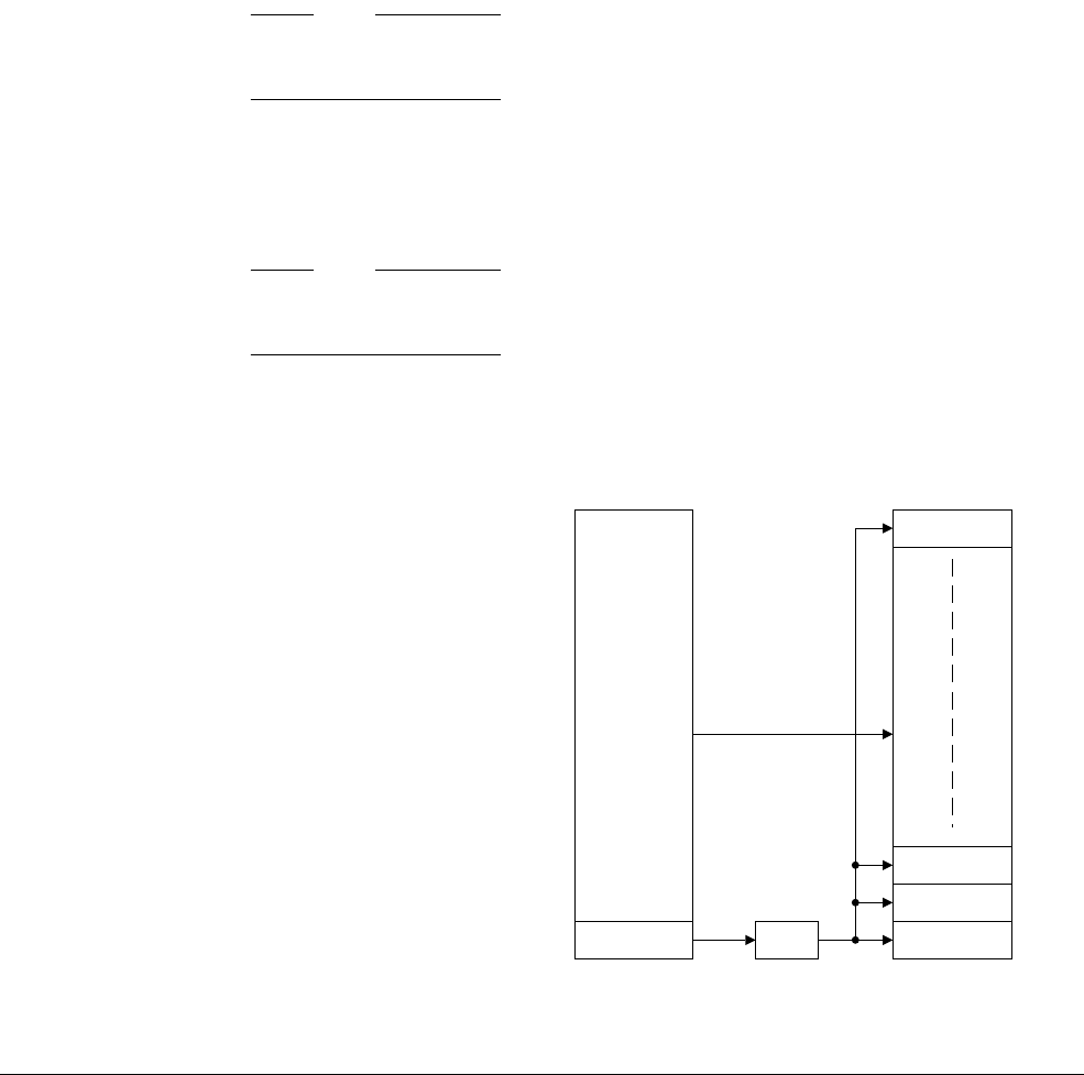
System Control Coprocessor
ARM DDI 0301H Copyright © 2004-2009 ARM Limited. All rights reserved. 3-127
ID012310 Non-Confidential, Unrestricted Access
To change the ProcID and perform a fast context switch, write to the FCSE PID Register. You
do not have to flush the contents of the TLB after the switch because the TLB still holds the valid
address tags.
From zero to six instructions after the MCR that writes the ProcID might be fetched with the old
ProcID:
{ProcID = 0}
MOV R0, #1 ; Fetched with ProcID = 0
MCR p15,0,R0,c13,c0,0 ; Fetched with ProcID = 0
A0 (any instruction) ; Fetched with ProcID = 0/1
A1 (any instruction) ; Fetched with ProcID = 0/1
A2 (any instruction) ; Fetched with ProcID = 0/1
A3 (any instruction) ; Fetched with ProcID = 0/1
A4 (any instruction) ; Fetched with ProcID = 0/1
A5 (any instruction) ; Fetched with ProcID = 0/1
A6 (any instruction) ; Fetched with ProcID = 1
Note
You must not rely on this behavior for future compatibility. An IMB must be executed between
changing the ProcID and fetching from locations that are translated by the ProcID.
Addresses issued by the ARM1176JZF-S processor in the range 0-32MB are translated by the
ProcID. Address A becomes A + (ProcID x 32MB). This translated address, the MVA, is used
by the MMU. Addresses higher than 32MB are not translated. The ProcID is a seven-bit field,
enabling 128 x 32MB processes to be mapped.
Note
If ProcID is 0, as it is on Reset, then there is a flat mapping between the ARM1176JZF-S
processor and the MMU.
Figure 3-69 shows how addresses are mapped using the FCSE PID Register.
Figure 3-69 Address mapping with the FCSE PID Register
C13
127
2
1
0
4GB
Modified virtual address (MVA)
input to MMU
Virtual address (VA)
issued by the processor
32MB
0
32MB
0
64MB
4GB

System Control Coprocessor
ARM DDI 0301H Copyright © 2004-2009 ARM Limited. All rights reserved. 3-128
ID012310 Non-Confidential, Unrestricted Access
3.2.47 c13, Context ID Register
The purpose of the Context ID Register is to provide information on the current ASID and
process ID, for example for the ETM and debug logic.
Table 3-129 lists the purposes of the individual bits of the Context ID Register.
Debug logic uses the ASID information to enable process-dependent breakpoints and
watchpoints.
The Context ID Register is:
• in CP15 c13
• a 32-bit read/write register banked for Secure and Non-secure worlds
• accessible in privileged modes only.
Writing to this register globally flushes the BTAC.
Figure 3-70 shows the arrangement of bits in the Context ID Register.
Figure 3-70 Context ID Register format
Table 3-129 lists how the bit values correspond with the Context ID Register functions.
Table 3-130 lists the results of attempted access for each mode.
The current ASID value in the ID Context Register is exported to the MMU.
To use the Context ID Register read or write CP15 with:
• Opcode_1 set to 0
• CRn set to c13
• CRm set to c0
• Opcode_2 set to 1.
For example:
MRC p15, 0, <Rd>, c13, c0, 1 ;Read Context ID Register
PROCID
31 8 7 0
ASID
Table 3-129 Context ID Register bit functions
Bits Field name Function
[31:8] PROCID Extends the ASID to form the process ID and identify the current process.
The value is the Process ID. The reset value is 0.
[8:0] ASID Holds the ASID of the current process to identify the current ASID.
The value is the ASID. The reset value is 0.
Table 3-130 Results of access to the Context ID Register
Secure Privileged Non-secure Privileged
User
Read Write Read Write
Secure data Secure data Non-secure data Non-secure data Undefined exception

System Control Coprocessor
ARM DDI 0301H Copyright © 2004-2009 ARM Limited. All rights reserved. 3-129
ID012310 Non-Confidential, Unrestricted Access
MCR p15, 0, <Rd>, c13, c0, 1 ;Write Context ID Register
You must ensure that software performs a Data Synchronization Barrier operation before
changes to this register. This ensures that all accesses are related to the correct context ID.
You must execute an IMB instruction immediately after changes to the Context ID Register. You
must not attempt to execute any instructions that are from an ASID-dependent memory region
between the change to the register and the IMB instruction. Code that updates the ASID must
execute from a global memory region.
You must program each process with a unique number to ensure that ETM and debug logic can
correctly distinguish between processes.
3.2.48 c13, Thread and process ID registers
The purpose of the thread and process ID registers is to provide locations to store the IDs of
software threads and processes for OS management purposes.
The thread and process ID registers are:
• in CP15 c13
• three 32-bit read/write registers banked for Secure and Non-secure worlds:
— User Read/Write Thread and Process ID Register
— User Read Only Thread and Process ID Register
— Privileged Only Thread and Process ID Register.
• each accessible in different modes:
— User Read/Write: read/write in User and privileged modes
— User Read Only: read only in User mode, read/write in privileged modes
— Privileged Only: read/write in privileged modes only.
Table 3-131 lists the results of attempted access to each register for each mode.
To use the thread and process ID registers read or write CP15 with:
• Opcode_1 set to 0
• CRn set to c13
• CRm set to c0
Table 3-131 Results of access to the thread and process ID registers
Thread
and
Process
ID
Register
Secure
Privileged Non-secure Privileged Secure User Non-secure User
Read Write Read Write Read Write Read Write
User
Read/
Writea
Secure
data
Secure
data
Non-secure
data
Non-secure
data
Secure
data
Secure
data
Non-secure
data
Non-secure
data
User Read
Onlya
Secure
data
Secure
data
Non-secure
data
Non-secure
data
Secure
data
Undefined
exception
Non-secure
data
Undefined
exception
Privileged
Onlya
Secure
data
Secure
data
Non-secure
data
Non-secure
data
Undefined
exception
Undefined
exception
Undefined
exception
Undefined
exception
a. The register names are:
- User Read/Write Thread and Process ID Register
- User Read Only Thread and Process ID Register
- Privileged Only Thread and Process ID Register.

System Control Coprocessor
ARM DDI 0301H Copyright © 2004-2009 ARM Limited. All rights reserved. 3-130
ID012310 Non-Confidential, Unrestricted Access
• Opcode_2 set to:
— 2, User Read/Write Thread and Process ID Register
— 3, User Read Only Thread and Process ID Register
— 4, Privileged Only Thread and Process ID Register.
For example:
MRC p15, 0, <Rd>, c13, c0, 2 ;Read User Read/Write Thread and Proc. ID Register
MCR p15, 0, <Rd>, c13, c0, 2 ;Write User Read/Write Thread and Proc. ID Register
MRC p15, 0, <Rd>, c13, c0, 3 ;Read User Read Only Thread and Proc. ID Register
MCR p15, 0, <Rd>, c13, c0, 3 ;Write User Read Only Thread and Proc. ID Register
MRC p15, 0, <Rd>, c13, c0, 4 ;Read Privileged Only Thread and Proc. ID Register
MCR p15, 0, <Rd>, c13, c0, 4 ;Write Privileged Only Thread and Proc. ID Register
Reading or writing the thread and process ID registers has no effect on processor state or
operation. These registers provide OS support and must be managed by the OS.
You must clear the contents of all thread and process ID registers on process switches to prevent
data leaking from one process to another. This is important to ensure the security of secure data.
The reset value of these registers is 0.
3.2.49 c15, Peripheral Port Memory Remap Register
The purpose of the Peripheral Port Memory Remap Register is to remap the memory attributes
to Non-Shared Device. This forces access to the peripheral port and overrides what is
programmed in the page tables. The remapping happens both with the MMU enabled and with
the MMU disabled, therefore you can remap the peripheral port even when you do not use the
MMU. The Peripheral Port Memory Remap Register has the highest priority, higher than that
of the Primary and Normal memory remap registers.
Table 3-132 on page 3-131 lists the purposes of the individual bits in the Peripheral Port
Memory Remap Register.
The Peripheral Port Memory Remap Register is:
• in CP15 c15
• a 32-bit read/write register banked for Secure and Non-secure worlds
• accessible in privileged modes only.
Figure 3-71 shows the arrangement of the bits in the register.
Figure 3-71 Peripheral Port Memory Remap Register format
Base address
31 12 11 40
UNP/SBZ Size
5

System Control Coprocessor
ARM DDI 0301H Copyright © 2004-2009 ARM Limited. All rights reserved. 3-131
ID012310 Non-Confidential, Unrestricted Access
Table 3-132 lists how the bit values correspond with the functions of the Peripheral Port
Memory Remap Register.
Attempts to write to this register in Secure Privileged mode when CP15SDISABLE is HIGH
result in an Undefined exception, see TrustZone write access disable on page 2-9.
Table 3-133 lists the results of attempted access for each mode.
Table 3-132 Peripheral Port Memory Remap Register bit functions
Bits Field name Function
[31:12] Base Address Gives the physical base address of the region of memory for remapping to the peripheral port.
If the processor uses the Peripheral Port Memory Remap Register while the MMU is disabled,
the virtual base address is equal to the physical base address that is used.
The assumption is that the Base Address is aligned to the size of the remapped region. Any
bits in the range [(log2(Region size)-1):12] are ignored.
The value is the base address. The reset value is 0.
[11:5] - UNP/SBZ
[4:0] Size Indicates the size of the memory region that the peripheral port is remapped to.
All other values are reserved:
b00000 = 0KBa
b00011 = 4KB
b00100 = 8KB
b00101 = 16KB
b00110 = 32KB
b00111 = 64KB
b01000 = 128KB
b01001 = 256KB
b01010 = 512KB
b01011 = 1MB
b01100 = 2MB
b01101 = 4MB
b01110 = 8MB
b01111 = 16MB
b10000 = 32MB
b10001 = 64MB
b10010 = 128MB
b10011 = 256MB
b10100 = 512MB
b10101 = 1GB
b10110 = 2GB.
a. The reset value, indicating that no remapping is to take place.
Table 3-133 Results of access to the Peripheral Port Remap Register
Secure Privileged Non-secure Privileged
User
Read Write Read Write
Secure data Secure data Non-secure data Non-secure data Undefined exception

System Control Coprocessor
ARM DDI 0301H Copyright © 2004-2009 ARM Limited. All rights reserved. 3-132
ID012310 Non-Confidential, Unrestricted Access
To use the memory remap registers read or write CP15 with:
• Opcode_1 set to 0
• CRn set to c15
• CRm set to c2
• Opcode_2 set to 4.
For example:
MRC p15, 0, <Rd>, c15, c2, 4 ; Read Peripheral Port Memory Remap Register
MCR p15, 0, <Rd>, c15, c2, 4 ; Write Peripheral Port Memory Remap Register
3.2.50 c15, Secure User and Non-secure Access Validation Control Register
The purpose of the Secure User and Non-secure Access Validation Control Register is to
control:
• access to the system validation registers in User mode and in the Non-secure world
• access to the performance monitor unit registers in User mode.
Table 3-134 lists the purpose of the individual bits in the register.
The Secure User and Non-secure Access Validation Control Register is:
• in CP15 c15
• a 32-bit read/write register in the Secure world only
• accessible in privileged modes only.
Figure 3-72 shows the bit arrangement for the Secure User and Non-secure Access Validation
Control Register.
Figure 3-72 Secure User and Non-secure Access Validation Control Register format
Table 3-134 lists how the bit values correspond with the Secure User and Non-secure Access
Validation Control Register functions.
Attempts to write to this register in Secure Privileged mode when CP15SDISABLE is HIGH
result in an Undefined exception, see TrustZone write access disable on page 2-9.
VSBZ
31 10
Table 3-134 Secure User and Non-secure Access Validation Control Register bit functions
Bits Field name Function
[31:1] - UNP/SBZ.
[0] V Controls access to system validation registers from User and Non-secure modes, and to
performance monitor registers in User mode.
0 = system validation registers accessible only from Secure privileged modes, performance
monitor registers accessible only from privileged modes. The reset value is 0.
1 = system validation and performance monitor registers accessible from any mode.

System Control Coprocessor
ARM DDI 0301H Copyright © 2004-2009 ARM Limited. All rights reserved. 3-133
ID012310 Non-Confidential, Unrestricted Access
Table 3-135 lists the results of attempted access for each mode.
To access the Secure User and Non-secure Access Validation Control Register read or write
CP15 with:
• Opcode_1 set to 0
• CRn set to c15
• CRm set to c9
• Opcode_2 set to 0.
For example:
MRC p15, 0, <Rd>, c15, c9, 0 ; Read Secure User and Non-secure Access Validation Control Register
MCR p15, 0, <Rd>, c15, c9, 0 ; Write Secure User and Non-secure Access Validation Control Register
3.2.51 c15, Performance Monitor Control Register
The purpose of the Performance Monitor Control Register is to control the operation of:
• the Cycle Counter Register
• the Count Register 0
• the Count Register 1.
Table 3-136 on page 3-134 lists the purpose of the individual bits in the register.
The Performance Monitor Control Register is:
• in CP15 c15
• a 32-bit read/write register common to Secure and Non-secure worlds
• accessible in User and Privileged modes.
Figure 3-73 shows the bit arrangement for the Performance Monitor Control Register.
Figure 3-73 Performance Monitor Control Register format
Table 3-135 Results of access to the Secure User and Non-secure Access
Validation Control Register
Secure Privileged
Non-secure Privileged User
Read Write
Data Data Undefined exception Undefined exception
ESBZ/UNP
31 28 27 20 19 12 11 7 6 4 3 2 1 0
EvtCount0 EvtCount1 X
S
B
Z
C PD
10 8
C
C
R
C
R
1
C
R
0
9
E
C
C
E
C
1
E
C
0
5

System Control Coprocessor
ARM DDI 0301H Copyright © 2004-2009 ARM Limited. All rights reserved. 3-134
ID012310 Non-Confidential, Unrestricted Access
Table 3-136 lists how the bit values correspond with the Performance Monitor Control Register.
Table 3-136 Performance Monitor Control Register bit functions
Bits Field name Function
[31:28] - UNP/SBZ.
[27:20] EvtCount0 Identifies the source of events for Count Register 0.
Table 3-137 on page 3-135 lists the values, functions and EVNTBUS bit position for Count
Register 0. The reset value is 0.
[19:12] EvtCount1 Identifies the source of events for Count Register 1.
Table 3-137 on page 3-135 lists the values and the bit functions for Count Register 1. The reset
value is 0.
[11] X Enable Export of the events to the event bus to an external monitoring block, such as the ETM
to trace events:
0 = Export disabled, EVNTBUS held at
0x0
, reset value
1 = Export enabled, EVNTBUS driven by the events.
[10] CCR Cycle Counter Register overflow flag:
0 = For reads No overflow, reset value.
For writes No effect.
1 = For reads, overflow occurred.
For writes Clear this bit.
[9] CR1 Count Register 1 overflow flag:
0 = For reads No overflow, reset value.
For writes No effect.
1 = For reads, overflow occurred.
For writes Clear this bit.
[8] CR0 Count Register 0 overflow flag:
0 = For reads No overflow, reset value.
For writes No effect.
1 = For reads overflow occurred.
For writes Clear this bit.
[7] - UNP/SBZ.
[6] ECC Used to enable and disable Cycle Counter interrupt reporting:
0 = Disable interrupt, reset value
1 = Enable interrupt.
[5] EC1 Used to enable and disable Count Register 1 interrupt reporting:
0 = Disable interrupt, reset value
1 = Enable interrupt.
[4] EC0 Used to enable and disable Count Register 0 interrupt reporting:
0 = Disable interrupt, reset value
1 = Enable interrupt.
[3] D Cycle count divider:
0 = Counts every processor clock cycle, reset value
1 = Counts every 64th processor clock cycle.

System Control Coprocessor
ARM DDI 0301H Copyright © 2004-2009 ARM Limited. All rights reserved. 3-135
ID012310 Non-Confidential, Unrestricted Access
The Performance Monitor Control Register:
• controls the events that Count Register 0 and Count Register 1 count
• indicates the counter that overflowed
• enables and disables the report of interrupts
• extends Cycle Count Register counting by six more bits, cycles between counter rollover
= 238
• resets all counters to zero
• enables the entire performance monitoring mechanism.
Table 3-137 lists the events that can be monitored using the Performance Monitor Control
Register.
[2] C Cycle Counter Register Reset. Reset on write, Unpredictable on read:
0 = No action, reset value
1 = Reset the Cycle Counter Register to
0x0
.
[1] P Count Register 1 and Count Register 0 Reset. Reset on write, Unpredictable on read:
0 = No action, reset value
1 = Reset both Count Registers to
0x0
.
[0] E Enable all counters:
0 = All counters disabled, reset value
1 = All counters enabled.
Table 3-136 Performance Monitor Control Register bit functions (continued)
Bits Field name Function
Table 3-137 Performance monitoring events
EVNTBUS
bit position
Event
number Event definition
-
0xFF
An increment each cycle.
-
0x26
Procedure return instruction executed and return address predicted incorrectly. The
procedure return address was restored to the return stack following the prediction
being identified as incorrect.
-
0x25
Procedure return instruction executed and return address predicted. The procedure
return address was popped off the return stack and the core branched to this address.
-
0x24
Procedure return instruction executed. The procedure return address was popped off
the return stack.
-
0x23
Procedure call instruction executed. The procedure return address was pushed on to
the return stack.
-
0x22
If both ETMEXTOUT[0] and ETMEXTOUT[1] signals are asserted then the count
is incremented by two. If either signal is asserted then the count increments by one.
-
0x21
ETMEXTOUT[1] signal was asserted for a cycle.
-
0x20
ETMEXTOUT[0] signal was asserted for a cycle.
[19]
0x12
Write Buffer drained because of a Data Synchronization Barrier operation or
Strongly Ordered operation.

System Control Coprocessor
ARM DDI 0301H Copyright © 2004-2009 ARM Limited. All rights reserved. 3-136
ID012310 Non-Confidential, Unrestricted Access
[18]
0x11
Stall because of a full Load Store Unit request queue. This event takes place each
clock cycle when the condition is met. A high incidence of this event indicates the
LSU is often waiting for transactions to complete on the external bus.
[17]
0x10
Explicit external data accesses, Data Cache linefills, Noncacheable, write-through.
[16]
0xF
Main TLB miss.
[15:14]
0xD
Software changed the PC. This event occurs any time the PC is changed by software
and there is not a mode change. For example, a MOV instruction with PC as the
destination triggers this event. Executing an SVC from User mode does not trigger
this event, because it incurs a mode change. If EVENTBUS bit [15] is HIGH, two
software PC changes occurred in this clock cycle and the count increments by two.
[13]
0xC
Data cache write-back. This event occurs once for each half line of four words that
are written back from the cache.
[12]
0xB
Data cache miss. Does not include Cache Operations.
[11]
0xA
Data cache access. Does not include Cache Operations. This event occurs for each
nonsequential access to a cache line, regardless of whether or not the location is
cacheable.
[10]
0x9
Data cache access. Does not include Cache Operations. This event occurs for each
nonsequential access to a cache line, for cacheable locations.
[9:8]
0x7
Instruction executed. If EVENTBUS bit [9] is HIGH, two instructions were executed
in this clock cycle and the count is increments by two.
[7]
0x6
Branch mispredicted.
[6] - Reserved.
[5]
0x5
Branch instruction executed, branch might or might not have changed program flow.
[4]
0x4
Data MicroTLB miss.
[3]
0x3
Instruction MicroTLB miss.
[2]
0x2
Stall because of a data dependency. This event occurs every cycle when the condition
is present.
[1]
0x1
Stall because instruction buffer cannot deliver an instruction. This can indicate an
Instruction Cache miss or an Instruction MicroTLB miss. This event occurs every
cycle when the condition is present.
[0]
0x0
Instruction cache miss.
Note
This event counts all instruction cache misses, including any speculative access that
would be a cache miss. If the instruction that caused a speculative access is not
executed then there might not be a fetch from external memory. This can happen, for
example, if the code branches round the instruction. This means that the value
returned in this counter can be much larger than the number of external memory
accesses caused by instruction cache misses.
- All other values Reserved. Unpredictable behavior.
Table 3-137 Performance monitoring events (continued)
EVNTBUS
bit position
Event
number Event definition

System Control Coprocessor
ARM DDI 0301H Copyright © 2004-2009 ARM Limited. All rights reserved. 3-137
ID012310 Non-Confidential, Unrestricted Access
Access to the Performance Monitor Control Register in User mode depends on the V bit, see
c15, Secure User and Non-secure Access Validation Control Register on page 3-132. The
Performance Monitor Control Register is always accessible in Privileged modes. Table 3-138
lists the results of attempted access for each mode.
To access the Performance Monitor Control Register read or write CP15 with:
• Opcode_1 set to 0
• CRn set to c15
• CRm set to c12
• Opcode_2 set to 0.
For example:
MRC p15, 0, <Rd>, c15, c12, 0 ; Read Performance Monitor Control Register
MCR p15, 0, <Rd>, c15, c12, 0 ; Write Performance Monitor Control Register
If this unit generates an interrupt, the processor asserts the pin nPMUIRQ. You can route this
pin to an external interrupt controller for prioritization and masking. This is the only mechanism
that signals this interrupt to the core. When asserted, this interrupt can only be cleared if bit 0 of
the Performance Monitor Control Register is high.
There is a delay of three cycles between an enable of the counter and the start of the event
counter. The information used to count events is taken from various pipeline stages. This means
that the absolute counts recorded might vary because of pipeline effects. This has negligible
effect except in cases where the counters are enabled for a very short time.
In addition to the two counters within the processor, most of the events that Table 3-137 on
page 3-135 lists are available on an external bus, EVNTBUS. You can connect this bus to the
ETM unit or other external trace hardware to enable the events to be monitored. If you do not
want this functionality, set the X bit in the Performance Monitor Control Register to 0. In Debug
state, the EVNTBUS is masked to zero.
3.2.52 c15, Cycle Counter Register
The purpose of the Cycle Counter Register is to count the core clock cycles.
The Cycle Counter Register:
•is in CP15 c15
• is a 32-bit read/write register common to Secure and Non-secure worlds
• counts up and can trigger an interrupt on overflow.
The Cycle Counter Register bits[31:0] contain the count value. The reset value is 0.
You can use this register in conjunction with the Performance Monitor Control Register and the
two Counter Registers to provide a variety of useful metrics that enable you to optimize system
performance.
Table 3-138 Results of access to the Performance Monitor Control Register
V bit
Secure Privileged Non-secure Privileged User
Read Write Read Write Read Write
0 Data Data Data Data Undefined exception Undefined exception
1 Data Data Data Data Data Data

System Control Coprocessor
ARM DDI 0301H Copyright © 2004-2009 ARM Limited. All rights reserved. 3-138
ID012310 Non-Confidential, Unrestricted Access
Access to the Cycle Counter Register in User mode depends on the V bit, see c15, Secure User
and Non-secure Access Validation Control Register on page 3-132. The Cycle Counter Register
is always accessible in Privileged modes. Table 3-139 lists the results of attempted access for
each mode.
To access the Cycle Counter Register read or write CP15 with:
• Opcode_1 set to 0
• CRn set to c15
• CRm set to c12
• Opcode_2 set to 1.
For example:
MRC p15, 0, <Rd>, c15, c12, 1 ; Read Cycle Counter Register
MCR p15, 0, <Rd>, c15, c12, 1 ; Write Cycle Counter Register
The value in the Cycle Counter Register is zero at Reset.
You can use the Performance Monitor Control Register to set the Cycle Counter Register to zero.
You can use the Performance Monitor Control Register to configure the Cycle Counter Register
to count every 64th clock cycle.
3.2.53 c15, Count Register 0
The purpose of the Count Register 0 is to count instances of an event that the Performance
Monitor Control Register selects.
The Count Register 0:
•is in CP15 c15
• is a 32-bit read/write register common to Secure and Non-secure worlds
• counts up and can trigger an interrupt on overflow.
Count Register 0 bits [31:0] contain the count value. The reset value is 0.
You can use this register in conjunction with the Performance Monitor Control Register, the
Cycle Count Register, and Count Register 1 to provide a variety of useful metrics that enable
you to optimize system performance.
Note
• In Debug state the counter is disabled.
• When the core is in a mode where noninvasive debug is not permitted, set by SPNIDEN
and the SUNIDEN bit, see c1, Secure Debug Enable Register on page 3-54, the processor
does not count events.
Table 3-139 Results of access to the Cycle Counter Register
V bit
Secure Privileged Non-secure Privileged User
Read Write Read Write Read Write
0 Data Data Data Data Undefined exception Undefined exception
1 Data Data Data Data Data Data

System Control Coprocessor
ARM DDI 0301H Copyright © 2004-2009 ARM Limited. All rights reserved. 3-139
ID012310 Non-Confidential, Unrestricted Access
Access to the Count Register 0 in User mode depends on the V bit, see c15, Secure User and
Non-secure Access Validation Control Register on page 3-132. The Count Register 0 is always
accessible in Privileged modes. Table 3-140 lists the results of attempted access for each mode.
To access Count Register 1 read or write CP15 with:
• Opcode_1 set to 0
• CRn set to c15
• CRm set to c12
• Opcode_2 set to 2.
For Example:
MRC p15, 0, <Rd>, c15, c12, 2 ; Read Count Register 0
MCR p15, 0, <Rd>, c15, c12, 2 ; Write Count Register 0
The value in Count Register 0 is 0 at Reset.
You can use the Performance Monitor Control Register to set Count Register 0 to zero.
3.2.54 c15, Count Register 1
The purpose of the Count Register 1 is to count instances of an event that the Performance
Monitor Control Register selects.
The Count Register 1:
•is in CP15 c15
• is a 32-bit read/write register common to Secure and Non-secure worlds
• counts up and can trigger an interrupt on overflow.
Count Register 1 bits [31:0] contain the count value. The reset value is 0.
You can use this register in conjunction with the Performance Monitor Control Register, the
Cycle Count Register, and Count Register 0 to provide a variety of useful metrics that enable
you to optimize system performance.
Note
• In Debug state the counter is disabled.
• When the core is in a mode where non-invasive debug is not permitted, set by SPNIDEN
and the SUNIDEN bit, see c1, Secure Debug Enable Register on page 3-54, the processor
does not count events.
Table 3-140 Results of access to the Count Register 0
V bit
Secure Privileged Non-secure Privileged User
Read Write Read Write Read Write
0 Data Data Data Data Undefined exception Undefined exception
1 Data Data Data Data Data Data

System Control Coprocessor
ARM DDI 0301H Copyright © 2004-2009 ARM Limited. All rights reserved. 3-140
ID012310 Non-Confidential, Unrestricted Access
Access to the Count Register 1 in User mode depends on the V bit, see c15, Secure User and
Non-secure Access Validation Control Register on page 3-132. The Count Register 1 is always
accessible in Privileged modes. Table 3-141 lists the results of attempted access for each mode.
To access Count Register 1 read or write CP15 with:
• Opcode_1 set to 0
• CRn set to c15
• CRm set to c12
• Opcode_2 set to 3.
For example:
MRC p15, 0, <Rd>, c15, c12, 3 ; Read Count Register 1
MCR p15, 0, <Rd>, c15, c12, 3 ; Write Count Register 1
The value in Count Register 1 is 0 at Reset.
You can use the Performance Monitor Control Register to set Count Register 1 to zero.
3.2.55 c15, System Validation Counter Register
The purpose of the System Validation Counter Register is to count core clock cycles to trigger
a system validation event.
The System Validation Counter Register is:
• in CP15 c15
• a 32 bit read/write register common to the Secure and Non-secure worlds
• accessible in User and Privileged modes.
The System Validation Counter Register consists of one 32-bit register that performs four
functions. Table 3-142 lists the arrangement of the functions in this group. The reset value is 0.
The reset, interrupt, and fast interrupt counters are 32-bits wide. The external debug request
counter is 6 bits wide. Figure 3-74 on page 3-141 shows the arrangement of bits for the external
debug request counter.
Table 3-141 Results of access to the Count Register 1
V bit
Secure Privileged Non-secure Privileged User
Read Write Read Write Read Write
0 Data Data Data Data Undefined exception Undefined exception
1 Data Data Data Data Data Data
Table 3-142 System validation counter register operations
CRn Opcode_1 CRm Opcode_2 R/W Operation
c15 0 c12 1 R/W Reset counter
2 R/W Interrupt counter
3 R/W Fast interrupt counter
7 W External debug request counter

System Control Coprocessor
ARM DDI 0301H Copyright © 2004-2009 ARM Limited. All rights reserved. 3-141
ID012310 Non-Confidential, Unrestricted Access
Figure 3-74 System Validation Counter Register format for external debug request counter
Table 3-143 lists the results of attempted access for each mode. Access in Secure User mode and
in the Non-secure world depends on the V bit, see c15, Secure User and Non-secure Access
Validation Control Register on page 3-132.
Attempts to write to this register in Secure Privileged mode when CP15SDISABLE is HIGH
result in an Undefined exception, see TrustZone write access disable on page 2-9.
To use the System Validation Counter Register read or write CP15 with:
• Opcode_1 set to 0
• CRn set to c15
• CRm set to c12
• Opcode_2 set to:
— 1, Read/write reset counter
— 2, Read/write interrupt counter
— 3, Read/write fast interrupt counter
— 7, Write external debug request counter.
For example:
MRC p15, 0, <Rd>, c15, c12, 1 ;Read reset counter
MCR p15, 0, <Rd>, c15, c12, 1 ;Write reset counter
MRC p15, 0, <Rd>, c15, c12, 2 ;Read interrupt counter
MCR p15, 0, <Rd>, c15, c12, 2 ;Write interrupt counter
MRC p15, 0, <Rd>, c15, c12, 3 ;Read fast interrupt counter
MCR p15, 0, <Rd>, c15, c12, 3 ;Write fast interrupt counter
MCR p15, 0, <Rd>, c15, c12, 7 ;Write external debug request counter
A read or write to the System Validation Counter Register with a value of Opcode_2 other than
1, 2, 3, or 7 has no effect.
When the system starts the counters they count up, incrementing by one on each core clock
cycle, until they wrap around. When the counters wrap around they cause the specified event to
occur. See c15, System Validation Operations Register on page 3-142.
SBZ/UNP
31 65 0
Counter value
Table 3-143 Results of access to the System Validation Counter Register
Function V
bit
Secure Privileged Non-secure Privileged User
Read Write Read Write Read Write
Reset, interrupt, and
fast interrupt counters
0 Data Data Undefined
exception
Undefined
exception
Undefined
exception
Undefined
exception
1 Data Data Data Data Data Data
External debug request
counter
0 Unpredictable Data Undefined
exception
Undefined
exception
Undefined
exception
Undefined
exception
1 Unpredictable Data Unpredictable Data Unpredictable Data

System Control Coprocessor
ARM DDI 0301H Copyright © 2004-2009 ARM Limited. All rights reserved. 3-142
ID012310 Non-Confidential, Unrestricted Access
The reset, interrupt, and fast interrupt counters reuse the Cycle Count Register, Count Register
0 and Count Register 1 of the System performance monitor registers respectively, see System
performance monitor on page 3-10. You must not use the System Validation Count Register
when the System Performance Monitor Registers are in use.
The reset, interrupt, and fast interrupt counters are read/write. The external debug request
counter is write only. Attempts to read the external debug request counter return
0x00000000
regardless or the actual value of the counter.
3.2.56 c15, System Validation Operations Register
The purpose of the System Validation Operations Register is to start and stop system validation
counters to trigger a system validation event.
The System Validation Operations Register is:
• in CP15 c15
• a 32 bit read/write register common to the Secure and Non-secure worlds
• accessible in user and privileged modes.
The System Validation Operations Register consists of one 32-bit register that performs 16
functions. Table 3-144 lists the arrangement of the functions in this group.
A write to the System Validation Operations Register with a combination of Opcode_1 and
Opcode_2 that Table 3-144 does not list has no effect. A read from the System Validation
Operations Register returns
0x00000000
.
The reset value of this register is 0.
Table 3-144 System Validation Operations Register functions
CRn Opcode_1 CRm Opcode_2 R/W Operation
c15 0 c13 1 W Start reset counter
2 W Start interrupt counter
3 W Start reset and interrupt counters
4 W Start fast interrupt counter
5 W Start reset and fast interrupt counters
6 W Start interrupt and fast interrupt counters
7 W Start reset, interrupt and fast interrupt counters
c15 1 c13 0-7 W Start external debug request counter
c15 2 c13 1 W Stop reset counter
2 W Stop interrupt counter
3 W Stop reset and interrupt counters
4 W Stop fast interrupt counter
5 W Stop reset and fast interrupt counters
6 W Stop interrupt and fast interrupt counters
7 W Stop reset, interrupt and fast interrupt counters
c15 3 c13 0-7 W Stop external debug request counter

System Control Coprocessor
ARM DDI 0301H Copyright © 2004-2009 ARM Limited. All rights reserved. 3-143
ID012310 Non-Confidential, Unrestricted Access
Attempts to write to this register in Secure Privileged mode when CP15SDISABLE is HIGH
result in an Undefined exception, see TrustZone write access disable on page 2-9.
Table 3-145 lists the results of attempted access for each mode. Access in Secure User mode and
in the Non-secure world depends on the V bit, see c15, Secure User and Non-secure Access
Validation Control Register on page 3-132.
To use the System Validation Operations Register write CP15 with <Rd> set to SBZ and:
• Opcode_1 set to:
— 0, Start reset, interrupt, or fast interrupt counters
— 1, Start external debug request counter
— 2, Stop reset, interrupt, or fast interrupt counters
— 3, Stop external debug request counter.
• CRn set to c15
• CRm set to c13
• Opcode_2 set to:
— 1, Reset counter
— 2, Interrupt counter
— 3, Reset and interrupt counters
— 4, Fast interrupt counter
— 5, Reset and fast interrupt counters
— 6, Interrupt and fast interrupt counters
— 7, Reset, interrupt and fast interrupt counters
— Any value, External debug request counter.
For example:
MCR p15, 0, <Rd>, c15, c13, 1 ; Start reset counter
MCR p15, 0, <Rd>, c15, c13, 2 ; Start interrupt counter
MCR p15, 0, <Rd>, c15, c13, 3 ; Start reset and interrupt counters
MCR p15, 0, <Rd>, c15, c13, 4 ; Start fast interrupt counter
MCR p15, 0, <Rd>, c15, c13, 5 ; Start reset and fast interrupt counters
MCR p15, 0, <Rd>, c15, c13, 6 ; Start interrupt and fast interrupt counters
MCR p15, 0, <Rd>, c15, c13, 7 ; Start reset, interrupt and fast interrupt counters
MCR p15, 1, <Rd>, c15, c13, 0 ; Start external debug request counter
MCR p15, 2, <Rd>, c15, c13, 1 ; Stop reset counter
MCR p15, 2, <Rd>, c15, c13, 2 ; Stop interrupt counter
MCR p15, 2, <Rd>, c15, c13, 3 ; Stop reset and interrupt counters
MCR p15, 2, <Rd>, c15, c13, 4 ; Stop fast interrupt counter
MCR p15, 2, <Rd>, c15, c13, 5 ; Stop reset and fast interrupt counters
MCR p15, 2, <Rd>, c15, c13, 6 ; Stop interrupt and fast interrupt counters
MCR p15, 2, <Rd>, c15, c13, 7 ; Stop reset, interrupt and fast interrupt counters
MCR p15, 3, <Rd>, c15, c13, 0 ; Stop external debug request counter
Table 3-145 Results of access to the System Validation Operations Register
V bit
Secure Privileged Non-secure Privileged User
Read Write Read Write Read Write
0 Unpredictable Data Undefined
exception
Undefined exception Undefined
exception
Undefined exception
1 Unpredictable Data Unpredictable Data Unpredictable Data

System Control Coprocessor
ARM DDI 0301H Copyright © 2004-2009 ARM Limited. All rights reserved. 3-144
ID012310 Non-Confidential, Unrestricted Access
You use the System Validation Operations Register to start and stop the reset, interrupt, fast
interrupt, and external debug request counters. When the system starts any of these counters,
they count up incrementing by one every core clock cycle, until they wrap around. When the
counters wrap around they cause nVALRESET, nVALIRQ, nVALFIQ, or VA L E D B G R Q to
go LOW depending on the operation. You can use these outputs to generate system Reset,
Interrupt request, Fast Interrupt request, or External Debug Request events. You can use the
System Validation Counter Register to set the start value of the counters, see c15, System
Validation Counter Register on page 3-140. Any number of events can occur simultaneously.
When you use the Validation Trickbox Operations Register to start a counter, there is one clock
cycle delay, that generally corresponds to one instruction, before the count begins. If you require
an event to occur on the next instruction, insert a NOP instruction between the MCR instruction,
to the System Validation Operations Register, that starts the counter and the instruction on which
you want the event to occur.
You must leave two clock cycles, that generally corresponds to two instructions, between a write
to a counter with the System Validation Counter Register and the start of that count with the
System Validation Operations Register.
After the system stops the reset, interrupt or fast interrupt counters, or after handling the events
they cause, you must explicitly clear the counters to return them to their System performance
monitoring function. To do this set bits in <Rn> and write to the Performance Monitor Control
Register to clear the relevant overflow flags:
• bit [10] to clear the reset counter
• bit [9] to clear the fast interrupt counter
• bit [8] to clear the interrupt counter.
You must carry out this operation with a read-modify-write sequence to avoid changes to other
bits, see c15, Performance Monitor Control Register on page 3-133. You do not have to clear
the external debug request counter explicitly in this way because it is not used for system
performance monitoring.
The reset, interrupt, and fast interrupt counters reuse the Cycle Count Register, Count Register
0 and Count Register 1 of the System performance monitor registers respectively, see System
performance monitor on page 3-10. As a result you must not perform read or write operations
to the System Validation Counter Register when the System performance monitor registers are
in use.
The System Validation Operations Register is write only and attempts to read this register are
reserved and return
0x00000000
.
To schedule system validation events follow this procedure:
1. Modify the Secure User and Non-secure Access Validation Control Register to permit
access from User or Non-secure modes if this is required.
2. Use the Validation Trickbox Counter Register to load the required counter with
0xFFFFFFFF
minus the number of core clock cycles to wait before the event occurs.
3. Use the Validation Trickbox Operations Register to start the required counter.
4. Use the appropriate Validation Trickbox Operations Register to stop the required counter,
after the event has occurred or as necessary.
5. Use the Performance Monitor Control Register to reset the counters and return them to
System performance monitoring functionality.

System Control Coprocessor
ARM DDI 0301H Copyright © 2004-2009 ARM Limited. All rights reserved. 3-145
ID012310 Non-Confidential, Unrestricted Access
3.2.57 c15, System Validation Cache Size Mask Register
The purpose of the System Validation Cache Size Mask Register is to change the apparent size
of the caches and TCMs as they appear to the processor, for validation by simulation. It does not
change the physical size of the caches and TCMs in a manufactured device.
The System Validation Cache Size Mask Register is:
• in CP15 c15
• a 32 bit read/write register common to the Secure and Non-secure worlds
• accessible in User and Privileged modes.
Figure 3-75 shows the arrangement of bits for the System Validation Cache Size Mask Register.
Figure 3-75 System Validation Cache Size Mask Register format
Table 3-146 lists how the bit values correspond with the System Validation Cache Size Mask
Register functions.
SBZ
31 15 14 12 11 10 8 7 6 4 3 2 0
DTCM
S
B
Z
ITCM
S
B
Z
DCache
S
B
Z
ICache
Write enable
Table 3-146 System Validation Cache Size Mask Register bit functions
Bits Field name Function
[31] Write enable Enables the update of the Cache and TCM sizes:
0 = The Cache and TCM sizes are not changed, reset value.
1 = The Cache and TCM sizes take the new values that the DTCM, ITCM, DCache and ICache
fields of this register specify.
Note
This is bit is write access only and Read As Zero.
[30:15] SBZ UNP/SBZ.
[14:12] DTCM Specifies apparent size of Data TCM and apparent number of Data TCM banks, as it appears
to the processor. All other values are reserved:
b000 = Not present
b011 = 1 bank, 4KB
b100 = 2 banks, 4KB each
b101 = 2 banks, 8KB each
b110 = 2 banks, 16KB each
b111 = 2 banks, 32KB each.
[11] SBZ UNP/SBZ.
[10:8] ITCM Specifies apparent size of Instruction TCM and apparent number of Instruction TCM banks, as
it appears to the processor. All other values are reserved:
b000 = Not present
b011 = 1 bank, 4KB
b100 = 2 banks, 4KB each
b101 = 2 banks, 8KB each
b110 = 2 banks, 16KB each
b111 = 2 banks, 32KB each.

System Control Coprocessor
ARM DDI 0301H Copyright © 2004-2009 ARM Limited. All rights reserved. 3-146
ID012310 Non-Confidential, Unrestricted Access
At reset, the values in the System Validation Cache Size Mask Register are the correct values
for the implemented caches and TCMs.
Access to the System Validation Cache Size Mask Register in Secure User mode and in the
Non-secure world depends on the V bit, see c15, Secure User and Non-secure Access Validation
Control Register on page 3-132. Table 3-147 lists the results of attempted access for each mode.
Attempts to write to this register in Secure Privileged mode when CP15SDISABLE is HIGH
result in an Undefined exception, see TrustZone write access disable on page 2-9.
To use the System Validation Cache Size Mask Register read or write CP15 with:
• Opcode_1 set to 0
• CRn set to c15
• CRm set to c14
• Opcode_2 set to 0.
For example:
MRC p15, 0, <Rd>, c15, c14, 0 ; Read System Validation Cache Size Mask Register
MCR p15, 0, <Rd>, c15, c14, 0 ; Write System Validation Cache Size Mask Register
[7] SBZ UNP/SBZ.
[6:4] DCache Specifies apparent size of Data Cache, as it appears to the processor. All other values are
reserved:
b011 = 4KB
b100 = 8KB
b101 = 16KB
b110 = 32KB
b111 = 64KB.
[3] SBZ UNP/SBZ.
[2:0] ICache Specifies apparent size of Instruction Cache, as it appears to the processor. All other values are
reserved:
b011 = 4KB
b100 = 8KB
b101 = 16KB
b110 = 32KB
b111 = 64KB.
Table 3-146 System Validation Cache Size Mask Register bit functions (continued)
Bits Field name Function
Table 3-147 Results of access to the System Validation Cache Size Mask Register
V
bit
Secure
Privileged Non-secure Privileged User
Read Write Read Write Read Write
0 Data Data Undefined exception Undefined exception Undefined exception Undefined exception
1 Data Data Data Data Data Data

System Control Coprocessor
ARM DDI 0301H Copyright © 2004-2009 ARM Limited. All rights reserved. 3-147
ID012310 Non-Confidential, Unrestricted Access
You can use the System Validation Cache Size Mask Register, in a validation simulation
environment, to perform validation with cache and TCM sizes that appear to be a different size
from those that are actually implemented. The validation environment for the processor contains
validation RAMs that support cache and TCM size masking using this register. When you write
to the System Validation Cache Size Mask Register, the processor behaves as though the caches
and TCMs are the sizes that are written to the register. The sizes written to the register are
reflected in:
• The sizes of the cache and TCM RAMs.
• The sizes of the caches in the Cache Type Register, see c0, Cache Type Register on
page 3-21, the number of Instruction and Data TCM banks in the TCM Status Register,
see c0, TCM Status Register on page 3-24, the sizes of the TCMs in the Instruction TCM
Region Register, see c9, Instruction TCM Region Register on page 3-91, and the Data
TCM Region Register, see c9, Data TCM Region Register on page 3-89.
• The number and use of cache master valid bits, see Cache Master Valid Registers on
page 3-8.
• The hazard detection logic that prevents the same line being allocated twice into the
caches.
• The DMA. If the TCMs are both masked as not present, then the DMA also appears not
to be present.
Note
You must not modify the System Validation Cache Size Mask Register in a manufactured
device. Physical RAMs do not support cache and TCM size masking. Therefore, any attempt to
mask cache and TCM sizes using this register causes address aliasing effects and problems with
cache master valid bits, that result in incorrect operation and Unpredictable effects.
3.2.58 c15, Instruction Cache Master Valid Register
The purpose of the Instruction Cache Master Valid Register is to save and restore the instruction
cache master valid bits on entry to and exit from dormant mode, see Dormant mode on
page 10-4. You might also use this register during debug.
The Instruction Cache Master Valid Register is:
• in CP15 c15
• a 32-bit read/write register in Secure world only
• accessible in privileged modes only.
The number of Master Valid bits in the register is a function of the cache size. There is one
Master Valid bit for each 8 cache lines:
For instance, there are 64 Master Valid bits for a 16KB cache. You can access Master Valid bits
through 32-bit registers indexed using Opcode_2. The maximum number of 32-bit registers
required for the largest cache size, 64KB, is 8. The Master Valid bits fill the registers from the
LSB of the lowest numbered register upwards.
Writes to unimplemented Valid bits have no effect, and reads return 0. The reset value is 0.
Attempts to write to this register in Secure Privileged mode when CP15SDISABLE is HIGH
result in an Undefined exception, see TrustZone write access disable on page 2-9.
Master Valid bits = cache size
line length in bytes x 8

System Control Coprocessor
ARM DDI 0301H Copyright © 2004-2009 ARM Limited. All rights reserved. 3-148
ID012310 Non-Confidential, Unrestricted Access
Attempts to access the register in modes other than Secure privileged result in an Undefined
exception.
To use the Instruction Cache Master Valid Register write CP15 with:
• Opcode_1 set to 3
• CRn set to c15
• CRm set to c8
• Opcode_2 set to <Register Number>.
MRC p15, 3, <Rd>, c15, c8, <Register Number> ; Read Instruction Cache Master Valid Register
MCR p15, 3, <Rd>, c15, c8, <Register Number> ; Write Instruction Cache Master Valid Register
The <Register Number> field of the instruction designates one of the registers required to
capture all the Valid bits. The highest Register Number is one less than the number of times 8KB
divides into the cache size.
3.2.59 c15, Data Cache Master Valid Register
The purpose of the Data Cache Master Valid Register is to save and restore the Data cache
master valid bits on entry to and exit from dormant mode, see Dormant mode on page 10-4. You
might also use this register during debug.
The Data Cache Master Valid Register is:
• in CP15 c15
• a 32-bit read/write register in the Secure world only
• accessible in privileged modes only.
The number of Master Valid bits in the register is a function of the cache size. There is one
Master Valid bit for each 8 cache lines:
For instance, there are 64 Master Valid bits for a 16KB cache. You can access Master Valid bits
through 32-bit registers indexed using Opcode_2. The maximum number of 32-bit registers
required for the largest cache size, 64KB, is 8. The Master Valid bits fill the registers from the
LSB of the lowest numbered register upwards.
Writes to unimplemented Valid bits have no effect, and reads return 0. The reset value is 0.
Attempts to write to this register in Secure Privileged mode when CP15SDISABLE is HIGH
result in an Undefined exception, see TrustZone write access disable on page 2-9.
Attempts to access the register in modes other than Secure privileged result in an Undefined
exception.
To use the Data Cache Master Valid Register write CP15 with:
• Opcode_1 set to 3
• CRn set to c15
• CRm set to c12
• Opcode_2 set to <Register Number>.
MRC p15, 3, <Rd>, c15, c12, <Register Number> ; Read Data Cache Master Valid Register
MCR p15, 3, <Rd>, c15, c12, <Register Number> ; Write Data Cache Master Valid Register
The <Register Number> field of the instruction designates one of the registers required to
capture all the Valid bits. The highest Register Number is one less than the number of times 8KB
divides into the cache size.
Master Valid bits = cache size
line length in bytes x 8

System Control Coprocessor
ARM DDI 0301H Copyright © 2004-2009 ARM Limited. All rights reserved. 3-149
ID012310 Non-Confidential, Unrestricted Access
3.2.60 c15, TLB lockdown access registers
The purpose of the TLB lockdown access registers is to provide read and write access to the
contents of the lockdown region of the TLB. The processor requires these registers to enable it
to save state before it enters Dormant mode, see Dormant mode on page 10-4. You might also
use this register for debug.
The TLB lockdown access registers are:
• in CP15 c15
• four 32-bit read/write registers in the Secure world only:
— TLB Lockdown Index Register
— TLB Lockdown VA Register
— TLB Lockdown PA Register
— TLB Lockdown Attributes Register.
• accessible in privileged modes only.
The four registers have different bit arrangements and functions. Figure 3-76 shows the
arrangement of bits in the TLB Lockdown Index Register.
Figure 3-76 TLB Lockdown Index Register format
Table 3-148 lists how the bit values correspond with the TLB Lockdown Index Register
functions.
Figure 3-77 shows the arrangement of bits in the TLB Lockdown VA Register.
Figure 3-77 TLB Lockdown VA Register format
IndexUNP/SBZ
31 32 0
Table 3-148 TLB Lockdown Index Register bit functions
Bits Field name Function
[31:3] - UNP/SBZ.
[2:0] Index Selects the lockdown entry of the eight TLB lockdown entries to read or write when accessing
other TLB lockdown access registers.
Select lockdown entry 0 to 7.
VA
31 12 11 10 9 8 7 0
SBZ G
S
B
Z
ASID

System Control Coprocessor
ARM DDI 0301H Copyright © 2004-2009 ARM Limited. All rights reserved. 3-150
ID012310 Non-Confidential, Unrestricted Access
Table 3-149 lists how the bit values correspond with the TLB Lockdown VA Register functions.
Figure 3-78 shows the arrangement of bits in the TLB Lockdown PA Register.
Figure 3-78 TLB Lockdown PA Register format
Table 3-150 lists how the bit values correspond with the TLB Lockdown PA Register functions.
Table 3-149 TLB Lockdown VA Register bit functions
Bits Field name Function
[31:12] VA Holds the VA of this page table entry.
[11:10] - UNP/SBZ.
[9] G Defines if this page table entry is global, applies to all ASIDs, or application-specific, ASID
must match on lookups:
0 = Application-specific entry
1 = Global entry.
[8] - UNP/SBZ.
[7:0] ASID Holds the ASID for application-specific page table entries. For global entries, this field Should
Be Zero.
VPA
31 1211109876543210
SBZ
N
S
A
Size SBZ
A
P
X
AP
NSTID
Table 3-150 TLB Lockdown PA Register bit functions
Bits Field name Function
[31:12] PA Holds the PA of this page table entry.
[11:10] - UNP/SBZ.
[9] NSA Defines whether memory accesses in the memory region that this page table entry describes are
Secure or Non-secure accesses. This matches the Secure or Non-secure state of the memory
being accessed. If the NSTID bit is set, the NSA bit is also set regardless of the written value.
This ensures that Non-secure page table entries can only access Non-secure memory, but
Secure page table entries can access Secure or Non-secure memory:
0 = Memory accesses are Secure
1 = Memory accesses are Non-secure.
[8] NSTID Defines page table entry as Secure or Non-secure:
0 = Entry is Secure
1 = Entry is Non-secure.
[7:6] Size Defines the size of the memory region that this page table entry describes:
b00 = 16MB supersection
b01 = 4KB page
b10 = 64KB page
b11 = 1M section.
[5:4] - UNP/SBZ.

System Control Coprocessor
ARM DDI 0301H Copyright © 2004-2009 ARM Limited. All rights reserved. 3-151
ID012310 Non-Confidential, Unrestricted Access
Table 3-151 lists the encoding for the access permissions for bit fields APX and AP.
Figure 3-79 shows the arrangement of bits in the TLB Lockdown Attributes Register.
Figure 3-79 TLB Lockdown Attributes Register format
Table 3-152 lists how the bit values correspond with the TLB Lockdown Attributes Register
functions.
[3] APX Access permissions extension bit.
Defines the access permissions for this page table entry. See Table 3-151.
[2:1] AP Access permissions, or first sub-page access permissions if the page table entry supports
sub-pages.
[0] V Indicates if this page table entry is valid:
0 = Entry is not valid
1 = Entry is valid.
Table 3-150 TLB Lockdown PA Register bit functions (continued)
Bits Field name Function
Table 3-151 Access permissions APX and AP bit fields encoding
APX AP Supervisor permissions User permissions Access type
0 b00 No access No access All accesses generate a permission fault
0 b01 Read/write No access Supervisor access only
0 b10 Read/write Read only Writes in user mode generate permission faults
0 b11 Read/write Read/write Full access
1 b00 No access No access Domain fault encoded field
1 b01 Read only No access Supervisor read only
1 b10 Read only Read only Supervisor/User read only
1 b11 Read only Read only Supervisor/User read only
C SAP3
31 30 29 28 27 26 25 24 11 10 7 6 5 2 1 0
AP2 AP1
S
P
V
SBZ Domain X
NTEX B
3
Table 3-152 TLB Lockdown Attributes Register bit functions
Bits Field name Function
[31:30] AP3 Sub-page access permissions for the fourth sub-page. If the page table entry does not support
sub-pages this field Should Be Zero.
[29:28] AP2 Sub-page access permissions for the third sub-page. If the page table entry does not support
sub-pages this field Should Be Zero.
[27:26] AP1 Sub-page access permissions for the second sub-page. If the page table entry does not support
sub-pages this field Should Be Zero.

System Control Coprocessor
ARM DDI 0301H Copyright © 2004-2009 ARM Limited. All rights reserved. 3-152
ID012310 Non-Confidential, Unrestricted Access
Attempts to write to this register in Secure Privileged mode when CP15SDISABLE is HIGH
result in an Undefined exception, see TrustZone write access disable on page 2-9.
Table 3-153 lists the results of attempted access for each mode.
To read or write a TLB Lockdown entry, you must use this procedure:
1. Write TLB Lockdown Index Register to select the required TLB Lockdown entry.
2. Read or write TLB Lockdown VA Register.
3. Read or write TLB Lockdown Attributes Register.
4. Read or write TLB Lockdown PA Register. For writes, this sets the valid bit, enabling the
complete new entry to be used.
This procedure must not be interruptible, so your code must disable interrupts before it accesses
the TLB lockdown access registers.
Note
Software must avoid the creation of inconsistencies between the main TLB entries and the
entries already loaded in the micro-TLBs.
[25] SPV Indicates that this page table entry supports sub-pages. Page table entries that support
sub-pages must be marked as Global, see c15, TLB lockdown access registers on page 3-149:
0 = Sub-pages are not valid
1 = Sub-pages are valid.
[24:11] SBZ UNP/SBZ.
[10:7] Domain Specifies the Domain number for the page table entry.
[6] XN Specifies Execute Never attribute: when set, the contents of the memory region that this page
table entry describes cannot be executed as code. An attempt to execute an instruction in this
region results in a permission fault:
0 = Can execute
1 = Cannot execute.
[5:3] TEX TEX[2:0] bits. Describes the memory region attributes. See Memory region attributes on
page 6-14.
[2] C C bit. Describes the memory region attributes. See Memory region attributes on page 6-14.
[1] B B bit. Describes the memory region attributes. See Memory region attributes on page 6-14.
[0] S Indicates if the memory region that this page table entry describes is shareable:
0 = Region is not shared
1 = Region is shared.
Table 3-152 TLB Lockdown Attributes Register bit functions (continued)
Bits Field name Function
Table 3-153 Results of access to the TLB lockdown access registers
Secure Privileged Non-secure Privileged
User
Read Write Read Write
Data Data Undefined exception Undefined exception Undefined exception

System Control Coprocessor
ARM DDI 0301H Copyright © 2004-2009 ARM Limited. All rights reserved. 3-153
ID012310 Non-Confidential, Unrestricted Access
To use the TLB lockdown access registers read or write CP15 with:
• Opcode_1 set to 5
• CRn set to c15
• CRm set to:
— c4, TLB Lockdown Index Register
— c5, TLB Lockdown VA Register
— c6, TLB Lockdown PA Register
— c7, TLB Lockdown Attributes Register.
Opcode_2 set to 2.
For example:
MRC p15, 5, <Rd>, c15, c4, 2 ; Read TLB Lockdown Index Register
MCR p15, 5, <Rd>, c15, c4, 2 ; Write TLB Lockdown Index Register
MRC p15, 5, <Rd>, c15, c5, 2 ; Read TLB Lockdown VA Register
MCR p15, 5, <Rd>, c15, c5, 2 ; Write TLB Lockdown VA Register
MRC p15, 5, <Rd>, c15, c6, 2 ; Read TLB Lockdown PA Register
MCR p15, 5, <Rd>, c15, c6, 2 ; Write TLB Lockdown PA Register
MRC p15, 5, <Rd>, c15, c7, 2 ; Read TLB Lockdown Attributes Register
MCR p15, 5, <Rd>, c15, c7, 2 ; Write TLB Lockdown Attributes Register
Example 3-3 is a code sequence that stores all 8 TLB Lockdown entries to memory, and later
restores them to the TLB Lockdown region. You might use sequences similar to this for entry
into Dormant mode.
Example 3-3 Save and restore all TLB Lockdown entries
ADR r1,TLBLockAddr ; Set r1 to save address
MOV R0,#0 ; Initialize counter
CPSID aif ; Disable interrupts
TLBLockSave MCR p15,5,R0,c15,c4,2 ; Set TLB Lockdown Index
MRC p15,5,R2,c15,c5,2 ; Read TLB Lockdown VA
MRC p15,5,R3,c15,c7,2 ; Read TLB Lockdown Attrs
MRC p15,5,R4,c15,c6,2 ; Read TLB Lockdown PA
STMIA r1!,{R2-R4} ; Save TLB Lockdown entry
ADD R0,R0,#1 ; Increment counter
CMP R0,#8 ; Saved all 8 entries?
BNE TLBLockSave ; Loop until all saved
CPSIE aif ; Re-enable interrupts
; insert other code here
ADR r1,TLBLockAddr ; Set r1 to save address
MOV R0,#0 ; Initialize counter
CPSID aif ; Disable interrupts
TLBLockLoad LDMIA r1!,{R2-R4} ; Load TLB Lockdown entry
MCR p15,5,R0,c15,c4,2 ; Set TLB Lockdown Index
MCR p15,5,R2,c15,c5,2 ; Write TLB Lockdown VA
MCR p15,5,R3,c15,c7,2 ; Write TLB Lockdown Attrs
MCR p15,5,R4,c15,c6,2 ; Write TLB Lockdown PA
ADD R0,R0,#1 ; Increment counter
CMP R0,#8 ; Restored all 8 entries?
BNE TLBLockLoad ; Loop until all restored
CPSIE aif ; Re-enable interrupts

ARM DDI 0301H Copyright © 2004-2009 ARM Limited. All rights reserved. 4-1
ID012310 Non-Confidential, Unrestricted Access
Chapter 4
Unaligned and Mixed-endian Data Access Support
This chapter describes the unaligned and mixed-endianness data access support for the processor.
It contains the following sections:
•About unaligned and mixed-endian support on page 4-2
•Unaligned access support on page 4-3
•Endian support on page 4-6
•Operation of unaligned accesses on page 4-13
•Mixed-endian access support on page 4-17
•Instructions to reverse bytes in a general-purpose register on page 4-20
•Instructions to change the CPSR E bit on page 4-21.

Unaligned and Mixed-endian Data Access Support
ARM DDI 0301H Copyright © 2004-2009 ARM Limited. All rights reserved. 4-2
ID012310 Non-Confidential, Unrestricted Access
4.1 About unaligned and mixed-endian support
The processor executes the ARM architecture v6 instructions that support mixed-endian access
in hardware, and assist unaligned data accesses. The extensions to ARMv6 that support
unaligned and mixed-endian accesses include the following:
• CP15 Register c1 has a U bit that enables unaligned support. This bit was specified as zero
in previous architectures, and resets to zero for legacy-mode compatibility.
• Architecturally defined unaligned word and halfword access specification for hardware
implementation.
• Byte reverse instructions that operate on general-purpose register contents to support
signed/unsigned halfword data values.
• Separate instruction and data endianness, with instructions fixed as little-endian format,
naturally aligned, but with legacy support for 32-bit word-invariant binary images and
ROM.
• A PSR endian control flag, the E-bit, set to the value of the EE bit on exception entry, see
c1, Control Register on page 3-44, that adds a byte-reverse operation to the entire load and
store instruction space as data is loaded into and stored back out of the register file. In
previous architectures this Program Status Register bit was specified as zero. It is not set
in legacy code written to conform to architectures prior to ARMv6.
• ARM and Thumb instructions to set and clear the E-bit explicitly.
• A byte-invariant addressing scheme to support fine-grain big-endian and little-endian
shared data structures, to conform to a shared memory standard.
The original ARM architecture was designed as little-endian. This provides a consistent address
ordering of bits, bytes, words, cache lines, and pages, and is assumed by the documentation of
instruction set encoding and memory and register bit significance. Subsequently, big-endian
support was added to enable big-endian byte addressing of memory. A little-endian
nomenclature is used for bit-ordering and byte addressing throughout this manual.
Note
In the TrustZone architecture you can only modify the B bit in the Secure world. The A, U and
EE bits are banked for the Secure and Non-secure worlds, see c1, Control Register on page 3-44.
This means that you can only change the endian behavior of the memory system of the
processor, that the B bit controls, in the Secure world. The B bit is expected to have a static
value.
Unaligned data access, that the U bit controls, the value of the E bit in the CPSR on exceptions,
that the EE bit controls, and strict alignment of data, that the A bit controls, can differ in the
Secure and Non-secure worlds.

Unaligned and Mixed-endian Data Access Support
ARM DDI 0301H Copyright © 2004-2009 ARM Limited. All rights reserved. 4-3
ID012310 Non-Confidential, Unrestricted Access
4.2 Unaligned access support
Instructions must always be aligned as follows:
• ARM 32-bit instructions must be word boundary aligned, Address [1:0] = b00
• Thumb 16-bit instructions must be halfword boundary aligned, Address [0] = 0.
The following sections describe unaligned data access support:
•Legacy support
•ARMv6 extensions
•Legacy and ARMv6 configurations on page 4-4
•Legacy data access in ARMv6 (U=0) on page 4-4
•Support for unaligned data access in ARMv6 (U=1) on page 4-4
•ARMv6 unaligned data access restrictions on page 4-5.
4.2.1 Legacy support
For ARM architectures prior to ARM architecture v6, data access to non-aligned word and
halfword data was treated as aligned from the memory interface perspective. That is, the address
is treated as truncated with Address[1:0], treated as zero for word accesses, and Address[0]
treated as zero for halfword accesses.
Load single word ARM instructions are also architecturally defined to rotate right the word
aligned data transferred by a non word-aligned access, see the ARM Architecture Reference
Manual.
Alignment fault checking is specified for processors with architecturally compliant Memory
Management Units (MMUs), under control of CP15 Register c1 A control bit, bit 1. When a
transfer is not naturally aligned to the size of data transferred a Data Abort is signaled with an
Alignment fault status code, see ARM Architecture Reference Manual for more details.
4.2.2 ARMv6 extensions
ARMv6 adds unaligned word and halfword load and store data access support. When enabled,
one or more memory accesses are used to generate the required transfer of adjacent bytes
transparently, apart from a potentially greater access time where the transaction crosses a
word-boundary.
The memory management specification defines a programmable mechanism to enable
unaligned access support. This is controlled and programmed using the CP15 Register c1 U
control bit, bit 22.
Non word-aligned for load and store multiple/double, semaphore, synchronization, and
coprocessor accesses always signal Data Abort with Alignment Faults Status Code when the U
bit is set.
Strict alignment checking is also supported in ARMv6, under control of the CP15 Register c1
A control bit, bit [1], and signals a Data Abort with Alignment Fault Status Code if a 16-bit
access is not halfword aligned or a single 32-bit load/store transfer is not word aligned.
ARMv6 alignment fault detection is a mandatory function associated with address generation
rather than optionally supported in external memory management hardware.

Unaligned and Mixed-endian Data Access Support
ARM DDI 0301H Copyright © 2004-2009 ARM Limited. All rights reserved. 4-4
ID012310 Non-Confidential, Unrestricted Access
4.2.3 Legacy and ARMv6 configurations
Table 4-1 summarizes the unaligned access handling.
4.2.4 Legacy data access in ARMv6 (U=0)
The processor emulates earlier architecture unaligned accesses to memory as follows:
• If A bit is asserted alignment faults occur for:
Halfword access Address[0] is 1.
Word access Address[1:0] is not b00.
LDRD or STRD Address [2:0] is not b000.
Multiple access Address [1:0] is not b00.
• If alignment faults are enabled and the access is not aligned then the Data Abort vector is
entered with an Alignment Fault status code.
• If no alignment fault is enabled, that is, if bit 1 of CP15 Register c1, the A bit, is not set:
Byte access Memory interface uses full Address [31:0].
Halfword access Memory interface uses Address [31:1]. Address [0] asserted as 0.
Word access Memory interface uses Address [31:2]. Address [1:0] asserted as 0.
— ARM load data rotates the aligned read data and rotates this right by the byte-offset
denoted by Address [1:0], see the ARM Architecture Reference Manual.
— ARM and Thumb load-multiple accesses always treated as aligned. No rotation of
read data.
— ARM and Thumb store word and store multiple treated as aligned. No rotation of
write data.
— ARM load and store doubleword operations treated as 64-bit aligned.
For more information, see Operation of unaligned accesses on page 4-13.
4.2.5 Support for unaligned data access in ARMv6 (U=1)
The processor memory interfaces can generate unaligned low order byte address offsets only for
halfword and single word load and store operations, and byte accesses unless the A bit is set.
These accesses produce an alignment fault if the A bit is set, and for some of the cases that
ARMv6 unaligned data access restrictions on page 4-5 describes.
If alignment faults are enabled and the access is not aligned then the Data Abort vector is entered
with an Alignment Fault status code.
Table 4-1 Unaligned access handling
CP15 register
c1 U bit
CP15 register
c1 A bit Unaligned access model
0 0 Legacy ARMv5. See Legacy data access in ARMv6 (U=0).
0 1 Legacy natural alignment check.
1 0 ARMv6 unaligned half/word access, else strict word alignment check.
1 1 ARMv6 strict half/word alignment check.

Unaligned and Mixed-endian Data Access Support
ARM DDI 0301H Copyright © 2004-2009 ARM Limited. All rights reserved. 4-5
ID012310 Non-Confidential, Unrestricted Access
4.2.6 ARMv6 unaligned data access restrictions
The following restrictions apply for ARMv6 unaligned data access:
• Accesses are not guaranteed atomic. They might be synthesized out of a series of aligned
operations in a shared memory system without guaranteeing locked transaction cycles.
• Unaligned accesses loading the PC produce an alignment trap.
• Accesses typically take a greater number of cycles to complete compared to a naturally
aligned transfer. The real-time implications must be carefully analyzed and key data
structures might require to have their alignment adjusted for optimum performance.
• Accesses can abort on either or both halves of an access where this occurs over a page
boundary. The Data Abort handler must handle restartable aborts carefully after an
Alignment Fault status code is signaled.
As a result, shared memory schemes must not rely on seeing monotonic updates of non-aligned
data of loads, stores, and swaps for data items greater than byte width. Unaligned access
operations must not be used for accessing Device memory-mapped registers, and must be used
with care in Shared memory structures that are protected by aligned semaphores or
synchronization variables.
An Unalignment trap occurs if unaligned accesses to Strongly Ordered or Device when both:
• the MMU is enabled, that is CP15 c1 bit 0, M bit, is 1
• the Subpage AP bits are disabled, that is CP15 c1 bit 23, XP bit, is 1.
Swap and synchronization primitives, multiple-word or coprocessor access produce an
alignment fault regardless of the setting of the A bit.
Unaligned and Mixed-endian Data Access Support
ARM DDI 0301H Copyright © 2004-2009 ARM Limited. All rights reserved. 4-6
ID012310 Non-Confidential, Unrestricted Access
4.3 Endian support
The architectural specification of unaligned data representations is defined in terms of bytes
transferred between memory and register, regardless of bus width and bus endianness.
Little-endian data items are described using lower-case byte labeling bX…b0, byteX to byte 0,
and a pointer is always treated as pointing to the least significant byte of the addressed data.
Byte invariant, BE-8, big-endian data items are described using upper-case byte labeling
B0…BX, BYTE0 to BYTEX, and a pointer is always treated as pointing to the most significant
byte of the addressed data.
4.3.1 Load unsigned byte, endian independent
The addressed byte is loaded from memory into the low eight bits of the general-purpose register
and the upper 24 bits are zeroed, as Figure 4-1 shows.
Figure 4-1 Load unsigned byte
4.3.2 Load signed byte, endian independent
The addressed byte is loaded from the memory into the low eight bits of the general-purpose
register and the sign bit is extended into the upper 24 bits of the register as Figure 4-2 shows.
Figure 4-2 Load signed byte
In Figure 4-2, se means b, bit [7], sign extension.
4.3.3 Store byte, endian independent
The low eight bits of the general-purpose register are stored into the addressed byte in memory,
as Figure 4-3 on page 4-7 shows.
b
Memory Register
31 23 15 7 0
Address
A[31:0]
70
0 0 0 b
b
Memory Register
31 23 15 7 0
Address
A[31:0]
70
se se se b
Unaligned and Mixed-endian Data Access Support
ARM DDI 0301H Copyright © 2004-2009 ARM Limited. All rights reserved. 4-7
ID012310 Non-Confidential, Unrestricted Access
Figure 4-3 Store byte
4.3.4 Load unsigned halfword, little-endian
The addressed byte-pair is loaded from memory into the low 16 bits of the general-purpose
register, and the upper 16 bits are zeroed so that the least-significant addressed byte in memory
appears in bits [7:0] of the ARM register, as Figure 4-4 shows.
Figure 4-4 Load unsigned halfword, little-endian
If strict alignment fault checking is enabled and Address bit 0 is not zero, then a Data Abort is
generated and the MMU returns a Misaligned fault in the Fault Status Register.
4.3.5 Load unsigned halfword, big-endian
The addressed byte-pair is loaded from memory into the low 16 bits of the general-purpose
register, and the upper 16 bits are zeroed so that the most-significant addressed byte in memory
appears in bits [15:8] of the ARM register, as Figure 4-5 on page 4-8 shows.
Register
31 23 15 7 0
x x x b b
Memory
Address
A[31:0]
70
b1
b0
Memory Register
31 23 15 7 0
Address
A[31:0]
70
0 0 b1 b0
+1 msbyte
lsbyte
Unaligned and Mixed-endian Data Access Support
ARM DDI 0301H Copyright © 2004-2009 ARM Limited. All rights reserved. 4-8
ID012310 Non-Confidential, Unrestricted Access
Figure 4-5 Load unsigned halfword, big-endian
If strict alignment fault checking is enabled and Address bit 0 is not zero, then a Data Abort is
generated and the MMU returns a Misaligned fault in the Fault Status Register.
4.3.6 Load signed halfword, little-endian
The addressed byte-pair is loaded from memory into the low 16-bits of the general-purpose
register, so that the least-significant addressed byte in memory appears in bits [7:0] of the ARM
register and the upper 16 bits are sign-extended from bit 15, as Figure 4-6 shows.
Figure 4-6 Load signed halfword, little-endian
In Figure 4-6, se1 means bit 15, b1 bit [7], sign extended.
If strict alignment fault checking is enabled and Address bit 0 is not zero, then a Data Abort is
generated and the MMU returns a Misaligned fault in the Fault Status Register.
4.3.7 Load signed halfword, big-endian
The addressed byte-pair is loaded from memory into the low 16-bits of the general-purpose
register, so that the most significant addressed byte in memory appears in bits [15:8] of the ARM
register and bits [31:16] replicate the sign bit in bit 15, as Figure 4-7 on page 4-9 shows.
B1
B0
Memory Register
31 23 15 7 0
Address
A[31:0]
70
0 0 B0 B1
+1 lsbyte
msbyte
b1
b0
Memory Register
31 23 15 7 0
Address
A[31:0]
70
se1 se1 b1 b0
+1 msbyte
lsbyte

Unaligned and Mixed-endian Data Access Support
ARM DDI 0301H Copyright © 2004-2009 ARM Limited. All rights reserved. 4-9
ID012310 Non-Confidential, Unrestricted Access
Figure 4-7 Load signed halfword, big-endian
In Figure 4-7, SE0 means bit 15, B0 bit [7], sign extended.
If strict alignment fault checking is enabled and Address bit 0 is not zero, then a Data Abort is
generated and the MMU returns a Misaligned fault in the Fault Status Register.
4.3.8 Store halfword, little-endian
The low 16 bits of the general-purpose register are stored into the memory with bits [7:0] written
to the addressed byte in memory, bits [15:8] to the incremental byte address in memory, as
Figure 4-8 shows.
Figure 4-8 Store halfword, little-endian
If strict alignment fault checking is enabled and Address bit 0 is not zero, then a Data Abort is
generated and the MMU returns a Misaligned fault in the Fault Status Register.
4.3.9 Store halfword, big-endian
The low 16 bits of the general-purpose register are stored into the memory with bits [15:8]
written to the addressed byte in memory, bits [7:0] to the incremental byte address in memory,
as Figure 4-9 on page 4-10 shows.
B1
B0
Memory Register
31 23 15 7 0
Address
A[31:0]
70
SE0 SE0 B0 B1
+1 lsbyte
msbyte
Register
31 23 15 7 0
x x b1 b0
b1
b0
Memory
Address
A[31:0]
70
+1 msbyte
lsbyte
Unaligned and Mixed-endian Data Access Support
ARM DDI 0301H Copyright © 2004-2009 ARM Limited. All rights reserved. 4-10
ID012310 Non-Confidential, Unrestricted Access
Figure 4-9 Store halfword, big-endian
If strict alignment fault checking is enabled and Address bit 0 is not zero, then a Data Abort is
generated and the MMU returns a Misaligned fault in the Fault Status Register.
4.3.10 Load word, little-endian
The addressed byte-quad is loaded from memory into the 32-bit general-purpose register so that
the least-significant addressed byte in memory appears in bits [7:0] of the ARM register, as
Figure 4-10 shows.
Figure 4-10 Load word, little-endian
If strict alignment fault checking is enabled and Address bits [1:0] are not zero, then a Data
Abort is generated and the MMU returns a Misaligned fault in the Fault Status Register.
4.3.11 Load word, big-endian
The addressed byte-quad is loaded from memory into the 32-bit general-purpose register so that
the most significant addressed byte in memory appears in bits [31:24] of the ARM register, as
Figure 4-11 on page 4-11 shows.
Register
31 23 15 7 0
x x B0 B1
B1
B0
Memory
Address
A[31:0]
70
+1 lsbyte
msbyte
b1
b0
Memory Register
31 23 15 7 0
Address
A[31:0]
70
b3 b2 b1 b0
b2
+1
msbyte
lsbyte
b3
+2
+3
Unaligned and Mixed-endian Data Access Support
ARM DDI 0301H Copyright © 2004-2009 ARM Limited. All rights reserved. 4-11
ID012310 Non-Confidential, Unrestricted Access
Figure 4-11 Load word, big-endian
If strict alignment fault checking is enabled and Address bits [1:0] are not zero, then a Data
Abort is generated and the MMU returns a Misaligned fault in the Fault Status Register.
4.3.12 Store word, little-endian
The 32-bit general-purpose register is stored to four bytes in memory where bits [7:0] of the
ARM register are transferred to the least-significant addressed byte in memory, as Figure 4-12
shows.
Figure 4-12 Store word, little-endian
If strict alignment fault checking is enabled and Address bits [1:0] are not zero, then a Data
Abort is generated and the MMU returns a Misaligned fault in the Fault Status Register.
4.3.13 Store word, big-endian
The 32-bit general-purpose register is stored to four bytes in memory where bits [31:24] of the
ARM register are transferred to the most-significant addressed byte in memory, as Figure 4-13
on page 4-12 shows.
B1
B0
Memory Register
31 23 15 7 0
Address
A[31:0]
70
B0 B1 B2 B3
B2
+1
lsbyte
msbyte
B3
+2
+3
Register
31 23 15 7 0
b3 b2 b1 b0
b1
b0
Memory
Address
A[31:0]
70
b2
+1
msbyte
lsbyte
b3
+2
+3

Unaligned and Mixed-endian Data Access Support
ARM DDI 0301H Copyright © 2004-2009 ARM Limited. All rights reserved. 4-12
ID012310 Non-Confidential, Unrestricted Access
Figure 4-13 Store word, big-endian
If strict alignment fault checking is enabled and Address bits [1:0] are not zero, then a Data
Abort is generated and the MMU returns a Misaligned fault in the Fault Status Register.
4.3.14 Load double, load multiple, load coprocessor (little-endian, E = 0)
The access is treated as a series of incrementing aligned word loads from memory. The data is
treated as load word data, see Load word, little-endian on page 4-10, where the lowest two
address bits are zeroed. If strict alignment fault checking is enabled and effective Address
bits[1:0] are not zero, then a Data Abort is generated and the MMU returns an Alignment fault
in the Fault Status Register.
4.3.15 Load double, load multiple, load coprocessor (big-endian, E=1)
The access is treated as a series of incrementing aligned word loads from memory. The data is
treated as load word data, see Load word, big-endian on page 4-11, where the lowest two
address bits are zeroed. If strict alignment fault checking is enabled and effective Address
bits[1:0] are not zero, then a Data Abort is generated and the MMU returns an Alignment fault
in the Fault Status Register.
4.3.16 Store double, store multiple, store coprocessor (little-endian, E=0)
The access is treated as a series of incrementing aligned word stores to memory. The data is
treated as store word data, see Store word, little-endian on page 4-11, where the lowest two
address bits are zeroed. If strict alignment fault checking is enabled and effective Address
bits[1:0] are not zero, then a Data Abort is generated and the MMU returns an Alignment fault
in the Fault Status Register.
4.3.17 Store double, store multiple, store coprocessor (big-endian, E=1)
The access is treated as a series of incrementing aligned word stores to memory. The data is
treated as store word data, see Store word, big-endian, where the lowest two address bits are
zeroed. If strict alignment fault checking is enabled and effective Address bits[1:0] are not zero,
then a Data Abort is generated and the MMU returns an Alignment fault in the Fault Status
Register.
Register
31 23 15 7 0
B0 B1 B2 B3
B1
B0
Memory
Address
A[31:0]
70
B2
+1
lsbyte
msbyte
B3
+2
+3

Unaligned and Mixed-endian Data Access Support
ARM DDI 0301H Copyright © 2004-2009 ARM Limited. All rights reserved. 4-13
ID012310 Non-Confidential, Unrestricted Access
4.4 Operation of unaligned accesses
This section describes alignment faults and operation of non-faulting accesses of the processor.
Table 4-2 lists the memory access types.
The mechanism for the support of unaligned loads or stores is that if either the Base register or
the index offset of the address is misaligned, then the processor takes two cycles to issue the
instruction. If the resulting address is misaligned, then the instruction performs multiple
memory accesses in ascending order of address.
There is no support for misaligned accesses being atomic, and misaligned accesses to Device
memory might result in Unpredictable behavior.
Table 4-3 on page 4-14 lists details of when an alignment fault must occur for an access and of
when the behavior of an access is architecturally Unpredictable. When an access does not
generate an alignment fault, and is not Unpredictable, details of the precise memory locations
that are accessed are also given in the table.
The access type descriptions used in Table 4-3 on page 4-14 are determined from the load/store
instruction that Table 4-2 lists.
The following terminology is used to describe the memory locations accessed:
Byte[X] This means the byte whose address is X in the current endianness model. The
correspondence between the endianness models is that Byte[A] in the LE
endianness model, Byte[A] in the BE-8 endianness model, and Byte[A EOR 3] in
the BE-32 endianness model are the same actual byte of memory.
Halfword[X] This means the halfword consisting of the bytes whose addresses are X and X+1
in the current endianness model, combined to form a halfword in little-endian
order in the LE endianness model or in big-endian order in the BE-8 or BE-32
endianness model.
Word[X] This means the word consisting of the bytes whose addresses are X, X+1, X+2,
and X+3 in the current endianness model, combined to form a word in
little-endian order in the LE endianness model or in big-endian order in the BE-8
or BE-32 endianness model.
Table 4-2 Memory access types
Access type ARM instructions
Byte LDRB, LDRBT, STRB, STRBT
BSync SWPB, LDREXB, STREXB
Halfword LDRH, LDRSH, STRH
HWSync LDREXH, STREXH
WLoad LDR, LDRT, SWP, load access if U is set to 0
WStore STR, STRT, SWP, store access if U is set to 0
WSync LDREX, STREX, SWP, either access if U is set to 1
Two-word LDRD, STRD
Multi-word LDC, LDM, RFE, SRS, STC, STM
DWSync LDREXD, STREXD

Unaligned and Mixed-endian Data Access Support
ARM DDI 0301H Copyright © 2004-2009 ARM Limited. All rights reserved. 4-14
ID012310 Non-Confidential, Unrestricted Access
Note
It is a consequence of these definitions that if X is word-aligned, Word[X]
consists of the same four bytes of actual memory in the same order in the LE and
BE-32 endianness models.
Align(X) This means X AND
0xFFFFFFFC
. That is, X with its least significant two bits forced
to zero to make it word-aligned.
There is no difference between Addr and Align(Addr) on lines where Addr[1:0]
is set to b00. You can use this to simplify the control of when the least significant
bits are forced to zero.
For the Two-word and Multi-word access types, the Memory accessed column only specifies the
lowest word accessed. Subsequent words have addresses constructed by successively
incrementing the address of the lowest word by 4, and are constructed using the same endianness
model as the lowest word.
Table 4-3 Unalignment fault occurrence when access behavior is architecturally unpredictable
A U Addr[2:0] Access
types
Architectural
Behavior Memory accessed Note
0 0 - - - - Legacy, no alignment
0 0 bxxx Byte, BSync Normal Byte[Addr]
0 0 bxx0 Halfword Normal Halfword[Addr]
0 0 bxx1 Halfword Unpredictable - Halfword[Align16(Addr)];
Operation unaffected by Addr[0]
0 0 bxx0 HWSync Normal Halfword[Addr]
0 0 bxx1 HWSync Unpredictable - Halfword[Align16(Addr)];
Operation unaffected by Addr[0]
0 0 bxxx Wload Normal Word[Align32(Addr)] Loaded data rotated by
8*Addr[1:0] bits
0 0 bxxx WStore Normal Word[Align32(Addr)] Operation unaffected by
Addr[1:0]
0 0 bx00 WSync Normal Word[Addr]
0 0 bxx1, bx1x WSync Unpredictable - Word[Align32(Addr)]
0 0 bxxx Multi-word Normal Word[Align32(Addr)] Operation unaffected by
Addr[1:0]
0 0 b000 Two-word Normal Word[Addr]
0 0 bxx1,
bx1x, b1xx
Two-word Unpredictable - Same as LDM2 or STM2
0 0 b000 DWSync Normal Word[Addr]
0 0 bxx1,
bx1x,
b1xx
DWSync Unpredictable - DWord[Align64(Addr)];
Operation unaffected by
Addr[2:0]
0 1 - - - - ARMv6 unaligned support
0 1 bxxx Byte, BSync Normal Byte[Addr]

Unaligned and Mixed-endian Data Access Support
ARM DDI 0301H Copyright © 2004-2009 ARM Limited. All rights reserved. 4-15
ID012310 Non-Confidential, Unrestricted Access
The following causes override the behavior specified in the Table 4-3 on page 4-14:
• An LDR instruction that loads the PC, has Addr[1:0] != b00, and is specified in the table
as having Normal behavior instead has Unpredictable behavior.
0 1 bxxx Halfword Normal Halfword[Addr]
0 1 bxx0 HWSync Normal Halfword[Addr]
0 1 bxx1 HWSync Alignment fault
0 1 bxxx Wload,
WStore
Normal Word[Addr]
0 1 bx00 WSync,
Multi-word,
Two-word
Normal Word[Addr]
0 1 bxx1, bx1x WSync,
Multi-word,
Two-word
Alignment fault - -
0 1 b000 DWSync Normal Word[Addr]
0 1 bxx1,
bx1x, b1xx
DWSync Alignment fault -
1 x - - - - Full alignment faulting
1 x bxxx Byte, BSync Normal Byte[Addr]
1 x bxx0 Halfword,
HWSync
Normal Halfword[Addr]
1 x bxx1 Halfword,
HWSync
Alignment fault -
1 x bx00 WLoad,
WStore,
WSync,
Multi-word
Normal Word[Addr]
1 x bxx1, bx1x WLoad,
WStore,
WSync,
Multi-word
Alignment fault -
1 x b000 Two-word Normal Word[Addr]
1 0 b100 Two-word Alignment fault -
1 1 b100 Two-word Normal Word[Addr]
1 x bxx1, bx1x Two-word Alignment fault -
1 x b000 DWSync Normal Word[Addr]
1 x bxx1,
bx1x, b1xx
DWSync Alignment fault -
Table 4-3 Unalignment fault occurrence when access behavior is architecturally unpredictable (continued)
A U Addr[2:0] Access
types
Architectural
Behavior Memory accessed Note

Unaligned and Mixed-endian Data Access Support
ARM DDI 0301H Copyright © 2004-2009 ARM Limited. All rights reserved. 4-16
ID012310 Non-Confidential, Unrestricted Access
The reason why this applies only to LDR is that most other load instructions are
Unpredictable regardless of alignment if the PC is specified as their destination register.
The exceptions are ARM LDM and RFE instructions, and Thumbs POP instruction. If the
instruction for them is Addr[1:0] != b00, the effective address of the transfer has its two
least significant bits forced to 0 if A is set 0 and U is set to 0. Otherwise the behavior
specified in Table 4-3 on page 4-14 is either Unpredictable or Alignment Fault regardless
of the destination register.
• Any WLoad, WStore, WSync, Two-word, or Multi-word instruction that accesses device
memory, has Addr[1:0] != b00, and Table 4-3 on page 4-14 lists them as having Normal
behavior instead has Unpredictable behavior.
• Any Halfword instruction that accesses device memory, has Addr[0] != 0, and is specified
in the table as having Normal behavior instead has Unpredictable behavior.

Unaligned and Mixed-endian Data Access Support
ARM DDI 0301H Copyright © 2004-2009 ARM Limited. All rights reserved. 4-17
ID012310 Non-Confidential, Unrestricted Access
4.5 Mixed-endian access support
The following sections describe mixed-endian data access:
•Legacy fixed instruction and data endianness
•ARMv6 support for mixed-endian data
•Instructions to change the CPSR E bit on page 4-21.
For more information, see The ARM Architecture Reference Manual.
4.5.1 Legacy fixed instruction and data endianness
Prior to ARMv6 the endianness of both instructions and data are locked together, and the
configuration of the processor and the external memory system must either be hard-wired or
programmed in the first few instructions of the bootstrap code.
Where the endianness is configurable under program control, the MMU provides a mechanism
in CP15 c1 to set the B bit, that enables byte addressing renaming with 32-bit words. This model
of big-endian access, called BE-32 in this document, relies on a word-invariant view of memory
where an aligned 32-bit word reads and writes the same word of data in memory when
configured as either big-endian or little-endian.
For more information, see Endianness on page 8-38.
This behavior is still provided for legacy software when the U bit in CP15 Register c1 is zero,
as Table 4-4 lists.
4.5.2 ARMv6 support for mixed-endian data
In ARMv6 the instruction and data endianness are separated:
• instructions are fixed little-endian
• data accesses can be either little-endian or big-endian as controlled by bit 9, the E bit, of
the Program Status Register.
The value of the E bit on any exception entry, including reset, is determined by the CPSR
Register 15 EE bit.
Fixed little-endian Instructions
Instructions must be naturally aligned and are always treated as being stored in memory in
little-endian format. That is, the PC points to the least-significant-byte of the instruction.
Instructions must be treated as data by exception handlers, decoding SVC calls and Undefined
instructions, for example.
Instructions can also be written as data by debuggers, Just-In-Time (JIT) compilers, or in
operating systems that update exception vectors.
Table 4-4 Legacy endianness using CP15 c1
UBInstruction
endianness
Data
endianness Description
0 0 LE LE LE, reset condition
0 1 BE-32 BE-32 Legacy BE, 32-bit word-invariant

Unaligned and Mixed-endian Data Access Support
ARM DDI 0301H Copyright © 2004-2009 ARM Limited. All rights reserved. 4-18
ID012310 Non-Confidential, Unrestricted Access
Mixed-endian data access
The operating-system typically has a required endian representation of internal data structures,
but applications and device drivers have to work with data shared with other processors, DSP or
DMA interfaces, that might have fixed big-endian or little-endian data formatting.
A byte-invariant addressing mechanism is provided that enables the load/store architecture to be
qualified by the CPSR E bit that provides byte reversing of big-endian data in to, and out of, the
processor register bank transparently. This byte-invariant big-endian representation is referred
to as BE-8 in this document.
Mixed-endian configuration supported on page 4-19 describes the effect on byte, halfword,
word, and multi-word accesses of setting the CPSR E bit when the U bit enables unaligned
support.
Byte data access
The same physical byte in memory is accessed whether big-endian, BE-8, or little-endian:
• unsigned byte load as Load unsigned byte, endian independent on page 4-6 describes
• signed byte load as Load signed byte, endian independent on page 4-6 describes
• byte store as Store byte, endian independent on page 4-6 describes.
Halfword data access
The same two physical bytes in memory are accessed whether big-endian, BE-8, or little-endian.
Big-endian halfword load data is byte-reversed as read into the processor register to ensure
little-endian internal representation, and similarly is byte-reversed on store to memory:
• unsigned halfword load as Load unsigned halfword, little-endian on page 4-7, LE, and
Load unsigned halfword, big-endian on page 4-7, BE-8 describe
• signed halfword load as Load signed halfword, little-endian on page 4-8, LE, and Load
signed halfword, big-endian on page 4-8, BE-8 describe
• halfword store as Store halfword, little-endian on page 4-9, LE, and Store halfword,
big-endian on page 4-9, BE-8 describe.
Word data access
The same four physical bytes in memory are accessed whether big-endian, BE-8, or
little-endian. Big-endian word load data is byte reversed as read into the processor register to
ensure little-endian internal representation, and similarly is byte-reversed on store to memory:
• word load as Load word, little-endian on page 4-10, LE, and Load word, big-endian on
page 4-10, BE-8 describes
• word store as Store word, little-endian on page 4-11, LE, and Store word, big-endian on
page 4-11, BE-8 describes.

Unaligned and Mixed-endian Data Access Support
ARM DDI 0301H Copyright © 2004-2009 ARM Limited. All rights reserved. 4-19
ID012310 Non-Confidential, Unrestricted Access
Mixed-endian configuration supported
This behavior is enabled when the U bit in CP15 Register c1 is set. This is only supported when
the B bit in CP15 Register c1 is reset, as Table 4-5 lists.
4.5.3 Reset values of the U, B, and EE bits
Table 4-6 lists the reset values of the BIGENDINIT and UBITINIT pins that determine the
values of the U, B, and EE bits at reset. The pins determine the reset value of the B bit and both
the Secure and Non-secure reset values of the U and EE bits.
Table 4-5 Mixed-endian configuration
UBEInstruction
endianness
Data
endianness Description
1 0 0 LE LE LE instructions, little-endian data load/store. Unaligned data access
permitted.
1 0 1 LE BE-8 LE instructions, big-endian data load/store. Unaligned data access
permitted.
1 1 0 BE-32 BE-32 Legacy BE instructions/data.
1 1 1 - - Reserved.
Table 4-6 B bit, U bit, and EE bit settings
BIGENDINIT UBITINIT B U EE
00000
01010
10100
11011

Unaligned and Mixed-endian Data Access Support
ARM DDI 0301H Copyright © 2004-2009 ARM Limited. All rights reserved. 4-20
ID012310 Non-Confidential, Unrestricted Access
4.6 Instructions to reverse bytes in a general-purpose register
When an application or device driver has to interface to memory-mapped peripheral registers or
shared-memory DMA structures that are not the same endianness as that of the internal data
structures, or the endianness of the Operating System, an efficient way of being able to explicitly
transform the endianness of the data is required. The following new instructions are added to the
ARM and Thumb instruction sets to provide this functionality:
• reverse word, 4 bytes, register, for transforming big and little-endian 32-bit
representations
• reverse halfword and sign-extend, for transforming signed 16-bit representations
• Reverse packed halfwords in a register for transforming big- and little-endian 16-bit
representations.
ARM1176JZF-S instruction set summary on page 1-32 describes these instructions.
4.6.1 All load and store operations
All load and store instructions take account of the CPSR E bit. Data is transferred directly to
registers when E = 0, and byte reversed if E = 1 for halfword, word, or multiple word transfers.
Operation:
When CPSR[<E-bit>] = 1 then byte reverse load/store data

Unaligned and Mixed-endian Data Access Support
ARM DDI 0301H Copyright © 2004-2009 ARM Limited. All rights reserved. 4-21
ID012310 Non-Confidential, Unrestricted Access
4.7 Instructions to change the CPSR E bit
ARM and Thumb instructions are provided to set and clear the E-bit efficiently:
SETEND BE
Sets the CPSR E bit
SETEND LE
Resets the CPSR E bit.
These are specified as unconditional operations to minimize pipelined implementation
complexity.
ARM1176JZF-S instruction set summary on page 1-32 describe these instructions.

ARM DDI 0301H Copyright © 2004-2009 ARM Limited. All rights reserved. 5-1
ID012310 Non-Confidential, Unrestricted Access
Chapter 5
Program Flow Prediction
This chapter describes how program flow prediction locates branches in the instruction stream and
the strategies used for determining if a branch is likely to be taken or not. It also describes the two
architecturally-defined SVC functions required for backwards-compatibility with earlier
architectures for flushing the Prefetch Unit (PU) buffers. It contains the following sections:
•About program flow prediction on page 5-2
•Branch prediction on page 5-4
•Return stack on page 5-7
•Memory Barriers on page 5-8
•ARM1176JZF-S IMB implementation on page 5-10.

Program Flow Prediction
ARM DDI 0301H Copyright © 2004-2009 ARM Limited. All rights reserved. 5-2
ID012310 Non-Confidential, Unrestricted Access
5.1 About program flow prediction
Program flow prediction in the processor is carried out by:
The integer core Implements static branch prediction and the Return Stack.
The Prefetch Unit The PU implements dynamic branch prediction.
The processor is responsible for handling branches the first time they are executed, that is, when
no historical information is available for dynamic prediction by the PU.
The integer core makes static predictions about the likely outcome of a branch early in its
pipeline and then resolves those predictions when the outcome of conditional execution is
known. Condition codes are evaluated at three points in the integer core pipeline, and branches
are resolved as soon as the flags are guaranteed not to be modified by a preceding instruction.
When a branch is resolved, the integer core passes information to the PU so that it can make a
Branch Target Address Cache (BTAC) allocation or update an existing entry as appropriate. The
integer core is also responsible for identifying likely procedure calls and returns to predict the
returns. It can handle nested procedures up to three deep.
The integer core includes:
•a Static Branch Predictor (SBP)
•a Return Stack (RS)
• branch resolution logic
• a BTAC update interface to the PU
• a BTAC allocate interface to the PU.
The processor PU is responsible for fetching instructions from the memory system as required
by the integer core, and coprocessors. The PU buffers up to seven instructions in its FIFO to:
• detect branch instructions ahead of the integer core requirement
• dynamically predict those that it considers are to be taken
• provide branch folding of predicted branches if possible
• identify unconditional procedure return instructions.
This reduces the cycle time of the branch instructions, so increasing processor performance.
The PU includes:
•a BTAC
• branch update and allocate logic
•a Dynamic Branch Predictor (DBP), and associated update mechanism
• branch folding logic.
It is responsible for providing the integer core with instructions, and for requesting cache
accesses. The pattern of cache accesses is based on the predicted instruction stream as
determined by the dynamic branch prediction mechanism or the integer core flush mechanism.
The BTAC can:
• be globally flushed by a CP15 instruction
• have individual entries flushed by a CP15 instruction
• be enabled or disabled by a CP15 instruction.
For details of CP15 instructions see c7, Cache operations on page 3-69 and Flush operations on
page 3-79.
The BTAC is globally flushed for:
• Main TLB FCSE PID changes

Program Flow Prediction
ARM DDI 0301H Copyright © 2004-2009 ARM Limited. All rights reserved. 5-3
ID012310 Non-Confidential, Unrestricted Access
• Main TLB context ID changes
• Global instruction cache invalidation
• Switches by the integer core from Non-secure to Secure state.
When the processor switches from the Secure to the Non-secure state the Secure Monitor code
is responsible for flushing the BTAC if necessary.
The PU prefetches all instruction types regardless of the state of the integer core. That is, it
performs prefetches in ARM state, Thumb state, and Jazelle state. However the rate at which the
PU is drained is state-dependent, and the functioning of the branch prediction hardware is a
function of the state. Branch prediction is performed in all three states, but branch folding
operates only in ARM and Thumb states.
The PU is responsible for fetching the instruction stream as dictated by:
• the Program Counter
• the dynamic branch predictor
• static prediction results in the integer core
• procedure calls and returns signaled by the Return Stack residing in the integer core
• exceptions, instruction aborts, and interrupts signaled by the integer core.

Program Flow Prediction
ARM DDI 0301H Copyright © 2004-2009 ARM Limited. All rights reserved. 5-4
ID012310 Non-Confidential, Unrestricted Access
5.2 Branch prediction
In ARM processors that have no PU, the target of a branch is not known until the end of the
Execute stage. At the Execute stage it is known whether or not the branch is taken. The best
performance is obtained by predicting all branches as not taken and filling the pipeline with the
instructions that follow the branch in the current sequential path. In ARM processors without a
PU, an untaken branch requires one cycle and a taken branch requires three or more cycles.
Branch prediction enables the detection of branch instructions before they enter the integer core.
This permits the use of a branch prediction scheme that closely models actual conditional branch
behavior.
The increased pipeline length of the ARM1176JZF-S processor makes the performance penalty
of any changes in program flow, such as branches or other updates to the PC, more significant
than was the case on the ARM9TDMI or ARM1020T processors. Therefore, a significant
amount of hardware is dedicated to prediction of these changes. Two major classes of program
flow are addressed in the ARM1176JZF-S prediction scheme:
1. Branches, including BL, and BLX immediate, where the target address is a fixed offset
from the program counter. The prediction amounts to an examination of the probability
that a branch passes its condition codes. These branches are handled in the Branch
Predictors.
2. Loads, Moves, and ALU operations writing to the PC, that can be identified as being likely
to be a return from a procedure call. Two identifiable cases are Loads to the PC from an
address derived from R13, the stack pointer, and Moves or ALU operations to the PC
derived from R14, the Link Register. In these cases, if the calling operation can also be
identified, the likely return address can be stored in a hardware implemented stack, termed
a Return Stack (RS). Typical calling operations are BL and BLX instructions. In addition
Moves or ALU operations to the Link Register from the PC are often preludes to a branch
that serves as a calling operation. The Link Register value derived is the value required for
the RS. This was most commonly done on ARMv4T, before the BLX <register>
instruction was introduced in ARMv5T.
Branch prediction is required in the design to reduce the integer core CPI loss that arises from
the longer pipeline. To improve the branch prediction accuracy, a combination of static and
dynamic techniques is employed. It is possible to disable each of the predictors separately.
5.2.1 Enabling program flow prediction
The enabling of program flow prediction is controlled by the CP15 Register c1 Z bit, bit 11, that
is set to 0 on Reset. See c1, Control Register on page 3-44. The return stack, dynamic predictor,
and static predictor can also be individually controlled using the Auxiliary Control Register. See
c1, Auxiliary Control Register on page 3-48.
5.2.2 Dynamic branch predictor
The first line of branch prediction in the processor is dynamic, through a simple BTAC. It is
virtually addressed and holds virtual target addresses. In addition, a two bit value holds the
prediction history of the branch. If the address mappings change, this cache must be flushed. A
dynamic branch predictor flush is included in the CP15 coprocessor control instructions. Also
included are direct dynamic branch predictor flush from main TLB and integer core.
A BTAC works by storing the existence of branches at particular locations in memory. The
branch target address and a prediction of whether or not it might be taken is also stored.

Program Flow Prediction
ARM DDI 0301H Copyright © 2004-2009 ARM Limited. All rights reserved. 5-5
ID012310 Non-Confidential, Unrestricted Access
The BTAC provides dynamic prediction of branches, including BL and BLX instructions in both
ARM, Thumb, and Jazelle states. The BTAC is a 128-entry direct-mapped cache structure used
for allocation of Branch Target Addresses for resolved branches. The BTAC uses a 2-bit
saturating prediction history scheme to provide the dynamic branch prediction. When a branch
has been allocated into the BTAC, it is only evicted in the case of a capacity clash. That is, by
another branch at the same index.
The prediction is based on the previous behavior of this branch. The four possible states of the
prediction bits are:
• strongly predict branch taken
• weakly predict branch taken
• weakly predict branch not taken
• strongly predict branch not taken.
The history is updated for each occurrence of the branch. This updating is scheduled by the
integer core when the branch has been resolved.
Branch entries are allocated into the BTAC after having been resolved at Execute. BTAC hits
enable branch prediction with zero cycle delay. When a BTAC hit occurs, the Branch Target
Address stored in the BTAC is used as the Program Counter for the next Fetch. Both branches
resolved taken and not taken are allocated into the BTAC. This enables the BTAC to do the most
useful amount of work and improves performance for tight backward branching loops.
5.2.3 Static branch predictor
The second level of branch prediction in the processor uses static branch prediction that is based
solely on the characteristics of a branch instruction. It does not make use of any history
information. The scheme used in the ARM1176JZF-S processor predicts that all forward
conditional branches are not taken and all backward branches are taken. Around 65% of all
branches are preceded by enough non-branch cycles to be completely predicted.
Branch prediction is performed only when the Z bit in CP15 Register c1 is set to 1. See c1,
Control Register on page 3-44 for details of this register. Dynamic prediction works on the basis
of caching the previously seen branches in the BTAC, and like all caches suffers from the
compulsory miss that exists on the first encountering of the branch by the predictor. A second
static predictor is added to the design to counter these misses, and to deal with any capacity and
conflict misses in the BTAC. The static predictor amounts to an early evaluation of branches in
the pipeline, combined with a predictor based on the direction of the branches to handle the
evaluation of condition codes that are not known at the time of the handling of these branches.
Only items that have not been predicted in the dynamic predictor are handled by the static
predictor.
The static branch predictor is hard-wired with backward branches being predicted as taken, and
forward branches as not taken. The SBP looks at the MSB of the branch offset to determine the
branch direction. Statically predicted taken branches incur a one-cycle delay before the target
instructions start refilling the pipeline. The SBP works in both ARM and Thumb states. The SBP
does not function in Jazelle state.
5.2.4 Branch folding
Branch folding is a technique where, on the prediction of most branches, the branch instruction
is completely removed from the instruction stream presented to the execution pipeline. Branch
folding can significantly improve the performance of branches, taking the CPI for branches
significantly lower than 1.
Branch folding only operates in ARM and Thumb states.

Program Flow Prediction
ARM DDI 0301H Copyright © 2004-2009 ARM Limited. All rights reserved. 5-6
ID012310 Non-Confidential, Unrestricted Access
Branch folding is done for all dynamically predicted branches, except that branch folding is not
done for:
• BL and BLX instructions, to avoid losing the link
• predicted branches onto branches
• branches that are breakpointed or have generated an abort when fetched.
5.2.5 Incorrect predictions and correction
Branches are resolved at or before the Ex3 stage of the integer core pipeline. A misprediction
causes the pipeline to be flushed, and the correct instruction stream to be fetched. If branch
folding is implemented, the failure of the condition codes of a folded branch causes the
instruction that follows the folded branch to fail. Whenever a potentially incorrect prediction is
made, the following information, necessary for recovering from the error, is stored:
• a fall-through address in the case of a predicted taken branch instruction
• the branch target address in the case of a predicted not taken branch instruction.
The PU passes the conditional part of any optimized branch into the integer core. This enables
the integer core to compare these bits with the processor flags and determine if the prediction
was correct or not. If the prediction was incorrect, the integer core flushes the PU and requests
that prefetching begins from the stored recovery address.

Program Flow Prediction
ARM DDI 0301H Copyright © 2004-2009 ARM Limited. All rights reserved. 5-7
ID012310 Non-Confidential, Unrestricted Access
5.3 Return stack
A return stack is used for predicting the class of program flow changes that includes loads,
moves, and ALU operations, writing to the PC that can be identified as being likely to be a
procedure call or return.
The return stack is a three-entry circular buffer used for the prediction of procedure calls and
procedure returns. Only unconditional procedure returns are predicted.
When a procedure call instruction is predicted, the return address is taken from the Execute stage
of the pipeline and pushed onto the return stack. The instructions recognized as procedure calls
are:
•
BL <dest>
•
BLX <dest>
•
BLX <reg>
.
The first two instructions are predicted by the BTAC, unless they result in a BTAC miss. The
third instruction is not predicted. The SBP predicts unconditional procedure calls as taken, and
conditional procedure calls as not taken.
When a procedure return instruction is predicted, an instruction fetch from the location at the
top of the return stack occurs, and the return stack is popped. The instructions recognized as
procedure returns are:
•
BX R14
•
LDM sp!, {...,pc}
•
LDR pc, [sp...]
.
The SBP only predicts procedure returns that are always predicted as taken.
Two classes of return stack mispredictions can exist:
• condition code failures of the return operation
• incorrect return location.
In addition, an empty return stack gives no prediction.

Program Flow Prediction
ARM DDI 0301H Copyright © 2004-2009 ARM Limited. All rights reserved. 5-8
ID012310 Non-Confidential, Unrestricted Access
5.4 Memory Barriers
Memory barrier is the general term applied to an instruction, or sequence of instructions, used
to force synchronization events by a processor with respect to retiring load/store instructions in
a processor core. A memory barrier is used to guarantee completion of preceding load/store
instructions to the programmers model, flushing of any prefetched instructions prior to the
event, or both. The ARMv6 architecture mandates three explicit barrier instructions in the
System Control Coprocessor to support the memory order model, see the ARM Architecture
Reference Manual, and requires these instructions to be available in both Privileged and User
modes:
• Data Memory Barrier, see Data Memory Barrier operation on page 3-84
• Data Synchronization Barrier, see Data Synchronization Barrier operation on page 3-83
• Prefetch Flush, see Flush operations on page 3-79.
Note
The Data Synchronization Barrier operation is synonymous with Drain Write Buffer and Data
Write Barrier in earlier versions of the architecture.
These instructions might be sufficient on their own, or might have to be used in conjunction with
cache and memory management maintenance operations, operations that are only available in
Privileged modes.
5.4.1 Instruction Memory Barriers (IMBs)
Because it is impossible to entirely avoid self modifying code it is necessary to define a
sequence of operations that can be used in the middle of a self-modifying code sequence to make
it execute reliably. This sequence is called an Instruction Memory Barrier (IMB), and might
depend both on the ARM processor implementation and on the memory system implementation.
The IMB sequence must be executed after the new instructions have been stored to memory and
before they are executed, for example, after a program has been loaded and before its entry point
is branched to. Any self-modifying code sequence that does not use an IMB in this way has
Unpredictable behavior.
An IMB might be included in-line where required, however, it is recommended that software is
designed so that the IMB sequence is provided as a call to an easily replaceable system
dependencies module. This eases porting across different architecture variants, ARM
processors, and memory systems.
IMB sequences can include operations that are only usable from Privileged processor modes,
such as the cache cleaning and invalidation operations supplied by the system control
coprocessor. To enable User mode programs access to privileged IMB sequences, it is
recommended that they are supplied as operating system calls, invoked by SVC instructions. For
systems that use the 24-bit immediate in an SVC instruction to specify the required operating
system service, that are default values as follows:
SVC 0xF00000; the general case
SVC 0xF00001; where the system can take advantage of specifying an
; affected address range
These are recommended for general use unless an operating system has good reason to choose
differently, to align with a broader range of operating system specific system services.
The SVC
0xF00000
call takes no parameters, does not return a result, and, apart from the fact that
a SVC instruction is used for the call, rather than a BL instruction, uses the same calling
conventions as a call to a C function with prototype:

Program Flow Prediction
ARM DDI 0301H Copyright © 2004-2009 ARM Limited. All rights reserved. 5-9
ID012310 Non-Confidential, Unrestricted Access
void IMB(void);
The SVC
0xF00001
call uses similar calling conventions to those used by a call to a C function
with prototype:
void IMB_Range(unsigned long start_addr, unsigned long end_addr);
Where the address range runs from
start_addr (inclusive)
to
end_addr (exclusive)
. When the
standard ARM Procedure Call Standard is used, this means that
start_addr
is passed in R0 and
end_addr
in R1.
The execution time cost of an IMB can be very large, many thousands of clock cycles, even
when a small address range is specified. For small scale uses of self-modifying code, this is
likely to lead to a major loss of performance. It is therefore recommended that self-modifying
code is only used where it is unavoidable and/or it produces sufficiently large execution time
benefits to offset the cost of the IMB.

Program Flow Prediction
ARM DDI 0301H Copyright © 2004-2009 ARM Limited. All rights reserved. 5-10
ID012310 Non-Confidential, Unrestricted Access
5.5 ARM1176JZF-S IMB implementation
For the ARM1176JZF-S processor:
• executing the SVC instruction is sufficient to cause IMB operation
• both the
IMB
and the
IMBRange
instructions flush all stored information about the instruction
stream.
Note
The
IMB
implementation described here applies to the ARM1020T and later processors,
including the ARM1176JZF-S.
This means that all
IMB
instructions can be implemented in the operating system by returning
from the
IMB
or
IMBRange
service routine, and that the
IMB
and
IMBRange
service routines can be
exactly the same. The following service routine code can be used:
IMB_SVC_handler
IMBRange_SVC_handler
MOVS PC, R14_svc ; Return to the code after the SVC call
Note
• In new code, you are strongly encouraged to use the
IMBRange
instruction whenever the
changed area of code is small, even if there is no distinction between it and the
IMB
instruction on ARM1176JZF-S processors. Future processors might implement the
IMBRange
instruction in a more efficient and faster manner, and code migrated from the
ARM1176JZF-S core is likely to benefit when executed on these processors.
• ARM1176JZF-S processors implement a Flush Prefetch Buffer operation that is
user-accessible and acts as an IMB. For more details see c7, Cache operations on
page 3-69.
5.5.1 Execution of IMB instructions
This section comprises three examples that show what can happen during the execution of IMB
instructions. The pseudo code in the square brackets shows what happens to execute the
IMB
(or
IMBRange
) instruction in the SVC handler.
Example 5-1 shows how code that loads a program from a disk, and then branches to the entry
point of that program, must execute an
IMB
instruction between loading the program and trying
to execute it.
Example 5-1 Loading code from disk
IMB EQU 0xF00000
.
.
; code that loads program from disk
.
.
SVC IMB
[branch to IMB service routine]
[perform processor-specific operations to execute IMB]
[return to code]
.

Program Flow Prediction
ARM DDI 0301H Copyright © 2004-2009 ARM Limited. All rights reserved. 5-11
ID012310 Non-Confidential, Unrestricted Access
MOV PC, entry_point_of_loaded_program
.
.
Compiled BitBlt routines optimize large copy operations by constructing and executing a
copying loop that has been optimized for the exact operation wanted. When writing such a
routine an
IMB
is required between the code that constructs the loop and the actual execution of
the constructed loop. Example 5-2 shows this.
Example 5-2 Running BitBlt code
IMBRange EQU 0xF00001.
.
; code that constructs loop code
; load R0 with the start address of the constructed loop
; load R1 with the end address of the constructed loop
SVC IMBRange
[branch to IMBRange service routine]
[read registers R0 and R1 to set up address range parameters]
[perform processor-specific operations to execute IMBRange]
[within address range]
[return to code]
; start of loop code
.
.
When writing a self-decompressing program, an
IMB
must be issued after the routine that
decompresses the bulk of the code and before the decompressed code starts to be executed.
Example 5-3 shows this.
Example 5-3 Self-decompressing code
IMB EQU 0xF00000
.
.
; copy and decompress bulk of code
SVC IMB
; start of decompressed code
.
.
.

ARM DDI 0301H Copyright © 2004-2009 ARM Limited. All rights reserved. 6-1
ID012310 Non-Confidential, Unrestricted Access
Chapter 6
Memory Management Unit
This chapter describes the Memory Management Unit (MMU) and how it is used. It contains the
following sections:
•About the MMU on page 6-2
•TLB organization on page 6-4
•Memory access sequence on page 6-7
•Enabling and disabling the MMU on page 6-9
•Memory access control on page 6-11
•Memory region attributes on page 6-14
•Memory attributes and types on page 6-20
•MMU aborts on page 6-27
•MMU fault checking on page 6-29
•Fault status and address on page 6-34
•Hardware page table translation on page 6-36
•MMU descriptors on page 6-43
•MMU software-accessible registers on page 6-53.

Memory Management Unit
ARM DDI 0301H Copyright © 2004-2009 ARM Limited. All rights reserved. 6-2
ID012310 Non-Confidential, Unrestricted Access
6.1 About the MMU
The processor MMU works with the cache memory system to control accesses to and from
external memory. The MMU also controls the translation of virtual addresses to physical
addresses.
The processor implements an ARMv6 MMU enhanced with TrustZone features to provide
address translation and access permission checks for all ports of the processor. The MMU
controls table-walking hardware that accesses translation tables in main memory. In each world,
Secure and Non-secure, a single set of two-level page tables stored in main memory controls the
contents of the instruction and data side Translation Lookaside Buffers (TLBs). The finished
virtual address to physical address translation is put into the TLB, associated with a Non-secure
Table IDentifier (NSTID) that permits Secure and Non-secure entries to co-exist. The TLBs are
enabled in each world from a single bit in CP15 Control Register c1, providing a single address
translation and protection scheme from software.
The MMU features are:
• standard ARMv6 MMU mapping sizes, domains, and access protection scheme
• mapping sizes are 4KB, 64KB, 1MB, and 16MB
• the access permissions for 1MB sections and 16MB supersections are specified for the
entire section
• you can specify access permissions for 64KB large pages and 4KB small pages separately
for each quarter of the page, these quarters are called subpages
• 16 domains
• one 64-entry unified TLB and a lockdown region of eight entries
• you can mark entries as a global mapping, or associated with a specific application space
identifier to eliminate the requirement for TLB flushes on most context switches
• access permissions extended to enable Privileged read-only and Privileged or User
read-only modes to be simultaneously supported
• memory region attributes to mark pages shared by multiple processors
• hardware page table walks
• separate Secure and Non-secure entries and page tables
• Non-secure memory attribute
• possibility to restrict the eight lockdown entries to the Secure world.
The MMU memory system architecture enables fine-grained control of a memory system. This
is controlled by a set of virtual to physical address mappings and associated memory properties
held within one or more structures known as TLBs within the MMU. The contents of the TLBs
are managed through hardware translation lookups from a set of translation tables in memory.
To prevent requiring a TLB invalidation on a context switch, you can mark each virtual to
physical address mapping as being associated with a particular application space, or as global
for all application spaces. Only global mappings and those for the current application space are
enabled at any time. By changing the Application Space IDentifier (ASID) you can alter the
enabled set of virtual to physical address mappings.

Memory Management Unit
ARM DDI 0301H Copyright © 2004-2009 ARM Limited. All rights reserved. 6-3
ID012310 Non-Confidential, Unrestricted Access
TrustZone extensions enable the system to mark each entry in the TLB as Secure or Non-secure
with the NSTID. At any time the processor only enables entries with an NSTID that matches the
Security state of the current application.
The set of memory properties associated with each TLB entry include:
Memory access permission control
This controls if a program has no-access, read-only access, or read/write access
to the memory area. When an access is attempted without the required
permission, a memory abort is signaled to the processor. The level of access
possible can also be affected by whether the program is running in User mode, or
a privileged mode, and by the use of domains. See Memory access control on
page 6-11 for more details.
Memory region attributes
These describe properties of a memory region. Examples include Strongly
Ordered, Device, cacheable Write-Through, and cacheable Write-Back. If an
entry for a virtual address is not found in a TLB then a set of translation tables in
memory are automatically searched by hardware to create a TLB entry. This
process is known as a translation table walk. If the processor is in ARMv5
backwards-compatible mode some new features, such as ASIDs, are not
available. The MMU architecture also enables specific TLB entries to be locked
down in a TLB. This ensures that accesses to the associated memory areas never
require looking up by a translation table walk. This minimizes the worst-case
access time to code and data for real-time routines.
Non-secure memory region attribute
This attribute is a TrustZone security extension to the existing ARMv6 MMU. It
defines when the target memory is Secure or Non-secure. See NS attribute on
page 6-19 for a detailed explanation of this bit.

Memory Management Unit
ARM DDI 0301H Copyright © 2004-2009 ARM Limited. All rights reserved. 6-4
ID012310 Non-Confidential, Unrestricted Access
6.2 TLB organization
The following sections describe the TLB organization:
•MicroTLB
•Main TLB on page 6-5
•TLB control operations on page 6-5
•Page-based attributes on page 6-5
•Supersections on page 6-6.
6.2.1 MicroTLB
The first level of caching for the page table information is a small MicroTLB of ten entries that
is implemented on each of the instruction and data sides. These entities are implemented in
logic, providing a fully associative lookup of the virtual addresses in a cycle. This means that a
MicroTLB miss signal is returned at the end of the DC1 cycle. In addition to the virtual address,
an Address Space IDentifier (ASID) and a NSTID are used to distinguish different address
mappings that might be in use.
The current ASID is a small identifier, eight bits in size, that is programmed using CP15 when
different address mappings are required. A memory mapping for a page or section can be
marked as being global or referring to a specific ASID. The MicroTLB uses the current ASID
in the comparisons of the lookup for all pages for which the global bit is not set.
The NSTID consists of one bit, and is automatically set when a new entry is written. The entry
is marked as Secure when the MicroTLB request is Secure, that is when it is performed when
the core is in Secure Monitor mode, whatever the value of the NS bit in the CP15 SCR register,
or in any Secure mode, NS bit in CP15 SCR = 0.
The MicroTLB returns the physical address to the cache for the address comparison, and also
checks the protection attributes in sufficient time to signal a Data Abort in the DC2 cycle. An
additional set of attributes, to be used by the cache line miss handler, are provided by the
MicroTLB. The timing requirements for these are less critical than for the physical address and
the abort checking.
You can configure MicroTLB replacement to be round-robin or random. By default the
round-robin replacement algorithm is used. The random replacement algorithm is designed to
be selected for rare pathological code that causes extreme use of the MicroTLB. With such code,
you can often improve the situation by using a random replacement algorithm for the
MicroTLB. You can only select random replacement of the MicroTLB if random cache
selection is in force, as set by the Control Register RR bit. If the RR bit is 0, then you can select
random replacement of the MicroTLB by setting the Auxiliary Control Register bit 3. This
register is only accessible in Secure Privileged modes.
Note
The RR bit is common to the Secure and Non-secure worlds.
All main TLB maintenance operations affect both the instruction and data MicroTLBs, causing
them to be flushed.
The virtual addresses held in the MicroTLB include the FCSE translation from Virtual Address
(VA) to Modified Virtual Address (MVA). For more information see the ARM Architecture
Reference Manual. The process of loading the MicroTLB from the main TLB includes the
FCSE translation if appropriate.

Memory Management Unit
ARM DDI 0301H Copyright © 2004-2009 ARM Limited. All rights reserved. 6-5
ID012310 Non-Confidential, Unrestricted Access
6.2.2 Main TLB
The main TLB is the second layer in the TLB structure that catches the cache misses from the
MicroTLBs. It provides a centralized source for translation entries.
Misses from the instruction and data MicroTLBs are handled by a unified main TLB, that is
accessed only on MicroTLB misses. Accesses to the main TLB take a variable number of cycles,
according to competing requests between each of the MicroTLBs and other
implementation-dependent factors. Entries in the lockable region of the main TLB are lockable
at the granularity of a single entry, as c10, TLB Lockdown Register on page 3-100 describes.
Main TLB implementation
The main TLB is implemented as a combination of two elements:
• A fully-associative array of eight elements, that is lockable.
You can restrict this region to store Secure entries only, that is entries with NSTID=0,
when the TL bit is clear in the NSAC register, see c1, Non-Secure Access Control Register
on page 3-55
Note
— If you clear the TL bit, after creating some NS entries in the Lockdown region, this
does not invalidate these entries. The TL bit prevents the creation of new NS entries
in the Lockdown region.
— The TL bit has no influence on the Read/Write Lockdown entry operations, VA PA
or Attributes, in the system control coprocessor, see c15, TLB lockdown access
registers on page 3-149. When the TL bit is set, the processor can write an NS entry
in the Lockdown region with the Write Lockdown operation of the system control
coprocessor.
• A low-associativity Tag RAM and DataRAM structure similar to that used in the Cache.
The implementation of the low-associativity region is a 64-entry 2-way associative structure.
Depending on the RAMs available, you can implement this as either:
• four 32-bit wide RAMs
• two 64-bit wide RAMs
• a single 128-bit wide RAM.
Main TLB misses
Main TLB misses are handled in hardware by the two level page table walk mechanism, as used
on previous ARM processors. See c8, TLB Operations Register on page 3-86.
Note
Automatic page table walks might be disabled by PD0 and PD1 bits in the TTB Control register.
6.2.3 TLB control operations
c8, TLB Operations Register on page 3-86 and c10, TLB Lockdown Register on page 3-100
describe the TLB control operations.
6.2.4 Page-based attributes
Memory access control on page 6-11 describe the page-based attributes for access protection.
Memory region attributes on page 6-14 and Memory attributes and types on page 6-20 describe
the memory types and page-based cache control attributes. The processor interprets the Shared

Memory Management Unit
ARM DDI 0301H Copyright © 2004-2009 ARM Limited. All rights reserved. 6-6
ID012310 Non-Confidential, Unrestricted Access
bit in the MMU for regions that are Cacheable as making the accesses Noncacheable. This
ensures memory coherency without incurring the cost of dedicated cache coherency hardware.
Behavior with MMU disabled on page 6-9 describes the behavior of the memory system when
the MMU is disabled.
6.2.5 Supersections
Supersections are defined using a first level descriptor in the page tables, similar to the way a
Section is defined. Because each first level page table entry covers a 1MB region of virtual
memory, the 16MB supersections require that 16 identical copies of the first level descriptor of
the supersection exist in the first level page table.
Every supersection is defined to have its Domain as 0.
Supersections can be specified regardless of whether subpages are enabled or not, as controlled
by the CP15 Control Register XP bit, bit [23]. This bit is duplicated as Secure and Non-secure,
so that supersections can be enabled or disabled separately in each world. Figure 6-6 on
page 6-38 and Figure 6-9 on page 6-41 show the page table formats of supersections.

Memory Management Unit
ARM DDI 0301H Copyright © 2004-2009 ARM Limited. All rights reserved. 6-7
ID012310 Non-Confidential, Unrestricted Access
6.3 Memory access sequence
When the processor generates a memory access, the MMU:
1. Performs a lookup for a mapping for the requested virtual address and current ASID and
current world, Secure or Non-secure, in the relevant Instruction or Data MicroTLB.
2. If step 1 misses then a lookup for a mapping for the requested virtual address and current
ASID and current world, Secure or Non-secure, in the main TLB is performed.
If no global mapping, or mapping for the currently selected ASID, or no matching NSTID, for
the virtual address can be found in the TLBs then a translation table walk is automatically
performed by hardware, unless Page Table Walks are disabled by the PD0 or PD1 bits in the
TTB Control register, that cause the processor to return a Section Translation fault. See
Hardware page table translation on page 6-36.
If a matching TLB entry is found then the information it contains is used as follows:
1. The access permission bits and the domain are used to determine if the access is permitted.
If the access is not permitted the MMU signals a memory abort, otherwise the access is
enabled to proceed. Memory access control on page 6-11 describes how this is done.
2. The memory region attributes control the cache and write buffer, and determine if the
access is Secure or Non-secure cached, uncached, or device, and if it is shared, as Memory
region attributes on page 6-14 describes.
3. The physical address is used for any access to external or tightly coupled memory to
perform Tag matching for cache entries.
6.3.1 TLB match process
Each TLB entry contains a virtual address, a page size, a physical address, and a set of memory
properties. Each is marked as being associated with a particular application space, or as global
for all application spaces. Register c13 in CP15 determines the currently selected application
space. This register is duplicated as Secure and Non-secure to enable fast switching between
Secure and Non-secure applications. Each entry is also associated with the Secure or
Non-secure world by the NSTID.
A TLB entry matches if the NSTID matches the Secure or Non-secure request state of the MMU
request, and if bits [31:N] of the Virtual Address match, where N is log2 of the page size for the
TLB entry. It is either marked as global, or the Application Space IDentifier (ASID) matches the
current ASID. The behavior of a TLB if two or more entries match at any time, including global
and ASID-specific entries, is Unpredictable. The operating system must ensure that, at most,
one TLB entry matches at any time. With respect to operation in the Secure and Non-secure
worlds, multiple matching can only occur on entries with the same NSTID, that is a Non-secure
entry and a Secure entry can never be hit simultaneously.
A TLB can store entries based on the following four block sizes:
Supersections Consist of 16MB blocks of memory.
Sections Consist of 1MB blocks of memory.
Large pages Consist of 64KB blocks of memory.
Small pages Consist of 4KB blocks of memory.

Memory Management Unit
ARM DDI 0301H Copyright © 2004-2009 ARM Limited. All rights reserved. 6-8
ID012310 Non-Confidential, Unrestricted Access
Supersections, sections, and large pages are supported to permit mapping of a large region of
memory while using only a single entry in a TLB. If no mapping for an address is found within
the TLB, then the translation table is automatically read by hardware, if not disabled with PD0
and PD1 bits in the TTB Control register, and a mapping is placed in the TLB. See Hardware
page table translation on page 6-36 for more details.
6.3.2 Virtual to physical translation mapping restrictions
You can use the processor MMU architecture in conjunction with virtually indexed physically
tagged caches. For details of any mapping page table restrictions for virtual to physical
addresses see Restrictions on page table mappings page coloring on page 6-41.
6.3.3 Tightly-Coupled Memory
There are no page table restrictions for mappings to the Tightly-Coupled Memory (TCM). For
details of the TCM see Tightly-coupled memory on page 7-7.

Memory Management Unit
ARM DDI 0301H Copyright © 2004-2009 ARM Limited. All rights reserved. 6-9
ID012310 Non-Confidential, Unrestricted Access
6.4 Enabling and disabling the MMU
You can enable and disable the MMU by writing the M bit, bit 0, of the CP15 Control Register
c1. On reset, this bit is cleared to 0, disabling the MMU. This bit, in addition to most of the
MMU control parameters, is duplicated as Secure and Non-secure, to ensure a clear and distinct
memory management policy in each world.
6.4.1 Enabling the MMU
To enable the MMU in one world you must:
1. Program all relevant CP15 registers of the corresponding world.
2. Program first-level and second-level descriptor page tables as required.
3. Disable and invalidate the Instruction Cache for the corresponding world. You can then
re-enable the Instruction Cache when you enable the MMU.
4. Enable the MMU by setting bit 0 in the CP15 Control Register in the corresponding world.
6.4.2 Disabling the MMU
To disable the MMU in one world proceed as follows:
1. Clear bit 2 to 0 in the CP15 Control Register c1 of the corresponding world, to disable the
Data Cache. You must disable the Data Cache in the corresponding world before, or at the
same time as, disabling the MMU.
Note
If the MMU is enabled, then disabled, and subsequently re-enabled in the same world, the
contents of the TLBs for this world are preserved. If these are now invalid, you must
invalidate the TLBs in the corresponding world before you re-enable the MMU, see c8,
TLB Operations Register on page 3-86.
2. Clear bit 0 to 0 in the CP15 Control Register c1 of the corresponding world.
6.4.3 Behavior with MMU disabled
When the MMU is disabled, the Data Cache is disabled and memory accesses are treated as
follows for the corresponding world:
• When the TEX remap bit, bit [28] in the CP15 Control Register, is reset to 0, behavior is
backward compatible:
— All data accesses are treated as Strongly Ordered. The value of the C bit, bit [2] in
the CP15 Control Register of the corresponding world, Should Be Zero.
— All instruction accesses are treated as Cacheable if the I bit, bit [12] of the CP15
Control Register of the corresponding world, is set to 1, and Strongly Ordered if the
I bit is reset to 0.
• When the TEX remap bit, bit [28] in the CP15 Control Register, is set to 1:
— all accesses are treated with the same parameters, independently of the C and I bit
values
— those parameters depend on the programming of the PRRR and NMRR registers,
see TexRemap=1 configuration on page 6-16 for more information on this behavior.

Memory Management Unit
ARM DDI 0301H Copyright © 2004-2009 ARM Limited. All rights reserved. 6-10
ID012310 Non-Confidential, Unrestricted Access
Note
By default, the PRRR and NMRR registers are reset to that all accesses are treated
as Strongly Ordered.
The other parameters of the MMU behavior when disabled, independent of the TEX remap
configuration, are:
• No memory access permission or Access bit checks are performed, and no aborts are
generated by the MMU.
• The physical address for every access is equal to its virtual address. This is known as a flat
address mapping.
• The NS attribute for the target memory region is equal to the state, Secure or Non-secure,
of the request, that is Secure requests are considered to target Secure memory.
• The FCSE PID Should Be Zero when the MMU is disabled. This is the reset value of the
FCSE PID. If the MMU is to be disabled the FCSE PID must be cleared.
• All CP15 MMU and cache operations can be executed even when the MMU is disabled.
• Accesses to the TCMs work as normal if the TCMs are enabled.

Memory Management Unit
ARM DDI 0301H Copyright © 2004-2009 ARM Limited. All rights reserved. 6-11
ID012310 Non-Confidential, Unrestricted Access
6.5 Memory access control
Access to a memory region is controlled by:
•Domains
•Access permissions
•Execute never bits in the TLB entry on page 6-12.
6.5.1 Domains
A domain is a collection of memory regions. In compliance with the ARM Architecture and the
TrustZone Security Extensions, the ARM1176JZF-S supports 16 Domains in the Secure world
and 16 Domains in the Non-secure world. Domains provide support for multi-user operating
systems. All regions of memory have an associated domain.
A domain is the primary access control mechanism for a region of memory and defines the
conditions when an access can proceed. The domain determines whether:
• access permissions are used to qualify the access
• access is unconditionally permitted to proceed
• access is unconditionally aborted.
In the latter two cases, the access permission attributes are ignored.
Each page table entry and TLB entry contains a field that specifies the domain that the entry is
in. Access to each domain is controlled by a 2-bit field in the Domain Access Control Register,
CP15 c3. Each field enables very quick access to be achieved to an entire domain, so that whole
memory areas can be efficiently swapped in and out of virtual memory. Two kinds of domain
access are supported:
Clients Clients are users of domains in that they execute programs and access data. They
are guarded by the access permissions of the TLB entries for that domain.
A client is a domain user, and each access has to be checked against the access
permission settings for each memory block and the system protection bit, the S
bit, and the ROM protection bit, the R bit, in CP15 Control Register c1. Table 6-1
on page 6-12 lists the access permissions.
Managers Managers control the behavior of the domain, the current sections and pages in
the domain, and the domain access. They are not guarded by the access
permissions for TLB entries in that domain.
Because a manager controls the domain behavior, each access has only to be
checked to be a manager of the domain.
One program can be a client of some domains, and a manager of some other domains, and have
no access to the remaining domains. This enables flexible memory protection for programs that
access different memory resources.
6.5.2 Access permissions
The access permission bits control access to the corresponding memory region. If an access is
made to an area of memory without the required permissions, then a permission fault is raised.
The access permissions are determined by a combination of the AP and APX bits in the page
table, and the S and R bits in CP15 Control Register c1. For page tables not supporting the APX
bit, the value 0 is used.
You do not have to flush the TLB to enable the new S and R bit to take effect. Access
permissions of entries in the TLB are automatically affected by the new S and R values.

Memory Management Unit
ARM DDI 0301H Copyright © 2004-2009 ARM Limited. All rights reserved. 6-12
ID012310 Non-Confidential, Unrestricted Access
Note
The use of the S and R bits is deprecated.
Table 6-1 lists the encoding of the access permission bits.
Restricted access permissions and the access bit
The Access bit is an ARMv6 enhancement, for full details see Access bit fault on page 6-32.
Some OSs only use a restricted set of the access permissions:
• APX and AP[1:0] = b111, Read-Only for both Privileged and Unprivileged code
• APX and AP[1:0] = b011, Read-Write for both Privileged and Unprivileged code
• APX and AP[1:0] = b101, Read-Only for Privileged code, No Access for Unprivileged
• APX and AP[1:0] = b001, Read-Write for Privileged code, No Access for Unprivileged.
For such OSs the encoding of the Read-Only or Read-Write and the User or Kernel access
permissions are orthogonal:
• APX selects the Read-Only or Read-Write permission
• AP[1] selects the User or Kernel access.
In this case, the AP[0] bit provides Access bit information so that software can optimize the
memory management algorithm.
The Access bit behaves in this way except in the deprecated case that uses the S and R bits, that
is when the S and R bits have opposite values, and when APX and AP[1:0] = b000.
6.5.3 Execute never bits in the TLB entry
Each memory region can be tagged as not containing executable code. If the Execute Never, XN,
bit of the TLB entry is set to 1, then any attempt to execute an instruction in that region results
in a permission fault. If the XN bit is cleared, then code can execute from that memory region.
When the MMU is in ARMv5 mode, see the XP bit in c1, Control Register on page 3-44, the
Table 6-1 Access permission bit encoding
APX AP[1:0] Privileged permissions User permissions
0 b00 No access, recommended use.
Read-only when S=1 and R=0 or when S=0 and R=1,
deprecated.
No access, recommended use.
Read-only when S=0 and R=1, deprecated.
0 b01 Read/write. No access.
0 b10 Read/write. Read-only.
0 b11 Read/write. Read/write.
1 b00 Reserved. Reserved.
1 b01 Read-only. No access.
1 b10 Read-only. Read-only.
1 b11 Read-only. Read-only.

Memory Management Unit
ARM DDI 0301H Copyright © 2004-2009 ARM Limited. All rights reserved. 6-13
ID012310 Non-Confidential, Unrestricted Access
descriptors do not contain the XN bit, and all pages are executable. In ARMv6 mode, XP bit =1,
the descriptors specify the XN attribute, see Figure 6-7 on page 6-39 and Figure 6-8 on
page 6-40.

Memory Management Unit
ARM DDI 0301H Copyright © 2004-2009 ARM Limited. All rights reserved. 6-14
ID012310 Non-Confidential, Unrestricted Access
6.6 Memory region attributes
Each TLB entry has an associated set of memory region attributes. These control:
• accesses to the caches
• how the write buffer is used
• if the memory region is shareable
• if the targeted memory is Secure or not.
6.6.1 C and B bit, and type extension field encodings
The ARMv6 MMU architecture originally defined five bits to describe all of the options for
inner and outer cachability. These five bits, the Type Extension Field, TEX[2:0], Cacheable, C,
and Bufferable, B bits, are set in the descriptors.
Few application make use of all these options simultaneously. For this reason, a new
configuration bit, TEX remap, bit [28] in the CP15 Control Register, permits the core to support
a smaller number of options by using only the TEX[0], C and B bits.
The OS can configure this subset of options through a remap mechanism for these TEX[0], C,
and B bits. The TEX[2:1] bits in the descriptor then become 2 OS managed page table bits.
Additionally, certain page tables contain the Shared bit, S, used to determine if the memory
region is Shared or not. If not present in the descriptor, the Shared bit is assumed to be 0,
Non-Shared. In the TexRemap=1 configuration, the Shared bit can be remapped too.
For TrustZone support, the TEX remap bit is duplicated as Secure and Non-secure versions, so
it is possible to configure in each world the options that are available to the core.
The TLB does not cache the effect of the TEX remap bit on page tables. As a result, there is no
requirement for the processor to invalidate the TLB on a change of the TEX remap bit to rely on
the effect of those changes taking place.
Note
The terms Inner and Outer in this document represent the levels of caches that can be built in a
system. Inner refers to the innermost caches, including level one. Outer refers to the outermost
caches. The boundary between Inner and Outer caches is defined in the implementation of a
cached system. Inner must always include level one. In a system with three levels of caches, an
example is for the Inner attributes to apply to level one and level two, while the Outer attributes
apply to level three. In a two-level system, it is envisaged that Inner always applies to level one
and Outer to level two.
In the processor, Inner refers to level one and the ARSIDEBAND[4:1], for read, and
AWSIDEBAND[4:1], for writes, signals show the Inner Cacheable values.
ARCACHE, for reads, and AWCACHE, for writes, show the Outer Cacheable properties.
TexRemap=0 configuration
This is the standard ARMv6 configuration. The five TEX[2:0], C, and B bits are used to encode
the memory region type. For page tables formats with no TEX field, you must use the value
3'b000.

Memory Management Unit
ARM DDI 0301H Copyright © 2004-2009 ARM Limited. All rights reserved. 6-15
ID012310 Non-Confidential, Unrestricted Access
The S bit in the descriptors only applies to Normal, that is not Device and not Strongly Ordered
memory. Table 6-2 summarizes the TEX[2:0], C, and B encodings used in the page table
formats, and the value of the shareable attribute of the concerned page:
The Inner and Outer cache policy bits control the operation of memory accesses to the external
memory:
• The C and B bits are described as the AA bits and define the Inner cache policy
• The TEX[1:0] bits are described as the BB bits and define the Outer cache policy.
Table 6-2 TEX field, and C and B bit encodings used in page table formats
Page table encodings
Description Memory type Page shareable?
TEX C B
b000 0 0 Strongly Ordered Strongly Ordered Shareda
a. Shared, regardless of the value of the S bit in the page table.
b000 0 1 Shared Device Device Shareda
b000 1 0 Outer and Inner Write-Through,
No Allocate on Write
Normal sb
b. s is Shared if the value of the S bit in the page table is 1, or Non-shared if the value of the S bit is 0 or not
present.
b000 1 1 Outer and Inner Write-Back,
No Allocate on Write
Normal sb
b001 0 0 Outer and Inner Noncacheable Normal sb
b001 0 1 Reserved - -
b001 1 0 Reserved - -
b001 1 1 Outer and Inner Write-Back,
Allocate on Writec
c. The cache does not implement allocate on write.
Normal sb
b010 0 0 Non-Shared Device Device Non-shared
b010 0 1 Reserved - -
010 1 X Reserved - -
011 X X Reserved - -
1BB A A Cached memory.
BB = Outer policy,
AA = Inner policy.
See Table 6-3 on page 6-16.
Normal sb

Memory Management Unit
ARM DDI 0301H Copyright © 2004-2009 ARM Limited. All rights reserved. 6-16
ID012310 Non-Confidential, Unrestricted Access
Table 6-3 shows how the MMU and cache interpret the cache policy bits.
You can choose the write allocation policy that an implementation supports. The Allocate On
Write and No Allocate On Write cache policies indicate the preferred allocation policy for a
memory region, but you must not rely on the memory system implementing that policy. The
processor does not support Inner Allocate on Write.
Not all Inner and Outer cache policies are mandatory. Table 6-4 lists possible implementation
options.
When the MMU is off and TexRemap=0:
• All data accesses are treated as Shared, Inner Strongly Ordered, Outer Non-cacheable.
• Instruction accesses are treated as Non-Shared, Inner and Outer Write-Through, No
Allocate on Write, when the Instruction Cache is on, I=1, bit [12], see c1, Control Register
on page 3-44.
Instruction accesses are treated as Shared, Inner Strongly Ordered, Outer Non-Cacheable,
when the Instruction Cache is off, see Behavior with MMU disabled on page 6-9.
TexRemap=1 configuration
Only three bits, TEX[0], C, and B, are relevant in this configuration. The OS can use the
TEX[2:1] bits to manage the page tables.
In this configuration the processor provides the OS with a remap capability for the memory
attribute. Two CP15 registers, the Primary Region Remap Register (PRRR) and the Normal
Memory Region Register (NMRR) come into effect.
Table 6-3 Cache policy bits
BB or AA bits Cache policy
b00 Noncacheable
b01 Write-Back cached, Write Allocate
b10 Write-Through cached, No Allocate on Write
b11 Write-Back cached, No Allocate on Write
Table 6-4 Inner and Outer cache policy implementation options
Cache policy Implementation options Supported by
the processor
Inner Noncacheable Mandatory. Yes
Inner Write-Through Mandatory. Yes
Inner Write-Back Optional. If not supported, the memory system must implement this as
Inner Write-Through.
Yes
Outer Noncacheable Mandatory. System-dependent
Outer Write-Through Optional. If not supported, the memory system must implement this as
Outer Non-cacheable.
System-dependent
Outer Write-Back Optional. If not supported, the memory system must implement this as
Outer Write-Through.
System-dependent

Memory Management Unit
ARM DDI 0301H Copyright © 2004-2009 ARM Limited. All rights reserved. 6-17
ID012310 Non-Confidential, Unrestricted Access
You can access the memory region remap registers of the MMU with:
MCR/MRC {cond} p15, 0, Rd, c10, c2, 0
for the Primary Region Remap register and
MCR/MRC
{cond} p15, 0, Rd, c10, c2, 1
for the Normal Memory Region Remap register, see c10, Memory
region remap registers on page 3-101.
The remapping applies to all sources of MMU requests, that is the two registers are applicable
to Data, Instruction and DMA requests.
For TrustZone support, the PRRR and NMRR registers are duplicated as Secure and Non-
secure versions, and the processor uses the appropriate one for the remapping depending on
whether the MMU request is Secure or not.
The PRRR and NMRR registers are expected to be static throughout operation.
However, if the PRRR or NMRR registers are modified in one world, the changes take effect
immediately and enable each of the entries contained in the main TLB to be remapped, without
the requirement to invalidate the TLB.
The remap capability has two levels:
1. The first level, the Primary Region Remap, enables remap of the primary memory type,
Normal, Device or Strongly Ordered. See Table 6-5.
2. After primary remapping, any region remapped as Normal memory has the Inner and
Outer cacheable attributes remapped by the Normal Memory Region Remap register. See
Table 6-5. To provide maximum flexibility, this level of remapping permits regions that
were originally not Normal memory to be remapped independently.
Similarly, if the obtained, remapped, memory type is Device or Normal memory, the S bit in the
descriptor is independently remapped according to one of the PRRR[19:16] bit. See Table 6-6
on page 6-18.
Table 6-5 summarizes the parts of the PRRR and NMRR that are used to remap the different
memory region attributes.
Table 6-5 Effect of remapping memory with TEX remap = 1
Page Table encodings
Memory type Inner Cache attributes
when mapped as Normal
Outer Cache attributes
when mapped as Normal
TEX C B
XX0 0 0 PRRR[1:0] NMRR[1:0] NMRR[17:16]
XX0 0 1 PRRR[3:2] NMRR[3:2] NMRR[19:18]
XX0 1 0 PRRR[5:4] NMRR[5:4] NMRR[21:20]
XX0 1 1 PRRR[7:6] NMRR[7:6] NMRR[23:22]
XX1 0 0 PRRR[9:8] NMRR[9:8] NMRR[25:24]
XX1 0 1 PRRR[11:10] NMRR[11:10] NMRR[27:26]
XX1 1 0 PRRR[13:12] NMRR[13:12] NMRR[29:28[
XX1 1 1 PRRR[15:14] NMRR[15:14] NMRR[31:30]

Memory Management Unit
ARM DDI 0301H Copyright © 2004-2009 ARM Limited. All rights reserved. 6-18
ID012310 Non-Confidential, Unrestricted Access
Table 6-6 lists how the memory type, the value of the S bit in the page table attributes, and the
primary remap region register determine how the pages can be shared.
Table 6-7 lists the encoding used for each region in the PRRR register, bits [15:0].
Table 6-8 lists the encoding used for each Inner or Outer Cacheable attribute in the NMRR
register, bits [31:0].
When the MMU is off the remapping takes place according to the settings in PRRR[1:0], and
PRRR[19],PRRR[17], NMRR[1:0], and NMRR[17:16] as appropriate.
In this case, the S bit is treated as if it is 1 prior to remapping. This behavior takes place
regardless of whether or not the instruction cache is enabled.
Note
• The reset value for each field of the PRRR and NMRR makes the MMU behave as if no
remapping occurs, that is Strongly Ordered regions are remapped as Strongly Ordered and
so on.
• For security reasons, the NS Attribute bit has no remap capability.
Table 6-6 Values that remap the shareable attribute
Memory Type
Shareable attribute when:
S=0 S=1
Strongly Ordered Shareable Shareable
Device PRRR[16] PRRR[17]
Normal PRRR[18] PRRR[19]
Table 6-7 Primary region type encoding
Region Encoding
Strongly Ordered b00
Device b01
Normal Memory b10
Unpredictable, normal memory for ARM1176JZF-S b11
Table 6-8 Inner and outer region remap encoding
Inner or Outer Region Encoding
Non-Cacheable b00
WriteBack, WriteAllocate b01
WriteThrough, Non-Write Allocate b10
WriteBack, Non-WriteAllocate b11

Memory Management Unit
ARM DDI 0301H Copyright © 2004-2009 ARM Limited. All rights reserved. 6-19
ID012310 Non-Confidential, Unrestricted Access
6.6.2 Shared
This bit indicates that the memory region can be shared by multiple processors. For a full
explanation of the Shared attribute see Memory attributes and types on page 6-20.
6.6.3 NS attribute
The NS attribute is a TrustZone extension to the V6 MMU. It is specified in the L1 descriptors,
in position 19 for sections and supersections, and in position 3 for coarse pages. It defines if the
targeted memory region corresponding to the page is Secure or Non-secure, that is if this
memory region is accessed with Secure or with Non-secure rights. This bit is ignored in the
Non-secure world.
When the MMU is off, the NS Attribute is equal to the state, Secure or Non-secure, of the MMU
request.
When the NS Attribute is set to 1, the access is performed with Non-secure rights:
• If the access is cacheable, it can only hit a cache line whose NS-Tag is Non-secure. If this
access causes a linefill, then the created line in the cache has its NS Tag set to 1,
Non-secure.
• The access can only hit TCM configured as Non-secure.
• If the access goes external to the core, then it is marked as Non-secure with AxPROT[1]
= Non-secure.
The NS Attribute is specified in the L1 descriptors, in position 19 for sections and supersections,
and in position 3 for coarse pages. The bit contained in the NS descriptors is always ignored, so
that all NS entries in the TLB, that is entries with NSTID=1=Non-secure, have the NS
Attribute=1=Non-secure. This ensures that the NS world always perform accesses with NS
rights.
Note
This rule is also true when a new entry is created in the Lockdown region with the CP15
Read/Write PA in TLB Lockdown region operation. For this operation, when an entry is written
with NSTID=1, then the corresponding NS Attribute of the entry is forced to 1. See c15, TLB
lockdown access registers on page 3-149.
With this mechanism, only the Secure world can perform Secure accesses, and consequently is
the only one permitted to access Secure memory. The Secure world can also access Non-secure
memory, by setting the NS Attribute appropriately in the corresponding descriptor. The
Non-secure world can only access Non-secure memory.
There is no check of the NS Attribute internally, and therefore the system can not generate an
error because of a wrong NS Attribute. Only external aborts can be generated, if the system has
implemented this feature.

Memory Management Unit
ARM DDI 0301H Copyright © 2004-2009 ARM Limited. All rights reserved. 6-20
ID012310 Non-Confidential, Unrestricted Access
6.7 Memory attributes and types
The processor provides a set of memory attributes that have characteristics that are suited to
particular devices, including memory devices, that can be contained in the memory map. The
ordering of accesses for regions of memory is also defined by the memory attributes. There are
three mutually exclusive main memory type attributes:
• Strongly Ordered
•Device
• Normal.
These are used to describe the memory regions. The marking of the same memory locations as
having two different attributes in the MMU, for example using synonyms in a virtual to physical
address mapping, results in Unpredictable behavior but this does not break security. Table 6-9
lists a summary of the memory attributes.
6.7.1 Normal memory attribute
The Normal memory attribute is defined on a per-page basis in the MMU and provides memory
access orderings that are suitable for normal memory. This type of memory stores information
without side effects. Normal memory can be writable or read-only. For writable normal memory,
unless there is a change to the physical address mapping:
• a load from a specific location returns the most recently stored data at that location for the
same processor
• two loads from a specific location, without a store in between, return the same data for
each load.
For read-only normal memory:
• two loads from a specific location return the same data for each load.
Table 6-9 Memory attributes
Memory
type
attribute
Shared or
Non-shared Other attributes Description
Strongly
Ordered
- - All memory accesses to Strongly Ordered memory occur in
program order. Some backwards compatibility constraints
exist with ARMv5 instructions that change the CPSR interrupt
masks. See Strongly Ordered memory attribute on page 6-23.
All Strongly Ordered accesses are assumed to be shared.
Device Shared - Designed to handle memory-mapped peripherals that are
shared by several processors.
Non-shared - Designed to handle memory-mapped peripherals that are used
only by a single processor.
Normal Shared Noncacheable/
Write-Through
Cacheable/
Write-Back Cacheable
Designed to handle normal memory that is shared between
several processors.
Non-shared Noncacheable/
Write-Through
Cacheable/
Write-Back Cacheable
Designed to handle normal memory that is used only by a
single processor.

Memory Management Unit
ARM DDI 0301H Copyright © 2004-2009 ARM Limited. All rights reserved. 6-21
ID012310 Non-Confidential, Unrestricted Access
This behavior describes most memory used in a system, and the term memory-like is used to
describe this sort of memory. In this section, writable normal memory and read-only normal
memory are not distinguished. Regions of memory with the Normal attribute can be Shared or
Non-Shared, on a per-page basis in the MMU. The marking of the same memory locations as
being Shared Normal and Non-Shared Normal in the MMU, for example by the use of
synonyms in a virtual to physical address mapping, results in Unpredictable behavior but this
does not break security. All explicit accesses to memory marked as Normal must correspond to
the ordering requirements of accesses that Ordering requirements for memory accesses on
page 6-23 describes. Accesses to Normal memory conform to the Weakly Ordered model of
memory ordering. A description of this model is in standard texts describing memory ordering
issues.
Shared Normal memory
The Shared Normal memory attribute is designed to describe normal memory that can be
accessed by multiple processors or other system masters. A region of memory marked as Shared
Normal is one where the effect of interposing a cache, or caches, on the memory system is
entirely transparent. Implementations can use a variety of mechanisms to support this, from not
caching accesses in shared regions to more complex hardware schemes for cache coherency for
those regions. The processor does not cache shareable locations at level one. In systems that
implement a TCM, the regions of memory covered by the TCM must not be marked as Shared.
The attributes for these regions are remapped to Inner and Outer Write-Back Non-Shared.
Writes to Shared Normal memory might not be atomic. That is, all observers might not see the
writes occurring at the same time. To preserve coherence where two writes are made to the same
location, the order of those writes must be seen to be the same by all observers. Reads to Shared
Normal memory that are aligned in memory to the size of the access are atomic.
Non-Shared Normal memory
The Non-Shared Normal memory attribute describes normal memory that can be accessed only
by a single processor. A region of memory marked as Non-Shared Normal does not have any
requirement to make the effect of a cache transparent.
Cacheable Write-Through, Cacheable Write-Back, and Noncacheable
In addition to marking a region of Normal memory as being Shared or Non-Shared, a region of
memory marked as Normal can also be marked on a per-page basis in an MMU as being one of:
• Cacheable Write-Through
• Cacheable Write-Back
• Noncacheable.
This marking is independent of the marking of a region of memory as being Shared or
Non-Shared, and indicates the required handling of the data region for reasons other than those
to handle the requirements of shared data. As a result, a region of memory that is marked as
being Cacheable and Shared is not cached by the processor at level one. Marking the same
memory locations as having different Cacheable attributes, for example by the use of synonyms
in a virtual to physical address mapping, results in Unpredictable behavior but does not break
security.

Memory Management Unit
ARM DDI 0301H Copyright © 2004-2009 ARM Limited. All rights reserved. 6-22
ID012310 Non-Confidential, Unrestricted Access
6.7.2 Device memory attribute
The Device memory attribute is defined for memory locations where an access to the location
can cause side effects, or where the value returned for a load can vary depending on the number
of loads performed. Memory-mapped peripherals and I/O locations are typical examples of
areas of memory that you must mark as Device. The marking of a region of memory as Device
is performed on a per-page basis in the MMU.
Accesses to memory-mapped locations that have side effects that apply to memory locations
that are Normal memory might require Memory Barriers to ensure correct execution. An
example where this might be an issue is the programming of the control registers of a memory
controller while accesses are being made to the memories controlled by the controller.
Instruction fetches must not be performed to areas of memory containing read-sensitive devices,
because there is no ordering requirement between instruction fetches and explicit accesses.
As a result, instruction fetches from such devices can result in Unpredictable behavior. Up to 64
bytes can be prefetched sequentially ahead of the current instruction being executed. To enable
this, read-sensitive devices must be located in memory in such a way to enable this prefetching.
Explicit accesses from the processor to regions of memory marked as Device occur at the size
and order defined by the instruction. The number of location accesses is specified by the
program. Repeat accesses to such locations when there is only one access in the program, that
is the accesses are not restartable, are not possible in the processor.
An example of where a repeat access might be required is before and after an interrupt to enable
the interrupt to abandon a slow access. You must ensure these optimizations are not performed
on regions of memory marked as Device. If a memory operation that causes multiple
transactions, such as an LDM or an unaligned memory access, crosses a 4KB address boundary,
then it can perform more accesses than are specified by the program, regardless of one or both
of the areas being marked as Device.
For this reason, accesses to volatile memory devices must not be made using single instructions
that cross a 4KB address boundary. This restriction is expected to cause restrictions to the
placing of such devices in the memory map of a system, rather than to cause a compiler to be
aware of the alignment of memory accesses. In addition, address locations marked as Device are
not held in a cache.
Shared memory attribute
Regions of Memory marked as Device are also distinguished by the Shared attribute in the
MMU. These memory regions can be marked as:
• Shared Device
• Non-Shared Device.
Explicit accesses to memory with each of the sets of attributes occur in program order relative
to other explicit accesses to the same set of attributes. All explicit accesses to memory marked
as Device must correspond to the ordering requirements of accesses that Ordering requirements
for memory accesses on page 6-23 describes. The marking of the same memory location as
being Shared Device and Non-Shared Device in an MMU, for example by the use of synonyms
in a virtual to physical address mapping, results in Unpredictable behavior but this does not
break security.
An example of an implementation where the Shared attribute is used to distinguish memory
accesses is an implementation that supports a local bus for its private peripherals, while system
peripherals are situated on the main system bus. Such a system can have more predictable access
times for local peripherals such as watchdog timers or interrupt controllers. For shared device
memory, the data of a write is visible to all observers before the end of a Data Synchronization

Memory Management Unit
ARM DDI 0301H Copyright © 2004-2009 ARM Limited. All rights reserved. 6-23
ID012310 Non-Confidential, Unrestricted Access
Barrier memory barrier. For non-shared device memory, the data of a write is visible to the
processor before the end of a Data Synchronization Barrier memory barrier. See Explicit
Memory Barriers on page 6-25.
6.7.3 Strongly Ordered memory attribute
Another memory attribute, Strongly Ordered, is defined on a per-page basis in the MMU.
Accesses to memory marked as Strongly Ordered have a strong memory-ordering model with
respect to all explicit memory accesses from that processor. An access to memory marked as
Strongly Ordered acts as a memory barrier to all other explicit accesses from that processor,
until the point at which the access is complete.
That is, has changed the state of the target location or data has been returned. In addition, an
access to memory marked as Strongly Ordered must complete before the end of a Memory
Barrier. See Explicit Memory Barriers on page 6-25. To maintain backwards compatibility with
ARMv5 architecture, any ARMv5 instructions that implicitly or explicitly change the interrupt
masks in the CSPR that appear in program order after a Strongly Ordered access must wait for
the Strongly Ordered memory access to complete.
These instructions are MSR with the control field mask bit set, and the flag setting variants of
arithmetic and logical instructions whose destination register is R15, that copies the SPSR to
CSPR. This requirement exists only for backwards compatibility with previous versions of the
ARM architecture, and the behavior is deprecated in ARMv6. Programs must not rely on this
behavior, but instead include an explicit Memory Barrier between the memory access and the
following instruction. See Explicit Memory Barriers on page 6-25.
The processor does not require an explicit memory barrier in this situation, but for future
compatibility it is recommended that programmers insert a memory barrier.
Explicit accesses from the processor to memory marked as Strongly Ordered occur at their
program size, and the number of accesses that occur to such locations is the number that are
specified by the program. Implementations must not repeat accesses to such locations when
there is only one access in the program. That is, the accesses are not restartable.
If a memory operation that causes multiple transactions, such as LDM or an unaligned memory
access, crosses a 4KB address boundary, then it might perform more accesses than are specified
by the program regardless of one or both of the areas being marked as Strongly Ordered.
For this reason, it is important that accesses to volatile memory devices are not made using
single instructions that cross a 4KB address boundary. Address locations marked as Strongly
Ordered are not held in a cache, and are treated as Shared memory locations. For Strongly
Ordered memory, the data and side effects of a write are visible to all observers before the end
of a Data Synchronization Barrier memory barrier. See Explicit Memory Barriers on page 6-25.
6.7.4 Ordering requirements for memory accesses
The various memory types defined in this section have restrictions in the memory orderings that
are permitted.
Ordering requirements for two accesses
The order of any two explicit architectural memory accesses where one or more are to memory
marked as Non-Shared must obey the ordering requirements that Figure 6-1 on page 6-24 lists.

Memory Management Unit
ARM DDI 0301H Copyright © 2004-2009 ARM Limited. All rights reserved. 6-24
ID012310 Non-Confidential, Unrestricted Access
Figure 6-1 shows the memory ordering between two explicit accesses A1 and A2, where A1
occurs before A2 in program order. The symbols used in the figure are as follows:
< Accesses must occur strictly in program order. That is, A1 must occur strictly
before A2. It must be impossible to tell otherwise from observation of the
read/write values and side effects caused by the memory accesses.
? Accesses can occur in any order, provided that the requirements of uniprocessor
semantics are met, for example respecting dependencies between instructions
within a single processor.
Figure 6-1 Memory ordering restrictions
There are no ordering requirements for implicit accesses to any type of memory.
Definition of program order of memory accesses
The program order of instruction execution is defined as the order of the instructions in the
control flow trace. Two explicit memory accesses in an execution can either be:
Ordered Denoted by <. If the accesses are Ordered, then they must occur strictly in
order.
Weakly Ordered Denoted by <=. If the accesses are Weakly Ordered, then they must occur
in order or simultaneously.
The rules for determining this for two accesses A1 and A2 are:
1. If A1 and A2 are generated by two different instructions, then:
• A1 < A2 if the instruction that generates A1 occurs before the instruction that
generates A2 in program order.
• A2 < A1 if the instruction that generates A2 occurs before the instruction that
generates A1 in program order.
Normal
read
Device read Strongly
Ordered
read
Normal
write
Device write Strongly
Ordered
write
Non-
Shared Shared Non-
Shared Shared
Normal read
Strongly Ordered write
Device read, Non-Shared
Device write, Shared
Device read, Shared
Strongly Ordered read
Normal write
Device write, Non-Shared
?
<
?
?
?
<
?
?
?
<
<
?
?
<
?
<
?
<
?
<
<
<
?
?
<
<
<
<
<
<
<
<
?a
<
?
?
?
<
?
?
?
<
<
?
?
<
?
<
?
<
?
<
<
<
?
?
<
<
<
<
<
<
<
<
A1
A2
a. The processor orders the normal read ahead of normal write.

Memory Management Unit
ARM DDI 0301H Copyright © 2004-2009 ARM Limited. All rights reserved. 6-25
ID012310 Non-Confidential, Unrestricted Access
2. If A1 and A2 are generated by the same instruction, then:
• If A1 and A2 are the load and store generated by a SWP or SWPB instruction, then:
— A1 < A2 if A1 is the load and A2 is the store
— A2 < A1 if A2 is the load and A1 is the store.
• If A1 and A2 are two word loads generated by an LDC, LDRD, or LDM instruction,
or two word stores generated by an STC, STRD, or STM instruction, but excluding
LDM or STM instructions whose register list includes the PC, then:
— A1 <= A2 if the address of A1 is less than the address of A2
— A2 <= A1 if the address of A2 is less than the address of A1.
• If A1 and A2 are two word loads generated by an LDM instruction whose register
list includes the PC or two word stores generated by an STM instruction whose
register list includes the PC, then the program order of the memory operations is not
defined.
Multiple load and store instructions, such as LDM, LDRD, STM, and STRD, generate multiple
word accesses, each being a separate access to determine ordering.
6.7.5 Explicit Memory Barriers
This section describes two explicit Memory Barrier operations:
• Data Memory Barrier
• Data Synchronization Barrier.
In addition, to ensure correct operation where the processor writes code, an explicit Flush
Prefetch Buffer operation is provided.
These operations are implemented by writing to the CP15 Cache operation register c7. For
details on how to use this register see c7, Cache operations on page 3-69. For more information
on explicit memory barriers, see the ARM Architecture Reference Manual.
Data Memory Barrier
This memory barrier ensures that all explicit memory transactions occurring in program order
before this instruction are completed. No explicit memory transactions occurring in program
order after this instruction are started until this instruction completes. Other instructions can
complete out of order with the Data Memory Barrier instruction.
Data Synchronization Barrier
This memory barrier completes when all explicit memory transactions occurring in program
order before this instruction are completed. No explicit memory transactions occurring in
program order after this instruction are started until this instruction completes. In fact, no
instructions occurring in program order after the Data Synchronization Barrier complete, or
change the interrupt masks, until this instruction completes.
Flush Prefetch Buffer
The Flush Prefetch Buffer operation flushes the pipeline in the processor, so that all instructions
following the pipeline flush are fetched from memory, including the cache, after the instruction
has been completed. Combined with Data Synchronization Barrier, and potentially invalidating
the Instruction Cache, this ensures that any instructions written by the processor are executed.
This guarantee is required as part of the mechanism for handling self-modifying code.
Performing a Data Synchronization Barrier operation and invalidating the Instruction Cache and
Branch Target Cache are also required for the handling of self-modifying code. The Flush

Memory Management Unit
ARM DDI 0301H Copyright © 2004-2009 ARM Limited. All rights reserved. 6-26
ID012310 Non-Confidential, Unrestricted Access
Prefetch Buffer is guaranteed to perform this function, while alternative methods of performing
the same task, such as a branch instruction, can be optimized in the hardware to avoid the
pipeline flush, for example, by using a branch predictor.
6.7.6 Backwards compatibility
The ARMv6 memory attributes are significantly different from those in previous versions of the
architecture. Table 6-10 lists the interpretation of the earlier memory types in the light of this
definition.
Table 6-10 Memory region backwards compatibility
Previous architectures ARMv6 attribute
NCNB, Noncacheable, Non
Bufferable
Strongly Ordered
NCB, Noncacheable, Bufferable Shared Device
Write-Through, Cacheable,
Bufferable
Non-Shared Normal, Write-Through
Cacheable
Write-Back, Cacheable, Bufferable Non-Shared Normal, Write-Back Cacheable

Memory Management Unit
ARM DDI 0301H Copyright © 2004-2009 ARM Limited. All rights reserved. 6-27
ID012310 Non-Confidential, Unrestricted Access
6.8 MMU aborts
Mechanisms that can cause the processor to take an exception because of a memory access are:
MMU fault The MMU detects a restriction and signals the processor.
Debug abort Monitor debug-mode debug is enabled and a breakpoint or a watchpoint
has been detected.
External abort The external memory system signals an illegal or faulting memory access.
Collectively these are called aborts. Accesses that cause aborts are said to be aborted. If the
memory request that aborts is an instruction fetch, then a Prefetch Abort exception is raised if
and when the processor attempts to execute the instruction corresponding to the aborted access.
If the aborted access is a data access or a cache maintenance operation, a Data Abort exception
is raised.
All Data Aborts, and aborts caused by cache maintenance operations, cause the Data Fault
Status Register (DFSR) to be updated so that you can determine the cause of the abort.
For all Data Aborts, excluding external aborts, other than on translation, the Fault Address
Register (FAR) is updated with the address that caused the abort. External Data Aborts, other
than on translation, can all be imprecise and therefore the FAR does not contain the address of
the abort. See Imprecise Data Abort mask in the CPSR/SPSR on page 2-47 for more details on
imprecise Data Aborts.
For all prefetch aborts the processor updates the Instruction Fault Address Register (IFAR) with
the address of the instruction that causes the abort.
When the EA bit is set, see c1, Secure Configuration Register on page 3-52, all external aborts
are trapped to the Secure Monitor mode, and only the Secure versions of the FSR and FAR
registers are updated. In all other cases, the FAR or FSR registers are updated in the world
corresponding to the state of the core that caused the aborted access. For example if the core is
in Secure state, the Secure version of the FAR and FSR are updated, even in the case when the
aborted access has been performed with NS rights because of the NS Attribute being Non-secure
in the MMU.
6.8.1 External aborts
External memory errors are defined as those that occur in the memory system other than those
that are detected by an MMU. External memory errors are expected to be extremely rare and are
likely to be fatal to the running process. Examples of events that can cause an external memory
error are:
• an uncorrectable parity or ECC error on a level two memory structure
• a Non- Secure access to Secure memory.
External abort on instruction fetch
Externally generated errors during an instruction prefetch are precise in nature, and are only
recognized by the processor if it attempts to execute the instruction fetched from the location
that caused the error. The resulting failure is reported in the Instruction Fault Status Register if
no higher priority abort, including a Data Abort, has taken place.
The IFAR is updated with the address of the instruction that causes the abort.

Memory Management Unit
ARM DDI 0301H Copyright © 2004-2009 ARM Limited. All rights reserved. 6-28
ID012310 Non-Confidential, Unrestricted Access
External abort on data read/write
Externally generated errors during a data read or write can be imprecise. This means that
R14_abt on entry into the abort handler on such an abort might not hold an address that is related
to the instruction that caused the exception. Correspondingly, external aborts can be
unrecoverable. See Aborts on page 2-45 for more details.
The Fault Address Register is updated with an invalid value, all zeros, on an imprecise external
abort on a data access.
In case a precise external abort occurs during a multiple load or store operation, the FAR in the
appropriate world is always updated with the base address of an AXI burst.
External abort on VA to PA translation operation
For VA to PA translation operations, the only case when an external abort can be asserted is
during the page table walk.
In this case, the external abort is precise, and both the DFSR and the FAR are updated in the
world, Secure or Non-secure, that generated the VA to PA translation operation. This is in
addition to the standard abort mechanism occurring during VA to PA translation operations, that
update the PA register of the corresponding world with the appropriate FSR encoding.
External abort on a hardware page table walk
An external abort occurring on a hardware page table access must be returned with the page
table data. Such aborts are precise. The FAR is updated on an external abort on a hardware page
table walk on a data access, and the IFAR is updated on an external abort on a hardware page
table walk on an instruction access. The appropriate Fault Status Register indicates that this has
occurred.

Memory Management Unit
ARM DDI 0301H Copyright © 2004-2009 ARM Limited. All rights reserved. 6-29
ID012310 Non-Confidential, Unrestricted Access
6.9 MMU fault checking
During the processing of a section or page, the MMU behaves differently because it is checking
for faults. The MMU can generate these faults:
•Alignment fault on page 6-32
•Translation fault on page 6-32
•Access bit fault on page 6-32
•Domain fault on page 6-33
•Permission fault on page 6-33.
Aborts that are detected by the MMU are taken before any external memory access takes place.
Alignment fault checking is enabled by the A bit in the Control Register CP15, This bit is
duplicated in the Secure and Non-secure worlds for the support of TrustZone. Alignment fault
checking is independent of the MMU being enabled. Translation, Access bit, domain, and
permission faults are only generated when the MMU is enabled.
The access control mechanisms of the MMU detect the conditions that produce these faults. If
a fault is detected as the result of a memory access, the MMU aborts the access and signals the
fault condition to the processor. The MMU retains status and address information about faults
generated by data accesses in DFSR and FAR, see Fault status and address on page 6-34. The
MMU does not retain status about faults generated by instruction fetches.
An access violation for a given memory access inhibits any corresponding external access, and
an abort is returned to the processor.
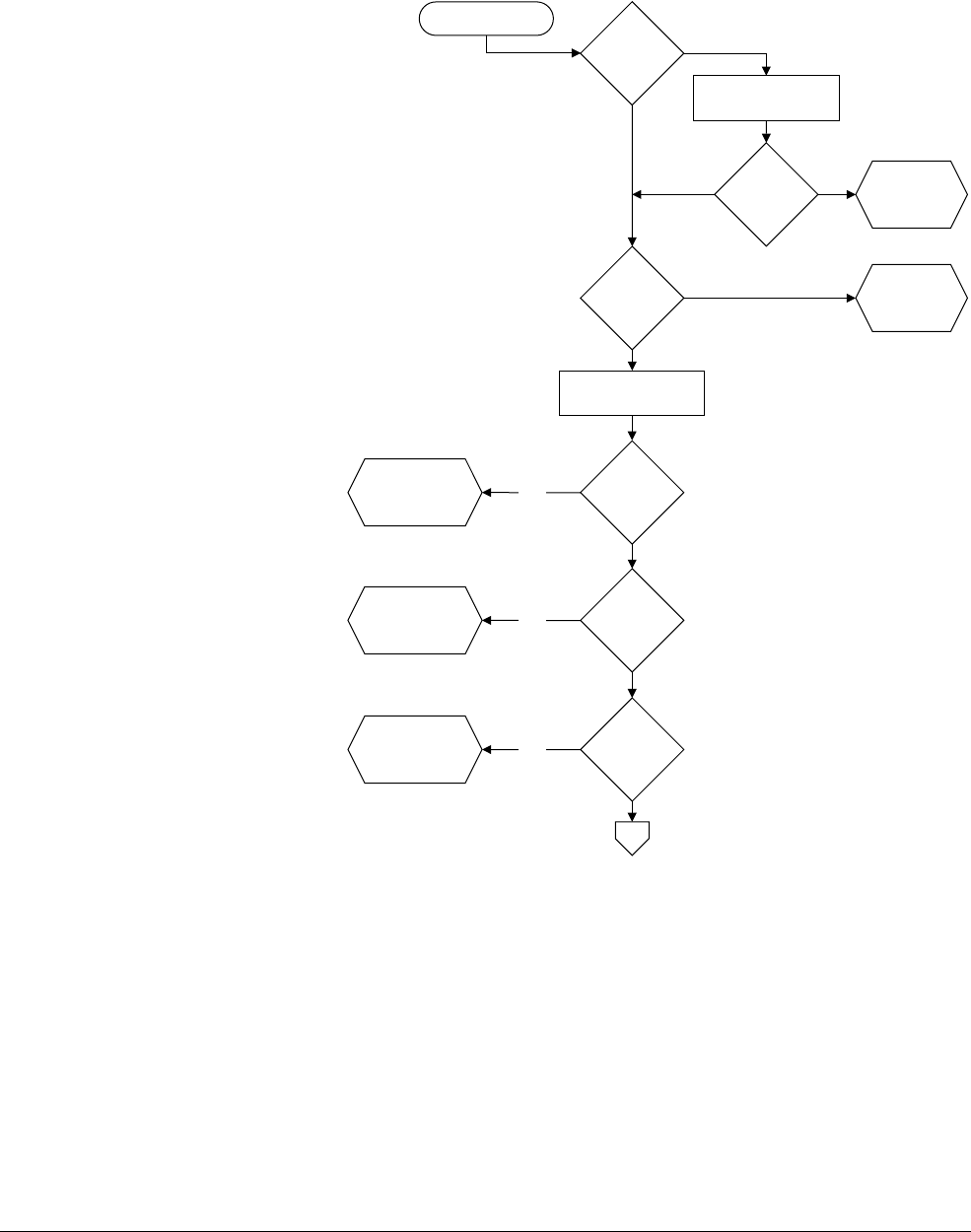
Memory Management Unit
ARM DDI 0301H Copyright © 2004-2009 ARM Limited. All rights reserved. 6-30
ID012310 Non-Confidential, Unrestricted Access
6.9.1 Fault checking sequence
Figure 6-2 and Figure 6-3 on page 6-31 show the fault checking sequence for translation table
managed TLB modes.
Figure 6-2 Translation table managed TLB fault checking sequence part 1
Virtual address
Check address
alignment
No
Yes
No Alignment
fault
Yes
Checking
alignment
?
Misaligned
?
Get first-level
descriptor
PTW
disabled?
Section
translation
fault
Yes
No
A
No
Translation
external abort
(first level)
Section/Page
access flag
fault
Section/Page
translation
abort
External
abort?
Descriptor
fault?
Access
bit fault?
Yes
Yes
Yes
No
No
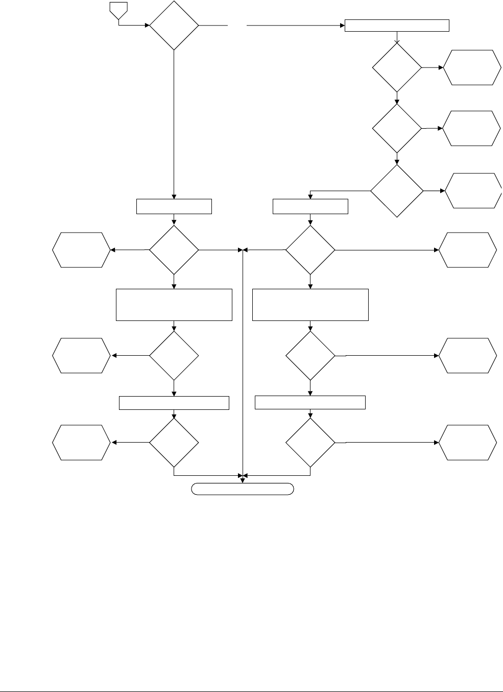
Memory Management Unit
ARM DDI 0301H Copyright © 2004-2009 ARM Limited. All rights reserved. 6-31
ID012310 Non-Confidential, Unrestricted Access
Figure 6-3 Translation table managed TLB fault checking sequence part 2
Client
Section
domain
fault
No access
Manager
Access
type?
Condition is: MMU on,
Strongly ordered or Device,
Unaligned access
Page
domain
fault
No access
Client
Access
type?
Manager
Condition is: MMU on,
Strongly ordered or Device,
Unaligned access
Section
A
Section
or page
?
Get second-level descriptor
Check domain
Check domain
Translation
external abort
(2nd level)
No
External
abort?
Yes
Page
translation
fault
Page
access bit
fault
Yes
Yes
No
Page
Alignment
fault
Yes
Check access permissions
No
Condition
true?
Alignment
fault
Yes
No
Condition
true?
Physical address
Section
permission
fault
Yes
Violation
?
Sub-page
permission
fault
Yes
Violation
?
No No
Check access permissions
Invalid
descriptor
?
Access
bit fault?

Memory Management Unit
ARM DDI 0301H Copyright © 2004-2009 ARM Limited. All rights reserved. 6-32
ID012310 Non-Confidential, Unrestricted Access
6.9.2 Alignment fault
An alignment fault occurs if the processor has attempted to access a particular data memory size
at an address location that is not aligned with that size.
Operation of unaligned accesses on page 4-13 describes the conditions for generating
Alignment faults.
Alignment checks are performed with the MMU both enabled and disabled.
6.9.3 Translation fault
There are two types of translation fault:
Section A section translation fault occurs if:
• The TLB tries to perform a page table walk but the page table walk is
disabled by one of the PD0 or PD1 bits. For more details, see Hardware
page table translation on page 6-36.
• The TLB fetches a first level translation table descriptor, and this first level
descriptor is invalid. This is the case when bits[1:0] of this descriptor are
b00 or b11.
Page A page translation fault occurs if the TLB fetches a second-level translation table
descriptor and this descriptor is marked as invalid, bits [1:0] = b00.
6.9.4 Access bit fault
When the Force AP bit, see c1, Control Register on page 3-44 bit [29], is set then AP[0]
indicates if there is an Access Bit Fault.
This bit is only taken into account when the MMU is in ARMv6 mode, that is XP=1, bit [23] in
the CP15 Control register.
In the configuration XP=1 and ForceAP=1, the OS uses only bits APX and AP[1] as Access
Permission bits, and AP[0] becomes an Access Bit, see Access permissions on page 6-11. The
Access Bit records recent TLB access to a page, or section, and the OS can use this to optimize
memory managements algorithms.
In the ARM1176JZF-S processor the Access Bit must be managed by the software.
Reading a page table entry into the TLB when the Access Bit is 0 causes an Access Bit fault.
This fault is readily distinguished from other faults that the TLB generates and this permits fast
setting of the Access Bit in software.
The processor can generate two kind of Access Bit faults:
• Section Access Bit fault, when the Access Bit, AP[0], is contained in a first level
translation table descriptor
• Page Access Bit fault, when the Access Bit, AP[0], is contained in a second level
translation table descriptor
The Force AP bit is banked in the Secure and Non-secure copies of the CP15 Control Register
for TrustZone support.
The Force AP and XP bits are expected to be static throughout operations.

Memory Management Unit
ARM DDI 0301H Copyright © 2004-2009 ARM Limited. All rights reserved. 6-33
ID012310 Non-Confidential, Unrestricted Access
Any change in the Force AP or XP bit configuration to enable or disable the generation of
Access Bit faults takes effect immediately. In the case where the TLB lookup hits an entry that
was created before Access Bit faults generation was enabled, and that this entry contains
AP[0]=0, then the TLB generates an Access Bit fault.
6.9.5 Domain fault
There are two types of domain fault:
Section For a section the domain is checked when the first-level descriptor is returned.
Page For a page the domain is checked when the second-level descriptor is returned.
For each type, the first-level descriptor indicates the domain in CP15 c3, the Domain Access
Control Register, to select. If the selected domain has bit 0 set to 0 indicating either no access
or reserved, then a domain fault occurs.
6.9.6 Permission fault
If the two-bit domain field returns Client, the access permission check is performed on the
access permission field in the TLB entry. A permission fault occurs if the access permission
check fails.
6.9.7 Debug event
When Monitor debug-mode debug is enabled an abort can be taken caused by a breakpoint on
an instruction access or a watchpoint on a data access. In both cases the memory system
completes the access before the abort is taken. If an abort is taken when in Monitor debug-mode
debug then the appropriate FSR, IFSR or DFSR, is updated to indicate a debug abort.
If a watchpoint is taken the WFAR is set to the address that caused the watchpoint. Watchpoints
are not taken precisely because following instructions can run underneath load and store
multiples.

Memory Management Unit
ARM DDI 0301H Copyright © 2004-2009 ARM Limited. All rights reserved. 6-34
ID012310 Non-Confidential, Unrestricted Access
6.10 Fault status and address
Table 6-11 lists the encodings for the Fault Status Register.
Note
All other Fault Status encodings are reserved.
If a translation abort occurs during a Data Cache maintenance operation by virtual address, then
a Data Abort is taken and the DFSR indicates the reason. The FAR indicates the faulting address,
and the IFAR indicates the address of the instruction causing the abort.
If a translation abort occurs during an Instruction Cache maintenance operation by virtual
address, then a Data Abort is taken, and an Instruction Cache Maintenance Operation Fault is
indicated in the DFSR. The IFSR indicates the reason. The FAR indicates the faulting address,
and the IFAR indicates the address of the instruction causing the abort.
Domain and fault address information is only available for data accesses. For instruction aborts
R14 must be used to determine the faulting address. You can determine the domain information
by performing a TLB lookup for the faulting address and extracting the domain field.
Table 6-12 on page 6-35 lists a summary of the abort vector that is taken, and the Fault Status
and Fault Address Registers that are updated for each abort type.
Table 6-11 Fault Status Register encoding
Priority Sources FSR[10,3:0] Domain FSR[12]
Highest Alignment b00001 Invalid SBZ
TLB miss b00000 Invalid SBZ
Instruction cache maintenancea
operation fault
b00100 Invalid SBZ
External abort on translation first-level b01100 Invalid SLVERR !DECERR
second-level b01110 Valid SLVERR !DECERR
Translation Section b00101 Invalid SBZ
Page b00111 Valid SBZ
Access Bit Fault, Force AP only Section b00011 Valid SBZ
Page b00110 Valid SBZ
Domain Section b01001 Valid SBZ
Page b01011 Valid SBZ
Permission Section b01101 Valid SBZ
Page b01111 Valid SBZ
Precise external abort b01000 Valid SLVERR !DECERR
Imprecise external abort b10110 Invalid SLVERR !DECERR
Parity error exception, not supported b11000 Invalid SBZ
Lowest Instruction debug event b00010 Valid SBZ
a. These aborts cannot be signaled with the IFSR because they do not occur on the instruction side.

Memory Management Unit
ARM DDI 0301H Copyright © 2004-2009 ARM Limited. All rights reserved. 6-35
ID012310 Non-Confidential, Unrestricted Access
Table 6-12 Summary of aborts
Abort type Abort taken Precise?
Register updated?
IFSR IFAR DFSR FAR WFAR
Instruction MMU fault Prefetch Abort Yes Yes Yes No No No
Instruction debug abort Prefetch Abort Yes Yes No No No No
Instruction external abort on translation Prefetch Abort Yes aYesaYes No No N o
Instruction external abort Prefetch Abort Yes aYesaYes No No No
Instruction cache maintenance operation Data Abort Yes Yes No Yes Yes No
Data MMU fault Data Abort Yes No No Yes Yes No
Data debug abort Data Abort No No No Yes Yes Yes
Data external abort on translation Data Abort Ye s aNo No YesaYe s aNoa
Data external abort Data Abort NobNo No YesaYe s N o
Data cache maintenance operation Data Abort Yes No No Yes Yes No
a. When the EA bit is set, the updated FSR or FAR is always Secure.
b. Data Aborts can be precise, see External aborts on page 6-27 for more details.

Memory Management Unit
ARM DDI 0301H Copyright © 2004-2009 ARM Limited. All rights reserved. 6-36
ID012310 Non-Confidential, Unrestricted Access
6.11 Hardware page table translation
The processor MMU implements the hardware page table walking mechanism from ARMv4
and ARMv5 cached processors with the exception of the removal of the fine page table
descriptor and the addition the page table walk disable bits in the TTB Control register.
The processor implements the page table walk disable feature. Two bits, PD0 and PD1, are
implemented in the TTB Control register. These bits are banked for the Secure and Non-secure
worlds for the support of TrustZone.
Each time a TLB miss occurs, the TLB computes the parameters for an automatic hardware page
table walk. The address of the page table walk is computed from TTB0 or TTB1, see First-level
descriptor address on page 6-43. If the address is computed with TTB0, and the PD0 bit is set
in the TTB Control register of the corresponding world, or if the address is computed using
TTB1 and the PD1 bit is set, then the processor does not perform the automatic hardware page
table walk, and it generates a Section translation fault instead.
With this feature, only a small portion of the memory can be mapped in one world, for example
the Secure world, if the code that runs in this world is expected to be small. This gives the system
a simple way to avoid using a lot of memory to store full page tables.
When hardware page table walks are not disabled, the processor performs the page table walk
in the usual way. A hardware page table walk occurs whenever there is a TLB miss. Processor
hardware page table walks do not cause a read from the level one Unified/Data Cache. or the
TCM. The P, RGN, S, and C bits in the Translation Table Base Registers determine the memory
region attributes for the page table walk.
Two formats of page tables are supported:
• A backwards-compatible format supporting subpage access permissions. These have been
extended so that certain page table entries support extended region types and with the NS
Attribute bit for TrustZone.
• ARMv6 format, not supporting sub-page access permissions, but with support for
ARMv6 MMU features. The NS Attribute bit for TrustZone has also been added. These
features are:
— extended region types
— global and process specific pages
— more access permissions
— marking of Shared and Non-Shared regions
— marking of Execute-Never regions.
Additionally, two translation table base registers are provided in each world. On a TLB miss,
the Translation Table Base Control Register, CP15 c2 that is also duplicated in each world, and
the top bits of the virtual address determine if the first or second translation table base is used.
See c2, Translation Table Base Control Register on page 3-60 for details. The first-level
descriptor indicates whether the access is to a section or to a page table. If the access is to a page
table, the processor MMU fetches a second-level descriptor.
A page table holds 256 32-bit entries 4KB in size. You can determine the page type by
examining bits [1:0] of the second-level descriptor. For both first and second level descriptors if
bits [1:0] are b00, the associated virtual addresses are unmapped, and attempts to access them
generate a translation fault. Software can use bits [31:2] for its own purposes in such a
descriptor, because they are ignored by the hardware. Where appropriate, ARM Limited
recommends that bits [31:2] continue to hold valid access permissions for the descriptor.
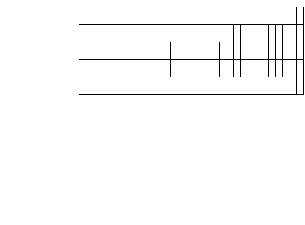
Memory Management Unit
ARM DDI 0301H Copyright © 2004-2009 ARM Limited. All rights reserved. 6-37
ID012310 Non-Confidential, Unrestricted Access
For both level 1 and level 2 page table walks, the processor performs external accesses with
Secure or Non-secure rights depending on the Secure or Non-secure state of the MMU request
that causes the page table walk. This ensures that Secure translation table descriptors are always
fetched from a Secure memory, and that Non-secure translation table descriptors are always
fetched from Non-secure memory.
6.11.1 Backwards-compatible page table translation subpage AP bits enabled
When the CP15 Control Register c1 bit 23 is set to 0, the subpage AP bits are enabled and the
page table formats are backwards-compatible with ARMv4 and ARMv5 MMU architectures.
This bit is duplicated as Secure and Non-secure versions so that the system can enable or disable
subpages independently in each world.
All mappings are treated as global, and executable, XN = 0. All Normal memory is Non-Shared.
Device memory can be Shared or Non-Shared as determined by the TEX bits and the C and B
bits. For large and small pages, there can be four subpages defined with different access
permissions. For a large page, the subpage size is 16KB and is accessed using bits [15:14] of the
page index of the virtual address. For a small page, the subpage size is 1KB and is accessed
using bits [11:10] of the page index of the virtual address.
The use of subpage AP bits where AP3, AP2, AP1, and AP0 contain different values is
deprecated.
Backwards-compatible page table format
Figure 6-4 shows a backwards-compatible format first-level descriptor.
Figure 6-4 Backwards-compatible first-level descriptor format
If the P bit is supported and set for the memory region, it indicates to the system memory
controller that this memory region has ECC enabled. ARM1176JZF-S processors do not support
the P bit.
When bits [1:0] of the first-level descriptor are b01, the descriptor points to a second-level page
table, called a Coarse page table. Figure 6-5 on page 6-38 shows a backwards-compatible
format second-level descriptors.
1
N
SSBZ
0SBZ
N
S
N
S
S
B
Z
S
B
Z
TEX
1Coarse page table base address P Domain 0
0Ignored
31 20 19 12 11 10 9 8 5 4 3 2 1 0
0
0Section base address AP P Domain 0 C B 1
11
Translation fault
Coarse page table
Section (1MB)
15 14
Reserved
TEX 0
Supersection base
address SBZ AP P Ignored 0 C B 1
Supersection
(16MB)
18 172324
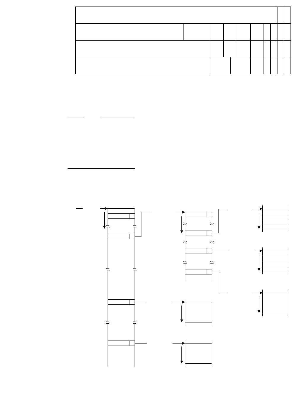
Memory Management Unit
ARM DDI 0301H Copyright © 2004-2009 ARM Limited. All rights reserved. 6-38
ID012310 Non-Confidential, Unrestricted Access
Figure 6-5 Backwards-compatible second-level descriptor format
For extended small page table entries without a TEX field you must use the value b000. For
details of TEX encodings see C and B bit, and type extension field encodings on page 6-14.
Note
For any Supersection description in a first-level page table, and any Large page description in a
second-level page table:
• you must repeat the description in 16 consecutive page table locations
• the first description must occur on a 16-word boundary
For more information see the ARM Architecture Reference Manual.
Figure 6-6 shows an overview of the section, supersection, and page translation process using
backwards-compatible descriptors.
Figure 6-6 Backwards-compatible section, supersection, and page translation
SBZ
TEX AP3 B
B
1Large page base address AP2 AP1 AP0 C 0
0Small page base address AP3 AP2 AP1 AP0 C B 1
1Extended small page base address TEX AP C 1
Translation fault
Large page (64KB)
Small page
(4KB)
0Ignored
31 16 15 12 11 10 9 8 7 6 5 4 3 2 1 0
0
Extended small
page (4KB)
16KB subpage
Invalid
Invalid
Indexed by
VA[19:12]
Base address
from L2D[31:12]
Indexed by
VA[11:0]
Indexed by
VA[15:0]
Base address
from L2D[31:16]
First level
page table Coarse page
table
4KB extended
small page
64KB large page
Translation
table base
Indexed by
VA[31:20]
31 0
31 0
31 0
Base address
from L1D[31:24]
Indexed by
VA[23:0]
16MB
supersection
Base address
from L1D[31:20]
Indexed by
VA[19:0]
1MB section
(bit 18 = 0)
Base address
from L1D[31:10] 16KB subpage
16KB subpage
16KB subpage
4KB small page
1KB subpage
31 0
1KB subpage
1KB subpage
1KB subpage
Indexed by
VA[11:0]
Base address
from L2D[31:12]
01
00 00
01
10
11
10
(bit 18 = 1) 10
Memory Management Unit
ARM DDI 0301H Copyright © 2004-2009 ARM Limited. All rights reserved. 6-39
ID012310 Non-Confidential, Unrestricted Access
6.11.2 ARMv6 page table translation subpage AP bits disabled
When the CP15 Control Register c1 Bit 23 is set to 1 in the corresponding world, the subpage
AP bits are disabled and the page tables have support for ARMv6 MMU features. Four new page
table bits are added to support these features:
• The Not-Global (nG) bit, determines if the translation is marked as global (0), or
process-specific (1) in the TLB. For process-specific translations the translation is
inserted into the TLB using the current ASID, from the ContextID Register, CP15 c13.
• The Shared (S) bit, determines if the translation is for Non-Shared (0), or Shared (1)
memory. This only applies to Normal memory regions. Device memory can be Shared or
Non-Shared as determined by the TEX bits and the C and B bits.
• The Execute-Never (XN) bit, determines if the region is Executable (0) or Not-executable
(1).
• Three access permission bits. The access permissions extension (APX) bit, provides an
extra access permission bit.
All ARMv6 page table mappings support the TEX field.
ARMv6 page table format
With the sub-pages enabled or not, all first level descriptors have been enhanced with the
addition of the NS Attribute bit to enable the support of TrustZone.
Figure 6-7 shows the format of an ARMv6 first-level descriptor when subpages are disabled.
Figure 6-7 ARMv6 first-level descriptor formats with subpages disabled
If the P bit is supported and set for the memory region, it indicates to the system memory
controller that this memory region has ECC enabled. ARM1176JZF-S processors do not support
the P bit. In addition to the invalid translation, bits [1:0] = b00, translations for the reserved
entry, bits [1:0] = b11, result in a translation fault.
As shown in Figure 6-7, bits [1:0] of a level 1 page table entry determine the type of the entry:
Bits [1:0] == b00
Translation fault.
N
S
S
B
Z
N
SS
A
P
X
A
P
X
S0
1
n
GTEX
S
B
Z
1Coarse page table base address P Domain 0
0Ignored
31 20 19 12 11 10 9 8 5 4 3 2 1 0
0
1Reserved 1
Translation fault
Coarse page table
Supersection
(16MB)
15 14
Translation fault
17 1618
n
GTEX 0
Supersection base
address SBZ AP P Ignored X
NC B 1
0Section base address N
SAP P Domain X
NC B 1
Section (1MB)
2324
N
S0Section base address AP P Domain X
NC B 1
Memory Management Unit
ARM DDI 0301H Copyright © 2004-2009 ARM Limited. All rights reserved. 6-40
ID012310 Non-Confidential, Unrestricted Access
Bits [1:0] == b01
The entry points to a second-level page table, called a Coarse page table.
Figure 6-8 on page 6-40 shows the formats of the possible entries in the Coarse
page table.
Bits [1:0] == b10
The entry points to a either a 1MB Section of memory or a 16MB Supersection
of memory. Bit [18] of the descriptor selects between a Section and a
Supersection. For details of supersections see Supersections on page 6-6.
Note
You must repeat any Supersection description in 16 consecutive page table
locations, with the first description occurring on a 16-word boundary. For more
information see the ARM Architecture Reference Manual.
Bits [1:0] == b11
Reserved.
Figure 6-8 shows the format of an ARMv6 second-level descriptors.
Figure 6-8 ARMv6 second-level descriptor format
As shown in Figure 6-8, bits [1:0] of a second-level descriptor determine the type of the
descriptor:
Bits [1:0] == b00
Translation fault.
Bits [1:0] == b01
The entry points to a 64KB Large page in memory.
Note
You must repeat any Large page description in 16 consecutive page table
locations, with the first description occurring on a 16-word boundary. For more
information see the ARM Architecture Reference Manual.
Bits [1:0] == b1x
The entry points to a 4KB Extended small page in memory.
Bit [0] of the entry is the XN bit for the entry.
Figure 6-9 on page 6-41 shows an overview of the section, supersection, and page translation
process using ARMv6 descriptors.
n
G
S
X
NS
A
P
X
TEX
B
1Large page base address SBZ AP C 0
X
N
Extended small page base address n
G
A
P
X
TEX AP C B 1
Translation fault
Large page (64KB)
Extended small
page (4KB)
0Ignored
31 16 15 12 11 10 9 8 7 6 5 4 3 2 1 0
0
14
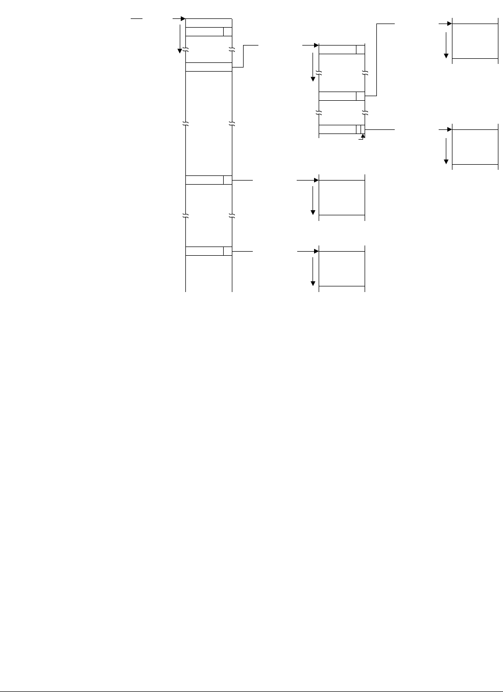
Memory Management Unit
ARM DDI 0301H Copyright © 2004-2009 ARM Limited. All rights reserved. 6-41
ID012310 Non-Confidential, Unrestricted Access
Figure 6-9 ARMv6 section, supersection, and page translation
6.11.3 Restrictions on page table mappings page coloring
The processor uses virtually indexed, physically addressed caches. To prevent alias problems
where cache sizes greater than 16KB have been implemented, you must restrict the mapping of
pages that remap virtual address bits [13:12].
• for the Instruction Cache, the Isize P bit, bit[11], of the Cache Type Register CP15 c0,
indicates if this is necessary
• for the Data Cache, the Dsize P bit, bit[23], of the Cache Type Register CP15 c0, indicates
if this is necessary.
See c0, Cache Type Register on page 3-21 for more information.
This restriction, referred to as page coloring, enables the virtual address bits[13:12] to be used
to index into the cache without requiring hardware support to avoid alias problems.
For pages marked as Non-Shared, if bit 11 or bit 23 of the Cache Type Register is set, the
restriction applies to pages that remap virtual address bits [13:12] and might cause aliasing
problems when 4KB pages are used. To prevent this you must ensure the following restrictions
are applied:
1. If multiple virtual addresses are mapped onto the same physical address then for all
mappings of bits [13:12] the virtual addresses must be equal and the same as bits [13:12]
of the physical address. The same physical address can be mapped by TLB entries of
different page sizes, including page sizes over 4KB. Imposing this requirement on the
virtual address is called page coloring.
Invalid
Invalid
01 Indexed by
VA[19:12]
Base address
from L2D[31:12]
Indexed by
VA[11:0]
Indexed by
VA[15:0]
Base address
from L2D[31:16]
First level
page table
Coarse page
table
4KB extended
small page
64KB large page
Translation
table base
Indexed by
VA[31:20] 31 0
31 0
31 0
Base address
from L1D[31:24]
Indexed by
VA[23:0]
16MB
supersection
Base address
from L1D[31:20]
Indexed by
VA[19:0]
1MB section
Base address
from L1D[31:10]
01
00
00
(bit 18 = 0) 10
(bit 18 = 1) 10
1
XN

Memory Management Unit
ARM DDI 0301H Copyright © 2004-2009 ARM Limited. All rights reserved. 6-42
ID012310 Non-Confidential, Unrestricted Access
2. Alternatively, if all mappings to a physical address are of a page size equal to 4KB, then
the restriction that bits [13:12] of the virtual address must equal bits [13:12] of the
physical address is not necessary. Bits [13:12] of all virtual address aliases must still be
equal.
There is no restriction on the more significant bits in the virtual address equalling those in the
physical address.
Avoiding the page coloring restriction
The processor provides the ability to restrict the cache size to 16KB so that software does not
have to support the page coloring restriction on mapping, see CZ bit in c1, Auxiliary Control
Register on page 3-48.
Note
Setting the CZ flag in the CP15 Auxiliary Control Register does not affect the contents of the
CP15 Cache Type Register. However, when the CZ flag is set, all caches are limited to 16KB,
even if a larger cache size is specified in the CP15 Cache Type Register.

Memory Management Unit
ARM DDI 0301H Copyright © 2004-2009 ARM Limited. All rights reserved. 6-43
ID012310 Non-Confidential, Unrestricted Access
6.12 MMU descriptors
To support sections and pages, the processor MMU uses a two-level descriptor definition. The
first-level descriptor indicates whether the access is to a section or to a page table. If the access
is to a page table, the processor MMU determines the page table type and fetches a second-level
descriptor.
6.12.1 First-level descriptor address
The ARM1176 contains:
• two Translation Table Base Registers, TTBR0 and TTBR1
• one Translation Table Base Control Register (TTBCR).
On a TLB miss, the top bits of the modified virtual address determine whether the first or second
Translation Table Base is used. Figure 6-10 on page 6-44 shows the creation of a first-level
descriptor address.
The expected use of two translation tables is to reduce the cost of OS context switches by
enabling the OS, and each individual task or process, to have its own pagetable without
consuming much memory.
In this model, the virtual address space is divided into two regions:
•
0x0
-> 1<<(32-N) that TTBR0 controls
• 1<<(32-N) -> 4GB that TTBR1 controls.
The value of N is set in the TTBCR. If N is zero, then TTBR0 is used for all addresses, and that
gives legacy v5 behavior. If N is not zero, the OS and memory mapped IO are located in the
upper part of the memory map, TTBR1, and the tasks or processes all occupy the same virtual
address space in the lower part of the memory, TTBR0.
The TTBCR, TTBR0, and TTBR1 registers used for this process are banked. Depending on the
state of the MMU requests that cause a page table walk, either Secure or Non-secure registers
are used.
The translation table that TTBR0 points to can be truncated because it must only cover the first
1<<(32-N) bytes of memory. The first entry always corresponds to address
0x0
, so this
mechanism is more efficient if processes start at a low virtual address such as
0x0
or
0x8000
.
Table 6-13 lists the translation table size.
Table 6-13 Translation table size
N Upper boundary Translation table 0 size
0 4GB 16KB, 4096 entries, v5 behavior, TTBR1 not used.
1 2GB 8KB, 2048 entries
2 1GB 4KB, 1024 entries
3 512MB 2KB, 512 entries
4 256MB 1KB, 256 entries
5 128MB 512B, 128 entries
6 64MB 256B, 64 entries
7 32MB 128B, 32 entries
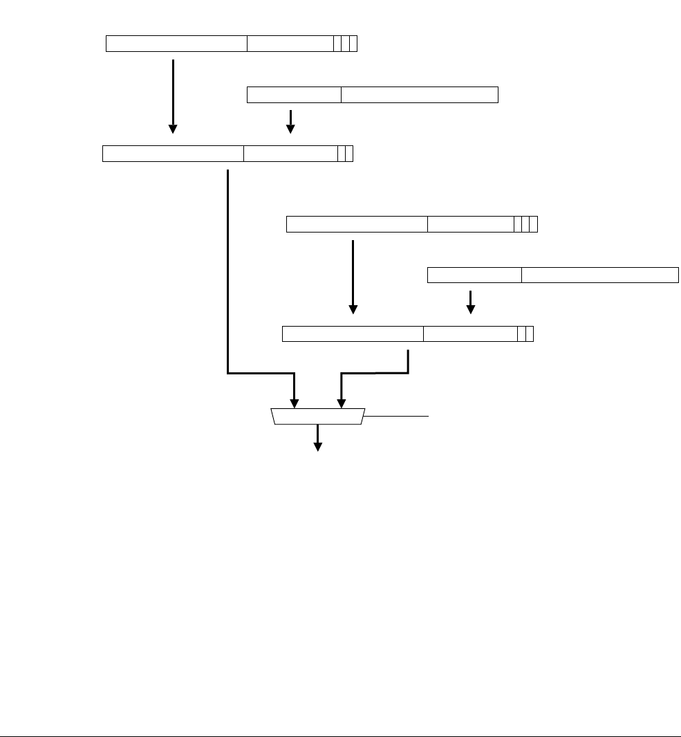
Memory Management Unit
ARM DDI 0301H Copyright © 2004-2009 ARM Limited. All rights reserved. 6-44
ID012310 Non-Confidential, Unrestricted Access
The OS can maintain a different pagetable for each process, and update TTRB0 on a context
switch. Using a truncated pagetable means that much less space is required to store the
individual process page tables. Different processes can have different size pagetables, that is,
different values of N, by updating the TTBCR during the context switch.
It is not required that the OS pagetables that TTBR1 points to are updated on a context switch.
Figure 6-10 shows how to create a first level descriptor address.
The PD0 and PD1 bits in TTBCR can be used to prevent pagetable walks from either TTBR. In
particular, disabling walks from TTBR1 and setting TTBR0 to the address of a truncated
translation table can minimize the overhead otherwise incurred in unused translation table
entries.
Figure 6-10 Creating a first-level descriptor address
Translation base
31 14-N 13-N 3 2 1 0
P S C
First-level table index
32-N 20 19 0
Translation table base 0
Modified virtual address
Translation base
31 14-N 13-N 2 1 0
Table index 0 0
Translation base
31 14 13 3 2 1 0
P S C
First-level table index
31 20 19 0
Translation table base 1
Modified virtual address
Translation base
31 14 13 2 1 0
Table index 0 0
01
First-level descriptor address
Translation table base control:
If (N > 0 && MVA[31:32-N] != 0)
{TTBR1[31:14], MVA[31:20], 00}
else
{TTBR0[31:14-N], MVA[31-N:20], 00}
Where N is the value of the Translation
Table Base Control Register c2

Memory Management Unit
ARM DDI 0301H Copyright © 2004-2009 ARM Limited. All rights reserved. 6-45
ID012310 Non-Confidential, Unrestricted Access
6.12.2 First-level descriptor
Using the first-level descriptor address, a request is made to external memory. This returns the
first-level descriptor. By examining bits [1:0] of the first-level descriptor, the access type is
indicated as Table 6-14 lists.
First-level translation fault
If bits [1:0] of the first-level descriptor are b00 or b11, a translation fault is generated. This
generates an abort to the processor, either a Prefetch Abort for the instruction side or a Data
Abort for the data side, see MMU fault checking on page 6-29.
If the first level descriptor describes a section or supersection when the Force AP bit is set and
the MMU is in ARMv6 mode, Access bit faults might be generated if AP[0]=0.
First-level page table address
If bits [1:0] of the first-level descriptor are b01, then a page table walk is required. Second-level
page table walk on page 6-47 describes this process.
First-level section base address
If bits [1:0] of the first-level descriptor are b10, a request to a section memory block has
occurred. Figure 6-11 on page 6-46 shows the translation process for a 1MB section using
ARMv6 format, AP bits disabled.
Table 6-14 Access types from first-level descriptor bit values
Bit values Access type
b00 Translation fault
b01 Page table base address
b10 Section base address
b11 Reserved, results in translation fault
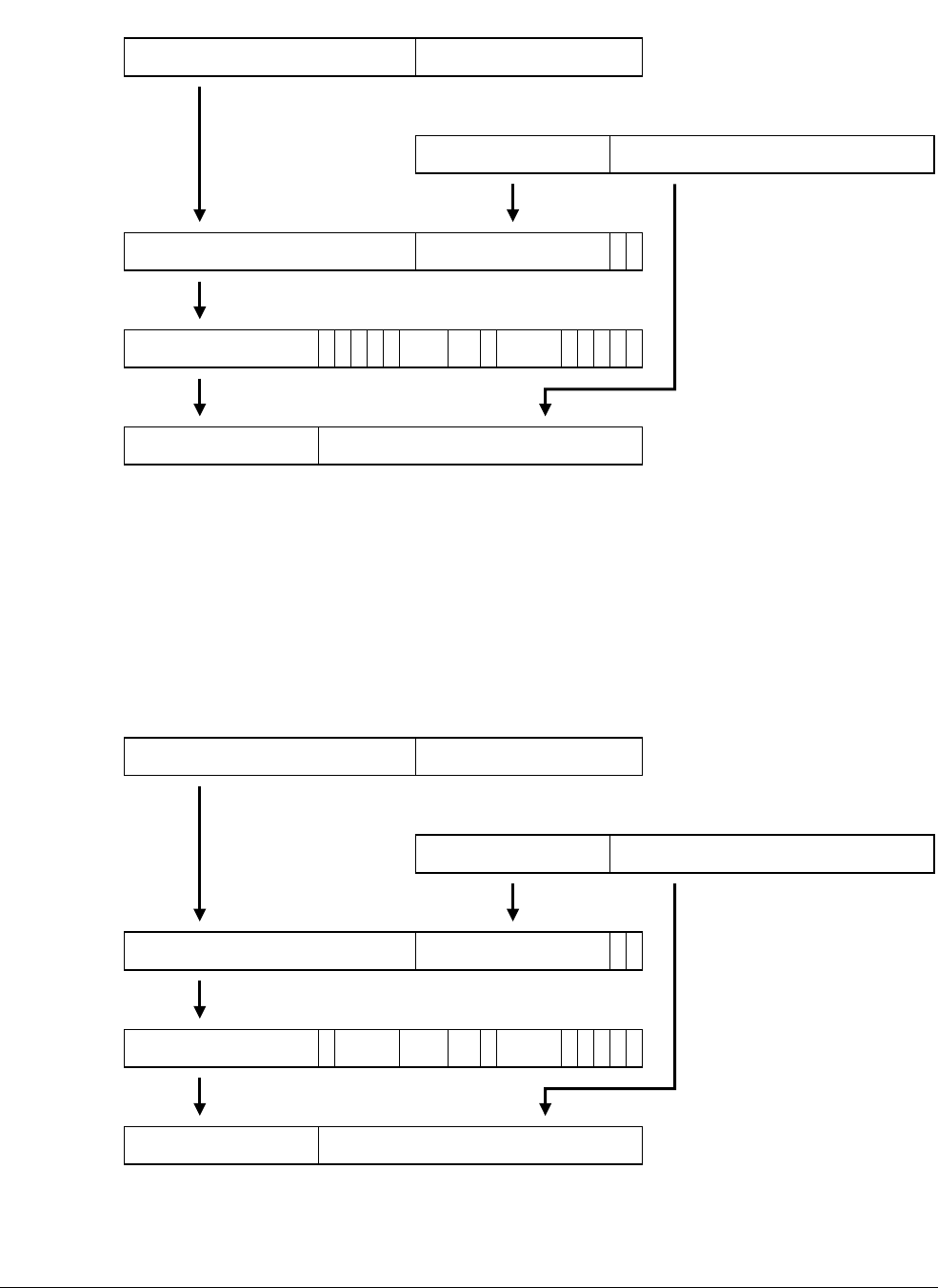
Memory Management Unit
ARM DDI 0301H Copyright © 2004-2009 ARM Limited. All rights reserved. 6-46
ID012310 Non-Confidential, Unrestricted Access
Figure 6-11 Translation for a 1MB section, ARMv6 format
Following the first-level descriptor translation, the physical address is used to transfer to and
from external memory the data requested from and to the processor. This is done only after the
domain and access permission checks are performed on the first-level descriptor for the section.
Memory access control on page 6-11 describes these checks.
Figure 6-12 shows the translation process for a 1MB section using backwards-compatible
format, AP bits enabled.
Figure 6-12 Translation for a 1MB section, backwards-compatible format
0 S
n
G
A
P
X
TEX 0
Section base address
31 2019 12111098 543210
N
SAP P Domain X
NC B 1
First-level table index
31 20 19 0
Section index
Translation base
31 14 13 0
0
Translation base
31 14 13 0
First-level table index 0
21
Physical address
First-level descriptor
First-level descriptor address
Modified virtual address
Translation table base
Section base address
31 20 19 0
Section index
1415161718
N
STEX 0
Section base address
31 2019 12111098 543210
SBZ AP P Domain 0 C B 1
First-level table index
31 20 19 0
Section index
Translation base
31 14 13 0
0
Translation base
31 14 13 0
First-level table index 0
21
Physical address
First-level descriptor
First-level descriptor address
Modified virtual address
Translation table base
Section base address
31 20 19 0
Section index
141518
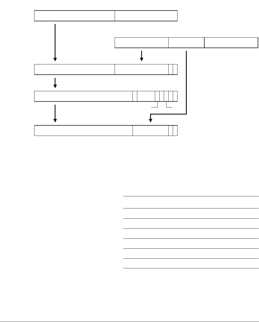
Memory Management Unit
ARM DDI 0301H Copyright © 2004-2009 ARM Limited. All rights reserved. 6-47
ID012310 Non-Confidential, Unrestricted Access
6.12.3 Second-level page table walk
If bits [1:0] of the first-level descriptor bits are b01, then a page table walk is required. The
MMU requests the second-level page table descriptor from external memory. Figure 6-13 shows
how the second-level page table address is generated.
Figure 6-13 Generating a second-level page table address
When the page table address is generated, a request is made to external memory for the
second-level descriptor.
By examining bits [1:0] of the second-level descriptor, the access type is indicated as Table 6-15
lists.
Second-level translation fault
If bits [1:0] of the second-level descriptor are b00, then a translation fault is generated. This
generates an abort to the processor, either a Prefetch Abort for the instruction side or a Data
Abort for the data side, see MMU fault checking on page 6-29.
N
S1
Coarse page table base address
31 10 9 8 5 4 2 1 0
P Domain 0
First-level table index
31 20 19 12 11 0
Second-level
table index
Translation base
31 14 13 0
0
Coarse page table base address
31 10 9 2 1 0
Second-level
table index 0
0
Translation base
31 14 13 0
First-level table index 0
21
Second-level descriptor address
First-level descriptor
First-level descriptor address
Modified virtual address
Translation table base
3
SBZ SBZ
Table 6-15 Access types from second-level descriptor bit values
Descriptor format Bit values Access type
Both b00 Translation fault
Backwards-compatible b01 64KB large page
ARMv6 b01 64KB large page
Backwards- compatible b10 4KB small page
ARMv6 b1XN 4KB extended small page
Backwards- compatible b11 4KB extended small page
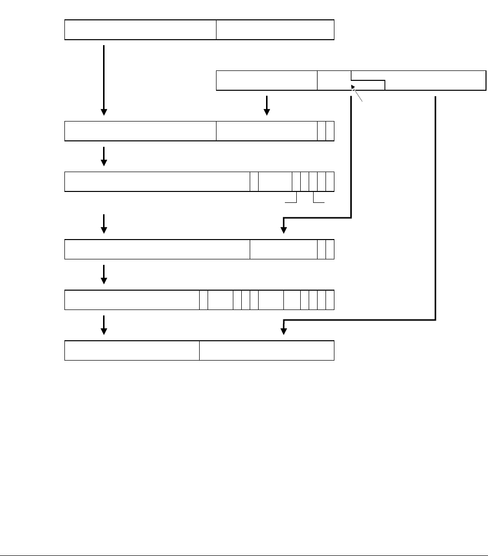
Memory Management Unit
ARM DDI 0301H Copyright © 2004-2009 ARM Limited. All rights reserved. 6-48
ID012310 Non-Confidential, Unrestricted Access
If the second level descriptor describes a large page, a small page, or an extended small page
when the Force AP bit is set and the MMU is in ARMv6 mode, Access bit faults might be
generated if AP[0]=0.
Second-level large page base address
If bits [1:0] of the second-level descriptor are b01, then a large page table walk is required.
Figure 6-14 shows the translation process for a 64KB large page using ARMv6 format, AP bits
disabled.
Figure 6-14 Large page table walk, ARMv6 format
Figure 6-15 on page 6-49 shows the translation process for a 64KB large page, or a 16KB large
page subpage, using backwards-compatible format, AP bits enabled.
N
S
X
NSTEX
1
Coarse page table base address
31 1098 54 210
P Domain 0
First-level table index
31 20 19 12 11 0
Page index
Translation base
31 14 13 0
1
Page base address
31 12111098 6543210
n
G
A
P
X
SBZ AP C B 0
0
Coarse page table base address
31 10 9 2 1 0
Second-level
table index 0
0
Translation base
31 14 13 0
First-level table index 0
21
Page index
Page base address
31 0
Second-level descriptor address
Second-level descriptor
Physical address
First-level descriptor
First-level descriptor address
Modified virtual address
Translation table base
16 15
16 15
16 15
14
Second-level
table index
3
SBZ SBZ
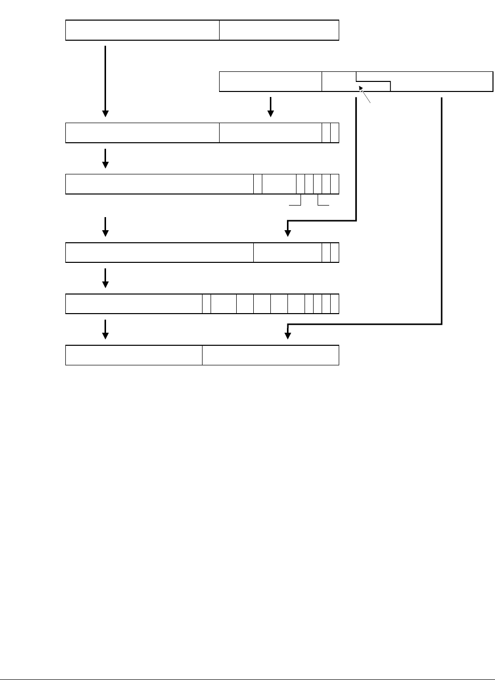
Memory Management Unit
ARM DDI 0301H Copyright © 2004-2009 ARM Limited. All rights reserved. 6-49
ID012310 Non-Confidential, Unrestricted Access
Figure 6-15 Large page table walk, backwards-compatible format
Using backwards-compatible format descriptors, the 64KB large page is generated by setting all
of the AP bit pairs to the same values, AP3=AP2=AP1=AP0. If any one of the pairs are different,
then the 64KB large page is converted into four 16KB large page subpages. The subpage access
permission bits are chosen using the virtual address bits [15:14].
Second-level small page table walk
If bits [1:0] of the second-level descriptor are b10 for backwards-compatible format, then a
small page table walk is required.
Figure 6-16 on page 6-50 shows the translation process for a 4KB small page or a 1KB small
page subpage using backwards-compatible format descriptors, AP bits enabled.
N
S
0TEX
1
Coarse page table base address
31 1098 54 210
P Domain 0
First-level table index
31 20 19 12 11 0
Page index
Translation base
31 14 13 0
1
Page base address
31 1211109876543210
AP
3
AP
2
AP
1
AP
0C B 0
0
Coarse page table base address
31 10 9 2 1 0
Second-level
table index 0
0
Translation base
31 14 13 0
First-level table index 0
21
Page index
Page base address
31 0
Second-level descriptor address
Second-level descriptor
Physical address
First-level descriptor
First-level descriptor address
Modified virtual address
Translation table base
16 15
1415
16 15
16
Second-level
table index
3
SBZ SBZ
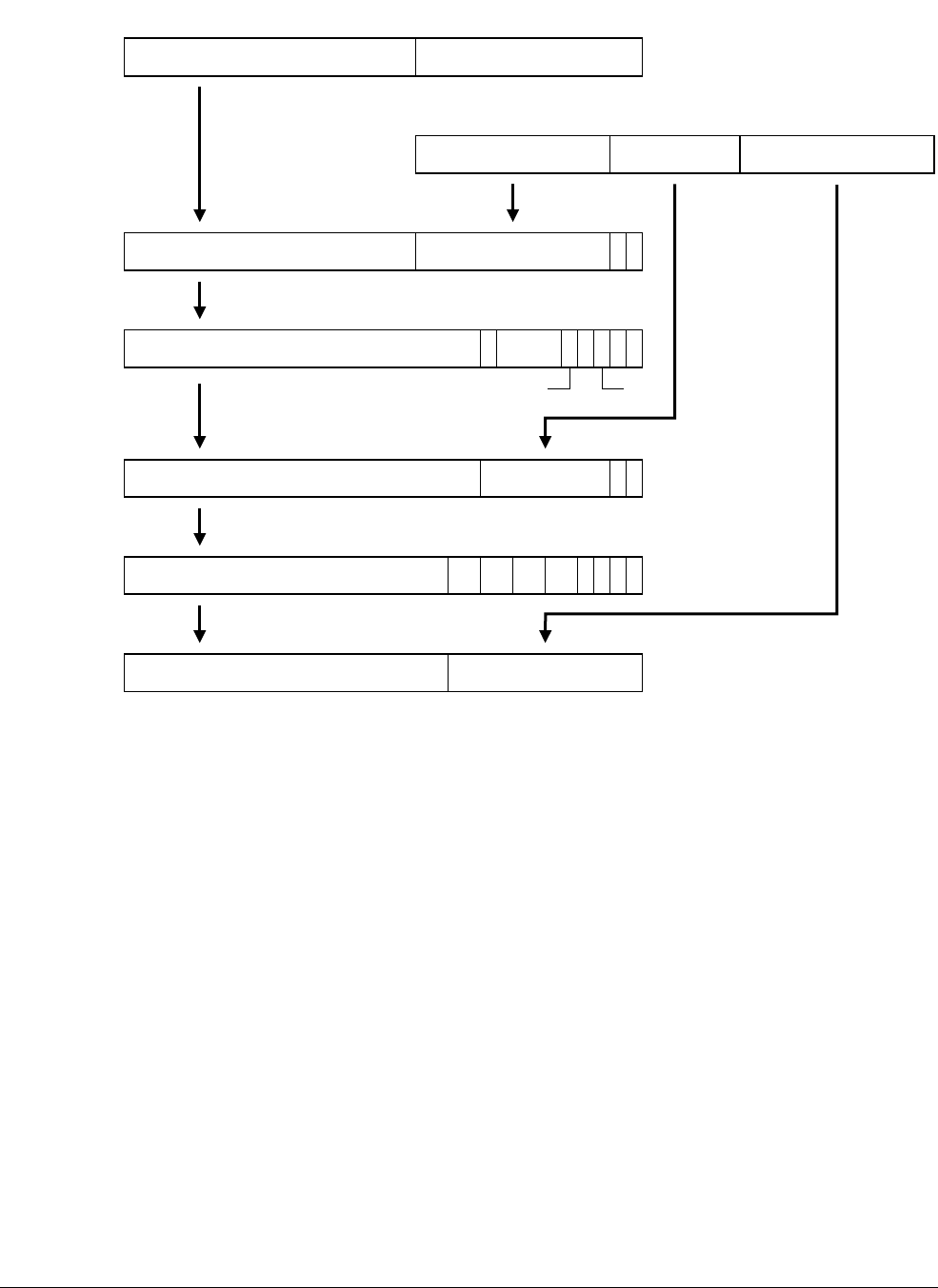
Memory Management Unit
ARM DDI 0301H Copyright © 2004-2009 ARM Limited. All rights reserved. 6-50
ID012310 Non-Confidential, Unrestricted Access
Figure 6-16 4KB small page or 1KB small subpage translations, backwards-compatible format
Using backwards-compatible descriptors, the 4KB small page is generated by setting all of the
AP bit pairs to the same values, AP3=AP2=AP1=AP0. If any one of the pairs are different, then
the 4KB small page is converted into four 1KB small page subpages. The subpage access
permission bits are chosen using the virtual address bits [11:10].
Second-level extended small page table walk
If bits [1:0] of the second-level descriptor are b1XN for ARMv6 format descriptors, or b11 for
backwards-compatible descriptors, then an extended small page table walk is required.
Figure 6-17 on page 6-51 shows the translation process for a 4KB extended small page using
ARMv6 format descriptors, AP bits disabled.
N
S1
Coarse page table base address
31 1098 54 210
P Domain 0
First-level table index
31 20 19 12 11 0
Second-level
table index Page index
Translation base
31 14 13 0
0
Small page base address
31 1211109876543210
AP
3
AP
2
AP
1
AP
0C B 1
0
Coarse page table base address
31 10 9 2 1 0
Second-level table
index 0
0
Translation base
31 14 13 0
First-level table index 0
21
Page index
Page base address
31 12 11 0
Second-level descriptor address
Second-level descriptor
Physical address
First-level descriptor
First-level descriptor address
Modified virtual address
Translation table base
3
SBZ SBZ

Memory Management Unit
ARM DDI 0301H Copyright © 2004-2009 ARM Limited. All rights reserved. 6-51
ID012310 Non-Confidential, Unrestricted Access
Figure 6-17 4KB extended small page translations, ARMv6 format
Figure 6-18 on page 6-52 shows the translation process for a 4KB extended small page or a 1KB
extended small page subpage using backwards-compatible format descriptors, AP bits enabled.
N
S
S
1
Coarse page table base address
31 1098 543210
P Domain 0
First-level table index
31 20 19 12 11 0
Second-level
table index Page index
Translation base
31 14 13 0
X
N
Extended small page base address
31 12111098 6543210
n
G
A
P
X
TEX AP C B 1
0
Coarse page table base address
31 10 9 2 1 0
Second-level table
index 0
0
Translation base
31 14 13 0
First-level table index 0
21
Page index
Page base address
31 12 11 0
Second-level descriptor address
Second-level descriptor
Physical address
First-level descriptor
First-level descriptor address
Modified virtual address
Translation table base
SBZ SBZ
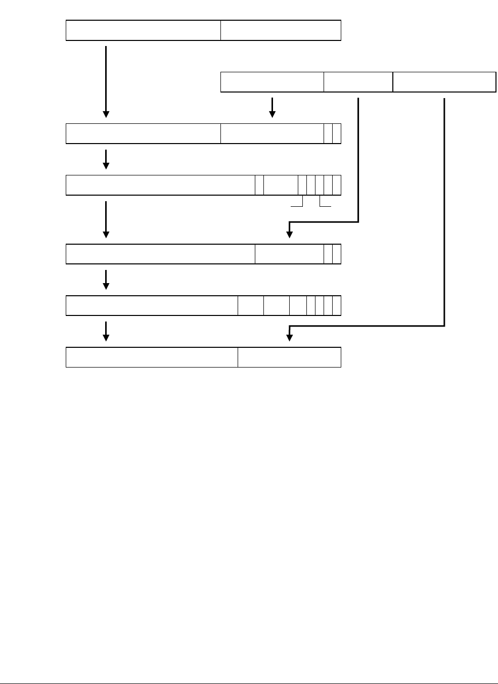
Memory Management Unit
ARM DDI 0301H Copyright © 2004-2009 ARM Limited. All rights reserved. 6-52
ID012310 Non-Confidential, Unrestricted Access
Figure 6-18 4KB extended small page or 1KB extended small subpage translations, backwards-compatible format
Using backwards-compatible descriptors, the 4KB extended small page is generated by setting
all of the AP bit pairs to the same values, AP3=AP2=AP1=AP0. If any one of the pairs are
different, then the 4KB extended small page is converted into four 1KB extended small page
subpages. The subpage access permission bits are chosen using the virtual address bits [11:10].
N
S1
Coarse page table base address
31 1098 54 210
P Domain 0
First-level table index
31 20 19 12 11 0
Second-level
table index Page index
Translation base
31 14 13 0
1
Extended small page base address
31 1211 98 6543210
SBZ TEX AP C B 1
0
Coarse page table base address
31 10 9 2 1 0
Second-level table
index 0
0
Translation base
31 14 13 0
First-level table index 0
21
Page index
Page base address
31 12 11 0
Second-level descriptor address
Second-level descriptor
Physical address
First-level descriptor
First-level descriptor address
Modified virtual address
Translation table base
3
SBZ SBZ

Memory Management Unit
ARM DDI 0301H Copyright © 2004-2009 ARM Limited. All rights reserved. 6-53
ID012310 Non-Confidential, Unrestricted Access
6.13 MMU software-accessible registers
The MMU is controlled by the system control coprocessor, CP15 registers. Table 6-16, lists the
system control processor registers and references to their detailed descriptions. For more
information on the system control coprocessor, see Chapter 3 System Control Coprocessor.
Note
All the CP15 MMU registers, except CP15 c8, contain state that you read from using MRC
instructions and write to using MCR instructions. Registers c5 and c6 are also written by the
MMU. Reading CP15 c8 results in an Undefined exception.
Table 6-16 CP15 register functions
Register Cross reference
TLB Type Register c0, TLB Type Register on page 3-25
Control Register c1, Control Register on page 3-44
Non-Secure Access Control Register c1, Non-Secure Access Control Register on page 3-55
Translation Table Base Register 0 c2, Translation Table Base Register 0 on page 3-57
Translation Table Base Register 1 c2, Translation Table Base Register 1 on page 3-59
Translation Table Base Control Register c2, Translation Table Base Control Register on page 3-60
Domain Access Control Register c3, Domain Access Control Register on page 3-63
Data Fault Status Register (DFSR) c5, Data Fault Status Register on page 3-64
Instruction Fault Status Register (IFSR) c5, Instruction Fault Status Register on page 3-66
Fault Address Register (FAR) c6, Fault Address Register on page 3-68 and MMU fault checking on
page 6-29
Instruction Fault Address Register (IFAR) c6, Instruction Fault Address Register on page 3-69 and MMU fault checking
on page 6-29
TLB Operations Register c8, TLB Operations Register on page 3-86
TLB Lockdown Register c10, TLB Lockdown Register on page 3-100
Primary Region Remap Register c10, Memory region remap registers on page 3-101
Normal Memory Remap Register c10, Memory region remap registers on page 3-101
FCSE PID Register c13, FCSE PID Register on page 3-126
ContextID Register c13, Context ID Register on page 3-128.
Peripheral Port Remap Register c15, Peripheral Port Memory Remap Register on page 3-130
TLB Lockdown Index Register c15, TLB lockdown access registers on page 3-149
TLB Lockdown VA Register c15, TLB lockdown access registers on page 3-149
TLB Lockdown PA Register c15, TLB lockdown access registers on page 3-149
TLB Lockdown Attributes Register c15, TLB lockdown access registers on page 3-149

Memory Management Unit
ARM DDI 0301H Copyright © 2004-2009 ARM Limited. All rights reserved. 6-54
ID012310 Non-Confidential, Unrestricted Access
The debug control coprocessor CP14 also influences the MMU when in Debug state. Table 6-17
lists the registers that affect the MMU.
Table 6-17 CP14 register functions
Register Cross reference
Debug State MMU Control Register CP14 c11, Debug State MMU Control Register on page 13-23
Debug State Cache Control Register CP14 c10, Debug State Cache Control Register on page 13-23

ARM DDI 0301H Copyright © 2004-2009 ARM Limited. All rights reserved. 7-1
ID012310 Non-Confidential, Unrestricted Access
Chapter 7
Level One Memory System
This chapter describes the processor level one memory system. It contains the following sections:
•About the level one memory system on page 7-2
•Cache organization on page 7-3
•Tightly-coupled memory on page 7-7
•DMA on page 7-10
•TCM and cache interactions on page 7-12
•Write buffer on page 7-16.

Level One Memory System
ARM DDI 0301H Copyright © 2004-2009 ARM Limited. All rights reserved. 7-2
ID012310 Non-Confidential, Unrestricted Access
7.1 About the level one memory system
The processor level one memory system consists of:
• separate Instruction and Data Caches in a Harvard arrangement
• separate Instruction and Data Tightly-Coupled Memory (TCM) areas
• a DMA system for accessing the TCMs
• a Write Buffer
• two MicroTLBs, backed by a main TLB.
Each cache line can contain Secure or Non-secure data. In parallel with each of the caches is an
area of dedicated RAM on both the instruction and data sides. These regions are referred to as
TCM. You can implement 0, 1 or 2 TCMs on each of the Instruction and Data sides.
You can configure each TCM to contain Secure or Non-secure data. Each TCM has a dedicated
base address that you can place anywhere in the physical address map, and does not have to be
backed by memory implemented externally. The Instruction and Data TCMs have separate base
addresses. A DMA mechanism can access TCMs and this enables loads from or stores to
another location in memory while the processor core is running.
The MMU provides the facilities required by sophisticated operating systems to deliver
protected virtual memory environments and demand paging. It also supports real-time tasks
with features that provide predictable execution time.
A full MMU handles address translation for each of the instruction and data sides. The MMU is
responsible for protection checking, address translation, and memory attributes, some of which
can be passed to the level two memory system. The cache stores each Non-secure memory
region attribute, NS attribute, along with each cache line as an NS Tag.
The processor caches memory translations in MicroTLBs for each of the instruction and data
sides and for the DMA, with a single main TLB backing the MicroTLBs.

Level One Memory System
ARM DDI 0301H Copyright © 2004-2009 ARM Limited. All rights reserved. 7-3
ID012310 Non-Confidential, Unrestricted Access
7.2 Cache organization
Each cache is implemented as a four-way set associative cache of configurable size. The caches
are virtually indexed and physically tagged. You can configure the cache sizes in the range of 4
to 64KB. Both the Instruction Cache and the Data Cache can provide two words per cycle for
all requesting sources.
Each cache way is architecturally limited to 16KB in size, because of the limitations of the
virtually indexed, physically tagged implementation. The number of cache ways is fixed at four,
but the cache way size can vary between 1KB and 16KB in powers of 2. The line length is not
configurable and is fixed at eight words per line.
Write operations must occur after the Tag RAM reads and associated address comparisons are
complete. A three-entry Write Buffer is included in the cache to enable the written words to be
held until they can be written to cache. One or two words can be written in a single store
operation. The addresses of these outstanding writes provide an additional input to the Tag RAM
comparison for reads.
To avoid a critical path from the Tag RAM comparison to the enable signals for the data RAMs,
there is a minimum of one cycle of latency between the determination of a hit to a particular
way, and the start of writing to the data RAM of that way. This requires the Data Cache Write
Buffer to hold three entries, for back-to-back writes. Accesses that read the dirty bits must also
check the Data Cache Write Buffer for pending writes that result in dirty bits being set. The
cache dirty bits for the Data Cache are updated when the Data Cache Write Buffer data is written
to the RAM. This requires the dirty bits to be held as a separate storage array. Significantly, the
Tag arrays cannot be written, because the arrays are not accessed during the data RAM writes,
but permits the dirty bits to be implemented as a small RAM.
The other main operations performed by the cache are cache line refills and Write-Back. These
occur to particular cache ways, that are determined at the point of the detection of the cache miss
by the victim selection logic.
To reduce overall power consumption, the number of full cache reads is reduced by the
sequential nature of many cache operations, especially on the instruction side. On a cache read
that is sequential to the previous cache read, only the data RAM set that was previously read is
accessed, if the read is within the same cache line. The Tag RAM is not accessed at all during
this sequential operation.
To reduce unnecessary power consumption additionally, only the addressed words within a
cache line are read at any time. With the required 64-bit read interface, this is achieved by
disabling half of the RAMs on occasions when only a 32-bit value is required. The
implementation uses two 32-bit wide RAMs to implement the cache data RAM shown in
Figure 7-1 on page 7-4, with the words of each line folded into the RAMs on an odd and even
basis. This means that cache refills can take several cycles, depending on the cache line lengths.
The cache line length is eight words.
The control of the level one memory system and the associated functionality, together with other
system wide control attributes are handled through the system control coprocessor, CP15.
Chapter 3 System Control Coprocessor describes this.
Figure 7-1 on page 7-4 shows the block diagram of the cache subsystem. It does not show the
cache refill paths.
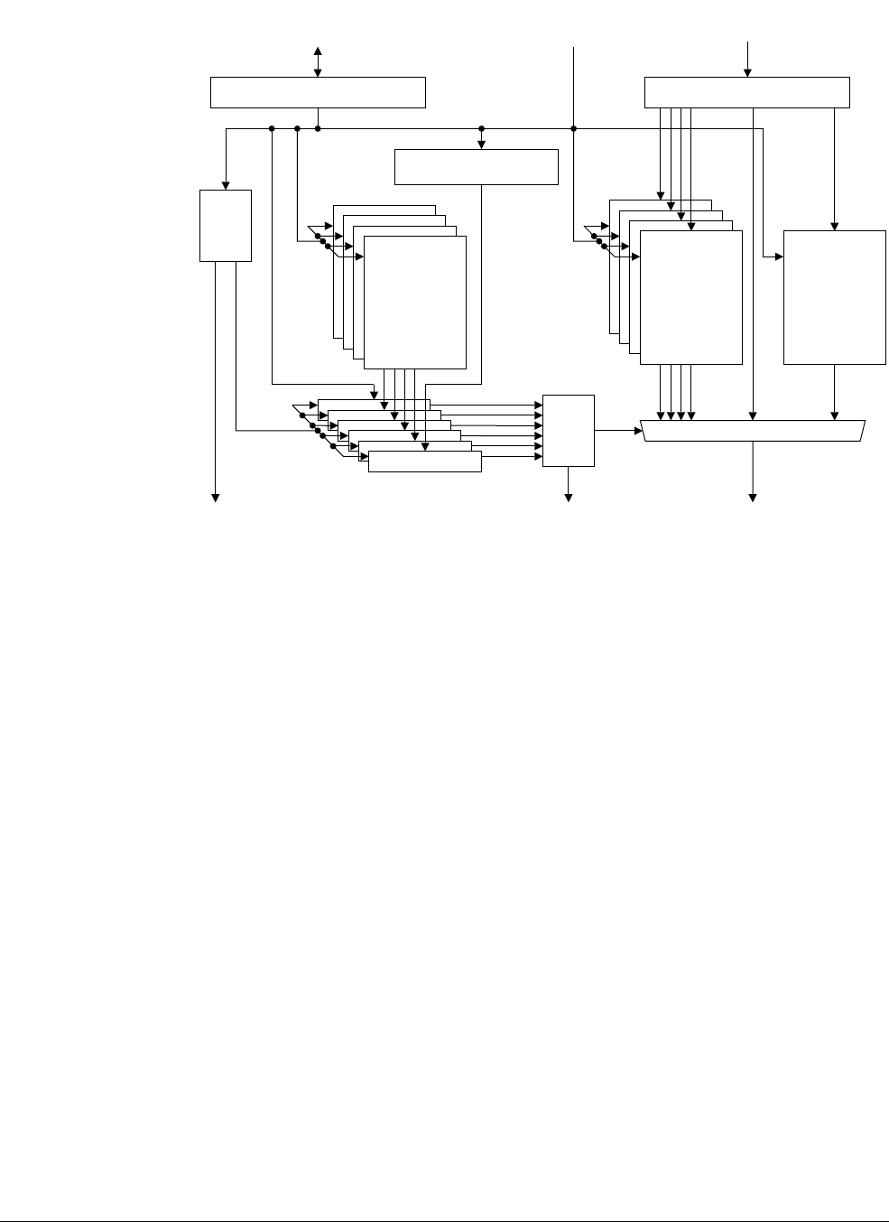
Level One Memory System
ARM DDI 0301H Copyright © 2004-2009 ARM Limited. All rights reserved. 7-4
ID012310 Non-Confidential, Unrestricted Access
Figure 7-1 Level one cache block diagram
7.2.1 Features of the cache system
The level one cache system has the following features:
• The cache is a Harvard implementation.
• The caches are lockable at a granularity of a cache way, using Format C lockdown. See
Cache control and configuration on page 3-7.
• Cache replacement policies are Pseudo-Random or Round-Robin, as controlled by the RR
bit in CP15 register c1. Round-Robin uses a single counter for all sets, that selects the way
used for replacement.
• Cache line allocation uses the cache replacement algorithm when all cache lines are valid.
If one or more lines is invalid, then the invalid cache line with the lowest way number is
allocated to in preference to replacing a valid cache line. This mechanism does not
allocate to locked cache ways unless all cache ways are locked. See Cache miss handling
when all ways are locked down on page 7-6.
• Cache lines can contain either Secure or Non-secure data and the NS Tag, that the
MicroTLB provides, indicates when the cache line comes from Secure or Non-secure
memory.
• Cache lines can be either Write-Back or Write-Through, determined by the MicroTLB
entry.
• Only read allocation is supported.
DATARAM
TAGRAM TCM
Comparator
Way
select
Write buffer data (1-2 words)
Write buffer addresses
Micro
TLB
Cache
hit
Data
out
Micro TLB
miss and
Data Abort
RAMSet base address and size
CP15
interface
Virtual
address
Write
data

Level One Memory System
ARM DDI 0301H Copyright © 2004-2009 ARM Limited. All rights reserved. 7-5
ID012310 Non-Confidential, Unrestricted Access
• The cache can be disabled independently from the TCM, under control of the appropriate
bits in CP15 c1. The cache can be disabled in Secure state while enabled in Non-secure
state and enabled in Secure state while disabled in Non-secure state.
The CL bit in the system control coprocessor, see c1, Non-Secure Access Control Register
on page 3-55, reserves cache lockdown registers for Secure world operation. When the CL
bit is 0 the cache lockdown registers are only available in the Secure world. When the CL
bit is 1 they are available for both Secure and Non-secure operation.
• Data cache misses are nonblocking with three outstanding Data Cache misses being
supported.
• Streaming of sequential data from LDM and LDRD operations, and for sequential
instruction fetches is supported.
7.2.2 Cache functional description
The cache and TCM exist to perform associative reads and writes on requested addresses. The
steps involved in this for reads are as follows:
1. The lower bits of the virtual address are used as the virtual index for the Tag and RAM
blocks, including the TCM.
2. In parallel the MicroTLB is accessed to perform the virtual to physical address translation.
3. The physical addresses read from the Tag RAMs and the TCM base address register, and
the Write Buffer address registers, in parallel with the NS Tag, are compared with the
physical address from the MicroTLB. The processor also compares the NS Tag, that the
processor stores in the Tag RAMs along with the physical address, with the NS attribute
from the MicroTLB. Both comparisons form hit signals for each of the cache ways.
4. The hit signals are used to select the data from the cache way that has a hit. Any bytes
contained in both the data RAMs and the Write Buffer entries are taken from the Write
Buffer. If two or three Write Buffer entries are to the same bytes, the most recently written
bytes are taken.
The steps for writes are as follows:
1. The lower bits of the virtual address are used as the virtual index for the Tag blocks.
2. In parallel, the MicroTLB is accessed to perform the virtual to physical address
translation.
3. The physical addresses read from the Tag RAMs and the TCM base address register are
compared with the physical address from the MicroTLB. The processor also compares the
NS Tag, that it stores in the Tag RAMs along with the physical address, with the NS
attribute from the MicroTLB. Both comparisons form hit signals for each of the cache
ways.
4. If a cache way, or the TCM, has recorded a hit, then the write data is written to an entry
in the Cache Write Buffer, along with the cache way, or TCM, that it must take place to.
5. The contents of the Cache Write Buffer are held until a subsequent write or CP15
operation requires space in the Write Buffer. At this point the oldest entry in the Cache
Write Buffer is written into the cache.
7.2.3 Cache control operations
c7, Cache operations on page 3-69 describes the cache control operations that are supported by
the processor. The processor supports all the block cache control operations in hardware.

Level One Memory System
ARM DDI 0301H Copyright © 2004-2009 ARM Limited. All rights reserved. 7-6
ID012310 Non-Confidential, Unrestricted Access
Note
• The cache operations executed in Secure state might affect all cache lines but cache
operations executed in Non-secure state only affect Non-secure lines.
• You can restrict the functional size of each cache to 16KB, even when the physical cache
is larger. This enables the processor to run software that does not support ARMv6 page
coloring restrictions. You enable the this feature with the CZ bit, see c1, Auxiliary Control
Register on page 3-48.
For more information about ARMv6 page coloring see Restrictions on page table
mappings page coloring on page 6-41.
7.2.4 Cache miss handling
A cache miss results in the requests required to do the line fill being made to the level two
interface, with a Write-Back occurring if the line to be replaced contains dirty data.
The Write-Back data is transferred to the Write Buffer. This is arranged to handle this data as a
sequential burst. Because of the requirement for nonblocking caches, additional write
transactions can occur during the transfer of Write-Back data from the cache to the Write Buffer.
These transactions do not interfere with the burst nature of the Write-Back data. The Write
Buffer is responsible for handling the potential Read After Write (RAW) data hazards that might
exist from a Data Cache line Write-Back. The caches perform critical word-first cache refilling.
The internal bandwidth from the level two data read port to the Data Caches is eight bytes per
cycle, and supports streaming.
Cache miss handling when all ways are locked down
The ARM architecture describes the behavior of the cache as being Unpredictable when all ways
in the cache are locked down. However, for ARM1176JZF-S processors a cache miss is serviced
as if Way 0 is not locked.
7.2.5 Cache disabled behavior
If the cache is disabled, then the cache is not accessed for reads or for writes. This ensures that
maximum power savings can be achieved. It is therefore important that before the cache is
disabled, all of the entries are cleaned to ensure that the external memory has been updated. In
addition, if the cache is enabled with valid entries in it, then it is possible that the entries in the
cache contain old data. Therefore, the cache must be disabled with clean and invalid entries.
Cache maintenance operations can be performed even if the cache is disabled. The system can
disable the cache in Secure state when it is enabled in Non-secure state and enable the cache in
Secure state when it is disabled in Non-secure state.
7.2.6 Unexpected hit behavior
An unexpected hit is where the cache reports a hit on a memory location that is marked as
Noncacheable or Shared. The unexpected hit behavior is that these hits are ignored and a level
two access occurs. The unexpected hit is ignored because the cache hit signal is qualified by the
cacheability.
For writes, an unexpected cache hit does not result in the cache being updated. Therefore, writes
appear to be Noncacheable accesses. For a data access, if it lies in the range of memory specified
by the Instruction TCM, then the access is made to that RAM rather than to level two memory.
This applies to both writes and reads.

Level One Memory System
ARM DDI 0301H Copyright © 2004-2009 ARM Limited. All rights reserved. 7-7
ID012310 Non-Confidential, Unrestricted Access
7.3 Tightly-coupled memory
The TCM is designed to provide low-latency memory that can be used by the processor without
the unpredictability that is a feature of caches.
You can use such memory to hold critical routines, such as interrupt handling routines or
real-time tasks where the indeterminacy of a cache is highly undesirable. In addition you can
use it to hold scratch pad data, data types whose locality properties are not well suited to
caching, and critical data structures such as interrupt stacks.
You can separately configure the size of the Instruction TCM (ITCM) and the size of the Data
TCM (DTCM) to be 0KB, 4KB. 8KB, 16KB, 32KB or 64KB. For each side, ITCM and DTCM:
• If you configure the TCM size to be 4KB you get one TCM, of 4KB, on this side.
• If you configure the TCM size to be larger than 4KB you get two TCMs on this side, each
of half the configured size. So, for example, if you configure an ITCM size of 16KB you
get two ITCMs, each of size 8KB.
Table 7-1 lists all possible TCM configurations:
When the number of TCM on one side is 2, to make the implementation easier, the TCM for this
side are implemented as one single RAM. This RAM then has a size in the 0-64 KB range. The
lower part of the RAM corresponds to the TCM called TCM0 and the upper part corresponds to
TCM1.
You can also configure each individual TCM to contain Secure or Non-secure data. You make
this configuration in CP15 register c9, accessible in Secure state only. See c9, Data TCM
Non-secure Control Access Register on page 3-93 and c9, Instruction TCM Non-secure Control
Access Register on page 3-94 for more information. After reset, all TCMs are configured as
Secure.
The TCM Status Register in CP15 c0 describes what TCM options and TCM sizes can be
implemented, see c0, TCM Status Register on page 3-24.
Each Data TCM is implemented in parallel with the Data Cache and each Instruction TCM is
implemented in parallel with the Instruction Cache. Each TCM has a single movable base
address, specified in CP15 register c9, see c9, Data TCM Region Register on page 3-89 and c9,
Instruction TCM Region Register on page 3-91.
The size of each TCM can differ from the size of a cache way, but forms a single contiguous
area of memory. Figure 7-1 on page 7-4 shows the entire level one memory system. To access
each of the TCM region and TCM Access Control registers, the TCM Selection registers are set
to the TCM of interest, see c9, TCM Selection Register on page 3-96.
Table 7-1 TCM configurations
Configured TCM size Number of TCMs Size of each TCM
0KB 0 0
4KB 1 4KB
8KB 2 4KB
16KB 2 8KB
32KB 2 16KB
64KB 2 32KB

Level One Memory System
ARM DDI 0301H Copyright © 2004-2009 ARM Limited. All rights reserved. 7-8
ID012310 Non-Confidential, Unrestricted Access
The base address of each TCM can be placed anywhere in the physical address map, and does
not have to be backed by memory implemented externally. The Instruction and Data TCMs have
separate base addresses.
You can disable each TCM to avoid an access being made to it. This gives a reduction in the
power consumption. You can disable each TCM independently from the enabling of the
associated cache, as determined by CP15 register c9. The disabling of a TCM invalidates the
base address, so there is no unexpected hit behavior for the TCM.
The timing of a TCM access is the same as for a cache access. The ARM1176JZF-S processor
does not support wait states on the TCM interfaces.
Table 7-2 lists the access types for TCM configured as Non-secure.
Table 7-3 lists the access types for TCM configured as Secure.
7.3.1 TCM behavior
TCM forms a continuous area of memory that is always valid if the TCM is enabled. The TCM
is used as part of the physical memory map of the system, and is not backed by a level of external
memory with the same physical addresses. For this reason, the TCM behaves differently from
the caches for regions of memory that are marked as being Write-Through Cacheable. In such
regions, no external writes occur in the event of a write to memory locations contained in the
TCM.
7.3.2 Restriction on page table mappings
The TCMs are implemented in a physically indexed, physically addressed manner, giving the
following behavior:
• aliases to the same physical address can exist in memory regions that are held in the TCM.
As a result, the page mapping restrictions for the TCM are less restrictive than for the cache, as
Restrictions on page table mappings page coloring on page 6-41 describes.
Table 7-2 Access to Non-secure TCM
Access type NS attribute of corresponding
page table Behavior
Non-secure access X Access done on TCM
Secure access 0 TCM not visible, go to Level 2 memory
Secure access 1 access done on TCM.
Table 7-3 Access to Secure TCM
Access type NS attribute of corresponding
page table Behavior
Non-secure access X TCM not visible
Secure access 0 Access done on TCM
Secure access 1 TCM is not visible, go to Level 2 memory.

Level One Memory System
ARM DDI 0301H Copyright © 2004-2009 ARM Limited. All rights reserved. 7-9
ID012310 Non-Confidential, Unrestricted Access
7.3.3 Restriction on page table attributes
The page table entries that describe areas of memory that are handled by the TCM are remapped
to normal, non-cacheable, non-shared type.
If the page table entry covers a region larger than the size of the TCM, then the attributes are
ignored for the TCM region but still apply to the rest of the region covered by the page table
entry.

Level One Memory System
ARM DDI 0301H Copyright © 2004-2009 ARM Limited. All rights reserved. 7-10
ID012310 Non-Confidential, Unrestricted Access
7.4 DMA
The level one DMA provides a background route to transfer blocks of data to or from the TCMs.
It is used to move large blocks, rather than individual words or small structures.
The level one DMA is initiated and controlled by accessing the appropriate CP15 registers and
instructions, see DMA control on page 3-9. This register is common to the Secure and
Non-secure world. DMA channels can be reserved for the Secure world only, or available for
both worlds, see bit [18] in the c1, Non-Secure Access Control Register on page 3-55. This bit
also determines the page tables, Secure or Non-secure, that DMA transfers use. In the
Non-secure world, the read/write access of these DMA registers depends on Non-secure Access
control register bit[18] value. Accessing these registers in the Non-secure world when not
permitted, NSAC[18] clear, results in an Undefined exception.
The value of NSAC[18] is also used during access to the Main TLB for comparison with the
NSTID of the TLB entries:
• When the channel is defined as Non-secure, NSAC[18] set, the Non-secure page tables
are used. DMA external accesses are done on Non-secure memory regions. For DMA
internal access, only TCM defined as Non-secure can be accessed.
• When the channel is defined as Secure. NSAC[18] clear, the Secure page tables are used.
The DMA external or internal access depends on the value of the NS attribute in the
corresponding descriptors. If the NS attribute in the descriptor, for external access, is
reset, the DMA channel accesses external Secure memory. If the NS attribute is set, the
DMA channel accesses external Non-secure memory. For internal access, the page
descriptor selects the TCM and the DMA performs a security permission check before
accessing the TCM.
The process specifies the internal start and end addresses and external start address, together
with the direction of the DMA. The addresses specified are Virtual Addresses, and the level one
DMA hardware includes translation of Virtual Addresses to Physical Addresses and checking
of protection attributes.
The TLB, that TLB organization on page 6-4 describes, holds the page table entries for the
DMA, and ensures that the entries in a TLB used by the DMA are consistent with the page
tables. Errors, arising from protection checks, are signaled to the processor using an interrupt.
Completion of the DMA can also be configured by software to signal the processor with an
interrupt using the same interrupt to the processor that the error uses. The status of the DMA is
read from the CP15 registers associated with the DMA.
The DMA controller is programmed using the CP15 coprocessor. DMA accesses can only be to
or from the TCM and must not be from areas of memory that can be contained in the caches.
That is, no coherency support is provided in the caches.
The processor implements two DMA channels. Only one channel can be active at a time. The
key features of the DMA system are:
• the DMA system runs in the background of processor operations
• DMA progress is accessible from software
• DMA is programmed with virtual addresses, with a MicroTLB dedicated to the DMA
function
• you can configure the DMA to work to either the instruction or data RAMs
• DMA is allocated by a privileged process, enabling User access to control the DMA.

Level One Memory System
ARM DDI 0301H Copyright © 2004-2009 ARM Limited. All rights reserved. 7-11
ID012310 Non-Confidential, Unrestricted Access
For some DMA events an interrupt is generated. If the channel is configured as Non-secure the
nDMAIRQ signal is asserted, otherwise if the channel is configured as Secure the nDMASIRQ
signal is asserted. When an external access caused by the DMA aborts, the processor asserts
nDMAEXTERRIRQ. You can route these output pins to an external interrupt controller for
prioritization and masking. This is the only mechanism to signal the interrupt to the core. For
more information, see c11, DMA Channel Status Register on page 3-117.
Each DMA channel has its own set of Control and Status Registers. The maximum number of
DMA channels that can be defined is architecturally limited to 2. Only 1 DMA channel can be
active at a time. If the other DMA channel has been started, it is queued to start performing
memory operations after the currently active channel has completed. The level one DMA
behaves as a distinct master from the rest of the processor, and the same mechanisms for
handling Shared memory regions must be used if the external addresses being accessed by the
level one DMA system are also accessed by the rest of the processor.
Memory attributes and types on page 6-20 describes these. If a User mode DMA transfer is
performed using an external address that is not marked as Shared, an error is signaled by the
DMA channel. There is no ordering requirement of memory accesses caused by the level one
DMA relative to those generated by reads and writes by the processor, while a channel is
running. When a channel has completed running, all its transactions are visible to all other
observers in the system.
All memory accesses caused by the DMA occur in the order specified by the DMA channel,
regardless of the memory type. If a DMA access is performed to Strongly Ordered memory, see
Memory attributes and types on page 6-20, then a transaction caused by the DMA prevents any
additional transactions being generated by the DMA until the point when the access is complete.
A transaction is complete when it has changed the state of the target location or data has been
returned to the DMA. If the FCSE PID, the Domain Access Control Register, or the page table
mappings are changed, or the TLB is flushed, while a DMA channel is in the Running or Queued
state, then the DMA channel must be stopped.

Level One Memory System
ARM DDI 0301H Copyright © 2004-2009 ARM Limited. All rights reserved. 7-12
ID012310 Non-Confidential, Unrestricted Access
7.5 TCM and cache interactions
In the event that a TCM and a cache both contain the requested address, it is architecturally
Unpredictable which memory the instruction data is returned from. It is expected that such an
event only arises from a failure to invalidate the cache when the base register of the TCM is
changed, and so is clearly a programming error. For a Harvard arrangement of caches and TCM,
data reads and writes can access any Instruction TCM for both reads and writes. This ensures
that accesses to literal pools, Undefined instructions, and SVC numbers are possible, and aids
debugging. For this reason, an Instruction TCM must behave as a unified TCM, but can be
optimized for instruction fetches.
You must not program an Instruction TCM to the same base address as a Data TCM and, if the
two RAMs are different sizes, the regions in physical memory of the two RAMs must not be
overlapped. This is because the resulting behavior is architecturally Unpredictable.
In these cases, you must not rely on the behavior of ARM1176JZF-S processor for code that is
intended to be ported to other ARM platforms.
In all cases, no security consideration is necessary because there cannot be a conflict between
accesses targeting Secure and Non-secure memory. Any cache line or TCM data is marked as
being Secure or Non-secure and no Unpredictable situations can result from this.
7.5.1 Overlapping between TCM regions
Where TCM regions overlap, the access priority is worked out using these rules, starting with
the highest priority rule:
1. Where there is an overlap between a DTCM and an ITCM, the DTCM has priority for data
accesses.
Note
Instruction accesses to the DTCM are not possible.
2. Where there is an overlap between two TCMs on the same side, TCM0 has priority. This
means that DTCM0 has priority over DTCM1, and ITCM0 has priority over ITCM1.
This means that, for data accesses, the priority order if all four TCMs overlap is:
1. DTCM0, highest priority
2. DTCM1
3. ITCM0
4. ITCM1, lowest priority.
For instruction accesses, the priority order is:
1. ITCM0, highest priority
2. ITCM1, lowest priority.
These priority rules are not affected by whether the TCMs are Secure or Non-secure. The only
effect of configuring TCMs as Secure or Non-secure is that a Secure TCM cannot overlap a
Non-secure TCM.
7.5.2 DMA and core access arbitration
DMA and core accesses to both the Instruction TCM and the Data TCM can occur in parallel.
So as not to disrupt the execution of the core, core-generated accesses have priority over those
requested by the DMA engine, regardless of the security level of the accesses.

Level One Memory System
ARM DDI 0301H Copyright © 2004-2009 ARM Limited. All rights reserved. 7-13
ID012310 Non-Confidential, Unrestricted Access
7.5.3 Instruction accesses to TCM
If the Instruction TCM and the Instruction Cache both contain the requested instruction address,
the processor returns data from the TCM. The instruction prefetch port of the processor cannot
access the Data TCM. If an instruction prefetch misses the Instruction TCM and Instruction
Cache but hits the Data TCM, then the result is an access to the level two memory.
An IMB must be inserted between a write to an Instruction TCM and the instructions being
written that it relies on. In addition, any branch prediction mechanism must be invalidated or
disabled if a branch in the Instruction TCM is overwritten.
7.5.4 Data accesses to the Instruction TCM
If the Data TCM and the Data Cache both contain the requested data address for a read, the
processor returns data from the Data TCM. For a write, the write occurs to the Data TCM. The
majority of data accesses are expected to go to the Data Cache or to the Data TCM, but it is
necessary for the Instruction TCM to be read or written on occasion.
The Instruction TCM base addresses are read by the processor data port as a possible source for
data for all memory accesses. This increases the data comparisons associated with the data,
compared with the number required for the instruction memory lookup, for the level one
memory hit generation. This functionality is required for reading literal values and for debug
purposes, such as setting software breakpoints.
Access to the Instruction TCM involves a delay of 5-12 cycles in reading or writing the data.
This delay enables the Instruction TCM access to be scheduled to take place only when the
presence of a hit to the Instruction TCM is known. This saves power and avoids unnecessary
delays being inserted into the instruction-fetch side. This delay is applied to all accesses in a
multiple operation in the case of an LDM, an LDCL, an STM, or an STCL.
Literal pool accesses
It can take 5-12 cycles for the data port to read data from the Instruction TCM.
Because the path lengths are short, there might sometimes be an increase in
latency to achieve greater clock speeds. Therefore, avoid literal pool accesses
inside critical loops. This does not affect code in cache, because the literal pool is
loaded into the D cache.
Switching penalty between cache & TCM
Normally, an access to the cache or TCM takes a single cycle. However, it can
take three cycles in certain cases.
To perform a cache or TCM read in a single cycle, the processor speculatively
reads the RAM contents. It does not know if it was the correct RAM until after
the read is complete. To save power, the processor performs a speculative read
either to the TCM or to the cache. If the read is wrong, the processor must repeat
the access to the correct location.
There is a penalty of three clock cycles when the core switches between accessing
cache and TCM, for example if it thinks the access is in TCM, but it is in fact in
cache. So. three cycles for the first non-sequential access to TCM, when the
previous access on that side, I-side or D-side, was to cache and similarly, three
cycles penalty for the first non-sequential access to cache, when the previous
access on that side was to TCM. This is not an issue on the I-side, where code does
not typically branch between TCM and cacheable areas, but can be an issue for
data.
For example, in the following code:
Loop LDR r0, [r2],#4 ; reads an item from D-TCM

Level One Memory System
ARM DDI 0301H Copyright © 2004-2009 ARM Limited. All rights reserved. 7-14
ID012310 Non-Confidential, Unrestricted Access
LDR r1, [r3],#4 ; reads an item from D-cache
ADD r4, r0, r1 ; perform some calculation on the loaded data
CMP r1, r5 ; finished yet?
BLT loop
Each iteration of this loop pays the three cycle penalty twice, because the loads
alternate between cache & TCM. This is an extreme example, of course. Because
of hit-under-miss, this 3 cycle penalty might not stall the integer core. If the same
code uses only D-TCM, or only D-cache, each load typically takes one cycle.
This can be important if a performance critical loop operates on two blocks of
data, one in D-TCM and one in main memory, especially if the data is consumed
in small blocks of a byte or word, rather than multiple words per iteration.
So, if you have all of the dhrystone code and data in TCM, you get better
performance than if you have nearly all in TCM.
It is not required for instruction port(s) to be able to access the Data TCM. An attempt to access
addresses in the range covered by a Data TCM from an instruction port does not result in an
access to the Data TCM. In this case, the instruction is fetched from main memory. It is
anticipated that such accesses can result in external aborts in some systems, because the address
range might not be supported in main memory.
Instruction TCMs must not be programmed to the same base address as a Data TCM and, if the
RAMs are of different sizes, the regions in physical memory of the two RAMs must not be
overlapped because the resulting behavior is architecturally Unpredictable. If an access is made
to a location that is covered by both an Instruction TCM and a Data TCM, the access is only to
the Data TCM.
Table 7-4 summarizes the results of data accesses to TCM and the cache. This also embodies
the unexpected hit behavior for the cache that Unexpected hit behavior on page 7-6 describes.
In Table 7-4, the Data Cache can only be hit if the memory location being accessed is marked
as being Cacheable and Not shareable. A hit to the Data TCM and Instruction TCM refers to
hitting an address in the range covered by that TCM.
Table 7-4 Summary of data accesses to TCM and caches
Data
TCM
Data
cache
Instruction
TCMaRead behavior Write behavior
Hit Hit Hit Read from Data TCM. Write to Data TCM. No write to the Instruction
TCM or Data Cache.
No write to level two, even if marked as
Write-Through.
Hit Hit Miss Read from Data TCM. Write to Data TCM. No write to Data Cache.
No write to level two even if marked as
Write-Through.
Hit Miss Hit Read from Data TCM.
No linefill to Data Cache fill
even if marked Cacheable.
Write to Data TCM. No write to Instruction TCM.
No write to level two even if marked as
Write-Through.
Hit Miss Miss Read from Data TCM.
No linefill to Data Cache even
if marked Cacheable.
Write to Data TCM.
No write to level two even if marked as
Write-Through.
Miss Hit Hit Read from Data Cache. Write to Data Cache.
If Write-Through, write to Instruction TCM.

Level One Memory System
ARM DDI 0301H Copyright © 2004-2009 ARM Limited. All rights reserved. 7-15
ID012310 Non-Confidential, Unrestricted Access
Table 7-5 summarizes the results of instruction accesses to TCM and the cache. This also
embodies the unexpected hit behavior for the cache that Unexpected hit behavior on page 7-6
describes. In Table 7-5, the Instruction Cache can only be hit if the memory location being
accessed is marked as being Cacheable and not shareable. A hit to the Instruction TCM refers
to hitting an address in the range covered by that TCM.
Miss Hit Miss Read from Data Cache. Write to Data Cache.
If Write-Through, write to level two.
Miss Miss Hit Read from Instruction TCM.
No cache fill even if marked
Cacheable.
Write to Instruction TCM.
No write to level two even if marked as
Write-Through.
Miss Miss Miss If Cacheable and cache
enabled, cache linefill.
If Noncacheable or cache
disabled, read to level two.
Write to level two.
a. Excludes unexpected hit.
Table 7-4 Summary of data accesses to TCM and caches (continued)
Data
TCM
Data
cache
Instruction
TCMaRead behavior Write behavior
Table 7-5 Summary of instruction accesses to TCM and caches
Instruction
TCM
Instruction
cachea
Data
TCM Read behavior
Hit Hit Don’t care Read from I TCMNo linefill to I Cache even if marked Cacheable
Hit Miss Don’t care Read from Instruction TCM.
No linefill to Instruction Cache, even if marked cacheable.
Miss Hit Don’t care Read from Instruction Cache.
Miss Miss Don’t care If Cacheable and cache enabled, cache linefill.
If Noncacheable or cache disabled, read to level two.
a. Excludes unexpected hit.

Level One Memory System
ARM DDI 0301H Copyright © 2004-2009 ARM Limited. All rights reserved. 7-16
ID012310 Non-Confidential, Unrestricted Access
7.6 Write buffer
All memory writes take place using the Write buffer. To ensure that the Write buffer is not
drained on reads, the following features are implemented:
• The Write buffer is a FIFO of outstanding writes to memory. It consists of a set of
addresses and a set of data words, together with their size information.
• If a sequence of data words is contained in the Write buffer, these are denoted as applying
to the same address by the Write buffer storing the size of the store multiple. This reduces
the number of address entries that must be stored in the Write buffer.
• In addition to this, a separate FIFO of Write-Back addresses and data words is
implemented. Having a separate structure avoids complications associated with
performing an external write while the write-though is being handled.
• The address of a new read access is compared against the addresses in the Write buffer. If
a read is to a location that is already in the Write buffer, the read is blocked until the Write
buffer has drained sufficiently far for that location to be no longer in the Write buffer. The
sequential marker only applies to words in the same 8 word, 8 word aligned, block, and
the address comparisons are based on 8 word aligned addresses.
Memory access control on page 6-11 describes the ordering of memory accesses.

ARM DDI 0301H Copyright © 2004-2009 ARM Limited. All rights reserved. 8-1
ID012310 Non-Confidential, Unrestricted Access
Chapter 8
Level Two Interface
The processor is designed to be used within larger chip designs using the Advanced Microcontroller
Bus Architecture (AMBA) AXI protocol. The processor uses the level two interface as its interface
to memory and peripherals. This chapter describes the features of the level two interface not
covered in the AMBA AXI Protocol Specification
The chapter contains the following sections:
•About the level two interface on page 8-2
•Synchronization primitives on page 8-6
•AXI control signals in the processor on page 8-8
•Instruction Fetch Interface transfers on page 8-14
•Data Read/Write Interface transfers on page 8-15
•Peripheral Interface transfers on page 8-37
•Endianness on page 8-38
•Peripheral Interface transfers on page 8-37.
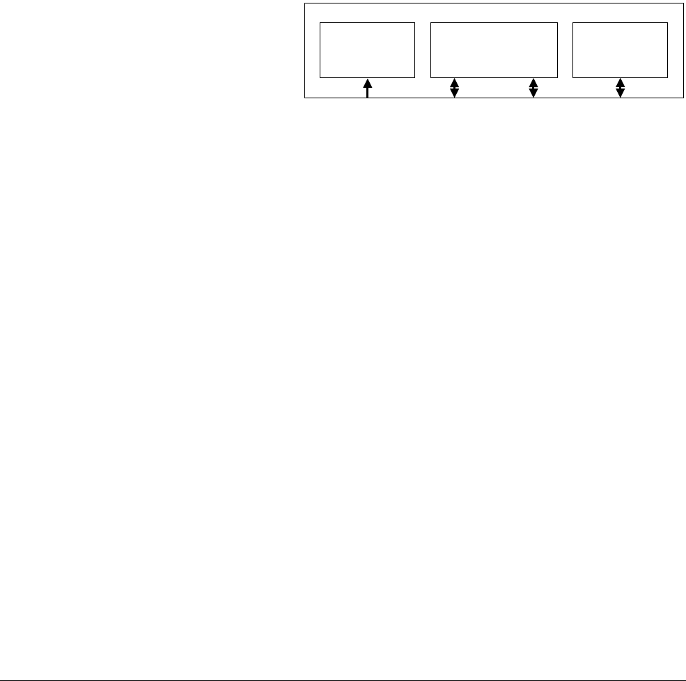
Level Two Interface
ARM DDI 0301H Copyright © 2004-2009 ARM Limited. All rights reserved. 8-2
ID012310 Non-Confidential, Unrestricted Access
8.1 About the level two interface
The level two memory interface exists to provide a high-bandwidth interface to second level
caches, on-chip RAM, peripherals, and interfaces to external memory.
It is a key feature in ensuring high system performance, providing a higher bandwidth
mechanism for filling the caches in a cache miss than has existed on previous ARM processors.
The processor level two interconnect system uses the following 64-bit wide AXI interfaces:
• Instruction Fetch Interface
• Data Read/Write Interface
• DMA Interface.
Another interface is also provided, the Peripheral Interface. This is a 32-bit AXI interface.
Figure 8-1 shows the level two interconnect interfaces.
Figure 8-1 Level two interconnect interfaces
These interfaces provide for several simultaneous outstanding transactions, giving the potential
for high performance from level two memory systems that support parallelism, and also for high
utilization of pipelined memories such as SDRAM.
• No outstanding accesses are issued on the DMA port. The DMA port can issue bursts of
32-bit or 64-bit data when the address is correctly aligned.
• The data read/write port can issue outstanding accesses. The maximum number of
outstanding accesses it can issue is two reads and two writes, to give a total of four
outstanding accesses.
• The instruction port can issue outstanding read accesses, up to a maximum of two
outstanding read accesses.
• No outstanding accesses are issued by the peripheral port.
Each of the four wide interfaces is an AXI interface, with additional signals to support additional
features for the level two memory system for multi-level cache support.
The processor does not drive the following AXI ID signals:
•ARIDI
•ARIDRW
•AW I D RW
•WIDRW
•ARIDP
•AW I D P
•WIDP
•ARIDD
•AW I D D
Processor
Level two
instruction side
controller
Level two data side
controller DMA
DMA
port
(64-bit)
Peripheral
port
(32-bit)
Data read/write
port
(64-bit)
Instruction fetch
port
(64-bit)

Level Two Interface
ARM DDI 0301H Copyright © 2004-2009 ARM Limited. All rights reserved. 8-3
ID012310 Non-Confidential, Unrestricted Access
•WIDD.
When you connect the processor in an AXI system, you can choose whatever ID value suits your
system. The only requirement is that AWI D and WID must have the same value.
8.1.1 AXI parameters for the level 2 interconnect interfaces
Table 8-1 shows the AXI parameters for the level 2 interconnect interfaces.
8.1.2 Level two instruction-side controller
The level two instruction-side controller contains the level two Instruction Fetch Interface. See
Instruction Fetch Interface.
The level two instruction-side controller handles all instruction-side cache misses including
those for Noncacheable locations. It is responsible for the sequencing of cache operations for
Instruction Cache linefills, making requests for the individual stores through the Prefetch Unit
(PU) to the Instruction Cache. The decoupling involved means that the level two instruction-side
controller contains some buffering.
Instruction Fetch Interface
The Instruction Fetch Interface is a read-only interface that services the Instruction Cache on
cache misses, including the fetching of instructions for the PU that are held in memory marked
as Noncacheable. The interface is optimized for cache linefills rather than individual requests.
8.1.3 Level two data-side controller
The level two data-side controller is responsible for the level two:
• Data Read/Write Interface
• Peripheral Interface.
Table 8-1 AXI parameters for the level 2 interconnect interfaces
Parameter
Interface:
Instruction, RO Data, RW Peripheral, RW DMA, RW
Write Issuing Capability Not applicable 2 1 1
Read Issuing Capability 2 2 1 1
Combined Issuing Capability Not applicable 4 1 1
Write ID Capability Not applicable 1 1 1
Write Interleave Capability Not applicable 1a1a1a
Write ID Width Not applicablebNot applicablebNot applicablebNot applicableb
Read ID Capability 1 1 1 1
Read ID Width Not applicablebNot applicablebNot applicablebNot applicableb
a. The value of 1 means that interleaving or re-ordering cannot occur.
b. The level 2 interconnect interfaces do not implement any AXI ID signals.

Level Two Interface
ARM DDI 0301H Copyright © 2004-2009 ARM Limited. All rights reserved. 8-4
ID012310 Non-Confidential, Unrestricted Access
The level two data-side controller handles:
• All external access requests from the Load Store Unit, including cache misses, data
Write-Through operations, and Noncacheable data.
• SWP instructions and semaphore operations. It schedules all reads and writes on the two
interfaces, that are closely related.
The level two data-side controller also handles the Peripheral Interface.
The level two data-side controller contains the Refill and Write-Back engines for the Data
Cache. These make requests through the Load Store Unit for the individual cache operations that
are required. The decoupling involved means that the level two data-side controller contains
some buffering. The write buffer is an integral part of the level two data-side controller.
Data Read/Write Interface
The Data Read/Write Interface performs reads and swap reads. It services the Data Cache on
cache misses, and reads noncacheable locations.
The Data Read/Write Interface performs writes and swap writes. It services the writes out of the
Write Buffer. Multiple writes can be queued up as part of this interface.
Peripheral Interface
The Peripheral Interface is a bidirectional AXI interface that services peripheral devices. In
ARM1176JZF-S processors, the Peripheral Interface is used for peripherals that are private to
the processor, such as the Vectored Interrupt Controller or Watchdog Timer. Accesses to regions
of memory that are marked as Device and Non-Shared are routed to the Peripheral Interface in
preference to the Data Read/Write Interface.
Instruction and DMA accesses are not routed to the Peripheral port.
Unaligned accesses and exclusive accesses are not supported by the peripheral port, because
they are not supported in Device memory. The order that accesses are presented on the
Peripheral Interface, relative to those on the Data Read/Write Interface is not defined, other than
Strongly Ordered accesses. For this reason, the peripheral port is expected to be used to access
a bus or memory system that is not accessible through the Data Read/Write port. See c15,
Peripheral Port Memory Remap Register on page 3-130 to find out how to remap data accesses
to a defined address region to the peripheral port. In some systems, designers might not want to
use the Peripheral port to access locations in memory that are marked in the page tables as
Non-Shared Device. In these cases, you can use the Remap Registers to remap Non-Shared
Device to Shared Device, so causing these accesses to be made using the main system memory
ports.
8.1.4 DMA
The DMA is responsible for:
• Performing all external memory transactions required by the DMA engine, and for
requesting accesses from the Instruction TCM and Data TCM as required.
• Queuing the DMA channels as required. The DMA Interface contains several registers
that are CP15 registers dedicated for DMA use, see DMA control on page 3-9 for details.
The DMA contains buffering to enable the decoupling of internal and external requests. This is
because of variable latency between internal and external accesses.

Level Two Interface
ARM DDI 0301H Copyright © 2004-2009 ARM Limited. All rights reserved. 8-5
ID012310 Non-Confidential, Unrestricted Access
It uses the Prefetch Unit (PU) and the Load Store Unit (LSU) to schedule its accesses to the
TCMs.
DMA Interface
The DMA Interface is a bidirectional interface that services the DMA subsystem for writing and
reading the TCMs. Although the DMA Interface is bidirectional, it is able to produce a stream
of successive accesses that are in the same direction, followed by either an extra stream in the
same direction, or a stream in the opposite direction. Correspondingly the direction turnaround
is not significantly optimized.
The size of the transfer is given in the parameters of the transfer in the CP15 registers. The
transfers are always aligned with the size of the transfer as indicated by the CP15 registers.

Level Two Interface
ARM DDI 0301H Copyright © 2004-2009 ARM Limited. All rights reserved. 8-6
ID012310 Non-Confidential, Unrestricted Access
8.2 Synchronization primitives
On previous architectures support for shared memory synchronization has been with the
read-locked-write operations that swap register contents with memory, the SWP and SWPB
instructions. These support basic busy and free semaphore mechanisms. For details of the swap
instructions, and how to use them to implement semaphores, see the ARM Architecture
Reference Manual.
ARMv6 and its extensions introduce support for more comprehensive shared-memory
synchronization primitives that scale for multiple-processor system designs. Two sets of
instructions are introduced that support multiple-processor and shared-memory inter-process
communication:
• load-exclusive, LDREX, LDREXB, LDREXH, and LDREXD
• store-exclusive, STREX, STREXB, STREXH, and STREXD.
The exclusive-access instructions rely on the ability to tag a physical address as exclusive-access
for a particular processor. This tag is later used to determine if an exclusive store to an address
occurs.
For non-shared memory regions, the LDREX{B,H,D} and STREX{B,H,D} instructions are
presented to the ports as normal LDR or STR. If a processor does an STR on a memory region
that it has already marked as exclusive, this does not clear the tag. However, if the region has
been marked by another processor, an STR clears the tag.
Other events might cause the tag to be cleared. In particular, for memory regions that are not
shared, it is systems dependent whether a store by another processor to a tagged physical address
causes the tag to be cleared.
An external abort on either a load-exclusive or store-exclusive puts the processor into Abort
mode.
For an exclusive read access, the processor considers any response apart from EXOKAY as an
external abort.
For an exclusive write access, the processor considers any error response as an external abort,
an OKAY response sets the returned status value to 1.
For SWP and SWPB instructions, in the case of an error response on the locked read access and
to unlock the bus, the processor performs a dummy normal write access with all byte strobes
disabled at the same address as the locked read access.
Note
An external abort on a load-exclusive can leave the processor internal monitor in its exclusive
state and might affect your software. If it does you must execute a CLREX instruction in your
abort handler to clear the processor internal monitor to an open state.
8.2.1 Load-exclusive instruction
Load-exclusive performs a load from memory and causes the physical address of the access to
be tagged as exclusive-access for the requesting processor. This causes any other physical
address that has been tagged by the requesting processor to no longer be tagged as
exclusive-access.

Level Two Interface
ARM DDI 0301H Copyright © 2004-2009 ARM Limited. All rights reserved. 8-7
ID012310 Non-Confidential, Unrestricted Access
8.2.2 Store-exclusive instruction
Store-exclusive performs a conditional store to memory. The store only takes place if the
physical address is tagged as exclusive-access for the requesting processor. This operation
returns a status value. If the store updates memory the return value is 0, otherwise it is 1. In both
cases, the physical address is no longer tagged as exclusive-access for any processor.
8.2.3 Example of LDREX and STREX usage
This is an example of typical usage. Suppose you are trying to claim a lock:
Lock address : LockAddr
Lock free : 0x00
Lock taken : 0xFF
MOV R1, #0xFF ; load the ‘lock taken’ value
try LDREX R0, [LockAddr] ; load the lock value
CMP R0, #0 ; is the lock free?
STREXEQ R0, R1, [LockAddr] ; try and claim the lock
CMPEQ R0, #0 ; did this succeed?
BNE try ; no – try again ....
; yes – we have the lock
The typical case, where the lock is free and you have exclusive-access, is six instructions.
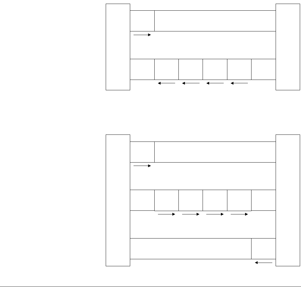
Level Two Interface
ARM DDI 0301H Copyright © 2004-2009 ARM Limited. All rights reserved. 8-8
ID012310 Non-Confidential, Unrestricted Access
8.3 AXI control signals in the processor
This section describes the processor implementation of the AXI control signals:
For additional information about AXI, see the AMBA AXI Protocol Specification.
The AXI protocol is burst-based. Every transaction has address and control information on the
address channel that describes the nature of the data to be transferred. The data is transferred
between master and slave using a write channel to the slave or a read channel to the master. In
write transactions, where all the data flows from the master to the slave, the AXI has an
additional write response channel to enable the slave to signal to the master the completion of
the write transaction.
The AXI protocol permits address information to be issued ahead of the actual data transfer and
enables support for multiple outstanding transactions in addition to out-of-order completion of
transactions.
Figure 8-2 shows how a read transaction uses the read address and read data channels.
Figure 8-2 Channel architecture of reads
Figure 8-3 shows how a write transaction uses the write address, write data, and write response
channels.
Figure 8-3 Channel architecture of writes
Master
interface
Slave
interface
Address
and
control
Read address channel
Read
data
Read
data
Read
data
Read
data
Read channel
Master
interface
Slave
interface
Address
and
control
Write address channel
Write
data
Write channel
Write
data
Write
data
Write
data
Write
response
Write response channel

Level Two Interface
ARM DDI 0301H Copyright © 2004-2009 ARM Limited. All rights reserved. 8-9
ID012310 Non-Confidential, Unrestricted Access
8.3.1 Channel definition
Each of the five independent channels consists of a set of information signals and uses a
two-way VA L I D and READY handshake mechanism.
The information source uses the VA L I D signal to show when valid data is available on the
channel. The destination uses the READY signal to show when it can accept the data. Both the
read data channel and the write data channel also include a LAST signal to indicate when the
transfer of the final data item within a transaction takes place.
Read Address channel
The read address channel is used in every transaction and carries all the required read address
and control information for that transaction. The AXI supports the following mechanisms:
• variable-length bursts, from 1 to 16 data transfers per burst
• bursts with a transfer size of eight bits up to the maximum data bus width
• wrapping, incrementing, and fixed address bursts
• atomic operations, using exclusive and locked access
• system-level caching and buffering control
• Secure and privileged access.
Write address channel
The write address channel is used in every transaction and carries all the required write address
and control information for that transaction. The AXI supports the following mechanisms:
• variable-length bursts, from 1 to 16 data transfers per burst
• bursts with a transfer size of eight bits up to the maximum data bus width
• wrapping, incrementing, and fixed address bursts
• atomic operations, using exclusive and locked access
• system-level caching and buffering control
• Secure and privileged access.
Read data channel
The read data channel conveys both the read data and any read response information from the
slave back to the master. The read data channel includes:
• the data bus, that is 32 bits wide for the Peripheral port, and 64 bits wide for the Data
Read/Write port, Instruction port and DMA port
• a read response indicating the completion status of the read transaction.
Write data channel
The write data channel conveys the write data from the master to the slave and includes:
• the data bus, that is 32 bits wide for the Peripheral port, and 64 bits wide for the Data
Read/Write port, Instruction port and DMA port
• one byte lane strobe for every eight data bits, indicating the bytes of the data bus that are
valid.
Write response channel
The write response channel provides a way for the slave to respond to write transactions. All
write transactions use completion signaling.

Level Two Interface
ARM DDI 0301H Copyright © 2004-2009 ARM Limited. All rights reserved. 8-10
ID012310 Non-Confidential, Unrestricted Access
Note
The completion signal occurs once for each burst, not for each individual data transfer within
the burst.
8.3.2 Signal name suffixes
The signal name for each of the interfaces denotes the interface that it applies to. The signals
have one of these suffixes:
I Instruction Fetch Interface.
D DMA Interface.
RW Data Read/Write Interface.
P Peripheral Interface.
The second character in the signal name indicates if the data direction is a read, R, or write, W.
For example, AxSIZE[2:0] is called ARSIZEI[2:0] for reads in the Instruction Fetch Interface.
8.3.3 Address channel signals
The address channel control signals in the processor are:
•AxLEN[3:0]
•AxSIZE[2:0] on page 8-11
•AxBURST[1:0] on page 8-11
•AxLOCK[1:0] on page 8-11
•AxCACHE[3:0] on page 8-12
•AxPROT[2:0] on page 8-12
•AxSIDEBAND[4:0] on page 8-13.
AxLEN[3:0]
The AxLEN[3:0] signal indicates the number of transfers in a burst. Table 8-2 shows the values
of AxLEN that the processor uses.
Table 8-2 AxLEN[3:0] encoding
AxLEN[3:0] Number of data transfers
b0000 1
b0001 2
b0010 3
b0011 4
b0100 5
b0101 6
b0110 7
b0111 8

Level Two Interface
ARM DDI 0301H Copyright © 2004-2009 ARM Limited. All rights reserved. 8-11
ID012310 Non-Confidential, Unrestricted Access
AxSIZE[2:0]
This signal indicates the size of each transfer. Table 8-3 shows the supported transfer sizes.
AxBURST[1:0]
The AxBURST[1:0] signals indicate a fixed, incrementing or wrapping burst. Table 8-4 shows
the burst types that the ARM1176JZF-S processor supports.
The processor uses:
• Wrapping bursts for some cache line fills
• Incrementing bursts for accesses to noncacheable memory, including instruction fetches.
AxLOCK[1:0]
The AxLOCK[1:0] signal indicates the lock type of access. The processor supports all locked
type accesses. The instruction port only generates Normal access types. The DMA port only
generates Normal access types. The Data Read/Write port generates all access types, Normal,
exclusive and locked access.
Table 8-5 shows the values of AxLOCK that the processor supports.
Table 8-3 AxSIZE[2:0] encoding
AxSIZE[2:0] Bytes in transfer
b000 1
b001 2
b010 4
b011 8
Table 8-4 AxBURST[1:0] encoding
AxBURST[2:0] Burst type Description
b00 Fixed Fixed address burst
b01 Incr Incrementing address burst
b10 Wrap Incrementing address burst that wraps to a lower address at the wrap boundary
Table 8-5 AxLOCK[1:0] encoding
AxLOCK[1:0] Description
b00 Normal access
b01 Exclusive access
b10 Locked access

Level Two Interface
ARM DDI 0301H Copyright © 2004-2009 ARM Limited. All rights reserved. 8-12
ID012310 Non-Confidential, Unrestricted Access
AxCACHE[3:0]
The AxCACHE[3:0] signals indicate the bufferable, cacheable, write-through, write-back, and
allocate attributes of the transaction. These attributes are for the level two memory system.
Table 8-6 shows the correspondence between the AxCACHE[3:0] encoding and TLB
cacheable attributes.
AxPROT[2:0]
The AxPROT[2:0] signal indicates the protection level of the transaction, that is if the
transaction is:
• normal or privileged
• Secure or Non-secure
• Data access or Instruction access.
All transactions from the instruction port are marked as instruction accesses, ARPROTI[2] = 1.
Transactions from the DMA port are marked as instruction accesses, AxPROTD[2] = 1, if the
transaction is to or from the Instruction TCM, and as data accesses, AxPROTD[2] = 0, for
transfers to or from the Data TCM.
Transactions on the peripheral and data read/write ports are marked as data accesses.
Table 8-7 shows the supported values for AxPROT[2:0].
Table 8-6 AxCACHE[3:0] encoding
AxCACHE[3:0] Transaction attributes
b0000 Strongly ordered
b0001 Shared device or non-shared device
b0010 Outer noncacheable
b0110 Outer write-through, no allocate on write
b0111 Outer write-back, no allocate on write
b1111 Outer write-back, write allocate.
Table 8-7 AxPROT[2:0] encoding
Signal Description
AxPROT[2] 0 = Data access
1 = Instruction access
AxPROT[1] 0 = Secure
1 = Non-secure
AxPROT[0] 0 = Normal, User
1 = Privileged

Level Two Interface
ARM DDI 0301H Copyright © 2004-2009 ARM Limited. All rights reserved. 8-13
ID012310 Non-Confidential, Unrestricted Access
AxSIDEBAND[4:0]
The AxSIDEBAND[4:1] signals indicate the bufferable, cacheable, write-through, write-back,
and allocate attributes of the level one memory. AxSIDEBAND[0] indicates the Shared
attribute. Table 8-8 shows the correspondence between the AxSIDEBAND[4:1] encoding and
the TLB cacheable attributes for the Read/Write, Peripheral, and DMA ports.
Table 8-9 shows the correspondence between the ARSIDEBANDI[4:1] encoding and the TLB
cacheable attributes for the Instruction port.
These signals are not part of the AXI protocol and are added for additional information.
Table 8-8 AxSIDEBAND[4:1] encoding
AxSIDEBAND[4:1] Transaction attributes
b0000 Strongly ordered
b0001 Shared device or non-shared device
b0010 Inner noncacheable
b0110 Inner write-through, no allocate on write
b0111 Inner write-back, no allocate on write
b1111 Inner write-back, write allocatea
a. The ARM1176JZF-S processor does not support write allocate.
Table 8-9 ARSIDEBANDI[4:1] encoding
ARSIDEBANDI[4:1] Transaction attributes
b0000 Strongly Ordered
b0001 Device
b0010 Inner Noncacheable
b0110 Inner Cacheable

Level Two Interface
ARM DDI 0301H Copyright © 2004-2009 ARM Limited. All rights reserved. 8-14
ID012310 Non-Confidential, Unrestricted Access
8.4 Instruction Fetch Interface transfers
The tables in this section describe the AXI interface behavior for instruction side fetches to
either Cacheable or Noncacheable regions of memory for the following interface signals:
•ARBURSTI[1:0]
•ARLENI[3:0]
•ARADDRI[31:0]
•ARSIZEI[2:0].
See the AMBA AXI Protocol Specification for details of the other AXI signals.
8.4.1 Cacheable fetches
Table 8-10 shows the values of ARADDRI, ARBURSTI, ARSIZEI, and ARLENI for
Cacheable fetches.
8.4.2 Noncacheable fetches
Table 8-11 shows the values of ARADDRI, ARBURSTI, ARSIZEI, and ARLENI for
Noncacheable fetches.
Table 8-10 AXI signals for Cacheable fetches
Address[4:0] ARADDRI ARBURSTI ARSIZEI ARLENI
0x00
, word 0
0x00
Incr 64-bit 4 data transfers
0x04
, word 1
0x00
Incr 64-bit 4 data transfers
0x08
, word 2
0x08
Wrap 64-bit 4 data transfers
0x0C
, word 3
0x08
Wrap 64-bit 4 data transfers
0x10
, word 4
0x10
Wrap 64-bit 4 data transfers
0x14
, word 5
0x10
Wrap 64-bit 4 data transfers
0x18
, word 6
0x18
Wrap 64-bit 4 data transfers
0x1C
, word 7
0x18
Wrap 64-bit 4 data transfers
Table 8-11 AXI signals for Noncacheable fetches
Address[4:0] ARADDRI ARBURSTI ARSIZEI ARLENI
0x00
, word 0
0x00
Incr 64-bit 4 data transfers
0x04
, word 1
0x04
Incr 64-bit 4 data transfers
0x08
, word 2
0x08
Incr 64-bit 3 data transfers
0x0C
, word 3
0x0C
Incr 64-bit 3 data transfers
0x10
, word 4
0x10
Incr 64-bit 2 data transfers
0x14
, word 5
0x14
Incr 64-bit 2 data transfers
0x18
, word 6
0x18
Incr 64-bit 1 data transfer
0x1C
, word 7
0x1C
Incr 64-bit 1 data transfer

Level Two Interface
ARM DDI 0301H Copyright © 2004-2009 ARM Limited. All rights reserved. 8-15
ID012310 Non-Confidential, Unrestricted Access
8.5 Data Read/Write Interface transfers
The tables in this section describe the AXI interface behavior for Data Read/Write Interface
transfers for the following interface signals:
•AxBURSTRW[1:0]
•AxLENRW[3:0]
•AxSIZERW[2:0]
•AxADDRRW[31:0]
•WSTRBRW[7:0].
8.5.1 Linefills
A linefill comprises four accesses to the Data Cache if there is no external abort returned. In the
event of an external abort, the doubleword and subsequent doublewords are not written into the
Data Cache and the line is never marked as Valid. The four accesses are:
• Write Tag and data doubleword
• Write data doubleword
• Write data doubleword
• Write Valid = 1, Dirty = 0, and data doubleword.
The linefill can only progress to attempt to write a doubleword if it does not contain dirty data.
This is determined in one of two ways:
• if the victim cache line is not valid, then there is no danger and the linefill progresses
• if the victim line is valid, a signal encodes the doublewords that are clean, either because
they were not dirty or they have been cleaned.
The order of words written into the cache is critical-word first, wrapping at the upper cache line
boundary.
Table 8-12 shows the values of ARADDRRW, ARBURSTRW, ARSIZERW, and
ARLENRW for linefills.
Table 8-12 Linefill behavior on the AXI interface
Address[4:0] ARADDRRW ARBURSTRW ARSIZERW ARLENRW
0x00
-
0x07 0x00
Incr 64-bit 4 data transfers
0x08
-
0x0F 0x08
Wrap 64-bit 4 data transfers
0x10
-
0x17 0x10
Wrap 64-bit 4 data transfers
0x18
-
0x1F 0x18
Wrap 64-bit 4 data transfers

Level Two Interface
ARM DDI 0301H Copyright © 2004-2009 ARM Limited. All rights reserved. 8-16
ID012310 Non-Confidential, Unrestricted Access
8.5.2 Noncacheable LDRB
Table 8-13 shows the values of ARADDRRW, ARBURSTRW, ARSIZERW, and
ARLENRW for Noncacheable LDRBs from bytes 0-7.
8.5.3 Noncacheable LDRH
Table 8-14 shows the values of ARADDRRW, ARBURSTRW, ARSIZERW, and
ARLENRW for Noncacheable LDRHs from bytes 0-7.
Table 8-13 Noncacheable LDRB
Address[4:0] ARADDRRW ARBURSTRW ARSIZERW ARLENRW
0x00
, byte 0
0x00
Incr 8-bit 1 data transfer
0x01
, byte 1
0x01
Incr 8-bit 1 data transfer
0x02
, byte 2
0x02
Incr 8-bit 1 data transfer
0x03
, byte 3
0x03
Incr 8-bit 1 data transfer
0x04
, byte 4
0x04
Incr 8-bit 1 data transfer
0x05
, byte 5
0x05
Incr 8-bit 1 data transfer
0x06
, byte 6
0x06
Incr 8-bit 1 data transfer
0x07
, byte 7
0x07
Incr 8-bit 1 data transfer
Table 8-14 Noncacheable LDRH
Address[4:0] ARADDRRW ARBURSTRW ARSIZERW ARLENRW
0x00
, byte 0
0x00
Incr 16-bit 1 data transfer
0x01
, byte 1
0x01
Incr 32-bit 1 data transfer
0x02
, byte 2
0x02
Incr 16-bit 1 data transfer
0x03
, byte 3
0x03
Incr 8-bit 1 data transfer
0x04
Incr 8-bit 1 data transfer
0x04
, byte 4
0x04
Incr 16-bit 1 data transfer
0x05
, byte 5
0x05
Incr 32-bit 1 data transfer
0x06
, byte 6
0x06
Incr 16-bit 1 data transfer
0x07
, byte 7
0x07
Incr 8-bit 1 data transfer
0x08
Incr 8-bit 1 data transfer

Level Two Interface
ARM DDI 0301H Copyright © 2004-2009 ARM Limited. All rights reserved. 8-17
ID012310 Non-Confidential, Unrestricted Access
8.5.4 Noncacheable LDR or LDM1
Table 8-15 shows the values of ARADDRRW, ARBURSTRW, ARSIZERW, and
ARLENRW for Noncacheable LDRs or LDM1s.
8.5.5 Noncacheable LDRD or LDM2
Table 8-16 shows the values of ARADDRRW, ARBURSTRW, ARSIZERW, and
ARLENRW for Noncacheable LDRDs or LDM2s addressing words 0 to 6.
A Noncacheable LDRD or LDM2 addressing word 7 is split into two LDRs, as shown in
Table 8-17 on page 8-18.
Table 8-15 Noncacheable LDR or LDM1
Address[4:0] ARADDRRW ARBURSTRW ARSIZERW ARLENRW
0x00
, byte 0, word 0
0x00
Incr 32-bit 1 data transfer
0x01
, byte 1
0x01
Incr 32-bit 1 data transfer
0x04
Incr 8-bit 1 data transfer
0x02
, byte 2
0x02
Incr 16-bit 1 data transfer
0x04
Incr 16-bit 1 data transfer
0x03
, byte 3
0x03
Incr 8-bit 1 data transfer
0x04
Incr 32-bit 1 data transfer
0x04
, byte 4, word 1
0x04
Incr 32-bit 1 data transfer
0x05
, byte 5
0x05
Incr 32-bit 1 data transfer
0x08
Incr 8-bit 1 data transfer
0x06
, byte 6
0x06
Incr 16-bit 1 data transfer
0x08
Incr 16-bit 1 data transfer
0x07
, byte 7
0x07
Incr 8-bit 1 data transfer
0x08
Incr 32-bit 1 data transfer
Table 8-16 Noncacheable LDRD or LDM2
Address[4:0] ARADDRRW ARBURSTRW ARSIZERW ARLENRW
0x00
, word 0
0x00
Incr 64-bit 1 data transfer
0x04
, word 1
0x04
Incr 32-bit 2 data transfers
0x08
, word 2
0x08
Incr 64-bit 1 data transfer
0x0C
, word 3
0x0C
Incr 32-bit 2 data transfers
0x10
, word 4
0x10
Incr 64-bit 1 data transfer
0x14
, word 5
0x14
Incr 32-bit 2 data transfers
0x18
, word 6
0x18
Incr 64-bit 1 data transfer

Level Two Interface
ARM DDI 0301H Copyright © 2004-2009 ARM Limited. All rights reserved. 8-18
ID012310 Non-Confidential, Unrestricted Access
8.5.6 Noncacheable LDM3
The values of ARADDRRW, ARBURSTRW, ARSIZERW, and ARLENRW for
Noncacheable LDM3s addressing words 0 to 5 are shown in:
• Table 8-18 for a load from Strongly Ordered or Device memory
• Table 8-19 for a load from Noncacheable memory or when the cache is disabled.
A Noncacheable LDM3 addressing word 6 or 7 is split into two operations as shown in
Table 8-20.
8.5.7 Noncacheable LDM4
The values of ARADDRRW, ARBURSTRW, ARSIZERW, and ARLENRW for
Noncacheable LDM4s addressing words 0 to 4 are shown in:
• Table 8-21 on page 8-19 for a load from Strongly Ordered or Device memory
Table 8-17 Noncacheable LDRD or LDM2 from word 7
Address[4:0] Operations
0x1C
, word 7 LDR from
0x1C
+ LDR from
0x00
Table 8-18 Noncacheable LDM3, Strongly Ordered or Device memory
Address[4:0] ARADDRRW ARBURSTRW ARSIZERW ARLENRW
0x00
, word 0
0x00
Incr 32-bit 3 data transfers
0x04
, word 1
0x04
Incr 32-bit 3 data transfers
0x08
, word 2
0x08
Incr 32-bit 3 data transfers
0x0C
, word 3
0x0C
Incr 32-bit 3 data transfers
0x10
, word 4
0x10
Incr 32-bit 3 data transfers
0x14
, word 5
0x14
Incr 32-bit 3 data transfers
Table 8-19 Noncacheable LDM3, Noncacheable memory or cache disabled
Address[4:0] ARADDRRW ARBURSTRW ARSIZERW ARLENRW
0x00
, word 0
0x00
Incr 64-bit 2 data transfers
0x04
, word 1
0x04
Incr 64-bit 2 data transfers
0x08
, word 2
0x08
Incr 64-bit 2 data transfers
0x0C
, word 3
0x0C
Incr 64-bit 2 data transfers
0x10
, word 4
0x10
Incr 64-bit 2 data transfers
0x14
, word 5
0x14
Incr 64-bit 2 data transfers
Table 8-20 Noncacheable LDM3 from word 6, or 7
Address[4:0] Operations
0x18
, word 6 LDM2 from
0x18
+ LDR from
0x00
0x1C
, word 7 LDR from
0x1C
+ LDM2 from
0x00

Level Two Interface
ARM DDI 0301H Copyright © 2004-2009 ARM Limited. All rights reserved. 8-19
ID012310 Non-Confidential, Unrestricted Access
• Table 8-22 for a load from Noncacheable memory or when the cache is disabled.
A Noncacheable LDM4 addressing words 5 to 7 is split into two operations as shown in
Table 8-23.
8.5.8 Noncacheable LDM5
The values of ARADDRRW, ARBURSTRW, ARSIZERW, and ARLENRW for
Noncacheable LDM5s addressing words 0 to 3 are shown in:
• Table 8-24 on page 8-20 for a load from Strongly Ordered or Device memory
• Table 8-25 on page 8-20 for a load from Noncacheable memory or when the cache is
disabled.
Table 8-21 Noncacheable LDM4, Strongly Ordered or Device memory
Address[4:0] ARADDRRW ARBURSTRW ARSIZERW ARLENRW
0x00
, word 0
0x00
Incr 64-bit 2 data transfers
0x04
, word 1
0x04
Incr 32-bit 4 data transfers
0x08
, word 2
0x08
Incr 64-bit 2 data transfers
0x0C
, word 3
0x0C
Incr 32-bit 4 data transfers
0x10
, word 4
0x10
Incr 64-bit 2 data transfers
Table 8-22 Noncacheable LDM4, Noncacheable memory or cache disabled
Address[4:0] ARADDRRW ARBURSTRW ARSIZERW ARLENRW
0x00
, word 0
0x00
Incr 64-bit 2 data transfers
0x04
, word 1
0x04
Incr 64-bit 3 data transfers
0x08
, word 2
0x08
Incr 64-bit 2 data transfers
0x0C
, word 3
0x0C
Incr 64-bit 3 data transfers
0x10
, word 4
0x10
Incr 64-bit 2 data transfers
Table 8-23 Noncacheable LDM4 from word 5, 6, or 7
Address[4:0] Operations
0x14
, word 5 LDM3 from
0x14
+ LDR from
0x00
0x18
, word 6 LDM2 from
0x18
+ LDM2 from
0x00
0x1C
, word 7 LDR from
0x1C
+ LDM3 from
0x00

Level Two Interface
ARM DDI 0301H Copyright © 2004-2009 ARM Limited. All rights reserved. 8-20
ID012310 Non-Confidential, Unrestricted Access
A Noncacheable LDM5 addressing words 4 to 7 is split into two operations as shown in
Table 8-26.
8.5.9 Noncacheable LDM6
The values of ARADDRRW, ARBURSTRW, ARSIZERW, and ARLENRW for
Noncacheable LDM6s addressing words 0 to 2 are shown in:
• Table 8-27 for a load from Strongly Ordered or Device memory
• Table 8-28 on page 8-21 for a load from Noncacheable memory or when the cache is
disabled.
A Noncacheable LDM6 addressing words 3 to 7 is split into two operations as shown in
Table 8-29 on page 8-21.
Table 8-24 Noncacheable LDM5, Strongly Ordered or Device memory
Address[4:0] ARADDRRW ARBURSTRW ARSIZERW ARLENRW
0x00
, word 0
0x00
Incr 32-bit 5 data transfers
0x04
, word 1
0x04
Incr 32-bit 5 data transfers
0x08
, word 2
0x08
Incr 32-bit 5 data transfers
0x0C
, word 3
0x0C
Incr 32-bit 5 data transfers
Table 8-25 Noncacheable LDM5, Noncacheable memory or cache disabled
Address[4:0] ARADDRRW ARBURSTRW ARSIZERW ARLENRW
0x00
, word 0
0x00
Incr 64-bit 3 data transfers
0x04
, word 1
0x04
Incr 64-bit 3 data transfers
0x08
, word 2
0x08
Incr 64-bit 3 data transfers
0x0C
, word 3
0x0C
Incr 64-bit 3 data transfers
Table 8-26 Noncacheable LDM5 from word 4, 5, 6, or 7
Address[4:0] Operations
0x10
, word 4 LDM4 from
0x10
+ LDR from
0x00
0x14
, word 5 LDM3 from
0x14
+ LDM2 from
0x00
0x18
, word 6 LDM2 from
0x18
+ LDM3 from
0x00
0x1C
, word 7 LDR from
0x1C
+ LDM4 from
0x00
Table 8-27 Noncacheable LDM6, Strongly Ordered or Device memory
Address[4:0] ARADDRRW ARBURSTRW ARSIZERW ARLENRW
0x00
, word 0
0x00
Incr 64-bit 3 data transfers
0x04
, word 1
0x04
Incr 32-bit 6 data transfers
0x08
, word 2
0x08
Incr 64-bit 3 data transfers

Level Two Interface
ARM DDI 0301H Copyright © 2004-2009 ARM Limited. All rights reserved. 8-21
ID012310 Non-Confidential, Unrestricted Access
8.5.10 Noncacheable LDM7
The values of ARADDRRW, ARBURSTRW, ARSIZERW, and ARLENRW for
Noncacheable LDM7s addressing word 0 or 1 are shown in:
• Table 8-30 for a load from Strongly Ordered or Device memory
• Table 8-31 for a load from Noncacheable memory or when the cache is disabled.
A Noncacheable LDM7 addressing words 2 to 7 is split into two operations as shown in
Table 8-32.
Table 8-28 Noncacheable LDM6, Noncacheable memory or cache disabled
Address[4:0] ARADDRRW ARBURSTRW ARSIZERW ARLENRW
0x00
, word 0
0x00
Incr 64-bit 3 data transfers
0x04
, word 1
0x04
Incr 64-bit 4 data transfers
0x08
, word 2
0x08
Incr 64-bit 3 data transfers
Table 8-29 Noncacheable LDM6 from word 3, 4, 5, 6, or 7
Address[4:0] Operations
0x0C
, word 3 LDM5 from
0x0C
+ LDR from
0x00
0x10
, word 4 LDM4 from
0x10
+ LDM2 from
0x00
0x14
, word 5 LDM3 from
0x14
+ LDM3 from
0x00
0x18
, word 6 LDM2 from
0x18
+ LDM4 from
0x00
0x1C
, word 7 LDR from
0x1C
+ LDM5 from
0x00
Table 8-30 Noncacheable LDM7, Strongly Ordered or Device memory
Address[4:0] ARADDRRW ARBURSTRW ARSIZERW ARLENRW
0x00
, word 0
0x00
Incr 32-bit 7 data transfers
0x04
, word 1
0x04
Incr 32-bit 7 data transfers
Table 8-31 Noncacheable LDM7, Noncacheable memory or cache disabled
Address[4:0] ARADDRRW ARBURSTRW ARSIZERW ARLENRW
0x00
, word 0
0x00
Incr 64-bit 4 data transfers
0x04
, word 1
0x04
Incr 64-bit 4 data transfers
Table 8-32 Noncacheable LDM7 from word 2, 3, 4, 5, 6, or 7
Address[4:0] Operations
0x08
, word 2 LDM6 from
0x08
+ LDR from
0x00
0x0C
, word 3 LDM5 from
0x0C
+ LDM2 from
0x00
0x10
, word 4 LDM4 from
0x10
+ LDM3 from
0x00

Level Two Interface
ARM DDI 0301H Copyright © 2004-2009 ARM Limited. All rights reserved. 8-22
ID012310 Non-Confidential, Unrestricted Access
8.5.11 Noncacheable LDM8
Table 8-33 shows the values of ARADDRRW, ARBURSTRW, ARSIZERW, and
ARLENRW for a Noncacheable LDM8 addressing word 0.
A Noncacheable LDM8 addressing words 1 to 7 is split into two operations as shown in
Table 8-34.
8.5.12 Noncacheable LDM9
A Noncacheable LDM9 is split into two operations as shown in Table 8-35.
0x14
, word 5 LDM3 from
0x14
+ LDM4 from
0x00
0x18
, word 6 LDM2 from
0x18
+ LDM5 from
0x00
0x1C
, word 7 LDR from
0x1C
+ LDM6 from
0x00
Table 8-32 Noncacheable LDM7 from word 2, 3, 4, 5, 6, or 7 (continued)
Address[4:0] Operations
Table 8-33 Noncacheable LDM8 from word 0
Address[4:0] ARADDRRW ARBURSTRW ARSIZERW ARLENRW
0x00
, word 0
0x00
Incr 64-bit 4 data transfers
Table 8-34 Noncacheable LDM8 from word 1, 2, 3, 4, 5, 6, or 7
Address[4:0] Operations
0x04
, word 1 LDM7 from
0x04
+ LDR from
0x00
0x08
, word 2 LDM6 from
0x08
+ LDM2 from
0x00
0x0C
, word 3 LDM5 from
0x0C
+ LDM3 from
0x00
0x10
, word 4 LDM4 from
0x10
+ LDM4 from
0x00
0x14
, word 5 LDM3 from
0x14
+ LDM5 from
0x00
0x18
, word 6 LDM2 from
0x18
+ LDM6 from
0x00
0x1C
, word 7 LDR from
0x1C
+ LDM7 from
0x00
Table 8-35 Noncacheable LDM9
Address[4:0] Operations
0x00
, word 0 LDM8 from
0x00
+ LDR from
0x00
0x04
, word 1 LDM7 from
0x04
+ LDM2 from
0x00
0x08
, word 2 LDM6 from
0x08
+ LDM3 from
0x00
0x0C
, word 3 LDM5 from
0x0C
+ LDM4 from
0x00
0x10
, word 4 LDM4 from
0x10
+ LDM5 from
0x00

Level Two Interface
ARM DDI 0301H Copyright © 2004-2009 ARM Limited. All rights reserved. 8-23
ID012310 Non-Confidential, Unrestricted Access
8.5.13 Noncacheable LDM10
A Noncacheable LDM10 is split into two or three operations as shown in Table 8-36.
8.5.14 Noncacheable LDM11
A Noncacheable LDM11 is split into two or three operations as shown in Table 8-37.
0x14
, word 5 LDM3 from
0x14
+ LDM6 from
0x00
0x18
, word 6 LDM2 from
0x18
+ LDM7 from
0x00
0x1C
, word 7 LDR from
0x1C
+ LDM8 from
0x00
Table 8-35 Noncacheable LDM9 (continued)
Address[4:0] Operations
Table 8-36 Noncacheable LDM10
Address[4:0] Operations
0x00
, word 0 LDM8 from
0x00
+ LDM2 from
0x00
0x04
, word 1 LDM7 from
0x04
+ LDM3 from
0x00
0x08
, word 2 LDM6 from
0x08
+ LDM4 from
0x00
0x0C
, word 3 LDM5 from
0x0C
+ LDM5 from
0x00
0x10
, word 4 LDM4 from
0x10
+ LDM6 from
0x00
0x14
, word 5 LDM3 from
0x14
+ LDM7 from
0x00
0x18
, word 6 LDM2 from
0x18
+ LDM8 from
0x00
0x1C
, word 7 LDR from
0x1C
+ LDM8 from
0x00
+ LDR from
0x00
Table 8-37 Noncacheable LDM11
Address[4:0] Operations
0x00
, word 0 LDM8 from
0x00
+ LDM3 from
0x00
0x04
, word 1 LDM7 from
0x04
+ LDM4 from
0x00
0x08
, word 2 LDM6 from
0x08
+ LDM5 from
0x00
0x0C
, word 3 LDM5 from
0x0C
+ LDM6 from
0x00
0x10
, word 4 LDM4 from
0x10
+ LDM7 from
0x00
0x14
, word 5 LDM3 from
0x14
+ LDM8 from
0x00
0x18
, word 6 LDM2 from
0x18
+ LDM8 from
0x00
+ LDR from
0x00
0x1C
, word 7 LDR from
0x1C
+ LDM8 from
0x00
+ LDM2 from
0x00

Level Two Interface
ARM DDI 0301H Copyright © 2004-2009 ARM Limited. All rights reserved. 8-24
ID012310 Non-Confidential, Unrestricted Access
8.5.15 Noncacheable LDM12
A Noncacheable LDM12 is split into two or three operations as shown in Table 8-38.
8.5.16 Noncacheable LDM13
A Noncacheable LDM13 is split into two or three operations as shown in Table 8-39.
8.5.17 Noncacheable LDM14
A Noncacheable LDM14 is split into two or three operations as shown in Table 8-40.
Table 8-38 Noncacheable LDM12
Address[4:0] Operations
0x00
, word 0 LDM8 from
0x00
+ LDM4 from
0x00
0x04
, word 1 LDM7 from
0x04
+ LDM5 from
0x00
0x08
, word 2 LDM6 from
0x08
+ LDM6 from
0x00
0x0C
, word 3 LDM5 from
0x0C
+ LDM7 from
0x00
0x10
, word 4 LDM4 from
0x10
+ LDM8 from
0x00
0x14
, word 5 LDM3 from
0x14
+ LDM8 from
0x00
+ LDR from
0x00
0x18
, word 6 LDM2 from
0x18
+ LDM8 from
0x00
+ LDM2 from
0x00
0x1C
, word 7 LDR from
0x1C
+ LDM8 from
0x00
+ LDM3 from
0x00
Table 8-39 Noncacheable LDM13
Address[4:0] Operations
0x00
, word 0 LDM8 from
0x00
+ LDM5 from
0x00
0x04
, word 1 LDM7 from
0x04
+ LDM6 from
0x00
0x08
, word 2 LDM6 from
0x08
+ LDM7 from
0x00
0x0C
, word 3 LDM5 from
0x0C
+ LDM8 from
0x00
0x10
, word 4 LDM4 from
0x10
+ LDM8 from
0x00
+ LDR from
0x00
0x14
, word 5 LDM3 from
0x14
+ LDM8 from
0x00
+ LDM2 from
0x00
0x18
, word 6 LDM2 from
0x18
+ LDM8 from
0x00
+ LDM3 from
0x00
0x1C
, word 7 LDR from
0x1C
+ LDM8 from
0x00
+ LDM4 from
0x00
Table 8-40 Noncacheable LDM14
Address[4:0] Operations
0x00
, word 0 LDM8 from
0x00
+ LDM6 from
0x00
0x04
, word 1 LDM7 from
0x04
+ LDM7 from
0x00
0x08
, word 2 LDM6 from
0x08
+ LDM8 from
0x00
0x0C
, word 3 LDM5 from
0x0C
+ LDM8 from
0x00
+ LDR from
0x00

Level Two Interface
ARM DDI 0301H Copyright © 2004-2009 ARM Limited. All rights reserved. 8-25
ID012310 Non-Confidential, Unrestricted Access
8.5.18 Noncacheable LDM15
A Noncacheable LDM15 is split into two or three operations as shown in Table 8-41.
8.5.19 Noncacheable LDM16
A Noncacheable LDM16 is split into two or three operations as shown in Table 8-41.
0x10
, word 4 LDM4 from
0x10
+ LDM8 from
0x00
+ LDM2 from
0x00
0x14
, word 5 LDM3 from
0x14
+ LDM8 from
0x00
+ LDM3 from
0x00
0x18
, word 6 LDM2 from
0x18
+ LDM8 from
0x00
+ LDM4 from
0x00
0x1C
, word 7 LDR from
0x1C
+ LDM8 from
0x00
+ LDM5 from
0x00
Table 8-40 Noncacheable LDM14 (continued)
Address[4:0] Operations
Table 8-41 Noncacheable LDM15
Address[4:0] Operations
0x00
, word 0 LDM8 from
0x00
+ LDM7 from
0x00
0x04
, word 1 LDM7 from
0x04
+ LDM8 from
0x00
0x08
, word 2 LDM6 from
0x08
+ LDM8 from
0x00
+ LDR from
0x00
0x0C
, word 3 LDM5 from
0x0C
+ LDM8 from
0x00
+ LDM2 from
0x00
0x10
, word 4 LDM4 from
0x10
+ LDM8 from
0x00
+ LDM3 from
0x00
0x14
, word 5 LDM3 from
0x14
+ LDM8 from
0x00
+ LDM4 from
0x00
0x18
, word 6 LDM2 from
0x18
+ LDM8 from
0x00
+ LDM5 from
0x00
0x1C
, word 7 LDR from
0x1C
+ LDM8 from
0x00
+ LDM6 from
0x00
Table 8-42 Noncacheable LDM16
Address[4:0] Operations
0x00
, word 0 LDM8 from
0x00
+ LDM8 from
0x00
0x04
, word 1 LDM7 from
0x04
+ LDM8 from
0x00
+ LDR from
0x00
0x08
, word 2 LDM6 from
0x08
+ LDM8 from
0x00
+ LDM2 from
0x00
0x0C
, word 3 LDM5 from
0x0C
+ LDM8 from
0x00
+ LDM3 from
0x00
0x10
, word 4 LDM4 from
0x10
+ LDM8 from
0x00
+ LDM4 from
0x00
0x14
, word 5 LDM3 from
0x14
+ LDM8 from
0x00
+ LDM5 from
0x00
0x18
, word 6 LDM2 from
0x18
+ LDM8 from
0x00
+ LDM6 from
0x00
0x1C
, word 7 LDR from
0x1C
+ LDM8 from
0x00
+ LDM7 from
0x00

Level Two Interface
ARM DDI 0301H Copyright © 2004-2009 ARM Limited. All rights reserved. 8-26
ID012310 Non-Confidential, Unrestricted Access
8.5.20 Half-line Write-Back
Table 8-43 shows the values of AWADDRRW, AWBURSTRW, AWSIZERW, and
AWLENRW for half-line Write-Backs over the Data Read/Write Interface.
8.5.21 Full-line Write-Back
Table 8-44 shows the values of AWADDRRW, AWBURSTRW, AWSIZERW, and
AWLENRW for full-line Write-Backs, evicted cache line valid and both halves dirty, over the
Data Read/Write Interface.
Table 8-43 Half-line Write-Back
Write address
[4:0] Description AWADDRR
W
AWBURSTR
WAWSIZERW AWLENRW
0x00
-
0x07
Evicted cache line valid
and lower half dirty
0x00
Incr 64-bit 2 data transfers
Evicted cache line valid
and upper half dirty
0x10
Incr 64-bit 2 data transfers
0x08
-
0x0F
Evicted cache line valid
and lower half dirty
0x08
Wrap 64-bit 2 data transfers
Evicted cache line valid
and upper half dirty
0x10
Incr 64-bit 2 data transfers
0x10
-
0x17
Evicted cache line valid
and lower half dirty
0x00
Incr 64-bit 2 data transfers
Evicted cache line valid
and upper half dirty
0x10
Incr 64-bit 2 data transfers
0x18
-
0x1F
Evicted cache line valid
and lower half dirty
0x00
Incr 64-bit 2 data transfers
Evicted cache line valid
and upper half dirty
0x18
Wrap 64-bit 2 data transfers
Table 8-44 Full-line Write-Back
Write address [4:0] AWADDRR
W
AWBURSTR
WAWSIZERW AWLENRW
0x00
-
0x07 0x00
Incr 64-bit 4 data transfers
0x08
-
0x0F 0x08
Wrap 64-bit 4 data transfers
0x10
-
0x17 0x10
Wrap 64-bit 4 data transfers
0x18
-
0x1F 0x18
Wrap 64-bit 4 data transfers

Level Two Interface
ARM DDI 0301H Copyright © 2004-2009 ARM Limited. All rights reserved. 8-27
ID012310 Non-Confidential, Unrestricted Access
8.5.22 Cacheable Write-Through or Noncacheable STRB
Table 8-45 shows the values of AWADDRRW, AWBURSTRW, AWSIZERW, and
AWLENRW for STRBs over the Data Read/Write Interface.
8.5.23 Cacheable Write-Through or Noncacheable STRH
Table 8-46 shows the values of AWADDRRW, AWBURSTRW, AWSIZERW, and
AWLENRW for STRHs over the Data Read/Write Interface.
Table 8-45 Cacheable Write-Through or Noncacheable STRB
Address[4:0] AWADDRRW AWBURSTRW AWSIZERW AWLENRW WSTRBRW
0x00
, byte 0
0x00
Incr 8-bit 1 data transfer b0000 0001
0x01
, byte 1
0x01
Incr 8-bit 1 data transfer b0000 0010
0x02
, byte 2
0x02
Incr 8-bit 1 data transfer b0000 0100
0x03
, byte 3
0x03
Incr 8-bit 1 data transfer b0000 1000
0x04
, byte 4
0x04
Incr 8-bit 1 data transfer b0001 0000
0x05
, byte 5
0x05
Incr 8-bit 1 data transfer b0010 0000
0x06
, byte 6
0x06
Incr 8-bit 1 data transfer b0100 0000
0x07
, byte 7
0x07
Incr 8-bit 1 data transfer b1000 0000
Table 8-46 Cacheable Write-Through or Noncacheable STRH
Address[4:0] AWADDRRW AWBURSTRW AWSIZERW AWLENRW WSTRBRW
0x00
, byte 0
0x00
Incr 16-bit 1 data transfer b0000 0011
0x01
, byte 1
0x01
Incr 32-bit 1 data transfer b0000 0110
0x02
, byte 2
0x02
Incr 16-bit 1 data transfer b0000 1100
0x03
, byte 3
0x03
Incr 8-bit 1 data transfer b0000 1000
0x04
Incr 8-bit 1 data transfer b0001 0000
0x04
, byte 4
0x04
Incr 16-bit 1 data transfer b0011 0000
0x05
, byte 5
0x05
Incr 32-bit 1 data transfer b0110 0000
0x06
, byte 6
0x06
Incr 16-bit 1 data transfer b1100 0000
0x07
, byte 7
0x07
Incr 8-bit 1 data transfer b1000 0000
0x08
Incr 8-bit 1 data transfer b0000 0001

Level Two Interface
ARM DDI 0301H Copyright © 2004-2009 ARM Limited. All rights reserved. 8-28
ID012310 Non-Confidential, Unrestricted Access
8.5.24 Cacheable Write-Through or Noncacheable STR or STM1
Table 8-47 shows the values of AWADDRRW, AWBURSTRW, AWSIZERW, and
AWLENRW for STRs or STM1s over the Data Read/Write Interface.
8.5.25 Cacheable Write-Through or Noncacheable STRD or STM2
Table 8-48 on page 8-29 shows the values of AWADDRRW, AWBURSTRW, AWSIZERW,
and AWLENRW for STM2s to words 0 to 6 over the Data Read/Write Interface.
Table 8-47 Cacheable Write-Through or Noncacheable STR or STM1
Address[4:0] AWADDRR
W
AWBURSTR
WAWSIZERW AWLENRW WSTRBRW
0x00
, byte 0, word 0
0x00
Incr 32-bit 1 data transfer b0000 1111
0x01
, byte 1
0x00
Incr 32-bit 1 data transfer b0000 1110
0x04
Incr 8-bit 1 data transfer b0001 0000
0x02
, byte 2
0x02
Incr 16-bit 1 data transfer b0000 1100
0x04
Incr 16-bit 1 data transfer b0011 0000
0x03
, byte 3
0x03
Incr 8-bit 1 data transfer b0000 1000
0x04
Incr 32-bit 1 data transfer b0111 0000
0x04
, byte 4, word 1
0x04
Incr 32-bit 1 data transfer b1111 0000
0x05
, byte 5
0x04
Incr 32-bit 1 data transfer b1110 0000
0x08
Incr 8-bit 1 data transfer b0000 0001
0x06
, byte 6
0x06
Incr 16-bit 1 data transfer b1100 0000
0x08
Incr 16-bit 1 data transfer b0000 0011
0x07
, byte 7
0x07
Incr 8-bit 1 data transfer b1000 0000
0x08
Incr 32-bit 1 data transfer b0000 0111
0x08
, byte 8, word 2
0x08
Incr 32-bit 1 data transfer b0000 1111
0x0C
, word 3
0x0C
Incr 32-bit 1 data transfer b1111 0000
0x10
, word 4
0x10
Incr 32-bit 1 data transfer b0000 1111
0x14
, word 5
0x14
Incr 32-bit 1 data transfer b1111 0000
0x18
, word 6
0x18
Incr 32-bit 1 data transfer b0000 1111
0x1C
, word 7
0x1C
Incr 32-bit 1 data transfer b1111 0000

Level Two Interface
ARM DDI 0301H Copyright © 2004-2009 ARM Limited. All rights reserved. 8-29
ID012310 Non-Confidential, Unrestricted Access
An STM2 to word 7 is split into two operations as shown in Table 8-49.
8.5.26 Cacheable Write-Through or Noncacheable STM3
Table 8-50 shows the values of AWADDRRW, AWBURSTRW, AWSIZERW, and
AWLENRW for STM3s to words 0 to 5 over the Data Read/Write Interface.
An STM3 to word 6 or 7 is split into two operations as shown in Table 8-51.
Table 8-48 Cacheable Write-Through or Noncacheable STRD or STM2 to words 0, 1, 2, 3, 4, 5, or 6
Address[4:0] AWADDRR
W
AWBURSTR
WAWSIZERW AWLENRW First WSTRBRW
0x00
, word 0
0x00
Incr 64-bit 1 data transfer b1111 1111
0x04
, word 1
0x04
Incr 32-bit 2 data transfers b1111 0000
0x08
, word 2
0x08
Incr 64-bit 1 data transfer b1111 1111
0x0C
, word 3
0x0C
Incr 32-bit 2 data transfers b1111 0000
0x10
, word 4
0x10
Incr 64-bit 1 data transfer b1111 1111
0x14
, word 5
0x14
Incr 32-bit 2 data transfers b1111 0000
0x18
, word 6
0x18
Incr 64-bit 1 data transfer b1111 1111
Table 8-49 Cacheable Write-Through or Noncacheable STM2 to word 7
Address[4:0] Operations
0x1C
STR to
0x1C
+ STR to
0x00
Table 8-50 Cacheable Write-Through or Noncacheable STM3 to words 0, 1, 2, 3, 4, or 5
Address[4:0] AWADDRR
W
AWBURSTR
WAWSIZERW AWLENRW First WSTRBRW
0x00
, word 0
0x00
Incr 32-bit 3 data transfers b0000 1111
0x04
, word 1
0x04
Incr 32-bit 3 data transfers b1111 0000
0x08
, word 2
0x08
Incr 32-bit 3 data transfers b0000 1111
0x0C
, word 3
0x0C
Incr 32-bit 3 data transfers b1111 0000
0x10
, word 4
0x10
Incr 32-bit 3 data transfers b0000 1111
0x14
, word 5
0x14
Incr 32-bit 3 data transfers b1111 0000
Table 8-51 Cacheable Write-Through or Noncacheable STM3 to words 6 or 7
Address[4:0] Operations
0x18
, word 6 STM2 to
0x18
+ STR to
0x00
0x1C
, word 7 STR to
0x1C
+ STM2 to
0x00

Level Two Interface
ARM DDI 0301H Copyright © 2004-2009 ARM Limited. All rights reserved. 8-30
ID012310 Non-Confidential, Unrestricted Access
8.5.27 Cacheable Write-Through or Noncacheable STM4
Table 8-52 shows the values of AWADDRRW, AWBURSTRW, AWSIZERW, and
AWLENRW for STM4s to words 0 to 4 over the Data Read/Write Interface.
An STM4 to words 5 to 7 is split into two operations as shown in Table 8-53.
8.5.28 Cacheable Write-Through or Noncacheable STM5
Table 8-54 shows the values of AWADDRRW, AWBURSTRW, AWSIZERW, and
AWLENRW for STM5s to words 0 to 3 over the Data Read/Write Interface.
An STM5 to words 4 to 7 is split into two operations as shown in Table 8-55.
Table 8-52 Cacheable Write-Through or Noncacheable STM4 to word 0, 1, 2, 3, or 4
Address[4:0] AWADDRR
W
AWBURSTR
WAWSIZERW AWLENRW First WSTRBRW
0x00
, word 0
0x00
Incr 64-bit 2 data transfers b1111 1111
0x04
, word 1
0x04
Incr 32-bit 4 data transfers b11110000
0x08
, word 2
0x08
Incr 64-bit 2 data transfers b11111111
0x0C
, word 3
0x0C
Incr 32-bit 4 data transfers b11110000
0x10
, word 4
0x10
Incr 64-bit 2 data transfers b11111111
Table 8-53 Cacheable Write-Through or Noncacheable STM4 to word 5, 6, or 7
Address[4:0] Operations
0x14
, word 5 STM3 to
0x14
+ STR to
0x00
0x18
, word 6 STM2 to
0x18
+ STM2 to
0x00
0x1C
, word 7 STR to
0x1C
+ STM3 to
0x00
Table 8-54 Cacheable Write-Through or Noncacheable STM5 to word 0, 1, 2, or 3
Address[4:0] AWADDRR
W
AWBURSTR
WAWSIZERW AWLENRW First WSTRBRW
0x00
, word 0
0x00
Incr 32-bit 5 data transfers b0000 1111
0x04
, word 1
0x04
Incr 32-bit 5 data transfers b1111 0000
0x08
, word 2
0x08
Incr 32-bit 5 data transfers b0000 1111
0x0C
, word 3
0x0C
Incr 32-bit 5 data transfers b1111 0000
Table 8-55 Cacheable Write-Through or Noncacheable STM5 to word 4, 5, 6, or 7
Address[4:0] Operations
0x10
, word 4 STM4 to
0x10
+ STR to
0x00

Level Two Interface
ARM DDI 0301H Copyright © 2004-2009 ARM Limited. All rights reserved. 8-31
ID012310 Non-Confidential, Unrestricted Access
8.5.29 Cacheable Write-Through or Noncacheable STM6
Table 8-56 shows the values of AWADDRRW, AWBURSTRW, AWSIZERW, and
AWLENRW for STM6s to words 0 to 2 over the Data Read/Write Interface.
An STM6 to words 3 to 7 is split into two operations as shown in Table 8-57.
8.5.30 Cacheable Write-Through or Noncacheable STM7
Table 8-58 shows the values of AWADDRRW, AWBURSTRW, AWSIZERW, and
AWLENRW for STM7s to words 0 or 1 over the Data Read/Write Interface.
An STM7 to words 2 to 7 is split into two operations as shown in Table 8-59 on page 8-32.
0x14
, word 5 STM3 to
0x14
+ STM2 to
0x00
0x18
, word 6 STM2 to
0x18
+ STM3 to
0x00
0x1C
, word 7 STR to
0x1C
+ STM4 to
0x00
Table 8-55 Cacheable Write-Through or Noncacheable STM5 to word 4, 5, 6, or 7
Address[4:0] Operations
Table 8-56 Cacheable Write-Through or Noncacheable STM6 to word 0, 1, or 2
Address[4:0] AWADDRR
W
AWBURSTR
WAWSIZERW AWLENRW First WSTRBRW
0x00
, word 0
0x00
Incr 64-bit 3 data transfers b1111 1111
0x04
, word 1
0x04
Incr 32-bit 6 data transfers b1111 0000
0x08
, word 2
0x08
Incr 64-bit 3 data transfers b1111 1111
Table 8-57 Cacheable Write-Through or Noncacheable STM6 to word 3, 4, 5, 6, or 7
Address[4:0] Operations
0x0C
, word 3 STM5 to
0x0C
+ STR to
0x00
0x10
, word 4 STM4 to
0x10
+ STM2 to
0x00
0x14
, word 5 STM3 to
0x14
+ STM3 to
0x00
0x18
, word 6 STM2 to
0x18
+ STM4 to
0x00
0x1C
, word 7 STR to
0x1C
+ STM5 to
0x00
Table 8-58 Cacheable Write-Through or Noncacheable STM7 to word 0 or 1
Address[4:0] AWADDRR
W
AWBURSTR
WAWSIZERW AWLENRW First WSTRBRW
0x00
, word 0
0x00
Incr 32-bit 7 data transfers b0000 1111
0x04
, word 1
0x04
Incr 32-bit 7 data transfers b1111 0000

Level Two Interface
ARM DDI 0301H Copyright © 2004-2009 ARM Limited. All rights reserved. 8-32
ID012310 Non-Confidential, Unrestricted Access
8.5.31 Cacheable Write-Through or Noncacheable STM8
Table 8-60 shows the values of AWADDRRW, AWBURSTRW, AWSIZERW, and
AWLENRW for an STM8 to word 0 over the Data Read/Write Interface.
An STM8 to words 1 to 7 is split into two operations as shown in Table 8-61.
8.5.32 Cacheable Write-Through or Noncacheable STM9
An STM9 over the Data Read/Write Interface is split into two operations as shown in
Table 8-62.
Table 8-59 Cacheable Write-Through or Noncacheable STM7 to word 2, 3, 4, 5, 6 or 7
Address[4:0] Operations
0x08
, word 2 STM6 to
0x08
+ STR to
0x00
0x0C
, word 3 STM5 to
0x0C
+ STM2 to
0x00
0x10
, word 4 STM4 to
0x10
+ STM3 to
0x00
0x14
, word 5 STM3 to
0x14
+ STM4 to
0x00
0x18
, word 6 STM2 to
0x18
+ STM5 to
0x00
0x1C
, word 7 STR to
0x1C
+ STM6 to
0x00
Table 8-60 Cacheable Write-Through or Noncacheable STM8 to word 0
Address[4:0] AWADDRR
W
AWBURSTR
WAWSIZERW AWLENRW First WSTRBRW
0x00
, word 0
0x00
Incr 64-bit 4 data transfers b1111 1111
Table 8-61 Cacheable Write-Through or Noncacheable STM8 to word 1, 2, 3, 4, 5, 6, or 7
Address[4:0] Operations
0x04
, word 1 STM7 to
0x04
+ STR to
0x00
0x08
, word 2 STM6 to
0x08
+ STM2 to
0x00
0x0C
, word 3 STM5 to
0x0C
+ STM3 to
0x00
0x10
, word 4 STM4 to
0x10
+ STM4 to
0x00
0x14
, word 5 STM3 to
0x14
+ STM5 to
0x00
0x18
, word 6 STM2 to
0x18
+ STM6 to
0x00
0x1C
, word 7 STR to
0x1C
+ STM7 to
0x00
Table 8-62 Cacheable Write-Through or Noncacheable STM9
Address[4:0] Operations
0x00
, word 0 STM8 to
0x00
+ STR to
0x00
0x04
, word 1 STM7 to
0x04
+ STM2 to
0x00
0x08
, word 2 STM6 to
0x08
+ STM3 to
0x00

Level Two Interface
ARM DDI 0301H Copyright © 2004-2009 ARM Limited. All rights reserved. 8-33
ID012310 Non-Confidential, Unrestricted Access
8.5.33 Cacheable Write-Through or Noncacheable STM10
An STM10 over the Data Read/Write Interface is split into two or three operations as shown in
Table 8-63.
8.5.34 Cacheable Write-Through or Noncacheable STM11
An STM11 over the Data Read/Write Interface is split into two or three operations as shown in
Table 8-64.
0x0C
, word 3 STM5 to
0x0C
+ STM4 to
0x00
0x10
, word 4 STM4 to
0x10
+ STM5 to
0x00
0x14
, word 5 STM3 to
0x14
+ STM6 to
0x00
0x18
, word 6 STM2 to
0x18
+ STM7 to
0x00
0x1C
, word 7 STR to
0x1C
+ STM8 to
0x00
Table 8-62 Cacheable Write-Through or Noncacheable STM9 (continued)
Address[4:0] Operations
Table 8-63 Cacheable Write-Through or Noncacheable STM10
Address[4:0] Operations
0x00
, word 0 STM8 to
0x00
+ STM2 to
0x00
0x04
, word 1 STM7 to
0x04
+ STM3 to
0x00
0x08
, word 2 STM6 to
0x08
+ STM4 to
0x00
0x0C
, word 3 STM5 to
0x0C
+ STM5 to
0x00
0x10
, word 4 STM4 to
0x10
+ STM6 to
0x00
0x14
, word 5 STM3 to
0x14
+ STM7 to
0x00
0x18
, word 6 STM2 to
0x18
+ STM8 to
0x00
0x1C
, word 7 STR to
0x1C
+ STM8 to
0x00
+ STR to
0x00
Table 8-64 Cacheable Write-Through or Noncacheable STM11
Address[4:0] Operations
0x00
, word 0 STM8 to
0x00
+ STM3 to
0x00
0x04
, word 1 STM7 to
0x04
+ STM4 to
0x00
0x08
, word 2 STM6 to
0x08
+ STM5 to
0x00
0x0C
, word 3 STM5 to
0x0C
+ STM6 to
0x00
0x10
, word 4 STM4 to
0x10
+ STM7 to
0x00
0x14
, word 5 STM3 to
0x14
+ STM8 to
0x00
0x18
, word 6 STM2 to
0x18
+ STM8 to
0x00
+ STR to
0x00
0x1C
, word 7 STR to
0x1C
+ STM8 to
0x00
+ STM2 to
0x00

Level Two Interface
ARM DDI 0301H Copyright © 2004-2009 ARM Limited. All rights reserved. 8-34
ID012310 Non-Confidential, Unrestricted Access
8.5.35 Cacheable Write-Through or Noncacheable STM12
An STM12 over the Data Read/Write Interface is split into two or three operations as shown in
Table 8-65.
8.5.36 Cacheable Write-Through or Noncacheable STM13
An STM13 over the Data Read/Write Interface is split into two or three operations as shown in
Table 8-66.
Table 8-65 Cacheable Write-Through or Noncacheable STM12
Address[4:0] Operations
0x00
, word 0 STM8 to
0x00
+ STM4 to
0x00
0x04
, word 1 STM7 to
0x04
+ STM5 to
0x00
0x08
, word 2 STM6 to
0x08
+ STM6 to
0x00
0x0C
, word 3 STM5 to
0x0C
+ STM7 to
0x00
0x10
, word 4 STM4 to
0x10
+ STM8 to
0x00
0x14
, word 5 STM3 to
0x14
+ STM8 to
0x00
+ STR to
0x00
0x18
, word 6 STM2 to
0x18
+ STM8 to
0x00
+ STM2 to
0x00
0x1C
, word 7 STR to
0x1C
+ STM8 to
0x00
+ STM3 to
0x00
Table 8-66 Cacheable Write-Through or Noncacheable STM13
Address[4:0] Operations
0x00
, word 0 STM8 to
0x00
+ STM5 to
0x00
0x04
, word 1 STM7 to
0x04
+ STM6 to
0x00
0x08
, word 2 STM6 to
0x08
+ STM7 to
0x00
0x0C
, word 3 STM5 to
0x0C
+ STM8 to
0x00
0x10
, word 4 STM4 to
0x10
+ STM8 to
0x00
+ STR to
0x00
0x14
, word 5 STM3 to
0x14
+ STM8 to
0x00
+ STM2 to
0x00
0x18
, word 6 STM2 to
0x18
+ STM8 to
0x00
+ STM3 to
0x00
0x1C
, word 7 STR to
0x1C
+ STM8 to
0x00
+ STM4 to
0x00

Level Two Interface
ARM DDI 0301H Copyright © 2004-2009 ARM Limited. All rights reserved. 8-35
ID012310 Non-Confidential, Unrestricted Access
8.5.37 Cacheable Write-Through or Noncacheable STM14
An STM14 over the Data Read/Write Interface is split into two or three operations as shown in
Table 8-67.
8.5.38 Cacheable Write-Through or Noncacheable STM15
An STM15 over the Data Read/Write Interface is split into two or three operations as shown in
Table 8-68.
Table 8-67 Cacheable Write-Through or Noncacheable STM14
Address[4:0] Operations
0x00
, word 0 STM8 to
0x00
+ STM6 to
0x00
0x04
, word 1 STM7 to
0x04
+ STM7 to
0x00
0x08
, word 2 STM6 to
0x08
+ STM8 to
0x00
0x0C
, word 3 STM5 to
0x0C
+ STM8 to
0x00
+ STR to
0x00
0x10
, word 4 STM4 to
0x10
+ STM8 to
0x00
+ STM2 to
0x00
0x14
, word 5 STM3 to
0x14
+ STM8 to
0x00
+ STM3 to
0x00
0x18
, word 6 STM2 to
0x18
+ STM8 to
0x00
+ STM4 to
0x00
0x1C
, word 7 STR to
0x1C
+ STM8 to
0x00
+ STM5 to
0x00
Table 8-68 Cacheable Write-Through or Noncacheable STM15
Address[4:0] Operations
0x00
, word 0 STM8 to
0x00
+ STM7 to
0x00
0x04
, word 1 STM7 to
0x04
+ STM8 to
0x00
0x08
, word 2 STM6 to
0x08
+ STM8 to
0x00
+ STR to
0x00
0x0C
, word 3 STM5 to
0x0C
+ STM8 to
0x00
+ STM2 to
0x00
0x10
, word 4 STM4 to
0x10
+ STM8 to
0x00
+ STM3 to
0x00
0x14
, word 5 STM3 to
0x14
+ STM8 to
0x00
+ STM4 to
0x00
0x18
, word 6 STM2 to
0x18
+ STM8 to
0x00
+ STM5 to
0x00
0x1C
, word 7 STR to
0x1C
+ STM8 to
0x00
+ STM6 to
0x00

Level Two Interface
ARM DDI 0301H Copyright © 2004-2009 ARM Limited. All rights reserved. 8-36
ID012310 Non-Confidential, Unrestricted Access
8.5.39 Cacheable Write-Through or Noncacheable STM16
An STM15 over the Data Read/Write Interface is split into two or three operations as shown in
Table 8-69.
Table 8-69 Cacheable Write-Through or Noncacheable STM16
Address[4:0] Operations
0x00
, word 0 STM8 to
0x00
+ STM8 to
0x00
0x04
, word 1 STM7 to
0x04
+ STM8 to
0x00
+ STR to
0x00
0x08
, word 2 STM6 to
0x08
+ STM8 to
0x00
+ STM2 to
0x00
0x0C
, word 3 STM5 to
0x0C
+ STM8 to
0x00
+ STM3 to
0x00
0x10
, word 4 STM4 to
0x10
+ STM8 to
0x00
+ STM4 to
0x00
0x14
, word 5 STM3 to
0x14
+ STM8 to
0x00
+ STM5 to
0x00
0x18
, word 6 STM2 to
0x18
+ STM8 to
0x00
+ STM6 to
0x00
0x1C
, word 7 STR to
0x1C
+ STM8 to
0x00
+ STM7 to
0x00

Level Two Interface
ARM DDI 0301H Copyright © 2004-2009 ARM Limited. All rights reserved. 8-37
ID012310 Non-Confidential, Unrestricted Access
8.6 Peripheral Interface transfers
The tables in this section describe the Peripheral Interface behavior for reads and writes for the
following interface signals:
•AxADDRP[31:0]
•AxBURSTP[1:0]
•AxSIZEP[2:0]
•AxLENP[3:0]
•WSTRBP[3:0], for write accesses.
See the AMBA AXI Protocol Specification for details of the other AXI signals.
Table 8-70 shows the values of AxADDRP, AxBURSTP, AxSIZEP, AxLENP, and WSTRBP
for example Peripheral Interface reads and writes.
The peripheral port can only do incrementing bursts of 2 data transfers maximum. It does not
support unaligned accesses.
Table 8-70 Example Peripheral Interface reads and writes
Example transfer, read or write AxADDRP AxBURSTP AxSIZEP AxLENP WSTRBP
Words 0-7
0x00
Incr 32-bit 2 data transfers b1111
0x04
b1111
0x08
Incr 32-bit 2 data transfers b1111
0x0C
b1111
0x10
Incr 32-bit 2 data transfers b1111
0x14
b1111
0x18
Incr 32-bit 2 data transfers b1111
0x1C
b1111
Words 0-3
0x00
Incr 32-bit 2 data transfers b1111
0x04
b1111
0x08
Incr 32-bit b1111
0x0C
b1111
Words 0-2
0x00
Incr 32-bit 2 data transfers b1111
0x04
b1111
0x08
Incr 32-bit 1 data transfer b1111
Words 0-1
0x00
Incr 32-bit 2 data transfers b1111
0x04
b1111
Word 2
0x08
Incr 32-bit 1 data transfer b1111
Word 0, bytes 0 and 1
0x00
Incr 16-bit 1 data transfer b0011
Word 1, bytes 2 and 3
0x06
Incr 16-bit 1 data transfer b1100
Word 2, byte 3
0x0B
Incr 8-bit 1 data transfer b1000

Level Two Interface
ARM DDI 0301H Copyright © 2004-2009 ARM Limited. All rights reserved. 8-38
ID012310 Non-Confidential, Unrestricted Access
8.7 Endianness
ARM1176JZF-S processors can be configured in one of three endianness modes of operation
using the U, B, and E bits of the CP15 c1 Control Register, see Mixed-endian access support on
page 4-17.
BE-8 refers to byte-invariant big-endian configuration on 16-bit, halfword, and 32-bit, word,
quantities only.
Even if the data and DMA ports are 64-bit wide, the accesses issued on these ports still have to
be considered as two 32-bit accesses in parallel. The BE-8 configuration does not apply to the
64-bit data but on the two 32-bit words forming these 64-bit data.
The AXI protocol does not support 32-bit word-invariant big-endian, BE-32, accesses.
Therefore, in this configuration the ARM1176JZF-S processor issues byte-invariant big-endian,
BE-8, accesses on the four ports by swizzling the byte lanes and the byte strobes as Figure 8-4
shows.
Figure 8-4 Swizzling of data and strobes in BE-32 big-endian configuration
Note
If you want to configure the processor for BE-32 mode, it is strongly recommended that you use
the BIGENDINIT and UBITINIT input pins. See c1, Control Register on page 3-44 bit [7].
DATA[63:56]
DATA[55:48]
DATA[47:40]
DATA[39:32]
DATA[31:24]
DATA[23:16]
DATA[15:8]
DATA[7:0]
DATA[63:56]
DATA[55:48]
DATA[47:40]
DATA[39:32]
DATA[31:24]
DATA[23:16]
DATA[15:8]
DATA[7:0]
STRB[7]
STRB[6]
STRB[5]
STRB[4]
STRB[3]
STRB[2]
STRB[1]
STRB[0]
STRB[7]
STRB[6]
STRB[5]
STRB[4]
STRB[3]
STRB[2]
STRB[1]
STRB[0]

Level Two Interface
ARM DDI 0301H Copyright © 2004-2009 ARM Limited. All rights reserved. 8-39
ID012310 Non-Confidential, Unrestricted Access
8.8 Locked access
The AXI protocol specifies that, when a locked transaction occurs, the master must follow the
locked transaction with an unlocked transaction to remove the lock of the interconnect. For
ARM1176JZF-S processors, this implies that, in the case of an abort received on the read part
of a SWP instruction, the Peripheral port or Data port issues a dummy write access with all byte
strobes LOW at the same address as the read access and with AW L O C K = 00, normal
transaction.

ARM DDI 0301H Copyright © 2004-2009 ARM Limited. All rights reserved. 9-1
ID012310 Non-Confidential, Unrestricted Access
Chapter 9
Clocking and Resets
This chapter describes the clocking and reset options available for the processor. It contains the
following sections:
•About clocking and resets on page 9-2
•Clocking and resets with no IEM on page 9-3
•Clocking and resets with IEM on page 9-5
•Reset modes on page 9-10.

Clocking and Resets
ARM DDI 0301H Copyright © 2004-2009 ARM Limited. All rights reserved. 9-2
ID012310 Non-Confidential, Unrestricted Access
9.1 About clocking and resets
The processor clocking and reset schemes depend on the, optional, implementation of IEM. This
chapter gives details of the way that clocking and resets work for processors that implement IEM
and for those that do not.
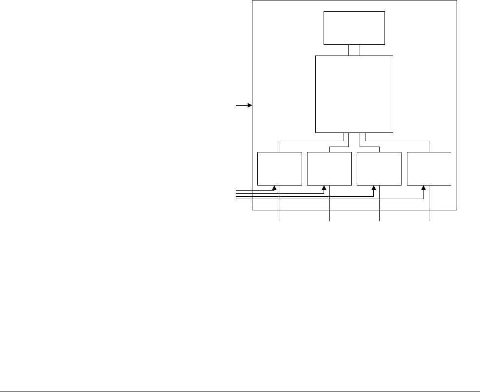
Clocking and Resets
ARM DDI 0301H Copyright © 2004-2009 ARM Limited. All rights reserved. 9-3
ID012310 Non-Confidential, Unrestricted Access
9.2 Clocking and resets with no IEM
This section describes clocking and resets for the processor with no IEM:
•Processor clocking with no IEM
•Reset with no IEM on page 9-4.
9.2.1 Processor clocking with no IEM
Externally to the processor, you must connect CLKIN and FREECLKIN together.
Logically, the processor has only one clock domain.
The four level two interfaces use dedicated clock enables ACLKENI, ACLKENRW,
ACLKENP, and ACLKEND.
The four clock inputs ACLKI, ACLKRW, ACLKP and ACLKD are not used and must be left
unconnected when you implement the processor.
The SYNCMODEREQ* and SYNCMODEACK* signals are not used and must be left
unconnected.
All clocks can be stopped indefinitely without loss of state.
Figure 9-1 shows the clocks for the processor with no IEM.
Figure 9-1 Processor clocks with no IEM
Read latency penalty with no IEM
The Nonsequential Noncacheable read-latency with zero-wait-state AXI is a six-cycle penalty
over a cache hit, where data is returned in the DC2 cycle, on the data side, and a five-cycle
penalty over a cache hit on the instruction side.
In the first cycle after the data cache miss, a read-after-write hazard check is performed against
the contents of the Write Buffer. This prevents stalling while waiting for the Write Buffer to
drain. Following that, a request is made to the AXI interface, and subsequently a transfer is
RAMs
Core
Instruction
level 2
interface
DMA level
2 interface
Clock enables
CLKIN
Data read/
write level
2 interface
Peripheral
level 2
interface
Level 2

Clocking and Resets
ARM DDI 0301H Copyright © 2004-2009 ARM Limited. All rights reserved. 9-4
ID012310 Non-Confidential, Unrestricted Access
started on the AXI. In the next cycle data is returned to the AXI interface, from where it is
returned first to the level one clock domain before being forwarded to the core. Figure 9-2 shows
this.
Figure 9-2 Read latency with no IEM
The same sequence appears on the I-Side, except that there is less to do in the equivalent RAW
cycle.
9.2.2 Reset with no IEM
The processor has the following reset inputs:
nRESETIN The nRESETIN signal is the main processor reset that initializes the
majority of the processor logic.
DBGnTRST The DBGnTRST signal is the DBGTAP reset.
nPORESETIN The nPORESETIN signal is the power-on reset that initializes the CP14
debug logic. See CP14 registers reset on page 13-25 for details.
nVFPRESETIN The nVFPRESETIN signal is the reset for the VFP block.
All of these are active LOW signals that reset logic in the processor.
The following reset signals are only used if IEM is implemented. Otherwise, these inputs are not
connected to any logic internally, and you must connect them according to your design rules:
•ARESETIn
•ARESETRWn
•ARESETPn
•ARESETDn.
DC1 DC2 RAW L2Req ARVALIDRW RDATARW Data to L1 Data to LSU
Fe1 Fe2 L2Req ARVALIDI RDATAI Data to L1 Data to PU

Clocking and Resets
ARM DDI 0301H Copyright © 2004-2009 ARM Limited. All rights reserved. 9-5
ID012310 Non-Confidential, Unrestricted Access
9.3 Clocking and resets with IEM
This section describes clocking and resets for the processor with IEM:
•Processor clocking with IEM
•Reset with IEM on page 9-8.
9.3.1 Processor clocking with IEM
Externally to the processor, you must connect CLKIN and FREECLKIN together.
It is possible to configure each of the four level two ports to instantiate an IEM register slice so
that the processor can have up to five clock domains, CLKIN, ACLKI, ACLKRW, ACLKP
and ACLKD. Because of the signals SYNCMODEREQI, SYNCMODEREQRW,
SYNCMODEREQP, SYNCMODEREQD, SYNCMODEACKI, SYNCMODEACKRW,
SYNCMODEACKP, and SYNCMODEACKD, it is possible to configure each IEM register
slice to operate synchronously or asynchronously.
The four level two interfaces and the VCore part of the IEM register slices use dedicated clock
enables, ACLKENI, ACLKENRW, ACLKENP, and ACLKEND.
If you configure an IEM register slice to operate asynchronously, its corresponding ACLKEN*
signal must be high. For example, when SYNCMODEACKI is low to indicate asynchronous
operation of the instruction port slice, the ACLKENI signal must be held high accordingly.
All clocks can be stopped indefinitely without loss of state.
Figure 9-3 on page 9-6 shows the clocks for the processor with IEM.
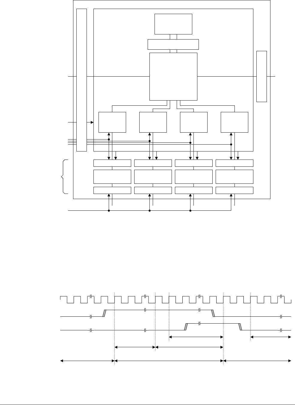
Clocking and Resets
ARM DDI 0301H Copyright © 2004-2009 ARM Limited. All rights reserved. 9-6
ID012310 Non-Confidential, Unrestricted Access
Figure 9-3 Processor clocks with IEM
Synchronization with IEM
When the core runs at maximum performance, the two clocks for the IEM Register Slice are
synchronous. At this point, when frequency and voltage changes have taken effect, the IEM
Register Slice can be bypassed. This removes all the latency that the synchronizers introduce.
The synchronization interface is a simple request and acknowledge system. Figure 9-4 shows
the processor synchronization with such a system.
Figure 9-4 Processor synchronization with IEM
RAMs
Level shift and clamp
Core
Instruction
level 2
interface
DMA level
2 interface
Level shift and clamp
Processor
Clock enables
CLKIN
ACLK clocks
VIC interface
Debug
interface
VCoreSliceI
Data read/
write level
2 interface
Peripheral
level 2
interface
Level shift and clamp
CLK
Level 2
Level shift and
clamp
VSoCSliceI
VCoreSliceRW
Level shift and
clamp
VSoCSliceRW
VCoreSliceD
Level shift and
clamp
VSoCSliceD
VCoreSliceP
Level shift and
clamp
VSoCSliceP
CLK CLK CLK
IEM
register
slices
Clock
SYNCMODEREQ
SYNCMODEACK
FIFO multiplexed out
FIFOs drain
Normal FIFO operation FIFOs closed to new data Normal FIFO operation
Synchronization
over
FIFOs all empty

Clocking and Resets
ARM DDI 0301H Copyright © 2004-2009 ARM Limited. All rights reserved. 9-7
ID012310 Non-Confidential, Unrestricted Access
When maximum performance is required, SYNCMODEREQ is asserted. When the IEM
register slice receives this signal it closes its FIFOs to new data, subject to the constraints
required by the AXI protocol, waits for the FIFOs to drain, and then switches the multiplexers
so that the AXI master and slave connect directly. The IEM register slice asserts
SYNCMODEACK to acknowledge the direct connection.
For reduced performance levels SYNCMODEREQ is deasserted, and the IEM register slice
switches the muxltiplexers and deasserts SYNCMODEACK when it has done so. The protocol
for these signals means that it is possible to connect different IEM register slices together. You
can connect SYNCMODEREQ to all the IEM register slices in parallel and AND together the
SYNCMODEACK outputs.
This means that the SYNCMODEACK signal only goes high when all the IEM register slices
have asserted their SYNCMODEACK signals. When coming out of bypass mode, all the IEM
registers slices take the same number of cycles, so the SYNCMODEACK signals all deassert
at the same time. Alternatively, if necessary, you can daisy chain the IEM register slices together,
so that each slice in the chain only closes its inputs when the previous slice has been multiplexed
out.
Read latency penalty for synchronous operation with IEM
When the IEM register slices are instantiated, but are synchronous because SYNCMODEREQ
is asserted, the read latency is the same as if the IEM register slices were not present. See Read
latency penalty with no IEM on page 9-3 and Figure 9-2 on page 9-4.
Read latency penalty for asynchronous operation with IEM
When the IEM register slices are instantiated and in asynchronous mode, data read or write
operations incur additional latency because of the synchronization required for the address and
the data between the core and the AXI system. The exact latency depends on:
• the clock ratios
• the clock alignments
• the latency of the AXI system.
On average, with zero-wait-state AXI the system incurs a penalty of 2.5 additional CLKIN
cycles and 4.5 additional ACLK cycles.
Figure 9-5 on page 9-8 shows the latency that the IEM register slices add in a system with
ACLK and CLKIN of the same frequency, but not synchronous. This example AXI system is
zero-wait-state.
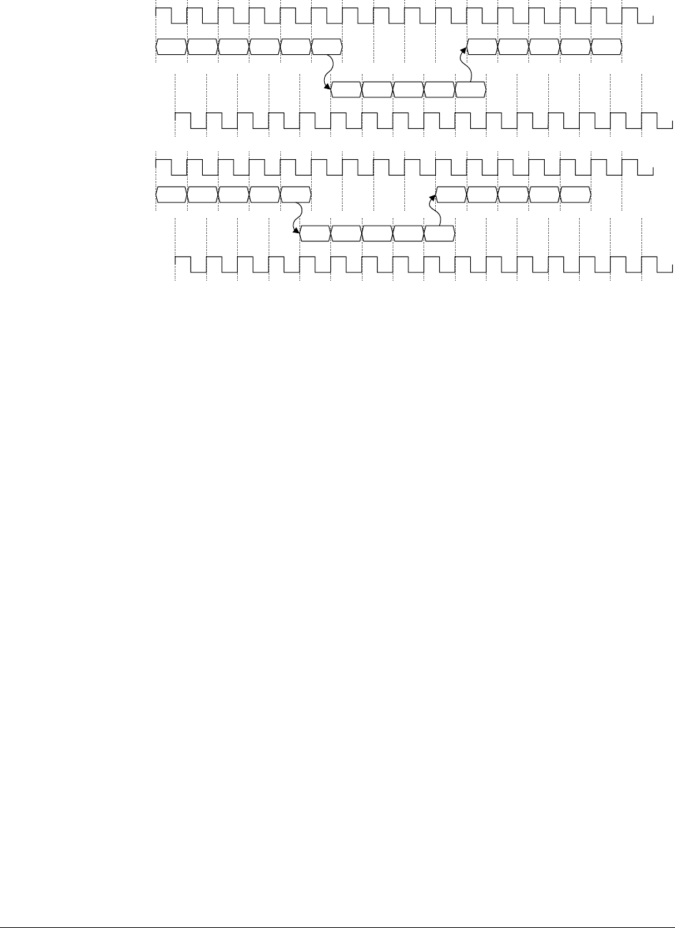
Clocking and Resets
ARM DDI 0301H Copyright © 2004-2009 ARM Limited. All rights reserved. 9-8
ID012310 Non-Confidential, Unrestricted Access
Figure 9-5 Read latency with IEM
The latency, from the pipeline cycles associated with cache reading DC1 and DC2 or Fe1 and
Fe2 to the level two AXI interfaces, is the same as that in Figure 9-2 on page 9-4. The level two
AXI interface, on the Core side of the IEM register slice, asserts ARVALIDRW or ARVALIDI
in cycle AVC. The IEM register slice must then synchronize the address to the ACLK clock
domain on the SoC side. The address is written into an address FIFO in cycle WPA. There are
then two synchronization cycles in the ACLK clock domain, SA1 and SA2, and a buffer cycle
before ARVALID is asserted on the SoC side of the IEM register slice in cycle AVS. Read data
returned from the AXI system in cycle RDS passes through the IEM register slice in a similar
way. In the ACLK clock domain, the data is written into a data FIFO in cycle WPD. The data
then synchronizes in the CLKIN clock domain, in cycles SD1 and SD2, and passes through a
buffer cycle before finally passing to the level two interfaces in cycle RDC. When the level two
interfaces of the core receive the data, they then pass it back to the LSU or PU in two cycles, see
Figure 9-2 on page 9-4.
Each of the IEM register slices, except the peripheral port slice, can store multiple items of read
and write data. This means that a burst of data can typically synchronize in fewer cycles than the
same number of individual data items. The number of cycles required to synchronize a burst of
data depends on:
• the length of the burst
• the ratio of the clock frequencies
• the clock that has the higher frequency
• the latency of the AXI system
• if the operation is a read or write.
9.3.2 Reset with IEM
The processor has the following reset inputs:
nRESETIN The nRESETIN signal is the main processor reset that initializes the
majority of the processor logic.
DBGnTRST The DBGnTRST signal is the DBGTAP reset.
nPORESETIN The nPORESETIN signal is the power-on reset that initializes the CP14
debug logic. See CP14 registers reset on page 13-25 for details.
DC1 DC2 RAW L2R AVC WPA
SA1 SA2 AVS RDS WPD
SD1 SD2 RDC L1 LSU
Fe1 Fe2 L2R AVC WPA
SA1 SA2 AVS RDS WPD
SD1 SD2 RDC L1 PU
CLKIN
ACLKRW
CLKIN
ACLKI
Core
SoC
Core
SoC

Clocking and Resets
ARM DDI 0301H Copyright © 2004-2009 ARM Limited. All rights reserved. 9-9
ID012310 Non-Confidential, Unrestricted Access
nVFPRESETIN The nVFPRESETIN signal is the reset for the VFP block.
ARESETIn, ARESETRWn, ARESETPn, ARESETDn
Reset signals for the SoC part of the IEM register slices.
All of these are active LOW signals that reset logic in the processor.
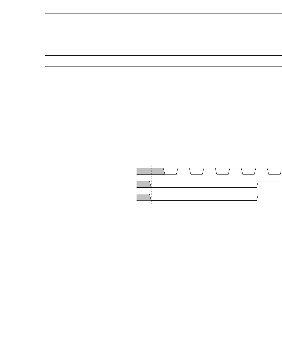
Clocking and Resets
ARM DDI 0301H Copyright © 2004-2009 ARM Limited. All rights reserved. 9-10
ID012310 Non-Confidential, Unrestricted Access
9.4 Reset modes
The reset signals present in the processor design enable you to reset different parts of the design
independently. Table 9-1 lists the reset signals, and the combinations and possible applications
that you can use them in.
If you do not use VFP shutdown for power saving, you can treat the nVFPRESETIN signal in
the same way as nRESETIN. For more information on power management and VFP, see VFP
shutdown on page 10-6.
9.4.1 Power-on reset
You must apply power-on or cold reset to the processor when power is first applied to the
system. In the case of power-on reset, the leading, falling, edge of the reset signals, nRESETIN
and nPORESETIN, does not have to be synchronous to CLKIN. Because the nRESETIN and
nPORESETIN signals are synchronized within the processor, you do not have to synchronize
these signals. Figure 9-6 shows the application of power-on reset.
Figure 9-6 Power-on reset
It is recommended that you assert the reset signals for at least three CLKIN cycles to ensure
correct reset behavior. Adopting a three-cycle reset eases the integration of other ARM parts into
the system, for example, ARM9TDMI-based designs.
It is not necessary to assert DBGnTRST on power-up.
9.4.2 CP14 debug logic
Because the nPORESETIN signal is synchronized within the processor, you do not have to
synchronize this signal.
Table 9-1 Reset modes
Reset mode nRESETIN DBGnTRST nPORESETIN Application
Power-on reset 0 x 0 Reset at power up, full system reset.
Hard reset or cold reset.
Processor reset 0 x 1 Reset of processor core only, watchdog
reset.
Soft reset or warm reset.
DBGTAP reset 1 0 1 Reset of DBGTAP logic.
Normal 1 x 1 No reset. Normal run mode.
CLKIN
nRESETIN
nPORESETIN

Clocking and Resets
ARM DDI 0301H Copyright © 2004-2009 ARM Limited. All rights reserved. 9-11
ID012310 Non-Confidential, Unrestricted Access
9.4.3 Processor reset
A processor or warm reset initializes the majority of the ARM1176JZF-S processor, excluding
the ARM1176JZF-S DBGTAP controller and the EmbeddedICE-RT logic. Processor reset is
typically used for resetting a system that has been operating for some time, for example,
watchdog reset.
Because the nRESETIN signal is synchronized within the processor, you do not have to
synchronize this signal.
9.4.4 DBGTAP reset
DBGTAP reset initializes the state of the processor DBGTAP controller. DBGTAP reset is
typically used by the RealView ICE module for hot connection of a debugger to a system.
DBGTAP reset enables initialization of the DBGTAP controller without affecting the normal
operation of the processor.
Because the DBGnTRST signal is synchronized within the processor, you do not have to
synchronize this signal.
9.4.5 Normal operation
During normal operation, neither processor reset nor power-on reset is asserted. If the DBGTAP
port is not being used, the value of DBGnTRST does not matter.

ARM DDI 0301H Copyright © 2004-2009 ARM Limited. All rights reserved. 10-1
ID012310 Non-Confidential, Unrestricted Access
Chapter 10
Power Control
This chapter describes the processor power control functions. It contains the following sections:
•About power control on page 10-2
•Power managemen t on page 10-3
•VFP shutdown on page 10-6
•Intelligent Energy Management on page 10-7.

Power Control
ARM DDI 0301H Copyright © 2004-2009 ARM Limited. All rights reserved. 10-2
ID012310 Non-Confidential, Unrestricted Access
10.1 About power control
The features of the processor that improve energy efficiency include:
• support for Intelligent Energy Management (IEM)
• accurate branch and return prediction, reducing the number of incorrect instruction fetch
and decode operations
• use of physically addressed caches to reduce the number of cache flushes and refills,
saving energy in the system
• the use of MicroTLBs reduces the power consumed in translation and protection look-ups
each cycle
• the caches use sequential access information to reduce the number of accesses to the
TagRAMs and to unwanted Data RAMs.
In the processor extensive use is also made of gated clocks and gates to disable inputs to unused
functional blocks. Only the logic actively in use to perform a calculation consumes any dynamic
power.

Power Control
ARM DDI 0301H Copyright © 2004-2009 ARM Limited. All rights reserved. 10-3
ID012310 Non-Confidential, Unrestricted Access
10.2 Power management
The processor supports these levels of power management:
•Run mode
•Standby mode
•Shutdown mode on page 10-4
• plus partial support for a fourth level, Dormant mode on page 10-4.
10.2.1 Run mode
Run mode is the normal mode of operation when all of the functionality of the core is available.
10.2.2 Standby mode
Standby mode disables most of the clocks of the device, while keeping the design powered up.
This reduces the power drawn to the static leakage current, plus a tiny clock power overhead
required to enable the device to wake up from the standby state.
The transition from Standby mode to Run mode is caused by the arrival of:
• an interrupt, whether masked or unmasked
• a debug request, only when debug is enabled
•a reset.
The debug request can be generated by an externally generated debug request, using the
EDBGRQ pin on the processor, or from a Debug Halt instruction issued to the processor
through the debug scan chains. Entry into Standby Mode is performed by executing the Wait For
Interrupt CP15 operation, see c7, Cache operations on page 3-69. To ensure that the memory
system is not affected by the entry into the Standby state, the following operations are
performed:
• A Data Synchronization Barrier operation ensures that all explicit memory accesses
occurring in program order before the Wait For Interrupt have completed. This avoids any
possible deadlocks that might be caused in a system where memory access triggers or
enables an interrupt that the core is waiting for. This might require some TLB page table
walks to take place as well.
• The DMA continues running during a Wait For Interrupt and any queued DMA operations
are executed as normal, before entering standby mode. This enables an application using
the DMA to set up the DMA to signal an interrupt when the DMA has completed, and then
for the application to issue a Wait For Interrupt operation. The degree of power-saving
while the DMA is running is less than in the case if the DMA is not running.
DMA can receive an AXI error response and generate an interrupt via
nDMAEXTERRIRQ to prevent entering Standby mode.
• Any other memory accesses that have been started at the time that the Wait For Interrupt
operation is executed are completed as normal. This ensures that the level two memory
system does not see any disruption caused by the Wait For Interrupt.
• The debug channel remains active throughout a Wait For Interrupt.
Systems using the VIC interface must ensure that the VIC is not masking any interrupts that are
required for restarting the processor when in this mode of operation.
After the processor clocks have been stopped the signal STANDBYWFI is asserted to indicate
that the processor is in Standby mode.

Power Control
ARM DDI 0301H Copyright © 2004-2009 ARM Limited. All rights reserved. 10-4
ID012310 Non-Confidential, Unrestricted Access
Note
The core clock does not stop when the core is prepared for debug activity, that is, when either
TCK or JTAGSYNCBYPASS is high.
10.2.3 Shutdown mode
Shutdown mode has the entire device powered down, and you must externally save all state,
including cache and TCM state. The processor is returned to Run mode by the assertion of
Reset. The state saving must be performed with interrupts disabled, and finish with a Data
Synchronization Barrier operation. When all the state of the processor is saved the processor
must execute a Wait For Interrupt operation. The signal STANDBYWFI is asserted to indicate
that the processor can enter Shutdown mode.
10.2.4 Dormant mode
Dormant mode enables the core to be powered down, leaving the caches and the
Tightly-Coupled Memory (TCM) powered up and maintaining their state.
The software visibility of the Cache Master Valid bits and the TLB lockdown entries is provided
to enable an implementation to be extended for Dormant mode.
The processor includes a placeholder that enables you to include the clamping logic necessary
for the full implementation of Dormant mode.
Considerations for Dormant mode
Dormant mode is only partially supported on the processor, because care is required in
implementing this on a standard synthesizable flow. The RAM blocks that are to remain
powered up must be implemented on a separate power domain, and there is a requirement to
clamp all of the inputs to the RAMs to a known logic level, with the chip enable being held
inactive. This clamping is not implemented in gates as part of the default synthesis flow because
it contributes to a critical path. The RAMCLAMP input is provided to drive this clamping.
Basic clamps are instantiated in the placeholder. They can be changed to explicit gates in the
RAM power domain, or pull-down transistors that clamp the values when the core is powered
down. For implementation details, see the ARM1176JZF-S and ARM1176JZ-S Implementation
Guide.
The RAM blocks that must remain powered up in Dormant mode, if it is implemented, are:
• all Data RAMs associated with the cache and tightly-coupled memories
• all TagRAMs associated with the cache
• all Valid RAMs and Dirty RAMs associated with the cache.
The states of the Branch Target Address Cache and the associative region of the TLB are not
maintained on entry into Dormant mode.
Implementations of the processor can optionally disable RAMs associated with the main TLB,
so that a trade-off can be made between Dormant mode leakage power and the recovery time.
Before entering Dormant mode, the state of the processor, excluding the contents of the RAMs
that remain powered up in dormant mode, must be saved to external memory. These state saving
operations must ensure that the following occur:
• All ARM registers, including CPSR and SPSR registers are saved.
• Any DMA operations in progress are stopped.

Power Control
ARM DDI 0301H Copyright © 2004-2009 ARM Limited. All rights reserved. 10-5
ID012310 Non-Confidential, Unrestricted Access
• All CP15 registers are saved, including the DMA state.
• All VFP registers are saved if the VFP contains defined state.
• Any locked entries in the main TLB are saved.
• All debug-related state are saved.
• The Master Valid bits for the cache are saved. These are accessed using CP15 register c15
as c15, Instruction Cache Master Valid Register on page 3-147 describes.
• A Data Synchronization Barrier operation is performed to ensure that all state saving has
been completed.
• A Wait For Interrupt CP15 operation is executed, enabling the signal STANDBYWFI to
indicate that the processor can enter Dormant mode.
• On entry into Dormant mode, the Reset signal to the processor must be asserted by the
external power control mechanism.
Transition from Dormant state to Run state is triggered by the external power controller
asserting Reset to the processor until the power to the processor is restored. When power has
been restored the core leaves reset and, by interrogating the external power controller, can
determine that the saved state must be restored.
10.2.5 Communication to the Power Management Controller
Your Power Management Controller in your system must perform the powering up and
powering down of the power domains of the processor. The Power Management Controller must
be a memory-mapped controller. The ARM1176JZF-S processor accesses this controller using
Strongly-Ordered accesses.
The STANDBYWFI signal can also be used to signal to the Power Management Controller that
the ARM1176JZF-S processor is ready to have its power state changed. STANDBYWFI is
asserted in response to a Wait For Interrupt operation.
Note
The Power Management Controller must not power down any of the processor power domains
unless STANDBYWFI is asserted.

Power Control
ARM DDI 0301H Copyright © 2004-2009 ARM Limited. All rights reserved. 10-6
ID012310 Non-Confidential, Unrestricted Access
10.3 VFP shutdown
The blocks in the top level of the ARM1176JZF-S are:
•
A1176RAM
, that includes all the RAMs
• when you have an IEM implementation:
— the four IEM register slices
— placeholders for level shifters and clamps between all the blocks
•
ARM1176JZFSNoRAM
, that includes all the remaining logic.
ARM1176JZFSNoRAM
contains:
• the VFP
• all other logic outside the VFP
• a placeholder for clamping logic between these two blocks.
With this hierarchy, you can switch off the VFP to save power, when the VFP is not in use.
There is a clamping placeholder between the VFP and the rest of the logic but this block is not
implemented in gates because it contributes to a critical path. You must add clamps to the
placeholder, either as explicit gates in the Core power domain, or as pull-down transistors that
clamp the values when the VFP is powered down.
To shutdown the VFP:
1. Save all VFP registers, if the VFP contains defined state.
2. Disable the VFP with the system control coprocessor, see c1, Coprocessor Access Control
Register on page 3-51.
3. Assert nVFPRESETIN LOW.
4. Assert VFPCLAMP HIGH.
5. Switch the VFP power off.
To take the VFP out of shutdown:
1. Switch the VFP power on.
2. When the power is stable, deassert VFPCLAMP.
3. Deassert nVFPRESETIN.
4. Enable the VFP with the system control coprocessor.
5. Restore the VFP registers, if required.

Power Control
ARM DDI 0301H Copyright © 2004-2009 ARM Limited. All rights reserved. 10-7
ID012310 Non-Confidential, Unrestricted Access
10.4 Intelligent Energy Management
This section describes the provision of IEM in the ARM1176JZF-S processors:
•Purpose of IEM
•Structure of IEM
•Operation of IEM on page 10-8
•Use of IEM on page 10-8
Note
The ARM1176JZF-S processor is IEM enabled but the level of support for the technology
depends on the specific implementation.
For information on clocks and resets with IEM, see Clocking and resets with IEM on page 9-5.
10.4.1 Purpose of IEM
The purpose of IEM technology is to provide a dynamic optimization between processor
performance and power consumption.
10.4.2 Structure of IEM
The ARM1176JZF-S processor provides a number of features that enable the processor voltage
to vary relative to the voltage of the rest of the system. For this purpose the processor optionally
implements:
• Placeholders for level shifters and clamps for some inputs and outputs including:
— the debug interface
— interrupt signals including the VIC interface
— resets
—clocks.
• IEM register slices for the AXI level two interfaces.
Note
The ETM and coprocessor interfaces do not implement level shifters or clamps.
Figure 10-1 on page 10-8 shows the basic structure for IEM in the processor.
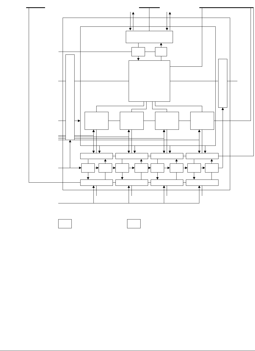
Power Control
ARM DDI 0301H Copyright © 2004-2009 ARM Limited. All rights reserved. 10-8
ID012310 Non-Confidential, Unrestricted Access
Figure 10-1 IEM structure
10.4.3 Operation of IEM
IEM balances performance and power consumption by dynamic alteration of the processor
clock frequency and supply voltage. CPUCLAMP is provided to control the clamp cells
between VCore and VSoc. Figure 10-1 shows this.
10.4.4 Use of IEM
To use IEM the processor must be implemented with appropriate register slices and included in
a SoC that contains an Intelligent Energy Controller (IEC™). For example systems, see the
Intelligent Energy Controller Technical Overview.
IEM is functionally transparent to the user.
RAMs
Core
Instruction
level 2
interface
DMA level
2 interface
Up level shift and clamp
Processor
Clock enables
CLKIN
ACLK clocks
VCoreSliceI
Data read/
write level
2 interface
Peripheral
level 2
interface
Down level shift and clamp
CLK
Level 2
VCoreSliceRW VCoreSliceD VCoreSliceP
CLK CLK CLK
VDD SoC VDD RAM VDD core
RAMCLAMP
VSoCSliceI VSoCSliceRW VSoCSliceD VSoCSliceP
Down Up
Up
CPUCLAMP DownUpDownUpDownUpDown
Test,
debug,
VIC,
and
other
outputs
Up DownUp level shifter and clamp Down level shifter and clamp
Test,
debug,
VIC, and
other
inputs
Coprocessor interface ETM interface

ARM DDI 0301H Copyright © 2004-2009 ARM Limited. All rights reserved. 11-1
ID012310 Non-Confidential, Unrestricted Access
Chapter 11
Coprocessor Interface
This chapter describes the coprocessor interface of the ARM1176JZF-S processor. It contains the
following sections:
•About the coprocessor interface on page 11-2
•Coprocessor pipeline on page 11-3
•Token queue management on page 11-9
•Token queues on page 11-12
•Data transfer on page 11-15
•Operations on page 11-19
•Multiple coprocessors on page 11-22.

Coprocessor Interface
ARM DDI 0301H Copyright © 2004-2009 ARM Limited. All rights reserved. 11-2
ID012310 Non-Confidential, Unrestricted Access
11.1 About the coprocessor interface
The processor supports the connection of on-chip coprocessors through an external coprocessor
interface. All types of coprocessor instruction are supported.
The ARM instruction set supports the connection of 16 coprocessors, numbered 0-15, to an
ARM processor. In the processor, the following coprocessor numbers are reserved:
CP10 VFP control
CP11 VFP control
CP14 Debug and ETM control
CP15 System control.
You can use CP0-9, CP12, and CP13 for your own external coprocessors.
The processor is designed to pass instructions to several coprocessors and exchange data with
them. These coprocessors are intended to run in step with the core and are pipelined in a similar
way to the core. Instructions are passed out of the Fetch stage of the core pipeline to the
coprocessor and decoded. The decoded instruction is passed down its own pipeline. Coprocessor
instructions can be canceled by the core if a condition code fails, or the entire coprocessor
pipeline can be flushed in the event of a mispredicted branch. Load and store data are also
required to pass between the core Logic Store Unit (LSU) and the coprocessor pipeline.
The coprocessor interface operates over a two-cycle delay. Any signal passing from the core to
the coprocessor, or from the coprocessor to the core, is given a whole clock cycle to propagate
from one to the other. This means that a signal crossing the interface is clocked out of a register
on one side of the interface and clocked directly into another register on the other side. No
combinatorial process must intervene. This constraint exists because the core and coprocessor
can be placed a considerable distance apart and generous timing margins are necessary to cover
signal propagation times. This delay in signal propagation makes it difficult to maintain pipeline
synchronization, ruling out a tightly-coupled synchronization method.
The processor implements a token-based pipeline synchronization method that enables some
slack between the two pipelines, while ensuring that the pipelines are correctly aligned for
crucial transfers of information.

Coprocessor Interface
ARM DDI 0301H Copyright © 2004-2009 ARM Limited. All rights reserved. 11-3
ID012310 Non-Confidential, Unrestricted Access
11.2 Coprocessor pipeline
The coprocessor interface achieves loose synchronization between the two pipelines by
exchanging tokens from one pipeline to the other. These tokens pass down queues between the
pipelines and can carry additional information. In most cases the primary purpose of the queue
is to carry information about the instruction being processed, or to inform one pipeline of events
occurring in the other.
Tokens are generated whenever a coprocessor instruction passes out of a pipeline stage
associated with a queue into the next stage. These tokens are picked up by the partner stage in
the other pipeline, and used to enable the corresponding instruction in that stage to move on. The
movement of coprocessor instructions down each pipeline is matched exactly by the movement
of tokens along the various queues that connect the pipelines.
If a pipeline stage has no associated queue, the instruction contained within it moves on in the
normal way. The coprocessor interface is data-driven rather than control-driven.
11.2.1 Coprocessor instructions
Each coprocessor might only execute a subset of all possible coprocessor instructions.
Coprocessors reject those instructions they cannot handle. Table 11-1 lists all the coprocessor
instructions supported by the processor and gives a brief description of each. For more details
of coprocessor instructions, see the ARM Architecture Reference Manual.
The coprocessor instructions fall into three groups:
• loads
•stores
• processing instructions.
The load and store instructions enable information to pass between the core and the coprocessor.
Some of them might be vectored. This enables several values to be transferred in a single
instruction. This typically involves the transfer of several words of data between a set of registers
in the coprocessor and a contiguous set of locations in memory.
Table 11-1 Coprocessor instructions
Instruction Data transfer Vectored Description
CDP None No Processes information already held within the coprocessor
MRC Store No Transfers information from the coprocessor to the core registers
MCR Load No Transfers information from the core registers to the coprocessor
MRRC Store No Transfers information from the coprocessor to a pair of registers in the
core
MCRR Load No Transfers information from a pair of registers in the core to the
coprocessor
STC Store Yes Transfers information from the coprocessor to memory and might be
iterated to transfer a vector
LDC Load Yes Transfers information from memory to the coprocessor and might be
iterated to transfer a vector

Coprocessor Interface
ARM DDI 0301H Copyright © 2004-2009 ARM Limited. All rights reserved. 11-4
ID012310 Non-Confidential, Unrestricted Access
Other instructions, for example MCR and MRC, transfer data between core and coprocessor
registers. The CDP instruction controls the execution of a specified operation on data already
held within the coprocessor, writing the result back into a coprocessor register, or changing the
state of the coprocessor in some other way. Opcode fields within the CDP instruction determine
the operation that is to be carried out.
The core pipeline handles both core and coprocessor instructions. The coprocessor, on the other
hand, only deals with coprocessor instructions, so the coprocessor pipeline is likely to be empty
for most of the time.
11.2.2 Coprocessor control
The coprocessor communicates with the core using several signals. Most of these signals control
the synchronizing queues that connect the coprocessor pipeline to the core pipeline. Table 11-2
lists the signals used for general coprocessor control.
11.2.3 Pipeline synchronization
Figure 11-1 on page 11-5 shows an outline of the core and coprocessor pipelines and the
synchronizing queues that communicate between them. Each queue is implemented as a very
short First In First Out (FIFO) buffer.
No explicit flow control is required for the queues, because the pipeline lengths between the
queues limits the number of items any queue can hold at any time. The geometry used means
that only three slots are required in each queue.
The only status information required is a flag to indicate when the queue is empty. This is
monitored by the receiving end of the queue, and determines if the associated pipeline stage can
move on. Any information that the queue carries can also be read and acted on at the same time.
Table 11-2 Coprocessor control signals
Signal Description
CLKIN This is the clock signal from the core.
nRESETIN This is the reset signal from the core.
ACPNUM[3:0] This is the fixed number assigned to the coprocessor, and is in the range 0-13. Coprocessor numbers
10, 11, 14, and 15 are reserved for system control coprocessors.
ACPENABLE When set, enables the coprocessor to respond to signals from the core.
ACPPRIV When asserted, indicates that the core is in privileged mode. This might affect the execution of certain
coprocessor instructions.
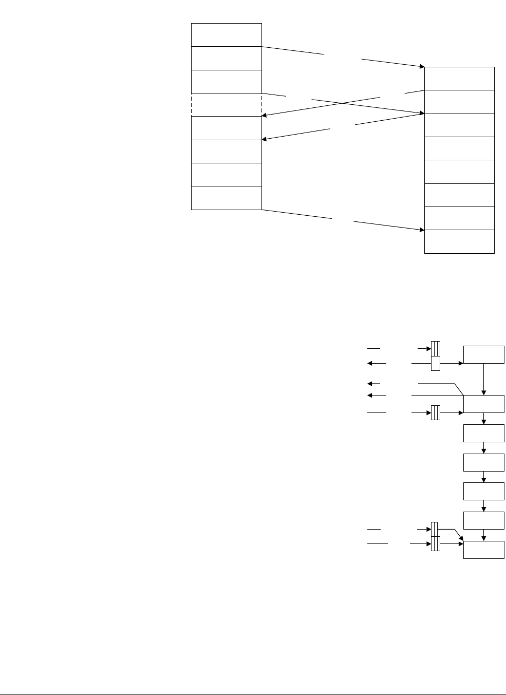
Coprocessor Interface
ARM DDI 0301H Copyright © 2004-2009 ARM Limited. All rights reserved. 11-5
ID012310 Non-Confidential, Unrestricted Access
Figure 11-1 Core and coprocessor pipelines
Figure 11-2 provides a more detailed picture of the pipeline and the queues maintained by the
coprocessor.
Figure 11-2 Coprocessor pipeline and queues
The instruction queue incorporates the instruction decoder and returns the length to the Ex1
stage of the core, using the length queue, that is maintained by the core. The coprocessor I stage
sends a token to the core Ex2 stage through the accept queue, that is also maintained by the core.
This token indicates to the core if the coprocessor is accepting the instruction in its I stage, or
bouncing it.
Fe2
Length
Core pipeline Coprocessor pipeline
De
Iss
Ex1
Ex2
Ex3
Wb
D
I
Ex1
Ex2
Ex3
Ex4
Ex5
Ex6
Instruction
Length
Cancel
Accept
Finish
I
Ex1
Ex2
Ex3
Ex4
Ex5
Ex6
Accept
Store data
D
Instruction
Length
Cancel
Load data
Finish
From core Fe2 stage
To core Fe1 stage
To LSU Add stage
From core Iss stage
To core Ex2 stage
From LSU Wbls stage
From core Wb stage
Decode stage
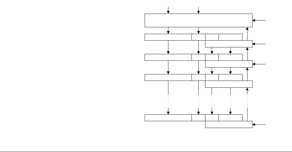
Coprocessor Interface
ARM DDI 0301H Copyright © 2004-2009 ARM Limited. All rights reserved. 11-6
ID012310 Non-Confidential, Unrestricted Access
The core can cancel an instruction currently in the coprocessor Ex1 stage by sending a signal
with the token passed down the cancel queue. When a coprocessor instruction reads the Ex6
stage it might retire. How it retires depends on the instruction:
• Load instructions retire when they find load data available in the load data queue, see
Loads on page 11-16
• Store instructions retire as soon as they leave the Ex1 stage, and are removed from the
pipeline, see Stores on page 11-17
• CDP instructions retire when they read a token passed by the core down the finish queue.
Figure 11-2 on page 11-5 shows how data transfer uses the load data and store data queues, and
Data transfer on page 11-15 explains this.
11.2.4 Pipeline control
The coprocessor pipeline is very similar to the core pipeline, but lacks the fetch stages.
Instructions are passed from the core directly into the Decode stage of the coprocessor pipeline,
that takes the form of a FIFO queue.
The Decode stage then decodes the instruction, rejecting non-coprocessor instructions and any
coprocessor instructions containing a nonmatching coprocessor number.
The length of any vectored data transfer is also decided at this point and sent back to the core.
The decoded instruction then passes into the issue (I) stage. This stage decides if this particular
instance of the instruction can be accepted. If it cannot, because it addresses a non-existent
register, the instruction is bounced, informing the core that it cannot be accepted.
If the instruction is both valid and executable, it then passes down the execution pipeline, Ex1
to Ex6. At the bottom of the pipeline, in Ex6, the instruction waits for retirement. It can do this
when it receives a matching token from another queue fed by the core.
Figure 11-3 shows the coprocessor pipeline, the main fields within each stage, and the main
control signals. Each stage controls the flow of information from the previous stage in the
pipeline by passing its Enable signal back. When a pipeline stage is not enabled, it cannot accept
information from the previous stage.
Figure 11-3 Coprocessor pipeline
Decoded instruction Tag Full Flags
I stage control
Decoded instruction Tag Full Flags
Ex1 stage control
Decoded instruction Tag Full Flags
Ex2 stage control
Decoded instruction Tag Full Flags
Ex6 stage control
Instruction queue and decoder
From core pipeline
I stage
Ex1 stage
Ex2 stage
Ex3 to Ex5 stages
(not shown)
Ex6 stage
Enable
Enable
Enable
Enable
Stall I
Stall Ex1
Stall Ex6
Stages Ex3 to Ex5 are same as stage Ex2
Stall D

Coprocessor Interface
ARM DDI 0301H Copyright © 2004-2009 ARM Limited. All rights reserved. 11-7
ID012310 Non-Confidential, Unrestricted Access
Each pipeline stage contains a decoded instruction, and a tag, plus a few status flags:
Full flag This flag is set whenever the pipeline stage contains an instruction.
Dead flag This flag is set to indicate that the instruction in the stage is a phantom. See
Cancel operations on page 11-19.
Tail flag This flag is set to indicate that the instruction is the tail of an iterated instruction.
See Loads on page 11-16.
There might also be other flags associated with the decoding of the instruction. Each stage is
controlled not only by its own state, but also by external signals and signals from the following
state, as follows:
Stall This signal prevents the stage from accepting a new instruction or passing its own
instruction on, and only affects the D, I, Ex1, and Ex6 stages.
Iterate This signal indicates that the instruction in the stage must be iterated to implement
a multiple load/store and only applies to the I stage.
Enable This signal indicates that the next stage in the pipeline is ready to accept data from
the current stage.
These signals are combined with the current state of the pipeline to determine if the stage can
accept new data, and what the new state of the stage is going to be. Table 11-3 lists how the new
state of the pipeline stage is derived.
The Enable input comes from the next stage in the pipeline and indicates if data can be passed
on. In general, if this signal is unasserted the pipeline stage cannot receive new data or pass on
its own contents. However, if the pipeline stage is empty it can receive new data without passing
any data on to the next stage. This is known as bubble closing, because it has the effect of filling
up empty stages in the pipeline by enabling them to move on while lower stages are stalled.
11.2.5 Instruction tagging
It is sometimes necessary for the core to be able to identify instructions in the coprocessor
pipeline. This is necessary for flushing, see Flush operations on page 11-19, so that the core can
indicate to the coprocessor the instructions that are to be flushed. The core therefore gives each
instruction sent to the coprocessor a tag, that is drawn from a pool of values large enough so that
all the tags in the pipeline at any moment are unique. Sixteen tags are sufficient to achieve this,
requiring a four-bit tag field. Each time a tag is assigned to an instruction, the tag number is
incremented modulo 16 to generate the next tag.
Table 11-3 Pipeline stage update
Stall Enable input Iterate State Enable To next stage Remarks
0 0 X Empty 1 None Bubble closing
0 0 X Full 0 - Stalled by next stage
0 1 0 Empty 1 None Normal pipeline movement
0 1 0 Full 1 Current Normal pipeline movement
0 1 1 Empty - - Impossible
0 1 1 Full 0 Current Iteration, I stage only
1 X X X 0 None Stalled, D, I, Ex1, and Ex6 only

Coprocessor Interface
ARM DDI 0301H Copyright © 2004-2009 ARM Limited. All rights reserved. 11-8
ID012310 Non-Confidential, Unrestricted Access
The flushing mechanism is simplified because successive coprocessor instructions have
contiguous tags. The core manages this by only incrementing the tag number when the
instruction passed to the coprocessor is a coprocessor instruction. This is done after sending the
instruction, so the tag changes after a coprocessor instruction is sent, rather than before. It is not
possible to increment the tag before sending the instruction because the core has not yet had time
to decode the instruction to determine what kind of instruction it is. When the coprocessor
Decode stage removes the non-coprocessor instructions, it is left with an instruction stream
carrying contiguous tags. The tags can also be used to verify that the sequence of tokens moving
down the queues matches the sequence of instructions moving down the core and coprocessor
pipelines.
11.2.6 Flush broadcast
If a branch has been mispredicted, it might be necessary for the core to flush both pipelines.
Because this action potentially affects the entire pipeline, it is not passed across in a queue but
is broadcast from the core to the coprocessor, subject to the same timing constraints as the
queues. When the flush signal is received by the coprocessor, it causes the pipeline and the
instruction queue to be cleared up to the instruction triggering the flush. This is explained in
more detail in Flush operations on page 11-19.
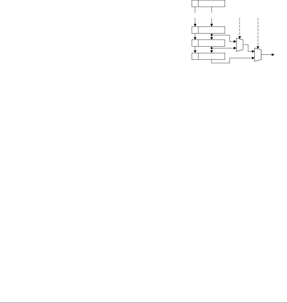
Coprocessor Interface
ARM DDI 0301H Copyright © 2004-2009 ARM Limited. All rights reserved. 11-9
ID012310 Non-Confidential, Unrestricted Access
11.3 Token queue management
The token queues, all of which are three slots long and function identically, are implemented as
short FIFOs. The following sections describe an example implementation of the queues:
•Queue implementation
•Queue modification
•Queue flushing on page 11-11.
11.3.1 Queue implementation
The queue FIFOs are implemented as three registers, with the current output selected by using
multiplexors. Figure 11-4 shows this arrangement.
Figure 11-4 Token queue buffers
The queue consists of three registers. Each of these is associated with a flag that indicates if the
register contains valid data. New data are moved into the queue by being written into buffer A
and continue to move along the queue if the next register is empty, or is about to become empty.
If the queue is full, the oldest data, and therefore the first to be read from the queue, occupies
buffer C and the newest occupies buffer A.
The multiplexors also select the current flag, that then indicates whether the selected output is
valid.
11.3.2 Queue modification
The queue is written to on each cycle. Buffer A accepts the data arriving at the interface, and the
buffer A flag accepts the valid bit associated with the data. If the queue is not full, this results in
no loss of data because the contents of buffer A are moved to buffer B during the same cycle.
If the queue is full, then the loading of buffer A is inhibited to prevent loss of data. In any case,
no valid data is presented by the interface when the queue is full, so no data loss ensues.
The state of the three buffer flags is used to decide the buffer that provides the queue output
during each cycle. The output is always provided by the buffer containing the oldest data. This
is buffer C if it is full, or buffer B or, if that is empty, buffer A.
Buffer AA
Buffer BB
Buffer CC
OutputV
Interconnect
Out
S1S0
0
1
0
1
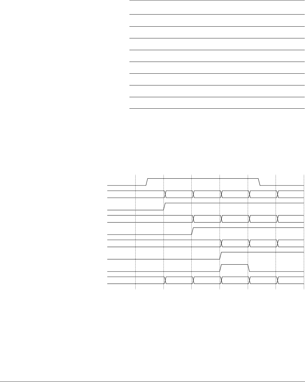
Coprocessor Interface
ARM DDI 0301H Copyright © 2004-2009 ARM Limited. All rights reserved. 11-10
ID012310 Non-Confidential, Unrestricted Access
A simple priority encoder, looking at the three flags, can supply the correct multiplexor select
signals. The state of the three flags can also determine how data are moved from one buffer to
another in the queue. Table 11-4 lists how the three flags are decoded.
New data can be moved into buffer A, provided the queue is not full, even if its flag is set,
because the current contents of buffer A are moved to buffer B. When the queue is read, the flag
associated with the buffer providing the information must be cleared. This operation can be
combined with an input operation so that the buffer is overwritten at the end of the cycle during
which it provides the queue output. This can be implemented by using the read enable signal to
mask the flag of the selected stage, making it available for input. Figure 11-5 shows reading and
writing a queue.
Figure 11-5 Queue reading and writing
Four valid inputs, labeled One, Two, Three, and Four, are written into the queue, and are clocked
into buffer A as they arrive. Figure 11-5 shows how these inputs are clocked from buffer to
buffer until the first input reaches buffer C. At this point a read from the queue is required.
Because buffer C is full, it is chosen to supply the data. Because it is being read, it is free to
accept more input, and so it receives the value Two from buffer B, that in turn receives the value
Three from buffer A. Because buffer A is being emptied by writing to buffer B, it can accept the
value Four from the input.
Table 11-4 Addressing of queue buffers
Flag C Flag B Flag A S1 S0 Remarks
000XXQueue is empty
00100B = A
01001C = B
01101C = B, B = A
1001X-
1011XB = A
1101X-
1111XQueue is full. Input inhibited
One Two Three Four
One Two Three
One Two
One One One Two
Buffer A
Flag A
Buffer B
Flag B
Buffer C
Flag C
Read queue
Output
Valid input
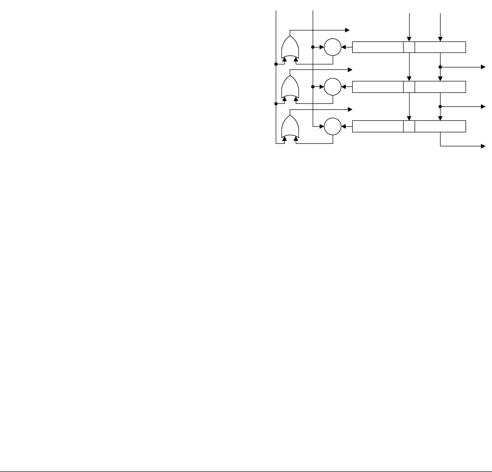
Coprocessor Interface
ARM DDI 0301H Copyright © 2004-2009 ARM Limited. All rights reserved. 11-11
ID012310 Non-Confidential, Unrestricted Access
11.3.3 Queue flushing
When the coprocessor pipeline is flushed, in response to a command from the core, some of the
queues might also require flushing. There are two possible ways of flushing the queue:
• the entire queue is cleared
• the queue is flushed from a selected buffer, along with all data in the queue newer than the
data in the selected buffer.
The method used depends on the point when flushing begins in the coprocessor pipeline. See
Flush operations on page 11-19 for more details. A flush command has associated with it a tag
value that indicates where the queue flushing starts. This is matched with the tag carried by
every instruction.
If the queue is to be flushed from a selected buffer, the buffer is chosen by looking for a matching
tag. When this is found, the flag associated with that buffer is cleared, and every flag newer than
the selected one is also cleared. Figure 11-6 shows queue flushing.
Figure 11-6 Queue flushing
Each buffer in the queue has a tag comparator associated with it. The flush tag is presented to
each comparator, to be compared with the tag belonging to each valid instruction held in the
queue. The flush tag is compared with each tag in the queue. If the flush tag is the same as, or
older than, any tag then that queue entry has its Full flag cleared. This indicates that it is empty.
A less-than-or-equal-to comparison is used to identify tags that are to be flushed. If a tag in the
pipeline later than the queue matches, the Flush all signal is asserted to clear the entire queue.
<= Tag A ABuffer A
<= Tag A ABuffer A
<= Tag A ABuffer A
Clear B
Clear C
Clear A
Flush tagFlush all
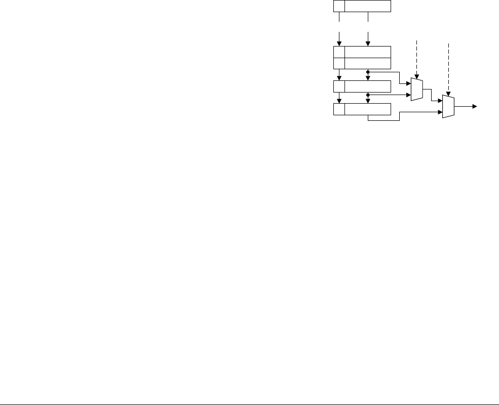
Coprocessor Interface
ARM DDI 0301H Copyright © 2004-2009 ARM Limited. All rights reserved. 11-12
ID012310 Non-Confidential, Unrestricted Access
11.4 Token queues
The following sections describe each of the synchronizing queues:
•Instruction queue
•Length queue on page 11-13
•Accept queue on page 11-13
•Cancel queue on page 11-14
•Finish queue on page 11-14.
11.4.1 Instruction queue
The core passes every instruction fetched from memory across the coprocessor interface, where
it enters the instruction queue. Ideally it only passes on the coprocessor instructions, but has not,
at this stage, had time to decode the instruction.
The coprocessor decodes the instruction on arrival in its own Decode stage and rejects the
non-coprocessor instructions. The core does not require any acknowledgement of the removal
of these instructions because each instruction type is determined within the coprocessors
Decode stage. This means that the instruction received from the core must be decoded as soon
as it enters the instruction queue. The instruction queue is a modified version of the standard
queue, that incorporates an instruction decoder. Figure 11-7 shows an instruction queue
implementation.
Figure 11-7 Instruction queue
The decoder decodes the instruction written into buffer A as soon as it arrives. The subsequent
buffers, B and C, receive the decoded version of the instruction in buffer A.
The A flag now indicates that the data in buffer A are valid and represent a coprocessor
instruction. This means that non-coprocessor or unrecognized instructions are immediately
dropped from the instruction queue and are never passed on.
The coprocessor must also compare the coprocessor number field in a coprocessor instruction
and compare it with its own number, given by ACPNUM. If the number does not match, the
instruction is invalid. The instruction queue provides an interface to the core through the
following signals, that the core drives:
ACPINSTRV This signal is asserted when valid data are available from the core. It must
be clocked directly into the buffer A flag, unless the queue is full, when
case it is ignored.
ACPINSTR[31:0] This is the instruction being passed to the coprocessor from the core, and
must be clocked into buffer A.
ACPINSTRT[3:0] This is the flush tag associated with the instruction in ACPINSTR, and
must be clocked into the tag associated with buffer A.
Buffer A
Buffer BB
Buffer CC
OutputV
Interconnect
Out
S1S0
0
1
0
1
DecoderA

Coprocessor Interface
ARM DDI 0301H Copyright © 2004-2009 ARM Limited. All rights reserved. 11-13
ID012310 Non-Confidential, Unrestricted Access
The instruction queue feeds the issue stage of the coprocessor pipeline, providing a new input
to the pipeline, in the form of a decoded instruction and its associated tag, whenever the queue
is not empty.
11.4.2 Length queue
When a coprocessor has decoded an instruction it knows how long a vectored load/store
operation is. This information is sent with the synchronizing token down the length queue, as
the relevant instruction leaves the instruction queue to enter the issue stage of the pipeline. The
length queue is maintained by the core and the coprocessor communicates with the queue using
the following signals:
CPALENGTH[3:0]
This is the length of a vectored data transfer to or from the coprocessor. It is
determined by the decoder in the instruction queue and asserted as the decoded
instruction moves into the issue stage. If the current instruction does not represent
a vectored data transfer, the length value is set to zero.
CPALENGTHT[3:0]
This is the tag associated with the instruction leaving the instruction queue, and
is copied from the queue buffer supplying the instruction.
CPALENGTHHOLD
This is deasserted when the instruction queue is providing valid information to the
core length queue. Otherwise, the signal is asserted to indicate that no valid data
are available.
11.4.3 Accept queue
The coprocessor must decide in the issue stage if it can accept an otherwise valid coprocessor
instruction. It passes this information with the synchronizing token down the accept queue, as
the relevant instruction passes from the issue stage to Ex1.
If an instruction cannot be accepted by the coprocessor it is said to have been bounced. If the
coprocessor bounces an instruction it does not remove the instruction from its pipeline, but
converts it to a phantom. This is explained in more detail in Bounce operations on page 11-19.
The accept queue is maintained by the core and the coprocessor communicates with the queue
using the following signals, that are all driven by the coprocessor:
CPAACCEPT
This is set to indicate that the instruction leaving the coprocessor issue stage has
been accepted.
CPAACCEPTT[3:0]
This is the tag associated with the instruction leaving the issue stage.
CPAACCEPTHOLD
This is deasserted when the issue stage is passing an instruction on to the Ex1
stage, whether it has been accepted or not. Otherwise, the signal is asserted to
indicate that no valid data are available.

Coprocessor Interface
ARM DDI 0301H Copyright © 2004-2009 ARM Limited. All rights reserved. 11-14
ID012310 Non-Confidential, Unrestricted Access
11.4.4 Cancel queue
The core might want to cancel an instruction that it has already passed on to the coprocessor.
This can happen if the instruction fails its condition codes, that requires the instruction to be
removed from the instruction stream in both the core and the coprocessor.
The queue, a standard queue, as Token queue management on page 11-9 describes, is maintained
by the coprocessor and is read by the coprocessor Ex1 stage.
The cancel queue provides an interface to the core through the following signals, that are all
driven by the core:
ACPCANCELV
This signal is asserted when valid data are available from the core. It must be
clocked directly into the buffer A flag, unless the queue is full, when it is ignored.
ACPCANCEL
This is the cancel command being passed to the coprocessor from the core, and
must be clocked into buffer A.
ACPCANCELT[3:0]
This is the flush tag associated with the cancel command, and must be clocked
into the tag associated with buffer A.
The coprocessor Ex1 stage reads the cancel queue, that then acts on the value of the queued
ACPCANCEL signal by removing the instruction from the Ex1 stage if the signal is set, and
not passing it on to the Ex2 stage.
11.4.5 Finish queue
The finish queue maintains synchronism at the end of the pipeline by providing permission for
CDP instructions in the coprocessor pipeline to retire. The queue, a standard queue, as Token
queue management on page 11-9 describes, is maintained by the coprocessor and is read by the
coprocessor Ex6 stage.
The finish queue provides an interface to the core using the ACPFINISHV signal, that the core
drives.
This signal is asserted to indicate that the instruction in the coprocessor Ex6 stage can retire. It
must be clocked directly into the buffer A flag, unless the queue is full, when it is ignored.
The finish queue is read by the coprocessor Ex6 stage. It can retire a CDP instruction if the finish
queue is not empty.
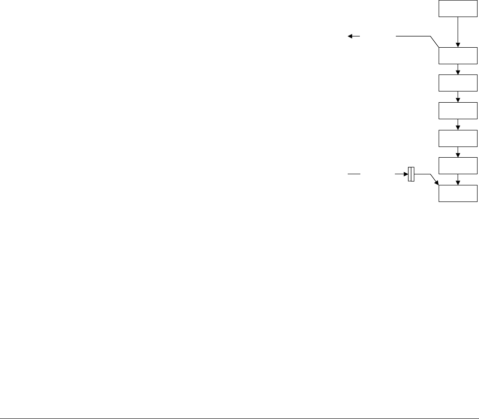
Coprocessor Interface
ARM DDI 0301H Copyright © 2004-2009 ARM Limited. All rights reserved. 11-15
ID012310 Non-Confidential, Unrestricted Access
11.5 Data transfer
Data transfers are managed by the LSU on the core side, and the pipeline itself on the
coprocessor side. Transfers can be a single value or a vector. In the latter case, the coprocessor
effectively converts a multiple transfer into a series of single transfers by iterating the instruction
in the issue stage. This creates an instance of the load/store instruction for each item to be
transferred.
The instruction stays in the coprocessor issue stage while it iterates, creating copies of itself that
move down the pipeline. Figure 11-9 on page 11-16 illustrates this process for a load
instruction.
The first of the iterated instructions, shown in uppercase, is the head and the others, shown in
lowercase, are the tails. In the example shown the vector length is four so there is one head and
three tails. At the first iteration of the instruction, the tail flag is set so that subsequent iterations
send tail instructions down the pipeline. In the example shown in Figure 11-9 on page 11-16,
instruction B has stalled in the Ex1 stage, that might be caused by the cancel queue being empty,
so that instruction C does not iterate during its first cycle in the issue stage, but only starts to
iterate after the stall has been removed.
Figure 11-8 shows the extra paths required for passing data to and from the coprocessor.
Figure 11-8 Coprocessor data transfer
Two data paths are required:
• One passes store data from the coprocessor to the core, and this requires a queue, that is
maintained by the core.
• The other passes load data from the core to the coprocessor and requires no queue, only
two pipeline registers.
Figure 11-9 on page 11-16 shows instruction iteration for loads.
I
Ex1
Ex2
Ex3
Ex4
Ex5
Ex6
Store data
Load data
To LSU Add stage
From LSU Wbls stage

Coprocessor Interface
ARM DDI 0301H Copyright © 2004-2009 ARM Limited. All rights reserved. 11-16
ID012310 Non-Confidential, Unrestricted Access
Figure 11-9 Instruction iteration for loads
Only the head instruction is involved in token exchange with the core pipeline, that does not
iterate instructions in this way, the tail instructions passing down the pipeline silently.
When an iterated load/store instruction is cancelled or flushed, all the tail instructions, bearing
the same tag, must be removed from the pipeline. Only the head instruction becomes a phantom
when cancelled. Any tail instruction can be left intact in the pipeline because it has no other
effect.
Because the cancel token is received in the coprocessor Ex1 stage, a cancelled iterated
instruction always consists of a head instruction in Ex1 and a single tail instruction in the issue
stage.
11.5.1 Loads
Load data emerge from the WBls stage of the core LSU and are received by the coprocessor Ex6
stage. Each item in a vectored load is picked up by one instance of the iterated load instruction.
The pipeline timing means that a load instruction is always ready, or arrived a short time ago, in
Ex6 to pick up each data item. If a load instruction has arrived in Ex6, but the load information
has not yet appeared, the load instruction must stall in Ex6, stalling the rest of the coprocessor
pipeline.
The following signals are driven by the core to pass load data across to the coprocessor:
ACPLDVALID
This signal, when set, indicates that the associated data are valid.
ACPLDDATA[63:0]
This is the information passed from the core to the coprocessor.
Load buffers
To achieve correct alignment of the load data with the load instruction in the coprocessor Ex6
stage, the data must be double buffered when they arrive at the coprocessor. Figure 11-10 on
page 11-17 shows an example.
[C]BA C c c c D
[B]A B C c c c D
A B C c c c D
A B C c c c D
A B C c c c D
A B C c c c D
A B C c c c D
I
Ex1
Ex2
Ex3
Ex4
Ex5
Ex6
1234567891011121314Time

Coprocessor Interface
ARM DDI 0301H Copyright © 2004-2009 ARM Limited. All rights reserved. 11-17
ID012310 Non-Confidential, Unrestricted Access
Figure 11-10 Load data buffering
The load data buffers function as pipeline registers and so require no flow control and are not
required to carry any tags. Only the data and a valid bit are required. For load transfers to work:
• instructions must always arrive in the coprocessor Ex6 stage coincident with, or before,
the arrival of the corresponding instruction in the core WBls stage
• finish tokens from the core must arrive at the same time as the corresponding load data
items arrive at the end of the load data pipeline buffers
• the LSU must see the token from the accept queue before it enables a load instruction to
move on from its Add stage.
Loads and flushes
If a flush does not involve the core WBls stage it cannot affect the load data buffers, and the load
transfer completes normally. If a flush is initiated by an instruction in the core WBls stage, this
is not a load instruction because load instructions cannot trigger a flush. Any coprocessor load
instructions behind the flush point find themselves stalled if they get as far as the Ex6 stage, for
the lack of a finish token, so no data transfers can have taken place. Any data in the load data
buffers expires naturally during the flush dead period while the pipeline reloads.
Loads and cancels
If a load instruction is canceled both the head and any tails must be removed. Because the
cancellation happens in the coprocessor Ex1 stage, no data transfers can have taken place and
therefore no special measures are required to deal with load data.
Loads and retirement
When a load instruction reaches the bottom of the coprocessor pipeline it must find a data item
at the end of the load data buffer. This applies to both head and tail instructions. Load
instructions do not use finish queue.
11.5.2 Stores
Store data emerge from the coprocessor issue stage and are received by the core LSU DC1 stage.
Each item of a vectored store is generated because the store instruction iterates in the
coprocessor issue stage. The iterated store instructions then pass down the pipeline but have no
other use, except to act as place markers for flushes and cancels.
Interconnect
InterconnectValid
Data
Valid
Data
WBls Ex6
Core Coprocessor

Coprocessor Interface
ARM DDI 0301H Copyright © 2004-2009 ARM Limited. All rights reserved. 11-18
ID012310 Non-Confidential, Unrestricted Access
The following signals control the transfer of store data across the coprocessor interface:
CPASTDATAV
This signal is asserted when valid data is available from the coprocessor.
CPASTDATAT[3:0]
This is the tag associated with the data being passed to the core.
CPASTDATA[63:0]
This is the information passed from the coprocessor to the core.
ACPSTSTOP
This signal from the core prevents additional transfers from the coprocessor to the
core, and is raised when the store queue, maintained by the core, can no longer
accept any more data. When the signal is deasserted, data transfers can resume.
When ACPSTSTOP is asserted, the data previously placed onto CPASTDATA
must be left there, until new data can be transferred. This enables the core to leave
data on CPASTDATA until there is sufficient space in the store data queue.
Store data queue
Because the store data transfer can be stopped at any time by the LSU, a store data queue is
required. Additionally, because store data vectors can be of arbitrary length, flow control is
required. A queue length of three slots is sufficient to enable flow control to be used without loss
of data.
Stores and flushes
When a store instruction is involved in a flush, the store data queue must be flushed by the core.
Because the queue continues to fill for two cycles after the core notifies the coprocessor of the
flush, because of the signal propagation delay, the core must delay for two cycles before
carrying out the store data queue flush. The dead period after the flush extends sufficiently far
to enable this to be done.
Stores and cancels
If the core cancels a store instruction, the coprocessor must ensure that it sends no store data for
that instruction. It can achieve this by either:
• delaying the start of the store data until the corresponding cancel token has been received
in the Ex1 stage
• looking ahead into the cancel queue and start the store data transfer when the correct token
is seen.
Stores and retirement
Because store instructions do not use the finish token queue they are retired as soon as they leave
the Ex1 stage of the pipeline.

Coprocessor Interface
ARM DDI 0301H Copyright © 2004-2009 ARM Limited. All rights reserved. 11-19
ID012310 Non-Confidential, Unrestricted Access
11.6 Operations
This section describes the various operations that can be performed and events that can take
place.
11.6.1 Normal operation
In normal operation the core passes all instructions across to the coprocessor, and then
increments the tag if the instruction was a coprocessor instruction. The coprocessor decodes the
instruction and throws it away if it is not a coprocessor instruction or if it contains the wrong
coprocessor number.
Each coprocessor instruction then passes down the pipeline, sending a token down the length
queue as it moves into the issue stage. The instruction then moves into the Ex1 stage, sending a
token down the accept queue, and remains there until it has received a token from the cancel
queue.
If the cancel token does not request that the instruction is cancelled, and is not a Store
instruction, it moves on to the Ex2 stage. The instruction then moves down the pipeline until it
reaches the Ex6 stage. At this point, it waits to receive a token from the finish queue, that enables
it to retire, unless it is either:
• a store instruction, where it requires no token from the finish queue
• a load instruction, where it must wait until load data are available.
Store instruction are removed from the pipeline as soon as they leave the Ex1 stage.
11.6.2 Cancel operations
When the coprocessor instruction reaches the Ex1 stage it looks for a token in the cancel queue.
If the token indicates that the instruction is to be cancelled, it is removed from the pipeline and
does not pass to Ex2. Any tail instruction in the I stage is also removed.
11.6.3 Bounce operations
The coprocessor can reject an instruction by bouncing it when it reaches the issue stage. This
can happen to an instruction that has been accepted as a valid coprocessor instruction by the
decoder, but that is found to be unexecutable by the issue stage, perhaps because it refers to a
non-existent register or operation.
When the bounced instruction leaves the issue stage to move into Ex1, the token sent down the
accept queue has its bounce bit set. This causes the instruction to be removed from the core
pipeline.
When the instruction moves into Ex1 it has its dead bit set, turning it into a phantom. This
enables the instruction to remain in the pipeline to match tokens in the cancel queue.
The core posts a token for the bounced instruction before the coprocessor can bounce it, so the
phantom is required to pick up the token for the bounced instruction. The instruction is
otherwise inert, and has no other effect. The core might already have decided to cancel the
instruction being bounced. In this case, the cancel token causes the phantom to be removed from
the pipeline. If the core does not cancel the phantom it continues to the bottom of the pipeline.
11.6.4 Flush operations
A flush can be triggered by the core in any stage from issue to WBls inclusive. When this
happens a broadcast signal is received by the coprocessor, passing it the tag associated with the
instruction triggering the flush.

Coprocessor Interface
ARM DDI 0301H Copyright © 2004-2009 ARM Limited. All rights reserved. 11-20
ID012310 Non-Confidential, Unrestricted Access
Because the tag is changed by the core after each new coprocessor instruction, the tag matches
the first coprocessor instruction following the instruction causing the flush. The coprocessor
must then find the first instruction that has a matching tag, working from the bottom of the
pipeline upwards, and remove all instructions from that point upwards.
Unlike tokens passing down a queue, a flush signal has a fixed delay so that the timing
relationship between a flush in the core and a flush in the coprocessor is known precisely. Most
of the token queues also require flushing and this can also be done using the tags attached to
each instruction. If a match has been found before the stage at the receiving end of a token queue
is passed, then the token queue is cleared.
Otherwise, it must be properly flushed by matching the tags in the queue. This operation must
be performed on all the queues except the finish queue, that is updated in the normal way.
Therefore, the coprocessor must flush the instruction and cancel queues. The flushing operation
can be carried out by the coprocessor as soon as the flush signal is received. The flushing
operation is simplified because the instruction and cancel queues cannot be performing any
other operation. This means that flushing is not required to be combined with queue updates for
these queues.
There is a single cycle following a flush where nothing happens that affects the flushed queues,
and this provides a good opportunity to carry out the queue flushing operation.
The following signals provide the flush broadcast signal from the core:
ACPFLUSH
This signal is asserted when a flush is to be performed.
ACPFLUSHT[3:0]
This is the tag associated with the first instruction to be flushed.
11.6.5 Retirement operations
When an instruction reaches the bottom of the coprocessor pipeline it is retired. How it retires
depends on the kind of instruction it is and if it is iterated, as Table 11-5 lists.
Table 11-5 lists the conditions for each coprocessor instruction:
• all store instructions retire unconditionally on leaving Ex1 because no token is required in
the finish queue
• CDP instructions require a token in the finish queue
Table 11-5 Retirement conditions
Instruction Typ
eRetirement conditions
CDP - Must find a token in the finish queue.
MRC Store No conditions. Immediate retirement on leaving Ex1.
MCR Load All load instructions must find data in the load data pipeline from the core.
MRRC Store No conditions. Immediate retirement on leaving Ex1.
MCRR Load All load instructions must find data in the load data pipeline from the core.
STC Store No conditions. Immediate retirement on leaving Ex1.
LDC Load Must find data in the load data pipeline from the core.

Coprocessor Interface
ARM DDI 0301H Copyright © 2004-2009 ARM Limited. All rights reserved. 11-21
ID012310 Non-Confidential, Unrestricted Access
• all load instructions must pick up data from the load pipeline
• phantom load instructions retire unconditionally.

Coprocessor Interface
ARM DDI 0301H Copyright © 2004-2009 ARM Limited. All rights reserved. 11-22
ID012310 Non-Confidential, Unrestricted Access
11.7 Multiple coprocessors
There might be more than one coprocessor attached to the core, and so some means is required
for dealing with multiple coprocessors. It is important, for reasons of economy, to ensure that as
little of the coprocessor interface is duplicated. In particular, the coprocessors must share the
length, accept, and store data queues, that the core maintains.
If these queues are to be shared, only one coprocessor can use the queues at any time. This is
achieved by enabling only one coprocessor to be active at any time. This is not a serious
limitation because only one coprocessor is in use at any time.
Typically, a processor is driven through driver software, that drives only one coprocessor. Calls
to the driver software, and returns from it, ensure that there are several core instructions between
the use of one coprocessor and the use of a different coprocessor.
11.7.1 Interconnect considerations
If only one coprocessor is permitted to communicate with the core at any time, all coprocessors
can share the coprocessor interface signals from the core. Signals from the coprocessors to the
core can be ORed together, provided that every coprocessor holds its outputs to zero when it is
inactive.
11.7.2 Coprocessor selection
Coprocessors are enabled by a signal ACPENABLE from the core. There are 12 of these
signals, one for each coprocessor. Only one can be active at any time. In addition, instructions
to the coprocessor include the coprocessor number, enabling coprocessors to reject instructions
that do not match their own number. Core instructions are also rejected.
11.7.3 Coprocessor switching
When the core decodes a coprocessor instruction destined for a different coprocessor to that last
addressed, it stalls this instruction until the previous coprocessor instruction has been retired.
This ensures that all activity in the currently selected coprocessor has ceased.
The coprocessor selection is switched, disabling the last active coprocessor and activating the
new coprocessor. The coprocessor that received the new coprocessor instruction must have
ignored it, being disabled. Therefore, the instruction is resent by the core, and is now accepted
by the newly activated coprocessor.
A coprocessor is disabled by the core by setting ACPENABLE LOW for the selected
coprocessor. The coprocessor responds by ceasing all activity and setting all its output signals
LOW.
When the coprocessor is enabled, signaled by setting ACPENABLE HIGH, it must
immediately set the signals CPALENGTHHOLD and CPAACCEPTHOLD HIGH, and
CPASTDATAV LOW, because the pipeline is empty at this point. The coprocessor can then
start normal operation.

ARM DDI 0301H Copyright © 2004-2009 ARM Limited. All rights reserved. 12-1
ID012310 Non-Confidential, Unrestricted Access
Chapter 12
Vectored Interrupt Controller Port
This chapter describes the vectored interrupt controller port of the processor. It contains the
following sections:
•About the PL192 Vectored Interrupt Controller on page 12-2
•About the processor VIC port on page 12-3
•Timing of the VIC port on page 12-5
•Interrupt entry flowchart on page 12-7.

Vectored Interrupt Controller Port
ARM DDI 0301H Copyright © 2004-2009 ARM Limited. All rights reserved. 12-2
ID012310 Non-Confidential, Unrestricted Access
12.1 About the PL192 Vectored Interrupt Controller
An interrupt controller is a peripheral that is used to handle multiple interrupt sources. Features
usually found in an interrupt controller are:
• multiple interrupt request inputs, one for each interrupt source, and one interrupt request
output for the processor interrupt request input
• software can mask out particular interrupt requests
• prioritization of interrupt sources for interrupt nesting.
In a system with an interrupt controller having the above features, software is still required to:
• determine the interrupt source that is requesting service
• determine where the service routine for that interrupt source is loaded.
A Vectored Interrupt Controller (VIC) does both things in hardware. It supplies the starting
address, vector address, of the service routine corresponding to the highest priority requesting
interrupt source. The PL192 VIC is an Advanced Microcontroller Bus Architecture (AMBA)
Advanced High-performance Bus (AHB) compliant, System-on-Chip (SoC) peripheral that is
developed, tested, and licensed by ARM Limited.
The processor VIC port and the Peripheral Interface enable you to connect a PL192 VIC to the
processor. See ARM PrimeCell Vectored Interrupt Controller (PL192) Technical Reference
Manual for more details.

Vectored Interrupt Controller Port
ARM DDI 0301H Copyright © 2004-2009 ARM Limited. All rights reserved. 12-3
ID012310 Non-Confidential, Unrestricted Access
12.2 About the processor VIC port
Figure 12-1 shows the VIC port and the Peripheral Interface connecting a PL192 VIC and the
processor.
Figure 12-1 Connection of a VIC to the processor
Note
Do not be confused by the naming of the IRQADDRVSYNCEN and nVICSYNCEN signals.
Although one is active HIGH and the other is active LOW they are connected to a common
external synchronization disable signal. See the signal descriptions in Table 12-1 for more
information.
The VIC port enables the processor to read the vector address as part of the IRQ interrupt entry.
That is, the processor takes a vector address from this interface instead of using the legacy
0x00000018
or
0xFFFF0018
.The VIC port does not support the reading of FIQ vector addresses.
The interrupt interface is designed to handle interrupts asserted by a controller that is clocked
either synchronously or asynchronously to the processor clock. This capability ensures that the
controller can be used in systems that have either a synchronous or asynchronous interface
between the core clock and the AXI clock.
The VIC port consists of the signals that Table 12-1 lists.
IRQACK is driven by the processor to indicate to an external VIC that the processor wants to
read the IRQADDR input.
nFIQ
nIRQ
IRQADDRV
IRQADDR[31:2] VICVECTADDROUT[31:2]
VICIRQADDRV
VICIRQACK
nVICIRQ
nVICFIQ
VIC
Processor
nVICSYNCEN
IRQACK
IRQADDRVSYNCEN
INTSYNCEN 0
VICVECTADDRIN[31:0]
VICINTSOURCE[(N-1):0]
nVICFIQIN
nVICIRQIN
Table 12-1 VIC port signals
Signal name Direction Description
nFIQ Input Active LOW fast interrupt request signal
nIRQ Input Active LOW normal interrupt request signal
INTSYNCEN Input If this signal is asserted HIGH, the internal nFIQ and nIRQ synchronizers are
bypassed and the interface is synchronous
IRQADDRVSYNCEN Input If this signal is asserted HIGH, the internal IRQADDRV synchronizer is
bypassed and the interface is synchronous
IRQACK Output Active HIGH IRQ acknowledge
IRQADDRV Input Active HIGH valid signal for the IRQ interrupt vector address below
IRQADDR[31:2] Input IRQ interrupt vector address. IRQADDR[31:2] holds the address of the first
ARM state instruction in the IRQ handler

Vectored Interrupt Controller Port
ARM DDI 0301H Copyright © 2004-2009 ARM Limited. All rights reserved. 12-4
ID012310 Non-Confidential, Unrestricted Access
IRQADDRV is driven by a VIC to tell the processor that the address on the IRQADDR bus is
valid and being held, and so it is safe for the processor to sample it.
IRQACK and IRQADDRV together implement a four-phase handshake between the processor
and a VIC. See Timing of the VIC port on page 12-5 for more details.
12.2.1 Synchronization of the VIC port signals
The AHB system bus clock signal HCLK can run at any frequency, synchronously or
asynchronously to the processor clock signal, CLKIN. The processor VIC port can cope with
any clocking mode.
nFIQ and nIRQ can be connected to either synchronous or asynchronous sources.
Synchronizers are provided internally for the case of asynchronous sources. The Synchronous
Interrupt Enable port, INTSYNCEN, is also provided to enable SoC designers to bypass the
synchronizers if required. Similarly, a synchronizer is provided inside the processor for the
IRQADDRV signal. If this signal is known to be synchronous, the synchronizer can be
bypassed by pulling IRQADDRVSYNCEN HIGH.
These signals enable SoC designers to reduce interrupt latency if it is known that the nFIQ,
nIRQ, or IRQADDRV input is always driven by a synchronous source. When connecting the
PL192 VIC to the processor, INTSYNCEN must be tied LOW regardless of the clocking mode.
This is because the PL192 nVICIRQ and nVICFIQ outputs are completely asynchronous,
because there are combinational paths that cross this device through to these outputs. However,
IRQADDRVSYNCEN must be set depending on the clocking mode.
12.2.2 Interrupt handler exit
The software acknowledges an IRQ interrupt handler exit to a VIC by issuing a write to the
vector address register.
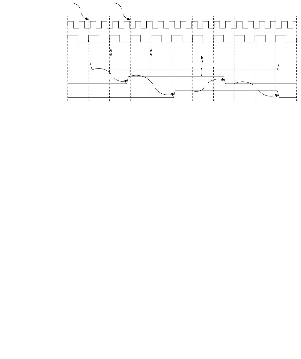
Vectored Interrupt Controller Port
ARM DDI 0301H Copyright © 2004-2009 ARM Limited. All rights reserved. 12-5
ID012310 Non-Confidential, Unrestricted Access
12.3 Timing of the VIC port
Figure 12-2 shows a timing example of VIC port operation. In this example IRQC is received
followed by IRQB having a higher priority. The waveforms in Figure 12-2 show an
asynchronous relationship between CLKIN and HCLK, and the delays marked Sync cater for
the delay of the synchronizers. When this interface is used synchronously, these delays are
reduced to being a single cycle of the receiving clock.
Figure 12-2 VIC port timing example
Figure 12-2 illustrates the basic handshake mechanism that operates between the processor and
a PL192 VIC:
1. An IRQC interrupt request occurs causing the PL192 VIC to set the processor nIRQ
input.
2. The processor samples the nIRQ input LOW and initiates an interrupt entry sequence.
3. Another IRQB interrupt request of higher priority than IRQC occurs.
4. Between B3 and B4, the processor decides that the pending interrupt is an IRQ rather than
a FIQ and asserts the IRQACK signal.
5. At B4 the VIC samples IRQACK HIGH and starts generating IRQADDRV. The VIC
can still change IRQADDR to the IRQB vector address while IRQADDRV is LOW.
6. At B6 the VIC asserts IRQADDRV while IRQADDR is set to the IRQB vector address.
IRQADDR is held until the processor acknowledges it has sampled it, even if a higher
priority interrupt is received while the VIC is waiting.
7. Around B8 the processor samples the value of the IRQADDR input bus and deasserts
IRQACK.
8. When the VIC samples IRQACK LOW, it stacks the priority of the IRQB interrupt and
deasserts IRQADDRV. It also deasserts nIRQ if there are no higher priority interrupts
pending.
9. When the processor samples IRQADDRV LOW, it knows it can sample the nIRQ input
again. Therefore, if the VIC requires some time for deasserting nIRQ, it must ensure that
IRQADDRV stays HIGH until nIRQ has been deasserted.
Processor
clock
Peripheral port
HCLK
IRQC vector address IRQB vector address IRQADDR[31:2]
nIRQ
IRQACK
IRQADDRV
IRQC IRQB
B1 B2 B3 B4 B5 B6 B7 B8 B9 B10 B11 B12
Sync
Sync
Sync
Sync
Address sampled

Vectored Interrupt Controller Port
ARM DDI 0301H Copyright © 2004-2009 ARM Limited. All rights reserved. 12-6
ID012310 Non-Confidential, Unrestricted Access
The clearing of the interrupt is handled in software by the interrupt handling routine. This
enables multiple interrupt sources to share a single interrupt priority. In addition, the interrupt
handling routine must communicate to the VIC that the interrupt currently being handled is
complete, using the memory-mapped or coprocessor-mapped interface, to enable the interrupt
masking to be unwound.
12.3.1 PL192 VIC timing
As its part of the handshake mechanism, the PL192 VIC:
1. Synchronizes IRQACK on its way in if the peripheral port clocking mode is
asynchronous or bypasses the synchronizers if it is in synchronous mode.
2. Asserts IRQADDRV when an address is ready at IRQADDR, and holds that address
until IRQACK is sampled LOW, even if higher priority interrupts come along.
3. Stacks the priority that corresponds to the vector address present at IRQADDR when it
samples the IRQACK signal LOW, while IRQADDRV is HIGH.
4. Clears IRQADDRV so the processor can recognize another interrupt. If nIRQ is also to
be deasserted at this point because there are no higher priority interrupts pending, it is
deasserted before or at the same time as IRQADDRV to ensure that the processor does
not take the same interrupt again.
12.3.2 Core timing
As its part of the handshake mechanism, the core:
1. Starts an interrupt entry sequence when it samples the nIRQ signal asserted.
2. Determines if an FIQ or an IRQ is going to be taken. This happens after the interrupt entry
sequence is started. If it decides that an IRQ is going to be taken, it starts the VIC port
handshake by asserting IRQACK. If it decides that the interrupt is an FIQ, then it does
not assert IRQACK and the VIC port handshake is not initiated.
3. Ignores the value of the nFIQ input until the IRQ interrupt entry sequence is completed
if it has decided that the interrupt is an IRQ.
4. Samples the IRQADDR input bus when both IRQACK and IRQADDRV are sampled
asserted. The interrupt entry sequence proceeds with this value of IRQADDR.
5. Ignores the nIRQ signal while IRQADDRV is HIGH. This gives the VIC time to deassert
the nIRQ signal if there is no higher priority interrupt pending.
6. Ignores the nFIQ signal while IRQADDRV is HIGH.
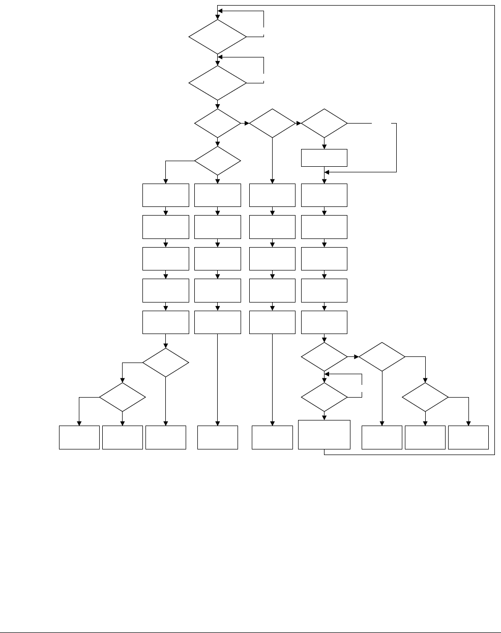
Vectored Interrupt Controller Port
ARM DDI 0301H Copyright © 2004-2009 ARM Limited. All rights reserved. 12-7
ID012310 Non-Confidential, Unrestricted Access
12.4 Interrupt entry flowchart
Figure 12-3.shows all the decisions and actions required to complete interrupt entry. For more
information on interrupt entry, see Exception vectors on page 2-48.
Figure 12-3 Interrupt entry sequence
!((nFIQ||F)
&&(nIRQ||I))
TRUE
!(nFIQ||F) VE==1
TRUE
Take IRQACK
HIGH
LR_irq =
RA+4
SPSR_irq =
CPSR
CPSR[4:0] =
IRQ mode
CPSR[5] =
ARM state
CPSR[7] =
IRQs disabled
VE==1
FALSE
V==1
LR_fiq =
RA+4
CPSR[4:0] =
FIQ mode
CPSR[5] =
ARM state
CPSR[7] =
FIQs and IRQs
disabled
SPSR_fiq =
CPSR
V==1
PC[31:0] =
0xFFFF0018
TRUE
PC[31:0] =
IRQADDR[31:2],
0b00
PC[31:0] =
NSBA + 0x1C
FALSE
PC[31:0] =
0xFFFF001C
TRUE
!(IRQADDRV
&& VE)
!IRQ
ADDRV==1
TRUE
TRUE
FALSE
FIQ = 1 in
SCR?
LR_mon =
RA+4
CPSR[4:0] =
MON mode
CPSR[5] =
ARM state
CPSR[7] =
FIQs and IRQs
disabled
SPSR_mon =
CPSR
TRUE
PC[31:0] =
MBA + 0x1C
IRQ = 1 in
SCR?
LR_mon =
RA+4
CPSR[4:0] =
MON mode
CPSR[5] =
ARM state
CPSR[7] =
IRQs disabled
SPSR_mon =
CPSR
TRUE
PC[31:0] =
MBA + 0x18
FALSE
FALSE
Secure
state?
FALSE
PC[31:0] =
SBA + 0x1C
TRUE
PC[31:0] =
NSBA + 0x18
FALSE
Secure
state?
FALSE
PC[31:0] =
SBA + 0x18
TRUE
TRUE
TRUE
FALSE
FALSE
FALSE
FALSE

ARM DDI 0301H Copyright © 2004-2009 ARM Limited. All rights reserved. 13-1
ID012310 Non-Confidential, Unrestricted Access
Chapter 13
Debug
This chapter describes the processor debug unit, that assists development of application software,
operating systems, and hardware, and contains the following sections:
•Debug systems on page 13-2
•About the debug unit on page 13-3
•Debug registers on page 13-5
•CP14 registers reset on page 13-25
•CP14 debug instructions on page 13-26
•External debug interface on page 13-28
•Changing the debug enable signals on page 13-31
•Debug events on page 13-32
•Debug exception on page 13-35
•Debug state on page 13-37
•Debug communications channel on page 13-42
•Debugging in a cached system on page 13-43
•Debugging in a system with TLBs on page 13-44
•Monitor debug-mode debugging on page 13-45
•Halting debug-mode debugging on page 13-50
•External signals on page 13-52.
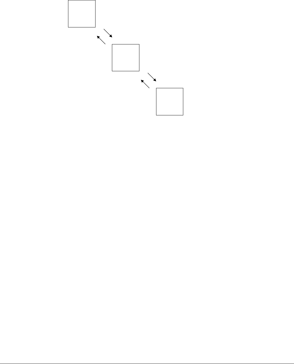
Debug
ARM DDI 0301H Copyright © 2004-2009 ARM Limited. All rights reserved. 13-2
ID012310 Non-Confidential, Unrestricted Access
13.1 Debug systems
The processor forms one component of a debug system that interfaces from the high-level
debugging performed by you, to the low-level interface supported by the processor. Figure 13-1
shows a typical system.
Figure 13-1 Typical debug system
This typical system has three parts:
•The debug host
•The protocol converter
•The processor.
13.1.1 The debug host
The debug host is a computer, for example a personal computer, running a software debugger
such as RealView Debugger. The debug host enables you to issue high-level commands such as
set breakpoint at location XX, or examine the contents of memory from 0x0-0x100.
13.1.2 The protocol converter
The debug host is connected to the processor development system using an interface, for
example an RS232. The messages broadcast over this connection must be converted to the
interface signals of the processor. This function is performed by a protocol converter, for
example, RealView ICE.
13.1.3 The processor
The processor, with debug unit, is the lowest level of the system. The debug extensions enable
you to:
• stall program execution
• examine its internal state and the state of the memory system
• resume program execution.
The debug host and the protocol converter are system-dependent.
Host computer running RealView™ Debugger
Debug
host
for example, RealView™ ICE
Development system containing ARM1176JZF-S
Debug
target
Protocol
converter

Debug
ARM DDI 0301H Copyright © 2004-2009 ARM Limited. All rights reserved. 13-3
ID012310 Non-Confidential, Unrestricted Access
13.2 About the debug unit
The processor debug unit assists in debugging software running on the processor. You can use
the processor debug unit, in combination with a software debugger program, to debug:
• application software
• operating systems
• ARM processor based hardware systems.
The debug unit enables you to:
• stop program execution
• examine and alter processor and coprocessor state
• examine and alter memory and input/output peripheral state
• restart the processor core.
You can debug the processor in the following ways:
•Halting debug-mode debugging
•Monitor debug-mode debugging
• Trace debugging. See Chapter 15 Trace Interface Port for interfacing with an ETM.
The processor debug interface is based on the IEEE Standard Test Access Port and
Boundary-Scan Architecture.
13.2.1 Halting debug-mode debugging
When the processor debug unit is in Halting debug-mode, the processor halts and enters Debug
state when a debug event, such as a breakpoint, occurs. When the processor is in Debug state,
an external host can examine and modify its state using the DBGTAP.
In Debug state you can examine and alter processor state, processor registers, coprocessor state,
memory, and input/output locations through the DBGTAP. This mode is intentionally invasive
to program execution. Halting debug-mode debugging requires:
• external hardware to control the DBGTAP
• a software debugger to provide the user interface to the debug hardware.
See CP14 c1, Debug Status and Control Register (DSCR) on page 13-7 to learn how to set the
processor debug unit into Halting debug-mode.
13.2.2 Monitor debug-mode debugging
When the processor debug unit is in Monitor debug-mode, the processor takes a Debug
exception instead of halting. A special piece of software, a debug monitor target, can then take
control to examine or alter the processor state. Monitor debug-mode is essential in real-time
systems where the core cannot be halted to collect information. For example, engine controllers
and servo mechanisms in hard drive controllers that cannot stop the code without physically
damaging the components.
When debugging in Monitor debug-mode the processor stops execution of the current program
and starts execution of a debug monitor target. The state of the processor is preserved in the same
manner as all ARM exceptions. See the ARM Architecture Reference Manual on exceptions and
exception priorities. The debug monitor target communicates with the debugger to access
processor and coprocessor state, and to access memory contents and input/output peripherals.
Monitor debug-mode requires a debug monitor program to interface between the debug
hardware and the software debugger.

Debug
ARM DDI 0301H Copyright © 2004-2009 ARM Limited. All rights reserved. 13-4
ID012310 Non-Confidential, Unrestricted Access
When debugging in Monitor debug-mode, you can program new debug events through CP14.
This coprocessor is the software interface of all the debug resources such as the breakpoint and
watchpoint registers. See CP14 c1, Debug Status and Control Register (DSCR) on page 13-7 to
learn how to set the processor debug unit into Monitor debug-mode.
Note
Monitor debug-mode, used for debugging, is not the same as Secure Monitor mode.
13.2.3 Secure Monitor mode and debug
Debug can be restricted to one of three levels, Non-secure only, Non-secure and Secure User
only, or any Secure or Non-secure levels so that you can prevent access to Secure parts of the
system while still permitting Non-secure and optionally Secure User parts to be debugged. This
is controlled by the SPIDEN and SPNIDEN signals and the two bits SUIDEN and SUNIDEN
in the Secure Debug Enable Register in the system control coprocessor, see External debug
interface on page 13-28 and c1, Secure Debug Enable Register on page 3-54.
Invasive debug
Invasive debug is debug where the system can be both observed and controlled
like all of the debug in this section that enables you to halt the processor and
examine and modify registers and memory.
SPIDEN and SUIDEN control invasive debug permissions.
Non-invasive debug
Non-invasive is debug where the system can only be observed but not affected.
The ETM interface, the System Performance Monitor and the DBGTAP program
counter sample register provide non-invasive debug.
SPNIDEN and SUNIDEN control non-invasive debug permissions.
13.2.4 Virtual addresses and debug
Unless otherwise stated, all addresses in this chapter are Modified Virtual Addresses (MVA) as
the ARM Architecture Reference Manual describes. For example, the Breakpoint Value
Registers (BVR) and Watchpoint Value Registers (WVR) must be programmed with MVAs.
The terms Instruction Modified Virtual Address (IMVA) and Data Modified Virtual Address
(DMVA), where used, mean the MVA corresponding to an instruction address and the MVA
corresponding to a data address respectively.
13.2.5 Programming the debug unit
The processor debug unit is programmed using CoProcessor 14 (CP14). CP14 provides:
• instruction address comparators for triggering breakpoints
• data address comparators for triggering watchpoints
• a bidirectional Debug Communication Channel (DCC)
• all other state information associated with processor debug.
CP14 is accessed using coprocessor instructions in Monitor debug-mode, and certain debug
scan chains in Debug state, see Chapter 14 Debug Test Access Port to learn how to access the
processor debug unit using scan chains.

Debug
ARM DDI 0301H Copyright © 2004-2009 ARM Limited. All rights reserved. 13-5
ID012310 Non-Confidential, Unrestricted Access
13.3 Debug registers
Table 13-1 lists definitions of terms used in register descriptions.
On a power-on reset, all the CP14 debug registers take the values indicated by the Reset value
column in the register bit field definition tables:
• Table 13-4 on page 13-8
• Table 13-6 on page 13-14
• Table 13-11 on page 13-18
• Table 13-14 on page 13-21
• Table 13-16 on page 13-21.
In these tables, - means an Undefined Reset value.
13.3.1 Accessing debug registers
To access the CP14 debug registers you must set Opcode_1 and CRn to 0. The Opcode_2 and
CRm fields of the coprocessor instructions are used to encode the CP14 debug register number,
where the register number is
{<Opcode2>, <CRm>}
.
Table 13-2 lists the CP14 debug register map. All of these registers are also accessible as scan
chains from the DBGTAP.
Table 13-1 Terms used in register descriptions
Term Description
R Read-only. Written values are ignored. However, it is written as 0 or preserved by writing the same value
previously read from the same fields on the same processor.
W Write-only. This bit cannot be read. Reads return an Unpredictable value.
RW Read or write.
C Cleared on read. This bit is cleared whenever the register is read.
UNP/SBZP Unpredictable or Should Be Zero or Preserved (SBZP). A read to this bit returns an Unpredictable value.
It is written as 0 or preserved by writing the same value previously read from the same fields on the same
processor. These bits are usually reserved for future expansion.
Core view This column defines the core access permission for a given bit.
External view This column defines the DBGTAP debugger view of a given bit.
Read/write
attributes
This is used when the core and the DBGTAP debugger view are the same.
Table 13-2 CP14 debug register map
Binary address Register
number CP14 debug register name Abbreviation
Opcode_2 CRm
b000 b0000 c0 Debug ID Register DIDR
b000 b0001 c1 Debug Status and Control Register DSCR
b000 b0010-b0100 c2-c4 Reserved -
b000 b0101 c5 Data Transfer Register DTR

Debug
ARM DDI 0301H Copyright © 2004-2009 ARM Limited. All rights reserved. 13-6
ID012310 Non-Confidential, Unrestricted Access
Note
All the debug resources required for Monitor debug-mode debugging are accessible through
CP14 registers. For Halting debug-mode debugging some additional resources are required. See
Chapter 14 Debug Test Access Port.
13.3.2 CP14 c0, Debug ID Register (DIDR)
The Debug ID Register is a read-only register that defines the configuration of debug registers
in a system. Figure 13-2 shows the format of the Debug ID Register.
Figure 13-2 Debug ID Register format
For the ARM1176JZF-S processor:
• DIDR[31:8] has the value 0x15121x
b000 b0110 c6 Watchpoint Fault Address Register WFAR
b000 b0111 c7 Vector Catch Register VCR
b000 b1000-b1001 c8-c9 Reserved -
b000 b1010 c10 Debug State Cache Control Register DSCCR
b000 b1011 c11 Debug State MMU Control Register DSMCR
b000 b1100-b1111 c12-c15 Reserved -
b001-b011 b0000-b1111 c16-c63 Reserved -
b100 b0000-b0101 c64-c69 Breakpoint Value Registers BVRya
b0110-b111 c70-c79 Reserved -
b101 b0000-b0101 c80-c85 Breakpoint Control Registers BCRya
b0110-b1111 c86-c95 Reserved -
b110 b0000-b0001 c96-c97 Watchpoint Value Registers WVRya
b0010-b1111 c98-c111 Reserved -
b111 b0000-b0001 c112-c113 Watchpoint Control Registers WCRya
b0010-b1111 c114-c127 Reserved -
a. y is the decimal representation for the binary number CRm.
Table 13-2 CP14 debug register map (continued)
Binary address Register
number CP14 debug register name Abbreviation
Opcode_2 CRm
WRP
31 28 27 24 23 20 19 16 15 8 7 4 3 0
BRP Context Version UNP/SBZ Variant Revision
12 11
Debug architecture revision

Debug
ARM DDI 0301H Copyright © 2004-2009 ARM Limited. All rights reserved. 13-7
ID012310 Non-Confidential, Unrestricted Access
• the value of DIDR[7:0] is determined by fields in the CP15 c0 Main ID Register, as
described in the field descriptions in Table 13-3.
Table 13-3 lists the bit field definitions for the Debug ID Register.
The reason for duplicating the Variant and Revision fields here is that the Debug ID Register is
accessible through scan chain 0. This enables an external debugger to determine the variant and
revision numbers without stopping the core.
13.3.3 CP14 c1, Debug Status and Control Register (DSCR)
The Debug Status and Control Register contains status and configuration information about the
state of the debug system. Figure 13-3 on page 13-8 shows the format of the Debug Status and
Control Register.
Table 13-3 Debug ID Register bit field definition
Bits Read/write
attributes Description
[31:28]
WRP
R Number of Watchpoint Register Pairs:
b0000 = 1 WRP
b0001 = 2 WRPs
…
b1111 = 16 WRPs.
For the ARM1176JZF-S processor these bits are b0001 (2 WRPs).
[27: 24]
BRP
R Number of Breakpoint Register Pairs:
b0000 = Reserved. The minimum number of BRPs is 2.
b0001 = 2 BRPs
b0010 = 3 BRPs
…
b1111 = 16 BRPs.
For the ARM1176JZF-S processor these bits are b0101 (6 BRPs).
[23: 20]
Context
R Number of Breakpoint Register Pairs with context ID comparison capability:
b0000 = 1 BRP has context ID comparison capability
b0001 = 2 BRPs have context ID comparison capability
…
b1111 = 16 BRPs have context ID comparison capability.
For the ARM1176JZF-S processor these bits are b0001 (2 BRPs).
[19:16]
Ve r s i o n
R Debug architecture version.
0x2
denotes v6.1
[15:12] R Debug architecture revision 0x1 denotes TrustZone features
[11:8] UNP/SBZP Reserved.
[7: 4]
Va r i a n t
R Implementation-defined variant number, incremented on major revisions of the product.
This field is identical to bits [23:20] of the CP15 c0 Main ID Register, see c0, Main ID
Register on page 3-20.
[3: 0]
Revision
R Implementation-defined revision number, incremented on minor revisions of the product.
This field is identical to bits [3:0] of the CP15 c0 Main ID Register, see c0, Main ID Register
on page 3-20.
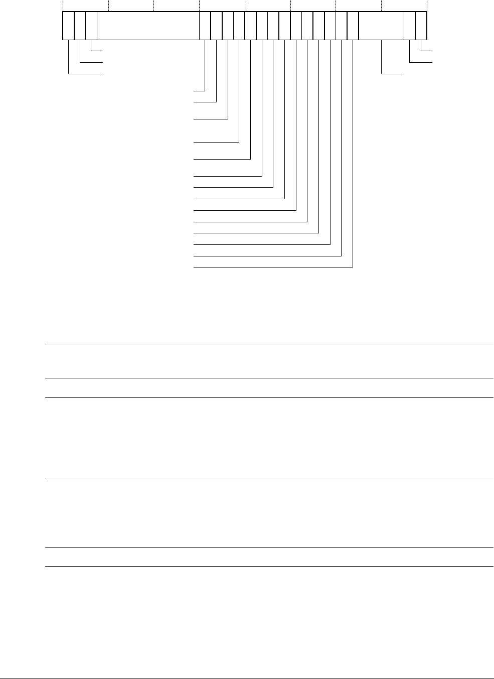
Debug
ARM DDI 0301H Copyright © 2004-2009 ARM Limited. All rights reserved. 13-8
ID012310 Non-Confidential, Unrestricted Access
Figure 13-3 Debug Status and Control Register format
Table 13-4 lists the bit field definitions for the Debug Status and Control Register.
31 30 29 28 16 15 14 13 12 11 10 6 5 2 1 0
UNP/SBZP
rDTRfull
wDTRfull
UNP/SBZP
Monitor debug-mode enable
Mode select
Execute ARM instruction enable
978
Core restarted
Core halted
17
18
19
20
Imprecise data abort ignored
Non-Secure World status
Not Secure Privileged Non-Invasive
Debug enable, SPNIDEN input pin
Not Secure Privileged Invasive
Debug Enable, SPIDEN input pin
Method of debug entry
User mode access to DCC control
DbgAck
Interrupts disable
Sticky imprecise Data Aborts flag
Sticky Undefined flag
Power down disable
Sticky precise Data Abort flag
Table 13-4 Debug Status and Control Register bit field definitions
Bits Core view External
view
Reset
value Description
[31] UNP/SBZP UNP/SBZP - Reserved.
[30] R R 0 The rDTRfull flag:
0 = rDTR empty
1 = rDTR full.
This flag is automatically set on writes by the DBGTAP debugger to
the rDTR and is cleared on reads by the core of the same register. No
writes to the rDTR are enabled if the rDTRfull flag is set.
[29] R R 0 The wDTRfull flag:
0 = wDTR empty
1 = wDTR full.
This flag is automatically cleared on reads by the DBGTAP debugger
of the wDTR and is set on writes by the core to the same register.
[28:20] UNP/SBZP UNP/SBZP - Reserved.
[19] R R 0 Imprecise Data Aborts Ignored. This read-only bit is set by the core in
Debug state following a Data Memory Barrier operation, and cleared
on exit from Debug state. When set, the core does not act on imprecise
data aborts. However, the sticky imprecise data abort bit is set if an
imprecise data abort occurs when in Debug state.

Debug
ARM DDI 0301H Copyright © 2004-2009 ARM Limited. All rights reserved. 13-9
ID012310 Non-Confidential, Unrestricted Access
[18] R R 0 Non-secure World Status bit 0 = The processor is in Secure state. NS
bit = 0 or Secure Monitor mode.1 = The processor is in Non-secure
state. NS bit = 1 and not Secure Monitor mode.
[17] R R n/a Not Secure Privilege Non-Invasive Debug Enable, SPNIDEN, input
pin.0 = SPNIDEN input pin is HIGH.1 = SPNIDEN input pin is LOW.
[16] R R n/a Not Secure Privilege Invasive Debug Enable, SPIDEN, input pin.0 =
SPIDEN input pin is HIGH.1 = SPIDEN input pin is LOW.
[15] RW R 0 The Monitor debug-mode enable bit:
0 = Monitor debug-mode disabled
1 = Monitor debug-mode enabled.
For the core to take a debug exception, Monitor debug-mode has to be
both selected and enabled, bit 14 clear and bit 15 set.
[14] R RW 0 Mode select bit:
0 = Monitor debug-mode selected
1 = Halting debug-mode selected and enabled.
[13] R RW 0 Execute ARM instruction enable bit:
0 = Disabled
1 = Enabled.
If this bit is set, the core can be forced to execute ARM instructions in
Debug state using the Debug Test Access Port. If this bit is set when
the core is not in Debug state, the behavior of the processor is
architecturally Unpredictable. For ARM1176JZF-S processors it has
no effect.
[12] RW R 0 User mode access to comms channel control bit:
0 = User mode access to comms channel enabled
1 = User mode access to comms channel disabled.
If this bit is set and a User mode process tries to access the DIDR,
DSCR, or the DTR, the Undefined instruction exception is taken.
Because accessing the rest of CP14 debug registers is never possible
in User mode, see Executing CP14 debug instructions on page 13-27,
setting this bit means that a User mode process cannot access any
CP14 debug register.
[11] R RW 0 Interrupts bit:
0 = Interrupts enabled
1 = Interrupts disabled.
If this bit is set, the IRQ and FIQ input signals are inhibited.a
[10] R RW 0 DbgAck bit.
If this bit is set, the DBGACK output signal (see External signals on
page 13-52) is forced HIGH, regardless of the processor state.a
[9] R RW 0 Powerdown disable:
0 = DBGNOPWRDWN is LOW
1 = DBGNOPWRDWN is HIGH.
See External signals on page 13-52.
Table 13-4 Debug Status and Control Register bit field definitions (continued)
Bits Core view External
view
Reset
value Description

Debug
ARM DDI 0301H Copyright © 2004-2009 ARM Limited. All rights reserved. 13-10
ID012310 Non-Confidential, Unrestricted Access
[8] R RC 0 Sticky Undefined flag:
0 = No Undefined exception trap occurred in Debug state since the last
time this bit was cleared.
1 = An undefined exception occurred while in Debug state since the
last time this bit was cleared.
This bit is cleared on reads of a DBGTAP debugger to the DSCR. The
Sticky Undefined bit does not prevent additional instructions from
being issued.
The Sticky Undefined bit is not set by Undefined exceptions occurring
when not in Debug state.
[7] R RC 0 Sticky imprecise Data Aborts flag:
0 = No imprecise Data Aborts occurred since the last time this bit was
cleared
1 = An imprecise Data Abort has occurred since the last time this bit
was cleared.
It is cleared on reads of a DBGTAP debugger to the DSCR.
The sticky imprecise data abort bit is only set by imprecise data aborts
occurring when in Debug state.
Note
In previous versions of the debug architecture, the sticky imprecise
data abort was set when the processor took an imprecise data abort. In
version 6.1, it is set when an imprecise data abort is detected.
[6] R RC 0 Sticky precise Data Abort flag:
0 = No precise Data Abort occurred since the last time this bit was
cleared
1 = A precise Data Abort has occurred since the last time this bit was
cleared.
This flag is meant to detect Data Aborts generated by instructions
issued to the processor using the Debug Test Access Port. Therefore,
if the DSCR[13] execute ARM instruction enable bit is a 0, the value
of the sticky precise Data Abort bit is architecturally Unpredictable.
For ARM1176JZF-S processors the sticky precise Data Abort bit is
set regardless of DSCR[13]. It is cleared on reads of a DBGTAP
debugger to the DSCR.
The sticky precise data abort bit is only set by precise data aborts
occurring when in Debug state.
Table 13-4 Debug Status and Control Register bit field definitions (continued)
Bits Core view External
view
Reset
value Description

Debug
ARM DDI 0301H Copyright © 2004-2009 ARM Limited. All rights reserved. 13-11
ID012310 Non-Confidential, Unrestricted Access
Bits [5:2] are set to indicate:
• the reason for jumping to the Prefetch or Data Abort vector
• the reason for entering Debug state.
A prefetch abort or data abort handler determines if it must jump to the debug monitor target by
examining the IFSR or DFSR respectively. A DBGTAP debugger or debug monitor target can
determine the specific debug event that caused the Debug state or debug exception entry by
examining DSCR[5:2].
13.3.4 CP14 c5, Data Transfer Registers (DTR)
This register consists of two separate physical registers:
• the rDTR, Read Data Transfer Register
• the wDTR, Write Data Transfer Register.
[5:2] RW R b0000 Method of debug entry bits:
b0000 = a Halt DBGTAP instruction occurred
b0001 = a breakpoint occurred
b0010 = a watchpoint occurred
b0011 = a BKPT instruction occurred
b0100 = an EDBGRQ signal activation occurred
b0101 = a vector catch occurred
b0110 = reserved
b0111 = reserved
b1xxx = reserved.
These bits are set to indicate any of:
• the cause of a Debug Exception
• the cause for entering Debug state
A Prefetch Abort or Data Abort handler must first check the IFSR or
DFSR register to determine a debug exception has occurred before
checking the DSCR to find the cause. These bits are not set on any
events in Debug state.
[1] R R 1 Core restarted bit:
0 = the processor is exiting Debug state
1 = the processor has exited Debug state.
The DBGTAP debugger can poll this bit to determine when the
processor has exited Debug state. See Debug state on page 13-37 for
a definition of Debug state.
[0] R R 0 Core halted bit:
0 = the processor is in normal state
1 = the processor is in Debug state.
The DBGTAP debugger can poll this bit to determine when the
processor has entered Debug state. See Debug state on page 13-37 for
a definition of Debug state.
a. Bits DSCR[11:10] can be controlled by a DBGTAP debugger to execute code in normal state as part of the debugging process.
For example, if the DBGTAP debugger has to execute an OS service to bring a page from disk into memory, and then return
to the application to see the effect this change of state produces, it is undesirable that interrupts are serviced during execution
of this routine.
Table 13-4 Debug Status and Control Register bit field definitions (continued)
Bits Core view External
view
Reset
value Description

Debug
ARM DDI 0301H Copyright © 2004-2009 ARM Limited. All rights reserved. 13-12
ID012310 Non-Confidential, Unrestricted Access
The register accessed is dependent on the instruction used:
• writes, MCR and LDC instructions, access the wDTR
• reads, MRC and STC instructions, access the rDTR.
Note
Read and write refer to the core view.
For details of the use of these registers with the rDTRfull flag and wDTRfull flag see Debug
communications channel on page 13-42. Figure 13-4 shows the format of both the rDTR and
wDTR.
Figure 13-4 DTR format
Table 13-5 lists the bit field definitions for rDTR and wDTR.
13.3.5 CP14 c6, Watchpoint Fault Address Register (WFAR)
The purpose of the Watchpoint Fault Address Register (WFAR) is to hold the Virtual Address
of the instruction that caused the watchpoint.
The register WFAR is:
•in CP14 c6
• a 32-bit read/write register
• accessible in privileged modes only.
When a watchpoint occurs in:
• ARM state, the WFAR contains the address of the instruction causing it plus
0x8
.
• Thumb state, the WFAR contains the address of the instruction causing it plus
0x4
.
• Jazelle state, the WFAR contains the address of the instruction causing it.
The contents of the WFAR are unaffected when a precise Data Abort or Prefetch Abort occurs.
To use the Watchpoint Fault Address Register read or write CP14 with:
• Opcode_1 set to 0
• CRn set to c0
• CRm set to c6
• Opcode_2 set to 0.
For example:
MRC p14, 0, <Rd>, c0, c6, 0 ; Read Watchpoint Fault Address Register
MCR p14, 0, <Rd>, c0, c6, 0 ; Write Watchpoint Fault Address Register
Data
31 0
Table 13-5 Data Transfer Register bit field definitions
Bits Core view External view Reset value Description
[31:0] R W - Read data transfer register, read-only
[31:0] W R - Write data transfer register, write-only
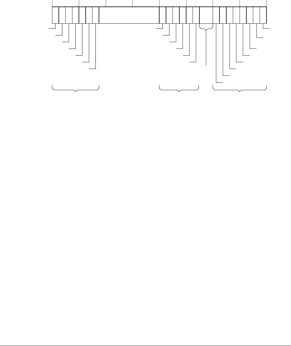
Debug
ARM DDI 0301H Copyright © 2004-2009 ARM Limited. All rights reserved. 13-13
ID012310 Non-Confidential, Unrestricted Access
A write to this register sets the WFAR to the value of the data written. This is useful for a
debugger to restore the value of the WFAR.
13.3.6 CP14 c7, Vector Catch Register (VCR)
The processor supports efficient exception vector catching. This is controlled by the VCR, as
Figure 13-5 shows.
Figure 13-5 Vector Catch Register format
If one of the bits in this register is set and the corresponding vector is committed for execution,
then a Debug exception or Debug state entry might be generated, depending on the value of the
DSCR[15:14] bits. See Behavior of the processor on debug events on page 13-33. Under this
model, any kind of fetch of an exception vector can trigger a vector catch, not only the ones
because of exception entries.
Vector catches related to bits[15:0] are only triggered by fetches in a Secure world. Catches
related to bits [31:25] are only triggered in the Non-secure world.
There are three groups of bits one each to catch exceptions relative to the three vector base
address registers for Non-secure, Secure and Secure Monitor modes.
The update of the VCR might occur several instruction after the corresponding MCR
instruction. It only takes effect by the next Instruction Memory Barrier (IMB).
Bits 29, [24:16], 13, [9:8] and bit 5 are reserved.
Table 13-6 on page 13-14 lists the bit field definitions for the Vector Catch Register. In
Table 13-6 on page 13-14, SBA means Secure Base Address, NSBA means Non-secure Base
Address, MBA means Monitor Base Address.
31 30 29 28 27 26 25 24 16 15 14 13 12 11 10 9 8 7 6 5 4 3 2 1 0
Reserved,
DNM / RAZ
Reset
Undefined
Instruction
SVC
Prefetch abort
Data abort
Reserved
IRQ
FIQ
SMC
Reserved
Prefetch abort
Data abort
Reserved
IRQ
FIQ
Undefined Instruction
SVC
Prefetch abort
Data abort
Reserved
IRQ
FIQ
Non-secure world Secure world,
Secure Monitor entry
Secure world

Debug
ARM DDI 0301H Copyright © 2004-2009 ARM Limited. All rights reserved. 13-14
ID012310 Non-Confidential, Unrestricted Access
Table 13-7 lists the conditions for generation of a Debug exception or entry into Debug State. In
this table, SBA means Secure Base Address, NSBA means Non-Secure Base Address, MBA
means Monitor Base Address.
Table 13-6 Vector Catch Register bit field definitions
Bits Read/Write
Attributes
Reset
value Vector base Description
[31] RW 0 NSBA Vector Catch Enable - FIQ in Non-secure world.
[30] RW 0 NSBA Vector Catch Enable - IRQ in Non-secure world.
[29] DNM/RAZ 0 - Reserved
[28] RW 0 NSBA Vector Catch Enable - Data Abort in Non-secure world.
[27] RW 0 NSBA Vector Catch Enable - Prefetch Abort in Non-secure world.
[26] RW 0 NSBA Vector Catch Enable - SVC in Non-secure world.
[25] RW 0 NSBA Vector Catch Enable - Undefined Instruction in Non-secure
world.
[24:16] DNM/RAZ 0 - Reserved
[15] RW 0 MBA Vector Catch Enable - FIQ in Secure world.
[14] RW 0 MBA Vector Catch Enable - IRQ in Secure world.
[13] DNM/RAZ 0 - Reserved
[12] RW 0 MBA Vector Catch Enable - Data Abort in Secure world.
[11] RW 0 MBA Vector Catch Enable - Prefetch Abort in Secure World
[10] RW 0 MBA Vector Catch Enable - SMC in Secure world.
[9:8] DNM/RAZ 0 - Reserved
[7] RW 0 SBA Vector Catch Enable - FIQ in Secure world.
[6] RW 0 SBA Vector Catch Enable - IRQ in Secure world.
[5] DNM/RAZ 0 - Reserved
[4] RW 0 SBA Vector Catch Enable - Data Abort in Secure world.
[3] RW 0 SBA Vector Catch Enable - Prefetch Abort in Secure world.
[2] RW 0 SBA Vector Catch Enable, SVC in Secure world.
[1] RW 0 SBA Vector Catch Enable, Undefined Instruction in Secure world.
[0] RW 0 SBA Vector Catch Enable, Reset
Table 13-7 Summary of debug entry and exception conditions
VCR bit NS bit, mode VE HIVECS Prefetch vector
VCR[0] = 1 NS bit = 0 or Mode = Secure
Monitor.
X0
0x00000000
1
0xFFFF0000

Debug
ARM DDI 0301H Copyright © 2004-2009 ARM Limited. All rights reserved. 13-15
ID012310 Non-Confidential, Unrestricted Access
VCR[1] = 1 NS bit = 0 or Mode = Secure
Monitor.
X0 SBA +
0x00000004
1
0xFFFF0004
VCR[2] = 1 NS bit = 0 or Mode = Secure
Monitor.
X0 SBA +
0x00000008
1
0xFFFF0008
VCR[3] = 1 NS bit = 0 or Mode = Secure
Monitor.
X0 SBA +
0x0000000C
1
0xFFFF000C
VCR[4] = 1 NS bit = 0 or Mode = Secure
Monitor.
X0 SBA +
0x00000010
1
0xFFFF0010
VCR[6] = 1 NS bit = 0 or Mode = Secure
Monitor.
00 SBA +
0x00000018
1
0xFFFF0018
1 X Most recent Secure IRQ address
VCR[7] = 1 NS bit = 0 or Mode = Secure
Monitor.
X0 SBA +
0x0000001C
1
0xFFFF001C
VCR[10] = 1 NS bit = 0 or Mode = Secure
Monitor.
XX MBA +
0x00000008
VCR[11] = 1 NS bit = 0 or Mode = Secure
Monitor.
XX MBA +
0x0000000C
VCR[12] = 1 NS bit = 0 or Mode = Secure
Monitor.
XX MBA +
0x00000010
VCR[14] = 1 NS bit = 0 or Mode = Secure
Monitor.
XX MBA +
0x00000018
VCR[15] = 1 NS bit = 0 or Mode = Secure
Monitor.
XX MBA +
0x0000001C
VCR[25] = 1 NS bit = 1 and mode ≠ Secure
Monitor
X0 NSBA +
0x00000004
1
0xFFFF0004
VCR[26] = 1 NS bit = 1 and mode ≠ Secure
Monitor
X0 NSBA +
0x00000008
1
0xFFFF0008
VCR[27] = 1 NS bit = 1 and mode ≠ Secure
Monitor
X0 NSBA +
0x0000000C
1
0xFFFF000C
VCR[28] = 1 NS bit = 1 and mode ≠ Secure
Monitor
X0 NSBA +
0x00000010
1
0xFFFF0010
Table 13-7 Summary of debug entry and exception conditions (continued)
VCR bit NS bit, mode VE HIVECS Prefetch vector

Debug
ARM DDI 0301H Copyright © 2004-2009 ARM Limited. All rights reserved. 13-16
ID012310 Non-Confidential, Unrestricted Access
13.3.7 CP14 c64-c69, Breakpoint Value Registers (BVR)
Table 13-8 lists the Breakpoint Value Registers that the processor implements.
Each BVR is associated with a BCR register. BCRy is the corresponding control register for
BVRy.
A pair of breakpoint registers, BVRy/BCRy, is called a Breakpoint Register Pair (BRP).
BVR0-5 are paired with BCR0-5 to make BRP0-5.
The BVR of a BRP is loaded with an IMVA and then its contents can be compared against the
IMVA bus of the processor. The breakpoint value contained in the BVR corresponds to either
an IMVA or a context ID. Breakpoints can be set on:
•an IMVA
•a context ID
• an IMVA/context ID pair.
The IMVA comparison can be programmed to either hit when the address matches or
mis-matches. The IMVA mis-match case is useful because it enables a debugger to implement
a single-step operation when the breakpoint is programmed to match any other IMVA than the
instruction about to be executed.
The processor supports thread-aware breakpoints and watchpoints. A context ID can be loaded
into the BVR and the BCR can be configured so this BVR value is compared against the CP15
Context ID Register, c13, instead of the IMVA bus. Another register pair loaded with an IMVA
or DMVA can then be linked with the context ID holding BRP. A breakpoint or watchpoint
debug event is only generated if both the address and the context ID match at the same time.
This means that unnecessary hits can be avoided when debugging a specific thread within a task.
Breakpoint debug events generated on context ID matches only are also supported. However, if
a context ID only match or any match including an IMVA mis-match occurs while the processor
is running in a privileged mode and the debug logic in Monitor debug-mode, it is ignored. This
is to avoid the processor ending in an unrecoverable state.
VCR[30] = 1 NS bit = 1 and mode ≠ Secure
Monitor
00 NSBA +
0x00000018
1
0xFFFF0018
1 X Most recent Non-secure IRQ address.
VCR[31] = 1 NS bit = 1 and mode ≠ Secure
Monitor
X0 NSBA +
0x0000001C
1
0xFFFF001C
Table 13-7 Summary of debug entry and exception conditions (continued)
VCR bit NS bit, mode VE HIVECS Prefetch vector
Table 13-8 Processor breakpoint and watchpoint registers
Binary address Register
number CP14 debug register name Abbreviation Context ID
capable?
Opcode_2 CRm
b100 b0000-b0011 c64-c67 Breakpoint Value Registers 0-3 BVR0-3 No
b0100-b0101 c68-c69 Breakpoint Value Registers 4-5 BVR4-5 Yes

Debug
ARM DDI 0301H Copyright © 2004-2009 ARM Limited. All rights reserved. 13-17
ID012310 Non-Confidential, Unrestricted Access
Table 13-9 lists the bit field definitions for context ID and non context ID Breakpoint Value
Registers.
When a context ID capable BRP is set for IMVA comparison, BVR bits [1:0] are ignored.
13.3.8 CP14 c80-c85, Breakpoint Control Registers (BCR)
These registers contain the necessary control bits for setting:
• breakpoints
• linked breakpoints.
Table 13-10 lists the Breakpoint Control Registers and that the processor implements.
Figure 13-6 shows the format of the Breakpoint Control Registers.
Figure 13-6 Breakpoint Control Registers, format
Table 13-9 Breakpoint Value Registers, bit field definition
Context ID capable? Bits Read/write attributes Description
No [31:2] RW Breakpoint address
Yes [31:0] RW Breakpoint address or context ID
Table 13-10 Processor Breakpoint Control Registers
Binary address Register
number CP14 debug register name Abbreviation Context ID
capable?
Opcode_2 CRm
b101 b0000-b0011 c80-c83 Breakpoint Control Registers 0-3 BCR0-3 No
b0100-b0101 c84-c85 Breakpoint Control Registers 4-5 BCR4-5 Yes
BUNP/SBZP
31 22 21 20 19 16 15 9 8 5 4 3 2 1 0
M E Linked BRP UNP/SBZP
Byte
address
select
UNP/
SBZ S
23 1314
Secure breakpoint match

Debug
ARM DDI 0301H Copyright © 2004-2009 ARM Limited. All rights reserved. 13-18
ID012310 Non-Confidential, Unrestricted Access
Table 13-11 lists the bit field definitions for the Breakpoint Control Registers.
Table 13-11 Breakpoint Control Registers, bit field definitions
Bits Read/write
attributes
Reset
value Description
[31:23] UNP/SBZP - Reserved.
[22:21] RW 00 Meaning of BVR00 = IMVA Match.01 = Context ID Match.10 = IMVA
Mis-match.11 = Reserved. If this breakpoint does not have Context ID capability, bit
21 is RAZ.
[20] RW - Enable linking:
0 = Linking disabled
1 = Linking enabled.
When this bit is set HIGH, the corresponding BRP is linked. See Table 13-12 on
page 13-19 for details.
[19:16] RW - Linked BRP number. The binary number encoded here indicates another BRP to link
this one with. If a BRP is linked with itself, it is architecturally Unpredictable if a
breakpoint debug event is generated. For ARM1176JZF-S processors the breakpoint
debug event is not generated.
[15:14] RW - b00 = Breakpoint matches in Secure or Non-secure world.
b01 = Breakpoint only matches in Non-secure world.
b10 = Breakpoint only matches in Secure world.b11 = Reserved
If this BRP is programmed for context ID comparison and linking (BCR[22:20] is
set b011), then the BCR[15:14] field of the IMVA-holding BRP takes precedence
and it is Undefined whether this field is included in the comparison or not. Therefore,
it must be set to b00.
The WCR[15:14] field of a WRP linked with this BRP also takes precedence over
this field.
[13:9] UNP/SBZP - Reserved.
[8:5] RW - Byte address select. The BVR is programmed with a word address. You can use this
field to program the breakpoint so it matches only if certain byte addresses are
accessed.
b0000 = The breakpoint never matches
bxxx1= If the byte at address {BVR[31:2], b00}+0 is accessed, the breakpoint
matches
bxx1x = If the byte at address {BVR[31:2], b00}+1 is accessed, the breakpoint
matches
bx1xx = If the byte at address {BVR[31:2], b00}+2 is accessed, the breakpoint
matches
b1xxx = If the byte at address {BVR[31:2], b00}+3 is accessed, the breakpoint
matches.
This field must be set to b1111 when this BRP is programmed for context ID
comparison, that is BCR[22:20] set to b01x. Otherwise breakpoint or watchpoint
debug events might not be generated as expected.
Note
These are little-endian byte addresses. This ensures that a breakpoint is triggered
regardless of the endianness of the instruction fetch.
For example, if a breakpoint is set on a certain Thumb instruction by doing BCR[8:5]
= b0011, it is triggered if in little-endian and IMVA[1:0] is b00 or if big-endian and
IMVA[1:0] is b10.

Debug
ARM DDI 0301H Copyright © 2004-2009 ARM Limited. All rights reserved. 13-19
ID012310 Non-Confidential, Unrestricted Access
Table 13-12 summarizes the meaning of BCR bits [22:20].
Note
• The BCR[8:5], BCR[15:14], and BCR[2:1] fields still apply when a BRP is set for context
ID comparison. See Setting breakpoints, watchpoints, and vector catch debug events on
page 13-45 for detailed programming sequences for linked breakpoints and linked
watchpoints.
[4:3] UNP/SBZP - Reserved
[2:1] RW - Supervisor Access. The breakpoint can be conditioned to the privilege of the access
being done:
b00 = Reserved
b01= Privileged
b10 = User
b11 = Either.
If this BRP is programmed for context ID comparison and linking, BCR[22:20] is
set b011, then the BCR[2:1] field of the IMVA-holding BRP takes precedence and it
is Undefined whether this field is included in the comparison or not. Therefore, it
must be set to either.
The WCR[2:1] field of a WRP linked with this BRP also takes precedence over this
field.
[0] RW 0 Breakpoint enable:
0 = Breakpoint disabled
1 = Breakpoint enabled.
Table 13-11 Breakpoint Control Registers, bit field definitions (continued)
Bits Read/write
attributes
Reset
value Description
Table 13-12 Meaning of BCR[22:20] bits
BCR[22:20] Meaning
b000 The corresponding BVR is compared against the IMVA bus. This BRP is not linked with any other one.
It generates a breakpoint debug event on an IMVA match.
b001 The corresponding BVR is compared against the IMVA bus. This BRP is linked with the one indicated
by BCR[19:16] linked BRP field. They generate a breakpoint debug event on a joint IMVA and context
ID match.
b010 The corresponding BVR is compared against CP15 Context Id Register, c13. This BRP is not linked with
any other one. It generates a breakpoint debug event on a context ID match.
b011 The corresponding BVR is compared against CP15 Context Id Register, c13. Another BRP, of the
BCR[21:20]=b01 type, or WRP, with WCR[20]=b1, is linked with this BRP. They generate a breakpoint
or watchpoint debug event on a joint IMVA or DMVA and context ID match.
b100 The corresponding BVR is compared against the IMVA bus. This BRP is not linked with any other one.
It generates a breakpoint debug event on an IMVA mismatch.
b101 The corresponding BVR is compared against the IMVA bus. This BRP is linked with the one indicated
by BCR[19:16] linked BRP field. They generate a breakpoint debug event on a joint IMVA mismatch and
context ID match.
b110 Reserved
b111 Reserved

Debug
ARM DDI 0301H Copyright © 2004-2009 ARM Limited. All rights reserved. 13-20
ID012310 Non-Confidential, Unrestricted Access
• The BCR[8:5] field is treated as part of the compared address, For an IMVA mismatch the
bits must be set to 1 for the corresponding byte lanes that are excluded from the
breakpoint.
The following rules apply to the processor for breakpoint debug event generation:
• The update of a BVR or a BCR can take effect several instructions after the corresponding
MCR. It takes effect by the next IMB.
• Updates of the CP15 Context ID Register c13, can take effect several instructions after the
corresponding MCR. However, the write takes place by the end of the exception return.
This is to ensure that a User mode process, switched in by a processor scheduler, can break
at its first instruction.
• Any BRP, holding an IMVA, can be linked with any other one with context ID capability.
Several BRPs, holding IMVAs, can be linked with the same context ID capable one.
• If a BRP, holding an IMVA, is linked with one that is not configured for context ID
comparison and linking, it is architecturally Unpredictable whether a breakpoint debug
event is generated or not. For ARM1176JZF-S processors the breakpoint debug event is
not generated. BCR[22:20] fields of the second BRP must be set to b011.
• If a BRP, holding an IMVA, is linked with one that is not implemented, it is architecturally
Unpredictable if a breakpoint debug event is generated or not. For ARM1176JZF-S
processors the breakpoint debug event is not generated.
• If a BRP is linked with itself, it is architecturally Unpredictable if a breakpoint debug
event is generated or not. For ARM1176JZF-S processors the breakpoint debug event is
not generated.
• If a BRP, holding an IMVA, is linked with another BRP, holding a context ID value, and
they are not both enabled, both BCR[0] bits set, the first one does not generate any
breakpoint debug event.
13.3.9 CP14 c96-c97, Watchpoint Value Registers (WVR)
Each WVR is associated with a WCR register. WCRy is the corresponding register for WVRy.
A pair of watchpoint registers, WVRy and WCRy, is called a Watchpoint Register Pair (WRP).
WVR0-1 are paired with WCR0-1 to make WRP0-1.
Table 13-13 lists the Watchpoint Value Registers that the processor implements.
The watchpoint value contained in the WVR always corresponds to a DMVA. Watchpoints can
be set on:
•a DMVA
• a DMVA/context ID pair.
Table 13-13 Processor Watchpoint Value Registers
Binary address Register
number CP14 debug register name Abbreviation Context ID
capable?
Opcode_2 CRm
b110 b0000-b0001 c96-c97 Watchpoint Value Registers 0-1 WVR0-1 -

Debug
ARM DDI 0301H Copyright © 2004-2009 ARM Limited. All rights reserved. 13-21
ID012310 Non-Confidential, Unrestricted Access
For the second case a WRP and a BRP with context ID comparison capability have to be linked.
A debug event is generated when both the DMVA and the context ID pair match simultaneously.
Table 13-14 lists the bit field definitions for the Watchpoint Value Registers.
13.3.10 CP14 c112-c113, Watchpoint Control Registers (WCR)
These registers contain the necessary control bits for setting:
• watchpoints
• linked watchpoints.
Table 13-15 lists the Watchpoint Control Registers that the processor implements.
Figure 13-7 shows the format of the Watchpoint Control Registers.
Figure 13-7 Watchpoint Control Registers, format
Table 13-16 lists the bit field definitions for the Watchpoint Control Registers.
Table 13-14 Watchpoint Value Registers, bit field definitions
Bits Read/write attributes Reset value Description
[31:2] RW - Watchpoint address
[1:0] UNP/SBZP - -
Table 13-15 Processor Watchpoint Control Registers
Binary address Register
number CP14 debug register name Abbreviation Context ID
capable?
Opcode_2 CRm
b111 b0000-b0001 c112-c113 Watchpoint Control Registers 0-1 WCR0-1 -
WUNP/SBZP
31 21 20 19 16 15 9 8 5 4 3 2 1 0
E Linked BRP
Byte
address
select
L/S S WUNP/SBZP
31 21 20 19 16 15 9 8 5 4 3 2 1 0
E Linked BRP UNP/SBZP
Byte
address
select
L/S S
14 13
Secure watchpoint match
Table 13-16 Watchpoint Control Registers, bit field definitions
Bits Read/write
attributes
Reset
value Description
[31:21] UNP/SBZP - Reserved.
[20] RW - Enable linking bit:
0 = Linking disabled
1 = Linking enabled.
When this bit is set, this watchpoint is linked with the context ID holding BRP
selected by the linked BRP field.
[19:16] RW - Linked BRP. The binary number encoded here indicates a context ID holding BRP
to link this WRP with.

Debug
ARM DDI 0301H Copyright © 2004-2009 ARM Limited. All rights reserved. 13-22
ID012310 Non-Confidential, Unrestricted Access
In addition to the rules for breakpoint debug event generation, see CP14 c80-c85, Breakpoint
Control Registers (BCR) on page 13-17, the following rules apply to the processor for
watchpoint debug event generation:
• The update of a WVR or a WCR can take effect several instructions after the
corresponding MCR. It only guaranteed to have taken effect by the next IMB.
[15:14] RW - b00 = Watchpoint matches in Secure or Non-secure world.
b01 = Watchpoint only matches in Non-secure world.
b10 = Watchpoint only matches in Secure world.
b11 = Reserved.
[13:9] SBZ - Reserved.
[8:5] RW - Byte address select. The WVR is programmed with a word address. This field can be
used to program the watchpoint so it hits only if certain byte addresses are
accessed.b0000 = The watchpoint never hits
bxxx1= If the byte at address {WVR[31:2], b00}+0 is accessed, the watchpoint
hitsbxx1x = If the byte at address {WVR[31:2], b00}+1 is accessed, the watchpoint
hitsbx1xx = If the byte at address {WVR[31:2], b00}+2 is accessed, the watchpoint
hitsb1xxx = If the byte at address {WVR[31:2], b00}+3 is accessed, the watchpoint
hits.
Note
These are little-endian byte addresses. This ensures that a watchpoint is triggered
regardless of the way it is accessed.
For example, if a watchpoint is set on a certain byte in memory by doing WCR[8:5]
= b0001.
LDRB R0, #0x0
it triggers the watchpoint in little-endian mode, as does
LDRB
R0, #x3
in legacy big-endian mode, B bit of CP15 c1 set.
[4:3] RW - Load/store access. The watchpoint can be conditioned to the type of access being
done:
b00 = Reserved
b01 = Load
b10 = Store
b11 = Either.
A SWP triggers on Load, Store, or Either. Load exclusive instructions, LDREX,
LDREXB, LDREXD, and LDREXH, trigger on Load or Either. Store exclusive
instructions, STREX, STREXB, STREXD, and STREXH, trigger on Store or Either,
whether it succeeded or not.
[2:1] RW - Supervisor Access. The watchpoint can be conditioned to the privilege of the access
being done:
b00 = Reserved
b01 = Privileged
b10 = User
b11 = Either.
[0] RW 0 Watchpoint enable:
0 = Watchpoint disabled
1 = Watchpoint enabled.
Table 13-16 Watchpoint Control Registers, bit field definitions (continued)
Bits Read/write
attributes
Reset
value Description

Debug
ARM DDI 0301H Copyright © 2004-2009 ARM Limited. All rights reserved. 13-23
ID012310 Non-Confidential, Unrestricted Access
• Any WRP can be linked with any BRP with context ID comparison capability. Several
BRPs, holding IMVAs, and WRPs can be linked with the same context ID capable BRP.
• If a WRP is linked with a BRP that is not configured for context ID comparison and
linking, it is architecturally Unpredictable if a watchpoint debug event is generated or not.
For ARM1176JZF-S processors the watchpoint debug event is not generated. BCR[22:20]
fields of the BRP must be set to b011.
• If a WRP is linked with a BRP that is not implemented, it is architecturally Unpredictable
if a watchpoint debug event is generated or not. For ARM1176JZF-S processors the
watchpoint debug event is not generated.
• If a WRP is linked with a BRP and they are not both enabled, BCR[0] and WCR[0] set, it
does not generate a watchpoint debug event.
13.3.11 CP14 c10, Debug State Cache Control Register
The Debug State Cache Control Register controls cache behavior in Debug state:
MRC p14, 0, <Rd>, c0, c10, 0
MCR p14, 0, <Rd>, c0, c10, 0
Table 13-17 lists the functional bits in the register.
The effect of these bits only applies in Debug state. The operation under control only occurs if
it is enabled in both this register and by the corresponding bit in the Cache Behavior Override
Register.
13.3.12 CP14 c11, Debug State MMU Control Register
The Debug State MMU Control Register controls main and micro TLB behavior in Debug state:
MRC p14, 0, <Rd>, c0, c11, 0
MCR p14, 0, <Rd>, c0, c11, 0
Table 13-18 on page 13-24 lists the functional bits in the register.
Table 13-17 Debug State Cache Control Register bit functions
Bits Reset value Name Description
[31:3] UNP/SBZ - Reserved.
[2] 0 nWT Not Write-Through:
1 = Normal operation of regions marked as Write-Back in Debug state.
0 = force Write-Through behavior for regions marked as Write-Back in Debug state.
[1] 0 nIL No Instruction Cache Line-Fill:
1 = Normal operation of Instruction Cache line fills in Debug state.
0 = Instruction Cache line-fill disabled in Debug state.
[0] 0 nDL No Data/Unified Cache Line-Fill:
1 = Normal operation of Data/Unified Cache line-fills in Debug state.
0 = Data/Unified Cache line-fill disabled in Debug state.

Debug
ARM DDI 0301H Copyright © 2004-2009 ARM Limited. All rights reserved. 13-24
ID012310 Non-Confidential, Unrestricted Access
Table 13-18 Debug State MMU Control Register bit functions
Bits Reset value Name Description
[31:7] UNP/SBZ - Reserved
[6] 0 nDMM 1 = Normal operation of Main TLB matching in Debug state.
0 = Main TLB match disabled in Debug state.
[5] UNP/SBZ - Reserved
[4] 0 nDML 1 = Normal operation of Main TLB loading in Debug state.
0 = Main TLB load disabled in Debug state.
[3] 0 nIUM 1 = Normal operation of Instruction Micro TLB matching in Debug state.
0 = Instruction Micro TLB match disabled in Debug state.
[2] 0 nDUM 1 = Normal operation of Data Micro TLB matching in Debug state.
0 = Data Micro TLB match disabled in Debug state.
[1] 0 nIUL 1 = Normal operation of Instruction Micro TLB loading and flushing in Debug state.
0 = Instruction Micro TLB load and flush disabled in Debug state.
[0] 0 nDUL 1 = Normal operation of Data Micro TLB loading and flushing in Debug state.
0 = Data Micro TLB load and flush disabled in Debug state.

Debug
ARM DDI 0301H Copyright © 2004-2009 ARM Limited. All rights reserved. 13-25
ID012310 Non-Confidential, Unrestricted Access
13.4 CP14 registers reset
The CP14 debug registers that are accessible through the external interface are all reset by the
processor power-on reset signal, nPORESETIN, see Reset with no IEM on page 9-4 or Reset
with IEM on page 9-8.
This ensures that a vector catch set on the reset vector is taken when nRESETIN is deasserted.
It also ensure that the DBGTAP debugger can be connected when the processor is running
without clearing CP14 debug setting, because DBGnTRST does not reset these registers.

Debug
ARM DDI 0301H Copyright © 2004-2009 ARM Limited. All rights reserved. 13-26
ID012310 Non-Confidential, Unrestricted Access
13.5 CP14 debug instructions
Table 13-19 lists the CP14 debug instructions.
In Table 13-19,
MRC p14,0,<Rd>,c0,c5,0
and
STC p14,c5,<addressing mode>
refer to the rDTR
and
MCR p14,0,<Rd>,c0,c5,0
and
LDC p14,c5,<addressing mode>
refer to the wDTR. See CP14
c5, Data Transfer Registers (DTR) on page 13-11 for more details. The
MRC p14,0,R15,c0,c1,0
instruction sets the CPSR flags as follows:
• N flag = DSCR[31]. This is an Unpredictable value.
• Z flag = DSCR[30]. This is the value of the rDTRfull flag.
• C flag = DSCR[29]. This is the value of the wDTRfull flag.
• V flag = DSCR[28]. This is an Unpredictable value.
Table 13-19 CP14 debug instructions
Binary address
Register number Abbreviation Legal instructions
Opcode_2 CRm
b000 b0000 0 DIDR
MRC p14, 0, <Rd>, c0, c0, 0
a
b000 b0001 1 DSCR
MRC p14, 0, <Rd>, c0, c1,0
a
MRC p14, 0, R15, c0, c1,0
MCR p14, 0, <Rd>, c0, c1,0
a
b000 b0101 5 DTR (rDTR/wDTR)
MRC p14, 0, <Rd>, c0, c5, 0
a
MCR p14, 0, <Rd>, c0, c5, 0
a
STC p14, c5, <addressing mode>
LDC p14, c5, <addressing mode>
b000 b0110 6 WFAR
MRC p14, 0, <Rd>, c0, c6, 0
a
MCR p14, 0, <Rd>, c0, c6, 0
a
b000 b0111 7 VCR
MRC p14, 0, <Rd>, c0, c7, 0
a
MCR p14, 0, <Rd>, c0, c7, 0
a
b000 b1010 10 DSCCR
MRC p14, 0, <Rd>, c0, c10, 0
a
MCR p14, 0, <Rd>, c0, c10, 0
a
b000 b1011 11 DSMCR
MRC p14, 0, <Rd>, c0, c11, 0
a
MCR p14, 0, <Rd>, c0, c11, 0
a
b100 b0000-b1111 64-79 BVR
MRC p14, 0, <Rd>, c0, cy,4
ab
MCR p14, 0, <Rd>, c0, cy,4
ab
b101 b0000-b1111 80-95 BCR
MRC p14, 0, <Rd>, c0, cy,5
ab
MCR p14, 0, <Rd>, c0, cy,5
ab
b110 b0000-b1111 96-111 WVR
MRC p14, 0, <Rd>, 0, cy, 6
ab
MCR p14, 0, <Rd>, 0, cy, 6
ab
b111 b0000-b1111 112-127 WCR
MRC p14, 0, <Rd>, c0, cy, 7
ab
MCR p14, 0, <Rd>, c0, cy, 7
ab
a. <Rd> is any of R0-R14 ARM registers.
b. y is the decimal representation for the binary number CRm.

Debug
ARM DDI 0301H Copyright © 2004-2009 ARM Limited. All rights reserved. 13-27
ID012310 Non-Confidential, Unrestricted Access
Use of R15 in all other MRC instructions that Table 13-19 on page 13-26 lists, sets all four flags
to Unpredictable values.
Instructions that follow the MRC instruction can be conditioned to these CPSR flags.
13.5.1 Executing CP14 debug instructions
If the core is in Debug state, see Debug state on page 13-37, you can execute any CP14 debug
instruction regardless of the processor mode.
If the processor tries to execute a CP14 debug instruction that either is not in Table 13-19 on
page 13-26, or is targeted to a reserved register, such as a non-implemented BVR, the Undefined
instruction exception is taken.
You can access the DCC, read DIDR, read DSCR and read/write DTR, in User mode. All other
CP14 debug instructions are privileged. If the processor tries to execute one of these in User
mode, the Undefined instruction exception is taken.
If the User mode access to DCC disable bit, DSCR[12], is set, all CP14 debug instructions are
considered as privileged, and all attempted User mode accesses to CP14 debug registers
generate an Undefined instruction exception.
When DSCR bit 14 is set, Halting debug-mode selected and enabled, if the software running on
the processor tries to access any register other than the DIDR, the DSCR, or the DTR, the core
takes the Undefined instruction exception. The same thing happens if the core is not in any
Debug mode, DSCR[15:14]=b00. This lockout mechanism ensures that the software running on
the core cannot modify the settings of a debug event programmed by the DBGTAP debugger.
Table 13-20 lists the results of executing CP14 debug instructions.
Table 13-20 Debug instruction execution
State when executing CP14 debug instruction: Results of CP14 debug instruction execution:
Processor
mode
Debug
state
DSCR[15:14],
Mode enabled
and selected
DSCR[12],
DCC User
accesses
disabled
Read DIDR,
read DSCR
and read/
write DTR
Write
DSCR
Read/write
other debug
registers
x Yes xx x Proceed Proceed Proceed
User No xx 0 Proceed Undefined
exception
Undefined
exception
User No xx 1 Undefined
exception
Undefined
exception
Undefined
exception
Privileged No b00, None x Proceed Proceed Undefined
exception
Privileged No b01, Halting x Proceed Proceed Undefined
exception
Privileged No b10, Monitor x Proceed Proceed Proceed
Privileged No b11, Halting x Proceed Proceed Undefined
exception

Debug
ARM DDI 0301H Copyright © 2004-2009 ARM Limited. All rights reserved. 13-28
ID012310 Non-Confidential, Unrestricted Access
13.6 External debug interface
The debug architecture provides two control signals called SPIDEN and SPNIDEN. that are
part of the external debug interface.
SPIDEN The Secure Privileged Invasive Debug Enable input pin, SPIDEN, that enables
and disables invasive debug in the Secure world:
• If this input signal is HIGH, invasive debug is permitted in all Secure
modes. In this case invasive debug is permitted in Secure User mode,
regardless value of SUIDEN bit.
• If this input signal is LOW, invasive debug is not permitted in any Secure
privileged mode. Invasive debug is permitted in Secure User mode
according to the SUIDEN bit.
SPNIDEN The Secure Privileged Non-Invasive Debug Enable input pin, SPNIDEN, that
enables and disables non-invasive debug in the Secure world:
• If this input signal is HIGH, non-invasive debug is permitted in all Secure
modes. In this case non-invasive debug is permitted in Secure User mode,
regardless of the value of the SUNIDEN bit.
• If this input signal is LOW, non-invasive debug is not permitted in all
Secure privileged modes. Non-invasive debug is permitted in Secure User
mode according to the SUNIDEN bit.
Note
• You must control access to the SPIDEN and SPNIDEN pins, as they represent a
significant security risk. For example, it must not be possible to set these pins through the
boundary scan in a final device.
• For software systems that do not use any TrustZone security features, the SPIDEN and
SPNIDEN pins must be driven HIGH to enable debug by default.
Table 13-21 lists the relationship between the DBGEN input pin, the SPIDEN input pin, the
SUIDEN control bit, the NS bit, the processor mode and the debug capabilities.
Table 13-21 Secure debug behavior
DBGEN DSCR
[15:14] SPIDEN SUIDEN NS
bit Mode Debug-mode Notes
0 XX X X X X Debug disabled. DSCR[15:14] reads as zero
1 00 1 X X X No debug mode
selecteda
Permitted in Non-secure
state and in all modes in
Secure state.
10000 1not Secure
Monitor
No debug mode
selecteda
Permitted only in
Non-secure state.
10000 XSecure
Monitor
Debug not
permittedb
Not permitted in Secure
state.
1 00 0 0 0 X Debug not
permittedb
Not permitted in Secure
state.
10001 1not Secure
Monitor
No debug mode
selecteda
Permitted in Non-secure
state.

Debug
ARM DDI 0301H Copyright © 2004-2009 ARM Limited. All rights reserved. 13-29
ID012310 Non-Confidential, Unrestricted Access
10001 XSecure
Monitor
Debug not
permittedb
Not permitted in privileged
modes in Secure state.
1 00 0 1 0 not User Debug not
permittedb
Not permitted in privileged
modes in Secure state.
1 00 0 1 0 User No debug mode
selecteda
Permitted in User mode in
Secure state.c
1 10 1 X X X Monitor
debug-mode
Permitted in Non-secure
state and in all modes in
Secure state.
11000 1not Secure
Monitor
Monitor
debug-mode
Permitted only in
Non-secure state.
11000 XSecure
Monitor
Debug not
permittedb
Not permitted in Secure
state.
1 10 0 0 0 X Debug not
permittedb
Not permitted in Secure
state.
11001 1not Secure
Monitor
Monitor
debug-mode
Permitted in Non-secure
state.
11001 XSecure
Monitor
Debug not
permittedb
Not permitted in privileged
modes in Secure state.
1 10 0 1 0 not User Debug not
permittedb
Not permitted in privileged
modes in Secure state.
1 10 0 1 0 User Monitor
debug-mode
Permitted in User mode in
Secure state.c
1 X1 1 X X X Halting
debug-mode
Permitted in Non-secure
state and in all modes in
Secure state.
1X100 1not Secure
Monitor
Halting
debug-mode
Permitted in Non-secure
state.
1X100 XSecure
Monitor
Debug not
permittedb
Not permitted in Secure
state.
1 X1 0 0 0 X Debug not
permittedb
Not permitted in Secure
state.
1X101 1not Secure
Monitor
Halting
debug-mode
Permitted in Non-secure
state.
1X101 XSecure
Monitor
Debug not
permittedb
Not permitted in privileged
modes in Secure state.
1 X1 0 1 0 not User Debug not
permittedb
Not permitted in privileged
modes in Secure state.
1 X1 0 1 0 User Halting
debug-mode
Permitted in User mode in
Secure state. Capabilities
restricted.
Table 13-21 Secure debug behavior (continued)
DBGEN DSCR
[15:14] SPIDEN SUIDEN NS
bit Mode Debug-mode Notes

Debug
ARM DDI 0301H Copyright © 2004-2009 ARM Limited. All rights reserved. 13-30
ID012310 Non-Confidential, Unrestricted Access
a. Behavior of the processor on debug events on page 13-33 describes the behavior when no debug mode is selected. Only the
BKPT instruction external debug request signal, and Halt DBGTAP instructions have an effect when no debug mode is
selected. All other debug events are ignored.
b. Behavior of the processor on debug events on page 13-33 describes the behavior marked as not permitted. Logically, the
processor is still configured for either Halting debug-mode or Monitor debug-mode, as appropriate.
c. Debug exceptions are handled in a privileged mode.

Debug
ARM DDI 0301H Copyright © 2004-2009 ARM Limited. All rights reserved. 13-31
ID012310 Non-Confidential, Unrestricted Access
13.7 Changing the debug enable signals
The behavior of these control signals, DBGEN, SPIDEN, and SPNIDEN, is primarily a
concern of the external debug interface. It is recommended that these signals do not change.
However, the architecture permits these signals to change when the processor is running or when
the processor is in Debug state.
If software running on the processor changes the state of one of these signals, before performing
debug or analysis operations that rely on the new value it must:
1. Execute the device specific sequence of instructions to change the signal value. For
instance, the software might have to write a value to a control register in a system
peripheral.
2. Perform a Data Memory Barrier operation. This stage can be omitted if the previous stage
does not involve any memory operations.
3. Poll debug registers for the view that the processor has of the signal values. This stage is
required because system specific issues might result in the processor not receiving a signal
change until some cycles after the Data Memory Barrier completes.
4. Issue an Instruction Memory Barrier sequence.
The same rules apply for instructions executed through the ITR when in Debug state.
The view that the processor has of the SPIDEN and SPNIDEN signals can be polled through
the DSCR. The processor has no register that shows its view of DBGEN. However, if DBGEN
is LOW, DSCR[15:14] read as zero, and therefore the view that the processor has of DBGEN
can be polled by writing to DSCR[15:14] and using the value read back to determine its setting.

Debug
ARM DDI 0301H Copyright © 2004-2009 ARM Limited. All rights reserved. 13-32
ID012310 Non-Confidential, Unrestricted Access
13.8 Debug events
A debug event is any of the following:
•Software debug event
•External debug request signal
•Halt DBGTAP instruction on page 13-33.
13.8.1 Software debug event
A software debug event is any of the following:
• A watchpoint debug event. This occurs when:
— the DMVA present in the data bus matches the watchpoint value
— all the conditions of the WCR match
— the watchpoint is enabled
— the linked contextID-holding BRP, if any, is enabled and its value matches the
context ID in CP15 c13.
• A breakpoint debug event. This occurs when:
— an instruction was fetched and the IMVA present in the instruction bus matched or
mismatched the breakpoint value, according to the meaning field in the BCR
— at the same time the instruction was fetched, all the conditions of the BCR matched
— the breakpoint was enabled
— at the same time the instruction was fetched, the linked contextID-holding BRP, if
any, was enabled and its value matched the context ID in CP15 c13
— the instruction is now committed for execution.
• A breakpoint debug event also occurs when:
— an instruction was fetched and the CP15 Context ID, register 13, matched the
breakpoint value
— at the same time the instruction was fetched, all the conditions of the BCR matched
— the breakpoint was enabled
— the instruction is now committed for execution.
• A software breakpoint debug event. This occurs when a BKPT instruction is committed
for execution.
• A vector catch debug event. This occurs when:
— The instruction at a vector location was fetched in the appropriate Secure or
Non-secure world. This includes any kind of prefetches, not only the ones because
of exception entry.
— At the same time the instruction was fetched, the corresponding bit of the VCR was
set, vector catch enabled.
— The instruction is now committed for execution.
13.8.2 External debug request signal
The processor has an external debug request input signal, EDBGRQ. When this signal is HIGH
it causes the processor to enter Debug state when execution of the current instruction has
completed. When this happens, the DSCR[5:2] method of entry bits are set to b0100.This signal
can be driven by the ETM to signal a trigger to the core. For example, if a memory permission

Debug
ARM DDI 0301H Copyright © 2004-2009 ARM Limited. All rights reserved. 13-33
ID012310 Non-Confidential, Unrestricted Access
fault occurs, an external Trace analyzer can collect trace information around this trigger event
at the same time that the processor is stopped to examine its state. See the Chapter 15 Trace
Interface Port for more details. A DBGTAP debugger can also drive this signal.
13.8.3 Halt DBGTAP instruction
The Halt mechanism is used by the Debug Test Access Port to force the core into Debug state.
When this happens, the DSCR[5:2] method of entry bits are set to b0000.
13.8.4 Behavior of the processor on debug events
This section describes how the processor behaves on debug events while not in Debug state. See
Debug state on page 13-37 for information on how the processor behaves while in Debug state.
When a software debug event occurs and Monitor debug-mode is selected and enabled and the
core is in a state that permits debug then a Debug exception is taken. However, Prefetch Abort
and Data Abort Vector catch debug events are ignored.
This is to avoid the processor ending in an unrecoverable state on certain combinations of
exceptions and vector catches. Unlinked context ID and all address mismatch breakpoint debug
events are also ignored if the processor is running in a privileged mode and Monitor debug-mode
is selected and enabled.
When the external debug request signal is activated, or the DBGTAP instruction is issued and
debug is enabled by DBGEN and the core is in a state that permits debug, the processor enters
Debug state regardless of any debug-mode selected by DSCR[15:14].
When a debug event occurs and Halting debug-mode is selected and enabled and the core is in
a state that debug is permitted, then the processor enters Debug state.
All software debug events other than the BKPT instruction, that is register breakpoints,
watchpoints, and vector catches, when no debug mode is selected and enabled or the core is in
a state that does not permit debug, are ignored.
When neither Halting nor Monitor debug-mode is selected and enabled or the core is in a state
that does not permit debug, the BKPT instruction generates a Prefetch Abort exception.
Table 13-22 lists the behavior of the processor in debug events.
Table 13-22 Behavior of the processor on debug events
DBGEN DSCR[15:14]
Mode
selected,
enabled and
permitted
Action on software
debug event
Action on external
debug request
signal activation
Action on Halt
DBGTAP
0bxx -aIgnore/Prefetch AbortbIgnore Ignore
1 b00 None Ignore/Prefetch AbortaDebug state entry Debug state entry
1 b01 Halting Debug state entry Debug state entry Debug state entry
1 b10 Monitor Debug
exception/Ignorec
Debug state entry Debug state entry
1 b11 Halting Debug state entry Debug state entry Debug state entry
a. Entry to Debug state is disabled.
b. When no debug mode is selected and enabled or the core is in a state that does not permit debug, a BKPT instruction generates
a Prefetch Abort exception instead of being ignored.
c. Prefetch Abort and Data Abort vector catch debug events are ignored in Monitor debug-mode. Unlinked context ID and
address mismatch breakpoint debug events are also ignored if the processor is running in a privileged mode and Monitor
debug-mode is selected and enabled.

Debug
ARM DDI 0301H Copyright © 2004-2009 ARM Limited. All rights reserved. 13-34
ID012310 Non-Confidential, Unrestricted Access
13.8.5 Effect of a debug event on CP15 registers
The four CP15 registers that can be set on a debug event are:
•Instruction Fault Status Register (IFSR)
•Data Fault Status Register (DFSR)
•Fault Address Register (FAR)
•Watchpoint Fault Address Register (WFAR).
The Instruction Fault Address Register (IFAR) is never updated on debug events.
The registers are set under the following circumstances:
• The IFSR is set whenever a breakpoint, software breakpoint, or vector catch debug event
generates a Debug exception entry. It is set to indicate the cause for the Prefetch Abort
vector fetch.
• The DFSR is set whenever a watchpoint debug event generates a Debug exception entry.
It is set to indicate the cause for the Data Abort vector fetch.
• The processor updates the FAR on debug exception entry because of watchpoints,
although this is architecturally Unpredictable. It is set to the Modified Virtual Address
(MVA) that triggered the watchpoint.
• The WFAR is set whenever a watchpoint debug event generates either a Debug exception
or Debug state entry. It is set to the VA of the instruction that caused the Watchpoint debug
event, plus an offset dependent on the processor state. These offsets are the same as the
ones that Table 13-25 on page 13-39 lists.
Table 13-23 lists the setting of CP15 registers on debug events.
You must take care when setting a breakpoint or software breakpoint debug event inside the
Prefetch Abort or Data Abort exception handlers, or when setting a watchpoint debug event on
a data address that might be accessed by any of these handlers. These debug events overwrite
the R14_abt, SPRS_abt and the CP15 registers listed in this section, leading to an unpredictable
software behavior if the handlers did not have the chance of saving the registers.
Table 13-23 Setting of CP15 registers on debug events
Register
Debug exception taken because of: Debug state entry because of:
A breakpoint,
software breakpoint,
or vector catch
debug event
A watchpoint
debug event
A debug event
other than a
watchpoint
A watchpoint
debug event
IFSR Cause of Prefetch Abort
exception handler entry
Unchanged Unchanged Unchanged
DFSR Unchanged Cause of Data Abort
exception handler entry
Unchanged Unchanged
FAR Unchanged Watchpointed address Unchanged Unchanged
WFAR Unchanged Address of the
instruction causing the
watchpoint debug event
Unchanged Address of the
instruction causing the
watchpoint debug
event

Debug
ARM DDI 0301H Copyright © 2004-2009 ARM Limited. All rights reserved. 13-35
ID012310 Non-Confidential, Unrestricted Access
13.9 Debug exception
When a Software debug event occurs and Monitor debug-mode is selected and enabled and the
core is in a state that permits debug then a Debug exception is taken. Prefetch Abort and Data
Abort Vector catch debug events are ignored though. Unlinked context ID and any IMVA
mismatch breakpoint debug events are also ignored if the processor is running in a privileged
mode and Monitor debug-mode is selected and enabled. If the cause of the Debug exception is
a watchpoint debug event, the processor performs the following actions:
• The DSCR[5:2] method of entry bits are set to indicate that a watchpoint occurred.
• The CP15 DFSR, FAR, and WFAR are set as Effect of a debug event on CP15 registers
on page 13-34 describes.
• The same sequence of actions as in a Data Abort exception is performed. This includes
setting the R14_abt, base register and destination registers to the same values as if this was
a Data Abort.
The Data Abort handler is responsible for checking the DFSR bit to determine if the routine
entry was caused by a debug exception or a Data Abort exception. On entry:
1. It must first check for the presence of a debug monitor target.
2. If present, the handler must disable the active watchpoints. This is necessary to prevent
corruption of the FAR because of an unexpected watchpoint debug event when servicing
a Data Abort exception.
3. If the cause is a Debug exception the Data Abort handler branches to the debug monitor
target.
Note
• the watchpointed address can be found in the FAR
• the address of the instruction that caused the watchpoint debug event can be found
in the WFAR
• the address of the instruction to restart at plus
0x08
can be found in the R14_abt
register.
If the cause of the Debug exception is a breakpoint, software breakpoint or vector catch debug
event, the processor performs the following actions:
• the DSCR[5:2] method of entry bits are set appropriately
• the CP15 IFSR register is set as Effect of a debug event on CP15 registers on page 13-34
describes.
• the same sequence of actions as in a Prefetch Abort exception is performed.
The Prefetch Abort handler is responsible for checking the IFSR bits to find out if the routine
entry is caused by a Debug exception or a Prefetch Abort exception. If the cause is a Debug
exception it branches to the debug monitor target.
Note
The address of the instruction causing the Software debug event plus
0x04
can be found in the
R14_abt register.
Table 13-24 on page 13-36 lists the values in the link register after exceptions.

Debug
ARM DDI 0301H Copyright © 2004-2009 ARM Limited. All rights reserved. 13-36
ID012310 Non-Confidential, Unrestricted Access
Table 13-24 Values in the link register after exceptions
Cause of fault ARM Thumb Jazelle Return address (RAa) meaning
Breakpoint RA+4 RA+4 RA+4 Breakpointed instruction address
Watchpoint RA+8 RA+8 RA+8 Address of the instruction where the execution resumes, a number
of instructions after the one that hit the watchpoint
BKPT instruction RA+4 RA+4 RA+4 BKPT instruction address
Vector catch RA+4 RA+4 RA+4 Vector address
Prefetch Abort RA+4 RA+4 RA+4 Address of the instruction where the execution resumes
Data Abort RA+8 RA+8 RA+8 Address of the instruction where the execution resumes
a. This is the address of the instruction that the processor first executes on Debug state exit. Watchpoints can be imprecise.
RA is not the address of the instruction immediately after the one that hit the watchpoint, the processor might stop a number of
instructions later. The address of the instruction that hit the watchpoint is in the CP15 WFAR.

Debug
ARM DDI 0301H Copyright © 2004-2009 ARM Limited. All rights reserved. 13-37
ID012310 Non-Confidential, Unrestricted Access
13.10 Debug state
When the conditions in Behavior of the processor on debug events on page 13-33 are met then
the processor switches to Debug state. While in Debug state, the processor behaves as follows:
• The DSCR[0] core halted bit is set.
•The DBGACK signal is asserted, see External signals on page 13-52.
• The DSCR[5:2] method of entry bits are set appropriately.
• The CP15 IFSR, DFSR, FAR, and WFAR registers are set as Effect of a debug event on
CP15 registers on page 13-34 describes.
• The processor is halted. The pipeline is flushed and no instructions are fetched.
• The processor does not change the execution mode. The CPSR is not altered.
• The DMA engine keeps on running. The DBGTAP debugger can stop it and restart it using
CP15 operations if it has permission to do so. See Chapter 7 Level One Memory System
for details.
• Interrupts and exceptions are treated as Interrupts on page 13-39 and Exceptions on
page 13-39 describe.
• Software debug events are ignored.
• The external debug request signal is ignored.
• Debug state entry request commands are ignored.
• There is a mechanism, using the Debug Test Access Port, where the core is forced to
execute an ARM state instruction. This mechanism is enabled using DSCR[13] execute
ARM instruction enable bit.
• The core executes the instruction as if it is in ARM state, regardless of the actual value of
the T and J bits of the CPSR.
• Any instruction issued in Debug state that puts the processor into a mode or state where
debug is not permitted is ignored.
• When in Debug state the CPSR must be modified using the MSR instruction.
• In Debug state MSR can be used to modify the CPSR mode bits from any mode to any
mode that is permitted by the debug level set by SPIDEN and SUIDEN.
For example, if SPIDEN is set, the CPSR mode bits can be altered to change to Secure
Monitor mode from any mode, including all Non-secure modes.
The CPSR mode can be altered from Non-secure User mode to any Non-secure Privileged
mode regardless of the state of SPIDEN.
• Instructions that write to the I, F, and A bits of the CPSR are ignored when:
— debug is only permitted in Non-secure world and in Secure User mode, SPIDEN=0,
SUIDEN=1
— the processor is in Secure user mode
• The MSR instruction can also be used to alter the J and T execution state bits of the CPSR.
• The PC behaves as Behavior of the PC in Debug state on page 13-38 describes.

Debug
ARM DDI 0301H Copyright © 2004-2009 ARM Limited. All rights reserved. 13-38
ID012310 Non-Confidential, Unrestricted Access
• Instructions that access CP14 registers are always permitted in Debug state. This applies
regardless of the debug permissions and the processor mode and state. For example even
if:
— debug is only permitted in Non-secure world and in Secure User mode, SPIDEN=0,
SUIDEN=1
— the processor is in Secure user mode
• For CP15 registers in Debug state the processor behaves as follows:
— If the debugger is permitted to write to the CPSR mode bits in the current world and
change to a privileged mode, then the debugger is permitted to access the CP15
registers of that world. There is no requirement to change to a privileged mode first.
— Access to the CP15 registers of that world is then limited to the access granted to
any privileged mode in that world.
— Any attempts to perform accesses that are not permitted are treated as Undefined
Exceptions and cause the sticky Undefined bit to be set in the DSCR.
For example:
— If debug is permitted everywhere, then if the processor is stopped in any Secure
mode, including Secure User mode, it has the same access to the Secure banked
CP15 registers as any Secure privileged mode. However, if the processor is stopped
in a Non-secure mode, including Non-secure User mode, the debugger can only
directly access the Non-secure banked CP15 registers, and those CP15 registers, for
example NSAC, or bits of CP15 registers, for example the B, FI, L4 and RR bits of
the Control Register, that are not banked and are read-only in Non-secure modes are
read-only to the debugger. The debugger can write to the CPSR mode bits to switch
to Secure Monitor mode, and thereby set or clear the NS bit to read or write all CP15
registers in either bank.
— If debug is permitted only in Non-secure state and in Secure User mode, then if the
processor is stopped in Secure User mode, it has no privileged access to any CP15
registers. If the processor is stopped in any Non-secure mode, including Non-secure
User mode, then it can only access the Non-secure banked CP15 registers, and those
CP15 registers or bits of CP15 registers that are not banked and are read-only in
Non-secure modes are read-only to the debugger. The debugger cannot write to the
mode bits to change the processor into Secure Monitor mode, so cannot access any
Secure CP15 registers.
— If debug is permitted only in Non-secure state, the processor can only be stopped in
Non-secure modes, including Non-secure User mode. It can only access the
Non-secure banked CP15 registers, and those CP15 registers or bits of CP15
registers that are not banked and are read-only in Non-secure modes are read-only
to the debugger. The debugger cannot write to the mode bits to change the processor
into Secure Monitor mode, so cannot access any Secure CP15 registers.
• A DBGTAP debugger can force the processor out of Debug state by issuing a Restart
instruction. See Table 14-1 on page 14-6. The Restart command clears the DSCR[1] core
restarted flag. When the processor has actually exited Debug state, the DSCR[1] core
restarted bit is set and the DSCR[0] core halted bit and DBGACK signal are cleared.
13.10.1 Behavior of the PC in Debug state
In Debug state:
• The PC is frozen on entry to Debug state. That is, it does not increment on the execution
of ARM instructions. However, branches and instructions that modify the PC directly do
update it.

Debug
ARM DDI 0301H Copyright © 2004-2009 ARM Limited. All rights reserved. 13-39
ID012310 Non-Confidential, Unrestricted Access
• If the PC is read after the processor has entered Debug state, it returns a value as
Table 13-25 lists, depending on the previous state and the type of debug event.
• If a sequence for writing a certain value to the PC is executed while in Debug state, and
then the processor is forced to restart, execution starts at the address corresponding to the
written value. However, the CPSR has to be set to the return ARM, Thumb, or Jazelle state
before the PC is written to, otherwise the processor behavior is Unpredictable.
• If the processor is forced to restart without having performed a write to the PC, the restart
address is Unpredictable.
• If the PC or CPSR are written to while in Debug state, subsequent reads to the PC return
an Unpredictable value.
• The MSR instruction has an Unpredictable effect on the PC so the PC must be written
before leaving Debug state.
• If a conditional branch is executed and it fails its condition code, an Unpredictable value
is written to the PC.
Table 13-25 lists the read PC value after Debug state entry for different debug events.
13.10.2 Interrupts
Interrupts are ignored regardless of the value of the I and F bits of the CPSR, although these bits
are not changed because of the Debug state entry.
13.10.3 Exceptions
Exceptions are handled as follows while in Debug state:
Reset This exception is taken as in a normal processor state, ARM, Thumb, or Jazelle.
This means the processor leaves Debug state as a result of the system reset.
Prefetch Abort
This exception cannot occur because no instructions are prefetched while in
Debug state.
Table 13-25 Read PC value after Debug state entry
Debug event ARM Thumb Jazelle Return address (RAa) meaning
Breakpoint RA+8 RA+4 RA Breakpointed instruction address
Watchpoint RA+8 RA+4 RA Address of the instruction where the execution
resumes, several instructions after the one that hit the
watchpoint
BKPT instruction RA+8 RA+4 RA BKPT instruction address
Vector catch RA+8 RA+4 RA Vector address
External debug request signal
activation
RA+8 RA+4 RA Address of the instruction where the execution
resumes
Debug state entry request
command
RA+8 RA+4 RA Address of the instruction where the execution
resumes
a. This is the address of the instruction that the processor first executes on Debug state exit. Watchpoints can be imprecise. RA
is not the address of the instruction immediately after the one that hit the watchpoint, the processor might stop a number of
instructions later. The address of the instruction that hit the watchpoint is in the CP15 WFAR.

Debug
ARM DDI 0301H Copyright © 2004-2009 ARM Limited. All rights reserved. 13-40
ID012310 Non-Confidential, Unrestricted Access
Debug This exception cannot occur because software debug events are ignored while in
Debug state.
SVC The instruction is ignored.
SMC The instruction is ignored.
Undefined Exception
When an Undefined exception occurs in Debug state, the behavior of the core is
as follows:
• PC, CPSR, SPSR_und, R14_und and DSCR[5:2], method of entry bits, are
unchanged.
• The processor remains in Debug state.
• DSCR[8], sticky undefined bit, is set.
Precise Data abort
When a precise Data Abort occurs in Debug state the behavior of the core is as
follows:
• PC, CPSR, SPSR_abt, R14_abt and DSCR [5:2], method of entry bits, are
unchanged
• the processor remains in Debug state
• DSCR[6], sticky precise data abort bit, is set
• DFSR and FAR are set.
Imprecise Data Abort
When an imprecise Data Abort is detected in Debug state, the behavior of the core
is as follows, regardless of the setting of the CPSR A bit:
• PC, CPSR, SPSR_abt, R14_abt and DSCR[5:2], method of entry bits, are
unchanged.
• The processor remains in Debug state.
• DSCR[7], sticky imprecise data abort bit, is set.
• The imprecise Data Abort is not taken, so DFSR is not set and the FAR is
not updated.
Note
The DFSR and FAR that are updated depends on if the core is in a Secure or Non-secure state.
The registers that can be read in Debug state depends on the current setting of the NS bit. The
DFSR and FAR are always updated for precise data aborts in Debug state even when the
processor is in Secure User mode, and SPIDEN is not set. In such circumstances the debugger
has no access to DFSR and FAR to restore their values.
Imprecise Data Aborts in detail
The processor takes imprecise data abort exceptions when:
• an imprecise data abort is pending
• the A bit in the CPSR is not set
• the processor is not in Debug state.
On entry to Debug state, DSCR[19] is normally zero. The debugger must issue a Data Memory
Barrier operation to flush all pending memory operations to the system. Once these operations
have completed, the processor sets DSCR[19]. If any of these operations cause imprecise data

Debug
ARM DDI 0301H Copyright © 2004-2009 ARM Limited. All rights reserved. 13-41
ID012310 Non-Confidential, Unrestricted Access
aborts, the processor latches the abort and its type until the processor leaves Debug state, in the
same way as if an imprecise data abort is detected in normal operation when the A bit in the
CPSR is set. The aborts are not taken immediately.
When the processor sets this bit, any memory accesses from Debug state that cause imprecise
data aborts cause DSCR[7], sticky imprecise data abort, to be set, but are otherwise discarded.
The cause and type of the abort are not recorded. In particular, if an abort is still latched from
the initial Data Memory Barrier that was completed on entry to Debug state, it is not overwritten
by the new abort. Following writes to memory by the debugger it issues a Data Memory Barrier
operation to ensure imprecise data aborts are detected.
Before exit from Debug state, a debugger must issue a Data Memory Barrier operation. On exit
from Debug state, DSCR[19] is cleared by the processor.
If an imprecise data abort has occurred during the period between entry to Debug state and the
when the processor set DSCR[19], it is taken by the processor on exit from Debug state,
providing the A bit in the CPSR is not set. If the A bit in the CPSR is set, it is pended until the
A bit in the CPSR is cleared, as for normal operation.
Table 13-26 lists an example sequence of a memory operation executed in normal operation that
eventually causes an imprecise abort when the processor is in Debug state. In addition, a
memory operation issued by the debugger in Debug state causes a second imprecise abort that
is ignored by the processor, apart from the sticky imprecise data abort bit being set. Throughout
the example the A bit in the CPSR is clear.
Table 13-26 Example memory operation sequence
Operation Result Debug
state? DCSR[19] DCSR[7] Abort
latched?
Abort
taken?
1 Memory write Buffered operation No 0 0
2 Debug
exception
Enters Debug state Yes 0 0
3Data Memory
Barrier
Buffered operation flushed
- imprecise data abort
Yes 0 1aYe s Nob
4 Processor sets DSCR[19] Yes 1 1
5 DSCR read Clears sticky bits Yes 1 0
6 Memory write Buffered operation Yes 1 0
7Data Memory
Barrier
Buffered operation flushed
- imprecise data abort
Yes 1 1 NocNo
8 DSCR read Clears sticky bits Yes 1 0
9 Exit Debug
state
Processor clears DSCR[19] No 0 0 Ye s d(d)
a. The sticky imprecise data abort bit is set because an imprecise data abort was signalled in Debug state.
b. Abort is not taken because the processor is in Debug state.
c. Abort is not latched because DSCR[19] is set.
d. The previous abort latched on row (3) is taken, now the processor has left Debug state and the A bit in the CPSR is not set.

Debug
ARM DDI 0301H Copyright © 2004-2009 ARM Limited. All rights reserved. 13-42
ID012310 Non-Confidential, Unrestricted Access
13.11 Debug communications channel
There are two ways that a DBGTAP debugger can send data to or receive data from the core:
• The debug communications channel, when the core is not in Debug state. It is defined as
the set of resources used for communicating between the DBGTAP debugger and a piece
of software running on the core.
• The mechanism for forcing the core to execute ARM instructions, when the core is in
Debug state. For details see Executing instructions in Debug state on page 14-21.
At the core side, the debug communications channel resources are:
• CP14 Debug Register c5, DTR. Data coming from a DBGTAP debugger can be read by
an MRC or STC instruction addressed to this register. The core can write to this register
any data intended for the DBGTAP debugger, using an MCR or LDC instruction. Because
the DTR comprises both a read, rDTR, and a write portion, wDTR, a data item written by
the core can be held in this register at the same time as one written by the DBGTAP
debugger.
• Some flags and control bits of CP14 Debug Register c1, DSCR:
— User mode access to comms channel disable, DSCR[12]. If this bit is set, only
privileged software is able to access the debug communications channel. That is,
access the DSCR and the DTR.
— wDTRfull flag, DSCR bit 29. When clear, this flag indicates to the core that the
wDTR is ready to receive data. It is automatically cleared on reads of the wDTR by
the DBGTAP debugger, and is set on writes by the core to the same register. If this
bit is set and the core attempts to write to the wDTR, the register contents are
overwritten and the wDTRfull flag remains set.
— rDTRfull flag, DSCR bit 30. When set, this flag indicates to the core that there is
data available to read at the rDTR. It is automatically set on writes to the rDTR by
the DBGTAP debugger, and is cleared on reads by the core of the same register.
Monitor debug-mode debugging on page 14-42 describes the DBGTAP debugger side of the
debug communications channel.

Debug
ARM DDI 0301H Copyright © 2004-2009 ARM Limited. All rights reserved. 13-43
ID012310 Non-Confidential, Unrestricted Access
13.12 Debugging in a cached system
Debugging must be non-invasive in a cached system. In processor based systems, you can
preserve the contents of the cache so the state of the target application is not altered, and to
maintain memory coherency during debugging.
To preserve the contents of the level one cache, you can disable the Instruction Cache and Data
Cache line fills so read misses from main memory do not update the caches. You can put the
caches in this mode by programming the operation of the caches during debug using CP14 c10.
See CP14 c10, Debug State Cache Control Register on page 13-23. This facility is accessible
from both the core and DBGTAP debugger sides.
In Debug state, the caches behave as follows, for memory coherency purposes:
• Cache reads behave as for normal operation.
• Writes are covered in Data cache writes.
• ARMv6 includes CP15 instructions for cleaning and invalidating the cache content, See
c7, Cache operations on page 3-69. These instructions enable you to reset the processor
memory system to a known safe state, and are accessible from both the core and the
DBGTAP debugger side.
When the processor is in Secure User mode and SPIDEN is not asserted, only the User mode
CP15 registers are accessible with the exception of Invalidate Instruction Cache Range and
Flush Entire BTAC that are always accessible in Debug state.
13.12.1 Data cache writes
The problem with Data Cache writes is that, while debugging, you might want to write some
instructions to memory, either some code to be debugged or a BKPT instruction. This poses
coherency issues on the Instruction Cache. In processor based systems, CP14 c10, the Debug
State Cache Control Register, enables you to use the following features:
• You can put the processor in a state where data writes work as if the cache is enabled and
every region of memory is Write-Through. See CP14 c10, Debug State Cache Control
Register on page 13-23.
• ARMv6 architecture provides CP15 instructions for invalidating the Instruction Cache,
specifically Invalidate Instruction Cache range and Flush Entire Branch Target Address
Cache, that c7, Cache operations on page 3-69 describes, to ensure that, after a write,
there are no out-of-date words in the Instruction Cache.

Debug
ARM DDI 0301H Copyright © 2004-2009 ARM Limited. All rights reserved. 13-44
ID012310 Non-Confidential, Unrestricted Access
13.13 Debugging in a system with TLBs
Debugging in a system with TLBs has to be as non-invasive as possible. There has to be a way
to put the TLBs in a state where their contents are not affected by the debugging process. The
processor enables you to put the TLBs in this mode using CP14 c11. See CP14 c11, Debug State
MMU Control Register on page 13-23.

Debug
ARM DDI 0301H Copyright © 2004-2009 ARM Limited. All rights reserved. 13-45
ID012310 Non-Confidential, Unrestricted Access
13.14 Monitor debug-mode debugging
Monitor debug-mode debugging is essential in real-time systems when the integer core cannot
be halted to collect information. Engine controllers and servo mechanisms in hard drive
controllers are examples of systems that might not be able to stop the code without physically
damaging components. These are typical systems that can be debugged using Monitor
debug-mode.
For situations that can only tolerate a small intrusion into the instruction stream, Monitor
debug-mode is ideal. Using this technique, code can be suspended with an exception long
enough to save off state information and important variables. The code continues when the
exception handler is finished. The IFSR and DFSR indicate whether a debug exception has
occurred, and if it has, the Method Of Entry (MOE) bits in the DSCR can be read to determine
what caused the exception.
When in Monitor debug-mode, all breakpoint and watchpoint registers can be read and written
with MRC and MCR instructions from a privileged processing mode.
13.14.1 Entering the debug monitor target
No debug-mode is the selected default by on power-on reset. Monitor debug-mode must be
selected after reset by setting DSCR[15]. See CP14 c1, Debug Status and Control Register
(DSCR) on page 13-7. When a software debug event occurs, as Software debug event on
page 13-32 describes, and Monitor debug-mode is selected and enabled, then a Debug exception
is taken, although Prefetch Abort and Data Abort vector catch debug events are ignored. Debug
exception on page 13-35 describes debug exception entry. The Prefetch Abort handler can check
the IFSR, and the Data Abort handler can check the DFSR, to find out the caused of the
exception. If the cause was a Debug exception, the handler branches to the debug monitor target.
When the debug monitor target is running, it can determine and modify the processor state and
new software debug events can be programmed.
13.14.2 Setting breakpoints, watchpoints, and vector catch debug events
When the debug monitor target is running, breakpoints, watchpoints, and vector catch debug
events can be set. This can be done by executing MCR instructions to program the appropriate
CP14 debug registers. The debug monitor target can only program these registers if the
processor is in a privileged mode and Monitor debug-mode is selected and enabled, see Debug
Status and Control Register bit field definitions on page 13-8.You can program a vector catch
debug event using CP14 Debug Vector Catch Register.
You can program a breakpoint debug event using CP14 Debug Breakpoint Value Registers and
CP14 Debug Breakpoint Control Registers, see CP14 c64-c69, Breakpoint Value Registers
(BVR) on page 13-16 and CP14 c80-c85, Breakpoint Control Registers (BCR) on
page 13-17.You can program a watchpoint debug event using CP14 Debug Watchpoint Value
Registers and CP14 Debug Watchpoint Control Registers, see CP14 c96-c97, Watchpoint Value
Registers (WVR) on page 13-20, and CP14 c112-c113, Watchpoint Control Registers (WCR) on
page 13-21.
Setting a simple breakpoint on an IMVA
You can set a simple breakpoint on an IMVA as follows:
1. Read the BCR.
2. Clear the BCR[0] enable breakpoint bit in the read word and write it back to the BCR.
Now the breakpoint is disabled.

Debug
ARM DDI 0301H Copyright © 2004-2009 ARM Limited. All rights reserved. 13-46
ID012310 Non-Confidential, Unrestricted Access
3. Write the IMVA to the BVR register.
4. Write to the BCR with its fields set as follows:
• BCR[22:21] meaning of BVR bit set to b00 or b10, to indicate that the value loaded
into BVR is to be compared against the IMVA bus as a match or mismatch.
• BCR[20] enable linking bit cleared, to indicate that this breakpoint is not to be
linked.
• BCR [15:14] Secure access BCR field as required.
• BCR[8:5] byte address select BCR field as required.
• BCR[2:1] supervisor access BCR field as required.
• BCR[0] enable breakpoint bit set.
Note
Any BVR can be compared against the IMVA bus.
Setting a simple breakpoint on a context ID value
A simple breakpoint on a context ID value can be set, using one of the context ID capable BRPs,
as follows:
1. Read the BCR.
2. Clear the BCR[0] enable breakpoint bit in the read word and write it back to the BCR.
Now the breakpoint is disabled.
3. Write the context ID value to the BVR register.
4. Write to the BCR with its fields set as follows:
• BCR[22:21] meaning of BVR bit set to b01, to indicate that the value loaded into
BVR is to be compared against the CP15 Context Id Register c13.
• BCR[20] enable linking bit cleared, to indicate that this breakpoint is not to be
linked.
• BCR [15:14] Secure access BCR field as required.
• BCR[8:5] byte address select BCR field set to b1111.
• BCR[2:1] supervisor access BCR field as required.
• BCR[0] enable breakpoint bit set.
Note
Any BVR can be compared against the IMVA bus.
Setting a linked breakpoint
In the following sequence b is any of the breakpoint registers pairs with context ID comparison
capability, and a is any of the implemented breakpoints different from b. You can link IMVA
holding and contextID-holding breakpoints register pairs as follows:
1. Read the BCRa and BCRb.
2. Clear the BCRa[0] and BCRb[0] enable breakpoint bits in the read words and write them
back to the BCRs. Now the breakpoints are disabled.
3. Write the IMVA to the BVRa register.

Debug
ARM DDI 0301H Copyright © 2004-2009 ARM Limited. All rights reserved. 13-47
ID012310 Non-Confidential, Unrestricted Access
4. Write the context ID to the BVRb register.
5. Write to the BCRb with its fields set as follows:
• BCRb[22:21] meaning of BVR bit set to b01, to indicate that the value loaded into
BVRb is to be compared against the CP15 context ID register 13
• BCRb[20] enable linking bit, set
• BCR [15:14] Secure access set to b00.
• BCRb[8:5] byte address select set to b1111
• BCRb[2:1] supervisor access set to b11
• BCRb[0] enable breakpoint bit set.
6. Write to the BCRa with its fields set as follows:
• BCRa[22:21] meaning of BVR bit set to b00 or b10, to indicate that the value loaded
into BVRa is to be compared against the IMVA bus as a match or mismatch
• BCRa[20] enable linking bit set, to link this BRP with the one indicated by
BCRa[19:16], BRPb in this example
• BCR [15:14] Secure access as required.
• binary representation of b into BCR[9:6] linked BRP field
• BCRa[8:5] byte address select field as required
• BCRa[2:1] supervisor access field as required
• BCRa[0] enable breakpoint set.
Setting a simple watchpoint
You can set a simple watchpoint as follows:
1. Read the WCR.
2. Clear the WCR[0] enable watchpoint bit in the read word and write it back to the WCR.
Now the watchpoint is disabled.
3. Write the DMVA to the WVR register.
4. Write to the WCR with its fields set as follows:
• WCR[20] enable linking bit cleared, to indicate that this watchpoint is not to be
linked
• WCR byte address select, load/store access, Secure access field, and supervisor
access fields as required
• WCR[0] enable watchpoint bit set.
Note
Any WVR can be compared against the DMVA bus.
Setting a linked watchpoint
In the following sequence b is any of the BRPs with context ID comparison capability. You can
use any of the WRPs. You can link WRPs and contextID-holding BRPs as follows:
1. Read the WCR and BCRb.

Debug
ARM DDI 0301H Copyright © 2004-2009 ARM Limited. All rights reserved. 13-48
ID012310 Non-Confidential, Unrestricted Access
2. Clear the WCR[0] Enable Watchpoint and the BCRb[0] Enable breakpoint bits in the read
words and write them back to the WCR and BCRb. Now the watchpoint and the
breakpoint are disabled.
3. Write the DMVA to the WVR register.
4. Write the context ID to the BVRb register.
5. Write to the WCR with its fields set as follows:
• WCR[20] enable linking bit set, to link this WRP with the BRP indicated by
WCR[19:16], BRPb in this example
• Binary representation of b into WCR[19:6] linked BRP field
• WCR byte address select, load/store access, Secure access field, and supervisor
access fields as required
• WCR[0] enable watchpoint bit set.
6. Write to the BCRb with its fields set as follows:
• BCRb[22:21] meaning of BVR bit set to b01, to indicate that the value loaded into
BVRb is to be compared against the CP15 Context ID Register.
• BCRb[20] enable linking bit, set
• BCR [15:14] Secure access set to b00
• BCRb[8:5] byte address select set to b1111
• BCRb[2:1] supervisor access set to b11
• BCRb[0] enable breakpoint bit set.
13.14.3 Setting software breakpoint debug events (BKPT)
To set a software breakpoint on a particular virtual address, the debug monitor target must
perform the following steps:
1. Read memory location and save actual instruction.
2. Write BKPT instruction to the memory location.
3. Read memory location again to check that the BKPT instruction has been written.
4. If it has not been written, determine the reason.
Note
Cache coherency issues might arise when writing a BKPT instruction. See Debugging in a
cached system on page 13-43.
13.14.4 Using the debug communications channel
To read a word sent by a DBGTAP debugger:
1. Read the DSCR register.
2. If DSCR[30] rDTRfull flag is clear, then go to 1.
3. Read the word from the rDTR, CP14 Debug Register c5.
To write a word for a DBGTAP debugger:
1. Read the DSCR register.

Debug
ARM DDI 0301H Copyright © 2004-2009 ARM Limited. All rights reserved. 13-49
ID012310 Non-Confidential, Unrestricted Access
2. If DSCR[29] wDTRfull flag is set, then go to 1.
3. Write the word to the wDTR, CP14 Debug Register c5.

Debug
ARM DDI 0301H Copyright © 2004-2009 ARM Limited. All rights reserved. 13-50
ID012310 Non-Confidential, Unrestricted Access
13.15 Halting debug-mode debugging
Halting debug-mode is used to debug the processor using external hardware connected to the
DBGTAP. The external hardware provides an interface to a DBGTAP debugger application. You
can only select Halting debug-mode by setting the halt bit, bit [14], of the DSCR. You can only
write to it through the Debug Test Access Port. See Chapter 14 Debug Test Access Port.
In Halting debug-mode the processor stops executing instructions and enters Debug state if one
of the following events occurs:
• a breakpoint hits
• a watchpoint hits
• a BKPT instruction is executed
• the EDBGRQ signal is asserted
• a Halt instruction has been scanned into the DBGTAP instruction register
• an vector catch occurs.
When the processor is in Debug state, you control it by sending instructions to the integer core
through the DBGTAP. This enables you to scan any valid instruction into the processor. The
effect of the instruction on the integer core is as if it was executed under normal operation. A
register to transfer data between CP14 and the DBGTAP debugger is also accessible through the
DBGTAP.
A DBGTAP Restart instruction restarts the integer core.
13.15.1 Entering Debug state
When a debug event occurs and Halting debug-mode is selected and enabled and the core is in
a state when debug is permitted then the processor enters Debug state as defined in Debug state
on page 13-37.When the core is in Debug state, the DBGTAP debugger can determine and
modify the processor state and new debug events can be programmed.
13.15.2 Exiting Debug state
You can force the processor out of Debug state using the DBGTAP Restart instruction. See
Exiting Debug state on page 14-5. The DSCR[1] core restarted bit indicates if the core has
already returned to normal operation.
13.15.3 Programming debug events
The following sections describe operations you require for Halting debug-mode debugging :
•Setting breakpoints, watchpoints, and vector catch debug events
•Setting software breakpoints (BKPT) on page 13-51.
Setting breakpoints, watchpoints, and vector catch debug events
For setting breakpoints, watchpoints, and vector catch debug events when in Halting
debug-mode, the debug host has to use the same CP14 debug registers and the same sequence
of operations as in Monitor debug-mode debugging. See Setting breakpoints, watchpoints, and
vector catch debug events on page 13-45. The only difference is that the CP14 debug registers
are accessed using the DBGTAP scan chains, see The DBGTAP port and debug registers on
page 14-6.

Debug
ARM DDI 0301H Copyright © 2004-2009 ARM Limited. All rights reserved. 13-51
ID012310 Non-Confidential, Unrestricted Access
Note
A DBGTAP debugger can access the CP14 debug registers whether the processor is in Debug
state or not, so these debug events can be programmed while the processor is in ARM, Thumb,
or Jazelle state.
Setting software breakpoints (BKPT)
To set a software breakpoint, the DBGTAP debugger must perform the same steps as the debug
monitor target. Setting breakpoints, watchpoints, and vector catch debug events on page 13-45
describes this. The difference is that CP14 debug registers are accessed using the DBGTAP scan
chains. See Chapter 14 Debug Test Access Port.
Reading and writing to memory
See Debug sequences on page 14-29 for memory access sequences using the processor Debug
Test Access Port.

Debug
ARM DDI 0301H Copyright © 2004-2009 ARM Limited. All rights reserved. 13-52
ID012310 Non-Confidential, Unrestricted Access
13.16 External signals
The following external signals are used by debug:
DBGACK Debug acknowledge signal. The processor asserts this output signal to
indicate the system has entered Debug state. See Debug state on
page 13-37 for a definition of the Debug state.
DBGEN Debug enable signal. When this signal is LOW, DSCR[15:14] is read as 0
and the processor cannot enter Debug state.
EDBGRQ External debug request signal. As External debug request signal on
page 13-32 describes, this input signal forces the core into Debug state if
the Debug logic is enabled by DBGEN and debug is permitted.
DBGNOPWRDWN
Powerdown disable signal generated from DSCR[9]. When this signal is
HIGH, the system power controller is forced into Emulate mode. This is
to avoid losing CP14 Debug state that can only be written through the
DBGTAP. Therefore, DSCR[9] must only be set if Halting debug-mode
debugging is necessary.
SPIDEN Secure Privileged Invasive Debug Enable input signal, as Secure Monitor
mode and debug on page 13-4 describes.
SPNIDEN Secure Privileged Non-invasive Debug Enable input signal, as Secure
Monitor mode and debug on page 13-4 describes.

ARM DDI 0301H Copyright © 2004-2009 ARM Limited. All rights reserved. 14-1
ID012310 Non-Confidential, Unrestricted Access
Chapter 14
Debug Test Access Port
This chapter introduces the Debug Test Access Port built into processor. It contains the following
sections:
•Debug Test Access Port and Debug state on page 14-2
•Synchronizing RealView ICE on page 14-3
•Entering Debug state on page 14-4
•Exiting Debug state on page 14-5
•The DBGTAP port and debug registers on page 14-6
•Debug registers on page 14-8
•Using the Debug Test Access Port on page 14-21
•Debug sequences on page 14-29
•Programming debug events on page 14-40
•Monitor debug-mode debugging on page 14-42.
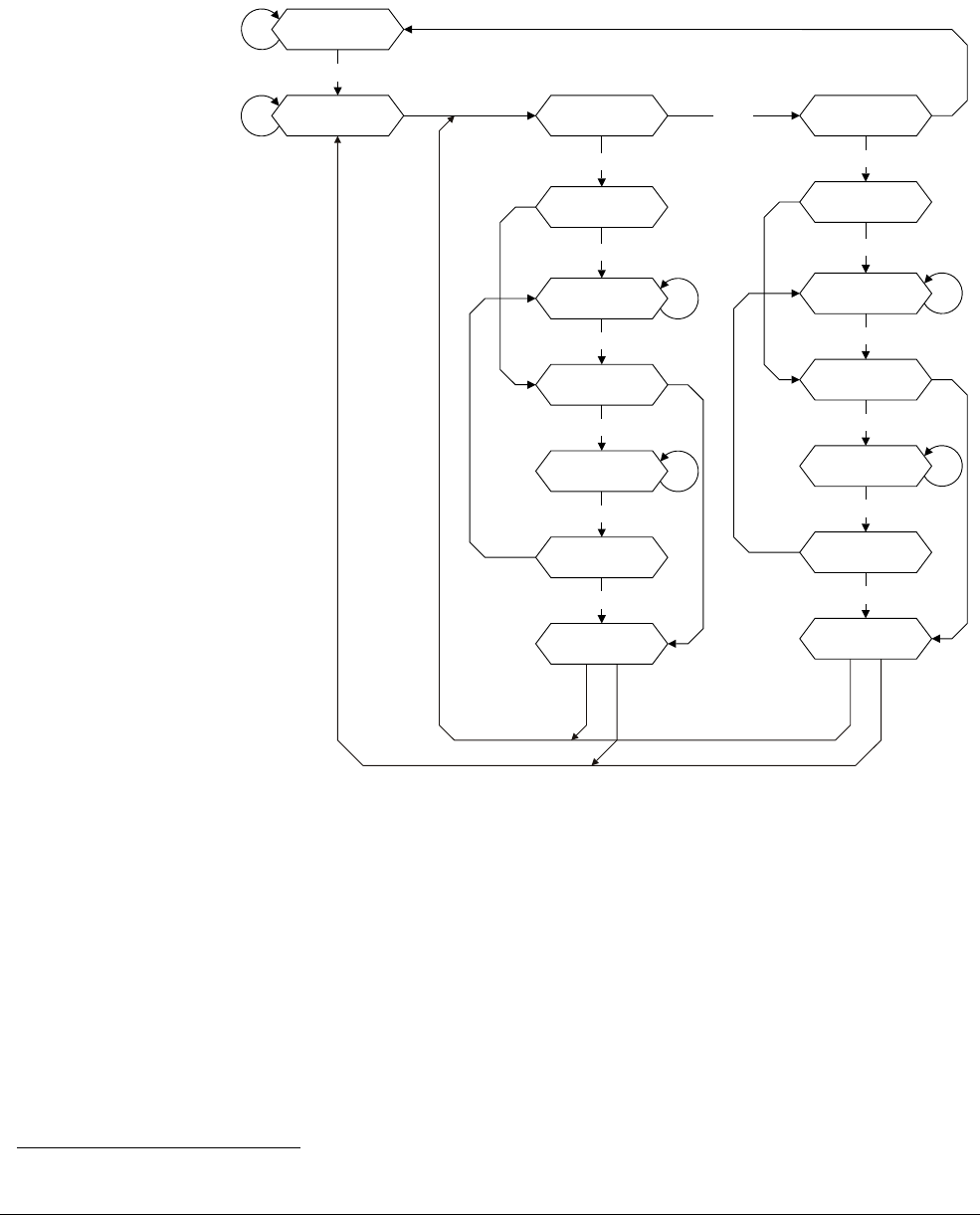
Debug Test Access Port
ARM DDI 0301H Copyright © 2004-2009 ARM Limited. All rights reserved. 14-2
ID012310 Non-Confidential, Unrestricted Access
14.1 Debug Test Access Port and Debug state
In Debug state, JTAG-based hardware provides access to the processor and debug unit. Access
is through scan chains and the Debug Test Access Port (DBGTAP). The DBGTAP state Machine
(DBGTAPSM) is illustrated in Figure 14-1.
Figure 14-1 JTAG DBGTAP state machine diagram1
1. From IEEE Std 1149.1-2001. Copyright 2001 IEEE. All rights reserved.
tms=1
tms=0
tms=1 tms=1
tms=1 tms=0 tms=1 tms=0
tms=1
tms=1
tms=0
Run-Test/Idle
Test-Logic-
Reset
Select-DR-Scan Select-IR-Scan
tms=1
Capture-DR
tms=0
tms=0
tms=0
Capture-IR
tms=0
Shift-IR
Exit1-IR
tms=1
Pause-IR
tms=0
Exit2-IR
tms=1
Update-IR
tms=1
tms=0
Shift-DR
Exit1-DR
tms=1
Pause-DR
tms=0
Exit2-DR
tms=1
Update-DR
tms=1
tms=0
tms=0
tms=1
tms=0 tms=0
tms=1
tms=0
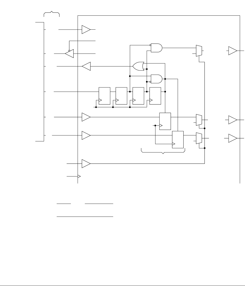
Debug Test Access Port
ARM DDI 0301H Copyright © 2004-2009 ARM Limited. All rights reserved. 14-3
ID012310 Non-Confidential, Unrestricted Access
14.2 Synchronizing RealView ICE
The system and test clocks are synchronized internally to the macrocell. The ARM RealView
ICE debug agent directly supports one or more cores within an ASIC design. The off-chip
device, for example, RealView ICE, issues a TCK signal and waits for the RTCK, Returned
TCK, signal to come back. Synchronization is maintained because the off-chip device does not
progress to the next TCK edge until after an RTCK edge is received. Figure 14-2 shows this
synchronization.
Figure 14-2 RealView ICE clock synchronization
Note
All of the D type flip-flops are reset by DBGnTRST.
DQ DQ DQ DQ
TMS
TDI
CLKIN
Input sample and hold
RTCK
nTRST
ARM1176JZ-S core
RealView
ICE
CLKIN
TCK
CLKIN
RealView ICE
interface pads
JTAGSYNCBYPASS
0
1
0
1
DBGTDI
DBGTMS
TDI
0
1
DBGTCKEN
DQ
EN
DQ
EN
TMS
TCK
TDO
DBGnTRST
DBGnTDOEN
DBGTDO

Debug Test Access Port
ARM DDI 0301H Copyright © 2004-2009 ARM Limited. All rights reserved. 14-4
ID012310 Non-Confidential, Unrestricted Access
14.3 Entering Debug state
Halting debug-mode is enabled by writing a 1 to bit 14 of the DSCR, see CP14 c1, Debug Status
and Control Register (DSCR) on page 13-7. This can only be done by a DBGTAP debugger
hardware such as RealView ICE. When this mode is enabled and the core is in a state where
debug is permitted the processor halts, instead of taking an exception in software, if one of the
following events occurs:
• vector catch occurs
• a breakpoint hits
• a watchpoint hits
• a BKPT instruction is executed.
The processor also enters Debug state, provided that its state permits debug, when:
• A Halt instruction has been scanned in through the DBGTAP. The DBGTAP controller
must pass through Run-Test/Idle to issue the Halt command to the processor.
•EDBGRQ is asserted.
If debug is enabled by DBGEN, scanning a Halt instruction in through the DBGTAP, or
asserting EDBGRQ, halts the processor and causes it to enter Debug state, regardless of the
selection of a debug-state in DSCR[15:14]. This means that a debugger can halt the processor
immediately after reset in a situation where it cannot first enable Halting debug-mode during
reset.
The core halted bit in the DSCR is set when Debug state is entered. At this point, the debugger
determines why the integer core was halted and preserves the processor state. The MSR
instruction can be used to change modes permitted by the SPIDEN signal and SUIDEN bit and
gain access to banked registers in the machine. While in Debug state:
• the PC is not incremented
• interrupts are ignored
• all instructions are read from the instruction transfer register, scan chain 4.
Debug state on page 13-37 describes the Debug state.

Debug Test Access Port
ARM DDI 0301H Copyright © 2004-2009 ARM Limited. All rights reserved. 14-5
ID012310 Non-Confidential, Unrestricted Access
14.4 Exiting Debug state
To exit from Debug state, scan in the Restart instruction through the processor DBGTAP. You
might want to adjust the PC before restarting, depending on the way the integer core entered
Debug state. When the state machine enters the Run-Test/Idle state, normal operations resume.
The delay, waiting until the state machine is in Run-Test/Idle, enables conditions to be set up in
other devices in a multiprocessor system without taking immediate effect. When Run-Test/Idle
state is entered, all the processors resume operation simultaneously. The core restarted bit is set
when the Restart sequence is complete.

Debug Test Access Port
ARM DDI 0301H Copyright © 2004-2009 ARM Limited. All rights reserved. 14-6
ID012310 Non-Confidential, Unrestricted Access
14.5 The DBGTAP port and debug registers
The processor DBGTAP controller is the part of the debug unit that enables access through the
DBGTAP to the on-chip debug resources, such as breakpoint and watchpoint registers. The
DBGTAP controller is based on the IEEE 1149.1 standard and supports:
• a device ID register
• a bypass register
• a five-bit instruction register
• a five-bit scan chain select register.
In addition, the public instructions that Table 14-1 lists are supported.
Table 14-1 Supported public instructions
Binary code Instruction Description
b00000 EXTEST This instruction connects the selected scan chain between DBGTDI and DBGTDO.
When the instruction register is loaded with the EXTEST instruction, the debug scan
chains can be written. See Scan chains on page 14-10.
b00001 - Reserved.
b00010 Scan_N Selects the Scan Chain Select Register (SCREG). This instruction connects SCREG
between DBGTDI and DBGTDO. See Scan chain select register (SCREG) on
page 14-9.
b00011 - Reserved.
b00100 Restart Forces the processor to leave Debug state. This instruction is used to exit from Debug
state. The processor restarts when the Run-Test/Idle state is entered.
b00101 - Reserved.
b00110 - Reserved.
b00111 - Reserved.
b01000 Halt Forces the processor to enter Debug state. This instruction stops the processor and puts
it into Debug state.
b01001 - Reserved.
b01010-b01011 - Reserved.
b01100 INTEST This instruction connects the selected scan chain between DBGTDI and DBGTDO.
When the instruction register is loaded with the INTEST instruction, the debug scan
chains can be read. See Scan chains on page 14-10.
b01101-b11100 - Reserved.

Debug Test Access Port
ARM DDI 0301H Copyright © 2004-2009 ARM Limited. All rights reserved. 14-7
ID012310 Non-Confidential, Unrestricted Access
Note
Sample/Preload, Clamp, HighZ, and ClampZ instructions are not implemented because the
processor DBGTAP controller does not support the attachment of external boundary scan
chains.
All unused DBGTAP controller instructions default to the Bypass instruction.
b11101 ITRsel When this instruction is loaded into the IR, Update-DR state, the DBGTAP controller
behaves as if IR=EXTEST and SCREG=4. The ITRsel instruction makes the
DBGTAP controller behave as if EXTEST and scan chain 4 are selected. It can be used
to speed up certain debug sequences. See Using the ITRsel IR instruction on
page 14-22 for the effects of using this instruction.
b11110 IDcode See IEEE 1149.1. Selects the DBGTAP controller device ID code register.
The IDcode instruction connects the device identification register, or ID register,
between DBGTDI and DBGTDO. The ID register is a 32-bit register that enables you
to determine the manufacturer, part number, and version of a component using the
DBGTAP.
See Device ID code register on page 14-8 for details of selecting and interpreting the
ID register value.
b11111 Bypass See IEEE 1149.1. Selects the DBGTAP controller bypass register. The Bypass
instruction connects a 1-bit shift register, the bypass register, between DBGTDI and
DBGTDO. The first bit shifted out is a 0. All unused DBGTAP controller instruction
codes default to the Bypass instruction. See Bypass register on page 14-8.
Table 14-1 Supported public instructions (continued)
Binary code Instruction Description
Debug Test Access Port
ARM DDI 0301H Copyright © 2004-2009 ARM Limited. All rights reserved. 14-8
ID012310 Non-Confidential, Unrestricted Access
14.6 Debug registers
You can connect the following debug registers between DBGTDI and DBGTDO:
•Bypass register
•Device ID code register
•Instruction register on page 14-9
•Scan chain select register (SCREG) on page 14-9
•Scan chain 0, debug ID register (DIDR) on page 14-11
•Scan chain 1, Debug Status and Control Register (DSCR) on page 14-11
•Scan chain 4, instruction transfer register (ITR) on page 14-13
•Scan chain 5 on page 14-15.
•Scan chain 6 on page 14-17.
•Scan chain 7 on page 14-17.
14.6.1 Bypass register
Purpose Bypasses the device by providing a path between DBGTDI and
DBGTDO.
Length 1 bit.
Operating mode When the bypass instruction is the current instruction in the instruction
register, serial data is transferred from DBGTDI to DBGTDO in the
Shift-DR state with a delay of one TCK cycle. There is no parallel output
from the bypass register. A logic 0 is loaded from the parallel input of the
bypass register in the Capture-DR state. Nothing happens at the
Update-DR state.
Order Figure 14-3 shows the order of bits in the bypass register.
Figure 14-3 Bypass register bit order
14.6.2 Device ID code register
Purpose Device identification. To distinguish the ARM1176JZF-S processors from
other processors, the DBGTAP controller ID is unique for each. This
means that a DBGTAP debugger, such as RealView ICE, can easily see the
processor that it is connected to. The Device ID register version and
manufacturer ID fields are routed to the edge of the chip so that partners
can create their own Device ID numbers by tying the pins to HIGH or
LOW values.
The default manufacturer ID for the ARM1176JZF-S processor is
b11110000111. The part number field is hard-wired inside the
ARM1176JZF-S to
0x7B76
.
0b0
DBGTDI DBGTDO
Bypass
Debug Test Access Port
ARM DDI 0301H Copyright © 2004-2009 ARM Limited. All rights reserved. 14-9
ID012310 Non-Confidential, Unrestricted Access
All ARM semiconductor partner-specific devices must be identified by
manufacturer ID numbers of the form shown in c0, Main ID Register on
page 3-20.
Length 32 bits.
Operating mode When the ID code instruction is current, the shift section of the device ID
register is selected as the serial path between DBGTDI and DBGTDO.
There is no parallel output from the ID register. The 32-bit device ID code
is loaded into this shift section during the Capture-DR state. This is shifted
out during Shift-DR, least significant bit first, while a don’t care value is
shifted in. The shifted-in data is ignored in the Update-DR state.
Order Figure 14-4 shows the order of bits in the ID code register.
Figure 14-4 Device ID code register bit order
14.6.3 Instruction register
Purpose Holds the current DBGTAP controller instruction.
Length 5 bits.
Operating mode When in Shift-IR state, the shift section of the instruction register is
selected as the serial path between DBGTDI and DBGTDO. At the
Capture-IR state, the binary value b00001 is loaded into this shift section.
This is shifted out during Shift-IR, least significant bit first, while a new
instruction is shifted in, least significant bit first. At the Update-IR state,
the value in the shift section is loaded into the instruction register so it
becomes the current instruction. On DBGTAP reset, the IDcode becomes
the current instruction.
Order Figure 14-5 shows the order of bits in the instruction register.
Figure 14-5 Instruction register bit order
14.6.4 Scan chain select register (SCREG)
Purpose Holds the currently active scan chain number.
DBGTDI DBGTDO
Data[31:0]
1
Version
31 28 27 12 11 1 0
Part number Manufacturer ID
0b00001
DBGTDI DBGTDO
Data[4:0]
IR[4:0]
Debug Test Access Port
ARM DDI 0301H Copyright © 2004-2009 ARM Limited. All rights reserved. 14-10
ID012310 Non-Confidential, Unrestricted Access
Length 5 bits.
Operating mode After Scan_N has been selected as the current instruction, when in
Shift-DR state, the shift section of the scan chain select register is selected
as the serial path between DBGTDI and DBGTDO. At the Capture-DR
state, the binary value b10000 is loaded into this shift section. This is
shifted out during Shift-DR, least significant bit first, while a new value is
shifted in, least significant bit first. At the Update-DR state, the value in
the shift section is loaded into the Scan Chain Select Register to become
the current active scan chain. All additional instructions such as INTEST
then apply to that scan chain. The currently selected scan chain only
changes when a Scan_N or ITRsel instruction is executed, or a DBGTAP
reset occurs. On DBGTAP reset, scan chain 3 is selected as the active scan
chain.
Order Figure 14-6 shows the order of bits in the scan chain select register.
Figure 14-6 Scan chain select register bit order
14.6.5 Scan chains
To access the debug scan chains you must:
1. Load the Scan_N instruction into the IR. Now SCREG is selected between DBGTDI and
DBGTDO.
2. Load the number of the required scan chain. For example, load b00101 to access scan
chain 5.
3. Load either INTEST or EXTEST into the IR.
4. Go through the DR leg of the DBGTAPSM to access the scan chain.
INTEST and EXTEST are used as follows:
INTEST Use INTEST for reading the active scan chain. Data is captured into the shift
register at the Capture-DR state. The previous value of the scan chain is shifted
out during the Shift-DR state, while a new value is shifted in. The scan chain is
not updated during Update-DR. Those bits or fields that are defined as cleared on
read are only cleared if INTEST is selected, even when EXTEST also captures
their values.
EXTEST Use EXTEST for writing the active scan chain. Data is captured into the shift
register at the Capture-DR state. The previous value of the scan chain is shifted
out during the Shift-DR state, while a new value is shifted in. The scan chain is
updated with the new value during Update-DR.
0b10000
DBGTDI DBGTDO
Data[4:0]
SCREG[4:0]
40
Debug Test Access Port
ARM DDI 0301H Copyright © 2004-2009 ARM Limited. All rights reserved. 14-11
ID012310 Non-Confidential, Unrestricted Access
Note
There are some exceptions to this use of INTEST and EXTEST to control reading and writing
the scan chain. These are noted in the relevant scan chain descriptions.
Scan chain 0, debug ID register (DIDR)
Purpose Debug.
Length 8 + 32 = 40 bits.
Description Debug identification. This scan chain accesses CP14 debug register 0, the debug
ID register. Additionally, the eight most significant bits of this scan chain contain
an implementor code. This field is hardwired to
0x41
, the implementor code for
ARM Limited, as specified in the ARM Architecture Reference Manual. This
register is read-only. Therefore, EXTEST has the same effect as INTEST.
Order Figure 14-7 shows the order of bits in scan chain 0.
Figure 14-7 Scan chain 0 bit order
Scan chain 1, Debug Status and Control Register (DSCR)
Purpose Debug.
Length 32 bits.
Description This scan chain accesses CP14 register 1, the DSCR. This is mostly a read/write
register, although certain bits are read-only for the Debug Test Access Port. See
CP14 c1, Debug Status and Control Register (DSCR) on page 13-7 for details of
DSCR bit definitions, and for read/write attributes for each bit. Those bits defined
as cleared on read are only cleared if INTEST is selected.
Order Figure 14-8 shows the order of bits in scan chain 1.
Figure 14-8 Scan chain 1 bit order
DBGTDI DBGTDO
Data[39:0]
Implementor
39 32 31 0
DIDR[31:0]
DBGTDI DBGTDO
Data[31:0]
DSCR[31:0]
31 0
DSCR[31:0]

Debug Test Access Port
ARM DDI 0301H Copyright © 2004-2009 ARM Limited. All rights reserved. 14-12
ID012310 Non-Confidential, Unrestricted Access
The following DSCR bits affect the operation of other scan chains:
DSCR[30:29] rDTRfull and wDTRfull flags. These indicate the status of the rDTR and
wDTR registers. They are copies of the rDTRempty, NOT rDTRfull, and
wDTRfull bits that the DBGTAP debugger sees in scan chain 5.
DSCR[13] Execute ARM instruction enable bit. This bit enables the mechanism used
for executing instructions in Debug state. It changes the behavior of the
rDTR and wDTR registers, the sticky precise Data Abort bit, rDTRempty,
wDTRfull, and InstCompl flags. See Scan chain 5 on page 14-15.
DSCR[6] Sticky precise Data Abort flag. If the core is in Debug state and the
DSCR[13] execute ARM instruction enable bit is HIGH, then this flag is
set on precise Data Aborts. See CP14 c1, Debug Status and Control
Register (DSCR) on page 13-7.
Note
Unlike DSCR[6], DSCR [7] sticky imprecise Data Aborts flag and
DSCR[8] sticky Undefined bits do not affect the operation of the other
scan chains.
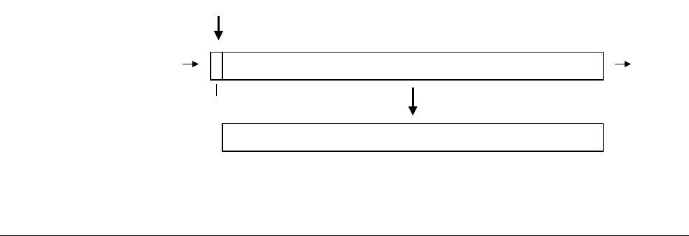
Debug Test Access Port
ARM DDI 0301H Copyright © 2004-2009 ARM Limited. All rights reserved. 14-13
ID012310 Non-Confidential, Unrestricted Access
Scan chain 4, instruction transfer register (ITR)
Purpose Debug
Length 1 + 32 = 33 bits
Description This scan chain accesses the Instruction Transfer Register (ITR), used to send
instructions to the core through the Prefetch Unit (PU). It consists of 32 bits of
information, plus an additional bit to indicate the completion of the instruction
sent to the core, InstCompl. The InstCompl bit is read-only.
While in Debug state, an instruction loaded into the ITR can be issued to the core
by making the DBGTAPSM go through the Run-Test/Idle state. The InstCompl
flag is cleared when the instruction is issued to the core and set when the
instruction completes.
For an instruction to be issued when going through Run-Test/Idle state, you must
ensure the following conditions are met:
• The processor must be in Debug state.
• The DSCR[13] execute ARM instruction enable bit must be set. For details
of the DSCR see CP14 c1, Debug Status and Control Register (DSCR) on
page 13-7.
• Scan chain 4 or 5 must be selected.
• INTEST or EXTEST must be selected.
• Ready flag must be captured set. That is, the last time the DBGTAPSM
went through Capture-DR the InstCompl flag must have been set.
• The DSCR[6] sticky precise Data Abort flag must be clear. This flag is set
on precise Data Aborts.
For an instruction to be loaded into the ITR when going through Update-DR, you
must ensure the following conditions are met:
• The processor can be in any state.
• The value of DSCR[13] execute ARM instruction enable bit does not
matter.
• Scan chain 4 must be selected.
• EXTEST must be selected.
• Ready flag must be captured set. That is, the last time the DBGTAPSM
went through Capture-DR the InstCompl flag must have been set.
• The value of DSCR[6] sticky precise Data Abort flag does not matter.
Order Figure 14-9 shows the order of bits in scan chain 4.
Figure 14-9 Scan chain 4 bit order
DBGTDI DBGTDO
Data[31:0]
ITR[31:0]
32 31 0
InstCompl
Ready

Debug Test Access Port
ARM DDI 0301H Copyright © 2004-2009 ARM Limited. All rights reserved. 14-14
ID012310 Non-Confidential, Unrestricted Access
It is important to distinguish between the InstCompl flag and the Ready flag:
• The InstCompl flag signals the completion of an instruction.
• The Ready flag is the captured version of the InstCompl flag, captured at the Capture-DR
state. The Ready flag conditions the execution of instructions and the update of the ITR.
The following points apply to the use of scan chain 4:
• When an instruction is issued to the core in Debug state, the PC is not incremented. It is
only changed if the instruction being executed explicitly writes to the PC. For example,
branch instructions and move to PC instructions.
• If CP14 debug register c5 is a source register for the instruction to be executed, the
DBGTAP debugger must set up the data in the rDTR before issuing the coprocessor
instruction to the core. See Scan chain 5 on page 14-15.
• Setting DSCR[13] the execute ARM instruction enable bit when the core is not in Debug
state leads to Unpredictable behavior.
• The ITR is write-only. When going through the Capture-DR state, an Unpredictable value
is loaded into the shift register.
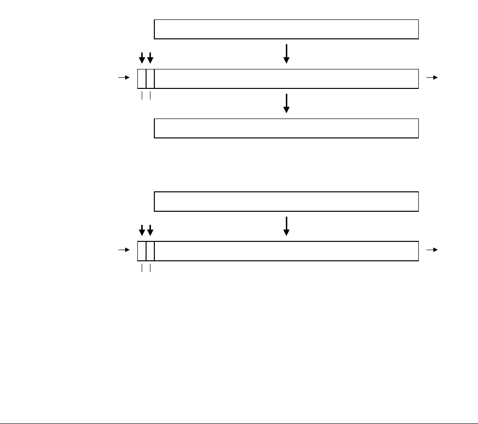
Debug Test Access Port
ARM DDI 0301H Copyright © 2004-2009 ARM Limited. All rights reserved. 14-15
ID012310 Non-Confidential, Unrestricted Access
Scan chain 5
Purpose Debug.
Length 1 + 1 + 32 = 34 bits.
Description This scan chain accesses CP14 register c5, the data transfer registers, rDTR and
wDTR. The rDTR is used to transfer words from the DBGTAP debugger to the
core, and is read-only to the core and write-only to the DBGTAP debugger. The
wDTR is used to transfer words from the core to the DBGTAP debugger, and is
read-only to the DBGTAP debugger and write-only to the core.
The DBGTAP controller only sees one, read/write, register through scan chain 5,
and the appropriate register is chosen depending on the instruction used. INTEST
selects the wDTR, and EXTEST selects the rDTR.
Additionally, scan chain 5 contains some status flags. These are nRetry, Valid, and
Ready. They are the captured versions of the rDTRempty, wDTRfull, and
InstCompl flags respectively. All are captured at the Capture-DR state.
Order Figure 14-10 shows the order of bits in scan chain 5 with EXTEST selected.
Figure 14-11 shows the order of bits in scan chain 5 with INTEST selected.
Figure 14-10 Scan chain 5 bit order, EXTEST selected
Figure 14-11 Scan chain 5 bit order, INTEST selected
You can use scan chain 5 for two purposes:
•As part of the Debug Communications Channel (DCC). The DBGTAP debugger uses scan
chain 5 to exchange data with software running on the core. The software accesses the
rDTR and wDTR using coprocessor instructions.
DBGTDI DBGTDO
Data[31:0]
rDTR[31:0]
32 31 0
InstCompl
Ready
wDTR[31:0]
33
rDTRempty
EXTEST selected
nRetry
DBGTDI DBGTDO
Data[31:0]
32 31 0
InstCompl
Ready
wDTR[31:0]
Valid
33
wDTRfull
INTEST selected

Debug Test Access Port
ARM DDI 0301H Copyright © 2004-2009 ARM Limited. All rights reserved. 14-16
ID012310 Non-Confidential, Unrestricted Access
• For examining and modifying the processor state while the core is halted. For example, to
read the value of an ARM register:
1. Issue a
MCR cp14, 0, Rd, c0, c5, 0
instruction to the core to transfer the register
contents to the CP14 debug c5 register.
2. Scan out the wDTR.
The DBGTAP debugger can use the DSCR[13] execute ARM instruction enable bit to indicate
to the core that it is going to use scan chain 5 as part of the DCC or for examining and modifying
the processor state. DSCR[13] = 0 indicates DCC use. The behavior of the rDTR and wDTR
registers, the sticky precise Data Abort, rDTRempty, wDTRfull, and InstCompl flags changes
accordingly:
•DSCR[13] = 0:
— The wDTRfull flag is set when the core writes a word of data to the DTR and cleared
when the DBGTAP debugger goes through the Capture-DR state with INTEST
selected. Valid indicates the state of the wDTR register, and is the captured version
of wDTRfull. Although the value of wDTR is captured into the shift register,
regardless of INTEST or EXTEST, wDTRfull is only cleared if INTEST is selected.
— The rDTR empty flag is cleared when the DBGTAP debugger writes a word of data
to the rDTR, and set when the core reads it. nRetry is the captured version of
rDTRempty.
— rDTR overwrite protection is controlled by the nRetry flag. If the nRetry flag is
sampled clear, meaning that the rDTR is full, when going through the Capture-DR
state, then the rDTR is not updated at the Update-DR state.
— The InstCompl flag is always set.
— The sticky precise Data Abort flag is Unpredictable. See CP14 c1, Debug Status
and Control Register (DSCR) on page 13-7.
•DSCR[13] = 1:
— The wDTR Full flag behaves as if DSCR[13] is clear. However, the Ready flag can
be used for handshaking in this mode.
— The rDTR Empty flag status behaves as if DSCR[13] is clear. However, the Ready
flag can be used for handshaking in this mode.
— rDTR overwrite protection is controlled by the Ready flag. If the InstCompl flag is
sampled clear when going through Capture-DR, then the rDTR is not updated at the
Update-DR state. This prevents an instruction that uses the rDTR as a source
operand from having it modified before it has time to complete.
— The InstCompl flag changes from 1 to 0 when an instruction is issued to the core,
and from 0 to 1 when the instruction completes execution.
— The sticky precise Data Abort flag is set on precise Data Aborts.
The behavior of the rDTR and wDTR registers, the sticky precise Data Abort, rDTRempty,
wDTRfull, and InstCompl flags when the core changes state is as follows:
• The DSCR[13] execute ARM instruction enable bit must be clear when the core is not in
Debug state. Otherwise, the behavior of the rDTR and wDTR registers, and the flags, is
Unpredictable.
• When the core enters Debug state, none of the registers and flags are altered.
• When the DSCR[13] execute ARM instruction enable bit is changed from 0 to 1:
1. None of the registers and flags are altered.
2. Ready flag can be used for handshaking.
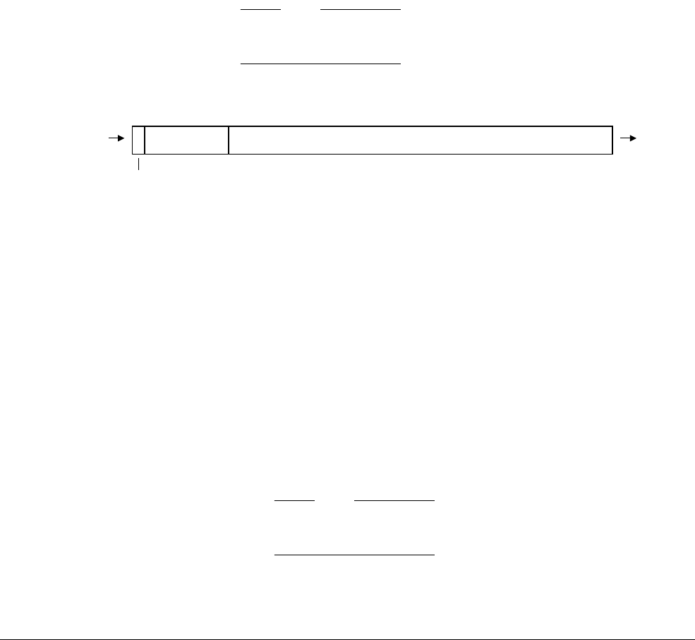
Debug Test Access Port
ARM DDI 0301H Copyright © 2004-2009 ARM Limited. All rights reserved. 14-17
ID012310 Non-Confidential, Unrestricted Access
• The InstCompl flag must be set when the DSCR[13] execute ARM instruction enable bit
is changed from 1 to 0. Otherwise, the behavior of the core is Unpredictable. If the
DSCR[13] flag is cleared correctly, none of the registers and flags are altered.
• When the core leaves Debug state, none of the registers and flags are altered.
Scan chain 6
Purpose Embedded Trace Macrocell.
Length 1 + 7 + 32 = 40 bits.
Description This scan chain accesses the register map of the Embedded Trace Macrocell. See
the description in the programmer’s model chapter in the Embedded Trace
Macrocell Architecture Specification for details of register allocation.
To access this scan chain you must select INTEST. Accesses to scan chain 6 with
EXTEST selected are ignored. In scan chain 6 you must use the nRW bit, bit[39],
to distinguish between reads and writes, as the Embedded Trace Macrocell
Architecture Specification describes.
Note
For scan chain 6, the use of INTEST and EXTEST differs from their standard use
that the start of this section describes.
Order Figure 14-12 shows the order of bits in scan chain 6.
Figure 14-12 Scan chain 6 bit order
Scan chain 7
Purpose Debug.
Length 7 + 32 + 1 = 40 bits.
Description Scan chain 7 accesses the VCR, PC, BRPs, and WRPs. The accesses are
performed with the help of read or write request commands. A read request copies
the data held by the addressed register into scan chain 7. A write request copies
the data held by the scan chain into the addressed register. When a request is
finished the ReqCompl flag is set. The DBGTAP debugger must poll it and check
it is set before another request can be issued. The exact behavior of the scan chain
is as follows:
• Either INTEST or EXTEST must be selected. INTEST and EXTEST have
the same meaning in this scan chain.
Note
For scan chain 7, the use of INTEST and EXTEST differs from the standard
use that the start of this section describes.
• If the value captured by the Ready/nRW bit at the Capture-DR state is 1, the
data that is being shifted in generates a request at the Update-DR state. The
Address field indicates the register being accessed, see Table 14-2 on
DBGTDI DBGTDO
Address[6:0]
39 32 31 0
Data[31:0]
38
nRW
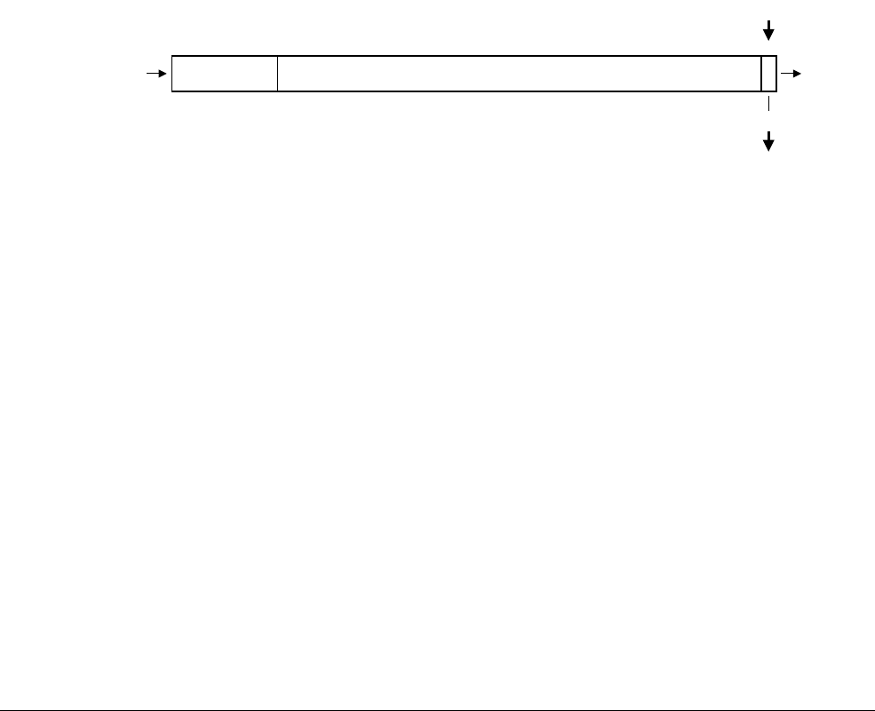
Debug Test Access Port
ARM DDI 0301H Copyright © 2004-2009 ARM Limited. All rights reserved. 14-18
ID012310 Non-Confidential, Unrestricted Access
page 14-19, the Data field contains the data to be written and the
Ready/nRW bit holds the read/write information, 0=read and 1=write. If the
request is a read, the Data field is ignored.
• When a request is placed, the Address and Data sections of the scan chain
are frozen. That is, their contents are not shifted until the request is
completed. This means that, if the value captured in the Ready/nRW field
at the Capture-DR state is 0, the shifted-in data is ignored and the
shifted-out value is all 0s.
• After a read request has been placed, if the DBGTAPSM goes through the
Capture-DR state and a logic 1 is captured in the Ready/nRW field, this
means that the shift register has also captured the requested register
contents. Therefore, they are shifted out at the same time as the Ready/nRW
bit. The Data field is corrupted as new data is shifted in.
• After a write request has been placed, if the DBGTAPSM goes through the
Capture-DR state and a logic 1 is captured in the Ready/nRW field, this
means that the requested write has completed successfully.
• If the Address field is all 0s, address of the NULL register, at the
Update-DR state, then no request is generated.
• A request to a reserved register generates Unpredictable behavior.
Order Figure 14-13 shows the order of bits in scan chain 7.
Figure 14-13 Scan chain 7 bit order
A typical sequence for writing registers is as follows:
1. Scan in the address of a first register, the data to write, and a 1 to indicate that this is a
write request.
2. Scan in the address of a second register, the data to write, and a 1 to indicate that this is a
write request.
Scan out 40 bits. If Ready/nRW is 0, repeat this step. If Ready/nRW is 1, the first write
request has completed successfully and the second has been placed.
3. Scan in the address 0. The rest of the fields are not important.
Scan out 40 bits. If Ready/nRW is 0, repeat this step. If Ready/nRW is 1, the second write
request has completed successfully. The scanned-in null request has avoided the
generation of another request.
A typical sequence for reading registers is as follows:
1. Scan in the address of a first register and a 0 to indicate that this is a read request. The Data
field is not important.
2. Scan in the address of a second register and a 0 to indicate that this is a read request.
DBGTDI DBGTDO
Address[6:0]
39 33 32 1
Data[31:0]
Ready/nRW
0
nRW
ReqCompl

Debug Test Access Port
ARM DDI 0301H Copyright © 2004-2009 ARM Limited. All rights reserved. 14-19
ID012310 Non-Confidential, Unrestricted Access
Scan out 40 bits. If Ready/nRW is 0, then repeat this step. If Ready/nRW is 1, the first read
request has completed successfully and the next scanned-out 32 bits are the requested
value. The second read request was placed at the Update-DR state.
3. Scan in the address 0, the rest of the fields are not important.
Scan out 40 bits. If Ready/nRW is 0, then repeat this step. If Ready/nRW is 1, the second
read request has completed successfully and the next scanned-out 32 bits are the requested
value. The scanned-in null request has avoided the generation of another request.
The register map is similar to the one of CP14 debug, and Table 14-2 lists it.
The following points apply to the use of scan chain 7:
• Every time there is a request to read the PC, a sample of its value is copied into scan chain
7. Writes are ignored. The sampled value can be used for profiling of the code. See
Interpreting the PC samples on page 14-20 for details of how to interpret the sampled
value.
• The external program counter sample register always reads
0xFFFFFFFF
in Debug state or
when the core is in a mode when Non-invasive debug is not permitted.
• When accessing registers using scan chain 7, the processor can be either in Debug state or
in normal state. This implies that breakpoints, watchpoints, and vector traps can be
programmed through the Debug Test Access Port even if the processor is running.
Table 14-2 Scan chain 7 register map
Address[6:0] Register number Abbreviation Register name
b0000000 0 NULL No request register
b0000001-b0000110 1-6 - Reserved
b0000111 7 VCR Vector catch register
b0001000 8 PC Program counter
b0010011-b0111111 19-63 - Reserved
b1000000-b1000101 64-69 BVRya
a. y is the decimal representation for the binary number Address[3:0]
Breakpoint value registers
b1000110-b1001111 70-79 - Reserved
b1010000-b1010101 80-85 BCRyaBreakpoint control registers
b1010110-b1011111 86-95 - Reserved
b1100000-b1100001 96-97 WVRyaWatchpoint value registers
b1100010-1b101111 98-111 - Reserved
b1110000-b1110001 112-113 WCRyaWatchpoint control registers
b1110010-b1111111 114-127 - Reserved

Debug Test Access Port
ARM DDI 0301H Copyright © 2004-2009 ARM Limited. All rights reserved. 14-20
ID012310 Non-Confidential, Unrestricted Access
Interpreting the PC samples
The PC values read correspond to instructions committed for execution, including those that
failed their condition code. However, these values are offset as Table 13-22 on page 13-33 lists.
These offsets are different for different processor states, so additional information is required:
• If a read request to the PC completes and Data[1:0] equals b00, the read value corresponds
to an ARM state instruction whose 30 most significant bits of the offset address,
instruction address + 8, are given in Data[31:2].
• If a read request to the PC completes and Data[0] equals b1, the read value corresponds
to a Thumb state instruction whose 31 most significant bits of the offset address,
instruction address + 4, are given in Data[31:1].
• If a read request to the PC completes and Data[1:0] equals b10, the read value corresponds
to a Jazelle state instruction whose 30 most significant bits of its address are given in
Data[31:2], the offset is 0. Because of the state encoding, the lower two bits of the Java
address are not sampled. However, the information provided is enough for profiling the
code.
• If the PC is read while the processor is in Debug state, the result is
0xFFFFFFFF
.
Scan chains 8-15
These scan chains are reserved.
Scan chains 16-31
These scan chains are unassigned.
14.6.6 Reset
The DBGTAP is reset either by asserting DBGnTRST, or by clocking it while DBGTAPSM is
in the Test-Logic-Reset state. The processor, including CP14 debug logic, is not affected by
these events. See Reset modes on page 9-10 and CP14 registers reset on page 13-25 for details.

Debug Test Access Port
ARM DDI 0301H Copyright © 2004-2009 ARM Limited. All rights reserved. 14-21
ID012310 Non-Confidential, Unrestricted Access
14.7 Using the Debug Test Access Port
This section contains the following subsections:
•Entering and leaving Debug state
•Executing instructions in Debug state
•Using the ITRsel IR instruction on page 14-22
•Transferring data between the host and the core on page 14-23
•Using the debug communications channel on page 14-23
•Target to host debug communications channel sequence on page 14-24
•Host to target debug communications channel on page 14-24
•Transferring data in Debug state on page 14-25
•Example sequences on page 14-26.
14.7.1 Entering and leaving Debug state
Debug sequences on page 14-29 describes these debug sequences in detail.
14.7.2 Executing instructions in Debug state
When the processor is in Debug state, it can be forced to execute ARM state instructions using
the DBGTAP. Two registers are used for this purpose, the Instruction Transfer Register (ITR)
and the Data Transfer Register (DTR). The ITR is used to insert an instruction into the processor
pipeline. An ARM state instruction can be loaded into this register using scan chain number 4.
When the instruction is loaded, and INTEST or EXTEST is selected, and scan chain 4 or 5 is
selected, the instruction can be issued to the core by making the DBGTAPSM go through the
Run-Test/Idle state, provided certain conditions, that this section describes, are met. This
mechanism enables re-executing the same instruction over and over without having to reload it.
The DTR can be used in conjunction with the ITR to transfer data in and out of the core. For
example, to read out the value of an ARM register:
1. issue an
MCR p14,0,Rd,c0,c5,0
instruction to the core to transfer the
<Rd>
contents to the
c5 register
2. scan out the wDTR.
The DSCR[13] execute ARM instruction enable bit controls the activation of the ARM
instruction execution mechanism. If this bit is cleared, no instruction is issued to the core when
the DBGTAPSM goes through Run-Test/Idle. Setting this bit while the core is not in Debug state
leads to Unpredictable behavior. If the core is in Debug state and this bit is set, the Ready and
the sticky precise Data Abort flags condition the updates of the ITR and the instruction issuing,
as Scan chain 4, instruction transfer register (ITR) on page 14-13 describes. As an example, this
sequence stores out the contents of the ARM register R0:
1. Scan_N into the IR.
2. 1 into the SCREG.
3. INTEST into the IR.
4. Scan out the contents of the DSCR. This action clears the sticky precise Data Abort and
sticky imprecise Data Abort flags and sticky Undefined bit.
5. EXTEST into the IR.
6. Scan in the previously read value with the DSCR[13] execute ARM instruction enable bit
set.
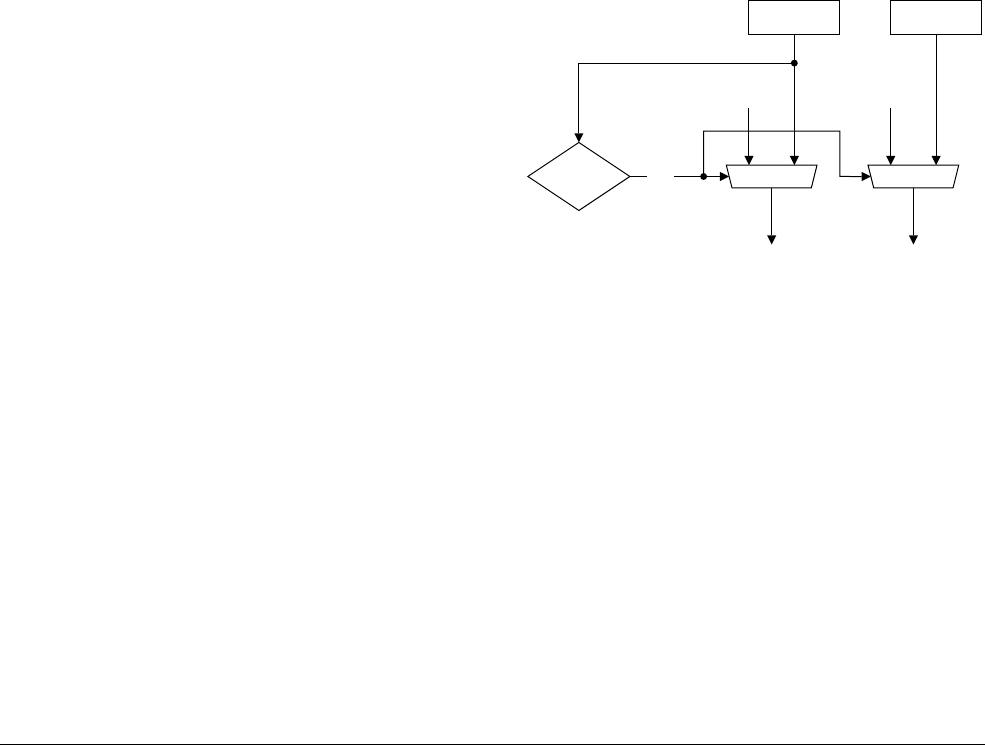
Debug Test Access Port
ARM DDI 0301H Copyright © 2004-2009 ARM Limited. All rights reserved. 14-22
ID012310 Non-Confidential, Unrestricted Access
7. Scan_N into the IR.
8. 4 into the SCREG.
9. EXTEST into the IR.
10. Scan the
MCR p14,0,R0,c0,c5,0
instruction into the ITR.
11. Go through the Run-Test/Idle state of the DBGTAPSM.
12. Scan_N into the IR.
13. 5 into the SCREG.
14. INTEST into the IR.
15. Scan out 34 bits. The 33rd bit indicates if the instruction has completed. If the bit is clear,
repeat this step again.
16. The least significant 32 bits hold the contents of R0.
14.7.3 Using the ITRsel IR instruction
When the ITRsel instruction is loaded into the IR, at the Update-IR state, the DBGTAP
controller behaves as if EXTEST and scan chain 4 are selected, but SCREG retains its value. It
can be used to speed up certain debug sequences.
Figure 14-14 shows the effect of the ITRsel IR instruction.
Figure 14-14 Behavior of the ITRsel IR instruction
Consider for example the preceding sequence to store out the contents of ARM register R0. This
is the same sequence using the ITRsel instruction:
1. Scan_N into the IR.
2. 1 into the SCREG.
3. INTEST into the IR.
4. Scan out the contents of the DSCR. This action clears the sticky precise Data Abort and
sticky imprecise Data Abort flags.
5. EXTEST into the IR.
6. Scan in the previously read value with the DSCR[13] execute ARM instruction enable bit
set.
7. Scan_N into the IR.
01
=ITRSEL?
IR SCREG
EXTEST
01
4
Current IR
instruction
Current
scan chain
Yes

Debug Test Access Port
ARM DDI 0301H Copyright © 2004-2009 ARM Limited. All rights reserved. 14-23
ID012310 Non-Confidential, Unrestricted Access
8. 5 into the SCREG.
9. ITRsel into the IR. Now the DBGTAP controller works as if EXTEST and scan chain 4 is
selected.
10. Scan the
MCR p14,0,R0,c0,c5,0
instruction into the ITR.
11. Go through the Run-Test/Idle state of the DBGTAPSM.
12. INTEST into the IR. Now INTEST and scan chain 5 are selected.
13. Scan out 34 bits. The 33rd bit indicates if the instruction has completed. If the bit is clear,
repeat this step again.
14. The least significant 32 bits hold the contents of R0.
The number of steps has been reduced from 16 to 14. However, the bigger reduction comes
when reading additional registers. Using the ITRsel instruction there are 6 extra steps, 9 to 14,
compared with 10 extra steps, 7 to 16, in the first sequence.
14.7.4 Transferring data between the host and the core
There are two ways that a DBGTAP debugger can send or receive data from the core:
• using the DCC, when the processor is not in Debug state
• using the instruction execution mechanism that Executing instructions in Debug state on
page 14-21 describes, when the core is in Debug state.
The following sections describe this:
•Using the debug communications channel.
•Target to host debug communications channel sequence on page 14-24
•Host to target debug communications channel on page 14-24
•Transferring data in Debug state on page 14-25
•Example sequences on page 14-26.
14.7.5 Using the debug communications channel
The DCC is defined as the set of resources that the external DBGTAP debugger uses to
communicate with a piece of software running on the core.
The DCC in the processor is implemented using the two physically separate DTRs and a
full/empty bit pair to augment each register, creating a bidirectional data port. One register can
be read from the DBGTAP and is written from the processor. The other register is written from
the DBGTAP and read by the processor. The full/empty bit pair for each register is automatically
updated by the debug unit hardware, and is accessible to both the DBGTAP and to software
running on the processor.
At the core side, the DCC resources are the following:
• CP14 debug register c5, DTR. Data coming from a DBGTAP debugger can be read by an
MRC or STC instruction addressed to this register. The core can write to this register any
data intended for the DBGTAP debugger, using an MCR or LDC instruction. Because the
DTR comprises both a read, rDTR, and a write portion, wDTR, a piece of data written by
the core and another coming from the DBGTAP debugger can be held in this register at
the same time.

Debug Test Access Port
ARM DDI 0301H Copyright © 2004-2009 ARM Limited. All rights reserved. 14-24
ID012310 Non-Confidential, Unrestricted Access
• Some flags and control bits at CP14 debug register c1, DSCR:
DSCR[12] User mode access to DCC disable bit. If this bit is set, only
privileged software can access the DCC. That is, access the DSCR
and the DTR.
DSCR[29] The wDTRfull flag. When clear, this flag indicates to the core that
the wDTR is ready to receive data from the core.
DSCR[30] The rDTRfull flag. When set, this flag indicates to the core that there
is data available to read at the DTR.
At the DBGTAP side, the resources are the following:
• Scan chain 5. See Scan chain 5 on page 14-15. The only part of this scan chain that it is
not used for the DCC is the Ready flag. The rest of the scan chain is to be used in the
following way:
rDTR When the DBGTAPSM goes through the Update-DR state with
EXTEST and scan chain 5 selected, and the nRetry flag set, the
contents of the Data field are loaded into the rDTR. This is how the
DBGTAP debugger sends data to the software running on the core.
wDTR When the DBGTAPSM goes through the Capture-DR state with
INTEST and scan chain 5 selected, the contents of the wDTR are
loaded into the Data field of the scan chain. This is how the
DBGTAP debugger reads the data sent by the software running on
the core.
Valid flag When set, this flag indicates to the DBGTAP debugger that the
contents of the wDTR that it captured a short time ago are valid.
nRetry flag When set, this flag indicates to the DBGTAP debugger that the
scanned-in Data field has been successfully written into the rDTR at
the Update-DR state.
14.7.6 Target to host debug communications channel sequence
The DBGTAP debugger can use the following sequence for receiving data from the core:
1. Scan_N into the IR.
2. 5 into the SCREG.
3. INTEST into the IR.
4. Scan out 34 bits of data. If the Valid flag is clear, repeat this step again.
5. The least significant 32 bits hold valid data.
6. Go to step 4 again to read out more data.
14.7.7 Host to target debug communications channel
The DBGTAP debugger can use the following sequence for sending data to the core:
1. Scan_N into the IR.
2. 5 into the SCREG.
3. EXTEST into the IR.
4. Scan in 34 bits, the least significant 32 holding the word to be sent. At the same time, 34
bits were scanned out. If the nRetry flag is clear, repeat this step again.

Debug Test Access Port
ARM DDI 0301H Copyright © 2004-2009 ARM Limited. All rights reserved. 14-25
ID012310 Non-Confidential, Unrestricted Access
5. Now the data has been written into the rDTR. Go to step 4 again to send in more data.
14.7.8 Transferring data in Debug state
When the core is in Debug state, the DBGTAP debugger can transfer data in and out of the core
using the instruction execution facilities that Executing instructions in Debug state on
page 14-21 describes in addition to scan chain 5. You must ensure that the DSCR[13] execute
ARM instruction enable bit is set for the instruction execution mechanism to work. When it is
set, the interface for the DBGTAP debugger consists of the following:
• Scan chain 4. See Scan chain 4, instruction transfer register (ITR) on page 14-13. It is
used for loading an instruction and for monitoring the status of the execution:
ITR When the DBGTAPSM goes through the Update-DR state with
EXTEST and scan chain 4 selected, and the Ready flag set, the ITR
is loaded with the least significant 32 bits of the scan chain.
InstCompl flag When clear, this flag indicates to the DBGTAP debugger that the last
issued instruction has not yet completed execution. While Ready,
captured version of InstCompl, is clear, no updates of the ITR and
the rDTR occur and the instruction execution mechanism is
disabled. No instruction is issued when going through
Run-Test/Idle.
• Scan chain 5. See Scan chain 5 on page 14-15. It is used for writing in or reading out the
data and for monitoring the state of the execution:
rDTR When the DBGTAPSM goes through the Update-DR state with
EXTEST and scan chain 5 selected, and the Ready flag set, the
contents of the Data field are loaded into the rDTR.
wDTR When the DBGTAPSM goes through the Capture-DR state with
INTEST or EXTEST selected, the contents of the wDTR are loaded
into the Data field of the scan chain.
InstCompl flag When clear, this flag indicates to the DBGTAP debugger that the last
issued instruction has not yet completed execution. While Ready,
captured version of InstCompl, is clear, no updates of the ITR and
the rDTR occur and the instruction execution mechanism is
disabled. No instruction is issued when going through
Run-Test/Idle.
• Some flags and control bits at CP14 debug register c1, DSCR:
DSCR[13] Execute ARM instruction enable bit. This bit must be set for the
instruction execution mechanism to work.
Sticky precise Data Abort flag
DSCR[6]. When set, this flag indicates to the DBGTAP debugger
that a precise Data Abort occurred while executing an instruction in
Debug state. While this bit is set, the instruction execution
mechanism is disabled. When this flag is set InstCompl stays HIGH,
and additional attempts to execute an instruction appear to succeed
but do not execute.
Sticky imprecise Data Abort flag
DSCR[7]. When set, this flag indicates to the DBGTAP debugger
that an imprecise Data Abort occurred while executing an
instruction in Debug state. This flag does not disable the Debug state
instruction execution.

Debug Test Access Port
ARM DDI 0301H Copyright © 2004-2009 ARM Limited. All rights reserved. 14-26
ID012310 Non-Confidential, Unrestricted Access
Sticky Undefined flag
DSCR[8]. When set, this flag indicates to the DBGTAP debugger
that an Undefined exception occurred while executing an instruction
in Debug state. This flag does not disable the Debug state instruction
execution.
14.7.9 Example sequences
This section includes some example sequences to illustrate how to transfer data between the
DBGTAP debugger and the core when it is in Debug state. The examples are related to accessing
the processor memory.
Target to host transfer
The DBGTAP debugger can use the following sequence for reading data from the processor
memory system. The sequence assumes that the ARM register R0 contains a pointer to the
address of memory where the read has to start:
1. Scan_N into the IR.
2. 1 into the SCREG.
3. INTEST into the IR.
4. Scan out the contents of the DSCR. This clears the sticky precise Data Abort, sticky
imprecise Data Abort flags, and sticky Undefined flags.
5. Scan_N into the IR.
6. 4 into the SCREG.
7. EXTEST into the IR.
8. Scan in the
LDC p14,c5,[R0],#4
instruction into the ITR.
9. Scan_N into the IR.
10. 5 into the SCREG.
11. INTEST into the IR.
12. Go through Run-Test/Idle state. The instruction loaded into the ITR is issued to the
processor pipeline.
13. Scan out 34 bits of data. If the Ready flag is clear, repeat this step again.
14. The instruction has completed execution. Store the least significant 32 bits.
15. Go to step 13 again for reading out more data.
16. Scan_N into the IR.
17. 1 into the SCREG.
18. INTEST into the IR.
19. Scan out the contents of the DSCR. This clears the sticky precise Data Abort and sticky
imprecise Data Abort and sticky Undefined flags. If the sticky precise Data Abort is set,
this means that during the sequence one of the instructions caused a precise Data Abort.
Not all the instructions that follow are executed. Register R0 points to the next word to be
read, and after the cause for the abort has been fixed the sequence resumes at step 5.

Debug Test Access Port
ARM DDI 0301H Copyright © 2004-2009 ARM Limited. All rights reserved. 14-27
ID012310 Non-Confidential, Unrestricted Access
Note
If the sticky imprecise Data Aborts flag is set, an imprecise Data Abort has occurred and
the sequence restarts at step 1 after the cause of the abort is fixed and R0 is reloaded.
Host to target transfer
The DBGTAP debugger can use the following sequence for writing data to the processor
memory system. The sequence assumes that the ARM register R0 contains a pointer to the
address of memory where the write has to start:
1. Scan_N into the IR.
2. 1 into the SCREG.
3. INTEST into the IR.
4. Scan out the contents of the DSCR. This clears the sticky precise Data Abort, sticky
imprecise Data Abort, and sticky Undefined flags.
5. Scan_N into the IR.
6. 4 into the SCREG.
7. EXTEST into the IR.
8. Scan in the
STC p14,c5,[R0],#4
instruction into the ITR.
9. Scan_N into the IR.
10. 5 into the SCREG.
11. EXTEST into the IR.
12. Scan in 34 bits, the least significant 32 holding the word to be sent. At the same time, 34
bits are scanned out. If the Ready flag is clear, repeat this step.
13. Go through Run-Test/Idle state.
14. Go to step 12 again for writing in more data.
15. Scan in 34 bits. All the values are don’t care. At the same time, 34 bits are scanned out. If
the Ready flag is clear, repeat this step. The don’t care value is written into the rDTR,
Update-DR state, immediately after Ready is seen set, Capture-DR state. However, the
STC instruction is not re-issued because the DBGTAPSM does not go through
Run-Test/Idle.
16. Scan_N into the IR.
17. 1 into the SCREG.
18. INTEST into the IR.
19. Scan out the contents of the DSCR. This clears the sticky precise Data Abort and sticky
imprecise Data Abort flags. If the sticky precise Data Abort is set, this means that during
the sequence one of the instructions caused a precise Data Abort. All the instructions that
follow are not executed. Register R0 points to the next word to be written, and after the
cause for the abort has been fixed, the sequences resumes at step 5.

Debug Test Access Port
ARM DDI 0301H Copyright © 2004-2009 ARM Limited. All rights reserved. 14-28
ID012310 Non-Confidential, Unrestricted Access
Note
If the sticky imprecise Data Abort flag is set, an imprecise Data Abort has occurred and
the sequence restarts at step 1 after the cause of the abort is fixed and c0 is reloaded.

Debug Test Access Port
ARM DDI 0301H Copyright © 2004-2009 ARM Limited. All rights reserved. 14-29
ID012310 Non-Confidential, Unrestricted Access
14.8 Debug sequences
This section describes how to debug a program running on the processor using a DBGTAP
debugger device such as RealView ICE. In Halting debug-mode, the processor stops when a
debug event occurs enabling the DBGTAP debugger to do the following:
1. Perform a Data Synchronization Barrier operation to ensure imprecise data aborts are
recognized and DSCR[19] is set.
2. Determine and modify the current state of the processor and memory.
3. Set up breakpoints, watchpoints, and vector traps.
4. Restart the processor.
You enable this mode by setting CP14 debug DSCR[14] bit. Only the DBGTAP debugger can
do this. From here, it is assumed that the debug unit is in Halting debug-mode. Monitor
debug-mode debugging on page 14-42 describes the monitor debug-mode debugging.
14.8.1 Debug macros
The debug code sequences in this section are written using a fixed set of macros. The mapping
of each macro into a debug scan chain sequence is given in this section.
Scan_N <n>
Select scan chain register number <n>:
1. Scan the Scan_N instruction into the IR.
2. Scan the number <n> into the DR.
INTEST
1. Scan the INTEST instruction into the IR.
EXTEST
1. Scan the EXTEST instruction into the IR.
ITRsel
1. Scan the ITRsel instruction into the IR.
Restart
1. Scan the Restart instruction into the IR.
2. Go to the DBGTAP controller Run-Test/Idle state so that the processor exits Debug state.
INST <instr> [stateout]
Go through Capture-DR, go to Shift-DR, scan in an ARM instruction to be read and executed
by the core and scan out the Ready flag, go through Update-DR. The ITR, scan chain 4, and
EXTEST must be selected when using this macro.
1. Scan in:
• Any value for the InstCompl flag. This bit is read-only.

Debug Test Access Port
ARM DDI 0301H Copyright © 2004-2009 ARM Limited. All rights reserved. 14-30
ID012310 Non-Confidential, Unrestricted Access
• 32-bit assembled code of the instruction, instr, to be executed, for ITR[31:0].
2. The following data is scanned out:
• The value of the Ready flag, to be stored in stateout.
• 32 bits to be ignored. The ITR is write-only.
DATA <datain> [<stateout> [dataout]]
Go through Capture-DR, go to Shift-DR. Scan in a data item and scan out another one, go
through Update-DR. Either the DTR, scan chain 5, or the DSCR, scan chain 1, must be selected
when using this macro.
1. If scan chain 5 is selected, scan in:
• Any value for the nRetry or Valid flag. These bits are read-only.
• Any value for the InstCompl flag. This bit is read-only.
• 32-bit datain value for rDTR[31:0].
2. The following data is scanned out:
• The contents of wDTR[31:0], to be stored in dataout.
• If the DSCR[13] execute ARM instruction enable bit is set, the value of the Ready
flag is stored in stateout.
• If the DSCR[13] execute ARM instruction enable bit is clear, the nRetry or Valid
flag, depending on whether EXTEST or INTEST is selected, is stored in stateout.
3. If scan chain 1 is selected, scan in:
• 32-bit datain value for DSCR[31:0].
Stateout and dataout fields are not used in this case.
DATAOUT <dataout>
1. Scan out a data value. DSCR, scan chain 1, and INTEST must be selected when using this
macro.
2. If scan chain 1 is selected, scan out the contents of the DSCR, to be stored in dataout.
3. The scanned-in value is discarded, because INTEST is selected.
REQ <address> <data> <nR/W> [<stateout> [dataout]]
Go through Capture-DR, go to Shift-DR, scan in a request and scan out the result of the former
one, go through Update-DR. Scan chain 7, and either INTEST or EXTEST, must be selected
when using this macro.
1. Scan in:
• 7-bit address value for Address[6:0]
• 32-bit data value for Data[31:0]
• 1-bit nR/W value, 0 for read and 1 for write, for the Ready/nRW field.
2. Scan out:
• the value of the Ready/nRW bit, to be stored in stateout
• the contents of the Data field, to be stored in dataout.

Debug Test Access Port
ARM DDI 0301H Copyright © 2004-2009 ARM Limited. All rights reserved. 14-31
ID012310 Non-Confidential, Unrestricted Access
RTI
1. Go through Run-Test/Idle DBGTAPSM state. This forces the execution of the instruction
currently loaded into the ITR, provided the execute ARM instruction enable bit,
DSCR[13], is set, the Ready flag was captured as set, and the sticky precise Data Abort
flag is cleared.
14.8.2 General setup
You must setup the following control bits before DBGTAP debugging can take place:
• DSCR[14] Debug-mode select bit must be set to 1.
• DSCR[6] sticky precise Data Abort flag must be cleared down, so that aborts are not
detected incorrectly immediately after startup.
The DSCR must be read, the DSCR[14] bit set, and the new value written back. The action of
reading the DSCR automatically clears the DSCR[6] sticky precise Data Abort flag. All
individual breakpoints, watchpoints, and vector catches reset disabled on power-up.
14.8.3 Forcing the processor to halt
Scan the Halt instruction into the DBGTAP controller IR and go through Run-Test/Idle.
14.8.4 Entering Debug state
To enter Debug state you must:
1. Check whether the core has entered Debug state, as follows:
SCAN_N 1 ; select DSCR
INTEST
LOOP
DATAOUT readDSCR
UNTIL readDSCR[0]==1 ; until Core Halted bit is set
2. Save DSCR, as follows:
DATAOUT readDSCR
Save value in readDSCR
3. Save wDTR, in case it contains some data, as follows:
SCAN_N 5 ; select DTR
INTEST
DATA 0x00000000 Valid wDTR
If Valid==1 then Save value in wDTR
4. Set the DSCR[13] execute ARM instruction enable bit, so instructions can be issued to the
core from now:
SCAN_N 1 ; select DSCR
EXTEST
DATA modifiedDSCR ; modifiedDSCR equals readDSCR with bit
; DSCR[13] set
5. Before executing any instruction in Debug state you have to drain the write buffer. This
ensures that no imprecise Data Aborts can return at a later point:
SCAN_N 4 ; select ITR
INST MCR p15,0,Rd,c7,c10,4 ; Data Synchronization Barrier
LOOP
LOOP
SCAN_N 4 ; select DTR

Debug Test Access Port
ARM DDI 0301H Copyright © 2004-2009 ARM Limited. All rights reserved. 14-32
ID012310 Non-Confidential, Unrestricted Access
RTI
INST 0x0 Ready
Until Ready == 1
SCAN_N 1
DATAOUT readDSCR
Until readDSCR[7]==1
SCAN_N 4
INST NOP ; NOP takes the
RTI ; imprecise Data Aborts
LOOP
INST 0 Ready
Until Ready == 1
SCAN_N 1
DATAOUT readDSCR ; clears DSCR[7]
6. Store out R0. It is going to be used to save the rDTR. Use the standard sequence of
Reading a current mode ARM register in the range R0-R14 on page 14-34. Scan chain 5
and INTEST are now selected.
7. Save the rDTR and the rDTRempty bit in three steps:
a. The rDTRempty bit is the inverted version of DSCR[30], saved in step 2. If
DSCR[30] is clear, register empty, there is no requirement to read the rDTR, go to 7.
b. Transfer the contents of rDTR to R0:
ITRSEL ; select the ITR and EXTEST
INST MRC p14,0,R0,c0,c5,0 ; instruction to copy CP14’s debug
; register c5 into R0
RTI
LOOP
INST 0x00000000 Ready
UNTIL Ready==1 ; wait until the instruction ends
c. Read R0 using the standard sequence of Reading a current mode ARM register in
the range R0-R14 on page 14-34.
8. Store out CPSR using the standard sequence of Reading the CPSR/SPSR on page 14-35.
9. Store out PC using the standard sequence of Reading the PC on page 14-36.
10. Adjust the PC to enable you to resume execution later:
• subtract
0x8
from the stored value if the processor was in ARM state when entering
Debug state
• subtract
0x4
from the stored value if the processor was in Thumb state when entering
Debug state
• subtract
0x0
from the stored value if the processor was in Jazelle state when entering
Debug state.
These values are not dependent on the Debug state entry method. See Behavior of the PC
in Debug state on page 13-38. The entry state can be determined by examining the T and
J bits of the CPSR.
11. Cache and MMU preservation measures must also be taken here. This includes saving all
the relevant CP15 registers using the standard coprocessor register reading sequence that
Coprocessor register reads and writes on page 14-38 describes.
14.8.5 Leaving Debug state
To leave Debug state:
1. Restore standard ARM registers for all modes, except R0, PC, and CPSR.

Debug Test Access Port
ARM DDI 0301H Copyright © 2004-2009 ARM Limited. All rights reserved. 14-33
ID012310 Non-Confidential, Unrestricted Access
2. Cache and MMU restoration must be done here. This includes writing the saved registers
back to CP15.
3. Ensure that rDTR and wDTR are empty:
ITRSE ; select the ITR and EXTEST
INST MCR p14,0,R0,c0,c5,0 ; instruction to copy R0 into
; CP14 debug register c5
RTI
LOOP
INST 0x00000000 Ready
UNTIL Ready==1 ; wait until the instruction ends
SCAN_N 5
INTEST
DATA 0x0 Valid wDTR
4. If the wDTR did not contain any valid data on Debug state entry go to step 5. Otherwise,
restore wDTRfull and wDTR, uses R0 as a temporary register, in two steps.
a. Load the saved wDTR contents into R0 using the standard sequence of Writing a
current mode ARM register in the range R0-R14 on page 14-34. Now scan chain 5
and EXTEST are selected
b. Transfer R0 into wDTR:
ITRSEL ; select the ITR and EXTEST
INST MCR p14,0,R0,c0,c5,0 ; instruction to copy R0 into
; CP14 debug register c5
RTI
LOOP
INST 0x00000000 Ready
UNTIL Ready==1 ; wait until the instruction ends
5. Restore CPSR using the standard CPSR writing sequence that Writing the CPSR/SPSR on
page 14-35 describes.
6. Restore the PC using the standard sequence of Writing the PC on page 14-36.
7. Restore R0 using the standard sequence of Writing a current mode ARM register in the
range R0-R14 on page 14-34. Now scan chain 5 and EXTEST are selected.
8. Restore the DSCR with the DSCR[13] execute ARM instruction enable bit clear, so no
more instructions can be issued to the core:
SCAN_N 1 ; select DSCR
EXTEST
DATA modifiedDSCR ; modifiedDSCR equals the saved contents
; of the DSCR with bit DSCR[13] clear
9. If the rDTR did not contain any valid data on Debug state entry, go to step 10. Otherwise,
restore the rDTR and rDTRempty flag:
SCAN_N 5 ; select DTR
EXTEST
DATA Saved_rDTR ; rDTRempty bit is automatically cleared
; as a result of this action
10. Restart processor:
RESTART
11. Wait until the core is restarted:
SCAN_N 1 ; select DSCR
INTEST
LOOP
DATAOUT readDSCR
UNTIL readDSCR[1]==1 ; until Core Restarted bit is set

Debug Test Access Port
ARM DDI 0301H Copyright © 2004-2009 ARM Limited. All rights reserved. 14-34
ID012310 Non-Confidential, Unrestricted Access
14.8.6 Reading a current mode ARM register in the range R0-R14
Use the following sequence to read a current mode ARM register in the range R0-R14:
SCAN_N 5 ; select DTR
ITRSEL ; select the ITR and EXTEST
INST MCR p14,0,Rd,c0,c5,0 ; instruction to copy Rd into CP14 debug
; register c5
RTI
INTEST ; select the DTR and INTEST
LOOP
DATA 0x00000000 Ready readData
UNTIL Ready==1 ; wait until the instruction ends
Save value in readData
Note
Register R15 cannot be read in this way because the effect of the required MCR is to take an
Undefined exception.
14.8.7 Writing a current mode ARM register in the range R0-R14
Use the following sequence to write a current mode ARM register in the range R0-R14:
SCAN_N 5 ; select DTR
ITRSEL ; select the ITR and EXTEST
INST MRC p14,0,Rd,c0,c5,0 ; instruction to copy CP14 debug
; register c5 into Rd
EXTEST ; select the DTR and EXTEST
DATA Data2Write
RTI
LOOP
DATA 0x00000000 Ready
UNTIL Ready==1 ; wait until the instruction ends
Note
Register R15 cannot be written in this way because the MRC instruction used updates the CPSR
flags rather than the PC.

Debug Test Access Port
ARM DDI 0301H Copyright © 2004-2009 ARM Limited. All rights reserved. 14-35
ID012310 Non-Confidential, Unrestricted Access
14.8.8 Reading the CPSR/SPSR
Here R0 is used as a temporary register:
1. Move the contents of CPSR/SPSR to R0.
SCAN_N 5 ; select DTR
ITRSEL ; select the ITR and EXTEST
INST MRS R0,CPSR ; or SPSR
RTI
LOOP
INST 0x00000000 Ready
UNTIL Ready==1 ; wait until the instruction ends
2. Perform the read of R0 using the standard sequence that Reading a current mode ARM
register in the range R0-R14 on page 14-34 describes. Scan chain 5 and ITRsel are already
selected.
14.8.9 Writing the CPSR/SPSR
Here R0 is used as a temporary register:
1. Load the required value into R0 using the standard sequence that Writing a current mode
ARM register in the range R0-R14 on page 14-34 describes. Now scan chain 5 and
EXTEST are selected.
2. Move the contents of R0 to CPRS/SPRS:
ITRSEL ; select the ITR and EXTEST
INST MSR CPSR,R0 ; or SPSR
RTI
LOOP
INST 0x00000000 Ready
UNTIL Ready==1 ; wait until the instruction ends
This instruction can modify the T and J bits. They have no effect in the execution of instructions
while in Debug state but take effect when the core leaves Debug state.
The CPSR mode and control bits can be written in User mode when the core is in Debug state
and the core is in a Non-secure world or the SPIDEN signal is asserted. This is essential so that
the debugger can change mode and then get at the other banked registers.

Debug Test Access Port
ARM DDI 0301H Copyright © 2004-2009 ARM Limited. All rights reserved. 14-36
ID012310 Non-Confidential, Unrestricted Access
14.8.10 Reading the PC
Here R0 is used as a temporary register:
1. Move the contents of the PC to R0:
ITRSEL ; select the ITR and EXTEST
INST MOV R0,PC
RTI
LOOP
INST 0x00000000 Ready
UNTIL Ready==1 ; wait until the instruction ends
2. Read the contents of R0 using the standard sequence that Reading a current mode ARM
register in the range R0-R14 on page 14-34 describes.
14.8.11 Writing the PC
Here R0 is used as a temporary register:
1. Load R0 with the address to resume using the standard sequence that Writing a current
mode ARM register in the range R0-R14 on page 14-34 describes. Now scan chain 5 and
EXTEST are selected.
2. Move the contents of R0 to the PC:
ITRSEL ; select the ITR and EXTEST
INST MOV PC,R0
RTI
LOOP
INST 0x00000000 Ready
UNTIL Ready==1 ; wait until the instruction ends
14.8.12 General notes about reading and writing memory
The word-based read and write sequences are substantially more efficient than the halfword and
byte sequences. This is because the ARM LDC and STC instructions always perform word
accesses, and this can be used for efficient access to word width memory. Halfword and byte
accesses must be done with a combination of loads or stores, and coprocessor register transfers.
This is much less efficient. When writing data, the Instruction Cache might become incoherent.
In those cases, the appropriate part of the Instruction Cache must be invalidated. In particular,
the Instruction Cache must be invalidated before setting a software breakpoint or downloading
code.
14.8.13 Reading memory as words
This sequence is optimized for a long sequential read. This sequence assumes that R0 has been
set to the address to load data from prior to running this sequence. R0 is post-incremented so
that it can be used by successive reads of memory.
1. Load and issue the LDC instruction:
SCAN_N 5 ; select DTR
ITRSEL ; select the ITR and EXTEST
INST LDC p14,c5,[R0],#4 ; load the content of the position of
; memory pointed by R0 into wDTR and
; increment R0 by 4
RTI
2. The DTR is selected to read the data:
INTEST ; select the DTR and INTEST

Debug Test Access Port
ARM DDI 0301H Copyright © 2004-2009 ARM Limited. All rights reserved. 14-37
ID012310 Non-Confidential, Unrestricted Access
3. This loop keeps on reading words, but it stops before the latest read. It is skipped if there
is only one word to read:
FOR(i=1; i <= (Words2Read-1); i++) DO
LOOP
DATA 0x00000000 Ready readData ; gets the result of
; the previous read
RTI ; issues the next read
UNTIL Ready==1 ; wait until the instruction ends
Save value in readData
ENDFOR
4. Wait for the last read to finish:
LOOP
DATA 0x00000000 Ready readData
UNTIL Ready==1 ; wait until instruction ends
Save value in readData
5. Now check whether an abort occurred:
SCAN_N 1 ; select DSCR
INTEST
DATAOUT DSCR ; this action clears the DSCR[6] flag
6. Scan out the contents of the DSCR. This clears the sticky precise Data Abort and sticky
imprecise Data Abort flags. If the sticky precise Data Abort is set, this means that during
the sequence one of the instructions caused a precise Data Abort. All the instructions that
follow are not executed. Register R0 points to the next word to be written, and after the
cause for the abort has been fixed the sequences resumes at step 1.
Note
If the sticky imprecise Data Aborts flag is set, an imprecise Data Abort has occurred and
the sequence restarts at step 1 after the cause of the abort is fixed and R0 is reloaded.
14.8.14 Writing memory as words
This sequence is optimized for a long sequential write. This sequence assumes that R0 has been
set to the address to store data to prior to running this sequence. Register R0 is post-incremented
so that it can be used by successive writes to memory:
1. The instruction is loaded:
SCAN_N 5 ; select DTR
ITRSEL ; select the ITR and EXTEST
INST STC p14,c5,[R0],#4 ; store the contents of rDTR into the
; position of memory pointed by R0 and
; increment it by 4
EXTEST ; select the DTR and EXTEST
2. This loop writes all the words:
FOR (i=1; i <= Words2Write; i++) DO
LOOP
DATA Data2Write Ready
RTI
UNTIL Ready==1 ; wait until instruction ends
ENDFOR
INTEST ; deselect the DTR
3. Wait for the last write to finish:
LOOP
DATA 0x00000000 Ready

Debug Test Access Port
ARM DDI 0301H Copyright © 2004-2009 ARM Limited. All rights reserved. 14-38
ID012310 Non-Confidential, Unrestricted Access
UNTIL Ready==1 ; wait until instruction ends
4. Check for aborts, as Reading memory as words on page 14-36 describes.
14.8.15 Reading memory as halfwords or bytes
The above sequences cannot be used to transfer halfwords or bytes because LDC and STC
instructions always transfer whole words. Two operations are required to complete a halfword
or byte transfer, from memory to ARM register and from ARM register to CP14 debug register.
Therefore, performance is decreased because the load instruction cannot be kept in the ITR. This
sequence assumes that R0 has been set to the address to load data from prior to running the
sequence. Register R0 is post-incremented so that it can be used by successive reads of memory.
Register R1 is used as a temporary register:
1. Load and issue the LDRH or LDRB instruction:
ITRSEL ; select the ITR and EXTEST
INST LDRH R1,[R0],#2 ; LDRB R1,[R0],#1 for byte reads
RTI
LOOP
INST 0x00000000 Ready
UNTIL Ready==1 ; wait until instruction ends
2. Use the standard sequence that Reading a current mode ARM register in the range R0-R14
on page 14-34 describes on register R1. Now scan chain 5 and INTEST are selected.
3. If there are more halfwords or bytes to be read go to 1.
4. Check for aborts, as Reading memory as words on page 14-36 describes.
14.8.16 Writing memory as halfwords/bytes
This sequence assumes that R0 has been set to the address to store data to prior to running this
sequence. Register R0 is post-incremented so that it can be used by successive writes to memory.
Register R1 is used as a temporary register:
1. Write the halfword/byte onto R1 using the standard sequence that Writing a current mode
ARM register in the range R0-R14 on page 14-34 describes. Scan chain 5 and EXTEST
are selected.
2. Write the contents of R1 to memory:
ITRSEL ; select the ITR and EXTEST
INST STRH R1,[R0],#2 ; STRB R1,[R0],#1 for byte writes
RTI
LOOP
INST 0x00000000 Ready
UNTIL Ready==1 ; wait until instruction ends
3. If there are more halfwords or bytes to be read go to 1.
4. Now check for aborts as Reading memory as words on page 14-36 describes.
14.8.17 Coprocessor register reads and writes
The processor can execute coprocessor instructions while in Debug state. Therefore, the
straightforward method to transfer data between a coprocessor and the DBGTAP debugger is
using an ARM register temporarily. For this method to work, the coprocessor must be able to
transfer all its registers to the core using coprocessor transfer instructions.

Debug Test Access Port
ARM DDI 0301H Copyright © 2004-2009 ARM Limited. All rights reserved. 14-39
ID012310 Non-Confidential, Unrestricted Access
14.8.18 Reading coprocessor registers
1. Load the value into ARM register R0:
ITRSEL ; select the ITR and EXTEST
INST MRC px,y,R0,ca,cb,z
RTI
LOOP
INST 0x00000000 Ready
UNTIL Ready==1 ; wait until instruction ends
2. Use the standard sequence that Reading a current mode ARM register in the range R0-R14
on page 14-34 describes.
14.8.19 Writing coprocessor registers
1. Write the value onto R0, using the standard sequence. See Writing a current mode ARM
register in the range R0-R14 on page 14-34 for more details. Scan chain 5 and EXTEST
are selected.
2. Transfer the contents of R0 to a coprocessor register:
ITRSEL ; select the ITR and EXTEST
INST MCR px,y,R0,ca,cb,z
RTI
LOOP
INST 0x00000000 Ready
UNTIL Ready==1 ; wait until instruction ends

Debug Test Access Port
ARM DDI 0301H Copyright © 2004-2009 ARM Limited. All rights reserved. 14-40
ID012310 Non-Confidential, Unrestricted Access
14.9 Programming debug events
This section describes the following operations:
•Reading registers using scan chain 7
•Writing registers using scan chain 7
•Setting breakpoints, watchpoints and vector traps
•Setting software breakpoints on page 14-41.
14.9.1 Reading registers using scan chain 7
A typical sequence for reading registers using scan chain 7 is as follows:
SCAN_N 7 ; select ITR
EXTEST
REQ 1stAddr2Rd0 0 ;read request for register 1stAddr2read
FOR(i=2; i <= Words2Read; i++) DO
LOOP
REQ ithAddr2Rd 0 0 Ready readData
; ith read request while waiting
UNTIL Ready==1 ; wait until the previous request completes
Save value in readData
ENDFOR
LOOP
REQ 0 0 0 Ready readData ; null request while waiting
UNTIL Ready==1 ; wait until last request completes
Save value in readData
14.9.2 Writing registers using scan chain 7
A typical sequence for writing to a register using scan chain 7 is as follows:
SCAN_N 7 ; select ITR
EXTEST
REQ 1stAddr2Wr 1stData2Wr 0b1 ; write request for register 1stAddr2write
FOR(i=2; i <= Words2Write; i++) DO
LOOP
REQ ithAddr2Wr ithData2Wr 1 Ready
; ith write request while waiting
UNTIL Ready==1 ; wait until the previous request completes
ENDFOR
LOOP
REQ 0 0 0 Ready ; null request while waiting
UNTIL Ready==1 ; wait until last request completes
14.9.3 Setting breakpoints, watchpoints and vector traps
You can program a vector catch debug event by writing to CP14 debug vector catch register.
You can program a breakpoint debug event by writing to CP14 debug 64-69 breakpoint value
registers and CP14 debug 80-84 breakpoint control registers.
You can program a watchpoint debug event by writing to CP14 debug 96-97 watchpoint value
registers and CP14 debug 112-113 watchpoint control registers.
Note
An External Debugger can access the CP14 debug registers whether the processor is in Debug
state or not, so these debug events can be programmed on-the-fly, while the processor is in
ARM/Thumb/Jazelle state.

Debug Test Access Port
ARM DDI 0301H Copyright © 2004-2009 ARM Limited. All rights reserved. 14-41
ID012310 Non-Confidential, Unrestricted Access
See Setting breakpoints, watchpoints, and vector catch debug events on page 13-45 for the
sequences of register accesses required to program these software debug events. See Writing
registers using scan chain 7 on page 14-40 to learn how to access CP14 debug registers using
scan chain 7.
14.9.4 Setting software breakpoints
To set a software breakpoint on a certain Virtual Address, a debugger must go through the
following steps:
1. Read memory location and save actual instruction.
2. Write the BKPT instruction to the memory location.
3. Read memory location again to check that the BKPT instruction got written.
4. If it is not written, determine the reason.
All of these can be done using the previously described sequences.
Note
Cache coherency issues might arise when writing a BKPT instruction. See Debugging in a
cached system on page 13-43.

Debug Test Access Port
ARM DDI 0301H Copyright © 2004-2009 ARM Limited. All rights reserved. 14-42
ID012310 Non-Confidential, Unrestricted Access
14.10 Monitor debug-mode debugging
If DSCR[15:14] b10 selecting Monitor debug-mode, then the processor takes an exception,
rather than halting, when a software debug event occurs. See Halting debug-mode debugging on
page 13-50 for details. When the exception is taken, the handler uses the DCC to transmit status
information to, and receive commands from the host using a DBGTAP debugger. Monitor
debug-mode is essential in real-time systems when the core cannot be halted to collect
information.
14.10.1 Receiving data from the core
SCAN_N 5 ; select DTR
INTEST
FOREACH Data2Read
LOOP
DATA 0x00000000 Valid readData
UNTIL Valid==1 ; wait until instruction ends
Save value in readData
END
14.10.2 Sending data to the core
SCAN_N 5 ; select DTR
EXTEST
FOREACH Data2Write
LOOP
DATA Data2Write nRetry
UNTIL nRetry==1 ; wait until instruction ends
END

ARM DDI 0301H Copyright © 2004-2009 ARM Limited. All rights reserved. 15-1
ID012310 Non-Confidential, Unrestricted Access
Chapter 15
Trace Interface Port
This chapter describes the Embedded Trace Macrocell (ETM) support for the processor. It contains
the following section:
•About the ETM interface on page 15-2.

Trace Interface Port
ARM DDI 0301H Copyright © 2004-2009 ARM Limited. All rights reserved. 15-2
ID012310 Non-Confidential, Unrestricted Access
15.1 About the ETM interface
The processor trace interface port enables connection of an ETM to the processor. The ARM
Embedded Trace Macrocell (ETM) provides instruction and data trace for the ARM11 family
of processors. For more details on how the ETM interface connects to an ARM11 processor, see
the CoreSight ETM11 Technical Reference Manual.
All inputs are registered immediately inside the ETM unless specified otherwise. All outputs are
driven directly from a register unless specified otherwise. All signals are relative to CLKIN
unless specified otherwise.
The ETM interface includes the following groups of signals:
• an instruction interface
• a Secure control bus
• a data address interface
• a pipeline advance interface
• a data value interface
• a coprocessor interface
• other connections to the core.
15.1.1 Instruction interface
The primary sampling point for these signals is on entry to write-back. See Typical pipeline
operations on page 1-28. This ensures that instructions are traced correctly before any data
transfers associated with them, as required by the ETM protocol.
Table 15-1 lists the instruction interface signals.
ETMIA is used for branch target address calculation.
Other than this the ETM must know, for each cycle, the current address of the instruction in
execute and the address of any branch phantom progressing through the pipeline. The processor
does not maintain the address of branch phantoms, instead it maintains the address to return to
if the branch proves to be incorrectly predicted.
The instruction interface can trace a branch phantom without an associated normal instruction.
In the case of a branch that is predicted taken, the return address, for when the branch is not
taken, is one instruction after the branch. Therefore, the branch address is:
ETMIABP = ETMIARET - <isize>
When the instruction is predicted not taken, the return address is the target of the branch.
However, because the branch was not taken, it must precede the normal instruction. Therefore,
the branch address is:
Table 15-1 Instruction interface signals
Signal name Description Qualified by
ETMIACTL[17:0] Instruction interface control signals -
ETMIA[31:0] This is the address for:
ARM executed instruction + 8
Thumb executed instruction + 4
Java executed instruction
IAValid
ETMIARET[31:0] Address to return to if branch is incorrectly predicted IABpValid

Trace Interface Port
ARM DDI 0301H Copyright © 2004-2009 ARM Limited. All rights reserved. 15-3
ID012310 Non-Confidential, Unrestricted Access
ETMIABP = ETMIA - <isize>
Table 15-2 lists the ETMIACTL[17:0] instruction interface control signals.
Exception reporting
The ARM1176JZF-S Trace Interface Port is designed for ETMs that support ETMv3.2 or above.
ETMv3.2 permits the determination of each type of exception without reference to the
destination address in the branch packet.
The ETM protocol does not permit the indication of an exception before the first instruction is
traced. If the first instruction traced, when turning on trace, is the instruction at an exception
vector, then the trace does not report an exception. Normally this is not a concern, because you
can expect some missing trace when the trace is turned off.
However, there are two occasions where trace is turned off automatically, so that trace might
lose exceptions even when the ETM is configured to trace continuously:
• the processor enters Debug state
• the processor enters a region where tracing is prohibited, a prohibited region.
Table 15-2 ETMIACTL[17:0]
Bits Reference name Description Qualified by
[17] IASlotKill Kill outstanding slots. IAException
[16] IADAbort Data Abort. IAException
[15] IAExCancel Exception canceled previous instruction. IAException
[12:14] IAExInt b001 = IRQb101 = FIQb100 = Java exception b110 = Precise Data
Abortb000 = Other exception.
IAException
[11] IAException Instruction is an exception vector. Nonea
[10] IABounce Kill the data slot associated with this instruction. There is only ever
one of these instructions. Used for bouncing coprocessor instructions.
IADataInst
[9] IADataInst Instruction is a data instruction. This includes any load, store, or
CPRT, but does not include preloads.
IAInstValid
[8] IAContextID Instruction updates context ID. IAInstValid
[7] IAIndBr Instruction is an indirect branch. IAInstValid
[6] IABpCCFail Branch phantom failed its condition codes. IABpValid
[5] IAInstCCFail Instruction failed its condition codes. IAInstValid
[4] IAJBit Instruction executed in Jazelle state. IAValid
[3] IATBit Instruction executed in Thumb state. IAValid
[2] IABpValid Branch phantom executed this cycle. IAValid
[1] IAInstValid (Non-phantom) instruction executed this cycle. IAValid
[0] IAValid Signals on the instruction interface are valid this cycle. This is kept
LOW when the ETM is powered down.
None
a. The exception signals become valid when the core takes the exception and remain valid until the next instruction is seen at the
exception vector.

Trace Interface Port
ARM DDI 0301H Copyright © 2004-2009 ARM Limited. All rights reserved. 15-4
ID012310 Non-Confidential, Unrestricted Access
In these cases, if an exception occurs before the first instruction is traced, an additional
placeholder instruction is traced. The placeholder instruction is followed immediately by a
branch packet that indicates the type of exception. This exception is marked as a canceling
exception, to indicate that the placeholder instruction was not executed. The instruction at the
exception vector is then traced, and trace continues as normal.
This extra instruction cannot be generated on a reset exception. Therefore, if the processor exits
Debug state or a prohibited region because of a reset, trace does not report a reset exception.
For more information on the ETM protocol, see the Embedded Trace Macrocell Architecture
Specification.
15.1.2 Secure control bus
The Secure control bus ETMIASECCTL indicates when the processor is in Secure state and
when the data trace is prohibited.
Table 15-3 lists the signals in the Secure control bus ETMIASECCTL.
15.1.3 Data address interface
Data addresses are sampled at the ADD stage because they are guaranteed to be in order at this
point. These are assigned a slot number for identification on retirement.
Table 15-4 lists the data address interface signals.
Table 15-3 ETMIASECCTL[1:0]
Bits Reference name Description Qualified by
[1] IASProhibited Trace prohibited for this instruction IAValid
[0] IASNonSecure Instruction executed in Non-secure state IAValid
Table 15-4 Data address interface signals
Signal name Description Qualified by
ETMDACTL[17:0
]
Data address interface control signals -
ETMDA[31:3] Address for data transfer DASlot != 00 AND !DACPRT

Trace Interface Port
ARM DDI 0301H Copyright © 2004-2009 ARM Limited. All rights reserved. 15-5
ID012310 Non-Confidential, Unrestricted Access
Table 15-5 lists the ETMDACTL[17:0] signals.
15.1.4 Data value interface
The data values are sampled at the WBls stage. Here the load, store, MCR, and MRC data is
combined. The memory view of the data is presented, and must be converted back to the register
view depending on the alignment and endianness.
Data is not returned for at least two cycles after the address. However, it is not necessary to
pipeline the address because the slot does not return data for a previous address during this time.
Data values are defined to correspond to the most recent data addresses with the same slot
number, starting from the previous cycle. In other words, data can correspond to an address from
the previous cycle, but not to an address from the same cycle.
Table 15-5 ETMDACTL[17:0]
Bits Reference name Description Qualified by
[17] DANSeq The data transfer is nonsequential from the last. This signal must be
asserted on the first cycle of each instruction, in addition to the second
transfer of a SWP or LDM pc, because the address of these transfers
is not one word greater than the previous transfer, and therefore the
transfer must have its address re-output.
During an unaligned access, this signal is only valid on the first
transfer of the access.
DASlot != 00
[16] DALast The data transfer is the last for this data instruction. This signal is
asserted for both halves of an unaligned access.
A related signal, DAFirst, can be implied from this signal, because the
next transfer must be the first transfer of the next data instruction.
DASlot != 00
[15] DACPRT The data transfer is a CPRT. DASlot != 00
[14] DASwizzle Words must be byte swizzled for ARM big-endian mode. During an
unaligned access, this signal is only valid on the first transfer of the
access.
DASlot != 00
[13:12] DARot Number of bytes to rotate right each word by. During an unaligned
access, this signal is only valid on the first transfer of the access.
DASlot != 00
[11] DAUnaligned First transfer of an unaligned access.
The next transfer must be the second half, where this signal is not
asserted.
DASlot != 00
[10:3] DABLSel Byte lane selects. DASlot != 00
[2] DAWrite Read or write.
During an unaligned access, this signal is only valid on the first
transfer of the access.
DASlot != 00
[1:0] DASlot Slot occupied by data item.
b00 indicates that no slot is in use in this cycle.
b11 indicates that ETM is in use in this cycle.
This slot holds the value even when the ETM is powered down.
None

Trace Interface Port
ARM DDI 0301H Copyright © 2004-2009 ARM Limited. All rights reserved. 15-6
ID012310 Non-Confidential, Unrestricted Access
Table 15-6 lists the data value interface signals.
Table 15-7 lists the ETMDDCTL[3:0] signals.
15.1.5 Pipeline advance interface
There are three points in the processor pipeline where signals are produced for the ETM. These
signals must be realigned by the ETM, so pipeline advance signals are provided.
The pipeline advance signals indicate when a new instruction enters pipeline stages Ex3, Ex2,
and ADD, see Typical pipeline operations on page 1-28.
Table 15-8 lists the ETMPADV[2:0] pipeline advance interface signals
The pipeline advance signals present in other interfaces are:
IAValid Instruction entered WBEx.
DASlot != 00 Data transfer entered DC1.
DDSlot != 00 Data transfer entered WBls.
15.1.6 Coprocessor interface
This interface enables an ETM to monitor a sub-set of CP14 and CP15 operations. Rather than
using the external coprocessor interface, the core provides a dedicated, cut-down coprocessor
interface similar to that used by the debug logic.
Table 15-6 Data value interface signals
Signal name Description Qualified by
ETMDDCTL[3:0] Data value interface control signals -
ETMDD[63:0] Contains the data for a load, store, MRC, or MCR instruction DDSlot != 00
Table 15-7 ETMDDCTL[3:0]
Bits Reference name Description Qualified by
[3] DDImpAbort Imprecise Data Aborts on this slot. Data is ignored. DDSlot != 00
[2] DDFail Store Exclusive data write failed. DDSlot != 00
[1:0] DDSlot Slot occupied by data item. b00 indicates that no slot is in use this cycle.
This is kept b00 when the ETM is powered down.
None
Table 15-8 ETMPADV[2:0]
Bits Reference name Description Qualified by
[2] PAEx3a
a. This is kept LOW when the ETM is powered down.
Instruction entered Ex3 -
[1] PAEx2aInstruction entered Ex2 -
[0] PAAddaInstruction entered Ex1 and load/store ADD stage -

Trace Interface Port
ARM DDI 0301H Copyright © 2004-2009 ARM Limited. All rights reserved. 15-7
ID012310 Non-Confidential, Unrestricted Access
Table 15-9 lists the coprocessor interface signals.
A complete transaction takes three cycles. The first and last cycles can overlap, giving a
sustained rate of one every two cycles.
Note
Because current ETMs do not use the ETMCPRDATA[31:0] signal you must ensure that the
signal is tied off to
0x00000000
.
Only the following instructions are presented by the coprocessor interface:
MRC p14, 1, <Rd>, c0, <CRm>, <Op2>
MCR p14, 1, <Rd>, c0, <CRm>, <Op2>
MCR p15, 0, <Rd>, c13, c0, 1
The ETMCPSECCTL[1:0] signals indicate when the access to the coprocessor registers is
Non-secure and when the trace is prohibited. Table 15-10 lists the format of the
ETMCPSECCTL[1:0] signals.
Figure 15-1 shows the format of the ETMCPADDRESS[14:0] signals.
Figure 15-1 ETMCPADDRESS format
Table 15-9 Coprocessor interface signals
Signal name Direction Description Qualified by Reg bound
ETMCPENABLE Output Interface enable.
ETMCPWRITE and
ETMCPADDRESS are valid this
cycle, and the remaining signals
are valid two cycles later.
None No, latea
ETMCPCOMMIT Output Commit. If this signal is LOW
two cycles after
ETMCPENABLE is asserted,
the transfer is canceled and must
not take any effect.
ETMCPENABLE +2 No, latea
ETMCPWRITE Output Read or write. Asserted for write. ETMCPENABLE Yes
ETMCPADDRESS[14:0] Output Register number. ETMCPENABLE Ye s
ETMCPRDATA[31:0] Input Read data. ETMCPCOMMIT Yes
ETMCPWDATA[31:0] Output Write value. ETMCPCOMMIT Yes
a. Used as a clock enable for coprocessor interface logic.
Table 15-10 ETMCPSECCTL[1:0] format
Bit Description
[1] Trace prohibited
[0] Non-secure access
14 12 11 8 7 4 3 2 0
Opcode
1CRn CRm C
P
Opcode
2

Trace Interface Port
ARM DDI 0301H Copyright © 2004-2009 ARM Limited. All rights reserved. 15-8
ID012310 Non-Confidential, Unrestricted Access
In Figure 15-1 on page 15-7, the CP bit is 0 for CP14 or 1 for CP15.
Non-ETM instructions are not presented on this interface.
In contrast to the debug logic, the core makes no attempt to decode if a given ETM register exists
or not. If a register does not exist, the write is silently ignored. For more details see the
Embedded Trace Macrocell Architecture Specification.
15.1.7 Other connections to the core
The signals that Table 15-11 lists are also connected to the core.
Table 15-11 Other connections
Signal name Direction Description
EVNTBUS[19:0] Output Gives the status of the performance monitoring events. See c15, Performance
Monitor Control Register on page 3-133.
ETMEXTOUT[1:0] Input Provides feedback to the core of the EVNTBUS signals after being passed through
ETM triggering facilities and comparators. This enables the performance
monitoring facilities provide by the processor to be conditioned in the same way as
ETM events. For more details see c15, Performance Monitor Control Register on
page 3-133 and the CoreSight ETM11 Technical Reference Manual.
ETMPWRUP Input Indicates that the ETM is active. When LOW the Trace Interface must be clock
gated to conserve power.

ARM DDI 0301H Copyright © 2004-2009 ARM Limited. All rights reserved. 16-1
ID012310 Non-Confidential, Unrestricted Access
Chapter 16
Cycle Timings and Interlock Behavior
This chapter describes the cycle timings and interlock behavior of integer instructions on the
ARM1176JZF-S processor. This chapter contains the following sections:
•About cycle timings and interlock behavior on page 16-2
•Register interlock examples on page 16-6
•Data processing instructions on page 16-7
•QADD, QDADD, QSUB, and QDSUB instructions on page 16-9
•ARMv6 media data-processing on page 16-10
•ARMv6 Sum of Absolute Differences (SAD) on page 16-11
•Multiplies on page 16-12
•Branches on page 16-14
•Processor state updating instructions on page 16-15
•Single load and store instructions on page 16-16
•Load and Store Double instructions on page 16-19
•Load and Store Multiple Instructions on page 16-21
•RFE and SRS instructions on page 16-23
•Synchronization instructions on page 16-24.
•Coprocessor instructions on page 16-25
•SVC, SMC, BKPT, Undefined, and Prefetch Aborted instructions on page 16-26
•No operation on page 16-27
•Thumb instructions on page 16-28.

Cycle Timings and Interlock Behavior
ARM DDI 0301H Copyright © 2004-2009 ARM Limited. All rights reserved. 16-2
ID012310 Non-Confidential, Unrestricted Access
16.1 About cycle timings and interlock behavior
Complex instruction dependencies and memory system interactions make it impossible to
describe briefly the exact cycle timing behavior for all instructions in all circumstances. The
timings that this chapter describes are accurate in most cases. If precise timings are required you
must use a cycle-accurate model of the processor.
Unless otherwise stated, cycle counts and result latencies that this chapter describes are best case
numbers. They assume:
• no outstanding data dependencies between the current instruction and a previous
instruction
• the instruction does not encounter any resource conflicts
• all data accesses hit in the MicroTLB and Data Cache, and do not cross protection region
boundaries
• all instruction accesses hit in the Instruction Cache.
This section describes:
•Changes in instruction flow overview
•Instruction execution overview on page 16-3
•Conditional instructions on page 16-4
•Opposite condition code checks on page 16-4
•Definition of terms on page 16-5.
16.1.1 Changes in instruction flow overview
To minimize the number of cycles, because of changes in instruction flow, the processor
includes a:
• dynamic branch predictor
• static branch predictor
• return stack.
The dynamic branch predictor is a 128-entry direct-mapped branch predictor using VA bits
[9:3]. The prediction scheme uses a two-bit saturating counter for predictions that are:
• Strongly Not Taken
• Weakly Not Taken
• Weakly Taken
• Strongly Taken.
Only branches with a constant offset are predicted. Branches with a register-based offset are not
predicted. A dynamically predicted branch can be folded out of the instruction stream if the
following instruction arrives while the branch is within the prefetch instruction buffer. A
dynamically predicted branch takes one cycle or zero cycles if folded out.
The static branch predictor operates on branches with a constant offset that are not predicted by
the dynamic branch predictor. Static predictions are issued from the Iss stage of the main
pipeline, consequently a statically predicted branch takes four cycles.
The return stack consists of three entries, and as with static predictions, issues a prediction from
the Iss stage of the main pipeline. The return stack mispredicts if the value taken from the return
stack is not the value that is returned by the instruction. Only unconditional returns are

Cycle Timings and Interlock Behavior
ARM DDI 0301H Copyright © 2004-2009 ARM Limited. All rights reserved. 16-3
ID012310 Non-Confidential, Unrestricted Access
predicted. A conditional return pops an entry from the return stack but is not predicted. If the
return stack is empty a return is not predicted. Items are placed on the return stack from the
following instructions:
• BL #<immed>
• BLX #<immed>
• BLX Rx
Items are popped from the return stack by the following types of instruction:
• BX lr
• MOV pc, lr
• LDR pc, [sp], #cns
• LDMIA sp!, {….,pc}
A correctly predicted return stack pop takes four cycles.
16.1.2 Instruction execution overview
The instruction execution pipeline is constructed from three parallel four-stage pipelines. See
Table 16-1. For a complete description of these pipeline stages see Pipeline stages on page 1-26.
The ALU and multiply pipelines operate in a lock-step manner, causing all instructions in these
pipelines to retire in order. The load/store pipeline is a decoupled pipeline enabling subsequent
instructions in the ALU and multiply pipeline to complete underneath outstanding loads.
Extensive forwarding to the Sh, MAC1, ADD, ALU, MAC2, and DC1 stages enables many
dependent instruction sequences to run without pipeline stalls. General forwarding occurs from
the ALU, Sat, WBex and WBls pipeline stages. In addition, the multiplier contains an internal
multiply accumulate forwarding path. Most instructions do not require a register until the ALU
stage. All result latencies are given as the number of cycles until the register is required by a
following instruction in the ALU stage.
The following sequence takes four cycles:
LDR R1, [R2] ;Result latency three
ADD R3, R3, R1 ;Register R1 required by ALU
If a subsequent instruction requires the register at the start of the Sh, MAC1, or ADD stage then
an extra cycle must be added to the result latency of the instruction producing the required
register. Instructions that require a register at the start of these stages are specified by describing
that register as an Early Reg. The following sequence, requiring an Early Reg, takes five cycles:
LDR R1, [R2] ;Result latency three plus one
ADD R3, R3, R1 LSL#6 ;plus one because Register R1 is required by Sh
Table 16-1 Pipeline stages
Pipeline Stages
ALU Sh ALU Sat WBex
Multiply MAC1 MAC2 MAC3
Load/Store ADD DC1 DC2 WBls

Cycle Timings and Interlock Behavior
ARM DDI 0301H Copyright © 2004-2009 ARM Limited. All rights reserved. 16-4
ID012310 Non-Confidential, Unrestricted Access
Finally, some instructions do not require a register until their second execution cycle. If a
register is not required until the ALU, MAC1, or Dc1 stage for the second execution cycle, then
a cycle can be subtracted from the result latency for the instruction producing the required
register. If a register is not required until this later point, it is specified as a Late Reg. The
following sequence where R1 is a Late Reg takes four cycles:
LDR R1, [R2] ;Result latency three minus one
ADD R3, R3, R1, R4 LSL#5 ;minus one because Register R1 is a Late Reg
;This ADD is a two issue cycle instruction
16.1.3 Conditional instructions
Most instructions execute in one or two cycles. If these instructions fail their condition codes
then they take one and two cycles respectively.
Multiplies, MSR, and some CP14 and CP15 coprocessor instructions are the only instructions
that require more than two cycles to execute. If one of these instructions fails its condition codes,
then it takes a variable number of cycles to execute. The number of cycles is dependent on:
• the length of the operation
• the number of cycles between the setting of the flags and the start of the dependent
instruction.
The worst-case number of cycles for a condition code failing multicycle instruction is five.
The following algorithm describes the number of cycles taken for multi-cycle instructions that
condition-code fail:
Min(NonFailingCycleCount, Max(5 - FlagCycleDistance, 3))
Where:
Max (a,b) Returns the maximum of the two values a,b.
Min (a,b) Returns the minimum of the two values a,b.
NonFailingCycleCount
Is the number of cycles that the failing instruction would have taken had it
passed.
FlagCycDistance Is the number of cycles between the instruction that sets the flags and the
conditional instruction, including interlocking cycles. For example:
• The following sequence has a FlagCycleDistance of 0 because the
instructions are back-to-back with no interlocks:
ADDS R1, R2, R3
MULEQ R4, R5, R6
• The following sequence has a FlagCycleDistance of one:
ADDS R1, R2, R3
MOV R0, R0
MULEQ R4, R5, R6
16.1.4 Opposite condition code checks
If instruction A and instruction B both write the same register the pipeline must ensure that the
register is written in the correct order. Therefore, interlocks might be required to correctly
resolve this pipeline hazard.

Cycle Timings and Interlock Behavior
ARM DDI 0301H Copyright © 2004-2009 ARM Limited. All rights reserved. 16-5
ID012310 Non-Confidential, Unrestricted Access
The only useful sequences where two instructions write the same register without an instruction
reading its value in between are when the two instructions have opposite sets of condition codes.
The processor optimizes these sequences to prevent unnecessary interlocks. For example:
• The following sequences take two cycles to execute:
— ADDNE R1, R5, R6
LDREQ R1, [R8]
— LDREQ R1, [R8]
ADDNE R1, R5, R6
• The following sequence also takes two cycles to execute, because the STR instruction
does not store the value of R1 produced by the QDADDNE instruction:
QDADDNE R1, R5, R6
STREQ R1, [R8]
16.1.5 Definition of terms
Table 16-2 lists descriptions of cycle timing terms used in this chapter.
Table 16-2 Definition of cycle timing terms
Term Description
Cycles This is the minimum number of cycles required by an instruction.
Result latency This is the number of cycles before the result of this instruction is available for a following
instruction requiring the result at the start of the ALU, MAC2, and DC1 stage. This is the normal
case. Exceptions to this mark the register as an Early Reg.
Note
The result latency is the number of cycles from the first cycle of an instruction.
Register Lock Latency For STM and STRD instructions only. This is the number of cycles that a register is write locked
for by this instruction, preventing subsequent instructions that want to write the register from
starting. This lock is required to prevent a following instruction from writing to a register before
it has been read.
Early Reg The specified registers are required at the start of the Sh, MAC1, and ADD stage. Add one cycle
to the result latency of the instruction producing this register for interlock calculations.
Late Reg The specified registers are not required until the start of the ALU, MAC1, and DC1 stage for the
second execution. Subtract one cycle from the result latency of the instruction producing this
register for interlock calculations.
FlagsCycleDistance The number of cycles between an instruction that sets the flags and the conditional instruction.

Cycle Timings and Interlock Behavior
ARM DDI 0301H Copyright © 2004-2009 ARM Limited. All rights reserved. 16-6
ID012310 Non-Confidential, Unrestricted Access
16.2 Register interlock examples
Table 16-3 lists register interlock examples using LDR and ADD instructions.
LDR instructions take one cycle, have a result latency of three, and require their base register as
an Early Reg.
ADD instructions take one cycle and have a result latency of one.
Table 16-3 Register interlock examples
Instruction sequence Behavior
LDR R1, [R2]
ADD R6, R5, R4
Takes two cycles because there are no register dependencies
ADD R1, R2, R3
ADD R9, R6, R1
Takes two cycles because ADD instructions have a result latency of one
LDR R1, [R2]
ADD R6, R5, R1
Takes four cycles because of the result latency of R1
ADD R1, R5, R6
LDR R2, [R1]
Takes three cycles because of the use of the result of R1 as an Early Reg
LDR R1, [R2]
LDR R5, [R1]
Takes five cycles because of the result latency and the use of the result of R1 as an Early Reg

Cycle Timings and Interlock Behavior
ARM DDI 0301H Copyright © 2004-2009 ARM Limited. All rights reserved. 16-7
ID012310 Non-Confidential, Unrestricted Access
16.3 Data processing instructions
This section describes the cycle timing behavior for the AND, EOR, SUB, RSB, ADD, ADC,
SBC, RSC, CMN, ORR, MOV, BIC, MVN, TST, TEQ, CMP, and CLZ instructions.
16.3.1 Cycle counts if destination is not PC
Table 16-4 lists the cycle timing behavior for data processing instructions if its destination is not
the PC. You can substitute ADD with any of the data processing instructions identified in the
opening paragraph of this section.
16.3.2 Cycle counts if destination is the PC
Table 16-5 lists the cycle timing behavior for data processing instructions if its destination is the
PC. You can substitute ADD with any data processing instruction except for a MOV and CLZ.
A CLZ with the PC as the destination is an Unpredictable instruction.
The timings for a MOV instruction are given separately in the table.
For condition code failing cycle counts, the cycles for the non-PC destination variants must be
used.
Table 16-4 Data Processing Instruction cycle timing behavior if destination is not PC
Example Instruction Cycle
s
Earl
y
Reg
Late
Reg
Result
latency Comment
ADD <Rd>, <Rn>, <Rm
. 1 - - 1 Normal case.
ADD <Rd>, <Rn>, <Rm>, LSL #<immed>
1
<Rm>
- 1 Requires a shifted source register.
ADD <Rd>, <Rn>, <Rm>, LSL <Rs
>2
<Rs> <Rn>
2 Requires a register controlled shifted
source register. Instruction takes two
issue cycles. In the first cycle the shift
distance
Rs
is sampled. In the second
cycle the actual shift of
Rm
and the
ADD instruction occurs.
Table 16-5 Data Processing Instruction cycle timing behavior if destination is the PC
Example Instruction Cycle
s
Earl
y
Reg
Late
Reg
Result
latency Comment
MOV pc, lr
4 - - - Correctly return stack
predicted
MOV pc, lr
MOV pc, lr
7 - - - Incorrectly return stack
predicted
MOV pc, lr
MOV <cond> pc, lr
5-7a- - - Conditional return, or return
when return stack is empty
MOV pc, <Rd
> 5 - - - MOV to PC, no shift required
MOV <cond> pc, <Rd>
5-7a- - - Conditional MOV to PC, no
shift required
MOV pc, <Rn>, <Rm>, LSL #<immed>
6
<Rm>
- - Conditional MOV to PC, with a
shifted source register

Cycle Timings and Interlock Behavior
ARM DDI 0301H Copyright © 2004-2009 ARM Limited. All rights reserved. 16-8
ID012310 Non-Confidential, Unrestricted Access
16.3.3 Example interlocks
Most data processing instructions are single-cycle and can be executed back-to-back without
interlock cycles, even if there are data dependencies between them. The exceptions to this are
when the Shifter or Register controlled shifts are used.
Shifter
The shifter is in a separate pipeline stage from the ALU. A register required by the shifter is an
Early Reg and requires an additional cycle of result availability before use. For example, the
following sequence introduces a one-cycle interlock, and takes three cycles to execute:
ADD R1,R2,R3
ADD R4,R5,R1 LSL #1
The second source register, that is not shifted, does not incur an extra data dependency check.
Therefore, the following sequence takes two cycles to execute:
ADD R1,R2,R3
ADD R4,R1,R9 LSL #1
Register controlled shifts
Register controlled shifts take two cycles to execute:
• the register containing the shift distance is read in the first cycle
• the shift is performed in the second cycle
• The final operand is not required until the ALU stage for the second cycle.
Because a shift distance is required, the register containing the shift distance is an Early Reg and
incurs an extra interlock penalty. For example, the following sequence takes four cycles to
execute:
ADD R1, R2, R3
ADD R4, R2, R4, LSL R1
MOV <cond> pc, <Rn>, <Rm>, LSL #<immed>
6-7a- - - Conditional MOV to PC, with a
shifted source register
MOV pc, <Rn>, <Rm>, LSL <Rs>
7
<Rs> <Rn>
- MOV to pc, with a register
controlled shifted source
register
ADD pc, <Rd>, <Rm>
7 - - - Normal case to PC
ADD pc, <Rn>, <Rm>, LSL #<immed>
7
<Rm>
- - Requires a shifted source
register
ADD pc, <Rn>, <Rm>, LSL <Rs>
8
<Rs> <Rn>
- Requires a register controlled
shifted source register
a. If the instruction is conditional and passes conditional checks it takes MAX (MaxCycles - FlagCycleDistance, MinCycles), If
the instruction is unconditional it takes Min Cycles.
Table 16-5 Data Processing Instruction cycle timing behavior if destination is the PC (continued)
Example Instruction Cycle
s
Earl
y
Reg
Late
Reg
Result
latency Comment

Cycle Timings and Interlock Behavior
ARM DDI 0301H Copyright © 2004-2009 ARM Limited. All rights reserved. 16-9
ID012310 Non-Confidential, Unrestricted Access
16.4 QADD, QDADD, QSUB, and QDSUB instructions
This section describes the cycle timing behavior for the QADD, QDADD, QSUB, and QDSUB
instructions.
These instructions perform saturating arithmetic. Their result is produced during the Sat stage,
consequently they have a result latency of two. The QDADD and QDSUB instructions must
double and saturate the register
<Rn>
before the addition. This operation occurs in the Sh stage
of the pipeline, consequently this register is an Early Reg.
Table 16-6 lists the cycle timing behavior for QADD, QDADD, QSUB, and QDSUB
instructions.
Table 16-6 QADD, QDADD, QSUB, and QDSUB instruction cycle timing behavior
Instructions Cycle
sEarly Reg Result latency
QADD, QSUB 1 - 2
QDADD, QDSUB 1
<Rn>
2

Cycle Timings and Interlock Behavior
ARM DDI 0301H Copyright © 2004-2009 ARM Limited. All rights reserved. 16-10
ID012310 Non-Confidential, Unrestricted Access
16.5 ARMv6 media data-processing
Table 16-7 lists ARMv6 media data-processing instructions and gives their cycle timing
behavior.
All ARMv6 media data-processing instructions are single-cycle issue instructions. These
instructions produce their results in either the ALU or Sat stage, and have result latencies of one
or two accordingly. Some of the instructions require an input register to be shifted before use
and therefore are marked as requiring an Early Reg.
Table 16-7 ARMv6 media data-processing instructions cycle timing behavior
Instructions Cycle
sEarly Reg Result latency
SADD16, SSUB16, SADD8, SSUB8 1 - 1
USAD8, USADA8 1
<Rm>, <Rs>
3
UADD16, USUB16, UADD8, USUB8 1 - 1
SEL 1 - 1
QADD16, QSUB16, QADD8, QSUB8 1 - 2
SHADD16, SHSUB16, SHADD8, SHSUB8 1 - 2
UQADD16, UQSUB16, UQADD8, UQSUB8 1 - 2
UHADD16, UHSUB16, UHADD8, UHSUB8 1 - 2
SSAT16, USAT16 1 - 2
SADDSUBX, SSUBADDX 1
<Rm>
1
UADDSUBX, USUBADDX 1
<Rm>
1
SADD8TO16, SADD8TO32, SADD16TO32 1
<Rm>
1
SUNPK8TO16, SUNPK8TO32, SUNPK16TO32 1
<Rm>
1
UUNPK8TO16, UUNPK8TO32, UUNPK16TO32 1
<Rm>
1
UADD8TO16, UADD8TO32, UADD16TO32 1
<Rm>
1
REV, REV16, REVSH 1
<Rm>
1
PKHBT, PKHTB 1
<Rm>
1
SSAT, USAT 1
<Rm>
2
QADDSUBX, QSUBADDX 1
<Rm>
2
SHADDSUBX, SHSUBADDX 1
<Rm>
2
UQADDSUBX, UQSUBADDX 1
<Rm>
2
UHADDSUBX, UHSUBADDX 1
<Rm>
2

Cycle Timings and Interlock Behavior
ARM DDI 0301H Copyright © 2004-2009 ARM Limited. All rights reserved. 16-11
ID012310 Non-Confidential, Unrestricted Access
16.6 ARMv6 Sum of Absolute Differences (SAD)
Table 16-8 lists ARMv6 SAD instructions and gives their cycle timing behavior.
16.6.1 Example interlocks
Table 16-9 lists interlock examples using USAD8 and USAD8 instructions.
Table 16-8 ARMv6 sum of absolute differences instruction timing behavior
Instructions Cycle
sEarly Reg Result latency
USAD8 1
<Rm>, <Rs>
3a
a. Result latency is one less If the destination is the
accumulate for a subsequent USADA8.
USADA8 1
<Rm>, <Rs>
3
Table 16-9 Example interlocks
Instruction sequence Behavior
USAD8 R1,R2,R3
ADD R5,R6,R1
Takes four cycles because USAD8 has a Result latency of three, and the ADD requires the
result of the USAD8 instruction.
USAD8 R1,R2,R3
MOV R9,R9
MOV R9,R9
ADD R5,R6,R1
Takes four cycles. The MOV instructions are scheduled during the Result latency of the
USAD8 instruction.
USAD8 R1,R2,R3
USADA8 R1,R4,R5,R1
Takes three cycles. The Result latency is one less because the result is used as the
accumulate for a subsequent USADA8 instruction.

Cycle Timings and Interlock Behavior
ARM DDI 0301H Copyright © 2004-2009 ARM Limited. All rights reserved. 16-12
ID012310 Non-Confidential, Unrestricted Access
16.7 Multiplies
The multiplier consists of a three-cycle pipeline with early result forwarding not possible other
than to the internal accumulate path. For a subsequent multiply accumulate the result is available
one cycle earlier than for all other uses of the result.
Certain multiplies require:
• more than one cycle to execute.
• more than one pipeline issue to produce a result.
Multiplies with 64-bit results take and require two cycles to write the results, consequently they
have two result latencies with the low half of the result always available first. The multiplicand
and multiplier are required as Early Regs because they are both required at the start of MAC1.
Table 16-10 lists the cycle timing behavior of example multiply instructions.
Table 16-10 Example multiply instruction cycle timing behavior
Example Instruction Cycle
sCycles if sets flags Early Reg Late Reg Result latency
MUL(S) 2 5
<Rm>, <Rs>
-4
MLA(S) 2 5
<Rm>, <Rs> <Rn>
4
SMULL(S) 3 6
<Rm>, <Rs>
-4/5
UMULL(S) 3 6
<Rm>, <Rs>
-4/5
SMLAL(S) 3 6
<Rm>, <Rs> <RdLo>
4/5
UMLAL(S) 3 6
<Rm>, <Rs> <RdLo>
4/5
SMULxy 1 -
<Rm>, <Rs>
-3
SMLAxy 1 -
<Rm>, <Rs>
-3
SMULWy 1 -
<Rm>, <Rs>
-3
SMLAWy 1 -
<Rm>, <Rs>
-3
SMLALxy 2 -
<Rm>, <Rs> <RdHi>
3/4
SMUAD, SMUADX 1 -
<Rm>, <Rs>
-3
SMLAD, SMLADX 1 -
<Rm>, <Rs>
-3
SMUSD, SMUSDX 1 -
<Rm>, <Rs>
-3
SMLSD, SMLSDX 1 -
<Rm>, <Rs>
-3
SMMUL, SMMULR 2 -
<Rm>, <Rs>
-4
SMMLA, SMMLAR 2 -
<Rm>, <Rs> <Rn>
4
SMMLS, SMMLSR 2 -
<Rm>, <Rs> <Rn>
4
SMLALD, SMLALDX 2 -
<Rm>, <Rs> <RdHi>
3/4
SMLSLD, SMLSLDX 2 -
<Rm>, <Rs> <RdHi>
3/4
UMAAL 3 -
<Rm>, <Rs> <RdLo>
4/5

Cycle Timings and Interlock Behavior
ARM DDI 0301H Copyright © 2004-2009 ARM Limited. All rights reserved. 16-13
ID012310 Non-Confidential, Unrestricted Access
Note
Result latency is one less if the result is used as the accumulate register for a subsequent multiply
accumulate.

Cycle Timings and Interlock Behavior
ARM DDI 0301H Copyright © 2004-2009 ARM Limited. All rights reserved. 16-14
ID012310 Non-Confidential, Unrestricted Access
16.8 Branches
This section describes the cycle timing behavior for the B, BL, and BLX instructions.
Branches are subject to dynamic, static and return stack predictions. Table 16-11 lists example
branch instructions and their cycle timing behavior.
Table 16-11 Branch instruction cycle timing behavior
Example instruction Cycle
sComment
B <immed>
0 Folded dynamic prediction
B<immed>, BL<immed>, BLX<immed>
1 Not-folded dynamic prediction
B<immed>, BL<immed>, BLX<immed>
1 Correct not-taken static prediction
B<immed>, BL<immed>, BLX<immed>
4 Correct taken static prediction
B<immed>, BL<immed>, BLX<immed>
5-7a
a. Mispredicted branches, including taken unpredicted branches, takes a varying
number of cycles to execute depending on their distance from a flag setting
instruction. The timing behavior is:
Cycle = MAX (MaxCycles - FlagCycleDistance, MinCycles).
Incorrect dynamic/static prediction
BX R14
4 Correct return stack prediction
BX R14
7 Incorrect return stack prediction
BX R14
5 Empty return stack
BX <cond> R14
5-7aConditional return
BX <cond> <reg>
,
BLX <cond> <reg>
1 If not taken
BX <cond> <reg>
,
BLX <cond> <reg>
5-7aIf taken

Cycle Timings and Interlock Behavior
ARM DDI 0301H Copyright © 2004-2009 ARM Limited. All rights reserved. 16-15
ID012310 Non-Confidential, Unrestricted Access
16.9 Processor state updating instructions
This section describes the cycle timing behavior for the MSR, MRS, CPS, and SETEND
instructions. Table 16-12 lists processor state updating instructions and their cycle timing
behavior.
Table 16-12 Processor state updating instructions cycle timing behavior
instruction Cycles Comments
MRS
1 All MRS instructions
MSR CPSR_f, s, fs
2 MSRs to CPSR flags and or status
MSR
4 All other MSRs to the CPSR
MSR SPSR
5 All MSRs to the SPSR
CPS <effect> <iflags>
1 Interrupt masks only
CPS <effect> <iflags>, #<mode>
2 Mode changing
SETEND
1-

Cycle Timings and Interlock Behavior
ARM DDI 0301H Copyright © 2004-2009 ARM Limited. All rights reserved. 16-16
ID012310 Non-Confidential, Unrestricted Access
16.10 Single load and store instructions
This section describes the cycle timing behavior for LDR, LDRT,LDRB, LDRBT, LDRSB,
LDRH, LDRSH, LDREX, LDREXB, LDREXH, LDREXD, STR, STRT, STRB, STRBT,
STRH, STREX, STREXB, STREXH, STREXD and PLD instructions.
Table 16-13 lists the cycle timing behavior for stores and loads, other than loads to the PC. You
can replace LDR with any of the above single load or store instructions. The following rules
apply:
• They are single-cycle issue if a constant offset is used or if a register offset with no shift,
or shift by 2 is used. Both the base and any offset register are Early Regs.
• They are two-cycle issue if either a negative register offset or a shift other than LSL #2 is
used. Only the offset register is an Early Reg.
• If ARMv6 unaligned support is enabled then accesses to addresses not aligned to the
access size generates two memory accesses, and so consume the load/store unit for an
additional cycle. This extra cycle is required if the base or the offset is not aligned to the
access size, consequently the final address is potentially unaligned, even if the final
address turns out to be aligned.
• If ARMv6 unaligned support is enabled and the final access address is unaligned there is
an extra cycle of result latency.
• PLD, data preload hint instructions, have cycle timing behavior as for load instructions.
Because they have no destination register, the result latency is not-applicable for such
instructions. Because a PLD instruction is treated as any other load instruction by all
levels of cache, standard data-dependency rules and eviction procedures are followed. The
PLD instruction is ignored in case of an address translation fault, a cache hit, or an abort,
during any stage of PLD execution. Only use the PLD instruction to preload from
cacheable Normal memory.
• The updated base register has a result latency of one. For back-to-back load/store
instructions with base write back, the updated base is available to the following load/store
instruction with a result latency of 0.
Table 16-13 Cycle timing behavior for stores and loads, other than loads to the PC
Example instruction Cycle
sMemory cycles Result latency Comments
LDR <Rd>, <addr_md_1cycle>
a1 1 3 Legacy access / ARMv6 aligned
access
LDR <Rd>, <addr_md_2cycle>
a2 2 4 Legacy access / ARMv6 aligned
access
LDR <Rd>, <addr_md_1cycle>
a1 2 3 Potentially ARMv6 unaligned
access
LDR <Rd>, <addr_md_2cycle>
a2 3 4 Potentially ARMv6 unaligned
access
LDR <Rd>, <addr_md_1cycle>
a1 2 4 ARMv6 unaligned access
LDR <Rd>, <addr_md_2cycle>
a1 2 4 ARMv6 unaligned access
a. See Table 16-15 on page 16-17 for an explanation of
<addr_md_1cycle>
and
<addr_md_2cycle>
.

Cycle Timings and Interlock Behavior
ARM DDI 0301H Copyright © 2004-2009 ARM Limited. All rights reserved. 16-17
ID012310 Non-Confidential, Unrestricted Access
Table 16-14 lists the cycle timing behavior for loads to the PC.
Only cycle times for aligned accesses are given because Unaligned accesses to the PC are not
supported.
The processor includes a three-entry return stack that can predict procedure returns. Any load
to the pc with an immediate offset, and the stack pointer R13 as the base register is considered
a procedure return.
For condition code failing cycle counts, you must use the cycles for the non-PC destination
variants.
Table 16-15 lists the explanation of
<addr_md_1cycle>
and
<addr_md_2cycle>
that Table 16-13 on
page 16-16 and Table 16-14 use.
Table 16-14 Cycle timing behavior for loads to the PC
Example instruction Cycle
sMemory cycles Result latency Comments
LDR pc, [sp, #cns] (!)
4 1 - Correctly return stack predicted
LDR pc, [sp], #cns
4 1 - Correctly return stack predicted
LDR pc, [sp, #cns] (!)
9 1 - Return stack mispredicted
LDR pc, [sp], #cns
9 1 - Return stack mispredicted
LDR <cond> pc, [sp, #cns] (!)
8 1 - Conditional return, or empty
return stack
LDR <cond> pc, [sp], #cn
s 8 1 - Conditional return, or empty
return stack
LDR pc, <addr_md_1cycle>
a81 - -
LDR pc, <addr_md_2cycle>
a
92 - -
a. Table 16-15 for an explanation of
<addr_md_1cycle>
and
<addr_md_2cycle>
.
Table 16-15 <addr_md_1cycle> and <addr_md_2cycle> LDR example instruction explanation
Example instruction Early Reg Comment
<addr_md_1cycle>
LDR <Rd>, [<Rn>, #cns] (!) <Rn>
If an immediate offset, or a positive register offset with no
shift or shift LSL #2, then one-issue cycle.
LDR <Rd>, [<Rn>, <Rm>] (!) <Rn>, <Rm>
LDR <Rd>, [<Rn>, <Rm>, LSL #2] (!) <Rn>, <Rm>
LDR <Rd>, [<Rn>], #cns <Rn>
LDR <Rd>, [<Rn>], <Rm> <Rn>, <Rm>
LDR <Rd>, [<Rn>], <Rm>, LSL #2 <Rn>, <Rm>
<addr_md_2cycle>

Cycle Timings and Interlock Behavior
ARM DDI 0301H Copyright © 2004-2009 ARM Limited. All rights reserved. 16-18
ID012310 Non-Confidential, Unrestricted Access
16.10.1 Base register update
The base register update for load or store instructions occurs in the ALU pipeline. To prevent an
interlock for back-to-back load or store instructions reusing the same base register, there is a
local forwarding path to recycle the updated base register around the ADD stage.
For example, the following instruction sequence take three cycles to execute:
LDR R5, [R2, #4]!
LDR R6, [R2, #0x10]!
LDR R7, [R2, #0x20]!
LDR <Rd>, [<Rn>, -<Rm>] (!) <Rm>
If negative register offset, or shift other than LSL #2 then
two-issue cycles.
LDR <Rd>, [Rm, -<Rm> <shf> <cns>] (!) <Rm>
LDR <Rd>, [<Rn>], -<Rm> <Rm>
LDR <Rd>, [<Rn>], -<Rm> <shf> <cns> <Rm>
Table 16-15 <addr_md_1cycle> and <addr_md_2cycle> LDR example instruction explanation (continued)
Example instruction Early Reg Comment

Cycle Timings and Interlock Behavior
ARM DDI 0301H Copyright © 2004-2009 ARM Limited. All rights reserved. 16-19
ID012310 Non-Confidential, Unrestricted Access
16.11 Load and Store Double instructions
This section describes the cycle timing behavior for the LDRD and STRD instructions
The LDRD and STRD instructions:
• Are two-cycle issue if either a negative register offset or a shift other than LSL #2 is used.
Only the offset register is an Early Reg.
• Are single-cycle issue if either a constant offset is used or if a register offset with no shift,
or shift by 2 is used. Both the base and any offset register are Early Regs.
• Take only one memory cycle if the address is doubleword aligned.
• Take two memory cycles if the address is not doubleword aligned.
The updated base register has a result latency of one. For back-to-back load/store instructions
with base write back, the updated base is available to the following load/store instruction with a
result latency of 0.
To prevent instructions after a STRD from writing to a register before it has stored that register,
the STRD registers have a lock latency that determines how many cycles it is before a
subsequent instruction that writes to that register can start.
Table 16-16 lists the cycle timing behavior for LDRD and STRD instructions.
Table 16-17 lists the explanation of
<addr_md_1cycle>
and
<addr_md_2cycle>
that Table 16-16
uses.
Table 16-16 Load and Store Double instructions cycle timing behavior
Example instruction Cycle
sMemory cycles Result latency
(LDRD)
Register lock latency
(STRD)
Address is double-word aligned
LDRD R1, <addr_md_1cycle>
a11 3/3 1,2
LDRD R1, <addr_md_2cycle>
a22 4/4 2,3
Address not double-word aligned
LDRD R1, <addr_md_1cycle>
a12 3/4 1,2
LDRD R1, <addr_md_2cycle>
a23 4/5 2,3
a. Table 16-17 for an explanation of
<addr_md_1cycle>
and
<addr_md_2cycle>
.
Table 16-17 <addr_md_1cycle> and <addr_md_2cycle> LDRD example instruction explanation
Example instruction Early Reg Comment
<addr_md_1cycle>

Cycle Timings and Interlock Behavior
ARM DDI 0301H Copyright © 2004-2009 ARM Limited. All rights reserved. 16-20
ID012310 Non-Confidential, Unrestricted Access
LDRD <Rd>, [<Rn>, #cns] (!) <Rn>
If an immediate offset, or a positive register offset with no
shift or shift LSL #2, then one-issue cycle.
LDRD <Rd>, [<Rn>, <Rm>] (!) <Rn>, <Rm>
LDRD <Rd>, [<Rn>, <Rm>, LSL #2] (!) <Rn>, <Rm>
LDRD <Rd>, [<Rn>], #cns <Rn>
LDRD <Rd>, [<Rn>], <Rm> <Rn>, <Rm>
LDRD <Rd>, [<Rn>], <Rm>, LSL #2 <Rn>, <Rm>
<addr_md_2cycle>
LDRD <Rd>, [<Rn>, -<Rm>] (!) <Rm>
If negative register offset, or shift other than LSL #2 then
two-issue cycles.
LDRD Rd, [<Rm>, -<Rm> <shf> <cns>] (!) <Rm>
LDRD <Rd>, [<Rn>], -<Rm> <Rm>
LDRD< Rd>, [Rn], -<Rm> <shf> <cns> <Rm>
Table 16-17 <addr_md_1cycle> and <addr_md_2cycle> LDRD example instruction explanation (continued)
Example instruction Early Reg Comment

Cycle Timings and Interlock Behavior
ARM DDI 0301H Copyright © 2004-2009 ARM Limited. All rights reserved. 16-21
ID012310 Non-Confidential, Unrestricted Access
16.12 Load and Store Multiple Instructions
This section describes the cycle timing behavior for the LDM and STM instructions.
These instructions take one cycle to issue but then use multiple memory cycles to load/store all
the registers. Because the memory datapath is 64-bits wide, two registers can be loaded or stored
on each cycle. Following non-dependent, non-memory instructions can execute in the integer
pipeline while these instructions complete. A dependent instruction is one that either:
• writes a register that has not yet been stored
• reads a register that has not yet been loaded.
Before a load or store multiple can begin, all the registers in the register list must be available.
For example, a STM cannot begin until all outstanding loads for registers in the register list have
completed.
To prevent instructions after a store multiple from writing to a register before a store multiple
has stored that register, the register list has a lock latency that determines how many cycles it is
before a subsequent instruction that writes to that register can start.
16.12.1 Load and Store Multiples, other than load multiples including the PC
In all cases the base register, Rx, is an Early Reg.
Table 16-18 lists the cycle timing behavior of load and store multiples including the PC.
Table 16-18 Cycle timing behavior of Load and Store Multiples, other than load multiples including the PC
Example Instruction Cycle
s
Memory
cycles
Result latency
(LDM)
Register Lock Latency
(STM)
First address 64-bit aligned
LDMIA Rx,{R1}
11 3 1
LDMIA Rx,{R1,R2}
11 3,3 1,2
LDMIA Rx,{R1,R2,R3}
1 2 3,3,4 1,2,2
LDMIA Rx,{R1,R2,R3,R4}
1 2 3,3,4,4 1,2,2,3
LDMIA Rx,{R1,R2,R3,R4,R5}
1 3 3,3,4,4,5 1,2,2,3,3
LDMIA Rx,{R1,R2,R3,R4,R5,R6}
1 3 3,3,4,4,5,5 1,2,2,3,3,4
LDMIA Rx,{R1,R2,R3,R4,R5,R6,R7}
1 4 3,3,4,4,5,5,6 1,2,2,3,3,4,4
First address not 64-bit aligned
LDMIA Rx,{R1}
11 3 1
LDMIA Rx,{R1,R2}
12 3,4 1,2
LDMIA Rx,{R1,R2,R3}
1 2 3,4,4 1,2,2
LDMIA Rx,{R1,R2,R3,R4}
1 3 3,4,4,5 1,2,2,3
LDMIA Rx,{R1,R2,R3,R4,R5}
1 3 3,4,4,5,5 1,2,2,3,4
LDMIA Rx,{R1,R2,R3,R4,R5,R6}
1 4 3,4,4,5,5,6 1,2,2,3,4,4
LDMIA Rx,{R1,R2,R3,R4,R5,R6,R7}
1 4 3,4,4,5,5,6,6 1,2,2,3,4,4,5

Cycle Timings and Interlock Behavior
ARM DDI 0301H Copyright © 2004-2009 ARM Limited. All rights reserved. 16-22
ID012310 Non-Confidential, Unrestricted Access
16.12.2 Load Multiples, where the PC is in the register list
If a LDM loads the PC then the PC access is performed first to accelerate the branch, followed
by the rest of the register loads. The cycle timings and all register load latencies for LDMs with
the pc in the list are one greater than the cycle times for the same LDM without the PC in the list.
The processor includes a three-entry return stack that can predict procedure returns. Any LDM
to the PC with the stack point, R13, as the base register, and that does not restore the SPSR to
the CPSR, is predicted as a procedure return.
For condition code failing cycle counts, the cycles for the non-PC destination variants must be
used. These are all single-cycle issue, consequently a condition code failing LDM to the PC
takes one cycle.
In all cases the base register, Rx, is an Early Reg, and requires an extra cycle of result latency to
provide its value.
Table 16-19 lists the cycle timing behavior of Load Multiples, where the PC is in the register list.
16.12.3 Example Interlocks
The following sequence that has an LDM instruction take five cycles, because R3 has a result
latency of four cycles:
LDMIA R0, {R1-R7}
ADD R10, R10, R3
The following that has an STM instruction takes five cycles to execute, because R6 has a register
lock latency of four cycles:
STMIA R0, {R1-R7}
ADD R6, R10, R11
Table 16-19 Cycle timing behavior of Load Multiples, where the PC is in the register list
Example instruction Cycle
s
Memory
Cycles
Result
latency Comments
LDMIA sp!,{...,pc}
41+na4,… Correctly return stack predicted
LDMIA sp!,{...,pc}
91+na4,… Return stack mispredicted
LDMIA <cond> sp!,{...,pc}
91+na4,… Conditional return, or empty return stack
LDMIA rx,{...,pc}
81+na4,… Not return stack predicted
a. Where n is the number of memory cycles for this instruction if the pc had not been in the register list.

Cycle Timings and Interlock Behavior
ARM DDI 0301H Copyright © 2004-2009 ARM Limited. All rights reserved. 16-23
ID012310 Non-Confidential, Unrestricted Access
16.13 RFE and SRS instructions
This section describes the cycle timing for the RFE and SRS instructions.
These instructions return from an exception and save exception return state respectively. The
RFE instruction always requires two memory cycles. It first loads the SPSR value from the
stack, and then the return address. The SRS instruction takes one or two memory cycles
depending on double-word alignment first address location.
In all cases the base register is an Early Reg, and requires an extra cycle of result latency to
provide its value.
Table 16-20 lists the cycle timing behavior for RFE and SRS instructions.
Table 16-20 RFE and SRS instructions cycle timing behavior
Example Instruction Cycle
sMemory Cycles
Address double-word aligned
RFEIA <Rn>
92
SRSIA #<mode>
11
Address not double-word aligned
RFEIA <Rn>
92
SRSIA #<mode>
12

Cycle Timings and Interlock Behavior
ARM DDI 0301H Copyright © 2004-2009 ARM Limited. All rights reserved. 16-24
ID012310 Non-Confidential, Unrestricted Access
16.14 Synchronization instructions
This section describes the cycle timing behavior for the SWP, SWPB, LDREX, and STREX
instructions.
In all cases the base register, Rn, is an Early Reg, and requires an extra cycle of result latency to
provide its value. Table 16-21 lists the synchronization instructions cycle timing behavior.
CLREX instructions have cycle timing behavior as for load instructions. Because they have no
destination register, the result latency is not-applicable for such instructions.
Table 16-21 Synchronization Instructions cycle timing behavior
Instruction Cycle
sMemory Cycles Result latency
SWP Rd, <Rm>, [Rn]
22 3
SWPB Rd, <Rm>, [Rn]
22 3
LDREX <Rd>, [Rn]
11 3
STREX, <Rd>, <Rm>, [Rn]
11 3
LDREX{B,H,D} <Rd>, [Rn]
11 3
STREX{B,H,D} <Rd>, <Rm>, [Rn]
11 3
CLREX
11 X

Cycle Timings and Interlock Behavior
ARM DDI 0301H Copyright © 2004-2009 ARM Limited. All rights reserved. 16-25
ID012310 Non-Confidential, Unrestricted Access
16.15 Coprocessor instructions
This section describes the cycle timing behavior for the CDP, LDC, STC, LDCL, STCL, MCR,
MRC, MCRR, and MRRC instructions.
The precise timing of coprocessor instructions is tightly linked with the behavior of the relevant
coprocessor. The numbers in Table 16-22 are best case numbers. For LDC/STC instructions, the
coprocessor can determine how many words are required. Table 16-22 lists the coprocessor
instructions cycle timing behavior.
Table 16-22 Coprocessor Instructions cycle timing behavior
Instruction Cycle
sMemory cycles Result latency
MCR
11 -
MCRR
11 -
MRC
11 3
MRRC
11 3/3
LDC/LDCL
1 As required -
STC/STCL
1 As required -
CDP
11 -

Cycle Timings and Interlock Behavior
ARM DDI 0301H Copyright © 2004-2009 ARM Limited. All rights reserved. 16-26
ID012310 Non-Confidential, Unrestricted Access
16.16 SVC, SMC, BKPT, Undefined, and Prefetch Aborted instructions
This section describes the cycle timing behavior for SVC, SMC, Undefined Instruction, BKPT
and Prefetch Abort.
In all cases, the exception is taken in the WBex stage of the pipeline. SVC, SMC, and most
Undefined instructions that fail their condition codes take one cycle. A small number of
undefined instructions that fail their condition codes take two cycles. Table 16-23 lists the SVC,
SMC, BKPT, undefined, prefetch aborted instructions cycle timing behavior.
Table 16-23 SVC, BKPT, undefined, prefetch aborted instructions cycle timing behavior
Instruction Cycle
s
SVC 8
SMC 8
BKPT 8
Prefetch Abort 8
Undefined Instruction 8

Cycle Timings and Interlock Behavior
ARM DDI 0301H Copyright © 2004-2009 ARM Limited. All rights reserved. 16-27
ID012310 Non-Confidential, Unrestricted Access
16.17 No operation
The no operation instruction,
NOP
, takes two cycles.

Cycle Timings and Interlock Behavior
ARM DDI 0301H Copyright © 2004-2009 ARM Limited. All rights reserved. 16-28
ID012310 Non-Confidential, Unrestricted Access
16.18 Thumb instructions
The cycle timing behavior for Thumb instructions follow the ARM equivalent instruction cycle
timing behavior.
Thumb BL instructions that are encoded as two Thumb instructions, can be dynamically
predicted. The predictions occurs on the second part of the BL pair, consequently a correct
prediction takes two cycles.

ARM DDI 0301H Copyright © 2004-2009 ARM Limited. All rights reserved. 17-1
ID012310 Non-Confidential, Unrestricted Access
Chapter 17
AC Characteristics
This chapter gives the timing diagrams and timing parameters for the processor. This chapter
contains the following sections:
•Processor timing diagrams on page 17-2
•Processor timing parameters on page 17-3.

AC Characteristics
ARM DDI 0301H Copyright © 2004-2009 ARM Limited. All rights reserved. 17-2
ID012310 Non-Confidential, Unrestricted Access
17.1 Processor timing diagrams
The AMBA AXI bus interface of the processor conforms to the AMBA Specification. See this
document for the relevant timing diagrams.

AC Characteristics
ARM DDI 0301H Copyright © 2004-2009 ARM Limited. All rights reserved. 17-3
ID012310 Non-Confidential, Unrestricted Access
17.2 Processor timing parameters
The maximum timing parameter or constraint delay for each processor signal applied to the SoC
is given as a percentage in Table 17-1 to Table 17-8 on page 17-6. The input delay columns
provide the maximum and minimum time as a percentage of the processor clock cycle given to
the SoC for that signal.
Note
The maximum delay timing parameter or constraint permitted for all processor output signals
enables 60% of the processor clock cycle to the SoC.
Table 17-1 lists the global signal timing parameters.
Table 17-2 lists the AXI interface timing parameters.
Table 17-1 Global signals
Name Minimum input delay Maximum input delay%
ACLKEND Clock uncertainty 40
ACLKENI Clock uncertainty 40
ACLKENP Clock uncertainty 40
ACLKENRW Clock uncertainty 40
ARESETDn Clock uncertainty 20
ARESETIn Clock uncertainty 20
ARESETPn Clock uncertainty 20
ARESETRWn Clock uncertainty 20
nPORESETIN Clock uncertainty 20
nRESETIN Clock uncertainty 20
nVFPRESETIN Clock uncertainty 20
RAMCLAMP Clock uncertainty 20
SYNCMODEREQD Clock uncertainty 60
SYNCMODEREQI Clock uncertainty 60
SYNCMODEREQP Clock uncertainty 60
SYNCMODEREQRW Clock uncertainty 60
VFPCLAMP Clock uncertainty 20
Table 17-2 AXI signals
Name Minimum input delay Maximum input delay%
ARREADYD Clock uncertainty 50
ARREADYI Clock uncertainty 50
ARREADYP Clock uncertainty 50

AC Characteristics
ARM DDI 0301H Copyright © 2004-2009 ARM Limited. All rights reserved. 17-4
ID012310 Non-Confidential, Unrestricted Access
ARREADYRW Clock uncertainty 50
BRESPD[1:0] Clock uncertainty 70
BRESPP[1:0] Clock uncertainty 70
BRESPRW[1:0] Clock uncertainty 70
BVALIDD Clock uncertainty 50
BVALIDP Clock uncertainty 50
BVALIDRW Clock uncertainty 50
RDATAD[63:0] Clock uncertainty 70
RDATAI[63:0] Clock uncertainty 70
RDATAP[31:0] Clock uncertainty 70
RDATARW[63:0
]
Clock uncertainty 70
RLASTD Clock uncertainty 70
RLASTI Clock uncertainty 70
RLASTP Clock uncertainty 70
RLASTRW Clock uncertainty 70
RRESPD[1:0] Clock uncertainty 70
RRESPI[1:0] Clock uncertainty 70
RRESPP[1:0] Clock uncertainty 70
RRESPRW[1:0] Clock uncertainty 70
RVALIDD Clock uncertainty 50
RVALIDI Clock uncertainty 50
RVALIDP Clock uncertainty 50
RVALIDRW Clock uncertainty 50
WREADYD Clock uncertainty 50
WREADYP Clock uncertainty 50
WREADYRW Clock uncertainty 50
Table 17-2 AXI signals (continued)
Name Minimum input delay Maximum input delay%

AC Characteristics
ARM DDI 0301H Copyright © 2004-2009 ARM Limited. All rights reserved. 17-5
ID012310 Non-Confidential, Unrestricted Access
Table 17-3 lists the coprocessor port timing parameters.
Table 17-4 lists the ETM interface port timing parameters.
Table 17-5 lists the interrupt port timing parameters.
Table 17-3 Coprocessor signals
Name Minimum input delay Maximum input delay%
CPAACCEPT Clock uncertainty 70
CPAACCEPTHOLD Clock uncertainty 70
CPAACCEPTT [3:0] Clock uncertainty 70
CPALENGTH [3:0] Clock uncertainty 70
CPALENGTHHOLD Clock uncertainty 70
CPALENGTHT [3:0] Clock uncertainty 70
CPAPRESENT[11:0] Clock uncertainty 70
CPASTDATA [63:0] Clock uncertainty 70
CPASTDATAT [3:0] Clock uncertainty 70
CPASTDATAV Clock uncertainty 70
Table 17-4 ETM interface signals
Name Minimum input delay Maximum input delay%
ETMEXTOUT[1:0] Clock uncertainty 60
ETMPWRUP Clock uncertainty 60
nETMWFIREADY Clock uncertainty 60
ETMCPRDATA[31:0
]
Clock uncertainty 60
Table 17-5 Interrupt signals
Name Minimum input delay Maximum input delay%
INTSYNCEN Clock uncertainty 60
IRQADDR[31:2] Clock uncertainty 60
IRQADDRV Clock uncertainty 60
IRQADDRVSYNCE
N
Clock uncertainty 60
nFIQ Clock uncertainty 60
nIRQ Clock uncertainty 60

AC Characteristics
ARM DDI 0301H Copyright © 2004-2009 ARM Limited. All rights reserved. 17-6
ID012310 Non-Confidential, Unrestricted Access
Table 17-6 lists the debug timing parameters.
Table 17-7 lists the test port timing parameters.
Table 17-8 lists the static configuration signal port timing parameters.
Table 17-6 Debug interface signals
Name Minimum input delay Maximum input delay%
TCK Clock uncertainty 20
JTAGSYNCBYPAS
S
Clock uncertainty 20
DBGnTRST Clock uncertainty 60
TDI Clock uncertainty 20
TMS Clock uncertainty 20
EDBGRQ Clock uncertainty 60
DBGEN Clock uncertainty 60
DBGVERSION[3:0] Clock uncertainty 50
DBGMANID[10:0] Clock uncertainty 50
SPIDEN Clock uncertainty 60
SPNIDEN Clock uncertainty 60
Table 17-7 Test signals
Name Minimum input delay Maximum input delay%
SE Clock uncertainty 20
RSTBYPASS Clock uncertainty 20
MTESTON Clock uncertainty 60
MBISTDIN[63:0] Clock uncertainty 60
MBISTADDR[12:0] Clock uncertainty 60
MBISTCE[19:0] Clock uncertainty 60
MBISTWE[7:0] Clock uncertainty 60
MBISTDOUT[63:0] Clock uncertainty 40
Table 17-8 Static configuration signals
Name Minimum input delay Maximum input delay%
BIGENDINIT Clock uncertainty 60
INITRAM Clock uncertainty 60
UBITINIT Clock uncertainty 60
VINITHI Clock uncertainty 60

AC Characteristics
ARM DDI 0301H Copyright © 2004-2009 ARM Limited. All rights reserved. 17-7
ID012310 Non-Confidential, Unrestricted Access
Table 17-9 lists the internal TrustZone signal port timing parameters.
Table 17-9 TrustZone internal signals
Name Minimum input delay Maximum input delay%
CP15SDISABLE Clock uncertainty 60

ARM DDI 0301H Copyright © 2004-2009 ARM Limited. All rights reserved. 18-1
ID012310 Non-Confidential, Unrestricted Access
Chapter 18
Introduction to the VFP coprocessor
This chapter introduces the VFP11 coprocessor. It contains the following sections:
•About the VFP11 coprocessor on page 18-2
•Applications on page 18-3
•Coprocessor interface on page 18-4
•VFP11 coprocessor pipelines on page 18-5
•Modes of operation on page 18-11
•Short vector instructions on page 18-13
•Parallel execution of instructions on page 18-14
•VFP11 treatment of branch instructions on page 18-15
•Writing optimal VFP11 code on page 18-16
•VFP11 revision information on page 18-17.

Introduction to the VFP coprocessor
ARM DDI 0301H Copyright © 2004-2009 ARM Limited. All rights reserved. 18-2
ID012310 Non-Confidential, Unrestricted Access
18.1 About the VFP11 coprocessor
The VFP11 coprocessor is an implementation of the ARM Vector Floating-point Architecture
(VFPv2). It provides low-cost floating-point computation that is fully compliant with the IEEE
Standard for Binary Floating-Point Arithmetic, referred to in this document as the IEEE 754
standard. The VFP11 coprocessor supports all of the VFP addressing modes described for
vector operations in the ARM Architecture Reference Manual.
The VFP11 coprocessor is optimized for:
• high data transfer bandwidth through 64-bit split load and store buses
• fast hardware execution of a high percentage of operations on normalized data, resulting
in higher overall performance while providing full IEEE 754 standard support when
required
• hardware divide and square root operations in parallel with other arithmetic operations to
reduce the impact of long-latency operations
• near IEEE 754 standard compatibility in RunFast mode without support code assistance,
providing determinable run-time calculations for all input data
• low power consumption, small die size, and reduced kernel code.
The VFP11 coprocessor is an ARM enhanced numeric coprocessor that provides operations that
are compatible with the IEEE 754 standard. Designed for the ARM11 family of cores, the
VFP11 coprocessor fully supports single-precision and double-precision add, subtract, multiply,
divide, multiply and accumulate, and square root operations. Conversions between
floating-point data formats and ARM integer word format are provided, with special operations
to perform the conversion in round-towards-zero mode for high-level language support.
The VFP11 coprocessor provides a performance-power-area solution for embedded
applications and high performance for general-purpose applications.
Note
This manual describes only VFP11-specific implementation issues. Refer also to the Vector
Floating-point Architecture section of the ARM Architecture Reference Manual.

Introduction to the VFP coprocessor
ARM DDI 0301H Copyright © 2004-2009 ARM Limited. All rights reserved. 18-3
ID012310 Non-Confidential, Unrestricted Access
18.2 Applications
The VFP11 coprocessor provides floating-point computation suitable for a wide spectrum of
applications such as:
• personal digital assistants and smartphones for graphics, voice compression and
decompression, user interfaces, Java interpretation, and Just-In-Time (JIT) compilation
• games machines for three-dimensional graphics and digital audio
• printers and MultiFunction Peripheral (MFP) controllers for high-definition color
rendering
• set-top boxes for digital audio and digital video, and three-dimensional user interfaces
• automotive applications for engine management and power train computations.

Introduction to the VFP coprocessor
ARM DDI 0301H Copyright © 2004-2009 ARM Limited. All rights reserved. 18-4
ID012310 Non-Confidential, Unrestricted Access
18.3 Coprocessor interface
The VFP11 coprocessor is integrated with an ARM11 processor through a dedicated VFP
coprocessor interface.
The VFP11 coprocessor uses coprocessor ID number 10 for single-precision instructions and
coprocessor ID number 11 for double-precision instructions. In some cases, such as
mixed-precision instructions, the coprocessor ID represents the destination precision. In a
system containing a VFP11 coprocessor, these coprocessor ID numbers must not be used by
another coprocessor.
Access to the VFP11 coprocessor is controlled by the ARM11 Coprocessor Access Control
Register. The coprocessor access rights must be configured correctly before any VFP11
instructions can be executed.

Introduction to the VFP coprocessor
ARM DDI 0301H Copyright © 2004-2009 ARM Limited. All rights reserved. 18-5
ID012310 Non-Confidential, Unrestricted Access
18.4 VFP11 coprocessor pipelines
The VFP11 coprocessor has three separate instruction pipelines:
• the Multiply and Accumulate (FMAC) pipeline
•the Divide and Square root (DS) pipeline
•the Load/Store (LS) pipeline.
Each pipeline can operate independently of the other pipelines and in parallel with them. Each
of the three pipelines shares the first two pipeline stages, Decode and Issue. These two stages
and the first cycle of the Execute stage of each pipeline remain in lockstep with the ARM11
pipeline stage but effectively one cycle behind the ARM11 pipeline. When the ARM11
processor is in the Issue stage for a particular VFP instruction, the VFP11 coprocessor is in the
Decode stage for the same instruction. This lockstep mechanism maintains in-order issue of
instructions between the ARM11 processor and the VFP11 coprocessor.
The three pipelines can operate in parallel, enabling more than one instruction to be completed
per cycle. Instructions issued to the FMAC pipeline can complete out of order with respect to
operations in the LS and DS pipelines. This out-of-order completion might be visible to you
when a short vector FMAC or DS operation generates an exception, and an LS operation begins
before the exception is detected. The destination registers or memory of the LS operation reflect
the completion of a transfer. The destination registers of the exceptional FMAC or DS operation
retain the values they had before the operation started. Parallel execution on page 21-20
describes it in more detail.
Except for divide and square root operations, the pipelines support single-cycle throughput for
all single-precision operations and most double-precision operations. Double-precision
multiply and multiply and accumulate operations have a two-cycle throughput. The LS pipeline
is capable of supplying two single-precision operands or one double-precision operand per
cycle, balancing the data transfer capability with the operand requirements.
18.4.1 FMAC pipeline
Figure 18-1 on page 18-6 shows the structure of the FMAC pipeline.
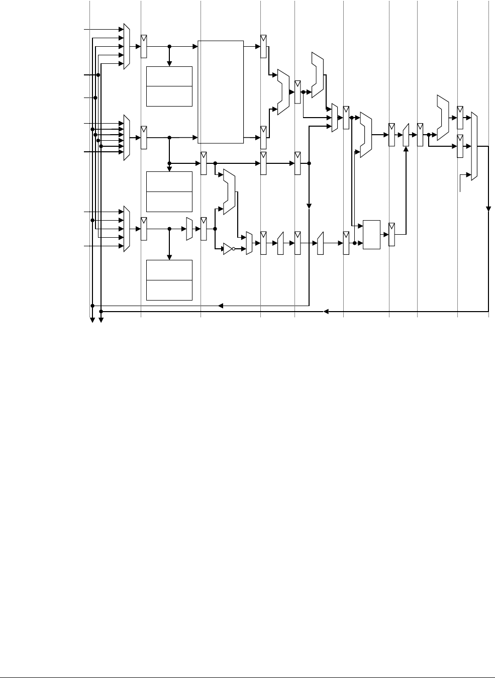
Introduction to the VFP coprocessor
ARM DDI 0301H Copyright © 2004-2009 ARM Limited. All rights reserved. 18-6
ID012310 Non-Confidential, Unrestricted Access
Figure 18-1 FMAC pipeline
FMAC pipeline instructions
The FMAC pipeline executes the following instructions:
FADD Add.
FSUB Subtract.
FMUL Multiply.
FNMUL Negated multiply.
FMAC Multiply and accumulate.
FNMAC Negated multiply and accumulate.
FMSC Multiply and subtract.
FNMSC Negated multiply and subtract.
FABS Absolute value.
FNEG Negation.
FUITO Convert unsigned integer to float.
FTOUI Convert float to unsigned integer.
FSITO Convert signed integer to float.
FTOSI Convert float to signed integer.
FTOUIZ Convert float to unsigned integer with forced round-towards-zero mode.
FTOSIZ Convert float to signed integer with forced round-towards-zero mode.
FCMP Compare.
To
register file
E3 E5E2Issue E6
Read
port Fm
Read
port Fd
Read
port Fn
Read
port Fm
Read
port Fn
Load
forward
DS
forward
Decode E1
Multiply
Exception
detect
Zero detect
OPB
Exception
detect
Zero detect
OPA
Exception
detect
Zero detect
E4
LZA
E7 Write-
back
Special
results
FMAC full writeback path
FMAC short writeback path
Product
sum Product
round
Final
sum
Normalize
Round Result
select
A operand
inversion
Align
low
Align
high
OPC

Introduction to the VFP coprocessor
ARM DDI 0301H Copyright © 2004-2009 ARM Limited. All rights reserved. 18-7
ID012310 Non-Confidential, Unrestricted Access
FCMPE Compare, NaN exceptions.
FCMPZ Compare with zero.
FCMPEZ Compare with zero, NaN exceptions.
FCVTSD Convert from double-precision to single-precision.
FCVTDS Convert from single-precision to double-precision.
FCPY Copy register.
See Execution timing on page 21-22 for cycle counts. The FMAC family of instructions. FMAC,
FNMAC, FMSC, and FNMSC, perform a chained multiply and accumulate operation. The
product is computed, rounded according to the specified rounding mode and destination
precision, and checked for exceptions before the accumulate operation is performed. The
accumulate operation is also rounded according to the specified rounding mode and destination
precision and checked for exceptions. The final result is identical to the equivalent sequence of
operations executed in sequence. Exception processing and status reporting also reflect the
independence of the components of the chained operations.
As an example, the FMAC instruction performs a chained multiply and add operation with the
following sequence of operations:
1. The product of the operands in the Fn and Fm registers is computed.
2. The product is rounded according to the current rounding mode and destination precision
and checked for exceptions.
3. The result is summed with the operand in the Fd register.
4. The sum is rounded according to the current rounding mode and destination precision and
checked for exceptions. If no exception conditions that require support code are present,
the result is written to the Fd register.
For example, the following two operations return the same result:
FMACS S0, S1, S2
FMULS TEMP, S1, S2
FADDS S0, S0, TEMP
18.4.2 DS pipeline
Figure 18-2 on page 18-8 shows the structure of the DS pipeline.
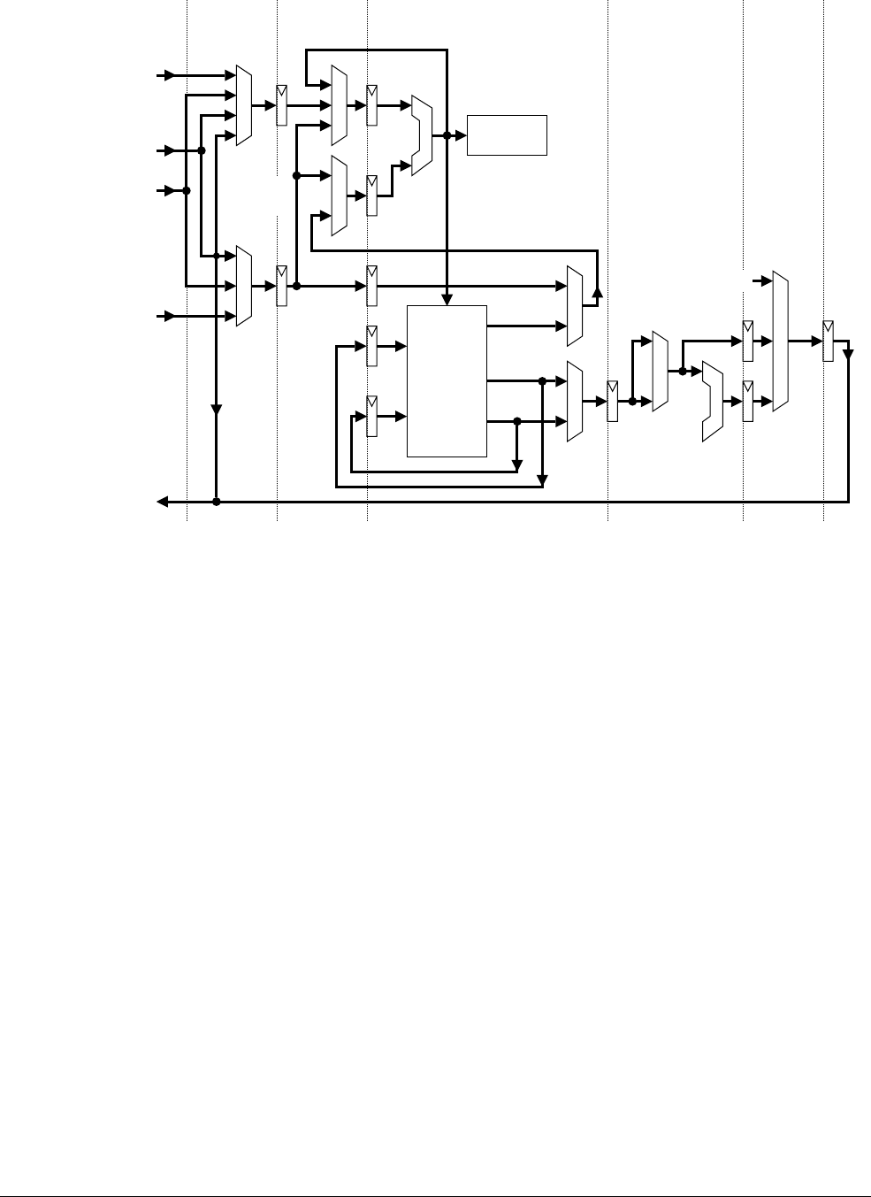
Introduction to the VFP coprocessor
ARM DDI 0301H Copyright © 2004-2009 ARM Limited. All rights reserved. 18-8
ID012310 Non-Confidential, Unrestricted Access
Figure 18-2 DS pipeline
DS pipeline instructions
The DS pipeline executes the following instructions:
FDIV Divide.
FSQRT Square root.
The VFP11 coprocessor executes divide and square root instructions for both single-precision
and double-precision operands with all IEEE 754 standard rounding modes supported. The DS
unit uses a shared radix-4 algorithm that provides a good balance between speed and chip area.
DS operations have a latency of 19 cycles for single-precision operations and 33 cycles for
double-precision operations. The throughput is 15 cycles for single-precision operations and 29
cycles for double-precision operations.
18.4.3 LS pipeline
The LS pipeline handles all of the instructions that involve data transfer to and from the ARM11
processor, including loads, stores, moves to coprocessor system registers, and moves from
coprocessor system registers. It remains synchronized with the ARM11 LS pipeline for the
duration of the instruction. Data written to the ARM11 processor is read from the VFP11
coprocessor register file in the Issue stage and transferred to the ARM11 processor in the next
cycle and is latched on the ARM11 data cache1/data cache 2 cycle boundary.
The transfer is made on a dedicated 64-bit store data bus between the VFP11 coprocessor and
the ARM11 processor. Load data is written to the VFP11 coprocessor on a dedicated 64-bit load
bus between the ARM11 processor and all coprocessors. Data is received by the VFP11
Read
port Fn
Next root
multiples
Increment
Divisor/root multiple
Final
result
select
Read
port Fm
Load
forward
FMAC
forward
Zero detect
Divisor/
radicand
Dividend
Next
quotient/
root
selection
Normalize
Sign
Partial
remainder/radicand
Execute 2 Execute 3Execute 1Issue Execute 4
To
register
file
Special results
Write-
back
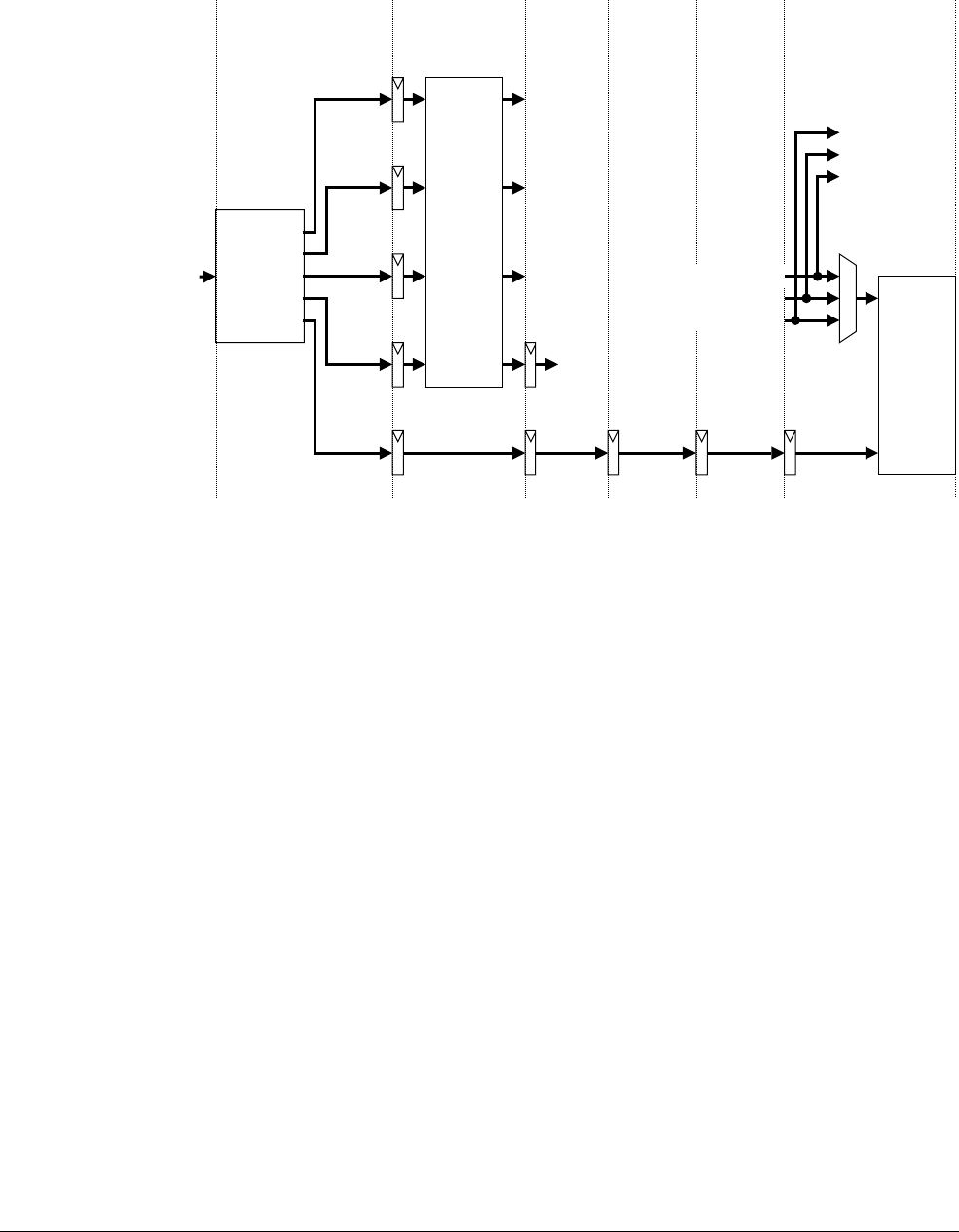
Introduction to the VFP coprocessor
ARM DDI 0301H Copyright © 2004-2009 ARM Limited. All rights reserved. 18-9
ID012310 Non-Confidential, Unrestricted Access
coprocessor in the Writeback stage. Data is written to the register file in the Writeback stage,
and available for forwarding to data processing operations in the same cycle. Figure 18-3 shows
the structure of the LS pipeline.
Figure 18-3 LS pipeline
LS pipeline instructions
The LS pipeline executes the following instructions:
FLD Load a single-precision, double-precision, or 32-bit integer value from memory
to the VFP11 register file.
FLDM Load up to 32 single-precision or integer values or 16 double-precision values
from memory to the VFP11 register file.
FST Store a single-precision, double-precision, or 32-bit integer value from the VFP11
register file to memory.
FSTM Store up to 32 single-precision or integer values or 16 double-precision values
from the VFP11 register file to memory.
FMSR Move a single-precision or integer value from an ARM11 register to a VFP11
single-precision register.
FMRS Move a single-precision or integer value from a VFP11 single-precision register
to an ARM11 register.
FMDHR Move an ARM11 register value to the upper half of a VFP11 double-precision
register.
FMDLR Move an ARM11 register value to the lower half of a VFP11 double-precision
register.
FMRDH Move the upper half of a double-precision value from a VFP11 double-precision
register to an ARM11 register.
ExecuteDecodeFetch
AVFPINSTR
(instruction
bus)
Fd
Fm
Fn
Store
Load
Read
port Fd
Read
port Fn
Store
data
bus
Register
file: read
and
format
muxes
Read
port Fm
FMAC writeback
Memory 2 Writeback
Register
file: write
and
format
muxes
DS forward
Load forward
Load data bus
FMAC forward
DS writeback
Register
address
generation
Memory 1Issue

Introduction to the VFP coprocessor
ARM DDI 0301H Copyright © 2004-2009 ARM Limited. All rights reserved. 18-10
ID012310 Non-Confidential, Unrestricted Access
FMRDL Move the lower half of a double-precision value from a VFP11 double-precision
register to an ARM11 register.
FMDRR Move two ARM11 register values to a VFP11 double-precision register.
FMRRD Move a double-precision VFP11 register value to two ARM11 registers.
FMSRR Move two ARM11 register values to two consecutively-numbered VFP11
single-precision registers.
FMRRS Move two consecutively-numbered VFP11 single-precision register values to two
ARM11 registers.
FMXR Move an ARM11 register value to a VFP11 control register.
FMRX Move a VFP11 control register value to an ARM11 register.
FMSTAT Move N, C, Z, and V flags from the VFP11 FPSCR to the ARM11 CPSR.

Introduction to the VFP coprocessor
ARM DDI 0301H Copyright © 2004-2009 ARM Limited. All rights reserved. 18-11
ID012310 Non-Confidential, Unrestricted Access
18.5 Modes of operation
The VFP11 coprocessor provides compatibility with the IEEE 754 standard through a
combination of hardware and software. There are rare cases that require significant additional
compute time to resolve correctly according to the requirements of the IEEE 754 standard. For
instance, the VFP11 coprocessor does not process subnormal input values directly. To provide
correct handling of subnormal inputs according to the IEEE 754 standard, a trap is made to
support code to process the operation. Using the support code for processing this operation can
require hundreds of cycles. In some applications this is unavoidable, because compliance with
the IEEE 754 standard is essential to proper operation of the program. In many other
applications, strict compliance to the IEEE 754 standard is unnecessary, while determinable
runtime, low interrupt latency, and low power are of more importance. To accommodate a
variety of applications, the VFP11 coprocessor provides four modes of operation:
•Full-compliance mode
•Flush-to-zero mode on page 18-12
•Default NaN mode on page 18-12
•RunFast mode on page 18-12.
18.5.1 Full-compliance mode
When the VFP11 coprocessor is in full-compliance mode, all operations that cannot be
processed according to the IEEE 754 standard use support code for assistance. The operations
requiring support code are:
• Any CDP operation involving a subnormal input when not in flush-to-zero mode. Enable
flush-to-zero mode by setting the FZ bit, FPSCR[24].
• Any CDP operation involving a NaN input when not in default NaN mode. Enable default
NaN mode by setting the DN bit, FPSCR[25].
• Any CDP operation that has the potential of generating an underflow condition when not
in flush-to-zero mode.
• Any CDP operation when Inexact exceptions are enabled. Enable Inexact exceptions by
setting the IXE bit, FPSCR[12].
• Any CDP operation that can cause an overflow while Overflow exceptions are enabled.
Enable Overflow exceptions by setting the OFE bit, FPSCR[10].
• Any CDP operation that involves an invalid arithmetic operation or an arithmetic
operation on a signaling NaN when Invalid Operation exceptions are enabled. Enable
Invalid Operation exceptions by setting the IOE bit, FPSCR[8].
• A float-to-integer conversion that has the potential to create an integer that cannot be
represented in the destination integer format when Invalid Operation exceptions are
enabled.
The support code:
• determines the nature of the exception
• determines if processing is required to perform the computation
• calls a function to compute the result and status
• transfers control to the user trap handler if the enable bit is set for a detected exception
• writes the result to the destination register, updates the FPSCR register, and returns to the
user code if no enabled exception is detected
• passes control to the user trap handler and supplies any specified intermediate result for
the exception if an enabled exception is detected.

Introduction to the VFP coprocessor
ARM DDI 0301H Copyright © 2004-2009 ARM Limited. All rights reserved. 18-12
ID012310 Non-Confidential, Unrestricted Access
Arithmetic exceptions on page 22-20 describes the conditions when the VFP11 coprocessor
traps to support code.
18.5.2 Flush-to-zero mode
Setting the FZ bit, FPSCR[24], enables flush-to-zero mode and increases performance on very
small inputs and results. In flush-to-zero mode, the VFP11 coprocessor treats all subnormal
input operands of arithmetic CDP operations as positive zeros in the operation. Exceptions that
result from a zero operand are signaled appropriately. FABS, FNEG, and FCPY are not
considered arithmetic CDP operations and are not affected by flush-to-zero mode. A result that
is tiny, as the IEEE 754 standard describes, for the destination precision is smaller in magnitude
than the minimum normal value before rounding and is replaced with a positive zero. The IDC
flag, FPSCR[7], indicates when an input flush occurs. The UFC flag, FPSCR[3], indicates when
a result flush occurs.
18.5.3 Default NaN mode
Setting the DN bit, FPSCR[25], enables default NaN mode. In default NaN mode, the result of
any operation that involves an input NaN or generated a NaN result returns the default NaN.
Propagation of the fraction bits is maintained only by FABS, FNEG, and FCPY operations, all
other CDP operations ignore any information in the fraction bits of an input NaN. See NaN
handling on page 20-4 for a description of default NaNs.
18.5.4 RunFast mode
RunFast mode is the combination of the following conditions:
• the VFP11 coprocessor is in flush-to-zero mode
• the VFP11 coprocessor is in default NaN mode
• all exception enable bits are cleared.
In RunFast mode the VFP11 coprocessor:
• processes subnormal input operands as positive zeros
• processes results that are tiny before rounding, that is, between the positive and negative
minimum normal values for the destination precision, as positive zeros
• processes input NaNs as default NaNs
• returns the default result specified by the IEEE 754 standard for overflow, division by
zero, invalid operation, or inexact operation conditions fully in hardware and without
additional latency
• processes all operations in hardware without trapping to support code.
RunFast mode enables the programmer to write code for the VFP11 coprocessor that runs in a
determinable time without support code assistance, regardless of the characteristics of the input
data. In RunFast mode, no user exception traps are available. However, the exception flags in
the FPSCR register are compliant with the IEEE 754 standard for Inexact, Overflow, Invalid
Operation, and Division by Zero exceptions. The underflow flag is modified for flush-to-zero
mode. Each of these flags is set by an exceptional condition and can by cleared only by a write
to the FPSCR register.

Introduction to the VFP coprocessor
ARM DDI 0301H Copyright © 2004-2009 ARM Limited. All rights reserved. 18-13
ID012310 Non-Confidential, Unrestricted Access
18.6 Short vector instructions
The VFPv2 architecture supports execution of short vector instructions of up to eight operations
on single-precision data and up to four operations on double-precision data. Short vectors are
most useful in graphics and signal-processing applications. They reduce code size, increase
speed of execution by supporting parallel operations and multiple transfers, and simplify
algorithms with high data throughput. Short vector operations issue the individual operations
specified in the instruction in a serial fashion. To eliminate data hazards, short vector operations
begin execution only after all source registers are available, and all destination registers are not
targets of other operations.
See Chapter 21 VFP Instruction Execution for more information on execution of short vector
instructions.

Introduction to the VFP coprocessor
ARM DDI 0301H Copyright © 2004-2009 ARM Limited. All rights reserved. 18-14
ID012310 Non-Confidential, Unrestricted Access
18.7 Parallel execution of instructions
The VFP11 coprocessor provides the ability to execute several floating-point operations in
parallel, while the ARM11 processor is executing ARM instructions. While a short vector
operation executes for a number of cycles in the VFP11 coprocessor, it appears to the ARM11
processor as a single-cycle instruction and is retired in the ARM11 processor before it completes
execution in the VFP11 coprocessor.
The three pipelines are designed to operate independently of one another when initial processing
is completed. This makes it possible to issue a short vector operation and a load or store multiple
operation in the next cycle and have both executing at the same time, provided no data hazards
exist between the two instructions. With this mechanism, algorithms that can be double-buffered
can be written to hide much of the time to transfer data to and from the VFP11 coprocessor
under the arithmetic operations, resulting in a significant improvement in performance.
The separate DS pipeline enables both data transfer operations and CDPs that are not to the DS
pipeline to execute in parallel with the divide. The DS block has a dedicated write port to the
register file, and no special care is required when executing operations in parallel with divide or
square root instructions. Parallel execution on page 21-20 describes it in more detail.

Introduction to the VFP coprocessor
ARM DDI 0301H Copyright © 2004-2009 ARM Limited. All rights reserved. 18-15
ID012310 Non-Confidential, Unrestricted Access
18.8 VFP11 treatment of branch instructions
The VFP11 coprocessor does not directly provide branch instructions. Instead, the result of a
floating-point compare instruction can be stored in the ARM11 condition code flags using the
FMSTAT instruction. This enables you to use the ARM11 branch instructions and conditional
execution capabilities to executing conditional floating-point code.
In some cases, full IEEE 754 standard comparisons are not required. Simple comparisons of
single-precision data, such as comparisons to zero or to a constant, can be done using an FMRS
transfer and the ARM11 CMP and CMN instructions. This method is faster in many cases than
using an FCMP instruction followed by an FMSTAT instruction. For more information, see
Compliance with the IEEE 754 standard on page 20-3 and Comparisons on page 20-5.

Introduction to the VFP coprocessor
ARM DDI 0301H Copyright © 2004-2009 ARM Limited. All rights reserved. 18-16
ID012310 Non-Confidential, Unrestricted Access
18.9 Writing optimal VFP11 code
The following guidelines provide significant performance increases for VFP11 code:
• Unless there is a read-after-write hazard, program most scalar operations to immediately
follow each other. Instead of a VFP11 FMAC instruction, use either a single ARM11
instruction or a VFP11 load or store instruction after the following instructions:
— a scalar double-precision multiply
— a multiply and accumulate
— a short vector instruction of length greater than one iteration.
• Avoid short vector divides and square roots. The VFP11 FMAC and DS pipelines are
unavailable until the final iteration of the short vector DS operation issues from the
Execute 1 stage. If the short vector DS operation can be separated, other VFP11
instructions can be issued in the cycles immediately following the divide or square root.
See Parallel execution on page 21-20.
• The best performance for data-intensive applications requires double-buffering looped
short vector instructions. The register banks can be divided to provide multiple
independent working areas. To take advantage of the simultaneous execution of data
transfer and short vector arithmetic instructions, follow the arithmetic instructions on one
bank with load or store instructions on the other bank.
• Moves to and from control registers are serializing. Avoid placing these in loops or
time-critical code.
• If fully compliant IEEE 754 standard comparisons are not required, avoid using FCMPE
and FCMPEZ. Using an FMRS instruction with an ARM11 CMP or CMN can be faster
for simple comparisons. See Comparisons on page 20-5.

Introduction to the VFP coprocessor
ARM DDI 0301H Copyright © 2004-2009 ARM Limited. All rights reserved. 18-17
ID012310 Non-Confidential, Unrestricted Access
18.10 VFP11 revision information
This manual describes the fifth version of the VFP11 coprocessor.
Updates in the fifth version of the VFP11 coprocessor are:
• corrections for errata
• update to the FPSID register to reflect the fifth version.
There are no other functional differences between the VFP11 fourth and fifth versions.

ARM DDI 0301H Copyright © 2004-2009 ARM Limited. All rights reserved. 19-1
ID012310 Non-Confidential, Unrestricted Access
Chapter 19
The VFP Register File
This chapter describes implementation-specific features of the VFP11 coprocessor that are useful
to programmers. It contains the following sections:
•About the register file on page 19-2
•Register file internal formats on page 19-3
•Decoding the register file on page 19-5
•Loading operands from ARM11 registers on page 19-6
•Maintaining consistency in register precision on page 19-8
•Data transfer between memory and VFP11 registers on page 19-9
•Access to register banks in CDP operations on page 19-10.

The VFP Register File
ARM DDI 0301H Copyright © 2004-2009 ARM Limited. All rights reserved. 19-2
ID012310 Non-Confidential, Unrestricted Access
19.1 About the register file
The register file is organized in four banks of eight registers. Each 32-bit register can store either
a single-precision floating-point number or an integer.
Any consecutive pair of registers, [Reven+1]:[Reven], can store a double-precision floating-point
number. Because a load and store operation does not modify the data, the VFP11 registers can
also be used as secondary data storage by another application that does not use floating-point
values.
The register file can be configured as four circular buffers for use by short vector instructions in
applications requiring high data throughput, such as filtering and graphics transforms. For short
vector instructions, register addressing is circular within each bank. Because load and store
operations do not circulate, you can load or store multiple banks, up to the entire register file,
with a single instruction. Short vector operations obey certain rules specifying the conditions
when the registers in the argument list specify circular buffers or single-scalar registers. The
LEN and STRIDE fields in the FPSCR register specify the number of operations performed by
short vector instructions and the increment scheme within the circular register banks. Section
C5 of the ARM Architecture Reference Manual contains more information and examples.

The VFP Register File
ARM DDI 0301H Copyright © 2004-2009 ARM Limited. All rights reserved. 19-3
ID012310 Non-Confidential, Unrestricted Access
19.2 Register file internal formats
The VFPv2 architecture provides the option of an internal data format that is different from
some or all of the external formats. In this implementation of the VFP11 coprocessor, data in
the register file has the same format as data in memory. Load or store operations for
single-precision, double-precision, or integer data do not modify the format as a consequence of
the transfer. However, to ensure compatibility with future VFP implementations, use
FLDMX/FSTMX instructions when saving context and restoring VFP11 registers. See section
C5 of the ARM Architecture Reference Manual for more information.
It is the responsibility of the programmer to be aware of the data type in each register. The
hardware does not perform any checking of the agreement between the data type in the source
registers and the data type expected by the instruction. Hardware always interprets the data
according to the precision implied in the instruction.
Accessing a register that has not been initialized or loaded with valid data is Unpredictable. A
way to detect access to an uninitialized register is to load all registers with Signaling NaNs
(SNaNs) in the precision of the initial access of the register and enable the Invalid Operation
exception.
19.2.1 Integer data format
The VFP11 coprocessor supports signed and unsigned 32-bit integers. Signed integers are
treated as two’s complement values. No modification to the data is implicit in a load, store, or
transfer operation on integer data. The format of integer data within the register file is identical
to the format in memory or in an ARM11 general-purpose register.
19.2.2 Single-precision data format
Figure 19-1 shows the single-precision bit fields.
Figure 19-1 Single-precision data format
The single-precision data format contains:
• the sign bit, bit [31]
• the exponent, bits [30:23]
• the fraction, bits [22:0].
The IEEE 754 standard defines the single-precision data format of the VFP11 coprocessor. See
the IEEE 754 standard for details about exponent bias, special formats, and numerical ranges.
19.2.3 Double-precision data format
Double-precision format has a Most Significant Word (MSW) and a Least Significant Word
(LSW). Figure 19-2 on page 19-4 shows the double-precision bit fields.
31
FractionS Exponent
22 030 23

The VFP Register File
ARM DDI 0301H Copyright © 2004-2009 ARM Limited. All rights reserved. 19-4
ID012310 Non-Confidential, Unrestricted Access
Figure 19-2 Double-precision data format
The MSW contains:
• the sign bit, bit [31]
• the exponent, bits [30:20]
• the upper 20 bits of the fraction, bits [19:0].
The LSW contains the lower 32 bits of the fraction.
The IEEE 754 standard defines the double-precision data format used in the VFP11
coprocessor. See the IEEE 754 standard for details about exponent bias, special formats, and
numerical ranges.
31
Exponent Fraction, upper 20 bitsS
30 20 19 0
Fraction, lower 32 bits
Double-precision
MSW
Double-precision
LSW
The VFP Register File
ARM DDI 0301H Copyright © 2004-2009 ARM Limited. All rights reserved. 19-5
ID012310 Non-Confidential, Unrestricted Access
19.3 Decoding the register file
Each register file access uses the five bits of the register number in the instruction word. For
single-precision and integer accesses, the most significant four bits are in the Fm, Fn, or Fd field,
and the least significant bit is the M, N, or D bit for each instruction format. For instructions
with double-precision operands or destinations, the M, N, and D bit corresponding to a
double-precision access must be zero. Figure 19-3 shows the register file. See the ARM
Architecture Reference Manual for instruction formats and the positions of these bits.
Figure 19-3 Register file access
31 0
S1
S3
S7
S5
S9
S11
S13
S15
S17
S19
S21
S23
S25
S27
S29
S31
031
63 0
D0
D1
D2
D3
D4
D5
D6
D7
D8
D9
D10
D11
D12
D13
D14
D15
S2
S4
S6
S8
S10
S12
S14
S16
S18
S20
S22
S24
S26
S28
S30
S0

The VFP Register File
ARM DDI 0301H Copyright © 2004-2009 ARM Limited. All rights reserved. 19-6
ID012310 Non-Confidential, Unrestricted Access
19.4 Loading operands from ARM11 registers
Floating-point data can be transferred between ARM11 registers and VFP11 registers using the
MCR, MRC, MCRR, and MRRC coprocessor data transfer instructions. No exceptions are
possible on these transfer instructions.
MCR instructions transfer 32-bit values from ARM11 registers to VFP11 registers as Table 19-1
lists.
MRC instructions transfer 32-bit values from VFP11 registers to ARM11 registers as Table 19-2
lists.
MCRR instructions transfer 64-bit quantities from ARM11 registers to VFP11 registers as
Table 19-3 lists.
MRRC instructions transfer 64-bit quantities from VFP11 registers to ARM11 registers as
Table 19-4 on page 19-7 lists.
Table 19-1 VFP11 MCR instructions
Instruction Operation Description
FMXR VFP11 system register = Rd Move from ARM11 register Rd to VFP11 system register FPSIDa,
FPSCR, FPEXC, FPINST, or FPINST2.
FMDLR Dn[31:0] = Rd Move from ARM11 register Rd to lower half of VFP11 double-precision
register Dn.
FMDHR Dn[63:32] = Rd Move from ARM11 register Rd to upper half of VFP11 double-precision
register Dn.
FMSR Sn = Rd Move from ARM11 register Rd to VFP11 single-precision or integer
register Sn.
a. Writing to the FPSID register does not change the contents of the FPSID but might be used as a serializing instruction.
Table 19-2 VFP11 MRC instructions
Instruction Operation Description
FMRX Rd = VFP11 system register Move from VFP11 system register FPSID, FPSCR, FPEXC, FPINST, or
FPINST2 to ARM11 register Rd.
FMRDL Rd = Dn[31:0] Move from lower half of VFP11 double-precision register Dn to ARM11
register Rd.
FMRDH Rd = Dn[63:32] Move from upper half of VFP11 double-precision register Dn to ARM11
register Rd.
FMRS Rd = Sn Move from VFP11 single-precision or integer register Sn to ARM11
register Rd.
Table 19-3 VFP11 MCRR instructions
Instruction Operation Description
FMDRR Dm[31:0] = Rd
Dm[63:32] = Rn
Move from ARM11 registers Rd and Rn to lower and upper halves of VFP11
double-precision register Dm.
FMSRR Sm = Rd
S(m + 1) = Rn
Move from ARM11 registers Rd and Rn to consecutive VFP11 single-precision
registers Sm and S(m + 1).

The VFP Register File
ARM DDI 0301H Copyright © 2004-2009 ARM Limited. All rights reserved. 19-7
ID012310 Non-Confidential, Unrestricted Access
Table 19-4 VFP11 MRRC instructions
Instruction Operation Description
FMRRD Rd = Dm[31:0]
Rn = Dm[63:32]
Move from lower and upper halves of VFP11 double-precision register Dm to
ARM11 registers Rd and Rn.
FMRRS Rd = Sm
Rn = S(m + 1)
Move from single-precision VFP11 registers Sm and S(m + 1) to ARM11 registers
Rd and Rn.

The VFP Register File
ARM DDI 0301H Copyright © 2004-2009 ARM Limited. All rights reserved. 19-8
ID012310 Non-Confidential, Unrestricted Access
19.5 Maintaining consistency in register precision
The VFP11 register file stores single-precision, double-precision, and integer data in the same
registers. For example, D6 occupies the same registers as S12 and S13. The usable format of the
register or registers depends on the last load or arithmetic instruction that wrote to the register
or registers.
The VFP11 hardware does not check the register format to see if it is consistent with the
precision of the current operation. Inconsistent use of the registers is possible but Unpredictable.
The hardware interprets the data in the format required by the instruction regardless of the latest
store or write operation to the register. It is the task of the compiler or programmer to maintain
consistency in register usage.

The VFP Register File
ARM DDI 0301H Copyright © 2004-2009 ARM Limited. All rights reserved. 19-9
ID012310 Non-Confidential, Unrestricted Access
19.6 Data transfer between memory and VFP11 registers
The B bit in the CP15 c1 Control Register, see Section B2 of the ARM Architecture Reference
Manual, determines whether access to stored memory is little-endian or big-endian. The
ARM11 processor supports both little-endian and big-endian access formats in memory.
The ARM11 processor stores 32-bit words in memory with the Least Significant Byte (LSB) in
the lowest byte of the memory address regardless of the endianness selected. For a store of a
single-precision floating-point value, the LSB is located at the target address with the lower two
bits of the address cleared. The Most Significant Byte (MSB) is at the target address with the
lower two bits set. For best performance, all single-precision data must be aligned in memory to
four-byte boundaries, and double-precision data must be aligned to eight-byte boundaries.
Table 19-5 lists how single-precision data is stored in memory and the address to access each
byte in both little-endian and big-endian formats. In this example, the target address is
0x40000000
.
For double-precision data, the location of the two words that comprise the data are stored in
different locations for little-endian and big-endian data access formats. Table 19-6 lists the data
storage in memory and the address to access each byte in little-endian and big-endian access
modes. In this example, the target address is
0x40000000
.
The memory image for the data is identical for both little-endian and big-endian within data
words. The ARM11 hardware performs the address transformations to provide both little-endian
and big-endian addressing to the programmer.
Table 19-5 Single-precision data memory images and byte addresses
Single-precision
data bytes Memory address Little-endian byte address Big-endian byte address
MSB, bits [31:24]
0x40000003 0x40000003 0x40000000
Bits [23:16]
0x40000002 0x40000002 0x40000001
Bits [15:8]
0x40000001 0x40000001 0x40000002
LSB, bits [7:0]
0x40000000 0x40000000 0x40000003
Table 19-6 Double-precision data memory images and byte addresses
Double- precision
data bytes
Little-endian address
in memory
Little-endian
byte address
Big-endian address
in memory
Big-endian
byte address
MSB, bits [63:56]
0x40000007 0x40000007 0x40000003 0x40000000
Bits [55:48]
0x40000006 0x40000006 0x40000002 0x40000001
Bits [47:40]
0x40000005 0x40000005 0x40000001 0x40000002
Bits [39:32]
0x40000004 0x40000004 0x40000000 0x40000003
Bits [31:24]
0x40000003 0x40000003 0x40000007 0x40000004
Bits [23:16]
0x40000002 0x40000002 0x40000006 0x40000005
Bits [15:8]
0x40000001 0x40000001 0x40000005 0x40000006
LSB, bits [7:0]
0x40000000 0x40000000 0x40000004 0x40000007
The VFP Register File
ARM DDI 0301H Copyright © 2004-2009 ARM Limited. All rights reserved. 19-10
ID012310 Non-Confidential, Unrestricted Access
19.7 Access to register banks in CDP operations
The register file is especially suited for short vector operations. The four register banks function
as four circular hardware queues. Short vector operations significantly improve the performance
of operations with high data throughput such as signal processing and matrix manipulation
functions.
19.7.1 About register banks
As Figure 19-4 shows, the register file is divided into four banks with eight registers in each
bank for single-precision instructions and four registers per bank for double-precision
instructions. CDP instructions access the banks in a circular manner. Load and store multiple
instructions do not access the registers in a circular manner but treat the register file as a linearly
ordered structure.
See ARM Architecture Reference Manual, Part C for more information on VFP addressing
modes.
Figure 19-4 Register banks
A short vector CDP operation that has a source or destination vector crossing a bank boundary
wraps around and accesses the first register in the bank.
Example 19-1 shows the iterations of the following short vector add instruction:
FADDS S11, S22, S31
In this instruction, the LEN field contains b101, selecting a vector length of six iterations, and
the STRIDE field contains b00, selecting a vector stride of one.
Example 19-1 Register bank wrapping
FADDS S11, S22, S31 ; 1st iteration
FADDS S12, S23, S24 ; 2nd iteration. The 2nd source vector wraps around
; and accesses the 1st register in the 4th bank
FADDS S13, S16, S25 ; 3rd iteration. The 1st source vector wraps around
; and accesses the 1st register in the 3rd bank
FADDS S14, S17, S26 ; 4th iteration
FADDS S15, S18, S27 ; 5th iteration
FADDS S8, S19, S28 ; 6th and last iteration. The destination vector
; wraps around and writes to the 1st register in the
S24
S25
S26
S27
S28
S29
S30
S31
Bank 3
D12
D13
D14
D15
S17
S18
S19
S20
S21
S22
S16
Bank 2
D8
D9
D10
D11 S23
S8
S9
S10
S11
S12
S13
S14
S15
Bank 1
D4
D5
D6
D7
S3
S2
S4
S5
S6
S7
S0
S1
Bank 0
D0
D1
D2
D3

The VFP Register File
ARM DDI 0301H Copyright © 2004-2009 ARM Limited. All rights reserved. 19-11
ID012310 Non-Confidential, Unrestricted Access
; 2nd bank
19.7.2 Operations using register banks
The register file organization supports four types of operations that the following sections
describe:
•Scalar-only instructions
•Short vector-only instructions
•Short vector instructions with scalar source on page 19-12
•Scalar instructions in short vector mode on page 19-12.
See Floating-Point Status and Control Register, FPSCR on page 20-14 for details of the LEN
and STRIDE fields and the FPSCR register.
Scalar-only instructions
An instruction is a scalar-only operation if the operands are treated as scalars and the result is a
scalar.
Clearing the LEN field in the FPSCR register selects a vector length of one iteration. For
example, if the LEN field contains b000, then the following operation writes the sum of the
single-precision values in S21 and S22 to S12:
FADDS S12, S21, S22
Some instructions can operate only on scalar data regardless of the value in the LEN field. These
instructions are:
Compare operations
FCMPS/D, FCMPZS/D, FCMPES/D, and FCMPEZS/D.
Integer conversions
FTOUIS/D, FTOUIZS/D, FTOSIS/D, FTOSIZS/D, FUITOS/D, and FSITOS/D.
Precision conversions
FCVTDS and FCVTSD.
Short vector-only instructions
Vector-only instructions require that the value in the LEN field is nonzero, and that the
destination and Fm registers are not in bank 0.
Example 19-2 shows the iterations of the following short vector instruction:
FMACS S16, S0, S8
In the example, the LEN field contains b011, selecting a vector length of four iterations, and the
STRIDE field contains b00, selecting a vector stride of one.
Example 19-2 Short vector instruction
FMACS S16, S0, S8 ; 1st iteration
FMACS S17, S1, S9 ; 2nd iteration
FMACS S18, S2, S10 ; 3rd iteration
FMACS S19, S3, S11 ; 4th and last iteration

The VFP Register File
ARM DDI 0301H Copyright © 2004-2009 ARM Limited. All rights reserved. 19-12
ID012310 Non-Confidential, Unrestricted Access
Short vector instructions with scalar source
The VFPv2 architecture enables a vector to be operated on by a scalar operand. The destination
must be a vector, that is, not in bank 0, and the Fm operand must be in bank 0.
Example 19-3 shows the iterations of the following short vector instruction with a scalar source:
FMULD D12, D8, D2
In the example, the LEN field contains b001, selecting a vector length of two iterations, and the
STRIDE field contains b00, selecting a vector stride of one.
Example 19-3 Short vector instruction with scalar source
FMULD D12, D8, D2 ; 1st iteration
FMULD D13, D9, D2 ; 2nd and last iteration
This scales the two source registers, D8 and D9, by the value in D2 and writes the new values
to D12 and D13.
Scalar instructions in short vector mode
You can mix scalar and short vector operations by carefully selecting the source and destination
registers. If the destination is in bank 0, the operation is scalar-only regardless of the value in
the LEN field. You do not have to change the LEN field from a nonzero value to b000 to perform
scalar operations.
Example 19-4 shows the sequence of operations for the following instructions:
FABSD D4, D8
FADDS S0, S0, S31
FMULS S24, S26, S1
In the example, the LEN field contains b001, selecting a vector length of two iterations, and the
STRIDE field contains b00, selecting a vector stride of one.
Example 19-4 Scalar operation in short vector mode
FABSD D4, D8 ; vector DP ABS operation on regs (D8, D9) to (D4, D5)
FABSD D5, D9
FADDS S0, S0, S31 ; scalar increment of S0 by S31
FMULS S24, S26, S1 ; vector (S26, S27) scaled by S1 and written to (S24, S25)
FMULS S25, S27, S1

The VFP Register File
ARM DDI 0301H Copyright © 2004-2009 ARM Limited. All rights reserved. 19-13
ID012310 Non-Confidential, Unrestricted Access
The tables that follow show the four types of operations possible in the VFPv2 architecture. In
the tables, Any refers to the availability of all registers in the precision for the specified operand.
S refers to a scalar operand with only a single register. V refers to a vector operand with multiple
registers. Table 19-7 lists single-precision three-operand register usage.
Table 19-8 lists single-precision two-operand register usage.
Table 19-9 lists double-precision three-operand register usage.
Table 19-10 lists double-precision two-operand register usage.
Table 19-7 Single-precision three-operand register usage
LEN field Fd Fn Fm Operation type
b000 Any Any Any S = S op S OR S = S S S
Nonzero 0-7 Any Any S = S op S OR S = S S S
Nonzero 8-31 Any 0-7 V = V op S OR V = V V S
Nonzero 8-31 Any 8-31 V = V op V OR V = V V V
Table 19-8 Single-precision two-operand register usage
LEN field Fd Fm Operation type
b000 Any Any S = op S
Nonzero 0-7 Any S = op S
Nonzero 8-31 0-7 V = op S
Nonzero 8-31 8-31 V = op V
Table 19-9 Double-precision three-operand register usage
LEN field Fd Fn Fm Operation type
b000 Any Any Any S = S op S OR S = S S S
Nonzero 0-3 Any Any S = S op S OR S = S S S
Nonzero 4-15 Any 0-3 V = V op S OR V = V V S
Nonzero 4-15 Any 4-15 V = V op V OR V = V V V
Table 19-10 Double-precision two-operand register usage
LEN field Fd Fm Operation type
b000 Any Any S = op S
Nonzero 0-3 Any S = op S
Nonzero 4-15 0-3 V = op S
Nonzero 4-15 4-15 V = op V

ARM DDI 0301H Copyright © 2004-2009 ARM Limited. All rights reserved. 20-1
ID012310 Non-Confidential, Unrestricted Access
Chapter 20
VFP Programmer’s Model
This chapter describes implementation-specific features of the VFP11 coprocessor that are useful
to programmers. It contains the following sections:
•About the programmer’s model on page 20-2
•Compliance with the IEEE 754 standard on page 20-3
•ARMv5TE coprocessor extensions on page 20-8
•VFP11 system registers on page 20-12.

VFP Programmer’s Model
ARM DDI 0301H Copyright © 2004-2009 ARM Limited. All rights reserved. 20-2
ID012310 Non-Confidential, Unrestricted Access
20.1 About the programmer’s model
This section introduces the VFP11 implementation of the VFPv2 floating-point architecture.
Note
The ARM Architecture Reference Manual describes the VFPv1 architecture.
The VFP11 coprocessor implements all the instructions and modes of the VFPv2 architecture.
The VFPv2 architecture adds the following features and enhancements to the VFPv1
architecture:
• The ARM v5TE instruction set. This includes the MRRC and MCRR instructions to
transfer 64-bit data between the ARM11 processor and the VFP11 coprocessor. These
instructions enable the transfer of a double-precision register or two consecutively
numbered single-precision registers to or from a pair of ARM11 registers. See Loading
operands from ARM11 registers on page 19-6 for syntax and usage of VFP MRRC and
MCRR instructions.
• Default NaN mode. In default NaN mode, any operation involving one or more NaN
operands produces the default NaN as a result, rather than returning the NaN or one of the
NaNs involved in the operation. This mode is compatible with the IEEE 754 standard but
not with current handling of NaNs by industry.
• Addition of the input subnormal flag, IDC (FPSCR[7]). IDC is set whenever the VFP11
coprocessor is in flush-to-zero mode and a subnormal input operand is replaced by a
positive zero. It remains set until cleared by writing to the FPSCR register. A new Input
Subnormal exception enable bit, IDE (FPSCR[15]), is also added. When IDE is set, the
VFP11 coprocessor traps to the Undefined trap handler for an instruction that has a
subnormal input operand.
• New functionality of the underflow flag, UFC (FPSCR[3]), in flush-to-zero mode. In
flush-to-zero mode, UFC is set whenever a result is lower than the threshold for normal
numbers before rounding, and the result is flushed to zero. UFC remains set until cleared
by writing to the FPSCR register. Setting the Underflow exception enable bit, UFE
(FPSCR[11]), does not cause a trap in flush-to-zero mode.
• New functionality of the inexact flag, IXC (FPSCR[4]), in flush-to-zero mode. In VFPv1,
IXC is set when an input or result is flushed to zero. In VFPv2 architecture, the IDC and
UFC flags provide this information. See Inexact exception on page 22-18 for more
information.
• Addition of RunFast mode. See RunFast mode on page 18-12 for details of RunFast mode
operation.

VFP Programmer’s Model
ARM DDI 0301H Copyright © 2004-2009 ARM Limited. All rights reserved. 20-3
ID012310 Non-Confidential, Unrestricted Access
20.2 Compliance with the IEEE 754 standard
This section introduces issues related to compliance with the IEEE 754 standard:
• hardware and software components
• software-based components and their availability.
Also see Section C1 of the ARM Architecture Reference Manual for information about VFP
architecture compliance with the IEEE 754 standard.
20.2.1 An IEEE 754 standard-compliant implementation
The VFP11 hardware and support code together provide VFPv2 floating-point instruction
implementations that are compliant with the IEEE 754 standard. Unless an enabled
floating-point exception occurs, it appears to the program that the floating-point instruction was
executed by the hardware. If an exceptional condition occurs that requires software support
during instruction execution, the instruction takes significantly more cycles than normal to
produce the result. This is a common practice in the industry, and the incidence of such
instructions is typically very low.
20.2.2 Complete implementation of the IEEE 754 standard
The following operations from the IEEE 754 standard are not supplied by the VFP11 instruction
set:
• remainder
• round floating-point number to integer-valued floating-point number
• binary-to-decimal conversions
• decimal-to-binary conversions
• direct comparison of single-precision and double-precision values.
For complete implementation of the IEEE 754 standard, the VFP11 coprocessor and support
code must be augmented with library functions that implement these operations. See
Application Note 98, VFP Support Code for details of support code and the available library
functions.
20.2.3 IEEE 754 standard implementation choices
Part C of the ARM Architecture Reference Manual describes some of the implementation
choices permitted by the IEEE 754 standard and used in the VFPv2 architecture.
Additional implementation choices are made within the VFP11 coprocessor about the cases that
are handled by the VFP11 hardware and the cases that bounce to the support code.
To execute frequently encountered operations as fast as possible and minimize silicon area,
handling of rarely occurring values and some exceptions is relegated to the support code. The
VFP11 coprocessor supports two modes for handling rarely occurring values:
Full-compliance mode
Full-compliance mode with support code assistance is fully compliant with the
IEEE 754 standard. Full-compliance mode requires the floating-point support
code to handle certain operands and exceptional conditions not supported in the
hardware. Although the support code gives full compliance with the IEEE 754
standard, it does increase the runtime of an application and the size of kernel code.

VFP Programmer’s Model
ARM DDI 0301H Copyright © 2004-2009 ARM Limited. All rights reserved. 20-4
ID012310 Non-Confidential, Unrestricted Access
RunFast mode
In RunFast mode, default handling of subnormal inputs, underflows, and NaN
inputs is not fully compliant with the IEEE 754 standard. No user trap handlers
are permitted in RunFast mode.
When flush-to-zero and default NaN modes are enabled, and all exceptions are
disabled, the VFP11 coprocessor operates in RunFast mode. While the potential
loss of accuracy for very small values is present, RunFast mode removes a
significant number of performance-limiting stall conditions. By not requiring the
floating-point support code, RunFast mode enables increased performance of
typical and optimized code and a reduction in the size of kernel code. See Hazards
on page 21-6 for more information on performance improvements in RunFast
mode.
Supported formats
The supported formats are:
• Single-precision and double-precision. No extended format is supported.
• Integer formats:
— unsigned 32-bit integers
— two’s complement signed 32-bit integers.
NaN handling
Any single-precision or double-precision values with the maximum exponent field value and a
nonzero fraction field are valid NaNs. A most significant fraction bit of zero indicates a
Signaling NaN (SNaN). A one indicates a Quiet NaN (QNaN). Two NaN values are treated as
different NaNs if they differ in any bit. Table 20-1 lists the default NaN values in both single and
double precision.
Any SNaN passed as input to an operation causes an Invalid Operation exception and sets the
IOC flag, FPSCR[0]. If the IOE bit, FPSCR[8], is set, control passes to a user trap handler if
present. If IOE is not set, a default QNaN is written to the destination register. The rules for cases
involving multiple NaN operands are in the ARM Architecture Reference Manual.
Processing of input NaNs for ARM floating-point coprocessors and libraries is defined as
follows:
• In full-compliance mode, NaNs are handled according to the ARM Architecture Reference
Manual. The hardware does not process the NaNs directly for arithmetic CDP
instructions, but traps to the support code for all NaN processing. For data transfer
operations, NaNs are transferred without raising the Invalid Operation exception or
trapping to support code. For the nonarithmetic CDP instructions, FABS, FNEG, and
FCPY, NaNs are copied, with a change of sign if specified in the instructions, without
causing the Invalid Operation exception or trapping to support code.
Table 20-1 Default NaN values
Single-precision Double-precision
Sign 0 0
Exponent
0xFF 0x7FF
Fraction Bit [22] = 1
Bits [21:0] are all zeros
Bit [51] = 1
Bits [50:0] are all zeros

VFP Programmer’s Model
ARM DDI 0301H Copyright © 2004-2009 ARM Limited. All rights reserved. 20-5
ID012310 Non-Confidential, Unrestricted Access
• In default NaN mode, NaNs are handled completely within the hardware without support
code assistance. SNaNs in an arithmetic CDP operation set the IOC flag, FPSCR[0]. NaN
handling by data transfer and nonarithmetic CDP instructions is the same as in
full-compliance mode. Arithmetic CDP instructions involving NaN operands return the
default NaN regardless of the fractions of any NaN operands.
Table 20-2 summarizes the effects of NaN operands on instruction execution.
Comparisons
Comparison results modify condition code flags in the FPSCR register. The FMSTAT
instruction transfers the current condition code flags in the FPSCR register to the ARM11 CPSR
register. See the ARM Architecture Reference Manual for mapping of IEEE 754 standard
predicates to ARM conditions. The condition code flags used are chosen so that subsequent
conditional execution of ARM instructions can test the predicates defined in the IEEE 754
standard.
The VFP11 coprocessor handles most comparisons of numeric values in hardware, generating
the appropriate condition code depending on whether the result is less than, equal to, or greater
than. When the VFP11 coprocessor is not in flush-to-zero mode, comparisons involving
subnormal operands bounce to support code.
Table 20-2 QNaN and SNaN handling
Instruction
type
Default
NaN
mode With QNaN operand With SNaN operand
Arithmetic CDP
Off INVa set. Bounce to support code to
process operation.
INV set. Bounce to support code to process
operation.
On No bounce. Default NaN returns. IOCb set. If IOEc set, bounce to Invalid
Operation user trap handler. If IOE clear,
default NaN returns.
Nonarithmetic
CDP
Off
NaN passes to destination with sign changed as appropriate.
On
FCMP(Z)
Off INV set. Bounce to support code to process
operation.
INV set. Bounce to support code to process
operation.
On No bounce. Unordered compare. IOC set. If IOE set, bounce to Invalid
Operation user trap handler. If IOE clear,
unordered compare.
FCMPE(Z)
Off INV set. Bounce to support code to process
operation.
INV set. Bounce to support code to process
operation.
On IOC set. If IOE set, bounce to Invalid
Operation user trap handler. If IOE clear,
unordered compare.
IOC set. If IOE set, bounce to Invalid
Operation user trap handler. If IOE clear,
unordered compare.
Load/store
Off
All NaNs transferred. No bounce.
On
a. INV is the Input exception flag, FPEXC[7].
b. IOC is the Invalid Operation cumulative exception flag, FPSCR[0].
c. IOE is the Invalid Operation exception trap enable bit, FPSCR[8].

VFP Programmer’s Model
ARM DDI 0301H Copyright © 2004-2009 ARM Limited. All rights reserved. 20-6
ID012310 Non-Confidential, Unrestricted Access
The VFP11 coprocessor supports:
Compare operations
The compare operations are FCMPS, FCMPZS, FCMPD, and FCMPZD.
In default NaN mode, a compare instruction involving a QNaN produces an
unordered result. An SNaN produces an unordered result and generates an Invalid
Operation exception. If the IOE bit, FPSCR[8], is set, the Invalid Operation user
trap handler is called. When the VFP11 coprocessor is not in default NaN mode,
comparisons involving NaNs bounce to support code.
Compare with exception operations
The compare with exception operations are FCMPES, FCMPEZS, FCMPED,
and FCMPEZD.
In default NaN mode, a compare with exception operation involving either an
SNaN or a QNaN produces an unordered result and generates an Invalid
Operation exception. When the VFP11 coprocessor is not in default NaN mode,
comparisons involving NaNs bounce to support code.
Some simple comparisons on single-precision data can be computed directly by the ARM11
processor. If only equality or comparison to zero is required, and NaNs are not an issue,
performing the comparison in ARM11 registers using CMP or CMN instructions can be faster.
If branching on the state of the Z flag is required, you can use the following instructions for
positive values:
FMRS Rx, Sn
CMP Rx, #0
BEQ label
If the input values can include negative numbers, including negative zero, you can use the
following code:
FMRS Rx, Sn
CMP Rx, #0x80000000
CMPNE Rx, #0
BEQ label
Using a temporary register is even faster:
FMRS Rx, Sn
MOVS Rt, Rx, LSL #1
BEQ label
Comparisons with particular values are also possible. For example, to check if a positive value
is greater or equal to +1.0, use:
FMRS Rx, Sn
CMP Rx,#0x3F800000
BGE label
When comparisons are required for double-precision values, or when IEEE 754 standard
comparisons are required, it is safer to use the FCMP and FCMPE instructions with FMSTAT.
Underflow
In the generation of Underflow exceptions, the after rounding form of tininess and the
subnormalization loss form of loss of accuracy as the IEEE 754 standard describes are used.

VFP Programmer’s Model
ARM DDI 0301H Copyright © 2004-2009 ARM Limited. All rights reserved. 20-7
ID012310 Non-Confidential, Unrestricted Access
In flush-to-zero mode, results that are tiny before rounding, as the IEEE 754 standard describes,
are flushed to a positive zero, and the UFC flag, FPSCR[3], is set. Support code is not involved.
See Part C of the ARM Architecture Reference Manual for information on flush-to-zero mode.
When the VFP11 coprocessor is not in flush-to-zero mode, any operation with a risk of
producing a tiny result bounces to support code. If the operation does not produce a tiny result,
it returns the computed result, and the UFC flag, FPSCR[3], is not set. The IXC flag, FPSCR[4],
is set if the operation is inexact. If the operation produces a tiny result, the result is a subnormal
or zero value, and the UFC flag, FPSCR[3], is set. See Underflow exception on page 22-17 for
more information on underflow handling.
Exceptions
Exceptions are taken in the VFP11 coprocessor in an imprecise manner. When exception
processing begins, the states of the ARM11 processor and the VFP11 coprocessor might not be
the same as when the exception occurred. Exceptional instructions cause the VFP11
coprocessor to enter the exceptional state, and the next VFP11 instruction triggers exception
processing. After the issue of the exceptional instruction and before exception processing
begins, non-VFP11 instructions and some VFP11 instructions can be executed and retired. Any
source registers involved in the exceptional instruction are preserved, and the destination
register is not overwritten on entry to the support code. If the detected exception enable bit is
not set, the support code returns to the program flow at the point of the trigger instruction after
processing the exception. If the detected exception enable bit is set, and a user trap handler is
installed, the support code passes control to the user trap handler. If the exception is overflow or
underflow, the intermediate result specified by the IEEE 754 standard is made available to the
user trap handler.
VFP Programmer’s Model
ARM DDI 0301H Copyright © 2004-2009 ARM Limited. All rights reserved. 20-8
ID012310 Non-Confidential, Unrestricted Access
20.3 ARMv5TE coprocessor extensions
This section describes the syntax and usage of the four ARMv5TE architecture coprocessor
extension instructions:
•FMDRR
•FMRRD on page 20-9
•FMSRR on page 20-10
•FMRRS on page 20-11.
Note
These instructions are implementations of the MCRR and MRRC instructions, that Section A10
of the ARM Architecture Reference Manual describes.
20.3.1 FMDRR
FMDRR transfers data from two ARM11 registers to a VFP11 double-precision register. The
ARM11 registers do not have to be contiguous. Figure 20-1 shows the format of the FMDRR
instruction.
Figure 20-1 FMDRR instruction format
Syntax
FMDRR {<cond>} <Dm>, <Rd>, <Rn>
where:
<cond>
Is the condition under which the instruction is executed. If <cond> is omitted, the
AL, always, condition is used.
<Dm>
Specifies the destination double-precision VFP11 coprocessor register.
<Rd>
Specifies the source ARM11 register for the lower 32 bits of the operand.
<Rn>
Specifies the source ARM11 register for the upper 32 bits of the operand.
Architecture version
D variants only
Exceptions
None
Operation
if ConditionPassed(cond) then
Dm[upper half] = Rn
Dm[lower half] = Rd
1 1 0 0 0 1 0 0 Rn Rd 1 0 1 1 0 0 0 1 Dm
31 30 29 28 27 26 25 24 23 22 21 20 19 18 17 16 15 14 13 12 11 10 9 8 7 6 5 4 3 2 1 0
cond
VFP Programmer’s Model
ARM DDI 0301H Copyright © 2004-2009 ARM Limited. All rights reserved. 20-9
ID012310 Non-Confidential, Unrestricted Access
Notes
Conversions In the programmer’s model, FMDRR does not perform any conversion of the
value transferred. Arithmetic instructions using either Rd or Rn treat the value as
an integer, whereas most VFP instructions treat the Dm value as a
double-precision floating-point number.
20.3.2 FMRRD
FMRRD transfers data in a VFP11 double-precision register to two ARM11 registers. The
ARM11 registers do not have to be contiguous. Figure 20-2 shows the format of the FMRRD
instruction.
Figure 20-2 FMRRD instruction format
Syntax
FMRRD {<cond>} <Rd>, <Rn>, <Dm>
where:
<cond>
Is the condition under which the instruction is executed. If <cond> is omitted, the
AL, always, condition is used.
<Rd>
Specifies the destination ARM11 register for the lower 32 bits of the operand.
<Rn>
Specifies the destination ARM11 register for the upper 32 bits of the operand.
<Dm>
Specifies the source double-precision VFP11 coprocessor register.
Architecture version
D variants only
Exceptions
None
Operation
if ConditionPassed(cond) then
Rn = Dm[upper half]
Rd = Dm[lower half]
Notes
Use of R15 If R15 is specified for
<Rd>
or
<Rn>
, the results are Unpredictable.
Conversions In the programmer’s model, FMRRD does not perform any conversion of the
value transferred. Arithmetic instructions using Rd and Rn treat the contents as an
integer, whereas most VFP instructions treat the Dm value as a double-precision
floating-point number.
1 1 0 0 0 1 0 1 Rn Rd 1 0 1 1 0 0 0 1 Dm
31 30 29 28 27 26 25 24 23 22 21 20 19 18 17 16 15 14 13 12 11 10 9 8 7 6 5 4 3 2 1 0
cond

VFP Programmer’s Model
ARM DDI 0301H Copyright © 2004-2009 ARM Limited. All rights reserved. 20-10
ID012310 Non-Confidential, Unrestricted Access
20.3.3 FMSRR
FMSRR transfers data in two ARM11 registers to two consecutively numbered single-precision
VFP11 registers, Sm and S(m + 1). The ARM11 registers do not have to be contiguous.
Figure 20-3 shows the format of the FMSRR instruction.
Figure 20-3 FMSRR instruction format
Syntax
FMSRR {<cond>} <registers>, <Rd>, <Rn>
where:
<cond>
Is the condition under which the instruction is executed. If <cond> is omitted, the
AL, always, condition is used.
<registers>
Specifies the pair of consecutively numbered single-precision destination VFP11
registers, separated by a comma and surrounded by brackets. If m is the number
of the first register in the list, the list is encoded in the instruction by setting Sm
to the top four bits of m and M to the bottom bit of m. For example, if
<registers>
is {S1, S2}, the Sm field of the instruction is b0000 and the M bit is 1.
<Rd>
Specifies the source ARM11 register for the Sm VFP11 single-precision register.
<Rn>
Specifies the source ARM11 register for the S(m + 1) VFP11 single-precision
register.
Architecture version
All
Exceptions
None
Operation
If ConditionPassed(cond) then
Sm = Rd
S(m + 1) = Rn
Notes
Conversions In the programmer’s model, FMSRR does not perform any conversion of
the value transferred. Arithmetic instructions using Rd and Rn treat the
contents as an integer, whereas most VFP instructions treat the Sm and
S(m + 1) values as single-precision floating-point numbers.
Invalid register lists
If Sm is b1111 and M is 1, an encoding of S31, the instruction is
Unpredictable.
1 1 0 0 0 1 0 0 Rn Rd 1 0 1 0 0 0 M 1 Sm
31 30 29 28 27 26 25 24 23 22 21 20 19 18 17 16 15 14 13 12 11 10 9 8 7 6 5 4 3 2 1 0
cond

VFP Programmer’s Model
ARM DDI 0301H Copyright © 2004-2009 ARM Limited. All rights reserved. 20-11
ID012310 Non-Confidential, Unrestricted Access
20.3.4 FMRRS
FMRRS transfers data in two consecutively numbered single-precision VFP11 registers to two
ARM11 registers. The ARM11 registers do not have to be contiguous. Figure 20-4 shows the
format of the FMRRS instruction.
Figure 20-4 FMRRS instruction format
Syntax
FMRRS {<cond>} <Rd>, <Rn>, <registers>
where:
<cond>
Is the condition under which the instruction is executed. If <cond> is omitted, the
AL, always, condition is used.
<Rd>
Specifies the destination ARM11 register for the Sm VFP11 coprocessor
single-precision value.
<Rn>
Specifies the destination ARM11 register for the S(m + 1) VFP11 coprocessor
single-precision value.
<registers>
Specifies the pair of consecutively numbered single-precision VFP11 source
registers, separated by a comma and surrounded by brackets. If m is the number
of the first register in the list, the list is encoded in the instruction by setting Sm
to the top four bits of m and M to the bottom bit of m. For example, if
<registers>
is {S16, S17}, the Sm field of the instruction is b1000 and the M bit is 0.
Architecture version
All
Exceptions
None
Operation
If ConditionPassed(cond) then
Rd = Sm
Rn = S(m + 1)
Notes
Conversions In the programmer’s model, FMRRS does not perform any conversion of
the value transferred. Arithmetic instructions using Rd and Rn treat the
contents as an integer, whereas most VFP11 instructions treat the Sm and
S(m + 1) values as single-precision floating-point numbers.
Invalid register lists
If Sm is b1111 and M is 1, an encoding of S31, the instruction is
Unpredictable.
Use of R15 If R15 is specified for Rd or Rn, the results are Unpredictable.
1 1 0 0 0 1 0 1 Rn Rd 1 0 1 0 0 0 M 1 Sm
31 30 29 28 27 26 25 24 23 22 21 20 19 18 17 16 15 14 13 12 11 10 9 8 7 6 5 4 3 2 1 0
cond

VFP Programmer’s Model
ARM DDI 0301H Copyright © 2004-2009 ARM Limited. All rights reserved. 20-12
ID012310 Non-Confidential, Unrestricted Access
20.4 VFP11 system registers
The VFPv2 architecture describes the following three system registers that must be present in a
VFP system:
•Floating-Point System ID Register, FPSID
•Floating-Point Status and Control Register, FPSCR
•Floating-Point Exception Register, FPEXC.
The VFP11 coprocessor provides sufficient information for processing all exceptional
conditions encountered by the hardware. In an exceptional situation, the hardware provides:
• the exceptional instruction
• the instruction that might have been issued to the VFP11 coprocessor before detection of
the exception
• exception status information:
— type of exception
— number of remaining short vector iterations after an exceptional iteration.
To support exceptional conditions, the VFP11 coprocessor provides two additional registers:
•Floating-Point Instruction Register, FPINST
•Floating-Point Instruction Register 2, FPINST2.
Also, the FPEXC register contains additional bits to support exceptional conditions.
These registers are designed to be used with the support code software available from ARM
Limited. As a result, this document does not fully specify exception handling in all cases.
The coprocessor also provides two feature registers:
•Media and VFP Feature Register 0 on page 20-19, MVFR0
•Media and VFP Feature Register 1 on page 20-20, MVFR1.
Table 20-3 lists the VFP11 system registers.
Use the FMRX instruction to transfer the contents of VFP11 registers to ARM11 registers and
the FMXR instruction to transfer the contents of ARM11 registers to VFP11 registers.
Table 20-3 VFP11 system registers
Register Access mode Access type Reset state See
Floating-Point System ID Register, FPSID Any Read-only
0x410120B3
page 20-13
Floating-Point Status and Control Register, FPSCR Any Read/write
0x00000000
page 20-14
Floating-Point Exception Register, FPEXC Privileged Read/write
0x00000000
page 20-16
Floating-Point Instruction Register, FPINST Privileged Read/write
0xEE000A00
page 20-18
Floating-Point Instruction Register 2, FPINST2 Privileged Read/write UNP page 20-18
Media and VFP Feature Register 0, MVFR0 Any Read-only
0x11111111
page 20-19
Media and VFP Feature Register 1, MVFR1 Any Read-only
0x00000000
page 20-20
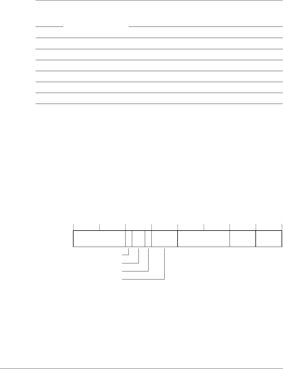
VFP Programmer’s Model
ARM DDI 0301H Copyright © 2004-2009 ARM Limited. All rights reserved. 20-13
ID012310 Non-Confidential, Unrestricted Access
Table 20-4 lists the ARM11 processor modes for accessing the VFP11 system registers.
Table 20-4 shows that a privileged ARM11 mode is sometimes required to access a VFP11
system register. When a privileged mode is required, an instruction that tries to access a register
in a nonprivileged mode takes the Undefined Instruction trap.
The following sections describe the VFP11 system registers:
•Floating-Point System ID Register, FPSID
•Floating-Point Status and Control Register, FPSCR on page 20-14
•Floating-point exception register, FPEXC on page 20-16
•Instruction registers, FPINST and FPINST2 on page 20-18.
20.4.1 Floating-Point System ID Register, FPSID
FPSID is a read-only register that identifies the VFP11 coprocessor. Figure 20-5 shows the
FPSID bit fields.
Figure 20-5 Floating-Point System ID Register
Table 20-4 Accessing VFP11 system registers
FMXR/FMRX <reg> field
ARM11 processor mode
Register VFP11 coprocessor enabled VFP11 coprocessor disabled
FPSID b0000 Any mode Privileged mode
FPSCR b0001 Any mode Nonea
FPEXC b1000 Privileged mode Privileged mode
FPINST b1001 Privileged mode Privileged mode
FPINST2 b1010 Privileged mode Privileged mode
MVFR0 b0111 Any mode Privileged mode
MVFR1 b0110 Any mode Privileged mode
a. An instruction that tries to access FPSCR while the VFP11 coprocessor is disabled takes the Undefined Instruction trap.
SW
Format
SNG
Architecture
Variant Revision
31 20 16 15 8 7 4 3 024 23 192122
Implementer Part number
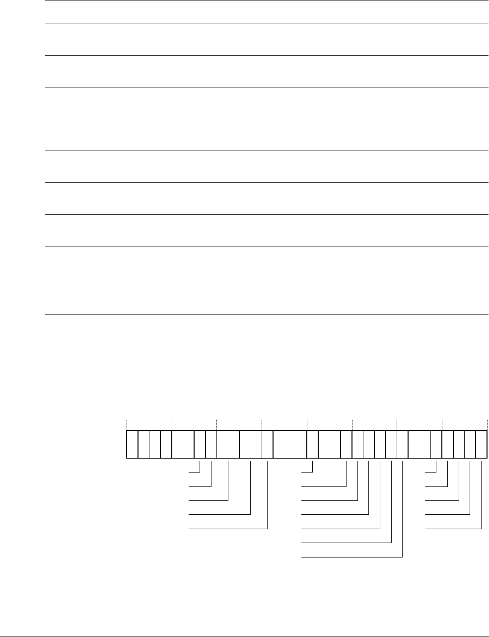
VFP Programmer’s Model
ARM DDI 0301H Copyright © 2004-2009 ARM Limited. All rights reserved. 20-14
ID012310 Non-Confidential, Unrestricted Access
Table 20-5 lists the FPSID bit fields.
20.4.2 Floating-Point Status and Control Register, FPSCR
FPSCR is a read/write register that can be accessed in both privileged and unprivileged modes.
All bits that Figure 20-6 describes as SBZ are reserved for future expansion. They must be
initialized to zeros. To ensure that these bits are not modified, code other than initialization code
must use read/modify/write techniques when writing to FPSCR. Failure to observe this rule can
cause Unpredictable results in future systems. Figure 20-6 shows the FPSCR bit fields.
Figure 20-6 Floating-Point Status and Control Register
Table 20-5 FPSID bit fields
Bit Meaning Value
[31:24] Implementer
0x41
A, ARM Limited
[23] Hardware/software 0
Hardware implementation
[22:21] FSTMX/FLDMX
format
b00
Format 1
[20] Precisions supported 0
Both single-precision and double-precision data supported
[19:16] Architecture version b0001
VFPv2 architecture
[15:8] Part number
0x20
VFP11
[7:4] Variant
0xB
ARM11 VFP coprocessor
[3:0] Revision Incremented on each revision of the VFP11 coprocessor. Values for the ARM11JZF-S
product releases are:
ARM1176JZF-S r0p0:
0x3
ARM1176JZF-S r0p1 and r0p2: 0x4
ARM1176JZF-S r0p4 and r0p6: 0x5
31 30 29 28 25 24 23 22 21 20 19 15 12 11 10 9 8 7 4 3 2 1 0
IXC
IDC
SBZ
DZE
IOE
UFE
OFE
SBZ
IXE
IDE
LEN
Rmode
Stride
SBZ
SBZ
DN
FZ
NZCV
UFC
OFC
DZC
IOC
27 26 18 16 14 13 6 5

VFP Programmer’s Model
ARM DDI 0301H Copyright © 2004-2009 ARM Limited. All rights reserved. 20-15
ID012310 Non-Confidential, Unrestricted Access
Table 20-6 lists the FPSCR bit fields.
Table 20-6 Encoding of the Floating-Point Status and Control Register
Bits Name Meaning
[31] N Set if comparison produces a less than result
[30] Z Set if comparison produces an equal result
[29] C Set if comparison produces an equal, greater than, or unordered result
[28] V Set if comparison produces an unordered result
[27:26] - Should Be Zero
[25] DN Default NaN mode enable bit:
1 = default NaN mode enabled
0 = default NaN mode disabled
[24] FZ Flush-to-zero mode enable bit:
1 = flush-to-zero mode enabled
0 = flush-to-zero mode disabled
[23:22] Rmode Rounding mode control field:
b00 = Round to nearest (RN) mode
b01 = Round towards plus infinity (RP) mode
b10 = Round towards minus infinity (RM) mode
b11 = Round towards zero (RZ) mode
[21:20] Stride See Vector length and stride control on page 20-16
[19] - Should Be Zero
[18:16] LEN See Vector length and stride control on page 20-16
[15] IDE Input Subnormal exception trap enable bit
[14:13] - Should Be Zero
[12] IXE Inexact exception trap enable bit
[11] UFE Underflow exception trap enable bit
[10] OFE Overflow exception trap enable bit
[9] DZE Division by Zero exception trap enable bit
[8] IOE Invalid Operation exception trap enable bit
[7] IDC Input Subnormal cumulative exception flag
[6:5] - Should Be Zero
[4] IXC Inexact cumulative exception flag
[3] UFC Underflow cumulative exception flag
[2] OFC Overflow cumulative exception flag
[1] DZC Division by Zero cumulative exception flag
[0] IOC Invalid Operation cumulative exception flag

VFP Programmer’s Model
ARM DDI 0301H Copyright © 2004-2009 ARM Limited. All rights reserved. 20-16
ID012310 Non-Confidential, Unrestricted Access
Vector length and stride control
FPSCR[18:16] is the LEN field and controls the vector length for VFP instructions that operate
on short vectors. The vector length is the number of iterations in a short vector instruction.
FPSCR[21:20] is the STRIDE field and controls the vector stride. The vector stride is the
increment value used to select the registers involved in the next iteration of the short vector
instruction.
The rules for vector operation do not enable a vector to use the same register more than once.
LEN and STRIDE combinations that use a register more than once produce Unpredictable
results, as Table 20-7 lists. Some combinations that work normally in single-precision short
vector instructions cause Unpredictable results in double-precision instructions.
20.4.3 Floating-point exception register, FPEXC
In a bounce situation, the FPEXC register records the exceptional status. The FPEXC register
information assists the support code in processing the exceptional condition or reporting the
condition to a system trap handler or a user trap handler.
You must save and restore the FPEXC register whenever changing the context. If the EX flag,
FPEXC[31], is set, then the VFP11 coprocessor is in the exceptional state, and you must also
save and restore the FPINST and FPINST2 registers. You can write the context switch code to
determine from the EX flag the registers to save and restore or to save all three.
The EN bit, FPEXC[30], is the VFP enable bit. Clearing EN disables the VFP11 coprocessor.
The VFP11 coprocessor clears the EN bit on reset.
Table 20-7 Vector length and stride combinations
LEN Vector length STRIDE Vector stride
Single-precision
vector instructions
Double-precision
vector instructions
b000 1 b00 - All instructions are scalar All instructions are scalar
b000 1 b11 - Unpredictable Unpredictable
b001 2 b00 1 Work normally Work normally
b001 2 b11 2 Work normally Work normally
b010 3 b00 1 Work normally Work normally
b010 3 b11 2 Work normally Unpredictable
b011 4 b00 1 Work normally Work normally
b011 4 b11 2 Work normally Unpredictable
b100 5 b00 1 Work normally Unpredictable
b100 5 b11 2 Unpredictable Unpredictable
b101 6 b00 1 Work normally Unpredictable
b101 6 b11 2 Unpredictable Unpredictable
b110 7 b00 1 Work normally Unpredictable
b110 7 b11 2 Unpredictable Unpredictable
b111 8 b00 1 Work normally Unpredictable
b111 8 b11 2 Unpredictable Unpredictable
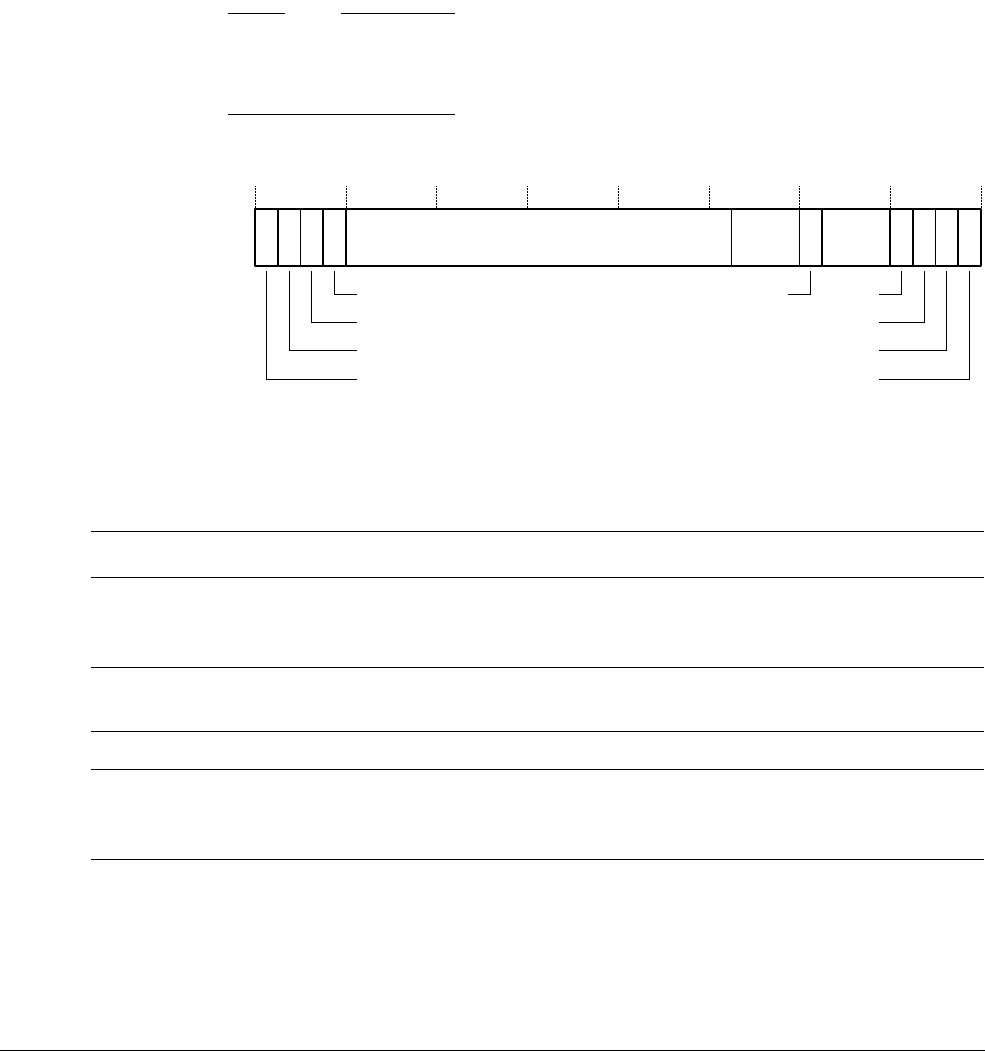
VFP Programmer’s Model
ARM DDI 0301H Copyright © 2004-2009 ARM Limited. All rights reserved. 20-17
ID012310 Non-Confidential, Unrestricted Access
The INV flag, FPEXC[7], signals Input exceptions. An Input exception is a condition when the
hardware cannot process one or more input operands according to the architectural
specifications. This includes subnormal inputs when the VFP11 coprocessor is not in
flush-to-zero mode and NaNs when the VFP11 coprocessor is not in default NaN mode.
The UFC flag, FPEXC[3], is set whenever an operation has the potential to generate a result that
is lower than the minimum threshold for the destination precision.
The OFC flag, FPEXC[2], is set whenever an operation has the potential to generate a result that,
after rounding, exceeds the largest representable number in the destination format.
The IOC flag, FPEXC[0], is set whenever an operation has the potential to generate a result that
cannot be represented or is not defined.
Note
To prevent an infinite loop of exceptions, the support code must clear the EX flag, FPEXC[31],
immediately on entry to the exception code. All exception flags must be cleared before returning
from exception code to user code.
Figure 20-7 shows the FPEXC bit fields.
Figure 20-7 Floating-Point Exception Register
Table 20-8 lists the bit fields of the FPEXC register.
IOC
31 30 29 28 10 8 7 6 4 3 2 1 0
SBZ
SBZ
UFC
OFC
INV
VECITRSBZ
EX
EN
SBZ
FP2V
27 11
Table 20-8 Encoding of the Floating-Point Exception Register
Bits Name Description
[31] EX Exception flag.
When EX is set, the VFP11 coprocessor is in the exceptional state.
EX must be cleared by the exception handling routine.
[30] EN VFP enable bit.
Setting EN enables the VFP11 coprocessor. Reset clears EN.
[29] - Should Be Zero.
[28] FP2V FPINST2 instruction valid flag.
Set when FPINST2 contains a valid instruction.
FP2V must be cleared by the exception handling routine.
[27:11] - Should Be Zero.

VFP Programmer’s Model
ARM DDI 0301H Copyright © 2004-2009 ARM Limited. All rights reserved. 20-18
ID012310 Non-Confidential, Unrestricted Access
20.4.4 Instruction registers, FPINST and FPINST2
The VFP11 coprocessor has two instruction registers:
• The FPINST register contains the exceptional instruction.
• The FPINST2 register contains the instruction that was issued to the VFP11 coprocessor
before the exception was detected. This instruction was retired in the ARM11 processor
and cannot be reissued. It must be executed by support code.
The FPINST and FPINST2 are accessible only in privileged modes.
The instruction in the FPINST register is in the same format as the issued instruction but is
modified in several ways. The condition code flags, FPINST[31:28], are forced to b1110, the
AL, always, condition. If the instruction is a short vector, the source and destination registers
that reference vectors are updated to point to the source and destination registers of the
exceptional iteration. See Exception processing for CDP short vector instructions on page 22-8
for more information.
The instruction in the FPINST2 register is in the same format as the issued instruction but is
modified by forcing the condition code flags, FPINST2[31:28] to b1110, the AL, always,
condition.
[10:8] VECITR Vector iteration count field.
VECITR contains the number of remaining short vector iterations after a potential exception was
detected in one of the iterations:
b000 = 1 iteration
b001 = 2 iterations
b010 = 3 iterations
b011 = 4 iterations
b100 = 5 iterations
b101 = 6 iterations
b110 = 7 iterations
b111 = 0 iterations.
[7] INV Input exception flag.
Set if the VFP11 coprocessor is not in flush-to-zero mode and an operand is subnormal or if the
VFP11 coprocessor is not in default NaN mode and an operand is a NaN.
[6:4] - Should Be Zero.
[3] UFC Potential underflow flag.
Set if the VFP11 coprocessor is not in flush-to-zero mode and a potential underflow condition
exists.
[2] OFC Potential overflow flag.
Set if the OFE bit, FPSCR[10], is set, the VFP11 coprocessor is not in RunFast mode, and a
potential overflow condition exists.
[1] - Should Be Zero.
[0] IOC Potential invalid operation flag.
Set if the IOE bit, FPSCR[8], is set, the VFP11 coprocessor is not in RunFast mode, and a potential
invalid operation condition exists.
Table 20-8 Encoding of the Floating-Point Exception Register (continued)
Bits Name Description

VFP Programmer’s Model
ARM DDI 0301H Copyright © 2004-2009 ARM Limited. All rights reserved. 20-19
ID012310 Non-Confidential, Unrestricted Access
20.4.5 Media and VFP Feature Register 0
The purpose of the Media and VFP Feature Register 0 is to provide information about the
features that the VFP unit contains.
Media and VFP Feature Register 0 is:
• a 32-bit read-only register
• accessible in any mode when the VFP is enabled by the EN bit, see Floating-point
exception register, FPEXC on page 20-16
• accessible only in Privileged modes when the VFP is disabled by the EN bit.
Figure 20-8 shows the bit arrangement for Media and VFP Feature Register 0.
Figure 20-8 Media and VFP Feature Register 0 format
Table 20-9 shows how the bit values correspond with the Media and VFP Feature Register 0
functions.
The values in the Media and VFP Feature Register 0 are implementation defined.
---- -
31 16 15 8 7 3 0
---
Table 20-9 Media and VFP Feature Register 0 bit functions
Bits Name Function
[31:28] - Indicates the VFP hardware support level when user traps are disabled.
0x1
, In ARM1176JZF-S processors when Flush-to-Zero and Default_NaN and Round-to-Nearest are
all selected in FPSCR, the coprocessor does not require support code. Otherwise floating point
support code is required.
[27:24] - Indicates support for short vectors.
0x1
, ARM1176JZF-S processors support short vectors.
[23:20] - Indicates support for hardware square root.
0x1
, ARM1176JZF-S processors support hardware square root.
[19:16] - Indicates support for hardware divide.
0x1
, ARM1176JZF-S processors support hardware divide.
[15:12] - Indicates support for user traps.
0x1
, ARM1176JZF-S processors support software traps, support code is required.
[11:8] - Indicates support for double precision VFP.
0x1
, ARM1176JZF-S processors support v2.
[7:4] - Indicates support for single precision VFP.
0x1
, ARM1176JZF-S processors support v2.
[3:0] - Indicates support for the media register bank.
0x1
, ARM1176JZF-S processors support 16, 64-bit registers.

VFP Programmer’s Model
ARM DDI 0301H Copyright © 2004-2009 ARM Limited. All rights reserved. 20-20
ID012310 Non-Confidential, Unrestricted Access
20.4.6 Media and VFP Feature Register 1
The purpose of the Media and VFP Feature Register 1 is to provide information about the
features that the VFP unit contains.
Media and VFP Feature Register 1 is:
• a 32-bit read-only register
• accessible in any mode when the VFP is enabled by the EN bit, see Floating-point
exception register, FPEXC on page 20-16
• accessible only in Privileged modes when the VFP is disabled by the EN bit.
Figure 20-9 shows the bit arrangement for Media and VFP Feature Register 1.
Figure 20-9 Media and VFP Feature Register 1 format
Table 20-10 shows how the bit values correspond with the Media and VFP Feature Register 1
functions.
The values in the Media and VFP Feature Register 1 are implementation defined.
-
31 8 7 3 0
---
41112
Table 20-10 Media and VFP Feature Register 1 bit functions
Bits Name Function
[31:12] - Reserved
UNP/SBZ.
[11:8] - Indicates support for media extension, single precision floating point instructions.
0x0
, no support in ARM1176JZF-S processors.
[7:4] - Indicates support for media extension, integer instructions.
0x0
, no support in ARM1176JZF-S processors.
[3:0] - Indicates support for media extension, load/store instructions.
0x0
, no support in ARM1176JZF-S processors.

ARM DDI 0301H Copyright © 2004-2009 ARM Limited. All rights reserved. 21-1
ID012310 Non-Confidential, Unrestricted Access
Chapter 21
VFP Instruction Execution
This chapter describes the VFP11 instruction pipeline and its relationship with the ARM processor
instruction pipeline. It contains the following sections:
•About instruction execution on page 21-2
•Serializing instructions on page 21-3
•Interrupting the VFP11 coprocessor on page 21-4
•Forwarding on page 21-5
•Hazards on page 21-6
•Operation of the scoreboards on page 21-7
•Data hazards in full-compliance mode on page 21-13
•Data hazards in RunFast mode on page 21-16
•Resource hazards on page 21-17
•Parallel execution on page 21-20
•Execution timing on page 21-22.

VFP Instruction Execution
ARM DDI 0301H Copyright © 2004-2009 ARM Limited. All rights reserved. 21-2
ID012310 Non-Confidential, Unrestricted Access
21.1 About instruction execution
Features of the VFP11 implementation of the instruction pipelines include the following:
• The FMXR, FMRX, and FMSTAT instructions stall in the VFP11 LS pipeline until all
currently executing instructions are completed. You can use these serializing instructions
to:
— capture condition codes and exception status
— modify the mode of operation of subsequent instructions
— create an exception boundary.
See Serializing instructions on page 21-3.
• Load or store instructions that cause a Data Abort exception restart after interrupt service.
LDM and STM instructions detect exceptional conditions after the first transfer and restart
after interrupt service if reissued.
See Interrupting the VFP11 coprocessor on page 21-4.
• To reduce stall time, the VFP11 coprocessor forwards data:
— from load instructions to CDP instructions
— from CDP instructions to CDP instructions.
See Forwarding on page 21-5.
• In full-compliance mode, the VFP11 coprocessor implements full data hazard and
resource hazard detection.
RunFast mode guarantees no instruction bouncing for applications that require less strict
hazard detection.
See Hazards on page 21-6 and Operation of the scoreboards on page 21-7.
• The L/S, FMAC, and DS pipelines operate independently, enabling data transfer and CDP
operations to execute in parallel.
See Parallel execution on page 21-20.
Execution timing on page 21-22 describes VFP11 instruction throughput and latency.

VFP Instruction Execution
ARM DDI 0301H Copyright © 2004-2009 ARM Limited. All rights reserved. 21-3
ID012310 Non-Confidential, Unrestricted Access
21.2 Serializing instructions
A serializing instruction is one that stalls because of activity in the VFP11 pipelines without the
presence of a register or resource hazard. In general, an access to a VFP11 control or status
register is a serializing instruction.
The serializing instructions are FMRX and FMXR, including the FMSTAT instruction.
Serializing instructions stall the VFP11 coprocessor in the Issue stage and the ARM processor
in the Execute 2 stage until:
• the VFP11 pipeline is past the point of updating either the condition codes or the exception
status
• a write to a system register can no longer affect the operation of a current or pending
instruction.
An FMRX or FMSTAT instruction stalls until all prior floating-point operations are completed,
and the data to be written by the VFP11 coprocessor is valid. For example, a compare operation
updates the FPSCR register condition codes in the Writeback stage of the compare.
An FMXR instruction stalls until all prior floating-point operations are past the point of being
affected by the instruction. For example, writing to the FPSCR register stalls until the point
when changing the control bits cannot affect any operation currently executing or awaiting
execution. Writing to the FPEXC, FPINST, or FPINST2 register stalls until the pipeline is
completely clear.
Uses of serializing instructions include:
• capturing condition codes and exception status
• delineating a block of instructions for execution with the ability to capture the exception
status of that block of instructions
• modifying the mode of operation of subsequent instructions, such as the rounding mode
or vector length.
While no instruction can change the contents of the FPSID register, you can access the FPSID
register with FMRX or FMXR as a general-purpose serializing operation or to create an
exception boundary.

VFP Instruction Execution
ARM DDI 0301H Copyright © 2004-2009 ARM Limited. All rights reserved. 21-4
ID012310 Non-Confidential, Unrestricted Access
21.3 Interrupting the VFP11 coprocessor
Instructions are issued to the VFP11 coprocessor directly from the ARM prefetch unit. The
VFP11 coprocessor has no external interface beyond the ARM processor and cannot be
separately interrupted by external sources. Any interrupt that causes a change of flow in the
ARM11 processor is also reflected to the VFP11 coprocessor. Any VFP instruction that is
cancelled because of condition code failure in the ARM11 pipeline is also cancelled in the
VFP11 pipeline.
If the interrupt is the result of a Data Abort condition, the load or store operation that caused the
abort restarts after interrupt processing is complete. Load and store multiple instructions can
detect some exception conditions and interrupt the operation after the initial transfer. If the load
or store instruction is reissued after interrupt processing, it can restart with the initial transfer.
The source data is guaranteed to be unchanged, and no operations that depend on the load or
store data can execute until the load or store operation is complete.
When interrupt processing begins, there can be a delay before the VFP11 coprocessor is
available to the interrupt routine. Any prior short vector instruction that passes the ARM11
Execute 2 stage also passes the VFP11 Execute 1 stage and executes to completion
uninterrupted. The maximum delay during which the VFP11 coprocessor is unavailable is equal
to the time it takes to process a short vector of eight single-precision divide or square root
iterations. Such an operation can cause a delay of as many as 114 cycles after the short vector
divide or square root enters the VFP11 Execute 1 stage.
In systems that require fast response time and access to the VFP11 coprocessor by the service
routine, avoid short vector divide and short vector square root operations. All other instructions,
including short vector instructions, have little or no impact. Limiting the number of VFP11
registers that must be saved and used in the service routine also reduces startup time. If the
VFP11 coprocessor is not required in the service routine, you can disable it with EN bit,
FPEXC[30]. This eliminates the necessity of saving the VFP11 coprocessor state. See
Application Note 98, VFP Support Code.

VFP Instruction Execution
ARM DDI 0301H Copyright © 2004-2009 ARM Limited. All rights reserved. 21-5
ID012310 Non-Confidential, Unrestricted Access
21.4 Forwarding
In general, any forwarding operation reduces the stall time of a dependent instruction by one
cycle. The VFP11 coprocessor forwards data from load instructions to CDP instructions and
from CDP instructions to CDP instructions.
The VFP11 coprocessor does not forward in the following cases:
• from an instruction that produces integer data
• to a store instruction, FST, FSTM, MRC, or MRRC
• to an instruction of different precision.
In the examples that follow, the stall counts given are based on two data transfer assumptions:
• accesses by load operations result in cache hits and are able to deliver one or two data
words per cycle
• store operations write directly to the write buffer or cache and can transfer one or two data
words per cycle.
When these assumptions are valid, the VFP11 coprocessor operates at its highest performance.
When these assumptions are not valid, load and store operations are affected by the delay
required to access data. Example 21-1, Example 21-2 and Example 21-3 illustrate the
capabilities of the VFP11 coprocessor in ideal conditions.
In Example 21-1, the second FADDS instruction depends on the result of the first FADDS
instruction. The result of the first FADDS instruction is forwarded, reducing the stall from eight
cycles to seven cycles.
Example 21-1 Data forwarded to dependent instruction
FADDS S1, S2, S3
FADDS S8, S9, S1
In Example 21-2, there is no data forwarding of the double-precision FMULD data in D2 to the
single-precision FADDS data in S5, even though S5 is the upper half of D2.
Example 21-2 Mixed-precision data not forwarded
FMULD D2, D0, D1
FADDS S12, S13, S5
In Example 21-3, the double-precision FSTD stalls for eight cycles until the result of the
FMULD is written to the register file. No forwarding is done from the FMULD to the store
instruction.
Example 21-3 Data not forwarded to store instruction
FMULD D1, D2, D3
FSTD D1, [Rx]

VFP Instruction Execution
ARM DDI 0301H Copyright © 2004-2009 ARM Limited. All rights reserved. 21-6
ID012310 Non-Confidential, Unrestricted Access
21.5 Hazards
The VFP11 coprocessor incorporates full hazard detection with a fully-interlocked pipeline
protocol. No compiler scheduling is required to avoid hazard conditions. The source and
destination scoreboards process interlocks caused by unavailable source or destination registers
or by unavailable data. The scoreboards stall instructions until all data operands and destination
registers are available before the instruction is issued to the instruction pipeline.
The determination of hazards and interlock conditions is different in full-compliance mode and
RunFast mode. RunFast mode guarantees no bounce conditions and has a less strict hazard
detection mechanism, enabling instructions to begin execution earlier than in full-compliance
mode.
There are two VFP11 pipeline hazards:
• A data hazard is a combination of instructions that creates the potential for operands to be
accessed in the wrong order.
—A Read-After-Write (RAW) data hazard occurs when the pipeline creates the
potential for an instruction to read an operand before a prior instruction writes to it.
It is a hazard to the intended read-after-write operand access.
—A Write-After-Read (WAR) data hazard occurs when the pipeline creates the
potential for an instruction to write to a register before a prior instruction reads it. It
is a hazard to the intended write-after-read operand access.
—A Write-After-Write (WAW) data hazard occurs when the pipeline creates the
potential for an instruction to write to a register before a prior instruction writes to
it. It is a hazard to the intended write-after-write operand access.
• Resource hazard. See Resource hazards on page 21-17.

VFP Instruction Execution
ARM DDI 0301H Copyright © 2004-2009 ARM Limited. All rights reserved. 21-7
ID012310 Non-Confidential, Unrestricted Access
21.6 Operation of the scoreboards
The VFP11 processor detects all hazard conditions that exist between issued and executing
instructions. It uses two scoreboards to ensure that all source and destination registers for an
instruction contain valid data and are available for reading or writing:
• The destination scoreboard contains a lock for each destination register for the current
operation.
• The source scoreboard contains a lock for each source register for the current operation.
In the Decode stage of the VFP11 pipeline, the VFP11 coprocessor determines the source and
destination registers that are involved in an operation and generates a lock mask for them. In a
short vector operation, the lock mask includes the registers involved in every iteration of the
operation. In the Issue stage, the VFP11 coprocessor checks and updates the source and
destination scoreboards. If it detects a hazard between the instruction in the Issue stage and a
prior instruction, the scoreboards are not updated, and the instruction stalls in the Issue stage.
A VFP11 instruction can begin execution only when its source and destination registers are free
of locks. A short vector operation can begin only when the registers for all its iterations are free
of locks. When a short vector instruction proceeds in the pipeline beyond the Issue stage, all the
registers involved in the operation are locked.
The source scoreboard clears a source register lock in the first Execute 1 stage of the pipeline or
in the first Execute 1 stage of the iteration. In store multiple instructions, the source scoreboard
clears source register locks in the Execute stage where the instruction writes the store data to the
ARM11 processor.
The destination scoreboard clears the destination register lock in the cycle before the result data
is written back to the register file or is available for forwarding, Execute 7 in the FMAC pipeline,
Execute 4 in the DS pipeline. In a load operation, the destination scoreboard normally clears the
destination register lock in the Memory 2 stage. If the load is delayed, the destination scoreboard
clears the destination register lock in the same cycle as the writeback to the register file.
21.6.1 Scoreboard operation when an instruction bounces
When a bounce occurs in full-compliance mode, support code is called to complete the
operation and to deliver the result and the exception status to the user trap handler. The source
scoreboard ensures that all source registers for the operation are preserved for the support code.
In a short vector operation, this includes the source registers for the bounced iteration and for
any iterations remaining after the bounced iteration. The preserved source registers include the
destination register for a multiply and accumulate instruction.
Because RunFast mode guarantees that no bouncing is possible, source registers do not have to
be preserved after they are used by the instruction. For all scalar operations and nonmultiple
store operations, no source registers are locked in RunFast mode. In short, vector operations, the
length of the vector determines the source registers that are locked. When the vector length
exceeds four single-precision iterations, the source scoreboard locks the source registers for
iterations 5 and above. When the vector length exceeds two double-precision iterations, the
source scoreboard locks the source registers for iterations 3 and above.

VFP Instruction Execution
ARM DDI 0301H Copyright © 2004-2009 ARM Limited. All rights reserved. 21-8
ID012310 Non-Confidential, Unrestricted Access
21.6.2 Single-precision source register locking
In full-compliance mode, the source scoreboard locks all source registers in the Issue stage of
the instruction. In RunFast mode, the source scoreboard locks the source registers for only
iterations 5, 6, 7, and 8. Table 21-1 summarizes source register locking in single-precision
operations.
For the following single-precision short vector instruction, the LEN field contains b100,
selecting a vector length of five iterations:
FADDS S8, S16, S24
The FADDS instruction performs the following operations:
FADDS S8, S16, S24
FADDS S9, S17, S25
FADDS S10, S18, S26
FADDS S11, S19, S27
FADDS S12, S20, S28
In full-compliance mode, the source scoreboard locks S16-S20 and S24-S28 in the Issue stage
of the instruction.
In RunFast mode, the source scoreboard locks only the fifth iteration source registers, S20 and
S28.
Table 21-1 Single-precision source register locking
LEN Vector length
Source registers locked in Issue stage
Full-compliance mode RunFast mode
b000 1 Iteration 1 registers -
b001 2 Iteration 1-2 registers -
b010 3 Iteration 1-3 registers -
b011 4 Iteration 1-4 registers -
b100 5 Iteration 1-5 registers Iteration 5 registers
b101 6 Iteration 1-6 registers Iteration 5-6 registers
b110 7 Iteration 1-7 registers Iteration 5-7 registers
b111 8 Iteration 1-8 registers Iteration 5-8 registers

VFP Instruction Execution
ARM DDI 0301H Copyright © 2004-2009 ARM Limited. All rights reserved. 21-9
ID012310 Non-Confidential, Unrestricted Access
21.6.3 Single-precision source register clearing
In full-compliance mode, the source scoreboard clears the source registers of each iteration in
the Execute 1 stage of the iteration. In RunFast mode, the source registers for only iterations 5,
6, 7, and 8 are locked, and the source scoreboard begins clearing them in the second Execute 1
cycle of the instruction. Table 21-2 summarizes source register clearing in single-precision
operations.
For the following single-precision short vector instruction, the LEN field contains b100,
selecting a vector length of five iterations:
FADDS S8, S16, S24
The FADDS instruction performs the following operations:
FADDS S8, S16, S24
FADDS S9, S17, S25
FADDS S10, S18, S26
FADDS S11, S19, S27
FADDS S12, S20, S28
In full-compliance mode, the source scoreboard clears the source registers of each iteration in
the Execute 1 cycle of the iteration.
In RunFast mode, the source scoreboard locks only the fifth iteration source registers, S20 and
S28. It clears S20 and S28 in the second Execute 1 cycle of the instruction.
Table 21-2 Single-precision source register clearing
Execute 1 cycle
Source registers cleared in Execute 1 stage of each iteration
Full-compliance mode RunFast mode
1 Iteration 1 registers -
2 Iteration 2 registers Iteration 5 registers
3 Iteration 3 registers Iteration 6 registers
4 Iteration 4 registers Iteration 7 registers
5 Iteration 5 registers Iteration 8 registers
6 Iteration 6 registers -
7 Iteration 7 registers -
8 Iteration 8 registers -

VFP Instruction Execution
ARM DDI 0301H Copyright © 2004-2009 ARM Limited. All rights reserved. 21-10
ID012310 Non-Confidential, Unrestricted Access
21.6.4 Double-precision source register locking
In full-compliance mode, the source scoreboard locks all source registers in the Issue stage of
the instruction. In RunFast mode, the source scoreboard locks the source registers for only
iterations 3 and 4. Table 21-3 summarizes source register locking in double-precision
operations.
For the following double-precision, short vector instruction, the LEN field contains b011,
selecting a vector length of four iterations:
FADDD D4, D8, D12
The FADDD instruction performs the following operations:
FADDD D4, D8, D12
FADDD D5, D9, D13
FADDD D6, D10, D14
FADDD D7, D11, D15
In full-compliance mode, the source scoreboard locks D8-D11 and D12-D15 in the Issue stage
of the instruction.
In RunFast mode, the source scoreboard locks only the third iteration source registers, D10 and
D14, and the fourth iteration source registers, D11 and D15.
21.6.5 Double-precision source register clearing
The number of Execute 1 cycles required to clear the source registers of a double-precision
instruction depends on the throughput of the instruction, as the following sections show:
•Instructions with one-cycle throughput on page 21-11
•Instructions with two-cycle throughput on page 21-11.
Table 21-3 Double-precision source register locking
LEN Vector length
Source registers locked in Issue stage
Full-compliance mode RunFast mode
b000 1 Iteration 1 registers -
b001 2 Iteration 1-2 registers -
b010 3 Iteration 1-3 registers Iteration 3 registers
b011 4 Iteration 1-4 registers Iteration 3-4 registers

VFP Instruction Execution
ARM DDI 0301H Copyright © 2004-2009 ARM Limited. All rights reserved. 21-11
ID012310 Non-Confidential, Unrestricted Access
Instructions with one-cycle throughput
In full-compliance mode, the source scoreboard clears the source registers of each iteration in
the Execute 1 stage of the iteration. In RunFast mode, the source registers for only iterations 3
and 4 are locked, and the source scoreboard begins clearing them in the first Execute 1 cycle of
the instruction. Table 21-4 summarizes source register clearing for double-precision one-cycle
instructions such as FADDD and FABSD.
For the following one-cycle, double-precision short vector instruction, the LEN field contains
b011, selecting a vector length of four iterations:
FADDD D4, D8, D12
The FADDD performs the following operations:
FADDD D4, D8, D12
FADDD D5, D9, D13
FADDD D6, D10, D14
FADDD D7, D11, D15
In full-compliance mode, the source scoreboard clears the source registers of each iteration in
the Execute 1 cycle of the iteration.
In RunFast mode, the source scoreboard locks only the third iteration source registers, D10 and
D14, and the fourth iteration source registers, D11 and D15. It clears D10 and D14 in the first
Execute 1 cycle of the instruction and clears D11 and D15 in the second Execute 1 cycle.
Instructions with two-cycle throughput
In full-compliance mode, the source scoreboard clears the source registers of each iteration in
the first Execute 1 cycle of the iteration. In RunFast mode, the source registers for only iterations
3 and 4 are locked, and the source scoreboard begins clearing them in the first Execute 1 cycle
of the instruction. Table 21-5 summarizes source register clearing for double-precision
two-cycle instructions such as FMULD and FMACD.
Table 21-4 Double-precision source register clearing for one-cycle instructions
Execute 1 cycle
Source registers cleared in Execute 1 stage of each iteration
Full-compliance mode RunFast mode
1 Iteration 1 registers Iteration 3 registers
2 Iteration 2 registers Iteration 4 registers
3 Iteration 3 registers -
4 Iteration 4 registers -
Table 21-5 Double-precision source register clearing for two-cycle instructions
Execute 1 cycle
Source registers cleared in Execute 1 stage of each iteration
Full-compliance mode RunFast mode
1 Iteration 1 registers Iteration 3 registers
2- -
3 Iteration 2 registers Iteration 4 registers

VFP Instruction Execution
ARM DDI 0301H Copyright © 2004-2009 ARM Limited. All rights reserved. 21-12
ID012310 Non-Confidential, Unrestricted Access
For the following two-cycle, double-precision, short vector instruction, the LEN field contains
b011, selecting a vector length of four iterations:
FMULD D4, D8, D12
The FMULD instruction performs the following operations:
FMULD D4, D8, D12
FMULD D5, D9, D13
FMULD D6, D10, D14
FMULD D7, D11, D15
In full-compliance mode, the source scoreboard clears the source registers of each iteration in
the first Execute 1 cycle of the iteration.
In RunFast mode, only the third iteration source registers, D10 and D14, and the fourth iteration
source registers, D11 and D15, are locked. The source scoreboard clears D10 and D14 in the
first Execute 1 cycle and clears D11 and D15 in the third Execute 1 cycle of the instruction.
4- -
5 Iteration 3 registers -
6- -
7 Iteration 4 registers -
8- -
Table 21-5 Double-precision source register clearing for two-cycle instructions
Execute 1 cycle
Source registers cleared in Execute 1 stage of each iteration
Full-compliance mode RunFast mode

VFP Instruction Execution
ARM DDI 0301H Copyright © 2004-2009 ARM Limited. All rights reserved. 21-13
ID012310 Non-Confidential, Unrestricted Access
21.7 Data hazards in full-compliance mode
The sections that follow give examples of data hazards in full-compliance mode:
•Status register RAW hazard example
•Load multiple-CDP RAW hazard example
•CDP-CDP RAW hazard example on page 21-14
•Load multiple-short vector CDP RAW hazard example on page 21-14
•Short vector CDP-load multiple WAR hazard example on page 21-15.
21.7.1 Status register RAW hazard example
In Example 21-4, the FMSTAT is stalled for four cycles in the Decode stage until the FCMPS
updates the condition codes in the FPSCR register. Two cycles later, the FMSTAT writes the
condition codes to the ARM11 processor.
Example 21-4 FCMPS-FMSTAT RAW hazard
FCMPS S1, S2
FMSTAT
Table 21-6 lists the VFP11 pipeline stages for Example 21-4.
21.7.2 Load multiple-CDP RAW hazard example
In Example 21-5, the FADDS is stalled in the Issue stage for six cycles until the FLDM makes
its last transfer to the VFP11 coprocessor. S15 is forwarded from the load in cycle 9 to the
FADDS.
Example 21-5 FLDM-FADDS RAW hazard
FLDM [Rx], {S8-S15}
FADDS S1, S2, S15
Table 21-6 FCMPS-FMSTAT RAW hazard
Instruction cycle number
Instruction1234567891011
FCMPS D I E1E2E3E4- - - - -
FMSTAT - DDDDDI E M1M2W

VFP Instruction Execution
ARM DDI 0301H Copyright © 2004-2009 ARM Limited. All rights reserved. 21-14
ID012310 Non-Confidential, Unrestricted Access
Table 21-7 lists the VFP11 pipeline stages for Example 21-5 on page 21-13.
21.7.3 Load multiple-short vector CDP RAW hazard example
In Example 21-6, the short vector FADDS is stalled in the Issue stage until the FLDM loads all
source registers required by the FADDS. In this case, the FADDS is stalled for three cycles.
Because the FADDS depends on the FLDM for only one register, S7, it does not have to wait
for completion of the FLDM. The S7 data is forwarded in cycle 6. The LEN field contains b011,
selecting a vector length of four iterations. The STRIDE field contains b00, selecting a vector
stride of one. The first source vector uses registers S7, S0, S1, and S2, and the only FADDS
source register loaded by the FLDM is S7. This example is based on the assumption that the
remaining source and destination registers are available to the FADDS in cycle 6.
Example 21-6 FLDM-short vector FADDS RAW hazard
FLDM [R2], {S7-S14}
FADDS S16, S7, S25
Table 21-8 lists the VFP11 pipeline stages of the FLDM and the first iteration of the short vector
FADDS for Example 21-6.
21.7.4 CDP-CDP RAW hazard example
In Example 21-7, the FADDS is stalled in the Issue stage for seven cycles until the FMULS data
is written and forwarded in cycle 10 to the Issue stage of the FADDS.
Example 21-7 FMULS-FADDS RAW hazard
FMULS S4, S1, S0
FADDS S5, S4, S3
Table 21-7 FLDM-FADDS RAW hazard
Instruction cycle number
Instruction 1 2 3 4 5 6 7 8 9 10 11 12 13 14 15 16
FLDM DIEM1M2WWWW-------
FADDS - D I I I I I I I E1 E2 E3 E4 E5 E6 E7
Table 21-8 FLDM-short vector FADDS RAW hazard
Instruction cycle number
Instruction 1 2 3 4 5 6 7 8 9 10 11 12 13 14 15 16 17
FLDM DIEM1M2WWWW---- ----
FADDS - D I I I I E1 E1 E1 E1 E2 E3 E4 E5 E6 E7 W

VFP Instruction Execution
ARM DDI 0301H Copyright © 2004-2009 ARM Limited. All rights reserved. 21-15
ID012310 Non-Confidential, Unrestricted Access
Table 21-9 lists the VFP11 pipeline stages of Example 21-7 on page 21-14.
21.7.5 Short vector CDP-load multiple WAR hazard example
In Example 21-8, the load multiple FLDMS creates a WAR hazard to the source registers of the
FMULS. The LEN field contains b011, selecting a vector length of four iterations, and the
STRIDE field contains b00, selecting a vector stride of one. The VFP11 coprocessor stalls the
FLDMS until the FMULS clears the scoreboard locks for all the source registers, S16-S19 and
S24-S27.
Example 21-8 Short vector FMULS-FLDMS WAR hazard
FMULS S8, S16, S24
FLDMS [R2], {S16-S27}
Table 21-10 lists the VFP11 pipeline stages for the first iteration of Example 21-8.
Table 21-9 FMULS-FADDS RAW hazard
Instruction cycle number
Instruction1234567891011
FMULS DI E1E2E3E4E5E6E7W -
FADDS - D I IIIIIIIEI
Table 21-10 Short vector FMULS-FLDMS WAR hazard
Instruction cycle number
Instruction123456789 10111213141516
FMULS DI E1E1E1E1E2E3E4 E5 E6E7W - - -
FLDMS -DIIIIIEM1M2WWWWWW

VFP Instruction Execution
ARM DDI 0301H Copyright © 2004-2009 ARM Limited. All rights reserved. 21-16
ID012310 Non-Confidential, Unrestricted Access
21.8 Data hazards in RunFast mode
In RunFast mode, source registers for the FMAC and FMUL family of instructions are locked:
• when the vector length exceeds four iterations in single-precision instructions
• when the vector length exceeds two iterations in double-precision instructions.
No source registers are locked for scalar instructions.
21.8.1 Short vector CDP-load multiple WAR hazard example
Example 21-9 is the same as Example 21-8 on page 21-15. The LEN field contains b011,
selecting a vector length of four iterations, and the STRIDE field contains b00, selecting a vector
stride of one. Executing these instructions in RunFast mode reduces the cycle count of the
FLDMS by four cycles.
Example 21-9 Short vector FMULS-FLDMS WAR hazard in RunFast mode
FMULS S8, S16, S24
FLDMS R2, {S16-S27}
Table 21-11 shows that the VFP11 coprocessor does not stall the FLDMS operation.
Table 21-11 Short vector FMULS-FLDMS WAR hazard in RunFast mode
Instruction cycle number
Instruction12345 6 78910111213
FMULS DI E1E1E1 E1 E2E3E4E5E6E7W
FLDMS - DI E M1M2WWWWWW-

VFP Instruction Execution
ARM DDI 0301H Copyright © 2004-2009 ARM Limited. All rights reserved. 21-17
ID012310 Non-Confidential, Unrestricted Access
21.9 Resource hazards
A resource hazard exists when the pipeline required for an instruction is unavailable because of
a prior instruction. VFP11 resource stalls are possible in the following cases:
• A data transfer operation following an incomplete data transfer operation can cause a
resource stall. The ARM11 processor can stall each data transfer because of unavailable
data caused by memory latency or a cache miss, increasing the latency of the data transfer
instruction and stalling any following data transfer instructions.
• An arithmetic operation following either a short vector arithmetic operation or a
double-precision multiply or multiply and accumulate operation can cause a resource
stall. The latency for a double-precision multiply or multiply and accumulate operation is
two cycles, causing a single-cycle stall for an arithmetic operation that immediately
follows.
• A single-precision divide or square root operation stalls subsequent DS operations for 15
cycles. A double-precision divide or square root operation stalls subsequent DS
operations for 29 cycles.
• A short vector divide or square root operation requires the FMAC pipeline for the first
cycle of each iteration and stalls any following CDP operation. The following CDP
operation stalls until the final iteration of the short vector divide or square root operation
completes the Execute 1 stage.
The LS pipeline is separate from the FMAC and DS pipelines. No resource hazards exist
between data transfer instructions and arithmetic instructions.
The sections that follow give examples of resource hazards:
•Load multiple-load-CDP resource hazard example
•Load multiple-short vector CDP resource hazard example on page 21-18
•Short vector CDP-CDP resource hazard example on page 21-18.
21.9.1 Load multiple-load-CDP resource hazard example
In Example 21-10, the FLDM is executing two transfers to the VFP11 coprocessor. The FLDS
is stalled behind the FLDM until the FLDM enters the final Execute cycle. The FADDS is stalled
for one cycle until the FLDS begins execution.
Example 21-10 FLDM-FLDS-FADDS resource hazard
FLDM [R2], {S8-S10}
FLDS [R4], S16
FADDS S2, S3, S4

VFP Instruction Execution
ARM DDI 0301H Copyright © 2004-2009 ARM Limited. All rights reserved. 21-18
ID012310 Non-Confidential, Unrestricted Access
Table 21-12 lists the pipeline stages for Example 21-10 on page 21-17.
21.9.2 Load multiple-short vector CDP resource hazard example
In Example 21-11, no resource hazard exists for the FMULS because of the FLDM in the prior
cycle. The FMULS is issued to the VFP11 coprocessor in the cycle following the issue of the
FLDM, and executes in parallel with it.
The LEN field contains, b011, selecting a vector length of four iterations. The STRIDE field
contains b00, selecting a vector stride of one.
Example 21-11 FLDM-short vector FMULS resource hazard
FLDM [R2], {S8-S10}
FMULS S16, S24, S4
Table 21-13 lists the pipeline stages for Example 21-11.
21.9.3 Short vector CDP-CDP resource hazard example
In Example 21-12, a short vector divide is followed by a FADDS instruction. The short vector
divide has b001 in the LEN field, selecting a vector length of two iterations. It requires the
Execute 1 stage of the FMAC pipeline for the first cycle of each iteration of the divide, resulting
in a stall of the FADDS until the final iteration of the divide completes the first Execute 1 cycle.
The divide iterates for 14 cycles in the Execute 1 and Execute 2 stages of the DS pipeline, that
Table 21-14 on page 21-19 lists, as E1. The first and shared Execute 1 cycle for each divide
iteration is designated as E1’.
Example 21-12 Short vector FDIVS-FADDS resource hazard
FDIVS S8, S10, S12
FADDS S0, S0, S1
Table 21-12 FLDM-FLDS-FADDS resource hazard
Instruction cycle number
Instruction 1 2 3 4 5 6 7 8 9 10 11 12 13
FLDM D I E M1 M2 W W - -
FLDS - D D I E M1 M2 W -
FADDS - - - D I E1 E2 E3 E4 E5 E6 E7 W
Table 21-13 FLDM-short vector FMULS resource hazard
Instruction cycle number
Instruction1234 5 67891011121314
FLDM DI EM1M2W W - -
FMULS - D I E1 E1 E1 E1 E2 E3 E4 E5 E6 E7 W

VFP Instruction Execution
ARM DDI 0301H Copyright © 2004-2009 ARM Limited. All rights reserved. 21-19
ID012310 Non-Confidential, Unrestricted Access
Table 21-14 lists the pipeline stages for Example 21-12 on page 21-18.
Table 21-14 Short vector FDIVS-FADDS resource hazard
Instruction cycle number
123 4…
1
6
1
7
1
8
1
9
2
0
2
1
2
2
2
3
2
4
2
5
2
6…
3
0
3
1
3
2
3
3
3
4
3
5
3
6
FDIVS D I E
1’
E
1
…E
1
E
1
E
1’
E
1
E
1
E
1
E
1
E
1
E
1
E
1
E
1
…E
1
E
1
E
1
E
2
E
3
E
4
W
FADDS - - D D … D D I E
1
E
2
E
3
E
4
E
5
E
6
E
7
W…-------

VFP Instruction Execution
ARM DDI 0301H Copyright © 2004-2009 ARM Limited. All rights reserved. 21-20
ID012310 Non-Confidential, Unrestricted Access
21.10 Parallel execution
The VFP11 coprocessor is capable of execution in each of the three pipelines independently of
the others and without blocking issue or writeback from any pipeline. Separate LS, FMAC, and
DS pipelines enable parallel operation of CDP and data transfer instructions. Scheduling
instructions to take advantage of the parallelism that occurs when multiple instructions execute
in the VFP11 pipelines can result in a significant improvement in program execution time.
A data transfer operation can begin execution if:
• no data hazards exist with any currently executing operations
• the LS pipeline is not currently stalled by the ARM11 processor or busy with a data
transfer multiple.
A CDP can be issued to the FMAC pipeline if:
• no data hazards exist with any currently executing operations
• the FMAC pipeline is available, that is, no short vector CDP is executing and no
double-precision multiply is in the first cycle of the multiply operation
• no short vector operation with unissued iterations is currently executing in either the
FMAC or DS pipeline.
A divide or square root instruction can be issued to the DS pipeline if:
• no data hazards exist with any currently executing operations
• the DS pipeline is available, that is, no current divide or square root is executing in the DS
pipeline E1 stage
• no short vector operation with unissued iterations is executing in the FMAC pipeline.
Example 21-13 on page 21-21 shows a case of the VFP11 coprocessor executing instructions in
parallel in each of the three pipelines:
• a load multiple in the L/S pipeline
• a divide in the DS pipeline
• a short vector add in the FMAC pipeline.
In this example, the LEN field contains b011, selecting a vector length of four iterations, and the
STRIDE field contains b00, for a vector stride of one.
Example 21-13 Parallel execution in all three pipelines
FLDM [R4], {S4-S13}
FDIVS S0, S1, S2
FADDS S16, S20, S24

VFP Instruction Execution
ARM DDI 0301H Copyright © 2004-2009 ARM Limited. All rights reserved. 21-21
ID012310 Non-Confidential, Unrestricted Access
Table 21-15 lists the pipeline progression of the three instructions.
In Example 21-13 on page 21-20, no data hazards exist between any of the three instructions.
The load multiple is able to begin execution immediately, and data is transferred to the register
file beginning in cycle 6. Because the destination is in bank 0, the FDIVS is a scalar operation
and requires one cycle in the FMAC pipeline E1 stage. If the FDIVS were a short vector
operation, the FADDS might not begin execution until the last FDIVS iteration passed the
FMAC E1 pipeline stage. The FADDS is a short vector operation and requires the FMAC
pipeline E1 stage for cycles 5-8.
Note
E1’ is the first cycle in E1 and is in both FMAC and DS blocks. Subsequent E1 cycles represent
the iteration cycles and occupy both E1 and E2 stages in the DS block.
Table 21-15 Parallel execution in all three pipelines
Instruction cycle number
1234 5 6789101112131415
FLDM DI EM1M2WWWWW- - - - -
FDIVS - DI E1’E1 E1E1E1E1E1E1E1E1E1E1
FADDS - - D I E1 E1 E1 E1 E2 E3 E4 E5 E6 E7 W

VFP Instruction Execution
ARM DDI 0301H Copyright © 2004-2009 ARM Limited. All rights reserved. 21-22
ID012310 Non-Confidential, Unrestricted Access
21.11 Execution timing
Complex instruction dependencies and memory system interactions make it impossible to
describe briefly the exact cycle timing of all instructions in all circumstances. The timing that
Table 21-16 lists is accurate in most cases. For precise timing, you must use a cycle-accurate
model of your ARM11 processor.
In Table 21-16, throughput is defined as the cycle after issue in which another instruction can
begin execution. Instruction latency is the number of cycles after which the data is available for
another operation. Forwarding reduces the latency by one cycle for operations that depend on
floating-point data. Table 21-16 lists the throughput and latency for all VFP11 instructions.
Table 21-16 Throughput and latency cycle counts for VFP11 instructions
Instructions
Single-precision Double-precision
Throughput Latency Throughput Latency
FABS, FNEG, FCVT, FCPY 1 4 1 4
FCMP, FCMPE, FCMPZ, FCMPEZ 1 4 1 4
FSITO, FUITO, FTOSI, FTOUI, FTOUIZ, FTOSIZ 1 8 1 8
FADD, FSUB 1 8 1 8
FMUL, FNMUL 1 8 2 9
FMAC, FNMAC, FMSC, FNMSC 1 8 2 9
FDIV, FSQRT 15 19 29 33
FLDa1414
FSTa1aSystem-
dependent
1 System-
dependent
FLDMaXbXb+3 X
bXb+3
FSTMaXbSystem-
dependent
XbSystem-
dependent
FMSTAT 1 2 - -
FMSR/FMSRRc14- -
FMDHR/FMDHC/FMDRRc--14
FMRS/FMRRSc12- -
FMRDH/FMRDL/FMRRDc--12
FMXRd14- -
FMRXd12- -
a. The cycle count for a load instruction is based on load data that is cached and available to the ARM11 processor from the
cache. The cycle count for a store instruction is based on store data that is written to the cache and/or write buffer immediately.
When the data is not cached or the write buffer is unavailable, the number of cycles also depends on the memory subsystem.
b. The number of cycles represented by X is (N/2) if N is even or (N/2 + 1) if N is odd.
c. FMDRR and FMRRD transfer one double-precision data per transfer. FMSRR and FMRRS transfer two single-precision data
per transfer.
d. FMXR and FMRX are serializing instructions. The latency depends on the register transferred and the current activity in the
VFP11 coprocessor when the instruction is issued.

ARM DDI 0301H Copyright © 2004-2009 ARM Limited. All rights reserved. 22-1
ID012310 Non-Confidential, Unrestricted Access
Chapter 22
VFP Exception Handling
This chapter describes VFP11 exception processing. It contains the following sections:
•About exception processing on page 22-2
•Bounced instructions on page 22-3
•Support code on page 22-5
•Exception processing on page 22-8
•Input Subnormal exception on page 22-12
•Invalid Operation exception on page 22-13
•Division by Zero exception on page 22-15
•Overflow exception on page 22-16
•Underflow exception on page 22-17
•Inexact exception on page 22-18
•Input exceptions on page 22-19
•Arithmetic exceptions on page 22-20.

VFP Exception Handling
ARM DDI 0301H Copyright © 2004-2009 ARM Limited. All rights reserved. 22-2
ID012310 Non-Confidential, Unrestricted Access
22.1 About exception processing
The VFP11 coprocessor handles exceptions, other than inexact exceptions, imprecisely with
respect to both the state of the ARM11 processor and the state of the VFP11 coprocessor. It
detects an exceptional instruction after the instruction passes the point for exception handling in
the ARM11 processor. It then enters the exceptional state and signals the presence of an
exception by refusing to accept a subsequent VFP instruction. The instruction that triggers
exception handling bounces to the ARM11 processor. The bounced instruction is not necessarily
the instruction immediately following the exceptional instruction. Depending on sequence of
instructions that follow, the bounce can occur several instructions later.
The VFP11 coprocessor can generate exceptions only on arithmetic operations. Data transfer
operations between the ARM11 processor and the VFP11 coprocessor, and instructions that
copy data between VFP11 registers, FCPY, FABS, and FNEG, cannot produce exceptions.
In full-compliance mode the VFP11 hardware and support code together process exceptions
according to the IEEE 754 standard. VFP11 exception processing includes calling user trap
handlers with intermediate operands specified by the IEEE 754 standard. In RunFast mode, the
VFP11 coprocessor generates the default, or trap disabled, value when an overflow, invalid
operation, division by zero, or inexact condition occurs. RunFast mode does not provide for user
trap handlers.
For descriptions of each of the exception flags and their bounce characteristics, see the sections
Input Subnormal exception on page 22-12 to Arithmetic exceptions on page 22-20.

VFP Exception Handling
ARM DDI 0301H Copyright © 2004-2009 ARM Limited. All rights reserved. 22-3
ID012310 Non-Confidential, Unrestricted Access
22.2 Bounced instructions
Normally, the VFP11 hardware executes floating-point instructions completely in hardware.
However, the VFP11 coprocessor can, under certain circumstances, refuse to accept a
floating-point instruction, causing the ARM Undefined Instruction exception. This is known as
bouncing the instruction.
There are three reasons for bouncing an instruction:
• a prior instruction generates a potential or actual floating-point exception that cannot be
properly handled by the VFP11 coprocessor, such as a potential underflow when the
VFP11 coprocessor is not in flush-to-zero mode
• a prior instruction generates a potential or actual floating-point exception when the
corresponding exception enable bit is set in the FPSCR, such as a square root of a negative
value when the IOE bit, FPSCR[8], is set
• the current instruction is Undefined.
When a floating-point exception is detected, the VFP11 hardware sets the EX flag, FPEXC[31],
and loads the FPINST register with a copy of the exceptional instruction. The VFP11
coprocessor is now in the exceptional state. The instruction that bounces as a result of the
exceptional state is referred to as the trigger instruction.
See Exception processing on page 22-8.
22.2.1 Potential or actual exception that the VFP11 coprocessor cannot handle
Three exceptional conditions cannot be handled by the VFP11 hardware:
• an operation that might underflow when the VFP11 coprocessor is not in flush-to-zero
mode
• an operation involving a subnormal operand when the VFP11 coprocessor is not in
flush-to-zero mode
• an operation involving a NaN when the VFP11 coprocessor is not in default NaN mode.
For these conditions the VFP11 coprocessor relies on support code to process the operation. See
Underflow exception on page 22-17 and Input exceptions on page 22-19.
22.2.2 Potential or actual exception with the exception enable bit set
The VFP11 coprocessor evaluates the instruction for exceptions in the E1 and E2 pipeline
stages. No means exist to signal exceptions to the ARM11 processor after the E2 stage. The
VFP11 coprocessor enters the exceptional state when it detects that an instruction has a potential
to generate a floating-point exception while the corresponding exception enable bit is set. Such
an instruction is called a potentially exceptional instruction.
An example of an instruction that generates an actual exception is a division of a normal value
by zero when the Division by Zero exception enable bit, FPSCR[9], is set. This mechanism
provides support for the IEEE 754 trap mechanism and provides programmers a means of
halting execution on certain conditions.
As an example of an instruction that generates a potential exception, if the overflow exception
enable bit, FPSCR[10], is set, and the initial exponent for a multiply operation is the maximum
exponent for a normal value in the destination precision, the VFP11 coprocessor bounces the
instruction pessimistically. Because the impact on the exponent because of mantissa overflow
and rounding is not known in the E1 or E2 stages of the FMAC pipeline, the decision to bounce

VFP Exception Handling
ARM DDI 0301H Copyright © 2004-2009 ARM Limited. All rights reserved. 22-4
ID012310 Non-Confidential, Unrestricted Access
must be made based on the potential for an exception. Support code performs the multiply
operation and determines the exception status. If the multiply operation results in an overflow,
the processor jumps to the Overflow user trap handler. If the operation does not result in an
overflow, it writes the computed result to the destination, sets the appropriate flags in the
FPSCR, and returns to user code.

VFP Exception Handling
ARM DDI 0301H Copyright © 2004-2009 ARM Limited. All rights reserved. 22-5
ID012310 Non-Confidential, Unrestricted Access
22.3 Support code
The VFP11 coprocessor provides floating-point functionality through a combination of
hardware and software support.
When an instruction bounces, software installed on the ARM Undefined Instruction vector
determines why the VFP11 coprocessor rejected the instruction and takes appropriate remedial
action. This software is called the VFP support code. The support code has two components:
• a library of routines that perform floating-point arithmetic functions
• a set of exception handlers that process exceptional conditions.
See Application Note 98, VFP Support Code for details of support code. Support code is
provided with the RealView Compilation Tools, or for the ARM Developer Suite as an add-on
downloadable from the ARM web site.
The remedial action is performed as follows:
1. The support code starts by reading the FPEXC register. If the EX flag, FPEXC[31], is set,
a potential exception is present. If not, an illegal instruction is detected. See Illegal
instructions on page 22-6.
The contents of the FPEXC register must be retained throughout exception processing.
Any VFP11 coprocessor activity might change FPEXC register bits from their state at the
time of the exception.
2. The support code writes to the FPEXC register to clear the EX flag. Failure to do this can
result in an infinite loop of exceptions when the support code next accesses the VFP11
hardware.
3. The support code reads the FPSCR to determine if IXE is set or not set. If IXE,
FPSCR[12], is set, an inexact exception has occurred, that takes priority over other
exceptions and is precise. Other exceptions are imprecise.
4. The support code reads either the FPINST register, or the instruction pointed to by R14-4,
depending on whether the exception is precise or not, to determine the instruction that
caused the potential exception.
5. The support code decodes the instruction in the FPINST register, reads its operands,
including implicit information such as the rounding mode and vector length in the FPSCR
register, executes the operation, and determines whether a floating-point exception
occurred.
6. If no floating-point exception occurred, the support code writes the correct result of the
operation and sets the appropriate flags in the FPSCR register.
If one or more floating-point exceptions occurred, but all of them were disabled, the
support code determines the correct result of the instruction, writes it to the destination
register, and sets the corresponding flags in the FPSCR register.
If one or more floating-point exceptions occurred, and at least one of them was enabled,
the support code computes the intermediate result specified by the IEEE 754 standard, if
required, and calls the user trap handler for that exception. The user trap handler can
provide a result for the instruction and continue program execution, generate a signal or
message to the operating system or the user, or terminate the program.
7. If the potentially exceptional instruction specified a short vector operation, the hardware
does not execute any vector iterations after the one that encountered the potentially
exceptional condition. The support code repeats steps 4 and 5 for any such iterations. See
Exception processing for CDP short vector instructions on page 22-8 for more details.

VFP Exception Handling
ARM DDI 0301H Copyright © 2004-2009 ARM Limited. All rights reserved. 22-6
ID012310 Non-Confidential, Unrestricted Access
8. If the FP2V flag, FPEXC[28], is set and IXE, FPSCR[12], is clear, the FPINST2 register
contains another VFP instruction that was issued between the potentially exceptional
instruction and the trigger instruction. This instruction is executed by the support code in
the same manner as the instruction in the FPINST register. The FP2V flag must be cleared
before returning to user code. See Instruction registers, FPINST and FPINST2 on
page 20-18 for more on FPINST2.
9. The support code finishes processing the potentially exceptional instruction and returns to
the program containing the trigger instruction. The ARM11 processor refetches the
trigger instruction from memory and reissues it to the VFP11 coprocessor. Unless another
bounce occurs, the trigger instruction is executed. Returning in this fashion is called
retrying the trigger instruction.
The support code can be written to use the VFP11 hardware for its internal calculations,
provided that:
• recursive bounces are prevented or handled correctly
• care is taken to restore the state of the original program before returning to it.
Restoring the state of the original program can be difficult if the original program was executing
in FIQ mode or in Undefined instruction mode. It is legitimate for support code to prevent or
restrict the use of VFP11 instructions in these two processor modes.
22.3.1 Illegal instructions
If there is not a potential floating-point exception from an earlier instruction, the current
instruction can still be bounced if it is architecturally Undefined in some way. When this
happens, the EX flag, FPEXC[31], is not set. The instruction that caused the bounce is contained
in the memory word pointed to by R14_undef – 4.
It is possible that both conditions for an instruction to be bounced occur simultaneously. This
happens when an illegal instruction is encountered and there is also a potential floating-point
exception from an earlier instruction. When this happens, the EX flag is set, and the support
code processes the potential exception in the earlier instruction. If and when it returns, it causes
the illegal instruction to be retried and the sequence of events that the paragraph above describes
occurs.
The following instruction types are architecturally Undefined. See ARM Architecture Reference
Manual, Rev E, Part C:
• instructions with opcode bit combinations defined as reserved in the architecture
specification
• load or store instructions with Undefined P, W, and U bit combinations
• FMRX/FMXR instructions to or from a control register that is not defined
• User mode FMRX/FMXR instructions to or from a control register that can be accessed
only in a privileged mode
• double precision operations with odd register numbers.
Certain instruction types do not have architecturally-defined behavior and are Unpredictable:
• load or store multiple instructions with a transfer count of zero or greater than 32, and any
combination of initial register and transfer count so that an attempt is made to transfer a
register beyond S31 for single-precision transfers, or D15 for double-precision transfers
• a short vector instruction with a combination of precision, length, and stride that causes
the vector to wrap around and make more than one access to the same register

VFP Exception Handling
ARM DDI 0301H Copyright © 2004-2009 ARM Limited. All rights reserved. 22-7
ID012310 Non-Confidential, Unrestricted Access
• a short vector instruction with overlapping source and destination register addresses that
are not exactly the same.

VFP Exception Handling
ARM DDI 0301H Copyright © 2004-2009 ARM Limited. All rights reserved. 22-8
ID012310 Non-Confidential, Unrestricted Access
22.4 Exception processing
The ARM11/VFP11 interface specifies that an exceptional instruction that bounces to support
code must signal on a subsequent coprocessor instruction. This is known as imprecise exception
handling. It means that when the exception is processed, the VFP11 and ARM11 user states
might be different from their states when the exceptional instruction executed. Parallel
execution of VFP11 CDP instructions and data transfer instructions enables the VFP11 and
ARM11 register files and memory to be modified outside of the program order.
22.4.1 Determination of the trigger instruction
The issue timing of VFP11 instructions affects the determination of the trigger instruction. The
last iteration of a short vector CDP can be followed in the next cycle by a second CDP
instruction. If there is no hazard, the VFP11 coprocessor accepts the second CDP instruction
before the exception status of the last iteration of the short vector CDP is known. The second
CDP instruction is said to be in the pretrigger slot and is retained in the FPINST2 register for
the support code.
The following rules determine the instruction that is the trigger instruction:
• The first nonserializing instruction after the exceptional condition has been detected is the
trigger instruction.
• An instruction that accesses the FPSCR register in any processor mode is a trigger
instruction.
• An instruction that accesses the FPEXC, FPINST, or FPINST2 register in a privileged
mode is not a trigger instruction.
• An instruction that accesses the FPSID register in any mode is not a trigger instruction.
• A data processing instruction that reaches the LS pipeline Execute stage or a CDP
instruction that reaches the FMAC or DS pipeline E1 stage is not the trigger instruction.
There can be several of these if the exceptional instruction is a sufficiently long short
vector instruction, and the exception is detected on a later iteration.
22.4.2 Exception processing for CDP scalar instructions
When the VFP11 coprocessor detects an exceptional scalar CDP instruction, it loads the
FPINST register with the instruction word for the exceptional instruction and flags the condition
in the FPEXC register. It blocks the exceptional instruction from additional execution and
completes any instructions currently executing in the FMAC and DS pipelines.
It then examines the pipeline for a trigger instruction:
• If there is a VFP CDP instruction or a load or store instruction in the VFP11 Issue stage,
it is the trigger instruction and is bounced in the cycle after the exception is detected.
• If there is no VFP instruction in the VFP11 Issue stage, the VFP11 coprocessor waits until
one is issued. The next VFP instruction is the trigger instruction and is bounced.
When the ARM11 processor returns from exception processing, it retries the trigger instruction.
22.4.3 Exception processing for CDP short vector instructions
For short vector instructions, any iteration might be exceptional. If an exceptional condition is
detected for a vector iteration, the vector iterations issued before the exceptional iteration are
permitted to complete and retire.

VFP Exception Handling
ARM DDI 0301H Copyright © 2004-2009 ARM Limited. All rights reserved. 22-9
ID012310 Non-Confidential, Unrestricted Access
When a short vector iteration is found to be potentially exceptional, the following operations
occur:
1. The EX flag, FPEXC[31], is set.
2. The source and destination register addresses are modified in the instruction word to point
to the source and destination registers of the potentially exceptional iteration.
3. The FPINST register is loaded with the operation instruction word.
4. The VECITR field, FPEXC[10:8], is written with the number of iterations remaining after
the potentially exceptional iteration.
5. The exceptional condition flags are set in the FPEXC.
22.4.4 Examples of exception detection for vector instructions
In Example 22-1, the FMULD instruction is a short vector operation with b011 in the LEN field
for a length of four iterations and b00 in the STRIDE field for a vector stride of one. A potential
Underflow exception is detected on the third iteration.
Example 22-1 Exceptional short vector FMULD followed by load/store instructions
FMULD D8, D12, D8 ; Short vector double-precision multiply of length 4
FLDD D0, [R5] ; Load of 1 double-precision register
FSTMS R3, {S2-S9} ; Store multiple of 8 single-precision registers
FLDS S8, [R9] ; Load of 1 single-precision register
A double-precision multiply requires two cycles in the Execute 2 stage. The exception on the
third iteration is detected in cycle 8. Before the FMULD exception is detected, the FLDD enters
the Decode stage in cycle 2, and the FSTMS enters the Decode stage in cycle 3. The FLDD and
the FSTMS complete execution and retire. The FLDS stalls in the Decode stage because of a
resource conflict with the FSTMS and is the trigger instruction. It is bounced in cycle 9 and can
be retried after exception processing. FPINST2 is invalid, and the FP2V flag, FPEXC[28], is not
set.
Table 22-1 lists the pipeline stages for Example 22-1.
After exception processing begins, the FPEXC register fields contain the following:
EX 1 The VFP11 coprocessor is in the exceptional state.
EN 1
FP2V 0 FPINST2 does not contain a valid instruction.
VECITR 000 One iteration remains after the exceptional iteration.
INV 0
Table 22-1 Exceptional short vector FMULD followed by load/store instructions
Instruction cycle number
Instruction 1 2 3 4 5 6 7 8 9 10 11 12 13 14 15 16
FMULD D8, D12, D8DIE1E2E1E2E1E2--------
FLDD D0, [R5] -DIEM1M2W---------
FSTMS R3, {S2-S9} - - D I E M1M2WWWW- - - - -
FLDS S8, [R9] ---DDDDI*-------

VFP Exception Handling
ARM DDI 0301H Copyright © 2004-2009 ARM Limited. All rights reserved. 22-10
ID012310 Non-Confidential, Unrestricted Access
UFC 1 Exception detected is a potential underflow.
OFC 0
IOC 0
The FPINST register contains the FMULD instruction with the following fields modified to
reflect the register address of the third iteration.
Fd/D 1010/0 Destination of the third exceptional iteration is D10.
Fm/M 1010/0 Fm source of the third exceptional iteration is D10.
Fn/N 1110/0 Fn source of the third exceptional iteration is D14.
The FPINST2 register contains invalid data.
In Example 22-2, the first FADDS is a short vector operation with b001 in the LEN field for a
vector length of two iterations and b00 in the STRIDE field for a vector stride of one. A potential
Invalid Operation exception is detected in the second iteration. The second FADDS progresses
to the Execute 1 stage and is captured in the FPINST2 register with the condition field changed
to AL, the FP2V flag set, and is not the trigger instruction. The FMULS is the trigger instruction
and bounces in cycle 6. It can be retried after exception processing.
Example 22-2 Exceptional short-vector FADDS with a FADDS in the pretrigger slot
FADDS S24, S26, S28 ; Vector single-precision add of length 2
FADDS S3, S4, S5 ; Scalar single-precision add
FMULS S12, S16, S16 ; Short vector single-precision multiply
Table 22-2 lists the pipeline stages for Example 22-2.
After exception processing begins, the FPEXC register fields contains the following:
EX 1 The VFP11 coprocessor is in the exceptional state.
EN 1
FP2V 1 FPINST2 contains a valid instruction.
VECITR 111 No iterations remaining after exceptional iteration.
INV 0
UFC 0
OFC 0
IOC 1 Exception detected is a potential invalid operation.
The FPINST register contains the FADDS instruction with the following fields modified to
reflect the register address of the second iteration:
Fd/D 1100/1 Destination is of the second exceptional iteration is S25.
Fn/N 1101/1 Fn source is of the second exceptional iteration is S27.
Fm/M 1110/1 Fm source is of the second exceptional iteration is S29.
The FPINST2 register contains the instruction word for the second FADDS with the condition
field changed to AL.
Table 22-2 Exceptional short vector FADDS with a FADDS in the pretrigger slot
Instruction cycle number
Instruction 1 2 3 4 5 678910111213141516
FADDS S24, S26, S28 D I E1 E1 E2 - - - - -------
FADDS S3, S4, S5 - D D I E1 - - - - -------
FMULS S12, S16, S16---DI*----------

VFP Exception Handling
ARM DDI 0301H Copyright © 2004-2009 ARM Limited. All rights reserved. 22-11
ID012310 Non-Confidential, Unrestricted Access
In Example 22-3, FADDD is a short vector instruction with b011 in the LEN field for a vector
length of four iterations and b00 in the STRIDE field for a vector stride of one. It has a potential
Overflow exception in the first iteration, detected in cycle 4. The following FMACS is stalled in
the Decode stage. The FMACS is the trigger instruction and can be retried after exception
processing. FPINST2 is invalid and the FP2V flag is not set.
Example 22-3 Exceptional short vector FADDD with an FMACS trigger instruction
FADDD D4, D4, D12 ; Short vector double-precision add of length 4
FMACS S0, S3, S2 ; Scalar single-precision mac
Table 22-3 lists the pipeline stages for Example 22-3.
After exception processing begins, the FPEXC register fields contain the following:
EX 1 The VFP11 coprocessor is in the exceptional state.
EN 1
FP2V 0 FPINST2 does not contain a valid instruction.
VECITR 010 Three iterations remain.
INV 0
UFC 0
OFC 1 Exception detected is a potential overflow.
IOC 0
The FPINST register contains the FADDD instruction with the following fields modified to
reflect the register address of the first iteration:
Fd/D 0100/0 Destination of exceptional iteration is D4.
Fn/N 0100/0 Fn source of the first exceptional iteration is D4.
Fm/M 1100/0 Fm source of the first exceptional iteration is D12.
FPINST2 contains invalid data.
Table 22-3 Exceptional short vector FADDD with an FMACS trigger instruction
Instruction cycle number
Instruction 1 2 3 4 5678910111213141516
FADDD D4, D4, D12 D I E1 E2 ------------
FMACS S0, S3, S2 -DDI* --------

VFP Exception Handling
ARM DDI 0301H Copyright © 2004-2009 ARM Limited. All rights reserved. 22-12
ID012310 Non-Confidential, Unrestricted Access
22.5 Input Subnormal exception
The IDC flag, FPSCR[7], is set to 1 whenever the VFP coprocessor is in flush-to-zero mode and
a subnormal input operand is replaced by a positive zero. The behavior of the VFP11
coprocessor with a subnormal input operand is a function of the FZ bit, FPSCR[24]. If FZ is not
set, the VFP11 coprocessor bounces on the presence of a subnormal input. If FZ is set, the IDE
bit, FPSCR[15], determines whether a bounce occurs.
22.5.1 Exception enabled
Setting the IDE bit enables Input Subnormal exceptions. An Input Subnormal exception sets the
EX flag, FPEXC[31], the INV flag, FPEXC[7], and calls the Input Subnormal user trap handler.
The source and destination registers for the instruction are unchanged in the VFP11 register file.
22.5.2 Exception disabled
Clearing the IDE bit disables Input Subnormal exceptions. In flush-to-zero mode, the result of
the operation, with the subnormal input replaced with a positive zero, is completed and written
to the register file. The IDC flag, FPSCR[7], is set.

VFP Exception Handling
ARM DDI 0301H Copyright © 2004-2009 ARM Limited. All rights reserved. 22-13
ID012310 Non-Confidential, Unrestricted Access
22.6 Invalid Operation exception
An operation is invalid if the result cannot be represented, or if the result is not defined.
Table 22-4 lists the operand combinations that produce Invalid Operation exceptions. In
addition to the conditions in Table 22-4, any CDP instruction other than FCPY, FNEG, or FABS
causes an Invalid Operation exception if one or more of its operands is an SNaN. See Table 20-1
on page 20-4.
22.6.1 Exception enabled
Setting the IOE bit, FPSCR[8], enables Invalid Operation exceptions.
The VFP11 coprocessor causes a bounce to support code for all the invalid operation conditions
that Table 22-4 lists. Any arithmetic operation involving an SNaN also causes a bounce to
support code. The VFP11 coprocessor detects most Invalid Operations exceptions conclusively
but some are detected based on the possibility of an invalid operation. The potentially invalid
operations are:
• FTOUI with a negative input. A small negative input might round to a zero, and this is not
an invalid condition.
• A float-to-integer conversion with a maximum exponent for the destination integer and
any rounding mode other than round-towards-zero. The impact of rounding is unknown
in the Execute 1 stage.
• An FMAC family operation with an infinity in the A operand and a potential product
overflow when an infinity with the sign of the product would result in an invalid condition.
Table 22-4 Possible Invalid Operation exceptions
Instruction Invalid Operation exceptions
FADD (+infinity) + (–infinity) or (–infinity) + (+infinity).
FSUB (+infinity) – (+infinity) or (–infinity) – (–infinity).
FCMPE/FCMPEZ Any NaN operand
FMUL/FNMUL Zero × ±infinity or ±infinity × zero.a
FDIV Zero/zero or infinity/infinity.a
FMAC/FNMAC Any condition that can cause an Invalid Operation exception for FMUL or FADD can cause an
Invalid Operation exception for FMAC and FNMAC. The product generated by the FMAC or
FNMAC multiply operation is considered in the detection of the Invalid Operation exception for the
subsequent sum operation.
FMSC/FNMSC Any of the conditions that can cause an Invalid Operation exception for FMUL or FSUB can cause
an Invalid Operation exception for FMSC and FNMSC. The product generated by the FMSC or
FNMSC multiply operation is considered in the detection of the Invalid Operation exception for the
subsequent difference operation.
FSQRT Source is less than 0.
FTOUI Rounded result would lie outside the range 0 ≤ result < 232.
FTOSI Rounded result would lie outside the range –231 ≤ result < 231.
a. In flush-to-zero mode, a subnormal input is treated as a positive zero for detecting an Invalid Operation exception.

VFP Exception Handling
ARM DDI 0301H Copyright © 2004-2009 ARM Limited. All rights reserved. 22-14
ID012310 Non-Confidential, Unrestricted Access
When the VFP11 coprocessor detects a potentially invalid condition, the EX flag, FPEXC[31],
and the IOC flag, FPEXC[0], are set. The IOC flag in the FPSCR register, FPSCR[0], is not set
by the hardware and must be set by the support code before calling the Invalid Operation user
trap handler.
The support code determines the exception status of all bounced instructions. If an invalid
condition exists, the Invalid Operation user trap handler is called. The source and destination
registers for the instruction are valid in the VFP11 register file.
22.6.2 Exception disabled
If the IOE bit is not set, the VFP11 coprocessor writes a default NaN into the destination register
for all operations except integer conversion operations.
Conversion of a floating-point value that is outside the range of the destination integer is an
invalid condition rather than an overflow condition. When an invalid condition exists for a
float-to-integer conversion, the VFP11 coprocessor delivers a default result to the destination
register and sets the IOC flag, FPSCR[0]. Table 22-5 lists the default results for input values
after rounding.
If the VFP11 coprocessor is not in default NaN mode, an arithmetic instruction with an SNaN
operand sets the IOC flag and causes a bounce to support code.
Note
A negative input to an unsigned conversion that does not round to a true zero in the conversion
process sets the IOC flag, FPEXC[0].
Table 22-5 Default results for invalid conversion inputs
Input value
after rounding
FTOUIS and FTOUID FTOSIS and FTOSID
Result FPSCR IOC flag set? Result FPSCR IOC flag set?
x 232
0xFFFFFFFF
Yes
0x7FFFFFFF
Yes
231 ≤ x < 232 Integer No
0x7FFFFFFF
Yes
0 ≤ x < 231 Integer No Integer No
0 ≥ x ≥ –231
0x00000000
Yes Integer No
x < –231
0x00000000
Yes
0x80000000
Yes
NaN
0x00000000
Yes
0x00000000
Yes
+infinity
0xFFFFFFFF
Yes
0x7FFFFFFF
Yes
–infinity
0x00000000
Yes
0x80000000
Yes

VFP Exception Handling
ARM DDI 0301H Copyright © 2004-2009 ARM Limited. All rights reserved. 22-15
ID012310 Non-Confidential, Unrestricted Access
22.7 Division by Zero exception
The Division by Zero exception is generated for a division by zero of a normal or subnormal
value. In flush-to-zero mode, a subnormal input is treated as a positive zero for detection of a
division by zero. What happens depends on whether or not the Invalid Operation exception is
enabled.
22.7.1 Exception enabled
If the DZE bit, FPSCR[9], is set, the Division by Zero user trap handler is called. The source
and destination registers for the instruction are unchanged in the VFP11 register file.
22.7.2 Exception disabled
Clearing the DZE bit disables Division by Zero exceptions. A correctly signed infinity is written
to the destination register, and the DZC flag, FPSCR[1], is set.

VFP Exception Handling
ARM DDI 0301H Copyright © 2004-2009 ARM Limited. All rights reserved. 22-16
ID012310 Non-Confidential, Unrestricted Access
22.8 Overflow exception
When the OFE bit, FPSCR[10], is set, the hardware detects overflow pessimistically based on
the preliminary calculation of the final exponent value. If the OFE bit is not set, the hardware
detects overflow conclusively.
22.8.1 Exception enabled
Setting the OFE bit enables overflow exceptions. The VFP11 coprocessor detects most overflow
conditions conclusively, but it detects some based on the possibility of overflow. The initial
computation of the result exponent might be the maximum exponent or one less than the
maximum exponent of the destination precision. Then the possibility of overflow because of
significand overflow or rounding exists, but cannot be known in the first Execute stage. The
VFP11 coprocessor bounces on such cases and uses the support code to determine the
exceptional status of the operation.
If there is no overflow, the support code writes the computed result to the destination register
and does not set the OFC flag, FPSCR[2]. If there is an overflow, the intermediate result is
written to the destination register, OFC is set, and the Overflow user trap handler is called. The
support code sets or clears the IXC flag, FPSCR[4], as appropriate.
When the VFP11 coprocessor detects a potential overflow condition, the EX flag, FPEXC[31],
and the OFC flag, FPEXC[2], are set. The OFC flag in the FPSCR register, FPSCR[2], is not set
by the hardware and must be set by the support code before calling the user trap handler. The
source and destination registers for the instruction are unchanged in the VFP11 register file. See
Arithmetic exceptions on page 22-20 for the conditions that cause an overflow bounce.
22.8.2 Exception disabled
Clearing the OFE bit disables overflow exceptions. A correctly signed infinity or the largest
signed finite number for the destination precision is written to the destination register as
Table 22-6 lists. The OFC and IXC flags, FPSCR[2] and FPSCR[4], are set.
Table 22-6 Rounding mode overflow results
Rounding mode Result
Round to nearest Infinity, with the sign of the intermediate result.
Round towards zero Largest magnitude value for the destination size, with the
sign of the intermediate result.
Round towards plus infinity Positive infinity if positive overflow. Largest negative value
for the destination size if negative overflow.
Round towards minus infinity Largest positive value for the destination size if positive
overflow. Negative infinity if negative overflow.

VFP Exception Handling
ARM DDI 0301H Copyright © 2004-2009 ARM Limited. All rights reserved. 22-17
ID012310 Non-Confidential, Unrestricted Access
22.9 Underflow exception
Underflow is detected pessimistically in non-RunFast mode. If the potential underflow is
confirmed by the support code for an operation with a floating-point result, an underflow
exception is generated. How this is confirmed depends on whether the VFP11 coprocessor is in
flush-to-zero mode.
If the FZ bit is set, all underflowing results are forced to a positive signed zero and written to the
destination register. The UFC flag is set in the FPSCR. No trap is taken. If the Underflow
exception enable bit is set, it is ignored.
If the FZ bit is not set what happens next depends on whether the Underflow exception is
enabled.
22.9.1 Exception enabled
Setting the UFE bit, FPSCR[11], enables Underflow exceptions. The VFP11 coprocessor
detects most underflow conditions conclusively, but it detects some based on the possibility of
an underflow. The initial computation of the result exponent might be lower than a threshold for
the destination precision. In this case, the possibility of underflow because of massive
cancellation exists, but cannot be known in the first Execute stage. The VFP11 coprocessor
bounces on such cases and uses the support code to determine the exceptional status of the
operation. Underflow is confirmed if the result of the operation after rounding is less in
magnitude than the smallest normalized number in the destination format. If there is no
underflow, either catastrophic or to a subnormal result, the support code writes the computed
result to the destination register and returns without setting the UFC flag, FPSCR[3]. If there is
underflow, regardless of any accuracy loss, the intermediate result is written to the destination
register, UFC is set, and the Underflow user trap handler is called. The support code sets or
clears the IXC flag, FPSCR[4], as appropriate.
When the VFP11 coprocessor detects a potential underflow condition, the EX flag, FPEXC[31],
and the UFC flag, FPEXC[3], are set. The UFC flag in the FPSCR register is not set by the
hardware and must be set by the support code before calling the user trap handler. The source
and destination registers for the instruction are valid in the VFP11 register file. See section
Arithmetic exceptions on page 22-20 for the conditions that cause an underflow bounce.
22.9.2 Exception disabled
Clearing the UFE bit, FPSCR[11], disables Underflow exceptions. When the FZ bit,
FPSCR[24], is not set, the VFP11 coprocessor bounces on potential underflow cases in the same
fashion as Exception enabled describes. The correct result is written to the destination register,
setting the appropriate exception flags.
When the FZ bit is set, the VFP11 coprocessor makes the determination of underflow before
rounding and flushes any result that underflows. A result that underflows returns a positive zero
to the destination register and sets the UFC flag, FPSCR[3].
Note
The determination of an underflow condition in flush-to-zero mode is made before rounding
rather than after. This means that the VFP11 coprocessor might not return the minimum normal
value when rounding would have produced it. Instead, it flushes to zero an intermediate value
with the minimum exponent for the destination precision, a fraction of all ones, and a round
increment. If the intermediate value was the minimum normal value before the underflow
condition test is made, it is not flushed to zero.

VFP Exception Handling
ARM DDI 0301H Copyright © 2004-2009 ARM Limited. All rights reserved. 22-18
ID012310 Non-Confidential, Unrestricted Access
22.10 Inexact exception
The result of an arithmetic operation on two floating-point values can have more significant bits
than the destination register can contain. When this happens, the result is rounded to a value that
the destination register can hold and is said to be inexact.
The Inexact exception occurs whenever:
• a result is not equal to the computed result before rounding
• an untrapped Overflow exception occurs
• an untrapped Underflow exception occurs, and there is loss of accuracy.
Note
The Inexact exception occurs frequently in normal floating-point calculations and does not
indicate a significant numerical error except in some specialized applications. Enabling the
Inexact exception by setting the IXE bit, FPSCR[12], can significantly reduce the performance
of the VFP11 coprocessor.
The VFP11 coprocessor handles the Inexact exception differently from the other floating-point
exceptions. It has no mechanism for reporting inexact results to the software, but can handle the
exception without software intervention as long as the IXE bit, FPSCR[12], is cleared, disabling
Inexact exceptions.
22.10.1 Exception enabled
If the IXE bit, FPSCR[12], is set, all CDP instructions are bounced to the support code without
any attempt to perform the calculation. The support code is then responsible for performing the
calculation, determining if any exceptions have taken place, and handling them appropriately. If
the support code detects an Inexact exception, it calls the Inexact user trap handler.
Note
• The inexact exception takes priority over all other exceptions.
• The inexact exception is taken precisely, unlike other exceptions. This means that when a
CDP is bounced, because it is potentially imprecise, the instruction can be found at the
address pointed to by R14-4 and is not stored in the FPINST register. There is never a
pre-trigger instruction in the FPINST2 register.
22.10.2 Exception disabled
If the IXE bit, FPSCR[12], is not set, the VFP11 coprocessor writes the result to the destination
register and sets the IXC flag, FPSCR[4].

VFP Exception Handling
ARM DDI 0301H Copyright © 2004-2009 ARM Limited. All rights reserved. 22-19
ID012310 Non-Confidential, Unrestricted Access
22.11 Input exceptions
The VFP11 hardware processes most input operands without support code assistance. However,
the hardware is incapable of processing some operands and bounces to support code to process
the instruction. An arithmetic operation bounces with an Input exception when it has either of
the following:
• a NaN operand or operands, and default NaN mode is not enabled
• a subnormal operand or operands, and flush-to-zero mode is not enabled.
Note
In default NaN mode, an SNaN input to an arithmetic operation causes an Invalid Operation
exception. When the IOE bit, FPSCR[8], is set, the instruction bounces to the Invalid Operation
user trap handler. When the IOE bit is clear, and the VFP11 coprocessor is not in default NaN
mode, the instruction bounces to the support code.

VFP Exception Handling
ARM DDI 0301H Copyright © 2004-2009 ARM Limited. All rights reserved. 22-20
ID012310 Non-Confidential, Unrestricted Access
22.12 Arithmetic exceptions
This section describes the conditions under which the VFP11 coprocessor bounces an arithmetic
instruction based on the potential for the exception. It is the task of the support code to determine
the actual exception status of the instruction. The support code must return either the result and
appropriate exception status bits, or the intermediate result and a call to a user trap handler.
The following sections describe the circumstances when arithmetic exceptions occur:
•FADD and FSUB
•FCMP, FCMPZ, FCMPE, and FCMPEZ on page 22-21
•FMUL and FNMUL on page 22-22
•FMAC, FMSC, FNMAC, and FNMSC on page 22-22
•FDIV on page 22-23
•FSQRT on page 22-23
•FCPY, FABS, and FNEG on page 22-24
•FCVTDS and FCVTSD on page 22-24
•FUITO and FSITO on page 22-24
•FTOUI, FTOUIZ, FTOSI, and FTOSIZ on page 22-24.
22.12.1 FADD and FSUB
In an addition or subtraction, the exponent is initially the larger of the two input exponents. For
clarity, we define the operation as a Like-Signed Addition (LSA) or an Unlike-Signed Addition
(USA). Table 22-7 specifies how this distinction is made. In the table, + indicates a positive
operand, and – indicates a negative operand.
Because it is possible for an LSA operation to cause the exponent to be incremented if the
significand overflows, overflow bounce ranges for an LSA are more pessimistic than they are
for a USA. The LSA ranges are made slightly more pessimistic to incorporate FMAC
instructions. See FMAC, FMSC, FNMAC, and FNMSC on page 22-22.
Underflow bounce ranges for a USA are more pessimistic than they are for an LSA. This is to
accommodate a massive cancellation when the result exponent is smaller than the larger operand
exponent by as much as the length of the significand. The overflow range for a USA is slightly
Table 22-7 LSA and USA determination
Instruction Operand A sign Operand B sign Operation type
FADD++LSA
FADD + – USA
FADD – + USA
FADD––LSA
FSUB + + USA
FSUB + – LSA
FSUB – + LSA
FSUB – – USA

VFP Exception Handling
ARM DDI 0301H Copyright © 2004-2009 ARM Limited. All rights reserved. 22-21
ID012310 Non-Confidential, Unrestricted Access
pessimistic, it is set to the LSA overflow range, to reduce the number of logic terms. Table 22-8
lists the USA and LSA values and conditions. The exponent values in Table 22-8 are in biased
format.
22.12.2 FCMP, FCMPZ, FCMPE, and FCMPEZ
Compare operations do not generate potential exceptions.
Table 22-8 FADD family bounce thresholds
Initial result
exponent
value
Float value
Condition when not in flush-to-zero mode
DPaSPbSP DP
>
0x7FF
- DP overflow - Bounce
0x7FF
- DP overflow, NaN, or infinity - Bounce
0x7FE
- DP overflow - Bounce
0x7FD
- DP overflow - Bounce
0x7FC
- DP normal - Normal
>
0x47F
>
0xFF
SP overflow Bounce Normal
0x47F 0xFF
SP NaN or infinity Bounce Normal
0x47E 0xFE
SP overflow Bounce Normal
0x47D 0xFD
SP overflow Bounce Normal
0x47C 0xFC
SP normal Normal Normal
0x3FF 0x7F
e = 0 bias value Normal Normal
0x3A0 0x20
SP normal, LSA Minimum, USA Normal
0x39F 0x1F
SP underflow, USA Bounce, USA, or normal, LSA Normal
0x381 0x01
SP normal, LSA MIN, LSA Normal
0x380 0x00
SP subnormal Bounce Normal
<
0x380
<
0x00
SP underflow Bounce Normal
0x040
- DP normal, USA - Normal, LSA, or minimum, USA
0x03F
- DP underflow, USA - Normal, LSA, or bounce, USA
0x001
- DP normal, LSA - Minimum, LSA, or bounce, USA
0x000
- DP subnormal - Bounce
<
0x000
- DP underflow - Bounce
a. DP = double-precision.
b. SP = single-precision.

VFP Exception Handling
ARM DDI 0301H Copyright © 2004-2009 ARM Limited. All rights reserved. 22-22
ID012310 Non-Confidential, Unrestricted Access
22.12.3 FMUL and FNMUL
Detection of a potential exception is based on the initial product exponent, that is the sum of the
multiplicand and multiplier exponents. Table 22-9 lists the result for specific values of the initial
product exponent. The exponent values in Table 22-9 are in biased format. The exponent can be
incremented by a significand overflow condition, and this is the cause for the additional bounce
values near the real overflow threshold. The one additional value in the bounce range makes the
FMUL and FNMUL overflow detection ranges identical to those in Table 22-8 on page 22-21.
22.12.4 FMAC, FMSC, FNMAC, and FNMSC
The FMAC family of operations adds to the potential overflow range by generating significand
values from zero up to but not including four. In this case it is possible for the final exponent to
require incrementing by two to normalize the significand.
The bounce thresholds for the FADD family in Table 22-8 on page 22-21 and for the FMUL
family in Table 22-9 incorporate this additional factor. Those ranges are used to detect potential
exceptions for the FMAC family.
Table 22-9 FMUL family bounce thresholds
Initial product exponent value
Float value
Condition in full-compliance mode
DPa
a. DP = double-precision.
SPb
b. SP = single-precision.
SP DP
>
0x7FF
- DP overflow - Bounce
0x7FF
- DP NaN or infinity - Bounce
0x7FE
- DP maximum normal - Bounce
0x7FD
- DP normal - Bounce
0x7FC
- DP normal - Normal
>
0x47F
>
0xFF
SP overflow Bounce Normal
0x47F 0xFF
SP NaN or infinity Bounce Normal
0x47E 0xFE
SP maximum normal Bounce Normal
0x47D 0xFD
SP normal Bounce Normal
0x47C 0xFC
SP normal Normal Normal
0x3FF 0x7F
e = 0 bias value Normal Normal
0x381 0x01
SP normal Normal Normal
0x380 0x00
SP subnormal Bounce Normal
<
0x380
<
0x00
SP underflow Bounce Normal
0x001
- DP normal - Normal
0x000
- DP subnormal - Bounce
<
0x000
- DP underflow - Bounce

VFP Exception Handling
ARM DDI 0301H Copyright © 2004-2009 ARM Limited. All rights reserved. 22-23
ID012310 Non-Confidential, Unrestricted Access
22.12.5 FDIV
The thresholds for divide are simple and based only on the difference of the exponents of the
dividend and the divisor. It is not possible in a divide operation for the significand to overflow
and cause an increment of the exponent. However, it is possible for the significand to require a
single bit left shift and the exponent to be decremented for normalization. To reduce logic
complexity, the overflow ranges are the same as those of the LSA operations in FADD and
FSUB on page 22-20. The underflow ranges include the minimum normal exponent,
0x01
for
single-precision and
0x001
for double-precision. Table 22-10 lists the FDIV bounce thresholds.
The exponent values shown in Table 22-10 are in biased format.
22.12.6 FSQRT
It is not possible for FSQRT to overflow or underflow.
Table 22-10 FDIV bounce thresholds
Initial quotient exponent value
Float value
Condition in full-compliance mode
DPa
a. DP = double-precision.
SPb
b. SP = single-precision.
SP DP
>
0x7FF
- DP overflow - Bounce
0x7FF
- DP NaN or infinity - Bounce
0x7FE
- DP maximum normal - Bounce
0x7FD
- DP normal - Bounce
0x7FC
- DP normal - Normal
>
0x47F
>
0xFF
SP overflow Bounce Normal
0x47F 0xFF
SP NaN or infinity Bounce Normal
0x47E 0xFE
SP maximum normal Bounce Normal
0x47D 0xFD
SP normal Bounce Normal
0x47C 0xFC
SP normal Normal Normal
0x3FF 0x7F
e = 0 bias value Normal Normal
0x382 0x02
SP normal Normal Normal
0x381 0x01
SP normal Bounce Normal
0x380 0x00
SP subnormal Bounce Normal
<
0x380
<
0x00
SP underflow Bounce Normal
0x002
- DP normal - Normal
0x001
- DP normal - Bounce
0x000
- DP subnormal - Bounce
<
0x000
- DP underflow - Bounce

VFP Exception Handling
ARM DDI 0301H Copyright © 2004-2009 ARM Limited. All rights reserved. 22-24
ID012310 Non-Confidential, Unrestricted Access
22.12.7 FCPY, FABS, and FNEG
It is not possible for FCPY, FABS, or FNEG to bounce for any operand.
22.12.8 FCVTDS and FCVTSD
Only the FCVTSD operation is capable of overflow or underflow. To reduce logic complexity,
the overflow ranges are the same as the LSA ranges. Table 22-11 lists the FCVTSD bounce
conditions. The exponent values that Table 22-11 lists are in biased format.
22.12.9 FUITO and FSITO
It is not possible to generate overflow or underflow in an integer-to-float conversion.
22.12.10FTOUI, FTOUIZ, FTOSI, and FTOSIZ
Float-to-integer conversions generate Invalid Operation exceptions rather than Overflow or
Underflow exceptions. To support signed conversions with round-towards-zero rounding in the
maximum range possible for C, C++, and Java compiled code, the thresholds for pessimistic
bouncing are different for the various rounding modes.
Table 22-12 on page 22-25 and Table 22-13 on page 22-26 use the following notation:
In the VFP Response column, the response notations are:
all These input values are bounced for all rounding modes.
S These input values are bounced for signed conversions in all rounding modes.
SnZ These input values are bounced for signed conversions in all rounding modes
except round-towards-zero.
U These input values are bounced for unsigned conversions in all rounding modes.
UnZ These input values are bounced for unsigned conversions in all rounding modes
except round-towards-zero.
Table 22-11 FCVTSD bounce thresholds
Double-precision operand
exponent value Float value
FCVTSD condition in full-compliance
mode
>
0x47F
SPa overflow Bounce
0x47F
SP NaN or infinity Bounce
0x47E
SP maximum normal Bounce
0x47D
SP normal Bounce
0x47C
SP normal Normal
0x3FF
e = 0 bias value Normal
0x381
SP normal Normal
0x380
SP subnormal Bounce
<
0x380
SP underflow Bounce
a. SP = single-precision.

VFP Exception Handling
ARM DDI 0301H Copyright © 2004-2009 ARM Limited. All rights reserved. 22-25
ID012310 Non-Confidential, Unrestricted Access
In the Unsigned results and Signed results columns, the rounding mode notations are:
N Round-to-nearest mode.
P Round-towards-plus-infinity mode.
M Round-towards-minus infinity mode.
Z Round-towards-zero mode.
Table 22-12 lists the single-precision float-to-integer bounce range and the results returned for
exceptional conditions. The exponent values that Table 22-12 lists are in biased format.
Table 22-12 Single-precision float-to-integer bounce thresholds and stored results
Floating-point
value Integer value Unsigned result Status Signed result Status Response
NaN -
0x00000000
Invalid
0x00000000
Invalid Bounce all
0x7F800000
+infinity
0xFFFFFFFF
Invalid
0x7FFFFFFF
Invalid Bounce all
0x7F7FFFFF
to
0x4F800000
+maximum SPa
to
232
0xFFFFFFFF
Invalid
0x7FFFFFFF
Invalid Bounce all
0x4F7FFFFF
to
0x4F000000
232 – 28
to
231
0xFFFFFF00
to
0x80000000
Va l i d
0x7FFFFFFF
Invalid Bounce S UnZ
0x4EFFFFFF
to
0x4E800000
231 – 27
to
230
0x7FFFFF80
to
0x40000000
Va l i d
0x7FFFFF80
to
0x40000000
Valid Bounce SnZ
0x4E7FFFFF
to
0x00000000
230 – 26
to
+0
0x3FFFFFC0
to
0x00000000
Va l i d
0x3FFFFFC0
to
0x00000000
Valid No bounce
0x80000000
to
0xCE7FFFFF
–0
to
–230 + 26
0x00000000
Invalidb
0x00000000
to
0xC0000040
Valid Bounce U
0xCE800000
to
0xCEFFFFFF
–230
to
–231 + 27)
0x00000000
Invalid
0xC0000000
to
0x80000080
Valid Bounce U
0xCF000000
–231
0x00000000
Invalid
0x80000000
Valid Bounce U SnZ
0xCF000000
to
0xFF7FFFFF
–231
to
–maximum SP
0x00000000
Invalid
0x80000000
Invalid Bounce all
0xFF800000
–infinity
0x00000000
Invalid
0x80000000
Invalid Bounce all
a. SP = single-precision.
b. A negative input value that rounds to a zero result returns zero and is not invalid.

VFP Exception Handling
ARM DDI 0301H Copyright © 2004-2009 ARM Limited. All rights reserved. 22-26
ID012310 Non-Confidential, Unrestricted Access
Table 22-13 lists the double-precision float-to-integer bounce range and the results returned for
exceptional conditions.
Table 22-13 Double-precision float-to-integer bounce thresholds and stored results
Floating-point
value Integer value
Unsigned
result Status
Signed
result Status Response
NaN -
0x00000000
Invalid
0x00000000
Invalid Bounce all
0x7FF00000 00000000
+infinity
0xFFFFFFFF
Invalid
0x7FFFFFFF
Invalid Bounce all
0x7FEFFFFF FFFFFFFF
to
0x41F00000 00000000
+maximum DPa
to
232
0xFFFFFFFF
Invalid
0x7FFFFFFF
Invalid
Bounce all
0x41EFFFFF FFFFFFFF
to
0x41EFFFFF FFF00000
232 – 221
to
232 – 2–1
0xFFFFFFFF
N, P
0xFFFFFFFF
Z, M
Invalid
Va l i d
0x7FFFFFFF
Invalid Bounce S
UnZ
0x41EFFFFF FFEFFFFF
to
0x41EFFFFF FFE00001
232 – 2–1 – 221
to
232 – 20 + 2–21
0xFFFFFFFF
P
0xFFFFFFFF
N, Z, M
Invalid
Va l i d
0x7FFFFFFF
Invalid Bounce S
UnZ
0x41EFFFFF FFE00000
to
0x41E00000 00000000
232 – 20
to
231
0xFFFFFFFF
to
0x80000000
Va l i d
0x7FFFFFFF
Invalid Bounce S
UnZ
0x41DFFFFF FFFFFFFF
to
0x41DFFFFF FFE00000
231 – 222
to
231 – 2–1
0x80000000
N, P
0x7FFFFFFF
Z, M
Va l i d
Va l i d
0x7FFFFFFF
N,
P
0x7FFFFFFF
Z,
M
Invalid
Va l i d Bounce
SnZ
0x41DFFFFF FFDFFFFF
to
0x41DFFFFF FFC00001
231 – 2–1 – 2–22
to
231 – 20 + 2–22
0x80000000
P
0x7FFFFFFF
N, Z, M
Va l i d
Va l i d
0x7FFFFFFF
P
0x7FFFFFFF
N,
Z, M
Invalid
Va l i d
Bounce
SnZ
0x41DFFFFF FFC00000
to
0x41D00000 00000000
231 – 20
to
230
0x7FFFFFFF
to
0x40000000
Va l i d
Va l i d
0x7FFFFFFF
to
0x40000000
Va l i d
Va l i d
Bounce
SnZ
0x41CFFFFF FFFFFFFF
to
0x00000000 00000000
230 – 223
to
+0
0x40000000
N, P
0x3FFFFFFF
Z, M
to
0x00000000
Va l i d
Va l i d
Va l i d
0x40000000
N,
P
0x3FFFFFFF
Z,
M
to
0x00000000
Va l i d
Va l i d
Va l i d
Bounce
none
0x80000000 00000000
to
0xC1CFFFFF FFFFFFFF
–0
to
–230 + 2–23
0x00000000
bInvalid
0x00000000
to
0xC0000001
Z,
P
0xC0000000
N,
M
Va l i d
Va l i d
Va l i d
Bounce U

VFP Exception Handling
ARM DDI 0301H Copyright © 2004-2009 ARM Limited. All rights reserved. 22-27
ID012310 Non-Confidential, Unrestricted Access
0xC1D00000 00000000
to
0xC1DFFFFF FFFFFFFF
–230
to
–231 + 2–22
0x00000000
Invalid
0xC0000000
to
0x80000001
Z,
P
0x80000000
N,
M
Va l i d
Va l i d
Va l i d
Bounce U
0xC1E00000 00000000
–231
0x00000000
Invalid
0x80000000
Valid Bounce U
SnZ
0xC1E00000 00000001
to
0xC1E00000 00100000
–231 – 2–21
to
–231 – 2–1
0x00000000
Invalid
0x80000000
N,
Z, P
0x80000000
M
Va l i d
Invalid
Bounce U
SnZ
0xC1E00000 00100001
to
0xC1E00000 001FFFFF
–231 – 2–1 – 2–21
to
231 – 20 + 2–21
0x00000000
Invalid
0x80000000
Z, P
0x80000000
N, M
Va l i d
Invalid
Bounce U
SnZ
0xC1E00000 00200000
to
0xFFEFFFFF FFFFFFFF
231 – 20
to
–maximum DP
0x00000000
Invalid
0x80000000
Invalid Bounce all
0xFFF00000 00000000
–infinity
0x00000000
Invalid
0x00000000
Invalid Bounce all
a. DP = double-precision.
b. A negative input value that rounds to a zero result returns zero and is not invalid.
Table 22-13 Double-precision float-to-integer bounce thresholds and stored results (continued)
Floating-point
value Integer value
Unsigned
result Status
Signed
result Status Response

ARM DDI 0301H Copyright © 2004-2009 ARM Limited. All rights reserved. A-1
ID012310 Non-Confidential, Unrestricted Access
Appendix A
Signal Descriptions
This appendix lists and describes the processor signals. It contains the following sections:
•Global signals on page A-2
•Static configuration signals on page A-4
•TrustZone internal signals on page A-5
•Interrupt signals, including VIC interface on page A-6
•AXI interface signals on page A-7
•Coprocessor interface signals on page A-12
•Debug interface signals, including JTAG on page A-14
•ETM interface signals on page A-15
•Test signals on page A-16.
Note
The output signals that Table A-1 on page A-2 to Table A-14 on page A-16 list are set to 0 on reset
unless otherwise stated.

Signal Descriptions
ARM DDI 0301H Copyright © 2004-2009 ARM Limited. All rights reserved. A-2
ID012310 Non-Confidential, Unrestricted Access
A.1 Global signals
Table A-1 lists the processor global signals.
Free clocks are the free running clocks with minimal insertion delay for clocking the clock
gating circuitry. Free clocks must be balanced with the incoming clock signal, but not with the
clocks clocking the core logic.
Table A-1 Global signals
Name Direction Description
CLKIN Input Core clock
FREECLKIN Input Free running version of the core clock
nPORESETIN Input Power on reset, resets debug logic
nRESETIN Input Core reset, not for VFP
nVFPRESETIN Input VFP reset
STANDBYWFI Output Indicates that the processor is in Standby mode
VFPCLAMP Input Controls clamping logic between core and VFP
RAMCLAMP Input Enables the clamp cells in Dormant mode
CPUCLAMP Input Enables the clamp cells between VDD Core and VDD SoC
ACLKENP Input Clock enable for the peripheral port to enable it to be clocked at a reduced rate
ACLKEND Input Clock enable for the DMA port to enable it to be clocked at a reduced rate
ACLKENI Input Clock enable for the instruction port to enable it to be clocked at a reduced rate
ACLKENRW Input Clock enable for the data port to enable it to be clocked at a reduced rate
ARESETIn Input AXI reset for Instruction IEM Register Slice
ARESETRWn Input AXI reset for Data IEM Register Slice
ARESETPn Input AXI reset for Peripheral IEM Register Slice
ARESETDn Input AXI reset for DMA IEM Register Slice
ACLKI Input AXI clock for Instruction IEM Register Slice
ACLKRW Input AXI clock for Data IEM Register Slice
ACLKP Input AXI clock for Peripheral IEM Register Slice
ACLKD Input AXI clock for DMA IEM Register Slice
SYNCMODEREQI Input Request for synchronous or asynchronous mode of Instruction IEM Register
Slice
SYNCMODEREQRW Input Request for synchronous or asynchronous mode of Data IEM Register Slice
SYNCMODEREQP Input Request for synchronous or asynchronous mode of Peripheral IEM Register
Slice
SYNCMODEREQD Input Request for synchronous or asynchronous mode of DMA IEM Register Slice
SYNCMODEACKI Output Acknowledge for synchronous or asynchronous mode of Instruction IEM
Register Slice

Signal Descriptions
ARM DDI 0301H Copyright © 2004-2009 ARM Limited. All rights reserved. A-3
ID012310 Non-Confidential, Unrestricted Access
SYNCMODEACKRW Output Acknowledge for synchronous or asynchronous mode of Data IEM Register
Slice
SYNCMODEACKP Output Acknowledge for synchronous or asynchronous mode of Peripheral IEM
Register Slice
SYNCMODEACKD Output Acknowledge for synchronous or asynchronous mode of DMA IEM Register
Slice
Table A-1 Global signals (continued)
Name Direction Description

Signal Descriptions
ARM DDI 0301H Copyright © 2004-2009 ARM Limited. All rights reserved. A-4
ID012310 Non-Confidential, Unrestricted Access
A.2 Static configuration signals
Table A-2 lists the processor static configuration signals.
Table A-2 Static configuration signals
Name Direction Description
BIGENDINIT Input When HIGH indicates v5 Big-endian mode.
CFGBIGEND Output Current state of CP15 Bigend bit.
INITRAM Input Determines the reset value of the En bit, bit 0, of the Instruction TCM Region Register.
When HIGH this bit resets to 1 and the Instruction TCM is enabled on reset. For more
information see c9, Instruction TCM Region Register on page 3-91.
UBITINIT Input When HIGH indicates ARMv6 unaligned behavior.
VINITHI Input When HIGH indicates High Vecs mode.

Signal Descriptions
ARM DDI 0301H Copyright © 2004-2009 ARM Limited. All rights reserved. A-5
ID012310 Non-Confidential, Unrestricted Access
A.3 TrustZone internal signals
Table A-3 lists the processor TrustZone internal signals. Depending on the implementation,
these signals do not appear at the chip level.
Table A-3 TrustZone internal signals
Name Direction Description
CP15SDISABLE Input Disables write access to some system control processor registers
SECMONBUS[24:0] Output Monitors the state of some of the key signals in the processor

Signal Descriptions
ARM DDI 0301H Copyright © 2004-2009 ARM Limited. All rights reserved. A-6
ID012310 Non-Confidential, Unrestricted Access
A.4 Interrupt signals, including VIC interface
Table A-4 lists the interrupt signals, including those used with the VIC interface.
Note
All the outputs listed in this section have their reset values in Standby mode.
Table A-4 Interrupt signals
Name Direction Description
INTSYNCEN Input When HIGH, indicates that the internal nFIQ and nIRQ
synchronizers are bypassed and the interface is synchronous
IRQACK Output Interrupt acknowledge
IRQADDR[31:2] Input Address of IRQ
IRQADDRV Input Indicates IRQADDR is valid
IRQADDRVSYNCEN Input When HIGH, indicates that IRQADDRV synchronizer is
bypassed and the interface is synchronous
nFIQa
a. Because this signal is level-sensitive, to generate an interrupt you must ensure it is held LOW until the
processor sends a suitable interrupt response.
Input Fast interrupt request
nIRQaInput Interrupt request
nPMUIRQ Output Interrupt request from System Metrics
nDMAIRQ Output Non-secure DMA Interrupt
nDMASIRQ Output Secure DMA Interrupt
nDMAEXTERRIRQ Output Not maskable error DMA Interrupt

Signal Descriptions
ARM DDI 0301H Copyright © 2004-2009 ARM Limited. All rights reserved. A-7
ID012310 Non-Confidential, Unrestricted Access
A.5 AXI interface signals
The AXI interface ports operate using standard AXI signals, described in the following sections:
•Instruction read port signals
•Data port signals on page A-8
•Peripheral port signals on page A-9
•DMA port signals on page A-10.
Note
• All the outputs listed in this section have their reset values during Standby.
• Full descriptions of the AXI interface signals are given in the AMBA® AXI Protocol V1.0
Specification. This section only summarizes how the AXI interfaces are implemented on
this processor.
The AXI signal names have a one or two-letter suffix that indicate the port, as shown in
Table A-5.
A.5.1 Instruction read port signals
The instruction read port is a 64-bit wide read-only AXI port. The standard AXI read channel
signal names are suffixed with I, and the implementation details of the port are:
•ARID[3:0] and RID[3:0] signals are not implemented
• the read data bus is implemented as RDATAI[63:0]
• the ARSIDEBANDI[4:0] output is implemented to indicate shared and inner cacheable
accesses.
Table A-6 on page A-8 gives more information about the instruction read port AXI
implementation. See the AMBA® AXI Protocol V1.0 Specification for details of the other
signals on this port.
Table A-5 Port signal name suffixes
Port Suffix Comment
Instruction fetch I Read-only
Data read/write RW Read/write
Peripheral P Read/write
DMA D Read/write

Signal Descriptions
ARM DDI 0301H Copyright © 2004-2009 ARM Limited. All rights reserved. A-8
ID012310 Non-Confidential, Unrestricted Access
A.5.2 Data port signals
The data port is a 64-bit wide read/write AXI port. The standard AXI read channel, write
channel, and write response channel signal names are suffixed with RW, and the
implementation details of the port are:
•AWID[3:0], WID[3:0], BID[3:0], ARID[3:0], and RID[3:0] signals are not
implemented
• the write data bus is implemented as WDATARW[63:0], and therefore the write strobe
signal is implemented as WSTRBRW[7:0]
• the read data bus is implemented as RDATARW[63:0]
• the ARSIDEBANDRW[4:0] output and AWSIDEBANDRW[4:0] output signals are
implemented to indicate shared and inner cacheable accesses
• the WRITEBACK output signal is implemented to indicate cache line evictions.
Table A-7 on page A-9 gives more information about the data port AXI implementation. See the
AMBA® AXI Protocol V1.0 Specification for details of the other signals on this port.
Table A-6 Instruction read port AXI signal implementation
Name Direction Type Description
ARLENI[3:0] Output Read Burst length that gives the exact number of transfers:
b0000, 1 data transfer
b0001, 2 data transfers
b0010, 3 data transfers
b0011, 4 data transfers, maximum for the instruction read port
ARSIZEI[2:0] Output Read Burst size, always set to b011, indicating 64-bit transfer
ARBURSTI[1:0] Output Read Burst type:
b01, INCR incrementing burst
b10, WRAP Wrapping burst
ARLOCKI[1:0] Output Read Lock type, always set to b00, indicating normal access
ARSIDEBANDI[4:0] Output - Indicates accesses to shared and inner cacheable memory

Signal Descriptions
ARM DDI 0301H Copyright © 2004-2009 ARM Limited. All rights reserved. A-9
ID012310 Non-Confidential, Unrestricted Access
A.5.3 Peripheral port signals
The peripheral port is a 32-bit wide read/write AXI port. The standard AXI read channel, write
channel, and write response channel signal names are suffixed with P, and the implementation
details of the port are:
•AWID[3:0], WID[3:0], BID[3:0], ARID[3:0], and RID[3:0] signals are not
implemented
• the write data bus is implemented as WDATAP[31:0], and therefore the write strobe
signal is implemented as WSTRBP[3:0]
Table A-7 Data port AXI signal implementation
Name Direction Type Description
AWSIZERW[2:0] Output Write Write burst size:
000, 8-bit transfers
001, 16-bit transfers
010, 32-bit transfers
011, 64-bit transfers, maximum for the data port.
AWBURSTRW[1:0] Output Write Write burst type:
01, INCR Incrementing burst
10, WRAP Wrapping burst.
AWLOCKRW[1:0] Output Write Write lock type:
00, Normal access
01, Exclusive access.
ARLENRW[3:0] Output Read Burst length that gives the exact number of transfer:
b0000, 1 data transfer
b0001, 2 data transfers
b0010, 3 data transfers
b0011, 4 data transfers
b0100, 5 data transfers
b0101, 6 data transfers
b0110, 7 data transfers.
ARSIZERW[2:0] Output Read Burst size:
b000, indicating 8-bit transfer
b001, indicating 16-bit transfer
b010, indicating 32-bit transfer
b011, indicating 64-bit transfer.
ARBURSTRW[1:0] Output Read Burst type:
b01, INCR, Incrementing burst
b10, WRAP, Wrapping burst.
ARSIDEBANDRW[4:0] Output Read Indicates read accesses to shared and inner cacheable memory.
AWSIDEBANDRW[4:0] Output Write Indicates write accesses to shared and inner cacheable memory.
WRITEBACK Output - Indicates that the current transaction is a cache line eviction. This
signal has the same timing as the write address channel signals.

Signal Descriptions
ARM DDI 0301H Copyright © 2004-2009 ARM Limited. All rights reserved. A-10
ID012310 Non-Confidential, Unrestricted Access
• the read data bus is implemented as RDATAP[31:0]
• the ARSIDEBANDP[4:0] output and AWSIDEBANDP[4:0] output signals are
implemented to indicate shared and inner cacheable accesses. These signals have fixed
values.
Table A-8 gives more information about the peripheral port AXI implementation. See the
AMBA® AXI Protocol V1.0 Specification for details of the other signals on this port.
A.5.4 DMA port signals
The DMA port is a 64-bit wide read/write AXI port. The standard AXI read channel, write
channel, and write response channel signal names are suffixed with D, and the implementation
details of the port are:
•AWID[3:0], WID[3:0], BID[3:0], ARID[3:0], and RID[3:0] signals are not
implemented
• the write data bus is implemented as WDATAD[63:0], and therefore the write strobe
signal is implemented as WSTRBD[7:0]
Table A-8 Peripheral port AXI signal implementation
Name Direction Type Description
AWSIZEP[2:0] Output Write Write burst size:
b000, 8-bit transfers
b001, 16-bit transfers
b010, 32-bit transfers, maximum for the peripheral port.
AWBURSTP[1:0] Output Write Write burst type, always set to b01, INCR, Incrementing burst.
AWLOCKP[1:0] Output Write Write lock type, always set to b00, Normal access.
AWCACHEP[3:0] Output Write Cache type giving additional information about cacheable
characteristics for write accesses. Always set to 0x1.
ARLENP[3:0] Output Read Burst length that gives the exact number of transfer:
b0000, 1 data transfer
b0001, 2 data transfers.
ARSIZEP[2:0] Output Read Burst size:
b000, 8-bit transfer
b001, 16-bit transfer
b010, 32-bit transfer.
ARBURSTP[1:0] Output Read Read burst type, always set to b01, INCR, Incrementing burst.
ARLOCKP[1:0] Output Read Lock type:
b00, normal access
b10, locked transfer.
ARCACHEP[3:0] Output Read Cache type giving additional information about cacheable
characteristics. Always set to 0x1.
ARSIDEBANDP[4:0] Output Read Indicates read accesses to shared and inner cacheable memory.
Always set to 0x2.
AWSIDEBANDP[4:0] Output Write Indicates write accesses to shared and inner cacheable memory.
Always set to 0x2.

Signal Descriptions
ARM DDI 0301H Copyright © 2004-2009 ARM Limited. All rights reserved. A-11
ID012310 Non-Confidential, Unrestricted Access
• the read data bus is implemented as RDATAD[63:0]
• the ARSIDEBANDD[4:0] output and AWSIDEBANDD[4:0] output signals are
implemented to indicate shared and inner cacheable accesses
• the WRITEBACK output signal is implemented to indicate cache line evictions.
The DMA port is a 64-bit wide AXI port that is read/write. Table A-9 lists the DMA port signals.
Table A-9 DMA port signals
Name Direction Type Description
AWLEND[3:0] Output Write Write burst length:
b0000, 1 data transfer
b0001, 2 data transfers
b0010, 3 data transfers
b0011, 4 data transfers, maximum for the DMA port.
AWSIZED[2:0] Output Write Write burst size:
b000, indicating 8-bit transfer
b001, indicating 16-bit transfer
b010, indicating 32-bit transfer
b011, indicating 64-bit transfer.
AWBURSTD[1:0] Output Write Write burst type:
b00, FIXED, fixed burst
b01, INCR, incrementing burst.
AWLOCKD[1:0] Output Write Write lock type, always set to b00, indicating normal access.
ARLEND[3:0] Output Read Burst length that gives the exact number of transfer:
b0000, 1 data transfer
b0011, 4 data transfers.
ARSIZED[2:0] Output Read Burst size:
b000, indicating 8-bit transfer
b001, indicating 16-bit transfer
b010, indicating 32-bit transfer
b011, indicating 64-bit transfer.
ARBURSTD[1:0] Output Read Burst type:
b00, FIXED, fixed burst
b01, INCR, incrementing burst.
ARLOCKD[1:0] Output Read Lock type, always set to b00, indicating normal access.
ARSIDEBANDD[4:0] Output Read Indicates read accesses to shared and inner cacheable memory.
AWSIDEBANDD[4:0] Output Write Indicates write accesses to shared and inner cacheable memory.

Signal Descriptions
ARM DDI 0301H Copyright © 2004-2009 ARM Limited. All rights reserved. A-12
ID012310 Non-Confidential, Unrestricted Access
A.6 Coprocessor interface signals
Table A-10 lists the interface signals from the core to the coprocessor.
Table A-11 lists the interface signals from the coprocessor to the core.
If no coprocessor is connected, the following control signals must be driven LOW:
•CPALENGHTHHOLD
•CPAACCEPT
•CPAACCEPTHOLD.
Table A-10 Core to coprocessor signals
Name Direction Description
ACPCANCEL Output Asserted to indicate that the instruction is to be canceled.
ACPCANCELT [3:0] Output The tag accompanying the cancel signal in ACPCANCEL.
ACPCANCELV Output Asserted to indicate that ACPCANCEL is valid.
ACPENABLE[11:0] Output Enables the coprocessor when this is asserted. All lines driven by the
coprocessor must be held to zero when the coprocessor is not enabled.
ACPFINISHV Output The finish token from the core WBls stage to the coprocessor Ex6 stage.
ACPFLUSH Output Flush broadcast from the core.
ACPFLUSHT[3:0] Output The tag to be flushed from.
ACPINSTR [31:0] Output The instruction passed from the core Fe2 stage to the coprocessor Decode stage.
ACPINSTRT [3:0] Output The tag accompanying the instruction in ACPINSTR.
ACPINSTRV Output Asserted to indicate that ACPINSTR carries a valid instruction.
ACPLDDATA [63:0] Output The load data from the core to the coprocessor.
ACPLDVALID Output Asserted to indicate that the data in ACPLDATA is valid.
ACPPRIV Output Asserted to indicate that the core is in Privileged mode.
ACPSTSTOP Output Asserted by the core to tell the coprocessor to stop sending store data.
Table A-11 Coprocessor to core signals
Name Direction Description
CPAACCEPT Input The bounce signal from the coprocessor issue stage to the core Ex2 stage.
CPAACCEPTHOLD Input Asserted to indicate that the bounce information in CPAACCEPT is not valid.
CPAACCEPTT [3:0] Input The tag accompanying the bounce signal in CPAACCEPT.
CPALENGTH [3:0] Input The length information from the coprocessor Decode stage to the core Ex1
stage.
CPALENGTHHOLD Input Asserted to indicate that the length information in CPALENGTH is not valid.
CPALENGTHT [3:0] Input The tag accompanying the length signal in CPALENGTH.
CPAPRESENT[11:0] Input Indicates the coprocessors that are present.

Signal Descriptions
ARM DDI 0301H Copyright © 2004-2009 ARM Limited. All rights reserved. A-13
ID012310 Non-Confidential, Unrestricted Access
CPASTDATA [63:0] Input The store data passing from the coprocessor to the core.
CPASTDATAT [3:0] Input The tag accompanying the store data in CPASTDATA.
CPASTDATAV Input Indicates that the store data to the core is valid.
Table A-11 Coprocessor to core signals (continued)
Name Direction Description

Signal Descriptions
ARM DDI 0301H Copyright © 2004-2009 ARM Limited. All rights reserved. A-14
ID012310 Non-Confidential, Unrestricted Access
A.7 Debug interface signals, including JTAG
Table A-12 lists the debug interface signals including JTAG.
Table A-12 Debug interface signals
Name Direction Description
TCK Input Debug clock.
RTCK Output Returned TCK.
JTAGSYNCBYPASS Input Bypass enable of JTAG synchronizers.
DBGTCKEN Output Debug clock enable.
DBGnTRST Input Debug nTRST.
TDI Input JTAG TDI.
TMS Input JTAG TMS.
DBGTDI Output Synchronized TDI.
DBGTMS Output Synchronized TMS.
EDBGRQ Input External debug request.
DBGEN Input Debug enable.
DBGVERSION[3:0] Input JTAG ID Version field. See Device ID code register
on page 14-8.
DBGMANID[10:0] Input JTAG manufacturer ID field. See Device ID code
register on page 14-8.
DBGTDO Output Debug TDO.
DBGnTDOEN Output Debug nTDOEN.
COMMTX Output Comms channel transmit.
COMMRX Output Comms channel receive.
DBGACK Output Debug acknowledge.
DBGNOPWRDWN Output Debugger has requested core is not powered down.
SPIDEN Input Secure Privileged Invasive Debug Enable.
SPNIDEN Input Secure Privileged Non-Invasive Debug Enable.

Signal Descriptions
ARM DDI 0301H Copyright © 2004-2009 ARM Limited. All rights reserved. A-15
ID012310 Non-Confidential, Unrestricted Access
A.8 ETM interface signals
Table A-13 lists the ETM interface signals.
Table A-13 ETM interface signals
Name Direction Description
ETMDA[31:3] Output ETM data address.
ETMDACTL[17:0] Output ETM data control, address phase.
ETMDD[63:0] Output ETM data.
ETMDDCTL[3:0] Output ETM data control, data phase.
ETMEXTOUT[1:0] Input ETM external event to be monitored.
ETMIA[31:0] Output ETM instruction address.
ETMIACTL[17:0] Output ETM instruction control.
ETMIASECCTL[1:0] Output TrustZone trace information.
ETMIARET[31:0] Output ETM return instruction address.
ETMPADV[2:0] Output ETM pipeline advance.
ETMPWRUP Input When HIGH, indicates that the ETM is powered up. When LOW, logic
supporting the ETM must be clock gated to conserve power.
nETMWFIREADY Input When LOW, indicates ETM can accept Wait For Interrupt.
ETMCPADDRESS[14:0] Output Coprocessor address.
ETMCPSECCTL[1:0] Output Coprocessor Non-secure access and prohibited trace.
ETMCPCOMMIT Output Coprocessor commit.
ETMCPENABLE Output Coprocessor interface enable.
ETMCPRDATA[31:0] Input Coprocessor read data.
ETMCPWDATA[31:0] Output Coprocessor write data.
ETMCPWRITE Output Coprocessor write control.
EVNTBUS[19:0] Output System metrics event bus.
WFIPENDING Output Indicates a Pending Wait For Interrupt. Handshakes with
nETMWFIREADY.

Signal Descriptions
ARM DDI 0301H Copyright © 2004-2009 ARM Limited. All rights reserved. A-16
ID012310 Non-Confidential, Unrestricted Access
A.9 Test signals
Table A-14 lists the test signals.
Table A-14 Test signals
Name Direction Description
SE Input Scan enable
RSTBYPASS Input Bypass of reset repeaters
MTESTON Input BIST enable
MBISTDIN[63:0] Input MBIST data in
MBISTADDR[12:0] Input MBIST address
MBISTCE[19:0] Input MBIST chip enable
MBISTWE[7:0] Input MBIST write enable
MBISTDOUT[63:0] Output MBIST data out
nVALIRQ Output Request for an interrupt
nVALFIQ Output Request for a fast interrupt
nVALRESET Output Request for a reset
VALEDBGRQ Output Request for an external debug request

ARM DDI 0301H Copyright © 2004-2009 ARM Limited. All rights reserved. B-1
ID012310 Non-Confidential, Unrestricted Access
Appendix B
Summary of ARM1136JF-S and ARM1176JZF-S
Processor Differences
This appendix describes the main differences between the ARM1136JF-S and ARM1176JZF-S
processors. It contains these sections:
•About the differences between the ARM1136JF-S and ARM1176JZF-S processors on
page B-2
•Summary of differences on page B-3.

Summary of ARM1136JF-S and ARM1176JZF-S Processor Differences
ARM DDI 0301H Copyright © 2004-2009 ARM Limited. All rights reserved. B-2
ID012310 Non-Confidential, Unrestricted Access
B.1 About the differences between the ARM1136JF-S and ARM1176JZF-S
processors
The ARM11 family of high performance processors implements the ARMv6 architecture and
includes the ARM1136JF-S and ARM1176JZF-S processors. These have:
•an integer core
• a level one memory system that comprises caches, write buffers, TCM, and MMU
• level two interfaces
• integrated VFP units
• high performance coprocessor interfaces
• debug and trace support.
The ARM1176JZF-S processor adds:
• the TrustZone architecture for enhanced OS security
• level two interfaces that use AXI busses compatible with AMBA 3.0
• support for IEM for improved low power operation
• support for ARMv6k extensions.
For details of the behavior of the ARM1136JF-S processor, see the ARM1136 Technical
Reference Manual.

Summary of ARM1136JF-S and ARM1176JZF-S Processor Differences
ARM DDI 0301H Copyright © 2004-2009 ARM Limited. All rights reserved. B-3
ID012310 Non-Confidential, Unrestricted Access
B.2 Summary of differences
The main differences between the ARM1136JF-S and ARM1176JZF-S processors are:
•TrustZone
•Power management on page B-4
•SmartCache on page B-5
•CPU ID on page B-5
•Block transfer operations on page B-5
•Tightly-Coupled Memories on page B-6
•Fault Address Register on page B-6
•Prefetch Unit on page B-7
•System control coprocessor operations on page B-7
•DMA on page B-9
•Debug on page B-10
•Level two interface on page B-10
•Memory BIST on page B-11.
B.2.1 TrustZone
The ARM1176JZF-S processor fully implements the TrustZone architecture for OS security
enhancements. This leads to numerous differences between ARM1136JF-S and
ARM1176JZF-S processors in the core and the Level 1 Memory System, see also Debug on
page B-10. The ARM1176JZF-S processor embodies, for TrustZone:
• operation in Secure or Non-secure states
• a new exception model
• a new mode, Secure Monitor mode
• a new instruction, SMC, to switch to Secure Monitor mode
• new CP15 registers to support the TrustZone architecture
• some CP15 registers that are:
— only accessible in Secure Privileged mode
— duplicated, banked, between Secure and Non-secure worlds
• a Level 1 Memory System that supports the Secure and Non-secure memory accesses
• a new NS attribute in the Level 1 page table descriptors to indicate if the targeted memory
is Secure or Non-secure.
• VA to PA operations
In addition:
• In the ARM1176JZF-S processor, in Non-secure state, the PLD instruction has no effect
on the memory system so it behaves like a NOP. In Secure state, this instruction behaves
as a cache preload instruction as implemented in ARM1136JF-S processor.
• The ARM1136JF-S CP15 c15 Cache Debug Control Register is the Cache Behavior
Override Register in the ARM1176JZF-S processor and is architectural with:
— Opcode_1=0
—Crn=9
—Crm=8

Summary of ARM1136JF-S and ARM1176JZF-S Processor Differences
ARM DDI 0301H Copyright © 2004-2009 ARM Limited. All rights reserved. B-4
ID012310 Non-Confidential, Unrestricted Access
— Opcode_2=0.
B.2.2 ARMv6k extensions support
The ARM1176JZF-S processor adds extra support for the ARMv6k extensions that are not
present in the ARM1136JF-S r0p2 processor.
Note
These extensions are present in the ARM1136JF-S r1p0 processor though.
This includes:
• New Store and Load Exclusive instructions for bytes, halfwords and doublewords and a
new Clear Exclusive instruction.
• A new true no-operation instruction and yield instruction.
• Architectural remap registers. The memory remap registers in the ARM1136JF-S
processor are replaced by registers in CP15 c10 in the ARM1176JZF-S processor.
• Cache size restriction through CP15 c1. Cache size can be restricted to 16KB for OSs that
do not support page coloring.
• Revised use of TEX bits.
• Revised use of AP bits.
Behavior of TEX bits
The ARMv6 MMU page table descriptors use a large number of bits to describe all of the
options for inner and outer cachability. In reality, it is believed that no application requires all of
these options simultaneously. Therefore, it is possible to configure the ARM1176JZF-S
processor to support only a small number of options by means of the TEX remap mechanism.
This implies a level of indirection in the page table mappings.
Recent cores, that include ARM1136JF-S processors support this mapping with the MMU
remap capability, that was originally designed for debug of the hardware, in CP15 register 15.
By moving one entry in the ARM1176JZF-S processor TEX CB encoding table, with an alias
for compatibility, TEX[2:1] is freed for use as two OS managed page table bits. Because binary
compatibility is important with existing ARMv6 ports of OSs, this change consists of a separate
mode of operation of the MMU. This is called the TEX remap configuration and is controlled
by bit [28] TR in CP15 Register 1. The MMU remap registers, other than the Peripheral Remap
Register, become architectural and move from CP15 register 15 to CP15 register 10.
Access permissions
In the ARM1176JZF-S processor the APX and AP[1:0] encoding b111 becomes Privileged or
User mode read only access. This releases AP[0] to indicate a new abort type, Access Bit fault,
when CP15 c1[29] is 1. In theARM1136JF-S the encoding b111 was reserved.
B.2.3 Power management
The differences in power management between the ARM1136JF-S and ARM1176JZF-S
processors are in two areas:
•Intelligent Energy Management on page B-5
•VFP on page B-5.

Summary of ARM1136JF-S and ARM1176JZF-S Processor Differences
ARM DDI 0301H Copyright © 2004-2009 ARM Limited. All rights reserved. B-5
ID012310 Non-Confidential, Unrestricted Access
Intelligent Energy Management
The ARM1136JF-S processor provides partial support for Dormant mode. The ARM1176JZF-S
processor extends this functionality and provides optional support for IEM and Dormant mode.
For Dormant mode the ARM1176JZF-S processor provides the option to instantiate a
placeholder that contains all the necessary input clamps to RAM blocks.
The ARM1176JZF-S RTL hierarchy is separated into three blocks to support three different
power domains:
•all the RAMs
• the core logic, clocked by CLKIN and FREECLKIN
• four optional IEM Register Slices.
The register slices can provide an asynchronous interface between:
• the Level 2 ports, powered by VCore and clocked by CLKIN
• the AXI system, powered by VSoc and clocked by ACLK signals, one clock for each port.
Level shifters and clamps must be instantiated between power domains.ARM1176JZF-S
processors do not implement the asynchronous interface present in the ARM1136JF-S
processor and, if implemented, you can use the IEM Register Slices to provide the asynchronous
interface in the Level 2 ports of the ARM1136JF-S processor.
VFP
The power domains in the ARM1176JZF-S processor are divided for:
• the VFP
• all other logic outside the VFP
• a placeholder for clamping logic between these two blocks.
With this hierarchy you can switch off the VFP power, to save power, when the VFP is not in use.
B.2.4 SmartCache
Unlike ARM1136JF-S processors, the ARM1176JZF-S processor does not implement the
SmartCache feature for the Tightly-Coupled Memories. As a consequence, the TCMs in
ARM1176JZF-S processors always behave as local RAMs and the SC bit, bit [1], of each TCM
Region Register is Read As Zero and Ignored on writes. The SmartCache dedicated valid and
dirty RAMs are not implemented in the ARM1176JZF-S processor.
The ARM1176JZF-S processor does not include these RAMs:
• ITCValidRAM
•DTCValidRAM
• DTCDirtyRAM.
B.2.5 CPU ID
The ARM1176JZF-S processor implements the revised ARMv7 CPU ID scheme using CP15
c0.
B.2.6 Block transfer operations
Unlike ARM1136JF-S processors, the ARM1176JZF-S processor does not implement some
block transfer operations and these operations are Undefined in ARM1176JZF-S processors:
• Prefetch Range operations, Instruction and Data

Summary of ARM1136JF-S and ARM1176JZF-S Processor Differences
ARM DDI 0301H Copyright © 2004-2009 ARM Limited. All rights reserved. B-6
ID012310 Non-Confidential, Unrestricted Access
• Stop Prefetch Range operations
• Read Block Transfer Status Register operations.
The ARM1176JZF-S processor implements all the other block transfer operations:
• Invalidate Cache Range, Instruction and Data
• Clean Data Cache Range
• Clean and Invalidate Data Cache Range.
B.2.7 Tightly-Coupled Memories
The ARM1136JF-S processor implements zero or one Tightly Coupled Memories on each side,
Instruction and Data. The possible TCM sizes for ARM1136JF-S for each side are:
•0KB
•4KB
•8KB
• 16KB
• 32KB
• 64KB.
The ARM1176JZF-S processor implements zero, one or two Tightly Coupled Memories on
each side. For each side, the two TCMs are physically located within one RAM. Table B-1 lists
the possible configurations for ARM1176JZF-S Tightly-Coupled Memories for each side:
B.2.8 Fault Address Register
ARM1136JF-S processors includes an Instruction Fault Address Register in the system control
coprocessor, CP15, with the encoding:
• Opcode_1 = 0
•Crn = 6
•Crm = 0
• Opcode_2 = 1.
The ARM1136JF-S IFAR is only updated on watchpoints.
The ARM1136JF-S IFAR is the Watchpoint Fault Address Register in ARM1176JZF-S
processors. The WFAR is in the CP14 coprocessor with the encoding:
• Opcode_1 = 0
•Crn = 0
•Crm = 6
• Opcode_2 = 0.
Table B-1 TCM for ARM1176JZF-S processors
Number of TCM TCM size RAM size
00 KB0 KB
14 KB4 KB
24 KB8 KB
2 8 KB 16 KB
2 16 KB 32 KB
2 32 KB 64 KB

Summary of ARM1136JF-S and ARM1176JZF-S Processor Differences
ARM DDI 0301H Copyright © 2004-2009 ARM Limited. All rights reserved. B-7
ID012310 Non-Confidential, Unrestricted Access
The CP15 access to this register is deprecated and only possible in Secure Privileged modes.
The ARM1176JZF-S processor introduces a new Instruction Fault Address Register in the
system control coprocessor with the encoding:
• Opcode_1 = 0
•Crn = 6
•Crm = 0
• Opcode_2 = 2.
This new IFAR is updated on prefetch aborts and contains the faulty instruction address.
Note
In Jazelle state, the IFAR is not as accurate as in ARM and Thumb states. In Jazelle state the
IFAR does not contain the address of the faulty bytecode but only the address of the word or
double-word that includes the faulty bytecode.
B.2.9 Fault Status Register
The fault status registers in the ARM1176JZF-S processor now use bit[12] to determine if the
external aborts are SLVERR or DECERR.
B.2.10 Prefetch Unit
In ARM1136JF-S processors, the Prefetch Unit has a three stage instruction buffer.
In ARM1176JZF-S processors, the Prefetch Unit has a seven stage instruction buffer. This
improves the performance of branch folding.
B.2.11 System control coprocessor operations
The CP15 c15 debug operations and registers are Implementation Defined and there is no
roadmap for debuggers to use them. These functionalities add complexity to the logic, require a
large validation effort and might introduce some security holes. As a consequence, many CP15
c15 debug operations and registers that are part of the ARM1136JF-S processor are removed in
ARM1176JZF-S processors. The ARM1176JZF-S processor only retains a small subset of the
ARM1136JF-S functionality. Direct read/write access to the TLB lockdown entries is present in
the two cores but the exact implementation of this feature has been changed.

Summary of ARM1136JF-S and ARM1176JZF-S Processor Differences
ARM DDI 0301H Copyright © 2004-2009 ARM Limited. All rights reserved. B-8
ID012310 Non-Confidential, Unrestricted Access
Table B-2 lists the CP15 c15 registers and operations common to both ARM1176JZF-S and
ARM1136JF-S processors.
Table B-2 CP15 c15 features common to ARM1136JF-S and ARM1176JZF-S processors
CRn Opcode_1 CRm Opcode_2 Register Function
c15 0 c2 4 Peripheral Memory Remap
c12 0 Performance Monitor Control
1 Cycle Counter
2 Count Register 0
3 Count Register 1
3 c8 0 Instruction Cache Master Valid
c12 0 Data Cache Master Valid
5a
a. Only applies for Lockdown entries.
c4 2 TLB Lockdown Index
c5 2 TLB Lockdown VA
c6 2 TLB Lockdown PA
c7 2 TLB Lockdown Attributes

Summary of ARM1136JF-S and ARM1176JZF-S Processor Differences
ARM DDI 0301H Copyright © 2004-2009 ARM Limited. All rights reserved. B-9
ID012310 Non-Confidential, Unrestricted Access
Table B-3 lists the features that are implemented in the ARM1136JF-S processor but not in
ARM1176JZF-S processors.
B.2.12 DMA
The ARM1176JZF-S processor transfers all data as part of the DMA transfer from TCM to
external memory. ARM1136JF-S processors only transfer dirty data at a granularity of four
words for the Data TCM.
The DMA in the ARM1176JZF-S processor now supports burst accesses in addition to single
accesses.
Table B-3 CP15 c15 only found in ARM1136JF-S processors
CRn Opcode_1 CRm Opcode_2 Register Function
c15 0 c2 0 Data Memory Remap Register
1 Instruction Memory Remap Register
2 DMA Memory Remap Register
3 C0 0 Data Debug Cache
1 Instruction Debug Cache
C2 0 Data TAG RAM Read Operation
1 Instruction TAG RAM Read Operation
C4 1 Instruction Cache RAM Data Read Operation
5 C4 0 Data MicroTLB Entry Operation
1 Instruction MicroTLB Entry Operation
2Read Main TLB Entrya
a. In the ARM1136JF-S processor is possible to read and write all TLB entries. In ARM1176JZF-S
processor you can only read or write the lockdown entries.
4Write Main TLB Entrya
C5 0 Data MicroTLB VA
1 Instruction MicroTLB VA
2Main TLB VAa
C6 0 Data MicroTLB PA
1 Instruction MicroTLB PA
2Main TLB PAa
C7 0 Data MicroTLB Attribute
1 Instruction MicroTLB Attribute
2Main TLB Attributea
c15 5 C14 Main TLB Valid
7 C0 0 Cache Debug Control
1 TLB Debug Control

Summary of ARM1136JF-S and ARM1176JZF-S Processor Differences
ARM DDI 0301H Copyright © 2004-2009 ARM Limited. All rights reserved. B-10
ID012310 Non-Confidential, Unrestricted Access
B.2.13 Debug
Debug changes between ARM1136JF-S and ARM1176JZF-S processors include:
•TrustZone
•Debug test access port
•ETM
•System metrics.
TrustZone
The ARM1136JF-S processor implements the debug v6 architecture but ARM1176JZF-S
processors implement the debug v6.1 architecture. Debug v6.1 architecture accounts for
TrustZone implementations.
The ARM1176JZF-S processor supports three levels of debug:
• debug everywhere
• debug in Non-secure and Secure user
• debug in Non-secure only.
Additional input signals, SPIDEN and SPNIDEN, configure the level of debug with
corresponding bits, SUIDEN and SUNIDEN, in the CP15 Control Register where:
• SU stands for Secure User
• SP for Secure Privileged
• I for Invasive, for example watchpoints and breakpoints
• NI for Non-invasive, for example trace and performance monitoring
• DEN for Debug Enable.
EDBGRQ
In the ARM1176JZF-S processor Halting debug-mode is entered when EDBGRQ is asserted
regardless of the selection of Debug state in DSCR[15:14].
Debug test access port
The ARM1136JF-S processor requires external synchronization of the system and test clocks,
that is outside processor core.
The ARM1176JZF-S processor performs this synchronization internally.
ETM
The ETM11RV macrocell supports the ARM1136JF-S processor whereas the CoreSight™
ETM11 macrocell supports both the ARM1136JF-S and ARM1176JZF-S processors.
System metrics
In Debug state the system metrics counters are disabled in the ARM1176JZF-S processor.
B.2.14 Level two interface
The external interfaces of the two processors are different to this extent:
• The ARM1136JF-S processor has four 64-bit AHB-Lite interfaces:
— Instruction
— Data Read

Summary of ARM1136JF-S and ARM1176JZF-S Processor Differences
ARM DDI 0301H Copyright © 2004-2009 ARM Limited. All rights reserved. B-11
ID012310 Non-Confidential, Unrestricted Access
— Data Write
—DMA
It has one 32-bit AHB-Lite Peripheral interface.
• The ARM1176JZF-S processor has three 64-bit AXI interfaces:
— Instruction
— Data Read/Write
—DMA
It has one 32-bit AXI Peripheral interface.
B.2.15 Memory BIST
MBISTWE from the ARM1136JF-S processor is extended to 8 bits, MBISTWE[7:0], in
ARM1176JZF-S processors to enable control of individual write enables for bit and byte write
RAMs.

ARM DDI 0301H Copyright © 2004-2009 ARM Limited. All rights reserved. C-1
ID012310 Non-Confidential, Unrestricted Access
Appendix C
Revisions
This appendix describes the technical changes between released issues of this book.
Table C-1 Differences between issue G and issue H
Change Location Affects
Change description of Main ID Register. Table 3-4 on page 3-20 All revisions
Correct description of Control Register bit functions Table 3-39 on page 3-45 All revisions
Expanded Note to include description of Monitor mode
access to non-secure banked copies of registers.
c1, Secure Configuration Register on page 3-52 All revisions
Improve description of MVA alignment for L1
operations.
Table 3-69 on page 3-73 All revisions
Improve description of DMA user access bits Table 3-107 on page 3-108 All revisions
Correct B and C bit descriptions for the TLB
Lockdown Attributes Register
Table 3-152 on page 3-151 All revisions
Correct user permissions for memory regions. Table 6-1 on page 6-12 All revisions
Improve description of page table attribute restrictions. Restriction on page table attributes on page 7-9 All revisions
Improve description of INTSYNCEN signal. Table 12-1 on page 12-3
Synchronization of the VIC port signals on page 12-4
Table A-4 on page A-6
All revisions
Improve description of DBGEN signal. Table 13-22 on page 13-33
External signals on page 13-52
All revisions

Revisions
ARM DDI 0301H Copyright © 2004-2009 ARM Limited. All rights reserved. C-2
ID012310 Non-Confidential, Unrestricted Access
Correct instruction for entering debug state Entering Debug state on page 14-31 All revisions
Deselect DTR in debug sequence. Writing memory as words on page 14-37 All revisions
Correct description of nETMWFIREADY signal. Table A-13 on page A-15 All revisions
Table C-1 Differences between issue G and issue H (continued)
Change Location Affects

ARM DDI 0301H Copyright © 2004-2009 ARM Limited. All rights reserved. Glossary-1
ID012310 Non-Confidential, Unrestricted Access
Glossary
This glossary describes some of the terms used in ARM manuals. Where terms can have several
meanings, the meaning presented here is intended.
Abort A mechanism that indicates to a core that the value associated with a memory access is invalid. An
abort can be caused by the external or internal memory system as a result of attempting to access
invalid instruction or data memory. An abort is classified as either a Prefetch or Data Abort, and an
internal or External Abort.
See also Data Abort, External Abort and Prefetch Abort.
Abort model An abort model is the defined behavior of an ARM processor in response to a Data Abort exception.
Different abort models behave differently with regard to load and store instructions that specify
base register write-back.
Addressing modes A mechanism, shared by many different instructions, for generating values used by the instructions.
For four of the ARM addressing modes, the values generated are memory addresses, the traditional
role of an addressing mode. A fifth addressing mode generates values to be used as operands by
data-processing instructions.
Advanced eXtensible Interface (AXI)
A bus protocol that supports separate address/control and data phases, unaligned data transfers
using byte strobes, burst-based transactions with only start address issued, separate read and write
data channels to enable low-cost DMA, ability to issue multiple outstanding addresses, out-of-order
transaction completion, and easy addition of register stages to provide timing closure.The AXI
protocol also includes optional extensions to cover signaling for low-power operation.
AXI is targeted at high performance, high clock frequency system designs and includes a number
of features that make it very suitable for high speed sub-micron interconnect.

Glossary
ARM DDI 0301H Copyright © 2004-2009 ARM Limited. All rights reserved. Glossary-2
ID012310 Non-Confidential, Unrestricted Access
Advanced High-performance Bus (AHB)
A bus protocol with a fixed pipeline between address/control and data phases. It only supports
a subset of the functionality provided by the AMBA AXI protocol. The full AMBA AHB
protocol specification includes a number of features that are not commonly required for master
and slave IP developments and ARM Limited recommends only a subset of the protocol is
usually used. This subset is defined as the AMBA AHB-Lite protocol.
See also Advanced Microcontroller Bus Architecture and AHB-Lite.
Advanced Microcontroller Bus Architecture (AMBA)
A family of protocol specifications that describe a strategy for the interconnect. AMBA is the
ARM open standard for on-chip buses. It is an on-chip bus specification that details a strategy
for the interconnection and management of functional blocks that make up a System-on-Chip
(SoC). It aids in the development of embedded processors with one or more CPUs or signal
processors and multiple peripherals. AMBA complements a reusable design methodology by
defining a common backbone for SoC modules.
Advanced Peripheral Bus (APB)
A simpler bus protocol than AXI and AHB. It is designed for use with ancillary or
general-purpose peripherals such as timers, interrupt controllers, UARTs, and I/O ports.
Connection to the main system bus is through a system-to-peripheral bus bridge that helps to
reduce system power consumption.
AHB See Advanced High-performance Bus.
AHB Access Port (AHB-AP)
An optional component of the DAP that provides an AHB interface to a SoC.
AHB-AP See AHB Access Port.
AHB-Lite A subset of the full AMBA AHB protocol specification. It provides all of the basic functions
required by the majority of AMBA AHB slave and master designs, particularly when used with
a multi-layer AMBA interconnect. In most cases, the extra facilities provided by a full AMBA
AHB interface are implemented more efficiently by using an AMBA AXI protocol interface.
Aligned A data item stored at an address that is divisible by the number of bytes that defines the data size
is said to be aligned. Aligned words and halfwords have addresses that are divisible by four and
two respectively. The terms word-aligned and halfword-aligned therefore stipulate addresses
that are divisible by four and two respectively.
AMBA See Advanced Microcontroller Bus Architecture.
Advanced Trace Bus (ATB)
A bus used by trace devices to share CoreSight capture resources.
APB See Advanced Peripheral Bus.
Application Specific Integrated Circuit (ASIC)
An integrated circuit that has been designed to perform a specific application function. It can be
custom-built or mass-produced.
Application Specific Standard Part/Product (ASSP)
An integrated circuit that has been designed to perform a specific application function. Usually
consists of two or more separate circuit functions combined as a building block suitable for use
in a range of products for one or more specific application markets.
Architecture The organization of hardware and/or software that characterizes a processor and its attached
components, and enables devices with similar characteristics to be grouped together when
describing their behavior, for example, Harvard architecture, instruction set architecture,
ARMv6 architecture.
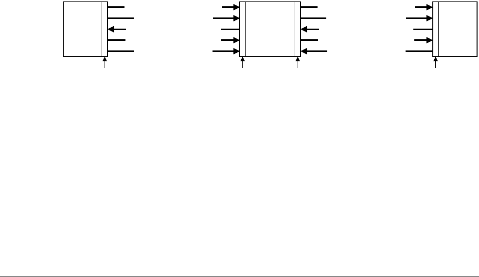
Glossary
ARM DDI 0301H Copyright © 2004-2009 ARM Limited. All rights reserved. Glossary-3
ID012310 Non-Confidential, Unrestricted Access
Arithmetic instruction
Any VFPv2 Coprocessor Data Processing (CDP) instruction except FCPY, FABS, and FNEG.
See also CDP instruction.
ARM instruction A word that specifies an operation for an ARM processor to perform. ARM instructions must
be word-aligned.
ARM state A processor that is executing ARM (32-bit) word-aligned instructions is operating in ARM
state.
ASIC See Application Specific Integrated Circuit.
ASSP See Application Specific Standard Part/Product.
ATB See Advanced Trace Bus.
ATB bridge A synchronous ATB bridge provides a register slice to facilitate timing closure through the
addition of a pipeline stage. It also provides a unidirectional link between two synchronous ATB
domains.
An asynchronous ATB bridge provides a unidirectional link between two ATB domains with
asynchronous clocks. It is intended to support connection of components with ATB ports
residing in different clock domains.
ATPG See Automatic Test Pattern Generation.
Automatic Test Pattern Generation (ATPG)
The process of automatically generating manufacturing test vectors for an ASIC design, using
a specialized software tool.
AXI See Advanced eXtensible Interface.
AXI channel order and interfaces
The block diagram shows:
• the order in which AXI channel signals are described
• the master and slave interface conventions for AXI components.
AXI terminology The following AXI terms are general. They apply to both masters and slaves:
Active read transaction
A transaction for which the read address has transferred, but the last read data has
not yet transferred.
Active transfer
A transfer for which the xVALID1 handshake has asserted, but for which
xREADY has not yet asserted.
Active write transaction
A transaction for which the write address or leading write data has transferred, but
the write response has not yet transferred.
AXI
interconnect
Write address channel (AW)
Write data channel (W)
Write response channel (B)
Read address channel (AR)
Read data channel (R)
Write address channel (AW)
Write data channel (W)
Write response channel (B)
Read address channel (AR)
Read data channel (R)
AXI slave
interface
AXI master
interface
AXI
master
AXI
slave
AXI master
interface
AXI slave
interface

Glossary
ARM DDI 0301H Copyright © 2004-2009 ARM Limited. All rights reserved. Glossary-4
ID012310 Non-Confidential, Unrestricted Access
Completed transfer
A transfer for which the xVALID/xREADY handshake is complete.
Payload The non-handshake signals in a transfer.
Transaction An entire burst of transfers, comprising an address, one or more data transfers and
a response transfer (writes only).
Transmit An initiator driving the payload and asserting the relevant xVALID signal.
Transfer A single exchange of information. That is, with one xVALID/xREADY
handshake.
The following AXI terms are master interface attributes. To obtain optimum performance, they
must be specified for all components with an AXI master interface:
Combined issuing capability
The maximum number of active transactions that a master interface can generate.
This is specified instead of write or read issuing capability for master interfaces
that use a combined storage for active write and read transactions.
Read ID capability
The maximum number of different ARID values that a master interface can
generate for all active read transactions at any one time.
Read ID width
The number of bits in the ARID bus.
Read issuing capability
The maximum number of active read transactions that a master interface can
generate.
Write ID capability
The maximum number of different AW I D values that a master interface can
generate for all active write transactions at any one time.
Write ID width
The number of bits in the AW I D and WID buses.
Write interleave capability
The number of active write transactions for which the master interface is capable
of transmitting data. This is counted from the earliest transaction.
Write issuing capability
The maximum number of active write transactions that a master interface can
generate.
1. The letter x in the signal name denotes an AXI channel as follows:
AW Write address channel.
W Write data channel.
B Write response channel.
AR Read address channel.
R Read data channel.

Glossary
ARM DDI 0301H Copyright © 2004-2009 ARM Limited. All rights reserved. Glossary-5
ID012310 Non-Confidential, Unrestricted Access
The following AXI terms are slave interface attributes. To obtain optimum performance, they
must be specified for all components with an AXI slave interface
Combined acceptance capability
The maximum number of active transactions that a slave interface can accept.
This is specified instead of write or read acceptance capability for slave interfaces
that use a combined storage for active write and read transactions.
Read acceptance capability
The maximum number of active read transactions that a slave interface can
accept.
Read data reordering depth
The number of active read transactions for which a slave interface can transmit
data. This is counted from the earliest transaction.
Write acceptance capability
The maximum number of active write transactions that a slave interface can
accept.
Write interleave depth
The number of active write transactions for which the slave interface can receive
data. This is counted from the earliest transaction.
Banked registers Those physical registers whose use is defined by the current processor mode. The banked
registers are R8 to R14.
Base register A register specified by a load or store instruction that is used to hold the base value for the
instruction’s address calculation. Depending on the instruction and its addressing mode, an
offset can be added to or subtracted from the base register value to form the virtual address that
is sent to memory.
Base register write-back
Updating the contents of the base register used in an instruction target address calculation so that
the modified address is changed to the next higher or lower sequential address in memory. This
means that it is not necessary to fetch the target address for successive instruction transfers and
enables faster burst accesses to sequential memory.
Beat Alternative word for an individual transfer within a burst. For example, an INCR4 burst
comprises four beats.
See also Burst.
BE-8 Big-endian view of memory in a byte-invariant system.
See also BE-32, LE, Byte-invariant and Word-invariant.
BE-32 Big-endian view of memory in a word-invariant system.
See also BE-8, LE, Byte-invariant and Word-invariant.
Big-endian Byte ordering scheme in which bytes of decreasing significance in a data word are stored at
increasing addresses in memory.
See also Little-endian and Endianness.
Big-endian memory Memory in which:
- a byte or halfword at a word-aligned address is the most significant byte or halfword within
the word at that address

Glossary
ARM DDI 0301H Copyright © 2004-2009 ARM Limited. All rights reserved. Glossary-6
ID012310 Non-Confidential, Unrestricted Access
- a byte at a halfword-aligned address is the most significant byte within the halfword at that
address.
See also Little-endian memory.
Block address An address that comprises a tag, an index, and a word field. The tag bits identify the way that
contains the matching cache entry for a cache hit. The index bits identify the set being
addressed. The word field contains the word address that can be used to identify specific words,
halfwords, or bytes within the cache entry.
See also Cache terminology diagram on the last page of this glossary.
Bounce The VFP coprocessor bounces an instruction when it fails to signal the acceptance of a valid
VFP instruction to the ARM processor. This action initiates Undefined instruction processing
by the ARM processor. The VFP support code is called to complete the instruction that was
found to be exceptional or unsupported by the VFP coprocessor.
See also Trigger instruction, Potentially exceptional instruction, and Exceptional state.
Boundary scan chain
A boundary scan chain is made up of serially-connected devices that implement boundary scan
technology using a standard JTAG TAP interface. Each device contains at least one TAP
controller containing shift registers that form the chain connected between TDI and TDO,
through which test data is shifted. Processors can contain several shift registers to enable you to
access selected parts of the device.
Branch folding Branch folding is a technique where, on the prediction of most branches, the branch instruction
is completely removed from the instruction stream presented to the execution pipeline. Branch
folding can significantly improve the performance of branches, taking the CPI for branches
lower than one.
Branch phantom The condition codes of a predicted taken branch.
Branch prediction The process of predicting if conditional branches are to be taken or not in pipelined processors.
Successfully predicting if branches are to be taken enables the processor to prefetch the
instructions following a branch before the condition is fully resolved. Branch prediction can be
done in software or by using custom hardware. Branch prediction techniques are categorized as
static, in which the prediction decision is decided before run time, and dynamic, in which the
prediction decision can change during program execution.
Breakpoint A breakpoint is a mechanism provided by debuggers to identify an instruction at which program
execution is to be halted. Breakpoints are inserted by the programmer to enable inspection of
register contents, memory locations, variable values at fixed points in the program execution to
test that the program is operating correctly. Breakpoints are removed after the program is
successfully tested.
See also Watchpoint.
Burst A group of transfers to consecutive addresses. Because the addresses are consecutive, there is
no requirement to supply an address for any of the transfers after the first one. This increases the
speed at which the group of transfers can occur. Bursts over AXI buses are controlled using the
AxBURST signals to specify if transfers are single, four-beat, eight-beat, or 16-beat bursts, and
to specify how the addresses are incremented.
See also Beat.
Byte An 8-bit data item.

Glossary
ARM DDI 0301H Copyright © 2004-2009 ARM Limited. All rights reserved. Glossary-7
ID012310 Non-Confidential, Unrestricted Access
Byte-invariant In a byte-invariant system, the address of each byte of memory remains unchanged when
switching between little-endian and big-endian operation. When a data item larger than a byte
is loaded from or stored to memory, the bytes making up that data item are arranged into the
correct order depending on the endianness of the memory access.
The ARM architecture supports byte-invariant systems in ARMv6 and later versions. When
byte-invariant support is selected, unaligned halfword and word memory accesses are also
supported. Multi-word accesses are expected to be word-aligned.
See also Word-invariant.
Byte lane strobe An AXI signal, WSTRB, that is used for unaligned or mixed-endian data accesses to determine
which byte lanes are active in a transfer. One bit of WSTRB corresponds to eight bits of the data
bus.
Byte swizzling The reverse ordering of bytes in a word.
Cache A block of on-chip or off-chip fast access memory locations, situated between the processor and
main memory, used for storing and retrieving copies of often used instructions and/or data. This
is done to greatly reduce the average speed of memory accesses and so to increase processor
performance.
See also Cache terminology diagram on the last page of this glossary.
Cache contention When the number of frequently-used memory cache lines that use a particular cache set exceeds
the set-associativity of the cache. In this case, main memory activity increases and performance
decreases.
Cache hit A memory access that can be processed at high speed because the instruction or data that it
addresses is already held in the cache.
Cache line The basic unit of storage in a cache. It is always a power of two words in size (usually four or
eight words), and is required to be aligned to a suitable memory boundary.
See also Cache terminology diagram on the last page of this glossary.
Cache line index The number associated with each cache line in a cache way. Within each cache way, the cache
lines are numbered from 0 to (set associativity) -1.
See also Cache terminology diagram on the last page of this glossary.
Cache lockdown To fix a line in cache memory so that it cannot be overwritten. Cache lockdown enables critical
instructions and/or data to be loaded into the cache so that the cache lines containing them are
not subsequently reallocated. This ensures that all subsequent accesses to the instructions/data
concerned are cache hits, and therefore complete as quickly as possible.
Cache miss A memory access that cannot be processed at high speed because the instruction/data it
addresses is not in the cache and a main memory access is required.
Cache set A cache set is a group of cache lines (or blocks). A set contains all the ways that can be
addressed with the same index. The number of cache sets is always a power of two.
See also Cache terminology diagram on the last page of this glossary.
Cache way A group of cache lines (or blocks). It is 2 to the power of the number of index bits in size.
See also Cache terminology diagram on the last page of this glossary.
Cast out See Victim.

Glossary
ARM DDI 0301H Copyright © 2004-2009 ARM Limited. All rights reserved. Glossary-8
ID012310 Non-Confidential, Unrestricted Access
CDP instruction Coprocessor data processing instruction. For the VFP11 coprocessor, CDP instructions are
arithmetic instructions and FCPY, FABS, and FNEG.
See also Arithmetic instruction.
Clean A cache line that has not been modified while it is in the cache is said to be clean. To clean a
cache is to write dirty cache entries into main memory. If a cache line is clean, it is not written
on a cache miss because the next level of memory contains the same data as the cache.
See also Dirty.
Clock gating Gating a clock signal for a macrocell with a control signal and using the modified clock that
results to control the operating state of the macrocell.
Clocks Per Instruction (CPI)
See Cycles Per Instruction (CPI).
Coherency See Memory coherency.
Cold reset Also known as power-on reset. Starting the processor by turning power on. Turning power off
and then back on again clears main memory and many internal settings. Some program failures
can lock up the processor and require a cold reset to enable the system to be used again. In other
cases, only a warm reset is required.
See also Warm reset.
Communications channel
The hardware used for communicating between the software running on the processor, and an
external host, using the debug interface. When this communication is for debug purposes, it is
called the Debug Comms Channel. In an ARMv6 compliant core, the communications channel
includes the Data Transfer Register, some bits of the Data Status and Control Register, and the
external debug interface controller, such as the DBGTAP controller in the case of the JTAG
interface.
Condition field A four-bit field in an instruction that specifies a condition under which the instruction can
execute.
Conditional execution
If the condition code flags indicate that the corresponding condition is true when the instruction
starts executing, it executes normally. Otherwise, the instruction does nothing.
Context The environment that each process operates in for a multitasking operating system. In ARM
processors, this is limited to mean the Physical Address range that it can access in memory and
the associated memory access permissions.
See also Fast context switch.
Control bits The bottom eight bits of a Program Status Register (PSR). The control bits change when an
exception arises and can be altered by software only when the processor is in a privileged mode.
Coprocessor A processor that supplements the main processor. It carries out additional functions that the
main processor cannot perform. Usually used for floating-point math calculations, signal
processing, or memory management.
Copy back See Write-back.
Core A core is that part of a processor that contains the ALU, the datapath, the general-purpose
registers, the Program Counter, and the instruction decode and control circuitry.
Core reset See Warm reset.
CPI See Cycles per instruction.

Glossary
ARM DDI 0301H Copyright © 2004-2009 ARM Limited. All rights reserved. Glossary-9
ID012310 Non-Confidential, Unrestricted Access
CPSR See Current Program Status Register
Current Program Status Register (CPSR)
The register that holds the current operating processor status.
Cycles Per instruction (CPI)
Cycles per instruction (or clocks per instruction) is a measure of the number of computer
instructions that can be performed in one clock cycle. This figure of merit can be used to
compare the performance of different CPUs that implement the same instruction set against each
other. The lower the value, the better the performance.
CoreSight The infrastructure for monitoring, tracing, and debugging a complete system on chip.
Data Abort An indication from a memory system to a core that it must halt execution of an attempted illegal
memory access. A Data Abort is attempting to access invalid data memory.
See also Abort, External Abort, and Prefetch Abort.
Data cache A block of on-chip fast access memory locations, situated between the processor and main
memory, used for storing and retrieving copies of often used data. This is done to greatly reduce
the average speed of memory accesses and so to increase processor performance.
DBGTAP See Debug Test Access Port.
Debugger A debugging system that includes a program, used to detect, locate, and correct software faults,
together with custom hardware that supports software debugging.
Debug Test Access Port (DBGTAP)
The collection of four mandatory and one optional terminals that form the input/output and
control interface to a JTAG boundary-scan architecture. The mandatory terminals are DBGTDI,
DBGTDO, DBGTMS, and TCK. The optional terminal is TRST. This signal is mandatory in
ARM cores because it is used to reset the debug logic.
Default NaN mode A mode in which all operations that result in a NaN return the default NaN, regardless of the
cause of the NaN result. This mode is compliant with the IEEE 754 standard but implies that all
information contained in any input NaNs to an operation is lost.
Denormalized value See Subnormal value.
Direct-mapped cache
A one-way set-associative cache. Each cache set consists of a single cache line, so cache look-up
selects and checks a single cache line.
Direct Memory Access (DMA)
An operation that accesses main memory directly, without the processor performing any
accesses to the data concerned.
Dirty A cache line in a write-back cache that has been modified while it is in the cache is said to be
dirty. A cache line is marked as dirty by setting the dirty bit. If a cache line is dirty, it must be
written to memory on a cache miss because the next level of memory contains data that has not
been updated. The process of writing dirty data to main memory is called cache cleaning.
See also Clean.
Disabled exception An exception is disabled when its exception enable bit in the FPCSR is not set. For these
exceptions, the IEEE 754 standard defines the result to be returned. An operation that generates
an exception condition can bounce to the support code to produce the result defined by the
IEEE 754 standard. The exception is not reported to the user trap handler.
DMA See Direct Memory Access.
DNM See Do Not Modify.

Glossary
ARM DDI 0301H Copyright © 2004-2009 ARM Limited. All rights reserved. Glossary-10
ID012310 Non-Confidential, Unrestricted Access
Do Not Modify (DNM)
In Do Not Modify fields, the value must not be altered by software. DNM fields read as
Unpredictable values, and must only be written with the same value read from the same field on
the same processor.
DNM fields are sometimes followed by RAZ or RAO in parentheses to show which way the bits
should read for future compatibility, but programmers must not rely on this behavior.
Double-precision value
Consists of two 32-bit words that must appear consecutively in memory and must both be
word-aligned, and that is interpreted as a basic double-precision floating-point number
according to the IEEE 754-1985 standard.
Doubleword A 64-bit data item. The contents are taken as being an unsigned integer unless otherwise stated.
Doubleword-aligned
A data item having a memory address that is divisible by eight.
EmbeddedICE logic An on-chip logic block that provides TAP-based debug support for ARM processor cores. It is
accessed through the TAP controller on the ARM core using the JTAG interface.
EmbeddedICE-RT The JTAG-based hardware provided by debuggable ARM processors to aid debugging in
real-time.
Embedded Trace Macrocell (ETM)
A hardware macrocell that, when connected to a processor core, outputs instruction and data
trace information on a trace port. The ETM provides processor driven trace through a trace port
compliant to the ATB protocol.
Enabled exception An exception is enabled when its exception enable bit in the FPCSR is set. When an enabled
exception occurs, a trap to the user handler is taken. An operation that generates an exception
condition might bounce to the support code to produce the result defined by the IEEE 754
standard. The exception is then reported to the user trap handler.
Endianness Byte ordering. The scheme that determines the order in which successive bytes of a data word
are stored in memory. An aspect of the system’s memory mapping.
See also Little-endian and Big-endian
ETM See Embedded Trace Macrocell.
Event 1 (Simple) An observable condition that can be used by an ETM to control aspects of a trace.
2 (Complex) A boolean combination of simple events that is used by an ETM to control aspects
of a trace.
Exception A fault or error event that is considered serious enough to require that program execution is
interrupted. Examples include attempting to perform an invalid memory access, external
interrupts, and undefined instructions. When an exception occurs, normal program flow is
interrupted and execution is resumed at the corresponding exception vector. This contains the
first instruction of the interrupt handler to deal with the exception.
Exceptional state When a potentially exceptional instruction is issued, the VFP11 coprocessor sets the EX bit,
FPEXC[31], and loads a copy of the potentially exceptional instruction in the FPINST register.
If the instruction is a short vector operation, the register fields in FPINST are altered to point to
the potentially exceptional iteration. When in the exceptional state, the issue of a trigger
instruction to the VFP11 coprocessor causes a bounce.
See also Bounce, Potentially exceptional instruction, and Trigger instruction.
Exception service routine
See Interrupt handler.

Glossary
ARM DDI 0301H Copyright © 2004-2009 ARM Limited. All rights reserved. Glossary-11
ID012310 Non-Confidential, Unrestricted Access
Exception vector See Interrupt vector.
Exponent The component of a floating-point number that normally signifies the integer power to which
two is raised in determining the value of the represented number.
External Abort An indication from an external memory system to a core that it must halt execution of an
attempted illegal memory access. An External Abort is caused by the external memory system
as a result of attempting to access invalid memory.
See also Abort, Data Abort and Prefetch Abort.
Fast context switch
In a multitasking system, the point at which the time-slice allocated to one process stops and the
one for the next process starts. If processes are switched often enough, they can appear to a user
to be running in parallel, in addition to being able to respond quicker to external events that
might affect them.
In ARM processors, a fast context switch is caused by the selection of a non-zero PID value to
switch the context to that of the next process. A fast context switch causes each Virtual Address
for a memory access, generated by the ARM processor, to produce a Modified Virtual Address
which is sent to the rest of the memory system to be used in place of a normal Virtual Address.
For some cache control operations Virtual Addresses are passed to the memory system as data.
In these cases no address modification takes place.
See also Fast Context Switch Extension.
Fast Context Switch Extension (FCSE)
An extension to the ARM architecture that enables cached processors with an MMU to present
different addresses to the rest of the memory system for different software processes, even when
those processes are using identical addresses.
See also Fast context switch.
FCSE See Fast Context Switch Extension.
Fd The destination register and the accumulate value in triadic operations. Sd for single-precision
operations and Dd for double-precision.
Flat address mapping
A system of organizing memory in which each Physical Address contained within the memory
space is the same as its corresponding Virtual Address.
Flush-to-zero mode In this mode, the VFP11 coprocessor treats the following values as positive zeros:
• arithmetic operation inputs that are in the subnormal range for the input precision
• arithmetic operation results, other than computed zero results, that are in the subnormal
range for the input precision before rounding.
The VFP11 coprocessor does not interpret these values as subnormal values or convert them to
subnormal values.
The subnormal range for the input precision is –2Emin < x < 0 or 0< x < 2Emin.
Fm The second source operand in dyadic or triadic operations. Sm for single-precision operations
and Dm for double-precision.
Fn The first source operand in dyadic or triadic operations. Sn for single-precision operations and
Dn for double-precision.
Fraction The floating-point field that lies to the right of the implied binary point.

Glossary
ARM DDI 0301H Copyright © 2004-2009 ARM Limited. All rights reserved. Glossary-12
ID012310 Non-Confidential, Unrestricted Access
Front of queue pointer
Pointer to the next entry to be written to in the write buffer.
Fully-associative cache
A cache that has only one cache set that consists of the entire cache. The number of cache entries
is the same as the number of cache ways.
See also Direct-mapped cache.
Halfword A 16-bit data item.
Halting debug-mode One of two mutually exclusive debug modes. In Halting debug-mode all processor execution
halts when a breakpoint or watchpoint is encountered. All processor state, coprocessor state,
memory and input/output locations can be examined and altered by the JTAG interface.
See also Monitor debug-mode.
High vectors Alternative locations for exception vectors. The high vector address range is near the top of the
address space, rather than at the bottom.
Hit-Under-Miss (HUM)
A buffer that enables program execution to continue, even though there has been a data miss in
the cache.
Host A computer that provides data and other services to another computer. Especially, a computer
providing debugging services to a target being debugged.
HUM See Hit-Under-Miss.
IEM See Intelligent Energy Management.
Illegal instruction An instruction that is architecturally Undefined.
IMB See Instruction Memory Barrier.
Implementation-defined
Means that the behavior is not architecturally defined, but should be defined and documented
by individual implementations.
Implementation-specific
Means that the behavior is not architecturally defined, and does not have to be documented by
individual implementations. Used when there are a number of implementation options available
and the option chosen does not affect software compatibility.
Imprecise tracing A filtering configuration where instruction or data tracing can start or finish earlier or later than
expected. Most cases cause tracing to start or finish later than expected.
For example, if TraceEnable is configured to use a counter so that tracing begins after the fourth
write to a location in memory, the instruction that caused the fourth write is not traced, although
subsequent instructions are. This is because the use of a counter in the TraceEnable
configuration always results in imprecise tracing.
Index See Cache index.
Index register A register specified in some load or store instructions. The value of this register is used as an
offset to be added to or subtracted from the base register value to form the virtual address, which
is sent to memory. Some addressing modes optionally enable the index register value to be
shifted prior to the addition or subtraction.
Infinity In the IEEE 754 standard format to represent infinity, the exponent is the maximum for the
precision and the fraction is all zeros.

Glossary
ARM DDI 0301H Copyright © 2004-2009 ARM Limited. All rights reserved. Glossary-13
ID012310 Non-Confidential, Unrestricted Access
Input exception A VFP exception condition in which one or more of the operands for a given operation are not
supported by the hardware. The operation bounces to support code for processing.
Instruction cache A block of on-chip fast access memory locations, situated between the processor and main
memory, used for storing and retrieving copies of often used instructions. This is done to greatly
reduce the average speed of memory accesses and so to increase processor performance.
Instruction cycle count
The number of cycles for which an instruction occupies the Execute stage of the pipeline.
Instruction Memory Barrier (IMB)
An operation to ensure that the prefetch buffer is flushed of all out-of-date instructions.
Instrumentation trace
A component for debugging real-time systems through a simple memory-mapped trace
interface, providing
printf
style debugging.
Intelligent Energy Management (IEM)
A technology that enables dynamic voltage scaling and clock frequency variation to be used to
reduce power consumption in a device.
Intermediate result An internal format used to store the result of a calculation before rounding. This format can have
a larger exponent field and fraction field than the destination format.
Internal scan chain A series of registers connected together to form a path through a device, used during production
testing to import test patterns into internal nodes of the device and export the resulting values.
Interrupt handler A program that control of the processor is passed to when an interrupt occurs.
Interrupt vector One of a number of fixed addresses in low memory, or in high memory if high vectors are
configured, that contains the first instruction of the corresponding interrupt handler.
Invalidate To mark a cache line as being not valid by clearing the valid bit. This must be done whenever
the line does not contain a valid cache entry. For example, after a cache flush all lines are invalid.
Jazelle architecture The ARM Jazelle architecture extends the Thumb and ARM operating states by adding a Jazelle
state to the processor. Instruction set support for entering and exiting Java applications, real-time
interrupt handling, and debug support for mixed Java/ARM applications is present. When in
Jazelle state, the processor fetches and decodes Java bytecodes and maintains the Java operand
stack.
Joint Test Action Group (JTAG)
The name of the organization that developed standard IEEE 1149.1. This standard defines a
boundary-scan architecture used for in-circuit testing of integrated circuit devices. It is
commonly known by the initials JTAG.
JTAG See Joint Test Action Group.
LE Little endian view of memory in both byte-invariant and word-invariant systems. See also
Byte-invariant, Word-invariant.
Line See Cache line.
Little-endian Byte ordering scheme in which bytes of increasing significance in a data word are stored at
increasing addresses in memory.
See also Big-endian and Endianness.
Little-endian memory
Memory in which:
- a byte or halfword at a word-aligned address is the least significant byte or halfword within the
word at that address

Glossary
ARM DDI 0301H Copyright © 2004-2009 ARM Limited. All rights reserved. Glossary-14
ID012310 Non-Confidential, Unrestricted Access
- a byte at a halfword-aligned address is the least significant byte within the halfword at that
address.
See also Big-endian memory.
Load/store architecture
A processor architecture where data-processing operations only operate on register contents, not
directly on memory contents.
Load Store Unit (LSU)
The part of a processor that handles load and store transfers.
LSU See Load Store Unit.
Macrocell A complex logic block with a defined interface and behavior. A typical VLSI system comprises
several macrocells, such as a processor, an ETM, and a memory block, plus application-specific
logic.
Memory bank One of two or more parallel divisions of interleaved memory, usually one word wide, that enable
reads and writes of multiple words at a time, rather than single words. All memory banks are
addressed simultaneously and a bank enable or chip select signal determines which of the banks
is accessed for each transfer. Accesses to sequential word addresses cause accesses to sequential
banks. This enables the delays associated with accessing a bank to occur during the access to its
adjacent bank, speeding up memory transfers.
Memory coherency A memory is coherent if the value read by a data read or instruction fetch is the value that was
most recently written to that location. Memory coherency is made difficult when there are
multiple possible physical locations that are involved, such as a system that has main memory,
a write buffer and a cache.
Memory Management Unit (MMU)
Hardware that controls caches and access permissions to blocks of memory, and translates
virtual addresses to physical addresses.
Microprocessor See Processor.
Miss See Cache miss.
MMU See Memory Management Unit.
Modified Virtual Address (MVA)
A Virtual Address produced by the ARM processor can be changed by the current Process ID
to provide a Modified Virtual Address (MVA) for the MMUs and caches.
See also Fast Context Switch Extension.
Monitor debug-mode
One of two mutually exclusive debug modes. In Monitor debug-mode the processor enables a
software abort handler provided by the debug monitor or operating system debug task. When a
breakpoint or watchpoint is encountered, this enables vital system interrupts to continue to be
serviced while normal program execution is suspended.
See also Halting debug-mode.
Multi-ICE A JTAG-based tool for debugging embedded systems.
Multi-layered An AMBA scheme to break a bus into segments that are controlled in access. This enables local
masters to reduce lock overhead.
Multi master An AMBA bus sharing scheme (not in AMBA Lite) where different masters can gain a bus lock
(Grant) to access the bus in an interleaved fashion.
MVA See Modified Virtual Address.

Glossary
ARM DDI 0301H Copyright © 2004-2009 ARM Limited. All rights reserved. Glossary-15
ID012310 Non-Confidential, Unrestricted Access
NaN Not a number. A symbolic entity encoded in a floating-point format that has the maximum
exponent field and a nonzero fraction. An SNaN causes an invalid operand exception if used as
an operand and a most significant fraction bit of zero. A QNaN propagates through almost every
arithmetic operation without signaling exceptions and has a most significant fraction bit of one.
PA See Physical Address.
Penalty The number of cycles in which no useful Execute stage pipeline activity can occur because an
instruction flow is different from that assumed or predicted.
Potentially exceptional instruction
An instruction that is determined, based on the exponents of the operands and the sign bits, to
have the potential to produce an overflow, underflow, or invalid condition. After this
determination is made, the instruction that has the potential to cause an exception causes the
VFP11 coprocessor to enter the exceptional state and bounce the next trigger instruction issued.
See also Bounce, Trigger instruction, and Exceptional state.
Power-on reset See Cold reset.
Prefetching In pipelined processors, the process of fetching instructions from memory to fill up the pipeline
before the preceding instructions have finished executing. Prefetching an instruction does not
mean that the instruction has to be executed.
Prefetch Abort An indication from a memory system to a core that it must halt execution of an attempted illegal
memory access. A Prefetch Abort can be caused by the external or internal memory system as
a result of attempting to access invalid instruction memory.
See also Data Abort, External Abort and Abort.
Processor A processor is the circuitry in a computer system required to process data using the computer
instructions. It is an abbreviation of microprocessor. A clock source, power supplies, and main
memory are also required to create a minimum complete working computer system.
Programming Language Interface (PLI)
For Verilog simulators, an interface by which so-called foreign code (code written in a different
language) can be included in a simulation.
Physical Address (PA)
The MMU performs a translation on Modified Virtual Addresses (MVA) to produce the Physical
Address (PA) which is given to AHB to perform an external access. The PA is also stored in the
data cache to avoid the necessity for address translation when data is cast out of the cache.
See also Fast Context Switch Extension.
Read Reads are defined as memory operations that have the semantics of a load. That is, the ARM
instructions LDM, LDRD, LDC, LDR, LDRT, LDRSH, LDRH, LDRSB, LDRB, LDRBT,
LDREX, RFE, STREX, SWP, and SWPB, and the Thumb instructions LDM, LDR, LDRSH,
LDRH, LDRSB, LDRB, and POP. Java instructions that are accelerated by hardware can cause
a number of reads to occur, according to the state of the Java stack and the implementation of
the Java hardware acceleration.
RealView ICE A system for debugging embedded processor cores using a JTAG interface.
Region A partition of instruction or data memory space.
Remapping Changing the address of physical memory or devices after the application has started executing.
This is typically done to enable RAM to replace ROM when the initialization has been
completed.

Glossary
ARM DDI 0301H Copyright © 2004-2009 ARM Limited. All rights reserved. Glossary-16
ID012310 Non-Confidential, Unrestricted Access
Reserved A field in a control register or instruction format is reserved if the field is to be defined by the
implementation, or produces Unpredictable results if the contents of the field are not zero. These
fields are reserved for use in future extensions of the architecture or are
implementation-specific. All reserved bits not used by the implementation must be written as 0
and read as 0.
Rounding mode The IEEE 754 standard requires all calculations to be performed as if to an infinite precision.
For example, a multiply of two single-precision values must accurately calculate the significand
to twice the number of bits of the significand. To represent this value in the destination precision,
rounding of the significand is often required. The IEEE 754 standard specifies four rounding
modes.
In round-to-nearest mode, the result is rounded at the halfway point, with the tie case rounding
up if it would clear the least significant bit of the significand, making it even.
Round-towards-zero mode chops any bits to the right of the significand, always rounding down,
and is used by the C, C++, and Java languages in integer conversions.
Round-towards-plus-infinity mode and round-towards-minus-infinity mode are used in interval
arithmetic.
RunFast mode In RunFast mode, hardware handles exceptional conditions and special operands. RunFast mode
is enabled by enabling default NaN and flush-to-zero modes and disabling all exceptions. In
RunFast mode, the VFP11 coprocessor does not bounce to the support code for any legal
operation or any operand, but supplies a result to the destination. For all inexact and overflow
results and all invalid operations that result from operations not involving NaNs, the result is as
specified by the IEEE 754 standard. For operations involving NaNs, the result is the default
NaN.
Saved Program Status Register (SPSR)
The register that holds the CPSR of the task immediately before the exception occurred that
caused the switch to the current mode.
SBO See Should Be One.
SBZ See Should Be Zero.
SBZP See Should Be Zero or Preserved.
Scalar operation A VFP coprocessor operation involving a single source register and a single destination register.
See also Vector operation.
Scan chain A scan chain is made up of serially-connected devices that implement boundary scan technology
using a standard JTAG TAP interface. Each device contains at least one TAP controller
containing shift registers that form the chain connected between TDI and TDO, through which
test data is shifted. Processors can contain several shift registers to enable you to access selected
parts of the device.
SCREG The currently selected scan chain number in an ARM TAP controller.
Set See Cache set.
Set-associative cache
In a set-associative cache, lines can only be placed in the cache in locations that correspond to
the modulo division of the memory address by the number of sets. If there are n ways in a cache,
the cache is termed n-way set-associative. The set-associativity can be any number greater than
or equal to 1 and is not restricted to being a power of two.

Glossary
ARM DDI 0301H Copyright © 2004-2009 ARM Limited. All rights reserved. Glossary-17
ID012310 Non-Confidential, Unrestricted Access
Short vector operation
A VFP coprocessor operation involving more than one destination register and perhaps more
than one source register in the generation of the result for each destination.
Should Be One (SBO)
Should be written as 1 (or all 1s for bit fields) by software. Writing a 0 produces Unpredictable
results.
Should Be Zero (SBZ)
Should be written as 0 (or all 0s for bit fields) by software. Writing a 1 produces Unpredictable
results.
Should Be Zero or Preserved (SBZP)
Should be written as 0 (or all 0s for bit fields) by software, or preserved by writing the same
value back that has been previously read from the same field on the same processor.
Significand The component of a binary floating-point number that consists of an explicit or implicit leading
bit to the left of the implied binary point and a fraction field to the right.
SPSR See Saved Program Status Register
Stride In the VFP extension, specifies the increment applied to register addresses in short vector
operations. A stride of 00, specifying an increment of +1, causes a short vector operation to
increment each vector register by +1 for each iteration, while a stride of 11 specifies an
increment of +2.
Subnormal value A value in the range (–2Emin <x<2
Emin), except for 0. In the IEEE 754 standard format for
single-precision and double-precision operands, a subnormal value has a zero exponent and a
nonzero fraction field. The IEEE 754 standard requires that the generation and manipulation of
subnormal operands be performed with the same precision as normal operands.
Support code Software that must be used to complement the hardware to provide compatibility with the
IEEE 754 standard. The support code has a library of routines that performs supported
functions, such as divide with unsupported inputs or inputs that might generate an exception in
addition to operations beyond the scope of the hardware. The support code has a set of exception
handlers to process exceptional conditions in compliance with the IEEE 754 standard.
Synchronization primitive
The memory synchronization primitive instructions are those instructions that are used to ensure
memory synchronization. That is, the LDREX, STREX, SWP, and SWPB instructions.
Tag The upper portion of a block address used to identify a cache line within a cache. The block
address from the CPU is compared with each tag in a set in parallel to determine if the
corresponding line is in the cache. If it is, it is said to be a cache hit and the line can be fetched
from cache. If the block address does not correspond to any of the tags, it is said to be a cache
miss and the line must be fetched from the next level of memory.
See also Cache terminology diagram on the last page of this glossary.
TAP See Test access port.
TCM See Tightly coupled memory.
Test Access Port (TAP)
The collection of four mandatory and one optional terminals that form the input/output and
control interface to a JTAG boundary-scan architecture. The mandatory terminals are TDI,
TDO, TMS, and TCK. The optional terminal is TRST. This signal is mandatory in ARM cores
because it is used to reset the debug logic.
Thumb instruction A halfword that specifies an operation for an ARM processor in Thumb state to perform. Thumb
instructions must be halfword-aligned.

Glossary
ARM DDI 0301H Copyright © 2004-2009 ARM Limited. All rights reserved. Glossary-18
ID012310 Non-Confidential, Unrestricted Access
Thumb state A processor that is executing Thumb (16-bit) halfword aligned instructions is operating in
Thumb state.
Tightly coupled memory (TCM)
An area of low latency memory that provides predictable instruction execution or data load
timing in cases where deterministic performance is required. TCMs are suited to holding:
- critical routines (such as for interrupt handling)
- scratchpad data
- data types whose locality is not suited to caching
- critical data structures, such as interrupt stacks.
Tiny A nonzero result or value that is between the positive and negative minimum normal values for
the destination precision.
TLB See Translation Look-aside Buffer.
Trace hardware A term for a device that contains an Embedded Trace Macrocell.
Trace port A port on a device, such as a processor or ASIC, used to output trace information.
Translation Lookaside Buffer (TLB)
A cache of recently used page table entries that avoid the overhead of page table walking on
every memory access. Part of the Memory Management Unit.
Translation table A table, held in memory, that contains data that defines the properties of memory areas of
various fixed sizes.
Translation table walk
The process of doing a full translation table lookup. It is performed automatically by hardware.
Trap An exceptional condition in a VFP coprocessor that has the respective exception enable bit set
in the FPSCR register. The user trap handler is executed.
Trigger instruction The VFP coprocessor instruction that causes a bounce at the time it is issued. A potentially
exceptional instruction causes the VFP11 coprocessor to enter the exceptional state. A
subsequent instruction, unless it is an FMXR or FMRX instruction accessing the FPEXC,
FPINST, or FPSID register, causes a bounce, beginning exception processing. The trigger
instruction is not necessarily exceptional, and no processing of it is performed. It is retried at the
return from exception processing of the potentially exceptional instruction.
See also Bounce, Potentially exceptional instruction, and Exceptional state.
Undefined Indicates an instruction that generates an Undefined instruction trap. See the ARM Architecture
Reference Manual for more details on ARM exceptions.
UNP See Unpredictable.
Unpredictable Unpredictable refers to Architecturally Unpredictable behavior. Unpredictable results of a
particular instruction or operation cannot be relied on. Unpredictable instructions or results do
not represent security holes and do not halt or hang the processor, or any parts of the system.
Unsupported values
Specific data values that are not processed by the VFP coprocessor hardware but bounced to the
support code for completion. These data can include infinities, NaNs, subnormal values, and
zeros. An implementation is free to select which of these values is supported in hardware fully
or partially, or requires assistance from support code to complete the operation. Any exception
resulting from processing unsupported data is trapped to user code if the corresponding
exception enable bit for the exception is set.

Glossary
ARM DDI 0301H Copyright © 2004-2009 ARM Limited. All rights reserved. Glossary-19
ID012310 Non-Confidential, Unrestricted Access
VA See Virtual Address.
Vector operation A VFP coprocessor operation involving more than one destination register, perhaps involving
different source registers in the generation of the result for each destination.
See also Scalar operation.
Victim A cache line, selected to be discarded to make room for a replacement cache line that is required
as a result of a cache miss. The way in which the victim is selected for eviction is
processor-specific. A victim is also known as a cast out.
Virtual Address (VA)
The MMU uses its page tables to translate a Virtual Address into a Physical Address. The
processor executes code at the Virtual Address, which might be located elsewhere in physical
memory.
See also Fast Context Switch Extension, Modified Virtual Address, and Physical Address.
Warm reset Also known as a core reset. Initializes the majority of the processor excluding the debug
controller and debug logic. This type of reset is useful if you are using the debugging features
of a processor.
Watchpoint A watchpoint is a mechanism provided by debuggers to halt program execution when the data
contained by a particular memory address is changed. Watchpoints are inserted by the
programmer to enable inspection of register contents, memory locations, and variable values
when memory is written to test that the program is operating correctly. Watchpoints are removed
after the program is successfully tested. See also Breakpoint.
Way See Cache way.
WB See Write-back.
Word A 32-bit data item.
Word-invariant In a word-invariant system, the address of each byte of memory changes when switching
between little-endian and big-endian operation, in such a way that the byte with address A in
one endianness has address A EOR 3 in the other endianness. As a result, each aligned word of
memory always consists of the same four bytes of memory in the same order, regardless of
endianness. The change of endianness occurs because of the change to the byte addresses, not
because the bytes are rearranged. The ARM architecture supports word-invariant systems in
ARMv3 and later versions. When word-invariant support is selected, the behavior of load or
store instructions that are given unaligned addresses is instruction-specific, and is in general not
the expected behavior for an unaligned access. It is recommended that word-invariant systems
should use the endianness that produces the required byte addresses at all times, apart possibly
from very early in their reset handlers before they have set up the endianness, and that this early
part of the reset handler should use only aligned word memory accesses.
See also Byte-invariant.
Write Writes are defined as operations that have the semantics of a store. That is, the ARM instructions
SRS, STM, STRD, STC, STRT, STRH, STRB, STRBT, STREX, SWP, and SWPB, and the
Thumb instructions STM, STR, STRH, STRB, and PUSH. Java instructions that are accelerated
by hardware can cause a number of writes to occur, according to the state of the Java stack and
the implementation of the Java hardware acceleration.
Write-back (WB) In a write-back cache, data is only written to main memory when it is forced out of the cache on
line replacement following a cache miss. Otherwise, writes by the processor only update the
cache. It is also known as copyback.
Write buffer A block of high-speed memory, arranged as a FIFO buffer, between the data cache and main
memory, whose purpose is to optimize stores to main memory.
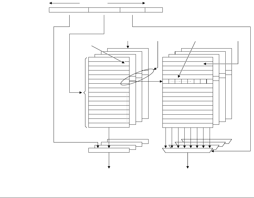
Glossary
ARM DDI 0301H Copyright © 2004-2009 ARM Limited. All rights reserved. Glossary-20
ID012310 Non-Confidential, Unrestricted Access
Write completion The memory system indicates to the processor that a write has been completed at a point in the
transaction where the memory system is able to guarantee that the effect of the write is visible
to all processors in the system. This is not the case if the write is associated with a memory
synchronization primitive, or is to a Device or Strongly Ordered region. In these cases the
memory system might only indicate completion of the write when the access has affected the
state of the target, unless it is impossible to distinguish between having the effect of the write
visible and having the state of target updated.
This stricter requirement for some types of memory ensures that any side-effects of the memory
access can be guaranteed by the processor to have taken place. You can use this to prevent the
starting of a subsequent operation in the program order until the side-effects are visible.
Write-through (WT) In a write-through cache, data is written to main memory at the same time as the cache is
updated.
WT See Write-through.
Cache terminology diagram
The following diagram illustrates the following cache terminology:
• block address
• cache line
• cache set
• cache way
• index
•tag.
Tag
Tag
Tag
Tag Index Word
Hit
(way number)
Read data
(way that corresponds)
=
3
1
Tag
0
0
2
1
3
4
5
6
7
n
Byte
Cache way Cache set
m 1
20
Cache line
2
Block address
Line number
Word number
Cache tag RAM Cache data RAM
