STM32L41xxx/42xxx/43xxx/44xxx/45xxx/46xxx Advanced Arm® Based 32 Bit MCUs Reference Manual STM32L4
STM32L4%20Reference%20manual
reference-manual-RM0394
reference-manual-RM0394
User Manual:
Open the PDF directly: View PDF ![]() .
.
Page Count: 1600 [warning: Documents this large are best viewed by clicking the View PDF Link!]
- 1 Documentation conventions
- 2 System and memory overview
- 3 Embedded Flash memory (FLASH)
- 3.1 Introduction
- 3.2 FLASH main features
- 3.3 FLASH functional description
- 3.4 FLASH option bytes
- 3.5 FLASH memory protection
- 3.6 FLASH interrupts
- 3.7 FLASH registers
- 3.7.1 Flash access control register (FLASH_ACR)
- 3.7.2 Flash Power-down key register (FLASH_PDKEYR)
- 3.7.3 Flash key register (FLASH_KEYR)
- 3.7.4 Flash option key register (FLASH_OPTKEYR)
- 3.7.5 Flash status register (FLASH_SR)
- 3.7.6 Flash control register (FLASH_CR)
- 3.7.7 Flash ECC register (FLASH_ECCR)
- 3.7.8 Flash option register (FLASH_OPTR)
- 3.7.9 Flash PCROP Start address register (FLASH_PCROP1SR)
- 3.7.10 Flash PCROP End address register (FLASH_PCROP1ER)
- 3.7.11 Flash WRP area A address register (FLASH_WRP1AR)
- 3.7.12 Flash WRP area B address register (FLASH_WRP1BR)
- 3.7.13 FLASH register map
- 4 Firewall (FW)
- 4.1 Introduction
- 4.2 Firewall main features
- 4.3 Firewall functional description
- 4.4 Firewall registers
- 4.4.1 Code segment start address (FW_CSSA)
- 4.4.2 Code segment length (FW_CSL)
- 4.4.3 Non-volatile data segment start address (FW_NVDSSA)
- 4.4.4 Non-volatile data segment length (FW_NVDSL)
- 4.4.5 Volatile data segment start address (FW_VDSSA)
- 4.4.6 Volatile data segment length (FW_VDSL)
- 4.4.7 Configuration register (FW_CR)
- 4.4.8 Firewall register map
- 5 Power control (PWR)
- 5.1 Power supplies
- 5.2 Power supply supervisor
- 5.3 Low-power modes
- Figure 11. Low-power modes possible transitions
- Table 20. Low-power mode summary
- Table 21. Functionalities depending on the working mode
- 5.3.1 Run mode
- 5.3.2 Low-power run mode (LP run)
- 5.3.3 Low power modes
- 5.3.4 Sleep mode
- 5.3.5 Low-power sleep mode (LP sleep)
- 5.3.6 Stop 0 mode
- 5.3.7 Stop 1 mode
- 5.3.8 Stop 2 mode
- 5.3.9 Standby mode
- 5.3.10 Shutdown mode
- 5.3.11 Auto-wakeup from low-power mode
- 5.4 PWR registers
- 5.4.1 Power control register 1 (PWR_CR1)
- 5.4.2 Power control register 2 (PWR_CR2)
- 5.4.3 Power control register 3 (PWR_CR3)
- 5.4.4 Power control register 4 (PWR_CR4)
- 5.4.5 Power status register 1 (PWR_SR1)
- 5.4.6 Power status register 2 (PWR_SR2)
- 5.4.7 Power status clear register (PWR_SCR)
- 5.4.8 Power Port A pull-up control register (PWR_PUCRA)
- 5.4.9 Power Port A pull-down control register (PWR_PDCRA)
- 5.4.10 Power Port B pull-up control register (PWR_PUCRB)
- 5.4.11 Power Port B pull-down control register (PWR_PDCRB)
- 5.4.12 Power Port C pull-up control register (PWR_PUCRC)
- 5.4.13 Power Port C pull-down control register (PWR_PDCRC)
- 5.4.14 Power Port D pull-up control register (PWR_PUCRD)
- 5.4.15 Power Port D pull-down control register (PWR_PDCRD)
- 5.4.16 Power Port E pull-up control register (PWR_PUCRE)
- 5.4.17 Power Port E pull-down control register (PWR_PDCRE)
- 5.4.18 Power Port H pull-up control register (PWR_PUCRH)
- 5.4.19 Power Port H pull-down control register (PWR_PDCRH)
- 5.4.20 PWR register map and reset value table
- 6 Reset and clock control (RCC)
- 6.1 Reset
- 6.2 Clocks
- Figure 13. Clock tree
- 6.2.1 HSE clock
- 6.2.2 HSI16 clock
- 6.2.3 MSI clock
- 6.2.4 HSI48 clock
- 6.2.5 PLL
- 6.2.6 LSE clock
- 6.2.7 LSI clock
- 6.2.8 System clock (SYSCLK) selection
- 6.2.9 Clock source frequency versus voltage scaling
- 6.2.10 Clock security system (CSS)
- 6.2.11 Clock security system on LSE
- 6.2.12 ADC clock
- 6.2.13 RTC clock
- 6.2.14 Timer clock
- 6.2.15 Watchdog clock
- 6.2.16 Clock-out capability
- 6.2.17 Internal/external clock measurement with TIM15/TIM16
- 6.2.18 Peripheral clock enable register (RCC_AHBxENR, RCC_APBxENRy)
- 6.3 Low-power modes
- 6.4 RCC registers
- 6.4.1 Clock control register (RCC_CR)
- 6.4.2 Internal clock sources calibration register (RCC_ICSCR)
- 6.4.3 Clock configuration register (RCC_CFGR)
- 6.4.4 PLL configuration register (RCC_PLLCFGR)
- 6.4.5 PLLSAI1 configuration register (RCC_PLLSAI1CFGR)
- 6.4.6 Clock interrupt enable register (RCC_CIER)
- 6.4.7 Clock interrupt flag register (RCC_CIFR)
- 6.4.8 Clock interrupt clear register (RCC_CICR)
- 6.4.9 AHB1 peripheral reset register (RCC_AHB1RSTR)
- 6.4.10 AHB2 peripheral reset register (RCC_AHB2RSTR)
- 6.4.11 AHB3 peripheral reset register (RCC_AHB3RSTR)
- 6.4.12 APB1 peripheral reset register 1 (RCC_APB1RSTR1)
- 6.4.13 APB1 peripheral reset register 2 (RCC_APB1RSTR2)
- 6.4.14 APB2 peripheral reset register (RCC_APB2RSTR)
- 6.4.15 AHB1 peripheral clock enable register (RCC_AHB1ENR)
- 6.4.16 AHB2 peripheral clock enable register (RCC_AHB2ENR)
- 6.4.17 AHB3 peripheral clock enable register(RCC_AHB3ENR)
- 6.4.18 APB1 peripheral clock enable register 1 (RCC_APB1ENR1)
- 6.4.19 APB1 peripheral clock enable register 2 (RCC_APB1ENR2)
- 6.4.20 APB2 peripheral clock enable register (RCC_APB2ENR)
- 6.4.21 AHB1 peripheral clocks enable in Sleep and Stop modes register (RCC_AHB1SMENR)
- 6.4.22 AHB2 peripheral clocks enable in Sleep and Stop modes register (RCC_AHB2SMENR)
- 6.4.23 AHB3 peripheral clocks enable in Sleep and Stop modes register (RCC_AHB3SMENR)
- 6.4.24 APB1 peripheral clocks enable in Sleep and Stop modes register 1 (RCC_APB1SMENR1)
- 6.4.25 APB1 peripheral clocks enable in Sleep and Stop modes register 2 (RCC_APB1SMENR2)
- 6.4.26 APB2 peripheral clocks enable in Sleep and Stop modes register (RCC_APB2SMENR)
- 6.4.27 Peripherals independent clock configuration register (RCC_CCIPR)
- 6.4.28 Backup domain control register (RCC_BDCR)
- 6.4.29 Control/status register (RCC_CSR)
- 6.4.30 Clock recovery RC register (RCC_CRRCR)
- 6.4.31 Peripherals independent clock configuration register (RCC_CCIPR2)
- 6.4.32 RCC register map
- 7 Clock recovery system (CRS)
- 8 General-purpose I/Os (GPIO)
- 8.1 Introduction
- 8.2 GPIO main features
- 8.3 GPIO functional description
- Figure 19. Basic structure of an I/O port bit
- Figure 20. Basic structure of a 5-Volt tolerant I/O port bit
- Table 36. Port bit configuration table
- 8.3.1 General-purpose I/O (GPIO)
- 8.3.2 I/O pin alternate function multiplexer and mapping
- 8.3.3 I/O port control registers
- 8.3.4 I/O port data registers
- 8.3.5 I/O data bitwise handling
- 8.3.6 GPIO locking mechanism
- 8.3.7 I/O alternate function input/output
- 8.3.8 External interrupt/wakeup lines
- 8.3.9 Input configuration
- 8.3.10 Output configuration
- 8.3.11 Alternate function configuration
- 8.3.12 Analog configuration
- 8.3.13 Using the HSE or LSE oscillator pins as GPIOs
- 8.3.14 Using the GPIO pins in the RTC supply domain
- 8.3.15 Using PH3 as GPIO
- 8.4 GPIO registers
- 8.4.1 GPIO port mode register (GPIOx_MODER) (x =A to E and H)
- 8.4.2 GPIO port output type register (GPIOx_OTYPER) (x = A to E and H)
- 8.4.3 GPIO port output speed register (GPIOx_OSPEEDR) (x = A to E and H)
- 8.4.4 GPIO port pull-up/pull-down register (GPIOx_PUPDR) (x = A to E and H)
- 8.4.5 GPIO port input data register (GPIOx_IDR) (x = A to E and H)
- 8.4.6 GPIO port output data register (GPIOx_ODR) (x = A to E and H)
- 8.4.7 GPIO port bit set/reset register (GPIOx_BSRR) (x = A to E and H)
- 8.4.8 GPIO port configuration lock register (GPIOx_LCKR) (x = A to E and H)
- 8.4.9 GPIO alternate function low register (GPIOx_AFRL) (x = A to E and H)
- 8.4.10 GPIO alternate function high register (GPIOx_AFRH) (x = A to E and H)
- 8.4.11 GPIO port bit reset register (GPIOx_BRR) (x = A to E and H)
- 8.4.12 GPIO register map
- 9 System configuration controller (SYSCFG)
- 9.1 SYSCFG main features
- 9.2 SYSCFG registers
- 9.2.1 SYSCFG memory remap register (SYSCFG_MEMRMP)
- 9.2.2 SYSCFG configuration register 1 (SYSCFG_CFGR1)
- 9.2.3 SYSCFG external interrupt configuration register 1 (SYSCFG_EXTICR1)
- 9.2.4 SYSCFG external interrupt configuration register 2 (SYSCFG_EXTICR2)
- 9.2.5 SYSCFG external interrupt configuration register 3 (SYSCFG_EXTICR3)
- 9.2.6 SYSCFG external interrupt configuration register 4 (SYSCFG_EXTICR4)
- 9.2.7 SYSCFG SRAM2 control and status register (SYSCFG_SCSR)
- 9.2.8 SYSCFG configuration register 2 (SYSCFG_CFGR2)
- 9.2.9 SYSCFG SRAM2 write protection register (SYSCFG_SWPR)
- 9.2.10 SYSCFG SRAM2 key register (SYSCFG_SKR)
- 9.2.11 SYSCFG register map
- 10 Peripherals interconnect matrix
- 10.1 Introduction
- 10.2 Connection summary
- 10.3 Interconnection details
- 10.3.1 From timer (TIM1/TIM2/TIM15/TIM16) to timer (TIM1/TIM2/TIM15/TIM16)
- 10.3.2 From timer (TIM1/TIM2/TIM6/TIM15) and EXTI to ADC (ADC1)
- 10.3.3 From ADC (ADC1) to timer (TIM1)
- 10.3.4 From timer (TIM2/TIM6/TIM7) and EXTI to DAC (DAC1/DAC2)
- 10.3.5 From HSE, LSE, LSI, MSI, MCO, RTC to timer (TIM2/TIM15/TIM16)
- 10.3.6 From RTC, COMP1, COMP2 to low-power timer (LPTIM1/LPTIM2)
- 10.3.7 From timer (TIM1/TIM2/TIM15) to comparators (COMP1/COMP2)
- 10.3.8 From ADC (ADC1) to ADC (ADC2)
- 10.3.9 From USB to timer (TIM2)
- 10.3.10 From internal analog source to ADC (ADC1) and OPAMP (OPAMP1)
- 10.3.11 From comparators (COMP1/COMP2) to timers (TIM1/TIM2/TIM15/TIM16)
- 10.3.12 From system errors to timers (TIM1/TIM15/TIM16)
- 10.3.13 From timers (TIM16) to IRTIM
- 11 Direct memory access controller (DMA)
- 11.1 Introduction
- 11.2 DMA main features
- 11.3 DMA implementation
- 11.4 DMA functional description
- 11.5 DMA interrupts
- 11.6 DMA registers
- 11.6.1 DMA interrupt status register (DMA_ISR)
- 11.6.2 DMA interrupt flag clear register (DMA_IFCR)
- 11.6.3 DMA channel x configuration register (DMA_CCRx)
- 11.6.4 DMA channel x number of data to transfer register (DMA_CNDTRx)
- 11.6.5 DMA channel x peripheral address register (DMA_CPARx)
- 11.6.6 DMA channel x memory address register (DMA_CMARx)
- 11.6.7 DMA channel selection register (DMA_CSELR)
- 11.6.8 DMA register map and reset values
- 12 Nested vectored interrupt controller (NVIC)
- 13 Extended interrupts and events controller (EXTI)
- 13.1 Introduction
- 13.2 EXTI main features
- 13.3 EXTI functional description
- 13.4 EXTI interrupt/event line mapping
- 13.5 EXTI registers
- 13.5.1 Interrupt mask register 1 (EXTI_IMR1)
- 13.5.2 Event mask register 1 (EXTI_EMR1)
- 13.5.3 Rising trigger selection register 1 (EXTI_RTSR1)
- 13.5.4 Falling trigger selection register 1 (EXTI_FTSR1)
- 13.5.5 Software interrupt event register 1 (EXTI_SWIER1)
- 13.5.6 Pending register 1 (EXTI_PR1)
- 13.5.7 Interrupt mask register 2 (EXTI_IMR2)
- 13.5.8 Event mask register 2 (EXTI_EMR2)
- 13.5.9 Rising trigger selection register 2 (EXTI_RTSR2)
- 13.5.10 Falling trigger selection register 2 (EXTI_FTSR2)
- 13.5.11 Software interrupt event register 2 (EXTI_SWIER2)
- 13.5.12 Pending register 2 (EXTI_PR2)
- 13.5.13 EXTI register map
- 14 Cyclic redundancy check calculation unit (CRC)
- 15 Quad-SPI interface (QUADSPI)
- 15.1 Introduction
- 15.2 QUADSPI main features
- 15.3 QUADSPI functional description
- 15.3.1 QUADSPI block diagram
- 15.3.2 QUADSPI pins
- 15.3.3 QUADSPI command sequence
- 15.3.4 QUADSPI signal interface protocol modes
- 15.3.5 QUADSPI indirect mode
- 15.3.6 QUADSPI status flag polling mode
- 15.3.7 QUADSPI memory-mapped mode
- 15.3.8 QUADSPI Flash memory configuration
- 15.3.9 QUADSPI delayed data sampling
- 15.3.10 QUADSPI configuration
- 15.3.11 QUADSPI usage
- 15.3.12 Sending the instruction only once
- 15.3.13 QUADSPI error management
- 15.3.14 QUADSPI busy bit and abort functionality
- 15.3.15 nCS behavior
- 15.4 QUADSPI interrupts
- 15.5 QUADSPI registers
- 15.5.1 QUADSPI control register (QUADSPI_CR)
- 15.5.2 QUADSPI device configuration register (QUADSPI_DCR)
- 15.5.3 QUADSPI status register (QUADSPI_SR)
- 15.5.4 QUADSPI flag clear register (QUADSPI_FCR)
- 15.5.5 QUADSPI data length register (QUADSPI_DLR)
- 15.5.6 QUADSPI communication configuration register (QUADSPI_CCR)
- 15.5.7 QUADSPI address register (QUADSPI_AR)
- 15.5.8 QUADSPI alternate bytes registers (QUADSPI_ABR)
- 15.5.9 QUADSPI data register (QUADSPI_DR)
- 15.5.10 QUADSPI polling status mask register (QUADSPI _PSMKR)
- 15.5.11 QUADSPI polling status match register (QUADSPI _PSMAR)
- 15.5.12 QUADSPI polling interval register (QUADSPI _PIR)
- 15.5.13 QUADSPI low-power timeout register (QUADSPI_LPTR)
- 15.5.14 QUADSPI register map
- 16 Analog-to-digital converters (ADC)
- 16.1 Introduction
- 16.2 ADC main features
- 16.3 ADC implementation
- 16.4 ADC functional description
- 16.4.1 ADC block diagram
- 16.4.2 ADC pins and internal signals
- 16.4.3 Clocks
- 16.4.4 ADC1/2 connectivity
- 16.4.5 Slave AHB interface
- 16.4.6 ADC Deep-power-down mode (DEEPPWD) and ADC voltage regulator (ADVREGEN)
- 16.4.7 Single-ended and differential input channels
- 16.4.8 Calibration (ADCAL, ADCALDIF, ADC_CALFACT)
- 16.4.9 ADC on-off control (ADEN, ADDIS, ADRDY)
- 16.4.10 Constraints when writing the ADC control bits
- 16.4.11 Channel selection (SQRx, JSQRx)
- 16.4.12 Channel-wise programmable sampling time (SMPR1, SMPR2)
- 16.4.13 Single conversion mode (CONT=0)
- 16.4.14 Continuous conversion mode (CONT=1)
- 16.4.15 Starting conversions (ADSTART, JADSTART)
- 16.4.16 ADC timing
- 16.4.17 Stopping an ongoing conversion (ADSTP, JADSTP)
- 16.4.18 Conversion on external trigger and trigger polarity (EXTSEL, EXTEN,JEXTSEL, JEXTEN)
- Table 57. Configuring the trigger polarity for regular external triggers
- Table 58. Configuring the trigger polarity for injected external triggers
- Figure 50. Triggers sharing between ADC master and ADC slave
- Table 59. ADC1 and ADC2 - External triggers for regular channels
- Table 60. ADC1 and ADC2 - External trigger for injected channels
- 16.4.19 Injected channel management
- 16.4.20 Discontinuous mode (DISCEN, DISCNUM, JDISCEN)
- 16.4.21 Queue of context for injected conversions
- Figure 52. Example of JSQR queue of context (sequence change)
- Figure 53. Example of JSQR queue of context (trigger change)
- Figure 54. Example of JSQR queue of context with overflow before conversion
- Figure 55. Example of JSQR queue of context with overflow during conversion
- Figure 56. Example of JSQR queue of context with empty queue (case JQM=0)
- Figure 57. Example of JSQR queue of context with empty queue (case JQM=1)
- Figure 58. Flushing JSQR queue of context by setting JADSTP=1 (JQM=0). Case when JADSTP occurs during an ongoing conversion.
- Figure 59. Flushing JSQR queue of context by setting JADSTP=1 (JQM=0). Case when JADSTP occurs during an ongoing conversion and a new trigger occurs.
- Figure 60. Flushing JSQR queue of context by setting JADSTP=1 (JQM=0). Case when JADSTP occurs outside an ongoing conversion
- Figure 61. Flushing JSQR queue of context by setting JADSTP=1 (JQM=1)
- Figure 62. Flushing JSQR queue of context by setting ADDIS=1 (JQM=0)
- Figure 63. Flushing JSQR queue of context by setting ADDIS=1 (JQM=1)
- 16.4.22 Programmable resolution (RES) - fast conversion mode
- 16.4.23 End of conversion, end of sampling phase (EOC, JEOC, EOSMP)
- 16.4.24 End of conversion sequence (EOS, JEOS)
- 16.4.25 Timing diagrams example (single/continuous modes, hardware/software triggers)
- 16.4.26 Data management
- Table 62. Offset computation versus data resolution
- Figure 68. Right alignment (offset disabled, unsigned value)
- Figure 69. Right alignment (offset enabled, signed value)
- Figure 70. Left alignment (offset disabled, unsigned value)
- Figure 71. Left alignment (offset enabled, signed value)
- Figure 72. Example of overrun (OVR)
- 16.4.27 Managing conversions using the DFSDM
- 16.4.28 Dynamic low-power features
- Figure 73. AUTODLY=1, regular conversion in continuous mode, software trigger
- Figure 74. AUTODLY=1, regular HW conversions interrupted by injected conversions (DISCEN=0; JDISCEN=0)
- Figure 75. AUTODLY=1, regular HW conversions interrupted by injected conversions (DISCEN=1, JDISCEN=1)
- Figure 76. AUTODLY=1, regular continuous conversions interrupted by injected conversions
- Figure 77. AUTODLY=1 in auto- injected mode (JAUTO=1)
- 16.4.29 Analog window watchdog (AWD1EN, JAWD1EN, AWD1SGL, AWD1CH, AWD2CH, AWD3CH, AWD_HTx, AWD_LTx, AWDx)
- Figure 78. Analog watchdog guarded area
- Table 63. Analog watchdog channel selection
- Table 64. Analog watchdog 1 comparison
- Table 65. Analog watchdog 2 and 3 comparison
- Figure 79. ADCy_AWDx_OUT signal generation (on all regular channels)
- Figure 80. ADCy_AWDx_OUT signal generation (AWDx flag not cleared by software)
- Figure 81. ADCy_AWDx_OUT signal generation (on a single regular channel)
- Figure 82. ADCy_AWDx_OUT signal generation (on all injected channels)
- 16.4.30 Oversampler
- Figure 83. 20-bit to 16-bit result truncation
- Figure 84. Numerical example with 5-bit shift and rounding
- Table 66. Maximum output results versus N and M (gray cells indicate truncation)
- Figure 85. Triggered regular oversampling mode (TROVS bit = 1)
- Figure 86. Regular oversampling modes (4x ratio)
- Figure 87. Regular and injected oversampling modes used simultaneously
- Figure 88. Triggered regular oversampling with injection
- Figure 89. Oversampling in auto-injected mode
- Table 67. Oversampler operating modes summary
- 16.4.31 Dual ADC modes
- Figure 90. Dual ADC block diagram(1)
- Figure 91. Injected simultaneous mode on 4 channels: dual ADC mode
- Figure 92. Regular simultaneous mode on 16 channels: dual ADC mode
- Figure 93. Interleaved mode on 1 channel in continuous conversion mode: dual ADC mode
- Figure 94. Interleaved mode on 1 channel in single conversion mode: dual ADC mode
- Figure 95. Interleaved conversion with injection
- Figure 96. Alternate trigger: injected group of each ADC
- Figure 97. Alternate trigger: 4 injected channels (each ADC) in discontinuous mode
- Figure 98. Alternate + regular simultaneous
- Figure 99. Case of trigger occurring during injected conversion
- Figure 100. Interleaved single channel CH0 with injected sequence CH11, CH12
- Figure 101. Two Interleaved channels (CH1, CH2) with injected sequence CH11, CH12 - case 1: Master interrupted first
- Figure 102. Two Interleaved channels (CH1, CH2) with injected sequence CH11, CH12 - case 2: Slave interrupted first
- Figure 103. DMA Requests in regular simultaneous mode when MDMA=0b00
- Figure 104. DMA requests in regular simultaneous mode when MDMA=0b10
- Figure 105. DMA requests in interleaved mode when MDMA=0b10
- 16.4.32 Temperature sensor
- 16.4.33 VBAT supply monitoring
- 16.4.34 Monitoring the internal voltage reference
- 16.5 ADC interrupts
- 16.6 ADC registers (for each ADC)
- 16.6.1 ADC interrupt and status register (ADC_ISR)
- 16.6.2 ADC interrupt enable register (ADC_IER)
- 16.6.3 ADC control register (ADC_CR)
- 16.6.4 ADC configuration register (ADC_CFGR)
- 16.6.5 ADC configuration register 2 (ADC_CFGR2)
- 16.6.6 ADC sample time register 1 (ADC_SMPR1)
- 16.6.7 ADC sample time register 2 (ADC_SMPR2)
- 16.6.8 ADC watchdog threshold register 1 (ADC_TR1)
- 16.6.9 ADC watchdog threshold register 2 (ADC_TR2)
- 16.6.10 ADC watchdog threshold register 3 (ADC_TR3)
- 16.6.11 ADC regular sequence register 1 (ADC_SQR1)
- 16.6.12 ADC regular sequence register 2 (ADC_SQR2)
- 16.6.13 ADC regular sequence register 3 (ADC_SQR3)
- 16.6.14 ADC regular sequence register 4 (ADC_SQR4)
- 16.6.15 ADC regular data register (ADC_DR)
- 16.6.16 ADC injected sequence register (ADC_JSQR)
- 16.6.17 ADC offset y register (ADC_OFRy)
- 16.6.18 ADC injected channel y data register (ADC_JDRy)
- 16.6.19 ADC Analog Watchdog 2 Configuration Register (ADC_AWD2CR)
- 16.6.20 ADC Analog Watchdog 3 Configuration Register (ADC_AWD3CR)
- 16.6.21 ADC Differential mode Selection Register (ADC_DIFSEL)
- 16.6.22 ADC Calibration Factors (ADC_CALFACT)
- 16.7 ADC common registers
- 17 Digital-to-analog converter (DAC)
- 17.1 Introduction
- 17.2 DAC main features
- 17.3 DAC implementation
- 17.4 DAC functional description
- 17.4.1 DAC block diagram
- 17.4.2 DAC channel enable
- 17.4.3 DAC data format
- 17.4.4 DAC conversion
- 17.4.5 DAC output voltage
- 17.4.6 DAC trigger selection
- 17.4.7 DMA requests
- 17.4.8 Noise generation
- 17.4.9 Triangle-wave generation
- 17.4.10 DAC channel modes
- 17.4.11 DAC channel buffer calibration
- 17.4.12 Dual DAC channel conversion (if available)
- 17.5 DAC low-power modes
- 17.6 DAC interrupts
- 17.7 DAC registers
- 17.7.1 DAC control register (DAC_CR)
- 17.7.2 DAC software trigger register (DAC_SWTRGR)
- 17.7.3 DAC channel1 12-bit right-aligned data holding register (DAC_DHR12R1)
- 17.7.4 DAC channel1 12-bit left aligned data holding register (DAC_DHR12L1)
- 17.7.5 DAC channel1 8-bit right aligned data holding register (DAC_DHR8R1)
- 17.7.6 DAC channel2 12-bit right aligned data holding register (DAC_DHR12R2)
- 17.7.7 DAC channel2 12-bit left aligned data holding register (DAC_DHR12L2)
- 17.7.8 DAC channel2 8-bit right-aligned data holding register (DAC_DHR8R2)
- 17.7.9 Dual DAC 12-bit right-aligned data holding register (DAC_DHR12RD)
- 17.7.10 Dual DAC 12-bit left aligned data holding register (DAC_DHR12LD)
- 17.7.11 Dual DAC 8-bit right aligned data holding register (DAC_DHR8RD)
- 17.7.12 DAC channel1 data output register (DAC_DOR1)
- 17.7.13 DAC channel2 data output register (DAC_DOR2)
- 17.7.14 DAC status register (DAC_SR)
- 17.7.15 DAC calibration control register (DAC_CCR)
- 17.7.16 DAC mode control register (DAC_MCR)
- 17.7.17 DAC channel 1 sample and hold sample time register (DAC_SHSR1)
- 17.7.18 DAC channel 2 sample and hold sample time register (DAC_SHSR2)
- 17.7.19 DAC sample and hold time register (DAC_SHHR)
- 17.7.20 DAC sample and hold refresh time register (DAC_SHRR)
- 17.7.21 DAC register map
- 18 Voltage reference buffer (VREFBUF)
- 19 Comparator (COMP)
- 19.1 Introduction
- 19.2 COMP main features
- 19.3 COMP functional description
- 19.4 COMP low-power modes
- 19.5 COMP interrupts
- 19.6 COMP registers
- 20 Operational amplifiers (OPAMP)
- 21 Digital filter for sigma delta modulators (DFSDM)
- 21.1 Introduction
- 21.2 DFSDM main features
- 21.3 DFSDM implementation
- 21.4 DFSDM functional description
- 21.4.1 DFSDM block diagram
- 21.4.2 DFSDM pins and internal signals
- 21.4.3 DFSDM reset and clocks
- 21.4.4 Serial channel transceivers
- 21.4.5 Configuring the input serial interface
- 21.4.6 Parallel data inputs
- 21.4.7 Channel selection
- 21.4.8 Digital filter configuration
- 21.4.9 Integrator unit
- 21.4.10 Analog watchdog
- 21.4.11 Short-circuit detector
- 21.4.12 Extreme detector
- 21.4.13 Data unit block
- 21.4.14 Signed data format
- 21.4.15 Launching conversions
- 21.4.16 Continuous and fast continuous modes
- 21.4.17 Request precedence
- 21.4.18 Power optimization in run mode
- 21.5 DFSDM interrupts
- 21.6 DFSDM DMA transfer
- 21.7 DFSDM channel y registers (y=0..3)
- 21.7.1 DFSDM channel y configuration register (DFSDM_CHyCFGR1)
- 21.7.2 DFSDM channel y configuration register (DFSDM_CHyCFGR2)
- 21.7.3 DFSDM channel y analog watchdog and short-circuit detector register (DFSDM_CHyAWSCDR)
- 21.7.4 DFSDM channel y watchdog filter data register (DFSDM_CHyWDATR)
- 21.7.5 DFSDM channel y data input register (DFSDM_CHyDATINR)
- 21.8 DFSDM filter x module registers (x=0..1)
- 21.8.1 DFSDM filter x control register 1 (DFSDM_FLTxCR1)
- 21.8.2 DFSDM filter x control register 2 (DFSDM_FLTxCR2)
- 21.8.3 DFSDM filter x interrupt and status register (DFSDM_FLTxISR)
- 21.8.4 DFSDM filter x interrupt flag clear register (DFSDM_FLTxICR)
- 21.8.5 DFSDM filter x injected channel group selection register (DFSDM_FLTxJCHGR)
- 21.8.6 DFSDM filter x control register (DFSDM_FLTxFCR)
- 21.8.7 DFSDM filter x data register for injected group (DFSDM_FLTxJDATAR)
- 21.8.8 DFSDM filter x data register for the regular channel (DFSDM_FLTxRDATAR)
- 21.8.9 DFSDM filter x analog watchdog high threshold register (DFSDM_FLTxAWHTR)
- 21.8.10 DFSDM filter x analog watchdog low threshold register (DFSDM_FLTxAWLTR)
- 21.8.11 DFSDM filter x analog watchdog status register (DFSDM_FLTxAWSR)
- 21.8.12 DFSDM filter x analog watchdog clear flag register (DFSDM_FLTxAWCFR)
- 21.8.13 DFSDM filter x extremes detector maximum register (DFSDM_FLTxEXMAX)
- 21.8.14 DFSDM filter x extremes detector minimum register (DFSDM_FLTxEXMIN)
- 21.8.15 DFSDM filter x conversion timer register (DFSDM_FLTxCNVTIMR)
- 21.8.16 DFSDM register map
- 22 Liquid crystal display controller (LCD)
- 22.1 Introduction
- 22.2 LCD main features
- 22.3 LCD functional description
- 22.4 LCD low-power modes
- 22.5 LCD interrupts
- 22.6 LCD registers
- 23 Touch sensing controller (TSC)
- 23.1 Introduction
- 23.2 TSC main features
- 23.3 TSC functional description
- 23.3.1 TSC block diagram
- 23.3.2 Surface charge transfer acquisition overview
- 23.3.3 Reset and clocks
- 23.3.4 Charge transfer acquisition sequence
- 23.3.5 Spread spectrum feature
- 23.3.6 Max count error
- 23.3.7 Sampling capacitor I/O and channel I/O mode selection
- 23.3.8 Acquisition mode
- 23.3.9 I/O hysteresis and analog switch control
- 23.4 TSC low-power modes
- 23.5 TSC interrupts
- 23.6 TSC registers
- 23.6.1 TSC control register (TSC_CR)
- 23.6.2 TSC interrupt enable register (TSC_IER)
- 23.6.3 TSC interrupt clear register (TSC_ICR)
- 23.6.4 TSC interrupt status register (TSC_ISR)
- 23.6.5 TSC I/O hysteresis control register (TSC_IOHCR)
- 23.6.6 TSC I/O analog switch control register (TSC_IOASCR)
- 23.6.7 TSC I/O sampling control register (TSC_IOSCR)
- 23.6.8 TSC I/O channel control register (TSC_IOCCR)
- 23.6.9 TSC I/O group control status register (TSC_IOGCSR)
- 23.6.10 TSC I/O group x counter register (TSC_IOGxCR)
- 23.6.11 TSC register map
- 24 True random number generator (RNG)
- 25 AES hardware accelerator (AES)
- 25.1 Introduction
- 25.2 AES main features
- 25.3 AES implementation
- 25.4 AES functional description
- 25.4.1 AES block diagram
- 25.4.2 AES internal signals
- 25.4.3 AES cryptographic core
- Figure 154. ECB encryption and decryption principle
- Figure 155. CBC encryption and decryption principle
- Figure 156. CTR encryption and decryption principle
- Figure 157. GCM encryption and authentication principle
- Figure 158. GMAC authentication principle
- Figure 159. CCM encryption and authentication principle
- 25.4.4 AES procedure to perform a cipher operation
- 25.4.5 AES decryption key preparation
- 25.4.6 AES ciphertext stealing and data padding
- 25.4.7 AES task suspend and resume
- 25.4.8 AES basic chaining modes (ECB, CBC)
- 25.4.9 AES counter (CTR) mode
- 25.4.10 AES Galois/counter mode (GCM)
- 25.4.11 AES Galois message authentication code (GMAC)
- 25.4.12 AES counter with CBC-MAC (CCM)
- 25.4.13 .AES data registers and data swapping
- 25.4.14 AES key registers
- 25.4.15 AES initialization vector registers
- 25.4.16 AES DMA interface
- 25.4.17 AES error management
- 25.5 AES interrupts
- 25.6 AES processing latency
- 25.7 AES registers
- 25.7.1 AES control register (AES_CR)
- 25.7.2 AES status register (AES_SR)
- 25.7.3 AES data input register (AES_DINR)
- 25.7.4 AES data output register (AES_DOUTR)
- 25.7.5 AES key register 0 (AES_KEYR0)
- 25.7.6 AES key register 1 (AES_KEYR1)
- 25.7.7 AES key register 2 (AES_KEYR2)
- 25.7.8 AES key register 3 (AES_KEYR3)
- 25.7.9 AES initialization vector register 0 (AES_IVR0)
- 25.7.10 AES initialization vector register 1 (AES_IVR1)
- 25.7.11 AES initialization vector register 2 (AES_IVR2)
- 25.7.12 AES initialization vector register 3 (AES_IVR3)
- 25.7.13 AES key register 4 (AES_KEYR4)
- 25.7.14 AES key register 5 (AES_KEYR5)
- 25.7.15 AES key register 6 (AES_KEYR6)
- 25.7.16 AES key register 7 (AES_KEYR7)
- 25.7.17 AES suspend registers (AES_SUSPxR)
- 25.7.18 AES register map
- 26 Advanced-control timers (TIM1)
- 26.1 TIM1 introduction
- 26.2 TIM1 main features
- 26.3 TIM1 functional description
- 26.3.1 Time-base unit
- 26.3.2 Counter modes
- Figure 186. Counter timing diagram, internal clock divided by 1
- Figure 187. Counter timing diagram, internal clock divided by 2
- Figure 188. Counter timing diagram, internal clock divided by 4
- Figure 189. Counter timing diagram, internal clock divided by N
- Figure 190. Counter timing diagram, update event when ARPE=0 (TIMx_ARR not preloaded)
- Figure 191. Counter timing diagram, update event when ARPE=1 (TIMx_ARR preloaded)
- Figure 192. Counter timing diagram, internal clock divided by 1
- Figure 193. Counter timing diagram, internal clock divided by 2
- Figure 194. Counter timing diagram, internal clock divided by 4
- Figure 195. Counter timing diagram, internal clock divided by N
- Figure 196. Counter timing diagram, update event when repetition counter is not used
- Figure 197. Counter timing diagram, internal clock divided by 1, TIMx_ARR = 0x6
- Figure 198. Counter timing diagram, internal clock divided by 2
- Figure 199. Counter timing diagram, internal clock divided by 4, TIMx_ARR=0x36
- Figure 200. Counter timing diagram, internal clock divided by N
- Figure 201. Counter timing diagram, update event with ARPE=1 (counter underflow)
- Figure 202. Counter timing diagram, Update event with ARPE=1 (counter overflow)
- 26.3.3 Repetition counter
- 26.3.4 External trigger input
- 26.3.5 Clock selection
- 26.3.6 Capture/compare channels
- Figure 211. Capture/compare channel (example: channel 1 input stage)
- Figure 212. Capture/compare channel 1 main circuit
- Figure 213. Output stage of capture/compare channel (channel 1, idem ch. 2 and 3)
- Figure 214. Output stage of capture/compare channel (channel 4)
- Figure 215. Output stage of capture/compare channel (channel 5, idem ch. 6)
- 26.3.7 Input capture mode
- 26.3.8 PWM input mode
- 26.3.9 Forced output mode
- 26.3.10 Output compare mode
- 26.3.11 PWM mode
- 26.3.12 Asymmetric PWM mode
- 26.3.13 Combined PWM mode
- 26.3.14 Combined 3-phase PWM mode
- 26.3.15 Complementary outputs and dead-time insertion
- 26.3.16 Using the break function
- Figure 226. Break and Break2 circuitry overview
- Figure 227. Various output behavior in response to a break event on BRK (OSSI = 1)
- Table 130. Behavior of timer outputs versus BRK/BRK2 inputs
- Figure 228. PWM output state following BRK and BRK2 pins assertion (OSSI=1)
- Figure 229. PWM output state following BRK assertion (OSSI=0)
- 26.3.17 Bidirectional break inputs
- 26.3.18 Clearing the OCxREF signal on an external event
- 26.3.19 6-step PWM generation
- 26.3.20 One-pulse mode
- 26.3.21 Retriggerable one pulse mode (OPM)
- 26.3.22 Encoder interface mode
- 26.3.23 UIF bit remapping
- 26.3.24 Timer input XOR function
- 26.3.25 Interfacing with Hall sensors
- 26.3.26 Timer synchronization
- 26.3.27 ADC synchronization
- 26.3.28 DMA burst mode
- 26.3.29 Debug mode
- 26.4 TIM1 registers
- 26.4.1 TIM1 control register 1 (TIM1_CR1)
- 26.4.2 TIM1 control register 2 (TIM1_CR2)
- 26.4.3 TIM1 slave mode control register (TIM1_SMCR)
- 26.4.4 TIM1 DMA/interrupt enable register (TIM1_DIER)
- 26.4.5 TIM1 status register (TIM1_SR)
- 26.4.6 TIM1 event generation register (TIM1_EGR)
- 26.4.7 TIM1 capture/compare mode register 1 [alternate] (TIM1_CCMR1)
- 26.4.8 TIM1 capture/compare mode register 1 [alternate] (TIM1_CCMR1)
- 26.4.9 TIM1 capture/compare mode register 2 [alternate] (TIM1_CCMR2)
- 26.4.10 TIM1 capture/compare mode register 2 [alternate] (TIM1_CCMR2)
- 26.4.11 TIM1 capture/compare enable register (TIM1_CCER)
- 26.4.12 TIM1 counter (TIM1_CNT)
- 26.4.13 TIM1 prescaler (TIM1_PSC)
- 26.4.14 TIM1 auto-reload register (TIM1_ARR)
- 26.4.15 TIM1 repetition counter register (TIM1_RCR)
- 26.4.16 TIM1 capture/compare register 1 (TIM1_CCR1)
- 26.4.17 TIM1 capture/compare register 2 (TIM1_CCR2)
- 26.4.18 TIM1 capture/compare register 3 (TIM1_CCR3)
- 26.4.19 TIM1 capture/compare register 4 (TIM1_CCR4)
- 26.4.20 TIM1 break and dead-time register (TIM1_BDTR)
- 26.4.21 TIM1 DMA control register (TIM1_DCR)
- 26.4.22 TIM1 DMA address for full transfer (TIM1_DMAR)
- 26.4.23 TIM1 option register 1 (TIM1_OR1)
- 26.4.24 TIM1 capture/compare mode register 3 (TIM1_CCMR3)
- 26.4.25 TIM1 capture/compare register 5 (TIM1_CCR5)
- 26.4.26 TIM1 capture/compare register 6 (TIM1_CCR6)
- 26.4.27 TIM1 option register 2 (TIM1_OR2)
- 26.4.28 TIM1 option register 3 (TIM1_OR3)
- 26.4.29 TIM1 register map
- 27 General-purpose timers (TIM2/TIM3)
- 27.1 TIM2/TIM3 introduction
- 27.2 TIM2/TIM3 main features
- 27.3 TIM2/TIM3 functional description
- 27.3.1 Time-base unit
- 27.3.2 Counter modes
- Figure 246. Counter timing diagram, internal clock divided by 1
- Figure 247. Counter timing diagram, internal clock divided by 2
- Figure 248. Counter timing diagram, internal clock divided by 4
- Figure 249. Counter timing diagram, internal clock divided by N
- Figure 250. Counter timing diagram, Update event when ARPE=0 (TIMx_ARR not preloaded)
- Figure 251. Counter timing diagram, Update event when ARPE=1 (TIMx_ARR preloaded)
- Figure 252. Counter timing diagram, internal clock divided by 1
- Figure 253. Counter timing diagram, internal clock divided by 2
- Figure 254. Counter timing diagram, internal clock divided by 4
- Figure 255. Counter timing diagram, internal clock divided by N
- Figure 256. Counter timing diagram, Update event when repetition counter is not used
- Figure 257. Counter timing diagram, internal clock divided by 1, TIMx_ARR=0x6
- Figure 258. Counter timing diagram, internal clock divided by 2
- Figure 259. Counter timing diagram, internal clock divided by 4, TIMx_ARR=0x36
- Figure 260. Counter timing diagram, internal clock divided by N
- Figure 261. Counter timing diagram, Update event with ARPE=1 (counter underflow)
- Figure 262. Counter timing diagram, Update event with ARPE=1 (counter overflow)
- 27.3.3 Clock selection
- 27.3.4 Capture/Compare channels
- 27.3.5 Input capture mode
- 27.3.6 PWM input mode
- 27.3.7 Forced output mode
- 27.3.8 Output compare mode
- 27.3.9 PWM mode
- 27.3.10 Asymmetric PWM mode
- 27.3.11 Combined PWM mode
- 27.3.12 Clearing the OCxREF signal on an external event
- 27.3.13 One-pulse mode
- 27.3.14 Retriggerable one pulse mode (OPM)
- 27.3.15 Encoder interface mode
- 27.3.16 UIF bit remapping
- 27.3.17 Timer input XOR function
- 27.3.18 Timers and external trigger synchronization
- 27.3.19 Timer synchronization
- 27.3.20 DMA burst mode
- 27.3.21 Debug mode
- 27.4 TIM2/TIM3 registers
- 27.4.1 TIMx control register 1 (TIMx_CR1)(x = 2 to 3)
- 27.4.2 TIMx control register 2 (TIMx_CR2)(x = 2 to 3)
- 27.4.3 TIMx slave mode control register (TIMx_SMCR)(x = 2 to 3)
- 27.4.4 TIMx DMA/Interrupt enable register (TIMx_DIER)(x = 2 to 3)
- 27.4.5 TIMx status register (TIMx_SR)(x = 2 to 3)
- 27.4.6 TIMx event generation register (TIMx_EGR)(x = 2 to 3)
- 27.4.7 TIMx capture/compare mode register 1 (TIMx_CCMR1)(x = 2 to 3)
- 27.4.8 TIMx capture/compare mode register 2 (TIMx_CCMR2)(x = 2 to 3)
- 27.4.9 TIMx capture/compare enable register (TIMx_CCER)(x = 2 to 3)
- 27.4.10 TIMx counter (TIMx_CNT)(x = 2 to 3)
- 27.4.11 TIMx prescaler (TIMx_PSC)(x = 2 to 3)
- 27.4.12 TIMx auto-reload register (TIMx_ARR)(x = 2 to 3)
- 27.4.13 TIMx capture/compare register 1 (TIMx_CCR1)(x = 2 to 3)
- 27.4.14 TIMx capture/compare register 2 (TIMx_CCR2)(x = 2 to 3)
- 27.4.15 TIMx capture/compare register 3 (TIMx_CCR3)(x = 2 to 3)
- 27.4.16 TIMx capture/compare register 4 (TIMx_CCR4)(x = 2 to 3)
- 27.4.17 TIMx DMA control register (TIMx_DCR)(x = 2 to 3)
- 27.4.18 TIMx DMA address for full transfer (TIMx_DMAR)(x = 2 to 3)
- 27.4.19 TIM2 option register 1 (TIM2_OR1)
- 27.4.20 TIM2 option register 2 (TIM2_OR2)
- 27.4.21 TIMx register map
- 28 General-purpose timers (TIM15/TIM16)
- 28.1 TIM15/TIM16 introduction
- 28.2 TIM15 main features
- 28.3 TIM16 main features
- 28.4 Implementation
- 28.5 TIM15/TIM16 functional description
- 28.5.1 Time-base unit
- 28.5.2 Counter modes
- Figure 296. Counter timing diagram, internal clock divided by 1
- Figure 297. Counter timing diagram, internal clock divided by 2
- Figure 298. Counter timing diagram, internal clock divided by 4
- Figure 299. Counter timing diagram, internal clock divided by N
- Figure 300. Counter timing diagram, update event when ARPE=0 (TIMx_ARR not preloaded)
- Figure 301. Counter timing diagram, update event when ARPE=1 (TIMx_ARR preloaded)
- 28.5.3 Repetition counter
- 28.5.4 Clock selection
- 28.5.5 Capture/compare channels
- 28.5.6 Input capture mode
- 28.5.7 PWM input mode (only for TIM15)
- 28.5.8 Forced output mode
- 28.5.9 Output compare mode
- 28.5.10 PWM mode
- 28.5.11 Combined PWM mode (TIM15 only)
- 28.5.12 Complementary outputs and dead-time insertion
- 28.5.13 Using the break function
- 28.5.14 One-pulse mode
- 28.5.15 Retriggerable one pulse mode (OPM) (TIM15 only)
- 28.5.16 UIF bit remapping
- 28.5.17 Timer input XOR function (TIM15 only)
- 28.5.18 External trigger synchronization (TIM15 only)
- 28.5.19 Slave mode – combined reset + trigger mode
- 28.5.20 DMA burst mode
- 28.5.21 Timer synchronization (TIM15)
- 28.5.22 Debug mode
- 28.6 TIM15 registers
- 28.6.1 TIM15 control register 1 (TIM15_CR1)
- 28.6.2 TIM15 control register 2 (TIM15_CR2)
- 28.6.3 TIM15 slave mode control register (TIM15_SMCR)
- 28.6.4 TIM15 DMA/interrupt enable register (TIM15_DIER)
- 28.6.5 TIM15 status register (TIM15_SR)
- 28.6.6 TIM15 event generation register (TIM15_EGR)
- 28.6.7 TIM15 capture/compare mode register 1 (TIM15_CCMR1)
- 28.6.8 TIM15 capture/compare enable register (TIM15_CCER)
- 28.6.9 TIM15 counter (TIM15_CNT)
- 28.6.10 TIM15 prescaler (TIM15_PSC)
- 28.6.11 TIM15 auto-reload register (TIM15_ARR)
- 28.6.12 TIM15 repetition counter register (TIM15_RCR)
- 28.6.13 TIM15 capture/compare register 1 (TIM15_CCR1)
- 28.6.14 TIM15 capture/compare register 2 (TIM15_CCR2)
- 28.6.15 TIM15 break and dead-time register (TIM15_BDTR)
- 28.6.16 TIM15 DMA control register (TIM15_DCR)
- 28.6.17 TIM15 DMA address for full transfer (TIM15_DMAR)
- 28.6.18 TIM15 option register 1 (TIM15_OR1)
- 28.6.19 TIM15 option register 2 (TIM15_OR2)
- 28.6.20 TIM15 register map
- 28.7 TIM16 registers
- 28.7.1 TIM16 control register 1 (TIM16_CR1)
- 28.7.2 TIM16 control register 2 (TIM16_CR2)
- 28.7.3 TIM16 DMA/interrupt enable register (TIM16_DIER)
- 28.7.4 TIM16 status register (TIM16_SR)
- 28.7.5 TIM16 event generation register (TIM16_EGR)
- 28.7.6 TIM16 capture/compare mode register 1 (TIM16_CCMR1)
- 28.7.7 TIM16 capture/compare enable register (TIM16_CCER)
- 28.7.8 TIM16 counter (TIM16_CNT)
- 28.7.9 TIM16 prescaler (TIM16_PSC)
- 28.7.10 TIM16 auto-reload register (TIM16_ARR)
- 28.7.11 TIM16 repetition counter register (TIM16_RCR)
- 28.7.12 TIM16 capture/compare register 1 (TIM16_CCR1)
- 28.7.13 TIM16 break and dead-time register (TIM16_BDTR)
- 28.7.14 TIM16 DMA control register (TIM16_DCR)
- 28.7.15 TIM16 DMA address for full transfer (TIM16_DMAR)
- 28.7.16 TIM16 option register 1 (TIM16_OR1)
- 28.7.17 TIM16 option register 2 (TIM16_OR2)
- 28.7.18 TIM16 register map
- 29 Basic timers (TIM6/TIM7)
- 29.1 TIM6/TIM7 introduction
- 29.2 TIM6/TIM7 main features
- 29.3 TIM6/TIM7 functional description
- 29.3.1 Time-base unit
- 29.3.2 Counting mode
- Figure 328. Counter timing diagram, internal clock divided by 1
- Figure 329. Counter timing diagram, internal clock divided by 2
- Figure 330. Counter timing diagram, internal clock divided by 4
- Figure 331. Counter timing diagram, internal clock divided by N
- Figure 332. Counter timing diagram, update event when ARPE = 0 (TIMx_ARR not preloaded)
- Figure 333. Counter timing diagram, update event when ARPE=1 (TIMx_ARR preloaded)
- 29.3.3 UIF bit remapping
- 29.3.4 Clock source
- 29.3.5 Debug mode
- 29.4 TIM6/TIM7 registers
- 29.4.1 TIM6/TIM7 control register 1 (TIMx_CR1)
- 29.4.2 TIM6/TIM7 control register 2 (TIMx_CR2)
- 29.4.3 TIM6/TIM7 DMA/Interrupt enable register (TIMx_DIER)
- 29.4.4 TIM6/TIM7 status register (TIMx_SR)
- 29.4.5 TIM6/TIM7 event generation register (TIMx_EGR)
- 29.4.6 TIM6/TIM7 counter (TIMx_CNT)
- 29.4.7 TIM6/TIM7 prescaler (TIMx_PSC)
- 29.4.8 TIM6/TIM7 auto-reload register (TIMx_ARR)
- 29.4.9 TIM6/TIM7 register map
- 30 Low-power timer (LPTIM)
- 30.1 Introduction
- 30.2 LPTIM main features
- 30.3 LPTIM implementation
- 30.4 LPTIM functional description
- 30.4.1 LPTIM block diagram
- 30.4.2 LPTIM trigger mapping
- 30.4.3 LPTIM reset and clocks
- 30.4.4 Glitch filter
- 30.4.5 Prescaler
- 30.4.6 Trigger multiplexer
- 30.4.7 Operating mode
- Figure 338. LPTIM output waveform, single counting mode configuration
- Figure 339. LPTIM output waveform, single counting mode configuration when repetition register content is different than zero (with PRELOAD = 1)
- Figure 340. LPTIM output waveform, Single counting mode configuration and Set-once mode activated (WAVE bit is set)
- Figure 341. LPTIM output waveform, Continuous counting mode configuration
- 30.4.8 Timeout function
- 30.4.9 Waveform generation
- 30.4.10 Register update
- 30.4.11 Counter mode
- 30.4.12 Timer enable
- 30.4.13 Timer counter reset
- 30.4.14 Encoder mode
- 30.4.15 Repetition Counter
- 30.4.16 Debug mode
- 30.5 LPTIM low-power modes
- 30.6 LPTIM interrupts
- 30.7 LPTIM registers
- 30.7.1 LPTIM interrupt and status register (LPTIM_ISR)
- 30.7.2 LPTIM interrupt clear register (LPTIM_ICR)
- 30.7.3 LPTIM interrupt enable register (LPTIM_IER)
- 30.7.4 LPTIM configuration register (LPTIM_CFGR)
- 30.7.5 LPTIM control register (LPTIM_CR)
- 30.7.6 LPTIM compare register (LPTIM_CMP)
- 30.7.7 LPTIM autoreload register (LPTIM_ARR)
- 30.7.8 LPTIM counter register (LPTIM_CNT)
- 30.7.9 LPTIM1 option register (LPTIM1_OR)
- 30.7.10 LPTIM2 option register (LPTIM2_OR)
- 30.7.11 LPTIM configuration register 2 (LPTIM_CFGR2)
- 30.7.12 LPTIM repetition register (LPTIM_RCR)
- 30.7.13 LPTIM register map
- 31 Infrared interface (IRTIM)
- 32 Independent watchdog (IWDG)
- 33 System window watchdog (WWDG)
- 34 Real-time clock (RTC) applied to STM32L41xxx and STM32L42xxx devices only
- 34.1 Introduction
- 34.2 RTC main features
- 34.3 RTC functional description
- 34.3.1 RTC block diagram
- 34.3.2 RTC pins and internal signals
- 34.3.3 GPIOs controlled by the RTC and TAMP
- 34.3.4 Clock and prescalers
- 34.3.5 Real-time clock and calendar
- 34.3.6 Calendar ultra-low power mode
- 34.3.7 Programmable alarms
- 34.3.8 Periodic auto-wakeup
- 34.3.9 RTC initialization and configuration
- 34.3.10 Reading the calendar
- 34.3.11 Resetting the RTC
- 34.3.12 RTC synchronization
- 34.3.13 RTC reference clock detection
- 34.3.14 RTC smooth digital calibration
- 34.3.15 Timestamp function
- 34.3.16 Calibration clock output
- 34.3.17 Tamper and alarm output
- 34.4 RTC low-power modes
- 34.5 RTC interrupts
- 34.6 RTC registers
- 34.6.1 RTC time register (RTC_TR)
- 34.6.2 RTC date register (RTC_DR)
- 34.6.3 RTC sub second register (RTC_SSR)
- 34.6.4 RTC initialization control and status register (RTC_ICSR)
- 34.6.5 RTC prescaler register (RTC_PRER)
- 34.6.6 RTC wakeup timer register (RTC_WUTR)
- 34.6.7 RTC control register (RTC_CR)
- 34.6.8 RTC write protection register (RTC_WPR)
- 34.6.9 RTC calibration register (RTC_CALR)
- 34.6.10 RTC shift control register (RTC_SHIFTR)
- 34.6.11 RTC timestamp time register (RTC_TSTR)
- 34.6.12 RTC timestamp date register (RTC_TSDR)
- 34.6.13 RTC timestamp sub second register (RTC_TSSSR)
- 34.6.14 RTC alarm A register (RTC_ALRMAR)
- 34.6.15 RTC alarm A sub second register (RTC_ALRMASSR)
- 34.6.16 RTC alarm B register (RTC_ALRMBR)
- 34.6.17 RTC alarm B sub second register (RTC_ALRMBSSR)
- 34.6.18 RTC status register (RTC_SR)
- 34.6.19 RTC masked interrupt status register (RTC_MISR)
- 34.6.20 RTC status clear register (RTC_SCR)
- 34.6.21 RTC register map
- 35 Tamper and backup registers (TAMP)
- 35.1 Introduction
- 35.2 TAMP main features
- 35.3 TAMP functional description
- 35.4 TAMP low-power modes
- 35.5 TAMP interrupts
- 35.6 TAMP registers
- 35.6.1 TAMP control register 1 (TAMP_CR1)
- 35.6.2 TAMP control register 2 (TAMP_CR2)
- 35.6.3 TAMP filter control register (TAMP_FLTCR)
- 35.6.4 TAMP interrupt enable register (TAMP_IER)
- 35.6.5 TAMP status register (TAMP_SR)
- 35.6.6 TAMP masked interrupt status register (TAMP_MISR)
- 35.6.7 TAMP status clear register (TAMP_SCR)
- 35.6.8 TAMP backup x register (TAMP_BKPxR)
- 35.6.9 TAMP register map
- 36 Real-time clock (RTC) applied to STM32L43x/44x/45x/46x devices only
- 36.1 Introduction
- 36.2 RTC main features
- 36.3 RTC functional description
- 36.3.1 RTC block diagram
- 36.3.2 GPIOs controlled by the RTC
- 36.3.3 Clock and prescalers
- 36.3.4 Real-time clock and calendar
- 36.3.5 Programmable alarms
- 36.3.6 Periodic auto-wakeup
- 36.3.7 RTC initialization and configuration
- 36.3.8 Reading the calendar
- 36.3.9 Resetting the RTC
- 36.3.10 RTC synchronization
- 36.3.11 RTC reference clock detection
- 36.3.12 RTC smooth digital calibration
- 36.3.13 Time-stamp function
- 36.3.14 Tamper detection
- 36.3.15 Calibration clock output
- 36.3.16 Alarm output
- 36.4 RTC low-power modes
- 36.5 RTC interrupts
- 36.6 RTC registers
- 36.6.1 RTC time register (RTC_TR)
- 36.6.2 RTC date register (RTC_DR)
- 36.6.3 RTC control register (RTC_CR)
- 36.6.4 RTC initialization and status register (RTC_ISR)
- 36.6.5 RTC prescaler register (RTC_PRER)
- 36.6.6 RTC wakeup timer register (RTC_WUTR)
- 36.6.7 RTC alarm A register (RTC_ALRMAR)
- 36.6.8 RTC alarm B register (RTC_ALRMBR)
- 36.6.9 RTC write protection register (RTC_WPR)
- 36.6.10 RTC sub second register (RTC_SSR)
- 36.6.11 RTC shift control register (RTC_SHIFTR)
- 36.6.12 RTC timestamp time register (RTC_TSTR)
- 36.6.13 RTC timestamp date register (RTC_TSDR)
- 36.6.14 RTC time-stamp sub second register (RTC_TSSSR)
- 36.6.15 RTC calibration register (RTC_CALR)
- 36.6.16 RTC tamper configuration register (RTC_TAMPCR)
- 36.6.17 RTC alarm A sub second register (RTC_ALRMASSR)
- 36.6.18 RTC alarm B sub second register (RTC_ALRMBSSR)
- 36.6.19 RTC option register (RTC_OR)
- 36.6.20 RTC backup registers (RTC_BKPxR)
- 36.6.21 RTC register map
- 37 Inter-integrated circuit (I2C) interface
- 37.1 Introduction
- 37.2 I2C main features
- 37.3 I2C implementation
- 37.4 I2C functional description
- 37.4.1 I2C block diagram
- 37.4.2 I2C clock requirements
- 37.4.3 Mode selection
- 37.4.4 I2C initialization
- 37.4.5 Software reset
- 37.4.6 Data transfer
- 37.4.7 I2C slave mode
- Figure 358. Slave initialization flowchart
- Figure 359. Transfer sequence flowchart for I2C slave transmitter, NOSTRETCH=0
- Figure 360. Transfer sequence flowchart for I2C slave transmitter, NOSTRETCH=1
- Figure 361. Transfer bus diagrams for I2C slave transmitter
- Figure 362. Transfer sequence flowchart for slave receiver with NOSTRETCH=0
- Figure 363. Transfer sequence flowchart for slave receiver with NOSTRETCH=1
- Figure 364. Transfer bus diagrams for I2C slave receiver
- 37.4.8 I2C master mode
- Figure 365. Master clock generation
- Table 180. I2C-SMBUS specification clock timings
- Figure 366. Master initialization flowchart
- Figure 367. 10-bit address read access with HEAD10R=0
- Figure 368. 10-bit address read access with HEAD10R=1
- Figure 369. Transfer sequence flowchart for I2C master transmitter for N≤255 bytes
- Figure 370. Transfer sequence flowchart for I2C master transmitter for N>255 bytes
- Figure 371. Transfer bus diagrams for I2C master transmitter
- Figure 372. Transfer sequence flowchart for I2C master receiver for N≤255 bytes
- Figure 373. Transfer sequence flowchart for I2C master receiver for N >255 bytes
- Figure 374. Transfer bus diagrams for I2C master receiver
- 37.4.9 I2C_TIMINGR register configuration examples
- 37.4.10 SMBus specific features
- 37.4.11 SMBus initialization
- 37.4.12 SMBus: I2C_TIMEOUTR register configuration examples
- 37.4.13 SMBus slave mode
- Figure 376. Transfer sequence flowchart for SMBus slave transmitter N bytes + PEC
- Figure 377. Transfer bus diagrams for SMBus slave transmitter (SBC=1)
- Figure 378. Transfer sequence flowchart for SMBus slave receiver N Bytes + PEC
- Figure 379. Bus transfer diagrams for SMBus slave receiver (SBC=1)
- Figure 380. Bus transfer diagrams for SMBus master transmitter
- Figure 381. Bus transfer diagrams for SMBus master receiver
- 37.4.14 Wakeup from Stop mode on address match
- 37.4.15 Error conditions
- 37.4.16 DMA requests
- 37.4.17 Debug mode
- 37.5 I2C low-power modes
- 37.6 I2C interrupts
- 37.7 I2C registers
- 37.7.1 I2C control register 1 (I2C_CR1)
- 37.7.2 I2C control register 2 (I2C_CR2)
- 37.7.3 I2C own address 1 register (I2C_OAR1)
- 37.7.4 I2C own address 2 register (I2C_OAR2)
- 37.7.5 I2C timing register (I2C_TIMINGR)
- 37.7.6 I2C timeout register (I2C_TIMEOUTR)
- 37.7.7 I2C interrupt and status register (I2C_ISR)
- 37.7.8 I2C interrupt clear register (I2C_ICR)(
- 37.7.9 I2C PEC register (I2C_PECR)
- 37.7.10 I2C receive data register (I2C_RXDR)
- 37.7.11 I2C transmit data register (I2C_TXDR)
- 37.7.12 I2C register map
- 38 Universal synchronous receiver transmitter (USART) /universal asynchronous receiver transmitter (UART)
- 38.1 Introduction
- 38.2 USART main features
- 38.3 USART extended features
- 38.4 USART implementation
- 38.5 USART functional description
- Figure 382. USART block diagram
- 38.5.1 USART character description
- 38.5.2 USART transmitter
- 38.5.3 USART receiver
- 38.5.4 USART baud rate generation
- 38.5.5 Tolerance of the USART receiver to clock deviation
- 38.5.6 USART auto baud rate detection
- 38.5.7 Multiprocessor communication using USART
- 38.5.8 Modbus communication using USART
- 38.5.9 USART parity control
- 38.5.10 USART LIN (local interconnection network) mode
- 38.5.11 USART synchronous mode
- 38.5.12 USART Single-wire Half-duplex communication
- 38.5.13 USART Smartcard mode
- 38.5.14 USART IrDA SIR ENDEC block
- 38.5.15 USART continuous communication in DMA mode
- 38.5.16 RS232 hardware flow control and RS485 driver enable using USART
- 38.5.17 Wakeup from Stop mode using USART
- 38.6 USART low-power modes
- 38.7 USART interrupts
- 38.8 USART registers
- 38.8.1 Control register 1 (USART_CR1)
- 38.8.2 Control register 2 (USART_CR2)
- 38.8.3 Control register 3 (USART_CR3)
- 38.8.4 Baud rate register (USART_BRR)
- 38.8.5 Guard time and prescaler register (USART_GTPR)
- 38.8.6 Receiver timeout register (USART_RTOR)
- 38.8.7 Request register (USART_RQR)
- 38.8.8 Interrupt and status register (USART_ISR)
- 38.8.9 Interrupt flag clear register (USART_ICR)
- 38.8.10 Receive data register (USART_RDR)
- 38.8.11 Transmit data register (USART_TDR)
- 38.8.12 USART register map
- 39 Low-power universal asynchronous receiver transmitter (LPUART)
- 39.1 Introduction
- 39.2 LPUART main features
- 39.3 LPUART implementation
- 39.4 LPUART functional description
- Figure 407. LPUART block diagram
- 39.4.1 LPUART character description
- 39.4.2 LPUART transmitter
- 39.4.3 LPUART receiver
- 39.4.4 LPUART baud rate generation
- 39.4.5 Tolerance of the LPUART receiver to clock deviation
- 39.4.6 Multiprocessor communication using LPUART
- 39.4.7 LPUART parity control
- 39.4.8 Single-wire Half-duplex communication using LPUART
- 39.4.9 Continuous communication in DMA mode using LPUART
- 39.4.10 RS232 Hardware flow control and RS485 Driver Enable using LPUART
- 39.4.11 Wakeup from Stop mode using LPUART
- 39.5 LPUART low-power mode
- 39.6 LPUART interrupts
- 39.7 LPUART registers
- 39.7.1 Control register 1 (LPUART_CR1)
- 39.7.2 Control register 2 (LPUART_CR2)
- 39.7.3 Control register 3 (LPUART_CR3)
- 39.7.4 Baud rate register (LPUART_BRR)
- 39.7.5 Request register (LPUART_RQR)
- 39.7.6 Interrupt & status register (LPUART_ISR)
- 39.7.7 Interrupt flag clear register (LPUART_ICR)
- 39.7.8 Receive data register (LPUART_RDR)
- 39.7.9 Transmit data register (LPUART_TDR)
- 39.7.10 LPUART register map
- 40 Serial peripheral interface (SPI)
- 40.1 Introduction
- 40.2 SPI main features
- 40.3 SPI implementation
- 40.4 SPI functional description
- 40.4.1 General description
- 40.4.2 Communications between one master and one slave
- 40.4.3 Standard multi-slave communication
- 40.4.4 Multi-master communication
- 40.4.5 Slave select (NSS) pin management
- 40.4.6 Communication formats
- 40.4.7 Configuration of SPI
- 40.4.8 Procedure for enabling SPI
- 40.4.9 Data transmission and reception procedures
- 40.4.10 SPI status flags
- 40.4.11 SPI error flags
- 40.4.12 NSS pulse mode
- 40.4.13 TI mode
- 40.4.14 CRC calculation
- 40.5 SPI interrupts
- 40.6 SPI registers
- 40.6.1 SPI control register 1 (SPIx_CR1)
- 40.6.2 SPI control register 2 (SPIx_CR2)
- 40.6.3 SPI status register (SPIx_SR)
- 40.6.4 SPI data register (SPIx_DR)
- 40.6.5 SPI CRC polynomial register (SPIx_CRCPR)
- 40.6.6 SPI Rx CRC register (SPIx_RXCRCR)
- 40.6.7 SPI Tx CRC register (SPIx_TXCRCR)
- 40.6.8 SPI register map
- 41 Serial audio interface (SAI)
- 41.1 Introduction
- 41.2 SAI main features
- 41.3 SAI implementation
- 41.4 SAI functional description
- 41.4.1 SAI block diagram
- 41.4.2 SAI pins and internal signals
- 41.4.3 Main SAI modes
- 41.4.4 SAI synchronization mode
- 41.4.5 Audio data size
- 41.4.6 Frame synchronization
- 41.4.7 Slot configuration
- 41.4.8 SAI clock generator
- 41.4.9 Internal FIFOs
- 41.4.10 AC’97 link controller
- 41.4.11 SPDIF output
- 41.4.12 Specific features
- 41.4.13 Error flags
- 41.4.14 Disabling the SAI
- 41.4.15 SAI DMA interface
- 41.5 SAI interrupts
- 41.6 SAI registers
- 41.6.1 Configuration register 1 (SAI_ACR1)
- 41.6.2 Configuration register 1 (SAI_BCR1)
- 41.6.3 Configuration register 2 (SAI_ACR2)
- 41.6.4 Configuration register 2 (SAI_BCR2)
- 41.6.5 Frame configuration register (SAI_AFRCR)
- 41.6.6 Frame configuration register (SAI_BFRCR)
- 41.6.7 Slot register (SAI_ASLOTR)
- 41.6.8 Slot register (SAI_BSLOTR)
- 41.6.9 Interrupt mask register (SAI_AIM)
- 41.6.10 Interrupt mask register (SAI_BIM)
- 41.6.11 Status register (SAI_ASR)
- 41.6.12 Status register (SAI_BSR)
- 41.6.13 Clear flag register (SAI_ACLRFR)
- 41.6.14 Clear flag register (SAI_BCLRFR)
- 41.6.15 Data register (SAI_ADR)
- 41.6.16 Data register (SAI_BDR)
- 41.6.17 SAI register map
- 42 Single Wire Protocol Master Interface (SWPMI)
- 42.1 Introduction
- 42.2 SWPMI main features
- 42.3 SWPMI functional description
- 42.4 SWPMI low-power modes
- 42.5 SWPMI interrupts
- 42.6 SWPMI registers
- 42.6.1 SWPMI Configuration/Control register (SWPMI_CR)
- 42.6.2 SWPMI Bitrate register (SWPMI_BRR)
- 42.6.3 SWPMI Interrupt and Status register (SWPMI_ISR)
- 42.6.4 SWPMI Interrupt Flag Clear register (SWPMI_ICR)
- 42.6.5 SWPMI Interrupt Enable register (SMPMI_IER)
- 42.6.6 SWPMI Receive Frame Length register (SWPMI_RFL)
- 42.6.7 SWPMI Transmit data register (SWPMI_TDR)
- 42.6.8 SWPMI Receive data register (SWPMI_RDR)
- 42.6.9 SWPMI Option register (SWPMI_OR)
- 42.6.10 SWPMI register map and reset value table
- 43 SD/SDIO/MMC card host interface (SDMMC)
- 43.1 SDMMC main features
- 43.2 SDMMC bus topology
- 43.3 SDMMC functional description
- Figure 467. SDMMC block diagram
- Table 226. SDMMC I/O definitions
- 43.3.1 SDMMC adapter
- Figure 468. SDMMC adapter
- Figure 469. Control unit
- Figure 470. SDMMC_CK clock dephasing (BYPASS = 0)
- Figure 471. SDMMC adapter command path
- Figure 472. Command path state machine (SDMMC)
- Figure 473. SDMMC command transfer
- Table 227. Command format
- Table 228. Short response format
- Table 229. Long response format
- Table 230. Command path status flags
- Figure 474. Data path
- Figure 475. Data path state machine (DPSM)
- Table 231. Data token format
- Table 232. DPSM flags
- Table 233. Transmit FIFO status flags
- Table 234. Receive FIFO status flags
- 43.3.2 SDMMC APB2 interface
- 43.4 Card functional description
- 43.4.1 Card identification mode
- 43.4.2 Card reset
- 43.4.3 Operating voltage range validation
- 43.4.4 Card identification process
- 43.4.5 Block write
- 43.4.6 Block read
- 43.4.7 Stream access, stream write and stream read (MultiMediaCard only)
- 43.4.8 Erase: group erase and sector erase
- 43.4.9 Wide bus selection or deselection
- 43.4.10 Protection management
- 43.4.11 Card status register
- 43.4.12 SD status register
- 43.4.13 SD I/O mode
- 43.4.14 Commands and responses
- 43.5 Response formats
- 43.6 SDIO I/O card-specific operations
- 43.7 HW flow control
- 43.8 SDMMC registers
- 43.8.1 SDMMC power control register (SDMMC_POWER)
- 43.8.2 SDMMC clock control register (SDMMC_CLKCR)
- 43.8.3 SDMMC argument register (SDMMC_ARG)
- 43.8.4 SDMMC command register (SDMMC_CMD)
- 43.8.5 SDMMC command response register (SDMMC_RESPCMD)
- 43.8.6 SDMMC response 1..4 register (SDMMC_RESPx)
- 43.8.7 SDMMC data timer register (SDMMC_DTIMER)
- 43.8.8 SDMMC data length register (SDMMC_DLEN)
- 43.8.9 SDMMC data control register (SDMMC_DCTRL)
- 43.8.10 SDMMC data counter register (SDMMC_DCOUNT)
- 43.8.11 SDMMC status register (SDMMC_STA)
- 43.8.12 SDMMC interrupt clear register (SDMMC_ICR)
- 43.8.13 SDMMC mask register (SDMMC_MASK)
- 43.8.14 SDMMC FIFO counter register (SDMMC_FIFOCNT)
- 43.8.15 SDMMC data FIFO register (SDMMC_FIFO)
- 43.8.16 SDMMC register map
- 44 Controller area network (bxCAN)
- 44.1 Introduction
- 44.2 bxCAN main features
- 44.3 bxCAN general description
- 44.4 bxCAN operating modes
- 44.5 Test mode
- 44.6 Behavior in debug mode
- 44.7 bxCAN functional description
- 44.8 bxCAN interrupts
- 44.9 CAN registers
- 45 Universal serial bus full-speed device interface (USB)
- 45.1 Introduction
- 45.2 USB main features
- 45.3 USB implementation
- 45.4 USB functional description
- 45.5 Programming considerations
- 45.6 USB and USB SRAM registers
- 46 Debug support (DBG)
- 46.1 Overview
- 46.2 Reference Arm® documentation
- 46.3 SWJ debug port (serial wire and JTAG)
- 46.4 Pinout and debug port pins
- 46.5 STM32L41xxx/42xxx/43xxx/44xxx/45xxx/46xxx JTAG TAP connection
- 46.6 ID codes and locking mechanism
- 46.7 JTAG debug port
- 46.8 SW debug port
- 46.9 AHB-AP (AHB access port) - valid for both JTAG-DP and SW-DP
- 46.10 Core debug
- 46.11 Capability of the debugger host to connect under system reset
- 46.12 FPB (Flash patch breakpoint)
- 46.13 DWT (data watchpoint trigger)
- 46.14 ITM (instrumentation trace macrocell)
- 46.15 ETM (Embedded trace macrocell)
- 46.16 MCU debug component (DBGMCU)
- 46.16.1 Debug support for low-power modes
- 46.16.2 Debug support for timers, RTC, watchdog, bxCAN and I2C
- 46.16.3 Debug MCU configuration register (DBGMCU_CR)
- 46.16.4 Debug MCU APB1 freeze register1(DBGMCU_APB1FZR1)
- 46.16.5 Debug MCU APB1 freeze register 2 (DBGMCU_APB1FZR2)
- 46.16.6 Debug MCU APB2 freeze register (DBGMCU_APB2FZR)
- 46.17 TPIU (trace port interface unit)
- 46.17.1 Introduction
- 46.17.2 TRACE pin assignment
- 46.17.3 TPUI formatter
- 46.17.4 TPUI frame synchronization packets
- 46.17.5 Transmission of the synchronization frame packet
- 46.17.6 Synchronous mode
- 46.17.7 Asynchronous mode
- 46.17.8 TRACECLKIN connection inside the STM32L41xxx/42xxx/43xxx/44xxx/45xxx/46xxx
- 46.17.9 TPIU registers
- 46.17.10 Example of configuration
- 46.18 DBG register map
- 47 Device electronic signature
- 48 Revision history

October 2018 RM0394 Rev 4 1/1600
1
RM0394
Reference manual
STM32L41xxx/42xxx/43xxx/44xxx/45xxx/46xxx
advanced Arm®-based 32-bit MCUs
Introduction
This reference manual targets application developers. It provides complete information on
how to use the STM32L41xxx/42xxx/43xxx/44xxx/45xxx/46xxx microcontroller memory and
peripherals.
The STM32L41xxx/42xxx/43xxx/44xxx/45xxx/46xxx is a family of microcontrollers with
different memory sizes, packages and peripherals.
For ordering information, mechanical and electrical device characteristics please refer to the
corresponding datasheets.
For information on the Arm® Cortex®-M4 core, please refer to the Cortex®-M4 Technical
Reference Manual.
Related documents
•Cortex®-M4 Technical Reference Manual, available from: http://infocenter.arm.com
•STM32L412xx, STM32L422xx, STM32L431xx, STM32L432xx, STM32L433xx,
STM32L442xx, STM32L443xx, STM32L451xx, STM32L452xx, STM32L462xx
datasheets
•STM32F3, STM32F4, STM32L4 and STM32L4+ Series Cortex®-M4 (PM0214)
www.st.com

Contents RM0394
2/1600 RM0394 Rev 4
Contents
1 Documentation conventions . . . . . . . . . . . . . . . . . . . . . . . . . . . . . . . . . 60
1.1 General information . . . . . . . . . . . . . . . . . . . . . . . . . . . . . . . . . . . . . . . . . 60
1.2 List of abbreviations for registers . . . . . . . . . . . . . . . . . . . . . . . . . . . . . . . 60
1.3 Glossary . . . . . . . . . . . . . . . . . . . . . . . . . . . . . . . . . . . . . . . . . . . . . . . . . . 61
1.4 Availability of peripherals . . . . . . . . . . . . . . . . . . . . . . . . . . . . . . . . . . . . . 61
1.5 Product specific features . . . . . . . . . . . . . . . . . . . . . . . . . . . . . . . . . . . . . 61
2 System and memory overview . . . . . . . . . . . . . . . . . . . . . . . . . . . . . . . . 63
2.1 System architecture . . . . . . . . . . . . . . . . . . . . . . . . . . . . . . . . . . . . . . . . . 63
2.1.1 S0: I-bus . . . . . . . . . . . . . . . . . . . . . . . . . . . . . . . . . . . . . . . . . . . . . . . . 64
2.1.2 S1: D-bus . . . . . . . . . . . . . . . . . . . . . . . . . . . . . . . . . . . . . . . . . . . . . . . . 64
2.1.3 S2: S-bus . . . . . . . . . . . . . . . . . . . . . . . . . . . . . . . . . . . . . . . . . . . . . . . . 65
2.1.4 S3, S4: DMA-bus . . . . . . . . . . . . . . . . . . . . . . . . . . . . . . . . . . . . . . . . . . 65
2.1.5 BusMatrix . . . . . . . . . . . . . . . . . . . . . . . . . . . . . . . . . . . . . . . . . . . . . . . 65
2.2 Memory organization . . . . . . . . . . . . . . . . . . . . . . . . . . . . . . . . . . . . . . . . 66
2.2.1 Introduction . . . . . . . . . . . . . . . . . . . . . . . . . . . . . . . . . . . . . . . . . . . . . . 66
2.2.2 Memory map and register boundary addresses . . . . . . . . . . . . . . . . . . 67
2.3 Bit banding . . . . . . . . . . . . . . . . . . . . . . . . . . . . . . . . . . . . . . . . . . . . . . . . 70
2.4 Embedded SRAM . . . . . . . . . . . . . . . . . . . . . . . . . . . . . . . . . . . . . . . . . . . 71
2.4.1 SRAM2 parity check . . . . . . . . . . . . . . . . . . . . . . . . . . . . . . . . . . . . . . . 71
2.4.2 SRAM2 Write protection . . . . . . . . . . . . . . . . . . . . . . . . . . . . . . . . . . . . 72
2.4.3 SRAM2 Read protection . . . . . . . . . . . . . . . . . . . . . . . . . . . . . . . . . . . . 73
2.4.4 SRAM2 Erase . . . . . . . . . . . . . . . . . . . . . . . . . . . . . . . . . . . . . . . . . . . . 73
2.5 Flash memory overview . . . . . . . . . . . . . . . . . . . . . . . . . . . . . . . . . . . . . . 74
2.6 Boot configuration . . . . . . . . . . . . . . . . . . . . . . . . . . . . . . . . . . . . . . . . . . 74
3 Embedded Flash memory (FLASH) . . . . . . . . . . . . . . . . . . . . . . . . . . . . 77
3.1 Introduction . . . . . . . . . . . . . . . . . . . . . . . . . . . . . . . . . . . . . . . . . . . . . . . 77
3.2 FLASH main features . . . . . . . . . . . . . . . . . . . . . . . . . . . . . . . . . . . . . . . . 77
3.3 FLASH functional description . . . . . . . . . . . . . . . . . . . . . . . . . . . . . . . . . . 77
3.3.1 Flash memory organization . . . . . . . . . . . . . . . . . . . . . . . . . . . . . . . . . . 77
3.3.2 Error code correction (ECC) . . . . . . . . . . . . . . . . . . . . . . . . . . . . . . . . . 78
3.3.3 Read access latency . . . . . . . . . . . . . . . . . . . . . . . . . . . . . . . . . . . . . . . 79

RM0394 Rev 4 3/1600
RM0394 Contents
43
3.3.4 Adaptive real-time memory accelerator (ART Accelerator™) . . . . . . . . 80
3.3.5 Flash program and erase operations . . . . . . . . . . . . . . . . . . . . . . . . . . . 82
3.3.6 Flash main memory erase sequences . . . . . . . . . . . . . . . . . . . . . . . . . . 83
3.3.7 Flash main memory programming sequences . . . . . . . . . . . . . . . . . . . . 84
3.4 FLASH option bytes . . . . . . . . . . . . . . . . . . . . . . . . . . . . . . . . . . . . . . . . . 88
3.4.1 Option bytes description . . . . . . . . . . . . . . . . . . . . . . . . . . . . . . . . . . . . 88
3.4.2 Option bytes programming . . . . . . . . . . . . . . . . . . . . . . . . . . . . . . . . . . 92
3.5 FLASH memory protection . . . . . . . . . . . . . . . . . . . . . . . . . . . . . . . . . . . . 94
3.5.1 Read protection (RDP) . . . . . . . . . . . . . . . . . . . . . . . . . . . . . . . . . . . . . 94
3.5.2 Proprietary code readout protection (PCROP) . . . . . . . . . . . . . . . . . . . 97
3.5.3 Write protection (WRP) . . . . . . . . . . . . . . . . . . . . . . . . . . . . . . . . . . . . . 98
3.6 FLASH interrupts . . . . . . . . . . . . . . . . . . . . . . . . . . . . . . . . . . . . . . . . . . . 99
3.7 FLASH registers . . . . . . . . . . . . . . . . . . . . . . . . . . . . . . . . . . . . . . . . . . . 100
3.7.1 Flash access control register (FLASH_ACR) . . . . . . . . . . . . . . . . . . . 100
3.7.2 Flash Power-down key register (FLASH_PDKEYR) . . . . . . . . . . . . . . 101
3.7.3 Flash key register (FLASH_KEYR) . . . . . . . . . . . . . . . . . . . . . . . . . . . 101
3.7.4 Flash option key register (FLASH_OPTKEYR) . . . . . . . . . . . . . . . . . . 102
3.7.5 Flash status register (FLASH_SR) . . . . . . . . . . . . . . . . . . . . . . . . . . . 102
3.7.6 Flash control register (FLASH_CR) . . . . . . . . . . . . . . . . . . . . . . . . . . . 104
3.7.7 Flash ECC register (FLASH_ECCR) . . . . . . . . . . . . . . . . . . . . . . . . . . 106
3.7.8 Flash option register (FLASH_OPTR) . . . . . . . . . . . . . . . . . . . . . . . . . 107
3.7.9 Flash PCROP Start address register (FLASH_PCROP1SR) . . . . . . . 109
3.7.10 Flash PCROP End address register (FLASH_PCROP1ER) . . . . . . . . 109
3.7.11 Flash WRP area A address register (FLASH_WRP1AR) . . . . . . . . . . 110
3.7.12 Flash WRP area B address register (FLASH_WRP1BR) . . . . . . . . . . 110
3.7.13 FLASH register map . . . . . . . . . . . . . . . . . . . . . . . . . . . . . . . . . . . . . . 112
4 Firewall (FW) . . . . . . . . . . . . . . . . . . . . . . . . . . . . . . . . . . . . . . . . . . . . . 114
4.1 Introduction . . . . . . . . . . . . . . . . . . . . . . . . . . . . . . . . . . . . . . . . . . . . . . .114
4.2 Firewall main features . . . . . . . . . . . . . . . . . . . . . . . . . . . . . . . . . . . . . . .114
4.3 Firewall functional description . . . . . . . . . . . . . . . . . . . . . . . . . . . . . . . . .115
4.3.1 Firewall AMBA bus snoop . . . . . . . . . . . . . . . . . . . . . . . . . . . . . . . . . . 115
4.3.2 Functional requirements . . . . . . . . . . . . . . . . . . . . . . . . . . . . . . . . . . . 115
4.3.3 Firewall segments . . . . . . . . . . . . . . . . . . . . . . . . . . . . . . . . . . . . . . . . 116
4.3.4 Segment accesses and properties . . . . . . . . . . . . . . . . . . . . . . . . . . . 117
4.3.5 Firewall initialization . . . . . . . . . . . . . . . . . . . . . . . . . . . . . . . . . . . . . . . 118

Contents RM0394
4/1600 RM0394 Rev 4
4.3.6 Firewall states . . . . . . . . . . . . . . . . . . . . . . . . . . . . . . . . . . . . . . . . . . . 119
4.4 Firewall registers . . . . . . . . . . . . . . . . . . . . . . . . . . . . . . . . . . . . . . . . . . 121
4.4.1 Code segment start address (FW_CSSA) . . . . . . . . . . . . . . . . . . . . . . 121
4.4.2 Code segment length (FW_CSL) . . . . . . . . . . . . . . . . . . . . . . . . . . . . . 121
4.4.3 Non-volatile data segment start address (FW_NVDSSA) . . . . . . . . . . 122
4.4.4 Non-volatile data segment length (FW_NVDSL) . . . . . . . . . . . . . . . . . 122
4.4.5 Volatile data segment start address (FW_VDSSA) . . . . . . . . . . . . . . . 123
4.4.6 Volatile data segment length (FW_VDSL) . . . . . . . . . . . . . . . . . . . . . . 123
4.4.7 Configuration register (FW_CR) . . . . . . . . . . . . . . . . . . . . . . . . . . . . . 124
4.4.8 Firewall register map . . . . . . . . . . . . . . . . . . . . . . . . . . . . . . . . . . . . . . 125
5 Power control (PWR) . . . . . . . . . . . . . . . . . . . . . . . . . . . . . . . . . . . . . . . 126
5.1 Power supplies . . . . . . . . . . . . . . . . . . . . . . . . . . . . . . . . . . . . . . . . . . . . 126
5.1.1 Independent analog peripherals supply . . . . . . . . . . . . . . . . . . . . . . . . 128
5.1.2 Independent USB transceivers supply . . . . . . . . . . . . . . . . . . . . . . . . . 129
5.1.3 Independent LCD supply . . . . . . . . . . . . . . . . . . . . . . . . . . . . . . . . . . . 129
5.1.4 Battery backup domain . . . . . . . . . . . . . . . . . . . . . . . . . . . . . . . . . . . . 130
5.1.5 Voltage regulator . . . . . . . . . . . . . . . . . . . . . . . . . . . . . . . . . . . . . . . . . 131
5.1.6 VDD12 domain . . . . . . . . . . . . . . . . . . . . . . . . . . . . . . . . . . . . . . . . . . 132
5.1.7 Dynamic voltage scaling management . . . . . . . . . . . . . . . . . . . . . . . . 133
5.2 Power supply supervisor . . . . . . . . . . . . . . . . . . . . . . . . . . . . . . . . . . . . 135
5.2.1 Power-on reset (POR) / power-down reset (PDR) / brown-out reset
(BOR) . . . . . . . . . . . . . . . . . . . . . . . . . . . . . . . . . . . . . . . . . . . . . . . . . . 135
5.2.2 Programmable voltage detector (PVD) . . . . . . . . . . . . . . . . . . . . . . . . 135
5.2.3 Peripheral Voltage Monitoring (PVM) . . . . . . . . . . . . . . . . . . . . . . . . . 136
5.3 Low-power modes . . . . . . . . . . . . . . . . . . . . . . . . . . . . . . . . . . . . . . . . . 137
5.3.1 Run mode . . . . . . . . . . . . . . . . . . . . . . . . . . . . . . . . . . . . . . . . . . . . . . 144
5.3.2 Low-power run mode (LP run) . . . . . . . . . . . . . . . . . . . . . . . . . . . . . . . 144
5.3.3 Low power modes . . . . . . . . . . . . . . . . . . . . . . . . . . . . . . . . . . . . . . . . 145
5.3.4 Sleep mode . . . . . . . . . . . . . . . . . . . . . . . . . . . . . . . . . . . . . . . . . . . . . 146
5.3.5 Low-power sleep mode (LP sleep) . . . . . . . . . . . . . . . . . . . . . . . . . . . 147
5.3.6 Stop 0 mode . . . . . . . . . . . . . . . . . . . . . . . . . . . . . . . . . . . . . . . . . . . . . 148
5.3.7 Stop 1 mode . . . . . . . . . . . . . . . . . . . . . . . . . . . . . . . . . . . . . . . . . . . . . 150
5.3.8 Stop 2 mode . . . . . . . . . . . . . . . . . . . . . . . . . . . . . . . . . . . . . . . . . . . . . 151
5.3.9 Standby mode . . . . . . . . . . . . . . . . . . . . . . . . . . . . . . . . . . . . . . . . . . . 153
5.3.10 Shutdown mode . . . . . . . . . . . . . . . . . . . . . . . . . . . . . . . . . . . . . . . . . . 156
5.3.11 Auto-wakeup from low-power mode . . . . . . . . . . . . . . . . . . . . . . . . . . 157

RM0394 Rev 4 5/1600
RM0394 Contents
43
5.4 PWR registers . . . . . . . . . . . . . . . . . . . . . . . . . . . . . . . . . . . . . . . . . . . . 158
5.4.1 Power control register 1 (PWR_CR1) . . . . . . . . . . . . . . . . . . . . . . . . . 158
5.4.2 Power control register 2 (PWR_CR2) . . . . . . . . . . . . . . . . . . . . . . . . . 159
5.4.3 Power control register 3 (PWR_CR3) . . . . . . . . . . . . . . . . . . . . . . . . . 160
5.4.4 Power control register 4 (PWR_CR4) . . . . . . . . . . . . . . . . . . . . . . . . . 161
5.4.5 Power status register 1 (PWR_SR1) . . . . . . . . . . . . . . . . . . . . . . . . . . 163
5.4.6 Power status register 2 (PWR_SR2) . . . . . . . . . . . . . . . . . . . . . . . . . . 164
5.4.7 Power status clear register (PWR_SCR) . . . . . . . . . . . . . . . . . . . . . . . 165
5.4.8 Power Port A pull-up control register (PWR_PUCRA) . . . . . . . . . . . . . 166
5.4.9 Power Port A pull-down control register (PWR_PDCRA) . . . . . . . . . . 166
5.4.10 Power Port B pull-up control register (PWR_PUCRB) . . . . . . . . . . . . . 167
5.4.11 Power Port B pull-down control register (PWR_PDCRB) . . . . . . . . . . 167
5.4.12 Power Port C pull-up control register (PWR_PUCRC) . . . . . . . . . . . . 168
5.4.13 Power Port C pull-down control register (PWR_PDCRC) . . . . . . . . . . 168
5.4.14 Power Port D pull-up control register (PWR_PUCRD) . . . . . . . . . . . . 169
5.4.15 Power Port D pull-down control register (PWR_PDCRD) . . . . . . . . . . 169
5.4.16 Power Port E pull-up control register (PWR_PUCRE) . . . . . . . . . . . . . 170
5.4.17 Power Port E pull-down control register (PWR_PDCRE) . . . . . . . . . . 170
5.4.18 Power Port H pull-up control register (PWR_PUCRH) . . . . . . . . . . . . 171
5.4.19 Power Port H pull-down control register (PWR_PDCRH) . . . . . . . . . . 171
5.4.20 PWR register map and reset value table . . . . . . . . . . . . . . . . . . . . . . . 173
6 Reset and clock control (RCC) . . . . . . . . . . . . . . . . . . . . . . . . . . . . . . . 175
6.1 Reset . . . . . . . . . . . . . . . . . . . . . . . . . . . . . . . . . . . . . . . . . . . . . . . . . . . 175
6.1.1 Power reset . . . . . . . . . . . . . . . . . . . . . . . . . . . . . . . . . . . . . . . . . . . . . 175
6.1.2 System reset . . . . . . . . . . . . . . . . . . . . . . . . . . . . . . . . . . . . . . . . . . . . 175
6.1.3 Backup domain reset . . . . . . . . . . . . . . . . . . . . . . . . . . . . . . . . . . . . . . 176
6.2 Clocks . . . . . . . . . . . . . . . . . . . . . . . . . . . . . . . . . . . . . . . . . . . . . . . . . . . 177
6.2.1 HSE clock . . . . . . . . . . . . . . . . . . . . . . . . . . . . . . . . . . . . . . . . . . . . . . 181
6.2.2 HSI16 clock . . . . . . . . . . . . . . . . . . . . . . . . . . . . . . . . . . . . . . . . . . . . . 182
6.2.3 MSI clock . . . . . . . . . . . . . . . . . . . . . . . . . . . . . . . . . . . . . . . . . . . . . . . 183
6.2.4 HSI48 clock . . . . . . . . . . . . . . . . . . . . . . . . . . . . . . . . . . . . . . . . . . . . . 183
6.2.5 PLL . . . . . . . . . . . . . . . . . . . . . . . . . . . . . . . . . . . . . . . . . . . . . . . . . . . 184
6.2.6 LSE clock . . . . . . . . . . . . . . . . . . . . . . . . . . . . . . . . . . . . . . . . . . . . . . . 185
6.2.7 LSI clock . . . . . . . . . . . . . . . . . . . . . . . . . . . . . . . . . . . . . . . . . . . . . . . 185
6.2.8 System clock (SYSCLK) selection . . . . . . . . . . . . . . . . . . . . . . . . . . . . 185
6.2.9 Clock source frequency versus voltage scaling . . . . . . . . . . . . . . . . . . 186

Contents RM0394
6/1600 RM0394 Rev 4
6.2.10 Clock security system (CSS) . . . . . . . . . . . . . . . . . . . . . . . . . . . . . . . . 186
6.2.11 Clock security system on LSE . . . . . . . . . . . . . . . . . . . . . . . . . . . . . . . 187
6.2.12 ADC clock . . . . . . . . . . . . . . . . . . . . . . . . . . . . . . . . . . . . . . . . . . . . . . 187
6.2.13 RTC clock . . . . . . . . . . . . . . . . . . . . . . . . . . . . . . . . . . . . . . . . . . . . . . 187
6.2.14 Timer clock . . . . . . . . . . . . . . . . . . . . . . . . . . . . . . . . . . . . . . . . . . . . . . 188
6.2.15 Watchdog clock . . . . . . . . . . . . . . . . . . . . . . . . . . . . . . . . . . . . . . . . . . 188
6.2.16 Clock-out capability . . . . . . . . . . . . . . . . . . . . . . . . . . . . . . . . . . . . . . . 189
6.2.17 Internal/external clock measurement with TIM15/TIM16 . . . . . . . . . . . 189
6.2.18 Peripheral clock enable register
(RCC_AHBxENR, RCC_APBxENRy) . . . . . . . . . . . . . . . . . . . . . . . . . 191
6.3 Low-power modes . . . . . . . . . . . . . . . . . . . . . . . . . . . . . . . . . . . . . . . . . 191
6.4 RCC registers . . . . . . . . . . . . . . . . . . . . . . . . . . . . . . . . . . . . . . . . . . . . . 193
6.4.1 Clock control register (RCC_CR) . . . . . . . . . . . . . . . . . . . . . . . . . . . . . 193
6.4.2 Internal clock sources calibration register (RCC_ICSCR) . . . . . . . . . . 196
6.4.3 Clock configuration register (RCC_CFGR) . . . . . . . . . . . . . . . . . . . . . 196
6.4.4 PLL configuration register (RCC_PLLCFGR) . . . . . . . . . . . . . . . . . . . 198
6.4.5 PLLSAI1 configuration register (RCC_PLLSAI1CFGR) . . . . . . . . . . . 201
6.4.6 Clock interrupt enable register (RCC_CIER) . . . . . . . . . . . . . . . . . . . . 204
6.4.7 Clock interrupt flag register (RCC_CIFR) . . . . . . . . . . . . . . . . . . . . . . 206
6.4.8 Clock interrupt clear register (RCC_CICR) . . . . . . . . . . . . . . . . . . . . . 207
6.4.9 AHB1 peripheral reset register (RCC_AHB1RSTR) . . . . . . . . . . . . . . 208
6.4.10 AHB2 peripheral reset register (RCC_AHB2RSTR) . . . . . . . . . . . . . . 209
6.4.11 AHB3 peripheral reset register (RCC_AHB3RSTR) . . . . . . . . . . . . . . 211
6.4.12 APB1 peripheral reset register 1 (RCC_APB1RSTR1) . . . . . . . . . . . . 211
6.4.13 APB1 peripheral reset register 2 (RCC_APB1RSTR2) . . . . . . . . . . . . 214
6.4.14 APB2 peripheral reset register (RCC_APB2RSTR) . . . . . . . . . . . . . . 215
6.4.15 AHB1 peripheral clock enable register (RCC_AHB1ENR) . . . . . . . . . 216
6.4.16 AHB2 peripheral clock enable register (RCC_AHB2ENR) . . . . . . . . . 218
6.4.17 AHB3 peripheral clock enable register(RCC_AHB3ENR) . . . . . . . . . . 219
6.4.18 APB1 peripheral clock enable register 1 (RCC_APB1ENR1) . . . . . . . 220
6.4.19 APB1 peripheral clock enable register 2 (RCC_APB1ENR2) . . . . . . . 222
6.4.20 APB2 peripheral clock enable register (RCC_APB2ENR) . . . . . . . . . . 224
6.4.21 AHB1 peripheral clocks enable in Sleep and Stop modes register
(RCC_AHB1SMENR) . . . . . . . . . . . . . . . . . . . . . . . . . . . . . . . . . . . . . 225
6.4.22 AHB2 peripheral clocks enable in Sleep and Stop modes register
(RCC_AHB2SMENR) . . . . . . . . . . . . . . . . . . . . . . . . . . . . . . . . . . . . . 226
6.4.23 AHB3 peripheral clocks enable in Sleep and Stop modes register
(RCC_AHB3SMENR) . . . . . . . . . . . . . . . . . . . . . . . . . . . . . . . . . . . . . 228

RM0394 Rev 4 7/1600
RM0394 Contents
43
6.4.24 APB1 peripheral clocks enable in Sleep and Stop modes register 1
(RCC_APB1SMENR1) . . . . . . . . . . . . . . . . . . . . . . . . . . . . . . . . . . . . 228
6.4.25 APB1 peripheral clocks enable in Sleep and Stop modes register 2
(RCC_APB1SMENR2) . . . . . . . . . . . . . . . . . . . . . . . . . . . . . . . . . . . . 231
6.4.26 APB2 peripheral clocks enable in Sleep and Stop modes register
(RCC_APB2SMENR) . . . . . . . . . . . . . . . . . . . . . . . . . . . . . . . . . . . . . 233
6.4.27 Peripherals independent clock configuration register (RCC_CCIPR) . 234
6.4.28 Backup domain control register (RCC_BDCR) . . . . . . . . . . . . . . . . . . 237
6.4.29 Control/status register (RCC_CSR) . . . . . . . . . . . . . . . . . . . . . . . . . . . 239
6.4.30 Clock recovery RC register (RCC_CRRCR) . . . . . . . . . . . . . . . . . . . . 241
6.4.31 Peripherals independent clock configuration register (RCC_CCIPR2) 242
6.4.32 RCC register map . . . . . . . . . . . . . . . . . . . . . . . . . . . . . . . . . . . . . . . . 242
7 Clock recovery system (CRS) . . . . . . . . . . . . . . . . . . . . . . . . . . . . . . . 247
7.1 Introduction . . . . . . . . . . . . . . . . . . . . . . . . . . . . . . . . . . . . . . . . . . . . . . 247
7.2 CRS main features . . . . . . . . . . . . . . . . . . . . . . . . . . . . . . . . . . . . . . . . . 247
7.3 CRS functional description . . . . . . . . . . . . . . . . . . . . . . . . . . . . . . . . . . . 248
7.3.1 CRS block diagram . . . . . . . . . . . . . . . . . . . . . . . . . . . . . . . . . . . . . . . 248
7.3.2 Synchronization input . . . . . . . . . . . . . . . . . . . . . . . . . . . . . . . . . . . . . 248
7.3.3 Frequency error measurement . . . . . . . . . . . . . . . . . . . . . . . . . . . . . . 249
7.3.4 Frequency error evaluation and automatic trimming . . . . . . . . . . . . . . 250
7.3.5 CRS initialization and configuration . . . . . . . . . . . . . . . . . . . . . . . . . . . 250
7.4 CRS low-power modes . . . . . . . . . . . . . . . . . . . . . . . . . . . . . . . . . . . . . . 251
7.5 CRS interrupts . . . . . . . . . . . . . . . . . . . . . . . . . . . . . . . . . . . . . . . . . . . . 251
7.6 CRS registers . . . . . . . . . . . . . . . . . . . . . . . . . . . . . . . . . . . . . . . . . . . . . 252
7.6.1 CRS control register (CRS_CR) . . . . . . . . . . . . . . . . . . . . . . . . . . . . . 252
7.6.2 CRS configuration register (CRS_CFGR) . . . . . . . . . . . . . . . . . . . . . . 253
7.6.3 CRS interrupt and status register (CRS_ISR) . . . . . . . . . . . . . . . . . . . 254
7.6.4 CRS interrupt flag clear register (CRS_ICR) . . . . . . . . . . . . . . . . . . . . 256
7.6.5 CRS register map . . . . . . . . . . . . . . . . . . . . . . . . . . . . . . . . . . . . . . . . 257
8 General-purpose I/Os (GPIO) . . . . . . . . . . . . . . . . . . . . . . . . . . . . . . . . 258
8.1 Introduction . . . . . . . . . . . . . . . . . . . . . . . . . . . . . . . . . . . . . . . . . . . . . . 258
8.2 GPIO main features . . . . . . . . . . . . . . . . . . . . . . . . . . . . . . . . . . . . . . . . 258
8.3 GPIO functional description . . . . . . . . . . . . . . . . . . . . . . . . . . . . . . . . . . 258
8.3.1 General-purpose I/O (GPIO) . . . . . . . . . . . . . . . . . . . . . . . . . . . . . . . . 261
8.3.2 I/O pin alternate function multiplexer and mapping . . . . . . . . . . . . . . . 261

Contents RM0394
8/1600 RM0394 Rev 4
8.3.3 I/O port control registers . . . . . . . . . . . . . . . . . . . . . . . . . . . . . . . . . . . 262
8.3.4 I/O port data registers . . . . . . . . . . . . . . . . . . . . . . . . . . . . . . . . . . . . . 262
8.3.5 I/O data bitwise handling . . . . . . . . . . . . . . . . . . . . . . . . . . . . . . . . . . . 262
8.3.6 GPIO locking mechanism . . . . . . . . . . . . . . . . . . . . . . . . . . . . . . . . . . 263
8.3.7 I/O alternate function input/output . . . . . . . . . . . . . . . . . . . . . . . . . . . . 263
8.3.8 External interrupt/wakeup lines . . . . . . . . . . . . . . . . . . . . . . . . . . . . . . 263
8.3.9 Input configuration . . . . . . . . . . . . . . . . . . . . . . . . . . . . . . . . . . . . . . . . 264
8.3.10 Output configuration . . . . . . . . . . . . . . . . . . . . . . . . . . . . . . . . . . . . . . 264
8.3.11 Alternate function configuration . . . . . . . . . . . . . . . . . . . . . . . . . . . . . . 265
8.3.12 Analog configuration . . . . . . . . . . . . . . . . . . . . . . . . . . . . . . . . . . . . . . 266
8.3.13 Using the HSE or LSE oscillator pins as GPIOs . . . . . . . . . . . . . . . . . 266
8.3.14 Using the GPIO pins in the RTC supply domain . . . . . . . . . . . . . . . . . 266
8.3.15 Using PH3 as GPIO . . . . . . . . . . . . . . . . . . . . . . . . . . . . . . . . . . . . . . . 267
8.4 GPIO registers . . . . . . . . . . . . . . . . . . . . . . . . . . . . . . . . . . . . . . . . . . . . 267
8.4.1 GPIO port mode register (GPIOx_MODER) (x =A to E and H) . . . . . . 267
8.4.2 GPIO port output type register (GPIOx_OTYPER) (x = A to E and H) 268
8.4.3 GPIO port output speed register (GPIOx_OSPEEDR)
(x = A to E and H) . . . . . . . . . . . . . . . . . . . . . . . . . . . . . . . . . . . . . . . . 268
8.4.4 GPIO port pull-up/pull-down register (GPIOx_PUPDR)
(x = A to E and H) . . . . . . . . . . . . . . . . . . . . . . . . . . . . . . . . . . . . . . . . 268
8.4.5 GPIO port input data register (GPIOx_IDR) (x = A to E and H) . . . . . . 269
8.4.6 GPIO port output data register (GPIOx_ODR) (x = A to E and H) . . . . 269
8.4.7 GPIO port bit set/reset register (GPIOx_BSRR) (x = A to E and H) . . 270
8.4.8 GPIO port configuration lock register (GPIOx_LCKR)
(x = A to E and H) . . . . . . . . . . . . . . . . . . . . . . . . . . . . . . . . . . . . . . . . 270
8.4.9 GPIO alternate function low register (GPIOx_AFRL)
(x = A to E and H) . . . . . . . . . . . . . . . . . . . . . . . . . . . . . . . . . . . . . . . . 271
8.4.10 GPIO alternate function high register (GPIOx_AFRH)
(x = A to E and H) . . . . . . . . . . . . . . . . . . . . . . . . . . . . . . . . . . . . . . . . 272
8.4.11 GPIO port bit reset register (GPIOx_BRR) (x = A to E and H) . . . . . . 273
8.4.12 GPIO register map . . . . . . . . . . . . . . . . . . . . . . . . . . . . . . . . . . . . . . . . 274
9 System configuration controller (SYSCFG) . . . . . . . . . . . . . . . . . . . . 276
9.1 SYSCFG main features . . . . . . . . . . . . . . . . . . . . . . . . . . . . . . . . . . . . . 276
9.2 SYSCFG registers . . . . . . . . . . . . . . . . . . . . . . . . . . . . . . . . . . . . . . . . . 276
9.2.1 SYSCFG memory remap register (SYSCFG_MEMRMP) . . . . . . . . . . 276
9.2.2 SYSCFG configuration register 1 (SYSCFG_CFGR1) . . . . . . . . . . . . 277
9.2.3 SYSCFG external interrupt configuration register 1
(SYSCFG_EXTICR1) . . . . . . . . . . . . . . . . . . . . . . . . . . . . . . . . . . . . . 278

RM0394 Rev 4 9/1600
RM0394 Contents
43
9.2.4 SYSCFG external interrupt configuration register 2
(SYSCFG_EXTICR2) . . . . . . . . . . . . . . . . . . . . . . . . . . . . . . . . . . . . . 280
9.2.5 SYSCFG external interrupt configuration register 3
(SYSCFG_EXTICR3) . . . . . . . . . . . . . . . . . . . . . . . . . . . . . . . . . . . . . 281
9.2.6 SYSCFG external interrupt configuration register 4
(SYSCFG_EXTICR4) . . . . . . . . . . . . . . . . . . . . . . . . . . . . . . . . . . . . . 283
9.2.7 SYSCFG SRAM2 control and status register (SYSCFG_SCSR) . . . . 284
9.2.8 SYSCFG configuration register 2 (SYSCFG_CFGR2) . . . . . . . . . . . . 285
9.2.9 SYSCFG SRAM2 write protection register (SYSCFG_SWPR) . . . . . . 286
9.2.10 SYSCFG SRAM2 key register (SYSCFG_SKR) . . . . . . . . . . . . . . . . . 286
9.2.11 SYSCFG register map . . . . . . . . . . . . . . . . . . . . . . . . . . . . . . . . . . . . . 287
10 Peripherals interconnect matrix . . . . . . . . . . . . . . . . . . . . . . . . . . . . . 288
10.1 Introduction . . . . . . . . . . . . . . . . . . . . . . . . . . . . . . . . . . . . . . . . . . . . . . 288
10.2 Connection summary . . . . . . . . . . . . . . . . . . . . . . . . . . . . . . . . . . . . . . . 288
10.3 Interconnection details . . . . . . . . . . . . . . . . . . . . . . . . . . . . . . . . . . . . . . 289
10.3.1 From timer (TIM1/TIM2/TIM15/TIM16) to timer (TIM1/TIM2/TIM15/TIM16)
289
10.3.2 From timer (TIM1/TIM2/TIM6/TIM15) and EXTI to ADC (ADC1) . . . . . 290
10.3.3 From ADC (ADC1) to timer (TIM1) . . . . . . . . . . . . . . . . . . . . . . . . . . . 290
10.3.4 From timer (TIM2/TIM6/TIM7) and EXTI to DAC (DAC1/DAC2) . . . . . 290
10.3.5 From HSE, LSE, LSI, MSI, MCO, RTC to timer (TIM2/TIM15/TIM16) . 291
10.3.6 From RTC, COMP1, COMP2 to low-power timer (LPTIM1/LPTIM2) . . 291
10.3.7 From timer (TIM1/TIM2/TIM15) to comparators
(COMP1/COMP2) . . . . . . . . . . . . . . . . . . . . . . . . . . . . . . . . . . . . . . . . 292
10.3.8 From ADC (ADC1) to ADC (ADC2) . . . . . . . . . . . . . . . . . . . . . . . . . . . 292
10.3.9 From USB to timer (TIM2) . . . . . . . . . . . . . . . . . . . . . . . . . . . . . . . . . . 292
10.3.10 From internal analog source to ADC (ADC1) and OPAMP
(OPAMP1) . . . . . . . . . . . . . . . . . . . . . . . . . . . . . . . . . . . . . . . . . . . . . . 293
10.3.11 From comparators (COMP1/COMP2) to timers
(TIM1/TIM2/TIM15/TIM16) . . . . . . . . . . . . . . . . . . . . . . . . . . . . . . . . . . 293
10.3.12 From system errors to timers (TIM1/TIM15/TIM16) . . . . . . . . . . . . . . . 294
10.3.13 From timers (TIM16) to IRTIM . . . . . . . . . . . . . . . . . . . . . . . . . . . . . . . 294
11 Direct memory access controller (DMA) . . . . . . . . . . . . . . . . . . . . . . . 295
11.1 Introduction . . . . . . . . . . . . . . . . . . . . . . . . . . . . . . . . . . . . . . . . . . . . . . 295
11.2 DMA main features . . . . . . . . . . . . . . . . . . . . . . . . . . . . . . . . . . . . . . . . . 295
11.3 DMA implementation . . . . . . . . . . . . . . . . . . . . . . . . . . . . . . . . . . . . . . . 296
11.3.1 DMA1 and DMA2 . . . . . . . . . . . . . . . . . . . . . . . . . . . . . . . . . . . . . . . . . 296

Contents RM0394
10/1600 RM0394 Rev 4
11.3.2 DMA request mapping . . . . . . . . . . . . . . . . . . . . . . . . . . . . . . . . . . . . . 296
11.4 DMA functional description . . . . . . . . . . . . . . . . . . . . . . . . . . . . . . . . . . . 299
11.4.1 DMA block diagram . . . . . . . . . . . . . . . . . . . . . . . . . . . . . . . . . . . . . . . 300
11.4.2 DMA transfers . . . . . . . . . . . . . . . . . . . . . . . . . . . . . . . . . . . . . . . . . . . 301
11.4.3 DMA arbitration . . . . . . . . . . . . . . . . . . . . . . . . . . . . . . . . . . . . . . . . . . 301
11.4.4 DMA channels . . . . . . . . . . . . . . . . . . . . . . . . . . . . . . . . . . . . . . . . . . . 302
11.4.5 DMA data width, alignment and endianness . . . . . . . . . . . . . . . . . . . . 306
11.4.6 DMA error management . . . . . . . . . . . . . . . . . . . . . . . . . . . . . . . . . . . 307
11.5 DMA interrupts . . . . . . . . . . . . . . . . . . . . . . . . . . . . . . . . . . . . . . . . . . . . 308
11.6 DMA registers . . . . . . . . . . . . . . . . . . . . . . . . . . . . . . . . . . . . . . . . . . . . . 308
11.6.1 DMA interrupt status register (DMA_ISR) . . . . . . . . . . . . . . . . . . . . . . 308
11.6.2 DMA interrupt flag clear register (DMA_IFCR) . . . . . . . . . . . . . . . . . . 311
11.6.3 DMA channel x configuration register (DMA_CCRx) . . . . . . . . . . . . . . 312
11.6.4 DMA channel x number of data to transfer register (DMA_CNDTRx) . 315
11.6.5 DMA channel x peripheral address register (DMA_CPARx) . . . . . . . . 315
11.6.6 DMA channel x memory address register (DMA_CMARx) . . . . . . . . . 316
11.6.7 DMA channel selection register (DMA_CSELR) . . . . . . . . . . . . . . . . . 317
11.6.8 DMA register map and reset values . . . . . . . . . . . . . . . . . . . . . . . . . . 317
12 Nested vectored interrupt controller (NVIC) . . . . . . . . . . . . . . . . . . . . 320
12.1 NVIC main features . . . . . . . . . . . . . . . . . . . . . . . . . . . . . . . . . . . . . . . . 320
12.2 SysTick calibration value register . . . . . . . . . . . . . . . . . . . . . . . . . . . . . . 320
12.3 Interrupt and exception vectors . . . . . . . . . . . . . . . . . . . . . . . . . . . . . . . 321
13 Extended interrupts and events controller (EXTI) . . . . . . . . . . . . . . . 325
13.1 Introduction . . . . . . . . . . . . . . . . . . . . . . . . . . . . . . . . . . . . . . . . . . . . . . 325
13.2 EXTI main features . . . . . . . . . . . . . . . . . . . . . . . . . . . . . . . . . . . . . . . . . 325
13.3 EXTI functional description . . . . . . . . . . . . . . . . . . . . . . . . . . . . . . . . . . . 325
13.3.1 EXTI block diagram . . . . . . . . . . . . . . . . . . . . . . . . . . . . . . . . . . . . . . . 326
13.3.2 Wakeup event management . . . . . . . . . . . . . . . . . . . . . . . . . . . . . . . . 326
13.3.3 Peripherals asynchronous Interrupts . . . . . . . . . . . . . . . . . . . . . . . . . . 327
13.3.4 Hardware interrupt selection . . . . . . . . . . . . . . . . . . . . . . . . . . . . . . . . 327
13.3.5 Hardware event selection . . . . . . . . . . . . . . . . . . . . . . . . . . . . . . . . . . 327
13.3.6 Software interrupt/event selection . . . . . . . . . . . . . . . . . . . . . . . . . . . . 327
13.4 EXTI interrupt/event line mapping . . . . . . . . . . . . . . . . . . . . . . . . . . . . . 327
13.5 EXTI registers . . . . . . . . . . . . . . . . . . . . . . . . . . . . . . . . . . . . . . . . . . . . . 330

RM0394 Rev 4 11/1600
RM0394 Contents
43
13.5.1 Interrupt mask register 1 (EXTI_IMR1) . . . . . . . . . . . . . . . . . . . . . . . . 330
13.5.2 Event mask register 1 (EXTI_EMR1) . . . . . . . . . . . . . . . . . . . . . . . . . . 330
13.5.3 Rising trigger selection register 1 (EXTI_RTSR1) . . . . . . . . . . . . . . . . 331
13.5.4 Falling trigger selection register 1 (EXTI_FTSR1) . . . . . . . . . . . . . . . . 331
13.5.5 Software interrupt event register 1 (EXTI_SWIER1) . . . . . . . . . . . . . . 332
13.5.6 Pending register 1 (EXTI_PR1) . . . . . . . . . . . . . . . . . . . . . . . . . . . . . . 333
13.5.7 Interrupt mask register 2 (EXTI_IMR2) . . . . . . . . . . . . . . . . . . . . . . . . 333
13.5.8 Event mask register 2 (EXTI_EMR2) . . . . . . . . . . . . . . . . . . . . . . . . . . 334
13.5.9 Rising trigger selection register 2 (EXTI_RTSR2) . . . . . . . . . . . . . . . . 334
13.5.10 Falling trigger selection register 2 (EXTI_FTSR2) . . . . . . . . . . . . . . . . 335
13.5.11 Software interrupt event register 2 (EXTI_SWIER2) . . . . . . . . . . . . . . 335
13.5.12 Pending register 2 (EXTI_PR2) . . . . . . . . . . . . . . . . . . . . . . . . . . . . . . 336
13.5.13 EXTI register map . . . . . . . . . . . . . . . . . . . . . . . . . . . . . . . . . . . . . . . . 337
14 Cyclic redundancy check calculation unit (CRC) . . . . . . . . . . . . . . . . 338
14.1 Introduction . . . . . . . . . . . . . . . . . . . . . . . . . . . . . . . . . . . . . . . . . . . . . . 338
14.2 CRC main features . . . . . . . . . . . . . . . . . . . . . . . . . . . . . . . . . . . . . . . . . 338
14.3 CRC functional description . . . . . . . . . . . . . . . . . . . . . . . . . . . . . . . . . . . 339
14.3.1 CRC block diagram . . . . . . . . . . . . . . . . . . . . . . . . . . . . . . . . . . . . . . . 339
14.3.2 CRC internal signals . . . . . . . . . . . . . . . . . . . . . . . . . . . . . . . . . . . . . . 339
14.3.3 CRC operation . . . . . . . . . . . . . . . . . . . . . . . . . . . . . . . . . . . . . . . . . . . 339
14.4 CRC registers . . . . . . . . . . . . . . . . . . . . . . . . . . . . . . . . . . . . . . . . . . . . . 341
14.4.1 Data register (CRC_DR) . . . . . . . . . . . . . . . . . . . . . . . . . . . . . . . . . . . 341
14.4.2 Independent data register (CRC_IDR) . . . . . . . . . . . . . . . . . . . . . . . . 341
14.4.3 Control register (CRC_CR) . . . . . . . . . . . . . . . . . . . . . . . . . . . . . . . . . 342
14.4.4 Initial CRC value (CRC_INIT) . . . . . . . . . . . . . . . . . . . . . . . . . . . . . . . 342
14.4.5 CRC polynomial (CRC_POL) . . . . . . . . . . . . . . . . . . . . . . . . . . . . . . . 343
14.4.6 CRC register map . . . . . . . . . . . . . . . . . . . . . . . . . . . . . . . . . . . . . . . . 343
15 Quad-SPI interface (QUADSPI) . . . . . . . . . . . . . . . . . . . . . . . . . . . . . . 344
15.1 Introduction . . . . . . . . . . . . . . . . . . . . . . . . . . . . . . . . . . . . . . . . . . . . . . 344
15.2 QUADSPI main features . . . . . . . . . . . . . . . . . . . . . . . . . . . . . . . . . . . . 344
15.3 QUADSPI functional description . . . . . . . . . . . . . . . . . . . . . . . . . . . . . . 344
15.3.1 QUADSPI block diagram . . . . . . . . . . . . . . . . . . . . . . . . . . . . . . . . . . . 344
15.3.2 QUADSPI pins . . . . . . . . . . . . . . . . . . . . . . . . . . . . . . . . . . . . . . . . . . . 345
15.3.3 QUADSPI command sequence . . . . . . . . . . . . . . . . . . . . . . . . . . . . . . 346

Contents RM0394
12/1600 RM0394 Rev 4
15.3.4 QUADSPI signal interface protocol modes . . . . . . . . . . . . . . . . . . . . . 348
15.3.5 QUADSPI indirect mode . . . . . . . . . . . . . . . . . . . . . . . . . . . . . . . . . . . 350
15.3.6 QUADSPI status flag polling mode . . . . . . . . . . . . . . . . . . . . . . . . . . . 352
15.3.7 QUADSPI memory-mapped mode . . . . . . . . . . . . . . . . . . . . . . . . . . . 352
15.3.8 QUADSPI Flash memory configuration . . . . . . . . . . . . . . . . . . . . . . . . 353
15.3.9 QUADSPI delayed data sampling . . . . . . . . . . . . . . . . . . . . . . . . . . . . 353
15.3.10 QUADSPI configuration . . . . . . . . . . . . . . . . . . . . . . . . . . . . . . . . . . . . 353
15.3.11 QUADSPI usage . . . . . . . . . . . . . . . . . . . . . . . . . . . . . . . . . . . . . . . . . 354
15.3.12 Sending the instruction only once . . . . . . . . . . . . . . . . . . . . . . . . . . . . 356
15.3.13 QUADSPI error management . . . . . . . . . . . . . . . . . . . . . . . . . . . . . . . 356
15.3.14 QUADSPI busy bit and abort functionality . . . . . . . . . . . . . . . . . . . . . . 357
15.3.15 nCS behavior . . . . . . . . . . . . . . . . . . . . . . . . . . . . . . . . . . . . . . . . . . . . 357
15.4 QUADSPI interrupts . . . . . . . . . . . . . . . . . . . . . . . . . . . . . . . . . . . . . . . . 359
15.5 QUADSPI registers . . . . . . . . . . . . . . . . . . . . . . . . . . . . . . . . . . . . . . . . 360
15.5.1 QUADSPI control register (QUADSPI_CR) . . . . . . . . . . . . . . . . . . . . . 360
15.5.2 QUADSPI device configuration register (QUADSPI_DCR) . . . . . . . . . 363
15.5.3 QUADSPI status register (QUADSPI_SR) . . . . . . . . . . . . . . . . . . . . . 364
15.5.4 QUADSPI flag clear register (QUADSPI_FCR) . . . . . . . . . . . . . . . . . . 365
15.5.5 QUADSPI data length register (QUADSPI_DLR) . . . . . . . . . . . . . . . . 365
15.5.6 QUADSPI communication configuration register (QUADSPI_CCR) . . 366
15.5.7 QUADSPI address register (QUADSPI_AR) . . . . . . . . . . . . . . . . . . . . 368
15.5.8 QUADSPI alternate bytes registers (QUADSPI_ABR) . . . . . . . . . . . . 369
15.5.9 QUADSPI data register (QUADSPI_DR) . . . . . . . . . . . . . . . . . . . . . . . 369
15.5.10 QUADSPI polling status mask register (QUADSPI _PSMKR) . . . . . . . 370
15.5.11 QUADSPI polling status match register (QUADSPI _PSMAR) . . . . . . 370
15.5.12 QUADSPI polling interval register (QUADSPI _PIR) . . . . . . . . . . . . . . 371
15.5.13 QUADSPI low-power timeout register (QUADSPI_LPTR) . . . . . . . . . . 371
15.5.14 QUADSPI register map . . . . . . . . . . . . . . . . . . . . . . . . . . . . . . . . . . . . 372
16 Analog-to-digital converters (ADC) . . . . . . . . . . . . . . . . . . . . . . . . . . . 373
16.1 Introduction . . . . . . . . . . . . . . . . . . . . . . . . . . . . . . . . . . . . . . . . . . . . . . 373
16.2 ADC main features . . . . . . . . . . . . . . . . . . . . . . . . . . . . . . . . . . . . . . . . . 374
16.3 ADC implementation . . . . . . . . . . . . . . . . . . . . . . . . . . . . . . . . . . . . . . . 375
16.4 ADC functional description . . . . . . . . . . . . . . . . . . . . . . . . . . . . . . . . . . . 376
16.4.1 ADC block diagram . . . . . . . . . . . . . . . . . . . . . . . . . . . . . . . . . . . . . . . 376
16.4.2 ADC pins and internal signals . . . . . . . . . . . . . . . . . . . . . . . . . . . . . . . 377

RM0394 Rev 4 13/1600
RM0394 Contents
43
16.4.3 Clocks . . . . . . . . . . . . . . . . . . . . . . . . . . . . . . . . . . . . . . . . . . . . . . . . . 378
16.4.4 ADC1/2 connectivity . . . . . . . . . . . . . . . . . . . . . . . . . . . . . . . . . . . . . . 380
16.4.5 Slave AHB interface . . . . . . . . . . . . . . . . . . . . . . . . . . . . . . . . . . . . . . . 382
16.4.6 ADC Deep-power-down mode (DEEPPWD) and ADC voltage regulator
(ADVREGEN) . . . . . . . . . . . . . . . . . . . . . . . . . . . . . . . . . . . . . . . . . . . 382
16.4.7 Single-ended and differential input channels . . . . . . . . . . . . . . . . . . . . 383
16.4.8 Calibration (ADCAL, ADCALDIF, ADC_CALFACT) . . . . . . . . . . . . . . . 383
16.4.9 ADC on-off control (ADEN, ADDIS, ADRDY) . . . . . . . . . . . . . . . . . . . 386
16.4.10 Constraints when writing the ADC control bits . . . . . . . . . . . . . . . . . . . 387
16.4.11 Channel selection (SQRx, JSQRx) . . . . . . . . . . . . . . . . . . . . . . . . . . . 388
16.4.12 Channel-wise programmable sampling time (SMPR1, SMPR2) . . . . . 389
16.4.13 Single conversion mode (CONT=0) . . . . . . . . . . . . . . . . . . . . . . . . . . . 389
16.4.14 Continuous conversion mode (CONT=1) . . . . . . . . . . . . . . . . . . . . . . . 390
16.4.15 Starting conversions (ADSTART, JADSTART) . . . . . . . . . . . . . . . . . . . 391
16.4.16 ADC timing . . . . . . . . . . . . . . . . . . . . . . . . . . . . . . . . . . . . . . . . . . . . . . 392
16.4.17 Stopping an ongoing conversion (ADSTP, JADSTP) . . . . . . . . . . . . . . 392
16.4.18 Conversion on external trigger and trigger polarity
(EXTSEL, EXTEN,JEXTSEL, JEXTEN) . . . . . . . . . . . . . . . . . . . . . . . 394
16.4.19 Injected channel management . . . . . . . . . . . . . . . . . . . . . . . . . . . . . . . 396
16.4.20 Discontinuous mode (DISCEN, DISCNUM, JDISCEN) . . . . . . . . . . . . 398
16.4.21 Queue of context for injected conversions . . . . . . . . . . . . . . . . . . . . . . 399
16.4.22 Programmable resolution (RES) - fast conversion mode . . . . . . . . . . 407
16.4.23 End of conversion, end of sampling phase (EOC, JEOC, EOSMP) . . 408
16.4.24 End of conversion sequence (EOS, JEOS) . . . . . . . . . . . . . . . . . . . . . 408
16.4.25 Timing diagrams example (single/continuous modes,
hardware/software triggers) . . . . . . . . . . . . . . . . . . . . . . . . . . . . . . . . . 409
16.4.26 Data management . . . . . . . . . . . . . . . . . . . . . . . . . . . . . . . . . . . . . . . . 411
16.4.27 Managing conversions using the DFSDM . . . . . . . . . . . . . . . . . . . . . . 416
16.4.28 Dynamic low-power features . . . . . . . . . . . . . . . . . . . . . . . . . . . . . . . . 417
16.4.29 Analog window watchdog (AWD1EN, JAWD1EN, AWD1SGL,
AWD1CH, AWD2CH, AWD3CH, AWD_HTx, AWD_LTx, AWDx) . . . . 422
16.4.30 Oversampler . . . . . . . . . . . . . . . . . . . . . . . . . . . . . . . . . . . . . . . . . . . . 426
16.4.31 Dual ADC modes . . . . . . . . . . . . . . . . . . . . . . . . . . . . . . . . . . . . . . . . . 432
16.4.32 Temperature sensor . . . . . . . . . . . . . . . . . . . . . . . . . . . . . . . . . . . . . . . 445
16.4.33 VBAT supply monitoring . . . . . . . . . . . . . . . . . . . . . . . . . . . . . . . . . . . 447
16.4.34 Monitoring the internal voltage reference . . . . . . . . . . . . . . . . . . . . . . 448
16.5 ADC interrupts . . . . . . . . . . . . . . . . . . . . . . . . . . . . . . . . . . . . . . . . . . . . 450
16.6 ADC registers (for each ADC) . . . . . . . . . . . . . . . . . . . . . . . . . . . . . . . . 451

Contents RM0394
14/1600 RM0394 Rev 4
16.6.1 ADC interrupt and status register (ADC_ISR) . . . . . . . . . . . . . . . . . . . 451
16.6.2 ADC interrupt enable register (ADC_IER) . . . . . . . . . . . . . . . . . . . . . . 453
16.6.3 ADC control register (ADC_CR) . . . . . . . . . . . . . . . . . . . . . . . . . . . . . 455
16.6.4 ADC configuration register (ADC_CFGR) . . . . . . . . . . . . . . . . . . . . . . 458
16.6.5 ADC configuration register 2 (ADC_CFGR2) . . . . . . . . . . . . . . . . . . . 462
16.6.6 ADC sample time register 1 (ADC_SMPR1) . . . . . . . . . . . . . . . . . . . . 464
16.6.7 ADC sample time register 2 (ADC_SMPR2) . . . . . . . . . . . . . . . . . . . . 465
16.6.8 ADC watchdog threshold register 1 (ADC_TR1) . . . . . . . . . . . . . . . . . 465
16.6.9 ADC watchdog threshold register 2 (ADC_TR2) . . . . . . . . . . . . . . . . . 466
16.6.10 ADC watchdog threshold register 3 (ADC_TR3) . . . . . . . . . . . . . . . . . 467
16.6.11 ADC regular sequence register 1 (ADC_SQR1) . . . . . . . . . . . . . . . . . 468
16.6.12 ADC regular sequence register 2 (ADC_SQR2) . . . . . . . . . . . . . . . . . 469
16.6.13 ADC regular sequence register 3 (ADC_SQR3) . . . . . . . . . . . . . . . . . 470
16.6.14 ADC regular sequence register 4 (ADC_SQR4) . . . . . . . . . . . . . . . . . 471
16.6.15 ADC regular data register (ADC_DR) . . . . . . . . . . . . . . . . . . . . . . . . . 471
16.6.16 ADC injected sequence register (ADC_JSQR) . . . . . . . . . . . . . . . . . . 472
16.6.17 ADC offset y register (ADC_OFRy) . . . . . . . . . . . . . . . . . . . . . . . . . . . 473
16.6.18 ADC injected channel y data register (ADC_JDRy) . . . . . . . . . . . . . . . 474
16.6.19 ADC Analog Watchdog 2 Configuration Register (ADC_AWD2CR) . . 475
16.6.20 ADC Analog Watchdog 3 Configuration Register (ADC_AWD3CR) . . 475
16.6.21 ADC Differential mode Selection Register (ADC_DIFSEL) . . . . . . . . . 476
16.6.22 ADC Calibration Factors (ADC_CALFACT) . . . . . . . . . . . . . . . . . . . . . 476
16.7 ADC common registers . . . . . . . . . . . . . . . . . . . . . . . . . . . . . . . . . . . . . 477
16.7.1 ADC common status register (ADC_CSR) . . . . . . . . . . . . . . . . . . . . . 477
16.7.2 ADC common control register (ADC_CCR) . . . . . . . . . . . . . . . . . . . . 479
16.7.3 Common regular data register for dual mode (ADC_CDR) . . . . . . . . . 482
16.7.4 ADC register map . . . . . . . . . . . . . . . . . . . . . . . . . . . . . . . . . . . . . . . . 482
17 Digital-to-analog converter (DAC) . . . . . . . . . . . . . . . . . . . . . . . . . . . . 486
17.1 Introduction . . . . . . . . . . . . . . . . . . . . . . . . . . . . . . . . . . . . . . . . . . . . . . 486
17.2 DAC main features . . . . . . . . . . . . . . . . . . . . . . . . . . . . . . . . . . . . . . . . . 486
17.3 DAC implementation . . . . . . . . . . . . . . . . . . . . . . . . . . . . . . . . . . . . . . . 487
17.4 DAC functional description . . . . . . . . . . . . . . . . . . . . . . . . . . . . . . . . . . . 488
17.4.1 DAC block diagram . . . . . . . . . . . . . . . . . . . . . . . . . . . . . . . . . . . . . . . 488
17.4.2 DAC channel enable . . . . . . . . . . . . . . . . . . . . . . . . . . . . . . . . . . . . . . 489
17.4.3 DAC data format . . . . . . . . . . . . . . . . . . . . . . . . . . . . . . . . . . . . . . . . . 489
17.4.4 DAC conversion . . . . . . . . . . . . . . . . . . . . . . . . . . . . . . . . . . . . . . . . . . 491

RM0394 Rev 4 15/1600
RM0394 Contents
43
17.4.5 DAC output voltage . . . . . . . . . . . . . . . . . . . . . . . . . . . . . . . . . . . . . . . 491
17.4.6 DAC trigger selection . . . . . . . . . . . . . . . . . . . . . . . . . . . . . . . . . . . . . . 491
17.4.7 DMA requests . . . . . . . . . . . . . . . . . . . . . . . . . . . . . . . . . . . . . . . . . . . 492
17.4.8 Noise generation . . . . . . . . . . . . . . . . . . . . . . . . . . . . . . . . . . . . . . . . . 493
17.4.9 Triangle-wave generation . . . . . . . . . . . . . . . . . . . . . . . . . . . . . . . . . . 494
17.4.10 DAC channel modes . . . . . . . . . . . . . . . . . . . . . . . . . . . . . . . . . . . . . . 494
17.4.11 DAC channel buffer calibration . . . . . . . . . . . . . . . . . . . . . . . . . . . . . . 498
17.4.12 Dual DAC channel conversion (if available) . . . . . . . . . . . . . . . . . . . . 499
17.5 DAC low-power modes . . . . . . . . . . . . . . . . . . . . . . . . . . . . . . . . . . . . . 504
17.6 DAC interrupts . . . . . . . . . . . . . . . . . . . . . . . . . . . . . . . . . . . . . . . . . . . . 504
17.7 DAC registers . . . . . . . . . . . . . . . . . . . . . . . . . . . . . . . . . . . . . . . . . . . . . 505
17.7.1 DAC control register (DAC_CR) . . . . . . . . . . . . . . . . . . . . . . . . . . . . . 505
17.7.2 DAC software trigger register (DAC_SWTRGR) . . . . . . . . . . . . . . . . . 508
17.7.3 DAC channel1 12-bit right-aligned data holding register
(DAC_DHR12R1) . . . . . . . . . . . . . . . . . . . . . . . . . . . . . . . . . . . . . . . . 508
17.7.4 DAC channel1 12-bit left aligned data holding register
(DAC_DHR12L1) . . . . . . . . . . . . . . . . . . . . . . . . . . . . . . . . . . . . . . . . . 509
17.7.5 DAC channel1 8-bit right aligned data holding register
(DAC_DHR8R1) . . . . . . . . . . . . . . . . . . . . . . . . . . . . . . . . . . . . . . . . . 509
17.7.6 DAC channel2 12-bit right aligned data holding register
(DAC_DHR12R2) . . . . . . . . . . . . . . . . . . . . . . . . . . . . . . . . . . . . . . . . 510
17.7.7 DAC channel2 12-bit left aligned data holding register
(DAC_DHR12L2) . . . . . . . . . . . . . . . . . . . . . . . . . . . . . . . . . . . . . . . . . 510
17.7.8 DAC channel2 8-bit right-aligned data holding register
(DAC_DHR8R2) . . . . . . . . . . . . . . . . . . . . . . . . . . . . . . . . . . . . . . . . . 510
17.7.9 Dual DAC 12-bit right-aligned data holding register
(DAC_DHR12RD) . . . . . . . . . . . . . . . . . . . . . . . . . . . . . . . . . . . . . . . . 511
17.7.10 Dual DAC 12-bit left aligned data holding register
(DAC_DHR12LD) . . . . . . . . . . . . . . . . . . . . . . . . . . . . . . . . . . . . . . . . 511
17.7.11 Dual DAC 8-bit right aligned data holding register
(DAC_DHR8RD) . . . . . . . . . . . . . . . . . . . . . . . . . . . . . . . . . . . . . . . . . 512
17.7.12 DAC channel1 data output register (DAC_DOR1) . . . . . . . . . . . . . . . . 512
17.7.13 DAC channel2 data output register (DAC_DOR2) . . . . . . . . . . . . . . . . 513
17.7.14 DAC status register (DAC_SR) . . . . . . . . . . . . . . . . . . . . . . . . . . . . . . 513
17.7.15 DAC calibration control register (DAC_CCR) . . . . . . . . . . . . . . . . . . . 515
17.7.16 DAC mode control register (DAC_MCR) . . . . . . . . . . . . . . . . . . . . . . . 515
17.7.17 DAC channel 1 sample and hold sample time register
(DAC_SHSR1) . . . . . . . . . . . . . . . . . . . . . . . . . . . . . . . . . . . . . . . . . . . 517
17.7.18 DAC channel 2 sample and hold sample time register
(DAC_SHSR2) . . . . . . . . . . . . . . . . . . . . . . . . . . . . . . . . . . . . . . . . . . . 517

Contents RM0394
16/1600 RM0394 Rev 4
17.7.19 DAC sample and hold time register (DAC_SHHR) . . . . . . . . . . . . . . . 518
17.7.20 DAC sample and hold refresh time register (DAC_SHRR) . . . . . . . . . 518
17.7.21 DAC register map . . . . . . . . . . . . . . . . . . . . . . . . . . . . . . . . . . . . . . . . 520
18 Voltage reference buffer (VREFBUF) . . . . . . . . . . . . . . . . . . . . . . . . . . 522
18.1 Introduction . . . . . . . . . . . . . . . . . . . . . . . . . . . . . . . . . . . . . . . . . . . . . . 522
18.2 VREFBUF functional description . . . . . . . . . . . . . . . . . . . . . . . . . . . . . . 522
18.3 VREFBUF registers . . . . . . . . . . . . . . . . . . . . . . . . . . . . . . . . . . . . . . . . 523
18.3.1 VREFBUF control and status register (VREFBUF_CSR) . . . . . . . . . . 523
18.3.2 VREFBUF calibration control register (VREFBUF_CCR) . . . . . . . . . . 524
18.3.3 VREFBUF register map . . . . . . . . . . . . . . . . . . . . . . . . . . . . . . . . . . . . 524
19 Comparator (COMP) . . . . . . . . . . . . . . . . . . . . . . . . . . . . . . . . . . . . . . . 525
19.1 Introduction . . . . . . . . . . . . . . . . . . . . . . . . . . . . . . . . . . . . . . . . . . . . . . 525
19.2 COMP main features . . . . . . . . . . . . . . . . . . . . . . . . . . . . . . . . . . . . . . . 525
19.3 COMP functional description . . . . . . . . . . . . . . . . . . . . . . . . . . . . . . . . . 526
19.3.1 COMP block diagram . . . . . . . . . . . . . . . . . . . . . . . . . . . . . . . . . . . . . . 526
19.3.2 COMP pins and internal signals . . . . . . . . . . . . . . . . . . . . . . . . . . . . . 526
19.3.3 COMP reset and clocks . . . . . . . . . . . . . . . . . . . . . . . . . . . . . . . . . . . . 528
19.3.4 Comparator LOCK mechanism . . . . . . . . . . . . . . . . . . . . . . . . . . . . . . 528
19.3.5 Window comparator . . . . . . . . . . . . . . . . . . . . . . . . . . . . . . . . . . . . . . . 528
19.3.6 Hysteresis . . . . . . . . . . . . . . . . . . . . . . . . . . . . . . . . . . . . . . . . . . . . . . 529
19.3.7 Comparator output blanking function . . . . . . . . . . . . . . . . . . . . . . . . . . 530
19.3.8 COMP power and speed modes . . . . . . . . . . . . . . . . . . . . . . . . . . . . . 530
19.4 COMP low-power modes . . . . . . . . . . . . . . . . . . . . . . . . . . . . . . . . . . . . 531
19.5 COMP interrupts . . . . . . . . . . . . . . . . . . . . . . . . . . . . . . . . . . . . . . . . . . . 531
19.6 COMP registers . . . . . . . . . . . . . . . . . . . . . . . . . . . . . . . . . . . . . . . . . . . 532
19.6.1 Comparator 1 control and status register (COMP1_CSR) . . . . . . . . . . 532
19.6.2 Comparator 2 control and status register (COMP2_CSR) . . . . . . . . . . 534
19.6.3 COMP register map . . . . . . . . . . . . . . . . . . . . . . . . . . . . . . . . . . . . . . . 537
20 Operational amplifiers (OPAMP) . . . . . . . . . . . . . . . . . . . . . . . . . . . . . 538
20.1 Introduction . . . . . . . . . . . . . . . . . . . . . . . . . . . . . . . . . . . . . . . . . . . . . . 538
20.2 OPAMP main features . . . . . . . . . . . . . . . . . . . . . . . . . . . . . . . . . . . . . . 538
20.3 OPAMP functional description . . . . . . . . . . . . . . . . . . . . . . . . . . . . . . . . 538
20.3.1 OPAMP reset and clocks . . . . . . . . . . . . . . . . . . . . . . . . . . . . . . . . . . . 538

RM0394 Rev 4 17/1600
RM0394 Contents
43
20.3.2 Initial configuration . . . . . . . . . . . . . . . . . . . . . . . . . . . . . . . . . . . . . . . . 539
20.3.3 Signal routing . . . . . . . . . . . . . . . . . . . . . . . . . . . . . . . . . . . . . . . . . . . . 539
20.3.4 OPAMP modes . . . . . . . . . . . . . . . . . . . . . . . . . . . . . . . . . . . . . . . . . . 539
20.3.5 Calibration . . . . . . . . . . . . . . . . . . . . . . . . . . . . . . . . . . . . . . . . . . . . . . 543
20.4 OPAMP low-power modes . . . . . . . . . . . . . . . . . . . . . . . . . . . . . . . . . . . 545
20.5 OPAMP registers . . . . . . . . . . . . . . . . . . . . . . . . . . . . . . . . . . . . . . . . . . 546
20.5.1 OPAMP1 control/status register (OPAMP1_CSR) . . . . . . . . . . . . . . . . 546
20.5.2 OPAMP1 offset trimming register in normal mode (OPAMP1_OTR) . . 547
20.5.3 OPAMP1 offset trimming register in low-power mode
(OPAMP1_LPOTR) . . . . . . . . . . . . . . . . . . . . . . . . . . . . . . . . . . . . . . . 547
20.5.4 OPAMP register map . . . . . . . . . . . . . . . . . . . . . . . . . . . . . . . . . . . . . . 548
21 Digital filter for sigma delta modulators (DFSDM) . . . . . . . . . . . . . . . 549
21.1 Introduction . . . . . . . . . . . . . . . . . . . . . . . . . . . . . . . . . . . . . . . . . . . . . . 549
21.2 DFSDM main features . . . . . . . . . . . . . . . . . . . . . . . . . . . . . . . . . . . . . . 550
21.3 DFSDM implementation . . . . . . . . . . . . . . . . . . . . . . . . . . . . . . . . . . . . . 551
21.4 DFSDM functional description . . . . . . . . . . . . . . . . . . . . . . . . . . . . . . . . 552
21.4.1 DFSDM block diagram . . . . . . . . . . . . . . . . . . . . . . . . . . . . . . . . . . . . . 552
21.4.2 DFSDM pins and internal signals . . . . . . . . . . . . . . . . . . . . . . . . . . . . 553
21.4.3 DFSDM reset and clocks . . . . . . . . . . . . . . . . . . . . . . . . . . . . . . . . . . . 554
21.4.4 Serial channel transceivers . . . . . . . . . . . . . . . . . . . . . . . . . . . . . . . . . 555
21.4.5 Configuring the input serial interface . . . . . . . . . . . . . . . . . . . . . . . . . . 564
21.4.6 Parallel data inputs . . . . . . . . . . . . . . . . . . . . . . . . . . . . . . . . . . . . . . . 564
21.4.7 Channel selection . . . . . . . . . . . . . . . . . . . . . . . . . . . . . . . . . . . . . . . . 566
21.4.8 Digital filter configuration . . . . . . . . . . . . . . . . . . . . . . . . . . . . . . . . . . . 566
21.4.9 Integrator unit . . . . . . . . . . . . . . . . . . . . . . . . . . . . . . . . . . . . . . . . . . . . 568
21.4.10 Analog watchdog . . . . . . . . . . . . . . . . . . . . . . . . . . . . . . . . . . . . . . . . . 568
21.4.11 Short-circuit detector . . . . . . . . . . . . . . . . . . . . . . . . . . . . . . . . . . . . . . 571
21.4.12 Extreme detector . . . . . . . . . . . . . . . . . . . . . . . . . . . . . . . . . . . . . . . . . 571
21.4.13 Data unit block . . . . . . . . . . . . . . . . . . . . . . . . . . . . . . . . . . . . . . . . . . . 572
21.4.14 Signed data format . . . . . . . . . . . . . . . . . . . . . . . . . . . . . . . . . . . . . . . 573
21.4.15 Launching conversions . . . . . . . . . . . . . . . . . . . . . . . . . . . . . . . . . . . . 573
21.4.16 Continuous and fast continuous modes . . . . . . . . . . . . . . . . . . . . . . . . 574
21.4.17 Request precedence . . . . . . . . . . . . . . . . . . . . . . . . . . . . . . . . . . . . . . 574
21.4.18 Power optimization in run mode . . . . . . . . . . . . . . . . . . . . . . . . . . . . . 575
21.5 DFSDM interrupts . . . . . . . . . . . . . . . . . . . . . . . . . . . . . . . . . . . . . . . . . . 575

Contents RM0394
18/1600 RM0394 Rev 4
21.6 DFSDM DMA transfer . . . . . . . . . . . . . . . . . . . . . . . . . . . . . . . . . . . . . . 577
21.7 DFSDM channel y registers (y=0..3) . . . . . . . . . . . . . . . . . . . . . . . . . . . 577
21.7.1 DFSDM channel y configuration register (DFSDM_CHyCFGR1) . . . . 577
21.7.2 DFSDM channel y configuration register (DFSDM_CHyCFGR2) . . . . 580
21.7.3 DFSDM channel y analog watchdog and short-circuit detector register
(DFSDM_CHyAWSCDR) . . . . . . . . . . . . . . . . . . . . . . . . . . . . . . . . . . . 580
21.7.4 DFSDM channel y watchdog filter data register
(DFSDM_CHyWDATR) . . . . . . . . . . . . . . . . . . . . . . . . . . . . . . . . . . . . 581
21.7.5 DFSDM channel y data input register (DFSDM_CHyDATINR) . . . . . . 582
21.8 DFSDM filter x module registers (x=0..1) . . . . . . . . . . . . . . . . . . . . . . . . 583
21.8.1 DFSDM filter x control register 1 (DFSDM_FLTxCR1) . . . . . . . . . . . . 583
21.8.2 DFSDM filter x control register 2 (DFSDM_FLTxCR2) . . . . . . . . . . . . 585
21.8.3 DFSDM filter x interrupt and status register (DFSDM_FLTxISR) . . . . . 587
21.8.4 DFSDM filter x interrupt flag clear register (DFSDM_FLTxICR) . . . . . 588
21.8.5 DFSDM filter x injected channel group selection register
(DFSDM_FLTxJCHGR) . . . . . . . . . . . . . . . . . . . . . . . . . . . . . . . . . . . . 589
21.8.6 DFSDM filter x control register (DFSDM_FLTxFCR) . . . . . . . . . . . . . . 590
21.8.7 DFSDM filter x data register for injected group
(DFSDM_FLTxJDATAR) . . . . . . . . . . . . . . . . . . . . . . . . . . . . . . . . . . . 591
21.8.8 DFSDM filter x data register for the regular channel
(DFSDM_FLTxRDATAR) . . . . . . . . . . . . . . . . . . . . . . . . . . . . . . . . . . . 592
21.8.9 DFSDM filter x analog watchdog high threshold register
(DFSDM_FLTxAWHTR) . . . . . . . . . . . . . . . . . . . . . . . . . . . . . . . . . . . . 592
21.8.10 DFSDM filter x analog watchdog low threshold register
(DFSDM_FLTxAWLTR) . . . . . . . . . . . . . . . . . . . . . . . . . . . . . . . . . . . . 593
21.8.11 DFSDM filter x analog watchdog status register
(DFSDM_FLTxAWSR) . . . . . . . . . . . . . . . . . . . . . . . . . . . . . . . . . . . . . 594
21.8.12 DFSDM filter x analog watchdog clear flag register
(DFSDM_FLTxAWCFR) . . . . . . . . . . . . . . . . . . . . . . . . . . . . . . . . . . . . 594
21.8.13 DFSDM filter x extremes detector maximum register
(DFSDM_FLTxEXMAX) . . . . . . . . . . . . . . . . . . . . . . . . . . . . . . . . . . . . 595
21.8.14 DFSDM filter x extremes detector minimum register
(DFSDM_FLTxEXMIN) . . . . . . . . . . . . . . . . . . . . . . . . . . . . . . . . . . . . 595
21.8.15 DFSDM filter x conversion timer register (DFSDM_FLTxCNVTIMR) . . 596
21.8.16 DFSDM register map . . . . . . . . . . . . . . . . . . . . . . . . . . . . . . . . . . . . . . 597
22 Liquid crystal display controller (LCD) . . . . . . . . . . . . . . . . . . . . . . . . 602
22.1 Introduction . . . . . . . . . . . . . . . . . . . . . . . . . . . . . . . . . . . . . . . . . . . . . . 602
22.2 LCD main features . . . . . . . . . . . . . . . . . . . . . . . . . . . . . . . . . . . . . . . . . 603
22.3 LCD functional description . . . . . . . . . . . . . . . . . . . . . . . . . . . . . . . . . . . 604

RM0394 Rev 4 19/1600
RM0394 Contents
43
22.3.1 General description . . . . . . . . . . . . . . . . . . . . . . . . . . . . . . . . . . . . . . . 604
22.3.2 Frequency generator . . . . . . . . . . . . . . . . . . . . . . . . . . . . . . . . . . . . . . 605
22.3.3 Common driver . . . . . . . . . . . . . . . . . . . . . . . . . . . . . . . . . . . . . . . . . . 606
22.3.4 Segment driver . . . . . . . . . . . . . . . . . . . . . . . . . . . . . . . . . . . . . . . . . . 609
22.3.5 Voltage generator and contrast control . . . . . . . . . . . . . . . . . . . . . . . . 613
22.3.6 Double buffer memory . . . . . . . . . . . . . . . . . . . . . . . . . . . . . . . . . . . . . 617
22.3.7 COM and SEG multiplexing . . . . . . . . . . . . . . . . . . . . . . . . . . . . . . . . . 617
22.3.8 Flowchart . . . . . . . . . . . . . . . . . . . . . . . . . . . . . . . . . . . . . . . . . . . . . . . 622
22.4 LCD low-power modes . . . . . . . . . . . . . . . . . . . . . . . . . . . . . . . . . . . . . . 623
22.5 LCD interrupts . . . . . . . . . . . . . . . . . . . . . . . . . . . . . . . . . . . . . . . . . . . . 623
22.6 LCD registers . . . . . . . . . . . . . . . . . . . . . . . . . . . . . . . . . . . . . . . . . . . . . 625
22.6.1 LCD control register (LCD_CR) . . . . . . . . . . . . . . . . . . . . . . . . . . . . . . 625
22.6.2 LCD frame control register (LCD_FCR) . . . . . . . . . . . . . . . . . . . . . . . . 626
22.6.3 LCD status register (LCD_SR) . . . . . . . . . . . . . . . . . . . . . . . . . . . . . . 629
22.6.4 LCD clear register (LCD_CLR) . . . . . . . . . . . . . . . . . . . . . . . . . . . . . . 630
22.6.5 LCD display memory (LCD_RAM) . . . . . . . . . . . . . . . . . . . . . . . . . . . . 630
22.6.6 LCD register map . . . . . . . . . . . . . . . . . . . . . . . . . . . . . . . . . . . . . . . . . 632
23 Touch sensing controller (TSC) . . . . . . . . . . . . . . . . . . . . . . . . . . . . . . 634
23.1 Introduction . . . . . . . . . . . . . . . . . . . . . . . . . . . . . . . . . . . . . . . . . . . . . . 634
23.2 TSC main features . . . . . . . . . . . . . . . . . . . . . . . . . . . . . . . . . . . . . . . . . 634
23.3 TSC functional description . . . . . . . . . . . . . . . . . . . . . . . . . . . . . . . . . . . 635
23.3.1 TSC block diagram . . . . . . . . . . . . . . . . . . . . . . . . . . . . . . . . . . . . . . . 635
23.3.2 Surface charge transfer acquisition overview . . . . . . . . . . . . . . . . . . . 635
23.3.3 Reset and clocks . . . . . . . . . . . . . . . . . . . . . . . . . . . . . . . . . . . . . . . . . 637
23.3.4 Charge transfer acquisition sequence . . . . . . . . . . . . . . . . . . . . . . . . . 638
23.3.5 Spread spectrum feature . . . . . . . . . . . . . . . . . . . . . . . . . . . . . . . . . . . 639
23.3.6 Max count error . . . . . . . . . . . . . . . . . . . . . . . . . . . . . . . . . . . . . . . . . . 639
23.3.7 Sampling capacitor I/O and channel I/O mode selection . . . . . . . . . . . 640
23.3.8 Acquisition mode . . . . . . . . . . . . . . . . . . . . . . . . . . . . . . . . . . . . . . . . . 641
23.3.9 I/O hysteresis and analog switch control . . . . . . . . . . . . . . . . . . . . . . . 641
23.4 TSC low-power modes . . . . . . . . . . . . . . . . . . . . . . . . . . . . . . . . . . . . . . 642
23.5 TSC interrupts . . . . . . . . . . . . . . . . . . . . . . . . . . . . . . . . . . . . . . . . . . . . 642
23.6 TSC registers . . . . . . . . . . . . . . . . . . . . . . . . . . . . . . . . . . . . . . . . . . . . . 643
23.6.1 TSC control register (TSC_CR) . . . . . . . . . . . . . . . . . . . . . . . . . . . . . . 643
23.6.2 TSC interrupt enable register (TSC_IER) . . . . . . . . . . . . . . . . . . . . . . 645

Contents RM0394
20/1600 RM0394 Rev 4
23.6.3 TSC interrupt clear register (TSC_ICR) . . . . . . . . . . . . . . . . . . . . . . . . 646
23.6.4 TSC interrupt status register (TSC_ISR) . . . . . . . . . . . . . . . . . . . . . . . 647
23.6.5 TSC I/O hysteresis control register (TSC_IOHCR) . . . . . . . . . . . . . . . 647
23.6.6 TSC I/O analog switch control register (TSC_IOASCR) . . . . . . . . . . . 648
23.6.7 TSC I/O sampling control register (TSC_IOSCR) . . . . . . . . . . . . . . . . 648
23.6.8 TSC I/O channel control register (TSC_IOCCR) . . . . . . . . . . . . . . . . . 649
23.6.9 TSC I/O group control status register (TSC_IOGCSR) . . . . . . . . . . . . 649
23.6.10 TSC I/O group x counter register (TSC_IOGxCR) . . . . . . . . . . . . . . . . 650
23.6.11 TSC register map . . . . . . . . . . . . . . . . . . . . . . . . . . . . . . . . . . . . . . . . . 651
24 True random number generator (RNG) . . . . . . . . . . . . . . . . . . . . . . . . 653
24.1 Introduction . . . . . . . . . . . . . . . . . . . . . . . . . . . . . . . . . . . . . . . . . . . . . . 653
24.2 RNG main features . . . . . . . . . . . . . . . . . . . . . . . . . . . . . . . . . . . . . . . . . 653
24.3 RNG functional description . . . . . . . . . . . . . . . . . . . . . . . . . . . . . . . . . . . 654
24.3.1 RNG block diagram . . . . . . . . . . . . . . . . . . . . . . . . . . . . . . . . . . . . . . . 654
24.3.2 RNG internal signals . . . . . . . . . . . . . . . . . . . . . . . . . . . . . . . . . . . . . . 654
24.3.3 Random number generation . . . . . . . . . . . . . . . . . . . . . . . . . . . . . . . . 655
24.3.4 RNG initialization . . . . . . . . . . . . . . . . . . . . . . . . . . . . . . . . . . . . . . . . . 657
24.3.5 RNG operation . . . . . . . . . . . . . . . . . . . . . . . . . . . . . . . . . . . . . . . . . . . 657
24.3.6 RNG clocking . . . . . . . . . . . . . . . . . . . . . . . . . . . . . . . . . . . . . . . . . . . . 658
24.3.7 Error management . . . . . . . . . . . . . . . . . . . . . . . . . . . . . . . . . . . . . . . . 658
24.4 RNG low-power usage . . . . . . . . . . . . . . . . . . . . . . . . . . . . . . . . . . . . . . 659
24.5 RNG interrupts . . . . . . . . . . . . . . . . . . . . . . . . . . . . . . . . . . . . . . . . . . . . 659
24.6 RNG processing time . . . . . . . . . . . . . . . . . . . . . . . . . . . . . . . . . . . . . . . 659
24.7 Entropy source validation . . . . . . . . . . . . . . . . . . . . . . . . . . . . . . . . . . . . 660
24.7.1 Introduction . . . . . . . . . . . . . . . . . . . . . . . . . . . . . . . . . . . . . . . . . . . . . 660
24.7.2 Validation conditions . . . . . . . . . . . . . . . . . . . . . . . . . . . . . . . . . . . . . . 660
24.8 RNG registers . . . . . . . . . . . . . . . . . . . . . . . . . . . . . . . . . . . . . . . . . . . . . 661
24.8.1 RNG control register (RNG_CR) . . . . . . . . . . . . . . . . . . . . . . . . . . . . . 661
24.8.2 RNG status register (RNG_SR) . . . . . . . . . . . . . . . . . . . . . . . . . . . . . . 662
24.8.3 RNG data register (RNG_DR) . . . . . . . . . . . . . . . . . . . . . . . . . . . . . . . 663
24.8.4 RNG register map . . . . . . . . . . . . . . . . . . . . . . . . . . . . . . . . . . . . . . . . 664
25 AES hardware accelerator (AES) . . . . . . . . . . . . . . . . . . . . . . . . . . . . . 665
25.1 Introduction . . . . . . . . . . . . . . . . . . . . . . . . . . . . . . . . . . . . . . . . . . . . . . 665
25.2 AES main features . . . . . . . . . . . . . . . . . . . . . . . . . . . . . . . . . . . . . . . . . 665

RM0394 Rev 4 21/1600
RM0394 Contents
43
25.3 AES implementation . . . . . . . . . . . . . . . . . . . . . . . . . . . . . . . . . . . . . . . . 666
25.4 AES functional description . . . . . . . . . . . . . . . . . . . . . . . . . . . . . . . . . . . 666
25.4.1 AES block diagram . . . . . . . . . . . . . . . . . . . . . . . . . . . . . . . . . . . . . . . 666
25.4.2 AES internal signals . . . . . . . . . . . . . . . . . . . . . . . . . . . . . . . . . . . . . . . 666
25.4.3 AES cryptographic core . . . . . . . . . . . . . . . . . . . . . . . . . . . . . . . . . . . . 667
25.4.4 AES procedure to perform a cipher operation . . . . . . . . . . . . . . . . . . . 672
25.4.5 AES decryption key preparation . . . . . . . . . . . . . . . . . . . . . . . . . . . . . 676
25.4.6 AES ciphertext stealing and data padding . . . . . . . . . . . . . . . . . . . . . . 677
25.4.7 AES task suspend and resume . . . . . . . . . . . . . . . . . . . . . . . . . . . . . . 678
25.4.8 AES basic chaining modes (ECB, CBC) . . . . . . . . . . . . . . . . . . . . . . . 679
25.4.9 AES counter (CTR) mode . . . . . . . . . . . . . . . . . . . . . . . . . . . . . . . . . . 684
25.4.10 AES Galois/counter mode (GCM) . . . . . . . . . . . . . . . . . . . . . . . . . . . . 686
25.4.11 AES Galois message authentication code (GMAC) . . . . . . . . . . . . . . 691
25.4.12 AES counter with CBC-MAC (CCM) . . . . . . . . . . . . . . . . . . . . . . . . . . 693
25.4.13 .AES data registers and data swapping . . . . . . . . . . . . . . . . . . . . . . . . 698
25.4.14 AES key registers . . . . . . . . . . . . . . . . . . . . . . . . . . . . . . . . . . . . . . . . 700
25.4.15 AES initialization vector registers . . . . . . . . . . . . . . . . . . . . . . . . . . . . 700
25.4.16 AES DMA interface . . . . . . . . . . . . . . . . . . . . . . . . . . . . . . . . . . . . . . . 700
25.4.17 AES error management . . . . . . . . . . . . . . . . . . . . . . . . . . . . . . . . . . . . 703
25.5 AES interrupts . . . . . . . . . . . . . . . . . . . . . . . . . . . . . . . . . . . . . . . . . . . . 703
25.6 AES processing latency . . . . . . . . . . . . . . . . . . . . . . . . . . . . . . . . . . . . . 704
25.7 AES registers . . . . . . . . . . . . . . . . . . . . . . . . . . . . . . . . . . . . . . . . . . . . . 705
25.7.1 AES control register (AES_CR) . . . . . . . . . . . . . . . . . . . . . . . . . . . . . . 705
25.7.2 AES status register (AES_SR) . . . . . . . . . . . . . . . . . . . . . . . . . . . . . . 708
25.7.3 AES data input register (AES_DINR) . . . . . . . . . . . . . . . . . . . . . . . . . 709
25.7.4 AES data output register (AES_DOUTR) . . . . . . . . . . . . . . . . . . . . . . 710
25.7.5 AES key register 0 (AES_KEYR0) . . . . . . . . . . . . . . . . . . . . . . . . . . . . 710
25.7.6 AES key register 1 (AES_KEYR1) . . . . . . . . . . . . . . . . . . . . . . . . . . . . 711
25.7.7 AES key register 2 (AES_KEYR2) . . . . . . . . . . . . . . . . . . . . . . . . . . . . 711
25.7.8 AES key register 3 (AES_KEYR3) . . . . . . . . . . . . . . . . . . . . . . . . . . . . 712
25.7.9 AES initialization vector register 0 (AES_IVR0) . . . . . . . . . . . . . . . . . . 712
25.7.10 AES initialization vector register 1 (AES_IVR1) . . . . . . . . . . . . . . . . . . 712
25.7.11 AES initialization vector register 2 (AES_IVR2) . . . . . . . . . . . . . . . . . . 713
25.7.12 AES initialization vector register 3 (AES_IVR3) . . . . . . . . . . . . . . . . . . 713
25.7.13 AES key register 4 (AES_KEYR4) . . . . . . . . . . . . . . . . . . . . . . . . . . . . 714
25.7.14 AES key register 5 (AES_KEYR5) . . . . . . . . . . . . . . . . . . . . . . . . . . . . 714

Contents RM0394
22/1600 RM0394 Rev 4
25.7.15 AES key register 6 (AES_KEYR6) . . . . . . . . . . . . . . . . . . . . . . . . . . . . 714
25.7.16 AES key register 7 (AES_KEYR7) . . . . . . . . . . . . . . . . . . . . . . . . . . . . 715
25.7.17 AES suspend registers (AES_SUSPxR) . . . . . . . . . . . . . . . . . . . . . . . 715
25.7.18 AES register map . . . . . . . . . . . . . . . . . . . . . . . . . . . . . . . . . . . . . . . . . 716
26 Advanced-control timers (TIM1) . . . . . . . . . . . . . . . . . . . . . . . . . . . . . 718
26.1 TIM1 introduction . . . . . . . . . . . . . . . . . . . . . . . . . . . . . . . . . . . . . . . . . . 718
26.2 TIM1 main features . . . . . . . . . . . . . . . . . . . . . . . . . . . . . . . . . . . . . . . . 719
26.3 TIM1 functional description . . . . . . . . . . . . . . . . . . . . . . . . . . . . . . . . . . 721
26.3.1 Time-base unit . . . . . . . . . . . . . . . . . . . . . . . . . . . . . . . . . . . . . . . . . . . 721
26.3.2 Counter modes . . . . . . . . . . . . . . . . . . . . . . . . . . . . . . . . . . . . . . . . . . 723
26.3.3 Repetition counter . . . . . . . . . . . . . . . . . . . . . . . . . . . . . . . . . . . . . . . . 734
26.3.4 External trigger input . . . . . . . . . . . . . . . . . . . . . . . . . . . . . . . . . . . . . . 736
26.3.5 Clock selection . . . . . . . . . . . . . . . . . . . . . . . . . . . . . . . . . . . . . . . . . . . 737
26.3.6 Capture/compare channels . . . . . . . . . . . . . . . . . . . . . . . . . . . . . . . . . 741
26.3.7 Input capture mode . . . . . . . . . . . . . . . . . . . . . . . . . . . . . . . . . . . . . . . 744
26.3.8 PWM input mode . . . . . . . . . . . . . . . . . . . . . . . . . . . . . . . . . . . . . . . . . 745
26.3.9 Forced output mode . . . . . . . . . . . . . . . . . . . . . . . . . . . . . . . . . . . . . . . 746
26.3.10 Output compare mode . . . . . . . . . . . . . . . . . . . . . . . . . . . . . . . . . . . . . 747
26.3.11 PWM mode . . . . . . . . . . . . . . . . . . . . . . . . . . . . . . . . . . . . . . . . . . . . . 748
26.3.12 Asymmetric PWM mode . . . . . . . . . . . . . . . . . . . . . . . . . . . . . . . . . . . 751
26.3.13 Combined PWM mode . . . . . . . . . . . . . . . . . . . . . . . . . . . . . . . . . . . . . 752
26.3.14 Combined 3-phase PWM mode . . . . . . . . . . . . . . . . . . . . . . . . . . . . . . 753
26.3.15 Complementary outputs and dead-time insertion . . . . . . . . . . . . . . . . 754
26.3.16 Using the break function . . . . . . . . . . . . . . . . . . . . . . . . . . . . . . . . . . . 756
26.3.17 Bidirectional break inputs . . . . . . . . . . . . . . . . . . . . . . . . . . . . . . . . . . . 762
26.3.18 Clearing the OCxREF signal on an external event . . . . . . . . . . . . . . . 763
26.3.19 6-step PWM generation . . . . . . . . . . . . . . . . . . . . . . . . . . . . . . . . . . . . 764
26.3.20 One-pulse mode . . . . . . . . . . . . . . . . . . . . . . . . . . . . . . . . . . . . . . . . . 765
26.3.21 Retriggerable one pulse mode (OPM) . . . . . . . . . . . . . . . . . . . . . . . . . 766
26.3.22 Encoder interface mode . . . . . . . . . . . . . . . . . . . . . . . . . . . . . . . . . . . . 767
26.3.23 UIF bit remapping . . . . . . . . . . . . . . . . . . . . . . . . . . . . . . . . . . . . . . . . 769
26.3.24 Timer input XOR function . . . . . . . . . . . . . . . . . . . . . . . . . . . . . . . . . . . 770
26.3.25 Interfacing with Hall sensors . . . . . . . . . . . . . . . . . . . . . . . . . . . . . . . . 770
26.3.26 Timer synchronization . . . . . . . . . . . . . . . . . . . . . . . . . . . . . . . . . . . . . 773
26.3.27 ADC synchronization . . . . . . . . . . . . . . . . . . . . . . . . . . . . . . . . . . . . . . 777
26.3.28 DMA burst mode . . . . . . . . . . . . . . . . . . . . . . . . . . . . . . . . . . . . . . . . . 777

RM0394 Rev 4 23/1600
RM0394 Contents
43
26.3.29 Debug mode . . . . . . . . . . . . . . . . . . . . . . . . . . . . . . . . . . . . . . . . . . . . 778
26.4 TIM1 registers . . . . . . . . . . . . . . . . . . . . . . . . . . . . . . . . . . . . . . . . . . . . 779
26.4.1 TIM1 control register 1 (TIM1_CR1) . . . . . . . . . . . . . . . . . . . . . . . . . . 779
26.4.2 TIM1 control register 2 (TIM1_CR2) . . . . . . . . . . . . . . . . . . . . . . . . . . 780
26.4.3 TIM1 slave mode control register (TIM1_SMCR) . . . . . . . . . . . . . . . . 783
26.4.4 TIM1 DMA/interrupt enable register (TIM1_DIER) . . . . . . . . . . . . . . . 785
26.4.5 TIM1 status register (TIM1_SR) . . . . . . . . . . . . . . . . . . . . . . . . . . . . . 787
26.4.6 TIM1 event generation register (TIM1_EGR) . . . . . . . . . . . . . . . . . . . 789
26.4.7 TIM1 capture/compare mode register 1 [alternate]
(TIM1_CCMR1) . . . . . . . . . . . . . . . . . . . . . . . . . . . . . . . . . . . . . . . . . . 790
26.4.8 TIM1 capture/compare mode register 1 [alternate]
(TIM1_CCMR1) . . . . . . . . . . . . . . . . . . . . . . . . . . . . . . . . . . . . . . . . . . 791
26.4.9 TIM1 capture/compare mode register 2 [alternate]
(TIM1_CCMR2) . . . . . . . . . . . . . . . . . . . . . . . . . . . . . . . . . . . . . . . . . . 794
26.4.10 TIM1 capture/compare mode register 2 [alternate]
(TIM1_CCMR2) . . . . . . . . . . . . . . . . . . . . . . . . . . . . . . . . . . . . . . . . . . 795
26.4.11 TIM1 capture/compare enable register
(TIM1_CCER) . . . . . . . . . . . . . . . . . . . . . . . . . . . . . . . . . . . . . . . . . . . 797
26.4.12 TIM1 counter (TIM1_CNT) . . . . . . . . . . . . . . . . . . . . . . . . . . . . . . . . . . 800
26.4.13 TIM1 prescaler (TIM1_PSC) . . . . . . . . . . . . . . . . . . . . . . . . . . . . . . . . 800
26.4.14 TIM1 auto-reload register (TIM1_ARR) . . . . . . . . . . . . . . . . . . . . . . . . 800
26.4.15 TIM1 repetition counter register (TIM1_RCR) . . . . . . . . . . . . . . . . . . . 801
26.4.16 TIM1 capture/compare register 1 (TIM1_CCR1) . . . . . . . . . . . . . . . . . 801
26.4.17 TIM1 capture/compare register 2 (TIM1_CCR2) . . . . . . . . . . . . . . . . . 802
26.4.18 TIM1 capture/compare register 3 (TIM1_CCR3) . . . . . . . . . . . . . . . . . 802
26.4.19 TIM1 capture/compare register 4 (TIM1_CCR4) . . . . . . . . . . . . . . . . . 803
26.4.20 TIM1 break and dead-time register
(TIM1_BDTR) . . . . . . . . . . . . . . . . . . . . . . . . . . . . . . . . . . . . . . . . . . . 803
26.4.21 TIM1 DMA control register (TIM1_DCR) . . . . . . . . . . . . . . . . . . . . . . . 806
26.4.22 TIM1 DMA address for full transfer
(TIM1_DMAR) . . . . . . . . . . . . . . . . . . . . . . . . . . . . . . . . . . . . . . . . . . . 807
26.4.23 TIM1 option register 1 (TIM1_OR1) . . . . . . . . . . . . . . . . . . . . . . . . . . . 808
26.4.24 TIM1 capture/compare mode register 3
(TIM1_CCMR3) . . . . . . . . . . . . . . . . . . . . . . . . . . . . . . . . . . . . . . . . . . 808
26.4.25 TIM1 capture/compare register 5 (TIM1_CCR5) . . . . . . . . . . . . . . . . . 809
26.4.26 TIM1 capture/compare register 6 (TIM1_CCR6) . . . . . . . . . . . . . . . . . 810
26.4.27 TIM1 option register 2 (TIM1_OR2) . . . . . . . . . . . . . . . . . . . . . . . . . . . 811
26.4.28 TIM1 option register 3 (TIM1_OR3) . . . . . . . . . . . . . . . . . . . . . . . . . . . 812
26.4.29 TIM1 register map . . . . . . . . . . . . . . . . . . . . . . . . . . . . . . . . . . . . . . . . 814

Contents RM0394
24/1600 RM0394 Rev 4
27 General-purpose timers (TIM2/TIM3) . . . . . . . . . . . . . . . . . . . . . . . . . . 817
27.1 TIM2/TIM3 introduction . . . . . . . . . . . . . . . . . . . . . . . . . . . . . . . . . . . . . 817
27.2 TIM2/TIM3 main features . . . . . . . . . . . . . . . . . . . . . . . . . . . . . . . . . . . . 817
27.3 TIM2/TIM3 functional description . . . . . . . . . . . . . . . . . . . . . . . . . . . . . . 819
27.3.1 Time-base unit . . . . . . . . . . . . . . . . . . . . . . . . . . . . . . . . . . . . . . . . . . . 819
27.3.2 Counter modes . . . . . . . . . . . . . . . . . . . . . . . . . . . . . . . . . . . . . . . . . . 821
27.3.3 Clock selection . . . . . . . . . . . . . . . . . . . . . . . . . . . . . . . . . . . . . . . . . . . 831
27.3.4 Capture/Compare channels . . . . . . . . . . . . . . . . . . . . . . . . . . . . . . . . . 835
27.3.5 Input capture mode . . . . . . . . . . . . . . . . . . . . . . . . . . . . . . . . . . . . . . . 837
27.3.6 PWM input mode . . . . . . . . . . . . . . . . . . . . . . . . . . . . . . . . . . . . . . . . . 838
27.3.7 Forced output mode . . . . . . . . . . . . . . . . . . . . . . . . . . . . . . . . . . . . . . . 839
27.3.8 Output compare mode . . . . . . . . . . . . . . . . . . . . . . . . . . . . . . . . . . . . . 840
27.3.9 PWM mode . . . . . . . . . . . . . . . . . . . . . . . . . . . . . . . . . . . . . . . . . . . . . 841
27.3.10 Asymmetric PWM mode . . . . . . . . . . . . . . . . . . . . . . . . . . . . . . . . . . . 844
27.3.11 Combined PWM mode . . . . . . . . . . . . . . . . . . . . . . . . . . . . . . . . . . . . . 845
27.3.12 Clearing the OCxREF signal on an external event . . . . . . . . . . . . . . . 846
27.3.13 One-pulse mode . . . . . . . . . . . . . . . . . . . . . . . . . . . . . . . . . . . . . . . . . 848
27.3.14 Retriggerable one pulse mode (OPM) . . . . . . . . . . . . . . . . . . . . . . . . . 849
27.3.15 Encoder interface mode . . . . . . . . . . . . . . . . . . . . . . . . . . . . . . . . . . . . 850
27.3.16 UIF bit remapping . . . . . . . . . . . . . . . . . . . . . . . . . . . . . . . . . . . . . . . . 852
27.3.17 Timer input XOR function . . . . . . . . . . . . . . . . . . . . . . . . . . . . . . . . . . . 852
27.3.18 Timers and external trigger synchronization . . . . . . . . . . . . . . . . . . . . 853
27.3.19 Timer synchronization . . . . . . . . . . . . . . . . . . . . . . . . . . . . . . . . . . . . . 856
27.3.20 DMA burst mode . . . . . . . . . . . . . . . . . . . . . . . . . . . . . . . . . . . . . . . . . 860
27.3.21 Debug mode . . . . . . . . . . . . . . . . . . . . . . . . . . . . . . . . . . . . . . . . . . . . 861
27.4 TIM2/TIM3 registers . . . . . . . . . . . . . . . . . . . . . . . . . . . . . . . . . . . . . . . . 862
27.4.1 TIMx control register 1 (TIMx_CR1)(x = 2 to 3) . . . . . . . . . . . . . . . . . . 862
27.4.2 TIMx control register 2 (TIMx_CR2)(x = 2 to 3) . . . . . . . . . . . . . . . . . . 863
27.4.3 TIMx slave mode control register (TIMx_SMCR)(x = 2 to 3) . . . . . . . . 865
27.4.4 TIMx DMA/Interrupt enable register (TIMx_DIER)(x = 2 to 3) . . . . . . . 868
27.4.5 TIMx status register (TIMx_SR)(x = 2 to 3) . . . . . . . . . . . . . . . . . . . . . 869
27.4.6 TIMx event generation register (TIMx_EGR)(x = 2 to 3) . . . . . . . . . . . 870
27.4.7 TIMx capture/compare mode register 1 (TIMx_CCMR1)(x = 2 to 3) . . 871
27.4.8 TIMx capture/compare mode register 2 (TIMx_CCMR2)(x = 2 to 3) . . 875
27.4.9 TIMx capture/compare enable register (TIMx_CCER)(x = 2 to 3) . . . . 877
27.4.10 TIMx counter (TIMx_CNT)(x = 2 to 3) . . . . . . . . . . . . . . . . . . . . . . . . . 878

RM0394 Rev 4 25/1600
RM0394 Contents
43
27.4.11 TIMx prescaler (TIMx_PSC)(x = 2 to 3) . . . . . . . . . . . . . . . . . . . . . . . . 879
27.4.12 TIMx auto-reload register (TIMx_ARR)(x = 2 to 3) . . . . . . . . . . . . . . . 879
27.4.13 TIMx capture/compare register 1 (TIMx_CCR1)(x = 2 to 3) . . . . . . . . 880
27.4.14 TIMx capture/compare register 2 (TIMx_CCR2)(x = 2 to 3) . . . . . . . . 880
27.4.15 TIMx capture/compare register 3 (TIMx_CCR3)(x = 2 to 3) . . . . . . . . 881
27.4.16 TIMx capture/compare register 4 (TIMx_CCR4)(x = 2 to 3) . . . . . . . . 881
27.4.17 TIMx DMA control register (TIMx_DCR)(x = 2 to 3) . . . . . . . . . . . . . . . 882
27.4.18 TIMx DMA address for full transfer (TIMx_DMAR)(x = 2 to 3) . . . . . . . 882
27.4.19 TIM2 option register 1 (TIM2_OR1) . . . . . . . . . . . . . . . . . . . . . . . . . . . 883
27.4.20 TIM2 option register 2 (TIM2_OR2) . . . . . . . . . . . . . . . . . . . . . . . . . . . 883
27.4.21 TIMx register map . . . . . . . . . . . . . . . . . . . . . . . . . . . . . . . . . . . . . . . . 884
28 General-purpose timers (TIM15/TIM16) . . . . . . . . . . . . . . . . . . . . . . . . 887
28.1 TIM15/TIM16 introduction . . . . . . . . . . . . . . . . . . . . . . . . . . . . . . . . . . . 887
28.2 TIM15 main features . . . . . . . . . . . . . . . . . . . . . . . . . . . . . . . . . . . . . . . 887
28.3 TIM16 main features . . . . . . . . . . . . . . . . . . . . . . . . . . . . . . . . . . . . . . . 888
28.4 Implementation . . . . . . . . . . . . . . . . . . . . . . . . . . . . . . . . . . . . . . . . . . . . 890
28.5 TIM15/TIM16 functional description . . . . . . . . . . . . . . . . . . . . . . . . . . . . 891
28.5.1 Time-base unit . . . . . . . . . . . . . . . . . . . . . . . . . . . . . . . . . . . . . . . . . . . 891
28.5.2 Counter modes . . . . . . . . . . . . . . . . . . . . . . . . . . . . . . . . . . . . . . . . . . 893
28.5.3 Repetition counter . . . . . . . . . . . . . . . . . . . . . . . . . . . . . . . . . . . . . . . . 897
28.5.4 Clock selection . . . . . . . . . . . . . . . . . . . . . . . . . . . . . . . . . . . . . . . . . . . 898
28.5.5 Capture/compare channels . . . . . . . . . . . . . . . . . . . . . . . . . . . . . . . . . 900
28.5.6 Input capture mode . . . . . . . . . . . . . . . . . . . . . . . . . . . . . . . . . . . . . . . 902
28.5.7 PWM input mode (only for TIM15) . . . . . . . . . . . . . . . . . . . . . . . . . . . . 903
28.5.8 Forced output mode . . . . . . . . . . . . . . . . . . . . . . . . . . . . . . . . . . . . . . . 904
28.5.9 Output compare mode . . . . . . . . . . . . . . . . . . . . . . . . . . . . . . . . . . . . . 905
28.5.10 PWM mode . . . . . . . . . . . . . . . . . . . . . . . . . . . . . . . . . . . . . . . . . . . . . 906
28.5.11 Combined PWM mode (TIM15 only) . . . . . . . . . . . . . . . . . . . . . . . . . . 907
28.5.12 Complementary outputs and dead-time insertion . . . . . . . . . . . . . . . . 908
28.5.13 Using the break function . . . . . . . . . . . . . . . . . . . . . . . . . . . . . . . . . . . 910
28.5.14 One-pulse mode . . . . . . . . . . . . . . . . . . . . . . . . . . . . . . . . . . . . . . . . . 915
28.5.15 Retriggerable one pulse mode (OPM) (TIM15 only) . . . . . . . . . . . . . . 916
28.5.16 UIF bit remapping . . . . . . . . . . . . . . . . . . . . . . . . . . . . . . . . . . . . . . . . 917
28.5.17 Timer input XOR function (TIM15 only) . . . . . . . . . . . . . . . . . . . . . . . . 918
28.5.18 External trigger synchronization (TIM15 only) . . . . . . . . . . . . . . . . . . . 919
28.5.19 Slave mode – combined reset + trigger mode . . . . . . . . . . . . . . . . . . . 921

Contents RM0394
26/1600 RM0394 Rev 4
28.5.20 DMA burst mode . . . . . . . . . . . . . . . . . . . . . . . . . . . . . . . . . . . . . . . . . 921
28.5.21 Timer synchronization (TIM15) . . . . . . . . . . . . . . . . . . . . . . . . . . . . . . 923
28.5.22 Debug mode . . . . . . . . . . . . . . . . . . . . . . . . . . . . . . . . . . . . . . . . . . . . 923
28.6 TIM15 registers . . . . . . . . . . . . . . . . . . . . . . . . . . . . . . . . . . . . . . . . . . . 924
28.6.1 TIM15 control register 1 (TIM15_CR1) . . . . . . . . . . . . . . . . . . . . . . . . 924
28.6.2 TIM15 control register 2 (TIM15_CR2) . . . . . . . . . . . . . . . . . . . . . . . . 925
28.6.3 TIM15 slave mode control register (TIM15_SMCR) . . . . . . . . . . . . . . 927
28.6.4 TIM15 DMA/interrupt enable register (TIM15_DIER) . . . . . . . . . . . . . 928
28.6.5 TIM15 status register (TIM15_SR) . . . . . . . . . . . . . . . . . . . . . . . . . . . 929
28.6.6 TIM15 event generation register (TIM15_EGR) . . . . . . . . . . . . . . . . . 931
28.6.7 TIM15 capture/compare mode register 1 (TIM15_CCMR1) . . . . . . . . 932
28.6.8 TIM15 capture/compare enable register (TIM15_CCER) . . . . . . . . . . 936
28.6.9 TIM15 counter (TIM15_CNT) . . . . . . . . . . . . . . . . . . . . . . . . . . . . . . . . 939
28.6.10 TIM15 prescaler (TIM15_PSC) . . . . . . . . . . . . . . . . . . . . . . . . . . . . . . 939
28.6.11 TIM15 auto-reload register (TIM15_ARR) . . . . . . . . . . . . . . . . . . . . . . 939
28.6.12 TIM15 repetition counter register (TIM15_RCR) . . . . . . . . . . . . . . . . . 940
28.6.13 TIM15 capture/compare register 1 (TIM15_CCR1) . . . . . . . . . . . . . . . 940
28.6.14 TIM15 capture/compare register 2 (TIM15_CCR2) . . . . . . . . . . . . . . . 941
28.6.15 TIM15 break and dead-time register (TIM15_BDTR) . . . . . . . . . . . . . 941
28.6.16 TIM15 DMA control register (TIM15_DCR) . . . . . . . . . . . . . . . . . . . . . 943
28.6.17 TIM15 DMA address for full transfer (TIM15_DMAR) . . . . . . . . . . . . . 944
28.6.18 TIM15 option register 1 (TIM15_OR1) . . . . . . . . . . . . . . . . . . . . . . . . . 944
28.6.19 TIM15 option register 2 (TIM15_OR2) . . . . . . . . . . . . . . . . . . . . . . . . . 945
28.6.20 TIM15 register map . . . . . . . . . . . . . . . . . . . . . . . . . . . . . . . . . . . . . . . 946
28.7 TIM16 registers . . . . . . . . . . . . . . . . . . . . . . . . . . . . . . . . . . . . . . . . . . . 949
28.7.1 TIM16 control register 1 (TIM16_CR1) . . . . . . . . . . . . . . . . . . . . . . . . 949
28.7.2 TIM16 control register 2 (TIM16_CR2) . . . . . . . . . . . . . . . . . . . . . . . . 950
28.7.3 TIM16 DMA/interrupt enable register (TIM16_DIER) . . . . . . . . . . . . . 951
28.7.4 TIM16 status register (TIM16_SR) . . . . . . . . . . . . . . . . . . . . . . . . . . . 952
28.7.5 TIM16 event generation register (TIM16_EGR) . . . . . . . . . . . . . . . . . 953
28.7.6 TIM16 capture/compare mode register 1 (TIM16_CCMR1) . . . . . . . . 954
28.7.7 TIM16 capture/compare enable register (TIM16_CCER) . . . . . . . . . . 956
28.7.8 TIM16 counter (TIM16_CNT) . . . . . . . . . . . . . . . . . . . . . . . . . . . . . . . . 958
28.7.9 TIM16 prescaler (TIM16_PSC) . . . . . . . . . . . . . . . . . . . . . . . . . . . . . . 959
28.7.10 TIM16 auto-reload register (TIM16_ARR) . . . . . . . . . . . . . . . . . . . . . . 959
28.7.11 TIM16 repetition counter register (TIM16_RCR) . . . . . . . . . . . . . . . . . 960
28.7.12 TIM16 capture/compare register 1 (TIM16_CCR1) . . . . . . . . . . . . . . . 960

RM0394 Rev 4 27/1600
RM0394 Contents
43
28.7.13 TIM16 break and dead-time register (TIM16_BDTR) . . . . . . . . . . . . . 961
28.7.14 TIM16 DMA control register (TIM16_DCR) . . . . . . . . . . . . . . . . . . . . . 963
28.7.15 TIM16 DMA address for full transfer (TIM16_DMAR) . . . . . . . . . . . . . 963
28.7.16 TIM16 option register 1 (TIM16_OR1) . . . . . . . . . . . . . . . . . . . . . . . . . 964
28.7.17 TIM16 option register 2 (TIM16_OR2) . . . . . . . . . . . . . . . . . . . . . . . . . 964
28.7.18 TIM16 register map . . . . . . . . . . . . . . . . . . . . . . . . . . . . . . . . . . . . . . . 966
29 Basic timers (TIM6/TIM7) . . . . . . . . . . . . . . . . . . . . . . . . . . . . . . . . . . . 968
29.1 TIM6/TIM7 introduction . . . . . . . . . . . . . . . . . . . . . . . . . . . . . . . . . . . . . 968
29.2 TIM6/TIM7 main features . . . . . . . . . . . . . . . . . . . . . . . . . . . . . . . . . . . . 968
29.3 TIM6/TIM7 functional description . . . . . . . . . . . . . . . . . . . . . . . . . . . . . . 969
29.3.1 Time-base unit . . . . . . . . . . . . . . . . . . . . . . . . . . . . . . . . . . . . . . . . . . . 969
29.3.2 Counting mode . . . . . . . . . . . . . . . . . . . . . . . . . . . . . . . . . . . . . . . . . . 971
29.3.3 UIF bit remapping . . . . . . . . . . . . . . . . . . . . . . . . . . . . . . . . . . . . . . . . 974
29.3.4 Clock source . . . . . . . . . . . . . . . . . . . . . . . . . . . . . . . . . . . . . . . . . . . . 974
29.3.5 Debug mode . . . . . . . . . . . . . . . . . . . . . . . . . . . . . . . . . . . . . . . . . . . . 975
29.4 TIM6/TIM7 registers . . . . . . . . . . . . . . . . . . . . . . . . . . . . . . . . . . . . . . . . 975
29.4.1 TIM6/TIM7 control register 1 (TIMx_CR1) . . . . . . . . . . . . . . . . . . . . . . 975
29.4.2 TIM6/TIM7 control register 2 (TIMx_CR2) . . . . . . . . . . . . . . . . . . . . . . 977
29.4.3 TIM6/TIM7 DMA/Interrupt enable register (TIMx_DIER) . . . . . . . . . . . 977
29.4.4 TIM6/TIM7 status register (TIMx_SR) . . . . . . . . . . . . . . . . . . . . . . . . . 978
29.4.5 TIM6/TIM7 event generation register (TIMx_EGR) . . . . . . . . . . . . . . . 978
29.4.6 TIM6/TIM7 counter (TIMx_CNT) . . . . . . . . . . . . . . . . . . . . . . . . . . . . . 978
29.4.7 TIM6/TIM7 prescaler (TIMx_PSC) . . . . . . . . . . . . . . . . . . . . . . . . . . . . 979
29.4.8 TIM6/TIM7 auto-reload register (TIMx_ARR) . . . . . . . . . . . . . . . . . . . 979
29.4.9 TIM6/TIM7 register map . . . . . . . . . . . . . . . . . . . . . . . . . . . . . . . . . . . 980
30 Low-power timer (LPTIM) . . . . . . . . . . . . . . . . . . . . . . . . . . . . . . . . . . . 981
30.1 Introduction . . . . . . . . . . . . . . . . . . . . . . . . . . . . . . . . . . . . . . . . . . . . . . 981
30.2 LPTIM main features . . . . . . . . . . . . . . . . . . . . . . . . . . . . . . . . . . . . . . . 981
30.3 LPTIM implementation . . . . . . . . . . . . . . . . . . . . . . . . . . . . . . . . . . . . . . 981
30.4 LPTIM functional description . . . . . . . . . . . . . . . . . . . . . . . . . . . . . . . . . 982
30.4.1 LPTIM block diagram . . . . . . . . . . . . . . . . . . . . . . . . . . . . . . . . . . . . . . 982
30.4.2 LPTIM trigger mapping . . . . . . . . . . . . . . . . . . . . . . . . . . . . . . . . . . . . 983
30.4.3 LPTIM reset and clocks . . . . . . . . . . . . . . . . . . . . . . . . . . . . . . . . . . . . 984
30.4.4 Glitch filter . . . . . . . . . . . . . . . . . . . . . . . . . . . . . . . . . . . . . . . . . . . . . . 984

Contents RM0394
28/1600 RM0394 Rev 4
30.4.5 Prescaler . . . . . . . . . . . . . . . . . . . . . . . . . . . . . . . . . . . . . . . . . . . . . . . 985
30.4.6 Trigger multiplexer . . . . . . . . . . . . . . . . . . . . . . . . . . . . . . . . . . . . . . . . 985
30.4.7 Operating mode . . . . . . . . . . . . . . . . . . . . . . . . . . . . . . . . . . . . . . . . . . 986
30.4.8 Timeout function . . . . . . . . . . . . . . . . . . . . . . . . . . . . . . . . . . . . . . . . . 988
30.4.9 Waveform generation . . . . . . . . . . . . . . . . . . . . . . . . . . . . . . . . . . . . . . 989
30.4.10 Register update . . . . . . . . . . . . . . . . . . . . . . . . . . . . . . . . . . . . . . . . . . 990
30.4.11 Counter mode . . . . . . . . . . . . . . . . . . . . . . . . . . . . . . . . . . . . . . . . . . . 991
30.4.12 Timer enable . . . . . . . . . . . . . . . . . . . . . . . . . . . . . . . . . . . . . . . . . . . . 991
30.4.13 Timer counter reset . . . . . . . . . . . . . . . . . . . . . . . . . . . . . . . . . . . . . . . 992
30.4.14 Encoder mode . . . . . . . . . . . . . . . . . . . . . . . . . . . . . . . . . . . . . . . . . . . 992
30.4.15 Repetition Counter . . . . . . . . . . . . . . . . . . . . . . . . . . . . . . . . . . . . . . . . 994
30.4.16 Debug mode . . . . . . . . . . . . . . . . . . . . . . . . . . . . . . . . . . . . . . . . . . . . 995
30.5 LPTIM low-power modes . . . . . . . . . . . . . . . . . . . . . . . . . . . . . . . . . . . . 996
30.6 LPTIM interrupts . . . . . . . . . . . . . . . . . . . . . . . . . . . . . . . . . . . . . . . . . . . 996
30.7 LPTIM registers . . . . . . . . . . . . . . . . . . . . . . . . . . . . . . . . . . . . . . . . . . . 997
30.7.1 LPTIM interrupt and status register (LPTIM_ISR) . . . . . . . . . . . . . . . . 997
30.7.2 LPTIM interrupt clear register (LPTIM_ICR) . . . . . . . . . . . . . . . . . . . . 999
30.7.3 LPTIM interrupt enable register (LPTIM_IER) . . . . . . . . . . . . . . . . . . 1000
30.7.4 LPTIM configuration register (LPTIM_CFGR) . . . . . . . . . . . . . . . . . . 1002
30.7.5 LPTIM control register (LPTIM_CR) . . . . . . . . . . . . . . . . . . . . . . . . . 1004
30.7.6 LPTIM compare register (LPTIM_CMP) . . . . . . . . . . . . . . . . . . . . . . 1006
30.7.7 LPTIM autoreload register (LPTIM_ARR) . . . . . . . . . . . . . . . . . . . . . 1006
30.7.8 LPTIM counter register (LPTIM_CNT) . . . . . . . . . . . . . . . . . . . . . . . . 1007
30.7.9 LPTIM1 option register (LPTIM1_OR) . . . . . . . . . . . . . . . . . . . . . . . . 1007
30.7.10 LPTIM2 option register (LPTIM2_OR) . . . . . . . . . . . . . . . . . . . . . . . . 1008
30.7.11 LPTIM configuration register 2 (LPTIM_CFGR2) . . . . . . . . . . . . . . . 1008
30.7.12 LPTIM repetition register (LPTIM_RCR) . . . . . . . . . . . . . . . . . . . . . . 1009
30.7.13 LPTIM register map . . . . . . . . . . . . . . . . . . . . . . . . . . . . . . . . . . . . . . 1010
31 Infrared interface (IRTIM) . . . . . . . . . . . . . . . . . . . . . . . . . . . . . . . . . . 1012
32 Independent watchdog (IWDG) . . . . . . . . . . . . . . . . . . . . . . . . . . . . . 1013
32.1 Introduction . . . . . . . . . . . . . . . . . . . . . . . . . . . . . . . . . . . . . . . . . . . . . 1013
32.2 IWDG main features . . . . . . . . . . . . . . . . . . . . . . . . . . . . . . . . . . . . . . . 1013
32.3 IWDG functional description . . . . . . . . . . . . . . . . . . . . . . . . . . . . . . . . . 1013
32.3.1 IWDG block diagram . . . . . . . . . . . . . . . . . . . . . . . . . . . . . . . . . . . . . 1013
32.3.2 Window option . . . . . . . . . . . . . . . . . . . . . . . . . . . . . . . . . . . . . . . . . . 1014

RM0394 Rev 4 29/1600
RM0394 Contents
43
32.3.3 Hardware watchdog . . . . . . . . . . . . . . . . . . . . . . . . . . . . . . . . . . . . . . 1015
32.3.4 Low-power freeze . . . . . . . . . . . . . . . . . . . . . . . . . . . . . . . . . . . . . . . 1015
32.3.5 Behavior in Stop and Standby modes . . . . . . . . . . . . . . . . . . . . . . . . 1015
32.3.6 Register access protection . . . . . . . . . . . . . . . . . . . . . . . . . . . . . . . . 1015
32.3.7 Debug mode . . . . . . . . . . . . . . . . . . . . . . . . . . . . . . . . . . . . . . . . . . . 1015
32.4 IWDG registers . . . . . . . . . . . . . . . . . . . . . . . . . . . . . . . . . . . . . . . . . . . 1016
32.4.1 Key register (IWDG_KR) . . . . . . . . . . . . . . . . . . . . . . . . . . . . . . . . . . 1016
32.4.2 Prescaler register (IWDG_PR) . . . . . . . . . . . . . . . . . . . . . . . . . . . . . 1017
32.4.3 Reload register (IWDG_RLR) . . . . . . . . . . . . . . . . . . . . . . . . . . . . . . 1018
32.4.4 Status register (IWDG_SR) . . . . . . . . . . . . . . . . . . . . . . . . . . . . . . . . 1019
32.4.5 Window register (IWDG_WINR) . . . . . . . . . . . . . . . . . . . . . . . . . . . . 1020
32.4.6 IWDG register map . . . . . . . . . . . . . . . . . . . . . . . . . . . . . . . . . . . . . . 1021
33 System window watchdog (WWDG) . . . . . . . . . . . . . . . . . . . . . . . . . 1022
33.1 Introduction . . . . . . . . . . . . . . . . . . . . . . . . . . . . . . . . . . . . . . . . . . . . . 1022
33.2 WWDG main features . . . . . . . . . . . . . . . . . . . . . . . . . . . . . . . . . . . . . 1022
33.3 WWDG functional description . . . . . . . . . . . . . . . . . . . . . . . . . . . . . . . 1022
33.3.1 WWDG block diagram . . . . . . . . . . . . . . . . . . . . . . . . . . . . . . . . . . . . 1023
33.3.2 Enabling the watchdog . . . . . . . . . . . . . . . . . . . . . . . . . . . . . . . . . . . 1023
33.3.3 Controlling the downcounter . . . . . . . . . . . . . . . . . . . . . . . . . . . . . . . 1023
33.3.4 Advanced watchdog interrupt feature . . . . . . . . . . . . . . . . . . . . . . . . 1023
33.3.5 How to program the watchdog timeout . . . . . . . . . . . . . . . . . . . . . . . 1024
33.3.6 Debug mode . . . . . . . . . . . . . . . . . . . . . . . . . . . . . . . . . . . . . . . . . . . 1025
33.4 WWDG registers . . . . . . . . . . . . . . . . . . . . . . . . . . . . . . . . . . . . . . . . . 1026
33.4.1 Control register (WWDG_CR) . . . . . . . . . . . . . . . . . . . . . . . . . . . . . . 1026
33.4.2 Configuration register (WWDG_CFR) . . . . . . . . . . . . . . . . . . . . . . . . 1026
33.4.3 Status register (WWDG_SR) . . . . . . . . . . . . . . . . . . . . . . . . . . . . . . . 1027
33.4.4 WWDG register map . . . . . . . . . . . . . . . . . . . . . . . . . . . . . . . . . . . . . 1028
34 Real-time clock (RTC) applied to
STM32L41xxx and STM32L42xxx devices only . . . . . . . . . . . . . . . . 1029
34.1 Introduction . . . . . . . . . . . . . . . . . . . . . . . . . . . . . . . . . . . . . . . . . . . . . 1029
34.2 RTC main features . . . . . . . . . . . . . . . . . . . . . . . . . . . . . . . . . . . . . . . . 1029
34.3 RTC functional description . . . . . . . . . . . . . . . . . . . . . . . . . . . . . . . . . . 1030
34.3.1 RTC block diagram . . . . . . . . . . . . . . . . . . . . . . . . . . . . . . . . . . . . . . 1030
34.3.2 RTC pins and internal signals . . . . . . . . . . . . . . . . . . . . . . . . . . . . . . 1032

Contents RM0394
30/1600 RM0394 Rev 4
34.3.3 GPIOs controlled by the RTC and TAMP . . . . . . . . . . . . . . . . . . . . . . 1033
34.3.4 Clock and prescalers . . . . . . . . . . . . . . . . . . . . . . . . . . . . . . . . . . . . . 1035
34.3.5 Real-time clock and calendar . . . . . . . . . . . . . . . . . . . . . . . . . . . . . . 1036
34.3.6 Calendar ultra-low power mode . . . . . . . . . . . . . . . . . . . . . . . . . . . . . 1036
34.3.7 Programmable alarms . . . . . . . . . . . . . . . . . . . . . . . . . . . . . . . . . . . . 1036
34.3.8 Periodic auto-wakeup . . . . . . . . . . . . . . . . . . . . . . . . . . . . . . . . . . . . 1037
34.3.9 RTC initialization and configuration . . . . . . . . . . . . . . . . . . . . . . . . . . 1038
34.3.10 Reading the calendar . . . . . . . . . . . . . . . . . . . . . . . . . . . . . . . . . . . . . 1040
34.3.11 Resetting the RTC . . . . . . . . . . . . . . . . . . . . . . . . . . . . . . . . . . . . . . . 1041
34.3.12 RTC synchronization . . . . . . . . . . . . . . . . . . . . . . . . . . . . . . . . . . . . . 1041
34.3.13 RTC reference clock detection . . . . . . . . . . . . . . . . . . . . . . . . . . . . . 1041
34.3.14 RTC smooth digital calibration . . . . . . . . . . . . . . . . . . . . . . . . . . . . . . 1042
34.3.15 Timestamp function . . . . . . . . . . . . . . . . . . . . . . . . . . . . . . . . . . . . . . 1044
34.3.16 Calibration clock output . . . . . . . . . . . . . . . . . . . . . . . . . . . . . . . . . . . 1045
34.3.17 Tamper and alarm output . . . . . . . . . . . . . . . . . . . . . . . . . . . . . . . . . . 1046
34.4 RTC low-power modes . . . . . . . . . . . . . . . . . . . . . . . . . . . . . . . . . . . . . 1046
34.5 RTC interrupts . . . . . . . . . . . . . . . . . . . . . . . . . . . . . . . . . . . . . . . . . . . 1047
34.6 RTC registers . . . . . . . . . . . . . . . . . . . . . . . . . . . . . . . . . . . . . . . . . . . . 1047
34.6.1 RTC time register (RTC_TR) . . . . . . . . . . . . . . . . . . . . . . . . . . . . . . . 1047
34.6.2 RTC date register (RTC_DR) . . . . . . . . . . . . . . . . . . . . . . . . . . . . . . . 1049
34.6.3 RTC sub second register (RTC_SSR) . . . . . . . . . . . . . . . . . . . . . . . . 1050
34.6.4 RTC initialization control and status register (RTC_ICSR) . . . . . . . . 1050
34.6.5 RTC prescaler register (RTC_PRER) . . . . . . . . . . . . . . . . . . . . . . . . 1052
34.6.6 RTC wakeup timer register (RTC_WUTR) . . . . . . . . . . . . . . . . . . . . . 1052
34.6.7 RTC control register (RTC_CR) . . . . . . . . . . . . . . . . . . . . . . . . . . . . . 1053
34.6.8 RTC write protection register (RTC_WPR) . . . . . . . . . . . . . . . . . . . . 1056
34.6.9 RTC calibration register (RTC_CALR) . . . . . . . . . . . . . . . . . . . . . . . . 1057
34.6.10 RTC shift control register (RTC_SHIFTR) . . . . . . . . . . . . . . . . . . . . . 1058
34.6.11 RTC timestamp time register (RTC_TSTR) . . . . . . . . . . . . . . . . . . . . 1059
34.6.12 RTC timestamp date register (RTC_TSDR) . . . . . . . . . . . . . . . . . . . 1059
34.6.13 RTC timestamp sub second register (RTC_TSSSR) . . . . . . . . . . . . . 1060
34.6.14 RTC alarm A register (RTC_ALRMAR) . . . . . . . . . . . . . . . . . . . . . . . 1060
34.6.15 RTC alarm A sub second register (RTC_ALRMASSR) . . . . . . . . . . . 1061
34.6.16 RTC alarm B register (RTC_ALRMBR) . . . . . . . . . . . . . . . . . . . . . . . 1062
34.6.17 RTC alarm B sub second register (RTC_ALRMBSSR) . . . . . . . . . . . 1063
34.6.18 RTC status register (RTC_SR) . . . . . . . . . . . . . . . . . . . . . . . . . . . . . 1064
34.6.19 RTC masked interrupt status register (RTC_MISR) . . . . . . . . . . . . . 1065

RM0394 Rev 4 31/1600
RM0394 Contents
43
34.6.20 RTC status clear register (RTC_SCR) . . . . . . . . . . . . . . . . . . . . . . . . 1066
34.6.21 RTC register map . . . . . . . . . . . . . . . . . . . . . . . . . . . . . . . . . . . . . . . 1067
35 Tamper and backup registers (TAMP) . . . . . . . . . . . . . . . . . . . . . . . . 1069
35.1 Introduction . . . . . . . . . . . . . . . . . . . . . . . . . . . . . . . . . . . . . . . . . . . . . 1069
35.2 TAMP main features . . . . . . . . . . . . . . . . . . . . . . . . . . . . . . . . . . . . . . . 1069
35.3 TAMP functional description . . . . . . . . . . . . . . . . . . . . . . . . . . . . . . . . . 1070
35.3.1 TAMP block diagram . . . . . . . . . . . . . . . . . . . . . . . . . . . . . . . . . . . . . 1070
35.3.2 TAMP pins and internal signals . . . . . . . . . . . . . . . . . . . . . . . . . . . . . 1070
35.3.3 Tamper detection . . . . . . . . . . . . . . . . . . . . . . . . . . . . . . . . . . . . . . . . 1071
35.4 TAMP low-power modes . . . . . . . . . . . . . . . . . . . . . . . . . . . . . . . . . . . 1073
35.5 TAMP interrupts . . . . . . . . . . . . . . . . . . . . . . . . . . . . . . . . . . . . . . . . . . 1073
35.6 TAMP registers . . . . . . . . . . . . . . . . . . . . . . . . . . . . . . . . . . . . . . . . . . . 1074
35.6.1 TAMP control register 1 (TAMP_CR1) . . . . . . . . . . . . . . . . . . . . . . . . 1074
35.6.2 TAMP control register 2 (TAMP_CR2) . . . . . . . . . . . . . . . . . . . . . . . . 1075
35.6.3 TAMP filter control register (TAMP_FLTCR) . . . . . . . . . . . . . . . . . . . 1076
35.6.4 TAMP interrupt enable register (TAMP_IER) . . . . . . . . . . . . . . . . . . . 1077
35.6.5 TAMP status register (TAMP_SR) . . . . . . . . . . . . . . . . . . . . . . . . . . . 1078
35.6.6 TAMP masked interrupt status register (TAMP_MISR) . . . . . . . . . . . 1079
35.6.7 TAMP status clear register (TAMP_SCR) . . . . . . . . . . . . . . . . . . . . . 1079
35.6.8 TAMP backup x register (TAMP_BKPxR) . . . . . . . . . . . . . . . . . . . . . 1080
35.6.9 TAMP register map . . . . . . . . . . . . . . . . . . . . . . . . . . . . . . . . . . . . . . 1081
36 Real-time clock (RTC) applied to
STM32L43x/44x/45x/46x devices only . . . . . . . . . . . . . . . . . . . . . . . . 1082
36.1 Introduction . . . . . . . . . . . . . . . . . . . . . . . . . . . . . . . . . . . . . . . . . . . . . 1082
36.2 RTC main features . . . . . . . . . . . . . . . . . . . . . . . . . . . . . . . . . . . . . . . . 1083
36.3 RTC functional description . . . . . . . . . . . . . . . . . . . . . . . . . . . . . . . . . . 1084
36.3.1 RTC block diagram . . . . . . . . . . . . . . . . . . . . . . . . . . . . . . . . . . . . . . 1084
36.3.2 GPIOs controlled by the RTC . . . . . . . . . . . . . . . . . . . . . . . . . . . . . . 1085
36.3.3 Clock and prescalers . . . . . . . . . . . . . . . . . . . . . . . . . . . . . . . . . . . . . 1087
36.3.4 Real-time clock and calendar . . . . . . . . . . . . . . . . . . . . . . . . . . . . . . 1088
36.3.5 Programmable alarms . . . . . . . . . . . . . . . . . . . . . . . . . . . . . . . . . . . . 1088
36.3.6 Periodic auto-wakeup . . . . . . . . . . . . . . . . . . . . . . . . . . . . . . . . . . . . 1088
36.3.7 RTC initialization and configuration . . . . . . . . . . . . . . . . . . . . . . . . . . 1089
36.3.8 Reading the calendar . . . . . . . . . . . . . . . . . . . . . . . . . . . . . . . . . . . . . 1091

Contents RM0394
32/1600 RM0394 Rev 4
36.3.9 Resetting the RTC . . . . . . . . . . . . . . . . . . . . . . . . . . . . . . . . . . . . . . . 1092
36.3.10 RTC synchronization . . . . . . . . . . . . . . . . . . . . . . . . . . . . . . . . . . . . . 1092
36.3.11 RTC reference clock detection . . . . . . . . . . . . . . . . . . . . . . . . . . . . . 1093
36.3.12 RTC smooth digital calibration . . . . . . . . . . . . . . . . . . . . . . . . . . . . . . 1094
36.3.13 Time-stamp function . . . . . . . . . . . . . . . . . . . . . . . . . . . . . . . . . . . . . 1096
36.3.14 Tamper detection . . . . . . . . . . . . . . . . . . . . . . . . . . . . . . . . . . . . . . . . 1096
36.3.15 Calibration clock output . . . . . . . . . . . . . . . . . . . . . . . . . . . . . . . . . . . 1098
36.3.16 Alarm output . . . . . . . . . . . . . . . . . . . . . . . . . . . . . . . . . . . . . . . . . . . 1099
36.4 RTC low-power modes . . . . . . . . . . . . . . . . . . . . . . . . . . . . . . . . . . . . . 1099
36.5 RTC interrupts . . . . . . . . . . . . . . . . . . . . . . . . . . . . . . . . . . . . . . . . . . . .1100
36.6 RTC registers . . . . . . . . . . . . . . . . . . . . . . . . . . . . . . . . . . . . . . . . . . . . .1101
36.6.1 RTC time register (RTC_TR) . . . . . . . . . . . . . . . . . . . . . . . . . . . . . . . 1101
36.6.2 RTC date register (RTC_DR) . . . . . . . . . . . . . . . . . . . . . . . . . . . . . . . 1102
36.6.3 RTC control register (RTC_CR) . . . . . . . . . . . . . . . . . . . . . . . . . . . . . 1103
36.6.4 RTC initialization and status register (RTC_ISR) . . . . . . . . . . . . . . . . 1106
36.6.5 RTC prescaler register (RTC_PRER) . . . . . . . . . . . . . . . . . . . . . . . . 1109
36.6.6 RTC wakeup timer register (RTC_WUTR) . . . . . . . . . . . . . . . . . . . . . 1110
36.6.7 RTC alarm A register (RTC_ALRMAR) . . . . . . . . . . . . . . . . . . . . . . . 1111
36.6.8 RTC alarm B register (RTC_ALRMBR) . . . . . . . . . . . . . . . . . . . . . . . 1112
36.6.9 RTC write protection register (RTC_WPR) . . . . . . . . . . . . . . . . . . . . 1113
36.6.10 RTC sub second register (RTC_SSR) . . . . . . . . . . . . . . . . . . . . . . . . 1113
36.6.11 RTC shift control register (RTC_SHIFTR) . . . . . . . . . . . . . . . . . . . . . 1114
36.6.12 RTC timestamp time register (RTC_TSTR) . . . . . . . . . . . . . . . . . . . . 1115
36.6.13 RTC timestamp date register (RTC_TSDR) . . . . . . . . . . . . . . . . . . . 1116
36.6.14 RTC time-stamp sub second register (RTC_TSSSR) . . . . . . . . . . . . 1117
36.6.15 RTC calibration register (RTC_CALR) . . . . . . . . . . . . . . . . . . . . . . . . 1118
36.6.16 RTC tamper configuration register (RTC_TAMPCR) . . . . . . . . . . . . . 1119
36.6.17 RTC alarm A sub second register (RTC_ALRMASSR) . . . . . . . . . . . 1122
36.6.18 RTC alarm B sub second register (RTC_ALRMBSSR) . . . . . . . . . . . 1123
36.6.19 RTC option register (RTC_OR) . . . . . . . . . . . . . . . . . . . . . . . . . . . . . 1124
36.6.20 RTC backup registers (RTC_BKPxR) . . . . . . . . . . . . . . . . . . . . . . . . 1124
36.6.21 RTC register map . . . . . . . . . . . . . . . . . . . . . . . . . . . . . . . . . . . . . . . 1125
37 Inter-integrated circuit (I2C) interface . . . . . . . . . . . . . . . . . . . . . . . . 1127
37.1 Introduction . . . . . . . . . . . . . . . . . . . . . . . . . . . . . . . . . . . . . . . . . . . . . .1127
37.2 I2C main features . . . . . . . . . . . . . . . . . . . . . . . . . . . . . . . . . . . . . . . . . .1127

RM0394 Rev 4 33/1600
RM0394 Contents
43
37.3 I2C implementation . . . . . . . . . . . . . . . . . . . . . . . . . . . . . . . . . . . . . . . .1128
37.4 I2C functional description . . . . . . . . . . . . . . . . . . . . . . . . . . . . . . . . . . . .1128
37.4.1 I2C block diagram . . . . . . . . . . . . . . . . . . . . . . . . . . . . . . . . . . . . . . . 1129
37.4.2 I2C clock requirements . . . . . . . . . . . . . . . . . . . . . . . . . . . . . . . . . . . 1130
37.4.3 Mode selection . . . . . . . . . . . . . . . . . . . . . . . . . . . . . . . . . . . . . . . . . . 1130
37.4.4 I2C initialization . . . . . . . . . . . . . . . . . . . . . . . . . . . . . . . . . . . . . . . . . 1131
37.4.5 Software reset . . . . . . . . . . . . . . . . . . . . . . . . . . . . . . . . . . . . . . . . . . 1135
37.4.6 Data transfer . . . . . . . . . . . . . . . . . . . . . . . . . . . . . . . . . . . . . . . . . . . 1136
37.4.7 I2C slave mode . . . . . . . . . . . . . . . . . . . . . . . . . . . . . . . . . . . . . . . . . 1138
37.4.8 I2C master mode . . . . . . . . . . . . . . . . . . . . . . . . . . . . . . . . . . . . . . . . 1147
37.4.9 I2C_TIMINGR register configuration examples . . . . . . . . . . . . . . . . . 1159
37.4.10 SMBus specific features . . . . . . . . . . . . . . . . . . . . . . . . . . . . . . . . . . 1160
37.4.11 SMBus initialization . . . . . . . . . . . . . . . . . . . . . . . . . . . . . . . . . . . . . . 1163
37.4.12 SMBus: I2C_TIMEOUTR register configuration examples . . . . . . . . 1165
37.4.13 SMBus slave mode . . . . . . . . . . . . . . . . . . . . . . . . . . . . . . . . . . . . . . 1165
37.4.14 Wakeup from Stop mode on address match . . . . . . . . . . . . . . . . . . . 1173
37.4.15 Error conditions . . . . . . . . . . . . . . . . . . . . . . . . . . . . . . . . . . . . . . . . . 1173
37.4.16 DMA requests . . . . . . . . . . . . . . . . . . . . . . . . . . . . . . . . . . . . . . . . . . 1175
37.4.17 Debug mode . . . . . . . . . . . . . . . . . . . . . . . . . . . . . . . . . . . . . . . . . . . 1176
37.5 I2C low-power modes . . . . . . . . . . . . . . . . . . . . . . . . . . . . . . . . . . . . . . .1176
37.6 I2C interrupts . . . . . . . . . . . . . . . . . . . . . . . . . . . . . . . . . . . . . . . . . . . . .1177
37.7 I2C registers . . . . . . . . . . . . . . . . . . . . . . . . . . . . . . . . . . . . . . . . . . . . . .1177
37.7.1 I2C control register 1 (I2C_CR1) . . . . . . . . . . . . . . . . . . . . . . . . . . . . 1177
37.7.2 I2C control register 2 (I2C_CR2) . . . . . . . . . . . . . . . . . . . . . . . . . . . . 1180
37.7.3 I2C own address 1 register (I2C_OAR1) . . . . . . . . . . . . . . . . . . . . . . 1183
37.7.4 I2C own address 2 register (I2C_OAR2) . . . . . . . . . . . . . . . . . . . . . . 1184
37.7.5 I2C timing register (I2C_TIMINGR) . . . . . . . . . . . . . . . . . . . . . . . . . . 1185
37.7.6 I2C timeout register (I2C_TIMEOUTR) . . . . . . . . . . . . . . . . . . . . . . . 1186
37.7.7 I2C interrupt and status register (I2C_ISR) . . . . . . . . . . . . . . . . . . . . 1187
37.7.8 I2C interrupt clear register (I2C_ICR)( . . . . . . . . . . . . . . . . . . . . . . . . 1189
37.7.9 I2C PEC register (I2C_PECR) . . . . . . . . . . . . . . . . . . . . . . . . . . . . . . 1190
37.7.10 I2C receive data register (I2C_RXDR) . . . . . . . . . . . . . . . . . . . . . . . 1191
37.7.11 I2C transmit data register (I2C_TXDR) . . . . . . . . . . . . . . . . . . . . . . . 1191
37.7.12 I2C register map . . . . . . . . . . . . . . . . . . . . . . . . . . . . . . . . . . . . . . . . 1192
38 Universal synchronous receiver transmitter (USART)
/universal asynchronous receiver transmitter (UART) . . . . . . . . . . 1194

Contents RM0394
34/1600 RM0394 Rev 4
38.1 Introduction . . . . . . . . . . . . . . . . . . . . . . . . . . . . . . . . . . . . . . . . . . . . . .1194
38.2 USART main features . . . . . . . . . . . . . . . . . . . . . . . . . . . . . . . . . . . . . .1194
38.3 USART extended features . . . . . . . . . . . . . . . . . . . . . . . . . . . . . . . . . . .1195
38.4 USART implementation . . . . . . . . . . . . . . . . . . . . . . . . . . . . . . . . . . . . .1196
38.5 USART functional description . . . . . . . . . . . . . . . . . . . . . . . . . . . . . . . .1196
38.5.1 USART character description . . . . . . . . . . . . . . . . . . . . . . . . . . . . . . 1199
38.5.2 USART transmitter . . . . . . . . . . . . . . . . . . . . . . . . . . . . . . . . . . . . . . . 1201
38.5.3 USART receiver . . . . . . . . . . . . . . . . . . . . . . . . . . . . . . . . . . . . . . . . . 1203
38.5.4 USART baud rate generation . . . . . . . . . . . . . . . . . . . . . . . . . . . . . . 1210
38.5.5 Tolerance of the USART receiver to clock deviation . . . . . . . . . . . . . 1212
38.5.6 USART auto baud rate detection . . . . . . . . . . . . . . . . . . . . . . . . . . . . 1213
38.5.7 Multiprocessor communication using USART . . . . . . . . . . . . . . . . . . 1214
38.5.8 Modbus communication using USART . . . . . . . . . . . . . . . . . . . . . . . 1216
38.5.9 USART parity control . . . . . . . . . . . . . . . . . . . . . . . . . . . . . . . . . . . . . 1217
38.5.10 USART LIN (local interconnection network) mode . . . . . . . . . . . . . . 1218
38.5.11 USART synchronous mode . . . . . . . . . . . . . . . . . . . . . . . . . . . . . . . . 1220
38.5.12 USART Single-wire Half-duplex communication . . . . . . . . . . . . . . . . 1223
38.5.13 USART Smartcard mode . . . . . . . . . . . . . . . . . . . . . . . . . . . . . . . . . . 1223
38.5.14 USART IrDA SIR ENDEC block . . . . . . . . . . . . . . . . . . . . . . . . . . . . . 1228
38.5.15 USART continuous communication in DMA mode . . . . . . . . . . . . . . 1230
38.5.16 RS232 hardware flow control and RS485 driver enable
using USART . . . . . . . . . . . . . . . . . . . . . . . . . . . . . . . . . . . . . . . . . . . 1232
38.5.17 Wakeup from Stop mode using USART . . . . . . . . . . . . . . . . . . . . . . . 1234
38.6 USART low-power modes . . . . . . . . . . . . . . . . . . . . . . . . . . . . . . . . . . 1236
38.7 USART interrupts . . . . . . . . . . . . . . . . . . . . . . . . . . . . . . . . . . . . . . . . . 1236
38.8 USART registers . . . . . . . . . . . . . . . . . . . . . . . . . . . . . . . . . . . . . . . . . 1238
38.8.1 Control register 1 (USART_CR1) . . . . . . . . . . . . . . . . . . . . . . . . . . . . 1238
38.8.2 Control register 2 (USART_CR2) . . . . . . . . . . . . . . . . . . . . . . . . . . . . 1241
38.8.3 Control register 3 (USART_CR3) . . . . . . . . . . . . . . . . . . . . . . . . . . . . 1245
38.8.4 Baud rate register (USART_BRR) . . . . . . . . . . . . . . . . . . . . . . . . . . . 1249
38.8.5 Guard time and prescaler register (USART_GTPR) . . . . . . . . . . . . . 1249
38.8.6 Receiver timeout register (USART_RTOR) . . . . . . . . . . . . . . . . . . . . 1251
38.8.7 Request register (USART_RQR) . . . . . . . . . . . . . . . . . . . . . . . . . . . . 1252
38.8.8 Interrupt and status register (USART_ISR) . . . . . . . . . . . . . . . . . . . . 1253
38.8.9 Interrupt flag clear register (USART_ICR) . . . . . . . . . . . . . . . . . . . . . 1257
38.8.10 Receive data register (USART_RDR) . . . . . . . . . . . . . . . . . . . . . . . . 1259

RM0394 Rev 4 35/1600
RM0394 Contents
43
38.8.11 Transmit data register (USART_TDR) . . . . . . . . . . . . . . . . . . . . . . . . 1259
38.8.12 USART register map . . . . . . . . . . . . . . . . . . . . . . . . . . . . . . . . . . . . . 1260
39 Low-power universal asynchronous receiver
transmitter (LPUART) . . . . . . . . . . . . . . . . . . . . . . . . . . . . . . . . . . . . . 1262
39.1 Introduction . . . . . . . . . . . . . . . . . . . . . . . . . . . . . . . . . . . . . . . . . . . . . 1262
39.2 LPUART main features . . . . . . . . . . . . . . . . . . . . . . . . . . . . . . . . . . . . 1263
39.3 LPUART implementation . . . . . . . . . . . . . . . . . . . . . . . . . . . . . . . . . . . 1263
39.4 LPUART functional description . . . . . . . . . . . . . . . . . . . . . . . . . . . . . . 1264
39.4.1 LPUART character description . . . . . . . . . . . . . . . . . . . . . . . . . . . . . 1266
39.4.2 LPUART transmitter . . . . . . . . . . . . . . . . . . . . . . . . . . . . . . . . . . . . . . 1268
39.4.3 LPUART receiver . . . . . . . . . . . . . . . . . . . . . . . . . . . . . . . . . . . . . . . . 1270
39.4.4 LPUART baud rate generation . . . . . . . . . . . . . . . . . . . . . . . . . . . . . 1273
39.4.5 Tolerance of the LPUART receiver to clock deviation . . . . . . . . . . . . 1275
39.4.6 Multiprocessor communication using LPUART . . . . . . . . . . . . . . . . . 1276
39.4.7 LPUART parity control . . . . . . . . . . . . . . . . . . . . . . . . . . . . . . . . . . . . 1278
39.4.8 Single-wire Half-duplex communication using LPUART . . . . . . . . . . 1279
39.4.9 Continuous communication in DMA mode using LPUART . . . . . . . . 1279
39.4.10 RS232 Hardware flow control and RS485 Driver Enable
using LPUART . . . . . . . . . . . . . . . . . . . . . . . . . . . . . . . . . . . . . . . . . . 1282
39.4.11 Wakeup from Stop mode using LPUART . . . . . . . . . . . . . . . . . . . . . . 1285
39.5 LPUART low-power mode . . . . . . . . . . . . . . . . . . . . . . . . . . . . . . . . . . 1286
39.6 LPUART interrupts . . . . . . . . . . . . . . . . . . . . . . . . . . . . . . . . . . . . . . . . 1287
39.7 LPUART registers . . . . . . . . . . . . . . . . . . . . . . . . . . . . . . . . . . . . . . . . 1289
39.7.1 Control register 1 (LPUART_CR1) . . . . . . . . . . . . . . . . . . . . . . . . . . . 1289
39.7.2 Control register 2 (LPUART_CR2) . . . . . . . . . . . . . . . . . . . . . . . . . . . 1291
39.7.3 Control register 3 (LPUART_CR3) . . . . . . . . . . . . . . . . . . . . . . . . . . . 1294
39.7.4 Baud rate register (LPUART_BRR) . . . . . . . . . . . . . . . . . . . . . . . . . . 1296
39.7.5 Request register (LPUART_RQR) . . . . . . . . . . . . . . . . . . . . . . . . . . . 1296
39.7.6 Interrupt & status register (LPUART_ISR) . . . . . . . . . . . . . . . . . . . . . 1297
39.7.7 Interrupt flag clear register (LPUART_ICR) . . . . . . . . . . . . . . . . . . . . 1300
39.7.8 Receive data register (LPUART_RDR) . . . . . . . . . . . . . . . . . . . . . . . 1301
39.7.9 Transmit data register (LPUART_TDR) . . . . . . . . . . . . . . . . . . . . . . . 1301
39.7.10 LPUART register map . . . . . . . . . . . . . . . . . . . . . . . . . . . . . . . . . . . . 1303
40 Serial peripheral interface (SPI) . . . . . . . . . . . . . . . . . . . . . . . . . . . . . 1304
40.1 Introduction . . . . . . . . . . . . . . . . . . . . . . . . . . . . . . . . . . . . . . . . . . . . . 1304

Contents RM0394
36/1600 RM0394 Rev 4
40.2 SPI main features . . . . . . . . . . . . . . . . . . . . . . . . . . . . . . . . . . . . . . . . . 1304
40.3 SPI implementation . . . . . . . . . . . . . . . . . . . . . . . . . . . . . . . . . . . . . . . 1304
40.4 SPI functional description . . . . . . . . . . . . . . . . . . . . . . . . . . . . . . . . . . . 1305
40.4.1 General description . . . . . . . . . . . . . . . . . . . . . . . . . . . . . . . . . . . . . . 1305
40.4.2 Communications between one master and one slave . . . . . . . . . . . . 1306
40.4.3 Standard multi-slave communication . . . . . . . . . . . . . . . . . . . . . . . . . 1308
40.4.4 Multi-master communication . . . . . . . . . . . . . . . . . . . . . . . . . . . . . . . 1309
40.4.5 Slave select (NSS) pin management . . . . . . . . . . . . . . . . . . . . . . . . . 1310
40.4.6 Communication formats . . . . . . . . . . . . . . . . . . . . . . . . . . . . . . . . . . . 1311
40.4.7 Configuration of SPI . . . . . . . . . . . . . . . . . . . . . . . . . . . . . . . . . . . . . . 1313
40.4.8 Procedure for enabling SPI . . . . . . . . . . . . . . . . . . . . . . . . . . . . . . . . 1314
40.4.9 Data transmission and reception procedures . . . . . . . . . . . . . . . . . . 1314
40.4.10 SPI status flags . . . . . . . . . . . . . . . . . . . . . . . . . . . . . . . . . . . . . . . . . 1324
40.4.11 SPI error flags . . . . . . . . . . . . . . . . . . . . . . . . . . . . . . . . . . . . . . . . . . 1325
40.4.12 NSS pulse mode . . . . . . . . . . . . . . . . . . . . . . . . . . . . . . . . . . . . . . . . 1326
40.4.13 TI mode . . . . . . . . . . . . . . . . . . . . . . . . . . . . . . . . . . . . . . . . . . . . . . . 1326
40.4.14 CRC calculation . . . . . . . . . . . . . . . . . . . . . . . . . . . . . . . . . . . . . . . . . 1327
40.5 SPI interrupts . . . . . . . . . . . . . . . . . . . . . . . . . . . . . . . . . . . . . . . . . . . . 1329
40.6 SPI registers . . . . . . . . . . . . . . . . . . . . . . . . . . . . . . . . . . . . . . . . . . . . 1330
40.6.1 SPI control register 1 (SPIx_CR1) . . . . . . . . . . . . . . . . . . . . . . . . . . . 1330
40.6.2 SPI control register 2 (SPIx_CR2) . . . . . . . . . . . . . . . . . . . . . . . . . . . 1332
40.6.3 SPI status register (SPIx_SR) . . . . . . . . . . . . . . . . . . . . . . . . . . . . . . 1334
40.6.4 SPI data register (SPIx_DR) . . . . . . . . . . . . . . . . . . . . . . . . . . . . . . . 1335
40.6.5 SPI CRC polynomial register (SPIx_CRCPR) . . . . . . . . . . . . . . . . . . 1336
40.6.6 SPI Rx CRC register (SPIx_RXCRCR) . . . . . . . . . . . . . . . . . . . . . . . 1336
40.6.7 SPI Tx CRC register (SPIx_TXCRCR) . . . . . . . . . . . . . . . . . . . . . . . 1336
40.6.8 SPI register map . . . . . . . . . . . . . . . . . . . . . . . . . . . . . . . . . . . . . . . . 1338
41 Serial audio interface (SAI) . . . . . . . . . . . . . . . . . . . . . . . . . . . . . . . . . 1339
41.1 Introduction . . . . . . . . . . . . . . . . . . . . . . . . . . . . . . . . . . . . . . . . . . . . . 1339
41.2 SAI main features . . . . . . . . . . . . . . . . . . . . . . . . . . . . . . . . . . . . . . . . . 1339
41.3 SAI implementation . . . . . . . . . . . . . . . . . . . . . . . . . . . . . . . . . . . . . . . 1340
41.4 SAI functional description . . . . . . . . . . . . . . . . . . . . . . . . . . . . . . . . . . . 1341
41.4.1 SAI block diagram . . . . . . . . . . . . . . . . . . . . . . . . . . . . . . . . . . . . . . . 1341
41.4.2 SAI pins and internal signals . . . . . . . . . . . . . . . . . . . . . . . . . . . . . . . 1342
41.4.3 Main SAI modes . . . . . . . . . . . . . . . . . . . . . . . . . . . . . . . . . . . . . . . . 1342

RM0394 Rev 4 37/1600
RM0394 Contents
43
41.4.4 SAI synchronization mode . . . . . . . . . . . . . . . . . . . . . . . . . . . . . . . . . 1343
41.4.5 Audio data size . . . . . . . . . . . . . . . . . . . . . . . . . . . . . . . . . . . . . . . . . 1344
41.4.6 Frame synchronization . . . . . . . . . . . . . . . . . . . . . . . . . . . . . . . . . . . 1344
41.4.7 Slot configuration . . . . . . . . . . . . . . . . . . . . . . . . . . . . . . . . . . . . . . . . 1347
41.4.8 SAI clock generator . . . . . . . . . . . . . . . . . . . . . . . . . . . . . . . . . . . . . 1349
41.4.9 Internal FIFOs . . . . . . . . . . . . . . . . . . . . . . . . . . . . . . . . . . . . . . . . . . 1351
41.4.10 AC’97 link controller . . . . . . . . . . . . . . . . . . . . . . . . . . . . . . . . . . . . . . 1353
41.4.11 SPDIF output . . . . . . . . . . . . . . . . . . . . . . . . . . . . . . . . . . . . . . . . . . . 1354
41.4.12 Specific features . . . . . . . . . . . . . . . . . . . . . . . . . . . . . . . . . . . . . . . . 1357
41.4.13 Error flags . . . . . . . . . . . . . . . . . . . . . . . . . . . . . . . . . . . . . . . . . . . . . 1361
41.4.14 Disabling the SAI . . . . . . . . . . . . . . . . . . . . . . . . . . . . . . . . . . . . . . . . 1364
41.4.15 SAI DMA interface . . . . . . . . . . . . . . . . . . . . . . . . . . . . . . . . . . . . . . . 1364
41.5 SAI interrupts . . . . . . . . . . . . . . . . . . . . . . . . . . . . . . . . . . . . . . . . . . . . 1365
41.6 SAI registers . . . . . . . . . . . . . . . . . . . . . . . . . . . . . . . . . . . . . . . . . . . . . 1366
41.6.1 Configuration register 1 (SAI_ACR1) . . . . . . . . . . . . . . . . . . . . . . . . . 1366
41.6.2 Configuration register 1 (SAI_BCR1) . . . . . . . . . . . . . . . . . . . . . . . . . 1368
41.6.3 Configuration register 2 (SAI_ACR2) . . . . . . . . . . . . . . . . . . . . . . . . . 1370
41.6.4 Configuration register 2 (SAI_BCR2) . . . . . . . . . . . . . . . . . . . . . . . . . 1372
41.6.5 Frame configuration register (SAI_AFRCR) . . . . . . . . . . . . . . . . . . . 1374
41.6.6 Frame configuration register (SAI_BFRCR) . . . . . . . . . . . . . . . . . . . 1375
41.6.7 Slot register (SAI_ASLOTR) . . . . . . . . . . . . . . . . . . . . . . . . . . . . . . . 1377
41.6.8 Slot register (SAI_BSLOTR) . . . . . . . . . . . . . . . . . . . . . . . . . . . . . . . 1378
41.6.9 Interrupt mask register (SAI_AIM) . . . . . . . . . . . . . . . . . . . . . . . . . . . 1379
41.6.10 Interrupt mask register (SAI_BIM) . . . . . . . . . . . . . . . . . . . . . . . . . . . 1380
41.6.11 Status register (SAI_ASR) . . . . . . . . . . . . . . . . . . . . . . . . . . . . . . . . . 1381
41.6.12 Status register (SAI_BSR) . . . . . . . . . . . . . . . . . . . . . . . . . . . . . . . . . 1383
41.6.13 Clear flag register (SAI_ACLRFR) . . . . . . . . . . . . . . . . . . . . . . . . . . . 1385
41.6.14 Clear flag register (SAI_BCLRFR) . . . . . . . . . . . . . . . . . . . . . . . . . . . 1386
41.6.15 Data register (SAI_ADR) . . . . . . . . . . . . . . . . . . . . . . . . . . . . . . . . . . 1387
41.6.16 Data register (SAI_BDR) . . . . . . . . . . . . . . . . . . . . . . . . . . . . . . . . . . 1388
41.6.17 SAI register map . . . . . . . . . . . . . . . . . . . . . . . . . . . . . . . . . . . . . . . . 1389
42 Single Wire Protocol Master Interface (SWPMI) . . . . . . . . . . . . . . . . 1390
42.1 Introduction . . . . . . . . . . . . . . . . . . . . . . . . . . . . . . . . . . . . . . . . . . . . . 1390
42.2 SWPMI main features . . . . . . . . . . . . . . . . . . . . . . . . . . . . . . . . . . . . . 1391
42.3 SWPMI functional description . . . . . . . . . . . . . . . . . . . . . . . . . . . . . . . 1392
42.3.1 SWPMI block diagram . . . . . . . . . . . . . . . . . . . . . . . . . . . . . . . . . . . . 1392

Contents RM0394
38/1600 RM0394 Rev 4
42.3.2 SWP initialization and activation . . . . . . . . . . . . . . . . . . . . . . . . . . . . 1392
42.3.3 SWP bus states . . . . . . . . . . . . . . . . . . . . . . . . . . . . . . . . . . . . . . . . . 1393
42.3.4 SWPMI_IO (internal transceiver) bypass . . . . . . . . . . . . . . . . . . . . . . 1394
42.3.5 SWPMI Bit rate . . . . . . . . . . . . . . . . . . . . . . . . . . . . . . . . . . . . . . . . . 1394
42.3.6 SWPMI frame handling . . . . . . . . . . . . . . . . . . . . . . . . . . . . . . . . . . . 1395
42.3.7 Transmission procedure . . . . . . . . . . . . . . . . . . . . . . . . . . . . . . . . . . 1395
42.3.8 Reception procedure . . . . . . . . . . . . . . . . . . . . . . . . . . . . . . . . . . . . . 1400
42.3.9 Error management . . . . . . . . . . . . . . . . . . . . . . . . . . . . . . . . . . . . . . . 1404
42.3.10 Loopback mode . . . . . . . . . . . . . . . . . . . . . . . . . . . . . . . . . . . . . . . . . 1406
42.4 SWPMI low-power modes . . . . . . . . . . . . . . . . . . . . . . . . . . . . . . . . . . 1406
42.5 SWPMI interrupts . . . . . . . . . . . . . . . . . . . . . . . . . . . . . . . . . . . . . . . . . 1407
42.6 SWPMI registers . . . . . . . . . . . . . . . . . . . . . . . . . . . . . . . . . . . . . . . . . 1408
42.6.1 SWPMI Configuration/Control register (SWPMI_CR) . . . . . . . . . . . . 1408
42.6.2 SWPMI Bitrate register (SWPMI_BRR) . . . . . . . . . . . . . . . . . . . . . . . 1409
42.6.3 SWPMI Interrupt and Status register (SWPMI_ISR) . . . . . . . . . . . . . 1410
42.6.4 SWPMI Interrupt Flag Clear register (SWPMI_ICR) . . . . . . . . . . . . . 1411
42.6.5 SWPMI Interrupt Enable register (SMPMI_IER) . . . . . . . . . . . . . . . . 1412
42.6.6 SWPMI Receive Frame Length register (SWPMI_RFL) . . . . . . . . . . 1413
42.6.7 SWPMI Transmit data register (SWPMI_TDR) . . . . . . . . . . . . . . . . . 1414
42.6.8 SWPMI Receive data register (SWPMI_RDR) . . . . . . . . . . . . . . . . . 1414
42.6.9 SWPMI Option register (SWPMI_OR) . . . . . . . . . . . . . . . . . . . . . . . . 1414
42.6.10 SWPMI register map and reset value table . . . . . . . . . . . . . . . . . . . . 1416
43 SD/SDIO/MMC card host interface (SDMMC) . . . . . . . . . . . . . . . . . . 1417
43.1 SDMMC main features . . . . . . . . . . . . . . . . . . . . . . . . . . . . . . . . . . . . . 1417
43.2 SDMMC bus topology . . . . . . . . . . . . . . . . . . . . . . . . . . . . . . . . . . . . . 1417
43.3 SDMMC functional description . . . . . . . . . . . . . . . . . . . . . . . . . . . . . . . 1419
43.3.1 SDMMC adapter . . . . . . . . . . . . . . . . . . . . . . . . . . . . . . . . . . . . . . . . 1421
43.3.2 SDMMC APB2 interface . . . . . . . . . . . . . . . . . . . . . . . . . . . . . . . . . . 1432
43.4 Card functional description . . . . . . . . . . . . . . . . . . . . . . . . . . . . . . . . . . 1433
43.4.1 Card identification mode . . . . . . . . . . . . . . . . . . . . . . . . . . . . . . . . . . 1433
43.4.2 Card reset . . . . . . . . . . . . . . . . . . . . . . . . . . . . . . . . . . . . . . . . . . . . . 1433
43.4.3 Operating voltage range validation . . . . . . . . . . . . . . . . . . . . . . . . . . 1434
43.4.4 Card identification process . . . . . . . . . . . . . . . . . . . . . . . . . . . . . . . . 1434
43.4.5 Block write . . . . . . . . . . . . . . . . . . . . . . . . . . . . . . . . . . . . . . . . . . . . . 1435
43.4.6 Block read . . . . . . . . . . . . . . . . . . . . . . . . . . . . . . . . . . . . . . . . . . . . . 1436

RM0394 Rev 4 39/1600
RM0394 Contents
43
43.4.7 Stream access, stream write and stream read
(MultiMediaCard only) . . . . . . . . . . . . . . . . . . . . . . . . . . . . . . . . . . . . 1436
43.4.8 Erase: group erase and sector erase . . . . . . . . . . . . . . . . . . . . . . . . 1438
43.4.9 Wide bus selection or deselection . . . . . . . . . . . . . . . . . . . . . . . . . . . 1438
43.4.10 Protection management . . . . . . . . . . . . . . . . . . . . . . . . . . . . . . . . . . . 1438
43.4.11 Card status register . . . . . . . . . . . . . . . . . . . . . . . . . . . . . . . . . . . . . . 1442
43.4.12 SD status register . . . . . . . . . . . . . . . . . . . . . . . . . . . . . . . . . . . . . . . 1445
43.4.13 SD I/O mode . . . . . . . . . . . . . . . . . . . . . . . . . . . . . . . . . . . . . . . . . . . 1449
43.4.14 Commands and responses . . . . . . . . . . . . . . . . . . . . . . . . . . . . . . . . 1450
43.5 Response formats . . . . . . . . . . . . . . . . . . . . . . . . . . . . . . . . . . . . . . . . 1453
43.5.1 R1 (normal response command) . . . . . . . . . . . . . . . . . . . . . . . . . . . . 1454
43.5.2 R1b . . . . . . . . . . . . . . . . . . . . . . . . . . . . . . . . . . . . . . . . . . . . . . . . . . 1454
43.5.3 R2 (CID, CSD register) . . . . . . . . . . . . . . . . . . . . . . . . . . . . . . . . . . . 1454
43.5.4 R3 (OCR register) . . . . . . . . . . . . . . . . . . . . . . . . . . . . . . . . . . . . . . . 1455
43.5.5 R4 (Fast I/O) . . . . . . . . . . . . . . . . . . . . . . . . . . . . . . . . . . . . . . . . . . . 1455
43.5.6 R4b . . . . . . . . . . . . . . . . . . . . . . . . . . . . . . . . . . . . . . . . . . . . . . . . . . 1455
43.5.7 R5 (interrupt request) . . . . . . . . . . . . . . . . . . . . . . . . . . . . . . . . . . . . . 1456
43.5.8 R6 . . . . . . . . . . . . . . . . . . . . . . . . . . . . . . . . . . . . . . . . . . . . . . . . . . . 1456
43.6 SDIO I/O card-specific operations . . . . . . . . . . . . . . . . . . . . . . . . . . . . 1457
43.6.1 SDIO I/O read wait operation by SDMMC_D2 signalling . . . . . . . . . . 1457
43.6.2 SDIO read wait operation by stopping SDMMC_CK . . . . . . . . . . . . . 1458
43.6.3 SDIO suspend/resume operation . . . . . . . . . . . . . . . . . . . . . . . . . . . 1458
43.6.4 SDIO interrupts . . . . . . . . . . . . . . . . . . . . . . . . . . . . . . . . . . . . . . . . . 1458
43.7 HW flow control . . . . . . . . . . . . . . . . . . . . . . . . . . . . . . . . . . . . . . . . . . 1458
43.8 SDMMC registers . . . . . . . . . . . . . . . . . . . . . . . . . . . . . . . . . . . . . . . . . 1459
43.8.1 SDMMC power control register (SDMMC_POWER) . . . . . . . . . . . . . 1459
43.8.2 SDMMC clock control register (SDMMC_CLKCR) . . . . . . . . . . . . . . 1459
43.8.3 SDMMC argument register (SDMMC_ARG) . . . . . . . . . . . . . . . . . . . 1461
43.8.4 SDMMC command register (SDMMC_CMD) . . . . . . . . . . . . . . . . . . 1461
43.8.5 SDMMC command response register (SDMMC_RESPCMD) . . . . . . 1462
43.8.6 SDMMC response 1..4 register (SDMMC_RESPx) . . . . . . . . . . . . . . 1462
43.8.7 SDMMC data timer register (SDMMC_DTIMER) . . . . . . . . . . . . . . . . 1463
43.8.8 SDMMC data length register (SDMMC_DLEN) . . . . . . . . . . . . . . . . . 1464
43.8.9 SDMMC data control register (SDMMC_DCTRL) . . . . . . . . . . . . . . . 1464
43.8.10 SDMMC data counter register (SDMMC_DCOUNT) . . . . . . . . . . . . . 1467
43.8.11 SDMMC status register (SDMMC_STA) . . . . . . . . . . . . . . . . . . . . . . 1467
43.8.12 SDMMC interrupt clear register (SDMMC_ICR) . . . . . . . . . . . . . . . . 1468

Contents RM0394
40/1600 RM0394 Rev 4
43.8.13 SDMMC mask register (SDMMC_MASK) . . . . . . . . . . . . . . . . . . . . . 1470
43.8.14 SDMMC FIFO counter register (SDMMC_FIFOCNT) . . . . . . . . . . . . 1472
43.8.15 SDMMC data FIFO register (SDMMC_FIFO) . . . . . . . . . . . . . . . . . . 1473
43.8.16 SDMMC register map . . . . . . . . . . . . . . . . . . . . . . . . . . . . . . . . . . . . 1474
44 Controller area network (bxCAN) . . . . . . . . . . . . . . . . . . . . . . . . . . . . 1476
44.1 Introduction . . . . . . . . . . . . . . . . . . . . . . . . . . . . . . . . . . . . . . . . . . . . . 1476
44.2 bxCAN main features . . . . . . . . . . . . . . . . . . . . . . . . . . . . . . . . . . . . . . 1476
44.3 bxCAN general description . . . . . . . . . . . . . . . . . . . . . . . . . . . . . . . . . . 1477
44.3.1 CAN 2.0B active core . . . . . . . . . . . . . . . . . . . . . . . . . . . . . . . . . . . . 1477
44.3.2 Control, status and configuration registers . . . . . . . . . . . . . . . . . . . . 1477
44.3.3 Tx mailboxes . . . . . . . . . . . . . . . . . . . . . . . . . . . . . . . . . . . . . . . . . . . 1477
44.3.4 Acceptance filters . . . . . . . . . . . . . . . . . . . . . . . . . . . . . . . . . . . . . . . 1478
44.4 bxCAN operating modes . . . . . . . . . . . . . . . . . . . . . . . . . . . . . . . . . . . 1478
44.4.1 Initialization mode . . . . . . . . . . . . . . . . . . . . . . . . . . . . . . . . . . . . . . . 1478
44.4.2 Normal mode . . . . . . . . . . . . . . . . . . . . . . . . . . . . . . . . . . . . . . . . . . . 1479
44.4.3 Sleep mode (low-power) . . . . . . . . . . . . . . . . . . . . . . . . . . . . . . . . . . 1479
44.5 Test mode . . . . . . . . . . . . . . . . . . . . . . . . . . . . . . . . . . . . . . . . . . . . . . . 1480
44.5.1 Silent mode . . . . . . . . . . . . . . . . . . . . . . . . . . . . . . . . . . . . . . . . . . . . 1480
44.5.2 Loop back mode . . . . . . . . . . . . . . . . . . . . . . . . . . . . . . . . . . . . . . . . 1481
44.5.3 Loop back combined with silent mode . . . . . . . . . . . . . . . . . . . . . . . . 1481
44.6 Behavior in debug mode . . . . . . . . . . . . . . . . . . . . . . . . . . . . . . . . . . . 1482
44.7 bxCAN functional description . . . . . . . . . . . . . . . . . . . . . . . . . . . . . . . . 1482
44.7.1 Transmission handling . . . . . . . . . . . . . . . . . . . . . . . . . . . . . . . . . . . . 1482
44.7.2 Time triggered communication mode . . . . . . . . . . . . . . . . . . . . . . . . . 1484
44.7.3 Reception handling . . . . . . . . . . . . . . . . . . . . . . . . . . . . . . . . . . . . . . 1484
44.7.4 Identifier filtering . . . . . . . . . . . . . . . . . . . . . . . . . . . . . . . . . . . . . . . . 1485
44.7.5 Message storage . . . . . . . . . . . . . . . . . . . . . . . . . . . . . . . . . . . . . . . . 1489
44.7.6 Error management . . . . . . . . . . . . . . . . . . . . . . . . . . . . . . . . . . . . . . . 1491
44.7.7 Bit timing . . . . . . . . . . . . . . . . . . . . . . . . . . . . . . . . . . . . . . . . . . . . . . 1491
44.8 bxCAN interrupts . . . . . . . . . . . . . . . . . . . . . . . . . . . . . . . . . . . . . . . . . 1494
44.9 CAN registers . . . . . . . . . . . . . . . . . . . . . . . . . . . . . . . . . . . . . . . . . . . . 1495
44.9.1 Register access protection . . . . . . . . . . . . . . . . . . . . . . . . . . . . . . . . 1495
44.9.2 CAN control and status registers . . . . . . . . . . . . . . . . . . . . . . . . . . . . 1495
44.9.3 CAN mailbox registers . . . . . . . . . . . . . . . . . . . . . . . . . . . . . . . . . . . . 1505
44.9.4 CAN filter registers . . . . . . . . . . . . . . . . . . . . . . . . . . . . . . . . . . . . . . . 1512

RM0394 Rev 4 41/1600
RM0394 Contents
43
44.9.5 bxCAN register map . . . . . . . . . . . . . . . . . . . . . . . . . . . . . . . . . . . . . 1516
45 Universal serial bus full-speed device interface (USB) . . . . . . . . . . 1520
45.1 Introduction . . . . . . . . . . . . . . . . . . . . . . . . . . . . . . . . . . . . . . . . . . . . . 1520
45.2 USB main features . . . . . . . . . . . . . . . . . . . . . . . . . . . . . . . . . . . . . . . . 1520
45.3 USB implementation . . . . . . . . . . . . . . . . . . . . . . . . . . . . . . . . . . . . . . . 1520
45.4 USB functional description . . . . . . . . . . . . . . . . . . . . . . . . . . . . . . . . . . 1521
45.4.1 Description of USB blocks . . . . . . . . . . . . . . . . . . . . . . . . . . . . . . . . . 1522
45.5 Programming considerations . . . . . . . . . . . . . . . . . . . . . . . . . . . . . . . . 1523
45.5.1 Generic USB device programming . . . . . . . . . . . . . . . . . . . . . . . . . . 1523
45.5.2 System and power-on reset . . . . . . . . . . . . . . . . . . . . . . . . . . . . . . . . 1524
45.5.3 Double-buffered endpoints . . . . . . . . . . . . . . . . . . . . . . . . . . . . . . . . . 1529
45.5.4 Isochronous transfers . . . . . . . . . . . . . . . . . . . . . . . . . . . . . . . . . . . . 1531
45.5.5 Suspend/Resume events . . . . . . . . . . . . . . . . . . . . . . . . . . . . . . . . . . 1532
45.6 USB and USB SRAM registers . . . . . . . . . . . . . . . . . . . . . . . . . . . . . . 1535
45.6.1 Common registers . . . . . . . . . . . . . . . . . . . . . . . . . . . . . . . . . . . . . . . 1535
45.6.2 Buffer descriptor table . . . . . . . . . . . . . . . . . . . . . . . . . . . . . . . . . . . . 1548
45.6.3 USB register map . . . . . . . . . . . . . . . . . . . . . . . . . . . . . . . . . . . . . . . 1551
46 Debug support (DBG) . . . . . . . . . . . . . . . . . . . . . . . . . . . . . . . . . . . . . 1553
46.1 Overview . . . . . . . . . . . . . . . . . . . . . . . . . . . . . . . . . . . . . . . . . . . . . . . 1553
46.2 Reference Arm® documentation . . . . . . . . . . . . . . . . . . . . . . . . . . . . . 1554
46.3 SWJ debug port (serial wire and JTAG) . . . . . . . . . . . . . . . . . . . . . . . . 1554
46.3.1 Mechanism to select the JTAG-DP or the SW-DP . . . . . . . . . . . . . . . 1555
46.4 Pinout and debug port pins . . . . . . . . . . . . . . . . . . . . . . . . . . . . . . . . . 1555
46.4.1 SWJ debug port pins . . . . . . . . . . . . . . . . . . . . . . . . . . . . . . . . . . . . . 1556
46.4.2 Flexible SWJ-DP pin assignment . . . . . . . . . . . . . . . . . . . . . . . . . . . 1556
46.4.3 Internal pull-up and pull-down on JTAG pins . . . . . . . . . . . . . . . . . . . 1557
46.4.4 Using serial wire and releasing the unused debug pins as GPIOs . . 1558
46.5 STM32L41xxx/42xxx/43xxx/44xxx/45xxx/46xxx JTAG TAP connection 1558
46.6 ID codes and locking mechanism . . . . . . . . . . . . . . . . . . . . . . . . . . . . . 1559
46.6.1 MCU device ID code . . . . . . . . . . . . . . . . . . . . . . . . . . . . . . . . . . . . . 1560
46.6.2 Boundary scan TAP . . . . . . . . . . . . . . . . . . . . . . . . . . . . . . . . . . . . . . 1560
46.6.3 Cortex®-M4 TAP . . . . . . . . . . . . . . . . . . . . . . . . . . . . . . . . . . . . . . . . 1560
46.6.4 Cortex®-M4 JEDEC-106 ID code . . . . . . . . . . . . . . . . . . . . . . . . . . . . 1561
46.7 JTAG debug port . . . . . . . . . . . . . . . . . . . . . . . . . . . . . . . . . . . . . . . . . 1561

Contents RM0394
42/1600 RM0394 Rev 4
46.8 SW debug port . . . . . . . . . . . . . . . . . . . . . . . . . . . . . . . . . . . . . . . . . . . 1563
46.8.1 SW protocol introduction . . . . . . . . . . . . . . . . . . . . . . . . . . . . . . . . . . 1563
46.8.2 SW protocol sequence . . . . . . . . . . . . . . . . . . . . . . . . . . . . . . . . . . . . 1563
46.8.3 SW-DP state machine (reset, idle states, ID code) . . . . . . . . . . . . . . 1564
46.8.4 DP and AP read/write accesses . . . . . . . . . . . . . . . . . . . . . . . . . . . . 1564
46.8.5 SW-DP registers . . . . . . . . . . . . . . . . . . . . . . . . . . . . . . . . . . . . . . . . 1565
46.8.6 SW-AP registers . . . . . . . . . . . . . . . . . . . . . . . . . . . . . . . . . . . . . . . . 1566
46.9 AHB-AP (AHB access port) - valid for both JTAG-DP
and SW-DP . . . . . . . . . . . . . . . . . . . . . . . . . . . . . . . . . . . . . . . . . . . . . 1566
46.10 Core debug . . . . . . . . . . . . . . . . . . . . . . . . . . . . . . . . . . . . . . . . . . . . . 1567
46.11 Capability of the debugger host to connect under system reset . . . . . 1567
46.12 FPB (Flash patch breakpoint) . . . . . . . . . . . . . . . . . . . . . . . . . . . . . . . . 1568
46.13 DWT (data watchpoint trigger) . . . . . . . . . . . . . . . . . . . . . . . . . . . . . . . 1568
46.14 ITM (instrumentation trace macrocell) . . . . . . . . . . . . . . . . . . . . . . . . . 1569
46.14.1 General description . . . . . . . . . . . . . . . . . . . . . . . . . . . . . . . . . . . . . . 1569
46.14.2 Time stamp packets, synchronization and overflow packets . . . . . . . 1569
46.15 ETM (Embedded trace macrocell) . . . . . . . . . . . . . . . . . . . . . . . . . . . . 1571
46.15.1 General description . . . . . . . . . . . . . . . . . . . . . . . . . . . . . . . . . . . . . . 1571
46.15.2 Signal protocol, packet types . . . . . . . . . . . . . . . . . . . . . . . . . . . . . . . 1571
46.15.3 Main ETM registers . . . . . . . . . . . . . . . . . . . . . . . . . . . . . . . . . . . . . . 1571
46.15.4 Configuration example . . . . . . . . . . . . . . . . . . . . . . . . . . . . . . . . . . . . 1572
46.16 MCU debug component (DBGMCU) . . . . . . . . . . . . . . . . . . . . . . . . . . 1572
46.16.1 Debug support for low-power modes . . . . . . . . . . . . . . . . . . . . . . . . . 1572
46.16.2 Debug support for timers, RTC, watchdog, bxCAN and I2C . . . . . . . 1573
46.16.3 Debug MCU configuration register (DBGMCU_CR) . . . . . . . . . . . . . 1573
46.16.4 Debug MCU APB1 freeze register1(DBGMCU_APB1FZR1) . . . . . . 1574
46.16.5 Debug MCU APB1 freeze register 2 (DBGMCU_APB1FZR2) . . . . . 1575
46.16.6 Debug MCU APB2 freeze register (DBGMCU_APB2FZR) . . . . . . . . 1576
46.17 TPIU (trace port interface unit) . . . . . . . . . . . . . . . . . . . . . . . . . . . . . . . 1577
46.17.1 Introduction . . . . . . . . . . . . . . . . . . . . . . . . . . . . . . . . . . . . . . . . . . . . 1577
46.17.2 TRACE pin assignment . . . . . . . . . . . . . . . . . . . . . . . . . . . . . . . . . . . 1577
46.17.3 TPUI formatter . . . . . . . . . . . . . . . . . . . . . . . . . . . . . . . . . . . . . . . . . . 1579
46.17.4 TPUI frame synchronization packets . . . . . . . . . . . . . . . . . . . . . . . . . 1580
46.17.5 Transmission of the synchronization frame packet . . . . . . . . . . . . . . 1580
46.17.6 Synchronous mode . . . . . . . . . . . . . . . . . . . . . . . . . . . . . . . . . . . . . . 1580
46.17.7 Asynchronous mode . . . . . . . . . . . . . . . . . . . . . . . . . . . . . . . . . . . . . 1581

RM0394 Rev 4 43/1600
RM0394 Contents
43
46.17.8 TRACECLKIN connection inside the
STM32L41xxx/42xxx/43xxx/44xxx/45xxx/46xxx . . . . . . . . . . . . . . . . 1581
46.17.9 TPIU registers . . . . . . . . . . . . . . . . . . . . . . . . . . . . . . . . . . . . . . . . . . 1582
46.17.10 Example of configuration . . . . . . . . . . . . . . . . . . . . . . . . . . . . . . . . . . 1583
46.18 DBG register map . . . . . . . . . . . . . . . . . . . . . . . . . . . . . . . . . . . . . . . . . 1584
47 Device electronic signature . . . . . . . . . . . . . . . . . . . . . . . . . . . . . . . . 1585
47.1 Unique device ID register (96 bits) . . . . . . . . . . . . . . . . . . . . . . . . . . . . 1585
47.2 Flash size data register . . . . . . . . . . . . . . . . . . . . . . . . . . . . . . . . . . . . 1586
47.3 Package data register . . . . . . . . . . . . . . . . . . . . . . . . . . . . . . . . . . . . . 1587
48 Revision history . . . . . . . . . . . . . . . . . . . . . . . . . . . . . . . . . . . . . . . . . 1588

List of tables RM0394
44/1600 RM0394 Rev 4
List of tables
Table 1. Product specific features . . . . . . . . . . . . . . . . . . . . . . . . . . . . . . . . . . . . . . . . . . . . . . . . . . 61
Table 2. STM32L41xxx/42xxx/43xxx/44xxx/45xxx/46xxx memory map and peripheral register
boundary addresses . . . . . . . . . . . . . . . . . . . . . . . . . . . . . . . . . . . . . . . . . . . . . . . . . . . . . 68
Table 3. SRAM2 organization. . . . . . . . . . . . . . . . . . . . . . . . . . . . . . . . . . . . . . . . . . . . . . . . . . . . . . 72
Table 4. SRAM2 organization
(continuation for STM32L43x/44x/45x/46x devices only) . . . . . . . . . . . . . . . . . . . . . . . . . . 72
Table 5. SRAM2 organization
(continuation for STM32L45x and STM32L46x devices only) . . . . . . . . . . . . . . . . . . . . . . 72
Table 6. Boot modes. . . . . . . . . . . . . . . . . . . . . . . . . . . . . . . . . . . . . . . . . . . . . . . . . . . . . . . . . . . . . 74
Table 7. Memory mapping vs. Boot mode/Physical remap. . . . . . . . . . . . . . . . . . . . . . . . . . . . . . . . 75
Table 8. Flash module - single bank organization . . . . . . . . . . . . . . . . . . . . . . . . . . . . . . . . . . . . . . 78
Table 9. Number of wait states according to CPU clock (HCLK) frequency . . . . . . . . . . . . . . . . . . . 79
Table 10. Option byte format . . . . . . . . . . . . . . . . . . . . . . . . . . . . . . . . . . . . . . . . . . . . . . . . . . . . . . . 88
Table 11. Option byte organization. . . . . . . . . . . . . . . . . . . . . . . . . . . . . . . . . . . . . . . . . . . . . . . . . . . 88
Table 12. Flash memory read protection status . . . . . . . . . . . . . . . . . . . . . . . . . . . . . . . . . . . . . . . . . 94
Table 13. Access status versus protection level and execution modes . . . . . . . . . . . . . . . . . . . . . . . 96
Table 14. Flash interrupt request . . . . . . . . . . . . . . . . . . . . . . . . . . . . . . . . . . . . . . . . . . . . . . . . . . . . 99
Table 15. Flash interface - register map and reset values . . . . . . . . . . . . . . . . . . . . . . . . . . . . . . . . 112
Table 16. Segment accesses according to the Firewall state. . . . . . . . . . . . . . . . . . . . . . . . . . . . . . 117
Table 17. Segment granularity and area ranges . . . . . . . . . . . . . . . . . . . . . . . . . . . . . . . . . . . . . . . 118
Table 18. Firewall register map and reset values . . . . . . . . . . . . . . . . . . . . . . . . . . . . . . . . . . . . . . . 125
Table 19. PVM features . . . . . . . . . . . . . . . . . . . . . . . . . . . . . . . . . . . . . . . . . . . . . . . . . . . . . . . . . . 136
Table 20. Low-power mode summary . . . . . . . . . . . . . . . . . . . . . . . . . . . . . . . . . . . . . . . . . . . . . . . 140
Table 21. Functionalities depending on the working mode. . . . . . . . . . . . . . . . . . . . . . . . . . . . . . . . 141
Table 22. Low-power run . . . . . . . . . . . . . . . . . . . . . . . . . . . . . . . . . . . . . . . . . . . . . . . . . . . . . . . . . 145
Table 23. Sleep. . . . . . . . . . . . . . . . . . . . . . . . . . . . . . . . . . . . . . . . . . . . . . . . . . . . . . . . . . . . . . . . . 146
Table 24. Low-power sleep. . . . . . . . . . . . . . . . . . . . . . . . . . . . . . . . . . . . . . . . . . . . . . . . . . . . . . . . 148
Table 25. Stop 0 mode . . . . . . . . . . . . . . . . . . . . . . . . . . . . . . . . . . . . . . . . . . . . . . . . . . . . . . . . . . . 150
Table 26. Stop 1 mode . . . . . . . . . . . . . . . . . . . . . . . . . . . . . . . . . . . . . . . . . . . . . . . . . . . . . . . . . . . 151
Table 27. Stop 2 mode . . . . . . . . . . . . . . . . . . . . . . . . . . . . . . . . . . . . . . . . . . . . . . . . . . . . . . . . . . . 153
Table 28. Standby mode. . . . . . . . . . . . . . . . . . . . . . . . . . . . . . . . . . . . . . . . . . . . . . . . . . . . . . . . . . 155
Table 29. Shutdown mode . . . . . . . . . . . . . . . . . . . . . . . . . . . . . . . . . . . . . . . . . . . . . . . . . . . . . . . . 157
Table 30. PWR register map and reset values . . . . . . . . . . . . . . . . . . . . . . . . . . . . . . . . . . . . . . . . . 173
Table 31. Clock source frequency . . . . . . . . . . . . . . . . . . . . . . . . . . . . . . . . . . . . . . . . . . . . . . . . . . 186
Table 32. RCC register map and reset values . . . . . . . . . . . . . . . . . . . . . . . . . . . . . . . . . . . . . . . . . 243
Table 33. Effect of low-power modes on CRS . . . . . . . . . . . . . . . . . . . . . . . . . . . . . . . . . . . . . . . . . 251
Table 34. Interrupt control bits . . . . . . . . . . . . . . . . . . . . . . . . . . . . . . . . . . . . . . . . . . . . . . . . . . . . . 251
Table 35. CRS register map and reset values . . . . . . . . . . . . . . . . . . . . . . . . . . . . . . . . . . . . . . . . . 257
Table 36. Port bit configuration table . . . . . . . . . . . . . . . . . . . . . . . . . . . . . . . . . . . . . . . . . . . . . . . . 260
Table 37. GPIO register map and reset values . . . . . . . . . . . . . . . . . . . . . . . . . . . . . . . . . . . . . . . . 274
Table 38. SYSCFG register map and reset values. . . . . . . . . . . . . . . . . . . . . . . . . . . . . . . . . . . . . . 287
Table 39. STM32L41xxx/42xxx/43xxx/44xxx/45xxx/46xxx peripherals interconnect matrix . . . . . . 288
Table 40. DMA1 and DMA2 implementation . . . . . . . . . . . . . . . . . . . . . . . . . . . . . . . . . . . . . . . . . . 296
Table 41. DMA1 requests for each channel . . . . . . . . . . . . . . . . . . . . . . . . . . . . . . . . . . . . . . . . . . . 298
Table 42. DMA2 requests for each channel . . . . . . . . . . . . . . . . . . . . . . . . . . . . . . . . . . . . . . . . . . . 299
Table 43. Programmable data width and endian behavior (when PINC = MINC = 1) . . . . . . . . . . . 306
Table 44. DMA interrupt requests . . . . . . . . . . . . . . . . . . . . . . . . . . . . . . . . . . . . . . . . . . . . . . . . . . . 308
Table 45. DMA register map and reset values . . . . . . . . . . . . . . . . . . . . . . . . . . . . . . . . . . . . . . . . . 317

RM0394 Rev 4 45/1600
RM0394 List of tables
49
Table 46. STM32L41xxx/42xxx/43xxx/44xxx/45xxx/46xxx vector table . . . . . . . . . . . . . . . . . . . . . . 321
Table 47. EXTI lines connections . . . . . . . . . . . . . . . . . . . . . . . . . . . . . . . . . . . . . . . . . . . . . . . . . . . 328
Table 48. Extended interrupt/event controller register map and reset values. . . . . . . . . . . . . . . . . . 337
Table 49. CRC internal input/output signals . . . . . . . . . . . . . . . . . . . . . . . . . . . . . . . . . . . . . . . . . . . 339
Table 50. CRC register map and reset values . . . . . . . . . . . . . . . . . . . . . . . . . . . . . . . . . . . . . . . . . 343
Table 51. QUADSPI pins . . . . . . . . . . . . . . . . . . . . . . . . . . . . . . . . . . . . . . . . . . . . . . . . . . . . . . . . . 345
Table 52. QUADSPI interrupt requests. . . . . . . . . . . . . . . . . . . . . . . . . . . . . . . . . . . . . . . . . . . . . . . 359
Table 53. QUADSPI register map and reset values . . . . . . . . . . . . . . . . . . . . . . . . . . . . . . . . . . . . . 372
Table 54. Main ADC features . . . . . . . . . . . . . . . . . . . . . . . . . . . . . . . . . . . . . . . . . . . . . . . . . . . . . . 375
Table 55. ADC internal input/output signals . . . . . . . . . . . . . . . . . . . . . . . . . . . . . . . . . . . . . . . . . . . 377
Table 56. ADC input/output pins . . . . . . . . . . . . . . . . . . . . . . . . . . . . . . . . . . . . . . . . . . . . . . . . . . . . 377
Table 57. Configuring the trigger polarity for regular external triggers . . . . . . . . . . . . . . . . . . . . . . . 394
Table 58. Configuring the trigger polarity for injected external triggers . . . . . . . . . . . . . . . . . . . . . . 394
Table 59. ADC1 and ADC2 - External triggers for regular channels. . . . . . . . . . . . . . . . . . . . . . . . . 395
Table 60. ADC1 and ADC2 - External trigger for injected channels . . . . . . . . . . . . . . . . . . . . . . . . . 396
Table 61. TSAR timings depending on resolution . . . . . . . . . . . . . . . . . . . . . . . . . . . . . . . . . . . . . . 408
Table 62. Offset computation versus data resolution . . . . . . . . . . . . . . . . . . . . . . . . . . . . . . . . . . . . 411
Table 63. Analog watchdog channel selection . . . . . . . . . . . . . . . . . . . . . . . . . . . . . . . . . . . . . . . . . 422
Table 64. Analog watchdog 1 comparison . . . . . . . . . . . . . . . . . . . . . . . . . . . . . . . . . . . . . . . . . . . . 423
Table 65. Analog watchdog 2 and 3 comparison . . . . . . . . . . . . . . . . . . . . . . . . . . . . . . . . . . . . . . . 423
Table 66. Maximum output results versus N and M (gray cells indicate truncation). . . . . . . . . . . . . 427
Table 67. Oversampler operating modes summary . . . . . . . . . . . . . . . . . . . . . . . . . . . . . . . . . . . . . 431
Table 68. ADC interrupts per each ADC. . . . . . . . . . . . . . . . . . . . . . . . . . . . . . . . . . . . . . . . . . . . . . 450
Table 69. DELAY bits versus ADC resolution. . . . . . . . . . . . . . . . . . . . . . . . . . . . . . . . . . . . . . . . . . 481
Table 70. ADC global register map. . . . . . . . . . . . . . . . . . . . . . . . . . . . . . . . . . . . . . . . . . . . . . . . . . 482
Table 71. ADC register map and reset values for each ADC (offset=0x000
for master ADC, 0x100 for slave ADC) . . . . . . . . . . . . . . . . . . . . . . . . . . . . . . . . . . . . . . . 482
Table 72. ADC register map and reset values (master and slave ADC
common registers) offset = 0x300 . . . . . . . . . . . . . . . . . . . . . . . . . . . . . . . . . . . . . . . . . . 485
Table 73. DAC implementation. . . . . . . . . . . . . . . . . . . . . . . . . . . . . . . . . . . . . . . . . . . . . . . . . . . . . 487
Table 74. DAC input/output pins . . . . . . . . . . . . . . . . . . . . . . . . . . . . . . . . . . . . . . . . . . . . . . . . . . . . 489
Table 75. DAC trigger selection . . . . . . . . . . . . . . . . . . . . . . . . . . . . . . . . . . . . . . . . . . . . . . . . . . . . 492
Table 76. Sample and refresh timings . . . . . . . . . . . . . . . . . . . . . . . . . . . . . . . . . . . . . . . . . . . . . . . 496
Table 77. Channel output modes summary . . . . . . . . . . . . . . . . . . . . . . . . . . . . . . . . . . . . . . . . . . . 497
Table 78. Effect of low-power modes on DAC . . . . . . . . . . . . . . . . . . . . . . . . . . . . . . . . . . . . . . . . . 504
Table 79. DAC interrupts . . . . . . . . . . . . . . . . . . . . . . . . . . . . . . . . . . . . . . . . . . . . . . . . . . . . . . . . . 504
Table 80. DAC register map and reset values . . . . . . . . . . . . . . . . . . . . . . . . . . . . . . . . . . . . . . . . . 520
Table 81. VREF buffer modes . . . . . . . . . . . . . . . . . . . . . . . . . . . . . . . . . . . . . . . . . . . . . . . . . . . . . 522
Table 82. VREFBUF register map and reset values. . . . . . . . . . . . . . . . . . . . . . . . . . . . . . . . . . . . . 524
Table 83. COMP1 input plus assignment . . . . . . . . . . . . . . . . . . . . . . . . . . . . . . . . . . . . . . . . . . . . . 526
Table 84. COMP1 input minus assignment . . . . . . . . . . . . . . . . . . . . . . . . . . . . . . . . . . . . . . . . . . . 527
Table 85. COMP2 input plus assignment . . . . . . . . . . . . . . . . . . . . . . . . . . . . . . . . . . . . . . . . . . . . . 527
Table 86. COMP2 input minus assignment . . . . . . . . . . . . . . . . . . . . . . . . . . . . . . . . . . . . . . . . . . . 527
Table 87. Comparator behavior in the low power modes . . . . . . . . . . . . . . . . . . . . . . . . . . . . . . . . . 531
Table 88. Interrupt control bits . . . . . . . . . . . . . . . . . . . . . . . . . . . . . . . . . . . . . . . . . . . . . . . . . . . . . 531
Table 89. COMP register map and reset values. . . . . . . . . . . . . . . . . . . . . . . . . . . . . . . . . . . . . . . . 537
Table 90. Operational amplifier possible connections . . . . . . . . . . . . . . . . . . . . . . . . . . . . . . . . . . . 539
Table 91. Operating modes and calibration . . . . . . . . . . . . . . . . . . . . . . . . . . . . . . . . . . . . . . . . . . . 544
Table 92. Effect of low-power modes on the OPAMP . . . . . . . . . . . . . . . . . . . . . . . . . . . . . . . . . . . 545
Table 93. OPAMP register map and reset values . . . . . . . . . . . . . . . . . . . . . . . . . . . . . . . . . . . . . . 548
Table 94. DFSDM1 implementation . . . . . . . . . . . . . . . . . . . . . . . . . . . . . . . . . . . . . . . . . . . . . . . . . 551
Table 95. DFSDM external pins . . . . . . . . . . . . . . . . . . . . . . . . . . . . . . . . . . . . . . . . . . . . . . . . . . . . 553

List of tables RM0394
46/1600 RM0394 Rev 4
Table 96. DFSDM internal signals . . . . . . . . . . . . . . . . . . . . . . . . . . . . . . . . . . . . . . . . . . . . . . . . . . 553
Table 97. DFSDM triggers connection . . . . . . . . . . . . . . . . . . . . . . . . . . . . . . . . . . . . . . . . . . . . . . . 553
Table 98. DFSDM break connection. . . . . . . . . . . . . . . . . . . . . . . . . . . . . . . . . . . . . . . . . . . . . . . . . 554
Table 99. Filter maximum output resolution (peak data values from filter output)
for some FOSR values . . . . . . . . . . . . . . . . . . . . . . . . . . . . . . . . . . . . . . . . . . . . . . . . . . . 568
Table 100. Integrator maximum output resolution (peak data values from integrator
output) for some IOSR values and FOSR = 256 and Sinc3 filter type (largest data) . . . . 568
Table 101. DFSDM interrupt requests . . . . . . . . . . . . . . . . . . . . . . . . . . . . . . . . . . . . . . . . . . . . . . . . 576
Table 102. DFSDM register map and reset values. . . . . . . . . . . . . . . . . . . . . . . . . . . . . . . . . . . . . . . 597
Table 103. Example of frame rate calculation . . . . . . . . . . . . . . . . . . . . . . . . . . . . . . . . . . . . . . . . . . 605
Table 104. Blink frequency . . . . . . . . . . . . . . . . . . . . . . . . . . . . . . . . . . . . . . . . . . . . . . . . . . . . . . . . . 613
Table 105. Remapping capability . . . . . . . . . . . . . . . . . . . . . . . . . . . . . . . . . . . . . . . . . . . . . . . . . . . . 618
Table 106. LCD behavior in low-power modes. . . . . . . . . . . . . . . . . . . . . . . . . . . . . . . . . . . . . . . . . . 623
Table 107. LCD interrupt requests . . . . . . . . . . . . . . . . . . . . . . . . . . . . . . . . . . . . . . . . . . . . . . . . . . . 623
Table 108. LCD register map and reset values . . . . . . . . . . . . . . . . . . . . . . . . . . . . . . . . . . . . . . . . . 632
Table 109. Acquisition sequence summary . . . . . . . . . . . . . . . . . . . . . . . . . . . . . . . . . . . . . . . . . . . . 637
Table 110. Spread spectrum deviation versus AHB clock frequency . . . . . . . . . . . . . . . . . . . . . . . . . 639
Table 111. I/O state depending on its mode and IODEF bit value . . . . . . . . . . . . . . . . . . . . . . . . . . . 640
Table 112. Effect of low-power modes on TSC . . . . . . . . . . . . . . . . . . . . . . . . . . . . . . . . . . . . . . . . . 642
Table 113. Interrupt control bits . . . . . . . . . . . . . . . . . . . . . . . . . . . . . . . . . . . . . . . . . . . . . . . . . . . . . 642
Table 114. TSC register map and reset values . . . . . . . . . . . . . . . . . . . . . . . . . . . . . . . . . . . . . . . . . 651
Table 115. RNG internal input/output signals . . . . . . . . . . . . . . . . . . . . . . . . . . . . . . . . . . . . . . . . . . . 654
Table 116. RNG interrupt requests . . . . . . . . . . . . . . . . . . . . . . . . . . . . . . . . . . . . . . . . . . . . . . . . . . . 659
Table 117. RNG register map and reset map . . . . . . . . . . . . . . . . . . . . . . . . . . . . . . . . . . . . . . . . . . . 664
Table 118. AES internal input/output signals . . . . . . . . . . . . . . . . . . . . . . . . . . . . . . . . . . . . . . . . . . . 666
Table 119. CTR mode initialization vector definition. . . . . . . . . . . . . . . . . . . . . . . . . . . . . . . . . . . . . . 685
Table 120. GCM last block definition . . . . . . . . . . . . . . . . . . . . . . . . . . . . . . . . . . . . . . . . . . . . . . . . . 687
Table 121. GCM mode IVI bitfield initialization . . . . . . . . . . . . . . . . . . . . . . . . . . . . . . . . . . . . . . . . . . 688
Table 122. Initialization of AES_IVRx registers in CCM mode . . . . . . . . . . . . . . . . . . . . . . . . . . . . . . 695
Table 123. Key endianness in AES_KEYRx registers (128- or 256-bit key length) . . . . . . . . . . . . . . 700
Table 124. DMA channel configuration for memory-to-AES data transfer . . . . . . . . . . . . . . . . . . . . . 701
Table 125. DMA channel configuration for AES-to-memory data transfer . . . . . . . . . . . . . . . . . . . . . 702
Table 126. AES interrupt requests . . . . . . . . . . . . . . . . . . . . . . . . . . . . . . . . . . . . . . . . . . . . . . . . . . . 704
Table 127. Processing latency (in clock cycle) for ECB, CBC and CTR. . . . . . . . . . . . . . . . . . . . . . . 704
Table 128. Processing latency for GCM and CCM (in clock cycle) . . . . . . . . . . . . . . . . . . . . . . . . . . 704
Table 129. AES register map and reset values . . . . . . . . . . . . . . . . . . . . . . . . . . . . . . . . . . . . . . . . . 716
Table 130. Behavior of timer outputs versus BRK/BRK2 inputs . . . . . . . . . . . . . . . . . . . . . . . . . . . . . 761
Table 131. Counting direction versus encoder signals . . . . . . . . . . . . . . . . . . . . . . . . . . . . . . . . . . . . 768
Table 132. TIM1 internal trigger connection . . . . . . . . . . . . . . . . . . . . . . . . . . . . . . . . . . . . . . . . . . . . 785
Table 133. Output control bits for complementary OCx and OCxN channels with break feature . . . . 799
Table 134. TIM1 register map and reset values . . . . . . . . . . . . . . . . . . . . . . . . . . . . . . . . . . . . . . . . . 814
Table 135. Counting direction versus encoder signals . . . . . . . . . . . . . . . . . . . . . . . . . . . . . . . . . . . . 851
Table 136. TIMx internal trigger connection . . . . . . . . . . . . . . . . . . . . . . . . . . . . . . . . . . . . . . . . . . . . 867
Table 137. Output control bit for standard OCx channels. . . . . . . . . . . . . . . . . . . . . . . . . . . . . . . . . . 878
Table 138. TIM2/TIM3 register map and reset values . . . . . . . . . . . . . . . . . . . . . . . . . . . . . . . . . . . . 884
Table 139. TIMx Internal trigger connection . . . . . . . . . . . . . . . . . . . . . . . . . . . . . . . . . . . . . . . . . . . . 928
Table 140. Output control bits for complementary OCx and OCxN channels with break feature
(TIM15) . . . . . . . . . . . . . . . . . . . . . . . . . . . . . . . . . . . . . . . . . . . . . . . . . . . . . . . . . . . . . . . 938
Table 141. TIM15 register map and reset values . . . . . . . . . . . . . . . . . . . . . . . . . . . . . . . . . . . . . . . . 946
Table 142. Output control bits for complementary OCx and OCxN channels with break feature
(TIM16/17) . . . . . . . . . . . . . . . . . . . . . . . . . . . . . . . . . . . . . . . . . . . . . . . . . . . . . . . . . . . . 958
Table 143. TIM16 register map and reset values . . . . . . . . . . . . . . . . . . . . . . . . . . . . . . . . . . . . . . . . 966

RM0394 Rev 4 47/1600
RM0394 List of tables
49
Table 144. TIM6/TIM7 register map and reset values . . . . . . . . . . . . . . . . . . . . . . . . . . . . . . . . . . . . 980
Table 145. STM32L41xxx/42xxx/43xxx/44xxx/45xxx/46xxx LPTIM features . . . . . . . . . . . . . . . . . . . 982
Table 146. LPTIM1 external trigger connection . . . . . . . . . . . . . . . . . . . . . . . . . . . . . . . . . . . . . . . . . 983
Table 147. LPTIM2 external trigger connection . . . . . . . . . . . . . . . . . . . . . . . . . . . . . . . . . . . . . . . . . 983
Table 148. Prescaler division ratios . . . . . . . . . . . . . . . . . . . . . . . . . . . . . . . . . . . . . . . . . . . . . . . . . . 985
Table 149. Encoder counting scenarios . . . . . . . . . . . . . . . . . . . . . . . . . . . . . . . . . . . . . . . . . . . . . . . 993
Table 150. Effect of low-power modes on the LPTIM. . . . . . . . . . . . . . . . . . . . . . . . . . . . . . . . . . . . . 996
Table 151. Interrupt events . . . . . . . . . . . . . . . . . . . . . . . . . . . . . . . . . . . . . . . . . . . . . . . . . . . . . . . . . 996
Table 152. LPTIM register map and reset values . . . . . . . . . . . . . . . . . . . . . . . . . . . . . . . . . . . . . . . 1010
Table 153. IWDG register map and reset values . . . . . . . . . . . . . . . . . . . . . . . . . . . . . . . . . . . . . . . 1021
Table 154. WWDG register map and reset values . . . . . . . . . . . . . . . . . . . . . . . . . . . . . . . . . . . . . . 1028
Table 155. RTC input/output pins . . . . . . . . . . . . . . . . . . . . . . . . . . . . . . . . . . . . . . . . . . . . . . . . . . . 1032
Table 156. RTC internal input/output signals . . . . . . . . . . . . . . . . . . . . . . . . . . . . . . . . . . . . . . . . . . 1032
Table 157. RTC interconnection . . . . . . . . . . . . . . . . . . . . . . . . . . . . . . . . . . . . . . . . . . . . . . . . . . . . 1032
Table 158. PC13 configuration . . . . . . . . . . . . . . . . . . . . . . . . . . . . . . . . . . . . . . . . . . . . . . . . . . . . . 1033
Table 159. RTC_OUT mapping . . . . . . . . . . . . . . . . . . . . . . . . . . . . . . . . . . . . . . . . . . . . . . . . . . . . 1035
Table 160. Effect of low-power modes on RTC . . . . . . . . . . . . . . . . . . . . . . . . . . . . . . . . . . . . . . . . 1046
Table 161. RTC pins functionality over modes . . . . . . . . . . . . . . . . . . . . . . . . . . . . . . . . . . . . . . . . . 1047
Table 162. Interrupt requests . . . . . . . . . . . . . . . . . . . . . . . . . . . . . . . . . . . . . . . . . . . . . . . . . . . . . . 1047
Table 163. RTC register map and reset values . . . . . . . . . . . . . . . . . . . . . . . . . . . . . . . . . . . . . . . . 1067
Table 164. TAMP input/output pins . . . . . . . . . . . . . . . . . . . . . . . . . . . . . . . . . . . . . . . . . . . . . . . . . 1070
Table 165. TAMP internal input/output signals . . . . . . . . . . . . . . . . . . . . . . . . . . . . . . . . . . . . . . . . . 1071
Table 166. TAMP interconnection . . . . . . . . . . . . . . . . . . . . . . . . . . . . . . . . . . . . . . . . . . . . . . . . . . 1071
Table 167. Effect of low-power modes on TAMP . . . . . . . . . . . . . . . . . . . . . . . . . . . . . . . . . . . . . . . 1073
Table 168. Interrupt requests . . . . . . . . . . . . . . . . . . . . . . . . . . . . . . . . . . . . . . . . . . . . . . . . . . . . . . 1074
Table 169. TAMP register map and reset values . . . . . . . . . . . . . . . . . . . . . . . . . . . . . . . . . . . . . . . 1081
Table 170. RTC pin PC13 configuration . . . . . . . . . . . . . . . . . . . . . . . . . . . . . . . . . . . . . . . . . . . . . . 1085
Table 171. RTC_OUT mapping . . . . . . . . . . . . . . . . . . . . . . . . . . . . . . . . . . . . . . . . . . . . . . . . . . . . 1086
Table 172. RTC functions over modes . . . . . . . . . . . . . . . . . . . . . . . . . . . . . . . . . . . . . . . . . . . . . . . 1087
Table 173. Effect of low-power modes on RTC . . . . . . . . . . . . . . . . . . . . . . . . . . . . . . . . . . . . . . . . 1099
Table 174. Interrupt control bits . . . . . . . . . . . . . . . . . . . . . . . . . . . . . . . . . . . . . . . . . . . . . . . . . . . . 1100
Table 175. RTC register map and reset values . . . . . . . . . . . . . . . . . . . . . . . . . . . . . . . . . . . . . . . . 1125
Table 176. I2C implementation. . . . . . . . . . . . . . . . . . . . . . . . . . . . . . . . . . . . . . . . . . . . . . . . . . . . . 1128
Table 177. Comparison of analog vs. digital filters . . . . . . . . . . . . . . . . . . . . . . . . . . . . . . . . . . . . . . 1131
Table 178. I2C-SMBUS specification data setup and hold times . . . . . . . . . . . . . . . . . . . . . . . . . . . 1134
Table 179. I2C configuration. . . . . . . . . . . . . . . . . . . . . . . . . . . . . . . . . . . . . . . . . . . . . . . . . . . . . . . 1138
Table 180. I2C-SMBUS specification clock timings . . . . . . . . . . . . . . . . . . . . . . . . . . . . . . . . . . . . . 1149
Table 181. Examples of timing settings for fI2CCLK = 8 MHz . . . . . . . . . . . . . . . . . . . . . . . . . . . . . 1159
Table 182. Examples of timings settings for fI2CCLK = 16 MHz . . . . . . . . . . . . . . . . . . . . . . . . . . . 1159
Table 183. Examples of timings settings for fI2CCLK = 48 MHz . . . . . . . . . . . . . . . . . . . . . . . . . . . 1160
Table 184. SMBus timeout specifications . . . . . . . . . . . . . . . . . . . . . . . . . . . . . . . . . . . . . . . . . . . . . 1162
Table 185. SMBUS with PEC configuration . . . . . . . . . . . . . . . . . . . . . . . . . . . . . . . . . . . . . . . . . . . 1164
Table 186. Examples of TIMEOUTA settings for various I2CCLK frequencies
(max tTIMEOUT = 25 ms) . . . . . . . . . . . . . . . . . . . . . . . . . . . . . . . . . . . . . . . . . . . . . . . . . 1165
Table 187. Examples of TIMEOUTB settings for various I2CCLK frequencies . . . . . . . . . . . . . . . . 1165
Table 188. Examples of TIMEOUTA settings for various I2CCLK frequencies
(max tIDLE = 50 µs) . . . . . . . . . . . . . . . . . . . . . . . . . . . . . . . . . . . . . . . . . . . . . . . . . . . . . 1165
Table 189. Effect of low-power modes on the I2C . . . . . . . . . . . . . . . . . . . . . . . . . . . . . . . . . . . . . . 1176
Table 190. I2C Interrupt requests . . . . . . . . . . . . . . . . . . . . . . . . . . . . . . . . . . . . . . . . . . . . . . . . . . . 1177
Table 191. I2C register map and reset values . . . . . . . . . . . . . . . . . . . . . . . . . . . . . . . . . . . . . . . . . 1192
Table 192. USART/LPUART implementation . . . . . . . . . . . . . . . . . . . . . . . . . . . . . . . . . . . . . . . . . 1196
Table 193. Noise detection from sampled data . . . . . . . . . . . . . . . . . . . . . . . . . . . . . . . . . . . . . . . . 1208

List of tables RM0394
48/1600 RM0394 Rev 4
Table 194. Error calculation for programmed baud rates at fCK = 72MHz in both cases of
oversampling by 16 or by 8. . . . . . . . . . . . . . . . . . . . . . . . . . . . . . . . . . . . . . . . . . . . . . . 1211
Table 195. Tolerance of the USART receiver when BRR [3:0] = 0000. . . . . . . . . . . . . . . . . . . . . . . 1213
Table 196. Tolerance of the USART receiver when BRR [3:0] is different from 0000 . . . . . . . . . . . 1213
Table 197. Frame formats . . . . . . . . . . . . . . . . . . . . . . . . . . . . . . . . . . . . . . . . . . . . . . . . . . . . . . . . 1217
Table 198. Effect of low-power modes on the USART . . . . . . . . . . . . . . . . . . . . . . . . . . . . . . . . . . . 1236
Table 199. USART interrupt requests. . . . . . . . . . . . . . . . . . . . . . . . . . . . . . . . . . . . . . . . . . . . . . . . 1236
Table 200. USART register map and reset values . . . . . . . . . . . . . . . . . . . . . . . . . . . . . . . . . . . . . . 1260
Table 201. USART/LPUART implementation . . . . . . . . . . . . . . . . . . . . . . . . . . . . . . . . . . . . . . . . . 1264
Table 202. Error calculation for programmed baud rates at fck = 32,768 KHz. . . . . . . . . . . . . . . . . 1274
Table 203. Error calculation for programmed baud rates at fck = 80 MHz . . . . . . . . . . . . . . . . . . . . 1274
Table 204. Tolerance of the LPUART receiver . . . . . . . . . . . . . . . . . . . . . . . . . . . . . . . . . . . . . . . . . 1275
Table 205. Frame formats . . . . . . . . . . . . . . . . . . . . . . . . . . . . . . . . . . . . . . . . . . . . . . . . . . . . . . . . 1278
Table 206. Effect of low-power modes on the LPUART . . . . . . . . . . . . . . . . . . . . . . . . . . . . . . . . . . 1286
Table 207. LPUART interrupt requests. . . . . . . . . . . . . . . . . . . . . . . . . . . . . . . . . . . . . . . . . . . . . . . 1287
Table 208. LPUART register map and reset values . . . . . . . . . . . . . . . . . . . . . . . . . . . . . . . . . . . . . 1303
Table 209. SPI implementation . . . . . . . . . . . . . . . . . . . . . . . . . . . . . . . . . . . . . . . . . . . . . . . . . . . . 1305
Table 210. SPI interrupt requests . . . . . . . . . . . . . . . . . . . . . . . . . . . . . . . . . . . . . . . . . . . . . . . . . . . 1329
Table 211. SPI register map and reset values . . . . . . . . . . . . . . . . . . . . . . . . . . . . . . . . . . . . . . . . . 1338
Table 212. STM32L43xxx/44xxx/45xxx/46xxx SAI interfaces . . . . . . . . . . . . . . . . . . . . . . . . . . . . . 1340
Table 213. SAI internal input/output signals . . . . . . . . . . . . . . . . . . . . . . . . . . . . . . . . . . . . . . . . . . . 1342
Table 214. SAI input/output pins. . . . . . . . . . . . . . . . . . . . . . . . . . . . . . . . . . . . . . . . . . . . . . . . . . . . 1342
Table 215. External synchronization selection . . . . . . . . . . . . . . . . . . . . . . . . . . . . . . . . . . . . . . . . . 1344
Table 216. Example of possible audio frequency sampling range . . . . . . . . . . . . . . . . . . . . . . . . . . 1350
Table 217. SOPD pattern . . . . . . . . . . . . . . . . . . . . . . . . . . . . . . . . . . . . . . . . . . . . . . . . . . . . . . . . . 1355
Table 218. Parity bit calculation . . . . . . . . . . . . . . . . . . . . . . . . . . . . . . . . . . . . . . . . . . . . . . . . . . . . 1355
Table 219. Audio sampling frequency versus symbol rates . . . . . . . . . . . . . . . . . . . . . . . . . . . . . . . 1356
Table 220. SAI interrupt sources . . . . . . . . . . . . . . . . . . . . . . . . . . . . . . . . . . . . . . . . . . . . . . . . . . . 1365
Table 221. SAI register map and reset values . . . . . . . . . . . . . . . . . . . . . . . . . . . . . . . . . . . . . . . . . 1389
Table 222. Effect of low-power modes on SWPMI . . . . . . . . . . . . . . . . . . . . . . . . . . . . . . . . . . . . . . 1406
Table 223. Interrupt control bits . . . . . . . . . . . . . . . . . . . . . . . . . . . . . . . . . . . . . . . . . . . . . . . . . . . . 1407
Table 224. Buffer modes selection for transmission/reception . . . . . . . . . . . . . . . . . . . . . . . . . . . . . 1409
Table 225. SWPMI register map and reset values . . . . . . . . . . . . . . . . . . . . . . . . . . . . . . . . . . . . . . 1416
Table 226. SDMMC I/O definitions . . . . . . . . . . . . . . . . . . . . . . . . . . . . . . . . . . . . . . . . . . . . . . . . . . 1420
Table 227. Command format . . . . . . . . . . . . . . . . . . . . . . . . . . . . . . . . . . . . . . . . . . . . . . . . . . . . . . 1425
Table 228. Short response format . . . . . . . . . . . . . . . . . . . . . . . . . . . . . . . . . . . . . . . . . . . . . . . . . . 1426
Table 229. Long response format . . . . . . . . . . . . . . . . . . . . . . . . . . . . . . . . . . . . . . . . . . . . . . . . . . . 1426
Table 230. Command path status flags . . . . . . . . . . . . . . . . . . . . . . . . . . . . . . . . . . . . . . . . . . . . . . 1426
Table 231. Data token format . . . . . . . . . . . . . . . . . . . . . . . . . . . . . . . . . . . . . . . . . . . . . . . . . . . . . . 1429
Table 232. DPSM flags. . . . . . . . . . . . . . . . . . . . . . . . . . . . . . . . . . . . . . . . . . . . . . . . . . . . . . . . . . . 1430
Table 233. Transmit FIFO status flags . . . . . . . . . . . . . . . . . . . . . . . . . . . . . . . . . . . . . . . . . . . . . . . 1431
Table 234. Receive FIFO status flags . . . . . . . . . . . . . . . . . . . . . . . . . . . . . . . . . . . . . . . . . . . . . . . 1431
Table 235. Card status . . . . . . . . . . . . . . . . . . . . . . . . . . . . . . . . . . . . . . . . . . . . . . . . . . . . . . . . . . . 1442
Table 236. SD status . . . . . . . . . . . . . . . . . . . . . . . . . . . . . . . . . . . . . . . . . . . . . . . . . . . . . . . . . . . . 1445
Table 237. Speed class code field . . . . . . . . . . . . . . . . . . . . . . . . . . . . . . . . . . . . . . . . . . . . . . . . . . 1446
Table 238. Performance move field . . . . . . . . . . . . . . . . . . . . . . . . . . . . . . . . . . . . . . . . . . . . . . . . . 1447
Table 239. AU_SIZE field . . . . . . . . . . . . . . . . . . . . . . . . . . . . . . . . . . . . . . . . . . . . . . . . . . . . . . . . . 1447
Table 240. Maximum AU size. . . . . . . . . . . . . . . . . . . . . . . . . . . . . . . . . . . . . . . . . . . . . . . . . . . . . . 1447
Table 241. Erase size field . . . . . . . . . . . . . . . . . . . . . . . . . . . . . . . . . . . . . . . . . . . . . . . . . . . . . . . . 1448
Table 242. Erase timeout field . . . . . . . . . . . . . . . . . . . . . . . . . . . . . . . . . . . . . . . . . . . . . . . . . . . . . 1448
Table 243. Erase offset field . . . . . . . . . . . . . . . . . . . . . . . . . . . . . . . . . . . . . . . . . . . . . . . . . . . . . . . 1448
Table 244. Block-oriented write commands . . . . . . . . . . . . . . . . . . . . . . . . . . . . . . . . . . . . . . . . . . . 1451

RM0394 Rev 4 49/1600
RM0394 List of tables
49
Table 245. Block-oriented write protection commands. . . . . . . . . . . . . . . . . . . . . . . . . . . . . . . . . . . 1452
Table 246. Erase commands . . . . . . . . . . . . . . . . . . . . . . . . . . . . . . . . . . . . . . . . . . . . . . . . . . . . . . 1452
Table 247. I/O mode commands . . . . . . . . . . . . . . . . . . . . . . . . . . . . . . . . . . . . . . . . . . . . . . . . . . . 1452
Table 248. Lock card . . . . . . . . . . . . . . . . . . . . . . . . . . . . . . . . . . . . . . . . . . . . . . . . . . . . . . . . . . . . 1453
Table 249. Application-specific commands . . . . . . . . . . . . . . . . . . . . . . . . . . . . . . . . . . . . . . . . . . . 1453
Table 250. R1 response . . . . . . . . . . . . . . . . . . . . . . . . . . . . . . . . . . . . . . . . . . . . . . . . . . . . . . . . . . 1454
Table 251. R2 response . . . . . . . . . . . . . . . . . . . . . . . . . . . . . . . . . . . . . . . . . . . . . . . . . . . . . . . . . . 1454
Table 252. R3 response . . . . . . . . . . . . . . . . . . . . . . . . . . . . . . . . . . . . . . . . . . . . . . . . . . . . . . . . . . 1455
Table 253. R4 response . . . . . . . . . . . . . . . . . . . . . . . . . . . . . . . . . . . . . . . . . . . . . . . . . . . . . . . . . . 1455
Table 254. R4b response . . . . . . . . . . . . . . . . . . . . . . . . . . . . . . . . . . . . . . . . . . . . . . . . . . . . . . . . . 1455
Table 255. R5 response . . . . . . . . . . . . . . . . . . . . . . . . . . . . . . . . . . . . . . . . . . . . . . . . . . . . . . . . . . 1456
Table 256. R6 response . . . . . . . . . . . . . . . . . . . . . . . . . . . . . . . . . . . . . . . . . . . . . . . . . . . . . . . . . . 1457
Table 257. Response type and SDMMC_RESPx registers . . . . . . . . . . . . . . . . . . . . . . . . . . . . . . . 1463
Table 258. SDMMC register map . . . . . . . . . . . . . . . . . . . . . . . . . . . . . . . . . . . . . . . . . . . . . . . . . . . 1474
Table 259. Transmit mailbox mapping . . . . . . . . . . . . . . . . . . . . . . . . . . . . . . . . . . . . . . . . . . . . . . . 1490
Table 260. Receive mailbox mapping. . . . . . . . . . . . . . . . . . . . . . . . . . . . . . . . . . . . . . . . . . . . . . . . 1490
Table 261. bxCAN register map and reset values . . . . . . . . . . . . . . . . . . . . . . . . . . . . . . . . . . . . . . 1516
Table 262. STM32L41xxx/42xxx/43xxx/44xxx/45xxx/46xxx USB implementation . . . . . . . . . . . . . . 1520
Table 263. Double-buffering buffer flag definition. . . . . . . . . . . . . . . . . . . . . . . . . . . . . . . . . . . . . . . 1530
Table 264. Bulk double-buffering memory buffers usage . . . . . . . . . . . . . . . . . . . . . . . . . . . . . . . . . 1530
Table 265. Isochronous memory buffers usage . . . . . . . . . . . . . . . . . . . . . . . . . . . . . . . . . . . . . . . . 1532
Table 266. Resume event detection . . . . . . . . . . . . . . . . . . . . . . . . . . . . . . . . . . . . . . . . . . . . . . . . . 1534
Table 267. Reception status encoding . . . . . . . . . . . . . . . . . . . . . . . . . . . . . . . . . . . . . . . . . . . . . . . 1546
Table 268. Endpoint type encoding . . . . . . . . . . . . . . . . . . . . . . . . . . . . . . . . . . . . . . . . . . . . . . . . . 1547
Table 269. Endpoint kind meaning . . . . . . . . . . . . . . . . . . . . . . . . . . . . . . . . . . . . . . . . . . . . . . . . . . 1547
Table 270. Transmission status encoding . . . . . . . . . . . . . . . . . . . . . . . . . . . . . . . . . . . . . . . . . . . . 1547
Table 271. Definition of allocated buffer memory . . . . . . . . . . . . . . . . . . . . . . . . . . . . . . . . . . . . . . . 1550
Table 272. USB register map and reset values . . . . . . . . . . . . . . . . . . . . . . . . . . . . . . . . . . . . . . . . 1551
Table 273. SWJ debug port pins . . . . . . . . . . . . . . . . . . . . . . . . . . . . . . . . . . . . . . . . . . . . . . . . . . . 1556
Table 274. Flexible SWJ-DP pin assignment . . . . . . . . . . . . . . . . . . . . . . . . . . . . . . . . . . . . . . . . . . 1556
Table 275. JTAG debug port data registers . . . . . . . . . . . . . . . . . . . . . . . . . . . . . . . . . . . . . . . . . . . 1561
Table 276. 32-bit debug port registers addressed through the shifted value A[3:2] . . . . . . . . . . . . . 1562
Table 277. Packet request (8-bits) . . . . . . . . . . . . . . . . . . . . . . . . . . . . . . . . . . . . . . . . . . . . . . . . . . 1563
Table 278. ACK response (3 bits). . . . . . . . . . . . . . . . . . . . . . . . . . . . . . . . . . . . . . . . . . . . . . . . . . . 1564
Table 279. DATA transfer (33 bits) . . . . . . . . . . . . . . . . . . . . . . . . . . . . . . . . . . . . . . . . . . . . . . . . . . 1564
Table 280. SW-DP registers . . . . . . . . . . . . . . . . . . . . . . . . . . . . . . . . . . . . . . . . . . . . . . . . . . . . . . . 1565
Table 281. Cortex®-M4 AHB-AP registers . . . . . . . . . . . . . . . . . . . . . . . . . . . . . . . . . . . . . . . . . . . . 1566
Table 282. Core debug registers . . . . . . . . . . . . . . . . . . . . . . . . . . . . . . . . . . . . . . . . . . . . . . . . . . . 1567
Table 283. Main ITM registers . . . . . . . . . . . . . . . . . . . . . . . . . . . . . . . . . . . . . . . . . . . . . . . . . . . . . 1569
Table 284. Main ETM registers. . . . . . . . . . . . . . . . . . . . . . . . . . . . . . . . . . . . . . . . . . . . . . . . . . . . . 1571
Table 285. Asynchronous TRACE pin assignment. . . . . . . . . . . . . . . . . . . . . . . . . . . . . . . . . . . . . . 1577
Table 286. Synchronous TRACE pin assignment . . . . . . . . . . . . . . . . . . . . . . . . . . . . . . . . . . . . . . 1578
Table 287. Flexible TRACE pin assignment . . . . . . . . . . . . . . . . . . . . . . . . . . . . . . . . . . . . . . . . . . . 1578
Table 288. Important TPIU registers. . . . . . . . . . . . . . . . . . . . . . . . . . . . . . . . . . . . . . . . . . . . . . . . . 1582
Table 289. DBG register map and reset values . . . . . . . . . . . . . . . . . . . . . . . . . . . . . . . . . . . . . . . . 1584
Table 290. Document revision history . . . . . . . . . . . . . . . . . . . . . . . . . . . . . . . . . . . . . . . . . . . . . . . 1588

List of figures RM0394
50/1600 RM0394 Rev 4
List of figures
Figure 1. System architecture . . . . . . . . . . . . . . . . . . . . . . . . . . . . . . . . . . . . . . . . . . . . . . . . . . . . . . 64
Figure 2. Memory map . . . . . . . . . . . . . . . . . . . . . . . . . . . . . . . . . . . . . . . . . . . . . . . . . . . . . . . . . . . . 67
Figure 3. Sequential 16-bit instructions execution . . . . . . . . . . . . . . . . . . . . . . . . . . . . . . . . . . . . . . . 81
Figure 4. Changing the Read protection (RDP) level. . . . . . . . . . . . . . . . . . . . . . . . . . . . . . . . . . . . . 96
Figure 5. STM32L41xxx/42xxx/43xxx/44xxx/45xxx/46xxx firewall connection schematics . . . . . . . 115
Figure 6. Firewall functional states . . . . . . . . . . . . . . . . . . . . . . . . . . . . . . . . . . . . . . . . . . . . . . . . . 119
Figure 7. Power supply overview . . . . . . . . . . . . . . . . . . . . . . . . . . . . . . . . . . . . . . . . . . . . . . . . . . . 128
Figure 8. Internal main regulator overview. . . . . . . . . . . . . . . . . . . . . . . . . . . . . . . . . . . . . . . . . . . . 132
Figure 9. Brown-out reset waveform . . . . . . . . . . . . . . . . . . . . . . . . . . . . . . . . . . . . . . . . . . . . . . . . 135
Figure 10. PVD thresholds. . . . . . . . . . . . . . . . . . . . . . . . . . . . . . . . . . . . . . . . . . . . . . . . . . . . . . . . . 136
Figure 11. Low-power modes possible transitions. . . . . . . . . . . . . . . . . . . . . . . . . . . . . . . . . . . . . . . 139
Figure 12. Simplified diagram of the reset circuit . . . . . . . . . . . . . . . . . . . . . . . . . . . . . . . . . . . . . . . . 176
Figure 13. Clock tree . . . . . . . . . . . . . . . . . . . . . . . . . . . . . . . . . . . . . . . . . . . . . . . . . . . . . . . . . . . . . 180
Figure 14. HSE/ LSE clock sources . . . . . . . . . . . . . . . . . . . . . . . . . . . . . . . . . . . . . . . . . . . . . . . . . . 181
Figure 15. Frequency measurement with TIM15 in capture mode. . . . . . . . . . . . . . . . . . . . . . . . . . . 189
Figure 16. Frequency measurement with TIM16 in capture mode. . . . . . . . . . . . . . . . . . . . . . . . . . . 190
Figure 17. CRS block diagram . . . . . . . . . . . . . . . . . . . . . . . . . . . . . . . . . . . . . . . . . . . . . . . . . . . . . . 248
Figure 18. CRS counter behavior . . . . . . . . . . . . . . . . . . . . . . . . . . . . . . . . . . . . . . . . . . . . . . . . . . . 249
Figure 19. Basic structure of an I/O port bit . . . . . . . . . . . . . . . . . . . . . . . . . . . . . . . . . . . . . . . . . . . 259
Figure 20. Basic structure of a 5-Volt tolerant I/O port bit . . . . . . . . . . . . . . . . . . . . . . . . . . . . . . . . . 259
Figure 21. Input floating/pull up/pull down configurations . . . . . . . . . . . . . . . . . . . . . . . . . . . . . . . . 264
Figure 22. Output configuration . . . . . . . . . . . . . . . . . . . . . . . . . . . . . . . . . . . . . . . . . . . . . . . . . . . . 265
Figure 23. Alternate function configuration . . . . . . . . . . . . . . . . . . . . . . . . . . . . . . . . . . . . . . . . . . . . 265
Figure 24. High impedance-analog configuration . . . . . . . . . . . . . . . . . . . . . . . . . . . . . . . . . . . . . . . 266
Figure 25. DMA1 request mapping . . . . . . . . . . . . . . . . . . . . . . . . . . . . . . . . . . . . . . . . . . . . . . . . . . 297
Figure 26. DMA2 request mapping . . . . . . . . . . . . . . . . . . . . . . . . . . . . . . . . . . . . . . . . . . . . . . . . . . 298
Figure 27. DMA block diagram . . . . . . . . . . . . . . . . . . . . . . . . . . . . . . . . . . . . . . . . . . . . . . . . . . . . 300
Figure 28. Configurable interrupt/event block diagram . . . . . . . . . . . . . . . . . . . . . . . . . . . . . . . . . . . 326
Figure 29. External interrupt/event GPIO mapping . . . . . . . . . . . . . . . . . . . . . . . . . . . . . . . . . . . . . . 328
Figure 30. CRC calculation unit block diagram . . . . . . . . . . . . . . . . . . . . . . . . . . . . . . . . . . . . . . . . . 339
Figure 31. QUADSPI block diagram when dual-flash mode is disabled . . . . . . . . . . . . . . . . . . . . . . 344
Figure 32. QUADSPI block diagram when dual-flash mode is enabled . . . . . . . . . . . . . . . . . . . . . . 345
Figure 33. An example of a read command in quad mode . . . . . . . . . . . . . . . . . . . . . . . . . . . . . . . . 346
Figure 34. An example of a DDR command in quad mode . . . . . . . . . . . . . . . . . . . . . . . . . . . . . . . . 349
Figure 35. nCS when CKMODE = 0 (T = CLK period). . . . . . . . . . . . . . . . . . . . . . . . . . . . . . . . . . . . 357
Figure 36. nCS when CKMODE = 1 in SDR mode (T = CLK period) . . . . . . . . . . . . . . . . . . . . . . . . 357
Figure 37. nCS when CKMODE = 1 in DDR mode (T = CLK period) . . . . . . . . . . . . . . . . . . . . . . . . 358
Figure 38. nCS when CKMODE = 1 with an abort (T = CLK period) . . . . . . . . . . . . . . . . . . . . . . . . . 358
Figure 39. ADC block diagram . . . . . . . . . . . . . . . . . . . . . . . . . . . . . . . . . . . . . . . . . . . . . . . . . . . . . 376
Figure 40. ADC clock scheme . . . . . . . . . . . . . . . . . . . . . . . . . . . . . . . . . . . . . . . . . . . . . . . . . . . . . . 379
Figure 41. ADC1 connectivity . . . . . . . . . . . . . . . . . . . . . . . . . . . . . . . . . . . . . . . . . . . . . . . . . . . . 380
Figure 42. ADC2 connectivity . . . . . . . . . . . . . . . . . . . . . . . . . . . . . . . . . . . . . . . . . . . . . . . . . . . . . 381
Figure 43. ADC calibration . . . . . . . . . . . . . . . . . . . . . . . . . . . . . . . . . . . . . . . . . . . . . . . . . . . . . . . . . 384
Figure 44. Updating the ADC calibration factor . . . . . . . . . . . . . . . . . . . . . . . . . . . . . . . . . . . . . . . . . 385
Figure 45. Mixing single-ended and differential channels . . . . . . . . . . . . . . . . . . . . . . . . . . . . . . . . . 385
Figure 46. Enabling / Disabling the ADC . . . . . . . . . . . . . . . . . . . . . . . . . . . . . . . . . . . . . . . . . . . . . . 387
Figure 47. Analog to digital conversion time . . . . . . . . . . . . . . . . . . . . . . . . . . . . . . . . . . . . . . . . . . . 392
Figure 48. Stopping ongoing regular conversions . . . . . . . . . . . . . . . . . . . . . . . . . . . . . . . . . . . . . . . 393

RM0394 Rev 4 51/1600
RM0394 List of figures
59
Figure 49. Stopping ongoing regular and injected conversions . . . . . . . . . . . . . . . . . . . . . . . . . . . . . 393
Figure 50. Triggers sharing between ADC master and ADC slave . . . . . . . . . . . . . . . . . . . . . . . . . . 395
Figure 51. Injected conversion latency . . . . . . . . . . . . . . . . . . . . . . . . . . . . . . . . . . . . . . . . . . . . . . . 397
Figure 52. Example of JSQR queue of context (sequence change) . . . . . . . . . . . . . . . . . . . . . . . . . 401
Figure 53. Example of JSQR queue of context (trigger change) . . . . . . . . . . . . . . . . . . . . . . . . . . . . 401
Figure 54. Example of JSQR queue of context with overflow before conversion . . . . . . . . . . . . . . . 402
Figure 55. Example of JSQR queue of context with overflow during conversion . . . . . . . . . . . . . . . 402
Figure 56. Example of JSQR queue of context with empty queue (case JQM=0). . . . . . . . . . . . . . . 403
Figure 57. Example of JSQR queue of context with empty queue (case JQM=1). . . . . . . . . . . . . . . 404
Figure 58. Flushing JSQR queue of context by setting JADSTP=1 (JQM=0).
Case when JADSTP occurs during an ongoing conversion. . . . . . . . . . . . . . . . . . . . . . . 404
Figure 59. Flushing JSQR queue of context by setting JADSTP=1 (JQM=0).
Case when JADSTP occurs during an ongoing conversion and a new
trigger occurs. . . . . . . . . . . . . . . . . . . . . . . . . . . . . . . . . . . . . . . . . . . . . . . . . . . . . . . . . . . 405
Figure 60. Flushing JSQR queue of context by setting JADSTP=1 (JQM=0).
Case when JADSTP occurs outside an ongoing conversion . . . . . . . . . . . . . . . . . . . . . . 405
Figure 61. Flushing JSQR queue of context by setting JADSTP=1 (JQM=1) . . . . . . . . . . . . . . . . . . 406
Figure 62. Flushing JSQR queue of context by setting ADDIS=1 (JQM=0). . . . . . . . . . . . . . . . . . . . 406
Figure 63. Flushing JSQR queue of context by setting ADDIS=1 (JQM=1). . . . . . . . . . . . . . . . . . . . 407
Figure 64. Single conversions of a sequence, software trigger . . . . . . . . . . . . . . . . . . . . . . . . . . . . . 409
Figure 65. Continuous conversion of a sequence, software trigger. . . . . . . . . . . . . . . . . . . . . . . . . . 409
Figure 66. Single conversions of a sequence, hardware trigger . . . . . . . . . . . . . . . . . . . . . . . . . . . . 410
Figure 67. Continuous conversions of a sequence, hardware trigger . . . . . . . . . . . . . . . . . . . . . . . . 410
Figure 68. Right alignment (offset disabled, unsigned value) . . . . . . . . . . . . . . . . . . . . . . . . . . . . . . 412
Figure 69. Right alignment (offset enabled, signed value). . . . . . . . . . . . . . . . . . . . . . . . . . . . . . . . . 413
Figure 70. Left alignment (offset disabled, unsigned value) . . . . . . . . . . . . . . . . . . . . . . . . . . . . . . . 413
Figure 71. Left alignment (offset enabled, signed value) . . . . . . . . . . . . . . . . . . . . . . . . . . . . . . . . . . 414
Figure 72. Example of overrun (OVR) . . . . . . . . . . . . . . . . . . . . . . . . . . . . . . . . . . . . . . . . . . . . . . . . 415
Figure 73. AUTODLY=1, regular conversion in continuous mode, software trigger . . . . . . . . . . . . . 418
Figure 74. AUTODLY=1, regular HW conversions interrupted by injected conversions
(DISCEN=0; JDISCEN=0) . . . . . . . . . . . . . . . . . . . . . . . . . . . . . . . . . . . . . . . . . . . . . . . . 419
Figure 75. AUTODLY=1, regular HW conversions interrupted by injected conversions . . . . . . . . . . . . .
(DISCEN=1, JDISCEN=1) . . . . . . . . . . . . . . . . . . . . . . . . . . . . . . . . . . . . . . . . . . . . . . . . 420
Figure 76. AUTODLY=1, regular continuous conversions interrupted by injected conversions . . . . 421
Figure 77. AUTODLY=1 in auto- injected mode (JAUTO=1) . . . . . . . . . . . . . . . . . . . . . . . . . . . . . . . 421
Figure 78. Analog watchdog guarded area . . . . . . . . . . . . . . . . . . . . . . . . . . . . . . . . . . . . . . . . . . . . 422
Figure 79. ADCy_AWDx_OUT signal generation (on all regular channels). . . . . . . . . . . . . . . . . . . . 424
Figure 80. ADCy_AWDx_OUT signal generation (AWDx flag not cleared by software) . . . . . . . . . . 425
Figure 81. ADCy_AWDx_OUT signal generation (on a single regular channel) . . . . . . . . . . . . . . . . 425
Figure 82. ADCy_AWDx_OUT signal generation (on all injected channels) . . . . . . . . . . . . . . . . . . . 425
Figure 83. 20-bit to 16-bit result truncation . . . . . . . . . . . . . . . . . . . . . . . . . . . . . . . . . . . . . . . . . . . . 426
Figure 84. Numerical example with 5-bit shift and rounding . . . . . . . . . . . . . . . . . . . . . . . . . . . . . . . 426
Figure 85. Triggered regular oversampling mode (TROVS bit = 1) . . . . . . . . . . . . . . . . . . . . . . . . . . 428
Figure 86. Regular oversampling modes (4x ratio) . . . . . . . . . . . . . . . . . . . . . . . . . . . . . . . . . . . . . . 429
Figure 87. Regular and injected oversampling modes used simultaneously . . . . . . . . . . . . . . . . . . . 430
Figure 88. Triggered regular oversampling with injection . . . . . . . . . . . . . . . . . . . . . . . . . . . . . . . . . 430
Figure 89. Oversampling in auto-injected mode . . . . . . . . . . . . . . . . . . . . . . . . . . . . . . . . . . . . . . . . 431
Figure 90. Dual ADC block diagram(1) . . . . . . . . . . . . . . . . . . . . . . . . . . . . . . . . . . . . . . . . . . . . . . . . 433
Figure 91. Injected simultaneous mode on 4 channels: dual ADC mode . . . . . . . . . . . . . . . . . . . . . 434
Figure 92. Regular simultaneous mode on 16 channels: dual ADC mode . . . . . . . . . . . . . . . . . . . . 436
Figure 93. Interleaved mode on 1 channel in continuous conversion mode: dual ADC mode. . . . . . 437
Figure 94. Interleaved mode on 1 channel in single conversion mode: dual ADC mode. . . . . . . . . . 438

List of figures RM0394
52/1600 RM0394 Rev 4
Figure 95. Interleaved conversion with injection . . . . . . . . . . . . . . . . . . . . . . . . . . . . . . . . . . . . . . . . 438
Figure 96. Alternate trigger: injected group of each ADC . . . . . . . . . . . . . . . . . . . . . . . . . . . . . . . . . 439
Figure 97. Alternate trigger: 4 injected channels (each ADC) in discontinuous mode . . . . . . . . . . . . 440
Figure 98. Alternate + regular simultaneous . . . . . . . . . . . . . . . . . . . . . . . . . . . . . . . . . . . . . . . . . . . 441
Figure 99. Case of trigger occurring during injected conversion . . . . . . . . . . . . . . . . . . . . . . . . . . . . 441
Figure 100. Interleaved single channel CH0 with injected sequence CH11, CH12 . . . . . . . . . . . . . . . 442
Figure 101. Two Interleaved channels (CH1, CH2) with injected sequence CH11, CH12
- case 1: Master interrupted first . . . . . . . . . . . . . . . . . . . . . . . . . . . . . . . . . . . . . . . . . . . . 442
Figure 102. Two Interleaved channels (CH1, CH2) with injected sequence CH11, CH12
- case 2: Slave interrupted first . . . . . . . . . . . . . . . . . . . . . . . . . . . . . . . . . . . . . . . . . . . . . 442
Figure 103. DMA Requests in regular simultaneous mode when MDMA=0b00 . . . . . . . . . . . . . . . . . 443
Figure 104. DMA requests in regular simultaneous mode when MDMA=0b10 . . . . . . . . . . . . . . . . . . 444
Figure 105. DMA requests in interleaved mode when MDMA=0b10 . . . . . . . . . . . . . . . . . . . . . . . . . . 444
Figure 106. Temperature sensor channel block diagram . . . . . . . . . . . . . . . . . . . . . . . . . . . . . . . . . . 446
Figure 107. VBAT channel block diagram . . . . . . . . . . . . . . . . . . . . . . . . . . . . . . . . . . . . . . . . . . . . . 448
Figure 108. VREFINT channel block diagram . . . . . . . . . . . . . . . . . . . . . . . . . . . . . . . . . . . . . . . . . . . 448
Figure 109. Dual-channel DAC block diagram . . . . . . . . . . . . . . . . . . . . . . . . . . . . . . . . . . . . . . . . . 488
Figure 110. Data registers in single DAC channel mode . . . . . . . . . . . . . . . . . . . . . . . . . . . . . . . . . . . 490
Figure 111. Data registers in dual DAC channel mode . . . . . . . . . . . . . . . . . . . . . . . . . . . . . . . . . . . . 490
Figure 112. Timing diagram for conversion with trigger disabled TEN = 0 . . . . . . . . . . . . . . . . . . . . . 491
Figure 113. DAC LFSR register calculation algorithm . . . . . . . . . . . . . . . . . . . . . . . . . . . . . . . . . . . . . 493
Figure 114. DAC conversion (SW trigger enabled) with LFSR wave generation . . . . . . . . . . . . . . . . 493
Figure 115. DAC triangle wave generation . . . . . . . . . . . . . . . . . . . . . . . . . . . . . . . . . . . . . . . . . . . . . 494
Figure 116. DAC conversion (SW trigger enabled) with triangle wave generation . . . . . . . . . . . . . . . 494
Figure 117. DAC Sample and Hold mode phase diagram. . . . . . . . . . . . . . . . . . . . . . . . . . . . . . . . . . 497
Figure 118. Comparators block diagram. . . . . . . . . . . . . . . . . . . . . . . . . . . . . . . . . . . . . . . . . . . . . . . 526
Figure 119. Window mode . . . . . . . . . . . . . . . . . . . . . . . . . . . . . . . . . . . . . . . . . . . . . . . . . . . . . . . . . . 529
Figure 120. Comparator hysteresis . . . . . . . . . . . . . . . . . . . . . . . . . . . . . . . . . . . . . . . . . . . . . . . . . . . 529
Figure 121. Comparator output blanking . . . . . . . . . . . . . . . . . . . . . . . . . . . . . . . . . . . . . . . . . . . . . . . 530
Figure 122. Standalone mode: external gain setting mode . . . . . . . . . . . . . . . . . . . . . . . . . . . . . . . . . 540
Figure 123. Follower configuration. . . . . . . . . . . . . . . . . . . . . . . . . . . . . . . . . . . . . . . . . . . . . . . . . . . . 541
Figure 124. PGA mode, internal gain setting (x2/x4/x8/x16), inverting input not used . . . . . . . . . . . . 542
Figure 125. PGA mode, internal gain setting (x2/x4/x8/x16), inverting input used for
filtering . . . . . . . . . . . . . . . . . . . . . . . . . . . . . . . . . . . . . . . . . . . . . . . . . . . . . . . . . . . . . . . 543
Figure 126. Single DFSDM block diagram. . . . . . . . . . . . . . . . . . . . . . . . . . . . . . . . . . . . . . . . . . . . . . 552
Figure 127. Input channel pins redirection. . . . . . . . . . . . . . . . . . . . . . . . . . . . . . . . . . . . . . . . . . . . . . 556
Figure 128. Channel transceiver timing diagrams . . . . . . . . . . . . . . . . . . . . . . . . . . . . . . . . . . . . . . . . 558
Figure 129. Clock absence timing diagram for SPI . . . . . . . . . . . . . . . . . . . . . . . . . . . . . . . . . . . . . . . 559
Figure 130. Clock absence timing diagram for Manchester coding . . . . . . . . . . . . . . . . . . . . . . . . . . . 560
Figure 131. First conversion for Manchester coding (Manchester synchronization) . . . . . . . . . . . . . . 562
Figure 132. DFSDM_CHyDATINR registers operation modes and assignment . . . . . . . . . . . . . . . . . 565
Figure 133. Example: Sinc3 filter response . . . . . . . . . . . . . . . . . . . . . . . . . . . . . . . . . . . . . . . . . . . . . 567
Figure 134. LCD controller block diagram . . . . . . . . . . . . . . . . . . . . . . . . . . . . . . . . . . . . . . . . . . . . . . 604
Figure 135. 1/3 bias, 1/4 duty . . . . . . . . . . . . . . . . . . . . . . . . . . . . . . . . . . . . . . . . . . . . . . . . . . . . . . . 606
Figure 136. Static duty case 1 . . . . . . . . . . . . . . . . . . . . . . . . . . . . . . . . . . . . . . . . . . . . . . . . . . . . . . . 607
Figure 137. Static duty case 2 . . . . . . . . . . . . . . . . . . . . . . . . . . . . . . . . . . . . . . . . . . . . . . . . . . . . . . . 608
Figure 138. 1/2 duty, 1/2 bias . . . . . . . . . . . . . . . . . . . . . . . . . . . . . . . . . . . . . . . . . . . . . . . . . . . . . . . 609
Figure 139. 1/3 duty, 1/3 bias . . . . . . . . . . . . . . . . . . . . . . . . . . . . . . . . . . . . . . . . . . . . . . . . . . . . . . . 610
Figure 140. 1/4 duty, 1/3 bias . . . . . . . . . . . . . . . . . . . . . . . . . . . . . . . . . . . . . . . . . . . . . . . . . . . . . . . 611
Figure 141. 1/8 duty, 1/4 bias . . . . . . . . . . . . . . . . . . . . . . . . . . . . . . . . . . . . . . . . . . . . . . . . . . . . . . . 612
Figure 142. LCD voltage control . . . . . . . . . . . . . . . . . . . . . . . . . . . . . . . . . . . . . . . . . . . . . . . . . . . . . 615
Figure 143. Deadtime . . . . . . . . . . . . . . . . . . . . . . . . . . . . . . . . . . . . . . . . . . . . . . . . . . . . . . . . . . . . . 616

RM0394 Rev 4 53/1600
RM0394 List of figures
59
Figure 144. SEG/COM mux feature example . . . . . . . . . . . . . . . . . . . . . . . . . . . . . . . . . . . . . . . . . . . 621
Figure 145. Flowchart example . . . . . . . . . . . . . . . . . . . . . . . . . . . . . . . . . . . . . . . . . . . . . . . . . . . . . . 622
Figure 146. TSC block diagram . . . . . . . . . . . . . . . . . . . . . . . . . . . . . . . . . . . . . . . . . . . . . . . . . . . . . . 635
Figure 147. Surface charge transfer analog I/O group structure . . . . . . . . . . . . . . . . . . . . . . . . . . . . . 636
Figure 148. Sampling capacitor voltage variation . . . . . . . . . . . . . . . . . . . . . . . . . . . . . . . . . . . . . . . . 637
Figure 149. Charge transfer acquisition sequence . . . . . . . . . . . . . . . . . . . . . . . . . . . . . . . . . . . . . . . 638
Figure 150. Spread spectrum variation principle . . . . . . . . . . . . . . . . . . . . . . . . . . . . . . . . . . . . . . . . . 639
Figure 151. RNG block diagram . . . . . . . . . . . . . . . . . . . . . . . . . . . . . . . . . . . . . . . . . . . . . . . . . . . . . 654
Figure 152. Entropy source model . . . . . . . . . . . . . . . . . . . . . . . . . . . . . . . . . . . . . . . . . . . . . . . . . . . . 655
Figure 153. AES block diagram . . . . . . . . . . . . . . . . . . . . . . . . . . . . . . . . . . . . . . . . . . . . . . . . . . . . . . 666
Figure 154. ECB encryption and decryption principle . . . . . . . . . . . . . . . . . . . . . . . . . . . . . . . . . . . . . 668
Figure 155. CBC encryption and decryption principle . . . . . . . . . . . . . . . . . . . . . . . . . . . . . . . . . . . . . 669
Figure 156. CTR encryption and decryption principle . . . . . . . . . . . . . . . . . . . . . . . . . . . . . . . . . . . . . 670
Figure 157. GCM encryption and authentication principle . . . . . . . . . . . . . . . . . . . . . . . . . . . . . . . . . . 671
Figure 158. GMAC authentication principle . . . . . . . . . . . . . . . . . . . . . . . . . . . . . . . . . . . . . . . . . . . . . 671
Figure 159. CCM encryption and authentication principle . . . . . . . . . . . . . . . . . . . . . . . . . . . . . . . . . . 672
Figure 160. STM32 cryptolib AES flowchart examples . . . . . . . . . . . . . . . . . . . . . . . . . . . . . . . . . . . . 673
Figure 161. STM32 cryptolib AES flowchart examples (continued). . . . . . . . . . . . . . . . . . . . . . . . . . . 674
Figure 162. Encryption key derivation for ECB/CBC decryption (Mode 2). . . . . . . . . . . . . . . . . . . . . . 677
Figure 163. Example of suspend mode management . . . . . . . . . . . . . . . . . . . . . . . . . . . . . . . . . . . . . 678
Figure 164. ECB encryption. . . . . . . . . . . . . . . . . . . . . . . . . . . . . . . . . . . . . . . . . . . . . . . . . . . . . . . . . 679
Figure 165. ECB decryption. . . . . . . . . . . . . . . . . . . . . . . . . . . . . . . . . . . . . . . . . . . . . . . . . . . . . . . . . 679
Figure 166. CBC encryption. . . . . . . . . . . . . . . . . . . . . . . . . . . . . . . . . . . . . . . . . . . . . . . . . . . . . . . . . 680
Figure 167. CBC decryption. . . . . . . . . . . . . . . . . . . . . . . . . . . . . . . . . . . . . . . . . . . . . . . . . . . . . . . . . 680
Figure 168. ECB/CBC encryption (Mode 1) . . . . . . . . . . . . . . . . . . . . . . . . . . . . . . . . . . . . . . . . . . . . . 681
Figure 169. ECB/CBC decryption (Mode 3) . . . . . . . . . . . . . . . . . . . . . . . . . . . . . . . . . . . . . . . . . . . . . 682
Figure 170. Message construction in CTR mode. . . . . . . . . . . . . . . . . . . . . . . . . . . . . . . . . . . . . . . . . 684
Figure 171. CTR encryption . . . . . . . . . . . . . . . . . . . . . . . . . . . . . . . . . . . . . . . . . . . . . . . . . . . . . . . . . 685
Figure 172. CTR decryption . . . . . . . . . . . . . . . . . . . . . . . . . . . . . . . . . . . . . . . . . . . . . . . . . . . . . . . . . 685
Figure 173. Message construction in GCM . . . . . . . . . . . . . . . . . . . . . . . . . . . . . . . . . . . . . . . . . . . . . 687
Figure 174. GCM authenticated encryption . . . . . . . . . . . . . . . . . . . . . . . . . . . . . . . . . . . . . . . . . . . . . 688
Figure 175. Message construction in GMAC mode . . . . . . . . . . . . . . . . . . . . . . . . . . . . . . . . . . . . . . . 692
Figure 176. GMAC authentication mode . . . . . . . . . . . . . . . . . . . . . . . . . . . . . . . . . . . . . . . . . . . . . . . 692
Figure 177. Message construction in CCM mode . . . . . . . . . . . . . . . . . . . . . . . . . . . . . . . . . . . . . . . . 693
Figure 178. CCM mode authenticated decryption . . . . . . . . . . . . . . . . . . . . . . . . . . . . . . . . . . . . . . . . 695
Figure 179. 128-bit block construction with respect to data swap . . . . . . . . . . . . . . . . . . . . . . . . . . . . 699
Figure 180. DMA transfer of a 128-bit data block during input phase . . . . . . . . . . . . . . . . . . . . . . . . . 701
Figure 181. DMA transfer of a 128-bit data block during output phase . . . . . . . . . . . . . . . . . . . . . . . . 702
Figure 182. AES interrupt signal generation . . . . . . . . . . . . . . . . . . . . . . . . . . . . . . . . . . . . . . . . . . . . 703
Figure 183. Advanced-control timer block diagram . . . . . . . . . . . . . . . . . . . . . . . . . . . . . . . . . . . . . . . 720
Figure 184. Counter timing diagram with prescaler division change from 1 to 2 . . . . . . . . . . . . . . . . . 722
Figure 185. Counter timing diagram with prescaler division change from 1 to 4 . . . . . . . . . . . . . . . . . 722
Figure 186. Counter timing diagram, internal clock divided by 1 . . . . . . . . . . . . . . . . . . . . . . . . . . . . . 724
Figure 187. Counter timing diagram, internal clock divided by 2 . . . . . . . . . . . . . . . . . . . . . . . . . . . . . 724
Figure 188. Counter timing diagram, internal clock divided by 4 . . . . . . . . . . . . . . . . . . . . . . . . . . . . . 725
Figure 189. Counter timing diagram, internal clock divided by N. . . . . . . . . . . . . . . . . . . . . . . . . . . . . 725
Figure 190. Counter timing diagram, update event when ARPE=0 (TIMx_ARR not preloaded) . . . . . 726
Figure 191. Counter timing diagram, update event when ARPE=1 (TIMx_ARR preloaded) . . . . . . . . 726
Figure 192. Counter timing diagram, internal clock divided by 1 . . . . . . . . . . . . . . . . . . . . . . . . . . . . . 728
Figure 193. Counter timing diagram, internal clock divided by 2 . . . . . . . . . . . . . . . . . . . . . . . . . . . . . 728
Figure 194. Counter timing diagram, internal clock divided by 4 . . . . . . . . . . . . . . . . . . . . . . . . . . . . . 729
Figure 195. Counter timing diagram, internal clock divided by N. . . . . . . . . . . . . . . . . . . . . . . . . . . . . 729

List of figures RM0394
54/1600 RM0394 Rev 4
Figure 196. Counter timing diagram, update event when repetition counter is not used . . . . . . . . . . . 730
Figure 197. Counter timing diagram, internal clock divided by 1, TIMx_ARR = 0x6 . . . . . . . . . . . . . . 731
Figure 198. Counter timing diagram, internal clock divided by 2 . . . . . . . . . . . . . . . . . . . . . . . . . . . . . 732
Figure 199. Counter timing diagram, internal clock divided by 4, TIMx_ARR=0x36 . . . . . . . . . . . . . . 732
Figure 200. Counter timing diagram, internal clock divided by N. . . . . . . . . . . . . . . . . . . . . . . . . . . . . 733
Figure 201. Counter timing diagram, update event with ARPE=1 (counter underflow) . . . . . . . . . . . . 733
Figure 202. Counter timing diagram, Update event with ARPE=1 (counter overflow) . . . . . . . . . . . . . 734
Figure 203. Update rate examples depending on mode and TIMx_RCR register settings . . . . . . . . . 735
Figure 204. External trigger input block . . . . . . . . . . . . . . . . . . . . . . . . . . . . . . . . . . . . . . . . . . . . . . . . 736
Figure 205. TIM1 ETR input circuitry . . . . . . . . . . . . . . . . . . . . . . . . . . . . . . . . . . . . . . . . . . . . . . . . . . 736
Figure 206. Control circuit in normal mode, internal clock divided by 1 . . . . . . . . . . . . . . . . . . . . . . . . 737
Figure 207. TI2 external clock connection example. . . . . . . . . . . . . . . . . . . . . . . . . . . . . . . . . . . . . . . 738
Figure 208. Control circuit in external clock mode 1 . . . . . . . . . . . . . . . . . . . . . . . . . . . . . . . . . . . . . . 739
Figure 209. External trigger input block . . . . . . . . . . . . . . . . . . . . . . . . . . . . . . . . . . . . . . . . . . . . . . . . 739
Figure 210. Control circuit in external clock mode 2 . . . . . . . . . . . . . . . . . . . . . . . . . . . . . . . . . . . . . . 740
Figure 211. Capture/compare channel (example: channel 1 input stage) . . . . . . . . . . . . . . . . . . . . . . 741
Figure 212. Capture/compare channel 1 main circuit . . . . . . . . . . . . . . . . . . . . . . . . . . . . . . . . . . . . . 742
Figure 213. Output stage of capture/compare channel (channel 1, idem ch. 2 and 3) . . . . . . . . . . . . 743
Figure 214. Output stage of capture/compare channel (channel 4). . . . . . . . . . . . . . . . . . . . . . . . . . . 743
Figure 215. Output stage of capture/compare channel (channel 5, idem ch. 6) . . . . . . . . . . . . . . . . . 744
Figure 216. PWM input mode timing . . . . . . . . . . . . . . . . . . . . . . . . . . . . . . . . . . . . . . . . . . . . . . . . . . 746
Figure 217. Output compare mode, toggle on OC1 . . . . . . . . . . . . . . . . . . . . . . . . . . . . . . . . . . . . . . . 748
Figure 218. Edge-aligned PWM waveforms (ARR=8) . . . . . . . . . . . . . . . . . . . . . . . . . . . . . . . . . . . . . 749
Figure 219. Center-aligned PWM waveforms (ARR=8) . . . . . . . . . . . . . . . . . . . . . . . . . . . . . . . . . . . . 750
Figure 220. Generation of 2 phase-shifted PWM signals with 50% duty cycle . . . . . . . . . . . . . . . . . . 752
Figure 221. Combined PWM mode on channel 1 and 3 . . . . . . . . . . . . . . . . . . . . . . . . . . . . . . . . . . . 753
Figure 222. 3-phase combined PWM signals with multiple trigger pulses per period . . . . . . . . . . . . . 754
Figure 223. Complementary output with dead-time insertion . . . . . . . . . . . . . . . . . . . . . . . . . . . . . . . 755
Figure 224. Dead-time waveforms with delay greater than the negative pulse . . . . . . . . . . . . . . . . . . 755
Figure 225. Dead-time waveforms with delay greater than the positive pulse. . . . . . . . . . . . . . . . . . . 756
Figure 226. Break and Break2 circuitry overview . . . . . . . . . . . . . . . . . . . . . . . . . . . . . . . . . . . . . . . . 758
Figure 227. Various output behavior in response to a break event on BRK (OSSI = 1) . . . . . . . . . . . 760
Figure 228. PWM output state following BRK and BRK2 pins assertion (OSSI=1) . . . . . . . . . . . . . . . 761
Figure 229. PWM output state following BRK assertion (OSSI=0) . . . . . . . . . . . . . . . . . . . . . . . . . . . 762
Figure 230. Output redirection . . . . . . . . . . . . . . . . . . . . . . . . . . . . . . . . . . . . . . . . . . . . . . . . . . . . . . . 762
Figure 231. Clearing TIMx OCxREF . . . . . . . . . . . . . . . . . . . . . . . . . . . . . . . . . . . . . . . . . . . . . . . . . . 763
Figure 232. 6-step generation, COM example (OSSR=1) . . . . . . . . . . . . . . . . . . . . . . . . . . . . . . . . . . 764
Figure 233. Example of one pulse mode. . . . . . . . . . . . . . . . . . . . . . . . . . . . . . . . . . . . . . . . . . . . . . . 765
Figure 234. Retriggerable one pulse mode . . . . . . . . . . . . . . . . . . . . . . . . . . . . . . . . . . . . . . . . . . . . . 767
Figure 235. Example of counter operation in encoder interface mode. . . . . . . . . . . . . . . . . . . . . . . . . 768
Figure 236. Example of encoder interface mode with TI1FP1 polarity inverted. . . . . . . . . . . . . . . . . . 769
Figure 237. Measuring time interval between edges on 3 signals . . . . . . . . . . . . . . . . . . . . . . . . . . . . 770
Figure 238. Example of Hall sensor interface . . . . . . . . . . . . . . . . . . . . . . . . . . . . . . . . . . . . . . . . . . . 772
Figure 239. Control circuit in reset mode . . . . . . . . . . . . . . . . . . . . . . . . . . . . . . . . . . . . . . . . . . . . . . . 773
Figure 240. Control circuit in Gated mode . . . . . . . . . . . . . . . . . . . . . . . . . . . . . . . . . . . . . . . . . . . . . . 774
Figure 241. Control circuit in trigger mode. . . . . . . . . . . . . . . . . . . . . . . . . . . . . . . . . . . . . . . . . . . . . . 775
Figure 242. Control circuit in external clock mode 2 + trigger mode . . . . . . . . . . . . . . . . . . . . . . . . . . 776
Figure 243. General-purpose timer block diagram . . . . . . . . . . . . . . . . . . . . . . . . . . . . . . . . . . . . . . . 818
Figure 244. Counter timing diagram with prescaler division change from 1 to 2 . . . . . . . . . . . . . . . . . 820
Figure 245. Counter timing diagram with prescaler division change from 1 to 4 . . . . . . . . . . . . . . . . . 820
Figure 246. Counter timing diagram, internal clock divided by 1 . . . . . . . . . . . . . . . . . . . . . . . . . . . . . 821
Figure 247. Counter timing diagram, internal clock divided by 2 . . . . . . . . . . . . . . . . . . . . . . . . . . . . . 822

RM0394 Rev 4 55/1600
RM0394 List of figures
59
Figure 248. Counter timing diagram, internal clock divided by 4 . . . . . . . . . . . . . . . . . . . . . . . . . . . . . 822
Figure 249. Counter timing diagram, internal clock divided by N. . . . . . . . . . . . . . . . . . . . . . . . . . . . . 823
Figure 250. Counter timing diagram, Update event when ARPE=0 (TIMx_ARR not preloaded). . . . . 823
Figure 251. Counter timing diagram, Update event when ARPE=1 (TIMx_ARR preloaded). . . . . . . . 824
Figure 252. Counter timing diagram, internal clock divided by 1 . . . . . . . . . . . . . . . . . . . . . . . . . . . . . 825
Figure 253. Counter timing diagram, internal clock divided by 2 . . . . . . . . . . . . . . . . . . . . . . . . . . . . . 825
Figure 254. Counter timing diagram, internal clock divided by 4 . . . . . . . . . . . . . . . . . . . . . . . . . . . . . 826
Figure 255. Counter timing diagram, internal clock divided by N. . . . . . . . . . . . . . . . . . . . . . . . . . . . . 826
Figure 256. Counter timing diagram, Update event when repetition counter
is not used . . . . . . . . . . . . . . . . . . . . . . . . . . . . . . . . . . . . . . . . . . . . . . . . . . . . . . . . . . . . 827
Figure 257. Counter timing diagram, internal clock divided by 1, TIMx_ARR=0x6 . . . . . . . . . . . . . . . 828
Figure 258. Counter timing diagram, internal clock divided by 2 . . . . . . . . . . . . . . . . . . . . . . . . . . . . . 829
Figure 259. Counter timing diagram, internal clock divided by 4, TIMx_ARR=0x36 . . . . . . . . . . . . . . 829
Figure 260. Counter timing diagram, internal clock divided by N. . . . . . . . . . . . . . . . . . . . . . . . . . . . . 830
Figure 261. Counter timing diagram, Update event with ARPE=1 (counter underflow). . . . . . . . . . . . 830
Figure 262. Counter timing diagram, Update event with ARPE=1 (counter overflow) . . . . . . . . . . . . . 831
Figure 263. Control circuit in normal mode, internal clock divided by 1 . . . . . . . . . . . . . . . . . . . . . . . . 832
Figure 264. TI2 external clock connection example. . . . . . . . . . . . . . . . . . . . . . . . . . . . . . . . . . . . . . . 832
Figure 265. Control circuit in external clock mode 1 . . . . . . . . . . . . . . . . . . . . . . . . . . . . . . . . . . . . . . 833
Figure 266. External trigger input block . . . . . . . . . . . . . . . . . . . . . . . . . . . . . . . . . . . . . . . . . . . . . . . . 834
Figure 267. Control circuit in external clock mode 2 . . . . . . . . . . . . . . . . . . . . . . . . . . . . . . . . . . . . . . 835
Figure 268. Capture/Compare channel (example: channel 1 input stage) . . . . . . . . . . . . . . . . . . . . . 836
Figure 269. Capture/Compare channel 1 main circuit . . . . . . . . . . . . . . . . . . . . . . . . . . . . . . . . . . . . . 836
Figure 270. Output stage of Capture/Compare channel (channel 1) . . . . . . . . . . . . . . . . . . . . . . . . . . 837
Figure 271. PWM input mode timing . . . . . . . . . . . . . . . . . . . . . . . . . . . . . . . . . . . . . . . . . . . . . . . . . . 839
Figure 272. Output compare mode, toggle on OC1 . . . . . . . . . . . . . . . . . . . . . . . . . . . . . . . . . . . . . . . 841
Figure 273. Edge-aligned PWM waveforms (ARR=8) . . . . . . . . . . . . . . . . . . . . . . . . . . . . . . . . . . . . . 842
Figure 274. Center-aligned PWM waveforms (ARR=8) . . . . . . . . . . . . . . . . . . . . . . . . . . . . . . . . . . . . 843
Figure 275. Generation of 2 phase-shifted PWM signals with 50% duty cycle . . . . . . . . . . . . . . . . . . 844
Figure 276. Combined PWM mode on channels 1 and 3 . . . . . . . . . . . . . . . . . . . . . . . . . . . . . . . . . . 846
Figure 277. Clearing TIMx OCxREF . . . . . . . . . . . . . . . . . . . . . . . . . . . . . . . . . . . . . . . . . . . . . . . . . . 847
Figure 278. Example of one-pulse mode. . . . . . . . . . . . . . . . . . . . . . . . . . . . . . . . . . . . . . . . . . . . . . . 848
Figure 279. Retriggerable one pulse mode . . . . . . . . . . . . . . . . . . . . . . . . . . . . . . . . . . . . . . . . . . . . . 850
Figure 280. Example of counter operation in encoder interface mode . . . . . . . . . . . . . . . . . . . . . . . . 851
Figure 281. Example of encoder interface mode with TI1FP1 polarity inverted . . . . . . . . . . . . . . . . . 852
Figure 282. Control circuit in reset mode . . . . . . . . . . . . . . . . . . . . . . . . . . . . . . . . . . . . . . . . . . . . . . . 853
Figure 283. Control circuit in gated mode . . . . . . . . . . . . . . . . . . . . . . . . . . . . . . . . . . . . . . . . . . . . . . 854
Figure 284. Control circuit in trigger mode. . . . . . . . . . . . . . . . . . . . . . . . . . . . . . . . . . . . . . . . . . . . . . 855
Figure 285. Control circuit in external clock mode 2 + trigger mode . . . . . . . . . . . . . . . . . . . . . . . . . . 856
Figure 286. Master/Slave timer example . . . . . . . . . . . . . . . . . . . . . . . . . . . . . . . . . . . . . . . . . . . . . . . 856
Figure 287. Gating TIMz with OC1REF of TIMy . . . . . . . . . . . . . . . . . . . . . . . . . . . . . . . . . . . . . . . . . 857
Figure 288. Gating TIMz with Enable of TIMy . . . . . . . . . . . . . . . . . . . . . . . . . . . . . . . . . . . . . . . . . . . 858
Figure 289. Triggering TIMz with update of TIMy . . . . . . . . . . . . . . . . . . . . . . . . . . . . . . . . . . . . . . . . 859
Figure 290. Triggering TIMz with Enable of TIMy . . . . . . . . . . . . . . . . . . . . . . . . . . . . . . . . . . . . . . . . 859
Figure 291. Triggering TIMy3 and TIMz2 with TIMy3 TI1 input . . . . . . . . . . . . . . . . . . . . . . . . . . . . . . 860
Figure 292. TIM15 block diagram . . . . . . . . . . . . . . . . . . . . . . . . . . . . . . . . . . . . . . . . . . . . . . . . . . . . 889
Figure 293. TIM16 block diagram . . . . . . . . . . . . . . . . . . . . . . . . . . . . . . . . . . . . . . . . . . . . . . . . . . . . 890
Figure 294. Counter timing diagram with prescaler division change from 1 to 2 . . . . . . . . . . . . . . . . . 892
Figure 295. Counter timing diagram with prescaler division change from 1 to 4 . . . . . . . . . . . . . . . . . 892
Figure 296. Counter timing diagram, internal clock divided by 1 . . . . . . . . . . . . . . . . . . . . . . . . . . . . . 894
Figure 297. Counter timing diagram, internal clock divided by 2 . . . . . . . . . . . . . . . . . . . . . . . . . . . . . 894
Figure 298. Counter timing diagram, internal clock divided by 4 . . . . . . . . . . . . . . . . . . . . . . . . . . . . . 895

List of figures RM0394
56/1600 RM0394 Rev 4
Figure 299. Counter timing diagram, internal clock divided by N. . . . . . . . . . . . . . . . . . . . . . . . . . . . . 895
Figure 300. Counter timing diagram, update event when ARPE=0 (TIMx_ARR not
preloaded). . . . . . . . . . . . . . . . . . . . . . . . . . . . . . . . . . . . . . . . . . . . . . . . . . . . . . . . . . . . . 896
Figure 301. Counter timing diagram, update event when ARPE=1 (TIMx_ARR
preloaded). . . . . . . . . . . . . . . . . . . . . . . . . . . . . . . . . . . . . . . . . . . . . . . . . . . . . . . . . . . . . 896
Figure 302. Update rate examples depending on mode and TIMx_RCR register settings . . . . . . . . . 898
Figure 303. Control circuit in normal mode, internal clock divided by 1 . . . . . . . . . . . . . . . . . . . . . . . . 899
Figure 304. TI2 external clock connection example. . . . . . . . . . . . . . . . . . . . . . . . . . . . . . . . . . . . . . . 899
Figure 305. Control circuit in external clock mode 1 . . . . . . . . . . . . . . . . . . . . . . . . . . . . . . . . . . . . . . 900
Figure 306. Capture/compare channel (example: channel 1 input stage) . . . . . . . . . . . . . . . . . . . . . . 901
Figure 307. Capture/compare channel 1 main circuit . . . . . . . . . . . . . . . . . . . . . . . . . . . . . . . . . . . . . 901
Figure 308. Output stage of capture/compare channel (channel 1). . . . . . . . . . . . . . . . . . . . . . . . . . . 902
Figure 309. Output stage of capture/compare channel (channel 2 for TIM15) . . . . . . . . . . . . . . . . . . 902
Figure 310. PWM input mode timing . . . . . . . . . . . . . . . . . . . . . . . . . . . . . . . . . . . . . . . . . . . . . . . . . . 904
Figure 311. Output compare mode, toggle on OC1 . . . . . . . . . . . . . . . . . . . . . . . . . . . . . . . . . . . . . . . 906
Figure 312. Edge-aligned PWM waveforms (ARR=8) . . . . . . . . . . . . . . . . . . . . . . . . . . . . . . . . . . . . . 907
Figure 313. Combined PWM mode on channel 1 and 2 . . . . . . . . . . . . . . . . . . . . . . . . . . . . . . . . . . . 908
Figure 314. Complementary output with dead-time insertion. . . . . . . . . . . . . . . . . . . . . . . . . . . . . . . . 909
Figure 315. Dead-time waveforms with delay greater than the negative pulse. . . . . . . . . . . . . . . . . . 909
Figure 316. Dead-time waveforms with delay greater than the positive pulse. . . . . . . . . . . . . . . . . . . 910
Figure 317. Break circuitry overview . . . . . . . . . . . . . . . . . . . . . . . . . . . . . . . . . . . . . . . . . . . . . . . . . . 912
Figure 318. Output behavior in response to a break . . . . . . . . . . . . . . . . . . . . . . . . . . . . . . . . . . . . . . 914
Figure 319. Example of one pulse mode. . . . . . . . . . . . . . . . . . . . . . . . . . . . . . . . . . . . . . . . . . . . . . . 915
Figure 320. Retriggerable one pulse mode . . . . . . . . . . . . . . . . . . . . . . . . . . . . . . . . . . . . . . . . . . . . . 917
Figure 321. Measuring time interval between edges on 2 signals . . . . . . . . . . . . . . . . . . . . . . . . . . . . 918
Figure 322. Control circuit in reset mode . . . . . . . . . . . . . . . . . . . . . . . . . . . . . . . . . . . . . . . . . . . . . . . 919
Figure 323. Control circuit in gated mode . . . . . . . . . . . . . . . . . . . . . . . . . . . . . . . . . . . . . . . . . . . . . . 920
Figure 324. Control circuit in trigger mode. . . . . . . . . . . . . . . . . . . . . . . . . . . . . . . . . . . . . . . . . . . . . . 921
Figure 325. Basic timer block diagram. . . . . . . . . . . . . . . . . . . . . . . . . . . . . . . . . . . . . . . . . . . . . . . . . 968
Figure 326. Counter timing diagram with prescaler division change from 1 to 2 . . . . . . . . . . . . . . . . . 970
Figure 327. Counter timing diagram with prescaler division change from 1 to 4 . . . . . . . . . . . . . . . . . 970
Figure 328. Counter timing diagram, internal clock divided by 1 . . . . . . . . . . . . . . . . . . . . . . . . . . . . . 971
Figure 329. Counter timing diagram, internal clock divided by 2 . . . . . . . . . . . . . . . . . . . . . . . . . . . . . 972
Figure 330. Counter timing diagram, internal clock divided by 4 . . . . . . . . . . . . . . . . . . . . . . . . . . . . . 972
Figure 331. Counter timing diagram, internal clock divided by N. . . . . . . . . . . . . . . . . . . . . . . . . . . . . 973
Figure 332. Counter timing diagram, update event when ARPE = 0 (TIMx_ARR not
preloaded). . . . . . . . . . . . . . . . . . . . . . . . . . . . . . . . . . . . . . . . . . . . . . . . . . . . . . . . . . . . . 973
Figure 333. Counter timing diagram, update event when ARPE=1 (TIMx_ARR
preloaded). . . . . . . . . . . . . . . . . . . . . . . . . . . . . . . . . . . . . . . . . . . . . . . . . . . . . . . . . . . . . 974
Figure 334. Control circuit in normal mode, internal clock divided by 1 . . . . . . . . . . . . . . . . . . . . . . . . 975
Figure 335. Low-power timer block diagram for STM32L43xxx/44xxx/45xxx/46xxx . . . . . . . . . . . . . . 982
Figure 336. Low-power timer block diagram for STM32L41xxx/42xxx . . . . . . . . . . . . . . . . . . . . . . . . 983
Figure 337. Glitch filter timing diagram . . . . . . . . . . . . . . . . . . . . . . . . . . . . . . . . . . . . . . . . . . . . . . . . 985
Figure 338. LPTIM output waveform, single counting mode configuration . . . . . . . . . . . . . . . . . . . . . 986
Figure 339. LPTIM output waveform, single counting mode configuration
when repetition register content is different than zero (with PRELOAD = 1) . . . . . . . . . . 987
Figure 340. LPTIM output waveform, Single counting mode configuration
and Set-once mode activated (WAVE bit is set) . . . . . . . . . . . . . . . . . . . . . . . . . . . . . . . . 987
Figure 341. LPTIM output waveform, Continuous counting mode configuration . . . . . . . . . . . . . . . . . 988
Figure 342. Waveform generation . . . . . . . . . . . . . . . . . . . . . . . . . . . . . . . . . . . . . . . . . . . . . . . . . . . . 990
Figure 343. Encoder mode counting sequence . . . . . . . . . . . . . . . . . . . . . . . . . . . . . . . . . . . . . . . . . . 994
Figure 344. Continuous counting mode when repetition register LPTIM_RCR

RM0394 Rev 4 57/1600
RM0394 List of figures
59
different from zero (with PRELOAD = 1). . . . . . . . . . . . . . . . . . . . . . . . . . . . . . . . . . . . . . 995
Figure 345. IRTIM internal hardware connections with TIM15 and TIM16 . . . . . . . . . . . . . . . . . . 1012
Figure 346. Independent watchdog block diagram . . . . . . . . . . . . . . . . . . . . . . . . . . . . . . . . . . . . . . 1013
Figure 347. Watchdog block diagram . . . . . . . . . . . . . . . . . . . . . . . . . . . . . . . . . . . . . . . . . . . . . . . . 1023
Figure 348. Window watchdog timing diagram . . . . . . . . . . . . . . . . . . . . . . . . . . . . . . . . . . . . . . . . 1024
Figure 349. RTC block diagram . . . . . . . . . . . . . . . . . . . . . . . . . . . . . . . . . . . . . . . . . . . . . . . . . . . . . 1031
Figure 350. TAMP block diagram . . . . . . . . . . . . . . . . . . . . . . . . . . . . . . . . . . . . . . . . . . . . . . . . . . . 1070
Figure 351. RTC block diagram . . . . . . . . . . . . . . . . . . . . . . . . . . . . . . . . . . . . . . . . . . . . . . . . . . . . . 1084
Figure 352. I2C block diagram . . . . . . . . . . . . . . . . . . . . . . . . . . . . . . . . . . . . . . . . . . . . . . . . . . . . . 1129
Figure 353. I2C bus protocol . . . . . . . . . . . . . . . . . . . . . . . . . . . . . . . . . . . . . . . . . . . . . . . . . . . . . . . 1131
Figure 354. Setup and hold timings . . . . . . . . . . . . . . . . . . . . . . . . . . . . . . . . . . . . . . . . . . . . . . . . . . 1132
Figure 355. I2C initialization flowchart . . . . . . . . . . . . . . . . . . . . . . . . . . . . . . . . . . . . . . . . . . . . . . . 1135
Figure 356. Data reception . . . . . . . . . . . . . . . . . . . . . . . . . . . . . . . . . . . . . . . . . . . . . . . . . . . . . . . . 1136
Figure 357. Data transmission . . . . . . . . . . . . . . . . . . . . . . . . . . . . . . . . . . . . . . . . . . . . . . . . . . . . . . 1137
Figure 358. Slave initialization flowchart . . . . . . . . . . . . . . . . . . . . . . . . . . . . . . . . . . . . . . . . . . . . . . 1140
Figure 359. Transfer sequence flowchart for I2C slave transmitter, NOSTRETCH=0. . . . . . . . . . . . 1142
Figure 360. Transfer sequence flowchart for I2C slave transmitter, NOSTRETCH=1. . . . . . . . . . . . 1143
Figure 361. Transfer bus diagrams for I2C slave transmitter. . . . . . . . . . . . . . . . . . . . . . . . . . . . . . . 1144
Figure 362. Transfer sequence flowchart for slave receiver with NOSTRETCH=0 . . . . . . . . . . . . . 1145
Figure 363. Transfer sequence flowchart for slave receiver with NOSTRETCH=1 . . . . . . . . . . . . . 1146
Figure 364. Transfer bus diagrams for I2C slave receiver. . . . . . . . . . . . . . . . . . . . . . . . . . . . . . . . . 1146
Figure 365. Master clock generation . . . . . . . . . . . . . . . . . . . . . . . . . . . . . . . . . . . . . . . . . . . . . . . . . 1148
Figure 366. Master initialization flowchart . . . . . . . . . . . . . . . . . . . . . . . . . . . . . . . . . . . . . . . . . . . . . 1150
Figure 367. 10-bit address read access with HEAD10R=0 . . . . . . . . . . . . . . . . . . . . . . . . . . . . . . . . 1150
Figure 368. 10-bit address read access with HEAD10R=1 . . . . . . . . . . . . . . . . . . . . . . . . . . . . . . . . 1151
Figure 369. Transfer sequence flowchart for I2C master transmitter for N255 bytes . . . . . . . . . . . 1152
Figure 370. Transfer sequence flowchart for I2C master transmitter for N>255 bytes . . . . . . . . . . . 1153
Figure 371. Transfer bus diagrams for I2C master transmitter . . . . . . . . . . . . . . . . . . . . . . . . . . . . . 1154
Figure 372. Transfer sequence flowchart for I2C master receiver for N255 bytes. . . . . . . . . . . . . . 1156
Figure 373. Transfer sequence flowchart for I2C master receiver for N >255 bytes . . . . . . . . . . . . . 1157
Figure 374. Transfer bus diagrams for I2C master receiver . . . . . . . . . . . . . . . . . . . . . . . . . . . . . . . 1158
Figure 375. Timeout intervals for tLOW:SEXT, tLOW:MEXT. . . . . . . . . . . . . . . . . . . . . . . . . . . . . . . . . . . 1162
Figure 376. Transfer sequence flowchart for SMBus slave transmitter N bytes + PEC. . . . . . . . . . . 1166
Figure 377. Transfer bus diagrams for SMBus slave transmitter (SBC=1) . . . . . . . . . . . . . . . . . . . . 1167
Figure 378. Transfer sequence flowchart for SMBus slave receiver N Bytes + PEC . . . . . . . . . . . . 1168
Figure 379. Bus transfer diagrams for SMBus slave receiver (SBC=1). . . . . . . . . . . . . . . . . . . . . . . 1169
Figure 380. Bus transfer diagrams for SMBus master transmitter. . . . . . . . . . . . . . . . . . . . . . . . . . . 1170
Figure 381. Bus transfer diagrams for SMBus master receiver . . . . . . . . . . . . . . . . . . . . . . . . . . . . . 1172
Figure 382. USART block diagram . . . . . . . . . . . . . . . . . . . . . . . . . . . . . . . . . . . . . . . . . . . . . . . . 1198
Figure 383. Word length programming . . . . . . . . . . . . . . . . . . . . . . . . . . . . . . . . . . . . . . . . . . . . . . 1200
Figure 384. Configurable stop bits . . . . . . . . . . . . . . . . . . . . . . . . . . . . . . . . . . . . . . . . . . . . . . . . . . . 1202
Figure 385. TC/TXE behavior when transmitting . . . . . . . . . . . . . . . . . . . . . . . . . . . . . . . . . . . . . . . . 1203
Figure 386. Start bit detection when oversampling by 16 or 8. . . . . . . . . . . . . . . . . . . . . . . . . . . . . . 1204
Figure 387. Data sampling when oversampling by 16 . . . . . . . . . . . . . . . . . . . . . . . . . . . . . . . . . . . . 1208
Figure 388. Data sampling when oversampling by 8 . . . . . . . . . . . . . . . . . . . . . . . . . . . . . . . . . . . . . 1208
Figure 389. Mute mode using Idle line detection . . . . . . . . . . . . . . . . . . . . . . . . . . . . . . . . . . . . . . . . 1215
Figure 390. Mute mode using address mark detection . . . . . . . . . . . . . . . . . . . . . . . . . . . . . . . . . . . 1216
Figure 391. Break detection in LIN mode (11-bit break length - LBDL bit is set) . . . . . . . . . . . . . . . . 1219
Figure 392. Break detection in LIN mode vs. Framing error detection. . . . . . . . . . . . . . . . . . . . . . . . 1220
Figure 393. USART example of synchronous transmission. . . . . . . . . . . . . . . . . . . . . . . . . . . . . . . . 1221
Figure 394. USART data clock timing diagram (M bits = 00). . . . . . . . . . . . . . . . . . . . . . . . . . . . . . . 1221
Figure 395. USART data clock timing diagram (M bits = 01) . . . . . . . . . . . . . . . . . . . . . . . . . . . . . . 1222

List of figures RM0394
58/1600 RM0394 Rev 4
Figure 396. RX data setup/hold time . . . . . . . . . . . . . . . . . . . . . . . . . . . . . . . . . . . . . . . . . . . . . . . . . 1222
Figure 397. ISO 7816-3 asynchronous protocol . . . . . . . . . . . . . . . . . . . . . . . . . . . . . . . . . . . . . . . . 1224
Figure 398. Parity error detection using the 1.5 stop bits . . . . . . . . . . . . . . . . . . . . . . . . . . . . . . . . . 1225
Figure 399. IrDA SIR ENDEC- block diagram . . . . . . . . . . . . . . . . . . . . . . . . . . . . . . . . . . . . . . . . . . 1229
Figure 400. IrDA data modulation (3/16) -Normal Mode . . . . . . . . . . . . . . . . . . . . . . . . . . . . . . . . . . 1230
Figure 401. Transmission using DMA . . . . . . . . . . . . . . . . . . . . . . . . . . . . . . . . . . . . . . . . . . . . . . . . 1231
Figure 402. Reception using DMA . . . . . . . . . . . . . . . . . . . . . . . . . . . . . . . . . . . . . . . . . . . . . . . . . . . 1232
Figure 403. Hardware flow control between 2 USARTs . . . . . . . . . . . . . . . . . . . . . . . . . . . . . . . . . . 1232
Figure 404. RS232 RTS flow control . . . . . . . . . . . . . . . . . . . . . . . . . . . . . . . . . . . . . . . . . . . . . . . . . 1233
Figure 405. RS232 CTS flow control . . . . . . . . . . . . . . . . . . . . . . . . . . . . . . . . . . . . . . . . . . . . . . . . . 1234
Figure 406. USART interrupt mapping diagram . . . . . . . . . . . . . . . . . . . . . . . . . . . . . . . . . . . . . . . . 1237
Figure 407. LPUART block diagram . . . . . . . . . . . . . . . . . . . . . . . . . . . . . . . . . . . . . . . . . . . . . . . . . 1265
Figure 408. Word length programming . . . . . . . . . . . . . . . . . . . . . . . . . . . . . . . . . . . . . . . . . . . . . . . 1267
Figure 409. Configurable stop bits . . . . . . . . . . . . . . . . . . . . . . . . . . . . . . . . . . . . . . . . . . . . . . . . . . . 1268
Figure 410. TC/TXE behavior when transmitting . . . . . . . . . . . . . . . . . . . . . . . . . . . . . . . . . . . . . . . . 1270
Figure 411. Mute mode using Idle line detection . . . . . . . . . . . . . . . . . . . . . . . . . . . . . . . . . . . . . . . . 1277
Figure 412. Mute mode using address mark detection . . . . . . . . . . . . . . . . . . . . . . . . . . . . . . . . . . . 1278
Figure 413. Transmission using DMA . . . . . . . . . . . . . . . . . . . . . . . . . . . . . . . . . . . . . . . . . . . . . . . . 1281
Figure 414. Reception using DMA . . . . . . . . . . . . . . . . . . . . . . . . . . . . . . . . . . . . . . . . . . . . . . . . . . . 1282
Figure 415. Hardware flow control between 2 LPUARTs . . . . . . . . . . . . . . . . . . . . . . . . . . . . . . . . . 1282
Figure 416. RS232 RTS flow control . . . . . . . . . . . . . . . . . . . . . . . . . . . . . . . . . . . . . . . . . . . . . . . . . 1283
Figure 417. RS232 CTS flow control . . . . . . . . . . . . . . . . . . . . . . . . . . . . . . . . . . . . . . . . . . . . . . . . . 1284
Figure 418. LPUART interrupt mapping diagram . . . . . . . . . . . . . . . . . . . . . . . . . . . . . . . . . . . . . . . 1288
Figure 419. SPI block diagram. . . . . . . . . . . . . . . . . . . . . . . . . . . . . . . . . . . . . . . . . . . . . . . . . . . . . . 1305
Figure 420. Full-duplex single master/ single slave application. . . . . . . . . . . . . . . . . . . . . . . . . . . . . 1306
Figure 421. Half-duplex single master/ single slave application . . . . . . . . . . . . . . . . . . . . . . . . . . . . 1307
Figure 422. Simplex single master/single slave application (master in transmit-only/
slave in receive-only mode) . . . . . . . . . . . . . . . . . . . . . . . . . . . . . . . . . . . . . . . . . . . . . . 1308
Figure 423. Master and three independent slaves. . . . . . . . . . . . . . . . . . . . . . . . . . . . . . . . . . . . . . . 1309
Figure 424. Multi-master application . . . . . . . . . . . . . . . . . . . . . . . . . . . . . . . . . . . . . . . . . . . . . . . . . 1310
Figure 425. Hardware/software slave select management . . . . . . . . . . . . . . . . . . . . . . . . . . . . . . . . 1311
Figure 426. Data clock timing diagram . . . . . . . . . . . . . . . . . . . . . . . . . . . . . . . . . . . . . . . . . . . . . . . 1312
Figure 427. Data alignment when data length is not equal to 8-bit or 16-bit . . . . . . . . . . . . . . . . . . . 1313
Figure 428. Packing data in FIFO for transmission and reception . . . . . . . . . . . . . . . . . . . . . . . . . . 1317
Figure 429. Master full-duplex communication . . . . . . . . . . . . . . . . . . . . . . . . . . . . . . . . . . . . . . . . . 1320
Figure 430. Slave full-duplex communication . . . . . . . . . . . . . . . . . . . . . . . . . . . . . . . . . . . . . . . . . . 1321
Figure 431. Master full-duplex communication with CRC . . . . . . . . . . . . . . . . . . . . . . . . . . . . . . . . . 1322
Figure 432. Master full-duplex communication in packed mode . . . . . . . . . . . . . . . . . . . . . . . . . . . . 1323
Figure 433. NSSP pulse generation in Motorola SPI master mode . . . . . . . . . . . . . . . . . . . . . . . . . . 1326
Figure 434. TI mode transfer . . . . . . . . . . . . . . . . . . . . . . . . . . . . . . . . . . . . . . . . . . . . . . . . . . . . . . . 1327
Figure 435. SAI functional block diagram . . . . . . . . . . . . . . . . . . . . . . . . . . . . . . . . . . . . . . . . . . . . . 1341
Figure 436. Audio frame . . . . . . . . . . . . . . . . . . . . . . . . . . . . . . . . . . . . . . . . . . . . . . . . . . . . . . . . . . 1344
Figure 437. FS role is start of frame + channel side identification (FSDEF = TRIS = 1) . . . . . . . . . . 1346
Figure 438. FS role is start of frame (FSDEF = 0) . . . . . . . . . . . . . . . . . . . . . . . . . . . . . . . . . . . . . . . 1347
Figure 439. Slot size configuration with FBOFF = 0 in SAI_xSLOTR . . . . . . . . . . . . . . . . . . . . . . . . 1348
Figure 440. First bit offset . . . . . . . . . . . . . . . . . . . . . . . . . . . . . . . . . . . . . . . . . . . . . . . . . . . . . . . . . 1348
Figure 441. Audio block clock generator overview . . . . . . . . . . . . . . . . . . . . . . . . . . . . . . . . . . . . . . 1349
Figure 442. AC’97 audio frame . . . . . . . . . . . . . . . . . . . . . . . . . . . . . . . . . . . . . . . . . . . . . . . . . . . . . 1353
Figure 443. SPDIF format . . . . . . . . . . . . . . . . . . . . . . . . . . . . . . . . . . . . . . . . . . . . . . . . . . . . . . . . . 1354
Figure 444. SAI_xDR register ordering . . . . . . . . . . . . . . . . . . . . . . . . . . . . . . . . . . . . . . . . . . . . . . . 1355
Figure 445. Data companding hardware in an audio block in the SAI . . . . . . . . . . . . . . . . . . . . . . . . 1359
Figure 446. Tristate strategy on SD output line on an inactive slot . . . . . . . . . . . . . . . . . . . . . . . . . . 1360

RM0394 Rev 4 59/1600
RM0394 List of figures
59
Figure 447. Tristate on output data line in a protocol like I2S . . . . . . . . . . . . . . . . . . . . . . . . . . . . . . 1361
Figure 448. Overrun detection error. . . . . . . . . . . . . . . . . . . . . . . . . . . . . . . . . . . . . . . . . . . . . . . . . . 1362
Figure 449. FIFO underrun event . . . . . . . . . . . . . . . . . . . . . . . . . . . . . . . . . . . . . . . . . . . . . . . . . . . 1362
Figure 450. S1 signal coding . . . . . . . . . . . . . . . . . . . . . . . . . . . . . . . . . . . . . . . . . . . . . . . . . . . . . . . 1390
Figure 451. S2 signal coding . . . . . . . . . . . . . . . . . . . . . . . . . . . . . . . . . . . . . . . . . . . . . . . . . . . . . . . 1391
Figure 452. SWPMI block diagram . . . . . . . . . . . . . . . . . . . . . . . . . . . . . . . . . . . . . . . . . . . . . . . . . . 1392
Figure 453. SWP bus states . . . . . . . . . . . . . . . . . . . . . . . . . . . . . . . . . . . . . . . . . . . . . . . . . . . . . . . 1394
Figure 454. SWP frame structure . . . . . . . . . . . . . . . . . . . . . . . . . . . . . . . . . . . . . . . . . . . . . . . . . . . 1395
Figure 455. SWPMI No software buffer mode transmission . . . . . . . . . . . . . . . . . . . . . . . . . . . . . . . 1396
Figure 456. SWPMI No software buffer mode transmission, consecutive frames . . . . . . . . . . . . . . . 1397
Figure 457. SWPMI Multi software buffer mode transmission . . . . . . . . . . . . . . . . . . . . . . . . . . . . . . 1399
Figure 458. SWPMI No software buffer mode reception . . . . . . . . . . . . . . . . . . . . . . . . . . . . . . . . . . 1401
Figure 459. SWPMI single software buffer mode reception. . . . . . . . . . . . . . . . . . . . . . . . . . . . . . . . 1402
Figure 460. SWPMI Multi software buffer mode reception . . . . . . . . . . . . . . . . . . . . . . . . . . . . . . . . 1404
Figure 461. SWPMI single buffer mode reception with CRC error. . . . . . . . . . . . . . . . . . . . . . . . . . . 1405
Figure 462. “No response” and “no data” operations . . . . . . . . . . . . . . . . . . . . . . . . . . . . . . . . . . . . . 1418
Figure 463. (Multiple) block read operation . . . . . . . . . . . . . . . . . . . . . . . . . . . . . . . . . . . . . . . . . . . . 1418
Figure 464. (Multiple) block write operation . . . . . . . . . . . . . . . . . . . . . . . . . . . . . . . . . . . . . . . . . . . . 1418
Figure 465. Sequential read operation. . . . . . . . . . . . . . . . . . . . . . . . . . . . . . . . . . . . . . . . . . . . . . . . 1419
Figure 466. Sequential write operation . . . . . . . . . . . . . . . . . . . . . . . . . . . . . . . . . . . . . . . . . . . . . . . 1419
Figure 467. SDMMC block diagram . . . . . . . . . . . . . . . . . . . . . . . . . . . . . . . . . . . . . . . . . . . . . . . . . . 1419
Figure 468. SDMMC adapter . . . . . . . . . . . . . . . . . . . . . . . . . . . . . . . . . . . . . . . . . . . . . . . . . . . . . . . 1421
Figure 469. Control unit . . . . . . . . . . . . . . . . . . . . . . . . . . . . . . . . . . . . . . . . . . . . . . . . . . . . . . . . . . . 1422
Figure 470. SDMMC_CK clock dephasing (BYPASS = 0). . . . . . . . . . . . . . . . . . . . . . . . . . . . . . . . . 1423
Figure 471. SDMMC adapter command path . . . . . . . . . . . . . . . . . . . . . . . . . . . . . . . . . . . . . . . . . . 1423
Figure 472. Command path state machine (SDMMC). . . . . . . . . . . . . . . . . . . . . . . . . . . . . . . . . . . . 1424
Figure 473. SDMMC command transfer . . . . . . . . . . . . . . . . . . . . . . . . . . . . . . . . . . . . . . . . . . . . . . 1425
Figure 474. Data path . . . . . . . . . . . . . . . . . . . . . . . . . . . . . . . . . . . . . . . . . . . . . . . . . . . . . . . . . . . . 1427
Figure 475. Data path state machine (DPSM) . . . . . . . . . . . . . . . . . . . . . . . . . . . . . . . . . . . . . . . . . . 1428
Figure 476. CAN network topology . . . . . . . . . . . . . . . . . . . . . . . . . . . . . . . . . . . . . . . . . . . . . . . . . . 1477
Figure 477. Single-CAN block diagram . . . . . . . . . . . . . . . . . . . . . . . . . . . . . . . . . . . . . . . . . . . . . . . 1478
Figure 478. bxCAN operating modes. . . . . . . . . . . . . . . . . . . . . . . . . . . . . . . . . . . . . . . . . . . . . . . . . 1480
Figure 479. bxCAN in silent mode . . . . . . . . . . . . . . . . . . . . . . . . . . . . . . . . . . . . . . . . . . . . . . . . . . . 1481
Figure 480. bxCAN in loop back mode . . . . . . . . . . . . . . . . . . . . . . . . . . . . . . . . . . . . . . . . . . . . . . . 1481
Figure 481. bxCAN in combined mode . . . . . . . . . . . . . . . . . . . . . . . . . . . . . . . . . . . . . . . . . . . . . . . 1482
Figure 482. Transmit mailbox states . . . . . . . . . . . . . . . . . . . . . . . . . . . . . . . . . . . . . . . . . . . . . . . . . 1483
Figure 483. Receive FIFO states . . . . . . . . . . . . . . . . . . . . . . . . . . . . . . . . . . . . . . . . . . . . . . . . . . . . 1484
Figure 484. Filter bank scale configuration - register organization . . . . . . . . . . . . . . . . . . . . . . . . . . 1487
Figure 485. Example of filter numbering . . . . . . . . . . . . . . . . . . . . . . . . . . . . . . . . . . . . . . . . . . . . . . 1488
Figure 486. Filtering mechanism - example. . . . . . . . . . . . . . . . . . . . . . . . . . . . . . . . . . . . . . . . . . . . 1489
Figure 487. CAN error state diagram . . . . . . . . . . . . . . . . . . . . . . . . . . . . . . . . . . . . . . . . . . . . . . . . . 1490
Figure 488. Bit timing . . . . . . . . . . . . . . . . . . . . . . . . . . . . . . . . . . . . . . . . . . . . . . . . . . . . . . . . . . . . . 1492
Figure 489. CAN frames . . . . . . . . . . . . . . . . . . . . . . . . . . . . . . . . . . . . . . . . . . . . . . . . . . . . . . . . . . 1493
Figure 490. Event flags and interrupt generation. . . . . . . . . . . . . . . . . . . . . . . . . . . . . . . . . . . . . . . . 1494
Figure 491. CAN mailbox registers . . . . . . . . . . . . . . . . . . . . . . . . . . . . . . . . . . . . . . . . . . . . . . . . . . 1506
Figure 492. USB peripheral block diagram . . . . . . . . . . . . . . . . . . . . . . . . . . . . . . . . . . . . . . . . . . . . 1521
Figure 493. Packet buffer areas with examples of buffer description table locations . . . . . . . . . . . . 1525
Figure 494. Block diagram of STM32 MCU and Cortex®-M4-level debug support . . . . . . . . . . . . . . 1553
Figure 495. SWJ debug port . . . . . . . . . . . . . . . . . . . . . . . . . . . . . . . . . . . . . . . . . . . . . . . . . . . . . . . 1555
Figure 496. JTAG TAP connections . . . . . . . . . . . . . . . . . . . . . . . . . . . . . . . . . . . . . . . . . . . . . . . . . 1559
Figure 497. TPIU block diagram . . . . . . . . . . . . . . . . . . . . . . . . . . . . . . . . . . . . . . . . . . . . . . . . . . . . 1577

Documentation conventions RM0394
60/1600 RM0394 Rev 4
1 Documentation conventions
1.1 General information
The STM32L41xxx/42xxx/43xxx/44xxx/45xxx/46xxx devices have an Arm®(a) Cortex®-M4
core
1.2 List of abbreviations for registers
The following abbreviations(b) are used in register descriptions:
a. Arm is a registered trademark of Arm Limited (or its subsidiaries) in the US and/or elsewhere.
b. This is an exhaustive list of all abbreviations applicable to STM microcontrollers, some of them may not be
used in the current document.
read/write (rw) Software can read and write to this bit.
read-only (r) Software can only read this bit.
write-only (w) Software can only write to this bit. Reading this bit returns the reset value.
read/clear write0 (rc_w0) Software can read as well as clear this bit by writing 0. Writing 1 has no
effect on the bit value.
read/clear write1 (rc_w1) Software can read as well as clear this bit by writing 1. Writing 0 has no
effect on the bit value.
read/clear write (rc_w) Software can read as well as clear this bit by writing to the register. The
value written to this bit is not important.
read/clear by read (rc_r) Software can read this bit. Reading this bit automatically clears it to 0.
Writing this bit has no effect on the bit value.
read/set by read (rs_r) Software can read this bit. Reading this bit automatically sets it to 1.
Writing this bit has no effect on the bit value.
read/set (rs) Software can read as well as set this bit. Writing 0 has no effect on the bit
value.
read/write once (rwo) Software can only write once to this bit and can also read it at any time.
Only a reset can return the bit to its reset value.
toggle (t) The software can toggle this bit by writing 1. Writing 0 has no effect.
read-only write trigger (rt_w1) Software can read this bit. Writing 1 triggers an event but has no effect on
the bit value.
Reserved (Res.) Reserved bit, must be kept at reset value.

RM0394 Rev 4 61/1600
RM0394 Documentation conventions
62
1.3 Glossary
This section gives a brief definition of acronyms and abbreviations used in this document:
•Word: data of 32-bit length.
•Half-word: data of 16-bit length.
•Byte: data of 8-bit length.
•IAP (in-application programming): IAP is the ability to re-program the Flash memory
of a microcontroller while the user program is running.
•ICP (in-circuit programming): ICP is the ability to program the Flash memory of a
microcontroller using the JTAG protocol, the SWD protocol or the bootloader while the
device is mounted on the user application board.
•Option bytes: product configuration bits stored in the Flash memory.
•OBL: option byte loader.
•AHB: advanced high-performance bus.
•APB: advanced peripheral bus.
1.4 Availability of peripherals
For availability of peripherals and their number across all sales types, refer to the particular
device datasheet.
1.5 Product specific features
Table 1. Product specific features
Feature STM32
L412xx
STM32
L422xx
STM32
L431xx
STM32
L432xx
STM32
L433xx
STM32
L442xx
STM32
L443xx
STM32
L451xx
STM32
L452xx
STM32
L462xx
ADC ADC1
ADC2
ADC1
ADC2
ADC1
-
ADC1
-
ADC1
-
ADC1
-
ADC1
-
ADC1
-
ADC1
-
ADC1
-
DAC - - DAC1 DAC1 DAC1 DAC1 DAC1 DAC1 DAC1 DAC1
COMP COMP1
-
COMP1
-
COMP1
COMP2
COMP1
COMP2
COMP1
COMP2
COMP1
COMP2
COMP1
COMP2
COMP1
COMP2
COMP1
COMP2
COMP1
COMP2
DFSDM-------DFSDM1DFSDM1DFSDM1
LCD ----LCD-LCD---
AES - AES - - - AES AES - - AES
TIM
TIM1
TIM2
-
TIM6
-
TIM15
TIM16
TIM1
TIM2
-
TIM6
-
TIM15
TIM16
TIM1
TIM2
-
TIM6
TIM7
TIM15
TIM16
TIM1
TIM2
-
TIM6
TIM7
TIM15
TIM16
TIM1
TIM2
-
TIM6
TIM7
TIM15
TIM16
TIM1
TIM2
-
TIM6
TIM7
TIM15
TIM16
TIM1
TIM2
-
TIM6
TIM7
TIM15
TIM16
TIM1
TIM2
TIM3
TIM6
-
TIM15
TIM16
TIM1
TIM2
TIM3
TIM6
-
TIM15
TIM16
TIM1
TIM2
TIM3
TIM6
-
TIM15
TIM16
I2C
I2C1
I2C2
I2C3
-
I2C1
I2C2
I2C3
-
I2C1
I2C2
I2C3
-
I2C1
-
I2C3
-
I2C1
I2C2
I2C3
-
I2C1
-
I2C3
-
I2C1
I2C2
I2C3
-
I2C1
I2C2
I2C3
I2C4
I2C1
I2C2
I2C3
I2C4
I2C1
I2C2
I2C3
I2C4

Documentation conventions RM0394
62/1600 RM0394 Rev 4
USART
USART1
USART2
USART3
-
USART1
USART2
USART3
-
USART1
USART2
USART3
-
USART1
USART2
-
-
USART1
USART2
USART3
-
USART1
USART2
-
-
USART1
USART2
USART3
-
USART1
USART2
USART3
UART4
USART1
USART2
USART3
UART4
USART1
USART2
USART3
UART4
LPUART LPUART1 LPUART1 LPUART1 LPUART1 LPUART1 LPUART1 LPUART1 LPUART1 LPUART1 LPUART1
SPI
SPI1
SPI2
-
SPI1
SPI2
-
SPI1
SPI2
SPI3
SPI1
-
SPI3
SPI1
SPI2
SPI3
SPI1
-
SPI3
SPI1
SPI2
SPI3
SPI1
SPI2
SPI3
SPI1
SPI2
SPI3
SPI1
SPI2
SPI3
SAI - - SAI SAI SAI SAI SAI SAI SAI SAI
SWPMI - - SWPMI1 SWPMI1 SWPMI1 SWPMI1 SWPMI1 - - -
SDMMC - - SDMMC - SDMMC - SDMMC SDMMC SDMMC SDMMC
USB USB FS USB FS - USB FS USB FS USB FS USB FS - USB FS USB FS
CAN1 - - CAN1 CAN1 CAN1 CAN1 CAN1 CAN1 CAN1 CAN1
Table 1. Product specific features (continued)
Feature STM32
L412xx
STM32
L422xx
STM32
L431xx
STM32
L432xx
STM32
L433xx
STM32
L442xx
STM32
L443xx
STM32
L451xx
STM32
L452xx
STM32
L462xx

RM0394 Rev 4 63/1600
RM0394 System and memory overview
65
2 System and memory overview
2.1 System architecture
The main system consists of 32-bit multilayer AHB bus matrix that interconnects:
•Five masters:
–Cortex
®-M4 with FPU core I-bus
–Cortex
®-M4 with FPU core D-bus
–Cortex
®-M4 with FPU core S-bus
–DMA1
–DMA2
•Seven slaves:
– Internal Flash memory on the ICode bus
– Internal Flash memory on DCode bus
– Internal SRAM1
– Internal SRAM2
– AHB1 peripherals including AHB to APB bridges and APB peripherals (connected
to APB1 and APB2)
– AHB2 peripherals
– The external memory controller (QUADSPI)
The bus matrix provides access from a master to a slave, enabling concurrent access and
efficient operation even when several high-speed peripherals work simultaneously. This
architecture is shown in Figure 1:
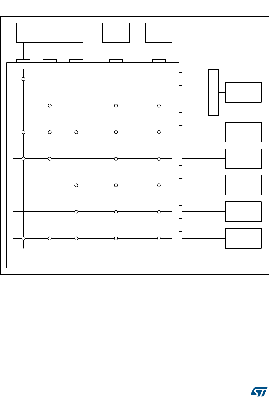
System and memory overview RM0394
64/1600 RM0394 Rev 4
Figure 1. System architecture
2.1.1 S0: I-bus
This bus connects the instruction bus of the Cortex®-M4 core to the BusMatrix. This bus is
used by the core to fetch instructions. The targets of this bus are the internal Flash memory,
SRAM1, SRAM2 and external memories through QUADSPI.
2.1.2 S1: D-bus
This bus connects the data bus of the Cortex®-M4 core to the BusMatrix. This bus is used
by the core for literal load and debug access. The targets of this bus are the internal Flash
memory, SRAM1, SRAM2 and external memories through QUADSPI.
06Y9
$50
&257(;0ZLWK)38 '0$ '0$
48$'63,
$+%
SHULSKHUDOV
$+%
SHULSKHUDOV
65$0
65$0
)/$6+
$&&(/
6 6 6 6 6
0 0 0 0 0 0 0
%XV0DWUL[6
,&RGH
'&RGH

RM0394 Rev 4 65/1600
RM0394 System and memory overview
65
2.1.3 S2: S-bus
This bus connects the system bus of the Cortex®-M4 core to the BusMatrix. This bus is
used by the core to access data located in a peripheral or SRAM area. The targets of this
bus are the SRAM1, the AHB1 peripherals including the APB1 and APB2 peripherals, the
AHB2 peripherals and the external memories through the QUADSPI.
2.1.4 S3, S4: DMA-bus
This bus connects the AHB master interface of the DMA to the BusMatrix.The targets of this
bus are the SRAM1 and SRAM2, the AHB1 peripherals including the APB1 and APB2
peripherals, the AHB2 peripherals and the external memories through the QUADSPI.
2.1.5 BusMatrix
The BusMatrix manages the access arbitration between masters. The arbitration uses a
Round Robin algorithm. The BusMatrix is composedof five masters (CPU AHB, system bus,
DCode bus, ICode bus, DMA1 and DMA2 bus) and seven slaves (FLASH, SRAM1,
SRAM2, AHB1 (including APB1 and APB2), AHB2 and QUADSPI).
AHB/APB bridges
The two AHB/APB bridges provide full synchronous connections between the AHB and the
two APB buses, allowing flexible selection of the peripheral frequency.
Refer to Section 2.2.2: Memory map and register boundary addresses on page 67 for the
address mapping of the peripherals connected to this bridge.
After each device reset, all peripheral clocks are disabled (except for the SRAM1/2 and
Flash memory interface). Before using a peripheral you have to enable its clock in the
RCC_AHBxENR and the RCC_APBxENR registers.
Note: When a 16- or 8-bit access is performed on an APB register, the access is transformed into
a 32-bit access: the bridge duplicates the 16- or 8-bit data to feed the 32-bit vector.

RM0394
66/1600 RM0394 Rev 4
2.2 Memory organization
2.2.1 Introduction
Program memory, data memory, registers and I/O ports are organized within the same linear
4-Gbyte address space.
The bytes are coded in memory in Little Endian format. The lowest numbered byte in a word
is considered the word’s least significant byte and the highest numbered byte the most
significant.
The addressable memory space is divided into eight main blocks, of 512 Mbytes each.
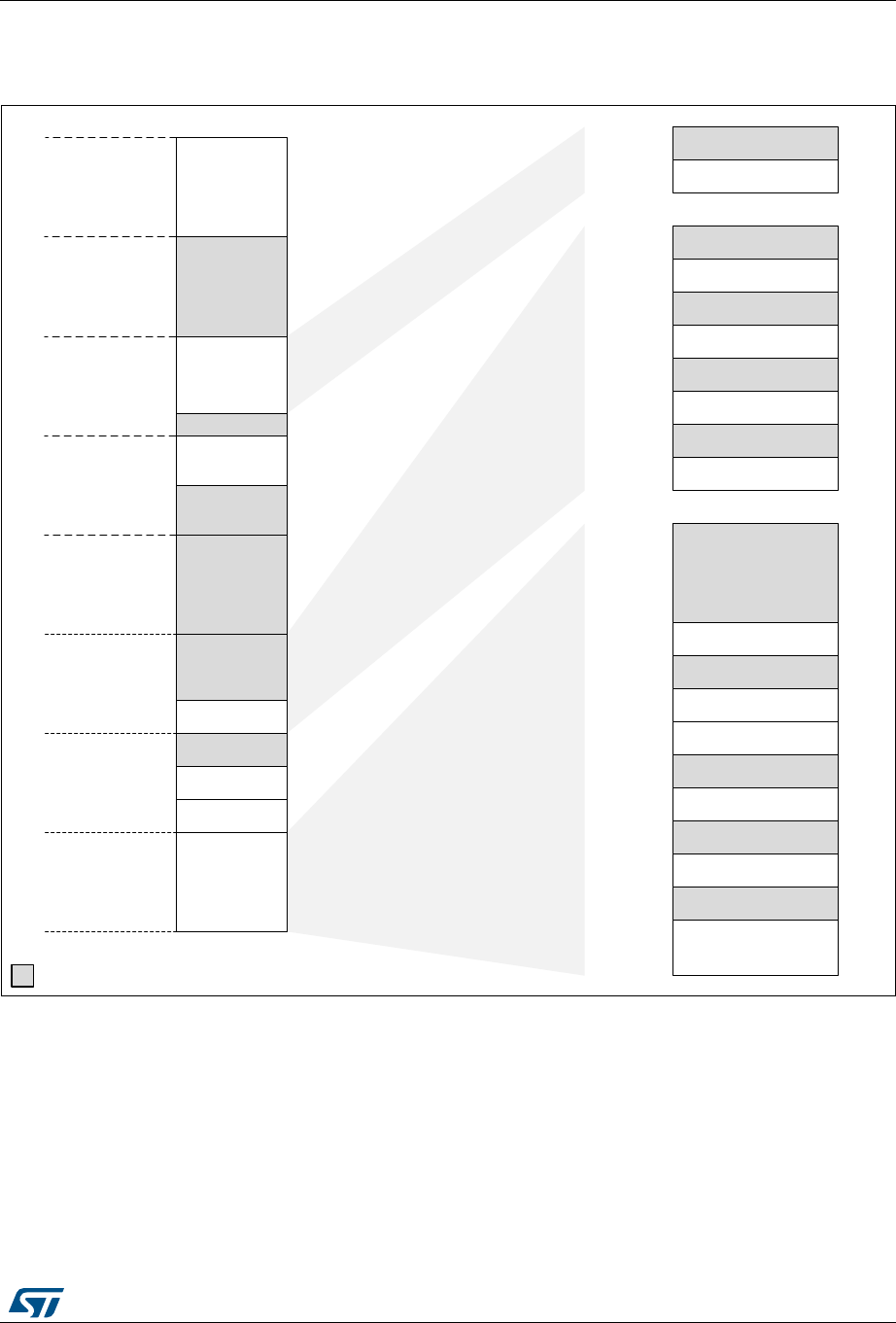
RM0394 Rev 4 67/1600
RM0394
76
2.2.2 Memory map and register boundary addresses
Figure 2. Memory map
1. 0x2000 8000 for STM32L41xxx and STM32L42xxx devices
0x2000 C000 for STM32L43xxx and STM32L44xxx devices
0x2002 0000 for STM32L45xxx and STM32L46xxx devices
2. 0x1000 2000 for STM32L41xxx and STM32L42xxx devices
0x1000 4000 for STM32L43xxx and STM32L44xxx devices
0x1000 8000 for STM32L45xxx and STM32L46xxx devices
It is forbidden to access QUADSPI Flash bank area before having properly configured and
enabled the QUADSPI peripheral.
All the memory map areas that are not allocated to on-chip memories and peripherals are
considered “Reserved”. For the detailed mapping of available memory and register areas,
refer to the following table.
06Y9
5HVHUYHG
&RGH
[
[ 65$0
65$0
3HULSKHUDOV
[
[
[
[
48$'63,
)ODVKEDQN
[$
[$
48$'63,
UHJLVWHUV
[&
&RUWH[0
ZLWK)38
LQWHUQDO
SHULSKHUDOV
)ODVKV\VWHPPHPRU\
RU65$0GHSHQGLQJ
RQ%227FRQILJXUDWLRQ
5HVHUYHG
)ODVKPHPRU\
[
[
[
5HVHUYHG
[
[ 65$0
5HVHUYHG
[)))
6\VWHPPHPRU\
[)))
273DUHD
[)))
5HVHUYHG
2SWLRQE\WHV
[)))
[)))
5HVHUYHG
[)))))))
$3%
5HVHUYHG
$3%
5HVHUYHG
$+%
5HVHUYHG
$+%
5HVHUYHG
[
[
[
[
[
[
[
[&
[)))))))
48$'63,UHJLVWHUV
5HVHUYHG
[$
[$
[%)))))))
[(
[))))))))
RM0394
68/1600 RM0394 Rev 4
The following table gives the boundary addresses of the peripherals available in the
devices.
Table 2. STM32L41xxx/42xxx/43xxx/44xxx/45xxx/46xxx memory map and peripheral register
boundary addresses
Bus Boundary address Size (bytes) Peripheral Peripheral register map
AHB2
0x5006 0800 - 0x5006 0BFF 1 KB RNG Section 24.8.4: RNG register map
0x5006 0400 - 0x5006 07FF 1KB Reserved -
0x5006 0000 - 0x5006 03FF 1 KB AES(1) Section 25.7.18: AES register map
0x5004 0400 - 0x5005 FFFF 127 KB Reserved -
0x5004 0000 - 0x5004 03FF 1 KB ADC Section 16.7.4: ADC register map on
page 482
0x5000 0000 - 0x5003 FFFF 16 KB Reserved -
0x4800 2000 - 0x4FFF FFFF ~127 MB Reserved -
0x4800 1C00 - 0x4800 1FFF 1 KB GPIOH Section 8.4.12: GPIO register map
0x4800 1400 - 0x4800 1BFF 2KB Reserved -
0x4800 1000 - 0x4800 13FF 1 KB GPIOE(2) (3) Section 8.4.12: GPIO register map
0x4800 0C00 - 0x4800 0FFF 1 KB GPIOD(2) Section 8.4.12: GPIO register map
0x4800 0800 - 0x4800 0BFF 1 KB GPIOC Section 8.4.12: GPIO register map
0x4800 0400 - 0x4800 07FF 1 KB GPIOB Section 8.4.12: GPIO register map
0x4800 0000 - 0x4800 03FF 1 KB GPIOA Section 8.4.12: GPIO register map
0x4002 4400 - 0x47FF FFFF ~127 MB Reserved -
AHB1
0x4002 4000 - 0x4002 43FF 1 KB TSC Section 23.6.11: TSC register map
0x4002 3400 - 0x4002 3FFF 1KB Reserved -
0x4002 3000 - 0x4002 33FF 1 KB CRC Section 14.4.6: CRC register map
0x4002 2400 - 0x4002 2FFF 3KB Reserved -
0x4002 2000 - 0x4002 23FF 1 KB FLASH
registers Section 3.7.13: FLASH register map
0x4002 1400 - 0x4002 1FFF 3KB Reserved -
0x4002 1000 - 0x4002 13FF 1 KB RCC Section 6.4.32: RCC register map
0x4002 0800 - 0x4002 0FFF 2KB Reserved -
0x4002 0400 - 0x4002 07FF 1 KB DMA2 Section 11.6.8: DMA register map and reset
values
0x4002 0000 - 0x4002 03FF 1 KB DMA1 Section 11.6.8: DMA register map and reset
values
APB2
0x4001 6400 - 0x4001 FFFF 39 KB Reserved -
0x4001 6000 - 0x4001 63FF 1 KB DFSDM1(3) Section 21.8.16: DFSDM register map
0x4001 5800 - 0x4001 5FFF 2kB Reserved -

RM0394 Rev 4 69/1600
RM0394
76
APB2
0x4001 5400 - 0x4001 57FF 1 KB SAI1(3) Section 41.6.17: SAI register map
0x4001 4400 - 0x4000 53FF 2KB Reserved -
0x4001 4400 - 0x4001 47FF 1 KB TIM16 Section 28.7.18: TIM16 register map
0x4001 4000 - 0x4001 43FF 1 KB TIM15 Section 28.6.20: TIM15 register map
0x4001 3C00 - 0x4001 3FFF 1KB Reserved -
0x4001 3800 - 0x4001 3BFF 1 KB USART1 Section 38.8.12: USART register map
0x4001 3400 - 0x4001 37FF 1KB Reserved -
0x4001 3000 - 0x4001 33FF 1 KB SPI1 Section 40.6.8: SPI register map
0x4001 2C00 - 0x4001 2FFF 1 KB TIM1 Section 26.4.29: TIM1 register map
0x4001 2800 - 0x4001 2BFF 1 KB SDMMC(2) (3) Section 43.8.16: SDMMC register map
0x4001 2000 - 0x4001 27FF 2KB Reserved -
0x4001 1C00 - 0x4001 1FFF 1 KB FIREWALL Section 4.4.8: Firewall register map
0x4001 0800- 0x4001 1BFF 5KB Reserved -
0x4001 0400 - 0x4001 07FF 1 KB EXTI Section 13.5.13: EXTI register map
0x4001 0200 - 0x4001 03FF
1 KB
COMP Section 19.6.3: COMP register map
0x4001 0030 - 0x4001 01FF VREFBUF(3) Section 18.3.3: VREFBUF register map
0x4001 0000 - 0x4001 002F SYSCFG Section 9.2.11: SYSCFG register map
APB1
0x4000 9800 - 0x4000 FFFF 26 KB Reserved -
0x4000 9400 - 0x4000 97FF 1 KB LPTIM2 Section 30.7.13: LPTIM register map
0x4000 8C00 - 0x4000 93FF 2KB Reserved -
0x4000 8800 - 0x4000 8BFF 1 KB SWPMI1(4) Section 42.6.10: SWPMI register map and
reset value table
0x4000 8400 - 0x4000 87FF 1 KB I2C4(5) Section 37.7.12: I2C register map
0x4000 8000 - 0x4000 83FF 1 KB LPUART1 Section 39.7.10: LPUART register map
0x4000 7C00 - 0x4000 7FFF 1 KB LPTIM1 Section 30.7.13: LPTIM register map
0x4000 7800 - 0x4000 7BFF 1 KB OPAMP Section 20.5.4: OPAMP register map
0x4000 7400 - 0x4000 77FF 1 KB DAC1(3) Section 17.7.21: DAC register map
0x4000 7000 - 0x4000 73FF 1 KB PWR Section 5.4.20: PWR register map and reset
value table
0x4000 6C00 - 0x4000 6FFF 1 KB USB SRAM(6)
Section 45.6.3: USB register map
0x4000 6800 - 0x4000 6BFF 1 KB USB FS(6)
0x4000 6400 - 0x4000 67FF 1 KB CAN1(3) Section 44.9: CAN registers
0x4000 6000 - 0x4000 63FF 1 KB CRS Section 7.6.5: CRS register map
0x4000 5C00- 0x4000 5FFF 1 KB I2C3 Section 37.7.12: I2C register map
0x4000 5800 - 0x4000 5BFF 1 KB I2C2 Section 37.7.12: I2C register map
Table 2. STM32L41xxx/42xxx/43xxx/44xxx/45xxx/46xxx memory map and peripheral register
boundary addresses (continued)
Bus Boundary address Size (bytes) Peripheral Peripheral register map
RM0394
70/1600 RM0394 Rev 4
2.3 Bit banding
The Cortex®-M4 memory map includes two bit-band regions. These regions map each word
in an alias region of memory to a bit in a bit-band region of memory. Writing to a word in the
alias region has the same effect as a read-modify-write operation on the targeted bit in the
bit-band region.
In the STM32L43xxx/44xxx/45xxx/46xxx devices both the peripheral registers and the
SRAM1 are mapped to a bit-band region, so that single bit-band write and read operations
are allowed. The operations are only available for Cortex®-M4 accesses, and not from other
bus masters (e.g. DMA).
APB1
0x4000 5400 - 0x4000 57FF 1 KB I2C1 Section 37.7.12: I2C register map
0x4000 5000 - 0x4000 53FF 1KB Reserved -
0x4000 4C00 - 0x4000 4FFF 1 KB USART4(5) Section 38.8.12: USART register map
0x4000 4800 - 0x4000 4BFF 1 KB USART3 Section 38.8.12: USART register map
0x4000 4400 - 0x4000 47FF 1 KB USART2 Section 38.8.12: USART register map
0x4000 4000 - 0x4000 43FF 1KB Reserved -
0x4000 3C00 - 0x4000 3FFF 1 KB SPI3(3) Section 40.6.8: SPI register map
0x4000 3800 - 0x4000 3BFF 1 KB SPI2 Section 40.6.8: SPI register map
0x4000 3400 - 0x4000 37FF 1KB Reserved -
0x4000 3000 - 0x4000 33FF 1 KB IWDG Section 32.4.6: IWDG register map
0x4000 2C00 - 0x4000 2FFF 1 KB WWDG Section 33.4.4: WWDG register map
0x4000 2800 - 0x4000 2BFF 1 KB RTC Section 36.6.21: RTC register map
0x4000 2400 - 0x4000 27FF 1 KB LCD(7) Section 22.6.6: LCD register map
0x4000 1800 - 0x4000 2400 3KB Reserved -
0x4000 1400 - 0x4000 17FF 1 KB TIM7(3) (8) Section 29.4.9: TIM6/TIM7 register map
0x4000 1000 - 0x4000 13FF 1 KB TIM6 Section 29.4.9: TIM6/TIM7 register map
0x4000 0800 - 0x4000 0FFF 2KB Reserved -
0x4000 0400 - 0x4000 07FF 1 KB TIM3(5) Section 27.4.21: TIMx register map
0x4000 0000 - 0x4000 03FF 1 KB TIM2 Section 27.4.21: TIMx register map
1. Available on STM32L44xxx and STM32L46xxx devices only.
2. Not available on STM32L42xxx, STM32L432xx and STM32L442xx devices.
3. Not available on STM32L41xxx and STM32L42xxx devices.
4. Available on STM32L43xxx and STM32L44xxx devices only.
5. Available on STM32L45xxx and STM32L46xxx devices only.
6. Available on STM32L4x2xx and STM32L4x3xx devices only.
7. Available on STM32L4x3xx devices only.
8. Not available on STM32L45xxx and STM32L46xxx devices.
Table 2. STM32L41xxx/42xxx/43xxx/44xxx/45xxx/46xxx memory map and peripheral register
boundary addresses (continued)
Bus Boundary address Size (bytes) Peripheral Peripheral register map

RM0394 Rev 4 71/1600
RM0394
76
A mapping formula shows how to reference each word in the alias region to a corresponding
bit in the bit-band region. The mapping formula is:
bit_word_addr = bit_band_base + (byte_offset x 32) + (bit_number × 4)
where:
–bit_word_addr is the address of the word in the alias memory region that maps to
the targeted bit
–bit_band_base is the starting address of the alias region
–byte_offset is the number of the byte in the bit-band region that contains the
targeted bit
–bit_number is the bit position (0-7) of the targeted bit
Example
The following example shows how to map bit 2 of the byte located at SRAM1 address
0x20000300 to the alias region:
0x22006008 = 0x22000000 + (0x300*32) + (2*4)
Writing to address 0x22006008 has the same effect as a read-modify-write operation on bit
2 of the byte at SRAM1 address 0x20000300.
Reading address 0x22006008 returns the value (0x01 or 0x00) of bit 2 of the byte at SRAM1
address 0x20000300 (0x01: bit set; 0x00: bit reset).
For more information on bit-banding, refer to the Cortex®-M4 programming manual (see
Related documents on page 1).
2.4 Embedded SRAM
The STM32L41xxx/42xxx/43xxx/44xxx/45xxx/46xxx devices feature up to 196 Kbytes
SRAM:
•Up to 128 Kbytes SRAM1
•Up to 32 Kbyte SRAM2.
These SRAM can be accessed as bytes, half-words (16 bits) or full words (32 bits). These
memories can be addressed at maximum system clock frequency without wait state and
thus by both CPU and DMA.
The CPU can access the SRAM1 through the system bus or through the ICode/DCode
buses when boot from SRAM1 is selected or when physical remap is selected
(Section 9.2.1: SYSCFG memory remap register (SYSCFG_MEMRMP) in the SYSCFG
controller). To get the maximum performance on SRAM1 execution, physical remap should
be selected (boot or software selection).
Execution can be performed from CCM SRAM with maximum performance without any
remap thanks to access through ICode bus.
2.4.1 SRAM2 parity check
The user can enable the SRAM2 parity check using the option bit SRAM2_PE in the user
option byte (refer to Section 3.4.1: Option bytes description).
The data bus width is 36 bits because 4 bits are available for parity check (1 bit per byte) in
order to increase memory robustness, as required for instance by Class B or SIL norms.
RM0394
72/1600 RM0394 Rev 4
The parity bits are computed and stored when writing into the SRAM2. Then, they are
automatically checked when reading. If one bit fails, an NMI is generated. The same error
can also be linked to the BRK_IN Break input of TIM1/TIM15/TIM16, with the SPL control bit
in the SYSCFG configuration register 2 (SYSCFG_CFGR2). The SRAM2 Parity Error flag
(SPF) is available in the SYSCFG configuration register 2 (SYSCFG_CFGR2).
Note: When enabling the RAM parity check, it is advised to initialize by software the whole RAM
memory at the beginning of the code, to avoid getting parity errors when reading non-
initialized locations.
2.4.2 SRAM2 Write protection
The SRAM2 can be write protected with a page granularity of 1 Kbyte.
Table 3. SRAM2 organization
Page number Start address End address
Page 0 0x1000 0000 0x1000 03FF
Page 1 0x1000 0400 0x1000 07FF
Page 2 0x1000 0800 0x1000 0BFF
Page 3 0x1000 0C00 0x1000 0FFF
Page 4 0x1000 1000 0x1000 13FF
Page 5 0x1000 1400 0x1000 17FF
Page 6 0x1000 1800 0x1000 1BFF
Page 7 0x1000 1C00 0x1000 1FFF
Table 4. SRAM2 organization
(continuation for STM32L43x/44x/45x/46x devices only)
Page number Start address End address
Page 8 0x1000 2000 0x1000 23FF
Page 9 0x1000 2400 0x1000 27FF
Page 10 0x1000 2800 0x1000 2BFF
Page 11 0x1000 2C00 0x1000 2FFF
Page 12 0x1000 3000 0x1000 33FF
Page 13 0x1000 3400 0x1000 37FF
Page 14 0x1000 3800 0x1000 3BFF
Page 15 0x1000 3C00 0x1000 3FFF
Table 5. SRAM2 organization
(continuation for STM32L45x and STM32L46x devices only)
Page number Start address End address
Page 16 0x1000 4000 0x1000 43FF
Page 17 0x1000 4400 0x1000 47FF

RM0394 Rev 4 73/1600
RM0394
76
The write protection can be enabled in SYSCFG SRAM2 write protection register
(SYSCFG_SWPR) in the SYSCFG block. This is a register with write ‘1’ once mechanism,
which means by writing ‘1’ on a bit it will setup the write protection for that page of SRAM
and it can be removed/cleared by a system reset only.
2.4.3 SRAM2 Read protection
The SRAM2 is protected with the Read protection (RDP). Refer to Section 3.5.1: Read
protection (RDP) for more details.
2.4.4 SRAM2 Erase
The SRAM2 can be erased with a system reset using the option bit SRAM2_RST in the user
option byte (refer to Section 3.4.1: Option bytes description).
The SRAM2 erase can also be requested by software by setting the bit SRAM2ER in the
SYSCFG SRAM2 control and status register (SYSCFG_SCSR).
Page 18 0x1000 4800 0x1000 4BFF
Page 19 0x1000 4C00 0x1000 4FFF
Page 20 0x1000 5000 0x1000 53FF
Page 21 0x1000 5400 0x1000 57FF
Page 22 0x1000 5800 0x1000 5BFF
Page 23 0x1000 5C00 0x1000 5FFF
Page 24 0x1000 6000 0x1000 63FF
Page 25 0x1000 6400 0x1000 67FF
Page 26 0x1000 6800 0x1000 6BFF
Page 27 0x1000 6C00 0x1000 6FFF
Page 28 0x1000 7000 0x1000 73FF
Page 29 0x1000 7400 0x1000 77FF
Page 30 0x1000 7800 0x1000 7BFF
Page 31 0x1000 7C00 0x1000 7FFF
Table 5. SRAM2 organization
(continuation for STM32L45x and STM32L46x devices only) (continued)
Page number Start address End address

RM0394
74/1600 RM0394 Rev 4
2.5 Flash memory overview
The Flash memory is composed of two distinct physical areas:
•The main Flash memory block. It contains the application program and user data if
necessary.
•The information block. It is composed of three parts:
– Option bytes for hardware and memory protection user configuration.
– System memory that contains the ST proprietary code.
– OTP (one-time programmable) area
The Flash interface implements instruction access and data access based on the AHB
protocol. It also implements the logic necessary to carry out the Flash memory operations
(program/erase) controlled through the Flash registers Refer to Section 3: Embedded Flash
memory (FLASH) for more details.
2.6 Boot configuration
In the STM32L41xxx/42xxx/43xxx/44xxx/45xxx/46xxx, three different boot modes can be
selected through the BOOT0 pin or the nBOOT0 bit into the FLASH_OPTR register (if the
nSWBOOT0 bit is cleared into the FLASH_OPTR register), and nBOOT1 bit in the
FLASH_OPTR register, as shown in the following table.
The values on both BOOT0 (coming from the pin or the option bit) and nBOOT1 bit are latched
on the 4th edge of the internal startup clock source after reset release. It is up to the user to
set nBOOT1 and BOOT0 to select the required boot mode.
Table 6. Boot modes
nBOOT1
FLASH_OPTR[23]
nBOOT0
FLASH_OPTR[27]
BOOT0
pin PH3
nSWBOOT0
FLASH_OPTR[26]
Main Flash
empty(1)
Boot Memory Space
Alias
XX010
Main Flash memory is
selected as boot area
XX011
System memory is
selected as boot area
X1X0X
Main Flash memory is
selected as boot area
0X11X
Embedded SRAM1 is
selected as boot area
00X0X
Embedded SRAM1 is
selected as boot area
1X11X
System memory is
selected as boot area
10X0X
System memory is
selected as boot area
1. A Flash empty check mechanism is implemented to force the boot from system Flash if the first Flash memory location is
not programmed (0xFFFF FFFF) and if the boot selection was configured to boot from the main Flash.

RM0394 Rev 4 75/1600
RM0394
76
The BOOT0 pin or user option bit (depending on the nSWBOOT0 bit value in the
FLASH_OPTR register), and nBOOT1 bit are also re-sampled when exiting from Standby
mode. Consequently they must be kept in the required Boot mode configuration in Standby
mode. After this startup delay has elapsed, the CPU fetches the top-of-stack value from
address 0x0000 0000, then starts code execution from the boot memory at 0x0000 0004.
Depending on the selected boot mode, main Flash memory, system memory or SRAM1 is
accessible as follows:
•Boot from main Flash memory: the main Flash memory is aliased in the boot memory
space (0x0000 0000), but still accessible from its original memory space
(0x0800 0000). In other words, the Flash memory contents can be accessed starting
from address 0x0000 0000 or 0x0800 0000.
•Boot from system memory: the system memory is aliased in the boot memory space
(0x0000 0000), but still accessible from its original memory space (0x1FFF 0000).
•Boot from the embedded SRAM1: the SRAM1 is aliased in the boot memory space
(0x0000 0000), but it is still accessible from its original memory space (0x2000 0000).
PH3/BOOT0 GPIO is configured in:
•Input mode during the complete reset phase if the option bit nSWBOOT0 is set into the
FLASH_OPTR register and then switches automatically in analog mode after reset is
released (BOOT0 pin).
•Input mode from the reset phase to the completion of the option byte loading if the bit
nSWBOOT0 is cleared into the FLASH_OPTR register (BOOT0 value coming from the
option bit). It switches then automatically to the analog mode even if the reset phase is
not complete.
Note: When the device boots from SRAM, in the application initialization code, you have to
relocate the vector table in SRAM using the NVIC exception table and the offset register.
Physical remap
Once the boot mode is selected, the application software can modify the memory accessible
in the code area (in this way the code can be executed through the ICode bus in
place of the System bus). This modification is performed by programming the SYSCFG
memory remap register (SYSCFG_MEMRMP) in the SYSCFG controller.
The following memories can thus be remapped:
•Main Flash memory
•System memory
•Embedded SRAM1
•Quad-SPI memory
Table 7. Memory mapping vs. Boot mode/Physical remap
Addresses
Boot/Remap in
main Flash mem-
ory
Boot/Remap in
embedded
SRAM1
Boot/Remap in
System memory
Remap in QUAD-
SPI
0x2000 0000 - 0x2001 7FFFF(1) SRAM1 SRAM1 SRAM1 SRAM1
0x1FFF 0000 - 0x1FFF FFFF
System mem-
ory/OTP/Options
bytes
System mem-
ory/OTP/Options
bytes
System mem-
ory/OTP/Options
bytes
System mem-
ory/OTP/Options
bytes

RM0394
76/1600 RM0394 Rev 4
Embedded boot loader
The embedded boot loader is located in the System memory, programmed by ST during
production. Refer to AN2606 STM32 microcontroller system memory boot mode.
0x1008 0000(1) - 0x1FFE FFFF Reserved Reserved Reserved Reserved
0x1000 0000 - 0x1007 FFFF(1) SRAM2 SRAM2 SRAM2 SRAM2
0x0808 0000(1) - 0x0FFF FFFF Reserved Reserved Reserved Reserved
0x0800 0000 - 0x0807 FFFF(1) Flash memory Flash memory Flash memory Flash memory
0x0400 0000 - 0x07FF FFFF Reserved Reserved Reserved QUADSPI bank
(128 MB) Aliased
0x0010 0000 - 0x03FF FFFF Reserved Reserved Reserved QUADSPI bank
(128 MB) Aliased
0x0000 0000 - 0x000F FFFF(2) (3) Flash Aliased SRAM1 Aliased System memory
Aliased
QUADSPI bank
(128 MB) Aliased
1. Address depends on the memory size available on given device.
2. When the QUADSPI is remapped at address 0x0000 0000, only 128 MB are remapped. In remap mode, the CPU can ac-
cess the external memory via ICode bus instead of System bus which boosts up the performance.
3. Even when aliased in the boot memory space, the related memory is still accessible at its original memory space.
Table 7. Memory mapping vs. Boot mode/Physical remap (continued)
Addresses
Boot/Remap in
main Flash mem-
ory
Boot/Remap in
embedded
SRAM1
Boot/Remap in
System memory
Remap in QUAD-
SPI

RM0394 Rev 4 77/1600
RM0394 Embedded Flash memory (FLASH)
113
3 Embedded Flash memory (FLASH)
3.1 Introduction
The Flash memory interface manages CPU AHB ICode and DCode accesses to the Flash
memory. It implements the erase and program Flash memory operations and the read and
write protection mechanisms.
The Flash memory interface accelerates code execution with a system of instruction
prefetch and cache lines.
3.2 FLASH main features
•72-bit wide data read (64 bits plus 8 ECC bits)
•72-bit wide data write (64 bits plus 8 ECC bits)
•Page erase (2 Kbyte) and mass erase
Flash memory interface features:
•Flash memory read operations
•Flash memory program/erase operations
•Read protection activated by option (RDP)
•Prefetch on ICODE
•Instruction Cache: 32 cache lines of 4 x 64 bits on ICode (1 KB RAM)
•Data Cache: 8 cache lines of 4 x 64 bits on DCode (256B RAM)
•Error Code Correction (ECC): 8 bits for 64-bit double-word
•Option byte loader
•Low-power mode
3.3 FLASH functional description
3.3.1 Flash memory organization
The Flash memory is organized as 72-bit wide memory cells (64 bits plus 8 ECC bits) that
can be used for storing both code and data constants.
The Flash memory is organized as follows:
•An Information block containing:
– System memory from which the device boots in System memory boot mode. The
area is reserved for use by STMicroelectronics and contains the boot loader that is
used to reprogram the Flash memory through one of the following interfaces:
USART1, USART2, USART3, USB (DFU), I2C1, I2C2, I2C3, SPI1, SPI2, SPI3. It
is programmed by STMicroelectronics when the device is manufactured, and
protected against spurious write/erase operations. For further details, please refer
to the AN2606 available from www.st.com.
– 1 Kbyte (128 double word) OTP (one-time programmable) bytes for user data. The
OTP data cannot be erased and can be written only once. If only one bit is at 0,
Embedded Flash memory (FLASH) RM0394
78/1600 RM0394 Rev 4
the entire double word cannot be written anymore, even with the value 0x0000
0000 0000 0000.
– Option bytes for user configuration.
The memory organization is based on a main area and an information block as shown in
Table 8.
3.3.2 Error code correction (ECC)
Data in Flash memory are 72-bits words: 8 bits are added per double word (64 bits). The
ECC mechanism supports:
•One error detection and correction
•Two errors detection
When one error is detected and corrected, the flag ECCC (ECC correction) is set in Flash
ECC register (FLASH_ECCR). If ECCCIE is set, an interrupt is generated.
When two errors are detected, a flag ECCD (ECC detection) is set in FLASH_ECCR
register. In this case, a NMI is generated.
When an ECC error is detected, the address of the failing double word saved in
ADDR_ECC[20:0] in the FLASH_ECCR register. ADDR_ECC[2:0] are always cleared.
When ECCC or ECCD is set, ADDR_ECC not updated if a new ECC error occurs.
FLASH_ECCR is updated only when ECC flags are cleared.
Table 8. Flash module - single bank organization
Flash area Flash memory addresses Size
(bytes) Name
Main memory
0x0800 0000 - 0x0800 07FF 2 K Page 0
0x0800 0800 - 0x0800 0FFF 2 K Page 1
0x0800 1000 - 0x0800 17FF 2 K Page 2
0x0800 1800 - 0x0800 1FFF 2 K Page 3
---
0x0801 F800 - 0x0801 FFFF 2 K Page 63(1)
1. Main Flash memory space of 128K devices is limited to page 63.
---
0x0803 F800 - 0x0803 FFFF 2 K Page 127(2)
2. Main Flash memory space of 256K devices is limited to page 127.
---
0x0807 F800 - 0x0807 FFFF 2 K Page 255(3)
3. Main Flash memory space of 512K devices is limited to page 255.
Information block
0x1FFF 0000 - 0x1FFF 6FFF 28 K System memory
0x1FFF 7000 - 0x1FFF 73FF 1 K OTP area
0x1FFF 7800 - 0x1FFF 780F 16 Option bytes
RM0394 Rev 4 79/1600
RM0394 Embedded Flash memory (FLASH)
113
Note: For a virgin data: 0xFF FFFF FFFF FFFF FFFF, one error is detected and corrected but two
errors detection is not supported.
When an ECC error is reported, a new read at the failing address may not generate an ECC
error if the data is still present in the current buffer, even if ECCC and ECCD are cleared.
3.3.3 Read access latency
To correctly read data from Flash memory, the number of wait states (LATENCY) must be
correctly programmed in the Flash access control register (FLASH_ACR) according to the
frequency of the CPU clock (HCLK) and the internal voltage range of the device VCORE.
Refer to Section 5.1.7: Dynamic voltage scaling management. Table 9 shows the
correspondence between wait states and CPU clock frequency.
After reset, the CPU clock frequency is 4 MHz and 0 wait state (WS) is configured in the
FLASH_ACR register.
When changing the CPU frequency, the following software sequences must be applied in
order to tune the number of wait states needed to access the Flash memory:
Increasing the CPU frequency:
1. Program the new number of wait states to the LATENCY bits in the Flash access
control register (FLASH_ACR).
2. Check that the new number of wait states is taken into account to access the Flash
memory by reading the FLASH_ACR register.
3. Modify the CPU clock source by writing the SW bits in the RCC_CFGR register.
4. If needed, modify the CPU clock prescaler by writing the HPRE bits in RCC_CFGR.
5. Check that the new CPU clock source or/and the new CPU clock prescaler value is/are
taken into account by reading the clock source status (SWS bits) or/and the AHB
prescaler value (HPRE bits), respectively, in the RCC_CFGR register.
Table 9. Number of wait states according to CPU clock (HCLK) frequency
Wait states (WS)
(LATENCY)
HCLK (MHz)
VCORE Range 1(1)
1. Also for SMPS Range1 or SMPS Range2 high.
VCORE Range 2(2)
2. Also for SMPS Range2 low.
0 WS (1 CPU cycles) 16 6
1 WS (2 CPU cycles) 32 12
2 WS (3 CPU cycles) 48 18
3 WS (4 CPU cycles) 64 26
4 WS (5 CPU cycles) 80 26

Embedded Flash memory (FLASH) RM0394
80/1600 RM0394 Rev 4
Decreasing the CPU frequency:
1. Modify the CPU clock source by writing the SW bits in the RCC_CFGR register.
2. If needed, modify the CPU clock prescaler by writing the HPRE bits in RCC_CFGR.
3. Check that the new CPU clock source or/and the new CPU clock prescaler value is/are
taken into account by reading the clock source status (SWS bits) or/and the AHB
prescaler value (HPRE bits), respectively, in the RCC_CFGR register.
4. Program the new number of wait states to the LATENCY bits in Flash access control
register (FLASH_ACR).
5. Check that the new number of wait states is used to access the Flash memory by
reading the FLASH_ACR register.
3.3.4 Adaptive real-time memory accelerator (ART Accelerator™)
The proprietary Adaptive real-time (ART) memory accelerator is optimized for STM32
industry-standard Arm® Cortex®-M4 with FPU processors. It balances the inherent
performance advantage of the Arm® Cortex®-M4 with FPU over Flash memory
technologies, which normally requires the processor to wait for the Flash memory at higher
operating frequencies.
To release the processor full performance, the accelerator implements an instruction
prefetch queue and branch cache which increases program execution speed from the 64-
bit Flash memory. Based on CoreMark benchmark, the performance achieved thanks to the
ART accelerator is equivalent to 0 wait state program execution from Flash memory at a
CPU frequency up to 80 MHz.
Instruction prefetch
The Cortex®-M4 fetches the instruction over the ICode bus and the literal pool
(constant/data) over the DCode bus. The prefetch block aims at increasing the efficiency of
ICode bus accesses.
Each Flash memory read operation provides 64 bits from either two instructions of 32 bits or
four instructions of 16 bits according to the program launched. This 64-bits current
instruction line is saved in a current buffer. So, in case of sequential code, at least two CPU
cycles are needed to execute the previous read instruction line. Prefetch on the ICode bus
can be used to read the next sequential instruction line from the Flash memory while the
current instruction line is being requested by the CPU.
Prefetch is enabled by setting the PRFTEN bit in the Flash access control register
(FLASH_ACR). This feature is useful if at least one wait state is needed to access the Flash
memory.
Figure 3 shows the execution of sequential 16-bit instructions with and without prefetch
when 3 WS are needed to access the Flash memory.
RM0394 Rev 4 81/1600
RM0394 Embedded Flash memory (FLASH)
113
Figure 3. Sequential 16-bit instructions execution
When the code is not sequential (branch), the instruction may not be present in the currently
used instruction line or in the prefetched instruction line. In this case (miss), the penalty in
terms of number of cycles is at least equal to the number of wait states.
069
:,7+28735()(7&+
#
)
:$,7 '
(
#
)
'
(
#
'
(
)
#
'
(
)
#
'
(
)
:$,7
'
(
)
#
)
'
#
)
#
5HDGLQV *LYHVLQV
LQV
IHWFK
LQV
IHWFK
LQV
IHWFK
LQV
IHWFK
5HDGLQV *LYHVLQV
LQV
IHWFK
LQV
IHWFK
LQV
IHWFK
LQV
IHWFK
:,7+35()(7&+
#
)
:$,7 '
(
#
)
'
(
#
'
(
)
#
'
(
)
#
'
(
)
'
(
)
)
'
#
)
#
5HDGLQV *LYHVLQV
LQV
IHWFK
LQV
IHWFK
LQV
IHWFK
LQV
IHWFK
*LYHVLQV
LQV
IHWFK
LQV
IHWFK
LQV
IHWFK
LQV
IHWFK
#
5HDGLQV 5HDGLQV
#DGGUHVVUHTXHVWHG
))HWFKVWDJH
''HFRGHVWDJH
(([HFXWHVWDJH
'
(
)
#
&RUWH[0SLSHOLQH
$+%SURWRFRO

Embedded Flash memory (FLASH) RM0394
82/1600 RM0394 Rev 4
If a loop is present in the current buffer, no new flash access is performed.
Instruction cache memory (I-Cache)
To limit the time lost due to jumps, it is possible to retain 32 lines of 4*64 bits in an instruction
cache memory.This feature can be enabled by setting the instruction cache enable (ICEN)
bit in the Flash access control register (FLASH_ACR). Each time a miss occurs (requested
data not present in the currently used instruction line, in the prefetched instruction line or in
the instruction cache memory), the line read is copied into the instruction cache memory. If
some data contained in the instruction cache memory are requested by the CPU, they are
provided without inserting any delay. Once all the instruction cache memory lines have been
filled, the LRU (least recently used) policy is used to determine the line to replace in the
instruction memory cache. This feature is particularly useful in case of code containing
loops.
The Instruction cache memory is enable after system reset.
Data cache memory (D-Cache)
Literal pools are fetched from Flash memory through the DCode bus during the execution
stage of the CPU pipeline. Each DCode bus read access fetches 64 bits which are saved in
a current buffer. The CPU pipeline is consequently stalled until the requested literal pool is
provided. To limit the time lost due to literal pools, accesses through the AHB databus
DCode have priority over accesses through the AHB instruction bus ICode.
If some literal pools are frequently used, the data cache memory can be enabled by setting
the data cache enable (DCEN) bit in the Flash access control register (FLASH_ACR). This
feature works like the instruction cache memory, but the retained data size is limited to 8
rows of 4*64 bits.
The Data cache memory is enable after system reset.
Note: The D-Cache is active only when data is requested by the CPU (not by DMA1 and DMA2).
Data in option bytes block are not cacheable.
3.3.5 Flash program and erase operations
The STM32L41xxx/42xxx/43xxx/44xxx/45xxx/46xxx embedded Flash memory can be
programmed using in-circuit programming or in-application programming.
The in-circuit programming (ICP) method is used to update the entire contents of the
Flash memory, using the JTAG, SWD protocol or the boot loader to load the user application
into the microcontroller. ICP offers quick and efficient design iterations and eliminates
unnecessary package handling or socketing of devices.
In contrast to the ICP method, in-application programming (IAP) can use any
communication interface supported by the microcontroller (I/Os, USB, CAN, UART, I2C, SPI,
etc.) to download programming data into memory. IAP allows the user to re-program the
Flash memory while the application is running. Nevertheless, part of the application has to
have been previously programmed in the Flash memory using ICP.
The contents of the Flash memory are not guaranteed if a device reset occurs during a
Flash memory operation.
During a program/erase operation to the Flash memory, any attempt to read the Flash
memory will stall the bus. The read operation will proceed correctly once the program/erase
operation has completed.

RM0394 Rev 4 83/1600
RM0394 Embedded Flash memory (FLASH)
113
Unlocking the Flash memory
After reset, write is not allowed in the Flash control register (FLASH_CR) to protect the
Flash memory against possible unwanted operations due, for example, to electric
disturbances. The following sequence is used to unlock this register:
1. Write KEY1 = 0x45670123 in the Flash key register (FLASH_KEYR)
2. Write KEY2 = 0xCDEF89AB in the FLASH_KEYR register.
Any wrong sequence will lock up the FLASH_CR register until the next system reset. In the
case of a wrong key sequence, a bus error is detected and a Hard Fault interrupt is
generated.
The FLASH_CR register can be locked again by software by setting the LOCK bit in the
FLASH_CR register.
Note: The FLASH_CR register cannot be written when the BSY bit in the Flash status register
(FLASH_SR) is set. Any attempt to write to it with the BSY bit set will cause the AHB bus to
stall until the BSY bit is cleared.
3.3.6 Flash main memory erase sequences
The Flash memory erase operation can be performed at page level or on the whole Flash
memory (Mass Erase). Mass Erase does not affect the Information block (system flash,
OTP and option bytes).
Page erase
To erase a page (2 Kbyte), follow the procedure below:
1. Check that no Flash memory operation is ongoing by checking the BSY bit in the Flash
status register (FLASH_SR).
2. Check and clear all error programming flags due to a previous programming. If not,
PGSERR is set.
3. Set the PER bit and select the page you wish to erase (PNB) in the Flash control
register (FLASH_CR).
4. Set the STRT bit in the FLASH_CR register.
5. Wait for the BSY bit to be cleared in the FLASH_SR register.
Note: The internal oscillator HSI16 (16 MHz) is enabled automatically when STRT bit is set, and
disabled automatically when STRT bit is cleared, except if the HSI16 is previously enabled
with HSION in RCC_CR register.
If the page erase is part of write-protected area (by WRP or PCROP), WRPERR is set and
the page erase request is aborted.
Mass erase
To perform a Mass Erase, follow the procedure below:

Embedded Flash memory (FLASH) RM0394
84/1600 RM0394 Rev 4
1. Check that no Flash memory operation is ongoing by checking the BSY bit in the
FLASH_SR register.
2. Check and clear all error programming flags due to a previous programming. If not,
PGSERR is set.
3. Set the MER1 bit in the Flash control register (FLASH_CR).
4. Set the STRT bit in the FLASH_CR register.
5. Wait for the BSY bit to be cleared in the Flash control register (FLASH_CR).
Note: The internal oscillator HSI16 (16 MHz) is enabled automatically when STRT bit is set, and
disabled automatically when STRT bit is cleared, except if the HSI16 is previously enabled
with HSION in RCC_CR register.
If the Flash memory contains a write-protected area (by WRP or PCROP), WRPERR is set
and the mass erase request is aborted.
3.3.7 Flash main memory programming sequences
The Flash memory is programmed 72 bits at a time (64 bits + 8 bits ECC).
Programming in a previously programmed address is not allowed except if the data to write
is full zero, and any attempt will set PROGERR flag in the Flash status register
(FLASH_SR).
It is only possible to program double word (2 x 32-bit data).
•Any attempt to write byte or half-word will set SIZERR flag in the FLASH_SR register.
•Any attempt to write a double word which is not aligned with a double word address will
set PGAERR flag in the FLASH_SR register.
Standard programming
The Flash memory programming sequence in standard mode is as follows:
1. Check that no Flash main memory operation is ongoing by checking the BSY bit in the
Flash status register (FLASH_SR).
2. Check and clear all error programming flags due to a previous programming. If not,
PGSERR is set.
3. Set the PG bit in the Flash control register (FLASH_CR).
4. Perform the data write operation at the desired memory address, inside main memory
block or OTP area. Only double word can be programmed.
– Write a first word in an address aligned with double word
– Write the second word
5. Wait until the BSY bit is cleared in the FLASH_SR register.
6. Check that EOP flag is set in the FLASH_SR register (meaning that the programming
operation has succeed), and clear it by software.
7. Clear the PG bit in the FLASH_CR register if there no more programming request
anymore.
Note: When the flash interface has received a good sequence (a double word), programming is
automatically launched and BSY bit is set. The internal oscillator HSI16 (16 MHz) is enabled

RM0394 Rev 4 85/1600
RM0394 Embedded Flash memory (FLASH)
113
automatically when PG bit is set, and disabled automatically when PG bit is cleared, except
if the HSI16 is previously enabled with HSION in RCC_CR register.
If the user needs to program only one word, double word must be completed with the erase
value 0xFFFF FFFF to launch automatically the programming.
ECC is calculated from the double word to program.
Fast programming
This mode allows to program a row (32 double word) and to reduce the page programming
time by eliminating the need for verifying the flash locations before they are programmed
and to avoid rising and falling time of high voltage for each double word. During fast
programming, the CPU clock frequency (HCLK) must be at least 8 MHz.
Only the main memory can be programmed in Fast programming mode.
The Flash main memory programming sequence in standard mode is as follows:
1. Perform a mass erase of the bank to program. If not, PGSERR is set.
2. Check that no Flash main memory operation is ongoing by checking the BSY bit in the
Flash status register (FLASH_SR).
3. Check and clear all error programming flag due to a previous programming.
4. Set the FSTPG bit in Flash control register (FLASH_CR).
5. Write the 32 double words to program a row. Only double words can be programmed:
– Write a first word in an address aligned with double word
– Write the second word.
6. Wait until the BSY bit is cleared in the FLASH_SR register.
7. Check that EOP flag is set in the FLASH_SR register (meaning that the programming
operation has succeed), and clear it by software.
8. Clear the FSTPG bit in the FLASH_CR register if there no more programming request
anymore.
Note: If the flash is attempted to be written in Fast programming mode while a read operation is on
going in the same bank, the programming is aborted without any system notification (no
error flag is set).
When the Flash interface has received the first double word, programming is automatically
launched. The BSY bit is set when the high voltage is applied for the first double word, and it
is cleared when the last double word has been programmed or in case of error. The internal
oscillator HSI16 (16 MHz) is enabled automatically when FSTPG bit is set, and disabled
automatically when FSTPG bit is cleared, except if the HSI16 is previously enabled with
HSION in RCC_CR register.
The 32 double word must be written successively. The high voltage is kept on the flash for
all the programming. Maximum time between two double words write requests is the time
programming (around 20us). If a second double word arrives after this time programming,
fast programming is interrupted and MISSERR is set.
High voltage mustn’t exceed 8 ms for a full row between 2 erases. This is guaranteed by the
sequence of 32 double words successively written with a clock system greater or equal to
8MHz. An internal time-out counter counts 7ms when Fast programming is set and stops the
programming when time-out is over. In this case the FASTERR bit is set.
If an error occurs, high voltage is stopped and next double word to programmed is not
programmed. Anyway, all previous double words have been properly programmed.

Embedded Flash memory (FLASH) RM0394
86/1600 RM0394 Rev 4
Programming errors
Several kind of errors can be detected. In case of error, the Flash operation (programming
or erasing) is aborted.
•PROGERR: Programming Error
In standard programming: PROGERR is set if the word to write is not previously erased
(except if the value to program is full zero).
•SIZERR: Size Programming Error
In standard programming or in fast programming: only double word can be
programmed and only 32-bit data can be written. SIZERR is set if a byte or an half-
word is written.
•PGAERR: Alignment Programming error
PGAERR is set if one of the following conditions occurs:
– In standard programming: the first word to be programmed is not aligned with a
double word address, or the second word doesn’t belong to the same double word
address.
– In fast programming: the data to program doesn’t belong to the same row than the
previous programmed double words, or the address to program is not greater than
the previous one.
•PGSERR: Programming Sequence Error
PGSERR is set if one of the following conditions occurs:
– In the standard programming sequence or the fast programming sequence: a data
is written when PG and FSTPG are cleared.
– In the standard programming sequence or the fast programming sequence: MER1
and PER are not cleared when PG or FSTPG is set.
– In the fast programming sequence: the Mass erase is not performed before setting
FSTPG bit.
– In the mass erase sequence: PG, FSTPG, and PER are not cleared when MER1 is
set.
– PGSERR is set also if PROGERR, SIZERR, PGAERR, MISSERR, FASTERR or
PGSERR is set due to a previous programming error.
•WRPERR: Write Protection Error
WRPERR is set if one of the following conditions occurs:
– Attempt to program or erase in a write protected area (WRP) or in a PCROP area.
– Attempt to perform a erase when one page or more is protected by WRP or
PCROP.
– The debug features are connected or the boot is executed from SRAM or from
System flash when the read protection (RDP) is set to Level 1.
– Attempt to modify the option bytes when the read protection (RDP) is set to
Level 2.
•MISSERR: Fast Programming Data Miss Error
In fast programming: all the data must be written successively. MISSERR is set if the
previous data programmation is finished and the next data to program is not written yet.
•FASTERR: Fast Programming Error
In fast programming: FASTERR is set if one of the following conditions occurs:
– When FSTPG bit is set for more than 7ms which generates a time-out detection.

RM0394 Rev 4 87/1600
RM0394 Embedded Flash memory (FLASH)
113
– When the row fast programming has been interrupted by a MISSERR, PGAERR,
WRPERR or SIZERR.
If an error occurs during a program or erase operation, one of the following error flags is set
in the FLASH_SR register:
PROGERR, SIZERR, PGAERR, PGSERR, MISSERR (Program error flags),
WRPERR (Protection error flag)
In this case, if the error interrupt enable bit ERRIE is set in the Flash status register
(FLASH_SR), an interrupt is generated and the operation error flag OPERR is set in the
FLASH_SR register.
Note: If several successive errors are detected (for example, in case of DMA transfer to the Flash
memory), the error flags cannot be cleared until the end of the successive write requests.
Programming and caches
If a Flash memory write access concerns some data in the data cache, the Flash write
access modifies the data in the Flash memory and the data in the cache.
If an erase operation in Flash memory also concerns data in the data or instruction cache,
you have to make sure that these data are rewritten before they are accessed during code
execution. If this cannot be done safely, it is recommended to flush the caches by setting the
DCRST and ICRST bits in the Flash access control register (FLASH_ACR).
Note: The I/D cache should be flushed only when it is disabled (I/DCEN = 0).

Embedded Flash memory (FLASH) RM0394
88/1600 RM0394 Rev 4
3.4 FLASH option bytes
3.4.1 Option bytes description
The option bytes are configured by the end user depending on the application requirements.
As a configuration example, the watchdog may be selected in hardware or software mode
(refer to Section 3.4.2: Option bytes programming).
A double word is split up as follows in the option bytes:
The organization of these bytes inside the information block is as shown in Table 11: Option
byte organization.
The option bytes can be read from the memory locations listed in Table 11: Option byte
organization or from the Option byte registers:
•Flash option register (FLASH_OPTR)
•Flash PCROP Start address register (FLASH_PCROP1SR)
•Flash PCROP End address register (FLASH_PCROP1ER)
•Flash WRP area A address register (FLASH_WRP1AR)
•Flash WRP area B address register (FLASH_WRP1BR)
User and read protection option bytes
Flash memory address: 0x1FFF 7800
ST production value: 0xFFEF F8AA
Table 10. Option byte format
63-24 23-16 15 -8 7-0 31-24 23-16 15 -8 7-0
Complemented
option byte 3
Complemented
option byte 2
Complemented
option byte 1
Complemented
option byte 0
Option
byte 3
Option
byte 2
Option
byte 1
Option
byte 0
Table 11. Option byte organization
Address 63 [62:56] [55:48] [47:40] [39:32] 31 [30:24] [23:16] [15:8] [7:0]
0x1FFF 7800 USER OPT RDP USER OPT RDP
0x1FFF 7808 Unused PCROP1_STRT Unused PCROP1_STRT
0x1FFF 7810
PCROP_RDP
Unused PCROP1_END
PCROP_RDP
Unused PCROP1_END
0x1FFF 7818 Unused WRP1A
_END Unused WRP1A
_STRT Unused WRP1A_
END Unused WRP1A
_STRT
0x1FFF 7820 Unused WRP1B
_END Unused WRP1B
_STRT Unused WRP1B_
END Unused WRP1B
_STRT

RM0394 Rev 4 89/1600
RM0394 Embedded Flash memory (FLASH)
113
31 30 29 28 27 26 25 24 23 22 21 20 19 18 17 16
Res. Res. Res. Res. n
BOOT0
nSW
BOOT0
SRAM2
_RST
SRAM2
_PE
n
BOOT1 Res. Res. Res. WWDG
_SW
IWGD_
STDBY
IWDG_
STOP
IWDG_
SW
rrrrr rrrr
1514131211109876543210
Res. nRST_
SHDW
nRST_
STDBY
nRST_
STOP Res. BOR_LEV[2:0] RDP[7:0]
rrr rrrrrrrrrrr
Bits 31:28 Reserved, must be kept at reset value.
Bit 27 nBOOT0: nBOOT0 option bit
0: nBOOT0 = 0
1: nBOOT0 = 1
Bit 26 nSWBOOT0: Software BOOT0
0: BOOT0 taken from the option bit nBOOT0
1: BOOT0 taken from PH3/BOOT0 pin
Bit 25 SRAM2_RST: SRAM2 Erase when system reset
0: SRAM2 erased when a system reset occurs
1: SRAM2 is not erased when a system reset occurs
Bit 24 SRAM2_PE: SRAM2 parity check enable
0: SRAM2 parity check enable
1: SRAM2 parity check disable
Bit 23 nBOOT1: Boot configuration
Together with the BOOT0 pin, this bit selects boot mode from the Flash main
memory, SRAM1 or the System memory. Refer to Section 2.6: Boot
configuration.
Bits 22:20 Reserved, must be kept at reset value.
Bit 19 WWDG_SW: Window watchdog selection
0: Hardware window watchdog
1: Software window watchdog
Bit 18 IWDG_STDBY: Independent watchdog counter freeze in Standby mode
0: Independent watchdog counter is frozen in Standby mode
1: Independent watchdog counter is running in Standby mode
Bit 17 IWDG_STOP: Independent watchdog counter freeze in Stop mode
0: Independent watchdog counter is frozen in Stop mode
1: Independent watchdog counter is running in Stop mode
Bit 16 IDWG_SW: Independent watchdog selection
0: Hardware independent watchdog
1: Software independent watchdog
Bit 15 Reserved, must be kept at reset value.
Bit 14 nRST_SHDW
0: Reset generated when entering the Shutdown mode
1: No reset generated when entering the Shutdown mode
Bit 13 nRST_STDBY
0: Reset generated when entering the Standby mode
1: No reset generate when entering the Standby mode
Embedded Flash memory (FLASH) RM0394
90/1600 RM0394 Rev 4
PCROP Start address option bytes
Flash memory address: 0x1FFF 7808
ST production value: 0xFFFF FFFF
PCROP End address option bytes
Flash memory address: 0x1FFF 7810
ST production value: 0xFFFF 0000
Bit 12 nRST_STOP
0: Reset generated when entering the Stop mode
1: No reset generated when entering the Stop mode
Bit 11 Reserved, must be kept at reset value.
Bits10:8 BOR_LEV: BOR reset Level
These bits contain the VDD supply level threshold that activates/releases the
reset.
000: BOR Level 0. Reset level threshold is around 1.7 V
001: BOR Level 1. Reset level threshold is around 2.0 V
010: BOR Level 2. Reset level threshold is around 2.2 V
011: BOR Level 3. Reset level threshold is around 2.5 V
100: BOR Level 4. Reset level threshold is around 2.8 V
Bits 7:0 RDP: Read protection level
0xAA: Level 0, read protection not active
0xCC: Level 2, chip read protection active
Others: Level 1, memories read protection active
31 30 29 28 27 26 25 24 23 22 21 20 19 18 17 16
Res. Res. Res. Res. Res. Res. Res. Res. Res. Res. Res. Res. Res. Res. Res. Res.
1514131211109 8 765432 1 0
PCROP1_STRT[15:0]
rrrrrr r r rrrrrr r r
Bits 31:16 Reserved, must be kept at reset value.
Bits 15:0 PCROP1_STRT: PCROP area start offset
PCROP1_STRT contains the first double-word of the PCROP area.
31 30 29 28 27 26 25 24 23 22 21 20 19 18 17 16
PCROP
_RDP Res. Res. Res. Res. Res. Res. Res. Res. Res. Res. Res. Res. Res. Res. Res.
r
15 14 13 12 11 10 9 8 7 6 5 4 3 2 1 0
PCROP1_END[15:0]
r rrrrr r r rrrrrr rr
RM0394 Rev 4 91/1600
RM0394 Embedded Flash memory (FLASH)
113
WRP Area A address option bytes
Flash memory address: 0x1FFF 7818
ST production value: 0xFF00 FFFF
WRP Area B address option bytes
Flash memory address: 0x1FFF 7820
ST production value: 0xFF00 FFFF
Bit 31 PCROP_RDP: PCROP area preserved when RDP level decreased
This bit is set only. It is reset after a full mass erase due to a change of RDP
from Level 1 to Level 0.
0: PCROP area is not erased when the RDP level is decreased from Level 1 to
Level 0.
1: PCROP area is erased when the RDP level is decreased from Level 1 to
Level 0 (full mass erase).
Bits 30:16 Reserved, must be kept at reset value.
Bits 15:0 PCROP1_END: Bank 1 PCROP area end offset
PCROP1_END contains the last double-word of the bank 1 PCROP area.
31 30 29 28 27 26 25 24 23 22 21 20 19 18 17 16
Res. Res. Res. Res. Res. Res. Res. Res. WRP1A_END[7:0]
rrrrrrrr
15 14 13 12 11 10 9 8 7 6 5 4 3 2 1 0
Res. Res. Res. Res. Res. Res. Res. Res. WRP1A_STRT[7:0]
rrrrrrrr
Bits 31:24 Reserved, must be kept at reset value.
Bits 23:16 WRP1A_END: WRP first area “A” end offset
WRPA1_END contains the last page of the WRP first area.
Bits 15:8 Reserved, must be kept at reset value.
Bits 7:0 WRP1A_STRT: WRP first area “A” start offset
WRPA1_STRT contains the first page of the WRP first area.
31 30 29 28 27 26 25 24 23 22 21 20 19 18 17 16
Res. Res. Res. Res. Res. Res. Res. Res. WRP1B_END[7:0]
rrrrrrrr
15 14 13 12 11 10 9 8 7 6 5 4 3 2 1 0
Res. Res. Res. Res. Res. Res. Res. Res. WRP1B_STRT[7:0]
rrrrrrrr
Bits 31:24 Reserved, must be kept at reset value.

Embedded Flash memory (FLASH) RM0394
92/1600 RM0394 Rev 4
3.4.2 Option bytes programming
After reset, the options related bits in the Flash control register (FLASH_CR) are write-
protected. To run any operation on the option bytes page, the option lock bit OPTLOCK in
the Flash control register (FLASH_CR) must be cleared. The following sequence is used to
unlock this register:
1. Unlock the FLASH_CR with the LOCK clearing sequence (refer to Unlocking the Flash
memory).
2. Write OPTKEY1 = 0x08192A3B in the Flash option key register (FLASH_OPTKEYR).
3. Write OPTKEY2 = 0x4C5D6E7F in the FLASH_OPTKEYR register.
The user options can be protected against unwanted erase/program operations by setting
the OPTLOCK bit by software.
Note: If LOCK is set by software, OPTLOCK is automatically set too.
Modifying user options
The option bytes are programmed differently from a main memory user address.
To modify the user options value, follow the procedure below:
1. Check that no Flash memory operation is on going by checking the BSY bit in the Flash
status register (FLASH_SR).
2. Clear OPTLOCK option lock bit with the clearing sequence described above.
3. Write the desired options value in the options registers: Flash option register
(FLASH_OPTR), Flash PCROP Start address register (FLASH_PCROP1SR), Flash
PCROP End address register (FLASH_PCROP1ER), Flash WRP area A address
register (FLASH_WRP1AR), Flash WRP area B address register (FLASH_WRP1BR).
4. Set the Options Start bit OPTSTRT in the Flash control register (FLASH_CR).
5. Wait for the BSY bit to be cleared.
Note: Any modification of the value of one option is automatically performed by erasing user
option bytes pages first and then programming all the option bytes with the values contained
in the flash option registers.
Option byte loading
After the BSY bit is cleared, all new options are updated into the flash but they are not
applied to the system. They will have effect on the system when they are loaded. Option
bytes loading (OBL) is performed in two cases:
– when OBL_LAUNCH bit is set in the Flash control register (FLASH_CR).
– after a power reset (BOR reset or exit from Standby/Shutdown modes).
Option byte loader performs a read of the options block and stores the data into internal
option registers. These internal registers configure the system and cannot be read with by
Bits 23:16 WRP1B_END: WRP first area “B” end offset
WRPB1_END contains the last page of the WRP second area.
Bits 15:8 Reserved, must be kept at reset value.
Bits 7:0 WRP1B_STRT: WRP first area “B” start offset
WRPB1_STRT contains the first page of the WRP second area.

RM0394 Rev 4 93/1600
RM0394 Embedded Flash memory (FLASH)
113
software. Setting OBL_LAUNCH generates a reset so the option byte loading is performed
under system reset.
Each option bit has also its complement in the same double word. During option loading, a
verification of the option bit and its complement allows to check the loading has correctly
taken place.
During option byte loading, the options are read by double word with ECC. If the word and
its complement are matching, the option word/byte is copied into the option register.
If the comparison between the word and its complement fails, a status bit OPTVERR is set.
Mismatch values are forced into the option registers:
– For USR OPT option, the value of mismatch is all options at ‘1’, except for
BOR_LEV which is “000” (lowest threshold)
– For WRP option, the value of mismatch is the default value “No protection”
– For RDP option, the value of mismatch is the default value “Level 1”
– For PCROP, the value of mismatch is “all memory protected”
On system reset rising, internal option registers are copied into option registers which can
be read and written by software (FLASH_OPTR, FLASH_PCROP1SR,
FLASH_PCROP1ER, FLASH_WRP1AR, FLASH_WRP1BR). These registers are also used
to modify options. If these registers are not modified by user, they reflects the options states
of the system. See Section : Modifying user options for more details.

Embedded Flash memory (FLASH) RM0394
94/1600 RM0394 Rev 4
3.5 FLASH memory protection
The Flash main memory can be protected against external accesses with the Read
protection (RDP). The pages of the Flash memory can also be protected against unwanted
write due to loss of program counter contexts. The write-protection (WRP) granularity is one
page (2 KByte). Apart of the flash memory can also be protected against read and write
from third parties (PCROP). The PCROP granularity is double word (64-bit).
3.5.1 Read protection (RDP)
The read protection is activated by setting the RDP option byte and then, by applying a
system reset to reload the new RDP option byte. The read protection protects to the Flash
main memory, the option bytes, the backup registers (RTC_BKPxR in the RTC) and the
SRAM2.
Note: If the read protection is set while the debugger is still connected through JTAG/SWD, apply
a POR (power-on reset) instead of a system reset.
There are three levels of read protection from no protection (level 0) to maximum protection
or no debug (level 2).
The Flash memory is protected when the RDP option byte and its complement contain the
pair of values shown in Table 12.
The System memory area is read accessible whatever the protection level. It is never
accessible for program/erase operation.
Level 0: no protection
Read, program and erase operations into the Flash main memory area are possible. The
option bytes, the SRAM2 and the backup registers are also accessible by all operations.
Table 12. Flash memory read protection status
RDP byte value RDP complement value Read protection level
0xAA 0x55 Level 0
Any value except 0xAA or
0xCC
Any value (not necessarily
complementary) except 0x55 and
0x33
Level 1 (default)
0xCC 0x33 Level 2

RM0394 Rev 4 95/1600
RM0394 Embedded Flash memory (FLASH)
113
Level 1: Read protection
This is the default protection level when RDP option byte is erased. It is defined as well
when RDP value is at any value different from 0xAA and 0xCC, or even if the complement is
not correct.
•User mode: Code executing in user mode (Boot Flash) can access Flash main
memory, option bytes, SRAM2 and backup registers with all operations.
Caution: In case the Level 1 is configured and no PCROP area is defined, it is mandatory to set
PCROP_RDP bit to 1 (full mass erase when the RDP level is decreased from Level 1 to
Level 0). In case the Level 1 is configured and a PCROP area is defined, if user code needs
to be protected by RDP but not by PCROP, it must not be placed in a page containing a
PCROP area.
Level 2: No debug
In this level, the protection level 1 is guaranteed. In addition, the Cortex®-M4 debug port, the
boot from RAM (boot RAM mode) and the boot from System memory (boot loader mode)
are no more available. In user execution mode (boot FLASH mode), all operations are
allowed on the Flash Main memory. On the contrary, only read operations can be performed
on the option bytes.
Option bytes cannot be programmed nor erased. Thus, the level 2 cannot be removed at all:
it is an irreversible operation. When attempting to modify the options bytes, the protection
error flag WRPERR is set in the Flash_SR register and an interrupt can be generated.
Note: The debug feature is also disabled under reset.
STMicroelectronics is not able to perform analysis on defective parts on which the level 2
protection has been set.
Changing the Read protection level
It is easy to move from level 0 to level 1 by changing the value of the RDP byte to any value
(except 0xCC). By programming the 0xCC value in the RDP byte, it is possible to go to level
2 either directly from level 0 or from level 1. Once in level 2, it is no more possible to modify
the Read protection level.
When the RDP is reprogrammed to the value 0xAA to move from Level 1 to Level 0, a mass
erase of the Flash main memory is performed if PCROP_RDP is set in the Flash PCROP
End address register (FLASH_PCROP1ER). The backup registers (RTC_BKPxR in the
RTC) and the SRAM2 are also erased. The user options except PCROP protection are set
to their previous values copied from FLASH_OPTR, FLASH_WRPxyR (x=1 and y =A or B).
PCROP is disable. The OTP area is not affected by mass erase and remains unchanged.
If the bit PCROP_RDP is cleared in the FLASH_PCROP1ER, the full mass erase is
replaced by a partial mass erase that is successive page erases in the bank where PCROP
is active, except for the pages protected by PCROP. This is done in order to keep the
PCROP code. Only when the Flash memory is erased, options are re-programmed with
their previous values. This is also true for FLASH_PCROPxSR and FLASH_PCROPxER
registers (x=1).
Note: Full Mass Erase or Partial Mass Erase is performed only when Level 1 is active and Level 0
requested. When the protection level is increased (0->1, 1->2, 0->2) there is no mass erase.
To validate the protection level change, the option bytes must be reloaded through the
OBL_LAUNCH bit in Flash control register.
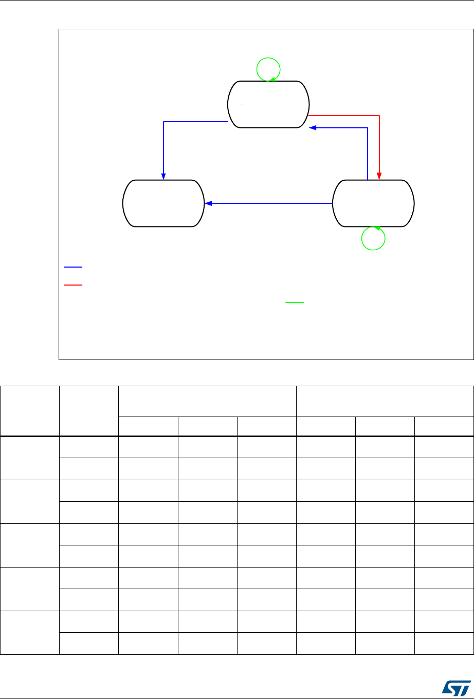
Embedded Flash memory (FLASH) RM0394
96/1600 RM0394 Rev 4
Figure 4. Changing the Read protection (RDP) level
069
2SWLRQVZULWH5'3OHYHOLQFUHDVHLQFOXGHV
2SWLRQVSDJHHUDVH
1HZRSWLRQVSURJUDP
5'3[$$DQG5'3[&&
2WKHUVRSWLRQVPRGLILHG
:ULWHRSWLRQVLQFOXGLQJ
5'3 [$$
:ULWHRSWLRQV,QFOXGLQJ
5'3 [&&
:ULWHRSWLRQVLQFOXGLQJ
5'3[&&DQG5'3[$$
/HYHO
5'3[$$
5'3[&&
GHIDXOW
/HYHO
5'3 [&&
/HYHO
5'3 [$$
5'3 [$$
2WKHUVRSWLRQVPRGLILHG
:ULWHRSWLRQVLQFOXGLQJ
5'3 [&&
2SWLRQVZULWH5'3OHYHOGHFUHDVHLQFOXGHV
)XOO0DVVHUDVHRU3DUWLDO0DVVHUDVHWRQRW
HUDVH3&523SDJHVLI3&523B5'3LVFOHDUHG
%DFNXSUHJLVWHUVDQG&&065$0HUDVH
2SWLRQVSDJHHUDVH
1HZRSWLRQVSURJUDP
2SWLRQVZULWH5'3OHYHOLGHQWLFDOLQFOXGHV
2SWLRQVSDJHHUDVH
1HZRSWLRQVSURJUDP
Table 13. Access status versus protection level and execution modes
Area Protection
level
User execution (BootFromFlash) Debug/ BootFromRam/
BootFromLoader(1)
Read Write Erase Read Write Erase
Flash main
memory
1 Yes Yes Yes N o No No(3)
2 Yes Yes Yes N/A N/A N/A
System
memory (2)
1 Yes No No Yes No No
2 Yes No No N/A N/A N/A
Option bytes
1Yes Yes
(3) Yes Yes Yes(3) Yes
2 Yes No No N/A N/A N/A
OTP
1Yes Yes
(4) N/A No No N/A
2Yes Yes
(4) N/A N/A N/A N/A
Backup
registers
1 Yes Yes N/A No No No(5)
2 Yes Yes N/A N/A N/A N/A

RM0394 Rev 4 97/1600
RM0394 Embedded Flash memory (FLASH)
113
3.5.2 Proprietary code readout protection (PCROP)
Apart of the flash memory can be protected against read and write from third parties. The
protected area is execute-only: it can only be reached by the STM32 CPU, as an instruction
code, while all other accesses (DMA, debug and CPU data read, write and erase) are
strictly prohibited. The PCROP area has a double word (64-bit) granularity. An additional
option bit (PCROP_RDP) allows to select if the PCROP area is erased or not when the RDP
protection is changed from Level 1 to Level 0 (refer to Changing the Read protection level).
The PCROP area is defined by a start page offset and an end page offset. These offsets are
defined in the PCROP address registers Flash PCROP Start address register
(FLASH_PCROP1SR), Flash PCROP End address register (FLASH_PCROP1ER).
The PCROP area is defined from the address: Flash memory Base address +
[PCROP1_STRT x 0x8] (included) to the address: Flash memory Base address +
[(PCROP1_END+1) x 0x8] (excluded). The minimum PCROP area size is two double-words
(128 bits).
For example, to protect by PCROP from the address 0x0806 2F80 (included) to the address
0x0807 0004 (included):
•if boot in flash is selected, FLASH_PCROP1SR and FLASH_PCROP1ER registers
must be programmed with:
– PCROP1_STRT = 0xC5F0.
– PCROP1_END = 0xE000.
Any read access performed through the D-bus to a PCROP protected area will trigger
RDERR flag error.
Any PCROP protected address is also write protected and any write access to one of these
addresses will trigger WRPERR.
Any PCROP area is also erase protected. Consequently, any erase to a page in this zone is
impossible (including the page containing the start address and the end address of this
zone). Moreover, a software mass erase cannot be performed if one zone is PCROP
protected.
SRAM2
1 Yes Yes N/A No No No(6)
2 Yes Yes N/A N/A N/A N/A
1. When the protection level 2 is active, the Debug port, the boot from RAM and the boot from system memory are disabled.
2. The system memory is only read-accessible, whatever the protection level (0, 1 or 2) and execution mode.
3. The Flash main memory is erased when the RDP option byte is programmed with all level protections disabled (0xAA).
4. OTP can only be written once.
5. The backup registers are erased when RDP changes from level 1 to level 0.
6. The SRAM2 is erased when RDP changes from level 1 to level 0.
Table 13. Access status versus protection level and execution modes (continued)
Area Protection
level
User execution (BootFromFlash) Debug/ BootFromRam/
BootFromLoader(1)
Read Write Erase Read Write Erase

Embedded Flash memory (FLASH) RM0394
98/1600 RM0394 Rev 4
For previous example, due to erase by page, all pages from page 0xC5 to 0xE0 are
protected in case of page erase. (All addresses from 0x0806 2800 to 0x0807 07FF can’t be
erased).
Deactivation of PCROP can only occurs when the RDP is changing from level 1 to level 0. If
the user options modification tries to clear PCROP or to decrease the PCROP area, the
options programming is launched but PCROP area stays unchanged. On the contrary, it is
possible to increase the PCROP area.
When option bit PCROP_RDP is cleared, when the RDP is changing from level 1 to level 0,
Full Mass Erase is replaced by Partial Mass Erase in order to keep the PCROP area (refer
to Changing the Read protection level). In this case, PCROP1_STRT and PCROP1_END
are also not erased.
Note: It is recommended to align PCROP area with page granularity when using PCROP_RDP, or
to leave free the rest of the page where PCROP zone starts or ends.
3.5.3 Write protection (WRP)
The user area in Flash memory can be protected against unwanted write operations. Two
write-protected (WRP) areas can be defined, with page (2 KByte) granularity. The area is
defined by a start page offset and an end page offset related to the physical Flash memory
base address. These offsets are defined in the WRP address registers: Flash WRP area A
address register (FLASH_WRP1AR), Flash WRP area B address register
(FLASH_WRP1BR).
The WRP “y” area (y=A,B) is defined from the address: Flash memory Base address +
[WRP1y_STRT x 0x800] (included) to the address: Flash memory Base address +
[(WRP1y_END+1) x 0x800] (excluded).
For example, to protect by WRP from the address 0x0806 2800 (included) to the address
0x0807 07FF (included):
•if boot in flash is selected, FLASH_WRP1AR register must be programmed with:
– WRP1A_STRT = 0xC5.
– WRP1A_END = 0xE0.
WRP1B_STRT and WRP1B_END in FLASH_WRP1BR can be used instead (area “B”
in Flash memory).
When WRP is active, it cannot be erased or programmed. Consequently, a software mass
erase cannot be performed if one area is write-protected.
If an erase/program operation to a write-protected part of the Flash memory is attempted,
the write protection error flag (WRPERR) is set in the FLASH_SR register. This flag is also
set for any write access to:
– OTP area
– part of the Flash memory that can never be written like the ICP
– PCROP area.
Note: When the memory read protection level is selected (RDP level = 1), it is not possible to
program or erase Flash memory if the CPU debug features are connected (JTAG or single
wire) or boot code is being executed from RAM or System flash, even if WRP is not
activated.

RM0394 Rev 4 99/1600
RM0394 Embedded Flash memory (FLASH)
113
Note: To validate the WRP options, the option bytes must be reloaded through the OBL_LAUNCH
bit in Flash control register.
3.6 FLASH interrupts
Table 14. Flash interrupt request
Interrupt event Event flag Event flag/interrupt
clearing method
Interrupt enable control
bit
End of operation EOP(1)
1. EOP is set only if EOPIE is set.
Write EOP=1 EOPIE
Operation error OPERR(2)
2. OPERR is set only if ERRIE is set.
Write OPERR=1 ERRIE
Read error RDERR Write RDERR=1 RDERRIE
ECC correction ECCC Write ECCC=1 ECCCIE

Embedded Flash memory (FLASH) RM0394
100/1600 RM0394 Rev 4
3.7 FLASH registers
3.7.1 Flash access control register (FLASH_ACR)
Address offset: 0x00
Reset value: 0x0000 0600
Access: no wait state, word, half-word and byte access
--
31 30 29 28 27 26 25 24 23 22 21 20 19 18 17 16
Res. Res. Res. Res. Res. Res. Res. Res. Res. Res. Res. Res. Res. Res. Res. Res.
15 14 13 12 11 10 9 8 7 6 5 4 3 2 1 0
Res. SLEEP
_PD
RUN_
PD DCRST ICRST DCEN ICEN PRFTEN Res. Res. Res. Res. Res. LATENCY[2:0]
rw rw rw rw rw rw rw rw rw rw
Bits 31:15 Reserved, must be kept at reset value.
Bit 14 SLEEP_PD: Flash Power-down mode during Sleep or Low-power sleep mode
This bit determines whether the flash memory is in Power-down mode or Idle
mode when the device is in Sleep or Low-power sleep mode.
0: Flash in Idle mode during Sleep and Low-power sleep modes
1: Flash in Power-down mode during Sleep and Low-power sleep modes
Caution: The flash must not be put in power-down while a program or an erase
operation is on-going.
Bit 13 RUN_PD: Flash Power-down mode during Run or Low-power run mode
This bit is write-protected with FLASH_PDKEYR.
This bit determines whether the flash memory is in Power-down mode or Idle
mode when the device is in Run or Low-power run mode. The flash memory can
be put in power-down mode only when the code is executed from RAM. The
Flash must not be accessed when RUN_PD is set.
0: Flash in Idle mode
1: Flash in Power-down mode
Caution: The flash must not be put in power-down while a program or an erase
operation is on-going.
Bit 12 DCRST: Data cache reset
0: Data cache is not reset
1: Data cache is reset
This bit can be written only when the data cache is disabled.
Bit 11 ICRST: Instruction cache reset
0: Instruction cache is not reset
1: Instruction cache is reset
This bit can be written only when the instruction cache is disabled.
Bit 10 DCEN: Data cache enable
0: Data cache is disabled
1: Data cache is enabled
RM0394 Rev 4 101/1600
RM0394 Embedded Flash memory (FLASH)
113
3.7.2 Flash Power-down key register (FLASH_PDKEYR)
Address offset: 0x04
Reset value: 0x0000 0000
Access: no wait state, word access
3.7.3 Flash key register (FLASH_KEYR)
Address offset: 0x08
Reset value: 0x0000 0000
Access: no wait state, word access
Bit 9 ICEN: Instruction cache enable
0: Instruction cache is disabled
1: Instruction cache is enabled
Bit 8 PRFTEN: Prefetch enable
0: Prefetch disabled
1: Prefetch enabled
Bits 7:3 Reserved, must be kept at reset value.
Bits 2:0 LATENCY[2:0]: Latency
These bits represent the period to the Flash access time.
000: Zero wait state
001: One wait state
010: Two wait states
011: Three wait states
100: Four wait states
others: Reserved
31 30 29 28 27 26 25 24 23 22 21 20 19 18 17 16
PDKEYR[31:16]
wwwwww w w wwwwww ww
15 14 13 12 11 10 9 8 7 6 5 4 3 2 1 0
PDKEYR[15:0]
wwwwww w w wwwwww ww
Bits 31:0 PDKEYR: Power-down in Run mode Flash key
The following values must be written consecutively to unlock the RUN_PD bit in
FLASH_ACR:
PDKEY1: 0x0415 2637
PDKEY2: 0xFAFB FCFD
31 30 29 28 27 26 25 24 23 22 21 20 19 18 17 16
KEYR[31:16]
wwwwww w w wwwwww ww
15 14 13 12 11 10 9 8 7 6 5 4 3 2 1 0
KEYR[15:0]
wwwwww w w wwwwww ww
Embedded Flash memory (FLASH) RM0394
102/1600 RM0394 Rev 4
3.7.4 Flash option key register (FLASH_OPTKEYR)
Address offset: 0x0C
Reset value: 0x0000 0000
Access: no wait state, word access
3.7.5 Flash status register (FLASH_SR)
Address offset: 0x10
Reset value:
Access: no wait state, word, half-word and byte access
Bits 31:0 KEYR: Flash key
The following values must be written consecutively to unlock the FLASH_CR
register allowing flash programming/erasing operations:
KEY1: 0x4567 0123
KEY2: 0xCDEF 89AB
31 30 29 28 27 26 25 24 23 22 21 20 19 18 17 16
OPTKEYR[31:16]
wwwwww w w wwwwww ww
15 14 13 12 11 10 9 8 7 6 5 4 3 2 1 0
OPTKEYR[15:0]
wwwwww w w wwwwww ww
Bits 31:0 OPTKEYR: Option byte key
The following values must be written consecutively to unlock the FLASH_OPTR
register allowing option byte programming/erasing operations:
KEY1: 0x0819 2A3B
KEY2: 0x4C5D 6E7F
31 30 29 28 27 26 25 24 23 22 21 20 19 18 17 16
Res. Res. Res. Res. Res. Res. Res. Res. Res. Res. Res. Res. Res. Res. PEMPT
YBSY
rs r
15 14 13 12 11 10 9 8 7 6 5 4 3 2 1 0
OPTV
ERR
RD
ERR Res. Res. Res. Res. FAST
ERR
MISS
ERR
PGS
ERR
SIZ
ERR
PGA
ERR
WRP
ERR
PROG
ERR Res. OP
ERR EOP
rc_w1 rc_w1 rc_w1 rc_w1 rc_w1 rc_w1 rc_w1 rc_w1 rc_w1 rc_w1 rc_w1

RM0394 Rev 4 103/1600
RM0394 Embedded Flash memory (FLASH)
113
Bits 31:18 Reserved, must be kept at reset value.
Bit 17 PEMPTY: Program EMPTY
Set by hardware on power-on reset or after OBL_LAUNCH command execution
if the Flash is not programmed and the user intends to boot from the main Flash.
Cleared by hardware on power-on reset or after OBL_LAUNCH command
execution if the Flash is programmed and the user intends to boot from main
Flash. This bit can also be set and cleared by software.
1: The bit value is toggling
0: No effect
This bit can be set to clear the Program Empty bit if an OBL_LAUNCH is done by
software after Flash programming (boot in main flash selected). It finally forces
the boot in the main flash, without loosing the debugger connection.
Bit 16 BSY: Busy
This indicates that a Flash operation is in progress. This is set on the beginning
of a Flash operation and reset when the operation finishes or when an error
occurs.
Bit 15 OPTVERR: Option validity error
Set by hardware when the options read may not be the one configured by the
user. If option haven’t been properly loaded, OPTVERR is set again after each
system reset.
Cleared by writing 1.
Bit 14 RDERR: PCROP read error
Set by hardware when an address to be read through the D-bus belongs to a
read protected area of the flash (PCROP protection). An interrupt is generated if
RDERRIE is set in FLASH_CR.
Cleared by writing 1.
Bits 13:10 Reserved, must be kept at reset value.
Bit 9 FASTERR: Fast programming error
Set by hardware when a fast programming sequence (activated by FSTPG) is
interrupted due to an error (alignment, size, write protection or data miss). The
corresponding status bit (PGAERR, SIZERR, WRPERR or MISSERR) is set at
the same time.
Cleared by writing 1.
Bit 8 MISERR: Fast programming data miss error
In Fast programming mode, 32 double words must be sent to flash successively,
and the new data must be sent to the flash logic control before the current data is
fully programmed. MISSERR is set by hardware when the new data is not
present in time.
Cleared by writing 1.
Bit 7 PGSERR: Programming sequence error
Set by hardware when a write access to the Flash memory is performed by the
code while PG or FSTPG have not been set previously. Set also by hardware
when PROGERR, SIZERR, PGAERR, MISSERR or FASTERR is set due to a
previous programming error.
Cleared by writing 1.

Embedded Flash memory (FLASH) RM0394
104/1600 RM0394 Rev 4
3.7.6 Flash control register (FLASH_CR)
Address offset: 0x14
Reset value: 0xC000 0000
Access: no wait state when no Flash memory operation is on going, word, half-word and
byte access
Bit 6 SIZERR: Size error
Set by hardware when the size of the access is a byte or half-word during a
program or a fast program sequence. Only double word programming is allowed
(consequently: word access).
Cleared by writing 1.
Bit 5 PGAERR: Programming alignment error
Set by hardware when the data to program cannot be contained in the same 64-
bit Flash memory row in case of standard programming, or if there is a change of
page during fast programming.
Cleared by writing 1.
Bit 4 WRPERR: Write protection error
Set by hardware when an address to be erased/programmed belongs to a write-
protected part (by WRP, PCROP or RDP level 1) of the Flash memory.
Cleared by writing 1.
Bit 3 PROGERR: Programming error
Set by hardware when a double-word address to be programmed contains a
value different from '0xFFFF FFFF' before programming, except if the data to
write is '0x0000 0000'.
Cleared by writing 1.
Bit 2 Reserved, must be kept at reset value.
Bit 1 OPERR: Operation error
Set by hardware when a Flash memory operation (program / erase) completes
unsuccessfully.
This bit is set only if error interrupts are enabled (ERRIE = 1).
Cleared by writing ‘1’.
Bit 0 EOP: End of operation
Set by hardware when one or more Flash memory operation (programming /
erase) has been completed successfully.
This bit is set only if the end of operation interrupts are enabled (EOPIE = 1).
Cleared by writing 1.
31 30 29 28 27 26 25 24 23 22 21 20 19 18 17 16
LOCK OPT
LOCK Res. Res. OBL_
LAUNCH
RD
ERRIE
ERR
IE
EOP
IE Res. Res. Res. Res. Res. FSTPG OPT
STRT STRT
rs rs rc_w1 rw rw rw rw rs rs
15 14 13 12 11 10 9 8 7 6 5 4 3 2 1 0
Res. Res. Res. Res. Res. PNB[7:0] MER1 PER PG
rw rw rw rw rw rw rw rw rw rw rw

RM0394 Rev 4 105/1600
RM0394 Embedded Flash memory (FLASH)
113
Bit 31 LOCK: FLASH_CR Lock
This bit is set only. When set, the FLASH_CR register is locked. It is cleared by
hardware after detecting the unlock sequence.
In case of an unsuccessful unlock operation, this bit remains set until the next
system reset.
Bit 30 OPTLOCK: Options Lock
This bit is set only. When set, all bits concerning user option in FLASH_CR
register and so option page are locked. This bit is cleared by hardware after
detecting the unlock sequence. The LOCK bit must be cleared before doing the
unlock sequence for OPTLOCK bit.
In case of an unsuccessful unlock operation, this bit remains set until the next
reset.
Bits 29:28 Reserved, must be kept at reset value.
Bit 27 OBL_LAUNCH: Force the option byte loading
When set to 1, this bit forces the option byte reloading. This bit is cleared only
when the option byte loading is complete. It cannot be written if OPTLOCK is set.
0: Option byte loading complete
1: Option byte loading requested
Bit 26 RDERRIE: PCROP read error interrupt enable
This bit enables the interrupt generation when the RDERR bit in the FLASH_SR
is set to 1.
0: PCROP read error interrupt disabled
1: PCROP read error interrupt enabled
Bit 25 ERRIE: Error interrupt enable
This bit enables the interrupt generation when the OPERR bit in the FLASH_SR
is set to 1.
0: OPERR error interrupt disabled
1: OPERR error interrupt enabled
Bit 24 EOPIE: End of operation interrupt enable
This bit enables the interrupt generation when the EOP bit in the FLASH_SR is
set to 1.
0: EOP Interrupt disabled
1: EOP Interrupt enabled
Bits 23:19 Reserved, must be kept at reset value
Bit 18 FSTPG: Fast programming
0: Fast programming disabled
1: Fast programming enabled
Bit 17 OPTSTRT: Options modification start
This bit triggers an options operation when set.
This bit is set only by software, and is cleared when the BSY bit is cleared in
FLASH_SR.
Bit 16 STRT: Start
This bit triggers an erase operation when set. If MER1, MER2 and PER bits are
reset and the STRT bit is set, an unpredictable behavior may occur without
generating any error flag. This condition should be forbidden.
This bit is set only by software, and is cleared when the BSY bit is cleared in
FLASH_SR.
Bits 15:11 Reserved, must be kept at reset value.

Embedded Flash memory (FLASH) RM0394
106/1600 RM0394 Rev 4
3.7.7 Flash ECC register (FLASH_ECCR)
Address offset: 0x18
Reset value: 0x0000 0000
Access: no wait state when no Flash memory operation is on going, word, half-word and
byte access
Bits 10:3 PNB[7:0]: Page number selection
These bits select the page to erase:
00000000: page 0
00000001: page 1
...
11111111: page 255
Note: Bit 10 is used on STM32L45x and STM32L46x devices only.
Bit 2 MER1: Mass erase
This bit triggers the mass erase (all user pages) when set.
Bit 1 PER: Page erase
0: page erase disabled
1: page erase enabled
Bit 0 PG: Programming
0: Flash programming disabled
1: Flash programming enabled
31 30 29 28 27 26 25 24 23 22 21 20 19 18 17 16
ECCD ECCC Res. Res. Res. Res. Res. ECCC
IE Res. Res. Res. SYSF_
ECC Res. ADDR_ECC[18:16]
rc_w1 rc_w1 rw r r r r
1514131211109 8 765432 1 0
ADDR_ECC[15:0]
rrrrrr r r rrrrrr r r
Bit 31 ECCD: ECC detection
Set by hardware when two ECC errors have been detected. When this bit is set,
a NMI is generated
Cleared by writing 1.
Bit 30 ECCC: ECC correction
Set by hardware when one ECC error has been detected and corrected. An
interrupt is generated if ECCIE is set.
Cleared by writing 1.
Bits 29:25 Reserved, must be kept at reset value.
Bit 24 ECCIE: ECC correction interrupt enable
0: ECCC interrupt disabled
1: ECCC interrupt enabled.
Bits 23:21 Reserved, must be kept at reset value.

RM0394 Rev 4 107/1600
RM0394 Embedded Flash memory (FLASH)
113
3.7.8 Flash option register (FLASH_OPTR)
Address offset: 0x20
Reset value: 0xXXXX XXXX. Register bits 0 to 31 are loaded with values from Flash
memory at OBL.
Access: no wait state when no Flash memory operation is on going; word, half-word and
byte access
Bit 20 SYSF_ECC: System Flash ECC fail
This bit indicates that the ECC error correction or double ECC error detection is
located in the System Flash.
Bit 19 Reserved, must be kept at reset value.
Bits 18:0 ADDR_ECC: ECC fail address
This bit indicates which address in the bank is concerned by the ECC error
correction or by the double ECC error detection.
31 30 29 28 27 26 25 24 23 22 21 20 19 18 17 16
Res. Res. Res. Res. n
BOOT0
nSW
BOOT0
SRAM2
_RST
SRAM2
_PE
nBOOT
1Res. Res. Res. WWDG
_SW
IWGD_
STDBY
IWDG_
StOP
IWDG_
SW
rw rw rw rw rw rw rw rw rw
1514131211109876543210
Res. nRST_
SHDW
nRST_
STDBY
nRST_
STOP Res. BOR_LEV[2:0] RDP[7:0]
rw rw rw rw rw rw rw rw rw rw rw rw rw rw
Bits 31:28 Reserved, must be kept at reset value.
Bit 27 nBOOT0: nBOOT0 option bit
0: nBOOT0 = 0
1: nBOOT0 = 1
Bit 26 nSWBOOT0: Software BOOT0
0: BOOT0 taken from the option bit nBOOT0
1: BOOT0 taken from PH3/BOOT0 pin
Bit 25 SRAM2_RST: SRAM2 Erase when system reset
0: SRAM2 erased when a system reset occurs
1: SRAM2 is not erased when a system reset occurs
Bit 24 SRAM2_PE: SRAM2 parity check enable
0: SRAM2 parity check enable
1: SRAM2 parity check disable
Bit 23 nBOOT1: Boot configuration
Together with the BOOT0 pin, this bit selects boot mode from the Flash main
memory, SRAM1 or the System memory. Refer to Section 2.6: Boot
configuration.
Bits 22:20 Reserved, must be kept at reset value.
Bit 19 WWDG_SW: Window watchdog selection
0: Hardware window watchdog
1: Software window watchdog

Embedded Flash memory (FLASH) RM0394
108/1600 RM0394 Rev 4
Bit 18 IWDG_STDBY: Independent watchdog counter freeze in Standby mode
0: Independent watchdog counter is frozen in Standby mode
1: Independent watchdog counter is running in Standby mode
Bit 17 IWDG_STOP: Independent watchdog counter freeze in Stop mode
0: Independent watchdog counter is frozen in Stop mode
1: Independent watchdog counter is running in Stop mode
Bit 16 IDWG_SW: Independent watchdog selection
0: Hardware independent watchdog
1: Software independent watchdog
Bit 15 Reserved, must be kept at reset value
Bit 14 nRST_SHDW
0: Reset generated when entering the Shutdown mode
1: No reset generated when entering the Shutdown mode
Bit 13 nRST_STDBY
0: Reset generated when entering the Standby mode
1: No reset generate when entering the Standby mode
Bit 12 nRST_STOP
0: Reset generated when entering the Stop mode
1: No reset generated when entering the Stop mode
Bit 11 Reserved, must be kept at reset value
Bits10:8 BOR_LEV: BOR reset Level
These bits contain the VDD supply level threshold that activates/releases the
reset.
000: BOR Level 0. Reset level threshold is around 1.7 V
001: BOR Level 1. Reset level threshold is around 2.0 V
010: BOR Level 2. Reset level threshold is around 2.2 V
011: BOR Level 3. Reset level threshold is around 2.5 V
100: BOR Level 4. Reset level threshold is around 2.8 V
Bits 7:0 RDP: Read protection level
0xAA: Level 0, read protection not active
0xCC: Level 2, chip read protection active
Others: Level 1, memories read protection active
Note: Take care about PCROP_RDP configuration in Level 1. Refer to Section :
Level 1: Read protection for more details.

RM0394 Rev 4 109/1600
RM0394 Embedded Flash memory (FLASH)
113
3.7.9 Flash PCROP Start address register (FLASH_PCROP1SR)
Address offset: 0x24
Reset value: 0xFFFF XXXX. Register bits are loaded with values from Flash memory at
OBL. Reserved bits are read as “1”.
Access: no wait state when no Flash memory operation is on going; word, half-word access.
3.7.10 Flash PCROP End address register (FLASH_PCROP1ER)
Address offset: 0x28
Reset value: 0xXFFF XXXX. Register bits are loaded with values from Flash memory at
OBL. Reserved bits are read as “1”.
Access: no wait state when no Flash memory operation is on going; word, half-word access.
PCROP_RDP bit can be accessed with byte access.
31 30 29 28 27 26 25 24 23 22 21 20 19 18 17 16
Res. Res. Res. Res. Res. Res. Res. Res. Res. Res. Res. Res. Res. Res. Res. Res.
1514131211109 8 765432 1 0
PCROP1_STRT[15:0]
rw rw rw rw rw rw rw rw rw rw rw rw rw rw rw rw
Bits 31:16 Reserved, must be kept at reset value
Bits 15:0 PCROP1_STRT: PCROP area start offset
PCROP1_STRT contains the first double-word of the PCROP area.
31 30 29 28 27 26 25 24 23 22 21 20 19 18 17 16
PCROP
_RDP Res. Res. Res. Res. Res. Res. Res. Res. Res. Res. Res. Res. Res. Res. Res.
rs
15 14 13 12 11 10 9 8 7 6 5 4 3 2 1 0
PCROP1_END[15:0]
rw rw rw rw rw rw rw rw rw rw rw rw rw rw rw rw
Bit 31 PCROP_RDP: PCROP area preserved when RDP level decreased
This bit is set only. It is reset after a full mass erase due to a change of RDP
from Level 1 to Level 0.
0: PCROP area is not erased when the RDP level is decreased from Level 1 to
Level 0.
1: PCROP area is erased when the RDP level is decreased from Level 1 to
Level 0 (full mass erase).
Bits 30:16 Reserved, must be kept at reset value
Bits 15:0 PCROP1_END: PCROP area end offset
PCROP1_END contains the last double-word of the PCROP area.
Embedded Flash memory (FLASH) RM0394
110/1600 RM0394 Rev 4
3.7.11 Flash WRP area A address register (FLASH_WRP1AR)
Address offset: 0x2C
Reset value: 0xFFXX FFXX. Register bits are loaded with values from Flash memory at
OBL. Reserved bits are read as “1”.
Access: no wait state when no Flash memory operation is on going; word, half-word and
byte access
3.7.12 Flash WRP area B address register (FLASH_WRP1BR)
Address offset: 0x30
Reset value: 0xFFXX FFXX. Register bits are loaded with values from Flash memory at
OBL. Reserved bits are read at “1”.
Access: no wait state when no Flash memory operation is on going; word, half-word and
byte access
31 30 29 28 27 26 25 24 23 22 21 20 19 18 17 16
Res. Res. Res. Res. Res. Res. Res. Res. WRP1A_END[7:0]
rw rw rw rw rw rw rw rw
15 14 13 12 11 10 9 8 7 6 5 4 3 2 1 0
Res. Res. Res. Res. Res. Res. Res. Res. WRP1A_STRT[7:0]
rw rw rw rw rw rw rw rw
Bits 31:24 Reserved, must be kept at reset value
Bits 23:16 WRP1A_END: WRP first area “A” end offset
WRP1A_END contains the last page of the WRP first area.
Note: Number of used bits depends on the size of Flash memory available on
given device.
Bits 15:8 Reserved, must be kept at reset value
Bits 7:0 WRP1A_STRT: WRP first area “A” start offset
WRP1A_STRT contains the first page of the WRP first area.
Note: Number of used bits depends on the size of Flash memory available on
given device.
31 30 29 28 27 26 25 24 23 22 21 20 19 18 17 16
Res. Res. Res. Res. Res. Res. Res. Res. WRP1B_END[7:0]
rw rw rw rw rw rw rw rw
15 14 13 12 11 10 9 8 7 6 5 4 3 2 1 0
Res. Res. Res. Res. Res. Res. Res. Res. WRP1B_STRT[7:0]
rw rw rw rw rw rw rw rw

RM0394 Rev 4 111/1600
RM0394 Embedded Flash memory (FLASH)
113
Bits 31:24 Reserved, must be kept at reset value
Bits 23:16 WRP1B_END: WRP second area “B” end offset
WRP1B_END contains the last page of the WRP second area.
Note: Number of used bits depends on the size of Flash memory available on
given device.
Bits 15:8 Reserved, must be kept at reset value
Bits 7:0 WRP1B_STRT: WRP second area “B” start offset
WRP1B_STRT contains the first page of the WRP second area.
Note: Number of used bits depends on the size of Flash memory available on
given device.

Embedded Flash memory (FLASH) RM0394
112/1600 RM0394 Rev 4
3.7.13 FLASH register map
Table 15. Flash interface - register map and reset values
Offset Register
31
30
29
28
27
26
25
24
23
22
21
20
19
18
17
16
15
14
13
12
11
10
9
8
7
6
5
4
3
2
1
0
0x00
FLASH_ACR
Res.
Res.
Res.
Res.
Res.
Res.
Res.
Res.
Res.
Res.
Res.
Res.
Res.
Res.
Res.
Res.
Res.
SLEEP_PD
RUN_PD
DCRST
ICRST
DCEN
ICEN
PRFTEN
Res.
Res.
Res.
Res.
Res.
LATENCY
[2:0]
Reset value 0000110 000
0x04
FLASH_
PDKEYR PDKEYR[31:0]
Reset value 00000000000000000000000000000000
0x08
FLASH_KEYR KEYR[31:0]
Reset value 00000000000000000000000000000000
0x0C
FLASH_OPT
KEYR OPTKEYR[31:0]
Reset value 00000000000000000000000000000000
0x10
FLASH_SR
Res.
Res.
Res.
Res.
Res.
Res.
Res.
Res.
Res.
Res.
Res.
Res.
Res.
Res.
BSY
OPTVERR
RDERR
Res.
Res.
Res.
Res.
FASTERR
MISERR
PGSERR
SIZERR
PGAERR
WRPERR
PROGERR
Res.
OPERR
EOP
Reset value X000 0000000 00
0x14
FLASH_CR
LOCK
OPTLOCK
Res.
Res.
OBL_LAUNCH
RDERRIE
ERRIE
EOPIE
Res.
Res.
Res.
Res.
Res.
FSTPG
OPTSTRT
STRT
Res.
Res.
Res.
PNB[7:0]
MER1
PER
PG
Reset value 11 0000 000 00000000000
0x18
FLASH_ECCR
ECCD
ECCC
Res.
Res.
Res.
Res.
Res.
ECCCIE
Res.
Res.
Res.
SYSF_ECC
ADDR_ECC[18:0]
Reset value 00 0 0 0000000000000000000
0x20
FLASH_OPTR
Res.
Res.
Res.
Res.
nBOOT0
nSWBOOT0
SRAM2_RST
SRAM2_PE
nBOOT1
Res.
WWDG_SW
IWDG_STBY
IWDG_STOP
IWDG_SW
Res.
nRST_SHDW
nRST_STDBY
nRST_STOP
Res.
BOR_
LEV[2:0] RDP[7:0]
Reset value XXXXXXXXXX XXXXXXXXXXXXXXXXXXXX
0x24
FLASH_
PCROP1SR
Res.
Res.
Res.
Res.
Res.
Res.
Res.
Res.
Res.
Res.
Res.
Res.
Res.
Res.
Res.
Res.
PCROP1_STRT[15:0]
Reset value XXXXXXXXXXXXXXXX
0x28
FLASH_
PCROP1ER
PCROP_RDP.
Res.
Res.
Res.
Res.
Res.
Res.
Res.
Res.
Res.
Res.
Res.
Res.
Res.
Res.
Res.
PCROP1_END[15:0]
Reset value X XXXXXXXXXXXXXXXX
0x2C
FLASH_
WRP1AR
Res.
Res.
Res.
Res.
Res.
Res.
Res.
Res.
WRP1A_END[7:0]
Res.
Res.
Res.
Res.
Res.
Res.
Res.
Res.
WRP1A_STRT[7:0]
Reset value XXXXXXXX XXXXXXXX

RM0394 Rev 4 113/1600
RM0394 Embedded Flash memory (FLASH)
113
Refer to Section 2.2.2 on page 67 for the register boundary addresses.
0x30
FLASH_
WRP1BR
Res.
Res.
Res.
Res.
Res.
Res.
Res.
Res.
WRP1B_END[7:0]
Res.
Res.
Res.
Res.
Res.
Res.
Res.
Res.
WRP1B_STRT[7:0]
Reset value XXXXXXXX XXXXXXXX
Table 15. Flash interface - register map and reset values (continued)
Offset Register
31
30
29
28
27
26
25
24
23
22
21
20
19
18
17
16
15
14
13
12
11
10
9
8
7
6
5
4
3
2
1
0

Firewall (FW) RM0394
114/1600 RM0394 Rev 4
4 Firewall (FW)
4.1 Introduction
The Firewall is made to protect a specific part of code or data into the Non-Volatile Memory,
and/or to protect the Volatile data into the SRAM 1 from the rest of the code executed
outside the protected area.
4.2 Firewall main features
•The code to protect by the Firewall (Code Segment) may be located in:
– The Flash memory map
– The SRAM 1 memory, if declared as an executable protected area during the
Firewall configuration step.
•The data to protect can be located either
– in the Flash memory (non-volatile data segment)
– in the SRAM 1 memory (volatile data segment)
The software can access these protected areas once the Firewall is opened. The Firewall
can be opened or closed using a mechanism based on “call gate” (Refer to Opening the
Firewall).
The start address of each segment and its respective length must be configured before
enabling the Firewall (Refer to Section 4.3.5: Firewall initialization).
Each illegal access into these protected segments (if the Firewall is enabled) generates a
reset which immediately kills the detected intrusion.
Any DMA access to protected segments is forbidden whatever the Firewall state (opened or
closed). It is considered as an illegal access and generates a reset.
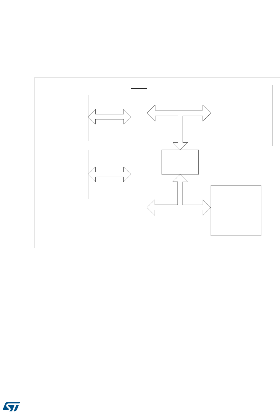
RM0394 Rev 4 115/1600
RM0394 Firewall (FW)
125
4.3 Firewall functional description
4.3.1 Firewall AMBA bus snoop
The Firewall peripheral is snooping the AMBA buses on which the memories (volatile and
non-volatile) are connected. A global architecture view is illustrated in Figure 5.
Figure 5. STM32L41xxx/42xxx/43xxx/44xxx/45xxx/46xxx firewall connection
schematics
4.3.2 Functional requirements
There are several requirements to guaranty the highest security level by the application
code/data which needs to be protected by the Firewall and to avoid unwanted Firewall alarm
(reset generation).
Debug consideration
In debug mode, if the Firewall is opened, the accesses by the debugger to the protected
segments are not blocked. For this reason, the Read out level 2 protection must be active in
conjunction with the Firewall implementation.
If the debug is needed, it is possible to proceed in the following way:
•A dummy code having the same API as the protected code may be developed during
the development phase of the final user code. This dummy code may send back
coherent answers (in terms of function and potentially timing if needed), as the
protected code should do in production phase.
•In the development phase, the protected code can be given to the customer-end under
NDA agreement and its software can be developed in level 0 protection. The customer-
0V99
&257(;0
'0$
,
1
7
(
5
)
$
&
(
%
8
6
0
$
7
5
,
;
),5(:$//
)/$6+
65$0
$+%0DVWHU
$+%0DVWHU
$+%6ODYH
$+%6ODYH

Firewall (FW) RM0394
116/1600 RM0394 Rev 4
end code needs to embed an IAP located in a write protected segment in order to allow
future code updates when the production parts will be Level 2 ROP.
Write protection
In order to offer a maximum security level, the following points need to be respected:
•It is mandatory to keep a write protection on the part of the code enabling the Firewall.
This activation code should be located outside the segments protected by the Firewall.
•The write protection is also mandatory on the code segment protected by the Firewall.
•The page including the reset vector must be write-protected.
Interrupts management
The code protected by the Firewall must not be interruptible. It is up to the user code to
disable any interrupt source before executing the code protected by the Firewall. If this
constraint is not respected, if an interruption comes while the protected code is executed
(Firewall opened), the Firewall will be closed as soon as the interrupt subroutine is
executed. When the code returns back to the protected code area, a Firewall alarm will raise
since the “call gate” sequence will not be applied and a reset will be generated.
Concerning the interrupt vectors and the first user page in the Flash memory:
•If the first user page (including the reset vector) is protected by the Firewall, the NVIC
vector should be reprogrammed outside the protected segment.
•If the first user page is not protected by the Firewall, the interrupt vectors may be kept
at this location.
There is no interrupt generated by the Firewall.
4.3.3 Firewall segments
The Firewall has been designed to protect three different segment areas:
Code segment
This segment is located into the Flash memory. It should contain the code to execute which
requires the Firewall protection. The segment must be reached using the “call gate” entry
sequence to open the Firewall. A system reset is generated if the “call gate” entry sequence
is not respected (refer to Opening the Firewall) and if the Firewall is enabled using the
FWDIS bit in the system configuration register. The length of the segment and the segment
base address must be configured before enabling the Firewall (refer to Section 4.3.5:
Firewall initialization).
Non-volatile data segment
This segment contains non-volatile data used by the protected code which must be
protected by the Firewall. The access to this segment is defined into Section 4.3.4: Segment
accesses and properties. The Firewall must be opened before accessing the data in this
area. The Non-Volatile data segment should be located into the Flash memory. The
segment length and the base address of the segment must be configured before enabling
the Firewall (refer to Section 4.3.5: Firewall initialization).

RM0394 Rev 4 117/1600
RM0394 Firewall (FW)
125
Volatile data segment
Volatile data used by the protected code located into the code segment must be defined into
the SRAM 1 memory. The access to this segment is defined into the Section 4.3.4: Segment
accesses and properties. Depending on the Volatile data segment configuration, the
Firewall must be opened or not before accessing this segment area. The segment length
and the base address of the segment as well as the segment options must be configured
before enabling the Firewall (refer to Section 4.3.5: Firewall initialization).
The Volatile data segment can also be defined as executable (for the code execution) or
shared using two bit of the Firewall configuration register (bit VDS for the volatile data
sharing option and bit VDE for the volatile data execution capability). For more details, refer
to Table 16.
4.3.4 Segment accesses and properties
All DMA accesses to the protected segments are forbidden, whatever the Firewall state, and
generate a system reset.
Segment access depending on the Firewall state
Each of the three segments has specific properties which are presented in Table 16.
Table 16. Segment accesses according to the Firewall state
Segment Firewall opened
access allowed
Firewall closed
access allowed
Firewall disabled
access allowed
Code segment Read and execute
No access allowed.
Any access to the segment
(except the “call gate” entry)
generates a system reset
All accesses are allowed
(according to the Flash page
protection properties in which
the code is located)
Non-volatile data
segment Read and write No access allowed
All accesses are allowed
(according to the Flash page
protection properties in which
the code is located)
Volatile data
segment
Read and Write
Execute if VDE = 1 and
VDS = 0 into the Firewall
configuration register
No access allowed if VDS = 0
and VDE = 0 into the Firewall
configuration register
Read/write/execute accesses
allowed if VDS = 1 (whatever
VDE bit value)
Execute if VDE = 1 and VDS = 0
but with a “call gate” entry to
open the Firewall at first.
All accesses are allowed
Firewall (FW) RM0394
118/1600 RM0394 Rev 4
The Volatile data segment is a bit different from the two others. The segment can be:
•Shared (VDS bit in the register)
It means that the area and the data located into this segment can be shared between
the protected code and the user code executed in a non-protected area. The access is
allowed whether the Firewall is opened or closed or disabled.
The VDS bit gets priority over the VDE bit, this last bit value being ignored in such a
case. It means that the Volatile data segment can execute parts of code located there
without any need to open the Firewall before executing the code.
•Execute
The VDE bit is considered as soon as the VDS bit = 0 in the FW_CR register. If the
VDS bit = 1, refer to the description above on the Volatile data segment sharing. If VDS
= 0 and VDE = 1, the Volatile data segment is executable. To avoid a system reset
generation from the Firewall, the “call gate” sequence should be applied on the Volatile
data segment to open the Firewall as an entry point for the code execution.
Segments properties
Each segment has a specific length register to define the segment size to be protected by
the Firewall: CSL register for the Code segment length register, NVDSL for the Non-volatile
data segment length register, and VDSL register for the Volatile data segment length
register. Granularity and area ranges for each of the segments are presented in Table 17.
4.3.5 Firewall initialization
The initialization phase should take place at the beginning of the user code execution (refer
to the Write protection).
The initialization phase consists of setting up the addresses and the lengths of each
segment which needs to be protected by the Firewall. It must be done before enabling the
Firewall, because the enabling bit can be written once. Thus, when the Firewall is enabled, it
cannot be disabled anymore until the next system reset.
Once the Firewall is enabled, the accesses to the address and length segments are no
longer possible. All write attempts are discarded.
A segment defined with a length equal to 0 is not considered as protected by the Firewall.
As a consequence, there is no reset generation from the Firewall when an access to the
base address of this segment is performed.
After a reset, the Firewall is disabled by default (FWDIS bit in the SYSCFG register is set). It
has to be cleared to enable the Firewall feature.
Table 17. Segment granularity and area ranges
Segment Granularity Area range
Code segment 256 byte 1024 Kbytes - 256 bytes
Non-volatile data segment 256 byte 1024 Kbytes - 256 bytes
Volatile data segment(1)
1. Applicable to STM32L43xxx and STM32L44xxx devices only.
64 byte 96 Kbytes - 64 bytes
Volatile data segment(2)
2. Applicable to STM32L45xxx and STM32L46xxx devices only.
64 byte 128 Kbyte - 64 byte

RM0394 Rev 4 119/1600
RM0394 Firewall (FW)
125
Below is the initialization procedure to follow:
1. Configure the RCC to enable the clock to the Firewall module
2. Configure the RCC to enable the clock of the system configuration registers
3. Set the base address and length of each segment (CSSA, CSL, NVDSSA, NVDSL,
VDSSA, VDSL registers)
4. Set the configuration register of the Firewall (FW_CR register)
5. Enable the Firewall clearing the FWDIS bit in the system configuration register.
The Firewall configuration register (FW_CR register) is the only one which can be managed
in a dynamic way even if the Firewall is enabled:
•when the Non-Volatile data segment is undefined (meaning the NVDSL register is
equal to 0), the accesses to this register are possible whatever the Firewall state
(opened or closed).
•when the Non-Volatile data segment is defined (meaning the NVDSL register is
different from 0), the accesses to this register are only possible when the Firewall is
opened.
4.3.6 Firewall states
The Firewall has three different states as shown in Figure 6:
•Disabled: The FWDIS bit is set by default after the reset. The Firewall is not active.
•Closed: The Firewall protects the accesses to the three segments (Code, Non-volatile
data, and Volatile data segments).
•Opened: The Firewall allows access to the protected segments as defined in
Section 4.3.4: Segment accesses and properties.
Figure 6. Firewall functional states
069
)LUHZDOOGLVDEOH
UHVHW
)LUHZDOO
FORVHG
)LUHZDOO
RSHQHG
(QDEOHWKHILUHZDOO
):',6
µµFDOOJDWH¶¶HQWU\
,OOHJDODFFHVVHVWR
WKHSURWHFWHG
VHJPHQWV
&RGHSURWHFWHGMXPSV
WRXQSURWHFWHG
VHJPHQWV
3URWHFWHGFRGHMXPSV
WRDQXQSURWHFWHG
VHJPHQWDQG)3$

Firewall (FW) RM0394
120/1600 RM0394 Rev 4
Opening the Firewall
As soon as the Firewall is enabled, it is closed. It means that most of the accesses to the
protected segments are forbidden (refer to Section 4.3.4: Segment accesses and
properties). In order to open the Firewall to interact with the protected segments, it is
mandatory to apply the “call gate” sequence described hereafter.
“call gate” sequence
The “call gate” is composed of 3 words located on the first three 32-bit addresses of the
base address of the code segment and of the Volatile data segment if it is declared as
not shared (VDS = 0) and executable (VDE = 1).
– 1st word: Dummy 32-bit words always closed in order to protect the “call gate”
opening from an access due to a prefetch buffer.
– 2nd and 3rd words: 2 specific 32-bit words called “call gate” and always opened.
To open the Firewall, the code currently executed must jump to the 2nd word of the “call
gate” and execute the code from this point. The 2nd word and 3rd word execution must not
be interrupted by any intermediate instruction fetch; otherwise, the Firewall is not
considered open and comes back to a close state. Then, executing the 3rd word after
receiving the intermediate instruction fetch would generate a system reset as a
consequence.
As soon as the Firewall is opened, the protected segments can be accessed as described in
Section 4.3.4: Segment accesses and properties.
Closing the Firewall
The Firewall is closed immediately after it is enabled (clearing the FWDIS bit in the system
configuration register).
To close the Firewall, the protected code must:
•Write the correct value in the Firewall Pre Arm Flag into the FW_CR register.
•Jump to any executable location outside the Firewall segments.
If the Firewall Pre Arm Flag is not set when the protected code jumps to a non protected
segment, a reset is generated. This control bit is an additional protection to avoid an
undesired attempt to close the Firewall with the private information not yet cleaned (see the
note below).
For security reasons, following the application for which the Firewall is used, it is advised to
clean all private information from CPU registers and hardware cells.

RM0394 Rev 4 121/1600
RM0394 Firewall (FW)
125
4.4 Firewall registers
4.4.1 Code segment start address (FW_CSSA)
Address offset: 0x00
Reset value: 0x0000 0000
4.4.2 Code segment length (FW_CSL)
Address offset: 0x04
Reset value: 0x0000 0000
31 30 29 28 27 26 25 24 23 22 21 20 19 18 17 16
Res. Res. Res. Res. Res. Res. Res. Res. ADD[23:16]
rw
15141312111098 7 6543210
ADD[15:8] Res. Res. Res. Res. Res. Res. Res. Res.
rw
Bits 31:24 Reserved, must be kept at reset value.
Bits 23:8 ADD[23:8]: code segment start address
The LSB bits of the start address (bit 7:0) are reserved and forced to 0 in order to allow a
256-byte granularity.
Note: These bits can be written only before enabling the Firewall. Refer to Section 4.3.5:
Firewall initialization.
Bits 7:0 Reserved, must be kept at the reset value.
31 30 29 28 27 26 25 24 23 22 21 20 19 18 17 16
Res. Res. Res. Res. Res. Res. Res. Res. Res. Res. LENG[21:16]
rw
1514131211109876543210
LENG15:8] Res. Res. Res. Res. Res. Res. Res. Res.
rw
Bits 31:22 Reserved, must be kept at the reset value.
Bits 21:8 LENG[21:8]: code segment length
LENG[21:8] selects the size of the code segment expressed in bytes but is a multiple of
256 bytes.
The segment area is defined from {ADD[23:8],0x00} to {ADD[23:8]+LENG[21:8], 0x00} - 0x01
Note: If LENG[21:8] = 0 after enabling the Firewall, this segment is not defined, thus not
protected by the Firewall.
These bits can only be written before enabling the Firewall. Refer to Section 4.3.5:
Firewall initialization.
Bits 7:0 Reserved, must be kept at the reset value.
Firewall (FW) RM0394
122/1600 RM0394 Rev 4
4.4.3 Non-volatile data segment start address (FW_NVDSSA)
Address offset: 0x08
Reset value: 0x0000 0000
4.4.4 Non-volatile data segment length (FW_NVDSL)
Address offset: 0x0C
Reset value: 0x0000 0000
31 30 29 28 27 26 25 24 23 22 21 20 19 18 17 16
Res. Res. Res. Res. Res. Res. Res. Res. ADD[23:16]
rw
15141312111098 7 6543210
ADD[15:8] Res. Res. Res. Res. Res. Res. Res. Res.
rw
Bits 31:24 Reserved, must be kept at the reset value.
Bits 23:8 ADD[23:8]: Non-volatile data segment start address
The LSB bits of the start address (bit 7:0) are reserved and forced to 0 in order to allow a
256-byte granularity.
Note: These bits can only be written before enabling the Firewall. Refer to Section 4.3.5:
Firewall initialization.
Bits 7:0 Reserved, must be kept at the reset value.
31 30 29 28 27 26 25 24 23 22 21 20 19 18 17 16
Res. Res. Res. Res. Res. Res. Res. Res. Res. Res. LENG[21:16]
rw
1514131211109876543210
LENG[15:8] Res. Res. Res. Res. Res. Res. Res. Res.
rw
Bits 31:22 Reserved, must be kept at the reset value.
Bits 21:8 LENG[21:8]: Non-volatile data segment length
LENG[21:8] selects the size of the Non-volatile data segment expressed in bytes but is a
multiple of 256 bytes.
The segment area is defined from {ADD[23:8],0x00} to {ADD[23:8]+LENG[21:8], 0x00} - 0x01
Note: If LENG[21:8] = 0 after enabling the Firewall, this segment is not defined, thus not
protected by the Firewall.
These bits can only be written before enabling the Firewall. Refer to Section 4.3.5:
Firewall initialization.
Bits 7:0 Reserved, must be kept at the reset value.

RM0394 Rev 4 123/1600
RM0394 Firewall (FW)
125
4.4.5 Volatile data segment start address (FW_VDSSA)
Address offset: 0x10
Reset value: 0x0000 0000
4.4.6 Volatile data segment length (FW_VDSL)
Address offset: 0x14
Reset value: 0x0000 0000
31 30 29 28 27 26 25 24 23 22 21 20 19 18 17 16
Res. Res. Res. Res. Res. Res. Res. Res. Res. Res. Res. Res. Res. Res. Res. ADD
[16]
rw
15141312111098 7 6543210
ADD[15:6] Res. Res. Res. Res. Res. Res.
rw
Bits 31:17 Reserved, must be kept at the reset value.
Bits 16:6 ADD[16:6]: Volatile data segment start address
The LSB bits of the start address (bit 5:0) are reserved and forced to 0 in order to allow a
64-byte granularity.
Note: These bits can only be written before enabling the Firewall. Refer to Section 4.3.5:
Firewall initialization
Bits 5:0 Reserved, must be kept at the reset value.
31 30 29 28 27 26 25 24 23 22 21 20 19 18 17 16
Res. Res. Res. Res. Res. Res. Res. Res. Res. Res. Res. Res. Res. Res. Res. LENG
[16]
rw
1514131211109876543210
LENG[15:6] Res. Res. Res. Res. Res. Res.
rw
Bits 31:17 Reserved, must be kept at the reset value.
Bits 16:6 LENG[16:6]: volatile data segment length
LENG[16:6] selects the size of the volatile data segment expressed in bytes but is a multiple
of 64 bytes.
The segment area is defined from {ADD[16:6],0x00} to {ADD[16:6]+LENG[16:6], 0x00} - 0x01
Note: If LENG[16:6] = 0 after enabling the Firewall, this segment is not defined, thus not
protected by the Firewall.
These bits can only be written before enabling the Firewall. Refer to Section 4.3.5:
Firewall initialization.
Bits 5:0 Reserved, must be kept at the reset value.

Firewall (FW) RM0394
124/1600 RM0394 Rev 4
4.4.7 Configuration register (FW_CR)
Address offset: 0x20
Reset value: 0x0000 0000
This register is protected in the same way as the Non-volatile data segment (refer to
Section 4.3.5: Firewall initialization).
31 30 29 28 27 26 25 24 23 22 21 20 19 18 17 16
Res. Res. Res. Res. Res. Res. Res. Res. Res. Res. Res. Res. Res. Res. Res. Res.
1514131211109876543210
Res. Res. Res. Res. Res. Res. Res. Res. Res. Res. Res. Res. Res. VDE VDS FPA
rw rw rw
Bits 31:3 Reserved, must be kept at the reset value.
Bit 2 VDE: Volatile data execution
0: Volatile data segment cannot be executed if VDS = 0
1: Volatile data segment is declared executable whatever VDS bit value
When VDS = 1, this bit has no meaning. The Volatile data segment can be executed whatever
the VDE bit value.
If VDS = 1, the code can be executed whatever the Firewall state (opened or closed)
If VDS = 0, the code can only be executed if the Firewall is opened or applying the “call gate”
entry sequence if the Firewall is closed.
Refer to Segment access depending on the Firewall state.
Bit 1 VDS: Volatile data shared
0: Volatile data segment is not shared and cannot be hit by a non protected executable code
when the Firewall is closed. If it is accessed in such a condition, a system reset will be
generated by the Firewall.
1: Volatile data segment is shared with non protected application code. It can be accessed
whatever the Firewall state (opened or closed).
Refer to Segment access depending on the Firewall state.
Bit 0 FPA: Firewall prearm
0: any code executed outside the protected segment when the Firewall is opened will
generate a system reset.
1: any code executed outside the protected segment will close the Firewall.
Refer to Closing the Firewall.

RM0394 Rev 4 125/1600
RM0394 Firewall (FW)
125
4.4.8 Firewall register map
The table below provides the Firewall register map and reset values.
Refer to Section 2.2.2 on page 67 for the register boundary addresses.
Table 18. Firewall register map and reset values
Offset Register
31
30
29
28
27
26
25
24
23
22
21
20
19
18
17
16
15
14
13
12
11
10
9
8
7
6
5
4
3
2
1
0
0x0 FW_CSSA
Res.
Res.
Res.
Res.
Res.
Res.
Res.
Res.
ADD
Res.
Res.
Res.
Res.
Res.
Res.
Res.
Res.
Reset Value 0000000000000000
0x4 FW_CSL
Res.
Res.
Res.
Res.
Res.
Res.
Res.
Res.
Res.
Res.
LENG
Res.
Res.
Res.
Res.
Res.
Res.
Res.
Res.
Reset Value 00000000000000
0x8 FW_NVDSSA
Res.
Res.
Res.
Res.
Res.
Res.
Res.
Res.
ADD
Res.
Res.
Res.
Res.
Res.
Res.
Res.
Res.
Reset Value 0000000000000000
0xC FW_NVDSL
Res.
Res.
Res.
Res.
Res.
Res.
Res.
Res.
Res.
Res.
LENG
Res.
Res.
Res.
Res.
Res.
Res.
Res.
Res.
Reset Value 00000000000000
0x10 FW_VDSSA
Res.
Res.
Res.
Res.
Res.
Res.
Res.
Res.
Res.
Res.
Res.
Res.
Res.
Res.
Res.
ADD
Res.
Res.
Res.
Res.
Res.
Res.
Reset Value 00000000000
0x14 FW_VDSL
Res.
Res.
Res.
Res.
Res.
Res.
Res.
Res.
Res.
Res.
Res.
Res.
Res.
Res.
Res.
LENG
Res.
Res.
Res.
Res.
Res.
Res.
Reset Value 00000000000
0x18
Res.
Res.
Res.
Res.
Res.
Res.
Res.
Res.
Res.
Res.
Res.
Res.
Res.
Res.
Res.
Res.
Res.
Res.
Res.
Res.
Res.
Res.
Res.
Res.
Res.
Res.
Res.
Res.
Res.
Res.
Res.
Res.
Reset Value
0x1C
Res.
Res.
Res.
Res.
Res.
Res.
Res.
Res.
Res.
Res.
Res.
Res.
Res.
Res.
Res.
Res.
Res.
Res.
Res.
Res.
Res.
Res.
Res.
Res.
Res.
Res.
Res.
Res.
Res.
Res.
Res.
Res.
Reset Value
0x20 FW_CR
Res.
Res.
Res.
Res.
Res.
Res.
Res.
Res.
Res.
Res.
Res.
Res.
Res.
Res.
Res.
Res.
Res.
Res.
Res.
Res.
Res.
Res.
Res.
Res.
Res.
Res.
Res.
Res.
Res.
VDE
VDS
FPA
Reset Value 000

Power control (PWR) RM0394
126/1600 RM0394 Rev 4
5 Power control (PWR)
5.1 Power supplies
The STM32L41xxx/42xxx/43xxx/44xxx/45xxx/46xxx devices require a 1.71 V to 3.6 V
operating supply voltage (VDD). Several peripherals are supplied through independent
power domains: VDDA, VDDUSB, VLCD. Those supplies must not be provided without a valid
operating supply on the VDD pin.
•VDD = 1.71 V to 3.6 V
VDD is the external power supply for the I/Os, the internal regulator and the system
analog such as reset, power management and internal clocks. It is provided externally
through VDD pins.
•VDD12 = 1.05 V to 1.32 V
External power supply, connected to VCORE, bypassing internal regulator when
connected to an external SMPS. It is provided externally through VDD12 pins and only
available on packages with the external SMPS supply option.
Note: On STM32L412xx and STM32L422xx devices, VDD12 range is extended down to 1.00 V
for better efficiency.
•VDDA = 1.62 V (ADCs/COMPs) / 1.8 V (DACs/OPAMPs) / 2.4 V (VREFBUF) to 3.6 V
VDDA is the external analog power supply for A/D converters, D/A converters, voltage
reference buffer, operational amplifiers and comparators. The VDDA voltage level is
independent from the VDD voltage. VDDA should be preferably connected to VDD when
these peripherals are not used.
•VDDUSB = 3.0 V to 3.6 V (available on STM32L4x2xx and STM32L4x3xx devices only)
VDDUSB is the external independent power supply for USB transceivers. The VDDUSB
voltage level is independent from the VDD voltage. VDDUSB should be preferably
connected to VDD when the USB is not used.
On small packages, VDDUSB power supply may not be present as a dedicated pin and
is internally bonded to VDD. For such devices, VDD has to respect the VDDUSB supply
range when USB is used.
•VLCD = 2.5 V to 3.6 V (available on STM32L4x3xx devices only)
The LCD controller can be powered either externally through VLCD pin, or internally
from an internal voltage generated by the embedded step-up converter. VLCD is
multiplexed with PC3 which can be used as GPIO when the LCD is not used.
•VBAT = 1.55 V to 3.6 V
VBAT is the power supply for RTC, external clock 32 kHz oscillator and backup registers
(through power switch) when VDD is not present. VBAT is internally bonded to VDD for
small packages without dedicated pin.
VBAT is internally bonded to VDD for small packages without dedicated pin.
•VREF-, VREF+
VREF+ is the input reference voltage for ADCs and DACs. It is also the output of the
internal voltage reference buffer when enabled.
When VDDA < 2 V, VREF+ must be equal to VDDA.

RM0394 Rev 4 127/1600
RM0394 Power control (PWR)
174
When VDDA 2 V, VREF+ must be between 2 V and VDDA.
VREF+ can be grounded when ADC and DAC are not active.
The internal voltage reference buffer supports two output voltages, which are
configured with VRS bit in the VREFBUF_CSR register:
–V
REF+ around 2.048 V. This requires VDDA equal to or higher than 2.4 V.
–V
REF+ around 2.5 V. This requires VDDA equal to or higher than 2.8 V.
VREF- and VREF+ pins are not available on all packages. When not available on the
package, they are bonded to VSSA and VDDA, respectively.
When the VREF+ is double-bonded with VDDA in a package, the internal voltage
reference buffer is not available and must be kept disable (refer to related device
datasheet for packages pinout description). Internal voltage reference buffer is not
supported on STM32L41xxx and STM32L42xxx devices, regardless the presence of
VREF+ pin.
VREF- must always be equal to VSSA.
An embedded linear voltage regulator is used to supply the internal digital power VCORE.
VCORE is the power supply for digital peripherals and memories.
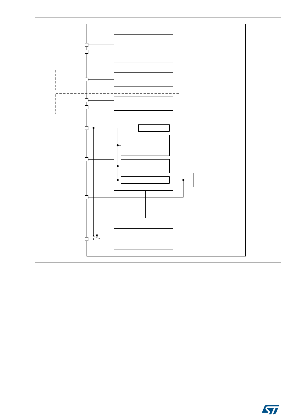
Power control (PWR) RM0394
128/1600 RM0394 Rev 4
Figure 7. Power supply overview
1. Available on STM32L4x3xx devices only.
2. Available on STM32L4x2xx and STM32L4x3xx devices only.
5.1.1 Independent analog peripherals supply
To improve ADC and DAC conversion accuracy and to extend the supply flexibility, the
analog peripherals have an independent power supply which can be separately filtered and
shielded from noise on the PCB.
•The analog peripherals voltage supply input is available on a separate VDDA pin.
•An isolated supply ground connection is provided on VSSA pin.
The VDDA supply voltage can be different from VDD. The presence of VDDA must be checked
before enabling any of the analog peripherals supplied by VDDA (A/D converter, D/A
converter, comparators, operational amplifier, voltage reference buffer).
The VDDA supply can be monitored by the Peripheral Voltage Monitoring, and compared
with two thresholds (1.65 V for PVM3 or 1.8 V for PVM4), refer to Section 5.2.3: Peripheral
Voltage Monitoring (PVM) for more details.
06Y9
/RZYROWDJHGHWHFWRU
9''$
9''$GRPDLQ
966
9''
9%$7
$'FRQYHUWHUV
&RPSDUDWRUV
'$FRQYHUWHUV
2SHUDWLRQDODPSOLILHUV
9ROWDJHUHIHUHQFHEXIIHU
9''GRPDLQ
,2ULQJ
966$
5HVHWEORFN
7HPSVHQVRU
3//+6,06,+6,
6WDQGE\FLUFXLWU\
:DNHXSORJLF,:'*
9ROWDJHUHJXODWRU
9'',2
/6(FU\VWDO.RVF
%.3UHJLVWHUV
5&&%'&5UHJLVWHU
57&
%DFNXSGRPDLQ
&RUH
0HPRULHV
'LJLWDOSHULSKHUDOV
9&25(GRPDLQ
9&25(
86%WUDQVFHLYHUV
9''86%
966
9''
9/&' /&'

RM0394 Rev 4 129/1600
RM0394 Power control (PWR)
174
When a single supply is used, VDDA can be externally connected to VDD through the
external filtering circuit in order to ensure a noise-free VDDA reference voltage.
ADC and DAC reference voltage
To ensure a better accuracy on low-voltage inputs and outputs, the user can connect to
VREF+ a separate reference voltage lower than VDDA. VREF+ is the highest voltage,
represented by the full scale value, for an analog input (ADC) or output (DAC) signal.
VREF+ can be provided either by an external reference or by an internal buffered voltage
reference (VREFBUF), except STM32L41xxx and STM32L42xxx devices, which does not
support VREFBUF.
The internal voltage reference is enabled by setting the ENVR bit in the Section 18.3.1:
VREFBUF control and status register (VREFBUF_CSR). The voltage reference is set to
2.5 V when the VRS bit is set and to 2.048 V when the VRS bit is cleared. The internal
voltage reference can also provide the voltage to external components through VREF+ pin.
Refer to the device datasheet and to Section 18: Voltage reference buffer (VREFBUF) for
further information.
5.1.2 Independent USB transceivers supply
This section is applicable to STM32L4x2xx and STM32L4x3xx devices only.
The USB transceivers are supplied from a separate VDDUSB power supply pin. VDDUSB
range is from 3.0 V to 3.6 V and is completely independent from VDD or VDDA.
On small packages, VDDUSB power supply may not be present as a dedicated pin, but
internally bonded to VDD. For such devices, VDD has to respect the VDDUSB supply range
when USB is used.
After reset, the USB features supplied by VDDUSB are logically and electrically isolated and
therefore are not available. The isolation must be removed before using the USB FS
peripheral, by setting the USV bit in the PWR_CR2 register, once the VDDUSB supply is
present.
The VDDUSB supply is monitored by the Peripheral Voltage Monitoring (PVM1) and
compared with the internal reference voltage (VREFINT
, around 1.2 V), refer to Section 5.2.3:
Peripheral Voltage Monitoring (PVM) for more details.
5.1.3 Independent LCD supply
This section is applicable to STM32L4x3xx devices only.
The VLCD pin is provided to control the contrast of the glass LCD. This pin can be used in
two ways:
•It can receive from an external circuitry the desired maximum voltage that is provided
on segment and common lines to the glass LCD by the microcontroller.
•It can also be used to connect an external capacitor that is used by the microcontroller
for its voltage step-up converter. This step-up converter is controlled by software to
provide the desired voltage to segment and common lines of the glass LCD.
The voltage provided to segment and common lines defines the contrast of the glass LCD
pixels. This contrast can be reduced when you configure the dead time between frames.
•When an external power supply is provided to the VLCD pin, it should range from 2.5 V

Power control (PWR) RM0394
130/1600 RM0394 Rev 4
to 3.6 V. It does not depend on VDD.
•When the LCD is based on the internal step-up converter, the VLCD pin should be
connected to a capacitor (see the product datasheet for further information).
5.1.4 Battery backup domain
To retain the content of the Backup registers and supply the RTC function when VDD is
turned off, the VBAT pin can be connected to an optional backup voltage supplied by a
battery or by another source.
VBAT pin is not available on low pin-count packages, VBAT is internally connected to VDD.
The VBAT pin powers the RTC unit, the LSE oscillator and the PC13 to PC15 I/Os, allowing
the RTC to operate even when the main power supply is turned off. The switch to the VBAT
supply is controlled by the power-down reset embedded in the Reset block.
Warning: During tRSTTEMPO (temporization at VDD startup) or after a PDR
has been detected, the power switch between VBAT and VDD
remains connected to VBAT
.
During the startup phase, if VDD is established in less than
tRSTTEMPO (refer to the datasheet for the value of tRSTTEMPO)
and VDD > VBAT + 0.6 V, a current may be injected into VBAT
through an internal diode connected between VDD and the
power switch (VBAT).
If the power supply/battery connected to the VBAT pin cannot
support this current injection, it is strongly recommended to
connect an external low-drop diode between this power
supply and the VBAT pin.
If no external battery is used in the application, it is recommended to connect VBAT
externally to VDD with a 100 nF external ceramic decoupling capacitor.
When the backup domain is supplied by VDD (analog switch connected to VDD), the
following pins are available:
•PC13, PC14 and PC15, which can be used as GPIO pins
•PC13, PC14 and PC15, which can be configured by RTC or LSE (refer to Section 36.3:
RTC functional description on page 1084)
•PA0/RTC_TAMP2 and PE6/RTC_TAMP3 when they are configured by the RTC as
tamper pins
Note: Due to the fact that the analog switch can transfer only a limited amount of current (3 mA),
the use of GPIO PC13 to PC15 in output mode is restricted: the speed has to be limited to
2 MHz with a maximum load of 30 pF and these I/Os must not be used as a current source
(e.g. to drive a LED).
When the backup domain is supplied by VBAT (analog switch connected to VBAT because
VDD is not present), the following functions are available:
•PC13, PC14 and PC15 can be controlled only by RTC or LSE (refer to Section 36.3:
RTC functional description)
•PA0/RTC_TAMP2 and PE6/RTC_TAMP3 when they are configured by the RTC as
tamper pins

RM0394 Rev 4 131/1600
RM0394 Power control (PWR)
174
Backup domain access
After a system reset, the backup domain (RTC registers and backup registers) is protected
against possible unwanted write accesses. To enable access to the backup domain,
proceed as follows:
1. Enable the power interface clock by setting the PWREN bits in the Section 6.4.18:
APB1 peripheral clock enable register 1 (RCC_APB1ENR1)
2. Set the DBP bit in the Power control register 1 (PWR_CR1) to enable access to the
backup domain
3. Select the RTC clock source in the Backup domain control register (RCC_BDCR).
4. Enable the RTC clock by setting the RTCEN [15] bit in the Backup domain control
register (RCC_BDCR).
VBAT battery charging
When VDD is present, It is possible to charge the external battery on VBAT through an
internal resistance.
The VBAT charging is done either through a 5 kOhm resistor or through a 1.5 kOhm resistor
depending on the VBRS bit value in the PWR_CR4 register.
The battery charging is enabled by setting VBE bit in the PWR_CR4 register. It is
automatically disabled in VBAT mode.
5.1.5 Voltage regulator
Two embedded linear voltage regulators supply all the digital circuitries, except for the
Standby circuitry and the backup domain. The main regulator output voltage (VCORE) can be
programmed by software to two different power ranges (Range 1 and Range 2) in order to
optimize the consumption depending on the system’s maximum operating frequency (refer
to Section 6.2.9: Clock source frequency versus voltage scaling and to Section 3.3.3: Read
access latency.
The voltage regulators are always enabled after a reset. Depending on the application
modes, the VCORE supply is provided either by the main regulator (MR) or by the low-power
regulator (LPR).
•In Run, Sleep and Stop 0 modes, both regulators are enabled and the main regulator
(MR) supplies full power to the VCORE domain (core, memories and digital peripherals).
•In low-power run and low-power sleep modes, the main regulator is off and the low-
power regulator (LPR) supplies low power to the VCORE domain, preserving the
contents of the registers, SRAM1 and SRAM2.
•In Stop 1 and Stop 2 modes, the main regulator is off and the low-power regulator
(LPR) supplies low power to the VCORE domain, preserving the contents of the
registers, SRAM1 and SRAM2.
•In Standby mode with SRAM2 content preserved (RRS bit is set in the PWR_CR3
register), the main regulator (MR) is off and the low-power regulator (LPR) provides the
supply to SRAM2 only. The core, digital peripherals (except Standby circuitry and
backup domain) and SRAM1 are powered off.
•In Standby mode, both regulators are powered off. The contents of the registers,
SRAM1 and SRAM2 is lost except for the Standby circuitry and the backup domain.
•In Shutdown mode, both regulators are powered off. When exiting from Shutdown
mode, a power-on reset is generated. Consequently, the contents of the registers,
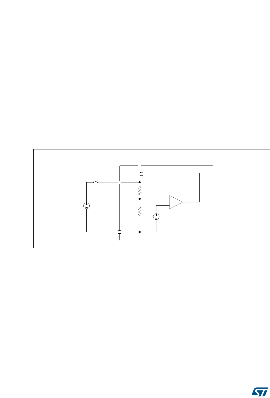
Power control (PWR) RM0394
132/1600 RM0394 Rev 4
SRAM1 and SRAM2 is lost, except for the backup domain.
5.1.6 VDD12 domain
VDD12 is intended to be connected with external SMPS (Switched-mode Power Supply) to
generate the VCORE logic supply in Run, Sleep and Stop 0 modes only.
VDD12 pins correspond to the internal VCORE powering the digital part of Core, memories
and peripherals. This improves significantly power consumption gain by 50% or more
depending of the SMPS performances.
The main benefit occurs in Run and Sleep modes whereas in Stop 0 mode, the gain is less
significant.
The Figure 8 shows a schematic to understand how the internal regulator stops supplying
VCORE when an external voltage VDD12 is provided.
As VDD12 shares the same pin as output of the internal regulator, applying a slightly higher
voltage (typically +50 mV) on the VDD12 blocks the PMOS and the regulator consumption
is negligible.
Figure 8. Internal main regulator overview
A switch, controlled by chosen GPIO, is inserted between the SMPS output and VDD12.
There are two possible states:
•Connected: Switch is closed so SMPS powers VDD12
•Disconnected: Switch is open and VDD12 is disconnected from SMPS output
Proper software management through GPIOs to enable/disable SMPS and
connect/disconnect SMPS through the switch, is required to conform with the rules
described below.
(See also Section 5.1.7: Dynamic voltage scaling management)
It is mandatory to respect the following rules to avoid any damage or instability on either
digital parts or internal regulators:
•In Run, Sleep and Stop 0 modes, VDD12 can be connected and should respect
–V
DD12 < 1.32 V
–V
DD12 VCORE + 50mV giving for Main Regulator
Range 1, VCORE = 1.2 V so VDD12 should be greater than 1.25 V
06Y9
6ZLWFK
3026
9ROWDJHUHJXODWRU
9''
9'' 9&25(
966
96036
5HI

RM0394 Rev 4 133/1600
RM0394 Power control (PWR)
174
Range 2, VCORE = 1.0 V so VDD12 should be greater than 1.05 V
–V
DD12 1.08 V in Range 2 when SYSCLK frequency 26 MHz
•In all other modes, ie LPRun, LPSleep, Stop 1, Stop 2, Standby and Shutdown modes,
VDD12 must be disconnected from SMPS output, ie pin must be connected to an high
impedance output:
– VDD12 connected to HiZ (voltage is provided by internal regulators)
•Transitions of VDD12 from connected to disconnected is only allowed when SYSCLK
frequency 26 MHz to avoid to big voltage drop on main regulator side.
Note: In case of reset while having the VDD12 ≤ 1.25 V, VDD12 should switch to HiZ in less than
regulator switching time from Range 2 to Range 1 (~1 us).
Note: On STM32L412xx and STM32L422xx devices, VDD12 Range 2 is extended down to 1.00 V
for better efficiency, thus following formula applies when bit EXT_SMPS_ON in the Power
control register 4 (PWR_CR4) is set:
Range 2, VCORE = 1.0 V so VDD12 should be greater than 1.00 V
Note: For more details on VDD12 management, refer to AN4978 "Design recommendations for
STM32L4xxxx with external SMPS, for ultra-low-power applications with high performance
5.1.7 Dynamic voltage scaling management
The dynamic voltage scaling is a power management technique which consists in
increasing or decreasing the voltage used for the digital peripherals (VCORE), according to
the application performance and power consumption needs.
Dynamic voltage scaling to increase VCORE is known as over-volting. It allows to improve
the device performance.
Dynamic voltage scaling to decrease VCORE is known as under-volting. It is performed to
save power, particularly in laptop and other mobile devices where the energy comes from a
battery and is thus limited.
•Range 1: High-performance range.
The main regulator provides a typical output voltage at 1.2 V. The system clock frequency
can be up to 80 MHz. The Flash access time for read access is minimum, write and erase
operations are possible.
•Range 2: Low-power range.
The main regulator provides a typical output voltage at 1.0 V. The system clock frequency
can be up to 26 MHz.The Flash access time for a read access is increased as compared to
Range 1; write and erase operations are possible.
Voltage scaling is selected through the VOS bit in the PWR_CR1 register.
The sequence to go from Range 1 to Range 2 is:
1.Reduce the system frequency to a value lower than 26 MHz
2. Adjust number of wait states according new frequency target in Range 2
(LATENCY bits in the FLASH_ACR).
3. Program the VOS bits to “10” in the PWR_CR1 register.
The sequence to go from Range 2 to Range 1 is:

Power control (PWR) RM0394
134/1600 RM0394 Rev 4
1. Program the VOS bits to “01” in the PWR_CR1 register.
2. Wait until the VOSF flag is cleared in the PWR_SR2 register.
3. Adjust number of wait states according new frequency target in Range 1
(LATENCY bits in the FLASH_ACR).
4. Increase the system frequency.
When supplying VDD12 with an external SMPS, we are defining 3 new states:
•“SMPS range 1”: main regulator is in Range 1 and VCORE is supplied by external
SMPS with VDD12 higher than 1.25 V
•“SMPS range 2 High”: main regulator is in Range 2 and VCORE is supplied by external
SMPS with VDD12 higher than 1.08 V
•“SMPS range 2 Low”: main regulator is in Range 2 and VCORE is supplied by external
SMPS with VDD12 higher than 1.05 V(a)
In order to match the upper rules described in Section 5.1.6: VDD12 domain, the transition
sequences can only be one of the following:
•Range 1 to “SMPS Range 1”:
1. Start SMPS converter (if not always enabled by HW).
2. Check that SMPS converter output is at the correct level i.e. 1.25 V VDD12 <
1.32 V.
3. Connect VDD12 to external SMPS converter through the switch.
•Range 2 to “SMPS Range 2 Low & High”:
1. Start SMPS (if not always enabled by HW).
2. Check that SMPS output is at the correct level ie 1.05 V(a) VDD12 < 1.32 V.
3. Connect VDD12 to external SMPS converter through the switch.
If 1.08 V VDD12 (ie SMPS Range 2 High), then the following steps can be applied:
4. Adjust the number of wait states in the FLASH_ACR (up to max frequency of
Range 1 refer to Section 3.3.3: Read access latency).
5. Increase the system frequency up to the maximum allowed value for Voltage
Range 1 (ie 80 MHz).
•“SMPS Range 1” to Range 1:
or
•SMPS Range 2 Low & High” to Range 2:
1. If in Range 1, reduce the system frequency to a value lower or equal to 26 MHz.
2. Adjust number of wait states according new frequency target corresponding to
Voltage Range (LATENCY bits in the FLASH_ACR).
3. Disconnect VDD12 by opening the switch.
4. Stop SMPS (if required and not kept always enabled).
If in Range 1, then the following step can be applied:
5. Increase the system frequency if needed.
a. On STM32L412xx and STM32L422xx devices, minimum limit of 1.00 V applies when bit EXT_SMPS_ON in
the Power control register 4 (PWR_CR4) is set.
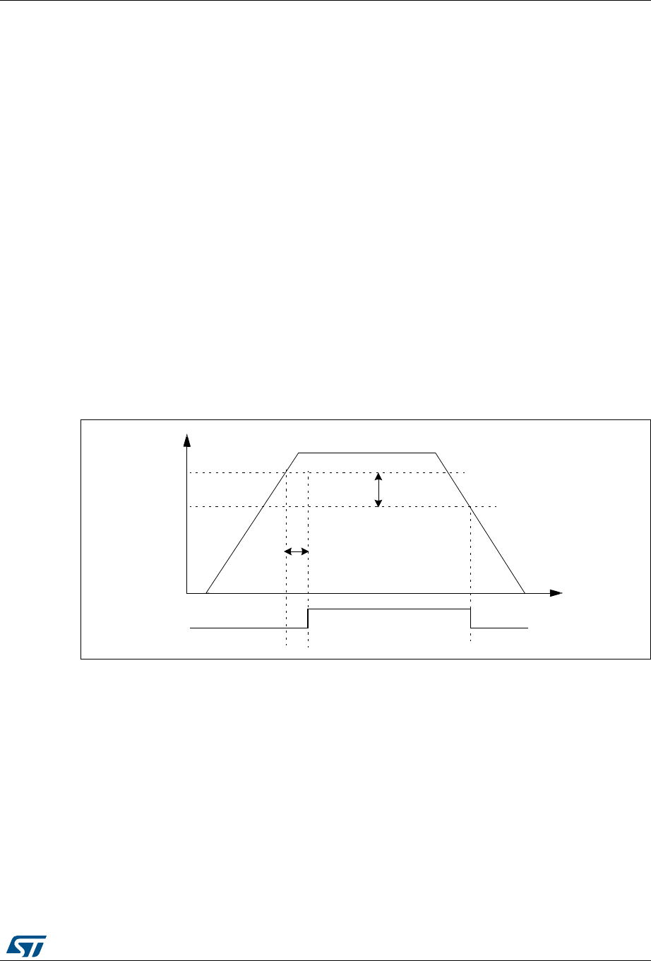
RM0394 Rev 4 135/1600
RM0394 Power control (PWR)
174
5.2 Power supply supervisor
5.2.1 Power-on reset (POR) / power-down reset (PDR) / brown-out reset
(BOR)
The device has an integrated power-on reset (POR) / power-down reset (PDR), coupled
with a brown-out reset (BOR) circuitry. The BOR is active in all power modes except
Shutdown mode, and cannot be disabled.
Five BOR thresholds can be selected through option bytes.
During power-on, the BOR keeps the device under reset until the supply voltage VDD
reaches the specified VBORx threshold. When VDD drops below the selected threshold, a
device reset is generated. When VDD is above the VBORx upper limit, the device reset is
released and the system can start.
For more details on the brown-out reset thresholds, refer to the electrical characteristics
section in the datasheet.
On STM32L412xx and STM32L422xx devices, continuous monitoring of the power supply
might be changed to periodical sampling to reduce power consumption in Stop2, Standby
and Shutdown modes by setting ENULP bit in Power control register 3 (PWR_CR3). When
sampling mode will be selected, fast supply drop between two samples will not be detected.
Figure 9. Brown-out reset waveform
1. The reset temporization tRSTTEMPO is present only for the BOR lowest threshold (VBOR0).
5.2.2 Programmable voltage detector (PVD)
You can use the PVD to monitor the VDD power supply by comparing it to a threshold
selected by the PLS[2:0] bits in the Power control register 2 (PWR_CR2).
The PVD is enabled by setting the PVDE bit.
A PVDO flag is available, in the Power status register 2 (PWR_SR2), to indicate if VDD is
higher or lower than the PVD threshold. This event is internally connected to the EXTI line16
and can generate an interrupt if enabled through the EXTI registers. The rising/falling edge
sensitivity of the EXTI Line16 should be configured according to PVD output behavior i.e. if
the EXTI line 16 is configured to rising edge sensitivity, the interrupt will be generated when
VDD drops below the PVD threshold. As an example the service routine could perform
emergency shutdown tasks.
069
9%25ULVLQJHGJH
K\VWHUHVLV
7HPSRUL]DWLRQ
W5677(032
5HVHW
9''
9%25IDOOLQJHGJH
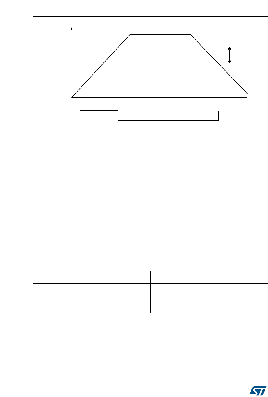
Power control (PWR) RM0394
136/1600 RM0394 Rev 4
Figure 10. PVD thresholds
5.2.3 Peripheral Voltage Monitoring (PVM)
Only VDD is monitored by default, as it is the only supply required for all system-related
functions. The other supplies (VDDA and VDDUSB) can be independent from VDD and can be
monitored with four Peripheral Voltage Monitoring (PVM).
Each of the three PVMx (x=1, 3, 4) is a comparator between a fixed threshold VPVMx and
the selected power supply. PVMOx flags indicate if the independent power supply is higher
or lower than the PVMx threshold: PVMOx flag is cleared when the supply voltage is above
the PVMx threshold, and is set when the supply voltage is below the PVMx threshold.
Each PVM output is connected to an EXTI line and can generate an interrupt if enabled
through the EXTI registers. The PVMx output interrupt is generated when the independent
power supply drops below the PVMx threshold and/or when it rises above the PVMx
threshold, depending on EXTI line rising/falling edge configuration.
Each PVM can remain active in Stop 0, Stop 1 and Stop 2 modes, and the PVM interrupt
can wake up from the Stop mode.
The independent supplies (VDDA and VDDUSB) are not considered as present by default,
and a logical and electrical isolation is applied to ignore any information coming from the
peripherals supplied by these dedicated supplies.
•If these supplies are shorted externally to VDD, the application should assume they are
available without enabling any Peripheral Voltage Monitoring.
•If these supplies are independent from VDD, the Peripheral Voltage Monitoring (PVM)
39'RXWSXW
9WKUHVKROG
39'
9
''
P9
K\VWHUHVLV
069
Table 19. PVM features
PVM Power supply PVM threshold EXTI line
PVM1(1)
1. Available on STM32L4x2xx and STM32L4x3xx devices only.
VDDUSB VPVM1 (around 1.2 V) 35
PVM3 VDDA VPVM3 (around 1.65 V) 37
PVM4 VDDA VPVM4 (around 1.8 V) 38

RM0394 Rev 4 137/1600
RM0394 Power control (PWR)
174
can be enabled to confirm whether the supply is present or not.
The following sequence must be done before using the USB FS peripheral on
STM32L4x2xx and STM32L4x3xx devices:
1. If VDDUSB is independent from VDD:
a) Enable the PVM1 by setting PVME1 bit in the Power control register 2
(PWR_CR2).
b) Wait for the PVM1 wakeup time
c) Wait until PVMO1 bit is cleared in the Power status register 2 (PWR_SR2).
d) Optional: Disable the PVM1 for consumption saving.
2. Set the USV bit in the Power control register 2 (PWR_CR2) to remove the VDDUSB
power isolation.
The following sequence must be done before using any of these analog peripherals: analog
to digital converters, digital to analog converters, comparators, operational amplifiers,
voltage reference buffer:
1. If VDDA is independent from VDD:
a) Enable the PVM3 (or PVM4) by setting PVME3 (or PVME4) bit in the Power
control register 2 (PWR_CR2).
b) Wait for the PVM3 (or PVM4) wakeup time
c) Wait until PVMO3 (or PVMO4) bit is cleared in the Power status register 2
(PWR_SR2).
d) Optional: Disable the PVM3 (or PVM4) for consumption saving.
2. Enable the analog peripheral, which automatically removes the VDDA isolation.
5.3 Low-power modes
By default, the microcontroller is in Run mode after a system or a power Reset. Several low-
power modes are available to save power when the CPU does not need to be kept running,
for example when waiting for an external event. It is up to the user to select the mode that
gives the best compromise between low-power consumption, short startup time and
available wakeup sources.
The device features seven low-power modes:
•Sleep mode: CPU clock off, all peripherals including Cortex®-M4 core peripherals such
as NVIC, SysTick, etc. can run and wake up the CPU when an interrupt or an event
occurs. Refer to Section 5.3.4: Sleep mode.
•Low-power run mode: This mode is achieved when the system clock frequency is
reduced below 2 MHz. The code is executed from the SRAM or the Flash memory. The
regulator is in low-power mode to minimize the regulator's operating current. Refer to
Section 5.3.2: Low-power run mode (LP run).
•Low-power sleep mode: This mode is entered from the Low-power run mode: Cortex®-
M4 is off. Refer to Section 5.3.5: Low-power sleep mode (LP sleep).
•Stop 0, Stop 1 and Stop 2 modes: SRAM1, SRAM2 and all registers content are
retained. All clocks in the VCORE domain are stopped, the PLL, the MSI, the HSI16 and
the HSE are disabled. The LSI and the LSE can be kept running.
The RTC can remain active (Stop mode with RTC, Stop mode without RTC).
Some peripherals with the wakeup capability can enable the HSI16 RC during the Stop

Power control (PWR) RM0394
138/1600 RM0394 Rev 4
mode to detect their wakeup condition.
In Stop 2 mode, most of the VCORE domain is put in a lower leakage mode.
Stop 1 offers the largest number of active peripherals and wakeup sources, a smaller
wakeup time but a higher consumption than Stop 2. In Stop 0 mode, the main regulator
remains ON, which allows the fastest wakeup time but with much higher consumption.
The active peripherals and wakeup sources are the same as in Stop 1 mode.
The system clock, when exiting from Stop 0, Stop 1 or Stop 2 mode, can be either MSI
up to 48 MHz or HSI16, depending on the software configuration.
Refer to Section 5.3.6: Stop 0 mode and Section 5.3.8: Stop 2 mode.
•Standby mode: VCORE domain is powered off. However, it is possible to preserve the
SRAM2 contents:
– Standby mode with SRAM2 retention when the bit RRS is set in PWR_CR3
register. In this case, SRAM2 is supplied by the low-power regulator.
– Standby mode when the bit RRS is cleared in PWR_CR3 register. In this case the
main regulator and the low-power regulator are powered off.
All clocks in the VCORE domain are stopped, the PLL, the MSI, the HSI16 and the HSE
are disabled. The LSI and the LSE can be kept running.
The RTC can remain active (Standby mode with RTC, Standby mode without RTC).
The system clock, when exiting Standby modes, is MSI from 1 MHz up to 8 MHz.
Refer to Section 5.3.9: Standby mode.
•Shutdown mode: VCORE domain is powered off. All clocks in the VCORE domain are
stopped, the PLL, the MSI, the HSI16, the LSI and the HSE are disabled. The LSE can
be kept running. The system clock, when exiting the Shutdown mode, is MSI at 4 MHz.
In this mode, the supply voltage monitoring is disabled and the product behavior is not
guaranteed in case of a power voltage drop. Refer to Section 5.3.10: Shutdown mode.
In addition, the power consumption in Run mode can be reduced by one of the following
means:
•Slowing down the system clocks
•Gating the clocks to the APB and AHB peripherals when they are unused.
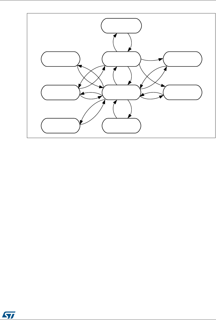
RM0394 Rev 4 139/1600
RM0394 Power control (PWR)
174
Figure 11. Low-power modes possible transitions
069
5XQPRGH
/RZSRZHUUXQPRGH
/RZSRZHUVOHHSPRGH
6WRSPRGH
6WRSPRGH
6KXWGRZQPRGH
6WDQGE\PRGH
6OHHSPRGH
6WRSPRGH

Power control (PWR) RM0394
140/1600 RM0394 Rev 4
Table 20. Low-power mode summary
Mode name Entry Wakeup
source(1)
Wakeup
system clock Effect on clocks
Voltage
regulators
MR LPR
Sleep
(Sleep-now or
Sleep-on-exit)
WFI or Return
from ISR Any interrupt Same as before
entering Sleep
mode
CPU clock OFF
no effect on other clocks
or analog clock sources
ON ON
WFE Wakeup event
Low-power
run Set LPR bit Clear LPR bit Same as Low-
power run clock None OFF ON
Low-power
sleep
Set LPR bit +
WFI or Return
from ISR
Any interrupt Same as before
entering Low-
power sleep
mode
CPU clock OFF
no effect on other clocks
or analog clock sources
OFF ON
Set LPR bit +
WFE Wakeup event OFF ON
Stop 0
LPMS=”000” +
SLEEPDEEP bit
+ WFI or Return
from ISR or WFE Any EXTI line
(configured in the
EXTI registers)
Specific
peripherals
events
HSI16 when
STOPWUCK=1 in
RCC_CFGR
MSI with the
frequency before
entering the Stop
mode when
STOPWUCK=0.
All clocks OFF except
LSI and LSE
ON
ON
Stop 1
LPMS=”001” +
SLEEPDEEP bit
+ WFI or Return
from ISR or WFE
OFF
Stop 2
LPMS=”010” +
SLEEPDEEP bit
+ WFI or Return
from ISR or WFE
Standby with
SRAM2
LPMS=”011”+
Set RRS bit +
SLEEPDEEP bit
+ WFI or Return
from ISR or WFE
WKUP pin edge,
RTC event,
external reset in
NRST pin,
IWDG reset MSI from 1 MHz
up to 8 MHz
Standby
LPMS=”011” +
Clear RRS bit +
SLEEPDEEP bit
+ WFI or Return
from ISR or WFE
WKUP pin edge,
RTC event,
external reset in
NRST pin,
IWDG reset
OFF OFF
Shutdown
LPMS=”1--” +
SLEEPDEEP bit
+ WFI or Return
from ISR or WFE
WKUP pin edge,
RTC event,
external reset in
NRST pin
MSI 4 MHz All clocks OFF except
LSE OFF OFF
1. Refer to Table 21: Functionalities depending on the working mode.

RM0394 Rev 4 141/1600
RM0394 Power control (PWR)
174
Table 21. Functionalities depending on the working mode(1)
Peripheral Run Sleep
Low-power run
Low-power sleep
Stop 0/1 Stop 2 Standby Shutdown
VBAT
-
Wakeup capability
-
Wakeup capability
-
Wakeup capability
-
Wakeup capability
CPU Y - Y - - ---- ----
Flash memory O(2) O(2) O(2) O(2) ----- ----
SRAM1 Y Y(3) YY
(3) Y-Y-- ----
SRAM2 Y Y(3) YY
(3) Y-Y-O
(4) ----
QUADSPI O O O O - ---- ----
Backup Registers YYYYY
-Y-Y -Y-Y
Brown-out reset (BOR) YYYYY
YYYY Y- --
Programmable Voltage
Detector (PVD) OOOOOOOO- ----
Peripheral Voltage Monitor
(PVMx; x=1,3,4) OOOOO
OOO- ----
DMA O O O O - ---- ----
Oscillator HSI16 O O O O (5) -(5) -- ----
Oscillator HSI48 O O - - - ---- ----
High Speed External (HSE) O O O O - ---- ----
Low Speed Internal (LSI) O O O O O -O-O ----
Low Speed External (LSE) O O O O O -O-O -O-O
Multi-Speed Internal (MSI) O O O O - ---- ----
Clock Security System
(CSS) OOOO-
---- ----
Clock Security System on
LSE OOOOO
OOOO O- --
RTC / Auto wakeup O O O O O OOOO OOOO
Number of RTC Tamper
pins 33333O3O3O3O3
LCD(6) OOOOOOOO- ----
USB FS (7) O(15) O(15) ---O- -- ----
USARTx (x=1,2,3(8),4(9))OOOO
O
(10)
O
(10) --- ----

Power control (PWR) RM0394
142/1600 RM0394 Rev 4
Low-power UART
(LPUART1) OOOO
O
(10)
O
(10)
O(1
0)
O
(10) -----
I2Cx (x=1,2,4(9))OOOO
O
(11)
O
(11) --- ----
I2C3 OOOO
O
(11)
O
(11)
O
(11)
O
(11) -----
SPIx (x=1,2(8),3) O O O O - ---- ----
CAN(12) OOOO----- ----
SDMMC1(8)(12) OOOO----- ----
SWPMI1 O O O O - O- -- ----
SAIx (x=1)(12) OOOO----- ----
DFSDM1(9) OOOO----- ----
ADCx (x=1,2(14))OOOO----- ----
DACx (x=1(12),2(13))OOOOO---- ----
VREFBUF(19) OOOOO---- ----
OPAMPx (x=1) O O O O O ---- ----
COMPx (x=1,2(19))OOOOOOOO- ----
Temperature sensor O O O O - ---- ----
Timers (TIMx) O O O O - ---- ----
Low-power timer 1
(LPTIM1) OOOOO
OOO- ----
Low-power timer 2
(LPTIM2) OOOOO
OO
(14) O- ----
Independent watchdog
(IWDG) OOOOO
OOOO O- --
Window watchdog (WWDG) O O O O - ---- ----
SysTick timer O O O O - ---- ----
Touch sensing controller
(TSC) OOOO-
---- ----
Random number generator
(RNG) O(15) O(15) ------- ----
Table 21. Functionalities depending on the working mode(1) (continued)
Peripheral Run Sleep
Low-power run
Low-power sleep
Stop 0/1 Stop 2 Standby Shutdown
VBAT
-
Wakeup capability
-
Wakeup capability
-
Wakeup capability
-
Wakeup capability

RM0394 Rev 4 143/1600
RM0394 Power control (PWR)
174
Debug mode
By default, the debug connection is lost if the application puts the MCU in Stop 0, Stop1,
Stop 2, Standby or Shutdown mode while the debug features are used. This is due to the
fact that the Cortex®-M4 core is no longer clocked.
However, by setting some configuration bits in the DBGMCU_CR register, the software can
be debugged even when using the low-power modes extensively. For more details, refer to
Section 46.16.1: Debug support for low-power modes.
AES hardware
accelerator(16) OOOO----- ----
CRC calculation unit O O O O - ---- ----
GPIOs O O O O O OOO(17)
up
to 5
pins
(18)
(19)
up
to 5
pins
(18)
-
1. Legend: Y = Yes (Enable). O = Optional (Disable by default. Can be enabled by software). - = Not available.
2. The Flash can be configured in power-down mode. By default, it is not in power-down mode.
3. The SRAM clock can be gated on or off.
4. SRAM2 content is preserved when the bit RRS is set in PWR_CR3 register.
5. Some peripherals with wakeup from Stop capability can request HSI16 to be enabled. In this case, HSI16 is woken up by
the peripheral, and only feeds the peripheral which requested it. HSI16 is automatically put off when the peripheral does not
need it anymore.
6. Available on STM32L4x3xx devices only.
7. Available on STM32L4x2xx and STM32L4x3xx devices only.
8. Not available on STM32L432xx and STM32L442xx devices.
9. Available on STM32L45xxx and STM32L46xxx devices only.
10. UART and LPUART reception is functional in Stop mode, and generates a wakeup interrupt on Start, address match or
received frame event.
11. I2C address detection is functional in Stop mode, and generates a wakeup interrupt in case of address match.
12. Not available on STM32L41xxx and STM32L42xxx devices.
13. Available on STM32L43xxx/44xxx devices only.
14. Available on STM32L41xxx and STM32L42xxx devices only.
15. Voltage scaling Range 1, SMPS Range 1 or SMPS Range 2 High only.
16. Available on STM32L42xxx, STM32L44xxx and STM32L46xxx devices only.
17. I/Os can be configured with internal pull-up, pull-down or floating in Standby mode.
18. The I/Os with wakeup from Standby/Shutdown capability are: PA0, PC13, PE6, PA2, PC5.
19. I/Os can be configured with internal pull-up, pull-down or floating in Shutdown mode but the configuration is lost when
exiting the Shutdown mode.
Table 21. Functionalities depending on the working mode(1) (continued)
Peripheral Run Sleep
Low-power run
Low-power sleep
Stop 0/1 Stop 2 Standby Shutdown
VBAT
-
Wakeup capability
-
Wakeup capability
-
Wakeup capability
-
Wakeup capability

Power control (PWR) RM0394
144/1600 RM0394 Rev 4
5.3.1 Run mode
Slowing down system clocks
In Run mode, the speed of the system clocks (SYSCLK, HCLK, PCLK) can be reduced by
programming the prescaler registers. These prescalers can also be used to slow down the
peripherals before entering the Sleep mode.
For more details, refer to Section 6.4.3: Clock configuration register (RCC_CFGR).
Peripheral clock gating
In Run mode, the HCLK and PCLK for individual peripherals and memories can be stopped
at any time to reduce the power consumption.
To further reduce the power consumption in Sleep mode, the peripheral clocks can be
disabled prior to executing the WFI or WFE instructions.
The peripheral clock gating is controlled by the RCC_AHBxENR and RCC_APBxENR
registers.
Disabling the peripherals clocks in Sleep mode can be performed automatically by resetting
the corresponding bit in the RCC_AHBxSMENR and RCC_APBxSMENR registers.
5.3.2 Low-power run mode (LP run)
To further reduce the consumption when the system is in Run mode, the regulator can be
configured in low-power mode. In this mode, the system frequency should not exceed
2MHz.
Please refer to the product datasheet for more details on voltage regulator and peripherals
operating conditions.
I/O states in Low-power run mode
In Low-power run mode, all I/O pins keep the same state as in Run mode.
Entering the Low-power run mode
To enter the Low-power run mode, proceed as follows:
1. Optional: Jump into the SRAM and power-down the Flash by setting the RUN_PD bit in
the Flash access control register (FLASH_ACR).
2. Decrease the system clock frequency below 2 MHz.
3. Force the regulator in low-power mode by setting the LPR bit in the PWR_CR1 register.
Refer to Table 22: Low-power run on how to enter the Low-power run mode.
Exiting the Low-power run mode
To exit the Low-power run mode, proceed as follows:
1. Force the regulator in main mode by clearing the LPR bit in the PWR_CR1 register.
2. Wait until REGLPF bit is cleared in the PWR_SR2 register.
3. Increase the system clock frequency.
Refer to Table 22: Low-power run on how to exit the Low-power run mode.

RM0394 Rev 4 145/1600
RM0394 Power control (PWR)
174
5.3.3 Low power modes
Entering low power mode
Low power modes are entered by the MCU by executing the WFI (Wait For Interrupt), or
WFE (Wait for Event) instructions, or when the SLEEPONEXIT bit in the Cortex®-M4
System Control register is set on Return from ISR.
Entering Low-power mode through WFI or WFE will be executed only if no interrupt is
pending or no event is pending.
Exiting low power mode
From Sleep modes, and Stop modes the MCU exit low power mode depending on the way
the low power mode was entered:
•If the WFI instruction or Return from ISR was used to enter the low power mode, any
peripheral interrupt acknowledged by the NVIC can wake up the device.
•If the WFE instruction is used to enter the low power mode, the MCU exits the low
power mode as soon as an event occurs. The wakeup event can be generated either
by:
– NVIC IRQ interrupt.
- When SEVONPEND = 0 in the Cortex®-M4 System Control register. By enabling
an interrupt in the peripheral control register and in the NVIC. When the MCU
resumes from WFE, the peripheral interrupt pending bit and the NVIC peripheral
IRQ channel pending bit (in the NVIC interrupt clear pending register) have to be
cleared.
Only NVIC interrupts with sufficient priority will wakeup and interrupt the MCU.
- When SEVONPEND = 1 in the Cortex®-M4 System Control register.
By enabling an interrupt in the peripheral control register and optionally in the
NVIC. When the MCU resumes from WFE, the peripheral interrupt pending bit and
Table 22. Low-power run
Low-power run mode Description
Mode entry Decrease the system clock frequency below 2 MHz
LPR = 1
Mode exit
LPR = 0
Wait until REGLPF = 0
Increase the system clock frequency
Wakeup latency Regulator wakeup time from low-power mode

Power control (PWR) RM0394
146/1600 RM0394 Rev 4
when enabled the NVIC peripheral IRQ channel pending bit (in the NVIC interrupt
clear pending register) have to be cleared.
All NVIC interrupts will wakeup the MCU, even the disabled ones. Only enabled
NVIC interrupts with sufficient priority will wakeup and interrupt the MCU.
–Event
Configuring a EXTI line in event mode. When the CPU resumes from WFE, it is
not necessary to clear the EXTI peripheral interrupt pending bit or the NVIC IRQ
channel pending bit as the pending bits corresponding to the event line is not set.
It may be necessary to clear the interrupt flag in the peripheral.
From Standby modes, and Shutdown modes the MCU exit low power mode through an
external reset (NRST pin), an IWDG reset, a rising edge on one of the enabled WKUPx pins
or a RTC event occurs (see Figure 351: RTC block diagrams).
After waking up from Standby or Shutdown mode, program execution restarts in the same
way as after a Reset (boot pin sampling, option bytes loading, reset vector is fetched, etc.).
5.3.4 Sleep mode
I/O states in Sleep mode
In Sleep mode, all I/O pins keep the same state as in Run mode.
Entering the Sleep mode
The Sleep mode is entered according Section : Entering low power mode, when the
SLEEPDEEP bit in the Cortex®-M4 System Control register is clear.
Refer to Table 23: Sleep for details on how to enter the Sleep mode.
Exiting the Sleep mode
The Sleep mode is exit according Section : Exiting low power mode.
Refer to Table 23: Sleep for more details on how to exit the Sleep mode.
Table 23. Sleep
Sleep-now mode Description
Mode entry
WFI (Wait for Interrupt) or WFE (Wait for Event) while:
– SLEEPDEEP = 0
– No interrupt (for WFI) or event (for WFE) is pending
Refer to the Cortex®-M4 System Control register.
On return from ISR while:
– SLEEPDEEP = 0 and
– SLEEPONEXIT = 1
– No interrupt is pending
Refer to the Cortex®-M4 System Control register.

RM0394 Rev 4 147/1600
RM0394 Power control (PWR)
174
5.3.5 Low-power sleep mode (LP sleep)
Please refer to the product datasheet for more details on voltage regulator and peripherals
operating conditions.
I/O states in Low-power sleep mode
In Low-power sleep mode, all I/O pins keep the same state as in Run mode.
Entering the Low-power sleep mode
The Low-power sleep mode is entered from low-power run mode according Section :
Entering low power mode, when the SLEEPDEEP bit in the Cortex®-M4 System Control
register is clear.
Refer to Table 24: Low-power sleep for details on how to enter the Low-power sleep mode.
Exiting the Low-power sleep mode
The low-power Sleep mode is exit according Section : Exiting low power mode. When
exiting the Low-power sleep mode by issuing an interrupt or an event, the MCU is in Low-
power run mode.
Refer to Table 24: Low-power sleep for details on how to exit the Low-power sleep mode.
Mode exit
If WFI or return from ISR was used for entry
Interrupt: refer to Table 46:
STM32L41xxx/42xxx/43xxx/44xxx/45xxx/46xxx vector table
If WFE was used for entry and SEVONPEND = 0:
Wakeup event: refer to Section 13.3.2: Wakeup event management
If WFE was used for entry and SEVONPEND = 1:
Interrupt even when disabled in NVIC: refer to Table 46:
STM32L41xxx/42xxx/43xxx/44xxx/45xxx/46xxx vector table or Wakeup
event: refer to Section 13.3.2: Wakeup event management
Wakeup latency None
Table 23. Sleep (continued)
Sleep-now mode Description

Power control (PWR) RM0394
148/1600 RM0394 Rev 4
5.3.6 Stop 0 mode
The Stop 0 mode is based on the Cortex®-M4 deepsleep mode combined with the
peripheral clock gating. The voltage regulator is configured in main regulator mode. In Stop
0 mode, all clocks in the VCORE domain are stopped; the PLL, the MSI, the HSI16 and the
HSE oscillators are disabled. Some peripherals with the wakeup capability (I2Cx (x=1,2,3),
U(S)ARTx(x=1,2,3) and LPUART) can switch on the HSI16 to receive a frame, and switch
off the HSI16 after receiving the frame if it is not a wakeup frame. In this case, the HSI16
clock is propagated only to the peripheral requesting it.
SRAM1, SRAM2 and register contents are preserved.
The BOR is always available in Stop 0 mode. The consumption is increased when
thresholds higher than VBOR0 are used.
I/O states in Stop 0 mode
In the Stop 0 mode, all I/O pins keep the same state as in the Run mode.
Entering the Stop 0 mode
The Stop 0 mode is entered according Section : Entering low power mode, when the
SLEEPDEEP bit in the Cortex®-M4 System Control register is set.
Table 24. Low-power sleep
Low-power sleep-now
mode Description
Mode entry
Low-power sleep mode is entered from the Low-power run mode.
WFI (Wait for Interrupt) or WFE (Wait for Event) while:
– SLEEPDEEP = 0
– No interrupt (for WFI) or event (for WFE) is pending
Refer to the Cortex®-M4 System Control register.
Low-power sleep mode is entered from the Low-power run mode.
On return from ISR while:
– SLEEPDEEP = 0 and
– SLEEPONEXIT = 1
– No interrupt is pending
Refer to the Cortex®-M4 System Control register.
Mode exit
If WFI or Return from ISR was used for entry
Interrupt: refer to Table 46:
STM32L41xxx/42xxx/43xxx/44xxx/45xxx/46xxx vector table
If WFE was used for entry and SEVONPEND = 0:
Wakeup event: refer to Section 13.3.2: Wakeup event management
If WFE was used for entry and SEVONPEND = 1:
Interrupt even when disabled in NVIC: refer to Table 46:
STM32L41xxx/42xxx/43xxx/44xxx/45xxx/46xxx vector table
Wakeup event: refer to Section 13.3.2: Wakeup event management
After exiting the Low-power sleep mode, the MCU is in Low-power run
mode.
Wakeup latency None

RM0394 Rev 4 149/1600
RM0394 Power control (PWR)
174
Refer to Table 25: Stop 0 mode for details on how to enter the Stop 0 mode.
If Flash memory programming is ongoing, the Stop 0 mode entry is delayed until the
memory access is finished.
If an access to the APB domain is ongoing, The Stop 0 mode entry is delayed until the APB
access is finished.
In Stop 0 mode, the following features can be selected by programming individual control
bits:
•Independent watchdog (IWDG): the IWDG is started by writing to its Key register or by
hardware option. Once started, it cannot be stopped except by a Reset. See
Section 32.3: IWDG functional description.
•real-time clock (RTC): this is configured by the RTCEN bit in the Backup domain
control register (RCC_BDCR)
•Internal RC oscillator (LSI): this is configured by the LSION bit in the Control/status
register (RCC_CSR).
•External 32.768 kHz oscillator (LSE): this is configured by the LSEON bit in the Backup
domain control register (RCC_BDCR).
Several peripherals can be used in Stop 0 mode and can add consumption if they are
enabled and clocked by LSI or LSE, or when they request the HSI16 clock: LCD, LPTIM1,
LPTIM2, I2Cx (x=1,2,3,4) U(S)ARTx(x=1,2,3,4), LPUART.
The DACx (x=1,2), the OPAMP and the comparators can be used in Stop 0 mode, the PVMx
(x=1,3,4) and the PVD as well. If they are not needed, they must be disabled by software to
save their power consumptions.
The ADCx (x=1), temperature sensor and VREFBUF buffer can consume power during the
Stop 0 mode, unless they are disabled before entering this mode.
Exiting the Stop 0 mode
The Stop 0 mode is exit according Section : Entering low power mode.
Refer to Table 25: Stop 0 mode for details on how to exit Stop 0 mode.
When exiting Stop 0 mode by issuing an interrupt or a wakeup event, the HSI16 oscillator is
selected as system clock if the bit STOPWUCK is set in Clock configuration register
(RCC_CFGR). The MSI oscillator is selected as system clock if the bit STOPWUCK is
cleared. The wakeup time is shorter when HSI16 is selected as wakeup system clock. The
MSI selection allows wakeup at higher frequency, up to 48 MHz.
When exiting the Stop 0 mode, the MCU is either in Run mode Range 1 or Run Mode Range
2 depending on VOS bit in PWR_CR1.

Power control (PWR) RM0394
150/1600 RM0394 Rev 4
5.3.7 Stop 1 mode
The Stop 1 mode is the same as Stop 0 mode except that the main regulator is OFF, and
only the low-power regulator is ON. Stop 1 mode can be entered from Run mode and from
Low-power run mode.
Refer to Table 26: Stop 1 mode for details on how to enter and exit Stop 1 mode.
Table 25. Stop 0 mode
Stop 0 mode Description
Mode entry
WFI (Wait for Interrupt) or WFE (Wait for Event) while:
– SLEEPDEEP bit is set in Cortex®-M4 System Control register
– No interrupt (for WFI) or event (for WFE) is pending
– LPMS = “000” in PWR_CR1
On Return from ISR while:
– SLEEPDEEP bit is set in Cortex®-M4 System Control register
– SLEEPONEXIT = 1
– No interrupt is pending
– LPMS = “000” in PWR_CR1
Note: To enter Stop 0 mode, all EXTI Line pending bits (in Pending
register 1 (EXTI_PR1)), and the peripheral flags generating wakeup
interrupts must be cleared. Otherwise, the Stop 0 mode entry
procedure is ignored and program execution continues.
Mode exit
If WFI or Return from ISR was used for entry
Any EXTI Line configured in Interrupt mode (the corresponding EXTI
Interrupt vector must be enabled in the NVIC). The interrupt source can
be external interrupts or peripherals with wakeup capability. Refer to
Table 46: STM32L41xxx/42xxx/43xxx/44xxx/45xxx/46xxx vector table.
If WFE was used for entry and SEVONPEND = 0:
Any EXTI Line configured in event mode. Refer to Section 13.3.2:
Wakeup event management.
If WFE was used for entry and SEVONPEND = 1:
Any EXTI Line configured in Interrupt mode (even if the corresponding
EXTI Interrupt vector is disabled in the NVIC). The interrupt source can
be external interrupts or peripherals with wakeup capability. Refer
toTable 46: STM32L41xxx/42xxx/43xxx/44xxx/45xxx/46xxx vector table.
Wakeup event: refer to Section 13.3.2: Wakeup event management
Wakeup latency Longest wakeup time between: MSI or HSI16 wakeup time and Flash
wakeup time from Stop 0 mode.

RM0394 Rev 4 151/1600
RM0394 Power control (PWR)
174
5.3.8 Stop 2 mode
The Stop 2 mode is based on the Cortex®-M4 deepsleep mode combined with peripheral
clock gating. In Stop 2 mode, all clocks in the VCORE domain are stopped, the PLL, the MSI,
the HSI16 and the HSE oscillators are disabled. Some peripherals with wakeup capability
(I2C3 and LPUART) can switch on the HSI16 to receive a frame, and switch off the HSI16
after receiving the frame if it is not a wakeup frame. In this case the HSI16 clock is
propagated only to the peripheral requesting it.
SRAM1, SRAM2 and register contents are preserved.
The BOR is always available in Stop 2 mode. The consumption is increased when
thresholds higher than VBOR0 are used.
Note: The comparators outputs, the LPUART outputs and the LPTIM1 outputs are forced to low
speed (OSPEEDy=00) during the Stop 2 mode.
Table 26. Stop 1 mode
Stop 1 mode Description
Mode entry
WFI (Wait for Interrupt) or WFE (Wait for Event) while:
– SLEEPDEEP bit is set in Cortex®-M4 System Control register
– No interrupt (for WFI) or event (for WFE) is pending
– LPMS = “001” in PWR_CR1
On Return from ISR while:
– SLEEPDEEP bit is set in Cortex®-M4 System Control register
– SLEEPONEXIT = 1
– No interrupt is pending
– LPMS = “001” in PWR_CR1
Note: To enter Stop 1 mode, all EXTI Line pending bits (in Pending
register 1 (EXTI_PR1)), and the peripheral flags generating wakeup
interrupts must be cleared. Otherwise, the Stop 1 mode entry
procedure is ignored and program execution continues.
Mode exit
If WFI or Return from ISR was used for entry
Any EXTI Line configured in Interrupt mode (the corresponding EXTI
Interrupt vector must be enabled in the NVIC). The interrupt source can
be external interrupts or peripherals with wakeup capability. Refer to
Table 46: STM32L41xxx/42xxx/43xxx/44xxx/45xxx/46xxx vector table.
If WFE was used for entry and SEVONPEND = 0:
Any EXTI Line configured in event mode. Refer to Section 13.3.2:
Wakeup event management.
If WFE was used for entry and SEVONPEND = 1:
Any EXTI Line configured in Interrupt mode (even if the corresponding
EXTI Interrupt vector is disabled in the NVIC). The interrupt source can
be external interrupts or peripherals with wakeup capability. Refer
toTable 46: STM32L41xxx/42xxx/43xxx/44xxx/45xxx/46xxx vector table.
Wakeup event: refer to Section 13.3.2: Wakeup event management
Wakeup latency
Longest wakeup time between: MSI or HSI16 wakeup time and regulator
wakeup time from Low-power mode + Flash wakeup time from Stop 1
mode.

Power control (PWR) RM0394
152/1600 RM0394 Rev 4
I/O states in Stop 2 mode
In the Stop 2 mode, all I/O pins keep the same state as in the Run mode.
Entering Stop 2 mode
The Stop 2 mode is entered according Section : Entering low power mode, when the
SLEEPDEEP bit in the Cortex®-M4 System Control register is set.
Refer to Table 27: Stop 2 mode for details on how to enter the Stop 2 mode.
Stop 2 mode can only be entered from Run mode. It is not possible to enter Stop 2 mode
from the Low-power run mode.
If Flash memory programming is ongoing, the Stop 2 mode entry is delayed until the
memory access is finished.
If an access to the APB domain is ongoing, The Stop 2 mode entry is delayed until the APB
access is finished.
In Stop 2 mode, the following features can be selected by programming individual control
bits:
•Independent watchdog (IWDG): the IWDG is started by writing to its Key register or by
hardware option. Once started it cannot be stopped except by a Reset. See
Section 32.3: IWDG functional description in Section 32: Independent watchdog
(IWDG).
•Real-time clock (RTC): this is configured by the RTCEN bit in the Backup domain
control register (RCC_BDCR)
•Internal RC oscillator (LSI): this is configured by the LSION bit in the Control/status
register (RCC_CSR).
•External 32.768 kHz oscillator (LSE): this is configured by the LSEON bit in the Backup
domain control register (RCC_BDCR).
Several peripherals can be used in Stop 2 mode and can add consumption if they are
enabled and clocked by LSI or LSE, or when they request the HSI16 clock: LCD, LPTIM1,
I2C3, LPUART.
The comparators can be used in Stop 2 mode, the PVMx (x=1,3,4) and the PVD as well. If
they are not needed, they must be disabled by software to save their power consumptions.
The ADCx, OPAMPx, DACx, temperature sensor and VREFBUF buffer can consume power
during Stop 2 mode, unless they are disabled before entering this mode.
All the peripherals which cannot be enabled in Stop 2 mode must be either disabled by
clearing the Enable bit in the peripheral itself, or put under reset state by setting the
corresponding bit in the AHB1 peripheral reset register (RCC_AHB1RSTR), AHB2
peripheral reset register (RCC_AHB2RSTR), AHB3 peripheral reset register
(RCC_AHB3RSTR), APB1 peripheral reset register 1 (RCC_APB1RSTR1), APB1
peripheral reset register 2 (RCC_APB1RSTR2), APB2 peripheral reset register
(RCC_APB2RSTR).
Exiting Stop 2 mode
The Stop 2 mode is exit according Section : Exiting low power mode.
Refer to Table 27: Stop 2 mode for details on how to exit Stop 2 mode.

RM0394 Rev 4 153/1600
RM0394 Power control (PWR)
174
When exiting Stop 2 mode by issuing an interrupt or a wakeup event, the HSI16 oscillator is
selected as system clock if the bit STOPWUCK is set in Clock configuration register
(RCC_CFGR). The MSI oscillator is selected as system clock if the bit STOPWUCK is
cleared. The wakeup time is shorter when HSI16 is selected as wakeup system clock. The
MSI selection allows wakeup at higher frequency, up to 48 MHz.
When exiting the Stop 2 mode, the MCU is in Run mode (Range 1 or Range 2 depending on
VOS bit in PWR_CR1).
5.3.9 Standby mode
The Standby mode allows to achieve the lowest power consumption with BOR. It is based
on the Cortex®-M4 deepsleep mode, with the voltage regulators disabled (except when
SRAM2 content is preserved). The PLL, the HSI16, the MSI and the HSE oscillators are
also switched off.
Table 27. Stop 2 mode
Stop 2 mode Description
Mode entry
WFI (Wait for Interrupt) or WFE (Wait for Event) while:
– SLEEPDEEP bit is set in Cortex®-M4 System Control register
– No interrupt (for WFI) or event (for WFE) is pending
– LPMS = “010” in PWR_CR1
On return from ISR while:
– SLEEPDEEP bit is set in Cortex®-M4 System Control register
– SLEEPONEXIT = 1
– No interrupt is pending
– LPMS = “010” in PWR_CR1
Note: To enter Stop 2 mode, all EXTI Line pending bits (in Pending
register 1 (EXTI_PR1)), and the peripheral flags generating wakeup
interrupts must be cleared. Otherwise, the Stop mode entry
procedure is ignored and program execution continues.
Mode exit
If WFI or Return from ISR was used for entry:
Any EXTI Line configured in Interrupt mode (the corresponding EXTI
Interrupt vector must be enabled in the NVIC). The interrupt source can
be external interrupts or peripherals with wakeup capability. Refer to
Table 46: STM32L41xxx/42xxx/43xxx/44xxx/45xxx/46xxx vector table.
If WFE was used for entry and SEVONPEND = 0:
Any EXTI Line configured in event mode. Refer to Section 13.3.2:
Wakeup event management.
If WFE was used for entry and SEVONPEND = 1:
Any EXTI Line configured in Interrupt mode (even if the corresponding
EXTI Interrupt vector is disabled in the NVIC). The interrupt source can
be external interrupts or peripherals with wakeup capability. Refer to
Table 46: STM32L41xxx/42xxx/43xxx/44xxx/45xxx/46xxx vector table.
Any EXTI Line configured in event mode. Refer to Section 13.3.2:
Wakeup event management.
Wakeup latency
Longest wakeup time between: MSI or HSI16 wakeup time and regulator
wakeup time from Low-power mode + Flash wakeup time from Stop 2
mode.

Power control (PWR) RM0394
154/1600 RM0394 Rev 4
SRAM1 and register contents are lost except for registers in the Backup domain and
Standby circuitry (see Figure 7). SRAM2 content can be preserved if the bit RRS is set in
the PWR_CR3 register. In this case the Low-power regulator is ON and provides the supply
to SRAM2 only.
The BOR is always available in Standby mode. The consumption is increased when
thresholds higher than VBOR0 are used.
I/O states in Standby mode
In the Standby mode, the IO’s are by default in floating state. If the APC bit of PWR_CR3
register has been set, the I/Os can be configured either with a pull-up (refer to
PWR_PUCRx registers (x=A,B,C,D,E,F,G,H)), or with a pull-down (refer to PWR_PDCRx
registers (x=A,B,C,D,E,F,G,H)), or can be kept in analog state if none of the PWR_PUCRx
or PWR_PDCRx register has been set. The pull-down configuration has highest priority over
pull-up configuration in case both PWR_PUCRx and PWR_PDCRx are set for the same IO.
Some I/Os (listed in Section 8.3.1: General-purpose I/O (GPIO)) are used for JTAG/SW
debug and can only be configured to their respective reset pull-up or pull-down state during
Standby mode setting their respective bit in the PWR_PUCRx or PWR_PDCRx registers to
‘1’, or will be configured to floating state if the bit is kept at ‘0’.
The RTC outputs on PC13 are functional in Standby mode. PC14 and PC15 used for LSE
are also functional. 5 wakeup pins (WKUPx, x=1,2...5) and the 3 RTC tampers are available.
Entering Standby mode
The Standby mode is entered according Section : Entering low power mode, when the
SLEEPDEEP bit in the Cortex®-M4 System Control register is set.
Refer to Table 28: Standby mode for details on how to enter Standby mode.
In Standby mode, the following features can be selected by programming individual control
bits:
•Independent watchdog (IWDG): the IWDG is started by writing to its Key register or by
hardware option. Once started it cannot be stopped except by a reset. See
Section 32.3: IWDG functional description in Section 32: Independent watchdog
(IWDG).
•real-time clock (RTC): this is configured by the RTCEN bit in the Backup domain
control register (RCC_BDCR)
•Internal RC oscillator (LSI): this is configured by the LSION bit in the Control/status
register (RCC_CSR).
•External 32.768 kHz oscillator (LSE): this is configured by the LSEON bit in the Backup
domain control register (RCC_BDCR)
Exiting Standby mode
The Standby mode is exited according Section : Entering low power mode. The SBF status
flag in the Power control register 3 (PWR_CR3) indicates that the MCU was in Standby
mode. All registers are reset after wakeup from Standby except for Power control register 3
(PWR_CR3).
Refer to Table 28: Standby mode for more details on how to exit Standby mode.

RM0394 Rev 4 155/1600
RM0394 Power control (PWR)
174
When exiting Standby mode, I/O’s that were configured with pull-up or pull-down during
Standby through registers PWR_PUCRx or PWR_PDCRx will keep this configuration upon
exiting Standby mode until the bit APC of PWR_CR3 register has been cleared. Once the bit
APC is cleared, they will be either configured to their reset values or to the pull-up/pull-down
state according the GPIOx_PUPDR registers. The content of the PWR_PUCRx or
PWR_PDCRx registers however is not lost and can be re-used for a sub-sequent entering
into Standby mode.
Some I/Os (listed in Section 8.3.1: General-purpose I/O (GPIO)) are used for JTAG/SW
debug and have internal pull-up or pull-down activated after reset so will be configured at
this reset value as well when exiting Standby mode.
For IO’s, with a pull-up or pull-down pre-defined after reset (some JTAG/SW IO’s) or with
GPIOx_PUPDR programming done after exiting from Standby, in case those programming
is different from the PWR_PUCRx or PWR_PDCRx programmed value during Standby, both
a pull-down and pull-up will be applied until the bit APC is cleared, releasing the
PWR_PUCRx or PWR_PDCRx programmed value.
Table 28. Standby mode
Standby mode Description
Mode entry
WFI (Wait for Interrupt) or WFE (Wait for Event) while:
– SLEEPDEEP bit is set in Cortex®-M4 System Control register
– No interrupt (for WFI) or event (for WFE) is pending
– LPMS = “011” in PWR_CR1
– WUFx bits are cleared in power status register 1 (PWR_SR1)
On return from ISR while:
– SLEEPDEEP bit is set in Cortex®-M4 System Control register
– SLEEPONEXIT = 1
– No interrupt is pending
– LPMS = “011” in PWR_CR1 and
– WUFx bits are cleared in power status register 1 (PWR_SR1)
– The RTC flag corresponding to the chosen wakeup source (RTC Alarm
A, RTC Alarm B, RTC wakeup, tamper or timestamp flags) is cleared
Mode exit WKUPx pin edge, RTC event, external Reset in NRST pin, IWDG Reset,
BOR reset
Wakeup latency Reset phase

Power control (PWR) RM0394
156/1600 RM0394 Rev 4
5.3.10 Shutdown mode
The Shutdown mode allows to achieve the lowest power consumption. It is based on the
deepsleep mode, with the voltage regulator disabled. The VCORE domain is consequently
powered off. The PLL, the HSI16, the MSI, the LSI and the HSE oscillators are also
switched off.
SRAM1, SRAM2 and register contents are lost except for registers in the Backup domain.
The BOR is not available in Shutdown mode. No power voltage monitoring is possible in this
mode, therefore the switch to Backup domain is not supported.
I/O states in Shutdown mode
In the Shutdown mode, are by default in floating state. If the APC bit of PWR_CR3 register
has been set, the I/Os can be configured either with a pull-up (refer to PWR_PUCRx
registers (x=A,B,C,D,E,F,G,H), or with a pull-down (refer to PWR_PDCRx registers
(x=A,B,C,D,E,F,G,H)), or can be kept in analog state if none of the PWR_PUCRx or
PWR_PDCRx register has been set. The pull-down configuration has highest priority over
pull-up configuration in case both PWR_PUCRx and PWR_PDCRx are set for the same IO.
However this configuration is lost when exiting the Shutdown mode due to the power-on
reset.
Some I/Os (listed in Section 8.3.1: General-purpose I/O (GPIO)) are used for JTAG/SW
debug and can only be configured to their respective reset pull-up or pull-down state during
Standby mode setting their respective bit in the PWR_PUCRx or PWR_PDCRx registers to
‘1’, or will be configured to floating state if the bit is kept at ‘0’.
The RTC outputs on PC13 are functional in Shutdown mode. PC14 and PC15 used for LSE
are also functional. 5 wakeup pins (WKUPx, x=1,2...5) and the 3 RTC tampers are available.
Entering Shutdown mode
The Shutdown mode is entered according Entering low power mode, when the
SLEEPDEEP bit in the Cortex®-M4 System Control register is set.
Refer to Table 29: Shutdown mode for details on how to enter Shutdown mode.
In Shutdown mode, the following features can be selected by programming individual
control bits:
•real-time clock (RTC): this is configured by the RTCEN bit in the Backup domain
control register (RCC_BDCR). Caution: in case of VDD power-down the RTC content
will be lost.
•external 32.768 kHz oscillator (LSE): this is configured by the LSEON bit in the Backup
domain control register (RCC_BDCR)
Exiting Shutdown mode
The Shutdown mode is exit according Section : Exiting low power mode. A power-on reset
occurs when exiting from Shutdown mode. All registers (except for the ones in the Backup
domain) are reset after wakeup from Shutdown.
Refer to Table 29: Shutdown mode for more details on how to exit Shutdown mode.
When exiting Shutdown mode, I/Os that were configured with pull-up or pull-down during
Shutdown through registers PWR_PUCRx or PWR_PDCRx will lose their configuration and
will be configured in floating state or to their pull-up pull-down reset value (for some I/Os

RM0394 Rev 4 157/1600
RM0394 Power control (PWR)
174
listed in Section 8.3.1: General-purpose I/O (GPIO)).
5.3.11 Auto-wakeup from low-power mode
The RTC can be used to wakeup the MCU from low-power mode without depending on an
external interrupt (Auto-wakeup mode). The RTC provides a programmable time base for
waking up from Stop (0, 1 or 2) or Standby mode at regular intervals. For this purpose, two
of the three alternative RTC clock sources can be selected by programming the
RTCSEL[1:0] bits in the Backup domain control register (RCC_BDCR):
•Low-power 32.768 kHz external crystal oscillator (LSE OSC)
This clock source provides a precise time base with very low-power consumption.
•Low-power internal RC Oscillator (LSI)
This clock source has the advantage of saving the cost of the 32.768 kHz crystal. This
internal RC Oscillator is designed to add minimum power consumption.
To wakeup from Stop mode with an RTC alarm event, it is necessary to:
•Configure the EXTI Line 18 to be sensitive to rising edge
•Configure the RTC to generate the RTC alarm
To wakeup from Standby mode, there is no need to configure the EXTI Line 18.
To wakeup from Stop mode with an RTC wakeup event, it is necessary to:
•Configure the EXTI Line 20 to be sensitive to rising edge
•Configure the RTC to generate the RTC alarm
To wakeup from Standby mode, there is no need to configure the EXTI Line 20.
The LCD Start of frame interrupt can also be used as a periodic wakeup from Stop (0, 1 or 2)
mode. The LCD is not available in Standby mode.
The LCD clock is derived from the RTC clock selected by RTCSEL[1:0].
Table 29. Shutdown mode
Shutdown mode Description
Mode entry
WFI (Wait for Interrupt) or WFE (Wait for Event) while:
– SLEEPDEEP bit is set in Cortex®-M4 System Control register
– No interrupt (for WFI) or event (for WFE) is pending
– LPMS = “1XX” in PWR_CR1
– WUFx bits are cleared in power status register 1 (PWR_SR1)
On return from ISR while:
– SLEEPDEEP bit is set in Cortex®-M4 System Control register
– SLEEPONEXT = 1
– No interrupt is pending
– LPMS = “1XX” in PWR_CR1 and
– WUFx bits are cleared in power status register 1 (PWR_SR1)
– The RTC flag corresponding to the chosen wakeup source (RTC
Alarm A, RTC Alarm B, RTC wakeup, tamper or timestamp flags) is
cleared
Mode exit WKUPx pin edge, RTC event, external Reset in NRST pin
Wakeup latency Reset phase

Power control (PWR) RM0394
158/1600 RM0394 Rev 4
5.4 PWR registers
The peripheral registers can be accessed by half-words (16-bit) or words (32-bit).
5.4.1 Power control register 1 (PWR_CR1)
Address offset: 0x00
Reset value: 0x0000 0200. This register is reset after wakeup from Standby mode.
31 30 29 28 27 26 25 24 23 22 21 20 19 18 17 16
Res. Res. Res. Res. Res. Res. Res. Res. Res. Res. Res. Res. Res. Res. Res. Res.
1514131211109876543210
Res. LPR Res. Res. Res. VOS[1:0] DBP Res. Res. Res. Res. Res. LPMS[2:0]
rw rw rw rw rw rw rw
Bits 31:15 Reserved, must be kept at reset value.
Bit 14 LPR: Low-power run
When this bit is set, the regulator is switched from main mode (MR) to low-power mode
(LPR).
Note: Stop 2 mode cannot be entered when LPR bit is set. Stop 1 is entered instead.
Bits 13:11 Reserved, must be kept at reset value.
Bits 10:9 VOS: Voltage scaling range selection
00: Cannot be written (forbidden by hardware)
01: Range 1
10: Range 2
11: Cannot be written (forbidden by hardware)
Bit 8 DBP: Disable backup domain write protection
In reset state, the RTC and backup registers are protected against parasitic write access.
This bit must be set to enable write access to these registers.
0: Access to RTC and Backup registers disabled
1: Access to RTC and Backup registers enabled
Bits 7:3 Reserved, must be kept at reset value.
Bits 2:0 LPMS[2:0]: Low-power mode selection
These bits select the low-power mode entered when CPU enters the deepsleep mode.
000: Stop 0 mode
001: Stop 1 mode
010: Stop 2 mode
011: Standby mode
1xx: Shutdown mode
Note: If LPR bit is set, Stop 2 mode cannot be selected and Stop 1 mode shall be entered
instead of Stop 2.
In Standby mode, SRAM2 can be preserved or not, depending on RRS bit configuration
in PWR_CR3.

RM0394 Rev 4 159/1600
RM0394 Power control (PWR)
174
5.4.2 Power control register 2 (PWR_CR2)
Address offset: 0x04
Reset value: 0x0000 0000. This register is reset when exiting the Standby mode.
31 30 29 28 27 26 25 24 23 22 21 20 19 18 17 16
Res. Res. Res. Res. Res. Res. Res. Res. Res. Res. Res. Res. Res. Res. Res. Res.
1514131211109876543210
Res. Res. Res. Res. Res. USV(1) Res. Res. PVME4 PVME3 Res. PVME1
(1) PLS[2:0] PVDE
rw rw rw rw rw rw rw rw
1. Available on STM32L4x2xx and STM32L4x3xx devices only.
Bits 31:11 Reserved, must be kept at reset value.
Bit 10 USV(1): VDDUSB USB supply valid
This bit is used to validate the VDDUSB supply for electrical and logical isolation purpose.
Setting this bit is mandatory to use the USB FS peripheral. If VDDUSB is not always
present in the application, the PVM can be used to determine whether this supply is ready or
not.
0: VDDUSB is not present. Logical and electrical isolation is applied to ignore this supply.
1: VDDUSB is valid.
Bits 9:8 Reserved, must be kept at reset value.
Bit 7 PVME4: Peripheral voltage monitoring 4 enable: VDDA vs. 1.8 V
0: PVM4 (VDDA monitoring vs. 1.8 V threshold) disable.
1: PVM4 (VDDA monitoring vs. 1.8 V threshold) enable.
Bit 6 PVME3: Peripheral voltage monitoring 3 enable: VDDA vs. 1.62 V
0: PVM3 (VDDA monitoring vs. 1.62 V threshold) disable.
1: PVM3 (VDDA monitoring vs. 1.62 V threshold) enable.
Bit 5 Reserved, must be kept at reset value.

Power control (PWR) RM0394
160/1600 RM0394 Rev 4
5.4.3 Power control register 3 (PWR_CR3)
Address offset: 0x08
Reset value: 0x0000 8000. This register is not reset when exiting Standby modes and with
the PWRRST bit in the RCC_APB1RSTR1 register.
Access: Additional APB cycles are needed to access this register vs. a standard APB
access (3 for a write and 2 for a read).
Bit 4 PVME1(1): Peripheral voltage monitoring 1 enable: VDDUSB vs. 1.2 V
0: PVM1 (VDDUSB monitoring vs. 1.2 V threshold) disable.
1: PVM1 (VDDUSB monitoring vs. 1.2 V threshold) enable.
Bits 3:1 PLS[2:0]: Power voltage detector level selection.
These bits select the voltage threshold detected by the power voltage detector:
000: VPVD0 around 2.0 V
001: VPVD1 around 2.2 V
010: VPVD2 around 2.4 V
011: VPVD3 around 2.5 V
100: VPVD4 around 2.6 V
101: VPVD5 around 2.8 V
110: VPVD6 around 2.9 V
111: External input analog voltage PVD_IN (compared internally to VREFINT)
Note: These bits are write-protected when the bit PVDL (PVD Lock) is set in the
SYSCFG_CBR register.
These bits are reset only by a system reset.
Bit 0 PVDE: Power voltage detector enable
0: Power voltage detector disable.
1: Power voltage detector enable.
Note: This bit is write-protected when the bit PVDL (PVD Lock) is set in the SYSCFG_CBR
register.
This bit is reset only by a system reset.
1. Available on STM32L4x2xx and STM32L4x3xx devices only.
31 30 29 28 27 26 25 24 23 22 21 20 19 18 17 16
Res. Res. Res. Res. Res. Res. Res. Res. Res. Res. Res. Res. Res. Res. Res. Res.
1514131211109876543210
EIWUL Res. Res. Res. ENULP
(1) APC Res. RRS Res. Res. Res. EWUP
5
EWUP
4
EWUP
3
EWUP
2
EWUP
1
rw rw rw rw rw rw rw rw rw
1. This bit is available on STM32L412xx and STM32L422xx devices only.
Bits 31:16 Reserved, must be kept at reset value.
Bit 15 EIWUL: Enable internal wakeup line
0: Internal wakeup line disable.
1: Internal wakeup line enable.
Bits 14:12 Reserved, must be kept at reset value.

RM0394 Rev 4 161/1600
RM0394 Power control (PWR)
174
5.4.4 Power control register 4 (PWR_CR4)
Address offset: 0x0C
Reset value: 0x0000 0000. This register is not reset when exiting Standby modes and with
the PWRRST bit in the RCC_APB1RSTR1 register.
Access: Additional APB cycles are needed to access this register vs. a standard APB
access (3 for a write and 2 for a read).
Bit 11 ENULP: Enable ULP sampling
When this bit is set, the BORL, BORH and PVD are periodically sampled instead continuous
monitoring to reduce power consumption. Fast supply drop between two sample/compare
phases will not be detected in this mode. This bit has impact only on STOP2, Standby and
shutdown low power modes.(1)
Bit 10 APC: Apply pull-up and pull-down configuration
When this bit is set, the I/O pull-up and pull-down configurations defined in the PWR_PUCRx
and PWR_PDCRx registers are applied. When this bit is cleared, the PWR_PUCRx and
PWR_PDCRx registers are not applied to the I/Os, instead the I/Os will be in floating mode
during Standby or configured according GPIO controller GPIOx_PUPDR register during RUN
mode.
Bit 9 Reserved, must be kept at reset value.
Bit 8 RRS: SRAM2 retention in Standby mode
0: SRAM2 is powered off in Standby mode (SRAM2 content is lost).
1: SRAM2 is powered by the low-power regulator in Standby mode (SRAM2 content is kept).
Bits 7:5 Reserved, must be kept at reset value.
Bit 4 EWUP5: Enable Wakeup pin WKUP5
When this bit is set, the external wakeup pin WKUP5 is enabled and triggers a wakeup from
Standby or Shutdown event when a rising or a falling edge occurs.The active edge is
configured via the WP5 bit in the PWR_CR4 register.
Bit 3 EWUP4: Enable Wakeup pin WKUP4
When this bit is set, the external wakeup pin WKUP4 is enabled and triggers a wakeup from
Standby or Shutdown event when a rising or a falling edge occurs. The active edge is
configured via the WP4 bit in the PWR_CR4 register.
Bit 2 EWUP3: Enable Wakeup pin WKUP3
When this bit is set, the external wakeup pin WKUP3 is enabled and triggers a wakeup from
Standby or Shutdown event when a rising or a falling edge occurs. The active edge is
configured via the WP3 bit in the PWR_CR4 register.
Bit 1 EWUP2: Enable Wakeup pin WKUP2
When this bit is set, the external wakeup pin WKUP2 is enabled and triggers a wakeup from
Standby or Shutdown event when a rising or a falling edge occurs. The active edge is
configured via the WP2 bit in the PWR_CR4 register.
Bit 0 EWUP1: Enable Wakeup pin WKUP1
When this bit is set, the external wakeup pin WKUP1 is enabled and triggers a wakeup from
Standby or Shutdown event when a rising or a falling edge occurs. The active edge is
configured via the WP1 bit in the PWR_CR4 register.
1. This bit is available on STM32L12x and STM3L422xx devices only.

Power control (PWR) RM0394
162/1600 RM0394 Rev 4
31 30 29 28 27 26 25 24 23 22 21 20 19 18 17 16
Res. Res. Res. Res. Res. Res. Res. Res. Res. Res. Res. Res. Res. Res. Res. Res.
1514131211109876543210
Res. Res.
EXT_S
MPS_O
N(1)
Res. Res. Res. VBRS VBE Res. Res. Res. WP5 WP4 WP3 WP2 WP1
rw rw rw rw rw rw rw rw
1. This bit is available on STM32L412xx and STM32L422xx devices only.
Bits 31:14 Reserved, must be kept at reset value.
Bit 13 EXT_SMPS_ON: External SMPS On(1)
This bit informs the internal regulator about external SMPS switch status to decrease regulator
output to 0.95 V in Range 2, allowing the external SMPS output down to 1.00 V.
0: the external SMPS switch is open
1: the external SMPS switch is closed, internal regulator output is set to 0.95 V
Bits 12:10 Reserved, must be kept at reset value.
Bit 9 VBRS: VBAT battery charging resistor selection
0: Charge VBAT through a 5 kOhms resistor
1: Charge VBAT through a 1.5 kOhms resistor
Bit 8 VBE: VBAT battery charging enable
0: VBAT battery charging disable
1: VBAT battery charging enable
Bits 7:5 Reserved, must be kept at reset value.
Bit 4 WP5: Wakeup pin WKUP5 polarity
This bit defines the polarity used for an event detection on external wake-up pin, WKUP5
0: Detection on high level (rising edge)
1: Detection on low level (falling edge)
Bit 3 WP4: Wakeup pin WKUP4 polarity
This bit defines the polarity used for an event detection on external wake-up pin, WKUP4
0: Detection on high level (rising edge)
1: Detection on low level (falling edge)
Bit 2 WP3: Wakeup pin WKUP3 polarity
This bit defines the polarity used for an event detection on external wake-up pin, WKUP3
0: Detection on high level (rising edge)
1: Detection on low level (falling edge)
Bit 1 WP2: Wakeup pin WKUP2 polarity
This bit defines the polarity used for an event detection on external wake-up pin, WKUP2
0: Detection on high level (rising edge)
1: Detection on low level (falling edge)
Bit 0 WP1: Wakeup pin WKUP1 polarity
This bit defines the polarity used for an event detection on external wake-up pin, WKUP1
0: Detection on high level (rising edge)
1: Detection on low level (falling edge)
1. This bit is available on STM32L412xx and STM32L422xx devices only.

RM0394 Rev 4 163/1600
RM0394 Power control (PWR)
174
5.4.5 Power status register 1 (PWR_SR1)
Address offset: 0x10
Reset value: 0x0000 0000. This register is not reset when exiting Standby modes and with
the PWRRST bit in the RCC_APB1RSTR1 register.
Access: 2 additional APB cycles are needed to read this register vs. a standard APB read.
31 30 29 28 27 26 25 24 23 22 21 20 19 18 17 16
Res. Res. Res. Res. Res. Res. Res. Res. Res. Res. Res. Res. Res. Res. Res. Res.
1514131211109876543210
WUFI Res.
EXT_S
MPS_R
DY(1)
Res. Res. Res. Res. SBF Res. Res. Res. WUF5 WUF4 WUF3 WUF2 WUF1
r r r rrrrr
1. This bit is available on STM32L412xx and STM32L422xx devices only.
Bits 31:16 Reserved, must be kept at reset value.
Bit 15 WUFI: Wakeup flag internal
This bit is set when a wakeup is detected on the internal wakeup line. It is cleared when all
internal wakeup sources are cleared.
Bit 14 Reserved, must be kept at reset value.
Bit 13 EXT_SMPS_RDY: External SMPS Ready(1)
This bit informs the state of regulator transition from Range 1 to Range 2..
0: Internal regulator not ready in Range 2, the external SMPS cannot be connected
1: Internal regulator ready in Range 2, the external SMPS can be connected
Bits 12:9 Reserved, must be kept at reset value.
Bit 8 SBF: Standby flag
This bit is set by hardware when the device enters the Standby mode and is cleared by
setting the CSBF bit in the PWR_SCR register, or by a power-on reset. It is not cleared by the
system reset.
0: The device did not enter the Standby mode
1: The device entered the Standby mode
Bits 7:5 Reserved, must be kept at reset value.
Bit 4 WUF5: Wakeup flag 5
This bit is set when a wakeup event is detected on wakeup pin, WKUP5. It is cleared by
writing ‘1’ in the CWUF5 bit of the PWR_SCR register.
Bit 3 WUF4: Wakeup flag 4
This bit is set when a wakeup event is detected on wakeup pin,WKUP4. It is cleared by
writing ‘1’ in the CWUF4 bit of the PWR_SCR register.

Power control (PWR) RM0394
164/1600 RM0394 Rev 4
5.4.6 Power status register 2 (PWR_SR2)
Address offset: 0x14
Reset value: 0x0000 0000. This register is partially reset when exiting Standby/Shutdown
modes.
Bit 2 WUF3: Wakeup flag 3
This bit is set when a wakeup event is detected on wakeup pin, WKUP3. It is cleared by
writing ‘1’ in the CWUF3 bit of the PWR_SCR register.
Bit 1 WUF2: Wakeup flag 2
This bit is set when a wakeup event is detected on wakeup pin, WKUP2. It is cleared by
writing ‘1’ in the CWUF2 bit of the PWR_SCR register.
Bit 0 WUF1: Wakeup flag 1
This bit is set when a wakeup event is detected on wakeup pin, WKUP1. It is cleared by
writing ‘1’ in the CWUF1 bit of the PWR_SCR register.
1. This bit is available on STM32L412xx and STM32L422xx devices only.
31 30 29 28 27 26 25 24 23 22 21 20 19 18 17 16
Res. Res. Res. Res. Res. Res. Res. Res. Res. Res. Res. Res. Res. Res. Res. Res.
1514131211109876543210
PVMO4 PVMO3 Res. PVMO1
(1) PVDO VOSF REGLP
F
REGLP
SRes. Res. Res. Res. Res. Res. Res. Res.
rr rrrrr
1. Available on STM32L4x2xx and STM32L4x3xx devices only.
Bits 31:16 Reserved, must be kept at reset value.
Bit 15 PVMO4: Peripheral voltage monitoring output: VDDA vs. 1.8 V
0: VDDA voltage is above PVM4 threshold (around 1.8 V).
1: VDDA voltage is below PVM4 threshold (around 1.8 V).
Note: PVMO4 is cleared when PVM4 is disabled (PVME4 = 0). After enabling PVM4, the
PVM4 output is valid after the PVM4 wakeup time.
Bit 14 PVMO3: Peripheral voltage monitoring output: VDDA vs. 1.62 V
0: VDDA voltage is above PVM3 threshold (around 1.62 V).
1: VDDA voltage is below PVM3 threshold (around 1.62 V).
Note: PVMO3 is cleared when PVM3 is disabled (PVME3 = 0). After enabling PVM3, the
PVM3 output is valid after the PVM3 wakeup time.
Bit 13 Reserved, must be kept at reset value.
Bit 12 PVMO1(1): Peripheral voltage monitoring output: VDDUSB vs. 1.2 V
0: VDDUSB voltage is above PVM1 threshold (around 1.2 V).
1: VDDUSB voltage is below PVM1 threshold (around 1.2 V).
Note: PVMO1 is cleared when PVM1 is disabled (PVME1 = 0). After enabling PVM1, the
PVM1 output is valid after the PVM1 wakeup time.
Bit 11 PVDO: Power voltage detector output
0: VDD is above the selected PVD threshold
1: VDD is below the selected PVD threshold

RM0394 Rev 4 165/1600
RM0394 Power control (PWR)
174
5.4.7 Power status clear register (PWR_SCR)
Address offset: 0x18
Reset value: 0x0000 0000.
Access: 3 additional APB cycles are needed to write this register vs. a standard APB write.
Bit 10 VOSF: Voltage scaling flag
A delay is required for the internal regulator to be ready after the voltage scaling has been
changed. VOSF indicates that the regulator reached the voltage level defined with VOS bits
of the PWR_CR1 register.
0: The regulator is ready in the selected voltage range
1: The regulator output voltage is changing to the required voltage level
Bit 9 REGLPF: Low-power regulator flag
This bit is set by hardware when the MCU is in Low-power run mode. When the MCU exits
from the Low-power run mode, this bit remains at 1 until the regulator is ready in main mode.
A polling on this bit must be done before increasing the product frequency.
This bit is cleared by hardware when the regulator is ready.
0: The regulator is ready in main mode (MR)
1: The regulator is in low-power mode (LPR)
Bit 8 REGLPS: Low-power regulator started
This bit provides the information whether the low-power regulator is ready after a power-on
reset or a Standby/Shutdown. If the Standby mode is entered while REGLPS bit is still
cleared, the wakeup from Standby mode time may be increased.
0: The low-power regulator is not ready
1: The low-power regulator is ready
Bits 7:0 Reserved, must be kept at reset value.
1. Available on STM32L4x2xx and STM32L4x3xx devices only.
31 30 29 28 27 26 25 24 23 22 21 20 19 18 17 16
Res. Res. Res. Res. Res. Res. Res. Res. Res. Res. Res. Res. Res. Res. Res. Res.
1514131211109876543210
Res. Res. Res. Res. Res. Res. Res. CSBF Res. Res. Res. CWUF
5
CWUF
4
CWUF
3
CWUF
2
CWUF
1
w wwwww
Bits 31:9 Reserved, must be kept at reset value.
Bit 8 CSBF: Clear standby flag
Setting this bit clears the SBF flag in the PWR_SR1 register.
Bits 7:5 Reserved, must be kept at reset value.
Bit 4 CWUF5: Clear wakeup flag 5
Setting this bit clears the WUF5 flag in the PWR_SR1 register.
Bit 3 CWUF4: Clear wakeup flag 4
Setting this bit clears the WUF4 flag in the PWR_SR1 register.

Power control (PWR) RM0394
166/1600 RM0394 Rev 4
5.4.8 Power Port A pull-up control register (PWR_PUCRA)
Address offset: 0x20.
Reset value: 0x0000 0000. This register is not reset when exiting Standby modes and with
PWRRST bit in the RCC_APB1RSTR1 register.
Access: Additional APB cycles are needed to access this register vs. a standard APB
access (3 for a write and 2 for a read).
5.4.9 Power Port A pull-down control register (PWR_PDCRA)
Address offset: 0x24.
Reset value: 0x0000 0000. This register is not reset when exiting Standby modes and with
PWRRST bit in the RCC_APB1RSTR1 register.
Access: Additional APB cycles are needed to access this register vs. a standard APB
access (3 for a write and 2 for a read).
Bit 2 CWUF3: Clear wakeup flag 3
Setting this bit clears the WUF3 flag in the PWR_SR1 register.
Bit 1 CWUF2: Clear wakeup flag 2
Setting this bit clears the WUF2 flag in the PWR_SR1 register.
Bit 0 CWUF1: Clear wakeup flag 1
Setting this bit clears the WUF1 flag in the PWR_SR1 register.
31 30 29 28 27 26 25 24 23 22 21 20 19 18 17 16
Res. Res. Res. Res. Res. Res. Res. Res. Res. Res. Res. Res. Res. Res. Res. Res.
1514131211109876543210
PU15 Res. PU13 PU12 PU11 PU10 PU9 PU8 PU7 PU6 PU5 PU4 PU3 PU2 PU1 PU0
rw rw rw rw rw rw rw rw rw rw rw rw rw rw rw
Bits 31:16 Reserved, must be kept at reset value.
Bit 15 PU15: Port A pull-up bit 15
When set, this bit activates the pull-up on PA[15] when APC bit is set in PWR_CR3 register.
If the corresponding PD15 bit is also set, the pull-up is not activated and the pull-down is
activated instead with highest priority.
Bit 14 Reserved, must be kept at reset value.
Bits 13:0 PUy: Port A pull-up bit y (y=0..13)
When set, this bit activates the pull-up on PA[y] when APC bit is set in PWR_CR3 register. If
the corresponding PDy bit is also set, the pull-up is not activated and the pull-down is
activated instead with highest priority.
RM0394 Rev 4 167/1600
RM0394 Power control (PWR)
174
5.4.10 Power Port B pull-up control register (PWR_PUCRB)
Address offset: 0x28.
Reset value: 0x0000 0000. This register is not reset when exiting Standby modes and with
PWRRST bit in the RCC_APB1RSTR1 register.
Access: Additional APB cycles are needed to access this register vs. a standard APB
access (3 for a write and 2 for a read).
5.4.11 Power Port B pull-down control register (PWR_PDCRB)
Address offset: 0x2C.
Reset value: 0x0000 0000. This register is not reset when exiting Standby modes and with
PWRRST bit in the RCC_APB1RSTR1 register.
Access: Additional APB cycles are needed to access this register vs. a standard APB
access (3 for a write and 2 for a read).
31 30 29 28 27 26 25 24 23 22 21 20 19 18 17 16
Res. Res. Res. Res. Res. Res. Res. Res. Res. Res. Res. Res. Res. Res. Res. Res.
1514131211109876543210
Res. PD14 Res. PD12 PD11 PD10 PD9 PD8 PD7 PD6 PD5 PD4 PD3 PD2 PD1 PD0
rw rw rw rw rw rw rw rw rw rw rw rw rw rw
Bits 31:15 Reserved, must be kept at reset value.
Bit 14 PD14: Port A pull-down bit 14
When set, this bit activates the pull-down on PA[14] when APC bit is set in PWR_CR3
register.
Bit 13 Reserved, must be kept at reset value.
Bits 12:0 PDy: Port A pull-down bit y (y=0..12)
When set, this bit activates the pull-down on PA[y] when APC bit is set in PWR_CR3 register.
31 30 29 28 27 26 25 24 23 22 21 20 19 18 17 16
Res. Res. Res. Res. Res. Res. Res. Res. Res. Res. Res. Res. Res. Res. Res. Res.
1514131211109876543210
PU15 PU14 PU13 PU12 PU11 PU10 PU9 PU8 PU7 PU6 PU5 PU4 PU3 PU2 PU1 PU0
rw rw rw rw rw rw rw rw rw rw rw rw rw rw rw rw
Bits 31:16 Reserved, must be kept at reset value.
Bits 15:0 PUy: Port B pull-up bit y (y=0..15)
When set, this bit activates the pull-up on PB[y] when APC bit is set in PWR_CR3 register. If
the corresponding PDy bit is also set, the pull-up is not activated and the pull-down is
activated instead with highest priority.
Power control (PWR) RM0394
168/1600 RM0394 Rev 4
5.4.12 Power Port C pull-up control register (PWR_PUCRC)
Address offset: 0x30.
Reset value: 0x0000 0000. This register is not reset when exiting Standby modes and with
PWRRST bit in the RCC_APB1RSTR1 register.
Access: Additional APB cycles are needed to access this register vs. a standard APB
access (3 for a write and 2 for a read).
5.4.13 Power Port C pull-down control register (PWR_PDCRC)
Address offset: 0x34.
Reset value: 0x0000 0000. This register is not reset when exiting Standby modes and with
PWRRST bit in the RCC_APB1RSTR1 register.
Access: Additional APB cycles are needed to access this register vs. a standard APB
access (3 for a write and 2 for a read).
31 30 29 28 27 26 25 24 23 22 21 20 19 18 17 16
Res. Res. Res. Res. Res. Res. Res. Res. Res. Res. Res. Res. Res. Res. Res. Res.
1514131211109876543210
PD15 PD14 PD13 PD12 PD11 PD10 PD9 PD8 PD7 PD6 PD5 Res. PD3 PD2 PD1 PD0
rw rw rw rw rw rw rw rw rw rw rw rw rw rw rw
Bits 31:16 Reserved, must be kept at reset value.
Bits 15:5 PDy: Port B pull-down bit y (y=5..15)
When set, this bit activates the pull-down on PB[y] when APC bit is set in PWR_CR3 register.
Bit 4 Reserved, must be kept at reset value.
Bits 3:0 PDy: Port B pull-down bit y (y=0..3)
When set, this bit activates the pull-down on PB[y] when APC bit is set in PWR_CR3 register.
31 30 29 28 27 26 25 24 23 22 21 20 19 18 17 16
Res. Res. Res. Res. Res. Res. Res. Res. Res. Res. Res. Res. Res. Res. Res. Res.
1514131211109876543210
PU15 PU14 PU13 PU12 PU11 PU10 PU9 PU8 PU7 PU6 PU5 PU4 PU3 PU2 PU1 PU0
rw rw rw rw rw rw rw rw rw rw rw rw rw rw rw rw
Bits 31:16 Reserved, must be kept at reset value.
Bits 15:0 PUy: Port C pull-up bit y (y=0..15)
When set, this bit activates the pull-up on PC[y] when APC bit is set in PWR_CR3 register. If
the corresponding PDy bit is also set, the pull-up is not activated and the pull-down is
activated instead with highest priority.

RM0394 Rev 4 169/1600
RM0394 Power control (PWR)
174
5.4.14 Power Port D pull-up control register (PWR_PUCRD)
Not available on STM32L432xx and STM32L442xx devices.
Address offset: 0x38.
Reset value: 0x0000 0000. This register is not reset when exiting Standby modes and with
PWRRST bit in the RCC_APB1RSTR1 register.
Access: Additional APB cycles are needed to access this register vs. a standard APB
access (3 for a write and 2 for a read).
5.4.15 Power Port D pull-down control register (PWR_PDCRD)
Not available on STM32L432xx and STM32L442xx devices.
Address offset: 0x3C.
Reset value: 0x0000 0000. This register is not reset when exiting Standby modes and with
PWRRST bit in the RCC_APB1RSTR1 register.
Access: Additional APB cycles are needed to access this register vs. a standard APB
access (3 for a write and 2 for a read).
31 30 29 28 27 26 25 24 23 22 21 20 19 18 17 16
Res. Res. Res. Res. Res. Res. Res. Res. Res. Res. Res. Res. Res. Res. Res. Res.
1514131211109876543210
PD15 PD14 PD13 PD12 PD11 PD10 PD9 PD8 PD7 PD6 PD5 PD4 PD3 PD2 PD1 PD0
rw rw rw rw rw rw rw rw rw rw rw rw rw rw rw rw
Bits 31:16 Reserved, must be kept at reset value.
Bits 15:0 PDy: Port C pull-down bit y (y=0..15)
When set, this bit activates the pull-down on PC[y] when APC bit is set in PWR_CR3 register.
31 30 29 28 27 26 25 24 23 22 21 20 19 18 17 16
Res. Res. Res. Res. Res. Res. Res. Res. Res. Res. Res. Res. Res. Res. Res. Res.
1514131211109876543210
PU15 PU14 PU13 PU12 PU11 PU10 PU9 PU8 PU7 PU6 PU5 PU4 PU3 PU2 PU1 PU0
rw rw rw rw rw rw rw rw rw rw rw rw rw rw rw rw
Bits 31:16 Reserved, must be kept at reset value.
Bits 15:0 PUy: Port D pull-up bit y (y=0..15)
When set, this bit activates the pull-up on PD[y] when APC bit is set in PWR_CR3 register. If
the corresponding PDy bit is also set, the pull-up is not activated and the pull-down is
activated instead with highest priority.

Power control (PWR) RM0394
170/1600 RM0394 Rev 4
5.4.16 Power Port E pull-up control register (PWR_PUCRE)
Not available on STM32L432xx and STM32L442xx devices.
Address offset: 0x20.
Reset value: 0x0000 0000. This register is not reset when exiting Standby modes and with
PWRRST bit in the RCC_APB1RSTR1 register.
Access: Additional APB cycles are needed to access this register vs. a standard APB
access (3 for a write and 2 for a read).
5.4.17 Power Port E pull-down control register (PWR_PDCRE)
Not available on STM32L432xx and STM32L442xx devices.
Address offset: 0x44.
Reset value: 0x0000 0000. This register is not reset when exiting Standby modes and with
PWRRST bit in the RCC_APB1RSTR1 register.
Access: Additional APB cycles are needed to access this register vs. a standard APB
access (3 for a write and 2 for a read).
31 30 29 28 27 26 25 24 23 22 21 20 19 18 17 16
Res. Res. Res. Res. Res. Res. Res. Res. Res. Res. Res. Res. Res. Res. Res. Res.
1514131211109876543210
PD15 PD14 PD13 PD12 PD11 PD10 PD9 PD8 PD7 PD6 PD5 PD4 PD3 PD2 PD1 PD0
rw rw rw rw rw rw rw rw rw rw rw rw rw rw rw rw
Bits 31:16 Reserved, must be kept at reset value.
Bits 15:0 PDy: Port D pull-down bit y (y=0..15)
When set, this bit activates the pull-down on PD[y] when APC bit is set in PWR_CR3 register.
31 30 29 28 27 26 25 24 23 22 21 20 19 18 17 16
Res. Res. Res. Res. Res. Res. Res. Res. Res. Res. Res. Res. Res. Res. Res. Res.
1514131211109876543210
PU15 PU14 PU13 PU12 PU11 PU10 PU9 PU8 PU7 PU6 PU5 PU4 PU3 PU2 PU1 PU0
rw rw rw rw rw rw rw rw rw rw rw rw rw rw rw rw
Bits 31:16 Reserved, must be kept at reset value.
Bits 15:0 PUy: Port E pull-up bit y (y=0..15)
When set, this bit activates the pull-up on PE[y] when APC bit is set in PWR_CR3 register. If
the corresponding PDy bit is also set, the pull-up is not activated and the pull-down is
activated instead with highest priority.

RM0394 Rev 4 171/1600
RM0394 Power control (PWR)
174
5.4.18 Power Port H pull-up control register (PWR_PUCRH)
Address offset: 0x58.
Reset value: 0x0000 0000. This register is not reset when exiting Standby modes and with
PWRRST bit in the RCC_APB1RSTR1 register.
Access: Additional APB cycles are needed to access this register vs. a standard APB
access (3 for a write and 2 for a read).
5.4.19 Power Port H pull-down control register (PWR_PDCRH)
Address offset: 0x5C.
Reset value: 0x0000 0000. This register is not reset when exiting Standby modes and with
PWRRST bit in the RCC_APB1RSTR1 register.
Access: Additional APB cycles are needed to access this register vs. a standard APB
access (3 for a write and 2 for a read).
31 30 29 28 27 26 25 24 23 22 21 20 19 18 17 16
Res. Res. Res. Res. Res. Res. Res. Res. Res. Res. Res. Res. Res. Res. Res. Res.
1514131211109876543210
PD15 PD14 PD13 PD12 PD11 PD10 PD9 PD8 PD7 PD6 PD5 PD4 PD3 PD2 PD1 PD0
rw rw rw rw rw rw rw rw rw rw rw rw rw rw rw rw
Bits 31:16 Reserved, must be kept at reset value.
Bits 15:0 PDy: Port E pull-down bit y (y=0..15)
When set, this bit activates the pull-down on PE[y] when APC bit is set in PWR_CR3 register.
31 30 29 28 27 26 25 24 23 22 21 20 19 18 17 16
Res. Res. Res. Res. Res. Res. Res. Res. Res. Res. Res. Res. Res. Res. Res. Res.
1514131211109876543210
Res. Res. Res. Res. Res. Res. Res. Res. Res. Res. Res. Res. PU3 Res. PU1 PU0
rw rw rw
Bits 31:4 Reserved, must be kept at reset value.
Bit 3 PU3: Port H pull-up bit 3
When set, this bit activates the pull-up on PH[y] when APC bit is set in PWR_CR3 register. If
the corresponding PDy bit is also set, the pull-up is not activated and the pull-down is
activated instead with highest priority.
Bit 2 Reserved, must be kept at reset value.
Bits 1:0 PUy: Port H pull-up bit y (y=0..1)
When set, this bit activates the pull-up on PH[y] when APC bit is set in PWR_CR3 register.
If the corresponding PDy bit is also set, the pull-up is not activated and the pull-down is
activated instead with highest priority.

Power control (PWR) RM0394
172/1600 RM0394 Rev 4
31 30 29 28 27 26 25 24 23 22 21 20 19 18 17 16
Res. Res. Res. Res. Res. Res. Res. Res. Res. Res. Res. Res. Res. Res. Res. Res.
1514131211109876543210
Res. Res. Res. Res. Res. Res. Res. Res. Res. Res. Res. Res. PD3 Res. PD1 PD0
rw rw rw
Bits 31:4 Reserved, must be kept at reset value.
Bit 3 PD3: Port H pull-down bit 3
When set, this bit activates the pull-down on PH[y] when APC bit is set in PWR_CR3 register.
Bit 2 Reserved, must be kept at reset value.
Bits 1:0 PDy: Port H pull-down bit y (y=0..1)
When set, this bit activates the pull-down on PH[y] when APC bit is set in PWR_CR3 register.

RM0394 Rev 4 173/1600
RM0394 Power control (PWR)
174
5.4.20 PWR register map and reset value table
Table 30. PWR register map and reset values
Offset Register
31
30
29
28
27
26
25
24
23
22
21
20
19
18
17
16
15
14
13
12
11
10
9
8
7
6
5
4
3
2
1
0
0x000
PWR_CR1
Res.
Res.
Res.
Res.
Res.
Res.
Res.
Res.
Res.
Res.
Res.
Res.
Res.
Res.
Res.
Res.
Res.
LPR
Res.
Res.
Res.
VOS
[1:0]
DBP
Res.
Res.
Res.
Res.
Res.
LPMS
[2:0]
Reset value 0 010 000
0x004 PWR_CR2
Res.
Res.
Res.
Res.
Res.
Res.
Res.
Res.
Res.
Res.
Res.
Res.
Res.
Res.
Res.
Res.
Res.
Res.
Res.
Res.
Res.
USV
Res.
Res.
PVME4
PVME3
Res.
PVME1
PLS [2:0]
PVDE
Reset value 0 00 00000
0x008 PWR_CR3
Res.
Res.
Res.
Res.
Res.
Res.
Res.
Res.
Res.
Res.
Res.
Res.
Res.
Res.
Res.
Res.
EIWUL
Res.
Res.
Res.
ENULP
APC
Res.
RRS
Res.
Res.
Res.
EWUP5
EWUP4
EWUP3
EWUP2
EWUP1
Reset value 1 00 0 00000
0x00C PWR_CR4
Res.
Res.
Res.
Res.
Res.
Res.
Res.
Res.
Res.
Res.
Res.
Res.
Res.
Res.
Res.
Res.
Res.
Res.
Res.
Res.
Res.
Res.
VBRS
VBE
Res.
Res.
Res.
WP5
WP4
WP3
WP2
WP1
Reset value 00 00000
0x010
PWR_SR1
Res.
Res.
Res.
Res.
Res.
Res.
Res.
Res.
Res.
Res.
Res.
Res.
Res.
Res.
Res.
Res.
WUFI
Res.
Res.
Res.
Res.
Res.
Res.
SBF
Res.
Res.
Res.
WUF5
WUF4
WUF3
WUF2
WUF1
Reset value 0 0 00000
0x014 PWR_SR2
Res.
Res.
Res.
Res.
Res.
Res.
Res.
Res.
Res.
Res.
Res.
Res.
Res.
Res.
Res.
Res.
PVMO4
PVMO3
Res.
PVMO1
PVDO
VOSF
REGLPF
REGLPS
Res.
Res.
Res.
Res.
Res.
Res.
Res.
Res.
Reset value 00 00000
0x018 PWR_SCR
Res.
Res.
Res.
Res.
Res.
Res.
Res.
Res.
Res.
Res.
Res.
Res.
Res.
Res.
Res.
Res.
Res.
Res.
Res.
Res.
Res.
Res.
Res.
CSBF
Res.
Res.
Res.
CWUF5
CWUF4
CWUF3
CWUF2
CWUF1
Reset value 0 00000
0x020 PWR_PUCRA
Res.
Res.
Res.
Res.
Res.
Res.
Res.
Res.
Res.
Res.
Res.
Res.
Res.
Res.
Res.
Res.
PU15
Res.
PU13
PU12
PU11
PU10
PU9
PU8
PU7
PU6
PU5
PU4
PU3
PU2
PU1
PU0
Reset value 0 00000000000000
0x024 PWR_PDCRA
Res.
Res.
Res.
Res.
Res.
Res.
Res.
Res.
Res.
Res.
Res.
Res.
Res.
Res.
Res.
Res.
Res.
PD14
Res.
PD12
PD11
PD10
PD9
PD8
PD7
PD6
PD5
PD4
PD3
PD2
PD1
PD0
Reset value 0 0000000000000
0x028
PWR_PUCRB
Res.
Res.
Res.
Res.
Res.
Res.
Res.
Res.
Res.
Res.
Res.
Res.
Res.
Res.
Res.
Res.
PU15
PU14
PU13
PU12
PU11
PU10
PU9
PU8
PU7
PU6
PU5
PU4
PU3
PU2
PU1
PU0
Reset value 0000000000000000
0x02C
PWR_PDCRB
Res.
Res.
Res.
Res.
Res.
Res.
Res.
Res.
Res.
Res.
Res.
Res.
Res.
Res.
Res.
Res.
PD15
PD14
PD13
PD12
PD11
PD10
PD9
PD8
PD7
PD6
PD5
Res.
PD3
PD2
PD1
PD0
Reset value 00000000000 0000
0x030
PWR_PUCRC
Res.
Res.
Res.
Res.
Res.
Res.
Res.
Res.
Res.
Res.
Res.
Res.
Res.
Res.
Res.
Res.
PU15
PU14
PU13
PU12
PU11
PU10
PU9
PU8
PU7
PU6
PU5
PU4
PU3
PU2
PU1
PU0
Reset value 0000000000000000
0x034
PWR_PDCRC
Res.
Res.
Res.
Res.
Res.
Res.
Res.
Res.
Res.
Res.
Res.
Res.
Res.
Res.
Res.
Res.
PD15
PD14
PD13
PD12
PD11
PD10
PD9
PD8
PD7
PD6
PD5
PD4
PD3
PD2
PD1
PD0
Reset value 0000000000000000
0x038
PWR_PUCRD
Res.
Res.
Res.
Res.
Res.
Res.
Res.
Res.
Res.
Res.
Res.
Res.
Res.
Res.
Res.
Res.
PU15
PU14
PU13
PU12
PU11
PU10
PU9
PU8
PU7
PU6
PU5
PU4
PU3
PU2
PU1
PU0
Reset value 0000000000000000
0x03C
PWR_PDCRD
Res.
Res.
Res.
Res.
Res.
Res.
Res.
Res.
Res.
Res.
Res.
Res.
Res.
Res.
Res.
Res.
PD15
PD14
PD13
PD12
PD11
PD10
PD9
PD8
PD7
PD6
PD5
PD4
PD3
PD2
PD1
PD0
Reset value 0000000000000000
0x040
PWR_PUCRE
Res.
Res.
Res.
Res.
Res.
Res.
Res.
Res.
Res.
Res.
Res.
Res.
Res.
Res.
Res.
Res.
PU15
PU14
PU13
PU12
PU11
PU10
PU9
PU8
PU7
PU6
PU5
PU4
PU3
PU2
PU1
PU0
Reset value 0000000000000000

Power control (PWR) RM0394
174/1600 RM0394 Rev 4
Refer toSection 2.2.2: Memory map and register boundary addresses for the register
boundary addresses.
0x044 PWR_PDCRE
Res.
Res.
Res.
Res.
Res.
Res.
Res.
Res.
Res.
Res.
Res.
Res.
Res.
Res.
Res.
Res.
PD15
PD14
PD13
PD12
PD11
PD10
PD9
PD8
PD7
PD6
PD5
PD4
PD3
PD2
PD1
PD0
Reset value 0000000000000000
0x058 PWR_PUCRH
Res.
Res.
Res.
Res.
Res.
Res.
Res.
Res.
Res.
Res.
Res.
Res.
Res.
Res.
Res.
Res.
Res.
Res.
Res.
Res.
Res.
Res.
Res.
Res.
Res.
Res.
Res.
Res.
PU3
Res.
PU1
PU0
Reset value 000
0x05C PWR_PDCRH
Res.
Res.
Res.
Res.
Res.
Res.
Res.
Res.
Res.
Res.
Res.
Res.
Res.
Res.
Res.
Res.
Res.
Res.
Res.
Res.
Res.
Res.
Res.
Res.
Res.
Res.
Res.
Res.
PD3
Res.
PD1
PD0
Reset value 000
Table 30. PWR register map and reset values (continued)
Offset Register
31
30
29
28
27
26
25
24
23
22
21
20
19
18
17
16
15
14
13
12
11
10
9
8
7
6
5
4
3
2
1
0

RM0394 Rev 4 175/1600
RM0394 Reset and clock control (RCC)
246
6 Reset and clock control (RCC)
6.1 Reset
There are three types of reset, defined as system reset, power reset and backup domain
reset.
6.1.1 Power reset
A power reset is generated when one of the following events occurs:
1. a Brown-out reset (BOR).
2. when exiting from Standby mode.
3. when exiting from Shutdown mode.
A Brown-out reset, including power-on or power-down reset (POR/PDR), sets all registers to
their reset values except the Backup domain.
When exiting Standby mode, all registers in the VCORE domain are set to their reset value.
Registers outside the VCORE domain (RTC, WKUP, IWDG, and Standby/Shutdown modes
control) are not impacted.
When exiting Shutdown mode, a Brown-out reset is generated, resetting all registers except
those in the Backup domain.
6.1.2 System reset
A system reset sets all registers to their reset values unless specified otherwise in the
register description.
A system reset is generated when one of the following events occurs:
1. A low level on the NRST pin (external reset)
2. Window watchdog event (WWDG reset)
3. Independent watchdog event (IWDG reset)
4. A firewall event (FIREWALL reset)
5. A software reset (SW reset) (see Software reset)
6. Low-power mode security reset (see Low-power mode security reset)
7. Option byte loader reset (see Option byte loader reset)
8. A Brown-out reset
The reset source can be identified by checking the reset flags in the Control/Status register,
RCC_CSR (see Section 6.4.29: Control/status register (RCC_CSR)).
These sources act on the NRST pin and it is always kept low during the delay phase. The
RESET service routine vector is fixed at address 0x0000_0004 in the memory map.
The system reset signal provided to the device is output on the NRST pin. The pulse
generator guarantees a minimum reset pulse duration of 20 µs for each internal reset
source. In case of an external reset, the reset pulse is generated while the NRST pin is
asserted low.
In case on an internal reset, the internal pull-up RPU is deactivated in order to save the
power consumption through the pull-up resistor.
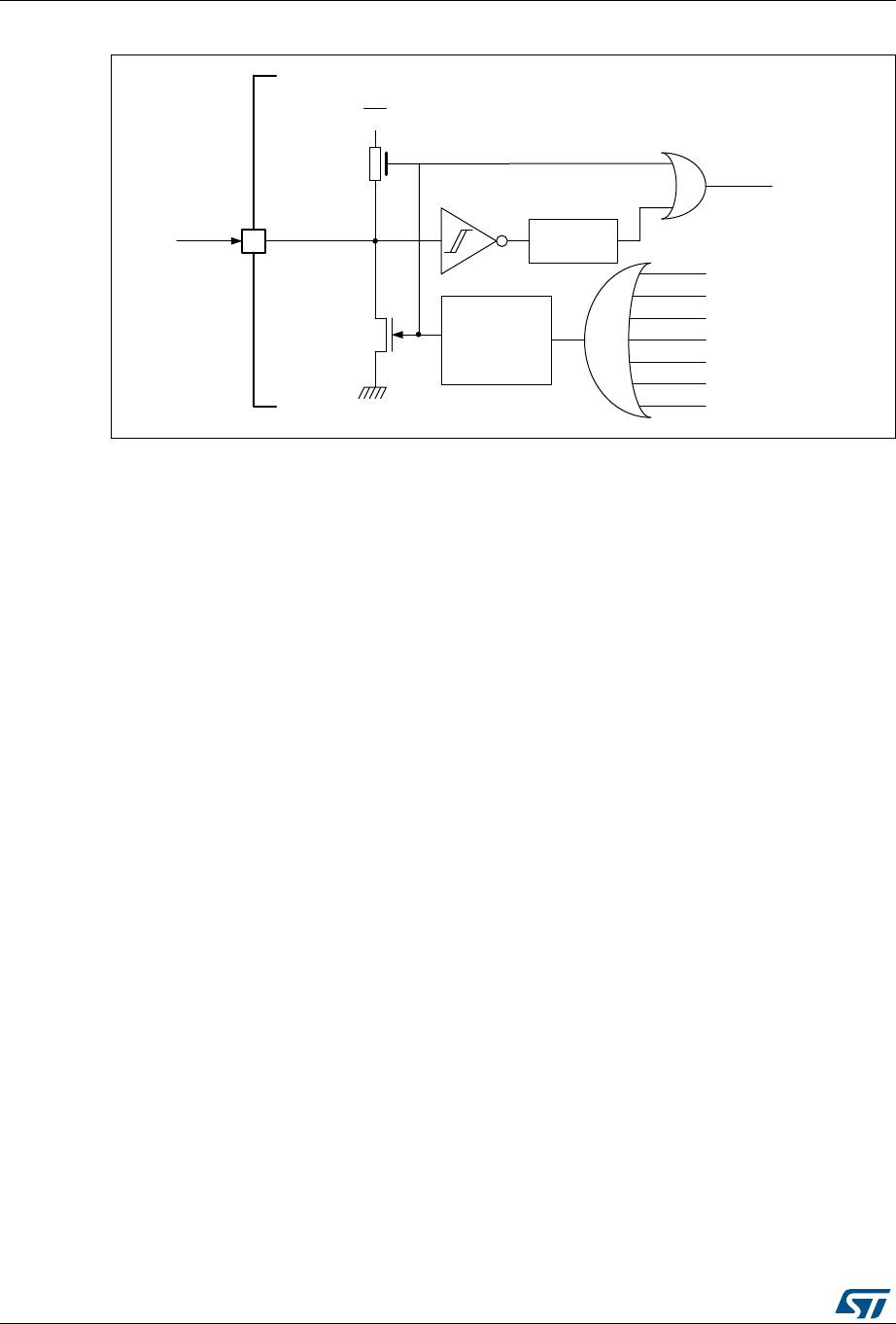
Reset and clock control (RCC) RM0394
176/1600 RM0394 Rev 4
Figure 12. Simplified diagram of the reset circuit
Software reset
The SYSRESETREQ bit in Cortex®-M4 Application Interrupt and Reset Control Register
must be set to force a software reset on the device (refer to the STM32F3, STM32F4,
STM32L4 and STM32L4+ Series Cortex®-M4 (PM0214)).
Low-power mode security reset
To prevent that critical applications mistakenly enter a low-power mode, two low-power
mode security resets are available. If enabled in option bytes, the resets are generated in
the following conditions:
1. Entering Standby mode: this type of reset is enabled by resetting nRST_STDBY bit in
User option Bytes. In this case, whenever a Standby mode entry sequence is
successfully executed, the device is reset instead of entering Standby mode.
2. Entering Stop mode: this type of reset is enabled by resetting nRST_STOP bit in User
option bytes. In this case, whenever a Stop mode entry sequence is successfully
executed, the device is reset instead of entering Stop mode.
3. Entering Shutdown mode: this type of reset is enabled by resetting nRST_SHDW bit in
User option bytes. In this case, whenever a Shutdown mode entry sequence is
successfully executed, the device is reset instead of entering Shutdown mode.
For further information on the User Option Bytes, refer to Section 3.4.1: Option bytes
description.
Option byte loader reset
The option byte loader reset is generated when the OBL_LAUNCH bit (bit 27) is set in the
FLASH_CR register. This bit is used to launch the option byte loading by software.
6.1.3 Backup domain reset
The backup domain has two specific resets.
A backup domain reset is generated when one of the following events occurs:
069
džƚĞƌŶĂů
ƌĞƐĞƚ
sͬs
ZWh
tt'ƌĞƐĞƚ
&ŝƌĞǁĂůůƌĞƐĞƚ
^ŽĨƚǁĂƌĞƌĞƐĞƚ
>ŽǁͲƉŽǁĞƌŵĂŶĂŐĞƌƌĞƐĞƚ
/t'ƌĞƐĞƚ
KƉƚŝŽŶďLJƚĞůŽĂĚĞƌƌĞƐĞƚ
KZƌĞƐĞƚ
3XOVH
JHQHUDWRU
PLQȝV
EZ^d ^LJƐƚĞŵƌĞƐĞƚ
)LOWHU
06Y9
džƚĞƌŶĂů
ƌĞƐĞƚ
s
ZWh
tt'ƌĞƐĞƚ
&ŝƌĞǁĂůůƌĞƐĞƚ
^ŽĨƚǁĂƌĞƌĞƐĞƚ
>ŽǁͲƉŽǁĞƌŵĂŶĂŐĞƌƌĞƐĞƚ
/t'ƌĞƐĞƚ
KƉƚŝŽŶďLJƚĞůŽĂĚĞƌƌĞƐĞƚ
KZƌĞƐĞƚ
3XOVH
JHQHUDWRU
PLQȝV
EZ^d
^LJƐƚĞŵƌĞƐĞƚ
)LOWHU

RM0394 Rev 4 177/1600
RM0394 Reset and clock control (RCC)
246
1. Software reset, triggered by setting the BDRST bit in the Backup domain control
register (RCC_BDCR).
2. VDD or VBAT power on, if both supplies have previously been powered off.
A backup domain reset only affects the LSE oscillator, the RTC, the Backup registers and
the RCC Backup domain control register.
6.2 Clocks
Four different clock sources can be used to drive the system clock (SYSCLK):
•HSI16 (high speed internal)16 MHz RC oscillator clock
•MSI (multispeed internal) RC oscillator clock
•HSE oscillator clock, from 4 to 48 MHz
•PLL clock
The MSI is used as system clock source after startup from Reset, configured at 4 MHz.
The devices have the following additional clock sources:
•32 kHz low speed internal RC (LSI RC) which drives the independent watchdog and
optionally the RTC used for Auto-wakeup from Stop and Standby modes.
•32.768 kHz low speed external crystal (LSE crystal) which optionally drives the real-
time clock (RTCCLK).
•RC 48 MHz internal clock sources (HSI48) to potentially drive the USB FS, the
SDMMC and the RNG.
Each clock source can be switched on or off independently when it is not used, to optimize
power consumption.
Several prescalers can be used to configure the AHB frequency, the high speed APB
(APB2) and the low speed APB (APB1) domains. The maximum frequency of the AHB, the
APB1 and the APB2 domains is 80 MHz.

Reset and clock control (RCC) RM0394
178/1600 RM0394 Rev 4
All the peripheral clocks are derived from their bus clock (HCLK, PCLK1 or PCLK2) except:
•The 48 MHz clock, used for USB FS, SDMMC and RNG. This clock is derived (selected
by software) from one of the four following sources:
– main PLL VCO (PLL48M1CLK)
– PLLSAI1 VCO (PLL48M2CLK)
– MSI clock
– HSI48 internal oscillator
When the MSI clock is auto-trimmed with the LSE, it can be used by the USB FS
device.
•The ADCs clock which is derived (selected by software) from one of the following
sources:
– system clock (SYSCLK)
– PLLSAI1 VCO (PLLADC1CLK)(not available on STM3L41xxx and STM32L42xxx
devices)
•The U(S)ARTs clocks which are derived (selected by software) from one of the four
following sources:
– system clock (SYSCLK)
– HSI16 clock
– LSE clock
– APB1 or APB2 clock (PCLK1 or PCLK2 depending on which APB is mapped the
U(S)ART)
The wakeup from Stop mode is supported only when the clock is HSI16 or LSE.
•The I2Cs clocks which are derived (selected by software) from one of the three
following sources:
– system clock (SYSCLK)
– HSI16 clock
– APB1 clock (PCLK1)
The wakeup from Stop mode is supported only when the clock is HSI16.
•The SAI1 clock which derived (selected by software) from one of the following
sources:
– an external clock mapped on SAI1_EXTCLK for SAI1
– PLLSAI1 VCO (PLLSAICLK)
– main PLL VCO (PLLSAICLK)
– HSI16 clock
•The SWPMI1 clock which is derived (selected by software) from one of the two
following sources:
– HSI16 clock
– APB1 clock (PCLK1)
The wakeup from Stop mode is supported only when the clock is HSI16.
•The DFSDM1 clock (only applicable for STM32L45x/46x) which is derived (selected by
software) from one of the two following sources:
– system clock (SYSCLK)
– APB2 clock (PCLK2)
•The low-power timers (LPTIMx) clock which are derived (selected by software) from

RM0394 Rev 4 179/1600
RM0394 Reset and clock control (RCC)
246
one of the five following sources:
– LSI clock
– LSE clock
– HSI16 clock
– APB1 clock (PCLK1)
– External clock mapped on LPTIMx_IN1
The functionality in Stop mode (including wakeup) is supported only when the clock is
LSI or LSE, or in external clock mode.
•The RTC and LCD clock which is derived (selected by software) from one of the three
following sources:
– LSE clock
– LSI clock
– HSE clock divided by 32
The functionality in Stop mode (including wakeup) is supported only when the clock is
LSI or LSE.
•The IWDG clock which is always the LSI clock.
The RCC feeds the Cortex® System Timer (SysTick) external clock with the AHB clock
(HCLK) divided by 8. The SysTick can work either with this clock or directly with the Cortex®
clock (HCLK), configurable in the SysTick Control and Status Register.
FCLK acts as Cortex®-M4 free-running clock. For more details refer to the STM32F3,
STM32F4, STM32L4 and STM32L4+ Series Cortex®-M4 programming manual (PM0214).
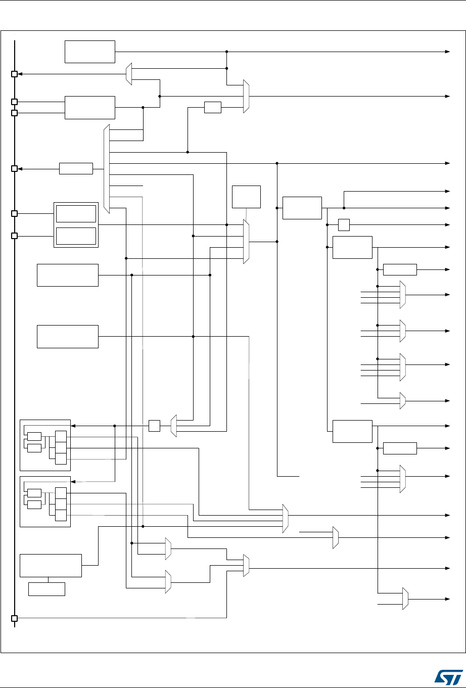
Reset and clock control (RCC) RM0394
180/1600 RM0394 Rev 4
Figure 13. Clock tree
069
6<6&/.
0&2
/6&2
0+]FORFNWR86%
51*6'00&
WR$'&[
[
WR,:'*
WR57&DQG/&'
WR3:5
+&/.
WR$+%EXVFRUHPHPRU\DQG'0$
)&/.&RUWH[IUHHUXQQLQJFORFN
WR&RUWH[V\VWHPWLPHU
WR$3%SHULSKHUDOV
WR$3%SHULSKHUDOV
3&/.
3&/.
WR6$,
/6(
+6,
6<6&/. WR86$57[
[
WR/38$57
WR,&[
[
WR/37,0[
[
6$,B(;7&/.
WR6:30,
WR7,0[
[
26&B287
26&B,1
06, +6,
+6(
+6,
/6,
/6(
+6(
6<6&/.
+6(
06,
+6,
06,
6<6&/.
/6(26&
N+]
$+%
35(6&
$3%
35(6&
[RU[
+6,
6<6&/.
/6,
/6(
+6,
+6,
$3%
35(6&
WR7,0[
[
[RU[
WR
86$57
/6(
+6,
6<6&/.
0
06,5&
N+]±0+]
+6,5&
0+]
+6(26&
0+]
&ORFN
GHWHFWRU
26&B287
26&B,1
ĺ
/6,5&N+]
&ORFN
VRXUFH
FRQWURO
3//6$,&/.
3//0&/.
3//&/.
3//6$,&/.
3//0&/.
3//$'&&/.
+6,
+6,
+6,5&
0+]
5&
&56
3
4
5
9&2
[1
3//6$,
3
4
5
9&2
[1
3//
2QO\6<6&/.FRXGEHVHOHFWHGRQ670/[[[DQG670/[[[GHYLFHV
3//6$,QRWDYDLODEOHRQ670/[[[DQG670/[[[GHYLFHV
06,
6<6&/.
WR')6'0
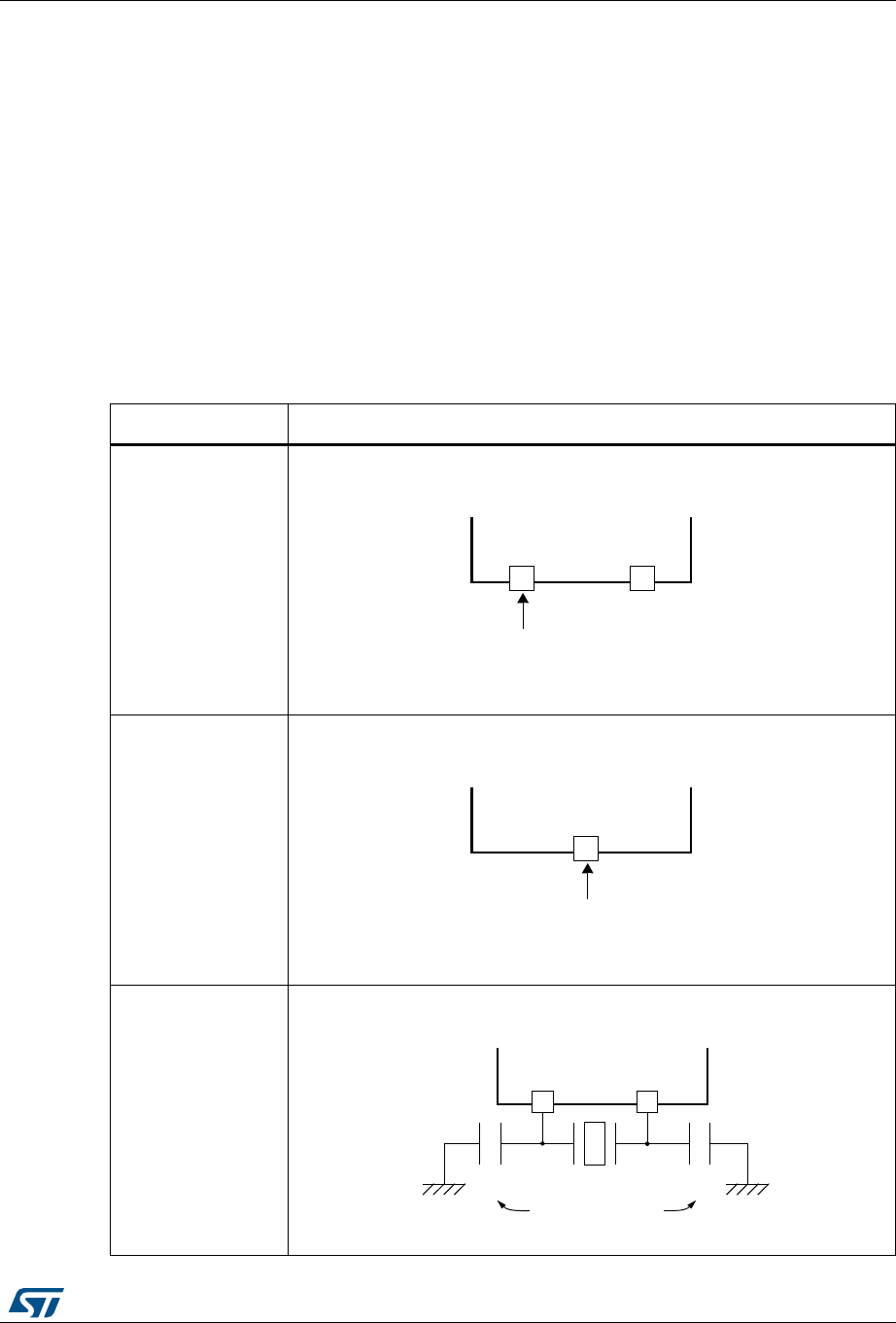
RM0394 Rev 4 181/1600
RM0394 Reset and clock control (RCC)
246
1. For full details about the internal and external clock source characteristics, please refer to the “Electrical
characteristics” section in your device datasheet.
2. The ADC clock can be derived from the AHB clock of the ADC bus interface, divided by a programmable
factor (1, 2 or 4). When the programmable factor is ‘1’, the AHB prescaler must be equal to ‘1’.
6.2.1 HSE clock
The high speed external clock signal (HSE) can be generated from two possible clock
sources:
•HSE external crystal/ceramic resonator
•HSE user external clock
The resonator and the load capacitors have to be placed as close as possible to the
oscillator pins in order to minimize output distortion and startup stabilization time. The
loading capacitance values must be adjusted according to the selected oscillator.
Figure 14. HSE/ LSE clock sources
Clock source Hardware configuration
External clock
External clock
(available on some
package, please
refer to the
corresponding
datasheet)
Crystal/Ceramic
resonators
OSC_OUT
External
source
GPIO
OSC_IN
External
source
CK_IN
GPIO
OSC_IN OSC_OUT
Load
capacitors
CL2
CL1

Reset and clock control (RCC) RM0394
182/1600 RM0394 Rev 4
External crystal/ceramic resonator (HSE crystal)
The 4 to 48 MHz external oscillator has the advantage of producing a very accurate rate on
the main clock.
The associated hardware configuration is shown in Figure 14. Refer to the electrical
characteristics section of the datasheet for more details.
The HSERDY flag in the Clock control register (RCC_CR) indicates if the HSE oscillator is
stable or not. At startup, the clock is not released until this bit is set by hardware. An
interrupt can be generated if enabled in the Clock interrupt enable register (RCC_CIER).
The HSE Crystal can be switched on and off using the HSEON bit in the Clock control
register (RCC_CR).
External source (HSE bypass)
In this mode, an external clock source must be provided. It can have a frequency of up to
48 MHz. You select this mode by setting the HSEBYP and HSEON bits in the Clock control
register (RCC_CR). The external clock signal (square, sinus or triangle) with ~40-60 % duty
cycle depending on the frequency (refer to the datasheet) has to drive the OSC_IN pin while
the OSC_OUT pin can be used a GPIO. See Figure 14.
6.2.2 HSI16 clock
The HSI16 clock signal is generated from an internal 16 MHz RC Oscillator.
The HSI16 RC oscillator has the advantage of providing a clock source at low cost (no
external components). It also has a faster startup time than the HSE crystal oscillator
however, even with calibration the frequency is less accurate than an external crystal
oscillator or ceramic resonator.
The HSI16 clock can be selected as system clock after wakeup from Stop modes (Stop 0,
Stop 1 or Stop 2). Refer to Section 6.3: Low-power modes. It can also be used as a backup
clock source (auxiliary clock) if the HSE crystal oscillator fails. Refer to Section 6.2.10: Clock
security system (CSS).
Calibration
RC oscillator frequencies can vary from one chip to another due to manufacturing process
variations, this is why each device is factory calibrated by ST for 1 % accuracy at TA=25°C.
After reset, the factory calibration value is loaded in the HSICAL[7:0] bits in the Internal
clock sources calibration register (RCC_ICSCR).
If the application is subject to voltage or temperature variations this may affect the RC
oscillator speed. You can trim the HSI16 frequency in the application using the
HSITRIM[6:0] bits in the Internal clock sources calibration register (RCC_ICSCR).
For more details on how to measure the HSI16 frequency variation, refer to Section 6.2.17:
Internal/external clock measurement with TIM15/TIM16.
The HSIRDY flag in the Clock control register (RCC_CR) indicates if the HSI16 RC is stable
or not. At startup, the HSI16 RC output clock is not released until this bit is set by hardware.
The HSI16 RC can be switched on and off using the HSION bit in the Clock control register
(RCC_CR).

RM0394 Rev 4 183/1600
RM0394 Reset and clock control (RCC)
246
The HSI16 signal can also be used as a backup source (Auxiliary clock) if the HSE crystal
oscillator fails. Refer to Section 6.2.10: Clock security system (CSS) on page 186.
6.2.3 MSI clock
The MSI clock signal is generated from an internal RC oscillator. Its frequency range can be
adjusted by software by using the MSIRANGE[3:0] bits in the Clock control register
(RCC_CR). Twelve frequency ranges are available: 100 kHz, 200 kHz, 400 kHz, 800 kHz,
1 MHz, 2 MHz, 4 MHz (default value), 8 MHz, 16 MHz, 24 MHz, 32 MHz and 48 MHz.
The MSI clock is used as system clock after restart from Reset, wakeup from Standby and
Shutdown low-power modes. After restart from Reset, the MSI frequency is set to its default
value 4 MHz. Refer to Section 6.3: Low-power modes.
The MSI clock can be selected as system clock after a wakeup from Stop mode (Stop 0,
Stop 1 or Stop 2). Refer to Section 6.3: Low-power modes. It can also be used as a backup
clock source (auxiliary clock) if the HSE crystal oscillator fails. Refer to Section 6.2.10: Clock
security system (CSS).
The MSI RC oscillator has the advantage of providing a low-cost (no external components)
low-power clock source. In addition, when used in PLL-mode with the LSE, it provides a
very accurate clock source which can be used by the USB FS device, and feed the main
PLL to run the system at the maximum speed 80 MHz.
The MSIRDY flag in the Clock control register (RCC_CR) indicates wether the MSI RC is
stable or not. At startup, the MSI RC output clock is not released until this bit is set by
hardware. The MSI RC can be switched on and off by using the MSION bit in the Clock
control register (RCC_CR).
Hardware auto calibration with LSE (PLL-mode)
When a 32.768 kHz external oscillator is present in the application, it is possible to configure
the MSI in a PLL-mode by setting the MSIPLLEN bit in the Clock control register (RCC_CR).
When configured in PLL-mode, the MSI automatically calibrates itself thanks to the LSE.
This mode is available for all MSI frequency ranges. At 48 MHz, the MSI in PLL-mode can
be used for the USB FS device, saving the need of an external high-speed crystal.
Software calibration
The MSI RC oscillator frequency can vary from one chip to another due to manufacturing
process variations, this is why each device is factory calibrated by ST for 1 % accuracy at an
ambient temperature, TA, of 25 °C. After reset, the factory calibration value is loaded in the
MSICAL[7:0] bits in the Internal clock sources calibration register (RCC_ICSCR). If the
application is subject to voltage or temperature variations, this may affect the RC oscillator
speed. You can trim the MSI frequency in the application by using the MSITRIM[7:0] bits in
the RCC_ICSCR register. For more details on how to measure the MSI frequency variation
please refer to Section 6.2.17: Internal/external clock measurement with TIM15/TIM16.
6.2.4 HSI48 clock
The HSI48 clock signal is generated from an internal 48 MHz RC oscillator and can be used
directly for USB and for random number generator (RNG) as well as SDMMC.
The internal 48 MHz RC oscillator is mainly dedicated to provide a high precision clock to
the USB peripheral by means of a special Clock Recovery System (CRS) circuitry. The CRS
can use the USB SOF signal, the LSE or an external signal to automatically and quickly

Reset and clock control (RCC) RM0394
184/1600 RM0394 Rev 4
adjust the oscillator frequency on-fly. It is disabled as soon as the system enters Stop or
Standby mode. When the CRS is not used, the HSI48 RC oscillator runs on its default
frequency which is subject to manufacturing process variations.
For more details on how to configure and use the CRS peripheral please refer to Section 7:
Clock recovery system (CRS).
The HSI48RDY flag in the Clock recovery RC register (RCC_CRRCR) indicates whether the
HSI48 RC oscillator is stable or not. At startup, the HSI48 RC oscillator output clock is not
released until this bit is set by hardware.
The HSI48 can be switched on and off using the HSI48ON bit in the Clock recovery RC
register (RCC_CRRCR).
6.2.5 PLL
The device embeds PLLs: PLL, PLLSAI1. Each PLL provides up to three independent
outputs. The internal PLLs can be used to multiply the HSI16, HSE or MSI output clock
frequency. The PLLs input frequency must be between 4 and 16 MHz. The selected clock
source is divided by a programmable factor PLLM from 1 to 8 to provide a clock frequency in
the requested input range. Refer to Figure 13: Clock treeand PLL configuration register
(RCC_PLLCFGR).
The PLLs configuration (selection of the input clock and multiplication factor) must be done
before enabling the PLL. Once the PLL is enabled, these parameters cannot be changed.
To modify the PLL configuration, proceed as follows:
1. Disable the PLL by setting PLLON to 0 in Clock control register (RCC_CR).
2. Wait until PLLRDY is cleared. The PLL is now fully stopped.
3. Change the desired parameter.
4. Enable the PLL again by setting PLLON to 1.
5. Enable the desired PLL outputs by configuring PLLPEN, PLLQEN, PLLREN in PLL
configuration register (RCC_PLLCFGR).
An interrupt can be generated when the PLL is ready, if enabled in the Clock interrupt
enable register (RCC_CIER).
The same procedure is applied for changing the configuration of the PLLSAI1:
1. Disable the PLLSAI1/PLLSAI2 by setting PLLSAI1ON to 0 in Clock control register
(RCC_CR).
2. Wait until PLLSAI1RDY is cleared. The PLLSAI1 is now fully stopped.
3. Change the desired parameter.
4. Enable the PLLSAI1 again by setting PLLSAI1ON to 1.
5. Enable the desired PLL outputs by configuring PLLSAI1PEN, PLLSAI1QEN,
PLLSAI1REN in PLLSAI1 configuration register (RCC_PLLSAI1CFGR).
The PLL output frequency must not exceed 80 MHz.
The enable bit of each PLL output clock (PLLPEN, PLLQEN, PLLREN, PLLSAI1PEN,
PLLSAI1QEN, PLLSAI1REN) can be modified at any time without stopping the
corresponding PLL. PLLREN cannot be cleared if PLLCLK is used as system clock.

RM0394 Rev 4 185/1600
RM0394 Reset and clock control (RCC)
246
6.2.6 LSE clock
The LSE crystal is a 32.768 kHz Low Speed External crystal or ceramic resonator. It has the
advantage of providing a low-power but highly accurate clock source to the real-time clock
peripheral (RTC) for clock/calendar or other timing functions.
The LSE crystal is switched on and off using the LSEON bit in Backup domain control
register (RCC_BDCR). The crystal oscillator driving strength can be changed at runtime
using the LSEDRV[1:0] bits in the Backup domain control register (RCC_BDCR) to obtain
the best compromise between robustness and short start-up time on one side and low-
power-consumption on the other side. The LSE drive can be decreased to the lower drive
capability (LSEDRV=00) when the LSE is ON. However, once LSEDRV is selected, the
drive capability can not be increased if LSEON=1.
The LSERDY flag in the Backup domain control register (RCC_BDCR) indicates whether
the LSE crystal is stable or not. At startup, the LSE crystal output clock signal is not released
until this bit is set by hardware. An interrupt can be generated if enabled in the Clock
interrupt enable register (RCC_CIER).
Distribution of the external 32 kHz clock (LSE) outside the RTC block could be disabled by
setting LSESYSDIS bit in Backup domain control register (RCC_BDCR) to reduce power
consumption. Propagation will be stoped regardless the use of LSE by other IP's. This
feature is present on STM32L412xx and STM32L422xx devices only.
External source (LSE bypass)
In this mode, an external clock source must be provided. It can have a frequency of up to
1 MHz. You select this mode by setting the LSEBYP and LSEON bits in the AHB1 peripheral
clocks enable in Sleep and Stop modes register (RCC_AHB1SMENR). The external clock
signal (square, sinus or triangle) with ~50 % duty cycle has to drive the OSC32_IN pin while
the OSC32_OUT pin can be used as GPIO. See Figure 14.
6.2.7 LSI clock
The LSI RC acts as a low-power clock source that can be kept running in Stop and Standby
mode for the independent watchdog (IWDG), RTC and LCD. The clock frequency is 32 kHz.
For more details, refer to the electrical characteristics section of the datasheets.
The LSI RC can be switched on and off using the LSION bit in the Control/status register
(RCC_CSR).
The LSIRDY flag in the Control/status register (RCC_CSR) indicates if the LSI oscillator is
stable or not. At startup, the clock is not released until this bit is set by hardware. An
interrupt can be generated if enabled in the Clock interrupt enable register (RCC_CIER).
6.2.8 System clock (SYSCLK) selection
Four different clock sources can be used to drive the system clock (SYSCLK):
•MSI oscillator
•HSI16 oscillator
•HSE oscillator
•PLL

Reset and clock control (RCC) RM0394
186/1600 RM0394 Rev 4
The system clock maximum frequency is 80 MHz. After a system reset, the MSI oscillator, at
4 MHz, is selected as system clock. When a clock source is used directly or through the PLL
as a system clock, it is not possible to stop it.
A switch from one clock source to another occurs only if the target clock source is ready
(clock stable after startup delay or PLL locked). If a clock source which is not yet ready is
selected, the switch will occur when the clock source becomes ready. Status bits in the
Internal clock sources calibration register (RCC_ICSCR) indicate which clock(s) is (are)
ready and which clock is currently used as a system clock.
6.2.9 Clock source frequency versus voltage scaling
The following table gives the different clock source frequencies depending on the product
voltage range.
6.2.10 Clock security system (CSS)
Clock Security System can be activated by software. In this case, the clock detector is
enabled after the HSE oscillator startup delay, and disabled when this oscillator is stopped.
If a failure is detected on the HSE clock, the HSE oscillator is automatically disabled, a clock
failure event is sent to the break input of the advanced-control timers (TIM1 and TIM15/16)
and an interrupt is generated to inform the software about the failure (Clock Security System
Interrupt CSSI), allowing the MCU to perform rescue operations. The CSSI is linked to the
Cortex®-M4 NMI (Non-Maskable Interrupt) exception vector.
Note: Once the CSS is enabled and if the HSE clock fails, the CSS interrupt occurs and a NMI is
automatically generated. The NMI will be executed indefinitely unless the CSS interrupt
pending bit is cleared. As a consequence, in the NMI ISR user must clear the CSS interrupt
by setting the CSSC bit in the Clock interrupt clear register (RCC_CICR).
If the HSE oscillator is used directly or indirectly as the system clock (indirectly means: it is
used as PLL input clock, and the PLL clock is used as system clock), a detected failure
causes a switch of the system clock to the MSI or the HSI16 oscillator depending on the
STOPWUCK configuration in the Clock configuration register (RCC_CFGR), and the
disabling of the HSE oscillator. If the HSE clock (divided or not) is the clock entry of the PLL
used as system clock when the failure occurs, the PLL is disabled too.
Table 31. Clock source frequency
Product voltage
range
Clock frequency
MSI HSI16 HSE PLL/PLLSAI1
Range 1 (1)
1. Also for SMPS Range1 and SMPS Range2 High
48 MHz 16 MHz 48 MHz 80 MHz
(VCO max = 344 MHz)
Range 2(2)
2. Also for SMPS Range2 Low
24 MHz range 16 MHz 26 MHz 26 MHz
(VCO max = 128 MHz)

RM0394 Rev 4 187/1600
RM0394 Reset and clock control (RCC)
246
6.2.11 Clock security system on LSE
A Clock Security System on LSE can be activated by software writing the LSECSSON bit in
the Backup domain control register (RCC_BDCR). This bit can be disabled only by a
hardware reset or RTC software reset, or after a failure detection on LSE. LSECSSON must
be written after LSE and LSI are enabled (LSEON and LSION enabled) and ready (LSERDY
and LSIRDY set by hardware), and after the RTC clock has been selected by RTCSEL.
The CSS on LSE is working in all modes except VBAT. It is working also under system reset
(excluding power on reset). If a failure is detected on the external 32 kHz oscillator, the LSE
clock is no longer supplied to the RTC but no hardware action is made to the registers. If the
MSI was in PLL-mode, this mode is disabled.
In Standby mode a wakeup is generated. In other modes an interrupt can be sent to wakeup
the software (see Clock interrupt enable register (RCC_CIER), Clock interrupt flag register
(RCC_CIFR), Clock interrupt clear register (RCC_CICR)).
The software MUST then disable the LSECSSON bit, stop the defective 32 kHz oscillator
(disabling LSEON), and change the RTC clock source (no clock or LSI or HSE, with
RTCSEL), or take any required action to secure the application.
The frequency of LSE oscillator have to be higher than 30 kHz to avoid false positive CSS
detection.
6.2.12 ADC clock
The ADC clock is derived from the system clock, or from the PLLSAI1 output(a). It can reach
80 MHz and can be divided by the following prescalers values: 1,2,4,6,8,10,12,16,32,64,128
or 256 by configuring the ADC1_CCR register. It is asynchronous to the AHB clock.
Alternatively, the ADC clock can be derived from the AHB clock of the ADC bus interface,
divided by a programmable factor (1, 2 or 4). This programmable factor is configured using
the CKMODE bit fields in the ADC1_CCR.
If the programmed factor is ‘1’, the AHB prescaler must be set to ‘1’.
6.2.13 RTC clock
The RTCCLK clock source can be either the HSE/32, LSE or LSI clock. It is selected by
programming the RTCSEL[1:0] bits in the Backup domain control register (RCC_BDCR).
This selection cannot be modified without resetting the Backup domain. The system must
always be configured so as to get a PCLK frequency greater then or equal to the RTCCLK
frequency for a proper operation of the RTC.
a. Except STM32L41xxx/42xxx devices

Reset and clock control (RCC) RM0394
188/1600 RM0394 Rev 4
The LSE clock is in the Backup domain, whereas the HSE and LSI clocks are not.
Consequently:
•If LSE is selected as RTC clock:
– The RTC continues to work even if the VDD supply is switched off, provided the
VBAT supply is maintained.
•If LSI is selected as the RTC clock:
– The RTC state is not guaranteed if the VDD supply is powered off.
•If the HSE clock divided by a prescaler is used as the RTC clock:
– The RTC state is not guaranteed if the VDD supply is powered off or if the internal
voltage regulator is powered off (removing power from the VCORE domain).
When the RTC clock is LSE or LSI, the RTC remains clocked and functional under system
reset.
6.2.14 Timer clock
The timer clock frequencies are automatically defined by hardware. There are two cases:
1. If the APB prescaler equals 1, the timer clock frequencies are set to the same
frequency as that of the APB domain.
2. Otherwise, they are set to twice (×2) the frequency of the APB domain.
6.2.15 Watchdog clock
If the Independent watchdog (IWDG) is started by either hardware option or software
access, the LSI oscillator is forced ON and cannot be disabled. After the LSI oscillator
temporization, the clock is provided to the IWDG.
6.2.16 Clock-out capability
•MCO
The microcontroller clock output (MCO) capability allows the clock to be output onto the
external MCO pin. One of eight clock signals can be selected as the MCO clock.
–LSI
–LSE
– SYSCLK
–HSI16
–HSI48
–HSE
–PLLCLK
–MSI
The selection is controlled by the MCOSEL[:0] bits of the Clock configuration register
(RCC_CFGR). The selected clock can be divided with the MCOPRE[2:0] field of the
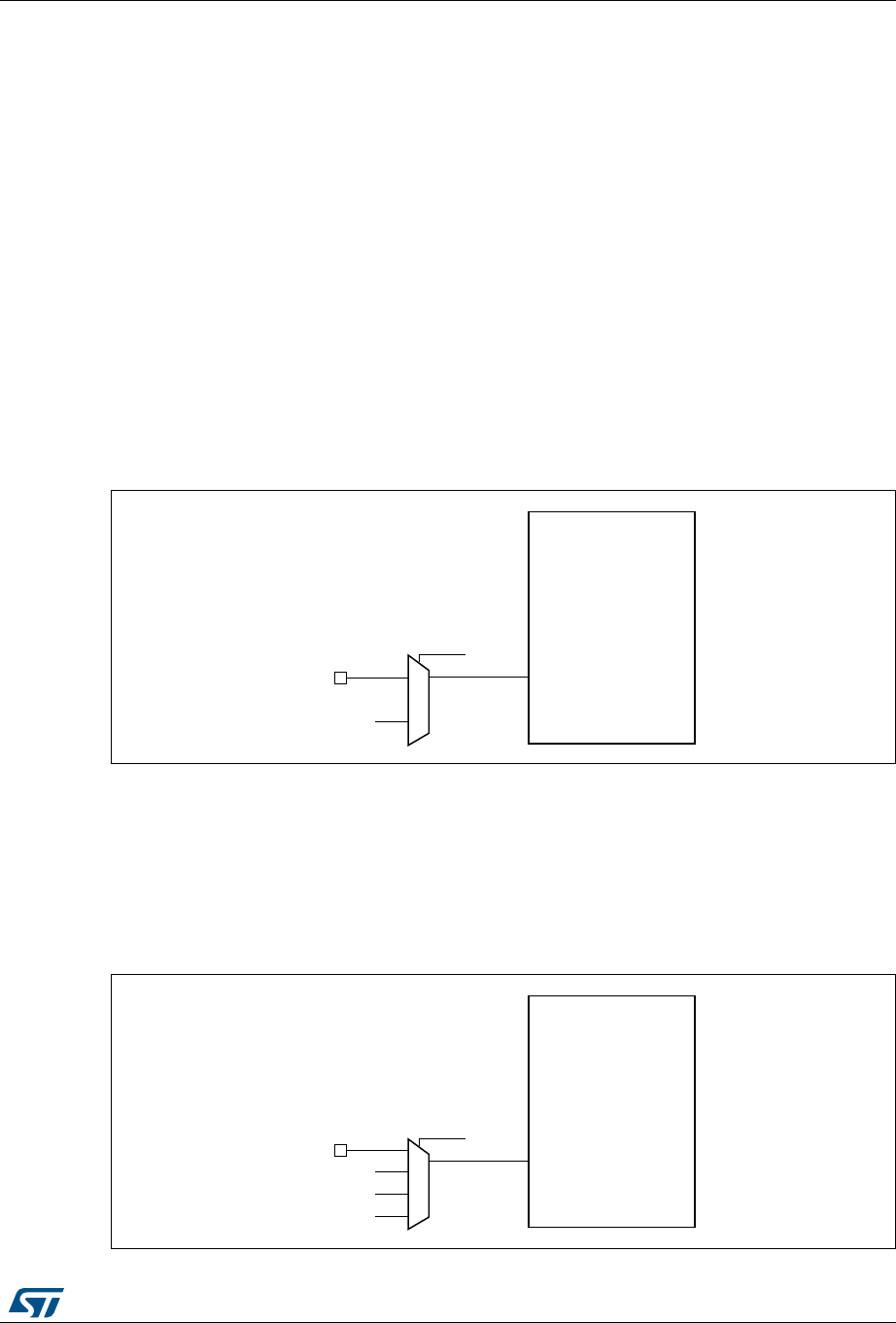
RM0394 Rev 4 189/1600
RM0394 Reset and clock control (RCC)
246
Clock configuration register (RCC_CFGR).
•LSCO
Another output (LSCO) allows a low speed clock to be output onto the external LSCO
pin:
–LSI
–LSE
This output remains available in Stop (Stop 0, Stop 1 and Stop 2) and Standby modes.
The selection is controlled by the LSCOSEL, and enabled with the LSCOEN in the
Backup domain control register (RCC_BDCR).
The MCO clock output requires the corresponding alternate function selected on the MCO
pin, the LSCO pin should be left in default POR state.
6.2.17 Internal/external clock measurement with TIM15/TIM16
It is possible to indirectly measure the frequency of all on-board clock sources by mean of
the TIM15 or TIM16 channel 1 input capture, as represented on Figure 15 and Figure 16
Figure 15. Frequency measurement with TIM15 in capture mode
The input capture channel of the Timer 15 can be a GPIO line or an internal clock of the
MCU. This selection is performed through the TI1_RMP bit in the TIM15_OR register. The
possibilities are the following ones:
•TIM15 Channel1 is connected to the GPIO. Refer to the alternate function mapping in
the device datasheets.
•TIM15 Channel1 is connected to the LSE.
Figure 16. Frequency measurement with TIM16 in capture mode
069
7,0
7,
7,B503
*3,2
/6(
069
7,0
7,
7,B503>@
*3,2
/6(
/6,
57&ZDNHXSLQWHUUXSW

Reset and clock control (RCC) RM0394
190/1600 RM0394 Rev 4
The input capture channel of the Timer 16 can be a GPIO line or an internal clock of the
MCU. This selection is performed through the TI1_RMP[1:0] bits in the TIM16_OR register.
The possibilities are the following ones:
•TIM16 Channel1 is connected to the GPIO. Refer to the alternate function mapping in
the device datasheets.
•TIM16 Channel1 is connected to the LSI clock.
•TIM16 Channel1 is connected to the LSE clock.
•TIM16 Channel1 is connected to the RTC wakeup interrupt signal. In this case the RTC
interrupt should be enabled.
Calibration of the HSI16 and the MSI
For TIM15 and TIM16, the primary purpose of connecting the LSE to the channel 1 input
capture is to be able to precisely measure the HSI16 and MSI system clocks (for this, either
the HSI16 or MSI should be used as the system clock source). The number of HSI16 (MSI,
respectively) clock counts between consecutive edges of the LSE signal provides a
measure of the internal clock period. Taking advantage of the high precision of LSE crystals
(typically a few tens of ppm’s), it is possible to determine the internal clock frequency with
the same resolution, and trim the source to compensate for manufacturing, process,
temperature and/or voltage related frequency deviations.
The MSI and HSI16 oscillator both have dedicated user-accessible calibration bits for this
purpose.
The basic concept consists in providing a relative measurement (e.g. the HSI16/LSE ratio):
the precision is therefore closely related to the ratio between the two clock sources. The
higher the ratio is, the better the measurement will be.
If LSE is not available, HSE/32 will be the better option in order to reach the most precise
calibration possible.
It is however not possible to have a good enough resolution when the MSI clock is low
(typically below 1 MHz). In this case, it is advised to:
•accumulate the results of several captures in a row
•use the timer’s input capture prescaler (up to 1 capture every 8 periods)
•use the RTC wakeup interrupt signal (when the RTC is clocked by the LSE) as the
input for the channel1 input capture. This improves the measurement precision. For
this purpose the RTC wakeup interrupt must be enable.
Calibration of the LSI
The calibration of the LSI will follow the same pattern that for the HSI16, but changing the
reference clock. It will be necessary to connect LSI clock to the channel 1 input capture of
the TIM16. Then define the HSE as system clock source, the number of his clock counts
between consecutive edges of the LSI signal provides a measure of the internal low speed
clock period.
The basic concept consists in providing a relative measurement (e.g. the HSE/LSI ratio): the
precision is therefore closely related to the ratio between the two clock sources. The higher
the ratio is, the better the measurement will be.

RM0394 Rev 4 191/1600
RM0394 Reset and clock control (RCC)
246
6.2.18 Peripheral clock enable register
(RCC_AHBxENR, RCC_APBxENRy)
Each peripheral clock can be enabled by the xxxxEN bit of the RCC_AHBxENR,
RCC_APBxENRy registers.
When the peripheral clock is not active, the peripheral registers read or write accesses are
not supported.
The enable bit has a synchronization mechanism to create a glitch free clock for the
peripheral. After the enable bit is set, there is a 2 clock cycles delay before the clock be
active.
Caution: Just after enabling the clock for a peripheral, software must wait for a delay before
accessing the peripheral registers.
6.3 Low-power modes
•AHB and APB peripheral clocks, including DMA clock, can be disabled by software.
•Sleep and Low Power Sleep modes stops the CPU clock. The memory interface clocks
(Flash and SRAM1 and SRAM2 interfaces) can be stopped by software during sleep
mode. The AHB to APB bridge clocks are disabled by hardware during Sleep mode
when all the clocks of the peripherals connected to them are disabled.
•Stop modes (Stop 0, Stop 1 and Stop 2) stops all the clocks in the VCORE domain and
disables the PLL, the HSI16, the MSI and the HSE oscillators.
All U(S)ARTs, LPUARTs and I2Cs have the capability to enable the HSI16 oscillator
even when the MCU is in Stop mode (if HSI16 is selected as the clock source for that
peripheral).
All U(S)ARTs and LPUARTs can also be driven by the LSE oscillator when the system
is in Stop mode (if LSE is selected as clock source for that peripheral) and the LSE
oscillator is enabled (LSEON). In that case the LSE remains always ON in Stop mode
(they do not have the capability to turn on the LSE oscillator).
•Standby and Shutdown modes stops all the clocks in the VCORE domain and disables
the PLL, the HSI16, the MSI and the HSE oscillators.
The CPU’s deepsleep mode can be overridden for debugging by setting the DBG_STOP or
DBG_STANDBY bits in the DBGMCU_CR register.
When leaving the Stop modes (Stop 0, Stop 1 or Stop 2), the system clock is either MSI or
HSI16, depending on the software configuration of the STOPWUCK bit in the RCC_CFGR
register. The frequency (range and user trim) of the MSI oscillator is the one configured
before entering Stop mode. The user trim of HSI16 is kept. If the MSI was in PLL-mode
before entering Stop mode, the PLL-mode stabilization time must be waited for after wakeup
even if the LSE was kept ON during the Stop mode.
When leaving the Standby and Shutdown modes, the system clock is MSI. The MSI
frequency at wakeup from Standby mode is configured with the MSISRANGE is the
RCC_CSR register, from 1 to 8 MHz. The MSI frequency at wakeup from Shutdown mode is
4 MHz. The user trim is lost.
If a Flash memory programming operation is on going, Stop, Standby and Shutdown modes
entry is delayed until the Flash memory interface access is finished. If an access to the APB
domain is ongoing, Stop, Standby and Shutdown modes entry is delayed until the APB
access is finished.

Reset and clock control (RCC) RM0394
192/1600 RM0394 Rev 4
6.4 RCC registers
6.4.1 Clock control register (RCC_CR)
Address offset: 0x00
Access: no wait state, word, half-word and byte access
31 30 29 28 27 26 25 24 23 22 21 20 19 18 17 16
Res. Res. Res. Res.
PLL
SAI1
RDY(1)
PLL
SAI1
ON(1)
PLL
RDY PLLON Res. Res. Res. Res. CSS
ON
HSE
BYP
HSE
RDY
HSE
ON
r rw r rw rs rw r rw
1514131211109 8 765432 1 0
Res. Res. Res. Res. HSI
ASFS
HSI
RDY
HSI
KERON HSION MSIRANGE[3:0] MSI
RGSEL
MSI
PLLEN
MSI
RDY MSION
rw r rw rwrwrwrwrw rs rw r rw
1. Not available on STM3L41xxx and STM32L42xxx devices
Bits 31: Reserved, must be kept at reset value.
Bit 27 PLLSAI1RDY: SAI1 PLL clock ready flag
Set by hardware to indicate that the PLLSAI1 is locked.
0: PLLSAI1 unlocked
1: PLLSAI1 locked
Bit 26 PLLSAI1ON: SAI1 PLL enable
Set and cleared by software to enable PLLSAI1.
Cleared by hardware when entering Stop, Standby or Shutdown mode.
0: PLLSAI1 OFF
1: PLLSAI1 ON
Bit 25 PLLRDY: Main PLL clock ready flag
Set by hardware to indicate that the main PLL is locked.
0: PLL unlocked
1: PLL locked
Bit 24 PLLON: Main PLL enable
Set and cleared by software to enable the main PLL.
Cleared by hardware when entering Stop, Standby or Shutdown mode. This bit cannot be
reset if the PLL clock is used as the system clock.
0: PLL OFF
1: PLL ON
Bits 23:20 Reserved, must be kept at reset value.
Bit 19 CSSON: Clock security system enable
Set by software to enable the clock security system. When CSSON is set, the clock detector
is enabled by hardware when the HSE oscillator is ready, and disabled by hardware if a HSE
clock failure is detected. This bit is set only and is cleared by reset.
0: Clock security system OFF (clock detector OFF)
1: Clock security system ON (Clock detector ON if the HSE oscillator is stable, OFF if not).

RM0394 Rev 4 193/1600
RM0394 Reset and clock control (RCC)
246
Bit 18 HSEBYP: HSE crystal oscillator bypass
Set and cleared by software to bypass the oscillator with an external clock. The external
clock must be enabled with the HSEON bit set, to be used by the device. The HSEBYP bit
can be written only if the HSE oscillator is disabled.
0: HSE crystal oscillator not bypassed
1: HSE crystal oscillator bypassed with external clock
Bit 17 HSERDY: HSE clock ready flag
Set by hardware to indicate that the HSE oscillator is stable.
0: HSE oscillator not ready
1: HSE oscillator ready
Note: Once the HSEON bit is cleared, HSERDY goes low after 6 HSE clock cycles.
Bit 16 HSEON: HSE clock enable
Set and cleared by software.
Cleared by hardware to stop the HSE oscillator when entering Stop, Standby or Shutdown
mode. This bit cannot be reset if the HSE oscillator is used directly or indirectly as the system
clock.
0: HSE oscillator OFF
1: HSE oscillator ON
Bits 15:12 Reserved, must be kept at reset value.
Bit 11 HSIASFS: HSI16 automatic start from Stop
Set and cleared by software. When the system wakeup clock is MSI, this bit is used to
wakeup the HSI16 is parallel of the system wakeup.
0: HSI16 oscillator is not enabled by hardware when exiting Stop mode with MSI as wakeup
clock.
1: HSI16 oscillator is enabled by hardware when exiting Stop mode with MSI as wakeup
clock.
Bit 10 HSIRDY: HSI16 clock ready flag
Set by hardware to indicate that HSI16 oscillator is stable. This bit is set only when HSI16 is
enabled by software by setting HSION.
0: HSI16 oscillator not ready
1: HSI16 oscillator ready
Note: Once the HSION bit is cleared, HSIRDY goes low after 6 HSI16 clock cycles.
Bit 9 HSIKERON: HSI16 always enable for peripheral kernels.
Set and cleared by software to force HSI16 ON even in Stop modes. The HSI16 can only
feed USARTs and I2Cs peripherals configured with HSI16 as kernel clock. Keeping the
HSI16 ON in Stop mode allows to avoid slowing down the communication speed because of
the HSI16 startup time. This bit has no effect on HSION value.
0: No effect on HSI16 oscillator.
1: HSI16 oscillator is forced ON even in Stop mode.
Bit 8 HSION: HSI16 clock enable
Set and cleared by software.
Cleared by hardware to stop the HSI16 oscillator when entering Stop, Standby or Shutdown
mode.
Set by hardware to force the HSI16 oscillator ON when STOPWUCK=1 or HSIASFS = 1
when leaving Stop modes, or in case of failure of the HSE crystal oscillator.
This bit is set by hardware if the HSI16 is used directly or indirectly as system clock.
0: HSI16 oscillator OFF
1: HSI16 oscillator ON

Reset and clock control (RCC) RM0394
194/1600 RM0394 Rev 4
Bit 18 HSEBYP: HSE crystal oscillator bypass
Set and cleared by software to bypass the oscillator with an external clock. The external
clock must be enabled with the HSEON bit set, to be used by the device. The HSEBYP bit
can be written only if the HSE oscillator is disabled.
0: HSE crystal oscillator not bypassed
1: HSE crystal oscillator bypassed with external clock
Bit 17 HSERDY: HSE clock ready flag
Set by hardware to indicate that the HSE oscillator is stable.
0: HSE oscillator not ready
1: HSE oscillator ready
Note: Once the HSEON bit is cleared, HSERDY goes low after 6 HSE clock cycles.
Bit 16 HSEON: HSE clock enable
Set and cleared by software.
Cleared by hardware to stop the HSE oscillator when entering Stop, Standby or Shutdown
mode. This bit cannot be reset if the HSE oscillator is used directly or indirectly as the system
clock.
0: HSE oscillator OFF
1: HSE oscillator ON
Bits 15:12 Reserved, must be kept at reset value.
Bit 11 HSIASFS: HSI16 automatic start from Stop
Set and cleared by software. When the system wakeup clock is MSI, this bit is used to
wakeup the HSI16 is parallel of the system wakeup.
0: HSI16 oscillator is not enabled by hardware when exiting Stop mode with MSI as wakeup
clock.
1: HSI16 oscillator is enabled by hardware when exiting Stop mode with MSI as wakeup
clock.
Bit 10 HSIRDY: HSI16 clock ready flag
Set by hardware to indicate that HSI16 oscillator is stable. This bit is set only when HSI16 is
enabled by software by setting HSION.
0: HSI16 oscillator not ready
1: HSI16 oscillator ready
Note: Once the HSION bit is cleared, HSIRDY goes low after 6 HSI16 clock cycles.
Bit 9 HSIKERON: HSI16 always enable for peripheral kernels.
Set and cleared by software to force HSI16 ON even in Stop modes. The HSI16 can only
feed USARTs and I2Cs peripherals configured with HSI16 as kernel clock. Keeping the
HSI16 ON in Stop mode allows to avoid slowing down the communication speed because of
the HSI16 startup time. This bit has no effect on HSION value.
0: No effect on HSI16 oscillator.
1: HSI16 oscillator is forced ON even in Stop mode.
Bit 8 HSION: HSI16 clock enable
Set and cleared by software.
Cleared by hardware to stop the HSI16 oscillator when entering Stop, Standby or Shutdown
mode.
Set by hardware to force the HSI16 oscillator ON when STOPWUCK=1 or HSIASFS = 1
when leaving Stop modes, or in case of failure of the HSE crystal oscillator.
This bit is set by hardware if the HSI16 is used directly or indirectly as system clock.
0: HSI16 oscillator OFF
1: HSI16 oscillator ON

RM0394 Rev 4 195/1600
RM0394 Reset and clock control (RCC)
246
Bits 7:4 MSIRANGE[3:0]: MSI clock ranges
These bits are configured by software to choose the frequency range of MSI when
MSIRGSEL is set.12 frequency ranges are available:
0000: range 0 around 100 kHz
0001: range 1 around 200 kHz
0010: range 2 around 400 kHz
0011: range 3 around 800 kHz
0100: range 4 around 1M Hz
0101: range 5 around 2 MHz
0110: range 6 around 4 MHz (reset value)
0111: range 7 around 8 MHz
1000: range 8 around 16 MHz
1001: range 9 around 24 MHz
1010: range 10 around 32 MHz
1011: range 11 around 48 MHz
others: not allowed (hardware write protection)
Note: Warning: MSIRANGE can be modified when MSI is OFF (MSION=0) or when MSI is
ready (MSIRDY=1). MSIRANGE must NOT be modified when MSI is ON and NOT
ready (MSION=1 and MSIRDY=0)
Bit 3 MSIRGSEL: MSI clock range selection
Set by software to select the MSI clock range with MSIRANGE[3:0]. Write 0 has no effect.
After a standby or a reset MSIRGSEL is at 0 and the MSI range value is provided by
MSISRANGE in CSR register.
0: MSI Range is provided by MSISRANGE[3:0] in RCC_CSR register
1: MSI Range is provided by MSIRANGE[3:0] in the RCC_CR register
Bit 2 MSIPLLEN: MSI clock PLL enable
Set and cleared by software to enable/ disable the PLL part of the MSI clock source.
MSIPLLEN must be enabled after LSE is enabled (LSEON enabled) and ready (LSERDY set
by hardware).There is a hardware protection to avoid enabling MSIPLLEN if LSE is not
ready.
This bit is cleared by hardware when LSE is disabled (LSEON = 0) or when the Clock
Security System on LSE detects a LSE failure (refer to RCC_CSR register).
0: MSI PLL OFF
1: MSI PLL ON
Bit 1 MSIRDY: MSI clock ready flag
This bit is set by hardware to indicate that the MSI oscillator is stable.
0: MSI oscillator not ready
1: MSI oscillator ready
Note: Once the MSION bit is cleared, MSIRDY goes low after 6 MSI clock cycles.
Bit 0 MSION: MSI clock enable
This bit is set and cleared by software.
Cleared by hardware to stop the MSI oscillator when entering Stop, Standby or Shutdown
mode.
Set by hardware to force the MSI oscillator ON when exiting Standby or Shutdown mode.
Set by hardware to force the MSI oscillator ON when STOPWUCK=0 when exiting from Stop
modes, or in case of a failure of the HSE oscillator
Set by hardware when used directly or indirectly as system clock.
0: MSI oscillator OFF
1: MSI oscillator ON

Reset and clock control (RCC) RM0394
196/1600 RM0394 Rev 4
6.4.2 Internal clock sources calibration register (RCC_ICSCR)
Address offset: 0x04
Reset value: 0x40XX 00XX where X is factory-programmed.
Access: no wait state, word, half-word and byte access
6.4.3 Clock configuration register (RCC_CFGR)
Address offset: 0x08
Reset value: 0x0000 0000
Access: 0 wait state 2, word, half-word and byte access
1 or 2 wait states inserted only if the access occurs during clock source switch.
From 0 to 15 wait states inserted if the access occurs when the APB or AHB prescalers
values update is on going.
31 30 29 28 27 26 25 24 23 22 21 20 19 18 17 16
Res. HSITRIM[6:0] HSICAL[7:0]
rwrwrwrwrwrwrwrrrrrr r r
1514131211109 8 765432 1 0
MSITRIM[7:0] MSICAL[7:0]
rwrwrwrwrwrwrrwrwrrrrrr r r
Bit 31 Reserved, must be kept at reset value.
Bits 30:24 HSITRIM[6:0]: HSI16 clock trimming
These bits provide an additional user-programmable trimming value that is added to the
HSICAL[7:0] bits. It can be programmed to adjust to variations in voltage and temperature
that influence the frequency of the HSI16.
The default value is 64 when added to the HSICAL value, trim the HSI16 to 16 MHz ± 1 %.
Bits 23:16 HSICAL[7:0]: HSI16 clock calibration
These bits are initialized at startup with the factory-programmed HSI16 calibration trim value.
When HSITRIM is written, HSICAL is updated with the sum of HSITRIM and the factory trim
value.
Bits 15:8 MSITRIM[7:0]: MSI clock trimming
These bits provide an additional user-programmable trimming value that is added to the
MSICAL[7:0] bits. It can be programmed to adjust to variations in voltage and temperature
that influence the frequency of the MSI.
Bits 7:0 MSICAL[7:0]: MSI clock calibration
These bits are initialized at startup with the factory-programmed MSI calibration trim value.
When MSITRIM is written, MSICAL is updated with the sum of MSITRIM and the factory trim
value.

RM0394 Rev 4 197/1600
RM0394 Reset and clock control (RCC)
246
31 30 29 28 27 26 25 24 23 22 21 20 19 18 17 16
Res. MCOPRE[2:0] MCOSEL[3:0] Res. Res. Res. Res. Res. Res. Res. Res.
rw rw rw rw rw rw rw
1514131211109 8 7 65432 1 0
STOP
WUCK Res. PPRE2[2:0] PPRE1[2:0] HPRE[3:0] SWS[1:0] SW[1:0]
rw rw rw rw rw rw rw rw rw rw rw r r rw rw
Bit 31 Reserved, must be kept at reset value.
Bits 30:28 MCOPRE[2:0]: Microcontroller clock output prescaler
These bits are set and cleared by software.
It is highly recommended to change this prescaler before MCO output is enabled.
000: MCO is divided by 1
001: MCO is divided by 2
010: MCO is divided by 4
011: MCO is divided by 8
100: MCO is divided by 16
Others: not allowed
Bits 27:24 MCOSEL[3:0]: Microcontroller clock output
Set and cleared by software.
0000: MCO output disabled, no clock on MCO
0001: SYSCLK system clock selected
0010: MSI clock selected.
0011: HSI16 clock selected.
0100: HSE clock selected
0101: Main PLL clock selected
0110: LSI clock selected
0111: LSE clock selected
1000: Internal HSI48 clock selected
Others: Reserved
Note: This clock output may have some truncated cycles at startup or during MCO clock
source switching.
Bits 23:16 Reserved, must be kept at reset value.
Bit 15 STOPWUCK: Wakeup from Stop and CSS backup clock selection
Set and cleared by software to select the system clock used when exiting Stop mode.
The selected clock is also used as emergency clock for the Clock Security System on HSE.
Warning: STOPWUCK must not be modified when the Clock Security System is enabled by
HSECSSON in RCC_CR register and the system clock is HSE (SWS=”10”) or a switch on
HSE is requested (SW=”10”).
0: MSI oscillator selected as wakeup from stop clock and CSS backup clock.
1: HSI16 oscillator selected as wakeup from stop clock and CSS backup clock
Bit 14 Reserved, must be kept at reset value.
Bits 13:11 PPRE2[2:0]: APB high-speed prescaler (APB2)
Set and cleared by software to control the division factor of the APB2 clock (PCLK2).
0xx: HCLK not divided
100: HCLK divided by 2
101: HCLK divided by 4
110: HCLK divided by 8
111: HCLK divided by 16

Reset and clock control (RCC) RM0394
198/1600 RM0394 Rev 4
6.4.4 PLL configuration register (RCC_PLLCFGR)
Address offset: 0x0C
Reset value: 0x0000 1000
Access: no wait state, word, half-word and byte access
This register is used to configure the PLL clock outputs according to the formulas:
•f(VCO clock) = f(PLL clock input) × (PLLN / PLLM)
Bits 10:8 PPRE1[2:0]:APB low-speed prescaler (APB1)
Set and cleared by software to control the division factor of the APB1 clock (PCLK1).
0xx: HCLK not divided
100: HCLK divided by 2
101: HCLK divided by 4
110: HCLK divided by 8
111: HCLK divided by 16
Bits 7:4 HPRE[3:0]: AHB prescaler
Set and cleared by software to control the division factor of the AHB clock.
Caution: Depending on the device voltage range, the software has to set
correctly these bits to ensure that the system frequency does not
exceed the maximum allowed frequency (for more details please refer to
Section 5.1.7: Dynamic voltage scaling management). After a write
operation to these bits and before decreasing the voltage range, this
register must be read to be sure that the new value has been taken into
account.
0xxx: SYSCLK not divided
1000: SYSCLK divided by 2
1001: SYSCLK divided by 4
1010: SYSCLK divided by 8
1011: SYSCLK divided by 16
1100: SYSCLK divided by 64
1101: SYSCLK divided by 128
1110: SYSCLK divided by 256
1111: SYSCLK divided by 512
Bits 3:2 SWS[1:0]: System clock switch status
Set and cleared by hardware to indicate which clock source is used as system clock.
00: MSI oscillator used as system clock
01: HSI16 oscillator used as system clock
10: HSE used as system clock
11: PLL used as system clock
Bits 1:0 SW[1:0]: System clock switch
Set and cleared by software to select system clock source (SYSCLK).
Configured by HW to force MSI oscillator selection when exiting Standby or Shutdown mode.
Configured by HW to force MSI or HSI16 oscillator selection when exiting Stop mode or in
case of failure of the HSE oscillator, depending on STOPWUCK value.
00: MSI selected as system clock
01: HSI16 selected as system clock
10: HSE selected as system clock
11: PLL selected as system clock

RM0394 Rev 4 199/1600
RM0394 Reset and clock control (RCC)
246
•f(PLL_P) = f(VCO clock) / PLLP
•f(PLL_Q) = f(VCO clock) / PLLQ
•f(PLL_R) = f(VCO clock) / PLLR
31 30 29 28 27 26 25 24 23 22 21 20 19 18 17 16
PLLPDIV[4:0] PLLR[1:0] PLL
REN Res. PLLQ[1:0] PLL
QEN Res. Res. PLLP PLL
PEN
rw rw rw rw rw rw rw rw rw rw rw rw rw
1514131211109 8 7 65432 1 0
Res. PLLN[7:0] Res. PLLM[2:0] Res. Res. PLLSRC[1:0]
rw rw rw rw rw rw rw rw rw rw rw rw
Bits 31:27 PLLPDIV[4:0]: Main PLL division factor for PLLSAI2CLK
Set and cleared by software to control the SAI1 clock frequency. PLLSAICLK output clock
frequency = VCO frequency / PLLPDIV.
00000: PLLSAICLK is controlled by the bit PLLP
00001: Reserved.
00010: PLLSAICLK = VCO / 2
....
11111: PLLSAICLK = VCO / 31
Bits 26:25 PLLR[1:0]: Main PLL division factor for PLLCLK (system clock)
Set and cleared by software to control the frequency of the main PLL output clock PLLCLK.
This output can be selected as system clock. These bits can be written only if PLL is
disabled.
PLLCLK output clock frequency = VCO frequency / PLLR with PLLR = 2, 4, 6, or 8
00: PLLR = 2
01: PLLR = 4
10: PLLR = 6
11: PLLR = 8
Caution: The software has to set these bits correctly not to exceed 80 MHz on
this domain.
Bit 24 PLLREN: Main PLL PLLCLK output enable
Set and reset by software to enable the PLLCLK output of the main PLL (used as system
clock).
This bit cannot be written when PLLCLK output of the PLL is used as System Clock.
In order to save power, when the PLLCLK output of the PLL is not used, the value of
PLLREN should be 0.
0: PLLCLK output disable
1: PLLCLK output enable
Bit 23 Reserved, must be kept at reset value.

Reset and clock control (RCC) RM0394
200/1600 RM0394 Rev 4
Bits 22:21 PLLQ[1:0]: Main PLL division factor for PLL48M1CLK (48 MHz clock).
Set and cleared by software to control the frequency of the main PLL output clock
PLL48M1CLK. This output can be selected for USB, RNG, SDMMC (48 MHz clock). These
bits can be written only if PLL is disabled.
PLL48M1CLK output clock frequency = VCO frequency / PLLQ with PLLQ = 2, 4, 6, or 8
00: PLLQ = 2
01: PLLQ = 4
10: PLLQ = 6
11: PLLQ = 8
Caution: The software has to set these bits correctly not to exceed 80 MHz on
this domain.
Bit 20 PLLQEN: Main PLL PLL48M1CLK output enable
Set and reset by software to enable the PLL48M1CLK output of the main PLL.
In order to save power, when the PLL48M1CLK output of the PLL is not used, the value of
PLLQEN should be 0.
0: PLL48M1CLK output disable
1: PLL48M1CLK output enable
Bits 19:18 Reserved, must be kept at reset value.
Bit 17 PLLP: Main PLL division factor for PLLSAICLK (SAI1 clock).
Set and cleared by software to control the frequency of the main PLL output clock
PLLSAICLK. This output can be selected for SAI1. These bits can be written only if PLL is
disabled.
When the PLLPDIV[4:0] is set to “00000”PLLSAICLK output clock frequency = VCO
frequency / PLLP with PLLP =7, or 17
0: PLLP = 7
1: PLLP = 17
Caution: The software has to set these bits correctly not to exceed 80 MHz on
this domain.
Bit 16 PLLPEN: Main PLL PLLSAICLK output enable
Set and reset by software to enable the PLLSAICLK output of the main PLL.
In order to save power, when the PLLSAICLK output of the PLL is not used, the value of
PLLPEN should be 0.
0: PLLSAICLK output disable
1: PLLSAICLK output enable
Bit 15 Reserved, must be kept at reset value.

RM0394 Rev 4 201/1600
RM0394 Reset and clock control (RCC)
246
6.4.5 PLLSAI1 configuration register (RCC_PLLSAI1CFGR)(a)
Address offset: 0x10
Reset value: 0x0000 1000
Access: no wait state, word, half-word and byte access
Bits 14:8 PLLN[6:0]: Main PLL multiplication factor for VCO
Set and cleared by software to control the multiplication factor of the VCO. These bits can be
written only when the PLL is disabled.
VCO output frequency = VCO input frequency x PLLN with 8 =< PLLN =< 86
0000000: PLLN = 0 wrong configuration
0000001: PLLN = 1 wrong configuration
...
0000111: PLLN = 7 wrong configuration
0001000: PLLN = 8
0001001: PLLN = 9
...
1010101: PLLN = 85
1010110: PLLN = 86
1010111: PLLN = 87 wrong configuration
...
1111111: PLLN = 127 wrong configuration
Caution: The software has to set correctly these bits to assure that the VCO
output frequency is between 64 and 344 MHz.
Bit 7 Reserved, must be kept at reset value.
Bits 6:4 PLLM: Division factor for the main PLL and audio PLL (PLLSAI1) input clock
Set and cleared by software to divide the PLL PLLSAI1 input clock before the VCO. These
bits can be written only when all PLLs are disabled.
VCO input frequency = PLL input clock frequency / PLLM with 1 <= PLLM <= 8
000: PLLM = 1
001: PLLM = 2
010: PLLM = 3
011: PLLM = 4
100: PLLM = 5
101: PLLM = 6
110: PLLM = 7
111: PLLM = 8
Caution: The software has to set these bits correctly to ensure that the VCO input
frequency ranges from 4 to 16 MHz.
Bits 3:2 Reserved, must be kept at reset value.
Bits 1:0 PLLSRC: Main PLL PLLSAI1 entry clock source
Set and cleared by software to select PLL PLLSAI1 clock source. These bits can be written
only when PLL PLLSAI1 are disabled.
In order to save power, when no PLL is used, the value of PLLSRC should be 00.
00: No clock sent to PLL PLLSAI1
01: MSI clock selected as PLL PLLSAI1 clock entry
10: HSI16 clock selected as PLL PLLSAI1 clock entry
11: HSE clock selected as PLL PLLSAI1 clock entry

Reset and clock control (RCC) RM0394
202/1600 RM0394 Rev 4
This register is used to configure the PLLSAI1 clock outputs according to the formulas:
•f(VCOSAI1 clock) = f(PLL clock input) × (PLLSAI1N / PLLM)
•f(PLLSAI1_P) = f(VCOSAI1 clock) / PLLSAI1P
•f(PLLSAI1_Q) = f(VCOSAI1 clock) / PLLSAI1Q
•f(PLLSAI1_R) = f(VCOSAI1 clock) / PLLSAI1R
a. Not available on STM3L41xxx and STM32L42xxx devices.
31 30 29 28 27 26 25 24 23 22 21 20 19 18 17 16
PLLSAI1PDIV[4:0] PLLSAI1R[1:0]
PLL
SAI1
REN
Res. PLLSAI1Q[1:0]
PLL
SAI1
QEN
Res. Res. PLL
SAI1P
PLL
SAI1
PEN
rw rw rw rw rw rw rw rw rw rw rw rw rw
1514131211109 8 7 65432 1 0
Res. PLLSAI1N[6:0] Res. Res. Res. Res. Res. Res. Res. Res.
rw rw rw rw rw rw rw
Bits 31:27 PLLSAI1PDIV[4:0]: PLLSAI1 division factor for PLLSAI1CLK
Set and cleared by software to control the SAI1 clock frequency. PLLSAI1CLK output clock
frequency = VCOSAI1 frequency / PLLPDIV.
00000: PLLSAI1CLK is controlled by the bit PLLP
00001: Reserved.
00010: PLLSAI1CLK = VCOSAI1 / 2
....
11111: PLLSAI1CLK = VCOSAI1 / 31
Bits 26:25 PLLSAI1R[1:0]: PLLSAI1 division factor for PLLADC1CLK (ADC clock)
Set and cleared by software to control the frequency of the PLLSAI1 output clock
PLLADC1CLK. This output can be selected as ADC clock. These bits can be written only if
PLLSAI1 is disabled.
PLLADC1CLK output clock frequency = VCOSAI1 frequency / PLLSAI1R with PLLSAI1R =
2, 4, 6, or 8
00: PLLSAI1R = 2
01: PLLSAI1R = 4
10: PLLSAI1R = 6
11: PLLSAI1R = 8
Bit 24 PLLSAI1REN: PLLSAI1 PLLADC1CLK output enable
Set and reset by software to enable the PLLADC1CLK output of the PLLSAI1 (used as clock
for ADC).
In order to save power, when the PLLADC1CLK output of the PLLSAI1 is not used, the value
of PLLSAI1REN should be 0.
0: PLLADC1CLK output disable
1: PLLADC1CLK output enable
Bit 23 Reserved, must be kept at reset value.

RM0394 Rev 4 203/1600
RM0394 Reset and clock control (RCC)
246
Bits 22:21 PLLSAI1Q[1:0]: PLLSAI1 division factor for PLL48M2CLK (48 MHz clock)
Set and cleared by software to control the frequency of the PLLSAI1 output clock
PLL48M2CLK. This output can be selected for USB, RNG, SDMMC (48 MHz clock). These
bits can be written only if PLLSAI1 is disabled.
PLL48M2CLK output clock frequency = VCOSAI1 frequency / PLLQ with PLLQ = 2, 4, 6, or
8
00: PLLQ = 2
01: PLLQ = 4
10: PLLQ = 6
11: PLLQ = 8
Caution: The software has to set these bits correctly not to exceed 80 MHz on
this domain.
Bit 20 PLLSAI1QEN: PLLSAI1 PLL48M2CLK output enable
Set and reset by software to enable the PLL48M2CLK output of the PLLSAI1.
In order to save power, when the PLL48M2CLK output of the PLLSAI1 is not used, the value
of PLLSAI1QEN should be 0.
0: PLL48M2CLK output disable
1: PLL48M2CLK output enable
Bits 19:18 Reserved, must be kept at reset value.
Bit 17 PLLSAI1P: PLLSAI1 division factor for PLLSAI1CLK (SAI1 clock).
Set and cleared by software to control the frequency of the PLLSAI1 output clock
PLLSAI1CLK. This output can be selected for SAI1. These bits can be written only if
PLLSAI1 is disabled.
When the PLLSAI1PDIV[4:0] is set to “00000”,PLLSAI1CLK output clock frequency =
VCOSAI1 frequency / PLLSAI1P with PLLSAI1P =7, or 17
0: PLLSAI1P = 7
1: PLLSAI1P = 17
Bit 16 PLLSAI1PEN: PLLSAI1 PLLSAI1CLK output enable
Set and reset by software to enable the PLLSAI1CLK output of the PLLSAI1.
In order to save power, when the PLLSAI1CLK output of the PLLSAI1 is not used, the value
of PLLSAI1PEN should be 0.
0: PLLSAI1CLK output disable
1: PLLSAI1CLK output enable

Reset and clock control (RCC) RM0394
204/1600 RM0394 Rev 4
6.4.6 Clock interrupt enable register (RCC_CIER)
Address offset: 0x18
Reset value: 0x0000 0000
Access: no wait state, word, half-word and byte access
Bit 15 Reserved, must be kept at reset value.
Bits 14:8 PLLSAI1N[6:0]: PLLSAI1 multiplication factor for VCO
Set and cleared by software to control the multiplication factor of the VCO. These bits can be
written only when the PLLSAI1 is disabled.
VCOSAI1 output frequency = VCOSAI1 input frequency x PLLSAI1N
with 8 =< PLLSAI1N =< 86
0000000: PLLSAI1N = 0 wrong configuration
0000001: PLLSAI1N = 1 wrong configuration
...
0000111: PLLSAI1N = 7 wrong configuration
0001000: PLLSAI1N = 8
0001001: PLLSAI1N = 9
...
1010101: PLLSAI1N = 85
1010110: PLLSAI1N = 86
1010111: PLLSAI1N = 87 wrong configuration
...
1111111: PLLSAI1N = 127 wrong configuration
Caution: The software has to set correctly these bits to ensure that the VCO
output frequency is between 64 and 344 MHz.
Bits 7:0 Reserved, must be kept at reset value.
31 30 29 28 27 26 25 24 23 22 21 20 19 18 17 16
Res. Res. Res. Res. Res. Res. Res. Res. Res. Res. Res. Res. Res. Res. Res. Res.
1514131211109 8 765432 1 0
Res. Res. Res. Res. Res. HSI48
RDYIE
LSE
CSSIE Res. Res.
PLL
SAI1
RDYIE
(1)
PLL
RDYIE
HSE
RDYIE
HSI
RDYIE
MSI
RDYIE
LSE
RDYIE
LSI
RDYIE
rw rw rw rw rw rw rw rw rw
1. Not available on STM3L41xxx and STM32L42xxx devices

RM0394 Rev 4 205/1600
RM0394 Reset and clock control (RCC)
246
Bits 31:11 Reserved, must be kept at reset value.
Bit 10 HSI48RDYIE: HSI48 ready interrupt enable
Set and cleared by software to enable/disable interrupt caused by the internal HSI48
oscillator.
0: HSI48 ready interrupt disabled
1: HSI48 ready interrupt enabled
Bit 9 LSECSSIE: LSE clock security system interrupt enable
Set and cleared by software to enable/disable interrupt caused by the clock security system
on LSE.
0: Clock security interrupt caused by LSE clock failure disabled
1: Clock security interrupt caused by LSE clock failure enabled
Bits 8:7 Reserved, must be kept at reset value.
Bit 6 PLLSAI1RDYIE: PLLSAI1 ready interrupt enable
Set and cleared by software to enable/disable interrupt caused by PLSAI1L lock.
0: PLLSAI1 lock interrupt disabled
1: PLLSAI1 lock interrupt enabled
Bit 5 PLLRDYIE: PLL ready interrupt enable
Set and cleared by software to enable/disable interrupt caused by PLL lock.
0: PLL lock interrupt disabled
1: PLL lock interrupt enabled
Bit 4 HSERDYIE: HSE ready interrupt enable
Set and cleared by software to enable/disable interrupt caused by the HSE oscillator
stabilization.
0: HSE ready interrupt disabled
1: HSE ready interrupt enabled
Bit 3 HSIRDYIE: HSI16 ready interrupt enable
Set and cleared by software to enable/disable interrupt caused by the HSI16 oscillator
stabilization.
0: HSI16 ready interrupt disabled
1: HSI16 ready interrupt enabled
Bit 2 MSIRDYIE: MSI ready interrupt enable
Set and cleared by software to enable/disable interrupt caused by the MSI oscillator
stabilization.
0: MSI ready interrupt disabled
1: MSI ready interrupt enabled
Bit 1 LSERDYIE: LSE ready interrupt enable
Set and cleared by software to enable/disable interrupt caused by the LSE oscillator
stabilization.
0: LSE ready interrupt disabled
1: LSE ready interrupt enabled
Bit 0 LSIRDYIE: LSI ready interrupt enable
Set and cleared by software to enable/disable interrupt caused by the LSI oscillator
stabilization.
0: LSI ready interrupt disabled
1: LSI ready interrupt enabled

Reset and clock control (RCC) RM0394
206/1600 RM0394 Rev 4
6.4.7 Clock interrupt flag register (RCC_CIFR)
Address offset: 0x1C
Reset value: 0x0000 0000
Access: no wait state, word, half-word and byte access
31 30 29 28 27 26 25 24 23 22 21 20 19 18 17 16
Res. Res. Res. Res. Res. Res. Res. Res. Res. Res. Res. Res. Res. Res. Res. Res.
1514131211109 8 765432 1 0
Res. Res. Res. Res. Res. HSI48
RDYF
LSE
CSSF CSSF Res.
PLLSAI
1RDYF
(1)
PLL
RDYF
HSE
RDYF
HSI
RDYF
MSI
RDYF
LSE
RDYF
LSI
RDYF
r r rrrrrr r
1. Not available on STM3L41xxx and STM32L42xxx devices
Bits 31:11 Reserved, must be kept at reset value.
Bit 10 HSI48RDYF: HSI48 ready interrupt flag
Set by hardware when the HSI48 clock becomes stable and HSI48RDYIE is set in a
response to setting the HSI48ON (refer to Clock recovery RC register (RCC_CRRCR)).
Cleared by software setting the HSI48RDYC bit.
0: No clock ready interrupt caused by the HSI48 oscillator
1: Clock ready interrupt caused by the HSI48 oscillator
Bit 9 LSECSSF: LSE Clock security system interrupt flag
Set by hardware when a failure is detected in the LSE oscillator.
Cleared by software setting the LSECSSC bit.
0: No clock security interrupt caused by LSE clock failure
1: Clock security interrupt caused by LSE clock failure
Bit 8 CSSF: Clock security system interrupt flag
Set by hardware when a failure is detected in the HSE oscillator.
Cleared by software setting the CSSC bit.
0: No clock security interrupt caused by HSE clock failure
1: Clock security interrupt caused by HSE clock failure
Bit 7 Reserved, must be kept at reset value.
Bit 6 PLLSAI1RDYF: PLLSAI1 ready interrupt flag
Set by hardware when the PLLSAI1 locks and PLLSAI1RDYDIE is set.
Cleared by software setting the PLLSAI1RDYC bit.
0: No clock ready interrupt caused by PLLSAI1 lock
1: Clock ready interrupt caused by PLLSAI1 lock
Bit 5 PLLRDYF: PLL ready interrupt flag
Set by hardware when the PLL locks and PLLRDYDIE is set.
Cleared by software setting the PLLRDYC bit.
0: No clock ready interrupt caused by PLL lock
1: Clock ready interrupt caused by PLL lock

RM0394 Rev 4 207/1600
RM0394 Reset and clock control (RCC)
246
6.4.8 Clock interrupt clear register (RCC_CICR)
Address offset: 0x20
Reset value: 0x0000 0000
Access: no wait state, word, half-word and byte access
Bit 4 HSERDYF: HSE ready interrupt flag
Set by hardware when the HSE clock becomes stable and HSERDYDIE is set.
Cleared by software setting the HSERDYC bit.
0: No clock ready interrupt caused by the HSE oscillator
1: Clock ready interrupt caused by the HSE oscillator
Bit 3 HSIRDYF: HSI16 ready interrupt flag
Set by hardware when the HSI16 clock becomes stable and HSIRDYDIE is set in a
response to setting the HSION (refer to Clock control register (RCC_CR)). When HSION is
not set but the HSI16 oscillator is enabled by the peripheral through a clock request, this bit
is not set and no interrupt is generated.
Cleared by software setting the HSIRDYC bit.
0: No clock ready interrupt caused by the HSI16 oscillator
1: Clock ready interrupt caused by the HSI16 oscillator
Bit 2 MSIRDYF: MSI ready interrupt flag
Set by hardware when the MSI clock becomes stable and MSIRDYDIE is set.
Cleared by software setting the MSIRDYC bit.
0: No clock ready interrupt caused by the MSI oscillator
1: Clock ready interrupt caused by the MSI oscillator
Bit 1 LSERDYF: LSE ready interrupt flag
Set by hardware when the LSE clock becomes stable and LSERDYDIE is set.
Cleared by software setting the LSERDYC bit.
0: No clock ready interrupt caused by the LSE oscillator
1: Clock ready interrupt caused by the LSE oscillator
Bit 0 LSIRDYF: LSI ready interrupt flag
Set by hardware when the LSI clock becomes stable and LSIRDYDIE is set.
Cleared by software setting the LSIRDYC bit.
0: No clock ready interrupt caused by the LSI oscillator
1: Clock ready interrupt caused by the LSI oscillator
31 30 29 28 27 26 25 24 23 22 21 20 19 18 17 16
Res. Res. Res. Res. Res. Res. Res. Res. Res. Res. Res. Res. Res. Res. Res. Res.
1514131211109 8 765432 1 0
Res. Res. Res. Res. Res. HSI48
RDYC
LSE
CSSC CSSC Res.
PLL
SAI1
RDYC
(1)
PLL
RDYC
HSE
RDYC
HSI
RDYC
MSI
RDYC
LSE
RDYC
LSI
RDYC
w w wwwww w w
1. Not available on STM3L41xxx and STM32L42xxx devices

Reset and clock control (RCC) RM0394
208/1600 RM0394 Rev 4
6.4.9 AHB1 peripheral reset register (RCC_AHB1RSTR)
Address offset: 0x28
Bits 31:11 Reserved, must be kept at reset value.
Bit 10 HSI48RDYC: HSI48 oscillator ready interrupt clear
This bit is set by software to clear the HSI48RDYF flag.
0: No effect
1: Clear the HSI48RDYC flag
Bit 9 LSECSSC: LSE Clock security system interrupt clear
This bit is set by software to clear the LSECSSF flag.
0: No effect
1: Clear LSECSSF flag
Bit 8 CSSC: Clock security system interrupt clear
This bit is set by software to clear the CSSF flag.
0: No effect
1: Clear CSSF flag
Bit 7 Reserved, must be kept at reset value.
Bit 6 PLLSAI1RDYC: PLLSAI1 ready interrupt clear
This bit is set by software to clear the PLLSAI1RDYF flag.
0: No effect
1: Clear PLLSAI1RDYF flag
Bit 5 PLLRDYC: PLL ready interrupt clear
This bit is set by software to clear the PLLRDYF flag.
0: No effect
1: Clear PLLRDYF flag
Bit 4 HSERDYC: HSE ready interrupt clear
This bit is set by software to clear the HSERDYF flag.
0: No effect
1: Clear HSERDYF flag
Bit 3 HSIRDYC: HSI16 ready interrupt clear
This bit is set software to clear the HSIRDYF flag.
0: No effect
1: Clear HSIRDYF flag
Bit 2 MSIRDYC: MSI ready interrupt clear
This bit is set by software to clear the MSIRDYF flag.
0: No effect
1: MSIRDYF cleared
Bit 1 LSERDYC: LSE ready interrupt clear
This bit is set by software to clear the LSERDYF flag.
0: No effect
1: LSERDYF cleared
Bit 0 LSIRDYC: LSI ready interrupt clear
This bit is set by software to clear the LSIRDYF flag.
0: No effect
1: LSIRDYF cleared

RM0394 Rev 4 209/1600
RM0394 Reset and clock control (RCC)
246
Reset value: 0x00000 0000
Access: no wait state, word, half-word and byte access
6.4.10 AHB2 peripheral reset register (RCC_AHB2RSTR)
Address offset: 0x2C
Reset value: 0x00000 0000
Access: no wait state, word, half-word and byte access
31 30 29 28 27 26 25 24 23 22 21 20 19 18 17 16
Res. Res. Res. Res. Res. Res. Res. Res. Res. Res. Res. Res. Res. Res. Res. TSC
RST
rw
1514131211109 8 76543 2 10
Res. Res. Res. CRC
RST Res. Res. Res. FLASH
RST Res. Res. Res. Res. Res. Res. DMA2
RST
DMA1
RST
rw rw rw rw
Bits 31:17 Reserved, must be kept at reset value.
Bit 16 TSCRST: Touch Sensing Controller reset
Set and cleared by software.
0: No effect
1: Reset TSC
Bits 15:13 Reserved, must be kept at reset value.
Bit 12 CRCRST: CRC reset
Set and cleared by software.
0: No effect
1: Reset CRC
Bits 11:9 Reserved, must be kept at reset value.
Bit 8 FLASHRST: Flash memory interface reset
Set and cleared by software. This bit can be activated only when the Flash memory is in
power down mode.
0: No effect
1: Reset Flash memory interface
Bits 7:2 Reserved, must be kept at reset value.
Bit 1 DMA2RST: DMA2 reset
Set and cleared by software.
0: No effect
1: Reset DMA2
Bit 0 DMA1RST: DMA1 reset
Set and cleared by software.
0: No effect
1: Reset DMA1

Reset and clock control (RCC) RM0394
210/1600 RM0394 Rev 4
31 30 29 28 27 26 25 24 23 22 21 20 19 18 17 16
Res. Res. Res. Res. Res. Res. Res. Res. Res. Res. Res. Res. Res. RNG
RST Res. AES
RST(1)
rw rw
1514131211109 8 76543210
Res. Res. ADC
RST Res. Res. Res. Res. Res. GPIOH
RST Res. Res. GPIOE
RST(2)
GPIOD
RST(2)
GPIOC
RST
GPIOB
RST
GPIOA
RST
rw rw rw rw rw rw rw rw
1. Available on STM32L42xxx, STM32L44xxx and STM32L46xxx devices only.
2. Not available on STM32L41xxx, STM32L42xxx, STM32L432xx and STM32L442xx devices.
Bits 31:19 Reserved, must be kept at reset value.
Bit 18 RNGRST: Random number generator reset
Set and cleared by software.
0: No effect
1: Reset RNG
Bit 17 Reserved, must be kept at reset value.
Bit 16 AESRST: AES hardware accelerator reset
Set and cleared by software.
0: No effect
1: Reset AES
Bits 15:14 Reserved, must be kept at reset value.
Bit 13 ADCRST: ADC reset
Set and cleared by software.
0: No effect
1: Reset ADC interface
Bits 12:8 Reserved, must be kept at reset value.
Bit 7 GPIOHRST: IO port H reset
Set and cleared by software.
0: No effect
1: Reset IO port H
Bits 6:5 Reserved, must be kept at reset value.
Bit 4 GPIOERST: IO port E reset
Set and cleared by software.
0: No effect
1: Reset IO port E
Bit 3 GPIODRST: IO port D reset
Set and cleared by software.
0: No effect
1: Reset IO port D

RM0394 Rev 4 211/1600
RM0394 Reset and clock control (RCC)
246
6.4.11 AHB3 peripheral reset register (RCC_AHB3RSTR)
Address offset: 0x30
Reset value: 0x00000 0000
Access: no wait state, word, half-word and byte access
6.4.12 APB1 peripheral reset register 1 (RCC_APB1RSTR1)
Address offset: 0x38
Reset value: 0x0000 0000
Access: no wait state, word, half-word and byte access
Bit 2 GPIOCRST: IO port C reset
Set and cleared by software.
0: No effect
1: Reset IO port C
Bit 1 GPIOBRST: IO port B reset
Set and cleared by software.
0: No effect
1: Reset IO port B
Bit 0 GPIOARST: IO port A reset
Set and cleared by software.
0: No effect
1: Reset IO port A
31 30 29 28 27 26 25 24 23 22 21 20 19 18 17 16
Res. Res. Res. Res. Res. Res. Res. Res. Res. Res. Res. Res. Res. Res. Res. Res.
1514131211109 8 76543210
Res. Res. Res. Res. Res. Res. Res. QSPI
RST Res. Res. Res. Res. Res. Res. Res. Res.
Bits 31:9 Reserved, must be kept at reset value.
Bit 8 QSPIRST: QUADSPI1 memory interface reset
Set and cleared by software.
0: No effect
1: Reset QUADSPI
Bits 7:0 Reserved, must be kept at reset value.

Reset and clock control (RCC) RM0394
212/1600 RM0394 Rev 4
31 30 29 28 27 26 25 24 23 22 21 20 19 18 17 16
LPTIM1
RST
OPAMP
RST
DAC1
RST(1)
PWR
RST Res. USBFS
RST(2)
CAN1
RST(1)
CRSRS
T
I2C3R
ST
I2C2
RST(3)
I2C1
RST Res. UART4
RST(4)
USART3
RST(3)
USART2
RST Res.
rw rw rw rw rw rw rw rw rw rw rw rw
15 14 13 12 11 10 9 8 7 6 5 4 3 2 1 0
SPI3
RST(1)
SPI2
RST Res. Res. Res. Res. LCD
RST(5) Res. Res. Res. TIM7
RST(6)
TIM6
RST Res. Res. TIM3
RST(4)
TIM2
RST
rw rw rw rw rw rw rw
1. Not available on STM3L41xxx and STM32L42xxx devices
2. Available on STM32L4x2xx and STM32L4x3xx devices only.
3. Not available on STM32L432xx and STM32L442xx devices.
4. Available on STM32L45xxx and STM32L46xxx devices only.
5. Available on STM32L4x3xx devices only.
6. Available on STM32L43xxx and STM32L44xxx devices only.
Bit 31 LPTIM1RST: Low Power Timer 1 reset
Set and cleared by software.
0: No effect
1: Reset LPTIM1
Bit 30 OPAMPRST: OPAMP interface reset
Set and cleared by software.
0: No effect
1: Reset OPAMP interface
Bit 29 DAC1RST: DAC1 interface reset
Set and cleared by software.
0: No effect
1: Reset DAC1 interface
Bit 28 PWRRST: Power interface reset
Set and cleared by software.
0: No effect
1: Reset PWR
Bit 27 Reserved, must be kept at reset value.
Bit 26 USBFSRST: USB FS reset
Set and cleared by software.
0: No effect
1: Reset the USB FS
Bit 25 CAN1RST: CAN1 reset
Set and reset by software.
0: No effect
1: Reset the CAN1
Bit 24 CRSRST: CRS reset
Set and cleared by software.
0: No effect
1: Reset the CRS

RM0394 Rev 4 213/1600
RM0394 Reset and clock control (RCC)
246
Bit 23 I2C3RST: I2C3 reset
Set and reset by software.
0: No effect
1: Reset I2C3
Bit 22 I2C2RST: I2C2 reset
Set and cleared by software.
0: No effect
1: Reset I2C2
Bit 21 I2C1RST: I2C1 reset
Set and cleared by software.
0: No effect
1: Reset I2C1
Bit 20 Reserved, must be kept at reset value.
Bit 19 UART4RST: UART4 reset
Set and cleared by software.
0: No effect
1: Reset UART4
Bit 18 USART3RST: USART3 reset
Set and cleared by software.
0: No effect
1: Reset USART3
Bit 17 USART2RST: USART2 reset
Set and cleared by software.
0: No effect
1: Reset USART2
Bit 16 Reserved, must be kept at reset value.
Bit 15 SPI3RST: SPI3 reset
Set and cleared by software.
0: No effect
1: Reset SPI3
Bit 14 SPI2RST: SPI2 reset
Set and cleared by software.
0: No effect
1: Reset SPI2
Bits 13:10 Reserved, must be kept at reset value.
Bit 9 LCDRST: LCD interface reset
Set and cleared by software.
0: No effect
1: Reset LCD
Bits 8:6 Reserved, must be kept at reset value.
Bit 5 TIM7RST: TIM7 timer reset
Set and cleared by software.
0: No effect
1: Reset TIM7

Reset and clock control (RCC) RM0394
214/1600 RM0394 Rev 4
6.4.13 APB1 peripheral reset register 2 (RCC_APB1RSTR2)
Address offset: 0x3C
Reset value: 0x00000 0000
Access: no wait state, word, half-word and byte access
Bit 4 TIM6RST: TIM6 timer reset
Set and cleared by software.
0: No effect
1: Reset TIM6
Bits 3:2 Reserved, must be kept at reset value.
Bit 1 TIM3RST: TIM3 timer reset
Set and cleared by software.
0: No effect
1: Reset TIM3
Bit 0 TIM2RST: TIM2 timer reset
Set and cleared by software.
0: No effect
1: Reset TIM2
31 30 29 28 27 26 25 24 23 22 21 20 19 18 17 16
Res. Res. Res. Res. Res. Res. Res. Res. Res. Res. Res. Res. Res. Res. Res. Res.
15 14 13 12 11 10 9 8 7 6 5 4 3 2 1 0
Res. Res. Res. Res. Res. Res. Res. Res. Res. Res. LPTIM2
RST Res. Res.
SWP
MI1
RST(1)
I2C4
RST
(2)
LP
UART1
RST
rw rw rw rw
1. Not available on STM32L41xxx and STM32L42xxx devices.
2. Available on STM32L45xxx and STM32L46xxx devices only.
Bits 31:6 Reserved, must be kept at reset value.
Bit 5 LPTIM2RST: Low-power timer 2 reset
Set and cleared by software.
0: No effect
1: Reset LPTIM2
Bits 4:3 Reserved, must be kept at reset value.

RM0394 Rev 4 215/1600
RM0394 Reset and clock control (RCC)
246
6.4.14 APB2 peripheral reset register (RCC_APB2RSTR)
Address offset: 0x40
Reset value: 0x00000 0000
Access: no wait state, word, half-word and byte access
Bit 2 SWPMI1RST: Single wire protocol reset
Set and cleared by software.
0: No effect
1: Reset SWPMI1
Bit 1 I2C4RST: I2C4 reset
Set and cleared by software
0: No effect
1: Reset I2C4
Bit 0 LPUART1RST: Low-power UART 1 reset
Set and cleared by software.
0: No effect
1: Reset LPUART1
31 30 29 28 27 26 25 24 23 22 21 20 19 18 17 16
Res. Res. Res. Res. Res. :Res. Res.
DFSD
M1
RST(1)
Res. Res. SAI1
RST(2) Res. Res. Res. TIM16
RST
TIM15
RST
rw rw rw rw
1514131211109876543210
Res.
USART
1
RST
Res. SPI1
RST
TIM1
RST
SD
MMC1
RST(3)
Res. Res. Res. Res. Res. Res. Res. Res. Res.
SYS
CFG
RST
rw rw rw rw rw
1. Available on STM32L45xxx and STM32L46xxx devices only.
2. Not available on STM3L41xxx and STM32L42xxx devices.
3. Not available on STM3L41xxx and STM32L42xxx, STM32L432 and STM32L442 devices.
Bits 31:25 Reserved, must be kept at reset value.
Bit 24 DFSDM1RST: Digital filters for sigma-delta modulators (DFSDM1) reset
Set and cleared by software.
0: No effect
1: Reset DFSDM1
Bit 23 Reserved, must be kept at reset value.
Bit 21 SAI1RST: Serial audio interface 1 (SAI1) reset
Set and cleared by software.
0: No effect
1: Reset SAI1
Bits 20:18 Reserved, must be kept at reset value.

Reset and clock control (RCC) RM0394
216/1600 RM0394 Rev 4
6.4.15 AHB1 peripheral clock enable register (RCC_AHB1ENR)
Address offset: 0x48
Reset value: 0x0000 0100
Access: no wait state, word, half-word and byte access
Note: When the peripheral clock is not active, the peripheral registers read or write access is not
supported.
Bit 17 TIM16RST: TIM16 timer reset
Set and cleared by software.
0: No effect
1: Reset TIM16 timer
Bit 16 TIM15RST: TIM15 timer reset
Set and cleared by software.
0: No effect
1: Reset TIM15 timer
Bit 15 Reserved, must be kept at reset value.
Bit 14 USART1RST: USART1 reset
Set and cleared by software.
0: No effect
1: Reset USART1
Bit 13 Reserved, must be kept at reset value.
Bit 12 SPI1RST: SPI1 reset
Set and cleared by software.
0: No effect
1: Reset SPI1
Bit 11 TIM1RST: TIM1 timer reset
Set and cleared by software.
0: No effect
1: Reset TIM1 timer
Bit 10 SDMMC1RST: SDMMC reset
Set and cleared by software.
0: No effect
1: Reset SDMMC
Bits 9:1 Reserved, must be kept at reset value.
Bit 0 SYSCFGRST: SYSCFG + COMP + VREFBUF reset
0: No effect
1: Reset SYSCFG + COMP + VREFBUF

RM0394 Rev 4 217/1600
RM0394 Reset and clock control (RCC)
246
31 30 29 28 27 26 25 24 23 22 21 20 19 18 17 16
Res. Res. Res. Res. Res. Res. Res. Res. Res. Res. Res. Res. Res. Res. Res. TSC
EN
rw
15 14 13 12 11 10 9 8 7 6 5 4 3 2 1 0
Res. Res. Res. CRCEN Res. Res. Res. FLASH
EN Res. Res. Res. Res. Res. Res. DMA2
EN
DMA1
EN
rw rw rw rw
Bits 31:17 Reserved, must be kept at reset value.
Bit 16 TSCEN: Touch Sensing Controller clock enable
Set and cleared by software.
0: TSC clock disable
1: TSC clock enable
Bits 15:13 Reserved, must be kept at reset value.
Bit 12 CRCEN: CRC clock enable
Set and cleared by software.
0: CRC clock disable
1: CRC clock enable
Bits 11:9 Reserved, must be kept at reset value.
Bit 8 FLASHEN: Flash memory interface clock enable
Set and cleared by software. This bit can be disabled only when the Flash is in power down
mode.
0: Flash memory interface clock disable
1: Flash memory interface clock enable
Bits 7:2 Reserved, must be kept at reset value.
Bit 1 DMA2EN: DMA2 clock enable
Set and cleared by software.
0: DMA2 clock disable
1: DMA2 clock enable
Bit 0 DMA1EN: DMA1 clock enable
Set and cleared by software.
0: DMA1 clock disable
1: DMA1 clock enable

Reset and clock control (RCC) RM0394
218/1600 RM0394 Rev 4
6.4.16 AHB2 peripheral clock enable register (RCC_AHB2ENR)
Address offset: 0x4C
Reset value: 0x0000 0000
Access: no wait state, word, half-word and byte access
Note: When the peripheral clock is not active, the peripheral registers read or write access is not
supported.
31 30 29 28 27 26 25 24 23 22 21 20 19 18 17 16
Res. Res. Res. Res. Res. Res. Res. Res. Res. Res. Res. Res. Res. RNG
EN res. AESEN
(1)
rw rw
1514131211109876543210
Res. res. ADCEN res. Res. Res. Res. res. GPIOH
EN res. res. GPIOE
EN
GPIOD
EN
GPIOC
EN
GPIOB
EN
GPIOA
EN
rw rw rw rw rw rw rw
1. Available on STM32L42xxx, STM32L44xxx and STM32L46xxx devices only.
Bits 31:19 Reserved, must be kept at reset value.
Bit 18 RNGEN: Random Number Generator clock enable
Set and cleared by software.
0: Random Number Generator clock disabled
1: Random Number Generator clock enabled
Bit 17 Reserved, must be kept at reset value.
Bit 16 AESEN: AES accelerator clock enable
Set and cleared by software.
0: AES clock disabled
1: AES clock enabled
Bits 15:14 Reserved, must be kept at reset value.
Bit 13 ADCEN: ADC clock enable
Set and cleared by software.
0: ADC clock disabled
1: ADC clock enabled
Bits 12:8 Reserved, must be kept at reset value.
Bit 7 GPIOHEN: IO port H clock enable
Set and cleared by software.
0: IO port H clock disabled
1: IO port H clock enabled
Bits 6:5 Reserved, must be kept at reset value.
Bit 4 GPIOEEN: IO port E clock enable
Set and cleared by software.
0: IO port E clock disabled
1: IO port E clock enabled

RM0394 Rev 4 219/1600
RM0394 Reset and clock control (RCC)
246
6.4.17 AHB3 peripheral clock enable register(RCC_AHB3ENR)
Address offset: 0x50
Reset value: 0x00000 0000
Access: no wait state, word, half-word and byte access
Note: When the peripheral clock is not active, the peripheral registers read or write access is not
supported.
Bit 3 GPIODEN: IO port D clock enable
Set and cleared by software.
0: IO port D clock disabled
1: IO port D clock enabled
Bit 2 GPIOCEN: IO port C clock enable
Set and cleared by software.
0: IO port C clock disabled
1: IO port C clock enabled
Bit 1 GPIOBEN: IO port B clock enable
Set and cleared by software.
0: IO port B clock disabled
1: IO port B clock enabled
Bit 0 GPIOAEN: IO port A clock enable
Set and cleared by software.
0: IO port A clock disabled
1: IO port A clock enabled
31 30 29 28 27 26 25 24 23 22 21 20 19 18 17 16
Res. Res. Res. Res. Res. Res. Res. Res. Res. Res. Res. Res. Res. Res. Res. Res.
1514131211109 8 76543210
Res. Res. Res. Res. Res. Res. Res. QSPI
EN Res. Res. Res. Res. Res. Res. Res. Res.
rw
Bits 31:9 Reserved, must be kept at reset value.
Bit 8 QSPIEN: Quad SPI memory interface clock enable
Set and cleared by software.
0: QUADSPI clock disable
1: QUADSPI clock enable
Bits 7:0 Reserved, must be kept at reset value.

Reset and clock control (RCC) RM0394
220/1600 RM0394 Rev 4
6.4.18 APB1 peripheral clock enable register 1 (RCC_APB1ENR1)
Address: 0x58
Reset value: 0x0000 0400
Access: no wait state, word, half-word and byte access
Note: When the peripheral clock is not active, the peripheral registers read or write access is not
supported.
31 30 29 28 27 26 25 24 23 22 21 20 19 18 17 16
LPTIM1
EN
OPAMP
EN
DAC1
EN(1)
PWR
EN Res.
USB
FSEN
(2)
CAN1
EN(1) CRSEN I2C3
EN
I2C2
EN(3)
I2C1
EN Res. UART4
EN(4)
USART3
EN(3)
USART2
EN Res.
rw rw rw rw rw rw rw rw rw rw rw rw rw
15 14 13 12 11 10 9 8 7 6 5 4 3 2 1 0
SPI3
EN(1)
SPI2
EN(3) Res. Res. WWD
GEN
RTCA
PBEN
LCD
EN(5) Res. Res. Res. TIM7
EN(6) TIM6EN Res. Res. TIM3EN
(1)
TIM2
EN
rw rw rs rw rw rw rw rw rw
1. Not available on STM32L41xxx and STM32L42xxx devices
2. Available on STM32L4x2xx and STM32L4x3xx devices only.
3. Not available on STM32L432xx and STM32L442xx devices.
4. Available on STM32L45xxx and STM32L46xxx devices only.
5. Available on STM32L4x3xx devices only.
6. Available on STM32L43xxx and STM32L44xxx devices only.
Bit 31 LPTIM1EN: Low power timer 1 clock enable
Set and cleared by software.
0: LPTIM1 clock disabled
1: LPTIM1 clock enabled
Bit 30 OPAMPEN: OPAMP interface clock enable
Set and cleared by software.
0: OPAMP interface clock disabled
1: OPAMP interface clock enabled
Bit 29 DAC1EN: DAC1 interface clock enable
Set and cleared by software.
0: DAC1 interface clock disabled
1: DAC1 interface clock enabled
Bit 28 PWREN: Power interface clock enable
Set and cleared by software.
0: Power interface clock disabled
1: Power interface clock enabled
Bit 27 Reserved, must be kept at reset value.
Bit 26 USBFSEN: USB FS clock enable
Set and cleared by software.
0: USB FS clock disabled
1: USB FS clock enabled

RM0394 Rev 4 221/1600
RM0394 Reset and clock control (RCC)
246
Bit 25 CAN1EN: CAN1 clock enable
Set and cleared by software.
0: CAN1 clock disabled
1: CAN1 clock enabled
Bit 24 CRSEN: CRS clock enable
Set and cleared by software.
0: CRS clock disabled
1: CRS clock enabled
Bit 23 I2C3EN: I2C3 clock enable
Set and cleared by software.
0: I2C3 clock disabled
1: I2C3 clock enabled
Bit 22 I2C2EN: I2C2 clock enable
Set and cleared by software.
0: I2C2 clock disabled
1: I2C2 clock enabled
Bit 21 I2C1EN: I2C1 clock enable
Set and cleared by software.
0: I2C1 clock disabled
1: I2C1 clock enabled
Bit 20 Reserved, must be kept at reset value.
Bit 19 UART4EN: UART4 clock enable
Set and cleared by software.
0: UART4 clock disabled
1: UART4 clock enabled
Bit 18 USART3EN: USART3 clock enable
Set and cleared by software.
0: USART3 clock disabled
1: USART3 clock enabled
Bit 17 USART2EN: USART2 clock enable
Set and cleared by software.
0: USART2 clock disabled
1: USART2 clock enabled
Bit 16 Reserved, must be kept at reset value.
Bit 15 SPI3EN: SPI3 clock enable
Set and cleared by software.
0: SPI3 clock disabled
1: SPI3 clock enabled
Bit 14 SPI2EN: SPI2 clock enable
Set and cleared by software.
0: SPI2 clock disabled
1: SPI2 clock enabled
Bits 13:12 Reserved, must be kept at reset value.

Reset and clock control (RCC) RM0394
222/1600 RM0394 Rev 4
6.4.19 APB1 peripheral clock enable register 2 (RCC_APB1ENR2)
Address offset: 0x5C
Reset value: 0x00000 0000
Access: no wait state, word, half-word and byte access
Note: When the peripheral clock is not active, the peripheral registers read or write access is not
supported.
Bit 11 WWDGEN: Window watchdog clock enable
Set by software to enable the window watchdog clock. Reset by hardware system reset.
This bit can also be set by hardware if the WWDG_SW option bit is reset.
0: Window watchdog clock disabled
1: Window watchdog clock enabled
Bit 10 RTCAPBEN: RTC APB clock enable
Set and cleared by software
0: RTC APB clock disabled
1: RTC APB clock enabled
Bit 9 LCDEN: LCD clock enable
Set and cleared by software.
0: LCD clock disabled
1: LCD clock enabled
Bits 8:6 Reserved, must be kept at reset value.
Bit 5 TIM7EN: TIM7 timer clock enable
Set and cleared by software.
0: TIM7 clock disabled
1: TIM7 clock enabled
Bit 4 TIM6EN: TIM6 timer clock enable
Set and cleared by software.
0: TIM6 clock disabled
1: TIM6 clock enabled
Bits 3:2 Reserved, must be kept at reset value.
Bit 1 TIM3EN: TIM3 timer clock enable
Set and cleared by software.
0: TIM3 clock disabled
1: TIM3 clock enabled
Bit 0 TIM2EN: TIM2 timer clock enable
Set and cleared by software.
0: TIM2 clock disabled
1: TIM2 clock enabled

RM0394 Rev 4 223/1600
RM0394 Reset and clock control (RCC)
246
31 30 29 28 27 26 25 24 23 22 21 20 19 18 17 16
Res. Res. Res. Res. Res. Res. Res. Res. Res. Res. Res. Res. Res. Res. Res. Res.
1514131211109876543210
Res. Res. Res. Res. Res. Res. Res. Res. Res. Res. LPTIM2
EN Res. Res.
SWP
MI1
EN(1)
I2C4EN
(2)
LP
UART1
EN
rw rw rw
1. Available on STM32L43xxx and STM32L44xxx devices only.
2. Available on STM32L45xxx and STM32L46xxx devices only.
Bits 31:6 Reserved, must be kept at reset value.
Bit 5 LPTIM2EN Low power timer 2 clock enable
Set and cleared by software.
0: LPTIM2 clock disable
1: LPTIM2 clock enable
Bits 4:3 Reserved, must be kept at reset value.
Bit 2 SWPMI1EN: Single wire protocol clock enable
Set and cleared by software.
0: SWPMI1 clock disable
1: SWPMI1 clock enable
Bit 1 I2C4EN: I2C4 clock enable
Set and cleared by software
0: I2C4 clock disabled
1: I2C4 clock enabled
Bit 0 LPUART1EN: Low power UART 1 clock enable
Set and cleared by software.
0: LPUART1 clock disable
1: LPUART1 clock enable

Reset and clock control (RCC) RM0394
224/1600 RM0394 Rev 4
6.4.20 APB2 peripheral clock enable register (RCC_APB2ENR)
Address: 0x60
Reset value: 0x0000 0000
Access: word, half-word and byte access
Note: When the peripheral clock is not active, the peripheral registers read or write access is not
supported.
31 30 29 28 27 26 25 24 23 22 21 20 19 18 17 16
Res. Res. Res. Res. Res. Res. Res.
DFSD
M1
EN(1)
Res. Res. SAI1
EN(2) Res. Res. Res. TIM16
EN
TIM15
EN
rw rw rw rw
1514131211109876543210
Res.
USART
1
EN
Res. SPI1
EN
TIM1
EN
SD
MMC1
EN(3)
Res. Res. FW
EN Res. Res. Res. Res. Res. Res. SYS
CFGEN
rw rw rw rw rs rw
1. Available on STM32L45xxx and STM32L46xxx devices only.
2. Not available on STM32L41xxx/42xxx devices.
3. Not available on STM3L41xxx and STM32L42xxx, STM32L432 and STM32L442 devices.
Bits 31:25 Reserved, must be kept at reset value.
Bit 24 DFSDM1EN: DFSDM1 timer clock enable
Set and cleared by software.
0: DFSDM1 clock disabled
1: DFSDM1 clock enabled
Bits 23:22 Reserved, must be kept at reset value.
Bit 21 SAI1EN: SAI1 clock enable
Set and cleared by software.
0: SAI1 clock disabled
1: SAI1 clock enabled
Bits 20:18 Reserved, must be kept at reset value.
Bit 17 TIM16EN: TIM16 timer clock enable
Set and cleared by software.
0: TIM16 timer clock disabled
1: TIM16 timer clock enabled
Bit 16 TIM15EN: TIM15 timer clock enable
Set and cleared by software.
0: TIM15 timer clock disabled
1: TIM15 timer clock enabled
Bit 15 Reserved, must be kept at reset value.
Bit 14 USART1EN: USART1clock enable
Set and cleared by software.
0: USART1clock disabled
1: USART1clock enabled
Bit 13 Reserved, must be kept at reset value.

RM0394 Rev 4 225/1600
RM0394 Reset and clock control (RCC)
246
6.4.21 AHB1 peripheral clocks enable in Sleep and Stop modes register
(RCC_AHB1SMENR)
Address offset: 0x68
Reset value:
Access: no wait state, word, half-word and byte access
Bit 12 SPI1EN: SPI1 clock enable
Set and cleared by software.
0: SPI1 clock disabled
1: SPI1 clock enabled
Bit 11 TIM1EN: TIM1 timer clock enable
Set and cleared by software.
0: TIM1 timer clock disabled
1: TIM1P timer clock enabled
Bit 10 SDMMC1EN: SDMMC clock enable
Set and cleared by software.
0: SDMMC clock disabled
1: SDMMC clock enabled
Bits 9:8 Reserved, must be kept at reset value.
Bit 7 FWEN: Firewall clock enable
Set by software, reset by hardware. Software can only write 1. A write at 0 has no effect.
0: Firewall clock disabled
1: Firewall clock enabled
Bits 6:1 Reserved, must be kept at reset value.
Bit 0 SYSCFGEN: SYSCFG + COMP + VREFBUF clock enable
Set and cleared by software.
0: SYSCFG + COMP + VREFBUF clock disabled
1: SYSCFG + COMP + VREFBUF clock enabled(1)
1. Not available on STM3L41xxx and STM32L42xxx.
31 30 29 28 27 26 25 24 23 22 21 20 19 18 17 16
Res. Res. Res. Res. Res. Res. Res. Res. Res. Res. Res. Res. Res. Res. Res. TSC
SMEN
rw
1514 13 12 11109 8765432 10
Res. Res. Res. CRCSMEN Res. Res. SRAM1
SMEN
FLASH
SMEN Res. Res. Res. Res. Res. Res. DMA2
SMEN
DMA1
SMEN
rw rw rw rw rw
Bits 31:17 Reserved, must be kept at reset value.
Bit 16 TSCSMEN: Touch Sensing Controller clocks enable during Sleep and Stop modes
Set and cleared by software.
0: TSC clocks disabled by the clock gating(1) during Sleep and Stop modes
1: TSC clocks enabled by the clock gating(1) during Sleep and Stop modes
Bits 15:13 Reserved, must be kept at reset value.

Reset and clock control (RCC) RM0394
226/1600 RM0394 Rev 4
6.4.22 AHB2 peripheral clocks enable in Sleep and Stop modes register
(RCC_AHB2SMENR)
Address offset: 0x6C
Reset value: 0x0005 229F
Access: no wait state, word, half-word and byte access
Bit 12 CRCSMEN: CRC clocks enable during Sleep and Stop modes
Set and cleared by software.
0: CRC clocks disabled by the clock gating(1) during Sleep and Stop modes
1: CRC clocks enabled by the clock gating(1) during Sleep and Stop modes
Bits 11:10 Reserved, must be kept at reset value.
Bit 9 SRAM1SMEN: SRAM1 interface clocks enable during Sleep and Stop modes
Set and cleared by software.
0: SRAM1 interface clocks disabled by the clock gating(1) during Sleep and Stop modes
1: SRAM1 interface clocks enabled by the clock gating(1) during Sleep and Stop modes
Bit 8 FLASHSMEN: Flash memory interface clocks enable during Sleep and Stop modes
Set and cleared by software.
0: Flash memory interface clocks disabled by the clock gating(1) during Sleep and Stop
modes
1: Flash memory interface clocks enabled by the clock gating(1) during Sleep and Stop
modes
Bits 7:2 Reserved, must be kept at reset value.
Bit 1 DMA2SMEN: DMA2 clocks enable during Sleep and Stop modes
Set and cleared by software during Sleep mode.
0: DMA2 clocks disabled by the clock gating(1) during Sleep and Stop modes
1: DMA2 clocks enabled by the clock gating(1) during Sleep and Stop modes
Bit 0 DMA1SMEN: DMA1 clocks enable during Sleep and Stop modes
Set and cleared by software.
0: DMA1 clocks disabled by the clock gating(1) during Sleep and Stop modes
1: DMA1 clocks enabled by the clock gating(1) during Sleep and Stop modes
1. This register only configures the clock gating, not the clock source itself. Most of the peripherals are clocked by a single
clock (AHB or APB clock), which is always disabled in Stop mode. In this case setting the bit has no effect in Stop mode.
31 30 29 28 27 26 25 24 23 22 21 20 19 18 17 16
Res. Res. Res. Res. Res. Res. Res. Res. Res. Res. Res. Res. Res. RNG
SMEN Res.
AES
SMEN
(1)
rw rw
1514131211109876543210
Res. Res. ADC
SMEN Res. Res. Res. SRAM2
SMEN Res. GPIOH
SMEN Res. Res.
GPIOE
SMEN
(2) (3)
GPIOD
SMEN
GPIOC
SMEN
GPIOB
SMEN
GPIOA
SMEN
rw rw rw rw rw rw rw rw
1. Available on STM32L44xxx and STM32L46xxx devices only.
2. Not available on STM32L432xx and STM32L442xx devices.
3. Not available on STM3L41xxx and STM32L42xxx.

RM0394 Rev 4 227/1600
RM0394 Reset and clock control (RCC)
246
Bits 31:19 Reserved, must be kept at reset value.
Bit 18 RNGSMEN: Random Number Generator clocks enable during Sleep and Stop modes
Set and cleared by software.
0: Random Number Generator clocks disabled by the clock gating during Sleep and Stop
modes
1: Random Number Generator clocks enabled by the clock gating during Sleep and Stop
modes
Bit 17 Reserved, must be kept at reset value.
Bit 16 AESSMEN: AES accelerator clocks enable during Sleep and Stop modes
Set and cleared by software.
0: AES clocks disabled by the clock gating(1) during Sleep and Stop modes
1: AES clocks enabled by the clock gating(1) during Sleep and Stop modes
Bits 15:14 Reserved, must be kept at reset value.
Bit 13 ADCSMEN: ADC clocks enable during Sleep and Stop modes
Set and cleared by software.
0: ADC clocks disabled by the clock gating(1) during Sleep and Stop modes
1: ADC clocks enabled by the clock gating(1) during Sleep and Stop modes
Bits 12:10 Reserved, must be kept at reset value.
Bit 9 SRAM2SMEN: SRAM2 interface clocks enable during Sleep and Stop modes
Set and cleared by software.
0: SRAM2 interface clocks disabled by the clock gating(1) during Sleep and Stop modes
1: SRAM2 interface clocks enabled by the clock gating(1) during Sleep and Stop modes
Bit 8 Reserved, must be kept at reset value.
Bit 7 GPIOHSMEN: IO port H clocks enable during Sleep and Stop modes
Set and cleared by software.
0: IO port H clocks disabled by the clock gating(1) during Sleep and Stop modes
1: IO port H clocks enabled by the clock gating(1) during Sleep and Stop modes
Bits 6:5 Reserved, must be kept at reset value.
Bit 4 GPIOESMEN: IO port E clocks enable during Sleep and Stop modes
Set and cleared by software.
0: IO port E clocks disabled by the clock gating(1) during Sleep and Stop modes
1: IO port E clocks enabled by the clock gating(1) during Sleep and Stop modes
Bit 3 GPIODSMEN: IO port D clocks enable during Sleep and Stop modes
Set and cleared by software.
0: IO port D clocks disabled by the clock gating(1) during Sleep and Stop modes
1: IO port D clocks enabled by the clock gating(1) during Sleep and Stop modes

Reset and clock control (RCC) RM0394
228/1600 RM0394 Rev 4
6.4.23 AHB3 peripheral clocks enable in Sleep and Stop modes register
(RCC_AHB3SMENR)
Address offset: 0x70
Reset value: 0x000 0100
Access: no wait state, word, half-word and byte access
6.4.24 APB1 peripheral clocks enable in Sleep and Stop modes register 1
(RCC_APB1SMENR1)
Address: 0x78
Reset value: 0xF7E6 CE31
Access: no wait state, word, half-word and byte access
Bit 2 GPIOCSMEN: IO port C clocks enable during Sleep and Stop modes
Set and cleared by software.
0: IO port C clocks disabled by the clock gating(1) during Sleep and Stop modes
1: IO port C clocks enabled by the clock gating(1) during Sleep and Stop modes
Bit 1 GPIOBSMEN: IO port B clocks enable during Sleep and Stop modes
Set and cleared by software.
0: IO port B clocks disabled by the clock gating(1) during Sleep and Stop modes
1: IO port B clocks enabled by the clock gating(1) during Sleep and Stop modes
Bit 0 GPIOASMEN: IO port A clocks enable during Sleep and Stop modes
Set and cleared by software.
0: IO port A clocks disabled by the clock gating(1) during Sleep and Stop modes
1: IO port A clocks enabled by the clock gating(1) during Sleep and Stop modes
31 30 29 28 27 26 25 24 23 22 21 20 19 18 17 16
Res. Res. Res. Res. Res. Res. Res. Res. Res. Res. Res. Res. Res. Res. Res. Res.
1514131211109 8 76543210
Res. Res. Res. Res. Res. Res. Res. QSPI
SMEN Res. Res. Res. Res. Res. Res. Res. Res.
rw
Bits 31:9 Reserved, must be kept at reset value.
Bit 8 QSPISMEN Quad SPI memory interface clocks enable during Sleep and Stop modes
Set and cleared by software.
0: QUADSPI clocks disabled by the clock gating(1) during Sleep and Stop modes
1: QUADSPI clocks enabled by the clock gating(1) during Sleep and Stop modes
Bits 7:0 Reserved, must be kept at reset value.
1. This register only configures the clock gating, not the clock source itself. Most of the peripherals are clocked by a single
clock (AHB or APB clock), which is always disabled in Stop mode. In this case setting the bit has no effect in Stop mode.

RM0394 Rev 4 229/1600
RM0394 Reset and clock control (RCC)
246
31 30 29 28 27 26 25 24 23 22 21 20 19 18 17 16
LPTIM1
SMEN
OPAMP
SMEN
DAC1
SMEN
(1)
PWR
SMEN Res.
USB
FSSM
EN(2)
CAN1
SMEN
(1)
CRSS
MEN
I2C3
SMEN
I2C2
SMEN
(3)
I2C1
SMEN Res. UART4
SMEN(4)
USART3
SMEN(3)
USART2
SMEN Res.
rw rw rw rw rw rw rw rw rw rw rw rw rw
15 14 13 12 11 10 9 8 7 6 5 4 3 2 1 0
SPI3
SMEN
(1)
SPI2
SMEN Res. Res. WWDG
SMEN
RTCA
PBSM
EN
LCD
SMEN
(5)
Res. Res. Res. TIM7
SMEN
TIM6
SMEN Res. Res.
TIM3
SMEN
(1)
TIM2
SMEN
rw rw rw rw rw rw rw rw rw
1. Not available on STM3L41xxx and STM32L42xxx.
2. Available on STM32L4x2xx and STM32L4x3xx devices only.
3. Not available on STM32L432xx and STM32L442xx devices.
4. Available on STM32L45xxx and STM32L46xxx devices only.
5. Available on STM32L4x3xx devices only.
Bit 31 LPTIM1SMEN: Low power timer 1 clocks enable during Sleep and Stop modes
Set and cleared by software.
0: LPTIM1 clocks disabled by the clock gating(1) during Sleep and Stop modes
1: LPTIM1 clocks enabled by the clock gating(1) during Sleep and Stop modes
Bit 30 OPAMPSMEN: OPAMP interface clocks enable during Sleep and Stop modes
Set and cleared by software.
0: OPAMP interface clocks disabled by the clock gating(1) during Sleep and Stop modes
1: OPAMP interface clocks enabled by the clock gating(1) during Sleep and Stop modes
Bit 29 DAC1SMEN: DAC1 interface clocks enable during Sleep and Stop modes
Set and cleared by software.
0: DAC1 interface clocks disabled by the clock gating(1) during Sleep and Stop modes
1: DAC1 interface clocks enabled by the clock gating(1) during Sleep and Stop modes
Bit 28 PWRSMEN: Power interface clocks enable during Sleep and Stop modes
Set and cleared by software.
0: Power interface clocks disabled by the clock gating(1) during Sleep and Stop modes
1: Power interface clocks enabled by the clock gating(1) during Sleep and Stop modes
Bit 27 Reserved, must be kept at reset value.
Bit 26 USBFSSMEN: USB FS clock enable during Sleep and Stop modes
Set and cleared by software.
0: USB FS clock disabled by the clock gating(1) during Sleep and Stop modes
1: USB FS clock enabled by the clock gating(1) during Sleep and Stop modes
Bit 25 CAN1SMEN: CAN1 clocks enable during Sleep and Stop modes
Set and cleared by software.
0: CAN1 clocks disabled by the clock gating(1) during Sleep and Stop modes
1: CAN1 clocks enabled by the clock gating(1) during Sleep and Stop modes
Bit 24 CRSSMEN: CRS clock enable during Sleep and Stop modes
Set and cleared by software.
0: CRS clocks disabled by the clock gating(1) during Sleep and Stop modes
1: CRS clocks enabled by the clock gating(1) during Sleep and Stop modes

Reset and clock control (RCC) RM0394
230/1600 RM0394 Rev 4
Bit 23 I2C3SMEN: I2C3 clocks enable during Sleep and Stop modes
Set and cleared by software.
0: I2C3 clocks disabled by the clock gating(1) during Sleep and Stop modes
1: I2C3 clocks enabled by the clock gating(1) during Sleep and Stop modes
Bit 22 I2C2SMEN: I2C2 clocks enable during Sleep and Stop modes
Set and cleared by software.
0: I2C2 clocks disabled by the clock gating(1) during Sleep and Stop modes
1: I2C2 clocks enabled by the clock gating(1) during Sleep and Stop modes
Bit 21 I2C1SMEN: I2C1 clocks enable during Sleep and Stop modes
Set and cleared by software.
0: I2C1 clocks disabled by the clock gating(1) during Sleep and Stop modes
1: I2C1 clocks enabled by the clock gating(1) during Sleep and Stop modes
Bit 20 Reserved, must be kept at reset value.
Bit 19 UART4SMEN: UART4 clocks enable during Sleep and Stop modes
Set and cleared by software.
0: UART4 clocks disabled by the clock gating(1) during Sleep and Stop modes
1: UART4 clocks enabled by the clock gating(1) during Sleep and Stop modes
Bit 18 USART3SMEN: USART3 clocks enable during Sleep and Stop modes
Set and cleared by software.
0: USART3 clocks disabled by the clock gating(1) during Sleep and Stop modes
1: USART3 clocks enabled by the clock gating(1) during Sleep and Stop modes
Bit 17 USART2SMEN: USART2 clocks enable during Sleep and Stop modes
Set and cleared by software.
0: USART2 clocks disabled by the clock gating(1) during Sleep and Stop modes
1: USART2 clocks enabled by the clock gating(1) during Sleep and Stop modes
Bit 16 Reserved, must be kept at reset value.
Bit 15 SPI3SMEN: SPI3 clocks enable during Sleep and Stop modes
Set and cleared by software.
0: SPI3 clocks disabled by the clock gating(1) during Sleep and Stop modes
1: SPI3 clocks enabled by the clock gating(1) during Sleep and Stop modes
Bit 14 SPI2SMEN: SPI2 clocks enable during Sleep and Stop modes
Set and cleared by software.
0: SPI2 clocks disabled by the clock gating(1) during Sleep and Stop modes
1: SPI2 clocks enabled by the clock gating(1) during Sleep and Stop modes
Bits 13:12 Reserved, must be kept at reset value.
Bit 11 WWDGSMEN: Window watchdog clocks enable during Sleep and Stop modes
Set and cleared by software. This bit is forced to ‘1’ by hardware when the hardware WWDG
option is activated.
0: Window watchdog clocks disabled by the clock gating(1) during Sleep and Stop modes
1: Window watchdog clocks enabled by the clock gating(1) during Sleep and Stop modes
Bit 10 RTCAPBSMEN: RTC APB clock enable during Sleep and Stop modes
Set and cleared by software
0: RTC APB clock disabled by the clock gating(1) during Sleep and Stop modes
1: RTC APB clock enabled by the clock gating(1) during Sleep and Stop modes

RM0394 Rev 4 231/1600
RM0394 Reset and clock control (RCC)
246
6.4.25 APB1 peripheral clocks enable in Sleep and Stop modes register 2
(RCC_APB1SMENR2)
Address offset: 0x7C
Reset value: 0x0000 0025
Access: no wait state, word, half-word and byte access
Bit 9 LCDSMEN: LCD clocks enable during Sleep and Stop modes
Set and cleared by software.
0: LCD clocks disabled by the clock gating(1) during Sleep and Stop modes
1: LCD clocks enabled by the clock gating(1) during Sleep and Stop modes
Bits 8:6 Reserved, must be kept at reset value.
Bit 5 TIM7SMEN: TIM7 timer clocks enable during Sleep and Stop modes
Set and cleared by software.
0: TIM7 clocks disabled by the clock gating(1) during Sleep and Stop modes
1: TIM7 clocks enabled by the clock gating(1) during Sleep and Stop modes
Bit 4 TIM6SMEN: TIM6 timer clocks enable during Sleep and Stop modes
Set and cleared by software.
0: TIM6 clocks disabled by the clock gating(1) during Sleep and Stop modes
1: TIM6 clocks enabled by the clock gating(1) during Sleep and Stop modes
Bits 3:2 Reserved, must be kept at reset value.
Bit 1 TIM3SMEN: TIM3 timer clocks enable during Sleep and Stop modes
Set and cleared by software.
0: TIM3 clocks disabled by the clock gating(1) during Sleep and Stop modes
1: TIM3 clocks enabled by the clock gating(1) during Sleep and Stop modes
Bit 0 TIM2SMEN: TIM2 timer clocks enable during Sleep and Stop modes
Set and cleared by software.
0: TIM2 clocks disabled by the clock gating(1) during Sleep and Stop modes
1: TIM2 clocks enabled by the clock gating(1) during Sleep and Stop modes
1. This register only configures the clock gating, not the clock source itself. Most of the peripherals are clocked by a single
clock (AHB or APB clock), which is always disabled in Stop mode. In this case setting the bit has no effect in Stop mode.
31 30 29 28 27 26 25 24 23 22 21 20 19 18 17 16
Res. Res. Res. Res. Res. Res. Res. Res. Res. Res. Res. Res. Res. Res. Res. Res.
1514131211109 8 765432 1 0
Res. Res. Res. Res. Res. Res. Res. Res. Res. Res. LPTIM
2SMEN Res. Res.
SWP
MI1
SMEN
(1)
Res.
LP
UART1
SMEN
rw rw rw
1. Available on STM32L43xxx and STM32L44xxx devices only.

Reset and clock control (RCC) RM0394
232/1600 RM0394 Rev 4
Bits 31:6 Reserved, must be kept at reset value.
Bit 5 LPTIM2SMEN Low power timer 2 clocks enable during Sleep and Stop modes
Set and cleared by software.
0: LPTIM2 clocks disabled by the clock gating(1) during Sleep and Stop modes
1: LPTIM2 clocks enabled by the clock gating(1) during Sleep and Stop modes
Bits 4:3 Reserved, must be kept at reset value.
Bit 2 SWPMI1SMEN: Single wire protocol clocks enable during Sleep and Stop modes
Set and cleared by software.
0: SWPMI1 clocks disabled by the clock gating(1) during Sleep and Stop modes
1: SWPMI1 clocks enabled by the clock gating(1) during Sleep and Stop modes
Bit 1 Reserved, must be kept at reset value.
Bit 0 LPUART1SMEN: Low power UART 1 clocks enable during Sleep and Stop modes
Set and cleared by software.
0: LPUART1 clocks disabled by the clock gating(1) during Sleep and Stop modes
1: LPUART1 clocks enabled by the clock gating(1) during Sleep and Stop modes
1. This register only configures the clock gating, not the clock source itself. Most of the peripherals are clocked by a single
clock (AHB or APB clock), which is always disabled in Stop mode. In this case setting the bit has no effect in Stop mode.

RM0394 Rev 4 233/1600
RM0394 Reset and clock control (RCC)
246
6.4.26 APB2 peripheral clocks enable in Sleep and Stop modes register
(RCC_APB2SMENR)
Address: 0x80
Reset value: 0x0235 7C01
Access: word, half-word and byte access
31 30 29 28 27 26 25 24 23 22 21 20 19 18 17 16
Res. Res. Res. Res. Res. Res. Res. Res. Res. Res.
SAI1
SMEN
(1)
Res. Res. Res. TIM16
SMEN
TIM15
SMEN
rw rw rw
1514131211109876543210
Res. USART1
SMEN Res. SPI1
SMEN
TIM1
SMEN
SD
MMC1
SMEN
(1)
Res. Res. Res. Res. Res. Res. Res. Res. Res.
SYS
CFG
SMEN
rw rw rw rw rw
1. Not available on STM3L41xxx and STM32L42xxx.
Bits 31:22 Reserved, must be kept at reset value.
Bit 21 SAI1SMEN: SAI1 clocks enable during Sleep and Stop modes
Set and cleared by software.
0: SAI1 clocks disabled by the clock gating(1) during Sleep and Stop modes
1: SAI1 clocks enabled by the clock gating(1) during Sleep and Stop modes
Bits 20:18 Reserved, must be kept at reset value.
Bit 17 TIM16SMEN: TIM16 timer clocks enable during Sleep and Stop modes
Set and cleared by software.
0: TIM16 timer clocks disabled by the clock gating(1) during Sleep and Stop modes
1: TIM16 timer clocks enabled by the clock gating(1) during Sleep and Stop modes
Bit 16 TIM15SMEN: TIM15 timer clocks enable during Sleep and Stop modes
Set and cleared by software.
0: TIM15 timer clocks disabled by the clock gating(1) during Sleep and Stop modes
1: TIM15 timer clocks enabled by the clock gating(1) during Sleep and Stop modes
Bit 15 Reserved, must be kept at reset value.
Bit 14 USART1SMEN: USART1clocks enable during Sleep and Stop modes
Set and cleared by software.
0: USART1clocks disabled by the clock gating(1) during Sleep and Stop modes
1: USART1clocks enabled by the clock gating(1) during Sleep and Stop modes
Bit 13 Reserved, must be kept at reset value.
Bit 12 SPI1SMEN: SPI1 clocks enable during Sleep and Stop modes
Set and cleared by software.
0: SPI1 clocks disabled by the clock gating during(1) Sleep and Stop modes
1: SPI1 clocks enabled by the clock gating during(1) Sleep and Stop modes

Reset and clock control (RCC) RM0394
234/1600 RM0394 Rev 4
6.4.27 Peripherals independent clock configuration register (RCC_CCIPR)
Address: 0x88
Reset value: 0x0000 0000
Access: no wait states, word, half-word and byte access
Bit 11 TIM1SMEN: TIM1 timer clocks enable during Sleep and Stop modes
Set and cleared by software.
0: TIM1 timer clocks disabled by the clock gating(1) during Sleep and Stop modes
1: TIM1P timer clocks enabled by the clock gating(1) during Sleep and Stop modes
Bit 10 SDMMC1SMEN: SDMMC clocks enable during Sleep and Stop modes
Set and cleared by software.
0: SDMMC clocks disabled by the clock gating(1) during Sleep and Stop modes
1: SDMMC clocks enabled by the clock gating(1) during Sleep and Stop modes
Bits 9:1 Reserved, must be kept at reset value.
Bit 0 SYSCFGSMEN: SYSCFG + COMP + VREFBUF clocks enable during Sleep and Stop modes
Set and cleared by software.
0: SYSCFG + COMP + VREFBUF clocks disabled by the clock gating(1) during Sleep and
Stop modes
1: SYSCFG + COMP + VREFBUF clocks enabled by the clock gating(1) during Sleep and
Stop modes(2)
1. This register only configures the clock gating, not the clock source itself. Most of the peripherals are clocked by a single
clock (AHB or APB clock), which is always disabled in Stop mode. In this case setting the bit has no effect in Stop mode.
2. Not available on STM3L41xxx and STM32L42xxx.
31 30 29 28 27 26 25 24 23 22 21 20 19 18 17 16
Res.
SWP
MI1
SEL(1)
ADCSEL[1:0](2) CLK48SEL[1:0] Res. Res. SAI1SEL[1:0]
(2) LPTIM2SEL[1:0] LPTIM1SEL[1:0 I2C3SEL[1:0]
rw rw rw rw rw rw rw rw rw rw rw rw rw
15 14 13 12 11 10 9 8 7 6 5 4 3 2 1 0
I2C2SEL[1:0](3) I2C1SEL[1:0] LPUART1SEL
[1:0] Res. Res. UART4SEL
[1:0](4)
USART3SEL
[1:0](3)
USART2SEL
[1:0]
USART1SEL
[1:0]
rw rw rw rw rw rw rw rw rw rw rw rw rw rw
1. Available on STM32L43x and STM32L44x devices only.
2. Not available on STM3L41xxx and STM32L42xxx.
3. Not available on STM32L432xx and STM32L442xx devices.
4. Available on STM32L45xxx and STM32L46xxx devices only.

RM0394 Rev 4 235/1600
RM0394 Reset and clock control (RCC)
246
Bit 31 Reserved, must be kept at reset value.
Bit 30 SWPMI1SEL: SWPMI1 clock source selection
This bit is set and cleared by software to select the SWPMI1 clock source.
0: APB1 (PCLK1) selected as SWPMI1 clock
1: HSI16 clock selected as SWPMI1 clock
Bits 29:28 ADCSEL[1:0]: ADCs clock source selection
These bits are set and cleared by software to select the clock source used by the ADC
interface.
00: No clock selected
01: PLLSAI1 “R” clock (PLLADC1CLK) selected as ADCs clock(1)
11: System clock selected as ADCs clock
Bits 27:26 CLK48SEL[1:0]: 48 MHz clock source selection
These bits are set and cleared by software to select the 48 MHz clock source used by USB
FS, RNG and SDMMC.
00: HSI48 clock selected as 48 MHz clock
01: PLLSAI1 “Q” clock (PLL48M2CLK) selected as 48 MHz clock
10: PLL “Q” clock (PLL48M1CLK) selected as 48 MHz clock
11: MSI clock selected as 48 MHz clock
Bits 25:24 Reserved, must be kept at reset value.
Bits 23:22 SAI1SEL[1:0]: SAI1 clock source selection(1)
These bits are set and cleared by software to select the SAI1 clock source.
00: PLLSAI1 “P” clock (PLLSAI1CLK) selected as SAI1 clock
01: Reserved
Note: When there is no PLL enabled, the HSI16 clock source is connected automatically to
the SAI1 to allow audio detection without the need to turn on the PLL source.
10: PLL “P” clock (PLLSAI3CLK) selected as SAI1 clock
11: External input SAI1_EXTCLK selected as SAI1 clock
Caution: If the selected clock is the external clock, it is not possible to switch to
another clock if the external clock is not present.
Bits 21:20 LPTIM2SEL[1:0]: Low power timer 2 clock source selection
These bits are set and cleared by software to select the LPTIM2 clock source.
00: PCLK selected as LPTIM2 clock
01: LSI clock selected as LPTIM2 clock
10: HSI16 clock selected as LPTIM2 clock
11: LSE clock selected as LPTIM2 clock
Bits 19:18 LPTIM1SEL[1:0]: Low power timer 1 clock source selection
These bits are set and cleared by software to select the LPTIM1 clock source.
00: PCLK selected as LPTIM1 clock
01: LSI clock selected as LPTIM1 clock
10: HSI16 clock selected as LPTIM1 clock
11: LSE clock selected as LPTIM1 clock
Bits 17:16 I2C3SEL[1:0]: I2C3 clock source selection
These bits are set and cleared by software to select the I2C3 clock source.
00: PCLK selected as I2C3 clock
01: System clock (SYSCLK) selected as I2C3 clock
10: HSI16 clock selected as I2C3 clock
11: Reserved

Reset and clock control (RCC) RM0394
236/1600 RM0394 Rev 4
Bits 15:14 I2C2SEL[1:0]: I2C2 clock source selection
These bits are set and cleared by software to select the I2C2 clock source.
00: PCLK selected as I2C2 clock
01: System clock (SYSCLK) selected as I2C2 clock
10: HSI16 clock selected as I2C2 clock
11: Reserved
Bits 13:12 I2C1SEL[1:0]: I2C1 clock source selection
These bits are set and cleared by software to select the I2C1 clock source.
00: PCLK selected as I2C1 clock
01: System clock (SYSCLK) selected as I2C1 clock
10: HSI16 clock selected as I2C1 clock
11: Reserved
Bits 11:10 LPUART1SEL[1:0]: LPUART1 clock source selection
These bits are set and cleared by software to select the LPUART1 clock source.
00: PCLK selected as LPUART1 clock
01: System clock (SYSCLK) selected as LPUART1 clock
10: HSI16 clock selected as LPUART1 clock
11: LSE clock selected as LPUART1 clock
Bits 9:8 Reserved, must be kept at reset value.
Bits 7:6 UART4SEL[1:0]: UART4 clock source selection
This bit is set and cleared by software to select the UART4 clock source.
00: PCLK selected as UART4 clock
01: System clock (SYSCLK) selected as UART4 clock
10: HSI16 clock selected as UART4 clock
11: LSE clock selected as UART4 clock
Bits 5:4 USART3SEL[1:0]: USART3 clock source selection
This bit is set and cleared by software to select the USART3 clock source.
00: PCLK selected as USART3 clock
01: System clock (SYSCLK) selected as USART3 clock
10: HSI16 clock selected as USART3 clock
11: LSE clock selected as USART3 clock
Bits 3:2 USART2SEL[1:0]: USART2 clock source selection
This bit is set and cleared by software to select the USART2 clock source.
00: PCLK selected as USART2 clock
01: System clock (SYSCLK) selected as USART2 clock
10: HSI16 clock selected as USART2 clock
11: LSE clock selected as USART2 clock
Bits 1:0 USART1SEL[1:0]: USART1 clock source selection
This bit is set and cleared by software to select the USART1 clock source.
00: PCLK selected as USART1 clock
01: System clock (SYSCLK) selected as USART1 clock
10: HSI16 clock selected as USART1 clock
11: LSE clock selected as USART1 clock
1. Not available on STM3L41xxx and STM32L42xxx.

RM0394 Rev 4 237/1600
RM0394 Reset and clock control (RCC)
246
6.4.28 Backup domain control register (RCC_BDCR)
Address offset: 0x90
Reset value: 0x0000 0000, reset by Backup domain Reset, except LSCOSEL, LSCOEN
and BDRST which are reset only by Backup domain power-on reset.
Access: 0 wait state 3, word, half-word and byte access
Wait states are inserted in case of successive accesses to this register.
Note: The bits of the Backup domain control register (RCC_BDCR) are outside of the VCORE
domain. As a result, after Reset, these bits are write-protected and the DBP bit in the
Section 5.4.1: Power control register 1 (PWR_CR1) has to be set before these can be
modified. Refer to Section 5.1.4: Battery backup domain on page 130 for further
information. These bits (except LSCOSEL, LSCOEN and BDRST) are only reset after a
Backup domain Reset (see Section 6.1.3: Backup domain reset). Any internal or external
Reset will not have any effect on these bits.
31 30 29 28 27 26 25 24 23 22 21 20 19 18 17 16
Res. Res. Res. Res. Res. Res. LSCO
SEL
LSCO
EN Res. Res. Res. Res. Res. Res. Res. BDRST
rw rw rw
15 14 13 12 11 10 9 8 7 6 5 4 3 2 1 0
RTC
EN Res. Res. Res. Res. Res. RTCSEL[1:0] LSESY
SDIS(1)
LSE
CSSD
LSE
CSSON LSEDRV[1:0] LSE
BYP
LSE
RDY LSEON
rw rw rw rw r rw rw rw rw r rw
1. This bit is available on STM32L412xx and STM32L422xx devices only.
Bits 31:26 Reserved, must be kept at reset value.
Bit 25 LSCOSEL: Low speed clock output selection
Set and cleared by software.
0: LSI clock selected
1: LSE clock selected
Bit 24 LSCOEN: Low speed clock output enable
Set and cleared by software.
0: Low speed clock output (LSCO) disable
1: Low speed clock output (LSCO) enable
Bits 23:17 Reserved, must be kept at reset value.
Bit 16 BDRST: Backup domain software reset
Set and cleared by software.
0: Reset not activated
1: Reset the entire Backup domain
Bit 15 RTCEN: RTC clock enable
Set and cleared by software.
0: RTC clock disabled
1: RTC clock enabled
Bits 14:10 Reserved, must be kept at reset value.

Reset and clock control (RCC) RM0394
238/1600 RM0394 Rev 4
Bits 9:8 RTCSEL[1:0]: RTC clock source selection
Set by software to select the clock source for the RTC. Once the RTC clock source has been
selected, it cannot be changed anymore unless the Backup domain is reset, or unless a
failure is detected on LSE (LSECSSD is set). The BDRST bit can be used to reset them.
00: No clock
01: LSE oscillator clock used as RTC clock
10: LSI oscillator clock used as RTC clock
11: HSE oscillator clock divided by 32 used as RTC clock
Bit 7 LSESYSDIS: Disable the Clock LSE propagation to the system.(1)
Set by software to disable the Clock LSE propagation to the system. Only RTC will be clocked
by LSE when this bit is set.
1: No clock LSE propagation
0: Clock LSE propagation enabled
Bit 6 LSECSSD CSS on LSE failure Detection
Set by hardware to indicate when a failure has been detected by the Clock Security System
on the external 32 kHz oscillator (LSE).
0: No failure detected on LSE (32 kHz oscillator)
1: Failure detected on LSE (32 kHz oscillator)
Bit 5 LSECSSON CSS on LSE enable
Set by software to enable the Clock Security System on LSE (32 kHz oscillator).
LSECSSON must be enabled after the LSE oscillator is enabled (LSEON bit enabled) and
ready (LSERDY flag set by hardware), and after the RTCSEL bit is selected.
Once enabled this bit cannot be disabled, except after a LSE failure detection (LSECSSD
=1). In that case the software MUST disable the LSECSSON bit.
0: CSS on LSE (32 kHz external oscillator) OFF
1: CSS on LSE (32 kHz external oscillator) ON
Bits 4:3 LSEDRV[1:0] LSE oscillator drive capability
Set by software to modulate the LSE oscillator’s drive capability.
00: ‘Xtal mode’ lower driving capability
01: ‘Xtal mode’ medium low driving capability
10: ‘Xtal mode’ medium high driving capability
11: ‘Xtal mode’ higher driving capability
The oscillator is in Xtal mode when it is not in bypass mode.

RM0394 Rev 4 239/1600
RM0394 Reset and clock control (RCC)
246
6.4.29 Control/status register (RCC_CSR)
Address: 0x94
Reset value: 0x0C00 0600, reset by system Reset, except reset flags by power Reset only.
Access: 0 wait state 3, word, half-word and byte access
Wait states are inserted in case of successive accesses to this register.
Bit 2 LSEBYP: LSE oscillator bypass
Set and cleared by software to bypass oscillator in debug mode. This bit can be written only
when the external 32 kHz oscillator is disabled (LSEON=0 and LSERDY=0).
0: LSE oscillator not bypassed
1: LSE oscillator bypassed
Bit 1 LSERDY: LSE oscillator ready
Set and cleared by hardware to indicate when the external 32 kHz oscillator is stable. After
the LSEON bit is cleared, LSERDY goes low after 6 external low-speed oscillator clock
cycles.
0: LSE oscillator not ready
1: LSE oscillator ready
Bit 0 LSEON: LSE oscillator enable
Set and cleared by software.
0: LSE oscillator OFF
1: LSE oscillator ON
1. This bit is available on STM32L412xx and STM32L422xx devices only.
31 30 29 28 27 26 25 24 23 22 21 20 19 18 17 16
LPWR
RSTF
WWDG
RSTF
IWWG
RSTF
SFT
RSTF
BOR
RSTF
PIN
RSTF
OBL
RSTF
FW
RSTF RMVF Res. Res. Res. Res. Res. Res. Res.
r r rrrr r rrw
1514131211109 8 765432 1 0
Res. Res. Res. Res. MSISRANGE[3:0] Res. Res. Res. LSIPR
EDIV(1) Res. Res. LSI
RDY LSION
rw rw rw rw rw r rw
1. This bit is available on STM32L412xx and STM32L422xx devices only.

Reset and clock control (RCC) RM0394
240/1600 RM0394 Rev 4
Bit 31 LPWRRSTF: Low-power reset flag
Set by hardware when a reset occurs due to illegal Stop, Standby or Shutdown mode entry.
Cleared by writing to the RMVF bit.
0: No illegal mode reset occurred
1: Illegal mode reset occurred
Bit 30 WWDGRSTF: Window watchdog reset flag
Set by hardware when a window watchdog reset occurs.
Cleared by writing to the RMVF bit.
0: No window watchdog reset occurred
1: Window watchdog reset occurred
Bit 29 IWDGRSTF: Independent window watchdog reset flag
Set by hardware when an independent watchdog reset domain occurs.
Cleared by writing to the RMVF bit.
0: No independent watchdog reset occurred
1: Independent watchdog reset occurred
Bit 28 SFTRSTF: Software reset flag
Set by hardware when a software reset occurs.
Cleared by writing to the RMVF bit.
0: No software reset occurred
1: Software reset occurred
Bit 27 BORRSTF: BOR flag
Set by hardware when a BOR occurs.
Cleared by writing to the RMVF bit.
0: No BOR occurred
1: BOR occurred
Bit 26 PINRSTF: Pin reset flag
Set by hardware when a reset from the NRST pin occurs.
Cleared by writing to the RMVF bit.
0: No reset from NRST pin occurred
1: Reset from NRST pin occurred
Bit 25 OBLRSTF: Option byte loader reset flag
Set by hardware when a reset from the Option Byte loading occurs.
Cleared by writing to the RMVF bit.
0: No reset from Option Byte loading occurred
1: Reset from Option Byte loading occurred
Bit 24 FWRSTF: Firewall reset flag
Set by hardware when a reset from the firewall occurs.
Cleared by writing to the RMVF bit.
0: No reset from the firewall occurred
1: Reset from the firewall occurred
Bit 23 RMVF: Remove reset flag
Set by software to clear the reset flags.
0: No effect
1: Clear the reset flags
Bits 22:12 Reserved, must be kept at reset value.

RM0394 Rev 4 241/1600
RM0394 Reset and clock control (RCC)
246
6.4.30 Clock recovery RC register (RCC_CRRCR)
Address: 0x98
Reset value: 0x0000 XXX0 where X is factory-programmed.
Access: no wait state, word, half-word and byte access
Bits 11:8 MSISRANGE[3:1] MSI range after Standby mode
Set by software to chose the MSI frequency at startup. This range is used after exiting
Standby mode until MSIRGSEL is set. After a pad or a power-on reset, the range is always
4 MHz. MSISRANGE can be written only when MSIRGSEL = ‘1’.
0100: Range 4 around 1 MHz
0101: Range 5 around 2 MHz
0101: Range 6 around 4 MHz (reset value)
0111: Range 7 around 8 MHz
others: Reserved
Note: Changing the MSISRANGE does not change the current MSI frequency.
Bits 7:25 Reserved, must be kept at reset value.
Bit 4 LSIPREDIV: Internal Low Speed oscillator pre-divided by 128
Set and reset by hardware to indicate when the Low Speed Internal RC oscillator has to be
divided by 128. The software has to switch off the LSI before to change this bit.
0: LSI RC oscillator is not divided
1: LSI RC oscillator divided by 128
Bits 3:2 Reserved, must be kept at reset value.
Bit 1 LSIRDY: LSI oscillator ready
Set and cleared by hardware to indicate when the LSI oscillator is stable. After the LSION bit
is cleared, LSIRDY goes low after 3 LSI oscillator clock cycles. This bit can be set even if
LSION = 0 if the LSI is requested by the Clock Security System on LSE, by the Independent
Watchdog or by the RTC.
0: LSI oscillator not ready
1: LSI oscillator ready
Bit 0 LSION: LSI oscillator enable
Set and cleared by software.
0: LSI oscillator OFF
1: LSI oscillator ON
31 30 29 28 27 26 25 24 23 22 21 20 19 18 17 16
Res. Res. Res. Res. Res. Res. Res. Res. Res. Res. Res. Res. Res. Res. Res. Res.
1514131211109 8 765432 1 0
HSI48CAL[8:0] Res. Res. Res. Res. Res. HSI48
RDY
HSI48
ON
r r rrrr r r r rrw

Reset and clock control (RCC) RM0394
242/1600 RM0394 Rev 4
6.4.31 Peripherals independent clock configuration register (RCC_CCIPR2)
Address: 0x9C
Reset value: 0x0000 0000
Access: no wait state, word, half-word and byte access
Wait states are inserted in case of successive accesses to this register.
6.4.32 RCC register map
The following table gives the RCC register map and the reset values.
Bits 31:16 Reserved, must be kept at reset value
Bits 15:7 HSI48CAL[8:0]: HSI48 clock calibration
These bits are initialized at startup with the factory-programmed HSI48 calibration trim value.
They are ready only.
Bits 6:2 Reserved, must be kept at reset value
Bit 1 HSI48RDY: HSI48 clock ready flag
Set by hardware to indicate that HSI48 oscillator is stable. This bit is set only when HSI48 is
enabled by software by setting HSI48ON.
0: HSI48 oscillator not ready
1: HSI48 oscillator ready
Bit 0 HSI48ON: HSI48 clock enable
Set and cleared by software.
Cleared by hardware to stop the HSI48 when entering in Stop, Standby or Shutdown modes.
0: HSI48 oscillator OFF
1: HSI48 oscillator ON
31 30 29 28 27 26 25 24 23 22 21 20 19 18 17 16
Res. Res. Res. Res. Res. Res. Res. Res. Res. Res. Res. Res. Res. Res. Res. Res.
1514131211109 8 765432 1 0
Res. Res. Res. Res. Res. Res. Res. Res. Res. Res. Res. Res. Res. Res. I2C4SEL[1:0]
rrw
Bits 31:2 Reserved, must be kept at reset value.
Bits 1:0 I2C4SEL[1:0]: I2C4 clock source selection
These bits are set and cleared by software to select the I2C4 clock source.
00: PCLK selected as I2C4 clock
01: System clock (SYSCLK) selected as I2C4 clock
10: HSI16 clock selected as I2C4 clock
11: reserved

RM0394 Rev 4 243/1600
RM0394 Reset and clock control (RCC)
246
Table 32. RCC register map and reset values
Off-
set Register
31
30
29
28
27
26
25
24
23
22
21
20
19
18
17
16
15
14
13
12
11
10
9
8
7
6
5
4
3
2
1
0
0x00
RCC_CR
Res.
Res.
Res.
Res.
PLLSAI1RDY
PLLSAI1ON
PLLRDY
PLLON
Res.
Res.
Res.
Res.
CSSON
HSEBYP
HSERDY
HSEON
Res.
Res.
Res.
Res.
HSIASFS
HSIRDY
HSIKERON
HSION
MSIRANG
E
[3:0]
MSIRGSEL
MSIPLLEN
MSIRDY
MSION
Reset value 0000 0000 000001100011
0x04
RCC_ICSCR
Res.
HSITRIM[6:0] HSICAL[7:0] MSITRIM[7:0] MSICAL[7:0]
Reset value 1000000xx x xx xxx00000000xxxxxxxx
0x08
RCC_CFGR
Res.
MCOP
RE
[2:0]
MCOSEL
[3:0]
Res.
Res.
Res.
Res.
Res.
Res.
Res.
Res.
STOPWUCK
Res.
PPRE2
[2:0]
PPRE1
[2:0] HPRE[3:0] SWS
[1:0]
SW
[1:0]
Reset value 0000000 0 00000000000000
0x0C
RCC_PLL
CFGR PLLPDIV[4:0] PLLR
[1:0]
PLLREN
Res.
PLL
Q
[1:0]
PLLQEN
Res.
Res.
PLLP
PLLPEN
Res.
PLLN
[6:0]
Res.
PLLM
[2:0]
Res.
Res.
PLL
SRC
[1:0]
Reset value 00000000 000 00 0010000 000 00
0x10
RCC_
PLLSAI1
CFGR
PLLSAI1PDI
V
[4:0]
PLL
SAI1
R
[1:0]
PLLSAI1REN
Res.
PLL
SAI1
Q
[1:0]
PLLSAI1QEN
Res.
Res.
PLLSAI1P
PLLSAI1PEN
Res.
PLLSAI1N
[6:0]
Res.
Res.
Res.
Res.
Res.
Res.
Res.
Res.
Reset value 00000000 000 00 0010000
0x18
RCC_CIER
Res.
Res.
Res.
Res.
Res.
Res.
Res.
Res.
Res.
Res.
Res.
Res.
Res.
Res.
Res.
Res.
Res.
Res.
Res.
Res.
Res.
HSI48RDYIE
LSECSSIE.
Res.
Res.
PLLSAI1RDYIE
PLLRDYIE
HSERDYIE
HSIRDYIE
MSIRDYIE
LSERDYIE
LSIRDYIE
Reset value 00 0000000
0x1C
RCC_CIFR
Res.
Res.
Res.
Res.
Res.
Res.
Res.
Res.
Res.
Res.
Res.
Res.
Res.
Res.
Res.
Res.
Res.
Res.
Res.
Res.
Res.
HSI48RDYF
LSECSSF
CSSF
Res.
PLLSAI1RDYF
PLLRDYF
HSERDYF
HSIRDYF
MSIRDYF
LSERDYF
LSIRDYF
Reset value 000 0000000
0x20
RCC_CICR
Res.
Res.
Res.
Res.
Res.
Res.
Res.
Res.
Res.
Res.
Res.
Res.
Res.
Res.
Res.
Res.
Res.
Res.
Res.
Res.
Res.
HSI48RDYC
LSECSSC
CSSC
Res.
PLLSAI1RDYC
PLLRDYC
HSERDYC
HSIRDYC
MSIRDYC
LSERDYC
LSIRDYC
Reset value 000 0000000

Reset and clock control (RCC) RM0394
244/1600 RM0394 Rev 4
0x28
RCC_
AHB1RSTR
Res.
Res.
Res.
Res.
Res.
Res.
Res.
Res.
Res.
Res.
Res.
Res.
Res.
Res.
Res.
TSCRST.
Res.
Res.
Res.
CRCRST.
Res.
Res.
Res.
FLASHRST.
Res.
Res.
Res.
Res.
Res.
Res.
DMA2RST
DMA1RST
Reset value 000 00
0x2C
RCC_
AHB2RSTR
Res.
Res.
Res.
Res.
Res.
Res.
Res.
Res.
Res.
Res.
Res.
Res.
Res.
RNGRST.
Res.
AESRST.
Res.
Res.
ADCRST.
Res.
Res.
Res.
Res.
GPIOHRST
Res.
Res.
GPIOERST
GPIODRST
GPIOCRST
GPIOBRST
GPIOARST
Reset value 0 0 0 0 00000
0x30
RCC_
AHB3RSTR
Res.
Res.
Res.
Res.
Res.
Res.
Res.
Res.
Res.
Res.
Res.
Res.
Res.
Res.
Res.
Res.
Res.
Res.
Res.
Res.
Res.
Res.
Res.
QSPIRST
Res.
Res.
Res.
Res.
Res.
Res.
Res.
Res.
Reset value 0
0x38
RCC_
APB1RSTR1
LPTIM1RST
OPAMPRST
DAC1RST
PWRRST
Res.
USBFSRST
CAN1RST
CRSRST
I2C3RST
I2C2RST
I2C1RST
Res.
UART4RST
USART3RST
USART2RST
Res.
SPI3RST
SPI2RST
Res.
Res.
Res.
Res.
LCDRST
Res.
Res.
Res.
TIM7RST
TIM6RST
Res.
Res.
TIM3RST
TIM2RST
Reset value 0000 000000 000 00 0 00 00
0x3C
RCC_
APB1RSTR2
Res.
Res.
Res.
Res.
Res.
Res.
Res.
Res.
Res.
Res.
Res.
Res.
Res.
Res.
Res.
Res.
Res.
Res.
Res.
Res.
Res.
Res.
Res.
Res.
Res.
Res.
LPTIM2RST
Res.
Res.
SWPMI1RST
I2C4RST
LPUART1RST
Reset value 0 000
0x40
RCC_
APB2RSTR
Res.
Res.
Res.
Res.
Res.
Res.
Res.
DFSDM1RST
Res.
Res.
SAI1RST
Res.
Res.
Res.
TIM16RST
TIM15RST
Res.
USART1RST
Res.
SPI1RST
TIM1RST
SDMMC1RST
Res.
Res.
Res.
Res.
Res.
Res.
Res.
Res.
Res.
SYSCFGRST
Reset value 0 0 00 0 000 0
0x48
RCC_AHB1
ENR
Res.
Res.
Res.
Res.
Res.
Res.
Res.
Res.
Res.
Res.
Res.
Res.
Res.
Res.
Res.
TSCEN.
Res.
Res.
Res.
CRCEN
Res.
Res.
Res.
FLASHEN
Res.
Res.
Res.
Res.
Res.
Res.
DMA2EN
DMA1EN
Reset value 001 00
0x4C
RCC_AHB2
ENR
Res.
Res.
Res.
Res.
Res.
Res.
Res.
Res.
Res.
Res.
Res.
Res.
Res.
RNGEN
Res.
AESEN
Res.
Res.
ADCEN
Res.
Res.
Res.
Res.
GPIOHEN
Res.
Res.
GPIOEEN
GPIODEN
GPIOCEN
GPIOBEN
GPIOAEN
Reset value 0 0 0 0 00000
Table 32. RCC register map and reset values (continued)
Off-
set Register
31
30
29
28
27
26
25
24
23
22
21
20
19
18
17
16
15
14
13
12
11
10
9
8
7
6
5
4
3
2
1
0

RM0394 Rev 4 245/1600
RM0394 Reset and clock control (RCC)
246
0x50
RCC_AHB3
ENR
Res.
Res.
Res.
Res.
Res.
Res.
Res.
Res.
Res.
Res.
Res.
Res.
Res.
Res.
Res.
Res.
Res.
Res.
Res.
Res.
Res.
Res.
Res.
QSPIEN
Res.
Res.
Res.
Res.
Res.
Res.
Res.
Reset value 0
0x58
RCC_
APB1ENR1
LPTIM1EN
OPAMPEN
DAC1EN
PWREN
Res.
USBFSEN
CAN1EN
CRSEN
I2C3EN
I2C2EN
I2C1EN
Res.
UART4EN
USART3EN
USART2EN
Res.
SP3EN
SPI2EN
Res.
Res.
WWDGEN
RTCAPBEN
LCDEN
Res.
Res.
Res.
TIM7EN
TIM6EN
Res.
Res.
TIM3EN
TIM2EN
Reset value 0000 000000 000 00 010 00 00
0x5C
RCC_
APB1ENR2
Res.
Res.
Res.
Res.
Res.
Res.
Res.
Res.
Res.
Res.
Res.
Res.
Res.
Res.
Res.
Res.
Res.
Res.
Res.
Res.
Res.
Res.
Res.
Res.
Res.
Res.
LPTIM2EN
Res.
Res.
SWPMI1EN
I2C4EN
LPUART1EN
Reset value 0 000
0x60
RCC_
APB2ENR
Res.
Res.
Res.
Res.
Res.
Res.
Res.
DFSDM1EN
Res.
SAI1EN
Res.
Res.
TIM16EN
TIM15EN
Res.
USART1EN
SPI1EN
TIM1EN
SDMMC1EN
Res.
Res.
FWEN
Res.
Res.
Res.
Res.
Res.
Res.
SYSCFGEN
Reset value 0 0 00 0 000 0 0
0x68
RCC_
AHB1SMENR
Res.
Res.
Res.
Res.
Res.
Res.
Res.
Res.
Res.
Res.
Res.
Res.
Res.
Res.
Res.
TSCSMEN.
Res.
Res.
Res.
CRCSMEN
Res.
Res.
SRAM1SMEN
FLASHSMEN
Res.
Res.
Res.
Res.
Res.
Res.
DMA2SMEN
DMA1SMEN
Reset value 1111 11
0x6C
RCC_
AHB2SMENR
Res.
Res.
Res.
Res.
Res.
Res.
Res.
Res.
Res.
Res.
Res.
Res.
Res.
RNGSMEN
Res.
AESSMEN
Res.
Res.
ADCFSSMEN
Res.
Res.
Res.
SRAM2SMEN
GPIOHSMEN
Res.
Res.
GPIOESMEN
GPIODSMEN
GPIOCSMEN
GPIOBSMEN
GPIOASMEN
Reset value 1 1 1 1 1 11111
0x70
RCC_
AHB3SMENR
Res.
Res.
Res.
Res.
Res.
Res.
Res.
Res.
Res.
Res.
Res.
Res.
Res.
Res.
Res.
Res.
Res.
Res.
Res.
Res.
Res.
Res.
Res.
QSPISMEN
Res.
Res.
Res.
Res.
Res.
Res.
Res.
Res.
Reset value 1
0x78
RCC_
APB1SM
ENR1
LPTIM1SMEN
OPAMPSMEN
DAC1SMEN
PWRSMEN
Res.
USBFSSMEN
CAN1SMEN
CRSSMEN
I2C3SMEN
I2C2SMEN
I2C1SMEN
Res.
UART4SMEN
USART3SMEN
USART2SMEN
Res.
SP3SMEN
SPI2SMEN
Res.
Res.
WWDGSMEN
RTCAPBSMEN
LCDSMEN
Res.
Res.
Res.
TIM7SMEN
TIM6SMEN
Res.
Res.
TIM3SMEN
TIM2SMEN
Reset value 1111 1 111 111 11 1 1 11 11
Table 32. RCC register map and reset values (continued)
Off-
set Register
31
30
29
28
27
26
25
24
23
22
21
20
19
18
17
16
15
14
13
12
11
10
9
8
7
6
5
4
3
2
1
0

Reset and clock control (RCC) RM0394
246/1600 RM0394 Rev 4
0x7C
RCC_
APB1SM
ENR2
Res.
Res.
Res.
Res.
Res.
Res.
Res.
Res.
Res.
Res.
Res.
Res.
Res.
Res.
Res.
Res.
Res.
Res.
Res.
Res.
Res.
Res.
Res.
Res.
Res.
Res.
LPTIM2SMEN
Res.
Res.
SWPMI1SMEN
I2C4SMEN
LPUART1SMEN
Reset value 1 111
0x80
RCC_
APB2SMENR
Res.
Res.
Res.
Res.
Res.
Res.
Res.
DFSDM1SMEN
Res.
Res.
SAI1SMEN
Res.
Res.
Res.
TIM16SMEN
TIM15SMEN
Res.
USART1SMEN
Res.
SPI1SMEN
TIM1SMEN
SDMMC1SMEN
Res.
Res.
Res.
Res.
Res.
Res.
Res.
Res.
Res.
SYSCFGSMEN
Reset value 1 1 11 1 111 1
0x88
RCC_CCIPR
DFSDM1SEL
SWPMI1SEL
ADCSEL
CLK48SEL
Res.
Res.
SAI1SEL
LPTIM2SEL
LPTIM1SEL
I2C3SEL
I2C2SEL
I2C1SEL
LPUART1SEL
Res.
Res.
UART4SEL
USART3SEL
USART2SEL
USART1SEL
Reset value 00000 00000000000000 00000000
0x90
RCC_BDCR
Res.
Res.
Res.
Res.
Res.
Res.
LSCOSEL
LSCOEN
Res.
Res.
Res.
Res.
Res.
Res.
Res.
BDRST
RTCEN
Res.
Res.
Res.
Res.
Res.
RTC
SEL
[1:0]
LSESYSDIS
LSECSSD
LSECSSON
LSE
DRV
[1:0]
LSEBYP
LSERDY
LSEON
Reset value 00 00 0000000000
0x94
RCC_CSR
LPWRRSTF
WWDGRSTF
IWDGRSTF
SFTRSTF
BORRSTF
PINRSTF
OBLRSTF
FIREWALLRSTF
RMVF
Res.
Res.
Res.
Res.
Res.
Res.
Res.
Res.
Res.
Res.
Res.
MSIS
RANGE
[3:0]
Res.
Res.
Res.
LSIPREDIV
Res.
Res.
LSIRDY
LSION
Reset value 000000000 0110 0 00
0x98
RCC_CRRCR
Res.
Res.
Res.
Res.
Res.
Res.
Res.
Res.
Res.
Res.
Res.
Res.
Res.
Res.
Res.
Res.
HSI48CAL[8:0]
Res.
Res.
Res.
Res.
Res.
HSI48RDY
HSI48ON
Reset value xxxxxxxxx 00
0x9C
RCC_CCIPR2
Res.
Res.
Res.
Res.
Res.
Res.
Res.
Res.
Res.
Res.
Res.
Res.
Res.
Res.
Res.
Res.
Res.
Res.
Res.
Res.
Res.
Res.
Res.
Res.
Res.
Res.
Res.
Res.
Res.
Res.
I2C4
SEL
[1:0]
Reset value 00
Table 32. RCC register map and reset values (continued)
Off-
set Register
31
30
29
28
27
26
25
24
23
22
21
20
19
18
17
16
15
14
13
12
11
10
9
8
7
6
5
4
3
2
1
0

RM0394 Rev 4 247/1600
RM0394 Clock recovery system (CRS)
257
7 Clock recovery system (CRS)
7.1 Introduction
The clock recovery system (CRS) is an advanced digital controller acting on the internal
fine-granularity trimmable RC oscillator HSI48. The CRS provides powerful means for
oscillator output frequency evaluation, based on comparison with a selectable
synchronization signal. It is capable of doing automatic adjustment of oscillator trimming
based on the measured frequency error value, while keeping the possibility of a manual
trimming.
The CRS is ideally suited to provide a precise clock to the USB peripheral. In such case, the
synchronization signal can be derived from the start-of-frame (SOF) packet signalization on
the USB bus, which is sent by a USB host at precise 1-ms intervals.
The synchronization signal can also be derived from the LSE oscillator output or it can be
generated by user software.
7.2 CRS main features
•Selectable synchronization source with programmable prescaler and polarity:
– External pin
– LSE oscillator output
– USB SOF packet reception
•Possibility to generate synchronization pulses by software
•Automatic oscillator trimming capability with no need of CPU action
•Manual control option for faster start-up convergence
•16-bit frequency error counter with automatic error value capture and reload
•Programmable limit for automatic frequency error value evaluation and status reporting
•Maskable interrupts/events:
– Expected synchronization (ESYNC)
– Synchronization OK (SYNCOK)
– Synchronization warning (SYNCWARN)
– Synchronization or trimming error (ERR)
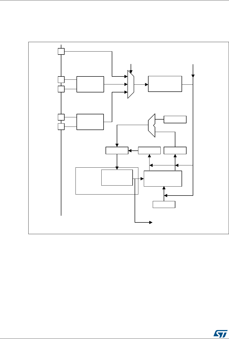
Clock recovery system (CRS) RM0394
248/1600 RM0394 Rev 4
7.3 CRS functional description
7.3.1 CRS block diagram
Figure 17. CRS block diagram
7.3.2 Synchronization input
The CRS synchronization (SYNC) source, selectable through the CRS_CFGR register, can
be the signal from the LSE clock or the USB SOF signal. For a better robustness of the
SYNC input, a simple digital filter (2 out of 3 majority votes, sampled by the HSI48 clock) is
implemented to filter out any glitches. This source signal also has a configurable polarity
and can then be divided by a programmable binary prescaler to obtain a synchronization
signal in a suitable frequency range (usually around 1 kHz).
For more information on the CRS synchronization source configuration, refer to
Section 7.6.2: CRS configuration register (CRS_CFGR).
It is also possible to generate a synchronization event by software, by setting the SWSYNC
bit in the CRS_CR register.
06Y9
/6(
86%
6<1&65&
*3,2
26&B,1
26&B287
86%B'3
86%B'0
6<1&GLYLGHU
«
6:6<1&
5(/2$'
6<1&
ELWFRXQWHU
)(&$3
5&0+]
+6,
5&&
&56B6<1&
)(/,0
75,0 )(',5
7R86%
7R51*
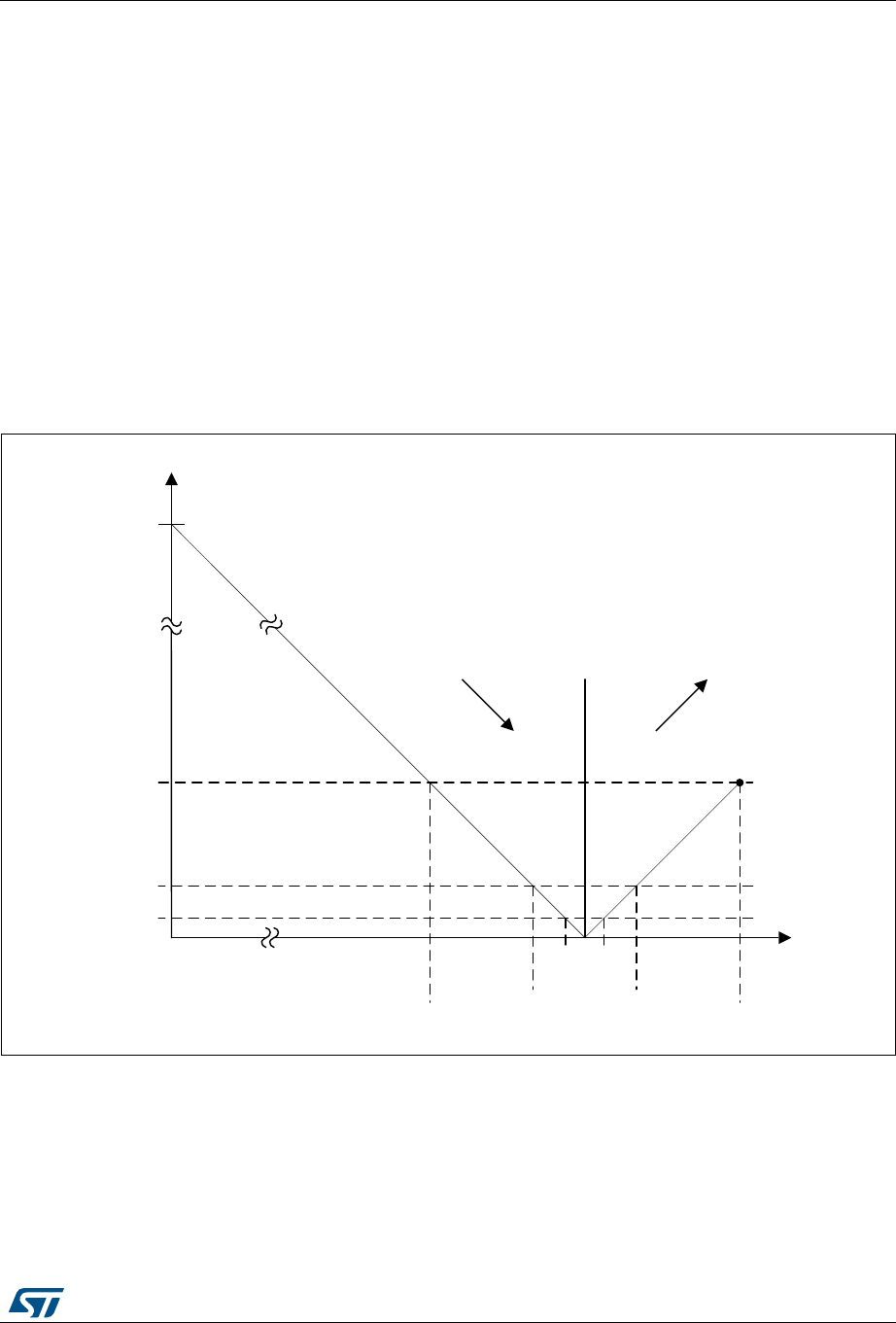
RM0394 Rev 4 249/1600
RM0394 Clock recovery system (CRS)
257
7.3.3 Frequency error measurement
The frequency error counter is a 16-bit down/up counter which is reloaded with the RELOAD
value on each SYNC event. It starts counting down till it reaches the zero value, where the
ESYNC (expected synchronization) event is generated. Then it starts counting up to the
OUTRANGE limit where it eventually stops (if no SYNC event is received) and generates a
SYNCMISS event. The OUTRANGE limit is defined as the frequency error limit (FELIM field
of the CRS_CFGR register) multiplied by 128.
When the SYNC event is detected, the actual value of the frequency error counter and its
counting direction are stored in the FECAP (frequency error capture) field and in the FEDIR
(frequency error direction) bit of the CRS_ISR register. When the SYNC event is detected
during the downcounting phase (before reaching the zero value), it means that the actual
frequency is lower than the target (and so, that the TRIM value should be incremented),
while when it is detected during the upcounting phase it means that the actual frequency is
higher (and that the TRIM value should be decremented).
Figure 18. CRS counter behavior
&56FRXQWHUYDOXH
5(/2$'
2875$1*(
[)(/,0
:$51,1*/,0,7
[)(/,0
72/(5$1&(/,0,7
)(/,0
6<1&(55 6<1&:$51 6<1&2. 6<1&:$51
6<1&0,66
'RZQ 8S
)UHTXHQF\
HUURUFRXQWHU
VWRSSHG
7ULPPLQJDFWLRQ
&56HYHQW
06Y9
(6<1&

Clock recovery system (CRS) RM0394
250/1600 RM0394 Rev 4
7.3.4 Frequency error evaluation and automatic trimming
The measured frequency error is evaluated by comparing its value with a set of limits:
– TOLERANCE LIMIT, given directly in the FELIM field of the CRS_CFGR register
– WARNING LIMIT, defined as 3 * FELIM value
– OUTRANGE (error limit), defined as 128 * FELIM value
The result of this comparison is used to generate the status indication and also to control the
automatic trimming which is enabled by setting the AUTOTRIMEN bit in the CRS_CR
register:
•When the frequency error is below the tolerance limit, it means that the actual trimming
value in the TRIM field is the optimal one and that then, no trimming action is
necessary.
– SYNCOK status indicated
– TRIM value not changed in AUTOTRIM mode
•When the frequency error is below the warning limit but above or equal to the tolerance
limit, it means that some trimming action is necessary but that adjustment by one
trimming step is enough to reach the optimal TRIM value.
– SYNCOK status indicated
– TRIM value adjusted by one trimming step in AUTOTRIM mode
•When the frequency error is above or equal to the warning limit but below the error
limit, it means that a stronger trimming action is necessary, and there is a risk that the
optimal TRIM value will not be reached for the next period.
– SYNCWARN status indicated
– TRIM value adjusted by two trimming steps in AUTOTRIM mode
•When the frequency error is above or equal to the error limit, it means that the
frequency is out of the trimming range. This can also happen when the SYNC input is
not clean or when some SYNC pulse is missing (for example when one USB SOF is
corrupted).
– SYNCERR or SYNCMISS status indicated
– TRIM value not changed in AUTOTRIM mode
Note: If the actual value of the TRIM field is so close to its limits that the automatic trimming would
force it to overflow or underflow, then the TRIM value is set just to the limit and the
TRIMOVF status is indicated.
In AUTOTRIM mode (AUTOTRIMEN bit set in the CRS_CR register), the TRIM field of
CRS_CR is adjusted by hardware and is read-only.
7.3.5 CRS initialization and configuration
RELOAD value
The RELOAD value should be selected according to the ratio between the target frequency
and the frequency of the synchronization source after prescaling. It is then decreased by
one in order to reach the expected synchronization on the zero value. The formula is the
following:
RELOAD = (fTARGET / fSYNC) - 1
The reset value of the RELOAD field corresponds to a target frequency of 48 MHz and a
synchronization signal frequency of 1 kHz (SOF signal from USB).
RM0394 Rev 4 251/1600
RM0394 Clock recovery system (CRS)
257
FELIM value
The selection of the FELIM value is closely coupled with the HSI48 oscillator characteristics
and its typical trimming step size. The optimal value corresponds to half of the trimming step
size, expressed as a number of HSI48 oscillator clock ticks. The following formula can be
used:
FELIM = (fTARGET / fSYNC) * STEP[%] / 100% / 2
The result should be always rounded up to the nearest integer value in order to obtain the
best trimming response. If frequent trimming actions are not wanted in the application, the
trimming hysteresis can be increased by increasing slightly the FELIM value.
The reset value of the FELIM field corresponds to (fTARGET / fSYNC) = 48000 and to a typical
trimming step size of 0.14%.
Caution: There is no hardware protection from a wrong configuration of the RELOAD and FELIM
fields which can lead to an erratic trimming response. The expected operational mode
requires proper setup of the RELOAD value (according to the synchronization source
frequency), which is also greater than 128 * FELIM value (OUTRANGE limit).
7.4 CRS low-power modes
7.5 CRS interrupts
Table 33. Effect of low-power modes on CRS
Mode Description
Sleep No effect.
CRS interrupts cause the device to exit the Sleep mode.
Stop CRS registers are frozen.
The CRS stops operating until the Stop or Standby mode is exited and the HSI48 oscillator
restarted.
Standby
Table 34. Interrupt control bits
Interrupt event Event flag Enable
control bit
Clear
flag bit
Expected synchronization ESYNCF ESYNCIE ESYNCC
Synchronization OK SYNCOKF SYNCOKIE SYNCOKC
Synchronization warning SYNCWARNF SYNCWARNIE SYNCWARNC
Synchronization or trimming error
(TRIMOVF, SYNCMISS, SYNCERR) ERRF ERRIE ERRC

Clock recovery system (CRS) RM0394
252/1600 RM0394 Rev 4
7.6 CRS registers
Refer to Section 1.2 on page 60 of the reference manual for a list of abbreviations used in
register descriptions.
The peripheral registers can be accessed by words (32-bit).
7.6.1 CRS control register (CRS_CR)
Address offset: 0x00
Reset value: 0x0000 2000
31 30 29 28 27 26 25 24 23 22 21 20 19 18 17 16
Res. Res. Res. Res. Res. Res. Res. Res. Res. Res. Res. Res. Res. Res. Res. Res.
15 14 13 12 11 10 9 8 7 6 5 4 3 2 1 0
Res. Res. TRIM[5:0] SW
SYNC
AUTO
TRIMEN CEN Res. ESYNC
IE ERRIE SYNC
WARNIE
SYNC
OKIE
rw rw rw rw rw rw rt_w1 rw rw rw rw rw rw
Bits 31:14 Reserved, must be kept at reset value.
Bits 13:8 TRIM[5:0]: HSI48 oscillator smooth trimming
These bits provide a user-programmable trimming value to the HSI48 oscillator. They can be
programmed to adjust to variations in voltage and temperature that influence the frequency
of the HSI48 oscillator.
The default value is 32, which corresponds to the middle of the trimming interval. The
trimming step is specified in the product datasheet. A higher TRIM value corresponds to a
higher output frequency.
When the AUTOTRIMEN bit is set, this field is controlled by hardware and is read-only.
Bit 7 SWSYNC: Generate software SYNC event
This bit is set by software in order to generate a software SYNC event. It is automatically
cleared by hardware.
0: No action
1: A software SYNC event is generated.
Bit 6 AUTOTRIMEN: Automatic trimming enable
This bit enables the automatic hardware adjustment of TRIM bits according to the measured
frequency error between two SYNC events. If this bit is set, the TRIM bits are read-only. The
TRIM value can be adjusted by hardware by one or two steps at a time, depending on the
measured frequency error value. Refer to Section 7.3.4: Frequency error evaluation and
automatic trimming for more details.
0: Automatic trimming disabled, TRIM bits can be adjusted by the user.
1: Automatic trimming enabled, TRIM bits are read-only and under hardware control.
Bit 5 CEN: Frequency error counter enable
This bit enables the oscillator clock for the frequency error counter.
0: Frequency error counter disabled
1: Frequency error counter enabled
When this bit is set, the CRS_CFGR register is write-protected and cannot be modified.
Bit 4 Reserved, must be kept at reset value.
RM0394 Rev 4 253/1600
RM0394 Clock recovery system (CRS)
257
7.6.2 CRS configuration register (CRS_CFGR)
This register can be written only when the frequency error counter is disabled (CEN bit is
cleared in CRS_CR). When the counter is enabled, this register is write-protected.
Address offset: 0x04
Reset value: 0x2022 BB7F
Bit 3 ESYNCIE: Expected SYNC interrupt enable
0: Expected SYNC (ESYNCF) interrupt disabled
1: Expected SYNC (ESYNCF) interrupt enabled
Bit 2 ERRIE: Synchronization or trimming error interrupt enable
0: Synchronization or trimming error (ERRF) interrupt disabled
1: Synchronization or trimming error (ERRF) interrupt enabled
Bit 1 SYNCWARNIE: SYNC warning interrupt enable
0: SYNC warning (SYNCWARNF) interrupt disabled
1: SYNC warning (SYNCWARNF) interrupt enabled
Bit 0 SYNCOKIE: SYNC event OK interrupt enable
0: SYNC event OK (SYNCOKF) interrupt disabled
1: SYNC event OK (SYNCOKF) interrupt enabled
31 30 29 28 27 26 25 24 23 22 21 20 19 18 17 16
SYNCPOL Res. SYNCSRC[1:0] Res. SYNCDIV[2:0] FELIM[7:0]
rw rw rw rw rw rw rw rw rw rw rw rw rw rw
15 14131211109876543210
RELOAD[15:0]
rw rw rw rw rw rw rw rw rw rw rw rw rw rw rw rw
Bit 31 SYNCPOL: SYNC polarity selection
This bit is set and cleared by software to select the input polarity for the SYNC signal source.
0: SYNC active on rising edge (default)
1: SYNC active on falling edge
Bit 30 Reserved, must be kept at reset value.
Bits 29:28 SYNCSRC[1:0]: SYNC signal source selection
These bits are set and cleared by software to select the SYNC signal source.
00: GPIO selected as SYNC signal source
01: LSE selected as SYNC signal source
10: USB SOF selected as SYNC signal source (default). Supported on STM32L4x2xx and
STM32L4x3xx devices only.
11: Reserved
Note: When using USB LPM (Link Power Management) and the device is in Sleep mode, the
periodic USB SOF will not be generated by the host. No SYNC signal will therefore be
provided to the CRS to calibrate the HSI48 oscillator on the run. To guarantee the
required clock precision after waking up from Sleep mode, the LSE or reference clock
on the GPIOs should be used as SYNC signal.
Bit 27 Reserved, must be kept at reset value.
Clock recovery system (CRS) RM0394
254/1600 RM0394 Rev 4
7.6.3 CRS interrupt and status register (CRS_ISR)
Address offset: 0x08
Reset value: 0x0000 0000
Bits 26:24 SYNCDIV[2:0]: SYNC divider
These bits are set and cleared by software to control the division factor of the SYNC signal.
000: SYNC not divided (default)
001: SYNC divided by 2
010: SYNC divided by 4
011: SYNC divided by 8
100: SYNC divided by 16
101: SYNC divided by 32
110: SYNC divided by 64
111: SYNC divided by 128
Bits 23:16 FELIM[7:0]: Frequency error limit
FELIM contains the value to be used to evaluate the captured frequency error value latched
in the FECAP[15:0] bits of the CRS_ISR register. Refer to Section 7.3.4: Frequency error
evaluation and automatic trimming for more details about FECAP evaluation.
Bits 15:0 RELOAD[15:0]: Counter reload value
RELOAD is the value to be loaded in the frequency error counter with each SYNC event.
Refer to Section 7.3.3: Frequency error measurement for more details about counter
behavior.
31 30 29 28 27 26 25 24 23 22 21 20 19 18 17 16
FECAP[15:0]
rrrrrr r rrrrr r r r r
15 14 13 12 11 10 9 8 7 6 5 4 3 2 1 0
FEDIR Res. Res. Res. Res. TRIM
OVF
SYNC
MISS
SYNC
ERR Res. Res. Res. Res. ESYNCF ERRF SYNC
WARNF
SYNC
OKF
r rrr r r r r
Bits 31:16 FECAP[15:0]: Frequency error capture
FECAP is the frequency error counter value latched in the time of the last SYNC event.
Refer to Section 7.3.4: Frequency error evaluation and automatic trimming for more details
about FECAP usage.
Bit 15 FEDIR: Frequency error direction
FEDIR is the counting direction of the frequency error counter latched in the time of the last
SYNC event. It shows whether the actual frequency is below or above the target.
0: Upcounting direction, the actual frequency is above the target.
1: Downcounting direction, the actual frequency is below the target.
Bits 14:11 Reserved, must be kept at reset value.
Bit 10 TRIMOVF: Trimming overflow or underflow
This flag is set by hardware when the automatic trimming tries to over- or under-flow the
TRIM value. An interrupt is generated if the ERRIE bit is set in the CRS_CR register. It is
cleared by software by setting the ERRC bit in the CRS_ICR register.
0: No trimming error signalized
1: Trimming error signalized

RM0394 Rev 4 255/1600
RM0394 Clock recovery system (CRS)
257
Bit 9 SYNCMISS: SYNC missed
This flag is set by hardware when the frequency error counter reached value FELIM * 128
and no SYNC was detected, meaning either that a SYNC pulse was missed or that the
frequency error is too big (internal frequency too high) to be compensated by adjusting the
TRIM value, and that some other action should be taken. At this point, the frequency error
counter is stopped (waiting for a next SYNC) and an interrupt is generated if the ERRIE bit is
set in the CRS_CR register. It is cleared by software by setting the ERRC bit in the
CRS_ICR register.
0: No SYNC missed error signalized
1: SYNC missed error signalized
Bit 8 SYNCERR: SYNC error
This flag is set by hardware when the SYNC pulse arrives before the ESYNC event and the
measured frequency error is greater than or equal to FELIM * 128. This means that the
frequency error is too big (internal frequency too low) to be compensated by adjusting the
TRIM value, and that some other action should be taken. An interrupt is generated if the
ERRIE bit is set in the CRS_CR register. It is cleared by software by setting the ERRC bit in
the CRS_ICR register.
0: No SYNC error signalized
1: SYNC error signalized
Bits 7:4 Reserved, must be kept at reset value.
Bit 3 ESYNCF: Expected SYNC flag
This flag is set by hardware when the frequency error counter reached a zero value. An
interrupt is generated if the ESYNCIE bit is set in the CRS_CR register. It is cleared by
software by setting the ESYNCC bit in the CRS_ICR register.
0: No expected SYNC signalized
1: Expected SYNC signalized
Bit 2 ERRF: Error flag
This flag is set by hardware in case of any synchronization or trimming error. It is the logical
OR of the TRIMOVF, SYNCMISS and SYNCERR bits. An interrupt is generated if the ERRIE
bit is set in the CRS_CR register. It is cleared by software in reaction to setting the ERRC bit
in the CRS_ICR register, which clears the TRIMOVF, SYNCMISS and SYNCERR bits.
0: No synchronization or trimming error signalized
1: Synchronization or trimming error signalized
Bit 1 SYNCWARNF: SYNC warning flag
This flag is set by hardware when the measured frequency error is greater than or equal to
FELIM * 3, but smaller than FELIM * 128. This means that to compensate the frequency
error, the TRIM value must be adjusted by two steps or more. An interrupt is generated if the
SYNCWARNIE bit is set in the CRS_CR register. It is cleared by software by setting the
SYNCWARNC bit in the CRS_ICR register.
0: No SYNC warning signalized
1: SYNC warning signalized
Bit 0 SYNCOKF: SYNC event OK flag
This flag is set by hardware when the measured frequency error is smaller than FELIM * 3.
This means that either no adjustment of the TRIM value is needed or that an adjustment by
one trimming step is enough to compensate the frequency error. An interrupt is generated if
the SYNCOKIE bit is set in the CRS_CR register. It is cleared by software by setting the
SYNCOKC bit in the CRS_ICR register.
0: No SYNC event OK signalized
1: SYNC event OK signalized

Clock recovery system (CRS) RM0394
256/1600 RM0394 Rev 4
7.6.4 CRS interrupt flag clear register (CRS_ICR)
Address offset: 0x0C
Reset value: 0x0000 0000
31 30 29 28 27 26 25 24 23 22 21 20 19 18 17 16
Res. Res. Res. Res. Res. Res. Res. Res. Res. Res. Res. Res. Res. Res. Res. Res.
151413121110987654 3 2 1 0
Res. Res. Res. Res. Res. Res. Res. Res. Res. Res. Res. Res. ESYNCC ERRC SYNC
WARNC
SYNC
OKC
rw rw rw rw
Bits 31:4 Reserved, must be kept at reset value.
Bit 3 ESYNCC: Expected SYNC clear flag
Writing 1 to this bit clears the ESYNCF flag in the CRS_ISR register.
Bit 2 ERRC: Error clear flag
Writing 1 to this bit clears TRIMOVF, SYNCMISS and SYNCERR bits and consequently also
the ERRF flag in the CRS_ISR register.
Bit 1 SYNCWARNC: SYNC warning clear flag
Writing 1 to this bit clears the SYNCWARNF flag in the CRS_ISR register.
Bit 0 SYNCOKC: SYNC event OK clear flag
Writing 1 to this bit clears the SYNCOKF flag in the CRS_ISR register.
RM0394 Rev 4 257/1600
RM0394 Clock recovery system (CRS)
257
7.6.5 CRS register map
Refer to Section 2.2.2 on page 67 for the register boundary addresses.
Table 35. CRS register map and reset values
Offset Register
31
30
29
28
27
26
25
24
23
22
21
20
19
18
17
16
15
14
13
12
11
10
9
8
7
6
5
4
3
2
1
0
0x00
CRS_CR
Res.
Res.
Res.
Res.
Res.
Res.
Res.
Res.
Res.
Res.
Res.
Res.
Res.
Res.
Res.
Res.
Res.
Res.
TRIM[5:0]
SWSYNC
AUTOTRIMEN
CEN
Res.
ESYNCIE
ERRIE
SYNCWARNIE
SYNCOKIE
Reset value 10000000000000
0x04
CRS_CFGR
SYNCPOL
Res.
SYNC
SRC
[1:0]
Res.
SYNC
DIV
[2:0]
FELIM[7:0] RELOAD[15:0]
Reset value 0 1 0 000001000101011101101111111
0x08
CRS_ISR FECAP[15:0]
FEDIR
Res.
Res.
Res.
Res.
TRIMOVF
SYNCMISS
SYNCERR
Res.
Res.
Res.
Res.
ESYNCF
ERRF
SYNCWARNF
SYNCOKF
Reset value 000 00000000000000 000 0000
0x0C
CRS_ICR
Res.
Res.
Res.
Res.
Res.
Res.
Res.
Res.
Res.
Res.
Res.
Res.
Res.
Res.
Res.
Res.
Res.
Res.
Res.
Res.
Res.
Res.
Res.
Res.
Res.
Res.
Res.
Res.
ESYNCC
ERRC
SYNCWARNC
SYNCOKC
Reset value 0000

General-purpose I/Os (GPIO) RM0394
258/1600 RM0394 Rev 4
8 General-purpose I/Os (GPIO)
8.1 Introduction
Each general-purpose I/O port has four 32-bit configuration registers (GPIOx_MODER,
GPIOx_OTYPER, GPIOx_OSPEEDR and GPIOx_PUPDR), two 32-bit data registers
(GPIOx_IDR and GPIOx_ODR) and a 32-bit set/reset register (GPIOx_BSRR). In addition
all GPIOs have a 32-bit locking register (GPIOx_LCKR) and two 32-bit alternate function
selection registers (GPIOx_AFRH and GPIOx_AFRL).
8.2 GPIO main features
•Output states: push-pull or open drain + pull-up/down
•Output data from output data register (GPIOx_ODR) or peripheral (alternate function
output)
•Speed selection for each I/O
•Input states: floating, pull-up/down, analog
•Input data to input data register (GPIOx_IDR) or peripheral (alternate function input)
•Bit set and reset register (GPIOx_ BSRR) for bitwise write access to GPIOx_ODR
•Locking mechanism (GPIOx_LCKR) provided to freeze the I/O port configurations
•Analog function
•Alternate function selection registers
•Fast toggle capable of changing every two clock cycles
•Highly flexible pin multiplexing allows the use of I/O pins as GPIOs or as one of several
peripheral functions
8.3 GPIO functional description
Subject to the specific hardware characteristics of each I/O port listed in the datasheet, each
port bit of the general-purpose I/O (GPIO) ports can be individually configured by software in
several modes:
•Input floating
•Input pull-up
•Input-pull-down
•Analog
•Output open-drain with pull-up or pull-down capability
•Output push-pull with pull-up or pull-down capability
•Alternate function push-pull with pull-up or pull-down capability
•Alternate function open-drain with pull-up or pull-down capability
Each I/O port bit is freely programmable, however the I/O port registers have to be
accessed as 32-bit words, half-words or bytes. The purpose of the GPIOx_BSRR and
GPIOx_BRR registers is to allow atomic read/modify accesses to any of the GPIOx_ODR
registers. In this way, there is no risk of an IRQ occurring between the read and the modify
access.
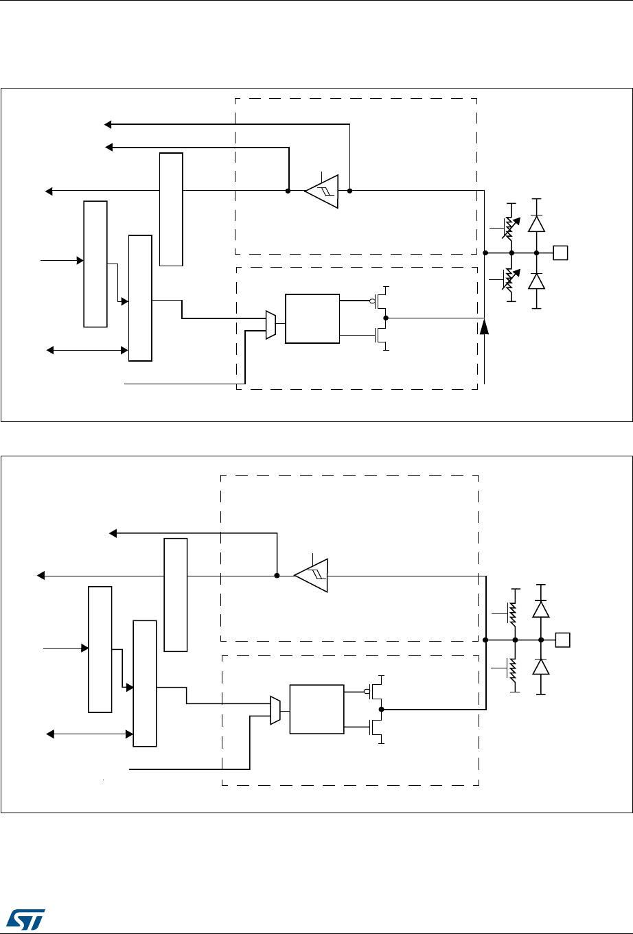
RM0394 Rev 4 259/1600
RM0394 General-purpose I/Os (GPIO)
275
Figure 19 and Figure 20 show the basic structures of a standard and a 5-Volt tolerant I/O
port bit, respectively. Table 36 gives the possible port bit configurations.
Figure 19. Basic structure of an I/O port bit
Figure 20. Basic structure of a 5-Volt tolerant I/O port bit
1. VDD_FT is a potential specific to five-volt tolerant I/Os and different from VDD.
$OWHUQDWHIXQFWLRQRXWSXW
$OWHUQDWHIXQFWLRQLQSXW
3XVKSXOO
RSHQGUDLQRU
GLVDEOHG
,QSXWGDWDUHJLVWHU
2XWSXWGDWDUHJLVWHU
5HDGZULWH
)URPRQFKLS
SHULSKHUDO
7RRQFKLS
SHULSKHUDO
2XWSXW
FRQWURO
$QDORJ
RQRII
3XOO
3XOO
GRZQ
RQRII
,2SLQ
9
'',2[
9
'',2[
9
66
9
66
WULJJHU
9
66
9
'',2[
3URWHFWLRQ
GLRGH
3URWHFWLRQ
GLRGH
RQRII
,QSXWGULYHU
2XWSXWGULYHU
XS
3026
1026
5HDG
%LWVHWUHVHWUHJLVWHUV
:ULWH
$QDORJ
069
$OWHUQDWHIXQFWLRQRXWSXW
$OWHUQDWHIXQFWLRQLQSXW
3XVKSXOO
RSHQGUDLQRU
GLVDEOHG
2XWSXWGDWDUHJLVWHU
5HDGZULWH
)URPRQFKLS
SHULSKHUDO
7RRQFKLS
SHULSKHUDO
2XWSXW
FRQWURO
RQRII 3XOO
3XOO
RQRII
,2SLQ
9
'',2[
9
'',2[
9
66
9
66
77/6FKPLWW
WULJJHU
9
66
9
''B)7
3URWHFWLRQ
GLRGH
3URWHFWLRQ
GLRGH
RQRII
,QSXWGULYHU
2XWSXWGULYHU
GRZQ
XS
3026
1026
5HDG
%LWVHWUHVHWUHJLVWHUV
:ULWH
,QSXWGDWDUHJLVWHU
DLG
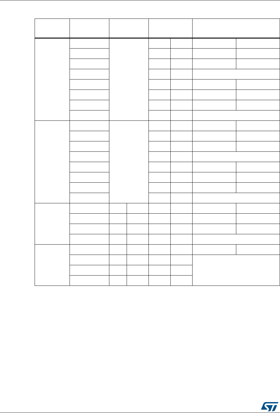
General-purpose I/Os (GPIO) RM0394
260/1600 RM0394 Rev 4
Table 36. Port bit configuration table(1)
1. GP = general-purpose, PP = push-pull, PU = pull-up, PD = pull-down, OD = open-drain, AF = alternate
function.
MODE(i)
[1:0] OTYPER(i) OSPEED(i)
[1:0]
PUPD(i)
[1:0] I/O configuration
01
0
SPEED
[1:0]
0 0 GP output PP
0 0 1 GP output PP + PU
0 1 0 GP output PP + PD
0 1 1 Reserved
1 0 0 GP output OD
1 0 1 GP output OD + PU
1 1 0 GP output OD + PD
1 1 1 Reserved (GP output OD)
10
0
SPEED
[1:0]
0 0 AF PP
0 0 1 AF PP + PU
0 1 0 AF PP + PD
0 1 1 Reserved
100AFOD
101AFOD + PU
110AFOD + PD
1 1 1 Reserved
00
x x x 0 0 Input Floating
x x x 0 1 Input PU
x x x 1 0 Input PD
x x x 1 1 Reserved (input floating)
11
x x x 0 0 Input/output Analog
xxx01
Reservedxxx10
xxx11

RM0394 Rev 4 261/1600
RM0394 General-purpose I/Os (GPIO)
275
8.3.1 General-purpose I/O (GPIO)
During and just after reset, the alternate functions are not active and most of the I/O ports
are configured in analog mode.
The debug pins are in AF pull-up/pull-down after reset:
•PA15: JTDI in pull-up
•PA14: JTCK/SWCLK in pull-down
•PA13: JTMS/SWDAT in pull-up
•PB4: NJTRST in pull-up
•PB3: JTDO in floating state no pull-up/pull-down
PH3/BOOT0 is in input mode during the reset until at least the end of the option byte loading
phase. See Section 8.3.15: Using PH3 as GPIO.
When the pin is configured as output, the value written to the output data register
(GPIOx_ODR) is output on the I/O pin. It is possible to use the output driver in push-pull
mode or open-drain mode (only the low level is driven, high level is HI-Z).
The input data register (GPIOx_IDR) captures the data present on the I/O pin at every AHB
clock cycle.
All GPIO pins have weak internal pull-up and pull-down resistors, which can be activated or
not depending on the value in the GPIOx_PUPDR register.
8.3.2 I/O pin alternate function multiplexer and mapping
The device I/O pins are connected to on-board peripherals/modules through a multiplexer
that allows only one peripheral alternate function (AF) connected to an I/O pin at a time. In
this way, there can be no conflict between peripherals available on the same I/O pin.
Each I/O pin (except PH3) has a multiplexer with up to sixteen alternate function inputs (AF0
to AF15) that can be configured through the GPIOx_AFRL (for pin 0 to 7) and GPIOx_AFRH
(for pin 8 to 15) registers:
•After reset the multiplexer selection is alternate function 0 (AF0). The I/Os are
configured in alternate function mode through GPIOx_MODER register.
•The specific alternate function assignments for each pin are detailed in the device
datasheet.
In addition to this flexible I/O multiplexing architecture, each peripheral has alternate
functions mapped onto different I/O pins to optimize the number of peripherals available in
smaller packages.
To use an I/O in a given configuration, the user has to proceed as follows:
•Debug function: after each device reset these pins are assigned as alternate function
pins immediately usable by the debugger host
•GPIO: configure the desired I/O as output, input or analog in the GPIOx_MODER
register.
•Peripheral alternate function:
– Connect the I/O to the desired AFx in one of the GPIOx_AFRL or GPIOx_AFRH
register.
– Select the type, pull-up/pull-down and output speed via the GPIOx_OTYPER,
GPIOx_PUPDR and GPIOx_OSPEEDER registers, respectively.

General-purpose I/Os (GPIO) RM0394
262/1600 RM0394 Rev 4
– Configure the desired I/O as an alternate function in the GPIOx_MODER register.
•Additional functions:
– For the ADC, DAC, OPAMP, and COMP, configure the desired I/O in analog mode
in the GPIOx_MODER register and configure the required function in the ADC,
DAC, OPAMP, and COMP registers.
– For the additional functions like RTC, WKUPx and oscillators, configure the
required function in the related RTC, PWR and RCC registers. These functions
have priority over the configuration in the standard GPIO registers.
Refer to the “Alternate function mapping” table in the device datasheet for the detailed
mapping of the alternate function I/O pins.
8.3.3 I/O port control registers
Each of the GPIO ports has four 32-bit memory-mapped control registers (GPIOx_MODER,
GPIOx_OTYPER, GPIOx_OSPEEDR, GPIOx_PUPDR) to configure up to 16 I/Os. The
GPIOx_MODER register is used to select the I/O mode (input, output, AF, analog). The
GPIOx_OTYPER and GPIOx_OSPEEDR registers are used to select the output type (push-
pull or open-drain) and speed. The GPIOx_PUPDR register is used to select the pull-
up/pull-down whatever the I/O direction.
8.3.4 I/O port data registers
Each GPIO has two 16-bit memory-mapped data registers: input and output data registers
(GPIOx_IDR and GPIOx_ODR). GPIOx_ODR stores the data to be output, it is read/write
accessible. The data input through the I/O are stored into the input data register
(GPIOx_IDR), a read-only register.
See Section 8.4.5: GPIO port input data register (GPIOx_IDR) (x = A to E and H) and
Section 8.4.6: GPIO port output data register (GPIOx_ODR) (x = A to E and H) for the
register descriptions.
8.3.5 I/O data bitwise handling
The bit set reset register (GPIOx_BSRR) is a 32-bit register which allows the application to
set and reset each individual bit in the output data register (GPIOx_ODR). The bit set reset
register has twice the size of GPIOx_ODR.
To each bit in GPIOx_ODR, correspond two control bits in GPIOx_BSRR: BS(i) and BR(i).
When written to 1, bit BS(i) sets the corresponding ODR(i) bit. When written to 1, bit BR(i)
resets the ODR(i) corresponding bit.
Writing any bit to 0 in GPIOx_BSRR does not have any effect on the corresponding bit in
GPIOx_ODR. If there is an attempt to both set and reset a bit in GPIOx_BSRR, the set
action takes priority.
Using the GPIOx_BSRR register to change the values of individual bits in GPIOx_ODR is a
“one-shot” effect that does not lock the GPIOx_ODR bits. The GPIOx_ODR bits can always
be accessed directly. The GPIOx_BSRR register provides a way of performing atomic
bitwise handling.
There is no need for the software to disable interrupts when programming the GPIOx_ODR
at bit level: it is possible to modify one or more bits in a single atomic AHB write access.

RM0394 Rev 4 263/1600
RM0394 General-purpose I/Os (GPIO)
275
8.3.6 GPIO locking mechanism
It is possible to freeze the GPIO control registers by applying a specific write sequence to
the GPIOx_LCKR register. The frozen registers are GPIOx_MODER, GPIOx_OTYPER,
GPIOx_OSPEEDR, GPIOx_PUPDR, GPIOx_AFRL and GPIOx_AFRH.
To write the GPIOx_LCKR register, a specific write / read sequence has to be applied. When
the right LOCK sequence is applied to bit 16 in this register, the value of LCKR[15:0] is used
to lock the configuration of the I/Os (during the write sequence the LCKR[15:0] value must
be the same). When the LOCK sequence has been applied to a port bit, the value of the port
bit can no longer be modified until the next MCU reset or peripheral reset. Each
GPIOx_LCKR bit freezes the corresponding bit in the control registers (GPIOx_MODER,
GPIOx_OTYPER, GPIOx_OSPEEDR, GPIOx_PUPDR, GPIOx_AFRL and GPIOx_AFRH.
The LOCK sequence (refer to Section 8.4.8: GPIO port configuration lock register
(GPIOx_LCKR) (x = A to E and H)) can only be performed using a word (32-bit long)
access to the GPIOx_LCKR register due to the fact that GPIOx_LCKR bit 16 has to be set
at the same time as the [15:0] bits.
For more details refer to LCKR register description in Section 8.4.8: GPIO port configuration
lock register (GPIOx_LCKR) (x = A to E and H).
8.3.7 I/O alternate function input/output
Two registers are provided to select one of the alternate function inputs/outputs available for
each I/O. With these registers, the user can connect an alternate function to some other pin
as required by the application.
This means that a number of possible peripheral functions are multiplexed on each GPIO
using the GPIOx_AFRL and GPIOx_AFRH alternate function registers. The application can
thus select any one of the possible functions for each I/O. The AF selection signal being
common to the alternate function input and alternate function output, a single channel is
selected for the alternate function input/output of a given I/O.
To know which functions are multiplexed on each GPIO pin, refer to the device datasheet.
No alternate function is mapped on PH3.
8.3.8 External interrupt/wakeup lines
All ports have external interrupt capability. To use external interrupt lines, the port can be
configured in input, output or alternate function mode (the port must not be configured in
analog mode). Refer to Section 13: Extended interrupts and events controller (EXTI) and
toSection 13.3.2: Wakeup event management.
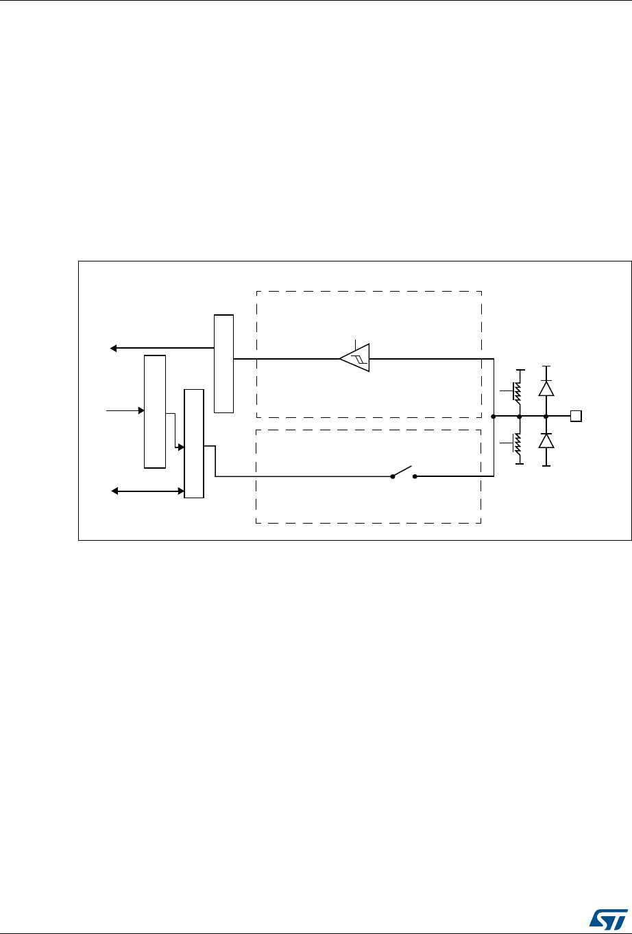
General-purpose I/Os (GPIO) RM0394
264/1600 RM0394 Rev 4
8.3.9 Input configuration
When the I/O port is programmed as input:
•The output buffer is disabled
•The Schmitt trigger input is activated
•The pull-up and pull-down resistors are activated depending on the value in the
GPIOx_PUPDR register
•The data present on the I/O pin are sampled into the input data register every AHB
clock cycle
•A read access to the input data register provides the I/O state
Figure 21 shows the input configuration of the I/O port bit.
Figure 21. Input floating/pull up/pull down configurations
8.3.10 Output configuration
When the I/O port is programmed as output:
•The output buffer is enabled:
– Open drain mode: A “0” in the Output register activates the N-MOS whereas a “1”
in the Output register leaves the port in Hi-Z (the P-MOS is never activated)
– Push-pull mode: A “0” in the Output register activates the N-MOS whereas a “1” in
the Output register activates the P-MOS
•The Schmitt trigger input is activated
•The pull-up and pull-down resistors are activated depending on the value in the
GPIOx_PUPDR register
•The data present on the I/O pin are sampled into the input data register every AHB
clock cycle
•A read access to the input data register gets the I/O state
•A read access to the output data register gets the last written value
Figure 22 shows the output configuration of the I/O port bit.
RQRII
SXOO
SXOO
RQRII
,2SLQ
9'',2[
966
77/6FKPLWW
WULJJHU
966
9'',2[
SURWHFWLRQ
GLRGH
SURWHFWLRQ
GLRGH
RQ
LQSXWGULYHU
RXWSXWGULYHU
GRZQ
XS
,QSXWGDWDUHJLVWHU
2XWSXWGDWDUHJLVWHU
5HDGZULWH
5HDG
%LWVHWUHVHWUHJLVWHUV
:ULWH
069
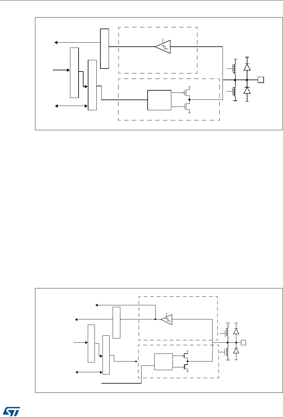
RM0394 Rev 4 265/1600
RM0394 General-purpose I/Os (GPIO)
275
Figure 22. Output configuration
8.3.11 Alternate function configuration
When the I/O port is programmed as alternate function:
•The output buffer can be configured in open-drain or push-pull mode
•The output buffer is driven by the signals coming from the peripheral (transmitter
enable and data)
•The Schmitt trigger input is activated
•The weak pull-up and pull-down resistors are activated or not depending on the value
in the GPIOx_PUPDR register
•The data present on the I/O pin are sampled into the input data register every AHB
clock cycle
•A read access to the input data register gets the I/O state
Note: The alternate function configuration described above is not applied when the selected
alternate function is an LCD function or a SWPMI_IO. In this case, the I/O, programmed as
an alternate function output, is configured as described in the analog configuration.
Figure 23 shows the Alternate function configuration of the I/O port bit.
Figure 23. Alternate function configuration
3XVKSXOORU
2SHQGUDLQ
2XWSXW
FRQWURO
9'',2[
966
77/6FKPLWW
WULJJHU
RQ
,QSXWGULYHU
2XWSXWGULYHU
3026
1026
,QSXWGDWDUHJLVWHU
2XWSXWGDWDUHJLVWHU
5HDGZULWH
5HDG
%LWVHWUHVHWUHJLVWHUV
:ULWH
RQRII
SXOO
SXOO
RQRII
9'',2[
966 966
9'',2[
SURWHFWLRQ
GLRGH
SURWHFWLRQ
GLRGH
GRZQ
XS
,2SLQ
069
06Y9
$OWHUQDWH IXQFWLRQ RXWSXW
$OWHUQDWH IXQFWLRQ LQSXW
SXVKSXOO RU
RSHQGUDLQ
)URP RQFKLS
SHULSKHUDO
7R RQFKLS
SHULSKHUDO
2XWSXW
FRQWURO
9''
966
77/ 6FKPLWW
WULJJHU
RQ
,QSXW GULYHU
2XWSXW GULYHU
3026
1026
,QSXW GDWD UHJLVWHU
2XWSXW GDWD UHJLVWHU
5HDGZULWH
5HDG
%LW VHWUHVHW UHJLVWHUV
:ULWH
RQRII
RQRII
9'',2[
966 966
SURWHFWLRQ
GLRGH
SURWHFWLRQ
GLRGH
3XOO
3XOO
,2 SLQ
GRZQ
XS
9'',2[
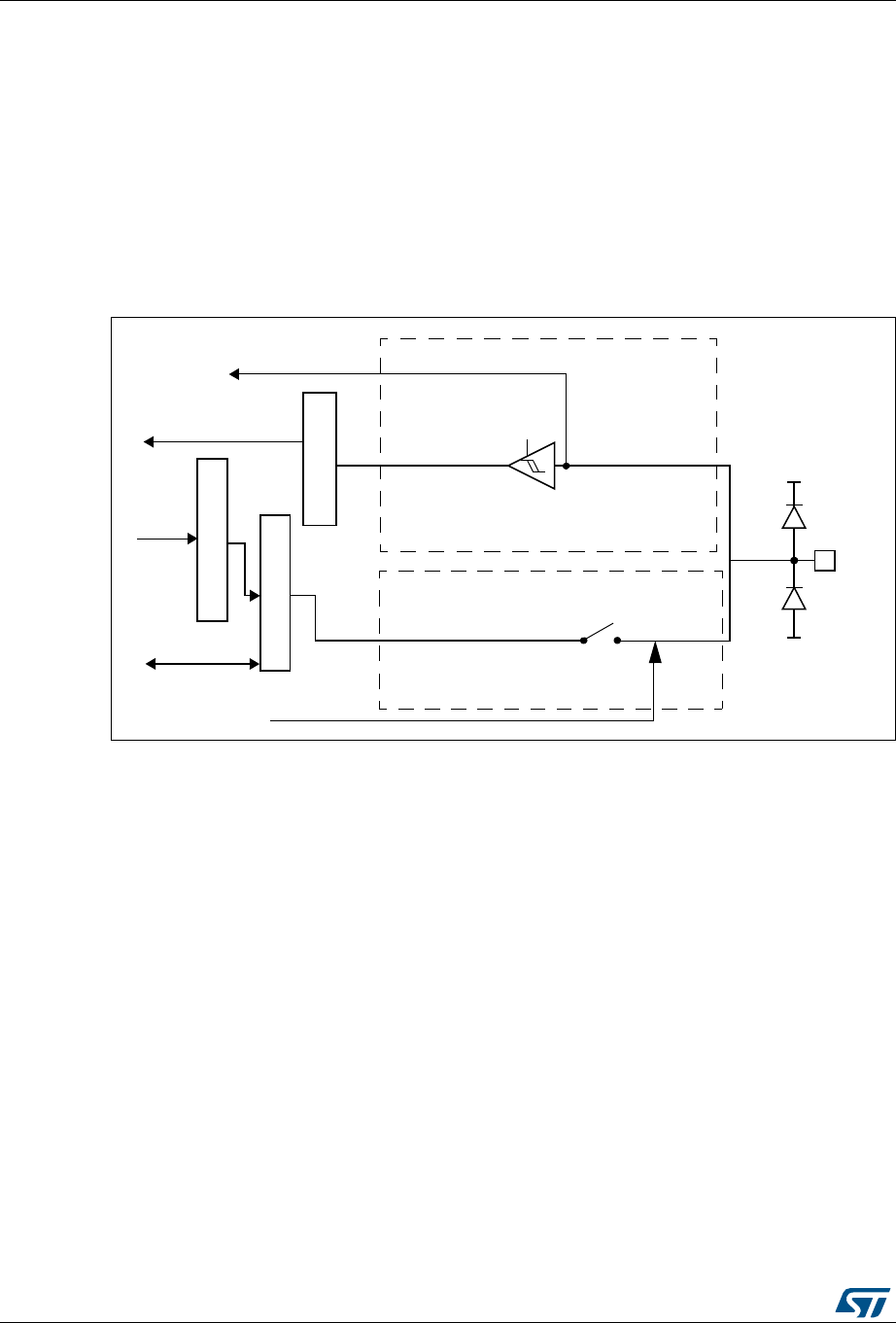
General-purpose I/Os (GPIO) RM0394
266/1600 RM0394 Rev 4
8.3.12 Analog configuration
When the I/O port is programmed as analog configuration:
•The output buffer is disabled
•The Schmitt trigger input is deactivated, providing zero consumption for every analog
value of the I/O pin. The output of the Schmitt trigger is forced to a constant value (0).
•The weak pull-up and pull-down resistors are disabled by hardware
•Read access to the input data register gets the value “0”
Figure 24 shows the high-impedance, analog-input configuration of the I/O port bits.
Figure 24. High impedance-analog configuration
8.3.13 Using the HSE or LSE oscillator pins as GPIOs
When the HSE or LSE oscillator is switched OFF (default state after reset), the related
oscillator pins can be used as normal GPIOs.
When the HSE or LSE oscillator is switched ON (by setting the HSEON or LSEON bit in the
RCC_CSR register) the oscillator takes control of its associated pins and the GPIO
configuration of these pins has no effect.
When the oscillator is configured in a user external clock mode, only the pin is reserved for
clock input and the OSC_OUT or OSC32_OUT pin can still be used as normal GPIO.
8.3.14 Using the GPIO pins in the RTC supply domain
The PC13/PC14/PC15 GPIO functionality is lost when the core supply domain is powered
off (when the device enters Standby mode). In this case, if their GPIO configuration is not
bypassed by the RTC configuration, these pins are set in an analog input mode.
For details about I/O control by the RTC, refer to Section 36.3: RTC functional description.
)URPRQFKLS
SHULSKHUDO
7RRQFKLS
SHULSKHUDO
$QDORJ
WULJJHU
RII
,QSXWGULYHU
,QSXWGDWDUHJLVWHU
2XWSXWGDWDUHJLVWHU
5HDGZULWH
5HDG
%LWVHWUHVHWUHJLVWHUV
:ULWH
$QDORJ
966
9'',2[
SURWHFWLRQ
GLRGH
SURWHFWLRQ
GLRGH
,2SLQ
069
77/6FKPLWW

RM0394 Rev 4 267/1600
RM0394 General-purpose I/Os (GPIO)
275
8.3.15 Using PH3 as GPIO
PH3 may be used as boot pin (BOOT0) or as a GPIO. Depending on the nSWBOOT0 bit in
the user option byte, it switches from the input mode to the analog input mode:
•After the option byte loading phase if nSWBOOT0 = 1.
•After reset if nSWBOOT0 = 0.
8.4 GPIO registers
This section gives a detailed description of the GPIO registers.
For a summary of register bits, register address offsets and reset values, refer to Table 37.
The peripheral registers can be written in word, half word or byte mode.
8.4.1 GPIO port mode register (GPIOx_MODER) (x =A to E and H)
Address offset:0x00
Reset value:
•0xABFF FFFF (for port A)
•0xFFFF FEBF (for port B)
•0xFFFF FFFF for ports C..E
•0x0000 000F (for port H)
31 30 29 28 27 26 25 24 23 22 21 20 19 18 17 16
MODE15[1:0] MODE14[1:0] MODE13[1:0] MODE12[1:0] MODE11[1:0] MODE10[1:0] MODE9[1:0] MODE8[1:0]
rw rw rw rw rw rw rw rw rw rw rw rw rw rw rw rw
1514131211109876543210
MODE7[1:0] MODE6[1:0] MODE5[1:0] MODE4[1:0] MODE3[1:0] MODE2[1:0] MODE1[1:0] MODE0[1:0]
rw rw rw rw rw rw rw rw rw rw rw rw rw rw rw rw
Bits 31:0 MODE[15:0][1:0]: Port x configuration I/O pin y (y = 15 to 0)
These bits are written by software to configure the I/O mode.
00: Input mode
01: General purpose output mode
10: Alternate function mode
11: Analog mode (reset state)
General-purpose I/Os (GPIO) RM0394
268/1600 RM0394 Rev 4
8.4.2 GPIO port output type register (GPIOx_OTYPER) (x = A to E and H)
Address offset: 0x04
Reset value: 0x0000 0000
8.4.3 GPIO port output speed register (GPIOx_OSPEEDR)
(x = A to E and H)
Address offset: 0x08
Reset value: 0x0C00 0000 (for port A)
Reset value: 0x0000 0000 (for the other ports)
8.4.4 GPIO port pull-up/pull-down register (GPIOx_PUPDR)
(x = A to E and H)
Address offset: 0x0C
Reset value: 0x6400 0000 (for port A)
31 30 29 28 27 26 25 24 23 22 21 20 19 18 17 16
Res. Res. Res. Res. Res. Res. Res. Res. Res. Res. Res. Res. Res. Res. Res. Res.
1514131211109876543210
OT15 OT14 OT13 OT12 OT11 OT10 OT9 OT8 OT7 OT6 OT5 OT4 OT3 OT2 OT1 OT0
rw rw rw rw rw rw rw rw rw rw rw rw rw rw rw rw
Bits 31:16 Reserved, must be kept at reset value.
Bits 15:0 OT[15:0]: Port x configuration I/O pin y (y = 15 to 0)
These bits are written by software to configure the I/O output type.
0: Output push-pull (reset state)
1: Output open-drain
31 30 29 28 27 26 25 24 23 22 21 20 19 18 17 16
OSPEED15
[1:0]
OSPEED14
[1:0]
OSPEED13
[1:0]
OSPEED12
[1:0]
OSPEED11
[1:0]
OSPEED10
[1:0]
OSPEED9
[1:0]
OSPEED8
[1:0]
rw rw rw rw rw rw rw rw rw rw rw rw rw rw rw rw
15 14 13 12 11 10 9 8 7 6 5 4 3 2 1 0
OSPEED7
[1:0]
OSPEED6
[1:0]
OSPEED5
[1:0]
OSPEED4
[1:0]
OSPEED3
[1:0]
OSPEED2
[1:0]
OSPEED1
[1:0]
OSPEED0
[1:0]
rw rw rw rw rw rw rw rw rw rw rw rw rw rw rw rw
Bits 31:0 OSPEED[15:0][1:0]: Port x configuration I/O pin y (y = 15 to 0)
These bits are written by software to configure the I/O output speed.
00: Low speed
01: Medium speed
10: High speed
11: Very high speed
Note: Refer to the device datasheet for the frequency specifications and the power supply
and load conditions for each speed..

RM0394 Rev 4 269/1600
RM0394 General-purpose I/Os (GPIO)
275
Reset value: 0x0000 0100 (for port B)
Reset value: 0x0000 0000 (for other ports)
8.4.5 GPIO port input data register (GPIOx_IDR) (x = A to E and H)
Address offset: 0x10
Reset value: 0x0000 XXXX
8.4.6 GPIO port output data register (GPIOx_ODR) (x = A to E and H)
Address offset: 0x14
Reset value: 0x0000 0000
31 30 29 28 27 26 25 24 23 22 21 20 19 18 17 16
PUPD15[1:0] PUPD14[1:0] PUPD13[1:0] PUPD12[1:0] PUPD11[1:0] PUPD10[1:0] PUPD9[1:0] PUPD8[1:0]
rw rw rw rw rw rw rw rw rw rw rw rw rw rw rw rw
1514131211109876543210
PUPD7[1:0] PUPD6[1:0] PUPD5[1:0] PUPD4[1:0] PUPD3[1:0] PUPD2[1:0] PUPD1[1:0] PUPD0[1:0]
rw rw rw rw rw rw rw rw rw rw rw rw rw rw rw rw
Bits 31:0 PUPD[15:0][1:0]: Port x configuration I/O pin y (y = 15 to 0)
These bits are written by software to configure the I/O pull-up or pull-down
00: No pull-up, pull-down
01: Pull-up
10: Pull-down
11: Reserved
31 30 29 28 27 26 25 24 23 22 21 20 19 18 17 16
Res. Res. Res. Res. Res. Res. Res. Res. Res. Res. Res. Res. Res. Res. Res. Res.
1514131211109876543210
ID15 ID14 ID13 ID12 ID11 ID10 ID9 ID8 ID7 ID6 ID5 ID4 ID3 ID2 ID1 ID0
rrrrrr r r r r rrrrrr
Bits 31:16 Reserved, must be kept at reset value.
Bits 15:0 ID[15:0]: Port x input data I/O pin y (y = 15 to 0)
These bits are read-only. They contain the input value of the corresponding I/O port.
31 30 29 28 27 26 25 24 23 22 21 20 19 18 17 16
Res. Res. Res. Res. Res. Res. Res. Res. Res. Res. Res. Res. Res. Res. Res. Res.
1514131211109876543210
OD15 OD14 OD13 OD12 OD11 OD10 OD9 OD8 OD7 OD6 OD5 OD4 OD3 OD2 OD1 OD0
rw rw rw rw rw rw rw rw rw rw rw rw rw rw rw rw

General-purpose I/Os (GPIO) RM0394
270/1600 RM0394 Rev 4
8.4.7 GPIO port bit set/reset register (GPIOx_BSRR) (x = A to E and H)
Address offset: 0x18
Reset value: 0x0000 0000
8.4.8 GPIO port configuration lock register (GPIOx_LCKR)
(x = A to E and H)
This register is used to lock the configuration of the port bits when a correct write sequence
is applied to bit 16 (LCKK). The value of bits [15:0] is used to lock the configuration of the
GPIO. During the write sequence, the value of LCKR[15:0] must not change. When the
LOCK sequence has been applied on a port bit, the value of this port bit can no longer be
modified until the next MCU reset or peripheral reset.
Note: A specific write sequence is used to write to the GPIOx_LCKR register. Only word access
(32-bit long) is allowed during this locking sequence.
Each lock bit freezes a specific configuration register (control and alternate function
registers).
Address offset: 0x1C
Reset value: 0x0000 0000
Bits 31:16 Reserved, must be kept at reset value.
Bits 15:0 OD[15:0]: Port output data I/O pin y (y = 15 to 0)
These bits can be read and written by software.
Note: For atomic bit set/reset, the OD bits can be individually set and/or reset by writing to the
GPIOx_BSRR or GPIOx_BRR registers (x = A..F).
31 30 29 28 27 26 25 24 23 22 21 20 19 18 17 16
BR15 BR14 BR13 BR12 BR11 BR10 BR9 BR8 BR7 BR6 BR5 BR4 BR3 BR2 BR1 BR0
wwwwwwwwwwwwwwww
1514131211109876543210
BS15 BS14 BS13 BS12 BS11 BS10 BS9 BS8 BS7 BS6 BS5 BS4 BS3 BS2 BS1 BS0
wwwwwwwwwwwwwwww
Bits 31:16 BR[15:0]: Port x reset I/O pin y (y = 15 to 0)
These bits are write-only. A read to these bits returns the value 0x0000.
0: No action on the corresponding ODx bit
1: Resets the corresponding ODx bit
Note: If both BSx and BRx are set, BSx has priority.
Bits 15:0 BS[15:0]: Port x set I/O pin y (y = 15 to 0)
These bits are write-only. A read to these bits returns the value 0x0000.
0: No action on the corresponding ODx bit
1: Sets the corresponding ODx bit
31 30 29 28 27 26 25 24 23 22 21 20 19 18 17 16
Res. Res. Res. Res. Res. Res. Res. Res. Res. Res. Res. Res. Res. Res. Res. LCKK
rw

RM0394 Rev 4 271/1600
RM0394 General-purpose I/Os (GPIO)
275
8.4.9 GPIO alternate function low register (GPIOx_AFRL)
(x = A to E and H)
Address offset: 0x20
Reset value: 0x0000 0000
15 14 13 12 11 10 9 8 7 6 5 4 3 2 1 0
LCK15 LCK14 LCK13 LCK12 LCK11 LCK10 LCK9 LCK8 LCK7 LCK6 LCK5 LCK4 LCK3 LCK2 LCK1 LCK0
rw rw rw rw rw rw rw rw rw rw rw rw rw rw rw rw
Bits 31:17 Reserved, must be kept at reset value.
Bit 16 LCKK: Lock key
This bit can be read any time. It can only be modified using the lock key write sequence.
0: Port configuration lock key not active
1: Port configuration lock key active. The GPIOx_LCKR register is locked until the next MCU
reset or peripheral reset.
LOCK key write sequence:
WR LCKR[16] = ‘1’ + LCKR[15:0]
WR LCKR[16] = ‘0’ + LCKR[15:0]
WR LCKR[16] = ‘1’ + LCKR[15:0]
RD LCKR
RD LCKR[16] = ‘1’ (this read operation is optional but it confirms that the lock is active)
Note: During the LOCK key write sequence, the value of LCK[15:0] must not change.
Any error in the lock sequence aborts the lock.
After the first lock sequence on any bit of the port, any read access on the LCKK bit will
return ‘1’ until the next MCU reset or peripheral reset.
Bits 15:0 LCK[15:0]: Port x lock I/O pin y (y = 15 to 0)
These bits are read/write but can only be written when the LCKK bit is ‘0.
0: Port configuration not locked
1: Port configuration locked
31 30 29 28 27 26 25 24 23 22 21 20 19 18 17 16
AFSEL7[3:0] AFSEL6[3:0] AFSEL5[3:0] AFSEL4[3:0]
rw rw rw rw rw rw rw rw rw rw rw rw rw rw rw rw
1514131211109876543210
AFSEL3[3:0] AFSEL2[3:0] AFSEL1[3:0] AFSEL0[3:0]
rw rw rw rw rw rw rw rw rw rw rw rw rw rw rw rw
General-purpose I/Os (GPIO) RM0394
272/1600 RM0394 Rev 4
8.4.10 GPIO alternate function high register (GPIOx_AFRH)
(x = A to E and H)
Address offset: 0x24
Reset value: 0x0000 0000
Bits 31:0 AFSEL[7:0][3:0]: Alternate function selection for port x I/O pin y (y = 7 to 0)
These bits are written by software to configure alternate function I/Os.
0000: AF0
0001: AF1
0010: AF2
0011: AF3
0100: AF4
0101: AF5
0110: AF6
0111: AF7
1000: AF8
1001: AF9
1010: AF10
1011: AF11
1100: AF12
1101: AF13
1110: AF14
1111: AF15
31 30 29 28 27 26 25 24 23 22 21 20 19 18 17 16
AFSEL15[3:0] AFSEL14[3:0] AFSEL13[3:0] AFSEL12[3:0]
rw rw rw rw rw rw rw rw rw rw rw rw rw rw rw rw
1514131211109876543210
AFSEL11[3:0] AFSEL10[3:0] AFSEL9[3:0] AFSEL8[3:0]
rw rw rw rw rw rw rw rw rw rw rw rw rw rw rw rw
Bits 31:0 AFSEL[15:8][3:0]: Alternate function selection for port x I/O pin y (y = 15 to 8)
These bits are written by software to configure alternate function I/Os.
0000: AF0
0001: AF1
0010: AF2
0011: AF3
0100: AF4
0101: AF5
0110: AF6
0111: AF7
1000: AF8
1001: AF9
1010: AF10
1011: AF11
1100: AF12
1101: AF13
1110: AF14
1111: AF15

RM0394 Rev 4 273/1600
RM0394 General-purpose I/Os (GPIO)
275
8.4.11 GPIO port bit reset register (GPIOx_BRR) (x = A to E and H)
Address offset: 0x28
Reset value: 0x0000 0000
31 30 29 28 27 26 25 24 23 22 21 20 19 18 17 16
Res. Res. Res. Res. Res. Res. Res. Res. Res. Res. Res. Res. Res. Res. Res. Res.
1514131211109876543210
BR15 BR14 BR13 BR12 BR11 BR10 BR9 BR8 BR7 BR6 BR5 BR4 BR3 BR2 BR1 BR0
wwwwwwwwwwwwwwww
Bits 31:16 Reserved, must be kept at reset value.
Bits 15:0 BR[15:0]: Port x reset IO pin y (y = 15 to 0)
These bits are write-only. A read to these bits returns the value 0x0000.
0: No action on the corresponding ODx bit
1: Reset the corresponding ODx bit
General-purpose I/Os (GPIO) RM0394
274/1600 RM0394 Rev 4
8.4.12 GPIO register map
The following table gives the GPIO register map and reset values.
Table 37. GPIO register map and reset values
Offset Register name
31
30
29
28
27
26
25
24
23
22
21
20
19
18
17
16
15
14
13
12
11
10
9
8
7
6
5
4
3
2
1
0
0x00 GPIOA_MODER
MODE15[1:0]
MODE14[1:0]
MODE13[1:0]
MODE12[1:0]
MODE11[1:0]
MODE10[1:0]
MODE9[1:0]
MODE8[1:0]
MODE7[1:0]
MODE6[1:0]
MODE5[1:0]
MODE4[1:0]
MODE3[1:0]
MODE2[1:0]
MODE1[1:0]
MODE0[1:0]
Reset value 10101011111111111111111111111111
0x00 GPIOB_MODER
MODE15[1:0]
MODE14[1:0]
MODE13[1:0]
MODE12[1:0]
MODE11[1:0]
MODE10[1:0]
MODE9[1:0]
MODE8[1:0]
MODE7[1:0]
MODE6[1:0]
MODE5[1:0]
MODE4[1:0]
MODE3[1:0]
MODE2[1:0]
MODE1[1:0]
MODE0[1:0]
Reset value 11111111111111111111111010111111
0x00
GPIOx_MODER
(where x = C..E,H)
MODE15[1:0]
MODE14[1:0]
MODE13[1:0]
MODE12[1:0]
MODE11[1:0]
MODE10[1:0]
MODE9[1:0]
MODE8[1:0]
MODE7[1:0]
MODE6[1:0]
MODE5[1:0]
MODE4[1:0]
MODE3[1:0]
MODE2[1:0]
MODE1[1:0]
MODE0[1:0]
Reset value 11111111111111111111111111111111
0x04
GPIOx_OTYPER
(where x = A..E,H)
Res.
Res.
Res.
Res.
Res.
Res.
Res.
Res.
Res.
Res.
Res.
Res.
Res.
Res.
Res.
Res.
OT15
OT14
OT13
OT12
OT11
OT10
OT9
OT8
OT7
OT6
OT5
OT4
OT3
OT2
OT1
OT0
Reset value 0000000000000000
0x08 GPIOA_OSPEEDR
OSPEED15[1:0]
OSPEED14[1:0]
OSPEED13[1:0]
OSPEED12[1:0]
OSPEED11[1:0]
OSPEED10[1:0]
OSPEED9[1:0]
OSPEED8[1:0]
OSPEED7[1:0]
OSPEED6[1:0]
OSPEED5[1:0]
OSPEED4[1:0]
OSPEED3[1:0]
OSPEED2[1:0]
OSPEED1[1:0]
OSPEED0[1:0]
Reset value 00001100000000000000000000000000
0x08
GPIOx_OSPEEDR
(where x = B..E,H)
OSPEED15[1:0]
OSPEED14[1:0]
OSPEED13[1:0]
OSPEED12[1:0]
OSPEED11[1:0]
OSPEED10[1:0]
OSPEED9[1:0]
OSPEED8[1:0]
OSPEED7[1:0]
OSPEED6[1:0]
OSPEED5[1:0]
OSPEED4[1:0]
OSPEED3[1:0]
OSPEED2[1:0]
OSPEED1[1:0]
OSPEED0[1:0]
Reset value 00000000000000000000000000000000
0x0C GPIOA_PUPDR
PUPD15[1:0]
PUPD14[1:0]
PUPD13[1:0]
PUPD12[1:0]
PUPD11[1:0]
PUPD10[1:0]
PUPD9[1:0]
PUPD8[1:0]
PUPD7[1:0]
PUPD6[1:0]
PUPD5[1:0]
PUPD4[1:0]
PUPD3[1:0]
PUPD2[1:0]
PUPD1[1:0]
PUPD0[1:0]
Reset value 01100100000000000000000000000000
0x0C GPIOB_PUPDR
PUPD15[1:0]
PUPD14[1:0]
PUPD13[1:0]
PUPD12[1:0]
PUPD11[1:0]
PUPD10[1:0]
PUPD9[1:0]
PUPD8[1:0]
PUPD7[1:0]
PUPD6[1:0]
PUPD5[1:0]
PUPD4[1:0]
PUPD3[1:0]
PUPD2[1:0]
PUPD1[1:0]
PUPD0[1:0]
Reset value 00000000000000000000000100000000
0x0C
GPIOx_PUPDR
(where x = C..E and
H)
PUPD15[1:0]
PUPD14[1:0]
PUPD13[1:0]
PUPD12[1:0]
PUPD11[1:0]
PUPD10[1:0]
PUPD9[1:0]
PUPD8[1:0]
PUPD7[1:0]
PUPD6[1:0]
PUPD5[1:0]
PUPD4[1:0]
PUPD3[1:0]
PUPD2[1:0]
PUPD1[1:0]
PUPD0[1:0]
Reset value 00000000000000000000000000000000
0x10
GPIOx_IDR
(where x = A..E,H)
Res.
Res.
Res.
Res.
Res.
Res.
Res.
Res.
Res.
Res.
Res.
Res.
Res.
Res.
Res.
Res.
ID15
ID14
ID13
ID12
ID11
ID10
ID9
ID8
ID7
ID6
ID5
ID4
ID3
ID2
ID1
ID0
Reset value xxxxxxxxxxxxxxxx
RM0394 Rev 4 275/1600
RM0394 General-purpose I/Os (GPIO)
275
Refer to Section 2.2 for the register boundary addresses.
0x14
GPIOx_ODR
(where x = A..E,H)
Res.
Res.
Res.
Res.
Res.
Res.
Res.
Res.
Res.
Res.
Res.
Res.
Res.
Res.
Res.
Res.
OD15
OD14
OD13
OD12
OD11
OD10
OD9
OD8
OD7
OD6
OD5
OD4
OD3
OD2
OD1
OD0
Reset value 0000000000000000
0x18
GPIOx_BSRR
(where x = A..E,H)
BR15
BR14
BR13
BR12
BR11
BR10
BR9
BR8
BR7
BR6
BR5
BR4
BR3
BR2
BR1
BR0
BS15
BS14
BS13
BS12
BS11
BS10
BS9
BS8
BS7
BS6
BS5
BS4
BS3
BS2
BS1
BS0
Reset value 00000000000000000000000000000000
0x1C
GPIOx_LCKR
(where x = A..E,H)
Res.
Res.
Res.
Res.
Res.
Res.
Res.
Res.
Res.
Res.
Res.
Res.
Res.
Res.
Res.
LCKK
LCK15
LCK14
LCK13
LCK12
LCK11
LCK10
LCK9
LCK8
LCK7
LCK6
LCK5
LCK4
LCK3
LCK2
LCK1
LCK0
Reset value 00000000000000000
0x20
GPIOx_AFRL
(where x = A..E,H)AFSEL7[3:0] AFSEL6[3:0] AFSEL5[3:0] AFSEL4[3:0] AFSEL3[3:0] AFSEL2[3:0] AFSEL1[3:0] AFSEL0[3:0]
Reset value 00000000000000000000000000000000
0x24
GPIOx_AFRH
(where x = A..E,H)
AFSEL15[3:0
]
AFSEL14[3:0
]
AFSEL13[3:0
]
AFSEL12[3:0
]
AFSEL11[3:0
]AFSEL10[3:0] AFSEL9[3:0] AFSEL8[3:0]
Reset value 00000000000000000000000000000000
0x28
GPIOx_BRR
(where x = A..E,H)
Res.
Res.
Res.
Res.
Res.
Res.
Res.
Res.
Res.
Res.
Res.
Res.
Res.
Res.
Res.
Res.
BR15
BR14
BR13
BR12
BR11
BR10
BR9
BR8
BR7
BR6
BR5
BR4
BR3
BR2
BR1
BR0
Reset value 0000000000000000
Table 37. GPIO register map and reset values (continued)
Offset Register name
31
30
29
28
27
26
25
24
23
22
21
20
19
18
17
16
15
14
13
12
11
10
9
8
7
6
5
4
3
2
1
0
System configuration controller (SYSCFG) RM0394
276/1600 RM0394 Rev 4
9 System configuration controller (SYSCFG)
9.1 SYSCFG main features
The STM32L41xxx/42xxx/43xxx/44xxx/45xxx/46xxx devices feature a set of configuration
registers. The main purposes of the system configuration controller are the following:
•Remapping memory areas
•Managing the external interrupt line connection to the GPIOs
•Managing robustness feature
•Setting SRAM2 write protection and software erase
•Configuring FPU interrupts
•Enabling the firewall
•Enabling /disabling I2C Fast-mode Plus driving capability on some I/Os and voltage
booster for I/Os analog switches.
9.2 SYSCFG registers
9.2.1 SYSCFG memory remap register (SYSCFG_MEMRMP)
This register is used for specific configurations on memory remap.
Address offset: 0x00
Reset value: 0x0000 000X (X is the memory mode selected by the BOOT0 pin and BOOT1
option bit)
31 30 29 28 27 26 25 24 23 22 21 20 19 18 17 16
Res Res Res Res Res Res Res Res Res Res Res Res Res Res Res Res
1514131211109876543210
Res Res Res Res Res Res Res Res Res Res Res Res Res MEM_MODE
rw rw rw
Bits 31:3 Reserved, must be kept at reset value.
Bits 2:0 MEM_MODE: Memory mapping selection
These bits control the memory internal mapping at address 0x0000 0000. These bits are
used to select the physical remap by software and so, bypass the BOOT mode setting. After
reset these bits take the value selected by BOOT0 (pin or option bit depending on
nSWBOOT0 option bit) and BOOT1 option bit.
000: Main Flash memory mapped at 0x00000000.
001: System Flash memory mapped at 0x00000000.
010: Reserved
011: SRAM1 mapped at 0x00000000.
100: Reserved
101: Reserved
110: QUADSPI memory mapped at 0x00000000.
111: Reserved

RM0394 Rev 4 277/1600
RM0394 System configuration controller (SYSCFG)
287
Note: In remap mode, the CPU can access the external memory via ICode bus instead of System
bus which boosts up the performance.
9.2.2 SYSCFG configuration register 1 (SYSCFG_CFGR1)
Address offset: 0x04
Reset value: 0x7C00 0001
31 30 29 28 27 26 25 24 23 22 21 20 19 18 17 16
FPU_IE[5..0] Res Res I2C4_
FMP
I2C3_
FMP
I2C2_
FMP
I2C1_
FMP
I2C_
PB9_
FMP
I2C_
PB8_
FMP
I2C_
PB7_
FMP
I2C_
PB6_
FMP
rw rw rw rw rw rw rw rw rw rw rw rw rw rw
1514131211109876543210
Res Res Res Res Res Res Res BOOST
EN Res Res Res Res Res Res Res FWDIS
rw rc_w0
Bits 31:26 FPU_IE[5..0]: Floating Point Unit interrupts enable bits
FPU_IE[5]: Inexact interrupt enable
FPU_IE[4]: Input denormal interrupt enable
FPU_IE[3]: Overflow interrupt enable
FPU_IE[2]: underflow interrupt enable
FPU_IE[1]: Divide-by-zero interrupt enable
FPU_IE[0]: Invalid operation interrupt enable
Bits 25:24 Reserved, must be kept at reset value.
Bit 23 I2C4_FMP: Fast-mode Plus driving capability activation
This bit enables the Fm+ driving mode on I2C4 pins selected through AF selection bits.
0: Fm+ mode is not enabled on I2C4 pins selected through AF selection bits
1: Fm+ mode is enabled on I2C4 pins selected through AF selection bits.
Bit 22 I2C3_FMP: I2C3 Fast-mode Plus driving capability activation
This bit enables the Fm+ driving mode on I2C3 pins selected through AF selection bits.
0: Fm+ mode is not enabled on I2C3 pins selected through AF selection bits
1: Fm+ mode is enabled on I2C3 pins selected through AF selection bits.
Bit 21 I2C2_FMP: I2C2 Fast-mode Plus driving capability activation
This bit enables the Fm+ driving mode on I2C2 pins selected through AF selection bits.
0: Fm+ mode is not enabled on I2C2 pins selected through AF selection bits
1: Fm+ mode is enabled on I2C2 pins selected through AF selection bits.
Bit 20 I2C1_FMP: I2C1 Fast-mode Plus driving capability activation
This bit enables the Fm+ driving mode on I2C1 pins selected through AF selection bits.
0: Fm+ mode is not enabled on I2C1 pins selected through AF selection bits
1: Fm+ mode is enabled on I2C1 pins selected through AF selection bits.
Bit 19 I2C_PB9_FMP: Fast-mode Plus (Fm+) driving capability activation on PB9
This bit enables the Fm+ driving mode for PB9.
0: PB9 pin operates in standard mode.
1: Fm+ mode enabled on PB9 pin, and the Speed control is bypassed.

System configuration controller (SYSCFG) RM0394
278/1600 RM0394 Rev 4
9.2.3 SYSCFG external interrupt configuration register 1
(SYSCFG_EXTICR1)
Address offset: 0x08
Reset value: 0x0000 0000
Bit 18 I2C_PB8_FMP: Fast-mode Plus (Fm+) driving capability activation on PB8
This bit enables the Fm+ driving mode for PB8.
0: PB8 pin operates in standard mode.
1: Fm+ mode enabled on PB8 pin, and the Speed control is bypassed.
Bit 17 I2C_PB7_FMP: Fast-mode Plus (Fm+) driving capability activation on PB7
This bit enables the Fm+ driving mode for PB7.
0: PB7 pin operates in standard mode.
1: Fm+ mode enabled on PB7 pin, and the Speed control is bypassed.
Bit 16 I2C_PB6_FMP: Fast-mode Plus (Fm+) driving capability activation on PB6
This bit enables the Fm+ driving mode for PB6.
0: PB6 pin operates in standard mode.
1: Fm+ mode enabled on PB6 pin, and the Speed control is bypassed.
Bits 15:9 Reserved, must be kept at reset value.
Bit 8 BOOSTEN: I/O analog switch voltage booster enable
0: I/O analog switches are supplied by VDDA voltage. This is the recommended configuration
when using the ADC in high VDDA voltage operation.
1: I/O analog switches are supplied by a dedicated voltage booster (supplied by VDD). This is
the recommended configuration when using the ADC in low VDDA voltage operation.
Bits 7:1 Reserved, must be kept at reset value.
Bit 0 FWDIS: Firewall disable
This bit is cleared by software to protect the access to the memory segments according to
the Firewall configuration. Once enabled, the firewall cannot be disabled by software. Only a
system reset set the bit.
0 : Firewall protection enabled
1 : Firewall protection disabled
31 30 29 28 27 26 25 24 23 22 21 20 19 18 17 16
Res Res Res Res Res Res Res Res Res Res Res Res Res Res Res Res
1514131211109876543210
Res EXTI3[2:0] Res EXTI2[2:0] Res EXTI1[2:0] Res EXTI0[2:0]
rw rw rw rw rw rw rw rw rw rw rw rw

RM0394 Rev 4 279/1600
RM0394 System configuration controller (SYSCFG)
287
Bits 31:15 Reserved, must be kept at reset value.
Bits 14:12 EXTI3[2:0]: EXTI 3 configuration bits
These bits are written by software to select the source input for the EXTI3
external interrupt.
000: PA[3] pin
001: PB[3] pin
010: PC[3] pin
011: PD[3] pin
100: PE[3] pin
101: Reserved
110: Reserved
111: PH[3] pin
Bit 11 Reserved, must be kept at reset value.
Bits 10:8 EXTI2[2:0]: EXTI 2 configuration bits
These bits are written by software to select the source input for the EXTI2
external interrupt.
000: PA[2] pin
001: PB[2] pin
010: PC[2] pin
011: PD[2] pin
100: PE[2] pin
101: Reserved
110: Reserved
111: Reserved
Bit 7 Reserved, must be kept at reset value.
Bits 6:4 EXTI1[2:0]: EXTI 1 configuration bits
These bits are written by software to select the source input for the EXTI1
external interrupt.
000: PA[1] pin
001: PB[1] pin
010: PC[1] pin
011: PD[1] pin
100: PE[1] pin
101: Reserved
110: Reserved
111: PH[1] pin
Bit 3 Reserved, must be kept at reset value.
Bits 2:0 EXTI0[2:0]: EXTI 0 configuration bits
These bits are written by software to select the source input for the EXTI0
external interrupt.
000: PA[0] pin
001: PB[0] pin
010: PC[0] pin
011: PD[0] pin
100: PE[0] pin
101: Reserved
110: Reserved
111: PH[0] pin

System configuration controller (SYSCFG) RM0394
280/1600 RM0394 Rev 4
9.2.4 SYSCFG external interrupt configuration register 2
(SYSCFG_EXTICR2)
Address offset: 0x0C
Reset value: 0x0000 0000
31 30 29 28 27 26 25 24 23 22 21 20 19 18 17 16
Res Res Res Res Res Res Res Res Res Res Res Res Res Res Res Res
1514131211109876543210
Res EXTI7[2:0] Res EXTI6[2:0] Res EXTI5[2:0] Res EXTI4[2:0]
rw rw rw rw rw rw rw rw rw rw rw rw
Bits 31:15 Reserved, must be kept at reset value.
Bits 14:12 EXTI7[2:0]: EXTI 7 configuration bits
These bits are written by software to select the source input for the EXTI7
external interrupt.
000: PA[7] pin
001: PB[7] pin
010: PC[7] pin
011: PD[7] pin
100: PE[7] pin
101: Reserved
110: Reserved
111: Reserved
Bit 11 Reserved, must be kept at reset value.
Bits 10:8 EXTI6[2:0]: EXTI 6 configuration bits
These bits are written by software to select the source input for the EXTI6
external interrupt.
000: PA[6] pin
001: PB[6] pin
010: PC[6] pin
011: PD[6] pin
100: PE[6] pin
101: Reserved
110: Reserved
111: Reserved
Bit 7 Reserved, must be kept at reset value.

RM0394 Rev 4 281/1600
RM0394 System configuration controller (SYSCFG)
287
Note: Some of the I/O pins mentioned in the above register may not be available on small
packages.
9.2.5 SYSCFG external interrupt configuration register 3
(SYSCFG_EXTICR3)
Address offset: 0x10
Reset value: 0x0000 0000
Bits 6:4 EXTI5[2:0]: EXTI 5 configuration bits
These bits are written by software to select the source input for the EXTI5
external interrupt.
000: PA[5] pin
001: PB[5] pin
010: PC[5] pin
011: PD[5] pin
100: PE[5] pin
101: Reserved
110: Reserved
111: Reserved
Bit 3 Reserved, must be kept at reset value.
Bits 2:0 EXTI4[2:0]: EXTI 4 configuration bits
These bits are written by software to select the source input for the EXTI4
external interrupt.
000: PA[4] pin
001: PB[4] pin
010: PC[4] pin
011: PD[4] pin
100: PE[4] pin
101: Reserved
110: Reserved
111: Reserved
31 30 29 28 27 26 25 24 23 22 21 20 19 18 17 16
Res Res Res Res Res Res Res Res Res Res Res Res Res Res Res Res
1514131211109876543210
Res EXTI11[2:0] Res EXTI10[2:0] Res EXTI9[2:0] Res EXTI8[2:0]
rw rw rw rw rw rw rw rw rw rw rw rw

System configuration controller (SYSCFG) RM0394
282/1600 RM0394 Rev 4
Note: Some of the I/O pins mentioned in the above register may not be available on small
packages.
Bits 31:15 Reserved, must be kept at reset value.
Bits 14:12 EXTI11[2:0]: EXTI 11 configuration bits
These bits are written by software to select the source input for the EXTI11
external interrupt.
000: PA[11] pin
001: PB[11] pin
010: PC[11] pin
011: PD[11] pin
100: PE[11] pin
101: Reserved
110: Reserved
111: Reserved
Bit 11 Reserved, must be kept at reset value.
Bits 10:8 EXTI10[2:0]: EXTI 10 configuration bits
These bits are written by software to select the source input for the EXTI10
external interrupt.
000: PA[10] pin
001: PB[10] pin
010: PC[10] pin
011: PD[10] pin
100: PE[10] pin
101: Reserved
110: Reserved
111: Reserved
Bit 7 Reserved, must be kept at reset value.
Bits 6:4 EXTI9[2:0]: EXTI 9 configuration bits
These bits are written by software to select the source input for the EXTI9
external interrupt.
000: PA[9] pin
001: PB[9] pin
010: PC[9] pin
011: PD[9] pin
100: PE[9] pin
101: Reserved
110: Reserved
111: Reserved
Bit 3 Reserved, must be kept at reset value.
Bits 2:0 EXTI8[2:0]: EXTI 8 configuration bits
These bits are written by software to select the source input for the EXTI8
external interrupt.
000: PA[8] pin
001: PB[8] pin
010: PC[8] pin
011: PD[8] pin
100: PE[8] pin
101: Reserved
110: Reserved
111: Reserved

RM0394 Rev 4 283/1600
RM0394 System configuration controller (SYSCFG)
287
9.2.6 SYSCFG external interrupt configuration register 4
(SYSCFG_EXTICR4)
Address offset: 0x14
Reset value: 0x0000 0000
31 30 29 28 27 26 25 24 23 22 21 20 19 18 17 16
Res Res Res Res Res Res Res Res Res Res Res Res Res Res Res Res
1514131211109876543210
Res EXTI15[2:0] Res EXTI14[2:0] Res EXTI13[2:0] Res EXTI12[2:0]
rw rw rw rw rw rw rw rw rw rw rw rw
Bits 31:15 Reserved, must be kept at reset value.
Bits 14:12 EXTI15[2:0]: EXTI15 configuration bits
These bits are written by software to select the source input for the EXTI15 external
interrupt.
000: PA[15] pin
001: PB[15] pin
010: PC[15] pin
011: PD[15] pin
100: PE[15] pin
101: Reserved
110: Reserved
111: Reserved
Bit 11 Reserved, must be kept at reset value.
Bits 10:8 EXTI14[2:0]: EXTI14 configuration bits
These bits are written by software to select the source input for the EXTI14 external
interrupt.
000: PA[14] pin
001: PB[14] pin
010: PC[14] pin
011: PD[14] pin
100: PE[14] pin
101: Reserved
110: Reserved
111: Reserved
Bit 7 Reserved, must be kept at reset value.

System configuration controller (SYSCFG) RM0394
284/1600 RM0394 Rev 4
Note: Some of the I/O pins mentioned in the above register may not be available on small
packages.
9.2.7 SYSCFG SRAM2 control and status register (SYSCFG_SCSR)
Address offset: 0x18
System reset value: 0x0000 0000
Bits 6:4 EXTI13[2:0]: EXTI13 configuration bits
These bits are written by software to select the source input for the EXTI13 external
interrupt.
000: PA[13] pin
001: PB[13] pin
010: PC[13] pin
011: PD[13] pin
100: PE[13] pin
101: Reserved
110: Reserved
111: Reserved
Bit 3 Reserved, must be kept at reset value.
Bits 2:0 EXTI12[2:0]: EXTI12 configuration bits
These bits are written by software to select the source input for the EXTI12 external
interrupt.
000: PA[12] pin
001: PB[12] pin
010: PC[12] pin
011: PD[12] pin
100: PE[12] pin
101: Reserved
110: Reserved
111: Reserved
31 30 29 28 27 26 25 24 23 22 21 20 19 18 17 16
Res Res Res Res Res Res Res Res Res Res Res Res Res Res Res Res
1514131211109876543210
Res Res Res Res Res Res Res Res Res Res Res Res Res Res SRAM2
BSY
SRAM2
ER
rrw
Bits 31:2 Reserved, must be kept at reset value
Bit 1 SRAM2BSY: SRAM2 busy by erase operation
0: No SRAM2 erase operation is on going.
1: SRAM2 erase operation is on going.
Bit 0 SRAM2ER: SRAM2 Erase
Setting this bit starts a hardware SRAM2 erase operation. This bit is
automatically cleared at the end of the SRAM2 erase operation.
Note: This bit is write-protected: setting this bit is possible only after the correct
key sequence is written in the SYSCFG_SKR register.

RM0394 Rev 4 285/1600
RM0394 System configuration controller (SYSCFG)
287
9.2.8 SYSCFG configuration register 2 (SYSCFG_CFGR2)
Address offset: 0x1C
System reset value: 0x0000 0000
31 30 29 28 27 26 25 24 23 22 21 20 19 18 17 16
Res Res Res Res Res Res Res Res Res Res Res Res Res Res Res Res
1514131211109876543210
Res Res Res Res Res Res Res SPF Res Res Res Res ECCL PVDL SPL CLL
rc_w1 rsrsrsrs
Bits 31:9 Reserved, must be kept at reset value
Bit 8 SPF: SRAM2 parity error flag
This bit is set by hardware when an SRAM2 parity error is detected. It is cleared
by software by writing ‘1’.
0: No SRAM2 parity error detected
1: SRAM2 parity error detected
Bits 7:4 Reserved, must be kept at reset value
Bit 3 ECCL: ECC Lock
This bit is set by software and cleared only by a system reset. It can be used to
enable and lock the Flash ECC error connection to TIM1/15/16 Break input.
0: ECC error disconnected from TIM1/15/16 Break input.
1: ECC error connected to TIM1/15/16 Break input.
Bit 2 PVDL: PVD lock enable bit
This bit is set by software and cleared only by a system reset. It can be used to
enable and lock the PVD connection to TIM1/15/16 Break input, as well as the
PVDE and PLS[2:0] in the PWR_CR2 register.
0: PVD interrupt disconnected from TIM1/15/16 Break input. PVDE and PLS[2:0]
bits can be programmed by the application.
1: PVD interrupt connected to TIM1/15/16 Break input, PVDE and PLS[2:0] bits
are read only.
Bit 1 SPL: SRAM2 parity lock bit
This bit is set by software and cleared only by a system reset. It can be used to
enable and lock the SRAM2 parity error signal connection to TIM1/15/16 Break
inputs.
0: SRAM2 parity error signal disconnected from TIM1/15/16 Break inputs
1: SRAM2 parity error signal connected to TIM1/15/16 Break inputs
Bit 0 CLL: Cortex®-M4 LOCKUP (Hardfault) output enable bit
This bit is set by software and cleared only by a system reset. It can be used to
enable and lock the connection of Cortex®-M4 LOCKUP (Hardfault) output to
TIM1/15/16 Break input
0: Cortex®-M4 LOCKUP output disconnected from TIM1/15/16 Break inputs
1: Cortex®-M4 LOCKUP output connected to TIM1/15/16 Break inputs

System configuration controller (SYSCFG) RM0394
286/1600 RM0394 Rev 4
9.2.9 SYSCFG SRAM2 write protection register (SYSCFG_SWPR)
Address offset: 0x20
System reset value: 0x0000 0000
9.2.10 SYSCFG SRAM2 key register (SYSCFG_SKR)
Address offset: 0x24
System reset value: 0x0000 0000
31 30 29 28 27 26 25 24 23 22 21 20 19 18 17 16
P31WP P30WP P29WP P28WP P27WP P26WP P25WP P24WP P23WP P22WP P21WP P20WP P19WP P18WP P17WP P16WP
rs rs rs rs rs rs rs rs rs rs rs rs rs rs rs rs
1514131211109876543210
P15WP P14WP P13WP P12WP P11WP P10WP P9WP P8WP P7WP P6WP P5WP P4WP P3WP P2WP P1WP P0WP
rs rs rs rs rs rs rs rs rs rs rs rs rs rs rs rs
Bits 31:0 PxWP (x = 0 to 31): SRAM2 page x write protection
These bits are set by software and cleared only by a system reset.
0: Write protection of SRAM2 page x is disabled.
1: Write protection of SRAM2 page x is enabled.
Note: PxWP (x = 16 to 31) available on STM32L45x and STM32L46x devices
only.
31 30 29 28 27 26 25 24 23 22 21 20 19 18 17 16
Res Res Res Res Res Res Res Res Res Res Res Res Res Res Res Res
1514131211109876543210
Res Res Res Res Res Res Res Res KEY[7:0]
wwwwwwww
Bits 31:8 Reserved, must be kept at reset value
Bits 7:0 KEY[7:0]: SRAM2 write protection key for software erase
The following steps are required to unlock the write protection of the SRAM2ER
bit in the SYSCFG_CFGR2 register.
1. Write "0xCA” into Key[7:0]
2. Write "0x53” into Key[7:0]
Writing a wrong key reactivates the write protection.

RM0394 Rev 4 287/1600
RM0394 System configuration controller (SYSCFG)
287
9.2.11 SYSCFG register map
The following table gives the SYSCFG register map and the reset values.
Refer to Section 2.2.2 on page 67 for the register boundary addresses.
Table 38. SYSCFG register map and reset values
Offset Register
31
30
29
28
27
26
25
24
23
22
21
20
19
18
17
16
15
14
13
12
11
10
9
8
7
6
5
4
3
2
1
0
0x00
SYSCFG_
MEMRMP
Res.
Res.
Res.
Res.
Res.
Res.
Res.
Res.
Res.
Res.
Res.
Res.
Res.
Res.
Res.
Res.
Res.
Res.
Res.
Res.
Res.
Res.
Res.
Res.
Res.
Res.
Res.
Res.
Res.
MEM_
MODE
Reset value xxx
0x04
SYSCFG_CFGR1 FPU_IE[5..0]
Res.
Res.
I2C4_FMP
I2C3_FMP
I2C2_FMP
I2C1_FMP
I2C_PB9_FMP
I2C_PB8_FMP
I2C_PB7_FMP
I2C_PB6_FMP
Res.
Res.
Res.
Res.
Res.
Res.
Res.
BOOSTEN
Res.
Res.
Res.
Res.
Res.
Res.
Res.
FWDIS
Reset value 011111 00000000 0 0001
0x08
SYSCFG_EXTICR1
Res.
Res.
Res.
Res.
Res.
Res.
Res.
Res.
Res.
Res.
Res.
Res.
Res.
Res.
Res.
Res.
Res.
EXTI3
[2:0]
Res.
EXTI2
[2:0]
Res.
EXTI1
[2:0]
Res.
EXTI0
[2:0]
Reset value 0 0 0 0 0 0 0 0 0 0 0 0
0x0C
SYSCFG_EXTICR2
Res.
Res.
Res.
Res.
Res.
Res.
Res.
Res.
Res.
Res.
Res.
Res.
Res.
Res.
Res.
Res.
Res.
EXTI7
[2:0]
Res.
EXTI6
[2:0]
Res.
EXTI5
[2:0]
Res.
EXTI4
[2:0]
Reset value 0 0 0 0 0 0 0 0 0 0 0 0
0x10
SYSCFG_EXTICR3
Res.
Res.
Res.
Res.
Res.
Res.
Res.
Res.
Res.
Res.
Res.
Res.
Res.
Res.
Res.
Res.
Res.
EXTI11
[2:0]
Res.
EXTI10
[2:0]
Res.
EXTI9
[2:0]
Res.
EXTI8
[2:0]
Reset value 0 0 0 0 0 0 0 0 0 0 0 0
0x14
SYSCFG_EXTICR4
Res.
Res.
Res.
Res.
Res.
Res.
Res.
Res.
Res.
Res.
Res.
Res.
Res.
Res.
Res.
Res.
Res.
EXTI15
[2:0]
Res.
EXTI14
[2:0]
Res.
EXTI13
[2:0]
Res.
EXTI12
[2:0]
Reset value 0 0 0 0 0 0 0 0 0 0 0 0
0x18
SYSCFG_SCSR
Res.
Res.
Res.
Res.
Res.
Res.
Res.
Res.
Res.
Res.
Res.
Res.
Res.
Res.
Res.
Res.
Res.
Res.
Res.
Res.
Res.
Res.
Res.
Res.
Res.
Res.
Res.
Res.
Res.
Res.
SRAM2BSY
SRAM2ER
Reset value 00
0x1C
SYSCFG_CFGR2
Res.
Res.
Res.
Res.
Res.
Res.
Res.
Res.
Res.
Res.
Res.
Res.
Res.
Res.
Res.
Res.
Res.
Res.
Res.
Res.
Res.
Res.
Res.
SPF
Res.
Res.
Res.
Res.
ECCL
PVDL
SPL
CLL
Reset value 00000
0x20
SYSCFG_SWPR
P31WP
P30WP
P29WP
P28WP
P27WP
P26WP
P25WP
P24WP
P23WP
P22WP
P21WP
P20WP
P19WP
P18WP
P17WP
P16WP
P15WP
P14WP
P13WP
P12WP
P11WP
P10WP
P9WP
P8WP
P7WP
P6WP
P5WP
P4WP
P3WP
P2WP
P1WP
P0WP
Reset value 00000000000000000000000000000000
0x24
SYSCFG_SKR
Res.
Res.
Res.
Res.
Res.
Res.
Res.
Res.
Res.
Res.
Res.
Res.
Res.
Res.
Res.
Res.
Res.
Res.
Res.
Res.
Res.
Res.
Res.
Res.
KEY
Reset value 00000000
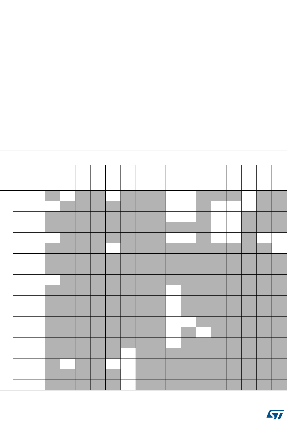
Peripherals interconnect matrix RM0394
288/1865 RM0394 Rev 4
10 Peripherals interconnect matrix
10.1 Introduction
Several peripherals have direct connections between them.
This allows autonomous communication and or synchronization between peripherals,
saving CPU resources thus power supply consumption.
In addition, these hardware connections remove software latency and allow design of
predictable system.
Depending on peripherals, these interconnections can operate in Run, Sleep, Low-power
run and sleep, Stop 0, Stop 1 and Stop 2 modes.
10.2 Connection summary
Table 39. STM32L41xxx/42xxx/43xxx/44xxx/45xxx/46xxx peripherals interconnect matrix(1) (2)
-
Destination
TIM1
TIM2
TIM6
TIM7
TIM15
TIM16
LPTIM1
LPTIM2
ADC1
ADC2
OPAMP1
DAC1
DAC2
COMP1
COMP2
IRTIM
Source
TIM1 -1- - 1- - - 22 - - - 7- -
TIM2 1- - - - - - - 22-447 - -
TIM6 - - - - - - - - 22-44 - - -
TIM7 -----------44 - - -
TIM15 1- - - - - - - 22 -44 -712
TIM16 - - - - 1----------12
LPTIM1 ----------------
LPTIM2 ----------------
ADC1 3---------------
T. Sensor - - - - - - - - 9- - - - - - -
VBAT - - - - - - - - 9- - - - - - -
VREFINT - - - - - - - - 9- - - - - - -
OPAMP1 - - - - - - - - 99- - - - - -
DAC1 - - - - - - - - 9-9- - - - -
DAC2 - - - - - - - - 9- - - - - - -
HSE - - - - - 5- - - - - - - - - -
LSE -5- - 55 - - - - - - - - - -
MSI - - - - - 5- - - - - - - - - -
LSI - - - - - 5- - - - - - - - - -

RM0394 Rev 4 289/1865
RM0394 Peripherals interconnect matrix
294
10.3 Interconnection details
10.3.1 From timer (TIM1/TIM2/TIM15/TIM16) to timer (TIM1/TIM2/TIM15/TIM16)
Purpose
Some of the TIMx timers are linked together internally for timer synchronization or chaining.
When one timer is configured in Master Mode, it can reset, start, stop or clock the counter of
another timer configured in Slave Mode.
A description of the feature is provided in: Section 27.3.19: Timer synchronization.
The modes of synchronization are detailed in:
•Section 27.3.19: Timer synchronization for advanced-control timers (TIM1)
•Section 27.3.18: Timers and external trigger synchronization for general-purpose
timers (TIM2)
•Section 28.5.18: External trigger synchronization (TIM15 only) for general-purpose
timer (TIM15)
Triggering signals
The output (from Master) is on signal TIMx_TRGO (and TIMx_TRGO2 for TIM1) following a
configurable timer event.
The input (to slave) is on signals TIMx_ITR0/ITR1/ITR2/ITR3
The input and output signals for TIM1 are shown in Figure 183: Advanced-control timer
block diagram.
The possible master/slave connections are given in:
•Table 132: TIM1 internal trigger connection
Source
MCO - - - - - 5- - - - - - - - - -
EXTI - - - - - - - - 22 -44 - - -
RTC - - - - - 566 - - - - - - - -
COMP1 10 10 - - 10 10 6 6 - - - - - - - -
COMP2 10 10 - - 10 10 6 6 - - - - - - - -
SYST ERR 11 - - - 11 11 - - - - - - - - - -
USB(3) -8--------------
1. Numbers in table are links to corresponding detailed sub-section in Section 10.3: Interconnection details.
2. The “-” symbol in grayed cells means no interconnect.
3. Not available for STM32L431xx devices.
Table 39. STM32L41xxx/42xxx/43xxx/44xxx/45xxx/46xxx peripherals interconnect matrix(1) (2)
-
Destination
TIM1
TIM2
TIM6
TIM7
TIM15
TIM16
LPTIM1
LPTIM2
ADC1
ADC2
OPAMP1
DAC1
DAC2
COMP1
COMP2
IRTIM

Peripherals interconnect matrix RM0394
290/1865 RM0394 Rev 4
Active power mode
Run, Sleep, Low-power run, Low-power sleep.
10.3.2 From timer (TIM1/TIM2/TIM6/TIM15) and EXTI to ADC (ADC1)
Purpose
General-purpose timers (TIM2), basic timer (TIM6), advanced-control timer (TIM1), general-
purpose timer (TIM15) and EXTI can be used to generate an ADC triggering event.
TIMx synchronization is described in: Section 26.3.5: Clock selection (TIM1).
ADC synchronization is described in: Section 16.4.18: Conversion on external trigger and
trigger polarity (EXTSEL, EXTEN,JEXTSEL, JEXTEN).
Triggering signals
The output (from timer) is on signal TIMx_TRGO, TIMx_TRGO2 or TIMx_CCx event.
The input (to ADC) is on signal EXT[15:0], JEXT[15:0].
The connection between timers and ADC is provided in:
•Table 59: ADC1 and ADC2 - External triggers for regular channels
•Table 60: ADC1 and ADC2 - External trigger for injected channels
Active power mode
Run, Sleep, Low-power run, Low-power sleep.
10.3.3 From ADC (ADC1) to timer (TIM1)
Purpose
ADC1 can provide trigger event through watchdog signals to advanced-control timers
(TIM1).
A description of the ADC analog watchdog setting is provided in: Section 16.4.29: Analog
window watchdog (AWD1EN, JAWD1EN, AWD1SGL, AWD1CH, AWD2CH, AWD3CH,
AWD_HTx, AWD_LTx, AWDx).
Trigger settings on the timer are provided in: Section 26.3.4: External trigger input.
Triggering signals
The output (from ADC) is on signals ADCn_AWDx_OUT n = 1, 2, 3 (for ADC1) x = 1, 2, 3 (3
watchdog per ADC) and the input (to timer) on signal TIMx_ETR (external trigger).
Active power mode
Run, Sleep, Low-power run, Low-power sleep.
10.3.4 From timer (TIM2/TIM6/TIM7) and EXTI to DAC (DAC1/DAC2)
Purpose
General-purpose timer (TIM2), basic timers (TIM6, TIM7), and EXTI can be used as
triggering event to start a DAC conversion.

RM0394 Rev 4 291/1865
RM0394 Peripherals interconnect matrix
294
Triggering signals
The output (from timer) is on signal TIMx_TRGO directly connected to corresponding DAC
inputs.
Selection of input triggers on DAC is provided in Section 17.4.6: DAC trigger selection
(single and dual mode).
Active power mode
Run, Sleep, Low-power run, Low-power sleep.
10.3.5 From HSE, LSE, LSI, MSI, MCO, RTC to timer (TIM2/TIM15/TIM16)
Purpose
External clocks (HSE, LSE), internal clocks (LSI, MSI), microcontroller output clock (MCO),
GPIO and RTC wakeup interrupt can be used as input to general-purpose timer (TIM15/16)
channel 1.
This allows to calibrate the HSI16/MSI system clocks (with TIM15/TIM16 and LSE) or LSI
(with TIM16 and HSE). This is also used to precisely measure LSI (with TIM16 and HSI16)
or MSI (with and HSI16) oscillator frequency.
When Low Speed External (LSE) oscillator is used, no additional hardware connections are
required.
This feature is described in Section 6.2.17: Internal/external clock measurement with
TIM15/TIM16.
External clock LSE can be used as input to general-purpose timers (TIM2) on TIM2_ETR
pin, see Section 27.4.19: TIM2 option register 1 (TIM2_OR1).
Active power mode
Run, Sleep, Low-power run, Low-power sleep.
10.3.6 From RTC, COMP1, COMP2 to low-power timer (LPTIM1/LPTIM2)
Purpose
RTC alarm A/B, RTC_TAMP1/2/3 input detection, COMP1/2_OUT can be used as trigger to
start LPTIM counters (LPTIM1/2).
Triggering signals
This trigger feature is described in Section 30.4.6: Trigger multiplexer (and following
sections).
The input selection is described in Table 146: LPTIM1 external trigger connection.
Active power mode
Run, Sleep, Low-power run, Low-power sleep, Stop 0, Stop 1, Stop 2 (LPTIM1 only).

Peripherals interconnect matrix RM0394
292/1865 RM0394 Rev 4
10.3.7 From timer (TIM1/TIM2/TIM15) to comparators
(COMP1/COMP2)
Purpose
Advanced-control timer (TIM1), general-purpose timer (TIM2) and general-purpose timer
(TIM15) can be used as blanking window input to COMP1/COMP2
The blanking function is described in Section 19.3.7: Comparator output blanking function.
The blanking sources are given in:
•Section 19.6.1: Comparator 1 control and status register (COMP1_CSR) bits 20:18
BLANKING[2:0]
•Section 19.6.2: Comparator 2 control and status register (COMP2_CSR) bits 20:18
BLANKING[2:0]
Triggering signals
Timer output signal TIMx_Ocx are the inputs to blanking source of COMP1/COMP2.
Active power mode
Run, Sleep, Low-power run, Low-power sleep.
10.3.8 From ADC (ADC1) to ADC (ADC2)
Purpose
ADC1 can be used as a “master” to trigger ADC2 “slave” start of conversion.
In dual ADC mode, the converted data of the master and slave ADCs can be read in
parallel.
A description of dual ADC mode is provided in: Section 16.4.31: Dual ADC modes.
Triggering signals
Internal to the ADCs.
Active power mode
Run, Sleep, Low-power run, Low-power sleep.
10.3.9 From USB to timer (TIM2)
Purpose
USB (FS SOF) can generate a trigger to general-purpose timer (TIM2).
Connection of USB to TIM2 is described in .
Triggering signals
Internal signal generated by USB FS Start Of Frame.
Active power mode
Run, Sleep.

RM0394 Rev 4 293/1865
RM0394 Peripherals interconnect matrix
294
10.3.10 From internal analog source to ADC (ADC1) and OPAMP
(OPAMP1)
Purpose
Internal temperature sensor (VTS) and VBAT monitoring channel are connected to ADC1
input channels.
Internal reference voltage (VREFINT) is connected to ADC1 input channels.
OPAMP1 output can be connected to ADC1 input channel through the GPIO.
DAC1_OUT1 and DAC1_OUT2 outputs can be connected to input channel.
DAC1_OUT1 can be connected to OPAMP1_VINP.
This is according:
•Section 16.2: ADC main features
•Section 16.4.11: Channel selection (SQRx, JSQRx)
•Figure 41: ADC1 connectivity
•Table 90: Operational amplifier possible connections
Active power mode
Run, Sleep, Low-power run, Low-power sleep.
10.3.11 From comparators (COMP1/COMP2) to timers
(TIM1/TIM2/TIM15/TIM16)
Purpose
Comparators (COMP1/COMP2) output values can be connected to timers
(TIM1/TIM2/TIM15/TIM16) input captures or TIMx_ETR signals.
The connection to ETR is described in Section 26.3.4: External trigger input.
Comparators (COMP1/COMP2) output values can also generate break input signals for
timers (TIM1) on input pins TIMx_BKIN or TIMx_BKIN2 through GPIO alternate function
selection using open drain connection of IO, see Section 26.3.17: Bidirectional break inputs.
The possible connections are given in:
•Section 26.4.23: TIM1 option register 1 (TIM1_OR1)
•Section 26.4.27: TIM1 option register 2 (TIM1_OR2)
•Section 27.4.19: TIM2 option register 1 (TIM2_OR1)
•Section 27.4.20: TIM2 option register 2 (TIM2_OR2)
•Section 28.3: TIM16 main features
Active power mode
Run, Sleep, Low-power run, Low-power sleep.

Peripherals interconnect matrix RM0394
294/1865 RM0394 Rev 4
10.3.12 From system errors to timers (TIM1/TIM15/TIM16)
Purpose
CSS, CPU hardfault, RAM parity error, FLASH ECC double error detection, PVD can
generate system errors in the form of timer break toward timers (TIM1/TIM15/TIM16).
The purpose of the break function is to protect power switches driven by PWM signals
generated by the timers.
List of possible source of break are described in:
•Section 26.3.16: Using the break function (TIM1)
•Section 28.5.13: Using the break function (TIM15/TIM16)
•Figure 292: TIM15 block diagram
•Figure 293: TIM16 block diagram
Active power mode
Run, Sleep, Low-power run, Low-power sleep.
10.3.13 From timers (TIM16) to IRTIM
Purpose
General-purpose timer (TIM16) output channel TIMx_OC1 are used to generate the
waveform of infrared signal output.
The functionality is described in Section 31: Infrared interface (IRTIM).
Active power mode
Run, Sleep, Low-power run, Low-power sleep.

RM0394 Rev 4 295/1600
RM0394 Direct memory access controller (DMA)
319
11 Direct memory access controller (DMA)
11.1 Introduction
The direct memory access (DMA) controller is a bus master and system peripheral.
The DMA is used to perform programmable data transfers between memory-mapped
peripherals and/or memories, upon the control of an off-loaded CPU.
The DMA controller features a single AHB master architecture.
There are two instances of DMA, DMA1 and DMA2.
Each channel is dedicated to managing memory access requests from one or more
peripherals. Each DMA includes an arbiter for handling the priority between DMA requests.
11.2 DMA main features
•Single AHB master
•Peripheral-to-memory, memory-to-peripheral, memory-to-memory and peripheral-to-
peripheral data transfers
•Access, as source and destination, to on-chip memory-mapped devices such as Flash
memory, SRAM, and AHB and APB peripherals
•All DMA channels independently configurable:
– Each channel is associated either with a DMA request signal coming from a
peripheral, or with a software trigger in memory-to-memory transfers. This
configuration is done by software.
– Priority between the requests is programmable by software (4 levels per channel:
very high, high, medium, low) and by hardware in case of equality (such as
request to channel 1 has priority over request to channel 2).
– Transfer size of source and destination are independent (byte, half-word, word),
emulating packing and unpacking. Source and destination addresses must be
aligned on the data size.
– Support of transfers from/to peripherals to/from memory with circular buffer
management
– Programmable number of data to be transferred: 0 to 216 -1
•Generation of an interrupt request per channel. Each interrupt request is caused from
any of the three DMA events: transfer complete, half transfer, or transfer error.

Direct memory access controller (DMA) RM0394
296/1600 RM0394 Rev 4
11.3 DMA implementation
11.3.1 DMA1 and DMA2
DMA1 and DMA2 are implemented with the hardware configuration parameters shown
in Table 40.
11.3.2 DMA request mapping
DMA controller
The hardware requests from the peripherals (TIM1/2/3/6/7/15/16, ADC1, DAC_CH1/2,
SPI1/2/3, I2C1/2/3/4, SDMMC1, QUADSPI, SWPMI1, SAI1, AES, USART1/2/3, UART4 and
LPUART1) are mapped to the DMA channels through the DMA_CSELR channel selection
registers (see Figure 25 and Figure 26).
The peripheral DMA requests can be independently activated/de-activated by programming
the DMA control bit in the registers of the corresponding peripheral.
Table 41 show the list of DMA requests for each channel.
Table 40. DMA1 and DMA2 implementation
Feature DMA1 DMA2
Number of channels 7 7
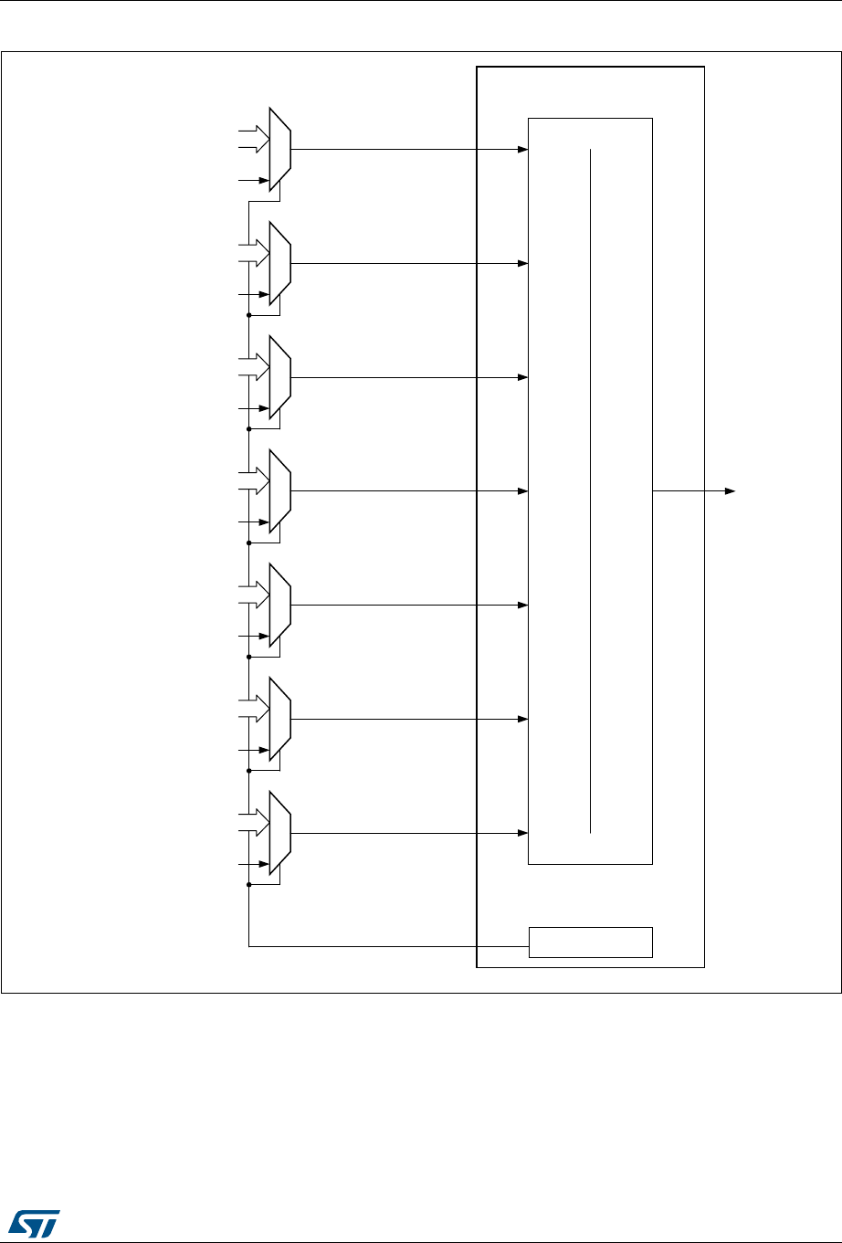
RM0394 Rev 4 297/1600
RM0394 Direct memory access controller (DMA)
319
Figure 25. DMA1 request mapping
06Y9
+LJKSULRULW\
/RZSULRULW\
'0$B&6(/5
$'&7,0B&+
6:WULJJHU0(00(0ELW &6
&KDQQHO
&KDQQHO
63,B5;86$57B7;,&B7;
7,0B837,0B&+7,0B&+
6:WULJJHU0(00(0ELW &6
&KDQQHO
63,B7;86$57B5;,&B5;
7,0B&+7,0B837,0B83
'$&B&+7,0B&+7,0B&+
7,0B83
6:WULJJHU0(00(0ELW &6
&KDQQHO
63,B5;86$57B7;,&B7;
7,0B83'$&B&+7,0B&+
7,0B75,*7,0B&20')6'0B)/7
6:WULJJHU0(00(0ELW &6
&KDQQHO
63,B7;86$57B5;,&B5;
7,0B&+48$'63,7,0B&+
7,0B837,0B75,*7,0B&20
')6'0B)/7
6:WULJJHU0(00(0ELW &6
&KDQQHO
86$57B5;,&B7;7,0B&+
7,0B837,0B837,0B&+
7,0B75,*
6:WULJJHU0(00(0ELW &6
&KDQQHO
86$57B7;,&B5;7,0B&+
7,0B&+7,0B&+
6:WULJJHU0(00(0ELW &6
3HULSKHUDOUHTXHVWVLJQDOV )L[HGKDUGZDUHSULRULW\
,QWHUQDO'0$
UHTXHVW
'0$FKDQQHO
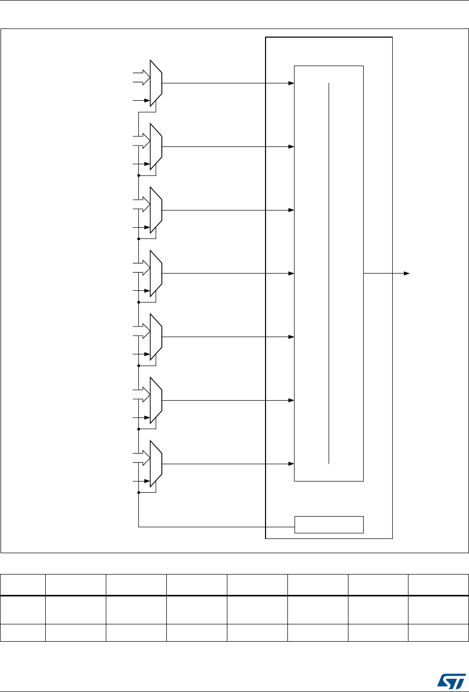
Direct memory access controller (DMA) RM0394
298/1600 RM0394 Rev 4
Figure 26. DMA2 request mapping
06Y9
+LJKSULRULW\
/RZSULRULW\
'0$B&6(/5
6$,B$63,B5;6:30,B5;$(6B,1
,&B5;
6:WULJJHU0(00(0ELW &6
&KDQQHO
&KDQQHO
6$,B%63,B7;6:30,B7;$(6B287
,&B7;
6:WULJJHU0(00(0ELW &6
&KDQQHO
$'&63,B5;$(6B2878$57B7;
6:WULJJHU0(00(0ELW &6
&KDQQHO
$'&7,0B83'$&B&+63,B7;
6'00&8$57B5;
6:WULJJHU0(00(0ELW &6
&KDQQHO
$'&7,0B83'$&B&+
$(6B,16'00&
6:WULJJHU0(00(0ELW &6
&KDQQHO
6$,B$86$57B7;/38$57B7;
,&B5;
6:WULJJHU0(00(0ELW &6
&KDQQHO
6$,B%86$57B5;48$'63,
/38$57B5;,&B7;
6:WULJJHU0(00(0ELW &6
3HULSKHUDOUHTXHVWVLJQDOV )L[HGKDUGZDUHSULRULW\
,QWHUQDO'0$
UHTXHVW
'0$FKDQQHO
Table 41. DMA1 requests for each channel
CxS[3:0] Channel 1 Channel 2 Channel 3 Channel 4 Channel 5 Channel 6 Channel 7
0000 ADC1 ADC2(1) --
DFSDM1_
FLT0(2)
DFSDM1_
FLT1(2) -
0001 - SPI1_RX SPI1_TX SPI2_RX(3) SPI2_TX(3) SAI2_A(4) SAI2_B(4)

RM0394 Rev 4 299/1600
RM0394 Direct memory access controller (DMA)
319
11.4 DMA functional description
0010 - USART3_TX
(3)
USART3_RX
(3) USART1_TX USART1_RX USART2_RX USART2_TX
0011 - I2C3_TX I2C3_RX I2C2_TX(3) I2C2_RX(3) I2C1_TX I2C1_RX
0100 TIM2_CH3 TIM2_UP TIM16_CH1
TIM16_UP - TIM2_CH1 TIM16_CH1
TIM16_UP
TIM2_CH2
TIM2_CH4
0101 - TIM3_CH3(2) TIM3_CH4(2)
TIM3_UP(2)
TIM7_UP.
DAC_CH2(5) QUADSPI
TIM3_CH1(2)
TIM3_TRIG
(2)
-
0110 - - TIM6_UP
DAC_CH1 ----
0111 - TIM1_CH1 TIM1_CH2
TIM1_CH4
TIM1_TRIG
TIM1_COM
TIM15_CH1
TIM15_UP
TIM15_TRIG
TIM15_COM
TIM1_UP TIM1_CH3
1. Available on STM32L412xx and STM32L422xx devices only.
2. Available on STM32L45xxx and STM32L46xxx devices only.
3. Not available on STM32L432xx and STM32L442xx devices.
4. Not available on STM32L412xx and STM32L422xx devices.
5. Available on STM32L43xx and STM32L44xx devices only.
Table 41. DMA1 requests for each channel (continued)
CxS[3:0] Channel 1 Channel 2 Channel 3 Channel 4 Channel 5 Channel 6 Channel 7
Table 42. DMA2 requests for each channel
CxS[3:0] Channel 1 Channel 2 Channel 3 Channel 4 Channel 5 Channel 6 Channel 7
0000 I2C4_RX(1) I2C4_TX(1) ADC1 ADC2(2) ---
0001 SAI1_A SAI1_B - - - SAI1_A SAI1_B
0010 - - UART4_TX
(1) -UART4_RX
(1) USART1_TX USART1_RX
0011 SPI3_RX SPI3_TX - TIM6_UP
DAC_CH1
TIM7_UP
DAC_CH2(3) - QUADSPI
0100 SWPMI1_RX
(3)
SWPMI1_TX
(3) SPI1_RX SPI1_TX - LPUART1_
TX
LPUART1_
RX
0101-----I2C1_RXI2C1_TX
0110 AES_IN(4) AES_OUT(4) AES_OUT(4) - AES_IN(4) --
0111 - - - SDMMC1(5) SDMMC1(5) --
1. Available on STM32L45xxx and STM32L46xxx devices only.
2. Available on STM32L41xxx and STM32L42xxx devices only.
3. Available on STM32L43xxx and STM32L44xxx devices only.
4. Available on STM32L44xxx and STM32L46xxx devices only
5. Not available on STM32L432xx and STM32L442xx devices.
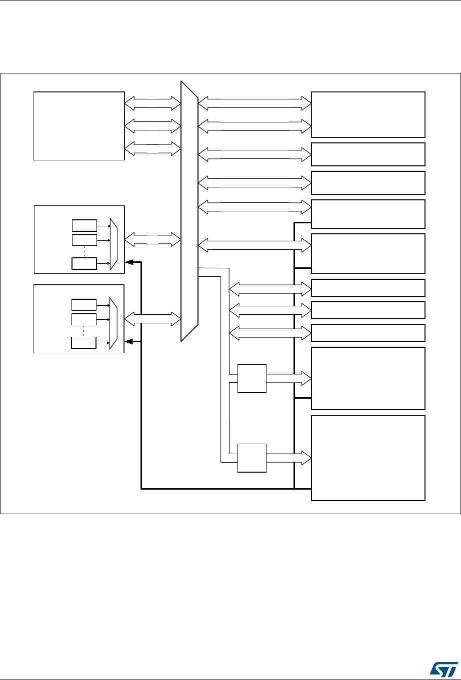
Direct memory access controller (DMA) RM0394
300/1600 RM0394 Rev 4
11.4.1 DMA block diagram
The DMA block diagram is shown in Figure 27.
Figure 27. DMA block diagram
The DMA controller performs direct memory transfer by sharing the AHB system bus with
other system masters. The bus matrix implements round-robin scheduling. DMA requests
may stop the CPU access to the system bus for a number of bus cycles, when CPU and
DMA target the same destination (memory or peripheral).
According to its configuration through the AHB slave interface, the DMA controller arbitrates
between the DMA channels and their associated received requests. The DMA controller
also schedules the DMA data transfers over the single AHB port master.
The DMA controller generates an interrupt per channel to the interrupt controller.
06Y9
65$0
&K
&K
&K
'0$
'0$UHTXHVWV
5HVHWFORFNFRQWURO5&&
&RUWH[0ZLWK)38
)ODVKLQWHUIDFH
$3%SHULSKHUDOV
ZLWK'0$FDSDELOLW\
')6'06$,6$,7,0
7,07,07,07,0
86$5763,6'00&
$3%SHULSKHUDOV
ZLWK'0$FDSDELOLW\
6:30,/38$57
'$&B&+'$&B&+,&
,&,&86$5786$57
8$578$5763,63,
7,07,07,07,07,0
7,0
)0&DQG4XDG63,
$+%SHULSKHUDOV
ZLWK'0$FDSDELOLW\
$'&$'&$'&
&5&
6EXV
'EXV
,EXV
76&
65$0
$+%
%ULGJH
$3%
$3%
,&RGH
'&RGH
%ULGJH
'0$
&K
&K
&K
'0$
%XVPDWUL[
'0$

RM0394 Rev 4 301/1600
RM0394 Direct memory access controller (DMA)
319
11.4.2 DMA transfers
The software configures the DMA controller at channel level, in order to perform a block
transfer, composed of a sequence of AHB bus transfers.
A DMA block transfer may be requested from a peripheral, or triggered by the software in
case of memory-to-memory transfer.
After an event, the following steps of a single DMA transfer occur:
1. The peripheral sends a single DMA request signal to the DMA controller.
2. The DMA controller serves the request, depending on the priority of the channel
associated to this peripheral request.
3. As soon as the DMA controller grants the peripheral, an acknowledge is sent to the
peripheral by the DMA controller.
4. The peripheral releases its request as soon as it gets the acknowledge from the DMA
controller.
5. Once the request is de-asserted by the peripheral, the DMA controller releases the
acknowledge.
The peripheral may order a further single request and initiate another single DMA transfer.
The request/acknowledge protocol is used when a peripheral is either the source or the
destination of the transfer. For example, in case of memory-to-peripheral transfer, the
peripheral initiates the transfer by driving its single request signal to the DMA controller. The
DMA controller reads then a single data in the memory and writes this data to the peripheral.
For a given channel x, a DMA block transfer consists of a repeated sequence of:
•a single DMA transfer, encapsulating two AHB transfers of a single data, over the DMA
AHB bus master:
– a single data read (byte, half-word or word) from the peripheral data register or a
location in the memory, addressed through an internal current peripheral/memory
address register.
The start address used for the first single transfer is the base address of the
peripheral or memory, and is programmed in the DMA_CPARx or DMA_CMARx
register.
– a single data write (byte, half-word or word) to the peripheral data register or a
location in the memory, addressed through an internal current peripheral/memory
address register.
The start address used for the first transfer is the base address of the peripheral or
memory, and is programmed in the DMA_CPARx or DMA_CMARx register.
•post-decrementing of the programmed DMA_CNDTRx register
This register contains the remaining number of data items to transfer (number of AHB
‘read followed by write’ transfers).
This sequence is repeated until DMA_CNDTRx is null.
Note: The AHB master bus source/destination address must be aligned with the programmed size
of the transferred single data to the source/destination.
11.4.3 DMA arbitration
The DMA arbiter manages the priority between the different channels.

Direct memory access controller (DMA) RM0394
302/1600 RM0394 Rev 4
When an active channel x is granted by the arbiter (hardware requested or software
triggered), a single DMA transfer is issued (such as a AHB ‘read followed by write’ transfer
of a single data). Then, the arbiter considers again the set of active channels and selects the
one with the highest priority.
The priorities are managed in two stages:
•software: priority of each channel is configured in the DMA_CCRx register, to one of
the four different levels:
– very high
–high
–medium
–low
•hardware: if two requests have the same software priority level, the channel with the
lowest index gets priority. For example, channel 2 gets priority over channel 4.
When a channel x is programmed for a block transfer in memory-to-memory mode,
re arbitration is considered between each single DMA transfer of this channel x. Whenever
there is another concurrent active requested channel, the DMA arbiter automatically
alternates and grants the other highest-priority requested channel, which may be of lower
priority than the memory-to-memory channel.
11.4.4 DMA channels
Each channel may handle a DMA transfer between a peripheral register located at a fixed
address, and a memory address. The amount of data items to transfer is programmable.
The register that contains the amount of data items to transfer is decremented after each
transfer.
A DMA channel is programmed at block transfer level.
Programmable data sizes
The transfer sizes of a single data (byte, half-word, or word) to the peripheral and memory
are programmable through, respectively, the PSIZE[1:0] and MSIZE[1:0] fields of the
DMA_CCRx register.
Pointer incrementation
The peripheral and memory pointers may be automatically incremented after each transfer,
depending on the PINC and MINC bits of the DMA_CCRx register.
If the incremented mode is enabled (PINC or MINC set to 1), the address of the next
transfer is the address of the previous one incremented by 1, 2 or 4, depending on the data
size defined in PSIZE[1:0] or MSIZE[1:0]. The first transfer address is the one programmed
in the DMA_CPARx or DMA_CMARx register. During transfers, these registers keep the
initially programmed value. The current transfer addresses (in the current internal
peripheral/memory address register) are not accessible by software.
If the channel x is configured in non-circular mode, no DMA request is served after the last
data transfer (once the number of single data to transfer reaches zero). The DMA channel
must be disabled in order to reload a new number of data items into the DMA_CNDTRx
register.

RM0394 Rev 4 303/1600
RM0394 Direct memory access controller (DMA)
319
Note: If the channel x is disabled, the DMA registers are not reset. The DMA channel registers
(DMA_CCRx, DMA_CPARx and DMA_CMARx) retain the initial values programmed during
the channel configuration phase.
In circular mode, after the last data transfer, the DMA_CNDTRx register is automatically
reloaded with the initially programmed value. The current internal address registers are
reloaded with the base address values from the DMA_CPARx and DMA_CMARx registers.
Channel configuration procedure
The following sequence is needed to configure a DMA channel x:
1. Set the peripheral register address in the DMA_CPARx register.
The data is moved from/to this address to/from the memory after the peripheral event,
or after the channel is enabled in memory-to-memory mode.
2. Set the memory address in the DMA_CMARx register.
The data is written to/read from the memory after the peripheral event or after the
channel is enabled in memory-to-memory mode.
3. Configure the total number of data to transfer in the DMA_CNDTRx register.
After each data transfer, this value is decremented.
4. Configure the parameters listed below in the DMA_CCRx register:
– the channel priority
– the data transfer direction
– the circular mode
– the peripheral and memory incremented mode
– the peripheral and memory data size
– the interrupt enable at half and/or full transfer and/or transfer error
5. Activate the channel by setting the EN bit in the DMA_CCRx register.
A channel, as soon as enabled, may serve any DMA request from the peripheral connected
to this channel, or may start a memory-to-memory block transfer.
Note: The two last steps of the channel configuration procedure may be merged into a single
access to the DMA_CCRx register, to configure and enable the channel.
When a channel is enabled and still active (not completed), the software must perform two
separate write accesses to the DMA_CCRx register, to disable the channel, then to
reprogram the channel for another next block transfer.
Some fields of the DMA_CCRx register are read-only when the EN bit is set to 1.
Stop and resume a channel
Once the software activates a channel, it waits for the completion of the programmed
transfer. The DMA controller is not able to resume an aborted active channel with a possible
suspended bus transfer.
To correctly stop and disable a channel, the software clears the EN bit of the DMA_CCRx
register. The software secures that no pending request from the peripheral is served by the
DMA controller before the transfer completion. The software waits for the transfer complete
or transfer error interrupt.
When a channel transfer error occurs, the EN bit of the DMA_CCRx register is cleared by
hardware. This EN bit can not be set again by software to re-activate the channel x, until the
TEIFx bit of the DMA_ISR register is set.

Direct memory access controller (DMA) RM0394
304/1600 RM0394 Rev 4
Circular mode (in memory-to-peripheral/peripheral-to-memory transfers)
The circular mode is available to handle circular buffers and continuous data flows (such as
ADC scan mode). This feature is enabled using the CIRC bit in the DMA_CCRx register.
Note: The circular mode must not be used in memory-to-memory mode. Before enabling a
channel in circular mode (CIRC = 1), the software must clear the MEM2MEM bit of the
DMA_CCRx register. When the circular mode is activated, the amount of data to transfer is
automatically reloaded with the initial value programmed during the channel configuration
phase, and the DMA requests continue to be served.
In order to stop a circular transfer, the software needs to stop the peripheral from generating
DMA requests (such as quit the ADC scan mode), before disabling the DMA channel.
The software must explicitly program the DMA_CNDTRx value before starting/enabling a
transfer, and after having stopped a circular transfer.
Memory-to-memory mode
The DMA channels may operate without being triggered by a request from a peripheral. This
mode is called memory-to-memory mode, and is initiated by software.
If the MEM2MEM bit in the DMA_CCRx register is set, the channel, if enabled, initiates
transfers. The transfer stops once the DMA_CNDTRx register reaches zero.
Note: The memory-to-memory mode must not be used in circular mode. Before enabling a
channel in memory-to-memory mode (MEM2MEM = 1), the software must clear the CIRC
bit of the DMA_CCRx register.
Peripheral-to-peripheral mode
Any DMA channel can operate in peripheral-to-peripheral mode:
•when the hardware request from a peripheral is selected to trigger the DMA channel
This peripheral is the DMA initiator and paces the data transfer from/to this peripheral
to/from a register belonging to another memory-mapped peripheral (this one being not
configured in DMA mode).
•when no peripheral request is selected and connected to the DMA channel
The software configures a register-to-register transfer by setting the MEM2MEM bit of
the DMA_CCRx register.
Programming transfer direction, assigning source/destination
The value of the DIR bit of the DMA_CCRx register sets the direction of the transfer, and
consequently, it identifies the source and the destination, regardless the source/destination
type (peripheral or memory):
•DIR = 1 defines typically a memory-to-peripheral transfer. More generally, if DIR = 1:
–The source attributes are defined by the DMA_MARx register, the MSIZE[1:0]
field and MINC bit of the DMA_CCRx register.
Regardless of their usual naming, these ‘memory’ register, field and bit are used to
define the source peripheral in peripheral-to-peripheral mode.
–The destination attributes are defined by the DMA_PARx register, the PSIZE[1:0]
field and PINC bit of the DMA_CCRx register.

RM0394 Rev 4 305/1600
RM0394 Direct memory access controller (DMA)
319
Regardless of their usual naming, these ‘peripheral’ register, field and bit are used
to define the destination memory in memory-to-memory mode.
•DIR = 0 defines typically a peripheral-to-memory transfer. More generally, if DIR = 0:
–The source attributes are defined by the DMA_PARx register, the PSIZE[1:0] field
and PINC bit of the DMA_CCRx register.
Regardless of their usual naming, these ‘peripheral’ register, field and bit are used
to define the source memory in memory-to-memory mode
–The destination attributes are defined by the DMA_MARx register, the
MSIZE[1:0] field and MINC bit of the DMA_CCRx register.
Regardless of their usual naming, these ‘memory’ register, field and bit are used to
define the destination peripheral in peripheral-to-peripheral mode.

Direct memory access controller (DMA) RM0394
306/1600 RM0394 Rev 4
11.4.5 DMA data width, alignment and endianness
When PSIZE[1:0] and MSIZE[1:0] are not equal, the DMA controller performs some data
alignments as described in Table 43.
Table 43. Programmable data width and endian behavior (when PINC = MINC = 1)
Source
port
width
(MSIZE
if
DIR = 1,
else
PSIZE)
Destinat
ion port
width
(PSIZE
if
DIR = 1,
else
MSIZE)
Number
of data
items to
transfer
(NDT)
Source content:
address / data
(DMA_CMARx if
DIR = 1, else
DMA_CPARx)
DMA transfers
Destination
content:
address / data
(DMA_CPARx if
DIR = 1, else
DMA_CMARx)
888
@0x0 / B0
@0x1 / B1
@0x2 / B2
@0x3 / B3
1: read B0[7:0] @0x0 then write B0[7:0] @0x0
2: read B1[7:0] @0x1 then write B1[7:0] @0x1
3: read B2[7:0] @0x2 then write B2[7:0] @0x2
4: read B3[7:0] @0x3 then write B3[7:0] @0x3
@0x0 / B0
@0x1 / B1
@0x2 / B2
@0x3 / B3
8164
@0x0 / B0
@0x1 / B1
@0x2 / B2
@0x3 / B3
1: read B0[7:0] @0x0 then write 00B0[15:0] @0x0
2: read B1[7:0] @0x1 then write 00B1[15:0] @0x2
3: read B2[7:0] @0x2 then write 00B2[15:0] @0x4
4: read B3[7:0] @0x3 then write 00B3[15:0] @0x6
@0x0 / 00B0
@0x2 / 00B1
@0x4 / 00B2
@0x6 / 00B3
8324
@0x0 / B0
@0x1 / B1
@0x2 / B2
@0x3 / B3
1: read B0[7:0] @0x0 then write 000000B0[31:0] @0x0
2: read B1[7:0] @0x1 then write 000000B1[31:0] @0x4
3: read B2[7:0] @0x2 then write 000000B2[31:0] @0x8
4: read B3[7:0] @0x3 then write 000000B3[31:0] @0xC
@0x0 / 000000B0
@0x4 / 000000B1
@0x8 / 000000B2
@0xC / 000000B3
16 8 4
@0x0 / B1B0
@0x2 / B3B2
@0x4 / B5B4
@0x6 / B7B6
1: read B1B0[15:0] @0x0 then write B0[7:0] @0x0
2: read B3B2[15:0] @0x2 then write B2[7:0] @0x1
3: read B5B4[15:0] @0x4 then write B4[7:0] @0x2
4: read B7B6[15:0] @0x6 then write B6[7:0] @0x3
@0x0 / B0
@0x1 / B2
@0x2 / B4
@0x3 / B6
16 16 4
@0x0 / B1B0
@0x2 / B3B2
@0x4 / B5B4
@0x6 / B7B6
1: read B1B0[15:0] @0x0 then write B1B0[15:0] @0x0
2: read B3B2[15:0] @0x2 then write B3B2[15:0] @0x2
3: read B5B4[15:0] @0x4 then write B5B4[15:0] @0x4
4: read B7B6[15:0] @0x6 then write B7B6[15:0] @0x6
@0x0 / B1B0
@0x2 / B3B2
@0x4 / B5B4
@0x6 / B7B6
16 32 4
@0x0 / B1B0
@0x2 / B3B2
@0x4 / B5B4
@0x6 / B7B6
1: read B1B0[15:0] @0x0 then write 0000B1B0[31:0] @0x0
2: read B3B2[15:0] @0x2 then write 0000B3B2[31:0] @0x4
3: read B5B4[15:0] @0x4 then write 0000B5B4[31:0] @0x8
4: read B7B6[15:0] @0x6 then write 0000B7B6[31:0] @0xC
@0x0 / 0000B1B0
@0x4 / 0000B3B2
@0x8 / 0000B5B4
@0xC / 0000B7B6
32 8 4
@0x0 / B3B2B1B0
@0x4 / B7B6B5B4
@0x8 / BBBAB9B8
@0xC / BFBEBDBC
1: read B3B2B1B0[31:0] @0x0 then write B0[7:0] @0x0
2: read B7B6B5B4[31:0] @0x4 then write B4[7:0] @0x1
3: read BBBAB9B8[31:0] @0x8 then write B8[7:0] @0x2
4: read BFBEBDBC[31:0] @0xC then write BC[7:0] @0x3
@0x0 / B0
@0x1 / B4
@0x2 / B8
@0x3 / BC
32 16 4
@0x0 / B3B2B1B0
@0x4 / B7B6B5B4
@0x8 / BBBAB9B8
@0xC / BFBEBDBC
1: read B3B2B1B0[31:0] @0x0 then write B1B0[15:0] @0x0
2: read B7B6B5B4[31:0] @0x4 then write B5B4[15:0] @0x2
3: read BBBAB9B8[31:0] @0x8 then write B9B8[15:0] @0x4
4: read BFBEBDBC[31:0] @0xC then write BDBC[15:0] @0x6
@0x0 / B1B0
@0x2 / B5B4
@0x4 / B9B8
@0x6 / BDBC
32 32 4
@0x0 / B3B2B1B0
@0x4 / B7B6B5B4
@0x8 / BBBAB9B8
@0xC / BFBEBDBC
1: read B3B2B1B0[31:0] @0x0 then write B3B2B1B0[31:0] @0x0
2: read B7B6B5B4[31:0] @0x4 then write B7B6B5B4[31:0] @0x4
3: read BBBAB9B8[31:0] @0x8 then write BBBAB9B8[31:0] @0x8
4: read BFBEBDBC[31:0] @0xC then write BFBEBDBC[31:0] @0xC
@0x0 / B3B2B1B0
@0x4 / B7B6B5B4
@0x8 / BBBAB9B8
@0xC / BFBEBDBC

RM0394 Rev 4 307/1600
RM0394 Direct memory access controller (DMA)
319
Addressing AHB peripherals not supporting byte/half-word write transfers
When the DMA controller initiates an AHB byte or half-word write transfer, the data are
duplicated on the unused lanes of the AHB master 32-bit data bus (HWDATA[31:0]).
When the AHB slave peripheral does not support byte or half-word write transfers and does
not generate any error, the DMA controller writes the 32 HWDATA bits as shown in the two
examples below:
•To write the half-word 0xABCD, the DMA controller sets the HWDATA bus to
0xABCDABCD with a half-word data size (HSIZE = HalfWord in AHB master bus).
•To write the byte 0xAB, the DMA controller sets the HWDATA bus to 0xABABABAB
with a byte data size (HSIZE = Byte in the AHB master bus).
Assuming the AHB/APB bridge is an AHB 32-bit slave peripheral that does not take into
account the HSIZE data, any AHB byte or half-word transfer is changed into a 32-bit APB
transfer as described below:
•An AHB byte write transfer of 0xB0 to one of the 0x0, 0x1, 0x2 or 0x3 addresses, is
converted to an APB word write transfer of 0xB0B0B0B0 to the 0x0 address.
•An AHB half-word write transfer of 0xB1B0 to the 0x0 or 0x2 addresses, is converted to
an APB word write transfer of 0xB1B0B1B0 to the 0x0 address.
11.4.6 DMA error management
A DMA transfer error is generated when reading from or writing to a reserved address
space. When a DMA transfer error occurs during a DMA read or write access, the faulty
channel x is automatically disabled through a hardware clear of its EN bit in the
corresponding DMA_CCRx register.
The TEIFx bit of the DMA_ISR register is set. An interrupt is then generated if the TEIE bit of
the DMA_CCRx register is set.
The EN bit of the DMA_CCRx register can not be set again by software (channel x re-
activated) until the TEIFx bit of the DMA_ISR register is cleared (by setting the CTEIFx bit of
the DMA_IFCR register).
When the software is notified with a transfer error over a channel which involves a
peripheral, the software has first to stop this peripheral in DMA mode, in order to disable any
pending or future DMA request. Then software may normally reconfigure both DMA and the
peripheral in DMA mode for a new transfer.

Direct memory access controller (DMA) RM0394
308/1600 RM0394 Rev 4
11.5 DMA interrupts
An interrupt can be generated on a half transfer, transfer complete or transfer error for each
DMA channel x. Separate interrupt enable bits are available for flexibility.
11.6 DMA registers
Refer to Section 1.2 for a list of abbreviations used in register descriptions.
The DMA registers have to be accessed by words (32-bit).
11.6.1 DMA interrupt status register (DMA_ISR)
Address offset: 0x00
Reset value: 0x0000 0000
Every status bit is cleared by hardware when the software sets the corresponding clear bit
or the corresponding global clear bit CGIFx, in the DMA_IFCR register.
Table 44. DMA interrupt requests
Interrupt request Interrupt event Event flag Interrupt
enable bit
Channel x interrupt
Half transfer on channel x HTIFx HTIEx
Transfer complete on channel x TCIFx TCIEx
Transfer error on channel x TEIFx TEIEx
Half transfer or transfer complete or transfer error on channel x GIFx -
31 30 29 28 27 26 25 24 23 22 21 20 19 18 17 16
Res. Res. Res. Res. TEIF7 HTIF7 TCIF7 GIF7 TEIF6 HTIF6 TCIF6 GIF6 TEIF5 HTIF5 TCIF5 GIF5
rrrrrrrrrrrr
1514131211109876543210
TEIF4 HTIF4 TCIF4 GIF4 TEIF3 HTIF3 TCIF3 GIF3 TEIF2 HTIF2 TCIF2 GIF2 TEIF1 HTIF1 TCIF1 GIF1
rrrrrr r r r r rrrrrr
Bits 31:28 Reserved, must be kept at reset value.
Bit 27 TEIF7: transfer error (TE) flag for channel 7
0: no TE event
1: a TE event occurred
Bit 26 HTIF7: half transfer (HT) flag for channel 7
0: no HT event
1: a HT event occurred
Bit 25 TCIF7: transfer complete (TC) flag for channel 7
0: no TC event
1: a TC event occurred
Bit 24 GIF7: global interrupt flag for channel 7
0: no TE, HT or TC event
1: a TE, HT or TC event occurred

RM0394 Rev 4 309/1600
RM0394 Direct memory access controller (DMA)
319
Bit 23 TEIF6: transfer error (TE) flag for channel 6
0: no TE event
1: a TE event occurred
Bit 22 HTIF6: half transfer (HT) flag for channel 6
0: no HT event
1: a HT event occurred
Bit 21 TCIF6: transfer complete (TC) flag for channel 6
0: no TC event
1: a TC event occurred
Bit 20 GIF6: global interrupt flag for channel 6
0: no TE, HT or TC event
1: a TE, HT or TC event occurred
Bit 19 TEIF5: transfer error (TE) flag for channel 5
0: no TE event
1: a TE event occurred
Bit 18 HTIF5: half transfer (HT) flag for channel 5
0: no HT event
1: a HT event occurred
Bit 17 TCIF5: transfer complete (TC) flag for channel 5
0: no TC event
1: a TC event occurred
Bit 16 GIF5: global interrupt flag for channel 5
0: no TE, HT or TC event
1: a TE, HT or TC event occurred
Bit 15 TEIF4: transfer error (TE) flag for channel 4
0: no TE event
1: a TE event occurred
Bit 14 HTIF4: half transfer (HT) flag for channel 4
0: no HT event
1: a HT event occurred
Bit 13 TCIF4: transfer complete (TC) flag for channel 4
0: no TC event
1: a TC event occurred
Bit 12 GIF4: global interrupt flag for channel 4
0: no TE, HT or TC event
1: a TE, HT or TC event occurred
Bit 11 TEIF3: transfer error (TE) flag for channel 3
0: no TE event
1: a TE event occurred
Bit 10 HTIF3: half transfer (HT) flag for channel 3
0: no HT event
1: a HT event occurred
Bit 9 TCIF3: transfer complete (TC) flag for channel 3
0: no TC event
1: a TC event occurred

Direct memory access controller (DMA) RM0394
310/1600 RM0394 Rev 4
Bit 8 GIF3: global interrupt flag for channel 3
0: no TE, HT or TC event
1: a TE, HT or TC event occurred
Bit 7 TEIF2: transfer error (TE) flag for channel 2
0: no TE event
1: a TE event occurred
Bit 6 HTIF2: half transfer (HT) flag for channel 2
0: no HT event
1: a HT event occurred
Bit 5 TCIF2: transfer complete (TC) flag for channel 2
0: no TC event
1: a TC event occurred
Bit 4 GIF2: global interrupt flag for channel 2
0: no TE, HT or TC event
1: a TE, HT or TC event occurred
Bit 3 TEIF1: transfer error (TE) flag for channel 1
0: no TE event
1: a TE event occurred
Bit 2 HTIF1: half transfer (HT) flag for channel 1
0: no HT event
1: a HT event occurred
Bit 1 TCIF1: transfer complete (TC) flag for channel 1
0: no TC event
1: a TC event occurred
Bit 0 GIF1: global interrupt flag for channel 1
0: no TE, HT or TC event
1: a TE, HT or TC event occurred

RM0394 Rev 4 311/1600
RM0394 Direct memory access controller (DMA)
319
11.6.2 DMA interrupt flag clear register (DMA_IFCR)
Address offset: 0x04
Reset value: 0x0000 0000
Setting the global clear bit CGIFx of the channel x in this DMA_IFCR register, causes the
DMA hardware to clear the corresponding GIFx bit and any individual flag among TEIFx,
HTIFx, TCIFx, in the DMA_ISR register.
Setting any individual clear bit among CTEIFx, CHTIFx, CTCIFx in this DMA_IFCR register,
causes the DMA hardware to clear the corresponding individual flag and the global flag
GIFx in the DMA_ISR register, provided that none of the two other individual flags is set.
Writing 0 into any flag clear bit has no effect.
31 30 29 28 27 26 25 24 23 22 21 20 19 18 17 16
Res. Res. Res. Res.
CTEIF7
CHTIF7
CTCIF7
CGIF7
CTEIF6
CHTIF6
CTCIF6
CGIF6
CTEIF5
CHTIF5
CTCIF5
CGIF5
wwwwwwwwwwww
1514131211109876543210
CTEIF4
CHTIF4
CTCIF4
CGIF4
CTEIF3
CHTIF3
CTCIF3
CGIF3
CTEIF2
CHTIF2
CTCIF2
CGIF2
CTEIF1
CHTIF1
CTCIF1
CGIF1
wwwwww w w w w w w w w w w
Bits 31:28 Reserved, must be kept at reset value.
Bit 27 CTEIF7: transfer error flag clear for channel 7
Bit 26 CHTIF7: half transfer flag clear for channel 7
Bit 25 CTCIF7: transfer complete flag clear for channel 7
Bit 24 CGIF7: global interrupt flag clear for channel 7
Bit 23 CTEIF6: transfer error flag clear for channel 6
Bit 22 CHTIF6: half transfer flag clear for channel 6
Bit 21 CTCIF6: transfer complete flag clear for channel 6
Bit 20 CGIF6: global interrupt flag clear for channel 6
Bit 19 CTEIF5: transfer error flag clear for channel 5
Bit 18 CHTIF5: half transfer flag clear for channel 5
Bit 17 CTCIF5: transfer complete flag clear for channel 5
Bit 16 CGIF5: global interrupt flag clear for channel 5
Bit 15 CTEIF4: transfer error flag clear for channel 4
Bit 14 CHTIF4: half transfer flag clear for channel 4
Bit 13 CTCIF4: transfer complete flag clear for channel 4
Bit 12 CGIF4: global interrupt flag clear for channel 4
Bit 11 CTEIF3: transfer error flag clear for channel 3
Bit 10 CHTIF3: half transfer flag clear for channel 3
Bit 9 CTCIF3: transfer complete flag clear for channel 3

Direct memory access controller (DMA) RM0394
312/1600 RM0394 Rev 4
11.6.3 DMA channel x configuration register (DMA_CCRx)
Address offset: 0x08 + 0x14 * (x - 1), (x = 1 to 7)
Reset value: 0x0000 0000
The register fields/bits MEM2MEM, PL[1:0], MSIZE[1:0], PSIZE[1:0], MINC, PINC, and DIR
are read-only when EN = 1.
The states of MEM2MEM and CIRC bits must not be both high at the same time.
Bit 8 CGIF3: global interrupt flag clear for channel 3
Bit 7 CTEIF2: transfer error flag clear for channel 2
Bit 6 CHTIF2: half transfer flag clear for channel 2
Bit 5 CTCIF2: transfer complete flag clear for channel 2
Bit 4 CGIF2: global interrupt flag clear for channel 2
Bit 3 CTEIF1: transfer error flag clear for channel 1
Bit 2 CHTIF1: half transfer flag clear for channel 1
Bit 1 CTCIF1: transfer complete flag clear for channel 1
Bit 0 CGIF1: global interrupt flag clear for channel 1
31 30 29 28 27 26 25 24 23 22 21 20 19 18 17 16
Res. Res. Res. Res. Res. Res. Res. Res. Res. Res. Res. Res. Res. Res. Res. Res.
1514131211109876543210
Res. MEM2
MEM PL[1:0] MSIZE[1:0] PSIZE[1:0] MINC PINC CIRC DIR TEIE HTIE TCIE EN
rw rw rw rw rw rw rw rw rw rw rw rw rw rw rw
Bits 31:15 Reserved, must be kept at reset value.
Bit 14 MEM2MEM: memory-to-memory mode
0: disabled
1: enabled
Note: this bit is set and cleared by software.
It must not be written when the channel is enabled (EN = 1).
It is read-only when the channel is enabled (EN = 1).
Bits 13:12 PL[1:0]: priority level
00: low
01: medium
10: high
11: very high
Note: this field is set and cleared by software.
It must not be written when the channel is enabled (EN = 1).
It is read-only when the channel is enabled (EN = 1).

RM0394 Rev 4 313/1600
RM0394 Direct memory access controller (DMA)
319
Bits 11:10 MSIZE[1:0]: memory size
Defines the data size of each DMA transfer to the identified memory.
In memory-to-memory mode, this field identifies the memory source if DIR = 1 and the
memory destination if DIR = 0.
In peripheral-to-peripheral mode, this field identifies the peripheral source if DIR = 1 and the
peripheral destination if DIR = 0.
00: 8 bits
01: 16 bits
10: 32 bits
11: reserved
Note: this field is set and cleared by software.
It must not be written when the channel is enabled (EN = 1).
It is read-only when the channel is enabled (EN = 1).
Bits 9:8 PSIZE[1:0]: peripheral size
Defines the data size of each DMA transfer to the identified peripheral.
In memory-to-memory mode, this field identifies the memory destination if DIR = 1 and the
memory source if DIR = 0.
In peripheral-to-peripheral mode, this field identifies the peripheral destination if DIR = 1 and
the peripheral source if DIR = 0.
00: 8 bits
01: 16 bits
10: 32 bits
11: reserved
Note: this field is set and cleared by software.
It must not be written when the channel is enabled (EN = 1).
It is read-only when the channel is enabled (EN = 1).
Bit 7 MINC: memory increment mode
Defines the increment mode for each DMA transfer to the identified memory.
In memory-to-memory mode, this field identifies the memory source if DIR = 1 and the
memory destination if DIR = 0.
In peripheral-to-peripheral mode, this field identifies the peripheral source if DIR = 1 and the
peripheral destination if DIR = 0.
0: disabled
1: enabled
Note: this bit is set and cleared by software.
It must not be written when the channel is enabled (EN = 1).
It is read-only when the channel is enabled (EN = 1).
Bit 6 PINC: peripheral increment mode
Defines the increment mode for each DMA transfer to the identified peripheral.
n memory-to-memory mode, this field identifies the memory destination if DIR = 1 and the
memory source if DIR = 0.
In peripheral-to-peripheral mode, this field identifies the peripheral destination if DIR = 1 and
the peripheral source if DIR = 0.
0: disabled
1: enabled
Note: this bit is set and cleared by software.
It must not be written when the channel is enabled (EN = 1).
It is read-only when the channel is enabled (EN = 1).

Direct memory access controller (DMA) RM0394
314/1600 RM0394 Rev 4
Bit 5 CIRC: circular mode
0: disabled
1: enabled
Note: this bit is set and cleared by software.
It must not be written when the channel is enabled (EN = 1).
It is not read-only when the channel is enabled (EN = 1).
Bit 4 DIR: data transfer direction
This bit must be set only in memory-to-peripheral and peripheral-to-memory modes.
0: read from peripheral
– Source attributes are defined by PSIZE and PINC, plus the DMA_CPARx register.
This is still valid in a memory-to-memory mode.
– Destination attributes are defined by MSIZE and MINC, plus the DMA_CMARx
register. This is still valid in a peripheral-to-peripheral mode.
1: read from memory
– Destination attributes are defined by PSIZE and PINC, plus the DMA_CPARx
register. This is still valid in a memory-to-memory mode.
– Source attributes are defined by MSIZE and MINC, plus the DMA_CMARx register.
This is still valid in a peripheral-to-peripheral mode.
Note: this bit is set and cleared by software.
It must not be written when the channel is enabled (EN = 1).
It is read-only when the channel is enabled (EN = 1).
Bit 3 TEIE: transfer error interrupt enable
0: disabled
1: enabled
Note: this bit is set and cleared by software.
It must not be written when the channel is enabled (EN = 1).
It is not read-only when the channel is enabled (EN = 1).
Bit 2 HTIE: half transfer interrupt enable
0: disabled
1: enabled
Note: this bit is set and cleared by software.
It must not be written when the channel is enabled (EN = 1).
It is not read-only when the channel is enabled (EN = 1).
Bit 1 TCIE: transfer complete interrupt enable
0: disabled
1: enabled
Note: this bit is set and cleared by software.
It must not be written when the channel is enabled (EN = 1).
It is not read-only when the channel is enabled (EN = 1).
Bit 0 EN: channel enable
When a channel transfer error occurs, this bit is cleared by hardware. It can not be set again
by software (channel x re-activated) until the TEIFx bit of the DMA_ISR register is cleared (by
setting the CTEIFx bit of the DMA_IFCR register).
0: disabled
1: enabled
Note: this bit is set and cleared by software.

RM0394 Rev 4 315/1600
RM0394 Direct memory access controller (DMA)
319
11.6.4 DMA channel x number of data to transfer register (DMA_CNDTRx)
Address offset: 0x0C + 0x14 * (x - 1), (x = 1 to 7)
Reset value: 0x0000 0000
11.6.5 DMA channel x peripheral address register (DMA_CPARx)
Address offset: 0x10 + 0x14 * (x - 1), (x = 1 to 7)
Reset value: 0x0000 0000
31 30 29 28 27 26 25 24 23 22 21 20 19 18 17 16
Res. Res. Res. Res. Res. Res. Res. Res. Res. Res. Res. Res. Res. Res. Res. Res.
1514131211109876543210
NDT[15:0]
rw rw rw rw rw rw rw rw rw rw rw rw rw rw rw rw
Bits 31:16 Reserved, must be kept at reset value.
Bits 15:0 NDT[15:0]: number of data to transfer (0 to 216 -1)
This field is updated by hardware when the channel is enabled:
– It is decremented after each single DMA ‘read followed by write’ transfer, indicating
the remaining amount of data items to transfer.
– It is kept at zero when the programmed amount of data to transfer is reached, if the
channel is not in circular mode (CIRC = 0 in the DMA_CCRx register).
– It is reloaded automatically by the previously programmed value, when the transfer
is complete, if the channel is in circular mode (CIRC = 1).
If this field is zero, no transfer can be served whatever the channel status (enabled or not).
Note: this field is set and cleared by software.
It must not be written when the channel is enabled (EN = 1).
It is read-only when the channel is enabled (EN = 1).
31 30 29 28 27 26 25 24 23 22 21 20 19 18 17 16
PA[31:16]
rw rw rw rw rw rw rw rw rw rw rw rw rw rw rw rw
1514131211109876543210
PA[15:0]
rw rw rw rw rw rw rw rw rw rw rw rw rw rw rw rw
Direct memory access controller (DMA) RM0394
316/1600 RM0394 Rev 4
11.6.6 DMA channel x memory address register (DMA_CMARx)
Address offset: 0x14 + 0x14 * (x - 1), (x = 1 to 7)
Reset value: 0x0000 0000
Bits 31:0 PA[31:0]: peripheral address
It contains the base address of the peripheral data register from/to which the data will be
read/written.
When PSIZE[1:0] = 01 (16 bits), bit 0 of PA[31:0] is ignored. Access is automatically aligned
to a half-word address.
When PSIZE = 10 (32 bits), bits 1 and 0 of PA[31:0] are ignored. Access is automatically
aligned to a word address.
In memory-to-memory mode, this register identifies the memory destination address if
DIR = 1 and the memory source address if DIR = 0.
In peripheral-to-peripheral mode, this register identifies the peripheral destination address
DIR = 1 and the peripheral source address if DIR = 0.
Note: this register is set and cleared by software.
It must not be written when the channel is enabled (EN = 1).
It is not read-only when the channel is enabled (EN = 1).
31 30 29 28 27 26 25 24 23 22 21 20 19 18 17 16
MA[31:16]
rw rw rw rw rw rw rw rw rw rw rw rw rw rw rw rw
1514131211109876543210
MA[15:0]
rw rw rw rw rw rw rw rw rw rw rw rw rw rw rw rw
Bits 31:0 MA[31:0]: peripheral address
It contains the base address of the memory from/to which the data will be read/written.
When MSIZE[1:0] = 01 (16 bits), bit 0 of MA[31:0] is ignored. Access is automatically aligned
to a half-word address.
When MSIZE = 10 (32 bits), bits 1 and 0 of MA[31:0] are ignored. Access is automatically
aligned to a word address.
In memory-to-memory mode, this register identifies the memory source address if DIR = 1
and the memory destination address if DIR = 0.
In peripheral-to-peripheral mode, this register identifies the peripheral source address
DIR = 1 and the peripheral destination address if DIR = 0.
Note: this register is set and cleared by software.
It must not be written when the channel is enabled (EN = 1).
It is not read-only when the channel is enabled (EN = 1).
RM0394 Rev 4 317/1600
RM0394 Direct memory access controller (DMA)
319
11.6.7 DMA channel selection register (DMA_CSELR)
Address offset: 0xA8
Reset value: 0x0000 0000
This register is used to manage the mapping of DMA channels as detailed in Section 11.3.2:
DMA request mapping.
11.6.8 DMA register map and reset values
Table 45 gives the DMA register map and reset values.
31 30 29 28 27 26 25 24 23 22 21 20 19 18 17 16
Res. Res. Res. Res. C7S[3:0] C6S[3:0] C5S[3:0]
rw rw rw rw rw rw rw rw rw rw rw rw
1514131211109876543210
C4S[3:0] C3S[3:0] C2S[3:0] C1S[3:0]
rw rw rw rw rw rw rw rw rw rw rw rw rw rw rw rw
Bits 31:28 Reserved, must be kept at reset value.
Bits 27:24 C7S[3:0]: DMA channel 7 selection
Details available in Section 11.3.2: DMA request mapping
Bits 23:20 C6S[3:0]: DMA channel 6 selection
Details available in Section 11.3.2: DMA request mapping
Bits 19:16 C5S[3:0]: DMA channel 5 selection
Details available in Section 11.3.2: DMA request mapping
Bits 15:12 C4S[3:0]: DMA channel 4 selection
Details available in Section 11.3.2: DMA request mapping
Bits 11:8 C3S[3:0]: DMA channel 3 selection
Details available in Section 11.3.2: DMA request mapping
Bits 7:4 C2S[3:0]: DMA channel 2 selection
Details available in Section 11.3.2: DMA request mapping
Bits 3:0 C1S[3:0]: DMA channel 1 selection
Details available in Section 11.3.2: DMA request mapping
Table 45. DMA register map and reset values
Offset Register
31
30
29
28
27
26
25
24
23
22
21
20
19
18
17
16
15
14
13
12
11
10
9
8
7
6
5
4
3
2
1
0
0x000 DMA_ISR
Res.
Res.
Res.
Res.
TEIF7
HTIF7
TCIF7
GIF7
TEIF6
HTIF6
TCIF6
GIF6
TEIF5
HTIF5
TCIF5
GIF5
TEIF4
HTIF4
TCIF4
GIF4
TEIF3
HTIF3
TCIF3
GIF3
TEIF2
HTIF2
TCIF2
GIF2
TEIF1
HTIF1
TCIF1
GIF1
Reset value 0000000000000000000000000000
0x004 DMA_IFCR
Res.
Res.
Res.
Res.
CTEIF7
CHTIF7
CTCIF7
CGIF7
CTEIF6
CHTIF6
CTCIF6
CGIF6
CTEIF5
CHTIF5
CTCIF5
CGIF5
CTEIF4
CHTIF4
CTCIF4
CGIF4
CTEIF3
CHTIF3
CTCIF3
CGIF3
CTEIF2
CHTIF2
CTCIF2
CGIF2
CTEIF1
CHTIF1
CTCIF1
CGIF1
Reset value 0000000000000000000000000000
0x008 DMA_CCR1
Res.
Res.
Res.
Res.
Res.
Res.
Res.
Res.
Res.
Res.
Res.
Res.
Res.
Res.
Res.
Res.
Res.
MEM2MEM
PL[1:0]
MSIZE[1:0]
PSIZE[1:0]
MINC
PINC
CIRC
DIR
TEIE
HTIE
TCIE
EN
Reset value 000000000000000
Direct memory access controller (DMA) RM0394
318/1600 RM0394 Rev 4
0x00C DMA_CNDTR1
Res.
Res.
Res.
Res.
Res.
Res.
Res.
Res.
Res.
Res.
Res.
Res.
Res.
Res.
Res.
Res.
NDTR[15:0]
Reset value 0000000000000000
0x010 DMA_CPAR1 PA[31:0]
Reset value 00000000000000000000000000000000
0x014 DMA_CMAR1 MA[31:0]
Reset value 00000000000000000000000000000000
0x018 Reserved Reserved.
0x01C DMA_CCR2
Res.
Res.
Res.
Res.
Res.
Res.
Res.
Res.
Res.
Res.
Res.
Res.
Res.
Res.
Res.
Res.
Res.
MEM2MEM
PL[1:0]
MSIZE[1:0]
PSIZE[1:0]
MINC
PINC
CIRC
DIR
TEIE
HTIE
TCIE
EN
Reset value 000000000000000
0x020 DMA_CNDTR2
Res.
Res.
Res.
Res.
Res.
Res.
Res.
Res.
Res.
Res.
Res.
Res.
Res.
Res.
Res.
Res.
NDTR[15:0]
Reset value 0000000000000000
0x024 DMA_CPAR2 PA[31:0]
Reset value 00000000000000000000000000000000
0x028 DMA_CMAR2 MA[31:0]
Reset value 00000000000000000000000000000000
0x02C Reserved Reserved.
0x030 DMA_CCR3
Res.
Res.
Res.
Res.
Res.
Res.
Res.
Res.
Res.
Res.
Res.
Res.
Res.
Res.
Res.
Res.
Res.
MEM2MEM
PL[1:0]
MSIZE[1:0]
PSIZE[1:0]
MINC
PINC
CIRC
DIR
TEIE
HTIE
TCIE
EN
Reset value 000000000000000
0x034 DMA_CNDTR3
Res.
Res.
Res.
Res.
Res.
Res.
Res.
Res.
Res.
Res.
Res.
Res.
Res.
Res.
Res.
Res.
NDTR[15:0]
Reset value 0000000000000000
0x038 DMA_CPAR3 PA[31:0]
Reset value 00000000000000000000000000000000
0x03C DMA_CMAR3 MA[31:0]
Reset value 00000000000000000000000000000000
0x040 Reserved Reserved.
0x044 DMA_CCR4
Res.
Res.
Res.
Res.
Res.
Res.
Res.
Res.
Res.
Res.
Res.
Res.
Res.
Res.
Res.
Res.
Res.
MEM2MEM
PL[1:0]
MSIZE[1:0]
PSIZE[1:0]
MINC
PINC
CIRC
DIR
TEIE
HTIE
TCIE
EN
Reset value 000000000000000
0x048 DMA_CNDTR4
Res.
Res.
Res.
Res.
Res.
Res.
Res.
Res.
Res.
Res.
Res.
Res.
Res.
Res.
Res.
Res.
NDTR[15:0]
Reset value 0000000000000000
0x04C DMA_CPAR4 PA[31:0]
Reset value 00000000000000000000000000000000
0x050 DMA_CMAR4 MA[31:0]
Reset value 00000000000000000000000000000000
0x054 Reserved Reserved.
0x058 DMA_CCR5
Res.
Res.
Res.
Res.
Res.
Res.
Res.
Res.
Res.
Res.
Res.
Res.
Res.
Res.
Res.
Res.
Res.
MEM2MEM
PL[1:0]
MSIZE[1:0]
PSIZE[1:0]
MINC
PINC
CIRC
DIR
TEIE
HTIE
TCIE
EN
Reset value 000000000000000
0x05C DMA_CNDTR5
Res.
Res.
Res.
Res.
Res.
Res.
Res.
Res.
Res.
Res.
Res.
Res.
Res.
Res.
Res.
Res.
NDTR[15:0]
Reset value 0000000000000000
0x060 DMA_CPAR5 PA[31:0]
Reset value 00000000000000000000000000000000
Table 45. DMA register map and reset values (continued)
Offset Register
31
30
29
28
27
26
25
24
23
22
21
20
19
18
17
16
15
14
13
12
11
10
9
8
7
6
5
4
3
2
1
0
RM0394 Rev 4 319/1600
RM0394 Direct memory access controller (DMA)
319
Refer to Section 2.2.2 for register boundary addresses.
0x064 DMA_CMAR5 MA[31:0]
Reset value 00000000000000000000000000000000
0x068 Reserved Reserved.
0x06C DMA_CCR6
Res.
Res.
Res.
Res.
Res.
Res.
Res.
Res.
Res.
Res.
Res.
Res.
Res.
Res.
Res.
Res.
Res.
MEM2MEM
PL[1:0]
MSIZE[1:0]
PSIZE[1:0]
MINC
PINC
CIRC
DIR
TEIE
HTIE
TCIE
EN
Reset value 000000000000000
0x070 DMA_CNDTR6
Res.
Res.
Res.
Res.
Res.
Res.
Res.
Res.
Res.
Res.
Res.
Res.
Res.
Res.
Res.
Res.
NDTR[15:0]
Reset value 0000000000000000
0x074 DMA_CPAR6 PA[31:0]
Reset value 00000000000000000000000000000000
0x078 DMA_CMAR6 MA[31:0]
Reset value 00000000000000000000000000000000
0x07C Reserved Reserved.
0x080 DMA_CCR7
Res.
Res.
Res.
Res.
Res.
Res.
Res.
Res.
Res.
Res.
Res.
Res.
Res.
Res.
Res.
Res.
Res.
MEM2MEM
PL[1:0]
MSIZE[1:0]
PSIZE[1:0]
MINC
PINC
CIRC
DIR
TEIE
HTIE
TCIE
EN
Reset value 000000000000000
0x084 DMA_CNDTR7
Res.
Res.
Res.
Res.
Res.
Res.
Res.
Res.
Res.
Res.
Res.
Res.
Res.
Res.
Res.
Res.
NDTR[15:0]
Reset value 0000000000000000
0x088 DMA_CPAR7 PA[31:0]
Reset value 00000000000000000000000000000000
0x08C DMA_CMAR7 MA[31:0]
Reset value 00000000000000000000000000000000
0x090 to
0x0A4 Reserved Reserved.
0x0A8 DMA_CSELR
Res.
Res.
Res.
Res.
C7S[3:0] C6S[3:0] C5S[3:0] C4S[3:0] C3S[3:0] C2S[3:0] C1S[3:0]
Reset value 0000000000000000000000000000
Table 45. DMA register map and reset values (continued)
Offset Register
31
30
29
28
27
26
25
24
23
22
21
20
19
18
17
16
15
14
13
12
11
10
9
8
7
6
5
4
3
2
1
0

Nested vectored interrupt controller (NVIC) RM0394
320/1600 RM0394 Rev 4
12 Nested vectored interrupt controller (NVIC)
12.1 NVIC main features
•67 maskable interrupt channels (not including the sixteen Cortex®-M4 with FPU
interrupt lines)
•16 programmable priority levels (4 bits of interrupt priority are used)
•Low-latency exception and interrupt handling
•Power management control
•Implementation of System Control Registers
The NVIC and the processor core interface are closely coupled, which enables low latency
interrupt processing and efficient processing of late arriving interrupts.
All interrupts including the core exceptions are managed by the NVIC. For more information
on exceptions and NVIC programming, refer to the PM0214 programming manual for
CortexTM-M4 products.
12.2 SysTick calibration value register
The SysTick calibration value is set to 0x4000270F, which gives a reference time base of
1 ms with the SysTick clock set to 10 MHz (max fHCLK/8).

RM0394 Rev 4 321/1600
RM0394 Nested vectored interrupt controller (NVIC)
337
12.3 Interrupt and exception vectors
The grey rows in Table 46 describe the vectors without specific position.
Refer to device datasheet for availability of each peripheral.
Table 46. STM32L41xxx/42xxx/43xxx/44xxx/45xxx/46xxx vector table
Position
Priority
Type of
priority Acronym Description Address
- - - - Reserved 0x0000 0000
--3 fixed Reset Reset 0x0000 0004
--2 fixed NMI
Non maskable interrupt. The RCC Clock
Security System (CSS) is linked to the NMI
vector.
0x0000 0008
--1 fixed HardFault All classes of fault 0x0000 000C
- 0 settable MemManage Memory management 0x0000 0010
- 1 settable BusFault Pre-fetch fault, memory access fault 0x0000 0014
- 2 settable UsageFault Undefined instruction or illegal state 0x0000 0018
- - - - Reserved 0x0000 001C -
0x0000 0028
- 3 settable SVCall System service call via SWI instruction 0x0000 002C
- 4 settable Debug Monitor 0x0000 0030
- - - - Reserved 0x0000 0034
- 5 settable PendSV Pendable request for system service 0x0000 0038
- 6 settable SysTick System tick timer 0x0000 003C
0 7 settable WWDG Window Watchdog interrupt 0x0000 0040
1 8 settable PVD_PVM
PVD/PVM1/PVM2(1)/PVM3/PVM4 through
EXTI
lines 16/35/36/37/38 interrupts
0x0000 0044
2 9 settable RTC_TAMP_STAMP
/CSS_LSE
RTC Tamper or TimeStamp /CSS on LSE
through EXTI line 19 interrupts 0x0000 0048
3 10 settable RTC_WKUP RTC Wakeup timer through EXTI line 20
interrupt 0x0000 004C
4 11 settable FLASH Flash global interrupt 0x0000 0050
5 12 settable RCC RCC global interrupt 0x0000 005C
6 13 settable EXTI0 EXTI Line0 interrupt 0x0000 005C
7 14 settable EXTI1 EXTI Line1 interrupt 0x0000 005C
8 15 settable EXTI2 EXTI Line2 interrupt 0x0000 0060
9 16 settable EXTI3 EXTI Line3 interrupt 0x0000 0064
10 17 settable EXTI4 EXTI Line4 interrupt 0x0000 0068

Nested vectored interrupt controller (NVIC) RM0394
322/1600 RM0394 Rev 4
11 18 settable DMA1_CH1 DMA1 channel 1 interrupt 0x0000 006C
12 19 settable DMA1_CH2 DMA1 channel 2 interrupt 0x0000 0070
13 20 settable DMA1_CH3 DMA1 channel 3 interrupt 0x0000 0074
14 21 settable DMA1_CH4 DMA1 channel 4 interrupt 0x0000 0078
15 22 settable DMA1_CH5 DMA1 channel 5 interrupt 0x0000 007C
16 23 settable DMA1_CH6 DMA1 channel 6 interrupt 0x0000 0080
17 24 settable DMA1_CH7 DMA1 channel 7 interrupt 0x0000 0084
18 25 settable ADC1_2 ADC1 and ADC2(2) global interrupt 0x0000 0088
19 26 settable CAN1_TX(1) CAN1_TX interrupts 0x0000 008C
20 27 settable CAN1_RX0(1) CAN1_RX0 interrupts 0x0000 0090
21 28 settable CAN1_RX1(1) CAN1_RX1 interrupt 0x0000 0094
22 29 settable CAN1_SCE(1) CAN1_SCE interrupt 0x0000 0098
23 30 settable EXTI9_5 EXTI Line[9:5] interrupts 0x0000 009C
24 31 settable TIM1_BRK/TIM15 TIM1 Break/TIM15 global interrupts 0x0000 00A0
25 32 settable TIM1_UP/TIM16 TIM1 Update/TIM16 global interrupts 0x0000 00A4
26 33 settable TIM1_TRG_COM TIM1 trigger and commutation interrupt 0x0000 00A8
27 34 settable TIM1_CC TIM1 capture compare interrupt 0x0000 00AC
28 35 settable TIM2 TIM2 global interrupt 0x0000 00B0
29 36 settable TIM3(3) TIM3 global interrupt 0x0000 00B4
30 37 settable - Reserved 0x0000 00B8
31 38 settable I2C1_EV I2C1 event interrupt 0x0000 00BC
32 39 settable I2C1_ER I2C1 error interrupt 0x0000 00C0
33 40 settable I2C2_EV(4) I2C2 event interrupt 0x0000 00C4
34 41 settable I2C2_ER(4) I2C2 error interrupt 0x0000 00C8
35 42 settable SPI1 SPI1 global interrupt 0x0000 00CC
36 43 settable SPI2(4) SPI2 global interrupt 0x0000 00D0
37 44 settable USART1 USART1 global interrupt 0x0000 00D4
38 45 settable USART2 USART2 global interrupt 0x0000 00D8
39 46 settable USART3(4) USART3 global interrupt 0x0000 00DC
40 47 settable EXTI15_10 EXTI Line[15:10] interrupts 0x0000 00E0
41 48 settable RTC_ALARM RTC alarms through EXTI line 18 interrupts 0x0000 00E4
42 49 settable - Reserved 0x0000 00E8
43 50 settable - Reserved 0x0000 00EC
Table 46. STM32L41xxx/42xxx/43xxx/44xxx/45xxx/46xxx vector table (continued)
Position
Priority
Type of
priority Acronym Description Address

RM0394 Rev 4 323/1600
RM0394 Nested vectored interrupt controller (NVIC)
337
44 51 settable - Reserved 0x0000 00F0
45 52 settable - Reserved 0x0000 00F4
46 53 settable - Reserved 0x0000 00F8
47 54 settable - Reserved 0x0000 00FC
48 55 settable - Reserved 0x0000 0100
49 56 settable SDMMC1(4)(1) SDMMC1 global interrupt 0x0000 0104
50 57 settable - Reserved 0x0000 0108
51 58 settable SPI3 SPI3 global interrupt 0x0000 010C
52 59 settable UART4(3) UART4 global interrupt 0x0000 0110
53 60 settable - Reserved 0x0000 0114
54 61 settable TIM6_DACUNDER TIM6 global and DAC1(1) underrun interrupts 0x0000 0118
55 62 settable TIM7(5) TIM7 global interrupt 0x0000 011C
56 63 settable DMA2_CH1 DMA2 channel 1 interrupt 0x0000 0120
57 64 settable DMA2_CH2 DMA2 channel 2 interrupt 0x0000 0124
58 65 settable DMA2_CH3 DMA2 channel 3 interrupt 0x0000 0128
59 66 settable DMA2_CH4 DMA2 channel 4 interrupt 0x0000 012C
60 67 settable DMA2_CH5 DMA2 channel 5 interrupt 0x0000 0130
61 68 settable DFSDM1_FLT0(3) DFSDM1_FLT0 global interrupt 0x0000 0134
62 69 settable DFSDM1_FLT1(3) DFSDM1_FLT1 global interrupt 0x0000 0138
63 70 settable - Reserved 0x0000 013C
64 71 settable COMP COMP1/COMP2(1) through EXTI lines 21/22
interrupts 0x0000 0140
65 72 settable LPTIM1 LPTIM1 global interrupt 0x0000 0144
66 73 settable LPTIM2 LPTIM2 global interrupt 0x0000 0148
67 74 settable USB_FS(6) USB event interrupt through EXTI line 17 0x0000 014C
68 75 settable DMA2_CH6 DMA2 channel 6 interrupt 0x0000 0150
69 76 settable DMA2_CH7 DMA2 channel 7 interrupt 0x0000 0154
70 77 settable LPUART1 LPUART1 global interrupt 0x0000 0158
71 78 settable QUADSPI QUADSPI global interrupt 0x0000 015C
72 79 settable I2C3_EV I2C3 event interrupt 0x0000 0160
73 80 settable I2C3_ER I2C3 error interrupt 0x0000 0164
74 81 settable SAI1(1) SAI1 global interrupt 0x0000 0168
75 74 settable - Reserved 0x0000 016C
Table 46. STM32L41xxx/42xxx/43xxx/44xxx/45xxx/46xxx vector table (continued)
Position
Priority
Type of
priority Acronym Description Address

Nested vectored interrupt controller (NVIC) RM0394
324/1600 RM0394 Rev 4
76 75 settable SWPMI1(5) SWPMI1 global interrupt 0x0000 0170
77 76 settable TSC TSC global interrupt 0x0000 0174
78 77 settable LCD(7) LCD global interrupt 0x0000 0178
79 78 settable AES(8) AES global interrupt 0x0000 017C
80 79 settable RNG RNG global interrupt 0x0000 0180
81 88 settable FPU Floating point interrupt 0x0000 0184
82 89 settable CRS CRS interrupt 0x0000 0188
83 90 settable I2C4_EV(3) I2C4 event interrupt, wakeup through EXTI
line 40 0x0000 018C
84 91 settable I2C4_ER(3) I2C4 error interrupt 0x0000 0190
1. Not available on STM32L41xxx and STM32L42xxx devices.
2. Available on STM32L41xxx and ST32L42xxx devices only.
3. Available on STM32L45xxx and STM32L46xxx devices only.
4. Not available on STM32L432xx and STM32L442xx devices.
5. Available on STM32L43xxx and STM32L44xxx devices only.
6. Available on STM32L4x2xx and STM32L4x3xx devices only.
7. Available on STM32L4x3xx devices only.
8. Available on STM32L42xx, STM32L44xxx and STM32L46xxx devices only.
Table 46. STM32L41xxx/42xxx/43xxx/44xxx/45xxx/46xxx vector table (continued)
Position
Priority
Type of
priority Acronym Description Address

RM0394 Rev 4 325/1600
RM0394 Extended interrupts and events controller (EXTI)
337
13 Extended interrupts and events controller (EXTI)
13.1 Introduction
The EXTI main features are as follows:
•Generation of up to 37 event/interrupt requests
– 25 configurable lines
– 12 direct lines
•Independent mask on each event/interrupt line
•Configurable rising or falling edge (configurable lines only)
•Dedicated status bit (configurable lines only)
•Emulation of event/interrupt requests (configurable lines only)
13.2 EXTI main features
The extended interrupts and events controller (EXTI) manages the external and internal
asynchronous events/interrupts and generates the event request to the CPU/Interrupt
Controller and a wake-up request to the Power Controller.
The EXTI allows the management of up to 38 event lines which can wake up from the Stop
0 and Stop 1 modes. Not all events can wake up from the Stop 2 mode (refer to Table 47:
EXTI lines connections).
The lines are either configurable or direct:
•The lines are configurable: the active edge can be chosen independently, and a status
flag indicates the source of the interrupt. The configurable lines are used by the I/Os
external interrupts, and by few peripherals.
•The lines are direct: they are used by some peripherals to generate a wakeup from
Stop event or interrupt. The status flag is provided by the peripheral.
Each line can be masked independently for an interrupt or an event generation.
This controller also allows to emulate events or interrupts by software, multiplexed with the
corresponding hardware event line, by writing to a dedicated register.
13.3 EXTI functional description
For the configurable interrupt lines, the interrupt line should be configured and enabled in
order to generate an interrupt. This is done by programming the two trigger registers with
the desired edge detection and by enabling the interrupt request by writing a ‘1’ to the
corresponding bit in the interrupt mask register. When the selected edge occurs on the
interrupt line, an interrupt request is generated. The pending bit corresponding to the
interrupt line is also set. This request is cleared by writing a ‘1’ in the pending register.
For the direct interrupt lines, the interrupt is enabled by default in the interrupt mask register
and there is no corresponding pending bit in the pending register.
To generate an event, the event line should be configured and enabled. This is done by
programming the two trigger registers with the desired edge detection and by enabling the
event request by writing a ‘1’ to the corresponding bit in the event mask register. When the
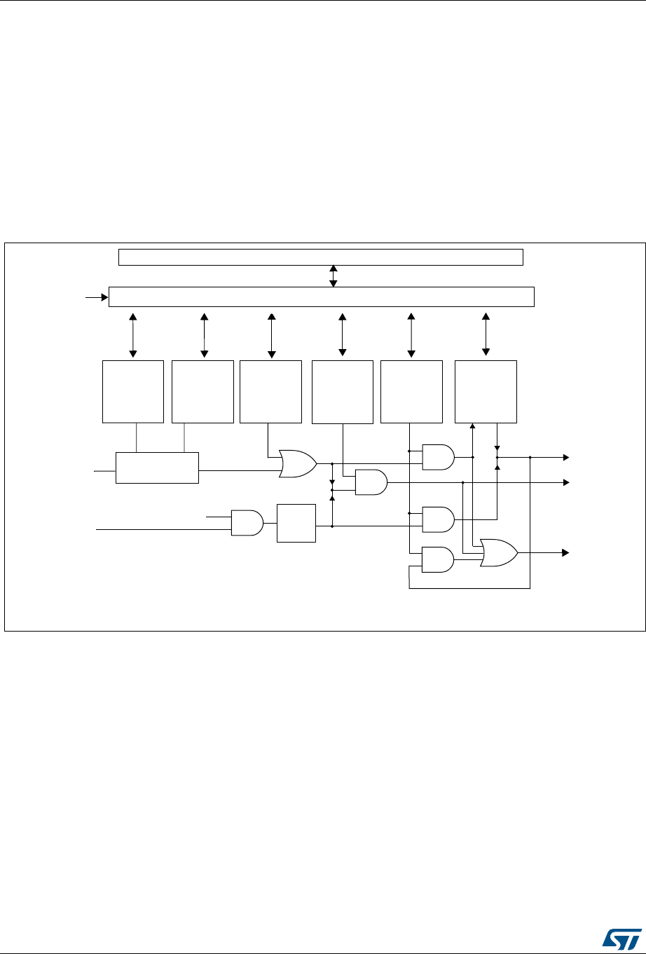
Extended interrupts and events controller (EXTI) RM0394
326/1600 RM0394 Rev 4
selected edge occurs on the event line, an event pulse is generated. The pending bit
corresponding to the event line is not set.
For the configurable lines, an interrupt/event request can also be generated by software by
writing a ‘1’ in the software interrupt/event register.
Note: The interrupts or events associated to the direct lines are triggered only when the system is
in Stop mode. If the system is still running, no interrupt/event is generated by the EXTI.
13.3.1 EXTI block diagram
The extended interrupt/event block diagram is shown on Figure 28.
Figure 28. Configurable interrupt/event block diagram
13.3.2 Wakeup event management
The STM32L41xxx/42xxx/43xxx/44xxx/45xxx/46xxx is able to handle external or internal
events in order to wake up the core (WFE). The wakeup event can be generated either by:
•enabling an interrupt in the peripheral control register but not in the NVIC, and enabling
the SEVONPEND bit in the CortexTM-M4 System Control register. When the MCU
resumes from WFE, the EXTI peripheral interrupt pending bit and the peripheral NVIC
IRQ channel pending bit (in the NVIC interrupt clear pending register) have to be
cleared
•or by configuring an EXTI line in event mode. When the CPU resumes from WFE, it is
not necessary to clear the peripheral interrupt pending bit or the NVIC IRQ channel
pending bit as the pending bit corresponding to the event line is not set.
3HULSKHUDOLQWHUIDFH
(GJHGHWHFW
FLUFXLW
$3%EXV
3&/.
,QWHUUXSWV
6RIWZDUH
LQWHUUXSW
HYHQW
UHJLVWHU
5LVLQJ
WULJJHU
VHOHFWLRQ
UHJLVWHU
3HQGLQJ
UHTXHVW
UHJLVWHU
069
,QWHUUXSW
PDVN
UHJLVWHU
)DOOLQJ
WULJJHU
VHOHFWLRQ
UHJLVWHU
(YHQW
PDVN
UHJLVWHU
3JTJOH
FEHF
EFUFDU
6WRSPRGH
'LUHFWHYHQWV
&RQILJXUDEOH
HYHQWV
(YHQWV
:DNHXS

RM0394 Rev 4 327/1600
RM0394 Extended interrupts and events controller (EXTI)
337
13.3.3 Peripherals asynchronous Interrupts
Some peripherals are able to generate events when the system is in run mode and also
when the system is in Stop mode, allowing to wake up the system from Stop mode.
To accomplish this, the peripheral generates both a synchronized (to the system clock, e.g.
APB clock) and an asynchronous version of the event. This asynchronous event is
connected to an EXTI direct line.
Note: Few peripherals with wakeup from Stop capability are connected to an EXTI configurable
line. In this case, the EXTI configuration is necessary to allow the wakeup from Stop mode.
13.3.4 Hardware interrupt selection
To configure a line as an interrupt source, use the following procedure:
1. Configure the corresponding mask bit in the EXTI_IMR register.
2. Configure the Trigger Selection bits of the Interrupt line (EXTI_RTSR and EXTI_FTSR).
3. Configure the enable and mask bits that control the NVIC IRQ channel mapped to the
EXTI so that an interrupt coming from one of the EXTI lines can be correctly
acknowledged.
Note: The direct lines do not require any EXTI configuration.
13.3.5 Hardware event selection
To configure a line as an event source, use the following procedure:
1. Configure the corresponding mask bit in the EXTI_EMR register.
2. Configure the Trigger Selection bits of the Event line (EXTI_RTSR and EXTI_FTSR).
13.3.6 Software interrupt/event selection
Any of the configurable lines can be configured as a software interrupt/event line. The
procedure to generate a software interrupt is as follows:
1. Configure the corresponding mask bit (EXTI_IMR, EXTI_EMR).
2. Set the required bit of the software interrupt register (EXTI_SWIER).
13.4 EXTI interrupt/event line mapping
In the STM32L41xxx/42xxx/43xxx/44xxx/45xxx/46xxx, 38 interrupt/event lines are available.
The GPIOs are connected to 16 configurable interrupt/event lines (see Figure 29).
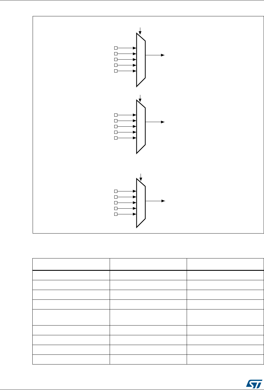
Extended interrupts and events controller (EXTI) RM0394
328/1600 RM0394 Rev 4
Figure 29. External interrupt/event GPIO mapping
The 38 lines are connected as shown in Table 47: EXTI lines connections.
Table 47. EXTI lines connections
EXTI line Line source(1) Line type
0-15 GPIO configurable
16 PVD configurable
17 USB FS wakeup event(3)(2) direct
18 RTC alarms configurable
19 RTC tamper or timestamp or
CSS_LSE configurable
20 RTC wakeup timer configurable
21 COMP1 output configurable
22 COMP2 output configurable
23 I2C1 wakeup(3) direct
06Y9
(;7,>@ELWVLQWKH6<6&)*B(;7,&5UHJLVWHU
(;7,>@ELWVLQWKH6<6&)*B(;7,&5UHJLVWHU
(;7,>@ELWVLQWKH6<6&)*B(;7,&5UHJLVWHU
3$
3%
3&
3'
3(
3$
3%
3&
3'
3(
3$
3%
3&
3'
3(
(;7,
(;7,
(;7,

RM0394 Rev 4 329/1600
RM0394 Extended interrupts and events controller (EXTI)
337
24 I2C2 wakeup(3)(4) direct
25 I2C3 wakeup direct
26 USART1 wakeup(3) direct
27 USART2 wakeup(3) direct
28 USART3 wakeup(3)(4) direct
30 - -
29 UART4 wakeup(3)(5) direct
31 LPUART1 wakeup direct
32 LPTIM1 direct
33 LPTIM2 (6) direct
34 SWPMI1 wakeup(3)(7) direct
35 PVM1 wakeup configurable
36 - -
37 PVM3 wakeup configurable
38 PVM4 wakeup configurable
39 LCD wakeup(8) direct
40 I2C4 wakeup(5) direct
1. All the lines can wake up from the Stop 0 and Stop 1 modes. All the lines, except the ones
mentioned above, can wake up from the Stop 2 mode.
2. Not available for STM32L431xx devices.
3. This line source cannot wake up from the Stop 2 mode.
4. Not available on STM32L432xx and STM32L442xx devices.
5. Available on STM32L45xxx and STM32L46xxx devices only.
6. This line can wake up from Stop 2 mode on STM32L41xxx and STM32L42xx devices only.
7. Available on STM32L43xxx and STM32L44xxx devices only.
8. Available on STM32L4x3 devices only.
Table 47. EXTI lines connections (continued)
EXTI line Line source(1) Line type

Extended interrupts and events controller (EXTI) RM0394
330/1600 RM0394 Rev 4
13.5 EXTI registers
Refer to Section 1.2 on page 60 for a list of abbreviations used in register descriptions.
The peripheral registers have to be accessed by words (32-bit).
13.5.1 Interrupt mask register 1 (EXTI_IMR1)
Address offset: 0x00
Reset value: 0xFF82 0000
Note: The reset value for the direct lines (line 17, lines from 23 to 34, line 39) is set to ‘1’ in order
to enable the interrupt by default.
13.5.2 Event mask register 1 (EXTI_EMR1)
Address offset: 0x04
Reset value: 0x0000 0000
31 30 29 28 27 26 25 24 23 22 21 20 19 18 17 16
IM31 Res. Res. IM28 IM27 IM26 IM25 IM24 IM23 IM22 IM21 IM20 IM19 IM18 IM17 IM16
rw rw rw rw rw rw rw rw rw rw rw rw rw rw
15 14 13 12 11 10 9 8 7 6 5 4 3 2 1 0
IM15 IM14 IM13 IM12 IM11 IM10 IM9 IM8 IM7 IM6 IM5 IM4 IM3 IM2 IM1 IM0
rw rw rw rw rw rw rw rw rw rw rw rw rw rw rw rw
Bit 31 IM31: Interrupt Mask on line 31
0: Interrupt request from Line 31 is masked
1: Interrupt request from Line 31 is not masked
Bits 30:29 Reserved, must be kept at reset value.
Bits 28:0 IMx: Interrupt Mask on line x (x = 28 to 0)
0: Interrupt request from Line x is masked
1: Interrupt request from Line x is not masked
31 30 29 28 27 26 25 24 23 22 21 20 19 18 17 16
EM31 Res. Res. EM28 EM27 EM26 EM25 EM24 EM23 EM22 EM21 EM20 EM19 EM18 EM17 EM16
rw rw rw rw rw rw rw rw rw rw rw rw rw rw
15 14 13 12 11 10 9 8 7 6 5 4 3 2 1 0
EM15 EM14 EM13 EM12 EM11 EM10 EM9 EM8 EM7 EM6 EM5 EM4 EM3 EM2 EM1 EM0
rw rw rw rw rw rw rw rw rw rw rw rw rw rw rw rw

RM0394 Rev 4 331/1600
RM0394 Extended interrupts and events controller (EXTI)
337
13.5.3 Rising trigger selection register 1 (EXTI_RTSR1)
Address offset: 0x08
Reset value: 0x0000 0000
Note: The configurable wakeup lines are edge-triggered. No glitch must be generated on these
lines. If a rising edge on a configurable interrupt line occurs during a write operation in the
EXTI_RTSR register, the pending bit is not set.
Rising and falling edge triggers can be set for the same interrupt line. In this case, both
generate a trigger condition.
13.5.4 Falling trigger selection register 1 (EXTI_FTSR1)
Address offset: 0x0C
Reset value: 0x0000 0000
Bit 31 EM31: Event mask on line 31
0: Event request from line 31 is masked
1: Event request from line 31 is not masked
Bits 30:29 Reserved, must be kept at reset value.
Bits 28:0 EMx: Event mask on line x (x = 28 to 0)
0: Event request from line x is masked
1: Event request from line x is not masked
31 30 29 28 27 26 25 24 23 22 21 20 19 18 17 16
Res. Res. Res. Res. Res. Res. Res. Res. Res. RT22 RT21 RT20 RT19 RT18 Res. RT16
rw rw rw rw rw rw
1514131211109 8 765432 1 0
RT15 RT14 RT13 RT12 RT11 RT10 RT9 RT8 RT7 RT6 RT5 RT4 RT3 RT2 RT1 RT0
rw rw rw rw rw rw rw rw rw rw rw rw rw rw rw rw
Bits 31:23 Reserved, must be kept at reset value.
Bits 22:18 RTx: Rising trigger event configuration bit of line x (x = 22 to 18)
0: Rising trigger disabled (for Event and Interrupt) for input line
1: Rising trigger enabled (for Event and Interrupt) for input line
Bit 17 Reserved, must be kept at reset value.
Bits 16:0 RTx: Rising trigger event configuration bit of line x (x = 16 to 0)
0: Rising trigger disabled (for Event and Interrupt) for input line
1: Rising trigger enabled (for Event and Interrupt) for input line
31 30 29 28 27 26 25 24 23 22 21 20 19 18 17 16
Res. Res. Res. Res. Res. Res. Res. Res. Res. FT22 FT21 FT20 FT19 FT18 Res. FT16
rw rw rw rw rw rw
1514131211109 8 765432 1 0
FT15 FT14 FT13 FT12 FT11 FT10 FT9 FT8 FT7 FT6 FT5 FT4 FT3 FT2 FT1 FT0
rw rw rw rw rw rw rw rw rw rw rw rw rw rw rw rw

Extended interrupts and events controller (EXTI) RM0394
332/1600 RM0394 Rev 4
Note: The configurable wakeup lines are edge-triggered. No glitch must be generated on these
lines. If a falling edge on a configurable interrupt line occurs during a write operation to the
EXTI_FTSR register, the pending bit is not set.
Rising and falling edge triggers can be set for the same interrupt line. In this case, both
generate a trigger condition.
13.5.5 Software interrupt event register 1 (EXTI_SWIER1)
Address offset: 0x10
Reset value: 0x0000 0000
Bits 31:23 Reserved, must be kept at reset value.
Bits 22:18 FTx: Falling trigger event configuration bit of line x (x = 22 to 18)
0: Falling trigger disabled (for Event and Interrupt) for input line
1: Falling trigger enabled (for Event and Interrupt) for input line
Bit 17 Reserved, must be kept at reset value.
Bits 16:0 FTx: Falling trigger event configuration bit of line x (x = 16 to 0)
0: Falling trigger disabled (for Event and Interrupt) for input line
1: Falling trigger enabled (for Event and Interrupt) for input line
31 30 29 28 27 26 25 24 23 22 21 20 19 18 17 16
Res. Res. Res. Res. Res. Res. Res. Res. Res. SWI
22
SWI
21
SWI
20
SWI
19
SWI
18 Res. SWI
16
rw rw rw rw rw rw
1514131211109 8 765432 1 0
SWI
15
SWI
14
SWI
13
SWI
12
SWI
11
SWI
10
SWI
9
SWI
8
SWI
7
SWI
6
SWI
5
SWI
4
SWI
3
SWI
2
SWI
1
SWI
0
rw rw rw rw rw rw rw rw rw rw rw rw rw rw rw rw
Bits 31:23 Reserved, must be kept at reset value.
Bits 22: 18 SWIx: Software interrupt on line x (x = 22 o 18)
If the interrupt is enabled on this line in the EXTI_IMR, writing a '1' to this bit
when it is at '0' sets the corresponding pending bit in EXTI_PR resulting in an
interrupt request generation.
This bit is cleared by clearing the corresponding bit in the EXTI_PR register (by
writing a ‘1’ into the bit).
Bit 17 Reserved, must be kept at reset value.
Bits 16:0 SWIx: Software interrupt on line x (x = 16 to 0)
If the interrupt is enabled on this line in the EXTI_IMR, writing a '1' to this bit
when it is at '0' sets the corresponding pending bit in EXTI_PR resulting in an
interrupt request generation.
This bit is cleared by clearing the corresponding bit of EXTI_PR (by writing a ‘1’
into the bit).

RM0394 Rev 4 333/1600
RM0394 Extended interrupts and events controller (EXTI)
337
13.5.6 Pending register 1 (EXTI_PR1)
Address offset: 0x14
Reset value: undefined
13.5.7 Interrupt mask register 2 (EXTI_IMR2)
Address offset: 0x20
Reset value: 0x0000 0087
Note: The reset value for the direct lines (line 17, lines from 23 to 34, line 39,) is set to ‘1’ in order
to enable the interrupt by default.
31 30 29 28 27 26 25 24 23 22 21 20 19 18 17 16
Res. Res. Res. Res. Res. Res. Res. Res. Res. PIF22 PIF21 PIF20 PIF19 PIF18 Res. PIF16
rc_w1 rc_w1 rc_w1 rc_w1 rc_w1 rc_w1
1514131211109 8 765432 1 0
PIF15 PIF14 PIF13 PIF12 PIF11 PIF10 PIF9 PIF8 PIF7 PIF6 PIF5 PIF4 PIF3 PIF2 PIF1 PIF0
rc_w1 rc_w1 rc_w1 rc_w1 rc_w1 rc_w1 rc_w1 rc_w1 rc_w1 rc_w1 rc_w1 rc_w1 rc_w1 rc_w1 rc_w1 rc_w1
Bits 31:23 Reserved, must be kept at reset value.
Bits 22:18 PIFx: Pending interrupt flag on line x (x = 22 to 18)
0: No trigger request occurred
1: Selected trigger request occurred
This bit is set when the selected edge event arrives on the interrupt line. This bit
is cleared by writing a ‘1’ to the bit.
Bit 17 Reserved, must be kept at reset value.
Bits 16:0 PIFx: Pending interrupt flag on line x (x = 16 to 0)
0: No trigger request occurred
1: Selected trigger request occurred
This bit is set when the selected edge event arrives on the interrupt line. This bit
is cleared by writing a ‘1’ to the bit.
31 30 29 28 27 26 25 24 23 22 21 20 19 18 17 16
Res. Res. Res. Res. Res. Res. Res. Res. Res. Res. Res. Res. Res. Res. Res. Res.
15 14 13 12 11 10 9 8 7 6 5 4 3 2 1 0
Res. Res. Res. Res. Res. Res. Res. Res IM39 IM38 IM37 IM36 IM35 IM34 IM33 IM32
rw rw rw rw rw rw rw rw
Bits 31:8 Reserved, must be kept at reset value
Bits 7:0 IMx: Interrupt mask on line x (x = 39 to 32)
0: Interrupt request from line x is masked
1: Interrupt request from line x is not masked

Extended interrupts and events controller (EXTI) RM0394
334/1600 RM0394 Rev 4
13.5.8 Event mask register 2 (EXTI_EMR2)
Address offset: 0x24
Reset value: 0x0000 0000
13.5.9 Rising trigger selection register 2 (EXTI_RTSR2)
Address offset: 0x28
Reset value: 0x0000 0000
Note: The configurable wakeup lines are edge-triggered. No glitch must be generated on these
lines. If a rising edge on a configurable interrupt line occurs during a write operation to the
EXTI_RTSR register, the pending bit is not set.
Rising and falling edge triggers can be set for the same interrupt line. In this case, both
generate a trigger condition.
31 30 29 28 27 26 25 24 23 22 21 20 19 18 17 16
Res. Res. Res. Res. Res. Res. Res. Res. Res. Res. Res. Res. Res. Res. Res. Res.
15 14 13 12 11 10 9 8 7 6 5 4 3 2 1 0
Res. Res. Res. Res. Res. Res. Res. Res EM39 EM38 EM37 EM36 EM35 EM34 EM33 EM32
rw rw rw rw rw rw rw rw
Bits 31:8 Reserved, must be kept at reset value
Bits 7:0 EMx: Event mask on line x (x = 39 to 32)
0: Event request from line x is masked
1: Event request from line x is not masked
31 30 29 28 27 26 25 24 23 22 21 20 19 18 17 16
Res. Res. Res. Res. Res. Res. Res. Res. Res. Res. Res. Res. Res. Res. Res. Res.
1514131211109 8 765432 1 0
Res. Res. Res. Res. Res. Res. Res. Res. Res. RT38 RT37 RT36 RT35 Res. Res. Res.
rw rw rw rw
Bits 31:8 Reserved, must be kept at reset value.
Bits 7:3 RTx: Rising trigger event configuration bit of line x (x = 35 to 38)
0: Rising trigger disabled (for Event and Interrupt) for input line
1: Rising trigger enabled (for Event and Interrupt) for input line
Bits 2:0 Reserved, must be kept at reset value.

RM0394 Rev 4 335/1600
RM0394 Extended interrupts and events controller (EXTI)
337
13.5.10 Falling trigger selection register 2 (EXTI_FTSR2)
Address offset: 0x2C
Reset value: 0x0000 0000
Note: The configurable wakeup lines are edge-triggered. No glitch must be generated on these
lines. If a falling edge on a configurable interrupt line occurs during a write operation to the
EXTI_FTSR register, the pending bit is not set.
Rising and falling edge triggers can be set for the same interrupt line. In this case, both
generate a trigger condition.
13.5.11 Software interrupt event register 2 (EXTI_SWIER2)
Address offset: 0x30
Reset value: 0x0000 0000
31 30 29 28 27 26 25 24 23 22 21 20 19 18 17 16
Res. Res. Res. Res. Res. Res. Res. Res. Res. Res. Res. Res. Res. Res. Res. Res.
1514131211109 8 765432 1 0
Res. Res. Res. Res. Res. Res. Res. Res. Res. FT38 FT37 FT36 FT35 Res. Res. Res.
rw rw rw rw
Bits 31:8 Reserved, must be kept at reset value.
Bits 7:3 FTx: Falling trigger event configuration bit of line x (x = 35 to 38)
0: Falling trigger disabled (for Event and Interrupt) for input line
1: Falling trigger enabled (for Event and Interrupt) for input line
Bits 2:0 Reserved, must be kept at reset value.
31 30 29 28 27 26 25 24 23 22 21 20 19 18 17 16
Res. Res. Res. Res. Res. Res. Res. Res. Res. Res. Res. Res. Res. Res. Res. Res.
1514131211109 8 765432 1 0
Res. Res. Res. Res. Res. Res. Res. Res. Res. SWI
38
SWI
37
SWI
36
SWI
35 Res. Res. Res.
rw rw rw rw
Bits 31:8 Reserved, must be kept at reset value.
Bit 7 SWIx: Software interrupt on line x (x = 35 to 38)
If the interrupt is enabled on this line in EXTI_IMR, writing a '1' to this bit when it
is at '0' sets the corresponding pending bit of EXTI_PR resulting in an interrupt
request generation.
This bit is cleared by clearing the corresponding bit of EXTI_PR (by writing a ‘1’
to the bit).
Bits 2:0 Reserved, must be kept at reset value.

Extended interrupts and events controller (EXTI) RM0394
336/1600 RM0394 Rev 4
13.5.12 Pending register 2 (EXTI_PR2)
Address offset: 0x34
Reset value: undefined
31 30 29 28 27 26 25 24 23 22 21 20 19 18 17 16
Res. Res. Res. Res. Res. Res. Res. Res. Res. Res. Res. Res. Res. Res. Res. Res.
1514131211109 8 765432 1 0
Res. Res. Res. Res. Res. Res. Res. Res. Res. PIF38 PIF37 PIF36 PIF35 Res. Res. Res.
rc_w1 rc_w1 rc_w1 rc_w1
Bits 31:8 Reserved, must be kept at reset value.
Bit 7 PIFx: Pending interrupt flag on line x (x = 35 to 38)
0: No trigger request occurred
1: Selected trigger request occurred
This bit is set when the selected edge event arrives on the interrupt line. This bit
is cleared by writing a ‘1’ into the bit.
Bits 2:0 Reserved, must be kept at reset value.

RM0394 Rev 4 337/1600
RM0394 Extended interrupts and events controller (EXTI)
337
13.5.13 EXTI register map
Table 48 gives the EXTI register map and the reset values.
Table 48. Extended interrupt/event controller register map and reset values
Offset Register
31
30
29
28
27
26
25
24
23
22
21
20
19
18
17
16
15
14
13
12
11
10
9
8
7
6
5
4
3
2
1
0
0x00
EXTI_IMR1
IM31
Res.
Res.
IM28
IM27
IM26
IM25
IM24
IM23
IM22
IM21
IM20
IM19
IM18
IM17
IM16
IM15
IM14
IM13
IM12
IM11
IM10
IM9
IM8
IM7
IM6
IM5
IM4
IM3
IM2
IM1
IM0
Reset value 1 11111100000100000000000000000
0x04
EXTI_EMR1
EM31
Res.
Res.
EM28
EM27
EM26
EM25
EM24
EM23
EM22
EM21
EM20
EM19
EM18
EM17
EM16
EM15
EM14
EM13
EM12
EM11
EM10
EM9
EM8
EM7
EM6
EM5
EM4
EM3
EM2
EM1
EM0
Reset value 0 00000000000000000000000000000
0x08
EXTI_RTSR1
Res.
Res.
Res.
Res.
Res.
Res.
Res.
Res.
Res.
RT22
RT21
RT20
RT19
RT18
Res.
RT16
RT15
RT14
RT13
RT12
RT11
RT10
RT9
RT8
RT7
RT6
RT5
RT4
RT3
RT2
RT1
RT0
Reset value 00000 00000000000000000
0x0C
EXTI_FTSR1
Res.
Res.
Res.
Res.
Res.
Res.
Res.
Res.
Res.
FT22
FT21
FT20
FT19
FT18
Res.
FT16
FT15
FT14
FT13
FT12
FT11
FT10
FT9
FT8
FT7
FT6
FT5
FT4
FT3
FT2
FT1
FT0
Reset value 00000 00000000000000000
0x10
EXTI_SWIER1
Res.
Res.
Res.
Res.
Res.
Res.
Res.
Res.
Res.
SWI22
SWI21
SWI20
SWI19
SWI18
Res.
SWI16
SWI15
SWI14
SWI13
SWI12
SWI11
SWI10
SWI9
SWI8
SWI7
SWI6
SWI5
SWI4
SWI3
SWI2
SWI1
SWI0
Reset value 00000 00000000000000000
0x14
EXTI_PR1
Res.
Res.
Res.
Res.
Res.
Res.
Res.
Res.
Res.
PIF22
PIF21
PIF20
PIF19
PIF18
Res.
PIF16
PIF15
PIF14
PIF13
PIF12
PIF11
PIF10
PIF9
PIF8
PIF7
PIF6
PIF5
PIF4
PIF3
PIF2
PIF1
PIF0
Reset value 00000 00000000000000000
0x20
EXTI_IMR2
Res.
Res.
Res.
Res.
Res.
Res.
Res.
Res.
Res.
Res.
Res.
Res.
Res.
Res.
Res.
Res.
Res.
Res.
Res.
Res.
Res.
Res.
Res.
Res.
IM39
IM38
IM37
IM36
IM35
IM34
IM33
IM32
Reset value 10000111
0x24
EXTI_EMR2
Res.
Res.
Res.
Res.
Res.
Res.
Res.
Res.
Res.
Res.
Res.
Res.
Res.
Res.
Res.
Res.
Res.
Res.
Res.
Res.
Res.
Res.
Res.
Res.
EM39
EM38
EM37
EM36
EM35
EM34
EM33
EM32
Reset value 00000000
0x28
EXTI_RTSR2
Res.
Res.
Res.
Res.
Res.
Res.
Res.
Res.
Res.
Res.
Res.
Res.
Res.
Res.
Res.
Res.
Res.
Res.
Res.
Res.
Res.
Res.
Res.
Res.
Res.
RT38
RT37
RT36
RT35
Res.
Res.
Res.
Reset value 0000
0x2C
EXTI_FTSR2
Res.
Res.
Res.
Res.
Res.
Res.
Res.
Res.
Res.
Res.
Res.
Res.
Res.
Res.
Res.
Res.
Res.
Res.
Res.
Res.
Res.
Res.
Res.
Res.
Res.
FT38
FT37
FT36
FT35
Res.
Res.
Res.
Reset value 0000
0x30
EXTI_SWIER2
Res.
Res.
Res.
Res.
Res.
Res.
Res.
Res.
Res.
Res.
Res.
Res.
Res.
Res.
Res.
Res.
Res.
Res.
Res.
Res.
Res.
Res.
Res.
Res.
Res.
SWI38
SWI37
SWI36
SWI35
Res.
Res.
Res.
Reset value 0000
0x34
EXTI_PR2
Res.
Res.
Res.
Res.
Res.
Res.
Res.
Res.
Res.
Res.
Res.
Res.
Res.
Res.
Res.
Res.
Res.
Res.
Res.
Res.
Res.
Res.
Res.
Res.
Res.
PIF38
PIF37
PIF36
PIF35
Res.
Res.
Res.
Reset value 0000

Cyclic redundancy check calculation unit (CRC) RM0394
338/1600 RM0394 Rev 4
14 Cyclic redundancy check calculation unit (CRC)
14.1 Introduction
The CRC (cyclic redundancy check) calculation unit is used to get a CRC code from 8-, 16-
or 32-bit data word and a generator polynomial.
Among other applications, CRC-based techniques are used to verify data transmission or
storage integrity. In the scope of the functional safety standards, they offer a means of
verifying the Flash memory integrity. The CRC calculation unit helps compute a signature of
the software during runtime, to be compared with a reference signature generated at link
time and stored at a given memory location.
14.2 CRC main features
•Uses CRC-32 (Ethernet) polynomial: 0x4C11DB7
X32 + X26 + X23 + X22 + X16 + X12 + X11 + X10 +X8 + X7 + X5 + X4 + X2+ X +1
•Alternatively, uses fully programmable polynomial with programmable size (7, 8, 16, 32
bits)
•Handles 8-,16-, 32-bit data size
•Programmable CRC initial value
•Single input/output 32-bit data register
•Input buffer to avoid bus stall during calculation
•CRC computation done in 4 AHB clock cycles (HCLK) for the 32-bit data size
•General-purpose 8-bit register (can be used for temporary storage)
•Reversibility option on I/O data
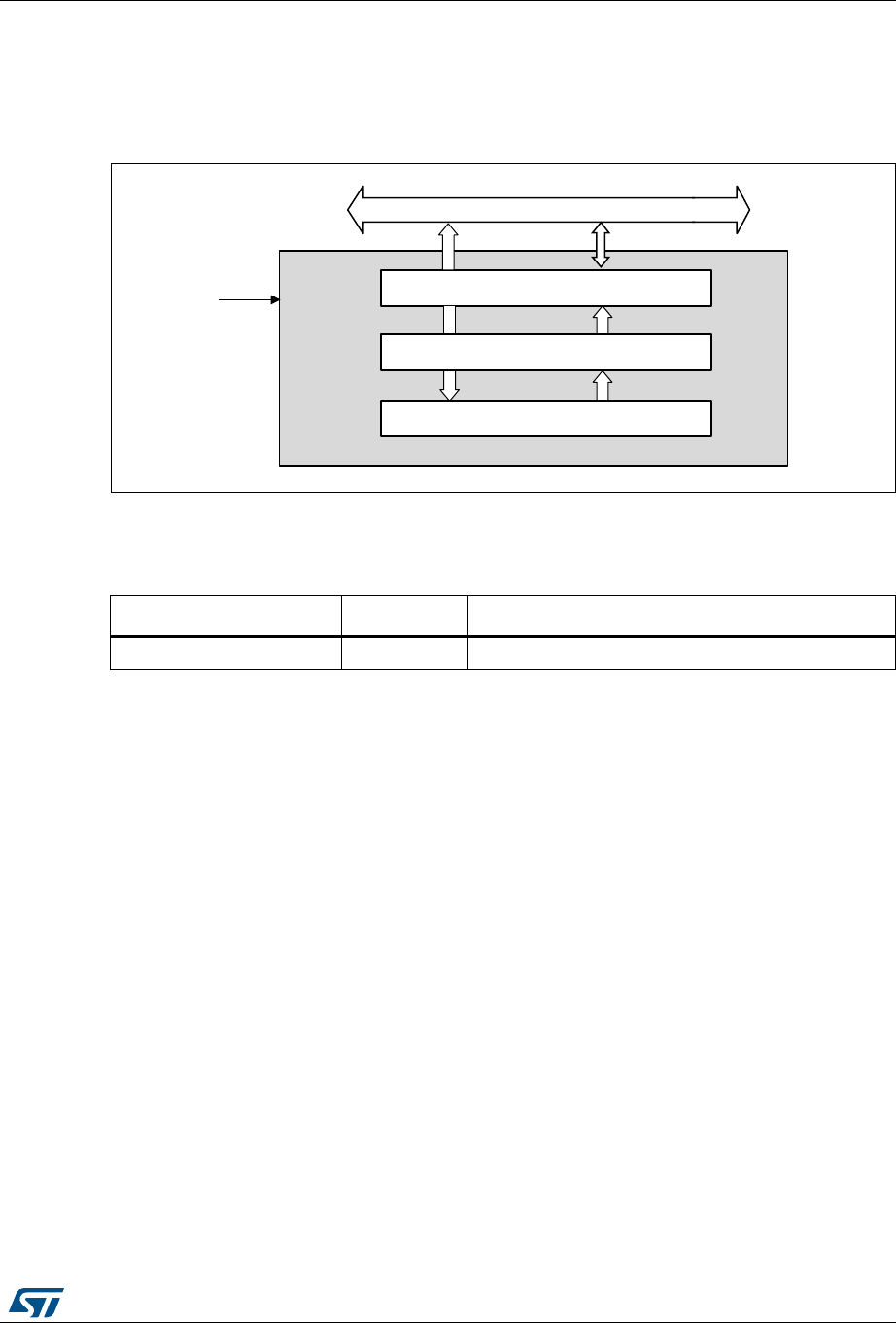
RM0394 Rev 4 339/1600
RM0394 Cyclic redundancy check calculation unit (CRC)
343
14.3 CRC functional description
14.3.1 CRC block diagram
Figure 30. CRC calculation unit block diagram
14.3.2 CRC internal signals
14.3.3 CRC operation
The CRC calculation unit has a single 32-bit read/write data register (CRC_DR). It is used to
input new data (write access), and holds the result of the previous CRC calculation (read
access).
Each write operation to the data register creates a combination of the previous CRC value
(stored in CRC_DR) and the new one. CRC computation is done on the whole 32-bit data
word or byte by byte depending on the format of the data being written.
The CRC_DR register can be accessed by word, right-aligned half-word and right-aligned
byte. For the other registers only 32-bit access is allowed.
The duration of the computation depends on data width:
•4 AHB clock cycles for 32-bit
•2 AHB clock cycles for 16-bit
•1 AHB clock cycles for 8-bit
An input buffer allows to immediately write a second data without waiting for any wait states
due to the previous CRC calculation.
The data size can be dynamically adjusted to minimize the number of write accesses for a
given number of bytes. For instance, a CRC for 5 bytes can be computed with a word write
followed by a byte write.
D^ϭϵϴϴϮsϮ
'DWDUHJLVWHURXWSXW
ELWUHDGDFFHVV
'DWDUHJLVWHULQSXW
ELWZULWHDFFHVV
ELW$+%EXV
FUFBKFON
&5&FRPSXWDWLRQ
Table 49. CRC internal input/output signals
Signal name Signal type Description
crc_hclk Digital input AHB clock

Cyclic redundancy check calculation unit (CRC) RM0394
340/1600 RM0394 Rev 4
The input data can be reversed, to manage the various endianness schemes. The reversing
operation can be performed on 8 bits, 16 bits and 32 bits depending on the REV_IN[1:0] bits
in the CRC_CR register.
For example: input data 0x1A2B3C4D is used for CRC calculation as:
•0x58D43CB2 with bit-reversal done by byte
•0xD458B23C with bit-reversal done by half-word
•0xB23CD458 with bit-reversal done on the full word
The output data can also be reversed by setting the REV_OUT bit in the CRC_CR register.
The operation is done at bit level: for example, output data 0x11223344 is converted into
0x22CC4488.
The CRC calculator can be initialized to a programmable value using the RESET control bit
in the CRC_CR register (the default value is 0xFFFFFFFF).
The initial CRC value can be programmed with the CRC_INIT register. The CRC_DR
register is automatically initialized upon CRC_INIT register write access.
The CRC_IDR register can be used to hold a temporary value related to CRC calculation. It
is not affected by the RESET bit in the CRC_CR register.
Polynomial programmability
The polynomial coefficients are fully programmable through the CRC_POL register, and the
polynomial size can be configured to be 7, 8, 16 or 32 bits by programming the
POLYSIZE[1:0] bits in the CRC_CR register. Even polynomials are not supported.
If the CRC data is less than 32-bit, its value can be read from the least significant bits of the
CRC_DR register.
To obtain a reliable CRC calculation, the change on-fly of the polynomial value or size can
not be performed during a CRC calculation. As a result, if a CRC calculation is ongoing, the
application must either reset it or perform a CRC_DR read before changing the polynomial.
The default polynomial value is the CRC-32 (Ethernet) polynomial: 0x4C11DB7.

RM0394 Rev 4 341/1600
RM0394 Cyclic redundancy check calculation unit (CRC)
343
14.4 CRC registers
14.4.1 Data register (CRC_DR)
Address offset: 0x00
Reset value: 0xFFFF FFFF
14.4.2 Independent data register (CRC_IDR)
Address offset: 0x04
Reset value: 0x0000 0000
31 30 29 28 27 26 25 24 23 22 21 20 19 18 17 16
DR[31:16]
rw rw rw rw rw rw rw rw rw rw rw rw rw rw rw rw
1514131211109876543210
DR[15:0]
rw rw rw rw rw rw rw rw rw rw rw rw rw rw rw rw
Bits 31:0 DR[31:0]: Data register bits
This register is used to write new data to the CRC calculator.
It holds the previous CRC calculation result when it is read.
If the data size is less than 32 bits, the least significant bits are used to write/read the
correct value.
31 30 29 28 27 26 25 24 23 22 21 20 19 18 17 16
Res. Res. Res. Res. Res. Res. Res. Res. Res. Res. Res. Res. Res. Res. Res. Res.
1514131211109876543210
Res. Res. Res. Res. Res. Res. Res. Res. IDR[7:0]
rw
Bits 31:8 Reserved, must be kept at reset value.
Bits 7:0 IDR[7:0]: General-purpose 8-bit data register bits
These bits can be used as a temporary storage location for one byte.
This register is not affected by CRC resets generated by the RESET bit in the CRC_CR register
Cyclic redundancy check calculation unit (CRC) RM0394
342/1600 RM0394 Rev 4
14.4.3 Control register (CRC_CR)
Address offset: 0x08
Reset value: 0x0000 0000
14.4.4 Initial CRC value (CRC_INIT)
Address offset: 0x10
Reset value: 0xFFFF FFFF
31 30 29 28 27 26 25 24 23 22 21 20 19 18 17 16
Res. Res. Res. Res. Res. Res. Res. Res. Res. Res. Res. Res. Res. Res. Res. Res.
1514131211109876543210
Res. Res. Res. Res. Res. Res. Res. Res. REV_
OUT REV_IN[1:0] POLYSIZE[1:0] Res. Res. RESET
rw rw rw rw rw rs
Bits 31:8 Reserved, must be kept at reset value.
Bit 7 REV_OUT: Reverse output data
This bit controls the reversal of the bit order of the output data.
0: Bit order not affected
1: Bit-reversed output format
Bits 6:5 REV_IN[1:0]: Reverse input data
These bits control the reversal of the bit order of the input data
00: Bit order not affected
01: Bit reversal done by byte
10: Bit reversal done by half-word
11: Bit reversal done by word
Bits 4:3 POLYSIZE[1:0]: Polynomial size
These bits control the size of the polynomial.
00: 32 bit polynomial
01: 16 bit polynomial
10: 8 bit polynomial
11: 7 bit polynomial
Bits 2:1 Reserved, must be kept at reset value.
Bit 0 RESET: RESET bit
This bit is set by software to reset the CRC calculation unit and set the data register to the value
stored in the CRC_INIT register. This bit can only be set, it is automatically cleared by hardware
31 30 29 28 27 26 25 24 23 22 21 20 19 18 17 16
CRC_INIT[31:16]
rw rw rw rw rw rw rw rw rw rw rw rw rw rw rw rw
15 14 13 12 11 10 9 8 7 6 5 4 3 2 1 0
CRC_INIT[15:0]
rw rw rw rw rw rw rw rw rw rw rw rw rw rw rw rw
RM0394 Rev 4 343/1600
RM0394 Cyclic redundancy check calculation unit (CRC)
343
14.4.5 CRC polynomial (CRC_POL)
Address offset: 0x14
Reset value: 0x04C1 1DB7
14.4.6 CRC register map
Refer to Section 2.2.2 on page 67 for the register boundary addresses.
Bits 31:0 CRC_INIT[31:0]: Programmable initial CRC value
This register is used to write the CRC initial value.
31 30 29 28 27 26 25 24 23 22 21 20 19 18 17 16
POL[31:16]
rw rw rw rw rw rw rw rw rw rw rw rw rw rw rw rw
15 14 13 12 11 10 9 8 7 6 5 4 3 2 1 0
POL[15:0]
rw rw rw rw rw rw rw rw rw rw rw rw rw rw rw rw
Bits 31:0 POL[31:0]: Programmable polynomial
This register is used to write the coefficients of the polynomial to be used for CRC calculation.
If the polynomial size is less than 32 bits, the least significant bits have to be used to program the
correct value.
Table 50. CRC register map and reset values
Offset Register
name
31
30
29
28
27
26
25
24
23
22
21
20
19
18
17
16
15
14
13
12
11
10
9
8
7
6
5
4
3
2
1
0
0x00
CRC_DR DR[31:0]
Reset value 11111111111111111111111111111111
0x04
CRC_IDR
Res.
Res.
Res.
Res.
Res.
Res.
Res.
Res.
Res.
Res.
Res.
Res.
Res.
Res.
Res.
Res.
Res.
Res.
Res.
Res.
Res.
Res.
Res.
Res.
IDR[7:0]
Reset value 00000000
0x08
CRC_CR
Res.
Res.
Res.
Res.
Res.
Res.
Res.
Res.
Res.
Res.
Res.
Res.
Res.
Res.
Res.
Res.
Res.
Res.
Res.
Res.
Res.
Res.
Res.
Res.
REV_OUT
REV_IN[1:0]
POLYSIZE[1:0]
Res.
Res.
RESET
Reset value 00000 0
0x10
CRC_INIT CRC_INIT[31:0]
Reset value 11111111111111111111111111111111
0x14
CRC_POL Polynomial coefficients
Reset value 0x04C11DB7
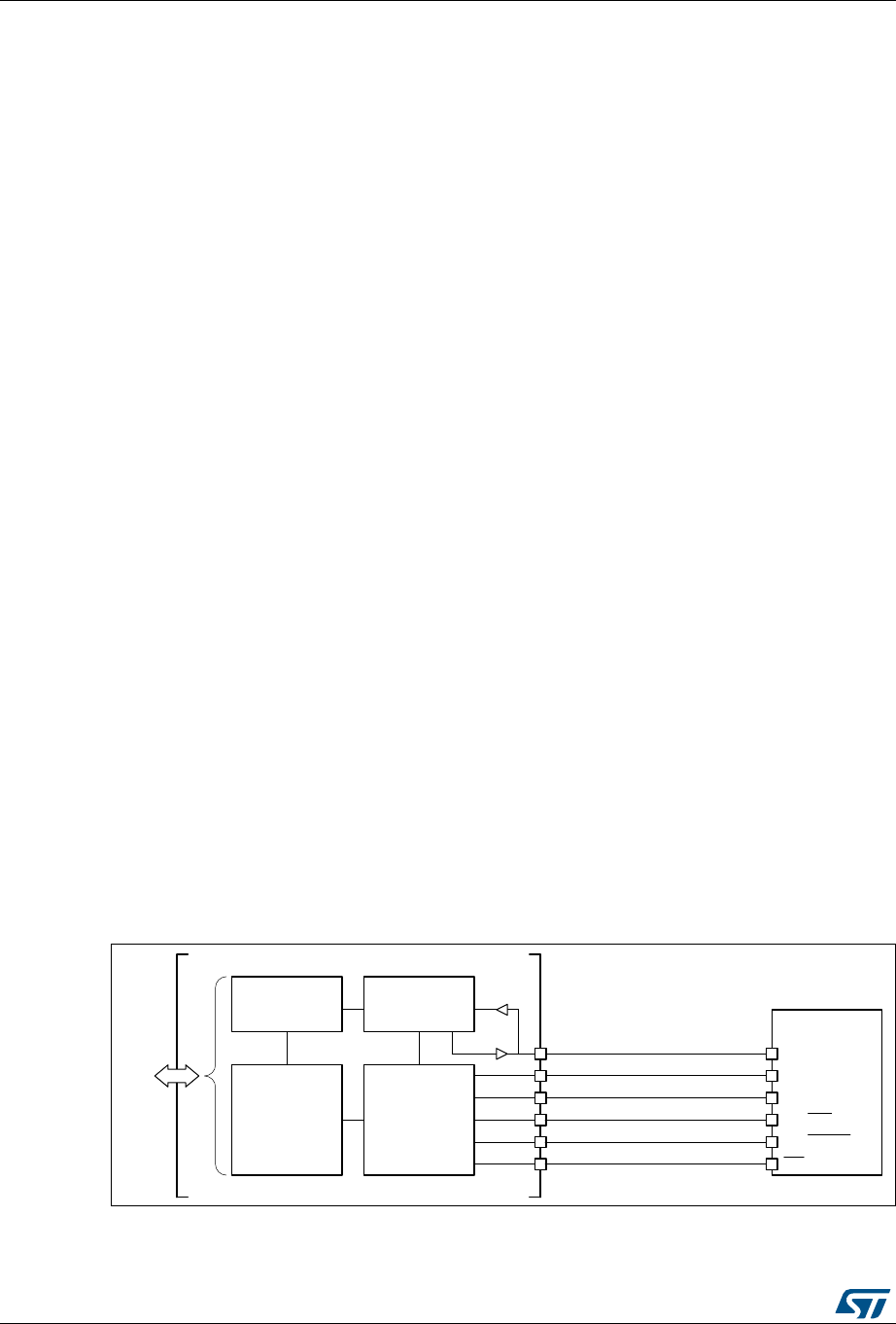
Quad-SPI interface (QUADSPI) RM0394
344/1600 RM0394 Rev 4
15 Quad-SPI interface (QUADSPI)
15.1 Introduction
The QUADSPI is a specialized communication interface targeting single, dual or quad SPI
Flash memories. It can operate in any of the three following modes:
•indirect mode: all the operations are performed using the QUADSPI registers
•status polling mode: the external Flash memory status register is periodically read and
an interrupt can be generated in case of flag setting
•memory-mapped mode: the external Flash memory is mapped to the device address
space and is seen by the system as if it was an internal memory
Both throughput and capacity can be increased two-fold using dual-flash mode, where two
Quad-SPI Flash memories are accessed simultaneously.
15.2 QUADSPI main features
•Three functional modes: indirect, status-polling, and memory-mapped
•Dual-flash mode, where 8 bits can be sent/received simultaneously by accessing two
Flash memories in parallel.
•SDR and DDR support
•Fully programmable opcode for both indirect and memory mapped mode
•Fully programmable frame format for both indirect and memory mapped mode
•Integrated FIFO for reception and transmission
•8, 16, and 32-bit data accesses are allowed
•DMA channel for indirect mode operations
•Interrupt generation on FIFO threshold, timeout, operation complete, and access error
15.3 QUADSPI functional description
15.3.1 QUADSPI block diagram
Figure 31. QUADSPI block diagram when dual-flash mode is disabled
63,)/$6+
069
&/.
%.B,262
%.B,26,
%.B,2
%.B,2
&/.
46,
462
4:3
4+2/'
%.BQ&6 &6
$+%
5HJLVWHUV
FRQWURO
&ORFN
PDQDJHPHQW
),)2 6KLIWUHJLVWHU
48$'63,
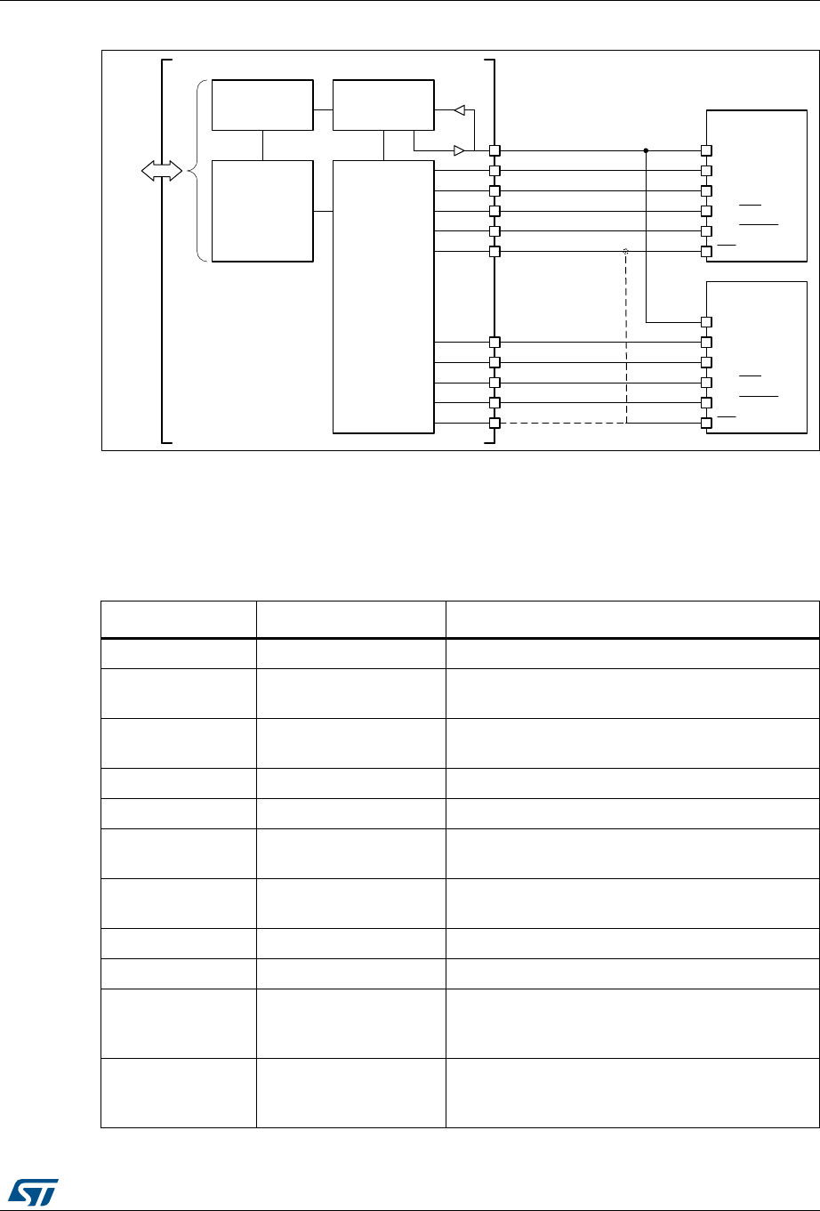
RM0394 Rev 4 345/1600
RM0394 Quad-SPI interface (QUADSPI)
372
Figure 32. QUADSPI block diagram when dual-flash mode is enabled
15.3.2 QUADSPI pins
Table 51 lists the QUADSPI pins, six for interfacing with a single Flash memory, or 10 to 11
for interfacing with two Flash memories (FLASH 1 and FLASH 2) in dual-flash mode.
069
63,)/$6+
&/.
%.B,262
%.B,26,
%.B,2
%.B,2
&/.
46,
462
4:3
4+2/'
%.BQ&6 &6
$+%
5HJLVWHUV
FRQWURO
&ORFN
PDQDJHPHQW
),)2
6KLIWUHJLVWHU
48$'63,
%.B,262
%.B,26,
%.B,2
%.B,2
%.BQ&6
63,)/$6+
&/.
46,
462
4:3
4+2/'
&6
Table 51. QUADSPI pins
Signal name Signal type Description
CLK Digital output Clock to FLASH 1 and FLASH 2
BK1_IO0/SO Digital input/output Bidirectional IO in dual/quad modes or serial output
in single mode, for FLASH 1
BK1_IO1/SI Digital input/output Bidirectional IO in dual/quad modes or serial input
in single mode, for FLASH 1
BK1_IO2 Digital input/output Bidirectional IO in quad mode, for FLASH 1
BK1_IO3 Digital input/output Bidirectional IO in quad mode, for FLASH 1
BK2_IO0/SO Digital input/output Bidirectional IO in dual/quad modes or serial output
in single mode, for FLASH 2
BK2_IO1/SI Digital input/output Bidirectional IO in dual/quad modes or serial input
in single mode, for FLASH 2
BK2_IO2 Digital input/output Bidirectional IO in quad mode, for FLASH 2
BK2_IO3 Digital input/output Bidirectional IO in quad mode, for FLASH 2
BK1_nCS Digital output
Chip select (active low) for FLASH 1. Can also be
used for FLASH 2 if QUADSPI is always used in
dual-flash mode.
BK2_nCS Digital output
Chip select (active low) for FLASH 2. Can also be
used for FLASH 1 if QUADSPI is always used in
dual-flash mode.
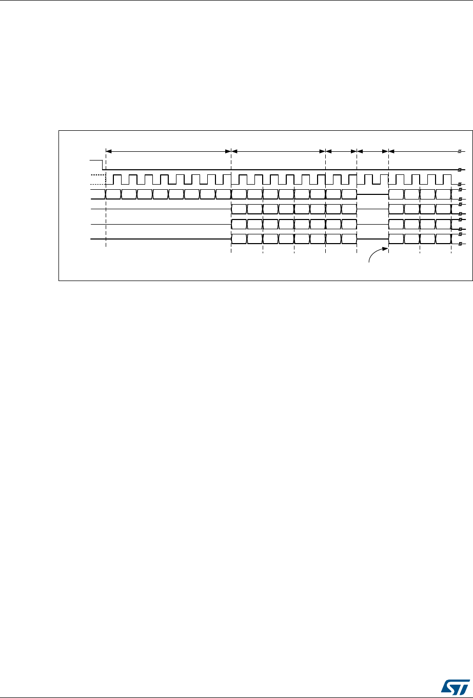
Quad-SPI interface (QUADSPI) RM0394
346/1600 RM0394 Rev 4
15.3.3 QUADSPI command sequence
The QUADSPI communicates with the Flash memory using commands. Each command
can include 5 phases: instruction, address, alternate byte, dummy, data. Any of these
phases can be configured to be skipped, but at least one of the instruction, address,
alternate byte, or data phase must be present.
nCS falls before the start of each command and rises again after each command finishes.
Figure 33. An example of a read command in quad mode
Instruction phase
During this phase, an 8-bit instruction, configured in INSTRUCTION field of
QUADSPI_CCR[7:0] register, is sent to the Flash memory, specifying the type of operation
to be performed.
Though most Flash memories can receive instructions only one bit at a time from the
IO0/SO signal (single SPI mode), the instruction phase can optionally send 2 bits at a time
(over IO0/IO1 in dual SPI mode) or 4 bits at a time (over IO0/IO1/IO2/IO3 in quad SPI
mode). This can be configured using the IMODE[1:0] field of QUADSPI_CCR[9:8] register.
When IMODE = 00, the instruction phase is skipped, and the command sequence starts
with the address phase, if present.
Address phase
In the address phase, 1-4 bytes are sent to the Flash memory to indicate the address of the
operation. The number of address bytes to be sent is configured in the ADSIZE[1:0] field of
QUADSPI_CCR[13:12] register. In indirect and automatic-polling modes, the address bytes
to be sent are specified in the ADDRESS[31:0] field of QUADSPI_AR register, while in
memory-mapped mode the address is given directly via the AHB (from the Cortex® or from
a DMA).
The address phase can send 1 bit at a time (over SO in single SPI mode), 2 bits at a time
(over IO0/IO1 in dual SPI mode), or 4 bits at a time (over IO0/IO1/IO2/IO3 in quad SPI
mode). This can be configured using the ADMODE[1:0] field of QUADSPI_CCR[11:10]
register.
When ADMODE = 00, the address phase is skipped, and the command sequence proceeds
directly to the next phase, if any.
069
Q&6
6&/.
,2
,2
,2
,2
$ $ $ 0 %\WH %\WH
,QVWUXFWLRQ $GGUHVV $OW 'XPP\ 'DWD
,2VZLWFKIURP
RXWSXWWRLQSXW

RM0394 Rev 4 347/1600
RM0394 Quad-SPI interface (QUADSPI)
372
Alternate-bytes phase
In the alternate-bytes phase, 1-4 bytes are sent to the Flash memory, generally to control
the mode of operation. The number of alternate bytes to be sent is configured in the
ABSIZE[1:0] field of QUADSPI_CCR[17:16] register. The bytes to be sent are specified in
the QUADSPI_ABR register.
The alternate-bytes phase can send 1 bit at a time (over SO in single SPI mode), 2 bits at a
time (over IO0/IO1 in dual SPI mode), or 4 bits at a time (over IO0/IO1/IO2/IO3 in quad SPI
mode). This can be configured using the ABMODE[1:0] field of QUADSPI_CCR[15:14]
register.
When ABMODE = 00, the alternate-bytes phase is skipped, and the command sequence
proceeds directly to the next phase, if any.
There may be times when only a single nibble needs to be sent during the alternate-byte
phase rather than a full byte, such as when dual-mode is used and only two cycles are used
for the alternate bytes. In this case, firmware can use quad-mode (ABMODE = 11) and send
a byte with bits 7 and 3 of ALTERNATE set to ‘1’ (keeping the IO3 line high), and bits 6 and
2 set to ‘0’ (keeping the IO2 line low). In this case the upper two bits of the nibble to be sent
are placed in bits 4:3 of ALTERNATE while the lower two bits are placed in bits 1 and 0. For
example, if the nibble 2 (0010) is to be sent over IO0/IO1, then ALTERNATE should be set
to 0x8A (1000_1010).
Dummy-cycles phase
In the dummy-cycles phase, 1-31 cycles are given without any data being sent or received,
in order to allow the Flash memory the time to prepare for the data phase when higher clock
frequencies are used. The number of cycles given during this phase is specified in the
DCYC[4:0] field of QUADSPI_CCR[22:18] register. In both SDR and DDR modes, the
duration is specified as a number of full CLK cycles.
When DCYC is zero, the dummy-cycles phase is skipped, and the command sequence
proceeds directly to the data phase, if present.
The operating mode of the dummy-cycles phase is determined by DMODE.
In order to assure enough “turn-around” time for changing the data signals from output
mode to input mode, there must be at least one dummy cycle when using dual or quad
mode to receive data from the Flash memory.
Data phase
During the data phase, any number of bytes can be sent to, or received from the Flash
memory.
In indirect and automatic-polling modes, the number of bytes to be sent/received is specified
in the QUADSPI_DLR register.
In indirect write mode the data to be sent to the Flash memory must be written to the
QUADSPI_DR register, while in indirect read mode the data received from the Flash
memory is obtained by reading from the QUADSPI_DR register.
In memory-mapped mode, the data which is read is sent back directly over the AHB to the
Cortex or to a DMA.
The data phase can send/receive 1 bit at a time (over SO/SI in single SPI mode), 2 bits at a
time (over IO0/IO1 in dual SPI mode), or 4 bits at a time (over IO0/IO1/IO2/IO3 in quad SPI

Quad-SPI interface (QUADSPI) RM0394
348/1600 RM0394 Rev 4
mode). This can be configured using the ABMODE[1:0] field of QUADSPI_CCR[15:14]
register.
When DMODE = 00, the data phase is skipped, and the command sequence finishes
immediately by raising nCS. This configuration must only be used in only indirect write
mode.
15.3.4 QUADSPI signal interface protocol modes
Single SPI mode
Legacy SPI mode allows just a single bit to be sent/received serially. In this mode, data is
sent to the Flash memory over the SO signal (whose I/O shared with IO0). Data received
from the Flash memory arrives via SI (whose I/O shared with IO1).
The different phases can each be configured separately to use this single bit mode by
setting the IMODE/ADMODE/ABMODE/DMODE fields (in QUADSPI_CCR) to 01.
In each phase which is configured in single mode:
•IO0 (SO) is in output mode
•IO1 (SI) is in input mode (high impedance)
•IO2 is in output mode and forced to ‘0’ (to deactivate the “write protect” function)
•IO3 is in output mode and forced to ‘1’ (to deactivate the “hold” function)
This is the case even for the dummy phase if DMODE = 01.
Dual SPI mode
In dual SPI mode, two bits are sent/received simultaneously over the IO0/IO1 signals.
The different phases can each be configured separately to use dual SPI mode by setting the
IMODE/ADMODE/ABMODE/DMODE fields of QUADSPI_CCR register to 10.
In each phase which is configured in dual mode:
•IO0/IO1 are at high-impedance (input) during the data phase for read operations, and
outputs in all other cases
•IO2 is in output mode and forced to ‘0’
•IO3 is in output mode and forced to ‘1’
In the dummy phase when DMODE = 01, IO0/IO1 are always high-impedance.
Quad SPI mode
In quad SPI mode, four bits are sent/received simultaneously over the IO0/IO1/IO2/IO3
signals.
The different phases can each be configured separately to use quad SPI mode by setting
the IMODE/ADMODE/ABMODE/DMODE fields of QUADSPI_CCR register to 11.
In each phase which is configured in quad mode, IO0/IO1/IO2/IO3 are all are at high-
impedance (input) during the data phase for read operations, and outputs in all other cases.
In the dummy phase when DMODE = 11, IO0/IO1/IO2/IO3 are all high-impedance.
IO2 and IO3 are used only in Quad SPI mode. If none of the phases are configured to use
Quad SPI mode, then the pins corresponding to IO2 and IO3 can be used for other functions
even while QUADSPI is active.
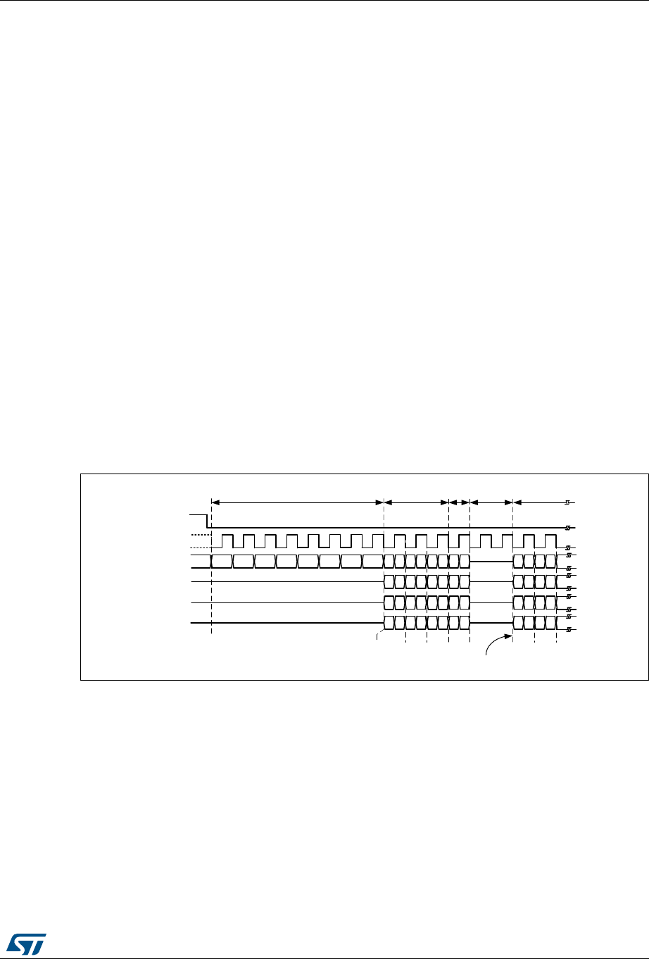
RM0394 Rev 4 349/1600
RM0394 Quad-SPI interface (QUADSPI)
372
SDR mode
By default, the DDRM bit (QUADSPI_CCR[31]) is 0 and the QUADSPI operates in single
data rate (SDR) mode.
In SDR mode, when the QUADSPI is driving the IO0/SO, IO1, IO2, IO3 signals, these
signals transition only with the falling edge of CLK.
When receiving data in SDR mode, the QUADSPI assumes that the Flash memories also
send the data using CLK’s falling edge. By default (when SSHIFT = 0), the signals are
sampled using the following (rising) edge of CLK.
DDR mode
When the DDRM bit (QUADSPI_CCR[31]) is set to 1, the QUADSPI operates in double data
rate (DDR) mode.
In DDR mode, when the QUADSPI is driving the IO0/SO, IO1, IO2, IO3 signals in the
address/alternate-byte/data phases, a bit is sent on each of the falling and rising edges of
CLK.
The instruction phase is not affected by DDRM. The instruction is always sent using CLK’s
falling edge.
When receiving data in DDR mode, the QUADSPI assumes that the Flash memories also
send the data using both rising and falling CLK edges. When DDRM = 1, firmware must
clear SSHIFT bit (bit 4 of QUADSPI_CR). Thus, the signals are sampled one half of a CLK
cycle later (on the following, opposite edge).
Figure 34. An example of a DDR command in quad mode
Dual-flash mode
When the DFM bit (bit 6 of QUADSPI_CR) is 1, the QUADSPI is in dual-flash mode, where
two external quad SPI Flash memories (FLASH 1 and FLASH 2) are used in order to
send/receive 8 bits (or 16 bits in DDR mode) every cycle, effectively doubling the throughput
as well as the capacity.
Each of the Flash memories use the same CLK and optionally the same nCS signals, but
each have separate IO0, IO1, IO2, and IO3 signals.
Dual-flash mode can be used in conjunction with single-bit, dual-bit, and quad-bit modes, as
well as with either SDR or DDR mode.
069
Q&6
6&/.
,2
,2
,2
,2
$$ 0 %\WH
,QVWUXFWLRQ $GGUHVV $OW 'XPP\ 'DWD
,2VZLWFKIURP
RXWSXWWRLQSXW
$
%\WH

Quad-SPI interface (QUADSPI) RM0394
350/1600 RM0394 Rev 4
The Flash memory size, as specified in FSIZE[4:0] (QUADSPI_DCR[20:16]), should reflect
the total Flash memory capacity, which is double the size of one individual component.
If address X is even, then the byte which the QUADSPI gives for address X is the byte at the
address X/2 of FLASH 1, and the byte which the QUADSPI gives for address X+1 is the
byte at the address X/2 of FLASH 2. In other words, bytes at even addresses are all stored
in FLASH 1 and bytes at odd addresses are all stored in FLASH 2.
When reading the Flash memories status registers in dual-flash mode, twice as many bytes
should be read compared to doing the same read in single-flash mode. This means that if
each Flash memory gives 8 valid bits after the instruction for fetching the status register,
then the QUADSPI must be configured with a data length of 2 bytes (16 bits), and the
QUADSPI will receive one byte from each Flash memory. If each Flash memory gives a
status of 16 bits, then the QUADSPI must be configured to read 4 bytes to get all the status
bits of both Flash memories in dual-flash mode. The least-significant byte of the result (in
the data register) is the least-significant byte of FLASH 1 status register, while the next byte
is the least-significant byte of FLASH 2 status register. Then, the third byte of the data
register is FLASH 1 second byte, while the forth byte is FLASH 2 second byte (in the case
that the Flash memories have 16-bit status registers).
An even number of bytes must always be accessed in dual-flash mode. For this reason, bit
0 of the data length field (QUADSPI_DLR[0]) is stuck at 1 when DRM = 1.
In dual-flash mode, the behavior of FLASH 1 interface signals are basically the same as in
normal mode. FLASH 2 interface signals have exactly the same waveforms as FLASH 1
during the instruction, address, alternate-byte, and dummy-cycles phases. In other words,
each Flash memory always receives the same instruction and the same address. Then,
during the data phase, the BK1_IOx and BK2_IOx buses are both transferring data in
parallel, but the data that are sent to (or received from) FLASH 1 are distinct from those of
FLASH 2.
15.3.5 QUADSPI indirect mode
When in indirect mode, commands are started by writing to QUADSPI registers and data is
transferred by writing or reading the data register, in the same way as for other
communication peripherals.
When FMODE = 00 (QUADSPI_CCR[27:26]), the QUADSPI is in indirect write mode,
where bytes are sent to the Flash memory during the data phase. Data are provided by
writing to the data register (QUADSPI_DR).
When FMODE = 01, the QUADSPI is in indirect read mode, where bytes are received from
the Flash memory during the data phase. Data are recovered by reading QUADSPI_DR.
The number of bytes to be read/written is specified in the data length register
(QUADSPI_DLR). If QUADSPI_DLR = 0xFFFF_FFFF (all 1’s), then the data length is
considered undefined and the QUADSPI simply continues to transfer data until the end of
Flash memory (as defined by FSIZE) is reached. If no bytes are to be transferred, DMODE
(QUADSPI_CCR[25:24]) should be set to 00.
If QUADSPI_DLR = 0xFFFF_FFFF and FSIZE = 0x1F (max value indicating a 4GB Flash
memory), then in this special case the transfers continue indefinitely, stopping only after an
abort request or after the QUADSPI is disabled. After the last memory address is read (at
address 0xFFFF_FFFF), reading continues with address = 0x0000_0000.
When the programmed number of bytes to be transmitted or received is reached, TCF is set
and an interrupt is generated if TCIE = 1. In the case of undefined number of data, the TCF

RM0394 Rev 4 351/1600
RM0394 Quad-SPI interface (QUADSPI)
372
is set when the limit of the external SPI memory is reached according to the Flash memory
size defined in the QUADSPI_CR.
Triggering the start of a command
Essentially, a command starts as soon as firmware gives the last information that is
necessary for this command. Depending on the QUADSPI configuration, there are three
different ways to trigger the start of a command in indirect mode. The commands starts
immediately after:
1. a write is performed to INSTRUCTION[7:0] (QUADSPI_CCR), if no address is
necessary (when ADMODE = 00) and if no data needs to be provided by the firmware
(when FMODE = 01 or DMODE = 00)
2. a write is performed to ADDRESS[31:0] (QUADSPI_AR), if an address is necessary
(when ADMODE != 00) and if no data needs to be provided by the firmware (when
FMODE = 01 or DMODE = 00)
3. a write is performed to DATA[31:0] (QUADSPI_DR), if an address is necessary (when
ADMODE != 00) and if data needs to be provided by the firmware (when FMODE = 00
and DMODE != 00)
Writes to the alternate byte register (QUADSPI_ABR) never trigger the communication start.
If alternate bytes are required, they must be programmed before.
As soon as a command is started, the BUSY bit (bit 5 of QUADSPI_SR) is automatically set.
FIFO and data management
In indirect mode, data go through a 16-byte FIFO which is internal to the QUADSPI.
FLEVEL[4:0] (QUADSPI_SR[12:8]) indicates how many bytes are currently being held in
the FIFO.
In indirect write mode (FMODE = 00), firmware adds data to the FIFO when it writes
QUADSPI_DR. Word writes add 4 bytes to the FIFO, halfword writes add 2 bytes, and byte
writes add only 1 byte. If firmware adds too many bytes to the FIFO (more than is indicated
by DL[31:0]), the extra bytes are flushed from the FIFO at the end of the write operation
(when TCF is set).
Byte/halfword accesses to QUADSPI_DR must be done only to the least significant
byte/halfword of the 32-bit register.
FTHRES[3:0] is used to define a FIFO threshold. When the threshold is reached, the FTF
(FIFO threshold flag) is set. In indirect read mode, FTF is set when the number of valid
bytes to be read from the FIFO is above the threshold. FTF is also set if there are data in the
FIFO after the last byte is read from the Flash memory, regardless of the FTHRES setting.
In indirect write mode, FTF is set when the number of empty bytes in the FIFO is above the
threshold.
If FTIE = 1, there is an interrupt when FTF is set. If DMAEN = 1, a DMA transfer is initiated
when FTF is set. FTF is cleared by HW as soon as the threshold condition is no longer true
(after enough data has been transferred by the CPU or DMA).
In indirect read mode when the FIFO becomes full, the QUADSPI temporarily stops reading
bytes from the Flash memory to avoid an overrun. Note that the reading of the Flash
memory does not restart until 4 bytes become vacant in the FIFO (when FLEVEL 11).
Thus, when FTHRES 13, the application must take care to read enough bytes to assure
that the QUADSPI starts retrieving data from the Flash memory again. Otherwise, the FTF
flag stays at '0' as long as 11 < FLEVEL < FTHRES.

Quad-SPI interface (QUADSPI) RM0394
352/1600 RM0394 Rev 4
15.3.6 QUADSPI status flag polling mode
In automatic-polling mode, the QUADSPI periodically starts a command to read a defined
number of status bytes (up to 4). The received bytes can be masked to isolate some status
bits and an interrupt can be generated when the selected bits have a defined value.
The accesses to the Flash memory begin in the same way as in indirect read mode: if no
address is required (AMODE = 00), accesses begin as soon as the QUADSPI_CCR is
written. Otherwise, if an address is required, the first access begins when QUADSPI_AR is
written. BUSY goes high at this point and stays high even between the periodic accesses.
The contents of MASK[31:0] (QUADSPI_PSMAR) are used to mask the data from the Flash
memory in automatic-polling mode. If the MASK[n] = 0, then bit n of the result is masked
and not considered. If MASK[n] = 1, and the content of bit[n] is the same as MATCH[n]
(QUADSPI_PSMAR), then there is a match for bit n.
If the polling match mode bit (PMM, bit 23 of QUADSPI_CR) is 0, then “AND” match mode is
activated. This means status match flag (SMF) is set only when there is a match on all of the
unmasked bits.
If PMM = 1, then “OR” match mode is activated. This means SMF is set if there is a match
on any of the unmasked bits.
An interrupt is called when SMF is set if SMIE = 1.
If the automatic-polling-mode-stop (APMS) bit is set, operation stops and BUSY goes to 0
as soon as a match is detected. Otherwise, BUSY stays at ‘1’ and the periodic accesses
continue until there is an abort or the QUADSPI is disabled (EN = 0).
The data register (QUADSPI_DR) contains the latest received status bytes (the FIFO is
deactivated). The content of the data register is not affected by the masking used in the
matching logic. The FTF status bit is set as soon as a new reading of the status is complete,
and FTF is cleared as soon as the data is read.
15.3.7 QUADSPI memory-mapped mode
When configured in memory-mapped mode, the external SPI device is seen as an internal
memory.
It is forbidden to access QUADSPI Flash bank area before having properly configured and
enabled the QUADSPI peripheral.
No more than 256MB can addressed even if the Flash memory capacity is larger.
If an access is made to an address outside of the range defined by FSIZE but still within the
256MB range, then a bus error is given. The effect of this error depends on the bus master
that attempted the access:
•If it is the Cortex® CPU, bus fault exception is generated when enabled (or a hard fault
exception when bus fault is disabled)
•If it is a DMA, a DMA transfer error is generated and the corresponding DMA channel is
automatically disabled.
Byte, halfword, and word access types are all supported.
Support for execute in place (XIP) operation is implemented, where the QUADSPI
anticipates the next access and load in advance the byte at the following address. If the
subsequent access is indeed made at a continuous address, the access will be completed
faster since the value is already prefetched.

RM0394 Rev 4 353/1600
RM0394 Quad-SPI interface (QUADSPI)
372
By default, the QUADSPI never stops its prefetch operation, keeping the previous read
operation active with nCS maintained low, even if no access to the Flash memory occurs for
a long time. Since Flash memories tend to consume more when nCS is held low, the
application might want to activate the timeout counter (TCEN = 1, bit 3 of QUADSPI_CR) so
that nCS is released after a period of TIMEOUT[15:0] (QUADSPI_LPTR) cycles have
elapsed without any access since when the FIFO becomes full with prefetch data.
BUSY goes high as soon as the first memory-mapped access occurs. Because of the
prefetch operations, BUSY does not fall until there is a timeout, there is an abort, or the
peripheral is disabled.
15.3.8 QUADSPI Flash memory configuration
The device configuration register (QUADSPI_DCR) can be used to specify the
characteristics of the external SPI Flash memory.
The FSIZE[4:0] field defines the size of external memory using the following formula:
Number of bytes in Flash memory = 2[FSIZE+1]
FSIZE+1 is effectively the number of address bits required to address the Flash memory.
The Flash memory capacity can be up to 4GB (addressed using 32 bits) in indirect mode,
but the addressable space in memory-mapped mode is limited to 256MB.
If DFM = 1, FSIZE indicates the total capacity of the two Flash memories together.
When the QUADSPI executes two commands, one immediately after the other, it raises the
chip select signal (nCS) high between the two commands for only one CLK cycle by default.
If the Flash memory requires more time between commands, the chip select high time
(CSHT) field can be used to specify the minimum number of CLK cycles (up to 8) that nCS
must remain high.
The clock mode (CKMODE) bit indicates the CLK signal logic level in between commands
(when nCS = 1).
15.3.9 QUADSPI delayed data sampling
By default, the QUADSPI samples the data driven by the Flash memory one half of a CLK
cycle after the Flash memory drives the signal.
In case of external signal delays, it may be beneficial to sample the data later. Using the
SSHIFT bit (bit 4 of QUADSPI_CR), the sampling of the data can be shifted by half of a CLK
cycle.
Clock shifting is not supported in DDR mode: the SSHIFT bit must be clear when DDRM bit
is set.
15.3.10 QUADSPI configuration
The QUADSPI configuration is done in two phases:
•QUADSPI IP configuration
•QUADSPI Flash memory configuration
Once configured and enabled, the QUADSPI can be used in one of its three operating
modes: indirect mode, status-polling mode, or memory-mapped mode.
QUADSPI IP configuration

Quad-SPI interface (QUADSPI) RM0394
354/1600 RM0394 Rev 4
The QUADSPI IP is configured using the QUADSPI_CR. The user shall configure the clock
prescaler division factor and the sample shifting settings for the incoming data.
DDR mode can be set through the DDRM bit. Once enabled, the address and the alternate
bytes are sent on both clock edges and the data are sent/received on both clock edges.
Regardless of the DDRM bit setting, instructions are always sent in SDR mode.
The DMA requests are enabled setting the DMAEN bit. In case of interrupt usage, their
respective enable bit can be also set during this phase.
FIFO level for either DMA request generation or interrupt generation is programmed in the
FTHRES bits.
If timeout counter is needed, the TCEN bit can be set and the timeout value programmed in
the QUADSPI_LPTR register.
Dual-flash mode can be activated by setting DFM to 1.
QUADSPI Flash memory configuration
The parameters related to the targeted external Flash memory are configured through the
QUADSPI_DCR register.The user shall program the Flash memory size in the FSIZE bits,
the Chip Select minimum high time in the CSHT bits, and the functional mode (Mode 0 or
Mode 3) in the MODE bit.
15.3.11 QUADSPI usage
The operating mode is selected using FMODE[1:0] (QUADSPI_CCR[27:26]).
Indirect mode procedure
When FMODE is programmed to 00, indirect write mode is selected and data can be sent to
the Flash memory. With FMODE = 01, indirect read mode is selected where data can be
read from the Flash memory.
When the QUADSPI is used in indirect mode, the frames are constructed in the following
way:
1. Specify a number of data bytes to read or write in the QUADSPI_DLR.
2. Specify the frame format, mode and instruction code in the QUADSPI_CCR.
3. Specify optional alternate byte to be sent right after the address phase in the
QUADSPI_ABR.
4. Specify the operating mode in the QUADSPI_CR. If FMODE = 00 (indirect write mode)
and DMAEN = 1, then QUADSPI_AR should be specified before QUADSPI_CR,
because otherwise QUADSPI_DR might be written by the DMA before QUADSPI_AR
is updated (if the DMA controller has already been enabled)
5. Specify the targeted address in the QUADSPI_AR.
6. Read/Write the data from/to the FIFO through the QUADSPI_DR.

RM0394 Rev 4 355/1600
RM0394 Quad-SPI interface (QUADSPI)
372
When writing the control register (QUADSPI_CR) the user specifies the following settings:
•The enable bit (EN) set to ‘1’
•The DMA enable bit (DMAEN) for transferring data to/from RAM
•Timeout counter enable bit (TCEN)
•Sample shift setting (SSHIFT)
•FIFO threshold level (FTRHES) to indicate when the FTF flag should be set
•Interrupt enables
•Automatic polling mode parameters: match mode and stop mode (valid when
FMODE = 11)
•Clock prescaler
When writing the communication configuration register (QUADSPI_CCR) the user specifies
the following parameters:
•The instruction byte through the INSTRUCTION bits
•The way the instruction has to be sent through the IMODE bits (1/2/4 lines)
•The way the address has to be sent through the ADMODE bits (None/1/2/4 lines)
•The address size (8/16/24/32-bit) through the ADSIZE bits
•The way the alternate bytes have to be sent through the ABMODE (None/1/2/4 lines)
•The alternate bytes number (1/2/3/4) through the ABSIZE bits
•The presence or not of dummy bytes through the DBMODE bit
•The number of dummy bytes through the DCYC bits
•The way the data have to be sent/received (None/1/2/4 lines) through the DMODE bits
If neither the address register (QUADSPI_AR) nor the data register (QUADSPI_DR) need to
be updated for a particular command, then the command sequence starts as soon as
QUADSPI_CCR is written. This is the case when both ADMODE and DMODE are 00, or if
just ADMODE = 00 when in indirect read mode (FMODE = 01).
When an address is required (ADMODE is not 00) and the data register does not need to be
written (when FMODE = 01 or DMODE = 00), the command sequence starts as soon as the
address is updated with a write to QUADSPI_AR.
In case of data transmission (FMODE = 00 and DMODE! = 00), the communication start is
triggered by a write in the FIFO through QUADSPI_DR.
Status flag polling mode
The status flag polling mode is enabled setting the FMODE field (QUADSPI_CCR[27:26]) to
10. In this mode, the programmed frame will be sent and the data retrieved periodically.
The maximum amount of data read in each frame is 4 bytes. If more data is requested in
QUADSPI_DLR, it will be ignored and only 4 bytes will be read.
The periodicity is specified in the QUADSPI_PISR register.
Once the status data has been retrieved, it can internally be processed i order to:
•set the status match flag and generate an interrupt if enabled
•stop automatically the periodic retrieving of the status bytes
The received value can be masked with the value stored in the QUADSPI_PSMKR and
ORed or ANDed with the value stored in the QUADSPI_PSMAR.

Quad-SPI interface (QUADSPI) RM0394
356/1600 RM0394 Rev 4
In case of match, the status match flag is set and an interrupt is generated if enabled, and
the QUADSPI can be automatically stopped if the AMPS bit is set.
In any case, the latest retrieved value is available in the QUADSPI_DR.
Memory-mapped mode
In memory-mapped mode, the external Flash memory is seen as internal memory but with
some latency during accesses. Only read operations are allowed to the external Flash
memory in this mode.
Memory-mapped mode is entered by setting the FMODE to 11 in the QUADSPI_CCR
register.
The programmed instruction and frame is sent when a master is accessing the memory
mapped space.
The FIFO is used as a prefetch buffer to anticipate linear reads. Any access to
QUADSPI_DR in this mode returns zero.
The data length register (QUADSPI_DLR) has no meaning in memory-mapped mode.
15.3.12 Sending the instruction only once
Some Flash memories (e.g. Winbound) might provide a mode where an instruction must be
sent only with the first command sequence, while subsequent commands start directly with
the address. One can take advantage of such a feature using the SIOO bit
(QUADSPI_CCR[28]).
SIOO is valid for all functional modes (indirect, automatic polling, and memory-mapped). If
the SIOO bit is set, the instruction is sent only for the first command following a write to
QUADSPI_CCR. Subsequent command sequences skip the instruction phase, until there is
a write to QUADSPI_CCR.
SIOO has no effect when IMODE = 00 (no instruction).
15.3.13 QUADSPI error management
An error can be generated in the following case:
•In indirect mode or status flag polling mode when a wrong address has been
programmed in the QUADSPI_AR (according to the Flash memory size defined by
FSIZE[4:0] in the QUADSPI_DCR): this will set the TEF and an interrupt is generated if
enabled.
•Also in indirect mode, if the address plus the data length exceeds the Flash memory
size, TEF will be set as soon as the access is triggered.
•In memory-mapped mode, when an out of range access is done by a master or when
the QUADSPI is disabled: this will generate a bus error as a response to the faulty bus
master request.
•When a master is accessing the memory mapped space while the memory mapped
mode is disabled: this will generate a bus error as a response to the faulty bus master
request.
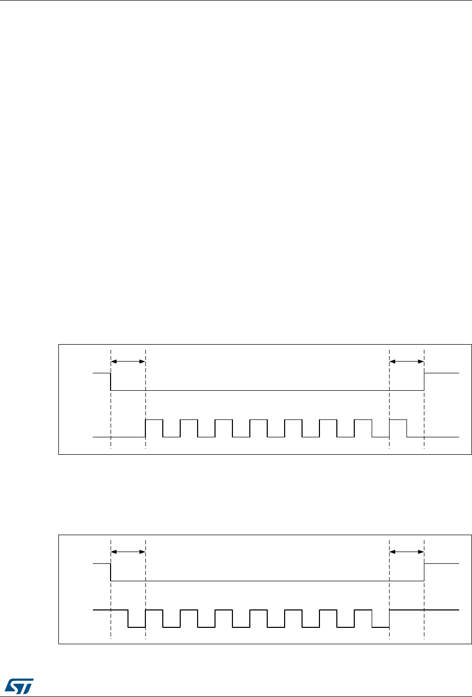
RM0394 Rev 4 357/1600
RM0394 Quad-SPI interface (QUADSPI)
372
15.3.14 QUADSPI busy bit and abort functionality
Once the QUADSPI starts an operation with the Flash memory, the BUSY bit is
automatically set in the QUADSPI_SR.
In indirect mode, the BUSY bit is reset once the QUADSPI has completed the requested
command sequence and the FIFO is empty.
In automatic-polling mode, BUSY goes low only after the last periodic access is complete,
due to a match when APMS = 1, or due to an abort.
After the first access in memory-mapped mode, BUSY goes low only on a timeout event or
on an abort.
Any operation can be aborted by setting the ABORT bit in the QUADSPI_CR. Once the
abort is completed, the BUSY bit and the ABORT bit are automatically reset, and the FIFO
is flushed.
Note: Some Flash memories might misbehave if a write operation to a status registers is aborted.
15.3.15 nCS behavior
By default, nCS is high, deselecting the external Flash memory. nCS falls before an
operation begins and rises as soon as it finishes.
When CKMODE = 0 (“mode0”, where CLK stays low when no operation is in progress) nCS
falls one CLK cycle before an operation first rising CLK edge, and nCS rises one CLK cycle
after the operation final rising CLK edge, as shown in Figure 35.
Figure 35. nCS when CKMODE = 0 (T = CLK period)
When CKMODE=1 (“mode3”, where CLK goes high when no operation is in progress) and
DDRM=0 (SDR mode), nCS still falls one CLK cycle before an operation first rising CLK
edge, and nCS rises one CLK cycle after the operation final rising CLK edge, as shown in
Figure 36.
Figure 36. nCS when CKMODE = 1 in SDR mode (T = CLK period)
069
Q&6
6&/.
77
069
Q&6
6&/.
77
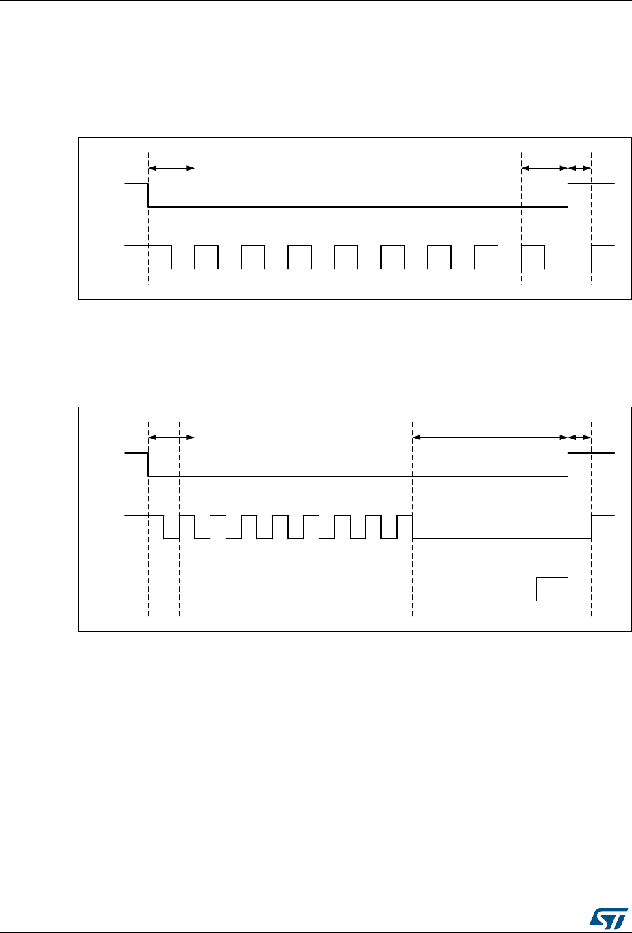
Quad-SPI interface (QUADSPI) RM0394
358/1600 RM0394 Rev 4
When CKMODE = 1 (“mode3”) and DDRM = 1 (DDR mode), nCS falls one CLK cycle
before an operation first rising CLK edge, and nCS rises one CLK cycle after the operation
final active rising CLK edge, as shown in Figure 37. Because DDR operations must finish
with a falling edge, CLK is low when nCS rises, and CLK rises back up one half of a CLK
cycle afterwards.
Figure 37. nCS when CKMODE = 1 in DDR mode (T = CLK period)
When the FIFO stays full in a read operation or if the FIFO stays empty in a write operation,
the operation stalls and CLK stays low until firmware services the FIFO. If an abort occurs
when an operation is stalled, nCS rises just after the abort is requested and then CLK rises
one half of a CLK cycle later, as shown in Figure 38.
Figure 38. nCS when CKMODE = 1 with an abort (T = CLK period)
When not in dual-flash mode (DFM = 0), only FLASH 1 is accessed and thus the BK2_nCS
stays high. In dual-flash mode, BK2_nCS behaves exactly the same as BK1_nCS. Thus, if
there is a FLASH 2 and if the application always stays in dual-flash mode, then FLASH 2
may use BK1_nCS and the pin outputting BK2_nCS can be used for other functions.
069
Q&6
6&/.
77 7
069
Q&6
6&/.
&ORFNVWDOOHG7 7
$ERUW
RM0394 Rev 4 359/1600
RM0394 Quad-SPI interface (QUADSPI)
372
15.4 QUADSPI interrupts
An interrupt can be produced on the following events:
•Timeout
•Status match
•FIFO threshold
•Transfer complete
•Transfer error
Separate interrupt enable bits are available for flexibility.
Table 52. QUADSPI interrupt requests
Interrupt event Event flag Enable control bit
Timeout TOF TOIE
Status match SMF SMIE
FIFO threshold FTF FTIE
Transfer complete TCF TCIE
Transfer error TEF TEIE

Quad-SPI interface (QUADSPI) RM0394
360/1600 RM0394 Rev 4
15.5 QUADSPI registers
15.5.1 QUADSPI control register (QUADSPI_CR)
Address offset: 0x0000
Reset value: 0x0000 0000
31 30 29 28 27 26 25 24 23 22 21 20 19 18 17 16
PRESCALER[7:0] PMM APMS Res. TOIE SMIE FTIE TCIE TEIE
rw rw rw rw rw rw rw rw rw rw rw rw rw rw rw
15 14 13 12 11 10 9 8 7 6 5 4 3 2 1 0
Res. Res. Res. Res. FTHRES[3:0] FSEL DFM Res. SSHIFT TCEN DMAEN ABORT EN
rw rw rw rw rw rw rw rw rw rw rw
Bits 31:24 PRESCALER[7:0]: Clock prescaler
This field defines the scaler factor for generating CLK based on the AHB clock
(value+1).
0: FCLK = FAHB, AHB clock used directly as QUADSPI CLK (prescaler bypassed)
1: FCLK = FAHB/2
2: FCLK = FAHB/3
...
255: FCLK = FAHB/256
For odd clock division factors, CLK’s duty cycle is not 50%. The clock signal remains
low one cycle longer than it stays high.
This field can be modified only when BUSY = 0.
Bit 23 PMM: Polling match mode
This bit indicates which method should be used for determining a “match” during
automatic polling mode.
0: AND match mode. SMF is set if all the unmasked bits received from the Flash
memory match the corresponding bits in the match register.
1: OR match mode. SMF is set if any one of the unmasked bits received from the Flash
memory matches its corresponding bit in the match register.
This bit can be modified only when BUSY = 0.
Bit 22 APMS: Automatic poll mode stop
This bit determines if automatic polling is stopped after a match.
0: Automatic polling mode is stopped only by abort or by disabling the QUADSPI.
1: Automatic polling mode stops as soon as there is a match.
This bit can be modified only when BUSY = 0.
Bit 21 Reserved, must be kept at reset value.
Bit 20 TOIE: TimeOut interrupt enable
This bit enables the TimeOut interrupt.
0: Interrupt disable
1: Interrupt enabled
Bit 19 SMIE: Status match interrupt enable
This bit enables the status match interrupt.
0: Interrupt disable
1: Interrupt enabled

RM0394 Rev 4 361/1600
RM0394 Quad-SPI interface (QUADSPI)
372
Bit 18 FTIE: FIFO threshold interrupt enable
This bit enables the FIFO threshold interrupt.
0: Interrupt disabled
1: Interrupt enabled
Bit 17 TCIE: Transfer complete interrupt enable
This bit enables the transfer complete interrupt.
0: Interrupt disabled
1: Interrupt enabled
Bit 16 TEIE: Transfer error interrupt enable
This bit enables the transfer error interrupt.
0: Interrupt disable
1: Interrupt enabled
Bits 15:12 Reserved, must be kept at reset value.
Bits 11:8 FTHRES[3:0]: FIFO threshold level
Defines, in indirect mode, the threshold number of bytes in the FIFO that will cause the
FIFO threshold flag (FTF, QUADSPI_SR[2]) to be set.
In indirect write mode (FMODE = 00):
0: FTF is set if there are 1 or more free bytes available to be written to in the FIFO
1: FTF is set if there are 2 or more free bytes available to be written to in the FIFO
...
15: FTF is set if there are 16 free bytes available to be written to in the FIFO
In indirect read mode (FMODE = 01):
0: FTF is set if there are 1 or more valid bytes that can be read from the FIFO
1: FTF is set if there are 2 or more valid bytes that can be read from the FIFO
...
15: FTF is set if there are 16 valid bytes that can be read from the FIFO
If DMAEN = 1, then the DMA controller for the corresponding channel must be disabled
before changing the FTHRES value.
Bit 7 FSEL: Flash memory selection
This bit selects the Flash memory to be addressed in single flash mode (when DFM =
0).
0: FLASH 1 selected
1: FLASH 2 selected
This bit can be modified only when BUSY = 0.
This bit is ignored when DFM = 1.
Bit 6 DFM: Dual-flash mode
This bit activates dual-flash mode, where two external Flash memories are used
simultaneously to double throughput and capacity.
0: Dual-flash mode disabled
1: Dual-flash mode enabled
This bit can be modified only when BUSY = 0.
Bit 5 Reserved, must be kept at reset value.

Quad-SPI interface (QUADSPI) RM0394
362/1600 RM0394 Rev 4
Bit 4 SSHIFT: Sample shift
By default, the QUADSPI samples data 1/2 of a CLK cycle after the data is driven by the
Flash memory. This bit allows the data is to be sampled later in order to account for
external signal delays.
0: No shift
1: 1/2 cycle shift
Firmware must assure that SSHIFT = 0 when in DDR mode (when DDRM = 1).
This field can be modified only when BUSY = 0.
Bit 3 TCEN: Timeout counter enable
This bit is valid only when memory-mapped mode (FMODE = 11) is selected. Activating
this bit causes the chip select (nCS) to be released (and thus reduces consumption) if
there has not been an access after a certain amount of time, where this time is defined
by TIMEOUT[15:0] (QUADSPI_LPTR).
Enable the timeout counter.
By default, the QUADSPI never stops its prefetch operation, keeping the previous read
operation active with nCS maintained low, even if no access to the Flash memory
occurs for a long time. Since Flash memories tend to consume more when nCS is held
low, the application might want to activate the timeout counter (TCEN = 1, bit 3 of
QUADSPI_CR) so that nCS is released after a period of TIMEOUT[15:0]
(QUADSPI_LPTR) cycles have elapsed without an access since when the FIFO
becomes full with prefetch data.
0: Timeout counter is disabled, and thus the chip select (nCS) remains active
indefinitely after an access in memory-mapped mode.
1: Timeout counter is enabled, and thus the chip select is released in memory-mapped
mode after TIMEOUT[15:0] cycles of Flash memory inactivity.
This bit can be modified only when BUSY = 0.
Bit 2 DMAEN: DMA enable
In indirect mode, DMA can be used to input or output data via the QUADSPI_DR
register. DMA transfers are initiated when the FIFO threshold flag, FTF, is set.
0: DMA is disabled for indirect mode
1: DMA is enabled for indirect mode
Bit 1 ABORT: Abort request
This bit aborts the on-going command sequence. It is automatically reset once the abort
is complete.
This bit stops the current transfer.
In polling mode or memory-mapped mode, this bit also reset the APM bit or the DM bit.
0: No abort requested
1: Abort requested
Bit 0 EN: Enable
Enable the QUADSPI.
0: QUADSPI is disabled
1: QUADSPI is enabled

RM0394 Rev 4 363/1600
RM0394 Quad-SPI interface (QUADSPI)
372
15.5.2 QUADSPI device configuration register (QUADSPI_DCR)
Address offset: 0x0004
Reset value: 0x0000 0000
31 30 29 28 27 26 25 24 23 22 21 20 19 18 17 16
Res. Res. Res. Res. Res. Res. Res. Res. Res. Res. Res. FSIZE[4:0]
rw rw rw rw rw
15 14 13 12 11 10 9 8 7 6 5 4 3 2 1 0
Res. Res. Res. Res. Res. CSHT[2:0] Res. Res. Res. Res. Res. Res. Res. CK
MODE
rw rw rw rw
Bits 31:21 Reserved, must be kept at reset value.
Bits 20:16 FSIZE[4:0]: Flash memory size
This field defines the size of external memory using the following formula:
Number of bytes in Flash memory = 2[FSIZE+1]
FSIZE+1 is effectively the number of address bits required to address the Flash
memory. The Flash memory capacity can be up to 4GB (addressed using 32 bits) in
indirect mode, but the addressable space in memory-mapped mode is limited to
256MB.
If DFM = 1, FSIZE indicates the total capacity of the two Flash memories together.
This field can be modified only when BUSY = 0.
Bits 15:11 Reserved, must be kept at reset value.
Bits 10:8 CSHT[2:0]: Chip select high time
CSHT+1 defines the minimum number of CLK cycles which the chip select (nCS) must
remain high between commands issued to the Flash memory.
0: nCS stays high for at least 1 cycle between Flash memory commands
1: nCS stays high for at least 2 cycles between Flash memory commands
...
7: nCS stays high for at least 8 cycles between Flash memory commands
This field can be modified only when BUSY = 0.
Bits 7:1 Reserved, must be kept at reset value.
Bit 0 CKMODE: Mode 0 / mode 3
This bit indicates the level that CLK takes between commands (when nCS = 1).
0: CLK must stay low while nCS is high (chip select released). This is referred to as
mode 0.
1: CLK must stay high while nCS is high (chip select released). This is referred to as
mode 3.
This field can be modified only when BUSY = 0.

Quad-SPI interface (QUADSPI) RM0394
364/1600 RM0394 Rev 4
15.5.3 QUADSPI status register (QUADSPI_SR)
Address offset: 0x0008
Reset value: 0x0000 0000
31 30 29 28 27 26 25 24 23 22 21 20 19 18 17 16
Res. Res. Res. Res. Res. Res. Res. Res. Res. Res. Res. Res. Res. Res. Res. Res.
15 14 13 12 11 10 9 8 7 6 5 4 3 2 1 0
Res. Res. Res. FLEVEL[4:0] Res. Res. BUSY TOF SMF FTF TCF TEF
rr r r r r r r r r r
Bits 31:13 Reserved, must be kept at reset value.
Bits 12:8 FLEVEL[4:0]: FIFO level
This field gives the number of valid bytes which are being held in the FIFO. FLEVEL = 0
when the FIFO is empty, and 16 when it is full. In memory-mapped mode and in
automatic status polling mode, FLEVEL is zero.
Bits 7:6 Reserved, must be kept at reset value.
Bit 5 BUSY: Busy
This bit is set when an operation is on going. This bit clears automatically when the
operation with the Flash memory is finished and the FIFO is empty.
Bit 4 TOF: Timeout flag
This bit is set when timeout occurs. It is cleared by writing 1 to CTOF.
Bit 3 SMF: Status match flag
This bit is set in automatic polling mode when the unmasked received data matches the
corresponding bits in the match register (QUADSPI_PSMAR). It is cleared by writing 1
to CSMF.
Bit 2 FTF: FIFO threshold flag
In indirect mode, this bit is set when the FIFO threshold has been reached, or if there is
any data left in the FIFO after reads from the Flash memory are complete. It is cleared
automatically as soon as threshold condition is no longer true.
In automatic polling mode this bit is set every time the status register is read, and the bit
is cleared when the data register is read.
Bit 1 TCF: Transfer complete flag
This bit is set in indirect mode when the programmed number of data has been
transferred or in any mode when the transfer has been aborted.It is cleared by writing 1
to CTCF.
Bit 0 TEF: Transfer error flag
This bit is set in indirect mode when an invalid address is being accessed in indirect
mode. It is cleared by writing 1 to CTEF.

RM0394 Rev 4 365/1600
RM0394 Quad-SPI interface (QUADSPI)
372
15.5.4 QUADSPI flag clear register (QUADSPI_FCR)
Address offset: 0x000C
Reset value: 0x0000 0000
15.5.5 QUADSPI data length register (QUADSPI_DLR)
Address offset: 0x0010
Reset value: 0x0000 0000
31 30 29 28 27 26 25 24 23 22 21 20 19 18 17 16
Res. Res. Res. Res. Res. Res. Res. Res. Res. Res. Res. Res. Res. Res. Res. Res.
15 14 13 12 11 10 9 8 7 6 5 4 3 2 1 0
Res. Res. Res. Res. Res. Res. Res. Res. Res. Res. Res. CTOF CSMF Res. CTCF CTEF
ww ww
Bits 31:5 Reserved, must be kept at reset value.
Bit 4 CTOF: Clear timeout flag
Writing 1 clears the TOF flag in the QUADSPI_SR register
Bit 3 CSMF: Clear status match flag
Writing 1 clears the SMF flag in the QUADSPI_SR register
Bit 2 Reserved, must be kept at reset value.
Bit 1 CTCF: Clear transfer complete flag
Writing 1 clears the TCF flag in the QUADSPI_SR register
Bit 0 CTEF: Clear transfer error flag
Writing 1 clears the TEF flag in the QUADSPI_SR register
31 30 29 28 27 26 25 24 23 22 21 20 19 18 17 16
DL[31:16]
rw rw rw rw rw rw rw rw rw rw rw rw rw rw rw rw
15 14 13 12 11 10 9 8 7 6 5 4 3 2 1 0
DL[15:0]
rw rw rw rw rw rw rw rw rw rw rw rw rw rw rw rw

Quad-SPI interface (QUADSPI) RM0394
366/1600 RM0394 Rev 4
15.5.6 QUADSPI communication configuration register (QUADSPI_CCR)
Address offset: 0x0014
Reset value: 0x0000 0000
Bits 31:0 DL[31:0]: Data length
Number of data to be retrieved (value+1) in indirect and status-polling modes. A value
no greater than 3 (indicating 4 bytes) should be used for status-polling mode.
All 1s in indirect mode means undefined length, where QUADSPI will continue until the
end of memory, as defined by FSIZE.
0x0000_0000: 1 byte is to be transferred
0x0000_0001: 2 bytes are to be transferred
0x0000_0002: 3 bytes are to be transferred
0x0000_0003: 4 bytes are to be transferred
...
0xFFFF_FFFD: 4,294,967,294 (4G-2) bytes are to be transferred
0xFFFF_FFFE: 4,294,967,295 (4G-1) bytes are to be transferred
0xFFFF_FFFF: undefined length -- all bytes until the end of Flash memory (as defined
by FSIZE) are to be transferred. Continue reading indefinitely if FSIZE = 0x1F.
DL[0] is stuck at ‘1’ in dual-flash mode (DFM = 1) even when ‘0’ is written to this bit, thus
assuring that each access transfers an even number of bytes.
This field has no effect when in memory-mapped mode (FMODE = 10).
This field can be written only when BUSY = 0.
31 30 29 28 27 26 25 24 23 22 21 20 19 18 17 16
DDRM DHHC Res. SIOO FMODE[1:0] DMODE[1:0] Res. DCYC[4:0] ABSIZE[1:0]
rw rw rw rw rw rw rw rw rw rw rw rw rw rw
15 14 13 12 11 10 9 8 7 6 5 4 3 2 1 0
ABMODE[1:0] ADSIZE[1:0] ADMODE[1:0] IMODE[1:0] INSTRUCTION[7:0]
rw rw rw rw rw rw rw rw rw rw rw rw rw rw rw rw
Bit 31 DDRM: Double data rate mode
This bit sets the DDR mode for the address, alternate byte and data phase:
0: DDR Mode disabled
1: DDR Mode enabled
This field can be written only when BUSY = 0.
Bit 30 DHHC: DDR hold
Delay the data output by 1/4 of the QUADSPI output clock cycle in DDR mode:
0: Delay the data output using analog delay
1: Delay the data output by 1/4 of a QUADSPI output clock cycle.
This feature is only active in DDR mode.
This field can be written only when BUSY = 0.
Bit 29 Reserved, must be kept at reset value.

RM0394 Rev 4 367/1600
RM0394 Quad-SPI interface (QUADSPI)
372
Bit 28 SIOO: Send instruction only once mode
See Section 15.3.12: Sending the instruction only once on page 356. This bit has no
effect when IMODE = 00.
0: Send instruction on every transaction
1: Send instruction only for the first command
This field can be written only when BUSY = 0.
Bits 27:26 FMODE[1:0]: Functional mode
This field defines the QUADSPI functional mode of operation.
00: Indirect write mode
01: Indirect read mode
10: Automatic polling mode
11: Memory-mapped mode
If DMAEN = 1 already, then the DMA controller for the corresponding channel must be
disabled before changing the FMODE value.
This field can be written only when BUSY = 0.
Bits 25:24 DMODE[1:0]: Data mode
This field defines the data phase’s mode of operation:
00: No data
01: Data on a single line
10: Data on two lines
11: Data on four lines
This field also determines the dummy phase mode of operation.
This field can be written only when BUSY = 0.
Bit 23 Reserved, must be kept at reset value.
Bits 22:18 DCYC[4:0]: Number of dummy cycles
This field defines the duration of the dummy phase. In both SDR and DDR modes, it
specifies a number of CLK cycles (0-31).
This field can be written only when BUSY = 0.
Bits 17:16 ABSIZE[1:0]: Alternate bytes size
This bit defines alternate bytes size:
00: 8-bit alternate byte
01: 16-bit alternate bytes
10: 24-bit alternate bytes
11: 32-bit alternate bytes
This field can be written only when BUSY = 0.
Bits 15:14 ABMODE[1:0]: Alternate bytes mode
This field defines the alternate-bytes phase mode of operation:
00: No alternate bytes
01: Alternate bytes on a single line
10: Alternate bytes on two lines
11: Alternate bytes on four lines
This field can be written only when BUSY = 0.

Quad-SPI interface (QUADSPI) RM0394
368/1600 RM0394 Rev 4
15.5.7 QUADSPI address register (QUADSPI_AR)
Address offset: 0x0018
Reset value: 0x0000 0000
Bits 13:12 ADSIZE[1:0]: Address size
This bit defines address size:
00: 8-bit address
01: 16-bit address
10: 24-bit address
11: 32-bit address
This field can be written only when BUSY = 0.
Bits 11:10 ADMODE[1:0]: Address mode
This field defines the address phase mode of operation:
00: No address
01: Address on a single line
10: Address on two lines
11: Address on four lines
This field can be written only when BUSY = 0.
Bits 9:8 IMODE[1:0]: Instruction mode
This field defines the instruction phase mode of operation:
00: No instruction
01: Instruction on a single line
10: Instruction on two lines
11: Instruction on four lines
This field can be written only when BUSY = 0.
Bits 7:0 INSTRUCTION[7:0]: Instruction
Instruction to be send to the external SPI device.
This field can be written only when BUSY = 0.
31 30 29 28 27 26 25 24 23 22 21 20 19 18 17 16
ADDRESS[31:16]
rw rw rw rw rw rw rw rw rw rw rw rw rw rw rw rw
15 14 13 12 11 10 9 8 7 6 5 4 3 2 1 0
ADDRESS[15:0]
rw rw rw rw rw rw rw rw rw rw rw rw rw rw rw rw
Bits 31:0 ADDRESS[31:0]: Address
Address to be send to the external Flash memory
Writes to this field are ignored when BUSY = 0 or when FMODE = 11 (memory-mapped
mode).
In dual flash mode, ADDRESS[0] is automatically stuck to ‘0’ as the address should
always be even
RM0394 Rev 4 369/1600
RM0394 Quad-SPI interface (QUADSPI)
372
15.5.8 QUADSPI alternate bytes registers (QUADSPI_ABR)
Address offset: 0x001C
Reset value: 0x0000 0000
15.5.9 QUADSPI data register (QUADSPI_DR)
Address offset: 0x0020
Reset value: 0x0000 0000
31 30 29 28 27 26 25 24 23 22 21 20 19 18 17 16
ALTERNATE[31:16]
rw rw rw rw rw rw rw rw rw rw rw rw rw rw rw rw
15 14 13 12 11 10 9 8 7 6 5 4 3 2 1 0
ALTERNATE[15:0]
rw rw rw rw rw rw rw rw rw rw rw rw rw rw rw rw
Bits 31:0 ALTERNATE[31:0]: Alternate Bytes
Optional data to be send to the external SPI device right after the address.
This field can be written only when BUSY = 0.
31 30 29 28 27 26 25 24 23 22 21 20 19 18 17 16
DATA[31:16]
rw rw rw rw rw rw rw rw rw rw rw rw rw rw rw rw
15 14 13 12 11 10 9 8 7 6 5 4 3 2 1 0
DATA[15:0]
rw rw rw rw rw rw rw rw rw rw rw rw rw rw rw rw
Bits 31:0 DATA[31:0]: Data
Data to be sent/received to/from the external SPI device.
In indirect write mode, data written to this register is stored on the FIFO before it is sent
to the Flash memory during the data phase. If the FIFO is too full, a write operation is
stalled until the FIFO has enough space to accept the amount of data being written.
In indirect read mode, reading this register gives (via the FIFO) the data which was
received from the Flash memory. If the FIFO does not have as many bytes as requested
by the read operation and if BUSY=1, the read operation is stalled until enough data is
present or until the transfer is complete, whichever happens first.
In automatic polling mode, this register contains the last data read from the Flash
memory (without masking).
Word, halfword, and byte accesses to this register are supported. In indirect write mode,
a byte write adds 1 byte to the FIFO, a halfword write 2, and a word write 4. Similarly, in
indirect read mode, a byte read removes 1 byte from the FIFO, a halfword read 2, and a
word read 4. Accesses in indirect mode must be aligned to the bottom of this register: a
byte read must read DATA[7:0] and a halfword read must read DATA[15:0].

Quad-SPI interface (QUADSPI) RM0394
370/1600 RM0394 Rev 4
15.5.10 QUADSPI polling status mask register (QUADSPI _PSMKR)
Address offset: 0x0024
Reset value: 0x0000 0000
15.5.11 QUADSPI polling status match register (QUADSPI _PSMAR)
Address offset: 0x0028
Reset value: 0x0000 0000
31 30 29 28 27 26 25 24 23 22 21 20 19 18 17 16
MASK[31:16]
rw rw rw rw rw rw rw rw rw rw rw rw rw rw rw rw
15 14 13 12 11 10 9 8 7 6 5 4 3 2 1 0
MASK[15:0]
rw rw rw rw rw rw rw rw rw rw rw rw rw rw rw rw
Bits 31:0 MASK[31:0]: Status mask
Mask to be applied to the status bytes received in polling mode.
For bit n:
0: Bit n of the data received in automatic polling mode is masked and its value is not
considered in the matching logic
1: Bit n of the data received in automatic polling mode is unmasked and its value is
considered in the matching logic
This field can be written only when BUSY = 0.
31 30 29 28 27 26 25 24 23 22 21 20 19 18 17 16
MATCH[31:16]
rw rw rw rw rw rw rw rw rw rw rw rw rw rw rw rw
15 14 13 12 11 10 9 8 7 6 5 4 3 2 1 0
MATCH[15:0]
rw rw rw rw rw rw rw rw rw rw rw rw rw rw rw rw
Bits 31:0 MATCH[31:0]: Status match
Value to be compared with the masked status register to get a match.
This field can be written only when BUSY = 0.

RM0394 Rev 4 371/1600
RM0394 Quad-SPI interface (QUADSPI)
372
15.5.12 QUADSPI polling interval register (QUADSPI _PIR)
Address offset: 0x002C
Reset value: 0x0000 0000
15.5.13 QUADSPI low-power timeout register (QUADSPI_LPTR)
Address offset: 0x0030
Reset value: 0x0000 0000
31 30 29 28 27 26 25 24 23 22 21 20 19 18 17 16
Res. Res. Res. Res. Res. Res. Res. Res. Res. Res. Res. Res. Res. Res. Res. Res.
15 14 13 12 11 10 9 8 7 6 5 4 3 2 1 0
INTERVAL[15:0]
rw rw rw rw rw rw rw rw rw rw rw rw rw rw rw rw
Bits 31:16 Reserved, must be kept at reset value.
Bits 15:0 INTERVAL[15:0]: Polling interval
Number of CLK cycles between to read during automatic polling phases.
This field can be written only when BUSY = 0.
31 30 29 28 27 26 25 24 23 22 21 20 19 18 17 16
Res. Res. Res. Res. Res. Res. Res. Res. Res. Res. Res. Res. Res. Res. Res. Res.
15 14 13 12 11 10 9 8 7 6 5 4 3 2 1 0
TIMEOUT[15:0]
rw rw rw rw rw rw rw rw rw rw rw rw rw rw rw rw
Bits 31:16 Reserved, must be kept at reset value.
Bits 15:0 TIMEOUT[15:0]: Timeout period
After each access in memory-mapped mode, the QUADSPI prefetches the subsequent
bytes and holds these bytes in the FIFO. This field indicates how many CLK cycles the
QUADSPI waits after the FIFO becomes full until it raises nCS, putting the Flash
memory in a lower-consumption state.
This field can be written only when BUSY = 0.
Quad-SPI interface (QUADSPI) RM0394
372/1600 RM0394 Rev 4
15.5.14 QUADSPI register map
Refer to Section 2.2.2 on page 67 for the register boundary addresses.
Table 53. QUADSPI register map and reset values
Offset Register
name
31
30
29
28
27
26
25
24
23
22
21
20
19
18
17
16
15
14
13
12
11
10
9
8
7
6
5
4
3
2
1
0
0x0000
QUADSPI_CR PRESCALER[7:0]
PMM
APMS
Res.
TOIE
SMIE
FTIE
TCIE
TEIE
Res.
Res.
Res.
Res.
FTHRES
[3:0]
FSEL
DFM
Res.
SSHIFT
TCEN
DMAEN
ABORT
EN
Reset value 0000000000 00000 000000 00000
0x0004
QUADSPI_DCR
Res.
Res.
Res.
Res.
Res.
Res.
Res.
Res.
Res.
Res.
Res.
FSIZE[4:0]
Res.
Res.
Res.
Res.
Res.
CSHT
Res.
Res.
Res.
Res.
Res.
Res.
Res.
CKMODE
Reset value 0 0 0 0 0 0 0 0 0
0x0008
QUADSPI_SR
Res.
Res.
Res.
Res.
Res.
Res.
Res.
Res.
Res.
Res.
Res.
Res.
Res.
Res.
Res.
Res.
Res.
Res.
FLEVEL[5:0]
Res.
Res.
BUSY
TOF
SMF
FTF
TCF
TEF
Reset value 000000 000000
0x000C
QUADSPI_FCR
Res.
Res.
Res.
Res.
Res.
Res.
Res.
Res.
Res.
Res.
Res.
Res.
Res.
Res.
Res.
Res.
Res.
Res.
Res.
Res.
Res.
Res.
Res.
Res.
Res.
Res.
Res.
CTOF
CSMF
Res.
CTCF
CTEF
Reset value 00 00
0x0010 QUADSPI_DLR DL[31:0]
Reset value 00000000000000000000000000000000
0x0014
QUADSPI_CCR
DDRM
DHHC
Res.
SIOO
FMODE[1:0]
DMODE[1:0]
Res.
DCYC[4:0]
ABSIZE[1:0]
ABMODE[1:0]
ADSIZE[1:0]
ADMODE[1:0]
IMODE[1:0]
INSTRUCTION[7:0]
Reset value 00 00000 00000000000000000000000
0x0018
QUADSPI_AR ADDRESS[31:0]
Reset value 00000000000000000000000000000000
0x001C QUADSPI_ABR ALTERNATE[31:0]
Reset value 00000000000000000000000000000000
0x0020
QUADSPI_DR DATA[31:0]
Reset value 00000000000000000000000000000000
0x0024
QUADSPI_
PSMKR MASK[31:0]
Reset value 00000000000000000000000000000000
0x0028
QUADSPI_
PSMAR MATCH[31:0]
Reset value 00000000000000000000000000000000
0x002C
QUADSPI_PIR
Res.
Res.
Res.
Res.
Res.
Res.
Res.
Res.
Res.
Res.
Res.
Res.
Res.
Res.
Res.
Res.
INTERVAL[15:0]
Reset value 0000000000000000
0x0030
QUADSPI_
LPTR
Res.
Res.
Res.
Res.
Res.
Res.
Res.
Res.
Res.
Res.
Res.
Res.
Res.
Res.
Res.
Res.
TIMEOUT[15:0]
Reset value 0000000000000000

RM0394 Rev 4 373/1600
RM0394 Analog-to-digital converters (ADC)
485
16 Analog-to-digital converters (ADC)
16.1 Introduction
This section describes the implementation of up to 2 ADCs:
•ADC1 and ADC2 are tightly coupled and can operate in dual mode (ADC1 is master).
Each ADC consists of a 12-bit successive approximation analog-to-digital converter.
Each ADC has up to 19 multiplexed channels. A/D conversion of the various channels can
be performed in single, continuous, scan or discontinuous mode. The result of the ADC is
stored in a left-aligned or right-aligned 16-bit data register.
The ADCs are mapped on the AHB bus to allow fast data handling.
The analog watchdog features allow the application to detect if the input voltage goes
outside the user-defined high or low thresholds.
A built-in hardware oversampler allows to improve analog performances while off-loading
the related computational burden from the CPU.
An efficient low-power mode is implemented to allow very low consumption at low
frequency.

Analog-to-digital converters (ADC) RM0394
374/1600 RM0394 Rev 4
16.2 ADC main features
•High-performance features
– Up to 2 ADCs which can operate in dual mode:
ADC1 is connected to 16 external channels + 3 internal channels
ADC2 is connected to 16 external channels
– 12, 10, 8 or 6-bit configurable resolution
– ADC conversion time:
Fast channels: 0.188 µs for 12-bit resolution (5.33 Ms/s)
Slow channels: 0.238 µs for 12-bit resolution (4.21 Ms/s)
– ADC conversion time is independent from the AHB bus clock frequency
– Faster conversion time by lowering resolution: 0.16 µs for 10-bit resolution
– Manage single-ended or differential inputs
– AHB slave bus interface to allow fast data handling
– Self-calibration
– Channel-wise programmable sampling time
– Up to four injected channels (analog inputs assignment to regular or injected
channels is fully configurable)
– Hardware assistant to prepare the context of the injected channels to allow fast
context switching
– Data alignment with in-built data coherency
– Data can be managed by DMA for regular channel conversions
– Data can be routed to DFSDM for post processing
– 4 dedicated data registers for the injected channels
•Oversampler
– 16-bit data register
– Oversampling ratio adjustable from 2 to 256x
– Programmable data shift up to 8-bit

RM0394 Rev 4 375/1600
RM0394 Analog-to-digital converters (ADC)
485
•Low-power features
– Speed adaptive low-power mode to reduce ADC consumption when operating at
low frequency
– Allows slow bus frequency application while keeping optimum ADC performance
(0.188 µs conversion time for fast channels can be kept whatever the AHB bus
clock frequency)
– Provides automatic control to avoid ADC overrun in low AHB bus clock frequency
application (auto-delayed mode)
•Several external analog input channel per ADC
– Up to 5 fast channels from GPIO pads
– Up to 11 slow channels from GPIO pads
•In addition, there are several internal dedicated channels
– The internal reference voltage (VREFINT), connected to ADC1
– The internal temperature sensor (VTS), connected to ADC1
–The V
BAT monitoring channel (VBAT/3), connected to ADC1
– DAC1 internal channels, connected to ADC1
•Start-of-conversion can be initiated:
– by software for both regular and injected conversions
– by hardware triggers with configurable polarity (internal timers events or GPIO
input events) for both regular and injected conversions
•Conversion modes
– Each ADC can convert a single channel or can scan a sequence of channels
– Single mode converts selected inputs once per trigger
– Continuous mode converts selected inputs continuously
– Discontinuous mode
•Dual ADC mode for ADC1 and 2
•Interrupt generation at ADC ready, the end of sampling, the end of conversion (regular
or injected), end of sequence conversion (regular or injected), analog watchdog 1, 2 or
3 or overrun events
•3 analog watchdogs per ADC
•ADC input range: VREF– VIN VREF+
Figure 39 shows the block diagram of one ADC.
16.3 ADC implementation
Table 54. Main ADC features
References ADC1 ADC2(2)
Dual mode X(2) X
DFSDM interface(1)
1. Available only on STM32L451xx/452xx/462xx.
X-
SMPPLUS control(2)
2. Available only on STM32L412xx/422xx.
-X
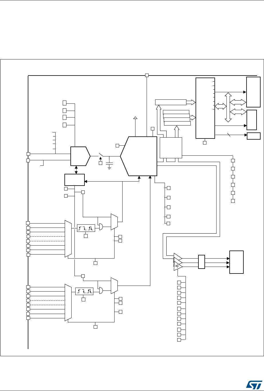
Analog-to-digital converters (ADC) RM0394
376/1600 RM0394 Rev 4
16.4 ADC functional description
16.4.1 ADC block diagram
Figure 39 shows the ADC block diagram and Table 56 gives the ADC pin description.
Figure 39. ADC block diagram
06Y9
(;7
(;7
(;7
(;7
(;7
(;7
&217
VLQJOHFRQW
,QSXW
VHOHFWLRQ
VFDQFRQWURO
603[>@
VDPSOLQJWLPH
6WDUW6WRS
&RQWURO
$'&B,13>@
DQDORJLQSXW
FKDQQHOV
$87'/<
DXWRGHOD\HG
$'673
VWRSFRQY
6:WULJJHU
(;7(1>@
WULJJHUHQDEOH
DQGHGJHVHOHFWLRQ
KZ
WULJJHU
(;7LPDSSHG
DWSURGXFWOHYHO (;76(/>@
WULJJHUVHOHFWLRQ
$'(1$'',6
$'&$/
VHOIFDOLEUDWLRQ
$QDORJ6XSSO\9''$
9WR9
95()
WR9
6$5$'&
VWDUW
%LDV5HI
$/,*1
OHIWULJKW
5(6>@
ELWV
29502'
RYHUUXQPRGH
$+%
LQWHUIDFH
'0$(1
'0$UHTXHVW
$'&,QWHUUXSW
&RUWH[
0ZLWK
)38
'0$
$+%
7,0(5V
(75
,54
$:'B287
-(;7
-(;7
-(;7
-(;7
-(;7
-(;7
-(;7(1>@
WULJJHUHQDEOH
DQGHGJHVHOHFWLRQ
+:
WULJJHU
-(;76(/>@
WULJJHUVHOHFWLRQ
-(;7LPDSSHG
DWSURGXFWOHYHO
$'&B-645[
$'&B645[
-$872
'0$&)*
$5($'<
(2603
(2&
(26
295
-(26
-429)
$:'[
$:'(1
-$:'(1
$QDORJZDWFKGRJ
$:'6*/
-
6:WULJJHU
$:'&+>@
-40
,QMFHG&RQWH[W
4XHXH0RGH
/7>@
+7>@
-2))6(7[>@
-2))6(7[B&+>@
&219(57('
'$7$
-',6&(1
-',6&180>@
',6&(1
',6&18>@
'LVFRQWLQXRXV
PRGH
$:'
$:'&+>@
$:'&+>@
/7>@
+7>@
/7>@
+7>@
$:'
$:'
$:'B287
$:'B287
VODYH
PDVWHU
5'$7$>@
9,1
95()
976
95(),17
9%$7
9,13>@
9,11>@
-'$7$>@
-'$7$>@
-'$7$>@
-'$7$>@
PDVWHU
2YHUVDPSOHU
52960
75296
-296(
5296(
2966>@
2965>@
2YHUVDPSOLQJ
RSWLRQV
')6'0
$'&B,11>@
GDFBRXW
GDFBRXW

RM0394 Rev 4 377/1600
RM0394 Analog-to-digital converters (ADC)
485
16.4.2 ADC pins and internal signals
Table 55. ADC internal input/output signals
Internal signal name Signal
type Description
EXT[15:0] Inputs
Up to 16 external trigger inputs for the regular conversions (can
be connected to on-chip timers).
These inputs are shared between the ADC master and the ADC
slave.
JEXT[15:0] Inputs
Up to 16 external trigger inputs for the injected conversions (can
be connected to on-chip timers).
These inputs are shared between the ADC master and the ADC
slave.
ADC_AWDx_OUT Output Internal analog watchdog output signal connected to on-chip
timers. (x = Analog watchdog number 1,2,3)
VTS Input Output voltage from internal temperature sensor
dac_out1 Input DAC internal channel 1
VREFINT Input Output voltage from internal reference voltage
dac_out2 Input DAC internal channel 2
VBAT
Input
supply External battery voltage supply
Table 56. ADC input/output pins
Pin name Signal type Comments
VREF+
Input, analog reference
positive
The higher/positive reference voltage for the ADC,
1.62 V VREF+ VDDA
VDDA Input, analog supply Analog power supply equal VDDA:
1.62 V VDDA 3.6 V
VREF
Input, analog reference
negative
The lower/negative reference voltage for the ADC.
VREF is internally connected to VSSA
VSSA
Input, analog supply
ground
Ground for analog power supply. On device package
which do not have a dedicated VSSA pin, VSSA is
internally connected to VSS.
VINP[18:0] Positive analog input
channels for each ADC
Connected either to external channels: ADCx_INPi or
internal channels.
VINN[18:0] Negative analog input
channels for each ADC
Connected to VREF or external channels:
ADCx_INNi and ADCx_INP[i+1]
ADCx_INN[16:1] External analog input
signals
Up to 16 analog input channels (x = ADC number = 1
or 2):
– 5 fast channels (ADCx_INN1 to INN5)
– Up to 11 slow channels (ADCx_INN6 to INN16)
ADCx_INP[16:1] External analog input
signals
Up to 16 analog input channels (x = ADC number = 1
or 2):
– 5 fast channels (ADCx_INP1 to INP5)
– Up to 11 slow channels (ADCx_INP6 to INP16)

Analog-to-digital converters (ADC) RM0394
378/1600 RM0394 Rev 4
16.4.3 Clocks
Dual clock domain architecture
The dual clock-domain architecture means that the ADC clock is independent from the AHB
bus clock.
The input clock is the same for the three ADCs and can be selected between two different
clock sources (see Figure 40: ADC clock scheme):
1. The ADC clock can be a specific clock source. It can be derived from the following
clock sources:
– The system clock
– PLLSAI1 (single ADC implementation)
Refer to RCC Section for more information on how to generate ADC dedicated clock.
To select this scheme, bits CKMODE[1:0] of the ADCx_CCR register must be reset.
2. The ADC clock can be derived from the AHB clock of the ADC bus interface, divided by
a programmable factor (1, 2 or 4). In this mode, a programmable divider factor can be
selected (/1, 2 or 4 according to bits CKMODE[1:0]).
To select this scheme, bits CKMODE[1:0] of the ADCx_CCR register must be different
from “00”.
Note: For option 2), a prescaling factor of 1 (CKMODE[1:0]=01) can be used only if the AHB
prescaler is set to 1 (HPRE[3:0] = 0xxx in RCC_CFGR register).
Option 1) has the advantage of reaching the maximum ADC clock frequency whatever the
AHB clock scheme selected. The ADC clock can eventually be divided by the following ratio:
1, 2, 4, 6, 8, 12, 16, 32, 64, 128, 256; using the prescaler configured with bits PRESC[3:0] in
the ADCx_CCR register.
Option 2) has the advantage of bypassing the clock domain resynchronizations. This can be
useful when the ADC is triggered by a timer and if the application requires that the ADC is
precisely triggered without any uncertainty (otherwise, an uncertainty of the trigger instant is
added by the resynchronizations between the two clock domains).
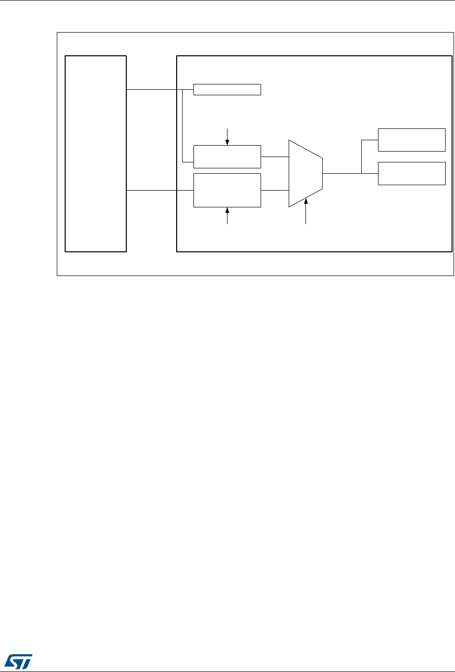
RM0394 Rev 4 379/1600
RM0394 Analog-to-digital converters (ADC)
485
Clock ratio constraint between ADC clock and AHB clock
There are generally no constraints to be respected for the ratio between the ADC clock and
the AHB clock except if some injected channels are programmed. In this case, it is
mandatory to respect the following ratio:
•FHCLK >= FADC / 4 if the resolution of all channels are 12-bit or 10-bit
•FHCLK >= FADC / 3 if there are some channels with resolutions equal to 8-bit (and none
with lower resolutions)
•FHCLK >= FADC / 2 if there are some channels with resolutions equal to 6-bit
Figure 40. ADC clock scheme
06Y9
2WKHUV
5&&
5HVHWDQG
FORFN
FRQWUROOHU
$'&DQG$'&
$+%LQWHUIDFH
$QDORJ$'&
PDVWHU
$QDORJ$'&
VODYH
RURU
%LWV35(&>@
RI$'&[B&&5
%LWV&.02'(>@
RI$'&[B&&5
+&/.
$'&B&.
%LWV&.02'(>@
RI$'&[B&&5
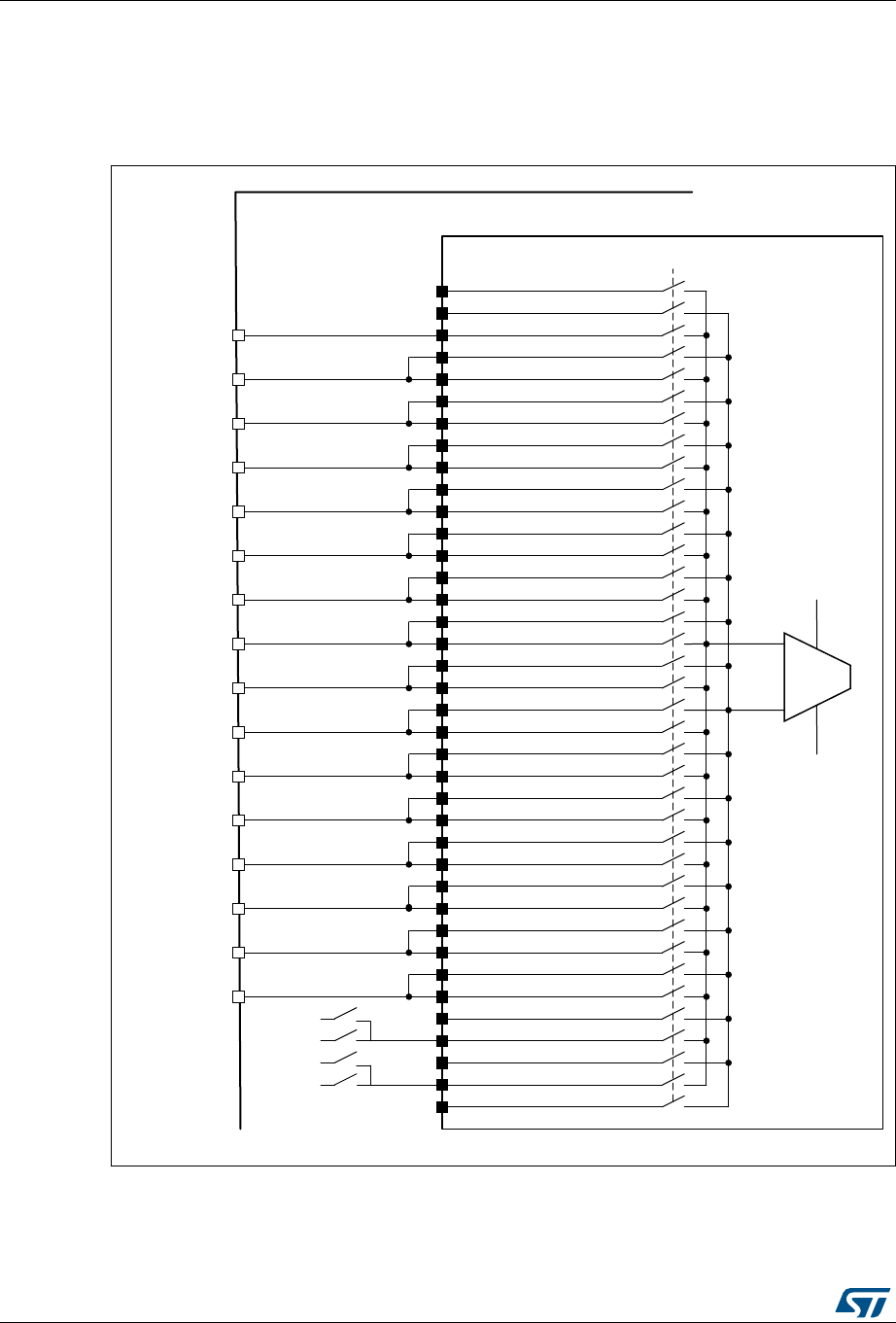
Analog-to-digital converters (ADC) RM0394
380/1600 RM0394 Rev 4
16.4.4 ADC1/2 connectivity
ADC1 and ADC2 are tightly coupled and share some external channels as described in the
below figures.
Figure 41. ADC1 connectivity
06Y9
^Z
$'&
ϭ
$'&B,13
$'&B,11
$'&B,13
$'&B,11
$'&B,13
$'&B,11
$'&B,13
$'&B,11
$'&B,13
$'&B,11
$'&B,13
s,13>@
s,11>@
s,13>@
&ĂƐƚĐŚĂŶŶĞů
670/[[[[[[[[[[[[
670/[[[[[[[[
s,13>@
s,11>@ &ĂƐƚĐŚĂŶŶĞů
s5(),17
95()í
s,11>@
s,13>@
&ĂƐƚĐŚĂŶŶĞů
s,11>@
s,13>@
&ĂƐƚĐŚĂŶŶĞů
s,11>@
s,13>@
&ĂƐƚĐŚĂŶŶĞů
s,11>@
s,13>@
&ĂƐƚĐŚĂŶŶĞů
s,11>@ ^ůŽǁĐŚĂŶŶĞů
s,13>@
s,11>@
s,13>@
s,13>@
s,11>@
s,11>@
s,13>@
s,11>@
s,13>@
s,11>@
s,13>@
s,11>@
s,13>@
s,11>@
s,13>@
s,11>@
s,13>@
s,11>@
s,13>@
s,11>@
s,13>@
s,11>@
s,13>@
s,11>@
95()í
95()í
95()í
s5()
s%$7
$'&B,11
$'&B,13
$'&B,11
$'&B,13
$'&B,11
$'&B,13
$'&B,11
$'&B,13
$'&B,11
$'&B,13
$'&B,11
$'&B,13
$'&B,11
$'&B,13
$'&B,11
$'&B,13
$'&B,11
$'&B,13
$'&B,11
$'&B,13
^ůŽǁĐŚĂŶŶĞů
^ůŽǁĐŚĂŶŶĞů
^ůŽǁĐŚĂŶŶĞů
^ůŽǁĐŚĂŶŶĞů
^ůŽǁĐŚĂŶŶĞů
^ůŽǁĐŚĂŶŶĞů
^ůŽǁĐŚĂŶŶĞů
^ůŽǁĐŚĂŶŶĞů
^ůŽǁĐŚĂŶŶĞů
^ůŽǁĐŚĂŶŶĞů
^ůŽǁĐŚĂŶŶĞů
^ůŽǁĐŚĂŶŶĞů
s,13
s,11
976
95()í
ŚĂŶŶĞůƐĞůĞĐƚŝŽŶ
GDFBRXW
GDFBRXW
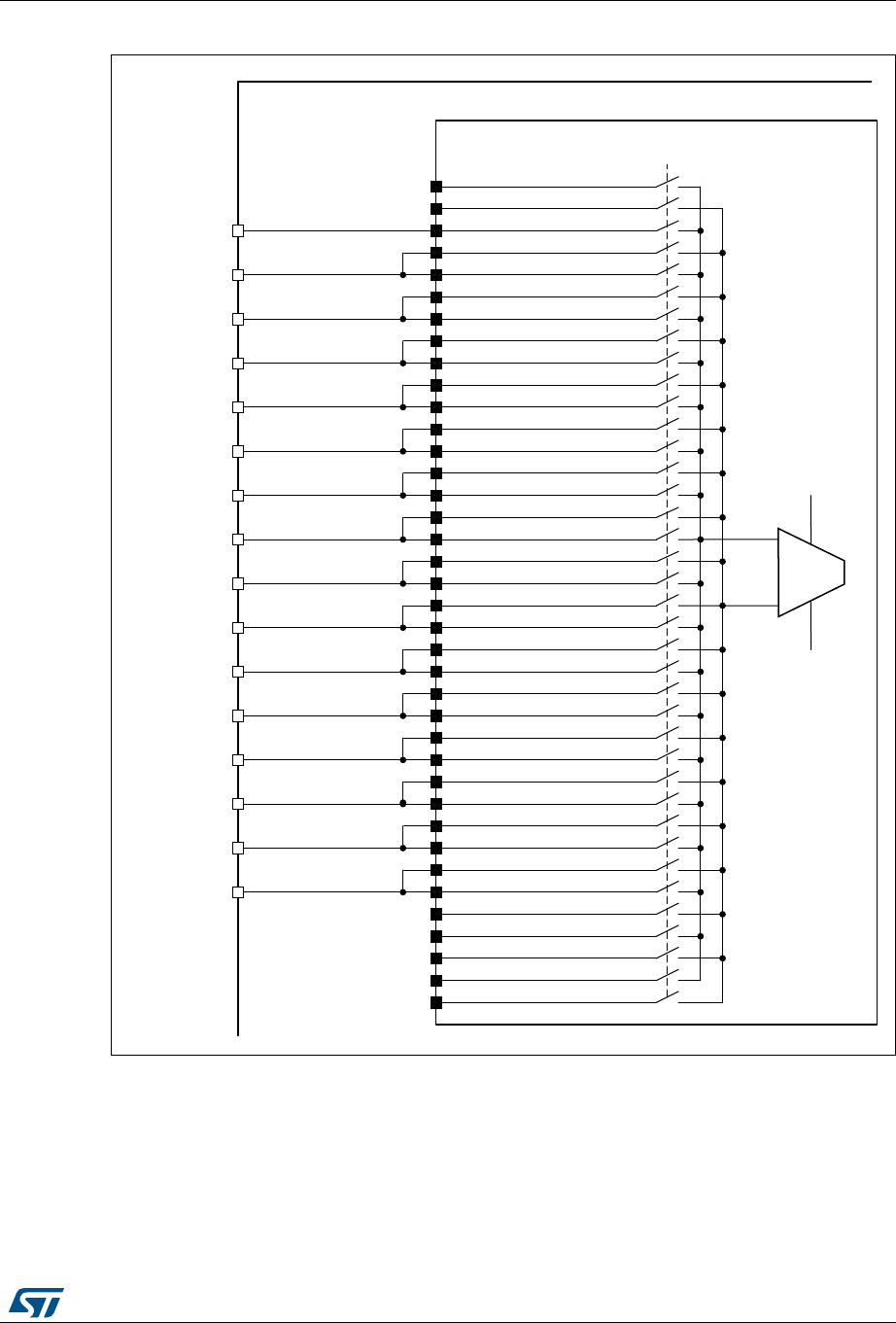
RM0394 Rev 4 381/1600
RM0394 Analog-to-digital converters (ADC)
485
Figure 42. ADC2 connectivity
06Y9
6$5
$'&
$'&
$'&B,13
$'&B,11
$'&B,13
$'&B,11
$'&B,13
$'&B,11
$'&B,13
$'&B,11
$'&B,13
$'&B,11
$'&B,13
9,13>@
9,11>@
9,13>@
)DVWFKDQQHO
670/[[[[
9,13>@
9,11>@ )DVWFKDQQHO
95()í
95()í
9,11>@
9,13>@
)DVWFKDQQHO
9,11>@
9,13>@
)DVWFKDQQHO
9,11>@
9,13>@
)DVWFKDQQHO
9,11>@
9,13>@
)DVWFKDQQHO
9,11>@ 6ORZFKDQQHO
9,13>@
9,11>@
9,13>@
9,13>@
9,11>@
9,11>@
9,13>@
9,11>@
9,13>@
9,11>@
9,13>@
9,11>@
9,13>@
9,11>@
9,13>@
9,11>@
9,13>@
9,11>@
9,13>@
9,11>@
9,13>@
9,11>@
9,13>@
9,11>@
95()í
95()í
95()í
95()
$'&B,11
$'&B,13
$'&B,11
$'&B,13
$'&B,11
$'&B,13
$'&B,11
$'&B,13
$'&B,11
$'&B,13
$'&B,11
$'&B,13
$'&B,11
$'&B,13
$'&B,11
$'&B,13
$'&B,11
$'&B,13
$'&B,11
$'&B,13
6ORZFKDQQHO
6ORZFKDQQHO
6ORZFKDQQHO
6ORZFKDQQHO
6ORZFKDQQHO
6ORZFKDQQHO
6ORZFKDQQHO
6ORZFKDQQHO
6ORZFKDQQHO
6ORZFKDQQHO
6ORZFKDQQHO
6ORZFKDQQHO
9,13
9,11
95()í
95()í
&KDQQHOVHOHFWLRQ
95()í

Analog-to-digital converters (ADC) RM0394
382/1600 RM0394 Rev 4
16.4.5 Slave AHB interface
The ADCs implement an AHB slave port for control/status register and data access. The
features of the AHB interface are listed below:
•Word (32-bit) accesses
•Single cycle response
•Response to all read/write accesses to the registers with zero wait states.
The AHB slave interface does not support split/retry requests, and never generates AHB
errors.
16.4.6 ADC Deep-power-down mode (DEEPPWD) and ADC voltage regulator
(ADVREGEN)
By default, the ADC is in Deep-power-down mode where its supply is internally switched off
to reduce the leakage currents (the reset state of bit DEEPPWD is 1 in the ADC_CR
register).
To start ADC operations, it is first needed to exit Deep-power-down mode by setting bit
DEEPPWD=0.
Then, it is mandatory to enable the ADC internal voltage regulator by setting the bit
ADVREGEN=1 into ADC_CR register. The software must wait for the startup time of the
ADC voltage regulator (TADCVREG_STUP) before launching a calibration or enabling the
ADC. This delay must be implemented by software.
For the startup time of the ADC voltage regulator, refer to device datasheet for
TADCVREG_STUP parameter.
After ADC operations are complete, the ADC can be disabled (ADEN=0). It is possible to
save power by also disabling the ADC voltage regulator. This is done by writing bit
ADVREGEN=0.
Then, to save more power by reducing the leakage currents, it is also possible to re-enter in
ADC Deep-power-down mode by setting bit DEEPPWD=1 into ADC_CR register. This is
particularly interesting before entering STOP mode.
Note: Writing DEEPPWD=1 automatically disables the ADC voltage regulator and bit ADVREGEN
is automatically cleared.
When the internal voltage regulator is disabled (ADVREGEN=0), the internal analog
calibration is kept.
In ADC Deep-power-down mode (DEEPPWD=1), the internal analog calibration is lost and
it is necessary to either relaunch a calibration or re-apply the calibration factor which was
previously saved (refer to Section 16.4.8: Calibration (ADCAL, ADCALDIF,
ADC_CALFACT)).

RM0394 Rev 4 383/1600
RM0394 Analog-to-digital converters (ADC)
485
16.4.7 Single-ended and differential input channels
Channels can be configured to be either single-ended input or differential input by writing
into bits DIFSEL[15:1] in the ADC_DIFSEL register. This configuration must be written while
the ADC is disabled (ADEN=0). Note that DIFSEL[18:16,0] are fixed to single ended
channels and are always read as 0.
In single-ended input mode, the analog voltage to be converted for channel “i” is the
difference between the external voltage VINP[i] (positive input) and VREF (negative input).
In differential input mode, the analog voltage to be converted for channel “i” is the difference
between the external voltage VINP[i] (positive input) and VINN[i] (negative input).
When ADC is configured as differential mode, both inputs should be biased at (VREF+) / 2
voltage.
The input signal are supposed to be differential (common mode voltage should be fixed).
For a complete description of how the input channels are connected for each ADC, refer to
Section 16.4.4: ADC1/2 connectivity.
Caution: When configuring the channel “i” in differential input mode, its negative input voltage VINN[i]
is connected to VINP[i+1]. As a consequence, channel “i+1” is no longer usable in single-
ended mode or in differential mode and must never be configured to be converted. Some
channels are shared between ADC1/ADC2: this can make the channel on the other ADC
unusable. Only exception is interleaved mode for ADC master and the slave.
Note: ADC channels 0, 16, 17, 18 are forced to single-ended configuration (corresponding bits
DIFSEL[i] is always zero), either because connected to a single-ended external analog input
or connected to an internal channel.
16.4.8 Calibration (ADCAL, ADCALDIF, ADC_CALFACT)
Each ADC provides an automatic calibration procedure which drives all the calibration
sequence including the power-on/off sequence of the ADC. During the procedure, the ADC
calculates a calibration factor which is 7-bit wide and which is applied internally to the ADC
until the next ADC power-off. During the calibration procedure, the application must not use
the ADC and must wait until calibration is complete.
Calibration is preliminary to any ADC operation. It removes the offset error which may vary
from chip to chip due to process or bandgap variation.
The calibration factor to be applied for single-ended input conversions is different from the
factor to be applied for differential input conversions:
•Write ADCALDIF=0 before launching a calibration which will be applied for single-
ended input conversions.
•Write ADCALDIF=1 before launching a calibration which will be applied for differential
input conversions.
The calibration is then initiated by software by setting bit ADCAL=1. Calibration can only be
initiated when the ADC is disabled (when ADEN=0). ADCAL bit stays at 1 during all the
calibration sequence. It is then cleared by hardware as soon the calibration completes. At
this time, the associated calibration factor is stored internally in the analog ADC and also in
the bits CALFACT_S[6:0] or CALFACT_D[6:0] of ADC_CALFACT register (depending on
single-ended or differential input calibration)
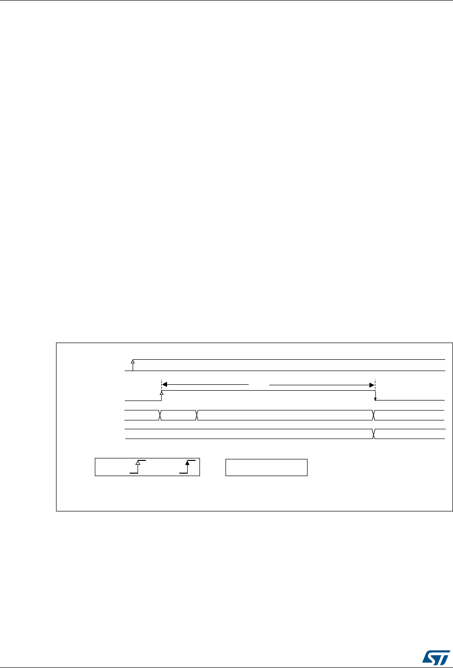
Analog-to-digital converters (ADC) RM0394
384/1600 RM0394 Rev 4
The internal analog calibration is kept if the ADC is disabled (ADEN=0). However, if the ADC
is disabled for extended periods, then it is recommended that a new calibration cycle is run
before re-enabling the ADC.
The internal analog calibration is lost each time the power of the ADC is removed (example,
when the product enters in STANDBY or VBAT mode). In this case, to avoid spending time
recalibrating the ADC, it is possible to re-write the calibration factor into the ADC_CALFACT
register without recalibrating, supposing that the software has previously saved the
calibration factor delivered during the previous calibration.
The calibration factor can be written if the ADC is enabled but not converting (ADEN=1 and
ADSTART=0 and JADSTART=0). Then, at the next start of conversion, the calibration factor
will automatically be injected into the analog ADC. This loading is transparent and does not
add any cycle latency to the start of the conversion. It is recommended to recalibrate when
VREF+ voltage changed more than 10%.
Software procedure to calibrate the ADC
1. Ensure DEEPPWD=0, ADVREGEN=1 and that ADC voltage regulator startup time has
elapsed.
2. Ensure that ADEN=0.
3. Select the input mode for this calibration by setting ADCALDIF=0 (single-ended input)
or ADCALDIF=1 (differential input).
4. Set ADCAL=1.
5. Wait until ADCAL=0.
6. The calibration factor can be read from ADC_CALFACT register.
Figure 43. ADC calibration
Software procedure to re-inject a calibration factor into the ADC
1. Ensure ADEN=1 and ADSTART=0 and JADSTART=0 (ADC enabled and no
conversion is ongoing).
2. Write CALFACT_S and CALFACT_D with the new calibration factors.
3. When a conversion is launched, the calibration factor will be injected into the analog
ADC only if the internal analog calibration factor differs from the one stored in bits
CALFACT_S for single-ended input channel or bits CALFACT_D for differential input
channel.
W&$%
$'&$/
$'&6WDWH
&$/)$&7B[>@ [ &DOLEUDWLRQIDFWRU
$'&$/',) 6LQJOHHQGHGLQSXW'LIIHUHQWLDOLQSXW
06Y9
2)) 6WDUWXS &DOLEUDWH 2))
,QGLFDWLYHWLPLQJV
E\6: E\+:
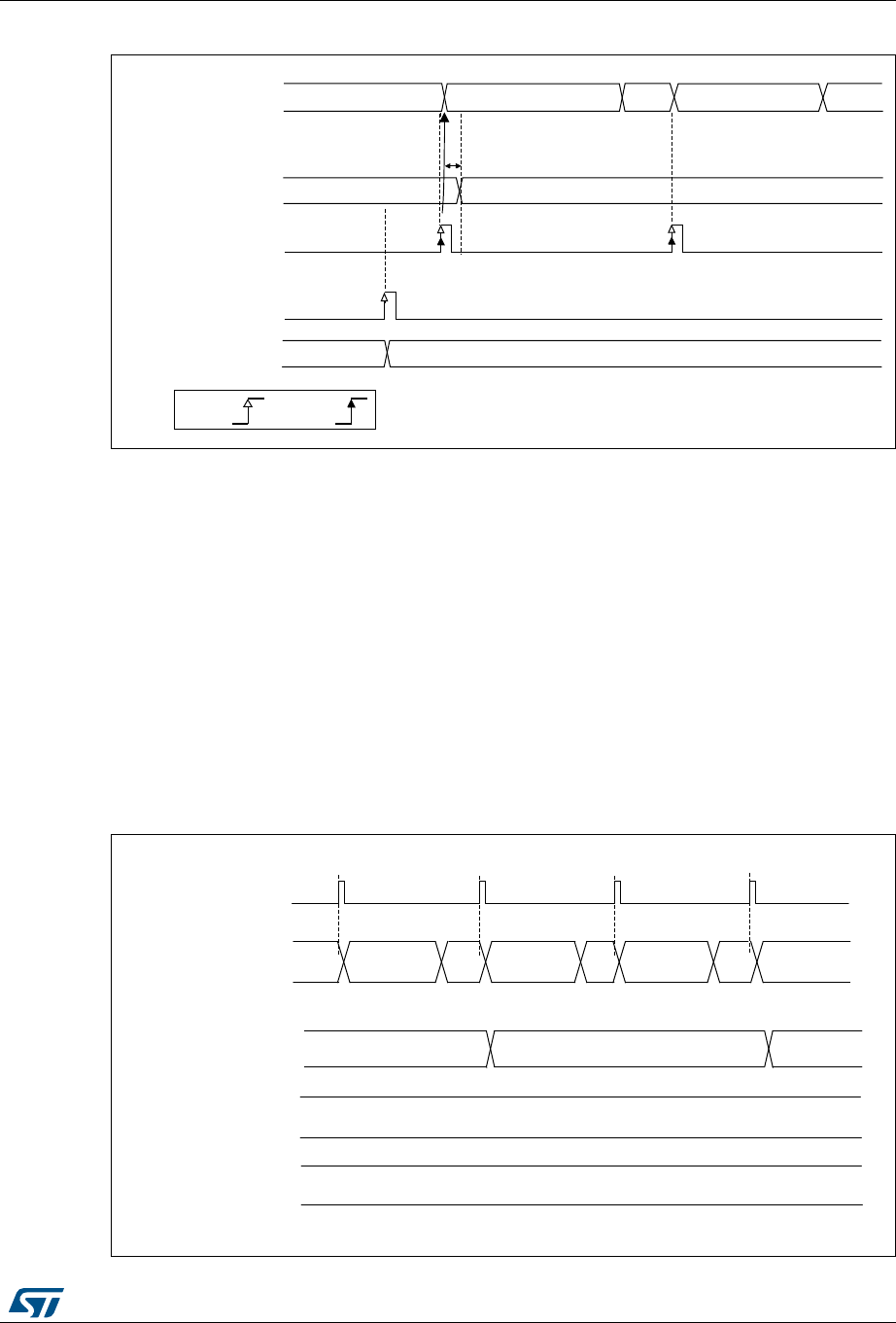
RM0394 Rev 4 385/1600
RM0394 Analog-to-digital converters (ADC)
485
Figure 44. Updating the ADC calibration factor
Converting single-ended and differential analog inputs with a single ADC
If the ADC is supposed to convert both differential and single-ended inputs, two calibrations
must be performed, one with ADCALDIF=0 and one with ADCALDIF=1. The procedure is
the following:
1. Disable the ADC.
2. Calibrate the ADC in single-ended input mode (with ADCALDIF=0). This updates the
register CALFACT_S[6:0].
3. Calibrate the ADC in differential input modes (with ADCALDIF=1). This updates the
register CALFACT_D[6:0].
4. Enable the ADC, configure the channels and launch the conversions. Each time there
is a switch from a single-ended to a differential inputs channel (and vice-versa), the
calibration will automatically be injected into the analog ADC.
Figure 45. Mixing single-ended and differential channels
:5,7($'&B&$/)$&7
$'&VWDWH
&$/)$&7B6>@ )
)
,QWHUQDO
FDOLEUDWLRQIDFWRU>@
6WDUWFRQYHUVLRQ
KDUGZDUHRUVRIZDUH
)
5HDG\QRWFRQYHUWLQJ &RQYHUWLQJFKDQQHO 5HDG\ &RQYHUWLQJFKDQQHO
6LQJOHHQGHG 6LQJOHHQGHG
06Y9
8SGDWLQJFDOLEUDWLRQ
E\VZ E\KZ
$'&VWDWH
&$/)$&7B6>@ )
)
,QWHUQDO
FDOLEUDWLRQIDFWRU>@
&219&+
&$/)$&7B'>@ )
6LQJOHHQGHG
LQSXWVFKDQQHO
&219&+ &219&+
6LQJOHLQSXWV
FKDQQHO
) )
7ULJJHUHYHQW
5'< 5'< 5'<
06Y9
&219&+
5'<
'LIIHUHQWLDO
LQSXWVFKDQQHO
'LIIHUHQWLDO
LQSXWVFKDQQHO

Analog-to-digital converters (ADC) RM0394
386/1600 RM0394 Rev 4
16.4.9 ADC on-off control (ADEN, ADDIS, ADRDY)
First of all, follow the procedure explained in Section 16.4.6: ADC Deep-power-down mode
(DEEPPWD) and ADC voltage regulator (ADVREGEN)).
Once DEEPPWD=0 and ADVREGEN=1, the ADC can be enabled and the ADC needs a
stabilization time of tSTAB before it starts converting accurately, as shown in Figure 46. Two
control bits enable or disable the ADC:
•ADEN=1 enables the ADC. The flag ADRDY will be set once the ADC is ready for
operation.
•ADDIS=1 disables the ADC. ADEN and ADDIS are then automatically cleared by
hardware as soon as the analog ADC is effectively disabled.
Regular conversion can then start either by setting ADSTART=1 (refer to Section 16.4.18:
Conversion on external trigger and trigger polarity (EXTSEL, EXTEN,JEXTSEL, JEXTEN))
or when an external trigger event occurs, if triggers are enabled.
Injected conversions start by setting JADSTART=1 or when an external injected trigger
event occurs, if injected triggers are enabled.
Software procedure to enable the ADC
1. Clear the ADRDY bit in the ADC_ISR register by writing ‘1’.
2. Set ADEN=1.
3. Wait until ADRDY=1 (ADRDY is set after the ADC startup time). This can be done
using the associated interrupt (setting ADRDYIE=1).
4. Clear the ADRDY bit in the ADC_ISR register by writing ‘1’ (optional).
Caution: ADEN bit cannot be set during ADCAL=1 and 4 ADC clock cycle after the ADCAL bit is
cleared by hardware (end of the calibration).
Software procedure to disable the ADC
1. Check that both ADSTART=0 and JADSTART=0 to ensure that no conversion is
ongoing. If required, stop any regular and injected conversion ongoing by setting
ADSTP=1 and JADSTP=1 and then wait until ADSTP=0 and JADSTP=0.
2. Set ADDIS=1.
3. If required by the application, wait until ADEN=0, until the analog ADC is effectively
disabled (ADDIS will automatically be reset once ADEN=0).

RM0394 Rev 4 387/1600
RM0394 Analog-to-digital converters (ADC)
485
Figure 46. Enabling / Disabling the ADC
16.4.10 Constraints when writing the ADC control bits
The software is allowed to write the RCC control bits to configure and enable the ADC clock
(refer to RCC Section), the control bits DIFSEL in the ADC_DIFSEL register and the control
bits ADCAL and ADEN in the ADC_CR register, only if the ADC is disabled (ADEN must be
equal to 0).
The software is then allowed to write the control bits ADSTART, JADSTART and ADDIS of
the ADC_CR register only if the ADC is enabled and there is no pending request to disable
the ADC (ADEN must be equal to 1 and ADDIS to 0).
For all the other control bits of the ADC_CFGR, ADC_SMPRx, ADC_SQRy, ADC_JDRy,
ADC_OFRy, ADC_OFCHRy and ADC_IER registers:
•For control bits related to configuration of regular conversions, the software is allowed
to write them only if the ADC is enabled (ADEN=1) and if there is no regular conversion
ongoing (ADSTART must be equal to 0).
•For control bits related to configuration of injected conversions, the software is allowed
to write them only if the ADC is enabled (ADEN=1) and if there is no injected
conversion ongoing (JADSTART must be equal to 0).
The software is allowed to write the ADSTP or JADSTP control bits of the ADC_CR register
only if the ADC is enabled, possibly converting, and if there is no pending request to disable
the ADC (ADSTART or JADSTART must be equal to 1 and ADDIS to 0).
The software can write the register ADC_JSQR at any time, when the ADC is enabled
(ADEN=1). Refer to Section 16.6.16: ADC injected sequence register (ADC_JSQR) for
additional details.
Note: There is no hardware protection to prevent these forbidden write accesses and ADC
behavior may become in an unknown state. To recover from this situation, the ADC must be
disabled (clear ADEN=0 as well as all the bits of ADC_CR register).
06Y9
W
67$%
$'(1
$'5'<
$'',6
$'& &RQYHUWLQJ&+ 2))
E\+:
E\6:
5(4
2)
VWDWH
2)) 6WDUWXS 5'< 5'<

Analog-to-digital converters (ADC) RM0394
388/1600 RM0394 Rev 4
16.4.11 Channel selection (SQRx, JSQRx)
There are up to 19 multiplexed channels per ADC:
•5 fast analog inputs coming from GPIO pads (ADCx_INP/INN[1..5])
•Up to 11 slow analog inputs coming from GPIO pads (ADCx_INP/INN[6..16]).
Depending on the products, not all of them are available on GPIO pads.
•The ADCs are connected to the following internal analog inputs:
– the internal reference voltage (VREFINT) is connected to ADC1_INP0/INN0.
– the internal temperature sensor (VTS) is connected to ADC1_INP17/INN17.
–the V
BAT monitoring channel (VBAT/3) is connected to ADC1_INP18/INN18.
– the DAC1 internal channel is connected to ADC1_INP/INN17.
Note: To convert one of the internal analog channels, the corresponding analog sources must first
be enabled by programming bits VREFEN, CH17SEL or CH18SEL in the ADCx_CCR
registers.
It is possible to organize the conversions in two groups: regular and injected. A group
consists of a sequence of conversions that can be done on any channel and in any order.
For instance, it is possible to implement the conversion sequence in the following order:
ADCx_INP/INN3, ADCx_INP/INN8, ADCx_INP/INN2, ADCx/INN2, ADCx_INP/INN0,
ADCx_INP/INN2, ADCx_INP/INN2, ADCx_INP/INN15.
•A regular group is composed of up to 16 conversions. The regular channels and their
order in the conversion sequence must be selected in the ADC_SQRy registers. The
total number of conversions in the regular group must be written in the L[3:0] bits in the
ADC_SQR1 register.
•An injected group is composed of up to 4 conversions. The injected channels and
their order in the conversion sequence must be selected in the ADC_JSQR register.
The total number of conversions in the injected group must be written in the L[1:0] bits
in the ADC_JSQR register.
ADC_SQRy registers must not be modified while regular conversions can occur. For this,
the ADC regular conversions must be first stopped by writing ADSTP=1 (refer to
Section 16.4.17: Stopping an ongoing conversion (ADSTP, JADSTP)).
The software is allowed to modify on-the-fly the ADC_JSQR register when JADSTART is set
to 1 (injected conversions ongoing) only when the context queue is enabled (JQDIS=0 in
ADC_CFGR register). Refer to Section 16.4.21: Queue of context for injected conversions

RM0394 Rev 4 389/1600
RM0394 Analog-to-digital converters (ADC)
485
16.4.12 Channel-wise programmable sampling time (SMPR1, SMPR2)
Before starting a conversion, the ADC must establish a direct connection between the
voltage source under measurement and the embedded sampling capacitor of the ADC. This
sampling time must be enough for the input voltage source to charge the embedded
capacitor to the input voltage level.
Each channel can be sampled with a different sampling time which is programmable using
the SMP[2:0] bits in the ADC_SMPR1 and ADC registers. It is therefore possible to select
among the following sampling time values:
•SMP = 000: 2.5 ADC clock cycles
•SMP = 001: 6.5 ADC clock cycles
•SMP = 010: 12.5 ADC clock cycles
•SMP = 011: 24.5 ADC clock cycles
•SMP = 100: 47.5 ADC clock cycles
•SMP = 101: 92.5 ADC clock cycles
•SMP = 110: 247.5 ADC clock cycles
•SMP = 111: 640.5 ADC clock cycles
The total conversion time is calculated as follows:
TCONV = Sampling time + 12.5 ADC clock cycles
Example:
With FADC_CLK = 80 MHz and a sampling time of 2.5 ADC clock cycles:
TCONV = (2.5 + 12.5) ADC clock cycles = 15 ADC clock cycles = 187.5 ns (for fast
channels)
The ADC notifies the end of the sampling phase by setting the status bit EOSMP (only for
regular conversion).
Constraints on the sampling time for fast and slow channels
For each channel, SMP[2:0] bits must be programmed to respect a minimum sampling time
as specified in the ADC characteristics section of the datasheets.
I/O analog switches voltage booster
The I/O analog switches resistance increases when the VDDA voltage is too low. This
requires to have the sampling time adapted accordingly (cf datasheet for electrical
characteristics). This resistance can be minimized at low VDDA by enabling an internal
voltage booster with BOOSTEN bit in the SYSCFG_CFGR1 register.
16.4.13 Single conversion mode (CONT=0)
In Single conversion mode, the ADC performs once all the conversions of the channels.
This mode is started with the CONT bit at 0 by either:
•Setting the ADSTART bit in the ADC_CR register (for a regular channel)
•Setting the JADSTART bit in the ADC_CR register (for an injected channel)
•External hardware trigger event (for a regular or injected channel)

Analog-to-digital converters (ADC) RM0394
390/1600 RM0394 Rev 4
Inside the regular sequence, after each conversion is complete:
•The converted data are stored into the 16-bit ADC_DR register
•The EOC (end of regular conversion) flag is set
•An interrupt is generated if the EOCIE bit is set
Inside the injected sequence, after each conversion is complete:
•The converted data are stored into one of the four 16-bit ADC_JDRy registers
•The JEOC (end of injected conversion) flag is set
•An interrupt is generated if the JEOCIE bit is set
After the regular sequence is complete:
•The EOS (end of regular sequence) flag is set
•An interrupt is generated if the EOSIE bit is set
After the injected sequence is complete:
•The JEOS (end of injected sequence) flag is set
•An interrupt is generated if the JEOSIE bit is set
Then the ADC stops until a new external regular or injected trigger occurs or until bit
ADSTART or JADSTART is set again.
Note: To convert a single channel, program a sequence with a length of 1.
16.4.14 Continuous conversion mode (CONT=1)
This mode applies to regular channels only.
In continuous conversion mode, when a software or hardware regular trigger event occurs,
the ADC performs once all the regular conversions of the channels and then automatically
restarts and continuously converts each conversions of the sequence. This mode is started
with the CONT bit at 1 either by external trigger or by setting the ADSTART bit in the
ADC_CR register.
Inside the regular sequence, after each conversion is complete:
•The converted data are stored into the 16-bit ADC_DR register
•The EOC (end of conversion) flag is set
•An interrupt is generated if the EOCIE bit is set
After the sequence of conversions is complete:
•The EOS (end of sequence) flag is set
•An interrupt is generated if the EOSIE bit is set
Then, a new sequence restarts immediately and the ADC continuously repeats the
conversion sequence.
Note: To convert a single channel, program a sequence with a length of 1.
It is not possible to have both discontinuous mode and continuous mode enabled: it is
forbidden to set both DISCEN=1 and CONT=1.
Injected channels cannot be converted continuously. The only exception is when an injected
channel is configured to be converted automatically after regular channels in continuous
mode (using JAUTO bit), refer to Auto-injection mode section).

RM0394 Rev 4 391/1600
RM0394 Analog-to-digital converters (ADC)
485
16.4.15 Starting conversions (ADSTART, JADSTART)
Software starts ADC regular conversions by setting ADSTART=1.
When ADSTART is set, the conversion starts:
•Immediately: if EXTEN = 0x0 (software trigger)
•At the next active edge of the selected regular hardware trigger: if EXTEN /= 0x0
Software starts ADC injected conversions by setting JADSTART=1.
When JADSTART is set, the conversion starts:
•Immediately, if JEXTEN = 0x0 (software trigger)
•At the next active edge of the selected injected hardware trigger: if JEXTEN /= 0x0
Note: In auto-injection mode (JAUTO=1), use ADSTART bit to start the regular conversions
followed by the auto-injected conversions (JADSTART must be kept cleared).
ADSTART and JADSTART also provide information on whether any ADC operation is
currently ongoing. It is possible to re-configure the ADC while ADSTART=0 and
JADSTART=0 are both true, indicating that the ADC is idle.
ADSTART is cleared by hardware:
•In single mode with software regular trigger (CONT=0, EXTSEL=0x0)
– at any end of regular conversion sequence (EOS assertion) or at any end of
subgroup processing if DISCEN = 1
•In all cases (CONT=x, EXTSEL=x)
– after execution of the ADSTP procedure asserted by the software.
Note: In continuous mode (CONT=1), ADSTART is not cleared by hardware with the assertion of
EOS because the sequence is automatically relaunched.
When a hardware trigger is selected in single mode (CONT=0 and EXTSEL /=0x00),
ADSTART is not cleared by hardware with the assertion of EOS to help the software which
does not need to reset ADSTART again for the next hardware trigger event. This ensures
that no further hardware triggers are missed.
JADSTART is cleared by hardware:
•in single mode with software injected trigger (JEXTSEL=0x0)
– at any end of injected conversion sequence (JEOS assertion) or at any end of
subgroup processing if JDISCEN = 1
•in all cases (JEXTSEL=x)
– after execution of the JADSTP procedure asserted by the software.
Note: When the software trigger is selected, ADSTART bit should not be set if the EOC flag is still
high.
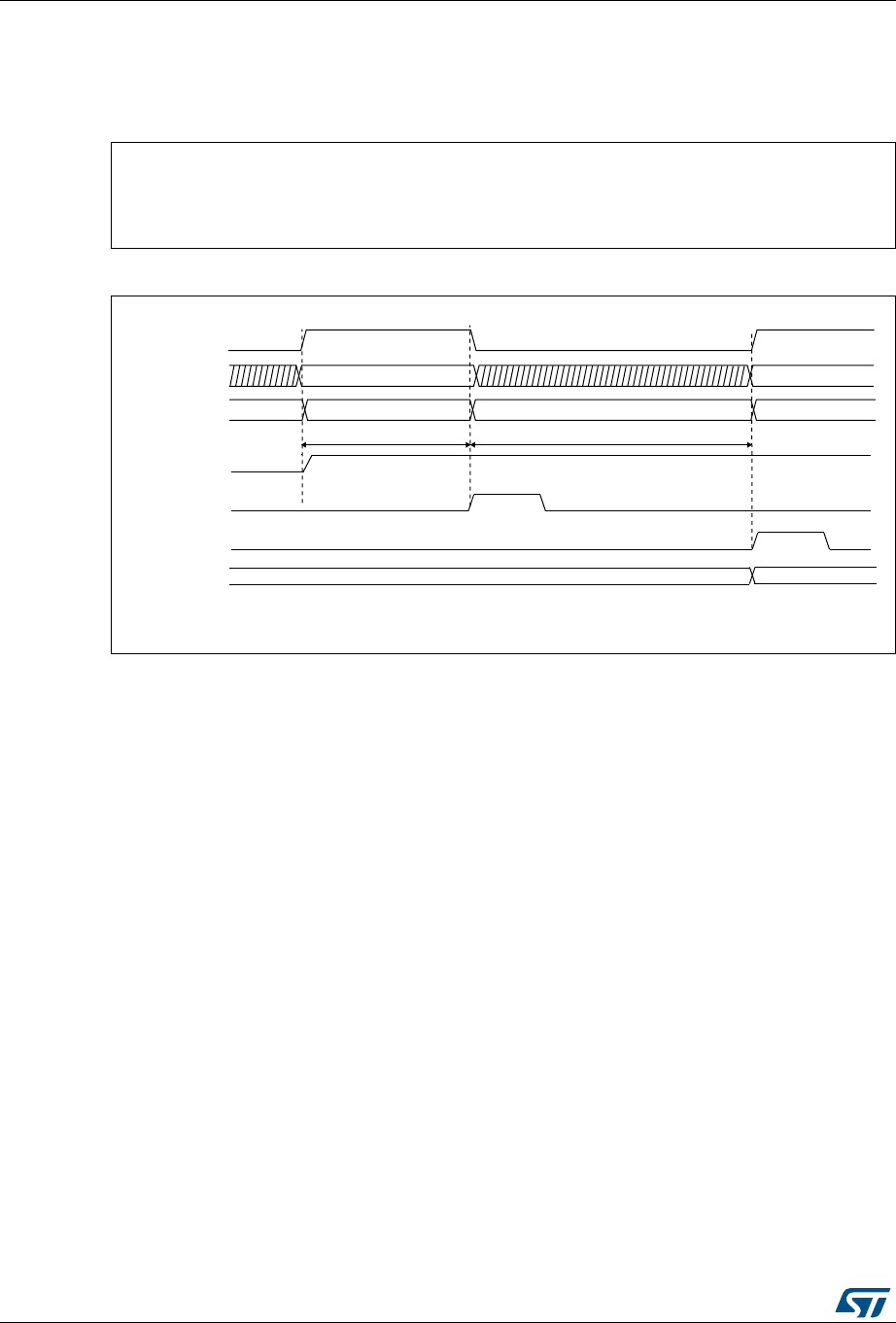
Analog-to-digital converters (ADC) RM0394
392/1600 RM0394 Rev 4
16.4.16 ADC timing
The elapsed time between the start of a conversion and the end of conversion is the sum of
the configured sampling time plus the successive approximation time depending on data
resolution:
Figure 47. Analog to digital conversion time
1. TSMPL depends on SMP[2:0]
2. TSAR depends on RES[2:0]
16.4.17 Stopping an ongoing conversion (ADSTP, JADSTP)
The software can decide to stop regular conversions ongoing by setting ADSTP=1 and
injected conversions ongoing by setting JADSTP=1.
Stopping conversions will reset the ongoing ADC operation. Then the ADC can be
reconfigured (ex: changing the channel selection or the trigger) ready for a new operation.
Note that it is possible to stop injected conversions while regular conversions are still
operating and vice-versa. This allows, for instance, re-configuration of the injected
conversion sequence and triggers while regular conversions are still operating (and vice-
versa).
When the ADSTP bit is set by software, any ongoing regular conversion is aborted with
partial result discarded (ADC_DR register is not updated with the current conversion).
When the JADSTP bit is set by software, any ongoing injected conversion is aborted with
partial result discarded (ADC_JDRy register is not updated with the current conversion).
The scan sequence is also aborted and reset (meaning that relaunching the ADC would
restart a new sequence).
Once this procedure is complete, bits ADSTP/ADSTART (in case of regular conversion), or
JADSTP/JADSTART (in case of injected conversion) are cleared by hardware and the
software must poll ADSTART (or JADSTART) until the bit is reset before assuming the ADC
is completely stopped.
TCONV= TSMPL + TSAR = [ 2.5 |min + 12.5 |12bit ] x TADC_CLK
TCONV = TSMPL + TSAR = 31.25 ns |min + 156.25 ns |12bit = 187.5 ns (for FADC_CLK = 80 MHz)
'DWD1 'DWD1
069
$'&VWDWH
$'67$57
$'&B'5
$QDORJFKDQQHO
,QWHUQDO6+
(2603
(2&
5'<
6HW
E\6:
&OHDUHG
E\6:
6HW
E\+:
6HW
E\+:
6DPSOLQJ&K1 &RQYHUWLQJ&K1 6DPSOLQJ&K1
&K1
6DPSOH$,11
&OHDUHG
E\6:
+ROG$,11
&K1
6DPSOH$,11
,QGLFDWLYHWLPLQJV
603/
W 6$5
W
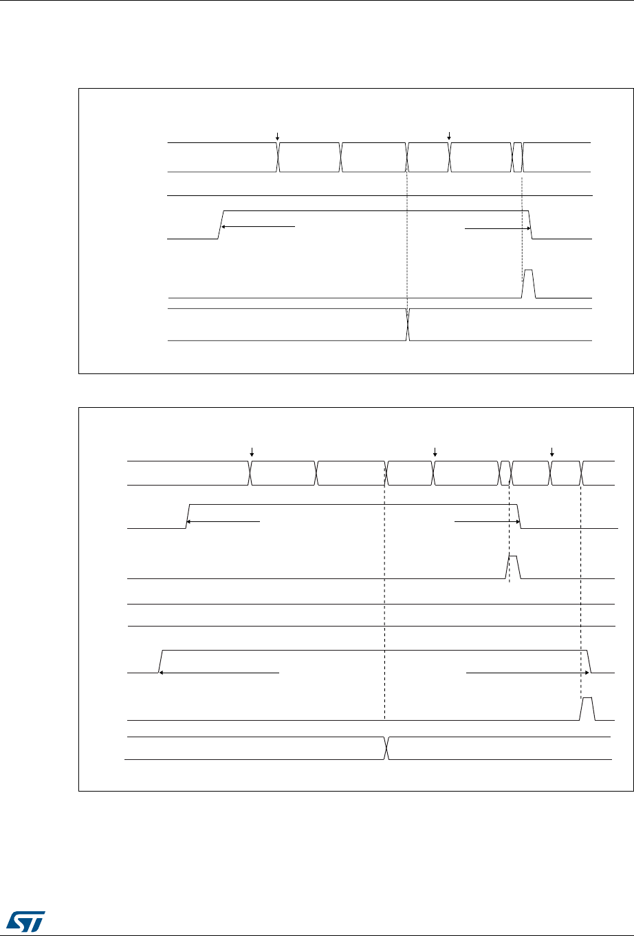
RM0394 Rev 4 393/1600
RM0394 Analog-to-digital converters (ADC)
485
Note: In auto-injection mode (JAUTO=1), setting ADSTP bit aborts both regular and injected
conversions (JADSTP must not be used).
Figure 48. Stopping ongoing regular conversions
Figure 49. Stopping ongoing regular and injected conversions
06Y9
&
7ULJJHU
$'&VWDWH 5'< &RQYHUW
&K1 5'< 5'<
6DPSOH
&K1
5(*8/$5&219(56,216RQJRLQJ
VRIWZDUHLVQRWDOORZHGWRFRQILJXUHUHJXODUFRQYHUVLRQVVHOHFWLRQDQGWULJJHUV
&OHDUHGE\
+:
6HWE\
6:
'DWD1 'DWD1
-$'67$57
$'67$57
$'673
$'&B'5
6DPSOH
&K1
7ULJJHU
&OHDUHGE\
+:
&OHDUHGE\
+:
3AMPLE
#H.
2$9
!$#?$2 $!4!.
2$9
!$340
*!$34!24
2%'5,!2#/.6%23)/.3ONGOING
#ONVERT
#H.
2EGULARTRIGGER
3AMPLE
#H- #
)NJECTEDTRIGGER
$!4!.
2$9
SOFTWAREISNOTALLOWEDTOCONFIGUREREGULARCONVERSIONSSELECTIONANDTRIGGERS
3ET
BY37 ).*%#4%$#/.6%23)/.3ONGOING
SOFTWAREISNOTALLOWEDTOCONFIGUREINJECTEDCONVERSIONSSELECTIONANDTRIGGERS
*!$340
!$#?*$2 $!4!-
3AMPL
2$9
#LEARED
BY(7
!$34!24
#LEARED
BY(7
3ET
BY37
069
2EGULARTRIGGER
3ET
BY37 #LEARED
BY(7
#LEARED
BY(7
3ET
BY37
$'&VWDWH
Analog-to-digital converters (ADC) RM0394
394/1600 RM0394 Rev 4
16.4.18 Conversion on external trigger and trigger polarity
(EXTSEL, EXTEN,JEXTSEL, JEXTEN)
A conversion or a sequence of conversions can be triggered either by software or by an
external event (e.g. timer capture, input pins). If the EXTEN[1:0] control bits (for a regular
conversion) or JEXTEN[1:0] bits (for an injected conversion) are different from 0b00, then
external events are able to trigger a conversion with the selected polarity.
When the Injected Queue is enabled (bit JQDIS=0), injected software triggers are not
possible.
The regular trigger selection is effective once software has set bit ADSTART=1 and the
injected trigger selection is effective once software has set bit JADSTART=1.
Any hardware triggers which occur while a conversion is ongoing are ignored.
•If bit ADSTART=0, any regular hardware triggers which occur are ignored.
•If bit JADSTART=0, any injected hardware triggers which occur are ignored.
Table 57 provides the correspondence between the EXTEN[1:0] and JEXTEN[1:0] values
and the trigger polarity.
Note: The polarity of the regular trigger cannot be changed on-the-fly.
Note: The polarity of the injected trigger can be anticipated and changed on-the-fly when the
queue is enabled (JQDIS=0). Refer to Section 16.4.21: Queue of context for injected
conversions.
The EXTSEL and JEXTSEL control bits select which out of 16 possible events can trigger
conversion for the regular and injected groups.
A regular group conversion can be interrupted by an injected trigger.
Table 57. Configuring the trigger polarity for regular external triggers
EXTEN[1:0] Source
00 Hardware Trigger detection disabled, software trigger detection enabled
01 Hardware Trigger with detection on the rising edge
10 Hardware Trigger with detection on the falling edge
11 Hardware Trigger with detection on both the rising and falling edges
Table 58. Configuring the trigger polarity for injected external triggers
JEXTEN[1:0] Source
00
– If JQDIS=1 (Queue disabled): Hardware trigger detection disabled, software
trigger detection enabled
– If JQDIS=0 (Queue enabled), Hardware and software trigger detection disabled
01 Hardware Trigger with detection on the rising edge
10 Hardware Trigger with detection on the falling edge
11 Hardware Trigger with detection on both the rising and falling edges
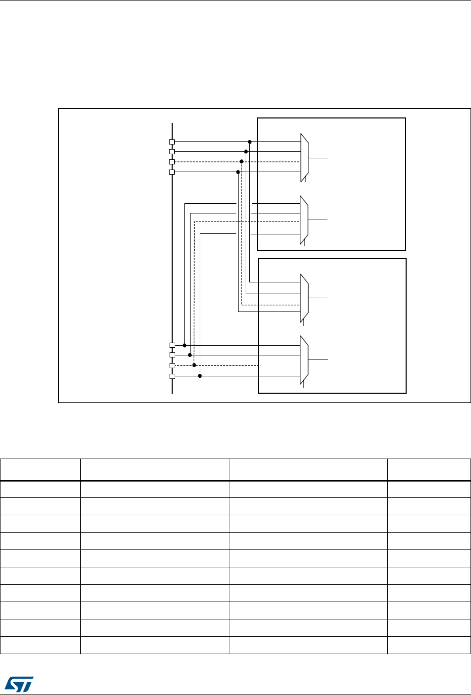
RM0394 Rev 4 395/1600
RM0394 Analog-to-digital converters (ADC)
485
Note: The regular trigger selection cannot be changed on-the-fly.
The injected trigger selection can be anticipated and changed on-the-fly. Refer to
Section 16.4.21: Queue of context for injected conversions on page 399
Each ADC master shares the same input triggers with its ADC slave as described in
Figure 50.
Figure 50. Triggers sharing between ADC master and ADC slave
Table 59 toTable 60 give all the possible external triggers of the three ADCs for regular and
injected conversion.
(;7
(;7
(;76(/>@
$'&0$67(5
(;7
-(;7
-(;7
,QMHFWHG
VHTXHQFHU
WULJJHUV
-(;7
-(;76(/>@
([WHUQDOUHJXODUWULJJHU
([WHUQDOLQMHFWHGWULJJHU
(;76(/>@
$'&6/$9(
-(;76(/>@
([WHUQDOUHJXODUWULJJHU
([WHUQDOLQMHFWHGWULJJHU
069
5HJXODU
VHTXHQFHU
WULJJHUV
Table 59. ADC1 and ADC2 - External triggers for regular channels
Name Source Type EXTSEL[3:0]
EXT0 TIM1_CH1 Internal signal from on-chip timers 0000
EXT1 TIM1_CH2 Internal signal from on-chip timers 0001
EXT2 TIM1_CH3 Internal signal from on-chip timers 0010
EXT3 TIM2_CH2 Internal signal from on-chip timers 0011
EXT4 TIM3_TRGO(1) Internal signal from on-chip timers 0100
EXT5 - - 0101
EXT6 EXTI line 11 External pin 0110
EXT9 TIM1_TRGO Internal signal from on-chip timers 1001
EXT10 TIM1_TRGO2 Internal signal from on-chip timers 1010
EXT11 TIM2_TRGO Internal signal from on-chip timers 1011
Analog-to-digital converters (ADC) RM0394
396/1600 RM0394 Rev 4
16.4.19 Injected channel management
Triggered injection mode
To use triggered injection, the JAUTO bit in the ADC_CFGR register must be cleared.
1. Start the conversion of a group of regular channels either by an external trigger or by
setting the ADSTART bit in the ADC_CR register.
2. If an external injected trigger occurs, or if the JADSTART bit in the ADC_CR register is
set during the conversion of a regular group of channels, the current conversion is
reset and the injected channel sequence switches are launched (all the injected
channels are converted once).
3. Then, the regular conversion of the regular group of channels is resumed from the last
interrupted regular conversion.
4. If a regular event occurs during an injected conversion, the injected conversion is not
interrupted but the regular sequence is executed at the end of the injected sequence.
Figure 51 shows the corresponding timing diagram.
Note: When using triggered injection, one must ensure that the interval between trigger events is
longer than the injection sequence. For instance, if the sequence length is 28 ADC clock
cycles (that is two conversions with a sampling time of 1.5 clock periods), the minimum
interval between triggers must be 29 ADC clock cycles.
EXT13 TIM6_TRGO Internal signal from on-chip timers 1101
EXT14 TIM15_TRGO Internal signal from on-chip timers 1110
1. Available only on STM32L451xx/452xx/462xx.
Table 59. ADC1 and ADC2 - External triggers for regular channels (continued)
Name Source Type EXTSEL[3:0]
Table 60. ADC1 and ADC2 - External trigger for injected channels
Name Source Type JEXTSEL[3..0]
JEXT0 TIM1_TRGO Internal signal from on-chip timers 0000
JEXT1 TIM1_CH4 Internal signal from on-chip timers 0001
JEXT2 TIM2_TRGO Internal signal from on-chip timers 0010
JEXT3 TIM2_CH1 Internal signal from on-chip timers 0011
JEXT4 TIM3_CH4(1) Internal signal from on-chip timers 0100
JEXT5 - - 0101
JEXT6 EXTI line 15 External pin 0110
JEXT8 TIM1_TRGO2 Internal signal from on-chip timers 1000
JEXT14 TIM6_TRGO Internal signal from on-chip timers 1110
JEXT15 TIM15_TRGO Internal signal from on-chip timers 1111
1. Available only on STM32L451xx/452xx/462xx.
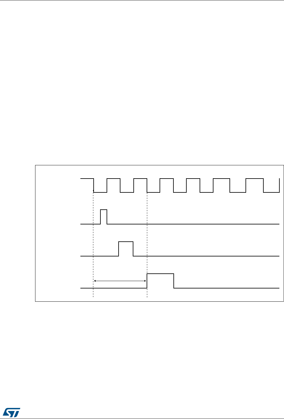
RM0394 Rev 4 397/1600
RM0394 Analog-to-digital converters (ADC)
485
Auto-injection mode
If the JAUTO bit in the ADC_CFGR register is set, then the channels in the injected group
are automatically converted after the regular group of channels. This can be used to convert
a sequence of up to 20 conversions programmed in the ADC_SQRy and ADC_JSQR
registers.
In this mode, the ADSTART bit in the ADC_CR register must be set to start regular
conversions, followed by injected conversions (JADSTART must be kept cleared). Setting
the ADSTP bit aborts both regular and injected conversions (JADSTP bit must not be used).
In this mode, external trigger on injected channels must be disabled.
If the CONT bit is also set in addition to the JAUTO bit, regular channels followed by injected
channels are continuously converted.
Note: It is not possible to use both the auto-injected and discontinuous modes simultaneously.
When the DMA is used for exporting regular sequencer’s data in JAUTO mode, it is
necessary to program it in circular mode (CIRC bit set in DMA_CCRx register). If the CIRC
bit is reset (single-shot mode), the JAUTO sequence will be stopped upon DMA Transfer
Complete event.
Figure 51. Injected conversion latency
1. The maximum latency value can be found in the electrical characteristics of the
STM32L41xxx/42xxx/43xxx/44xxx/45xxx/46xxx datasheet.
!$##,+
AIB
,QMHFWLRQHYHQW
5HVHW$'&
62&
PD[ODWHQF\

Analog-to-digital converters (ADC) RM0394
398/1600 RM0394 Rev 4
16.4.20 Discontinuous mode (DISCEN, DISCNUM, JDISCEN)
Regular group mode
This mode is enabled by setting the DISCEN bit in the ADC_CFGR register.
It is used to convert a short sequence (subgroup) of n conversions (n 8) that is part of the
sequence of conversions selected in the ADC_SQRy registers. The value of n is specified
by writing to the DISCNUM[2:0] bits in the ADC_CFGR register.
When an external trigger occurs, it starts the next n conversions selected in the ADC_SQRy
registers until all the conversions in the sequence are done. The total sequence length is
defined by the L[3:0] bits in the ADC_SQR1 register.
Example:
•DISCEN=1, n=3, channels to be converted = 1, 2, 3, 6, 7, 8, 9, 10, 11
– 1st trigger: channels converted are 1, 2, 3 (an EOC event is generated at each
conversion).
– 2nd trigger: channels converted are 6, 7, 8 (an EOC event is generated at each
conversion).
– 3rd trigger: channels converted are 9, 10, 11 (an EOC event is generated at each
conversion) and an EOS event is generated after the conversion of channel 11.
– 4th trigger: channels converted are 1, 2, 3 (an EOC event is generated at each
conversion).
–...
•DISCEN=0, channels to be converted = 1, 2, 3, 6, 7, 8, 9, 10,11
– 1st trigger: the complete sequence is converted: channel 1, then 2, 3, 6, 7, 8, 9, 10
and 11. Each conversion generates an EOC event and the last one also generates
an EOS event.
– all the next trigger events will relaunch the complete sequence.
Note: When a regular group is converted in discontinuous mode, no rollover occurs (the last
subgroup of the sequence can have less than n conversions).
When all subgroups are converted, the next trigger starts the conversion of the first
subgroup. In the example above, the 4th trigger reconverts the channels 1, 2 and 3 in the
1st subgroup.
It is not possible to have both discontinuous mode and continuous mode enabled. In this
case (if DISCEN=1, CONT=1), the ADC behaves as if continuous mode was disabled.

RM0394 Rev 4 399/1600
RM0394 Analog-to-digital converters (ADC)
485
Injected group mode
This mode is enabled by setting the JDISCEN bit in the ADC_CFGR register. It converts the
sequence selected in the ADC_JSQR register, channel by channel, after an external
injected trigger event. This is equivalent to discontinuous mode for regular channels where
‘n’ is fixed to 1.
When an external trigger occurs, it starts the next channel conversions selected in the
ADC_JSQR registers until all the conversions in the sequence are done. The total sequence
length is defined by the JL[1:0] bits in the ADC_JSQR register.
Example:
•JDISCEN=1, channels to be converted = 1, 2, 3
– 1st trigger: channel 1 converted (a JEOC event is generated)
– 2nd trigger: channel 2 converted (a JEOC event is generated)
– 3rd trigger: channel 3 converted and a JEOC event + a JEOS event are generated
–...
Note: When all injected channels have been converted, the next trigger starts the conversion of
the first injected channel. In the example above, the 4th trigger reconverts the 1st injected
channel 1.
It is not possible to use both auto-injected mode and discontinuous mode simultaneously:
the bits DISCEN and JDISCEN must be kept cleared by software when JAUTO is set.
16.4.21 Queue of context for injected conversions
A queue of context is implemented to anticipate up to 2 contexts for the next injected
sequence of conversions. JQDIS bit of ADC_CFGR register must be reset to enable this
feature. Only hardware-triggered conversions are possible when the context queue is
enabled.
This context consists of:
•Configuration of the injected triggers (bits JEXTEN[1:0] and JEXTSEL bits in
ADC_JSQR register)
•Definition of the injected sequence (bits JSQx[4:0] and JL[1:0] in ADC_JSQR register)
All the parameters of the context are defined into a single register ADC_JSQR and this
register implements a queue of 2 buffers, allowing the bufferization of up to 2 sets of
parameters:
•The JSQR register can be written at any moment even when injected conversions are
ongoing.
•Each data written into the JSQR register is stored into the Queue of context.
•At the beginning, the Queue is empty and the first write access into the JSQR register
immediately changes the context and the ADC is ready to receive injected triggers.
•Once an injected sequence is complete, the Queue is consumed and the context
changes according to the next JSQR parameters stored in the Queue. This new
context is applied for the next injected sequence of conversions.

Analog-to-digital converters (ADC) RM0394
400/1600 RM0394 Rev 4
•A Queue overflow occurs when writing into register JSQR while the Queue is full. This
overflow is signaled by the assertion of the flag JQOVF. When an overflow occurs, the
write access of JSQR register which has created the overflow is ignored and the queue
of context is unchanged. An interrupt can be generated if bit JQOVFIE is set.
•Two possible behaviors are possible when the Queue becomes empty, depending on
the value of the control bit JQM of register ADC_CFGR:
– If JQM=0, the Queue is empty just after enabling the ADC, but then it can never be
empty during run operations: the Queue always maintains the last active context
and any further valid start of injected sequence will be served according to the last
active context.
– If JQM=1, the Queue can be empty after the end of an injected sequence or if the
Queue is flushed. When this occurs, there is no more context in the queue and
hardware triggers are disabled. Therefore, any further hardware injected triggers
are ignored until the software re-writes a new injected context into JSQR register.
•Reading JSQR register returns the current JSQR context which is active at that
moment. When the JSQR context is empty, JSQR is read as 0x0000.
•The Queue is flushed when stopping injected conversions by setting JADSTP=1 or
when disabling the ADC by setting ADDIS=1:
– If JQM=0, the Queue is maintained with the last active context.
– If JQM=1, the Queue becomes empty and triggers are ignored.
Note: When configured in discontinuous mode (bit JDISCEN=1), only the last trigger of the
injected sequence changes the context and consumes the Queue.The 1st trigger only
consumes the queue but others are still valid triggers as shown by the discontinuous mode
example below (length = 3 for both contexts):
•
1st trigger, discontinuous. Sequence 1: context 1 consumed, 1st conversion carried out
•
2nd trigger, disc. Sequence 1: 2nd conversion.
•
3rd trigger, discontinuous. Sequence 1: 3rd conversion.
•
4th trigger, discontinuous. Sequence 2: context 2 consumed, 1st conversion carried out.
•
5th trigger, discontinuous. Sequence 2: 2nd conversion.
•
6th trigger, discontinuous. Sequence 2: 3rd conversion.
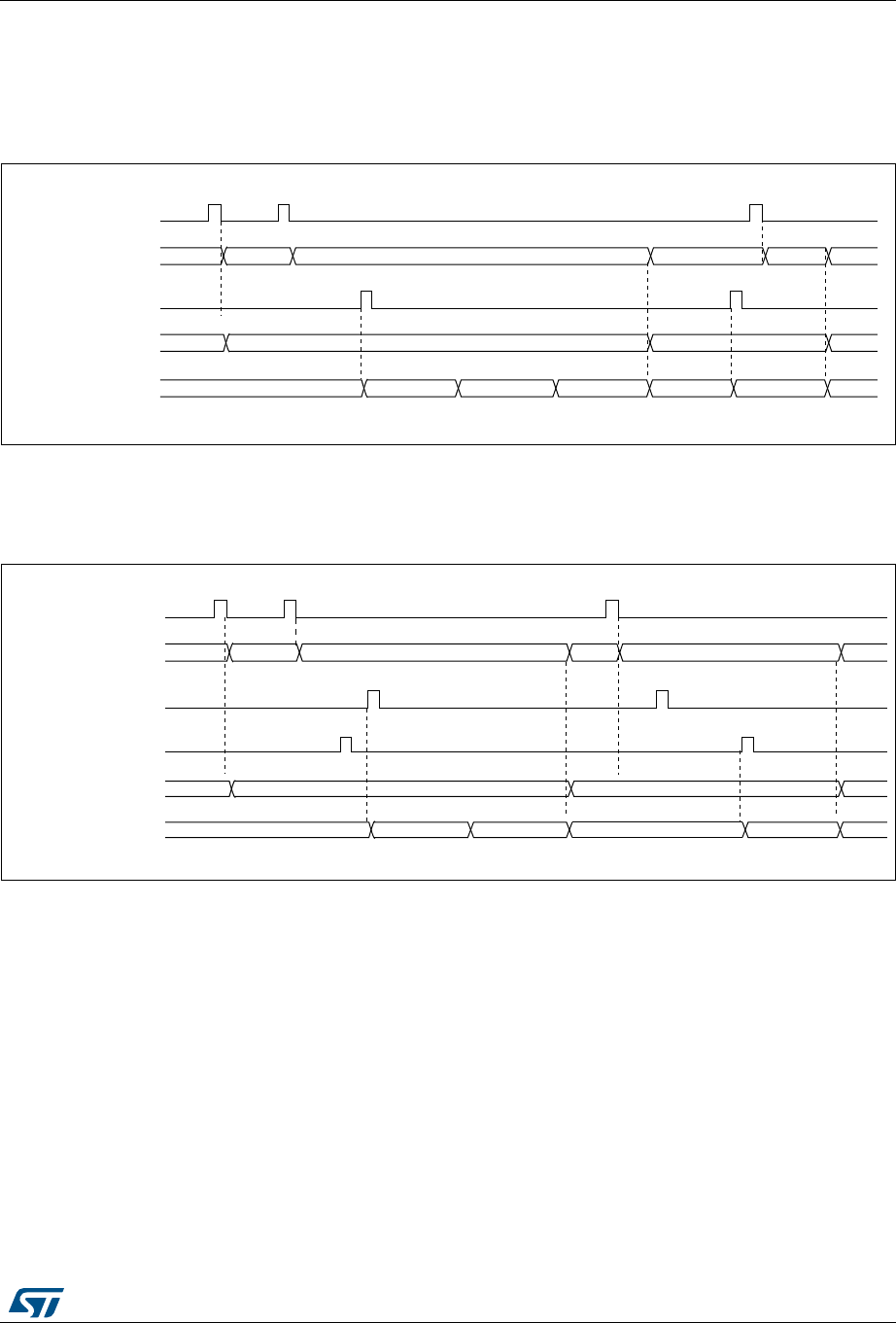
RM0394 Rev 4 401/1600
RM0394 Analog-to-digital converters (ADC)
485
Behavior when changing the trigger or sequence context
The Figure 52 and Figure 53 show the behavior of the context Queue when changing the
sequence or the triggers.
Figure 52. Example of JSQR queue of context (sequence change)
1. Parameters:
P1: sequence of 3 conversions, hardware trigger 1
P2: sequence of 1 conversion, hardware trigger 1
P3: sequence of 4 conversions, hardware trigger 1
Figure 53. Example of JSQR queue of context (trigger change)
1. Parameters:
P1: sequence of 2 conversions, hardware trigger 1
P2: sequence of 1 conversion, hardware trigger 2
P3: sequence of 4 conversions, hardware trigger 1
069
3 3 3
(037<
&RQYHUVLRQ &RQYHUVLRQ &RQYHUVLRQ
3 33 33
3 3
3 3 3
(037<
5'< 5'< 5'<&RQYHUVLRQ
-645TXHXH
:ULWH-645
7ULJJHU
$'&VWDWH
$'&-FRQWH[W
UHWXUQHGE\UHDGLQJ
-465
069
3 3 3
&RQYHUVLRQ &RQYHUVLRQ5'< 5'< 5'<&RQYHUVLRQ
3 3 3(037<
(037< 3 33 33
3 3
,JQRUHG
,JQRUHG
-645TXHXH
:ULWH-645
7ULJJHU
$'&VWDWH
$'&-FRQWH[W
UHWXUQHGE\UHDGLQJ
-465
7ULJJHU
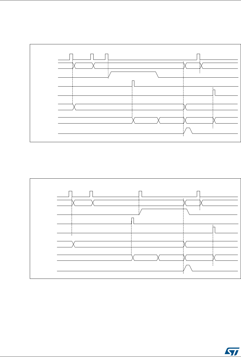
Analog-to-digital converters (ADC) RM0394
402/1600 RM0394 Rev 4
Queue of context: Behavior when a queue overflow occurs
The Figure 54 and Figure 55 show the behavior of the context Queue if an overflow occurs
before or during a conversion.
Figure 54. Example of JSQR queue of context with overflow before conversion
1. Parameters:
P1: sequence of 2 conversions, hardware trigger 1
P2: sequence of 1 conversion, hardware trigger 2
P3: sequence of 3 conversions, hardware trigger 1
P4: sequence of 4 conversions, hardware trigger 1
Figure 55. Example of JSQR queue of context with overflow during conversion
1. Parameters:
P1: sequence of 2 conversions, hardware trigger 1
P2: sequence of 1 conversion, hardware trigger 2
P3: sequence of 3 conversions, hardware trigger 1
P4: sequence of 4 conversions, hardware trigger 1
069
-645
TXHXH
:ULWH-645
3 3
(037<
7ULJJHU
$'&VWDWH &RQYHUVLRQ5'< &RQYHUVLRQ 5'<
3
-429)
&OHDUHGE\6:
3 33
3
3
33(037<
33
!2YHUIORZ
LJQRUHG
-(26
$'&
-FRQWH[W
UHWXUQHGE\
UHDGLQJ-465
7ULJJHU
&RQYHUVLRQ
069
-645
TXHXH
:ULWH-645
3 3
(037<
7ULJJHU
$'&VWDWH &RQYHUVLRQ5'< &RQYHUVLRQ 5'<
3
-429)
&OHDUHGE\6:
3 33
3
3
33(037<
33
!2YHUIORZ
LJQRUHG
-(26
$'&
-FRQWH[W
UHWXUQHGE\
UHDGLQJ-465
7ULJJHU
&RQYHUVLRQ
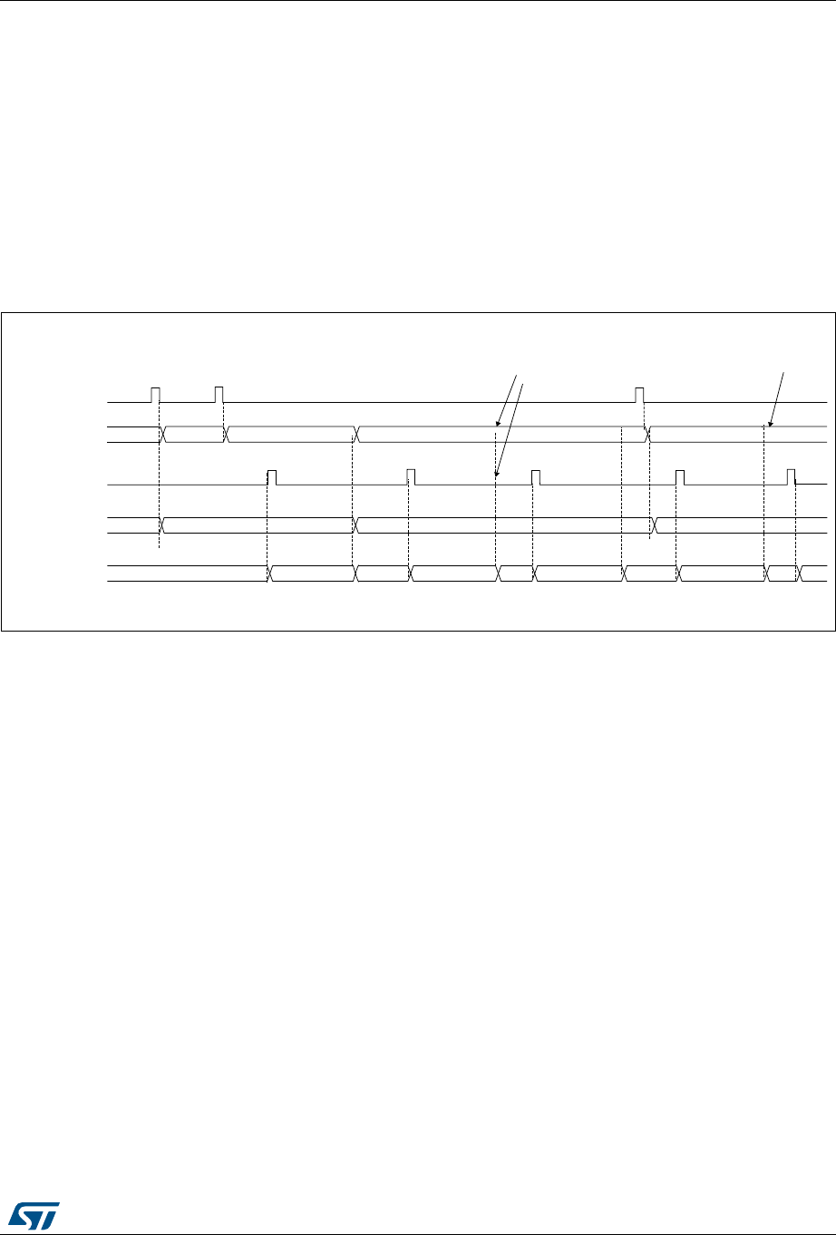
RM0394 Rev 4 403/1600
RM0394 Analog-to-digital converters (ADC)
485
It is recommended to manage the queue overflows as described below:
•After each P context write into JSQR register, flag JQOVF shows if the write has been
ignored or not (an interrupt can be generated).
•Avoid Queue overflows by writing the third context (P3) only once the flag JEOS of the
previous context P2 has been set. This ensures that the previous context has been
consumed and that the queue is not full.
Queue of context: Behavior when the queue becomes empty
Figure 56 and Figure 57 show the behavior of the context Queue when the Queue becomes
empty in both cases JQM=0 or 1.
Figure 56. Example of JSQR queue of context with empty queue (case JQM=0)
1. Parameters:
P1: sequence of 1 conversion, hardware trigger 1
P2: sequence of 1 conversion, hardware trigger 1
P3: sequence of 1 conversion, hardware trigger 1
Note: When writing P3, the context changes immediately. However, because of internal
resynchronization, there is a latency and if a trigger occurs just after or before writing P3, it
can happen that the conversion is launched considering the context P2. To avoid this
situation, the user must ensure that there is no ADC trigger happening when writing a new
context that applies immediately.
069
3
7KHTXHXHLVQRWHPSW\
DQGPDLQWDLQV3EHFDXVH-40
4XHXHQRWHPSW\
3PDLQWDLQHG
3 3
#ONVERSION #ONVERSION
5'< 5'< 5'< 5'<
#ONVERSION #ONVERSION #ONV
5'<
(037< 3 3 3
33 3 3
(037< 3
-645TXHXH
:ULWH-645
7ULJJHU
$'&VWDWH
$'&-FRQWH[W
UHWXUQHGE\
UHDGLQJ-465
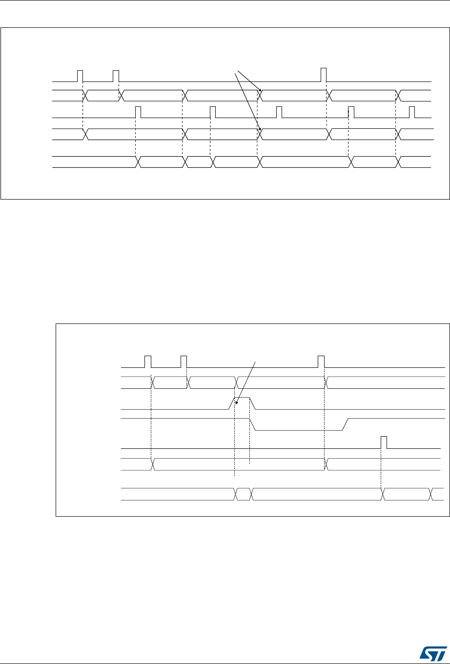
Analog-to-digital converters (ADC) RM0394
404/1600 RM0394 Rev 4
Figure 57. Example of JSQR queue of context with empty queue (case JQM=1)
1. Parameters:
P1: sequence of 1 conversion, hardware trigger 1
P2: sequence of 1 conversion, hardware trigger 1
P3: sequence of 1 conversion, hardware trigger 1
Flushing the queue of context
The figures below show the behavior of the context Queue in various situations when the
queue is flushed.
Figure 58. Flushing JSQR queue of context by setting JADSTP=1 (JQM=0).
Case when JADSTP occurs during an ongoing conversion.
1. Parameters:
P1: sequence of 1 conversion, hardware trigger 1
P2: sequence of 1 conversion, hardware trigger 1
P3: sequence of 1 conversion, hardware trigger 1
)GNORED
1UEUEBECOMESEMPTY
ANDTRIGGERSAREIGNORED
BECAUSE*1-
-36
3 3 3
(037<
&RQYHUVLRQ &RQYHUVLRQ
3 33 33
3 3 3
(037<
5'< 5'< 5'<&RQYHUVLRQ
-645
TXHXH
:ULWH-645
7U L J J HU
$'&VWDWH
$'&
-FRQWH[W
UHWXUQHGE\UHDGLQJ-465
5'<
(037<[
(037< (037<
(037<
)GNORED
069
-645TXHXH
:ULWH-645
3
3
3
(037<
7ULJJHU
$'&VWDWH 5'< 673
3
3 3
33
5'<
3
(037<
-$'673
3
5'<
4XHXHLVIOXVKHGDQGPDLQWDLQV
WKHODVWDFWLYHFRQWH[W
3LVORVW
-$'67$57
$'&-FRQWH[W
UHWXUQHGE\UHDGLQJ-645
6HW
E\6:
5HVHW
E\+:
&RQYHUVLRQ
5HVHW
E\+: 6HW
E\6:
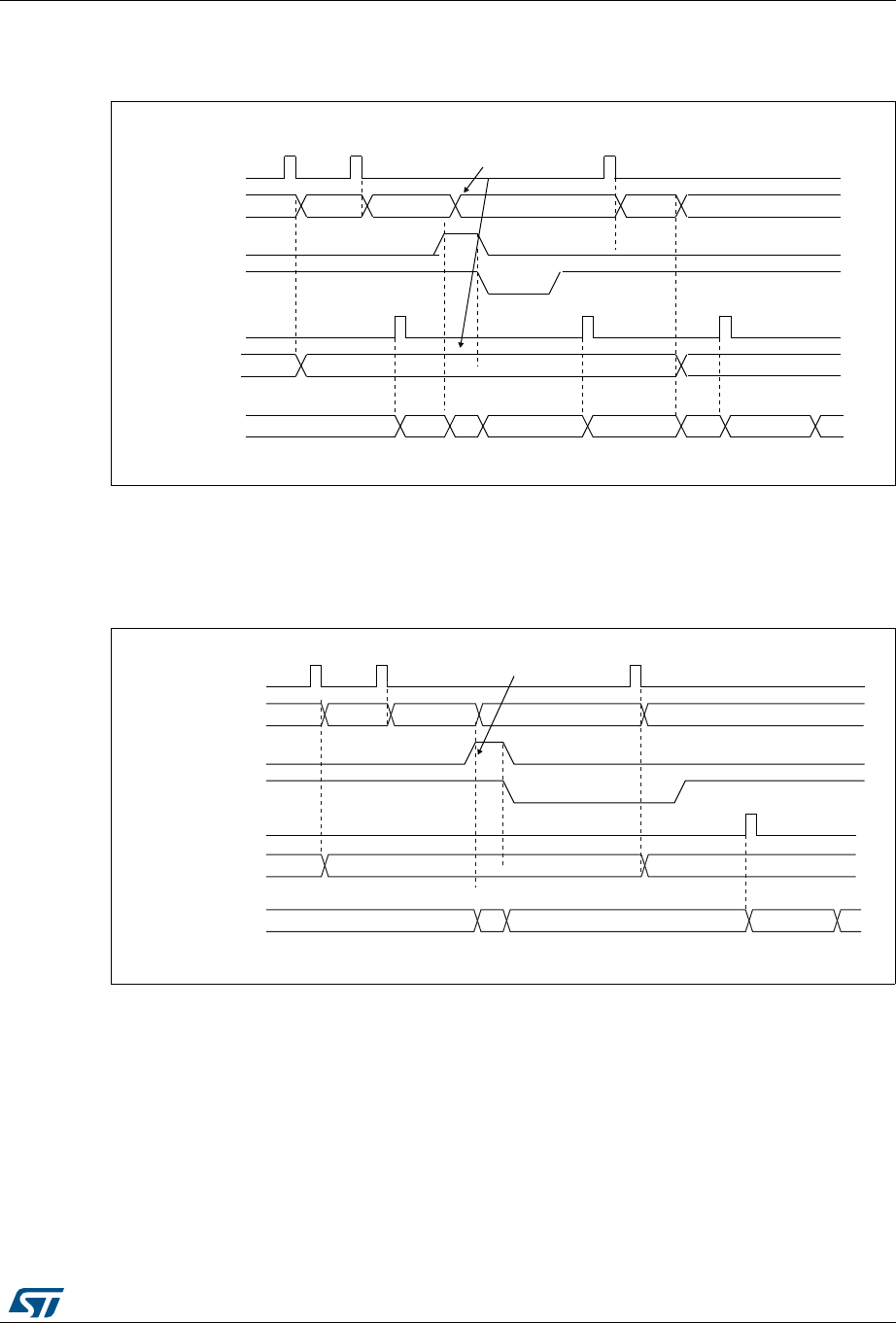
RM0394 Rev 4 405/1600
RM0394 Analog-to-digital converters (ADC)
485
Figure 59. Flushing JSQR queue of context by setting JADSTP=1 (JQM=0).
Case when JADSTP occurs during an ongoing conversion and a new
trigger occurs.
1. Parameters:
P1: sequence of 1 conversion, hardware trigger 1
P2: sequence of 1 conversion, hardware trigger 1
P3: sequence of 1 conversion, hardware trigger 1
Figure 60. Flushing JSQR queue of context by setting JADSTP=1 (JQM=0).
Case when JADSTP occurs outside an ongoing conversion
1. Parameters:
P1: sequence of 1 conversion, hardware trigger 1
P2: sequence of 1 conversion, hardware trigger 1
P3: sequence of 1 conversion, hardware trigger 1
*312
QUEUE
7RITE*312
0
0
0
%-049
4RIGGER
!$#STATE 2$9
340
0
0 0
00
#ONVERSION 2$9
000
%-049
*!$340
2$9
0
2$9
1UEUEISFLUSHEDANDMAINTAINS
THELASTACTIVECONTEXT
0ISLOST
!BORTED
*!$34!24
!$#*
CONTEXT
RETURNEDBYREADING*312
3ET
BY37
2ESET
BY(7
-36
#ONVERSION
#ONV
2ESET
BY(7 3ET
BY37
069
-645TXHXH
:ULWH-645
3
3
3
(037<
7ULJJHU
$'&VWDWH 5'<
673
3
3 3
33
5'<
3
(037<
-$'673
3
5'<
WKHODVWDFWLYHFRQWH[W
3LVORVW
-$'67$57
$'&-FRQWH[W
UHWXUQHGE\
UHDGLQJ-645
6HW
E\6:
5HVHW
E\+:
&RQYHUVLRQ
5HVHW
E\+: 6HW
E\6:
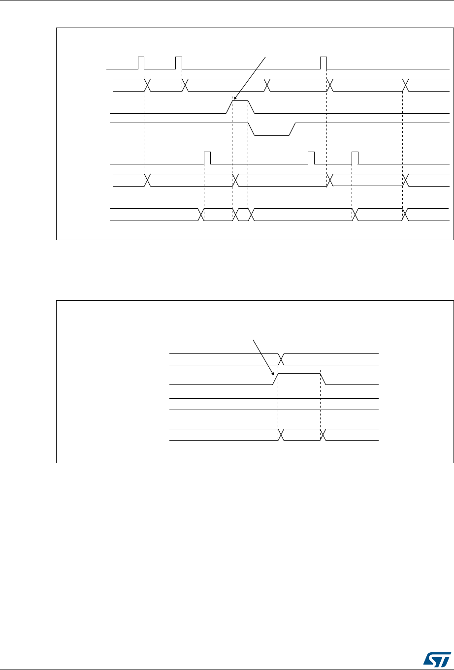
Analog-to-digital converters (ADC) RM0394
406/1600 RM0394 Rev 4
Figure 61. Flushing JSQR queue of context by setting JADSTP=1 (JQM=1)
1. Parameters:
P1: sequence of 1 conversion, hardware trigger 1
P2: sequence of 1 conversion, hardware trigger 1
P3: sequence of 1 conversion, hardware trigger 1
Figure 62. Flushing JSQR queue of context by setting ADDIS=1 (JQM=0)
1. Parameters:
P1: sequence of 1 conversion, hardware trigger 1
P2: sequence of 1 conversion, hardware trigger 1
P3: sequence of 1 conversion, hardware trigger 1
*312QUEUE
7RITE*312
0
0
0
%-049
4RIGGER
!$#STATE 2$9
340
0
0 0
00
%-049
*!$340
2$9
0
2$9
1UEUEISFLUSHEDAND
BECOMESEMPTY0ISLOST
!BORTED
*!$34!24
!$#*CONTEXT
RETURNEDBYREADING*312
3ET
BY37
2ESET
BY(7
-36
#ONVERSION
#ONV
2ESET
BY(7
3ET
BY37
%-049
%-049X %-049
)GNORED
%-049
*312QUEUE
!$#STATE 2$9
0
00
2%1/&&
0
!$$)3
1UEUEISFLUSHEDANDMAINTAINS
THELASTACTIVECONTEXT
0WHICHWASNOTCONSUMEDISLOST
!$#*CONTEXT
RETURNEDBYREADING*312
3ET
BY37
2ESET
BY(7
-36
/&&

RM0394 Rev 4 407/1600
RM0394 Analog-to-digital converters (ADC)
485
Figure 63. Flushing JSQR queue of context by setting ADDIS=1 (JQM=1)
1. Parameters:
P1: sequence of 1 conversion, hardware trigger 1
P2: sequence of 1 conversion, hardware trigger 1
P3: sequence of 1 conversion, hardware trigger 1
Queue of context: Starting the ADC with an empty queue
The following procedure must be followed to start ADC operation with an empty queue, in
case the first context is not known at the time the ADC is initialized. This procedure is only
applicable when JQM bit is reset:
5. Write a dummy JSQR with JEXTEN not equal to 0 (otherwise triggering a software
conversion)
6. Set JADSTART
7. Set JADSTP
8. Wait until JADSTART is reset
9. Set JADSTART.
Disabling the queue
It is possible to disable the queue by setting bit JQDIS=1 into the ADC_CFGR register.
16.4.22 Programmable resolution (RES) - fast conversion mode
It is possible to perform faster conversion by reducing the ADC resolution.
The resolution can be configured to be either 12, 10, 8, or 6 bits by programming the control
bits RES[1:0]. Figure 68, Figure 69, Figure 70 and Figure 71 show the conversion result
format with respect to the resolution as well as to the data alignment.
Lower resolution allows faster conversion time for applications where high-data precision is
not required. It reduces the conversion time spent by the successive approximation steps
according to Table 61.
*312QUEUE
!$#STATE 2$9
0
00
2%1/&&
%-049
!$$)3
1UEUEISFLUSHEDANDBEOMESEMPTY
*312ISREADASX
!$#*CONTEXT
RETURNEDBYREADING*312
3ET
BY37
2ESET
BY(7
-36
/&&
%-049X

Analog-to-digital converters (ADC) RM0394
408/1600 RM0394 Rev 4
16.4.23 End of conversion, end of sampling phase (EOC, JEOC, EOSMP)
The ADC notifies the application for each end of regular conversion (EOC) event and each
injected conversion (JEOC) event.
The ADC sets the EOC flag as soon as a new regular conversion data is available in the
ADC_DR register. An interrupt can be generated if bit EOCIE is set. EOC flag is cleared by
the software either by writing 1 to it or by reading ADC_DR.
The ADC sets the JEOC flag as soon as a new injected conversion data is available in one
of the ADC_JDRy register. An interrupt can be generated if bit JEOCIE is set. JEOC flag is
cleared by the software either by writing 1 to it or by reading the corresponding ADC_JDRy
register.
The ADC also notifies the end of Sampling phase by setting the status bit EOSMP (for
regular conversions only). EOSMP flag is cleared by software by writing 1 to it. An interrupt
can be generated if bit EOSMPIE is set.
16.4.24 End of conversion sequence (EOS, JEOS)
The ADC notifies the application for each end of regular sequence (EOS) and for each end
of injected sequence (JEOS) event.
The ADC sets the EOS flag as soon as the last data of the regular conversion sequence is
available in the ADC_DR register. An interrupt can be generated if bit EOSIE is set. EOS
flag is cleared by the software either by writing 1 to it.
The ADC sets the JEOS flag as soon as the last data of the injected conversion sequence is
complete. An interrupt can be generated if bit JEOSIE is set. JEOS flag is cleared by the
software either by writing 1 to it.
Table 61. TSAR timings depending on resolution
RES
(bits)
TSAR
(ADC clock cycles)
TSAR (ns) at
FADC=80 MHz
TCONV (ADC clock cycles)
(with Sampling Time=
2.5 ADC clock cycles)
TCONV (ns) at
FADC=80 MHz
12 12.5 ADC clock cycles 156.25 ns 15 ADC clock cycles 187.5 ns
10 10.5 ADC clock cycles 131.25 ns 13 ADC clock cycles 162.5 ns
8 8.5 ADC clock cycles 106.25 ns 11 ADC clock cycles 137.5 ns
6 6.5 ADC clock cycles 81.25 ns 9 ADC clock cycles 112.5 ns
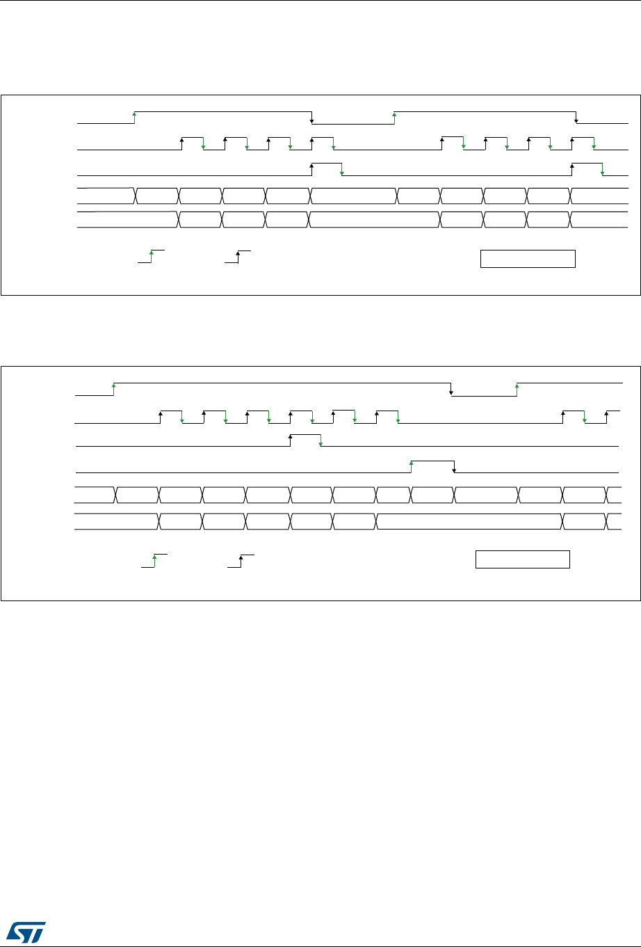
RM0394 Rev 4 409/1600
RM0394 Analog-to-digital converters (ADC)
485
16.4.25 Timing diagrams example (single/continuous modes,
hardware/software triggers)
Figure 64. Single conversions of a sequence, software trigger
1. EXTEN=0x0, CONT=0
2. Channels selected = 1,9, 10, 17; AUTDLY=0.
Figure 65. Continuous conversion of a sequence, software trigger
1. EXTEN=0x0, CONT=1
2. Channels selected = 1,9, 10, 17; AUTDLY=0.
5'<
$'67$57
(2&
(26
$'&VWDWH &+
E\VZ E\KZ
&+ 5'<
&+ &+ &+ &+ &+ &+ 5'<
$'&B'5 ' ' ' ' ' ' '
069
,QGLFDWLYHWLPLQJV
'
$'67$57
(2&
(26
$'673
$'&VWDWH
$'&B'5
-36
5($'< &+ &+ &+
&+ &+ &+ &+ 673 5($'< &+
' ' ' ' ' '
'
&+
E\VZ E\KZ ,QGLFDWLYHWLPLQJV
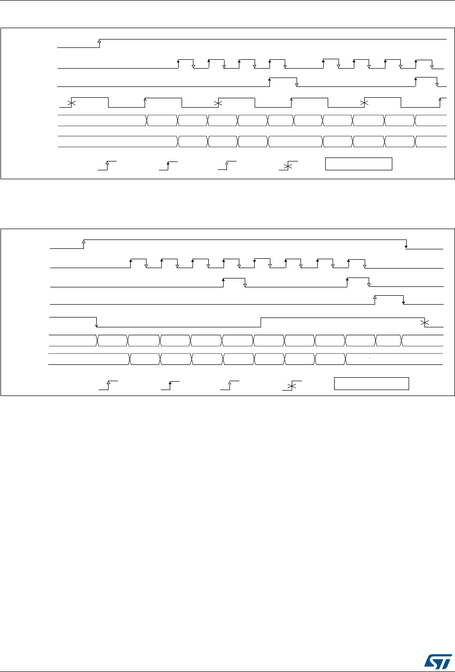
Analog-to-digital converters (ADC) RM0394
410/1600 RM0394 Rev 4
Figure 66. Single conversions of a sequence, hardware trigger
1. TRGx (over-frequency) is selected as trigger source, EXTEN = 01, CONT = 0
2. Channels selected = 1, 2, 3, 4; AUTDLY=0.
Figure 67. Continuous conversions of a sequence, hardware trigger
1. TRGx is selected as trigger source, EXTEN = 10, CONT = 1
2. Channels selected = 1, 2, 3, 4; AUTDLY=0.
16.4.26 Data management
Data register, data alignment and offset (ADC_DR, OFFSETy, OFFSETy_CH,
ALIGN)
Data and alignment
At the end of each regular conversion channel (when EOC event occurs), the result of the
converted data is stored into the ADC_DR data register which is 16 bits wide.
At the end of each injected conversion channel (when JEOC event occurs), the result of the
converted data is stored into the corresponding ADC_JDRy data register which is 16 bits
wide.
The ALIGN bit in the ADC_CFGR register selects the alignment of the data stored after
conversion. Data can be right- or left-aligned as shown in Figure 68, Figure 69, Figure 70
069
(2&
(26
75*;
$'&B'5
5'< &+ &+ 5($'<
&+ &+ &+ &+ &+ &+ 5'<
' ' ' ' ''
E\VZ E\KZ
' '
WULJJHUHG LJQRUHG
$'67$57
$'&VWDWH
,QGLFDWLYHWLPLQJV
069
(2&
(26
75*[
$'&B'5
5'< &+ &+ &+
&+ &+ &+ &+ &+ &+ 5'<
' ' ' ' ''
E\VZ E\KZ 1RWLQVFDOHWLPLQJV
' '
WULJJHUHG LJQRUHG
6723
$'673
$'67$57
$'&

RM0394 Rev 4 411/1600
RM0394 Analog-to-digital converters (ADC)
485
and Figure 71.
Special case: when left-aligned, the data are aligned on a half-word basis except when the
resolution is set to 6-bit. In that case, the data are aligned on a byte basis as shown in
Figure 70 and Figure 71.
Note: Left-alignment is not supported in oversampling mode. When ROVSE and/or JOVSE bit is
set, the ALIGN bit value is ignored and the ADC only provides right-aligned data.
Offset
An offset y (y=1,2,3,4) can be applied to a channel by setting the bit OFFSETy_EN=1 into
ADC_OFRy register. The channel to which the offset will be applied is programmed into the
bits OFFSETy_CH[4:0] of ADC_OFRy register. In this case, the converted value is
decreased by the user-defined offset written in the bits OFFSETy[11:0]. The result may be a
negative value so the read data is signed and the SEXT bit represents the extended sign
value.
Note: Offset correction is not supported in oversampling mode. When ROVSE and/or JOVSE bit is
set, the value of the OFFSETy_EN bit in ADC_OFRy register is ignored (considered as
reset).
Table 64 describes how the comparison is performed for all the possible resolutions for
analog watchdog 1.
When reading data from ADC_DR (regular channel) or from ADC_JDRy (injected channel,
y=1,2,3,4) corresponding to the channel “i”:
•If one of the offsets is enabled (bit OFFSETy_EN=1) for the corresponding channel, the
read data is signed.
•If none of the four offsets is enabled for this channel, the read data is not signed.
Figure 68, Figure 69, Figure 70 and Figure 71 show alignments for signed and unsigned
data.
Table 62. Offset computation versus data resolution
Resolution
(bits
RES[1:0])
Subtraction between raw
converted data and offset
Result Comments
Raw
converted
Data, left
aligned
Offset
00: 12-bit DATA[11:0] OFFSET[11:0] Signed
12-bit data -
01: 10-bit DATA[11:2],00 OFFSET[11:0] Signed
10-bit data
The user must configure OFFSET[1:0]
to “00”
10: 8-bit DATA[11:4],00
00 OFFSET[11:0] Signed
8-bit data
The user must configure OFFSET[3:0]
to “0000”
11: 6-bit DATA[11:6],00
0000 OFFSET[11:0] Signed
6-bit data
The user must configure OFFSET[5:0]
to “000000”
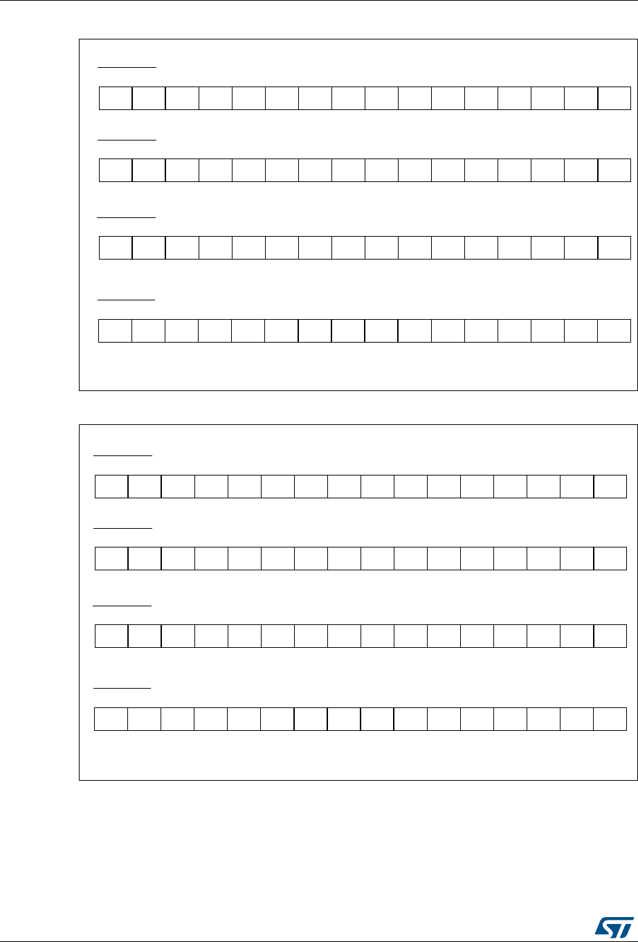
Analog-to-digital converters (ADC) RM0394
412/1600 RM0394 Rev 4
Figure 68. Right alignment (offset disabled, unsigned value)
Figure 69. Right alignment (offset enabled, signed value)
'''''
ELWGDWD
' ' ' ' ' '
'
ELWGDWD
' ' ' ' ' '
'''
ELWGDWD
' ' ' ' ' '
ELWGDWD
'''''
'
'
'
'
ELW ELWELW
ELW ELWELW
ELW ELWELW
ELW ELWELW
069
6(;7 6(;7 6(;7 6(;7 ' ' ' ' '
ELWGDWD
' ' ' ' ' '
'
ELWGDWD
' ' ' ' ' '
6(;7 6(;7 6(;7 6(;7 6(;7 6(;7 ' ' '
ELWGDWD
' ' ' ' ' '
ELWGDWD
' ' ' '
'
'
'
'
ELW ELWELW
ELW ELWELW
ELW ELWELW
ELW ELWELW
069
6(;7 6(;7 6(;7 6(;7 6(;7 6(;7 6(;7 6(;7
'
6(;7 6(;7 6(;7 6(;7 6(;7 6(;7 6(;7 6(;7 6(;7 6(;7
RM0394 Rev 4 413/1600
RM0394 Analog-to-digital converters (ADC)
485
Figure 70. Left alignment (offset disabled, unsigned value)
Figure 71. Left alignment (offset enabled, signed value)
ELWGDWD
ELWGDWD
ELWGDWD
ELWGDWD
ELW ELWELW
ELW ELWELW
ELW ELWELW
ELW ELWELW
069
' ' ' ' ' ' ' ' ' ' ' '
' ' ' ' ' ' ' '
' ' ' ' ' ' ' ' ' '
'''''
'
ELWGDWD
ELWGDWD
ELWGDWD
ELWGDWD
ELW ELWELW
ELW ELWELW
ELW ELWELW
ELW ELWELW
069
6(;7 ' ' ' ' ' ' ' ' ' ' ' '
6(;7 ' ' ' ' ' ' ' '
6(;7 ' ' ' ' ' ' ' ' ' '
6(;7 6(;7 6(;7 6(;7 6(;7 6(;7 6(;7 ' ' ' ' ' '
6(;7 6(;7
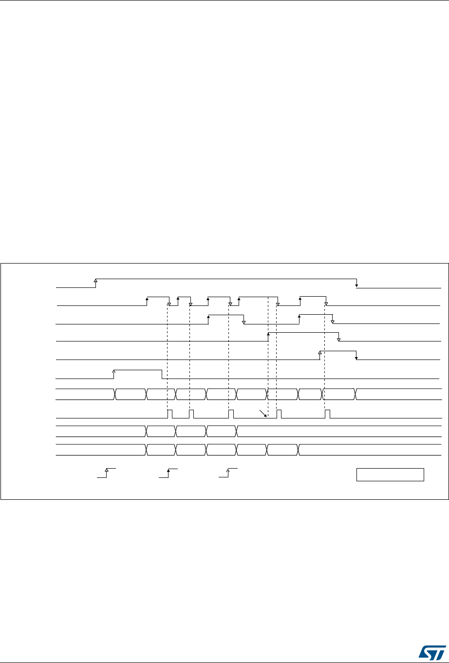
Analog-to-digital converters (ADC) RM0394
414/1600 RM0394 Rev 4
ADC overrun (OVR, OVRMOD)
The overrun flag (OVR) notifies of a buffer overrun event, when the regular converted data
was not read (by the CPU or the DMA) before new converted data became available.
The OVR flag is set if the EOC flag is still 1 at the time when a new conversion completes.
An interrupt can be generated if bit OVRIE=1.
When an overrun condition occurs, the ADC is still operating and can continue to convert
unless the software decides to stop and reset the sequence by setting bit ADSTP=1.
OVR flag is cleared by software by writing 1 to it.
It is possible to configure if data is preserved or overwritten when an overrun event occurs
by programming the control bit OVRMOD:
•OVRMOD=0: The overrun event preserves the data register from being overrun: the
old data is maintained and the new conversion is discarded and lost. If OVR remains at
1, any further conversions will occur but the result data will be also discarded.
•OVRMOD=1: The data register is overwritten with the last conversion result and the
previous unread data is lost. If OVR remains at 1, any further conversions will operate
normally and the ADC_DR register will always contain the latest converted data.
Figure 72. Example of overrun (OVR)
Note: There is no overrun detection on the injected channels since there is a dedicated data
register for each of the four injected channels.
Managing a sequence of conversion without using the DMA
If the conversions are slow enough, the conversion sequence can be handled by the
software. In this case the software must use the EOC flag and its associated interrupt to
handle each data. Each time a conversion is complete, EOC is set and the ADC_DR
register can be read. OVRMOD should be configured to 0 to manage overrun events as an
error.
2YHUXQ
-36
$'67$57
(2&
(26
75*[
$'&VWDWH
$'&B'5UHDGDFFHVV
E\VZ E\KZ ,QGLFDWLYHWLPLQJV
WULJJHUHG
5'< &+ &+ &+
&+ &+ &+ &+ 6723 5'<
'
'
'' '
' '
' ' '
$'673
295
$'&B'5
29502'
$'&B'5
29502'

RM0394 Rev 4 415/1600
RM0394 Analog-to-digital converters (ADC)
485
Managing conversions without using the DMA and without overrun
It may be useful to let the ADC convert one or more channels without reading the data each
time (if there is an analog watchdog for instance). In this case, the OVRMOD bit must be
configured to 1 and OVR flag should be ignored by the software. An overrun event will not
prevent the ADC from continuing to convert and the ADC_DR register will always contain
the latest conversion.
Managing conversions using the DMA
Since converted channel values are stored into a unique data register, it is useful to use
DMA for conversion of more than one channel. This avoids the loss of the data already
stored in the ADC_DR register.
When the DMA mode is enabled (DMAEN bit set to 1 in the ADC_CFGR register in single
ADC mode or MDMA different from 0b00 in dual ADC mode), a DMA request is generated
after each conversion of a channel. This allows the transfer of the converted data from the
ADC_DR register to the destination location selected by the software.
Despite this, if an overrun occurs (OVR=1) because the DMA could not serve the DMA
transfer request in time, the ADC stops generating DMA requests and the data
corresponding to the new conversion is not transferred by the DMA. Which means that all
the data transferred to the RAM can be considered as valid.
Depending on the configuration of OVRMOD bit, the data is either preserved or overwritten
(refer to Section : ADC overrun (OVR, OVRMOD)).
The DMA transfer requests are blocked until the software clears the OVR bit.
Two different DMA modes are proposed depending on the application use and are
configured with bit DMACFG of the ADC_CFGR register in single ADC mode, or with bit
DMACFG of the ADC_CCR register in dual ADC mode:
•DMA one shot mode (DMACFG=0).
This mode is suitable when the DMA is programmed to transfer a fixed number of data.
•DMA circular mode (DMACFG=1)
This mode is suitable when programming the DMA in circular mode.
DMA one shot mode (DMACFG=0)
In this mode, the ADC generates a DMA transfer request each time a new conversion data
is available and stops generating DMA requests once the DMA has reached the last DMA
transfer (when DMA_EOT interrupt occurs - refer to DMA paragraph) even if a conversion
has been started again.
When the DMA transfer is complete (all the transfers configured in the DMA controller have
been done):
•The content of the ADC data register is frozen.
•Any ongoing conversion is aborted with partial result discarded.
•No new DMA request is issued to the DMA controller. This avoids generating an
overrun error if there are still conversions which are started.
•Scan sequence is stopped and reset.
•The DMA is stopped.

Analog-to-digital converters (ADC) RM0394
416/1600 RM0394 Rev 4
DMA circular mode (DMACFG=1)
In this mode, the ADC generates a DMA transfer request each time a new conversion data
is available in the data register, even if the DMA has reached the last DMA transfer. This
allows configuring the DMA in circular mode to handle a continuous analog input data
stream.
16.4.27 Managing conversions using the DFSDM
The ADC conversion results can be transferred directly to the Digital filter for sigma delta
modulators (DFSDM).
In this case, the DFSDMCFG bit must be set to 1 and DMAEN bit must be cleared to 0.
The ADC transfers all the 16 bits of the regular data register data to the DFSDM and resets
the EOC flag once the transfer is complete.
The data format must be 16-bit signed:
ADC_DR[15:12] = sign extended
ADC_DR[11] = sign
ADC_DR[11:0] = data
To obtain 16-bit signed format in 12-bit ADC mode, the software needs to configure the
OFFSETy[11:0] to 0x800 after having set OFFSETy_EN to 1.
Only right aligned data format is available for the DFSDM interface (see Figure 69: Right
alignment (offset enabled, signed value)).
16.4.28 Dynamic low-power features
Auto-delayed conversion mode (AUTDLY)
The ADC implements an auto-delayed conversion mode controlled by the AUTDLY
configuration bit. Auto-delayed conversions are useful to simplify the software as well as to
optimize performance of an application clocked at low frequency where there would be risk
of encountering an ADC overrun.
When AUTDLY=1, a new conversion can start only if all the previous data of the same group
has been treated:
•For a regular conversion: once the ADC_DR register has been read or if the EOC bit
has been cleared (see Figure 73).
•For an injected conversion: when the JEOS bit has been cleared (see Figure 74).
This is a way to automatically adapt the speed of the ADC to the speed of the system which
will read the data.
The delay is inserted after each regular conversion (whatever DISCEN=0 or 1) and after
each sequence of injected conversions (whatever JDISCEN=0 or 1).
Note: There is no delay inserted between each conversions of the injected sequence, except after
the last one.
During a conversion, a hardware trigger event (for the same group of conversions) occurring
during this delay is ignored.

RM0394 Rev 4 417/1600
RM0394 Analog-to-digital converters (ADC)
485
Note: This is not true for software triggers where it remains possible during this delay to set the
bits ADSTART or JADSTART to restart a conversion: it is up to the software to read the data
before launching a new conversion.
No delay is inserted between conversions of different groups (a regular conversion followed
by an injected conversion or conversely):
•If an injected trigger occurs during the automatic delay of a regular conversion, the
injected conversion starts immediately (see Figure 74).
•Once the injected sequence is complete, the ADC waits for the delay (if not ended) of
the previous regular conversion before launching a new regular conversion (see
Figure 76).
The behavior is slightly different in auto-injected mode (JAUTO=1) where a new regular
conversion can start only when the automatic delay of the previous injected sequence of
conversion has ended (when JEOS has been cleared). This is to ensure that the software
can read all the data of a given sequence before starting a new sequence (see Figure 77).
To stop a conversion in continuous auto-injection mode combined with autodelay mode
(JAUTO=1, CONT=1 and AUTDLY=1), follow the following procedure:
1. Wait until JEOS=1 (no more conversions are restarted)
2. Clear JEOS,
3. Set ADSTP=1
4. Read the regular data.
If this procedure is not respected, a new regular sequence can restart if JEOS is cleared
after ADSTP has been set.
In AUTDLY mode, a hardware regular trigger event is ignored if it occurs during an already
ongoing regular sequence or during the delay that follows the last regular conversion of the
sequence. It is however considered pending if it occurs after this delay, even if it occurs
during an injected sequence of the delay that follows it. The conversion then starts at the
end of the delay of the injected sequence.
In AUTDLY mode, a hardware injected trigger event is ignored if it occurs during an already
ongoing injected sequence or during the delay that follows the last injected conversion of
the sequence.
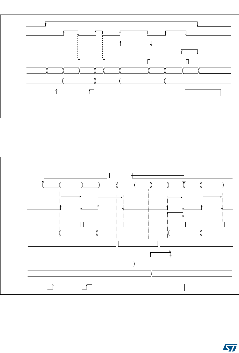
Analog-to-digital converters (ADC) RM0394
418/1600 RM0394 Rev 4
Figure 73. AUTODLY=1, regular conversion in continuous mode, software trigger
1. AUTDLY=1
2. Regular configuration: EXTEN=0x0 (SW trigger), CONT=1, CHANNELS = 1,2,3
3. Injected configuration DISABLED
Figure 74. AUTODLY=1, regular HW conversions interrupted by injected conversions
(DISCEN=0; JDISCEN=0)
1. AUTDLY=1
2. Regular configuration: EXTEN=0x1 (HW trigger), CONT=0, DISCEN=0, CHANNELS = 1, 2, 3
3. Injected configuration: JEXTEN=0x1 (HW Trigger), JDISCEN=0, CHANNELS = 5,6
$'&B'5
069
$'67$57
(2&
(26
$'&VWDWH
$'&B'5UHDGDFFHVV
E\VZ E\KZ ,QGLFDWLYHWLPLQJV
5'< &+ '/< &+
&+ '/< '/< &+ 6723 5'<
$'673
'/<
' '
' '
069
,QMHFWHG
WULJJHU
UHJXODU
-(26
$'&B-'5
$'&B-'5
5HJXODU
WULJJHU
LQMHFWHG UHJXODU UHJXODU
'/<&+ '/<&+
'/<LQM
'/<&+
1RWLJQRUHG
RFFXUVGXULQJLQMHFWHGVHTXHQFH
,JQRUHG
'/<&+
UHJXODU
,JQRUHG
$'&B'5
(2&
(26
$'&B'5
UHDGDFFHVV
E\VZ E\KZ ,QGLFDWLYHWLPLQJV
5'< &+ '/< &+
&+ '/< &+ &+ &+ '/<
'/<
' '
' '
&+
'
'
LQMHFWHG
UHJXODU
$'&VWDWH
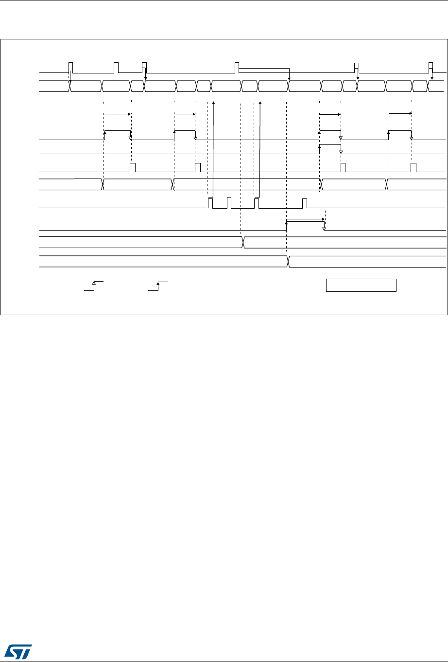
RM0394 Rev 4 419/1600
RM0394 Analog-to-digital converters (ADC)
485
Figure 75. AUTODLY=1, regular HW conversions interrupted by injected conversions
(DISCEN=1, JDISCEN=1)
1. AUTDLY=1
2. Regular configuration: EXTEN=0x1 (HW trigger), CONT=0, DISCEN=1, DISCNUM=1, CHANNELS = 1, 2, 3.
3. Injected configuration: JEXTEN=0x1 (HW Trigger), JDISCEN=1, CHANNELS = 5,6
,JQRUHG
,JQRUHG
069
,QMHFWHG
WULJJHU
UHJXODU
-(26
$'&B-'5
$'&B-'5
5HJXODU
WULJJHU
LQMHFWHG UHJXODU
UHJXODU
'/<&+
'/<LQM
1RWLJQRUHG
RFFXUVGXULQJLQMHFWHGVHTXHQFH
,JQRUHG
UHJXODU
'/<&+
$'&B'5
(2&
(26
$'&
VWDWH
$'&B'5UHDGDFFHVV
E\VZ E\KZ ,QGLFDWLYHWLPLQJV
5'< &+ '/< '/<
5'< &+ 5'< &+ &+ &+
5'<
' '
' '
'/<
'
'
UHJXODU LQMHFWHG
5'< &+ '/< 5'<&+
'/<&+ '/<&+
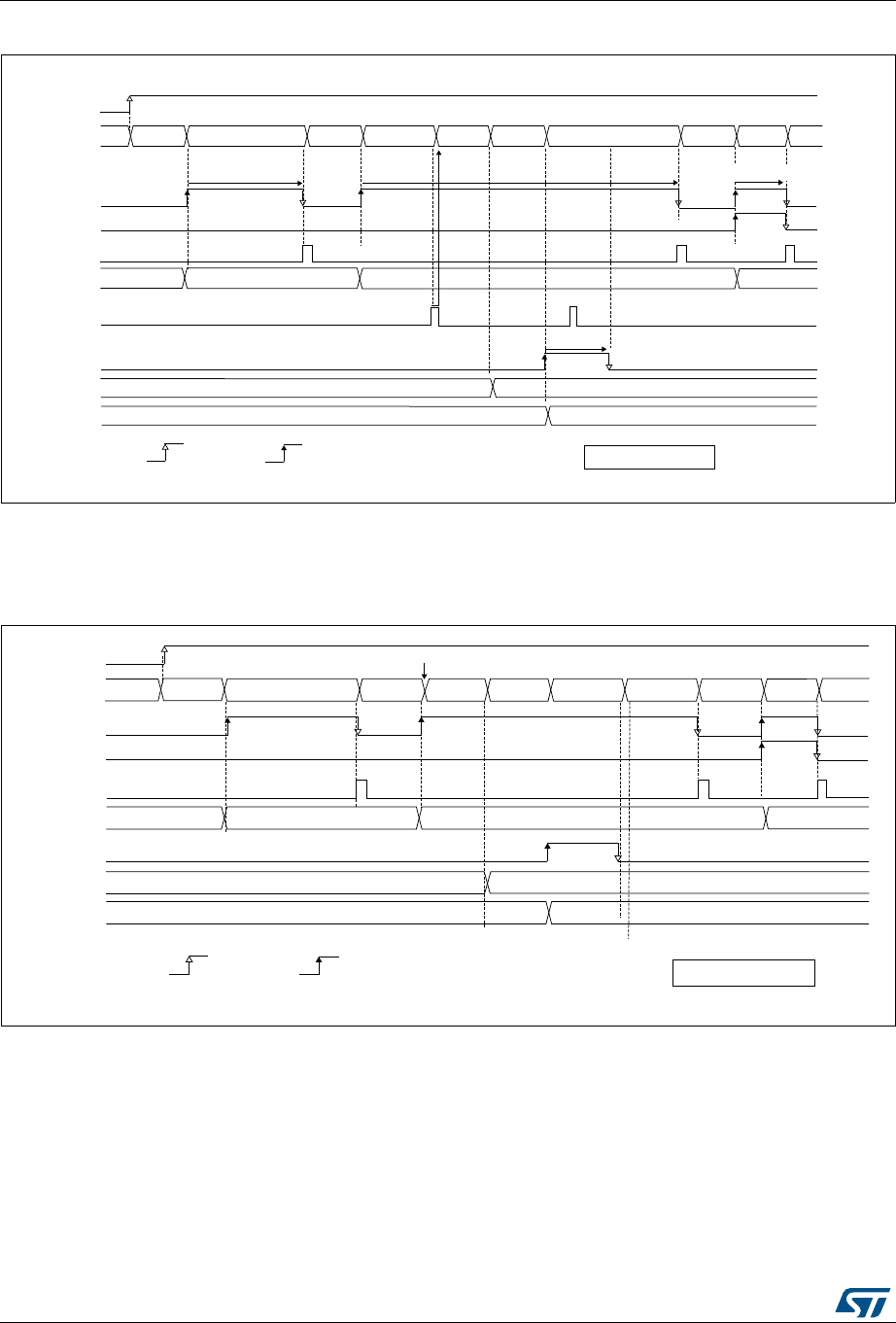
Analog-to-digital converters (ADC) RM0394
420/1600 RM0394 Rev 4
Figure 76. AUTODLY=1, regular continuous conversions interrupted by injected conversions
1. AUTDLY=1
2. Regular configuration: EXTEN=0x0 (SW trigger), CONT=1, DISCEN=0, CHANNELS = 1, 2, 3
3. Injected configuration: JEXTEN=0x1 (HW Trigger), JDISCEN=0, CHANNELS = 5,6
Figure 77. AUTODLY=1 in auto- injected mode (JAUTO=1)
1. AUTDLY=1
2. Regular configuration: EXTEN=0x0 (SW trigger), CONT=1, DISCEN=0, CHANNELS = 1, 2
3. Injected configuration: JAUTO=1, CHANNELS = 5,6
069
,JQRUHG
,QMHFWHG
WULJJHU
UHJXODU
-(26
$'&B-'5
$'&B-'5
LQMHFWHG UHJXODU
'/<&+ '/<&+
'/<LQM
UHJXODU
$'&B'5
(2&
(26
$'&
VWDWH
$'&B'5UHDGDFFHVV
E\VZ E\KZ ,QGLFDWLYHWLPLQJV
5'< &+ '/< &+
&+ '/< &+ '/< '/< &+
&+
' ' '
'
'
UHJXODU LQMHFWHG
'/<&+
$'67$57
D^ϯϭϬϮϰsϯ
ƌĞŐƵůĂƌ
:K^
ͺ:Zϭ
ͺ:ZϮ
ŝŶũĞĐƚĞĚ ƌĞŐƵůĂƌ
>z;,ϭͿ >z;ŝŶũͿ
ƌĞŐƵůĂƌ
ͺZ
K
K^
ƐƚĂƚĞ
ͺZƌĞĂĚĂĐĐĞƐƐ
ďLJƐͬǁ ďLJŚͬǁ /ŶĚŝĐĂƚŝǀĞƚŝŵŝŶŐƐ
Zz ,ϭ ,ϲ
,Ϯ ,ϱ >z;,ϮͿ >z ,ϭ
,ϯ
ϭ Ϯ ϯ
ϲ
ϱ
ƌĞŐƵůĂƌ ŝŶũĞĐƚĞĚ
EŽĚĞůĂLJ
^dZd;ϭͿ
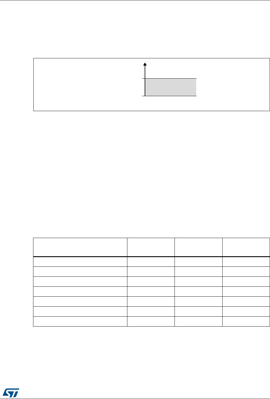
RM0394 Rev 4 421/1600
RM0394 Analog-to-digital converters (ADC)
485
16.4.29 Analog window watchdog (AWD1EN, JAWD1EN, AWD1SGL,
AWD1CH, AWD2CH, AWD3CH, AWD_HTx, AWD_LTx, AWDx)
The three AWD analog watchdogs monitor whether some channels remain within a
configured voltage range (window).
Figure 78. Analog watchdog guarded area
AWDx flag and interrupt
An interrupt can be enabled for each of the 3 analog watchdogs by setting AWDxIE in the
ADC_IER register (x=1,2,3).
AWDx (x=1,2,3) flag is cleared by software by writing 1 to it.
The ADC conversion result is compared to the lower and higher thresholds before
alignment.
Description of analog watchdog 1
The AWD analog watchdog 1 is enabled by setting the AWD1EN bit in the ADC_CFGR
register. This watchdog monitors whether either one selected channel or all enabled
channels(1) remain within a configured voltage range (window).
Table 63 shows how the ADC_CFGR registers should be configured to enable the analog
watchdog on one or more channels.
Table 63. Analog watchdog channel selection
The AWD1 analog watchdog status bit is set if the analog voltage converted by the ADC is
below a lower threshold or above a higher threshold.
Channels guarded by the analog
watchdog AWD1SGL bit AWD1EN bit JAWD1EN bit
None x 0 0
All injected channels 0 0 1
All regular channels 0 1 0
All regular and injected channels 0 1 1
Single(1) injected channel
1. Selected by the AWD1CH[4:0] bits. The channels must also be programmed to be converted in the
appropriate regular or injected sequence.
101
Single(1) regular channel 1 1 0
Single(1) regular or injected channel 1 1 1
DL
$QDORJYROWDJH
+LJKHUWKUHVKROG
/RZHUWKUHVKROG
*XDUGHGDUHD
+75
/75

Analog-to-digital converters (ADC) RM0394
422/1600 RM0394 Rev 4
These thresholds are programmed in bits HT1[11:0] and LT1[11:0] of the ADC_TR1 register
for the analog watchdog 1. When converting data with a resolution of less than 12 bits
(according to bits RES[1:0]), the LSB of the programmed thresholds must be kept cleared
because the internal comparison is always performed on the full 12-bit raw converted data
(left aligned).
Table 64 describes how the comparison is performed for all the possible resolutions for
analog watchdog 1.
Description of analog watchdog 2 and 3
The second and third analog watchdogs are more flexible and can guard several selected
channels by programming the corresponding bits in AWDCHx[19:0] (x=2,3).
The corresponding watchdog is enabled when any bit of AWDCHx[19:0] (x=2,3) is set.
They are limited to a resolution of 8 bits and only the 8 MSBs of the thresholds can be
programmed into HTx[7:0] and LTx[7:0]. Table 65 describes how the comparison is
performed for all the possible resolutions.
Table 64. Analog watchdog 1 comparison
Resolution
(bit
RES[1:0])
Analog watchdog comparison
between:
Comments
Raw converted data,
left aligned(1)
1. The watchdog comparison is performed on the raw converted data before any alignment calculation and
before applying any offsets (the data which is compared is not signed).
Thresholds
00: 12-bit DATA[11:0] LT1[11:0] and
HT1[11:0] -
01: 10-bit DATA[11:2],00 LT1[11:0] and
HT1[11:0]
User must configure LT1[1:0] and HT1[1:0] to
00
10: 8-bit DATA[11:4],0000 LT1[11:0] and
HT1[11:0]
User must configure LT1[3:0] and HT1[3:0] to
0000
11: 6-bit DATA[11:6],0000
00
LT1[11:0] and
HT1[11:0]
User must configure LT1[5:0] and HT1[5:0] to
000000
Table 65. Analog watchdog 2 and 3 comparison
Resolution
(bits RES[1:0])
Analog watchdog comparison between:
Comments
Raw converted data,
left aligned(1) Thresholds
00: 12-bit DATA[11:4] LTx[7:0] and HTx[7:0] DATA[3:0] are not relevant for the comparison
01: 10-bit DATA[11:4] LTx[7:0] and HTx[7:0] DATA[3:2] are not relevant for the comparison
10: 8-bit DATA[11:4] LTx[7:0] and HTx[7:0] -
11: 6-bit DATA[11:6],00 LTx[7:0] and HTx[7:0] User must configure LTx[1:0] and HTx[1:0] to 00
1. The watchdog comparison is performed on the raw converted data before any alignment calculation and before applying
any offsets (the data which is compared is not signed).
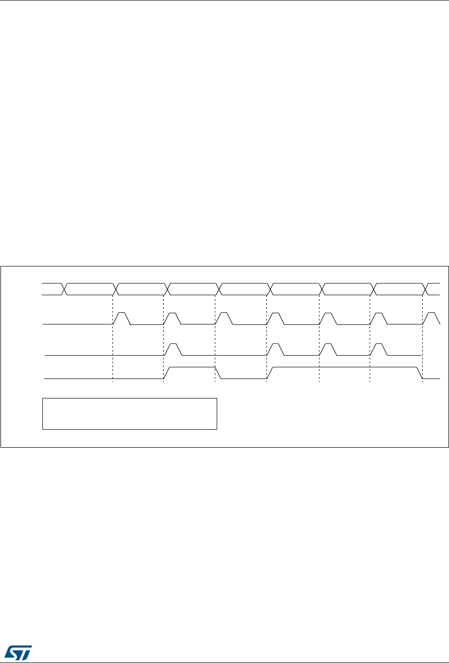
RM0394 Rev 4 423/1600
RM0394 Analog-to-digital converters (ADC)
485
ADCy_AWDx_OUT signal output generation
Each analog watchdog is associated to an internal hardware signal ADCy_AWDx_OUT
(y=ADC number, x=watchdog number) which is directly connected to the ETR input
(external trigger) of some on-chip timers. Refer to the on-chip timers section to understand
how to select the ADCy_AWDx_OUT signal as ETR.
ADCy_AWDx_OUT is activated when the associated analog watchdog is enabled:
•ADCy_AWDx_OUT is set when a guarded conversion is outside the programmed
thresholds.
•ADCy_AWDx_OUT is reset after the end of the next guarded conversion which is
inside the programmed thresholds (It remains at 1 if the next guarded conversions are
still outside the programmed thresholds).
•ADCy_AWDx_OUT is also reset when disabling the ADC (when setting ADDIS=1).
Note that stopping regular or injected conversions (setting ADSTP=1 or JADSTP=1)
has no influence on the generation of ADCy_AWDx_OUT.
Note: AWDx flag is set by hardware and reset by software: AWDx flag has no influence on the
generation of ADCy_AWDx_OUT (ex: ADCy_AWDx_OUT can toggle while AWDx flag
remains at 1 if the software did not clear the flag).
Figure 79. ADCy_AWDx_OUT signal generation (on all regular channels)
(2&)/$*
$'&
67$7( 5'<
$:'[)/$*
&RQYHUVLRQ
RXWVLGH
$'&\B$:'[B287
LQVLGH
FOHDUHG
E\6:
&RQYHUWLQJUHJXODUFKDQQHOV
5HJXODUFKDQQHOVDUHDOOJXDUGHG
069
&RQYHUVLRQ &RQYHUVLRQ &RQYHUVLRQ &RQYHUVLRQ &RQYHUVLRQ &RQYHUVLRQ
RXWVLGHLQVLGH RXWVLGH RXWVLGH LQVLGH
FOHDUHG
E\6:
FOHDUHG
E\6:
FOHDUHG
E\6:
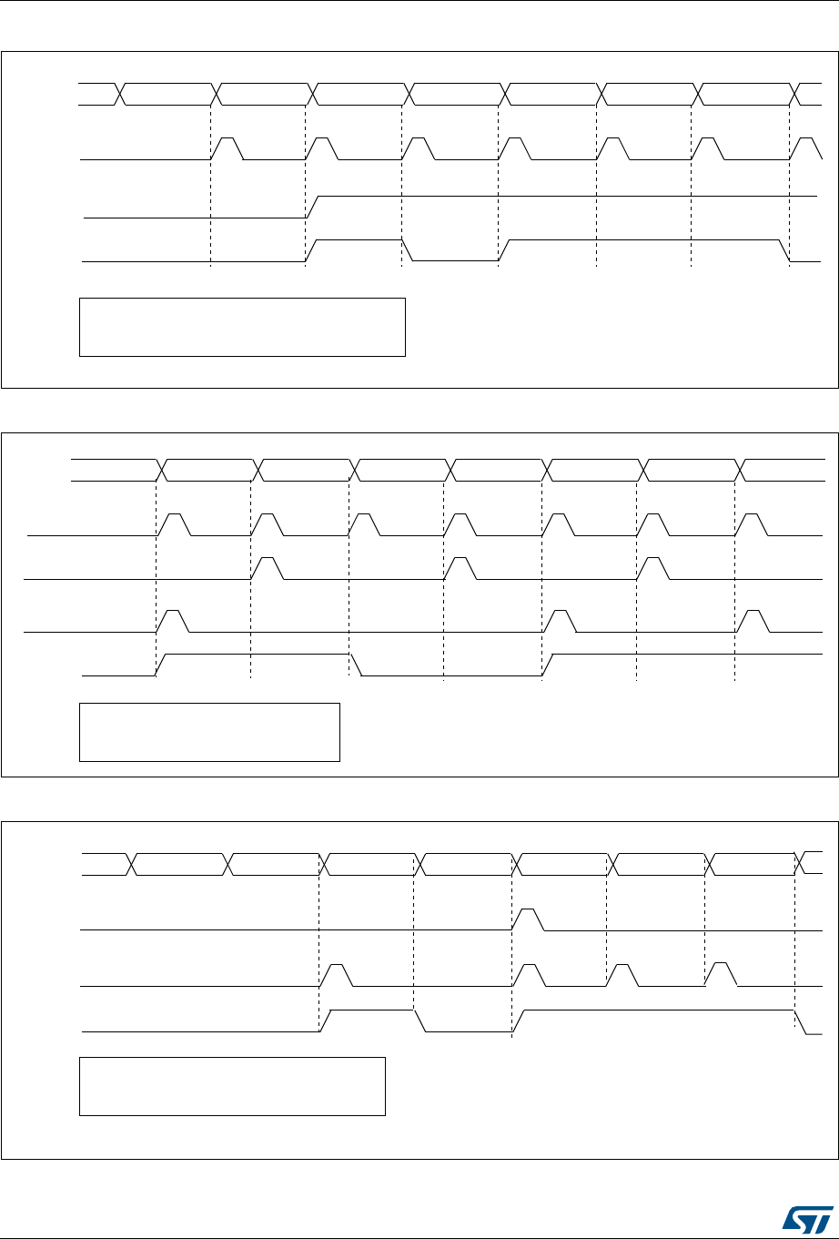
Analog-to-digital converters (ADC) RM0394
424/1600 RM0394 Rev 4
Figure 80. ADCy_AWDx_OUT signal generation (AWDx flag not cleared by software)
Figure 81. ADCy_AWDx_OUT signal generation (on a single regular channel)
Figure 82. ADCy_AWDx_OUT signal generation (on all injected channels)
(2&)/$*
$'&
67$7( 5'<
$:'[)/$*
&RQYHUVLRQ
RXWVLGH
$'&\B$:'[B287
LQVLGH
QRWFOHDUHG E\6:
&RQYHUWLQJUHJXODUFKDQQHOV
5HJXODUFKDQQHOVDUHDOOJXDUGHG
069
&RQYHUVLRQ &RQYHUVLRQ &RQYHUVLRQ &RQYHUVLRQ &RQYHUVLRQ &RQYHUVLRQ
RXWVLGHLQVLGH RXWVLGH RXWVLGH LQVLGH
(2&)/$*
$'&
67$7(
$:'[)/$*
&RQYHUVLRQ
RXWVLGH
$'&\B$:'[B287
FOHDUHG
E\6:
&RQYHUWLQJUHJXODUFKDQQHOVDQG
2QO\FKDQQHOLVJXDUGHG
069
&RQYHUVLRQ &RQYHUVLRQ &RQYHUVLRQ &RQYHUVLRQ &RQYHUVLRQ &RQYHUVLRQ
LQVLGH RXWVLGH RXWVLGH
FOHDUHG
E\6:
&RQYHUVLRQ
(26)/$*
-(26)/$*
$'&
67$7(
$:'[)/$*
5'<
RXWVLGH
$'&\B$:'[B287
FOHDUHG
E\6:
&RQYHUWLQJWKHLQMHFWHGFKDQQHOV
$OOLQMHFWHGFKDQQHOVDUHJXDUGHG
069
&RQYHUVLRQ &RQYHUVLRQ &RQYHUVLRQ &RQYHUVLRQ &RQYHUVLRQ &RQYHUVLRQ
LQVLGH RXWVLGH RXWVLGH
FOHDUHG
E\6:
&RQYHUVLRQ
LQVLGH RXWVLGH LQVLGH
FOHDUHG
E\6:
FOHDUHG
E\6:
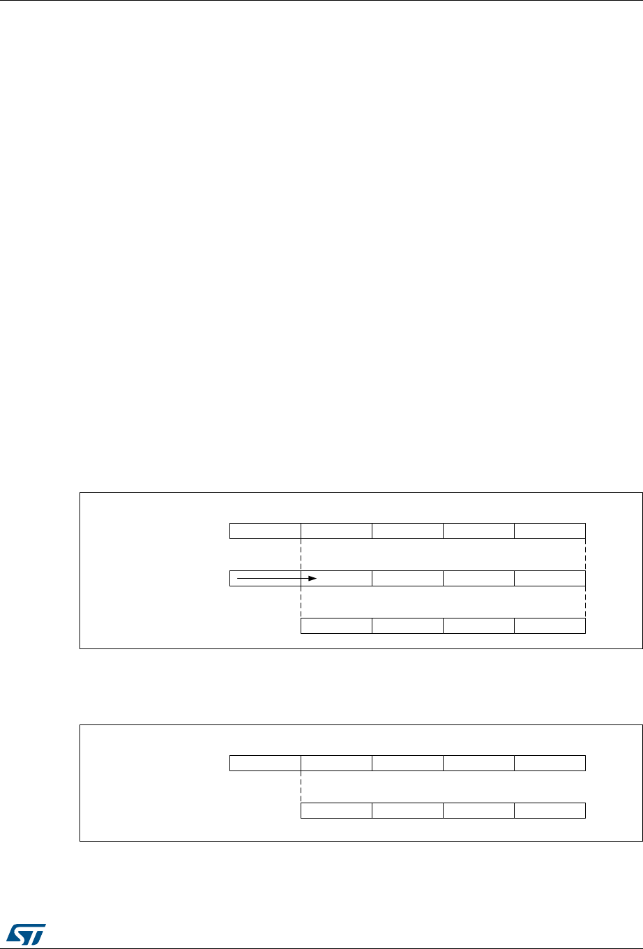
RM0394 Rev 4 425/1600
RM0394 Analog-to-digital converters (ADC)
485
16.4.30 Oversampler
The oversampling unit performs data pre-processing to offload the CPU. It is able to handle
multiple conversions and average them into a single data with increased data width, up to
16-bit.
It provides a result with the following form, where N and M can be adjusted:
It allows to perform by hardware the following functions: averaging, data rate reduction,
SNR improvement, basic filtering.
The oversampling ratio N is defined using the OVFS[2:0] bits in the ADC_CFGR2 register,
and can range from 2x to 256x. The division coefficient M consists of a right bit shift up to
8 bits, and is defined using the OVSS[3:0] bits in the ADC_CFGR2 register.
The summation unit can yield a result up to 20 bits (256x 12-bit results), which is first shifted
right. It is then truncated to the 16 least significant bits, rounded to the nearest value using
the least significant bits left apart by the shifting, before being finally transferred into the
ADC_DR data register.
Note: If the intermediary result after the shifting exceeds 16-bit, the result is truncated as is,
without saturation.
Figure 83. 20-bit to 16-bit result truncation
The Figure 84 gives a numerical example of the processing, from a raw 20-bit accumulated
data to the final 16-bit result.
Figure 84. Numerical example with 5-bit shift and rounding
Table 66 gives the data format for the various N and M combinations, for a raw conversion
data equal to 0xFFF.
Result 1
M
-----Conversion tn
()
n0=
nN1–=
∑
×=
069
5DZELWGDWD
6KLIWLQJ
7UXQFDWLRQDQGURXQGLQJ
069
'5DZELWGDWD
)%'
)LQDOUHVXOWDIWHUELWVKLIW
DQGURXQGLQJWRQHDUHVW
%

Analog-to-digital converters (ADC) RM0394
426/1600 RM0394 Rev 4
There are no changes for conversion timings in oversampled mode: the sample time is
maintained equal during the whole oversampling sequence. A new data is provided every N
conversions, with an equivalent delay equal to N x TCONV = N x (tSMPL + tSAR). The flags are
set as follow:
•the end of the sampling phase (EOSMP) is set after each sampling phase
•the end of conversion (EOC) occurs once every N conversions, when the oversampled
result is available
•the end of sequence (EOS) occurs once the sequence of oversampled data is
completed (i.e. after N x sequence length conversions total)
ADC operating modes supported when oversampling (single ADC mode)
In oversampling mode, most of the ADC operating modes are maintained:
•Single or continuous mode conversions
•ADC conversions start either by software or with triggers
•ADC stop during a conversion (abort)
•Data read via CPU or DMA with overrun detection
•Low-power modes (AUTDLY)
•Programmable resolution: in this case, the reduced conversion values (as per RES[1:0]
bits in ADC_CFGR1 register) are accumulated, truncated, rounded and shifted in the
same way as 12-bit conversions are
Note: The alignment mode is not available when working with oversampled data. The ALIGN bit in
ADC_CFGR1 is ignored and the data are always provided right-aligned.
Offset correction is not supported in oversampling mode. When ROVSE and/or JOVSE bit is
set, the value of the OFFSETy_EN bit in ADC_OFRy register is ignored (considered as
reset).
Table 66. Maximum output results versus N and M (gray cells indicate truncation)
Over
sampling
ratio
Max
Raw data
No-shift
OVSS =
0000
1-bit
shift
OVSS =
0001
2-bit
shift
OVSS =
0010
3-bit
shift
OVSS =
0011
4-bit
shift
OVSS =
0100
5-bit
shift
OVSS =
0101
6-bit
shift
OVSS =
0110
7-bit
shift
OVSS =
0111
8-bit
shift
OVSS =
1000
2x 0x1FFE 0x1FFE 0x0FFF 0x0800 0x0400 0x0200 0x0100 0x0080 0x0040 0x020
4x 0x3FFC 0x3FFC 0x1FFE 0x0FFF 0x0800 0x0400 0x0200 0x0100 0x0080 0x0040
8x 0x7FF8 0x7FF8 0x3FFC 0x1FFE 0x0FFF 0x0800 0x0400 0x0200 0x0100 0x0080
16x 0xFFF0 0xFFF0 0x7FF8 0x3FFC 0x1FFE 0x0FFF 0x0800 0x0400 0x0200 0x0100
32x 0x1FFE0 0xFFE0 0xFFF0 0x7FF8 0x3FFC 0x1FFE 0x0FFF 0x0800 0x0400 0x0200
64x 0x3FFC0 0xFFC0 0xFFE0 0xFFF0 0x7FF8 0x3FFC 0x1FFE 0x0FFF 0x0800 0x0400
128x 0x7FF80 0xFF80 0xFFC0 0xFFE0 0xFFF0 0x7FF8 0x3FFC 0x1FFE 0x0FFF 0x0800
256x 0xFFF00 0xFF00 0xFF80 0xFFC0 0xFFE0 0xFFF0 0x7FF8 0x3FFC 0x1FFE 0x0FFF
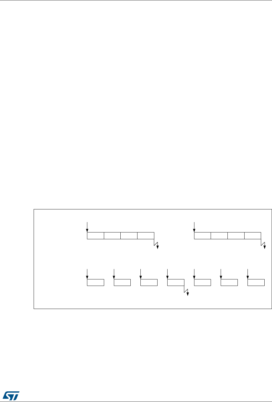
RM0394 Rev 4 427/1600
RM0394 Analog-to-digital converters (ADC)
485
Analog watchdog
The analog watchdog functionality is maintained (AWDSGL and AWDEN bits), with the
following difference:
– the RES[1:0] bits are ignored, comparison is always done on using the full 12-bit
values HT[11:0] and LT[11:0]
– the comparison is performed on the most significant 12-bit of the 16-bit
oversampled results ADC_DR[15:4]
Note: Care must be taken when using high shifting values, this will reduce the comparison range.
For instance, if the oversampled result is shifted by 4 bits, thus yielding a 12-bit data right-
aligned, the effective analog watchdog comparison can only be performed on 8 bits. The
comparison is done between ADC_DR[11:4] and HT[0:7] / LT[[0:7], and HT[11:8] / LT[11:8]
must be kept reset.
Triggered mode
The averager can also be used for basic filtering purpose. Although not a very powerful filter
(slow roll-off and limited stop band attenuation), it can be used as a notch filter to reject
constant parasitic frequencies (typically coming from the mains or from a switched mode
power supply). For this purpose, a specific discontinuous mode can be enabled with
TROVS bit in ADC_CFGR2, to be able to have an oversampling frequency defined by a
user and independent from the conversion time itself.
The Figure 85 below shows how conversions are started in response to triggers during
discontinuous mode.
If the TROVS bit is set, the content of the DISCEN bit is ignored and considered as 1.
Figure 85. Triggered regular oversampling mode (TROVS bit = 1)
Injected and regular sequencer management when oversampling
In oversampling mode, it is possible to have differentiated behavior for injected and regular
sequencers. The oversampling can be enabled for both sequencers with some limitations if
they have to be used simultaneously (this is related to a unique accumulation unit).
069
&K1
7ULJJHU
&217
',6&(1
75296 &K1
&K1
&K1
&K1
7ULJJHU
&K1
&K1
&K1
&K1
7ULJJHU
&K1
7ULJJHU
&K1
7ULJJHU
&K1
7ULJJHU
&K1
7ULJJHU
&K1
7ULJJHU
&K1
7ULJJHU
&217
',6&(1
75296
(2&IODJVHW
(2&IODJVHW
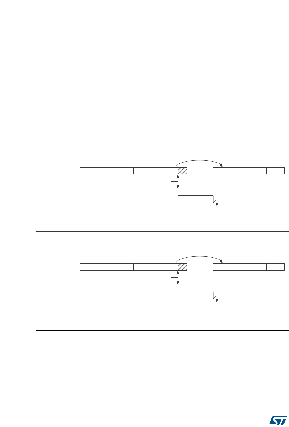
Analog-to-digital converters (ADC) RM0394
428/1600 RM0394 Rev 4
Oversampling regular channels only
The regular oversampling mode bit ROVSM defines how the regular oversampling
sequence is resumed if it is interrupted by injected conversion:
•in continued mode, the accumulation restarts from the last valid data (prior to the
conversion abort request due to the injected trigger). This ensures that oversampling
will be completed whatever the injection frequency (providing at least one regular
conversion can be completed between triggers);
•in resumed mode, the accumulation restarts from 0 (previous conversions results are
ignored). This mode allows to guarantee that all data used for oversampling were
converted back-to-back within a single timeslot. Care must be taken to have a injection
trigger period above the oversampling period length. If this condition is not respected,
the oversampling cannot be completed and the regular sequencer will be blocked.
The Figure 86 gives examples for a 4x oversampling ratio.
Figure 86. Regular oversampling modes (4x ratio)
Oversampling Injected channels only
The Injected oversampling mode bit JOVSE enables oversampling solely for conversions in
the injected sequencer.
069
&K2
2YHUVDPSOLQJ
FRQWLQXHG
5HJXODUFKDQQHOV &K0
&K0
&K0
&K1
&K1
&K1
&K1&K0&K0
2YHUVDPSOLQJ
VWRSSHG
&K- &K.
7ULJJHU
,QMHFWHGFKDQQHOV
&RQWLQXHGPRGH5296( -296( 52960 75296 ;
&K0
2YHUVDPSOLQJ
UHVXPHG
5HJXODUFKDQQHOV &K0
&K0
&K0
&K1
&K1
&K1
&K1&K0&K0
2YHUVDPSOLQJ
DERUWHG
&K- &K.
7ULJJHU
,QMHFWHGFKDQQHOV
5HVXPHGPRGH5296( -296( 52960 75296 ;
$ERUW
$ERUW
-(2&
-(2&
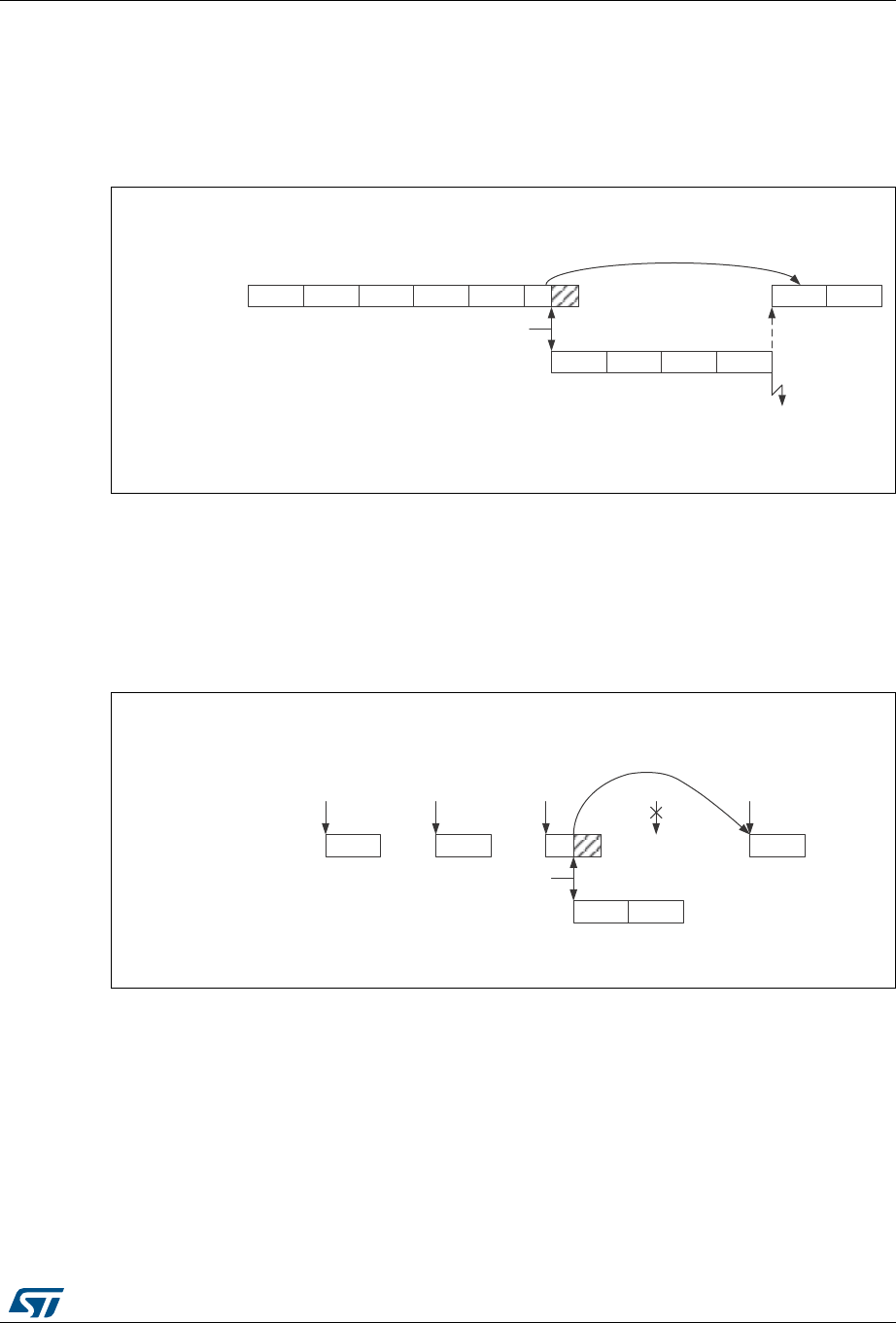
RM0394 Rev 4 429/1600
RM0394 Analog-to-digital converters (ADC)
485
Oversampling regular and Injected channels
It is possible to have both ROVSE and JOVSE bits set. In this case, the regular
oversampling mode is forced to resumed mode (ROVSM bit ignored), as represented on
Figure 87 below.
Figure 87. Regular and injected oversampling modes used simultaneously
Triggered regular oversampling with injected conversions
It is possible to have triggered regular mode with injected conversions. In this case, the
injected mode oversampling mode must be disabled, and the ROVSM bit is ignored
(resumed mode is forced). The JOVSE bit must be reset. The behavior is represented on
Figure 88 below.
Figure 88. Triggered regular oversampling with injection
069
2YHUVDPSOLQJ
UHVXPHG
5HJXODUFKDQQHOV &K0
&K0
&K1
&K1
&K1
&K1&K0&K0
2YHUVDPSOLQJ
DERUWHG
&K-&K-
7ULJJHU
,QMHFWHGFKDQQHOV
5296( -296( 52960 ;75296
$ERUW
-(2&
&K-&K-
069
2YHUVDPSOLQJ
UHVXPHG
5HJXODUFKDQQHOV &K1
&K1
&K1&K1
&K- &K.
7ULJJHU
,QMHFWHGFKDQQHOV
5296( -296( 52960 ;75296
$ERUW
7ULJJHU 7ULJJHU 7ULJJHU 7ULJJHU 7ULJJHU
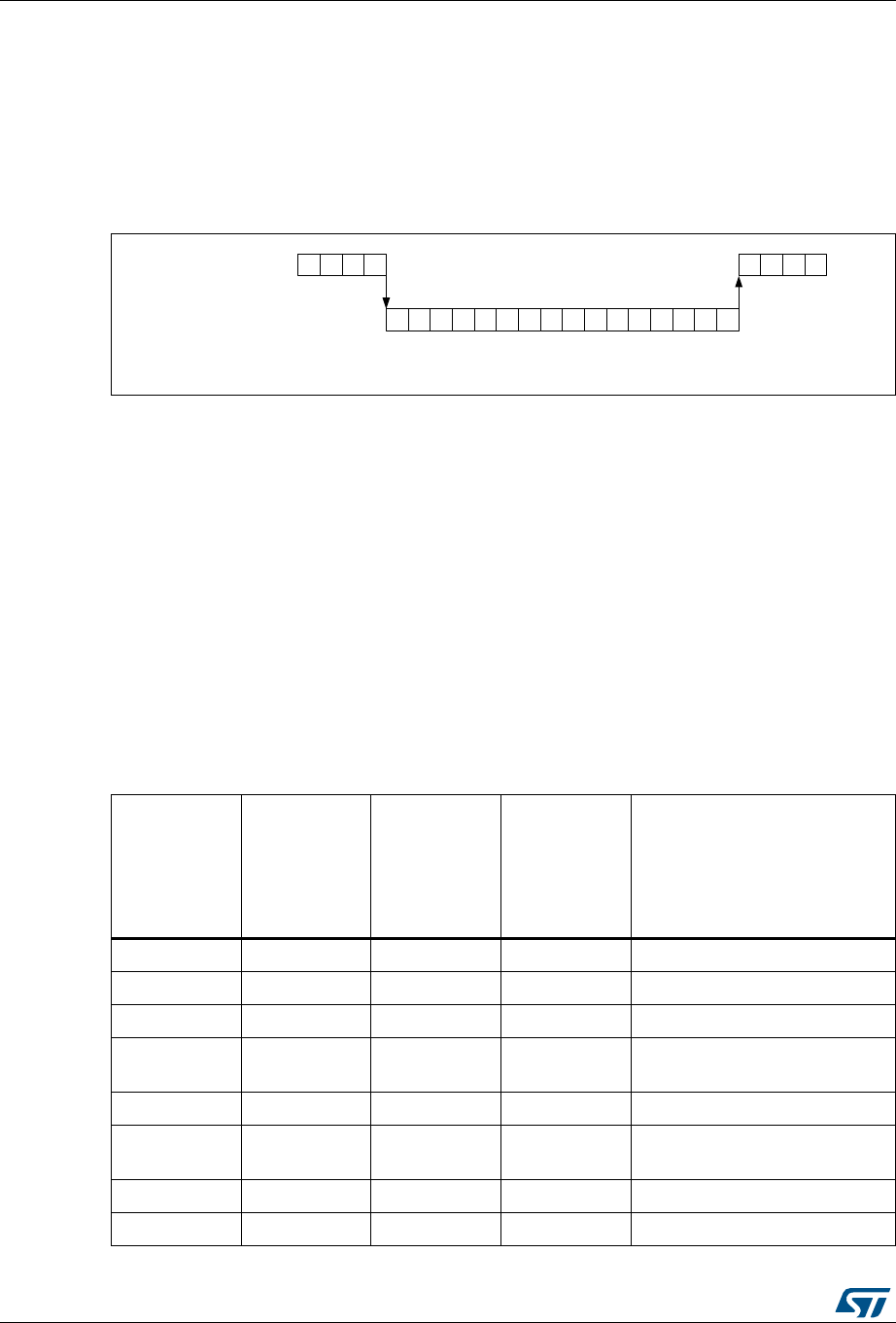
Analog-to-digital converters (ADC) RM0394
430/1600 RM0394 Rev 4
Auto-injected mode
It is possible to oversample auto-injected sequences and have all conversions results stored
in registers to save a DMA resource. This mode is available only with both regular and
injected oversampling active: JAUTO = 1, ROVSE = 1 and JOVSE = 1, other combinations
are not supported. The ROVSM bit is ignored in auto-injected mode. The Figure 89 below
shows how the conversions are sequenced.
Figure 89. Oversampling in auto-injected mode
It is possible to have also the triggered mode enabled, using the TROVS bit. In this case,
the ADC must be configured as following: JAUTO = 1, DISCEN = 0, JDISCEN = 0, ROVSE
= 1, JOVSE = 1 and TROVSE = 1.
Dual ADC modes supported when oversampling
It is possible to have oversampling enabled when working in dual ADC configuration, for the
injected simultaneous mode and regular simultaneous mode. In this case, the two ADCs
must be programmed with the very same settings (including oversampling).
All other dual ADC modes are not supported when either regular or injected oversampling is
enabled (ROVSE = 1 or JOVSE = 1).
Combined modes summary
The Table 67 below summarizes all combinations, including modes not supported.
Table 67. Oversampler operating modes summary
Regular
Oversampling
ROVSE
Injected
Oversampling
JOVSE
Oversampler
mode
ROVSM
0 = continued
1 = resumed
Triggered
Regular mode
TROVS
Comment
1 0 0 0 Regular continued mode
1 0 0 1 Not supported
1 0 1 0 Regular resumed mode
1011Triggered regular resumed
mode
1 1 0 X Not supported
1110Injected and regular resumed
mode
1 1 1 1 Not supported
0 1 X X Injected oversampling
069
5HJXODUFKDQQHOV 1
-$872 5296( -296( 52960 ;75296
111
,,,,----....////
1111
,QMHFWHGFKDQQHOV

RM0394 Rev 4 431/1600
RM0394 Analog-to-digital converters (ADC)
485
16.4.31 Dual ADC modes
Dual ADC modes can be used in devices with two ADCs or more (see Figure 90).
In dual ADC mode the start of conversion is triggered alternately or simultaneously by the
ADCx master to the ADC slave, depending on the mode selected by the bits DUAL[4:0] in
the ADCx_CCR register.
Four possible modes are implemented:
•Injected simultaneous mode
•Regular simultaneous mode
•Interleaved mode
•Alternate trigger mode
It is also possible to use these modes combined in the following ways:
•Injected simultaneous mode + Regular simultaneous mode
•Regular simultaneous mode + Alternate trigger mode
•Injected simultaneous mode + Interleaved mode
In dual ADC mode (when bits DUAL[4:0] in ADCx_CCR register are not equal to zero), the
bits CONT, AUTDLY, DISCEN, DISCNUM[2:0], JDISCEN, JQM, JAUTO of the ADC_CFGR
register are shared between the master and slave ADC: the bits in the slave ADC are
always equal to the corresponding bits of the master ADC.
To start a conversion in dual mode, the user must program the bits EXTEN, EXTSEL,
JEXTEN, JEXTSEL of the master ADC only, to configure a software or hardware trigger,
and a regular or injected trigger. (the bits EXTEN[1:0] and JEXTEN[1:0] of the slave ADC
are don’t care).
In regular simultaneous or interleaved modes: once the user sets bit ADSTART or bit
ADSTP of the master ADC, the corresponding bit of the slave ADC is also automatically
set. However, bit ADSTART or bit ADSTP of the slave ADC is not necessary cleared at the
same time as the master ADC bit.
In injected simultaneous or alternate trigger modes: once the user sets bit JADSTART or bit
JADSTP of the master ADC, the corresponding bit of the slave ADC is also automatically
set. However, bit JADSTART or bit JADSTP of the slave ADC is not necessary cleared at
the same time as the master ADC bit.
In dual ADC mode, the converted data of the master and slave ADC can be read in parallel,
by reading the ADC common data register (ADCx_CDR). The status bits can be also read in
parallel by reading the dual-mode status register (ADCx_CSR).
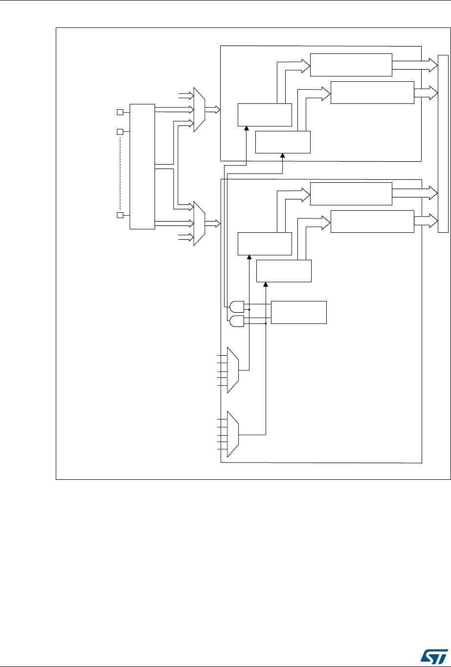
Analog-to-digital converters (ADC) RM0394
432/1600 RM0394 Rev 4
Figure 90. Dual ADC block diagram(1)
1. External triggers also exist on slave ADC but are not shown for the purposes of this diagram.
2. The ADC common data register (ADCx_CDR) contains both the master and slave ADC regular converted data.
06Y9
ZĞŐƵůĂƌĚĂƚĂƌĞŐŝƐƚĞƌ;ϭϲͲ
ďŝƚƐͿ
/ŶũĞĐƚĞĚĚĂƚĂƌĞŐŝƐƚĞƌƐ;ϰ
džϭϲͲďŝƚƐͿ
/ŶũĞĐƚĞĚ
ĐŚĂŶŶĞůƐ
ZĞŐƵůĂƌ
ĐŚĂŶŶĞůƐ
ZĞŐƵůĂƌĚĂƚĂƌĞŐŝƐƚĞƌ;ϭϲͲ
ďŝƚƐͿ
/ŶũĞĐƚĞĚĚĂƚĂƌĞŐŝƐƚĞƌƐ;ϰ
džϭϲͲďŝƚƐͿ
/ŶũĞĐƚĞĚ
ĐŚĂŶŶĞůƐ
ZĞŐƵůĂƌ
ĐŚĂŶŶĞůƐ
ĚĚƌĞƐƐͬĚĂƚĂďƵƐ
$'&[B,11
$'&[B,13
ƵĂůŵŽĚĞ
ĐŽŶƚƌŽů
0DVWHU$'&
6ODYH$'&
6WDUWWULJJHUPX[
UHJXODUJURXS
6WDUWWULJJHUPX[
LQMHFWHGJURXS
,QWHUQDODQDORJLQSXWV
,QWHUQDOWULJJHUV
,QWHUQDODQDORJLQSXWV
$'&[B,11
$'&[B,13
$'&[B,11
$'&[B,13
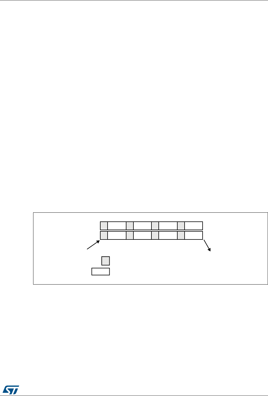
RM0394 Rev 4 433/1600
RM0394 Analog-to-digital converters (ADC)
485
Injected simultaneous mode
This mode is selected by programming bits DUAL[4:0]=00101
This mode converts an injected group of channels. The external trigger source comes from
the injected group multiplexer of the master ADC (selected by the JEXTSEL bits in the
ADC_JSQR register).
Note: Do not convert the same channel on the two ADCs (no overlapping sampling times for the
two ADCs when converting the same channel).
In simultaneous mode, one must convert sequences with the same length or ensure that the
interval between triggers is longer than the longer of the 2 sequences. Otherwise, the ADC
with the shortest sequence may restart while the ADC with the longest sequence is
completing the previous conversions.
Regular conversions can be performed on one or all ADCs. In that case, they are
independent of each other and are interrupted when an injected event occurs. They are
resumed at the end of the injected conversion group.
•At the end of injected sequence of conversion event (JEOS) on the master ADC, the
converted data is stored into the master ADC_JDRy registers and a JEOS interrupt is
generated (if enabled)
•At the end of injected sequence of conversion event (JEOS) on the slave ADC, the
converted data is stored into the slave ADC_JDRy registers and a JEOS interrupt is
generated (if enabled)
•If the duration of the master injected sequence is equal to the duration of the slave
injected one (like in Figure 91), it is possible for the software to enable only one of the
two JEOS interrupt (ex: master JEOS) and read both converted data (from master
ADC_JDRy and slave ADC_JDRy registers).
Figure 91. Injected simultaneous mode on 4 channels: dual ADC mode
If JDISCEN=1, each simultaneous conversion of the injected sequence requires an injected
trigger event to occur.
This mode can be combined with AUTDLY mode:
•Once a simultaneous injected sequence of conversions has ended, a new injected
trigger event is accepted only if both JEOS bits of the master and the slave ADC have
been cleared (delay phase). Any new injected trigger events occurring during the
ongoing injected sequence and the associated delay phase are ignored.
•Once a regular sequence of conversions of the master ADC has ended, a new regular
trigger event of the master ADC is accepted only if the master data register (ADC_DR)
has been read. Any new regular trigger events occurring for the master ADC during the
0$67(5$'&
6/$9($'&
(QGRILQMHFWHGVHTXHQFHRQ
0$67(5DQG6/$9($'&
069
7ULJJHU
&+
&+ &+ &+ &+
&+ &+ &+
6DPSOLQJ
&RQYHUVLRQ

Analog-to-digital converters (ADC) RM0394
434/1600 RM0394 Rev 4
ongoing regular sequence and the associated delay phases are ignored.
There is the same behavior for regular sequences occurring on the slave ADC.
Regular simultaneous mode with independent injected
This mode is selected by programming bits DUAL[4:0] = 00110.
This mode is performed on a regular group of channels. The external trigger source comes
from the regular group multiplexer of the master ADC (selected by the EXTSEL bits in the
ADC_CFGR register). A simultaneous trigger is provided to the slave ADC.
In this mode, independent injected conversions are supported. An injection request (either
on master or on the slave) will abort the current simultaneous conversions, which are
restarted once the injected conversion is completed.
Note: Do not convert the same channel on the two ADCs (no overlapping sampling times for the
two ADCs when converting the same channel).
In regular simultaneous mode, one must convert sequences with the same length or ensure
that the interval between triggers is longer than the longer conversion time of the 2
sequences. Otherwise, the ADC with the shortest sequence may restart while the ADC with
the longest sequence is completing the previous conversions.
Software is notified by interrupts when it can read the data:
•At the end of each conversion event (EOC) on the master ADC, a master EOC interrupt
is generated (if EOCIE is enabled) and software can read the ADC_DR of the master
ADC.
•At the end of each conversion event (EOC) on the slave ADC, a slave EOC interrupt is
generated (if EOCIE is enabled) and software can read the ADC_DR of the slave ADC.
•If the duration of the master regular sequence is equal to the duration of the slave one
(like in Figure 92), it is possible for the software to enable only one of the two EOC
interrupt (ex: master EOC) and read both converted data from the Common Data
register (ADCx_CDR).
It is also possible to read the regular data using the DMA. Two methods are possible:
•Using two DMA channels (one for the master and one for the slave). In this case bits
MDMA[1:0] must be kept cleared.
– Configure the DMA master ADC channel to read ADC_DR from the master. DMA
requests are generated at each EOC event of the master ADC.
– Configure the DMA slave ADC channel to read ADC_DR from the slave. DMA
requests are generated at each EOC event of the slave ADC.
•Using MDMA mode, which leaves one DMA channel free for other uses:
– Configure MDMA[1:0]=0b10 or 0b11 (depending on resolution).
– A single DMA channel is used (the one of the master). Configure the DMA master
ADC channel to read the common ADC register (ADCx_CDR)
– A single DMA request is generated each time both master and slave EOC events
have occurred. At that time, the slave ADC converted data is available in the
upper half-word of the ADCx_CDR 32-bit register and the master ADC converted
data is available in the lower half-word of ADCx_CCR register.
– both EOC flags are cleared when the DMA reads the ADCx_CCR register.
Note: In MDMA mode (MDMA[1:0]=0b10 or 0b11), the user must program the same number of
conversions in the master’s sequence as in the slave’s sequence. Otherwise, the remaining
conversions will not generate a DMA request.

RM0394 Rev 4 435/1600
RM0394 Analog-to-digital converters (ADC)
485
Figure 92. Regular simultaneous mode on 16 channels: dual ADC mode
If DISCEN=1 then each “n” simultaneous conversions of the regular sequence require a
regular trigger event to occur (“n” is defined by DISCNUM).
This mode can be combined with AUTDLY mode:
•Once a simultaneous conversion of the sequence has ended, the next conversion in
the sequence is started only if the common data register, ADCx_CDR (or the regular
data register of the master ADC) has been read (delay phase).
•Once a simultaneous regular sequence of conversions has ended, a new regular
trigger event is accepted only if the common data register (ADCx_CDR) has been read
(delay phase). Any new regular trigger events occurring during the ongoing regular
sequence and the associated delay phases are ignored.
It is possible to use the DMA to handle data in regular simultaneous mode combined with
AUTDLY mode, assuming that multi-DMA mode is used: bits MDMA must be set to 0b10 or
0b11.
When regular simultaneous mode is combined with AUTDLY mode, it is mandatory for the
user to ensure that:
•The number of conversions in the master’s sequence is equal to the number of
conversions in the slave’s.
•For each simultaneous conversions of the sequence, the length of the conversion of
the slave ADC is inferior to the length of the conversion of the master ADC. Note that
the length of the sequence depends on the number of channels to convert and the
sampling time and the resolution of each channels.
Note: This combination of regular simultaneous mode and AUTDLY mode is restricted to the use
case when only regular channels are programmed: it is forbidden to program injected
channels in this combined mode.
Interleaved mode with independent injected
This mode is selected by programming bits DUAL[4:0] = 00111.
This mode can be started only on a regular group (usually one channel). The external
trigger source comes from the regular channel multiplexer of the master ADC.
After an external trigger occurs:
•The master ADC starts immediately.
•The slave ADC starts after a delay of several ADC clock cycles after the sampling
phase of the master ADC has complete.
The minimum delay which separates 2 conversions in interleaved mode is configured in the
DELAY bits in the ADCx_CCR register. This delay starts to count after the end of the
sampling phase of the master conversion. This way, an ADC cannot start a conversion if the
0$67(5$'&
6/$9($'&
(QGRIUHJXODUVHTXHQFHRQ
0$67(5DQG6/$9($'&
&+
&+
DLE
6DPSOLQJ
&RQYHUVLRQ
7ULJJHU
&+
&+ &+ &+ &+
&+ &+ &+
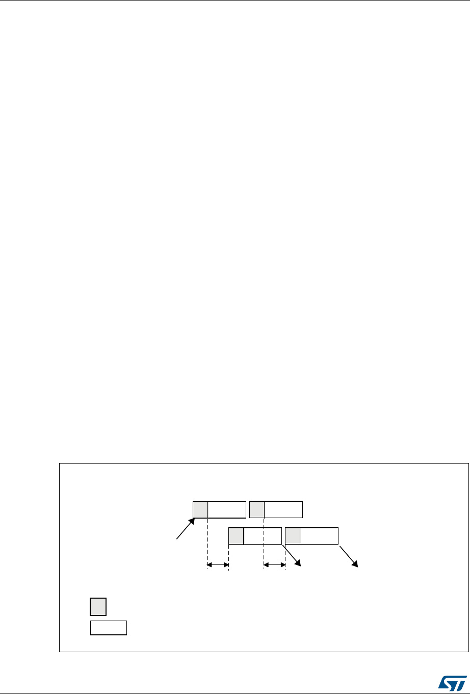
Analog-to-digital converters (ADC) RM0394
436/1600 RM0394 Rev 4
complementary ADC is still sampling its input (only one ADC can sample the input signal at
a given time).
•The minimum possible DELAY is 1 to ensure that there is at least one cycle time
between the opening of the analog switch of the master ADC sampling phase and the
closing of the analog switch of the slave ADC sampling phase.
•The maximum DELAY is equal to the number of cycles corresponding to the selected
resolution. However the user must properly calculate this delay to ensure that an ADC
does not start a conversion while the other ADC is still sampling its input.
If the CONT bit is set on both master and slave ADCs, the selected regular channels of both
ADCs are continuously converted.
The software is notified by interrupts when it can read the data at the end of each
conversion event (EOC) on the slave ADC. A slave and master EOC interrupts are
generated (if EOCIE is enabled) and the software can read the ADC_DR of the slave/master
ADC.
Note: It is possible to enable only the EOC interrupt of the slave and read the common data
register (ADCx_CDR). But in this case, the user must ensure that the duration of the
conversions are compatible to ensure that inside the sequence, a master conversion is
always followed by a slave conversion before a new master conversion restarts. It is
recommended to use the MDMA mode.
It is also possible to have the regular data transferred by DMA. In this case, individual DMA
requests on each ADC cannot be used and it is mandatory to use the MDMA mode, as
following:
•Configure MDMA[1:0]=0b10 or 0b11 (depending on resolution).
•A single DMA channel is used (the one of the master). Configure the DMA master ADC
channel to read the common ADC register (ADCx_CDR).
•A single DMA request is generated each time both master and slave EOC events have
occurred. At that time, the slave ADC converted data is available in the upper half-word
of the ADCx_CDR 32-bit register and the master ADC converted data is available in the
lower half-word of ADCx_CCR register.
•Both EOC flags are cleared when the DMA reads the ADCx_CCR register.
Figure 93. Interleaved mode on 1 channel in continuous conversion mode: dual ADC
mode
06Y9
0$67(5$'&
7ULJJHU
&+
6DPSOLQJ
&RQYHUVLRQ
&+
$'&&/.
F\FOHV
&+
&+
$'&&/.
F\FOHV
6/$9($'&
(QGRIFRQYHUVLRQRQPDVWHUDQG
VODYH$'&
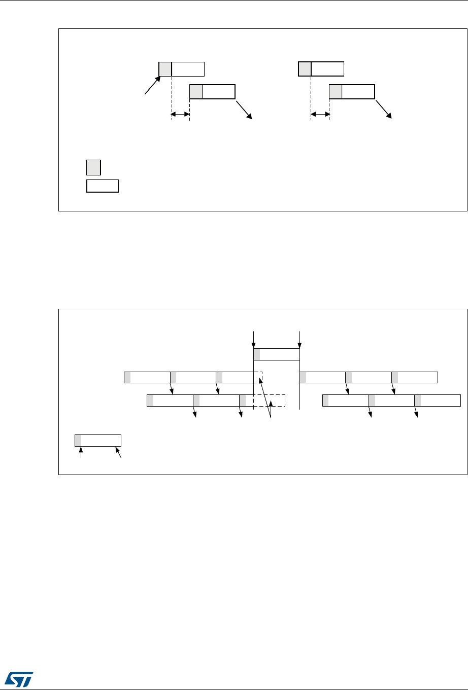
RM0394 Rev 4 437/1600
RM0394 Analog-to-digital converters (ADC)
485
Figure 94. Interleaved mode on 1 channel in single conversion mode: dual ADC mode
If DISCEN=1, each “n” simultaneous conversions (“n” is defined by DISCNUM) of the
regular sequence require a regular trigger event to occur.
In this mode, injected conversions are supported. When injection is done (either on master
or on slave), both the master and the slave regular conversions are aborted and the
sequence is restarted from the master (see Figure 95 below).
Figure 95. Interleaved conversion with injection
Alternate trigger mode
This mode is selected by programming bits DUAL[4:0] = 01001.
This mode can be started only on an injected group. The source of external trigger comes
from the injected group multiplexer of the master ADC.
This mode is only possible when selecting hardware triggers: JEXTEN must not be 0x0.
Injected discontinuous mode disabled (JDISCEN=0 for both ADC)
1. When the 1st trigger occurs, all injected master ADC channels in the group are
converted.
2. When the 2nd trigger occurs, all injected slave ADC channels in the group are
converted.
3. And so on.
06Y9
0$67(5$'&
7ULJJHU
&+
6DPSOLQJ
&RQYHUVLRQ
&+
$'&&/.
F\FOHV
&+
&+
$'&&/.
F\FOHV
6/$9($'&
(QGRIFRQYHUVLRQRQ
PDVWHUDQGVODYH$'&
(QGRIFRQYHUVLRQRQ
PDVWHUDQGVODYH$'&
069
$'&PDVWHU &+ &+ &+
&+
&+ &+ &+
&+ &+ &+&+ &+ &+$'&VODYH
,QMHFWHGWULJJHU 5HVXPHDOZD\VRQPDVWHU
UHDG
&'5
UHDG
&'5
UHDG
&'5
UHDG
&'5
FRQYHUVLRQV
DERUWHG
/HJHQG
6DPSOLQJ &RQYHUVLRQ
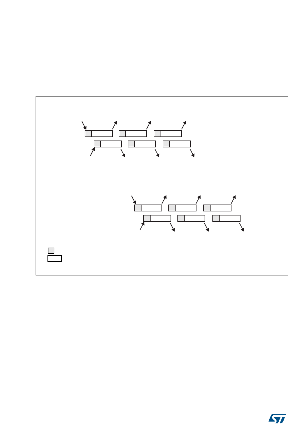
Analog-to-digital converters (ADC) RM0394
438/1600 RM0394 Rev 4
A JEOS interrupt, if enabled, is generated after all injected channels of the master ADC in
the group have been converted.
A JEOS interrupt, if enabled, is generated after all injected channels of the slave ADC in the
group have been converted.
JEOC interrupts, if enabled, can also be generated after each injected conversion.
If another external trigger occurs after all injected channels in the group have been
converted then the alternate trigger process restarts by converting the injected channels of
the master ADC in the group.
Figure 96. Alternate trigger: injected group of each ADC
Note: Regular conversions can be enabled on one or all ADCs. In this case the regular
conversions are independent of each other. A regular conversion is interrupted when the
ADC has to perform an injected conversion. It is resumed when the injected conversion is
finished.
The time interval between 2 trigger events must be greater than or equal to 1 ADC clock
period. The minimum time interval between 2 trigger events that start conversions on the
same ADC is the same as in the single ADC mode.
Injected discontinuous mode enabled (JDISCEN=1 for both ADC)
If the injected discontinuous mode is enabled for both master and slave ADCs:
•When the 1st trigger occurs, the first injected channel of the master ADC is converted.
•When the 2nd trigger occurs, the first injected channel of the slave ADC is converted.
•And so on.
A JEOS interrupt, if enabled, is generated after all injected channels of the master ADC in
the group have been converted.
0$67(5$'&
DLP
6/$9($'&
-(2&RQ
PDVWHU$'&
-(2&RQ
VODYH$'&
-(2&-(26RQ
PDVWHU$'&
-(2&RQ
PDVWHU$'&
-(2&RQ
VODYH$'&
-(2&-(26RQ
VODYH$'&
VWWULJJHU
QGWULJJHU
0$67(5$'&
6/$9($'&
-(2&RQ
PDVWHU$'&
-(2&RQ
VODYH$'&
-(2&-(26RQ
PDVWHU$'&
-(2&RQ
PDVWHU$'&
-(2&RQ
VODYH$'&
-(2&-(26RQ
VODYH$'&
UGWULJJHU
WKWULJJHU
6DPSOLQJ
&RQYHUVLRQ
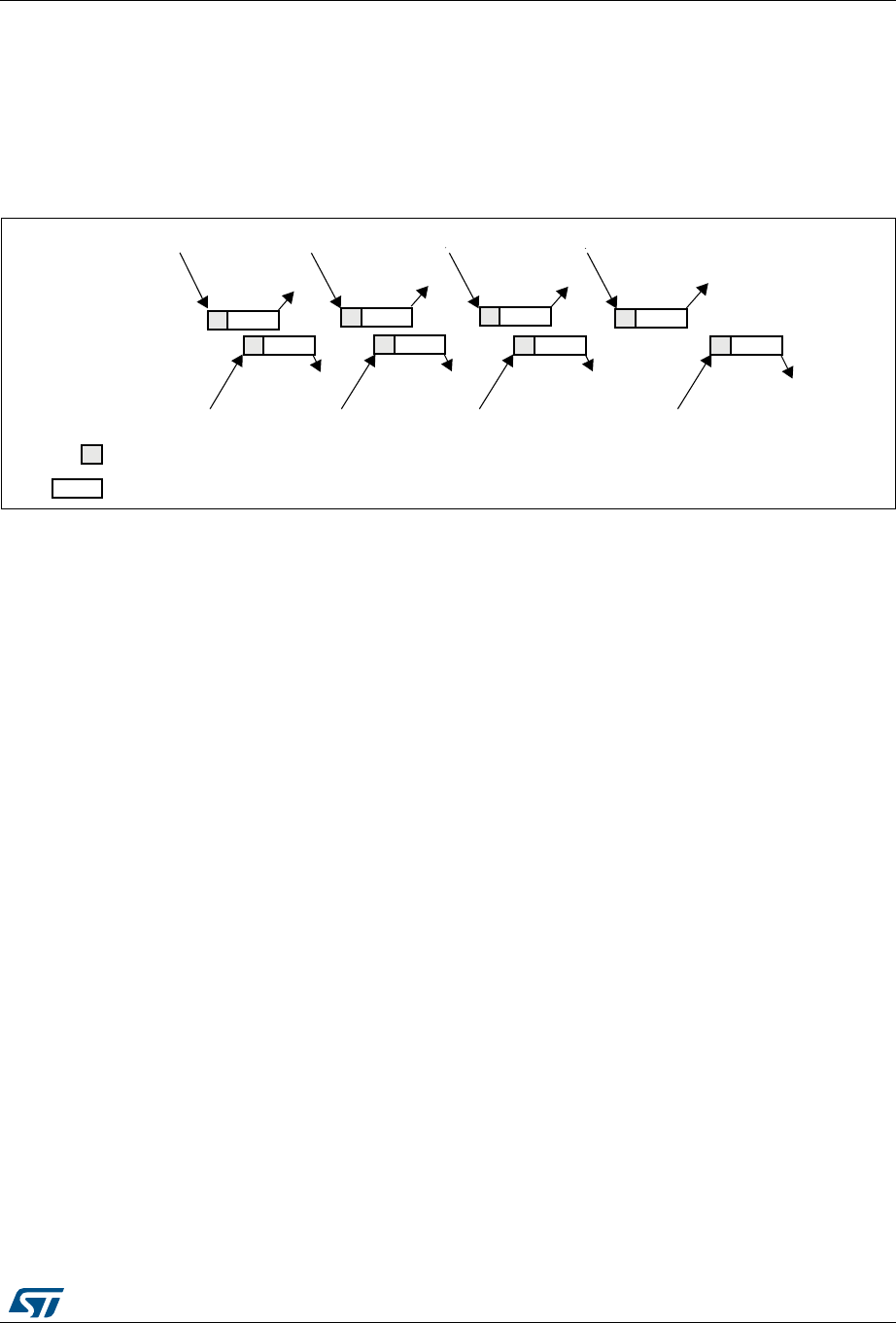
RM0394 Rev 4 439/1600
RM0394 Analog-to-digital converters (ADC)
485
A JEOS interrupt, if enabled, is generated after all injected channels of the slave ADC in the
group have been converted.
JEOC interrupts, if enabled, can also be generated after each injected conversions.
If another external trigger occurs after all injected channels in the group have been
converted then the alternate trigger process restarts.
Figure 97. Alternate trigger: 4 injected channels (each ADC) in discontinuous mode
Combined regular/injected simultaneous mode
This mode is selected by programming bits DUAL[4:0] = 00001.
It is possible to interrupt the simultaneous conversion of a regular group to start the
simultaneous conversion of an injected group.
Note: In combined regular/injected simultaneous mode, one must convert sequences with the
same length or ensure that the interval between triggers is longer than the long conversion
time of the 2 sequences. Otherwise, the ADC with the shortest sequence may restart while
the ADC with the longest sequence is completing the previous conversions.
Combined regular simultaneous + alternate trigger mode
This mode is selected by programming bits DUAL[4:0]=00010.
It is possible to interrupt the simultaneous conversion of a regular group to start the alternate
trigger conversion of an injected group. Figure 98 shows the behavior of an alternate trigger
interrupting a simultaneous regular conversion.
The injected alternate conversion is immediately started after the injected event. If a regular
conversion is already running, in order to ensure synchronization after the injected
conversion, the regular conversion of all (master/slave) ADCs is stopped and resumed
synchronously at the end of the injected conversion.
Note: In combined regular simultaneous + alternate trigger mode, one must convert sequences
with the same length or ensure that the interval between triggers is longer than the long
conversion time of the 2 sequences. Otherwise, the ADC with the shortest sequence may
restart while the ADC with the longest sequence is completing the previous conversions.
VWWULJJHU
QGWULJJHU
UGWULJJHU
WKWULJJHU
WKWULJJHU
WKWULJJHU
WKWULJJHU
WKWULJJHU
-(2&-(26RQ
PDVWHU$'&
DL9P
0$67(5$'&
6/$9($'&
-(2&RQ
PDVWHU$'&
-(2&-(26RQ
PDVWHU$'&
-(2&RQ
PDVWHU$'& -(2&RQ
PDVWHU$'&
-(2&RQ
PDVWHU$'&
-(2&RQ
PDVWHU$'&
-(2&RQ
PDVWHU$'&
6DPSOLQJ
&RQYHUVLRQ
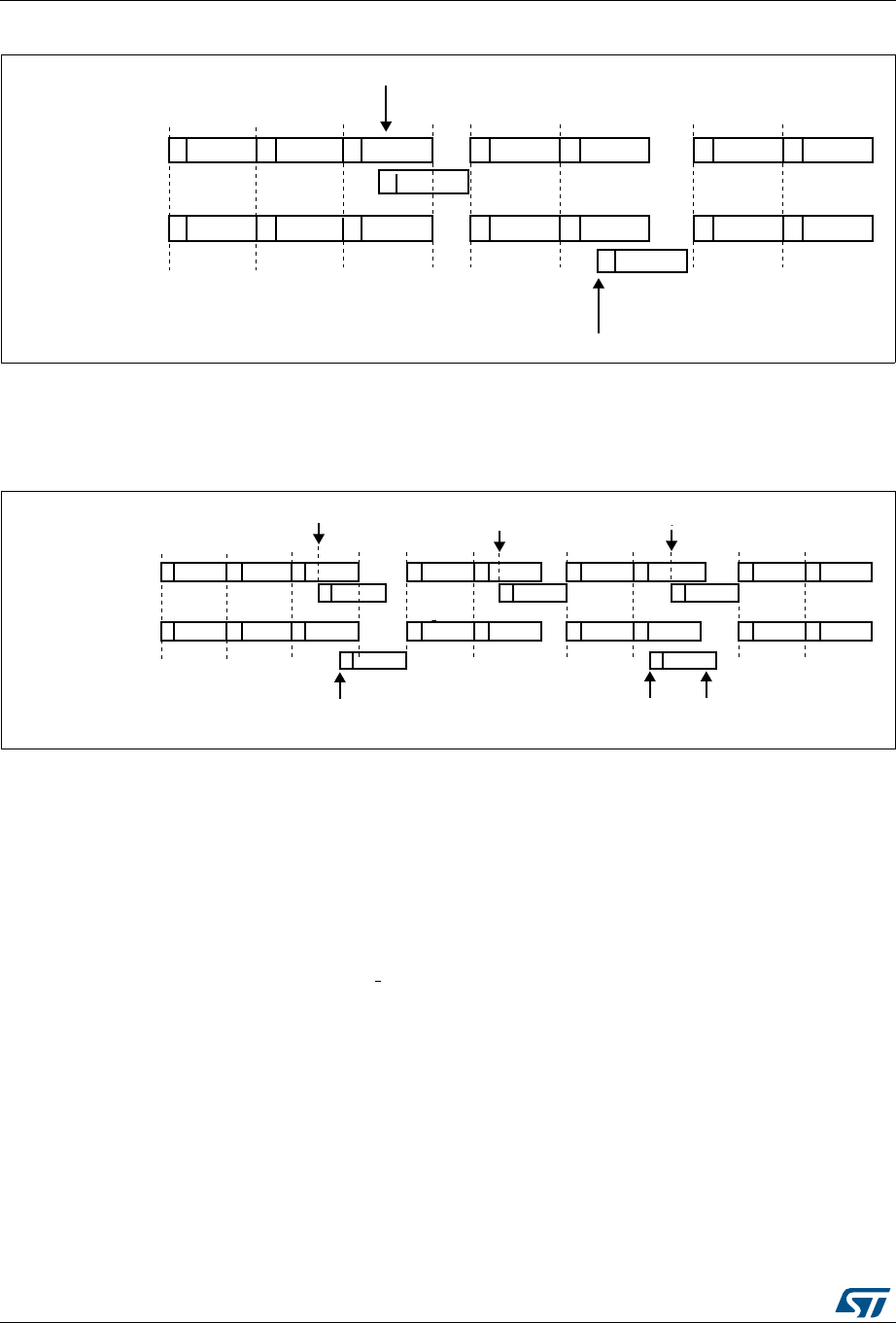
Analog-to-digital converters (ADC) RM0394
440/1600 RM0394 Rev 4
Figure 98. Alternate + regular simultaneous
If a trigger occurs during an injected conversion that has interrupted a regular conversion,
the alternate trigger is served. Figure 99 shows the behavior in this case (note that the 6th
trigger is ignored because the associated alternate conversion is not complete).
Figure 99. Case of trigger occurring during injected conversion
Combined injected simultaneous plus interleaved
This mode is selected by programming bits DUAL[4:0]=00011
It is possible to interrupt an interleaved conversion with a simultaneous injected event.
In this case the interleaved conversion is interrupted immediately and the simultaneous
injected conversion starts. At the end of the injected sequence the interleaved conversion is
resumed. When the interleaved regular conversion resumes, the first regular conversion
which is performed is alway the master’s one. Figure 100, Figure 101 and Figure 102 show
the behavior using an example.
Caution: In this mode, it is mandatory to use the Common Data Register to read the regular data with
a single read access. On the contrary, master-slave data coherency is not guaranteed.
$'&0$67(5UHJ &+ &+ &+
&+
&+ &+
&+
$'&0$67(5LQM
$'&6/$9(UHJ
$'&6/$9(LQM
VWWULJJHU
QGWULJJHU
V\QFKURQRWORVW
&+ &+ &+ &+ &+
&+ &+
&+ &+
DL9P
$'&0$67(5UHJ &+
&+
&+
$'&0$67(5LQM
$'&6/$9(UHJ
$'&6/$9(LQM
VWWULJJHU
QGWULJJHU
&+ &+
&+
&+
DL9
&+
WKWULJJHU
UGWULJJHU
&+
&+
WKWULJJHU
&+
WKWULJJHU
LJQRUHG
&+
&+
&+
&+
&+ &+ &+
&+ &+ &+
&+
&+
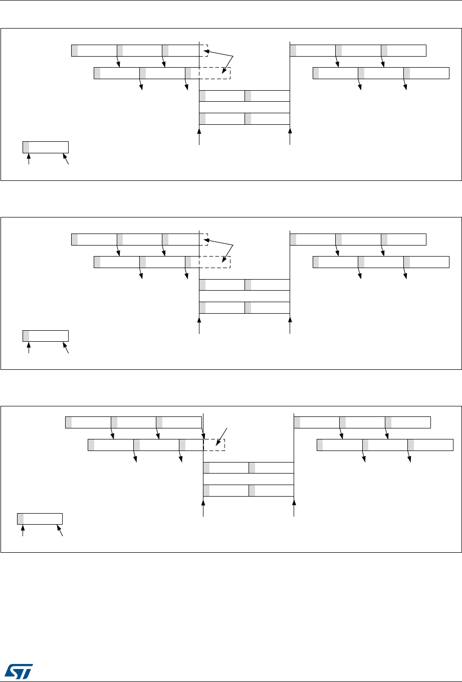
RM0394 Rev 4 441/1600
RM0394 Analog-to-digital converters (ADC)
485
Figure 100. Interleaved single channel CH0 with injected sequence CH11, CH12
Figure 101. Two Interleaved channels (CH1, CH2) with injected sequence CH11, CH12
- case 1: Master interrupted first
Figure 102. Two Interleaved channels (CH1, CH2) with injected sequence CH11, CH12
- case 2: Slave interrupted first
069
/HJHQG
6DPSOLQJ &RQYHUVLRQ
$'&PDVWHU &+ &+ &+
&+
&+ &+ &+
&+ &+ &+&+ &+ &+$'&VODYH
UHDG
&'5
UHDG
&'5
UHDG
&'5
UHDG
&'5
&+
&+ &+
,QMHFWHGWULJJHU 5HVXPH
DOZD\VUHVWDUWZLWKWKHPDVWHU
&RQYHUVLRQV
DERUWHG
069
/HJHQG
6DPSOLQJ &RQYHUVLRQ
$'&PDVWHU &+ &+ &+
&+
&+ &+ &+
&+ &+ &+&+ &+ &+$'&VODYH
UHDG
&'5
UHDG
&'5
UHDG
&'5
UHDG
&'5
&+
&+ &+
,QMHFWHGWULJJHU 5HVXPH
DOZD\VUHVWDUWZLWKWKHPDVWHU
&RQYHUVLRQV
DERUWHG
069
/HJHQG
6DPSOLQJ &RQYHUVLRQ
$'&PDVWHU &+ &+ &+
&+
&+ &+ &+
&+ &+ &+&+ &+ &+$'&VODYH
UHDG
&'5
UHDG
&'5
UHDG
&'5
UHDG
&'5
&+
&+ &+
,QMHFWHGWULJJHU 5HVXPH
DOZD\VUHVWDUWZLWKWKHPDVWHU
&RQYHUVLRQV
DERUWHG
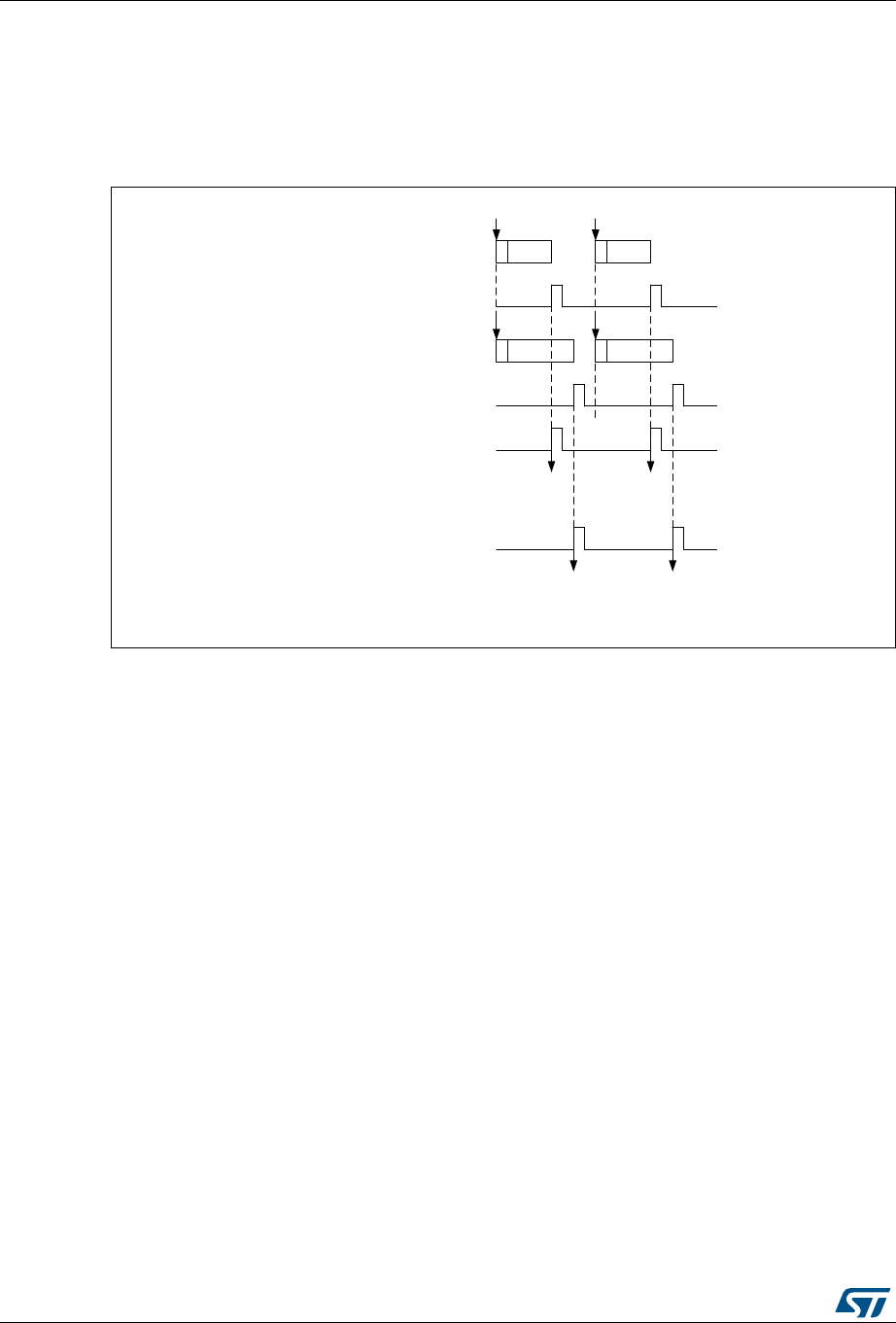
Analog-to-digital converters (ADC) RM0394
442/1600 RM0394 Rev 4
DMA requests in dual ADC mode
In all dual ADC modes, it is possible to use two DMA channels (one for the master, one for
the slave) to transfer the data, like in single mode (refer to Figure 103: DMA Requests in
regular simultaneous mode when MDMA=0b00).
Figure 103. DMA Requests in regular simultaneous mode when MDMA=0b00
In simultaneous regular and interleaved modes, it is also possible to save one DMA channel
and transfer both data using a single DMA channel. For this MDMA bits must be configured
in the ADCx_CCR register:
•MDMA=0b10: A single DMA request is generated each time both master and slave
EOC events have occurred. At that time, two data items are available and the 32-bit
register ADCx_CDR contains the two half-words representing two ADC-converted data
items. The slave ADC data take the upper half-word and the master ADC data take the
lower half-word.
This mode is used in interleaved mode and in regular simultaneous mode when
resolution is 10-bit or 12-bit.
Example:
Interleaved dual mode: a DMA request is generated each time 2 data items are
available:
1st DMA request: ADCx_CDR[31:0] = SLV_ADC_DR[15:0] | MST_ADC_DR[15:0]
2nd DMA request: ADCx_CDR[31:0] = SLV_ADC_DR[15:0] |
MST_ADC_DR[15:0]
06Y9
&+$'&0DVWHUUHJXODU
&+
7ULJJHU 7ULJJHU
&+
&+
&RQILJXUDWLRQZKHUHHDFKVHTXHQFHFRQWDLQVRQO\RQHFRQYHUVLRQ
$'&0DVWHU(2&
$'&6ODYHUHJXODU
$'&6ODYH(2&
'0$UHTXHVWIURP$'&0DVWHU
'0$UHTXHVWIURP$'&6ODYH
'0$UHDGV0DVWHU
$'&B'5
'0$UHDGV0DWHU
$'&B'5
'0$UHDGV6ODYH
$'&B'5
'0$UHDGV6ODYH
$'&B'5
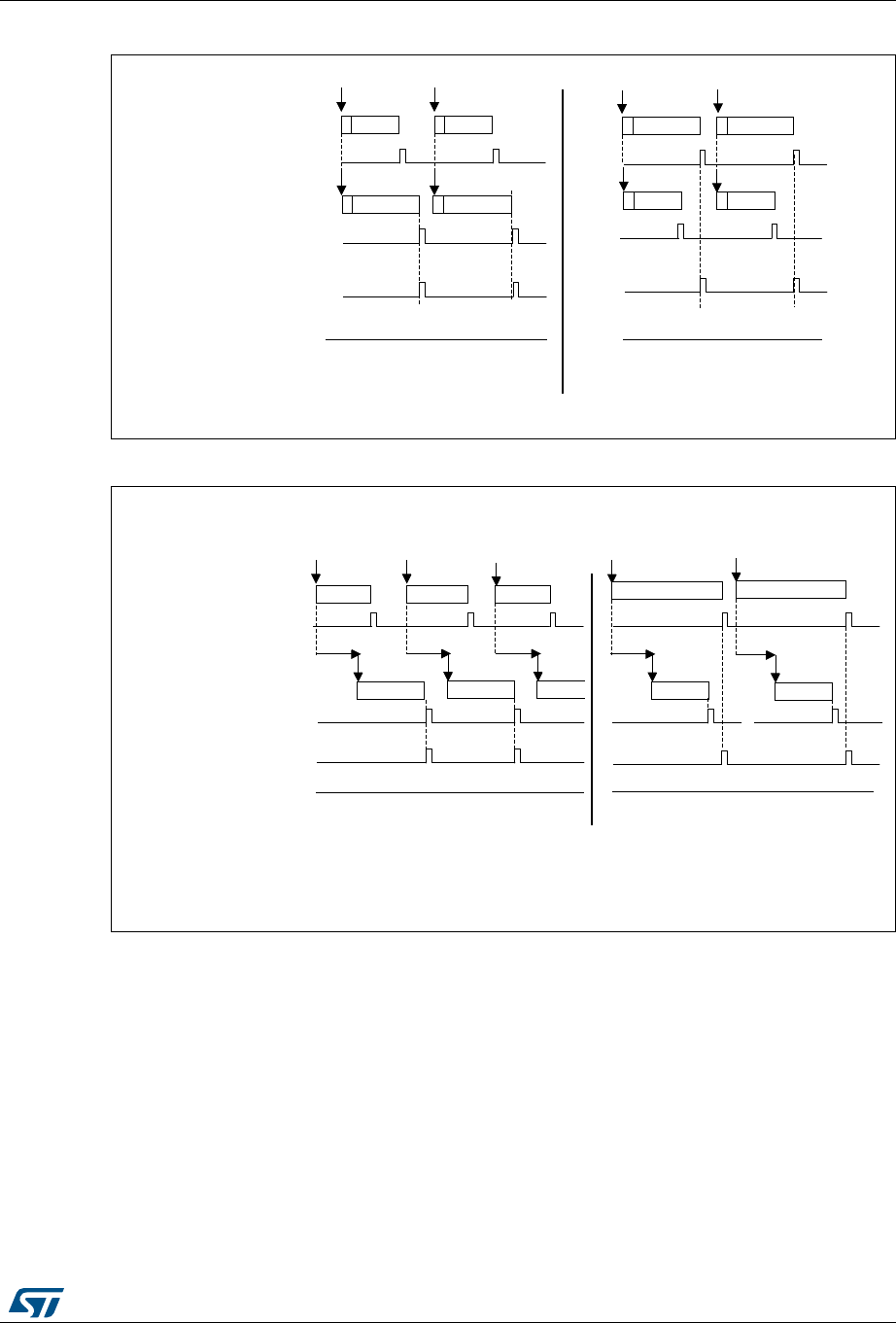
RM0394 Rev 4 443/1600
RM0394 Analog-to-digital converters (ADC)
485
Figure 104. DMA requests in regular simultaneous mode when MDMA=0b10
Figure 105. DMA requests in interleaved mode when MDMA=0b10
06Y9
$'&0DVWHUUHJXODU
$'&6ODYH(2&
&+
7ULJJHU
&+
7ULJJHU
&+ &+
&RQILJXUDWLRQZKHUHHDFKVHTXHQFHFRQWDLQVRQO\RQHFRQYHUVLRQ
$'&6ODYHUHJXODU
$'&6ODYH(2&
'0$UHTXHVWIURP
$'&0DVWHU
'0$UHTXHVWIURP
$'&6ODYH
&+
7ULJJHU
&+
7ULJJHU
&+ &+
06Y9
$'&0DVWHUUHJXODU
$'&0DVWHU(2&
&+
7ULJJHU
&+
7ULJJHU
&+
&RQILJXUDWLRQZKHUHHDFKVHTXHQFHFRQWDLQVRQO\RQHFRQYHUVLRQ
$'&6ODYHUHJXODU
$'&6ODYH(2&
'0$UHTXHVWIURP
$'&0DVWHU
'0$UHTXHVWIURP
$'&6ODYH
7ULJJHU 7ULJJHU
&+ &+
&+
7ULJJHU
'HOD\
&+
'HOD\ 'HOD\
&+ &+
'HOD\
&+
'HOD\

Analog-to-digital converters (ADC) RM0394
444/1600 RM0394 Rev 4
Note: When using MDMA mode, the user must take care to configure properly the duration of the
master and slave conversions so that a DMA request is generated and served for reading
both data (master + slave) before a new conversion is available.
•MDMA=0b11: This mode is similar to the MDMA=0b10. The only differences are that
on each DMA request (two data items are available), two bytes representing two ADC
converted data items are transferred as a half-word.
This mode is used in interleaved and regular simultaneous mode when resolution is 6-
bit or when resolution is 8-bit and data is not signed (offsets must be disabled for all the
involved channels).
Example:
Interleaved dual mode: a DMA request is generated each time 2 data items are
available:
1st DMA request: ADCx_CDR[15:0] = SLV_ADC_DR[7:0] | MST_ADC_DR[7:0]
2nd DMA request: ADCx_CDR[15:0] = SLV_ADC_DR[7:0] | MST_ADC_DR[7:0]
Overrun detection
In dual ADC mode (when DUAL[4:0] is not equal to b00000), if an overrun is detected on
one of the ADCs, the DMA requests are no longer issued to ensure that all the data
transferred to the RAM are valid (this behavior occurs whatever the MDMA configuration). It
may happen that the EOC bit corresponding to one ADC remains set because the data
register of this ADC contains valid data.
DMA one shot mode/ DMA circular mode when MDMA mode is selected
When MDMA mode is selected (0b10 or 0b11), bit DMACFG of the ADCx_CCR register
must also be configured to select between DMA one shot mode and circular mode, as
explained in section Section : Managing conversions using the DMA (bits DMACFG of
master and slave ADC_CFGR are not relevant).
Stopping the conversions in dual ADC modes
The user must set the control bits ADSTP/JADSTP of the master ADC to stop the
conversions of both ADC in dual ADC mode. The other ADSTP control bit of the slave ADC
has no effect in dual ADC mode.
Once both ADC are effectively stopped, the bits ADSTART/JADSTART of the master and
slave ADCs are both cleared by hardware.
16.4.32 Temperature sensor
The temperature sensor can be used to measure the junction temperature (Tj) of the device.
The temperature sensor is internally connected to the ADC input channels which are used
to convert the sensor output voltage to a digital value. When not in use, the sensor can be
put in power down mode. It support the temperature range –40 to 125 °C.
Figure 106 shows the block diagram of connections between the temperature sensor and
the ADC.
The temperature sensor output voltage changes linearly with temperature. The offset of this
line varies from chip to chip due to process variation (up to 45 °C from one chip to another).
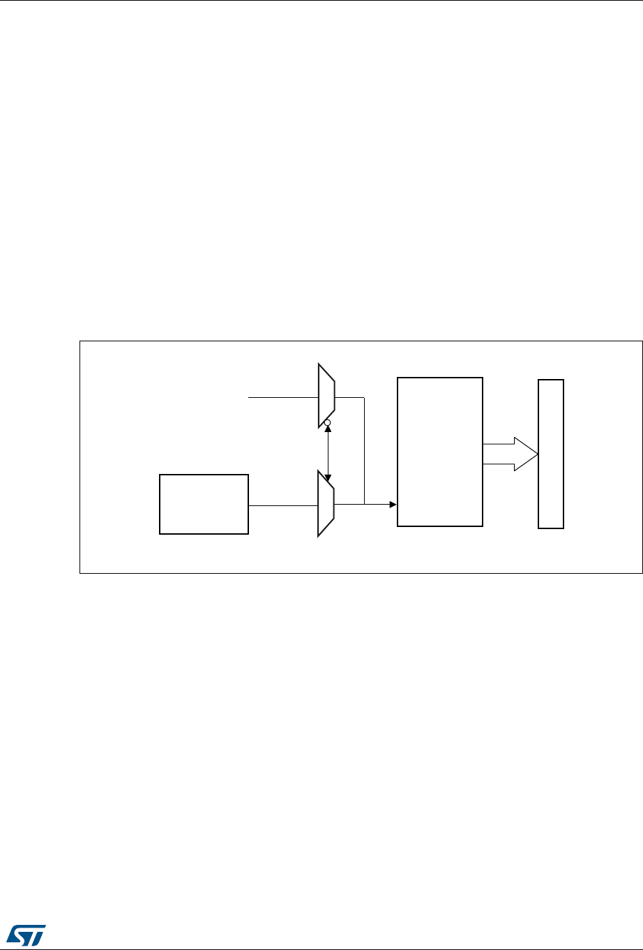
RM0394 Rev 4 445/1600
RM0394 Analog-to-digital converters (ADC)
485
The uncalibrated internal temperature sensor is more suited for applications that detect
temperature variations instead of absolute temperatures. To improve the accuracy of the
temperature sensor measurement, calibration values are stored in system memory for each
device by ST during production.
During the manufacturing process, the calibration data of the temperature sensor and the
internal voltage reference are stored in the system memory area. The user application can
then read them and use them to improve the accuracy of the temperature sensor or the
internal reference (refer to the datasheet for additional information).
The temperature sensor is internally connected to the ADC input channel which is used to
convert the sensor’s output voltage to a digital value. Refer to the electrical characteristics
section of the device datasheet for the sampling time value to be applied when converting
the internal temperature sensor.
When not in use, the sensor can be put in power-down mode.
Figure 106 shows the block diagram of the temperature sensor. The dac_out1 signal and
the temperature sensor share the same input.
Figure 106. Temperature sensor channel block diagram
Reading the temperature
To use the sensor:
1. Select the ADC input channels which is connected to VTS.
2. Program with the appropriate sampling time (refer to electrical characteristics section of
the device datasheet).
3. Set the CH17SEL bit in the ADCx_CCR register to wake up the temperature sensor
from power-down mode.
4. Start the ADC conversion.
5. Read the resulting VTS data in the ADC data register.
6. Calculate the actual temperature using the following formula:
06Y9
976
&+6(/FRQWUROELW $'&[
$'&&+
LQSXW
$GGUHVVGDWDEXV
7HPSHUDWXUH
VHQVRU
GDFBRXW
&RQYHUWHG
GDWD

Analog-to-digital converters (ADC) RM0394
446/1600 RM0394 Rev 4
Where:
•TS_CAL2 is the temperature sensor calibration value acquired at TS_CAL2_TEMP.
•TS_CAL1 is the temperature sensor calibration value acquired at TS_CAL1_TEMP.
•TS_DATA is the actual temperature sensor output value converted by ADC.
Refer to the device datasheet for more information about TS_CAL1 and TS_CAL2
calibration points.
Note: The sensor has a startup time after waking from power-down mode before it can output VTS
at the correct level. The ADC also has a startup time after power-on, so to minimize the
delay, the ADEN and CH17SEL bits should be set at the same time.
16.4.33 VBAT supply monitoring
The CH18SEL bit in the ADCx_CCR register is used to switch to the battery voltage. As the
VBAT voltage could be higher than VDDA, to ensure the correct operation of the ADC, the
VBAT pin is internally connected to a bridge divider by 3. This bridge is automatically enabled
when CH18SEL is set, to connect VBAT/3 to the ADC input channels. As a consequence, the
converted digital value is one third of the VBAT voltage. To prevent any unwanted
consumption on the battery, it is recommended to enable the bridge divider only when
needed, for ADC conversion.
Refer to the electrical characteristics of the device datasheet for the sampling time value to
be applied when converting the VBAT/3 voltage.
The figure below shows the block diagram of the VBAT sensing feature. The dac_out2 signal
and VBAT sensing input share the same input.
Temperature in °C()
TS_CAL2_TEMP TS_CAL1_TEMP–
TS_CAL2 TS_CAL1–
--------------------------------------------------------------------------------------------------TS_DATA TS_CAL1–()30 °C+×=
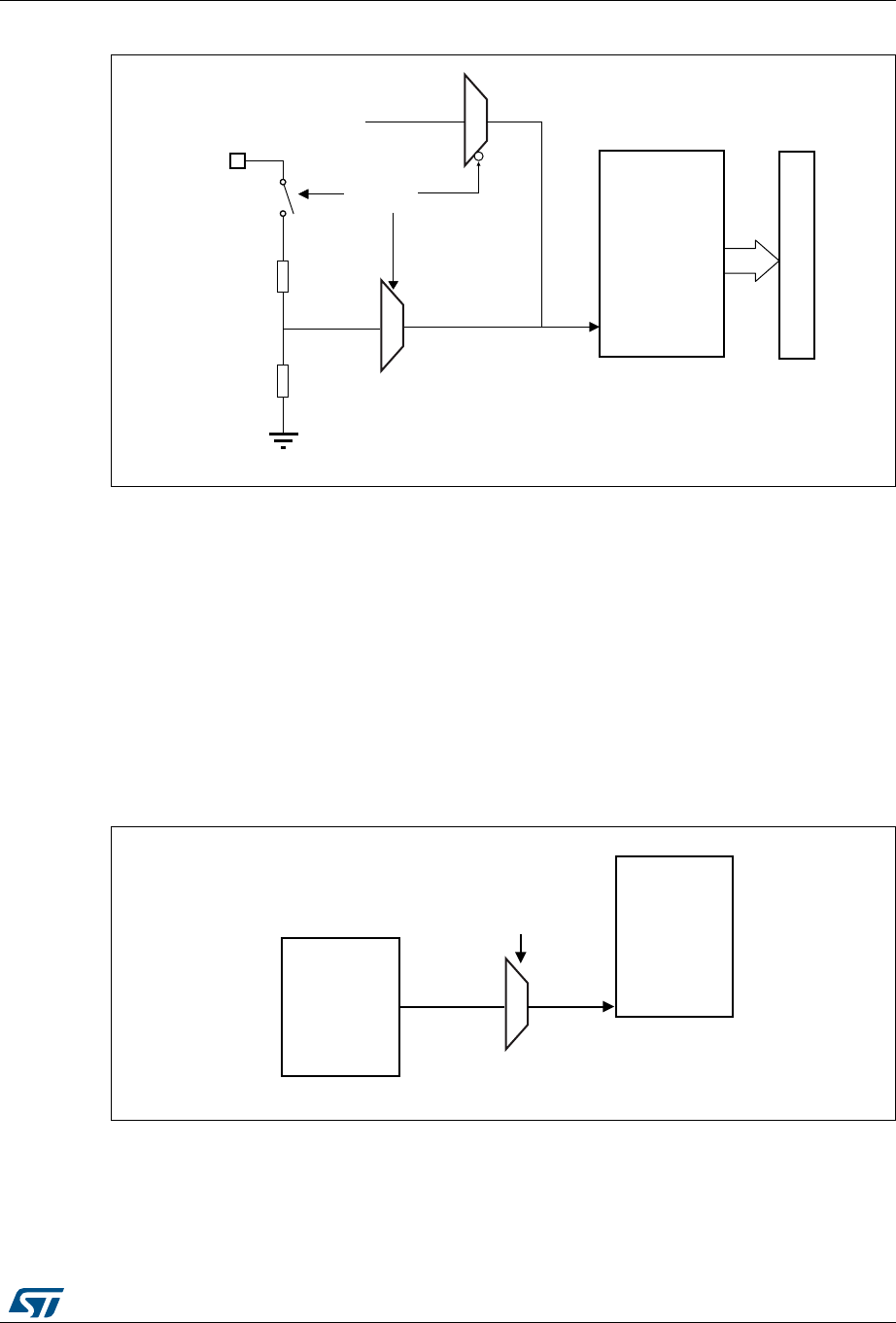
RM0394 Rev 4 447/1600
RM0394 Analog-to-digital converters (ADC)
485
Figure 107. VBAT channel block diagram
1. The CH18SEL bit must be set to enable the conversion of internal channel for VBAT/3.
16.4.34 Monitoring the internal voltage reference
It is possible to monitor the internal voltage reference (VREFINT) to have a reference point for
evaluating the ADC VREF+ voltage level.
The internal voltage reference is internally connected to the input channel 0 of the ADC1
(ADC1_INP0).
Refer to the electrical characteristics section of the product datasheet for the sampling time
value to be applied when converting the internal voltage reference voltage.
Figure 108 shows the block diagram of the VREFINT sensing feature.
Figure 108. VREFINT channel block diagram
1. The VREFEN bit into ADCx_CCR register must be set to enable the conversion of internal channels
(VREFINT).
06Y9
9%$7
9%$7
&+6(/
$'&[
$'&LQSXW
$GGUHVVGDWDEXV
GDFBRXW
06Y9
95(),17
$'&[
$'&LQSXW
95()(1FRQWUROELW
,QWHUQDO
SRZHUEORFN

Analog-to-digital converters (ADC) RM0394
448/1600 RM0394 Rev 4
Calculating the actual VDDA voltage using the internal reference voltage
The VDDA power supply voltage applied to the microcontroller may be subject to variation or
not precisely known. The embedded internal voltage reference (VREFINT) and its calibration
data acquired by the ADC during the manufacturing process at VDDA = 3.0 V can be used to
evaluate the actual VDDA voltage level.
The following formula gives the actual VDDA voltage supplying the device:
VDDA = 3.0 V x VREFINT_CAL / VREFINT_DATA
where:
•VREFINT_CAL is the VREFINT calibration value
•VREFINT_DATA is the actual VREFINT output value converted by ADC
Converting a supply-relative ADC measurement to an absolute voltage value
The ADC is designed to deliver a digital value corresponding to the ratio between the analog
power supply and the voltage applied on the converted channel. For most application use
cases, it is necessary to convert this ratio into a voltage independent of VDDA. For
applications where VDDA is known and ADC converted values are right-aligned you can use
the following formula to get this absolute value:
For applications where VDDA value is not known, you must use the internal voltage
reference and VDDA can be replaced by the expression provided in Calculating the actual
VDDA voltage using the internal reference voltage, resulting in the following formula:
Where:
•VREFINT_CAL is the VREFINT calibration value
•ADC_DATA is the value measured by the ADC on channel x (right-aligned)
•VREFINT_DATA is the actual VREFINT output value converted by the ADC
•FULL_SCALE is the maximum digital value of the ADC output. For example with 12-bit
resolution, it will be 212 1 = 4095 or with 8-bit resolution, 28 1 = 255.
Note: If ADC measurements are done using an output format other than 12 bit right-aligned, all the
parameters must first be converted to a compatible format before the calculation is done.
VCHANNELx
VDDA
FULL_SCALE
------------------------------------- ADCx_DATA×=
VCHANNELx
3.0 V VREFINT_CAL ADCx_DATA××
VREFINT_DATA FULL_SCALE×
--------------------------------------------------------------------------------------------------------
=
RM0394 Rev 4 449/1600
RM0394 Analog-to-digital converters (ADC)
485
16.5 ADC interrupts
For each ADC, an interrupt can be generated:
•after ADC power-up, when the ADC is ready (flag ADRDY)
•on the end of any conversion for regular groups (flag EOC)
•on the end of a sequence of conversion for regular groups (flag EOS)
•on the end of any conversion for injected groups (flag JEOC)
•on the end of a sequence of conversion for injected groups (flag JEOS)
•when an analog watchdog detection occurs (flag AWD1, AWD2 and AWD3)
•when the end of sampling phase occurs (flag EOSMP)
•when the data overrun occurs (flag OVR)
•when the injected sequence context queue overflows (flag JQOVF)
Separate interrupt enable bits are available for flexibility.
Table 68. ADC interrupts per each ADC
Interrupt event Event flag Enable control bit
ADC ready ADRDY ADRDYIE
End of conversion of a regular group EOC EOCIE
End of sequence of conversions of a regular group EOS EOSIE
End of conversion of a injected group JEOC JEOCIE
End of sequence of conversions of an injected group JEOS JEOSIE
Analog watchdog 1 status bit is set AWD1 AWD1IE
Analog watchdog 2 status bit is set AWD2 AWD2IE
Analog watchdog 3 status bit is set AWD3 AWD3IE
End of sampling phase EOSMP EOSMPIE
Overrun OVR OVRIE
Injected context queue overflows JQOVF JQOVFIE

Analog-to-digital converters (ADC) RM0394
450/1600 RM0394 Rev 4
16.6 ADC registers (for each ADC)
Refer to Section 1.2 on page 60 for a list of abbreviations used in register descriptions.
16.6.1 ADC interrupt and status register (ADC_ISR)
Address offset: 0x00
Reset value: 0x0000 0000
31 30 29 28 27 26 25 24 23 22 21 20 19 18 17 16
Res. Res. Res. Res. Res. Res. Res. Res. Res. Res. Res. Res. Res. Res. Res. Res.
1514131211109876543210
Res. Res. Res. Res. Res. JQOVF AWD3 AWD2 AWD1 JEOS JEOC OVR EOS EOC EOSMP ADRDY
rc_w1 rc_w1 rc_w1 rc_w1 rc_w1 rc_w1 rc_w1 rc_w1 rc_w1 rc_w1 rc_w1
Bits 31:11 Reserved, must be kept at reset value.
Bit 10 JQOVF: Injected context queue overflow
This bit is set by hardware when an Overflow of the Injected Queue of Context occurs. It is cleared
by software writing 1 to it. Refer to Section 16.4.21: Queue of context for injected conversions for
more information.
0: No injected context queue overflow occurred (or the flag event was already acknowledged and
cleared by software)
1: Injected context queue overflow has occurred
Bit 9 AWD3: Analog watchdog 3 flag
This bit is set by hardware when the converted voltage crosses the values programmed in the fields
LT3[7:0] and HT3[7:0] of ADC_TR3 register. It is cleared by software writing 1 to it.
0: No analog watchdog 3 event occurred (or the flag event was already acknowledged and cleared
by software)
1: Analog watchdog 3 event occurred
Bit 8 AWD2: Analog watchdog 2 flag
This bit is set by hardware when the converted voltage crosses the values programmed in the fields
LT2[7:0] and HT2[7:0] of ADC_TR2 register. It is cleared by software writing 1 to it.
0: No analog watchdog 2 event occurred (or the flag event was already acknowledged and cleared
by software)
1: Analog watchdog 2 event occurred
Bit 7 AWD1: Analog watchdog 1 flag
This bit is set by hardware when the converted voltage crosses the values programmed in the fields
LT1[11:0] and HT1[11:0] of ADC_TR1 register. It is cleared by software. writing 1 to it.
0: No analog watchdog 1 event occurred (or the flag event was already acknowledged and cleared
by software)
1: Analog watchdog 1 event occurred
Bit 6 JEOS: Injected channel end of sequence flag
This bit is set by hardware at the end of the conversions of all injected channels in the group. It is
cleared by software writing 1 to it.
0: Injected conversion sequence not complete (or the flag event was already acknowledged and
cleared by software)
1: Injected conversions complete

RM0394 Rev 4 451/1600
RM0394 Analog-to-digital converters (ADC)
485
Bit 5 JEOC: Injected channel end of conversion flag
This bit is set by hardware at the end of each injected conversion of a channel when a new data is
available in the corresponding ADC_JDRy register. It is cleared by software writing 1 to it or by
reading the corresponding ADC_JDRy register
0: Injected channel conversion not complete (or the flag event was already acknowledged and
cleared by software)
1: Injected channel conversion complete
Bit 4 OVR: ADC overrun
This bit is set by hardware when an overrun occurs on a regular channel, meaning that a new
conversion has completed while the EOC flag was already set. It is cleared by software writing 1 to
it.
0: No overrun occurred (or the flag event was already acknowledged and cleared by software)
1: Overrun has occurred
Bit 3 EOS: End of regular sequence flag
This bit is set by hardware at the end of the conversions of a regular sequence of channels. It is
cleared by software writing 1 to it.
0: Regular Conversions sequence not complete (or the flag event was already acknowledged and
cleared by software)
1: Regular Conversions sequence complete
Bit 2 EOC: End of conversion flag
This bit is set by hardware at the end of each regular conversion of a channel when a new data is
available in the ADC_DR register. It is cleared by software writing 1 to it or by reading the ADC_DR
register
0: Regular channel conversion not complete (or the flag event was already acknowledged and
cleared by software)
1: Regular channel conversion complete
Bit 1 EOSMP: End of sampling flag
This bit is set by hardware during the conversion of any channel (only for regular channels), at the
end of the sampling phase.
0: not at the end of the sampling phase (or the flag event was already acknowledged and cleared by
software)
1: End of sampling phase reached
Bit 0 ADRDY: ADC ready
This bit is set by hardware after the ADC has been enabled (bit ADEN=1) and when the ADC
reaches a state where it is ready to accept conversion requests.
It is cleared by software writing 1 to it.
0: ADC not yet ready to start conversion (or the flag event was already acknowledged and cleared
by software)
1: ADC is ready to start conversion

Analog-to-digital converters (ADC) RM0394
452/1600 RM0394 Rev 4
16.6.2 ADC interrupt enable register (ADC_IER)
Address offset: 0x04
Reset value: 0x0000 0000
31 30 29 28 27 26 25 24 23 22 21 20 19 18 17 16
Res. Res. Res. Res. Res. Res. Res. Res. Res. Res. Res. Res. Res. Res. Res. Res.
15 14 13 12 11 10 9 8 7 6 5 4 3 2 1 0
Res. Res. Res. Res. Res. JQOVF
IE
AWD3I
E
AWD2I
E
AWD1I
EJEOSIE JEOCIE OVRIE EOSIE EOCIE EOSMP
IE
ADRDY
IE
rw rw rw rw rw rw rw rw rw rw rw
Bits 31:11 Reserved, must be kept at reset value.
Bit 10 JQOVFIE: Injected context queue overflow interrupt enable
This bit is set and cleared by software to enable/disable the Injected Context Queue Overflow
interrupt.
0: Injected Context Queue Overflow interrupt disabled
1: Injected Context Queue Overflow interrupt enabled. An interrupt is generated when the JQOVF bit
is set.
Note: The software is allowed to write this bit only when JADSTART=0 (which ensures that no
injected conversion is ongoing).
Bit 9 AWD3IE: Analog watchdog 3 interrupt enable
This bit is set and cleared by software to enable/disable the analog watchdog 2 interrupt.
0: Analog watchdog 3 interrupt disabled
1: Analog watchdog 3 interrupt enabled
Note: The software is allowed to write this bit only when ADSTART=0 and JADSTART=0 (which
ensures that no conversion is ongoing).
Bit 8 AWD2IE: Analog watchdog 2 interrupt enable
This bit is set and cleared by software to enable/disable the analog watchdog 2 interrupt.
0: Analog watchdog 2 interrupt disabled
1: Analog watchdog 2 interrupt enabled
Note: The software is allowed to write this bit only when ADSTART=0 and JADSTART=0 (which
ensures that no conversion is ongoing).
Bit 7 AWD1IE: Analog watchdog 1 interrupt enable
This bit is set and cleared by software to enable/disable the analog watchdog 1 interrupt.
0: Analog watchdog 1 interrupt disabled
1: Analog watchdog 1 interrupt enabled
Note: The software is allowed to write this bit only when ADSTART=0 and JADSTART=0 (which
ensures that no conversion is ongoing).
Bit 6 JEOSIE: End of injected sequence of conversions interrupt enable
This bit is set and cleared by software to enable/disable the end of injected sequence of conversions
interrupt.
0: JEOS interrupt disabled
1: JEOS interrupt enabled. An interrupt is generated when the JEOS bit is set.
Note: The software is allowed to write this bit only when JADSTART=0 (which ensures that no
injected conversion is ongoing).

RM0394 Rev 4 453/1600
RM0394 Analog-to-digital converters (ADC)
485
Bit 5 JEOCIE: End of injected conversion interrupt enable
This bit is set and cleared by software to enable/disable the end of an injected conversion interrupt.
0: JEOC interrupt disabled.
1: JEOC interrupt enabled. An interrupt is generated when the JEOC bit is set.
Note: The software is allowed to write this bit only when JADSTART=0 (which ensures that no regular
conversion is ongoing).
Bit 4 OVRIE: Overrun interrupt enable
This bit is set and cleared by software to enable/disable the Overrun interrupt of a regular
conversion.
0: Overrun interrupt disabled
1: Overrun interrupt enabled. An interrupt is generated when the OVR bit is set.
Note: The software is allowed to write this bit only when ADSTART=0 (which ensures that no regular
conversion is ongoing).
Bit 3 EOSIE: End of regular sequence of conversions interrupt enable
This bit is set and cleared by software to enable/disable the end of regular sequence of conversions
interrupt.
0: EOS interrupt disabled
1: EOS interrupt enabled. An interrupt is generated when the EOS bit is set.
Note: The software is allowed to write this bit only when ADSTART=0 (which ensures that no regular
conversion is ongoing).
Bit 2 EOCIE: End of regular conversion interrupt enable
This bit is set and cleared by software to enable/disable the end of a regular conversion interrupt.
0: EOC interrupt disabled.
1: EOC interrupt enabled. An interrupt is generated when the EOC bit is set.
Note: The software is allowed to write this bit only when ADSTART=0 (which ensures that no regular
conversion is ongoing).
Bit 1 EOSMPIE: End of sampling flag interrupt enable for regular conversions
This bit is set and cleared by software to enable/disable the end of the sampling phase interrupt for
regular conversions.
0: EOSMP interrupt disabled.
1: EOSMP interrupt enabled. An interrupt is generated when the EOSMP bit is set.
Note: The software is allowed to write this bit only when ADSTART=0 (which ensures that no regular
conversion is ongoing).
Bit 0 ADRDYIE: ADC ready interrupt enable
This bit is set and cleared by software to enable/disable the ADC Ready interrupt.
0: ADRDY interrupt disabled
1: ADRDY interrupt enabled. An interrupt is generated when the ADRDY bit is set.
Note: The software is allowed to write this bit only when ADSTART=0 and JADSTART=0 (which
ensures that no conversion is ongoing).

Analog-to-digital converters (ADC) RM0394
454/1600 RM0394 Rev 4
16.6.3 ADC control register (ADC_CR)
Address offset: 0x08
Reset value: 0x2000 0000
31 30 29 28 27 26 25 24 23 22 21 20 19 18 17 16
ADCA
L
ADCA
LDIF
DEEP
PWD
ADVREG
EN Res. Res. Res. Res. Res. Res. Res. Res. Res. Res. Res. Res.
rs rw rw rw
15 14 13 12 11 10 9 8 7 6 5 4 3 2 1 0
Res. Res. Res. Res. Res. Res. Res. Res. Res. Res. JADST
PADSTP JADST
ART
ADSTA
RT ADDIS ADEN
rs rs rs rs rs rs
Bit 31 ADCAL: ADC calibration
This bit is set by software to start the calibration of the ADC. Program first the bit ADCALDIF
to determine if this calibration applies for single-ended or differential inputs mode.
It is cleared by hardware after calibration is complete.
0: Calibration complete
1: Write 1 to calibrate the ADC. Read at 1 means that a calibration in progress.
Note: The software is allowed to launch a calibration by setting ADCAL only when ADEN=0.
The software is allowed to update the calibration factor by writing ADC_CALFACT only
when ADEN=1 and ADSTART=0 and JADSTART=0 (ADC enabled and no conversion is
ongoing)
Bit 30 ADCALDIF: Differential mode for calibration
This bit is set and cleared by software to configure the single-ended or differential inputs
mode for the calibration.
0: Writing ADCAL will launch a calibration in single-ended inputs mode.
1: Writing ADCAL will launch a calibration in differential inputs mode.
Note: The software is allowed to write this bit only when the ADC is disabled and is not
calibrating (ADCAL=0, JADSTART=0, JADSTP=0, ADSTART=0, ADSTP=0, ADDIS=0
and ADEN=0).
Bit 29 DEEPPWD: Deep-power-down enable
This bit is set and cleared by software to put the ADC in Deep-power-down mode.
0: ADC not in Deep-power down
1: ADC in Deep-power-down (default reset state)
Note: The software is allowed to write this bit only when the ADC is disabled (ADCAL=0,
JADSTART=0, JADSTP=0, ADSTART=0, ADSTP=0, ADDIS=0 and ADEN=0).
Bit 28 ADVREGEN: ADC voltage regulator enable
This bits is set by software to enable the ADC voltage regulator.
Before performing any operation such as launching a calibration or enabling the ADC, the
ADC voltage regulator must first be enabled and the software must wait for the regulator
start-up time.
0: ADC Voltage regulator disabled
1: ADC Voltage regulator enabled.
For more details about the ADC voltage regulator enable and disable sequences, refer to
Section 16.4.6: ADC Deep-power-down mode (DEEPPWD) and ADC voltage regulator
(ADVREGEN).
The software can program this bit field only when the ADC is disabled (ADCAL=0,
JADSTART=0, ADSTART=0, ADSTP=0, ADDIS=0 and ADEN=0).

RM0394 Rev 4 455/1600
RM0394 Analog-to-digital converters (ADC)
485
Bits 27:6 Reserved, must be kept at reset value.
Bit 5 JADSTP: ADC stop of injected conversion command
This bit is set by software to stop and discard an ongoing injected conversion (JADSTP
Command).
It is cleared by hardware when the conversion is effectively discarded and the ADC injected
sequence and triggers can be re-configured. The ADC is then ready to accept a new start of
injected conversions (JADSTART command).
0: No ADC stop injected conversion command ongoing
1: Write 1 to stop injected conversions ongoing. Read 1 means that an ADSTP command is
in progress.
Note: The software is allowed to set JADSTP only when JADSTART=1 and ADDIS=0 (ADC is
enabled and eventually converting an injected conversion and there is no pending
request to disable the ADC)
In auto-injection mode (JAUTO=1), setting ADSTP bit aborts both regular and injected
conversions (do not use JADSTP)
Bit 4 ADSTP: ADC stop of regular conversion command
This bit is set by software to stop and discard an ongoing regular conversion (ADSTP
Command).
It is cleared by hardware when the conversion is effectively discarded and the ADC regular
sequence and triggers can be re-configured. The ADC is then ready to accept a new start of
regular conversions (ADSTART command).
0: No ADC stop regular conversion command ongoing
1: Write 1 to stop regular conversions ongoing. Read 1 means that an ADSTP command is in
progress.
Note: The software is allowed to set ADSTP only when ADSTART=1 and ADDIS=0 (ADC is
enabled and eventually converting a regular conversion and there is no pending request
to disable the ADC).
In auto-injection mode (JAUTO=1), setting ADSTP bit aborts both regular and injected
conversions (do not use JADSTP).
Bit 3 JADSTART: ADC start of injected conversion
This bit is set by software to start ADC conversion of injected channels. Depending on the
configuration bits JEXTEN, a conversion will start immediately (software trigger
configuration) or once an injected hardware trigger event occurs (hardware trigger
configuration).
It is cleared by hardware:
– in single conversion mode when software trigger is selected (JEXTSEL=0x0): at the
assertion of the End of Injected Conversion Sequence (JEOS) flag.
– in all cases: after the execution of the JADSTP command, at the same time that JADSTP is
cleared by hardware.
0: No ADC injected conversion is ongoing.
1: Write 1 to start injected conversions. Read 1 means that the ADC is operating and
eventually converting an injected channel.
Note: The software is allowed to set JADSTART only when ADEN=1 and ADDIS=0 (ADC is
enabled and there is no pending request to disable the ADC).
In auto-injection mode (JAUTO=1), regular and auto-injected conversions are started by
setting bit ADSTART (JADSTART must be kept cleared)

Analog-to-digital converters (ADC) RM0394
456/1600 RM0394 Rev 4
Bits 27:6 Reserved, must be kept at reset value.
Bit 5 JADSTP: ADC stop of injected conversion command
This bit is set by software to stop and discard an ongoing injected conversion (JADSTP
Command).
It is cleared by hardware when the conversion is effectively discarded and the ADC injected
sequence and triggers can be re-configured. The ADC is then ready to accept a new start of
injected conversions (JADSTART command).
0: No ADC stop injected conversion command ongoing
1: Write 1 to stop injected conversions ongoing. Read 1 means that an ADSTP command is
in progress.
Note: The software is allowed to set JADSTP only when JADSTART=1 and ADDIS=0 (ADC is
enabled and eventually converting an injected conversion and there is no pending
request to disable the ADC)
In auto-injection mode (JAUTO=1), setting ADSTP bit aborts both regular and injected
conversions (do not use JADSTP)
Bit 4 ADSTP: ADC stop of regular conversion command
This bit is set by software to stop and discard an ongoing regular conversion (ADSTP
Command).
It is cleared by hardware when the conversion is effectively discarded and the ADC regular
sequence and triggers can be re-configured. The ADC is then ready to accept a new start of
regular conversions (ADSTART command).
0: No ADC stop regular conversion command ongoing
1: Write 1 to stop regular conversions ongoing. Read 1 means that an ADSTP command is in
progress.
Note: The software is allowed to set ADSTP only when ADSTART=1 and ADDIS=0 (ADC is
enabled and eventually converting a regular conversion and there is no pending request
to disable the ADC).
In auto-injection mode (JAUTO=1), setting ADSTP bit aborts both regular and injected
conversions (do not use JADSTP).
Bit 3 JADSTART: ADC start of injected conversion
This bit is set by software to start ADC conversion of injected channels. Depending on the
configuration bits JEXTEN, a conversion will start immediately (software trigger
configuration) or once an injected hardware trigger event occurs (hardware trigger
configuration).
It is cleared by hardware:
– in single conversion mode when software trigger is selected (JEXTSEL=0x0): at the
assertion of the End of Injected Conversion Sequence (JEOS) flag.
– in all cases: after the execution of the JADSTP command, at the same time that JADSTP is
cleared by hardware.
0: No ADC injected conversion is ongoing.
1: Write 1 to start injected conversions. Read 1 means that the ADC is operating and
eventually converting an injected channel.
Note: The software is allowed to set JADSTART only when ADEN=1 and ADDIS=0 (ADC is
enabled and there is no pending request to disable the ADC).
In auto-injection mode (JAUTO=1), regular and auto-injected conversions are started by
setting bit ADSTART (JADSTART must be kept cleared)

RM0394 Rev 4 457/1600
RM0394 Analog-to-digital converters (ADC)
485
Bit 2 ADSTART: ADC start of regular conversion
This bit is set by software to start ADC conversion of regular channels. Depending on the
configuration bits EXTEN, a conversion will start immediately (software trigger configuration)
or once a regular hardware trigger event occurs (hardware trigger configuration).
It is cleared by hardware:
– in single conversion mode when software trigger is selected (EXTSEL=0x0): at the assertion
of the End of Regular Conversion Sequence (EOS) flag.
– in all cases: after the execution of the ADSTP command, at the same time that ADSTP is
cleared by hardware.
0: No ADC regular conversion is ongoing.
1: Write 1 to start regular conversions. Read 1 means that the ADC is operating and
eventually converting a regular channel.
Note: The software is allowed to set ADSTART only when ADEN=1 and ADDIS=0 (ADC is
enabled and there is no pending request to disable the ADC)
In auto-injection mode (JAUTO=1), regular and auto-injected conversions are started by
setting bit ADSTART (JADSTART must be kept cleared)
Bit 1 ADDIS: ADC disable command
This bit is set by software to disable the ADC (ADDIS command) and put it into power-down
state (OFF state).
It is cleared by hardware once the ADC is effectively disabled (ADEN is also cleared by
hardware at this time).
0: no ADDIS command ongoing
1: Write 1 to disable the ADC. Read 1 means that an ADDIS command is in progress.
Note: The software is allowed to set ADDIS only when ADEN=1 and both ADSTART=0 and
JADSTART=0 (which ensures that no conversion is ongoing)
Bit 0 ADEN: ADC enable control
This bit is set by software to enable the ADC. The ADC will be effectively ready to operate
once the flag ADRDY has been set.
It is cleared by hardware when the ADC is disabled, after the execution of the ADDIS
command.
0: ADC is disabled (OFF state)
1: Write 1 to enable the ADC.
Note: The software is allowed to set ADEN only when all bits of ADC_CR registers are 0
(ADCAL=0, JADSTART=0, ADSTART=0, ADSTP=0, ADDIS=0 and ADEN=0) except for
bit ADVREGEN which must be 1 (and the software must have wait for the startup time of
the voltage regulator)

Analog-to-digital converters (ADC) RM0394
458/1600 RM0394 Rev 4
16.6.4 ADC configuration register (ADC_CFGR)
Address offset: 0x0C
Reset value: 0x8000 0000
31 30 29 28 27 26 25 24 23 22 21 20 19 18 17 16
JQDIS AWD1CH[4:0] JAUTO JAWD1
EN
AWD1
EN
AWD1S
GL JQM JDISC
EN DISCNUM[2:0] DISC
EN
rw rw rw rw rw rw rw rw rw rw rw rw rw rw rw rw
1514131211109876543210
Res. AUT
DLY CONT OVR
MOD EXTEN[1:0] EXTSE
L3
EXTSE
L2
EXTSE
L1
EXTSE
L0 ALIGN RES[1:0] DFSD
MCFG
DMA
CFG
DMA
EN
rw rw rw rw rw rw rw rw rw rw rw rw rw rw rw
Bit 31 JQDIS: Injected Queue disable
These bits are set and cleared by software to disable the Injected Queue mechanism :
0: Injected Queue enabled
1: Injected Queue disabled
Note: The software is allowed to write this bit only when ADSTART=0 and JADSTART=0 (which
ensures that no regular nor injected conversion is ongoing).
A set or reset of JQDIS bit causes the injected queue to be flushed and the JSQR register is
cleared.
Bits 30:26 AWD1CH[4:0]: Analog watchdog 1 channel selection
These bits are set and cleared by software. They select the input channel to be guarded by the
analog watchdog.
00000: ADC analog input channel 0 monitored by AWD1 (available on ADC1 only)
00001: ADC analog input channel 1 monitored by AWD1
.....
10010: ADC analog input channel 18 monitored by AWD1
others: reserved, must not be used
Note: The channel selected by AWD1CH must be also selected into the SQRi or JSQRi registers.
The software is allowed to write these bits only when ADSTART=0 and JADSTART=0 (which
ensures that no conversion is ongoing).
Bit 25 JAUTO: Automatic injected group conversion
This bit is set and cleared by software to enable/disable automatic injected group conversion after
regular group conversion.
0: Automatic injected group conversion disabled
1: Automatic injected group conversion enabled
Note: The software is allowed to write this bit only when ADSTART=0 and JADSTART=0 (which
ensures that no regular nor injected conversion is ongoing).
When dual mode is enabled (DUAL bits in ADCx_CCR register are not equal to zero), the bit
JAUTO of the slave ADC is no more writable and its content is equal to the bit JAUTO of the
master ADC.
Bit 24 JAWD1EN: Analog watchdog 1 enable on injected channels
This bit is set and cleared by software
0: Analog watchdog 1 disabled on injected channels
1: Analog watchdog 1 enabled on injected channels
Note: The software is allowed to write this bit only when JADSTART=0 (which ensures that no
injected conversion is ongoing).

RM0394 Rev 4 459/1600
RM0394 Analog-to-digital converters (ADC)
485
Bit 23 AWD1EN: Analog watchdog 1 enable on regular channels
This bit is set and cleared by software
0: Analog watchdog 1 disabled on regular channels
1: Analog watchdog 1 enabled on regular channels
Note: The software is allowed to write this bit only when ADSTART=0 (which ensures that no regular
conversion is ongoing).
Bit 22 AWD1SGL: Enable the watchdog 1 on a single channel or on all channels
This bit is set and cleared by software to enable the analog watchdog on the channel identified by
the AWD1CH[4:0] bits or on all the channels
0: Analog watchdog 1 enabled on all channels
1: Analog watchdog 1 enabled on a single channel
Note: The software is allowed to write these bits only when ADSTART=0 and JADSTART=0 (which
ensures that no conversion is ongoing).
Bit 21 JQM: JSQR queue mode
This bit is set and cleared by software.
It defines how an empty Queue is managed.
0: JSQR mode 0: The Queue is never empty and maintains the last written configuration into JSQR.
1: JSQR mode 1: The Queue can be empty and when this occurs, the software and hardware
triggers of the injected sequence are both internally disabled just after the completion of the last valid
injected sequence.
Refer to Section 16.4.21: Queue of context for injected conversions for more information.
Note: The software is allowed to write this bit only when JADSTART=0 (which ensures that no
injected conversion is ongoing).
When dual mode is enabled (DUAL bits in ADCx_CCR register are not equal to zero), the bit
JQM of the slave ADC is no more writable and its content is equal to the bit JQM of the master
ADC.
Bit 20 JDISCEN: Discontinuous mode on injected channels
This bit is set and cleared by software to enable/disable discontinuous mode on the injected
channels of a group.
0: Discontinuous mode on injected channels disabled
1: Discontinuous mode on injected channels enabled
Note: The software is allowed to write this bit only when JADSTART=0 (which ensures that no
injected conversion is ongoing).
It is not possible to use both auto-injected mode and discontinuous mode simultaneously: the
bits DISCEN and JDISCEN must be kept cleared by software when JAUTO is set.
When dual mode is enabled (bits DUAL of ADCx_CCR register are not equal to zero), the bit
JDISCEN of the slave ADC is no more writable and its content is equal to the bit JDISCEN of
the master ADC.
Bits 19:17 DISCNUM[2:0]: Discontinuous mode channel count
These bits are written by software to define the number of regular channels to be converted in
discontinuous mode, after receiving an external trigger.
000: 1 channel
001: 2 channels
...
111: 8 channels
Note: The software is allowed to write these bits only when ADSTART=0 (which ensures that no
regular conversion is ongoing).
When dual mode is enabled (DUAL bits in ADCx_CCR register are not equal to zero), the bits
DISCNUM[2:0] of the slave ADC are no more writable and their content is equal to the bits
DISCNUM[2:0] of the master ADC.

Analog-to-digital converters (ADC) RM0394
460/1600 RM0394 Rev 4
Bit 16 DISCEN: Discontinuous mode for regular channels
This bit is set and cleared by software to enable/disable Discontinuous mode for regular channels.
0: Discontinuous mode for regular channels disabled
1: Discontinuous mode for regular channels enabled
Note: It is not possible to have both discontinuous mode and continuous mode enabled: it is forbidden
to set both DISCEN=1 and CONT=1.
It is not possible to use both auto-injected mode and discontinuous mode simultaneously: the
bits DISCEN and JDISCEN must be kept cleared by software when JAUTO is set.
The software is allowed to write this bit only when ADSTART=0 (which ensures that no regular
conversion is ongoing).
When dual mode is enabled (DUAL bits in ADCx_CCR register are not equal to zero), the bit
DISCEN of the slave ADC is no more writable and its content is equal to the bit DISCEN of the
master ADC.
Bit 15 Reserved, must be kept at reset value.
Bit 14 AUTDLY: Delayed conversion mode
This bit is set and cleared by software to enable/disable the Auto Delayed Conversion mode..
0: Auto-delayed conversion mode off
1: Auto-delayed conversion mode on
Note: The software is allowed to write this bit only when ADSTART=0 and JADSTART=0 (which
ensures that no conversion is ongoing).
When dual mode is enabled (DUAL bits in ADCx_CCR register are not equal to zero), the bit
AUTDLY of the slave ADC is no more writable and its content is equal to the bit AUTDLY of the
master ADC.
Bit 13 CONT: Single / continuous conversion mode for regular conversions
This bit is set and cleared by software. If it is set, regular conversion takes place continuously until it
is cleared.
0: Single conversion mode
1: Continuous conversion mode
Note: It is not possible to have both discontinuous mode and continuous mode enabled: it is forbidden
to set both DISCEN=1 and CONT=1.
The software is allowed to write this bit only when ADSTART=0 (which ensures that no regular
conversion is ongoing).
When dual mode is enabled (DUAL bits in ADCx_CCR register are not equal to zero), the bit
CONT of the slave ADC is no more writable and its content is equal to the bit CONT of the
master ADC.
Bit 12 OVRMOD: Overrun mode
This bit is set and cleared by software and configure the way data overrun is managed.
0: ADC_DR register is preserved with the old data when an overrun is detected.
1: ADC_DR register is overwritten with the last conversion result when an overrun is detected.
Note: The software is allowed to write this bit only when ADSTART=0 (which ensures that no regular
conversion is ongoing).
Bits 11:10 EXTEN[1:0]: External trigger enable and polarity selection for regular channels
These bits are set and cleared by software to select the external trigger polarity and enable the
trigger of a regular group.
00: Hardware trigger detection disabled (conversions can be launched by software)
01: Hardware trigger detection on the rising edge
10: Hardware trigger detection on the falling edge
11: Hardware trigger detection on both the rising and falling edges
Note: The software is allowed to write these bits only when ADSTART=0 (which ensures that no
regular conversion is ongoing).

RM0394 Rev 4 461/1600
RM0394 Analog-to-digital converters (ADC)
485
Bits 9:6 EXTSEL[3:0]: External trigger selection for regular group
These bits select the external event used to trigger the start of conversion of a regular group:
0000: Event 0
0001: Event 1
0010: Event 2
0011: Event 3
0100: Event 4
0101: Event 5
0110: Event 6
0111: Event 7
...
1111: Event 15
Note: The software is allowed to write these bits only when ADSTART=0 (which ensures that no
regular conversion is ongoing).
Bit 5 ALIGN: Data alignment
This bit is set and cleared by software to select right or left alignment. Refer to Section : Data
register, data alignment and offset (ADC_DR, OFFSETy, OFFSETy_CH, ALIGN)
0: Right alignment
1: Left alignment
Note: The software is allowed to write this bit only when ADSTART=0 and JADSTART=0 (which
ensures that no conversion is ongoing).
Bits 4:3 RES[1:0]: Data resolution
These bits are written by software to select the resolution of the conversion.
00: 12-bit
01: 10-bit
10: 8-bit
11: 6-bit
Note: The software is allowed to write these bits only when ADSTART=0 and JADSTART=0 (which
ensures that no conversion is ongoing).

Analog-to-digital converters (ADC) RM0394
462/1600 RM0394 Rev 4
16.6.5 ADC configuration register 2 (ADC_CFGR2)
Address offset: 0x10
Reset value: 0x0000 0000
Bit 2 DFSDMCFG: DFSDM mode configuration
This bit is set and cleared by software to enable the DFSDM mode. It is effective only when
DMAEN=0.
0: DFSDM mode disabled
1: DFSDM mode enabled
Note: To make sure no conversion is ongoing, the software is allowed to write this bit only when
ADSTART= 0 and JADSTART= 0.
Bit 1 DMACFG: Direct memory access configuration
This bit is set and cleared by software to select between two DMA modes of operation and is
effective only when DMAEN=1.
0: DMA One Shot mode selected
1: DMA Circular mode selected
For more details, refer to Section : Managing conversions using the DMA
Note: The software is allowed to write this bit only when ADSTART=0 and JADSTART=0 (which
ensures that no conversion is ongoing).
In dual-ADC modes, this bit is not relevant and replaced by control bit DMACFG of the
ADCx_CCR register.
Bit 0 DMAEN: Direct memory access enable
This bit is set and cleared by software to enable the generation of DMA requests. This allows to use
the DMA to manage automatically the converted data. For more details, refer to Section : Managing
conversions using the DMA.
0: DMA disabled
1: DMA enabled
Note: The software is allowed to write this bit only when ADSTART=0 and JADSTART=0 (which
ensures that no conversion is ongoing).
In dual-ADC modes, this bit is not relevant and replaced by control bits MDMA[1:0] of the
ADCx_CCR register.
31 30 29 28 27 26 25 24 23 22 21 20 19 18 17 16
Res. Res. Res. Res. Res. Res. Res. Res. Res. Res. Res. Res. Res. Res. Res. Res.
1514131211109876543210
Res. Res. Res. Res. Res. ROV
SM TROVS OVSS[3:0] OVSR[2:0] JOVSE ROVSE
rw rw rw rw rw rw rw rw rw rw rw
Bits 31:28 Reserved, must be kept at reset value.
Bits 27:17 Reserved, must be kept at reset value.
Bits 16:11 Reserved, must be kept at reset value.

RM0394 Rev 4 463/1600
RM0394 Analog-to-digital converters (ADC)
485
Bit 10 ROVSM: Regular Oversampling mode
This bit is set and cleared by software to select the regular oversampling mode.
0: Continued mode: When injected conversions are triggered, the oversampling is temporary
stopped and continued after the injection sequence (oversampling buffer is maintained during
injected sequence)
1: Resumed mode: When injected conversions are triggered, the current oversampling is aborted
and resumed from start after the injection sequence (oversampling buffer is zeroed by injected
sequence start)
Note: The software is allowed to write this bit only when ADSTART=0 (which ensures that no
conversion is ongoing).
Bit 9 TROVS: Triggered Regular Oversampling
This bit is set and cleared by software to enable triggered oversampling
0: All oversampled conversions for a channel are done consecutively following a trigger
1: Each oversampled conversion for a channel needs a new trigger
Note: The software is allowed to write this bit only when ADSTART=0 (which ensures that no
conversion is ongoing).
Bits 8:5 OVSS[3:0]: Oversampling shift
This bitfield is set and cleared by software to define the right shifting applied to the raw oversampling
result.
0000: No shift
0001: Shift 1-bit
0010: Shift 2-bits
0011: Shift 3-bits
0100: Shift 4-bits
0101: Shift 5-bits
0110: Shift 6-bits
0111: Shift 7-bits
1000: Shift 8-bits
Other codes reserved
Note: The software is allowed to write these bits only when ADSTART=0 (which ensures that no
conversion is ongoing).

Analog-to-digital converters (ADC) RM0394
464/1600 RM0394 Rev 4
16.6.6 ADC sample time register 1 (ADC_SMPR1)
Address offset: 0x14
Reset value: 0x0000 0000
Bits 4:2 OVSR[2:0]: Oversampling ratio
This bitfield is set and cleared by software to define the oversampling ratio.
000: 2x
001: 4x
010: 8x
011: 16x
100: 32x
101: 64x
110: 128x
111: 256x
Note: The software is allowed to write these bits only when ADSTART=0 (which ensures that no
conversion is ongoing).
Bit 1 JOVSE: Injected Oversampling Enable
This bit is set and cleared by software to enable injected oversampling.
0: Injected Oversampling disabled
1: Injected Oversampling enabled
Note: The software is allowed to write this bit only when ADSTART=0 and JADSTART=0 (which
ensures that no conversion is ongoing)
Bit 0 ROVSE: Regular Oversampling Enable
This bit is set and cleared by software to enable regular oversampling.
0: Regular Oversampling disabled
1: Regular Oversampling enabled
Note: The software is allowed to write this bit only when ADSTART=0 and JADSTART=0 (which
ensures that no conversion is ongoing)
31 30 29 28 27 26 25 24 23 22 21 20 19 18 17 16
Res. Res. SMP9[2:0] SMP8[2:0] SMP7[2:0] SMP6[2:0] SMP5[2:1]
rw rw rw rw rw rw rw rw rw rw rw rw rw rw
1514131211109876543210
SMP
5_0 SMP4[2:0] SMP3[2:0] SMP2[2:0] SMP1[2:0] SMP0[2:0]
rw rw rw rw rw rw rw rw rw rw rw rw rw rw rw rw
RM0394 Rev 4 465/1600
RM0394 Analog-to-digital converters (ADC)
485
16.6.7 ADC sample time register 2 (ADC_SMPR2)
Address offset: 0x18
Reset value: 0x0000 0000
16.6.8 ADC watchdog threshold register 1 (ADC_TR1)
Address offset: 0x20
Reset value: 0x0FFF 0000
Bits 31:30 Reserved, must be kept at reset value.
Bits 29:0 SMPx[2:0]: Channel x sampling time selection
These bits are written by software to select the sampling time individually for each channel.
During sample cycles, the channel selection bits must remain unchanged.
000: 2.5 ADC clock cycles
001: 6.5 ADC clock cycles
010: 12.5 ADC clock cycles
011: 24.5 ADC clock cycles
100: 47.5 ADC clock cycles
101: 92.5 ADC clock cycles
110: 247.5 ADC clock cycles
111: 640.5 ADC clock cycles
Note: The software is allowed to write these bits only when ADSTART=0 and JADSTART=0
(which ensures that no conversion is ongoing).
31 30 29 28 27 26 25 24 23 22 21 20 19 18 17 16
Res. Res. Res. Res. Res. SMP18[2:0] SMP17[2:0] SMP16[2:0] SMP15[2:1]
rw rw rw rw rw rw rw rw rw rw rw
15 14 13 12 11 10 9 8 7 6 5 4 3 2 1 0
SMP15_0 SMP14[2:0] SMP13[2:0] SMP12[2:0] SMP11[2:0] SMP10[2:0]
rw rw rw rw rw rw rw rw rw rw rw rw rw rw rw rw
Bits 31:27 Reserved, must be kept at reset value.
Bits 26:0 SMPx[2:0]: Channel x sampling time selection
These bits are written by software to select the sampling time individually for each channel.
During sampling cycles, the channel selection bits must remain unchanged.
000: 2.5 ADC clock cycles
001: 6.5 ADC clock cycles
010: 12.5 ADC clock cycles
011: 24.5 ADC clock cycles
100: 47.5 ADC clock cycles
101: 92.5 ADC clock cycles
110: 247.5 ADC clock cycles
111: 640.5 ADC clock cycles
Note: The software is allowed to write these bits only when ADSTART=0 and JADSTART=0
(which ensures that no conversion is ongoing).

Analog-to-digital converters (ADC) RM0394
466/1600 RM0394 Rev 4
16.6.9 ADC watchdog threshold register 2 (ADC_TR2)
Address offset: 0x24
Reset value: 0x00FF 0000
31 30 29 28 27 26 25 24 23 22 21 20 19 18 17 16
Res. Res. Res. Res. HT1[11:0]
rw rw rw rw rw rw rw rw rw rw rw rw
1514131211109876543210
Res. Res. Res. Res. LT1[11:0]
rw rw rw rw rw rw rw rw rw rw rw rw
Bits 31:28 Reserved, must be kept at reset value.
Bits 27:16 HT1[11:0]: Analog watchdog 1 higher threshold
These bits are written by software to define the higher threshold for the analog watchdog 1.
Refer to Section 16.4.29: Analog window watchdog (AWD1EN, JAWD1EN, AWD1SGL, AWD1CH,
AWD2CH, AWD3CH, AWD_HTx, AWD_LTx, AWDx)
Note: The software is allowed to write these bits only when ADSTART=0 and JADSTART=0 (which
ensures that no conversion is ongoing).
Bits 15:12 Reserved, must be kept at reset value.
Bits 11:0 LT1[11:0]: Analog watchdog 1 lower threshold
These bits are written by software to define the lower threshold for the analog watchdog 1.
Refer to Section 16.4.29: Analog window watchdog (AWD1EN, JAWD1EN, AWD1SGL, AWD1CH,
AWD2CH, AWD3CH, AWD_HTx, AWD_LTx, AWDx)
Note: The software is allowed to write these bits only when ADSTART=0 and JADSTART=0 (which
ensures that no conversion is ongoing).
31 30 29 28 27 26 25 24 23 22 21 20 19 18 17 16
Res. Res. Res. Res. Res. Res. Res. Res. HT2[7:0]
rw rw rw rw rw rw rw rw
1514131211109876543210
Res. Res. Res. Res. Res. Res. Res. Res. LT2[7:0]
rw rw rw rw rw rw rw rw
Bits 31:24 Reserved, must be kept at reset value.

RM0394 Rev 4 467/1600
RM0394 Analog-to-digital converters (ADC)
485
16.6.10 ADC watchdog threshold register 3 (ADC_TR3)
Address offset: 0x28
Reset value: 0x00FF 0000
Bits 23:16 HT2[7:0]: Analog watchdog 2 higher threshold
These bits are written by software to define the higher threshold for the analog watchdog 2.
Refer to Section 16.4.29: Analog window watchdog (AWD1EN, JAWD1EN, AWD1SGL, AWD1CH,
AWD2CH, AWD3CH, AWD_HTx, AWD_LTx, AWDx)
Note: The software is allowed to write these bits only when ADSTART=0 and JADSTART=0 (which
ensures that no conversion is ongoing).
Bits 15:8 Reserved, must be kept at reset value.
Bits 7:0 LT2[7:0]: Analog watchdog 2 lower threshold
These bits are written by software to define the lower threshold for the analog watchdog 2.
Refer to Section 16.4.29: Analog window watchdog (AWD1EN, JAWD1EN, AWD1SGL, AWD1CH,
AWD2CH, AWD3CH, AWD_HTx, AWD_LTx, AWDx)
Note: The software is allowed to write these bits only when ADSTART=0 and JADSTART=0 (which
ensures that no conversion is ongoing).
31 30 29 28 27 26 25 24 23 22 21 20 19 18 17 16
Res. Res. Res. Res. Res. Res. Res. Res. HT3[7:0]
rw rw rw rw rw rw rw rw
1514131211109876543210
Res. Res. Res. Res. Res. Res. Res. Res. LT3[7:0]
rw rw rw rw rw rw rw rw
Bits 31:24 Reserved, must be kept at reset value.
Bits 23:16 HT3[7:0]: Analog watchdog 3 higher threshold
These bits are written by software to define the higher threshold for the analog watchdog 3.
Refer to Section 16.4.29: Analog window watchdog (AWD1EN, JAWD1EN, AWD1SGL, AWD1CH,
AWD2CH, AWD3CH, AWD_HTx, AWD_LTx, AWDx)
Note: The software is allowed to write these bits only when ADSTART=0 and JADSTART=0 (which
ensures that no conversion is ongoing).
Bits 15:8 Reserved, must be kept at reset value.
Bits 7:0 LT3[7:0]: Analog watchdog 3 lower threshold
These bits are written by software to define the lower threshold for the analog watchdog 3.
This watchdog compares the 8-bit of LT3 with the 8 MSB of the converted data.
Note: The software is allowed to write these bits only when ADSTART=0 and JADSTART=0 (which
ensures that no conversion is ongoing).

Analog-to-digital converters (ADC) RM0394
468/1600 RM0394 Rev 4
16.6.11 ADC regular sequence register 1 (ADC_SQR1)
Address offset: 0x30
Reset value: 0x0000 0000
31 30 29 28 27 26 25 24 23 22 21 20 19 18 17 16
Res. Res. Res. SQ4[4:0] Res. SQ3[4:0] Res. SQ2[4]
rw rw rw rw rw rw rw rw rw rw rw
15 14 13 12 11 10 9 8 7 6 5 4 3 2 1 0
SQ2[3:0] Res. SQ1[4:0] Res. Res. L[3:0]
rw rw rw rw rw rw rw rw rw rw rw rw rw
Bits 31:29 Reserved, must be kept at reset value.
Bits 28:24 SQ4[4:0]: 4th conversion in regular sequence
These bits are written by software with the channel number (0..18) assigned as the 4th in the
regular conversion sequence.
Note: The software is allowed to write these bits only when ADSTART=0 (which ensures that
no regular conversion is ongoing).
Bit 23 Reserved, must be kept at reset value.
Bits 22:18 SQ3[4:0]: 3rd conversion in regular sequence
These bits are written by software with the channel number (0..18) assigned as the 3rd in the
regular conversion sequence.
Note: The software is allowed to write these bits only when ADSTART=0 (which ensures that
no regular conversion is ongoing).
Bit 17 Reserved, must be kept at reset value.
Bits 16:12 SQ2[4:0]: 2nd conversion in regular sequence
These bits are written by software with the channel number (0..18) assigned as the 2nd in
the regular conversion sequence.
Note: The software is allowed to write these bits only when ADSTART=0 (which ensures that
no regular conversion is ongoing).
Bit 11 Reserved, must be kept at reset value.
Bits 10:6 SQ1[4:0]: 1st conversion in regular sequence
These bits are written by software with the channel number (0..18) assigned as the 1st in the
regular conversion sequence.
Note: The software is allowed to write these bits only when ADSTART=0 (which ensures that
no regular conversion is ongoing).
Bits 5:4 Reserved, must be kept at reset value.
Bits 3:0 L[3:0]: Regular channel sequence length
These bits are written by software to define the total number of conversions in the regular
channel conversion sequence.
0000: 1 conversion
0001: 2 conversions
...
1111: 16 conversions
Note: The software is allowed to write these bits only when ADSTART=0 (which ensures that
no regular conversion is ongoing).

RM0394 Rev 4 469/1600
RM0394 Analog-to-digital converters (ADC)
485
16.6.12 ADC regular sequence register 2 (ADC_SQR2)
Address offset: 0x34
Reset value: 0x0000 0000
31 30 29 28 27 26 25 24 23 22 21 20 19 18 17 16
Res. Res. Res. SQ9[4:0] Res. SQ8[4:0] Res. SQ7[4]
rw rw rw rw rw rw rw rw rw rw rw
15 14 13 12 11 10 9 8 7 6 5 4 3 2 1 0
SQ7[3:0] Res. SQ6[4:0] Res. SQ5[4:0]
rw rw rw rw rw rw rw rw rw rw rw rw rw rw
Bits 31:29 Reserved, must be kept at reset value.
Bits 28:24 SQ9[4:0]: 9th conversion in regular sequence
These bits are written by software with the channel number (0..18) assigned as the 9th in the
regular conversion sequence.
Note: The software is allowed to write these bits only when ADSTART=0 (which ensures that
no regular conversion is ongoing).
Bit 23 Reserved, must be kept at reset value.
Bits 22:18 SQ8[4:0]: 8th conversion in regular sequence
These bits are written by software with the channel number (0..18) assigned as the 8th in the
regular conversion sequence
Note: The software is allowed to write these bits only when ADSTART=0 (which ensures that
no regular conversion is ongoing).
Bit 17 Reserved, must be kept at reset value.
Bits 16:12 SQ7[4:0]: 7th conversion in regular sequence
These bits are written by software with the channel number (0..18) assigned as the 7th in the
regular conversion sequence.
Note: The software is allowed to write these bits only when ADSTART=0 (which ensures that
no regular conversion is ongoing).
Bit 11 Reserved, must be kept at reset value.
Bits 10:6 SQ6[4:0]: 6th conversion in regular sequence
These bits are written by software with the channel number (0..18) assigned as the 6th in the
regular conversion sequence.
Note: The software is allowed to write these bits only when ADSTART=0 (which ensures that
no regular conversion is ongoing).
Bit 5 Reserved, must be kept at reset value.
Bits 4:0 SQ5[4:0]: 5th conversion in regular sequence
These bits are written by software with the channel number (0..18) assigned as the 5th in the
regular conversion sequence.
Note: The software is allowed to write these bits only when ADSTART=0 (which ensures that
no regular conversion is ongoing).

Analog-to-digital converters (ADC) RM0394
470/1600 RM0394 Rev 4
16.6.13 ADC regular sequence register 3 (ADC_SQR3)
Address offset: 0x38
Reset value: 0x0000 0000
31 30 29 28 27 26 25 24 23 22 21 20 19 18 17 16
Res. Res. Res. SQ14[4:0] Res. SQ13[4:0] Res. SQ12[4]
rw rw rw rw rw rw rw rw rw rw rw
15 14 13 12 11 10 9 8 7 6 5 4 3 2 1 0
SQ12[3:0] Res. SQ11[4:0] Res. SQ10[4:0]
rw rw rw rw rw rw rw rw rw rw rw rw rw rw
Bits 31:29 Reserved, must be kept at reset value.
Bits 28:24 SQ14[4:0]: 14th conversion in regular sequence
These bits are written by software with the channel number (0..18) assigned as the 14th in
the regular conversion sequence.
Note: The software is allowed to write these bits only when ADSTART=0 (which ensures that
no regular conversion is ongoing).
Bit 23 Reserved, must be kept at reset value.
Bits 22:18 SQ13[4:0]: 13th conversion in regular sequence
These bits are written by software with the channel number (0..18) assigned as the 13th in
the regular conversion sequence.
Note: The software is allowed to write these bits only when ADSTART=0 (which ensures that
no regular conversion is ongoing).
Bit 17 Reserved, must be kept at reset value.
Bits 16:12 SQ12[4:0]: 12th conversion in regular sequence
These bits are written by software with the channel number (0..18) assigned as the 12th in
the regular conversion sequence.
Note: The software is allowed to write these bits only when ADSTART=0 (which ensures that
no regular conversion is ongoing).
Bit 11 Reserved, must be kept at reset value.
Bits 10:6 SQ11[4:0]: 11th conversion in regular sequence
These bits are written by software with the channel number (0..18) assigned as the 11th in
the regular conversion sequence.
Note: The software is allowed to write these bits only when ADSTART=0 (which ensures that
no regular conversion is ongoing).
Bit 5 Reserved, must be kept at reset value.
Bits 4:0 SQ10[4:0]: 10th conversion in regular sequence
These bits are written by software with the channel number (0..18) assigned as the 10th in
the regular conversion sequence.
Note: The software is allowed to write these bits only when ADSTART=0 (which ensures that
no regular conversion is ongoing).

RM0394 Rev 4 471/1600
RM0394 Analog-to-digital converters (ADC)
485
16.6.14 ADC regular sequence register 4 (ADC_SQR4)
Address offset: 0x3C
Reset value: 0x0000 0000
16.6.15 ADC regular data register (ADC_DR)
Address offset: 0x40
Reset value: 0x0000 0000
31 30 29 28 27 26 25 24 23 22 21 20 19 18 17 16
Res. Res. Res. Res. Res. Res. Res. Res. Res. Res. Res. Res. Res. Res. Res. Res.
15 14 13 12 11 10 9 8 7 6 5 4 3 2 1 0
Res. Res. Res. Res. Res. SQ16[4:0] Res. SQ15[4:0]
rw rw rw rw rw rw rw rw rw rw
Bits 31:11 Reserved, must be kept at reset value.
Bits 10:6 SQ16[4:0]: 16th conversion in regular sequence
These bits are written by software with the channel number (0..18) assigned as the 16th in
the regular conversion sequence.
Note: The software is allowed to write these bits only when ADSTART=0 (which ensures that
no regular conversion is ongoing).
Bit 5 Reserved, must be kept at reset value.
Bits 4:0 SQ15[4:0]: 15th conversion in regular sequence
These bits are written by software with the channel number (0..18) assigned as the 15th in
the regular conversion sequence.
Note: The software is allowed to write these bits only when ADSTART=0 (which ensures that
no regular conversion is ongoing).
31 30 29 28 27 26 25 24 23 22 21 20 19 18 17 16
Res. Res. Res. Res. Res. Res. Res. Res. Res. Res. Res. Res. Res. Res. Res. Res.
1514131211109876543210
RDATA[15:0]
rrrrrrrrrrrrrrrr
Bits 31:16 Reserved, must be kept at reset value.
Bits 15:0 RDATA[15:0]: Regular Data converted
These bits are read-only. They contain the conversion result from the last converted regular channel.
The data are left- or right-aligned as described in Section 16.4.26: Data management.

Analog-to-digital converters (ADC) RM0394
472/1600 RM0394 Rev 4
16.6.16 ADC injected sequence register (ADC_JSQR)
Address offset: 0x4C
Reset value: 0x0000 0000
31 30 29 28 27 26 25 24 23 22 21 20 19 18 17 16
Res. JSQ4[4:0] Res. JSQ3[4:0] Res. JSQ2[4:2]
rw rw rw rw rw rw rw rw rw rw rw rw rw
15 14 13 12 11 10 9 8 7 6 5 4 3 2 1 0
JSQ2[1:0] Res. JSQ1[4:0] JEXTEN[1:0] JEXTSEL[3:0] JL[1:0]
rw rw rw rw rw rw rw rw rw rw rw rw rw rw
Bit 31 Reserved, must be kept at reset value.
Bits 30:26 JSQ4[4:0]: 4th conversion in the injected sequence
These bits are written by software with the channel number (0..18) assigned as the 4th in the
injected conversion sequence.
Note: The software is allowed to write these bits only when JADSTART=0 (which ensures that
no injected conversion is ongoing).
Bit 25 Reserved, must be kept at reset value.
Bits 24:20 JSQ3[4:0]: 3rd conversion in the injected sequence
These bits are written by software with the channel number (0..18) assigned as the 3rd in the
injected conversion sequence.
Note: The software is allowed to write these bits only when JADSTART=0 (which ensures that
no injected conversion is ongoing).
Bit 19 Reserved, must be kept at reset value.
Bits 18:14 JSQ2[4:0]: 2nd conversion in the injected sequence
These bits are written by software with the channel number (0..18) assigned as the 2nd in
the injected conversion sequence.
Note: The software is allowed to write these bits only when JADSTART=0 (which ensures that
no injected conversion is ongoing).
Bit 13 Reserved, must be kept at reset value.
Bits 12:8 JSQ1[4:0]: 1st conversion in the injected sequence
These bits are written by software with the channel number (0..18) assigned as the 1st in the
injected conversion sequence.
Note: The software is allowed to write these bits only when JADSTART=0 (which ensures that
no injected conversion is ongoing).

RM0394 Rev 4 473/1600
RM0394 Analog-to-digital converters (ADC)
485
16.6.17 ADC offset y register (ADC_OFRy)
Address offset: 0x60 + 0x04 * (y -1), (y= 1 to 4)
Reset value: 0x0000 0000
Bits 7:6 JEXTEN[1:0]: External Trigger Enable and Polarity Selection for injected channels
These bits are set and cleared by software to select the external trigger polarity and enable
the trigger of an injected group.
00: If JQDIS=0 (queue enabled), Hardware and software trigger detection disabled
00: If JQDIS=1 (queue disabled), Hardware trigger detection disabled (conversions can be
launched by software)
01: Hardware trigger detection on the rising edge
10: Hardware trigger detection on the falling edge
11: Hardware trigger detection on both the rising and falling edges
Note: The software is allowed to write these bits only when JADSTART=0 (which ensures that
no injected conversion is ongoing).
If JQM=1 and if the Queue of Context becomes empty, the software and hardware
triggers of the injected sequence are both internally disabled (refer to Section 16.4.21:
Queue of context for injected conversions)
Bits 5:2 JEXTSEL[3:0]: External Trigger Selection for injected group
These bits select the external event used to trigger the start of conversion of an injected
group:
0000: Event 0
0001: Event 1
0010: Event 2
0011: Event 3
0100: Event 4
0101: Event 5
0110: Event 6
0111: Event 7
...
1111: Event 15
Note: The software is allowed to write these bits only when JADSTART=0 (which ensures that
no injected conversion is ongoing).
Bits 1:0 JL[1:0]: Injected channel sequence length
These bits are written by software to define the total number of conversions in the injected
channel conversion sequence.
00: 1 conversion
01: 2 conversions
10: 3 conversions
11: 4 conversions
Note: The software is allowed to write these bits only when JADSTART=0 (which ensures that
no injected conversion is ongoing).
31 30 29 28 27 26 25 24 23 22 21 20 19 18 17 16
OFFSETy
_EN OFFSETy_CH[4:0] Res. Res. Res. Res. Res. Res. Res. Res. Res. Res.
rw rw rw rw rw rw
15 14 13 12 11 10 9 8 7 6 5 4 3 2 1 0
Res. Res. Res. Res. OFFSETy[11:0]
rw rw rw rw rw rw rw rw rw rw rw rw

Analog-to-digital converters (ADC) RM0394
474/1600 RM0394 Rev 4
16.6.18 ADC injected channel y data register (ADC_JDRy)
Address offset: 0x80 + 0x04 * (y - 1), (y = 1 to 4)
Reset value: 0x0000 0000
Bit 31 OFFSETy_EN: Offset y Enable
This bit is written by software to enable or disable the offset programmed into bits
OFFSETy[11:0].
Note: The software is allowed to write this bit only when ADSTART=0 and JADSTART=0
(which ensures that no conversion is ongoing).
Bits 30:26 OFFSETy_CH[4:0]: Channel selection for the Data offset y
These bits are written by software to define the channel to which the offset programmed into
bits OFFSETy[11:0] will apply.
Note: The software is allowed to write these bits only when ADSTART=0 and JADSTART=0
(which ensures that no conversion is ongoing).
Bits 25:12 Reserved, must be kept at reset value.
Bits 11:0 OFFSETy[11:0]: Data offset y for the channel programmed into bits OFFSETy_CH[4:0]
These bits are written by software to define the offset y to be subtracted from the raw
converted data when converting a channel (can be regular or injected). The channel to which
applies the data offset y must be programmed in the bits OFFSETy_CH[4:0]. The conversion
result can be read from in the ADC_DR (regular conversion) or from in the ADC_JDRyi
registers (injected conversion).
Note: The software is allowed to write these bits only when ADSTART=0 and JADSTART=0
(which ensures that no conversion is ongoing).
If several offset (OFFSETy) point to the same channel, only the offset with the lowest x
value is considered for the subtraction.
Ex: if OFFSET1_CH[4:0]=4 and OFFSET2_CH[4:0]=4, this is OFFSET1[11:0] which is
subtracted when converting channel 4.
31 30 29 28 27 26 25 24 23 22 21 20 19 18 17 16
Res. Res. Res. Res. Res. Res. Res. Res. Res. Res. Res. Res. Res. Res. Res. Res.
1514131211109876543210
JDATA[15:0]
rrrrrr r r r r rrrrrr
Bits 31:16 Reserved, must be kept at reset value.
Bits 15:0 JDATA[15:0]: Injected data
These bits are read-only. They contain the conversion result from injected channel y. The
data are left -or right-aligned as described in Section 16.4.26: Data management.

RM0394 Rev 4 475/1600
RM0394 Analog-to-digital converters (ADC)
485
16.6.19 ADC Analog Watchdog 2 Configuration Register (ADC_AWD2CR)
Address offset: 0xA0
Reset value: 0x0000 0000
16.6.20 ADC Analog Watchdog 3 Configuration Register (ADC_AWD3CR)
Address offset: 0xA4
Reset value: 0x0000 0000
31 30 29 28 27 26 25 24 23 22 21 20 19 18 17 16
Res. Res. Res. Res. Res. Res. Res. Res. Res. Res. Res. Res. Res. AWD2CH[18:16]
rw rw rw
151413121110987654321 0
AWD2CH[15:0]
rw rw rw rw rw rw rw rw rw rw rw rw rw rw rw rw
Bits 31:19 Reserved, must be kept at reset value.
Bits 18:0 AWD2CH[18:0]: Analog watchdog 2 channel selection
These bits are set and cleared by software. They enable and select the input channels to be guarded
by the analog watchdog 2.
AWD2CH[i] = 0: ADC analog input channel i is not monitored by AWD2
AWD2CH[i] = 1: ADC analog input channel i is monitored by AWD2
When AWD2CH[18:0] = 000..0, the analog Watchdog 2 is disabled
Note: The channels selected by AWD2CH must be also selected into the SQRi or JSQRi registers.
The software is allowed to write these bits only when ADSTART=0 and JADSTART=0 (which
ensures that no conversion is ongoing).
31 30 29 28 27 26 25 24 23 22 21 20 19 18 17 16
Res. Res. Res. Res. Res. Res. Res. Res. Res. Res. Res. Res. Res. AWD3CH[18:16]
1514131211109876543210
AWD3CH[15:0]
rw rw rw rw rw rw rw rw rw rw rw rw rw rw rw rw
Bits 31:19 Reserved, must be kept at reset value.
Bits 18:0 AWD3CH[18:0]: Analog watchdog 3 channel selection
These bits are set and cleared by software. They enable and select the input channels to be guarded
by the analog watchdog 3.
AWD3CH[i] = 0: ADC analog input channel i is not monitored by AWD3
AWD3CH[i] = 1: ADC analog input channel i is monitored by AWD3
When AWD3CH[18:0] = 000..0, the analog Watchdog 3 is disabled
Note: The channels selected by AWD3CH must be also selected into the SQRi or JSQRi registers.
The software is allowed to write these bits only when ADSTART=0 and JADSTART=0 (which
ensures that no conversion is ongoing).

Analog-to-digital converters (ADC) RM0394
476/1600 RM0394 Rev 4
16.6.21 ADC Differential mode Selection Register (ADC_DIFSEL)
Address offset: 0xB0
Reset value: 0x0000 0000
16.6.22 ADC Calibration Factors (ADC_CALFACT)
Address offset: 0xB4
Reset value: 0x0000 0000
31 30 29 28 27 26 25 24 23 22 21 20 19 18 17 16
Res. Res. Res. Res. Res. Res. Res. Res. Res. Res. Res. Res. Res. DIFSEL[18:16]
rrr
1514131211109876543210
DIFSEL[15:0]
rw rw rw rw rw rw rw rw rw rw rw rw rw rw rw r
Bits 31:19 Reserved, must be kept at reset value.
Bits 18:16 DIFSEL[18:16]: Differential mode for channels 18 to 16.
These bits are read only. These channels are forced to single-ended input mode (either connected to
a single-ended I/O port or to an internal channel).
Bits 15:1 DIFSEL[15:1]: Differential mode for channels 15 to 1
These bits are set and cleared by software. They allow to select if a channel is configured as single
ended or differential mode.
DIFSEL[i] = 0: ADC analog input channel i is configured in single ended mode
DIFSEL[i] = 1: ADC analog input channel i is configured in differential mode
Note: The software is allowed to write these bits only when the ADC is disabled (ADCAL=0,
JADSTART=0, JADSTP=0, ADSTART=0, ADSTP=0, ADDIS=0 and ADEN=0).
Bit 0 DIFSEL[0]: Differential mode for channel 0
This bit is read only. This channel is forced to single-ended input mode (connected to an internal
channel).
31 30 29 28 27 26 25 24 23 22 21 20 19 18 17 16
Res. Res. Res. Res. Res. Res. Res. Res. Res. CALFACT_D[6:0]
rw rw rw rw rw rw rw
151413121110987654321 0
Res. Res. Res. Res. Res. Res. Res. Res. Res. CALFACT_S[6:0]
rw rw rw rw rw rw rw

RM0394 Rev 4 477/1600
RM0394 Analog-to-digital converters (ADC)
485
16.7 ADC common registers
These registers define the control and status registers common to master and slave ADCs:
16.7.1 ADC common status register (ADC_CSR)
Address offset: 0x00 (this offset address is relative to the master ADC base address +
0x300)
Reset value: 0x0000 0000
This register provides an image of the status bits of the different ADCs. Nevertheless it is
read-only and does not allow to clear the different status bits. Instead each status bit must
be cleared by writing 0 to it in the corresponding ADC_ISR register.
Bits 31:23 Reserved, must be kept at reset value.
Bits 22:16 CALFACT_D[6:0]: Calibration Factors in differential mode
These bits are written by hardware or by software.
Once a differential inputs calibration is complete, they are updated by hardware with the calibration
factors.
Software can write these bits with a new calibration factor. If the new calibration factor is different
from the current one stored into the analog ADC, it will then be applied once a new differential
calibration is launched.
Note: The software is allowed to write these bits only when ADEN=1, ADSTART=0 and JADSTART=0
(ADC is enabled and no calibration is ongoing and no conversion is ongoing).
Bits 15:7 Reserved, must be kept at reset value.
Bits 6:0 CALFACT_S[6:0]: Calibration Factors In single-ended mode
These bits are written by hardware or by software.
Once a single-ended inputs calibration is complete, they are updated by hardware with the
calibration factors.
Software can write these bits with a new calibration factor. If the new calibration factor is different
from the current one stored into the analog ADC, it will then be applied once a new single-ended
calibration is launched.
Note: The software is allowed to write these bits only when ADEN=1, ADSTART=0 and JADSTART=0
(ADC is enabled and no calibration is ongoing and no conversion is ongoing).
31 30 29 28 27 26 25 24 23 22 21 20 19 18 17 16
Res. Res. Res. Res. Res. JQOVF_
SLV
AWD3_
SLV
AWD2_
SLV
AWD1_
SLV
JEOS_
SLV
JEOC_
SLV
OVR_
SLV
EOS_
SLV
EOC_
SLV
EOSMP_
SLV
ADRDY_
SLV
rrrrrrrrr r r
15 14 13 12 11 10 9 8 7 6 5 4 3 2 1 0
Res. Res. Res. Res. Res. JQOVF_
MST
AWD3_
MST
AWD2_
MST
AWD1_
MST
JEOS_
MST
JEOC_
MST
OVR_
MST
EOS_
MST
EOC_
MST
EOSMP_
MST
ADRDY_
MST
rrrrrrrrr r r

Analog-to-digital converters (ADC) RM0394
478/1600 RM0394 Rev 4
Bits 31:27 Reserved, must be kept at reset value.
Bit 26 JQOVF_SLV: Injected Context Queue Overflow flag of the slave ADC
This bit is a copy of the JQOVF bit in the corresponding ADC_ISR register.
Bit 25 AWD3_SLV: Analog watchdog 3 flag of the slave ADC
This bit is a copy of the AWD3 bit in the corresponding ADC_ISR register.
Bit 24 AWD2_SLV: Analog watchdog 2 flag of the slave ADC
This bit is a copy of the AWD2 bit in the corresponding ADC_ISR register.
Bit 23 AWD1_SLV: Analog watchdog 1 flag of the slave ADC
This bit is a copy of the AWD1 bit in the corresponding ADC_ISR register.
Bit 22 JEOS_SLV: End of injected sequence flag of the slave ADC
This bit is a copy of the JEOS bit in the corresponding ADC_ISR register.
Bit 21 JEOC_SLV: End of injected conversion flag of the slave ADC
This bit is a copy of the JEOC bit in the corresponding ADC_ISR register.
Bit 20 OVR_SLV: Overrun flag of the slave ADC
This bit is a copy of the OVR bit in the corresponding ADC_ISR register.
Bit 19 EOS_SLV: End of regular sequence flag of the slave ADC. This bit is a copy of the EOS bit in
the corresponding ADC_ISR register.
Bit 18 EOC_SLV: End of regular conversion of the slave ADC
This bit is a copy of the EOC bit in the corresponding ADC_ISR register.
Bit 17 EOSMP_SLV: End of Sampling phase flag of the slave ADC
This bit is a copy of the EOSMP2 bit in the corresponding ADC_ISR register.
Bit 16 ADRDY_SLV: Slave ADC ready
This bit is a copy of the ADRDY bit in the corresponding ADC_ISR register.
Bits 15:11 Reserved, must be kept at reset value.
Bit 10 JQOVF_MST: Injected Context Queue Overflow flag of the master ADC
This bit is a copy of the JQOVF bit in the corresponding ADC_ISR register.
Bit 9 AWD3_MST: Analog watchdog 3 flag of the master ADC
This bit is a copy of the AWD3 bit in the corresponding ADC_ISR register.
Bit 8 AWD2_MST: Analog watchdog 2 flag of the master ADC
This bit is a copy of the AWD2 bit in the corresponding ADC_ISR register.
Bit 7 AWD1_MST: Analog watchdog 1 flag of the master ADC
This bit is a copy of the AWD1 bit in the corresponding ADC_ISR register.
Bit 6 JEOS_MST: End of injected sequence flag of the master ADC
This bit is a copy of the JEOS bit in the corresponding ADC_ISR register.
Bit 5 JEOC_MST: End of injected conversion flag of the master ADC
This bit is a copy of the JEOC bit in the corresponding ADC_ISR register.
Bit 4 OVR_MST: Overrun flag of the master ADC
This bit is a copy of the OVR bit in the corresponding ADC_ISR register.
Bit 3 EOS_MST: End of regular sequence flag of the master ADC
This bit is a copy of the EOS bit in the corresponding ADC_ISR register.

RM0394 Rev 4 479/1600
RM0394 Analog-to-digital converters (ADC)
485
16.7.2 ADC common control register (ADC_CCR)
Address offset: 0x08 (this offset address is relative to the master ADC base address +
0x300)
Reset value: 0x0000 0000
Bit 2 EOC_MST: End of regular conversion of the master ADC
This bit is a copy of the EOC bit in the corresponding ADC_ISR register.
Bit 1 EOSMP_MST: End of Sampling phase flag of the master ADC
This bit is a copy of the EOSMP bit in the corresponding ADC_ISR register.
Bit 0 ADRDY_MST: Master ADC ready
This bit is a copy of the ADRDY bit in the corresponding ADC_ISR register.
31 30 29 28 27 26 25 24 23 22 21 20 19 18 17 16
Res. Res. Res. Res. Res. Res. Res. CH18S
EL CH17SEL VREF
EN PRESC[3:0] CKMODE[1:0]
rw rw rw rw rw rw rw rw rw
15141312111098 7 654321 0
MDMA[1:0] DMA
CFG Res. DELAY[3:0] Res. Res. Res. DUAL[4:0]
rw rw rw rw rw rw rw rw rw rw rw rw
Bits 31:25 Reserved, must be kept at reset value.
Bit 24 CH18SEL: CH18 selection
This bit is set and cleared by software to control channel 18
0: VBAT channel disabled, dac_out2 selected.
1: VBAT channel enabled
Bit 23 CH17SEL: CH17 selection
This bit is set and cleared by software to control channel 17
0: Temperature sensor channel disabled, dac_out1 selected
1: Temperature sensor channel enabled
Bit 22 VREFEN: VREFINT enable
This bit is set and cleared by software to enable/disable the VREFINT channel.
0: VREFINT channel disabled
1: VREFINT channel enabled

Analog-to-digital converters (ADC) RM0394
480/1600 RM0394 Rev 4
Bits 21:18 PRESC[3:0]: ADC prescaler
These bits are set and cleared by software to select the frequency of the clock to the ADC.
The clock is common for all the ADCs.
0000: input ADC clock not divided
0001: input ADC clock divided by 2
0010: input ADC clock divided by 4
0011: input ADC clock divided by 6
0100: input ADC clock divided by 8
0101: input ADC clock divided by 10
0110: input ADC clock divided by 12
0111: input ADC clock divided by 16
1000: input ADC clock divided by 32
1001: input ADC clock divided by 64
1010: input ADC clock divided by 128
1011: input ADC clock divided by 256
other: reserved
Note: The software is allowed to write these bits only when the ADC is disabled (ADCAL=0,
JADSTART=0, ADSTART=0, ADSTP=0, ADDIS=0 and ADEN=0). The ADC prescaler
value is applied only when CKMODE[1:0] = 0b00.
Bits 17:16 CKMODE[1:0]: ADC clock mode
These bits are set and cleared by software to define the ADC clock scheme (which is
common to both master and slave ADCs):
00: CK_ADCx (x=123) (Asynchronous clock mode), generated at product level (refer to
Section 6: Reset and clock control (RCC))
01: HCLK/1 (Synchronous clock mode). This configuration must be enabled only if the AHB
clock prescaler is set to 1 (HPRE[3:0] = 0xxx in RCC_CFGR register) and if the system clock
has a 50% duty cycle.
10: HCLK/2 (Synchronous clock mode)
11: HCLK/4 (Synchronous clock mode)
In all synchronous clock modes, there is no jitter in the delay from a timer trigger to the start
of a conversion.
Note: The software is allowed to write these bits only when the ADCs are disabled
(ADCAL=0, JADSTART=0, ADSTART=0, ADSTP=0, ADDIS=0 and ADEN=0).
Bits 15:14 MDMA[1:0]: Direct memory access mode for dual ADC mode
This bitfield is set and cleared by software. Refer to the DMA controller section for more
details.
00: MDMA mode disabled
01: Enable dual interleaved mode to output to the master channel of DFSDM interface both
Master and the Slave result (16-bit data width)
10: MDMA mode enabled for 12 and 10-bit resolution
11: MDMA mode enabled for 8 and 6-bit resolution
Note: The software is allowed to write these bits only when ADSTART=0 (which ensures that
no regular conversion is ongoing).
Bit 13 DMACFG: DMA configuration (for dual ADC mode)
This bit is set and cleared by software to select between two DMA modes of operation and is
effective only when DMAEN=1.
0: DMA One Shot mode selected
1: DMA Circular mode selected
For more details, refer to Section : Managing conversions using the DMA
Note: The software is allowed to write these bits only when ADSTART=0 (which ensures that
no regular conversion is ongoing).

RM0394 Rev 4 481/1600
RM0394 Analog-to-digital converters (ADC)
485
Bit 12 Reserved, must be kept at reset value.
Bits 11:8 DELAY: Delay between 2 sampling phases
These bits are set and cleared by software. These bits are used in dual interleaved modes.
Refer to Table 69 for the value of ADC resolution versus DELAY bits values.
Note: The software is allowed to write these bits only when the ADCs are disabled
(ADCAL=0, JADSTART=0, ADSTART=0, ADSTP=0, ADDIS=0 and ADEN=0).
Bits 7:5 Reserved, must be kept at reset value.
Bits 4:0 DUAL[4:0]: Dual ADC mode selection
These bits are written by software to select the operating mode.
All the ADCs independent:
00000: Independent mode
00001 to 01001: Dual mode, master and slave ADCs working together
00001: Combined regular simultaneous + injected simultaneous mode
00010: Combined regular simultaneous + alternate trigger mode
00011: Combined Interleaved mode + injected simultaneous mode
00100: Reserved
00101: Injected simultaneous mode only
00110: Regular simultaneous mode only
00111: Interleaved mode only
01001: Alternate trigger mode only
All other combinations are reserved and must not be programmed
Note: The software is allowed to write these bits only when the ADCs are disabled
(ADCAL=0, JADSTART=0, ADSTART=0, ADSTP=0, ADDIS=0 and ADEN=0).
Table 69. DELAY bits versus ADC resolution
DELAY bits 12-bit resolution 10-bit resolution 8-bit resolution 6-bit resolution
0000 1 * TADC_CLK 1 * TADC_CLK 1 * TADC_CLK 1 * TADC_CLK
0001 2 * TADC_CLK 2 * TADC_CLK 2 * TADC_CLK 2 * TADC_CLK
0010 3 * TADC_CLK 3 * TADC_CLK 3 * TADC_CLK 3 * TADC_CLK
0011 4 * TADC_CLK 4 * TADC_CLK 4 * TADC_CLK 4 * TADC_CLK
0100 5 * TADC_CLK 5 * TADC_CLK 5 * TADC_CLK 5 * TADC_CLK
0101 6 * TADC_CLK 6 * TADC_CLK 6 * TADC_CLK 6 * TADC_CLK
0110 7 * TADC_CLK 7 * TADC_CLK 7 * TADC_CLK 6 * TADC_CLK
0111 8 * TADC_CLK 8 * TADC_CLK 8 * TADC_CLK 6 * TADC_CLK
1000 9 * TADC_CLK 9 * TADC_CLK 8 * TADC_CLK 6 * TADC_CLK
1001 10 * TADC_CLK 10 * TADC_CLK 8 * TADC_CLK 6 * TADC_CLK
1010 11 * TADC_CLK 10 * TADC_CLK 8 * TADC_CLK 6 * TADC_CLK
1011 12 * TADC_CLK 10 * TADC_CLK 8 * TADC_CLK 6 * TADC_CLK
others 12 * TADC_CLK 10 * TADC_CLK 8 * TADC_CLK 6 * TADC_CLK
Analog-to-digital converters (ADC) RM0394
482/1600 RM0394 Rev 4
16.7.3 Common regular data register for dual mode (ADC_CDR)
Address offset: 0x0C (this offset address is relative to the master ADC base address +
0x300)
Reset value: 0x0000 0000
16.7.4 ADC register map
The following table summarizes the ADC registers.
31 30 29 28 27 26 25 24 23 22 21 20 19 18 17 16
RDATA_SLV[15:0]
rrrrrr r r r r rrrrrr
1514131211109876543210
RDATA_MST[15:0]
rrrrrr r r r r rrrrrr
Bits 31:16 RDATA_SLV[15:0]: Regular data of the slave ADC
In dual mode, these bits contain the regular data of the slave ADC. Refer to Section 16.4.31:
Dual ADC modes.
The data alignment is applied as described in Section : Data register, data alignment and
offset (ADC_DR, OFFSETy, OFFSETy_CH, ALIGN))
Bits 15:0 RDATA_MST[15:0]: Regular data of the master ADC.
In dual mode, these bits contain the regular data of the master ADC. Refer to
Section 16.4.31: Dual ADC modes.
The data alignment is applied as described in Section : Data register, data alignment and
offset (ADC_DR, OFFSETy, OFFSETy_CH, ALIGN))
In MDMA=0b11 mode, bits 15:8 contains SLV_ADC_DR[7:0], bits 7:0 contains
MST_ADC_DR[7:0].
Table 70. ADC global register map
Offset Register
0x000 - 0x0B4 Master ADC1
0x0B8 - 0x0FC Reserved
0x100 - 0x1B4 Slave ADC2
0x1B8 - 0x2FC Reserved
0x300 - 0x30C Master and slave ADCs common registers
Table 71. ADC register map and reset values for each ADC (offset=0x000
for master ADC, 0x100 for slave ADC)
Offset Register
31
30
29
28
27
26
25
24
23
22
21
20
19
18
17
16
15
14
13
12
11
10
9
8
7
6
5
4
3
2
1
0
0x00 ADC_ISR
Res.
Res.
Res.
Res.
Res.
Res.
Res.
Res.
Res.
Res.
Res.
Res.
Res.
Res.
Res.
Res.
Res.
Res.
Res.
Res.
Res.
JQOVF
AWD3
AWD2
AWD1
JEOS
JEOC
OVR
EOS
EOC
EOSMP
ADRDY
Reset value 00000000000
RM0394 Rev 4 483/1600
RM0394 Analog-to-digital converters (ADC)
485
0x04 ADC_IER
Res.
Res.
Res.
Res.
Res.
Res.
Res.
Res.
Res.
Res.
Res.
Res.
Res.
Res.
Res.
Res.
Res.
Res.
Res.
Res.
Res.
JQOVFIE
AWD3IE
AWD2IE
AWD1IE
JEOSIE
JEOCIE
OVRIE
EOSIE
EOCIE
EOSMPIE
ADRDYIE
Reset value 00000000000
0x08 ADC_CR
ADCAL
ADCALDIF
DEEPPWD
ADVREGEN
Res.
Res.
Res.
Res.
Res.
Res.
Res.
Res.
Res.
Res.
Res.
Res.
Res.
Res.
Res.
Res.
Res.
Res.
Res.
Res.
Res.
Res.
JADSTP
ADSTP
JADSTART
ADSTART
ADDIS
ADEN
Reset value 0 010 000000
0x0C ADC_CFGR
JQDIS.
AWD1CH[4:0]
JAUTO
JAWD1EN
AWD1EN
AWD1SGL
JQM
JDISCEN
DISCNUM
[2:0]
DISCEN
Res.
AUTDLY
CONT
OVRMOD
EXTEN[1:0]
EXTSEL3
EXTSEL2
EXTSEL1
EXTSEL0
ALIGN
RES
[1:0]
DFSDMCFG
DMACFG
DMAEN
Reset value 1 000000 000000000 000000000000000
0x0C ADC_CFGR2
Res.
Res.
Res.
Res.
Res.
Res.
Res.
Res.
Res.
Res.
Res.
Res.
Res.
Res.
Res.
Res.
Res.
Res.
Res.
Res.
Res.
ROVSM
TROVS
OVSS[3:0] OVSR
[2:0]
JOVSE
ROVSE
Reset value 00000000000
0x14 ADC_SMPR1
Res.
Res.
SMP9
[2:0]
SMP8
[2:0]
SMP7
[2:0]
SMP6
[2:0]
SMP5
[2:0]
SMP4
[2:0]
SMP3
[2:0]
SMP2
[2:0]
SMP1
[2:0]
SMP0
[2:0]
Reset value 00000 0000000000000000000000000
0x18 ADC_SMPR2
Res.
Res.
Res.
Res.
Res.
SMP18
[2:0]
SMP17
[2:0]
SMP16
[2:0]
SMP15
[2:0]
SMP14
[2:0]
SMP13
[2:0]
SMP12
[2:0]
SMP11
[2:0]
SMP10
[2:0]
Reset value 000000000000000000000000000
0x1C Reserved Res.
0x20 ADC_TR1
Res.
Res.
Res.
Res.
HT1[11:0]
Res.
Res.
Res.
Res.
LT1[11:0]
Reset value 111111111111 000000000000
0x24 ADC_TR2
Res.
Res.
Res.
Res.
Res.
Res.
Res.
Res.
HT2[[7:0]
Res.
Res.
Res.
Res.
Res.
Res.
Res.
Res.
LT2[7:0]
Reset value 11111111 00000000
0x28 ADC_TR3
Res.
Res.
Res.
Res.
Res.
Res.
Res.
Res.
HT3[[7:0]
Res.
Res.
Res.
Res.
Res.
Res.
Res.
Res.
LT3[7:0]
Reset value 11111111 00000000
0x2C Reserved Res.
0x30 ADC_SQR1
Res.
Res.
Res.
SQ4[4:0]
Res.
SQ3[4:0]
Res.
SQ2[4:0]
Res.
SQ1[4:0]
Res.
Res.
L[3:0]
Reset value 00000 00000 00000 00000 0000
0x34 ADC_SQR2
Res.
Res.
Res.
SQ9[4:0]
Res.
SQ8[4:0]
Res.
SQ7[4:0]
Res.
SQ6[4:0]
Res.
SQ5[4:0]
Reset value 00000 00000 00000 00000 00000
0x38 ADC_SQR3
Res.
Res.
Res.
SQ14[4:0]
Res.
SQ13[4:0]
Res.
SQ12[4:0]
Res.
SQ11[4:0]
Res.
SQ10[4:0]
Reset value 00000 00000 00000 00000 00000
0x3C ADC_SQR4
Res.
Res.
Res.
Res.
Res.
Res.
Res.
Res.
Res.
Res.
Res.
Res.
Res.
Res.
Res.
Res.
Res.
Res.
Res.
Res.
Res.
SQ16[4:0]
Res.
SQ15[4:0]
Reset value 00000 00000
0x40 ADC_DR
Res.
Res.
Res.
Res.
Res.
Res.
Res.
Res.
Res.
Res.
Res.
Res.
Res.
Res.
Res.
Res.
regular RDATA[15:0]
Reset value 0000000000000000
0x44-
0x48 Reserved Res.
0x4C ADC_JSQR
Res.
JSQ4[4:0]
Res.
JSQ3[4:0]
Res.
JSQ2[4:0]
Res.
JSQ1[4:0]
JEXTEN[1:0]
JEXTSEL
[3:0] JL[1:0]
Reset value 00000 00000 00000 0000000000000
Table 71. ADC register map and reset values for each ADC (offset=0x000
for master ADC, 0x100 for slave ADC) (continued)
Offset Register
31
30
29
28
27
26
25
24
23
22
21
20
19
18
17
16
15
14
13
12
11
10
9
8
7
6
5
4
3
2
1
0
Analog-to-digital converters (ADC) RM0394
484/1600 RM0394 Rev 4
0x50-
0x5C Reserved Res.
0x60 ADC_OFR1
OFFSET1_EN
OFFSET1_
CH[4:0]
Res.
Res.
Res.
Res.
Res.
Res.
Res.
Res.
Res.
Res.
Res.
Res.
Res.
Res.
OFFSET1[11:0]
Reset value 0 00000 000000000000
0x64 ADC_OFR2
OFFSET2_EN
OFFSET2_
CH[4:0]
Res.
Res.
Res.
Res.
Res.
Res.
Res.
Res.
Res.
Res.
Res.
Res.
Res.
Res.
OFFSET2[11:0]
Reset value 0 00000 000000000000
0x68 ADC_OFR3
OFFSET3_EN
OFFSET3_
CH[4:0]
Res.
Res.
Res.
Res.
Res.
Res.
Res.
Res.
Res.
Res.
Res.
Res.
Res.
Res.
OFFSET3[11:0]
Reset value 0 00000 000000000000
0x6C ADC_OFR4
OFFSET4_EN
OFFSET4_
CH[4:0]
Res.
Res.
Res.
Res.
Res.
Res.
Res.
Res.
Res.
Res.
Res.
Res.
Res.
Res.
OFFSET4[11:0]
Reset value 0 00000 000000000000
0x70-
0x7C Reserved Res.
0x80 ADC_JDR1
Res.
Res.
Res.
Res.
Res.
Res.
Res.
Res.
Res.
Res.
Res.
Res.
Res.
Res.
Res.
Res.
JDATA1[15:0]
Reset value 0000000000000000
0x84 ADC_JDR2
Res.
Res.
Res.
Res.
Res.
Res.
Res.
Res.
Res.
Res.
Res.
Res.
Res.
Res.
Res.
Res.
JDATA2[15:0]
Reset value 0000000000000000
0x88 ADC_JDR3
Res.
Res.
Res.
Res.
Res.
Res.
Res.
Res.
Res.
Res.
Res.
Res.
Res.
Res.
Res.
Res.
JDATA3[15:0]
Reset value 0000000000000000
0x8C ADC_JDR4
Res.
Res.
Res.
Res.
Res.
Res.
Res.
Res.
Res.
Res.
Res.
Res.
Res.
Res.
Res.
Res.
JDATA4[15:0]
Reset value 0000000000000000
0x8C-
0x9C Reserved Res.
0xA0 ADC_AWD2CR
Res.
Res.
Res.
Res.
Res.
Res.
Res.
Res.
Res.
Res.
Res.
Res.
Res.
AWD2CH[18:0]
Reset value 0000000000000000000
0xA4 ADC_AWD3CR
Res.
Res.
Res.
Res.
Res.
Res.
Res.
Res.
Res.
Res.
Res.
Res.
Res.
AWD3CH[18:0]
Reset value 0000000000000000000
0xA8-
0xAC Reserved
Res.
Res.
Res.
Res.
Res.
Res.
Res.
Res.
Res.
Res.
Res.
Res.
Res.
Res.
Res.
Res.
Res.
Res.
Res.
Res.
Res.
Res.
Res.
Res.
Res.
Res.
Res.
Res.
Res.
Res.
Res.
Res.
0xB0 ADC_DIFSEL
Res.
Res.
Res.
Res.
Res.
Res.
Res.
Res.
Res.
Res.
Res.
Res.
Res.
DIFSEL[18:0]
Reset value 0000000000000000000
0xB4 ADC_CALFACT
Res.
Res.
Res.
Res.
Res.
Res.
Res.
Res.
Res.
CALFACT_D[6:0]
Res.
Res.
Res.
Res.
Res.
Res.
Res.
Res.
Res.
CALFACT_S[6:0]
Reset value 0000000 0000000
Table 71. ADC register map and reset values for each ADC (offset=0x000
for master ADC, 0x100 for slave ADC) (continued)
Offset Register
31
30
29
28
27
26
25
24
23
22
21
20
19
18
17
16
15
14
13
12
11
10
9
8
7
6
5
4
3
2
1
0

RM0394 Rev 4 485/1600
RM0394 Analog-to-digital converters (ADC)
485
Refer to Section 2.2.2: Memory map and register boundary addresses for the register
boundary addresses.
Table 72. ADC register map and reset values (master and slave ADC
common registers) offset = 0x300
Offset Register
31
30
29
28
27
26
25
24
23
22
21
20
19
18
17
16
15
14
13
12
11
10
9
8
7
6
5
4
3
2
1
0
0x00 ADC_CSR
Res.
Res.
Res.
Res.
Res.
JQOVF_SLV
AWD3_SLV
AWD2_SLV
AWD1_SLV
JEOS_SLV
JEOC_SLV
OVR_SLV
EOS_SLV
EOC_SLV
EOSMP_SLV
ADRDY_SLV
Res.
Res.
Res.
Res.
Res.
JQOVF_MST
AWD3_MST
AWD2_MST
AWD1_MST
JEOS_MST
JEOC_MST
OVR_MST
EOS_MST
EOC_MST
EOSMP_MST
ADRDY_MST
slave ADC2 master ADC1
Reset value 00000000000 00000000000
0x04 Reserved Res.
0x08 ADC_CCR
Res.
Res.
Res.
Res.
Res.
Res.
Res.
CH18SEL
CH17SEL
VREFEN
PRESC[3:0]
CKMODE[1:0]
MDMA[1:0]
DMACFG
Res.
DELAY[3:0]
Res.
Res.
Res.
DUAL[4:0]
Reset value 000000000000 0000 00000
0x0C ADC_CDR RDATA_SLV[15:0] RDATA_MST[15:0]
Reset value 00000000000000000000000000000000

Digital-to-analog converter (DAC) RM0394
486/1600 RM0394 Rev 4
17 Digital-to-analog converter (DAC)
This section does not apply to STM32L41xxx and STM32L42xxx devices.
17.1 Introduction
The DAC module is a 12-bit, voltage output digital-to-analog converter. The DAC can be
configured in 8- or 12-bit mode and may be used in conjunction with the DMA controller. In
12-bit mode, the data could be left- or right-aligned. The DAC features up to two output
channels, each with its own converter. In dual DAC channel mode, conversions could be
done independently or simultaneously when both channels are grouped together for
synchronous update operations. An input reference pin, VREF+ (shared with others analog
peripherals) is available for better resolution. An internal reference can also be set on the
same input. Refer to voltage reference buffer (VREFBUF) section.
The DAC_OUTx pin can be used as general purpose input/output (GPIO) when the DAC
output is disconnected from output pad and connected to on chip peripheral. The DAC
output buffer can be optionally enabled to allow a high drive output current. An individual
calibration can be applied on each DAC output channel. The DAC output channels support
a low power mode, the Sample and Hold mode.
17.2 DAC main features
The DAC main features are the following (see Figure 109: Dual-channel DAC block
diagram)
•One DAC interface, maximum two output channels
•Left or right data alignment in 12-bit mode
•Synchronized update capability
•Noise-wave and Triangular-wave generation
•Dual DAC channel for independent or simultaneous conversions
•DMA capability for each channel including DMA underrun error detection
•External triggers for conversion
•DAC output channel buffered/unbuffered modes
•Buffer offset calibration
•Each DAC output can be disconnected from the DAC_OUTx output pin
•DAC output connection to on chip peripherals
•Sample and Hold mode for low power operation in Stop mode
•Input voltage reference, VREF+
Figure 109 shows the block diagram of a DAC channel and Table 74 gives the pin
description.

RM0394 Rev 4 487/1600
RM0394 Digital-to-analog converter (DAC)
521
17.3 DAC implementation
Table 73. DAC implementation
References DAC1
STM32L431xx, STM32L432xx, STM32L433xx,
STM32L442xx, STM32L443xx
Dual channel,
DAC1_OUT1 on PA4, DAC1_OUT2 on PA5
STM32L451xx, STM32L452xx, STM32L462xx Single channel,
DAC1_OUT1 on PA4
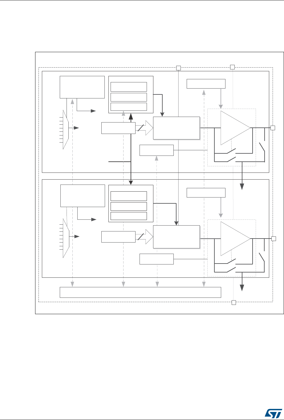
Digital-to-analog converter (DAC) RM0394
488/1600 RM0394 Rev 4
17.4 DAC functional description
17.4.1 DAC block diagram
Figure 109. Dual-channel DAC block diagram
1. MODEx bits in the DAC_MCR control the output mode and allow switching between the Normal mode in
buffer/unbuffered configuration and the Sample and Hold mode.
2. Refer to Section 17.3: DAC implementation for channel 2 availability.
06Y9
sZ&н s
KŶͲĐŚŝƉ
WĞƌŝƉŚĞƌĂůƐ
'$&B287
ƵĨĨĞƌϭ
ĐŽŶǀĞƌƚĞƌϭ
'$&B287
ƵĨĨĞƌϮ
s^^
ϭϮͲďŝƚ
DKϭďŝƚƐ
d^DW>ϭ
d,K>ϭ
dZ&Z^,ϭ
^ĂŵƉůĞΘ,ŽůĚZĞŐŝƐƚĞƌƐ KdZ/Dϭϱ͗ϬďŝƚƐ
ŽŶƚƌŽůƌĞŐŝƐƚĞƌƐ
ΘůŽŐŝĐŚĂŶŶĞůϭ
ϭϮͲďŝƚ
>^/ĐůŽĐŬ
d^>ϭϮ͗Ϭ
ďŝƚƐ DͺZĞƋƵĞƐƚ
d/DϲͺdZ/'
E
d/DϳͺdZ/'
KŶͲĐŚŝƉ
WĞƌŝƉŚĞƌĂůƐ
E
d/DϮͺdZ/'
E
yd/ϵͺdZ/'
^tͺdZ/'
dZ/'
d^>ϮϮ͗Ϭ
ďŝƚƐ DͺZĞƋƵĞƐƚ
d/DϲͺdZ/'
E
d/DϳͺdZ/'
E
d/DϮͺdZ/'
E
yd/ϵͺdZ/'
^tͺdZ/'
dZ/'
KĨĨƐĞƚĐĂůŝďƌĂƚŝŽŶ
WϭƵƐ
ͺKZϮ
ŽŶƚƌŽůƌĞŐŝƐƚĞƌƐ
ΘůŽŐŝĐŚĂŶŶĞůϮ
ͺKZϭ
^ĂŵƉůĞΘ,ŽůĚZĞŐŝƐƚĞƌƐ
d^DW>Ϯ
d,K>Ϯ
dZ&Z^,Ϯ
ĐŽŶǀĞƌƚĞƌϮ
DKϮďŝƚƐ
KdZ/DϮϱ͗ϬďŝƚƐ
KĨĨƐĞƚĐĂůŝďƌĂƚŝŽŶ
'$&FKDQQHO
'$&FKDQQHO
GDFBRXW
GDFBRXW
RM0394 Rev 4 489/1600
RM0394 Digital-to-analog converter (DAC)
521
The DAC includes:
•Up to two output channels
•The DAC_OUTx can be disconnected from the output pin and used as an ordinary
GPIO
•The DAC_OUTx can use an internal pin connection to on-chip peripherals such as
comparator, operational amplifier and ADC (if available).
•DAC output channel buffered or non buffered
•Sample and Hold block and registers operational in Stop mode, using LSI clock source
for static conversion
The DAC includes up to two separate output channels. Each output channel can be
connected to on-chip peripherals such as comparator, operational amplifier and ADC (if
available). In this case, the DAC output channel can be disconnected from the DAC_OUTx
output pin and the corresponding GPIO can be used for another purpose.
The DAC output can be buffered or not. The Sample and Hold block and its associated
registers can run in Stop mode using the LSI clock source.
17.4.2 DAC channel enable
Each DAC channel can be powered on by setting its corresponding ENx bit in the DAC_CR
register. The DAC channel is then enabled after a tWAKEUP startup time.
Note: The ENx bit enables the analog DAC Channelx only. The DAC Channelx digital interface is
enabled even if the ENx bit is reset.
17.4.3 DAC data format
Depending on the selected configuration mode, the data have to be written into the specified
register as described below:
•Single DAC channel
There are three possibilities:
– 8-bit right alignment: the software has to load data into the DAC_DHR8Rx[7:0] bits
(stored into the DHRx[11:4] bits)
– 12-bit left alignment: the software has to load data into the DAC_DHR12Lx [15:4]
bits (stored into the DHRx[11:0] bits)
– 12-bit right alignment: the software has to load data into the DAC_DHR12Rx [11:0]
bits (stored into the DHRx[11:0] bits)
Depending on the loaded DAC_DHRyyyx register, the data written by the user is shifted and
stored into the corresponding DHRx (data holding registerx, which are internal non-memory-
Table 74. DAC input/output pins
Pin name Signal type Remarks
VREF+
Input, analog reference
positive
The higher/positive reference voltage for the DAC,
VREF+ VDDAmax (refer to datasheet)
VDDA Input, analog supply Analog power supply
VSSA Input, analog supply ground Ground for analog power supply
DAC_OUTx Analog output signal DAC channelx analog output
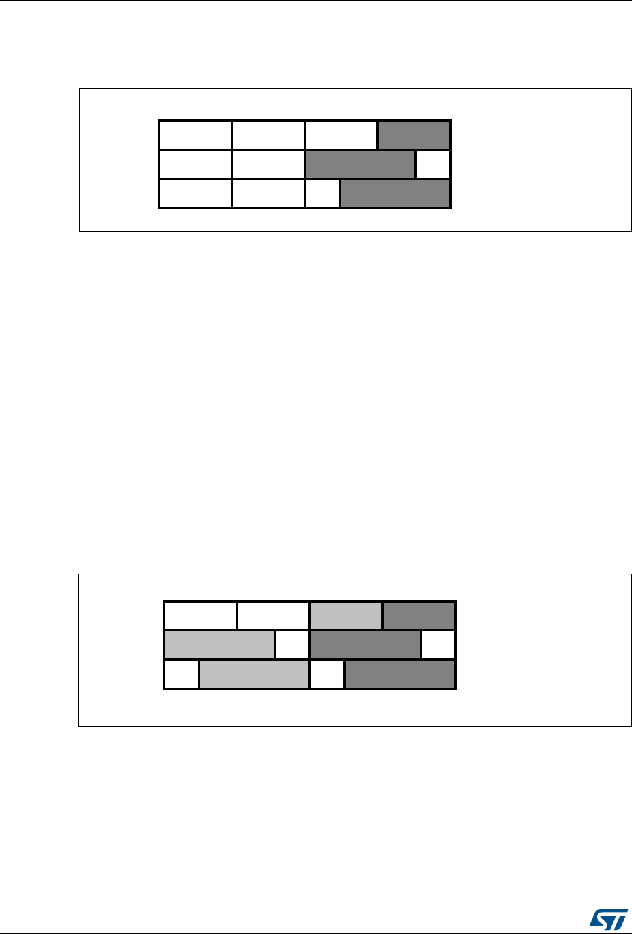
Digital-to-analog converter (DAC) RM0394
490/1600 RM0394 Rev 4
mapped registers). The DHRx register is then loaded into the DORx register either
automatically, by software trigger or by an external event trigger.
Figure 110. Data registers in single DAC channel mode
•Dual DAC channels (when available)
There are three possibilities:
– 8-bit right alignment: data for DAC channel1 to be loaded into the DAC_DHR8RD
[7:0] bits (stored into the DHR1[11:4] bits) and data for DAC channel2 to be loaded
into the DAC_DHR8RD [15:8] bits (stored into the DHR2[11:4] bits)
– 12-bit left alignment: data for DAC channel1 to be loaded into the DAC_DHR12LD
[15:4] bits (stored into the DHR1[11:0] bits) and data for DAC channel2 to be
loaded into the DAC_DHR12LD [31:20] bits (stored into the DHR2[11:0] bits)
– 12-bit right alignment: data for DAC channel1 to be loaded into the
DAC_DHR12RD [11:0] bits (stored into the DHR1[11:0] bits) and data for DAC
channel2 to be loaded into the DAC_DHR12RD [27:16] bits (stored into the
DHR2[11:0] bits)
Depending on the loaded DAC_DHRyyyD register, the data written by the user is shifted
and stored into DHR1 and DHR2 (data holding registers, which are internal non-memory-
mapped registers). The DHR1 and DHR2 registers are then loaded into the DAC_DOR1
and DOR2 registers, respectively, either automatically, by software trigger or by an external
event trigger.
Figure 111. Data registers in dual DAC channel mode
ELWULJKWDOLJQHG
ELWOHIWDOLJQHG
ELWULJKWDOLJQHG
DLE
ELWULJKWDOLJQHG
ELWOHIWDOLJQHG
ELWULJKWDOLJQHG
DLE
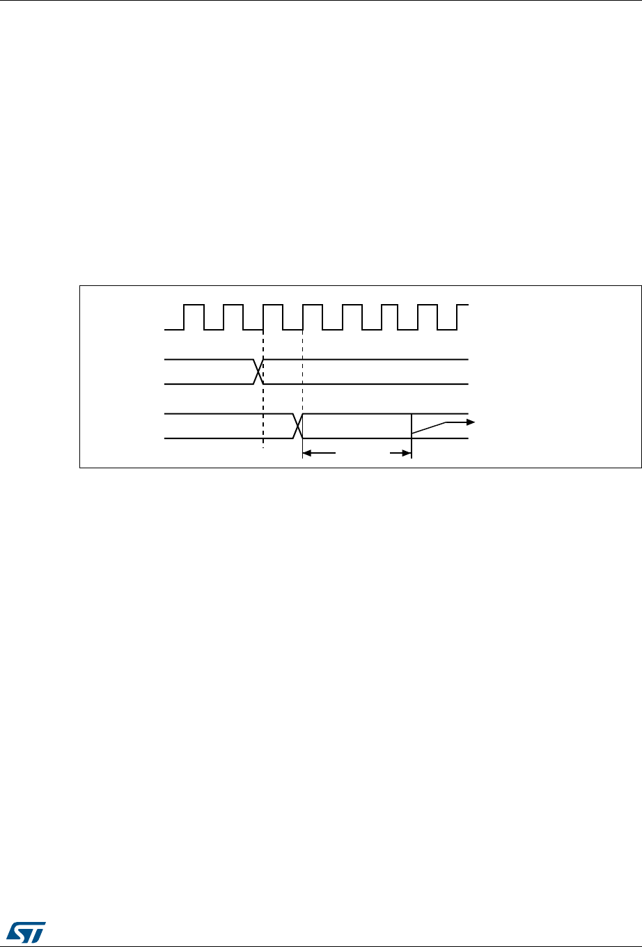
RM0394 Rev 4 491/1600
RM0394 Digital-to-analog converter (DAC)
521
17.4.4 DAC conversion
The DAC_DORx cannot be written directly and any data transfer to the DAC channelx must
be performed by loading the DAC_DHRx register (write operation to DAC_DHR8Rx,
DAC_DHR12Lx, DAC_DHR12Rx, DAC_DHR8RD, DAC_DHR12RD or DAC_DHR12LD).
Data stored in the DAC_DHRx register are automatically transferred to the DAC_DORx
register after one APB1 clock cycle, if no hardware trigger is selected (TENx bit in DAC_CR
register is reset). However, when a hardware trigger is selected (TENx bit in DAC_CR
register is set) and a trigger occurs, the transfer is performed three APB1 clock cycles after
the trigger signal.
When DAC_DORx is loaded with the DAC_DHRx contents, the analog output voltage
becomes available after a time tSETTLING that depends on the power supply voltage and the
analog output load.
Figure 112. Timing diagram for conversion with trigger disabled TEN = 0
17.4.5 DAC output voltage
Digital inputs are converted to output voltages on a linear conversion between 0 and VREF+.
The analog output voltages on each DAC channel pin are determined by the following
equation:
17.4.6 DAC trigger selection
If the TENx control bit is set, conversion can then be triggered by an external event (timer
counter, external interrupt line). The TSELx[2:0] control bits determine which out of 8 possi-
ble events will trigger conversion as shown in bits TSEL1[2:0] and TSEL2[2:0] in Table 75:
DAC trigger selection.
Each time a DAC interface detects a rising edge on the selected trigger source (refer to the
table below), the last data stored into the DAC_DHRx register are transferred into the
DAC_DORx register. The DAC_DORx register is updated three APB1 cycles after the
trigger occurs.
!0"?#,+
X!#
X!#
T3%44,).'
$(2
$/2
/UTPUTVOLTAGE
AVAILABLEON$!#?/54PIN
AIC
DACoutput VREF
DOR
4096
--------------
×=
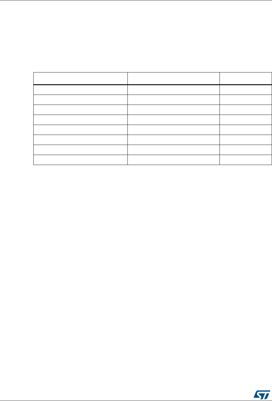
Digital-to-analog converter (DAC) RM0394
492/1600 RM0394 Rev 4
If the software trigger is selected, the conversion starts once the SWTRIG bit is set.
SWTRIG is reset by hardware once the DAC_DORx register has been loaded with the
DAC_DHRx register contents.
Note: TSELx[2:0] bit cannot be changed when the ENx bit is set.
When software trigger is selected, the transfer from the DAC_DHRx register to the
DAC_DORx register takes only one APB1 clock cycle.
17.4.7 DMA requests
Each DAC channel has a DMA capability. Two DMA channels are used to service DAC
channel DMA requests.
When an external trigger (but not a software trigger) occurs while the DMAENx bit is set, the
value of the DAC_DHRx register is transferred into the DAC_DORx register when the
transfer is complete, and a DMA request is generated.
In dual mode, if both DMAENx bits are set, two DMA requests are generated. If only one
DMA request is needed, only the corresponding DMAENx bit should be set. In this way, the
application can manage both DAC channels in dual mode by using one DMA request and a
unique DMA channel.
As DAC_DHRx to DAC_DORx data transfer occurred before the DMA request, the very first
data has to be written to the DAC_DHRx before the first trigger event occurs.
DMA underrun
The DAC DMA request is not queued so that if a second external trigger arrives before the
acknowledgment for the first external trigger is received (first request), then no new request
is issued and the DMA channelx underrun flag DMAUDRx in the DAC_SR register is set,
reporting the error condition. The DAC channelx continues to convert old data.
The software should clear the DMAUDRx flag by writing 1, clear the DMAEN bit of the used
DMA stream and re-initialize both DMA and DAC channelx to restart the transfer correctly.
The software should modify the DAC trigger conversion frequency or lighten the DMA
workload to avoid a new DMA underrun. Finally, the DAC conversion could be resumed by
enabling both DMA data transfer and conversion trigger.
Table 75. DAC trigger selection
Source Type TSELx[2:0]
TIM6_TRGO Internal signal from on-chip timers 000
TIM8_TRGO Internal signal from on-chip timers 001
TIM7_TRGO(1)
1. Reserved on STM32L45xxx and STM32L46xxx devices.
Internal signal from on-chip timers 010
TIM5_TRGO Internal signal from on-chip timers 011
TIM2_TRGO Internal signal from on-chip timers 100
TIM4_TRGO Internal signal from on-chip timers 101
EXTI9 External pin 110
SWTRIG Software control bit 111
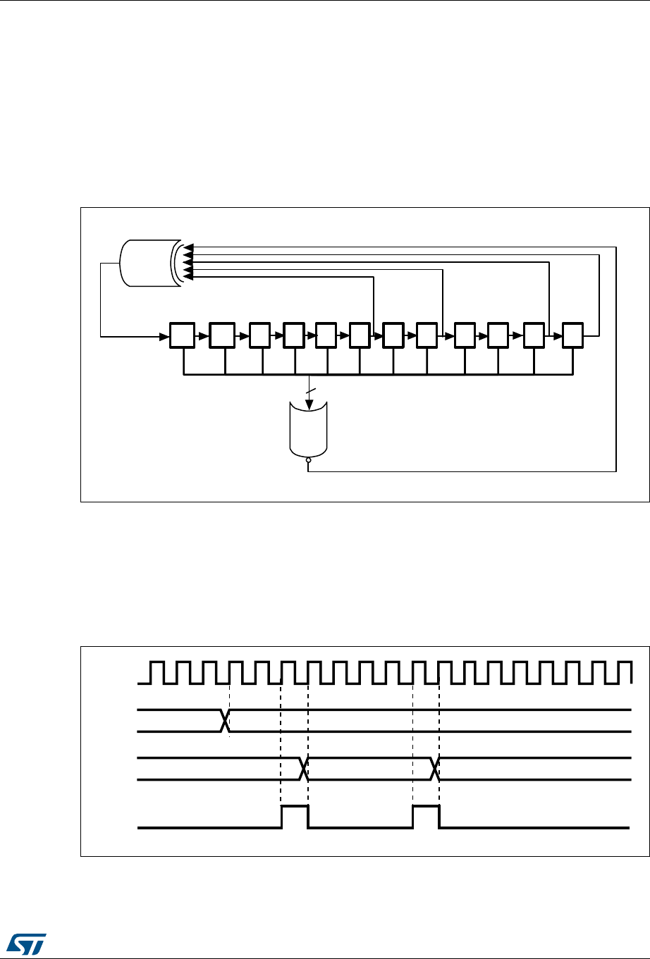
RM0394 Rev 4 493/1600
RM0394 Digital-to-analog converter (DAC)
521
For each DAC channelx, an interrupt is also generated if its corresponding DMAUDRIEx bit
in the DAC_CR register is enabled.
17.4.8 Noise generation
In order to generate a variable-amplitude pseudonoise, an LFSR (linear feedback shift
register) is available. DAC noise generation is selected by setting WAVEx[1:0] to 01”. The
preloaded value in LFSR is 0xAAA. This register is updated three APB1 clock cycles after
each trigger event, following a specific calculation algorithm.
Figure 113. DAC LFSR register calculation algorithm
The LFSR value, that may be masked partially or totally by means of the MAMPx[3:0] bits in
the DAC_CR register, is added up to the DAC_DHRx contents without overflow and this
value is then transferred into the DAC_DORx register.
If LFSR is 0x0000, a ‘1 is injected into it (antilock-up mechanism).
It is possible to reset LFSR wave generation by resetting the WAVEx[1:0] bits.
Figure 114. DAC conversion (SW trigger enabled) with LFSR wave generation
Note: The DAC trigger must be enabled for noise generation by setting the TENx bit in the
DAC_CR register.
125
;
;
;
;
;
;25
DLF
$3%B&/.
[
[$$$
'+5
'25
DLE
['
6:75,*
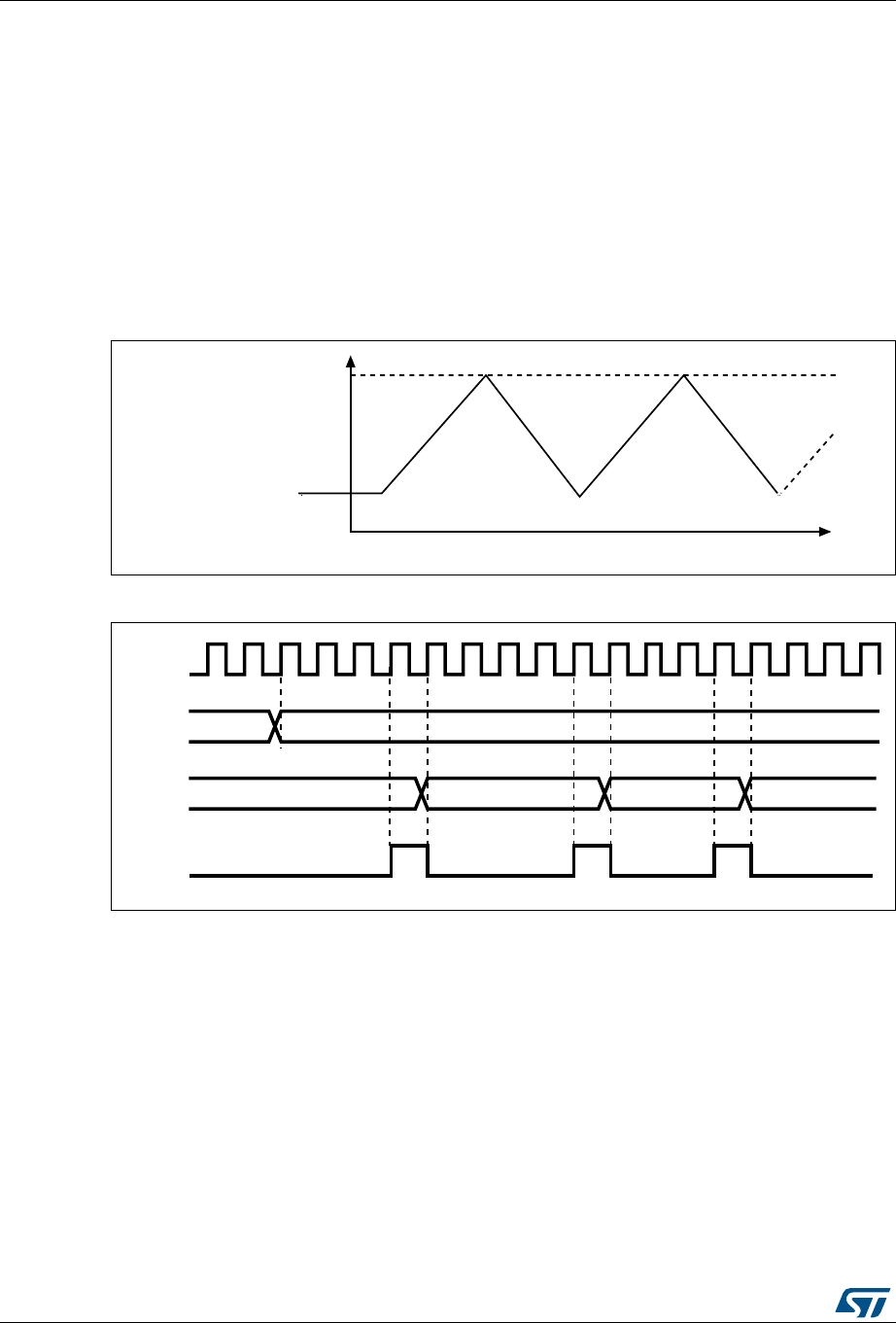
Digital-to-analog converter (DAC) RM0394
494/1600 RM0394 Rev 4
17.4.9 Triangle-wave generation
It is possible to add a small-amplitude triangular waveform on a DC or slowly varying signal.
DAC triangle-wave generation is selected by setting WAVEx[1:0] to 10”. The amplitude is
configured through the MAMPx[3:0] bits in the DAC_CR register. An internal triangle counter
is incremented three APB1 clock cycles after each trigger event. The value of this counter is
then added to the DAC_DHRx register without overflow and the sum is transferred into the
DAC_DORx register. The triangle counter is incremented as long as it is less than the
maximum amplitude defined by the MAMPx[3:0] bits. Once the configured amplitude is
reached, the counter is decremented down to 0, then incremented again and so on.
It is possible to reset triangle wave generation by resetting the WAVEx[1:0] bits.
Figure 115. DAC triangle wave generation
Figure 116. DAC conversion (SW trigger enabled) with triangle wave generation
Note: The DAC trigger must be enabled for triangle wave generation by setting the TENx bit in the
DAC_CR register.
The MAMPx[3:0] bits must be configured before enabling the DAC, otherwise they cannot
be changed.
17.4.10 DAC channel modes
Each DAC channel can be configured in Normal mode or Sample and Hold mode. The
output buffer can be enabled to allow a high drive capability. Before enabling output buffer,
the voltage offset needs to be calibrated. This calibration is performed at the factory (loaded
after reset) and can be adjusted by software during application operation.
-!-0X;=MAXAMPLITUDE
$!#?$(2XBASEVALUE
$!#?$(2XBASEVALUE
)NCREMENTATION
AIC
$ECREMENTATION
$3%B&/.
[$%(
[$%(
'+5
'25
DLE
[$%)
6:75,*
[$&

RM0394 Rev 4 495/1600
RM0394 Digital-to-analog converter (DAC)
521
Normal mode
In Normal mode, there are four combinations, by changing the buffer state and by changing
the DAC_OUTx pin interconnections.
To enable the output buffer, the MODEx[2:0] bits in DAC_MCR register should be:
•000: DAC is connected to the external pin
•001: DAC is connected to external pin and to on-chip peripherals
To disable the output buffer, the MODEx[2:0] bits in DAC_MCR register should be:
•010: DAC is connected to the external pin
•011: DAC is connected to on-chip peripherals
Sample and Hold mode
In sample and Hold mode, the DAC core converts data on a triggered conversion, then,
holds the converted voltage on a capacitor. When not converting, the DAC cores and buffer
are completely turned off between samples and the DAC output is tri-stated, therefore
reducing the overall power consumption. A new stabilization period, which value depends
on the buffer state, is required before each new conversion.
In this mode, the DAC core and all corresponding logic and registers are driven by the low-
speed clock (LSI) in addition to the APB1 clock, allowing to use the DAC channels in deep
low power modes such as Stop mode.
The sample/hold mode operations can be divided into 3 phases:
1. Sample phase: the sample/hold element is charged to the desired voltage. The
charging time depends on capacitor value (internal or external, selected by the user).
The sampling time is configured with the TSAMPLEx[9:0] bits in DAC_SHSRx register.
During the write of the TSAMPLEx[9:0] bits; the BWSTx bit in DAC_SR register is set to
1 to synchronize between both clocks domains (APB and low speed clock) and
allowing the software to change the value of sample phase during the DAC channel
operation
2. Hold phase: the DAC output channel is tri-stated, the DAC core and the buffer are
turned off, to reduce the current consumption. The hold time is configured with the
THOLDx[9:0] bits in DAC_SHHR register
3. Refresh phase: the refresh time is configured with the TREFRESHx[7:0] bits in
DAC_SHRR register
The timings for the three phases above are in units of LSI clocks. As an example, to
configure a sample time of 350 µs, a hold time of 2 ms and a refresh time of 100 µs
assuming LSI ~32 KHz is selected:
12 cycles are required for sample phase: TSAMPLEx[9:0] = 11,
62 cycles are required for hold phase: THOLDx[9:0] = 62,
and 4 cycles are required for refresh period: TREFRESHx[7:0] = 4.
In this example, the power consumption is reduced by almost a factor of 15 versus Normal
modes.
The formulas to compute the right sample and refresh timings are described in the table
below, the Hold time depends on the leakage current.

Digital-to-analog converter (DAC) RM0394
496/1600 RM0394 Rev 4
Example of the sample and refresh time calculation with output buffer on
The values used in the example below are provided as indication only. Please refer to the
product datasheet for product data.
CSH = 100 nF
VDDA = 3.0 V
Sampling phase:
tSAMP = 7 s + (10 * 2000 * 100 * 10-9) = 2.007 ms
(where RBON = 2 k)
Refresh phase:
tREFRESH = 7 s + (2000 * 100 * 10-9) * ln(2*10) = 606.1 s
(where NLSB = 10 (10 LSB drop during the hold phase)
Hold phase:
Dv = ileak * thold / CSH = 0.0073 V (10 LSB of 12bit at 3 V)
ileak = 150 nA (worst case on the IO leakage on all the temperature range)
thold = 0.0073 * 100 * 10-9 / (150 * 10-9) = 4.867 ms
Table 76. Sample and refresh timings
Buffer
State tSAMP(1)(2)
1. In the above formula the settling to the desired code value with ½ LSB or accuracy requires 10 constant
time for 12 bits resolution. For 8 bits resolution, the settling time is 7 constant time.
2. CSH is the capacitor in Sample and Hold mode.
tREFRESH(2)(3)
3. The tolerated voltage drop during the hold phase “Vd” is represented by the number of LSBs after the
capacitor discharging with the output leakage current. The settling back to the desired value with ½ LSB
error accuracy requires ln(2*Nlsb) constant time of the DAC.
Enable 7 s + (10*RBON*CSH)7s + (RBON*CSH)*ln(2*NLSB)
Disable 3 s + (10*RBOFF*CSH)3s + (RBOFF*CSH)*ln(2*NLSB)
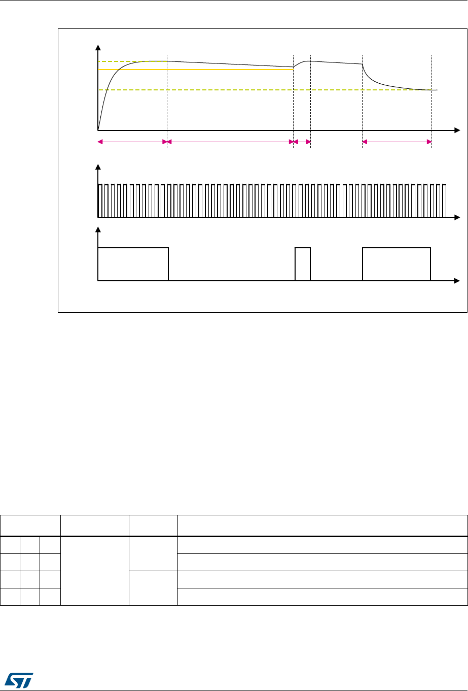
RM0394 Rev 4 497/1600
RM0394 Digital-to-analog converter (DAC)
521
Figure 117. DAC Sample and Hold mode phase diagram
Like in Normal mode, the Sample and Hold mode has different configurations.
To enable the output buffer, the MODEx[2:0] bits in DAC_MCR register should be:
•100: DAC is connected to the external pin
•101: DAC is connected to external pin and to on chip peripherals
To disabled the output buffer, The MODEx[2:0] bits in DAC_MCR register should be:
•110: DAC is connected to external pin and to on chip peripherals
•111: DAC is connected to on chip peripherals
When MODEx[2:0] bits in DAC_MCR register is equal to 111. An internal capacitor, CLint, will
hold the voltage output of the DAC Core and then drive it to on-chip peripherals.
All Sample and Hold phases are interruptible and any change in DAC_DHRx will trigger
immediately a new sample phase.
06Y9
/6,
'$&
21 2121
W
W
9
9
6DPSOLQJSKDVH +ROGSKDVH 5HIUHVK
SKDVH
6DPSOLQJSKDVH
9G
Table 77. Channel output modes summary
MODEx[2:0] Mode Buffer Output connections
000
Normal mode
Enabled
Connected to external pin
0 0 1 Connected to external pin and to on chip-peripherals (ex, comparators)
010
Disabled
Connected to external pin
0 1 1 Connected to on chip peripherals (ex, comparators)

Digital-to-analog converter (DAC) RM0394
498/1600 RM0394 Rev 4
17.4.11 DAC channel buffer calibration
The transfer function for an N-bit digital-to-analog converter (DAC) is:
Where VOUT is the analog output, D is the digital input, G is the gain, Vref is the nominal full-
scale voltage, and Vos is the offset voltage. For an ideal DAC channel, G = 1 and Vos = 0.
Due to output buffer characteristics, the voltage offset may differ from part-to-part and
introduce an absolute offset error on the analog output. To compensate the Vos, a calibration
is required by a trimming technique.
The calibration is only valid when the DAC channelx is operating with buffer enabled
(MODEx[2:0] = 000b or 001b or 100b or 101b). if applied in other modes when the buffer is
off, it has no effect. During the calibration:
•The buffer output will be disconnected from the pin internal/external connections and
put in tristate mode (HiZ),
•The buffer will act as a comparator, to sense the middle-code value 0x800 and
compare it to VREF+/2 signal through an internal bridge, then toggle its output signal to
0 or 1 depending on the comparison result (CAL_FLAGx bit)
Two calibration techniques are provided:
•Factory trimming (always enabled)
The DAC buffer offset is factory trimmed. The default value of OTRIMx[4:0] bits in
DAC_CCR register is the factory trimming value and it is loaded once DAC digital
interface is reset.
•User trimming
The user trimming can be done when the operating conditions differs from nominal
factory trimming conditions and in particular when VDD/VDDA voltage, temperature,
VREF+ values change and can be done at any point during application by software.
Note: Refer to the datasheet for more details of the Nominal factory trimming conditions
In addition, when VDD/VDDA is removed (example the device enters in STANDBY or VBAT
modes) the calibration is required.
The steps to perform a user trimming calibration are as below:
100
Sample and
Hold mode
Enabled
Connected to external pin
1 0 1 Connected to external pin and to on chip peripherals (ex, comparators)
110
Disabled
Connected to external pin and to on chip peripherals (ex, comparators)
1 1 1 Connected to on chip peripherals (ex, comparators)
Table 77. Channel output modes summary (continued)
MODEx[2:0] Mode Buffer Output connections
Vout D2
N1–
⁄()GV
ref
××()VOS
+=

RM0394 Rev 4 499/1600
RM0394 Digital-to-analog converter (DAC)
521
1. If the DAC channel is active, Write 0 to ENx bit in DAC_CR to disable the channel.
2. Select a mode where the buffer is enabled, by writing to DAC_MCR register,
MODEx[2:0] = 000b or 001b or 100b or 101b,
3. Start the DAC channelx calibration, by setting the CENx bit in DAC_CR register to 1,
4. Apply a trimming algorithm:
a) Write a code into OTRIMx[4:0] bits, starting by 00000b.
b) Wait for tTRIM delay.
c) Check if CAL_FLAGx bit in DAC_SR is set to 1.
d) if CAL_FLAGx is set to 1 the trimming code OTRIMx[4:0] is found and will be used
during operation to compensate the output value, else increment OTRIMx[4:0] and
repeat sub-steps from (a) to (d) again.
The software algorithm may use either a successive approximation or dichotomy techniques
to compute and set the content of OTRIMx[4:0] bits in a faster way,
The commutation/toggle of CAL_FLAGx bit indicates that the offset is correctly
compensated and the corresponding trim code must be kept in the OTRIMx[4:0] bits in
DAC_CCR register.
Note: A tTRIM delay must be respected between the write to the OTRIMx[4:0] bits and the read of
the CAL_FLAGx bit in DAC_SR register in order to get a correct value.This parameter is
specified into datasheet electrical characteristics section.
If the VDD/VDDA, VREF+ and temperature conditions will not change during the device
operation while it enters more often in standby and VBAT mode, the software may store the
OTRIMx[4:0] bits found in the first user calibration in the flash or in back-up registers. then to
load/write them directly when the device power is back again thus avoiding to wait for a new
calibration time.
When CENx bit is set, it is not allowed to set ENx bit.
17.4.12 Dual DAC channel conversion (if available)
To efficiently use the bus bandwidth in applications that require the two DAC channels at the
same time, three dual registers are implemented: DHR8RD, DHR12RD and DHR12LD. A
unique register access is then required to drive both DAC channels at the same time. For
the wave generation, no accesses to DHRxxxD registers are required. As a result, two
output channels can be used either independently or simultaneously.
11 possible conversion modes are possible using the two DAC channels and these dual
registers. All the conversion modes can nevertheless be obtained using separate DHRx
registers if needed.
All modes are described in the paragraphs below.
Independent trigger without wave generation
To configure the DAC in this conversion mode, the following sequence is required:
1. Set the two DAC channel trigger enable bits TEN1 and TEN2.
2. Configure different trigger sources by setting different values in the TSEL1[2:0] and
TSEL2[2:0] bits.
3. Load the dual DAC channel data into the desired DHR register (DAC_DHR12RD,
DAC_DHR12LD or DAC_DHR8RD).

Digital-to-analog converter (DAC) RM0394
500/1600 RM0394 Rev 4
When a DAC channel1 trigger arrives, the DHR1 register is transferred into DAC_DOR1
(three APB1 clock cycles later).
When a DAC channel2 trigger arrives, the DHR2 register is transferred into DAC_DOR2
(three APB1 clock cycles later).
Independent trigger with single LFSR generation
To configure the DAC in this conversion mode, the following sequence is required:
1. Set the two DAC channel trigger enable bits TEN1 and TEN2.
2. Configure different trigger sources by setting different values in the TSEL1[2:0] and
TSEL2[2:0] bits.
3. Configure the two DAC channel WAVEx[1:0] bits as 01 and the same LFSR mask value
in the MAMPx[3:0] bits.
4. Load the dual DAC channel data into the desired DHR register (DHR12RD, DHR12LD
or DHR8RD).
When a DAC channel1 trigger arrives, the LFSR1 counter, with the same mask, is added to
the DHR1 register and the sum is transferred into DAC_DOR1 (three APB1 clock cycles
later). Then the LFSR1 counter is updated.
When a DAC channel2 trigger arrives, the LFSR2 counter, with the same mask, is added to
the DHR2 register and the sum is transferred into DAC_DOR2 (three APB1 clock cycles
later). Then the LFSR2 counter is updated.
Independent trigger with different LFSR generation
To configure the DAC in this conversion mode, the following sequence is required:
1. Set the two DAC channel trigger enable bits TEN1 and TEN2.
2. Configure different trigger sources by setting different values in the TSEL1[2:0] and
TSEL2[2:0] bits.
3. Configure the two DAC channel WAVEx[1:0] bits as 01 and set different LFSR masks
values in the MAMP1[3:0] and MAMP2[3:0] bits.
4. Load the dual DAC channel data into the desired DHR register (DAC_DHR12RD,
DAC_DHR12LD or DAC_DHR8RD).
When a DAC channel1 trigger arrives, the LFSR1 counter, with the mask configured by
MAMP1[3:0], is added to the DHR1 register and the sum is transferred into DAC_DOR1
(three APB1 clock cycles later). Then the LFSR1 counter is updated.
When a DAC channel2 trigger arrives, the LFSR2 counter, with the mask configured by
MAMP2[3:0], is added to the DHR2 register and the sum is transferred into DAC_DOR2
(three APB1 clock cycles later). Then the LFSR2 counter is updated.
Independent trigger with single triangle generation
To configure the DAC in this conversion mode, the following sequence is required:

RM0394 Rev 4 501/1600
RM0394 Digital-to-analog converter (DAC)
521
1. Set the two DAC channel trigger enable bits TEN1 and TEN2.
2. Configure different trigger sources by setting different values in the TSEL1[2:0] and
TSEL2[2:0] bits.
3. Configure the two DAC channel WAVEx[1:0] bits as 1x and the same maximum
amplitude value in the MAMPx[3:0] bits.
4. Load the dual DAC channel data into the desired DHR register (DAC_DHR12RD,
DAC_DHR12LD or DAC_DHR8RD).
When a DAC channel1 trigger arrives, the DAC channel1 triangle counter, with the same
triangle amplitude, is added to the DHR1 register and the sum is transferred into
DAC_DOR1 (three APB1 clock cycles later). The DAC channel1 triangle counter is then
updated.
When a DAC channel2 trigger arrives, the DAC channel2 triangle counter, with the same
triangle amplitude, is added to the DHR2 register and the sum is transferred into
DAC_DOR2 (three APB1 clock cycles later). The DAC channel2 triangle counter is then
updated.
Independent trigger with different triangle generation
To configure the DAC in this conversion mode, the following sequence is required:
1. Set the two DAC channel trigger enable bits TEN1 and TEN2.
2. Configure different trigger sources by setting different values in the TSEL1[2:0] and
TSEL2[2:0] bits.
3. Configure the two DAC channel WAVEx[1:0] bits as 1x and set different maximum
amplitude values in the MAMP1[3:0] and MAMP2[3:0] bits.
4. Load the dual DAC channel data into the desired DHR register (DAC_DHR12RD,
DAC_DHR12LD or DAC_DHR8RD).
When a DAC channel1 trigger arrives, the DAC channel1 triangle counter, with a triangle
amplitude configured by MAMP1[3:0], is added to the DHR1 register and the sum is
transferred into DAC_DOR1 (three APB1 clock cycles later). The DAC channel1 triangle
counter is then updated.
When a DAC channel2 trigger arrives, the DAC channel2 triangle counter, with a triangle
amplitude configured by MAMP2[3:0], is added to the DHR2 register and the sum is
transferred into DAC_DOR2 (three APB1 clock cycles later). The DAC channel2 triangle
counter is then updated.
Simultaneous software start
To configure the DAC in this conversion mode, the following sequence is required:
•Load the dual DAC channel data to the desired DHR register (DAC_DHR12RD,
DAC_DHR12LD or DAC_DHR8RD)
In this configuration, one APB1 clock cycle later, the DHR1 and DHR2 registers are
transferred into DAC_DOR1 and DAC_DOR2, respectively.

Digital-to-analog converter (DAC) RM0394
502/1600 RM0394 Rev 4
Simultaneous trigger without wave generation
To configure the DAC in this conversion mode, the following sequence is required:
•Set the two DAC channel trigger enable bits TEN1 and TEN2
•Configure the same trigger source for both DAC channels by setting the same value in
the TSEL1[2:0] and TSEL2[2:0] bits
•Load the dual DAC channel data to the desired DHR register (DAC_DHR12RD,
DAC_DHR12LD or DAC_DHR8RD)
When a trigger arrives, the DHR1 and DHR2 registers are transferred into DAC_DOR1 and
DAC_DOR2, respectively (after three APB1 clock cycles).
Simultaneous trigger with single LFSR generation
To configure the DAC in this conversion mode, the following sequence is required:
•Set the two DAC channel trigger enable bits TEN1 and TEN2
•Configure the same trigger source for both DAC channels by setting the same value in
the TSEL1[2:0] and TSEL2[2:0] bits
•Configure the two DAC channel WAVEx[1:0] bits as 01 and the same LFSR mask value
in the MAMPx[3:0] bits
•Load the dual DAC channel data to the desired DHR register (DHR12RD, DHR12LD or
DHR8RD)
When a trigger arrives, the LFSR1 counter, with the same mask, is added to the DHR1
register and the sum is transferred into DAC_DOR1 (three APB1 clock cycles later). The
LFSR1 counter is then updated. At the same time, the LFSR2 counter, with the same mask,
is added to the DHR2 register and the sum is transferred into DAC_DOR2 (three APB1
clock cycles later). The LFSR2 counter is then updated.
Simultaneous trigger with different LFSR generation
To configure the DAC in this conversion mode, the following sequence is required:
•Set the two DAC channel trigger enable bits TEN1 and TEN2
•Configure the same trigger source for both DAC channels by setting the same value in
the TSEL1[2:0] and TSEL2[2:0] bits
•Configure the two DAC channel WAVEx[1:0] bits as 01 and set different LFSR mask
values using the MAMP1[3:0] and MAMP2[3:0] bits
•Load the dual DAC channel data into the desired DHR register (DAC_DHR12RD,
DAC_DHR12LD or DAC_DHR8RD)
When a trigger arrives, the LFSR1 counter, with the mask configured by MAMP1[3:0], is
added to the DHR1 register and the sum is transferred into DAC_DOR1 (three APB1 clock
cycles later). The LFSR1 counter is then updated.
At the same time, the LFSR2 counter, with the mask configured by MAMP2[3:0], is added to
the DHR2 register and the sum is transferred into DAC_DOR2 (three APB1 clock cycles
later). The LFSR2 counter is then updated.

RM0394 Rev 4 503/1600
RM0394 Digital-to-analog converter (DAC)
521
Simultaneous trigger with single triangle generation
To configure the DAC in this conversion mode, the following sequence is required:
•Set the two DAC channel trigger enable bits TEN1 and TEN2
•Configure the same trigger source for both DAC channels by setting the same value in
the TSEL1[2:0] and TSEL2[2:0] bits
•Configure the two DAC channel WAVEx[1:0] bits as 1x and the same maximum
amplitude value using the MAMPx[3:0] bits
•Load the dual DAC channel data into the desired DHR register (DAC_DHR12RD,
DAC_DHR12LD or DAC_DHR8RD)
When a trigger arrives, the DAC channel1 triangle counter, with the same triangle
amplitude, is added to the DHR1 register and the sum is transferred into DAC_DOR1 (three
APB1 clock cycles later). The DAC channel1 triangle counter is then updated.
At the same time, the DAC channel2 triangle counter, with the same triangle amplitude, is
added to the DHR2 register and the sum is transferred into DAC_DOR2 (three APB1 clock
cycles later). The DAC channel2 triangle counter is then updated.
Simultaneous trigger with different triangle generation
To configure the DAC in this conversion mode, the following sequence is required:
•Set the two DAC channel trigger enable bits TEN1 and TEN2
•Configure the same trigger source for both DAC channels by setting the same value in
the TSEL1[2:0] and TSEL2[2:0] bits
•Configure the two DAC channel WAVEx[1:0] bits as 1x and set different maximum
amplitude values in the MAMP1[3:0] and MAMP2[3:0] bits
•Load the dual DAC channel data into the desired DHR register (DAC_DHR12RD,
DAC_DHR12LD or DAC_DHR8RD)
When a trigger arrives, the DAC channel1 triangle counter, with a triangle amplitude
configured by MAMP1[3:0], is added to the DHR1 register and the sum is transferred into
DAC_DOR1 (three APB clock cycles later). Then the DAC channel1 triangle counter is
updated.
At the same time, the DAC channel2 triangle counter, with a triangle amplitude configured
by MAMP2[3:0], is added to the DHR2 register and the sum is transferred into DAC_DOR2
(three APB1 clock cycles later). Then the DAC channel2 triangle counter is updated.
Digital-to-analog converter (DAC) RM0394
504/1600 RM0394 Rev 4
17.5 DAC low-power modes
17.6 DAC interrupts
Table 78. Effect of low-power modes on DAC
Mode Description
Sleep No effect, DAC used with DMA
Low-power run No effect.
Low-power sleep No effect. DAC used with DMA.
Stop 0 / Stop 1 DAC remains active with a static value, if Sample and Hold mode is
selected using LSI clock
Stop 2 The DAC registers content is kept. The DAC must be disabled before
entering Stop 2.
Standby The DAC peripheral is powered down and must be reinitialized after exiting
Standby or Shutdown mode.
Shutdown
Table 79. DAC interrupts
Interrupt event Event flag Enable control bit
DMA underrun DMAUDRx DMAUDRIEx

RM0394 Rev 4 505/1600
RM0394 Digital-to-analog converter (DAC)
521
17.7 DAC registers
Refer to Section 1 on page 60 for a list of abbreviations used in register descriptions.
The peripheral registers have to be accessed by words (32-bit).
17.7.1 DAC control register (DAC_CR)
Address offset: 0x00
Reset value: 0x0000 0000
31 30 29 28 27 26 25 24 23 22 21 20 19 18 17 16
Res. CEN2 DMAU
DRIE2
DMAE
N2 MAMP2[3:0] WAVE2[1:0] TSEL22 TSEL21 TSEL20 TEN2 Res. EN2
rw rw rw rw rw rw rw rw rw rw rw rw rw rw
1514131211109876543210
Res. CEN1 DMAU
DRIE1
DMAE
N1 MAMP1[3:0] WAVE1[1:0] TSEL12 TSEL11 TSEL10 TEN1 Res. EN1
rw rw rw rw rw rw rw rw rw rw rw rw rw rw
Bit 31 Reserved, must be kept at reset value.
Bit 30 CEN2: DAC Channel 2 calibration enable
This bit is set and cleared by software to enable/disable DAC channel 2 calibration, it can be
written only if EN2 bit is set to 0 into DAC_CR (the calibration mode can be entered/exit only
when the DAC channel is disabled) Otherwise, the write operation is ignored.
0: DAC channel 2 in Normal operating mode
1: DAC channel 2 in calibration mode
Note: This bit is available only on dual-channel DACs. Refer to Section 17.3: DAC
implementation.
Bit 29 DMAUDRIE2: DAC channel2 DMA underrun interrupt enable
This bit is set and cleared by software.
0: DAC channel2 DMA underrun interrupt disabled
1: DAC channel2 DMA underrun interrupt enabled
Note: This bit is available only on dual-channel DACs. Refer to Section 17.3: DAC
implementation.
Bit 28 DMAEN2: DAC channel2 DMA enable
This bit is set and cleared by software.
0: DAC channel2 DMA mode disabled
1: DAC channel2 DMA mode enabled
Note: This bit is available only on dual-channel DACs. Refer to Section 17.3: DAC
implementation.

Digital-to-analog converter (DAC) RM0394
506/1600 RM0394 Rev 4
Bits 27:24 MAMP2[3:0]: DAC channel2 mask/amplitude selector
These bits are written by software to select mask in wave generation mode or amplitude in
triangle generation mode.
0000: Unmask bit0 of LFSR/ triangle amplitude equal to 1
0001: Unmask bits[1:0] of LFSR/ triangle amplitude equal to 3
0010: Unmask bits[2:0] of LFSR/ triangle amplitude equal to 7
0011: Unmask bits[3:0] of LFSR/ triangle amplitude equal to 15
0100: Unmask bits[4:0] of LFSR/ triangle amplitude equal to 31
0101: Unmask bits[5:0] of LFSR/ triangle amplitude equal to 63
0110: Unmask bits[6:0] of LFSR/ triangle amplitude equal to 127
0111: Unmask bits[7:0] of LFSR/ triangle amplitude equal to 255
1000: Unmask bits[8:0] of LFSR/ triangle amplitude equal to 511
1001: Unmask bits[9:0] of LFSR/ triangle amplitude equal to 1023
1010: Unmask bits[10:0] of LFSR/ triangle amplitude equal to 2047
1011: Unmask bits[11:0] of LFSR/ triangle amplitude equal to 4095
Note: These bits are available only on dual-channel DACs. Refer to Section 17.3: DAC
implementation.
Bits 23:22 WAVE2[1:0]: DAC channel2 noise/triangle wave generation enable
These bits are set/reset by software.
00: wave generation disabled
01: Noise wave generation enabled
1x: Triangle wave generation enabled
Note: Only used if bit TEN2 = 1 (DAC channel2 trigger enabled)
These bits are available only on dual-channel DACs. Refer to Section 17.3: DAC
implementation.
Bits 21:19 TSEL2[2:0]: DAC channel2 trigger selection
These bits select the external event used to trigger DAC channel2
Refer to the trigger selection tables in Section 17.4.6: DAC trigger selection for the details on
trigger configuration and mapping.
Note: Only used if bit TEN2 = 1 (DAC channel2 trigger enabled).
These bits are available only on dual-channel DACs. Refer to Section 17.3: DAC
implementation.
Bit 18 TEN2: DAC channel2 trigger enable
This bit is set and cleared by software to enable/disable DAC channel2 trigger
0: DAC channel2 trigger disabled and data written into the DAC_DHR2 register are
transferred one APB1 clock cycle later to the DAC_DOR2 register
1: DAC channel2 trigger enabled and data from the DAC_DHR2 register are transferred
three APB1 clock cycles later to the DAC_DOR2 register
Note: When software trigger is selected, the transfer from the DAC_DHR2 register to the
DAC_DOR2 register takes only one APB1 clock cycle.
These bits are available only on dual-channel DACs. Refer to Section 17.3: DAC
implementation.
Bit 17 Reserved, must be kept at reset value.
Bit 16 EN2: DAC channel2 enable
This bit is set and cleared by software to enable/disable DAC channel2.
0: DAC channel2 disabled
1: DAC channel2 enabled
Note: These bits are available only on dual-channel DACs. Refer to Section 17.3: DAC
implementation.

RM0394 Rev 4 507/1600
RM0394 Digital-to-analog converter (DAC)
521
Bit 15 Reserved, must be kept at reset value.
Bit 14 CEN1: DAC Channel 1 calibration enable
This bit is set and cleared by software to enable/disable DAC channel 1 calibration, it can be
written only if bit EN1=0 into DAC_CR (the calibration mode can be entered/exit only when
the DAC channel is disabled) Otherwise, the write operation is ignored.
0: DAC channel 1 in Normal operating mode
1: DAC channel 1 in calibration mode
Bit 13 DMAUDRIE1: DAC channel1 DMA Underrun Interrupt enable
This bit is set and cleared by software.
0: DAC channel1 DMA Underrun Interrupt disabled
1: DAC channel1 DMA Underrun Interrupt enabled
Bit 12 DMAEN1: DAC channel1 DMA enable
This bit is set and cleared by software.
0: DAC channel1 DMA mode disabled
1: DAC channel1 DMA mode enabled
Bits 11:8 MAMP1[3:0]: DAC channel1 mask/amplitude selector
These bits are written by software to select mask in wave generation mode or amplitude in
triangle generation mode.
0000: Unmask bit0 of LFSR/ triangle amplitude equal to 1
0001: Unmask bits[1:0] of LFSR/ triangle amplitude equal to 3
0010: Unmask bits[2:0] of LFSR/ triangle amplitude equal to 7
0011: Unmask bits[3:0] of LFSR/ triangle amplitude equal to 15
0100: Unmask bits[4:0] of LFSR/ triangle amplitude equal to 31
0101: Unmask bits[5:0] of LFSR/ triangle amplitude equal to 63
0110: Unmask bits[6:0] of LFSR/ triangle amplitude equal to 127
0111: Unmask bits[7:0] of LFSR/ triangle amplitude equal to 255
1000: Unmask bits[8:0] of LFSR/ triangle amplitude equal to 511
1001: Unmask bits[9:0] of LFSR/ triangle amplitude equal to 1023
1010: Unmask bits[10:0] of LFSR/ triangle amplitude equal to 2047
1011: Unmask bits[11:0] of LFSR/ triangle amplitude equal to 4095
Bits 7:6 WAVE1[1:0]: DAC channel1 noise/triangle wave generation enable
These bits are set and cleared by software.
00: wave generation disabled
01: Noise wave generation enabled
1x: Triangle wave generation enabled
Only used if bit TEN1 = 1 (DAC channel1 trigger enabled).
Bits 5:3 TSEL1[2:0]: DAC channel1 trigger selection
These bits select the external event used to trigger DAC channel1
Refer to the trigger selection tables in Section 17.4.6: DAC trigger selection for the details on
trigger configuration and mapping.
Note: Only used if bit TEN1 = 1 (DAC channel1 trigger enabled).

Digital-to-analog converter (DAC) RM0394
508/1600 RM0394 Rev 4
17.7.2 DAC software trigger register (DAC_SWTRGR)
Address offset: 0x04
Reset value: 0x0000 0000
17.7.3 DAC channel1 12-bit right-aligned data holding register
(DAC_DHR12R1)
Address offset: 0x08
Reset value: 0x0000 0000
Bit 2 TEN1: DAC channel1 trigger enable
This bit is set and cleared by software to enable/disable DAC channel1 trigger.
0: DAC channel1 trigger disabled and data written into the DAC_DHR1 register are
transferred one APB1 clock cycle later to the DAC_DOR1 register
1: DAC channel1 trigger enabled and data from the DAC_DHR1 register are transferred
three APB1 clock cycles later to the DAC_DOR1 register
Note: When software trigger is selected, the transfer from the DAC_DHR1 register to the
DAC_DOR1 register takes only one APB1 clock cycle.
Bit 1 Reserved, must be kept at reset value.
Bit 0 EN1: DAC channel1 enable
This bit is set and cleared by software to enable/disable DAC channel1.
0: DAC channel1 disabled
1: DAC channel1 enabled
31 30 29 28 27 26 25 24 23 22 21 20 19 18 17 16
Res. Res. Res. Res. Res. Res. Res. Res. Res. Res. Res. Res. Res. Res. Res. Res.
15 14 13 12 11 10 9 8 7 6 5 4 3 2 1 0
Res. Res. Res. Res. Res. Res. Res. Res. Res. Res. Res. Res. Res. Res. SWTRIG2 SWTRIG1
ww
Bits 31:2 Reserved, must be kept at reset value.
Bit 1 SWTRIG2: DAC channel2 software trigger
This bit is set by software to trigger the DAC in software trigger mode.
0: No trigger
1: Trigger
Note: This bit is cleared by hardware (one APB1 clock cycle later) once the DAC_DHR2
register value has been loaded into the DAC_DOR2 register.
This bit is available only on dual-channel DACs. Refer to Section 17.3: DAC
implementation.
Bit 0 SWTRIG1: DAC channel1 software trigger
This bit is set by software to trigger the DAC in software trigger mode.
0: No trigger
1: Trigger
Note: This bit is cleared by hardware (one APB1 clock cycle later) once the DAC_DHR1
register value has been loaded into the DAC_DOR1 register.
RM0394 Rev 4 509/1600
RM0394 Digital-to-analog converter (DAC)
521
17.7.4 DAC channel1 12-bit left aligned data holding register
(DAC_DHR12L1)
Address offset: 0x0C
Reset value: 0x0000 0000
17.7.5 DAC channel1 8-bit right aligned data holding register
(DAC_DHR8R1)
Address offset: 0x10
Reset value: 0x0000 0000
31 30 29 28 27 26 25 24 23 22 21 20 19 18 17 16
Res. Res. Res. Res. Res. Res. Res. Res. Res. Res. Res. Res. Res. Res. Res. Res.
1514131211109876543210
Res. Res. Res. Res. DACC1DHR[11:0]
rw rw rw rw rw rw rw rw rw rw rw rw
Bits 31:12 Reserved, must be kept at reset value.
Bits 11:0 DACC1DHR[11:0]: DAC channel1 12-bit right-aligned data
These bits are written by software. They specify 12-bit data for DAC channel1.
31 30 29 28 27 26 25 24 23 22 21 20 19 18 17 16
Res. Res. Res. Res. Res. Res. Res. Res. Res. Res. Res. Res. Res. Res. Res. Res.
1514131211109876543210
DACC1DHR[11:0] Res. Res. Res. Res.
rw rw rw rw rw rw rw rw rw rw rw rw
Bits 31:16 Reserved, must be kept at reset value.
Bits 15:4 DACC1DHR[11:0]: DAC channel1 12-bit left-aligned data
These bits are written by software.
They specify 12-bit data for DAC channel1.
Bits 3:0 Reserved, must be kept at reset value.
31 30 29 28 27 26 25 24 23 22 21 20 19 18 17 16
Res. Res. Res. Res. Res. Res. Res. Res. Res. Res. Res. Res. Res. Res. Res. Res.
1514131211109876543210
Res. Res. Res. Res. Res. Res. Res. Res. DACC1DHR[7:0]
rw rw rw rw rw rw rw rw
Bits 31:8 Reserved, must be kept at reset value.
Bits 7:0 DACC1DHR[7:0]: DAC channel1 8-bit right-aligned data
These bits are written by software. They specify 8-bit data for DAC channel1.

Digital-to-analog converter (DAC) RM0394
510/1600 RM0394 Rev 4
17.7.6 DAC channel2 12-bit right aligned data holding register
(DAC_DHR12R2)
This register is available only on dual-channel DACs. Refer to Section 17.3: DAC
implementation.
Address offset: 0x14
Reset value: 0x0000 0000
17.7.7 DAC channel2 12-bit left aligned data holding register
(DAC_DHR12L2)
This register is available only on dual-channel DACs. Refer to Section 17.3: DAC
implementation.
Address offset: 0x18
Reset value: 0x0000 0000
17.7.8 DAC channel2 8-bit right-aligned data holding register
(DAC_DHR8R2)
This register is available only on dual-channel DACs. Refer to Section 17.3: DAC
implementation.
31 30 29 28 27 26 25 24 23 22 21 20 19 18 17 16
Res. Res. Res. Res. Res. Res. Res. Res. Res. Res. Res. Res. Res. Res. Res. Res.
1514131211109876543210
Res. Res. Res. Res. DACC2DHR[11:0]
rw rw rw rw rw rw rw rw rw rw rw rw
Bits 31:12 Reserved, must be kept at reset value.
Bits 11:0 DACC2DHR[11:0]: DAC channel2 12-bit right-aligned data
These bits are written by software. They specify 12-bit data for DAC channel2.
31 30 29 28 27 26 25 24 23 22 21 20 19 18 17 16
Res. Res. Res. Res. Res. Res. Res. Res. Res. Res. Res. Res. Res. Res. Res. Res.
1514131211109876543210
DACC2DHR[11:0] Res. Res. Res. Res.
rw rw rw rw rw rw rw rw rw rw rw rw
Bits 31:16 Reserved, must be kept at reset value.
Bits 15:4 DACC2DHR[11:0]: DAC channel2 12-bit left-aligned data
These bits are written by software which specify 12-bit data for DAC channel2.
Bits 3:0 Reserved, must be kept at reset value.
RM0394 Rev 4 511/1600
RM0394 Digital-to-analog converter (DAC)
521
Address offset: 0x1C
Reset value: 0x0000 0000
17.7.9 Dual DAC 12-bit right-aligned data holding register
(DAC_DHR12RD)
Address offset: 0x20
Reset value: 0x0000 0000
17.7.10 Dual DAC 12-bit left aligned data holding register
(DAC_DHR12LD)
Address offset: 0x24
Reset value: 0x0000 0000
31 30 29 28 27 26 25 24 23 22 21 20 19 18 17 16
Res. Res. Res. Res. Res. Res. Res. Res. Res. Res. Res. Res. Res. Res. Res. Res.
1514131211109876543210
Res. Res. Res. Res. Res. Res. Res. Res. DACC2DHR[7:0]
rw rw rw rw rw rw rw rw
Bits 31:8 Reserved, must be kept at reset value.
Bits 7:0 DACC2DHR[7:0]: DAC channel2 8-bit right-aligned data
These bits are written by software which specifies 8-bit data for DAC channel2.
31 30 29 28 27 26 25 24 23 22 21 20 19 18 17 16
Res. Res. Res. Res. DACC2DHR[11:0]
rw rw rw rw rw rw rw rw rw rw rw rw
1514131211109876543210
Res. Res. Res. Res. DACC1DHR[11:0]
rw rw rw rw rw rw rw rw rw rw rw rw
Bits 31:28 Reserved, must be kept at reset value.
Bits 27:16 DACC2DHR[11:0]: DAC channel2 12-bit right-aligned data
These bits are written by software which specifies 12-bit data for DAC channel2.
Bits 15:12 Reserved, must be kept at reset value.
Bits 11:0 DACC1DHR[11:0]: DAC channel1 12-bit right-aligned data
These bits are written by software which specifies 12-bit data for DAC channel1.
31 30 29 28 27 26 25 24 23 22 21 20 19 18 17 16
DACC2DHR[11:0] Res. Res. Res. Res.
rw rw rw rw rw rw rw rw rw rw rw rw
1514131211109876543210
DACC1DHR[11:0] Res. Res. Res. Res.
rw rw rw rw rw rw rw rw rw rw rw rw

Digital-to-analog converter (DAC) RM0394
512/1600 RM0394 Rev 4
17.7.11 Dual DAC 8-bit right aligned data holding register
(DAC_DHR8RD)
Address offset: 0x28
Reset value: 0x0000 0000
17.7.12 DAC channel1 data output register (DAC_DOR1)
Address offset: 0x2C
Reset value: 0x0000 0000
Bits 31:20 DACC2DHR[11:0]: DAC channel2 12-bit left-aligned data
These bits are written by software which specifies 12-bit data for DAC channel2.
Bits 19:16 Reserved, must be kept at reset value.
Bits 15:4 DACC1DHR[11:0]: DAC channel1 12-bit left-aligned data
These bits are written by software which specifies 12-bit data for DAC channel1.
Bits 3:0 Reserved, must be kept at reset value.
31 30 29 28 27 26 25 24 23 22 21 20 19 18 17 16
Res. Res. Res. Res. Res. Res. Res. Res. Res. Res. Res. Res. Res. Res. Res. Res.
1514131211109876543210
DACC2DHR[7:0] DACC1DHR[7:0]
rw rw rw rw rw rw rw rw rw rw rw rw rw rw rw rw
Bits 31:16 Reserved, must be kept at reset value.
Bits 15:8 DACC2DHR[7:0]: DAC channel2 8-bit right-aligned data
These bits are written by software which specifies 8-bit data for DAC channel2.
Bits 7:0 DACC1DHR[7:0]: DAC channel1 8-bit right-aligned data
These bits are written by software which specifies 8-bit data for DAC channel1.
31 30 29 28 27 26 25 24 23 22 21 20 19 18 17 16
Res. Res. Res. Res. Res. Res. Res. Res. Res. Res. Res. Res. Res. Res. Res. Res.
1514131211109876543210
Res. Res. Res. Res. DACC1DOR[11:0]
rrrrrrrrrrrr
Bits 31:12 Reserved, must be kept at reset value.
Bits 11:0 DACC1DOR[11:0]: DAC channel1 data output
These bits are read-only, they contain data output for DAC channel1.

RM0394 Rev 4 513/1600
RM0394 Digital-to-analog converter (DAC)
521
17.7.13 DAC channel2 data output register (DAC_DOR2)
This register is available only on dual-channel DACs. Refer to Section 17.3: DAC
implementation.
Address offset: 0x30
Reset value: 0x0000 0000
17.7.14 DAC status register (DAC_SR)
Address offset: 0x34
Reset value: 0x0000 0000
31 30 29 28 27 26 25 24 23 22 21 20 19 18 17 16
Res. Res. Res. Res. Res. Res. Res. Res. Res. Res. Res. Res. Res. Res. Res. Res.
1514131211109876543210
Res. Res. Res. Res. DACC2DOR[11:0]
rrrrrrrrrrrr
Bits 31:12 Reserved, must be kept at reset value.
Bits 11:0 DACC2DOR[11:0]: DAC channel2 data output
These bits are read-only, they contain data output for DAC channel2.
31 30 29 28 27 26 25 24 23 22 21 20 19 18 17 16
BWST2 CAL_
FLAG2
DMAU
DR2 Res. Res. Res. Res. Res. Res. Res. Res. Res. Res. Res. Res. Res.
rrrc_w1
1514131211109876543210
BWST1 CAL_
FLAG1
DMAU
DR1 Res. Res. Res. Res. Res. Res. Res. Res. Res. Res. Res. Res. Res.
rrrc_w1

Digital-to-analog converter (DAC) RM0394
514/1600 RM0394 Rev 4
Bit 31 BWST2: DAC Channel 2 busy writing sample time flag
This bit is systematically set just after Sample and Hold mode enable. It is set each time the
software writes the register DAC_SHSR2, It is cleared by hardware when the write operation
of DAC_SHSR2 is complete. (It takes about 3 LSI periods of synchronization).
0:There is no write operation of DAC_SHSR2 ongoing: DAC_SHSR2 can be written
1:There is a write operation of DAC_SHSR2 ongoing: DAC_SHSR2 cannot be written
Note: This bit is available only on dual-channel DACs. Refer to Section 17.3: DAC
implementation.
Bit 30 CAL_FLAG2: DAC Channel 2 calibration offset status
This bit is set and cleared by hardware
0: calibration trimming value is lower than the offset correction value
1: calibration trimming value is equal or greater than the offset correction value
Note: This bit is available only on dual-channel DACs. Refer to Section 17.3: DAC
implementation.
Bit 29 DMAUDR2: DAC channel2 DMA underrun flag
This bit is set by hardware and cleared by software (by writing it to 1).
0: No DMA underrun error condition occurred for DAC channel2
1: DMA underrun error condition occurred for DAC channel2 (the currently selected trigger is
driving DAC channel2 conversion at a frequency higher than the DMA service capability
rate).
Note: This bit is available only on dual-channel DACs. Refer to Section 17.3: DAC
implementation.
Bit 28 Reserved, must be kept at reset value.
Bit 27 Reserved, must be kept at reset value.
Bits 26:16 Reserved, must be kept at reset value.
Bit 15 BWST1: DAC Channel 1 busy writing sample time flag
This bit is systematically set just after Sample and Hold mode enable and is set each time the
software writes the register DAC_SHSR1, It is cleared by hardware when the write operation of
DAC_SHSR1 is complete. (It takes about 3 LSI periods of synchronization).
0:There is no write operation of DAC_SHSR1 ongoing: DAC_SHSR1 can be written
1:There is a write operation of DAC_SHSR1 ongoing: DAC_SHSR1 cannot be written
Bit 14 CAL_FLAG1: DAC Channel 1 calibration offset status
This bit is set and cleared by hardware
0: calibration trimming value is lower than the offset correction value
1: calibration trimming value is equal or greater than the offset correction value
Bit 13 DMAUDR1: DAC channel1 DMA underrun flag
This bit is set by hardware and cleared by software (by writing it to 1).
0: No DMA underrun error condition occurred for DAC channel1
1: DMA underrun error condition occurred for DAC channel1 (the currently selected trigger is
driving DAC channel1 conversion at a frequency higher than the DMA service capability rate)
Bit 12 Reserved, must be kept at reset value.
Bit 11 Reserved, must be kept at reset value.
Bits 10:0 Reserved, must be kept at reset value.

RM0394 Rev 4 515/1600
RM0394 Digital-to-analog converter (DAC)
521
17.7.15 DAC calibration control register (DAC_CCR)
Address offset: 0x38
Reset value: 0x00XX 00XX
17.7.16 DAC mode control register (DAC_MCR)
Address offset: 0x3C
Reset value: 0x0000 0000
31 30 29 28 27 26 25 24 23 22 21 20 19 18 17 16
Res. Res. Res. Res. Res. Res. Res. Res. Res. Res. Res. OTRIM2[4:0]
rw rw rw rw rw
1514131211109876543210
Res. Res. Res. Res. Res. Res. Res. Res. Res. Res. Res. OTRIM1[4:0]
rw rw rw rw rw
Bits 31:21 Reserved, must be kept at reset value.
Bits 20:16 OTRIM2[4:0]: DAC Channel 2 offset trimming value
These bits are available only on dual-channel DACs. Refer to Section 17.3: DAC
implementation.
Bits 15:5 Reserved, must be kept at reset value.
Bits 4:0 OTRIM1[4:0]: DAC Channel 1 offset trimming value
31 30 29 28 27 26 25 24 23 22 21 20 19 18 17 16
Res. Res. Res. Res. Res. Res. Res. Res. Res. Res. Res. Res. Res. MODE2[2:0]
rw rw rw
1514131211109876543210
Res. Res. Res. Res. Res. Res. Res. Res. Res. Res. Res. Res. Res. MODE1[2:0]
rw rw rw
Bits 31:26 Reserved, must be kept at reset value.
Bit 25 Reserved, must be kept at reset value.
Bit 24 Reserved, must be kept at reset value.
Bits 23:19 Reserved, must be kept at reset value.

Digital-to-analog converter (DAC) RM0394
516/1600 RM0394 Rev 4
Bits 18:16 MODE2[2:0]: DAC Channel 2 mode
These bits can be written only when the DAC is disabled and not in the calibration mode
(when bit EN2=0 and bit CEN2 =0 in the DAC_CR register). If EN2=1 or CEN2 =1 the write
operation is ignored.
They can be set and cleared by software to select the DAC Channel 2 mode:
– DAC Channel 2 in Normal mode
000: DAC Channel 2 is connected to external pin with Buffer enabled
001: DAC Channel 2 is connected to external pin and to on chip peripherals with buffer
enabled
010: DAC Channel 2 is connected to external pin with buffer disabled
011: DAC Channel 2 is connected to on chip peripherals with Buffer disabled
– DAC Channel 2 in Sample and Hold mode
100: DAC Channel 2 is connected to external pin with Buffer enabled
101: DAC Channel 2 is connected to external pin and to on chip peripherals with Buffer
enabled
110: DAC Channel 2 is connected to external pin and to on chip peripherals with Buffer
disabled
111: DAC Channel 2 is connected to on chip peripherals with Buffer disabled
Note: This register can be modified only when EN2=0.
Refer to Section 17.3: DAC implementation for the availability of DAC channel 2.
Bits 15:14 Reserved, must be kept at reset value.
Bits 13:10 Reserved, must be kept at reset value.
Bit 9 Reserved, must be kept at reset value.
Bit 8 Reserved, must be kept at reset value.
Bits 7:3 Reserved, must be kept at reset value.
Bits 2:0 MODE1[2:0]: DAC Channel 1 mode
These bits can be written only when the DAC is disabled and not in the calibration mode
(when bit EN1=0 and bit CEN1 =0 in the DAC_CR register). If EN1=1 or CEN1 =1 the write
operation is ignored.
They can be set and cleared by software to select the DAC Channel 1 mode:
– DAC Channel 1 in Normal mode
000: DAC Channel 1 is connected to external pin with Buffer enabled
001: DAC Channel 1 is connected to external pin and to on chip peripherals with Buffer
enabled
010: DAC Channel 1 is connected to external pin with Buffer disabled
011: DAC Channel 1 is connected to on chip peripherals with Buffer disabled
– DAC Channel 1 in sample & hold mode
100: DAC Channel 1 is connected to external pin with Buffer enabled
101: DAC Channel 1 is connected to external pin and to on chip peripherals with Buffer
enabled
110: DAC Channel 1 is connected to external pin and to on chip peripherals with Buffer
disabled
111: DAC Channel 1 is connected to on chip peripherals with Buffer disabled
Note: This register can be modified only when EN1=0.

RM0394 Rev 4 517/1600
RM0394 Digital-to-analog converter (DAC)
521
17.7.17 DAC channel 1 sample and hold sample time register
(DAC_SHSR1)
Address offset: 0x40
Reset value: 0x0000 0000
Note: It represents the number of LSI clocks to perform a sample phase. Sampling time =
(TSAMPLE1[9:0] + 1) x LSI clock period.
17.7.18 DAC channel 2 sample and hold sample time register
(DAC_SHSR2)
This register is available only on dual-channel DACs. Refer to Section 17.3: DAC
implementation.
Address offset: 0x44
Reset value: 0x0000 0000
Note: It represents the number of LSI clocks to perform a sample phase. Sampling time =
(TSAMPLE1[9:0] + 1) x LSI clock period.
31 30 29 28 27 26 25 24 23 22 21 20 19 18 17 16
Res. Res. Res. Res. Res. Res. Res. Res. Res. Res. Res. Res. Res. Res. Res. Res.
1514131211109876543210
Res. Res. Res. Res. Res. Res. TSAMPLE1[9:0]
rw rw rw rw rw rw rw rw rw rw
Bits 31:10 Reserved, must be kept at reset value.
Bits 9:0 TSAMPLE1[9:0]: DAC Channel 1 sample Time (only valid in Sample and Hold mode)
These bits can be written when the DAC channel1 is disabled or also during normal operation.
in the latter case, the write can be done only when BWSTx of DAC_SCR register is low, If
BWSTx=1, the write operation is ignored.
31 30 29 28 27 26 25 24 23 22 21 20 19 18 17 16
Res. Res. Res. Res. Res. Res. Res. Res. Res. Res. Res. Res. Res. Res. Res. Res.
1514131211109876543210
Res. Res. Res. Res. Res. Res. TSAMPLE2[9:0]
rw rw rw rw rw rw rw rw rw rw
Bits 31:10 Reserved, must be kept at reset value.
Bits 9:0 TSAMPLE2[9:0]: DAC Channel 2 sample Time (only valid in Sample and Hold mode)
These bits can be written when the DAC channel2 is disabled or also during normal
operation. in the latter case, the write can be done only when BWSTx of DAC_SR register is
low, if BWSTx=1, the write operation is ignored.

Digital-to-analog converter (DAC) RM0394
518/1600 RM0394 Rev 4
17.7.19 DAC sample and hold time register (DAC_SHHR)
Address offset: 0x48
Reset value: 0x0001 0001
Note: These bits can be written only when the DAC channel is disabled and in Normal operating
mode (when bit ENx=0 and bit CEN2x=0 in the DAC_CR register). If ENx=1 or CENx=1 the
write operation is ignored.
17.7.20 DAC sample and hold refresh time register (DAC_SHRR)
Address offset: 0x4C
Reset value: 0x0001 0001
31 30 29 28 27 26 25 24 23 22 21 20 19 18 17 16
Res. Res. Res. Res. Res. Res. THOLD2[9:0]
rw rw rw rw rw rw rw rw rw rw
1514131211109876543210
Res. Res. Res. Res. Res. Res. THOLD1[9:0]
rw rw rw rw rw rw rw rw rw rw
Bits 31:26 Reserved, must be kept at reset value.
Bits 25:16 THOLD2[9:0]: DAC Channel 2 hold time (only valid in Sample and Hold mode).
Hold time= (THOLD[9:0]) x LSI clock period
Note: This register can be modified only when EN2=0.
These bits are available only on dual-channel DACs. Refer to Section 17.3: DAC
implementation.
Bits 15:10 Reserved, must be kept at reset value.
Bits 9:0 THOLD1[9:0]: DAC Channel 1 hold Time (only valid in Sample and Hold mode)
Hold time= (THOLD[9:0]) x LSI clock period
Note: This register can be modified only when EN2=0.
31 30 29 28 27 26 25 24 23 22 21 20 19 18 17 16
Res. Res. Res. Res. Res. Res. Res. Res. TREFRESH2[7:0]
rw rw rw rw rw rw rw rw
1514131211109876543210
Res. Res. Res. Res. Res. Res. Res. Res. TREFRESH1[7:0]
rw rw rw rw rw rw rw rw

RM0394 Rev 4 519/1600
RM0394 Digital-to-analog converter (DAC)
521
Note: These bits can be written only when the DAC channel is disabled and in Normal operating
mode (when bit ENx=0 and bit CEN2x=0 in the DAC_CR register). If ENx=1 or CENx=1 the
write operation is ignored.
Bits 31:24 Reserved, must be kept at reset value.
Bits 23:16 TREFRESH2[7:0]: DAC Channel 2 refresh Time (only valid in Sample and Hold mode)
Refresh time= (TREFRESH[7:0]) x LSI clock period
Note: This register can be modified only when EN2=0.
These bits are available only on dual-channel DACs. Refer to Section 17.3: DAC
implementation.
Bits 15:8 Reserved, must be kept at reset value.
Bits 7:0 TREFRESH1[7:0]: DAC Channel 1 refresh Time (only valid in Sample and Hold mode)
Refresh time= (TREFRESH[7:0]) x LSI clock period
Note: This register can be modified only when EN2=0.

Digital-to-analog converter (DAC) RM0394
520/1600 RM0394 Rev 4
17.7.21 DAC register map
Table 80 summarizes the DAC registers.
Table 80. DAC register map and reset values
Offset Register
name
31
30
29
28
27
26
25
24
23
22
21
20
19
18
17
16
15
14
13
12
11
10
9
8
7
6
5
4
3
2
1
0
0x00 DAC_CR
Res.
CEN2
DMAUDRIE2
DMAEN2
MAMP2[3:0]
WAVE2[2:0]
TSEL22
TSEL21
TSEL20
TEN2
Res.
EN2
Res.
CEN1
DMAUDRIE1
DMAEN1
MAMP1[3:0]
WAVE1[2:0]
TSEL12
TSEL11
TSEL10
TEN1
Res.
EN1
Reset value 0000000000 000 0 0000000000 000 0
0x04
DAC_
SWTRGR
Res.
Res.
Res.
Res.
Res.
Res.
Res.
Res.
Res.
Res.
Res.
Res.
Res.
Res.
Res.
Res.
Res.
Res.
Res.
Res.
Res.
Res.
Res.
Res.
Res.
Res.
Res.
Res.
Res.
Res.
SWTRIG2
SWTRIG1
Reset value 00
0x08
DAC_
DHR12R1
Res.
Res.
Res.
Res.
Res.
Res.
Res.
Res.
Res.
Res.
Res.
Res.
Res.
Res.
Res.
Res.
Res.
Res.
Res.
Res.
DACC1DHR[11:0]
Reset value 000000000000
0x0C
DAC_
DHR12L1
Res.
Res.
Res.
Res.
Res.
Res.
Res.
Res.
Res.
Res.
Res.
Res.
Res.
Res.
Res.
Res.
DACC1DHR[11:0]
Res.
Res.
Res.
Res.
Reset value 00000000000 0
0x10
DAC_
DHR8R1
Res.
Res.
Res.
Res.
Res.
Res.
Res.
Res.
Res.
Res.
Res.
Res.
Res.
Res.
Res.
Res.
Res.
Res.
Res.
Res.
Res.
Res.
Res.
Res.
DACC1DHR[7:0]
Reset value 00000000
0x14
DAC_
DHR12R2
Res.
Res.
Res.
Res.
Res.
Res.
Res.
Res.
Res.
Res.
Res.
Res.
Res.
Res.
Res.
Res.
Res.
Res.
Res.
Res.
DACC2DHR[11:0]
Reset value 000000000000
0x18
DAC_
DHR12L2
Res.
Res.
Res.
Res.
Res.
Res.
Res.
Res.
Res.
Res.
Res.
Res.
Res.
Res.
Res.
Res.
DACC2DHR[11:0]
Res.
Res.
Res.
Res.
Reset value 00000000000 0
0x1C
DAC_
DHR8R2
Res.
Res.
Res.
Res.
Res.
Res.
Res.
Res.
Res.
Res.
Res.
Res.
Res.
Res.
Res.
Res.
Res.
Res.
Res.
Res.
Res.
Res.
Res.
Res.
DACC2DHR[7:0]
Reset value 00000000
0x20
DAC_
DHR12RD
Res.
Res.
Res.
Res.
DACC2DHR[11:0]
Res.
Res.
Res.
Res.
DACC1DHR[11:0]
Reset value 0000000 00000 000000000000
0x24
DAC_
DHR12LD DACC2DHR[11:0]
Res.
Res.
Res.
Res.
DACC1DHR[11:0]
Res.
Res.
Res.
Res.
Reset value 000000000000 000000000000
0x28
DAC_
DHR8RD
Res.
Res.
Res.
Res.
Res.
Res.
Res.
Res.
Res.
Res.
Res.
Res.
Res.
Res.
Res.
Res.
DACC2DHR[7:0] DACC1DHR[7:0]
Reset value 00000000000 00000
0x2C
DAC_
DOR1
Res.
Res.
Res.
Res.
Res.
Res.
Res.
Res.
Res.
Res.
Res.
Res.
Res.
Res.
Res.
Res.
Res.
Res.
Res.
Res.
DACC1DOR[11:0]
Reset value 000000000000
0x30
DAC_
DOR2
Res.
Res.
Res.
Res.
Res.
Res.
Res.
Res.
Res.
Res.
Res.
Res.
Res.
Res.
Res.
Res.
Res.
Res.
Res.
Res.
DACC2DOR[11:0]
Reset value 000000000000
0x34 DAC_SR
BWST2
CAL_FLAG2
DMAUDR2
Res.
Res.
Res.
Res.
Res.
Res.
Res.
Res.
Res.
Res.
Res.
Res.
Res.
BWST1
CAL_FLAG1
DMAUDR1
Res.
Res.
Res.
Res.
Res.
Res.
Res.
Res.
Res.
Res.
Res.
Res.
Res.
Reset value 0 0 0 0 0 0
RM0394 Rev 4 521/1600
RM0394 Digital-to-analog converter (DAC)
521
Refer to Section 2.2.2 on page 67 for the register boundary addresses.
0x38 DAC_CCR
Res.
Res.
Res.
Res.
Res.
Res.
Res.
Res.
Res.
Res.
Res.
OTRIM2[4:0]
Res.
Res.
Res.
Res.
Res.
Res.
Res.
Res.
Res.
Res.
Res.
OTRIM1[4:0]
Reset value XXXXX XXXXX
0x3C DAC_MCR
Res.
Res.
Res.
Res.
Res.
Res.
Res.
Res.
Res.
Res.
Res.
Res.
Res.
MODE2
[2:0]
Res.
Res.
Res.
Res.
Res.
Res.
Res.
Res.
Res.
Res.
Res.
Res.
Res.
MODE1
[2:0]
Reset value 0 0 0 0 0 0
0x40
DAC_
SHSR1
Res.
Res.
Res.
Res.
Res.
Res.
Res.
Res.
Res.
Res.
Res.
Res.
Res.
Res.
Res.
Res.
Res.
Res.
Res.
Res.
Res.
Res.
TSAMPLE1[9:0]
Reset value 00000 00000
0x44
DAC_
SHSR2
Res.
Res.
Res.
Res.
Res.
Res.
Res.
Res.
Res.
Res.
Res.
Res.
Res.
Res.
Res.
Res.
Res.
Res.
Res.
Res.
Res.
Res.
TSAMPLE2[9:0]
Reset value 00000 00000
0x48
DAC_
SHHR
Res.
Res.
Res.
Res.
Res.
Res.
THOLD2[9:0]
Res.
Res.
Res.
Res.
Res.
Res.
THOLD1[9:0]
Reset value 00000 00001 00000 00001
0x4C
DAC_
SHRR
Res.
Res.
Res.
Res.
Res.
Res.
Res.
Res.
TREFRESH2[7:0]
Res.
Res.
Res.
Res.
Res.
Res.
Res.
Res.
TREFRESH1[7:0]
Reset value 0 0 0 0 0 0 0 1 0 0 0 0 0 0 0 1
Table 80. DAC register map and reset values (continued)
Offset Register
name
31
30
29
28
27
26
25
24
23
22
21
20
19
18
17
16
15
14
13
12
11
10
9
8
7
6
5
4
3
2
1
0

Voltage reference buffer (VREFBUF) RM0394
522/1600 RM0394 Rev 4
18 Voltage reference buffer (VREFBUF)
This section does not apply to STM32L41xxx and STM32L42xxx devices.
18.1 Introduction
The STM32L43xxx/44xxx/45xxx/46xxx devices embed a voltage reference buffer which can
be used as voltage reference for ADCs, DACs and also as voltage reference for external
components through the VREF+ pin. When the VREF+ pin is double-bonded with VDDA pin
in a package, the voltage reference buffer is not available and must be kept disabled (refer
to datasheet for packages pinout description).
18.2 VREFBUF functional description
The internal voltage reference buffer supports two voltages(a), which are configured with
VRS bits in the VREFBUF_CSR register:
•VRS = 0: VREF_OUT1 around 2.048 V.
•VRS = 1: VREF_OUT2 around 2.5 V.
The internal voltage reference can be configured in four different modes depending on
ENVR and HIZ bits configuration. These modes are provided in the table below:
After enabling the VREFBUF by setting ENVR bit and clearing HIZ bit in the VREFBUF_CSR register,
the user must wait until VRR bit is set, meaning that the voltage reference output has reached its
expected value.
a. The minimum VDDA voltage depends on VRS setting, refer to the product datasheet.
Table 81. VREF buffer modes
ENVR HIZ VREF buffer configuration
00
VREFBUF buffer OFF:
–V
REF+ pin pulled-down to VSSA
01
External voltage reference mode (default value):
– VREFBUF buffer OFF
–V
REF+ pin input mode
10
Internal voltage reference mode:
– VREFBUF buffer ON
–V
REF+ pin connected to VREFBUF buffer output
11
Hold mode:
– VREFBUF buffer OFF
–V
REF+ pin floating. The voltage is held with the external capacitor
– VRR detection disabled and VRR bit keeps last state

RM0394 Rev 4 523/1600
RM0394 Voltage reference buffer (VREFBUF)
524
18.3 VREFBUF registers
18.3.1 VREFBUF control and status register (VREFBUF_CSR)
Address offset: 0x00
Reset value: 0x0000 0002
31 30 29 28 27 26 25 24 23 22 21 20 19 18 17 16
Res. Res. Res. Res. Res. Res. Res. Res. Res. Res. Res. Res. Res. Res. Res. Res.
1514131211109876543210
Res. Res. Res. Res. Res. Res. Res. Res. Res. Res. Res. Res. VRR VRS HIZ ENVR
rrwrwrw
Bits 31:4 Reserved, must be kept at reset value.
Bit 3 VRR: Voltage reference buffer ready
0: the voltage reference buffer output is not ready.
1: the voltage reference buffer output reached the requested level.
Bit 2 VRS: Voltage reference scale
This bit selects the value generated by the voltage reference buffer.
0: Voltage reference set to VREF_OUT1 (around 2.048 V).
1: Voltage reference set to VREF_OUT2 (around 2.5 V).
Bit 1 HIZ: High impedance mode
This bit controls the analog switch to connect or not the VREF+ pin.
0: VREF+ pin is internally connected to the voltage reference buffer output.
1: VREF+ pin is high impedance.
Refer to Table 81: VREF buffer modes for the mode descriptions depending on ENVR bit
configuration.
Bit 0 ENVR: Voltage reference buffer mode enable
This bit is used to enable the voltage reference buffer mode.
0: Internal voltage reference mode disable (external voltage reference mode).
1: Internal voltage reference mode (reference buffer enable or hold mode) enable.
Voltage reference buffer (VREFBUF) RM0394
524/1600 RM0394 Rev 4
18.3.2 VREFBUF calibration control register (VREFBUF_CCR)
Address offset: 0x04
Reset value: 0x0000 00XX
18.3.3 VREFBUF register map
The following table gives the VREFBUF register map and the reset values.
Refer to Section 2.2.2 on page 67 for the register boundary addresses.
31 30 29 28 27 26 25 24 23 22 21 20 19 18 17 16
Res. Res. Res. Res. Res. Res. Res. Res. Res. Res. Res. Res. Res. Res. Res. Res.
1514131211109876543210
Res. Res. Res. Res. Res. Res. Res. Res. Res. Res. TRIM[5:0]
rw rw rw rw rw rw
Bits 31:6 Reserved, must be kept at reset value.
Bits 5:0 TRIM[5:0]: Trimming code
These bits are automatically initialized after reset with the trimming value stored in the Flash
memory during the production test. Writing into these bits allows to tune the internal
reference buffer voltage.
Table 82. VREFBUF register map and reset values
Offset Register name
31
30
29
28
27
26
25
24
23
22
21
20
19
18
17
16
15
14
13
12
11
10
9
8
7
6
5
4
3
2
1
0
0x00
VREFBUF_CSR
Res.
Res.
Res.
Res.
Res.
Res.
Res.
Res.
Res.
Res.
Res.
Res.
Res.
Res.
Res.
Res.
Res.
Res.
Res.
Res.
Res.
Res.
Res.
Res.
Res.
Res.
Res.
Res.
VRR
VRS
HIZ
ENVR
Reset value 0010
0x04
VREFBUF_CCR
Res.
Res.
Res.
Res.
Res.
Res.
Res.
Res.
Res.
Res.
Res.
Res.
Res.
Res.
Res.
Res.
Res.
Res.
Res.
Res.
Res.
Res.
Res.
Res.
Res.
Res.
TRIM[5:0]
Reset value xxxxxx

RM0394 Rev 4 525/1600
RM0394 Comparator (COMP)
537
19 Comparator (COMP)
19.1 Introduction
The device embeds two ultra-low-power comparators COMP1, and COMP2(a)
The comparators can be used for a variety of functions including:
•Wake-up from low-power mode triggered by an analog signal,
•Analog signal conditioning,
•Cycle-by-cycle current control loop when combined with a PWM output from a timer.
19.2 COMP main features
•Each comparator has configurable plus and minus inputs used for flexible voltage
selection:
– Multiplexed I/O pins
– DAC Channel1 and Channel2
– Internal reference voltage and three submultiple values (1/4, 1/2, 3/4) provided by
scaler (buffered voltage divider)
•Programmable hysteresis
•Programmable speed / consumption
•The outputs can be redirected to an I/O or to timer inputs for triggering:
– Break events for fast PWM shutdowns
•Comparator outputs with blanking source
•The two comparators can be combined in a window comparator
•Each comparator has interrupt generation capability with wake-up from Sleep and Stop
modes (through the EXTI controller)
a. COMP2 is not available on STM32L41xxx and STM32L42xxx devices.
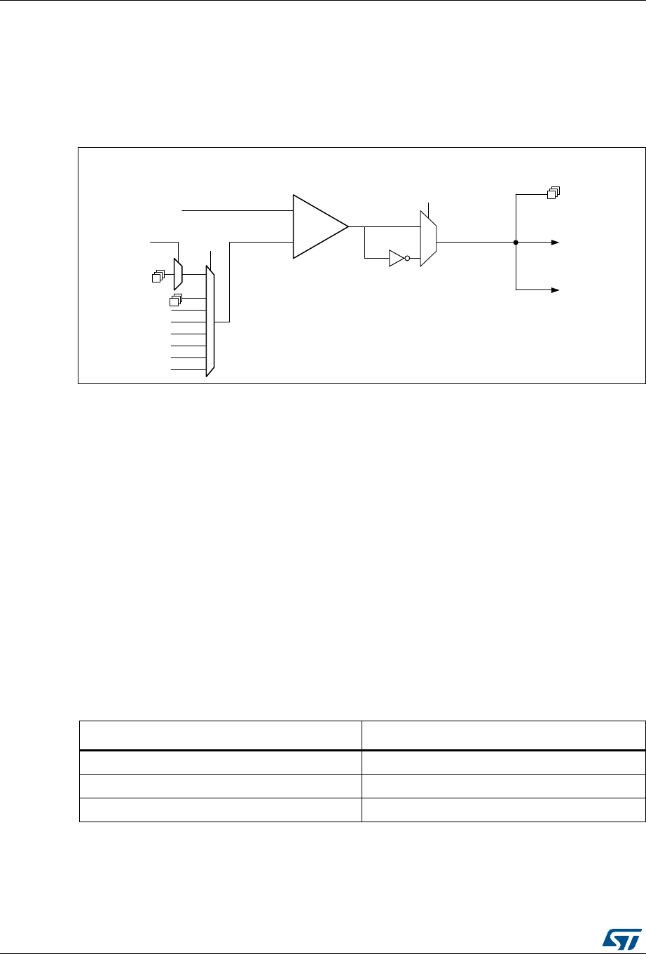
Comparator (COMP) RM0394
526/1600 RM0394 Rev 4
19.3 COMP functional description
19.3.1 COMP block diagram
The block diagram of the comparators is shown in Figure 118: Comparators block diagram.
Figure 118. Comparators block diagram
1. STM32L45xxx and STM32L46xxx devices feature only DAC_CH1.
19.3.2 COMP pins and internal signals
The I/Os used as comparators inputs must be configured in analog mode in the GPIOs
registers.
The comparator output can be connected to the I/Os using the alternate function channel
given in “Alternate function mapping” table in the datasheet.
The output can also be internally redirected to a variety of timer input for the following
purposes:
•Emergency shut-down of PWM signals, using BKIN and BKIN2 inputs
•Cycle-by-cycle current control, using OCREF_CLR inputs
•Input capture for timing measures
It is possible to have the comparator output simultaneously redirected internally and
externally.
06Y9
&203[B,10,2V
&203[B,13,2V
95(),17
95(),17
95(),17
95(),17
'$&B&+
'$&B&+
&203[B,13
&203[B,10 :DNHXS(;7,OLQH
LQWHUUXSW
3RODULW\VHOHFWLRQ
&203[B32/
&203[B9$/8(
&203[B287
&203[B
,106(/
7,0(56
*3,2
DOWHUQDWH
IXQFWLRQ
&203[
&203[B,136(/
&203[B
,10(6(/
Table 83. COMP1 input plus assignment
COMP1_INP COMP1_INPSEL
PC5 00
PB2 01
PA1 10
RM0394 Rev 4 527/1600
RM0394 Comparator (COMP)
537
Table 84. COMP1 input minus assignment
COMP1_INM COMP1_INMSEL[2:0] COMP1_INMESEL[1:0]
¼ VREFINT 000 N. A.(1)
1. N. A.: not affected.
½ VREFINT 001 N. A.(1)
¾ VREFINT 010 N. A.(1)
VREFINT 011 N. A.(1)
DAC Channel1 100 N. A.(1)
DAC Channel2 101 N. A.(1)
PB1 110 N. A.(1)
PC4 111 00
PA0 111 01
PA4 111 10
PA5 111 11
Table 85. COMP2 input plus assignment
COMP2_INP COMP2_INPSEL
PB4 00
PB6 01
PA3 10
Table 86. COMP2 input minus assignment
COMP2_INM COMP2_INMSEL[2:0] COMP2_INMESEL[1:0]
¼ VREFINT 000 N.A.(1)
1. N. A.: not affected.
½ VREFINT 001 N.A.(1)
¾ VREFINT 010 N.A.(1)
VREFINT 011 N.A.(1)
DAC Channel1 100 N.A.(1)
DAC Channel2 101 N.A.(1)
PB3 110 N.A.(1)
PB7 111 00
PA2 111 01
PA4 111 10
PA5 111 11

Comparator (COMP) RM0394
528/1600 RM0394 Rev 4
19.3.3 COMP reset and clocks
The COMP clock provided by the clock controller is synchronous with the APB2 clock.
There is no clock enable control bit provided in the RCC controller. Reset and clock enable
bits are common for COMP and SYSCFG.
Note: Important: The polarity selection logic and the output redirection to the port works
independently from the APB2 clock. This allows the comparator to work even in Stop mode.
19.3.4 Comparator LOCK mechanism
The comparators can be used for safety purposes, such as over-current or thermal
protection. For applications having specific functional safety requirements, it is necessary to
insure that the comparator programming cannot be altered in case of spurious register
access or program counter corruption.
For this purpose, the comparator control and status registers can be write-protected (read-
only).
Once the programming is completed, the COMPx LOCK bit can be set to 1. This causes the
whole register to become read-only, including the COMPx LOCK bit.
The write protection can only be reset by a MCU reset.
19.3.5 Window comparator
The purpose of window comparator is to monitor the analog voltage if it is within specified
voltage range defined by lower and upper threshold.
Two embedded comparators can be utilized to create window comparator. The monitored
analog voltage is connected to the non-inverting (plus) inputs of comparators connected
together and the upper and lower threshold voltages are connected to the inverting (minus)
inputs of the comparators. Two non-inverting inputs can be connected internally together by
enabling WINMODE bit to save one IO for other purposes.
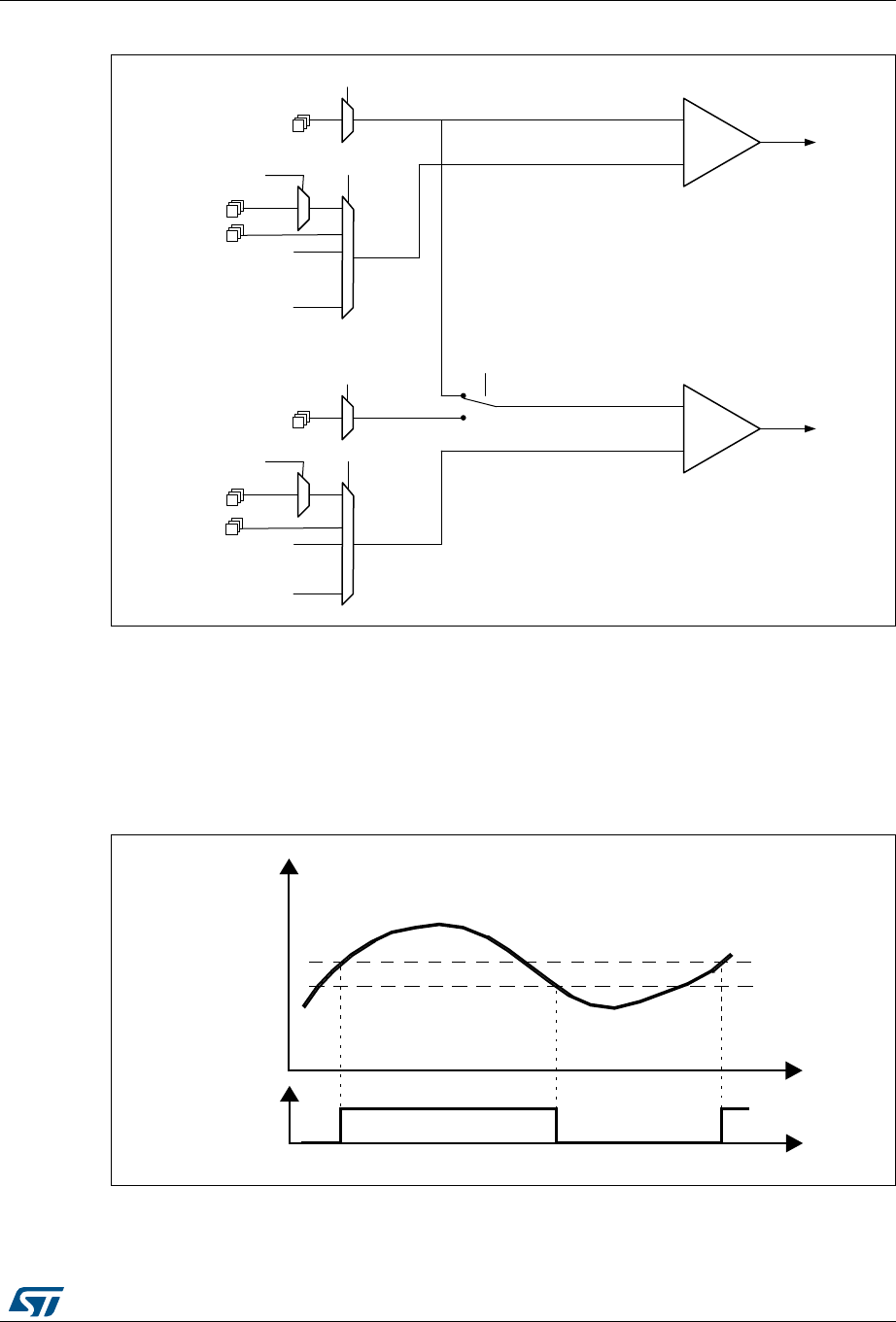
RM0394 Rev 4 529/1600
RM0394 Comparator (COMP)
537
Figure 119. Window mode
19.3.6 Hysteresis
The comparator includes a programmable hysteresis to avoid spurious output transitions in
case of noisy signals. The hysteresis can be disabled if it is not needed (for instance when
exiting from low-power mode) to be able to force the hysteresis value using external
components.
Figure 120. Comparator hysteresis
06Y9
&203\B,10,2V
&203\B,13,2V
,QWHUQDOVRXUFHV
&203\B,13
&203\B,10
&203\B,106(/
&203\
:,102'(
&203[B,10,2V
&203[B,13,2V
,QWHUQDOVRXUFHV
&203[B,13
&203[B,10
&203[B,136(/
&203[B,106(/
&203[
&203[B,136(/
&203[B,10,2V
&203[B,10(6(/
&203\B,10(6(/
&203\B,10,2V
069
).0
).-
).-6HYST
#/-0?/54
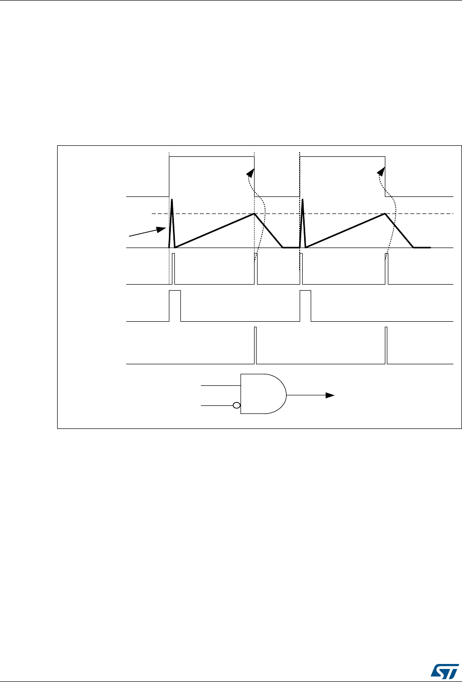
Comparator (COMP) RM0394
530/1600 RM0394 Rev 4
19.3.7 Comparator output blanking function
The purpose of the blanking function is to prevent the current regulation to trip upon short
current spikes at the beginning of the PWM period (typically the recovery current in power
switches anti parallel diodes).It consists of a selection of a blanking window which is a timer
output compare signal. The selection is done by software (refer to the comparator register
description for possible blanking signals). Then, the complementary of the blanking signal is
ANDed with the comparator output to provide the wanted comparator output. See the
example provided in the figure below.
Figure 121. Comparator output blanking
19.3.8 COMP power and speed modes
COMP1 and COMP2 power consumption versus propagation delay can be adjusted to have
the optimum trade-off for a given application.
The bits PWRMODE[1:0] in COMPx_CSR registers can be programmed as follows:
00: High speed / full power
01 or 10: Medium speed / medium power
11: Low speed / ultra-low-power
069
&XUUHQWOLPLW
&XUUHQW
5DZFRPSRXWSXW
%ODQNLQJZLQGRZ
)LQDOFRPSRXWSXW
3:0
&RPSRXW
%ODQN
&RPSRXWWR7,0B%.«

RM0394 Rev 4 531/1600
RM0394 Comparator (COMP)
537
19.4 COMP low-power modes
19.5 COMP interrupts
The comparator outputs are internally connected to the Extended interrupts and events
controller. Each comparator has its own EXTI line and can generate either interrupts or
events. The same mechanism is used to exit from low-power modes.
Refer to Interrupt and events section for more details.
To enable the COMPx interrupt, it is required to follow this sequence:
1. Configure and enable the EXTI line corresponding to the COMPx output event in
interrupt mode and select the rising, falling or both edges sensitivity
2. Configure and enable the NVIC IRQ channel mapped to the corresponding EXTI lines
3. Enable the COMPx
Table 87. Comparator behavior in the low power modes
Mode Description
Sleep No effect on the comparators.
Comparator interrupts cause the device to exit the Sleep mode.
Low-power run No effect.
Low-power sleep No effect. COMP interrupts cause the device to exit the Low-power sleep mode.
Stop 0
No effect on the comparators.
Comparator interrupts cause the device to exit the Stop mode.Stop 1
Stop 2
Standby
The COMP registers are powered down and must be reinitialized after exiting
Standby or Shutdown mode.
Shutdown
Table 88. Interrupt control bits
Interrupt event Event flag Enable control
bit
Exit from Sleep
mode
Exit from Stop
modes
Exit from
Standby mode
COMP1 output VALUE in
COMP1_CSR through EXTI yes yes N/A
COMP2 output VALUE in
COMP2_CSR through EXTI yes yes N/A

Comparator (COMP) RM0394
532/1600 RM0394 Rev 4
19.6 COMP registers
19.6.1 Comparator 1 control and status register (COMP1_CSR)
The COMP1_CSR is the Comparator 1 control/status register. It contains all the bits /flags
related to comparator1.
Address offset: 0x00
System reset value: 0x0000 0000
31 30 29 28 27 26 25 24 23 22 21 20 19 18 17 16
LOCK VALUE Res. Res. Res. INMESEL Res. SCAL
EN
BRG
EN Res. BLANKING HYST
rsr rwrwrw rwrw
1514131211109876543210
POLA
RITY Res. Res. Res. Res. Res. Res. INP
SEL. INMSEL PWRMODE Res. EN
rw rw rw rw rw
Bit 31 LOCK: COMP1_CSR register lock bit
This bit is set by software and cleared by a hardware system reset. It locks the whole
content of the comparator 1 control register, COMP1_CSR[31:0].
0: COMP1_CSR[31:0] for comparator 1 are read/write
1: COMP1_CSR[31:0] for comparator 1 are read-only
Bit 30 VALUE: Comparator 1 output status bit
This bit is read-only. It reflects the current comparator 1 output taking into account
POLARITY bit effect.
Bits 29:27 Reserved, must be kept at reset value.
Bits 26:25 INMESEL: comparator 1 input minus extended selection bits.
These bits are set and cleared by software (only if LOCK is not set). They select which
extended GPIO input is connected to the input minus of comparator if INMSEL = 111.
00: PC4
01: PA0
10: PA4
11: PA5
Bit 24 Reserved, must be kept at reset value.
Bit 23 SCALEN: Voltage scaler enable bit
This bit is set and cleared by software. This bit enable the outputs of the VREFINT divider
available on the minus input of the Comparator 1.
0: Bandgap scaler disable (if SCALEN bit of COMP2_CSR register is also reset)
1: Bandgap scaler enable

RM0394 Rev 4 533/1600
RM0394 Comparator (COMP)
537
Bit 22 BRGEN: Scaler bridge enable
This bit is set and cleared by software (only if LOCK not set). This bit enable the bridge of
the scaler.
0: Scaler resistor bridge disable (if BRGEN bit of COMP2_CSR register is also reset)
1: Scaler resistor bridge enable
If SCALEN is set and BRGEN is reset, BG voltage reference is available but not 1/4 BGAP,
1/2 BGAP, 3/4 BGAP. BGAP value is sent instead of 1/4 BGAP, 1/2 BGAP, 3/4 BGAP.
If SCALEN and BRGEN are set, 1/4 BGAP 1/2 BGAP 3/4 BGAP and BGAP voltage
references are available.
Bit 21 Reserved, must be kept at reset value
Bits 20:18 BLANKING[2:0]: Comparator 1 blanking source selection bits
These bits select which timer output controls the comparator 1 output blanking.
000: No blanking
001: TIM1 OC5 selected as blanking source
010: TIM2 OC3 selected as blanking source
All other values: reserved
Bits 17:16 HYST[1:0]: Comparator 1 hysteresis selection bits
These bits are set and cleared by software (only if LOCK not set). They select the
Hysteresis voltage of the comparator 1.
00: No hysteresis
01: Low hysteresis
10: Medium hysteresis
11: High hysteresis
Bit 15 POLARITY: Comparator 1 polarity selection bit
This bit is set and cleared by software (only if LOCK not set). It inverts Comparator 1
polarity.
0: Comparator 1 output value not inverted
1: Comparator 1 output value inverted
Bits 14:9 Reserved, must be kept at reset value.
Bits 8:7 INPSEL: Comparator1 input plus selection bit
This bit is set and cleared by software (only if LOCK not set).
00: External I/O - PC5
01: PB2
10: PA1
11: Reserved, the bit must be kept at the reset value
Bits 6:4 INMSEL: Comparator 1 input minus selection bits
These bits are set and cleared by software (only if LOCK not set). They select which input is
connected to the input minus of comparator 1.
000 = 1/4 VREFINT
001 = 1/2 VREFINT
010 = 3/4 VREFINT
011 = VREFINT
100 = DAC Channel1
101 = DAC Channel2
110 = PB1111 : GPIOx selected by INMESEL bits

Comparator (COMP) RM0394
534/1600 RM0394 Rev 4
19.6.2 Comparator 2 control and status register (COMP2_CSR)
The COMP2_CSR is the Comparator 2 control/status register. It contains all the bits /flags
related to comparator 2.
Address offset: 0x04
System reset value: 0x0000 0000
Bits 3:2 PWRMODE[1:0]: Power Mode of the comparator 1
These bits are set and cleared by software (only if LOCK not set). They control the
power/speed of the Comparator 1.
00: High speed
01 or 10: Medium speed
11: Ultra low power
Bit 1 Reserved, must be kept cleared.
Bit 0 EN: Comparator 1 enable bit
This bit is set and cleared by software (only if LOCK not set). It switches on Comparator1.
0: Comparator 1 switched OFF
1: Comparator 1 switched ON
31 30 29 28 27 26 25 24 23 22 21 20 19 18 17 16
LOCK VALUE Res. Res. Res. INMESEL Res. SCAL
EN
BRG
EN Res. BLANKING HYST
rsr rwrwrw rwrw
1514131211109876543210
POLA
RITY Res. Res. Res. Res. Res. WIN
MODE INPSEL. INMSEL PWRMODE Res. EN
rw rw rw rw rw rw
Bit 31 LOCK: CSR register lock bit
This bit is set by software and cleared by a hardware system reset. It locks the whole
content of the comparator 2 control register, COMP2_CSR[31:0].
0: COMP2_CSR[31:0] for comparator 2 are read/write
1: COMP2_CSR[31:0] for comparator 2 are read-only
Bit 30 VALUE: Comparator 2 output status bit
This bit is read-only. It reflects the current comparator 2 output taking into account
POLARITY bit effect.
Bits 29:27 Reserved, must be kept at reset value
Bits 26:25 INMESEL: comparator 2 input minus extended selection bits.
These bits are set and cleared by software (only if LOCK is not set). They select which
extended GPIO input is connected to the input minus of comparator if INMSEL = 111.
00: PB7
01: PA2
10: PA4
11: PA5
Bit 24 Reserved, must be kept at reset value

RM0394 Rev 4 535/1600
RM0394 Comparator (COMP)
537
Bit 23 SCALEN: Voltage scaler enable bit
This bit is set and cleared by software. This bit enable the outputs of the VREFINT divider
available on the minus input of the Comparator 2.
0: Bandgap scaler disable (if SCALEN bit of COMP1_CSR register is also reset)
1: Bandgap scaler enable
Bit 22 BRGEN: Scaler bridge enable
This bit is set and cleared by software (only if LOCK not set). This bit enable the bridge of
the scaler.
0: Scaler resistor bridge disable (if BRGEN bit of COMP1_CSR register is also reset)
1: Scaler resistor bridge enable
If SCALEN is set and BRGEN is reset, BG voltage reference is available but not 1/4 BGAP,
1/2 BGAP, 3/4 BGAP. BGAP value is sent instead of 1/4 BGAP, 1/2 BGAP, 3/4 BGAP.
If SCALEN and BRGEN are set, 1/4 BGAP 1/2 BGAP 3/4 BGAP and BGAP voltage
references are available.
Bit 21 Reserved, must be kept at reset value
Bits 20:18 BLANKING[2:0]: Comparator 2 blanking source selection bits
These bits select which timer output controls the comparator 2 output blanking.
000: No blanking
001: Reserved
010: Reserved
100: TIM15 OC1 selected as blanking source
All other values: reserved
Bits 17:16 HYST[1:0]: Comparator 2 hysteresis selection bits
These bits are set and cleared by software (only if LOCK not set). Select the hysteresis
voltage of the comparator 2.
00: No hysteresis
01: Low hysteresis
10: Medium hysteresis
11: High hysteresis
Bit 15 POLARITY: Comparator 2 polarity selection bit
This bit is set and cleared by software (only if LOCK not set). It inverts Comparator 2
polarity.
0: Comparator 2 output value not inverted
1: Comparator 2 output value inverted
Bits 14:10 Reserved, must be kept at reset value.
Bit 9 WINMODE: Windows mode selection bit
This bit is set and cleared by software (only if LOCK not set). This bit selects the window
mode of the comparators. If set, both positive inputs of comparators will be connected
together.
0: Input plus of Comparator 2 is not connected to Comparator 1
1: Input plus of Comparator 2 is connected with input plus of Comparator 1
Bits 8:7 INPSEL: Comparator 1 input plus selection bit
This bit is set and cleared by software (only if LOCK not set).
00: PB4
01: PB6
10: PA3
11: Reserved, the bit must be kept at the reset value

Comparator (COMP) RM0394
536/1600 RM0394 Rev 4
Bits 6:4 INMSEL: Comparator 2 input minus selection bits
These bits are set and cleared by software (only if LOCK not set). They select which input is
connected to the input minus of comparator 2.
000 = 1/4 VREFINT
001 = 1/2 VREFINT
010 = 3/4 VREFINT
011 = VREFINT
100 = DAC Channel1
101 = DAC Channel2
110 = PB3
111: GPIOx selected by INMESEL bits
Bits 3:2 PWRMODE[1:0]: Power Mode of the comparator 2
These bits are set and cleared by software (only if LOCK not set). They control the
power/speed of the Comparator 2.
00: High speed
01 or 10: Medium speed
11: Ultra low power
Bit 1 Reserved, must be kept cleared.
Bit 0 EN: Comparator 2 enable bit
This bit is set and cleared by software (only if LOCK not set). It switches oncomparator2.
0: Comparator 2 switched OFF
1: Comparator 2 switched ON

RM0394 Rev 4 537/1600
RM0394 Comparator (COMP)
537
19.6.3 COMP register map
The following table summarizes the comparator registers.
Refer to Section 2.2.2 on page 67 for the register boundary addresses.
Table 89. COMP register map and reset values
Offset Register
31
30
29
28
27
26
25
24
23
22
21
20
19
18
17
16
15
14
13
12
11
10
9
8
7
6
5
4
3
2
1
0
0x00 COMP1_CSR
LOCK
VALUE
Res.
Res.
Res.
INMESEL
Res.
SCALEN
BRGEN.
Res.
BLANKING
HYST
POLARITY.
Res.
Res.
Res.
Res.
Res.
Res.
INPSEL
INMSEL
PWRMODE
Res.
EN
Reset value 00 00 00 000000 0000000 0
0x04 COMP2_CSR
LOCK
VALUE
Res.
Res.
Res.
INMESEL
Res.
SCALEN.
BRGEN.
Res.
BLANKING
HYST.
POLARITY.
Res.
Res.
Res.
Res.
Res.
WINMODE
INPSEL
INMSEL
PWRMODE
Res.
EN
Reset value 00 00 00 000000 00000000 0

Operational amplifiers (OPAMP) RM0394
538/1600 RM0394 Rev 4
20 Operational amplifiers (OPAMP)
20.1 Introduction
The device embeds an operational amplifier with two inputs and one output. The three I/Os
can be connected to the external pins, this enables any type of external interconnections.
The operational amplifier can be configured internally as a follower or as an amplifier with a
non-inverting gain ranging from 2 to 16.
The positive input can be connected to the internal DAC.
The output can be connected to the internal ADC.
20.2 OPAMP main features
•Rail-to-rail input and output voltage range
•Low input bias current (down to 1 nA)
•Low input offset voltage (1.5 mV after calibration, 3 mV with factory calibration)
•Low-power mode (current consumption reduced to 30 µA instead of 100 µA)
•Fast wakeup time (10 µs in normal mode, 30 µs in low-power mode)
•Gain bandwidth of 1.6 MHz
20.3 OPAMP functional description
The OPAMP has several modes.
When the OPAMP is disabled, the output is high impedance.
When enabled, it can be in calibration mode, all input and output of the OPAMP are then
disconnected, or in functional mode.
There are two functional modes, the low-power mode or the normal mode. In functional
mode the inputs and output of the OPAMP are connected as described in the
Section 20.3.3: Signal routing.
20.3.1 OPAMP reset and clocks
The operational amplifier clock is necessary for accessing the registers. When the
application does not need to have read or write access to those registers, the clock can be
switched off using the peripheral clock enable register (see OPAMPEN bit in Section 6.4.18:
APB1 peripheral clock enable register 1 (RCC_APB1ENR1)).
The bit OPAEN enables and disables the OPAMP operation. The OPAMP registers
configurations should be changed before enabling the OPAEN bit in order to avoid spurious
effects on the output.
When the output of the operational amplifier is no more needed the operational amplifier can
be disabled to save power. All the configurations previously set (including the calibration)
are maintained while OPAMP is disabled.

RM0394 Rev 4 539/1600
RM0394 Operational amplifiers (OPAMP)
548
20.3.2 Initial configuration
The default configuration of the operational amplifier is a functional mode where the three
IOs are connected to external pins. In the default mode the operational amplifier uses the
factory trimming values. See electrical characteristics section of the datasheet for factory
trimming conditions, usually the temperature is 30 °C and the voltage is 3 V. The trimming
values can be adjusted, see Section 20.3.5: Calibration for changing the trimming values.
The default configuration uses the normal mode, which provides the highest performance.
Bit OPALPM can be set in order to switch the operational amplifier to low-power mode and
reduced performance. Both normal and low-power mode characteristics are defined in the
section “electrical characteristics” of the datasheet. Before utilization, the bit OPA_RANGE
of OPAMP_CSR must be set to 1 if VDDA is above 2.4V, or kept at 0 otherwise.
As soon as the OPAEN bit in OPAMP_CSR register is set, the operational amplifier is
functional. The two input pins and the output pin are connected as defined in Section 20.3.3:
Signal routing and the default connection settings can be changed.
Note: The inputs and output pins must be configured in analog mode (default state) in the
corresponding GPIOx_MODER register.
20.3.3 Signal routing
The routing for the operational amplifier pins is determined by OPAMP_CSR register.
The connections of the operational amplifier OPAMP1 is described in the table below.
20.3.4 OPAMP modes
The operational amplifier inputs and outputs are all accessible on terminals. The amplifier
can be used in multiple configuration environments:
•Standalone mode (external gain setting mode)
•Follower configuration mode
•PGA modes
Note: The amplifier output pin is directly connected to the output pad to minimize the output
impedance. It cannot be used as a general purpose I/O, even if the amplifier is configured
as a PGA and only connected to the ADC channel.
Note: The impedance of the signal must be maintained below a level which avoids the input
leakage to create significant artifacts (due to a resistive drop in the source). Please refer to
the electrical characteristics section in the datasheet for further details.
Table 90. Operational amplifier possible connections
Signal Pin Internal comment
OPAMP1_VINM PA1 or dedicated pin OPAMP1_OUT
or PGA
controlled by bits OPAMODE
and VM_SEL.
OPAMP1_VINP PA0 DAC1_OUT1 controlled by bit VP_SEL.
OPAMP1_VOUT PA3 ADC1_IN8
The pin is connected when the
OPAMP is enabled. The ADC
input is controlled by ADC.
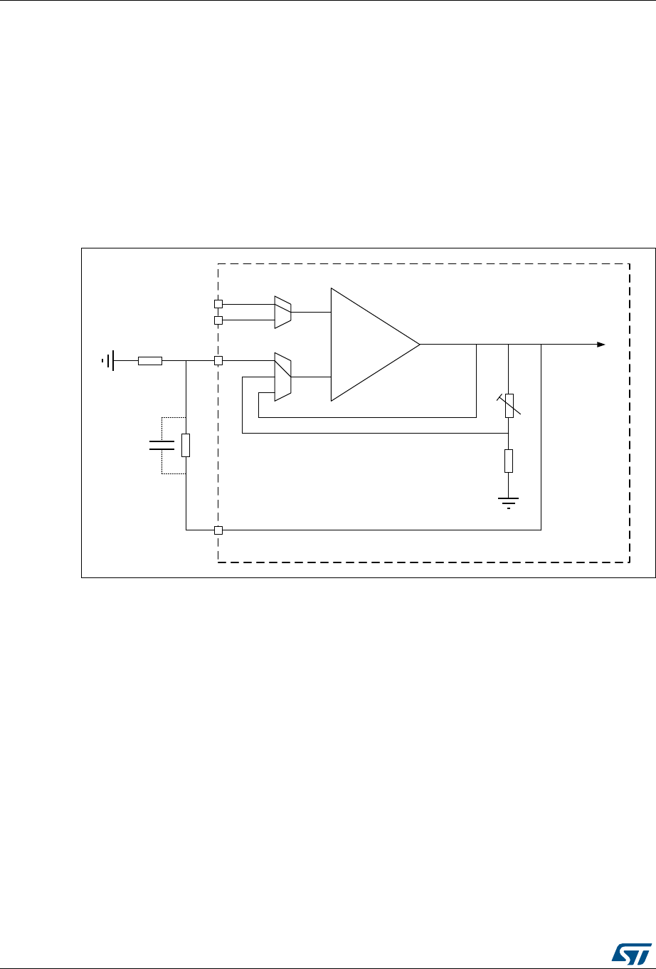
Operational amplifiers (OPAMP) RM0394
540/1600 RM0394 Rev 4
Standalone mode (external gain setting mode)
The procedure to use the OPAMP in standalone mode is presented hereafter.
Starting from the default value of OPAMP_CSR, and the default state of GPIOx_MODER,
configure bit OPA_RANGE according the VDDA voltage. As soon as the OPAEN bit is set,
the two input pins and the output pin are connected to the operational amplifier.
This default configuration uses the factory trimming values and operates in normal mode
(highest performance). The behavior of the OPAMP can be changed as follows:
•OPALPM can be set to “operational amplifier low-power” mode in order to save power.
•USERTRIM can be set to modify the trimming values for the input offset.
Figure 122. Standalone mode: external gain setting mode
Follower configuration mode
The procedure to use the OPAMP in follower mode is presented hereafter.
•configure OPAMODE bits as “internal follower”
•configure VP_SEL bits as “GPIO connected to VINP”.
•As soon as the OPAEN bit is set, the signal on pin OPAMP_VINP is copied to pin
OPAMP_VOUT.
Note: The pin corresponding to OPAMP_VINM is free for another usage.
Note: The signal on the operational amplifier output is also seen as an ADC input. As a
consequence, the OPAMP configured in follower mode can be used to perform impedance
adaptation on input signals before feeding them to the ADC input, assuming the input signal
frequency is compatible with the operational amplifier gain bandwidth specification.
069
670
*3,2
'$&B287
*3,2
$'&
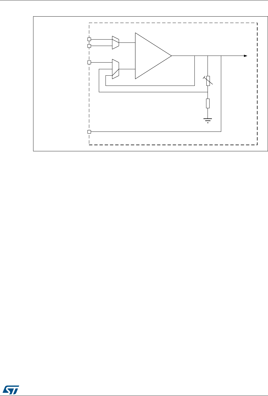
RM0394 Rev 4 541/1600
RM0394 Operational amplifiers (OPAMP)
548
Figure 123. Follower configuration
069
670
*3,2
'$&B287
*3,2
$'&
$OZD\VFRQQHFWHGWR
23$03RXWSXWFDQEH
XVHGGXULQJGHEXJ
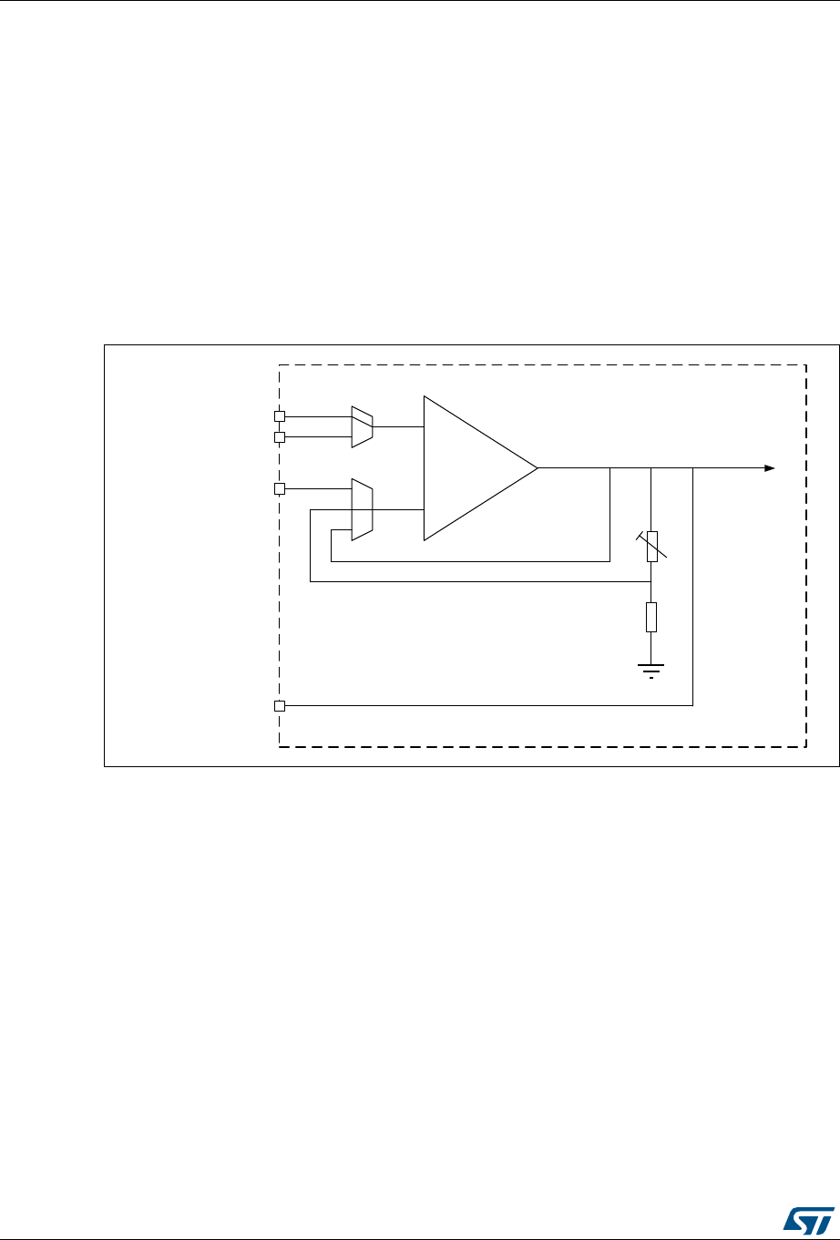
Operational amplifiers (OPAMP) RM0394
542/1600 RM0394 Rev 4
Programmable Gain Amplifier mode
The procedure to use the OPAMP to amplify the amplitude of an input signal is
presented hereafter.
•configure OPAMODE bits as “internal PGA enabled”,
•configure PGA_GAIN bits as “internal PGA Gain 2, 4, 8 or 16”,
•configure VM_SEL bits as “inverting not externally connected”,
•configure VP_SEL bits as “GPIO connected to VINP”.
As soon as the OPAEN bit is set, the signal on pin OPAMP_VINP is amplified by the
selected gain and visible on pin OPAMP_VOUT.
Note: To avoid saturation, the input voltage should stay below VDDA divided by the selected gain.
Figure 124. PGA mode, internal gain setting (x2/x4/x8/x16), inverting input not used
069
670
*3,2
'$&B287
*3,2
$'&
$OZD\VFRQQHFWHGWR
23$03RXWSXWFDQEH
XVHGGXULQJGHEXJ
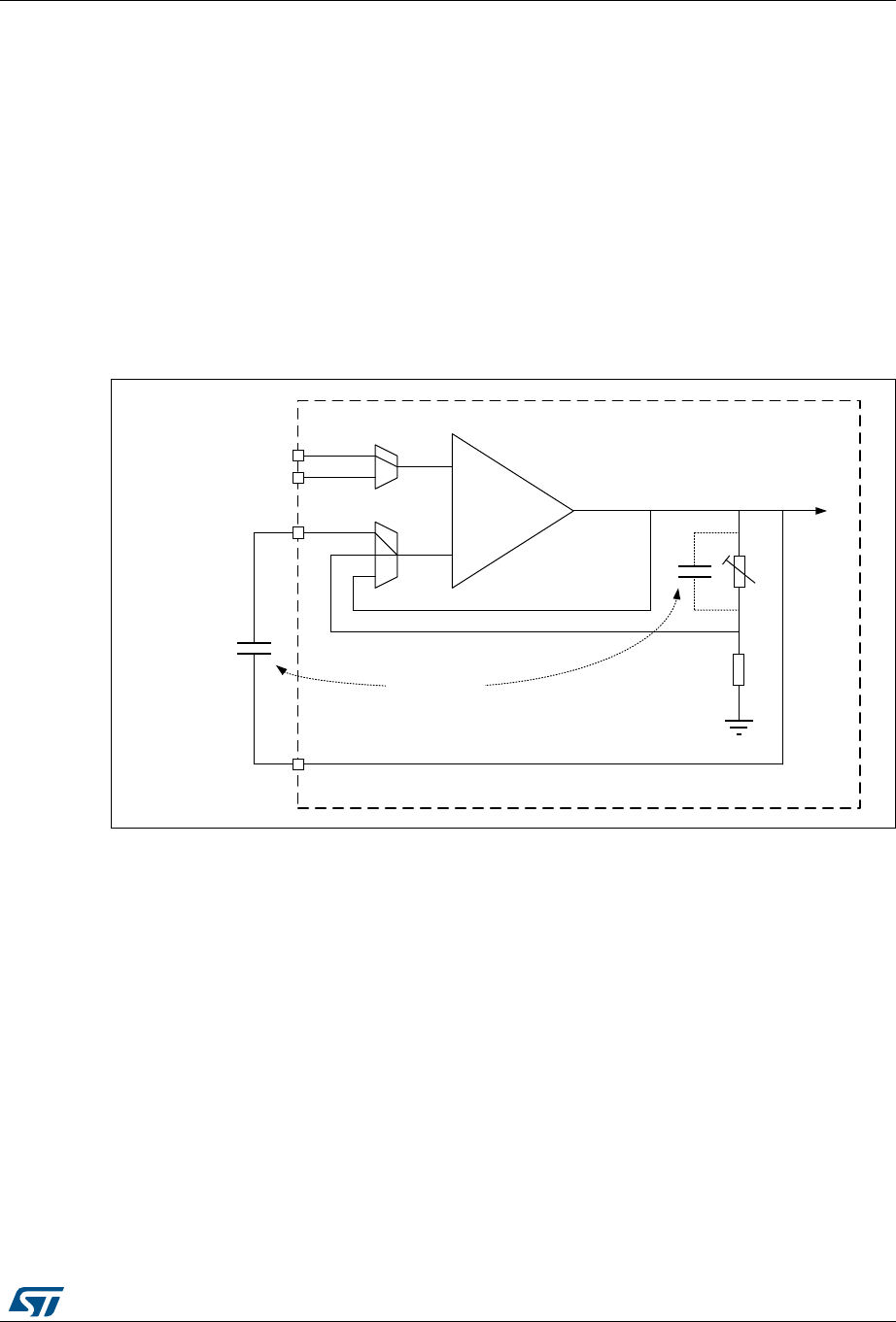
RM0394 Rev 4 543/1600
RM0394 Operational amplifiers (OPAMP)
548
Programmable Gain Amplifier mode with external filtering
The procedure to use the OPAMP to amplify the amplitude of an input signal, with an
external filtering, is presented hereafter.
•configure OPAMODE bits as “internal PGA enabled”,
•configure PGA_GAIN bits as “internal PGA Gain 2, 4, 8 or 16”,
•configure VM_SEL bits as “GPIO connected to VINM”,
•configure VP_SEL bits as “GPIO connected to VINP”.
Any external connection on VINP can be used in parallel with the internal PGA, for
example a capacitor can be connected between VOUT and VINM for filtering purpose
(see datasheet for the value of resistors used in the PGA resistor network).
Figure 125. PGA mode, internal gain setting (x2/x4/x8/x16), inverting input used for
filtering
1. The gain depends on the cut-off frequency.
20.3.5 Calibration
At startup, the trimming values are initialized with the preset ‘factory’ trimming value.
The operational amplifier offset can be trimmed by the user. Specific registers allow to have
different trimming values for normal mode and for low-power mode.
The aim of the calibration is to cancel as much as possible the OPAMP inputs offset voltage.
The calibration circuitry allows to reduce the inputs offset voltage to less than +/-1.5 mV
within stable voltage and temperature conditions.
For each mode of the operational amplifier, two trimming values need to be trimmed, one for
N differential pair and one for P differential pair.
There are two registers for trimming the operational amplifier offset, one for normal mode
(OPAMP_OTR) and one low-power mode (OPAMP_LPOTR). Each register is composed of
five bits for P differential pair trimming and five bits for N differential pair trimming. These are
the ‘user’ values.
069
670
*3,2
'$&B287
*3,2
$'&
$OORZVRSWLRQDO
ORZSDVV
ILOWHULQJ
(TXLYDOHQWWR

Operational amplifiers (OPAMP) RM0394
544/1600 RM0394 Rev 4
The user is able to switch from ‘factory’ values to ‘user’ trimmed values using the
USERTRIM bit in the OPAMP_CSR register. This bit is reset at startup and so the ‘factory’
value are applied by default to the OPAMP trimming registers.
User is liable to change the trimming values in calibration or in functional mode.
The offset trimming registers are typically configured after the calibration operation is
initialized by setting bit CALON to 1. When CALON = 1 the inputs of the operational
amplifier are disconnected from the functional environment.
•Setting CALSEL to 1 initializes the offset calibration for the P differential pair (low
voltage reference used).
•Resetting CALSEL to 0 initializes the offset calibration for the N differential pair (high
voltage reference used).
When CALON = 1, the bit CALOUT will reflect the influence of the trimming value selected
by CALSEL and OPALPM. When the value of CALOUT switches between two consecutive
trimming values, this means that those two values are the best trimming values. The
CALOUT flag needs up to 1 ms after the trimming value is changed to become steady (see
tOFFTRIMmax delay specification in the electrical characteristics section of the datasheet).
Note: The closer the trimming value is to the optimum trimming value, the longer it takes to
stabilize (with a maximum stabilization time remaining below 1 ms in any case).
Table 91. Operating modes and calibration
Mode
Control bits Output
OPAEN OPALPM CALON CALSEL VOUT
CALOUT
flag
Normal operating
mode 1 0 0 X analog 0
Low-power mode 1 1 0 X analog 0
Power down 0 X X X Z 0
Offset cal high for
normal mode 1 0 1 0 analog X
Offset cal low for
normal mode 1 0 1 1 analog X
Offset cal high for
low-power mode 1 1 1 0 analog X
Offset cal low for
low-power mode 1 1 1 1 analog X

RM0394 Rev 4 545/1600
RM0394 Operational amplifiers (OPAMP)
548
Calibration procedure
Here are the steps to perform full operational amplifier calibration:
1. Select correct OPA_RANGE in OPAMP_CSR, then set the OPAEN bit in OPAMP_CSR
to 1 to enable the operational amplifier.
2. Set the USERTRIM bit in the OPAMP_CSR register to 1.
3. Choose a calibration mode (refer to Table 91: Operating modes and calibration). The
steps 3 to 4 will have to be repeated 4 times. For the first iteration select
– Normal mode, offset cal high (N differential pair)
The above calibration mode correspond to OPALPM=0 and CALSEL=0 in the
OPAMP_CSR register.
4. Increment TRIMOFFSETN[4:0] in OPAMP_OTR starting from 00000b until CALOUT
changes to 1 in OPAMP_CSR.
Note: CALOUT will switch from 0 to 1 for offset cal high and from 1 to 0 for offset cal low.
Note: Between the write to the OPAMP_OTR register and the read of the CALOUT value, make
sure to wait for the tOFFTRIMmax delay specified in the electrical characteristics section of
the datasheet, to get the correct CALOUT value.
The commutation means that the offset is correctly compensated and that the
corresponding trim code must be saved in the OPAMP_OTR register.
Repeat steps 3 to 4 for:
– Normal_mode and offset cal low
– Low power mode and offset cal high
– Low power mode and offset cal low
If a mode is not used it is not necessary to perform the corresponding calibration.
Note: During the whole calibration phase the external connection of the operational amplifier
output must not pull up or down currents higher than 500 µA.
During the calibration procedure, it is necessary to set up OPAMODE bits as 00 or 01 (PGA
disable) or 11 (internal follower).
20.4 OPAMP low-power modes
Table 92. Effect of low-power modes on the OPAMP
Mode Description
Sleep No effect.
Low-power run No effect.
Low-power sleep No effect.
Stop 0 / Stop 1 No effect, OPAMP registers content is kept.
Stop 2 OPAMP registers content is kept. OPAMP must be disabled before entering
Stop 2 mode.
Standby The OPAMP registers are powered down and must be re-initialized after
exiting Standby or Shutdown mode.
Shutdown

Operational amplifiers (OPAMP) RM0394
546/1600 RM0394 Rev 4
20.5 OPAMP registers
20.5.1 OPAMP1 control/status register (OPAMP1_CSR)
Address offset: 0x00
Reset value: 0x0000 0000
31 30 29 28 27 26 25 24 23 22 21 20 19 18 17 16
OPA_
RANGE Res. Res. Res. Res. Res. Res. Res. Res. Res. Res. Res. Res. Res. Res. Res.
rw
1514131211109876543210
CAL
OUT
USER
TRIM
CAL
SEL CALON Res. VP_
SEL VM_SEL Res. Res. PGA_GAIN OPAMODE OPA
LPM OPAEN
r rwrwrw rwrwrw rwrwrw w rwrw
Bit 31 OPA_RANGE: Operational amplifier power supply range for stability
All AOP must be in power down to allow AOP-RANGE bit write. It applies to all AOP
embedded in the product.
0: Low range (VDDA < 2.4V)
1: High range (VDDA > 2.4V)
Bits 30:16 Reserved, must be kept at reset value.
Bit 15 CALOUT: Operational amplifier calibration output
During calibration mode offset is trimmed when this signal toggle.
Bit 14 USERTRIM: allows to switch from ‘factory’ AOP offset trimmed values to AOP offset ‘user’
trimmed values
This bit is active for both mode normal and low-power.
0: ‘factory’ trim code used
1: ‘user’ trim code used
Bit 13 CALSEL: Calibration selection
0: NMOS calibration (200mV applied on OPAMP inputs)
1: PMOS calibration (VDDA-200mV applied on OPAMP inputs)
Bit 12 CALON: Calibration mode enabled
0: Normal mode
1: Calibration mode (all switches opened by HW)
Bit 11 Reserved, must be kept at reset value.
Bit 10 VP_SEL: Non inverted input selection
0: GPIO connected to VINP
1: DAC connected to VINP
Bits 9:8 VM_SEL: Inverting input selection
These bits are used only when OPAMODE = 00, 01 or 10.
00: GPIO connected to VINM (valid also in PGA mode for filtering)
01: Reserved
1x: Inverting input not externally connected. These configurations are valid only when
OPAMODE = 10 (PGA mode)
Bits 7:6 Reserved, must be kept at reset value.

RM0394 Rev 4 547/1600
RM0394 Operational amplifiers (OPAMP)
548
20.5.2 OPAMP1 offset trimming register in normal mode (OPAMP1_OTR)
Address offset: 0x04
Reset value: 0x0000 XXXX (factory trimmed values)
20.5.3 OPAMP1 offset trimming register in low-power mode
(OPAMP1_LPOTR)
Address offset: 0x08
Reset value: 0x0000 XXXX (factory trimmed values)
Bits 5:4 PGA_GAIN: Operational amplifier Programmable amplifier gain value
00: internal PGA Gain 2
01: internal PGA Gain 4
10: internal PGA Gain 8
11: internal PGA Gain 16
Bits 3:2 OPAMODE: Operational amplifier PGA mode
00: internal PGA disable
01: internal PGA disable
10: internal PGA enable, gain programmed in PGA_GAIN
11: internal follower
Bit 1 OPALPM: Operational amplifier Low Power Mode
The operational amplifier must be disable to change this configuration.
0: operational amplifier in normal mode
1: operational amplifier in low-power mode
Bit 0 OPAEN: Operational amplifier Enable
0: operational amplifier disabled
1: operational amplifier enabled
31 30 29 28 27 26 25 24 23 22 21 20 19 18 17 16
Res. Res. Res. Res. Res. Res. Res. Res. Res. Res. Res. Res. Res. Res. Res. Res.
1514131211109876543210
Res. Res. Res. TRIMOFFSETP Res. Res. Res. TRIMOFFSETN
rw rw rw rw rw rw rw rw rw rw
Bits 31:13 Reserved, must be kept at reset value.
Bits 12:8 TRIMOFFSETP[4:0]: Trim for PMOS differential pairs
Bits 7:5 Reserved, must be kept at reset value.
Bits 4:0 TRIMOFFSETN[4:0]: Trim for NMOS differential pairs
Operational amplifiers (OPAMP) RM0394
548/1600 RM0394 Rev 4
20.5.4 OPAMP register map
Refer to Section 2.2.2: Memory map and register boundary addresses for the register
boundary addresses.
31 30 29 28 27 26 25 24 23 22 21 20 19 18 17 16
Res. Res. Res. Res. Res. Res. Res. Res. Res. Res. Res. Res. Res. Res. Res. Res.
1514131211109876543210
Res. Res. Res. TRIMLPOFFSETP Res. Res. Res. TRIMLPOFFSETN
rw rw rw rw rw rw rw rw rw rw
Bits 31:13 Reserved, must be kept at reset value.
Bits 12:8 TRIMLPOFFSETP[4:0]: Low-power mode trim for PMOS differential pairs
Bits 7:5 Reserved, must be kept at reset value.
Bits 4:0 TRIMLPOFFSETN[4:0]: Low-power mode trim for NMOS differential pairs
Table 93. OPAMP register map and reset values
Offset Register
31
30
29
28
27
26
25
24
23
22
21
20
19
18
17
16
15
14
13
12
11
10
9
8
7
6
5
4
3
2
1
0
0x00 OPAMP1_CSR
OPA_RANGE
Res.
Res.
Res.
Res.
Res.
Res.
Res.
Res.
Res.
Res.
Res.
Res.
Res.
Res.
Res.
CALOUT
USERTRIM
CALSEL
CALON
Res.
VP_SEL
VM_SEL
Res.
Res.
PGA_GAIN
OPAMODE
OPALPM
OPAEN
Reset value 0 0000 000 000000
0x04 OPAMP1_OTR
Res.
Res.
Res.
Res.
Res.
Res.
Res.
Res.
Res.
Res.
Res.
Res.
Res.
Res.
Res.
Res.
Res.
Res.
Res.
TRIM
OFFSETP[4:0]
Res.
Res.
Res.
TRIM
OFFSETN[4:0]
Reset value (1) (1)
0x08
OPAMP1_
LPOTR
Res.
Res.
Res.
Res.
Res.
Res.
Res.
Res.
Res.
Res.
Res.
Res.
Res.
Res.
Res.
Res.
Res.
Res.
Res.
TRIMLP
OFFSETP[4:0]
Res.
Res.
Res.
TRIMLP
OFFSETN[4:0]
Reset value (1) (1)
1. Factory trimmed values.

RM0394 Rev 4 549/1600
RM0394 Digital filter for sigma delta modulators (DFSDM)
601
21 Digital filter for sigma delta modulators (DFSDM)
DFSDM is available only on STM32L451xx, STM32L452xx and STM32L462xx.
21.1 Introduction
Digital filter for sigma delta modulators (DFSDM) is a high-performance module dedicated to
interface external modulators. It is featuring up to 4 external digital serial interfaces
(channels) and up to 2 digital filters with flexible Sigma Delta stream digital processing
options to offer up to 24-bit final ADC resolution. DFSDM also features optional parallel data
stream input from device memory.
An external modulator provides digital data stream of converted analog values from the
external modulator analog input. This digital data stream is sent into a DFSDM input
channel through a serial interface. DFSDM supports several standards to connect various
modulator outputs: SPI interface and Manchester coded 1-wire interface (both with
adjustable parameters). DFSDM module supports the connection of up to 4 multiplexed
input digital serial channels which are shared with up to 2 DFSDM modules. DFSDM
module also supports alternative parallel data inputs from up to 4 internal 16-bit data
channels (from device memory).
DFSDM is converting an input data stream into a final digital data word which represents an
analog input value on a modulator analog input. The conversion is based on a
configurable digital process: the digital filtering and decimation of the input serial data
stream.
The conversion speed and resolution are adjustable according to configurable parameters
for digital processing: filter type, filter order, length of filter, integrator length. The maximum
output data resolution is up to 24 bits. There are two conversion modes: single conversion
mode and continuous mode. The data can be automatically stored in a system RAM buffer
through DMA, thus reducing the software overhead.
A flexible timer triggering system can be used to control the start of conversion of DFSDM.
This timing control is capable of triggering simultaneous conversions or inserting a
programmable delay between conversions.
DFSDM features an analog watchdog function. Analog watchdog can be assigned to any of
the input channel data stream or to final output data. Analog watchdog has its own digital
filtering of input data stream to reach the required speed and resolution of watched data.
To detect short-circuit in control applications, there is a short-circuit detector. This block
watches each input channel data stream for occurrence of stable data for a defined time
duration (several 0’s or 1’s in an input data stream).
An extremes detector block watches final output data and stores maximum and minimum
values from the output data values. The extremes values stored can be restarted by
software.
Two power modes are supported: normal mode and stop mode.

Digital filter for sigma delta modulators (DFSDM) RM0394
550/1600 RM0394 Rev 4
21.2 DFSDM main features
•Up to 4 multiplexed input digital serial channels:
– configurable SPI interface to connect various modulators
– configurable Manchester coded 1 wire interface support
– clock output for modulator(s)
•Alternative inputs from up to 4 internal digital parallel channels:
– inputs with up to 16 bit resolution
– internal sources: memory (CPU/DMA write) data streams
•Adjustable digital signal processing:
–Sinc
x filter: filter order/type (1..5), oversampling ratio (up to 1..1024)
– integrator: oversampling ratio (1..256)
•Up to 24-bit output data resolution:
– right bit-shifter on final data (0..31 bits)
•Signed output data format
•Automatic data offset correction (offset stored in register by user)
•Continuous or single conversion
•Start-of-conversion synchronization with:
– software trigger
– internal timers
– external events
– start-of-conversion synchronously with first DFSDM filter (DFSDM_FLT0)
•Analog watchdog feature:
– low value and high value data threshold registers
– own configurable Sincx digital filter (order = 1..3, oversampling ratio = 1..32)
– input from output data register or from one or more input digital serial channels
– continuous monitoring independently from standard conversion
•Short-circuit detector to detect saturated analog input values (bottom and top ranges):
– up to 8-bit counter to detect 1..256 consecutive 0’s or 1’s on input data stream
– monitoring continuously each channel (4 serial channel transceiver outputs)
•Break generation on analog watchdog event or short-circuit detector event
•Extremes detector:
– store minimum and maximum values of output data values
– refreshed by software
•DMA may be used to read the conversion data
•Interrupts: end of conversion, overrun, analog watchdog, short-circuit, channel clock
absence
•“regular” or “injected” conversions:
– “regular” conversions can be requested at any time or even in continuous mode
without having any impact on the timing of “injected” conversions

RM0394 Rev 4 551/1600
RM0394 Digital filter for sigma delta modulators (DFSDM)
601
21.3 DFSDM implementation
This section describes the configuration implemented in DFSDMx.
Table 94. DFSDM1 implementation
DFSDM features DFSDM1
Number of channels 4
Number of filters 2
Input from internal ADC -
Supported trigger sources 10
Pulses skipper -
ID registers support -
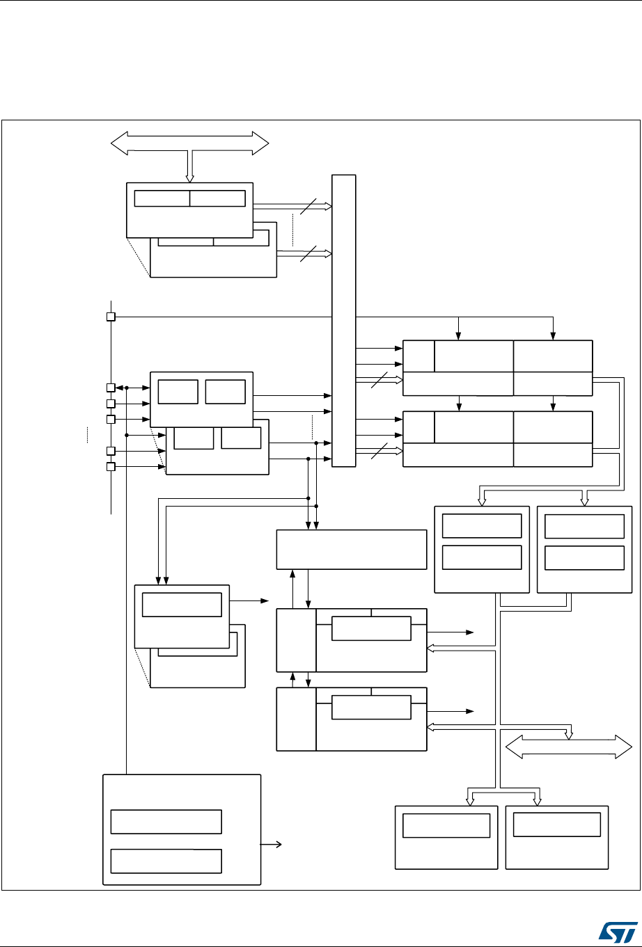
Digital filter for sigma delta modulators (DFSDM) RM0394
552/1600 RM0394 Rev 4
21.4 DFSDM functional description
21.4.1 DFSDM block diagram
Figure 126. Single DFSDM block diagram
06Y9
&RQWUROXQLW
,QWHUUXSW
EUHDN
,QWHUUXSWVDQGHYHQWV
HQGRIFRQYHUVLRQ
DQDORJZDWFKGRJ
VKRUWFLUFXLWGHWHFWLRQ
RYHUUXQ
'DWDRXWSXW
&RQILJXUDWLRQ
UHJLVWHUV
'0$LQWHUUXSWEUHDN
FRQWUROFORFNFRQWURO
)LOWHU
FRQILJ $QDORJZDWFKGRJ
+LJKWKUHVKROG
/RZWKUHVKROG
)LOWHU
FRQILJ $QDORJZDWFKGRJ
+LJKWKUHVKROG
/RZWKUHVKROG
')6'0GDWD
5LJKWELWVKLIW
FRXQW
&DOLEUDWLRQGDWD
FRUUHFWLRQXQLW
ZDWFKGRJILOWHUV
ZDWFKGRJFRPSDUDWRUV
&RQILJ
6WDWXV
6KRUWFLUFXLW
GHWHFWRU
VVFRXQWHU
WKUHVKROG
6KRUWFLUFXLW
GHWHFWRU
VVFRXQWHU
WKUHVKROG
6HULDOWUDQVFHLYHU
&ORFN
FRQWURO
0RGH
FRQWURO
6HULDOWUDQVFHLYHU
&ORFN
FRQWURO
0RGH
FRQWURO
&ORFNLQ
'DWDLQ
,QWHUUXSW
EUHDN
&.,1
'$7,1
&.287
&.,1
'$7,1
(;75*>@
')6'0GDWD
5LJKWELWVKLIW
FRXQW
&DOLEUDWLRQGDWD
FRUUHFWLRQXQLW
3DUDOOHOLQSXWGDWD
UHJLVWHU
6DPSOH 6DPSOH
3DUDOOHOLQSXWGDWD
UHJLVWHU
6DPSOH 6DPSOH
$3%EXV
$3%EXV
&KDQQHOPXOWLSOH[HU
6LQF[ILOWHU
)LOWHU
RUGHU
2YHUVDPSOLQJ
UDWLR
,QWHJUDWRUXQLW
2YHUVDPSOLQJ
UDWLR
&ORFN
'DWD
6LQF[ILOWHU
)LOWHU
RUGHU
2YHUVDPSOLQJ
UDWLR
,QWHJUDWRUXQLW
2YHUVDPSOLQJ
UDWLR
&ORFN
'DWD
([WUHPHV
GHWHFWRU
0D[LPXPYDOXH
0LQLPXPYDOXH
([WUHPHV
GHWHFWRU
0D[LPXPYDOXH
0LQLPXPYDOXH
,QWHUUXSW
EUHDN

RM0394 Rev 4 553/1600
RM0394 Digital filter for sigma delta modulators (DFSDM)
601
1. This example shows 2 DFSDM filters and 4 input channels.
21.4.2 DFSDM pins and internal signals
Table 95. DFSDM external pins
Name Signal Type Remarks
VDD Power supply Digital power supply.
VSS Power supply Digital ground power supply.
CKIN[3:0] Clock input Clock signal provided from external modulator. FT input.
DATIN[3:0] Data input Data signal provided from external modulator. FT input.
CKOUT Clock output Clock output to provide clock signal into external
modulator.
EXTRG[1:0] External trigger
signal
Input trigger from two EXTI signals to start analog
conversion (from GPIOs: EXTI11, EXTI15).
Table 96. DFSDM internal signals
Name Signal Type Remarks
dfsdm_jtrg[10:0]
Internal/
external trigger
signal
Input trigger from internal/external trigger sources to start
analog conversion, see Table 97 for details.
dfsdm_break[3:0] break signal
output
Break signals event generation from Analog watchdog or
short-circuit detector
dfsdm_dma[1:0] DMA request
signal
DMA request signal from each DFSDM_FLTx (x=0..1):
end of injected conversion event.
dfsdm_it[1:0] Interrupt
request signal Interrupt signal for each DFSDM_FLTx (x=0..1)
Table 97. DFSDM triggers connection
Trigger name Trigger source
dfsdm_jtrg0 TIM1_TRGO
dfsdm_jtrg1 TIM1_TRGO2
dfsdm_jtrg2 TIM3_TRGO
dfsdm_jtrg3 TIM16_OC1
dfsdm_jtrg4 Reserved
dfsdm_jtrg5 Reserved
dfsdm_jtrg6 Reserved
dfsdm_jtrg7 TIM6_TRGO
dfsdm_jtrg8 Reserved
dfsdm_jtrg9 EXTI11
dfsdm_jtrg10 EXTI15

Digital filter for sigma delta modulators (DFSDM) RM0394
554/1600 RM0394 Rev 4
21.4.3 DFSDM reset and clocks
DFSDM on-off control
The DFSDM interface is globally enabled by setting DFSDMEN=1 in the
DFSDM_CH0CFGR1 register. Once DFSDM is globally enabled, all input channels (y=0..3)
and digital filters DFSDM_FLTx (x=0..1) start to work if their enable bits are set (channel
enable bit CHEN in DFSDM_CHyCFGR1 and DFSDM_FLTx enable bit DFEN in
DFSDM_FLTxCR1).
Digital filter x DFSDM_FLTx (x=0..1) is enabled by setting DFEN=1 in the
DFSDM_FLTxCR1 register. Once DFSDM_FLTx is enabled (DFEN=1), both Sincx digital
filter unit and integrator unit are reinitialized.
By clearing DFEN, any conversion which may be in progress is immediately stopped and
DFSDM_FLTx is put into stop mode. All register settings remain unchanged except
DFSDM_FLTxAWSR and DFSDM_FLTxISR (which are reset).
Channel y (y=0..3) is enabled by setting CHEN=1 in the DFSDM_CHyCFGR1 register.
Once the channel is enabled, it receives serial data from the external modulator or
parallel internal data sources (CPU/DMA wire from memory).
DFSDM must be globally disabled (by DFSDMEN=0 in DFSDM_CH0CFGR1) before
stopping the system clock to enter in the STOP mode of the device.
DFSDM clocks
The internal DFSDM clock fDFSDMCLK, which is used to drive the channel transceivers,
digital processing blocks (digital filter, integrator) and next additional blocks (analog
watchdog, short-circuit detector, extremes detector, control block) is generated by the RCC
block and is derived from the system clock SYSCLK or peripheral clock PCLK2 (see
DFSDMSEL bit description in ). The DFSDM clock is automatically stopped in stop mode (if
DFEN = 0 for all DFSDM_FLTx, x=0..1).
The DFSDM serial channel transceivers can receive an external serial clock to sample an
external serial data stream. The internal DFSDM clock must be at least 4 times faster than
the external serial clock if standard SPI coding is used, and 6 times faster than the external
serial clock if Manchester coding is used.
DFSDM can provide one external output clock signal to drive external modulator(s) clock
input(s). It is provided on CKOUT pin. This output clock signal must be in the range
specified in given device datasheet and is derived from DFSDM clock or from audio clock
(see CKOUTSRC bit in DFSDM_CH0CFGR1 register) by programmable divider in the
range 2 - 256 (CKOUTDIV in DFSDM_CH0CFGR1 register). Audio clock source is SAI1
clock selected by SAI1SEL[1:0] field in RCC configuration (see ).
Table 98. DFSDM break connection
Break name Break destination
dfsdm_break[0] TIM1 break
dfsdm_break[1] TIM1 break2
dfsdm_break[2] TIM15 break
dfsdm_break[3] TIM16 break

RM0394 Rev 4 555/1600
RM0394 Digital filter for sigma delta modulators (DFSDM)
601
21.4.4 Serial channel transceivers
There are 4 multiplexed serial data channels which can be selected for conversion by each
filter or Analog watchdog or Short-circuit detector. Those serial transceivers receive data
stream from external modulator. Data stream can be sent in SPI format or Manchester
coded format (see SITP[1:0] bits in DFSDM_CHyCFGR1 register).
The channel is enabled for operation by setting CHEN=1 in DFSDM_CHyCFGR1 register.
Channel inputs selection
Serial inputs (data and clock signals) from DATINy and CKINy pins can be redirected from
the following channel pins. This serial input channel redirection is set by CHINSEL bit in
DFSDM_CHyCFGR1 register.
Channel redirection can be used to collect audio data from PDM (pulse density modulation)
stereo microphone type. PDM stereo microphone has one data and one clock signal. Data
signal provides information for both left and right audio channel (rising clock edge samples
for left channel and falling clock edge samples for right channel).
Configuration of serial channels for PDM microphone input:
•PDM microphone signals (data, clock) will be connected to DFSDM input serial channel
y (DATINy, CKOUT) pins.
•Channel y will be configured: CHINSEL = 0 (input from given channel pins: DATINy,
CKINy).
•Channel (y-1) (modulo 4) will be configured: CHINSEL = 1 (input from the following
channel ((y-1)+1) pins: DATINy, CKINy).
•Channel y: SITP[1:0] = 0 (rising edge to strobe data) => left audio channel on channel
y.
•Channel (y-1): SITP[1:0] = 1 (falling edge to strobe data) => right audio channel on
channel y-1.
•Two DFSDM filters will be assigned to channel y and channel (y-1) (to filter left and
right channels from PDM microphone).
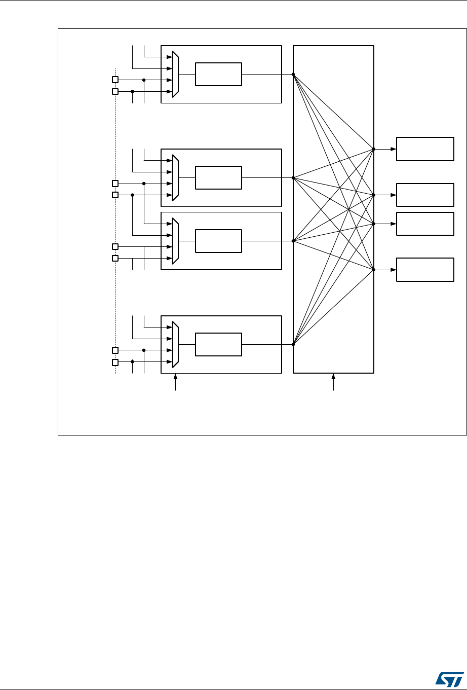
Digital filter for sigma delta modulators (DFSDM) RM0394
556/1600 RM0394 Rev 4
Figure 127. Input channel pins redirection
Output clock generation
A clock signal can be provided on CKOUT pin to drive external modulator clock inputs.
The frequency of this CKOUT signal is derived from DFSDM clock or from audio clock (see
CKOUTSRC bit in DFSDM_CH0CFGR1 register) divided by a predivider (see CKOUTDIV
bits in DFSDM_CH0CFGR1 register). If the output clock is stopped, then CKOUT signal is
set to low state (output clock can be stopped by CKOUTDIV=0 in DFSDM_CHyCFGR1
register or by DFSDMEN=0 in DFSDM_CH0CFGR1 register). The output clock stopping is
performed:
•4 system clocks after DFSDMEN is cleared (if CKOUTSRC=0)
•1 system clock and 3 audio clocks after DFSDMEN is cleared (if CKOUTSRC=1)
Before changing CKOUTSRC the software has to wait for CKOUT being stopped to avoid
glitch on CKOUT pin. The output clock signal frequency must be in the range 0 - 20 MHz.
06Y9
)/7[
)/7[
'$7$,1
'$7,1\
'$7,1\
'$7,1\PD[
&+,16(/
5&+
)/7
)/7[PD[
&.,1\PD[
&.,1\
&.,1\
&.,1
&+\PD[
'HFRGH
&+\
'HFRGH
&+\
'HFRGH
&+
'HFRGH

RM0394 Rev 4 557/1600
RM0394 Digital filter for sigma delta modulators (DFSDM)
601
SPI data input format operation
In SPI format, the data stream is sent in serial format through data and clock signals. Data
signal is always provided from DATINy pin. A clock signal can be provided externally from
CKINy pin or internally from a signal derived from the CKOUT signal source.
In case of external clock source selection (SPICKSEL[1:0]=0) data signal (on DATINy pin) is
sampled on rising or falling clock edge (of CKINy pin) according SITP[1:0] bits setting (in
DFSDM_CHyCFGR1 register).
Internal clock sources - see SPICKSEL[1:0] in DFSDM_CHyCFGR1 register:
•CKOUT signal:
– For connection to external modulator which uses directly its clock input (from
CKOUT) to generate its output serial communication clock.
– Sampling point: on rising/falling edge according SITP[1:0] setting.
•CKOUT/2 signal (generated on CKOUT rising edge):
– For connection to external modulator which divides its clock input (from
CKOUT) by 2 to generate its output serial communication clock (and this output
clock change is active on each clock input rising edge).
– Sampling point: on each second CKOUT falling edge.
•CKOUT/2 signal (generated on CKOUT falling edge):
– For connection to external modulator which divides its clock input (from
CKOUT) by 2 to generate its output serial communication clock (and this output
clock change is active on each clock input falling edge).
– Sampling point: on each second CKOUT rising edge.
Note: An internal clock source can only be used when the external Σ∆ modulator uses CKOUT
signal as a clock input (to have synchronous clock and data operation).
Internal clock source usage can save CKINy pin connection (CKINy pins can be used for
other purpose).
The clock source signal frequency must be in the range 0 - 20 MHz for SPI coding and less
than fDFSDMCLK/4.
Manchester coded data input format operation
In Manchester coded format, the data stream is sent in serial format through DATINy pin
only. Decoded data and clock signal are recovered from serial stream after Manchester
decoding. There are two possible settings of Manchester codings (see SITP[1:0] bits in
DFSDM_CHyCFGR1 register):
•signal rising edge = log 0; signal falling edge = log 1
•signal rising edge = log 1; signal falling edge = log 0
The recovered clock signal frequency for Manchester coding must be in the range
0 - 10 MHz and less than fDFSDMCLK/6.
To correctly receive Manchester coded data, the CKOUTDIV divider (in
DFSDM_CH0CFGR1 register) must be set with respect to expected Manchester data rate
according formula:
CKOUTDIV 1+()TSYSCLK
×()TManchester clock 2 CKOUTDIV×TSYSCLK
×()<<
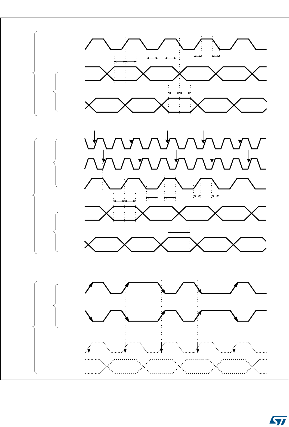
Digital filter for sigma delta modulators (DFSDM) RM0394
558/1600 RM0394 Rev 4
Figure 128. Channel transceiver timing diagrams
069
6,73
&.287
'$7,1\
6,73
WVX WK
WVX WK
WIWU
WZO WZK
63,WLPLQJ63,&.6(/
UHFRYHUHGFORFN
6,73
'$7,1\
6,73
0DQFKHVWHUWLPLQJ
UHFRYHUHGGDWD
6,73
&.,1\'$7,1\
6,73
WVX WK
WVX WK
WIWU
WZO WZK
63,WLPLQJ63,&.6(/
63,&.6(/
63,&.6(/
63,&.6(/
63,&.6(/
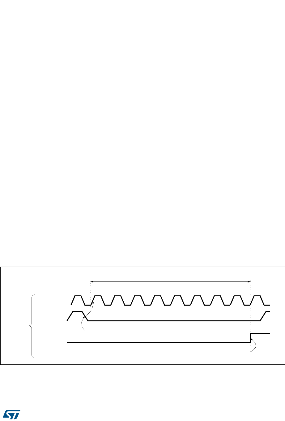
RM0394 Rev 4 559/1600
RM0394 Digital filter for sigma delta modulators (DFSDM)
601
Clock absence detection
Channels serial clock inputs can be checked for clock absence/presence to ensure the
correct operation of conversion and error reporting. Clock absence detection can be
enabled or disabled on each input channel y by bit CKABEN in DFSDM_CHyCFGR1
register. If enabled, then this clock absence detection is performed continuously on a given
channel. A clock absence flag is set (CKABF[y] = 1) and an interrupt can be invoked (if
CKABIE=1) in case of an input clock error (see CKABF[3:0] in DFSDM_FLT0ISR register
and CKABEN in DFSDM_CHyCFGR1). After a clock absence flag clearing (by CLRCKABF
in DFSDM_FLT0ICR register), the clock absence flag is refreshed. Clock absence status bit
CKABF[y] is set also by hardware when corresponding channel y is disabled (if CHEN[y] = 0
then CKABF[y] is held in set state).
When a clock absence event has occurred, the data conversion (and/or analog watchdog
and short-circuit detector) provides incorrect data. The user should manage this event and
discard given data while a clock absence is reported.
The clock absence feature is available only when the system clock is used for the CKOUT
signal (CKOUTSRC=0 in DFSDM_CH0CFGR1 register).
When the transceiver is not yet synchronized, the clock absence flag is set and cannot be
cleared by CLRCKABF[y] bit (in DFSDM_FLT0ICR register). The software sequence
concerning clock absence detection feature should be:
•Enable given channel by CHEN = 1
•Try to clear the clock absence flag (by CLRCKABF = 1) until the clock absence flag is
really cleared (CKABF = 0). At this time, the transceiver is synchronized (signal clock is
valid) and is able to receive data.
•Enable the clock absence feature CKABEN = 1 and the associated interrupt CKABIE =
1 to detect if the SPI clock is lost or Manchester data edges are missing.
If SPI data format is used, then the clock absence detection is based on the comparison of
an external input clock with an output clock generation (CKOUT signal). The external input
clock signal into the input channel must be changed at least once per 8 signal periods of
CKOUT signal (which is controlled by CKOUTDIV field in DFSDM_CH0CFGR1 register).
Figure 129. Clock absence timing diagram for SPI
If Manchester data format is used, then the clock absence means that the clock recovery is
unable to perform from Manchester coded signal. For a correct clock recovery, it is first
necessary to receive data with 1 to 0 or 0 to 1 transition (see Figure 131 for Manchester
synchronization).
069
&.287
63,FORFNSUHVHQFH
WLPLQJ
PD[SHULRGV
&.,1\
ODVWFORFNFKDQJH
&.$%)>\@
HUURUUHSRUWHG
UHVWDUWFRXQWLQJ
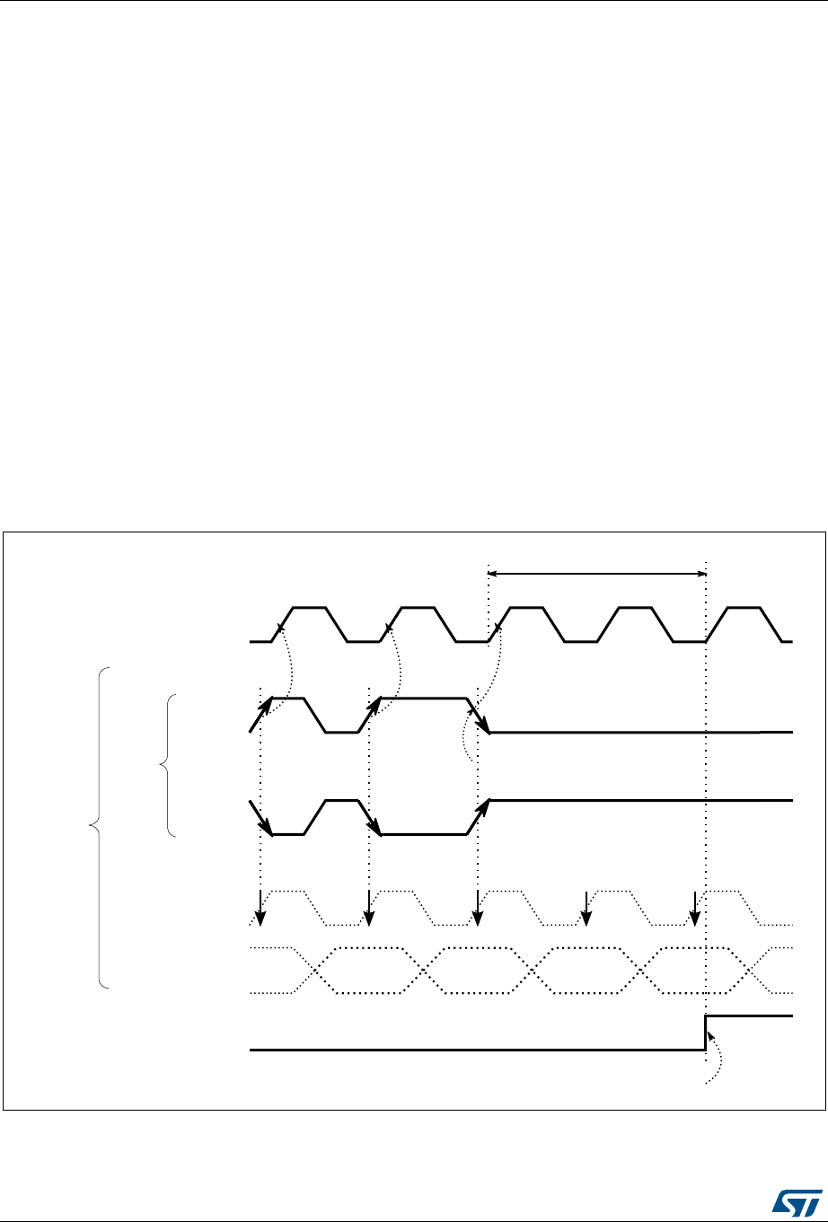
Digital filter for sigma delta modulators (DFSDM) RM0394
560/1600 RM0394 Rev 4
The detection of a clock absence in Manchester coding (after a first successful
synchronization) is based on changes comparison of coded serial data input signal with
output clock generation (CKOUT signal). There must be a voltage level change on DATINy
pin during 2 periods of CKOUT signal (which is controlled by CKOUTDIV bits in
DFSDM_CH0CFGR1 register). This condition also defines the minimum data rate to be able
to correctly recover the Manchester coded data and clock signals.
The maximum data rate of Manchester coded data must be less than the CKOUT signal.
So to correctly receive Manchester coded data, the CKOUTDIV divider must be set
according the formula:
A clock absence flag is set (CKABF[y] = 1) and an interrupt can be invoked (if CKABIE=1) in
case of an input clock recovery error (see CKABF[3:0] in DFSDM_FLT0ISR register and
CKABEN in DFSDM_CHyCFGR1). After a clock absence flag clearing (by CLRCKABF in
DFSDM_FLT0ICR register), the clock absence flag is refreshed.
Figure 130. Clock absence timing diagram for Manchester coding
CKOUTDIV 1+()TSYSCLK
×()TManchester clock 2 CKOUTDIV×TSYSCLK
×()<<
069
&.287
UHFRYHUHGFORFN
6,73
'$7,1\
6,73
0DQFKHVWHUFORFNSUHVHQFH
WLPLQJ
UHFRYHUHGGDWD ""
ODVWGDWDFKDQJH
&.$%)>\@
HUURUUHSRUWHG
UHVWDUWFRXQWLQJ
PD[SHULRGV

RM0394 Rev 4 561/1600
RM0394 Digital filter for sigma delta modulators (DFSDM)
601
Manchester/SPI code synchronization
The Manchester coded stream must be synchronized the first time after enabling the
channel (CHEN=1 in DFSDM_CHyCFGR1 register). The synchronization ends when a data
transition from 0 to 1 or from 1 to 0 (to be able to detect valid data edge) is received. The
end of the synchronization can be checked by polling CKABF[y]=0 for a given channel after
it has been cleared by CLRCKABF[y] in DFSDM_FLT0ICR, following the software sequence
detailed hereafter:
CKABF[y] flag is cleared by setting CLRCKABF[y] bit. If channel y is not yet synchronized
the hardware immediately set the CKABF[y] flag. Software is then reading back the
CKABF[y] flag and if it is set then perform again clearing of this flag by setting
CLRCKABF[y] bit. This software sequence (polling of CKABF[y] flag) continues until
CKABF[y] flag is set (signalizing that Manchester stream is synchronized). To be able to
synchronize/receive Manchester coded data the CKOUTDIV divider (in
DFSDM_CH0CFGR1 register) must be set with respect to expected Manchester data rate
according the formula below.
SPI coded stream is synchronized after first detection of clock input signal (valid
rising/falling edge).
Note: When the transceiver is not yet synchronized, the clock absence flag is set and cannot be
cleared by CLRCKABF[y] bit (in DFSDM_FLT0ICR register).
CKOUTDIV 1+()TSYSCLK
×()TManchester clock 2 CKOUTDIV×TSYSCLK
×()<<
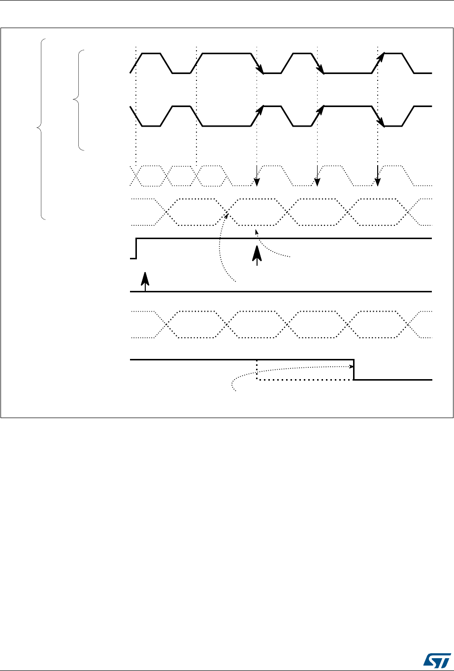
Digital filter for sigma delta modulators (DFSDM) RM0394
562/1600 RM0394 Rev 4
Figure 131. First conversion for Manchester coding (Manchester synchronization)
External serial clock frequency measurement
The measuring of a channel serial clock input frequency provides a real data rate from an
external modulator, which is important for application purposes.
An external serial clock input frequency can be measured by a timer counting DFSDM
clocks (fDFSDMCLK) during one conversion duration. The counting starts at the first input data
clock after a conversion trigger (regular or injected) and finishes by last input data clock
before conversion ends (end of conversion flag is set). Each conversion duration (time
between first serial sample and last serial sample) is updated in counter CNVCNT[27:0] in
register DFSDM_FLTxCNVTIMR when the conversion finishes (JEOCF=1 or REOCF=1).
The user can then compute the data rate according to the digital filter settings (FORD,
FOSR, IOSR, FAST). The external serial frequency measurement is stopped only if the filter
is bypassed (FOSR=0, only integrator is active, CNVCNT[27:0]=0 in
DFSDM_FLTxCNVTIMR register).
In case of parallel data input (Section 21.4.6: Parallel data inputs) the measured frequency
is the average input data rate during one conversion.
069
UHFRYHUHGFORFN
6,73
'$7,1\
6,73
0DQFKHVWHUWLPLQJ
GDWDIURP
PRGXODWRU
&+(1
ILUVWGDWDELWWRJJOHHQGRI0DQFKHVWHUV\QFKURQL]DWLRQ
ILUVWFRQYHUVLRQ
VWDUWWULJJHU
UHFRYHUHGGDWD ""
UHDOVWDUWRIILUVWFRQYHUVLRQ
&.$%)>\@
FOHDULQJRI&.$%)>\@IODJE\VRIWZDUHSROOLQJ

RM0394 Rev 4 563/1600
RM0394 Digital filter for sigma delta modulators (DFSDM)
601
Note: When conversion is interrupted (e.g. by disabling/enabling the selected channel) the
interruption time is also counted in CNVCNT[27:0]. Therefore it is recommended to not
interrupt the conversion for correct conversion duration result.
Conversion times:
injected conversion or regular conversion with FAST = 0 (or first conversion if
FAST=1):
for Sincx filters (x=1..5):
t = CNVCNT/fDFSDMCLK = [FOSR * (IOSR-1 + FORD) + FORD] / fCKIN
for FastSinc filter:
t = CNVCNT/fDFSDMCLK = [FOSR * (IOSR-1 + 4) + 2] / fCKIN
regular conversion with FAST = 1 (except first conversion):
for Sincx and FastSinc filters:
t = CNVCNT/fDFSDMCLK = [FOSR * IOSR] / fCKIN
in case if FOSR = FOSR[9:0]+1 = 1 (filter bypassed, active only integrator):
t = IOSR / fCKIN (... but CNVCNT=0)
where:
•fCKIN is the channel input clock frequency (on given channel CKINy pin) or input data
rate (in case of parallel data input)
•FOSR is the filter oversampling ratio: FOSR = FOSR[9:0]+1 (see DFSDM_FLTxFCR
register)
•IOSR is the integrator oversampling ratio: IOSR = IOSR[7:0]+1 (see DFSDM_FLTxFCR
register)
•FORD is the filter order: FORD = FORD[2:0] (see DFSDM_FLTxFCR register)
Channel offset setting
Each channel has its own offset setting (in register) which is finally subtracted from each
conversion result (injected or regular) from a given channel. Offset correction is performed
after the data right bit shift. The offset is stored as a 24-bit signed value in OFFSET[23:0]
field in DFSDM_CHyCFGR2 register.
Data right bit shift
To have the result aligned to a 24-bit value, each channel defines a number of right bit shifts
which will be applied on each conversion result (injected or regular) from a given channel.
The data bit shift number is stored in DTRBS[4:0] bits in DFSDM_CHyCFGR2 register.
The right bit-shift is rounding the result to nearest integer value. The sign of shifted result is
maintained, in order to have valid 24-bit signed format of result data.

Digital filter for sigma delta modulators (DFSDM) RM0394
564/1600 RM0394 Rev 4
21.4.5 Configuring the input serial interface
The following parameters must be configured for the input serial interface:
•Output clock predivider. There is a programmable predivider to generate the output
clock from DFSDM clock (2 - 256). It is defined by CKOUTDIV[7:0] bits in
DFSDM_CH0CFGR1 register.
•Serial interface type and input clock phase. Selection of SPI or Manchester coding
and sampling edge of input clock. It is defined by SITP [1:0] bits in
DFSDM_CHyCFGR1 register.
•Input clock source. External source from CKINy pin or internal from CKOUT pin. It is
defined by SPICKSEL[1:0] field in DFSDM_CHyCFGR1 register.
•Final data right bit-shift. Defines the final data right bit shift to have the result aligned
to a 24-bit value. It is defined by DTRBS[4:0] in DFSDM_CHyCFGR2 register.
•Channel offset per channel. Defines the analog offset of a given serial channel (offset
of connected external modulator). It is defined by OFFSET[23:0] bits in
DFSDM_CHyCFGR2 register.
•short-circuit detector and clock absence per channel enable. To enable or disable
the short-circuit detector (by SCDEN bit) and the clock absence monitoring (by
CKABEN bit) on a given serial channel in register DFSDM_CHyCFGR1.
•Analog watchdog filter and short-circuit detector threshold settings. To configure
channel analog watchdog filter parameters and channel short-circuit detector
parameters. Configurations are defined in DFSDM_CHyAWSCDR register.
21.4.6 Parallel data inputs
Each input channel provides a register for 16-bit parallel data input (besides serial data
input). Each 16-bit parallel input can be sourced from internal data sources only:
•direct CPU/DMA writing.
The selection for using serial or parallel data input for a given channel is done by field
DATMPX[1:0] of DFSDM_CHyCFGR1 register. In DATMPX[1:0] is also defined the parallel
data source: direct write by CPU/DMA.
Each channel contains a 32-bit data input register DFSDM_CHyDATINR in which it can be
written a 16-bit data. Data are in 16-bit signed format. Those data can be used as input to
the digital filter which is accepting 16-bit parallel data.
If serial data input is selected (DATMPX[1:0] = 0), the DFSDM_CHyDATINR register is write
protected.
Input from memory (direct CPU/DMA write)
The direct data write into DFSDM_CHyDATINR register by CPU or DMA (DATMPX[1:0]=2)
can be used as data input in order to process digital data streams from memory or
peripherals.
Data can be written by CPU or DMA into DFSDM_CHyDATINR register:
1. CPU data write:
Input data are written directly by CPU into DFSDM_CHyDATINR register.
2. DMA data write:
The DMA should be configured in memory-to-memory transfer mode to transfer data
from memory buffer into DFSDM_CHyDATINR register. The destination memory

RM0394 Rev 4 565/1600
RM0394 Digital filter for sigma delta modulators (DFSDM)
601
address is the address of DFSDM_CHyDATINR register. Data are transferred at DMA
transfer speed from memory to DFSDM parallel input.
This DMA transfer is different from DMA used to read DFSDM conversion results. Both
DMA can be used at the same time - first DMA (configured as memory-to-memory
transfer) for input data writings and second DMA (configured as peripheral-to-memory
transfer) for data results reading.
The accesses to DFSDM_CHyDATINR can be either 16-bit or 32-bit wide, allowing to load
respectively one or two samples in one write operation. 32-bit input data register
(DFSDM_CHyDATINR) can be filled with one or two 16-bit data samples, depending on the
data packing operation mode defined in field DATPACK[1:0] of DFSDM_CHyCFGR1
register:
1. Standard mode (DATPACK[1:0]=0):
Only one sample is stored in field INDAT0[15:0] of DFSDM_CHyDATINR register which
is used as input data for channel y. The upper 16 bits (INDAT1[15:0]) are ignored and
write protected. The digital filter must perform one input sampling (from INDAT0[15:0])
to empty data register after it has been filled by CPU/DMA. This mode is used together
with 16-bit CPU/DMA access to DFSDM_CHyDATINR register to load one sample per
write operation.
2. Interleaved mode (DATPACK[1:0]=1):
DFSDM_CHyDATINR register is used as a two sample buffer. The first sample is
stored in INDAT0[15:0] and the second sample is stored in INDAT1[15:0]. The digital
filter must perform two input samplings from channel y to empty DFSDM_CHyDATINR
register. This mode is used together with 32-bit CPU/DMA access to
DFSDM_CHyDATINR register to load two samples per write operation.
3. Dual mode (DATPACK[1:0]=2):
Two samples are written into DFSDM_CHyDATINR register. The data INDAT0[15:0] is
for channel y, the data in INDAT1[15:0] is for channel y+1. The data in INDAT1[15:0] is
automatically copied INDAT0[15:0] of the following (y+1) channel data register
DFSDM_CH[y+1]DATINR). The digital filters must perform two samplings - one from
channel y and one from channel (y+1) - in order to empty DFSDM_CHyDATINR
registers.
Dual mode setting (DATPACK[1:0]=2) is available only on even channel numbers (y =
0, 2). If odd channel (y = 1, 3) is set to Dual mode then both INDAT0[15:0] and
INDAT1[15:0] parts are write protected for this channel. If even channel is set to Dual
mode then the following odd channel must be set into Standard mode
(DATPACK[1:0]=0) for correct cooperation with even channels.
See Figure 132 for DFSDM_CHyDATINR registers data modes and assignments of data
samples to channels.
Figure 132. DFSDM_CHyDATINR registers operation modes and assignment
06Y9
&KVDPSOH &KVDPSOH
8QXVHG &KVDPSOH
&KVDPSOH &KVDPSOH
8QXVHG &KVDPSOH
\
\
\
\
&KVDPSOH &KVDPSOH
&KVDPSOH &KVDPSOH
&KVDPSOH &KVDPSOH
&KVDPSOH &KVDPSOH
8QXVHG &KVDPSOH
8QXVHG &KVDPSOH
8QXVHG &KVDPSOH
8QXVHG &KVDPSOH
6WDQGDUGPRGH ,QWHUOHDYHGPRGH 'XDOPRGH

Digital filter for sigma delta modulators (DFSDM) RM0394
566/1600 RM0394 Rev 4
The write into DFSDM_CHyDATINR register to load one or two samples must be performed
after the selected input channel (channel y) is enabled for data collection (starting
conversion for channel y). Otherwise written data are lost for next processing.
For example: for single conversion and interleaved mode, do not start writing pair of data
samples into DFSDM_CHyDATINR before the single conversion is started (any data
present in the DFSDM_CHyDATINR before starting a conversion is discarded).
21.4.7 Channel selection
There are 4 multiplexed channels which can be selected for conversion using the injected
channel group and/or using the regular channel.
The injected channel group is a selection of any or all of the 4 channels. JCHG[3:0] in the
DFSDM_FLTxJCHGR register selects the channels of the injected group, where JCHG[y]=1
means that channel y is selected.
Injected conversions can operate in scan mode (JSCAN=1) or single mode (JSCAN=0). In
scan mode, each of the selected channels is converted, one after another. The lowest
channel (channel 0, if selected) is converted first, followed immediately by the next higher
channel until all the channels selected by JCHG[3:0] have been converted. In single mode
(JSCAN=0), only one channel from the selected channels is converted, and the channel
selection is moved to the next channel. Writing to JCHG[3:0] if JSCAN=0 resets the channel
selection to the lowest selected channel.
Injected conversions can be launched by software or by a trigger. They are never
interrupted by regular conversions.
The regular channel is a selection of just one of the 4 channels. RCH[1:0] in the
DFSDM_FLTxCR1 register indicates the selected channel.
Regular conversions can be launched only by software (not by a trigger). A sequence of
continuous regular conversions is temporarily interrupted when an injected conversion is
requested.
Performing a conversion on a disabled channel (CHEN=0 in DFSDM_CHyCFGR1 register)
causes that the conversion will never end - because no input data is provided (with no clock
signal). In this case, it is necessary to enable a given channel (CHEN=1 in
DFSDM_CHyCFGR1 register) or to stop the conversion by DFEN=0 in DFSDM_FLTxCR1
register.
21.4.8 Digital filter configuration
DFSDM contains a Sincx type digital filter implementation. This Sincx filter performs an input
digital data stream filtering, which results in decreasing the output data rate (decimation)
and increasing the output data resolution. The Sincx digital filter is configurable in order to
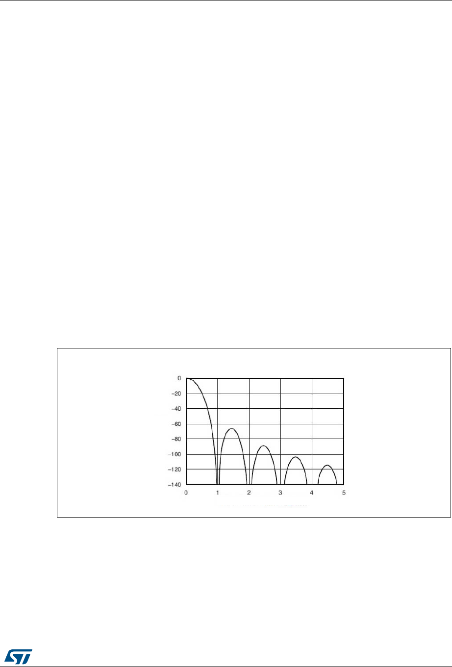
RM0394 Rev 4 567/1600
RM0394 Digital filter for sigma delta modulators (DFSDM)
601
reach the required output data rates and required output data resolution. The configurable
parameters are:
•Filter order/type: (see FORD[2:0] bits in DFSDM_FLTxFCR register):
–FastSinc
–Sinc
1
–Sinc
2
–Sinc
3
–Sinc
4
–Sinc
5
•Filter oversampling/decimation ratio (see FOSR[9:0] bits in DFSDM_FLTxFCR
register):
– FOSR = 1-1024 - for FastSinc filter and Sincx filter x = FORD = 1..3
– FOSR = 1-215 - for Sincx filter x = FORD = 4
– FOSR = 1-73 - for Sincx filter x = FORD = 5
The filter has the following transfer function (impulse response in H domain):
•Sincx filter type:
•FastSinc filter type:
Figure 133. Example: Sinc3 filter response
Hz() 1z
FOSR–
–
1z
1–
–
-----------------------------
⎝⎠
⎜⎟
⎛⎞
x
=
Hz() 1z
FOSR–
–
1z
1–
–
-----------------------------
⎝⎠
⎜⎟
⎛⎞
2
1z
2FOSR⋅()–
+()⋅=
1RUPDOL]HGIUHTXHQF\I,1I'$7$
*DLQG%
069
Digital filter for sigma delta modulators (DFSDM) RM0394
568/1600 RM0394 Rev 4
For more information about Sinc filter type properties and usage, it is recommended to study
the theory about digital filters (more resources can be downloaded from internet).
21.4.9 Integrator unit
The integrator performs additional decimation and a resolution increase of data coming from
the digital filter. The integrator simply performs the sum of data from a digital filter for a given
number of data samples from a filter.
The integrator oversampling ratio parameter defines how many data counts will be summed
to one data output from the integrator. IOSR can be set in the range 1-256 (see IOSR[7:0]
bits description in DFSDM_FLTxFCR register).
21.4.10 Analog watchdog
The analog watchdog purpose is to trigger an external signal (break or interrupt) when an
analog signal reaches or crosses given maximum and minimum threshold values. An
interrupt/event/break generation can then be invoked.
Each analog watchdog will supervise serial data receiver outputs (after the analog watchdog
filter on each channel) or data output register (current injected or regular conversion result)
according to AWFSEL bit setting (in DFSDM_FLTxCR1 register). The input channels to be
monitored or not by the analog watchdog x will be selected by AWDCH[3:0] in
DFSDM_FLTxCR2 register.
Table 99. Filter maximum output resolution (peak data values from filter output)
for some FOSR values
FOSR Sinc1Sinc2FastSinc Sinc3Sinc4Sinc5
x +/- x +/- x2 +/- 2x2 +/- x3+/- x4 +/- x5
4 +/- 4 +/- 16 +/- 32 +/- 64 +/- 256 +/- 1024
8 +/- 8 +/- 64 +/- 128 +/- 512 +/- 4096 -
32 +/- 32 +/- 1024 +/- 2048 +/- 32768 +/- 1048576 +/- 33554432
64 +/- 64 +/- 4096 +/- 8192 +/- 262144 +/- 16777216 +/- 1073741824
128 +/- 128 +/- 16384 +/- 32768 +/- 2097152 +/- 268435456
256 +/- 256 +/- 65536 +/- 131072 +/- 16777216 Result can overflow on full scale
input (> 32-bit signed integer)
1024 +/- 1024 +/- 1048576 +/- 2097152 +/- 1073741824
Table 100. Integrator maximum output resolution (peak data values from integrator
output) for some IOSR values and FOSR = 256 and Sinc3 filter type (largest data)
IOSR Sinc1Sinc2FastSinc Sinc3Sinc4Sinc5
x +/- FOSR. x +/- FOSR2. x +/- 2.FOSR2. x +/- FOSR3. x +/- FOSR4. x +/- FOSR5. x
4 - - - +/- 67 108 864 - -
32 - - - +/- 536 870 912 - -
128 - - - +/- 2 147 483
648 --
256 - - - +/- 232 --

RM0394 Rev 4 569/1600
RM0394 Digital filter for sigma delta modulators (DFSDM)
601
Analog watchdog conversions on input channels are independent from standard
conversions. In this case, the analog watchdog uses its own filters and signal processing on
each input channel independently from the main injected or regular conversions. Analog
watchdog conversions are performed in a continuous mode on the selected input channels
in order to watch channels also when main injected or regular conversions are paused
(RCIP = 0, JCIP = 0).
There are high and low threshold registers which are compared with given data values (set
by AWHT[23:0] bits in DFSDM_FLTxAWHTR register and by AWLT[23:0] bits in
DFSDM_FLTxAWLTR register).
There are 2 options for comparing the threshold registers with the data values
•Option1: in this case, the input data are taken from final output data register
(AWFSEL=0). This option is characterized by:
– high input data resolution (up to 24-bits)
– slow response time - inappropriate for fast response applications like overcurrent
detection
– for the comparison the final data are taken after bit shifting and offset data
correction
– final data are available only after main regular or injected conversions are
performed
– can be used in case of parallel input data source (DATMPX[1:0] 0 in
DFSDM_CHyCFGR1 register)
•Option2: in this case, the input data are taken from any serial data receivers output
(AWFSEL=1). This option is characterized by:
– input serial data are processed by dedicated analog watchdog Sincx channel
filters with configurable oversampling ratio (1..32) and filter order (1..3) (see
AWFOSR[4:0] and AWFORD[1:0] bits setting in DFSDM_CHyAWSCDR register)
– lower resolution (up to 16-bit)
– fast response time - appropriate for applications which require a fast response like
overcurrent/overvoltage detection)
– data are available in continuous mode independently from main regular or injected
conversions activity
In case of input channels monitoring (AWFSEL=1), the data for comparison to threshold is
taken from channels selected by AWDCH[3:0] field (DFSDM_FLTxCR2 register). Each of
the selected channels filter result is compared to one threshold value pair (AWHT[23:0] /
AWLT[23:0]). In this case, only higher 16 bits (AWHT[23:8] / AWLT[23:8]) define the 16-bit
threshold compared with the analog watchdog filter output because data coming from the
analog watchdog filter is up to a 16-bit resolution. Bits AWHT[7:0] / AWLT[7:0] are not taken
into comparison in this case (AWFSEL=1).
Parameters of the analog watchdog filter configuration for each input channel are set in
DFSDM_CHyAWSCDR register (filter order AWFORD[1:0] and filter oversampling ratio
AWFOSR[4:0]).
Each input channel has its own comparator which compares the analog watchdog data
(from analog watchdog filter) with analog watchdog threshold values (AWHT/AWLT). When
several channels are selected (field AWDCH[3:0] field of DFSDM_FLTxCR2 register),
several comparison requests may be received simultaneously. In this case, the channel
request with the lowest number is managed first and then continuing to higher selected
channels. For each channel, the result can be recorded in a separate flag (fields

Digital filter for sigma delta modulators (DFSDM) RM0394
570/1600 RM0394 Rev 4
AWHTF[3:0], AWLTF[3:0] of DFSDM_FLTxAWSR register). Each channel request is
executed in 8 DFSDM clock cycles. So, the bandwidth from each channel is limited to 8
DFSDM clock cycles (if AWDCH[3:0] = 0x0F). Because the maximum input channel
sampling clock frequency is the DFSDM clock frequency divided by 4, the configuration
AWFOSR = 0 (analog watchdog filter is bypassed) cannot be used for analog watchdog
feature at this input clock speed. Therefore user must properly configure the number of
watched channels and analog watchdog filter parameters with respect to input sampling
clock speed and DFSDM frequency.
Analog watchdog filter data for given channel y is available for reading by firmware on field
WDATA[15:0] in DFSDM_CHyWDATR register. That analog watchdog filter data is
converted continuously (if CHEN=1 in DFSDM_CHyCFGR1 register) with the data rate
given by the analog watchdog filter setting and the channel input clock frequency.
The analog watchdog filter conversion works like a regular Fast Continuous Conversion
without the intergator. The number of serial samples needed for one result from analog
watchdog filter output (at channel input clock frequency fCKIN):
first conversion:
for Sincx filters (x=1..5): number of samples = [FOSR * FORD + FORD + 1]
for FastSinc filter: number of samples = [FOSR * 4 + 2 + 1]
next conversions:
for Sincx and FastSinc filters: number of samples = [FOSR * IOSR]
where:
FOSR ....... filter oversampling ratio: FOSR = AWFOSR[4:0]+1 (see DFSDM_CHyAWSCDR
register)
FORD ....... the filter order: FORD = AWFORD[1:0] (see DFSDM_CHyAWSCDR register)
In case of output data register monitoring (AWFSEL=0), the comparison is done after a right
bit shift and an offset correction of final data (see OFFSET[23:0] and DTRBS[4:0] fields in
DFSDM_CHyCFGR2 register). A comparison is performed after each injected or regular
end of conversion for the channels selected by AWDCH[3:0] field (in DFSDM_FLTxCR2
register).
The status of an analog watchdog event is signalized in DFSDM_FLTxAWSR register where
a given event is latched. AWHTF[y]=1 flag signalizes crossing AWHT[23:0] value on
channel y. AWLTF[y]=1 flag signalizes crossing AWLT[23:0] value on channel y. Latched
events in DFSDM_FLTxAWSR register are cleared by writing ‘1’ into the corresponding
clearing bit CLRAWHTF[y] or CLRAWLTF[y] in DFSDM_FLTxAWCFR register.
The global status of an analog watchdog is signalized by the AWDF flag bit in
DFSDM_FLTxISR register (it is used for the fast detection of an interrupt source). AWDF=1
signalizes that at least one watchdog occurred (AWHTF[y]=1 or AWLTF[y]=1 for at least one
channel). AWDF bit is cleared when all AWHTF[3:0] and AWLTF[3:0] are cleared.
An analog watchdog event can be assigned to break output signal. There are four break
outputs to be assigned to a high or low threshold crossing event (dfsdm_break[3:0]). The
break signal assignment to a given analog watchdog event is done by BKAWH[3:0] and
BKAWL[3:0] fields in DFSDM_FLTxAWHTR and DFSDM_FLTxAWLTR register.

RM0394 Rev 4 571/1600
RM0394 Digital filter for sigma delta modulators (DFSDM)
601
21.4.11 Short-circuit detector
The purpose of a short-circuit detector is to signalize with a very fast response time if an
analog signal reached saturated values (out of full scale ranges) and remained on this value
given time. This behavior can detect short-circuit or open circuit errors (e.g. overcurrent or
overvoltage). An interrupt/event/break generation can be invoked.
Input data into a short-circuit detector is taken from channel transceiver outputs.
There is an upcounting counter on each input channel which is counting consecutive 0’s or
1’s on serial data receiver outputs. A counter is restarted if there is a change in the data
stream received - 1 to 0 or 0 to 1 change of data signal. If this counter reaches a short-circuit
threshold register value (SCDT[7:0] bits in DFSDM_CHyAWSCDR register), then a short-
circuit event is invoked. Each input channel has its short-circuit detector. Any channel can
be selected to be continuously monitored by setting the SCDEN bit (in DFSDM_CHyCFGR1
register) and it has its own short-circuit detector settings (threshold value in SCDT[7:0] bits,
status bit SCDF[3:0], status clearing bits CLRSCDF[3:0]). Status flag SCDF[y] is cleared
also by hardware when corresponding channel y is disabled (CHEN[y] = 0).
On each channel, a short-circuit detector event can be assigned to break output signal
dfsdm_break[3:0]. There are four break outputs to be assigned to a short-circuit detector
event. The break signal assignment to a given channel short-circuit detector event is done
by BKSCD[3:0] field in DFSDM_CHyAWSCDR register.
Short circuit detector cannot be used in case of parallel input data channel selection
(DATMPX[1:0] 0 in DFSDM_CHyCFGR1 register).
Four break outputs are totally available (shared with the analog watchdog function).
21.4.12 Extreme detector
The purpose of an extremes detector is to collect the minimum and maximum values of final
output data words (peak to peak values).
If the output data word is higher than the value stored in the extremes detector maximum
register (EXMAX[23:0] bits in DFSDM_FLTxEXMAX register), then this register is updated
with the current output data word value and the channel from which the data is stored is in
EXMAXCH[1:0] bits (in DFSDM_FLTxEXMAX register) .
If the output data word is lower than the value stored in the extremes detector minimum
register (EXMIN[23:0] bits in DFSDM_FLTxEXMIN register), then this register is updated
with the current output data word value and the channel from which the data is stored is in
EXMINCH[1:0] bits (in DFSDM_FLTxEXMIN register).
The minimum and maximum register values can be refreshed by software (by reading given
DFSDM_FLTxEXMAX or DFSDM_FLTxEXMIN register). After refresh, the extremes
detector minimum data register DFSDM_FLTxEXMIN is filled with 0x7FFFFF (maximum
positive value) and the extremes detector maximum register DFSDM_FLTxEXMAX is filled
with 0x800000 (minimum negative value).
The extremes detector performs a comparison after a right bit shift and an offset data
correction. For each extremes detector, the input channels to be considered into computing
the extremes value are selected in EXCH[3:0] bits (in DFSDM_FLTxCR2 register).

Digital filter for sigma delta modulators (DFSDM) RM0394
572/1600 RM0394 Rev 4
21.4.13 Data unit block
The data unit block is the last block of the whole processing path: External modulators -
Serial transceivers - Sinc filter - Integrator - Data unit block.
The output data rate depends on the serial data stream rate, and filter and integrator
settings. The maximum output data rate is:
or
Maximum output data rate in case of parallel data input:
or
or
The right bit-shift of final data is performed in this module because the final data width is 24-
bit and data coming from the processing path can be up to 32 bits. This right bit-shift is
configurable in the range 0-31 bits for each selected input channel (see DTRBS[4:0] bits in
DFSDM_CHyCFGR2 register). The right bit-shift is rounding the result to nearest integer
value. The sign of shifted result is maintained - to have valid 24-bit signed format of result
data.
In the next step, an offset correction of the result is performed. The offset correction value
(OFFSET[23:0] stored in register DFSDM_CHyCFGR2) is subtracted from the output data
for a given channel. Data in the OFFSET[23:0] field is set by software by the appropriate
calibration routine.
Due to the fact that all operations in digital processing are performed on 32-bit signed
registers, the following conditions must be fulfilled not to overflow the result:
FOSR FORD . IOSR <= 231 ... for Sincx filters, x = 1..5)
2 . FOSR 2 . IOSR <= 231 ... for FastSinc filter)
Datarate samples s⁄fCKIN
FOSR IOSR 1–FORD
+()FORD 1+()+⋅
----------------------------------------------------------------------------------------------------------
=...FAST = 0, Sincx filter
Datarate samples s⁄fCKIN
FOSR IOSR 1–4+()21+()+⋅
-----------------------------------------------------------------------------------
=...FAST = 0, FastSinc filter
Datarate samples s⁄fCKIN
FOSR IOSR
⋅
----------------------------------
=...FAST = 1
Datarate samples s⁄fDATAIN_RATE
FOSR IOSR 1–FORD
+()FORD 1+()+⋅
----------------------------------------------------------------------------------------------------------
=...FAST = 0, Sincx filter
Datarate samples s⁄fDATAIN_RATE
FOSR IOSR 1–4+()21+()+⋅
-----------------------------------------------------------------------------------
=...FAST = 0, FastSinc filter
Datarate samples s⁄fDATAIN_RATE
FOSR IOSR
⋅
------------------------------------
=...FAST=1 or any filter bypass case FOSR 1=()
where: fDATAIN_RATE...input data rate from CPU/DMA

RM0394 Rev 4 573/1600
RM0394 Digital filter for sigma delta modulators (DFSDM)
601
Note: In case of filter and integrator bypass (IOSR[7:0]=0, FOSR[9:0]=0), the input data rate
(fDATAIN_RATE) must be limited to be able to read all output data:
fDATAIN_RATE ≤ fAPB
where fAPB is the bus frequency to which the DFSDM peripheral is connected.
21.4.14 Signed data format
Each DFSDM input serial channel can be connected to one external modulator. An
external modulator can have 2 differential inputs (positive and negative) which can be
used for a differential or single-ended signal measurement.
A modulator output is always assumed in a signed format (a data stream of zeros and
ones from a modulator represents values -1 and +1).
Signed data format in registers: Data is in a signed format in registers for final output data,
analog watchdog, extremes detector, offset correction. The msb of output data word
represents the sign of value (two’s complement format).
21.4.15 Launching conversions
Injected conversions can be launched using the following methods:
•Software: writing ‘1’ to JSWSTART in the DFSDM_FLTxCR1 register.
•Trigger: JEXTSEL[2:0] selects the trigger signal while JEXTEN activates the trigger
and selects the active edge at the same time (see the DFSDM_FLTxCR1 register).
•Synchronous with DFSDM_FLT0 if JSYNC=1: for DFSDM_FLTx (x>0), an injected
conversion is automatically launched when in DFSDM_FLT0; the injected conversion is
started by software (JSWSTART=1 in DFSDM_FLT0CR2 register). Each injected
conversion in DFSDM_FLTx (x>0) is always executed according to its local
configuration settings (JSCAN, JCHG, etc.).
If the scan conversion is enabled (bit JSCAN=1) then, each time an injected conversion is
triggered, all of the selected channels in the injected group (JCHG[3:0] bits in
DFSDM_FLTxJCHGR register) are converted sequentially, starting with the lowest channel
(channel 0, if selected).
If the scan conversion is disabled (bit JSCAN=0) then, each time an injected conversion is
triggered, only one of the selected channels in the injected group (JCHG[3:0] bits in
DFSDM_FLTxJCHGR register) is converted and the channel selection is then moved to the
next selected channel. Writing to the JCHG[3:0] bits when JSCAN=0 sets the channel
selection to the lowest selected injected channel.
Only one injected conversion can be ongoing at a given time. Thus, any request to launch
an injected conversion is ignored if another request for an injected conversion has already
been issued but not yet completed.
Regular conversions can be launched using the following methods:
•Software: by writing ‘1’ to RSWSTART in the DFSDM_FLTxCR1 register.
•Synchronous with DFSDM_FLT0 if RSYNC=1: for DFSDM_FLTx (x>0), a regular
conversion is automatically launched when in DFSDM_FLT0; a regular conversion is
started by software (RSWSTART=1 in DFSDM_FLT0CR2 register). Each regular
conversion in DFSDM_FLTx (x>0) is always executed according to its local
configuration settings (RCONT, RCH, etc.).
Only one regular conversion can be pending or ongoing at a given time. Thus, any request
to launch a regular conversion is ignored if another request for a regular conversion has

Digital filter for sigma delta modulators (DFSDM) RM0394
574/1600 RM0394 Rev 4
already been issued but not yet completed. A regular conversion can be pending if it was
interrupted by an injected conversion or if it was started while an injected conversion was in
progress. This pending regular conversion is then delayed and is performed when all
injected conversion are finished. Any delayed regular conversion is signalized by RPEND bit
in DFSDM_FLTxRDATAR register.
21.4.16 Continuous and fast continuous modes
Setting RCONT in the DFSDM_FLTxCR1 register causes regular conversions to execute in
continuous mode. RCONT=1 means that the channel selected by RCH[1:0] is converted
repeatedly after ‘1’ is written to RSWSTART.
The regular conversions executing in continuous mode can be stopped by writing ‘0’ to
RCONT. After clearing RCONT, the on-going conversion is stopped immediately.
In continuous mode, the data rate can be increased by setting the FAST bit in the
DFSDM_FLTxCR1 register. In this case, the filter does not need to be refilled by new fresh
data if converting continuously from one channel because data inside the filter is valid from
previously sampled continuous data. The speed increase depends on the chosen filter
order. The first conversion in fast mode (FAST=1) after starting a continuous conversion by
RSWSTART=1 takes still full time (as when FAST=0), then each subsequent conversion is
finished in shorter intervals.
Conversion time in continuous mode:
if FAST = 0 (or first conversion if FAST=1):
for Sincx filters:
t = CNVCNT/fDFSDMCLK = [FOSR * (IOSR-1 + FORD) + FORD] / fCKIN
for FastSinc filter:
t = CNVCNT/fDFSDMCLK = [FOSR * (IOSR-1 + 4) + 2] / fCKIN
if FAST = 1 (except first conversion):
for Sincx and FastSinc filters:
t = CNVCNT/fDFSDMCLK = [FOSR * IOSR] / fCKIN
in case FOSR = FOSR[9:0]+1 = 1 (filter bypassed, only integrator active):
t = IOSR / fCKIN (... but CNVCNT=0)
Continuous mode is not available for injected conversions. Injected conversions can be
started by timer trigger to emulate the continuous mode with precise timing.
If a regular continuous conversion is in progress (RCONT=1) and if a write access to
DFSDM_FLTxCR1 register requesting regular continuous conversion (RCONT=1) is
performed, then regular continuous conversion is restarted from the next conversion cycle
(like new regular continuous conversion is applied for new channel selection - even if there
is no change in DFSDM_FLTxCR1 register).
21.4.17 Request precedence
An injected conversion has a higher precedence than a regular conversion. A regular
conversion which is already in progress is immediately interrupted by the request of an
injected conversion; this regular conversion is restarted after the injected conversion
finishes.

RM0394 Rev 4 575/1600
RM0394 Digital filter for sigma delta modulators (DFSDM)
601
An injected conversion cannot be launched if another injected conversion is pending or
already in progress: any request to launch an injected conversion (either by JSWSTART or
by a trigger) is ignored as long as bit JCIP is ‘1’ (in the DFSDM_FLTxISR register).
Similarly, a regular conversion cannot be launched if another regular conversion is pending
or already in progress: any request to launch a regular conversion (using RSWSTART) is
ignored as long as bit RCIP is ‘1’ (in the DFSDM_FLTxISR register).
However, if an injected conversion is requested while a regular conversion is already in
progress, the regular conversion is immediately stopped and an injected conversion is
launched. The regular conversion is then restarted and this delayed restart is signalized in
bit RPEND.
Injected conversions have precedence over regular conversions in that a injected
conversion can temporarily interrupt a sequence of continuous regular conversions. When
the sequence of injected conversions finishes, the continuous regular conversions start
again if RCONT is still set (and RPEND bit will signalize the delayed start on the first regular
conversion result).
Precedence also matters when actions are initiated by the same write to DFSDM, or if
multiple actions are pending at the end of another action. For example, suppose that, while
an injected conversion is in process (JCIP=1), a single write operation to DFSDM_FLTxCR1
writes ‘1’ to RSWSTART, requesting a regular conversion. When the injected sequence
finishes, the precedence dictates that the regular conversion is performed next and its
delayed start is signalized in RPEND bit.
21.4.18 Power optimization in run mode
In order to reduce the consumption, the DFSDM filter and integrator are automatically put
into idle when not used by conversions (RCIP=0, JCIP=0).
21.5 DFSDM interrupts
In order to increase the CPU performance, a set of interrupts related to the CPU event
occurrence has been implemented:
•End of injected conversion interrupt:
– enabled by JEOCIE bit in DFSDM_FLTxCR2 register
– indicated in JEOCF bit in DFSDM_FLTxISR register
– cleared by reading DFSDM_FLTxJDATAR register (injected data)
– indication of which channel end of conversion occurred, reported in JDATACH[1:0]
bits in DFSDM_FLTxJDATAR register
•End of regular conversion interrupt:
– enabled by REOCIE bit in DFSDM_FLTxCR2 register
– indicated in REOCF bit in DFSDM_FLTxISR register
– cleared by reading DFSDM_FLTxRDATAR register (regular data)
– indication of which channel end of conversion occurred, reported in
RDATACH[1:0] bits in DFSDM_FLTxRDATAR register
•Data overrun interrupt for injected conversions:
– occurred when injected converted data were not read from DFSDM_FLTxJDATAR
register (by CPU or DMA) and were overwritten by a new injected conversion

Digital filter for sigma delta modulators (DFSDM) RM0394
576/1600 RM0394 Rev 4
– enabled by JOVRIE bit in DFSDM_FLTxCR2 register
– indicated in JOVRF bit in DFSDM_FLTxISR register
– cleared by writing ‘1’ into CLRJOVRF bit in DFSDM_FLTxICR register
•Data overrun interrupt for regular conversions:
– occurred when regular converted data were not read from DFSDM_FLTxRDATAR
register (by CPU or DMA) and were overwritten by a new regular conversion
– enabled by ROVRIE bit in DFSDM_FLTxCR2 register
– indicated in ROVRF bit in DFSDM_FLTxISR register
– cleared by writing ‘1’ into CLRROVRF bit in DFSDM_FLTxICR register
•Analog watchdog interrupt:
– occurred when converted data (output data or data from analog watchdog filter -
according to AWFSEL bit setting in DFSDM_FLTxCR1 register) crosses
over/under high/low thresholds in DFSDM_FLTxAWHTR / DFSDM_FLTxAWLTR
registers
– enabled by AWDIE bit in DFSDM_FLTxCR2 register (on selected channels
AWDCH[3:0])
– indicated in AWDF bit in DFSDM_FLTxISR register
– separate indication of high or low analog watchdog threshold error by AWHTF[3:0]
and AWLTF[3:0] fields in DFSDM_FLTxAWSR register
– cleared by writing ‘1’ into corresponding CLRAWHTF[3:0] or CLRAWLTF[3:0] bits
in DFSDM_FLTxAWCFR register
•Short-circuit detector interrupt:
– occurred when the number of stable data crosses over thresholds in
DFSDM_CHyAWSCDR register
– enabled by SCDIE bit in DFSDM_FLTxCR2 register (on channel selected by
SCDEN bi tin DFSDM_CHyCFGR1 register)
– indicated in SCDF[3:0] bits in DFSDM_FLTxISR register (which also reports the
channel on which the short-circuit detector event occurred)
– cleared by writing ‘1’ into the corresponding CLRSCDF[3:0] bit in
DFSDM_FLTxICR register
•Channel clock absence interrupt:
– occurred when there is clock absence on CKINy pin (see Clock absence detection
in Section 21.4.4: Serial channel transceivers)
– enabled by CKABIE bit in DFSDM_FLTxCR2 register (on channels selected by
CKABEN bit in DFSDM_CHyCFGR1 register)
– indicated in CKABF[y] bit in DFSDM_FLTxISR register
– cleared by writing ‘1’ into CLRCKABF[y] bit in DFSDM_FLTxICR register
Table 101. DFSDM interrupt requests
Interrupt event Event flag Event/Interrupt clearing
method
Interrupt enable
control bit
End of injected conversion JEOCF reading DFSDM_FLTxJDATAR JEOCIE
End of regular conversion REOCF reading DFSDM_FLTxRDATAR REOCIE
Injected data overrun JOVRF writing CLRJOVRF = 1 JOVRIE

RM0394 Rev 4 577/1600
RM0394 Digital filter for sigma delta modulators (DFSDM)
601
21.6 DFSDM DMA transfer
To decrease the CPU intervention, conversions can be transferred into memory using a
DMA transfer. A DMA transfer for injected conversions is enabled by setting bit JDMAEN=1
in DFSDM_FLTxCR1 register. A DMA transfer for regular conversions is enabled by setting
bit RDMAEN=1 in DFSDM_FLTxCR1 register.
Note: With a DMA transfer, the interrupt flag is automatically cleared at the end of the injected or
regular conversion (JEOCF or REOCF bit in DFSDM_FLTxISR register) because DMA is
reading DFSDM_FLTxJDATAR or DFSDM_FLTxRDATAR register.
21.7 DFSDM channel y registers (y=0..3)
21.7.1 DFSDM channel y configuration register (DFSDM_CHyCFGR1)
This register specifies the parameters used by channel y.
Address offset: 0x00 + 0x20 * y, (y = 0 to 3)
Reset value: 0x0000 0000
Regular data overrun ROVRF writing CLRROVRF = 1 ROVRIE
Analog watchdog
AWDF,
AWHTF[3:0],
AWLTF[3:0]
writing CLRAWHTF[3:0] = 1
writing CLRAWLTF[3:0] = 1
AWDIE,
(AWDCH[3:0])
short-circuit detector SCDF[3:0] writing CLRSCDF[3:0] = 1 SCDIE,
(SCDEN)
Channel clock absence CKABF[3:0] writing CLRCKABF[3:0] = 1 CKABIE,
(CKABEN)
Table 101. DFSDM interrupt requests (continued)
Interrupt event Event flag Event/Interrupt clearing
method
Interrupt enable
control bit
31 30 29 28 27 26 25 24 23 22 21 20 19 18 17 16
DFSDM
EN
CKOUT
SRC Res. Res. Res. Res. Res. Res. CKOUTDIV[7:0]
rw rw rw rw rw rw rw rw rw rw
1514131211109876543210
DATPACK[1:0] DATMPX[1:0] Res. Res. Res. CHIN
SEL CHEN CKAB
EN SCDEN Res. SPICKSEL[1:0] SITP[1:0]
rw rw rw rw rw rw rw rw rw rw rw rw

Digital filter for sigma delta modulators (DFSDM) RM0394
578/1600 RM0394 Rev 4
Bit 31 DFSDMEN: Global enable for DFSDM interface
0: DFSDM interface disabled
1: DFSDM interface enabled
If DFSDM interface is enabled, then it is started to operate according to enabled y channels and
enabled x filters settings (CHEN bit in DFSDM_CHyCFGR1 and DFEN bit in DFSDM_FLTxCR1).
Data cleared by setting DFSDMEN=0:
–all registers DFSDM_FLTxISR are set to reset state (x = 0..1)
–all registers DFSDM_FLTxAWSR are set to reset state (x = 0..1)
Note: DFSDMEN is present only in DFSDM_CH0CFGR1 register (channel y=0)
Bit 30 CKOUTSRC: Output serial clock source selection
0: Source for output clock is from system clock
1: Source for output clock is from audio clock
This value can be modified only when DFSDMEN=0 (in DFSDM_CH0CFGR1 register).
Note: CKOUTSRC is present only in DFSDM_CH0CFGR1 register (channel y=0)
Bits 29:24 Reserved, must be kept at reset value.
Bits 23:16 CKOUTDIV[7:0]: Output serial clock divider
0: Output clock generation is disabled (CKOUT signal is set to low state)
1- 255: Defines the division of system clock for the serial clock output for CKOUT signal in range 2 -
256 (Divider = CKOUTDIV+1).
CKOUTDIV also defines the threshold for a clock absence detection.
This value can only be modified when DFSDMEN=0 (in DFSDM_CH0CFGR1 register).
If DFSDMEN=0 (in DFSDM_CH0CFGR1 register) then CKOUT signal is set to low state (setting is
performed one DFSDM clock cycle after DFSDMEN=0).
Note: CKOUTDIV is present only in DFSDM_CH0CFGR1 register (channel y=0)
Bits 15:14 DATPACK[1:0]: Data packing mode in DFSDM_CHyDATINR register.
0:Standard: input data in DFSDM_CHyDATINR register are stored only in INDAT0[15:0]. To empty
DFSDM_CHyDATINR register one sample must be read by the DFSDM filter from channel y.
1: Interleaved: input data in DFSDM_CHyDATINR register are stored as two samples:
–first sample in INDAT0[15:0] (assigned to channel y)
–second sample INDAT1[15:0] (assigned to channel y)
To empty DFSDM_CHyDATINR register, two samples must be read by the digital filter from
channel y (INDAT0[15:0] part is read as first sample and then INDAT1[15:0] part is read as next
sample).
2: Dual: input data in DFSDM_CHyDATINR register are stored as two samples:
–first sample INDAT0[15:0] (assigned to channel y)
–second sample INDAT1[15:0] (assigned to channel y+1)
To empty DFSDM_CHyDATINR register first sample must be read by the digital filter from channel
y and second sample must be read by another digital filter from channel y+1. Dual mode is
available only on even channel numbers (y = 0, 2), for odd channel numbers (y = 1, 3)
DFSDM_CHyDATINR is write protected. If an even channel is set to dual mode then the following
odd channel must be set into standard mode (DATPACK[1:0]=0) for correct cooperation with even
channel.
3: Reserved
This value can be modified only when CHEN=0 (in DFSDM_CHyCFGR1 register).

RM0394 Rev 4 579/1600
RM0394 Digital filter for sigma delta modulators (DFSDM)
601
Bits 13:12 DATMPX[1:0]: Input data multiplexer for channel y
0:Data to channel y are taken from external serial inputs as 1-bit values. DFSDM_CHyDATINR
register is write protected.
1: Reserved
2:Data to channel y are taken from internal DFSDM_CHyDATINR register by direct CPU/DMA write.
There can be written one or two 16-bit data samples according DATPACK[1:0] bit field setting.
3:Reserved
Note: This value can be modified only when CHEN=0 (in DFSDM_CHyCFGR1 register).
Bits 11:9 Reserved, must be kept at reset value.
Bit 8 CHINSEL: Channel inputs selection
0: Channel inputs are taken from pins of the same channel y.
1: Channel inputs are taken from pins of the following channel (channel (y+1) modulo 8).
This value can be modified only when CHEN=0 (in DFSDM_CHyCFGR1 register).
Bit 7 CHEN: Channel y enable
0: Channel y disabled
1: Channel y enabled
If channel y is enabled, then serial data receiving is started according to the given channel setting.
Bit 6 CKABEN: Clock absence detector enable on channel y
0: Clock absence detector disabled on channel y
1: Clock absence detector enabled on channel y
Bit 5 SCDEN: Short-circuit detector enable on channel y
0: Input channel y will not be guarded by the short-circuit detector
1: Input channel y will be continuously guarded by the short-circuit detector
Bit 4 Reserved, must be kept at reset value.
Bits 3:2 SPICKSEL[1:0]: SPI clock select for channel y
0:clock coming from external CKINy input - sampling point according SITP[1:0]
1:clock coming from internal CKOUT output - sampling point according SITP[1:0]
2:clock coming from internal CKOUT - sampling point on each second CKOUT falling edge.
For connection to external modulator which divides its clock input (from CKOUT) by 2 to
generate its output serial communication clock (and this output clock change is active on each
clock input rising edge).
3:clock coming from internal CKOUT output - sampling point on each second CKOUT rising edge.
For connection to external modulator which divides its clock input (from CKOUT) by 2 to
generate its output serial communication clock (and this output clock change is active on each
clock input falling edge).
This value can be modified only when CHEN=0 (in DFSDM_CHyCFGR1 register).
Bits 1:0 SITP[1:0]: Serial interface type for channel y
00: SPI with rising edge to strobe data
01: SPI with falling edge to strobe data
10: Manchester coded input on DATINy pin: rising edge = logic 0, falling edge = logic 1
11: Manchester coded input on DATINy pin: rising edge = logic 1, falling edge = logic 0
This value can only be modified when CHEN=0 (in DFSDM_CHyCFGR1 register).
Digital filter for sigma delta modulators (DFSDM) RM0394
580/1600 RM0394 Rev 4
21.7.2 DFSDM channel y configuration register (DFSDM_CHyCFGR2)
This register specifies the parameters used by channel y.
Address offset: 0x04 + 0x20 * y, (y = 0 to 3)
Reset value: 0x0000 0000
21.7.3 DFSDM channel y analog watchdog and short-circuit detector register
(DFSDM_CHyAWSCDR)
Short-circuit detector and analog watchdog settings for channel y.
Address offset: 0x08 + 0x20 * y, (y = 0 to 3)
Reset value: 0x0000 0000
31 30 29 28 27 26 25 24 23 22 21 20 19 18 17 16
OFFSET[23:8]
rw rw rw rw rw rw rw rw rw rw rw rw rw rw rw rw
15 14 13 12 11 10 9 8 7 6 5 4 3 2 1 0
OFFSET[7:0] DTRBS[4:0] Res. Res. Res.
rw rw rw rw rw rw rw rw rw rw rw rw rw
Bits 31:8 OFFSET[23:0]: 24-bit calibration offset for channel y
For channel y, OFFSET is applied to the results of each conversion from this channel.
This value is set by software.
Bits 7:3 DTRBS[4:0]: Data right bit-shift for channel y
0-31: Defines the shift of the data result coming from the integrator - how many bit shifts to the right
will be performed to have final results. Bit-shift is performed before offset correction. The data shift is
rounding the result to nearest integer value. The sign of shifted result is maintained (to have valid
24-bit signed format of result data).
This value can be modified only when CHEN=0 (in DFSDM_CHyCFGR1 register).
Bits 2:0 Reserved, must be kept at reset value.
31 30 29 28 27 26 25 24 23 22 21 20 19 18 17 16
Res. Res. Res. Res. Res. Res. Res. Res. AWFORD[1:0] Res. AWFOSR[4:0]
rw rw rw rw rw rw rw
15 14 13 12 11 10 9 8 7 6 5 4 3 2 1 0
BKSCD[3:0] Res. Res. Res. Res. SCDT[7:0]
rw rw rw rw rw rw rw rw rw rw rw rw

RM0394 Rev 4 581/1600
RM0394 Digital filter for sigma delta modulators (DFSDM)
601
21.7.4 DFSDM channel y watchdog filter data register
(DFSDM_CHyWDATR)
This register contains the data resulting from the analog watchdog filter associated to the
input channel y.
Address offset: 0x0C + 0x20 * y, (y = 0 to 3)
Reset value: 0x0000 0000
Bits 31:24 Reserved, must be kept at reset value.
Bits 23:22 AWFORD[1:0]: Analog watchdog Sinc filter order on channel y
0: FastSinc filter type
1: Sinc1 filter type
2: Sinc2 filter type
3: Sinc3 filter type
Sincx filter type transfer function:
FastSinc filter type transfer function:
This bit can be modified only when CHEN=0 (in DFSDM_CHyCFGR1 register).
Bit 21 Reserved, must be kept at reset value.
Bits 20:16 AWFOSR[4:0]: Analog watchdog filter oversampling ratio (decimation rate) on channel y
0 - 31: Defines the length of the Sinc type filter in the range 1 - 32 (AWFOSR + 1). This number is
also the decimation ratio of the analog data rate.
This bit can be modified only when CHEN=0 (in DFSDM_CHyCFGR1 register).
Note: If AWFOSR = 0 then the filter has no effect (filter bypass).
Bits 15:12 BKSCD[3:0]: Break signal assignment for short-circuit detector on channel y
BKSCD[i] = 0: Break i signal not assigned to short-circuit detector on channel y
BKSCD[i] = 1: Break i signal assigned to short-circuit detector on channel y
Bits 11:8 Reserved, must be kept at reset value.
Bits 7:0 SCDT[7:0]: short-circuit detector threshold for channel y
These bits are written by software to define the threshold counter for the short-circuit detector. If this
value is reached, then a short-circuit detector event occurs on a given channel.
Hz() 1z
FOSR–
–
1z
1–
–
-----------------------------
⎝⎠
⎜⎟
⎛⎞
x
=
Hz() 1z
FOSR–
–
1z
1–
–
-----------------------------
⎝⎠
⎜⎟
⎛⎞
2
1z
2FOSR⋅()–
+()⋅=
31 30 29 28 27 26 25 24 23 22 21 20 19 18 17 16
Res. Res. Res. Res. Res. Res. Res. Res. Res. Res. Res. Res. Res. Res. Res. Res.
15 14 13 12 11 10 9 8 7 6 5 4 3 2 1 0
WDATA[15:0]
rrrrrrrrrrrrrrrr

Digital filter for sigma delta modulators (DFSDM) RM0394
582/1600 RM0394 Rev 4
21.7.5 DFSDM channel y data input register (DFSDM_CHyDATINR)
This register contains 16-bit input data to be processed by DFSDM filter module.
Address offset: 0x10 + 0x20 * y, (y = 0 to 3)
Reset value: 0x0000 0000
Bits 31:16 Reserved, must be kept at reset value.
Bits 15:0 WDATA[15:0]: Input channel y watchdog data
Data converted by the analog watchdog filter for input channel y. This data is continuously converted
(no trigger) for this channel, with a limited resolution (OSR=1..32/sinc order = 1..3).
31 30 29 28 27 26 25 24 23 22 21 20 19 18 17 16
INDAT1[15:0]
rw rw rw rw rw rw rw rw rw rw rw rw rw rw rw rw
15 14 13 12 11 10 9 8 7 6 5 4 3 2 1 0
INDAT0[15:0]
rw rw rw rw rw rw rw rw rw rw rw rw rw rw rw rw
Bits 31:16 INDAT1[15:0]: Input data for channel y or channel y+1
Input parallel channel data to be processed by the digital filter if DATMPX[1:0]=1 or DATMPX[1:0]=2.
Data can be written by CPU/DMA (if DATMPX[1:0]=2).
If DATPACK[1:0]=0 (standard mode)
INDAT0[15:0] is write protected (not used for input sample).
If DATPACK[1:0]=1 (interleaved mode)
Second channel y data sample is stored into INDAT1[15:0]. First channel y data sample is stored
into INDAT0[15:0]. Both samples are read sequentially by DFSDM_FLTx filter as two channel y
data samples.
If DATPACK[1:0]=2 (dual mode).
For even y channels: sample in INDAT1[15:0] is automatically copied into INDAT0[15:0] of
channel (y+1).
For odd y channels: INDAT1[15:0] is write protected.
See Section 21.4.6: Parallel data inputs for more details.
INDAT0[15:1] is in the16-bit signed format.
Bits 15:0 INDAT0[15:0]: Input data for channel y
Input parallel channel data to be processed by the digital filter if DATMPX[1:0]=1 or DATMPX[1:0]=2.
Data can be written by CPU/DMA (if DATMPX[1:0]=2).
If DATPACK[1:0]=0 (standard mode)
Channel y data sample is stored into INDAT0[15:0].
If DATPACK[1:0]=1 (interleaved mode)
First channel y data sample is stored into INDAT0[15:0]. Second channel y data sample is stored
into INDAT1[15:0]. Both samples are read sequentially by DFSDM_FLTx filter as two channel y
data samples.
If DATPACK[1:0]=2 (dual mode).
For even y channels: Channel y data sample is stored into INDAT0[15:0].
For odd y channels: INDAT0[15:0] is write protected.
See Section 21.4.6: Parallel data inputs for more details.
INDAT0[15:0] is in the16-bit signed format.

RM0394 Rev 4 583/1600
RM0394 Digital filter for sigma delta modulators (DFSDM)
601
21.8 DFSDM filter x module registers (x=0..1)
21.8.1 DFSDM filter x control register 1 (DFSDM_FLTxCR1)
Address offset: 0x100 + 0x80 * x, (x = 0 to 1)
Reset value: 0x0000 0000
31 30 29 28 27 26 25 24 23 22 21 20 19 18 17 16
Res. AWF
SEL FAST Res. Res. Res. RCH[1:0] Res. Res. RDMA
EN Res. RSYNC RCON
T
RSW
START Res.
rw rw rw rw rw rw rw rt_w1
1514131211109876543210
Res. JEXTEN[1:0] Res. Res. JEXTSEL[2:0] Res. Res. JDMA
EN JSCAN JSYNC Res. JSW
START DFEN
rw rw rw rw rw rw rw rw rt_w1 rw
Bit 31 Reserved, must be kept at reset value.
Bit 30 AWFSEL: Analog watchdog fast mode select
0: Analog watchdog on data output value (after the digital filter). The comparison is done after offset
correction and shift
1: Analog watchdog on channel transceivers value (after watchdog filter)
Bit 29 FAST: Fast conversion mode selection for regular conversions
0: Fast conversion mode disabled
1: Fast conversion mode enabled
When converting a regular conversion in continuous mode, having enabled the fast mode causes
each conversion (except the first) to execute faster than in standard mode. This bit has no effect on
conversions which are not continuous.
This bit can be modified only when DFEN=0 (DFSDM_FLTxCR1).
if FAST=0 (or first conversion in continuous mode if FAST=1):
t = [FOSR * (IOSR-1 + FORD) + FORD] / fCKIN..... for Sincx filters
t = [FOSR * (IOSR-1 + 4) + 2] / fCKIN..... for FastSinc filter
if FAST=1 in continuous mode (except first conversion):
t = [FOSR * IOSR] / fCKIN
in case if FOSR = FOSR[9:0]+1 = 1 (filter bypassed, active only integrator):
t = IOSR / fCKIN (... but CNVCNT=0)
where: fCKIN is the channel input clock frequency (on given channel CKINy pin) or input data rate in
case of parallel data input.
Bits 28:26 Reserved, must be kept at reset value.
Bits 25:24 RCH[1:0]: Regular channel selection
0: Channel 0 is selected as the regular channel
1: Channel 1 is selected as the regular channel
...
3: Chanel 3 is selected as the regular channel
Writing this bit when RCIP=1 takes effect when the next regular conversion begins. This is
especially useful in continuous mode (when RCONT=1). It also affects regular conversions which
are pending (due to ongoing injected conversion).
Bits 23:22 Reserved, must be kept at reset value.

Digital filter for sigma delta modulators (DFSDM) RM0394
584/1600 RM0394 Rev 4
Bit 21 RDMAEN: DMA channel enabled to read data for the regular conversion
0: The DMA channel is not enabled to read regular data
1: The DMA channel is enabled to read regular data
This bit can be modified only when DFEN=0 (DFSDM_FLTxCR1).
Bit 20 Reserved, must be kept at reset value.
Bit 19 RSYNC: Launch regular conversion synchronously with DFSDM_FLT0
0: Do not launch a regular conversion synchronously with DFSDM_FLT0
1: Launch a regular conversion in this DFSDM_FLTx at the very moment when a regular conversion
is launched in DFSDM_FLT0
This bit can be modified only when DFEN=0 (DFSDM_FLTxCR1).
Bit 18 RCONT: Continuous mode selection for regular conversions
0: The regular channel is converted just once for each conversion request
1: The regular channel is converted repeatedly after each conversion request
Writing ‘0’ to this bit while a continuous regular conversion is already in progress stops the
continuous mode immediately.
Bit 17 RSWSTART: Software start of a conversion on the regular channel
0: Writing ‘0’ has no effect
1: Writing ‘1’ makes a request to start a conversion on the regular channel and causes RCIP to
become ‘1’. If RCIP=1 already, writing to RSWSTART has no effect. Writing ‘1’ has no effect if
RSYNC=1.
This bit is always read as ‘0’.
Bits 16:15 Reserved, must be kept at reset value.
Bits 14:13 JEXTEN[1:0]: Trigger enable and trigger edge selection for injected conversions
00: Trigger detection is disabled
01: Each rising edge on the selected trigger makes a request to launch an injected conversion
10: Each falling edge on the selected trigger makes a request to launch an injected conversion
11: Both rising edges and falling edges on the selected trigger make requests to launch injected
conversions
This bit can be modified only when DFEN=0 (DFSDM_FLTxCR1).
Bits 12:11 Reserved, must be kept at reset value.
Bits 10:8 JEXTSEL[2:0]: Trigger signal selection for launching injected conversions
0x0-0x7: Trigger inputs selected by the following table.
This bit can be modified only when DFEN=0 (DFSDM_FLTxCR1).
DFSDM_FLT0 DFSDM_FLT1
0x00 dfsdm_jtrg0 dfsdm_jtrg0
0x01 dfsdm_jtrg1 dfsdm_jtrg1
0x02 dfsdm_jtrg2 dfsdm_jtrg2
0x03 dfsdm_jtrg3 dfsdm_jtrg3
0x04 dfsdm_jtrg5 dfsdm_jtrg5
0x05 dfsdm_jtrg7 dfsdm_jtrg7
0x06 dfsdm_jtrg9 dfsdm_jtrg9
0x07 dfsdm_jtrg10 dfsdm_jtrg10
Refer to Table 97: DFSDM triggers connection.
Bits 7:6 Reserved, must be kept at reset value.

RM0394 Rev 4 585/1600
RM0394 Digital filter for sigma delta modulators (DFSDM)
601
21.8.2 DFSDM filter x control register 2 (DFSDM_FLTxCR2)
Address offset: 0x104 + 0x80 * x, (x = 0 to 1)
Reset value: 0x0000 0000
Bit 5 JDMAEN: DMA channel enabled to read data for the injected channel group
0: The DMA channel is not enabled to read injected data
1: The DMA channel is enabled to read injected data
This bit can be modified only when DFEN=0 (DFSDM_FLTxCR1).
Bit 4 JSCAN: Scanning conversion mode for injected conversions
0: One channel conversion is performed from the injected channel group and next the selected
channel from this group is selected.
1: The series of conversions for the injected group channels is executed, starting over with the
lowest selected channel.
This bit can be modified only when DFEN=0 (DFSDM_FLTxCR1).
Writing JCHG if JSCAN=0 resets the channel selection to the lowest selected channel.
Bit 3 JSYNC: Launch an injected conversion synchronously with the DFSDM_FLT0 JSWSTART trigger
0: Do not launch an injected conversion synchronously with DFSDM_FLT0
1: Launch an injected conversion in this DFSDM_FLTx at the very moment when an injected
conversion is launched in DFSDM_FLT0 by its JSWSTART trigger
This bit can be modified only when DFEN=0 (DFSDM_FLTxCR1).
Bit 2 Reserved, must be kept at reset value.
Bit 1 JSWSTART: Start a conversion of the injected group of channels
0: Writing ‘0’ has no effect.
1: Writing ‘1’ makes a request to convert the channels in the injected conversion group, causing
JCIP to become ‘1’ at the same time. If JCIP=1 already, then writing to JSWSTART has no effect.
Writing ‘1’ has no effect if JSYNC=1.
This bit is always read as ‘0’.
Bit 0 DFEN: DFSDM_FLTx enable
0: DFSDM_FLTx is disabled. All conversions of given DFSDM_FLTx are stopped immediately and
all DFSDM_FLTx functions are stopped.
1: DFSDM_FLTx is enabled. If DFSDM_FLTx is enabled, then DFSDM_FLTx starts operating
according to its setting.
Data which are cleared by setting DFEN=0:
–register DFSDM_FLTxISR is set to the reset state
–register DFSDM_FLTxAWSR is set to the reset state
31 30 29 28 27 26 25 24 23 22 21 20 19 18 17 16
Res. Res. Res. Res. Res. Res. Res. Res. Res. Res. Res. Res. AWDCH[3:0]
rw rw rw rw
1514131211109876543210
Res. Res. Res. Res. EXCH[3:0] Res. CKAB
IE SCDIE AWDIE ROVR
IE
JOVR
IE
REOC
IE
JEOC
IE
rw rw rw rw rw rw rw rw rw rw rw

Digital filter for sigma delta modulators (DFSDM) RM0394
586/1600 RM0394 Rev 4
Bits 31:20 Reserved, must be kept at reset value.
Bits 19:16 AWDCH[3:0]: Analog watchdog channel selection
These bits select the input channel to be guarded continuously by the analog watchdog.
AWDCH[y] = 0: Analog watchdog is disabled on channel y
AWDCH[y] = 1: Analog watchdog is enabled on channel y
Bits 15:12 Reserved, must be kept at reset value.
Bits 11:8 EXCH[3:0]: Extremes detector channel selection
These bits select the input channels to be taken by the Extremes detector.
EXCH[y] = 0: Extremes detector does not accept data from channel y
EXCH[y] = 1: Extremes detector accepts data from channel y
Bit 7 Reserved, must be kept at reset value.
Bit 6 CKABIE: Clock absence interrupt enable
0: Detection of channel input clock absence interrupt is disabled
1: Detection of channel input clock absence interrupt is enabled
Please see the explanation of CKABF[3:0] in DFSDM_FLTxISR.
Note: CKABIE is present only in DFSDM_FLT0CR2 register (filter x=0)
Bit 5 SCDIE: Short-circuit detector interrupt enable
0: short-circuit detector interrupt is disabled
1: short-circuit detector interrupt is enabled
Please see the explanation of SCDF[3:0] in DFSDM_FLTxISR.
Note: SCDIE is present only in DFSDM_FLT0CR2 register (filter x=0)
Bit 4 AWDIE: Analog watchdog interrupt enable
0: Analog watchdog interrupt is disabled
1: Analog watchdog interrupt is enabled
Please see the explanation of AWDF in DFSDM_FLTxISR.
Bit 3 ROVRIE: Regular data overrun interrupt enable
0: Regular data overrun interrupt is disabled
1: Regular data overrun interrupt is enabled
Please see the explanation of ROVRF in DFSDM_FLTxISR.
Bit 2 JOVRIE: Injected data overrun interrupt enable
0: Injected data overrun interrupt is disabled
1: Injected data overrun interrupt is enabled
Please see the explanation of JOVRF in DFSDM_FLTxISR.
Bit 1 REOCIE: Regular end of conversion interrupt enable
0: Regular end of conversion interrupt is disabled
1: Regular end of conversion interrupt is enabled
Please see the explanation of REOCF in DFSDM_FLTxISR.
Bit 0 JEOCIE: Injected end of conversion interrupt enable
0: Injected end of conversion interrupt is disabled
1: Injected end of conversion interrupt is enabled
Please see the explanation of JEOCF in DFSDM_FLTxISR.

RM0394 Rev 4 587/1600
RM0394 Digital filter for sigma delta modulators (DFSDM)
601
21.8.3 DFSDM filter x interrupt and status register (DFSDM_FLTxISR)
Address offset: 0x108 + 0x80 * x, (x = 0 to 1)
Reset value: 0x00FF 0000
31 30 29 28 27 26 25 24 23 22 21 20 19 18 17 16
Res. Res. Res. Res. SCDF[3:0] Res. Res. Res. Res. CKABF[3:0]
rrrr rrrr
1514131211109876543210
Res. RCIP JCIP Res. Res. Res. Res. Res. Res. Res. Res. AWDF ROVRF JOVRF REOCF JEOCF
rr rrrrr
Bits 31:28 Reserved, must be kept at reset value.
Bits 27:24 SCDF[3:0]: short-circuit detector flag
SDCF[y]=0: No short-circuit detector event occurred on channel y
SDCF[y]=1: The short-circuit detector counter reaches, on channel y, the value programmed in the
DFSDM_CHyAWSCDR registers
This bit is set by hardware. It can be cleared by software using the corresponding CLRSCDF[y] bit in
the DFSDM_FLTxICR register. SCDF[y] is cleared also by hardware when CHEN[y] = 0 (given
channel is disabled).
Note: SCDF[3:0] is present only in DFSDM_FLT0ISR register (filter x=0)
Bits 23:20 Reserved, must be kept at reset value.
Bits 19:16 CKABF[3:0]: Clock absence flag
CKABF[y]=0: Clock signal on channel y is present.
CKABF[y]=1: Clock signal on channel y is not present.
Given y bit is set by hardware when clock absence is detected on channel y. It is held at
CKABF[y]=1 state by hardware when CHEN=0 (see DFSDM_CHyCFGR1 register). It is held at
CKABF[y]=1 state by hardware when the transceiver is not yet synchronized.It can be cleared by
software using the corresponding CLRCKABF[y] bit in the DFSDM_FLTxICR register.
Note: CKABF[3:0] is present only in DFSDM_FLT0ISR register (filter x=0)
Bit 15 Reserved, must be kept at reset value.
Bit 14 RCIP: Regular conversion in progress status
0: No request to convert the regular channel has been issued
1: The conversion of the regular channel is in progress or a request for a regular conversion is
pending
A request to start a regular conversion is ignored when RCIP=1.
Bit 13 JCIP: Injected conversion in progress status
0: No request to convert the injected channel group (neither by software nor by trigger) has been
issued
1: The conversion of the injected channel group is in progress or a request for a injected conversion
is pending, due either to ‘1’ being written to JSWSTART or to a trigger detection
A request to start an injected conversion is ignored when JCIP=1.
Bits 12:5 Reserved, must be kept at reset value.

Digital filter for sigma delta modulators (DFSDM) RM0394
588/1600 RM0394 Rev 4
Note: For each of the flag bits, an interrupt can be enabled by setting the corresponding bit in
DFSDM_FLTxCR2. If an interrupt is called, the flag must be cleared before exiting the
interrupt service routine.
All the bits of DFSDM_FLTxISR are automatically reset when DFEN=0.
21.8.4 DFSDM filter x interrupt flag clear register (DFSDM_FLTxICR)
Address offset: 0x10C + 0x80 * x, (x = 0 to 1)
Reset value: 0x0000 0000
Bit 4 AWDF: Analog watchdog
0: No Analog watchdog event occurred
1: The analog watchdog block detected voltage which crosses the value programmed in the
DFSDM_FLTxAWLTR or DFSDM_FLTxAWHTR registers.
This bit is set by hardware. It is cleared by software by clearing all source flag bits AWHTF[3:0] and
AWLTF[3:0] in DFSDM_FLTxAWSR register (by writing ‘1’ into the clear bits in
DFSDM_FLTxAWCFR register).
Bit 3 ROVRF: Regular conversion overrun flag
0: No regular conversion overrun has occurred
1: A regular conversion overrun has occurred, which means that a regular conversion finished while
REOCF was already ‘1’. RDATAR is not affected by overruns
This bit is set by hardware. It can be cleared by software using the CLRROVRF bit in the
DFSDM_FLTxICR register.
Bit 2 JOVRF: Injected conversion overrun flag
0: No injected conversion overrun has occurred
1: An injected conversion overrun has occurred, which means that an injected conversion finished
while JEOCF was already ‘1’. JDATAR is not affected by overruns
This bit is set by hardware. It can be cleared by software using the CLRJOVRF bit in the
DFSDM_FLTxICR register.
Bit 1 REOCF: End of regular conversion flag
0: No regular conversion has completed
1: A regular conversion has completed and its data may be read
This bit is set by hardware. It is cleared when the software or DMA reads DFSDM_FLTxRDATAR.
Bit 0 JEOCF: End of injected conversion flag
0: No injected conversion has completed
1: An injected conversion has completed and its data may be read
This bit is set by hardware. It is cleared when the software or DMA reads DFSDM_FLTxJDATAR.
31 30 29 28 27 26 25 24 23 22 21 20 19 18 17 16
Res. Res. Res. Res. CLRSCDF[3:0] Res. Res. Res. Res. CLRCKABF[3:0]
rc_w1 rc_w1 rc_w1 rc_w1 rc_w1 rc_w1 rc_w1 rc_w1
1514131211109876543210
Res. Res. Res. Res. Res. Res. Res. Res. Res. Res. Res. Res. CLRR
OVRF
CLRJ
OVRF Res. Res.
rc_w1 rc_w1

RM0394 Rev 4 589/1600
RM0394 Digital filter for sigma delta modulators (DFSDM)
601
Note: The bits of DFSDM_FLTxICR are always read as ‘0’.
21.8.5 DFSDM filter x injected channel group selection register
(DFSDM_FLTxJCHGR)
Address offset: 0x110 + 0x80 * x, (x = 0 to 1)
Reset value: 0x0000 0001
Bits 31:28 Reserved, must be kept at reset value.
Bits 27:24 CLRSCDF[3:0]: Clear the short-circuit detector flag
CLRSCDF[y]=0: Writing ‘0’ has no effect
CLRSCDF[y]=1: Writing ‘1’ to position y clears the corresponding SCDF[y] bit in the
DFSDM_FLTxISR register
Note: CLRSCDF[3:0] is present only in DFSDM_FLT0ICR register (filter x=0)
Bits 23:20 Reserved, must be kept at reset value.
Bits 19:16 CLRCKABF[3:0]: Clear the clock absence flag
CLRCKABF[y]=0: Writing ‘0’ has no effect
CLRCKABF[y]=1: Writing ‘1’ to position y clears the corresponding CKABF[y] bit in the
DFSDM_FLTxISR register. When the transceiver is not yet synchronized, the clock absence flag is
set and cannot be cleared by CLRCKABF[y].
Note: CLRCKABF[3:0] is present only in DFSDM_FLT0ICR register (filter x=0)
Bits 15:4 Reserved, must be kept at reset value.
Bit 3 CLRROVRF: Clear the regular conversion overrun flag
0: Writing ‘0’ has no effect
1: Writing ‘1’ clears the ROVRF bit in the DFSDM_FLTxISR register
Bit 2 CLRJOVRF: Clear the injected conversion overrun flag
0: Writing ‘0’ has no effect
1: Writing ‘1’ clears the JOVRF bit in the DFSDM_FLTxISR register
Bits 1:0 Reserved, must be kept at reset value.
31 30 29 28 27 26 25 24 23 22 21 20 19 18 17 16
Res. Res. Res. Res. Res. Res. Res. Res. Res. Res. Res. Res. Res. Res. Res. Res.
1514131211109876543210
Res. Res. Res. Res. Res. Res. Res. Res. Res. Res. Res. Res. JCHG[3:0]
rw rw rw rw
Digital filter for sigma delta modulators (DFSDM) RM0394
590/1600 RM0394 Rev 4
21.8.6 DFSDM filter x control register (DFSDM_FLTxFCR)
Address offset: 0x114 + 0x80 * x, (x = 0 to 1)
Reset value: 0x0000 0000
Bits 31:4 Reserved, must be kept at reset value.
Bits 3:0 JCHG[3:0]: Injected channel group selection
JCHG[y]=0: channel y is not part of the injected group
JCHG[y]=1: channel y is part of the injected group
If JSCAN=1, each of the selected channels is converted, one after another. The lowest channel
(channel 0, if selected) is converted first and the sequence ends at the highest selected channel.
If JSCAN=0, then only one channel is converted from the selected channels, and the channel
selection is moved to the next channel. Writing JCHG, if JSCAN=0, resets the channel selection to
the lowest selected channel.
At least one channel must always be selected for the injected group. Writes causing all JCHG bits to
be zero are ignored.
31 30 29 28 27 26 25 24 23 22 21 20 19 18 17 16
FORD[2:0] Res. Res. Res. FOSR[9:0]
rw rw rw rw rw rw rw rw rw rw rw rw rw
1514131211109876543210
Res. Res. Res. Res. Res. Res. Res. Res. IOSR[7:0]
rw rw rw rw rw rw rw rw
Bits 31:29 FORD[2:0]: Sinc filter order
0: FastSinc filter type
1: Sinc1 filter type
2: Sinc2 filter type
3: Sinc3 filter type
4: Sinc4 filter type
5: Sinc5 filter type
6-7: Reserved
Sincx filter type transfer function:
FastSinc filter type transfer function:
This bit can only be modified when DFEN=0 (DFSDM_FLTxCR1).
Bits 28:26 Reserved, must be kept at reset value.
Hz() 1z
FOSR–
–
1z
1–
–
-----------------------------
⎝⎠
⎜⎟
⎛⎞
x
=
Hz() 1z
FOSR–
–
1z
1–
–
-----------------------------
⎝⎠
⎜⎟
⎛⎞
2
1z
2FOSR⋅()–
+()⋅=
RM0394 Rev 4 591/1600
RM0394 Digital filter for sigma delta modulators (DFSDM)
601
21.8.7 DFSDM filter x data register for injected group
(DFSDM_FLTxJDATAR)
Address offset: 0x118 + 0x80 * x, (x = 0 to 1)
Reset value: 0x0000 0000
Note: DMA may be used to read the data from this register. Half-word accesses may be used to
read only the MSBs of conversion data.
Reading this register also clears JEOCF in DFSDM_FLTxISR. Thus, the firmware must not
read this register if DMA is activated to read data from this register.
Bits 25:16 FOSR[9:0]: Sinc filter oversampling ratio (decimation rate)
0 - 1023: Defines the length of the Sinc type filter in the range 1 - 1024 (FOSR = FOSR[9:0] +1). This
number is also the decimation ratio of the output data rate from filter.
This bit can only be modified when DFEN=0 (DFSDM_FLTxCR1)
Note: If FOSR = 0, then the filter has no effect (filter bypass).
Bits 15:8 Reserved, must be kept at reset value.
Bits 7:0 IOSR[7:0]: Integrator oversampling ratio (averaging length)
0- 255: The length of the Integrator in the range 1 - 256 (IOSR + 1). Defines how many samples
from Sinc filter will be summed into one output data sample from the integrator. The output data rate
from the integrator will be decreased by this number (additional data decimation ratio).
This bit can only be modified when DFEN=0 (DFSDM_FLTxCR1)
Note: If IOSR = 0, then the Integrator has no effect (Integrator bypass).
31 30 29 28 27 26 25 24 23 22 21 20 19 18 17 16
JDATA[23:8]
rrrrrrrrrrrrrrrr
1514131211109876543210
JDATA[7:0] Res. Res. Res. Res. Res. Res. JDATACH[1:0]
rrrrrrrr rr
Bits 31:8 JDATA[23:0]: Injected group conversion data
When each conversion of a channel in the injected group finishes, its resulting data is stored in this
field. The data is valid when JEOCF=1. Reading this register clears the corresponding JEOCF.
Bits 7:2 Reserved, must be kept at reset value.
Bits 1:0 JDATACH[1:0]: Injected channel most recently converted
When each conversion of a channel in the injected group finishes, JDATACH[1:0] is updated to
indicate which channel was converted. Thus, JDATA[23:0] holds the data that corresponds to the
channel indicated by JDATACH[1:0].
Digital filter for sigma delta modulators (DFSDM) RM0394
592/1600 RM0394 Rev 4
21.8.8 DFSDM filter x data register for the regular channel
(DFSDM_FLTxRDATAR)
Address offset: 0x11C + 0x80 * x, (x = 0 to 1)
Reset value: 0x0000 0000
Note: Half-word accesses may be used to read only the MSBs of conversion data.
Reading this register also clears REOCF in DFSDM_FLTxISR.
21.8.9 DFSDM filter x analog watchdog high threshold register
(DFSDM_FLTxAWHTR)
Address offset: 0x120 + 0x80 * x, (x = 0 to 1)
Reset value: 0x0000 0000
31 30 29 28 27 26 25 24 23 22 21 20 19 18 17 16
RDATA[23:8]
rrrrrrrrrrrrrrrr
1514131211109876543210
RDATA[7:0] Res. Res. Res. RPEND Res. Res. RDATACH[1:0]
rrrrrrrr r rr
Bits 31:8 RDATA[23:0]: Regular channel conversion data
When each regular conversion finishes, its data is stored in this register. The data is valid when
REOCF=1. Reading this register clears the corresponding REOCF.
Bits 7:5 Reserved, must be kept at reset value.
Bit 4 RPEND: Regular channel pending data
Regular data in RDATA[23:0] was delayed due to an injected channel trigger during the conversion
Bits 3:2 Reserved, must be kept at reset value.
Bits 1:0 RDATACH[1:0]: Regular channel most recently converted
When each regular conversion finishes, RDATACH[1:0] is updated to indicate which channel was
converted (because regular channel selection RCH[1:0] in DFSDM_FLTxCR1 register can be
updated during regular conversion). Thus RDATA[23:0] holds the data that corresponds to the
channel indicated by RDATACH[1:0].
31 30 29 28 27 26 25 24 23 22 21 20 19 18 17 16
AWHT[23:8]
rw rw rw rw rw rw rw rw rw rw rw rw rw rw rw rw
1514131211109876543210
AWHT[7:0] Res. Res. Res. Res. BKAWH[3:0]
rw rw rw rw rw rw rw rw rw rw rw rw

RM0394 Rev 4 593/1600
RM0394 Digital filter for sigma delta modulators (DFSDM)
601
21.8.10 DFSDM filter x analog watchdog low threshold register
(DFSDM_FLTxAWLTR)
Address offset: 0x124 + 0x80 * x, (x = 0 to 1)
Reset value: 0x0000 0000
Bits 31:8 AWHT[23:0]: Analog watchdog high threshold
These bits are written by software to define the high threshold for the analog watchdog.
Note: In case channel transceivers monitor (AWFSEL=1), the higher 16 bits (AWHT[23:8]) define the
16-bit threshold as compared with the analog watchdog filter output (because data coming from
the analog watchdog filter are up to a 16-bit resolution). Bits AWHT[7:0] are not taken into
comparison in this case.
Bits 7:4 Reserved, must be kept at reset value.
Bits 3:0 BKAWH[3:0]: Break signal assignment to analog watchdog high threshold event
BKAWH[i] = 0: Break i signal is not assigned to an analog watchdog high threshold event
BKAWH[i] = 1: Break i signal is assigned to an analog watchdog high threshold event
31 30 29 28 27 26 25 24 23 22 21 20 19 18 17 16
AWLT[23:8]
rw rw rw rw rw rw rw rw rw rw rw rw rw rw rw rw
1514131211109876543210
AWLT[7:0] Res. Res. Res. Res. BKAWL[3:0]
rw rw rw rw rw rw rw rw rw rw rw rw
Bits 31:8 AWLT[23:0]: Analog watchdog low threshold
These bits are written by software to define the low threshold for the analog watchdog.
Note: In case channel transceivers monitor (AWFSEL=1), only the higher 16 bits (AWLT[23:8]) define
the 16-bit threshold as compared with the analog watchdog filter output (because data coming
from the analog watchdog filter are up to a 16-bit resolution). Bits AWLT[7:0] are not taken into
comparison in this case.
Bits 7:4 Reserved, must be kept at reset value.
Bits 3:0 BKAWL[3:0]: Break signal assignment to analog watchdog low threshold event
BKAWL[i] = 0: Break i signal is not assigned to an analog watchdog low threshold event
BKAWL[i] = 1: Break i signal is assigned to an analog watchdog low threshold event

Digital filter for sigma delta modulators (DFSDM) RM0394
594/1600 RM0394 Rev 4
21.8.11 DFSDM filter x analog watchdog status register
(DFSDM_FLTxAWSR)
Address offset: 0x128 + 0x80 * x, (x = 0 to 1)
Reset value: 0x0000 0000
Note: All the bits of DFSDM_FLTxAWSR are automatically reset when DFEN=0.
21.8.12 DFSDM filter x analog watchdog clear flag register
(DFSDM_FLTxAWCFR)
Address offset: 0x12C + 0x80 * x, (x = 0 to 1)
Reset value: 0x0000 0000
31 30 29 28 27 26 25 24 23 22 21 20 19 18 17 16
Res. Res. Res. Res. Res. Res. Res. Res. Res. Res. Res. Res. Res. Res. Res. Res.
1514131211109876543210
Res. Res. Res. Res. AWHTF[3:0] Res. Res. Res. Res. AWLTF[3:0]
rrrr rrrr
Bits 31:12 Reserved, must be kept at reset value.
Bits 11:8 AWHTF[3:0]: Analog watchdog high threshold flag
AWHTF[y]=1 indicates a high threshold error on channel y. It is set by hardware. It can be cleared by
software using the corresponding CLRAWHTF[y] bit in the DFSDM_FLTxAWCFR register.
Bits 7:4 Reserved, must be kept at reset value.
Bits 3:0 AWLTF[3:0]: Analog watchdog low threshold flag
AWLTF[y]=1 indicates a low threshold error on channel y. It is set by hardware. It can be cleared by
software using the corresponding CLRAWLTF[y] bit in the DFSDM_FLTxAWCFR register.
31 30 29 28 27 26 25 24 23 22 21 20 19 18 17 16
Res. Res. Res. Res. Res. Res. Res. Res. Res. Res. Res. Res. Res. Res. Res. Res.
1514131211109876543210
Res. Res. Res. Res. CLRAWHTF[3:0] Res. Res. Res. Res. CLRAWLTF[3:0]
rc_w1 rc_w1 rc_w1 rc_w1 rc_w1 rc_w1 rc_w1 rc_w1
Bits 31:12 Reserved, must be kept at reset value.
RM0394 Rev 4 595/1600
RM0394 Digital filter for sigma delta modulators (DFSDM)
601
21.8.13 DFSDM filter x extremes detector maximum register
(DFSDM_FLTxEXMAX)
Address offset: 0x130 + 0x80 * x, (x = 0 to 1)
Reset value: 0x8000 0000
21.8.14 DFSDM filter x extremes detector minimum register
(DFSDM_FLTxEXMIN)
Address offset: 0x134 + 0x80 * x, (x = 0 to 1)
Reset value: 0x7FFF FF00
Bits 11:8 CLRAWHTF[3:0]: Clear the analog watchdog high threshold flag
CLRAWHTF[y]=0: Writing ‘0’ has no effect
CLRAWHTF[y]=1: Writing ‘1’ to position y clears the corresponding AWHTF[y] bit in the
DFSDM_FLTxAWSR register
Bits 7:4 Reserved, must be kept at reset value.
Bits 3:0 CLRAWLTF[3:0]: Clear the analog watchdog low threshold flag
CLRAWLTF[y]=0: Writing ‘0’ has no effect
CLRAWLTF[y]=1: Writing ‘1’ to position y clears the corresponding AWLTF[y] bit in the
DFSDM_FLTxAWSR register
31 30 29 28 27 26 25 24 23 22 21 20 19 18 17 16
EXMAX[23:8]
rs_r rc_r rc_r rc_r rc_r rc_r rc_r rc_r rc_r rc_r rc_r rc_r rc_r rc_r rc_r rc_r
1514131211109876543210
EXMAX[7:0] Res. Res. Res. Res. Res. Res. EXMAXCH[1:0]
rc_r rc_r rc_r rc_r rc_r rc_r rc_r rc_r r r
Bits 31:8 EXMAX[23:0]: Extremes detector maximum value
These bits are set by hardware and indicate the highest value converted by DFSDM_FLTx.
EXMAX[23:0] bits are reset to value (0x800000) by reading of this register.
Bits 7:2 Reserved, must be kept at reset value.
Bits 1:0 EXMAXCH[1:0]: Extremes detector maximum data channel.
These bits contains information about the channel on which the data is stored into EXMAX[23:0].
Bits are cleared by reading of this register.
31 30 29 28 27 26 25 24 23 22 21 20 19 18 17 16
EXMIN[23:8]
rc_r rs_r rs_r rs_r rs_r rs_r rs_r rs_r rs_r rs_r rs_r rs_r rs_r rs_r rs_r rs_r
1514131211109876543210
EXMIN[7:0] Res. Res. Res. Res. Res. Res. EXMINCH[1:0]
rs_r rs_r rs_r rs_r rs_r rs_r rs_r rs_r r r

Digital filter for sigma delta modulators (DFSDM) RM0394
596/1600 RM0394 Rev 4
21.8.15 DFSDM filter x conversion timer register (DFSDM_FLTxCNVTIMR)
Address offset: 0x138 + 0x80 * x, (x = 0 to 1)
Reset value: 0x0000 0000
Bits 31:8 EXMIN[23:0]: Extremes detector minimum value
These bits are set by hardware and indicate the lowest value converted by DFSDM_FLTx.
EXMIN[23:0] bits are reset to value (0x7FFFFF) by reading of this register.
Bits 7:2 Reserved, must be kept at reset value.
Bits 1:0 EXMINCH[1:0]: Extremes detector minimum data channel
These bits contain information about the channel on which the data is stored into EXMIN[23:0]. Bits
are cleared by reading of this register.
31 30 29 28 27 26 25 24 23 22 21 20 19 18 17 16
CNVCNT[27:12]
rrrrrrrrrrrrrrrr
1514131211109876543210
CNVCNT[11:0] Res. Res. Res. Res.
rrrrrrrrrrrr
Bits 31:4 CNVCNT[27:0]: 28-bit timer counting conversion time t = CNVCNT[27:0] / fDFSDMCLK
The timer has an input clock from DFSDM clock (system clock fDFSDMCLK). Conversion time
measurement is started on each conversion start and stopped when conversion finishes (interval
between first and last serial sample). Only in case of filter bypass (FOSR[9:0] = 0) is the conversion
time measurement stopped and CNVCNT[27:0] = 0. The counted time is:
if FAST=0 (or first conversion in continuous mode if FAST=1):
t = [FOSR * (IOSR-1 + FORD) + FORD] / fCKIN..... for Sincx filters
t = [FOSR * (IOSR-1 + 4) + 2] / fCKIN..... for FastSinc filter
if FAST=1 in continuous mode (except first conversion):
t = [FOSR * IOSR] / fCKIN
in case if FOSR = FOSR[9:0]+1 = 1 (filter bypassed, active only integrator):
CNVCNT = 0 (counting is stopped, conversion time: t = IOSR / fCKIN)
where: fCKIN is the channel input clock frequency (on given channel CKINy pin) or input data rate in
case of parallel data input (from CPU/DMA write)
Note: When conversion is interrupted (e.g. by disable/enable selected channel) the timer counts also
this interruption time.
Bits 3:0 Reserved, must be kept at reset value.
RM0394 Rev 4 597/1600
RM0394 Digital filter for sigma delta modulators (DFSDM)
601
21.8.16 DFSDM register map
The following table summarizes the DFSDM registers.
Table 102. DFSDM register map and reset values
Offset Register
name
31
30
29
28
27
26
25
24
23
22
21
20
19
18
17
16
15
14
13
12
11
10
9
8
7
6
5
4
3
2
1
0
0x00
DFSDM_
CH0CFGR1
DFSDMEN
CKOUTSRC
Res.
Res.
Res.
Res.
Res.
Res.
CKOUTDIV[7:0]
DATPACK[1:0]
DATMPX[1:0]
Res.
Res.
Res.
CHINSEL
CHEN
CKABEN
SCDEN
Res.
SPICKSEL
[1:0]
SITP[1:0]
reset value 00 000000000000 0000 0000
0x04
DFSDM_
CH0CFGR2 OFFSET[23:0] DTRBS[4:0]
Res.
Res.
Res.
reset value 0 0
0x08
DFSDM_
CH0AWSCDR
Res.
Res.
Res.
Res.
Res.
Res.
Res.
Res.
AWFORD
[1:0]
Res.
AWFOSR[4:0] BKSCD[3:0]
Res.
Res.
Res.
Res.
SCDT[7:0]
reset value 00 000000000 00000000
0x0C
DFSDM_
CH0WDATR
Res.
Res.
Res.
Res.
Res.
Res.
Res.
Res.
Res.
Res.
Res.
Res.
Res.
Res.
Res.
Res.
WDATA[15:0]
reset value 0000000000000000
0x10
DFSDM_
CH0DATINR INDAT1[15:0] INDAT0[15:0]
reset value 00000000000000000000000000000000
0x14 -
0x1C Reserved
Res.
Res.
Res.
Res.
Res.
Res.
Res.
Res.
Res.
Res.
Res.
Res.
Res.
Res.
Res.
Res.
Res.
Res.
Res.
Res.
Res.
Res.
Res.
Res.
Res.
Res.
Res.
Res.
Res.
Res.
Res.
Res.
0x20
DFSDM_
CH1CFGR1
Res.
Res.
Res.
Res.
Res.
Res.
Res.
Res.
Res.
Res.
Res.
Res.
Res.
Res.
Res.
Res.
DATPACK[1:0]
DATMPX[1:0]
Res.
Res.
Res.
CHINSEL
CHEN
CKABEN
SCDEN
Res.
SPICKSEL
[1:0]
SITP[1:0]
reset value 0000 0000 0000
0x24
DFSDM_
CH1CFGR2 OFFSET[23:0] DTRBS[4:0]
Res.
Res.
Res.
reset value 00000000000000000000000000000
0x28
DFSDM_
CH1AWSCDR
Res.
Res.
Res.
Res.
Res.
Res.
Res.
Res.
AWFORD[1:0]
Res.
AWFOSR[4:0] BKSCD[3:0]
Res.
Res.
Res.
Res.
SCDT[7:0]
reset value 00 000000000 00000000
0x2C
DFSDM_
CH1WDATR
Res.
Res.
Res.
Res.
Res.
Res.
Res.
Res.
Res.
Res.
Res.
Res.
Res.
Res.
Res.
Res.
WDATA[15:0]
reset value 00000000000000000
0x30
DFSDM_
CH1DATINR INDAT1[15:0] INDAT0[15:0]
reset value 00000000000000000000000000000000
0x34 -
0x3C Reserved
Res.
Res.
Res.
Res.
Res.
Res.
Res.
Res.
Res.
Res.
Res.
Res.
Res.
Res.
Res.
Res.
Res.
Res.
Res.
Res.
Res.
Res.
Res.
Res.
Res.
Res.
Res.
Res.
Res.
Res.
Res.
Res.

Digital filter for sigma delta modulators (DFSDM) RM0394
598/1600 RM0394 Rev 4
0x40
DFSDM_
CH2CFGR1
Res.
Res.
Res.
Res.
Res.
Res.
Res.
Res.
Res.
Res.
Res.
Res.
Res.
Res.
Res.
Res.
DATPACK[1:0]
DATMPX[1:0]
Res.
Res.
Res.
CHINSEL
CHEN
CKABEN
SCDEN
Res.
SPICKSEL[1:0]
SITP[1:0]
reset value 0000 0000 0000
0x44
DFSDM_
CH2CFGR2 OFFSET[23:0] DTRBS[4:0]
Res.
Res.
Res.
reset value 00000000000000000000000000000
0x48
DFSDM_
CH2AWSCDR
Res.
Res.
Res.
Res.
Res.
Res.
Res.
Res.
AWFORD[1:0]
Res.
AWFOSR[4:0] BKSCD[3:0]
Res.
Res.
Res.
Res.
SCDT[7:0]
reset value 00 000000000 00000000
0x4C
DFSDM_
CH2WDATR
Res.
Res.
Res.
Res.
Res.
Res.
Res.
Res.
Res.
Res.
Res.
Res.
Res.
Res.
Res.
Res.
WDATA[15:0]
reset value 0000000000000000
0x50
DFSDM_
CH2DATINR INDAT1[15:0] INDAT0[15:0]
reset value 00000000000000000000000000000000
0x54 -
0x5C Reserved
Res.
Res.
Res.
Res.
Res.
Res.
Res.
Res.
Res.
Res.
Res.
Res.
Res.
Res.
Res.
Res.
Res.
Res.
Res.
Res.
Res.
Res.
Res.
Res.
Res.
Res.
Res.
Res.
Res.
Res.
Res.
Res.
0x60
DFSDM_
CH3CFGR1
Res.
Res.
Res.
Res.
Res.
Res.
Res.
Res.
Res.
Res.
Res.
Res.
Res.
Res.
Res.
Res.
DATPACK[1:0]
DATMPX[1:0]
Res.
Res.
Res.
CHINSEL
CHEN
CKABEN
SCDEN
Res.
SPICKSEL[1:0]
SITP[1:0]
reset value 0000 0000 0000
0x64
DFSDM_
CH3CFGR2 OFFSET[23:0] DTRBS[4:0]
Res.
Res.
Res.
reset value 00000000000000000000000000000
0x68
DFSDM_
CH3AWSCDR
Res.
Res.
Res.
Res.
Res.
Res.
Res.
Res.
AWFORD[1:0]
Res.
AWFOSR[4:0] BKSCD[3:0]
Res.
Res.
Res.
Res.
SCDT[7:0]
reset value 00 000000000 00000000
0x6C
DFSDM_
CH3WDATR
Res.
Res.
Res.
Res.
Res.
Res.
Res.
Res.
Res.
Res.
Res.
Res.
Res.
Res.
Res.
Res.
WDATA[15:0]
reset value 0000000000000000
0x70
DFSDM_
CH3DATINR INDAT1[15:0] INDAT0[15:0]
reset value 00000000000000000000000000000000
0x74 -
0xFC Reserved
Res.
Res.
Res.
Res.
Res.
Res.
Res.
Res.
Res.
Res.
Res.
Res.
Res.
Res.
Res.
Res.
Res.
Res.
Res.
Res.
Res.
Res.
Res.
Res.
Res.
Res.
Res.
Res.
Res.
Res.
Res.
Res.
0x100
DFSDM_
FLT0CR1
Res.
AWFSEL
FAST
Res.
Res.
Res.
RCH[1:0]
Res.
Res.
RDMAEN
Res.
RSYNC
RCONT
RSW START
Res.
Res.
JEXTEN[1:0]
Res.
Res.
JEXTSEL[2:0]
Res.
Res.
JDMAEN
JSCAN
JSYNC
Res.
JSW START
DFEN
reset value 00 00 0 000 00 000 000 00
Table 102. DFSDM register map and reset values (continued)
Offset Register
name
31
30
29
28
27
26
25
24
23
22
21
20
19
18
17
16
15
14
13
12
11
10
9
8
7
6
5
4
3
2
1
0

RM0394 Rev 4 599/1600
RM0394 Digital filter for sigma delta modulators (DFSDM)
601
0x104
DFSDM_
FLT0CR2
Res.
Res.
Res.
Res.
Res.
Res.
Res.
Res.
Res.
Res.
Res.
Res.
AWDCH[3:0]
Res.
Res.
Res.
Res.
EXCH[3:0]
Res.
CKABIE
SCDIE
AWDIE
ROVRIE
JOVRIE
REOCIE
JEOCIE
reset value 0000 0000 0000000
0x108
DFSDM_
FLT0ISR
Res.
Res.
Res.
Res.
SCDF[3:0]
Res.
Res.
Res.
Res.
CKABF[3:0]
Res.
RCIP
JCIP
Res.
Res.
Res.
Res.
Res.
Res.
Res.
Res.
AWDF
ROVRF
JOVRF
REOCF
JEOCF
reset value 0000 1111 00 00000
0x10C
DFSDM_
FLT0ICR
Res.
Res.
Res.
Res.
CLRSCDF
[3:0]
Res.
Res.
Res.
Res.
CLRCKABF
[3:0]
Res.
Res.
Res.
Res.
Res.
Res.
Res.
Res.
Res.
Res.
Res.
Res.
CLR ROVRF
CLR JOVRF
Res.
Res.
reset value 0000 0000 00
0x110
DFSDM_
FLT0JCHGR
Res.
Res.
Res.
Res.
Res.
Res.
Res.
Res.
Res.
Res.
Res.
Res.
Res.
Res.
Res.
Res.
Res.
Res.
Res.
Res.
Res.
Res.
Res.
Res.
Res.
Res.
Res.
Res.
JCHG[3:0]
reset value 0001
0x114
DFSDM_
FLT0FCR
FORD[2:0]
Res.
Res.
Res.
FOSR[9:0]
Res.
Res.
Res.
Res.
Res.
Res.
Res.
Res.
IOSR[7:0]
reset value 000 0000000000 00000000
0x118
DFSDM_
FLT0JDATAR JDATA[23:0]
Res.
Res.
Res.
Res.
Res.
Res.
JDATACH [1:0]
reset value 000000000000000000000000 00
0x11C
DFSDM_
FLT0RDATAR RDATA[23:0]
Res.
Res.
Res.
RPEND
Res.
Res.
RDATACH[1:0]
reset value 000000000000000000000000 0 00
0x120
DFSDM_
FLT0AWHTR AWHT[23:0]
Res.
Res.
Res.
Res.
BKAWH[3:0]
reset value 000000000000000000000000 0000
0x124
DFSDM_
FLT0AWLTR AWLT[23:0]
Res.
Res.
Res.
Res.
BKAWL[3:0]
reset value 000000000000000000000000 0000
0x128
DFSDM_
FLT0AWSR
Res.
Res.
Res.
Res.
Res.
Res.
Res.
Res.
Res.
Res.
Res.
Res.
Res.
Res.
Res.
Res.
Res.
Res.
Res.
Res.
AWHTF[3:0]
Res.
Res.
Res.
Res.
AWLTF[3:0]
reset value 0000 0000
0x12C
DFSDM_
FLT0AWCFR
Res.
Res.
Res.
Res.
Res.
Res.
Res.
Res.
Res.
Res.
Res.
Res.
Res.
Res.
Res.
Res.
Res.
Res.
Res.
Res.
CLRAWHTF
[3:0]
Res.
Res.
Res.
Res.
CLRAWLTF
[3:0]
reset value 0000 0000
0x130
DFSDM_
FLT0EXMAX EXMAX[23:0]
Res.
Res.
Res.
Res.
Res.
Res.
EXMAXCH[1:0]
reset value 100000000000000000000000 00
Table 102. DFSDM register map and reset values (continued)
Offset Register
name
31
30
29
28
27
26
25
24
23
22
21
20
19
18
17
16
15
14
13
12
11
10
9
8
7
6
5
4
3
2
1
0

Digital filter for sigma delta modulators (DFSDM) RM0394
600/1600 RM0394 Rev 4
0x134
DFSDM_
FLT0EXMIN EXMIN[23:0]
Res.
Res.
Res.
Res.
Res.
Res.
EXMINCH[1:0]
reset value 011111111111111111111111 00
0x138
DFSDM_
FLT0CNVTIMR CNVCNT[27:0]
Res.
Res.
Res.
Res.
reset value 0000000000000000000000000000
0x13C -
0x17C Reserved
Res.
Res.
Res.
Res.
Res.
Res.
Res.
Res.
Res.
Res.
Res.
Res.
Res.
Res.
Res.
Res.
Res.
Res.
Res.
Res.
Res.
Res.
Res.
Res.
Res.
Res.
Res.
Res.
Res.
Res.
Res.
Res.
0x180
DFSDM_
FLT1CR1
Res.
AWFSEL
FAST
Res.
Res.
Res.
RCH[1:0]
Res.
Res.
RDMAEN
Res.
RSYNC
RCONT
RSW START
Res.
Res.
JEXTEN[1:0]
Res.
Res.
JEXTSEL[2:0]
Res.
Res.
JDMAEN
JSCAN
JSYNC
Res.
JSW START
DFEN
reset value 00 00 0 000 00 000 000 00
0x184
DFSDM_
FLT1CR2
Res.
Res.
Res.
Res.
Res.
Res.
Res.
Res.
Res.
Res.
Res.
Res.
AWDCH[3:0]
Res.
Res.
Res.
Res.
EXCH[3:0]
Res.
Res.
Res.
AWDIE
ROVRIE
JOVRIE
REOCIE
JEOCIE
reset value 0000 0000 00000
0x188
DFSDM_
FLT1ISR
Res.
Res.
Res.
Res.
Res.
Res.
Res.
Res.
Res.
Res.
Res.
Res.
Res.
Res.
Res.
Res.
Res.
RCIP
JCIP
Res.
Res.
Res.
Res.
Res.
Res.
Res.
Res.
AWDF
ROVRF
JOVRF
REOCF
JEOCF
reset value 00 00000
0x18C
DFSDM_
FLT1ICR
Res.
Res.
Res.
Res.
Res.
Res.
Res.
Res.
Res.
Res.
Res.
Res.
Res.
Res.
Res.
Res.
Res.
Res.
Res.
Res.
Res.
Res.
Res.
Res.
Res.
Res.
Res.
Res.
CLR ROVRF
CLR JOVRF
Res.
Res.
reset value 00
0x190
DFSDM_
FLT1JCHGR
Res.
Res.
Res.
Res.
Res.
Res.
Res.
Res.
Res.
Res.
Res.
Res.
Res.
Res.
Res.
Res.
Res.
Res.
Res.
Res.
Res.
Res.
Res.
Res.
Res.
Res.
Res.
Res.
JCHG[3:0]
reset value 0001
0x194
DFSDM_
FLT1FCR
FORD[2:0]
Res.
Res.
Res.
FOSR[9:0]
Res.
Res.
Res.
Res.
Res.
Res.
Res.
Res.
IOSR[7:0]
reset value 000 0000000000 00000000
0x198
DFSDM_
FLT1JDATAR JDATA[23:0]
Res.
Res.
Res.
Res.
Res.
Res.
JDATACH[1:0]
reset value 000000000000000000000000 00
0x19C
DFSDM_
FLT1RDATAR RDATA[23:0]
Res.
Res.
Res.
RPEND
Res.
Res.
RDATACH[1:0]
reset value 000000000000000000000000 0 00
0x1A0
DFSDM_
FLT1AWHTR AWHT[23:0]
Res.
Res.
Res.
Res.
BKAWH[3:0]
reset value 000000000000000000000000 0000
Table 102. DFSDM register map and reset values (continued)
Offset Register
name
31
30
29
28
27
26
25
24
23
22
21
20
19
18
17
16
15
14
13
12
11
10
9
8
7
6
5
4
3
2
1
0
RM0394 Rev 4 601/1600
RM0394 Digital filter for sigma delta modulators (DFSDM)
601
Refer to Section 2.2.2 on page 67 for the register boundary addresses.
0x1A4
DFSDM_
FLT1AWLTR AWLT[23:0]
Res.
Res.
Res.
Res.
BKAWL[3:0]
reset value 000000000000000000000000 0000
0x1A8
DFSDM_
FLT1AWSR
Res.
Res.
Res.
Res.
Res.
Res.
Res.
Res.
Res.
Res.
Res.
Res.
Res.
Res.
Res.
Res.
Res.
Res.
Res.
Res.
AWHTF[3:0]
Res.
Res.
Res.
Res.
AWLTF[3:0]
reset value 0000 0000
0x1AC
DFSDM_
FLT1AWCFR
Res.
Res.
Res.
Res.
Res.
Res.
Res.
Res.
Res.
Res.
Res.
Res.
Res.
Res.
Res.
Res.
Res.
Res.
Res.
Res.
CLRAWHTF
[3:0]
Res.
Res.
Res.
Res.
CLRAWLTF
[3:0]
reset value 0000 0000
0x1B0
DFSDM_
FLT1EXMAX EXMAX[23:0]
Res.
Res.
Res.
Res.
Res.
Res.
EXMAXCH[1:0]
reset value 100000000000000000000000 00
0x1B4
DFSDM_
FLT1EXMIN EXMIN[23:0]
Res.
Res.
Res.
Res.
Res.
Res.
EXMINCH[1:0]
reset value 011111111111111111111111 00
0x1B8
DFSDM_
FLT1CNVTIMR CNVCNT[27:0]
Res.
Res.
Res.
Res.
reset value 0000000000000000000000000000
0x1BC -
0x2FC Reserved
Res.
Res.
Res.
Res.
Res.
Res.
Res.
Res.
Res.
Res.
Res.
Res.
Res.
Res.
Res.
Res.
Res.
Res.
Res.
Res.
Res.
Res.
Res.
Res.
Res.
Res.
Res.
Res.
Res.
Res.
Res.
Res.
Table 102. DFSDM register map and reset values (continued)
Offset Register
name
31
30
29
28
27
26
25
24
23
22
21
20
19
18
17
16
15
14
13
12
11
10
9
8
7
6
5
4
3
2
1
0

Liquid crystal display controller (LCD) RM0394
602/1600 RM0394 Rev 4
22 Liquid crystal display controller (LCD)
This section applies to STM32L4x3xx devices only.
22.1 Introduction
The LCD controller is a digital controller/driver for monochrome passive liquid crystal display
(LCD) with up to 8 common terminals and up to 44 segment terminals to drive 176 (44x4) or
320 (40x8) LCD picture elements (pixels). The exact number of terminals depends on the
device pinout as described in the datasheet.
The LCD is made up of several segments (pixels or complete symbols) that can be turned
visible or invisible. Each segment consists of a layer of liquid crystal molecules aligned
between two electrodes. When a voltage greater than a threshold voltage is applied across
the liquid crystal, the segment becomes visible. The segment voltage must be alternated to
avoid an electrophoresis effect in the liquid crystal (which degrades the display). The
waveform across a segment must then be generated so as to avoid having a direct current
(DC).
Glossary
Bias: Number of voltage levels used when driving an LCD. It is defined as 1/(number of
voltage levels used to drive an LCD display - 1).
Boost circuit: Contrast controller circuit
Common: Electrical connection terminal connected to several segments (44 segments).
Duty ratio: Number defined as 1/(number of common terminals on a given LCD display).
Frame: One period of the waveform written to a segment.
Frame rate: Number of frames per second, that is, the number of times the LCD segments
are energized per second.
LCD: (liquid crystal display) a passive display panel with terminals leading directly to a
segment.
Segment: The smallest viewing element (a single bar or dot that is used to help create a
character on an LCD display).

RM0394 Rev 4 603/1600
RM0394 Liquid crystal display controller (LCD)
633
22.2 LCD main features
•Highly flexible frame rate control.
•Supports Static, 1/2, 1/3, 1/4 and 1/8 duty.
•Supports Static, 1/2, 1/3 and 1/4 bias.
•Double buffered memory allows data in LCD_RAM registers to be updated at any time
by the application firmware without affecting the integrity of the data displayed.
– LCD data RAM of up to 16 x 32-bit registers which contain pixel information
(active/inactive)
•Software selectable LCD output voltage (contrast) from VLCDmin to VLCDmax.
•No need for external analog components:
– A step-up converter is embedded to generate an internal VLCD voltage higher than
VDD
– Software selection between external and internal VLCD voltage source. In case of
an external source, the internal boost circuit is disabled to reduce power
consumption
– A resistive network is embedded to generate intermediate VLCD voltages
– The structure of the resistive network is configurable by software to adapt the
power consumption to match the capacitive charge required by the LCD panel
– Integrated voltage output buffers for higher LCD driving capability.
•The contrast can be adjusted using two different methods:
– When using the internal step-up converter, the software can adjust VLCD between
VLCDmin and VLCDmax.
– Programmable dead time (up to 8 phase periods) between frames.
•Full support of low-power modes: the LCD controller can be displayed in Sleep, Low-
power run, Low-power sleep and Stop modes or can be fully disabled to reduce power
consumption.
•Built in phase inversion for reduced power consumption and EMI (electromagnetic
interference).
•Start of frame interrupt to synchronize the software when updating the LCD data RAM.
•Blink capability:
– Up to 1, 2, 3, 4, 8 or all pixels which can be programmed to blink at a configurable
frequency
– Software adjustable blink frequency to achieve around 0.5 Hz, 1 Hz, 2 Hz or 4 Hz.
•Used LCD segment and common pins should be configured as GPIO alternate
functions and unused segment and common pins can be used for general purpose I/O
or for another peripheral alternate function.
Note: When the LCD relies on the internal step-up converter, the VLCD pin should be connected
to VSS with a capacitor. Its typical value is 1 µF (see CEXT value in the product datasheets
for further information).
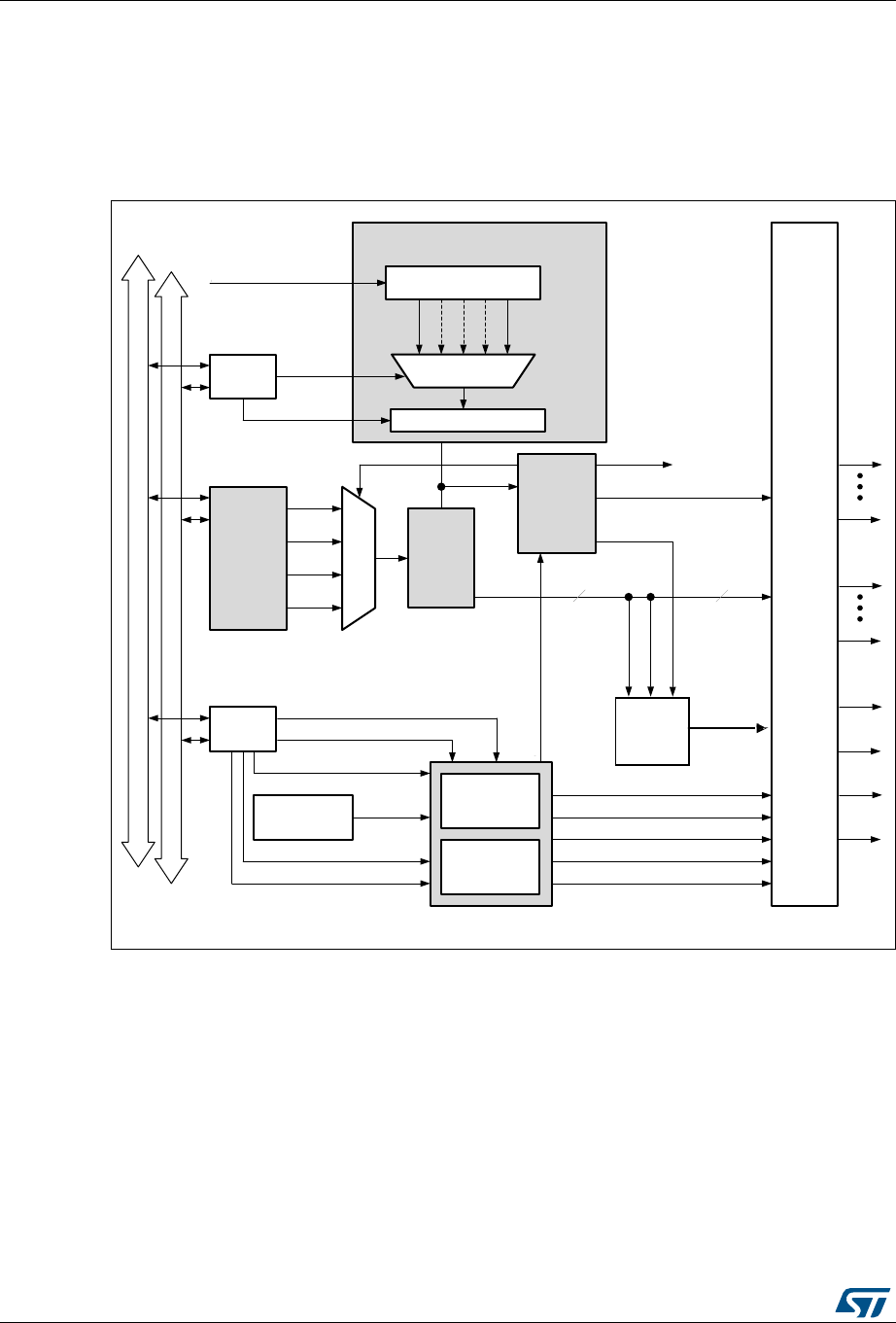
Liquid crystal display controller (LCD) RM0394
604/1600 RM0394 Rev 4
22.3 LCD functional description
22.3.1 General description
The LCD controller has five main blocks (see Figure 134):
Figure 134. LCD controller block diagram
Note: LCDCLK is the same as RTCCLK. Refer to the RTC/LCD clock description in the RCC
section of this manual.
The frequency generator allows you to achieve various LCD frame rates starting from an
LCD input clock frequency (LCDCLK) which can vary from 32 kHz up to 1 MHz.
3 different clock sources can be used to provide the LCD clock (LCDCLK/RTCCLK):
•32 kHz Low speed external RC (LSE)
•32 kHz Low speed internal RC (LSI)
•High speed external (HSE) divided by 32
$''5(66%86
'$7$%86
)5(48(1&<*(1(5$725
069
/&'&/.
&20
&20
9/&'
966
&20>@
36>@
',9>@
/&'&/./&'&/.
FNBGLY
(1
+'
$QDORJ
VZLWFK
DUUD\
&&>@
9/&'
9/&'
9/&'
%,$6>@
,QWHUUXSW
FNBSV
,23RUWV
$QDORJVWHSXS
FRQYHUWHU
5($'<
96(/
67$7,&
6(*>@
6(*>@
6(*>@
&20>@
6(*
08;
&20
$QDORJ
VZLWFK
DUUUD\ 6(*
6(*
6(*
&20
6(*
&20
6(*
&20
6(*
&20
92/7$*(
*(1(5$725
&2175$67
&21752//(5
/&'
5(*6
38/6(*(1
/&'5$0
[ELWV
WR08;
6(*
'5,9(5
&20
'5,9(5
6(*>@
6(*>@
&/2&.08;
ELWSUHVFDOHU
'LYLGHE\WR
/&'
5(*6

RM0394 Rev 4 605/1600
RM0394 Liquid crystal display controller (LCD)
633
22.3.2 Frequency generator
This clock source must be stable in order to obtain accurate LCD timing and hence
minimize DC voltage offset across LCD segments. The input clock LCDCLK can be divided
by any value from 1 to 215x 31 (see Section 22.6.2: LCD frame control register (LCD_FCR)
on page 626). The frequency generator consists of a prescaler (16-bit ripple counter) and a
16 to 31 clock divider. The PS[3:0] bits, in the LCD_FCR register, select LCDCLK divided by
2PS[3:0]. If a finer resolution rate is required, the DIV[3:0] bits, in the LCD_FCR register, can
be used to divide the clock further by 16 to 31. In this way you can roughly scale the
frequency, and then fine-tune it by linearly scaling the clock with the counter. The output of
the frequency generator block is fck_div which constitutes the time base for the entire LCD
controller. The ck_div frequency is equivalent to the LCD phase frequency, rather than the
frame frequency (they are equal only in case of static duty). The frame frequency (fframe) is
obtained from fck_div by dividing it by the number of active common terminals (or by
multiplying it for the duty). Thus the relation between the input clock frequency (fLCDCLK) of
the frequency generator and its output clock frequency fck_div is:
This makes the frequency generator very flexible. An example of frame rate calculation is
shown in Table 103.
The frame frequency must be selected to be within a range of around ~30 Hz to ~100 Hz
and is a compromise between power consumption and the acceptable refresh rate. In
Table 103. Example of frame rate calculation
LCDCLK PS[3:0] DIV[3:0] Ratio Duty fframe
32.768 kHz 3 1 136 1/8 30.12 Hz
32.768 kHz 4 1 272 1/4 30.12 Hz
32.768 kHz 4 6 352 1/3 31.03 Hz
32.768 kHz 5 1 544 1/2 30.12 Hz
32.768 kHz 6 1 1088 static 30.12 Hz
32.768 kHz 1 4 40 1/8 102.40 Hz
32.768 kHz 2 4 80 1/4 102.40 Hz
32.768 kHz 2 11 108 1/3 101.14 Hz
32.768 kHz 3 4 160 1/2 102.40 Hz
32.768 kHz 4 4 320 static 102.40 Hz
1.00 MHz 6 3 1216 1/8 102.80 Hz
1.00 MHz 7 3 2432 1/4 102.80 Hz
1.00 MHz 7 10 3328 1/3 100.16 Hz
1.00 MHz 8 3 4864 1/2 102.80 Hz
1.00 MHz 9 3 9728 static 102.80 Hz
fckdiv
fLCDCLK
2PS 16 DIV+()×
----------------------------------------------=
fframe fckdiv duty×=
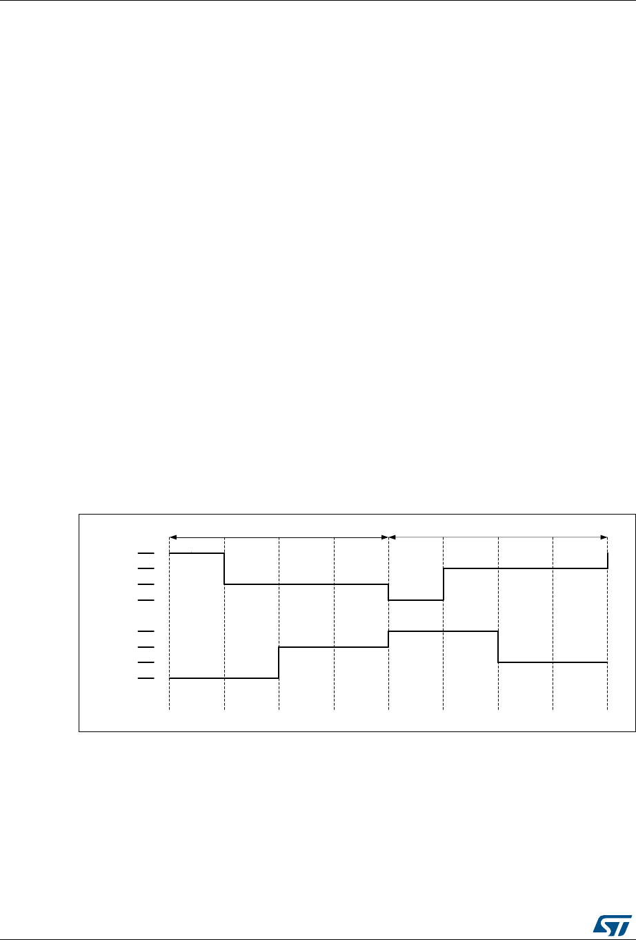
Liquid crystal display controller (LCD) RM0394
606/1600 RM0394 Rev 4
addition, a dedicated blink prescaler selects the blink frequency. This frequency is defined
as:
fBLINK = fck_div/2(BLINKF + 3),
with BLINKF[2:0] = 0, 1, 2, ... ,7
The blink frequency achieved is in the range of 0.5 Hz, 1 Hz, 2 Hz or 4 Hz.
22.3.3 Common driver
Common signals are generated by the common driver block (see Figure 134).
COM signal bias
Each COM signal has identical waveforms, but different phases. It has its max amplitude
VLCD or VSS only in the corresponding phase of a frame cycle, while during the other
phases, the signal amplitude is:
•1/4 VLCD or 3/4 VLCD in case of 1/4 bias
•1/3 VLCD or 2/3 VLCD in case of 1/3 bias
•and 1/2 VLCD in case of 1/2 bias.
Selection between 1/2, 1/3 and 1/4 bias mode can be done through the BIAS bits in the
LCD_CR register.
A pixel is activated when both of its corresponding common and segment lines are active
during the same phase, it means when the voltage difference between common and
segment is maximum during this phase. Common signals are phase inverted in order to
reduce EMI. As shown in Figure 135, with phase inversion, there is a mean voltage of 1/2
VLCD at the end of every odd cycle.
Figure 135. 1/3 bias, 1/4 duty
In case of 1/2 bias (BIAS = 01) the VLCD pin generates an intermediate voltage equal to 1/2
VLCD on node b for odd and even frames (see Figure 138).
COM signal duty
Depending on the DUTY[2:0] bits in the LCD_CR register, the COM signals are generated
with static duty (see Figure 137), 1/2 duty (see Figure 138), 1/3 duty (see Figure 139), 1/4
duty (see Figure 140) or 1/8 duty (see Figure 141).
069
9
/&'
2GGIUDPH (YHQIUDPH
&RPDFWLYH &RPLQDFWLYH &RPLQDFWLYH &RPLQDFWLYH &RPDFWLYH &RPLQDFWLYH &RPLQDFWLYH &RPLQDFWLYH
9
/&'
9
/&'
9
66
9
/&'
9
/&'
9
/&'
9
66
&RPDFWLYH &RPDFWLYH &RPLQDFWLYH &RPLQDFWLYH &RPDFWLYH &RPDFWLYH &RPLQDFWLYH &RPLQDFWLYH
3KDVH 3KDVH 3KDVH 3KDVH 3KDVH 3KDVH 3KDVH 3KDVH
6HJPHQW &RPPRQ
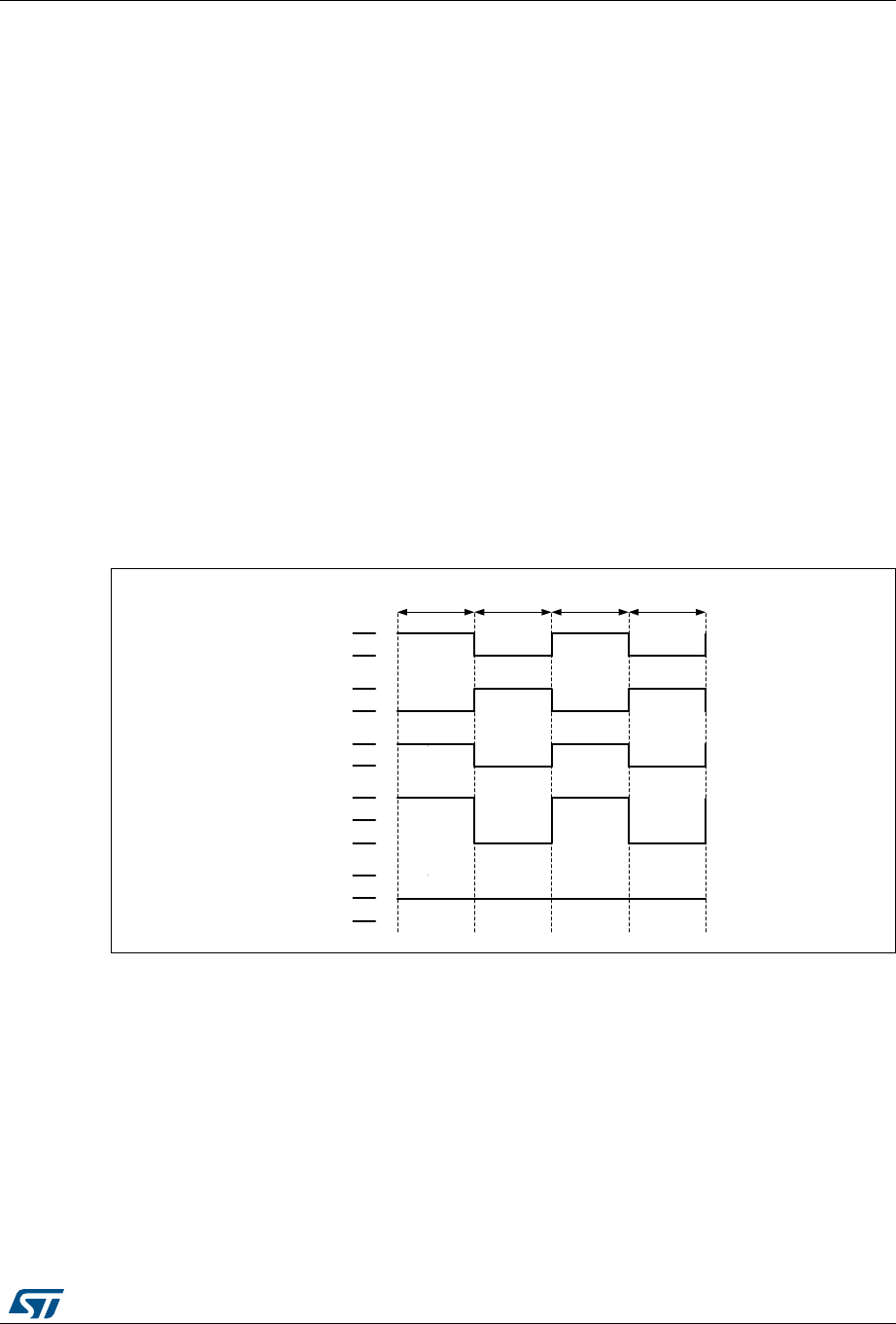
RM0394 Rev 4 607/1600
RM0394 Liquid crystal display controller (LCD)
633
COM[n] n[0 to 7] is active during phase n in the odd frame, so the COM pin is driven to
VLCD.
During phase n of the even frame the COM pin is driven to VSS.
In the case of 1/3 or 1/4) bias:
•COM[n] is inactive during phases other than n so the COM pin is driven to 1/3 (1/4)
VLCD during odd frames and to 2/3 (3/4) VLCD during even frames
In the case of 1/2 bias:
•If COM[n] is inactive during phases other than n, the COM pin is always driven (odd
and even frame) to 1/2 VLCD.
When static duty is selected, the segment lines are not multiplexed, which means that each
segment output corresponds to one pixel. In this way only up to 44 pixels can be driven.
COM[0] is always active while COM[7:1] are not used and are driven to VSS.
When the LCDEN bit in the LCD_CR register is reset, all common lines are pulled down to
VSS and the ENS flag in the LCD_SR register becomes 0. Static duty means that COM[0] is
always active and only two voltage levels are used for the segment and common lines: VLCD
and VSS. A pixel is active if the corresponding SEG line has a voltage opposite to that of the
COM, and inactive when the voltages are equal. In this way the LCD has maximum contrast
(see Figure 136, Figure 137). In the Figure 136 pixel 0 is active while pixel 1 is inactive.
Figure 136. Static duty case 1
In each frame there is only one phase, this is why fframe is equal to fLCD. If 1/4 duty is
selected there are four phases in a frame in which COM[0] is active during phase 0, COM[1]
is active during phase 1, COM[2] is active during phase 2, and COM[3] is active during
phase 3.
069
9/&'
2GGIUDPH
966
&20
(YHQIUDPH 2GGIUDPH (YHQIUDPH
9/&'
966
6(*
9/&'
&20
6(*
9/&'
9/&'
966
6(*
9/&'
&20
6(*
9/&'
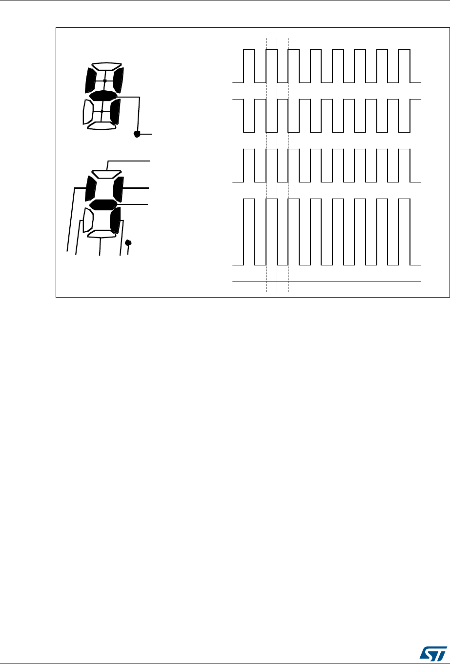
Liquid crystal display controller (LCD) RM0394
608/1600 RM0394 Rev 4
Figure 137. Static duty case 2
In this mode, the segment terminals are multiplexed and each of them control four pixels. A
pixel is activated only when both of its corresponding SEG and COM lines are active in the
same phase. In case of 1/4 duty, to deactivate pixel 0 connected to COM[0] the SEG[0]
needs to be inactive during the phase 0 when COM[0] is active. To activate pixel 0
connected to COM[1], the SEG[0] needs to be active during phase 1 when COM[1] is active
(see Figure 140). To activate pixels from 0 to 43 connected to COM[0], SEG[0:43] need to
be active during phase 0 when COM[0] is active. These considerations can be extended to
the other pixels.
8 to 1 Mux
When COM[0] is active the common driver block, also drives the 8 to 1 mux shown in
Figure 134 in order to select the content of first two RAM register locations. When COM[7] is
active, the output of the 8 to 1 mux is the content of the last two RAM locations.
069
9
9
3,1
&20
/LTXLGFU\VWDOGLVSOD\
DQGWHUPLQDOFRQQHFWLRQ
&20
6(*
6(*
6(*
6(*
6(*
6(*
6(*
6(*
9
9
3,1
6(*
9
9
3,1
6(*
9
9
9
&206(*
VHOHFWHGZDYHIRUP
9
&206(*
QRQVHOHFWHGZDYHIRUP
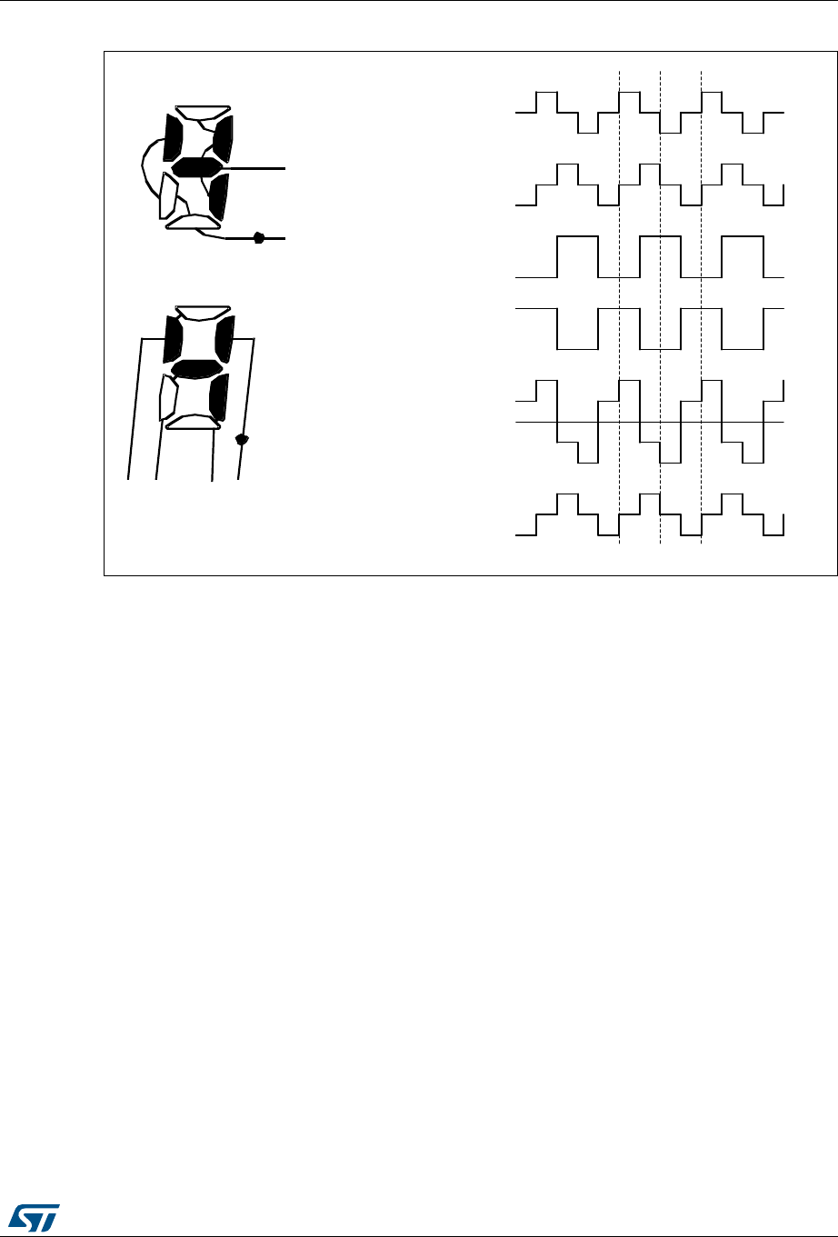
RM0394 Rev 4 609/1600
RM0394 Liquid crystal display controller (LCD)
633
Figure 138. 1/2 duty, 1/2 bias
22.3.4 Segment driver
The segment driver block controls the SEG lines according to the pixel data coming from the
8 to 1 mux driven in each phase by the common driver block.
In the case of 1/4 or 1/8 duty
When COM[0] is active, the pixel information (active/inactive) related to the pixel connected
to COM[0] (content of the first two LCD_RAM locations) goes through the 8 to 1 mux.
The SEG[n] pin n [0 to 43] is driven to VSS (indicating pixel n is active when COM[0] is
active) in phase 0 of the odd frame.
The SEG[n] pin is driven to VLCD in phase 0 of the even frame. If pixel n is inactive then the
SEG[n] pin is driven to 2/3 (2/4) VLCD in the odd frame or 1/3 (2/4) VLCD in the even frame
(current inversion in VLCD pad) (see Figure 135).
In case of 1/2 bias, if the pixel is inactive the SEG[n] pin is driven to VLCD in the odd and to
VSS in the even frame.
When the LCD controller is disabled (LCDEN bit cleared in the LCD_CR register) then the
SEG lines are pulled down to VSS.
069
9
9
9
3,1
&20
/LTXLGFU\VWDOGLVSOD\
DQGWHUPLQDOFRQQHFWLRQ
&20
6(*
6(*
6(*
6(*
&206(*
QRQVHOHFWHGZDYHIRUP
&20 3,1
&20
9
9
9
3,1
6(*
9
9
3,1
6(*
9
9
&206(*
VHOHFWHGZDYHIRUP
9
9
9
9
9
9
9
9
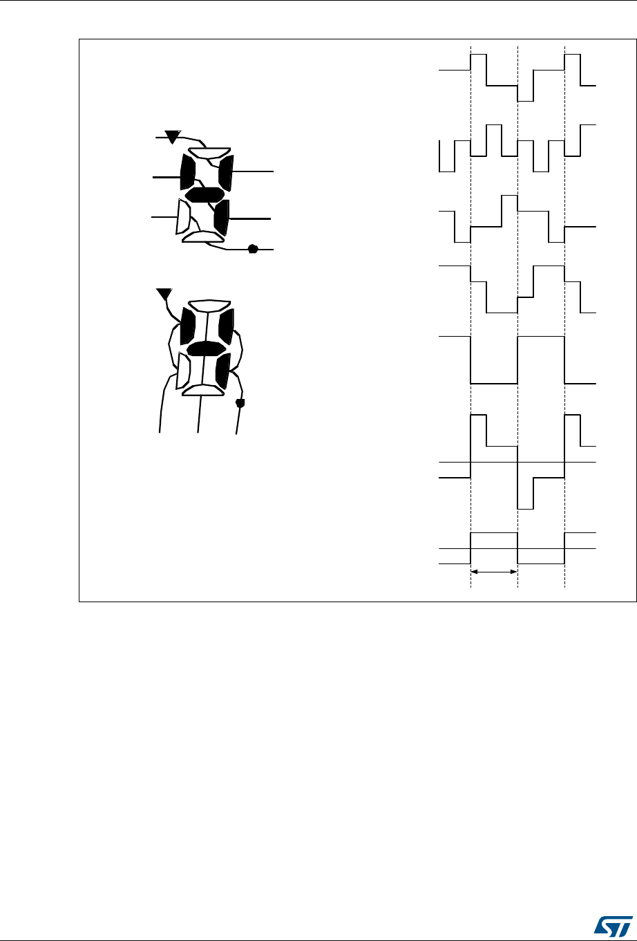
Liquid crystal display controller (LCD) RM0394
610/1600 RM0394 Rev 4
Figure 139. 1/3 duty, 1/3 bias
069
9
9
9
9
3,1
&20
/LTXLGFU\VWDOGLVSOD\
DQGWHUPLQDOFRQQHFWLRQ
&20
6(* 6(*
&20
&206(*
VHOHFWHGZDYHIRUP
9
9
9
9
9
9
9
&20
6(*
9
9
9
9
3,1
&20
9
9
9
9
3,1
&20
9
9
9
9
3,1
6(*
9
9
9
9
3,1
6(*
&206(*
QRQVHOHFWHGZDYHIRUP
9
9
9
IUDPH
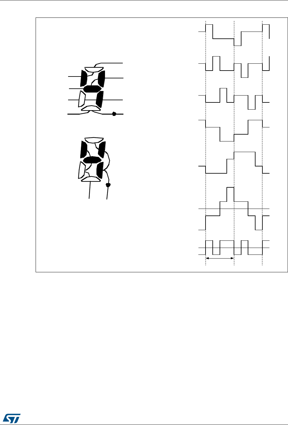
RM0394 Rev 4 611/1600
RM0394 Liquid crystal display controller (LCD)
633
Figure 140. 1/4 duty, 1/3 bias
069
9
9
9
9
3,1
&20
/LTXLGFU\VWDOGLVSOD\
DQGWHUPLQDOFRQQHFWLRQ
&20
6(*
&20
&206(*
VHOHFWHGZDYHIRUP
9
9
9
9
9
9
9
&20
6(*
9
9
9
9
3,1
&20
9
9
9
9
3,1
&20
9
9
9
9
3,1
6(*
9
9
9
9
3,1
6(*
&206(*
QRQVHOHFWHGZDYHIRUP
9
9
9
IUDPH
&20
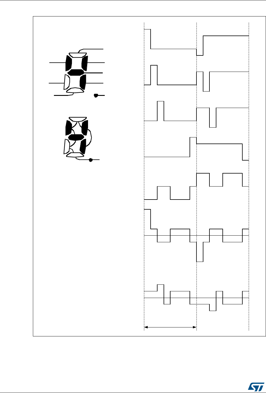
Liquid crystal display controller (LCD) RM0394
612/1600 RM0394 Rev 4
Figure 141. 1/8 duty, 1/4 bias
069
/LTXLGFU\VWDOGLVSOD\
DQGWHUPLQDOFRQQHFWLRQ
&20
6(*
&20
&206(*
QRQVHOHFWHGZDYHIRUP
9
9
9
9
9
9
9
9
9
&20
9
9
9
9
9
3,1
6(*
&20
&20
&20
&20
&20
&206(*
VHOHFWHGZDYHIRUP
9
9
9
9
9
9
9
9
9
9
9
9
9
9
3,1
&20
9
9
9
9
9
3,1
&20
9
9
9
9
9
3,1
&20
9
9
9
9
9
3,1
&20
IUDPH

RM0394 Rev 4 613/1600
RM0394 Liquid crystal display controller (LCD)
633
Blink
The segment driver also implements a programmable blink feature to allow some pixels to
continuously switch on at a specific frequency. The blink mode can be configured by the
BLINK[1:0] bits in the LCD_FCR register, making possible to blink up to 1, 2, 4, 8 or all
pixels (see Section 22.6.2: LCD frame control register (LCD_FCR)). The blink frequency
can be selected from eight different values using the BLINKF[2:0] bits in the LCD_FCR
register.
Table 104 gives examples of different blink frequencies (as a function of ck_div frequency).
22.3.5 Voltage generator and contrast control
LCD supply source
The LCD power supply source may come from either the internal step-up converter or from
an external voltage applied on the VLCD pin. Internal or external voltage source can be
selected using the VSEL bit in the LCD_CR register. In case of external source selected, the
internal boost circuit (step-up converter) is disabled to reduce power consumption.
When the step-up converter is selected as VLCD source, the VLCD value can be chosen
among a wide set of values from VLCDmin to VLCDmax by means of CC[2:0] (Contrast
Control) bits inside LCD_FCR (see Section 22.6.2) register. New values of VLCD takes effect
every beginning of a new frame.
When external power source is selected as VLCD source, the VLCD voltage must be chosen
in the range of VLCDmin to VLCDmax (see datasheets). The contrast can then be controlled by
programming a dead time between frames (see Deadtime on page 616).
A specific software sequence must be performed to configure the LCD depending on the
LCD power supply source to be used. Here we consider the LCD controller is disabled prior
to the configuration sequence.
Table 104. Blink frequency
BLINKF[2:0]
bits
ck_div frequency (with LCDCLK frequency of 32.768 kHz)
32 Hz 64 Hz 128 Hz 256 Hz
0 0 0 4.0 Hz N/A N/A N/A
0 0 1 2.0 Hz 4.0 Hz N/A N/A
0 1 0 1.0 Hz 2.0 Hz 4.0 Hz N/A
0 1 1 0.5Hz 1.0Hz 2.0Hz 4.0Hz
1 0 0 0.25 Hz 0.5 Hz 1.0 Hz 2.0 Hz
1 0 1 N/A 0.25 Hz 0.5 Hz 1.0 Hz
1 1 0 N/A N/A 0.25 Hz 0.5 Hz
1 1 1 N/A N/A N/A 0.25 Hz

Liquid crystal display controller (LCD) RM0394
614/1600 RM0394 Rev 4
In case the internal step-up converter is used (capacitor CEXT on VLCD pin is required):
•Configure the VLCD pin as alternate function LCD in the GPIO_AFR register.
•Wait for the external capacitor CEXT to be charged (CEXT connected to the VLCD pin,
approximately 2 ms for CEXT = 1 F)
•Set voltage source to internal source by resetting VSEL bit in the LCD_CR register
•Enable the LCD controller by setting LCDEN bit in the LCD_CR register
In case of LCD external power source is used:
•Set voltage source to external source by setting VSEL bit in the LCD_CR register
•Configure the VLCD pin as alternate function LCD in the GPIO_AFR register
•Enable the LCD controller by setting LCDEN bit in the LCD_CR register
LCD intermediate voltages
The LCD intermediate voltage levels are generated through an internal resistor divider
network as shown in Figure 142.
The LCD voltage generator issues intermediate voltage levels between VSS and VLCD:
•1/3 VLCD and 2/3 VLCD in case of 1/3 bias
•1/4 VLCD, 2/4 VLCD and 3/4 VLCD in case of 1/4 bias
•only 1/2 VLCD in case of 1/2 bias.
LCD drive selection
Two resistive networks, one with low value resistors (RL) and one with high value resistors
(RH) are respectively used to increase the current during transitions and reduce power
consumption in static state.
The EN switch follows the rules described below (see Figure 142):
•If LCDEN bit in the LCD_CR register is set, the EN switch is closed.
•When clearing the LCDEN bit in the LCD_CR register, the EN switch is open at the end
of the even frame in order to avoid a medium voltage level different from 0 considering
the entire frame odd plus even.
The PON[2:0] (Pulse ON duration) bits in the LCD_FCR register configure the time during
which RL is enabled through the HD (high drive) switch when the levels of the common and
segment lines change (see Figure 142). A short drive time will lead to lower power
consumption, but displays with high internal resistance may need a longer drive time to
achieve satisfactory contrast.
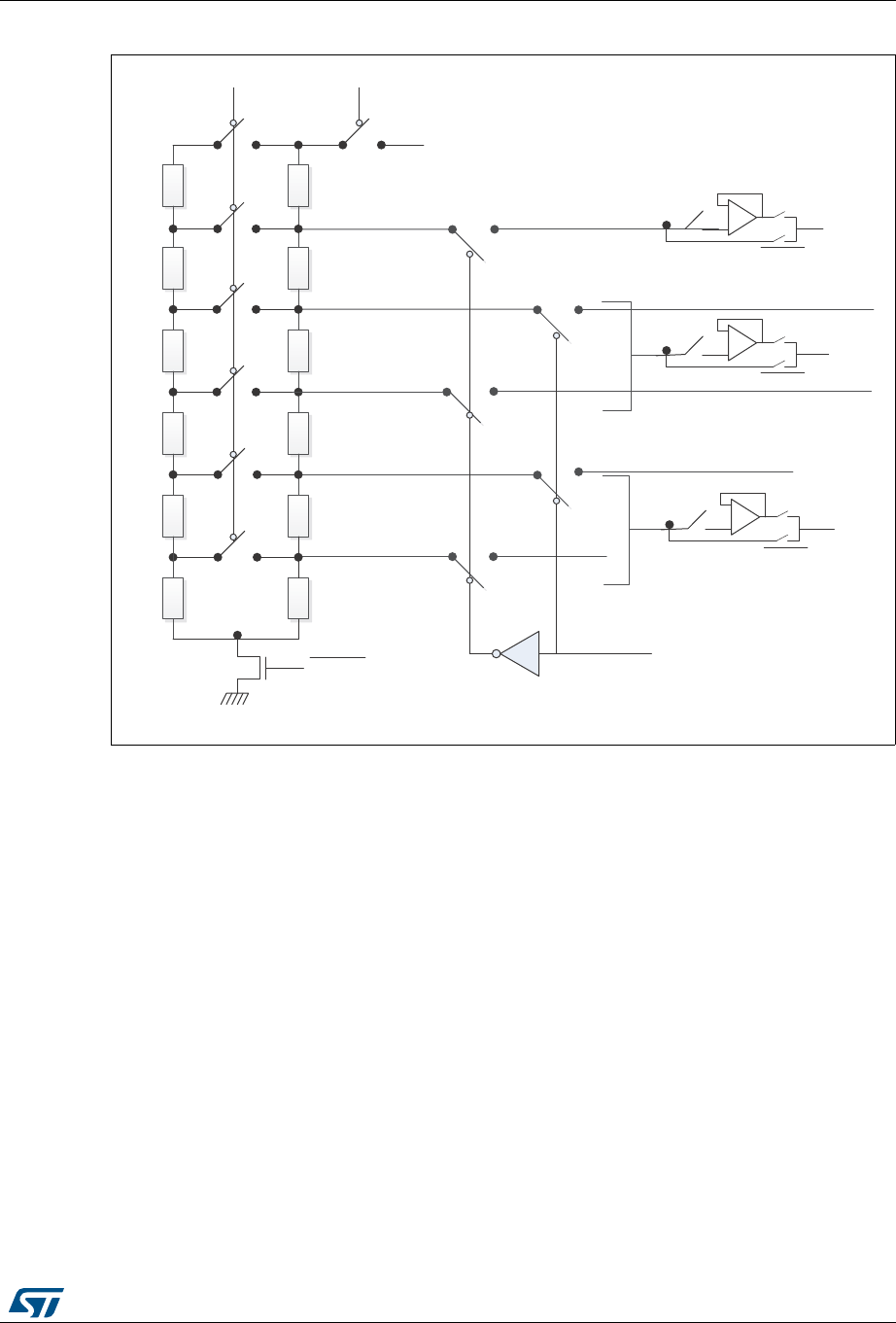
RM0394 Rev 4 615/1600
RM0394 Liquid crystal display controller (LCD)
633
Figure 142. LCD voltage control
1. RLN and RHN are the low value resistance network and the high value resistance network, respectively.
The RLN divider can be always switched on using the HD bit in the LCD_FCR configuration
register (see Section 22.6.2).
The HD switch follows the rules described below:
•If the HD bit and the PON[2:0] bits in the LCD_FCR register are reset, then HD switch
is open.
•If the HD bit in the LCD_FCR register is reset and the PON[2:0] bits in the LCD_FCR
are different from 00 then, the HD switch is closed during the number of pulses defined
in the PON[2:0] bits.
•If HD bit in the LCD_FCR register is 1 then HD switch is always closed.
Buffered mode
When voltage output buffers are enabled by setting BUFEN bit in the LCD_CR register, LCD
driving capability is improved as buffers prevent the LCD capacitive loads from loading the
resistor bridge unacceptably and interfering with its voltage generation. As a result we
obtain more stable intermediate voltage levels thus improving RMS voltage applied to the
LCD pixels.
069
[9/&'
[9/&'
[9/&'
[9/&'
[9/&'
9/&'5DLO
%,$6>@
5+
5+
5+
5+
5+
5+
9/&'
5/
5/
5/
+' (1
67$7,&
966
5/
5/
5/
%8)(1
%8)(1
%8)(1
9/&'5DLO
%8)(1
%8)(1
%8)(1
9/&'5DLO
%8)(1
%8)(1
%8)(1
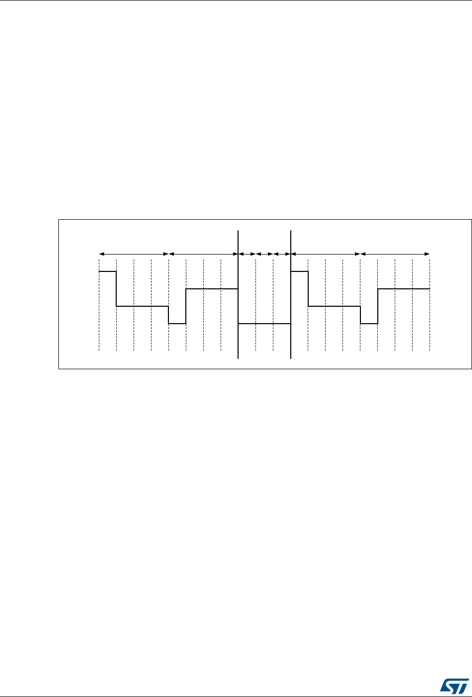
Liquid crystal display controller (LCD) RM0394
616/1600 RM0394 Rev 4
In buffer mode, intermediate voltages are generated by the high value resistor bridge RHN to
reduce power consumption, the low value resistor bridge RLN is automatically disabled
whatever the HD bit or PON bits configuration.
Buffers can be used independently of the VLCD supply source (internal or external) but can
only be enabled or disabled when LCD controller is not activated.
After the LCDEN bit is activated, the RDY bit is set in the LCD_SR register to indicate that
voltage levels are stable and the LCD controller can start to work.
Deadtime
In addition to using the CC[2:0] bits, the contrast can be controlled by programming a dead
time between each frame. During the dead time the COM and SEG values are put to VSS.
The DEAD[2:0] bits in the LCD_FCR register can be used to program a time of up to eight
phase periods. This dead time reduces the contrast without modifying the frame rate.
Figure 143. Deadtime
069
ŽĚĚĨƌĂŵĞ ĞǀĞŶĨƌĂŵĞ ŽĚĚĨƌĂŵĞ ĞǀĞŶĨƌĂŵĞĚĞĂĚƚŝŵĞ

RM0394 Rev 4 617/1600
RM0394 Liquid crystal display controller (LCD)
633
22.3.6 Double buffer memory
Using its double buffer memory the LCD controller ensures the coherency of the displayed
information without having to use interrupts to control LCD_RAM modification.
The application software can access the first buffer level (LCD_RAM) through the APB
interface. Once it has modified the LCD_RAM, it sets the UDR flag in the LCD_SR register.
This UDR flag (update display request) requests the updated information to be moved into
the second buffer level (LCD_DISPLAY).
This operation is done synchronously with the frame (at the beginning of the next frame),
until the update is completed, the LCD_RAM is write protected and the UDR flag stays high.
Once the update is completed another flag (UDD - Update Display Done) is set and
generates an interrupt if the UDDIE bit in the LCD_FCR register is set.
The time it takes to update LCD_DISPLAY is, in the worst case, one odd and one even
frame.
The update will not occur (UDR = 1 and UDD = 0) until the display is enabled (LCDEN = 1)
22.3.7 COM and SEG multiplexing
Output pins versus duty modes
The output pins consists of:
•SEG[43:0]
•COM[3:0]
Depending on the duty configuration, the COM and SEG output pins may have different
functions:
•In static, 1/2, 1/3 and 1/4 duty modes there are up to 44 SEG pins and respectively 1, 2,
3 and 4 COM pins
•In 1/8 duty mode (DUTY[2:0] = 100), COM[7:4] outputs are available on the
SEG[43:40] pins, reducing to the number of available segments to 40.
Remapping capability for small packages
Additionally, it is possible to remap 4 segments by setting the MUX_SEG bit in the LCD_CR
register. This is particularly useful when using smaller device types with fewer external pins.
When MUX_SEG is set, output pins SEG[43:40] have the same function as SEG[31:28].
This feature is available only if the mode 1/8 duty is not selected.
Check the availability of this feature referring to the pinout section of the product datasheet.
For the considered package, check the availability of the SEG/COM multiplexing pin as
follow:
LCD_SEG[n-1]/LCD_COM7/LCD_SEG[31]
LCD_SEG[n-2]/LCD_COM6/LCD_SEG[30]
LCD_SEG[n-3]/LCD_COM5/LCD_SEG[29]
LCD_SEG[n-4]/LCD_COM4/LCD_SEG[28]
with n = number of segment for the considered package.

Liquid crystal display controller (LCD) RM0394
618/1600 RM0394 Rev 4
Summary of COM and SEG functions versus duty and remap
All the possible ways of multiplexing the COM and SEG functions are described in
Table 105. Figure 144 gives examples showing the signal connections to the external pins.
Table 105. Remapping capability
Configuration bits
SEG x COM Output pin Function
DUTY MUX_SEG
1/8
0/1 40x8
SEG[43:40]/SEG[31:28]/COM[7:4] COM[7:4]
COM[3:0] COM[3:0]
SEG[39:0] SEG[39:0]
0/1 28x8
SEG[43:40]/SEG[31:28]/COM[7:4] COM[7:4]
COM[3:0] COM[3:0]
SEG[27:0] SEG[27:0]
1/4
044x4
COM[3:0] COM[3:0]
SEG[43:40]/SEG[31:28]/COM[7:4] SEG[43:40]
SEG[39:0] SEG[39:0]
140x4
COM[3:0] COM[3:0]
SEG[43:40]/SEG[31:28]/COM[7:4] SEG[31:28]
SEG[39:32] SEG[39:32]
SEG[31:28] not used
SEG[27:0] SEG[27:0]
028x4
COM[3:0] COM[3:0]
SEG[43:40]/SEG[31:28]/COM[7:4] not used
SEG[27:0] SEG[27:0]
132x4
COM[3:0] COM[3:0]
SEG[43:40]/SEG[31:28]/COM[7:4] SEG[31:28]
SEG[27:0] SEG[27:0]

RM0394 Rev 4 619/1600
RM0394 Liquid crystal display controller (LCD)
633
1/3
044x3
COM3 not used
COM[2:0] COM[2:0]
SEG[43:40]/SEG[31:28]/COM[7:4] SEG[43:40]
SEG[39:0] SEG[39:0]
140x3
COM3 not used
COM[2:0] COM[2:0]
SEG[43:40]/SEG[31:28]/COM[7:4] SEG[31:28]
SEG[39:32] SEG[39:32]
SEG[31:28] not used
SEG[27:0] SEG[27:0]
028x3
COM3 not used
COM[2:0] COM[2:0]
SEG[43:40]/SEG[31:28]/COM[7:4] not used
SEG[31:0] SEG[31:0]
132x3
COM3 not used
COM[2:0] COM[2:0]
SEG[43:40]/SEG[31:28]/COM[7:4] SEG[31:28]
SEG[27:0] SEG[27:0]
1/2
044x2
COM[3:2] not used
COM[1:0] COM[1:0]
SEG[43:40]/SEG[31:28]/COM[7:4] SEG[43:40]
SEG[39:0] SEG[39:0]
140x2
COM[3:2] not used
COM[1:0] COM[1:0]
SEG[43:40]/SEG[31:28]/COM[7:4] SEG[31:28]
SEG[39:32] SEG[39:32]
SEG[31:28] not used
SEG[27:0] SEG[27:0]
Table 105. Remapping capability (continued)
Configuration bits
SEG x COM Output pin Function
DUTY MUX_SEG

Liquid crystal display controller (LCD) RM0394
620/1600 RM0394 Rev 4
1/2
028x2
COM[3:2] not used
COM[1:0] COM[1:0]
SEG[43:40]/SEG[31:28]/COM[7:4] not used
SEG[27:0] SEG[27:0]
132x2
COM[3:2] not used
COM[1:0] COM[1:0]
SEG[43:40]/SEG[31:28]/COM[7:4] SEG[31:28]
SEG[27:0] SEG[27:0]
STATIC
044x1
COM[3:1] not used
COM0 COM0
SEG[43:40]/SEG[31:28]/COM[7:4] SEG[43:40]
SEG[39:0] SEG[39:0]
140x1
COM[3:1] not used
COM0 COM0
SEG[43:40]/SEG[31:28]/COM[7:4] SEG[31:28]
SEG[39:32] SEG[39:32]
SEG[31:28] not used
SEG[27:0] SEG[27:0]
028x1
COM[3:1] not used
COM0 COM0
SEG[43:40]/SEG[31:28]/COM[7:4] not used
SEG[27:0] SEG[27:0]
132x1
COM[3:1] not used
COM0 COM0
SEG[43:40]/SEG[31:28]/COM[7:4] SEG[31:28]
SEG[27:0] SEG[27:0]
Table 105. Remapping capability (continued)
Configuration bits
SEG x COM Output pin Function
DUTY MUX_SEG
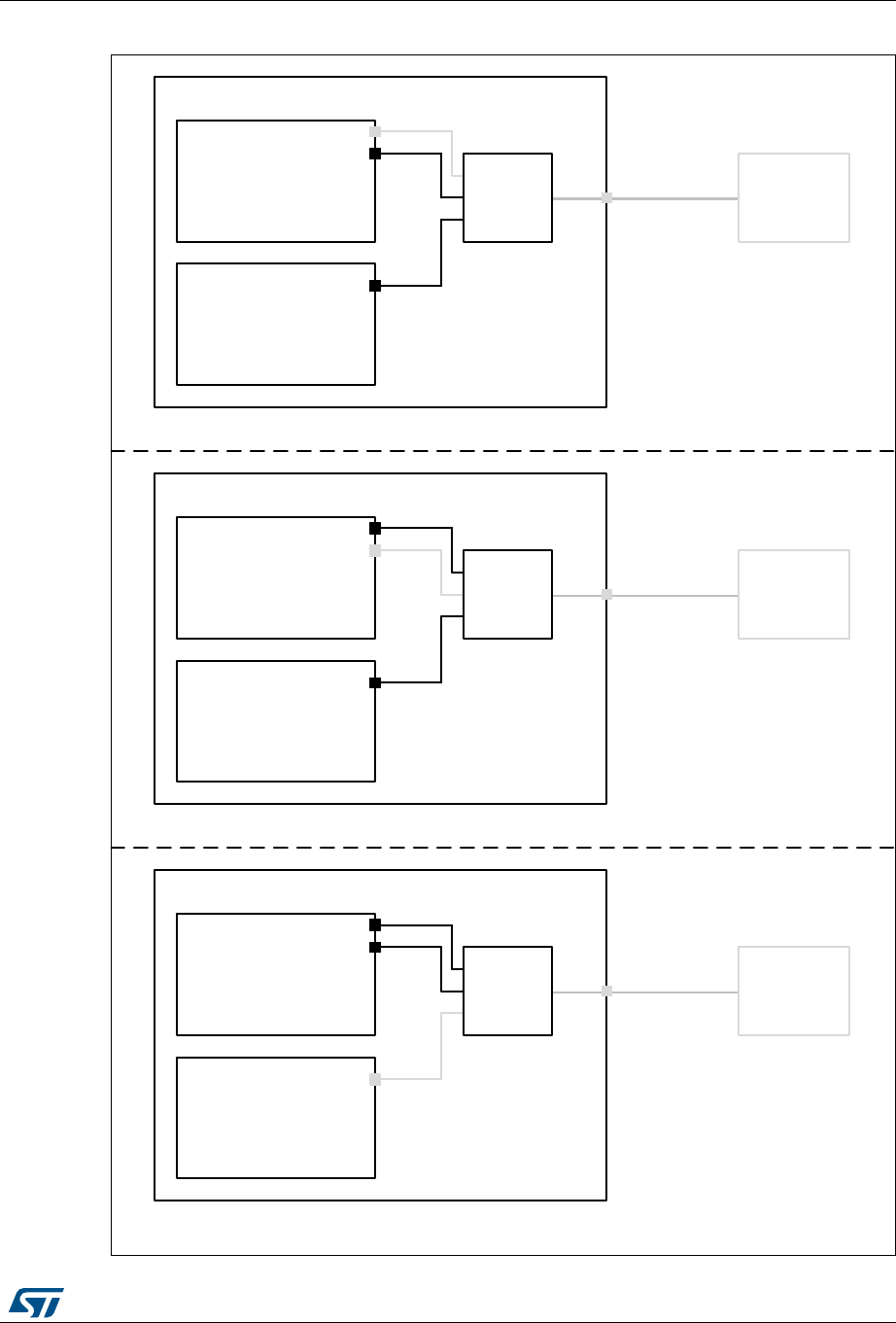
RM0394 Rev 4 621/1600
RM0394 Liquid crystal display controller (LCD)
633
Figure 144. SEG/COM mux feature example
/&'&21752//(5
069
&20>@
'87<DQG08;B6(*
/&'B6(*>@
3,1
&20'5,9(5
6(*>@
6(*>@
6(*'5,9(5 6(*
&20
08;
/&'&21752//(5
&20>@
'87<DQG08;B6(*
/&'B6(*>@
3,1
&20'5,9(5
6(*>@
6(*>@
6(*'5,9(5 6(*
&20
08;
/&'&21752//(5
&20>@
'87< DQG08;B6(*
&20>@
3,1
&20'5,9(5
6(*>@
6(*>@
6(*'5,9(5 6(*
&20
08;
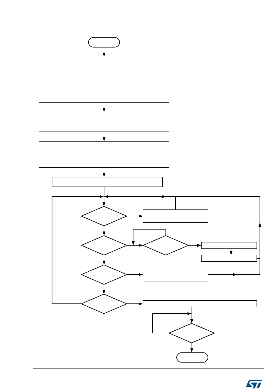
Liquid crystal display controller (LCD) RM0394
622/1600 RM0394 Rev 4
22.3.8 Flowchart
Figure 145. Flowchart example
069
67$57
,1,7
(QDEOHWKH*3,2SRUWFORFNV
&RQILJXUHWKH/&'*3,2SLQVDVDOWHUQDWH
IXQFWLRQV
&RQILJXUH/&'FRQWUROOHUDFFRUGLQJWRWKH
'LVSOD\WREHGULYHQ
/RDGWKHLQLWLDOGDWDWREHGLVSOD\HGLQWR
/&'B5$0DQGVHWWKH8'5ELWLQWKH/&'B65
UHJLVWHU
3URJUDPWKHGHVLUHGIUDPHUDWH36DQG',9
ELWVLQ/&'B)&5
3URJUDPWKHFRQWUDVW&&ELWVLQ/&'B)&5
UHJLVWHU
%NABLETHEDISPLAY,#$%.BITIN,#$?#2REGISTER
!DJUSTCONTRAST
-ODIFYDATA
#HANGEBLINK
$ISABLE,#$
.O
9E S
.O
.O
9E S
9E S
9E S
5$2
9E S
&KDQJH36',9&&321
'($'RU+'LQ/&'B)&5
.O 0RGLI\WKH/&'B5$0
&KDQJH%/,1.RU%/,1.)LQ
/&'B)&5
6HW8'5ELWLQ/&'B65
'LVDEOHWKHGLVSOD\/&'(1ELWLQ/&'B&5UHJLVWHU
(1'
%.3
9E S
.O
RM0394 Rev 4 623/1600
RM0394 Liquid crystal display controller (LCD)
633
22.4 LCD low-power modes
the LCD controller can be displayed in Stop mode or can be fully disabled to reduce power
consumption.
22.5 LCD interrupts
The table below gives the list of LCD interrupt requests.
Start of frame (SOF)
The LCD start of frame interrupt is executed if the SOFIE (start of frame interrupt enable) bit
is set (see Section 22.6.2: LCD frame control register (LCD_FCR)). SOF is cleared by
writing the SOFC bit to 1 in the LCD_CLR register when executing the corresponding
interrupt handling vector.
Update display done (UDD)
The LCD update display interrupt is executed if the UDDIE (update display done interrupt
enable) bit is set (see Section 22.6.2: LCD frame control register (LCD_FCR)). UDD is
cleared by writing the UDDC bit to 1 in the LCD_CLR register when executing the
corresponding interrupt handling vector.
Depending on the product implementation, all these interrupts events can either share the
same interrupt vector (LCD global interrupt), or be grouped into 2 interrupt vectors (LCD
SOF interrupt and LCD UDD interrupt). Refer to the Table 46:
STM32L41xxx/42xxx/43xxx/44xxx/45xxx/46xxx vector table for details.
To enable the LCD interrupts, the following sequence is required:
Table 106. LCD behavior in low-power modes
Mode Description
Sleep No effect. LCD interrupt causes the device to exit the Sleep mode.
Low-power run No effect.
Low-power sleep No effect. LCD interrupt causes the device to exit the Low-power sleep
mode.
Stop 0
No effect. LCD interrupt causes the device to exit the Stop mode.Stop 1
Stop 2
Standby The LCD peripheral is powered down and must be reinitialized after exiting
Standby or Shutdown mode.
Shutdown
Table 107. LCD interrupt requests
Interrupt event Event flag Event flag/Interrupt
clearing method
Interrupt enable
control bit
Start Of Frame (SOF) SOF Write SOFC =1 SOFIE
Update Display Done (UDD) UDD Write UDDC = 1 UDDIE

Liquid crystal display controller (LCD) RM0394
624/1600 RM0394 Rev 4
1. Configure and enable the LCD IRQ channel in the NVIC
2. Configure the LCD to generate interrupts

RM0394 Rev 4 625/1600
RM0394 Liquid crystal display controller (LCD)
633
22.6 LCD registers
The peripheral registers have to be accessed by words (32-bit).
22.6.1 LCD control register (LCD_CR)
Address offset: 0x00
Reset value: 0x0000 0000
31 30 29 28 27 26 25 24 23 22 21 20 19 18 17 16
Res. Res. Res. Res. Res. Res. Res. Res. Res. Res. Res. Res. Res. Res. Res. Res.
1514131211109876543210
Res. Res. Res. Res. Res. Res. Res. BUFEN MUX_
SEG BIAS[1:0] DUTY[2:0] VSEL LCDEN
rw rw rw rw rw rw rw rw rw
Bits 31:9 Reserved, must be kept at reset value
Bit 8 BUFEN: Voltage output buffer enable
This bit is used to enable/disable the voltage output buffer for higher driving capability.
0: Output buffer disabled
1: Output buffer enabled
Bit 7 MUX_SEG: Mux segment enable
This bit is used to enable SEG pin remapping. Four SEG pins can be multiplexed with
SEG[31:28]. See Section 22.3.7.
0: SEG pin multiplexing disabled
1: SEG[31:28] are multiplexed with SEG[43:40]
Bits 6:5 BIAS[1:0]: Bias selector
These bits determine the bias used. Value 11 is forbidden.
00: Bias 1/4
01: Bias 1/2
10: Bias 1/3
11: Reserved
Bits 4:2 DUTY[2:0]: Duty selection
These bits determine the duty cycle. Values 101, 110 and 111 are forbidden.
000: Static duty
001: 1/2 duty
010: 1/3 duty
011: 1/4 duty
100: 1/8 duty
101: Reserved
110: Reserved
111: Reserved
Liquid crystal display controller (LCD) RM0394
626/1600 RM0394 Rev 4
Note: The VSEL, MUX_SEG, BIAS, DUTY and BUFEN bits are write-protected when the LCD is
enabled (ENS bit in LCD_SR to 1).
22.6.2 LCD frame control register (LCD_FCR)
Address offset: 0x04
Reset value: 0x0000 0000
Bit 1 VSEL: Voltage source selection
The VSEL bit determines the voltage source for the LCD.
0: Internal source (voltage step-up converter)
1: External source (VLCD pin)
Bit 0 LCDEN: LCD controller enable
This bit is set by software to enable the LCD Controller/Driver. It is cleared by software to turn
off the LCD at the beginning of the next frame. When the LCD is disabled all COM and SEG
pins are driven to VSS.
0: LCD Controller disabled
1: LCD Controller enabled
31 30 29 28 27 26 25 24 23 22 21 20 19 18 17 16
Res. Res. Res. Res. Res. Res. PS[3:0] DIV[3:0] BLINK[1:0]
rw rw rw rw rw rw rw rw rw rw
15 14 13 12 11 10 9 8 7 6 5 4 3 2 1 0
BLINKF[2:0] CC[2:0] DEAD[2:0] PON[2:0] UDDIE Res. SOFIE HD
rw rw rw rw rw rw rw rw rw rw rw rw rw rw rw
Bits 31:26 Reserved, must be kept at reset value
Bits 25:22 PS[3:0]: PS 16-bit prescaler
These bits are written by software to define the division factor of the PS 16-bit prescaler.
ck_ps = LCDCLK/(2). See Section 22.3.2.
0000: ck_ps = LCDCLK
0001: ck_ps = LCDCLK/2
0002: ck_ps = LCDCLK/4
...
1111:ck_ps = LCDCLK/32768
Bits 21:18 DIV[3:0]: DIV clock divider
These bits are written by software to define the division factor of the DIV divider. See
Section 22.3.2.
0000: ck_div = ck_ps/16
0001: ck_div = ck_ps/17
0002: ck_div = ck_ps/18
...
1111:ck_div = ck_ps/31

RM0394 Rev 4 627/1600
RM0394 Liquid crystal display controller (LCD)
633
Bits 17:16 BLINK[1:0]: Blink mode selection
00: Blink disabled
01: Blink enabled on SEG[0], COM[0] (1 pixel)
10: Blink enabled on SEG[0], all COMs (up to 8 pixels depending on the programmed duty)
11: Blink enabled on all SEGs and all COMs (all pixels)
Bits 15:13 BLINKF[2:0]: Blink frequency selection
000: fLCD/8
001: fLCD/16
010: fLCD/32
011: fLCD/64
100: fLCD/128
101: fLCD/256
110: fLCD/512
111: fLCD/1024
Bits 12:10 CC[2:0]: Contrast control
These bits specify one of the VLCD maximum voltages (independent of VDD). It ranges from
2.60 V to 3.51V.
000: VLCD0
001: VLCD1
010: VLCD2
011: VLCD3
100: VLCD4
101: VLCD5
110: VLCD6
111: VLCD7
Refer to the product datasheet for the VLCDx values.
Bits 9:7 DEAD[2:0]: Dead time duration
These bits are written by software to configure the length of the dead time between frames.
During the dead time the COM and SEG voltage levels are held at 0 V to reduce the contrast
without modifying the frame rate.
000: No dead time
001: 1 phase period dead time
010: 2 phase period dead time
......
111: 7 phase period dead time

Liquid crystal display controller (LCD) RM0394
628/1600 RM0394 Rev 4
Note: The data in this register can be updated any time, however the new values are applied only
at the beginning of the next frame (except for UDDIE, SOFIE that affect the device behavior
immediately).
The new value of CC[2:0] bits is also applied immediately but its effect on device is delayed
at the beginning of next frame by the voltage generator.
Reading this register obtains the last value written in the register and not the configuration
used to display the current frame.
Note: When BUFEN bit is set in the LCD_CR register, low resistor divider network is automatically
disabled whatever the HD or PON[2:0] bits configuration.
Bits 6:4 PON[2:0]: Pulse ON duration
These bits are written by software to define the pulse duration in terms of ck_ps pulses. A short
pulse will lead to lower power consumption, but displays with high internal resistance may
need a longer pulse to achieve satisfactory contrast.
Note that the pulse will never be longer than one half prescaled LCD clock period.
000: 0
001: 1/ck_ps
010: 2/ck_ps
011: 3/ck_ps
100: 4/ck_ps
101: 5/ck_ps
110: 6/ck_ps
111: 7/ck_ps
PON duration example with LCDCLK = 32.768 kHz and PS=0x03:
000: 0 µs
001: 244 µs
010: 488 µs
011: 782 µs
100: 976 µs
101: 1.22 ms
110: 1.46 ms
111: 1.71 ms
Bit 3 UDDIE: Update display done interrupt enable
This bit is set and cleared by software.
0: LCD Update Display Done interrupt disabled
1: LCD Update Display Done interrupt enabled
Bit 2 Reserved, must be kept at reset value
Bit 1 SOFIE: Start of frame interrupt enable
This bit is set and cleared by software.
0: LCD Start of Frame interrupt disabled
1: LCD Start of Frame interrupt enabled
Bit 0 HD: High drive enable
This bit is written by software to enable a low resistance divider. Displays with high internal
resistance may need a longer drive time to achieve satisfactory contrast. This bit is useful in
this case if some additional power consumption can be tolerated.
0: Permanent high drive disabled
1: Permanent high drive enabled. When HD=1, then the PON bits have to be programmed
to 001.

RM0394 Rev 4 629/1600
RM0394 Liquid crystal display controller (LCD)
633
22.6.3 LCD status register (LCD_SR)
Address offset: 0x08
Reset value: 0x0000 0020
31 30 29 28 27 26 25 24 23 22 21 20 19 18 17 16
Res. Res. Res. Res. Res. Res. Res. Res. Res. Res. Res. Res. Res. Res. Res. Res.
15 14 13 12 11 10 9 8 7 6 5 4 3 2 1 0
Res. Res. Res. Res. Res. Res. Res. Res. Res. Res. FCRSF RDY UDD UDR SOF ENS
rrrrsrr
Bits 31:6 Reserved, must be kept at reset value
Bit 5 FCRSF: LCD Frame Control Register Synchronization flag
This bit is set by hardware each time the LCD_FCR register is updated in the LCDCLK
domain. It is cleared by hardware when writing to the LCD_FCR register.
0: LCD Frame Control Register not yet synchronized
1: LCD Frame Control Register synchronized
Bit 4 RDY: Ready flag
This bit is set and cleared by hardware. It indicates the status of the step-up converter.
0: Not ready
1: Step-up converter is enabled and ready to provide the correct voltage.
Bit 3 UDD: Update Display Done
This bit is set by hardware. It is cleared by writing 1 to the UDDC bit in the LCD_CLR register.
The bit set has priority over the clear.
0: No event
1: Update Display Request done. A UDD interrupt is generated if the UDDIE bit in the
LCD_FCR register is set.
Note: If the device is in Stop mode (PCLK not provided) UDD will not generate an interrupt
even if UDDIE = 1.
If the display is not enabled the UDD interrupt will never occur.
Bit 2 UDR: Update display request
Each time software modifies the LCD_RAM it must set the UDR bit to transfer the updated
data to the second level buffer. The UDR bit stays set until the end of the update and during
this time the LCD_RAM is write protected.
0: No effect
1: Update Display request
Note: When the display is disabled, the update is performed for all LCD_DISPLAY locations.
When the display is enabled, the update is performed only for locations for which
commons are active (depending on DUTY). For example if DUTY = 1/2, only the
LCD_DISPLAY of COM0 and COM1 will be updated.
Note: Writing 0 on this bit or writing 1 when it is already 1 has no effect. This bit can be
cleared by hardware only. It can be cleared only when LCDEN = 1

Liquid crystal display controller (LCD) RM0394
630/1600 RM0394 Rev 4
22.6.4 LCD clear register (LCD_CLR)
Address offset: 0x0C
Reset value: 0x0000 0000
22.6.5 LCD display memory (LCD_RAM)
Address offset: 0x14 to 0x50
Reset value: 0x0000 0000
Bit 1 SOF: Start of frame flag
This bit is set by hardware at the beginning of a new frame, at the same time as the display
data is updated. It is cleared by writing a 1 to the SOFC bit in the LCD_CLR register. The bit
clear has priority over the set.
0: No event
1: Start of Frame event occurred. An LCD Start of Frame Interrupt is generated if the SOFIE
bit is set.
Bit 0
ENS: LCD enabled status
This bit is set and cleared by hardware. It indicates the LCD controller status.
0: LCD Controller disabled.
1: LCD Controller enabled
Note: The ENS bit is set immediately when the LCDEN bit in the LCD_CR goes from 0 to 1.
On deactivation it reflects the real status of LCD so it becomes 0 at the end of the last
displayed frame.
31 30 29 28 27 26 25 24 23 22 21 20 19 18 17 16
Res. Res. Res. Res. Res. Res. Res. Res. Res. Res. Res. Res. Res. Res. Res. Res.
15 14 13 12 11 10 9 8 7 6 5 4 3 2 1 0
Res. Res. Res. Res. Res. Res. Res. Res. Res. Res. Res. Res. UDDC Res. SOFC Res.
ww
Bits 31:4 Reserved, must be kept at reset value
Bit 3 UDDC: Update display done clear
This bit is written by software to clear the UDD flag in the LCD_SR register.
0: No effect
1: Clear UDD flag
Bit 2 Reserved, must be kept at reset value
Bit 1 SOFC: Start of frame flag clear
This bit is written by software to clear the SOF flag in the LCD_SR register.
0: No effect
1: Clear SOF flag
Bit 0 Reserved, must be kept at reset value

RM0394 Rev 4 631/1600
RM0394 Liquid crystal display controller (LCD)
633
31 30 29 28 27 26 25 24 23 22 21 20 19 18 17 16
SEGMENT_DATA[31:16]
rw rw rw rw rw rw rw rw rw rw rw rw rw rw rw rw
15 14 13 12 11 10 9 8 7 6 5 4 3 2 1 0
SEGMENT_DATA[15:0]
rw rw rw rw rw rw rw rw rw rw rw rw rw rw rw rw
Bits 31:0 SEGMENT_DATA[31:0]
Each bit corresponds to one pixel of the LCD display.
0: Pixel inactive
1: Pixel active

Liquid crystal display controller (LCD) RM0394
632/1600 RM0394 Rev 4
22.6.6 LCD register map
The following table summarizes the LCD registers.
Table 108. LCD register map and reset values
Offset
Register
31
30
29
28
27
26
25
24
23
22
21
20
19
18
17
16
15
14
13
12
11
10
9
8
7
6
5
4
3
2
1
0
0x00
LCD_CR
Res.
Res.
Res.
Res.
Res.
Res.
Res.
Res.
Res.
Res.
Res.
Res.
Res.
Res.
Res.
Res.
Res.
Res.
Res.
Res.
Res.
Res.
Res.
BUFEN
MUX_SEG.
BIAS[1:0]
DUTY
[2:0]
VSEL
LCDEN
Reset value 000000000
0x04
LCD_FCR
Res.
Res.
Res.
Res.
Res.
Res.
PS[3:0] DIV[3:0]
BLINK[1:0]
BLINKF[2:0]
CC
[2:0]
DEAD
[2:0]
PON
[2:0]
UDDIE
Res.
SOFIE
HD
Reset value 00000000000000000000000 00
0x08
LCD_SR
Res.
Res.
Res.
Res.
Res.
Res.
Res.
Res.
Res.
Res.
Res.
Res.
Res.
Res.
Res.
Res.
Res.
Res.
Res.
Res.
Res.
Res.
Res.
Res.
Res.
Res.
FCRSF
RDY
UDD
UDR
SOF
ENS
Reset value 100000
0x0C
LCD_CLR
Res.
Res.
Res.
Res.
Res.
Res.
Res.
Res.
Res.
Res.
Res.
Res.
Res.
Res.
Res.
Res.
Res.
Res.
Res.
Res.
Res.
Res.
Res.
Res.
Res.
Res.
Res.
Res.
UDDC
Res.
SOFC
Res.
Reset value 00
0x14
LCD_RAM
(COM0)
S31
S30
S29
S28
S27
S26
S25
S24
S23
S22
S21
S20
S19
S18
S17
S16
S15
S14
S13
S12
S11
S10
S09
S08
S07
S06
S05
S04
S03
S02
S01
S00
00000000000000000000000000000000
0x18
Res.
Res.
Res.
Res.
Res.
Res.
Res.
Res.
Res.
Res.
Res.
Res.
Res.
Res.
Res.
Res.
Res.
Res.
Res.
Res.
S43
S42
S41
S40
S39
S38
S37
S36
S35
S34
S33
S32
000000000000
0x1C
LCD_RAM
(COM1)
S31
S30
S29
S28
S27
S26
S25
S24
S23
S22
S21
S20
S19
S18
S17
S16
S15
S14
S13
S12
S11
S10
S09
S08
S07
S06
S05
S04
S03
S02
S01
S00
00000000000000000000000000000000
0x20
Res.
Res.
Res.
Res.
Res.
Res.
Res.
Res.
Res.
Res.
Res.
Res.
Res.
Res.
Res.
Res.
Res.
Res.
Res.
Res.
S43
S42
S41
S40
S39
S38
S37
S36
S35
S34
S33
S32
000000000000
0x24
LCD_RAM
(COM2)
S31
S30
S29
S28
S27
S26
S25
S24
S23
S22
S21
S20
S19
S18
S17
S16
S15
S14
S13
S12
S11
S10
S09
S08
S07
S06
S05
S04
S03
S02
S01
S00
00000000000000000000000000000000
0x28
Res.
Res.
Res.
Res.
Res.
Res.
Res.
Res.
Res.
Res.
Res.
Res.
Res.
Res.
Res.
Res.
Res.
Res.
Res.
Res.
S43
S42
S41
S40
S39
S38
S37
S36
S35
S34
S33
S32
000000000000
0x2C
LCD_RAM
(COM3)
S31
S30
S29
S28
S27
S26
S25
S24
S23
S22
S21
S20
S19
S18
S17
S16
S15
S14
S13
S12
S11
S10
S09
S08
S07
S06
S05
S04
S03
S02
S01
S00
00000000000000000000000000000000
0x30
Res.
Res.
Res.
Res.
Res.
Res.
Res.
Res.
Res.
Res.
Res.
Res.
Res.
Res.
Res.
Res.
Res.
Res.
Res.
Res.
S43
S42
S41
S40
S39
S38
S37
S36
S35
S34
S33
S32
000000000000

RM0394 Rev 4 633/1600
RM0394 Liquid crystal display controller (LCD)
633
Refer to Section 2.2.2 on page 67 for the Register boundary addresses table.
0x34
LCD_RAM
(COM4)
S31
S30
S29
S28
S27
S26
S25
S24
S23
S22
S21
S20
S19
S18
S17
S16
S15
S14
S13
S12
S11
S10
S09
S08
S07
S06
S05
S04
S03
S02
S01
S00
00000000000000000000000000000000
0x38
Res.
Res.
Res.
Res.
Res.
Res.
Res.
Res.
Res.
Res.
Res.
Res.
Res.
Res.
Res.
Res.
Res.
Res.
Res.
Res.
Res.
Res.
Res.
Res.
S39
S38
S37
S36
S35
S34
S33
S32
00000000
0x3C
LCD_RAM
(COM5)
S31
S30
S29
S28
S27
S26
S25
S24
S23
S22
S21
S20
S19
S18
S17
S16
S15
S14
S13
S12
S11
S10
S09
S08
S07
S06
S05
S04
S03
S02
S01
S00
00000000000000000000000000000000
0x40
Res.
Res.
Res.
Res.
Res.
Res.
Res.
Res.
Res.
Res.
Res.
Res.
Res.
Res.
Res.
Res.
Res.
Res.
Res.
Res.
Res.
Res.
Res.
Res.
S39
S38
S37
S36
S35
S34
S33
S32
00000000000000000000000000000000
0x44
LCD_RAM
(COM6)
S31
S30
S29
S28
S27
S26
S25
S24
S23
S22
S21
S20
S19
S18
S17
S16
S15
S14
S13
S12
S11
S10
S09
S08
S07
S06
S05
S04
S03
S02
S01
S00
00000000000000000000000000000000
0x48
Res.
Res.
Res.
Res.
Res.
Res.
Res.
Res.
Res.
Res.
Res.
Res.
Res.
Res.
Res.
Res.
Res.
Res.
Res.
Res.
Res.
Res.
Res.
Res.
S39
S38
S37
S36
S35
S34
S33
S32
00000000000000000000000000000000
0x4C
LCD_RAM
(COM7)
S31
S30
S29
S28
S27
S26
S25
S24
S23
S22
S21
S20
S19
S18
S17
S16
S15
S14
S13
S12
S11
S10
S09
S08
S07
S06
S05
S04
S03
S02
S01
S00
00000000000000000000000000000000
0x50
Res.
Res.
Res.
Res.
Res.
Res.
Res.
Res.
Res.
Res.
Res.
Res.
Res.
Res.
Res.
Res.
Res.
Res.
Res.
Res.
Res.
Res.
Res.
Res.
S39
S38
S37
S36
S35
S34
S33
S32
00000000000000000000000000000000
Table 108. LCD register map and reset values (continued)
Offset
Register
31
30
29
28
27
26
25
24
23
22
21
20
19
18
17
16
15
14
13
12
11
10
9
8
7
6
5
4
3
2
1
0

Touch sensing controller (TSC) RM0394
634/1600 RM0394 Rev 4
23 Touch sensing controller (TSC)
23.1 Introduction
The touch sensing controller provides a simple solution for adding capacitive sensing
functionality to any application. Capacitive sensing technology is able to detect finger
presence near an electrode that is protected from direct touch by a dielectric (for example
glass, plastic). The capacitive variation introduced by the finger (or any conductive object) is
measured using a proven implementation based on a surface charge transfer acquisition
principle.
The touch sensing controller is fully supported by the STMTouch touch sensing firmware
library, which is free to use and allows touch sensing functionality to be implemented reliably
in the end application.
23.2 TSC main features
The touch sensing controller has the following main features:
•Proven and robust surface charge transfer acquisition principle
•Supports up to 21 capacitive sensing channels
•Up to 7 capacitive sensing channels can be acquired in parallel offering a very good
response time
•Spread spectrum feature to improve system robustness in noisy environments
•full hardware management of the charge transfer acquisition sequence
•Programmable charge transfer frequency
•Programmable sampling capacitor I/O pin
•Programmable channel I/O pin
•Programmable max count value to avoid long acquisition when a channel is faulty
•Dedicated end of acquisition and max count error flags with interrupt capability
•One sampling capacitor for up to 3 capacitive sensing channels to reduce the system
components
•Compatible with proximity, touchkey, linear and rotary touch sensor implementation
•Designed to operate with STMTouch touch sensing firmware library
Note: The number of capacitive sensing channels is dependent on the size of the packages and
subject to IO availability.
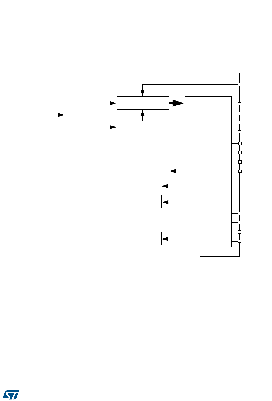
RM0394 Rev 4 635/1600
RM0394 Touch sensing controller (TSC)
652
23.3 TSC functional description
23.3.1 TSC block diagram
The block diagram of the touch sensing controller is shown in Figure 146: TSC block
diagram.
Figure 146. TSC block diagram
23.3.2 Surface charge transfer acquisition overview
The surface charge transfer acquisition is a proven, robust and efficient way to measure a
capacitance. It uses a minimum number of external components to operate with a single
ended electrode type. This acquisition is designed around an analog I/O group which is
composed of four GPIOs (see Figure 147). Several analog I/O groups are available to allow
the acquisition of several capacitive sensing channels simultaneously and to support a
larger number of capacitive sensing channels. Within a same analog I/O group, the
acquisition of the capacitive sensing channels is sequential.
One of the GPIOs is dedicated to the sampling capacitor CS. Only one sampling capacitor
I/O per analog I/O group must be enabled at a time.
-36
'?)/
'?)/
'?)/
'?)/
'?)/
'?)/
'?)/
'?)/
'X?)/
'X?)/
'X?)/
'X?)/
)/CONTROL
LOGIC
39.#
0ULSEGENERATOR
3PREADSPECTRUM
43#?)/'#2
43#?)/'#2
43#?)/'X#2
F(#,+ #LOCK
PRESCALERS
'ROUPCOUNTERS
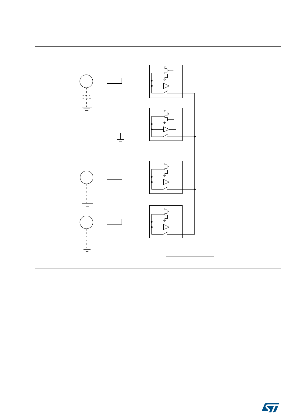
Touch sensing controller (TSC) RM0394
636/1600 RM0394 Rev 4
The remaining GPIOs are dedicated to the electrodes and are commonly called channels.
For some specific needs (such as proximity detection), it is possible to simultaneously
enable more than one channel per analog I/O group.
Figure 147. Surface charge transfer analog I/O group structure
Note: Gx_IOy where x is the analog I/O group number and y the GPIO number within the selected
group.
The surface charge transfer acquisition principle consists of charging an electrode
capacitance (CX) and transferring a part of the accumulated charge into a sampling
capacitor (CS). This sequence is repeated until the voltage across CS reaches a given
threshold (VIH in our case). The number of charge transfers required to reach the threshold
is a direct representation of the size of the electrode capacitance.
The Table 109 details the charge transfer acquisition sequence of the capacitive sensing
channel 1. States 3 to 7 are repeated until the voltage across CS reaches the given
threshold. The same sequence applies to the acquisition of the other channels. The
electrode serial resistor RS improves the ESD immunity of the solution.
-36
#8
'?)/
23
#8
'?)/
23
#8
'?)/
23
'?)/
#3
!NALOG
)/GROUP
%LECTRODE
%LECTRODE
%LECTRODE
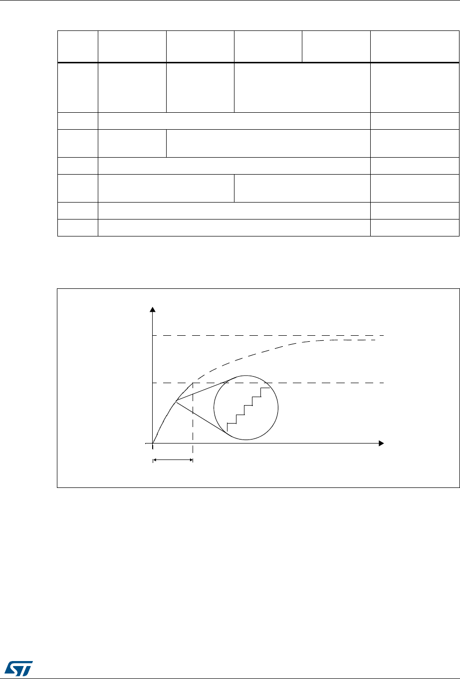
RM0394 Rev 4 637/1600
RM0394 Touch sensing controller (TSC)
652
The voltage variation over the time on the sampling capacitor CS is detailed below:
Figure 148. Sampling capacitor voltage variation
23.3.3 Reset and clocks
The TSC clock source is the AHB clock (HCLK). Two programmable prescalers are used to
generate the pulse generator and the spread spectrum internal clocks:
•The pulse generator clock (PGCLK) is defined using the PGPSC[2:0] bits of the
TSC_CR register
•The spread spectrum clock (SSCLK) is defined using the SSPSC bit of the TSC_CR
register
The Reset and Clock Controller (RCC) provides dedicated bits to enable the touch sensing
controller clock and to reset this peripheral. For more information, refer to Section 6: Reset
and clock control (RCC).
Table 109. Acquisition sequence summary
State G1_IO1
(channel)
G1_IO2
(sampling)
G1_IO3
(channel)
G1_IO4
(channel) State description
#1
Input floating
with analog
switch closed
Output open-
drain low with
analog switch
closed
Input floating with analog switch
closed
Discharge all CX and
CS
#2 Input floating Dead time
#3 Output push-
pull high Input floating Charge CX1
#4 Input floating Dead time
#5 Input floating with analog switch
closed Input floating Charge transfer from
CX1 to CS
#6 Input floating Dead time
#7 Input floating Measure CS voltage
069
W
9&6
7KUHVKROG 9,+
9''
%XUVWGXUDWLRQ
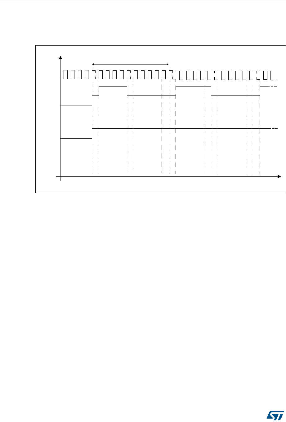
Touch sensing controller (TSC) RM0394
638/1600 RM0394 Rev 4
23.3.4 Charge transfer acquisition sequence
An example of a charge transfer acquisition sequence is detailed in Figure 149.
Figure 149. Charge transfer acquisition sequence
For higher flexibility, the charge transfer frequency is fully configurable. Both the pulse high
state (charge of CX) and the pulse low state (transfer of charge from CX to CS) duration can
be defined using the CTPH[3:0] and CTPL[3:0] bits in the TSC_CR register. The standard
range for the pulse high and low states duration is 500 ns to 2 µs. To ensure a correct
measurement of the electrode capacitance, the pulse high state duration must be set to
ensure that CX is always fully charged.
A dead time where both the sampling capacitor I/O and the channel I/O are in input floating
state is inserted between the pulse high and low states to ensure an optimum charge
transfer acquisition sequence. This state duration is 1 periods of HCLK.
At the end of the pulse high state and if the spread spectrum feature is enabled, a variable
number of periods of the SSCLK clock are added.
The reading of the sampling capacitor I/O, to determine if the voltage across CS has
reached the given threshold, is performed at the end of the pulse low state and its duration
is one period of HCLK.
Note: The following TSC control register configurations are forbidden:
•
bits PGPSC are set to ‘000’ and bits CTPL are set to ‘0000’
•
bits PGPSC are set to ‘000’ and bits CTPL are set to ‘0001’
•
bits PGPSC are set to ‘001’ and bits CTPL are set to ‘0000’
-36
#HARGETRANSFERFREQUENCY
$EADTIMESTATE
0ULSELOWSTATE
3PREAD3PECTRUMSTATE
CHARGETRANSFER
#3READINGSTATE
#8(I:
#3(I:
3TATE
#
,+?!("
T
$ISCHARGE
#8AND#3
0ULSEHIGHSTATE
CHARGEOF#8
FROM#8TO#3
$EADTIMESTATE
$EADTIMESTATE
$EADTIMESTATE
#3READINGSTATE
$EADTIMESTATE
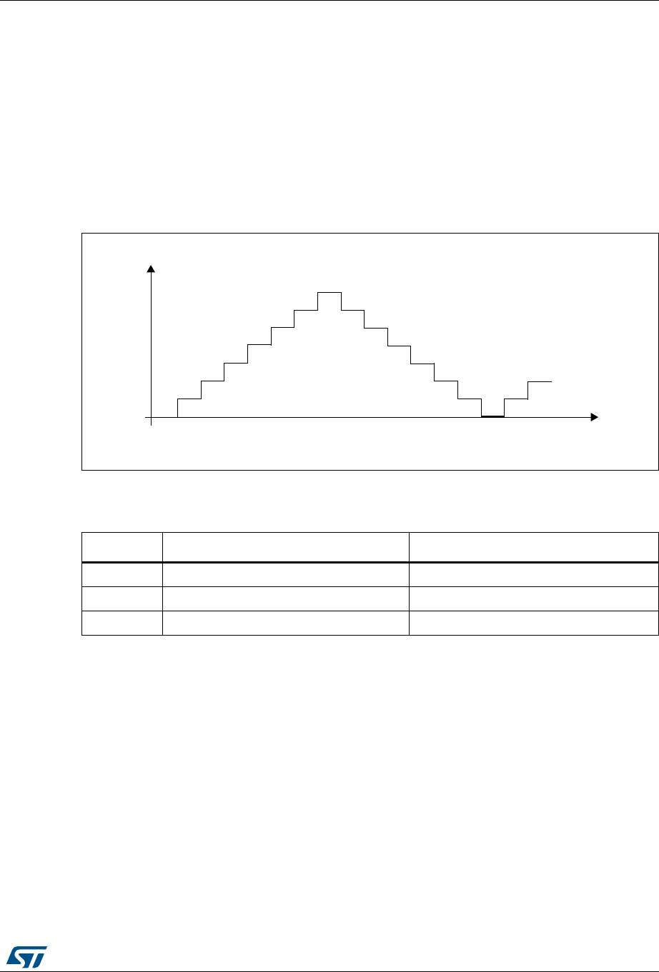
RM0394 Rev 4 639/1600
RM0394 Touch sensing controller (TSC)
652
23.3.5 Spread spectrum feature
The spread spectrum feature allows to generate a variation of the charge transfer
frequency. This is done to improve the robustness of the charge transfer acquisition in noisy
environments and also to reduce the induced emission. The maximum frequency variation
is in the range of 10% to 50% of the nominal charge transfer period. For instance, for a
nominal charge transfer frequency of 250 kHz (4 µs), the typical spread spectrum deviation
is 10% (400 ns) which leads to a minimum charge transfer frequency of ~227 kHz.
In practice, the spread spectrum consists of adding a variable number of SSCLK periods to
the pulse high state using the principle shown below:
Figure 150. Spread spectrum variation principle
The table below details the maximum frequency deviation with different HCLK settings:
The spread spectrum feature can be disabled/enabled using the SSE bit in the TSC_CR
register. The frequency deviation is also configurable to accommodate the device HCLK
clock frequency and the selected charge transfer frequency through the SSPSC and
SSD[6:0] bits in the TSC_CR register.
23.3.6 Max count error
The max count error prevents long acquisition times resulting from a faulty capacitive
sensing channel. It consists of specifying a maximum count value for the analog I/O group
counters. This maximum count value is specified using the MCV[2:0] bits in the TSC_CR
register. As soon as an acquisition group counter reaches this maximum value, the ongoing
acquisition is stopped and the end of acquisition (EOAF bit) and max count error (MCEF bit)
flags are both set. An interrupt can also be generated if the corresponding end of acquisition
(EOAIE bit) or/and max count error (MCEIE bit) interrupt enable bits are set.
Table 110. Spread spectrum deviation versus AHB clock frequency
fHCLK Spread spectrum step Maximum spread spectrum deviation
24 MHz 41.6 ns 10666.6 ns
48 MHz 20.8 ns 5333.3 ns
80 MHz 12.5 ns 3205.1 ns
-36
.UMBEROFPULSES
$EVIATIONVALUE
33$
N N
N

Touch sensing controller (TSC) RM0394
640/1600 RM0394 Rev 4
23.3.7 Sampling capacitor I/O and channel I/O mode selection
To allow the GPIOs to be controlled by the touch sensing controller, the corresponding
alternate function must be enabled through the standard GPIO registers and the GPIOxAFR
registers.
The GPIOs modes controlled by the TSC are defined using the TSC_IOSCR and
TSC_IOCCR register.
When there is no ongoing acquisition, all the I/Os controlled by the touch sensing controller
are in default state. While an acquisition is ongoing, only unused I/Os (neither defined as
sampling capacitor I/O nor as channel I/O) are in default state. The IODEF bit in the
TSC_CR register defines the configuration of the I/Os which are in default state. The table
below summarizes the configuration of the I/O depending on its mode.
Unused I/O mode
An unused I/O corresponds to a GPIO controlled by the TSC peripheral but not defined as
an electrode I/O nor as a sampling capacitor I/O.
Sampling capacitor I/O mode
To allow the control of the sampling capacitor I/O by the TSC peripheral, the corresponding
GPIO must be first set to alternate output open drain mode and then the corresponding
Gx_IOy bit in the TSC_IOSCR register must be set.
Only one sampling capacitor per analog I/O group must be enabled at a time.
Channel I/O mode
To allow the control of the channel I/O by the TSC peripheral, the corresponding GPIO must
be first set to alternate output push-pull mode and the corresponding Gx_IOy bit in the
TSC_IOCCR register must be set.
For proximity detection where a higher equivalent electrode surface is required or to speed-
up the acquisition process, it is possible to enable and simultaneously acquire several
channels belonging to the same analog I/O group.
Note: During the acquisition phase and even if the TSC peripheral alternate function is not
enabled, as soon as the TSC_IOSCR or TSC_IOCCR bit is set, the corresponding GPIO
analog switch is automatically controlled by the touch sensing controller.
Table 111. I/O state depending on its mode and IODEF bit value
IODEF bit Acquisition
status
Unused I/O
mode
Channel I/O
mode
Sampling
capacitor I/O
mode
0
(output push-pull low) No Output push-pull
low
Output push-pull
low
Output push-pull
low
0
(output push-pull low) Ongoing Output push-pull
low --
1
(input floating) No Input floating Input floating Input floating
1
(input floating) Ongoing Input floating - -

RM0394 Rev 4 641/1600
RM0394 Touch sensing controller (TSC)
652
23.3.8 Acquisition mode
The touch sensing controller offers two acquisition modes:
•Normal acquisition mode: the acquisition starts as soon as the START bit in the
TSC_CR register is set.
•Synchronized acquisition mode: the acquisition is enabled by setting the START bit in
the TSC_CR register but only starts upon the detection of a falling edge or a rising
edge and high level on the SYNC input pin. This mode is useful for synchronizing the
capacitive sensing channels acquisition with an external signal without additional CPU
load.
The GxE bits in the TSC_IOGCSR registers specify which analog I/O groups are enabled
(corresponding counter is counting). The CS voltage of a disabled analog I/O group is not
monitored and this group does not participate in the triggering of the end of acquisition flag.
However, if the disabled analog I/O group contains some channels, they will be pulsed.
When the CS voltage of an enabled analog I/O group reaches the given threshold, the
corresponding GxS bit of the TSC_IOGCSR register is set. When the acquisition of all
enabled analog I/O groups is complete (all GxS bits of all enabled analog I/O groups are
set), the EOAF flag in the TSC_ISR register is set. An interrupt request is generated if the
EOAIE bit in the TSC_IER register is set.
In the case that a max count error is detected, the ongoing acquisition is stopped and both
the EOAF and MCEF flags in the TSC_ISR register are set. Interrupt requests can be
generated for both events if the corresponding bits (EOAIE and MCEIE bits of the TSCIER
register) are set. Note that when the max count error is detected the remaining GxS bits in
the enabled analog I/O groups are not set.
To clear the interrupt flags, the corresponding EOAIC and MCEIC bits in the TSC_ICR
register must be set.
The analog I/O group counters are cleared when a new acquisition is started. They are
updated with the number of charge transfer cycles generated on the corresponding
channel(s) upon the completion of the acquisition.
23.3.9 I/O hysteresis and analog switch control
In order to offer a higher flexibility, the touch sensing controller also allows to take the control
of the Schmitt trigger hysteresis and analog switch of each Gx_IOy. This control is available
whatever the I/O control mode is (controlled by standard GPIO registers or other
peripherals) assuming that the touch sensing controller is enabled. This may be useful to
perform a different acquisition sequence or for other purposes.
In order to improve the system immunity, the Schmitt trigger hysteresis of the GPIOs
controlled by the TSC must be disabled by resetting the corresponding Gx_IOy bit in the
TSC_IOHCR register.
Touch sensing controller (TSC) RM0394
642/1600 RM0394 Rev 4
23.4 TSC low-power modes
23.5 TSC interrupts
Table 112. Effect of low-power modes on TSC
Mode Description
Sleep No effect. Peripheral interrupts cause the device to exit Sleep mode.
Low power run No effect.
Low power sleep No effect. Peripheral interrupts cause the device to exit Low-power sleep mode.
Stop 0 / Stop 1
Peripheral registers content is kept.
Stop 2
Standby Powered-down. The peripheral must be reinitialized after exiting Standby or
Shutdown mode.
Shutdown
Table 113. Interrupt control bits
Interrupt event Enable
control bit Event flag Clear flag
bit
Exit the
Sleep
mode
Exit the
Stop mode
Exit the
Standby
mode
End of acquisition EOAIE EOAIF EOAIC Yes No No
Max count error MCEIE MCEIF MCEIC Yes No No

RM0394 Rev 4 643/1600
RM0394 Touch sensing controller (TSC)
652
23.6 TSC registers
Refer to Section 1.2 on page 60 of the reference manual for a list of abbreviations used in
register descriptions.
The peripheral registers can be accessed by words (32-bit).
23.6.1 TSC control register (TSC_CR)
Address offset: 0x00
Reset value: 0x0000 0000
31 30 29 28 27 26 25 24 23 22 21 20 19 18 17 16
CTPH[3:0] CTPL[3:0] SSD[6:0] SSE
rw rw rw rw rw rw rw rw rw rw rw rw rw rw rw rw
1514131211109876543210
SSPSC PGPSC[2:0] Res. Res. Res. Res. MCV[2:0] IODEF SYNC
POL AM START TSCE
rw rw rw rw rw rw rw rw rw rw rw rw
Bits 31:28 CTPH[3:0]: Charge transfer pulse high
These bits are set and cleared by software. They define the duration of the high state of the
charge transfer pulse (charge of CX).
0000: 1x tPGCLK
0001: 2x tPGCLK
...
1111: 16x tPGCLK
Note: These bits must not be modified when an acquisition is ongoing.
Bits 27:24 CTPL[3:0]: Charge transfer pulse low
These bits are set and cleared by software. They define the duration of the low state of the
charge transfer pulse (transfer of charge from CX to CS).
0000: 1x tPGCLK
0001: 2x tPGCLK
...
1111: 16x tPGCLK
Note: These bits must not be modified when an acquisition is ongoing.
Note: Some configurations are forbidden. Refer to the Section 23.3.4: Charge transfer
acquisition sequence for details.
Bits 23:17 SSD[6:0]: Spread spectrum deviation
These bits are set and cleared by software. They define the spread spectrum deviation which
consists in adding a variable number of periods of the SSCLK clock to the charge transfer
pulse high state.
0000000: 1x tSSCLK
0000001: 2x tSSCLK
...
1111111: 128x tSSCLK
Note: These bits must not be modified when an acquisition is ongoing.

Touch sensing controller (TSC) RM0394
644/1600 RM0394 Rev 4
Bit 16 SSE: Spread spectrum enable
This bit is set and cleared by software to enable/disable the spread spectrum feature.
0: Spread spectrum disabled
1: Spread spectrum enabled
Note: This bit must not be modified when an acquisition is ongoing.
Bit 15 SSPSC: Spread spectrum prescaler
This bit is set and cleared by software. It selects the AHB clock divider used to generate the
spread spectrum clock (SSCLK).
0: fHCLK
1: fHCLK /2
Note: This bit must not be modified when an acquisition is ongoing.
Bits 14:12 PGPSC[2:0]: Pulse generator prescaler
These bits are set and cleared by software.They select the AHB clock divider used to
generate the pulse generator clock (PGCLK).
000: fHCLK
001: fHCLK /2
010: fHCLK /4
011: fHCLK /8
100: fHCLK /16
101: fHCLK /32
110: fHCLK /64
111: fHCLK /128
Note: These bits must not be modified when an acquisition is ongoing.
Note: Some configurations are forbidden. Refer to the Section 23.3.4: Charge transfer
acquisition sequence for details.
Bits 11:8 Reserved, must be kept at reset value.
Bits 7:5 MCV[2:0]: Max count value
These bits are set and cleared by software. They define the maximum number of charge
transfer pulses that can be generated before a max count error is generated.
000: 255
001: 511
010: 1023
011: 2047
100: 4095
101: 8191
110: 16383
111: reserved
Note: These bits must not be modified when an acquisition is ongoing.
Bit 4 IODEF: I/O Default mode
This bit is set and cleared by software. It defines the configuration of all the TSC I/Os when
there is no ongoing acquisition. When there is an ongoing acquisition, it defines the
configuration of all unused I/Os (not defined as sampling capacitor I/O or as channel I/O).
0: I/Os are forced to output push-pull low
1: I/Os are in input floating
Note: This bit must not be modified when an acquisition is ongoing.
Bit 3 SYNCPOL: Synchronization pin polarity
This bit is set and cleared by software to select the polarity of the synchronization input pin.
0: Falling edge only
1: Rising edge and high level

RM0394 Rev 4 645/1600
RM0394 Touch sensing controller (TSC)
652
23.6.2 TSC interrupt enable register (TSC_IER)
Address offset: 0x04
Reset value: 0x0000 0000
Bit 2 AM: Acquisition mode
This bit is set and cleared by software to select the acquisition mode.
0: Normal acquisition mode (acquisition starts as soon as START bit is set)
1: Synchronized acquisition mode (acquisition starts if START bit is set and when the
selected signal is detected on the SYNC input pin)
Note: This bit must not be modified when an acquisition is ongoing.
Bit 1 START: Start a new acquisition
This bit is set by software to start a new acquisition. It is cleared by hardware as soon as the
acquisition is complete or by software to cancel the ongoing acquisition.
0: Acquisition not started
1: Start a new acquisition
Bit 0 TSCE: Touch sensing controller enable
This bit is set and cleared by software to enable/disable the touch sensing controller.
0: Touch sensing controller disabled
1: Touch sensing controller enabled
Note: When the touch sensing controller is disabled, TSC registers settings have no effect.
31 30 29 28 27 26 25 24 23 22 21 20 19 18 17 16
Res. Res. Res. Res. Res. Res. Res. Res. Res. Res. Res. Res. Res. Res. Res. Res.
1514131211109876543210
Res. Res. Res. Res. Res. Res. Res. Res. Res. Res. Res. Res. Res. Res. MCEIE EOAIE
rw rw
Bits 31:2 Reserved, must be kept at reset value.
Bit 1 MCEIE: Max count error interrupt enable
This bit is set and cleared by software to enable/disable the max count error interrupt.
0: Max count error interrupt disabled
1: Max count error interrupt enabled
Bit 0 EOAIE: End of acquisition interrupt enable
This bit is set and cleared by software to enable/disable the end of acquisition interrupt.
0: End of acquisition interrupt disabled
1: End of acquisition interrupt enabled

Touch sensing controller (TSC) RM0394
646/1600 RM0394 Rev 4
23.6.3 TSC interrupt clear register (TSC_ICR)
Address offset: 0x08
Reset value: 0x0000 0000
31 30 29 28 27 26 25 24 23 22 21 20 19 18 17 16
Res. Res. Res. Res. Res. Res. Res. Res. Res. Res. Res. Res. Res. Res. Res. Res.
1514131211109876543210
Res. Res. Res. Res. Res. Res. Res. Res. Res. Res. Res. Res. Res. Res. MCEIC EOAIC
rw rw
Bits 31:2 Reserved, must be kept at reset value.
Bit 1 MCEIC: Max count error interrupt clear
This bit is set by software to clear the max count error flag and it is cleared by hardware
when the flag is reset. Writing a ‘0’ has no effect.
0: No effect
1: Clears the corresponding MCEF of the TSC_ISR register
Bit 0 EOAIC: End of acquisition interrupt clear
This bit is set by software to clear the end of acquisition flag and it is cleared by hardware
when the flag is reset. Writing a ‘0’ has no effect.
0: No effect
1: Clears the corresponding EOAF of the TSC_ISR register

RM0394 Rev 4 647/1600
RM0394 Touch sensing controller (TSC)
652
23.6.4 TSC interrupt status register (TSC_ISR)
Address offset: 0x0C
Reset value: 0x0000 0000
23.6.5 TSC I/O hysteresis control register (TSC_IOHCR)
Address offset: 0x10
Reset value: 0xFFFF FFFF
31 30 29 28 27 26 25 24 23 22 21 20 19 18 17 16
Res. Res. Res. Res. Res. Res. Res. Res. Res. Res. Res. Res. Res. Res. Res. Res.
1514131211109876543210
Res. Res. Res. Res. Res. Res. Res. Res. Res. Res. Res. Res. Res. Res. MCEF EOAF
rr
Bits 31:2 Reserved, must be kept at reset value.
Bit 1 MCEF: Max count error flag
This bit is set by hardware as soon as an analog I/O group counter reaches the max count
value specified. It is cleared by software writing 1 to the bit MCEIC of the TSC_ICR register.
0: No max count error (MCE) detected
1: Max count error (MCE) detected
Bit 0 EOAF: End of acquisition flag
This bit is set by hardware when the acquisition of all enabled group is complete (all GxS bits
of all enabled analog I/O groups are set or when a max count error is detected). It is cleared
by software writing 1 to the bit EOAIC of the TSC_ICR register.
0: Acquisition is ongoing or not started
1: Acquisition is complete
31 30 29 28 27 26 25 24 23 22 21 20 19 18 17 16
Res. Res. Res. Res. G7_IO4 G7_IO3 G7_IO2 G7_IO1 G6_IO4 G6_IO3 G6_IO2 G6_IO1 G5_IO4 G5_IO3 G5_IO2 G5_IO1
rw rw rw rw rw rw rw rw rw rw rw rw
1514131211109876543210
G4_IO4 G4_IO3 G4_IO2 G4_IO1 G3_IO4 G3_IO3 G3_IO2 G3_IO1 G2_IO4 G2_IO3 G2_IO2 G2_IO1 G1_IO4 G1_IO3 G1_IO2 G1_IO1
rw rw rw rw rw rw rw rw rw rw rw rw rw rw rw rw
Bits 31:28 Reserved, must be kept at reset value.
Bits 27:0 Gx_IOy: Gx_IOy Schmitt trigger hysteresis mode
These bits are set and cleared by software to enable/disable the Gx_IOy Schmitt trigger
hysteresis.
0: Gx_IOy Schmitt trigger hysteresis disabled
1: Gx_IOy Schmitt trigger hysteresis enabled
Note: These bits control the I/O Schmitt trigger hysteresis whatever the I/O control mode is
(even if controlled by standard GPIO registers).

Touch sensing controller (TSC) RM0394
648/1600 RM0394 Rev 4
23.6.6 TSC I/O analog switch control register (TSC_IOASCR)
Address offset: 0x18
Reset value: 0x0000 0000
23.6.7 TSC I/O sampling control register (TSC_IOSCR)
Address offset: 0x20
Reset value: 0x0000 0000
31 30 29 28 27 26 25 24 23 22 21 20 19 18 17 16
Res. Res. Res. Res. G7_IO4 G7_IO3 G7_IO2 G7_IO1 G6_IO4 G6_IO3 G6_IO2 G6_IO1 G5_IO4 G5_IO3 G5_IO2 G5_IO1
rw rw rw rw rw rw rw rw rw rw rw rw
1514131211109876543210
G4_IO4 G4_IO3 G4_IO2 G4_IO1 G3_IO4 G3_IO3 G3_IO2 G3_IO1 G2_IO4 G2_IO3 G2_IO2 G2_IO1 G1_IO4 G1_IO3 G1_IO2 G1_IO1
rw rw rw rw rw rw rw rw rw rw rw rw rw rw rw rw
Bits 31:28 Reserved, must be kept at reset value.
Bits 27:0 Gx_IOy: Gx_IOy analog switch enable
These bits are set and cleared by software to enable/disable the Gx_IOy analog switch.
0: Gx_IOy analog switch disabled (opened)
1: Gx_IOy analog switch enabled (closed)
Note: These bits control the I/O analog switch whatever the I/O control mode is (even if
controlled by standard GPIO registers).
31 30 29 28 27 26 25 24 23 22 21 20 19 18 17 16
Res. Res. Res. Res. G7_IO4 G7_IO3 G7_IO2 G7_IO1 G6_IO4 G6_IO3 G6_IO2 G6_IO1 G5_IO4 G5_IO3 G5_IO2 G5_IO1
rw rw rw rw rw rw rw rw rw rw rw rw
1514131211109876543210
G4_IO4 G4_IO3 G4_IO2 G4_IO1 G3_IO4 G3_IO3 G3_IO2 G3_IO1 G2_IO4 G2_IO3 G2_IO2 G2_IO1 G1_IO4 G1_IO3 G1_IO2 G1_IO1
rw rw rw rw rw rw rw rw rw rw rw rw rw rw rw rw
Bits 31:28 Reserved, must be kept at reset value.
Bits 27:0 Gx_IOy: Gx_IOy sampling mode
These bits are set and cleared by software to configure the Gx_IOy as a sampling capacitor
I/O. Only one I/O per analog I/O group must be defined as sampling capacitor.
0: Gx_IOy unused
1: Gx_IOy used as sampling capacitor
Note: These bits must not be modified when an acquisition is ongoing.
During the acquisition phase and even if the TSC peripheral alternate function is not
enabled, as soon as the TSC_IOSCR bit is set, the corresponding GPIO analog switch
is automatically controlled by the touch sensing controller.

RM0394 Rev 4 649/1600
RM0394 Touch sensing controller (TSC)
652
23.6.8 TSC I/O channel control register (TSC_IOCCR)
Address offset: 0x28
Reset value: 0x0000 0000
23.6.9 TSC I/O group control status register (TSC_IOGCSR)
Address offset: 0x30
Reset value: 0x0000 0000
31 30 29 28 27 26 25 24 23 22 21 20 19 18 17 16
Res. Res. Res. Res. G7_IO4 G7_IO3 G7_IO2 G7_IO1 G6_IO4 G6_IO3 G6_IO2 G6_IO1 G5_IO4 G5_IO3 G5_IO2 G5_IO1
rw rw rw rw rw rw rw rw rw rw rw rw
1514131211109876543210
G4_IO4 G4_IO3 G4_IO2 G4_IO1 G3_IO4 G3_IO3 G3_IO2 G3_IO1 G2_IO4 G2_IO3 G2_IO2 G2_IO1 G1_IO4 G1_IO3 G1_IO2 G1_IO1
rw rw rw rw rw rw rw rw rw rw rw rw rw rw rw rw
Bits 31:28 Reserved, must be kept at reset value.
Bits 27:0 Gx_IOy: Gx_IOy channel mode
These bits are set and cleared by software to configure the Gx_IOy as a channel I/O.
0: Gx_IOy unused
1: Gx_IOy used as channel
Note: These bits must not be modified when an acquisition is ongoing.
During the acquisition phase and even if the TSC peripheral alternate function is not
enabled, as soon as the TSC_IOCCR bit is set, the corresponding GPIO analog switch
is automatically controlled by the touch sensing controller.
31 30 29 28 27 26 25 24 23 22 21 20 19 18 17 16
Res. Res. Res. Res. Res. Res. Res. Res. Res. G7S G6S G5S G4S G3S G2S G1S
rrrrrrr
1514131211109876543210
Res. Res. Res. Res. Res. Res. Res. Res. Res. G7E G6E G5E G4E G3E G2E G1E
rw rw rw rw rw rw rw
Bits 31:23 Reserved, must be kept at reset value.
Bits 22:16 GxS: Analog I/O group x status
These bits are set by hardware when the acquisition on the corresponding enabled analog
I/O group x is complete. They are cleared by hardware when a new acquisition is started.
0: Acquisition on analog I/O group x is ongoing or not started
1: Acquisition on analog I/O group x is complete
Note: When a max count error is detected the remaining GxS bits of the enabled analog I/O
groups are not set.
Bits 15:7 Reserved, must be kept at reset value.
Bits 6:0 GxE: Analog I/O group x enable
These bits are set and cleared by software to enable/disable the acquisition (counter is
counting) on the corresponding analog I/O group x.
0: Acquisition on analog I/O group x disabled
1: Acquisition on analog I/O group x enabled

Touch sensing controller (TSC) RM0394
650/1600 RM0394 Rev 4
23.6.10 TSC I/O group x counter register (TSC_IOGxCR)
x represents the analog I/O group number.
Address offset: 0x30 + 0x04 * x, (x = 1..7)
Reset value: 0x0000 0000
31 30 29 28 27 26 25 24 23 22 21 20 19 18 17 16
Res. Res. Res. Res. Res. Res. Res. Res. Res. Res. Res. Res. Res. Res. Res. Res.
1514131211109876543210
Res. Res. CNT[13:0]
rrrrrrrrrrrrrr
Bits 31:14 Reserved, must be kept at reset value.
Bits 13:0 CNT[13:0]: Counter value
These bits represent the number of charge transfer cycles generated on the analog I/O
group x to complete its acquisition (voltage across CS has reached the threshold).

RM0394 Rev 4 651/1600
RM0394 Touch sensing controller (TSC)
652
23.6.11 TSC register map
Table 114. TSC register map and reset values
Offset Register
31
30
29
28
27
26
25
24
23
22
21
20
19
18
17
16
15
14
13
12
11
10
9
8
7
6
5
4
3
2
1
0
0x0000
TSC_CR CTPH[3:0] CTPL[3:0] SSD[6:0]
SSE
SSPSC
PGPSC[2:0]
Res.
Res.
Res.
Res.
MCV
[2:0]
IODEF
SYNCPOL
AM
START
TSCE
Reset value 00000000000000000000 00000000
0x0004
TSC_IER
Res.
Res.
Res.
Res.
Res.
Res.
Res.
Res.
Res.
Res.
Res.
Res.
Res.
Res.
Res.
Res.
Res.
Res.
Res.
Res.
Res.
Res.
Res.
Res.
Res.
Res.
Res.
Res.
Res.
Res.
MCEIE
EOAIE
Reset value 00
0x0008
TSC_ICR
Res.
Res.
Res.
Res.
Res.
Res.
Res.
Res.
Res.
Res.
Res.
Res.
Res.
Res.
Res.
Res.
Res.
Res.
Res.
Res.
Res.
Res.
Res.
Res.
Res.
Res.
Res.
Res.
Res.
Res.
MCEIC
EOAIC
Reset value 00
0x000C
TSC_ISR
Res.
Res.
Res.
Res.
Res.
Res.
Res.
Res.
Res.
Res.
Res.
Res.
Res.
Res.
Res.
Res.
Res.
Res.
Res.
Res.
Res.
Res.
Res.
Res.
Res.
Res.
Res.
Res.
Res.
Res.
MCEF
EOAF
Reset value 00
0x0010
TSC_IOHCR
Res.
Res.
Res.
Res.
G7_IO4
G7_IO3
G7_IO2
G7_IO1
G6_IO4
G6_IO3
G6_IO2
G6_IO1
G5_IO4
G5_IO3
G5_IO2
G5_IO1
G4_IO4
G4_IO3
G4_IO2
G4_IO1
G3_IO4
G3_IO3
G3_IO2
G3_IO1
G2_IO4
G2_IO3
G2_IO2
G2_IO1
G1_IO4
G1_IO3
G1_IO2
G1_IO1
Reset value 1111111111111111111111111111
0x0014 Reserved
0x0018
TSC_IOASCR
Res.
Res.
Res.
Res.
G7_IO4
G7_IO3
G7_IO2
G7_IO1
G6_IO4
G6_IO3
G6_IO2
G6_IO1
G5_IO4
G5_IO3
G5_IO2
G5_IO1
G4_IO4
G4_IO3
G4_IO2
G4_IO1
G3_IO4
G3_IO3
G3_IO2
G3_IO1
G2_IO4
G2_IO3
G2_IO2
G2_IO1
G1_IO4
G1_IO3
G1_IO2
G1_IO1
Reset value 0000000000000000000000000000
0x001C Reserved
0x0020
TSC_IOSCR
Res.
Res.
Res.
Res.
G7_IO4
G7_IO3
G7_IO2
G7_IO1
G6_IO4
G6_IO3
G6_IO2
G6_IO1
G5_IO4
G5_IO3
G5_IO2
G5_IO1
G4_IO4
G4_IO3
G4_IO2
G4_IO1
G3_IO4
G3_IO3
G3_IO2
G3_IO1
G2_IO4
G2_IO3
G2_IO2
G2_IO1
G1_IO4
G1_IO3
G1_IO2
G1_IO1
Reset value 0000000000000000000000000000
0x0024 Reserved
0x0028
TSC_IOCCR
Res.
Res.
Res.
Res.
G7_IO4
G7_IO3
G7_IO2
G7_IO1
G6_IO4
G6_IO3
G6_IO2
G6_IO1
G5_IO4
G5_IO3
G5_IO2
G5_IO1
G4_IO4
G4_IO3
G4_IO2
G4_IO1
G3_IO4
G3_IO3
G3_IO2
G3_IO1
G2_IO4
G2_IO3
G2_IO2
G2_IO1
G1_IO4
G1_IO3
G1_IO2
G1_IO1
Reset value 0000000000000000000000000000
0x002C Reserved
0x0030
TSC_IOGCSR
Res.
Res.
Res.
Res.
Res.
Res.
Res.
Res.
Res.
G7S
G6S
G5S
G4S
G3S
G2S
G1S
Res.
Res.
Res.
Res.
Res.
Res.
Res.
Res.
Res.
G7E
G6E
G5E
G4E
G3E
G2E
G1E
Reset value 0000000 0000000
0x0034
TSC_IOG1CR
Res.
Res.
Res.
Res.
Res.
Res.
Res.
Res.
Res.
Res.
Res.
Res.
Res.
Res.
Res.
Res.
Res.
Res.
CNT[13:0]
Reset value 00000000000000
0x0038
TSC_IOG2CR
Res.
Res.
Res.
Res.
Res.
Res.
Res.
Res.
Res.
Res.
Res.
Res.
Res.
Res.
Res.
Res.
Res.
Res.
CNT[13:0]
Reset value 00000000000000
Touch sensing controller (TSC) RM0394
652/1600 RM0394 Rev 4
Refer to Section 2.2.2 on page 67 for the register boundary addresses.
0x003C
TSC_IOG3CR
Res.
Res.
Res.
Res.
Res.
Res.
Res.
Res.
Res.
Res.
Res.
Res.
Res.
Res.
Res.
Res.
Res.
Res.
CNT[13:0]
Reset value 00000000000000
0x0040
TSC_IOG4CR
Res.
Res.
Res.
Res.
Res.
Res.
Res.
Res.
Res.
Res.
Res.
Res.
Res.
Res.
Res.
Res.
Res.
Res.
CNT[13:0]
Reset value 00000000000000
0x0044
TSC_IOG5CR
Res.
Res.
Res.
Res.
Res.
Res.
Res.
Res.
Res.
Res.
Res.
Res.
Res.
Res.
Res.
Res.
Res.
Res.
CNT[13:0]
Reset value 00000000000000
0x0048
TSC_IOG6CR
Res.
Res.
Res.
Res.
Res.
Res.
Res.
Res.
Res.
Res.
Res.
Res.
Res.
Res.
Res.
Res.
Res.
Res.
CNT[13:0]
Reset value 00000000000000
0x004C
TSC_IOG7CR
Res.
Res.
Res.
Res.
Res.
Res.
Res.
Res.
Res.
Res.
Res.
Res.
Res.
Res.
Res.
Res.
Res.
Res.
CNT[13:0]
Reset value 00000000000000
Table 114. TSC register map and reset values (continued)
Offset Register
31
30
29
28
27
26
25
24
23
22
21
20
19
18
17
16
15
14
13
12
11
10
9
8
7
6
5
4
3
2
1
0

RM0394 Rev 4 653/1600
RM0394 True random number generator (RNG)
664
24 True random number generator (RNG)
24.1 Introduction
The RNG is a true random number generator that continuously provides 32-bit entropy
samples, based on an analog noise source. It can be used by the application as a live
entropy source to build a NIST compliant Deterministic Random Bit Generator (DRBG).
The RNG true random number generator has been tested using NIST statistical test suite
SP800 rev1a (April 2010).
24.2 RNG main features
•The RNG delivers 32-bit true random numbers, produced by an analog entropy source
post-processed with linear-feedback shift registers (LFSR).
•It produces one 32-bit random samples every 42 RNG clock cycles (dedicated clock).
•It allows embedded continuous basic health tests with associated error management
– Includes too low sampling clock detection and repetition count tests.
•It can be disabled to reduce power consumption.
•It has an AMBA AHB slave peripheral, accessible through 32-bit word single accesses
only (else an AHB bus error is generated). Warning! any write not equal to 32 bits might
corrupt the register content.
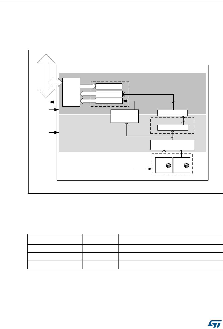
True random number generator (RNG) RM0394
654/1600 RM0394 Rev 4
24.3 RNG functional description
24.3.1 RNG block diagram
Figure 151 shows the RNG block diagram.
Figure 151. RNG block diagram
24.3.2 RNG internal signals
Table 115 describes a list of useful-to-know internal signals available at the RNG level, not
at the STM32 product level (on pads).
06Y9
751*Y
51*B65
$+%
LQWHUIDFH
VWDWXV
51*B&5
$QDORJ
QRLVH
VRXUFH
%DQNHG5HJLVWHUV
6DPSOLQJ
1RUPDOL]DWLRQ[
$QDORJQRLVHVRXUFH
ELW
$QDORJ
QRLVH
VRXUFH
HQBRVF
ELW$+%%XV
UQJBLW
UQJBKFON
UQJBFON
$+%FORFNGRPDLQ
51*FORFNGRPDLQ
'DWDVKLIWUHJ
ELW
ELW/)65[
3RVWSURFHVVLQJORJLF ELW
)DXOWGHWHFWLRQ
&ORFNFKHFNHU
$ODUPV
51*B'5
GDWD
FRQWURO
Table 115. RNG internal input/output signals
Signal name Signal type Description
rng_it Digital output RNG global interrupt request
rng_hclk Digital input AHB clock
rng_clk Digital input RNG dedicated clock, asynchronous to rng_hclk
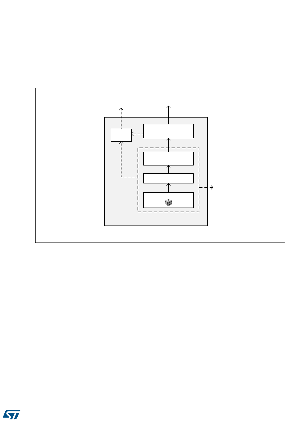
RM0394 Rev 4 655/1600
RM0394 True random number generator (RNG)
664
24.3.3 Random number generation
The true random number generator (RNG) delivers truly random data through its AHB
interface at deterministic intervals. The RNG implements the entropy source model pictured
on Figure 152, and provides three main functions to the application:
•Collects the bitstring output of the entropy source box
•Obtains samples of the noise source for validation purpose
•Collects error messages from continuous health tests
Figure 152. Entropy source model
The main components of the RNG are:
•A source of physical randomness (analog noise source)
•A digitization stage for this analog noise source
•A stage delivering post-processed noise source (raw data)
•An output buffer for the raw data. If further cryptographic conditioning is required by the
application it will need to be performed by software.
•An optional output for the digitized noise source (unbuffered, on digital pads)
•Basic health tests on the digitized noise source
All those components are detailed below.
Noise source
The noise source is the component that contains the non-deterministic, entropy-providing
activity that is ultimately responsible for the uncertainty associated with the bitstring output
by the entropy source. It is composed of:
•Two analog noise sources, each based on three XORed free-running ring oscillator
outputs. It is possible to disable those analog oscillators to save power, as described in
06Y9
(QWURS\VRXUFH
1RLVH6RXUFH
'LJLWL]DWLRQ
3RVWSURFHVVLQJ
RSWLRQDO
5DZGDWD
&RQGLWLRQLQJ
RSWLRQDO
+HDWK
WHVWV
2XWSXW
(UURU
PHVVDJH
2XWSXW
UDZGDWDRU
GLJLWL]HGQRLVH
VRXUFH

True random number generator (RNG) RM0394
656/1600 RM0394 Rev 4
Section 24.4: RNG low-power usage.
•A sampling stage of these outputs clocked by a dedicated clock input (rng_clk),
delivering a 2-bit raw data output.
This noise source sampling is independent to the AHB interface clock frequency (rng_hclk).
Note: In Section 24.7: Entropy source validation recommended RNG clock frequencies are given.
Post processing
The sample values obtained from a true random noise source consist of 2-bit bitstrings.
Because this noise source output is biased, the RNG implements a post-processing
component that reduces that bias to a tolerable level.
The RNG post-processing consists of two stages, applied to each noise source bits:
•The RNG takes half of the bits from the sampled noise source, and half of the bits from
inverted sampled noise source. Thus, if the source generates more ‘1’ than ‘0’ (or the
opposite), it is filtered
•A linear feedback shift register (LFSR) performs a whitening process, producing 8-bit
strings.
This component is clocked by the RNG clock.
The times required between two random number generations, and between the RNG
initialization and availability of first sample are described in Section 24.6: RNG processing
time.
Output buffer
The RNG_DR data output register can store up to two 16-bit words which have been output
from the post-processing component (LFSR). In order to read back 32-bit random samples it
is required to wait 42 RNG clock cycles.
Whenever a random number is available through the RNG_DR register the DRDY flag
transitions from “0” to “1”. This flag remains high until output buffer becomes empty after
reading one word from the RNG_DR register.
Note: When interrupts are enabled an interrupt is generated when this data ready flag transitions
from “0” to “1”. Interrupt is then cleared automatically by the RNG as explained above.

RM0394 Rev 4 657/1600
RM0394 True random number generator (RNG)
664
Health checks
This component ensures that the entire entropy source (with its noise source) starts then
operates as expected, obtaining assurance that failures are caught quickly and with a high
probability and reliability.
The RNG implements the following health check features:
3. Continuous health tests, running indefinitely on the outputs of the noise source
– Repetition count test, flagging an error when:
a) One of the noise source has provided more than 64 consecutive bits at a constant
value (“0” or “1”)
b) One of the noise sources has delivered more than 32 consecutive occurrence of
two bits patterns (“01” or “10”)
4. Vendor specific continuous test
– Real-time “too slow” sampling clock detector, flagging an error when one RNG
clock cycle is smaller than AHB clock cycle divided by 16.
The CECS and SECS status bits in the RNG_SR register indicate when an error condition is
detected, as detailed in Section 24.3.7: Error management.
Note: An interrupt can be generated when an error is detected.
24.3.4 RNG initialization
When a hardware reset occurs the following chain of events occurs:
1. The analog noise source is enabled, and logic starts sampling the analog output after
four RNG clock cycles, filling LFSR shift register and associated 16-bit post-processing
shift register.
2. The output buffer is refilled automatically according to the RNG usage.
The associated initialization time can be found in Section 24.6: RNG processing time.
24.3.5 RNG operation
Normal operations
To run the RNG using interrupts the following steps are recommended:
1. Enable the interrupts by setting the IE bit in the RNG_CR register. At the same time
enable the RNG by setting the bit RNGEN=1.
2. An interrupt is now generated when a random number is ready or when an error
occurs. Therefore at each interrupt, check that:
– No error occurred. The SEIS and CEIS bits should be set to ‘0’ in the RNG_SR
register.
– A random number is ready. The DRDY bit must be set to ‘1’ in the RNG_SR
register.
– If above two conditions are true the content of the RNG_DR register can be read.

True random number generator (RNG) RM0394
658/1600 RM0394 Rev 4
To run the RNG in polling mode following steps are recommended:
1. Enable the random number generation by setting the RNGEN bit to “1” in the RNG_CR
register.
2. Read the RNG_SR register and check that:
– No error occurred (the SEIS and CEIS bits should be set to ‘0’)
– A random number is ready (the DRDY bit should be set to ‘1’)
3. If above conditions are true read the content of the RNG_DR register.
Note: When data is not ready (DRDY=”0”) RNG_DR returns zero.
Low-power operations
If the power consumption is a concern to the application, low-power strategies can be used,
as described in Section 24.4: RNG low-power usage on page 659.
Software post-processing
If a NIST approved DRBG with 128 bits of security strength is required an approved random
generator software must be built around the RNG true random number generator.
24.3.6 RNG clocking
The RNG runs on two different clocks: the AHB bus clock and a dedicated RNG clock.
The AHB clock is used to clock the AHB banked registers and the post-processing
component. The RNG clock is used for noise source sampling. Recommended clock
configurations are detailed in Section 24.7: Entropy source validation.
Caution: When the CED bit in the RNG_CR register is set to “0”, the RNG clock frequency must be
higher than AHB clock frequency divided by 16, otherwise the clock checker will flag a clock
error (CECS or CEIS in the RNG_SR register) and the RNG will stop producing random
numbers.
See Section 24.3.1: RNG block diagram for details (AHB and RNG clock domains).
24.3.7 Error management
In parallel to random number generation an health check block verifies the correct noise
source behavior and the frequency of the RNG source clock as detailed in this section.
Associated error state is also described.
Clock error detection
When the clock error detection is enabled (CED = 0) and if the RNG clock frequency is too
low, the RNG stops generating random numbers and sets to “1” both the CEIS and CECS
bits to indicate that a clock error occurred. In this case, the application should check that the
RNG clock is configured correctly (see Section 24.3.6: RNG clocking) and then it must clear
the CEIS bit interrupt flag. As soon as the RNG clock operates correctly, the CECS bit will
be automatically cleared.
The RNG operates only when the CECS flag is set to “0”. However note that the clock error
has no impact on the previously generated random numbers, and the RNG_DR register
contents can still be used.
RM0394 Rev 4 659/1600
RM0394 True random number generator (RNG)
664
Noise source error detection
When a noise source (or seed) error occurs, the RNG stops generating random numbers
and sets to “1” both SEIS and SECS bits to indicate that a seed error occurred. If a value is
available in the RNG_DR register, it must not be used as it may not have enough entropy.
In order to fully recover from a seed error application must clear the SEIS bit by writing it to
“0”, then clear and set the RNGEN bit to reinitialize and restart the RNG.
24.4 RNG low-power usage
If power consumption is a concern, the RNG can be disabled as soon as the DRDY bit is set
to “1” by setting the RNGEN bit to “0” in the RNG_CR register. The 32-bit random value
stored in the RNG_DR register will be still be available. If a new random is needed the
application will need to re-enable the RNG and wait for 42+4 RNG clock cycles.
When disabling the RNG the user deactivates all the analog seed generators, whose power
consumption is given in the datasheet electrical characteristics section.
24.5 RNG interrupts
In the RNG an interrupt can be produced on the following events:
•Data ready flag
•Seed error, see Section 24.3.7: Error management
•Clock error, see Section 24.3.7: Error management
Dedicated interrupt enable control bits are available as shown in Table 116
The user can enable or disable the above interrupt sources individually by changing the
mask bits or the general interrupt control bit IE in the RNG_CR register. The status of the
individual interrupt sources can be read from the RNG_SR register.
Note: Interrupts are generated only when RNG is enabled.
24.6 RNG processing time
The RNG can produce one 32-bit random numbers every 42 RNG clock cycles.
After enabling or re-enabling the RNG using the RNGEN bit it takes 46 RNG clock cycles
before random data are available.
Table 116. RNG interrupt requests
Interrupt event Event flag Enable control bit
Data ready flag DRDY IE
Seed error flag SEIS IE
Clock error flag CEIS IE

True random number generator (RNG) RM0394
660/1600 RM0394 Rev 4
24.7 Entropy source validation
24.7.1 Introduction
In order to assess the amount of entropy available from the RNG, STMicroelectronics has
tested the peripheral using NIST SP800-22 rev1a statistical tests.
For more information on running this NIST statistical test suite, refer to STM32
microcontrollers random number generation validation using NIST statistical test suite
application note (AN4230), available on STMicroelectronics website.
24.7.2 Validation conditions
STMicroelectronics has tested the RNG true random number generator in the following
conditions:
•RNG clock rng_clk= 48 MHz (CED bit = ‘0’ in RNG_CR register) and rng_clk= 400kHz
(CED bit=”1” in RNG_CR register)

RM0394 Rev 4 661/1600
RM0394 True random number generator (RNG)
664
24.8 RNG registers
The RNG is associated with a control register, a data register and a status register.
24.8.1 RNG control register (RNG_CR)
Address offset: 0x000
Reset value: 0x0000 0000
31 30 29 28 27 26 25 24 23 22 21 20 19 18 17 16
Res. Res. Res. Res. Res. Res. Res. Res. Res. Res. Res. Res. Res. Res. Res. Res.
15 14 13 12 11 10 9 8 7 6 5 4 3 2 1 0
Res. Res. Res. Res. Res. Res. Res. Res. Res. Res. CED Res. IE RNGEN Res. Res.
rw rw rw
Bits 31:6 Reserved, must be kept at reset value
Bit 5 CED: Clock error detection
0: Clock error detection is enable
1: Clock error detection is disable
The clock error detection cannot be enabled nor disabled on-the-fly when the RNG is
enabled, i.e. to enable or disable CED the RNG must be disabled.
Bit 4 Reserved, must be kept at reset value.
Bit 3 IE: Interrupt Enable
0: RNG Interrupt is disabled
1: RNG Interrupt is enabled. An interrupt is pending as soon as DRDY=’1’, SEIS=’1’ or
CEIS=’1’ in the RNG_SR register.
Bit 2 RNGEN: True random number generator enable
0: True random number generator is disabled. Analog noise sources are powered off and
logic clocked by the RNG clock is gated.
1: True random number generator is enabled.
Bits 1:0 Reserved, must be kept at reset value.

True random number generator (RNG) RM0394
662/1600 RM0394 Rev 4
24.8.2 RNG status register (RNG_SR)
Address offset: 0x004
Reset value: 0x0000 0000
31 30 29 28 27 26 25 24 23 22 21 20 19 18 17 16
Res. Res. Res. Res. Res. Res. Res. Res. Res. Res. Res. Res. Res. Res. Res. Res.
1514131211109876543210
Res. Res. Res. Res. Res. Res. Res. Res. Res. SEIS CEIS Res. Res. SECS CECS DRDY
rc_w0 rc_w0 r r r
Bits 31:7 Reserved, must be kept at reset value.
Bit 6 SEIS: Seed error interrupt status
This bit is set at the same time as SECS. It is cleared by writing it to ‘0’.
0: No faulty sequence detected
1: At least one faulty sequence has been detected. See SECS bit description for details.
An interrupt is pending if IE = ‘1’ in the RNG_CR register.
Bit 5 CEIS: Clock error interrupt status
This bit is set at the same time as CECS. It is cleared by writing it to ‘0’.
0: The RNG clock is correct (fRNGCLK > fHCLK/16)
1: The RNG has been detected too slow (fRNGCLK < fHCLK/16)
An interrupt is pending if IE = ‘1’ in the RNG_CR register.
Bits 4:3 Reserved, must be kept at reset value.
Bit 2 SECS: Seed error current status
0: No faulty sequence has currently been detected. If the SEIS bit is set, this means that a
faulty sequence was detected and the situation has been recovered.
1: One of the noise source has provided more than 64 consecutive bits at a constant value
(“0” or “1”), or more than 32 consecutive occurrence of two bits patterns (“01” or “10”)
Bit 1 CECS: Clock error current status
0: The RNG clock is correct (fRNGCLK> fHCLK/16). If the CEIS bit is set, this means that a
slow clock was detected and the situation has been recovered.
1: The RNG clock is too slow (fRNGCLK< fHCLK/16).
Note: CECS bit is valid only if the CED bit in the RNG_CR register is set to “0”.
Bit 0 DRDY: Data Ready
0: The RNG_DR register is not yet valid, no random data is available.
1: The RNG_DR register contains valid random data.
Once the RNG_DR register has been read, this bit returns to ‘0’ until a new random value is
generated.
If IE=’1’ in the RNG_CR register, an interrupt is generated when DRDY=’1’.

RM0394 Rev 4 663/1600
RM0394 True random number generator (RNG)
664
24.8.3 RNG data register (RNG_DR)
Address offset: 0x008
Reset value: 0x0000 0000
The RNG_DR register is a read-only register that delivers a 32-bit random value when read.
After being read this register delivers a new random value after 42 periods of RNG clock if
the output FIFO is empty.
The content of this register is valid when DRDY=’1’, even if RNGEN=’0’.
31 30 29 28 27 26 25 24 23 22 21 20 19 18 17 16
RNDATA[31:16]
rrrrrrrrrrrrrrrr
1514131211109876543210
RNDATA[15:0]
rrrrrrrrrrrrrrrr
Bits 31:0 RNDATA[31:0]: Random data
32-bit random data which are valid when DRDY=’1’. When DRDY=’0’ RNDATA value is zero.

True random number generator (RNG) RM0394
664/1600 RM0394 Rev 4
24.8.4 RNG register map
Table 117 gives the RNG register map and reset values.
Table 117. RNG register map and reset map
Offset Register name
31
30
29
28
27
26
25
24
23
22
21
20
19
18
17
16
15
14
13
12
11
10
9
8
7
6
5
4
3
2
1
0
0x000 RNG_CR
Res.
Res.
Res.
Res.
Res.
Res.
Res.
Res.
Res.
Res.
Res.
Res.
Res.
Res.
Res.
Res.
Res.
Res.
Res.
Res.
Res.
Res.
Res.
Res.
Res.
Res.
CED
Res.
IE
RNGEN
Res.
Res.
Reset value 000
0x004 RNG_SR
Res.
Res.
Res.
Res.
Res.
Res.
Res.
Res.
Res.
Res.
Res.
Res.
Res.
Res.
Res.
Res.
Res.
Res.
Res.
Res.
Res.
Res.
Res.
Res.
Res.
SEIS
CEIS
Res.
Res.
SECS
CECS
DRDY
Reset value 00 000
0x008 RNG_DR RNDATA[31:0]
Reset value 00000000000000000000000000000000

RM0394 Rev 4 665/1600
RM0394 AES hardware accelerator (AES)
717
25 AES hardware accelerator (AES)
This section applies to STM32L42xxx, STM32L44xxx and STM32L46xxx devices only.
25.1 Introduction
The AES hardware accelerator (AES) encrypts or decrypts data, using an algorithm and
implementation fully compliant with the advanced encryption standard (AES) defined in
Federal information processing standards (FIPS) publication 197.
Multiple chaining modes are supported (ECB, CBC, CTR, GCM, GMAC, CCM), for key
sizes of 128 or 256 bits.
The AES accelerator is a 32-bit AHB peripheral. It supports DMA single transfers for
incoming and outgoing data (two DMA channels required).
The AES peripheral provides hardware acceleration to AES cryptographic algorithms
packaged in STM32 cryptographic library.
AES is an AMBA AHB slave peripheral, accessible through 32-bit word single accesses only
(otherwise an AHB bus error is generated and write accesses are ignored).
25.2 AES main features
•Compliance with NIST “Advanced encryption standard (AES), FIPS publication 197”
from November 2001
•128-bit data block processing
•Support for cipher key lengths of 128-bit and 256-bit
•Encryption and decryption with multiple chaining modes:
– Electronic codebook (ECB) mode
– Cipher block chaining (CBC) mode
– Counter (CTR) mode
– Galois counter mode (GCM)
– Galois message authentication code (GMAC) mode
– Counter with CBC-MAC (CCM) mode
•51 or 75 clock cycle latency in ECB mode for processing one 128-bit block of data with,
respectively, 128-bit or 256-bit key
•Integrated key scheduler with its key derivation stage (ECB or CBC decryption only)
•AMBA AHB slave peripheral, accessible through 32-bit word single accesses only
•256-bit register for storing the cryptographic key (eight 32-bit registers)
•128-bit register for storing initialization vector (four 32-bit registers)
•32-bit buffer for data input and output
•Automatic data flow control with support of single-transfer direct memory access (DMA)
using two channels (one for incoming data, one for processed data)
•Data-swapping logic to support 1-, 8-, 16- or 32-bit data
•Possibility for software to suspend a message if AES needs to process another
message with a higher priority, then resume the original message
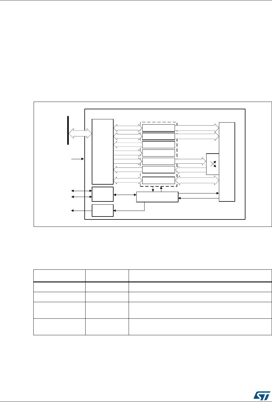
AES hardware accelerator (AES) RM0394
666/1600 RM0394 Rev 4
25.3 AES implementation
The device has a single instance of AES peripheral.
25.4 AES functional description
25.4.1 AES block diagram
Figure 153 shows the block diagram of AES.
Figure 153. AES block diagram
25.4.2 AES internal signals
Table 118 describes the user relevant internal signals interfacing the AES peripheral.
06Y9
DHVBKFON
%DQNHGUHJLVWHUV
'287
.(<
,9,
',1
$(6
NH\
FRQWURO
VWDWXV
,9FRXQWHU
GDWDLQ
GDWDRXW
DHVBLW
ELW
$+%EXV
DHVBLQBGPD
$(6B&5
$(6B.(<5[
$(6B65
$(6B,95[
$(6B',15
$(6B'2875
$(6
&RUH
$($
VZDS
$+%
LQWHUIDFH
,54
LQWHUIDFH
&RQWURO/RJLF
'0$
LQWHUIDFH
DHVBRXWBGPD
ELW
DFFHVV
6DYH5HVWRUH
$(6B68635[
Table 118. AES internal input/output signals
Signal name Signal type Description
aes_hclk digital input AHB bus clock
aes_it digital output AES interrupt request
aes_in_dma digital
input/output Input DMA single request/acknowledge
aes_out_dma digital
input/output Output DMA single request/acknowledge

RM0394 Rev 4 667/1600
RM0394 AES hardware accelerator (AES)
717
25.4.3 AES cryptographic core
Overview
The AES cryptographic core consists of the following components:
•AES algorithm (AEA)
•multiplier over a binary Galois field (GF2mul)
•key input
•initialization vector (IV) input
•chaining algorithm logic (XOR, feedback/counter, mask)
The AES core works on 128-bit data blocks (four words) with 128-bit or 256-bit key length.
Depending on the chaining mode, the AES requires zero or one 96-bit initialization vector IV
(and a 32-bit counter field).
The AES features the following modes of operation:
•Mode 1:
Plaintext encryption using a key stored in the AES_KEYRx registers
•Mode 2:
ECB or CBC decryption key preparation. It must be used prior to selecting Mode 3 with
ECB or CBC chaining modes. The key prepared for decryption is stored automatically
in the AES_KEYRx registers. Now the AES peripheral is ready to switch to Mode 3 for
executing data decryption.
•Mode 3:
Ciphertext decryption using a key stored in the AES_KEYRx registers. When ECB and
CBC chaining modes are selected, the key must be prepared beforehand, through
Mode 2.
•Mode 4:
ECB or CBC ciphertext single decryption using the key stored in the AES_KEYRx
registers (the initial key is derived automatically).
Note: Mode 2 and mode 4 are only used when performing ECB and CBC decryption.
When Mode 4 is selected only one decryption can be done, therefore usage of Mode 2 and
Mode 3 is recommended instead.
The operating mode is selected by programming the MODE[1:0] bitfield of the AES_CR
register. It may be done only when the AES peripheral is disabled.
Typical data processing
Typical usage of the AES is described in Section 25.4.4: AES procedure to perform a cipher
operation on page 672.
Note: The outputs of the intermediate AEA stages are never revealed outside the cryptographic
boundary, with the exclusion of the IVI bitfield.
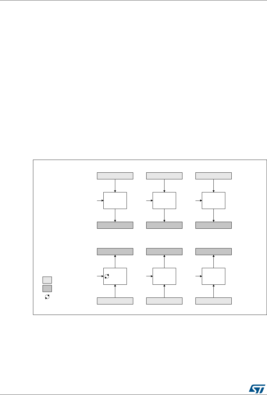
AES hardware accelerator (AES) RM0394
668/1600 RM0394 Rev 4
Chaining modes
The following chaining modes are supported by AES, selected through the CHMOD[2:0]
bitfield of the AES_CR register:
•Electronic code book (ECB)
•Cipher block chaining (CBC)
•Counter (CTR)
•Galois counter mode (GCM)
•Galois message authentication code (GMAC)
•Counter with CBC-MAC (CCM)
Note: The chaining mode may be changed only when AES is disabled (bit EN of the AES_CR
register set).
Principle of each AES chaining mode is provided in the following subsections.
Detailed information is in dedicated sections, starting from Section 25.4.8: AES basic
chaining modes (ECB, CBC).
Electronic codebook (ECB) mode
Figure 154. ECB encryption and decryption principle
ECB is the simplest mode of operation. There are no chaining operations, and no special
initialization stage. The message is divided into blocks and each block is encrypted or
decrypted separately.
Note: For decryption, a special key scheduling is required before processing the first block.
06Y9
(QFU\SWLRQ
3ODLQWH[WEORFN 3ODLQWH[WEORFN 3ODLQWH[WEORFN
&LSKHUWH[WEORFN &LSKHUWH[WEORFN &LSKHUWH[WEORFN
(QFU\SW (QFU\SW (QFU\SW
'HFU\SWLRQ
NH\ NH\ NH\
3ODLQWH[WEORFN 3ODLQWH[WEORFN 3ODLQWH[WEORFN
&LSKHUWH[WEORFN &LSKHUWH[WEORFN &LSKHUWH[WEORFN
'HFU\SW 'HFU\SW 'HFU\SW
NH\ NH\ NH\
LQSXW
RXWSXW
NH\
VFKHGXOLQJ
/HJHQG
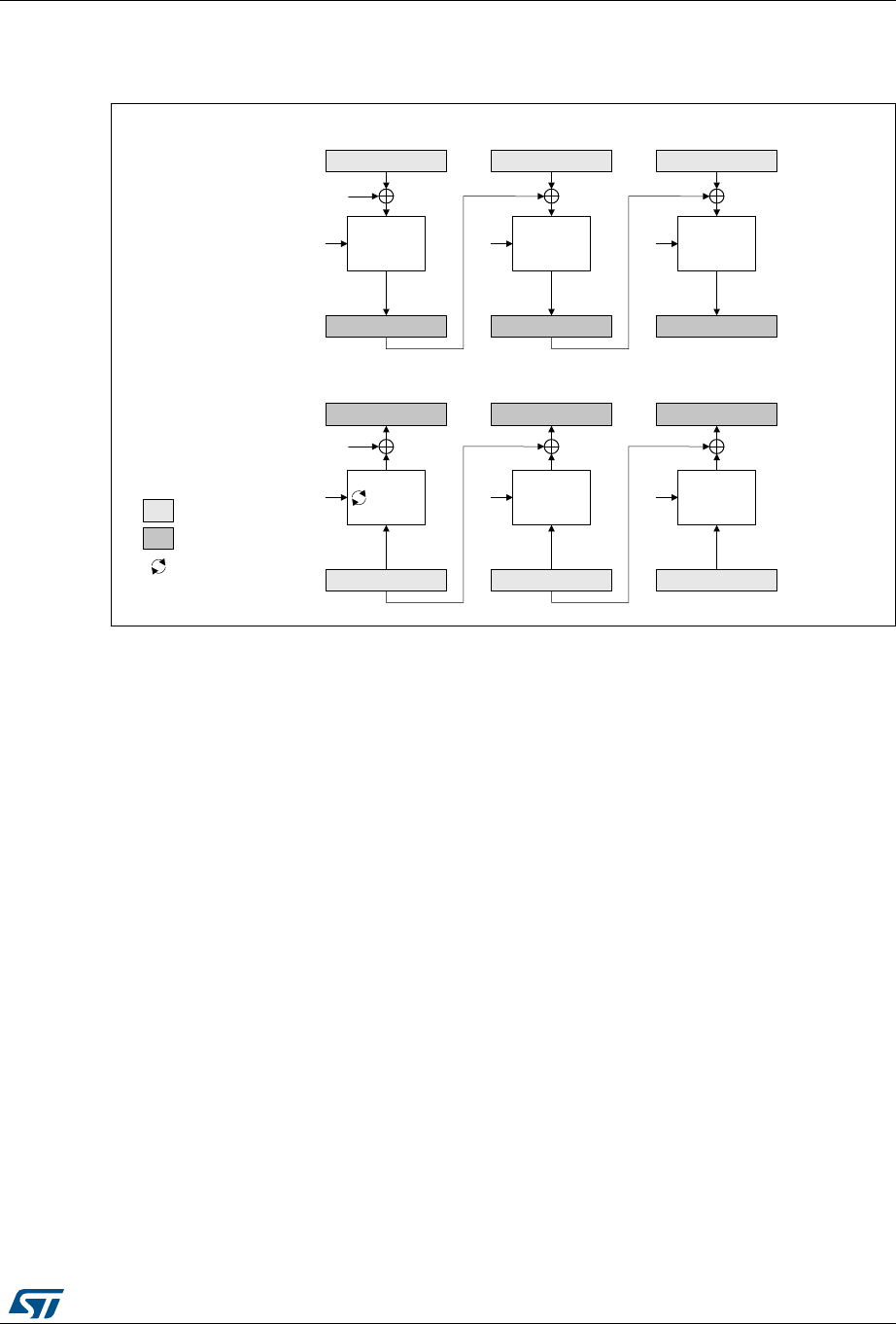
RM0394 Rev 4 669/1600
RM0394 AES hardware accelerator (AES)
717
Cipher block chaining (CBC) mode
Figure 155. CBC encryption and decryption principle
In CBC mode the output of each block chains with the input of the following block. To make
each message unique, an initialization vector is used during the first block processing.
Note: For decryption, a special key scheduling is required before processing the first block.
06Y9
(QFU\SWLRQ
3ODLQWH[WEORFN 3ODLQWH[WEORFN 3ODLQWH[WEORFN
&LSKHUWH[WEORFN &LSKHUWH[WEORFN &LSKHUWH[WEORFN
(QFU\SW (QFU\SW (QFU\SW
'HFU\SWLRQ
NH\ NH\ NH\
3ODLQWH[WEORFN 3ODLQWH[WEORFN 3ODLQWH[WEORFN
&LSKHUWH[WEORFN &LSKHUWH[WEORFN &LSKHUWH[WEORFN
'HFU\SW 'HFU\SW 'HFU\SW
NH\ NH\ NH\
LQSXW
RXWSXW
NH\
VFKHGXOLQJ
/HJHQG
LQLWLDOL]DWLRQ
YHFWRU
LQLWLDOL]DWLRQ
YHFWRU
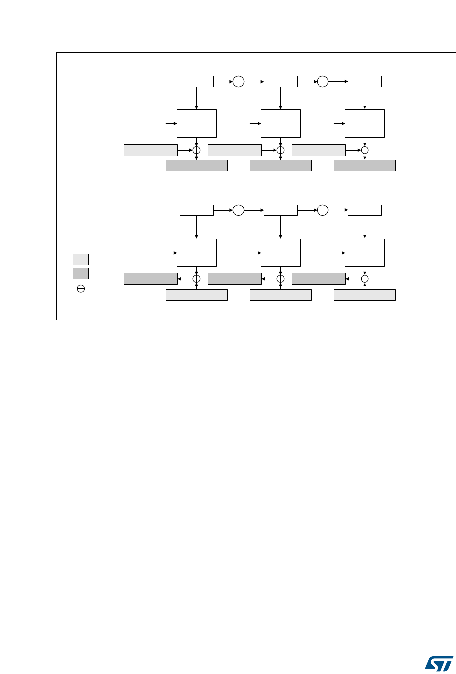
AES hardware accelerator (AES) RM0394
670/1600 RM0394 Rev 4
Counter (CTR) mode
Figure 156. CTR encryption and decryption principle
The CTR mode uses the AES core to generate a key stream. The keys are then XORed
with the plaintext to obtain the ciphertext as specified in NIST Special Publication 800-38A,
Recommendation for Block Cipher Modes of Operation.
Note: Unlike with ECB and CBC modes, no key scheduling is required for the CTR decryption,
since in this chaining scheme the AES core is always used in encryption mode for producing
the key stream, or counter blocks.
06Y9
(QFU\SWLRQ
3ODLQWH[WEORFN
&LSKHUWH[WEORFN &LSKHUWH[WEORFN &LSKHUWH[WEORFN
(QFU\SW (QFU\SW (QFU\SW
'HFU\SWLRQ
&LSKHUWH[WEORFN &LSKHUWH[WEORFN &LSKHUWH[WEORFN
'HFU\SW 'HFU\SW 'HFU\SW
LQSXW
RXWSXW
/HJHQG
NH\ NH\ NH\
NH\ NH\ NH\
3ODLQWH[WEORFN 3ODLQWH[WEORFN
&RXQWHU &RXQWHU &RXQWHU
3ODLQWH[WEORFN 3ODLQWH[WEORFN 3ODLQWH[WEORFN
&RXQWHU &RXQWHU &RXQWHU
;25
YDOXH YDOXH YDOXH
YDOXH YDOXH YDOXH
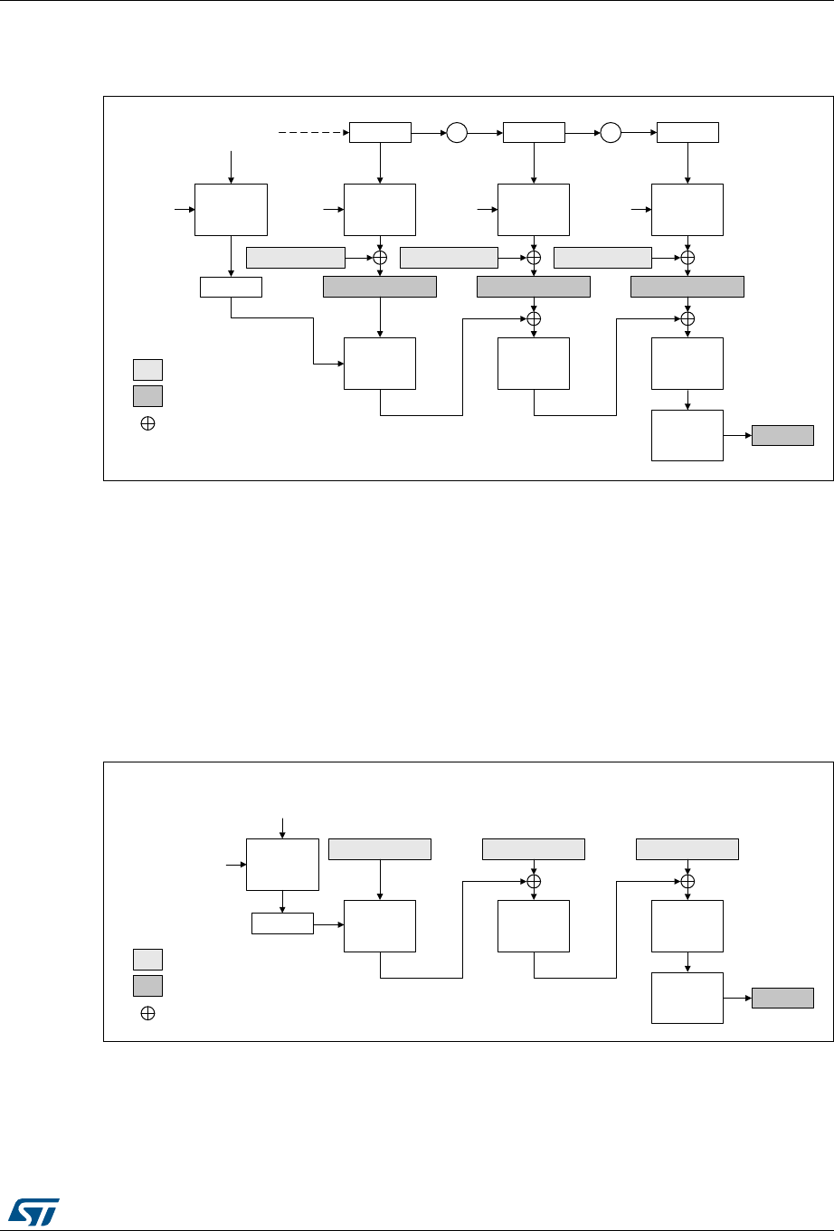
RM0394 Rev 4 671/1600
RM0394 AES hardware accelerator (AES)
717
Galois/counter mode (GCM)
Figure 157. GCM encryption and authentication principle
In Galois/counter mode (GCM), the plaintext message is encrypted while a message
authentication code (MAC) is computed in parallel, thus generating the corresponding
ciphertext and its MAC (also known as authentication tag). It is defined in NIST Special
Publication 800-38D, Recommendation for Block Cipher Modes of Operation -
Galois/Counter Mode (GCM) and GMAC.
GCM mode is based on AES in counter mode for confidentiality. It uses a multiplier over a
fixed finite field for computing the message authentication code. It requires an initial value
and a particular 128-bit block at the end of the message.
Galois message authentication code (GMAC) principle
Figure 158. GMAC authentication principle
Galois message authentication code (GMAC) allows authenticating a message and
generating the corresponding message authentication code (MAC). It is defined in NIST
Special Publication 800-38D, Recommendation for Block Cipher Modes of Operation -
Galois/Counter Mode (GCM) and GMAC.
06Y9
3ODLQWH[WEORFN
&LSKHUWH[WEORFN &LSKHUWH[WEORFN &LSKHUWH[WEORFN
(QFU\SW (QFU\SW (QFU\SW
NH\ NH\ NH\
3ODLQWH[WEORFN 3ODLQWH[WEORFN
&RXQWHU &RXQWHU &RXQWHU
*)PXO *)PXO *)PXO
)LQDO 7$*
,QLW
(QFU\SW
NH\
,QLWLDOL]DWLRQ
YHFWRU
+
LQSXW
RXWSXW
/HJHQG
;25
YDOXH YDOXH YDOXH
06Y9
3ODLQWH[WEORFN 3ODLQWH[WEORFN 3ODLQWH[WEORFN
*)PXO *)PXO *)PXO
)LQDO 7$*
,QLW
(QFU\SW
NH\
,QLWLDOL]DWLRQ
YHFWRU
+
LQSXW
RXWSXW
/HJHQG
;25
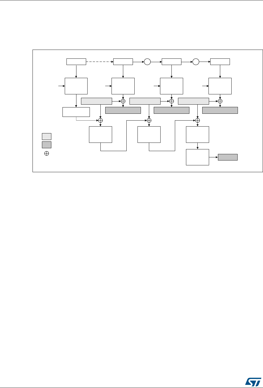
AES hardware accelerator (AES) RM0394
672/1600 RM0394 Rev 4
GMAC is similar to GCM, except that it is applied on a message composed only by plaintext
authenticated data (that is, only header, no payload).
Counter with CBC-MAC (CCM) principle
Figure 159. CCM encryption and authentication principle
In Counter with cipher block chaining-message authentication code (CCM) mode, the
plaintext message is encrypted while a message authentication code (MAC) is computed in
parallel, thus generating the corresponding ciphertext and the corresponding MAC (also
known as tag). It is described by NIST in Special Publication 800-38C, Recommendation for
Block Cipher Modes of Operation - The CCM Mode for Authentication and Confidentiality.
CCM mode is based on AES in counter mode for confidentiality and it uses CBC for
computing the message authentication code. It requires an initial value.
Like GCM, the CCM chaining mode can be applied on a message composed only by
plaintext authenticated data (that is, only header, no payload). Note that this way of using
CCM is not called CMAC (it is not similar to GCM/GMAC), and its usage is not
recommended by NIST.
25.4.4 AES procedure to perform a cipher operation
Introduction
A typical cipher operation is explained below. Detailed information is provided in sections
starting from Section 25.4.8: AES basic chaining modes (ECB, CBC).
The flowcharts shown in Figure 160 and Figure 161 describe the way STM32 cryptographic
library implements the AES algorithm. AES accelerates the execution of the AES-128 and
AES-256 cryptographic algorithms in ECB, CBC, CTR, CCM, and GCM operating modes.
Note: For more details on the cryptographic library, refer to the UM1924 user manual “STM32
crypto library” available from www.st.com.
06Y9
3ODLQWH[WEORFN
&LSKHUWH[WEORFN &LSKHUWH[WEORFN &LSKHUWH[WEORFN
(QFU\SW (QFU\SW (QFU\SW
NH\ NH\ NH\
3ODLQWH[WEORFN 3ODLQWH[WEORFN
&RXQW &RXQW &RXQW
(QFU\SW (QFU\SW (QFU\SW
)LQDO 7$*
,QLW
(QFU\SW
NH\
,QLWLDOL]DWLRQ
YHFWRU
LQSXW
RXWSXW
/HJHQG
;25
%
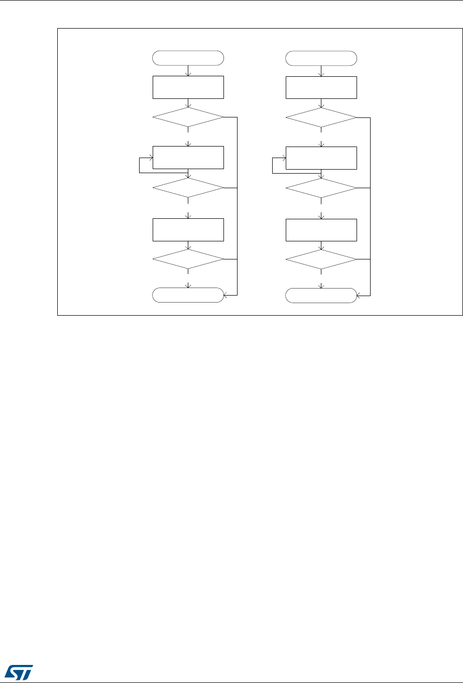
RM0394 Rev 4 673/1600
RM0394 AES hardware accelerator (AES)
717
Figure 160. STM32 cryptolib AES flowchart examples
06Y9
(UURUVWDWXV
%HJLQ
$(6B[HQFU\SWLQLW
$(6B[HQFU\SW
DSSHQG
(UURUVWDWXV
$(6B[HQFU\SWILQLVK
ILQDO
(UURUVWDWXV
(QG
VXFFHVV
VXFFHVV
VXFFHVV
(QFU\SWLRQ
(UURUVWDWXV
%HJLQ
$(6B[GHFU\SWLQLW
$(6B[GHFU\SW
DSSHQG
(UURUVWDWXV
$(6B[GHFU\SWILQLVK
ILQDO
(UURUVWDWXV
(QG
VXFFHVV
VXFFHVV
VXFFHVV
'HFU\SWLRQ
'DWDWRDSSHQG 'DWDWRDSSHQG
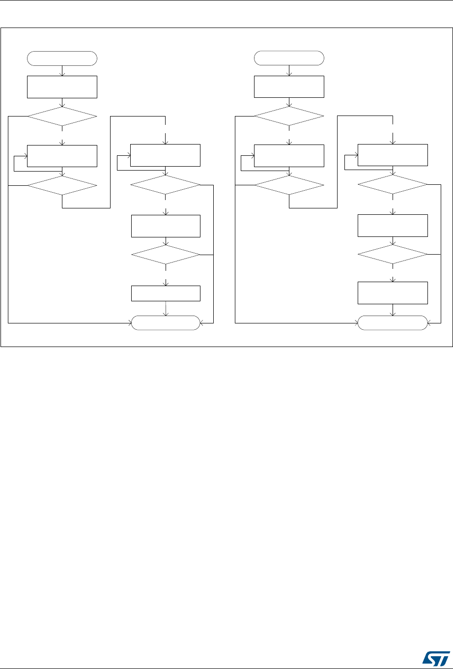
AES hardware accelerator (AES) RM0394
674/1600 RM0394 Rev 4
Figure 161. STM32 cryptolib AES flowchart examples (continued)
Initialization of AES
To initialize AES, first disable it by clearing the EN bit of the AES_CR register. Then perform
the following steps in any order:
•Configure the AES mode, by programming the MODE[1:0] bitfield of the AES_CR
register.
– For encryption, Mode 1 must be selected (MODE[1:0] = 00).
– For decryption, Mode 3 must be selected (MODE[1:0] = 10), unless ECB or CBC
chaining modes are used. In this latter case, an initial key derivation of the
encryption key must be performed, as described in Section 25.4.5: AES
decryption key preparation.
•Select the chaining mode, by programming the CHMOD[2:0] bitfield of the AES_CR
register
•Configure the key size (128-bit or 256-bit), with the KEYSIZE bitfield of the AES_CR
register.
•Write a symmetric key into the AES_KEYRx registers (4 or 8 registers depending on
the key size).
•Configure the data type (1-, 8-, 16- or 32-bit), with the DATATYPE[1:0] bitfield in the
AES_CR register.
•When it is required (for example in CBC or CTR chaining modes), write the initialization
vectors into the AES_IVRx register.
06Y9
(UURUVWDWXV
%HJLQ
$(6B[HQFU\SWLQLW
$(6B[KHDGHU
DSSHQG
(UURUVWDWXV
VXFFHVV VXFFHVV
$XWKHQWLFDWHG(QFU\SWLRQ
$(6B[HQFU\SW
DSSHQG
(UURUVWDWXV
$(6B[HQFU\SW
ILQLVKILQDO
(UURUVWDWXV
(QG
VXFFHVV
VXFFHVV
(UURUVWDWXV
%HJLQ
$(6B[GHFU\SWLQLW
$(6B[KHDGHU
DSSHQG
(UURUVWDWXV
VXFFHVV VXFFHVV
$XWKHQWLFDWHG'HFU\SWLRQ
$(6B[GHFU\SW
DSSHQG
(UURUVWDWXV
$(6B[GHFU\SW
ILQLVKILQDO
(UURUVWDWXV
(QG
VXFFHVV
VXFFHVV
0$&7DJ
FRPSDULVRQ
'DWDWRDSSHQG 'DWDWRDSSHQG 'DWDWRDSSHQG 'DWDWRDSSHQG
5HWUHLYH7DJ

RM0394 Rev 4 675/1600
RM0394 AES hardware accelerator (AES)
717
Data append
This section describes different ways of appending data for processing, where the size of
data to process is not a multiple of 128 bits.
For ECB, CBC and GCM encryption mode, refer to Section 25.4.6: AES ciphertext stealing
and data padding. The second-last and the last block management in these cases is more
complex than in the sequence described in this section.
Data append through polling
This method uses flag polling to control the data append.
For all other cases, the data is appended through the following sequence:
1. Enable the AES peripheral by setting the EN bit of the AES_CR register.
2. Repeat the following sub-sequence until the payload is entirely processed:
a) Write four input data words into the AES_DINR register.
b) Wait until the status flag CCF is set in the AES_SR, then read the four data words
from the AES_DOUTR register.
c) Clear the CCF flag, by setting the CCFC bit of the AES_CR register.
d) If the data block just processed is the second-last block of the message and the
significant data in the last block to process is inferior to 128 bits, pad the
remainder of the last block with zeros
3. Discard the data that is not part of the payload, then disable the AES peripheral by
clearing the EN bit of the AES_CR register.
Note: Up to three wait cycles are automatically inserted between two consecutive writes to the
AES_DINR register, to allow sending the key to the AES processor.
Data append using interrupt
The method uses interrupt from the AES peripheral to control the data append, through the
following sequence:
1. Enable interrupts from AES by setting the CCFIE bit of the AES_CR register.
2. Enable the AES peripheral by setting the EN bit of the AES_CR register.
3. Write first four input data words into the AES_DINR register.
4. Handle the data in the AES interrupt service routine, upon interrupt:
a) Read four output data words from the AES_DOUTR register.
b) Clear the CCF flag and thus the pending interrupt, by setting the CCFC bit of the
AES_CR register
c) If the data block just processed is the second-last block of an message and the
significant data in the last block to process is inferior to 128 bits, pad the
remainder of the last block with zeros. Then proceed with point 4e).
d) If the data block just processed is the last block of the message, discard the data
that is not part of the payload, then disable the AES peripheral by clearing the EN
bit of the AES_CR register and quit the interrupt service routine.
e) Write next four input data words into the AES_DINR register and quit the interrupt
service routine.
Note: AES is tolerant of delays between consecutive read or write operations, which allows, for
example, an interrupt from another peripheral to be served between two AES computations.

AES hardware accelerator (AES) RM0394
676/1600 RM0394 Rev 4
Data append using DMA
With this method, all the transfers and processing are managed by DMA and AES. To use
the method, proceed as follows:
1. Prepare the last four-word data block (if the data to process does not fill it completely),
by padding the remainder of the block with zeros.
2. Configure the DMA controller so as to transfer the data to process from the memory to
the AES peripheral input and the processed data from the AES peripheral output to the
memory, as described in Section 25.4.16: AES DMA interface. Configure the DMA
controller so as to generate an interrupt on transfer completion.
3. Enable the AES peripheral by setting the EN bit of the AES_CR register
4. Enable DMA requests by setting the DMAINEN and DMAOUTEN bits of the AES_CR
register.
5. Upon DMA interrupt indicating the transfer completion, get the AES-processed data
from the memory.
Note: The CCF flag has no use with this method, because the reading of the AES_DOUTR
register is managed by DMA automatically, without any software action, at the end of the
computation phase.
25.4.5 AES decryption key preparation
For an ECB or CBC decryption, a key for the first round of decryption must be derived from
the key of the last round of encryption. This is why a complete key schedule of encryption is
required before performing the decryption. This key preparation is not required for AES
decryption in modes other than ECB or CBC.
Recommended method is to select the Mode 2 by setting to 01 the MODE[1:0] bitfield of the
AES_CR (key process only), then proceed with the decryption by setting MODE[1:0] to 10
(Mode 3, decryption only). Mode 2 usage is described below:
1. Disable the AES peripheral by clearing the EN bit of the AES_CR register.
2. Select Mode 2 by setting to 01 the MODE[1:0] bitfield of the AES_CR. The
CHMOD[2:0] bitfield is not significant in this case because this key derivation mode is
independent of the chaining algorithm selected.
3. Set key length to 128 or 256 bits, via KEYSIZE bit of AES_CR register.
4. Write the AES_KEYRx registers (128 or 256 bits) with encryption key, as shown in
Figure 162. Writes to the AES_IVRx registers have no effect.
5. Enable the AES peripheral, by setting the EN bit of the AES_CR register.
6. Wait until the CCF flag is set in the AES_SR register.
7. Derived key is available in AES core, ready to use for decryption. Application can also
read the AES_KEYRx register to obtain the derived key if needed, as shown in
Figure 162 (the processed key is loaded automatically into the AES_KEYRx registers).
Note: The AES is disabled by hardware when the derivation key is available.
To restart a derivation key computation, repeat steps 4, 5, 6 and 7.
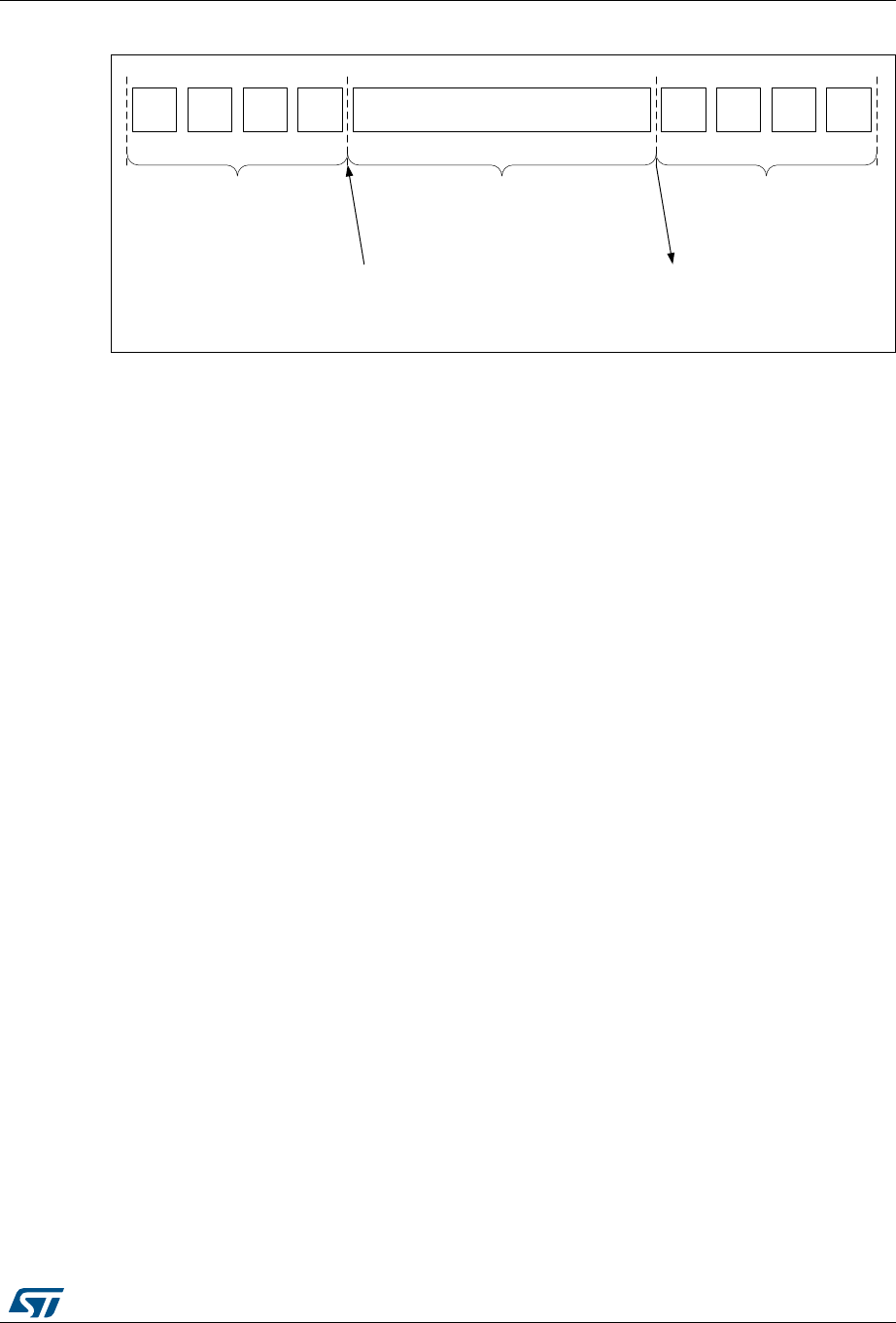
RM0394 Rev 4 677/1600
RM0394 AES hardware accelerator (AES)
717
Figure 162. Encryption key derivation for ECB/CBC decryption (Mode 2)
If the software stores the initial key prepared for decryption, it is enough to do the key
schedule operation only once for all the data to be decrypted with a given cipher key.
Note: The operation of the key preparation lasts 80 or 109 clock cycles, depending on the key size
(128- or 256-bit).
Note: Alternative key preparation is to select Mode 4 by setting to 11 the MODE[1:0] bitfield of the
AES_CR register. In this case Mode 3 cannot be used.
25.4.6 AES ciphertext stealing and data padding
When using AES in ECB or CBC modes to manage messages the size of which is not a
multiple of the block size (128 bits), ciphertext stealing techniques are used, such as those
described in NIST Special Publication 800-38A, Recommendation for Block Cipher Modes
of Operation: Three Variants of Ciphertext Stealing for CBC Mode. Since the AES peripheral
on the device does not support such techniques, the last two blocks of input data must be
handled in a special way by the application.
Note: Ciphertext stealing techniques are not documented in this reference manual.
Similarly, when AES is used in other modes than ECB or CBC, an incomplete input data
block (that is, block with input data shorter than 128 bits) must be padded with zeros prior to
encryption (that is, extra bits must be appended to the trailing end of the data string). After
decryption, the extra bits must be discarded. As AES does not implement automatic data
padding operation to the last block, the application must follow the recommendation given
in Section 25.4.4: AES procedure to perform a cipher operation on page 672 to manage
messages the size of which is not a multiple of 128 bits.
Note: Padding data are swapped in a similar way as normal data, according to the
DATATYPE[1:0] field of the AES_CR register (see Section 25.4.13: .AES data registers and
data swapping on page 698 for details).
A workaround is required in order to properly compute authentication tags for GCM
encryption, when the input data in the last block is inferior to 128 bits. During GCM
encryption payload phase and before inserting a last plaintext block smaller than 128 bits,
then application must apply the following steps:
069
:5
(.
:5
(.
:5
(.
:5
(. :DLWXQWLOIODJ&&) 5'
'.
5'
'.
5'
'.
5'
'.
,QSXWSKDVH
ZULWHRSHUDWLRQVLQWR
$(6B.(<5[>@
&RPSXWDWLRQSKDVH
2XWSXWSKDVHRSWLRQDO
UHDGRSHUDWLRQVRI
$(6B.(<5[>@
(. HQFU\SWLRQNH\ ZRUGV(.«(.
'. GHFU\SWLRQNH\ ZRUGV'.«'.
06% /6% 06% /6%
(1 LQWR$(6B&5 ELWGHULYDWLRQNH\
VWRUHGLQWR$(6B.(<5[
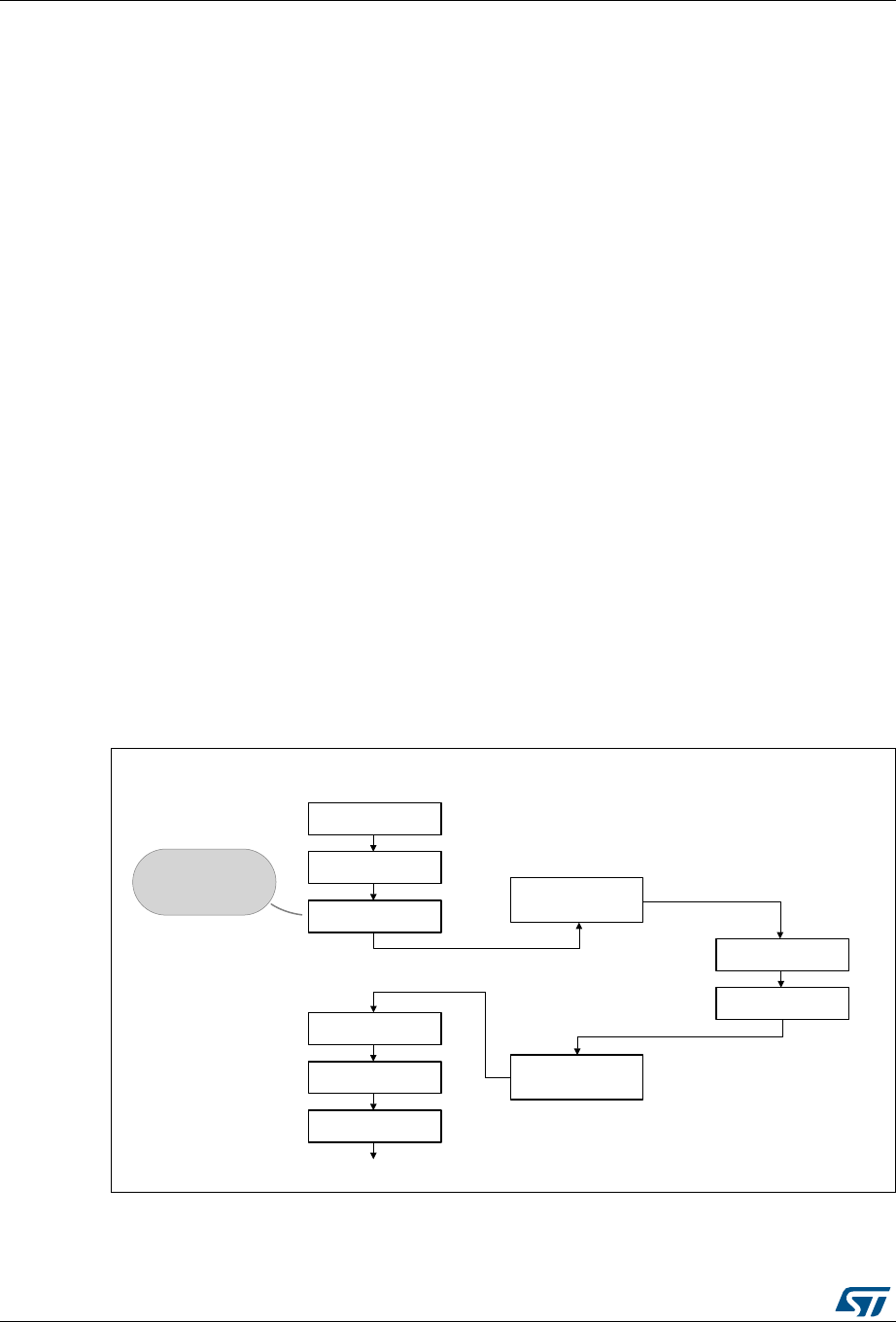
AES hardware accelerator (AES) RM0394
678/1600 RM0394 Rev 4
1. Disable the AES peripheral by clearing the EN bit of the AES_CR register
2. Change the mode to CTR by writing 010 to the CHMOD[2:0] bitfield of the AES_CR
register.
3. Pad the last block (smaller than 128 bits) with zeros to have a complete block of 128
bits, then write it into AES_DINR register.
4. Upon encryption completion, read the 128-bit ciphertext from the AES_DOUTR register
and store it as intermediate data.
5. Change again the mode to GCM by writing 011 to the CHMOD[2:0] bitfield of the
AES_CR register.
6. Select Final phase by writing 11 to the GCMPH[1:0] bitfield of the AES_CR register.
7. In the intermediate data, set to zero the bits corresponding to the padded bits of the last
block of payload, then insert the resulting data into AES_DINR register.
8. Wait for operation completion, and read data on AES_DOUTR. This data is to be
discarded.
9. Apply the normal Final phase as described in Section 25.4.10: AES Galois/counter
mode (GCM) on page 686
25.4.7 AES task suspend and resume
A message can be suspended if another message with a higher priority must be processed.
When this highest priority message is sent, the suspended message can resume in both
encryption or decryption mode.
Suspend/resume operations do not break the chaining operation and the message
processing can resume as soon as AES is enabled again to receive the next data block.
Figure 163 gives an example of suspend/resume operation: Message 1 is suspended in
order to send a shorter and higher-priority Message 2.
Figure 163. Example of suspend mode management
A detailed description of suspend/resume operations is in the sections dedicated to each
AES mode.
06Y9
ELWEORFN
0HVVDJH
ELWEORFN
ELWEORFN
ELWEORFN
ELWEORFN
$(6VXVSHQG
VHTXHQFH
$(6UHVXPH
VHTXHQFH
ELWEORFN
ELWEORFN
0HVVDJH
ELWEORFN
1HZKLJKHUSULRULW\
PHVVDJHWREH
SURFHVVHG
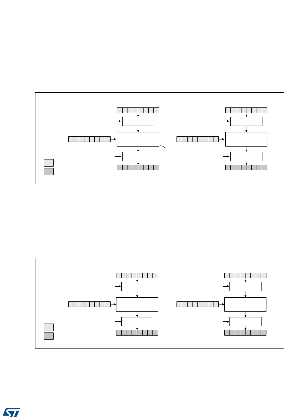
RM0394 Rev 4 679/1600
RM0394 AES hardware accelerator (AES)
717
25.4.8 AES basic chaining modes (ECB, CBC)
Overview
This section gives a brief explanation of the four basic operation modes provided by the
AES computing core: ECB encryption, ECB decryption, CBC encryption and CBC
decryption. For detailed information, refer to the FIPS publication 197 from November 26,
2001.
Figure 164 illustrates the electronic codebook (ECB) encryption.
Figure 164. ECB encryption
In ECB encrypt mode, the 128-bit plaintext input data block Px in the AES_DINR register
first goes through bit/byte/half-word swapping. The swap result Ix is processed with the AES
core set in encrypt mode, using a 128- or 256-bit key. The encryption result Ox goes through
bit/byte/half-word swapping, then is stored in the AES_DOUTR register as 128-bit ciphertext
output data block Cx. The ECB encryption continues in this way until the last complete
plaintext block is encrypted.
Figure 165 illustrates the electronic codebook (ECB) decryption.
Figure 165. ECB decryption
To perform an AES decryption in the ECB mode, the secret key has to be prepared by
collecting the last-round encryption key (which requires to first execute the complete key
schedule for encryption), and using it as the first-round key for the decryption of the
ciphertext. This preparation is supported by the AES core.
06Y9
(QFU\SW
$(6B.(<5[.(<
$(6B',15SODLQWH[W3
$(6B'2875FLSKHUWH[W&
6ZDS
PDQDJHPHQW
'$7$7<3(>@
'$7$7<3(>@ 6ZDS
PDQDJHPHQW
(QFU\SW
$(6B.(<5[.(<
$(6B',15SODLQWH[W3
$(6B'2875FLSKHUWH[W&
6ZDS
PDQDJHPHQW
'$7$7<3(>@
'$7$7<3(>@ 6ZDS
PDQDJHPHQW
LQSXW
RXWSXW
/HJHQG
, ,
2 2
%ORFN %ORFN
$(6FRUH
06Y9
'HFU\SW
$(6B.(<5[.(<
$(6B',15FLSKHUWH[W&
$(6B'2875SODLQWH[W3
6ZDS
PDQDJHPHQW
'$7$7<3(>@
'$7$7<3(>@ 6ZDS
PDQDJHPHQW
'HFU\SW
$(6B.(<5[.(<
$(6B',15FLSKHUWH[W&
$(6B'2875SODLQWH[W3
6ZDS
PDQDJHPHQW
'$7$7<3(>@
'$7$7<3(>@ 6ZDS
PDQDJHPHQW
LQSXW
RXWSXW
/HJHQG
, ,
2 2
%ORFN %ORFN
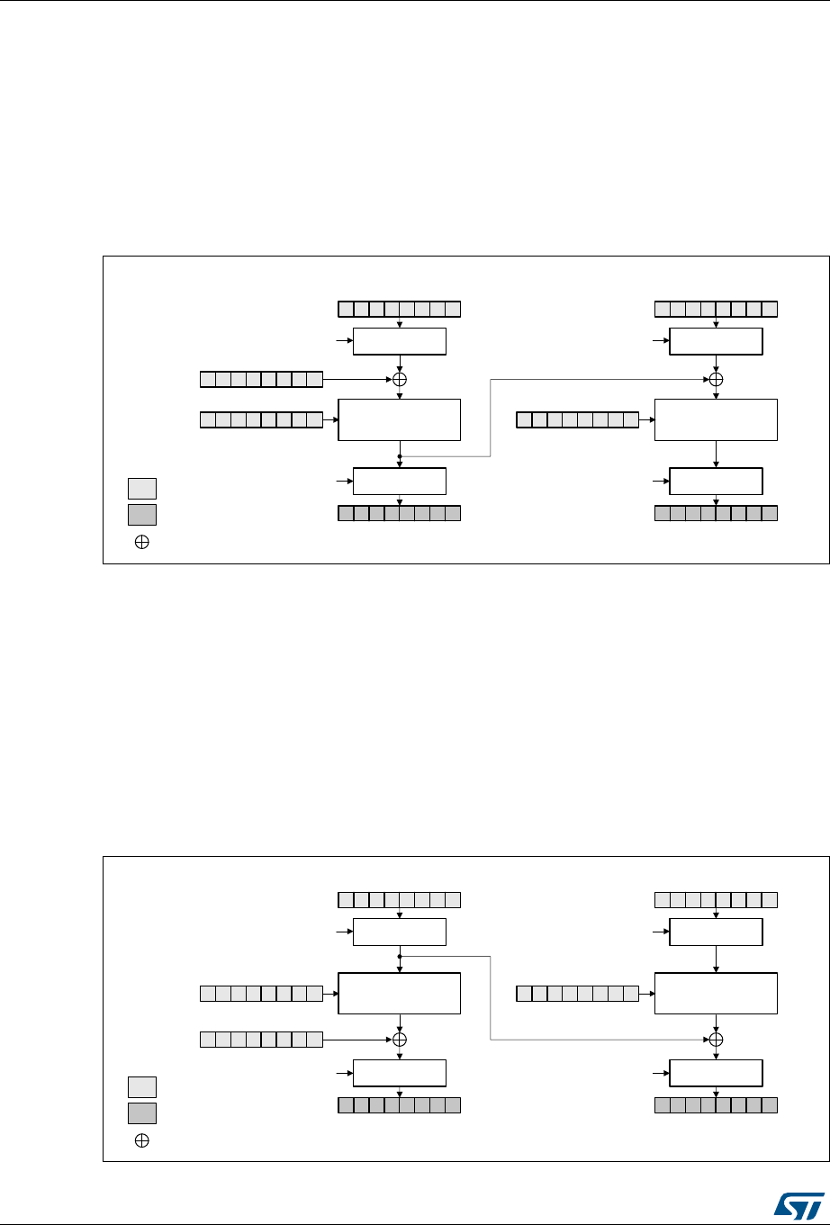
AES hardware accelerator (AES) RM0394
680/1600 RM0394 Rev 4
In ECB decrypt mode, the 128-bit ciphertext input data block C1 in the AES_DINR register
first goes through bit/byte/half-word swapping. The keying sequence is reversed compared
to that of the ECB encryption. The swap result I1 is processed with the AES core set in
decrypt mode, using the formerly prepared decryption key. The decryption result goes
through bit/byte/half-word swapping, then is stored in the AES_DOUTR register as 128-bit
plaintext output data block P1. The ECB decryption continues in this way until the last
complete ciphertext block is decrypted.
Figure 166 illustrates the cipher block chaining (CBC) encryption mode.
Figure 166. CBC encryption
In CBC encrypt mode, the first plaintext input block, after bit/byte/half-word swapping (P1’),
is XOR-ed with a 128-bit IVI bitfield (initialization vector and counter), producing the I1 input
data for encrypt with the AES core, using a 128- or 256-bit key. The resulting 128-bit output
block O1, after swapping operation, is used as ciphertext C1. The O1 data is then XOR-ed
with the second-block plaintext data P2’ to produce the I2 input data for the AES core to
produce the second block of ciphertext data. The chaining of data blocks continues in this
way until the last plaintext block in the message is encrypted.
If the message size is not a multiple of 128 bits, the final partial data block is encrypted in
the way explained in Section 25.4.6: AES ciphertext stealing and data padding.
Figure 167 illustrates the cipher block chaining (CBC) decryption mode.
Figure 167. CBC decryption
06Y9
%ORFNFLSKHU
HQFU\SWLRQ
$(6B.(<5[.(<
$(6B',15SODLQWH[W3
$(6B'2875FLSKHUWH[W&
6ZDS
PDQDJHPHQW
'$7$7<3(>@
'$7$7<3(>@ 6ZDS
PDQDJHPHQW
%ORFNFLSKHU
HQFU\SWLRQ
$(6B.(<5[.(<
$(6B',15SODLQWH[W3
$(6B'2875FLSKHUWH[W&
6ZDS
PDQDJHPHQW
'$7$7<3(>@
'$7$7<3(>@ 6ZDS
PDQDJHPHQW
$(6B,95[LQLWYHFWRU
LQSXW
RXWSXW
/HJHQG
;25
, ,
2 2
%ORFN %ORFN
,9, 3 3
06Y9
'HFU\SW
$(6B.(<5[.(<
$(6B',15FLSKHUWH[W&
$(6B'2875SODLQWH[W3
6ZDS
PDQDJHPHQW
'$7$7<3(>@
'$7$7<3(>@ 6ZDS
PDQDJHPHQW
'HFU\SW
$(6B.(<5[.(<
$(6B',15FLSKHUWH[W&
$(6B'2875SODLQWH[W3
6ZDS
PDQDJHPHQW
'$7$7<3(>@
'$7$7<3(>@ 6ZDS
PDQDJHPHQW
$(6B,95[,9
LQSXW
RXWSXW
/HJHQG
;25
, ,
2 2
%ORFN %ORFN
,9,
3 3

RM0394 Rev 4 681/1600
RM0394 AES hardware accelerator (AES)
717
In CBC decrypt mode, like in ECB decrypt mode, the secret key must be prepared to
perform an AES decryption.
After the key preparation process, the decryption goes as follows: the first 128-bit ciphertext
block (after the swap operation) is used directly as the AES core input block I1 for decrypt
operation, using the 128-bit or 256-bit key. Its output O1 is XOR-ed with the 128-bit IVI field
(that must be identical to that used during encryption) to produce the first plaintext block P1.
The second ciphertext block is processed in the same way as the first block, except that the
I1 data from the first block is used in place of the initialization vector.
The decryption continues in this way until the last complete ciphertext block is decrypted.
If the message size is not a multiple of 128 bits, the final partial data block is decrypted in
the way explained in Section 25.4.6: AES ciphertext stealing and data padding.
For more information on data swapping, refer to Section 25.4.13: .AES data registers and
data swapping.
ECB/CBC encryption sequence
The sequence of events to perform an ECB/CBC encryption (more detail in Section 25.4.4):
1. Disable the AES peripheral by clearing the EN bit of the AES_CR register.
2. Select the Mode 1 by to 00 the MODE[1:0] bitfield of the AES_CR register and select
ECB or CBC chaining mode by setting the CHMOD[2:0] bitfield of the AES_CR register
to 000 or 001, respectively. Data type can also be defined, using DATATYPE[1:0]
bitfield.
3. Select 128- or 256-bit key length through the KEYSIZE bit of the AES_CR register.
4. Write the AES_KEYRx registers (128 or 256 bits) with encryption key. Fill the
AES_IVRx registers with the initialization vector data if CBC mode has been selected.
5. Enable the AES peripheral by setting the EN bit of the AES_CR register.
6. Write the AES_DINR register four times to input the plaintext (MSB first), as shown in
Figure 168.
7. Wait until the CCF flag is set in the AES_SR register.
8. Read the AES_DOUTR register four times to get the ciphertext (MSB first) as shown in
Figure 168. Then clear the CCF flag by setting the CCFC bit of the AES_CR register.
9. Repeat steps 6,7,8 to process all the blocks with the same encryption key.
Figure 168. ECB/CBC encryption (Mode 1)
069
:5
37
:5
37
:5
37
:5
37 :DLWXQWLOIODJ&&) 5'
&7
5'
&7
5'
&7
5'
&7
,QSXWSKDVH
ZULWHRSHUDWLRQVLQWR
$(6B',15>@
&RPSXWDWLRQSKDVH 2XWSXWSKDVH
UHDGRSHUDWLRQVRI
$(6B'2875>@
37 SODLQWH[W ZRUGV37«37
&7 FLSKHUWH[W ZRUGV&7«&7
06% /6% 06% /6%
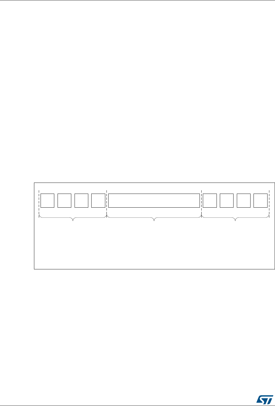
AES hardware accelerator (AES) RM0394
682/1600 RM0394 Rev 4
ECB/CBC decryption sequence
The sequence of events to perform an AES ECB/CBC decryption is as follows (more detail
in Section 25.4.4):
1. Follow the steps described in Section 25.4.5: AES decryption key preparation on
page 676, in order to prepare the decryption key in AES core.
2. Disable the AES peripheral by clearing the EN bit of the AES_CR register.
3. Select the Mode 3 by setting to 10 the MODE[1:0] bitfield of the AES_CR register and
select ECB or CBC chaining mode by setting the CHMOD[2:0] bitfield of the AES_CR
register to 000 or 001, respectively. Data type can also be defined, using
DATATYPE[1:0] bitfield.
4. Select key length of 128 or 256 bits via KEYSIZE bitfield of the AES_CR register.
5. Write the AES_IVRx registers with the initialization vector (required in CBC mode only).
6. Enable AES by setting the EN bit of the AES_CR register.
7. Write the AES_DINR register four times to input the cipher text (MSB first), as shown in
Figure 169.
8. Wait until the CCF flag is set in the AES_SR register.
9. Read the AES_DOUTR register four times to get the plain text (MSB first), as shown in
Figure 169. Then clear the CCF flag by setting the CCFC bit of the AES_CR register.
10. Repeat steps 7,8,9 to process all the blocks encrypted with the same key.
Figure 169. ECB/CBC decryption (Mode 3)
Suspend/resume operations in ECB/CBC modes
To suspend the processing of a message, proceed as follows:
1. If DMA is used, stop the AES DMA transfers to the IN FIFO by clearing the DMAINEN
bit of the AES_CR register.
2. If DMA is not used, read four times the AES_DOUTR register to save the last
processed block. If DMA is used, wait until the CCF flag is set in the AES_SR register
069
:5
&7
:5
&7
:5
&7
:5
&7 :DLWXQWLOIODJ&&) 5'
37
5'
37
5'
37
5'
37
,QSXWSKDVH
ZULWHRSHUDWLRQVLQWR
$(6B',15>@
&RPSXWDWLRQSKDVH 2XWSXWSKDVH
UHDGRSHUDWLRQVIURP
$(6B'2875>@
37 SODLQWH[W ZRUGV37«37
&7 FLSKHUWH[W ZRUGV&7«&7
06% /6% 06% /6%

RM0394 Rev 4 683/1600
RM0394 AES hardware accelerator (AES)
717
then stop the DMA transfers from the OUT FIFO by clearing the DMAOUTEN bit of the
AES_CR register.
3. If DMA is not used, poll the CCF flag of the AES_SR register until it becomes 1
(computation completed).
4. Clear the CCF flag by setting the CCFC bit of the AES_CR register.
5. Save initialization vector registers (only required in CBC mode as AES_IVRx registers
are altered during the data processing).
6. Disable the AES peripheral by clearing the bit EN of the AES_CR register.
7. Save the current AES configuration in the memory (except AES initialization vector
values).
8. If DMA is used, save the DMA controller status (pointers for IN and OUT data transfers,
number of remaining bytes, and so on).
Note: In point 7, the derived key information stored in AES_KEYRx registers can optionally be
saved in memory if the interrupted process is a decryption. Otherwise those registers do not
need to be saved as the original key value is known by the application
To resume the processing of a message, proceed as follows:
1. If DMA is used, configure the DMA controller so as to complete the rest of the FIFO IN
and FIFO OUT transfers.
2. Ensure that AES is disabled (the EN bit of the AES_CR must be 0).
3. Restore the AES_CR and AES_KEYRx register setting, using the values of the saved
configuration. In case of decryption, derived key information can be written in
AES_KEYRx register instead of the original key value.
4. Prepare the decryption key as described in Section 25.4.5: AES decryption key
preparation (only required for ECB or CBC decryption). This step is not necessary if
derived key information has been loaded in AES_KEYRx registers.
5. Restore AES_IVRx registers using the saved configuration (only required in CBC
mode).
6. Enable the AES peripheral by setting the EN bit of the AES_CR register.
7. If DMA is used, enable AES DMA transfers by setting the DMAINEN and DMAOUTEN
bits of the AES_CR register.
Alternative single ECB/CBC decryption using Mode 4
The sequence of events to perform a single round of ECB/CBC decryption using Mode 4 is:
1. Disable the AES peripheral by clearing the EN bit of the AES_CR register.
2. Select the Mode 4 by setting to 11 the MODE[1:0] bitfield of the AES_CR register and
select ECB or CBC chaining mode by setting the CHMOD[2:0] bitfield of the AES_CR
register to 000 or 001, respectively.
3. Select key length of 128 or 256 bits via KEYSIZE bitfield of the AES_CR register.
4. Write the AES_KEYRx registers with the encryption key. Write the AES_IVRx registers
if the CBC mode is selected.
5. Enable the AES peripheral by setting the EN bit of the AES_CR register.
6. Write the AES_DINR register four times to input the cipher text (MSB first).
7. Wait until the CCF flag is set in the AES_SR register.
8. Read the AES_DOUTR register four times to get the plain text (MSB first). Then clear
the CCF flag by setting the CCFC bit of the AES_CR register.
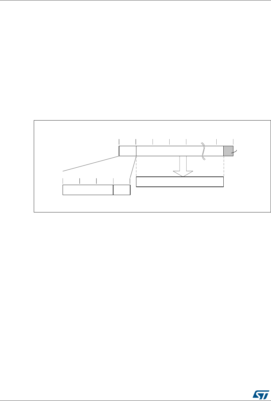
AES hardware accelerator (AES) RM0394
684/1600 RM0394 Rev 4
Note: When mode 4 is selected mode 3 cannot be used.
In mode 4, the AES_KEYRx registers contain the encryption key during all phases of the
processing. No derivation key is stored in these registers. It is stored internally in AES.
25.4.9 AES counter (CTR) mode
Overview
The counter mode (CTR) uses AES as a key-stream generator. The generated keys are
then XOR-ed with the plaintext to obtain the ciphertext.
CTR chaining is defined in NIST Special Publication 800-38A, Recommendation for Block
Cipher Modes of Operation. A typical message construction in CTR mode is given in
Figure 170.
Figure 170. Message construction in CTR mode
The structure of this message is:
•A 16-byte initial counter block (ICB), composed of two distinct fields:
–Initialization vector (IV): a 96-bit value that must be unique for each encryption
cycle with a given key.
–Counter: a 32-bit big-endian integer that is incremented each time a block
processing is completed. The initial value of the counter should be set to 1.
•The plaintext P is encrypted as ciphertext C, with a known length. This length can be
non-multiple of 16 bytes, in which case a plaintext padding is required.
CTR encryption and decryption
Figure 171 and Figure 172 describe the CTR encryption and decryption process,
respectively, as implemented in the AES peripheral. The CTR mode is selected by writing
010 to the CHMOD[2:0] bitfield of AES_CR register.
06Y9
E\WHERXQGDULHV
,&% &LSKHUWH[W&
E\WHERXQGDULHV
&RXQWHU,QLWLDOL]DWLRQYHFWRU,9
GHFU\SW
3ODLQWH[W3
=HUR
SDGGLQJ
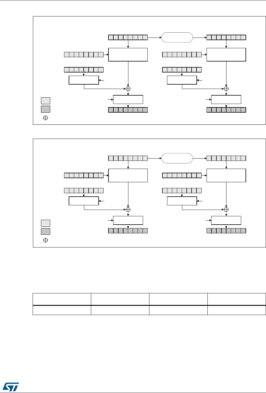
RM0394 Rev 4 685/1600
RM0394 AES hardware accelerator (AES)
717
Figure 171. CTR encryption
Figure 172. CTR decryption
In CTR mode, the cryptographic core output (also called keystream) Ox is XOR-ed with
relevant input block (Px' for encryption, Cx' for decryption), to produce the correct output
block (Cx' for encryption, Px' for decryption). Initialization vectors in AES must be initialized
as shown in Table 119.
Unlike in CBC mode that uses the AES_IVRx registers only once when processing the first
data block, in CTR mode AES_IVRx registers are used for processing each data block, and
the AES peripheral increments the counter bits of the initialization vector (leaving the nonce
bits unchanged).
CTR decryption does not differ from CTR encryption, since the core always encrypts the
current counter block to produce the key stream that is then XOR-ed with the plaintext (CTR
Table 119. CTR mode initialization vector definition
AES_IVR3[31:0] AES_IVR2[31:0] AES_IVR1[31:0] AES_IVR0[31:0]
Nonce[31:0] Nonce[63:32] Nonce[95:64] 32-bit counter = 0x0001
06Y9
(QFU\SW
$(6B.(<5[.(<
$(6B',15SODLQWH[W3
$(6B'2875FLSKHUWH[W&
'$7$7<3(>@ 6ZDS
PDQDJHPHQW
$(6B,95[
,9ELWFRXQWHU
LQSXW
RXWSXW
/HJHQG
;25
6ZDS
PDQDJHPHQW
'$7$7<3(>@
(QFU\SW
$(6B.(<5[.(<
$(6B'2875FLSKHUWH[W&
'$7$7<3(>@ 6ZDS
PDQDJHPHQW
$(6B,95[
6ZDS
PDQDJHPHQW
'$7$7<3(>@
&RXQWHU
LQFUHPHQW
$(6B',15SODLQWH[W3
, ,
2 2
%ORFN %ORFN
3 3
& &
06Y9
(QFU\SW
$(6B.(<5[.(<
$(6B',15FLSKHUWH[W&
$(6B'2875SODLQWH[W3
'$7$7<3(>@ 6ZDS
PDQDJHPHQW
$(6B,95[
1RQFHELWFRXQWHU
LQSXW
RXWSXW
/HJHQG
;25
6ZDS
PDQDJHPHQW
'$7$7<3(>@
(QFU\SW
$(6B.(<5[.(<
$(6B'2875SODLQWH[W3
'$7$7<3(>@ 6ZDS
PDQDJHPHQW
$(6B,95[
1RQFHELWFRXQWHU
6ZDS
PDQDJHPHQW
'$7$7<3(>@
&RXQWHU
LQFUHPHQW
$(6B',15FLSKHUWH[W&
, ,
2 2
%ORFN %ORFN
& &
3 3

AES hardware accelerator (AES) RM0394
686/1600 RM0394 Rev 4
encryption) or ciphertext (CTR decryption) input. In CTR mode, the MODE[1:0] bitfield
settings 11, 10 or 00 default all to encryption mode, and the setting 01 (key derivation) is
forbidden.
The sequence of events to perform an encryption or a decryption in CTR chaining mode:
1. Ensure that AES is disabled (the EN bit of the AES_CR must be 0).
2. Select CTR chaining mode by setting to 010 the CHMOD[2:0] bitfield of the AES_CR
register. Set MODE[1:0] bitfield to any value other than 01.
3. Initialize the AES_KEYRx registers, and load the AES_IVRx registers as described in
Table 119.
4. Set the EN bit of the AES_CR register, to start encrypting the current counter (EN is
automatically reset when the calculation finishes).
5. If it is the last block, pad the data with zeros to have a complete block, if needed.
6. Append data in AES, and read the result. The three possible scenarios are described in
Section 25.4.4: AES procedure to perform a cipher operation.
7. Repeat the previous step till the second-last block is processed. For the last block,
apply the two previous steps and discard the bits that are not part of the payload (if the
size of the significant data in the last input block is less than 16 bytes).
Suspend/resume operations in CTR mode
Like for the CBC mode, it is possible to interrupt a message to send a higher priority
message, and resume the message that was interrupted. Detailed CBC suspend/resume
sequence is described in Section 25.4.8: AES basic chaining modes (ECB, CBC).
Note: Like for CBC mode, the AES_IVRx registers must be reloaded during the resume operation.
25.4.10 AES Galois/counter mode (GCM)
Overview
The AES Galois/counter mode (GCM) allows encrypting and authenticating a plaintext
message into the corresponding ciphertext and tag (also known as message authentication
code). To ensure confidentiality, GCM algorithm is based on AES counter mode. It uses a
multiplier over a fixed finite field to generate the tag.
GCM chaining is defined in NIST Special Publication 800-38D, Recommendation for Block
Cipher Modes of Operation - Galois/Counter Mode (GCM) and GMAC. A typical message
construction in GCM mode is given in Figure 173.
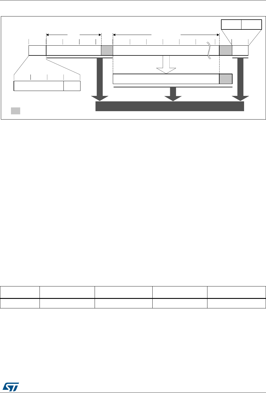
RM0394 Rev 4 687/1600
RM0394 AES hardware accelerator (AES)
717
Figure 173. Message construction in GCM
The message has the following structure:
•16-byte initial counter block (ICB), composed of two distinct fields:
–Initialization vector (IV): a 96-bit value that must be unique for each encryption
cycle with a given key. Note that the GCM standard supports IVs with less than 96
bits, but in this case strict rules apply.
–Counter: a 32-bit big-endian integer that is incremented each time a block
processing is completed. According to NIST specification, the counter value is 0x2
when processing the first block of payload.
•Authenticated header AAD (also knows as additional authentication data) has a
known length Len(A) that may be a non-multiple of 16 bytes, and must not exceed
264 – 1 bits. This part of the message is only authenticated, not encrypted.
•Plaintext message P is both authenticated and encrypted as ciphertext C, with a
known length Len(P) that may be non-multiple of 16 bytes, and cannot exceed 232 -2
128-bit blocks.
•Last block contains the AAD header length (bits [32:63]) and the payload length (bits
[96:127]) information, as shown in Table 120.
The GCM standard specifies that ciphertext C has the same bit length as the plaintext P.
When a part of the message (AAD or P) has a length that is a non-multiple of 16-bytes a
special padding scheme is required.
06Y9
3ODLQWH[W3
E\WH
ERXQGDULHV
$GGLWLRQDODXWKHQWLFDWHGGDWD
$$'
$XWKHQWLFDWHGHQFU\SWHGFLSKHUWH[W&
/HQ$ /HQ3 /HQ&
>/HQ$@
/DVW
EORFN
>/HQ&@
$XWKHQWLFDWLRQWDJ7
,&%
E\WHERXQGDULHV
&RXQWHU,QLWLDOL]DWLRQYHFWRU,9
DXWKHQWLFDWH
HQFU\SW
=HURSDGGLQJ]HURHGELWV
DXWKHQWLFDWH
DXWK
Table 120. GCM last block definition
Endianness Bit[0] ---------- Bit[31] Bit[32]---------- Bit[63] Bit[64] -------- Bit[95] Bit[96] --------- Bit[127]
Input data 0x0 AAD length[31:0] 0x0 Payload length[31:0]
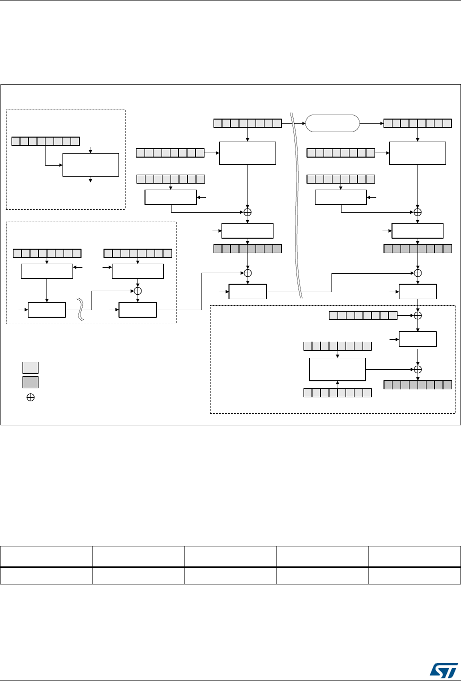
AES hardware accelerator (AES) RM0394
688/1600 RM0394 Rev 4
GCM processing
Figure 174 describes the GCM implementation in the AES peripheral. The GCM is selected
by writing 011 to the CHMOD[2:0] bitfield of the AES_CR register.
Figure 174. GCM authenticated encryption
The mechanism for the confidentiality of the plaintext in GCM mode is similar to that in the
Counter mode, with a particular increment function (denoted 32-bit increment) that
generates the sequence of input counter blocks.
AES_IVRx registers keeping the counter block of data are used for processing each data
block. The AES peripheral automatically increments the Counter[31:0] bitfield. The first
counter block (CB1) is derived from the initial counter block ICB by the application software
(see Table 121).
Note: In GCM mode, the settings 01 and 11 of the MODE[1:0] bitfield are forbidden.
06Y9
)LQDO
,QLW
+HDGHU
$(6B.(<5[.(<
$(6B',15SODLQWH[W3
$(6B'2875
FLSKHUWH[W&
'$7$7<3(
>@ 6ZDS
PDQDJHPHQW
$(6B,95[
,&%ELWFRXQWHU [
LQSXW
RXWSXW
/HJHQG
;25
6ZDS
PDQDJHPHQW
'$7$7<3(
>@
$(6B.(<5[.(<
'$7$7<3(>@ 6ZDS
PDQDJHPHQW
$(6B,95[
6ZDS
PDQDJHPHQW
'$7$7<3(
>@
&RXQWHU
LQFUHPHQW
$(6B',15SODLQWH[W3Q
+
$(6B'2875
FLSKHUWH[W&Q
+
(QFU\SW
>@
+
$(6B',15$$'
6ZDS
PDQDJHPHQW 6ZDS
PDQDJHPHQW
$(6B',15$$'L
*)PXO
'$7$7<3(
>@
*)PXO
++
$(6B.(<5[.(<
*)PXO *)PXO
*)PXO
+
$(6B',15
/HQ$__/HQ&
(QFU\SW
$(6B.(<5[NH\
$(6B,95[
,9ELWFRXQWHU [
$(6B'2875
$XWKHQWLFDWLRQ7$*7
6
(QFU\SW (QFU\SW
%ORFN %ORFNQ
&%Q
&% &%Q
3D\ORDG
Table 121. GCM mode IVI bitfield initialization
Register AES_IVR3[31:0] AES_IVR2[31:0] AES_IVR1[31:0] AES_IVR0[31:0]
Input data ICB[31:0] ICB[63:32] ICB[95:64] Counter[31:0] = 0x2

RM0394 Rev 4 689/1600
RM0394 AES hardware accelerator (AES)
717
The authentication mechanism in GCM mode is based on a hash function called GF2mul
that performs multiplication by a fixed parameter, called hash subkey (H), within a binary
Galois field.
A GCM message is processed through the following phases, further described in next
subsections:
•Init phase: AES prepares the GCM hash subkey (H).
•Header phase: AES processes the additional authenticated data (AAD), with hash
computation only.
•Payload phase: AES processes the plaintext (P) with hash computation, counter block
encryption and data XOR-ing. It operates in a similar way for ciphertext (C).
•Final phase: AES generates the authenticated tag (T) using the last block of the
message.
GCM init phase
During this first step, the GCM hash subkey (H) is calculated and saved internally, to be
used for processing all the blocks. The recommended sequence is:
1. Ensure that AES is disabled (the EN bit of the AES_CR must be 0).
2. Select GCM chaining mode, by setting to 011 the CHMOD[2:0] bitfield of the AES_CR
register, and set to 00 (no data swapping) the DATATYPE[1:0] bitfield.
3. Indicate the Init phase, by setting to 00 the GCMPH[1:0] bitfield of the AES_CR
register.
4. Set the MODE[1:0] bitfield of the AES_CR register to 00 or 10.
5. Initialize the AES_KEYRx registers with a key, and initialize AES_IVRx registers with
the information as defined in Table 121.
6. Start the calculation of the hash key, by setting to 1 the EN bit of the AES_CR register
(EN is automatically reset when the calculation finishes).
7. Wait until the end of computation, indicated by the CCF flag of the AES_SR transiting
to 1. Alternatively, use the corresponding interrupt.
8. Clear the CCF flag of the AES_SR register, by setting to 1 the CCFC bit of the AES_CR
register, and optionally set the data type (1-, 8- or 16-bit) using the DATATYPE[1:0]
bitfield.
GCM header phase
This phase coming after the GCM Init phase must be completed before the payload phase.
The sequence to execute, identical for encryption and decryption, is:
1. Indicate the header phase, by setting to 01 the GCMPH[1:0] bitfield of the AES_CR
register. Do not modify the MODE[1:0] bitfield as set in the Init phase.
2. Enable the AES peripheral by setting the EN bit of the AES_CR register.
3. If it is the last block and the AAD size in the block is inferior to 128 bits, pad the
remainder of the block with zeros. Then append the data block into AES in one of ways
described in Section 25.4.4: AES procedure to perform a cipher operation on
page 672.
4. Repeat the step 3 until the last additional authenticated data block is processed.
Note: The header phase can be skipped if there is no AAD, that is, Len(A) = 0.

AES hardware accelerator (AES) RM0394
690/1600 RM0394 Rev 4
GCM payload phase
This phase, identical for encryption and decryption, is executed after the GCM header
phase. During this phase, the encrypted/decrypted payload is stored in the AES_DOUTR
register. The sequence to execute is:
1. If the header phase was skipped, enable the AES peripheral by setting the EN bit of the
AES_CR register.
2. Indicate the payload phase, by setting to 10 the GCMPH[1:0] bitfield of the AES_CR
register. Do not modify the MODE[1:0] bitfield as set in the Init phase.
3. If it is the last block and the plaintext (encryption) or ciphertext (decryption) size in the
block is inferior to 128 bits, pad the remainder of the block with zeros.
4. Append the data block into AES in one of ways described in Section 25.4.4: AES
procedure to perform a cipher operation on page 672, and read the result.
5. Repeat the previous step till the second-last plaintext block is encrypted or till the last
block of ciphertext is decrypted. For the last block of plaintext (encryption only),
execute the two previous steps. For the last block, discard the bits that are not part of
the payload when the last block size is less than 16 bytes.
Note: The payload phase can be skipped if there is no payload data, that is, Len(C) = 0 (see
GMAC mode).
GCM final phase
In this last phase, the AES peripheral generates the GCM authentication tag and stores it in
the AES_DOUTR register. The sequence to execute is:
1. Indicate the final phase, by setting to 11 the GCMPH[1:0] bitfield of the AES_CR
register. Select encrypt mode by setting to 00 the MODE[1:0] bitfield of the AES_CR
register.
2. Compose the data of the block, by concatenating the AAD bit length and the payload
bit length, as shown in Table 120. Write the block into the AES_DINR register.
3. Wait until the end of computation, indicated by the CCF flag of the AES_SR transiting
to 1.
4. Get the GCM authentication tag, by reading the AES_DOUTR register four times.
5. Clear the CCF flag in the AES_SR register, by setting to 1 the CCFC bit of the AES_CR
register.
6. Disable the AES peripheral, by clearing the bit EN of the AES_CR register. If it is an
authenticated decryption, compare the generated tag with the expected tag passed
with the message.
Note: In the final phase, data must be swapped according to the data type set in the
DATATYPE[1:0] bitfield of the AES_CR register.
When transiting from the header or the payload phase to the final phase, the AES peripheral
must not be disabled, otherwise the result is wrong.

RM0394 Rev 4 691/1600
RM0394 AES hardware accelerator (AES)
717
Suspend/resume operations in GCM mode
To suspend the processing of a message, proceed as follows:
1. If DMA is used, stop the AES DMA transfers to the IN FIFO by clearing the DMAINEN
bit of the AES_CR register. If DMA is not used, make sure that the current computation
is completed, which is indicated by the CCF flag of the AES_SR register set to 1.
2. In the payload phase, if DMA is not used, read four times the AES_DOUTR register to
save the last-processed block. If DMA is used, wait until the CCF flag is set in the
AES_SR register then stop the DMA transfers from the OUT FIFO by clearing the
DMAOUTEN bit of the AES_CR register.
3. Clear the CCF flag of the AES_SR register, by setting to 1 the CCFC bit of the AES_CR
register.
4. Save the AES_SUSPxR registers in the memory, where x is from 0 to 7.
5. In the payload phase, save the AES_IVRx registers as, during the data processing,
they changed from their initial values. In the header phase, this step is not required.
6. Disable the AES peripheral, by clearing the EN bit of the AES_CR register.
7. Save the current AES configuration in the memory, excluding the initialization vector
registers AES_IVRx. Key registers do not need to be saved as the original key value is
known by the application.
8. If DMA is used, save the DMA controller status (pointers for IN data transfers, number
of remaining bytes, and so on). In the payload phase, pointers for OUT data transfers
must also be saved.
To resume the processing of a message, proceed as follows:
1. If DMA is used, configure the DMA controller in order to complete the rest of the FIFO
IN transfers. In the payload phase, the rest of the FIFO OUT transfers must also be
configured in the DMA controller.
2. Ensure that the AES peripheral is disabled (the EN bit of the AES_CR register must be
0).
3. Write the suspend register values, previously saved in the memory, back into their
corresponding AES_SUSPxR registers, where x is from 0 to 7.
4. In the payload phase, write the initialization vector register values, previously saved in
the memory, back into their corresponding AES_IVRx registers. In the header phase,
write initial setting values back into the AES_IVRx registers.
5. Restore the initial setting values in the AES_CR and AES_KEYRx registers.
6. Enable the AES peripheral by setting the EN bit of the AES_CR register.
7. If DMA is used, enable AES DMA requests by setting the DMAINEN bit (and
DMAOUTEN bit if in payload phase) of the AES_CR register.
25.4.11 AES Galois message authentication code (GMAC)
Overview
The Galois message authentication code (GMAC) allows the authentication of a plaintext,
generating the corresponding tag information (also known as message authentication
code). It is based on GCM algorithm, as defined in NIST Special Publication 800-38D,
Recommendation for Block Cipher Modes of Operation - Galois/Counter Mode (GCM) and
GMAC.
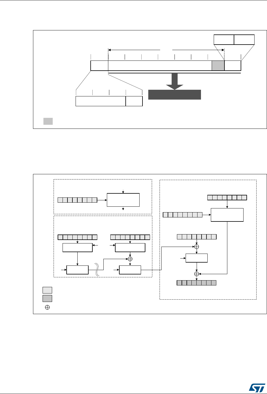
AES hardware accelerator (AES) RM0394
692/1600 RM0394 Rev 4
A typical message construction for GMAC is given in Figure 175.
Figure 175. Message construction in GMAC mode
AES GMAC processing
Figure 176 describes the GMAC mode implementation in the AES peripheral. This mode is
selected by writing 011 to the CHMOD[2:0] bitfield of the AES_CR register.
Figure 176. GMAC authentication mode
The GMAC algorithm corresponds to the GCM algorithm applied on a message only
containing a header. As a consequence, all steps and settings are the same as with the
GCM, except that the payload phase is omitted.
Suspend/resume operations in GMAC
In GMAC mode, the sequence described for the GCM applies except that only the header
phase can be interrupted.
06Y9
$XWKHQWLFDWHGGDWD
E\WH
ERXQGDULHV
/HQ$
>/HQ$@
/DVW
EORFN
>@
$XWKHQWLFDWLRQWDJ7
,&%
E\WHERXQGDULHV
&RXQWHU,QLWLDOL]DWLRQYHFWRU,9
=HURSDGGLQJ
DXWK
06Y9
)LQDO
,QLW
+HDGHU
$(6B.(<5[.(<
LQSXW
RXWSXW
/HJHQG
;25
$(6B.(<5[.(<
$(6B,95[
,9ELWFRXQWHU [
(QFU\SW
>@
+
$(6B',15
PHVVDJHEORFN
6ZDS
PDQDJHPHQW 6ZDS
PDQDJHPHQW
$(6B',15
PHVVDJHEORFNQ
*)PXO
'$7$7<3(
>@
*)PXO
++
*)PXO
+
$(6B',15
OHQ$__OHQ&
$(6B'2875
DXWKHQWLFDWLRQWDJ7
6
(QFU\SW
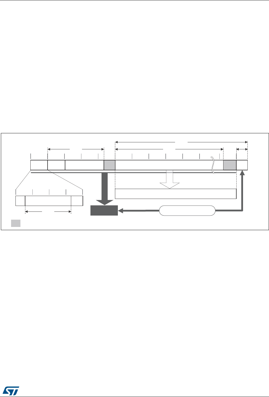
RM0394 Rev 4 693/1600
RM0394 AES hardware accelerator (AES)
717
25.4.12 AES counter with CBC-MAC (CCM)
Overview
The AES counter with cipher block chaining-message authentication code (CCM)
algorithm allows encryption and authentication of plaintext, generating the corresponding
ciphertext and tag (also known as message authentication code). To ensure confidentiality,
the CCM algorithm is based on AES in counter mode. It uses cipher block chaining
technique to generate the message authentication code. This is commonly called CBC-
MAC.
Note: NIST does not approve this CBC-MAC as an authentication mode outside the context of the
CCM specification.
CCM chaining is specified in NIST Special Publication 800-38C, Recommendation for Block
Cipher Modes of Operation - The CCM Mode for Authentication and Confidentiality. A typical
message construction for CCM is given in Figure 177.
Figure 177. Message construction in CCM mode
The structure of the message is:
•16-byte first authentication block (B0), composed of three distinct fields:
–Q: a bit string representation of the octet length of P (Len(P))
–Nonce (N): a single-use value (that is, a new nonce should be assigned to each
new communication) of Len(N) size. The sum Len(N) + Len(P) must be equal to
15 bytes.
–Flags: most significant octet containing four flags for control information, as
specified by the standard. It contains two 3-bit strings to encode the values t (MAC
length expressed in bytes) and Q (plaintext length such that Len(P) < 28q bytes).
The counter blocks range associated to Q is equal to 28Q-4, that is, if the maximum
value of Q is 8, the counter blocks used in cipher shall be on 60 bits.
•16-byte blocks (B) associated to the Associated Data (A).
This part of the message is only authenticated, not encrypted. This section has a
known length Len(A) that can be a non-multiple of 16 bytes (see Figure 177). The
06Y9
3ODLQWH[W3
E\WH
ERXQGDULHV
$VVRFLDWHGGDWD$
$XWKHQWLFDWHGHQFU\SWHGFLSKHUWH[W&
/HQ$ /HQ3
(QF
7
0$&7
%
E\WHERXQGDULHV
41RQFH1
DXWKHQWLFDWH
HQFU\SW
=HURSDGGLQJ
/HQ&
>D@
>D@
/HQ7
IODJV
/HQ1 'HFU\SWDQGFRPSDUH

AES hardware accelerator (AES) RM0394
694/1600 RM0394 Rev 4
standard also states that, on MSB bits of the first message block (B1), the associated
data length expressed in bytes (a) must be encoded as follows:
– If 0 < a < 216 -2
8, then it is encoded as [a]16, that is, on two bytes.
–If 2
16 -2
8 < a < 232, then it is encoded as 0xff || 0xfe || [a]32, that is, on six bytes.
–If 2
32 < a < 264, then it is encoded as 0xff || 0xff || [a]64, that is, on ten bytes.
•16-byte blocks (B) associated to the plaintext message P, which is both authenticated
and encrypted as ciphertext C, with a known length Len(P). This length can be a non-
multiple of 16 bytes (see Figure 177).
•Encrypted MAC (T) of length Len(T) appended to the ciphertext C of overall length
Len(C).
When a part of the message (A or P) has a length that is a non-multiple of 16-bytes, a
special padding scheme is required.
Note: CCM chaining mode can also be used with associated data only (that is, no payload).
As an example, the C.1 section in NIST Special Publication 800-38C gives the following
values (hexadecimal numbers):
N: 10111213 141516 (Len(N)= 56 bits or 7 bytes)
A: 00010203 04050607 (Len(A)= 64 bits or 8 bytes)
P: 20212223 (Len(P)= 32 bits or 4 bytes)
T: 6084341B (Len(T)= 32 bits or t = 4)
B0: 4F101112 13141516 00000000 00000004
B1: 00080001 02030405 06070000 00000000
B2: 20212223 00000000 00000000 00000000
CTR0: 0710111213 141516 00000000 00000000
CTR1: 0710111213 141516 00000000 00000001
Generation of formatted input data blocks Bx (especially B0 and B1) must be managed by
the application.
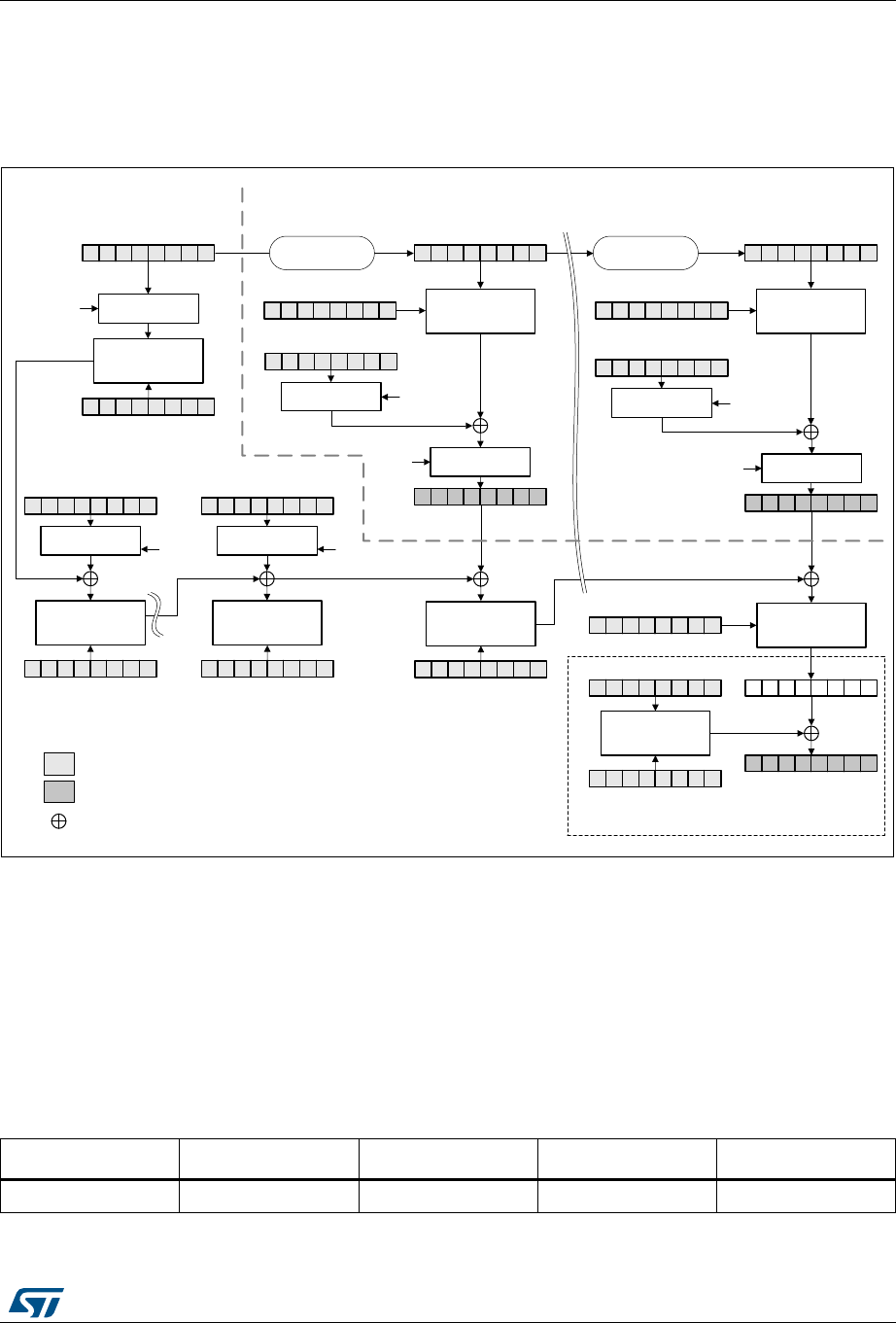
RM0394 Rev 4 695/1600
RM0394 AES hardware accelerator (AES)
717
CCM processing
Figure 178 describes the CCM implementation within the AES peripheral (decryption
example).
Figure 178. CCM mode authenticated decryption
The data input to the generation-encryption process are a valid nonce, a valid payload
string, and a valid associated data string, all properly formatted. The CBC chaining
mechanism is applied to the formatted plaintext data to generate a MAC, with a known
length. Counter mode encryption that requires a sufficiently long sequence of counter blocks
as input, is applied to the payload string and separately to the MAC. The resulting ciphertext
C is the output of the generation-encryption process on plaintext P.
AES_IVRx registers are used for processing each data block, AES automatically
incrementing the CTR counter with a bit length defined by the first block B0. Table 122
shows how the application must load the B0 data.
06Y9
$(6&&0ILQDO
$(6B'2875FLSKHUWH[W&
$(6B',15
SODLQWH[W3
'$7$7<3(
>@ 6ZDS
PDQDJHPHQW
$(6B,95[&75
LQSXW
RXWSXW
/HJHQG
;25
6ZDS
PDQDJHPHQW
'$7$7<3(
>@
$(6B.(<5[.(<
'$7$7<3(>@
6ZDS
PDQDJHPHQW
$(6B,95[&75P
6ZDS
PDQDJHPHQW
'$7$7<3(
>@
ELW
LQFUHPHQW
$(6B'2875FLSKHUWH[W
PLQXVWDJODVWEORFN&P
$(6B',15
SODLQWH[WODVWEORFN3P
(QFU\SW
$(6B',15
ILUVWEORFN%
$(6B',15DVVRFLDWHG
GDWDEORFN%
6ZDS
PDQDJHPHQW 6ZDS
PDQDJHPHQW
$(6B',15DVVRFLDWHG
GDWDODVWEORFN%X
$(6B.(<5[.(<
$(6B',15&75
%ORFNFLSKHU
HQFU\SWLRQ
$(6B.(<5[.(<
$(6B'2875
DXWKHQWLFDWLRQWDJ7
0$&7
(QFU\SW (QFU\SW
6
%U
%X
(QFU\SW
$(6B.(<5[.(<
(QFU\SW
$(6B.(<5[.(<
(QFU\SW
$(6B.(<5[.(<
(QFU\SW
$(6B.(<5[.(<
$(6B.(<5[NH\
'$7$7<3(>@ 6ZDS
PDQDJHPHQW
&&0DXWKHQWLFDWLRQRQO\ &75
'$7$7<3(>@
'$7$7<3(>@
6P
6
%ORFN %ORFNP
6:SURFHVVLQJ
3D\ORDG
Table 122. Initialization of AES_IVRx registers in CCM mode
Register AES_IVR3[31:0] AES_IVR2[31:0] AES_IVR1[31:0] AES_IVR0[31:0]
Input data B0[31:0] B0[63:32] B0[95:64] B0[127:96]

AES hardware accelerator (AES) RM0394
696/1600 RM0394 Rev 4
A CCM message is processed through two distinct processes - first, payload encryption or
decryption, in which the AES peripheral is configured in CTR mode, then associated data
and payload authentication, in which the AES peripheral first executes the CCM header
phase, then the CCM final phase.
Payload encryption/decryption
This step is performed independently of the tag computation. It uses standard CTR chaining
mode. Refer to Section 25.4.9: AES counter (CTR) mode for details. The construction of the
CTR1 initialization vector (see Figure 178) to load into AES_IVRx registers is defined in
NIST Special Publication 800-38C.
Note: This phase can be skipped if there is no payload data, that is, when Len(P) = 0 or
Len(C) = Len(T).
Remove LSBLen(T)(C) encrypted tag information when decrypting ciphertext C.
Associated data and payload authentication
In order to compute the CCM authentication tag associated with the plaintext message, it is
recommended to execute the following header phase sequence:
1. Ensure that the AES peripheral is disabled (the EN bit of the AES_CR must be 0).
2. Select CCM chaining mode, by setting to 100 the CHMOD[2:0] bitfield of the AES_CR
register, and optionally, set the DATATYPE[1:0] bitfield.
3. Indicate the header phase, by setting to 01 the GCMPH[1:0] bitfield of the AES_CR
register. Select encrypt mode by setting to 00 the MODE[1:0] bitfield of the AES_CR
register.
4. Initialize the AES_KEYRx registers with a key, and initialize AES_IVRx registers with
zero values.
5. Enable the AES peripheral by setting the EN bit of the AES_CR register.
6. Write the AES_DINR register with B0, as shown in Table 122. B0 data must be
swapped according to the DATATYPE[1:0] bitfield of the AES_CR register.
7. Wait until the end-of-computation flag CCF of the AES_SR register is set to 1.
8. Clear the CCF flag of the AES_SR register by setting the CCFC bit of the AES_CR
register.
9. Process data block. If it is the last block of associated data or plaintext and data size in
the block is inferior to 128 bits, pad the remainder of the block with zeros. Then append
the data block into AES in one of ways described in Section 25.4.4: AES procedure to
perform a cipher operation on page 672.
10. Repeat the previous step to process all data blocks, starting from the first block of
associated data and ending with the last block of plaintext payload data.

RM0394 Rev 4 697/1600
RM0394 AES hardware accelerator (AES)
717
In final phase, the AES peripheral generates the CCM authentication tag and stores it in the
AES_DOUTR register:
11. Indicate the final phase, by setting to 11 the GCMPH[1:0] bitfield of the AES_CR
register. Keep as-is the encryption mode in the MODE[1:0] bitfield.
12. Write four times the last data input into the AES_DIN register. This input must be the
128-bit value CTR0, formatted from the original B0 packet (that is, 5 flag bits set to 0,
and Q length bits set to 0).
13. Wait until the end-of-computation flag CCF of the AES_SR register is set.
14. Read four times the AES_DOUTR register: the output corresponds to the encrypted
CCM authentication tag.
15. Clear the CCF flag of the AES_SR register by setting the CCFC bit of the AES_CR
register.
16. Disable the AES peripheral, by clearing the EN bit of the AES_CR register.
17. For authenticated decryption, compare the generated encrypted tag with the encrypted
tag padded in the ciphertext.
Note: In this final phase, data must be swapped according to the DATATYPE[1:0] bitfield of the
AES_CR register.
When transiting from the header phase to the final phase, the AES peripheral must not be
disabled, otherwise the result is wrong.
Application must mask the authentication tag output with tag length to obtain a valid tag.
Suspend/resume operations in CCM mode
To suspend the authentication of the associated data and payload (GCMPH[1:0]= 01),
proceed as follows. Suspending the message during the encryption/decryption phase is
described in Section 25.4.9: AES counter (CTR) mode on page 684.
1. If DMA is used, stop the AES DMA transfers to the IN FIFO by clearing the DMAINEN
bit of the AES_CR register. If DMA is not used, make sure that the current computation
is completed, which is indicated by the CCF flag of the AES_SR register set to 1.
2. Clear the CCF flag of the AES_SR register, by setting to 1 the CCFC bit of the AES_CR
register.
3. Save the AES_SUSPxR registers (where x is from 0 to 7) in the memory.
4. Save the AES_IVRx registers, as during the data processing they changed from their
initial values.
5. Disable the AES peripheral, by clearing the bit EN of the AES_CR register.
6. Save the current AES configuration in the memory, excluding the initialization vector
registers AES_IVRx. Key registers do not need to be saved as the original key value is
known by the application.
7. If DMA is used, save the DMA controller status (pointers for IN data transfers, number
of remaining bytes, and so on).

AES hardware accelerator (AES) RM0394
698/1600 RM0394 Rev 4
To resume the authentication of the associated data and payload (GCMPH[1:0]= 01 or
11), proceed as follows:
1. If DMA is used, configure the DMA controller in order to complete the rest of the FIFO
IN transfers.
2. Ensure that AES processor is disabled (the EN bit of the AES_CR register must be 0).
3. Write the suspend register values, previously saved in the memory, back into their
corresponding AES_SUSPxR registers (where x is from 0 to 7).
4. Write the initialization vector register values, previously saved in the memory, back into
their corresponding AES_IVRx registers.
5. Restore the initial setting values in the AES_CR and AES_KEYRx registers.
6. Enable the AES peripheral by setting the EN bit of the AES_CR register.
7. If DMA is used, enable AES DMA requests by setting the DMAINEN bit of the AES_CR
register.
Note: In CCM mode the MODE[1:0] bitfield settings 01 and 11 (key derivation) are forbidden.
25.4.13 .AES data registers and data swapping
Data input and output
A 128-bit data block is entered into the AES peripheral with four successive 32-bit word
writes into the AES_DINR register (bitfield DIN[127:0]), the most significant word (bits
[127:96]) first, the least significant word (bits [31:0]) last.
A 128-bit data block is retrieved from the AES peripheral with four successive 32-bit word
reads from the AES_DOUTR register (bitfield DOUT[127:0]), the most significant word (bits
[127:96]) first, the least significant word (bits [31:0]) last.
The 32-bit data word for AES_DINR register or from AES_DOUTR register is organized in
big endian order, that is:
•the most significant byte of a word to write into AES_DINR must be put on the lowest
address out of the four adjacent memory locations keeping the word to write, or
•the most significant byte of a word read from AES_DOUTR goes to the lowest address
out of the four adjacent memory locations receiving the word
For using DMA for input data block write into AES, the four words of the input block must be
stored in the memory consecutively and in big-endian order, that is, the most significant
word on the lowest address. See Section 25.4.16: AES DMA interface.
Data swapping
The AES peripheral can be configured to perform a bit-, a byte-, a half-word-, or no
swapping on the input data word in the AES_DINR register, before loading it to the AES
processing core, and on the data output from the AES processing core, before sending it to
the AES_DOUTR register. The choice depends on the type of data. For example, a byte
swapping is used for an ASCII text stream.
The data swap type is selected through the DATATYPE[1:0] bitfield of the AES_CR register.
The selection applies both to the input and the output of the AES core.
For different data swap types, Figure 179 shows the construction of AES processing core
input buffer data P127..0, from the input data entered through the AES_DINR register, or the
construction of the output data available through the AES_DOUTR register, from the AES
processing core output buffer data P127..0.
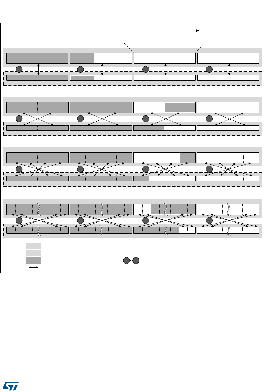
RM0394 Rev 4 699/1600
RM0394 AES hardware accelerator (AES)
717
Figure 179. 128-bit block construction with respect to data swap
Note: The data in AES key registers (AES_KEYRx) and initialization registers (AES_IVRx) are not
sensitive to the swap mode selection.
Data padding
Figure 179 also gives an example of memory data block padding with zeros such that the
zeroed bits after the data swap form a contiguous zone at the MSB end of the AES core
input buffer. The example shows the padding of an input data block containing:
•48 message bits, with DATATYPE[1:0] = 01
•56 message bits, with DATATYPE[1:0] = 10
•34 message bits, with DATATYPE[1:0] = 11
06Y9
'$7$7<3(>@ QRVZDSSLQJ
:RUG:RUG
' ' 3
/6%06%
'$7$7<3(>@ ELWKDOIZRUGVZDSSLQJ
:RUG
'$7$7<3(>@ ELWE\WHVZDSSLQJ
:RUG:RUG
'$7$7<3(>@ ELWVZDSSLQJ
:RUG
/6%
06%
/6%
06%
/6%06%
/6%06%
06%
06%
06% /6%
/6%
:RUG:RUG
/6%
:RUG
:RUG:RUG
' ' ' '
'
:RUG
=HURSDGGLQJH[DPSOH
/HJHQG
'DWDVZDS
:RUG
'
:RUG
:RUG:RUG
$(6LQSXWRXWSXWGDWDEORFNLQPHPRU\
$(6FRUHLQSXWRXWSXWEXIIHUGDWD
2UGHURIZULWHWR$(6B',15UHDGIURP$(6B'2875
06%
/6%
LQFUHDVLQJPHPRU\DGGUHVV
' ' ' ' ' '
''
' ' '' ' ' ' ''''' '' ' '
' '' ' '' ' ' ' ' ' ' ' ' ' '
' ' ' ' ' ' ' ' ' ' ' ' '''' ' ' ' ' ' ' ' '
E\WH E\WH E\WH E\WH
' ' ' '' ' ' '
PRVWVLJQLILFDQWELWRIPHPRU\GDWDEORFN$(&FRUHEXIIHU
OHDVWVLJQLILFDQWELWRIPHPRU\GDWDEORFN$(&FRUHEXIIHU
'[ LQSXWRXWSXWGDWDELWµ[
'' ' ' '' ' ' '' ' ' '' ' '
' ' ' ' ' ' ' ' ' ' ' ' ' ' ' '
' '' '' ' '' '' '' '' '' '' '' '' ''

AES hardware accelerator (AES) RM0394
700/1600 RM0394 Rev 4
25.4.14 AES key registers
The AES_KEYRx registers store the encryption or decryption key bitfield KEY[127:0] or
KEY[255:0]. The data to write to or to read from each register is organized in the memory in
little-endian order, that is, with most significant byte on the highest address.
The key is spread over the eight registers as shown in Table 123.
The key for encryption or decryption may be written into these registers when the AES
peripheral is disabled.
The key registers are not affected by the data swapping controlled by DATATYPE[1:0]
bitfield of the AES_CR register.
25.4.15 AES initialization vector registers
The four AES_IVRx registers keep the initialization vector input bitfield IVI[127:0]. The data
to write to or to read from each register is organized in the memory in little-endian order, that
is, with most significant byte on the highest address. The registers are also ordered from
lowest address (AES_IVR0) to highest address (AES_IVR3).
The signification of data in the bitfield depends on the chaining mode selected. When used,
the bitfield is updated upon each computation cycle of the AES core.
Write operations to the AES_IVRx registers when the AES peripheral is enabled have no
effect to the register contents. For modifying the contents of the AES_IVRx registers, the EN
bit of the AES_CR register must first be cleared.
Reading the AES_IVRx registers returns the latest counter value (useful for managing
suspend mode).
The AES_IVRx registers are not affected by the data swapping feature controlled by the
DATATYPE[1:0] bitfield of the CRYP_CR register.
25.4.16 AES DMA interface
The AES peripheral provides an interface to connect to the DMA (direct memory access)
controller. The DMA operation is controlled through the AES_CR register.
Data input using DMA
Setting the DMAINEN bit of the AES_CR register enables DMA writing into AES. The AES
peripheral then initiates a DMA request during the input phase each time it requires a word
to be written to the AES_DINR register. It asserts four DMA requests to transfer one 128-bit
(four-word) input data block from memory, as shown in Figure 180.
See Table 124 for recommended DMA configuration.
Table 123. Key endianness in AES_KEYRx registers (128- or 256-bit key length)
AES_KEYR7
[31:0]
AES_KEYR6
[31:0]
AES_KEYR5
[31:0]
AES_KEYR4
[31:0]
AES_KEYR3
[31:0]
AES_KEYR2
[31:0]
AES_KEYR1
[31:0]
AES_KEYR0
[31:0]
- - - - KEY[127:96] KEY[95:64] KEY[63:32] KEY[31:0]
KEY[255:224] KEY[223:192] KEY[191:160] KEY[159:128] KEY[127:96] KEY[95:64] KEY[63:32] KEY[31:0]
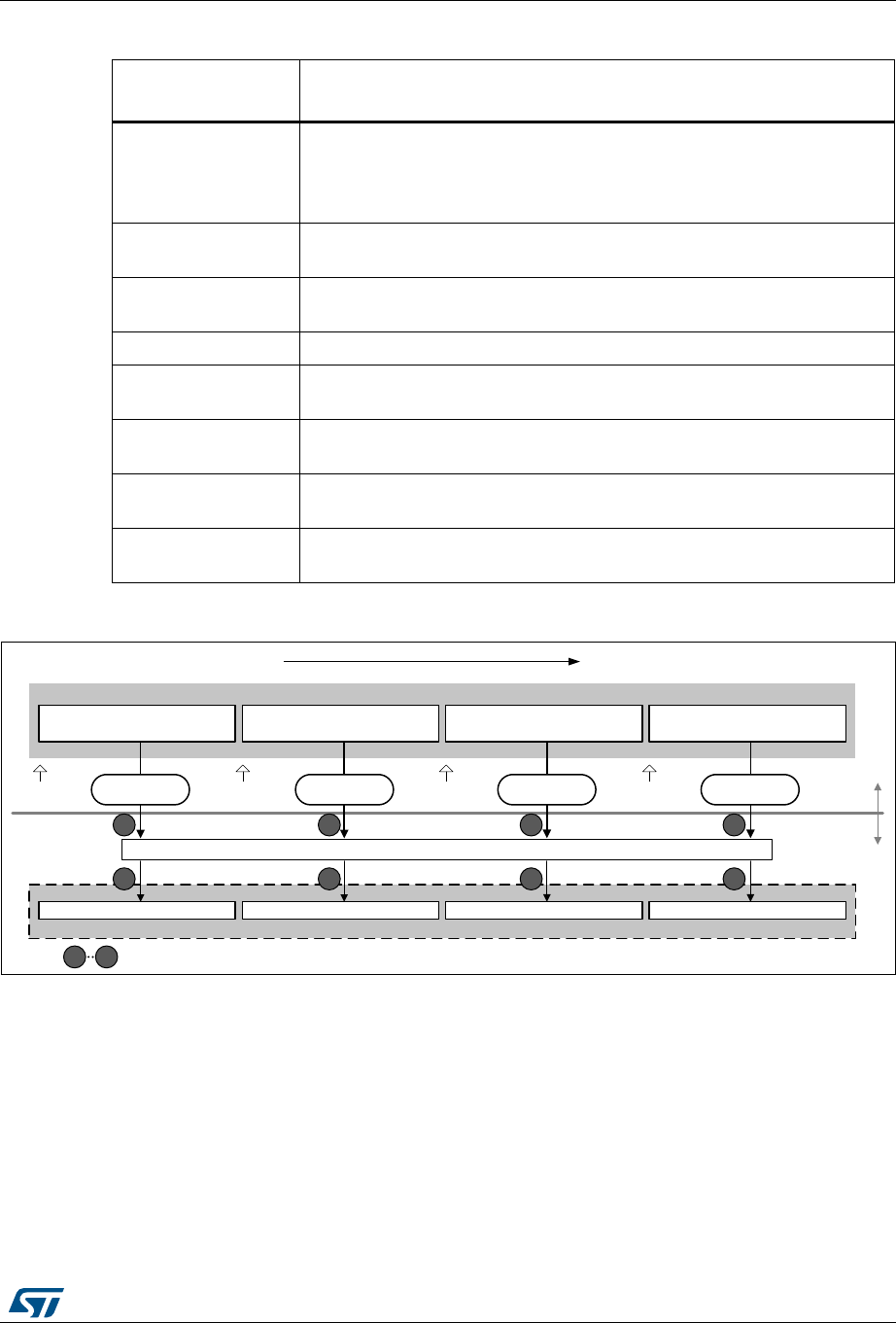
RM0394 Rev 4 701/1600
RM0394 AES hardware accelerator (AES)
717
Figure 180. DMA transfer of a 128-bit data block during input phase
Data output using DMA
Setting the DMAOUTEN bit of the AES_CR register enables DMA reading from AES. The
AES peripheral then initiates a DMA request during the Output phase each time it requires a
word to be read from the AES_DOUTR register. It asserts four DMA requests to transfer one
128-bit (four-word) output data block to memory, as shown in Figure 181.
See Table 125 for recommended DMA configuration.
Table 124. DMA channel configuration for memory-to-AES data transfer
DMA channel control
register field Recommended configuration
Transfer size
Message length: a multiple of 128 bits.
According to the algorithm and the mode selected, special padding/
ciphertext stealing might be required. Refer to Section 25.4.6: AES
ciphertext stealing and data padding on page 677 for details.
Source burst size
(memory) Single
Destination burst size
(peripheral) Single
DMA FIFO size AES FIFO_size = 4 bytes.
Source transfer width
(memory) 32-bit words
Destination transfer
width (peripheral) 32-bit words
Source address
increment (memory) Yes, after each 32-bit transfer
Destination address
increment (peripheral)
Fixed address of AES_DINR (no increment)
06Y9
$(6FRUHLQSXWEXIIHU
$(6B',15
/6%
06%
1RVZDSSLQJ
0HPRU\DFFHVVHGWKURXJK'0$
:RUG:RUG :RUG:RUG
'0$
VLQJOHZULWH
'0$UHT1 '0$UHT1 '0$UHT1 '0$UHT1
, , , , , ,
,,
' ' ' ' ' '
''
',1>@ ',1>@ ',1>@ ',1>@
'0$
VLQJOHZULWH '0$
VLQJOHZULWH '0$
VLQJOHZULWH
&KURQRORJLFDORUGHU
,QFUHDVLQJDGGUHVV
/6%06%
$(6
SHULSKHUDO 6\VWHP
2UGHURIZULWHWR$(6B',15
AES hardware accelerator (AES) RM0394
702/1600 RM0394 Rev 4
Figure 181. DMA transfer of a 128-bit data block during output phase
DMA operation in different operating modes
DMA operations are usable when Mode 1 (encryption) or Mode 3 (decryption) are selected
via the MODE[1:0] bitfield of the register AES_CR. As in Mode 2 (key derivation) the
AES_KEYRx registers must be written by software, enabling the DMA transfer through the
DMAINEN and DMAOUTEN bits of the AES_CR register have no effect in that mode.
DMA single requests are generated by AES until it is disabled. So, after the data output
phase at the end of processing of a 128-bit data block, AES switches automatically to a new
data input phase for the next data block, if any.
When the data transferring between AES and memory is managed by DMA, the CCF flag is
not relevant and can be ignored (left set) by software. It must only be cleared when
transiting back to data transferring managed by software. See Suspend/resume operations
Table 125. DMA channel configuration for AES-to-memory data transfer
DMA channel control
register field Recommended configuration
Transfer size It is the message length multiple of AES block size (4 words). According to
the case extra bytes will have to be discarded.
Source burst size
(peripheral) Single
Destination burst size
(memory) Single
DMA FIFIO size AES FIFO_size = 4 bytes
Source transfer width
(peripheral) 32-bit words
Destination transfer
width (memory) 32-bit words
Source address
increment (peripheral) Fixed address of AES_DINR (no increment)
Destination address
increment (memory)
Yes, after each 32-bit transfer
06Y9
$(6FRUHRXWSXWEXIIHU
/6%
06%
1RVZDSSLQJ
0HPRU\DFFHVVHGWKURXJK'0$
:RUG:RUG :RUG:RUG
'0$
VLQJOHUHDG
'0$UHT1 '0$UHT1 '0$UHT1 '0$UHT1
2 2 2 2 2 2
22
' ' ' ' ' '
''
'287>@ '287>@ '287>@ '287>@
'0$
VLQJOHUHDG '0$
VLQJOHUHDG '0$
VLQJOHUHDG
&KURQRORJLFDORUGHU
,QFUHDVLQJDGGUHVV
/6%06%
6\VWHP
$(6
SHULSKHUDO
2UGHURIUHDGIURP$(6B'2875
$(6B'2875
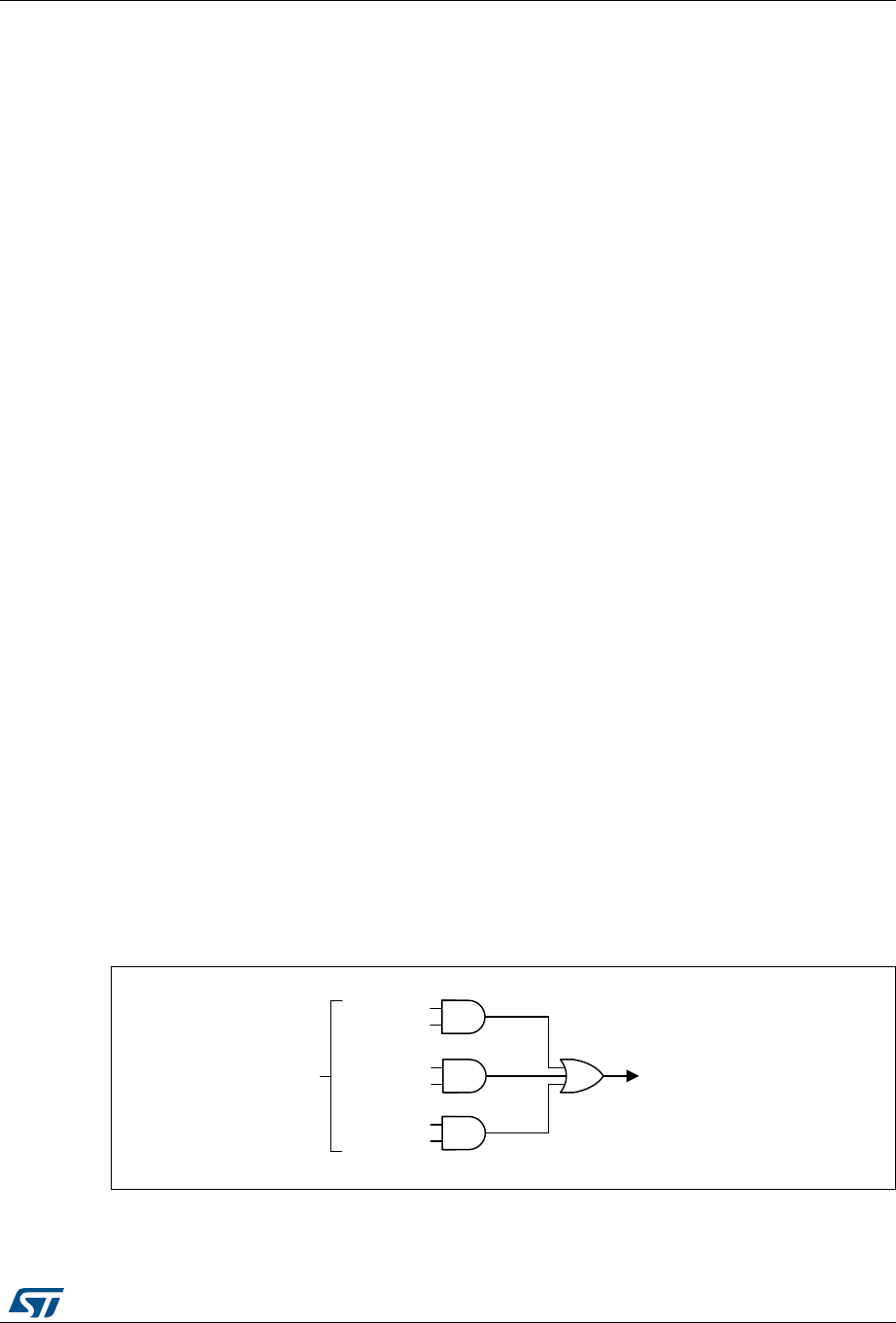
RM0394 Rev 4 703/1600
RM0394 AES hardware accelerator (AES)
717
in ECB/CBC modes in Section 25.4.8: AES basic chaining modes (ECB, CBC) as example.
25.4.17 AES error management
The read error flag (RDERR) and write error flag (WRERR) of the AES_SR register are set
when an unexpected read or write operation, respectively, is detected. An interrupt can be
generated if the error interrupt enable (ERRIE) bit of the AES_CR register is set. For more
details, refer to Section 25.5: AES interrupts.
Note: AES is not disabled after an error detection and continues processing.
AES can be re-initialized at any moment by clearing then setting the EN bit of the AES_CR
register.
Read error flag (RDERR)
When an unexpected read operation is detected during the computation phase or during the
input phase, the AES read error flag (RDERR) is set in the AES_SR register. An interrupt is
generated if the ERRIE bit of the AES_CR register is set.
The RDERR flag is cleared by setting the corresponding ERRC bit of the AES_CR register.
Write error flag (WDERR)
When an unexpected write operation is detected during the computation phase or during the
output phase, the AES write error flag (WRERR) is set in the AES_SR register. An interrupt
is generated if the ERRIE bit of the AES_CR register is set.
The WDERR flag is cleared by setting the corresponding ERRC bit of the AES_CR register.
25.5 AES interrupts
There are three individual maskable interrupt sources generated by the AES peripheral, to
signal the following events:
•computation completed
•read error, see Section 25.4.17
•write error, see Section 25.4.17
These three sources are combined into a common interrupt signal aes_it that connects to
NVIC (nested vectored interrupt controller).
Figure 182. AES interrupt signal generation
Each AES interrupt source can individually be enabled/disabled, by setting/clearing the
corresponding enable bit of the AES_CR register. See Figure 182.
06Y9
:5(55
(55,( DHVBLW
JRHVWR19,&
5'(55
(55,(
&&)
&&),(
)ODJVLQ$(6B65UHJLVWHU
%LWVRI$(6B&5UHJLVWHU
AES hardware accelerator (AES) RM0394
704/1600 RM0394 Rev 4
The status of the individual maskable interrupt sources can be read from the AES_SR
register.
Table 126 gives a summary of the interrupt sources, their event flags and enable bits.
25.6 AES processing latency
The tables below summarize the latency to process a 128-bit block for each mode of
operation.
Table 126. AES interrupt requests
AES interrupt event Event flag Enable bit
computation completed flag CCF CCFIE
read error flag RDERR ERRIE
write error flag WRERR ERRIE
Table 127. Processing latency (in clock cycle) for ECB, CBC and CTR
Key size Mode of operation Algorithm Input
phase
Computation
phase
Output
phase Total
128-bit
Mode 1: Encryption ECB, CBC, CTR 8 202 4 214
Mode 2: Key derivation - - 80 - 80
Mode 3: Decryption ECB, CBC, CTR 8 202 4 214
Mode 4: Key derivation then
decryption ECB, CBC 8 276 4 288
256-bit
Mode 1: Encryption ECB, CBC, CTR 8 286 4 298
Mode 2: Key derivation - - 109 - 109
Mode 3: Decryption ECB, CBC, CTR 8 286 4 298
Mode 4: Key derivation then
decryption ECB, CBC 8 380 4 392
Table 128. Processing latency for GCM and CCM (in clock cycle)
Key size Mode of operation Algorithm Init Phase Header
phase
Payload
phase Tag phase
128-bit
Mode 1: Encryption/
Mode 3: Decryption GCM 215 67 202 202
-CCM
authentication -206-202
256-bit
Mode 1: Encryption/
Mode 3: Decryption GCM 299 67 286 286
-CCM
authentication -290-286

RM0394 Rev 4 705/1600
RM0394 AES hardware accelerator (AES)
717
Note: Data insertion can include wait states forced by AES on the AHB bus (maximum 3 cycles,
typical 1 cycle). This applies to all header/payload/tag phases.
25.7 AES registers
25.7.1 AES control register (AES_CR)
Address offset: 0x00
Reset value: 0x0000 0000
31 30 29 28 27 26 25 24 23 22 21 20 19 18 17 16
Res. Res. Res. Res. Res. Res. Res. Res. Res. Res. Res. Res. Res. KEYSI
ZE Res. CHMO
D[2]
rw rw
1514131211109876543210
Res. GCMPH[1:0] DMAO
UTEN
DMAIN
EN ERRIE CCFIE ERRC CCFC CHMOD[1:0] MODE[1:0] DATATYPE[1:0] EN
rw rw rw rw rw rw rw rw rw rw rw rw rw rw rw
Bits 31:19 Reserved, must be kept at zero
Bit 18 KEYSIZE: Key size selection
This bitfield defines the length of the key used in the AES cryptographic core, in bits:
0: 128
1: 256
The bit value change is allowed only when AES is disabled, so as to avoid an unpredictable
behavior.
Bit 17 Reserved, must be kept at zero
Bit 16 CHMOD[2]: Chaining mode selection, bit [2]
Refer to the bits [5:6] of the register for the description of the CHMOD[2:0] bitfield
Bit 15 Reserved, must be kept at zero
Bits 14:13 GCMPH[1:0]: GCM or CCM phase selection
This bitfield selects the phase of GCM, GMAC or CCM algorithm:
00: Init phase
01: Header phase
10: Payload phase
11: Final phase
The bitfield has no effect if other than GCM, GMAC or CCM algorithms are selected (through the
ALGOMODE bitfield).

AES hardware accelerator (AES) RM0394
706/1600 RM0394 Rev 4
Bit 12 DMAOUTEN: DMA output enable
This bit enables/disables data transferring with DMA, in the output phase:
0: Disable
1: Enable
When the bit is set, DMA requests are automatically generated by AES during the output data
phase. This feature is only effective when Mode 1 or Mode 3 is selected through the MODE[1:0]
bitfield. It is not effective for Mode 2 (key derivation).
Usage of DMA with Mode 4 (single decryption) is not recommended.
Bit 11 DMAINEN: DMA input enable
This bit enables/disables data transferring with DMA, in the input phase:
0: Disable
1: Enable
When the bit is set, DMA requests are automatically generated by AES during the input data phase.
This feature is only effective when Mode 1 or Mode 3 is selected through the MODE[1:0] bitfield. It is
not effective for Mode 2 (key derivation).
Usage of DMA with Mode 4 (single decryption) is not recommended.
Bit 10 ERRIE: Error interrupt enable
This bit enables or disables (masks) the AES interrupt generation when RDERR and/or WRERR is
set:
0: Disable (mask)
1: Enable
Bit 9 CCFIE: CCF interrupt enable
This bit enables or disables (masks) the AES interrupt generation when CCF (computation complete
flag) is set:
0: Disable (mask)
1: Enable
Bit 8 ERRC: Error flag clear
Upon written to 1, this bit clears the RDERR and WRERR error flags in the AES_SR register:
0: No effect
1: Clear RDERR and WRERR flags
Reading the flag always returns zero.
Bit 7 CCFC: Computation complete flag clear
Upon written to 1, this bit clears the computation complete flag (CCF) in the AES_SR register:
0: No effect
1: Clear CCF
Reading the flag always returns zero.

RM0394 Rev 4 707/1600
RM0394 AES hardware accelerator (AES)
717
Bits 6:5 CHMOD[1:0]: Chaining mode selection, bits [1:0]
These bits, together with the bit CHMOD[2] (see bit 16 of this register), form CHMOD[2:0] bitfield that
selects the AES chaining mode:
000: Electronic codebook (ECB)
001: Cipher-Block Chaining (CBC)
010: Counter Mode (CTR)
011: Galois Counter Mode (GCM) and Galois Message Authentication Code (GMAC)
100: Counter with CBC-MAC (CCM)
>100: Reserved
The bitfield value change is allowed only when AES is disabled, so as to avoid an unpredictable
behavior.
Bits 4:3 MODE[1:0]: AES operating mode
This bitfield selects the AES operating mode:
00: Mode 1: encryption
01: Mode 2: key derivation (or key preparation for ECB/CBC decryption)
10: Mode 3: decryption
11: Mode 4: key derivation then single decryption
The bitfield value change is allowed only when AES is disabled, so as to avoid an unpredictable
behavior. Any attempt to selecting Mode 4 while either ECB or CBC chaining mode is not selected,
defaults to effective selection of Mode 3. It is not possible to select a Mode 3 following a Mode 4.
Bits 2:1 DATATYPE[1:0]: Data type selection
This bitfield defines the format of data written in the AES_DINR register or read from the
AES_DOUTR register, through selecting the mode of data swapping:
00: None
01: Half-word (16-bit)
10: Byte (8-bit)
11: Bit
For more details, refer to Section 25.4.13: .AES data registers and data swapping.
The bitfield value change is allowed only when AES is disabled, so as to avoid an unpredictable
behavior.
Bit 0 EN: AES enable
This bit enables/disables the AES peripheral:
0: Disable
1: Enable
At any moment, clearing then setting the bit re-initializes the AES peripheral.
This bit is automatically cleared by hardware when the key preparation process ends (Mode 2).

AES hardware accelerator (AES) RM0394
708/1600 RM0394 Rev 4
25.7.2 AES status register (AES_SR)
Address offset: 0x04
Reset value: 0x0000 0000
31 30 29 28 27 26 25 24 23 22 21 20 19 18 17 16
Res. Res. Res. Res. Res. Res. Res. Res. Res. Res. Res. Res. Res. Res. Res. Res.
r rrrr r r r r r r r r r r r
15 14 13 12 11 10 9 8 7 6 5 4 3 2 1 0
Res. Res. Res. Res. Res. Res. Res. Res. Res. Res. Res. Res. BUSY WRERR RDERR CCF
r rrrr r r r r r r r r r r r
Bits 31:4 Reserved, must be kept at zero
Bit 3 BUSY: Busy
This flag indicates whether AES is idle or busy during GCM payload encryption phase:
0: Idle
1: Busy
The flag is controlled by hardware. When the flag indicates “idle”, the current message processing
may be suspended to process a higher-priority message.
This flag is effective only in GCM payload encryption phase. in other chaining modes, or in GCM
phases other than payload encryption, the flag must be ignored.

RM0394 Rev 4 709/1600
RM0394 AES hardware accelerator (AES)
717
25.7.3 AES data input register (AES_DINR)
Address offset: 0x08
Reset value: 0x0000 0000
Only 32-bit access type is supported.
Bit 2 WRERR: Write error
This flag indicates the detection of an unexpected write operation to the AES_DINR register (during
computation or data output phase):
0: Not detected
1: Detected
The flag is set by hardware. It is cleared by software upon setting the ERRC bit of the AES_CR
register.
Upon the flag setting, an interrupt is generated if enabled through the ERRIE bit of the AES_CR
register.
The flag setting has no impact on the AES operation.
The flag is not effective when key derivation mode, or GCM/CCM Init phase is selected.
Bit 1 RDERR: Read error flag
This flag indicates the detection of an unexpected read operation from the AES_DOUTR register
(during computation or data input phase):
0: Not detected
1: Detected
The flag is set by hardware. It is cleared by software upon setting the ERRC bit of the AES_CR
register.
Upon the flag setting, an interrupt is generated if enabled through the ERRIE bit of the AES_CR
register.
The flag setting has no impact on the AES operation.
The flag is not effective when key derivation mode, nor GCM/CCM init/header phase is selected.
Bit 0 CCF: Computation completed flag
This flag indicates whether the computation is completed:
0: Not completed
1: Completed
The flag is set by hardware upon the completion of the computation. It is cleared by software, upon
setting the CCFC bit of the AES_CR register.
Upon the flag setting, an interrupt is generated if enabled through the CCFIE bit of the AES_CR
register.
The flag is significant only when the DMAOUTEN bit is 0. It may stay high when DMA_EN is 1.
31 30 29 28 27 26 25 24 23 22 21 20 19 18 17 16
DIN[x+31:x+16]
rw rw rw rw rw rw rw rw rw rw rw rw rw rw rw rw
15 14 13 12 11 10 9 8 7 6 5 4 3 2 1 0
DIN[x+15:x]
rw rw rw rw rw rw rw rw rw rw rw rw rw rw rw rw

AES hardware accelerator (AES) RM0394
710/1600 RM0394 Rev 4
25.7.4 AES data output register (AES_DOUTR)
Address offset: 0x0C
Reset value: 0x0000 0000
Only 32-bit access type is supported.
25.7.5 AES key register 0 (AES_KEYR0)
Address offset: 0x10
Reset value: 0x0000 0000
Bits 31:0 DIN[x+31:x]: One of four 32-bit words of a 128-bit input data block being written into the peripheral
This bitfield feeds a 32-bit input buffer. A 4-fold sequential write to this bitfield during the input phase
virtually writes a complete 128-bit block of input data to the AES peripheral. Upon each write, the
data from the input buffer are handled by the data swap block according to the DATATYPE[1:0]
bitfield, then written into the AES core 128-bit input buffer.
The substitution for “x”, from the first to the fourth write operation, is: 96, 64, 32, and 0. In other
words, data from the first to the fourth write operation are: DIN[127:96], DIN[95:64], DIN[63:32], and
DIN[31:0].
The data signification of the input data block depends on the AES operating mode:
- Mode 1 (encryption): plaintext
- Mode 2 (key derivation): the bitfield is not used (AES_KEYRx registers used for input)
- Mode 3 (decryption) and Mode 4 (key derivation then single decryption): ciphertext
The data swap operation is described in Section 25.4.13: .AES data registers and data swapping on
page 698.
31 30 29 28 27 26 25 24 23 22 21 20 19 18 17 16
DOUT[x+31:x+16]
rrrrrrrrrrrrrrrr
1514131211109876543210
DOUT[x+15:0]
rrrrrrrrrrrrrrrr
Bits 31:0 DOUT[x+31:x]: One of four 32-bit words of a 128-bit output data block being read from the peripheral
This bitfield fetches a 32-bit output buffer. A 4-fold sequential read of this bitfield, upon the
computation completion (CCF set), virtually reads a complete 128-bit block of output data from the
AES peripheral. Before reaching the output buffer, the data produced by the AES core are handled
by the data swap block according to the DATATYPE[1:0] bitfield.
The substitution for DOUT[x+31:x], from the first to the fourth read operation, is: 96, 64, 32, and 0. In
other words, data from the first to the fourth read operation are: DOUT[127:96], DOUT[95:64],
DOUT[63:32], and DOUT[31:0].
The data signification of the output data block depends on the AES operating mode:
- Mode 1 (encryption): ciphertext
- Mode 2 (key derivation): the bitfield is not used (AES_KEYRx registers used for output).
- Mode 3 (decryption) and Mode 4 (key derivation then single decryption): plaintext
The data swap operation is described in Section 25.4.13: .AES data registers and data swapping on
page 698.
RM0394 Rev 4 711/1600
RM0394 AES hardware accelerator (AES)
717
25.7.6 AES key register 1 (AES_KEYR1)
Address offset: 0x14
Reset value: 0x0000 0000
25.7.7 AES key register 2 (AES_KEYR2)
Address offset: 0x18
Reset value: 0x0000 0000
31 30 29 28 27 26 25 24 23 22 21 20 19 18 17 16
KEY[31:16]
rw rw rw rw rw rw rw rw rw rw rw rw rw rw rw rw
1514131211109876543210
KEY[15:0]
rw rw rw rw rw rw rw rw rw rw rw rw rw rw rw rw
Bits 31:0 KEY[31:0]: Cryptographic key, bits [31:0]
This bitfield contains the bits [31:0] of the AES encryption or decryption key, depending on the
operating mode:
- In Mode 1 (encryption), Mode 2 (key derivation) and Mode 4 (key derivation then single
decryption): the value to write into the bitfield is the encryption key.
- In Mode 3 (decryption): the value to write into the bitfield is the encryption key to be derived before
being used for decryption. After writing the encryption key into the bitfield, its reading before
enabling AES returns the same value. Its reading after enabling AES and after the CCF flag is set
returns the decryption key derived from the encryption key.
Note: In mode 4 (key derivation then decryption) the bitfield always contains the encryption key.
The AES_KEYRx registers may be written only when the AES peripheral is disabled.
Refer to Section 25.4.14: AES key registers on page 700 for more details.
31 30 29 28 27 26 25 24 23 22 21 20 19 18 17 16
KEY[63:48]
rw rw rw rw rw rw rw rw rw rw rw rw rw rw rw rw
1514131211109876543210
KEY[47:32]
rw rw rw rw rw rw rw rw rw rw rw rw rw rw rw rw
Bits 31:0 KEY[63:32]: Cryptographic key, bits [63:32]
Refer to the AES_KEYR0 register for description of the KEY[255:0] bitfield.
31 30 29 28 27 26 25 24 23 22 21 20 19 18 17 16
KEY[95:80]
rw rw rw rw rw rw rw rw rw rw rw rw rw rw rw rw
1514131211109876543210
KEY[79:64]
rw rw rw rw rw rw rw rw rw rw rw rw rw rw rw rw
AES hardware accelerator (AES) RM0394
712/1600 RM0394 Rev 4
25.7.8 AES key register 3 (AES_KEYR3)
Address offset: 0x1C
Reset value: 0x0000 0000
25.7.9 AES initialization vector register 0 (AES_IVR0)
Address offset: 0x20
Reset value: 0x0000 0000
25.7.10 AES initialization vector register 1 (AES_IVR1)
Address offset: 0x24
Reset value: 0x0000 0000
Bits 31:0 KEY[95:64]: Cryptographic key, bits [95:64]
Refer to the AES_KEYR0 register for description of the KEY[255:0] bitfield.
31 30 29 28 27 26 25 24 23 22 21 20 19 18 17 16
KEY[127:112]
rw rw rw rw rw rw rw rw rw rw rw rw rw rw rw rw
15 14 13 12 11 10 9 8 7 6 5 4 3 2 1 0
KEY[111:96]
rw rw rw rw rw rw rw rw rw rw rw rw rw rw rw rw
Bits 31:0 KEY[127:96]: Cryptographic key, bits [127:96]
Refer to the AES_KEYR0 register for description of the KEY[255:0] bitfield.
31 30 29 28 27 26 25 24 23 22 21 20 19 18 17 16
IVI[31:16]
rw rw rw rw rw rw rw rw rw rw rw rw rw rw rw rw
1514131211109876543210
IVI[15:0]
rw rw rw rw rw rw rw rw rw rw rw rw rw rw rw rw
Bits 31:0 IVI[31:0]: Initialization vector input, bits [31:0]
Refer to Section 25.4.15: AES initialization vector registers on page 700 for description of the
IVI[127:0] bitfield.
The initialization vector is only used in chaining modes other than ECB.
The initialization vector may be written only when the AES peripheral is disabled.
RM0394 Rev 4 713/1600
RM0394 AES hardware accelerator (AES)
717
25.7.11 AES initialization vector register 2 (AES_IVR2)
Address offset: 0x28
Reset value: 0x0000 0000
25.7.12 AES initialization vector register 3 (AES_IVR3)
Address offset: 0x2C
Reset value: 0x0000 0000
31 30 29 28 27 26 25 24 23 22 21 20 19 18 17 16
IVI[63:48]
rw rw rw rw rw rw rw rw rw rw rw rw rw rw rw rw
1514131211109876543210
IVI[47:32]
rw rw rw rw rw rw rw rw rw rw rw rw rw rw rw rw
Bits 31:0 IVI[63:32]: Initialization vector input, bits [63:32]
Refer to Section 25.4.15: AES initialization vector registers on page 700 for description of the
IVI[127:0] bitfield.
The initialization vector is only used in chaining modes other than ECB.
The initialization vector may be written only when the AES peripheral is disabled.
31 30 29 28 27 26 25 24 23 22 21 20 19 18 17 16
IVI[95:80]
rw rw rw rw rw rw rw rw rw rw rw rw rw rw rw rw
1514131211109876543210
IVI[79:64]
rw rw rw rw rw rw rw rw rw rw rw rw rw rw rw rw
Bits 31:0 IVI[95:64]: Initialization vector input, bits [95:64]
Refer to Section 25.4.15: AES initialization vector registers on page 700 for description of the
IVI[127:0] bitfield.
The initialization vector is only used in chaining modes other than ECB.
The initialization vector may be written only when the AES peripheral is disabled.
31 30 29 28 27 26 25 24 23 22 21 20 19 18 17 16
IVI[127:112]
rw rw rw rw rw rw rw rw rw rw rw rw rw rw rw rw
1514131211109876543210
IVI[111:96]
rw rw rw rw rw rw rw rw rw rw rw rw rw rw rw rw
AES hardware accelerator (AES) RM0394
714/1600 RM0394 Rev 4
25.7.13 AES key register 4 (AES_KEYR4)
Address offset: 0x30
Reset value: 0x0000 0000
25.7.14 AES key register 5 (AES_KEYR5)
Address offset: 0x34
Reset value: 0x0000 0000
25.7.15 AES key register 6 (AES_KEYR6)
Address offset: 0x38
Reset value: 0x0000 0000
Bits 31:0 IVI[127:96]: Initialization vector input, bits [127:96]
Refer to Section 25.4.15: AES initialization vector registers on page 700 for description of the
IVI[127:0] bitfield.
The initialization vector is only used in chaining modes other than ECB.
The initialization vector may be written only when the AES peripheral is disabled.
31 30 29 28 27 26 25 24 23 22 21 20 19 18 17 16
KEY[159:144]
rw rw rw rw rw rw rw rw rw rw rw rw rw rw rw rw
1514131211109876543210
KEY[143:128]
rw rw rw rw rw rw rw rw rw rw rw rw rw rw rw rw
Bits 31:0 KEY[159:128]: Cryptographic key, bits [159:128]
Refer to the AES_KEYR0 register for description of the KEY[255:0] bitfield.
31 30 29 28 27 26 25 24 23 22 21 20 19 18 17 16
KEY[191:176]
rw rw rw rw rw rw rw rw rw rw rw rw rw rw rw rw
1514131211109876543210
KEY[175:160]
rw rw rw rw rw rw rw rw rw rw rw rw rw rw rw rw
Bits 31:0 KEY[191:160]: Cryptographic key, bits [191:160]
Refer to the AES_KEYR0 register for description of the KEY[255:0] bitfield.
31 30 29 28 27 26 25 24 23 22 21 20 19 18 17 16
KEY[223:208]
rw rw rw rw rw rw rw rw rw rw rw rw rw rw rw rw
1514131211109876543210
KEY[207:192]
rw rw rw rw rw rw rw rw rw rw rw rw rw rw rw rw
RM0394 Rev 4 715/1600
RM0394 AES hardware accelerator (AES)
717
25.7.16 AES key register 7 (AES_KEYR7)
Address offset: 0x3C
Reset value: 0x0000 0000
Note: The key registers from 4 to 7 are used only when the key length of 256 bits is selected. They
have no effect when the key length of 128 bits is selected (only key registers 0 to 3 are used
in that case).
25.7.17 AES suspend registers (AES_SUSPxR)
Address offset: 0x040 + x * 0x4, (x = 0 to 7)
Reset value: 0x0000 0000
These registers contain the complete internal register states of the AES processor when the
AES processing of the current task is suspended to process a higher-priority task.
Upon suspend, the software reads and saves the AES_SUSPxR register contents (where x
is from 0 to 7) into memory, before using the AES processor for the higher-priority task.
Upon completion, the software restores the saved contents back into the corresponding
suspend registers, before resuming the original task.
Note: These registers are used only when GCM, GMAC, or CCM chaining mode is selected.
These registers can be read only when AES is enabled. Reading these registers while AES
is disabled returns 0x0000 0000.
Bits 31:0 KEY[223:192]: Cryptographic key, bits [223:192]
Refer to the AES_KEYR0 register for description of the KEY[255:0] bitfield.
31 30 29 28 27 26 25 24 23 22 21 20 19 18 17 16
KEY[255:240]
rw rw rw rw rw rw rw rw rw rw rw rw rw rw rw rw
1514131211109876543210
KEY[239:224]
rw rw rw rw rw rw rw rw rw rw rw rw rw rw rw rw
Bits 31:0 KEY[255:224]: Cryptographic key, bits [255:224]
Refer to the AES_KEYR0 register for description of the KEY[255:0] bitfield.
31 30 29 28 27 26 25 24 23 22 21 20 19 18 17 16
SUSPx
rw rw rw rw rw rw rw rw rw rw rw rw rw rw rw rw
1514131211109876543210
SUSPx
rw rw rw rw rw rw rw rw rw rw rw rw rw rw rw rw
Bits 31:0 SUSPx: AES suspend
Upon suspend operation, this bitfield of every AES_SUSPxR register takes the value of one of
internal AES registers.
AES hardware accelerator (AES) RM0394
716/1600 RM0394 Rev 4
25.7.18 AES register map
Table 129. AES register map and reset values
Offset Register
31
30
29
28
27
26
25
24
23
22
21
20
19
18
17
16
15
14
13
12
11
10
9
8
7
6
5
4
3
2
1
0
0x0000
AES_CR
Res.
Res.
Res.
Res.
Res.
Res.
Res.
Res.
Res.
Res.
Res.
Res.
Res.
KEYSIZE
Res.
CHMOD[2]
Res.
GCMPH[1:0]
DMAOUTEN
DMAINEN
ERRIE
CCFIE
ERRC
CCFC
CHMOD[1:0]
MODE[1:0]
DATATYPE[1:0]
EN
Reset value 0 0 000000000000000
0x0004
AES_SR
Res.
Res.
Res.
Res.
Res.
Res.
Res.
Res.
Res.
Res.
Res.
Res.
Res.
Res.
Res.
Res.
Res.
Res.
Res.
Res.
Res.
Res.
Res.
Res.
Res.
Res.
Res.
Res.
BUSY
WRERR
RDERR
CCF
Reset value 0000
0x0008
AES_DINR
x=96,64,32,0 DIN[x+31:x]
Reset value 00000000000000000000000000000000
0x000
C
AES_DOUTR
x=96,64,32,0 DOUT[x+31:x]
Reset value 00000000000000000000000000000000
0x0010
AES_KEYR0 KEY[31:0]
Reset value 00000000000000000000000000000000
0x0014
AES_KEYR1 KEY[63:32]
Reset value 00000000000000000000000000000000
0x0018
AES_KEYR2 KEY[95:64]
Reset value 00000000000000000000000000000000
0x001
C
AES_KEYR3 KEY[127:96]
Reset value 00000000000000000000000000000000
0x0020
AES_IVR0 IVI[31:0]
Reset value 00000000000000000000000000000000
0x0024
AES_IVR1 IVI[63:32]
Reset value 00000000000000000000000000000000
0x0028
AES_IVR2 IVI[95:64]
Reset value 00000000000000000000000000000000
0x002
C
AES_IVR3 IVI[127:96]
Reset value 00000000000000000000000000000000
0x0030
AES_KEYR4 KEY[159:128]
Reset value 00000000000000000000000000000000
0x0034
AES_KEYR5 KEY[191:160]
Reset value 00000000000000000000000000000000
0x0038
AES_KEYR6 KEY[223:192]
Reset value 00000000000000000000000000000000
RM0394 Rev 4 717/1600
RM0394 AES hardware accelerator (AES)
717
0x003
C
AES_KEYR7 KEY[255:224]
Reset value 00000000000000000000000000000000
0x0040
AES_SUSP0R SUSP0[31:0]
Reset value 00000000000000000000000000000000
0x0044
AES_SUSP1R SUSP1[31:0]
Reset value 00000000000000000000000000000000
0x0048
AES_SUSP2R SUSP2[31:0]
Reset value 00000000000000000000000000000000
0x004
C
AES_SUSP3R SUSP3[31:0]
Reset value 00000000000000000000000000000000
0x0050
AES_SUSP4R SUSP4[31:0]
Reset value 00000000000000000000000000000000
0x0054
AES_SUSP5R SUSP5[31:0]
Reset value 00000000000000000000000000000000
0x0058
AES_SUSP6R SUSP6[31:0]
Reset value 00000000000000000000000000000000
0x005
C
AES_SUSP7R SUSP7[31:0]
Reset value 00000000000000000000000000000000
Table 129. AES register map and reset values (continued)
Offset Register
31
30
29
28
27
26
25
24
23
22
21
20
19
18
17
16
15
14
13
12
11
10
9
8
7
6
5
4
3
2
1
0

Advanced-control timers (TIM1) RM0394
718/1600 RM0394 Rev 4
26 Advanced-control timers (TIM1)
In this section, “TIMx” should be understood as “TIM1” since there is only one instance of
this type of timer for the products to which this reference manual applies.
26.1 TIM1 introduction
The advanced-control timer (TIM1) consists of a 16-bit auto-reload counter driven by a
programmable prescaler.
It may be used for a variety of purposes, including measuring the pulse lengths of input
signals (input capture) or generating output waveforms (output compare, PWM,
complementary PWM with dead-time insertion).
Pulse lengths and waveform periods can be modulated from a few microseconds to several
milliseconds using the timer prescaler and the RCC clock controller prescalers.
The advanced-control (TIM1) and general-purpose (TIMy) timers are completely
independent, and do not share any resources. They can be synchronized together as
described in Section 26.3.26: Timer synchronization.

RM0394 Rev 4 719/1600
RM0394 Advanced-control timers (TIM1)
816
26.2 TIM1 main features
TIM1 timer features include:
•16-bit up, down, up/down auto-reload counter.
•16-bit programmable prescaler allowing dividing (also “on the fly”) the counter clock
frequency either by any factor between 1 and 65536.
•Up to 6 independent channels for:
– Input Capture (but channels 5 and 6)
– Output Compare
– PWM generation (Edge and Center-aligned Mode)
– One-pulse mode output
•Complementary outputs with programmable dead-time
•Synchronization circuit to control the timer with external signals and to interconnect
several timers together.
•Repetition counter to update the timer registers only after a given number of cycles of
the counter.
•2 break inputs to put the timer’s output signals in a safe user selectable configuration.
•Interrupt/DMA generation on the following events:
– Update: counter overflow/underflow, counter initialization (by software or
internal/external trigger)
– Trigger event (counter start, stop, initialization or count by internal/external trigger)
– Input capture
– Output compare
•Supports incremental (quadrature) encoder and Hall-sensor circuitry for positioning
purposes
•Trigger input for external clock or cycle-by-cycle current management
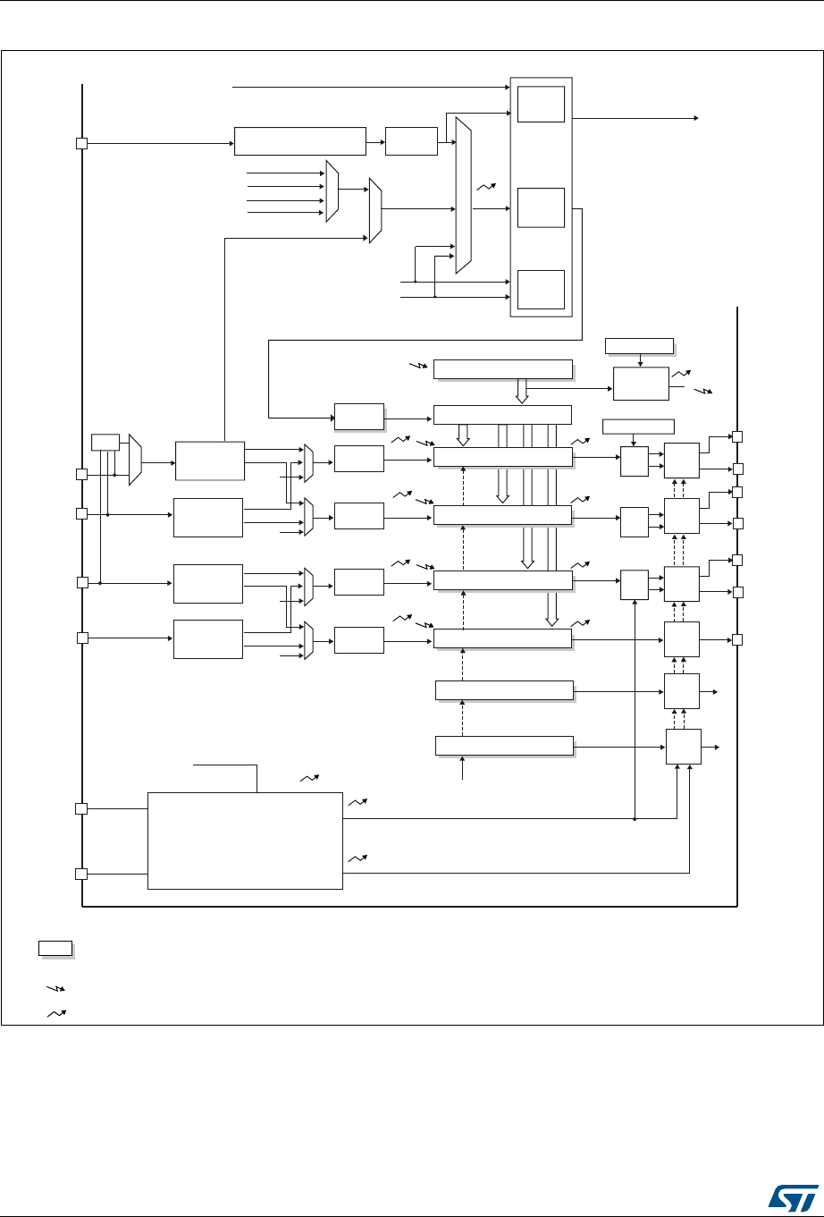
Advanced-control timers (TIM1) RM0394
720/1600 RM0394 Rev 4
Figure 183. Advanced-control timer block diagram
1. See Figure 226: Break and Break2 circuitry overview for details
h
h
h
ϭ/
Ϯ/
dƌŝŐŐĞƌ
ĐŽŶƚƌŽůůĞƌ
нͬͲ
^ƚŽƉ͕ĐůĞĂƌŽƌƵƉͬĚŽǁŶ
d/ϭ&Wϭ
d/Ϯ&WϮ
/dZϬ
/dZϭ
/dZϮ dZ'/
KƵƚƉƵƚ
ĐŽŶƚƌŽů
d'
dZ'K
KϭZ&
KϮZ&
ZWƌĞŐŝƐƚĞƌ
h
ZĞƉĞƚŝƚŝŽŶ
ĐŽƵŶƚĞƌ
h/
ZĞƐĞƚ͕ĞŶĂďůĞ͕ƵƉͬĚŽǁŶ͕ĐŽƵŶƚ
<ͺW^
/ϭ
/Ϯ /ϮW^
/ϭW^
d/ϭ&Wϭ
d'/
dZ
dZ
/dZ
dZ
d/ϭ&ͺ
ϭ/
Ϯ/
d/ϭ&WϮ
d/Ϯ&Wϭ
d/Ϯ&WϮ
d/ϭ
d/Ϯ
d/Ddžͺ,ϭ
d/Ddžͺ,Ϯ
Kϭ
d/Ddžͺ,ϭ
d/Ddžͺ,ϭE
KϭE
ƚŽŽƚŚĞƌƚŝŵĞƌƐƚŽͬ
^ůĂǀĞ
ĐŽŶƚƌŽůůĞƌ
ŵŽĚĞ
W^
ƉƌĞƐĐĂůĞƌ EdĐŽƵŶƚĞƌ
/ŶƚĞƌŶĂůĐůŽĐŬ;<ͺ/EdͿ
<ͺEd
<ͺd/DϭĨƌŽŵZ
/dZϯ
D^ǀϯϳϲϯϬsϭ
yKZ
d'ƌĞŐŝƐƚĞƌƐ
/ŶƉƵƚĨŝůƚĞƌΘ
ĞĚŐĞĚĞƚĞĐƚŽƌ
ĂƉƚƵƌĞͬŽŵƉĂƌĞϭƌĞŐŝƐƚĞƌ
EŽƚĞƐ͗
ZĞŐ WƌĞůŽĂĚƌĞŐŝƐƚĞƌƐƚƌĂŶƐĨĞƌƌĞĚ
ƚŽĂĐƚŝǀĞƌĞŐŝƐƚĞƌƐŽŶhĞǀĞŶƚ
ĂĐĐŽƌĚŝŶŐƚŽĐŽŶƚƌŽůďŝƚ
ǀĞŶƚ
/ŶƚĞƌƌƵƉƚΘDŽƵƚƉƵƚ
d/Ddžͺ</E
/ŶƚĞƌŶĂůƐŽƵƌĐĞƐ
ƵƚŽͲƌĞůŽĂĚƌĞŐŝƐƚĞƌ
ĂƉƚƵƌĞͬŽŵƉĂƌĞϮƌĞŐŝƐƚĞƌ
WƌĞƐĐĂůĞƌ
WƌĞƐĐĂůĞƌ
KƵƚƉƵƚ
ĐŽŶƚƌŽů
ŶĐŽĚĞƌ
/ŶƚĞƌĨĂĐĞ
WŽůĂƌŝƚLJƐĞůĞĐƚŝŽŶΘ
ĞĚŐĞĚĞƚĞĐƚŽƌΘƉƌĞƐĐĂůĞƌ
/ŶƉƵƚ
ĨŝůƚĞƌ
dZ&
dZW
dZ
d/DdžͺdZ
h
h
ϯ/
ϰ/
KƵƚƉƵƚ
ĐŽŶƚƌŽů
d'
KϯZ&
KϰZ&
/ϯ
/ϰ /ϰW^
/ϯW^
d/ϯ&Wϯ
dZ
dZ
ϯ/
ϰ/
d/ϯ&Wϰ
d/ϰ&Wϯ
d/ϰ&Wϰ
Kϯ
Kϰ
d/Ddžͺ,ϯ
d/Ddžͺ,ϰ
d/Ddžͺ,ϯE
KϯE
ĂƉƚƵƌĞͬŽŵƉĂƌĞϯƌĞŐŝƐƚĞƌ
ĂƉƚƵƌĞͬŽŵƉĂƌĞϰƌĞŐŝƐƚĞƌ
WƌĞƐĐĂůĞƌ
WƌĞƐĐĂůĞƌ
KƵƚƉƵƚ
ĐŽŶƚƌŽů
d'
KϮ
d/Ddžͺ,Ϯ
d/Ddžͺ,ϮE
KϮE
d/ϯ
d/ϰ
d/Ddžͺ,ϯ
d/Ddžͺ,ϰ
KϱZ& Kϱ
ĂƉƚƵƌĞͬŽŵƉĂƌĞϱƌĞŐŝƐƚĞƌ KƵƚƉƵƚ
ĐŽŶƚƌŽů
KϲZ& Kϲ
ĂƉƚƵƌĞͬŽŵƉĂƌĞϲƌĞŐŝƐƚĞƌ KƵƚƉƵƚ
ĐŽŶƚƌŽů
ƌĞĂŬĂŶĚƌĞĂŬϮĐŝƌĐƵŝƚƌLJ;ϭͿ
d/Ddžͺ</EϮ
dZ&
/ŶƉƵƚĨŝůƚĞƌΘ
ĞĚŐĞĚĞƚĞĐƚŽƌ
/ŶƉƵƚĨŝůƚĞƌΘ
ĞĚŐĞĚĞƚĞĐƚŽƌ
/ŶƉƵƚĨŝůƚĞƌΘ
ĞĚŐĞĚĞƚĞĐƚŽƌ
^/&
/&
Ϯ/&
Z<ƌĞƋƵĞƐƚ
Z<ϮƌĞƋƵĞƐƚ

RM0394 Rev 4 721/1600
RM0394 Advanced-control timers (TIM1)
816
26.3 TIM1 functional description
26.3.1 Time-base unit
The main block of the programmable advanced-control timer is a 16-bit counter with its
related auto-reload register. The counter can count up, down or both up and down. The
counter clock can be divided by a prescaler.
The counter, the auto-reload register and the prescaler register can be written or read by
software. This is true even when the counter is running.
The time-base unit includes:
•Counter register (TIMx_CNT)
•Prescaler register (TIMx_PSC)
•Auto-reload register (TIMx_ARR)
•Repetition counter register (TIMx_RCR)
The auto-reload register is preloaded. Writing to or reading from the auto-reload register
accesses the preload register. The content of the preload register are transferred into the
shadow register permanently or at each update event (UEV), depending on the auto-reload
preload enable bit (ARPE) in TIMx_CR1 register. The update event is sent when the counter
reaches the overflow (or underflow when downcounting) and if the UDIS bit equals 0 in the
TIMx_CR1 register. It can also be generated by software. The generation of the update
event is described in detailed for each configuration.
The counter is clocked by the prescaler output CK_CNT, which is enabled only when the
counter enable bit (CEN) in TIMx_CR1 register is set (refer also to the slave mode controller
description to get more details on counter enabling).
Note that the counter starts counting 1 clock cycle after setting the CEN bit in the TIMx_CR1
register.
Prescaler description
The prescaler can divide the counter clock frequency by any factor between 1 and 65536. It
is based on a 16-bit counter controlled through a 16-bit register (in the TIMx_PSC register).
It can be changed on the fly as this control register is buffered. The new prescaler ratio is
taken into account at the next update event.
Figure 184 and Figure 185 give some examples of the counter behavior when the prescaler
ratio is changed on the fly:
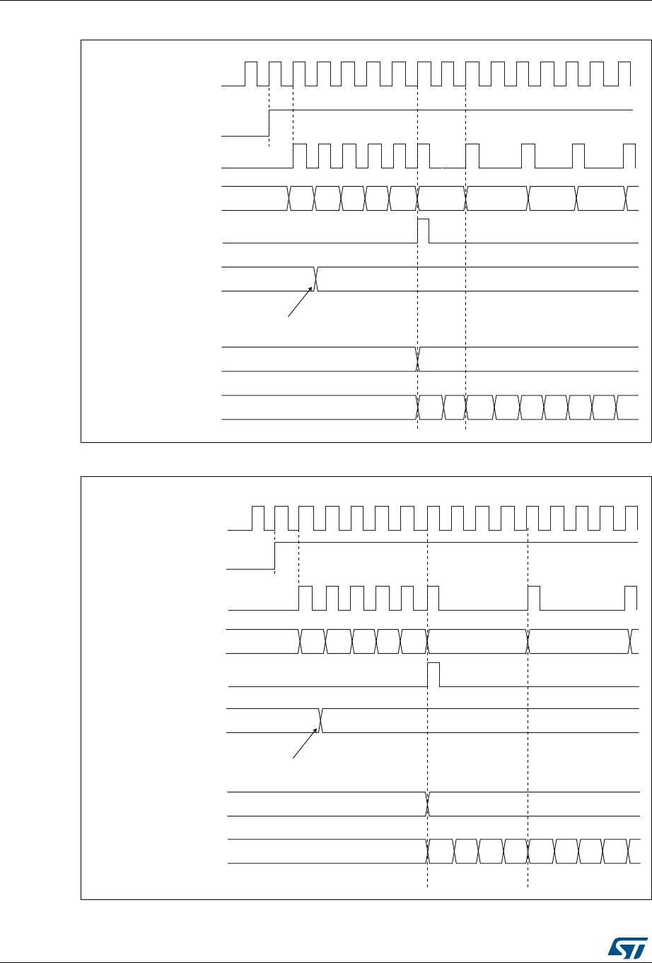
Advanced-control timers (TIM1) RM0394
722/1600 RM0394 Rev 4
Figure 184. Counter timing diagram with prescaler division change from 1 to 2
Figure 185. Counter timing diagram with prescaler division change from 1 to 4
&.B36&
&(1
7LPHUFORFN &.B&17
&RXQWHUUHJLVWHU
8SGDWHHYHQW8(9
3UHVFDOHUFRQWUROUHJLVWHU
:ULWHDQHZYDOXHLQ7,0[B36&
3UHVFDOHUEXIIHU
3UHVFDOHUFRXQWHU
)$ )%) ) ) )&
069
069
&.B36&
&(1
7LPHUFORFN &.B&17
&RXQWHUUHJLVWHU
8SGDWHHYHQW8(9
3UHVFDOHUFRQWUROUHJLVWHU
:ULWHDQHZYDOXHLQ7,0[B36&
3UHVFDOHUEXIIHU
3UHVFDOHUFRXQWHU
)$ )%
) ) ) )&

RM0394 Rev 4 723/1600
RM0394 Advanced-control timers (TIM1)
816
26.3.2 Counter modes
Upcounting mode
In upcounting mode, the counter counts from 0 to the auto-reload value (content of the
TIMx_ARR register), then restarts from 0 and generates a counter overflow event.
If the repetition counter is used, the update event (UEV) is generated after upcounting is
repeated for the number of times programmed in the repetition counter register
(TIMx_RCR) + 1. Else the update event is generated at each counter overflow.
Setting the UG bit in the TIMx_EGR register (by software or by using the slave mode
controller) also generates an update event.
The UEV event can be disabled by software by setting the UDIS bit in the TIMx_CR1
register. This is to avoid updating the shadow registers while writing new values in the
preload registers. Then no update event occurs until the UDIS bit has been written to 0.
However, the counter restarts from 0, as well as the counter of the prescaler (but the
prescale rate does not change). In addition, if the URS bit (update request selection) in
TIMx_CR1 register is set, setting the UG bit generates an update event UEV but without
setting the UIF flag (thus no interrupt or DMA request is sent). This is to avoid generating
both update and capture interrupts when clearing the counter on the capture event.
When an update event occurs, all the registers are updated and the update flag (UIF bit in
TIMx_SR register) is set (depending on the URS bit):
•The repetition counter is reloaded with the content of TIMx_RCR register,
•The auto-reload shadow register is updated with the preload value (TIMx_ARR),
•The buffer of the prescaler is reloaded with the preload value (content of the TIMx_PSC
register).
The following figures show some examples of the counter behavior for different clock
frequencies when TIMx_ARR=0x36.

Advanced-control timers (TIM1) RM0394
724/1600 RM0394 Rev 4
Figure 186. Counter timing diagram, internal clock divided by 1
Figure 187. Counter timing diagram, internal clock divided by 2
069
&.B36&
&17B(1
7LPHUFORFN &.B&17
&RXQWHUUHJLVWHU
8SGDWHHYHQW8(9
&RXQWHURYHUIORZ
8SGDWHLQWHUUXSWIODJ
8,)
069
&.B36&
&17B(1
7LPHUFORFN &.B&17
&RXQWHUUHJLVWHU
8SGDWHHYHQW8(9
&RXQWHURYHUIORZ
8SGDWHLQWHUUXSWIODJ
8,)
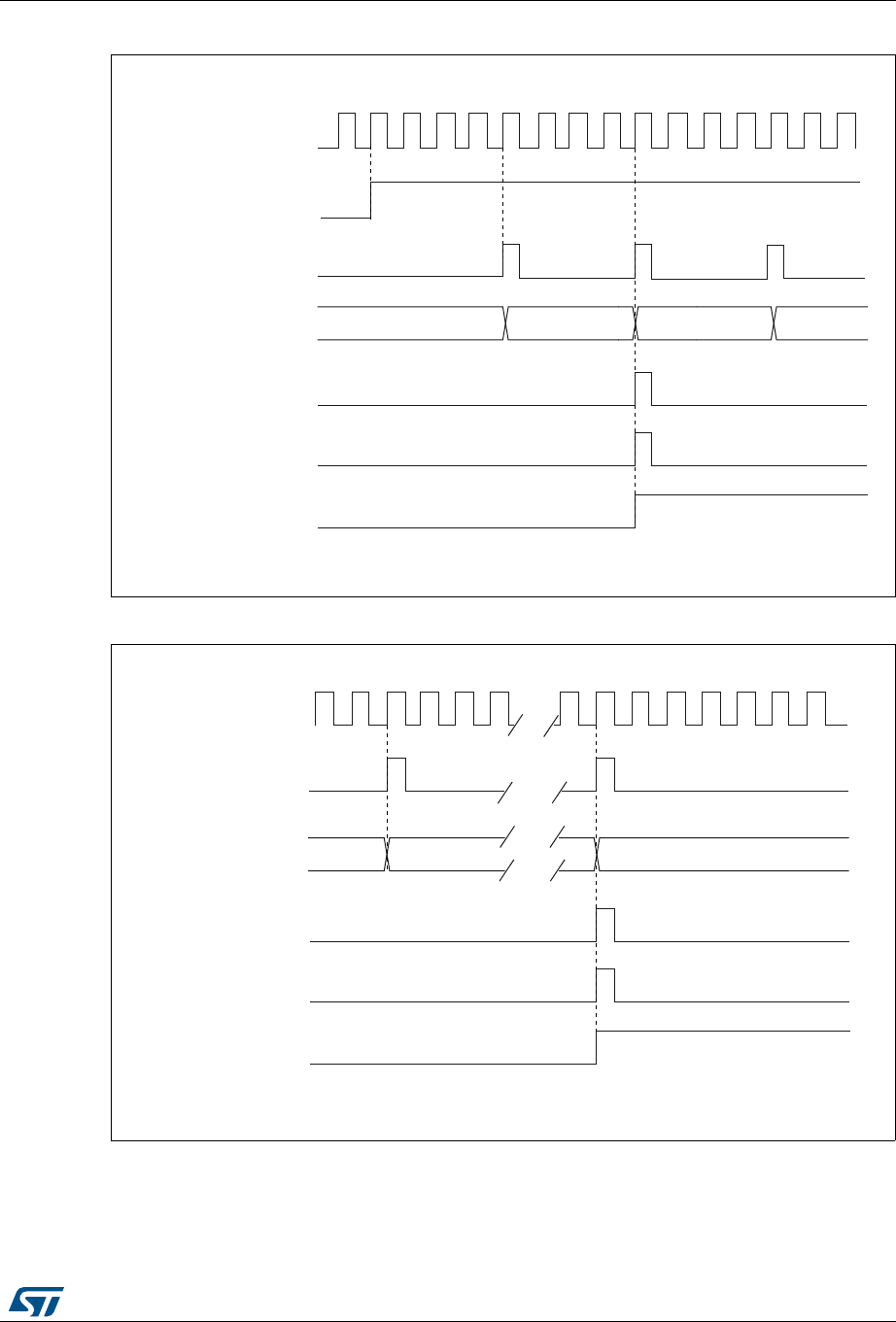
RM0394 Rev 4 725/1600
RM0394 Advanced-control timers (TIM1)
816
Figure 188. Counter timing diagram, internal clock divided by 4
Figure 189. Counter timing diagram, internal clock divided by N
069
&.B36&
7LPHUFORFN &.B&17
&RXQWHUUHJLVWHU
8SGDWHHYHQW8(9
&RXQWHURYHUIORZ
8SGDWHLQWHUUXSWIODJ
8,)
&17B(1
)
069
&.B36&
7LPHUFORFN &.B&17
&RXQWHUUHJLVWHU
8SGDWHHYHQW8(9
&RXQWHURYHUIORZ
8SGDWHLQWHUUXSWIODJ
8,)
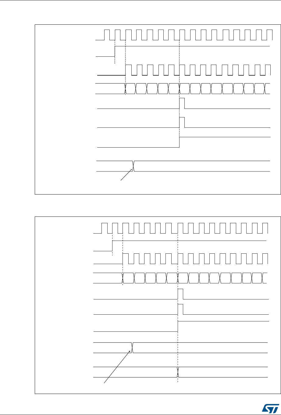
Advanced-control timers (TIM1) RM0394
726/1600 RM0394 Rev 4
Figure 190. Counter timing diagram, update event when ARPE=0 (TIMx_ARR not
preloaded)
Figure 191. Counter timing diagram, update event when ARPE=1 (TIMx_ARR
preloaded)
&& ϯϲ
069
<ͺW^
dŝŵĞƌĐůŽĐŬс<ͺEd
ŽƵŶƚĞƌƌĞŐŝƐƚĞƌ
hƉĚĂƚĞĞǀĞŶƚ;hsͿ
ŽƵŶƚĞƌŽǀĞƌĨůŽǁ
hƉĚĂƚĞŝŶƚĞƌƌƵƉƚĨůĂŐ;h/&Ϳ
ϬϬ ϬϮ Ϭϯ Ϭϰ Ϭϱ Ϭϲ ϬϳϯϮ ϯϯ ϯϰ ϯϱ ϯϲϯϭ Ϭϭ
E
ƵƚŽͲƌĞůŽĂĚƉƌĞůŽĂĚƌĞŐŝƐƚĞƌ
tƌŝƚĞĂŶĞǁǀĂůƵĞŝŶd/DdžͺZZ
069
)
&.B36&
7LPHUFORFN &.B&17
&RXQWHUUHJLVWHU
8SGDWHHYHQW8(9
&RXQWHURYHUIORZ
8SGDWHLQWHUUXSWIODJ
8,)
) ) ) ) ))
&(1
$XWRUHORDGSUHORDG
UHJLVWHU
:ULWHDQHZYDOXHLQ7,0[B$55
$XWRUHORDGVKDGRZ
UHJLVWHU )

RM0394 Rev 4 727/1600
RM0394 Advanced-control timers (TIM1)
816
Downcounting mode
In downcounting mode, the counter counts from the auto-reload value (content of the
TIMx_ARR register) down to 0, then restarts from the auto-reload value and generates a
counter underflow event.
If the repetition counter is used, the update event (UEV) is generated after downcounting is
repeated for the number of times programmed in the repetition counter register
(TIMx_RCR) + 1. Else the update event is generated at each counter underflow.
Setting the UG bit in the TIMx_EGR register (by software or by using the slave mode
controller) also generates an update event.
The UEV update event can be disabled by software by setting the UDIS bit in TIMx_CR1
register. This is to avoid updating the shadow registers while writing new values in the
preload registers. Then no update event occurs until UDIS bit has been written to 0.
However, the counter restarts from the current auto-reload value, whereas the counter of the
prescaler restarts from 0 (but the prescale rate doesn’t change).
In addition, if the URS bit (update request selection) in TIMx_CR1 register is set, setting the
UG bit generates an update event UEV but without setting the UIF flag (thus no interrupt or
DMA request is sent). This is to avoid generating both update and capture interrupts when
clearing the counter on the capture event.
When an update event occurs, all the registers are updated and the update flag (UIF bit in
TIMx_SR register) is set (depending on the URS bit):
•The repetition counter is reloaded with the content of TIMx_RCR register.
•The buffer of the prescaler is reloaded with the preload value (content of the TIMx_PSC
register).
•The auto-reload active register is updated with the preload value (content of the
TIMx_ARR register). Note that the auto-reload is updated before the counter is
reloaded, so that the next period is the expected one.
The following figures show some examples of the counter behavior for different clock
frequencies when TIMx_ARR=0x36.
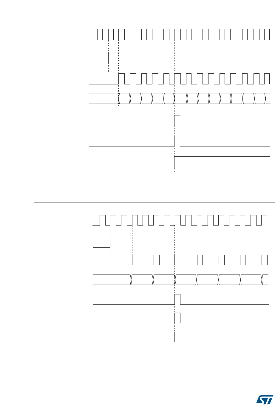
Advanced-control timers (TIM1) RM0394
728/1600 RM0394 Rev 4
Figure 192. Counter timing diagram, internal clock divided by 1
Figure 193. Counter timing diagram, internal clock divided by 2
)
069
&.B36&
&17B(1
7LPHUFORFN &.B&17
&RXQWHUUHJLVWHU
8SGDWHHYHQW8(9
&RXQWHUXQGHUIORZ
FQWBXGI
8SGDWHLQWHUUXSWIODJ
8,)
069
&.B36&
&17B(1
7LPHUFORFN &.B&17
&RXQWHUUHJLVWHU
8SGDWHHYHQW8(9
&RXQWHUXQGHUIORZ
8SGDWHLQWHUUXSWIODJ
8,)
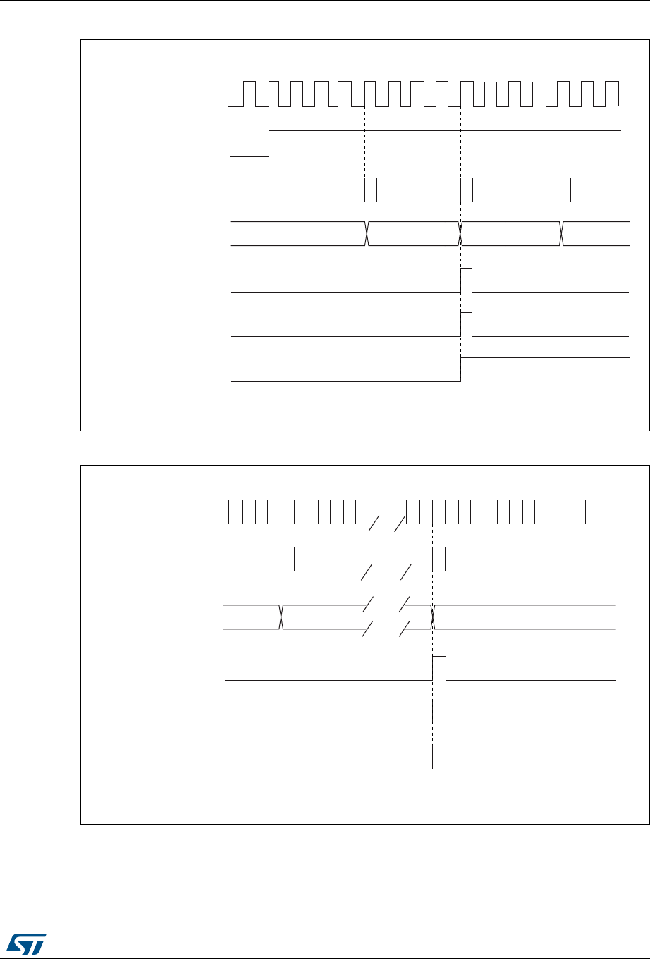
RM0394 Rev 4 729/1600
RM0394 Advanced-control timers (TIM1)
816
Figure 194. Counter timing diagram, internal clock divided by 4
Figure 195. Counter timing diagram, internal clock divided by N
069
&.B36&
7LPHUFORFN &.B&17
&RXQWHUUHJLVWHU
8SGDWHHYHQW8(9
&RXQWHUXQGHUIORZ
8SGDWHLQWHUUXSWIODJ
8,)
&17B(1
)
069
&.B36&
7LPHUFORFN &.B&17
&RXQWHUUHJLVWHU
8SGDWHHYHQW8(9
&RXQWHUXQGHUIORZ
8SGDWHLQWHUUXSWIODJ
8,)
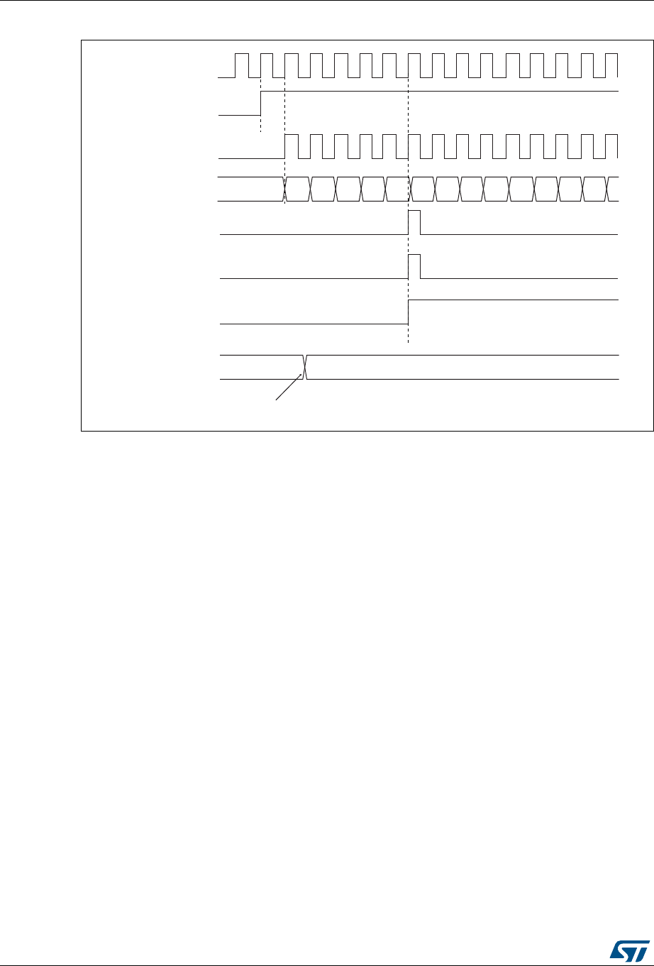
Advanced-control timers (TIM1) RM0394
730/1600 RM0394 Rev 4
Figure 196. Counter timing diagram, update event when repetition counter is not used
Center-aligned mode (up/down counting)
In center-aligned mode, the counter counts from 0 to the auto-reload value (content of the
TIMx_ARR register) – 1, generates a counter overflow event, then counts from the auto-
reload value down to 1 and generates a counter underflow event. Then it restarts counting
from 0.
Center-aligned mode is active when the CMS bits in TIMx_CR1 register are not equal to
'00'. The Output compare interrupt flag of channels configured in output is set when: the
counter counts down (Center aligned mode 1, CMS = "01"), the counter counts up (Center
aligned mode 2, CMS = "10") the counter counts up and down (Center aligned mode 3,
CMS = "11").
In this mode, the DIR direction bit in the TIMx_CR1 register cannot be written. It is updated
by hardware and gives the current direction of the counter.
The update event can be generated at each counter overflow and at each counter underflow
or by setting the UG bit in the TIMx_EGR register (by software or by using the slave mode
controller) also generates an update event. In this case, the counter restarts counting from
0, as well as the counter of the prescaler.
The UEV update event can be disabled by software by setting the UDIS bit in the TIMx_CR1
register. This is to avoid updating the shadow registers while writing new values in the
preload registers. Then no update event occurs until UDIS bit has been written to 0.
However, the counter continues counting up and down, based on the current auto-reload
value.
In addition, if the URS bit (update request selection) in TIMx_CR1 register is set, setting the
UG bit generates an UEV update event but without setting the UIF flag (thus no interrupt or
))
069
&.B36&
7LPHUFORFN &.B&17
&RXQWHUUHJLVWHU
8SGDWHHYHQW8(9
&RXQWHUXQGHUIORZ
8SGDWHLQWHUUXSWIODJ
8,)
)
&(1
$XWRUHORDGSUHORDG
UHJLVWHU
:ULWHDQHZYDOXHLQ7,0[B$55
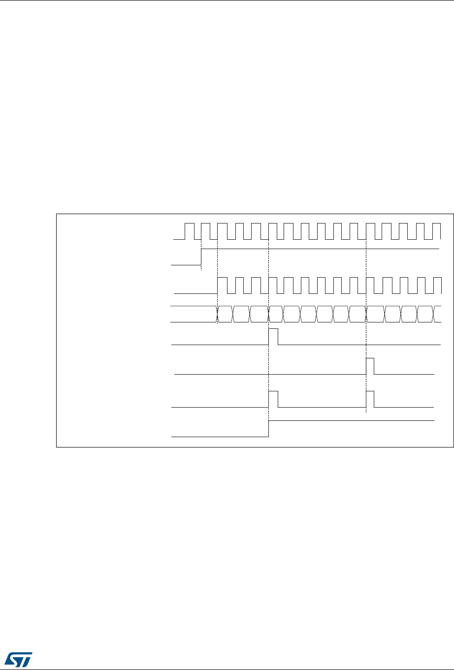
RM0394 Rev 4 731/1600
RM0394 Advanced-control timers (TIM1)
816
DMA request is sent). This is to avoid generating both update and capture interrupts when
clearing the counter on the capture event.
When an update event occurs, all the registers are updated and the update flag (UIF bit in
TIMx_SR register) is set (depending on the URS bit):
•The repetition counter is reloaded with the content of TIMx_RCR register
•The buffer of the prescaler is reloaded with the preload value (content of the TIMx_PSC
register)
•The auto-reload active register is updated with the preload value (content of the
TIMx_ARR register). Note that if the update source is a counter overflow, the auto-
reload is updated before the counter is reloaded, so that the next period is the expected
one (the counter is loaded with the new value).
The following figures show some examples of the counter behavior for different clock
frequencies.
Figure 197. Counter timing diagram, internal clock divided by 1, TIMx_ARR = 0x6
1. Here, center-aligned mode 1 is used (for more details refer to Section 26.4: TIM1 registers).
069
&.B36&
7LPHUFORFN &.B&17
&RXQWHUUHJLVWHU
8SGDWHHYHQW8(9
&RXQWHURYHUIORZ
8SGDWHLQWHUUXSWIODJ8,)
&(1
&RXQWHUXQGHUIORZ

Advanced-control timers (TIM1) RM0394
732/1600 RM0394 Rev 4
Figure 198. Counter timing diagram, internal clock divided by 2
Figure 199. Counter timing diagram, internal clock divided by 4, TIMx_ARR=0x36
069
&.B36&
&17B(1
7LPHUFORFN &.B&17
&RXQWHUUHJLVWHU
8SGDWHHYHQW8(9
&RXQWHUXQGHUIORZ
8SGDWHLQWHUUXSWIODJ
8,)
069
&.B36&
7LPHUFORFN &.B&17
&RXQWHUUHJLVWHU
8SGDWHHYHQW8(9
&RXQWHURYHUIORZ
8SGDWHLQWHUUXSWIODJ
8,)
&17B(1
1RWH+HUHFHQWHUBDOLJQHGPRGHRULVXSGDWHGZLWKDQ8,)RQRYHUIORZ
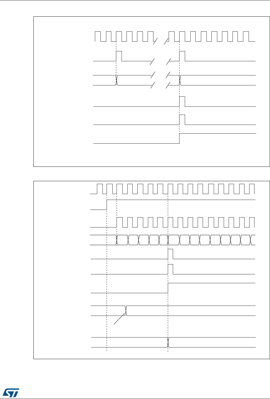
RM0394 Rev 4 733/1600
RM0394 Advanced-control timers (TIM1)
816
Figure 200. Counter timing diagram, internal clock divided by N
Figure 201. Counter timing diagram, update event with ARPE=1 (counter underflow)
)
069
&.B36&
7LPHUFORFN &.B&17
&RXQWHUUHJLVWHU
8SGDWHHYHQW8(9
&RXQWHUXQGHUIORZ
8SGDWHLQWHUUXSWIODJ
8,)
)'
069
&.B36&
7LPHUFORFN &.B&17
&RXQWHUUHJLVWHU
8SGDWHHYHQW8(9
&RXQWHUXQGHUIORZ
8SGDWHLQWHUUXSWIODJ
8,)
&(1
$XWRUHORDGSUHORDG
UHJLVWHU
:ULWHDQHZYDOXHLQ7,0[B$55
)'
$XWRUHORDGDFWLYH
UHJLVWHU
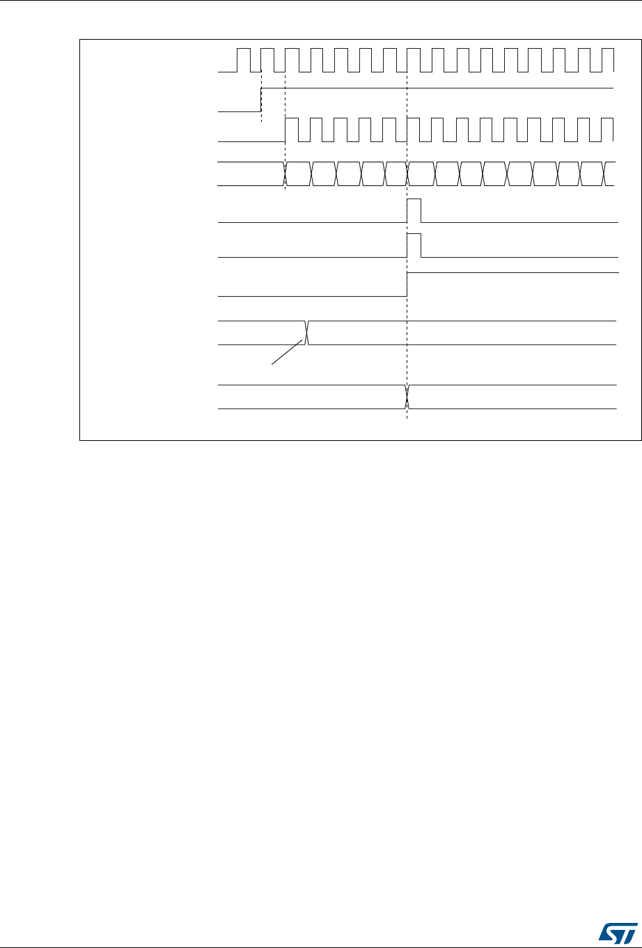
Advanced-control timers (TIM1) RM0394
734/1600 RM0394 Rev 4
Figure 202. Counter timing diagram, Update event with ARPE=1 (counter overflow)
26.3.3 Repetition counter
Section 26.3.1: Time-base unit describes how the update event (UEV) is generated with
respect to the counter overflows/underflows. It is actually generated only when the repetition
counter has reached zero. This can be useful when generating PWM signals.
This means that data are transferred from the preload registers to the shadow registers
(TIMx_ARR auto-reload register, TIMx_PSC prescaler register, but also TIMx_CCRx
capture/compare registers in compare mode) every N+1 counter overflows or underflows,
where N is the value in the TIMx_RCR repetition counter register.
The repetition counter is decremented:
•At each counter overflow in upcounting mode,
•At each counter underflow in downcounting mode,
•At each counter overflow and at each counter underflow in center-aligned mode.
Although this limits the maximum number of repetition to 32768 PWM cycles, it makes
it possible to update the duty cycle twice per PWM period. When refreshing compare
registers only once per PWM period in center-aligned mode, maximum resolution is
2xTck, due to the symmetry of the pattern.
The repetition counter is an auto-reload type; the repetition rate is maintained as defined by
the TIMx_RCR register value (refer to Figure 203). When the update event is generated by
software (by setting the UG bit in TIMx_EGR register) or by hardware through the slave
mode controller, it occurs immediately whatever the value of the repetition counter is and the
repetition counter is reloaded with the content of the TIMx_RCR register.
069
)'
&.B36&
7LPHUFORFN &.B&17
&RXQWHUUHJLVWHU
8SGDWHHYHQW8(9
&RXQWHURYHUIORZ
8SGDWHLQWHUUXSWIODJ
8,)
)
) ) )$ )% )&)
&(1
$XWRUHORDGSUHORDG
UHJLVWHU
:ULWHDQHZYDOXHLQ7,0[B$55
$XWRUHORDGDFWLYH
UHJLVWHU )'
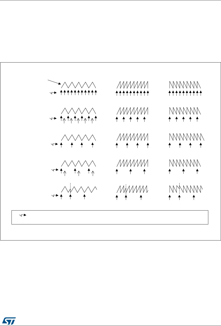
RM0394 Rev 4 735/1600
RM0394 Advanced-control timers (TIM1)
816
In Center aligned mode, for odd values of RCR, the update event occurs either on the
overflow or on the underflow depending on when the RCR register was written and when
the counter was launched: if the RCR was written before launching the counter, the UEV
occurs on the overflow. If the RCR was written after launching the counter, the UEV occurs
on the underflow.
For example, for RCR = 3, the UEV is generated each 4th overflow or underflow event
depending on when the RCR was written.
Figure 203. Update rate examples depending on mode and TIMx_RCR register settings
06Y9
8(9
8(9
8(9
8(9
8(9
&RXQWHUDOLJQHGPRGH (GJHDOLJQHGPRGH
8SFRXQWLQJ 'RZQFRXQWLQJ
E\6:E\6:E\6:
7,0[B5&5
DQG
UHV\QFKURQL]DWLRQ
7,0[B5&5
7,0[B5&5
7,0[B5&5
7,0[B5&5
&RXQWHU
7,0[B&17
8(9 8SGDWHHYHQW3UHORDGUHJLVWHUVWUDQVIHUUHGWRDFWLYHUHJLVWHUVDQGXSGDWHLQWHUUXSWJHQHUDWHG
8SGDWH(YHQWLIWKHUHSHWLWLRQFRXQWHUXQGHUIORZRFFXUVZKHQWKHFRXQWHULVHTXDOWRWKHDXWRUHORDGYDOXH
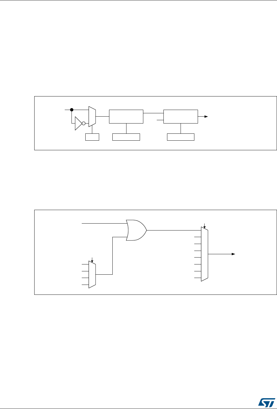
Advanced-control timers (TIM1) RM0394
736/1600 RM0394 Rev 4
26.3.4 External trigger input
The timer features an external trigger input ETR. It can be used as:
•external clock (external clock mode 2, see Section 26.3.5)
•trigger for the slave mode (see Section 26.3.26)
•PWM reset input for cycle-by-cycle current regulation (see Section 26.3.7)
Figure 204 below describes the ETR input conditioning. The input polarity is defined with the
ETP bit in TIMxSMCR register. The trigger can be prescaled with the divider programmed
by the ETPS[1:0] bitfield and digitally filtered with the ETF[3:0] bitfield.
Figure 204. External trigger input block
The ETR input comes from multiple sources: input pins (default configuration), comparator
outputs and analog watchdogs. The selection is done with:
•the ETRSEL[2:0] bitfield in the TIMx_OR2 register
•the ETR_ADC1_RMP bitfield in the TIMxOR1[1:0] register
•the ETR_ADC3_RMP bitfield in the TIMxOR1[3:2] register.
Figure 205. TIM1 ETR input circuitry
069
7RWKH2XWSXWPRGHFRQWUROOHU
7RWKH&.B36&FLUFXLWU\
7RWKH6ODYHPRGHFRQWUROOHU
(75LQSXW (75
(73
7,0[B60&5
'LYLGHU
(736>@
7,0[B60&5
)LOWHU
GRZQFRXQWHU
(7)>@
7,0[B60&5
(753
I'76
06Y9
$'&B$:'
$'&B$:'
$'&B$:'
1&
7,0B25>@
(75LQSXWVIURP
$)FRQWUROOHU
7,0B25>@
(75OHJDF\PRGH
&203
&203
1&
1&
1&
1&
1&
(75LQSXW
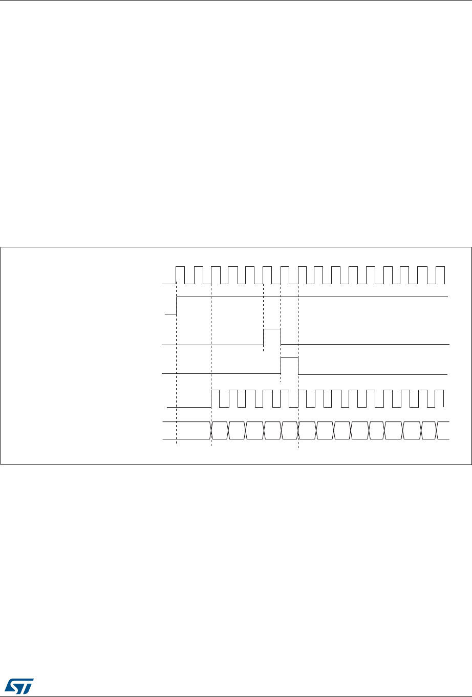
RM0394 Rev 4 737/1600
RM0394 Advanced-control timers (TIM1)
816
26.3.5 Clock selection
The counter clock can be provided by the following clock sources:
•Internal clock (CK_INT)
•External clock mode1: external input pin
•External clock mode2: external trigger input ETR
•Encoder mode
Internal clock source (CK_INT)
If the slave mode controller is disabled (SMS=000), then the CEN, DIR (in the TIMx_CR1
register) and UG bits (in the TIMx_EGR register) are actual control bits and can be changed
only by software (except UG which remains cleared automatically). As soon as the CEN bit
is written to 1, the prescaler is clocked by the internal clock CK_INT.
Figure 206 shows the behavior of the control circuit and the upcounter in normal mode,
without prescaler.
Figure 206. Control circuit in normal mode, internal clock divided by 1
External clock source mode 1
This mode is selected when SMS=111 in the TIMx_SMCR register. The counter can count at
each rising or falling edge on a selected input.
,QWHUQDOFORFN
&RXQWHUFORFN &.B&17 &.B36&
&RXQWHUUHJLVWHU
&(1 &17B(1
8*
&17B,1,7
069
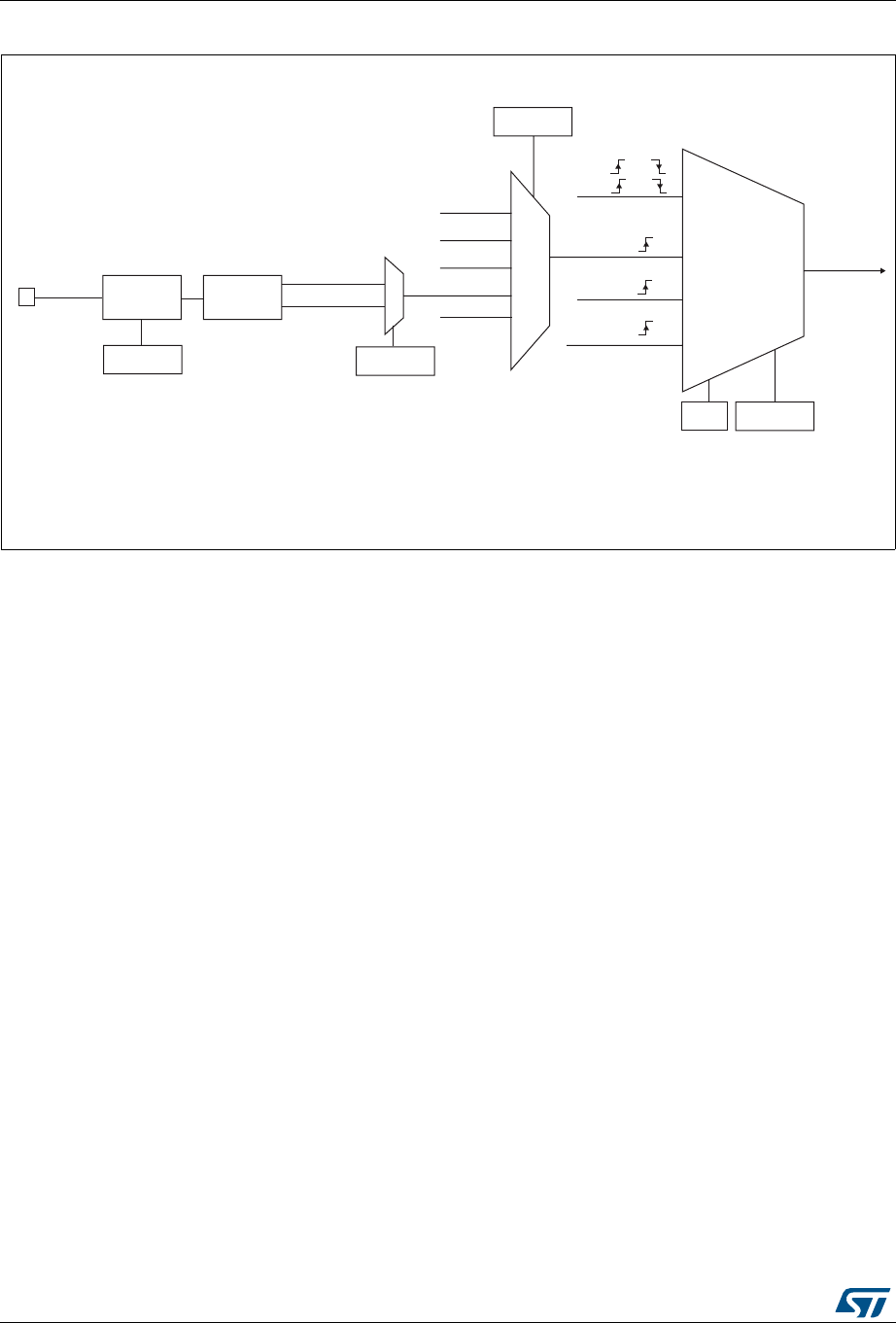
Advanced-control timers (TIM1) RM0394
738/1600 RM0394 Rev 4
Figure 207. TI2 external clock connection example
For example, to configure the upcounter to count in response to a rising edge on the TI2
input, use the following procedure:
1. Configure channel 2 to detect rising edges on the TI2 input by writing CC2S = ‘01’ in
the TIMx_CCMR1 register.
2. Configure the input filter duration by writing the IC2F[3:0] bits in the TIMx_CCMR1
register (if no filter is needed, keep IC2F=0000).
3. Select rising edge polarity by writing CC2P=0 and CC2NP=0 in the TIMx_CCER
register.
4. Configure the timer in external clock mode 1 by writing SMS=111 in the TIMx_SMCR
register.
5. Select TI2 as the trigger input source by writing TS=110 in the TIMx_SMCR register.
6. Enable the counter by writing CEN=1 in the TIMx_CR1 register.
Note: The capture prescaler is not used for triggering, so the user does not need to configure it.
When a rising edge occurs on TI2, the counter counts once and the TIF flag is set.
The delay between the rising edge on TI2 and the actual clock of the counter is due to the
resynchronization circuit on TI2 input.
([WHUQDOFORFN
PRGH
,QWHUQDOFORFN
PRGH
75*,
&.B,17
&.B36&
7,0[B60&5
606>@
,75[
7,B('
7,)3
7,)3
7,0[B60&5
76>@
7,
7,0[B&&(5
&&3
)LOWHU
,&)>@
7,0[B&&05
(GJH
GHWHFWRU
7,)B5LVLQJ
7,)B)DOOLQJ
[[
069
LQWHUQDOFORFN
7,) RU
7,) RU
RU
(QFRGHU
PRGH
(75)
([WHUQDOFORFN
PRGH
(75)
(&(
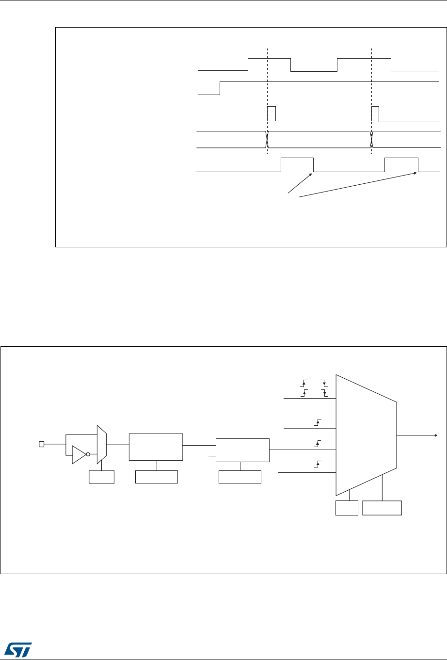
RM0394 Rev 4 739/1600
RM0394 Advanced-control timers (TIM1)
816
Figure 208. Control circuit in external clock mode 1
External clock source mode 2
This mode is selected by writing ECE=1 in the TIMx_SMCR register.
The counter can count at each rising or falling edge on the external trigger input ETR.
The Figure 209 gives an overview of the external trigger input block.
Figure 209. External trigger input block
For example, to configure the upcounter to count each 2 rising edges on ETR, use the
following procedure:
&RXQWHUFORFN &.B&17 &.B36&
&RXQWHUUHJLVWHU
7,
&17B(1
7,)
:ULWH7,)
069
([WHUQDOFORFN
PRGH
,QWHUQDOFORFN
PRGH
75*,
&.B,17
&.B36&
7,0[B60&5
606>@
069
LQWHUQDOFORFN
7,) RU
7,) RU
RU
(QFRGHU
PRGH
([WHUQDOFORFN
PRGH
(75)
(&(
7,0[B60&5
(73
(75SLQ
(75
'LYLGHU
)LOWHU
GRZQFRXQWHU
I
(753
7,0[B60&5
(736>@
7,0[B60&5
(7)>@
'76
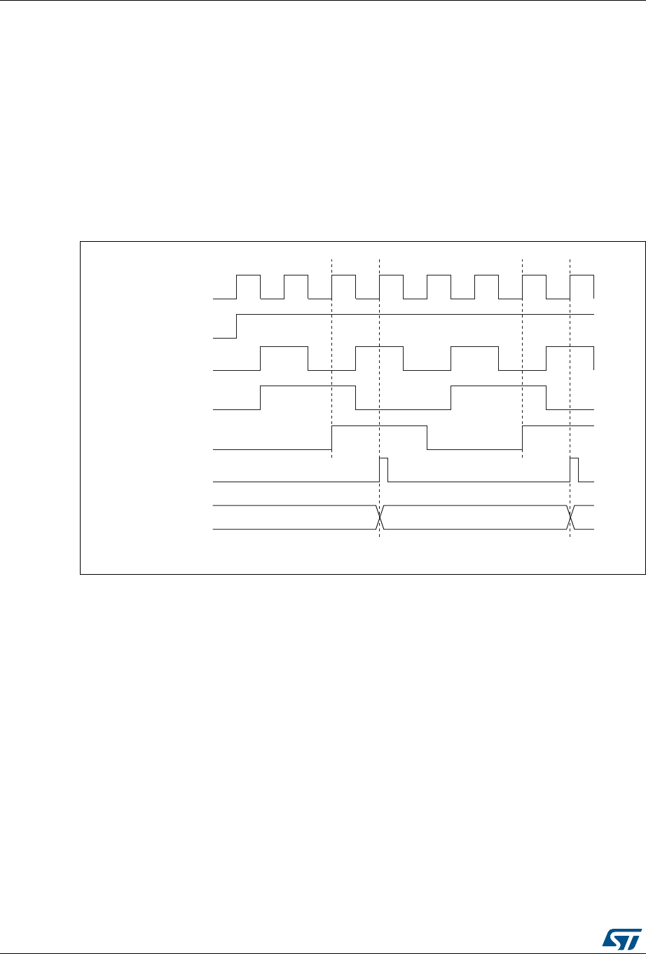
Advanced-control timers (TIM1) RM0394
740/1600 RM0394 Rev 4
1. As no filter is needed in this example, write ETF[3:0]=0000 in the TIMx_SMCR register.
2. Set the prescaler by writing ETPS[1:0]=01 in the TIMx_SMCR register
3. Select rising edge detection on the ETR pin by writing ETP=0 in the TIMx_SMCR
register
4. Enable external clock mode 2 by writing ECE=1 in the TIMx_SMCR register.
5. Enable the counter by writing CEN=1 in the TIMx_CR1 register.
The counter counts once each 2 ETR rising edges.
The delay between the rising edge on ETR and the actual clock of the counter is due to the
resynchronization circuit on the ETRP signal.
Figure 210. Control circuit in external clock mode 2
069
I&.B,17
&17B(1
(75
(753
(75)
&RXQWHUFORFN
&.B,17 &.B36&
&RXQWHUUHJLVWHU
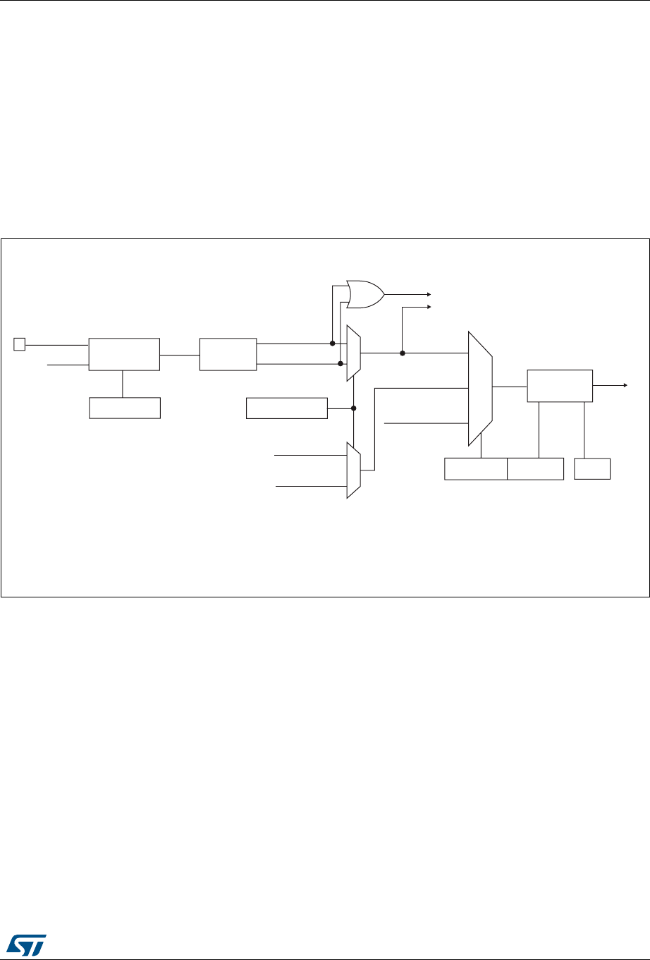
RM0394 Rev 4 741/1600
RM0394 Advanced-control timers (TIM1)
816
26.3.6 Capture/compare channels
Each Capture/Compare channel is built around a capture/compare register (including a
shadow register), an input stage for capture (with digital filter, multiplexing, and prescaler,
except for channels 5 and 6) and an output stage (with comparator and output control).
Figure 211 to Figure 214 give an overview of one Capture/Compare channel.
The input stage samples the corresponding TIx input to generate a filtered signal TIxF.
Then, an edge detector with polarity selection generates a signal (TIxFPx) which can be
used as trigger input by the slave mode controller or as the capture command. It is
prescaled before the capture register (ICxPS).
Figure 211. Capture/compare channel (example: channel 1 input stage)
The output stage generates an intermediate waveform which is then used for reference:
OCxRef (active high). The polarity acts at the end of the chain.
'LYLGHU
,&36>@
7,)B('
7RWKHVODYHPRGHFRQWUROOHU
7,)3
&&6>@
,&
7,)3
75&
IURPVODYHPRGH
FRQWUROOHU
,&36
069
7,
7,0[B&&(5
&&3&&13
)LOWHU
GRZQFRXQWHU
,&)>@
7,0[B&&05
(GJH
GHWHFWRU
7,)B5LVLQJ
7,)B)DOOLQJ
7,0[B&&05
7,0[B&&(5
7,)B5LVLQJ
IURPFKDQQHO
7,)B)DOOLQJ
IURPFKDQQHO
7,)
I
&&(
'76
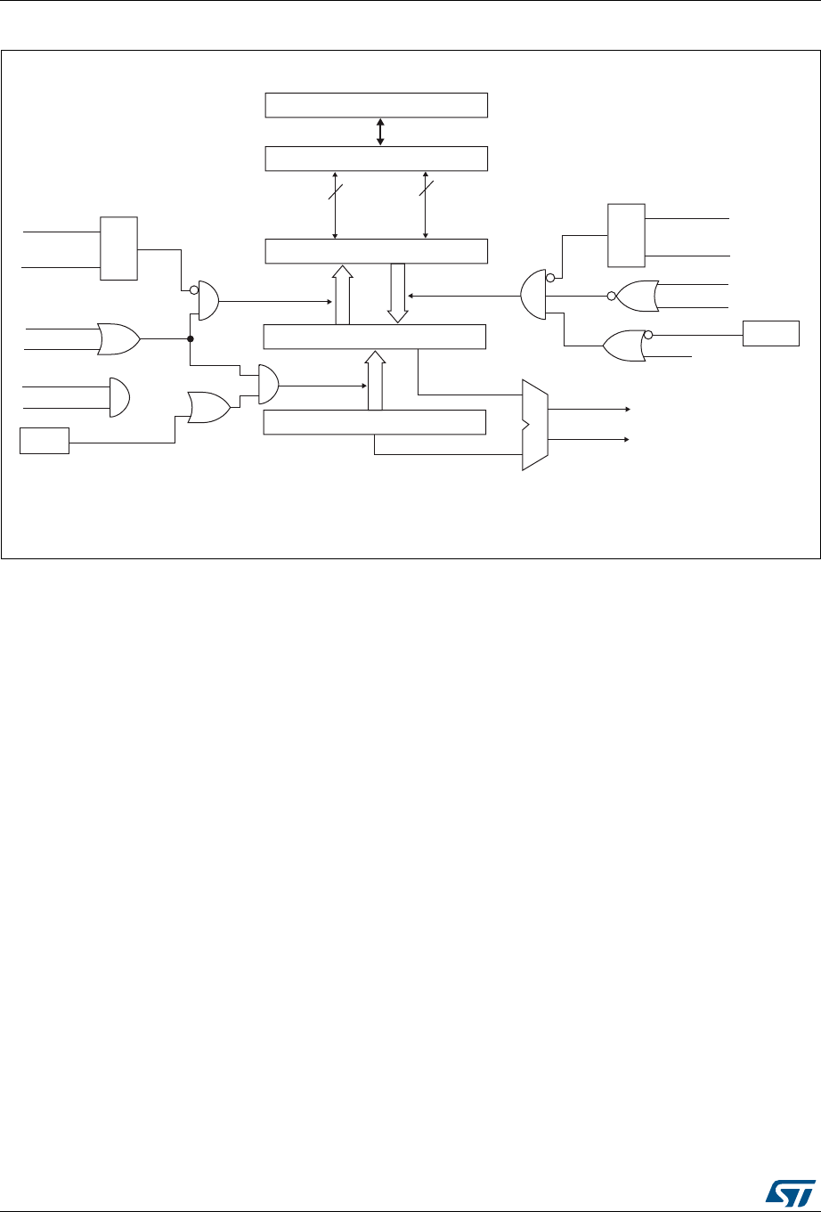
Advanced-control timers (TIM1) RM0394
742/1600 RM0394 Rev 4
Figure 212. Capture/compare channel 1 main circuit
&&(
&DSWXUHFRPSDUHVKDGRZUHJLVWHU
&RPSDUDWRU
&DSWXUHFRPSDUHSUHORDGUHJLVWHU
&RXQWHU
,&36
&&6>@
&&6>@
&DSWXUH
,QSXW
PRGH
6
5
5HDG&&5+
5HDG&&5/
UHDGBLQBSURJUHVV
FDSWXUHBWUDQVIHU &&6>@
&&6>@
6
5
ZULWH&&5+
ZULWH&&5/
ZULWHBLQBSURJUHVV
2XWSXW
PRGH
8(9
2&3(
IURPWLPH
EDVHXQLW
FRPSDUHBWUDQVIHU
$3%%XV
KLJK
ORZ
LIELW
0&8SHULSKHUDOLQWHUIDFH
7,0B&&05
2&3(
&17!&&5
&17 &&5
7,0B(*5
&&*
069
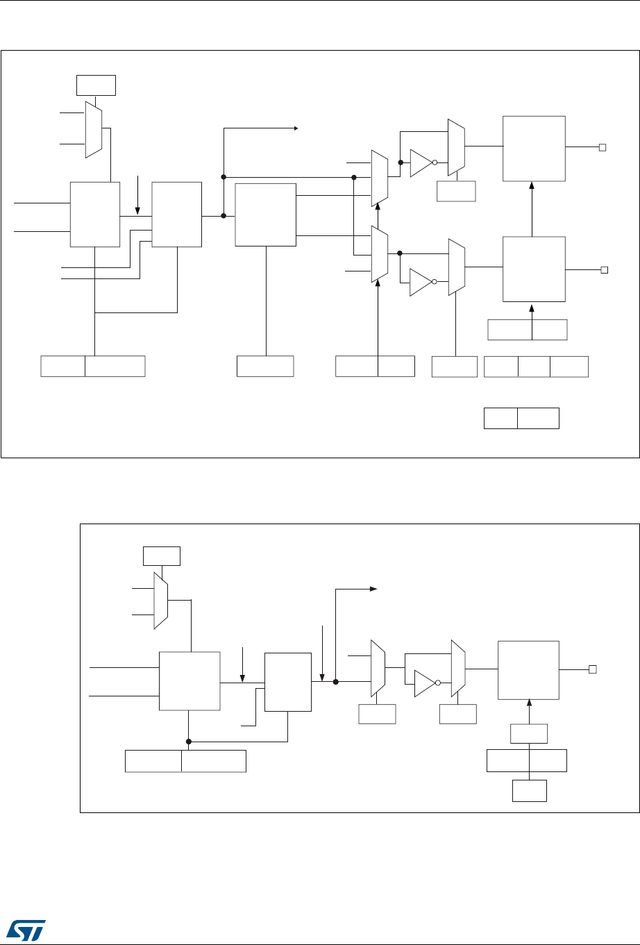
RM0394 Rev 4 743/1600
RM0394 Advanced-control timers (TIM1)
816
Figure 213. Output stage of capture/compare channel (channel 1, idem ch. 2 and 3)
1. OCxREF, where x is the rank of the complementary channel
Figure 214. Output stage of capture/compare channel (channel 4)
06Y9
2XWSXW
PRGH
FRQWUROOHU
&17!&&5
&17 &&5
7,0B&&05
2&0>@
2&5()
2&&(
'HDGWLPH
JHQHUDWRU
2&B'7
2&1B'7
'7*>@
7,0B%'75
µ
µ
&&(
7,0B&&(5
&&1(
&&3
7,0B&&(5
&&13
7,0B&&(5
2&
2XWSXW
HQDEOH
FLUFXLW
2&1
&&( 7,0B&&(5
&&1(
266,
7,0B%'75
02( 2665
[
[
2XWSXW
VHOHFWRU
2&[5()
2&5()&
7RWKHPDVWHUPRGH
FRQWUROOHU
2XWSXW
HQDEOH
FLUFXLW
2&5()
RFUHIBFOUBLQW
1&
(75)
2&&6
7,0[B60&5
2,61
7,0B&5
2,6
06Y9
2XWSXW
PRGH
FRQWUROOHU
&17!&&5
&17 &&5
7,0B&&05
2&0>@
&&3
7,0B&&(5
2XWSXW
HQDEOH
FLUFXLW
2&
&&( 7,0B&&(5
7RWKHPDVWHU
PRGHFRQWUROOHU
2&5()
2&&(
&&(
7,0B&&(5
µ
7,0B%'75
266,
02(
2,6 7,0B&5
RFUHIBFOUBLQW
(75)
1&
2&&6
7,0[B60&5
2XWSXW
VHOHFWRU
2&5()
2&5()&
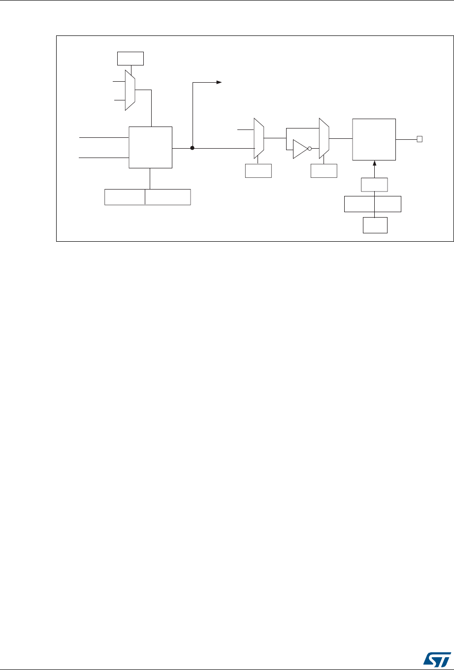
Advanced-control timers (TIM1) RM0394
744/1600 RM0394 Rev 4
Figure 215. Output stage of capture/compare channel (channel 5, idem ch. 6)
1. Not available externally.
The capture/compare block is made of one preload register and one shadow register. Write
and read always access the preload register.
In capture mode, captures are actually done in the shadow register, which is copied into the
preload register.
In compare mode, the content of the preload register is copied into the shadow register
which is compared to the counter.
26.3.7 Input capture mode
In Input capture mode, the Capture/Compare Registers (TIMx_CCRx) are used to latch the
value of the counter after a transition detected by the corresponding ICx signal. When a
capture occurs, the corresponding CCXIF flag (TIMx_SR register) is set and an interrupt or
a DMA request can be sent if they are enabled. If a capture occurs while the CCxIF flag was
already high, then the over-capture flag CCxOF (TIMx_SR register) is set. CCxIF can be
cleared by software by writing it to ‘0’ or by reading the captured data stored in the
TIMx_CCRx register. CCxOF is cleared when you write it to ‘0’.
The following example shows how to capture the counter value in TIMx_CCR1 when TI1
input rises. To do this, use the following procedure:
1. Select the active input: TIMx_CCR1 must be linked to the TI1 input, so write the CC1S
bits to 01 in the TIMx_CCMR1 register. As soon as CC1S becomes different from 00,
the channel is configured in input and the TIMx_CCR1 register becomes read-only.
2. Program the input filter duration you need with respect to the signal you connect to the
timer (when the input is one of the TIx (ICxF bits in the TIMx_CCMRx register). Let’s
imagine that, when toggling, the input signal is not stable during at must 5 internal clock
cycles. We must program a filter duration longer than these 5 clock cycles. We can
validate a transition on TI1 when 8 consecutive samples with the new level have been
06Y9
2XWSXW
PRGH
FRQWUROOHU
&17!&&5
&17 &&5
7,0B&&05
2&0>@
&&3
7,0B&&(5
2XWSXW
HQDEOH
FLUFXLW
2&
&&( 7,0B&&(5
7RWKHPDVWHU
PRGHFRQWUROOHU
2&5()
2&&(
&&(
7,0B&&(5
µ
7,0B%'75
266,
02(
2,6 7,0B&5
RFUHIBFOUBLQW
(75)
1&
2&&6
7,0[B60&5

RM0394 Rev 4 745/1600
RM0394 Advanced-control timers (TIM1)
816
detected (sampled at fDTS frequency). Then write IC1F bits to 0011 in the
TIMx_CCMR1 register.
3. Select the edge of the active transition on the TI1 channel by writing CC1P and CC1NP
bits to 0 in the TIMx_CCER register (rising edge in this case).
4. Program the input prescaler. In our example, we wish the capture to be performed at
each valid transition, so the prescaler is disabled (write IC1PS bits to ‘00’ in the
TIMx_CCMR1 register).
5. Enable capture from the counter into the capture register by setting the CC1E bit in the
TIMx_CCER register.
6. If needed, enable the related interrupt request by setting the CC1IE bit in the
TIMx_DIER register, and/or the DMA request by setting the CC1DE bit in the
TIMx_DIER register.
When an input capture occurs:
•The TIMx_CCR1 register gets the value of the counter on the active transition.
•CC1IF flag is set (interrupt flag). CC1OF is also set if at least two consecutive captures
occurred whereas the flag was not cleared.
•An interrupt is generated depending on the CC1IE bit.
•A DMA request is generated depending on the CC1DE bit.
In order to handle the overcapture, it is recommended to read the data before the
overcapture flag. This is to avoid missing an overcapture which could happen after reading
the flag and before reading the data.
Note: IC interrupt and/or DMA requests can be generated by software by setting the
corresponding CCxG bit in the TIMx_EGR register.
26.3.8 PWM input mode
This mode is a particular case of input capture mode. The procedure is the same except:
•Two ICx signals are mapped on the same TIx input.
•These 2 ICx signals are active on edges with opposite polarity.
•One of the two TIxFP signals is selected as trigger input and the slave mode controller
is configured in reset mode.
For example, the user can measure the period (in TIMx_CCR1 register) and the duty cycle
(in TIMx_CCR2 register) of the PWM applied on TI1 using the following procedure
(depending on CK_INT frequency and prescaler value):

Advanced-control timers (TIM1) RM0394
746/1600 RM0394 Rev 4
1. Select the active input for TIMx_CCR1: write the CC1S bits to 01 in the TIMx_CCMR1
register (TI1 selected).
2. Select the active polarity for TI1FP1 (used both for capture in TIMx_CCR1 and counter
clear): write the CC1P and CC1NP bits to ‘0’ (active on rising edge).
3. Select the active input for TIMx_CCR2: write the CC2S bits to 10 in the TIMx_CCMR1
register (TI1 selected).
4. Select the active polarity for TI1FP2 (used for capture in TIMx_CCR2): write the CC2P
and CC2NP bits to CC2P/CC2NP=’10’ (active on falling edge).
5. Select the valid trigger input: write the TS bits to 101 in the TIMx_SMCR register
(TI1FP1 selected).
6. Configure the slave mode controller in reset mode: write the SMS bits to 0100 in the
TIMx_SMCR register.
7. Enable the captures: write the CC1E and CC2E bits to ‘1’ in the TIMx_CCER register.
Figure 216. PWM input mode timing
26.3.9 Forced output mode
In output mode (CCxS bits = 00 in the TIMx_CCMRx register), each output compare signal
(OCxREF and then OCx/OCxN) can be forced to active or inactive level directly by software,
independently of any comparison between the output compare register and the counter.
To force an output compare signal (OCXREF/OCx) to its active level, user just needs to
write 0101 in the OCxM bits in the corresponding TIMx_CCMRx register. Thus OCXREF is
forced high (OCxREF is always active high) and OCx get opposite value to CCxP polarity
bit.
For example: CCxP=0 (OCx active high) => OCx is forced to high level.
The OCxREF signal can be forced low by writing the OCxM bits to 0100 in the
TIMx_CCMRx register.
Anyway, the comparison between the TIMx_CCRx shadow register and the counter is still
performed and allows the flag to be set. Interrupt and DMA requests can be sent
accordingly. This is described in the output compare mode section below.

RM0394 Rev 4 747/1600
RM0394 Advanced-control timers (TIM1)
816
26.3.10 Output compare mode
This function is used to control an output waveform or indicate when a period of time has
elapsed. Channels 1 to 4 can be output, while Channel 5 and 6 are only available inside the
device (for instance, for compound waveform generation or for ADC triggering).
When a match is found between the capture/compare register and the counter, the output
compare function:
•Assigns the corresponding output pin to a programmable value defined by the output
compare mode (OCxM bits in the TIMx_CCMRx register) and the output polarity (CCxP
bit in the TIMx_CCER register). The output pin can keep its level (OCXM=0000), be set
active (OCxM=0001), be set inactive (OCxM=0010) or can toggle (OCxM=0011) on
match.
•Sets a flag in the interrupt status register (CCxIF bit in the TIMx_SR register).
•Generates an interrupt if the corresponding interrupt mask is set (CCXIE bit in the
TIMx_DIER register).
•Sends a DMA request if the corresponding enable bit is set (CCxDE bit in the
TIMx_DIER register, CCDS bit in the TIMx_CR2 register for the DMA request
selection).
The TIMx_CCRx registers can be programmed with or without preload registers using the
OCxPE bit in the TIMx_CCMRx register.
In output compare mode, the update event UEV has no effect on OCxREF and OCx output.
The timing resolution is one count of the counter. Output compare mode can also be used to
output a single pulse (in One Pulse mode).
Procedure
1. Select the counter clock (internal, external, prescaler).
2. Write the desired data in the TIMx_ARR and TIMx_CCRx registers.
3. Set the CCxIE bit if an interrupt request is to be generated.
4. Select the output mode. For example:
– Write OCxM = 0011 to toggle OCx output pin when CNT matches CCRx
– Write OCxPE = 0 to disable preload register
– Write CCxP = 0 to select active high polarity
– Write CCxE = 1 to enable the output
5. Enable the counter by setting the CEN bit in the TIMx_CR1 register.
The TIMx_CCRx register can be updated at any time by software to control the output
waveform, provided that the preload register is not enabled (OCxPE=’0’, else TIMx_CCRx
shadow register is updated only at the next update event UEV). An example is given in
Figure 217.
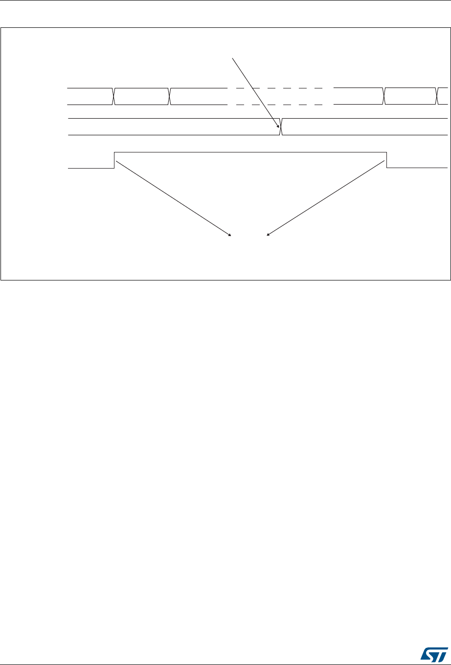
Advanced-control timers (TIM1) RM0394
748/1600 RM0394 Rev 4
Figure 217. Output compare mode, toggle on OC1
26.3.11 PWM mode
Pulse Width Modulation mode allows you to generate a signal with a frequency determined
by the value of the TIMx_ARR register and a duty cycle determined by the value of the
TIMx_CCRx register.
The PWM mode can be selected independently on each channel (one PWM per OCx
output) by writing ‘0110’ (PWM mode 1) or ‘0111’ (PWM mode 2) in the OCxM bits in the
TIMx_CCMRx register. You must enable the corresponding preload register by setting the
OCxPE bit in the TIMx_CCMRx register, and eventually the auto-reload preload register (in
upcounting or center-aligned modes) by setting the ARPE bit in the TIMx_CR1 register.
As the preload registers are transferred to the shadow registers only when an update event
occurs, before starting the counter, you have to initialize all the registers by setting the UG
bit in the TIMx_EGR register.
OCx polarity is software programmable using the CCxP bit in the TIMx_CCER register. It
can be programmed as active high or active low. OCx output is enabled by a combination of
the CCxE, CCxNE, MOE, OSSI and OSSR bits (TIMx_CCER and TIMx_BDTR registers).
Refer to the TIMx_CCER register description for more details.
In PWM mode (1 or 2), TIMx_CNT and TIMx_CCRx are always compared to determine
whether TIMx_CCRx TIMx_CNT or TIMx_CNT TIMx_CCRx (depending on the direction
of the counter).
The timer is able to generate PWM in edge-aligned mode or center-aligned mode
depending on the CMS bits in the TIMx_CR1 register.
069
2&5() 2&
7,0B&17 % %
7,0B&&5 $
:ULWH%KLQWKH&&5UHJLVWHU
0DWFKGHWHFWHGRQ&&5
,QWHUUXSWJHQHUDWHGLIHQDEOHG
%
%
$
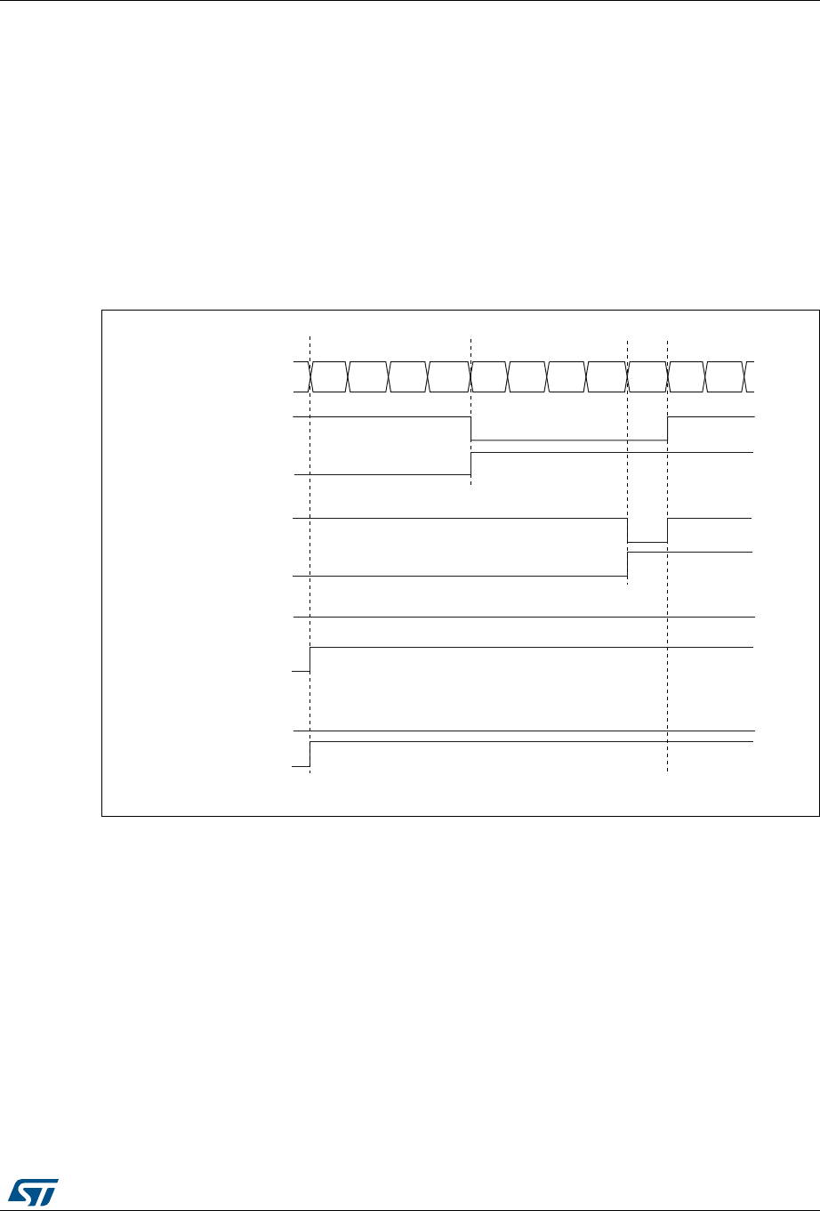
RM0394 Rev 4 749/1600
RM0394 Advanced-control timers (TIM1)
816
PWM edge-aligned mode
•Upcounting configuration
Upcounting is active when the DIR bit in the TIMx_CR1 register is low. Refer to the
Upcounting mode on page 723.
In the following example, we consider PWM mode 1. The reference PWM signal
OCxREF is high as long as TIMx_CNT < TIMx_CCRx else it becomes low. If the
compare value in TIMx_CCRx is greater than the auto-reload value (in TIMx_ARR)
then OCxREF is held at ‘1’. If the compare value is 0 then OCxRef is held at ‘0’.
Figure 218 shows some edge-aligned PWM waveforms in an example where
TIMx_ARR=8.
Figure 218. Edge-aligned PWM waveforms (ARR=8)
•Downcounting configuration
Downcounting is active when DIR bit in TIMx_CR1 register is high. Refer to the
Downcounting mode on page 727
In PWM mode 1, the reference signal OCxRef is low as long as
TIMx_CNT > TIMx_CCRx else it becomes high. If the compare value in TIMx_CCRx is
greater than the auto-reload value in TIMx_ARR, then OCxREF is held at ‘1’. 0% PWM
is not possible in this mode.
PWM center-aligned mode
Center-aligned mode is active when the CMS bits in TIMx_CR1 register are different from
‘00’ (all the remaining configurations having the same effect on the OCxRef/OCx signals).
The compare flag is set when the counter counts up, when it counts down or both when it
counts up and down depending on the CMS bits configuration. The direction bit (DIR) in the
TIMx_CR1 register is updated by hardware and must not be changed by software. Refer to
069
&RXQWHUUHJLVWHU
µ
2&;5()
&&[,)
2&;5()
&&[,)
2&;5()
&&[,)
2&;5()
&&[,)
&&5[
&&5[
&&5[!
&&5[
µ
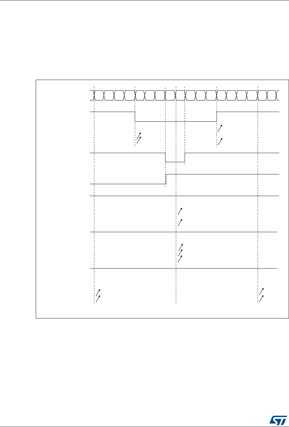
Advanced-control timers (TIM1) RM0394
750/1600 RM0394 Rev 4
the Center-aligned mode (up/down counting) on page 730.
Figure 219 shows some center-aligned PWM waveforms in an example where:
•TIMx_ARR=8,
•PWM mode is the PWM mode 1,
•The flag is set when the counter counts down corresponding to the center-aligned
mode 1 selected for CMS=01 in TIMx_CR1 register.
Figure 219. Center-aligned PWM waveforms (ARR=8)
Hints on using center-aligned mode
•When starting in center-aligned mode, the current up-down configuration is used. It
means that the counter counts up or down depending on the value written in the DIR bit
&&[,)
&RXQWHUUHJLVWHU
&&5[
2&[5()
&06
&06
&06
&&[,)
&&5[
2&[5()
&06 RU
&&[,)
&&5[
2&[5()
&06
&06
&06
µ
&&[,)
&&5[!
2&[5()
&06
&06
&06
µ
&&[,)
&&5[
2&[5()
&06
&06
&06
µ
$,E

RM0394 Rev 4 751/1600
RM0394 Advanced-control timers (TIM1)
816
in the TIMx_CR1 register. Moreover, the DIR and CMS bits must not be changed at the
same time by the software.
•Writing to the counter while running in center-aligned mode is not recommended as it
can lead to unexpected results. In particular:
– The direction is not updated if you write a value in the counter that is greater than
the auto-reload value (TIMx_CNT>TIMx_ARR). For example, if the counter was
counting up, it continues to count up.
– The direction is updated if you write 0 or write the TIMx_ARR value in the counter
but no Update Event UEV is generated.
•The safest way to use center-aligned mode is to generate an update by software
(setting the UG bit in the TIMx_EGR register) just before starting the counter and not to
write the counter while it is running.
26.3.12 Asymmetric PWM mode
Asymmetric mode allows two center-aligned PWM signals to be generated with a
programmable phase shift. While the frequency is determined by the value of the
TIMx_ARR register, the duty cycle and the phase-shift are determined by a pair of
TIMx_CCRx register. One register controls the PWM during up-counting, the second during
down counting, so that PWM is adjusted every half PWM cycle:
– OC1REFC (or OC2REFC) is controlled by TIMx_CCR1 and TIMx_CCR2
– OC3REFC (or OC4REFC) is controlled by TIMx_CCR3 and TIMx_CCR4
Asymmetric PWM mode can be selected independently on two channel (one OCx output
per pair of CCR registers) by writing ‘1110’ (Asymmetric PWM mode 1) or ‘1111’
(Asymmetric PWM mode 2) in the OCxM bits in the TIMx_CCMRx register.
Note: The OCxM[3:0] bit field is split into two parts for compatibility reasons, the most significant
bit is not contiguous with the 3 least significant ones.
When a given channel is used as asymmetric PWM channel, its complementary channel
can also be used. For instance, if an OC1REFC signal is generated on channel 1
(Asymmetric PWM mode 1), it is possible to output either the OC2REF signal on channel 2,
or an OC2REFC signal resulting from asymmetric PWM mode 1.
Figure 220 represents an example of signals that can be generated using Asymmetric PWM
mode (channels 1 to 4 are configured in Asymmetric PWM mode 1). Together with the
deadtime generator, this allows a full-bridge phase-shifted DC to DC converter to be
controlled.

Advanced-control timers (TIM1) RM0394
752/1600 RM0394 Rev 4
Figure 220. Generation of 2 phase-shifted PWM signals with 50% duty cycle
26.3.13 Combined PWM mode
Combined PWM mode allows two edge or center-aligned PWM signals to be generated with
programmable delay and phase shift between respective pulses. While the frequency is
determined by the value of the TIMx_ARR register, the duty cycle and delay are determined
by the two TIMx_CCRx registers. The resulting signals, OCxREFC, are made of an OR or
AND logical combination of two reference PWMs:
– OC1REFC (or OC2REFC) is controlled by TIMx_CCR1 and TIMx_CCR2
– OC3REFC (or OC4REFC) is controlled by TIMx_CCR3 and TIMx_CCR4
Combined PWM mode can be selected independently on two channels (one OCx output per
pair of CCR registers) by writing ‘1100’ (Combined PWM mode 1) or ‘1101’ (Combined PWM
mode 2) in the OCxM bits in the TIMx_CCMRx register.
When a given channel is used as combined PWM channel, its complementary channel must
be configured in the opposite PWM mode (for instance, one in Combined PWM mode 1 and
the other in Combined PWM mode 2).
Note: The OCxM[3:0] bit field is split into two parts for compatibility reasons, the most significant
bit is not contiguous with the 3 least significant ones.
Figure 221 represents an example of signals that can be generated using Asymmetric PWM
mode, obtained with the following configuration:
– Channel 1 is configured in Combined PWM mode 2,
– Channel 2 is configured in PWM mode 1,
– Channel 3 is configured in Combined PWM mode 2,
– Channel 4 is configured in PWM mode 1.
069
&RXQWHUUHJLVWHU
2&5()&
&&5
&&5
&&5
&&5
2&5()&
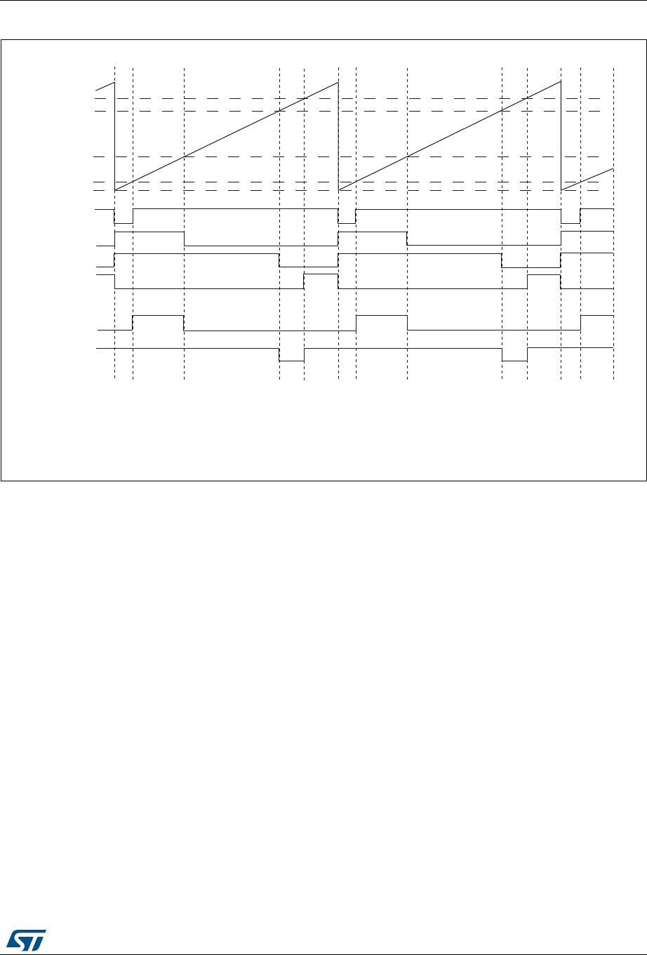
RM0394 Rev 4 753/1600
RM0394 Advanced-control timers (TIM1)
816
Figure 221. Combined PWM mode on channel 1 and 3
26.3.14 Combined 3-phase PWM mode
Combined 3-phase PWM mode allows one to three center-aligned PWM signals to be
generated with a single programmable signal ANDed in the middle of the pulses. The
OC5REF signal is used to define the resulting combined signal. The 3-bits GC5C[3:1] in the
TIMx_CCR5 allow selection on which reference signal the OC5REF is combined. The
resulting signals, OCxREFC, are made of an AND logical combination of two reference
PWMs:
– If GC5C1 is set, OC1REFC is controlled by TIMx_CCR1 and TIMx_CCR5
– If GC5C2 is set, OC2REFC is controlled by TIMx_CCR2 and TIMx_CCR5
– If GC5C3 is set, OC3REFC is controlled by TIMx_CCR3 and TIMx_CCR5
Combined 3-phase PWM mode can be selected independently on channels 1 to 3 by setting
at least one of the 3-bits GC5C[3:1].
069
2&5()
2&5()
2&5()
2&5()
2&5()&
2&5()&
2&5()& 2&5()$1'2&5()
2&5()&¶ 2&5()¶252&5()
2&
2&
2&
2&
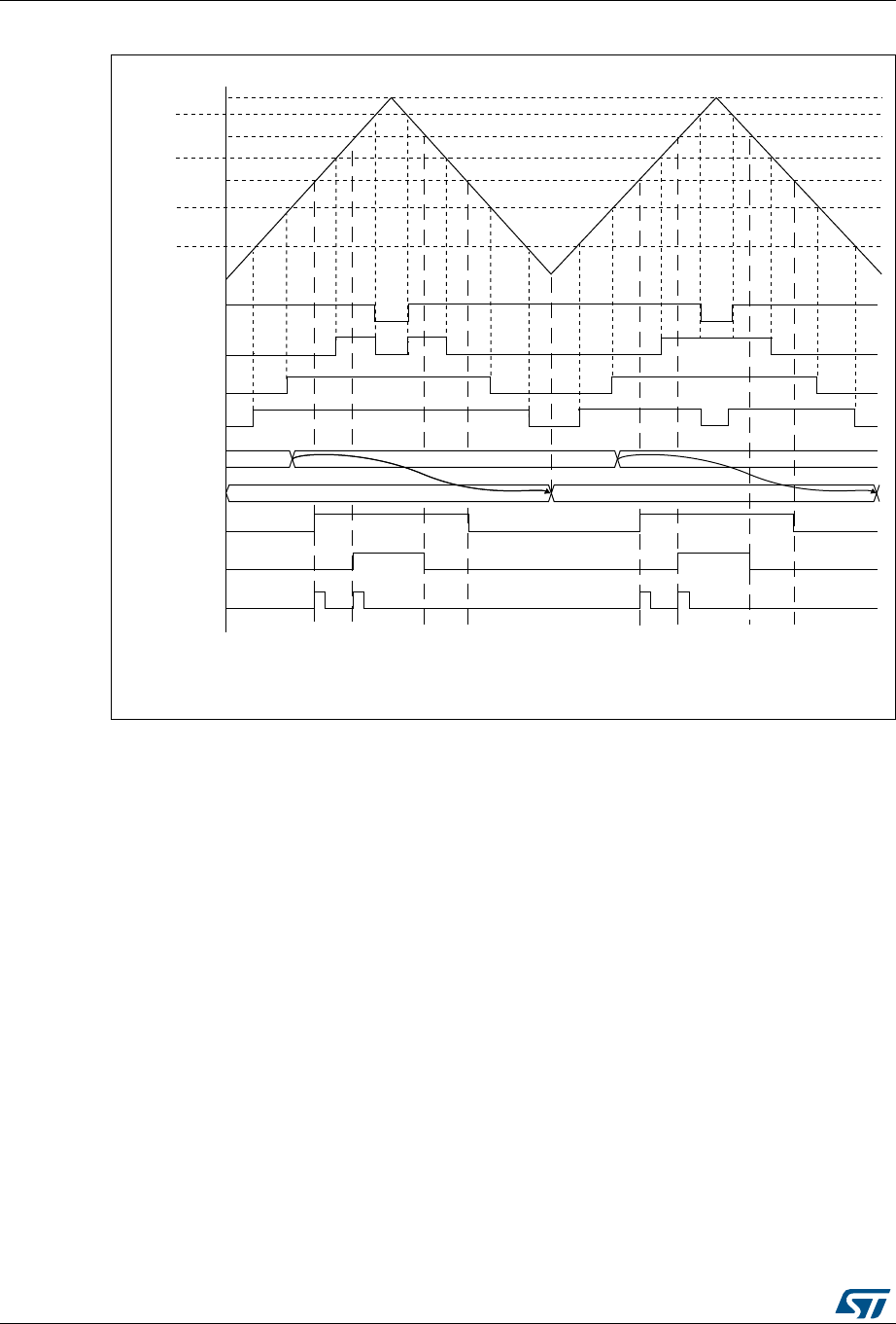
Advanced-control timers (TIM1) RM0394
754/1600 RM0394 Rev 4
Figure 222. 3-phase combined PWM signals with multiple trigger pulses per period
The TRGO2 waveform shows how the ADC can be synchronized on given 3-phase PWM
signals. Refer to Section 26.3.27: ADC synchronization for more details.
26.3.15 Complementary outputs and dead-time insertion
The advanced-control timers (TIM1) can output two complementary signals and manage the
switching-off and the switching-on instants of the outputs.
This time is generally known as dead-time and you have to adjust it depending on the
devices you have connected to the outputs and their characteristics (intrinsic delays of level-
shifters, delays due to power switches...)
You can select the polarity of the outputs (main output OCx or complementary OCxN)
independently for each output. This is done by writing to the CCxP and CCxNP bits in the
TIMx_CCER register.
The complementary signals OCx and OCxN are activated by a combination of several
control bits: the CCxE and CCxNE bits in the TIMx_CCER register and the MOE, OISx,
OISxN, OSSI and OSSR bits in the TIMx_BDTR and TIMx_CR2 registers. Refer to
Table 133: Output control bits for complementary OCx and OCxN channels with break
feature on page 799 for more details. In particular, the dead-time is activated when
switching to the idle state (MOE falling down to 0).
$55
2&
2&
2&
2&
2&UHI
2&UHI&
2&
2&
75*2
[[[
3UHORDG
*&&>@
[[[
&RXQWHU
069
2&UHI&
2&UHI&
$FWLYH
2&UHI
2&UHI
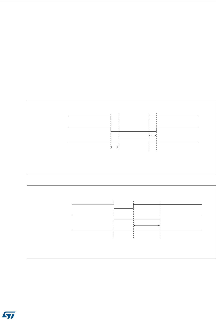
RM0394 Rev 4 755/1600
RM0394 Advanced-control timers (TIM1)
816
Dead-time insertion is enabled by setting both CCxE and CCxNE bits, and the MOE bit if the
break circuit is present. There is one 10-bit dead-time generator for each channel. From a
reference waveform OCxREF, it generates 2 outputs OCx and OCxN. If OCx and OCxN are
active high:
•The OCx output signal is the same as the reference signal except for the rising edge,
which is delayed relative to the reference rising edge.
•The OCxN output signal is the opposite of the reference signal except for the rising
edge, which is delayed relative to the reference falling edge.
If the delay is greater than the width of the active output (OCx or OCxN) then the
corresponding pulse is not generated.
The following figures show the relationships between the output signals of the dead-time
generator and the reference signal OCxREF. (we suppose CCxP=0, CCxNP=0, MOE=1,
CCxE=1 and CCxNE=1 in these examples)
Figure 223. Complementary output with dead-time insertion
Figure 224. Dead-time waveforms with delay greater than the negative pulse
GHOD\
GHOD\
2&[5()
2&[
2&[1
069
069
GHOD\
2&[5()
2&[
2&[1

Advanced-control timers (TIM1) RM0394
756/1600 RM0394 Rev 4
Figure 225. Dead-time waveforms with delay greater than the positive pulse
The dead-time delay is the same for each of the channels and is programmable with the
DTG bits in the TIMx_BDTR register. Refer to Section 26.4.20: TIM1 break and dead-time
register (TIM1_BDTR) for delay calculation.
Re-directing OCxREF to OCx or OCxN
In output mode (forced, output compare or PWM), OCxREF can be re-directed to the OCx
output or to OCxN output by configuring the CCxE and CCxNE bits in the TIMx_CCER
register.
This allows you to send a specific waveform (such as PWM or static active level) on one
output while the complementary remains at its inactive level. Other alternative possibilities
are to have both outputs at inactive level or both outputs active and complementary with
dead-time.
Note: When only OCxN is enabled (CCxE=0, CCxNE=1), it is not complemented and becomes
active as soon as OCxREF is high. For example, if CCxNP=0 then OCxN=OCxRef. On the
other hand, when both OCx and OCxN are enabled (CCxE=CCxNE=1) OCx becomes
active when OCxREF is high whereas OCxN is complemented and becomes active when
OCxREF is low.
26.3.16 Using the break function
The purpose of the break function is to protect power switches driven by PWM signals
generated with the TIM1 timer. The two break inputs are usually connected to fault outputs
of power stages and 3-phase inverters. When activated, the break circuitry shuts down the
PWM outputs and forces them to a predefined safe state. A number of internal MCU events
can also be selected to trigger an output shut-down.
The break features two channels. A break channel which gathers both system-level fault
(clock failure, parity error,...) and application fault (from input pins and built-in comparator),
and can force the outputs to a predefined level (either active or inactive) after a deadtime
duration. A break2 channel which only includes application faults and is able to force the
outputs to an inactive state.
069
GHOD\
2&[5()
2&[
2&[1

RM0394 Rev 4 757/1600
RM0394 Advanced-control timers (TIM1)
816
The output enable signal and output levels during break are depending on several control
bits:
– the MOE bit in TIMx_BDTR register allows to enable /disable the outputs by
software and is reset in case of break or break2 event.
– the OSSI bit in the TIMx_BDTR register defines whether the timer controls the
output in inactive state or releases the control to the GPIO controller (typically to
have it in Hi-Z mode)
– the OISx and OISxN bits in the TIMx_CR2 register which are setting the output
shut-down level, either active or inactive. The OCx and OCxN outputs cannot be
set both to active level at a given time, whatever the OISx and OISxN values.
Refer to Table 133: Output control bits for complementary OCx and OCxN
channels with break feature on page 799 for more details.
When exiting from reset, the break circuit is disabled and the MOE bit is low. You can enable
the break functions by setting the BKE and BK2E bits in the TIMx_BDTR register. The break
input polarities can be selected by configuring the BKP and BK2P bits in the same register.
BKE/BK2E and BKP/BK2P can be modified at the same time. When the BKE/BK2E and
BKP/BK2P bits are written, a delay of 1 APB clock cycle is applied before the writing is
effective. Consequently, it is necessary to wait 1 APB clock period to correctly read back the
bit after the write operation.
Because MOE falling edge can be asynchronous, a resynchronization circuit has been
inserted between the actual signal (acting on the outputs) and the synchronous control bit
(accessed in the TIMx_BDTR register). It results in some delays between the asynchronous
and the synchronous signals. In particular, if you write MOE to 1 whereas it was low, you
must insert a delay (dummy instruction) before reading it correctly. This is because you write
the asynchronous signal and read the synchronous signal.
The break can be generated from multiple sources which can be individually enabled and
with programmable edge sensitivity, using the TIMx_OR2 and TIMx_OR3 registers.
The sources for break (BRK) channel are:
•An external source connected to one of the BKIN pin (as per selection done in the
AFIO controller), with polarity selection and optional digital filtering
•An internal source:
–the Cortex
®-M4 LOCKUP output
– the PVD output
– the SRAM parity error signal
– a flash ECC error
– a clock failure event generated by the CSS detector
– the output from a comparator, with polarity selection and optional digital filtering
The sources for break2 (BRK2) are:
•An external source connected to one of the BKIN pin (as per selection done in the
AFIO controller), with polarity selection and optional digital filtering
•An internal source coming from a comparator output.
Break events can also be generated by software using BG and B2G bits in the TIMx_EGR
register. The software break generation using BG and B2G is active whatever the BKE and
BK2E enable bits values.
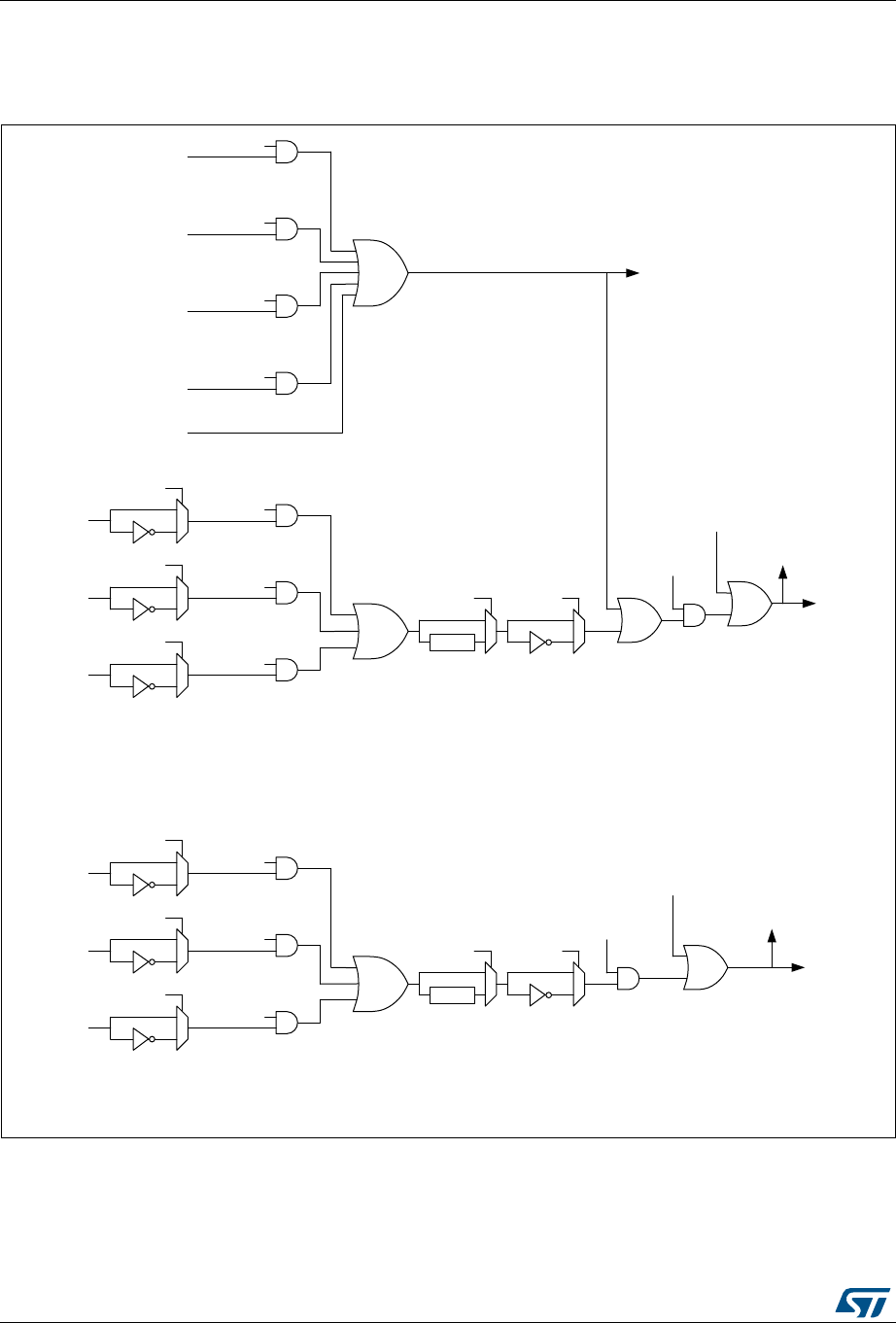
Advanced-control timers (TIM1) RM0394
758/1600 RM0394 Rev 4
All sources are ORed before entering the timer BRK or BRK2 inputs, as per Figure 226
below.
Figure 226. Break and Break2 circuitry overview
Note: An asynchronous (clockless) operation is only guaranteed when the programmable filter is
disabled. If it is enabled, a fail safe clock mode (for example by using the internal PLL and/or
the CSS) must be used to guarantee that break events are handled.
&203RXWSXW
%.&03(
%.&033
&203RXWSXW
%.&03(
%.&033
%.,1LQSXWV
IURP$)
FRQWUROOHU
%.,1(
%.,13
%.)>@
)LOWHU
%.3
$SSOLFDWLRQEUHDNUHTXHVWV
&203RXWSXW
%.&03(
%.&033
&203RXWSXW
%.&03(
%.&033
%.,1LQSXWV
IURP$)
FRQWUROOHU
%.,1(
%.,13
%.)>@
)LOWHU
%.3
$SSOLFDWLRQEUHDNUHTXHVWV
(&&/2&.
3DULW\/2&.
39'/2&.
/RFNXS/2&.
(&&(UURU
5$0SDULW\(UURU
39'
&RUH/RFNXS
&66
6%,)IODJ
6\VWHPEUHDNUHTXHVWV
6RIWZDUHEUHDNUHTXHVWV%*
%,)IODJ
%5.UHTXHVW
%.(
%5.UHTXHVW
%,)IODJ
6RIWZDUHEUHDNUHTXHVWV%*
06Y9
%.(

RM0394 Rev 4 759/1600
RM0394 Advanced-control timers (TIM1)
816
When one of the breaks occurs (selected level on one of the break inputs):
•The MOE bit is cleared asynchronously, putting the outputs in inactive state, idle state
or even releasing the control to the GPIO controller (selected by the OSSI bit). This
feature is enabled even if the MCU oscillator is off.
•Each output channel is driven with the level programmed in the OISx bit in the
TIMx_CR2 register as soon as MOE=0. If OSSI=0, the timer releases the output control
(taken over by the GPIO controller), otherwise the enable output remains high.
•When complementary outputs are used:
– The outputs are first put in inactive state (depending on the polarity). This is done
asynchronously so that it works even if no clock is provided to the timer.
– If the timer clock is still present, then the dead-time generator is reactivated in
order to drive the outputs with the level programmed in the OISx and OISxN bits
after a dead-time. Even in this case, OCx and OCxN cannot be driven to their
active level together. Note that because of the resynchronization on MOE, the
dead-time duration is slightly longer than usual (around 2 ck_tim clock cycles).
– If OSSI=0, the timer releases the output control (taken over by the GPIO controller
which forces a Hi-Z state), otherwise the enable outputs remain or become high as
soon as one of the CCxE or CCxNE bits is high.
•The break status flag (SBIF, BIF and B2IF bits in the TIMx_SR register) is set. An
interrupt is generated if the BIE bit in the TIMx_DIER register is set.
•If the AOE bit in the TIMx_BDTR register is set, the MOE bit is automatically set again
at the next update event (UEV). As an example, this can be used to perform a
regulation. Otherwise, MOE remains low until the application sets it to ‘1’ again. In this
case, it can be used for security and you can connect the break input to an alarm from
power drivers, thermal sensors or any security components.
Note: The break inputs are active on level. Thus, the MOE cannot be set while the break input is
active (neither automatically nor by software). In the meantime, the status flag BIF and B2IF
cannot be cleared.
In addition to the break input and the output management, a write protection has been
implemented inside the break circuit to safeguard the application. It allows to freeze the
configuration of several parameters (dead-time duration, OCx/OCxN polarities and state
when disabled, OCxM configurations, break enable and polarity). The application can
choose from 3 levels of protection selected by the LOCK bits in the TIMx_BDTR register.
Refer to Section 26.4.20: TIM1 break and dead-time register (TIM1_BDTR). The LOCK bits
can be written only once after an MCU reset.
Figure 227 shows an example of behavior of the outputs in response to a break.

Advanced-control timers (TIM1) RM0394
760/1600 RM0394 Rev 4
Figure 227. Various output behavior in response to a break event on BRK (OSSI = 1)
GHOD\ GHOD\ GHOD\
GHOD\ GHOD\ GHOD\
GHOD\
GHOD\
2&[5()
2&[
2&[1QRWLPSOHPHQWHG&&[3 2,6[
2&[
2&[1QRWLPSOHPHQWHG&&[3 2,6[
2&[
2&[1QRWLPSOHPHQWHG&&[3 2,6[
2&[
2&[1QRWLPSOHPHQWHG&&[3 2,6[
2&[
2&[1
&&[( &&[3 2,6[ &&[1( &&[13 2,6[1
2&[
2&[1
&&[( &&[3 2,6[ &&[1( &&[13 2,6[1
2&[
2&[1
&&[( &&[3 2,6[ &&[1( &&[13 2,6[1
2&[
2&[1
&&[( &&[3 2,6[ &&[1( &&[13 2,6[1
2&[
2&[1
&&[( &&[3 &&[1( &&[13 2,6[ 2,6[1 RU2,6[ 2,6[1
069
%5($.02(
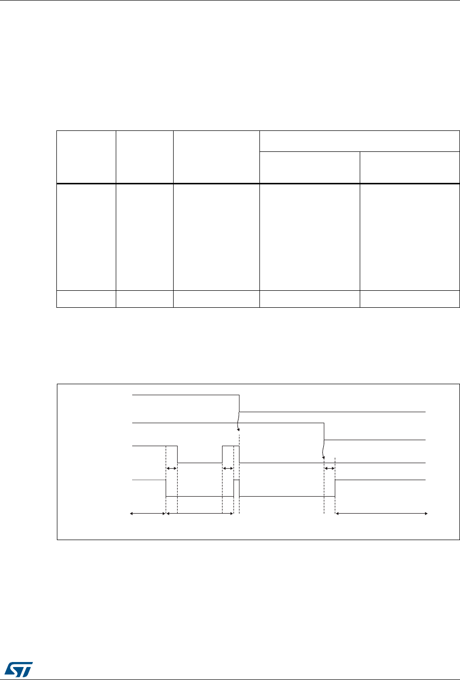
RM0394 Rev 4 761/1600
RM0394 Advanced-control timers (TIM1)
816
The two break inputs have different behaviors on timer outputs:
– The BRK input can either disable (inactive state) or force the PWM outputs to a
predefined safe state.
– BRK2 can only disable (inactive state) the PWM outputs.
The BRK has a higher priority than BRK2 input, as described in Table 130.
Note: BRK2 must only be used with OSSR = OSSI = 1.
Figure 228 gives an example of OCx and OCxN output behavior in case of active signals on
BRK and BRK2 inputs. In this case, both outputs have active high polarities (CCxP =
CCxNP = 0 in TIMx_CCER register).
Figure 228. PWM output state following BRK and BRK2 pins assertion (OSSI=1)
Table 130. Behavior of timer outputs versus BRK/BRK2 inputs
BRK BRK2 Timer outputs
state
Typical use case
OCxN output
(low side switches)
OCx output
(high side switches)
Active X
– Inactive then
forced output
state (after a
deadtime)
– Outputs disabled
if OSSI = 0
(control taken
over by GPIO
logic)
ON after deadtime
insertion OFF
Inactive Active Inactive OFF OFF
D^ϯϰϭϬϲsϭ
Z<Ϯ
Z<
Kdž
/ͬKƐƚĂƚĞ
ĞĂĚƚŝŵĞ ĞĂĚƚŝŵĞ
ĐƚŝǀĞ /ŶĂĐƚŝǀĞ /ĚůĞ
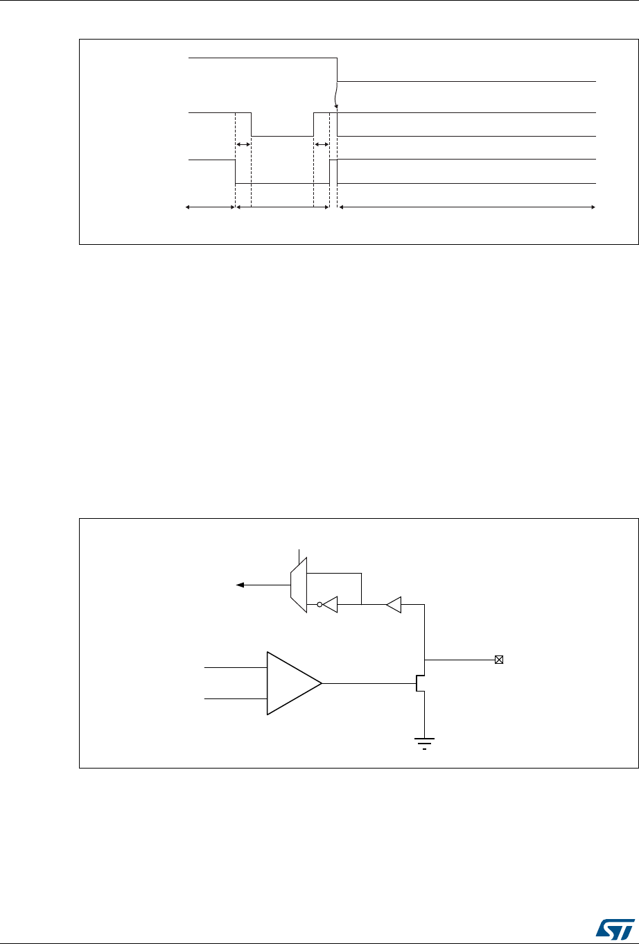
Advanced-control timers (TIM1) RM0394
762/1600 RM0394 Rev 4
Figure 229. PWM output state following BRK assertion (OSSI=0)
26.3.17 Bidirectional break inputs
Beside regular digital break inputs and internal break events coming from the comparators,
the timer 1 and 8 are featuring bidirectional break inputs/outputs combining the two sources,
as represented on Figure 230.
The TIMx_BKINy_COMPz pins are combining the COMPz output (to be configured in open
drain) and the Timerx’s TIMx_BKINy input. They allow to have:
- A global break information available for external MCUs or gate drivers shut down inputs,
with a single-pin.
- An internal comparator and multiple external open drain comparators outputs ORed
together and triggering a break event, when the multiple internal and external break inputs
must be merged.
Figure 230. Output redirection
D^ϯϰϭϬϳsϭ
Z<
Kdž
/ͬKƐƚĂƚĞ
ĞĂĚƚŝŵĞ
ĐƚŝǀĞ /ŶĂĐƚŝǀĞ ŝƐĂďůĞĚ
/ͬKƐƚĂƚĞĚĞĨŝŶĞĚďLJƚŚĞ'W/KĐŽŶƚƌŽůůĞƌ;,/ͲͿ
/ͬKƐƚĂƚĞĚĞĨŝŶĞĚďLJƚŚĞ'W/KĐŽŶƚƌŽůůĞƌ;,/ͲͿ
06Y9
&203
%.,13
$)2
7,0B%.,1\B&203]
\ 1$]
$)LQSXWHQDEOHGDFWLYHORZ
$)RXWSXWFRQILJXUHGDVRSHQGUDLQ
$),
7RWKHWLPHUEUHDNLQSXW
DFWLYHKLJK
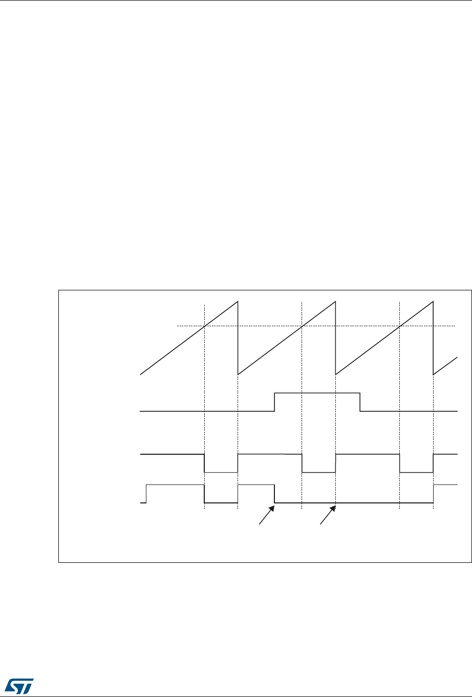
RM0394 Rev 4 763/1600
RM0394 Advanced-control timers (TIM1)
816
26.3.18 Clearing the OCxREF signal on an external event
When ETRF is chosen, ETR must be configured as follows:
1. The External Trigger Prescaler should be kept off: bits ETPS[1:0] of the TIMx_SMCR
register set to ‘00’.
2. The external clock mode 2 must be disabled: bit ECE of the TIMx_SMCR register set to
‘0’.
3. The External Trigger Polarity (ETP) and the External Trigger Filter (ETF) can be
configured according to the user needs.
Figure 231 shows the behavior of the OCxREF signal when the ETRF Input becomes High,
for both values of the enable bit OCxCE. In this example, the timer TIMx is programmed in
PWM mode.
Figure 231. Clearing TIMx OCxREF
Note: In case of a PWM with a 100% duty cycle (if CCRx>ARR), then OCxREF is enabled again at
the next counter overflow.
The OCxREF signal of a given channel can be cleared when a high level is applied on the
ocref_clr_int input (OCxCE enable bit in the corresponding TIMx_CCMRx register set to 1).
OCxREF remains low until the next update event (UEV) occurs. This function can only be
used in Output compare and PWM modes. It does not work in Forced mode. The
OCREF_CLR input is not connected (NC) in this product. The OCCS bit must be set to work
in OCxREF clearing mode.
069
&&5[
&RXQWHU&17
(75)
2&[5()
2&[&( µ
2&[5()
2&[&( µ
RFUHIBFOUBLQW
EHFRPHVKLJK
RFUHIBFOUBLQW
VWLOOKLJK
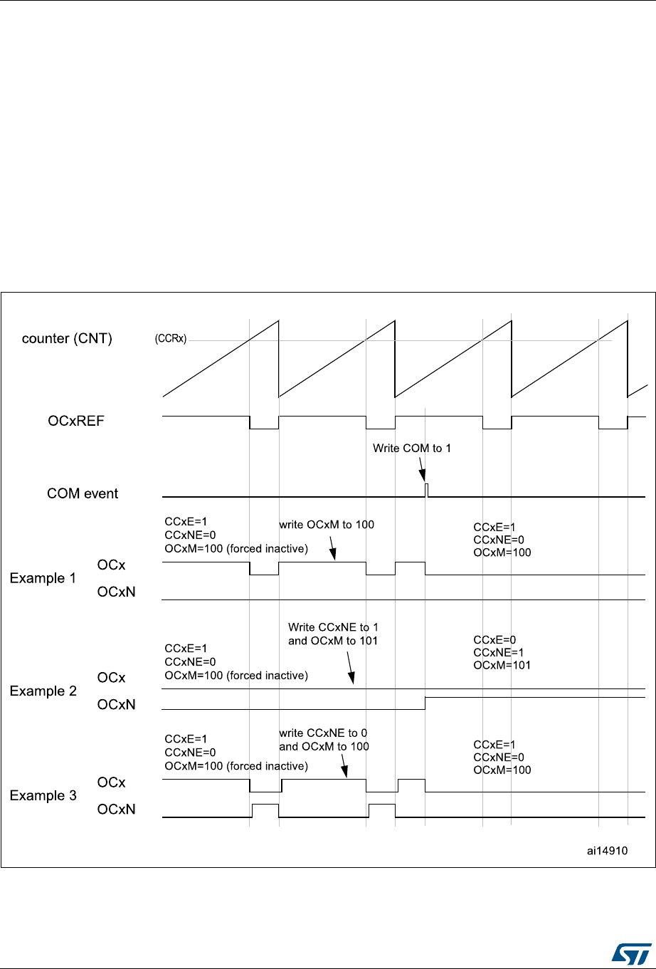
Advanced-control timers (TIM1) RM0394
764/1600 RM0394 Rev 4
26.3.19 6-step PWM generation
When complementary outputs are used on a channel, preload bits are available on the
OCxM, CCxE and CCxNE bits. The preload bits are transferred to the shadow bits at the
COM commutation event. Thus you can program in advance the configuration for the next
step and change the configuration of all the channels at the same time. COM can be
generated by software by setting the COM bit in the TIMx_EGR register or by hardware (on
TRGI rising edge).
A flag is set when the COM event occurs (COMIF bit in the TIMx_SR register), which can
generate an interrupt (if the COMIE bit is set in the TIMx_DIER register) or a DMA request
(if the COMDE bit is set in the TIMx_DIER register).
The Figure 232 describes the behavior of the OCx and OCxN outputs when a COM event
occurs, in 3 different examples of programmed configurations.
Figure 232. 6-step generation, COM example (OSSR=1)
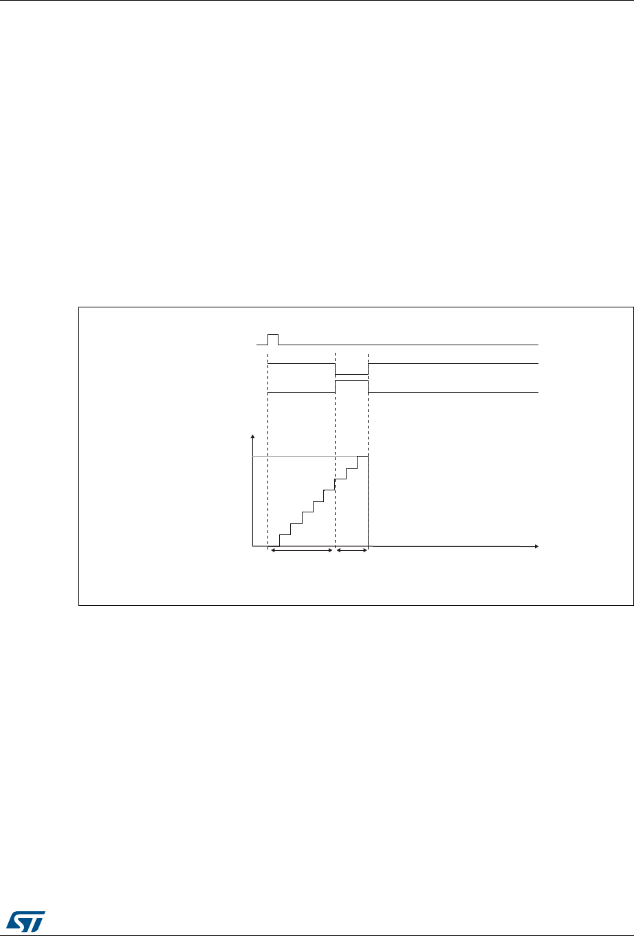
RM0394 Rev 4 765/1600
RM0394 Advanced-control timers (TIM1)
816
26.3.20 One-pulse mode
One-pulse mode (OPM) is a particular case of the previous modes. It allows the counter to
be started in response to a stimulus and to generate a pulse with a programmable length
after a programmable delay.
Starting the counter can be controlled through the slave mode controller. Generating the
waveform can be done in output compare mode or PWM mode. You select One-pulse mode
by setting the OPM bit in the TIMx_CR1 register. This makes the counter stop automatically
at the next update event UEV.
A pulse can be correctly generated only if the compare value is different from the counter
initial value. Before starting (when the timer is waiting for the trigger), the configuration must
be:
•In upcounting: CNT < CCRx ARR (in particular, 0 < CCRx)
•In downcounting: CNT > CCRx
Figure 233. Example of one pulse mode.
For example you may want to generate a positive pulse on OC1 with a length of tPULSE and
after a delay of tDELAY as soon as a positive edge is detected on the TI2 input pin.
Let’s use TI2FP2 as trigger 1:
1. Map TI2FP2 to TI2 by writing CC2S=’01’ in the TIMx_CCMR1 register.
2. TI2FP2 must detect a rising edge, write CC2P=’0’ and CC2NP=’0’ in the TIMx_CCER
register.
3. Configure TI2FP2 as trigger for the slave mode controller (TRGI) by writing TS=110 in
the TIMx_SMCR register.
4. TI2FP2 is used to start the counter by writing SMS to ‘110’ in the TIMx_SMCR register
(trigger mode).
069
7,
2&5()
&RXQWHU
W
7,0B$55
7,0B&&5
2&
W'(/$< W38/6(

Advanced-control timers (TIM1) RM0394
766/1600 RM0394 Rev 4
The OPM waveform is defined by writing the compare registers (taking into account the
clock frequency and the counter prescaler).
•The tDELAY is defined by the value written in the TIMx_CCR1 register.
•The tPULSE is defined by the difference between the auto-reload value and the compare
value (TIMx_ARR - TIMx_CCR1).
•Let’s say you want to build a waveform with a transition from ‘0’ to ‘1’ when a compare
match occurs and a transition from ‘1’ to ‘0’ when the counter reaches the auto-reload
value. To do this you enable PWM mode 2 by writing OC1M=111 in the TIMx_CCMR1
register. You can optionally enable the preload registers by writing OC1PE=’1’ in the
TIMx_CCMR1 register and ARPE in the TIMx_CR1 register. In this case you have to
write the compare value in the TIMx_CCR1 register, the auto-reload value in the
TIMx_ARR register, generate an update by setting the UG bit and wait for external
trigger event on TI2. CC1P is written to ‘0’ in this example.
In our example, the DIR and CMS bits in the TIMx_CR1 register should be low.
You only want 1 pulse (Single mode), so you write '1 in the OPM bit in the TIMx_CR1
register to stop the counter at the next update event (when the counter rolls over from the
auto-reload value back to 0). When OPM bit in the TIMx_CR1 register is set to '0', so the
Repetitive Mode is selected.
Particular case: OCx fast enable:
In One-pulse mode, the edge detection on TIx input set the CEN bit which enables the
counter. Then the comparison between the counter and the compare value makes the
output toggle. But several clock cycles are needed for these operations and it limits the
minimum delay tDELAY min we can get.
If you want to output a waveform with the minimum delay, you can set the OCxFE bit in the
TIMx_CCMRx register. Then OCxRef (and OCx) are forced in response to the stimulus,
without taking in account the comparison. Its new level is the same as if a compare match
had occurred. OCxFE acts only if the channel is configured in PWM1 or PWM2 mode.
26.3.21 Retriggerable one pulse mode (OPM)
This mode allows the counter to be started in response to a stimulus and to generate a
pulse with a programmable length, but with the following differences with Non-retriggerable
one pulse mode described in Section 26.3.20:
– The pulse starts as soon as the trigger occurs (no programmable delay)
– The pulse is extended if a new trigger occurs before the previous one is completed
The timer must be in Slave mode, with the bits SMS[3:0] = ‘1000’ (Combined Reset + trigger
mode) in the TIMx_SMCR register, and the OCxM[3:0] bits set to ‘1000’ or ‘1001’ for
Retrigerrable OPM mode 1 or 2.
If the timer is configured in Up-counting mode, the corresponding CCRx must be set to 0
(the ARR register sets the pulse length). If the timer is configured in Down-counting mode,
CCRx must be above or equal to ARR.
Note: The OCxM[3:0] and SMS[3:0] bit fields are split into two parts for compatibility reasons, the
most significant bit are not contiguous with the 3 least significant ones.
This mode must not be used with center-aligned PWM modes. It is mandatory to have
CMS[1:0] = 00 in TIMx_CR1.

RM0394 Rev 4 767/1600
RM0394 Advanced-control timers (TIM1)
816
Figure 234. Retriggerable one pulse mode
26.3.22 Encoder interface mode
To select Encoder Interface mode write SMS=‘001’ in the TIMx_SMCR register if the
counter is counting on TI2 edges only, SMS=’010’ if it is counting on TI1 edges only and
SMS=’011’ if it is counting on both TI1 and TI2 edges.
Select the TI1 and TI2 polarity by programming the CC1P and CC2P bits in the TIMx_CCER
register. When needed, you can program the input filter as well. CC1NP and CC2NP must
be kept low.
The two inputs TI1 and TI2 are used to interface to an quadrature encoder. Refer to
Table 131. The counter is clocked by each valid transition on TI1FP1 or TI2FP2 (TI1 and TI2
after input filter and polarity selection, TI1FP1=TI1 if not filtered and not inverted,
TI2FP2=TI2 if not filtered and not inverted) assuming that it is enabled (CEN bit in
TIMx_CR1 register written to ‘1’). The sequence of transitions of the two inputs is evaluated
and generates count pulses as well as the direction signal. Depending on the sequence the
counter counts up or down, the DIR bit in the TIMx_CR1 register is modified by hardware
accordingly. The DIR bit is calculated at each transition on any input (TI1 or TI2), whatever
the counter is counting on TI1 only, TI2 only or both TI1 and TI2.
Encoder interface mode acts simply as an external clock with direction selection. This
means that the counter just counts continuously between 0 and the auto-reload value in the
TIMx_ARR register (0 to ARR or ARR down to 0 depending on the direction). So you must
configure TIMx_ARR before starting. In the same way, the capture, compare, repetition
counter, trigger output features continue to work as normal. Encoder mode and External
clock mode 2 are not compatible and must not be selected together.
Note: The prescaler must be set to zero when encoder mode is enabled
In this mode, the counter is modified automatically following the speed and the direction of
the quadrature encoder and its content, therefore, always represents the encoder’s position.
The count direction correspond to the rotation direction of the connected sensor. The table
summarizes the possible combinations, assuming TI1 and TI2 don’t switch at the same
time.
75*,
&RXQWHU
2XWSXW
069
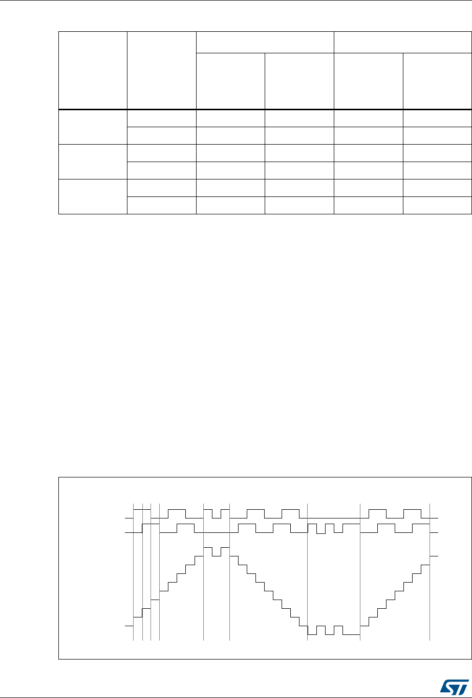
Advanced-control timers (TIM1) RM0394
768/1600 RM0394 Rev 4
A quadrature encoder can be connected directly to the MCU without external interface logic.
However, comparators are normally be used to convert the encoder’s differential outputs to
digital signals. This greatly increases noise immunity. The third encoder output which
indicate the mechanical zero position, may be connected to an external interrupt input and
trigger a counter reset.
The Figure 235 gives an example of counter operation, showing count signal generation
and direction control. It also shows how input jitter is compensated where both edges are
selected. This might occur if the sensor is positioned near to one of the switching points. For
this example we assume that the configuration is the following:
•CC1S=’01’ (TIMx_CCMR1 register, TI1FP1 mapped on TI1).
•CC2S=’01’ (TIMx_CCMR2 register, TI1FP2 mapped on TI2).
•CC1P=’0’ and CC1NP=’0’ (TIMx_CCER register, TI1FP1 non-inverted, TI1FP1=TI1).
•CC2P=’0’ and CC2NP=’0’ (TIMx_CCER register, TI1FP2 non-inverted, TI1FP2= TI2).
•SMS=’011’ (TIMx_SMCR register, both inputs are active on both rising and falling
edges).
•CEN=’1’ (TIMx_CR1 register, Counter enabled).
Figure 235. Example of counter operation in encoder interface mode.
Table 131. Counting direction versus encoder signals
Active edge
Level on
opposite
signal (TI1FP1
for TI2,
TI2FP2 for
TI1)
TI1FP1 signal TI2FP2 signal
Rising Falling Rising Falling
Counting on
TI1 only
High Down Up No Count No Count
Low Up Down No Count No Count
Counting on
TI2 only
High No Count No Count Up Down
Low No Count No Count Down Up
Counting on
TI1 and TI2
High Down Up Up Down
Low Up Down Down Up
7,
EDFNZDUGMLWWHU MLWWHU
XS GRZQ XS
7,
&RXQWHU
IRUZDUG IRUZDUG
069
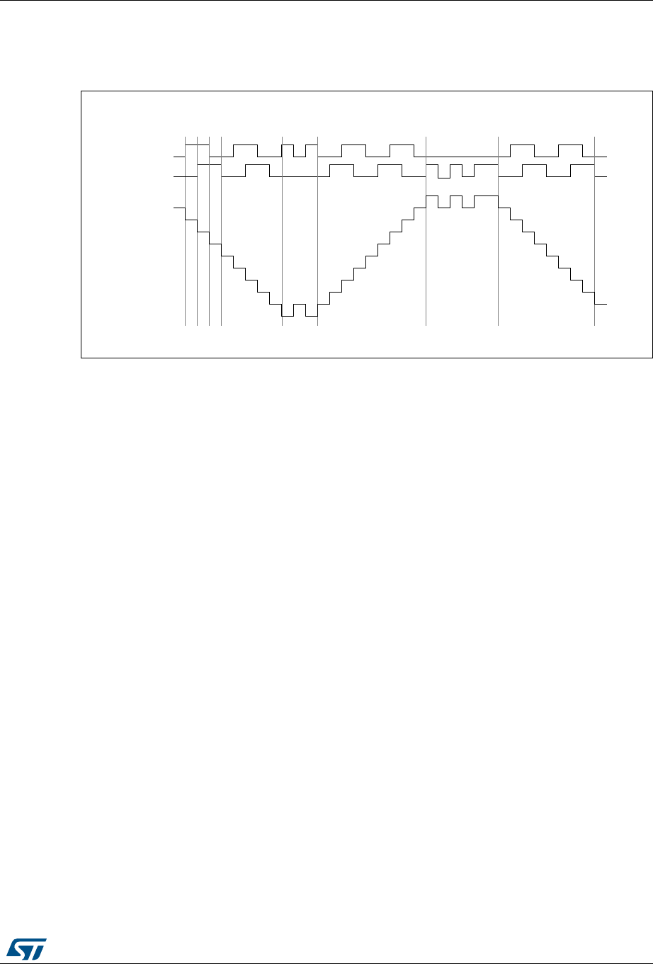
RM0394 Rev 4 769/1600
RM0394 Advanced-control timers (TIM1)
816
Figure 236 gives an example of counter behavior when TI1FP1 polarity is inverted (same
configuration as above except CC1P=’1’).
Figure 236. Example of encoder interface mode with TI1FP1 polarity inverted.
The timer, when configured in Encoder Interface mode provides information on the sensor’s
current position. You can obtain dynamic information (speed, acceleration, deceleration) by
measuring the period between two encoder events using a second timer configured in
capture mode. The output of the encoder which indicates the mechanical zero can be used
for this purpose. Depending on the time between two events, the counter can also be read
at regular times. You can do this by latching the counter value into a third input capture
register if available (then the capture signal must be periodic and can be generated by
another timer). when available, it is also possible to read its value through a DMA request.
The IUFREMAP bit in the TIMx_CR1 register forces a continuous copy of the update
interrupt flag (UIF) into the timer counter register’s bit 31 (TIMxCNT[31]). This allows both
the counter value and a potential roll-over condition signaled by the UIFCPY flag to be read
in an atomic way. It eases the calculation of angular speed by avoiding race conditions
caused, for instance, by a processing shared between a background task (counter reading)
and an interrupt (update interrupt).
There is no latency between the UIF and UIFCPY flag assertions.
In 32-bit timer implementations, when the IUFREMAP bit is set, bit 31 of the counter is
overwritten by the UIFCPY flag upon read access (the counter’s most significant bit is only
accessible in write mode).
26.3.23 UIF bit remapping
The IUFREMAP bit in the TIMx_CR1 register forces a continuous copy of the Update
Interrupt Flag UIF into the timer counter register’s bit 31 (TIMxCNT[31]). This allows both
the counter value and a potential roll-over condition signaled by the UIFCPY flag to be read
in an atomic way. In particular cases, it can ease the calculations by avoiding race
conditions, caused for instance by a processing shared between a background task
(counter reading) and an interrupt (Update Interrupt).
There is no latency between the UIF and UIFCPY flags assertion.
7,
EDFNZDUGMLWWHU MLWWHU
XSGRZQ
7,
&RXQWHU
IRUZDUG IRUZDUG
069
GRZQ
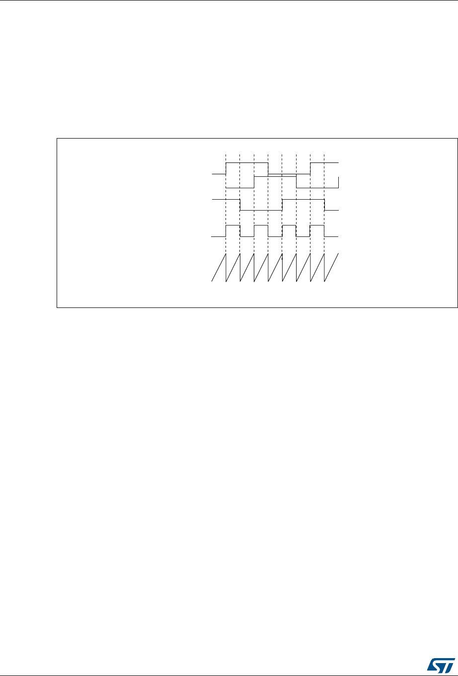
Advanced-control timers (TIM1) RM0394
770/1600 RM0394 Rev 4
26.3.24 Timer input XOR function
The TI1S bit in the TIMx_CR2 register, allows the input filter of channel 1 to be connected to
the output of an XOR gate, combining the three input pins TIMx_CH1, TIMx_CH2 and
TIMx_CH3.
The XOR output can be used with all the timer input functions such as trigger or input
capture. It is convenient to measure the interval between edges on two input signals, as per
Figure 237 below.
Figure 237. Measuring time interval between edges on 3 signals
26.3.25 Interfacing with Hall sensors
This is done using the advanced-control timer (TIM1) to generate PWM signals to drive the
motor and another timer TIMx (TIM2) referred to as “interfacing timer” in Figure 238. The
“interfacing timer” captures the 3 timer input pins (CC1, CC2, CC3) connected through a
XOR to the TI1 input channel (selected by setting the TI1S bit in the TIMx_CR2 register).
The slave mode controller is configured in reset mode; the slave input is TI1F_ED. Thus,
each time one of the 3 inputs toggles, the counter restarts counting from 0. This creates a
time base triggered by any change on the Hall inputs.
On the “interfacing timer”, capture/compare channel 1 is configured in capture mode,
capture signal is TRC (See Figure 211: Capture/compare channel (example: channel 1 input
stage) on page 741). The captured value, which corresponds to the time elapsed between 2
changes on the inputs, gives information about motor speed.
The “interfacing timer” can be used in output mode to generate a pulse which changes the
configuration of the channels of the advanced-control timer (TIM1) (by triggering a COM
event). The TIM1 timer is used to generate PWM signals to drive the motor. To do this, the
interfacing timer channel must be programmed so that a positive pulse is generated after a
programmed delay (in output compare or PWM mode). This pulse is sent to the advanced-
control timer (TIM1) through the TRGO output.
069
7,
7,
;25
&RXQWHU
7,
7,0[

RM0394 Rev 4 771/1600
RM0394 Advanced-control timers (TIM1)
816
Example: you want to change the PWM configuration of your advanced-control timer TIM1
after a programmed delay each time a change occurs on the Hall inputs connected to one of
the TIMx timers.
•Configure 3 timer inputs ORed to the TI1 input channel by writing the TI1S bit in the
TIMx_CR2 register to ‘1’,
•Program the time base: write the TIMx_ARR to the max value (the counter must be
cleared by the TI1 change. Set the prescaler to get a maximum counter period longer
than the time between 2 changes on the sensors,
•Program the channel 1 in capture mode (TRC selected): write the CC1S bits in the
TIMx_CCMR1 register to ‘01’. You can also program the digital filter if needed,
•Program the channel 2 in PWM 2 mode with the desired delay: write the OC2M bits to
‘111’ and the CC2S bits to ‘00’ in the TIMx_CCMR1 register,
•Select OC2REF as trigger output on TRGO: write the MMS bits in the TIMx_CR2
register to ‘101’,
In the advanced-control timer TIM1, the right ITR input must be selected as trigger input, the
timer is programmed to generate PWM signals, the capture/compare control signals are
preloaded (CCPC=1 in the TIMx_CR2 register) and the COM event is controlled by the
trigger input (CCUS=1 in the TIMx_CR2 register). The PWM control bits (CCxE, OCxM) are
written after a COM event for the next step (this can be done in an interrupt subroutine
generated by the rising edge of OC2REF).
The Figure 238 describes this example.
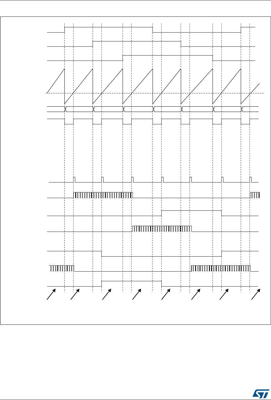
Advanced-control timers (TIM1) RM0394
772/1600 RM0394 Rev 4
Figure 238. Example of Hall sensor interface
&RXQWHU&17
75*2 2&5()
&&5
2&
2&1
&20
:ULWH&&[(&&[1(
7,+
7,+
7,+
&&5
2&
2&1
2&
2&1
&
DQG2&[0IRUQH[WVWHS
,QWHUIDFLQJWLPHU$GYDQFHGFRQWUROWLPHUV7,0
069
&$ &$ & &$ &$%
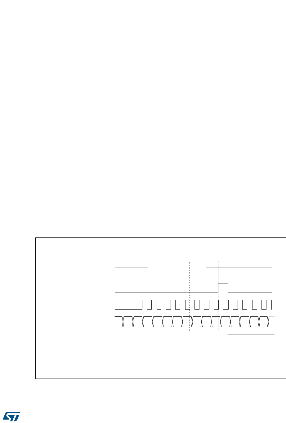
RM0394 Rev 4 773/1600
RM0394 Advanced-control timers (TIM1)
816
26.3.26 Timer synchronization
The TIMx timers are linked together internally for timer synchronization or chaining. They
can be synchronized in several modes: Reset mode, Gated mode, and Trigger mode.
Slave mode: Reset mode
The counter and its prescaler can be reinitialized in response to an event on a trigger input.
Moreover, if the URS bit from the TIMx_CR1 register is low, an update event UEV is
generated. Then all the preloaded registers (TIMx_ARR, TIMx_CCRx) are updated.
In the following example, the upcounter is cleared in response to a rising edge on TI1 input:
•Configure the channel 1 to detect rising edges on TI1. Configure the input filter duration
(in this example, we don’t need any filter, so we keep IC1F=0000). The capture
prescaler is not used for triggering, so you don’t need to configure it. The CC1S bits
select the input capture source only, CC1S = 01 in the TIMx_CCMR1 register. Write
CC1P=0 and CC1NP=’0’ in TIMx_CCER register to validate the polarity (and detect
rising edges only).
•Configure the timer in reset mode by writing SMS=100 in TIMx_SMCR register. Select
TI1 as the input source by writing TS=101 in TIMx_SMCR register.
•Start the counter by writing CEN=1 in the TIMx_CR1 register.
The counter starts counting on the internal clock, then behaves normally until TI1 rising
edge. When TI1 rises, the counter is cleared and restarts from 0. In the meantime, the
trigger flag is set (TIF bit in the TIMx_SR register) and an interrupt request, or a DMA
request can be sent if enabled (depending on the TIE and TDE bits in TIMx_DIER register).
The following figure shows this behavior when the auto-reload register TIMx_ARR=0x36.
The delay between the rising edge on TI1 and the actual reset of the counter is due to the
resynchronization circuit on TI1 input.
Figure 239. Control circuit in reset mode
069
&RXQWHUFORFN FNBFQW FNBSVF
&RXQWHUUHJLVWHU
8*
7,
7,)
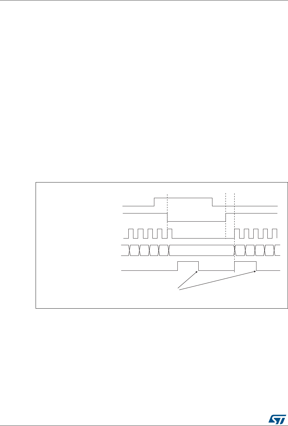
Advanced-control timers (TIM1) RM0394
774/1600 RM0394 Rev 4
Slave mode: Gated mode
The counter can be enabled depending on the level of a selected input.
In the following example, the upcounter counts only when TI1 input is low:
•Configure the channel 1 to detect low levels on TI1. Configure the input filter duration
(in this example, we don’t need any filter, so we keep IC1F=0000). The capture
prescaler is not used for triggering, so you don’t need to configure it. The CC1S bits
select the input capture source only, CC1S=01 in TIMx_CCMR1 register. Write
CC1P=1 and CC1NP=’0’ in TIMx_CCER register to validate the polarity (and detect
low level only).
•Configure the timer in gated mode by writing SMS=101 in TIMx_SMCR register. Select
TI1 as the input source by writing TS=101 in TIMx_SMCR register.
•Enable the counter by writing CEN=1 in the TIMx_CR1 register (in gated mode, the
counter doesn’t start if CEN=0, whatever is the trigger input level).
The counter starts counting on the internal clock as long as TI1 is low and stops as soon as
TI1 becomes high. The TIF flag in the TIMx_SR register is set both when the counter starts
or stops.
The delay between the rising edge on TI1 and the actual stop of the counter is due to the
resynchronization circuit on TI1 input.
Figure 240. Control circuit in Gated mode
Slave mode: Trigger mode
The counter can start in response to an event on a selected input.
In the following example, the upcounter starts in response to a rising edge on TI2 input:
•Configure the channel 2 to detect rising edges on TI2. Configure the input filter duration
(in this example, we don’t need any filter, so we keep IC2F=0000). The capture
prescaler is not used for triggering, so you don’t need to configure it. The CC2S bits are
configured to select the input capture source only, CC2S=01 in TIMx_CCMR1 register.
069
7,
FQWBHQ
:ULWH7,)
&RXQWHUFORFN FNBFQW FNBSVF
&RXQWHUUHJLVWHU
7,)
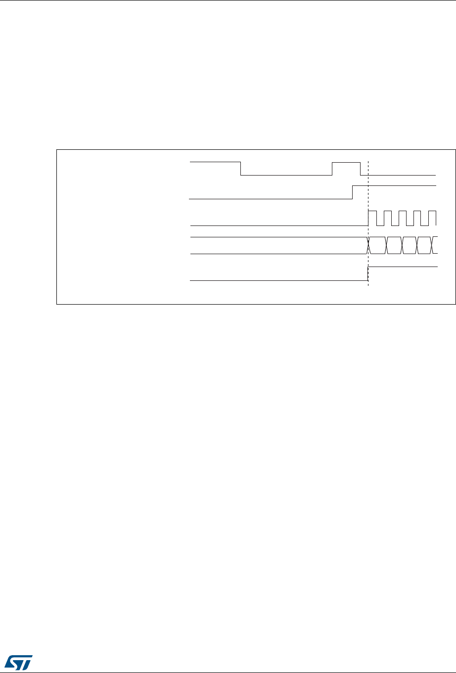
RM0394 Rev 4 775/1600
RM0394 Advanced-control timers (TIM1)
816
Write CC2P=1 and CC2NP=0 in TIMx_CCER register to validate the polarity (and
detect low level only).
•Configure the timer in trigger mode by writing SMS=110 in TIMx_SMCR register. Select
TI2 as the input source by writing TS=110 in TIMx_SMCR register.
When a rising edge occurs on TI2, the counter starts counting on the internal clock and the
TIF flag is set.
The delay between the rising edge on TI2 and the actual start of the counter is due to the
resynchronization circuit on TI2 input.
Figure 241. Control circuit in trigger mode
Slave mode: Combined reset + trigger mode
In this case, a rising edge of the selected trigger input (TRGI) reinitializes the counter,
generates an update of the registers, and starts the counter.
This mode is used for one-pulse mode.
Slave mode: external clock mode 2 + trigger mode
The external clock mode 2 can be used in addition to another slave mode (except external
clock mode 1 and encoder mode). In this case, the ETR signal is used as external clock
input, and another input can be selected as trigger input (in reset mode, gated mode or
trigger mode). It is recommended not to select ETR as TRGI through the TS bits of
TIMx_SMCR register.
In the following example, the upcounter is incremented at each rising edge of the ETR
signal as soon as a rising edge of TI1 occurs:
069
7,
FQWBHQ
&RXQWHUFORFN FNBFQW FNBSVF
&RXQWHUUHJLVWHU
7,)
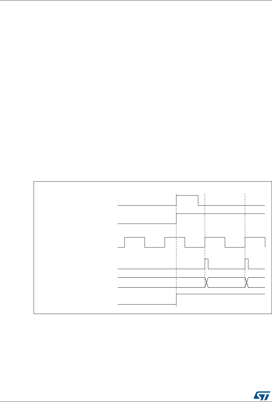
Advanced-control timers (TIM1) RM0394
776/1600 RM0394 Rev 4
1. Configure the external trigger input circuit by programming the TIMx_SMCR register as
follows:
– ETF = 0000: no filter
– ETPS=00: prescaler disabled
– ETP=0: detection of rising edges on ETR and ECE=1 to enable the external clock
mode 2.
2. Configure the channel 1 as follows, to detect rising edges on TI:
– IC1F=0000: no filter.
– The capture prescaler is not used for triggering and does not need to be
configured.
– CC1S=01in TIMx_CCMR1 register to select only the input capture source
– CC1P=0 and CC1NP=’0’ in TIMx_CCER register to validate the polarity (and
detect rising edge only).
3. Configure the timer in trigger mode by writing SMS=110 in TIMx_SMCR register. Select
TI1 as the input source by writing TS=101 in TIMx_SMCR register.
A rising edge on TI1 enables the counter and sets the TIF flag. The counter then counts on
ETR rising edges.
The delay between the rising edge of the ETR signal and the actual reset of the counter is
due to the resynchronization circuit on ETRP input.
Figure 242. Control circuit in external clock mode 2 + trigger mode
Note: The clock of the slave peripherals (timer, ADC, ...) receiving the TRGO or the TRGO2
signals must be enabled prior to receive events from the master timer, and the clock
frequency (prescaler) must not be changed on-the-fly while triggers are received from the
master timer.
069
7,)
&RXQWHUUHJLVWHU
&RXQWHUFORFN &.B&17 &.B36&
(75
&(1&17B(1
7,

RM0394 Rev 4 777/1600
RM0394 Advanced-control timers (TIM1)
816
26.3.27 ADC synchronization
The timer can generate an ADC triggering event with various internal signals, such as reset,
enable or compare events. It is also possible to generate a pulse issued by internal edge
detectors, such as:
– Rising and falling edges of OC4ref
– Rising edge on OC5ref or falling edge on OC6ref
The triggers are issued on the TRGO2 internal line which is redirected to the ADC. There is
a total of 16 possible events, which can be selected using the MMS2[3:0] bits in the
TIMx_CR2 register.
An example of an application for 3-phase motor drives is given in Figure 222 on page 754.
Note: The clock of the slave peripherals (timer, ADC, ...) receiving the TRGO or the TRGO2
signals must be enabled prior to receive events from the master timer, and the clock
frequency (prescaler) must not be changed on-the-fly while triggers are received from the
master timer.
Note: The clock of the ADC must be enabled prior to receive events from the master timer, and
must not be changed on-the-fly while triggers are received from the timer.
26.3.28 DMA burst mode
The TIMx timers have the capability to generate multiple DMA requests upon a single event.
The main purpose is to be able to re-program part of the timer multiple times without
software overhead, but it can also be used to read several registers in a row, at regular
intervals.
The DMA controller destination is unique and must point to the virtual register TIMx_DMAR.
On a given timer event, the timer launches a sequence of DMA requests (burst). Each write
into the TIMx_DMAR register is actually redirected to one of the timer registers.
The DBL[4:0] bits in the TIMx_DCR register set the DMA burst length. The timer recognizes
a burst transfer when a read or a write access is done to the TIMx_DMAR address), i.e. the
number of transfers (either in half-words or in bytes).
The DBA[4:0] bits in the TIMx_DCR registers define the DMA base address for DMA
transfers (when read/write access are done through the TIMx_DMAR address). DBA is
defined as an offset starting from the address of the TIMx_CR1 register:
Example:
00000: TIMx_CR1
00001: TIMx_CR2
00010: TIMx_SMCR
As an example, the timer DMA burst feature is used to update the contents of the CCRx
registers (x = 2, 3, 4) upon an update event, with the DMA transferring half words into the
CCRx registers.

Advanced-control timers (TIM1) RM0394
778/1600 RM0394 Rev 4
This is done in the following steps:
1. Configure the corresponding DMA channel as follows:
– DMA channel peripheral address is the DMAR register address
– DMA channel memory address is the address of the buffer in the RAM containing
the data to be transferred by DMA into CCRx registers.
– Number of data to transfer = 3 (See note below).
– Circular mode disabled.
2. Configure the DCR register by configuring the DBA and DBL bit fields as follows:
DBL = 3 transfers, DBA = 0xE.
3. Enable the TIMx update DMA request (set the UDE bit in the DIER register).
4. Enable TIMx
5. Enable the DMA channel
This example is for the case where every CCRx register to be updated once. If every CCRx
register is to be updated twice for example, the number of data to transfer should be 6. Let's
take the example of a buffer in the RAM containing data1, data2, data3, data4, data5 and
data6. The data is transferred to the CCRx registers as follows: on the first update DMA
request, data1 is transferred to CCR2, data2 is transferred to CCR3, data3 is transferred to
CCR4 and on the second update DMA request, data4 is transferred to CCR2, data5 is
transferred to CCR3 and data6 is transferred to CCR4.
Note: A null value can be written to the reserved registers.
26.3.29 Debug mode
When the microcontroller enters debug mode (Cortex®-M4 core halted), the TIMx counter
either continues to work normally or stops, depending on DBG_TIMx_STOP configuration
bit in DBG module.
For safety purposes, when the counter is stopped (DBG_TIMx_STOP = 1), the outputs are
disabled (as if the MOE bit was reset). The outputs can either be forced to an inactive state
(OSSI bit = 1), or have their control taken over by the GPIO controller (OSSI bit = 0),
typically to force a Hi-Z.
For more details, refer to Section 46.16.2: Debug support for timers, RTC, watchdog,
bxCAN and I2C.
For safety purposes, when the counter is stopped (DBG_TIMx_STOP = 1), the outputs are
disabled (as if the MOE bit was reset). The outputs can either be forced to an inactive state
(OSSI bit = 1), or have their control taken over by the GPIO controller (OSSI bit = 0) to force
them to Hi-Z.

RM0394 Rev 4 779/1600
RM0394 Advanced-control timers (TIM1)
816
26.4 TIM1 registers
Refer to for a list of abbreviations used in register descriptions.
26.4.1 TIM1 control register 1 (TIM1_CR1)
Address offset: 0x00
Reset value: 0x0000
1514131211109876543210
Res. Res. Res. Res. UIFRE
MAP Res. CKD[1:0] ARPE CMS[1:0] DIR OPM URS UDIS CEN
rw rw rw rw rw rw rw rw rw rw rw
Bits 15:12 Reserved, must be kept at reset value.
Bit 11 UIFREMAP: UIF status bit remapping
0: No remapping. UIF status bit is not copied to TIMx_CNT register bit 31.
1: Remapping enabled. UIF status bit is copied to TIMx_CNT register bit 31.
Bit 10 Reserved, must be kept at reset value.
Bits 9:8 CKD[1:0]: Clock division
This bit-field indicates the division ratio between the timer clock (CK_INT) frequency and the
dead-time and sampling clock (tDTS)used by the dead-time generators and the digital filters
(ETR, TIx),
00: tDTS=tCK_INT
01: tDTS=2*tCK_INT
10: tDTS=4*tCK_INT
11: Reserved, do not program this value
Bit 7 ARPE: Auto-reload preload enable
0: TIMx_ARR register is not buffered
1: TIMx_ARR register is buffered
Bits 6:5 CMS[1:0]: Center-aligned mode selection
00: Edge-aligned mode. The counter counts up or down depending on the direction bit
(DIR).
01: Center-aligned mode 1. The counter counts up and down alternatively. Output compare
interrupt flags of channels configured in output (CCxS=00 in TIMx_CCMRx register) are set
only when the counter is counting down.
10: Center-aligned mode 2. The counter counts up and down alternatively. Output compare
interrupt flags of channels configured in output (CCxS=00 in TIMx_CCMRx register) are set
only when the counter is counting up.
11: Center-aligned mode 3. The counter counts up and down alternatively. Output compare
interrupt flags of channels configured in output (CCxS=00 in TIMx_CCMRx register) are set
both when the counter is counting up or down.
Note: It is not allowed to switch from edge-aligned mode to center-aligned mode as long as
the counter is enabled (CEN=1)
Bit 4 DIR: Direction
0: Counter used as upcounter
1: Counter used as downcounter
Note: This bit is read only when the timer is configured in Center-aligned mode or Encoder
mode.

Advanced-control timers (TIM1) RM0394
780/1600 RM0394 Rev 4
26.4.2 TIM1 control register 2 (TIM1_CR2)
Address offset: 0x04
Reset value: 0x0000 0000
Bit 3 OPM: One pulse mode
0: Counter is not stopped at update event
1: Counter stops counting at the next update event (clearing the bit CEN)
Bit 2 URS: Update request source
This bit is set and cleared by software to select the UEV event sources.
0: Any of the following events generate an update interrupt or DMA request if enabled.
These events can be:
– Counter overflow/underflow
– Setting the UG bit
– Update generation through the slave mode controller
1: Only counter overflow/underflow generates an update interrupt or DMA request if
enabled.
Bit 1 UDIS: Update disable
This bit is set and cleared by software to enable/disable UEV event generation.
0: UEV enabled. The Update (UEV) event is generated by one of the following events:
– Counter overflow/underflow
– Setting the UG bit
– Update generation through the slave mode controller
Buffered registers are then loaded with their preload values.
1: UEV disabled. The Update event is not generated, shadow registers keep their value
(ARR, PSC, CCRx). However the counter and the prescaler are reinitialized if the UG bit is
set or if a hardware reset is received from the slave mode controller.
Bit 0 CEN: Counter enable
0: Counter disabled
1: Counter enabled
Note: External clock, gated mode and encoder mode can work only if the CEN bit has been
previously set by software. However trigger mode can set the CEN bit automatically by
hardware.
31 30 29 28 27 26 25 24 23 22 21 20 19 18 17 16
Res. Res. Res. Res. Res. Res. Res. Res. MMS2[3:0] Res. OIS6 Res. OIS5
rw rw rw rw rw rw
1514131211109876543210
Res. OIS4 OIS3N OIS3 OIS2N OIS2 OIS1N OIS1 TI1S MMS[2:0] CCDS CCUS Res. CCPC
rw rw rw rw rw rw rw rw rw rw rw rw rw rw

RM0394 Rev 4 781/1600
RM0394 Advanced-control timers (TIM1)
816
Bits 31:24 Reserved, must be kept at reset value.
Bits 23:20 MMS2[3:0]: Master mode selection 2
These bits allow the information to be sent to ADC for synchronization (TRGO2) to be
selected. The combination is as follows:
0000: Reset - the UG bit from the TIMx_EGR register is used as trigger output (TRGO2). If
the reset is generated by the trigger input (slave mode controller configured in reset mode),
the signal on TRGO2 is delayed compared to the actual reset.
0001: Enable - the Counter Enable signal CNT_EN is used as trigger output (TRGO2). It is
useful to start several timers at the same time or to control a window in which a slave timer is
enabled. The Counter Enable signal is generated by a logic OR between the CEN control bit
and the trigger input when configured in Gated mode. When the Counter Enable signal is
controlled by the trigger input, there is a delay on TRGO2, except if the Master/Slave mode
is selected (see the MSM bit description in TIMx_SMCR register).
0010: Update - the update event is selected as trigger output (TRGO2). For instance, a
master timer can then be used as a prescaler for a slave timer.
0011: Compare pulse - the trigger output sends a positive pulse when the CC1IF flag is to
be set (even if it was already high), as soon as a capture or compare match occurs
(TRGO2).
0100: Compare - OC1REF signal is used as trigger output (TRGO2)
0101: Compare - OC2REF signal is used as trigger output (TRGO2)
0110: Compare - OC3REF signal is used as trigger output (TRGO2)
0111: Compare - OC4REF signal is used as trigger output (TRGO2)
1000: Compare - OC5REF signal is used as trigger output (TRGO2)
1001: Compare - OC6REF signal is used as trigger output (TRGO2)
1010: Compare Pulse - OC4REF rising or falling edges generate pulses on TRGO2
1011: Compare Pulse - OC6REF rising or falling edges generate pulses on TRGO2
1100: Compare Pulse - OC4REF or OC6REF rising edges generate pulses on TRGO2
1101: Compare Pulse - OC4REF rising or OC6REF falling edges generate pulses on
TRGO2
1110: Compare Pulse - OC5REF or OC6REF rising edges generate pulses on TRGO2
1111: Compare Pulse - OC5REF rising or OC6REF falling edges generate pulses on
TRGO2
Note: The clock of the slave timer or ADC must be enabled prior to receive events from the
master timer, and must not be changed on-the-fly while triggers are received from the
master timer.
Bit 19 Reserved, must be kept at reset value.
Bit 18 OIS6: Output Idle state 6 (OC6 output)
Refer to OIS1 bit
Bit 17 Reserved, must be kept at reset value.
Bit 16 OIS5: Output Idle state 5 (OC5 output)
Refer to OIS1 bit
Bit 15 Reserved, must be kept at reset value.
Bit 14 OIS4: Output Idle state 4 (OC4 output)
Refer to OIS1 bit
Bit 13 OIS3N: Output Idle state 3 (OC3N output)
Refer to OIS1N bit
Bit 12 OIS3: Output Idle state 3 (OC3 output)
Refer to OIS1 bit

Advanced-control timers (TIM1) RM0394
782/1600 RM0394 Rev 4
Bit 11 OIS2N: Output Idle state 2 (OC2N output)
Refer to OIS1N bit
Bit 10 OIS2: Output Idle state 2 (OC2 output)
Refer to OIS1 bit
Bit 9 OIS1N: Output Idle state 1 (OC1N output)
0: OC1N=0 after a dead-time when MOE=0
1: OC1N=1 after a dead-time when MOE=0
Note: This bit can not be modified as long as LOCK level 1, 2 or 3 has been programmed
(LOCK bits in TIMx_BDTR register).
Bit 8 OIS1: Output Idle state 1 (OC1 output)
0: OC1=0 (after a dead-time if OC1N is implemented) when MOE=0
1: OC1=1 (after a dead-time if OC1N is implemented) when MOE=0
Note: This bit can not be modified as long as LOCK level 1, 2 or 3 has been programmed
(LOCK bits in TIMx_BDTR register).
Bit 7 TI1S: TI1 selection
0: The TIMx_CH1 pin is connected to TI1 input
1: The TIMx_CH1, CH2 and CH3 pins are connected to the TI1 input (XOR combination)
Bits 6:4 MMS[2:0]: Master mode selection
These bits allow to select the information to be sent in master mode to slave timers for
synchronization (TRGO). The combination is as follows:
000: Reset - the UG bit from the TIMx_EGR register is used as trigger output (TRGO). If the
reset is generated by the trigger input (slave mode controller configured in reset mode) then
the signal on TRGO is delayed compared to the actual reset.
001: Enable - the Counter Enable signal CNT_EN is used as trigger output (TRGO). It is
useful to start several timers at the same time or to control a window in which a slave timer is
enable. The Counter Enable signal is generated by a logic OR between CEN control bit and
the trigger input when configured in gated mode. When the Counter Enable signal is
controlled by the trigger input, there is a delay on TRGO, except if the master/slave mode is
selected (see the MSM bit description in TIMx_SMCR register).
010: Update - The update event is selected as trigger output (TRGO). For instance a master
timer can then be used as a prescaler for a slave timer.
011: Compare Pulse - The trigger output send a positive pulse when the CC1IF flag is to be
set (even if it was already high), as soon as a capture or a compare match occurred.
(TRGO).
100: Compare - OC1REF signal is used as trigger output (TRGO)
101: Compare - OC2REF signal is used as trigger output (TRGO)
110: Compare - OC3REF signal is used as trigger output (TRGO)
111: Compare - OC4REF signal is used as trigger output (TRGO)
Note: The clock of the slave timer or ADC must be enabled prior to receive events from the
master timer, and must not be changed on-the-fly while triggers are received from the
master timer.
Bit 3 CCDS: Capture/compare DMA selection
0: CCx DMA request sent when CCx event occurs
1: CCx DMA requests sent when update event occurs

RM0394 Rev 4 783/1600
RM0394 Advanced-control timers (TIM1)
816
26.4.3 TIM1 slave mode control register (TIM1_SMCR)
Address offset: 0x08
Reset value: 0x0000 0000
Bit 2 CCUS: Capture/compare control update selection
0: When capture/compare control bits are preloaded (CCPC=1), they are updated by setting
the COMG bit only
1: When capture/compare control bits are preloaded (CCPC=1), they are updated by setting
the COMG bit or when an rising edge occurs on TRGI
Note: This bit acts only on channels that have a complementary output.
Bit 1 Reserved, must be kept at reset value.
Bit 0 CCPC: Capture/compare preloaded control
0: CCxE, CCxNE and OCxM bits are not preloaded
1: CCxE, CCxNE and OCxM bits are preloaded, after having been written, they are updated
only when a commutation event (COM) occurs (COMG bit set or rising edge detected on
TRGI, depending on the CCUS bit).
Note: This bit acts only on channels that have a complementary output.
31 30 29 28 27 26 25 24 23 22 21 20 19 18 17 16
Res. Res. Res. Res. Res. Res. Res. Res. Res. Res. Res. Res. Res. Res. Res. SMS[3]
rw
15 14 13 12 11 10 9 8 7 6 5 4 3 2 1 0
ETP ECE ETPS[1:0] ETF[3:0] MSM TS[2:0] OCCS SMS[2:0]
rw rw rw rw rw rw rw rw rw rw rw rw rw rw rw rw
Bits 31:17 Reserved, must be kept at reset value.
Bit 15 ETP: External trigger polarity
This bit selects whether ETR or ETR is used for trigger operations
0: ETR is non-inverted, active at high level or rising edge.
1: ETR is inverted, active at low level or falling edge.
Bit 14 ECE: External clock enable
This bit enables External clock mode 2.
0: External clock mode 2 disabled
1: External clock mode 2 enabled. The counter is clocked by any active edge on the ETRF
signal.
Note: 1: Setting the ECE bit has the same effect as selecting external clock mode 1 with
TRGI connected to ETRF (SMS=111 and TS=111).
2: It is possible to simultaneously use external clock mode 2 with the following slave
modes: reset mode, gated mode and trigger mode. Nevertheless, TRGI must not be
connected to ETRF in this case (TS bits must not be 111).
3: If external clock mode 1 and external clock mode 2 are enabled at the same time,
the external clock input is ETRF.

Advanced-control timers (TIM1) RM0394
784/1600 RM0394 Rev 4
Bits 13:12 ETPS[1:0]: External trigger prescaler
External trigger signal ETRP frequency must be at most 1/4 of TIMxCLK frequency. A
prescaler can be enabled to reduce ETRP frequency. It is useful when inputting fast external
clocks.
00: Prescaler OFF
01: ETRP frequency divided by 2
10: ETRP frequency divided by 4
11: ETRP frequency divided by 8
Bits 11:8 ETF[3:0]: External trigger filter
This bit-field then defines the frequency used to sample ETRP signal and the length of the
digital filter applied to ETRP. The digital filter is made of an event counter in which N
consecutive events are needed to validate a transition on the output:
0000: No filter, sampling is done at fDTS
0001: fSAMPLING=fCK_INT
, N=2
0010: fSAMPLING=fCK_INT
, N=4
0011: fSAMPLING=fCK_INT
, N=8
0100: fSAMPLING=fDTS/2, N=6
0101: fSAMPLING=fDTS/2, N=8
0110: fSAMPLING=fDTS/4, N=6
0111: fSAMPLING=fDTS/4, N=8
1000: fSAMPLING=fDTS/8, N=6
1001: fSAMPLING=fDTS/8, N=8
1010: fSAMPLING=fDTS/16, N=5
1011: fSAMPLING=fDTS/16, N=6
1100: fSAMPLING=fDTS/16, N=8
1101: fSAMPLING=fDTS/32, N=5
1110: fSAMPLING=fDTS/32, N=6
1111: fSAMPLING=fDTS/32, N=8
Bit 7 MSM: Master/slave mode
0: No action
1: The effect of an event on the trigger input (TRGI) is delayed to allow a perfect
synchronization between the current timer and its slaves (through TRGO). It is useful if we
want to synchronize several timers on a single external event.
Bits 6:4 TS[2:0]: Trigger selection
This bit-field selects the trigger input to be used to synchronize the counter.
000: Internal Trigger 0 (ITR0)
001: Internal Trigger 1 (ITR1)
010: Reserved
011: Reserved
100: TI1 Edge Detector (TI1F_ED)
101: Filtered Timer Input 1 (TI1FP1)
110: Filtered Timer Input 2 (TI2FP2)
111: External Trigger input (ETRF)
See Table 132: TIM1 internal trigger connection on page 785 for more details on ITRx
meaning for each Timer.
Note: These bits must be changed only when they are not used (e.g. when SMS=000) to
avoid wrong edge detections at the transition.
Note: The other bit is at position 16 in the same register
Bit 3 OCCS: OCREF clear selection
This bit is used to select the OCREF clear source.
0: OCREF_CLR_INT is not connected (reserved configuration)
1: OCREF_CLR_INT is connected to ETRF

RM0394 Rev 4 785/1600
RM0394 Advanced-control timers (TIM1)
816
26.4.4 TIM1 DMA/interrupt enable register (TIM1_DIER)
Address offset: 0x0C
Reset value: 0x0000
Bits 16, 2, 1, 0 SMS[3:0]: Slave mode selection
When external signals are selected the active edge of the trigger signal (TRGI) is linked to
the polarity selected on the external input (see Input Control register and Control Register
description.
0000: Slave mode disabled - if CEN = ‘1’ then the prescaler is clocked directly by the internal
clock.
0001: Encoder mode 1 - Counter counts up/down on TI1FP1 edge depending on TI2FP2
level.
0010: Encoder mode 2 - Counter counts up/down on TI2FP2 edge depending on TI1FP1
level.
0011: Encoder mode 3 - Counter counts up/down on both TI1FP1 and TI2FP2 edges
depending on the level of the other input.
0100: Reset Mode - Rising edge of the selected trigger input (TRGI) reinitializes the counter
and generates an update of the registers.
0101: Gated Mode - The counter clock is enabled when the trigger input (TRGI) is high. The
counter stops (but is not reset) as soon as the trigger becomes low. Both start and stop of
the counter are controlled.
0110: Trigger Mode - The counter starts at a rising edge of the trigger TRGI (but it is not
reset). Only the start of the counter is controlled.
0111: External Clock Mode 1 - Rising edges of the selected trigger (TRGI) clock the counter.
1000: Combined reset + trigger mode - Rising edge of the selected trigger input (TRGI)
reinitializes the counter, generates an update of the registers and starts the counter.
Codes above 1000: Reserved.
Note: The gated mode must not be used if TI1F_ED is selected as the trigger input (TS=100).
Indeed, TI1F_ED outputs 1 pulse for each transition on TI1F, whereas the gated mode
checks the level of the trigger signal.
Note: The clock of the slave peripherals (timer, ADC, ...) receiving the TRGO or the TRGO2
signals must be enabled prior to receive events from the master timer, and the clock
frequency (prescaler) must not be changed on-the-fly while triggers are received from
the master timer.
Table 132. TIM1 internal trigger connection
Slave TIM ITR0 (TS = 000) ITR1 (TS = 001) ITR2 (TS = 010) ITR3 (TS = 011)
TIM1 TIM15 TIM2 Not connected Not connected
1514131211109876543210
Res. TDE COMDE CC4DE CC3DE CC2DE CC1DE UDE BIE TIE COMIE CC4IE CC3IE CC2IE CC1IE UIE
rw rw rw rw rw rw rw rw rw rw rw rw rw rw rw

Advanced-control timers (TIM1) RM0394
786/1600 RM0394 Rev 4
Bit 15 Reserved, must be kept at reset value.
Bit 14 TDE: Trigger DMA request enable
0: Trigger DMA request disabled
1: Trigger DMA request enabled
Bit 13 COMDE: COM DMA request enable
0: COM DMA request disabled
1: COM DMA request enabled
Bit 12 CC4DE: Capture/Compare 4 DMA request enable
0: CC4 DMA request disabled
1: CC4 DMA request enabled
Bit 11 CC3DE: Capture/Compare 3 DMA request enable
0: CC3 DMA request disabled
1: CC3 DMA request enabled
Bit 10 CC2DE: Capture/Compare 2 DMA request enable
0: CC2 DMA request disabled
1: CC2 DMA request enabled
Bit 9 CC1DE: Capture/Compare 1 DMA request enable
0: CC1 DMA request disabled
1: CC1 DMA request enabled
Bit 8 UDE: Update DMA request enable
0: Update DMA request disabled
1: Update DMA request enabled
Bit 7 BIE: Break interrupt enable
0: Break interrupt disabled
1: Break interrupt enabled
Bit 6 TIE: Trigger interrupt enable
0: Trigger interrupt disabled
1: Trigger interrupt enabled
Bit 5 COMIE: COM interrupt enable
0: COM interrupt disabled
1: COM interrupt enabled
Bit 4 CC4IE: Capture/Compare 4 interrupt enable
0: CC4 interrupt disabled
1: CC4 interrupt enabled
Bit 3 CC3IE: Capture/Compare 3 interrupt enable
0: CC3 interrupt disabled
1: CC3 interrupt enabled

RM0394 Rev 4 787/1600
RM0394 Advanced-control timers (TIM1)
816
26.4.5 TIM1 status register (TIM1_SR)
Address offset: 0x10
Reset value: 0x0000 0000
Bit 2 CC2IE: Capture/Compare 2 interrupt enable
0: CC2 interrupt disabled
1: CC2 interrupt enabled
Bit 1 CC1IE: Capture/Compare 1 interrupt enable
0: CC1 interrupt disabled
1: CC1 interrupt enabled
Bit 0 UIE: Update interrupt enable
0: Update interrupt disabled
1: Update interrupt enabled
31 30 29 28 27 26 25 24 23 22 21 20 19 18 17 16
Res. Res. Res. Res. Res. Res. Res. Res. Res. Res. Res. Res. Res. Res. CC6IF CC5IF
rc_w0 rc_w0
1514131211109876543210
Res. Res. SBIF CC4OF CC3OF CC2OF CC1OF B2IF BIF TIF COMIF CC4IF CC3IF CC2IF CC1IF UIF
rc_w0 rc_w0 rc_w0 rc_w0 rc_w0 rc_w0 rc_w0 rc_w0 rc_w0 rc_w0 rc_w0 rc_w0 rc_w0 rc_w0
Bits 31:18 Reserved, must be kept at reset value.
Bit 17 CC6IF: Compare 6 interrupt flag
Refer to CC1IF description (Note: Channel 6 can only be configured as output)
Bit 16 CC5IF: Compare 5 interrupt flag
Refer to CC1IF description (Note: Channel 5 can only be configured as output)
Bits 15:14 Reserved, must be kept at reset value.
Bit 13 SBIF: System Break interrupt flag
This flag is set by hardware as soon as the system break input goes active. It can be
cleared by software if the system break input is not active.
This flag must be reset to re-start PWM operation.
0: No break event occurred.
1: An active level has been detected on the system break input. An interrupt is generated if
BIE=1 in the TIMx_DIER register.
Bit 12 CC4OF: Capture/Compare 4 overcapture flag
Refer to CC1OF description
Bit 11 CC3OF: Capture/Compare 3 overcapture flag
Refer to CC1OF description
Bit 10 CC2OF: Capture/Compare 2 overcapture flag
Refer to CC1OF description

Advanced-control timers (TIM1) RM0394
788/1600 RM0394 Rev 4
Bit 9 CC1OF: Capture/Compare 1 overcapture flag
This flag is set by hardware only when the corresponding channel is configured in input
capture mode. It is cleared by software by writing it to ‘0’.
0: No overcapture has been detected.
1: The counter value has been captured in TIMx_CCR1 register while CC1IF flag was
already set
Bit 8 B2IF: Break 2 interrupt flag
This flag is set by hardware as soon as the break 2 input goes active. It can be cleared by
software if the break 2 input is not active.
0: No break event occurred.
1: An active level has been detected on the break 2 input. An interrupt is generated if BIE=1
in the TIMx_DIER register.
Bit 7 BIF: Break interrupt flag
This flag is set by hardware as soon as the break input goes active. It can be cleared by
software if the break input is not active.
0: No break event occurred.
1: An active level has been detected on the break input. An interrupt is generated if BIE=1 in
the TIMx_DIER register.
Bit 6 TIF: Trigger interrupt flag
This flag is set by hardware on trigger event (active edge detected on TRGI input when the
slave mode controller is enabled in all modes but gated mode. It is set when the counter
starts or stops when gated mode is selected. It is cleared by software.
0: No trigger event occurred.
1: Trigger interrupt pending.
Bit 5 COMIF: COM interrupt flag
This flag is set by hardware on COM event (when Capture/compare Control bits - CCxE,
CCxNE, OCxM - have been updated). It is cleared by software.
0: No COM event occurred.
1: COM interrupt pending.
Bit 4 CC4IF: Capture/Compare 4 interrupt flag
Refer to CC1IF description
Bit 3 CC3IF: Capture/Compare 3 interrupt flag
Refer to CC1IF description
Bit 2 CC2IF: Capture/Compare 2 interrupt flag
Refer to CC1IF description
Bit 1 CC1IF: Capture/Compare 1 interrupt flag
If channel CC1 is configured as output: This flag is set by hardware when the counter
matches the compare value, with some exception in center-aligned mode (refer to the CMS
bits in the TIMx_CR1 register description). It is cleared by software.
0: No match.
1: The content of the counter TIMx_CNT matches the content of the TIMx_CCR1 register.
When the contents of TIMx_CCR1 are greater than the contents of TIMx_ARR, the CC1IF
bit goes high on the counter overflow (in upcounting and up/down-counting modes) or
underflow (in downcounting mode)
If channel CC1 is configured as input: This bit is set by hardware on a capture. It is
cleared by software or by reading the TIMx_CCR1 register.
0: No input capture occurred
1: The counter value has been captured in TIMx_CCR1 register (An edge has been
detected on IC1 which matches the selected polarity)

RM0394 Rev 4 789/1600
RM0394 Advanced-control timers (TIM1)
816
26.4.6 TIM1 event generation register (TIM1_EGR)
Address offset: 0x14
Reset value: 0x0000
Bit 0 UIF: Update interrupt flag
This bit is set by hardware on an update event. It is cleared by software.
0: No update occurred.
1: Update interrupt pending. This bit is set by hardware when the registers are updated:
– At overflow or underflow regarding the repetition counter value (update if repetition
counter = 0) and if the UDIS=0 in the TIMx_CR1 register.
– When CNT is reinitialized by software using the UG bit in TIMx_EGR register, if URS=0
and UDIS=0 in the TIMx_CR1 register.
– When CNT is reinitialized by a trigger event (refer to Section 26.4.3: TIM1 slave mode
control register (TIM1_SMCR)), if URS=0 and UDIS=0 in the TIMx_CR1 register.
1514131211109876543210
Res. Res. Res. Res. Res. Res. Res. B2G BG TG COMG CC4G CC3G CC2G CC1G UG
wwwwwwwww
Bits 15:9 Reserved, must be kept at reset value.
Bit 8 B2G: Break 2 generation
This bit is set by software in order to generate an event, it is automatically cleared by
hardware.
0: No action
1: A break 2 event is generated. MOE bit is cleared and B2IF flag is set. Related interrupt
can occur if enabled.
Bit 7 BG: Break generation
This bit is set by software in order to generate an event, it is automatically cleared by
hardware.
0: No action
1: A break event is generated. MOE bit is cleared and BIF flag is set. Related interrupt or
DMA transfer can occur if enabled.
Bit 6 TG: Trigger generation
This bit is set by software in order to generate an event, it is automatically cleared by
hardware.
0: No action
1: The TIF flag is set in TIMx_SR register. Related interrupt or DMA transfer can occur if
enabled.
Bit 5 COMG: Capture/Compare control update generation
This bit can be set by software, it is automatically cleared by hardware
0: No action
1: When CCPC bit is set, it allows to update CCxE, CCxNE and OCxM bits
Note: This bit acts only on channels having a complementary output.
Bit 4 CC4G: Capture/Compare 4 generation
Refer to CC1G description
Bit 3 CC3G: Capture/Compare 3 generation
Refer to CC1G description

Advanced-control timers (TIM1) RM0394
790/1600 RM0394 Rev 4
26.4.7 TIM1 capture/compare mode register 1 [alternate]
(TIM1_CCMR1)
Address offset: 0x18
Reset value: 0x0000 0000
The same register can be used for input capture mode (this section) or for output compare
mode (next section). The direction of a channel is defined by configuring the corresponding
CCxS bits. All the other bits of this register have a different function for input capture and for
output compare modes. It is possible to combine both modes independently (e.g. channel 1
in input capture mode and channel 2 in output compare mode).
Input capture mode:
Bit 2 CC2G: Capture/Compare 2 generation
Refer to CC1G description
Bit 1 CC1G: Capture/Compare 1 generation
This bit is set by software in order to generate an event, it is automatically cleared by
hardware.
0: No action
1: A capture/compare event is generated on channel 1:
If channel CC1 is configured as output:
CC1IF flag is set, Corresponding interrupt or DMA request is sent if enabled.
If channel CC1 is configured as input:
The current value of the counter is captured in TIMx_CCR1 register. The CC1IF flag is set,
the corresponding interrupt or DMA request is sent if enabled. The CC1OF flag is set if the
CC1IF flag was already high.
Bit 0 UG: Update generation
This bit can be set by software, it is automatically cleared by hardware.
0: No action
1: Reinitialize the counter and generates an update of the registers. Note that the prescaler
counter is cleared too (anyway the prescaler ratio is not affected). The counter is cleared if
the center-aligned mode is selected or if DIR=0 (upcounting), else it takes the auto-reload
value (TIMx_ARR) if DIR=1 (downcounting).
31 30 29 28 27 26 25 24 23 22 21 20 19 18 17 16
Res. Res. Res. Res. Res. Res. Res. Res. Res. Res. Res. Res. Res. Res. Res. Res.
1514131211109 8 7654321 0
IC2F[3:0] IC2PSC[1:0] CC2S[1:0] IC1F[3:0] IC1PSC[1:0] CC1S[1:0]
rw rw rw rw rw rw rw rw rw rw rw rw rw rw rw rw
Bits 31:16 Reserved, must be kept at reset value.
Bits 15:12 IC2F[3:0]: Input capture 2 filter
Refer to IC1F[3:0] description.
Bits 11:10 IC2PSC[1:0]: Input capture 2 prescaler
Refer to OC1PSC[1:0] description.

RM0394 Rev 4 791/1600
RM0394 Advanced-control timers (TIM1)
816
26.4.8 TIM1 capture/compare mode register 1 [alternate]
(TIM1_CCMR1)
Address offset: 0x18
Reset value: 0x0000 0000
The same register can be used for output compare mode (this section) or for input capture
mode (previous section). The direction of a channel is defined by configuring the
Bits 9:8 CC2S[1:0]: Capture/Compare 2 selection
This bit-field defines the direction of the channel (input/output) as well as the used input.
00: CC2 channel is configured as output
01: CC2 channel is configured as input, IC2 is mapped on TI2
10: CC2 channel is configured as input, IC2 is mapped on TI1
11: CC2 channel is configured as input, IC2 is mapped on TRC. This mode is working only if an
internal trigger input is selected through TS bit (TIMx_SMCR register)
Note: CC2S bits are writable only when the channel is OFF (CC2E = ‘0’ in TIMx_CCER).
Bits 7:4 IC1F[3:0]: Input capture 1 filter
This bit-field defines the frequency used to sample TI1 input and the length of the digital filter applied
to TI1. The digital filter is made of an event counter in which N consecutive events are needed to
validate a transition on the output:
0000: No filter, sampling is done at fDTS
0001: fSAMPLING=fCK_INT
, N=2
0010: fSAMPLING=fCK_INT
, N=4
0011: fSAMPLING=fCK_INT
, N=8
0100: fSAMPLING=fDTS/2, N=6
0101: fSAMPLING=fDTS/2, N=8
0110: fSAMPLING=fDTS/4, N=6
0111: fSAMPLING=fDTS/4, N=8
1000: fSAMPLING=fDTS/8, N=6
1001: fSAMPLING=fDTS/8, N=8
1010: fSAMPLING=fDTS/16, N=5
1011: fSAMPLING=fDTS/16, N=6
1100: fSAMPLING=fDTS/16, N=8
1101: fSAMPLING=fDTS/32, N=5
1110: fSAMPLING=fDTS/32, N=6
1111: fSAMPLING=fDTS/32, N=8
Bits 3:2 IC1PSC[1:0]: Input capture 1 prescaler
This bit-field defines the ratio of the prescaler acting on CC1 input (IC1). The prescaler is reset as
soon as CC1E=’0’ (TIMx_CCER register).
00: no prescaler, capture is done each time an edge is detected on the capture input
01: capture is done once every 2 events
10: capture is done once every 4 events
11: capture is done once every 8 events
Bits 1:0 CC1S[1:0]: Capture/Compare 1 Selection
This bit-field defines the direction of the channel (input/output) as well as the used input.
00: CC1 channel is configured as output
01: CC1 channel is configured as input, IC1 is mapped on TI1
10: CC1 channel is configured as input, IC1 is mapped on TI2
11: CC1 channel is configured as input, IC1 is mapped on TRC. This mode is working only if an
internal trigger input is selected through TS bit (TIMx_SMCR register)
Note: CC1S bits are writable only when the channel is OFF (CC1E = ‘0’ in TIMx_CCER).

Advanced-control timers (TIM1) RM0394
792/1600 RM0394 Rev 4
corresponding CCxS bits. All the other bits of this register have a different function for input
capture and for output compare modes. It is possible to combine both modes independently
(e.g. channel 1 in input capture mode and channel 2 in output compare mode).
Output compare mode:
31 30 29 28 27 26 25 24 23 22 21 20 19 18 17 16
Res. Res. Res. Res. Res. Res. Res. OC2M[3] Res. Res. Res. Res. Res. Res. Res. OC1M[3]
rw rw
1514131211109 8 7654321 0
OC2
CE OC2M[2:0] OC2
PE
OC2
FE CC2S[1:0] OC1
CE OC1M[2:0] OC1
PE
OC1
FE CC1S[1:0]
rw rw rw rw rw rw rw rw rw rw rw rw rw rw rw rw
Bits 31:25 Reserved, must be kept at reset value.
Bit 24 OC2M[3]: Output Compare 2 mode - bit 3
Refer to OC2M description on bits 14:12.
Bits 23:17 Reserved, must be kept at reset value.
Bit 16 OC1M[3]: Output Compare 1 mode - bit 3
Refer to OC1M description on bits 6:4
Bit 15 OC2CE: Output Compare 2 clear enable
Refer to OC1CE description.
Bits 14:12 OC2M[2:0]: Output Compare 2 mode
Refer to OC1M[2:0] description.
Bit 11 OC2PE: Output Compare 2 preload enable
Refer to OC1PE description.
Bit 10 OC2FE: Output Compare 2 fast enable
Refer to OC1FE description.
Bits 9:8 CC2S[1:0]: Capture/Compare 2 selection
This bit-field defines the direction of the channel (input/output) as well as the used input.
00: CC2 channel is configured as output
01: CC2 channel is configured as input, IC2 is mapped on TI2
10: CC2 channel is configured as input, IC2 is mapped on TI1
11: CC2 channel is configured as input, IC2 is mapped on TRC. This mode is working only if
an internal trigger input is selected through the TS bit (TIMx_SMCR register)
Note: CC2S bits are writable only when the channel is OFF (CC2E = ‘0’ in TIMx_CCER).
Bit 7 OC1CE: Output Compare 1 clear enable
0: OC1Ref is not affected by the ocref_clr_int signal
1: OC1Ref is cleared as soon as a High level is detected on ocref_clr_int signal
(OCREF_CLR input or ETRF input)

RM0394 Rev 4 793/1600
RM0394 Advanced-control timers (TIM1)
816
Bits 6:4 OC1M[2:0]: Output Compare 1 mode
These bits define the behavior of the output reference signal OC1REF from which OC1 and
OC1N are derived. OC1REF is active high whereas OC1 and OC1N active level depends
on CC1P and CC1NP bits.
0000: Frozen - The comparison between the output compare register TIMx_CCR1 and the
counter TIMx_CNT has no effect on the outputs.(this mode is used to generate a timing
base).
0001: Set channel 1 to active level on match. OC1REF signal is forced high when the
counter TIMx_CNT matches the capture/compare register 1 (TIMx_CCR1).
0010: Set channel 1 to inactive level on match. OC1REF signal is forced low when the
counter TIMx_CNT matches the capture/compare register 1 (TIMx_CCR1).
0011: Toggle - OC1REF toggles when TIMx_CNT=TIMx_CCR1.
0100: Force inactive level - OC1REF is forced low.
0101: Force active level - OC1REF is forced high.
0110: PWM mode 1 - In upcounting, channel 1 is active as long as TIMx_CNT<TIMx_CCR1
else inactive. In downcounting, channel 1 is inactive (OC1REF=‘0’) as long as
TIMx_CNT>TIMx_CCR1 else active (OC1REF=’1’).
0111: PWM mode 2 - In upcounting, channel 1 is inactive as long as
TIMx_CNT<TIMx_CCR1 else active. In downcounting, channel 1 is active as long as
TIMx_CNT>TIMx_CCR1 else inactive.
1000: Retrigerrable OPM mode 1 - In up-counting mode, the channel is active until a trigger
event is detected (on TRGI signal). Then, a comparison is performed as in PWM mode 1
and the channels becomes active again at the next update. In down-counting mode, the
channel is inactive until a trigger event is detected (on TRGI signal). Then, a comparison is
performed as in PWM mode 1 and the channels becomes inactive again at the next update.
1001: Retrigerrable OPM mode 2 - In up-counting mode, the channel is inactive until a
trigger event is detected (on TRGI signal). Then, a comparison is performed as in PWM
mode 2 and the channels becomes inactive again at the next update. In down-counting
mode, the channel is active until a trigger event is detected (on TRGI signal). Then, a
comparison is performed as in PWM mode 1 and the channels becomes active again at the
next update.
1010: Reserved,
1011: Reserved,
1100: Combined PWM mode 1 - OC1REF has the same behavior as in PWM mode 1.
OC1REFC is the logical OR between OC1REF and OC2REF.
1101: Combined PWM mode 2 - OC1REF has the same behavior as in PWM mode 2.
OC1REFC is the logical AND between OC1REF and OC2REF.
1110: Asymmetric PWM mode 1 - OC1REF has the same behavior as in PWM mode 1.
OC1REFC outputs OC1REF when the counter is counting up, OC2REF when it is counting
down.
1111: Asymmetric PWM mode 2 - OC1REF has the same behavior as in PWM mode 2.
OC1REFC outputs OC1REF when the counter is counting up, OC2REF when it is counting
down.
Note: These bits can not be modified as long as LOCK level 3 has been programmed (LOCK
bits in TIMx_BDTR register) and CC1S=’00’ (the channel is configured in output).
Note: In PWM mode, the OCREF level changes only when the result of the comparison
changes or when the output compare mode switches from “frozen” mode to “PWM”
mode.
Note: On channels having a complementary output, this bit field is preloaded. If the CCPC bit
is set in the TIMx_CR2 register then the OC1M active bits take the new value from the
preloaded bits only when a COM event is generated.

Advanced-control timers (TIM1) RM0394
794/1600 RM0394 Rev 4
26.4.9 TIM1 capture/compare mode register 2 [alternate]
(TIM1_CCMR2)
Address offset: 0x1C
Reset value: 0x0000 0000
The same register can be used for input capture mode (this section) or for output compare
mode (next section). The direction of a channel is defined by configuring the corresponding
CCxS bits. All the other bits of this register have a different function for input capture and for
output compare modes. It is possible to combine both modes independently (e.g. channel 1
in input capture mode and channel 2 in output compare mode).
Input capture mode:
Bit 3 OC1PE: Output Compare 1 preload enable
0: Preload register on TIMx_CCR1 disabled. TIMx_CCR1 can be written at anytime, the
new value is taken in account immediately.
1: Preload register on TIMx_CCR1 enabled. Read/Write operations access the preload
register. TIMx_CCR1 preload value is loaded in the active register at each update event.
Note: 1: These bits can not be modified as long as LOCK level 3 has been programmed
(LOCK bits in TIMx_BDTR register) and CC1S=’00’ (the channel is configured in
output).
2: The PWM mode can be used without validating the preload register only in one
pulse mode (OPM bit set in TIMx_CR1 register). Else the behavior is not guaranteed.
Bit 2 OC1FE: Output Compare 1 fast enable
This bit is used to accelerate the effect of an event on the trigger in input on the CC output.
0: CC1 behaves normally depending on counter and CCR1 values even when the trigger is
ON. The minimum delay to activate CC1 output when an edge occurs on the trigger input is
5 clock cycles.
1: An active edge on the trigger input acts like a compare match on CC1 output. Then, OC is
set to the compare level independently from the result of the comparison. Delay to sample
the trigger input and to activate CC1 output is reduced to 3 clock cycles. OCFE acts only if
the channel is configured in PWM1 or PWM2 mode.
Bits 1:0 CC1S[1:0]: Capture/Compare 1 selection
This bit-field defines the direction of the channel (input/output) as well as the used input.
00: CC1 channel is configured as output
01: CC1 channel is configured as input, IC1 is mapped on TI1
10: CC1 channel is configured as input, IC1 is mapped on TI2
11: CC1 channel is configured as input, IC1 is mapped on TRC. This mode is working only if
an internal trigger input is selected through TS bit (TIMx_SMCR register)
Note: CC1S bits are writable only when the channel is OFF (CC1E = ‘0’ in TIMx_CCER).
31 30 29 28 27 26 25 24 23 22 21 20 19 18 17 16
Res. Res. Res. Res. Res. Res. Res. Res. Res. Res. Res. Res. Res. Res. Res. Res.
15 14 13 12 11 10 9 8 7 6 5 4 3 2 1 0
IC4F[3:0] IC4PSC[1:0] CC4S[1:0] IC3F[3:0] IC3PSC[1:0] CC3S[1:0]
rw rw rw rw rw rw rw rw rw rw rw rw rw rw rw rw

RM0394 Rev 4 795/1600
RM0394 Advanced-control timers (TIM1)
816
26.4.10 TIM1 capture/compare mode register 2 [alternate]
(TIM1_CCMR2)
Address offset: 0x1C
Reset value: 0x0000 0000
The same register can be used for output compare mode (this section) or for input capture
mode (previous section). The direction of a channel is defined by configuring the
corresponding CCxS bits. All the other bits of this register have a different function for input
capture and for output compare modes. It is possible to combine both modes independently
(e.g. channel 1 in input capture mode and channel 2 in output compare mode).
Output compare mode
Bits 31:16 Reserved, must be kept at reset value.
Bits 15:12 IC4F[3:0]: Input capture 4 filter
Refer to IC1F[3:0] description.
Bits 11:10 IC4PSC[1:0]: Input capture 4 prescaler
Refer to IC1PSC[1:0] description.
Bits 9:8 CC4S[1:0]: Capture/Compare 4 selection
This bit-field defines the direction of the channel (input/output) as well as the used input.
00: CC4 channel is configured as output
01: CC4 channel is configured as input, IC4 is mapped on TI4
10: CC4 channel is configured as input, IC4 is mapped on TI3
11: CC4 channel is configured as input, IC4 is mapped on TRC. This mode is working only if
an internal trigger input is selected through TS bit (TIMx_SMCR register)
Note: CC4S bits are writable only when the channel is OFF (CC4E = ‘0’ in TIMx_CCER).
Bits 7:4 IC3F[3:0]: Input capture 3 filter
Refer to IC1F[3:0] description.
Bits 3:2 IC3PSC[1:0]: Input capture 3 prescaler
Refer to IC1PSC[1:0] description.
Bits 1:0 CC3S[1:0]: Capture/compare 3 selection
This bit-field defines the direction of the channel (input/output) as well as the used input.
00: CC3 channel is configured as output
01: CC3 channel is configured as input, IC3 is mapped on TI3
10: CC3 channel is configured as input, IC3 is mapped on TI4
11: CC3 channel is configured as input, IC3 is mapped on TRC. This mode is working only if
an internal trigger input is selected through TS bit (TIMx_SMCR register)
Note: CC3S bits are writable only when the channel is OFF (CC3E = ‘0’ in TIMx_CCER).
31 30 29 28 27 26 25 24 23 22 21 20 19 18 17 16
Res. Res. Res. Res. Res. Res. Res. OC4M[3] Res. Res. Res. Res. Res. Res. Res. OC3M[3]
rw rw
15 14 13 12 11 10 9 8 7 6 5 4 3 2 1 0
OC4
CE OC4M[2:0] OC4
PE
OC4
FE CC4S[1:0] OC3
CE OC3M[2:0] OC3
PE
OC3
FE CC3S[1:0]
rw rw rw rw rw rw rw rw rw rw rw rw rw rw rw rw

Advanced-control timers (TIM1) RM0394
796/1600 RM0394 Rev 4
Bits 31:25 Reserved, must be kept at reset value.
Bit 24 OC4M[3]: Output Compare 4 mode - bit 3
Refer to OC1M description.
Bits 23:17 Reserved, must be kept at reset value.
Bit 16 OC3M[3]: Output Compare 3 mode - bit 3
Refer to OC1M description.
Bit 15 OC4CE: Output compare 4 clear enable
Refer to OC1CE description.
Bits 14:12 OC4M[2:0]: Output compare 4 mode
Refer to OC4M description.
Bit 11 OC4PE: Output compare 4 preload enable
Refer to OC1PE description.
Bit 10 OC4FE: Output compare 4 fast enable
Refer to OC1FE description.
Bits 9:8 CC4S[1:0]: Capture/Compare 4 selection
This bit-field defines the direction of the channel (input/output) as well as the used input.
00: CC4 channel is configured as output
01: CC4 channel is configured as input, IC4 is mapped on TI4
10: CC4 channel is configured as input, IC4 is mapped on TI3
11: CC4 channel is configured as input, IC4 is mapped on TRC. This mode is working only if
an internal trigger input is selected through TS bit (TIMx_SMCR register)
Note: CC4S bits are writable only when the channel is OFF (CC4E = ‘0’ in TIMx_CCER).
Bit 7 OC3CE: Output compare 3 clear enable
Refer to OC1CE description.
Bits 6:4 OC3M[2:0]: Output compare 3 mode
Refer to OC1M description.
Bit 3 OC3PE: Output compare 3 preload enable
Refer to OC1PE description.
Bit 2 OC3FE: Output compare 3 fast enable
Refer to OC1FE description.
Bits 1:0 CC3S[1:0]: Capture/Compare 3 selection
This bit-field defines the direction of the channel (input/output) as well as the used input.
00: CC3 channel is configured as output
01: CC3 channel is configured as input, IC3 is mapped on TI3
10: CC3 channel is configured as input, IC3 is mapped on TI4
11: CC3 channel is configured as input, IC3 is mapped on TRC. This mode is working only if
an internal trigger input is selected through TS bit (TIMx_SMCR register)
Note: CC3S bits are writable only when the channel is OFF (CC3E = ‘0’ in TIMx_CCER).

RM0394 Rev 4 797/1600
RM0394 Advanced-control timers (TIM1)
816
26.4.11 TIM1 capture/compare enable register
(TIM1_CCER)
Address offset: 0x20
Reset value: 0x0000 0000
31 30 29 28 27 26 25 24 23 22 21 20 19 18 17 16
Res. Res. Res. Res. Res. Res. Res. Res. Res. Res. CC6P CC6E Res. Res. CC5P CC5E
rw rw rw rw
1514131211109876543210
CC4NP Res. CC4P CC4E CC3NP CC3NE CC3P CC3E CC2NP CC2NE CC2P CC2E CC1NP CC1NE CC1P CC1E
rw rw rw rw rw rw rw rw rw rw rw rw rw rw rw
Bits 31:22 Reserved, must be kept at reset value.
Bit 21 CC6P: Capture/Compare 6 output polarity
Refer to CC1P description
Bit 20 CC6E: Capture/Compare 6 output enable
Refer to CC1E description
Bits 19:18 Reserved, must be kept at reset value.
Bit 17 CC5P: Capture/Compare 5 output polarity
Refer to CC1P description
Bit 16 CC5E: Capture/Compare 5 output enable
Refer to CC1E description
Bit 15 CC4NP: Capture/Compare 4 complementary output polarity
Refer to CC1NP description
Bit 14 Reserved, must be kept at reset value.
Bit 13 CC4P: Capture/Compare 4 output polarity
Refer to CC1P description
Bit 12 CC4E: Capture/Compare 4 output enable
Refer to CC1E description
Bit 11 CC3NP: Capture/Compare 3 complementary output polarity
Refer to CC1NP description
Bit 10 CC3NE: Capture/Compare 3 complementary output enable
Refer to CC1NE description
Bit 9 CC3P: Capture/Compare 3 output polarity
Refer to CC1P description
Bit 8 CC3E: Capture/Compare 3 output enable
Refer to CC1E description
Bit 7 CC2NP: Capture/Compare 2 complementary output polarity
Refer to CC1NP description
Bit 6 CC2NE: Capture/Compare 2 complementary output enable
Refer to CC1NE description

Advanced-control timers (TIM1) RM0394
798/1600 RM0394 Rev 4
Bit 5 CC2P: Capture/Compare 2 output polarity
Refer to CC1P description
Bit 4 CC2E: Capture/Compare 2 output enable
Refer to CC1E description
Bit 3 CC1NP: Capture/Compare 1 complementary output polarity
CC1 channel configured as output:
0: OC1N active high.
1: OC1N active low.
CC1 channel configured as input:
This bit is used in conjunction with CC1P to define the polarity of TI1FP1 and TI2FP1. Refer
to CC1P description.
Note: This bit is not writable as soon as LOCK level 2 or 3 has been programmed (LOCK bits
in TIMx_BDTR register) and CC1S=”00” (channel configured as output).
On channels having a complementary output, this bit is preloaded. If the CCPC bit is set in the
TIMx_CR2 register then the CC1NP active bit takes the new value from the preloaded bit only
when a Commutation event is generated.
Bit 2 CC1NE: Capture/Compare 1 complementary output enable
0: Off - OC1N is not active. OC1N level is then function of MOE, OSSI, OSSR, OIS1, OIS1N
and CC1E bits.
1: On - OC1N signal is output on the corresponding output pin depending on MOE, OSSI,
OSSR, OIS1, OIS1N and CC1E bits.
On channels having a complementary output, this bit is preloaded. If the CCPC bit is set in the
TIMx_CR2 register then the CC1NE active bit takes the new value from the preloaded bit only
when a Commutation event is generated.
Bit 1 CC1P: Capture/Compare 1 output polarity
CC1 channel configured as output:
0: OC1 active high
1: OC1 active low
CC1 channel configured as input: CC1NP/CC1P bits select the active polarity of TI1FP1
and TI2FP1 for trigger or capture operations.
00: non-inverted/rising edge. The circuit is sensitive to TIxFP1 rising edge (capture or trigger
operations in reset, external clock or trigger mode), TIxFP1 is not inverted (trigger operation
in gated mode or encoder mode).
01: inverted/falling edge. The circuit is sensitive to TIxFP1 falling edge (capture or trigger
operations in reset, external clock or trigger mode), TIxFP1 is inverted (trigger operation in
gated mode or encoder mode).
10: reserved, do not use this configuration.
11: non-inverted/both edges/ The circuit is sensitive to both TIxFP1 rising and falling edges
(capture or trigger operations in reset, external clock or trigger mode), TIxFP1 is not inverted
(trigger operation in gated mode). This configuration must not be used in encoder mode.
Note: This bit is not writable as soon as LOCK level 2 or 3 has been programmed (LOCK bits
in TIMx_BDTR register).
On channels having a complementary output, this bit is preloaded. If the CCPC bit is set in the
TIMx_CR2 register then the CC1P active bit takes the new value from the preloaded bit only
when a Commutation event is generated.

RM0394 Rev 4 799/1600
RM0394 Advanced-control timers (TIM1)
816
Bit 0 CC1E: Capture/Compare 1 output enable
CC1 channel configured as output:
0: Off - OC1 is not active. OC1 level is then function of MOE, OSSI, OSSR, OIS1, OIS1N
and CC1NE bits.
1: On - OC1 signal is output on the corresponding output pin depending on MOE, OSSI,
OSSR, OIS1, OIS1N and CC1NE bits.
CC1 channel configured as input: This bit determines if a capture of the counter value
can actually be done into the input capture/compare register 1 (TIMx_CCR1) or not.
0: Capture disabled.
1: Capture enabled.
On channels having a complementary output, this bit is preloaded. If the CCPC bit is set in the
TIMx_CR2 register then the CC1E active bit takes the new value from the preloaded bit only
when a Commutation event is generated.
Table 133. Output control bits for complementary OCx and OCxN channels with break feature
Control bits Output states(1)
MOE bit OSSI bit OSSR bit CCxE bit CCxNE bit OCx output state OCxN output state
1X
X0 0
Output disabled (not driven by the timer: Hi-Z)
OCx=0, OCxN=0
00 1
Output disabled (not driven
by the timer: Hi-Z)
OCx=0
OCxREF + Polarity
OCxN = OCxREF xor CCxNP
01 0
OCxREF + Polarity
OCx=OCxREF xor CCxP
Output Disabled (not driven by
the timer: Hi-Z)
OCxN=0
X1 1
OCREF + Polarity + dead-
time
Complementary to OCREF (not
OCREF) + Polarity + dead-time
10 1
Off-State (output enabled
with inactive state)
OCx=CCxP
OCxREF + Polarity
OCxN = OCxREF x or CCxNP
11 0
OCxREF + Polarity
OCx=OCxREF xor CCxP
Off-State (output enabled with
inactive state)
OCxN=CCxNP
0
0
X
X X Output disabled (not driven by the timer anymore). The
output state is defined by the GPIO controller and can be
High, Low or Hi-Z.
1
00
0 1 Off-State (output enabled with inactive state)
Asynchronously: OCx=CCxP, OCxN=CCxNP (if BRK or
BRK2 is triggered).
Then (this is valid only if BRK is triggered), if the clock is
present: OCx=OISx and OCxN=OISxN after a dead-time,
assuming that OISx and OISxN do not correspond to OCX
and OCxN both in active state (may cause a short circuit
when driving switches in half-bridge configuration).
Note: BRK2 can only be used if OSSI = OSSR = 1.
10
11
1. When both outputs of a channel are not used (control taken over by GPIO), the OISx, OISxN, CCxP and CCxNP bits must
be kept cleared.
Advanced-control timers (TIM1) RM0394
800/1600 RM0394 Rev 4
Note: The state of the external I/O pins connected to the complementary OCx and OCxN channels
depends on the OCx and OCxN channel state and the GPIO registers.
26.4.12 TIM1 counter (TIM1_CNT)
Address offset: 0x24
Reset value: 0x0000 0000
26.4.13 TIM1 prescaler (TIM1_PSC)
Address offset: 0x28
Reset value: 0x0000
26.4.14 TIM1 auto-reload register (TIM1_ARR)
Address offset: 0x2C
Reset value: 0xFFFF
31 30 29 28 27 26 25 24 23 22 21 20 19 18 17 16
UIF
CPY Res. Res. Res. Res. Res. Res. Res. Res. Res. Res. Res. Res. Res. Res. Res.
r
1514131211109876543210
CNT[15:0]
rw rw rw rw rw rw rw rw rw rw rw rw rw rw rw rw
Bit 31 UIFCPY: UIF copy
This bit is a read-only copy of the UIF bit of the TIMx_ISR register. If the UIFREMAP bit in
the TIMxCR1 is reset, bit 31 is reserved and read at 0.
Bits 30:16 Reserved, must be kept at reset value.
Bits 15:0 CNT[15:0]: Counter value
1514131211109876543210
PSC[15:0]
rw rw rw rw rw rw rw rw rw rw rw rw rw rw rw rw
Bits 15:0 PSC[15:0]: Prescaler value
The counter clock frequency (CK_CNT) is equal to fCK_PSC / (PSC[15:0] + 1).
PSC contains the value to be loaded in the active prescaler register at each update event
(including when the counter is cleared through UG bit of TIMx_EGR register or through
trigger controller when configured in “reset mode”).
1514131211109876543210
ARR[15:0]
rw rw rw rw rw rw rw rw rw rw rw rw rw rw rw rw

RM0394 Rev 4 801/1600
RM0394 Advanced-control timers (TIM1)
816
26.4.15 TIM1 repetition counter register (TIM1_RCR)
Address offset: 0x30
Reset value: 0x0000
26.4.16 TIM1 capture/compare register 1 (TIM1_CCR1)
Address offset: 0x34
Reset value: 0x0000
Bits 15:0 ARR[15:0]: Auto-reload value
ARR is the value to be loaded in the actual auto-reload register.
Refer to the Section 26.3.1: Time-base unit on page 721 for more details about ARR update
and behavior.
The counter is blocked while the auto-reload value is null.
1514131211109876543210
REP[15:0]
rw rw rw rw rw rw rw rw rw rw rw rw rw rw rw rw
Bits 15:0 REP[15:0]: Repetition counter value
These bits allow the user to set-up the update rate of the compare registers (i.e. periodic
transfers from preload to active registers) when preload registers are enable, as well as the
update interrupt generation rate, if this interrupt is enable.
Each time the REP_CNT related downcounter reaches zero, an update event is generated
and it restarts counting from REP value. As REP_CNT is reloaded with REP value only at
the repetition update event U_RC, any write to the TIMx_RCR register is not taken in
account until the next repetition update event.
It means in PWM mode (REP+1) corresponds to:
the number of PWM periods in edge-aligned mode
the number of half PWM period in center-aligned mode.
1514131211109876543210
CCR1[15:0]
rw rw rw rw rw rw rw rw rw rw rw rw rw rw rw rw
Bits 15:0 CCR1[15:0]: Capture/Compare 1 value
If channel CC1 is configured as output: CCR1 is the value to be loaded in the actual
capture/compare 1 register (preload value).
It is loaded permanently if the preload feature is not selected in the TIMx_CCMR1 register
(bit OC1PE). Else the preload value is copied in the active capture/compare 1 register when
an update event occurs.
The active capture/compare register contains the value to be compared to the counter
TIMx_CNT and signaled on OC1 output.
If channel CC1 is configured as input: CR1 is the counter value transferred by the last
input capture 1 event (IC1). The TIMx_CCR1 register is read-only and cannot be
programmed.

Advanced-control timers (TIM1) RM0394
802/1600 RM0394 Rev 4
26.4.17 TIM1 capture/compare register 2 (TIM1_CCR2)
Address offset: 0x38
Reset value: 0x0000
26.4.18 TIM1 capture/compare register 3 (TIM1_CCR3)
Address offset: 0x3C
Reset value: 0x0000
1514131211109876543210
CCR2[15:0]
rw rw rw rw rw rw rw rw rw rw rw rw rw rw rw rw
Bits 15:0 CCR2[15:0]: Capture/Compare 2 value
If channel CC2 is configured as output: CCR2 is the value to be loaded in the actual
capture/compare 2 register (preload value).
It is loaded permanently if the preload feature is not selected in the TIMx_CCMR1 register
(bit OC2PE). Else the preload value is copied in the active capture/compare 2 register when
an update event occurs.
The active capture/compare register contains the value to be compared to the counter
TIMx_CNT and signaled on OC2 output.
If channel CC2 is configured as input: CCR2 is the counter value transferred by the last
input capture 2 event (IC2). The TIMx_CCR2 register is read-only and cannot be
programmed.
1514131211109876543210
CCR3[15:0]
rw rw rw rw rw rw rw rw rw rw rw rw rw rw rw rw
Bits 15:0 CCR3[15:0]: Capture/Compare value
If channel CC3 is configured as output: CCR3 is the value to be loaded in the actual
capture/compare 3 register (preload value).
It is loaded permanently if the preload feature is not selected in the TIMx_CCMR2 register
(bit OC3PE). Else the preload value is copied in the active capture/compare 3 register when
an update event occurs.
The active capture/compare register contains the value to be compared to the counter
TIMx_CNT and signalled on OC3 output.
If channel CC3 is configured as input: CCR3 is the counter value transferred by the last
input capture 3 event (IC3). The TIMx_CCR3 register is read-only and cannot be
programmed.

RM0394 Rev 4 803/1600
RM0394 Advanced-control timers (TIM1)
816
26.4.19 TIM1 capture/compare register 4 (TIM1_CCR4)
Address offset: 0x40
Reset value: 0x0000
26.4.20 TIM1 break and dead-time register
(TIM1_BDTR)
Address offset: 0x44
Reset value: 0x0000 0000
Note: As the bits BK2P, BK2E, BK2F[3:0], BKF[3:0], AOE, BKP, BKE, OSSI, OSSR and DTG[7:0]
can be write-locked depending on the LOCK configuration, it can be necessary to configure
all of them during the first write access to the TIMx_BDTR register.
1514131211109876543210
CCR4[15:0]
rw rw rw rw rw rw rw rw rw rw rw rw rw rw rw rw
Bits 15:0 CCR4[15:0]: Capture/Compare value
If channel CC4 is configured as output: CCR4 is the value to be loaded in the actual
capture/compare 4 register (preload value).
It is loaded permanently if the preload feature is not selected in the TIMx_CCMR2 register
(bit OC4PE). Else the preload value is copied in the active capture/compare 4 register when
an update event occurs.
The active capture/compare register contains the value to be compared to the counter
TIMx_CNT and signalled on OC4 output.
If channel CC4 is configured as input: CCR4 is the counter value transferred by the last
input capture 4 event (IC4). The TIMx_CCR4 register is read-only and cannot be
programmed.
31 30 29 28 27 26 25 24 23 22 21 20 19 18 17 16
Res. Res. Res. Res. Res. Res. BK2P BK2E BK2F[3:0] BKF[3:0]
rw rw rw rw rw rw rw rw rw rw
1514131211109876543210
MOE AOE BKP BKE OSSR OSSI LOCK[1:0] DTG[7:0]
rw rw rw rw rw rw rw rw rw rw rw rw rw rw rw rw
Bits 31:26 Reserved, must be kept at reset value.
Bit 25 BK2P: Break 2 polarity
0: Break input BRK2 is active low
1: Break input BRK2 is active high
Note: This bit cannot be modified as long as LOCK level 1 has been programmed (LOCK bits
in TIMx_BDTR register).
Note: Any write operation to this bit takes a delay of 1 APB clock cycle to become effective.

Advanced-control timers (TIM1) RM0394
804/1600 RM0394 Rev 4
Bit 24 BK2E: Break 2 enable
This bit enables the complete break 2 protection (including all sources connected to bk_acth
and BKIN sources, as per Figure 226: Break and Break2 circuitry overview).
0: Break2 function disabled
1: Break2 function enabled
Note: The BRKIN2 must only be used with OSSR = OSSI = 1.
Note: This bit cannot be modified when LOCK level 1 has been programmed (LOCK bits in
TIMx_BDTR register).
Note: Any write operation to this bit takes a delay of 1 APB clock cycle to become effective.
Bits 23:20 BK2F[3:0]: Break 2 filter
This bit-field defines the frequency used to sample BRK2 input and the length of the digital
filter applied to BRK2. The digital filter is made of an event counter in which N consecutive
events are needed to validate a transition on the output:
0000: No filter, BRK2 acts asynchronously
0001: fSAMPLING=fCK_INT
, N=2
0010: fSAMPLING=fCK_INT
, N=4
0011: fSAMPLING=fCK_INT
, N=8
0100: fSAMPLING=fDTS/2, N=6
0101: fSAMPLING=fDTS/2, N=8
0110: fSAMPLING=fDTS/4, N=6
0111: fSAMPLING=fDTS/4, N=8
1000: fSAMPLING=fDTS/8, N=6
1001: fSAMPLING=fDTS/8, N=8
1010: fSAMPLING=fDTS/16, N=5
1011: fSAMPLING=fDTS/16, N=6
1100: fSAMPLING=fDTS/16, N=8
1101: fSAMPLING=fDTS/32, N=5
1110: fSAMPLING=fDTS/32, N=6
1111: fSAMPLING=fDTS/32, N=8
Note: This bit cannot be modified when LOCK level 1 has been programmed (LOCK bits in
TIMx_BDTR register).
Bits 19:16 BKF[3:0]: Break filter
This bit-field defines the frequency used to sample BRK input and the length of the digital
filter applied to BRK. The digital filter is made of an event counter in which N consecutive
events are needed to validate a transition on the output:
0000: No filter, BRK acts asynchronously
0001: fSAMPLING=fCK_INT
, N=2
0010: fSAMPLING=fCK_INT
, N=4
0011: fSAMPLING=fCK_INT
, N=8
0100: fSAMPLING=fDTS/2, N=6
0101: fSAMPLING=fDTS/2, N=8
0110: fSAMPLING=fDTS/4, N=6
0111: fSAMPLING=fDTS/4, N=8
1000: fSAMPLING=fDTS/8, N=6
1001: fSAMPLING=fDTS/8, N=8
1010: fSAMPLING=fDTS/16, N=5
1011: fSAMPLING=fDTS/16, N=6
1100: fSAMPLING=fDTS/16, N=8
1101: fSAMPLING=fDTS/32, N=5
1110: fSAMPLING=fDTS/32, N=6
1111: fSAMPLING=fDTS/32, N=8
Note: This bit cannot be modified when LOCK level 1 has been programmed (LOCK bits in
TIMx_BDTR register).

RM0394 Rev 4 805/1600
RM0394 Advanced-control timers (TIM1)
816
Bit 15 MOE: Main output enable
This bit is cleared asynchronously by hardware as soon as one of the break inputs is active
(BRK or BRK2). It is set by software or automatically depending on the AOE bit. It is acting
only on the channels which are configured in output.
0: In response to a break 2 event. OC and OCN outputs are disabled
In response to a break event or if MOE is written to 0: OC and OCN outputs are disabled or
forced to idle state depending on the OSSI bit.
1: OC and OCN outputs are enabled if their respective enable bits are set (CCxE, CCxNE in
TIMx_CCER register).
See OC/OCN enable description for more details (Section 26.4.11: TIM1 capture/compare
enable register (TIM1_CCER)).
Bit 14 AOE: Automatic output enable
0: MOE can be set only by software
1: MOE can be set by software or automatically at the next update event (if none of the break
inputs BRK and BRK2 is active)
Note: This bit can not be modified as long as LOCK level 1 has been programmed (LOCK bits
in TIMx_BDTR register).
Bit 13 BKP: Break polarity
0: Break input BRK is active low
1: Break input BRK is active high
Note: This bit can not be modified as long as LOCK level 1 has been programmed (LOCK bits
in TIMx_BDTR register).
Note: Any write operation to this bit takes a delay of 1 APB clock cycle to become effective.
Bit 12 BKE: Break enable
This bit enables the complete break protection (including all sources connected to bk_acth
and BKIN sources, as per Figure 226: Break and Break2 circuitry overview).
0: Break function disabled
1: Break function enabled
Note: This bit cannot be modified when LOCK level 1 has been programmed (LOCK bits in
TIMx_BDTR register).
Note: Any write operation to this bit takes a delay of 1 APB clock cycle to become effective.
Bit 11 OSSR: Off-state selection for Run mode
This bit is used when MOE=1 on channels having a complementary output which are
configured as outputs. OSSR is not implemented if no complementary output is implemented
in the timer.
See OC/OCN enable description for more details (Section 26.4.11: TIM1 capture/compare
enable register (TIM1_CCER)).
0: When inactive, OC/OCN outputs are disabled (the timer releases the output control which
is taken over by the GPIO logic, which forces a Hi-Z state).
1: When inactive, OC/OCN outputs are enabled with their inactive level as soon as CCxE=1
or CCxNE=1 (the output is still controlled by the timer).
Note: This bit can not be modified as soon as the LOCK level 2 has been programmed (LOCK
bits in TIMx_BDTR register).

Advanced-control timers (TIM1) RM0394
806/1600 RM0394 Rev 4
26.4.21 TIM1 DMA control register (TIM1_DCR)
Address offset: 0x48
Reset value: 0x0000
Bit 10 OSSI: Off-state selection for Idle mode
This bit is used when MOE=0 due to a break event or by a software write, on channels
configured as outputs.
See OC/OCN enable description for more details (Section 26.4.11: TIM1 capture/compare
enable register (TIM1_CCER)).
0: When inactive, OC/OCN outputs are disabled (the timer releases the output control which
is taken over by the GPIO logic and which imposes a Hi-Z state).
1: When inactive, OC/OCN outputs are first forced with their inactive level then forced to their
idle level after the deadtime. The timer maintains its control over the output.
Note: This bit can not be modified as soon as the LOCK level 2 has been programmed (LOCK
bits in TIMx_BDTR register).
Bits 9:8 LOCK[1:0]: Lock configuration
These bits offer a write protection against software errors.
00: LOCK OFF - No bit is write protected.
01: LOCK Level 1 = DTG bits in TIMx_BDTR register, OISx and OISxN bits in TIMx_CR2
register and BKE/BKP/AOE bits in TIMx_BDTR register can no longer be written.
10: LOCK Level 2 = LOCK Level 1 + CC Polarity bits (CCxP/CCxNP bits in TIMx_CCER
register, as long as the related channel is configured in output through the CCxS bits) as well
as OSSR and OSSI bits can no longer be written.
11: LOCK Level 3 = LOCK Level 2 + CC Control bits (OCxM and OCxPE bits in
TIMx_CCMRx registers, as long as the related channel is configured in output through the
CCxS bits) can no longer be written.
Note: The LOCK bits can be written only once after the reset. Once the TIMx_BDTR register
has been written, their content is frozen until the next reset.
Bits 7:0 DTG[7:0]: Dead-time generator setup
This bit-field defines the duration of the dead-time inserted between the complementary
outputs. DT correspond to this duration.
DTG[7:5]=0xx => DT=DTG[7:0]x tdtg with tdtg=tDTS.
DTG[7:5]=10x => DT=(64+DTG[5:0])xtdtg with Tdtg=2xtDTS.
DTG[7:5]=110 => DT=(32+DTG[4:0])xtdtg with Tdtg=8xtDTS.
DTG[7:5]=111 => DT=(32+DTG[4:0])xtdtg with Tdtg=16xtDTS.
Example if TDTS=125ns (8MHz), dead-time possible values are:
0 to 15875 ns by 125 ns steps,
16 us to 31750 ns by 250 ns steps,
32 us to 63us by 1 us steps,
64 us to 126 us by 2 us steps
Note: This bit-field can not be modified as long as LOCK level 1, 2 or 3 has been programmed
(LOCK bits in TIMx_BDTR register).
1514131211109876543210
Res. Res. Res. DBL[4:0] Res. Res. Res. DBA[4:0]
rw rw rw rw rw rw rw rw rw rw
Bits 15:13 Reserved, must be kept at reset value.

RM0394 Rev 4 807/1600
RM0394 Advanced-control timers (TIM1)
816
26.4.22 TIM1 DMA address for full transfer
(TIM1_DMAR)
Address offset: 0x4C
Reset value: 0x0000 0000
Bits 12:8 DBL[4:0]: DMA burst length
This 5-bit vector defines the length of DMA transfers (the timer recognizes a burst transfer
when a read or a write access is done to the TIMx_DMAR address), i.e. the number of
transfers. Transfers can be in half-words or in bytes (see example below).
00000: 1 transfer
00001: 2 transfers
00010: 3 transfers
...
10001: 18 transfers
Example: Let us consider the following transfer: DBL = 7 bytes & DBA = TIM2_CR1.
– If DBL = 7 bytes and DBA = TIM2_CR1 represents the address of the byte to be
transferred, the address of the transfer should be given by the following equation:
(TIMx_CR1 address) + DBA + (DMA index), where DMA index = DBL
In this example, 7 bytes are added to (TIMx_CR1 address) + DBA, which gives us the
address from/to which the data will be copied. In this case, the transfer is done to 7 registers
starting from the following address: (TIMx_CR1 address) + DBA
According to the configuration of the DMA Data Size, several cases may occur:
– If you configure the DMA Data Size in half-words, 16-bit data will be transferred to each of
the 7 registers.
– If you configure the DMA Data Size in bytes, the data will also be transferred to 7 registers:
the first register will contain the first MSB byte, the second register, the first LSB byte and
so on. So with the transfer Timer, you also have to specify the size of data transferred by
DMA.
Bits 7:5 Reserved, must be kept at reset value.
Bits 4:0 DBA[4:0]: DMA base address
This 5-bits vector defines the base-address for DMA transfers (when read/write access are
done through the TIMx_DMAR address). DBA is defined as an offset starting from the
address of the TIMx_CR1 register.
Example:
00000: TIMx_CR1,
00001: TIMx_CR2,
00010: TIMx_SMCR,
...
31 30 29 28 27 26 25 24 23 22 21 20 19 18 17 16
DMAB[31:16]
rw rw rw rw rw rw rw rw rw rw rw rw rw rw rw rw
1514131211109876543210
DMAB[15:0]
rw rw rw rw rw rw rw rw rw rw rw rw rw rw rw rw

Advanced-control timers (TIM1) RM0394
808/1600 RM0394 Rev 4
26.4.23 TIM1 option register 1 (TIM1_OR1)
Address offset: 0x50
Reset value: 0x0000 0000
26.4.24 TIM1 capture/compare mode register 3
(TIM1_CCMR3)
Address offset: 0x54
Reset value: 0x0000 0000
The channels 5 and 6 can only be configured in output.
Output compare mode:
Bits 31:0 DMAB[31:0]: DMA register for burst accesses
A read or write operation to the DMAR register accesses the register located at the address
(TIMx_CR1 address) + (DBA + DMA index) x 4
where TIMx_CR1 address is the address of the control register 1, DBA is the DMA base
address configured in TIMx_DCR register, DMA index is automatically controlled by the DMA
transfer, and ranges from 0 to DBL (DBL configured in TIMx_DCR).
31 30 29 28 27 26 25 24 23 22 21 20 19 18 17 16
Res. Res. Res. Res. Res. Res. Res. Res. Res. Res. Res. Res. Res. Res. Res. Res.
15 14 13 12 11 10 9 8 7 6 5 4 3 2 1 0
Res. Res. Res. Res. Res. Res. Res. Res. Res. Res. Res. TI1_
RMP Res. Res. ETR_ADC1_RMP
rw rw rw
Bits 31:5 Reserved, must be kept at reset value.
Bit 4 TI1_RMP: Input Capture 1 remap
0: TIM1 input capture 1 is connected to I/O
1: TIM1 input capture 1 is connected to COMP1 output.
Bits 3:2 Reserved, must be kept at reset value.
Bits 1:0 ETR_ADC1_RMP: External trigger remap on ADC1 analog watchdog
00 : TIM1_ETR is not connected to ADC1 AWDx. This configuration must be selected when
the ETR comes from the I/O.
01 : TIM1_ETR is connected to ADC1 AWD1.
10 : TIM1_ETR is connected to ADC1 AWD2.
11 : TIM1_ETR is connected to ADC1 AWD3.
Note: ADC1 AWDx sources are ‘ORed’ with the TIM1_ETR input signals. When ADC1 AWDx
is used, it is necessary to make sure that the corresponding TIM1_ETR input pin is not
enabled in the alternate function controller. Refer to Figure 205: TIM1 ETR input
circuitry.
RM0394 Rev 4 809/1600
RM0394 Advanced-control timers (TIM1)
816
26.4.25 TIM1 capture/compare register 5 (TIM1_CCR5)
Address offset: 0x58
Reset value: 0x0000 0000
31 30 29 28 27 26 25 24 23 22 21 20 19 18 17 16
Res. Res. Res. Res. Res. Res. Res. OC6M[3] Res. Res. Res. Res. Res. Res. Res. OC5M[3]
rw rw
1514131211109 8 7654321 0
OC6
CE OC6M[2:0] OC6
PE OC6FE Res. Res. OC5
CE OC5M[2:0] OC5PE OC5FE Res. Res.
rw rw rw rw rw rw rw rw rw rw rw rw
Bits 31:25 Reserved, must be kept at reset value.
Bits 23:17 Reserved, must be kept at reset value.
Bit 15 OC6CE: Output compare 6 clear enable
Refer to OC1CE description.
Bits 24, 14, 13, 12 OC6M[3:0]: Output compare 6 mode
Refer to OC1M description.
Bit 11 OC6PE: Output compare 6 preload enable
Refer to OC1PE description.
Bit 10 OC6FE: Output compare 6 fast enable
Refer to OC1FE description.
Bits 9:8 Reserved, must be kept at reset value.
Bit 7 OC5CE: Output compare 5 clear enable
Refer to OC1CE description.
Bits 16, 6, 5, 4 OC5M[3:0]: Output compare 5 mode
Refer to OC1M description.
Bit 3 OC5PE: Output compare 5 preload enable
Refer to OC1PE description.
Bit 2 OC5FE: Output compare 5 fast enable
Refer to OC1FE description.
Bits 1:0 Reserved, must be kept at reset value.
31 30 29 28 27 26 25 24 23 22 21 20 19 18 17 16
GC5C3 GC5C2 GC5C1 Res. Res. Res. Res. Res. Res. Res. Res. Res. Res. Res. Res. Res.
rw rw rw
1514131211109876543210
CCR5[15:0]
rw rw rw rw rw rw rw rw rw rw rw rw rw rw rw rw

Advanced-control timers (TIM1) RM0394
810/1600 RM0394 Rev 4
26.4.26 TIM1 capture/compare register 6 (TIM1_CCR6)
Address offset: 0x5C
Reset value: 0x0000
Bit 31 GC5C3: Group Channel 5 and Channel 3
Distortion on Channel 3 output:
0: No effect of OC5REF on OC3REFC
1: OC3REFC is the logical AND of OC3REFC and OC5REF
This bit can either have immediate effect or be preloaded and taken into account after an
update event (if preload feature is selected in TIMxCCMR2).
Note: it is also possible to apply this distortion on combined PWM signals.
Bit 30 GC5C2: Group Channel 5 and Channel 2
Distortion on Channel 2 output:
0: No effect of OC5REF on OC2REFC
1: OC2REFC is the logical AND of OC2REFC and OC5REF
This bit can either have immediate effect or be preloaded and taken into account after an
update event (if preload feature is selected in TIMxCCMR1).
Note: it is also possible to apply this distortion on combined PWM signals.
Bit 29 GC5C1: Group Channel 5 and Channel 1
Distortion on Channel 1 output:
0: No effect of OC5REF on OC1REFC5
1: OC1REFC is the logical AND of OC1REFC and OC5REF
This bit can either have immediate effect or be preloaded and taken into account after an
update event (if preload feature is selected in TIMxCCMR1).
Note: it is also possible to apply this distortion on combined PWM signals.
Bits 28:16 Reserved, must be kept at reset value.
Bits 15:0 CCR5[15:0]: Capture/Compare 5 value
CCR5 is the value to be loaded in the actual capture/compare 5 register (preload value).
It is loaded permanently if the preload feature is not selected in the TIMx_CCMR3 register
(bit OC5PE). Else the preload value is copied in the active capture/compare 5 register when
an update event occurs.
The active capture/compare register contains the value to be compared to the counter
TIMx_CNT and signaled on OC5 output.
1514131211109876543210
CCR6[15:0]
rw rw rw rw rw rw rw rw rw rw rw rw rw rw rw rw
Bits 15:0 CCR6[15:0]: Capture/Compare 6 value
CCR6 is the value to be loaded in the actual capture/compare 6 register (preload value).
It is loaded permanently if the preload feature is not selected in the TIMx_CCMR3 register
(bit OC6PE). Else the preload value is copied in the active capture/compare 6 register when
an update event occurs.
The active capture/compare register contains the value to be compared to the counter
TIMx_CNT and signaled on OC6 output.

RM0394 Rev 4 811/1600
RM0394 Advanced-control timers (TIM1)
816
26.4.27 TIM1 option register 2 (TIM1_OR2)
Address offset: 0x60
Reset value: 0x0000 0001
31 30 29 28 27 26 25 24 23 22 21 20 19 18 17 16
Res. Res. Res. Res. Res. Res. Res. Res. Res. Res. Res. Res. Res. Res. Res.
ETR
SEL
[2]
rw
1514131211109876543210
ETRSEL[1:0] Res. Res. BK
CMP2P
BK
CMP1P BKINP Res. Res. Res. Res. Res. Res. BK
CMP2E
BK
CMP1E BKINE
rw rw rw rw rw rw rw rw
Bits 31:17 Reserved, must be kept at reset value.
Bits 16:14 ETRSEL[2:0]: ETR source selection
These bits select the ETR input source.
000: TIM1_ETR source is selected with the ETR_ADC3_RMP and ETR_ADC1_RMP bitfield
in TIM1_OR1 register
001: COMP1 output connected to ETR input
010: COMP2 output connected to ETR input
Others: Reserved
Note: These bits can not be modified as long as LOCK level 1 has been programmed (LOCK
bits in TIMx_BDTR register).
Bits 13:12 Reserved, must be kept at reset value.
Bit 11 BKCMP2P: BRK COMP2 input polarity
This bit selects the COMP2 input sensitivity. It must be programmed together with the BKP
polarity bit.
0: COMP2 input is active high
1: COMP2 input is active low
Note: This bit can not be modified as long as LOCK level 1 has been programmed (LOCK bits
in TIMx_BDTR register).
Bit 10 BKCMP1P: BRK COMP1 input polarity
This bit selects the COMP1 input sensitivity. It must be programmed together with the BKP
polarity bit.
0: COMP1 input is active high
1: COMP1 input is active low
Note: This bit can not be modified as long as LOCK level 1 has been programmed (LOCK bits
in TIMx_BDTR register).
Bit 9 BKINP: BRK BKIN input polarity
This bit selects the BKIN alternate function input sensitivity. It must be programmed together
with the BKP polarity bit.
0: BKIN input is active high
1: BKIN input is active low
Note: This bit can not be modified as long as LOCK level 1 has been programmed (LOCK bits
in TIMx_BDTR register).
Bit 8 Reserved, must be kept at reset value.
Bits 7:3 Reserved, must be kept at reset value.

Advanced-control timers (TIM1) RM0394
812/1600 RM0394 Rev 4
Note: Refer to Figure 205: TIM1 ETR input circuitry and to Figure 226: Break and Break2 circuitry
overview.
26.4.28 TIM1 option register 3 (TIM1_OR3)
Address offset: 0x64
Reset value: 0x0000 0001
Bit 2 BKCMP2E: BRK COMP2 enable
This bit enables the COMP2 for the timer’s BRK input. COMP2 output is ‘ORed’ with the
other BRK sources.
0: COMP2 input disabled
1: COMP2 input enabled
Note: This bit can not be modified as long as LOCK level 1 has been programmed (LOCK bits
in TIMx_BDTR register).
Bit 1 BKCMP1E: BRK COMP1 enable
This bit enables the COMP1 for the timer’s BRK input. COMP1 output is ‘ORed’ with the
other BRK sources.
0: COMP1 input disabled
1: COMP1 input enabled
Note: This bit can not be modified as long as LOCK level 1 has been programmed (LOCK bits
in TIMx_BDTR register).
Bit 0 BKINE: BRK BKIN input enable
This bit enables the BKIN alternate function input for the timer’s BRK input. BKIN input is
‘ORed’ with the other BRK sources.
0: BKIN input disabled
1: BKIN input enabled
Note: This bit can not be modified as long as LOCK level 1 has been programmed (LOCK bits
in TIMx_BDTR register).
31 30 29 28 27 26 25 24 23 22 21 20 19 18 17 16
Res. Res. Res. Res. Res. Res. Res. Res. Res. Res. Res. Res. Res. Res. Res. Res.
15 14 13 12 11 10 9 8 7 6 5 4 3 2 1 0
Res. Res. Res. Res.
BK2
CMP2
P
BK2
CMP1
P
BK2
INP Res. Res. Res. Res. Res. Res. BK2
CMP2E
BK2
CMP1E BK2INE
rw rw rw rw rw rw
Bits 31:12 Reserved, must be kept at reset value.
Bit 11 BK2CMP2P: BRK2 COMP2 input polarity
This bit selects the COMP2 input sensitivity. It must be programmed together with the BK2P
polarity bit.
0: COMP2 input is active low
1: COMP2 input is active high
Note: This bit can not be modified as long as LOCK level 1 has been programmed (LOCK bits
in TIMx_BDTR register).

RM0394 Rev 4 813/1600
RM0394 Advanced-control timers (TIM1)
816
Note: Refer to Figure 226: Break and Break2 circuitry overview.
Bit 10 BK2CMP1P: BRK2 COMP1 input polarity
This bit selects the COMP1 input sensitivity. It must be programmed together with the BK2P
polarity bit.
0: COMP1 input is active low
1: COMP1 input is active high
Note: This bit can not be modified as long as LOCK level 1 has been programmed (LOCK bits
in TIMx_BDTR register).
Bit 9 BK2INP: BRK2 BKIN2 input polarity
This bit selects the BKIN2 alternate function input sensitivity. It must be programmed
together with the BK2P polarity bit.
0: BKIN2 input is active low
1: BKIN2 input is active high
Note: This bit can not be modified as long as LOCK level 1 has been programmed (LOCK bits
in TIMx_BDTR register).
Bit 8 Reserved, must be kept at reset value.
Bits 7:3 Reserved, must be kept at reset value.
Bit 2 BK2CMP2E: BRK2 COMP2 enable
This bit enables the COMP2 for the timer’s BRK2 input. COMP2 output is ‘ORed’ with the
other BRK2 sources.
0: COMP2 input disabled
1: COMP2 input enabled
Note: This bit can not be modified as long as LOCK level 1 has been programmed (LOCK bits
in TIMx_BDTR register).
Bit 1 BK2CMP1E: BRK2 COMP1 enable
This bit enables the COMP1 for the timer’s BRK2 input. COMP1 output is ‘ORed’ with the
other BRK2 sources.
0: COMP1 input disabled
1: COMP1 input enabled
Note: This bit can not be modified as long as LOCK level 1 has been programmed (LOCK bits
in TIMx_BDTR register).
Bit 0 BK2INE: BRK2 BKIN input enable
This bit enables the BKIN2 alternate function input for the timer’s BRK2 input. BKIN2 input is
‘ORed’ with the other BRK2 sources.
0: BKIN2 input disabled
1: BKIN2 input enabled
Note: This bit can not be modified as long as LOCK level 1 has been programmed (LOCK bits
in TIMx_BDTR register).

Advanced-control timers (TIM1) RM0394
814/1600 RM0394 Rev 4
26.4.29 TIM1 register map
TIM1 registers are mapped as 16-bit addressable registers as described in the table below:
Table 134. TIM1 register map and reset values
Offset Register
name
31
30
29
28
27
26
25
24
23
22
21
20
19
18
17
16
15
14
13
12
11
10
9
8
7
6
5
4
3
2
1
0
0x00
TIM1_CR1
Res.
Res.
Res.
Res.
Res.
Res.
Res.
Res.
Res.
Res.
Res.
Res.
Res.
Res.
Res.
Res.
Res.
Res.
Res.
Res.
UIFREMAP
Res.
CKD
[1:0]
ARPE
CMS
[1:0]
DIR
OPM
URS
UDIS
CEN
Reset value 0 0000000000
0x04
TIM1_CR2
Res.
Res.
Res.
Res.
Res.
Res.
Res.
Res.
MMS2[3:0]
Res.
OIS6
Res.
OIS5
Res.
OIS4
OIS3N
OIS3
OIS2N
OIS2
OIS1N
OIS1
TI1S
MMS
[2:0]
CCDS
CCUS
Res.
CCPC
Reset value 0000 0 0 0000000000000 0
0x08
TIM1_SMCR
Res.
Res.
Res.
Res.
Res.
Res.
Res.
Res.
Res.
Res.
Res.
Res.
Res.
Res.
Res.
SMS[3]
ETP
ECE
ETP
S
[1:0]
ETF[3:0]
MSM
TS[2:0]
OCCS
SMS[2:0]
Reset value 00000000000000000
0x0C
TIM1_DIER
Res.
Res.
Res.
Res.
Res.
Res.
Res.
Res.
Res.
Res.
Res.
Res.
Res.
Res.
Res.
Res.
Res.
TDE
COMDE
CC4DE
CC3DE
CC2DE
CC1DE
UDE
BIE
TIE
COMIE
CC4IE
CC3IE
CC2IE
CC1IE
UIE
Reset value 000000000000000
0x10
TIM1_SR
Res.
Res.
Res.
Res.
Res.
Res.
Res.
Res.
Res.
Res.
Res.
Res.
Res.
Res.
CC6IF
CC5IF
Res.
Res.
SBIF
CC4OF
CC3OF
CC2OF
CC1OF
B2IF
BIF
TIF
COMIF
CC4IF
CC3IF
CC2IF
CC1IF
UIF
Reset value 00 00000000000000
0x14
TIM1_EGR
Res.
Res.
Res.
Res.
Res.
Res.
Res.
Res.
Res.
Res.
Res.
Res.
Res.
Res.
Res.
Res.
Res.
Res.
Res.
Res.
Res.
Res.
Res.
B2G
BG
TG
COM
CC4G
CC3G
CC2G
CC1G
UG
Reset value 000000000
0x18
TIM1_CCMR1
Output
Compare mode
Res.
Res.
Res.
Res.
Res.
Res.
Res.
OC2M[3]
Res.
Res.
Res.
Res.
Res.
Res.
Res.
OC1M[3]
OC2CE
OC2M
[2:0]
OC2PE
OC2FE
CC2
S
[1:0]
OC1CE
OC1M
[2:0]
OC1PE
OC1FE
CC1
S
[1:0]
Reset value 0 00000000000000000
TIM1_CCMR1
Input Capture
mode
Res.
Res.
Res.
Res.
Res.
Res.
Res.
Res.
Res.
Res.
Res.
Res.
Res.
Res.
Res.
Res.
IC2F[3:0]
IC2
PSC
[1:0]
CC2
S
[1:0]
IC1F[3:0]
IC1
PSC
[1:0]
CC1
S
[1:0]
Reset value 0000000000000000
0x1C
TIM1_CCMR2
Output
Compare mode
Res.
Res.
Res.
Res.
Res.
Res.
Res.
OC4M[3]
Res.
Res.
Res.
Res.
Res.
Res.
Res.
OC3M[3]
OC4CE
OC4M
[2:0]
OC4PE
OC4FE
CC4
S
[1:0]
OC3CE
OC3M
[2:0]
OC3PE
OC3FE
CC3
S
[1:0]
Reset value 0 00000000000000000
TIM1_CCMR2
Input Capture
mode
Res.
Res.
Res.
Res.
Res.
Res.
Res.
Res.
Res.
Res.
Res.
Res.
Res.
Res.
Res.
Res.
IC4F[3:0]
IC4
PSC
[1:0]
CC4
S
[1:0]
IC3F[3:0]
IC3
PSC
[1:0]
CC3
S
[1:0]
Reset value 0000000000000000
0x20
TIM1_CCER
Res.
Res.
Res.
Res.
Res.
Res.
Res.
Res.
Res.
Res.
CC6P
CC6E
Res.
Res.
CC5P
CC5E
CC4NP
Res.
CC4P
CC4E
CC3NP
CC3NE
CC3P
CC3E
CC2NP
CC2NE
CC2P
CC2E
CC1NP
CC1NE
CC1P
CC1E
Reset value 00 00000000000000000

RM0394 Rev 4 815/1600
RM0394 Advanced-control timers (TIM1)
816
0x24
TIM1_CNT
UIFCPY
Res.
Res.
Res.
Res.
Res.
Res.
Res.
Res.
Res.
Res.
Res.
Res.
Res.
Res.
Res.
CNT[15:0]
Reset value 0 0000000000000000
0x28
TIM1_PSC
Res.
Res.
Res.
Res.
Res.
Res.
Res.
Res.
Res.
Res.
Res.
Res.
Res.
Res.
Res.
Res.
PSC[15:0]
Reset value 0000000000000000
0x2C
TIM1_ARR
Res.
Res.
Res.
Res.
Res.
Res.
Res.
Res.
Res.
Res.
Res.
Res.
Res.
Res.
Res.
Res.
ARR[15:0]
Reset value 1111111111111111
0x30
TIM1_RCR
Res.
Res.
Res.
Res.
Res.
Res.
Res.
Res.
Res.
Res.
Res.
Res.
Res.
Res.
Res.
Res.
REP[15:0]
Reset value 0000000000000000
0x34
TIM1_CCR1
Res.
Res.
Res.
Res.
Res.
Res.
Res.
Res.
Res.
Res.
Res.
Res.
Res.
Res.
Res.
Res.
CCR1[15:0]
Reset value 0000000000000000
0x38
TIM1_CCR2
Res.
Res.
Res.
Res.
Res.
Res.
Res.
Res.
Res.
Res.
Res.
Res.
Res.
Res.
Res.
Res.
CCR2[15:0]
Reset value 0000000000000000
0x3C
TIM1_CCR3
Res.
Res.
Res.
Res.
Res.
Res.
Res.
Res.
Res.
Res.
Res.
Res.
Res.
Res.
Res.
Res.
CCR3[15:0]
Reset value 0000000000000000
0x40
TIM1_CCR4
Res.
Res.
Res.
Res.
Res.
Res.
Res.
Res.
Res.
Res.
Res.
Res.
Res.
Res.
Res.
Res.
CCR4[15:0]
Reset value 0000000000000000
0x44
TIM1_BDTR
Res.
Res.
Res.
Res.
Res.
Res.
BK2P
BK2E
BK2F[3:0] BKF[3:0]
MOE
AOE
BKP
BKE
OSSR
OSSI
LOC
K
[1:0]
DT[7:0]
Reset value 00000000000000000000000000
0x48
TIM1_DCR
Res.
Res.
Res.
Res.
Res.
Res.
Res.
Res.
Res.
Res.
Res.
Res.
Res.
Res.
Res.
Res.
Res.
Res.
Res.
DBL[4:0]
Res.
Res.
Res.
DBA[4:0]
Reset value 00000 00000
0x4C
TIM1_DMAR DMAB[31:0]
Reset value 0000000000000000
0x50
TIM1_OR1
Res.
Res.
Res.
Res.
Res.
Res.
Res.
Res.
Res.
Res.
Res.
Res.
Res.
Res.
Res.
Res.
Res.
Res.
Res.
Res.
Res.
Res.
Res.
Res.
Res.
Res.
Res.
TI1_RMP
Res.
Res.
ETR_ADC1_RMP
Reset value 000
0x54
TIM1_CCMR3
Output
Compare mode
Res.
Res.
Res.
Res.
Res.
Res.
Res.
OC6M[3]
Res.
Res.
Res.
Res.
Res.
Res.
Res.
OC5M[3]
OC6CE
OC6M
[2:0]
OC6PE
OC6FE
Res.
Res.
OC5CE
OC5M
[2:0]
OC5PE
OC5FE
Res.
Res.
Reset value 0 0000000 000000
Table 134. TIM1 register map and reset values (continued)
Offset Register
name
31
30
29
28
27
26
25
24
23
22
21
20
19
18
17
16
15
14
13
12
11
10
9
8
7
6
5
4
3
2
1
0

Advanced-control timers (TIM1) RM0394
816/1600 RM0394 Rev 4
Refer to Section 2.2.2: Memory map and register boundary addresses for the register
boundary addresses.
0x58
TIM1_CCR5
GC5C3
GC5C2
GC5C1
Res.
Res.
Res.
Res.
Res.
Res.
Res.
Res.
Res.
Res.
Res.
Res.
Res.
CCR5[15:0]
Reset value 000 0000000000000000
0x5C
TIM1_CCR6
Res.
Res.
Res.
Res.
Res.
Res.
Res.
Res.
Res.
Res.
Res.
Res.
Res.
Res.
Res.
Res.
CCR6[15:0]
Reset value 0000000000000000
0x60
TIM1_OR2
Res.
Res.
Res.
Res.
Res.
Res.
Res.
Res.
Res.
Res.
Res.
Res.
Res.
Res.
Res.
ETRSEL
[2:0]
Res.
Res.
BKCMP2P
BKCMP1P
BKINP
Res.
Res.
Res.
Res.
Res.
Res.
BKCMP2E
BKCMP1E
BKINE
Reset value 000 000 001
0x64
TIM1_OR3
Res.
Res.
Res.
Res.
Res.
Res.
Res.
Res.
Res.
Res.
Res.
Res.
Res.
Res.
Res.
Res.
Res.
Res.
Res.
Res.
BK2CMP2P
BK2CMP1P
BK2INP
Res.
Res.
Res.
Res.
Res.
Res.
BK2CMP2E
BK2CMP1E
BK2INE
Reset value 000 001
Table 134. TIM1 register map and reset values (continued)
Offset Register
name
31
30
29
28
27
26
25
24
23
22
21
20
19
18
17
16
15
14
13
12
11
10
9
8
7
6
5
4
3
2
1
0

RM0394 Rev 4 817/1600
RM0394 General-purpose timers (TIM2/TIM3)
886
27 General-purpose timers (TIM2/TIM3)
TIM3 is available only on STM32L451xx, STM32L452xx and STM32L462xx.
27.1 TIM2/TIM3 introduction
The general-purpose timers consist of a 16-bit or 32-bit auto-reload counter driven by a
programmable prescaler.
They may be used for a variety of purposes, including measuring the pulse lengths of input
signals (input capture) or generating output waveforms (output compare and PWM).
Pulse lengths and waveform periods can be modulated from a few microseconds to several
milliseconds using the timer prescaler and the RCC clock controller prescalers.
The timers are completely independent, and do not share any resources. They can be
synchronized together as described in Section 27.3.19: Timer synchronization.
27.2 TIM2/TIM3 main features
•32-bit (TIM2) up, down, up/down auto-reload counter.
•16-bit programmable prescaler used to divide (also “on the fly”) the counter clock
frequency by any factor between 1 and 65535.
•Up to 4 independent channels for:
– Input capture
– Output compare
– PWM generation (Edge- and Center-aligned modes)
– One-pulse mode output
•Synchronization circuit to control the timer with external signals and to interconnect
several timers.
•Interrupt/DMA generation on the following events:
– Update: counter overflow/underflow, counter initialization (by software or
internal/external trigger)
– Trigger event (counter start, stop, initialization or count by internal/external trigger)
– Input capture
– Output compare
•Supports incremental (quadrature) encoder and hall-sensor circuitry for positioning
purposes
•Trigger input for external clock or cycle-by-cycle current management
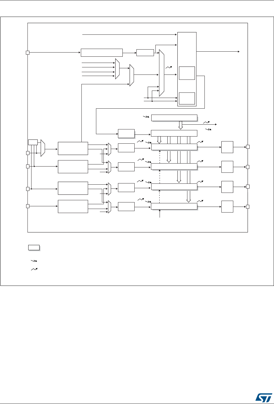
General-purpose timers (TIM2/TIM3) RM0394
818/1600 RM0394 Rev 4
Figure 243. General-purpose timer block diagram
8
8
8
&&,
&&,
7ULJJHU
FRQWUROOHU
6WRSFOHDURUXSGRZQ
7,)3
7,)3
,75
,75
,75 75*,
2XWSXW
FRQWURO
75*2
2&5()
2&5()
8
8,
5HVHWHQDEOHXSFRXQW
&.B36&
,&
,& ,&36
,&36
7,)3
7*,
75&
75&
,75
75&
7,)B('
&&,
&&,
7,)3
7,)3
7,)3
7,
7,
7,0[B&+
7,0[B&+
2&
2& 7,0[B&+
7,0[B&+
WRRWKHUWLPHUV
WR'$&$'&
6ODYH
FRQWUROOHU
PRGH
36&
SUHVFDOHU &17FRXQWHU
,QWHUQDOFORFN&.B,17
&.B&17
7,0[&/.IURP5&&
,75
069
;25
,QSXWILOWHU
HGJHGHWHFWRU
&DSWXUH&RPSDUHUHJLVWHU
1RWHV
5HJ 3UHORDGUHJLVWHUVWUDQVIHUUHG
WRDFWLYHUHJLVWHUVRQ8HYHQW
DFFRUGLQJWRFRQWUROELW
(YHQW
,QWHUUXSW'0$RXWSXW
$XWRUHORDGUHJLVWHU
&DSWXUH&RPSDUHUHJLVWHU
3UHVFDOHU
3UHVFDOHU
,QSXWILOWHU
HGJHGHWHFWRU
2XWSXW
FRQWURO
8
8
&&,
&&,
2XWSXW
FRQWURO
2&5()
2&5()
,&
,& ,&36
,&36
7,)3
7,)3
7,0[B&+
7,0[B&+
2&
2& 7,0[B&+
7,0[B&+
,QSXWILOWHU
HGJHGHWHFWRU
&DSWXUH&RPSDUHUHJLVWHU
&DSWXUH&RPSDUHUHJLVWHU
3UHVFDOHU
3UHVFDOHU
,QSXWILOWHU
HGJHGHWHFWRU
2XWSXW
FRQWURO
75&
7,)3
7,)3
75&
&&,
&&,
7,
7,
(QFRGHU
LQWHUIDFH
7,0[B(75 ,QSXWILOWHU
3RODULW\VHOHFWLRQHGJH
GHWHFWRUSUHVFDOHU
(75 (753
(75)
(75)

RM0394 Rev 4 819/1600
RM0394 General-purpose timers (TIM2/TIM3)
886
27.3 TIM2/TIM3 functional description
27.3.1 Time-base unit
The main block of the programmable timer is a 16-bit/32-bit counter with its related auto-
reload register. The counter can count up, down or both up and down but also down or both
up and down. The counter clock can be divided by a prescaler.
The counter, the auto-reload register and the prescaler register can be written or read by
software. This is true even when the counter is running.
The time-base unit includes:
•Counter Register (TIMx_CNT)
•Prescaler Register (TIMx_PSC):
•Auto-Reload Register (TIMx_ARR)
The auto-reload register is preloaded. Writing to or reading from the auto-reload register
accesses the preload register. The content of the preload register are transferred into the
shadow register permanently or at each update event (UEV), depending on the auto-reload
preload enable bit (ARPE) in TIMx_CR1 register. The update event is sent when the counter
reaches the overflow (or underflow when downcounting) and if the UDIS bit equals 0 in the
TIMx_CR1 register. It can also be generated by software. The generation of the update
event is described in detail for each configuration.
The counter is clocked by the prescaler output CK_CNT, which is enabled only when the
counter enable bit (CEN) in TIMx_CR1 register is set (refer also to the slave mode controller
description to get more details on counter enabling).
Note that the actual counter enable signal CNT_EN is set 1 clock cycle after CEN.
Prescaler description
The prescaler can divide the counter clock frequency by any factor between 1 and 65536. It
is based on a 16-bit counter controlled through a 16-bit/32-bit register (in the TIMx_PSC
register). It can be changed on the fly as this control register is buffered. The new prescaler
ratio is taken into account at the next update event.
Figure 244 and Figure 245 give some examples of the counter behavior when the prescaler
ratio is changed on the fly:
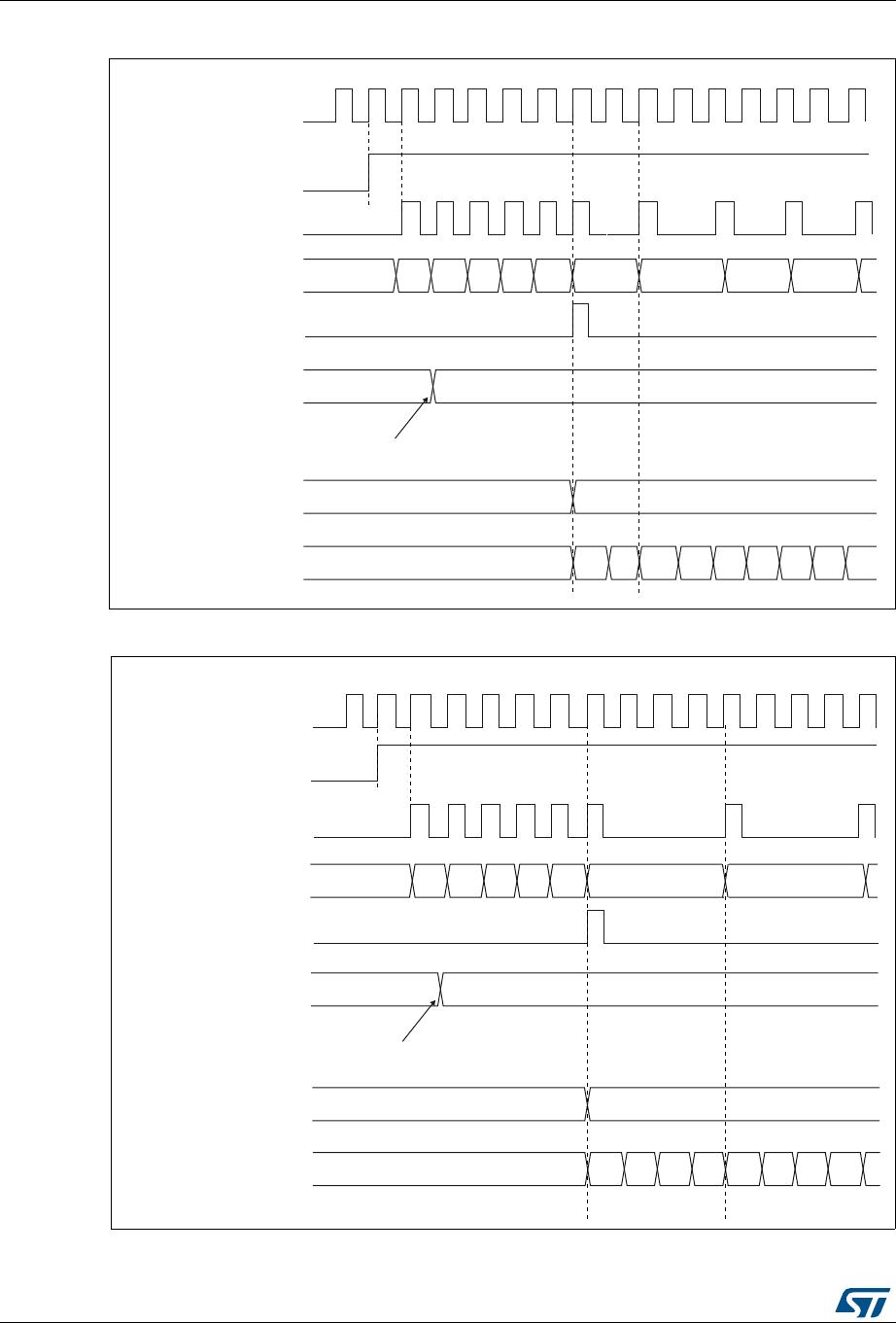
General-purpose timers (TIM2/TIM3) RM0394
820/1600 RM0394 Rev 4
Figure 244. Counter timing diagram with prescaler division change from 1 to 2
Figure 245. Counter timing diagram with prescaler division change from 1 to 4
&.B36&
&(1
7LPHUFORFN &.B&17
&RXQWHUUHJLVWHU
8SGDWHHYHQW8(9
3UHVFDOHUFRQWUROUHJLVWHU
:ULWHDQHZYDOXHLQ7,0[B36&
3UHVFDOHUEXIIHU
3UHVFDOHUFRXQWHU
)$ )%) ) ) )&
069
069
&.B36&
&(1
7LPHUFORFN &.B&17
&RXQWHUUHJLVWHU
8SGDWHHYHQW8(9
3UHVFDOHUFRQWUROUHJLVWHU
:ULWHDQHZYDOXHLQ7,0[B36&
3UHVFDOHUEXIIHU
3UHVFDOHUFRXQWHU
)$ )%
) ) ) )&
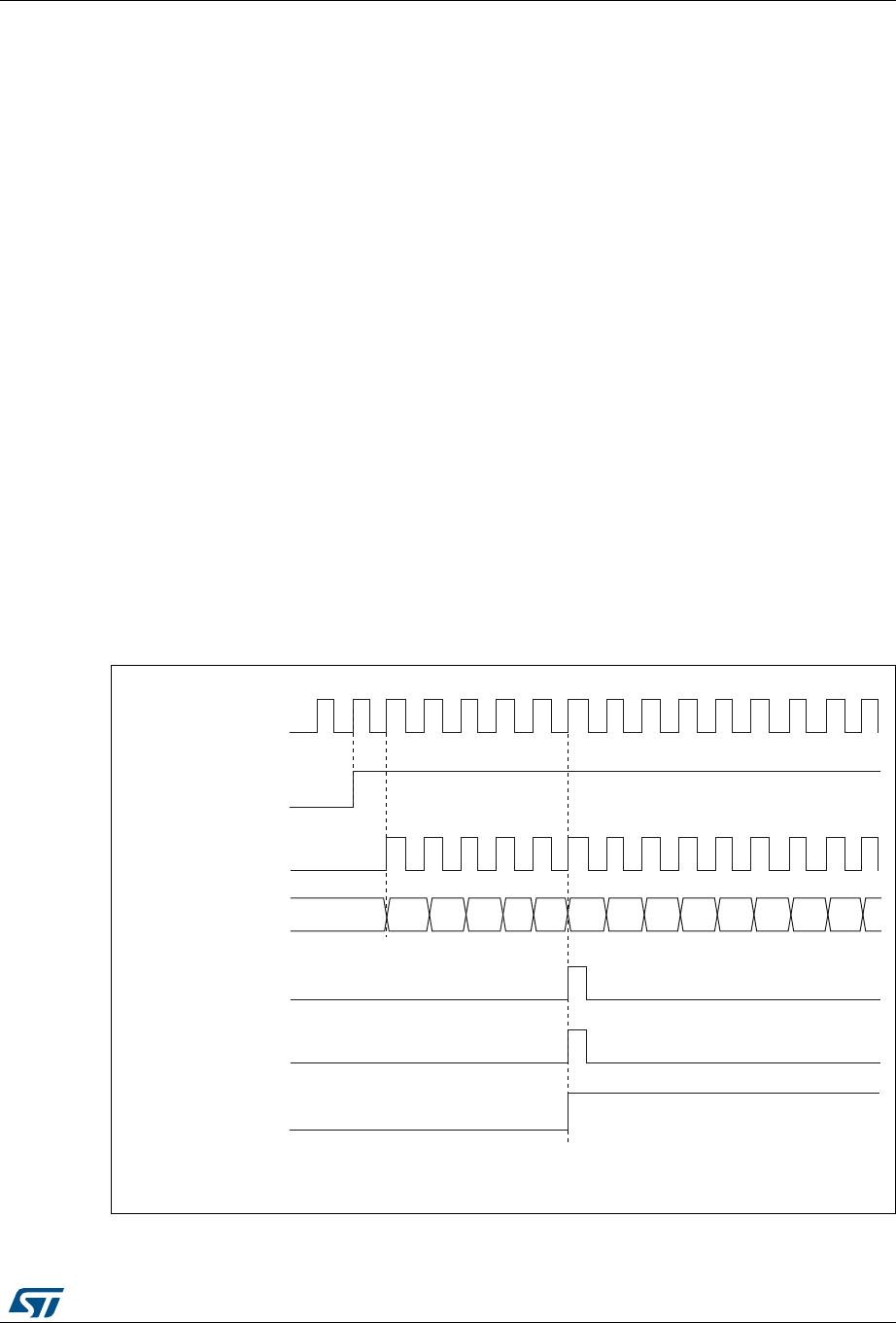
RM0394 Rev 4 821/1600
RM0394 General-purpose timers (TIM2/TIM3)
886
27.3.2 Counter modes
Upcounting mode
In upcounting mode, the counter counts from 0 to the auto-reload value (content of the
TIMx_ARR register), then restarts from 0 and generates a counter overflow event.
An Update event can be generated at each counter overflow or by setting the UG bit in the
TIMx_EGR register (by software or by using the slave mode controller).
The UEV event can be disabled by software by setting the UDIS bit in TIMx_CR1 register.
This is to avoid updating the shadow registers while writing new values in the preload
registers. Then no update event occurs until the UDIS bit has been written to 0. However,
the counter restarts from 0, as well as the counter of the prescaler (but the prescale rate
does not change). In addition, if the URS bit (update request selection) in TIMx_CR1
register is set, setting the UG bit generates an update event UEV but without setting the UIF
flag (thus no interrupt or DMA request is sent). This is to avoid generating both update and
capture interrupts when clearing the counter on the capture event.
When an update event occurs, all the registers are updated and the update flag (UIF bit in
TIMx_SR register) is set (depending on the URS bit):
•The buffer of the prescaler is reloaded with the preload value (content of the TIMx_PSC
register)
•The auto-reload shadow register is updated with the preload value (TIMx_ARR)
The following figures show some examples of the counter behavior for different clock
frequencies when TIMx_ARR=0x36.
Figure 246. Counter timing diagram, internal clock divided by 1
069
&.B36&
&17B(1
7LPHUFORFN &.B&17
&RXQWHUUHJLVWHU
8SGDWHHYHQW8(9
&RXQWHURYHUIORZ
8SGDWHLQWHUUXSWIODJ
8,)

General-purpose timers (TIM2/TIM3) RM0394
822/1600 RM0394 Rev 4
Figure 247. Counter timing diagram, internal clock divided by 2
Figure 248. Counter timing diagram, internal clock divided by 4
069
&.B36&
&17B(1
7LPHUFORFN &.B&17
&RXQWHUUHJLVWHU
8SGDWHHYHQW8(9
&RXQWHURYHUIORZ
8SGDWHLQWHUUXSWIODJ
8,)
069
&.B36&
7LPHUFORFN &.B&17
&RXQWHUUHJLVWHU
8SGDWHHYHQW8(9
&RXQWHURYHUIORZ
8SGDWHLQWHUUXSWIODJ
8,)
&17B(1
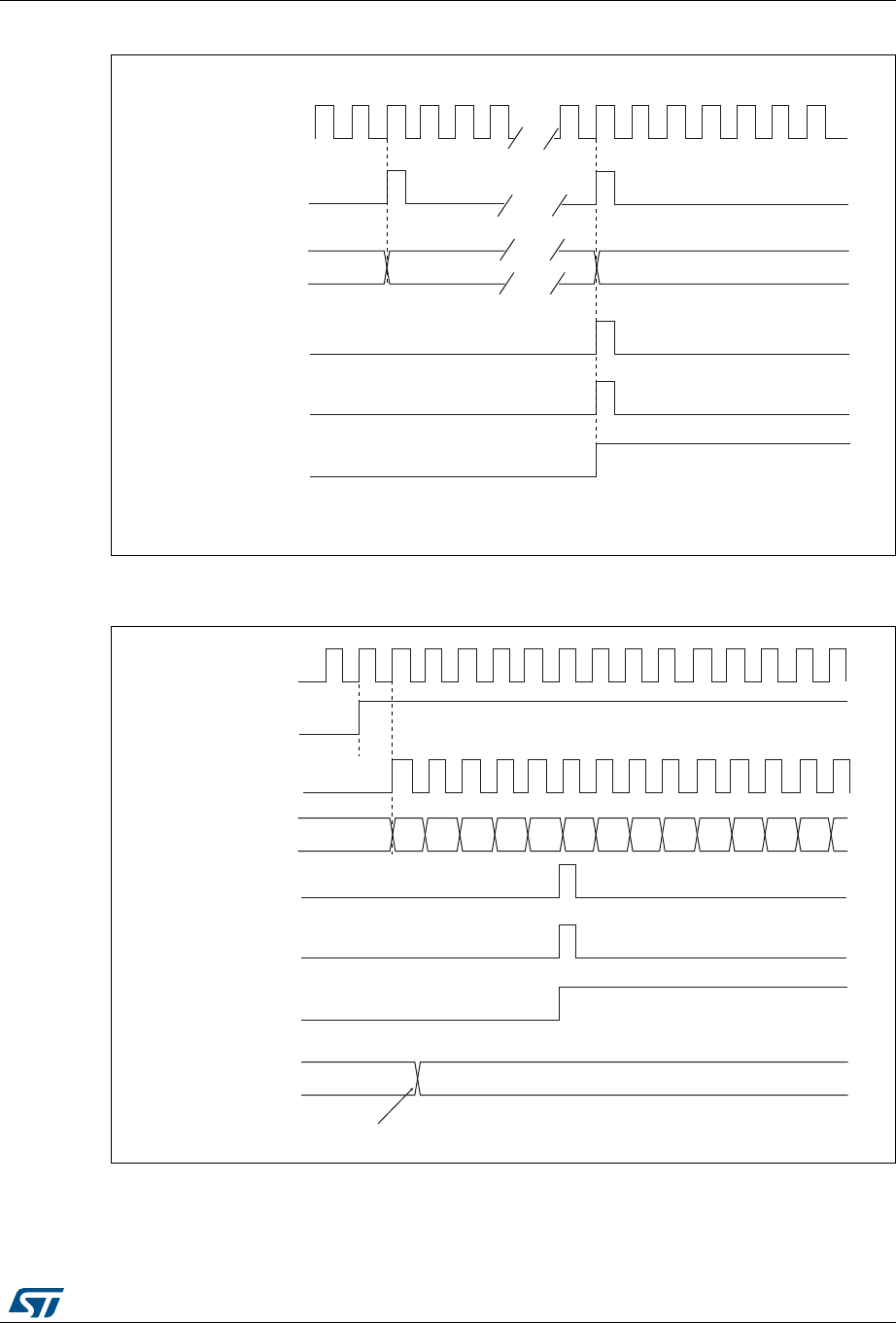
RM0394 Rev 4 823/1600
RM0394 General-purpose timers (TIM2/TIM3)
886
Figure 249. Counter timing diagram, internal clock divided by N
Figure 250. Counter timing diagram, Update event when ARPE=0 (TIMx_ARR not
preloaded)
)
069
&.B36&
7LPHUFORFN &.B&17
&RXQWHUUHJLVWHU
8SGDWHHYHQW8(9
&RXQWHURYHUIORZ
8SGDWHLQWHUUXSWIODJ
8,)
))
069
&.B36&
7LPHUFORFN &.B&17
&RXQWHUUHJLVWHU
8SGDWHHYHQW8(9
&RXQWHURYHUIORZ
8SGDWHLQWHUUXSWIODJ
8,)
&(1
$XWRUHORDGSUHORDG
UHJLVWHU
:ULWHDQHZYDOXHLQ7,0[B$55
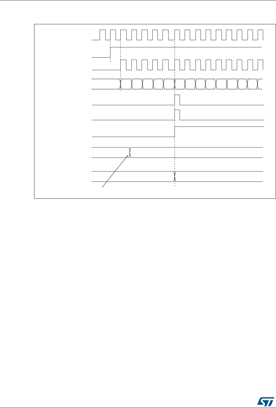
General-purpose timers (TIM2/TIM3) RM0394
824/1600 RM0394 Rev 4
Figure 251. Counter timing diagram, Update event when ARPE=1 (TIMx_ARR
preloaded)
Downcounting mode
In downcounting mode, the counter counts from the auto-reload value (content of the
TIMx_ARR register) down to 0, then restarts from the auto-reload value and generates a
counter underflow event.
An Update event can be generate at each counter underflow or by setting the UG bit in the
TIMx_EGR register (by software or by using the slave mode controller)
The UEV update event can be disabled by software by setting the UDIS bit in TIMx_CR1
register. This is to avoid updating the shadow registers while writing new values in the
preload registers. Then no update event occurs until UDIS bit has been written to 0.
However, the counter restarts from the current auto-reload value, whereas the counter of the
prescaler restarts from 0 (but the prescale rate doesn’t change).
In addition, if the URS bit (update request selection) in TIMx_CR1 register is set, setting the
UG bit generates an update event UEV but without setting the UIF flag (thus no interrupt or
DMA request is sent). This is to avoid generating both update and capture interrupts when
clearing the counter on the capture event.
When an update event occurs, all the registers are updated and the update flag (UIF bit in
TIMx_SR register) is set (depending on the URS bit):
•The buffer of the prescaler is reloaded with the preload value (content of the TIMx_PSC
register).
•The auto-reload active register is updated with the preload value (content of the
TIMx_ARR register). Note that the auto-reload is updated before the counter is
reloaded, so that the next period is the expected one.
069
)
&.B36&
7LPHUFORFN &.B&17
&RXQWHUUHJLVWHU
8SGDWHHYHQW8(9
&RXQWHURYHUIORZ
8SGDWHLQWHUUXSWIODJ
8,)
) ) ) ) ))
&(1
$XWRUHORDGSUHORDG
UHJLVWHU
:ULWHDQHZYDOXHLQ7,0[B$55
$XWRUHORDGVKDGRZ
UHJLVWHU )
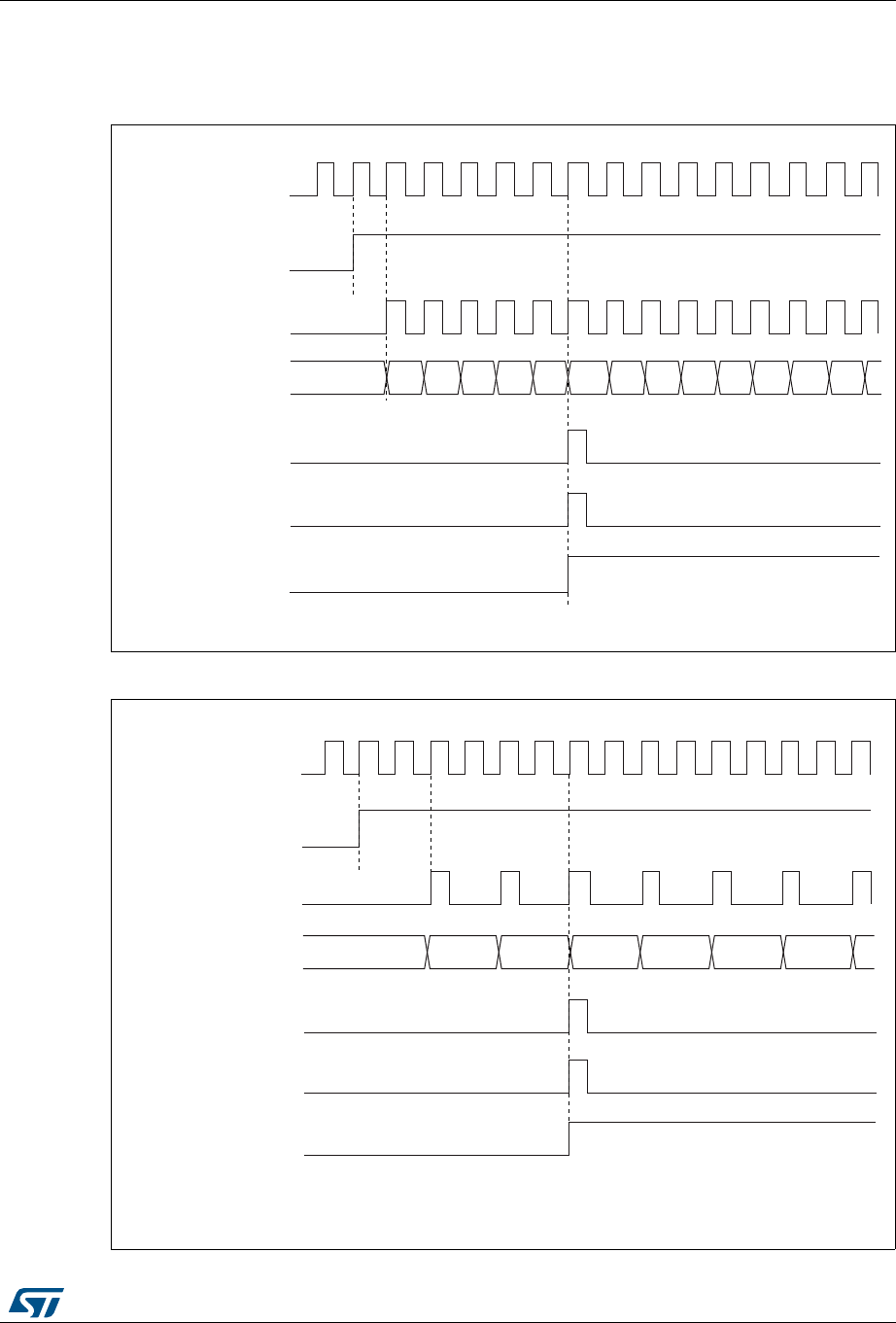
RM0394 Rev 4 825/1600
RM0394 General-purpose timers (TIM2/TIM3)
886
The following figures show some examples of the counter behavior for different clock
frequencies when TIMx_ARR=0x36.
Figure 252. Counter timing diagram, internal clock divided by 1
Figure 253. Counter timing diagram, internal clock divided by 2
)
069
&.B36&
&17B(1
7LPHUFORFN &.B&17
&RXQWHUUHJLVWHU
8SGDWHHYHQW8(9
&RXQWHUXQGHUIORZ
FQWBXGI
8SGDWHLQWHUUXSWIODJ
8,)
069
&.B36&
&17B(1
7LPHUFORFN &.B&17
&RXQWHUUHJLVWHU
8SGDWHHYHQW8(9
&RXQWHUXQGHUIORZ
8SGDWHLQWHUUXSWIODJ
8,)
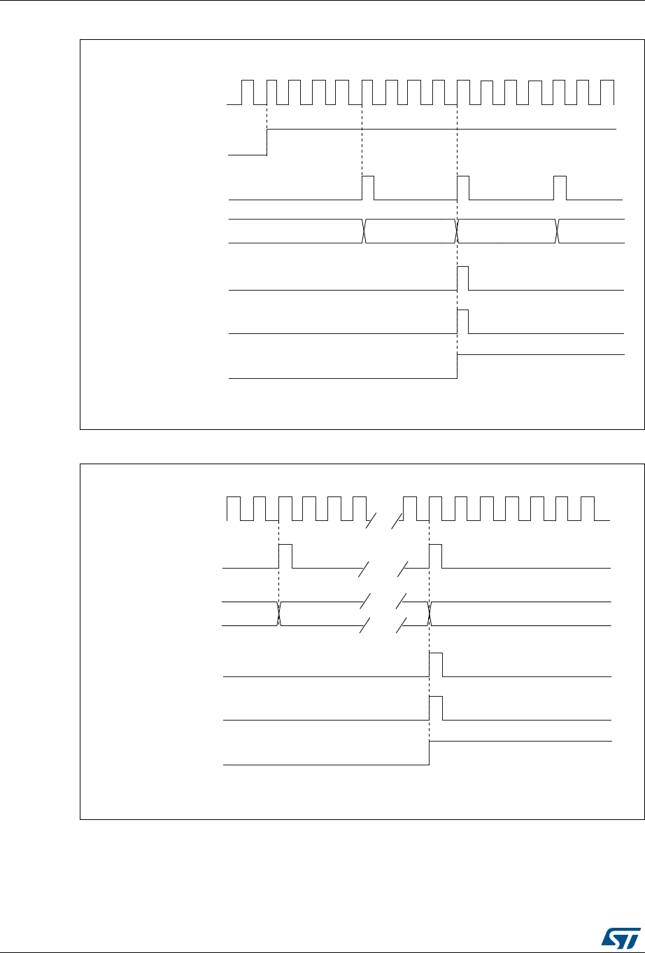
General-purpose timers (TIM2/TIM3) RM0394
826/1600 RM0394 Rev 4
Figure 254. Counter timing diagram, internal clock divided by 4
Figure 255. Counter timing diagram, internal clock divided by N
069
&.B36&
7LPHUFORFN &.B&17
&RXQWHUUHJLVWHU
8SGDWHHYHQW8(9
&RXQWHUXQGHUIORZ
8SGDWHLQWHUUXSWIODJ
8,)
&17B(1
)
069
&.B36&
7LPHUFORFN &.B&17
&RXQWHUUHJLVWHU
8SGDWHHYHQW8(9
&RXQWHUXQGHUIORZ
8SGDWHLQWHUUXSWIODJ
8,)
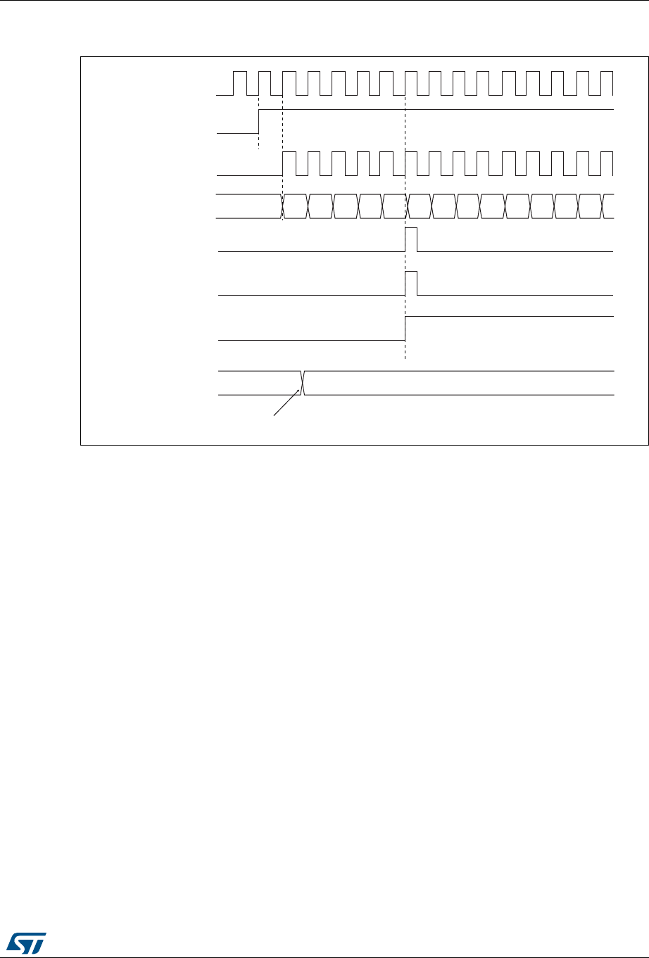
RM0394 Rev 4 827/1600
RM0394 General-purpose timers (TIM2/TIM3)
886
Figure 256. Counter timing diagram, Update event when repetition counter
is not used
Center-aligned mode (up/down counting)
In center-aligned mode, the counter counts from 0 to the auto-reload value (content of the
TIMx_ARR register) – 1, generates a counter overflow event, then counts from the auto-
reload value down to 1 and generates a counter underflow event. Then it restarts counting
from 0.
Center-aligned mode is active when the CMS bits in TIMx_CR1 register are not equal to
'00'. The Output compare interrupt flag of channels configured in output is set when: the
counter counts down (Center aligned mode 1, CMS = "01"), the counter counts up (Center
aligned mode 2, CMS = "10") the counter counts up and down (Center aligned mode 3,
CMS = "11").
In this mode, the direction bit (DIR from TIMx_CR1 register) cannot be written. It is updated
by hardware and gives the current direction of the counter.
The update event can be generated at each counter overflow and at each counter underflow
or by setting the UG bit in the TIMx_EGR register (by software or by using the slave mode
controller) also generates an update event. In this case, the counter restarts counting from
0, as well as the counter of the prescaler.
The UEV update event can be disabled by software by setting the UDIS bit in TIMx_CR1
register. This is to avoid updating the shadow registers while writing new values in the
preload registers. Then no update event occurs until the UDIS bit has been written to 0.
However, the counter continues counting up and down, based on the current auto-reload
value.
In addition, if the URS bit (update request selection) in TIMx_CR1 register is set, setting the
UG bit generates an update event UEV but without setting the UIF flag (thus no interrupt or
))
069
&.B36&
7LPHUFORFN &.B&17
&RXQWHUUHJLVWHU
8SGDWHHYHQW8(9
&RXQWHUXQGHUIORZ
8SGDWHLQWHUUXSWIODJ
8,)
)
&(1
$XWRUHORDGSUHORDG
UHJLVWHU
:ULWHDQHZYDOXHLQ7,0[B$55
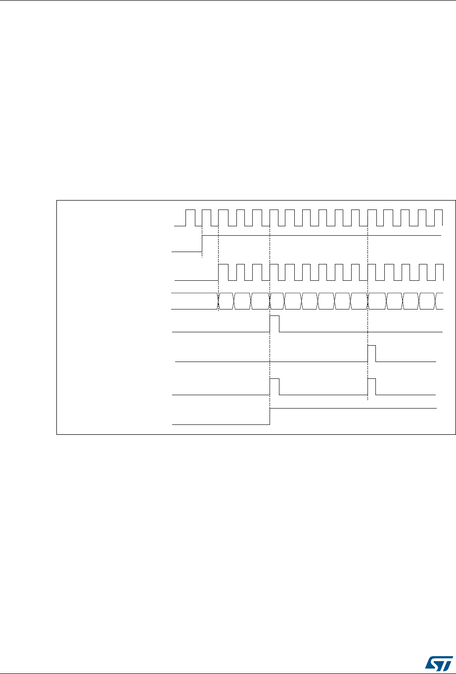
General-purpose timers (TIM2/TIM3) RM0394
828/1600 RM0394 Rev 4
DMA request is sent). This is to avoid generating both update and capture interrupt when
clearing the counter on the capture event.
When an update event occurs, all the registers are updated and the update flag (UIF bit in
TIMx_SR register) is set (depending on the URS bit):
•The buffer of the prescaler is reloaded with the preload value (content of the TIMx_PSC
register).
•The auto-reload active register is updated with the preload value (content of the
TIMx_ARR register). Note that if the update source is a counter overflow, the auto-
reload is updated before the counter is reloaded, so that the next period is the expected
one (the counter is loaded with the new value).
The following figures show some examples of the counter behavior for different clock
frequencies.
Figure 257. Counter timing diagram, internal clock divided by 1, TIMx_ARR=0x6
1. Here, center-aligned mode 1 is used (for more details refer to Section 27.4.1: TIMx control register 1
(TIMx_CR1)(x = 2 to 3) on page 862).
069
&.B36&
7LPHUFORFN &.B&17
&RXQWHUUHJLVWHU
8SGDWHHYHQW8(9
&RXQWHURYHUIORZ
8SGDWHLQWHUUXSWIODJ8,)
&(1
&RXQWHUXQGHUIORZ
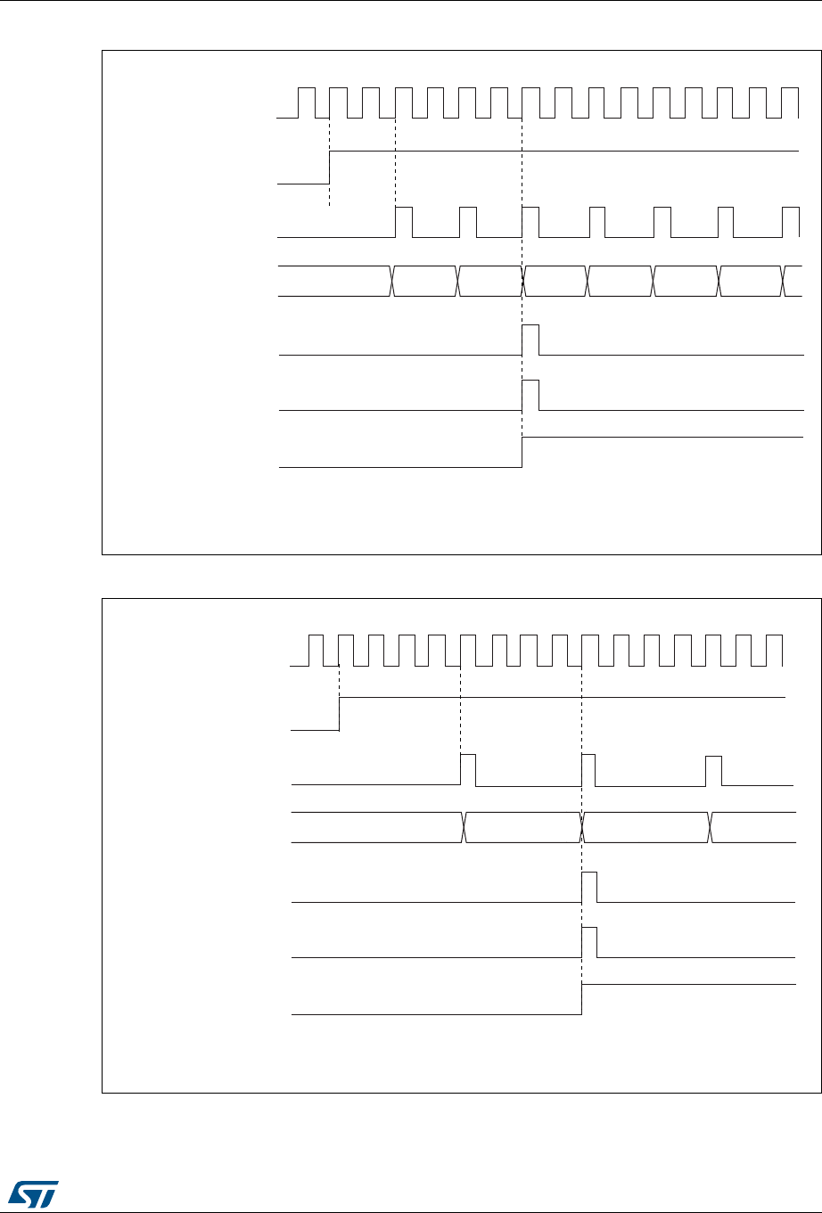
RM0394 Rev 4 829/1600
RM0394 General-purpose timers (TIM2/TIM3)
886
Figure 258. Counter timing diagram, internal clock divided by 2
Figure 259. Counter timing diagram, internal clock divided by 4, TIMx_ARR=0x36
1. Center-aligned mode 2 or 3 is used with an UIF on overflow.
069
&.B36&
&17B(1
7LPHUFORFN &.B&17
&RXQWHUUHJLVWHU
8SGDWHHYHQW8(9
&RXQWHUXQGHUIORZ
8SGDWHLQWHUUXSWIODJ
8,)
069
&.B36&
7LPHUFORFN &.B&17
&RXQWHUUHJLVWHU
8SGDWHHYHQW8(9
&RXQWHURYHUIORZ
8SGDWHLQWHUUXSWIODJ
8,)
&17B(1
1RWH+HUHFHQWHUBDOLJQHGPRGHRULVXSGDWHGZLWKDQ8,)RQRYHUIORZ
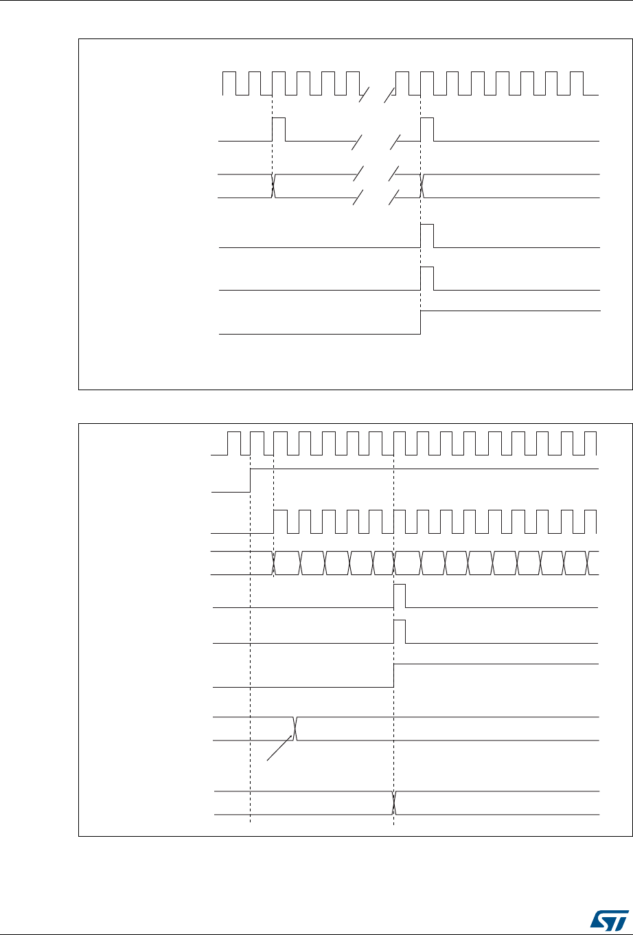
General-purpose timers (TIM2/TIM3) RM0394
830/1600 RM0394 Rev 4
Figure 260. Counter timing diagram, internal clock divided by N
Figure 261. Counter timing diagram, Update event with ARPE=1 (counter underflow)
)
069
&.B36&
7LPHUFORFN &.B&17
&RXQWHUUHJLVWHU
8SGDWHHYHQW8(9
&RXQWHUXQGHUIORZ
8SGDWHLQWHUUXSWIODJ
8,)
)'
069
&.B36&
7LPHUFORFN &.B&17
&RXQWHUUHJLVWHU
8SGDWHHYHQW8(9
&RXQWHUXQGHUIORZ
8SGDWHLQWHUUXSWIODJ
8,)
&(1
$XWRUHORDGSUHORDG
UHJLVWHU
:ULWHDQHZYDOXHLQ7,0[B$55
)'
$XWRUHORDGDFWLYH
UHJLVWHU
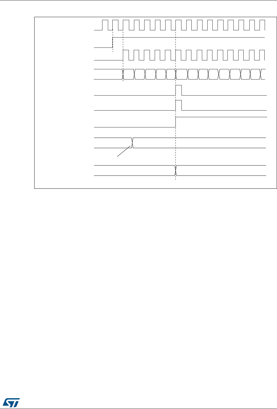
RM0394 Rev 4 831/1600
RM0394 General-purpose timers (TIM2/TIM3)
886
Figure 262. Counter timing diagram, Update event with ARPE=1 (counter overflow)
27.3.3 Clock selection
The counter clock can be provided by the following clock sources:
•Internal clock (CK_INT)
•External clock mode1: external input pin (TIx)
•External clock mode2: external trigger input (ETR)
•Internal trigger inputs (ITRx): using one timer as prescaler for another timer, for
example, you can configure Timer 13 to act as a prescaler for Timer 2. Refer to : Using
one timer as prescaler for another timer on page 857 for more details.
Internal clock source (CK_INT)
If the slave mode controller is disabled (SMS=000 in the TIMx_SMCR register), then the
CEN, DIR (in the TIMx_CR1 register) and UG bits (in the TIMx_EGR register) are actual
control bits and can be changed only by software (except UG which remains cleared
automatically). As soon as the CEN bit is written to 1, the prescaler is clocked by the internal
clock CK_INT.
Figure 263 shows the behavior of the control circuit and the upcounter in normal mode,
without prescaler.
069
)'
&.B36&
7LPHUFORFN &.B&17
&RXQWHUUHJLVWHU
8SGDWHHYHQW8(9
&RXQWHURYHUIORZ
8SGDWHLQWHUUXSWIODJ
8,)
)
) ) )$ )% )&)
&(1
$XWRUHORDGSUHORDG
UHJLVWHU
:ULWHDQHZYDOXHLQ7,0[B$55
$XWRUHORDGDFWLYH
UHJLVWHU )'
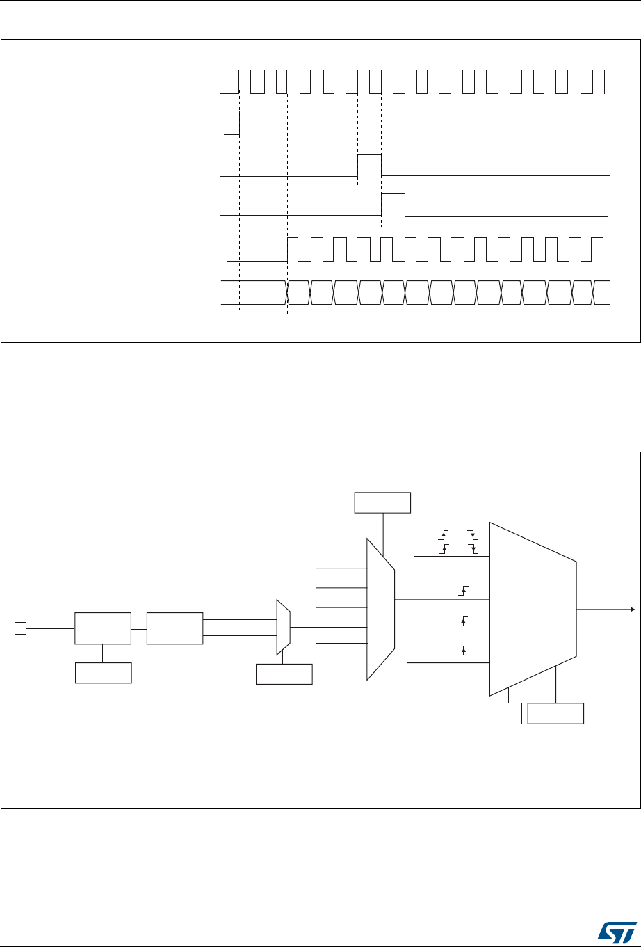
General-purpose timers (TIM2/TIM3) RM0394
832/1600 RM0394 Rev 4
Figure 263. Control circuit in normal mode, internal clock divided by 1
External clock source mode 1
This mode is selected when SMS=111 in the TIMx_SMCR register. The counter can count at
each rising or falling edge on a selected input.
Figure 264. TI2 external clock connection example
For example, to configure the upcounter to count in response to a rising edge on the TI2
input, use the following procedure:
For example, to configure the upcounter to count in response to a rising edge on the TI2
input, use the following procedure:
,QWHUQDOFORFN
&RXQWHUFORFN &.B&17 &.B36&
&RXQWHUUHJLVWHU
&(1 &17B(1
8*
&17B,1,7
069
([WHUQDOFORFN
PRGH
,QWHUQDOFORFN
PRGH
75*,
&.B,17
&.B36&
7,0[B60&5
606>@
,75[
7,B('
7,)3
7,)3
7,0[B60&5
76>@
7,
7,0[B&&(5
&&3
)LOWHU
,&)>@
7,0[B&&05
(GJH
GHWHFWRU
7,)B5LVLQJ
7,)B)DOOLQJ
[[
069
LQWHUQDOFORFN
7,) RU
7,) RU
RU
(QFRGHU
PRGH
(75)
([WHUQDOFORFN
PRGH
(75)
(&(
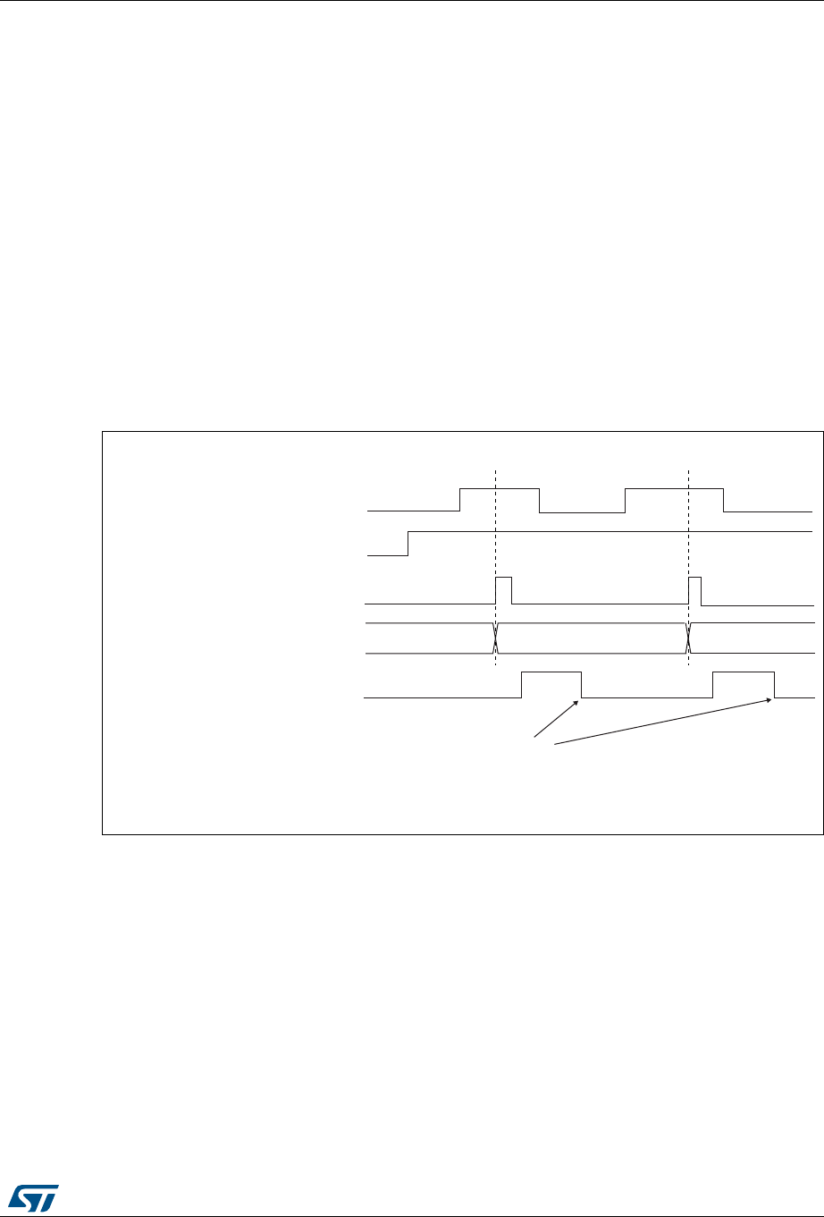
RM0394 Rev 4 833/1600
RM0394 General-purpose timers (TIM2/TIM3)
886
1. Configure channel 2 to detect rising edges on the TI2 input by writing CC2S= ‘01 in the
TIMx_CCMR1 register.
2. Configure the input filter duration by writing the IC2F[3:0] bits in the TIMx_CCMR1
register (if no filter is needed, keep IC2F=0000).
Note: The capture prescaler is not used for triggering, so you don’t need to configure it.
3. Select rising edge polarity by writing CC2P=0 and CC2NP=0 and CC2NP=0 in the
TIMx_CCER register.
4. Configure the timer in external clock mode 1 by writing SMS=111 in the TIMx_SMCR
register.
5. Select TI2 as the input source by writing TS=110 in the TIMx_SMCR register.
6. Enable the counter by writing CEN=1 in the TIMx_CR1 register.
When a rising edge occurs on TI2, the counter counts once and the TIF flag is set.
The delay between the rising edge on TI2 and the actual clock of the counter is due to the
resynchronization circuit on TI2 input.
Figure 265. Control circuit in external clock mode 1
External clock source mode 2
This mode is selected by writing ECE=1 in the TIMx_SMCR register.
The counter can count at each rising or falling edge on the external trigger input ETR.
Figure 266 gives an overview of the external trigger input block.
&RXQWHUFORFN &.B&17 &.B36&
&RXQWHUUHJLVWHU
7,
&17B(1
7,)
:ULWH7,)
069
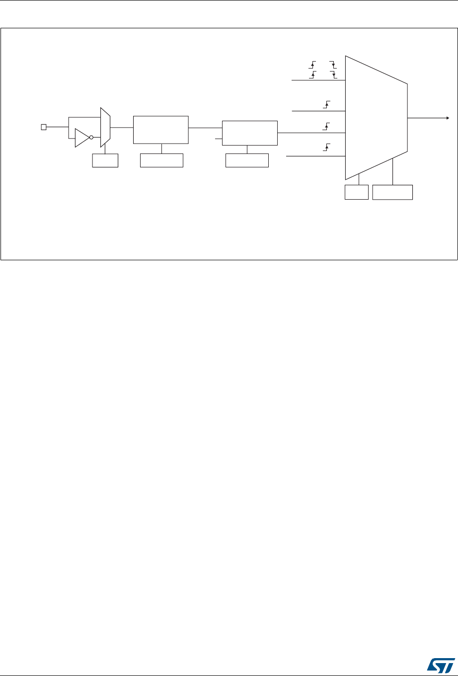
General-purpose timers (TIM2/TIM3) RM0394
834/1600 RM0394 Rev 4
Figure 266. External trigger input block
For example, to configure the upcounter to count each 2 rising edges on ETR, use the
following procedure:
1. As no filter is needed in this example, write ETF[3:0]=0000 in the TIMx_SMCR register.
2. Set the prescaler by writing ETPS[1:0]=01 in the TIMx_SMCR register
3. Select rising edge detection on the ETR pin by writing ETP=0 in the TIMx_SMCR
register
4. Enable external clock mode 2 by writing ECE=1 in the TIMx_SMCR register.
5. Enable the counter by writing CEN=1 in the TIMx_CR1 register.
The counter counts once each 2 ETR rising edges.
The delay between the rising edge on ETR and the actual clock of the counter is due to the
resynchronization circuit on the ETRP signal.
([WHUQDOFORFN
PRGH
,QWHUQDOFORFN
PRGH
75*,
&.B,17
&.B36&
7,0[B60&5
606>@
069
LQWHUQDOFORFN
7,) RU
7,) RU
RU
(QFRGHU
PRGH
([WHUQDOFORFN
PRGH
(75)
(&(
7,0[B60&5
(73
(75SLQ
(75
'LYLGHU
)LOWHU
GRZQFRXQWHU
I
(753
7,0[B60&5
(736>@
7,0[B60&5
(7)>@
'76
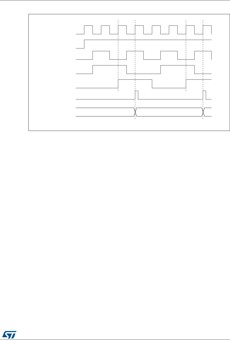
RM0394 Rev 4 835/1600
RM0394 General-purpose timers (TIM2/TIM3)
886
Figure 267. Control circuit in external clock mode 2
27.3.4 Capture/Compare channels
Each Capture/Compare channel is built around a capture/compare register (including a
shadow register), a input stage for capture (with digital filter, multiplexing and prescaler) and
an output stage (with comparator and output control).
The following figure gives an overview of one Capture/Compare channel.
The input stage samples the corresponding TIx input to generate a filtered signal TIxF.
Then, an edge detector with polarity selection generates a signal (TIxFPx) which can be
used as trigger input by the slave mode controller or as the capture command. It is
prescaled before the capture register (ICxPS).
069
I&.B,17
&17B(1
(75
(753
(75)
&RXQWHUFORFN
&.B,17 &.B36&
&RXQWHUUHJLVWHU
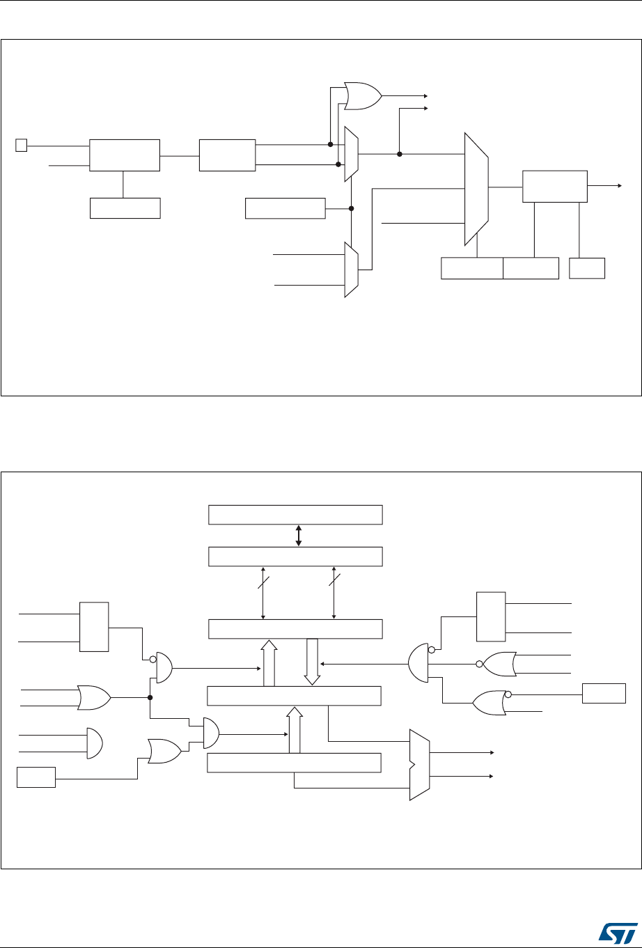
General-purpose timers (TIM2/TIM3) RM0394
836/1600 RM0394 Rev 4
Figure 268. Capture/Compare channel (example: channel 1 input stage)
The output stage generates an intermediate waveform which is then used for reference:
OCxRef (active high). The polarity acts at the end of the chain.
Figure 269. Capture/Compare channel 1 main circuit
'LYLGHU
,&36>@
7,)B('
7RWKHVODYHPRGHFRQWUROOHU
7,)3
&&6>@
,&
7,)3
75&
IURPVODYHPRGH
FRQWUROOHU
,&36
069
7,
7,0[B&&(5
&&3&&13
)LOWHU
GRZQFRXQWHU
,&)>@
7,0[B&&05
(GJH
GHWHFWRU
7,)B5LVLQJ
7,)B)DOOLQJ
7,0[B&&05
7,0[B&&(5
7,)B5LVLQJ
IURPFKDQQHO
7,)B)DOOLQJ
IURPFKDQQHO
7,)
I
&&(
'76
&&(
&DSWXUHFRPSDUHVKDGRZUHJLVWHU
&RPSDUDWRU
&DSWXUHFRPSDUHSUHORDGUHJLVWHU
&RXQWHU
,&36
&&6>@
&&6>@
&DSWXUH
,QSXW
PRGH
6
5
5HDG&&5+
5HDG&&5/
UHDGBLQBSURJUHVV
FDSWXUHBWUDQVIHU &&6>@
&&6>@
6
5
ZULWH&&5+
ZULWH&&5/
ZULWHBLQBSURJUHVV
2XWSXW
PRGH
8(9
2&3(
IURPWLPH
EDVHXQLW
FRPSDUHBWUDQVIHU
$3%%XV
KLJK
ORZ
LIELW
0&8SHULSKHUDOLQWHUIDFH
7,0[B&&05
2&3(
&17!&&5
&17 &&5
7,0[B(*5
&&*
069
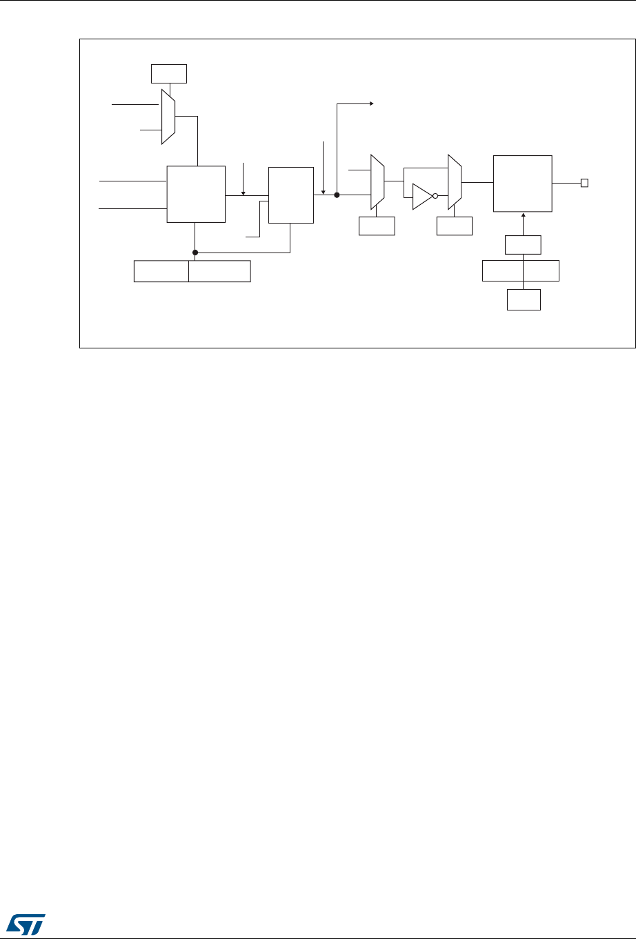
RM0394 Rev 4 837/1600
RM0394 General-purpose timers (TIM2/TIM3)
886
Figure 270. Output stage of Capture/Compare channel (channel 1)
The capture/compare block is made of one preload register and one shadow register. Write
and read always access the preload register.
In capture mode, captures are actually done in the shadow register, which is copied into the
preload register.
In compare mode, the content of the preload register is copied into the shadow register
which is compared to the counter.
27.3.5 Input capture mode
In Input capture mode, the Capture/Compare Registers (TIMx_CCRx) are used to latch the
value of the counter after a transition detected by the corresponding ICx signal. When a
capture occurs, the corresponding CCXIF flag (TIMx_SR register) is set and an interrupt or
a DMA request can be sent if they are enabled. If a capture occurs while the CCxIF flag was
already high, then the over-capture flag CCxOF (TIMx_SR register) is set. CCxIF can be
cleared by software by writing it to 0 or by reading the captured data stored in the
TIMx_CCRx register. CCxOF is cleared when you write it to 0.
The following example shows how to capture the counter value in TIMx_CCR1 when TI1
input rises. To do this, use the following procedure:
1. Select the active input: TIMx_CCR1 must be linked to the TI1 input, so write the CC1S
bits to 01 in the TIMx_CCMR1 register. As soon as CC1S becomes different from 00,
the channel is configured in input and the TIMx_CCR1 register becomes read-only.
2. Program the input filter duration you need with respect to the signal you connect to the
timer (when the input is one of the TIx (ICxF bits in the TIMx_CCMRx register). Let’s
imagine that, when toggling, the input signal is not stable during at must 5 internal clock
cycles. We must program a filter duration longer than these 5 clock cycles. We can
validate a transition on TI1 when 8 consecutive samples with the new level have been
069
2XWSXW
PRGH
FRQWUROOHU
&17!&&5
&17 &&5
7,0[B&&05
2&0>@
&&3
7,0[B&&(5
2XWSXW
HQDEOH
FLUFXLW
2&
&&( 7,0[B&&(5
7RWKHPDVWHU
PRGHFRQWUROOHU
2&5()
2&&(
&&(
7,0[B&&(5
µ
7,0[B%'75
266,
02(
2,6 7,0[B&5
RFUHIBFOUBLQW
(75)
2&5()B&/5
2&&6
7,0[B60&5
2XWSXW
VHOHFWRU
2&5()
2&5()&

General-purpose timers (TIM2/TIM3) RM0394
838/1600 RM0394 Rev 4
detected (sampled at fDTS frequency). Then write IC1F bits to 0011 in the
TIMx_CCMR1 register.
3. Select the edge of the active transition on the TI1 channel by writing the CC1P and
CC1NP and CC1NP bits to 000 in the TIMx_CCER register (rising edge in this case).
4. Program the input prescaler. In our example, we wish the capture to be performed at
each valid transition, so the prescaler is disabled (write IC1PS bits to 00 in the
TIMx_CCMR1 register).
5. Enable capture from the counter into the capture register by setting the CC1E bit in the
TIMx_CCER register.
6. If needed, enable the related interrupt request by setting the CC1IE bit in the
TIMx_DIER register, and/or the DMA request by setting the CC1DE bit in the
TIMx_DIER register.
When an input capture occurs:
•The TIMx_CCR1 register gets the value of the counter on the active transition.
•CC1IF flag is set (interrupt flag). CC1OF is also set if at least two consecutive captures
occurred whereas the flag was not cleared.
•An interrupt is generated depending on the CC1IE bit.
•A DMA request is generated depending on the CC1DE bit.
In order to handle the overcapture, it is recommended to read the data before the
overcapture flag. This is to avoid missing an overcapture which could happen after reading
the flag and before reading the data.
Note: IC interrupt and/or DMA requests can be generated by software by setting the
corresponding CCxG bit in the TIMx_EGR register.
27.3.6 PWM input mode
This mode is a particular case of input capture mode. The procedure is the same except:
•Two ICx signals are mapped on the same TIx input.
•These 2 ICx signals are active on edges with opposite polarity.
•One of the two TIxFP signals is selected as trigger input and the slave mode controller
is configured in reset mode.
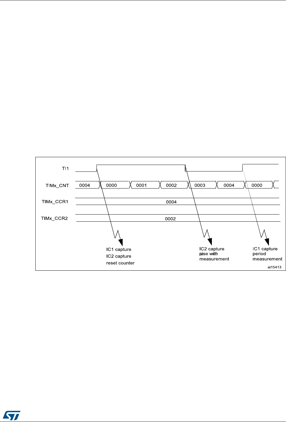
RM0394 Rev 4 839/1600
RM0394 General-purpose timers (TIM2/TIM3)
886
For example, you can measure the period (in TIMx_CCR1 register) and the duty cycle (in
TIMx_CCR2 register) of the PWM applied on TI1 using the following procedure (depending
on CK_INT frequency and prescaler value):
1. Select the active input for TIMx_CCR1: write the CC1S bits to 01 in the TIMx_CCMR1
register (TI1 selected).
2. Select the active polarity for TI1FP1 (used both for capture in TIMx_CCR1 and counter
clear): write the CC1P to ‘0’ and the CC1NP bit to ‘0’ (active on rising edge).
3. Select the active input for TIMx_CCR2: write the CC2S bits to 10 in the TIMx_CCMR1
register (TI1 selected).
4. Select the active polarity for TI1FP2 (used for capture in TIMx_CCR2): write the CC2P
bit to ‘1’ and the CC2NP bit to ’0’ (active on falling edge).
5. Select the valid trigger input: write the TS bits to 101 in the TIMx_SMCR register
(TI1FP1 selected).
6. Configure the slave mode controller in reset mode: write the SMS bits to 100 in the
TIMx_SMCR register.
7. Enable the captures: write the CC1E and CC2E bits to ‘1 in the TIMx_CCER register.
Figure 271. PWM input mode timing
1. The PWM input mode can be used only with the TIMx_CH1/TIMx_CH2 signals due to the fact that only
TI1FP1 and TI2FP2 are connected to the slave mode controller.
27.3.7 Forced output mode
In output mode (CCxS bits = 00 in the TIMx_CCMRx register), each output compare signal
(OCxREF and then OCx) can be forced to active or inactive level directly by software,
independently of any comparison between the output compare register and the counter.
To force an output compare signal (ocxref/OCx) to its active level, you just need to write 101
in the OCxM bits in the corresponding TIMx_CCMRx register. Thus ocxref is forced high
(OCxREF is always active high) and OCx get opposite value to CCxP polarity bit.
e.g.: CCxP=0 (OCx active high) => OCx is forced to high level.
ocxref signal can be forced low by writing the OCxM bits to 100 in the TIMx_CCMRx
register.

General-purpose timers (TIM2/TIM3) RM0394
840/1600 RM0394 Rev 4
Anyway, the comparison between the TIMx_CCRx shadow register and the counter is still
performed and allows the flag to be set. Interrupt and DMA requests can be sent
accordingly. This is described in the Output Compare Mode section.
27.3.8 Output compare mode
This function is used to control an output waveform or indicating when a period of time has
elapsed.
When a match is found between the capture/compare register and the counter, the output
compare function:
•Assigns the corresponding output pin to a programmable value defined by the output
compare mode (OCxM bits in the TIMx_CCMRx register) and the output polarity (CCxP
bit in the TIMx_CCER register). The output pin can keep its level (OCXM=000), be set
active (OCxM=001), be set inactive (OCxM=010) or can toggle (OCxM=011) on match.
•Sets a flag in the interrupt status register (CCxIF bit in the TIMx_SR register).
•Generates an interrupt if the corresponding interrupt mask is set (CCXIE bit in the
TIMx_DIER register).
•Sends a DMA request if the corresponding enable bit is set (CCxDE bit in the
TIMx_DIER register, CCDS bit in the TIMx_CR2 register for the DMA request
selection).
The TIMx_CCRx registers can be programmed with or without preload registers using the
OCxPE bit in the TIMx_CCMRx register.
In output compare mode, the update event UEV has no effect on ocxref and OCx output.
The timing resolution is one count of the counter. Output compare mode can also be used to
output a single pulse (in One-pulse mode).
Procedure
1. Select the counter clock (internal, external, prescaler).
2. Write the desired data in the TIMx_ARR and TIMx_CCRx registers.
3. Set the CCxIE and/or CCxDE bits if an interrupt and/or a DMA request is to be
generated.
4. Select the output mode. For example, you must write OCxM=011, OCxPE=0, CCxP=0
and CCxE=1 to toggle OCx output pin when CNT matches CCRx, CCRx preload is not
used, OCx is enabled and active high.
5. Enable the counter by setting the CEN bit in the TIMx_CR1 register.
The TIMx_CCRx register can be updated at any time by software to control the output
waveform, provided that the preload register is not enabled (OCxPE=0, else TIMx_CCRx
shadow register is updated only at the next update event UEV). An example is given in
Figure 272.

RM0394 Rev 4 841/1600
RM0394 General-purpose timers (TIM2/TIM3)
886
Figure 272. Output compare mode, toggle on OC1
27.3.9 PWM mode
Pulse width modulation mode allows you to generate a signal with a frequency determined
by the value of the TIMx_ARR register and a duty cycle determined by the value of the
TIMx_CCRx register.
The PWM mode can be selected independently on each channel (one PWM per OCx
output) by writing 110 (PWM mode 1) or ‘111 (PWM mode 2) in the OCxM bits in the
TIMx_CCMRx register. You must enable the corresponding preload register by setting the
OCxPE bit in the TIMx_CCMRx register, and eventually the auto-reload preload register (in
upcounting or center-aligned modes) by setting the ARPE bit in the TIMx_CR1 register.
As the preload registers are transferred to the shadow registers only when an update event
occurs, before starting the counter, you have to initialize all the registers by setting the UG
bit in the TIMx_EGR register.
OCx polarity is software programmable using the CCxP bit in the TIMx_CCER register. It
can be programmed as active high or active low. OCx output is enabled by the CCxE bit in
the TIMx_CCER register. Refer to the TIMx_CCERx register description for more details.
In PWM mode (1 or 2), TIMx_CNT and TIMx_CCRx are always compared to determine
whether TIMx_CCRx TIMx_CNT or TIMx_CNT TIMx_CCRx (depending on the direction
of the counter). However, to comply with the OCREF_CLR functionality (OCREF can be
cleared by an external event through the ETR signal until the next PWM period), the
OCREF signal is asserted only:
•When the result of the comparison or
•When the output compare mode (OCxM bits in TIMx_CCMRx register) switches from
the “frozen” configuration (no comparison, OCxM=‘000) to one of the PWM modes
(OCxM=‘110 or ‘111).
This forces the PWM by software while the timer is running.
069
2&5() 2&
7,0B&17 % %
7,0B&&5 $
:ULWH%KLQWKH&&5UHJLVWHU
0DWFKGHWHFWHGRQ&&5
,QWHUUXSWJHQHUDWHGLIHQDEOHG
%
%
$
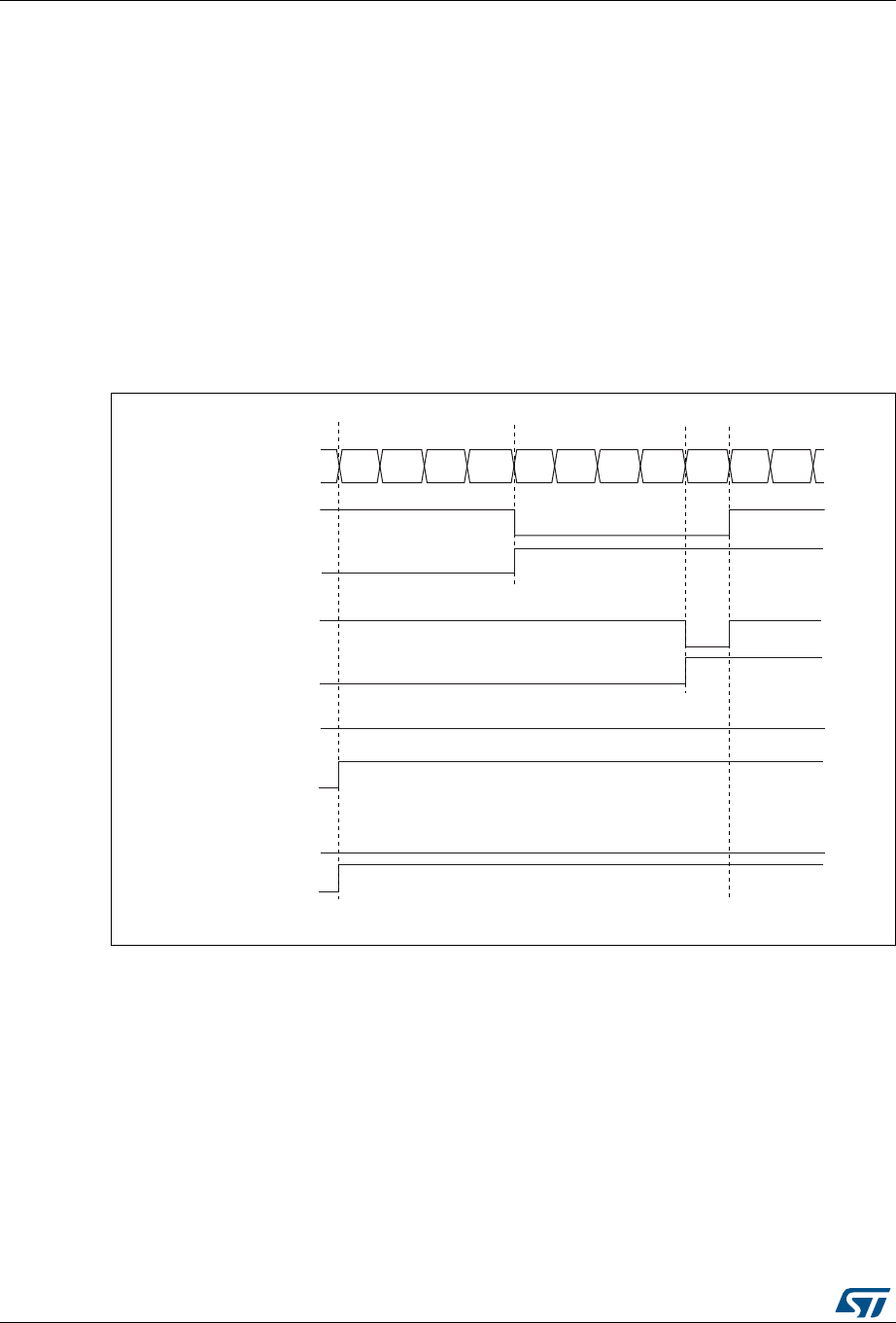
General-purpose timers (TIM2/TIM3) RM0394
842/1600 RM0394 Rev 4
The timer is able to generate PWM in edge-aligned mode or center-aligned mode
depending on the CMS bits in the TIMx_CR1 register.
PWM edge-aligned mode
Upcounting configuration
Upcounting is active when the DIR bit in the TIMx_CR1 register is low. Refer to Upcounting
mode on page 821.
In the following example, we consider PWM mode 1. The reference PWM signal OCxREF is
high as long as TIMx_CNT <TIMx_CCRx else it becomes low. If the compare value in
TIMx_CCRx is greater than the auto-reload value (in TIMx_ARR) then OCxREF is held at ‘1.
If the compare value is 0 then OCxREF is held at ‘0. Figure 273 shows some edge-aligned
PWM waveforms in an example where TIMx_ARR=8.
Figure 273. Edge-aligned PWM waveforms (ARR=8)
Downcounting configuration
Downcounting is active when DIR bit in TIMx_CR1 register is high. Refer to Downcounting
mode on page 824.
In PWM mode 1, the reference signal ocxref is low as long as TIMx_CNT>TIMx_CCRx else
it becomes high. If the compare value in TIMx_CCRx is greater than the auto-reload value in
TIMx_ARR, then ocxref is held at 100%. PWM is not possible in this mode.
PWM center-aligned mode
Center-aligned mode is active when the CMS bits in TIMx_CR1 register are different from
‘00 (all the remaining configurations having the same effect on the ocxref/OCx signals). The
069
&RXQWHUUHJLVWHU
µ
2&;5()
&&[,)
2&;5()
&&[,)
2&;5()
&&[,)
2&;5()
&&[,)
&&5[
&&5[
&&5[!
&&5[
µ
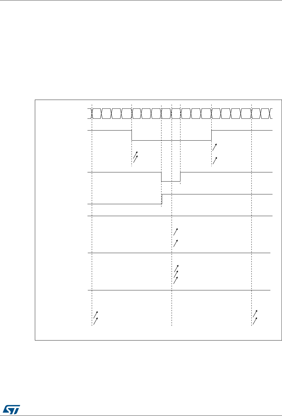
RM0394 Rev 4 843/1600
RM0394 General-purpose timers (TIM2/TIM3)
886
compare flag is set when the counter counts up, when it counts down or both when it counts
up and down depending on the CMS bits configuration. The direction bit (DIR) in the
TIMx_CR1 register is updated by hardware and must not be changed by software. Refer to
Center-aligned mode (up/down counting) on page 827.
Figure 274 shows some center-aligned PWM waveforms in an example where:
•TIMx_ARR=8,
•PWM mode is the PWM mode 1,
•The flag is set when the counter counts down corresponding to the center-aligned
mode 1 selected for CMS=01 in TIMx_CR1 register.
Figure 274. Center-aligned PWM waveforms (ARR=8)
Hints on using center-aligned mode:
•When starting in center-aligned mode, the current up-down configuration is used. It
means that the counter counts up or down depending on the value written in the DIR bit
&&[,)
&RXQWHUUHJLVWHU
&&5[
2&[5()
&06
&06
&06
&&[,)
&&5[
2&[5()
&06 RU
&&[,)
&&5[
2&[5()
&06
&06
&06
µ
&&[,)
&&5[!
2&[5()
&06
&06
&06
µ
&&[,)
&&5[
2&[5()
&06
&06
&06
µ
$,E

General-purpose timers (TIM2/TIM3) RM0394
844/1600 RM0394 Rev 4
in the TIMx_CR1 register. Moreover, the DIR and CMS bits must not be changed at the
same time by the software.
•Writing to the counter while running in center-aligned mode is not recommended as it
can lead to unexpected results. In particular:
– The direction is not updated if you write a value in the counter that is greater than
the auto-reload value (TIMx_CNT>TIMx_ARR). For example, if the counter was
counting up, it continues to count up.
– The direction is updated if you write 0 or write the TIMx_ARR value in the counter
but no Update Event UEV is generated.
•The safest way to use center-aligned mode is to generate an update by software
(setting the UG bit in the TIMx_EGR register) just before starting the counter and not to
write the counter while it is running.
27.3.10 Asymmetric PWM mode
Asymmetric mode allows two center-aligned PWM signals to be generated with a
programmable phase shift. While the frequency is determined by the value of the
TIMx_ARR register, the duty cycle and the phase-shift are determined by a pair of
TIMx_CCRx registers. One register controls the PWM during up-counting, the second
during down counting, so that PWM is adjusted every half PWM cycle:
•OC1REFC (or OC2REFC) is controlled by TIMx_CCR1 and TIMx_CCR2
•OC3REFC (or OC4REFC) is controlled by TIMx_CCR3 and TIMx_CCR4
Asymmetric PWM mode can be selected independently on two channels (one OCx output
per pair of CCR registers) by writing ‘1110’ (Asymmetric PWM mode 1) or ‘1111’
(Asymmetric PWM mode 2) in the OCxM bits in the TIMx_CCMRx register.
Note: The OCxM[3:0] bit field is split into two parts for compatibility reasons, the most significant
bit is not contiguous with the 3 least significant ones.
When a given channel is used as asymmetric PWM channel, its secondary channel can also
be used. For instance, if an OC1REFC signal is generated on channel 1 (Asymmetric PWM
mode 1), it is possible to output either the OC2REF signal on channel 2, or an OC2REFC
signal resulting from asymmetric PWM mode 2.
Figure 275 shows an example of signals that can be generated using Asymmetric PWM
mode (channels 1 to 4 are configured in Asymmetric PWM mode 1).
Figure 275. Generation of 2 phase-shifted PWM signals with 50% duty cycle
069
&RXQWHUUHJLVWHU
2&5()&
&&5
&&5
&&5
&&5
2&5()&

RM0394 Rev 4 845/1600
RM0394 General-purpose timers (TIM2/TIM3)
886
27.3.11 Combined PWM mode
Combined PWM mode allows two edge or center-aligned PWM signals to be generated with
programmable delay and phase shift between respective pulses. While the frequency is
determined by the value of the TIMx_ARR register, the duty cycle and delay are determined
by the two TIMx_CCRx registers. The resulting signals, OCxREFC, are made of an OR or
AND logical combination of two reference PWMs:
– OC1REFC (or OC2REFC) is controlled by TIMx_CCR1 and TIMx_CCR2
– OC3REFC (or OC4REFC) is controlled by TIMx_CCR3 and TIMx_CCR4
Combined PWM mode can be selected independently on two channels (one OCx output per
pair of CCR registers) by writing ‘1100’ (Combined PWM mode 1) or ‘1101’ (Combined PWM
mode 2) in the OCxM bits in the TIMx_CCMRx register.
When a given channel is used as combined PWM channel, its secondary channel must be
configured in the opposite PWM mode (for instance, one in Combined PWM mode 1 and the
other in Combined PWM mode 2).
Note: The OCxM[3:0] bit field is split into two parts for compatibility reasons, the most significant
bit is not contiguous with the 3 least significant ones.
Figure 276 shows an example of signals that can be generated using Asymmetric PWM
mode, obtained with the following configuration:
•Channel 1 is configured in Combined PWM mode 2,
•Channel 2 is configured in PWM mode 1,
•Channel 3 is configured in Combined PWM mode 2,
•Channel 4 is configured in PWM mode 1
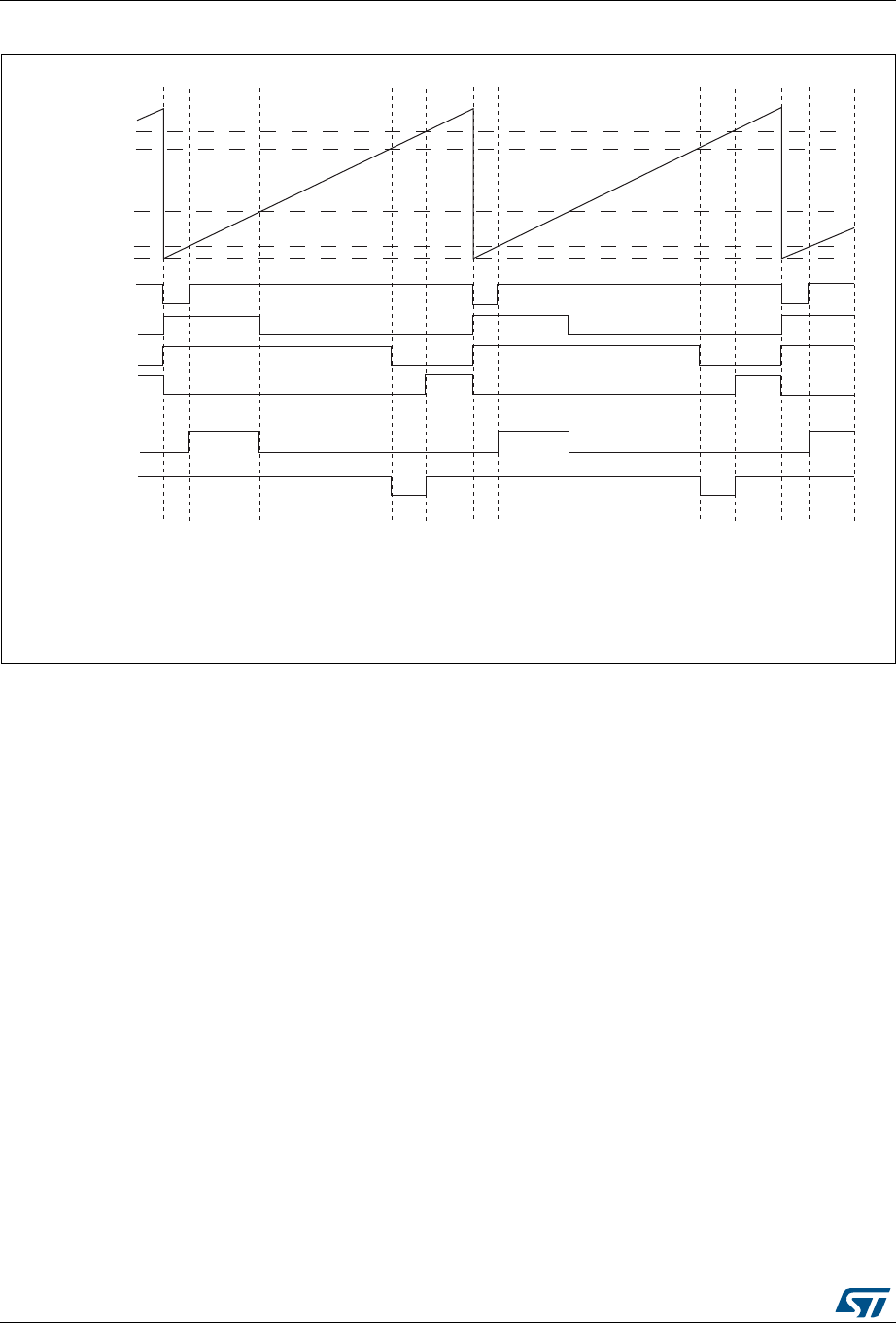
General-purpose timers (TIM2/TIM3) RM0394
846/1600 RM0394 Rev 4
Figure 276. Combined PWM mode on channels 1 and 3
27.3.12 Clearing the OCxREF signal on an external event
The OCxREF signal of a given channel can be cleared when a high level is applied on the
ocref_clr_int input (OCxCE enable bit in the corresponding TIMx_CCMRx register set to 1).
OCxREF remains low until the next update event (UEV) occurs. This function can only be
used in Output compare and PWM modes. It does not work in Forced mode.
OCREF_CLR_INPUT can be selected between the OCREF_CLR input and ETRF (ETR
after the filter) by configuring the OCCS bit in the TIMx_SMCR register.
The OCxREF signal for a given channel can be reset by applying a high level on the ETRF
input (OCxCE enable bit set to 1 in the corresponding TIMx_CCMRx register). OCxREF
remains low until the next update event (UEV) occurs.
This function can be used only in the output compare and PWM modes. It does not work in
forced mode.
For example, the OCxREF signal can be connected to the output of a comparator to be
used for current handling. In this case, ETR must be configured as follows:
1. The external trigger prescaler should be kept off: bits ETPS[1:0] in the TIMx_SMCR
register are cleared to 00.
2. The external clock mode 2 must be disabled: bit ECE in the TIM1_SMCR register is
cleared to 0.
3. The external trigger polarity (ETP) and the external trigger filter (ETF) can be
configured according to the application’s needs.
069
2&5()
2&5()
2&5()
2&5()
2&5()&
2&5()&
2&5()& 2&5()$1'2&5()
2&5()&¶ 2&5()¶252&5()
2&
2&
2&
2&
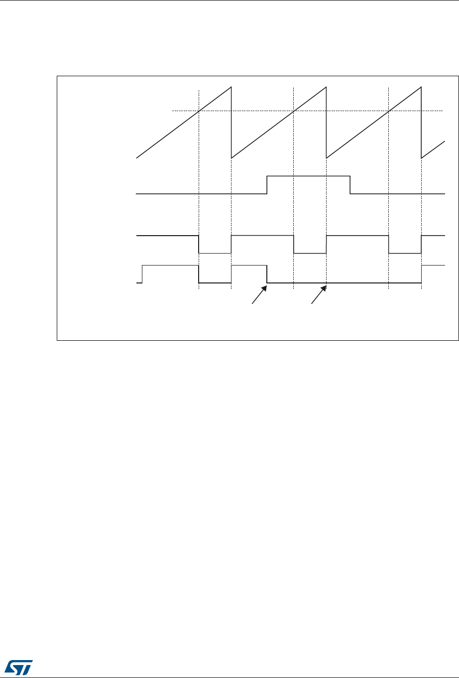
RM0394 Rev 4 847/1600
RM0394 General-purpose timers (TIM2/TIM3)
886
Figure 277 shows the behavior of the OCxREF signal when the ETRF input becomes high,
for both values of the OCxCE enable bit. In this example, the timer TIMx is programmed in
PWM mode.
Figure 277. Clearing TIMx OCxREF
Note: In case of a PWM with a 100% duty cycle (if CCRx>ARR), OCxREF is enabled again at the
next counter overflow.
069
&&5[
&RXQWHU&17
(75)
2&[5()
2&[&( µ
2&[5()
2&[&( µ
RFUHIBFOUBLQW
EHFRPHVKLJK
RFUHIBFOUBLQW
VWLOOKLJK
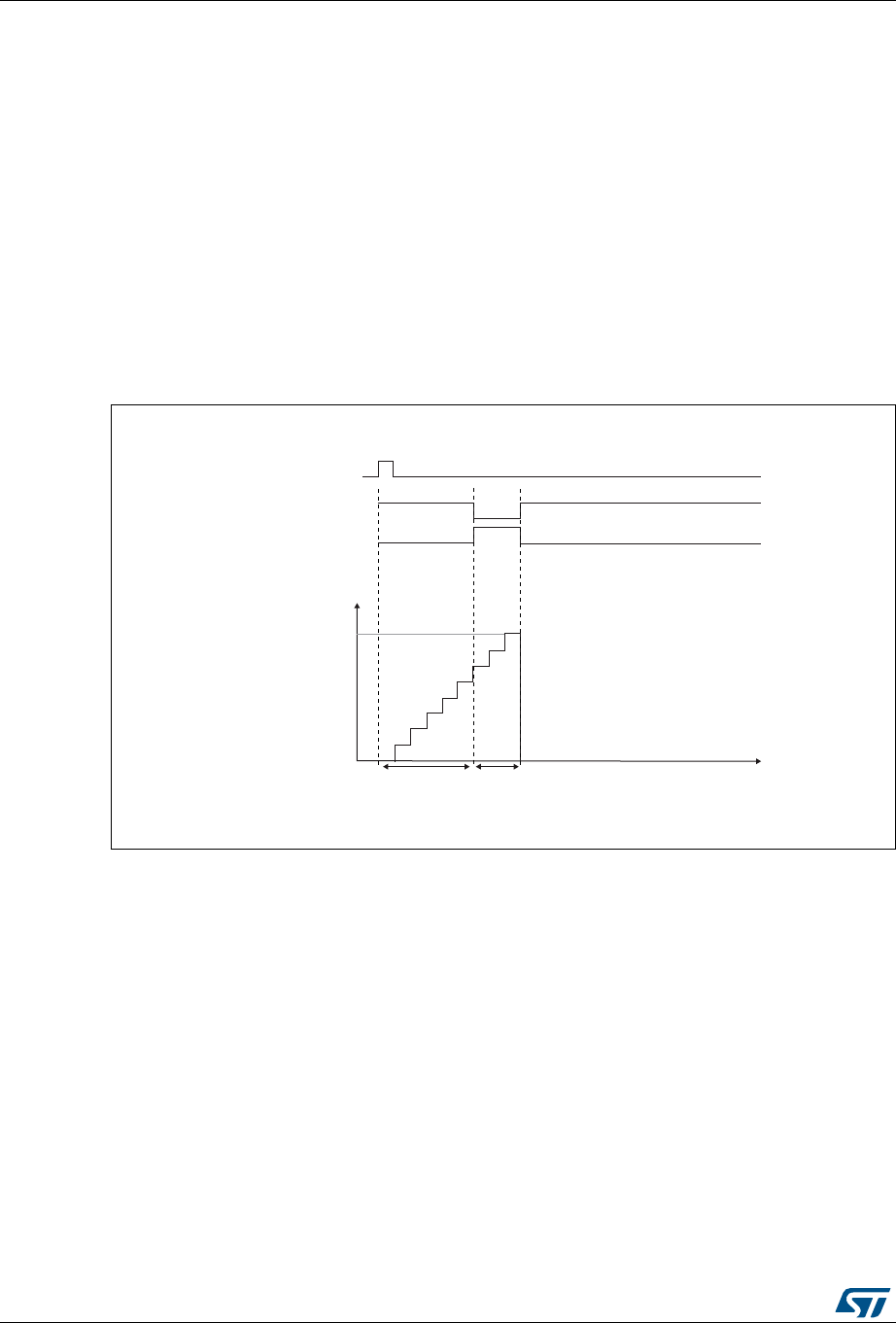
General-purpose timers (TIM2/TIM3) RM0394
848/1600 RM0394 Rev 4
27.3.13 One-pulse mode
One-pulse mode (OPM) is a particular case of the previous modes. It allows the counter to
be started in response to a stimulus and to generate a pulse with a programmable length
after a programmable delay.
Starting the counter can be controlled through the slave mode controller. Generating the
waveform can be done in output compare mode or PWM mode. You select One-pulse mode
by setting the OPM bit in the TIMx_CR1 register. This makes the counter stop automatically
at the next update event UEV.
A pulse can be correctly generated only if the compare value is different from the counter
initial value. Before starting (when the timer is waiting for the trigger), the configuration must
be:
•CNT<CCRx ARR (in particular, 0<CCRx),
Figure 278. Example of one-pulse mode.
For example you may want to generate a positive pulse on OC1 with a length of tPULSE and
after a delay of tDELAY as soon as a positive edge is detected on the TI2 input pin.
Let’s use TI2FP2 as trigger 1:
1. Map TI2FP2 on TI2 by writing CC2S=01 in the TIMx_CCMR1 register.
2. TI2FP2 must detect a rising edge, write CC2P=0 and CC2NP=’0’ in the TIMx_CCER
register.
3. Configure TI2FP2 as trigger for the slave mode controller (TRGI) by writing TS=110 in
the TIMx_SMCR register.
4. TI2FP2 is used to start the counter by writing SMS to ‘110 in the TIMx_SMCR register
(trigger mode).
069
7,
2&5()
&RXQWHU
W
7,0B$55
7,0B&&5
2&
W'(/$< W38/6(

RM0394 Rev 4 849/1600
RM0394 General-purpose timers (TIM2/TIM3)
886
The OPM waveform is defined by writing the compare registers (taking into account the
clock frequency and the counter prescaler).
•The tDELAY is defined by the value written in the TIMx_CCR1 register.
•The tPULSE is defined by the difference between the auto-reload value and the compare
value (TIMx_ARR - TIMx_CCR1).
•Let’s say you want to build a waveform with a transition from ‘0 to ‘1 when a compare
match occurs and a transition from ‘1 to ‘0 when the counter reaches the auto-reload
value. To do this you enable PWM mode 2 by writing OC1M=111 in the TIMx_CCMR1
register. You can optionally enable the preload registers by writing OC1PE=1 in the
TIMx_CCMR1 register and ARPE in the TIMx_CR1 register. In this case you have to
write the compare value in the TIMx_CCR1 register, the auto-reload value in the
TIMx_ARR register, generate an update by setting the UG bit and wait for external
trigger event on TI2. CC1P is written to ‘0 in this example.
In our example, the DIR and CMS bits in the TIMx_CR1 register should be low.
You only want 1 pulse (Single mode), so you write '1 in the OPM bit in the TIMx_CR1
register to stop the counter at the next update event (when the counter rolls over from the
auto-reload value back to 0). When OPM bit in the TIMx_CR1 register is set to '0', so the
Repetitive Mode is selected.
Particular case: OCx fast enable:
In One-pulse mode, the edge detection on TIx input set the CEN bit which enables the
counter. Then the comparison between the counter and the compare value makes the
output toggle. But several clock cycles are needed for these operations and it limits the
minimum delay tDELAY min we can get.
If you want to output a waveform with the minimum delay, you can set the OCxFE bit in the
TIMx_CCMRx register. Then OCxRef (and OCx) is forced in response to the stimulus,
without taking in account the comparison. Its new level is the same as if a compare match
had occurred. OCxFE acts only if the channel is configured in PWM1 or PWM2 mode.
27.3.14 Retriggerable one pulse mode (OPM)
This mode allows the counter to be started in response to a stimulus and to generate a
pulse with a programmable length, but with the following differences with Non-retriggerable
one pulse mode described in Section 27.3.13:
•The pulse starts as soon as the trigger occurs (no programmable delay)
•The pulse is extended if a new trigger occurs before the previous one is completed
The timer must be in Slave mode, with the bits SMS[3:0] = ‘1000’ (Combined Reset + trigger
mode) in the TIMx_SMCR register, and the OCxM[3:0] bits set to ‘1000’ or ‘1001’ for
Retriggerable OPM mode 1 or 2.
If the timer is configured in Up-counting mode, the corresponding CCRx must be set to 0
(the ARR register sets the pulse length). If the timer is configured in Down-counting mode
CCRx must be above or equal to ARR.
Note: In retriggerable one pulse mode, the CCxIF flag is not significant.
The OCxM[3:0] and SMS[3:0] bit fields are split into two parts for compatibility reasons, the
most significant bit is not contiguous with the 3 least significant ones.
This mode must not be used with center-aligned PWM modes. It is mandatory to have
CMS[1:0] = 00 in TIMx_CR1.

General-purpose timers (TIM2/TIM3) RM0394
850/1600 RM0394 Rev 4
Figure 279. Retriggerable one pulse mode
27.3.15 Encoder interface mode
To select Encoder Interface mode write SMS=‘001 in the TIMx_SMCR register if the counter
is counting on TI2 edges only, SMS=010 if it is counting on TI1 edges only and SMS=011 if
it is counting on both TI1 and TI2 edges.
Select the TI1 and TI2 polarity by programming the CC1P and CC2P bits in the TIMx_CCER
register. CC1NP and CC2NP must be kept cleared. When needed, you can program the
input filter as well. CC1NP and CC2NP must be kept low.
The two inputs TI1 and TI2 are used to interface to an incremental encoder. Refer to
Table 135. The counter is clocked by each valid transition on TI1FP1 or TI2FP2 (TI1 and TI2
after input filter and polarity selection, TI1FP1=TI1 if not filtered and not inverted,
TI2FP2=TI2 if not filtered and not inverted) assuming that it is enabled (CEN bit in
TIMx_CR1 register written to ‘1). The sequence of transitions of the two inputs is evaluated
and generates count pulses as well as the direction signal. Depending on the sequence the
counter counts up or down, the DIR bit in the TIMx_CR1 register is modified by hardware
accordingly. The DIR bit is calculated at each transition on any input (TI1 or TI2), whatever
the counter is counting on TI1 only, TI2 only or both TI1 and TI2.
Encoder interface mode acts simply as an external clock with direction selection. This
means that the counter just counts continuously between 0 and the auto-reload value in the
TIMx_ARR register (0 to ARR or ARR down to 0 depending on the direction). So you must
configure TIMx_ARR before starting. In the same way, the capture, compare, prescaler,
trigger output features continue to work as normal.
In this mode, the counter is modified automatically following the speed and the direction of
the quadrature encoder and its content, therefore, always represents the encoder’s position.
The count direction correspond to the rotation direction of the connected sensor. The table
summarizes the possible combinations, assuming TI1 and TI2 don’t switch at the same
time.
75*,
&RXQWHU
2XWSXW
069
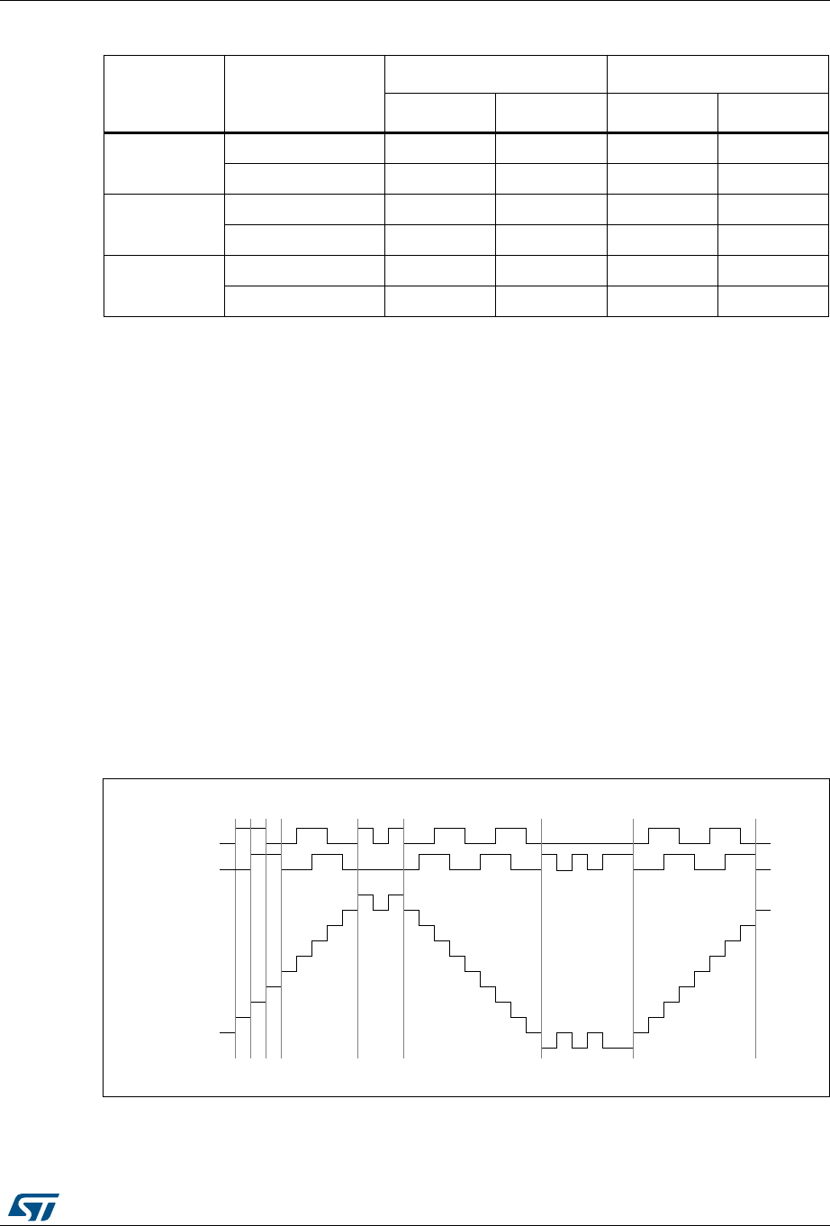
RM0394 Rev 4 851/1600
RM0394 General-purpose timers (TIM2/TIM3)
886
An external incremental encoder can be connected directly to the MCU without external
interface logic. However, comparators are normally be used to convert the encoder’s
differential outputs to digital signals. This greatly increases noise immunity. The third
encoder output which indicate the mechanical zero position, may be connected to an
external interrupt input and trigger a counter reset.
Figure 280 gives an example of counter operation, showing count signal generation and
direction control. It also shows how input jitter is compensated where both edges are
selected. This might occur if the sensor is positioned near to one of the switching points. For
this example we assume that the configuration is the following:
•CC1S= 01 (TIMx_CCMR1 register, TI1FP1 mapped on TI1)
•CC2S= 01 (TIMx_CCMR2 register, TI2FP2 mapped on TI2)
•CC1P and CC1NP = ‘0’ (TIMx_CCER register, TI1FP1 noninverted, TI1FP1=TI1)
•CC2P and CC2NP = ‘0’ (TIMx_CCER register, TI2FP2 noninverted, TI2FP2=TI2)
•SMS= 011 (TIMx_SMCR register, both inputs are active on both rising and falling
edges)
•CEN= 1 (TIMx_CR1 register, Counter is enabled)
Figure 280. Example of counter operation in encoder interface mode
Figure 281 gives an example of counter behavior when TI1FP1 polarity is inverted (same
configuration as above except CC1P=1).
Table 135. Counting direction versus encoder signals
Active edge
Level on opposite
signal (TI1FP1 for
TI2, TI2FP2 for TI1)
TI1FP1 signal TI2FP2 signal
Rising Falling Rising Falling
Counting on
TI1 only
High Down Up No Count No Count
Low Up Down No Count No Count
Counting on
TI2 only
High No Count No Count Up Down
Low No Count No Count Down Up
Counting on
TI1 and TI2
High Down Up Up Down
Low Up Down Down Up
7,
EDFNZDUGMLWWHU MLWWHU
XS GRZQ XS
7,
&RXQWHU
IRUZDUG IRUZDUG
069

General-purpose timers (TIM2/TIM3) RM0394
852/1600 RM0394 Rev 4
Figure 281. Example of encoder interface mode with TI1FP1 polarity inverted
The timer, when configured in Encoder Interface mode provides information on the sensor’s
current position. You can obtain dynamic information (speed, acceleration, deceleration) by
measuring the period between two encoder events using a second timer configured in
capture mode. The output of the encoder which indicates the mechanical zero can be used
for this purpose. Depending on the time between two events, the counter can also be read
at regular times. You can do this by latching the counter value into a third input capture
register if available (then the capture signal must be periodic and can be generated by
another timer). when available, it is also possible to read its value through a DMA request
generated by a Real-Time clock.
27.3.16 UIF bit remapping
The IUFREMAP bit in the TIMx_CR1 register forces a continuous copy of the update
interrupt flag (UIF) into bit 31 of the timer counter register’s bit 31 (TIMxCNT[31]). This
allows to atomically read both the counter value and a potential roll-over condition signaled
by the UIFCPY flag. It eases the calculation of angular speed by avoiding race conditions
caused, for instance, by a processing shared between a background task (counter reading)
and an interrupt (update interrupt).
There is no latency between the UIF and UIFCPY flag assertions.
In 32-bit timer implementations, when the IUFREMAP bit is set, bit 31 of the counter is
overwritten by the UIFCPY flag upon read access (the counter’s most significant bit is only
accessible in write mode).
27.3.17 Timer input XOR function
The TI1S bit in the TIM1xx_CR2 register, allows the input filter of channel 1 to be connected
to the output of a XOR gate, combining the three input pins TIMx_CH1 to TIMx_CH3.
The XOR output can be used with all the timer input functions such as trigger or input
capture.
An example of this feature used to interface Hall sensors is given in Section 26.3.25:
Interfacing with Hall sensors on page 770.
7,
EDFNZDUGMLWWHU MLWWHU
XSGRZQ
7,
&RXQWHU
IRUZDUG IRUZDUG
069
GRZQ
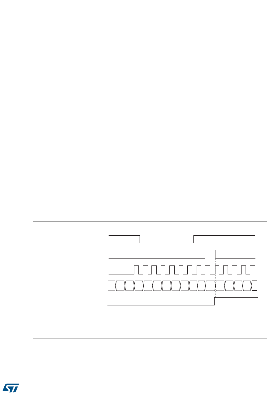
RM0394 Rev 4 853/1600
RM0394 General-purpose timers (TIM2/TIM3)
886
27.3.18 Timers and external trigger synchronization
The TIMx Timers can be synchronized with an external trigger in several modes: Reset
mode, Gated mode and Trigger mode.
Slave mode: Reset mode
The counter and its prescaler can be reinitialized in response to an event on a trigger input.
Moreover, if the URS bit from the TIMx_CR1 register is low, an update event UEV is
generated. Then all the preloaded registers (TIMx_ARR, TIMx_CCRx) are updated.
In the following example, the upcounter is cleared in response to a rising edge on TI1 input:
1. Configure the channel 1 to detect rising edges on TI1. Configure the input filter duration
(in this example, we don’t need any filter, so we keep IC1F=0000). The capture
prescaler is not used for triggering, so you don’t need to configure it. The CC1S bits
select the input capture source only, CC1S = 01 in the TIMx_CCMR1 register. Write
CC1P=0 and CC1NP=0 in TIMx_CCER register to validate the polarity (and detect
rising edges only).
2. Configure the timer in reset mode by writing SMS=100 in TIMx_SMCR register. Select
TI1 as the input source by writing TS=101 in TIMx_SMCR register.
3. Start the counter by writing CEN=1 in the TIMx_CR1 register.
The counter starts counting on the internal clock, then behaves normally until TI1 rising
edge. When TI1 rises, the counter is cleared and restarts from 0. In the meantime, the
trigger flag is set (TIF bit in the TIMx_SR register) and an interrupt request, or a DMA
request can be sent if enabled (depending on the TIE and TDE bits in TIMx_DIER register).
The following figure shows this behavior when the auto-reload register TIMx_ARR=0x36.
The delay between the rising edge on TI1 and the actual reset of the counter is due to the
resynchronization circuit on TI1 input.
Figure 282. Control circuit in reset mode
Slave mode: Gated mode
The counter can be enabled depending on the level of a selected input.
In the following example, the upcounter counts only when TI1 input is low:
069
&RXQWHUFORFN FNBFQW FNBSVF
&RXQWHUUHJLVWHU
8*
7,
7,)
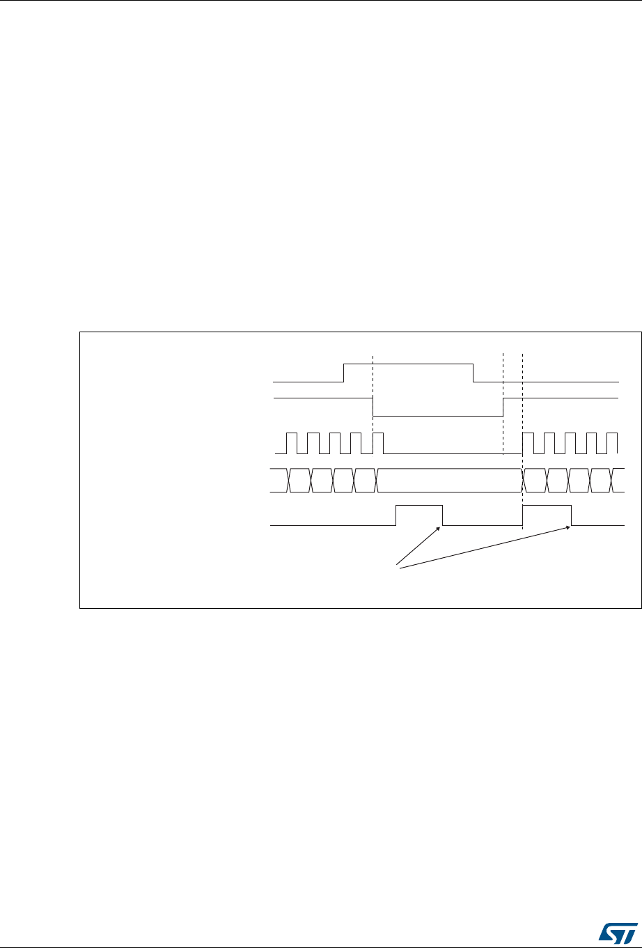
General-purpose timers (TIM2/TIM3) RM0394
854/1600 RM0394 Rev 4
1. Configure the channel 1 to detect low levels on TI1. Configure the input filter duration
(in this example, we don’t need any filter, so we keep IC1F=0000). The capture
prescaler is not used for triggering, so you don’t need to configure it. The CC1S bits
select the input capture source only, CC1S=01 in TIMx_CCMR1 register. Write
CC1P=1 and CC1NP=0 in TIMx_CCER register to validate the polarity (and detect low
level only).
2. Configure the timer in gated mode by writing SMS=101 in TIMx_SMCR register. Select
TI1 as the input source by writing TS=101 in TIMx_SMCR register.
3. Enable the counter by writing CEN=1 in the TIMx_CR1 register (in gated mode, the
counter doesn’t start if CEN=0, whatever is the trigger input level).
The counter starts counting on the internal clock as long as TI1 is low and stops as soon as
TI1 becomes high. The TIF flag in the TIMx_SR register is set both when the counter starts
or stops.
The delay between the rising edge on TI1 and the actual stop of the counter is due to the
resynchronization circuit on TI1 input.
Figure 283. Control circuit in gated mode
1. The configuration “CCxP=CCxNP=1” (detection of both rising and falling edges) does not have any effect
in gated mode because gated mode acts on a level and not on an edge.
Note: The configuration “CCxP=CCxNP=1” (detection of both rising and falling edges) does not
have any effect in gated mode because gated mode acts on a level and not on an edge.
Slave mode: Trigger mode
The counter can start in response to an event on a selected input.
In the following example, the upcounter starts in response to a rising edge on TI2 input:
1. Configure the channel 2 to detect rising edges on TI2. Configure the input filter duration
(in this example, we don’t need any filter, so we keep IC2F=0000). The capture
prescaler is not used for triggering, so you don’t need to configure it. CC2S bits are
selecting the input capture source only, CC2S=01 in TIMx_CCMR1 register. Write
069
7,
FQWBHQ
:ULWH7,)
&RXQWHUFORFN FNBFQW FNBSVF
&RXQWHUUHJLVWHU
7,)

RM0394 Rev 4 855/1600
RM0394 General-purpose timers (TIM2/TIM3)
886
CC2P=1 and CC2NP=0 in TIMx_CCER register to validate the polarity (and detect low
level only).
2. Configure the timer in trigger mode by writing SMS=110 in TIMx_SMCR register. Select
TI2 as the input source by writing TS=110 in TIMx_SMCR register.
When a rising edge occurs on TI2, the counter starts counting on the internal clock and the
TIF flag is set.
The delay between the rising edge on TI2 and the actual start of the counter is due to the
resynchronization circuit on TI2 input.
Figure 284. Control circuit in trigger mode
Slave mode: External Clock mode 2 + trigger mode
The external clock mode 2 can be used in addition to another slave mode (except external
clock mode 1 and encoder mode). In this case, the ETR signal is used as external clock
input, and another input can be selected as trigger input when operating in reset mode,
gated mode or trigger mode. It is recommended not to select ETR as TRGI through the TS
bits of TIMx_SMCR register.
In the following example, the upcounter is incremented at each rising edge of the ETR
signal as soon as a rising edge of TI1 occurs:
1. Configure the external trigger input circuit by programming the TIMx_SMCR register as
follows:
– ETF = 0000: no filter
– ETPS=00: prescaler disabled
– ETP=0: detection of rising edges on ETR and ECE=1 to enable the external clock
mode 2.
2. Configure the channel 1 as follows, to detect rising edges on TI:
– IC1F=0000: no filter.
– The capture prescaler is not used for triggering and does not need to be
configured.
– CC1S=01in TIMx_CCMR1 register to select only the input capture source
– CC1P=0 and CC1NP=0 in TIMx_CCER register to validate the polarity (and detect
rising edge only).
3. Configure the timer in trigger mode by writing SMS=110 in TIMx_SMCR register. Select
TI1 as the input source by writing TS=101 in TIMx_SMCR register.
069
7,
FQWBHQ
&RXQWHUFORFN FNBFQW FNBSVF
&RXQWHUUHJLVWHU
7,)
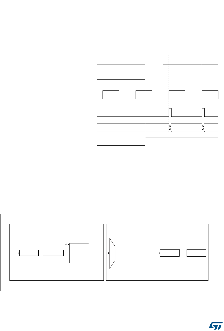
General-purpose timers (TIM2/TIM3) RM0394
856/1600 RM0394 Rev 4
A rising edge on TI1 enables the counter and sets the TIF flag. The counter then counts on
ETR rising edges.
The delay between the rising edge of the ETR signal and the actual reset of the counter is
due to the resynchronization circuit on ETRP input.
Figure 285. Control circuit in external clock mode 2 + trigger mode
27.3.19 Timer synchronization
The TIMx timers are linked together internally for timer synchronization or chaining. When
one Timer is configured in Master Mode, it can reset, start, stop or clock the counter of
another Timer configured in Slave Mode.
Figure 286: Master/Slave timer example presents an overview of the trigger selection and
the master mode selection blocks.
Figure 286. Master/Slave timer example
069
7,)
&RXQWHUUHJLVWHU
&RXQWHUFORFN &.B&17 &.B36&
(75
&(1&17B(1
7,
D^ǀϯϳϲϯϯsϭ
ŽƵŶƚĞƌ
DĂƐƚĞƌ
ŵŽĚĞ
ĐŽŶƚƌŽů
hs
WƌĞƐĐĂůĞƌ
ůŽĐŬ
^ůĂǀĞ
ŵŽĚĞ
ĐŽŶƚƌŽů ŽƵŶƚĞƌWƌĞƐĐĂůĞƌ
<ͺW^/dZϮdZ'Kϭ
DD^ ^D^
d^
/ŶƉƵƚ
ƚƌŝŐŐĞƌ
ƐĞůĞĐƚŝŽŶ
d/DLJ d/Dnj
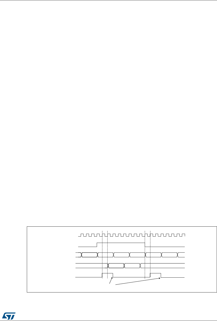
RM0394 Rev 4 857/1600
RM0394 General-purpose timers (TIM2/TIM3)
886
Using one timer as prescaler for another timer
For example, you can configure TIMy to act as a prescaler for TIMz. Refer to Figure 286. To
do this:
1. Configure TIMy in master mode so that it outputs a periodic trigger signal on each
update event UEV. If you write MMS=010 in the TIMy_CR2 register, a rising edge is
output on TRGO each time an update event is generated.
2. To connect the TRGO output of TIMy to TIMz, TIMz must be configured in slave mode
using ITR2 as internal trigger. You select this through the TS bits in the TIMz_SMCR
register (writing TS=010).
3. Then you put the slave mode controller in external clock mode 1 (write SMS=111 in the
TIMz_SMCR register). This causes TIMz to be clocked by the rising edge of the
periodic TIMy trigger signal (which correspond to the TIMy counter overflow).
4. Finally both timers must be enabled by setting their respective CEN bits (TIMx_CR1
register).
Note: If OCx is selected on TIMy as the trigger output (MMS=1xx), its rising edge is used to clock
the counter of TIMz.
Using one timer to enable another timer
In this example, we control the enable of TIMz with the output compare 1 of Timer y. Refer
to Figure 286 for connections. TIMz counts on the divided internal clock only when OC1REF
of TIMy is high. Both counter clock frequencies are divided by 3 by the prescaler compared
to CK_INT (fCK_CNT = fCK_INT/3).
1. Configure TIMy master mode to send its Output Compare 1 Reference (OC1REF)
signal as trigger output (MMS=100 in the TIMy_CR2 register).
2. Configure the TIMy OC1REF waveform (TIMy_CCMR1 register).
3. Configure TIMz to get the input trigger from TIMy (TS=010 in the TIMz_SMCR
register).
4. Configure TIMz in gated mode (SMS=101 in TIMz_SMCR register).
5. Enable TIMz by writing ‘1 in the CEN bit (TIMz_CR1 register).
6. Start TIMy by writing ‘1 in the CEN bit (TIMy_CR1 register).
Note: The counter z clock is not synchronized with counter 1, this mode only affects the TIMz
counter enable signal.
Figure 287. Gating TIMz with OC1REF of TIMy
06Y9
&.B,17
)& )' )( ))
7,0\2&5()
7,0\&17
7,0]&17
7,0]7,)
:ULWH7,)
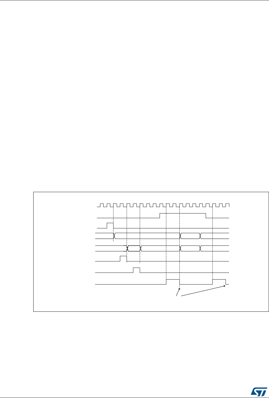
General-purpose timers (TIM2/TIM3) RM0394
858/1600 RM0394 Rev 4
In the example in Figure 287, the TIMz counter and prescaler are not initialized before being
started. So they start counting from their current value. It is possible to start from a given
value by resetting both timers before starting TIMy. You can then write any value you want in
the timer counters. The timers can easily be reset by software using the UG bit in the
TIMx_EGR registers.
In the next example (refer to Figure 288), we synchronize TIMy and TIMz. TIMy is the
master and starts from 0. TIMz is the slave and starts from 0xE7. The prescaler ratio is the
same for both timers. TIMz stops when TIMy is disabled by writing ‘0 to the CEN bit in the
TIMy_CR1 register:
1. Configure TIMy master mode to send its Output Compare 1 Reference (OC1REF)
signal as trigger output (MMS=100 in the TIMy_CR2 register).
2. Configure the TIMy OC1REF waveform (TIMy_CCMR1 register).
3. Configure TIMz to get the input trigger from TIMy (TS=010 in the TIMz_SMCR
register).
4. Configure TIMz in gated mode (SMS=101 in TIMz_SMCR register).
5. Reset TIMy by writing ‘1 in UG bit (TIMy_EGR register).
6. Reset TIMz by writing ‘1 in UG bit (TIMz_EGR register).
7. Initialize TIMz to 0xE7 by writing ‘0xE7’ in the TIMz counter (TIMz_CNTL).
8. Enable TIMz by writing ‘1 in the CEN bit (TIMz_CR1 register).
9. Start TIMy by writing ‘1 in the CEN bit (TIMy_CR1 register).
10. Stop TIMy by writing ‘0 in the CEN bit (TIMy_CR1 register).
Figure 288. Gating TIMz with Enable of TIMy
Using one timer to start another timer
In this example, we set the enable of Timer z with the update event of Timer y. Refer to
Figure 286 for connections. Timer z starts counting from its current value (which can be non-
zero) on the divided internal clock as soon as the update event is generated by Timer 1.
When Timer z receives the trigger signal its CEN bit is automatically set and the counter
counts until we write ‘0 to the CEN bit in the TIMz_CR1 register. Both counter clock
frequencies are divided by 3 by the prescaler compared to CK_INT (fCK_CNT = fCK_INT/3).
06Y9
&.B,17
(
7,0\&17B,1,7
7,0\&17
$%
7,0]&17
7,0]&17B,1,7
:ULWH7,)
((
7,0\&(1 &17B(1
7,0]ZULWH&17
7,0]7,)
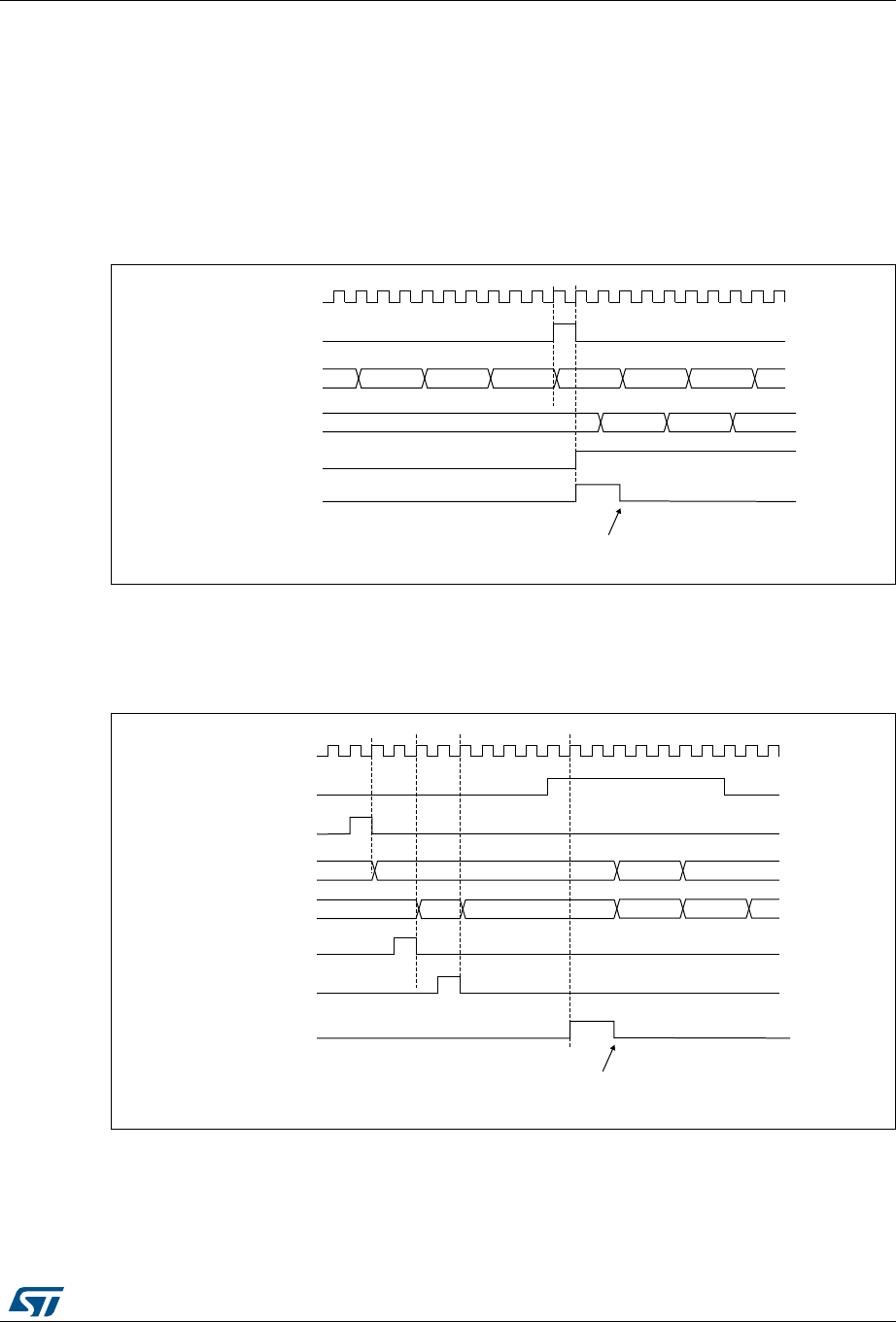
RM0394 Rev 4 859/1600
RM0394 General-purpose timers (TIM2/TIM3)
886
1. Configure TIMy master mode to send its Update Event (UEV) as trigger output
(MMS=010 in the TIMy_CR2 register).
2. Configure the TIMy period (TIMy_ARR registers).
3. Configure TIMz to get the input trigger from TIMy (TS=010 in the TIMz_SMCR
register).
4. Configure TIMz in trigger mode (SMS=110 in TIMz_SMCR register).
5. Start TIMy by writing ‘1 in the CEN bit (TIMy_CR1 register).
Figure 289. Triggering TIMz with update of TIMy
As in the previous example, you can initialize both counters before starting counting.
Figure 290 shows the behavior with the same configuration as in Figure 289 but in trigger
mode instead of gated mode (SMS=110 in the TIMz_SMCR register).
Figure 290. Triggering TIMz with Enable of TIMy
Starting 2 timers synchronously in response to an external trigger
In this example, we set the enable of TIMy when its TI1 input rises, and the enable of TIMz2
with the enable of TIMy3. Refer to Figure 286 for connections. To ensure the counters are
06Y9
&.B,17
7,0]&17
)'
7,0\&17
:ULWH7,)
7,0]&(1 &17B(1
7,0]7,)
)( ))
7,0\8(9
06Y9
&.B,17
7,0]&17
7,0\&17B,1,7
:ULWH7,)
7,0\&(1 &17B(1
7,0]7,)
(
(
&' ( ($
7,0\&17
7,0]&17B,1,7
7,0]
ZULWH&17
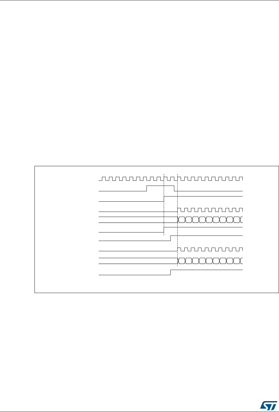
General-purpose timers (TIM2/TIM3) RM0394
860/1600 RM0394 Rev 4
aligned, TIMy3 must be configured in Master/Slave mode (slave with respect to TI1, master
with respect to TIMz2):
1. Configure TIMy3 master mode to send its Enable as trigger output (MMS=001 in the
TIMy3_CR2 register).
2. Configure TIMy slave mode to get the input trigger from TI1 (TS=100 in the
TIMy3_SMCR register).
3. Configure TIMy3 in trigger mode (SMS=110 in the TIMy3_SMCR register).
4. Configure the TIMy3 in Master/Slave mode by writing MSM=1 (TIMy3_SMCR register).
5. Configure TIMz2 to get the input trigger from TIMy (TS=000 in the TIMz2_SMCR
register).
6. Configure TIMz2 in trigger mode (SMS=110 in the TIMz2_SMCR register).
When a rising edge occurs on TI1 (TIMy3), both counters starts counting synchronously on
the internal clock and both TIF flags are set.
Note: In this example both timers are initialized before starting (by setting their respective UG
bits). Both counters starts from 0, but you can easily insert an offset between them by
writing any of the counter registers (TIMx_CNT). You can see that the master/slave mode
insert a delay between CNT_EN and CK_PSC on TIMy3.
Figure 291. Triggering TIMy3 and TIMz2 with TIMy3 TI1 input
Note: The clock of the slave peripherals (timer, ADC, ...) receiving the TRGO or the TRGO2
signals must be enabled prior to receive events from the master timer, and the clock
frequency (prescaler) must not be changed on-the-fly while triggers are received from the
master timer.
27.3.20 DMA burst mode
The TIMx timers have the capability to generate multiple DMA requests upon a single event.
The main purpose is to be able to re-program part of the timer multiple times without
software overhead, but it can also be used to read several registers in a row, at regular
intervals.
06Y9
&.B,17
7,0]&17
7,0\&(1 &17B(1
7,0]7,)
7,0\&17
7,0]&(1 &17B(1
7,0\7,)
7,0\&.B36&
7,0\7,
7,0]&.B36&

RM0394 Rev 4 861/1600
RM0394 General-purpose timers (TIM2/TIM3)
886
The DMA controller destination is unique and must point to the virtual register TIMx_DMAR.
On a given timer event, the timer launches a sequence of DMA requests (burst). Each write
into the TIMx_DMAR register is actually redirected to one of the timer registers.
The DBL[4:0] bits in the TIMx_DCR register set the DMA burst length. The timer recognizes
a burst transfer when a read or a write access is done to the TIMx_DMAR address), i.e. the
number of transfers (either in half-words or in bytes).
The DBA[4:0] bits in the TIMx_DCR registers define the DMA base address for DMA
transfers (when read/write access are done through the TIMx_DMAR address). DBA is
defined as an offset starting from the address of the TIMx_CR1 register:
Example:
00000: TIMx_CR1
00001: TIMx_CR2
00010: TIMx_SMCR
As an example, the timer DMA burst feature is used to update the contents of the CCRx
registers (x = 2, 3, 4) upon an update event, with the DMA transferring half words into the
CCRx registers.
This is done in the following steps:
1. Configure the corresponding DMA channel as follows:
– DMA channel peripheral address is the DMAR register address
– DMA channel memory address is the address of the buffer in the RAM containing
the data to be transferred by DMA into CCRx registers.
– Number of data to transfer = 3 (See note below).
– Circular mode disabled.
2. Configure the DCR register by configuring the DBA and DBL bit fields as follows:
DBL = 3 transfers, DBA = 0xE.
3. Enable the TIMx update DMA request (set the UDE bit in the DIER register).
4. Enable TIMx
5. Enable the DMA channel
This example is for the case where every CCRx register has to be updated once. If every
CCRx register is to be updated twice for example, the number of data to transfer should be
6. Let's take the example of a buffer in the RAM containing data1, data2, data3, data4, data5
and data6. The data is transferred to the CCRx registers as follows: on the first update DMA
request, data1 is transferred to CCR2, data2 is transferred to CCR3, data3 is transferred to
CCR4 and on the second update DMA request, data4 is transferred to CCR2, data5 is
transferred to CCR3 and data6 is transferred to CCR4.
Note: A null value can be written to the reserved registers.
27.3.21 Debug mode
When the microcontroller enters debug mode (Cortex®-M4 core - halted), the TIMx counter
either continues to work normally or stops, depending on DBG_TIMx_STOP configuration
bit in DBGMCU module. For more details, refer to Section 46.16.2: Debug support for
timers, RTC, watchdog, bxCAN and I2C.

General-purpose timers (TIM2/TIM3) RM0394
862/1600 RM0394 Rev 4
27.4 TIM2/TIM3 registers
Refer to Section 1.2 for a list of abbreviations used in register descriptions.
The peripheral registers can be accessed by half-words (16-bit) or words (32-bit).
27.4.1 TIMx control register 1 (TIMx_CR1)(x = 2 to 3)
Address offset: 0x00
Reset value: 0x0000
1514131211109876543210
Res. Res. Res. Res. UIFRE
MAP Res. CKD[1:0] ARPE CMS DIR OPM URS UDIS CEN
rw rw rw rw rw rw rw rw rw rw rw
Bits 15:12 Reserved, must be kept at reset value.
Bit 11 UIFREMAP: UIF status bit remapping
0: No remapping. UIF status bit is not copied to TIMx_CNT register bit 31.
1: Remapping enabled. UIF status bit is copied to TIMx_CNT register bit 31.
Bit 10 Reserved, must be kept at reset value.
Bits 9:8 CKD[1:0]: Clock division
This bit-field indicates the division ratio between the timer clock (CK_INT) frequency and
sampling clock used by the digital filters (ETR, TIx),
00: tDTS = tCK_INT
01: tDTS = 2 × tCK_INT
10: tDTS = 4 × tCK_INT
11: Reserved
Bit 7 ARPE: Auto-reload preload enable
0: TIMx_ARR register is not buffered
1: TIMx_ARR register is buffered
Bits 6:5 CMS: Center-aligned mode selection
00: Edge-aligned mode. The counter counts up or down depending on the direction bit
(DIR).
01: Center-aligned mode 1. The counter counts up and down alternatively. Output compare
interrupt flags of channels configured in output (CCxS=00 in TIMx_CCMRx register) are set
only when the counter is counting down.
10: Center-aligned mode 2. The counter counts up and down alternatively. Output compare
interrupt flags of channels configured in output (CCxS=00 in TIMx_CCMRx register) are set
only when the counter is counting up.
11: Center-aligned mode 3. The counter counts up and down alternatively. Output compare
interrupt flags of channels configured in output (CCxS=00 in TIMx_CCMRx register) are set
both when the counter is counting up or down.
Note: It is not allowed to switch from edge-aligned mode to center-aligned mode as long as
the counter is enabled (CEN=1)
Bit 4 DIR: Direction
0: Counter used as upcounter
1: Counter used as downcounter
Note: This bit is read only when the timer is configured in Center-aligned mode or Encoder
mode.

RM0394 Rev 4 863/1600
RM0394 General-purpose timers (TIM2/TIM3)
886
27.4.2 TIMx control register 2 (TIMx_CR2)(x = 2 to 3)
Address offset: 0x04
Reset value: 0x0000
Bit 3 OPM: One-pulse mode
0: Counter is not stopped at update event
1: Counter stops counting at the next update event (clearing the bit CEN)
Bit 2 URS: Update request source
This bit is set and cleared by software to select the UEV event sources.
0: Any of the following events generate an update interrupt or DMA request if enabled.
These events can be:
– Counter overflow/underflow
– Setting the UG bit
– Update generation through the slave mode controller
1: Only counter overflow/underflow generates an update interrupt or DMA request if
enabled.
Bit 1 UDIS: Update disable
This bit is set and cleared by software to enable/disable UEV event generation.
0: UEV enabled. The Update (UEV) event is generated by one of the following events:
– Counter overflow/underflow
– Setting the UG bit
– Update generation through the slave mode controller
Buffered registers are then loaded with their preload values.
1: UEV disabled. The Update event is not generated, shadow registers keep their value
(ARR, PSC, CCRx). However the counter and the prescaler are reinitialized if the UG bit is
set or if a hardware reset is received from the slave mode controller.
Bit 0 CEN: Counter enable
0: Counter disabled
1: Counter enabled
Note: External clock, gated mode and encoder mode can work only if the CEN bit has been
previously set by software. However trigger mode can set the CEN bit automatically by
hardware.
CEN is cleared automatically in one-pulse mode, when an update event occurs.
1514131211109876543210
Res. Res. Res. Res. Res. Res. Res. Res. TI1S MMS[2:0] CCDS Res. Res. Res.
rw rw rw rw rw

General-purpose timers (TIM2/TIM3) RM0394
864/1600 RM0394 Rev 4
Bits 15:8 Reserved, must be kept at reset value.
Bit 7 TI1S: TI1 selection
0: The TIMx_CH1 pin is connected to TI1 input
1: The TIMx_CH1, CH2 and CH3 pins are connected to the TI1 input (XOR combination)
See also Section 26.3.25: Interfacing with Hall sensors on page 770
Bits 6:4 MMS[2:0]: Master mode selection
These bits allow to select the information to be sent in master mode to slave timers for
synchronization (TRGO). The combination is as follows:
000: Reset - the UG bit from the TIMx_EGR register is used as trigger output (TRGO). If the
reset is generated by the trigger input (slave mode controller configured in reset mode) then
the signal on TRGO is delayed compared to the actual reset.
001: Enable - the Counter enable signal, CNT_EN, is used as trigger output (TRGO). It is
useful to start several timers at the same time or to control a window in which a slave timer is
enabled. The Counter Enable signal is generated by a logic OR between CEN control bit
and the trigger input when configured in gated mode.
When the Counter Enable signal is controlled by the trigger input, there is a delay on TRGO,
except if the master/slave mode is selected (see the MSM bit description in TIMx_SMCR
register).
010: Update - The update event is selected as trigger output (TRGO). For instance a master
timer can then be used as a prescaler for a slave timer.
011: Compare Pulse - The trigger output send a positive pulse when the CC1IF flag is to be
set (even if it was already high), as soon as a capture or a compare match occurred.
(TRGO)
100: Compare - OC1REF signal is used as trigger output (TRGO)
101: Compare - OC2REF signal is used as trigger output (TRGO)
110: Compare - OC3REF signal is used as trigger output (TRGO)
111: Compare - OC4REF signal is used as trigger output (TRGO)
Note: The clock of the slave timer or ADC must be enabled prior to receive events from the
master timer, and must not be changed on-the-fly while triggers are received from the
master timer.
Bit 3 CCDS: Capture/compare DMA selection
0: CCx DMA request sent when CCx event occurs
1: CCx DMA requests sent when update event occurs
Bits 2:0 Reserved, must be kept at reset value.

RM0394 Rev 4 865/1600
RM0394 General-purpose timers (TIM2/TIM3)
886
27.4.3 TIMx slave mode control register (TIMx_SMCR)(x = 2 to 3)
Address offset: 0x08
Reset value: 0x0000 0000
31 30 29 28 27 26 25 24 23 22 21 20 19 18 17 16
Res. Res. Res. Res. Res. Res. Res. Res. Res. Res. Res. Res. Res. Res. Res. SMS[3]
rw
1514131211109876543210
ETP ECE ETPS[1:0] ETF[3:0] MSM TS[2:0] OCCS SMS[2:0]
rw rw rw rw rw rw rw rw rw rw rw rw rw rw rw rw
Bits 31:17 Reserved, must be kept at reset value.
Bit 16 SMS[3]: Slave mode selection - bit 3
Refer to SMS description - bits 2:0.
Bit 15 ETP: External trigger polarity
This bit selects whether ETR or ETR is used for trigger operations
0: ETR is non-inverted, active at high level or rising edge
1: ETR is inverted, active at low level or falling edge
Bit 14 ECE: External clock enable
This bit enables External clock mode 2.
0: External clock mode 2 disabled
1: External clock mode 2 enabled. The counter is clocked by any active edge on the ETRF
signal.
1: Setting the ECE bit has the same effect as selecting external clock mode 1 with TRGI
connected to ETRF (SMS=111 and TS=111).
2: It is possible to simultaneously use external clock mode 2 with the following slave modes:
reset mode, gated mode and trigger mode. Nevertheless, TRGI must not be connected to
ETRF in this case (TS bits must not be 111).
3: If external clock mode 1 and external clock mode 2 are enabled at the same time, the
external clock input is ETRF.
Bits 13:12 ETPS[1:0]: External trigger prescaler
External trigger signal ETRP frequency must be at most 1/4 of CK_INT frequency. A
prescaler can be enabled to reduce ETRP frequency. It is useful when inputting fast external
clocks.
00: Prescaler OFF
01: ETRP frequency divided by 2
10: ETRP frequency divided by 4
11: ETRP frequency divided by 8

General-purpose timers (TIM2/TIM3) RM0394
866/1600 RM0394 Rev 4
Bits 11:8 ETF[3:0]: External trigger filter
This bit-field then defines the frequency used to sample ETRP signal and the length of the
digital filter applied to ETRP. The digital filter is made of an event counter in which N
consecutive events are needed to validate a transition on the output:
0000: No filter, sampling is done at fDTS
0001: fSAMPLING=fCK_INT
, N=2
0010: fSAMPLING=fCK_INT
, N=4
0011: fSAMPLING=fCK_INT
, N=8
0100: fSAMPLING=fDTS/2, N=6
0101: fSAMPLING=fDTS/2, N=8
0110: fSAMPLING=fDTS/4, N=6
0111: fSAMPLING=fDTS/4, N=8
1000: fSAMPLING=fDTS/8, N=6
1001: fSAMPLING=fDTS/8, N=8
1010: fSAMPLING=fDTS/16, N=5
1011: fSAMPLING=fDTS/16, N=6
1100: fSAMPLING=fDTS/16, N=8
1101: fSAMPLING=fDTS/32, N=5
1110: fSAMPLING=fDTS/32, N=6
1111: fSAMPLING=fDTS/32, N=8
Bit 7 MSM: Master/Slave mode
0: No action
1: The effect of an event on the trigger input (TRGI) is delayed to allow a perfect
synchronization between the current timer and its slaves (through TRGO). It is useful if we
want to synchronize several timers on a single external event.

RM0394 Rev 4 867/1600
RM0394 General-purpose timers (TIM2/TIM3)
886
Bits 6:4 TS: Trigger selection
This bit-field selects the trigger input to be used to synchronize the counter.
000: Internal Trigger 0 (ITR0)
001: Internal Trigger 1 (ITR1)
010: reserved
011: reserved
100: TI1 Edge Detector (TI1F_ED)
101: Filtered Timer Input 1 (TI1FP1)
110: Filtered Timer Input 2 (TI2FP2)
111: External Trigger input (ETRF)
See Table 136: TIMx internal trigger connection on page 867 for more details on ITRx
meaning for each Timer.
Note: These bits must be changed only when they are not used (e.g. when SMS=000) to
avoid wrong edge detections at the transition.
Bit 3 OCCS: OCREF clear selection
This bit is used to select the OCREF clear source
0: OCREF_CLR_INT is connected to the OCREF_CLR input
1: OCREF_CLR_INT is connected to ETRF
Bits 16, 2, 1, 0 SMS[3:0]: Slave mode selection
When external signals are selected the active edge of the trigger signal (TRGI) is linked to
the polarity selected on the external input (see Input Control register and Control Register
description.
0000: Slave mode disabled - if CEN = ‘1 then the prescaler is clocked directly by the internal
clock.
0001: Encoder mode 1 - Counter counts up/down on TI1FP1 edge depending on TI2FP2
level.
0010: Encoder mode 2 - Counter counts up/down on TI2FP2 edge depending on TI1FP1
level.
0011: Encoder mode 3 - Counter counts up/down on both TI1FP1 and TI2FP2 edges
depending on the level of the other input.
0100: Reset Mode - Rising edge of the selected trigger input (TRGI) reinitializes the counter
and generates an update of the registers.
0101: Gated Mode - The counter clock is enabled when the trigger input (TRGI) is high. The
counter stops (but is not reset) as soon as the trigger becomes low. Both start and stop of
the counter are controlled.
0110: Trigger Mode - The counter starts at a rising edge of the trigger TRGI (but it is not
reset). Only the start of the counter is controlled.
0111: External Clock Mode 1 - Rising edges of the selected trigger (TRGI) clock the counter.
1000: Combined reset + trigger mode - Rising edge of the selected trigger input (TRGI)
reinitializes the counter, generates an update of the registers and starts the counter.
Note: The gated mode must not be used if TI1F_ED is selected as the trigger input (TS=100).
Indeed, TI1F_ED outputs 1 pulse for each transition on TI1F, whereas the gated mode
checks the level of the trigger signal.
Note: The clock of the slave peripherals (timer, ADC, ...) receiving the TRGO or the TRGO2
signals must be enabled prior to receive events from the master timer, and the clock
frequency (prescaler) must not be changed on-the-fly while triggers are received from
the master timer.
Table 136. TIMx internal trigger connection
Slave TIM ITR0 (TS = 000) ITR1 (TS = 001) ITR2 (TS = 010) ITR3 (TS = 011)
TIM2 TIM1 USB(1)
1. Depends on the bit ITR1_RMP in TIM2_OR1 register.
Reserved Reserved

General-purpose timers (TIM2/TIM3) RM0394
868/1600 RM0394 Rev 4
27.4.4 TIMx DMA/Interrupt enable register (TIMx_DIER)(x = 2 to 3)
Address offset: 0x0C
Reset value: 0x0000
1514131211109876543210
Res. TDE Res. CC4DE CC3DE CC2DE CC1DE UDE Res. TIE Res. CC4IE CC3IE CC2IE CC1IE UIE
rw rw rw rw rw rw rw rw rw rw rw rw
Bit 15 Reserved, must be kept at reset value.
Bit 14 TDE: Trigger DMA request enable
0: Trigger DMA request disabled.
1: Trigger DMA request enabled.
Bit 13 Reserved, must be kept at reset value.
Bit 12 CC4DE: Capture/Compare 4 DMA request enable
0: CC4 DMA request disabled.
1: CC4 DMA request enabled.
Bit 11 CC3DE: Capture/Compare 3 DMA request enable
0: CC3 DMA request disabled.
1: CC3 DMA request enabled.
Bit 10 CC2DE: Capture/Compare 2 DMA request enable
0: CC2 DMA request disabled.
1: CC2 DMA request enabled.
Bit 9 CC1DE: Capture/Compare 1 DMA request enable
0: CC1 DMA request disabled.
1: CC1 DMA request enabled.
Bit 8 UDE: Update DMA request enable
0: Update DMA request disabled.
1: Update DMA request enabled.
Bit 7 Reserved, must be kept at reset value.
Bit 6 TIE: Trigger interrupt enable
0: Trigger interrupt disabled.
1: Trigger interrupt enabled.
Bit 5 Reserved, must be kept at reset value.
Bit 4 CC4IE: Capture/Compare 4 interrupt enable
0: CC4 interrupt disabled.
1: CC4 interrupt enabled.
Bit 3 CC3IE: Capture/Compare 3 interrupt enable
0: CC3 interrupt disabled.
1: CC3 interrupt enabled.

RM0394 Rev 4 869/1600
RM0394 General-purpose timers (TIM2/TIM3)
886
27.4.5 TIMx status register (TIMx_SR)(x = 2 to 3)
Address offset: 0x10
Reset value: 0x0000
Bit 2 CC2IE: Capture/Compare 2 interrupt enable
0: CC2 interrupt disabled.
1: CC2 interrupt enabled.
Bit 1 CC1IE: Capture/Compare 1 interrupt enable
0: CC1 interrupt disabled.
1: CC1 interrupt enabled.
Bit 0 UIE: Update interrupt enable
0: Update interrupt disabled.
1: Update interrupt enabled.
1514131211109876543210
Res. Res. Res. CC4OF CC3OF CC2OF CC1OF Res. Res. TIF Res. CC4IF CC3IF CC2IF CC1IF UIF
rc_w0 rc_w0 rc_w0 rc_w0 rc_w0 rc_w0 rc_w0 rc_w0 rc_w0 rc_w0
Bits 15:13 Reserved, must be kept at reset value.
Bit 12 CC4OF: Capture/Compare 4 overcapture flag
refer to CC1OF description
Bit 11 CC3OF: Capture/Compare 3 overcapture flag
refer to CC1OF description
Bit 10 CC2OF: Capture/compare 2 overcapture flag
refer to CC1OF description
Bit 9 CC1OF: Capture/Compare 1 overcapture flag
This flag is set by hardware only when the corresponding channel is configured in input
capture mode. It is cleared by software by writing it to ‘0’.
0: No overcapture has been detected.
1: The counter value has been captured in TIMx_CCR1 register while CC1IF flag was
already set
Bits 8:7 Reserved, must be kept at reset value.
Bit 6 TIF: Trigger interrupt flag
This flag is set by hardware on trigger event (active edge detected on TRGI input when the
slave mode controller is enabled in all modes but gated mode. It is set when the counter
starts or stops when gated mode is selected. It is cleared by software.
0: No trigger event occurred.
1: Trigger interrupt pending.
Bit 5 Reserved, must be kept at reset value.
Bit 4 CC4IF: Capture/Compare 4 interrupt flag
Refer to CC1IF description
Bit 3 CC3IF: Capture/Compare 3 interrupt flag
Refer to CC1IF description

General-purpose timers (TIM2/TIM3) RM0394
870/1600 RM0394 Rev 4
27.4.6 TIMx event generation register (TIMx_EGR)(x = 2 to 3)
Address offset: 0x14
Reset value: 0x0000
Bit 2 CC2IF: Capture/Compare 2 interrupt flag
Refer to CC1IF description
Bit 1 CC1IF: Capture/compare 1 interrupt flag
If channel CC1 is configured as output: This flag is set by hardware when the counter
matches the compare value, with some exception in center-aligned mode (refer to the CMS
bits in the TIMx_CR1 register description) and in retriggerable one pulse mode. It is cleared
by software.
0: No match.
1: The content of the counter TIMx_CNT has matched the content of the TIMx_CCR1
register.
If channel CC1 is configured as input: This bit is set by hardware on a capture. It is cleared
by software or by reading the TIMx_CCR1 register.
0: No input capture occurred.
1: The counter value has been captured in TIMx_CCR1 register (An edge has been detected
on IC1 which matches the selected polarity).
Bit 0 UIF: Update interrupt flag
This bit is set by hardware on an update event. It is cleared by software.
0: No update occurred
1: Update interrupt pending. This bit is set by hardware when the registers are updated:
At overflow or underflow (for TIM2) and if UDIS=0 in the TIMx_CR1 register.
When CNT is reinitialized by software using the UG bit in TIMx_EGR register, if URS=0 and
UDIS=0 in the TIMx_CR1 register.
When CNT is reinitialized by a trigger event (refer to the synchro control register description),
if URS=0 and UDIS=0 in the TIMx_CR1 register.
1514131211109876543210
Res. Res. Res. Res. Res. Res. Res. Res. Res. TG Res. CC4G CC3G CC2G CC1G UG
w wwwww
Bits 15:7 Reserved, must be kept at reset value.
Bit 6 TG: Trigger generation
This bit is set by software in order to generate an event, it is automatically cleared by
hardware.
0: No action
1: The TIF flag is set in TIMx_SR register. Related interrupt or DMA transfer can occur if
enabled.
Bit 5 Reserved, must be kept at reset value.
Bit 4 CC4G: Capture/compare 4 generation
Refer to CC1G description
Bit 3 CC3G: Capture/compare 3 generation
Refer to CC1G description

RM0394 Rev 4 871/1600
RM0394 General-purpose timers (TIM2/TIM3)
886
27.4.7 TIMx capture/compare mode register 1 (TIMx_CCMR1)(x = 2 to 3)
Address offset: 0x18
Reset value: 0x0000
The channels can be used in input (capture mode) or in output (compare mode). The
direction of a channel is defined by configuring the corresponding CCxS bits. All the other
bits of this register have a different function in input and in output mode. For a given bit,
OCxx describes its function when the channel is configured in output, ICxx describes its
function when the channel is configured in input. So you must take care that the same bit
can have a different meaning for the input stage and for the output stage.
Output compare mode
Bit 2 CC2G: Capture/compare 2 generation
Refer to CC1G description
Bit 1 CC1G: Capture/compare 1 generation
This bit is set by software in order to generate an event, it is automatically cleared by
hardware.
0: No action
1: A capture/compare event is generated on channel 1:
If channel CC1 is configured as output:
CC1IF flag is set, Corresponding interrupt or DMA request is sent if enabled.
If channel CC1 is configured as input:
The current value of the counter is captured in TIMx_CCR1 register. The CC1IF flag is set,
the corresponding interrupt or DMA request is sent if enabled. The CC1OF flag is set if the
CC1IF flag was already high.
Bit 0 UG: Update generation
This bit can be set by software, it is automatically cleared by hardware.
0: No action
1: Re-initialize the counter and generates an update of the registers. Note that the prescaler
counter is cleared too (anyway the prescaler ratio is not affected). The counter is cleared if
the center-aligned mode is selected or if DIR=0 (upcounting), else it takes the auto-reload
value (TIMx_ARR) if DIR=1 (downcounting).
31 30 29 28 27 26 25 24 23 22 21 20 19 18 17 16
Res. Res. Res. Res. Res. Res. Res. OC2M
[3] Res. Res. Res. Res. Res. Res. Res. OC1M
[3]
Res. Res.
rw rw
1514131211109876543210
OC2CE OC2M[2:0] OC2PE OC2FE
CC2S[1:0]
OC1CE OC1M[2:0] OC1PE OC1FE
CC1S[1:0]
IC2F[3:0] IC2PSC[1:0] IC1F[3:0] IC1PSC[1:0]
rw rw rw rw rw rw rw rw rw rw rw rw rw rw rw rw
Bits 31:25 Reserved, always read as 0.
Bit 24 OC2M[3]: Output Compare 2 mode - bit 3
Bits 23:17 Reserved, always read as 0.
Bit 16 OC1M[3]: Output Compare 1 mode - bit 3
Bit 15 OC2CE: Output compare 2 clear enable

General-purpose timers (TIM2/TIM3) RM0394
872/1600 RM0394 Rev 4
Bits 14:12 OC2M[2:0]: Output compare 2 mode
refer to OC1M description on bits 6:4
Bit 11 OC2PE: Output compare 2 preload enable
Bit 10 OC2FE: Output compare 2 fast enable
Bits 9:8 CC2S[1:0]: Capture/Compare 2 selection
This bit-field defines the direction of the channel (input/output) as well as the used input.
00: CC2 channel is configured as output
01: CC2 channel is configured as input, IC2 is mapped on TI2
10: CC2 channel is configured as input, IC2 is mapped on TI1
11: CC2 channel is configured as input, IC2 is mapped on TRC. This mode is working only if
an internal trigger input is selected through the TS bit (TIMx_SMCR register)
Note: CC2S bits are writable only when the channel is OFF (CC2E = 0 in TIMx_CCER).
Bit 7 OC1CE: Output compare 1 clear enable
0: OC1Ref is not affected by the ETRF input
1: OC1Ref is cleared as soon as a High level is detected on ETRF input

RM0394 Rev 4 873/1600
RM0394 General-purpose timers (TIM2/TIM3)
886
Bits 6:4 OC1M: Output compare 1 mode
These bits define the behavior of the output reference signal OC1REF from which OC1 and
OC1N are derived. OC1REF is active high whereas OC1 and OC1N active level depends
on CC1P and CC1NP bits.
0000: Frozen - The comparison between the output compare register TIMx_CCR1 and the
counter TIMx_CNT has no effect on the outputs.(this mode is used to generate a timing
base).
0001: Set channel 1 to active level on match. OC1REF signal is forced high when the
counter TIMx_CNT matches the capture/compare register 1 (TIMx_CCR1).
0010: Set channel 1 to inactive level on match. OC1REF signal is forced low when the
counter TIMx_CNT matches the capture/compare register 1 (TIMx_CCR1).
0011: Toggle - OC1REF toggles when TIMx_CNT=TIMx_CCR1.
0100: Force inactive level - OC1REF is forced low.
0101: Force active level - OC1REF is forced high.
0110: PWM mode 1 - In upcounting, channel 1 is active as long as TIMx_CNT<TIMx_CCR1
else inactive. In downcounting, channel 1 is inactive (OC1REF=‘0) as long as
TIMx_CNT>TIMx_CCR1 else active (OC1REF=1).
0111: PWM mode 2 - In upcounting, channel 1 is inactive as long as
TIMx_CNT<TIMx_CCR1 else active. In downcounting, channel 1 is active as long as
TIMx_CNT>TIMx_CCR1 else inactive.
1000: Retriggerable OPM mode 1 - In up-counting mode, the channel is active until a trigger
event is detected (on TRGI signal). Then, a comparison is performed as in PWM mode 1
and the channels becomes inactive again at the next update. In down-counting mode, the
channel is inactive until a trigger event is detected (on TRGI signal). Then, a comparison is
performed as in PWM mode 1 and the channels becomes inactive again at the next update.
1001: Retriggerable OPM mode 2 - In up-counting mode, the channel is inactive until a
trigger event is detected (on TRGI signal). Then, a comparison is performed as in PWM
mode 2 and the channels becomes inactive again at the next update. In down-counting
mode, the channel is active until a trigger event is detected (on TRGI signal). Then, a
comparison is performed as in PWM mode 1 and the channels becomes active again at the
next update.
1010: Reserved,
1011: Reserved,
1100: Combined PWM mode 1 - OC1REF has the same behavior as in PWM mode 1.
OC1REFC is the logical OR between OC1REF and OC2REF.
1101: Combined PWM mode 2 - OC1REF has the same behavior as in PWM mode 2.
OC1REFC is the logical AND between OC1REF and OC2REF.
1110: Asymmetric PWM mode 1 - OC1REF has the same behavior as in PWM mode 1.
OC1REFC outputs OC1REF when the counter is counting up, OC2REF when it is counting
down.
1111: Asymmetric PWM mode 2 - OC1REF has the same behavior as in PWM mode 2.
OC1REFC outputs OC1REF when the counter is counting up, OC2REF when it is counting
down.
Note: 1: These bits can not be modified as long as LOCK level 3 has been programmed
(LOCK bits in TIMx_BDTR register) and CC1S=00 (the channel is configured in
output).
2: In PWM mode, the OCREF level changes only when the result of the comparison
changes or when the output compare mode switches from “frozen” mode to “PWM”
mode.

General-purpose timers (TIM2/TIM3) RM0394
874/1600 RM0394 Rev 4
Input capture mode
Bit 3 OC1PE: Output compare 1 preload enable
0: Preload register on TIMx_CCR1 disabled. TIMx_CCR1 can be written at anytime, the
new value is taken in account immediately.
1: Preload register on TIMx_CCR1 enabled. Read/Write operations access the preload
register. TIMx_CCR1 preload value is loaded in the active register at each update event.
Note: 1: These bits can not be modified as long as LOCK level 3 has been programmed
(LOCK bits in TIMx_BDTR register) and CC1S=00 (the channel is configured in
output).
2: The PWM mode can be used without validating the preload register only in one-
pulse mode (OPM bit set in TIMx_CR1 register). Else the behavior is not guaranteed.
Bit 2 OC1FE: Output compare 1 fast enable
This bit is used to accelerate the effect of an event on the trigger in input on the CC output.
0: CC1 behaves normally depending on counter and CCR1 values even when the trigger is
ON. The minimum delay to activate CC1 output when an edge occurs on the trigger input is
5 clock cycles.
1: An active edge on the trigger input acts like a compare match on CC1 output. Then, OC
is set to the compare level independently from the result of the comparison. Delay to sample
the trigger input and to activate CC1 output is reduced to 3 clock cycles. OCFE acts only if
the channel is configured in PWM1 or PWM2 mode.
Bits 1:0 CC1S: Capture/Compare 1 selection
This bit-field defines the direction of the channel (input/output) as well as the used input.
00: CC1 channel is configured as output.
01: CC1 channel is configured as input, IC1 is mapped on TI1.
10: CC1 channel is configured as input, IC1 is mapped on TI2.
11: CC1 channel is configured as input, IC1 is mapped on TRC. This mode is working only if
an internal trigger input is selected through TS bit (TIMx_SMCR register)
Note: CC1S bits are writable only when the channel is OFF (CC1E = 0 in TIMx_CCER).
Bits 31:16 Reserved, always read as 0.
Bits 15:12 IC2F: Input capture 2 filter
Bits 11:10 IC2PSC[1:0]: Input capture 2 prescaler
Bits 9:8 CC2S: Capture/compare 2 selection
This bit-field defines the direction of the channel (input/output) as well as the used input.
00: CC2 channel is configured as output.
01: CC2 channel is configured as input, IC2 is mapped on TI2.
10: CC2 channel is configured as input, IC2 is mapped on TI1.
11: CC2 channel is configured as input, IC2 is mapped on TRC. This mode is working only if
an internal trigger input is selected through TS bit (TIMx_SMCR register)
Note: CC2S bits are writable only when the channel is OFF (CC2E = 0 in TIMx_CCER).

RM0394 Rev 4 875/1600
RM0394 General-purpose timers (TIM2/TIM3)
886
27.4.8 TIMx capture/compare mode register 2 (TIMx_CCMR2)(x = 2 to 3)
Address offset: 0x1C
Reset value: 0x0000
Refer to the above CCMR1 register description.
Bits 7:4 IC1F: Input capture 1 filter
This bit-field defines the frequency used to sample TI1 input and the length of the digital filter
applied to TI1. The digital filter is made of an event counter in which N consecutive events
are needed to validate a transition on the output:
0000: No filter, sampling is done at fDTS
0001: fSAMPLING=fCK_INT
, N=2
0010: fSAMPLING=fCK_INT
, N=4
0011: fSAMPLING=fCK_INT
, N=8
0100: fSAMPLING=fDTS/2, N=6
0101: fSAMPLING=fDTS/2, N=8
0110: fSAMPLING=fDTS/4, N=6
0111: fSAMPLING=fDTS/4, N=8
1000: fSAMPLING=fDTS/8, N=6
1001: fSAMPLING=fDTS/8, N=8
1010: fSAMPLING=fDTS/16, N=5
1011: fSAMPLING=fDTS/16, N=6
1100: fSAMPLING=fDTS/16, N=8
1101: fSAMPLING=fDTS/32, N=5
1110: fSAMPLING=fDTS/32, N=6
1111: fSAMPLING=fDTS/32, N=8
Bits 3:2 IC1PSC: Input capture 1 prescaler
This bit-field defines the ratio of the prescaler acting on CC1 input (IC1). The prescaler is
reset as soon as CC1E=0 (TIMx_CCER register).
00: no prescaler, capture is done each time an edge is detected on the capture input
01: capture is done once every 2 events
10: capture is done once every 4 events
11: capture is done once every 8 events
Bits 1:0 CC1S: Capture/Compare 1 selection
This bit-field defines the direction of the channel (input/output) as well as the used input.
00: CC1 channel is configured as output
01: CC1 channel is configured as input, IC1 is mapped on TI1
10: CC1 channel is configured as input, IC1 is mapped on TI2
11: CC1 channel is configured as input, IC1 is mapped on TRC. This mode is working only if
an internal trigger input is selected through TS bit (TIMx_SMCR register)
Note: CC1S bits are writable only when the channel is OFF (CC1E = 0 in TIMx_CCER).
31 30 29 28 27 26 25 24 23 22 21 20 19 18 17 16
Res. Res. Res. Res. Res. Res. Res. OC4M
[3] Res. Res. Res. Res. Res. Res. Res. OC3M
[3]
Res. Res.
rw rw
1514131211109876543210
OC4CE OC4M[2:0] OC4PE OC4FE CC4S[1:0] OC3CE OC3M[2:0] OC3PE OC3FE CC3S[1:0]
IC4F[3:0] IC4PSC[1:0] IC3F[3:0] IC3PSC[1:0]
rw rw rw rw rw rw rw rw rw rw rw rw rw rw rw rw

General-purpose timers (TIM2/TIM3) RM0394
876/1600 RM0394 Rev 4
Output compare mode
Input capture mode
Bits 31:25 Reserved, always read as 0.
Bit 24 OC4M[3]: Output Compare 2 mode - bit 3
Bits 23:17 Reserved, always read as 0.
Bit 16 OC3M[3]: Output Compare 1 mode - bit 3
Bit 15 OC4CE: Output compare 4 clear enable
Bits 14:12 OC4M: Output compare 4 mode
Refer to OC1M description (bits 6:4 in TIMx_CCMR1 register)
Bit 11 OC4PE: Output compare 4 preload enable
Bit 10 OC4FE: Output compare 4 fast enable
Bits 9:8 CC4S: Capture/Compare 4 selection
This bit-field defines the direction of the channel (input/output) as well as the used input.
00: CC4 channel is configured as output
01: CC4 channel is configured as input, IC4 is mapped on TI4
10: CC4 channel is configured as input, IC4 is mapped on TI3
11: CC4 channel is configured as input, IC4 is mapped on TRC. This mode is working only if
an internal trigger input is selected through TS bit (TIMx_SMCR register)
Note: CC4S bits are writable only when the channel is OFF (CC4E = 0 in TIMx_CCER).
Bit 7 OC3CE: Output compare 3 clear enable
Bits 6:4 OC3M: Output compare 3 mode
Refer to OC1M description (bits 6:4 in TIMx_CCMR1 register)
Bit 3 OC3PE: Output compare 3 preload enable
Bit 2 OC3FE: Output compare 3 fast enable
Bits 1:0 CC3S: Capture/Compare 3 selection
This bit-field defines the direction of the channel (input/output) as well as the used input.
00: CC3 channel is configured as output
01: CC3 channel is configured as input, IC3 is mapped on TI3
10: CC3 channel is configured as input, IC3 is mapped on TI4
11: CC3 channel is configured as input, IC3 is mapped on TRC. This mode is working only if
an internal trigger input is selected through TS bit (TIMx_SMCR register)
Note: CC3S bits are writable only when the channel is OFF (CC3E = 0 in TIMx_CCER).
Bits 31:16 Reserved, always read as 0.
Bits 15:12 IC4F: Input capture 4 filter
Bits 11:10 IC4PSC: Input capture 4 prescaler
Bits 9:8 CC4S: Capture/Compare 4 selection
This bit-field defines the direction of the channel (input/output) as well as the used input.
00: CC4 channel is configured as output
01: CC4 channel is configured as input, IC4 is mapped on TI4
10: CC4 channel is configured as input, IC4 is mapped on TI3
11: CC4 channel is configured as input, IC4 is mapped on TRC. This mode is working only if
an internal trigger input is selected through TS bit (TIMx_SMCR register)
Note: CC4S bits are writable only when the channel is OFF (CC4E = 0 in TIMx_CCER).

RM0394 Rev 4 877/1600
RM0394 General-purpose timers (TIM2/TIM3)
886
27.4.9 TIMx capture/compare enable register (TIMx_CCER)(x = 2 to 3)
Address offset: 0x20
Reset value: 0x0000
Bits 7:4 IC3F: Input capture 3 filter
Bits 3:2 IC3PSC: Input capture 3 prescaler
Bits 1:0 CC3S: Capture/Compare 3 selection
This bit-field defines the direction of the channel (input/output) as well as the used input.
00: CC3 channel is configured as output
01: CC3 channel is configured as input, IC3 is mapped on TI3
10: CC3 channel is configured as input, IC3 is mapped on TI4
11: CC3 channel is configured as input, IC3 is mapped on TRC. This mode is working only if
an internal trigger input is selected through TS bit (TIMx_SMCR register)
Note: CC3S bits are writable only when the channel is OFF (CC3E = 0 in TIMx_CCER).
1514131211109876543210
CC4NP Res. CC4P CC4E CC3NP Res. CC3P CC3E CC2NP Res. CC2P CC2E CC1NP Res. CC1P CC1E
rw rw rw rw rw rw rw rw rw rw rw rw
Bit 15 CC4NP: Capture/Compare 4 output Polarity.
Refer to CC1NP description
Bit 14 Reserved, must be kept at reset value.
Bit 13 CC4P: Capture/Compare 4 output Polarity.
Refer to CC1P description
Bit 12 CC4E: Capture/Compare 4 output enable.
refer to CC1E description
Bit 11 CC3NP: Capture/Compare 3 output Polarity.
Refer to CC1NP description
Bit 10 Reserved, must be kept at reset value.
Bit 9 CC3P: Capture/Compare 3 output Polarity.
Refer to CC1P description
Bit 8 CC3E: Capture/Compare 3 output enable.
Refer to CC1E description
Bit 7 CC2NP: Capture/Compare 2 output Polarity.
Refer to CC1NP description
Bit 6 Reserved, must be kept at reset value.
Bit 5 CC2P: Capture/Compare 2 output Polarity.
refer to CC1P description
Bit 4 CC2E: Capture/Compare 2 output enable.
Refer to CC1E description
Bit 3 CC1NP: Capture/Compare 1 output Polarity.
CC1 channel configured as output: CC1NP must be kept cleared in this case.
CC1 channel configured as input: This bit is used in conjunction with CC1P to define
TI1FP1/TI2FP1 polarity. refer to CC1P description.
General-purpose timers (TIM2/TIM3) RM0394
878/1600 RM0394 Rev 4
Note: The state of the external IO pins connected to the standard OCx channels depends on the
OCx channel state and the GPIO and AFIO registers.
27.4.10 TIMx counter (TIMx_CNT)(x = 2 to 3)
Address offset: 0x24
Reset value: 0x0000 0000
Bit 2 Reserved, must be kept at reset value.
Bit 1 CC1P: Capture/Compare 1 output Polarity.
CC1 channel configured as output:
0: OC1 active high
1: OC1 active low
CC1 channel configured as input: CC1NP/CC1P bits select TI1FP1 and TI2FP1 polarity
for trigger or capture operations.
00: noninverted/rising edge
Circuit is sensitive to TIxFP1 rising edge (capture, trigger in reset, external clock or trigger
mode), TIxFP1 is not inverted (trigger in gated mode, encoder mode).
01: inverted/falling edge
Circuit is sensitive to TIxFP1 falling edge (capture, trigger in reset, external clock or trigger
mode), TIxFP1 is inverted (trigger in gated mode, encoder mode).
10: reserved, do not use this configuration.
11: noninverted/both edges
Circuit is sensitive to both TIxFP1 rising and falling edges (capture, trigger in reset, external
clock or trigger mode), TIxFP1 is not inverted (trigger in gated mode). This configuration
must not be used for encoder mode.
Bit 0 CC1E: Capture/Compare 1 output enable.
CC1 channel configured as output:
0: Off - OC1 is not active
1: On - OC1 signal is output on the corresponding output pin
CC1 channel configured as input: This bit determines if a capture of the counter value can
actually be done into the input capture/compare register 1 (TIMx_CCR1) or not.
0: Capture disabled
1: Capture enabled
Table 137. Output control bit for standard OCx channels
CCxE bit OCx output state
0 Output Disabled (OCx=0, OCx_EN=0)
1 OCx=OCxREF + Polarity, OCx_EN=1
31 30 29 28 27 26 25 24 23 22 21 20 19 18 17 16
CNT[31]
or
UIFCPY
CNT[30:16]
rw rw rw rw rw rw rw rw rw rw rw rw rw rw rw rw
1514131211109876543210
CNT[15:0]
rw rw rw rw rw rw rw rw rw rw rw rw rw rw rw rw

RM0394 Rev 4 879/1600
RM0394 General-purpose timers (TIM2/TIM3)
886
27.4.11 TIMx prescaler (TIMx_PSC)(x = 2 to 3)
Address offset: 0x28
Reset value: 0x0000
27.4.12 TIMx auto-reload register (TIMx_ARR)(x = 2 to 3)
Address offset: 0x2C
Reset value: 0xFFFF FFFF
Bit 31 Value depends on IUFREMAP in TIMx_CR1.
If UIFREMAP = 0
CNT[31]: Most significant bit of counter value
Reserved on other timers
If UIFREMAP = 1
UIFCPY: UIF Copy
This bit is a read-only copy of the UIF bit of the TIMx_ISR register
Bits 30:16 CNT[30:16]: Most significant part counter value
Bits 15:0 CNT[15:0]: Least significant part of counter value
1514131211109876543210
PSC[15:0]
rw rw rw rw rw rw rw rw rw rw rw rw rw rw rw rw
Bits 15:0 PSC[15:0]: Prescaler value
The counter clock frequency CK_CNT is equal to fCK_PSC / (PSC[15:0] + 1).
PSC contains the value to be loaded in the active prescaler register at each update event
(including when the counter is cleared through UG bit of TIMx_EGR register or through
trigger controller when configured in “reset mode”).
31 30 29 28 27 26 25 24 23 22 21 20 19 18 17 16
ARR[31:16]
rw rw rw rw rw rw rw rw rw rw rw rw rw rw rw rw
1514131211109876543210
ARR[15:0]
rw rw rw rw rw rw rw rw rw rw rw rw rw rw rw rw
Bits 31:16 ARR[31:16]: High auto-reload value
Bits 15:0 ARR[15:0]: Low Auto-reload value
ARR is the value to be loaded in the actual auto-reload register.
Refer to the Section 27.3.1: Time-base unit on page 819 for more details about ARR update
and behavior.
The counter is blocked while the auto-reload value is null.

General-purpose timers (TIM2/TIM3) RM0394
880/1600 RM0394 Rev 4
27.4.13 TIMx capture/compare register 1 (TIMx_CCR1)(x = 2 to 3)
Address offset: 0x34
Reset value: 0x0000 0000
27.4.14 TIMx capture/compare register 2 (TIMx_CCR2)(x = 2 to 3)
Address offset: 0x38
Reset value: 0x0000 0000
31 30 29 28 27 26 25 24 23 22 21 20 19 18 17 16
CCR1[31:16] (depending on timers)
rw rw rw rw rw rw rw rw rw rw rw rw rw rw rw rw
1514131211109876543210
CCR1[15:0]
rw rw rw rw rw rw rw rw rw rw rw rw rw rw rw rw
Bits 31:16 CCR1[31:16]: High Capture/Compare 1 value
Bits 15:0 CCR1[15:0]: Low Capture/Compare 1 value
If channel CC1 is configured as output:
CCR1 is the value to be loaded in the actual capture/compare 1 register (preload value).
It is loaded permanently if the preload feature is not selected in the TIMx_CCMR1 register
(bit OC1PE). Else the preload value is copied in the active capture/compare 1 register when
an update event occurs.
The active capture/compare register contains the value to be compared to the counter
TIMx_CNT and signaled on OC1 output.
If channel CC1is configured as input:
CCR1 is the counter value transferred by the last input capture 1 event (IC1). The
TIMx_CCR1 register is read-only and cannot be programmed.
31 30 29 28 27 26 25 24 23 22 21 20 19 18 17 16
CCR2[31:16] (depending on timers)
rw rw rw rw rw rw rw rw rw rw rw rw rw rw rw rw
1514131211109876543210
CCR2[15:0]
rw rw rw rw rw rw rw rw rw rw rw rw rw rw rw rw
Bits 31:16 CCR2[31:16]: High Capture/Compare 2 value
Bits 15:0 CCR2[15:0]: Low Capture/Compare 2 value
If channel CC2 is configured as output:
CCR2 is the value to be loaded in the actual capture/compare 2 register (preload value).
It is loaded permanently if the preload feature is not selected in the TIMx_CCMR1 register
(bit OC2PE). Else the preload value is copied in the active capture/compare 2 register when
an update event occurs.
The active capture/compare register contains the value to be compared to the counter
TIMx_CNT and signalled on OC2 output.
If channel CC2 is configured as input:
CCR2 is the counter value transferred by the last input capture 2 event (IC2). The
TIMx_CCR2 register is read-only and cannot be programmed.

RM0394 Rev 4 881/1600
RM0394 General-purpose timers (TIM2/TIM3)
886
27.4.15 TIMx capture/compare register 3 (TIMx_CCR3)(x = 2 to 3)
Address offset: 0x3C
Reset value: 0x0000 0000
27.4.16 TIMx capture/compare register 4 (TIMx_CCR4)(x = 2 to 3)
Address offset: 0x40
Reset value: 0x0000 0000
31 30 29 28 27 26 25 24 23 22 21 20 19 18 17 16
CCR3[31:16] (depending on timers)
rw rw rw rw rw rw rw rw rw rw rw rw rw rw rw rw
1514131211109876543210
CCR3[15:0]
rw rw rw rw rw rw rw rw rw rw rw rw rw rw rw rw
Bits 31:16 CCR3[31:16]: High Capture/Compare 3 value
Bits 15:0 CCR3[15:0]: Low Capture/Compare value
If channel CC3 is configured as output:
CCR3 is the value to be loaded in the actual capture/compare 3 register (preload value).
It is loaded permanently if the preload feature is not selected in the TIMx_CCMR2 register
(bit OC3PE). Else the preload value is copied in the active capture/compare 3 register when
an update event occurs.
The active capture/compare register contains the value to be compared to the counter
TIMx_CNT and signalled on OC3 output.
If channel CC3is configured as input:
CCR3 is the counter value transferred by the last input capture 3 event (IC3). The
TIMx_CCR3 register is read-only and cannot be programmed.
31 30 29 28 27 26 25 24 23 22 21 20 19 18 17 16
CCR4[31:16] (depending on timers)
rw rw rw rw rw rw rw rw rw rw rw rw rw rw rw rw
1514131211109876543210
CCR4[15:0]
rw rw rw rw rw rw rw rw rw rw rw rw rw rw rw rw
Bits 31:16 CCR4[31:16]: High Capture/Compare 4 value
Bits 15:0 CCR4[15:0]: Low Capture/Compare value
1. if CC4 channel is configured as output (CC4S bits):
CCR4 is the value to be loaded in the actual capture/compare 4 register (preload value).
It is loaded permanently if the preload feature is not selected in the TIMx_CCMR2
register (bit OC4PE). Else the preload value is copied in the active capture/compare 4
register when an update event occurs.
The active capture/compare register contains the value to be compared to the counter
TIMx_CNT and signalled on OC4 output.
2. if CC4 channel is configured as input (CC4S bits in TIMx_CCMR4 register):
CCR4 is the counter value transferred by the last input capture 4 event (IC4). The
TIMx_CCR4 register is read-only and cannot be programmed.

General-purpose timers (TIM2/TIM3) RM0394
882/1600 RM0394 Rev 4
27.4.17 TIMx DMA control register (TIMx_DCR)(x = 2 to 3)
Address offset: 0x48
Reset value: 0x0000
27.4.18 TIMx DMA address for full transfer (TIMx_DMAR)(x = 2 to 3)
Address offset: 0x4C
Reset value: 0x0000
1514131211109876543210
Res. Res. Res. DBL[4:0] Res. Res. Res. DBA[4:0]
rw rw rw rw rw rw rw rw rw rw
Bits 15:13 Reserved, must be kept at reset value.
Bits 12:8 DBL[4:0]: DMA burst length
This 5-bit vector defines the number of DMA transfers (the timer recognizes a burst transfer
when a read or a write access is done to the TIMx_DMAR address).
00000: 1 transfer,
00001: 2 transfers,
00010: 3 transfers,
...
10001: 18 transfers.
Bits 7:5 Reserved, must be kept at reset value.
Bits 4:0 DBA[4:0]: DMA base address
This 5-bit vector defines the base-address for DMA transfers (when read/write access are
done through the TIMx_DMAR address). DBA is defined as an offset starting from the
address of the TIMx_CR1 register.
Example:
00000: TIMx_CR1
00001: TIMx_CR2
00010: TIMx_SMCR
...
Example: Let us consider the following transfer: DBL = 7 transfers & DBA = TIMx_CR1. In
this case the transfer is done to/from 7 registers starting from the TIMx_CR1 address.
1514131211109876543210
DMAB[15:0]
rw rw rw rw rw rw rw rw rw rw rw rw rw rw rw rw
Bits 15:0 DMAB[15:0]: DMA register for burst accesses
A read or write operation to the DMAR register accesses the register located at the address
(TIMx_CR1 address) + (DBA + DMA index) x 4
where TIMx_CR1 address is the address of the control register 1, DBA is the DMA base
address configured in TIMx_DCR register, DMA index is automatically controlled by the
DMA transfer, and ranges from 0 to DBL (DBL configured in TIMx_DCR).

RM0394 Rev 4 883/1600
RM0394 General-purpose timers (TIM2/TIM3)
886
27.4.19 TIM2 option register 1 (TIM2_OR1)
Address offset: 0x50
Reset value: 0x0000
27.4.20 TIM2 option register 2 (TIM2_OR2)
Address offset: 0x60
Reset value: 0x0000
31 30 29 28 27 26 25 24 23 22 21 20 19 18 17 16
Res. Res. Res. Res. Res. Res. Res. Res. Res. Res. Res. Res. Res. Res. Res. Res.
1514131211109876543210
Res. Res. Res. Res. Res. Res. Res. Res. Res. Res. Res. Res. TI4_RMP[1:0] ETR1_
RMP
ITR1_
RMP
rw rw rw rw
Bits 31:4 Reserved, must be kept at reset value.
Bits 3:2 TI4_RMP[1:0]: Input Capture 4 remap
00: TIM2 input capture 4 is connected to I/O
01: TIM2 input capture 4 is connected to COMP1_OUT
10: TIM2 input capture 4 is connected to COMP2_OUT
11: TIM2 input capture 4 is connected to logical OR between COMP1_OUT and
COMP2_OUT
Bit 1 ETR1_RMP: External trigger remap
0: TIM2_ETR is connected to I/O
1: TIM2_ETR is connected to LSE
Bit 0 ITR1_RMP: Internal trigger 1 remap
0: No internal Trigger on TIM2_ITR1
1: TIM2_ITR1 is connected to USB_SOF
31 30 29 28 27 26 25 24 23 22 21 20 19 18 17 16
Res. Res. Res. Res. Res. Res. Res. Res. Res. Res. Res. Res. Res. Res. Res. ETR
SEL2
rw
1514131211109876543210
ETRSEL[1:0] Res. Res. Res. Res. Res. Res. Res. Res. Res. Res. Res. Res. Res. Res.
rw rw
Bits 31:17 Reserved, must be kept at reset value.
Bits 16:14 ETRSEL[2:0]: ETR source selection
These bits select the ETR input source.
000: TIM2_ETR source is selected with the ETR1_RMP bitfield in TIM2_OR1 register
001: COMP1 output connected to ETR input
010: COMP2 output connected to ETR input
Others: Reserved
Note: These bits can not be modified as long as LOCK level 1 has been programmed (LOCK
bits in TIMx_BDTR register).
Bits 13:0 Reserved, must be kept at reset value.

General-purpose timers (TIM2/TIM3) RM0394
884/1600 RM0394 Rev 4
27.4.21 TIMx register map
TIMx registers are mapped as described in the table below:
Table 138. TIM2/TIM3 register map and reset values
Offset Register
name
31
30
29
28
27
26
25
24
23
22
21
20
19
18
17
16
15
14
13
12
11
10
9
8
7
6
5
4
3
2
1
0
0x00
TIMx_CR1
Res.
Res.
Res.
Res.
Res.
Res.
Res.
Res.
Res.
Res.
Res.
Res.
Res.
Res.
Res.
Res.
Res.
Res.
Res.
Res.
UIFREMAP
Res.
CKD
[1:0]
ARPE
CMS
[1:0]
DIR
OPM
URS
UDIS
CEN
Reset value 0 0000000000
0x04
TIMx_CR2
Res.
Res.
Res.
Res.
Res.
Res.
Res.
Res.
Res.
Res.
Res.
Res.
Res.
Res.
Res.
Res.
Res.
Res.
Res.
Res.
Res.
Res.
Res.
Res.
TI1S
MMS[2:0]
CCDS
Res.
Res.
Res.
Reset value 00000
0x08
TIMx_SMCR
Res.
Res.
Res.
Res.
Res.
Res.
Res.
Res.
Res.
Res.
Res.
Res.
Res.
Res.
Res.
SMS[3]
ETP
ECE
ETPS
[1:0] ETF[3:0]
MSM
TS[2:0]
OCCS
SMS[2:0]
Reset value 00000000000000000
0x0C
TIMx_DIER
Res.
Res.
Res.
Res.
Res.
Res.
Res.
Res.
Res.
Res.
Res.
Res.
Res.
Res.
Res.
Res.
Res.
TDE
Res.
CC4DE
CC3DE
CC2DE
CC1DE
UDE
Res.
TIE
Res.
CC4IE
CC3IE
CC2IE
CC1IE
UIE
Reset value 0 00000 0 00000
0x10
TIMx_SR
Res.
Res.
Res.
Res.
Res.
Res.
Res.
Res.
Res.
Res.
Res.
Res.
Res.
Res.
Res.
Res.
Res.
Res.
Res.
CC4OF
CC3OF
CC2OF
CC1OF
Res.
Res.
TIF
Res.
CC4IF
CC3IF
CC2IF
CC1IF
UIF
Reset value 0000 0 00000
0x14
TIMx_EGR
Res.
Res.
Res.
Res.
Res.
Res.
Res.
Res.
Res.
Res.
Res.
Res.
Res.
Res.
Res.
Res.
Res.
Res.
Res.
Res.
Res.
Res.
Res.
Res.
Res.
TG
Res.
CC4G
CC3G
CC2G
CC1G
UG
Reset value 000000
0x18
TIMx_CCMR1
Output
Compare mode
Res.
Res.
Res.
Res.
Res.
Res.
Res.
OC2M[3]
Res.
Res.
Res.
Res.
Res.
Res.
Res.
OC1M[3]
OC2CE
OC2M
[2:0]
OC2PE
OC2FE
CC2S
[1:0]
OC1CE
OC1M
[2:0]
OC1PE
OC1FE
CC1S
[1:0]
Reset value 0 00000000000000000
TIMx_CCMR1
Input Capture
mode
Res.
Res.
Res.
Res.
Res.
Res.
Res.
Res.
Res.
Res.
Res.
Res.
Res.
Res.
Res.
Res.
IC2F[3:0]
IC2
PSC
[1:0]
CC2S
[1:0] IC1F[3:0]
IC1
PSC
[1:0]
CC1S
[1:0]
Reset value 0000000000000000
0x1C
TIMx_CCMR2
Output
Compare mode
Res.
Res.
Res.
Res.
Res.
Res.
Res.
OC4M[3]
Res.
Res.
Res.
Res.
Res.
Res.
Res.
OC3M[3]
O24CE
OC4M
[2:0]
OC4PE
OC4FE
CC4S
[1:0]
OC3CE
OC3M
[2:0]
OC3PE
OC3FE
CC3S
[1:0]
Reset value 0 00000000000000000
TIMx_CCMR2
Input Capture
mode
Res.
Res.
Res.
Res.
Res.
Res.
Res.
Res.
Res.
Res.
Res.
Res.
Res.
Res.
Res.
Res.
IC4F[3:0]
IC4
PSC
[1:0]
CC4S
[1:0] IC3F[3:0]
IC3
PSC
[1:0]
CC3S
[1:0]
Reset value 0000000000000000
0x20
TIMx_CCER
Res.
Res.
Res.
Res.
Res.
Res.
Res.
Res.
Res.
Res.
Res.
Res.
Res.
Res.
Res.
Res.
CC4NP
Res.
CC4P
CC4E
CC3NP
Res.
CC3P
CC3E
CC2NP
Res.
CC2P
CC2E
CC1NP
Res.
CC1P
CC1E
Reset value 0 000 000 000 00
RM0394 Rev 4 885/1600
RM0394 General-purpose timers (TIM2/TIM3)
886
0x24
TIMx_CNT
CNT[31] or UIFCPY
CNT[30:16]
(TIM2 only, reserved on the other timers) CNT[15:0]
Reset value 0000000000000000000 000 0 000 00000 0
0x28
TIMx_PSC
Res.
Res.
Res.
Res.
Res.
Res.
Res.
Res.
Res.
Res.
Res.
Res.
Res.
Res.
Res.
Res.
PSC[15:0]
Reset value 0000000000000000
0x2C
TIMx_ARR ARR[31:16]
(TIM2 only, reserved on the other timers) ARR[15:0]
Reset value 1111111111111111111 111 1 111 11111 1
0x30 Reserved
0x34
TIMx_CCR1 CCR1[31:16]
(TIM2 only, reserved on the other timers) CCR1[15:0]
Reset value 0000000000000000000 000 0 000 00000 0
0x38
TIMx_CCR2 CCR2[31:16]
(TIM2 only, reserved on the other timers) CCR2[15:0]
Reset value 0000000000000000000 000 0 000 00000 0
0x3C
TIMx_CCR3 CCR3[31:16]
(TIM2 only, reserved on the other timers) CCR3[15:0]
Reset value 0000000000000000000 000 0 000 00000 0
0x40
TIMx_CCR4 CCR4[31:16]
(TIM2 only, reserved on the other timers) CCR4[15:0]
Reset value 0000000000000000000 000 0 000 00000 0
0x44 Reserved
0x48
TIMx_DCR
Res.
Res.
Res.
Res.
Res.
Res.
Res.
Res.
Res.
Res.
Res.
Res.
Res.
Res.
Res.
Res.
Res.
Res.
Res.
DBL[4:0]
Res.
Res.
Res.
DBA[4:0]
Reset value 0000 0 00000
0x4C
TIMx_DMAR
Res.
Res.
Res.
Res.
Res.
Res.
Res.
Res.
Res.
Res.
Res.
Res.
Res.
Res.
Res.
Res.
DMAB[15:0]
Reset value 0000000000000000
0x50
TIM2_OR1
Res.
Res.
Res.
Res.
Res.
Res.
Res.
Res.
Res.
Res.
Res.
Res.
Res.
Res.
Res.
Res.
Res.
Res.
Res.
Res.
Res.
Res.
Res.
Res.
Res.
Res.
Res.
Res.
TI4_RMP[1:0]
ETR1_RMP
ITR1_RMP
Reset value 000 0
0x60
TIM2_OR2
Res.
Res.
Res.
Res.
Res.
Res.
Res.
Res.
Res.
Res.
Res.
Res.
Res.
Res.
Res.
ETRSEL
[2:0]
Res.
Res.
Res.
Res.
Res.
Res.
Res.
Res.
Res.
Res.
Res.
Res.
Res.
Res.
Reset value 0 0 0
Table 138. TIM2/TIM3 register map and reset values (continued)
Offset Register
name
31
30
29
28
27
26
25
24
23
22
21
20
19
18
17
16
15
14
13
12
11
10
9
8
7
6
5
4
3
2
1
0


RM0394 Rev 4 887/1600
RM0394 General-purpose timers (TIM15/TIM16)
967
28 General-purpose timers (TIM15/TIM16)
28.1 TIM15/TIM16 introduction
The TIM15/TIM16 timers consist of a 16-bit auto-reload counter driven by a programmable
prescaler.
They may be used for a variety of purposes, including measuring the pulse lengths of input
signals (input capture) or generating output waveforms (output compare, PWM,
complementary PWM with dead-time insertion).
Pulse lengths and waveform periods can be modulated from a few microseconds to several
milliseconds using the timer prescaler and the RCC clock controller prescalers.
The TIM15/TIM16 timers are completely independent, and do not share any resources.
TIM15 can be synchronized as described in Section 28.5.21: Timer synchronization
(TIM15).
28.2 TIM15 main features
TIM15 includes the following features:
•16-bit auto-reload upcounter
•16-bit programmable prescaler used to divide (also “on the fly”) the counter clock
frequency by any factor between 1 and 65535
•Up to 2 independent channels for:
– Input capture
– Output compare
– PWM generation (edge mode)
– One-pulse mode output
•Complementary outputs with programmable dead-time (for channel 1 only)
•Synchronization circuit to control the timer with external signals and to interconnect
several timers together
•Repetition counter to update the timer registers only after a given number of cycles of
the counter
•Break input to put the timer’s output signals in the reset state or a known state
•Interrupt/DMA generation on the following events:
– Update: counter overflow, counter initialization (by software or internal/external
trigger)
– Trigger event (counter start, stop, initialization or count by internal/external trigger)
– Input capture
– Output compare
– Break input (interrupt request)

General-purpose timers (TIM15/TIM16) RM0394
888/1600 RM0394 Rev 4
28.3 TIM16 main features
The TIM16 timer include the following features:
•16-bit auto-reload upcounter
•16-bit programmable prescaler used to divide (also “on the fly”) the counter clock
frequency by any factor between 1 and 65535
•One channel for:
– Input capture
– Output compare
– PWM generation (edge-aligned mode)
– One-pulse mode output
•Complementary outputs with programmable dead-time
•Repetition counter to update the timer registers only after a given number of cycles of
the counter
•Break input to put the timer’s output signals in the reset state or a known state
•Interrupt/DMA generation on the following events:
– Update: counter overflow
– Input capture
– Output compare
– Break input
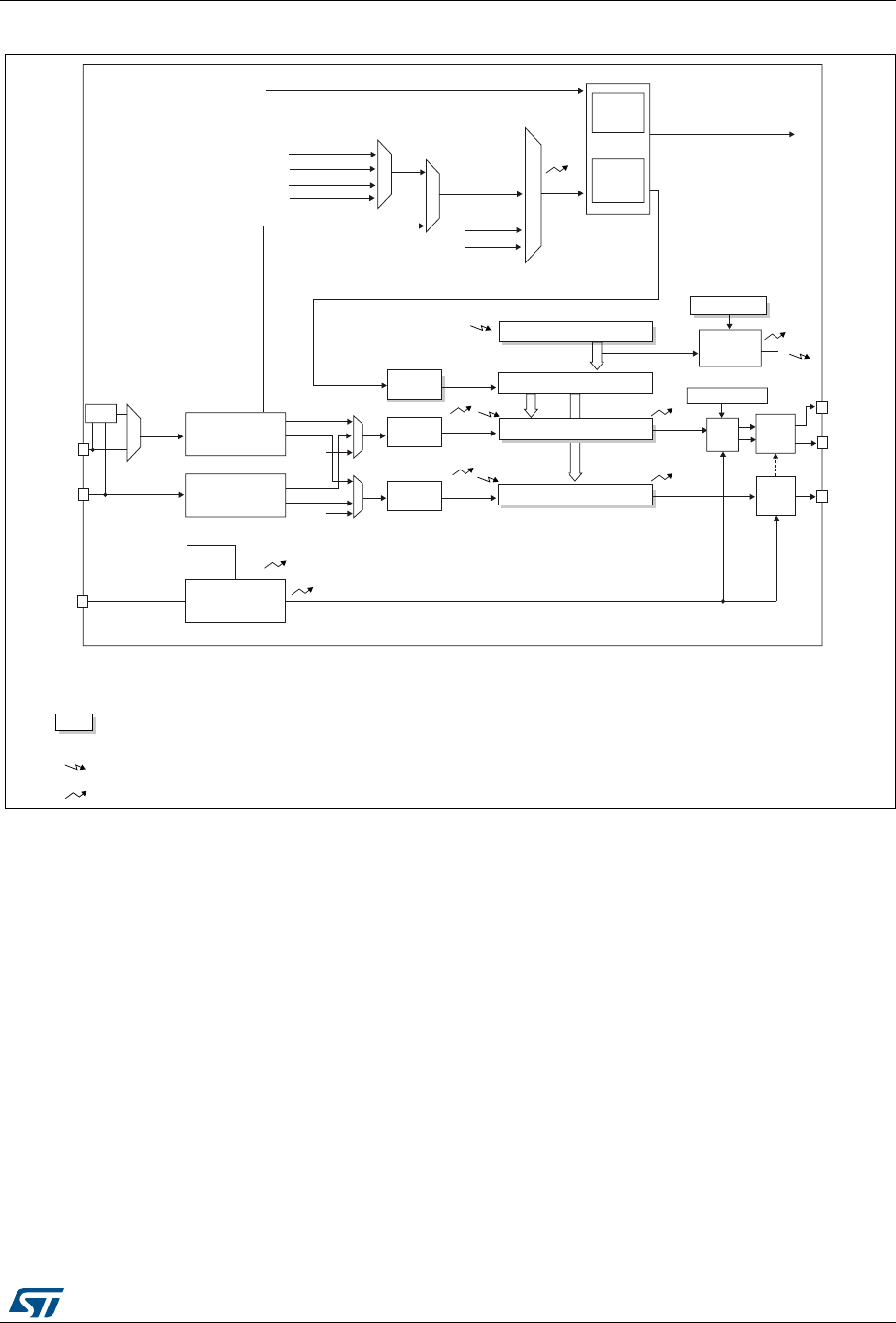
RM0394 Rev 4 889/1600
RM0394 General-purpose timers (TIM15/TIM16)
967
Figure 292. TIM15 block diagram
1. The internal break event source can be:
- A clock failure event generated by CSS. For further information on the CSS, refer to Section 6.2.10: Clock security system
(CSS)
- A PVD output
- SRAM parity error signal
- Cortex®-M4 LOCKUP (Hardfault) output
- COMP output
06Y9
8
8
8
&&,
&&,
7ULJJHU
FRQWUROOHU
6WRSFOHDURUXSGRZQ
7,)3
7,)3
,75
,75
,75 75*,
2XWSXW
FRQWURO
'7*
75*2
2&5()
2&5()
5(3UHJLVWHU
8
5HSHWLWLRQ
FRXQWHU
8,
5HVHWHQDEOHXSFRXQW
&.B36&
,&
,& ,&36
,&36
7,)3
7*,
75&
75&
,75
75&
7,)B('
&&,
&&,
7,)3
7,)3
7,)3
7,
7,
7,0[B&+
7,0[B&+
2&
2&
7,0[B&+
7,0[B&+
7,0[B&+1
2&1
WRRWKHUWLPHUV
6ODYH
FRQWUROOHU
PRGH
36&
SUHVFDOHU &17FRXQWHU
,QWHUQDOFORFN&.B,17
&.B&17
&.B7,0IURP5&&
,75
;25
'7*UHJLVWHUV
,QSXWILOWHU
HGJHGHWHFWRU
&DSWXUH&RPSDUHUHJLVWHU
1RWHV
5HJ 3UHORDGUHJLVWHUVWUDQVIHUUHG
WRDFWLYHUHJLVWHUVRQ8HYHQW
DFFRUGLQJWRFRQWUROELW
(YHQW
,QWHUUXSW'0$RXWSXW
7,0[B%.,1
,QWHUQDOVRXUFHV
6%,)
$XWRUHORDGUHJLVWHU
&DSWXUH&RPSDUHUHJLVWHU
3UHVFDOHU
3UHVFDOHU
,QSXWILOWHU
HGJHGHWHFWRU
2XWSXW
FRQWURO
%UHDNFLUFXLWU\
%,) %5.UHTXHVW
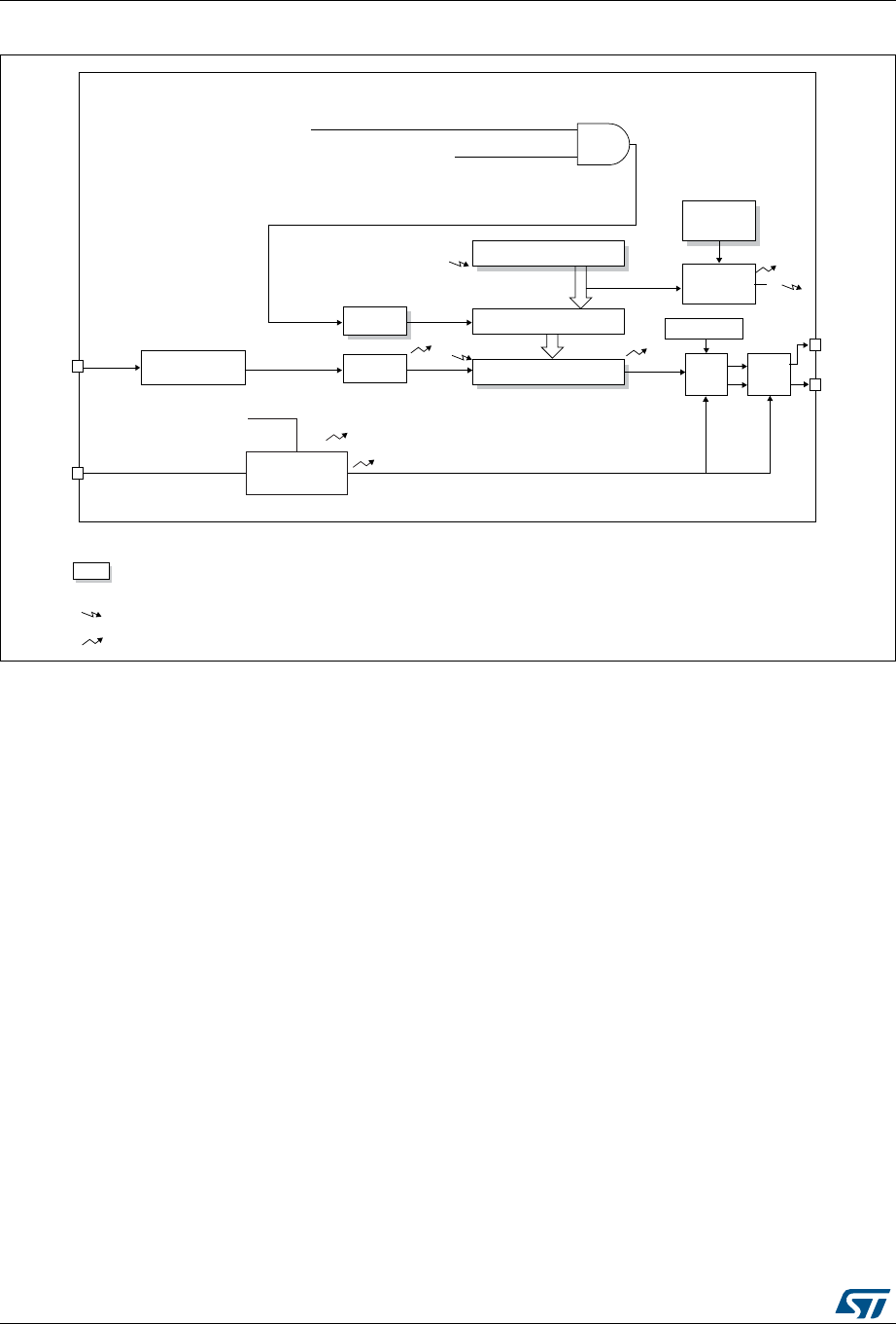
General-purpose timers (TIM15/TIM16) RM0394
890/1600 RM0394 Rev 4
Figure 293. TIM16 block diagram
1. The internal break event source can be:
- A clock failure event generated by CSS. For further information on the CSS, refer to Section 6.2.10: Clock security system
(CSS)
- A PVD output
- SRAM parity error signal
- Cortex®-M4 LOCKUP (Hardfault) output
- COMP output
28.4 Implementation
The extended remap feature described in register TIM16_OR1 is not available on
STM32L471xx devices.
06Y9
,QWHUQDOFORFN&.B,17
&RXQWHU(QDEOH&(1
7,0[B&+
7,0[B%.,1
7, ,QSXWILOWHU
HGJHVHOHFWRU
$XWRUHORDGUHJLVWHU
&17FRXQWHU
&DSWXUHFRPSDUHUHJLVWHU
7,)3 ,&
5(3UHJLVWHU
5HSHWLWLRQ
FRXQWHU
'7*UHJLVWHUV
'7* 2XWSXW
FRQWURO
&.B36& &.B&17
,&36
6WRSFOHDURUXSGRZQ
2&5()
&&,
&,
8
8,
8
2&
2&1
7,0[B&+
7,0[B&+1
8
1RWHV
5HJ 3UHORDGUHJLVWHUVWUDQVIHUUHG
WRDFWLYHUHJLVWHUVRQ8HYHQW
DFFRUGLQJWRFRQWUROELW
(YHQW
,QWHUUXSW'0$RXWSXW
36&
SUHVFDOHU
3UHVFDOHU
,QWHUQDOVRXUFHV
6%,)
%UHDNFLUFXLWU\
%,) %5.UHTXHVW

RM0394 Rev 4 891/1600
RM0394 General-purpose timers (TIM15/TIM16)
967
28.5 TIM15/TIM16 functional description
28.5.1 Time-base unit
The main block of the programmable advanced-control timer is a 16-bit upcounter with its
related auto-reload register. The counter clock can be divided by a prescaler.
The counter, the auto-reload register and the prescaler register can be written or read by
software. This is true even when the counter is running.
The time-base unit includes:
•Counter register (TIMx_CNT)
•Prescaler register (TIMx_PSC)
•Auto-reload register (TIMx_ARR)
•Repetition counter register (TIMx_RCR)
The auto-reload register is preloaded. Writing to or reading from the auto-reload register
accesses the preload register. The content of the preload register are transferred into the
shadow register permanently or at each update event (UEV), depending on the auto-reload
preload enable bit (ARPE) in TIMx_CR1 register. The update event is sent when the counter
reaches the overflow and if the UDIS bit equals 0 in the TIMx_CR1 register. It can also be
generated by software. The generation of the update event is described in detailed for each
configuration.
The counter is clocked by the prescaler output CK_CNT, which is enabled only when the
counter enable bit (CEN) in TIMx_CR1 register is set (refer also to the slave mode controller
description to get more details on counter enabling).
Note that the counter starts counting 1 clock cycle after setting the CEN bit in the TIMx_CR1
register.
Prescaler description
The prescaler can divide the counter clock frequency by any factor between 1 and 65536. It
is based on a 16-bit counter controlled through a 16-bit register (in the TIMx_PSC register).
It can be changed on the fly as this control register is buffered. The new prescaler ratio is
taken into account at the next update event.
Figure 294 and Figure 295 give some examples of the counter behavior when the prescaler
ratio is changed on the fly:
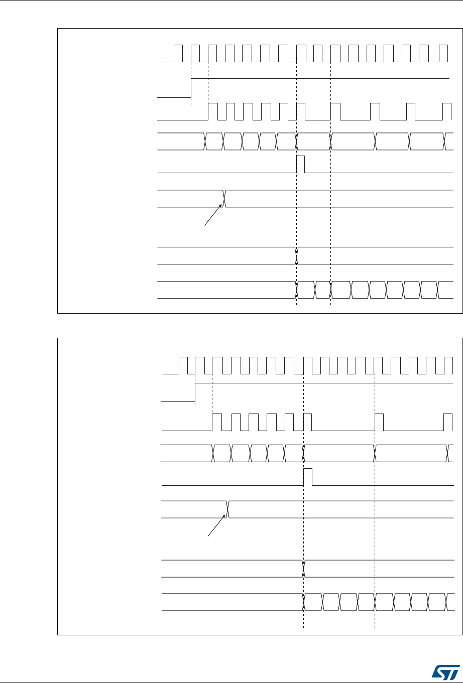
General-purpose timers (TIM15/TIM16) RM0394
892/1600 RM0394 Rev 4
Figure 294. Counter timing diagram with prescaler division change from 1 to 2
Figure 295. Counter timing diagram with prescaler division change from 1 to 4
&.B36&
&(1
7LPHUFORFN &.B&17
&RXQWHUUHJLVWHU
8SGDWHHYHQW8(9
3UHVFDOHUFRQWUROUHJLVWHU
:ULWHDQHZYDOXHLQ7,0[B36&
3UHVFDOHUEXIIHU
3UHVFDOHUFRXQWHU
)$ )%) ) ) )&
069
069
&.B36&
&(1
7LPHUFORFN &.B&17
&RXQWHUUHJLVWHU
8SGDWHHYHQW8(9
3UHVFDOHUFRQWUROUHJLVWHU
:ULWHDQHZYDOXHLQ7,0[B36&
3UHVFDOHUEXIIHU
3UHVFDOHUFRXQWHU
)$ )%
) ) ) )&

RM0394 Rev 4 893/1600
RM0394 General-purpose timers (TIM15/TIM16)
967
28.5.2 Counter modes
Upcounting mode
In upcounting mode, the counter counts from 0 to the auto-reload value (content of the
TIMx_ARR register), then restarts from 0 and generates a counter overflow event.
If the repetition counter is used, the update event (UEV) is generated after upcounting is
repeated for the number of times programmed in the repetition counter register
(TIMx_RCR). Else the update event is generated at each counter overflow.
Setting the UG bit in the TIMx_EGR register (by software or by using the slave mode
controller) also generates an update event.
The UEV event can be disabled by software by setting the UDIS bit in the TIMx_CR1
register. This is to avoid updating the shadow registers while writing new values in the
preload registers. Then no update event occurs until the UDIS bit has been written to 0.
However, the counter restarts from 0, as well as the counter of the prescaler (but the
prescale rate does not change). In addition, if the URS bit (update request selection) in
TIMx_CR1 register is set, setting the UG bit generates an update event UEV but without
setting the UIF flag (thus no interrupt or DMA request is sent). This is to avoid generating
both update and capture interrupts when clearing the counter on the capture event.
When an update event occurs, all the registers are updated and the update flag (UIF bit in
TIMx_SR register) is set (depending on the URS bit):
•The repetition counter is reloaded with the content of TIMx_RCR register,
•The auto-reload shadow register is updated with the preload value (TIMx_ARR),
•The buffer of the prescaler is reloaded with the preload value (content of the TIMx_PSC
register).
The following figures show some examples of the counter behavior for different clock
frequencies when TIMx_ARR=0x36.
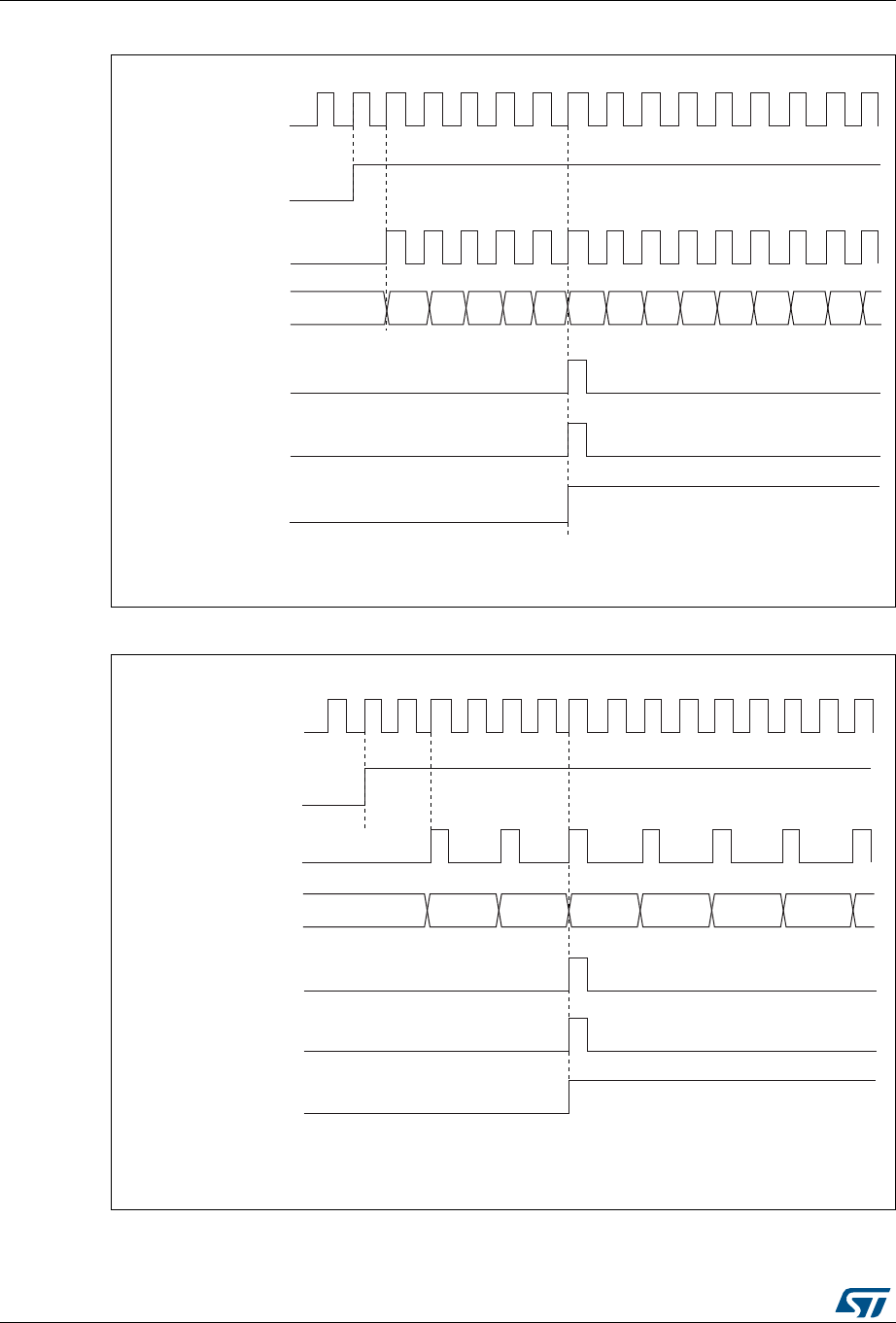
General-purpose timers (TIM15/TIM16) RM0394
894/1600 RM0394 Rev 4
Figure 296. Counter timing diagram, internal clock divided by 1
Figure 297. Counter timing diagram, internal clock divided by 2
069
&.B36&
&17B(1
7LPHUFORFN &.B&17
&RXQWHUUHJLVWHU
8SGDWHHYHQW8(9
&RXQWHURYHUIORZ
8SGDWHLQWHUUXSWIODJ
8,)
069
&.B36&
&17B(1
7LPHUFORFN &.B&17
&RXQWHUUHJLVWHU
8SGDWHHYHQW8(9
&RXQWHURYHUIORZ
8SGDWHLQWHUUXSWIODJ
8,)

RM0394 Rev 4 895/1600
RM0394 General-purpose timers (TIM15/TIM16)
967
Figure 298. Counter timing diagram, internal clock divided by 4
Figure 299. Counter timing diagram, internal clock divided by N
069
&.B36&
7LPHUFORFN &.B&17
&RXQWHUUHJLVWHU
8SGDWHHYHQW8(9
&RXQWHURYHUIORZ
8SGDWHLQWHUUXSWIODJ
8,)
&17B(1
)
069
&.B36&
7LPHUFORFN &.B&17
&RXQWHUUHJLVWHU
8SGDWHHYHQW8(9
&RXQWHURYHUIORZ
8SGDWHLQWHUUXSWIODJ
8,)
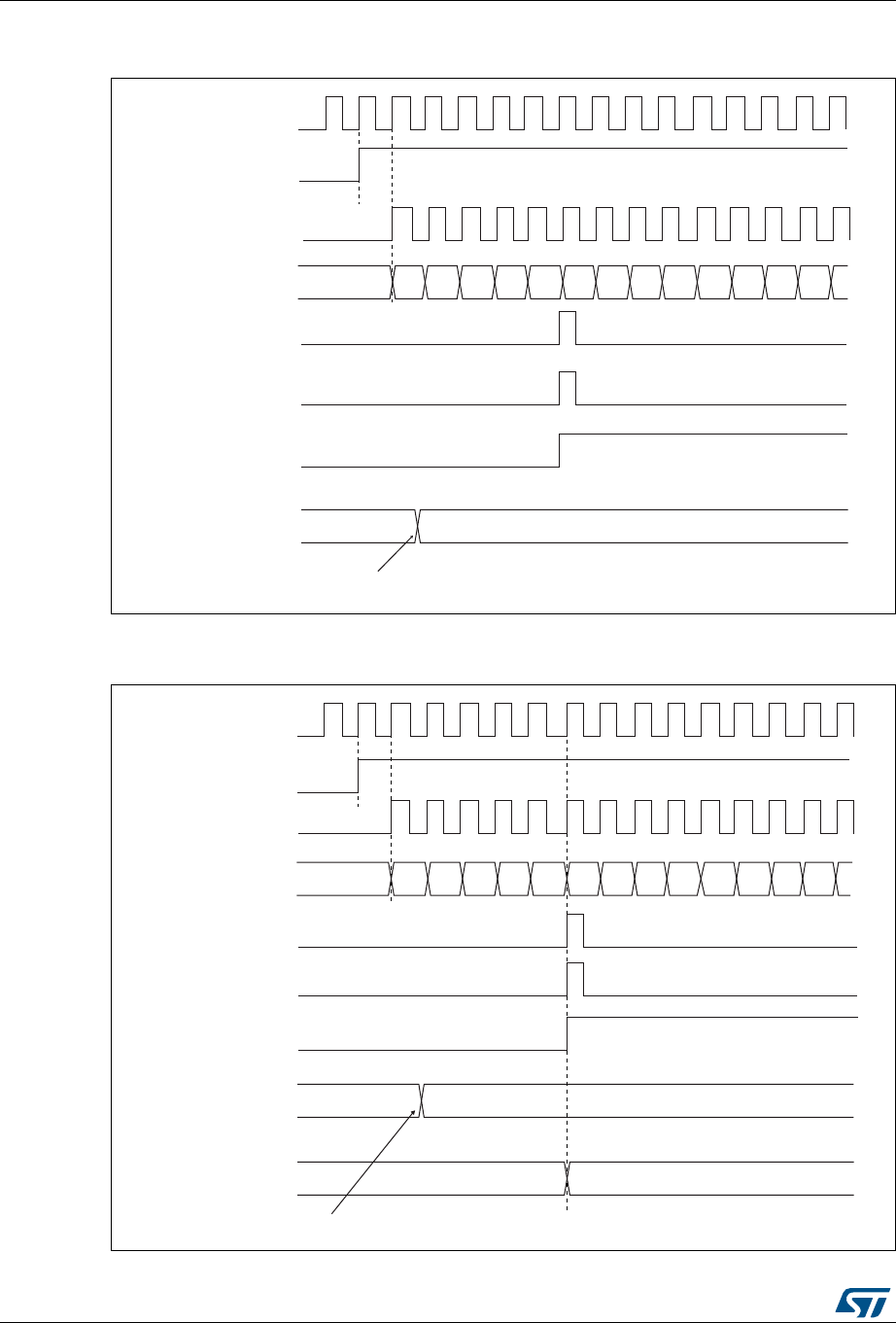
General-purpose timers (TIM15/TIM16) RM0394
896/1600 RM0394 Rev 4
Figure 300. Counter timing diagram, update event when ARPE=0 (TIMx_ARR not
preloaded)
Figure 301. Counter timing diagram, update event when ARPE=1 (TIMx_ARR
preloaded)
))
069
&.B36&
7LPHUFORFN &.B&17
&RXQWHUUHJLVWHU
8SGDWHHYHQW8(9
&RXQWHURYHUIORZ
8SGDWHLQWHUUXSWIODJ
8,)
&(1
$XWRUHORDGSUHORDG
UHJLVWHU
:ULWHDQHZYDOXHLQ7,0[B$55
069
)
&.B36&
7LPHUFORFN &.B&17
&RXQWHUUHJLVWHU
8SGDWHHYHQW8(9
&RXQWHURYHUIORZ
8SGDWHLQWHUUXSWIODJ
8,)
) ) ) ) ))
&(1
$XWRUHORDGSUHORDG
UHJLVWHU
:ULWHDQHZYDOXHLQ7,0[B$55
$XWRUHORDGVKDGRZ
UHJLVWHU )

RM0394 Rev 4 897/1600
RM0394 General-purpose timers (TIM15/TIM16)
967
28.5.3 Repetition counter
Section 28.5.1: Time-base unit describes how the update event (UEV) is generated with
respect to the counter overflows. It is actually generated only when the repetition counter
has reached zero. This can be useful when generating PWM signals.
This means that data are transferred from the preload registers to the shadow registers
(TIMx_ARR auto-reload register, TIMx_PSC prescaler register, but also TIMx_CCRx
capture/compare registers in compare mode) every N counter overflows, where N is the
value in the TIMx_RCR repetition counter register.
The repetition counter is decremented at each counter overflow.
The repetition counter is an auto-reload type; the repetition rate is maintained as defined by
the TIMx_RCR register value (refer to Figure 302). When the update event is generated by
software (by setting the UG bit in TIMx_EGR register) or by hardware through the slave
mode controller, it occurs immediately whatever the value of the repetition counter is and the
repetition counter is reloaded with the content of the TIMx_RCR register.
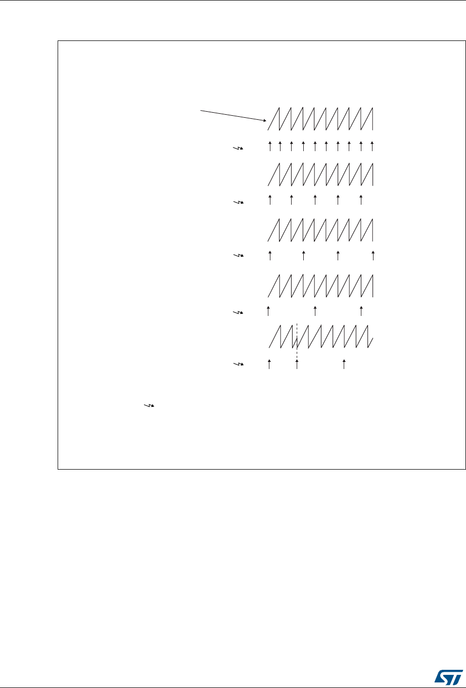
General-purpose timers (TIM15/TIM16) RM0394
898/1600 RM0394 Rev 4
Figure 302. Update rate examples depending on mode and TIMx_RCR register
settings
28.5.4 Clock selection
The counter clock can be provided by the following clock sources:
•Internal clock (CK_INT)
•External clock mode1: external input pin
•Internal trigger inputs (ITRx) (only for TIM15): using one timer as the prescaler for
another timer, for example, you can configure TIM1 to act as a prescaler for TIM15.
Refer to Using one timer as prescaler for another timer on page 857 for more details.
Internal clock source (CK_INT)
If the slave mode controller is disabled (SMS=000), then the CEN (in the TIMx_CR1
register) and UG bits (in the TIMx_EGR register) are actual control bits and can be changed
(GJHDOLJQHGPRGH
8(9 8SGDWH(YHQWSUHORDGUHJLVWHUVWUDQVIHUUHGWRDFWLYHUHJLVWHUV
DQGXSGDWHLQWHUUXSWJHQHUDWHG
&RXQWHU
7,0[B&17
7,0[B5&5 8(9
7,0[B5&5 8(9
7,0[B5&5 8(9
7,0[B5&5 8(9
7,0[B5&5
DQG
UHV\QFKURQL]DWLRQ8(9
E\6:
8SFRXQWLQJ
069
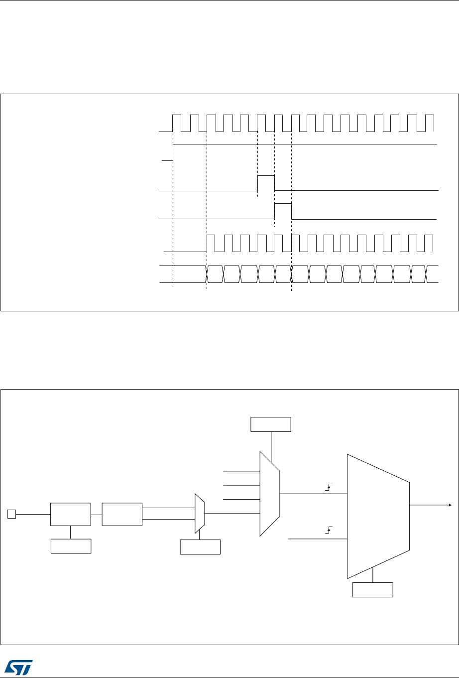
RM0394 Rev 4 899/1600
RM0394 General-purpose timers (TIM15/TIM16)
967
only by software (except UG which remains cleared automatically). As soon as the CEN bit
is written to 1, the prescaler is clocked by the internal clock CK_INT.
Figure 303 shows the behavior of the control circuit and the upcounter in normal mode,
without prescaler.
Figure 303. Control circuit in normal mode, internal clock divided by 1
External clock source mode 1
This mode is selected when SMS=111 in the TIMx_SMCR register. The counter can count at
each rising or falling edge on a selected input.
Figure 304. TI2 external clock connection example
,QWHUQDOFORFN
&RXQWHUFORFN &.B&17 &.B36&
&RXQWHUUHJLVWHU
&(1 &17B(1
8*
&17B,1,7
069
([WHUQDOFORFN
PRGH
,QWHUQDOFORFN
PRGH
75*,
&.B,17
&.B36&
7,0[B60&5
606>@
,75[
7,B('
7,)3
7,)3
7,0[B60&5
76>@
7,
7,0[B&&(5
&&3
)LOWHU
,&)>@
7,0[B&&05
(GJH
GHWHFWRU
7,)B5LVLQJ
7,)B)DOOLQJ
[[
069
LQWHUQDOFORFN
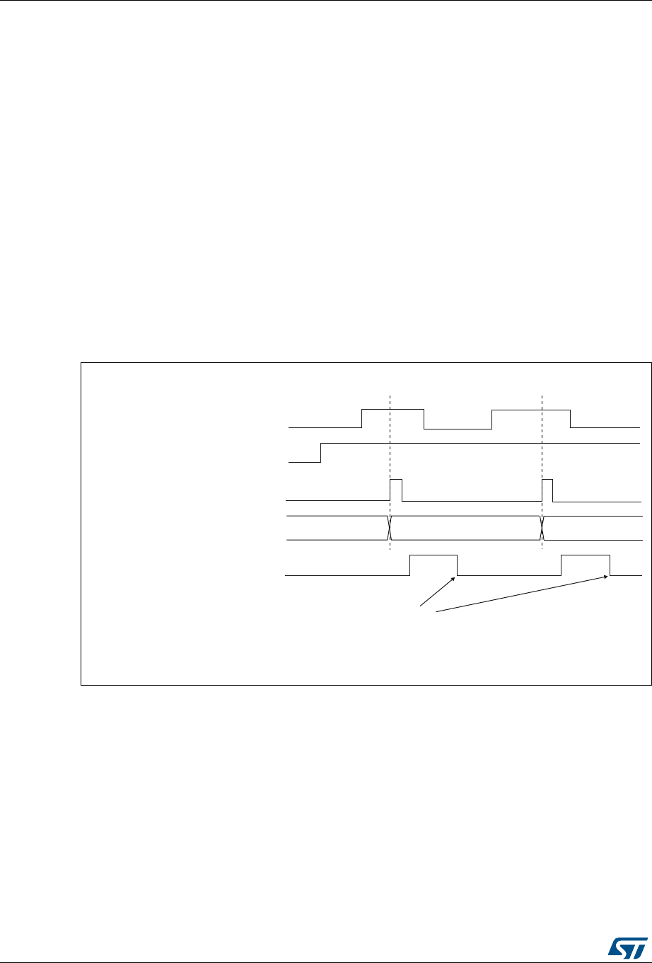
General-purpose timers (TIM15/TIM16) RM0394
900/1600 RM0394 Rev 4
For example, to configure the upcounter to count in response to a rising edge on the TI2
input, use the following procedure:
1. Configure channel 2 to detect rising edges on the TI2 input by writing CC2S = ‘01’ in
the TIMx_CCMR1 register.
2. Configure the input filter duration by writing the IC2F[3:0] bits in the TIMx_CCMR1
register (if no filter is needed, keep IC2F=0000).
3. Select rising edge polarity by writing CC2P=0 in the TIMx_CCER register.
4. Configure the timer in external clock mode 1 by writing SMS=111 in the TIMx_SMCR
register.
5. Select TI2 as the trigger input source by writing TS=110 in the TIMx_SMCR register.
6. Enable the counter by writing CEN=1 in the TIMx_CR1 register.
Note: The capture prescaler is not used for triggering, so you don’t need to configure it.
When a rising edge occurs on TI2, the counter counts once and the TIF flag is set.
The delay between the rising edge on TI2 and the actual clock of the counter is due to the
resynchronization circuit on TI2 input.
Figure 305. Control circuit in external clock mode 1
28.5.5 Capture/compare channels
Each Capture/Compare channel is built around a capture/compare register (including a
shadow register), a input stage for capture (with digital filter, multiplexing and prescaler) and
an output stage (with comparator and output control).
Figure 306 to Figure 309 give an overview of one Capture/Compare channel.
The input stage samples the corresponding TIx input to generate a filtered signal TIxF.
Then, an edge detector with polarity selection generates a signal (TIxFPx) which can be
used as trigger input by the slave mode controller or as the capture command. It is
prescaled before the capture register (ICxPS).
&RXQWHUFORFN &.B&17 &.B36&
&RXQWHUUHJLVWHU
7,
&17B(1
7,)
:ULWH7,)
069
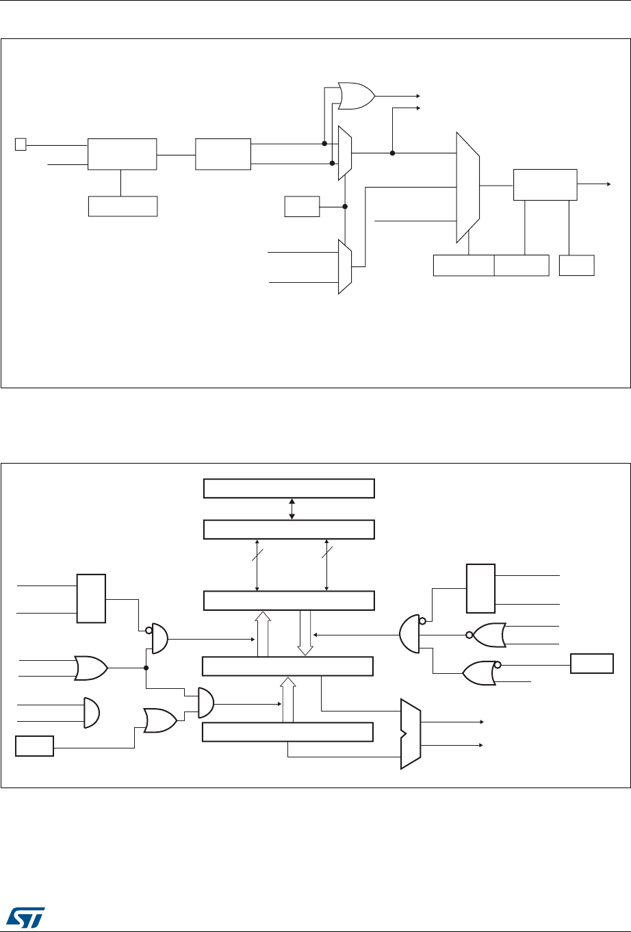
RM0394 Rev 4 901/1600
RM0394 General-purpose timers (TIM15/TIM16)
967
Figure 306. Capture/compare channel (example: channel 1 input stage)
The output stage generates an intermediate waveform which is then used for reference:
OCxRef (active high). The polarity acts at the end of the chain.
Figure 307. Capture/compare channel 1 main circuit
'LYLGHU
,&36>@
7,)B('
7RWKHVODYHPRGHFRQWUROOHU
7,)3
&&6>@
,&
7,)3
75&
IURPVODYHPRGH
FRQWUROOHU
,&36
069
7,
7,0[B&&(5
&&3
)LOWHU
GRZQFRXQWHU
,&)>@
7,0[B&&05
(GJH
GHWHFWRU
7,)B5LVLQJ
7,)B)DOOLQJ
7,0[B&&05
7,0[B&&(5
7,)B5LVLQJ
IURPFKDQQHO
7,)B)DOOLQJ
IURPFKDQQHO
7,)
I
&&(
'76
069
&&(
&DSWXUHFRPSDUH VKDGRZ UHJLVWHU
&RPSDUDWRU
&DSWXUHFRPSDUHSUHORDGUHJLVWHU
&RXQWHU
,&36
&&6>@
&&6>@
&DSWXUH
,QSXW
PRGH
6
5
5HDG&&5+
5HDG&&5/
UHDGBLQBSURJUHVV
FDSWXUHBWUDQVIHU &&6>@
&&6>@
6
5
ZULWH&&5+
ZULWH&&5/
ZULWHBLQBSURJUHVV
2XWSXW
PRGH
8(9
2&3(
IURPWLPH
EDVHXQLW
FRPSDUHBWUDQVIHU
$3%%XV
KLJK
ORZ
LIELW
0&8SHULSKHUDOLQWHUIDFH
7,0[B&&05
2&3(
&17!&&5
&17 &&5
7,0[B(*5
&&*
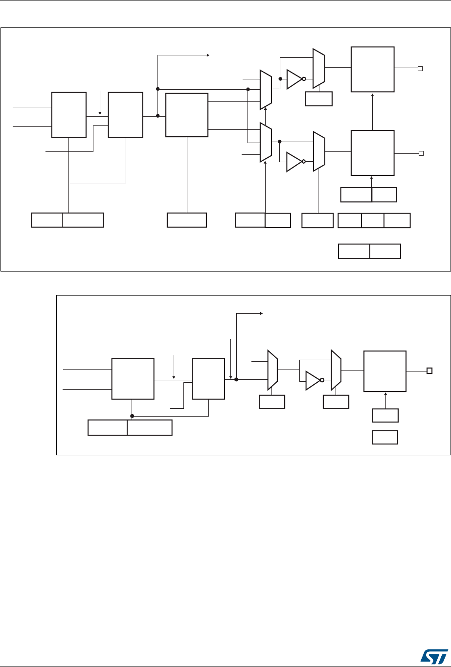
General-purpose timers (TIM15/TIM16) RM0394
902/1600 RM0394 Rev 4
Figure 308. Output stage of capture/compare channel (channel 1)
Figure 309. Output stage of capture/compare channel (channel 2 for TIM15)
The capture/compare block is made of one preload register and one shadow register. Write
and read always access the preload register.
In capture mode, captures are actually done in the shadow register, which is copied into the
preload register.
In compare mode, the content of the preload register is copied into the shadow register
which is compared to the counter.
28.5.6 Input capture mode
In Input capture mode, the Capture/Compare Registers (TIMx_CCRx) are used to latch the
value of the counter after a transition detected by the corresponding ICx signal. When a
capture occurs, the corresponding CCXIF flag (TIMx_SR register) is set and an interrupt or
a DMA request can be sent if they are enabled. If a capture occurs while the CCxIF flag was
069
2XWSXW
PRGH
FRQWUROOHU
&17!&&5
&17 &&5
7,0[B&&05
2&0>@
2&5()
2&&(
'HDGWLPH
JHQHUDWRU
2&B'7
2&1B'7
'7*>@
7,0[B%'75
µ
µ
&&(
7,0[B&&(5
&&1(
&&3
7,0B&&(5
&&13
7,0[B&&(5
2&
2XWSXW
HQDEOH
FLUFXLW
2&1
&&( 7,0[B&&(5
&&1(
266,
7,0[B%'75
02( 2665
[
[
2XWSXW
VHOHFWRU
2&5()
2&5()&
7RWKHPDVWHUPRGH
FRQWUROOHU
2XWSXW
HQDEOH
FLUFXLW
2,6 2,61 7,0[B&5
069
2XWSXW
PRGH
FRQWUROOHU
&17!&&5
&17 &&5
7,0[B&&05
2&0>@
&&3
7,0[B&&(5
2XWSXW
HQDEOH
FLUFXLW
2&
&&( 7,0[B&&(5
7RWKHPDVWHU
PRGHFRQWUROOHU
2&5()
2XWSXW
VHOHFWRU
2&5()
2&&(
&&(
7,0[B&&(5
2&5()&
µ
2,6 7,0[B&5

RM0394 Rev 4 903/1600
RM0394 General-purpose timers (TIM15/TIM16)
967
already high, then the over-capture flag CCxOF (TIMx_SR register) is set. CCxIF can be
cleared by software by writing it to ‘0’ or by reading the captured data stored in the
TIMx_CCRx register. CCxOF is cleared when you write it to ‘0’.
The following example shows how to capture the counter value in TIMx_CCR1 when TI1
input rises. To do this, use the following procedure:
1. Select the active input: TIMx_CCR1 must be linked to the TI1 input, so write the CC1S
bits to 01 in the TIMx_CCMR1 register. As soon as CC1S becomes different from 00,
the channel is configured in input and the TIMx_CCR1 register becomes read-only.
2. Program the input filter duration you need with respect to the signal you connect to the
timer (when the input is one of the TIx (ICxF bits in the TIMx_CCMRx register). Let’s
imagine that, when toggling, the input signal is not stable during at least 5 internal clock
cycles. We must program a filter duration longer than these 5 clock cycles. We can
validate a transition on TI1 when 8 consecutive samples with the new level have been
detected (sampled at fDTS frequency). Then write IC1F bits to 0011 in the
TIMx_CCMR1 register.
3. Select the edge of the active transition on the TI1 channel by writing CC1P bit to 0 in
the TIMx_CCER register (rising edge in this case).
4. Program the input prescaler. In our example, we wish the capture to be performed at
each valid transition, so the prescaler is disabled (write IC1PS bits to ‘00’ in the
TIMx_CCMR1 register).
5. Enable capture from the counter into the capture register by setting the CC1E bit in the
TIMx_CCER register.
6. If needed, enable the related interrupt request by setting the CC1IE bit in the
TIMx_DIER register, and/or the DMA request by setting the CC1DE bit in the
TIMx_DIER register.
When an input capture occurs:
•The TIMx_CCR1 register gets the value of the counter on the active transition.
•CC1IF flag is set (interrupt flag). CC1OF is also set if at least two consecutive captures
occurred whereas the flag was not cleared.
•An interrupt is generated depending on the CC1IE bit.
•A DMA request is generated depending on the CC1DE bit.
In order to handle the overcapture, it is recommended to read the data before the
overcapture flag. This is to avoid missing an overcapture which could happen after reading
the flag and before reading the data.
Note: IC interrupt and/or DMA requests can be generated by software by setting the
corresponding CCxG bit in the TIMx_EGR register.
28.5.7 PWM input mode (only for TIM15)
This mode is a particular case of input capture mode. The procedure is the same except:
•Two ICx signals are mapped on the same TIx input.
•These 2 ICx signals are active on edges with opposite polarity.
•One of the two TIxFP signals is selected as trigger input and the slave mode controller
is configured in reset mode.
For example, you can measure the period (in TIMx_CCR1 register) and the duty cycle (in
TIMx_CCR2 register) of the PWM applied on TI1 using the following procedure (depending
on CK_INT frequency and prescaler value):
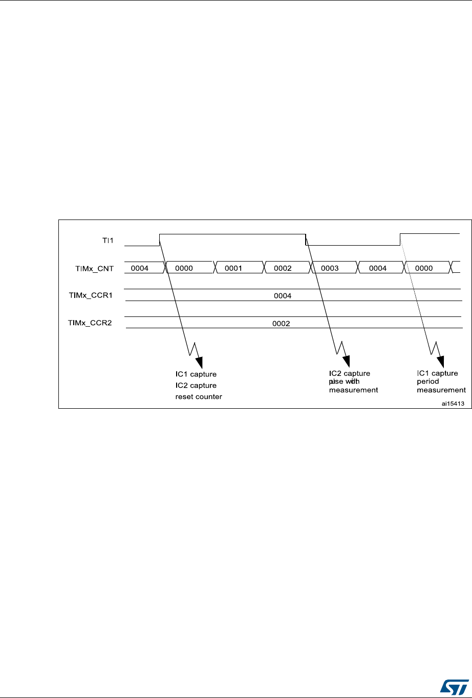
General-purpose timers (TIM15/TIM16) RM0394
904/1600 RM0394 Rev 4
1. Select the active input for TIMx_CCR1: write the CC1S bits to 01 in the TIMx_CCMR1
register (TI1 selected).
2. Select the active polarity for TI1FP1 (used both for capture in TIMx_CCR1 and counter
clear): write the CC1P and CC1NP bits to ‘0’ (active on rising edge).
3. Select the active input for TIMx_CCR2: write the CC2S bits to 10 in the TIMx_CCMR1
register (TI1 selected).
4. Select the active polarity for TI1FP2 (used for capture in TIMx_CCR2): write the CC2P
and CC2NP bits to ‘1’ (active on falling edge).
5. Select the valid trigger input: write the TS bits to 101 in the TIMx_SMCR register
(TI1FP1 selected).
6. Configure the slave mode controller in reset mode: write the SMS bits to 100 in the
TIMx_SMCR register.
7. Enable the captures: write the CC1E and CC2E bits to ‘1’ in the TIMx_CCER register.
Figure 310. PWM input mode timing
1. The PWM input mode can be used only with the TIMx_CH1/TIMx_CH2 signals due to the fact that only
TI1FP1 and TI2FP2 are connected to the slave mode controller.
28.5.8 Forced output mode
In output mode (CCxS bits = 00 in the TIMx_CCMRx register), each output compare signal
(OCxREF and then OCx/OCxN) can be forced to active or inactive level directly by software,
independently of any comparison between the output compare register and the counter.
To force an output compare signal (OCXREF/OCx) to its active level, you just need to write
101 in the OCxM bits in the corresponding TIMx_CCMRx register. Thus OCXREF is forced
high (OCxREF is always active high) and OCx get opposite value to CCxP polarity bit.
For example: CCxP=0 (OCx active high) => OCx is forced to high level.
The OCxREF signal can be forced low by writing the OCxM bits to 100 in the TIMx_CCMRx
register.
Anyway, the comparison between the TIMx_CCRx shadow register and the counter is still
performed and allows the flag to be set. Interrupt and DMA requests can be sent
accordingly. This is described in the output compare mode section below.

RM0394 Rev 4 905/1600
RM0394 General-purpose timers (TIM15/TIM16)
967
28.5.9 Output compare mode
This function is used to control an output waveform or indicating when a period of time has
elapsed.
When a match is found between the capture/compare register and the counter, the output
compare function:
•Assigns the corresponding output pin to a programmable value defined by the output
compare mode (OCxM bits in the TIMx_CCMRx register) and the output polarity (CCxP
bit in the TIMx_CCER register). The output pin can keep its level (OCXM=000), be set
active (OCxM=001), be set inactive (OCxM=010) or can toggle (OCxM=011) on match.
•Sets a flag in the interrupt status register (CCxIF bit in the TIMx_SR register).
•Generates an interrupt if the corresponding interrupt mask is set (CCXIE bit in the
TIMx_DIER register).
•Sends a DMA request if the corresponding enable bit is set (CCxDE bit in the
TIMx_DIER register, CCDS bit in the TIMx_CR2 register for the DMA request
selection).
The TIMx_CCRx registers can be programmed with or without preload registers using the
OCxPE bit in the TIMx_CCMRx register.
In output compare mode, the update event UEV has no effect on OCxREF and OCx output.
The timing resolution is one count of the counter. Output compare mode can also be used to
output a single pulse (in One-pulse mode).
Procedure
1. Select the counter clock (internal, external, prescaler).
2. Write the desired data in the TIMx_ARR and TIMx_CCRx registers.
3. Set the CCxIE bit if an interrupt request is to be generated.
4. Select the output mode. For example:
– Write OCxM = 011 to toggle OCx output pin when CNT matches CCRx
– Write OCxPE = 0 to disable preload register
– Write CCxP = 0 to select active high polarity
– Write CCxE = 1 to enable the output
5. Enable the counter by setting the CEN bit in the TIMx_CR1 register.
The TIMx_CCRx register can be updated at any time by software to control the output
waveform, provided that the preload register is not enabled (OCxPE=’0’, else TIMx_CCRx
shadow register is updated only at the next update event UEV). An example is given in
Figure 311.

General-purpose timers (TIM15/TIM16) RM0394
906/1600 RM0394 Rev 4
Figure 311. Output compare mode, toggle on OC1
28.5.10 PWM mode
Pulse Width Modulation mode allows you to generate a signal with a frequency determined
by the value of the TIMx_ARR register and a duty cycle determined by the value of the
TIMx_CCRx register.
The PWM mode can be selected independently on each channel (one PWM per OCx
output) by writing ‘110’ (PWM mode 1) or ‘111’ (PWM mode 2) in the OCxM bits in the
TIMx_CCMRx register. You must enable the corresponding preload register by setting the
OCxPE bit in the TIMx_CCMRx register, and eventually the auto-reload preload register (in
upcounting or center-aligned modes) by setting the ARPE bit in the TIMx_CR1 register.
As the preload registers are transferred to the shadow registers only when an update event
occurs, before starting the counter, you have to initialize all the registers by setting the UG
bit in the TIMx_EGR register.
OCx polarity is software programmable using the CCxP bit in the TIMx_CCER register. It
can be programmed as active high or active low. OCx output is enabled by a combination of
the CCxE, CCxNE, MOE, OSSI and OSSR bits (TIMx_CCER and TIMx_BDTR registers).
Refer to the TIMx_CCER register description for more details.
In PWM mode (1 or 2), TIMx_CNT and TIMx_CCRx are always compared to determine
whether TIMx_CCRx TIMx_CNT or TIMx_CNT TIMx_CCRx (depending on the direction
of the counter).
The TIM15/TIM16 are capable of upcounting only. Refer to Upcounting mode on page 893.
In the following example, we consider PWM mode 1. The reference PWM signal OCxREF is
high as long as TIMx_CNT < TIMx_CCRx else it becomes low. If the compare value in
TIMx_CCRx is greater than the auto-reload value (in TIMx_ARR) then OCxREF is held at
‘1’. If the compare value is 0 then OCxRef is held at ‘0’. Figure 312 shows some edge-
aligned PWM waveforms in an example where TIMx_ARR=8.
069
2&5() 2&
7,0B&17 % %
7,0B&&5 $
:ULWH%KLQWKH&&5UHJLVWHU
0DWFKGHWHFWHGRQ&&5
,QWHUUXSWJHQHUDWHGLIHQDEOHG
%
%
$
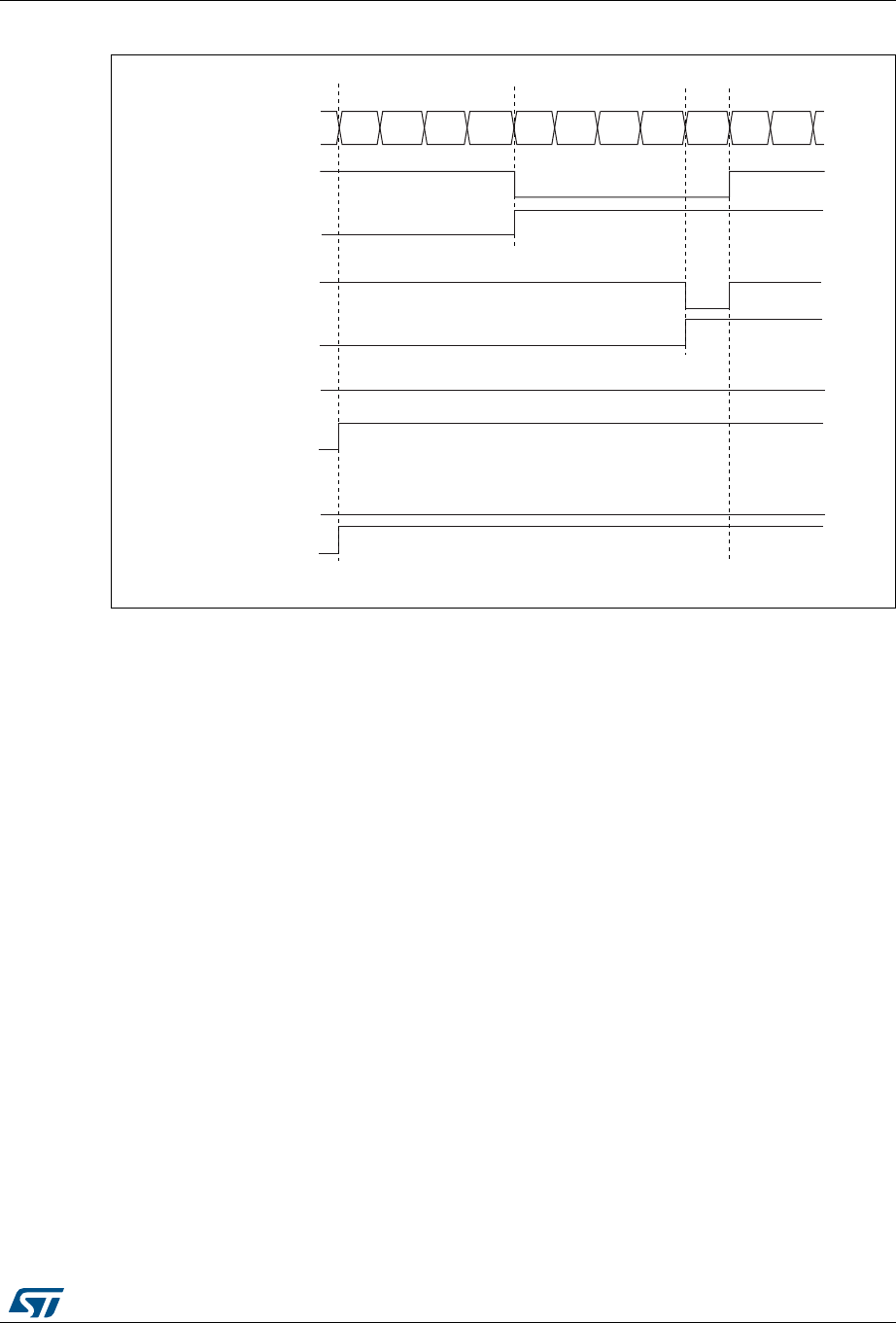
RM0394 Rev 4 907/1600
RM0394 General-purpose timers (TIM15/TIM16)
967
Figure 312. Edge-aligned PWM waveforms (ARR=8)
28.5.11 Combined PWM mode (TIM15 only)
Combined PWM mode allows two edge or center-aligned PWM signals to be generated with
programmable delay and phase shift between respective pulses. While the frequency is
determined by the value of the TIMx_ARR register, the duty cycle and delay are determined
by the two TIMx_CCRx registers. The resulting signals, OCxREFC, are made of an OR or
AND logical combination of two reference PWMs:
•OC1REFC (or OC2REFC) is controlled by the TIMx_CCR1 and TIMx_CCR2 registers
Combined PWM mode can be selected independently on two channels (one OCx output per
pair of CCR registers) by writing ‘1100’ (Combined PWM mode 1) or ‘1101’ (Combined PWM
mode 2) in the OCxM bits in the TIMx_CCMRx register.
When a given channel is used as a combined PWM channel, its complementary channel
must be configured in the opposite PWM mode (for instance, one in Combined PWM mode
1 and the other in Combined PWM mode 2).
Note: The OCxM[3:0] bit field is split into two parts for compatibility reasons, the most significant
bit is not contiguous with the 3 least significant ones.
Figure 313 represents an example of signals that can be generated using Asymmetric PWM
mode, obtained with the following configuration:
•Channel 1 is configured in Combined PWM mode 2,
•Channel 2 is configured in PWM mode 1,
069
&RXQWHUUHJLVWHU
µ
2&;5()
&&[,)
2&;5()
&&[,)
2&;5()
&&[,)
2&;5()
&&[,)
&&5[
&&5[
&&5[!
&&5[
µ
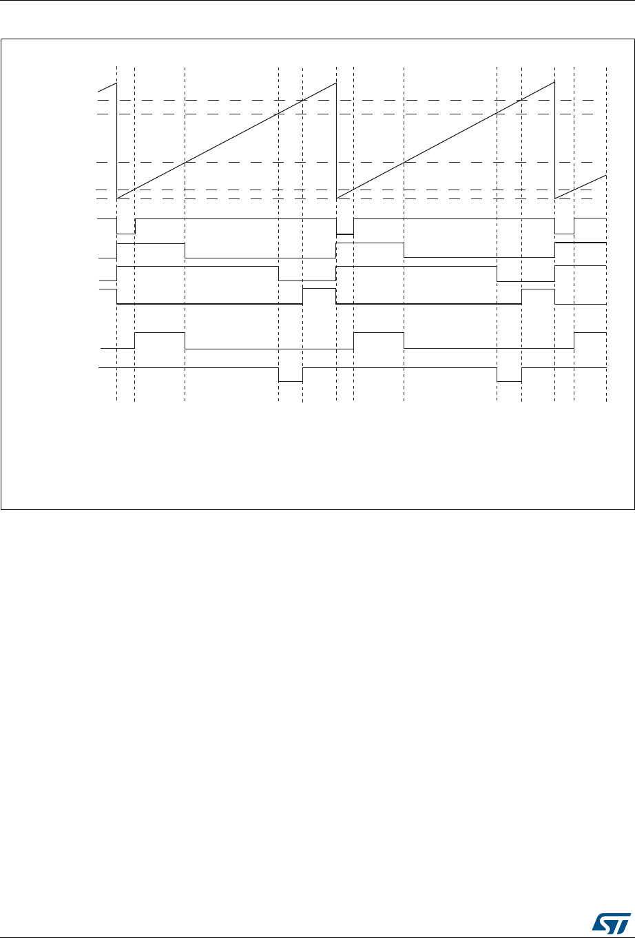
General-purpose timers (TIM15/TIM16) RM0394
908/1600 RM0394 Rev 4
Figure 313. Combined PWM mode on channel 1 and 2
28.5.12 Complementary outputs and dead-time insertion
The TIM15/TIM16 general-purpose timers can output one complementary signal and
manage the switching-off and switching-on of the outputs.
This time is generally known as dead-time and you have to adjust it depending on the
devices you have connected to the outputs and their characteristics (intrinsic delays of level-
shifters, delays due to power switches...)
You can select the polarity of the outputs (main output OCx or complementary OCxN)
independently for each output. This is done by writing to the CCxP and CCxNP bits in the
TIMx_CCER register.
The complementary signals OCx and OCxN are activated by a combination of several
control bits: the CCxE and CCxNE bits in the TIMx_CCER register and the MOE, OISx,
OISxN, OSSI and OSSR bits in the TIMx_BDTR and TIMx_CR2 registers. Refer to
Table 142: Output control bits for complementary OCx and OCxN channels with break
feature (TIM16/17) on page 958 for more details. In particular, the dead-time is activated
when switching to the idle state (MOE falling down to 0).
Dead-time insertion is enabled by setting both CCxE and CCxNE bits, and the MOE bit if the
break circuit is present. There is one 10-bit dead-time generator for each channel. From a
069
2&5()
2&5()
2&5()
2&5()
2&5()&
2&5()&
2&5()& 2&5()$1'2&5()
2&5()&¶ 2&5()¶252&5()
2&
2&
2&
2&
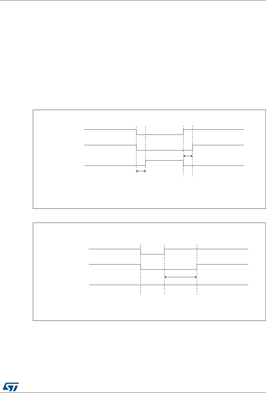
RM0394 Rev 4 909/1600
RM0394 General-purpose timers (TIM15/TIM16)
967
reference waveform OCxREF, it generates 2 outputs OCx and OCxN. If OCx and OCxN are
active high:
•The OCx output signal is the same as the reference signal except for the rising edge,
which is delayed relative to the reference rising edge.
•The OCxN output signal is the opposite of the reference signal except for the rising
edge, which is delayed relative to the reference falling edge.
If the delay is greater than the width of the active output (OCx or OCxN) then the
corresponding pulse is not generated.
The following figures show the relationships between the output signals of the dead-time
generator and the reference signal OCxREF. (we suppose CCxP=0, CCxNP=0, MOE=1,
CCxE=1 and CCxNE=1 in these examples)
Figure 314. Complementary output with dead-time insertion.
Figure 315. Dead-time waveforms with delay greater than the negative pulse.
GHOD\
GHOD\
2&[5()
2&[
2&[1
069
069
GHOD\
2&[5()
2&[
2&[1

General-purpose timers (TIM15/TIM16) RM0394
910/1600 RM0394 Rev 4
Figure 316. Dead-time waveforms with delay greater than the positive pulse.
The dead-time delay is the same for each of the channels and is programmable with the
DTG bits in the TIMx_BDTR register. Refer to Section 28.7.13: TIM16 break and dead-time
register (TIM16_BDTR) on page 961 for delay calculation.
Re-directing OCxREF to OCx or OCxN
In output mode (forced, output compare or PWM), OCxREF can be re-directed to the OCx
output or to OCxN output by configuring the CCxE and CCxNE bits in the TIMx_CCER
register.
This allows you to send a specific waveform (such as PWM or static active level) on one
output while the complementary remains at its inactive level. Other alternative possibilities
are to have both outputs at inactive level or both outputs active and complementary with
dead-time.
Note: When only OCxN is enabled (CCxE=0, CCxNE=1), it is not complemented and becomes
active as soon as OCxREF is high. For example, if CCxNP=0 then OCxN=OCxRef. On the
other hand, when both OCx and OCxN are enabled (CCxE=CCxNE=1) OCx becomes
active when OCxREF is high whereas OCxN is complemented and becomes active when
OCxREF is low.
28.5.13 Using the break function
The purpose of the break function is to protect power switches driven by PWM signals
generated with the TIM15/TIM16 timers. The break input is usually connected to fault
outputs of power stages and 3-phase inverters. When activated, the break circuitry shuts
down the PWM outputs and forces them to a predefined safe state.
The break channel gathers both system-level fault (clock failure, parity error,...) and
application fault (from input pins and built-in comparator), and can force the outputs to a
predefined level (either active or inactive) after a deadtime duration.
069
GHOD\
2&[5()
2&[
2&[1

RM0394 Rev 4 911/1600
RM0394 General-purpose timers (TIM15/TIM16)
967
The output enable signal and output levels during break are depending on several control
bits:
•the MOE bit in TIMx_BDTR register allows to enable /disable the outputs by software
and is reset in case of break or break2 event.
•the OSSI bit in the TIMx_BDTR register defines whether the timer controls the output in
inactive state or releases the control to the GPIO controller (typically to have it in Hi-Z
mode)
•the OISx and OISxN bits in the TIMx_CR2 register which are setting the output shut-
down level, either active or inactive. The OCx and OCxN outputs cannot be set both to
active level at a given time, whatever the OISx and OISxN values. Refer to Table 140:
Output control bits for complementary OCx and OCxN channels with break feature
(TIM15) on page 938 for more details.
When exiting from reset, the break circuit is disabled and the MOE bit is low. The break
function is enabled by setting the BKE bit in the TIMx_BDTR register. The break input
polarity can be selected by configuring the BKP bit in the same register. BKE and BKP can
be modified at the same time. When the BKE and BKP bits are written, a delay of 1 APB
clock cycle is applied before the writing is effective. Consequently, it is necessary to wait 1
APB clock period to correctly read back the bit after the write operation.
Because MOE falling edge can be asynchronous, a resynchronization circuit has been
inserted between the actual signal (acting on the outputs) and the synchronous control bit
(accessed in the TIMx_BDTR register). It results in some delays between the asynchronous
and the synchronous signals. In particular, if you write MOE to 1 whereas it was low, you
must insert a delay (dummy instruction) before reading it correctly. This is because you write
the asynchronous signal and read the synchronous signal.
The break can be generated from multiple sources which can be individually enabled and
with programmable edge sensitivity, using the TIMx_OR2 register.
The sources for break (BRK) channel are:
•An external source connected to one of the BKIN pin (as per selection done in the
AFIO controller), with polarity selection and optional digital filtering
•An internal source:
–the Cortex
®-M4 LOCKUP output
– the PVD output
– the SRAM parity error signal
– a flash ECC error
– a clock failure event generated by the CSS detector
– the output from a comparator, with polarity selection and optional digital filtering
Break events can also be generated by software using BG bit in the TIMx_EGR register.
All sources are ORed before entering the timer BRK inputs, as per Figure 317 below.
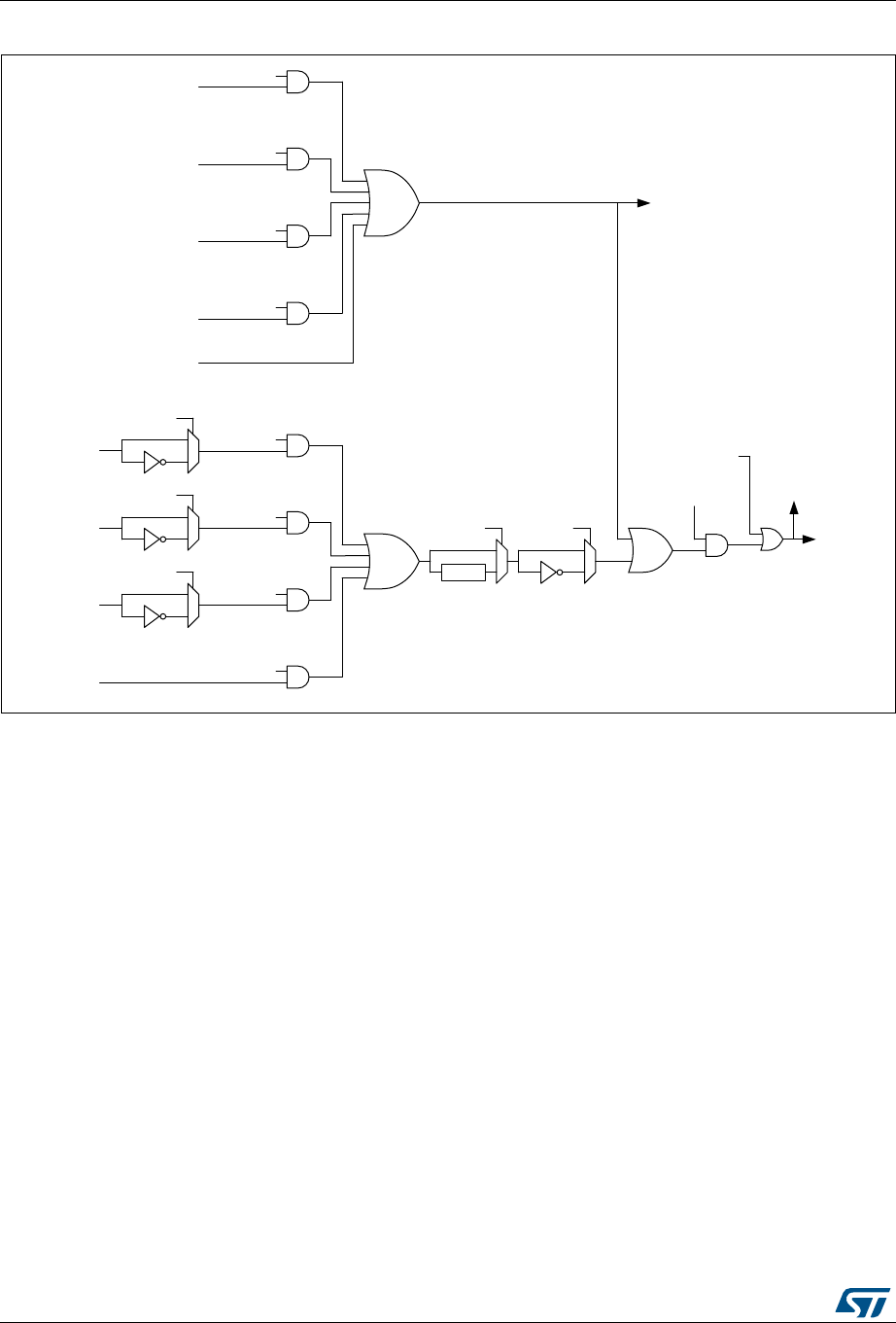
General-purpose timers (TIM15/TIM16) RM0394
912/1600 RM0394 Rev 4
Figure 317. Break circuitry overview
When a break occurs (selected level on the break input):
•The MOE bit is cleared asynchronously, putting the outputs in inactive state, idle state
or even releasing the control to the AFIO controller (selected by the OSSI bit). This
feature functions even if the MCU oscillator is off.
•Each output channel is driven with the level programmed in the OISx bit in the
TIMx_CR2 register as soon as MOE=0. If OSSI=0, the timer releases the output control
(taken over by the AFIO controller) else the enable output remains high.
•When complementary outputs are used:
– The outputs are first put in reset state inactive state (depending on the polarity).
This is done asynchronously so that it works even if no clock is provided to the
timer.
– If the timer clock is still present, then the dead-time generator is reactivated in
order to drive the outputs with the level programmed in the OISx and OISxN bits
after a dead-time. Even in this case, OCx and OCxN cannot be driven to their
06Y9
&203RXWSXW
')6'0
%5($.RXWSXW
%.')%.[(
%.&03(
%.&033
&203RXWSXW
%.&03(
%.&033
%.,1LQSXWV
IURP$)
FRQWUROOHU
%.,1(
%.,13
%.)>@
)LOWHU
%.3
$SSOLFDWLRQEUHDNUHTXHVWV
(&&/2&.
3DULW\/2&.
39'/2&.
/RFNXS/2&.
(&&(UURU
5$0SDULW\(UURU
39'
&RUH/RFNXS
&66
6%,)IODJ
6\VWHPEUHDNUHTXHVWV
6RIWZDUHEUHDN
UHTXHVWV%*
%.(
%5.UHTXHVW
%,)IODJ

RM0394 Rev 4 913/1600
RM0394 General-purpose timers (TIM15/TIM16)
967
active level together. Note that because of the resynchronization on MOE, the
dead-time duration is a bit longer than usual (around 2 ck_tim clock cycles).
– If OSSI=0 then the timer releases the enable outputs (taken over by the AFIO
controller which forces a Hi-Z state) else the enable outputs remain or become
high as soon as one of the CCxE or CCxNE bits is high.
•The break status flag (BIF bit in the TIMx_SR register) is set. An interrupt can be
generated if the BIE bit in the TIMx_DIER register is set.
•If the AOE bit in the TIMx_BDTR register is set, the MOE bit is automatically set again
at the next update event UEV. This can be used to perform a regulation, for instance.
Else, MOE remains low until you write it to ‘1’ again. In this case, it can be used for
security and you can connect the break input to an alarm from power drivers, thermal
sensors or any security components.
Note: The break inputs is acting on level. Thus, the MOE cannot be set while the break input is
active (neither automatically nor by software). In the meantime, the status flag BIF cannot
be cleared.
The break can be generated by the BRK input which has a programmable polarity and an
enable bit BKE in the TIMx_BDTR Register.
In addition to the break input and the output management, a write protection has been
implemented inside the break circuit to safeguard the application. It allows you to freeze the
configuration of several parameters (dead-time duration, OCx/OCxN polarities and state
when disabled, OCxM configurations, break enable and polarity). You can choose from 3
levels of protection selected by the LOCK bits in the TIMx_BDTR register. Refer to
Section 28.7.13: TIM16 break and dead-time register (TIM16_BDTR) on page 961. The
LOCK bits can be written only once after an MCU reset.
The Figure 318 shows an example of behavior of the outputs in response to a break.
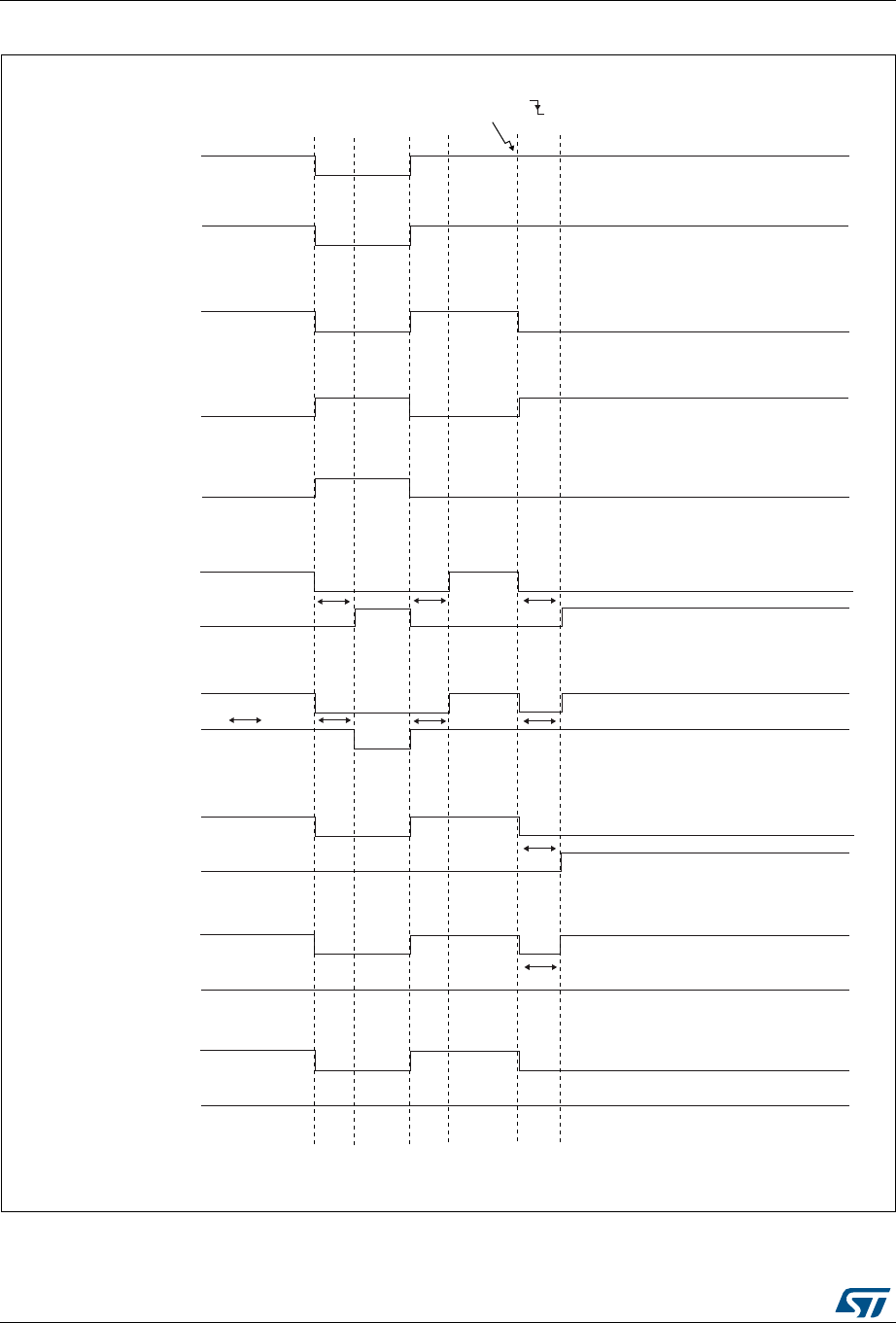
General-purpose timers (TIM15/TIM16) RM0394
914/1600 RM0394 Rev 4
Figure 318. Output behavior in response to a break
GHOD\ GHOD\ GHOD\
GHOD\ GHOD\ GHOD\
GHOD\
GHOD\
2&[5()
2&[
2&[1QRWLPSOHPHQWHG&&[3 2,6[
2&[
2&[1QRWLPSOHPHQWHG&&[3 2,6[
2&[
2&[1QRWLPSOHPHQWHG&&[3 2,6[
2&[
2&[1QRWLPSOHPHQWHG&&[3 2,6[
2&[
2&[1
&&[( &&[3 2,6[ &&[1( &&[13 2,6[1
2&[
2&[1
&&[( &&[3 2,6[ &&[1( &&[13 2,6[1
2&[
2&[1
&&[( &&[3 2,6[ &&[1( &&[13 2,6[1
2&[
2&[1
&&[( &&[3 2,6[ &&[1( &&[13 2,6[1
2&[
2&[1
&&[( &&[3 &&[1( &&[13 2,6[ 2,6[1 RU2,6[ 2,6[1
069
%5($.02(
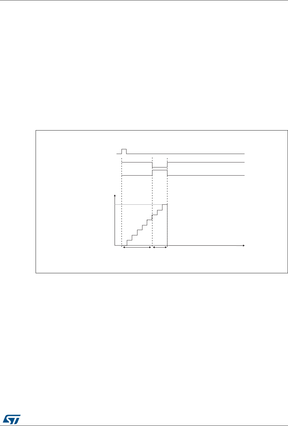
RM0394 Rev 4 915/1600
RM0394 General-purpose timers (TIM15/TIM16)
967
28.5.14 One-pulse mode
One-pulse mode (OPM) is a particular case of the previous modes. It allows the counter to
be started in response to a stimulus and to generate a pulse with a programmable length
after a programmable delay.
Starting the counter can be controlled through the slave mode controller. Generating the
waveform can be done in output compare mode or PWM mode. You select One-pulse mode
by setting the OPM bit in the TIMx_CR1 register. This makes the counter stop automatically
at the next update event UEV.
A pulse can be correctly generated only if the compare value is different from the counter
initial value. Before starting (when the timer is waiting for the trigger), the configuration must
be:
•CNT < CCRx ARR (in particular, 0 < CCRx)
Figure 319. Example of one pulse mode.
For example you may want to generate a positive pulse on OC1 with a length of tPULSE and
after a delay of tDELAY as soon as a positive edge is detected on the TI2 input pin.
Let’s use TI2FP2 as trigger 1:
1. Map TI2FP2 to TI2 by writing CC2S=’01’ in the TIMx_CCMR1 register.
2. TI2FP2 must detect a rising edge, write CC2P=’0’ and CC2NP=’0’ in the TIMx_CCER
register.
3. Configure TI2FP2 as trigger for the slave mode controller (TRGI) by writing TS=’110’ in
the TIMx_SMCR register.
4. TI2FP2 is used to start the counter by writing SMS to ‘110’ in the TIMx_SMCR register
(trigger mode).
069
7,
2&5()
&RXQWHU
W
7,0B$55
7,0B&&5
2&
W'(/$< W38/6(

General-purpose timers (TIM15/TIM16) RM0394
916/1600 RM0394 Rev 4
The OPM waveform is defined by writing the compare registers (taking into account the
clock frequency and the counter prescaler).
•The tDELAY is defined by the value written in the TIMx_CCR1 register.
•The tPULSE is defined by the difference between the auto-reload value and the compare
value (TIMx_ARR - TIMx_CCR1).
•Let’s say you want to build a waveform with a transition from ‘0’ to ‘1’ when a compare
match occurs and a transition from ‘1’ to ‘0’ when the counter reaches the auto-reload
value. To do this you enable PWM mode 2 by writing OC1M=111 in the TIMx_CCMR1
register. You can optionally enable the preload registers by writing OC1PE=’1’ in the
TIMx_CCMR1 register and ARPE in the TIMx_CR1 register. In this case you have to
write the compare value in the TIMx_CCR1 register, the auto-reload value in the
TIMx_ARR register, generate an update by setting the UG bit and wait for external
trigger event on TI2. CC1P is written to ‘0’ in this example.
You only want 1 pulse, so you write ‘1’ in the OPM bit in the TIMx_CR1 register to stop the
counter at the next update event (when the counter rolls over from the auto-reload value
back to 0).
Particular case: OCx fast enable
In One-pulse mode, the edge detection on TIx input set the CEN bit which enables the
counter. Then the comparison between the counter and the compare value makes the
output toggle. But several clock cycles are needed for these operations and it limits the
minimum delay tDELAY min we can get.
If you want to output a waveform with the minimum delay, you can set the OCxFE bit in the
TIMx_CCMRx register. Then OCxRef (and OCx) are forced in response to the stimulus,
without taking in account the comparison. Its new level is the same as if a compare match
had occurred. OCxFE acts only if the channel is configured in PWM1 or PWM2 mode.
28.5.15 Retriggerable one pulse mode (OPM) (TIM15 only)
This mode allows the counter to be started in response to a stimulus and to generate a
pulse with a programmable length, but with the following differences with Non-retriggerable
one pulse mode described in Section 28.5.14:
– The pulse starts as soon as the trigger occurs (no programmable delay)
– The pulse is extended if a new trigger occurs before the previous one is completed
The timer must be in Slave mode, with the bits SMS[3:0] = ‘1000’ (Combined Reset + trigger
mode) in the TIMx_SMCR register, and the OCxM[3:0] bits set to ‘1000’ or ‘1001’ for
Retrigerrable OPM mode 1 or 2.
If the timer is configured in Up-counting mode, the corresponding CCRx must be set to 0
(the ARR register sets the pulse length). If the timer is configured in Down-counting mode,
CCRx must be above or equal to ARR.
Note: The OCxM[3:0] and SMS[3:0] bit fields are split into two parts for compatibility reasons, the
most significant bit are not contiguous with the 3 least significant ones.
This mode must not be used with center-aligned PWM modes. It is mandatory to have
CMS[1:0] = 00 in TIMx_CR1.

RM0394 Rev 4 917/1600
RM0394 General-purpose timers (TIM15/TIM16)
967
Figure 320. Retriggerable one pulse mode
28.5.16 UIF bit remapping
The IUFREMAP bit in the TIMx_CR1 register forces a continuous copy of the Update
Interrupt Flag UIF into bit 31 of the timer counter register (TIMxCNT[31]). This allows to
atomically read both the counter value and a potential roll-over condition signaled by the
UIFCPY flag. In particular cases, it can ease the calculations by avoiding race conditions
caused for instance by a processing shared between a background task (counter reading)
and an interrupt (Update Interrupt).
There is no latency between the assertions of the UIF and UIFCPY flags.
75*,
&RXQWHU
2XWSXW
069
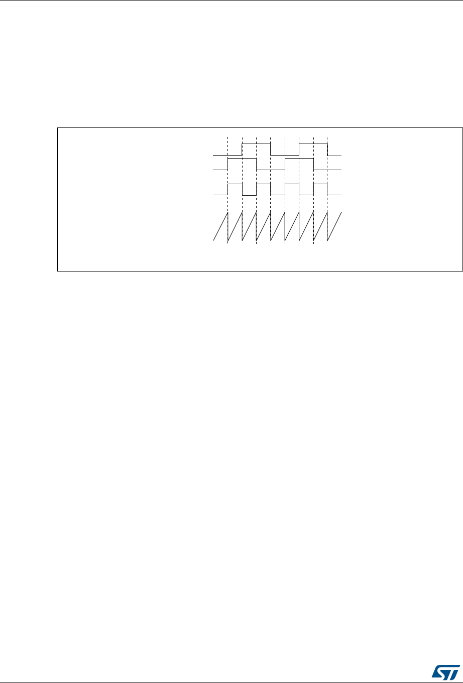
General-purpose timers (TIM15/TIM16) RM0394
918/1600 RM0394 Rev 4
28.5.17 Timer input XOR function (TIM15 only)
The TI1S bit in the TIMx_CR2 register, allows the input filter of channel 1 to be connected to
the output of a XOR gate, combining the two input pins TIMx_CH1 and TIMx_CH2.
The XOR output can be used with all the timer input functions such as trigger or input
capture. It is useful for measuring the interval between the edges on two input signals, as
shown in Figure 321.
Figure 321. Measuring time interval between edges on 2 signals
069
7,
7,
7,;257,
&RXQWHU

RM0394 Rev 4 919/1600
RM0394 General-purpose timers (TIM15/TIM16)
967
28.5.18 External trigger synchronization (TIM15 only)
The TIM timers are linked together internally for timer synchronization or chaining.
The TIM15 timer can be synchronized with an external trigger in several modes: Reset
mode, Gated mode and Trigger mode.
Slave mode: Reset mode
The counter and its prescaler can be reinitialized in response to an event on a trigger input.
Moreover, if the URS bit from the TIMx_CR1 register is low, an update event UEV is
generated. Then all the preloaded registers (TIMx_ARR, TIMx_CCRx) are updated.
In the following example, the upcounter is cleared in response to a rising edge on TI1 input:
1. Configure the channel 1 to detect rising edges on TI1. Configure the input filter duration
(in this example, we don’t need any filter, so we keep IC1F=0000). The capture
prescaler is not used for triggering, so you don’t need to configure it. The CC1S bits
select the input capture source only, CC1S = 01 in the TIMx_CCMR1 register. Write
CC1P=’0’ and CC1NP=’0’ in the TIMx_CCER register to validate the polarity (and
detect rising edges only).
2. Configure the timer in reset mode by writing SMS=100 in TIMx_SMCR register. Select
TI1 as the input source by writing TS=101 in TIMx_SMCR register.
3. Start the counter by writing CEN=1 in the TIMx_CR1 register.
The counter starts counting on the internal clock, then behaves normally until TI1 rising
edge. When TI1 rises, the counter is cleared and restarts from 0. In the meantime, the
trigger flag is set (TIF bit in the TIMx_SR register) and an interrupt request, or a DMA
request can be sent if enabled (depending on the TIE and TDE bits in TIMx_DIER register).
The following figure shows this behavior when the auto-reload register TIMx_ARR=0x36.
The delay between the rising edge on TI1 and the actual reset of the counter is due to the
resynchronization circuit on TI1 input.
Figure 322. Control circuit in reset mode
069
&RXQWHUFORFN FNBFQW FNBSVF
&RXQWHUUHJLVWHU
8*
7,
7,)

General-purpose timers (TIM15/TIM16) RM0394
920/1600 RM0394 Rev 4
Slave mode: Gated mode
The counter can be enabled depending on the level of a selected input.
In the following example, the upcounter counts only when TI1 input is low:
1. Configure the channel 1 to detect low levels on TI1. Configure the input filter duration
(in this example, we don’t need any filter, so we keep IC1F=0000). The capture
prescaler is not used for triggering, so you don’t need to configure it. The CC1S bits
select the input capture source only, CC1S=01 in TIMx_CCMR1 register. Write
CC1P=1 and CC1NP = ‘0’ in the TIMx_CCER register to validate the polarity (and
detect low level only).
2. Configure the timer in gated mode by writing SMS=101 in TIMx_SMCR register. Select
TI1 as the input source by writing TS=101 in TIMx_SMCR register.
3. Enable the counter by writing CEN=1 in the TIMx_CR1 register (in gated mode, the
counter doesn’t start if CEN=0, whatever is the trigger input level).
The counter starts counting on the internal clock as long as TI1 is low and stops as soon as
TI1 becomes high. The TIF flag in the TIMx_SR register is set both when the counter starts
or stops.
The delay between the rising edge on TI1 and the actual stop of the counter is due to the
resynchronization circuit on TI1 input.
Figure 323. Control circuit in gated mode
069
7,
FQWBHQ
:ULWH7,)
&RXQWHUFORFN FNBFQW FNBSVF
&RXQWHUUHJLVWHU
7,)
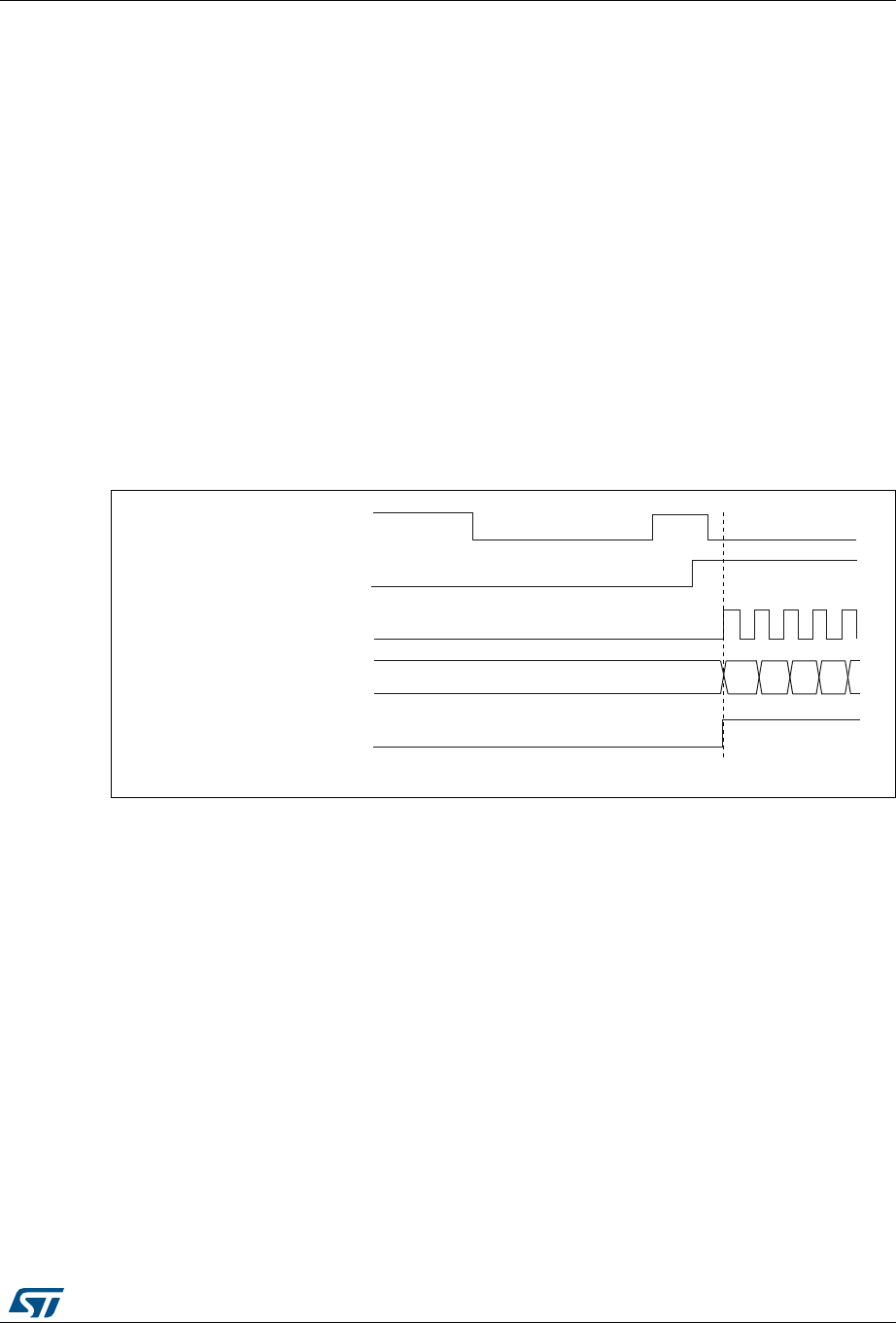
RM0394 Rev 4 921/1600
RM0394 General-purpose timers (TIM15/TIM16)
967
Slave mode: Trigger mode
The counter can start in response to an event on a selected input.
In the following example, the upcounter starts in response to a rising edge on TI2 input:
1. Configure the channel 2 to detect rising edges on TI2. Configure the input filter duration
(in this example, we don’t need any filter, so we keep IC2F=0000). The capture
prescaler is not used for triggering, so you don’t need to configure it. The CC2S bits are
configured to select the input capture source only, CC2S=01 in TIMx_CCMR1 register.
Write CC2P=’1’ and CC2NP=’0’ in the TIMx_CCER register to validate the polarity (and
detect low level only).
2. Configure the timer in trigger mode by writing SMS=110 in the TIMx_SMCR register.
Select TI2 as the input source by writing TS=110 in the TIMx_SMCR register.
When a rising edge occurs on TI2, the counter starts counting on the internal clock and the
TIF flag is set.
The delay between the rising edge on TI2 and the actual start of the counter is due to the
resynchronization circuit on TI2 input.
Figure 324. Control circuit in trigger mode
28.5.19 Slave mode – combined reset + trigger mode
In this case, a rising edge of the selected trigger input (TRGI) reinitializes the counter,
generates an update of the registers, and starts the counter.
This mode is used for one-pulse mode.
28.5.20 DMA burst mode
The TIMx timers have the capability to generate multiple DMA requests on a single event.
The main purpose is to be able to re-program several timer registers multiple times without
software overhead, but it can also be used to read several registers in a row, at regular
intervals.
The DMA controller destination is unique and must point to the virtual register TIMx_DMAR.
On a given timer event, the timer launches a sequence of DMA requests (burst). Each write
into the TIMx_DMAR register is actually redirected to one of the timer registers.
069
7,
FQWBHQ
&RXQWHUFORFN FNBFQW FNBSVF
&RXQWHUUHJLVWHU
7,)

General-purpose timers (TIM15/TIM16) RM0394
922/1600 RM0394 Rev 4
The DBL[4:0] bits in the TIMx_DCR register set the DMA burst length. The timer recognizes
a burst transfer when a read or a write access is done to the TIMx_DMAR address), i.e. the
number of transfers (either in half-words or in bytes).
The DBA[4:0] bits in the TIMx_DCR registers define the DMA base address for DMA
transfers (when read/write access are done through the TIMx_DMAR address). DBA is
defined as an offset starting from the address of the TIMx_CR1 register.
Example:
00000: TIMx_CR1,
00001: TIMx_CR2,
00010: TIMx_SMCR,
For example, the timer DMA burst feature could be used to update the contents of the CCRx
registers (x = 2, 3, 4) on an update event, with the DMA transferring half words into the
CCRx registers.
This is done in the following steps:
1. Configure the corresponding DMA channel as follows:
– DMA channel peripheral address is the DMAR register address
– DMA channel memory address is the address of the buffer in the RAM containing
the data to be transferred by DMA into the CCRx registers.
– Number of data to transfer = 3 (See note below).
– Circular mode disabled.
2. Configure the DCR register by configuring the DBA and DBL bit fields as follows:
DBL = 3 transfers, DBA = 0xE.
3. Enable the TIMx update DMA request (set the UDE bit in the DIER register).
4. Enable TIMx
5. Enable the DMA channel
This example is for the case where every CCRx register is to be updated once. If every
CCRx register is to be updated twice for example, the number of data to transfer should be
6. Let's take the example of a buffer in the RAM containing data1, data2, data3, data4, data5
and data6. The data is transferred to the CCRx registers as follows: on the first update DMA
request, data1 is transferred to CCR2, data2 is transferred to CCR3, data3 is transferred to
CCR4 and on the second update DMA request, data4 is transferred to CCR2, data5 is
transferred to CCR3 and data6 is transferred to CCR4.
Note: A null value can be written to the reserved registers.

RM0394 Rev 4 923/1600
RM0394 General-purpose timers (TIM15/TIM16)
967
28.5.21 Timer synchronization (TIM15)
The TIMx timers are linked together internally for timer synchronization or chaining. Refer to
Section 27.3.19: Timer synchronization for details.
Note: The clock of the slave peripherals (timer, ADC, ...) receiving the TRGO or the TRGO2
signals must be enabled prior to receive events from the master timer, and the clock
frequency (prescaler) must not be changed on-the-fly while triggers are received from the
master timer.
28.5.22 Debug mode
When the microcontroller enters debug mode (Cortex®-M4 core halted), the TIMx counter
either continues to work normally or stops, depending on DBG_TIMx_STOP configuration
bit in DBG module. For more details, refer to Section 46.16.2: Debug support for timers,
RTC, watchdog, bxCAN and I2C.
For safety purposes, when the counter is stopped (DBG_TIMx_STOP = 1), the outputs are
disabled (as if the MOE bit was reset). The outputs can either be forced to an inactive state
(OSSI bit = 1), or have their control taken over by the GPIO controller (OSSI bit = 0) to force
them to Hi-Z.

General-purpose timers (TIM15/TIM16) RM0394
924/1600 RM0394 Rev 4
28.6 TIM15 registers
Refer to Section 1.2 for a list of abbreviations used in register descriptions.
28.6.1 TIM15 control register 1 (TIM15_CR1)
Address offset: 0x00
Reset value: 0x0000
1514131211109876543210
Res. Res. Res. Res. UIFRE
MAP Res. CKD[1:0] ARPE Res. Res. Res. OPM URS UDIS CEN
rw rw rw rw rw rw rw rw
Bits 15:12 Reserved, must be kept at reset value.
Bit 11 UIFREMAP: UIF status bit remapping
0: No remapping. UIF status bit is not copied to TIMx_CNT register bit 31.
1: Remapping enabled. UIF status bit is copied to TIMx_CNT register bit 31.
Bit 10 Reserved, must be kept at reset value.
Bits 9:8 CKD[1:0]: Clock division
This bitfield indicates the division ratio between the timer clock (CK_INT) frequency and the
dead-time and sampling clock (tDTS) used by the dead-time generators and the digital filters
(TIx)
00: tDTS = tCK_INT
01: tDTS = 2*tCK_INT
10: tDTS = 4*tCK_INT
11: Reserved, do not program this value
Bit 7 ARPE: Auto-reload preload enable
0: TIMx_ARR register is not buffered
1: TIMx_ARR register is buffered
Bits 6:4 Reserved, must be kept at reset value.
Bit 3 OPM: One-pulse mode
0: Counter is not stopped at update event
1: Counter stops counting at the next update event (clearing the bit CEN)

RM0394 Rev 4 925/1600
RM0394 General-purpose timers (TIM15/TIM16)
967
28.6.2 TIM15 control register 2 (TIM15_CR2)
Address offset: 0x04
Reset value: 0x0000
Bit 2 URS: Update request source
This bit is set and cleared by software to select the UEV event sources.
0: Any of the following events generate an update interrupt if enabled. These events can be:
– Counter overflow/underflow
– Setting the UG bit
– Update generation through the slave mode controller
1: Only counter overflow/underflow generates an update interrupt if enabled
Bit 1 UDIS: Update disable
This bit is set and cleared by software to enable/disable UEV event generation.
0: UEV enabled. The Update (UEV) event is generated by one of the following events:
– Counter overflow/underflow
– Setting the UG bit
– Update generation through the slave mode controller
Buffered registers are then loaded with their preload values.
1: UEV disabled. The Update event is not generated, shadow registers keep their value
(ARR, PSC, CCRx). However the counter and the prescaler are reinitialized if the UG bit is
set or if a hardware reset is received from the slave mode controller.
Bit 0 CEN: Counter enable
0: Counter disabled
1: Counter enabled
Note: External clock and gated mode can work only if the CEN bit has been previously set by
software. However trigger mode can set the CEN bit automatically by hardware.
1514131211109876543210
Res. Res. Res. Res. Res. OIS2 OIS1N OIS1 TI1S MMS[2:0] CCDS CCUS Res. CCPC
rw rw rw rw rw rw rw rw rw rw
Bits 15:11 Reserved, must be kept at reset value.
Bit 10 OIS2: Output idle state 2 (OC2 output)
0: OC2=0 when MOE=0
1: OC2=1 when MOE=0
Note: This bit cannot be modified as long as LOCK level 1, 2 or 3 has been programmed
(LOCK bits in the TIMx_BKR register).
Bit 9 OIS1N: Output Idle state 1 (OC1N output)
0: OC1N=0 after a dead-time when MOE=0
1: OC1N=1 after a dead-time when MOE=0
Note: This bit can not be modified as long as LOCK level 1, 2 or 3 has been programmed
(LOCK bits in TIMx_BKR register).
Bit 8 OIS1: Output Idle state 1 (OC1 output)
0: OC1=0 (after a dead-time if OC1N is implemented) when MOE=0
1: OC1=1 (after a dead-time if OC1N is implemented) when MOE=0
Note: This bit can not be modified as long as LOCK level 1, 2 or 3 has been programmed
(LOCK bits in TIMx_BKR register).

General-purpose timers (TIM15/TIM16) RM0394
926/1600 RM0394 Rev 4
Bit 7 TI1S: TI1 selection
0: The TIMx_CH1 pin is connected to TI1 input
1: The TIMx_CH1, CH2 pins are connected to the TI1 input (XOR combination)
Bits 6:4 MMS[2:0]: Master mode selection
These bits allow to select the information to be sent in master mode to slave timers for
synchronization (TRGO). The combination is as follows:
000: Reset - the UG bit from the TIMx_EGR register is used as trigger output (TRGO). If the
reset is generated by the trigger input (slave mode controller configured in reset mode) then
the signal on TRGO is delayed compared to the actual reset.
001: Enable - the Counter Enable signal CNT_EN is used as trigger output (TRGO). It is
useful to start several timers at the same time or to control a window in which a slave timer is
enable. The Counter Enable signal is generated by a logic OR between CEN control bit and
the trigger input when configured in gated mode. When the Counter Enable signal is
controlled by the trigger input, there is a delay on TRGO, except if the master/slave mode is
selected (see the MSM bit description in TIMx_SMCR register).
010: Update - The update event is selected as trigger output (TRGO). For instance a master
timer can then be used as a prescaler for a slave timer.
011: Compare Pulse - The trigger output send a positive pulse when the CC1IF flag is to be
set (even if it was already high), as soon as a capture or a compare match occurred.
(TRGO).
100: Compare - OC1REF signal is used as trigger output (TRGO).
101: Compare - OC2REF signal is used as trigger output (TRGO).
Bit 3 CCDS: Capture/compare DMA selection
0: CCx DMA request sent when CCx event occurs
1: CCx DMA requests sent when update event occurs
Bit 2 CCUS: Capture/compare control update selection
0: When capture/compare control bits are preloaded (CCPC=1), they are updated by setting
the COMG bit only.
1: When capture/compare control bits are preloaded (CCPC=1), they are updated by setting
the COMG bit or when an rising edge occurs on TRGI.
Note: This bit acts only on channels that have a complementary output.
Bit 1 Reserved, must be kept at reset value.
Bit 0 CCPC: Capture/compare preloaded control
0: CCxE, CCxNE and OCxM bits are not preloaded
1: CCxE, CCxNE and OCxM bits are preloaded, after having been written, they are updated
only when a commutation event (COM) occurs (COMG bit set or rising edge detected on
TRGI, depending on the CCUS bit).
Note: This bit acts only on channels that have a complementary output.

RM0394 Rev 4 927/1600
RM0394 General-purpose timers (TIM15/TIM16)
967
28.6.3 TIM15 slave mode control register (TIM15_SMCR)
Address offset: 0x08
Reset value: 0x0000 0000
31 30 29 28 27 26 25 24 23 22 21 20 19 18 17 16
Res. Res. Res. Res. Res. Res. Res. Res. Res. Res. Res. Res. Res. Res. Res. SMS[3]
rw
1514131211109876543210
Res. Res. Res. Res. Res. Res. Res. Res. MSM TS[2:0] Res. SMS[2:0]
rw rw rw rw rw rw rw
Bits 31:17 Reserved, must be kept at reset value.
Bit 16 SMS[3]: Slave mode selection - bit 3
Refer to SMS description - bits 2:0.
Bits 15:8 Reserved, must be kept at reset value.
Bit 7 MSM: Master/slave mode
0: No action
1: The effect of an event on the trigger input (TRGI) is delayed to allow a perfect
synchronization between the current timer and its slaves (through TRGO). It is useful if we
want to synchronize several timers on a single external event.
Bits 6:4 TS[2:0]: Trigger selection
This bit field selects the trigger input to be used to synchronize the counter.
000: Internal Trigger 0 (ITR0)
001: Internal Trigger 1 (ITR1)
010: Internal Trigger 2 (ITR2)
011: Internal Trigger 3 (ITR3)
100: TI1 Edge Detector (TI1F_ED)
101: Filtered Timer Input 1 (TI1FP1)
110: Filtered Timer Input 2 (TI2FP2)
See Table 139: TIMx Internal trigger connection on page 928 for more details on ITRx
meaning for each Timer.
Note: These bits must be changed only when they are not used (e.g. when SMS=000) to
avoid wrong edge detections at the transition.
Bit 3 Reserved, must be kept at reset value.

General-purpose timers (TIM15/TIM16) RM0394
928/1600 RM0394 Rev 4
28.6.4 TIM15 DMA/interrupt enable register (TIM15_DIER)
Address offset: 0x0C
Reset value: 0x0000
Bits 16, 2, 1, 0 SMS[3:0]: Slave mode selection
When external signals are selected the active edge of the trigger signal (TRGI) is linked to
the polarity selected on the external input (see Input Control register and Control Register
description.
0000: Slave mode disabled - if CEN = ‘1’ then the prescaler is clocked directly by the internal
clock.
0001: Reserved
0010: Reserved
0011: Reserved
0100: Reset Mode - Rising edge of the selected trigger input (TRGI) reinitializes the counter
and generates an update of the registers.
0101: Gated Mode - The counter clock is enabled when the trigger input (TRGI) is high. The
counter stops (but is not reset) as soon as the trigger becomes low. Both start and stop of
the counter are controlled.
0110: Trigger Mode - The counter starts at a rising edge of the trigger TRGI (but it is not
reset). Only the start of the counter is controlled.
0111: External Clock Mode 1 - Rising edges of the selected trigger (TRGI) clock the counter.
1000: Combined reset + trigger mode - Rising edge of the selected trigger input (TRGI)
reinitializes the counter, generates an update of the registers and starts the counter.
Other codes: reserved.
Note: The gated mode must not be used if TI1F_ED is selected as the trigger input
(TS=’100’). Indeed, TI1F_ED outputs 1 pulse for each transition on TI1F, whereas the
gated mode checks the level of the trigger signal.
Note: The clock of the slave peripherals (timer, ADC, ...) receiving the TRGO or the TRGO2
signals must be enabled prior to receive events from the master timer, and the clock
frequency (prescaler) must not be changed on-the-fly while triggers are received from
the master timer.
Table 139. TIMx Internal trigger connection
Slave TIM ITR0 (TS = 000) ITR1 (TS = 001) ITR2 (TS = 010) ITR3 (TS = 011)
TIM15 TIM1 Reserved TIM16 OC1 Reserved
1514131211109876543210
Res. TDE COMD
ERes. Res. CC2DE CC1DE UDE BIE TIE COMIE Res. Res. CC2IE CC1IE UIE
rw rw rw rw rw rw rw rw rw rw rw
Bit 15 Reserved, must be kept at reset value.
Bit 14 TDE: Trigger DMA request enable
0: Trigger DMA request disabled
1: Trigger DMA request enabled
Bit 13 COMDE: COM DMA request enable
0: COM DMA request disabled
1: COM DMA request enabled

RM0394 Rev 4 929/1600
RM0394 General-purpose timers (TIM15/TIM16)
967
28.6.5 TIM15 status register (TIM15_SR)
Address offset: 0x10
Reset value: 0x0000
Bits 12:11 Reserved, must be kept at reset value.
Bit 10 CC2DE: Capture/Compare 2 DMA request enable
0: CC2 DMA request disabled
1: CC2 DMA request enabled
Bit 9 CC1DE: Capture/Compare 1 DMA request enable
0: CC1 DMA request disabled
1: CC1 DMA request enabled
Bit 8 UDE: Update DMA request enable
0: Update DMA request disabled
1: Update DMA request enabled
Bit 7 BIE: Break interrupt enable
0: Break interrupt disabled
1: Break interrupt enabled
Bit 6 TIE: Trigger interrupt enable
0: Trigger interrupt disabled
1: Trigger interrupt enabled
Bit 5 COMIE: COM interrupt enable
0: COM interrupt disabled
1: COM interrupt enabled
Bits 4:3 Reserved, must be kept at reset value.
Bit 2 CC2IE: Capture/Compare 2 interrupt enable
0: CC2 interrupt disabled
1: CC2 interrupt enabled
Bit 1 CC1IE: Capture/Compare 1 interrupt enable
0: CC1 interrupt disabled
1: CC1 interrupt enabled
Bit 0 UIE: Update interrupt enable
0: Update interrupt disabled
1: Update interrupt enabled
1514131211109876543210
Res. Res. Res. Res. Res. CC2OF CC1OF Res. BIF TIF COMIF Res. Res. CC2IF CC1IF UIF
rc_w0 rc_w0 rc_w0 rc_w0 rc_w0 rc_w0 rc_w0 rc_w0

General-purpose timers (TIM15/TIM16) RM0394
930/1600 RM0394 Rev 4
Bits 15:11 Reserved, must be kept at reset value.
Bit 10 CC2OF: Capture/Compare 2 overcapture flag
Refer to CC1OF description
Bit 9 CC1OF: Capture/Compare 1 overcapture flag
This flag is set by hardware only when the corresponding channel is configured in input
capture mode. It is cleared by software by writing it to ‘0’.
0: No overcapture has been detected
1: The counter value has been captured in TIMx_CCR1 register while CC1IF flag was
already set
Bit 8 Reserved, must be kept at reset value.
Bit 7 BIF: Break interrupt flag
This flag is set by hardware as soon as the break input goes active. It can be cleared by
software if the break input is not active.
0: No break event occurred
1: An active level has been detected on the break input
Bit 6 TIF: Trigger interrupt flag
This flag is set by hardware on trigger event (active edge detected on TRGI input when the
slave mode controller is enabled in all modes but gated mode, both edges in case gated
mode is selected). It is set when the counter starts or stops when gated mode is selected. It
is cleared by software.
0: No trigger event occurred
1: Trigger interrupt pending
Bit 5 COMIF: COM interrupt flag
This flag is set by hardware on a COM event (once the capture/compare control bits –CCxE,
CCxNE, OCxM– have been updated). It is cleared by software.
0: No COM event occurred
1: COM interrupt pending
Bits 4:3 Reserved, must be kept at reset value.

RM0394 Rev 4 931/1600
RM0394 General-purpose timers (TIM15/TIM16)
967
28.6.6 TIM15 event generation register (TIM15_EGR)
Address offset: 0x14
Reset value: 0x0000
Bit 2 CC2IF: Capture/Compare 2 interrupt flag
refer to CC1IF description
Bit 1 CC1IF: Capture/Compare 1 interrupt flag
If channel CC1 is configured as output: This flag is set by hardware when the counter
matches the compare value. It is cleared by software.
0: No match.
1: The content of the counter TIMx_CNT matches the content of the TIMx_CCR1 register.
When the contents of TIMx_CCR1 are greater than the contents of TIMx_ARR, the CC1IF
bit goes high on the counter overflow.
If channel CC1 is configured as input: This bit is set by hardware on a capture. It is
cleared by software or by reading the TIMx_CCR1 register.
0: No input capture occurred
1: The counter value has been captured in TIMx_CCR1 register (An edge has been
detected on IC1 which matches the selected polarity)
Bit 0 UIF: Update interrupt flag
This bit is set by hardware on an update event. It is cleared by software.
0: No update occurred.
1: Update interrupt pending. This bit is set by hardware when the registers are updated:
– At overflow regarding the repetition counter value (update if repetition counter = 0) and if
the UDIS=0 in the TIMx_CR1 register.
– When CNT is reinitialized by software using the UG bit in TIMx_EGR register, if URS=0
and UDIS=0 in the TIMx_CR1 register.
– When CNT is reinitialized by a trigger event (refer to Section 28.6.3: TIM15 slave mode
control register (TIM15_SMCR)), if URS=0 and UDIS=0 in the TIMx_CR1 register.
1514131211109876543210
Res. Res. Res. Res. Res. Res. Res. Res. BG TG COMG Res. Res. CC2G CC1G UG
wwrw www
Bits 15:8 Reserved, must be kept at reset value.
Bit 7 BG: Break generation
This bit is set by software in order to generate an event, it is automatically cleared by
hardware.
0: No action
1: A break event is generated. MOE bit is cleared and BIF flag is set. Related interrupt or
DMA transfer can occur if enabled.
Bit 6 TG: Trigger generation
This bit is set by software in order to generate an event, it is automatically cleared by
hardware.
0: No action
1: The TIF flag is set in TIMx_SR register. Related interrupt or DMA transfer can occur if
enabled

General-purpose timers (TIM15/TIM16) RM0394
932/1600 RM0394 Rev 4
28.6.7 TIM15 capture/compare mode register 1 (TIM15_CCMR1)
Address offset: 0x18
Reset value: 0x0000 0000
The channels can be used in input (capture mode) or in output (compare mode). The
direction of a channel is defined by configuring the corresponding CCxS bits. All the other
bits of this register have a different function in input and in output mode. For a given bit,
OCxx describes its function when the channel is configured in output, ICxx describes its
function when the channel is configured in input. So you must take care that the same bit
can have a different meaning for the input stage and for the output stage.
Bit 5 COMG: Capture/Compare control update generation
This bit can be set by software, it is automatically cleared by hardware.
0: No action
1: When the CCPC bit is set, it is possible to update the CCxE, CCxNE and OCxM bits
Note: This bit acts only on channels that have a complementary output.
Bits 4:3 Reserved, must be kept at reset value.
Bit 2 CC2G: Capture/Compare 2 generation
Refer to CC1G description
Bit 1 CC1G: Capture/Compare 1 generation
This bit is set by software in order to generate an event, it is automatically cleared by
hardware.
0: No action
1: A capture/compare event is generated on channel 1:
If channel CC1 is configured as output:
CC1IF flag is set, Corresponding interrupt or DMA request is sent if enabled.
If channel CC1 is configured as input:
The current value of the counter is captured in TIMx_CCR1 register. The CC1IF flag is set,
the corresponding interrupt or DMA request is sent if enabled. The CC1OF flag is set if the
CC1IF flag was already high.
Bit 0 UG: Update generation
This bit can be set by software, it is automatically cleared by hardware.
0: No action.
1: Reinitialize the counter and generates an update of the registers. Note that the prescaler
counter is cleared too (anyway the prescaler ratio is not affected).
31 30 29 28 27 26 25 24 23 22 21 20 19 18 17 16
Res. Res. Res. Res. Res. Res. Res.
OC2M
[3] Res. Res. Res. Res. Res. Res. Res.
OC1M
[3]
Res. Res.
rw rw
1514131211109876543210
Res. OC2M[2:0] OC2
PE
OC2
FE CC2S[1:0] Res. OC1M[2:0] OC1
PE
OC1
FE CC1S[1:0]
IC2F[3:0] IC2PSC[1:0] IC1F[3:0] IC1PSC[1:0]
rw rw rw rw rw rw rw rw rw rw rw rw rw rw rw rw

RM0394 Rev 4 933/1600
RM0394 General-purpose timers (TIM15/TIM16)
967
Output compare mode:
Bits 31:25 Reserved, always read as 0
Bit 24 OC2M[3]: Output Compare 2 mode - bit 3
Bits 23:17 Reserved, always read as 0
Bit 16 OC1M[3]: Output Compare 1 mode - bit 3
refer to OC1M description on bits 6:4
Bit 15 Reserved, always read as 0
Bits 14:12 OC2M[2:0]: Output Compare 2 mode
Bit 11 OC2PE: Output Compare 2 preload enable
Bit 10 OC2FE: Output Compare 2 fast enable
Bits 9:8 CC2S[1:0]: Capture/Compare 2 selection
This bit-field defines the direction of the channel (input/output) as well as the used input.
00: CC2 channel is configured as output.
01: CC2 channel is configured as input, IC2 is mapped on TI2.
10: CC2 channel is configured as input, IC2 is mapped on TI1.
11: CC2 channel is configured as input, IC2 is mapped on TRC. This mode is working only if
an internal trigger input is selected through the TS bit (TIMx_SMCR register)
Note: CC2S bits are writable only when the channel is OFF (CC2E = ‘0’ in TIMx_CCER).
Bit 7 Reserved, always read as 0

General-purpose timers (TIM15/TIM16) RM0394
934/1600 RM0394 Rev 4
Bits 6:4 OC1M: Output Compare 1 mode
These bits define the behavior of the output reference signal OC1REF from which OC1 and
OC1N are derived. OC1REF is active high whereas OC1 and OC1N active level depends
on CC1P and CC1NP bits.
0000: Frozen - The comparison between the output compare register TIMx_CCR1 and the
counter TIMx_CNT has no effect on the outputs.
0001: Set channel 1 to active level on match. OC1REF signal is forced high when the
counter TIMx_CNT matches the capture/compare register 1 (TIMx_CCR1).
0010: Set channel 1 to inactive level on match. OC1REF signal is forced low when the
counter TIMx_CNT matches the capture/compare register 1 (TIMx_CCR1).
0011: Toggle - OC1REF toggles when TIMx_CNT=TIMx_CCR1.
0100: Force inactive level - OC1REF is forced low.
0101: Force active level - OC1REF is forced high.
0110: PWM mode 1 - Channel 1 is active as long as TIMx_CNT<TIMx_CCR1 else inactive.
0111: PWM mode 2 - Channel 1 is inactive as long as TIMx_CNT<TIMx_CCR1 else
active.
1000: Retrigerrable OPM mode 1 - In up-counting mode, the channel is active until a trigger
event is detected (on TRGI signal). Then, a comparison is performed as in PWM
mode 1 and the channels becomes active again at the next update. In down-counting
mode, the channel is inactive until a trigger event is detected (on TRGI signal). Then,
a comparison is performed as in PWM mode 1 and the channels becomes inactive
again at the next update.
1001: Retrigerrable OPM mode 2 - In up-counting mode, the channel is inactive until a
trigger event is detected (on TRGI signal). Then, a comparison is performed as in
PWM mode 2 and the channels becomes inactive again at the next update. In down-
counting mode, the channel is active until a trigger event is detected (on TRGI
signal). Then, a comparison is performed as in PWM mode 1 and the channels
becomes active again at the next update.
1010: Reserved
1011: Reserved
1100: Combined PWM mode 1 - OC1REF has the same behavior as in PWM mode 1.
OC1REFC is the logical OR between OC1REF and OC2REF.
1101: Combined PWM mode 2 - OC1REF has the same behavior as in PWM mode 2.
OC1REFC is the logical AND between OC1REF and OC2REF.
1110: Reserved,
1111: Reserved,
Note: 1: These bits can not be modified as long as LOCK level 3 has been programmed
(LOCK bits in TIMx_BDTR register) and CC1S=’00’ (the channel is configured in
output).
2: In PWM mode, the OCREF level changes only when the result of the comparison
changes or when the output compare mode switches from “frozen” mode to “PWM”
mode.
3: On channels that have a complementary output, this bit field is preloaded. If
the CCPC bit is set in the TIMx_CR2 register then the OC1M active bits take
the new value from the preloaded bits only when a COM event is generated.

RM0394 Rev 4 935/1600
RM0394 General-purpose timers (TIM15/TIM16)
967
Input capture mode
Bit 3 OC1PE: Output Compare 1 preload enable
0: Preload register on TIMx_CCR1 disabled. TIMx_CCR1 can be written at anytime, the
new value is taken in account immediately.
1: Preload register on TIMx_CCR1 enabled. Read/Write operations access the preload
register. TIMx_CCR1 preload value is loaded in the active register at each update event.
Note: 1: These bits can not be modified as long as LOCK level 3 has been programmed
(LOCK bits in TIMx_BDTR register) and CC1S=’00’ (the channel is configured in
output).
2: The PWM mode can be used without validating the preload register only in one
pulse mode (OPM bit set in TIMx_CR1 register). Else the behavior is not guaranteed.
Bit 2 OC1FE: Output Compare 1 fast enable
This bit is used to accelerate the effect of an event on the trigger in input on the CC output.
0: CC1 behaves normally depending on counter and CCR1 values even when the trigger is
ON. The minimum delay to activate CC1 output when an edge occurs on the trigger input is
5 clock cycles.
1: An active edge on the trigger input acts like a compare match on CC1 output. Then, OC is
set to the compare level independently of the result of the comparison. Delay to sample the
trigger input and to activate CC1 output is reduced to 3 clock cycles. OCFE acts only if the
channel is configured in PWM1 or PWM2 mode.
Bits 1:0 CC1S: Capture/Compare 1 selection
This bit-field defines the direction of the channel (input/output) as well as the used input.
00: CC1 channel is configured as output.
01: CC1 channel is configured as input, IC1 is mapped on TI1.
10: CC1 channel is configured as input, IC1 is mapped on TI2.
11: CC1 channel is configured as input, IC1 is mapped on TRC. This mode is working only if
an internal trigger input is selected through TS bit (TIMx_SMCR register)
Note: CC1S bits are writable only when the channel is OFF (CC1E = ‘0’ in TIMx_CCER).
Bits 31:16 Reserved, always read as 0
Bits 15:12 IC2F: Input capture 2 filter
Bits 11:10 IC2PSC[1:0]: Input capture 2 prescaler
Bits 9:8 CC2S: Capture/Compare 2 selection
This bit-field defines the direction of the channel (input/output) as well as the used input.
00: CC2 channel is configured as output
01: CC2 channel is configured as input, IC2 is mapped on TI2
10: CC2 channel is configured as input, IC2 is mapped on TI1
11: CC2 channel is configured as input, IC2 is mapped on TRC. This mode is working only if an
internal trigger input is selected through TS bit (TIMx_SMCR register)
Note: CC2S bits are writable only when the channel is OFF (CC2E = ‘0’ in TIMx_CCER).

General-purpose timers (TIM15/TIM16) RM0394
936/1600 RM0394 Rev 4
28.6.8 TIM15 capture/compare enable register (TIM15_CCER)
Address offset: 0x20
Reset value: 0x0000
Bits 7:4 IC1F[3:0]: Input capture 1 filter
This bit-field defines the frequency used to sample TI1 input and the length of the digital filter applied
to TI1. The digital filter is made of an event counter in which N consecutive events are needed to
validate a transition on the output:
0000: No filter, sampling is done at fDTS
0001: fSAMPLING=fCK_INT
, N=2
0010: fSAMPLING=fCK_INT
, N=4
0011: fSAMPLING=fCK_INT
, N=8
0100: fSAMPLING=fDTS/2, N=6
0101: fSAMPLING=fDTS/2, N=8
0110: fSAMPLING=fDTS/4, N=6
0111: fSAMPLING=fDTS/4, N=8
1000: fSAMPLING=fDTS/8, N=6
1001: fSAMPLING=fDTS/8, N=8
1010: fSAMPLING=fDTS/16, N=5
1011: fSAMPLING=fDTS/16, N=6
1100: fSAMPLING=fDTS/16, N=8
1101: fSAMPLING=fDTS/32, N=5
1110: fSAMPLING=fDTS/32, N=6
1111: fSAMPLING=fDTS/32, N=8
Bits 3:2 IC1PSC: Input capture 1 prescaler
This bit-field defines the ratio of the prescaler acting on CC1 input (IC1). The prescaler is reset as
soon as CC1E=’0’ (TIMx_CCER register).
00: no prescaler, capture is done each time an edge is detected on the capture input
01: capture is done once every 2 events
10: capture is done once every 4 events
11: capture is done once every 8 events
Bits 1:0 CC1S: Capture/Compare 1 Selection
This bit-field defines the direction of the channel (input/output) as well as the used input.
00: CC1 channel is configured as output
01: CC1 channel is configured as input, IC1 is mapped on TI1
10: CC1 channel is configured as input, IC1 is mapped on TI2
11: CC1 channel is configured as input, IC1 is mapped on TRC. This mode is working only if an
internal trigger input is selected through TS bit (TIMx_SMCR register)
Note: CC1S bits are writable only when the channel is OFF (CC1E = ‘0’ in TIMx_CCER).
1514131211109876543210
Res. Res. Res. Res. Res. Res. Res. Res. CC2NP Res. CC2P CC2E CC1NP CC1NE CC1P CC1E
rw rw rw rw rw rw rw
Bits 15:8 Reserved, must be kept at reset value.
Bit 7 CC2NP: Capture/Compare 2 complementary output polarity
Refer to CC1NP description
Bit 6 Reserved, must be kept at reset value.

RM0394 Rev 4 937/1600
RM0394 General-purpose timers (TIM15/TIM16)
967
Bit 5 CC2P: Capture/Compare 2 output polarity
Refer to CC1P description
Bit 4 CC2E: Capture/Compare 2 output enable
Refer to CC1E description
Bit 3 CC1NP: Capture/Compare 1 complementary output polarity
CC1 channel configured as output:
0: OC1N active high
1: OC1N active low
CC1 channel configured as input:
This bit is used in conjunction with CC1P to define the polarity of TI1FP1 and TI2FP1. Refer
to CC1P description.
Note: 1.This bit is not writable as soon as LOCK level 2 or 3 has been programmed (LOCK
bits in TIMx_BDTR register) and CC1S=”00” (the channel is configured in output).
2. On channels that have a complementary output, this bit is preloaded. If the CCPC bit
is set in the TIMx_CR2 register then the CC1NP active bit takes the new value from the
preloaded bit only when a Commutation event is generated.
Bit 2 CC1NE: Capture/Compare 1 complementary output enable
0: Off - OC1N is not active. OC1N level is then function of MOE, OSSI, OSSR, OIS1, OIS1N
and CC1E bits.
1: On - OC1N signal is output on the corresponding output pin depending on MOE, OSSI,
OSSR, OIS1, OIS1N and CC1E bits.
Bit 1 CC1P: Capture/Compare 1 output polarity
CC1 channel configured as output:
0: OC1 active high
1: OC1 active low
CC1 channel configured as input: The CC1NP/CC1P bits select the polarity of TI1FP1
and TI2FP1 for trigger or capture operations.
00: non-inverted/rising edge. The circuit is sensitive to TIxFP1 rising edge (capture or trigger
operations in reset, external clock or trigger mode), TIxFP1 is not inverted (trigger operation
in gated mode).
01: inverted/falling edge. The circuit is sensitive to TIxFP1 falling edge (capture or trigger
operations in reset, external clock or trigger mode), TIxFP1 is inverted (trigger operation in
gated mode).
10: reserved, do not use this configuration.
11: non-inverted/both edges. The circuit is sensitive to both TIxFP1 rising and falling edges
(capture or trigger operations in reset, external clock or trigger mode), TIxFP1 is not inverted
(trigger operation in gated mode).
Note: 1. This bit is not writable as soon as LOCK level 2 or 3 has been programmed (LOCK
bits in TIMx_BDTR register).
2. On channels that have a complementary output, this bit is preloaded. If the CCPC bit
is set in the TIMx_CR2 register then the CC1P active bit takes the new value from the
preloaded bit only when a Commutation event is generated.

General-purpose timers (TIM15/TIM16) RM0394
938/1600 RM0394 Rev 4
Note: The state of the external I/O pins connected to the complementary OCx and OCxN channels
depends on the OCx and OCxN channel state and AFIO registers.
Bit 0 CC1E: Capture/Compare 1 output enable
CC1 channel configured as output:
0: Off - OC1 is not active. OC1 level is then function of MOE, OSSI, OSSR, OIS1, OIS1N
and CC1NE bits.
1: On - OC1 signal is output on the corresponding output pin depending on MOE, OSSI,
OSSR, OIS1, OIS1N and CC1NE bits.
CC1 channel configured as input: This bit determines if a capture of the counter value can
actually be done into the input capture/compare register 1 (TIMx_CCR1) or not.
0: Capture disabled
1: Capture enabled
Table 140. Output control bits for complementary OCx and OCxN channels with break feature
(TIM15)
Control bits Output states(1)
MOE bit OSSI bit OSSR bit CCxE bit CCxNE bit OCx output state OCxN output state
1X
X0 0
Output Disabled (not driven by the timer: Hi-Z)
OCx=0
OCxN=0, OCxN_EN=0
00 1
Output Disabled (not driven
by the timer: Hi-Z)
OCx=0
OCxREF + Polarity
OCxN=OCxREF XOR CCxNP
01 0
OCxREF + Polarity
OCx=OCxREF XOR CCxP
Output Disabled (not driven by
the timer: Hi-Z)
OCxN=0
X1 1
OCREF + Polarity + dead-
time
Complementary to OCREF (not
OCREF) + Polarity + dead-time
10 1
Off-State (output enabled
with inactive state)
OCx=CCxP
OCxREF + Polarity
OCxN=OCxREF XOR CCxNP
11 0
OCxREF + Polarity
OCx=OCxREF xor CCxP,
OCx_EN=1
Off-State (output enabled with
inactive state)
OCxN=CCxNP, OCxN_EN=1
0
0
X
X X Output disabled (not driven by the timer anymore). The
output state is defined by the GPIO controller and can be
High, Low or Hi-Z.
1
00
0 1 Off-State (output enabled with inactive state)
Asynchronously: OCx=CCxP, OCxN=CCxNP
Then if the clock is present: OCx=OISx and OCxN=OISxN
after a dead-time, assuming that OISx and OISxN do not
correspond to OCX and OCxN both in active state
10
11
1. When both outputs of a channel are not used (control taken over by GPIO controller), the OISx, OISxN, CCxP and CCxNP
bits must be kept cleared.

RM0394 Rev 4 939/1600
RM0394 General-purpose timers (TIM15/TIM16)
967
28.6.9 TIM15 counter (TIM15_CNT)
Address offset: 0x24
Reset value: 0x0000 0000
28.6.10 TIM15 prescaler (TIM15_PSC)
Address offset: 0x28
Reset value: 0x0000
28.6.11 TIM15 auto-reload register (TIM15_ARR)
Address offset: 0x2C
Reset value: 0xFFFF
31 30 29 28 27 26 25 24 23 22 21 20 19 18 17 16
UIF
CPY Res. Res. Res. Res. Res. Res. Res. Res. Res. Res. Res. Res. Res. Res. Res.
r
1514131211109876543210
CNT[15:0]
rw rw rw rw rw rw rw rw rw rw rw rw rw rw rw rw
Bit 31 UIFCPY: UIF Copy
This bit is a read-only copy of the UIF bit in the TIMx_ISR register.
Bits 30:16 Reserved, must be kept at reset value.
Bits 15:0 CNT[15:0]: Counter value
1514131211109876543210
PSC[15:0]
rw rw rw rw rw rw rw rw rw rw rw rw rw rw rw rw
Bits 15:0 PSC[15:0]: Prescaler value
The counter clock frequency (CK_CNT) is equal to fCK_PSC / (PSC[15:0] + 1).
PSC contains the value to be loaded in the active prescaler register at each update event
(including when the counter is cleared through UG bit of TIMx_EGR register or through
trigger controller when configured in “reset mode”).
1514131211109876543210
ARR[15:0]
rw rw rw rw rw rw rw rw rw rw rw rw rw rw rw rw
Bits 15:0 ARR[15:0]: Auto-reload value
ARR is the value to be loaded in the actual auto-reload register.
Refer to the Section 28.5.1: Time-base unit on page 891 for more details about ARR update
and behavior.
The counter is blocked while the auto-reload value is null.

General-purpose timers (TIM15/TIM16) RM0394
940/1600 RM0394 Rev 4
28.6.12 TIM15 repetition counter register (TIM15_RCR)
Address offset: 0x30
Reset value: 0x0000
28.6.13 TIM15 capture/compare register 1 (TIM15_CCR1)
Address offset: 0x34
Reset value: 0x0000
1514131211109876543210
Res. Res. Res. Res. Res. Res. Res. Res. REP[7:0]
rw rw rw rw rw rw rw rw
Bits 15:8 Reserved, must be kept at reset value.
Bits 7:0 REP[7:0]: Repetition counter value
These bits allow the user to set-up the update rate of the compare registers (i.e. periodic
transfers from preload to active registers) when preload registers are enable, as well as the
update interrupt generation rate, if this interrupt is enable.
Each time the REP_CNT related downcounter reaches zero, an update event is generated
and it restarts counting from REP value. As REP_CNT is reloaded with REP value only at
the repetition update event U_RC, any write to the TIMx_RCR register is not taken in
account until the next repetition update event.
It means in PWM mode (REP+1) corresponds to the number of PWM periods in edge-
aligned mode.
1514131211109876543210
CCR1[15:0]
rw rw rw rw rw rw rw rw rw rw rw rw rw rw rw rw
Bits 15:0 CCR1[15:0]: Capture/Compare 1 value
If channel CC1 is configured as output:
CCR1 is the value to be loaded in the actual capture/compare 1 register (preload value).
It is loaded permanently if the preload feature is not selected in the TIMx_CCMR1 register
(bit OC1PE). Else the preload value is copied in the active capture/compare 1 register when
an update event occurs.
The active capture/compare register contains the value to be compared to the counter
TIMx_CNT and signaled on OC1 output.
If channel CC1 is configured as input:
CCR1 is the counter value transferred by the last input capture 1 event (IC1).
RM0394 Rev 4 941/1600
RM0394 General-purpose timers (TIM15/TIM16)
967
28.6.14 TIM15 capture/compare register 2 (TIM15_CCR2)
Address offset: 0x38
Reset value: 0x0000
28.6.15 TIM15 break and dead-time register (TIM15_BDTR)
Address offset: 0x44
Reset value: 0x0000 0000
1514131211109876543210
CCR2[15:0]
rw rw rw rw rw rw rw rw rw rw rw rw rw rw rw rw
Bits 15:0 CCR2[15:0]: Capture/Compare 2 value
If channel CC2 is configured as output:
CCR2 is the value to be loaded in the actual capture/compare 2 register (preload value).
It is loaded permanently if the preload feature is not selected in the TIMx_CCMR2 register
(bit OC2PE). Else the preload value is copied in the active capture/compare 2 register when
an update event occurs.
The active capture/compare register contains the value to be compared to the counter
TIMx_CNT and signalled on OC2 output.
If channel CC2 is configured as input:
CCR2 is the counter value transferred by the last input capture 2 event (IC2).
31 30 29 28 27 26 25 24 23 22 21 20 19 18 17 16
Res. Res. Res. Res. Res. Res. Res. Res. Res. Res. Res. Res. Res. Res. Res. Res.
1514131211109876543210
MOE AOE BKP BKE OSSR OSSI LOCK[1:0] DTG[7:0]
rw rw rw rw rw rw rw rw rw rw rw rw rw rw rw rw
Note: As the AOE, BKP, BKE, OSSI, OSSR and DTG[7:0] bits may be write-locked depending on
the LOCK configuration, it may be necessary to configure all of them during the first write
access to the TIMx_BDTR register.
Bits 31:20 Reserved, must be kept at reset value.
Bits 19:16 Reserved, must be kept at reset value.
Bit 15 MOE: Main output enable
This bit is cleared asynchronously by hardware as soon as the break input is active. It is set
by software or automatically depending on the AOE bit. It is acting only on the channels
which are configured in output.
0: OC and OCN outputs are disabled or forced to idle state depending on the OSSI bit.
1: OC and OCN outputs are enabled if their respective enable bits are set (CCxE, CCxNE in
TIMx_CCER register)
See OC/OCN enable description for more details (Section 28.6.8: TIM15 capture/compare
enable register (TIM15_CCER) on page 936).

General-purpose timers (TIM15/TIM16) RM0394
942/1600 RM0394 Rev 4
Bit 14 AOE: Automatic output enable
0: MOE can be set only by software
1: MOE can be set by software or automatically at the next update event (if the break input is
not be active)
Note: This bit can not be modified as long as LOCK level 1 has been programmed (LOCK bits
in TIMx_BDTR register).
Bit 13 BKP: Break polarity
0: Break input BRK is active low
1: Break input BRK is active high
Note: 1: This bit can not be modified as long as LOCK level 1 has been programmed (LOCK
bits in TIMx_BDTR register).
2: Any write operation to this bit takes a delay of 1 APB clock cycle to become effective.
Bit 12 BKE: Break enable
0: Break inputs (BRK and CCS clock failure event) disabled
1; Break inputs (BRK and CCS clock failure event) enabled
This bit cannot be modified when LOCK level 1 has been programmed (LOCK bits in
TIMx_BDTR register).
Note: Any write operation to this bit takes a delay of 1 APB clock cycle to become effective.
Bit 11 OSSR: Off-state selection for Run mode
This bit is used when MOE=1 on channels that have a complementary output which are
configured as outputs. OSSR is not implemented if no complementary output is implemented
in the timer.
See OC/OCN enable description for more details (Section 28.6.8: TIM15 capture/compare
enable register (TIM15_CCER) on page 936).
0: When inactive, OC/OCN outputs are disabled (the timer releases the output control which
is taken over by the AFIO logic, which forces a Hi-Z state)
1: When inactive, OC/OCN outputs are enabled with their inactive level as soon as CCxE=1
or CCxNE=1 (the output is still controlled by the timer).
Note: This bit can not be modified as soon as the LOCK level 2 has been programmed (LOCK
bits in TIMx_BDTR register).
Bit 10 OSSI: Off-state selection for Idle mode
This bit is used when MOE=0 on channels configured as outputs.
See OC/OCN enable description for more details (Section 28.6.8: TIM15 capture/compare
enable register (TIM15_CCER) on page 936).
0: When inactive, OC/OCN outputs are disabled (OC/OCN enable output signal=0)
1: When inactive, OC/OCN outputs are forced first with their idle level as soon as CCxE=1 or
CCxNE=1. OC/OCN enable output signal=1)
Note: This bit can not be modified as soon as the LOCK level 2 has been programmed (LOCK
bits in TIMx_BDTR register).

RM0394 Rev 4 943/1600
RM0394 General-purpose timers (TIM15/TIM16)
967
28.6.16 TIM15 DMA control register (TIM15_DCR)
Address offset: 0x48
Reset value: 0x0000
Bits 9:8 LOCK[1:0]: Lock configuration
These bits offer a write protection against software errors.
00: LOCK OFF - No bit is write protected
01: LOCK Level 1 = DTG bits in TIMx_BDTR register, OISx and OISxN bits in TIMx_CR2
register and BKE/BKP/AOE bits in TIMx_BDTR register can no longer be written
10: LOCK Level 2 = LOCK Level 1 + CC Polarity bits (CCxP/CCxNP bits in TIMx_CCER
register, as long as the related channel is configured in output through the CCxS bits) as well
as OSSR and OSSI bits can no longer be written.
11: LOCK Level 3 = LOCK Level 2 + CC Control bits (OCxM and OCxPE bits in
TIMx_CCMRx registers, as long as the related channel is configured in output through the
CCxS bits) can no longer be written.
Note: The LOCK bits can be written only once after the reset. Once the TIMx_BDTR register
has been written, their content is frozen until the next reset.
Bits 7:0 DTG[7:0]: Dead-time generator setup
This bit-field defines the duration of the dead-time inserted between the complementary
outputs. DT correspond to this duration.
DTG[7:5]=0xx => DT=DTG[7:0]x tdtg with tdtg=tDTS
DTG[7:5]=10x => DT=(64+DTG[5:0])xtdtg with Tdtg=2xtDTS
DTG[7:5]=110 => DT=(32+DTG[4:0])xtdtg with Tdtg=8xtDTS
DTG[7:5]=111 => DT=(32+DTG[4:0])xtdtg with Tdtg=16xtDTS
Example if TDTS=125ns (8MHz), dead-time possible values are:
0 to 15875 ns by 125 ns steps,
16 µs to 31750 ns by 250 ns steps,
32 µs to 63 µs by 1 µs steps,
64 µs to 126 µs by 2 µs steps
Note: This bit-field can not be modified as long as LOCK level 1, 2 or 3 has been programmed
(LOCK bits in TIMx_BDTR register).
1514131211109876543210
Res. Res. Res. DBL[4:0] Res. Res. Res. DBA[4:0]
rw rw rw rw rw rw rw rw rw rw
Bits 15:13 Reserved, must be kept at reset value.

General-purpose timers (TIM15/TIM16) RM0394
944/1600 RM0394 Rev 4
28.6.17 TIM15 DMA address for full transfer (TIM15_DMAR)
Address offset: 0x4C
Reset value: 0x0000
28.6.18 TIM15 option register 1 (TIM15_OR1)
Address offset: 0x50
Reset value: 0x0000
Bits 12:8 DBL[4:0]: DMA burst length
This 5-bit field defines the length of DMA transfers (the timer recognizes a burst transfer
when a read or a write access is done to the TIMx_DMAR address).
00000: 1 transfer,
00001: 2 transfers,
00010: 3 transfers,
...
10001: 18 transfers.
Bits 7:5 Reserved, must be kept at reset value.
Bits 4:0 DBA[4:0]: DMA base address
This 5-bit field defines the base-address for DMA transfers (when read/write access are
done through the TIMx_DMAR address). DBA is defined as an offset starting from the
address of the TIMx_CR1 register.
Example:
00000: TIMx_CR1,
00001: TIMx_CR2,
00010: TIMx_SMCR,
...
1514131211109876543210
DMAB[15:0]
rw rw rw rw rw rw rw rw rw rw rw rw rw rw rw rw
Bits 15:0 DMAB[15:0]: DMA register for burst accesses
A read or write operation to the DMAR register accesses the register located at the address
(TIMx_CR1 address) + (DBA + DMA index) x 4
where TIMx_CR1 address is the address of the control register 1, DBA is the DMA base
address configured in TIMx_DCR register, DMA index is automatically controlled by the
DMA transfer, and ranges from 0 to DBL (DBL configured in TIMx_DCR).
31 30 29 28 27 26 25 24 23 22 21 20 19 18 17 16
Res. Res. Res. Res. Res. Res. Res. Res. Res. Res. Res. Res. Res. Res. Res. Res.
1514131211109876543210
Res. Res. Res. Res. Res. Res. Res. Res. Res. Res. Res. Res. Res. ENCODER_
MODE[1:0]
TI1_
RMP
rw rw rw

RM0394 Rev 4 945/1600
RM0394 General-purpose timers (TIM15/TIM16)
967
28.6.19 TIM15 option register 2 (TIM15_OR2)
Address offset: 0x60
Reset value: 0x0000 0001
Bits 31:3 Reserved, must be kept at reset value.
Bits 2:1 ENCODER_MODE[1:0]: Encoder mode
00: No redirection
01:TIM2 IC1 and TIM2 IC2 are connected to TIM15 IC1 and TIM15 IC2 respectively
10:Reserved
11:Reserved
Bit 0 TI1_RMP: Input capture 1 remap
0: TIM15 input capture 1 is connected to I/O
1: TIM15 input capture 1 is connected to LSE
31 30 29 28 27 26 25 24 23 22 21 20 19 18 17 16
Res. Res. Res. Res. Res. Res. Res. Res. Res. Res. Res. Res. Res. Res. Res. Res.
1514131211109876543210
Res. Res. Res. Res. BKCM
P2P
BKCM
P1P BKINP Res. Res. Res. Res. Res. Res. BKCM
P2E
BKCM
P1E BKINE
rw rw rw rw rw rw
Bits 31:12 Reserved, must be kept at reset value.
Bit 11 BKCMP2P: BRK COMP2 input polarity
This bit selects the COMP2 input sensitivity. It must be programmed together with the BKP
polarity bit.
0: COMP2 input is active low
1: COMP2 input is active high
Note: This bit can not be modified as long as LOCK level 1 has been programmed (LOCK bits
in TIMx_BDTR register).
Bit 10 BKCMP1P: BRK COMP1 input polarity
This bit selects the COMP1 input sensitivity. It must be programmed together with the BKP
polarity bit.
0: COMP1 input is active low
1: COMP1 input is active high
Note: This bit can not be modified as long as LOCK level 1 has been programmed (LOCK bits
in TIMx_BDTR register).
Bit 9 BKINP: BRK BKIN input polarity
This bit selects the BKIN alternate function input sensitivity. It must be programmed together
with the BKP polarity bit.
0: BKIN input is active low
1: BKIN input is active high
Note: This bit can not be modified as long as LOCK level 1 has been programmed (LOCK bits
in TIMx_BDTR register).
Bits 8:3 Reserved, must be kept at reset value.
General-purpose timers (TIM15/TIM16) RM0394
946/1600 RM0394 Rev 4
28.6.20 TIM15 register map
TIM15 registers are mapped as 16-bit addressable registers as described in the table
below:
Bit 2 BKCMP2E: BRK COMP2 enable
This bit enables the COMP2 for the timer’s BRK input. COMP2 output is ‘ORed’ with the
other BRK sources.
0: COMP2 input disabled
1: COMP2 input enabled
Note: This bit can not be modified as long as LOCK level 1 has been programmed (LOCK bits
in TIMx_BDTR register).
Bit 1 BKCMP1E: BRK COMP1 enable
This bit enables the COMP1 for the timer’s BRK input. COMP1 output is ‘ORed’ with the
other BRK sources.
0: COMP1 input disabled
1: COMP1 input enabled
Note: This bit can not be modified as long as LOCK level 1 has been programmed (LOCK bits
in TIMx_BDTR register).
Bit 0 BKINE: BRK BKIN input enable
This bit enables the BKIN alternate function input for the timer’s BRK input. BKIN input is
‘ORed’ with the other BRK sources.
0: BKIN input disabled
1: BKIN input enabled
Note: This bit can not be modified as long as LOCK level 1 has been programmed (LOCK bits
in TIMx_BDTR register).
Table 141. TIM15 register map and reset values
Offset Register
name
31
30
29
28
27
26
25
24
23
22
21
20
19
18
17
16
15
14
13
12
11
10
9
8
7
6
5
4
3
2
1
0
0x00
TIM15_CR1
Res.
Res.
Res.
Res.
Res.
Res.
Res.
Res.
Res.
Res.
Res.
Res.
Res.
Res.
Res.
Res.
Res.
Res.
Res.
Res.
UIFREMAP
Res.
CKD
[1:0]
ARPE
Res.
Res.
Res.
OPM
URS
UDIS
CEN
Reset value 0000 0000
0x04
TIM15_CR2
Res.
Res.
Res.
Res.
Res.
Res.
Res.
Res.
Res.
Res.
Res.
Res.
Res.
Res.
Res.
Res.
Res.
Res.
Res.
Res.
Res.
OIS2
OIS1N
OIS1
TI1S
MMS[2:0]
CCDS
CCUS
Res.
CCPC
Reset value 000000000 0
0x08
TIM15_SMCR
Res.
Res.
Res.
Res.
Res.
Res.
Res.
Res.
Res.
Res.
Res.
Res.
Res.
Res.
Res.
SMS[3]
Res.
Res.
Res.
Res.
Res.
Res.
Res.
Res.
MSM
TS[2:0]
Res.
SMS[2:0]
Reset value 0 0 0 0 0 0 0 0
0x0C
TIM15_DIER
Res.
Res.
Res.
Res.
Res.
Res.
Res.
Res.
Res.
Res.
Res.
Res.
Res.
Res.
Res.
Res.
Res.
TDE
COMDE
Res.
Res.
CC2DE
CC1DE
UDE
BIE
TIE
COMIE
Res.
Res.
CC2IE
CC1IE
UIE
Reset value 0 0 0 0 0 0 0 0 0 0 0

RM0394 Rev 4 947/1600
RM0394 General-purpose timers (TIM15/TIM16)
967
0x10
TIM15_SR
Res.
Res.
Res.
Res.
Res.
Res.
Res.
Res.
Res.
Res.
Res.
Res.
Res.
Res.
Res.
Res.
Res.
Res.
Res.
Res.
Res.
CC2OF
CC1OF
Res.
BIF
TIF
COMIF
Res.
Res.
CC2IF
CC1IF
UIF
Reset value 00 000 000
0x14
TIM15_EGR
Res.
Res.
Res.
Res.
Res.
Res.
Res.
Res.
Res.
Res.
Res.
Res.
Res.
Res.
Res.
Res.
Res.
Res.
Res.
Res.
Res.
Res.
Res.
Res.
BG
TG
COMG
Res.
Res.
CC2G
CC1G
UG
Reset value 000 000
0x18
TIM15_CCMR1
Output
Compare mode
Res.
Res.
Res.
Res.
Res.
Res.
Res.
OC2M[3]
Res.
Res.
Res.
Res.
Res.
Res.
Res.
OC1M[3]
Res.
OC2M
[2:0]
OC2PE
OC2FE
CC2S
[1:0]
Res.
OC1M
[2:0]
OC1PE
OC1FE
CC1S
[1:0]
Reset value 0 0 000000 0 0 00000 0
TIM15_CCMR1
Input Capture
mode
Res.
Res.
Res.
Res.
Res.
Res.
Res.
Res.
Res.
Res.
Res.
Res.
Res.
Res.
Res.
Res.
IC2F[3:0]
IC2
PSC
[1:0]
CC2S
[1:0] IC1F[3:0]
IC1
PSC
[1:0]
CC1S
[1:0]
Reset value 0000000 0000 0000 0
0x20
TIM15_CCER
Res.
Res.
Res.
Res.
Res.
Res.
Res.
Res.
Res.
Res.
Res.
Res.
Res.
Res.
Res.
Res.
Res.
Res.
Res.
Res.
Res.
Res.
Res.
Res.
CC2NP
Res.
CC2P
CC2E
CC1NP
CC1NE
CC1P
CC1E
Reset value 0 000000
0x24
TIM15_CNT
UIFCPY or Res.
Res.
Res.
Res.
Res.
Res.
Res.
Res.
Res.
Res.
Res.
Res.
Res.
Res.
Res.
Res.
CNT[15:0]
Reset value 0 0000000 000000000
0x28
TIM15_PSC
Res.
Res.
Res.
Res.
Res.
Res.
Res.
Res.
Res.
Res.
Res.
Res.
Res.
Res.
Res.
Res.
PSC[15:0]
Reset value 0000000 0000 0000 0
0x2C
TIM15_ARR
Res.
Res.
Res.
Res.
Res.
Res.
Res.
Res.
Res.
Res.
Res.
Res.
Res.
Res.
Res.
Res.
ARR[15:0]
Reset value 1111111 1111 1111 1
0x30
TIM15_RCR
Res.
Res.
Res.
Res.
Res.
Res.
Res.
Res.
Res.
Res.
Res.
Res.
Res.
Res.
Res.
Res.
Res.
Res.
Res.
Res.
Res.
Res.
Res.
Res.
REP[7:0]
Reset value 00000000
0x34
TIM15_CCR1
Res.
Res.
Res.
Res.
Res.
Res.
Res.
Res.
Res.
Res.
Res.
Res.
Res.
Res.
Res.
Res.
CCR1[15:0]
Reset value 0000000 0000 0000 0
0x38
TIM15_CCR2
Res.
Res.
Res.
Res.
Res.
Res.
Res.
Res.
Res.
Res.
Res.
Res.
Res.
Res.
Res.
Res.
CCR2[15:0]
Reset value 0000000 0000 0000 0
0x44
TIM15_BDTR
Res.
Res.
Res.
Res.
Res.
Res.
Res.
Res.
Res.
Res.
Res.
Res.
Res.
Res.
Res.
Res.
MOE
AOE
BKP
BKE
OSSR
OSSI
LOCK
[1:0] DT[7:0]
Reset value 0000000 0000 0000 0
Table 141. TIM15 register map and reset values (continued)
Offset Register
name
31
30
29
28
27
26
25
24
23
22
21
20
19
18
17
16
15
14
13
12
11
10
9
8
7
6
5
4
3
2
1
0
General-purpose timers (TIM15/TIM16) RM0394
948/1600 RM0394 Rev 4
Refer to Section 2.2.2 on page 67 for the register boundary addresses.
0x48
TIM15_DCR
Res.
Res.
Res.
Res.
Res.
Res.
Res.
Res.
Res.
Res.
Res.
Res.
Res.
Res.
Res.
Res.
Res.
Res.
Res.
DBL[4:0]
Res.
Res.
Res.
DBA[4:0]
Reset value 00000 00000
0x4C
TIM15_DMAR
Res.
Res.
Res.
Res.
Res.
Res.
Res.
Res.
Res.
Res.
Res.
Res.
Res.
Res.
Res.
Res.
DMAB[15:0]
Reset value 0000000 0000 0000 0
0x50
TIM15_OR1
Res.
Res.
Res.
Res.
Res.
Res.
Res.
Res.
Res.
Res.
Res.
Res.
Res.
Res.
Res.
Res.
Res.
Res.
Res.
Res.
Res.
Res.
Res.
Res.
Res.
Res.
Res.
Res.
Res.
ENCODER_MODE[1:0]
TI1_RMP
Reset value 000
0x60
TIM15_OR2
Res.
Res.
Res.
Res.
Res.
Res.
Res.
Res.
Res.
Res.
Res.
Res.
Res.
Res.
Res.
Res.
Res.
Res.
Res.
Res.
BKCMP2P
BKCMP1P
BKINP
Res.
Res.
Res.
Res.
Res.
Res.
BKCMP2E
BKCMP1E
BKINE
Reset value 000 001
Table 141. TIM15 register map and reset values (continued)
Offset Register
name
31
30
29
28
27
26
25
24
23
22
21
20
19
18
17
16
15
14
13
12
11
10
9
8
7
6
5
4
3
2
1
0

RM0394 Rev 4 949/1600
RM0394 General-purpose timers (TIM15/TIM16)
967
28.7 TIM16 registers
Refer to Section 1.2 for a list of abbreviations used in register descriptions.
28.7.1 TIM16 control register 1 (TIM16_CR1)
Address offset: 0x00
Reset value: 0x0000
1514131211109876543210
Res. Res. Res. Res. UIFRE
MAP Res. CKD[1:0] ARPE Res. Res. Res. OPM URS UDIS CEN
rw rw rw rw rw rw rw rw
Bits 15:12 Reserved, must be kept at reset value.
Bit 11 UIFREMAP: UIF status bit remapping
0: No remapping. UIF status bit is not copied to TIMx_CNT register bit 31.
1: Remapping enabled. UIF status bit is copied to TIMx_CNT register bit 31.
Bit 10 Reserved, must be kept at reset value.
Bits 9:8 CKD[1:0]: Clock division
This bit-field indicates the division ratio between the timer clock (CK_INT) frequency and the
dead-time and sampling clock (tDTS)used by the dead-time generators and the digital filters
(TIx),
00: tDTS=tCK_INT
01: tDTS=2*tCK_INT
10: tDTS=4*tCK_INT
11: Reserved, do not program this value
Bit 7 ARPE: Auto-reload preload enable
0: TIMx_ARR register is not buffered
1: TIMx_ARR register is buffered
Bits 6:4 Reserved, must be kept at reset value.
Bit 3 OPM: One pulse mode
0: Counter is not stopped at update event
1: Counter stops counting at the next update event (clearing the bit CEN)
Bit 2 URS: Update request source
This bit is set and cleared by software to select the UEV event sources.
0: Any of the following events generate an update interrupt or DMA request if enabled.
These events can be:
– Counter overflow/underflow
– Setting the UG bit
– Update generation through the slave mode controller
1: Only counter overflow/underflow generates an update interrupt or DMA request if
enabled.

General-purpose timers (TIM15/TIM16) RM0394
950/1600 RM0394 Rev 4
28.7.2 TIM16 control register 2 (TIM16_CR2)
Address offset: 0x04
Reset value: 0x0000
Bit 1 UDIS: Update disable
This bit is set and cleared by software to enable/disable UEV event generation.
0: UEV enabled. The Update (UEV) event is generated by one of the following events:
– Counter overflow/underflow
– Setting the UG bit
– Update generation through the slave mode controller
Buffered registers are then loaded with their preload values.
1: UEV disabled. The Update event is not generated, shadow registers keep their value
(ARR, PSC, CCRx). However the counter and the prescaler are reinitialized if the UG bit is
set or if a hardware reset is received from the slave mode controller.
Bit 0 CEN: Counter enable
0: Counter disabled
1: Counter enabled
Note: External clock and gated mode can work only if the CEN bit has been previously set by
software. However trigger mode can set the CEN bit automatically by hardware.
1514131211109876543210
Res. Res. Res. Res. Res. Res. OIS1N OIS1 Res. Res. Res. Res. CCDS CCUS Res. CCPC
rw rw rw rw rw
Bits 15:10 Reserved, must be kept at reset value.
Bit 9 OIS1N: Output Idle state 1 (OC1N output)
0: OC1N=0 after a dead-time when MOE=0
1: OC1N=1 after a dead-time when MOE=0
Note: This bit can not be modified as long as LOCK level 1, 2 or 3 has been programmed
(LOCK bits in TIMx_BKR register).
Bit 8 OIS1: Output Idle state 1 (OC1 output)
0: OC1=0 (after a dead-time if OC1N is implemented) when MOE=0
1: OC1=1 (after a dead-time if OC1N is implemented) when MOE=0
Note: This bit can not be modified as long as LOCK level 1, 2 or 3 has been programmed
(LOCK bits in TIMx_BKR register).
Bits 7:4 Reserved, must be kept at reset value.
Bit 3 CCDS: Capture/compare DMA selection
0: CCx DMA request sent when CCx event occurs
1: CCx DMA requests sent when update event occurs
Bit 2 CCUS: Capture/compare control update selection
0: When capture/compare control bits are preloaded (CCPC=1), they are updated by setting
the COMG bit only.
1: When capture/compare control bits are preloaded (CCPC=1), they are updated by setting
the COMG bit or when an rising edge occurs on TRGI.
Note: This bit acts only on channels that have a complementary output.
Bit 1 Reserved, must be kept at reset value.

RM0394 Rev 4 951/1600
RM0394 General-purpose timers (TIM15/TIM16)
967
28.7.3 TIM16 DMA/interrupt enable register (TIM16_DIER)
Address offset: 0x0C
Reset value: 0x0000
Bit 0 CCPC: Capture/compare preloaded control
0: CCxE, CCxNE and OCxM bits are not preloaded
1: CCxE, CCxNE and OCxM bits are preloaded, after having been written, they are updated
only when COM bit is set.
Note: This bit acts only on channels that have a complementary output.
1514131211109876543210
Res. Res. COMDE Res. Res. Res. CC1DE UDE BIE Res. COMIE Res. Res. Res. CC1IE UIE
rw rw rw rw rw rw rw
Bits 15:14 Reserved, must be kept at reset value.
Bit 13 COMDE: COM DMA request enable
0: COM DMA request disabled
1: COM DMA request enabled
Bits 12:10 Reserved, must be kept at reset value.
Bit 9 CC1DE: Capture/Compare 1 DMA request enable
0: CC1 DMA request disabled
1: CC1 DMA request enabled
Bit 8 UDE: Update DMA request enable
0: Update DMA request disabled
1: Update DMA request enabled
Bit 7 BIE: Break interrupt enable
0: Break interrupt disabled
1: Break interrupt enabled
Bit 6 Reserved, must be kept at reset value.
Bit 5 COMIE: COM interrupt enable
0: COM interrupt disabled
1: COM interrupt enabled
Bits 4:2 Reserved, must be kept at reset value.
Bit 1 CC1IE: Capture/Compare 1 interrupt enable
0: CC1 interrupt disabled
1: CC1 interrupt enabled
Bit 0 UIE: Update interrupt enable
0: Update interrupt disabled
1: Update interrupt enabled

General-purpose timers (TIM15/TIM16) RM0394
952/1600 RM0394 Rev 4
28.7.4 TIM16 status register (TIM16_SR)
Address offset: 0x10
Reset value: 0x0000
1514131211109876543210
Res. Res. Res. Res. Res. Res. CC1OF Res. BIF Res. COMIF Res. Res. Res. CC1IF UIF
rc_w0 rc_w0 rc_w0 rc_w0 rc_w0
Bits 15:10 Reserved, must be kept at reset value.
Bit 9 CC1OF: Capture/Compare 1 overcapture flag
This flag is set by hardware only when the corresponding channel is configured in input
capture mode. It is cleared by software by writing it to ‘0’.
0: No overcapture has been detected
1: The counter value has been captured in TIMx_CCR1 register while CC1IF flag was
already set
Bit 8 Reserved, must be kept at reset value.
Bit 7 BIF: Break interrupt flag
This flag is set by hardware as soon as the break input goes active. It can be cleared by
software if the break input is not active.
0: No break event occurred
1: An active level has been detected on the break input
Bit 6 Reserved, must be kept at reset value.
Bit 5 COMIF: COM interrupt flag
This flag is set by hardware on a COM event (once the capture/compare control bits –CCxE,
CCxNE, OCxM– have been updated). It is cleared by software.
0: No COM event occurred
1: COM interrupt pending
Bits 4:2 Reserved, must be kept at reset value.
Bit 1 CC1IF: Capture/Compare 1 interrupt flag
If channel CC1 is configured as output:
This flag is set by hardware when the counter matches the compare value. It is cleared by
software.
0: No match.
1: The content of the counter TIMx_CNT matches the content of the TIMx_CCR1 register.
When the contents of TIMx_CCR1 are greater than the contents of TIMx_ARR, the CC1IF
bit goes high on the counter overflow
If channel CC1 is configured as input:
This bit is set by hardware on a capture. It is cleared by software or by reading the
TIMx_CCR1 register.
0: No input capture occurred
1: The counter value has been captured in TIMx_CCR1 register (An edge has been
detected on IC1 which matches the selected polarity)

RM0394 Rev 4 953/1600
RM0394 General-purpose timers (TIM15/TIM16)
967
28.7.5 TIM16 event generation register (TIM16_EGR)
Address offset: 0x14
Reset value: 0x0000
Bit 0 UIF: Update interrupt flag
This bit is set by hardware on an update event. It is cleared by software.
0: No update occurred.
1: Update interrupt pending. This bit is set by hardware when the registers are updated:
– At overflow regarding the repetition counter value (update if repetition counter = 0)
and if the UDIS=0 in the TIMx_CR1 register.
– When CNT is reinitialized by software using the UG bit in TIMx_EGR register, if
URS=0 and UDIS=0 in the TIMx_CR1 register.
1514131211109876543210
Res. Res. Res. Res. Res. Res. Res. Res. BG Res. COMG Res. Res. Res. CC1G UG
ww ww
Bits 15:8 Reserved, must be kept at reset value.
Bit 7 BG: Break generation
This bit is set by software in order to generate an event, it is automatically cleared by
hardware.
0: No action.
1: A break event is generated. MOE bit is cleared and BIF flag is set. Related interrupt or
DMA transfer can occur if enabled.
Bit 6 Reserved, must be kept at reset value.
Bit 5 COMG: Capture/Compare control update generation
This bit can be set by software, it is automatically cleared by hardware.
0: No action
1: When the CCPC bit is set, it is possible to update the CCxE, CCxNE and OCxM bits
Note: This bit acts only on channels that have a complementary output.
Bits 4:2 Reserved, must be kept at reset value.
Bit 1 CC1G: Capture/Compare 1 generation
This bit is set by software in order to generate an event, it is automatically cleared by
hardware.
0: No action.
1: A capture/compare event is generated on channel 1:
If channel CC1 is configured as output:
CC1IF flag is set, Corresponding interrupt or DMA request is sent if enabled.
If channel CC1 is configured as input:
The current value of the counter is captured in TIMx_CCR1 register. The CC1IF flag is set,
the corresponding interrupt or DMA request is sent if enabled. The CC1OF flag is set if the
CC1IF flag was already high.
Bit 0 UG: Update generation
This bit can be set by software, it is automatically cleared by hardware.
0: No action.
1: Reinitialize the counter and generates an update of the registers. Note that the prescaler
counter is cleared too (anyway the prescaler ratio is not affected).

General-purpose timers (TIM15/TIM16) RM0394
954/1600 RM0394 Rev 4
28.7.6 TIM16 capture/compare mode register 1 (TIM16_CCMR1)
Address offset: 0x18
Reset value: 0x0000 0000
The channels can be used in input (capture mode) or in output (compare mode). The
direction of a channel is defined by configuring the corresponding CCxS bits. All the other
bits of this register have a different function in input and in output mode. For a given bit,
OCxx describes its function when the channel is configured in output, ICxx describes its
function when the channel is configured in input. So you must take care that the same bit
can have a different meaning for the input stage and for the output stage.
Output compare mode:
31 30 29 28 27 26 25 24 23 22 21 20 19 18 17 16
Res. Res. Res. Res. Res. Res. Res. Res. Res. Res. Res. Res. Res. Res. Res.
OC1M
[3]
Res.
rw
1514131211109876543210
Res. Res. Res. Res. Res. Res. Res. Res. Res. OC1M[2:0] OC1PE OC1FE CC1S[1:0]
IC1F[3:0] IC1PSC[1:0]
rw rw rw rw rw rw rw rw
Bits 31:17 Reserved, always read as 0
Bit 16 OC1M[3]: Output Compare 1 mode (bit 3)
Bits 15:7 Reserved
Bits 6:4 OC1M[2:0]: Output Compare 1 mode (bits 2 to 0)
These bits define the behavior of the output reference signal OC1REF from which OC1 and
OC1N are derived. OC1REF is active high whereas OC1 and OC1N active level depends
on CC1P and CC1NP bits.
0000: Frozen - The comparison between the output compare register TIMx_CCR1 and the
counter TIMx_CNT has no effect on the outputs.
0001: Set channel 1 to active level on match. OC1REF signal is forced high when the
counter TIMx_CNT matches the capture/compare register 1 (TIMx_CCR1).
0010: Set channel 1 to inactive level on match. OC1REF signal is forced low when the
counter TIMx_CNT matches the capture/compare register 1 (TIMx_CCR1).
0011: Toggle - OC1REF toggles when TIMx_CNT=TIMx_CCR1.
0100: Force inactive level - OC1REF is forced low.
0101: Force active level - OC1REF is forced high.
0110: PWM mode 1 - Channel 1 is active as long as TIMx_CNT<TIMx_CCR1 else inactive.
0111: PWM mode 2 - Channel 1 is inactive as long as TIMx_CNT<TIMx_CCR1 else active.
All other values: Reserved
Note: 1: These bits can not be modified as long as LOCK level 3 has been programmed
(LOCK bits in TIMx_BDTR register) and CC1S=’00’ (the channel is configured in
output).
2: In PWM mode 1 or 2, the OCREF level changes only when the result of the
comparison changes or when the output compare mode switches from “frozen” mode
to “PWM” mode.

RM0394 Rev 4 955/1600
RM0394 General-purpose timers (TIM15/TIM16)
967
Bit 3 OC1PE: Output Compare 1 preload enable
0: Preload register on TIMx_CCR1 disabled. TIMx_CCR1 can be written at anytime, the
new value is taken in account immediately.
1: Preload register on TIMx_CCR1 enabled. Read/Write operations access the preload
register. TIMx_CCR1 preload value is loaded in the active register at each update event.
Note: 1: These bits can not be modified as long as LOCK level 3 has been programmed
(LOCK bits in TIMx_BDTR register) and CC1S=’00’ (the channel is configured in
output).
2: The PWM mode can be used without validating the preload register only in one
pulse mode (OPM bit set in TIMx_CR1 register). Else the behavior is not guaranteed.
Bit 2 OC1FE: Output Compare 1 fast enable
This bit is used to accelerate the effect of an event on the trigger in input on the CC output.
0: CC1 behaves normally depending on counter and CCR1 values even when the trigger is
ON. The minimum delay to activate CC1 output when an edge occurs on the trigger input is
5 clock cycles.
1: An active edge on the trigger input acts like a compare match on CC1 output. Then, OC
is set to the compare level independently of the result of the comparison. Delay to sample
the trigger input and to activate CC1 output is reduced to 3 clock cycles. OC1FE acts only if
the channel is configured in PWM1 or PWM2 mode.
Bits 1:0 CC1S: Capture/Compare 1 selection
This bit-field defines the direction of the channel (input/output) as well as the used input.
00: CC1 channel is configured as output
01: CC1 channel is configured as input, IC1 is mapped on TI1
10: CC1 channel is configured as input, IC1 is mapped on TI2
11: CC1 channel is configured as input, IC1 is mapped on TRC. This mode is working only
if an internal trigger input is selected through TS bit (TIMx_SMCR register)
Note: CC1S bits are writable only when the channel is OFF (CC1E = ‘0’ in TIMx_CCER).

General-purpose timers (TIM15/TIM16) RM0394
956/1600 RM0394 Rev 4
Input capture mode
28.7.7 TIM16 capture/compare enable register (TIM16_CCER)
Address offset: 0x20
Reset value: 0x0000
Bits 31:8 Reserved, must be kept at reset value.
Bits 7:4 IC1F[3:0]: Input capture 1 filter
This bit-field defines the frequency used to sample TI1 input and the length of the digital filter
applied to TI1. The digital filter is made of an event counter in which N consecutive events
are needed to validate a transition on the output:
0000: No filter, sampling is done at fDTS
0001: fSAMPLING=fCK_INT
, N=2
0010: fSAMPLING=fCK_INT
, N=4
0011: fSAMPLING=fCK_INT
, N=8
0100: fSAMPLING=fDTS/2, N=
0101: fSAMPLING=fDTS/2, N=8
0110: fSAMPLING=fDTS/4, N=6
0111: fSAMPLING=fDTS/4, N=8
1000: fSAMPLING=fDTS/8, N=6
1001: fSAMPLING=fDTS/8, N=8
1010: fSAMPLING=fDTS/16, N=5
1011: fSAMPLING=fDTS/16, N=6
1100: fSAMPLING=fDTS/16, N=8
1101: fSAMPLING=fDTS/32, N=5
1110: fSAMPLING=fDTS/32, N=6
1111: fSAMPLING=fDTS/32, N=8
Bits 3:2 IC1PSC: Input capture 1 prescaler
This bit-field defines the ratio of the prescaler acting on CC1 input (IC1).
The prescaler is reset as soon as CC1E=’0’ (TIMx_CCER register).
00: no prescaler, capture is done each time an edge is detected on the capture input.
01: capture is done once every 2 events
10: capture is done once every 4 events
11: capture is done once every 8 events
Bits 1:0 CC1S: Capture/Compare 1 Selection
This bit-field defines the direction of the channel (input/output) as well as the used input.
00: CC1 channel is configured as output
01: CC1 channel is configured as input, IC1 is mapped on TI1
10: CC1 channel is configured as input, IC1 is mapped on TI2
11: CC1 channel is configured as input, IC1 is mapped on TRC. This mode is working only if
an internal trigger input is selected through TS bit (TIMx_SMCR register)
Note: CC1S bits are writable only when the channel is OFF (CC1E = ‘0’ in TIMx_CCER).
1514131211109876543210
Res. Res. Res. Res. Res. Res. Res. Res. Res. Res. Res. Res. CC1NP CC1NE CC1P CC1E
rw rw rw rw

RM0394 Rev 4 957/1600
RM0394 General-purpose timers (TIM15/TIM16)
967
Bits 15:4 Reserved, must be kept at reset value.
Bit 3 CC1NP: Capture/Compare 1 complementary output polarity
CC1 channel configured as output:
0: OC1N active high
1: OC1N active low
CC1 channel configured as input:
This bit is used in conjunction with CC1P to define the polarity of TI1FP1 and TI2FP1. Refer
to the description of CC1P.
Note: 1. This bit is not writable as soon as LOCK level 2 or 3 has been programmed (LOCK
bits in TIMx_BDTR register) and CC1S=”00” (the channel is configured in output).
2. On channels that have a complementary output, this bit is preloaded. If the CCPC bit
is set in the TIMx_CR2 register then the CC1NP active bit takes the new value from the
preloaded bit only when a commutation event is generated.
Bit 2 CC1NE: Capture/Compare 1 complementary output enable
0: Off - OC1N is not active. OC1N level is then function of MOE, OSSI, OSSR, OIS1, OIS1N
and CC1E bits.
1: On - OC1N signal is output on the corresponding output pin depending on MOE, OSSI,
OSSR, OIS1, OIS1N and CC1E bits.
Bit 1 CC1P: Capture/Compare 1 output polarity
CC1 channel configured as output:
0: OC1 active high
1: OC1 active low
CC1 channel configured as input:
The CC1NP/CC1P bits select the polarity of TI1FP1 and TI2FP1 for trigger or capture
operations.
00: Non-inverted/rising edge. The circuit is sensitive to TIxFP1 rising edge (capture or
trigger operations in reset, external clock or trigger mode), TIxFP1 is not inverted (trigger
operation in gated mode).
01: Inverted/falling edge. The circuit is sensitive to TIxFP1 falling edge (capture or trigger
operations in reset, external clock or trigger mode), TIxFP1 is inverted (trigger operation in
gated mode.
10: Reserved, do not use this configuration.
1: Non-inverted/both edges. The circuit is sensitive to both TIxFP1 rising and falling edges
(capture or trigger operations in reset, external clock or trigger mode), TIxFP1 is not inverted
(trigger operation in gated mode).
Note: 1. This bit is not writable as soon as LOCK level 2 or 3 has been programmed (LOCK
bits in TIMx_BDTR register).
2. On channels that have a complementary output, this bit is preloaded. If the CCPC bit
is set in the TIMx_CR2 register then the CC1P active bit takes the new value from the
preloaded bit only when a Commutation event is generated.
Bit 0 CC1E: Capture/Compare 1 output enable
CC1 channel configured as output:
0: Off - OC1 is not active. OC1 level is then function of MOE, OSSI, OSSR, OIS1, OIS1N
and CC1NE bits.
1: On - OC1 signal is output on the corresponding output pin depending on MOE, OSSI,
OSSR, OIS1, OIS1N and CC1NE bits.
CC1 channel configured as input:
This bit determines if a capture of the counter value can actually be done into the input
capture/compare register 1 (TIMx_CCR1) or not.
0: Capture disabled
1: Capture enabled

General-purpose timers (TIM15/TIM16) RM0394
958/1600 RM0394 Rev 4
Note: The state of the external I/O pins connected to the complementary OCx and OCxN channels
depends on the OCx and OCxN channel state and AFIO registers.
28.7.8 TIM16 counter (TIM16_CNT)
Address offset: 0x24
Reset value: 0x0000 0000
Table 142. Output control bits for complementary OCx and OCxN channels with break feature
(TIM16/17)
Control bits Output states(1)
MOE bit OSSI bit OSSR bit CCxE bit CCxNE bit OCx output state OCxN output state
1X
X0 0
Output Disabled (not driven by the timer: Hi-Z)
OCx=0
OCxN=0, OCxN_EN=0
00 1
Output Disabled (not driven
by the timer: Hi-Z)
OCx=0
OCxREF + Polarity
OCxN=OCxREF XOR CCxNP
01 0
OCxREF + Polarity
OCx=OCxREF XOR CCxP
Output Disabled (not driven by
the timer: Hi-Z)
OCxN=0
X1 1
OCREF + Polarity + dead-
time
Complementary to OCREF (not
OCREF) + Polarity + dead-time
10 1
Off-State (output enabled
with inactive state)
OCx=CCxP
OCxREF + Polarity
OCxN=OCxREF XOR CCxNP
11 0
OCxREF + Polarity
OCx=OCxREF XOR CCxP,
OCx_EN=1
Off-State (output enabled with
inactive state)
OCxN=CCxNP, OCxN_EN=1
0
0
X
X X Output disabled (not driven by the timer anymore). The
output state is defined by the GPIO controller and can be
High, Low or Hi-Z.
1
00
0 1 Off-State (output enabled with inactive state)
Asynchronously: OCx=CCxP, OCxN=CCxNP
Then if the clock is present: OCx=OISx and OCxN=OISxN
after a dead-time, assuming that OISx and OISxN do not
correspond to OCX and OCxN both in active state
10
11
1. When both outputs of a channel are not used (control taken over by GPIO controller), the OISx, OISxN, CCxP and CCxNP
bits must be kept cleared.
31 30 29 28 27 26 25 24 23 22 21 20 19 18 17 16
UIF
CPY Res. Res. Res. Res. Res. Res. Res. Res. Res. Res. Res. Res. Res. Res. Res.
r
1514131211109876543210
CNT[15:0]
rw rw rw rw rw rw rw rw rw rw rw rw rw rw rw rw

RM0394 Rev 4 959/1600
RM0394 General-purpose timers (TIM15/TIM16)
967
28.7.9 TIM16 prescaler (TIM16_PSC)
Address offset: 0x28
Reset value: 0x0000
28.7.10 TIM16 auto-reload register (TIM16_ARR)
Address offset: 0x2C
Reset value: 0xFFFF
Bit 31 UIFCPY: UIF Copy
This bit is a read-only copy of the UIF bit of the TIMx_ISR register. If the UIFREMAP bit in
TIMx_CR1 is reset, bit 31 is reserved and read as 0.
Bits 30:16 Reserved, must be kept at reset value.
Bits 15:0 CNT[15:0]: Counter value
1514131211109876543210
PSC[15:0]
rw rw rw rw rw rw rw rw rw rw rw rw rw rw rw rw
Bits 15:0 PSC[15:0]: Prescaler value
The counter clock frequency (CK_CNT) is equal to fCK_PSC / (PSC[15:0] + 1).
PSC contains the value to be loaded in the active prescaler register at each update event
(including when the counter is cleared through UG bit of TIMx_EGR register or through
trigger controller when configured in “reset mode”).
1514131211109876543210
ARR[15:0]
rw rw rw rw rw rw rw rw rw rw rw rw rw rw rw rw
Bits 15:0 ARR[15:0]: Auto-reload value
ARR is the value to be loaded in the actual auto-reload register.
Refer to the Section 28.5.1: Time-base unit on page 891 for more details about ARR update
and behavior.
The counter is blocked while the auto-reload value is null.

General-purpose timers (TIM15/TIM16) RM0394
960/1600 RM0394 Rev 4
28.7.11 TIM16 repetition counter register (TIM16_RCR)
Address offset: 0x30
Reset value: 0x0000
28.7.12 TIM16 capture/compare register 1 (TIM16_CCR1)
Address offset: 0x34
Reset value: 0x0000
1514131211109876543210
Res. Res. Res. Res. Res. Res. Res. Res. REP[7:0]
rw rw rw rw rw rw rw rw
Bits 15:8 Reserved, must be kept at reset value.
Bits 7:0 REP[7:0]: Repetition counter value
These bits allow the user to set-up the update rate of the compare registers (i.e. periodic
transfers from preload to active registers) when preload registers are enable, as well as the
update interrupt generation rate, if this interrupt is enable.
Each time the REP_CNT related downcounter reaches zero, an update event is generated
and it restarts counting from REP value. As REP_CNT is reloaded with REP value only at
the repetition update event U_RC, any write to the TIMx_RCR register is not taken in
account until the next repetition update event.
It means in PWM mode (REP+1) corresponds to the number of PWM periods in edge-
aligned mode.
1514131211109876543210
CCR1[15:0]
rw rw rw rw rw rw rw rw rw rw rw rw rw rw rw rw
Bits 15:0 CCR1[15:0]: Capture/Compare 1 value
If channel CC1 is configured as output:
CCR1 is the value to be loaded in the actual capture/compare 1 register (preload value).
It is loaded permanently if the preload feature is not selected in the TIMx_CCMR1 register
(bit OC1PE). Else the preload value is copied in the active capture/compare 1 register when
an update event occurs.
The active capture/compare register contains the value to be compared to the counter
TIMx_CNT and signaled on OC1 output.
If channel CC1 is configured as input:
CCR1 is the counter value transferred by the last input capture 1 event (IC1).

RM0394 Rev 4 961/1600
RM0394 General-purpose timers (TIM15/TIM16)
967
28.7.13 TIM16 break and dead-time register (TIM16_BDTR)
Address offset: 0x44
Reset value: 0x0000 0000
Note: As the AOE, BKP, BKE, OSSI, OSSR and DTG[7:0] bits may be write-locked depending on
the LOCK configuration, it may be necessary to configure all of them during the first write
access to the TIMx_BDTR register.
31 30 29 28 27 26 25 24 23 22 21 20 19 18 17 16
Res. Res. Res. Res. Res. Res. Res. Res. Res. Res. Res. Res. Res. Res. Res. Res.
1514131211109876543210
MOE AOE BKP BKE OSSR OSSI LOCK[1:0] DTG[7:0]
rw rw rw rw rw rw rw rw rw rw rw rw rw rw rw rw
Bits 31:20 Reserved, must be kept at reset value.
Bits 19:16 Reserved, must be kept at reset value.
Bit 15 MOE: Main output enable
This bit is cleared asynchronously by hardware as soon as the break input is active. It is set
by software or automatically depending on the AOE bit. It is acting only on the channels
which are configured in output.
0: OC and OCN outputs are disabled or forced to idle state depending on the OSSI bit.
1: OC and OCN outputs are enabled if their respective enable bits are set (CCxE, CCxNE in
TIMx_CCER register)
See OC/OCN enable description for more details (Section 28.7.7: TIM16 capture/compare
enable register (TIM16_CCER) on page 956).
Bit 14 AOE: Automatic output enable
0: MOE can be set only by software
1: MOE can be set by software or automatically at the next update event (if the break input is
not be active)
Note: This bit can not be modified as long as LOCK level 1 has been programmed (LOCK bits
in TIMx_BDTR register).
Bit 13 BKP: Break polarity
0: Break input BRK is active low
1: Break input BRK is active high
Note: 1. This bit can not be modified as long as LOCK level 1 has been programmed (LOCK
bits in TIMx_BDTR register).
2. Any write operation to this bit takes a delay of 1 APB clock cycle to become effective.
Bit 12 BKE: Break enable
0: Break inputs (BRK and CCS clock failure event) disabled
1; Break inputs (BRK and CCS clock failure event) enabled
Note: 1. This bit cannot be modified when LOCK level 1 has been programmed (LOCK bits in
TIMx_BDTR register).
2. Any write operation to this bit takes a delay of 1 APB clock cycle to become effective.

General-purpose timers (TIM15/TIM16) RM0394
962/1600 RM0394 Rev 4
Bit 11 OSSR: Off-state selection for Run mode
This bit is used when MOE=1 on channels that have a complementary output which are
configured as outputs. OSSR is not implemented if no complementary output is implemented
in the timer.
See OC/OCN enable description for more details (Section 28.7.7: TIM16 capture/compare
enable register (TIM16_CCER) on page 956).
0: When inactive, OC/OCN outputs are disabled (the timer releases the output control which
is taken over by the AFIO logic, which forces a Hi-Z state)
1: When inactive, OC/OCN outputs are enabled with their inactive level as soon as CCxE=1
or CCxNE=1 (the output is still controlled by the timer).
Note: This bit can not be modified as soon as the LOCK level 2 has been programmed (LOCK
bits in TIMx_BDTR register).
Bit 10 OSSI: Off-state selection for Idle mode
This bit is used when MOE=0 on channels configured as outputs.
See OC/OCN enable description for more details (Section 28.7.7: TIM16 capture/compare
enable register (TIM16_CCER) on page 956).
0: When inactive, OC/OCN outputs are disabled (OC/OCN enable output signal=0)
1: When inactive, OC/OCN outputs are forced first with their idle level as soon as CCxE=1 or
CCxNE=1. OC/OCN enable output signal=1)
Note: This bit can not be modified as soon as the LOCK level 2 has been programmed (LOCK
bits in TIMx_BDTR register).
Bits 9:8 LOCK[1:0]: Lock configuration
These bits offer a write protection against software errors.
00: LOCK OFF - No bit is write protected
01: LOCK Level 1 = DTG bits in TIMx_BDTR register, OISx and OISxN bits in TIMx_CR2
register and BKE/BKP/AOE bits in TIMx_BDTR register can no longer be written.
10: LOCK Level 2 = LOCK Level 1 + CC Polarity bits (CCxP/CCxNP bits in TIMx_CCER
register, as long as the related channel is configured in output through the CCxS bits) as well
as OSSR and OSSI bits can no longer be written.
11: LOCK Level 3 = LOCK Level 2 + CC Control bits (OCxM and OCxPE bits in
TIMx_CCMRx registers, as long as the related channel is configured in output through the
CCxS bits) can no longer be written.
Note: The LOCK bits can be written only once after the reset. Once the TIMx_BDTR register
has been written, their content is frozen until the next reset.
Bits 7:0 DTG[7:0]: Dead-time generator setup
This bit-field defines the duration of the dead-time inserted between the complementary
outputs. DT correspond to this duration.
DTG[7:5]=0xx => DT=DTG[7:0]x tdtg with tdtg=tDTS
DTG[7:5]=10x => DT=(64+DTG[5:0])xtdtg with Tdtg=2xtDTS
DTG[7:5]=110 => DT=(32+DTG[4:0])xtdtg with Tdtg=8xtDTS
DTG[7:5]=111 => DT=(32+DTG[4:0])xtdtg with Tdtg=16xtDTS
Example if TDTS=125ns (8MHz), dead-time possible values are:
0 to 15875 ns by 125 ns steps,
16 µs to 31750 ns by 250 ns steps,
32 µs to 63 µs by 1 µs steps,
64 µs to 126 µs by 2 µs steps
Note: This bit-field can not be modified as long as LOCK level 1, 2 or 3 has been programmed
(LOCK bits in TIMx_BDTR register).

RM0394 Rev 4 963/1600
RM0394 General-purpose timers (TIM15/TIM16)
967
28.7.14 TIM16 DMA control register (TIM16_DCR)
Address offset: 0x48
Reset value: 0x0000
28.7.15 TIM16 DMA address for full transfer (TIM16_DMAR)
Address offset: 0x4C
Reset value: 0x0000
1514131211109876543210
Res. Res. Res. DBL[4:0] Res. Res. Res. DBA[4:0]
rw rw rw rw rw rw rw rw rw rw
Bits 15:13 Reserved, must be kept at reset value.
Bits 12:8 DBL[4:0]: DMA burst length
This 5-bit field defines the length of DMA transfers (the timer recognizes a burst transfer
when a read or a write access is done to the TIMx_DMAR address), i.e. the number of
transfers. Transfers can be in half-words or in bytes (see example below).
00000: 1 transfer,
00001: 2 transfers,
00010: 3 transfers,
...
10001: 18 transfers.
Bits 7:5 Reserved, must be kept at reset value.
Bits 4:0 DBA[4:0]: DMA base address
This 5-bit field defines the base-address for DMA transfers (when read/write access are
done through the TIMx_DMAR address). DBA is defined as an offset starting from the
address of the TIMx_CR1 register.
Example:
00000: TIMx_CR1,
00001: TIMx_CR2,
00010: TIMx_SMCR,
...
Example: Let us consider the following transfer: DBL = 7 transfers and DBA = TIMx_CR1. In
this case the transfer is done to/from 7 registers starting from the TIMx_CR1 address.
1514131211109876543210
DMAB[15:0]
rw rw rw rw rw rw rw rw rw rw rw rw rw rw rw rw
Bits 15:0 DMAB[15:0]: DMA register for burst accesses
A read or write operation to the DMAR register accesses the register located at the address
(TIMx_CR1 address) + (DBA + DMA index) x 4
where TIMx_CR1 address is the address of the control register 1, DBA is the DMA base
address configured in TIMx_DCR register, DMA index is automatically controlled by the
DMA transfer, and ranges from 0 to DBL (DBL configured in TIMx_DCR).

General-purpose timers (TIM15/TIM16) RM0394
964/1600 RM0394 Rev 4
28.7.16 TIM16 option register 1 (TIM16_OR1)
Address offset: 0x50
Reset value: 0x0000
28.7.17 TIM16 option register 2 (TIM16_OR2)
Address offset: 0x60
Reset value: 0x0000 0001
31 30 29 28 27 26 25 24 23 22 21 20 19 18 17 16
Res. Res. Res. Res. Res. Res. Res. Res. Res. Res. Res. Res. Res. Res. Res. Res.
1514131211109876543210
Res. Res. Res. Res. Res. Res. Res. Res. Res. Res. Res. Res. Res. TI1_RMP[2:0]
rw rw rw
Bits 31:3 Reserved, must be kept at reset value.
Bits2:0 TI1_RMP[2:0]: Input capture 1 remap
000: TIM16 input capture 1 is connected to I/O
001: TIM16 input capture 1 is connected to LSI
010: TIM16 input capture 1 is connected to LSE
011: TIM16 input capture 1 is connected to RTC wakeup interrupt
100: TIM16 input capture 1 is connected to MSI(1)
101: TIM16 input capture 1 is connected to HSE/32(1)(2)
110: TIM16 input capture 1 is connected to MCO(1)
111: reserved
1. Extended Remap. This feature is not available on some devices, Refer to Section 28.4: Implementation. When not
available, the corresponding values are reserved.
2. To use this input the RTC must be enable and the HSE/32 must be selected as RTC clock source.
31 30 29 28 27 26 25 24 23 22 21 20 19 18 17 16
Res. Res. Res. Res. Res. Res. Res. Res. Res. Res. Res. Res. Res. Res. Res. Res.
1514131211109876543210
Res. Res. Res. Res. BKCM
P2P
BKCM
P1P BKINP Res. Res. Res. Res. Res. Res. BKCM
P2E
BKCM
P1E BKINE
rw rw rw rw rw rw

RM0394 Rev 4 965/1600
RM0394 General-purpose timers (TIM15/TIM16)
967
Bits 31:12 Reserved, must be kept at reset value.
Bit 11 BKCMP2P: BRK COMP2 input polarity
This bit selects the COMP2 input sensitivity. It must be programmed together with the BKP
polarity bit.
0: COMP2 input is active low
1: COMP2 input is active high
Note: This bit can not be modified as long as LOCK level 1 has been programmed (LOCK bits
in TIMx_BDTR register).
Bit 10 BKCMP1P: BRK COMP1 input polarity
This bit selects the COMP1 input sensitivity. It must be programmed together with the BKP
polarity bit.
0: COMP1 input is active low
1: COMP1 input is active high
Note: This bit can not be modified as long as LOCK level 1 has been programmed (LOCK bits
in TIMx_BDTR register).
Bit 9 BKINP: BRK BKIN input polarity
This bit selects the BKIN alternate function input sensitivity. It must be programmed together
with the BKP polarity bit.
0: BKIN input is active low
1: BKIN input is active high
Note: This bit can not be modified as long as LOCK level 1 has been programmed (LOCK bits
in TIMx_BDTR register).
Bits 8:3 Reserved, must be kept at reset value.
Bit 2 BKCMP2E: BRK COMP2 enable
This bit enables the COMP2 for the timer’s BRK input. COMP2 output is ‘ORed’ with the
other BRK sources.
0: COMP2 input disabled
1: COMP2 input enabled
Note: This bit can not be modified as long as LOCK level 1 has been programmed (LOCK bits
in TIMx_BDTR register).
Bit 1 BKCMP1E: BRK COMP1 enable
This bit enables the COMP1 for the timer’s BRK input. COMP1 output is ‘ORed’ with the
other BRK sources.
0: COMP1 input disabled
1: COMP1 input enabled
Note: This bit can not be modified as long as LOCK level 1 has been programmed (LOCK bits
in TIMx_BDTR register).
Bit 0 BKINE: BRK BKIN input enable
This bit enables the BKIN alternate function input for the timer’s BRK input. BKIN input is
‘ORed’ with the other BRK sources.
0: BKIN input disabled
1: BKIN input enabled
Note: This bit can not be modified as long as LOCK level 1 has been programmed (LOCK bits
in TIMx_BDTR register).

General-purpose timers (TIM15/TIM16) RM0394
966/1600 RM0394 Rev 4
28.7.18 TIM16 register map
TIM16 register is mapped as 16-bit addressable register as described in the table below:
Table 143. TIM16 register map and reset values
Offset Register
name
31
30
29
28
27
26
25
24
23
22
21
20
19
18
17
16
15
14
13
12
11
10
9
8
7
6
5
4
3
2
1
0
0x00
TIMx_CR1
Res.
Res.
Res.
Res.
Res.
Res.
Res.
Res.
Res.
Res.
Res.
Res.
Res.
Res.
Res.
Res.
Res.
Res.
Res.
Res.
UIFREMAP
Res.
CKD
[1:0]
ARPE
Res.
Res.
Res.
OPM
URS
UDIS
CEN
Reset value 0000 0000
0x04
TIMx_CR2
Res.
Res.
Res.
Res.
Res.
Res.
Res.
Res.
Res.
Res.
Res.
Res.
Res.
Res.
Res.
Res.
Res.
Res.
Res.
Res.
Res.
Res.
OIS1N
OIS1
Res.
Res.
Res.
Res.
CCDS
CCUS
Res.
CCPC
Reset value 00 00 0
0x0C
TIMx_DIER
Res.
Res.
Res.
Res.
Res.
Res.
Res.
Res.
Res.
Res.
Res.
Res.
Res.
Res.
Res.
Res.
Res.
Res.
COMDE
Res.
Res.
Res.
CC1DE
UDE
BIE
Res.
COMIE
Res.
Res.
Res.
CC1IE
UIE
Reset value 0000000
0x10
TIMx_SR
Res.
Res.
Res.
Res.
Res.
Res.
Res.
Res.
Res.
Res.
Res.
Res.
Res.
Res.
Res.
Res.
Res.
Res.
Res.
Res.
Res.
Res.
CC1OF
Res.
BIF
Res.
COMIF
Res.
Res.
Res.
CC1IF
UIF
Reset value 000 00
0x14
TIMx_EGR
Res.
Res.
Res.
Res.
Res.
Res.
Res.
Res.
Res.
Res.
Res.
Res.
Res.
Res.
Res.
Res.
Res.
Res.
Res.
Res.
Res.
Res.
Res.
Res.
BG
Res.
COMG
Res.
Res.
Res.
CC1G
UG
Reset value 00 00
0x18
TIMx_CCMR1
Output
Compare mode
Res.
Res.
Res.
Res.
Res.
Res.
Res.
Res.
Res.
Res.
Res.
Res.
Res.
Res.
Res.
OC1M[3]
Res.
Res.
Res.
Res.
Res.
Res.
Res.
Res.
Res.
OC1M
[2:0]
OC1PE
OC1FE
CC1
S
[1:0]
Reset value 0 0 0 0 0 0 0 0
TIMx_CCMR1
Input Capture
mode
Res.
Res.
Res.
Res.
Res.
Res.
Res.
Res.
Res.
Res.
Res.
Res.
Res.
Res.
Res.
Res.
Res.
Res.
Res.
Res.
Res.
Res.
Res.
Res.
IC1F[3:0]
IC1
PSC
[1:0]
CC1
S
[1:0]
Reset value 00000000
0x20
TIMx_CCER
Res.
Res.
Res.
Res.
Res.
Res.
Res.
Res.
Res.
Res.
Res.
Res.
Res.
Res.
Res.
Res.
Res.
Res.
Res.
Res.
Res.
Res.
Res.
Res.
Res.
Res.
Res.
Res.
CC1NP
CC1NE
CC1P
CC1E
Reset value 0000
0x24
TIMx_CNT
UIFCPY or Res.
Res.
Res.
Res.
Res.
Res.
Res.
Res.
Res.
Res.
Res.
Res.
Res.
Res.
Res.
Res.
CNT[15:0]
Reset value 0 0000000000000000
0x28
TIMx_PSC
Res.
Res.
Res.
Res.
Res.
Res.
Res.
Res.
Res.
Res.
Res.
Res.
Res.
Res.
Res.
Res.
PSC[15:0]
Reset value 0000000000000000
0x2C
TIMx_ARR
Res.
Res.
Res.
Res.
Res.
Res.
Res.
Res.
Res.
Res.
Res.
Res.
Res.
Res.
Res.
Res.
ARR[15:0]
Reset value 1111111111111111
RM0394 Rev 4 967/1600
RM0394 General-purpose timers (TIM15/TIM16)
967
Refer to Section 2.2.2 on page 67 for the register boundary addresses.
0x30
TIMx_RCR
Res.
Res.
Res.
Res.
Res.
Res.
Res.
Res.
Res.
Res.
Res.
Res.
Res.
Res.
Res.
Res.
Res.
Res.
Res.
Res.
Res.
Res.
Res.
Res.
REP[7:0]
Reset value 00000000
0x34
TIMx_CCR1
Res.
Res.
Res.
Res.
Res.
Res.
Res.
Res.
Res.
Res.
Res.
Res.
Res.
Res.
Res.
Res.
CCR1[15:0]
Reset value 0000000000000000
0x44
TIMx_BDTR
Res.
Res.
Res.
Res.
Res.
Res.
Res.
Res.
Res.
Res.
Res.
Res.
Res.
Res.
Res.
Res.
MOE
AOE
BKP
BKE
OSSR
OSSI
LOC
K
[1:0]
DT[7:0]
Reset value 0000000000000000
0x48
TIMx_DCR
Res.
Res.
Res.
Res.
Res.
Res.
Res.
Res.
Res.
Res.
Res.
Res.
Res.
Res.
Res.
Res.
Res.
Res.
Res.
DBL[4:0]
Res.
Res.
Res.
DBA[4:0]
Reset value 00000 00000
0x4C
TIMx_DMAR
Res.
Res.
Res.
Res.
Res.
Res.
Res.
Res.
Res.
Res.
Res.
Res.
Res.
Res.
Res.
Res.
DMAB[15:0]
Reset value 0000000000000000
0x50
TIM16_OR1
Res.
Res.
Res.
Res.
Res.
Res.
Res.
Res.
Res.
Res.
Res.
Res.
Res.
Res.
Res.
Res.
Res.
Res.
Res.
Res.
Res.
Res.
Res.
Res.
Res.
Res.
Res.
Res.
Res.
TI1_
RMP
[2:0]
Reset value 000
0x60
TIM16_OR2
Res.
Res.
Res.
Res.
Res.
Res.
Res.
Res.
Res.
Res.
Res.
Res.
Res.
Res.
Res.
Res.
Res.
Res.
Res.
Res.
BKCMP2P
BKCMP1P
BKINP
Res
Res.
Res.
Res.
Res.
Res.
BKCMP2E
BKCMP1E
BKINE
Reset value 000 001
Table 143. TIM16 register map and reset values (continued)
Offset Register
name
31
30
29
28
27
26
25
24
23
22
21
20
19
18
17
16
15
14
13
12
11
10
9
8
7
6
5
4
3
2
1
0
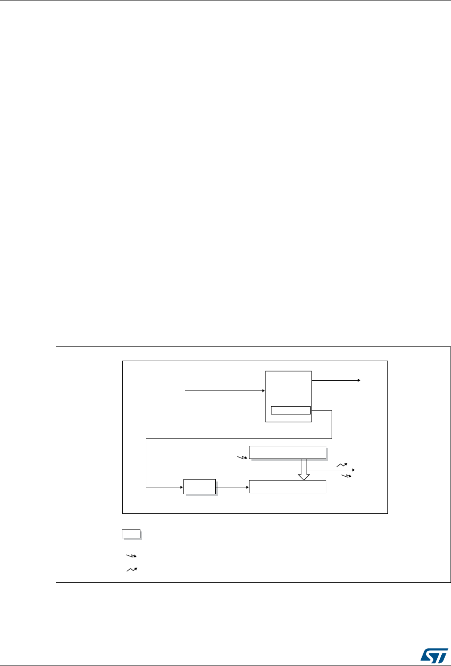
Basic timers (TIM6/TIM7) RM0394
968/1600 RM0394 Rev 4
29 Basic timers (TIM6/TIM7)
Timer TIM7 is available on STM32L43xxx and STM32L44xxx devices only.
29.1 TIM6/TIM7 introduction
The basic timers TIM6 and TIM7 consist of a 16-bit auto-reload counter driven by a
programmable prescaler.
They may be used as generic timers for time-base generation but they are also specifically
used to drive the digital-to-analog converter (DAC). In fact, the timers are internally
connected to the DAC and are able to drive it through their trigger outputs.
The timers are completely independent, and do not share any resources.
29.2 TIM6/TIM7 main features
Basic timer (TIM6/TIM7) features include:
•16-bit auto-reload upcounter
•16-bit programmable prescaler used to divide (also “on the fly”) the counter clock
frequency by any factor between 1 and 65535
•Synchronization circuit to trigger the DAC
•Interrupt/DMA generation on the update event: counter overflow
Figure 325. Basic timer block diagram
069
,QWHUQDOFORFN&.B,17
$XWRUHORDGUHJLVWHU
&17FRXQWHU
&.B36& &.B&17
6WRSFOHDURUXS
8,
8
8
1RWHV
5HJ 3UHORDGUHJLVWHUVWUDQVIHUUHG
WRDFWLYHUHJLVWHUVRQ8HYHQW
DFFRUGLQJWRFRQWUROELW
(YHQW
,QWHUUXSW'0$RXWSXW
36&
SUHVFDOHU
7ULJJHU
FRQWUROOHU
5HVHWHQDEOH&RXQW
7,0[&/.IURP5&&
75*2 WR'$&
&RQWURO

RM0394 Rev 4 969/1600
RM0394 Basic timers (TIM6/TIM7)
980
29.3 TIM6/TIM7 functional description
29.3.1 Time-base unit
The main block of the programmable timer is a 16-bit upcounter with its related auto-reload
register. The counter clock can be divided by a prescaler.
The counter, the auto-reload register and the prescaler register can be written or read by
software. This is true even when the counter is running.
The time-base unit includes:
•Counter Register (TIMx_CNT)
•Prescaler Register (TIMx_PSC)
•Auto-Reload Register (TIMx_ARR)
The auto-reload register is preloaded. The preload register is accessed each time an
attempt is made to write or read the auto-reload register. The contents of the preload
register are transferred into the shadow register permanently or at each update event UEV,
depending on the auto-reload preload enable bit (ARPE) in the TIMx_CR1 register. The
update event is sent when the counter reaches the overflow value and if the UDIS bit equals
0 in the TIMx_CR1 register. It can also be generated by software. The generation of the
update event is described in detail for each configuration.
The counter is clocked by the prescaler output CK_CNT, which is enabled only when the
counter enable bit (CEN) in the TIMx_CR1 register is set.
Note that the actual counter enable signal CNT_EN is set 1 clock cycle after CEN.
Prescaler description
The prescaler can divide the counter clock frequency by any factor between 1 and 65536. It
is based on a 16-bit counter controlled through a 16-bit register (in the TIMx_PSC register).
It can be changed on the fly as the TIMx_PSC control register is buffered. The new
prescaler ratio is taken into account at the next update event.
Figure 326 and Figure 327 give some examples of the counter behavior when the prescaler
ratio is changed on the fly.
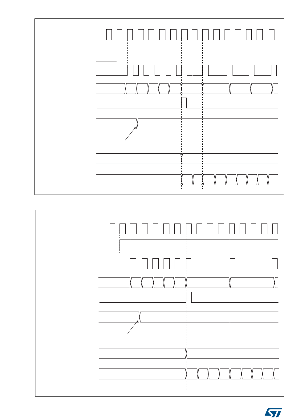
Basic timers (TIM6/TIM7) RM0394
970/1600 RM0394 Rev 4
Figure 326. Counter timing diagram with prescaler division change from 1 to 2
Figure 327. Counter timing diagram with prescaler division change from 1 to 4
&.B36&
&(1
7LPHUFORFN &.B&17
&RXQWHUUHJLVWHU
8SGDWHHYHQW8(9
3UHVFDOHUFRQWUROUHJLVWHU
:ULWHDQHZYDOXHLQ7,0[B36&
3UHVFDOHUEXIIHU
3UHVFDOHUFRXQWHU
)$ )%) ) ) )&
069
069
&.B36&
&(1
7LPHUFORFN &.B&17
&RXQWHUUHJLVWHU
8SGDWHHYHQW8(9
3UHVFDOHUFRQWUROUHJLVWHU
:ULWHDQHZYDOXHLQ7,0[B36&
3UHVFDOHUEXIIHU
3UHVFDOHUFRXQWHU
)$ )%
) ) ) )&
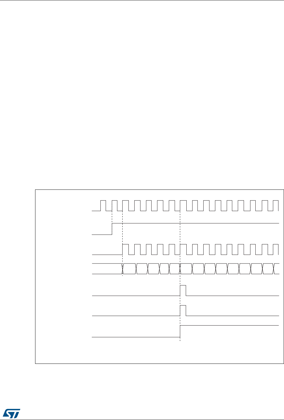
RM0394 Rev 4 971/1600
RM0394 Basic timers (TIM6/TIM7)
980
29.3.2 Counting mode
The counter counts from 0 to the auto-reload value (contents of the TIMx_ARR register),
then restarts from 0 and generates a counter overflow event.
An update event can be generate at each counter overflow or by setting the UG bit in the
TIMx_EGR register (by software or by using the slave mode controller).
The UEV event can be disabled by software by setting the UDIS bit in the TIMx_CR1
register. This avoids updating the shadow registers while writing new values into the preload
registers. In this way, no update event occurs until the UDIS bit has been written to 0,
however, the counter and the prescaler counter both restart from 0 (but the prescale rate
does not change). In addition, if the URS (update request selection) bit in the TIMx_CR1
register is set, setting the UG bit generates an update event UEV, but the UIF flag is not set
(so no interrupt or DMA request is sent).
When an update event occurs, all the registers are updated and the update flag (UIF bit in
the TIMx_SR register) is set (depending on the URS bit):
•The buffer of the prescaler is reloaded with the preload value (contents of the
TIMx_PSC register)
•The auto-reload shadow register is updated with the preload value (TIMx_ARR)
The following figures show some examples of the counter behavior for different clock
frequencies when TIMx_ARR = 0x36.
Figure 328. Counter timing diagram, internal clock divided by 1
069
&.B36&
&17B(1
7LPHUFORFN &.B&17
&RXQWHUUHJLVWHU
8SGDWHHYHQW8(9
&RXQWHURYHUIORZ
8SGDWHLQWHUUXSWIODJ
8,)
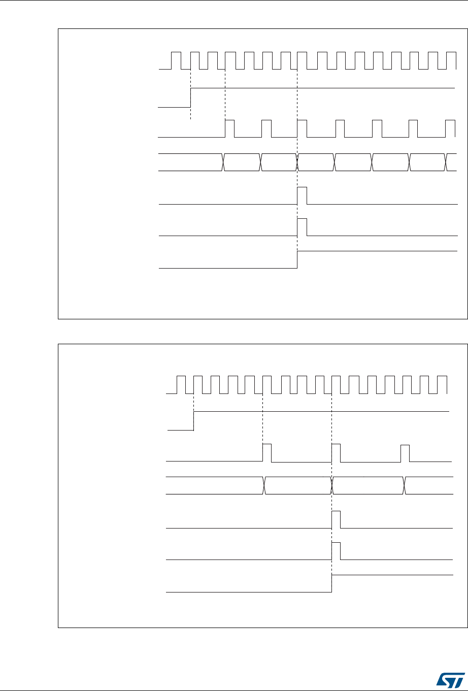
Basic timers (TIM6/TIM7) RM0394
972/1600 RM0394 Rev 4
Figure 329. Counter timing diagram, internal clock divided by 2
Figure 330. Counter timing diagram, internal clock divided by 4
069
&.B36&
&17B(1
7LPHUFORFN &.B&17
&RXQWHUUHJLVWHU
8SGDWHHYHQW8(9
&RXQWHURYHUIORZ
8SGDWHLQWHUUXSWIODJ
8,)
069
&.B36&
7LPHUFORFN &.B&17
&RXQWHUUHJLVWHU
8SGDWHHYHQW8(9
&RXQWHURYHUIORZ
8SGDWHLQWHUUXSWIODJ
8,)
&17B(1

RM0394 Rev 4 973/1600
RM0394 Basic timers (TIM6/TIM7)
980
Figure 331. Counter timing diagram, internal clock divided by N
Figure 332. Counter timing diagram, update event when ARPE = 0 (TIMx_ARR not
preloaded)
)
069
&.B36&
7LPHUFORFN &.B&17
&RXQWHUUHJLVWHU
8SGDWHHYHQW8(9
&RXQWHURYHUIORZ
8SGDWHLQWHUUXSWIODJ
8,)
))
069
&.B36&
7LPHUFORFN &.B&17
&RXQWHUUHJLVWHU
8SGDWHHYHQW8(9
&RXQWHURYHUIORZ
8SGDWHLQWHUUXSWIODJ
8,)
&(1
$XWRUHORDGSUHORDG
UHJLVWHU
:ULWHDQHZYDOXHLQ7,0[B$55

Basic timers (TIM6/TIM7) RM0394
974/1600 RM0394 Rev 4
Figure 333. Counter timing diagram, update event when ARPE=1 (TIMx_ARR
preloaded)
29.3.3 UIF bit remapping
The IUFREMAP bit in the TIMx_CR1 register forces a continuous copy of the Update
Interrupt Flag UIF into the timer counter register’s bit 31 (TIMxCNT[31]). This allows to
atomically read both the counter value and a potential roll-over condition signaled by the
UIFCPY flag. In particular cases, it can ease the calculations by avoiding race conditions
caused for instance by a processing shared between a background task (counter reading)
and an interrupt (Update Interrupt).
There is no latency between the assertions of the UIF and UIFCPY flags.
29.3.4 Clock source
The counter clock is provided by the Internal clock (CK_INT) source.
The CEN (in the TIMx_CR1 register) and UG bits (in the TIMx_EGR register) are actual
control bits and can be changed only by software (except for UG that remains cleared
automatically). As soon as the CEN bit is written to 1, the prescaler is clocked by the internal
clock CK_INT.
Figure 334 shows the behavior of the control circuit and the upcounter in normal mode,
without prescaler.
069
)
&.B36&
7LPHUFORFN &.B&17
&RXQWHUUHJLVWHU
8SGDWHHYHQW8(9
&RXQWHURYHUIORZ
8SGDWHLQWHUUXSWIODJ
8,)
) ) ) ) ))
&(1
$XWRUHORDGSUHORDG
UHJLVWHU
:ULWHDQHZYDOXHLQ7,0[B$55
$XWRUHORDGVKDGRZ
UHJLVWHU )
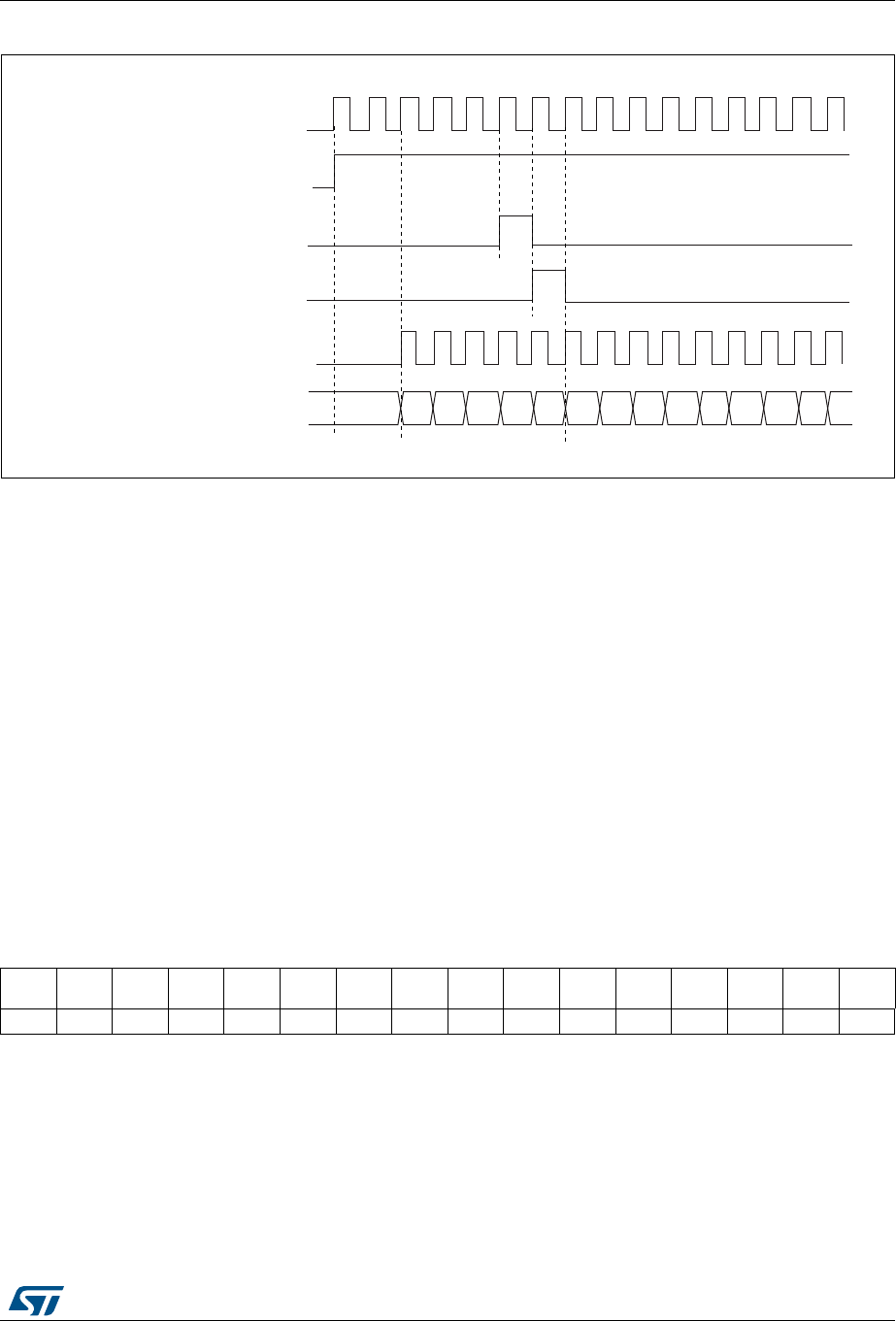
RM0394 Rev 4 975/1600
RM0394 Basic timers (TIM6/TIM7)
980
Figure 334. Control circuit in normal mode, internal clock divided by 1
29.3.5 Debug mode
When the microcontroller enters the debug mode (Cortex®-M4 core - halted), the TIMx
counter either continues to work normally or stops, depending on the DBG_TIMx_STOP
configuration bit in the DBG module. For more details, refer to Section 46.16.2: Debug
support for timers, RTC, watchdog, bxCAN and I2C.
29.4 TIM6/TIM7 registers
Refer to Section 1.2 on page 60 for a list of abbreviations used in register descriptions.
The peripheral registers can be accessed by half-words (16-bit) or words (32-bit).
29.4.1 TIM6/TIM7 control register 1 (TIMx_CR1)
Address offset: 0x00
Reset value: 0x0000
,QWHUQDOFORFN
&RXQWHUFORFN &.B&17 &.B36&
&RXQWHUUHJLVWHU
&(1 &17B(1
8*
&17B,1,7
069
1514131211109876543210
Res. Res. Res. Res. UIFRE
MAP Res. Res. Res. ARPE Res. Res. Res. OPM URS UDIS CEN
rw rw rw rw rw rw
Bits 15:12 Reserved, must be kept at reset value.
Bit 11 UIFREMAP: UIF status bit remapping
0: No remapping. UIF status bit is not copied to TIMx_CNT register bit 31.
1: Remapping enabled. UIF status bit is copied to TIMx_CNT register bit 31.
Bits 10:8 Reserved, must be kept at reset value.

Basic timers (TIM6/TIM7) RM0394
976/1600 RM0394 Rev 4
Bit 7 ARPE: Auto-reload preload enable
0: TIMx_ARR register is not buffered.
1: TIMx_ARR register is buffered.
Bits 6:4 Reserved, must be kept at reset value.
Bit 3 OPM: One-pulse mode
0: Counter is not stopped at update event
1: Counter stops counting at the next update event (clearing the CEN bit).
Bit 2 URS: Update request source
This bit is set and cleared by software to select the UEV event sources.
0: Any of the following events generates an update interrupt or DMA request if enabled.
These events can be:
– Counter overflow/underflow
– Setting the UG bit
– Update generation through the slave mode controller
1: Only counter overflow/underflow generates an update interrupt or DMA request if
enabled.
Bit 1 UDIS: Update disable
This bit is set and cleared by software to enable/disable UEV event generation.
0: UEV enabled. The Update (UEV) event is generated by one of the following events:
– Counter overflow/underflow
– Setting the UG bit
– Update generation through the slave mode controller
Buffered registers are then loaded with their preload values.
1: UEV disabled. The Update event is not generated, shadow registers keep their value
(ARR, PSC). However the counter and the prescaler are reinitialized if the UG bit is set or if
a hardware reset is received from the slave mode controller.
Bit 0 CEN: Counter enable
0: Counter disabled
1: Counter enabled
Note: Gated mode can work only if the CEN bit has been previously set by software.
However trigger mode can set the CEN bit automatically by hardware.
CEN is cleared automatically in one-pulse mode, when an update event occurs.

RM0394 Rev 4 977/1600
RM0394 Basic timers (TIM6/TIM7)
980
29.4.2 TIM6/TIM7 control register 2 (TIMx_CR2)
Address offset: 0x04
Reset value: 0x0000
29.4.3 TIM6/TIM7 DMA/Interrupt enable register (TIMx_DIER)
Address offset: 0x0C
Reset value: 0x0000
1514131211109876543210
Res. Res. Res. Res. Res. Res. Res. Res. Res. MMS[2:0] Res. Res. Res. Res.
rw rw rw
Bits 15:7 Reserved, must be kept at reset value.
Bits 6:4 MMS: Master mode selection
These bits are used to select the information to be sent in master mode to slave timers for
synchronization (TRGO). The combination is as follows:
000: Reset - the UG bit from the TIMx_EGR register is used as a trigger output (TRGO). If
reset is generated by the trigger input (slave mode controller configured in reset mode) then
the signal on TRGO is delayed compared to the actual reset.
001: Enable - the Counter enable signal, CNT_EN, is used as a trigger output (TRGO). It is
useful to start several timers at the same time or to control a window in which a slave timer
is enabled. The Counter Enable signal is generated by a logic OR between CEN control bit
and the trigger input when configured in gated mode.
When the Counter Enable signal is controlled by the trigger input, there is a delay on TRGO,
except if the master/slave mode is selected (see the MSM bit description in the TIMx_SMCR
register).
010: Update - The update event is selected as a trigger output (TRGO). For instance a
master timer can then be used as a prescaler for a slave timer.
Note: The clock of the slave timer or ADC must be enabled prior to receive events from the
master timer, and must not be changed on-the-fly while triggers are received from the
master timer.
Bits 3:0 Reserved, must be kept at reset value.
1514131211109876543210
Res. Res. Res. Res. Res. Res. Res. UDE Res. Res. Res. Res. Res. Res. Res. UIE
rw rw
Bits 15:9 Reserved, must be kept at reset value.
Bit 8 UDE: Update DMA request enable
0: Update DMA request disabled.
1: Update DMA request enabled.
Bits 7:1 Reserved, must be kept at reset value.
Bit 0 UIE: Update interrupt enable
0: Update interrupt disabled.
1: Update interrupt enabled.
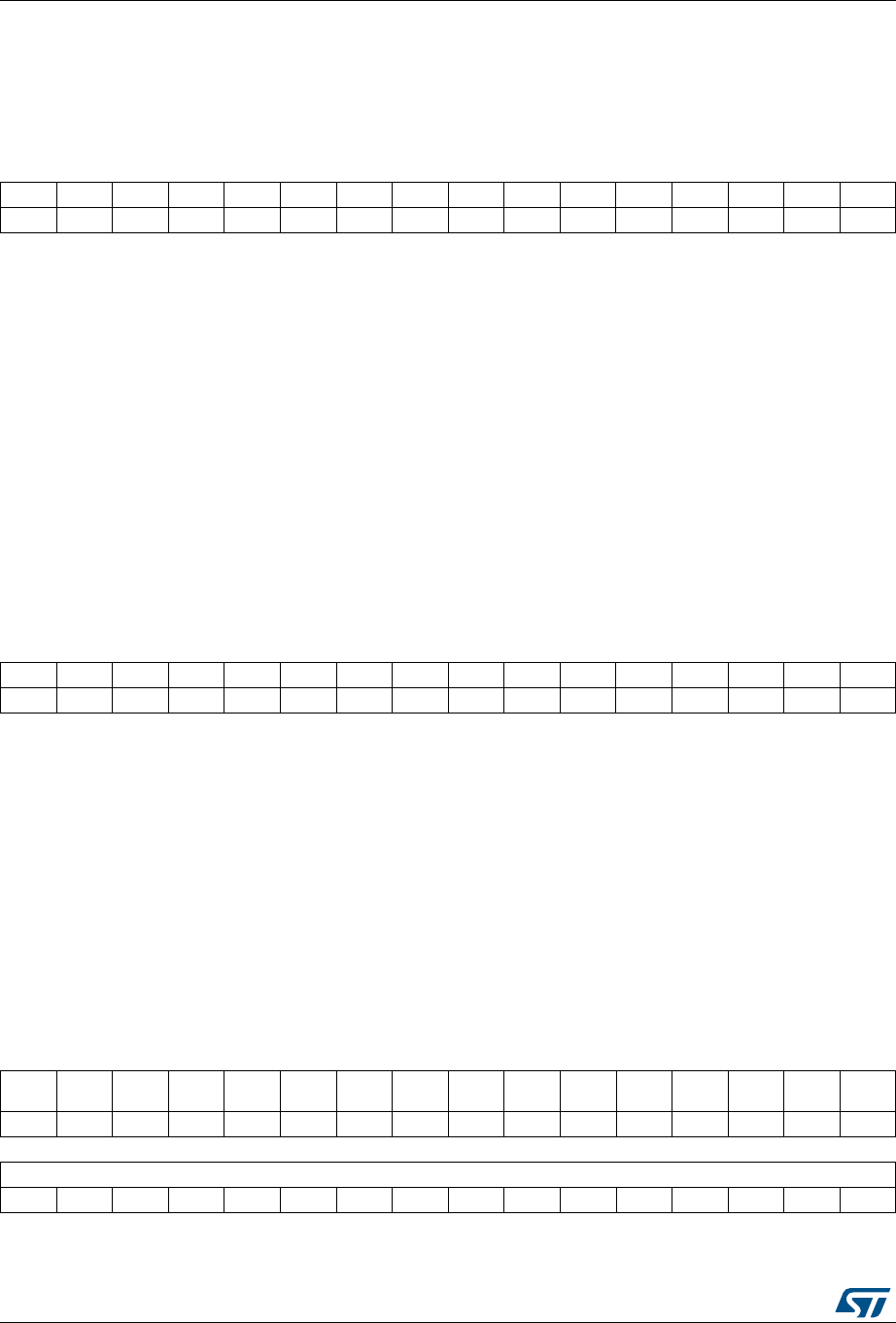
Basic timers (TIM6/TIM7) RM0394
978/1600 RM0394 Rev 4
29.4.4 TIM6/TIM7 status register (TIMx_SR)
Address offset: 0x10
Reset value: 0x0000
29.4.5 TIM6/TIM7 event generation register (TIMx_EGR)
Address offset: 0x14
Reset value: 0x0000
29.4.6 TIM6/TIM7 counter (TIMx_CNT)
Address offset: 0x24
Reset value: 0x0000 0000
1514131211109876543210
Res. Res. Res. Res. Res. Res. Res. Res. Res. Res. Res. Res. Res. Res. Res. UIF
rc_w0
Bits 15:1 Reserved, must be kept at reset value.
Bit 0 UIF: Update interrupt flag
This bit is set by hardware on an update event. It is cleared by software.
0: No update occurred.
1: Update interrupt pending. This bit is set by hardware when the registers are updated:
– At overflow or underflow regarding the repetition counter value and if UDIS = 0 in the
TIMx_CR1 register.
– When CNT is reinitialized by software using the UG bit in the TIMx_EGR register, if URS = 0
and UDIS = 0 in the TIMx_CR1 register.
1514131211109876543210
Res. Res. Res. Res. Res. Res. Res. Res. Res. Res. Res. Res. Res. Res. Res. UG
w
Bits 15:1 Reserved, must be kept at reset value.
Bit 0 UG: Update generation
This bit can be set by software, it is automatically cleared by hardware.
0: No action.
1: Re-initializes the timer counter and generates an update of the registers. Note that the
prescaler counter is cleared too (but the prescaler ratio is not affected).
31 30 29 28 27 26 25 24 23 22 21 20 19 18 17 16
UIF
CPY Res. Res. Res. Res. Res. Res. Res. Res. Res. Res. Res. Res. Res. Res. Res.
r
1514131211109876543210
CNT[15:0]
rw rw rw rw rw rw rw rw rw rw rw rw rw rw rw rw

RM0394 Rev 4 979/1600
RM0394 Basic timers (TIM6/TIM7)
980
29.4.7 TIM6/TIM7 prescaler (TIMx_PSC)
Address offset: 0x28
Reset value: 0x0000
29.4.8 TIM6/TIM7 auto-reload register (TIMx_ARR)
Address offset: 0x2C
Reset value: 0xFFFF
Bit 31 UIFCPY: UIF Copy
This bit is a read-only copy of the UIF bit of the TIMx_ISR register. If the UIFREMAP bit in
TIMx_CR1 is reset, bit 31 is reserved and read as 0.
Bits 30:16 Reserved, must be kept at reset value.
Bits 15:0 CNT[15:0]: Counter value
1514131211109876543210
PSC[15:0]
rw rw rw rw rw rw rw rw rw rw rw rw rw rw rw rw
Bits 15:0 PSC[15:0]: Prescaler value
The counter clock frequency CK_CNT is equal to fCK_PSC / (PSC[15:0] + 1).
PSC contains the value to be loaded into the active prescaler register at each update event.
(including when the counter is cleared through UG bit of TIMx_EGR register or through
trigger controller when configured in “reset mode”).
1514131211109876543210
ARR[15:0]
rw rw rw rw rw rw rw rw rw rw rw rw rw rw rw rw
Bits 15:0 ARR[15:0]: Prescaler value
ARR is the value to be loaded into the actual auto-reload register.
Refer to Section 29.3.1: Time-base unit on page 969 for more details about ARR update and
behavior.
The counter is blocked while the auto-reload value is null.
Basic timers (TIM6/TIM7) RM0394
980/1600 RM0394 Rev 4
29.4.9 TIM6/TIM7 register map
TIMx registers are mapped as 16-bit addressable registers as described in the table below:
Refer to Section 2.2.2 on page 67 for the register boundary addresses.
Table 144. TIM6/TIM7 register map and reset values
Offset Register
name
31
30
29
28
27
26
25
24
23
22
21
20
19
18
17
16
15
14
13
12
11
10
9
8
7
6
5
4
3
2
1
0
0x00
TIMx_CR1
Res.
Res.
Res.
Res.
Res.
Res.
Res.
Res.
Res.
Res.
Res.
Res.
Res.
Res.
Res.
Res.
Res.
Res.
Res.
Res.
UIFREMAP
Res.
Res.
Res.
ARPE
Res.
Res.
Res.
OPM
URS
UDIS
CEN
Reset value 000000
0x04
TIMx_CR2
Res.
Res.
Res.
Res.
Res.
Res.
Res.
Res.
Res.
Res.
Res.
Res.
Res.
Res.
Res.
Res.
Res.
Res.
Res.
Res.
Res.
Res.
Res.
Res.
Res.
MMS
[2:0]
Res.
Res.
Res.
Res.
Reset value 000
0x08 Reserved
0x0C
TIMx_DIER
Res.
Res.
Res.
Res.
Res.
Res.
Res.
Res.
Res.
Res.
Res.
Res.
Res.
Res.
Res.
Res.
Res.
Res.
Res.
Res.
Res.
Res.
Res.
UDE
Res.
Res.
Res.
Res.
Res.
Res.
Res.
UIE
Reset value 00
0x10
TIMx_SR
Res.
Res.
Res.
Res.
Res.
Res.
Res.
Res.
Res.
Res.
Res.
Res.
Res.
Res.
Res.
Res.
Res.
Res.
Res.
Res.
Res.
Res.
Res.
Res.
Res.
Res.
Res.
Res.
Res.
Res.
Res.
UIF
Reset value 0
0x14
TIMx_EGR
Res.
Res.
Res.
Res.
Res.
Res.
Res.
Res.
Res.
Res.
Res.
Res.
Res.
Res.
Res.
Res.
Res.
Res.
Res.
Res.
Res.
Res.
Res.
Res.
Res.
Res.
Res.
Res.
Res.
Res.
Res.
UG
Reset value 0
0x18-
0x20 Reserved
0x24
TIMx_CNT
UIFCPY or Res.
Res.
Res.
Res.
Res.
Res.
Res.
Res.
Res.
Res.
Res.
Res.
Res.
Res.
Res.
Res.
CNT[15:0]
Reset value 0 0000000000000000
0x28
TIMx_PSC
Res.
Res.
Res.
Res.
Res.
Res.
Res.
Res.
Res.
Res.
Res.
Res.
Res.
Res.
Res.
Res.
PSC[15:0]
Reset value 0000000000000000
0x2C
TIMx_ARR
Res.
Res.
Res.
Res.
Res.
Res.
Res.
Res.
Res.
Res.
Res.
Res.
Res.
Res.
Res.
Res.
ARR[15:0]
Reset value 1111111111111111

RM0394 Rev 4 981/1600
RM0394 Low-power timer (LPTIM)
1011
30 Low-power timer (LPTIM)
30.1 Introduction
The LPTIM is a 16-bit timer that benefits from the ultimate developments in power
consumption reduction. Thanks to its diversity of clock sources, the LPTIM is able to keep
running in all power modes except for Standby mode. Given its capability to run even with
no internal clock source, the LPTIM can be used as a “Pulse Counter” which can be useful
in some applications. Also, the LPTIM capability to wake up the system from low-power
modes, makes it suitable to realize “Timeout functions” with extremely low power
consumption.
The LPTIM introduces a flexible clock scheme that provides the needed functionalities and
performance, while minimizing the power consumption.
30.2 LPTIM main features
•16 bit upcounter
•3-bit prescaler with 8 possible dividing factors (1,2,4,8,16,32,64,128)
•Selectable clock
– Internal clock sources: LSE, LSI, HSI16 or APB clock
– External clock source over LPTIM input (working with no LP oscillator running,
used by Pulse Counter application)
•16 bit ARR autoreload register
•16 bit compare register
•Continuous/One-shot mode
•Selectable software/hardware input trigger
•Programmable Digital Glitch filter
•Configurable output: Pulse, PWM
•Configurable I/O polarity
•Encoder mode
•Repetition counter
30.3 LPTIM implementation
Table 145 describes LPTIM implementation on
STM32L41xxx/42xxx/43xxx/44xxx/45xxx/46xxx devices: the full set of features is
implemented in LPTIM1. LPTIM2 supports a smaller set of features, but is otherwise
identical to LPTIM1.
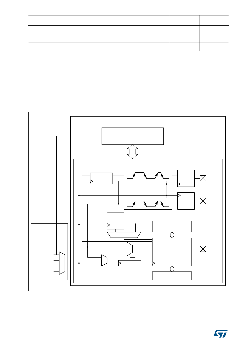
Low-power timer (LPTIM) RM0394
982/1600 RM0394 Rev 4
30.4 LPTIM functional description
30.4.1 LPTIM block diagram
Figure 335. Low-power timer block diagram for STM32L43xxx/44xxx/45xxx/46xxx
Table 145. STM32L41xxx/42xxx/43xxx/44xxx/45xxx/46xxx LPTIM features
LPTIM modes/features(1)
1. X = supported.
LPTIM1 LPTIM2
Encoder mode X -
Timer counter reset X(2)
2. Available only on STM32L41xxx and STM32L42xxx devices.
X(2)
Repetition counter X(2) X(2)
5&&
/37,0
$3%B,7)
.HUQHO
069
VZ
WULJJHU
XSWRH[W
WULJJHU
&/.08;
+6,
/6,
/6(
$3%FORFN
ELWFRPSDUH
ELWFRXQWHU
ELW$55
2XW
3UHVFDOHU
0X[WULJJHU
*OLWFK
ILOWHU
*OLWFK
ILOWHU ,QSXW
(QFRGHU *OLWFK
ILOWHU ,QSXW
8SGRZQ
µ &2817
02'(
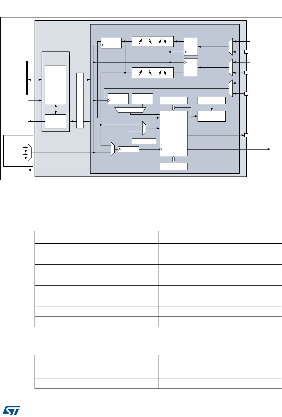
RM0394 Rev 4 983/1600
RM0394 Low-power timer (LPTIM)
1011
Figure 336. Low-power timer block diagram for STM32L41xxx/42xxx
1. lptim_out is the internal LPTIM output signal that can be connected to internal peripherals.
30.4.2 LPTIM trigger mapping
The LPTIM external trigger connections are detailed hereafter:
06Y9
/37,0
.HUQHOFORFNGRPDLQ
,54
LQWHUIDFH
/37,0
UHJLVWHU
LQWHUIDFH
$3%FORFN
GRPDLQ
ELW$3%EXV
5&&
:DNHXS
$3%FORFN
/37,0
LQWHUUXSW
&/.08;
ELWFRXQWHU
&RXQWPRGH
ELWFRPSDUH
5HSHWLWLRQ
FRXQWHU
3UHVFDOHU
/37,0B287
OSWLPBRXW
6\QFKURQ]DWLRQ
+6,
/6,
/6(
$3%&/.
ELW$55 /37,0B5&5
0X[WULJJHU
*OLWFK
ILOWHU
&176757
61*6757
*OLWFK
ILOWHU /37,0B,1
(QFRGHU
8SGRZQ
/37,0B,1
OSWLPBLQBPX[
OSWLPBLQBPX[
OSWLPBLQBPX[
OSWLPBLQBPX[
OSWLPBLQBPX[
OSWLPBLQBPX[
*OLWFK
ILOWHU
/37,0B(75
OSWLPBH[WBWULJ[
Table 146. LPTIM1 external trigger connection
TRIGSEL External trigger
lptim_ext_trig0 GPIO
lptim_ext_trig1 RTC alarm A
lptim_ext_trig2 RTC alarm B
lptim_ext_trig3 RTC_TAMP1 input detection
lptim_ext_trig4 RTC_TAMP2 input detection
lptim_ext_trig5 RTC_TAMP3 input detection(1)
1. Reserved on STM32L412xx and STM32L422xx devices.
lptim_ext_trig6 COMP1_OUT
lptim_ext_trig7 COMP2_OUT(1)
Table 147. LPTIM2 external trigger connection
TRIGSEL External trigger
lptim_ext_trig0 GPIO
lptim_ext_trig1 RTC alarm A

Low-power timer (LPTIM) RM0394
984/1600 RM0394 Rev 4
30.4.3 LPTIM reset and clocks
The LPTIM can be clocked using several clock sources. It can be clocked using an internal
clock signal which can be chosen among APB, LSI, LSE or HSI16 sources through the
Reset and Clock controller (RCC). Also, the LPTIM can be clocked using an external clock
signal injected on its external Input1. When clocked with an external clock source, the
LPTIM may run in one of these two possible configurations:
•The first configuration is when the LPTIM is clocked by an external signal but in the
same time an internal clock signal is provided to the LPTIM either from APB or any
other embedded oscillator including LSE, LSI and HSI16.
•The second configuration is when the LPTIM is solely clocked by an external clock
source through its external Input1. This configuration is the one used to realize Timeout
function or Pulse counter function when all the embedded oscillators are turned off
after entering a low-power mode.
Programming the CKSEL and COUNTMODE bits allows controlling whether the LPTIM will
use an external clock source or an internal one.
When configured to use an external clock source, the CKPOL bits are used to select the
external clock signal active edge. If both edges are configured to be active ones, an internal
clock signal should also be provided (first configuration). In this case, the internal clock
signal frequency should be at least four times higher than the external clock signal
frequency.
30.4.4 Glitch filter
The LPTIM inputs, either external (mapped to GPIOs) or internal (mapped on the chip-level
to other embedded peripherals, such as embedded comparators), are protected with digital
filters that prevent any glitches and noise perturbations to propagate inside the LPTIM. This
is in order to prevent spurious counts or triggers.
Before activating the digital filters, an internal clock source should first be provided to the
LPTIM. This is necessary to guarantee the proper operation of the filters.
The digital filters are divided into two groups:
•The first group of digital filters protects the LPTIM external inputs. The digital filters
sensitivity is controlled by the CKFLT bits
•The second group of digital filters protects the LPTIM internal trigger inputs. The digital
filters sensitivity is controlled by the TRGFLT bits.
lptim_ext_trig2 RTC alarm B
lptim_ext_trig3 RTC_TAMP1 input detection
lptim_ext_trig4 RTC_TAMP2 input detection
lptim_ext_trig5 RTC_TAMP3 input detection(1)
lptim_ext_trig6 COMP1_OUT
lptim_ext_trig7 COMP2_OUT(1)
1. Reserved on STM32L412xx and STM32L422xx devices.
Table 147. LPTIM2 external trigger connection (continued)
TRIGSEL External trigger
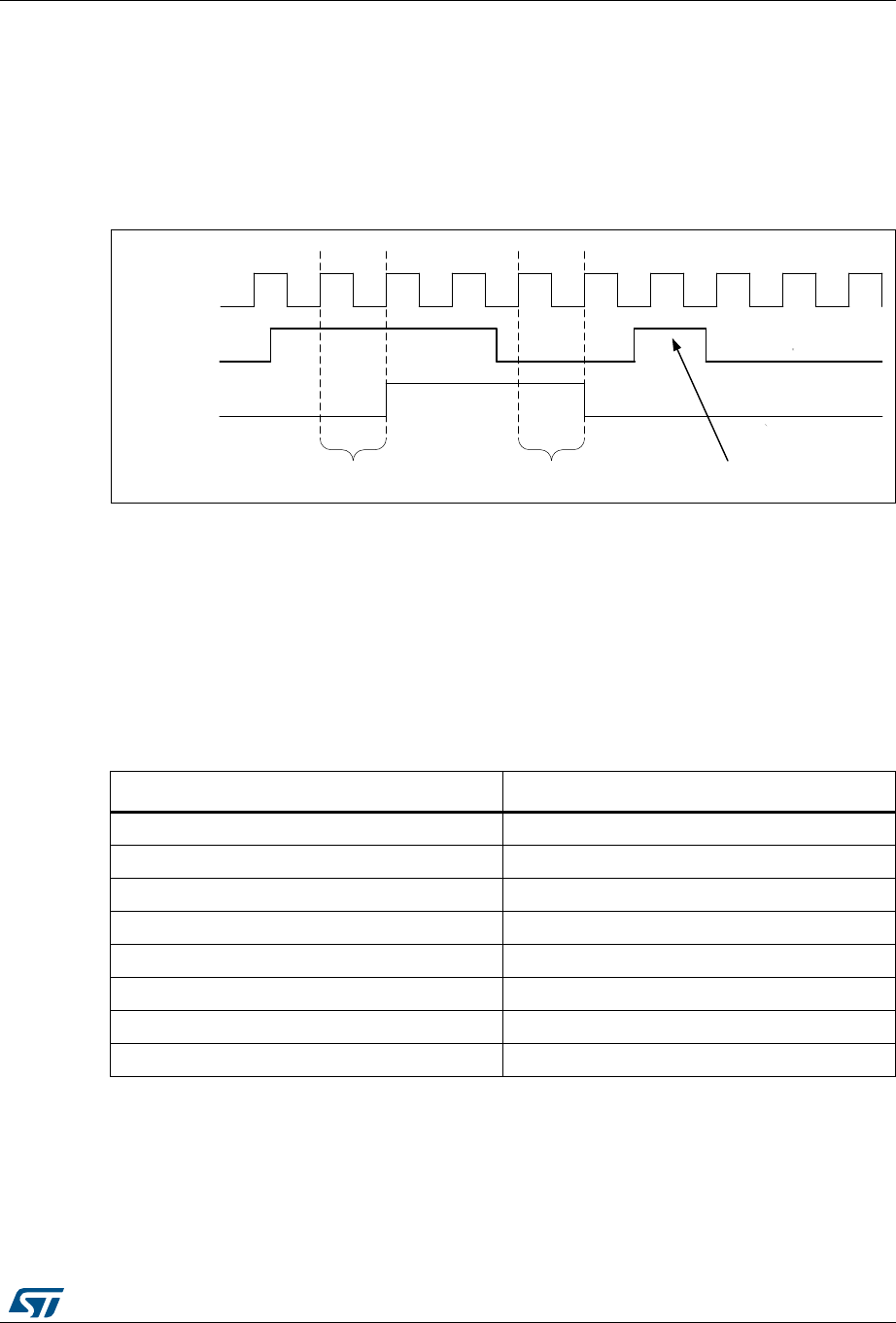
RM0394 Rev 4 985/1600
RM0394 Low-power timer (LPTIM)
1011
Note: The digital filters sensitivity is controlled by groups. It is not possible to configure each digital
filter sensitivity separately inside the same group.
The filter sensitivity acts on the number of consecutive equal samples that should be
detected on one of the LPTIM inputs to consider a signal level change as a valid transition.
Figure 337 shows an example of glitch filter behavior in case of a 2 consecutive samples
programmed.
Figure 337. Glitch filter timing diagram
Note: In case no internal clock signal is provided, the digital filter must be deactivated by setting
the CKFLT and TRGFLT bits to ‘0’. In that case, an external analog filter may be used to
protect the LPTIM external inputs against glitches.
30.4.5 Prescaler
The LPTIM 16-bit counter is preceded by a configurable power-of-2 prescaler. The prescaler
division ratio is controlled by the PRESC[2:0] 3-bit field. The table below lists all the possible
division ratios:
30.4.6 Trigger multiplexer
The LPTIM counter may be started either by software or after the detection of an active
edge on one of the 8 trigger inputs.
069
&/.08;
,QSXW
)LOWHURXW
FRQVHFXWLYHVDPSOHV FRQVHFXWLYHVDPSOHV )LOWHUHG
Table 148. Prescaler division ratios
programming dividing factor
000 /1
001 /2
010 /4
011 /8
100 /16
101 /32
110 /64
111 /128

Low-power timer (LPTIM) RM0394
986/1600 RM0394 Rev 4
TRIGEN[1:0] is used to determine the LPTIM trigger source:
•When TRIGEN[1:0] equals ‘00’, The LPTIM counter is started as soon as one of the
CNTSTRT or the SNGSTRT bits is set by software. The three remaining possible
values for the TRIGEN[1:0] are used to configure the active edge used by the trigger
inputs. The LPTIM counter starts as soon as an active edge is detected.
•When TRIGEN[1:0] is different than ‘00’, TRIGSEL[2:0] is used to select which of the 8
trigger inputs is used to start the counter.
The external triggers are considered asynchronous signals for the LPTIM. So after a trigger
detection, a two-counter-clock period latency is needed before the timer starts running due
to the synchronization.
If a new trigger event occurs when the timer is already started it will be ignored (unless
timeout function is enabled).
Note: The timer must be enabled before setting the SNGSTRT/CNTSTRT bits. Any write on these
bits when the timer is disabled will be discarded by hardware.
30.4.7 Operating mode
The LPTIM features two operating modes:
•The Continuous mode: the timer is free running, the timer is started from a trigger event
and never stops until the timer is disabled
•One-shot mode: the timer is started from a trigger event and stops when an LPTIM
update event is generated (or when reaching the ARR value for products without
repetition counter).
One-shot mode
To enable the one-shot counting, the SNGSTRT bit must be set.
- When repetition counter feature is not available:
A new trigger event will re-start the timer. Any trigger event occurring after the counter starts
and before the counter reaches ARR will be discarded.
In case an external trigger is selected, each external trigger event arriving after the
SNGSTRT bit is set, and after the counter register has stopped (contains zero value), will
start the counter for a new one-shot counting cycle as shown in Figure 338.
Figure 338. LPTIM output waveform, single counting mode configuration
- When repetition counter feature is available:
06Y9
3:0
&RPSDUH
/37,0B$55
([WHUQDOWULJJHUHYHQW
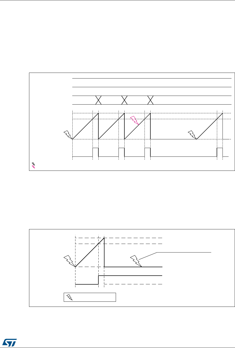
RM0394 Rev 4 987/1600
RM0394 Low-power timer (LPTIM)
1011
A new trigger event will re-start the timer. Any trigger event occurring after the counter starts
and before the next LPTIM update event, will be discarded.
In case an external trigger is selected, each external trigger event arriving after the
SNGSTRT bit is set, and after the repetition counter has stopped (after the update event),
and if the repetition register content is different from zero, the repetition counter gets
reloaded with the value already contained by the repetition register and a new one-shot
counting cycle is started as shown in Figure 339.
Figure 339. LPTIM output waveform, single counting mode configuration
when repetition register content is different than zero (with PRELOAD = 1)
- Set-once mode activated:
It should be noted that when the WAVE bit-field in the LPTIM_CFGR register is set, the Set-
once mode is activated. In this case, the counter is only started once following the first
trigger, and any subsequent trigger event is discarded as shown in Figure 340.
Figure 340. LPTIM output waveform, Single counting mode configuration
and Set-once mode activated (WAVE bit is set)
In case of software start (TRIGEN[1:0] = ‘00’), the SNGSTRT setting will start the counter for
one-shot counting.
06Y9
/37,0B5&5
5HSHWLWLRQFRXQWHU
/37,0B$55
&RPSDUH
3:0
([WHUQDOWULJJHUHYHQW
,JQRUHGH[WHUQDOWULJJHUHYHQW
06Y9
3:0
&RPSDUH
/37,0B$55
'LVFDUGHGWULJJHU
([WHUQDOWULJJHUHYHQW
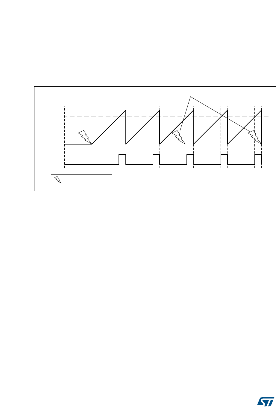
Low-power timer (LPTIM) RM0394
988/1600 RM0394 Rev 4
Continous mode
To enable the continuous counting, the CNTSTRT bit must be set.
In case an external trigger is selected, an external trigger event arriving after CNTSTRT is
set will start the counter for continuous counting. Any subsequent external trigger event will
be discarded as shown in Figure 341.
In case of software start (TRIGEN[1:0] = ‘00’), setting CNTSTRT will start the counter for
continuous counting.
Figure 341. LPTIM output waveform, Continuous counting mode configuration
SNGSTRT and CNTSTRT bits can only be set when the timer is enabled (The ENABLE bit
is set to ‘1’). It is possible to change “on the fly” from One-shot mode to Continuous mode.
If the Continous mode was previously selected, setting SNGSTRT will switch the LPTIM to
the One-shot mode. The counter (if active) will stop as soon as an LPTIM update event is
generated (or as soon as it reaches ARR for products without repetition counter).
If the One-shot mode was previously selected, setting CNTSTRT will switch the LPTIM to
the Continuous mode. The counter (if active) will restart as soon as it reaches ARR.
30.4.8 Timeout function
The detection of an active edge on one selected trigger input can be used to reset the
LPTIM counter. This feature is controlled through the TIMOUT bit.
The first trigger event will start the timer, any successive trigger event will reset the LPTIM
counter and the repetition counter and the timer will restart.
A low-power timeout function can be realized. The timeout value corresponds to the
compare value; if no trigger occurs within the expected time frame, the MCU is waked-up by
the compare match event.
06Y9
3:0
&RPSDUH
/37,0B$55
'LVFDUGHGWULJJHUV
([WHUQDOWULJJHUHYHQW

RM0394 Rev 4 989/1600
RM0394 Low-power timer (LPTIM)
1011
30.4.9 Waveform generation
Two 16-bit registers, the LPTIM_ARR (autoreload register) and LPTIM_CMP (compare
register), are used to generate several different waveforms on LPTIM output
The timer can generate the following waveforms:
•The PWM mode: the LPTIM output is set as soon as the counter value in LPTIM_CNT
exceeds the compare value in LPTIM_CMP. The LPTIM output is reset as soon as a
match occurs between the LPTIM_ARR and the LPTIM_CNT registers.
•The One-pulse mode: the output waveform is similar to the one of the PWM mode for
the first pulse, then the output is permanently reset
•The Set-once mode: the output waveform is similar to the One-pulse mode except that
the output is kept to the last signal level (depends on the output configured polarity).
The above described modes require that the LPTIM_ARR register value be strictly greater
than the LPTIM_CMP register value.
The LPTIM output waveform can be configured through the WAVE bit as follow:
•Resetting the WAVE bit to ‘0’ forces the LPTIM to generate either a PWM waveform or
a One pulse waveform depending on which bit is set: CNTSTRT or SNGSTRT.
•Setting the WAVE bit to ‘1’ forces the LPTIM to generate a Set-once mode waveform.
The WAVPOL bit controls the LPTIM output polarity. The change takes effect immediately,
so the output default value will change immediately after the polarity is re-configured, even
before the timer is enabled.
Signals with frequencies up to the LPTIM clock frequency divided by 2 can be generated.
Figure 342 below shows the three possible waveforms that can be generated on the LPTIM
output. Also, it shows the effect of the polarity change using the WAVPOL bit.
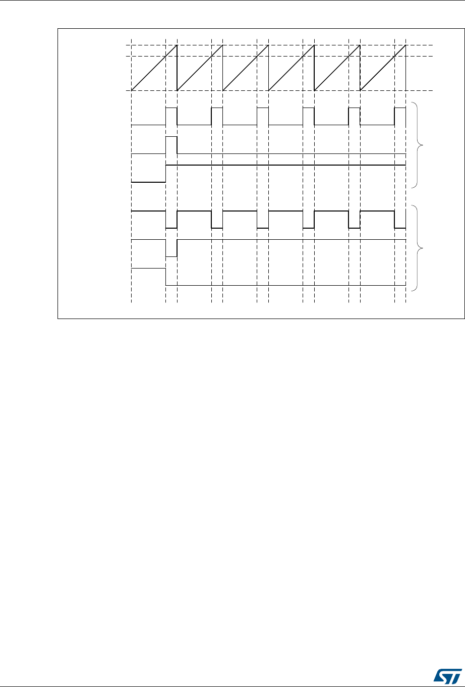
Low-power timer (LPTIM) RM0394
990/1600 RM0394 Rev 4
Figure 342. Waveform generation
30.4.10 Register update
The LPTIM_ARR register and LPTIM_CMP register are updated immediately after the APB
bus write operation or in synchronization with the next LPTIM update event if the timer is
already started (or at the end of the current period if the timer is already started for products
without repetition counter).
The PRELOAD bit controls how the LPTIM_ARR and the LPTIM_CMP registers are
updated:
•When the PRELOAD bit is reset to ‘0’, the LPTIM_ARR and the LPTIM_CMP registers
are immediately updated after any write access.
•When the PRELOAD bit is set to ‘1’, the LPTIM_ARR and the LPTIM_CMP registers
are updated at next LPTIM update event (or at the end of the current period for
products without repetition counter), if the timer has been already started.
The LPTIM APB interface and the LPTIM kernel logic use different clocks, so there is some
latency between the APB write and the moment when these values are available to the
counter comparator. Within this latency period, any additional write into these registers must
be avoided.
The ARROK flag and the CMPOK flag in the LPTIM_ISR register indicate when the write
operation is completed to respectively the LPTIM_ARR register and the LPTIM_CMP
register.
After a write to the LPTIM_ARR register or the LPTIM_CMP register, a new write operation
to the same register can only be performed when the previous write operation is completed.
Any successive write before respectively the ARROK flag or the CMPOK flag be set, will
lead to unpredictable results.
069
/37,0B$55
&RPSDUH
3:0
2QHVKRW
6HWRQFH
3:0
2QHVKRW
6HWRQFH
3RO
3RO

RM0394 Rev 4 991/1600
RM0394 Low-power timer (LPTIM)
1011
30.4.11 Counter mode
The LPTIM counter can be used to count external events on the LPTIM Input1 or it can be
used to count internal clock cycles. The CKSEL and COUNTMODE bits control which
source will be used for updating the counter.
In case the LPTIM is configured to count external events on Input1, the counter can be
updated following a rising edge, falling edge or both edges depending on the value written
to the CKPOL[1:0] bits.
The count modes below can be selected, depending on CKSEL and COUNTMODE values:
•CKSEL = 0: the LPTIM is clocked by an internal clock source
– COUNTMODE = 0
The LPTIM is configured to be clocked by an internal clock source and the LPTIM
counter is configured to be updated following each internal clock pulse.
– COUNTMODE = 1
The LPTIM external Input1 is sampled with the internal clock provided to the
LPTIM.
Consequently, in order not to miss any event, the frequency of the changes on the
external Input1 signal should never exceed the frequency of the internal clock
provided to the LPTIM. Also, the internal clock provided to the LPTIM must not be
prescaled (PRESC[2:0] = 000).
•CKSEL = 1: the LPTIM is clocked by an external clock source
COUNTMODE value is don’t care.
In this configuration, the LPTIM has no need for an internal clock source (except if the
glitch filters are enabled). The signal injected on the LPTIM external Input1 is used as
system clock for the LPTIM. This configuration is suitable for operation modes where
no embedded oscillator is enabled.
For this configuration, the LPTIM counter can be updated either on rising edges or
falling edges of the input1 clock signal but not on both rising and falling edges.
Since the signal injected on the LPTIM external Input1 is also used to clock the LPTIM
kernel logic, there is some initial latency (after the LPTIM is enabled) before the counter
is incremented. More precisely, the first five active edges on the LPTIM external Input1
(after LPTIM is enable) are lost.
30.4.12 Timer enable
The ENABLE bit located in the LPTIM_CR register is used to enable/disable the LPTIM
kernel logic. After setting the ENABLE bit, a delay of two counter clock is needed before the
LPTIM is actually enabled.
The LPTIM_CFGR and LPTIM_IER registers must be modified only when the LPTIM is
disabled.

Low-power timer (LPTIM) RM0394
992/1600 RM0394 Rev 4
30.4.13 Timer counter reset(a)
In order to reset the content of LPTIM_CNT register to zero, two reset mechanisms are
implemented:
•The synchronous reset mechanism: the synchronous reset is controlled by the
COUNTRST bit in the LPTIM_CR register. After setting the COUNTRST bit-field to '1',
the reset signal is propagated in the LPTIM kernel clock domain. So it is important to
note that a few clock pulses of the LPTIM kernel logic will elapse before the reset is
taken into account. This will make the LPTIM counter count few extra pluses between
the time when the reset is trigger and it become effective. Since the COUNTRST bit is
located in the APB clock domain and the LPTIM counter is located in the LPTIM kernel
clock domain, a delay of 3 clock cycles of the kernel clock is needed to synchronize the
reset signal issued by the APB clock domain when writing '1' to the COUNTRST bit.
•The asynchronous reset mechanism: the asynchronous reset is controlled by the
RSTARE bit located in the LPTIM_CR register. When this bit is set to '1', any read
access to the LPTIM_CNT register will reset its content to zero. Asynchronous reset
should be triggered within a timeframe in which no LPTIM core clock is provided. For
example when LPTIM Input1 is used as external clock source, the asynchronous reset
should be applied only when there is enough insurance that no toggle will occur on the
LPTIM Input1.
It should be noted that to read reliably the content of the LPTIM_CNT register two
successive read accesses must be performed and compared. A read access can be
considered reliable when the value of the two read accesses is equal. Unfortunately
when asynchronous reset is enabled there is no possibility to read twice the
LPTIM_CNT register.
Warning: There is no mechanism inside the LPTIM that prevents the
two reset mechanisms from being used simultaneously. So
developer should make sure that these two mechanisms are
used exclusively.
30.4.14 Encoder mode
This mode allows handling signals from quadrature encoders used to detect angular
position of rotary elements. Encoder interface mode acts simply as an external clock with
direction selection. This means that the counter just counts continuously between 0 and the
auto-reload value programmed into the LPTIM_ARR register (0 up to ARR or ARR down to
0 depending on the direction). Therefore you must configure LPTIM_ARR before starting.
From the two external input signals, Input1 and Input2, a clock signal is generated to clock
the LPTIM counter. The phase between those two signals determines the counting direction.
The Encoder mode is only available when the LPTIM is clocked by an internal clock source.
The signals frequency on both Input1 and Input2 inputs must not exceed the LPTIM internal
clock frequency divided by 4. This is mandatory in order to guarantee a proper operation of
the LPTIM.
a. Available only on STM32L41xxx and STM32L42xxx devices.
RM0394 Rev 4 993/1600
RM0394 Low-power timer (LPTIM)
1011
Direction change is signalized by the two Down and Up flags in the LPTIM_ISR register.
Also, an interrupt can be generated for both direction change events if enabled through the
DOWNIE bit.
To activate the Encoder mode the ENC bit has to be set to ‘1’. The LPTIM must first be
configured in Continuous mode.
When Encoder mode is active, the LPTIM counter is modified automatically following the
speed and the direction of the incremental encoder. Therefore, its content always
represents the encoder’s position. The count direction, signaled by the Up and Down flags,
correspond to the rotation direction of the encoder rotor.
According to the edge sensitivity configured using the CKPOL[1:0] bits, different counting
scenarios are possible. The following table summarizes the possible combinations,
assuming that Input1 and Input2 do not switch at the same time.
The following figure shows a counting sequence for Encoder mode where both-edge
sensitivity is configured.
Caution: In this mode the LPTIM must be clocked by an internal clock source, so the CKSEL bit must
be maintained to its reset value which is equal to ‘0’. Also, the prescaler division ratio must
be equal to its reset value which is 1 (PRESC[2:0] bits must be ‘000’).
Table 149. Encoder counting scenarios
Active edge
Level on opposite
signal (Input1 for
Input2, Input2 for
Input1)
Input1 signal Input2 signal
Rising Falling Rising Falling
Rising Edge
High Down No count Up No count
Low Up No count Down No count
Falling Edge
High No count Up No count Down
Low No count Down No count Up
Both Edges
High Down Up Up Down
Low Up Down Down Up
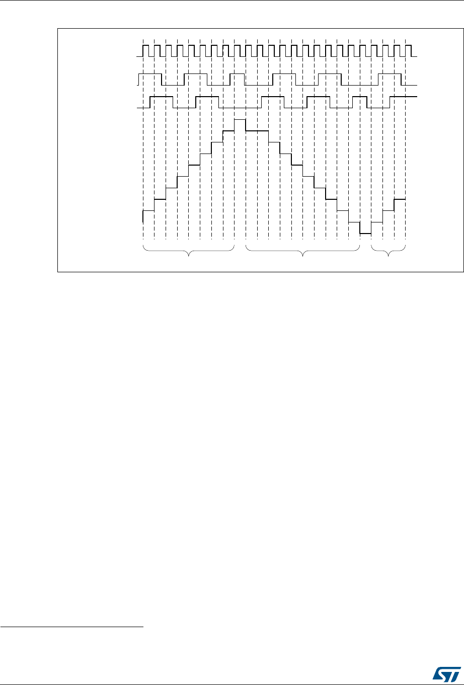
Low-power timer (LPTIM) RM0394
994/1600 RM0394 Rev 4
Figure 343. Encoder mode counting sequence
30.4.15 Repetition Counter(a)
The LPTIM features a repetition counter that decrements by 1 each time an LPTIM counter
overflow event occurs. A repetition counter underflow event is generated when the repetition
counter contains zero and the LPTIM counter overflows. Next to each repetition counter
underflow event, the repetition counter gets loaded with the content of the REP[7:0] bit-field
which belongs to the repetition register LPTIM_RCR.
A repetition underflow event is generated on each and every LPTIM counter overflow when
the REP[7:0] register is set to 0.
Writing to the REP[7:0] bit-field has no effect on the content of the repetition counter until the
next repetition underflow event occurs. The repetition counter continues to decrement each
LPTIM counter overflow event and only when a repetition underflow event is generated, the
new value written into REP[7:0] is loaded into the repetition counter. This behavior is
depicted in Figure 344.
069
7
&RXQWHU
XS XSGRZQ
7
a. Available only on STM32L41xxx and STM32L42xxx devices.
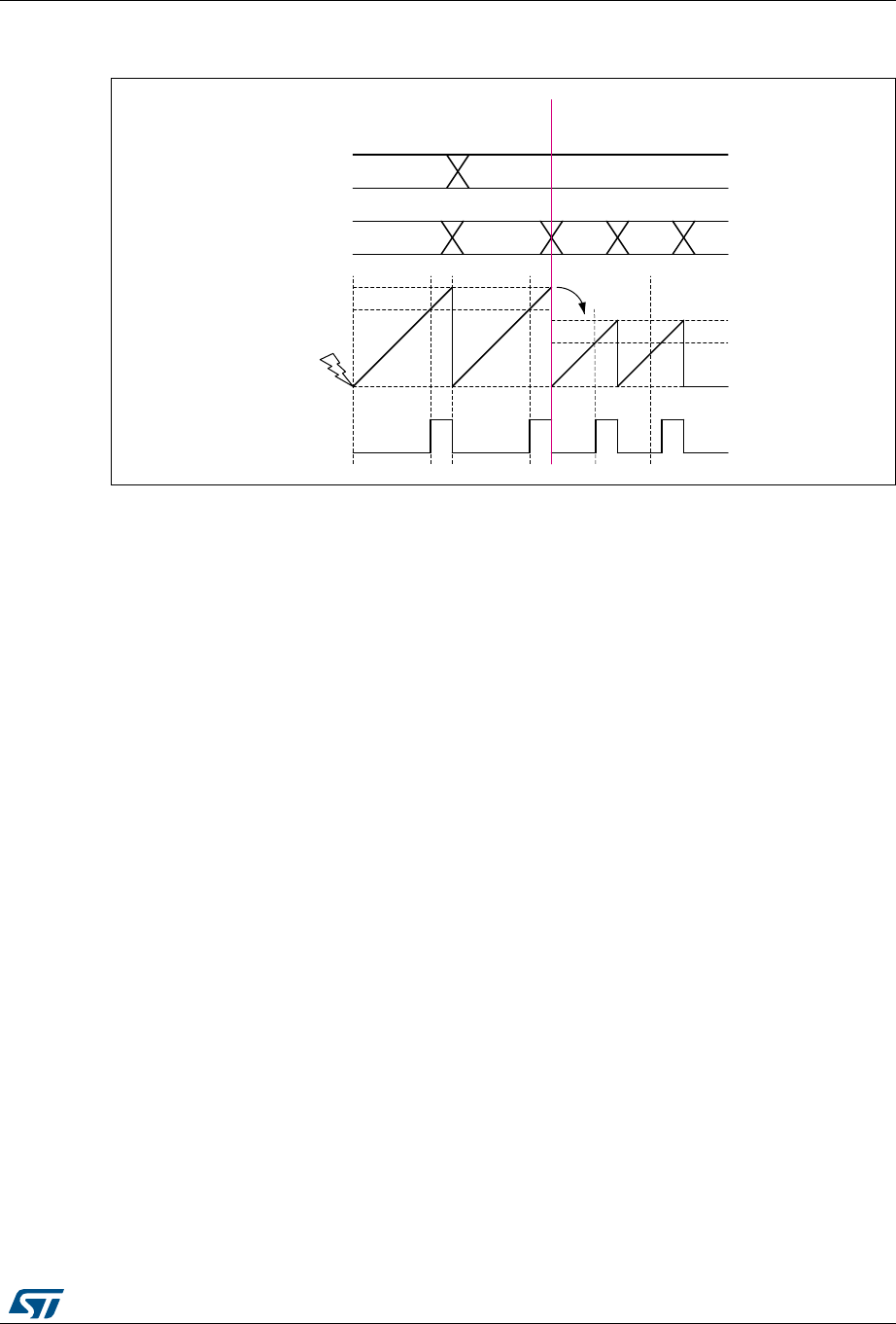
RM0394 Rev 4 995/1600
RM0394 Low-power timer (LPTIM)
1011
Figure 344. Continuous counting mode when repetition register LPTIM_RCR
different from zero (with PRELOAD = 1)
A repetition counter underflow event is systematically associated with LPTIM preloaded
registers update (refer to section "Register update" for more information).
Repetition counter underflow event is signaled to the software through the Update Event
(UE) flag mapped into the LPTIM_ISR register. When set, the UE flag can trigger an LPTIM
interrupt if its respective Update Event Interrupt Enable (UEIE) control bit, mapped to the
LPTIM_IER register, is set.
The repetition register LPTIM_RCR is located in the APB bus interface clock domain where
the repetition counter itself is located in the LPTIM kernel clock domain. Each time a new
value is written to the LPTIM_RCR register, that new content is propagated from the APB
bus interface clock domain to the LPTIM kernel clock domain so that the new written value
is loaded to the repetition counter immediately after a repetition counter underflow event.
The synchronization delay for the new written content is four APB clock cycles plus three
LPTIM kernel clock cycles and it is signaled by the REPOK flag located in the LPTIM_ISR
register when it is elapsed. When the LPTIM kernel clock cycle is relatively slow, for
instance when the LPTIM kernel is being clocked by the LSI clock source, it can be lengthy
to keep polling on the REPOK flag by software to detect that the synchronization of the
LPTIM_RCR register content is finished. For that reason, the REPOK flag, when set, can
generate an interrupt if its associated REPOKIE control bit in the LPTIM_IER register is set.
Note: After a write to the LPTIM_RCR register, a new write operation to the same register can only
be performed when the previous write operation is completed. Any successive write before
the REPOK flag is set, will lead to unpredictable results.
Caution: When using repetition counter the PRELOAD bit in the LPTIM_CFGR register must be set,
otherwise an unpredictable behavior may occur.
30.4.16 Debug mode
When the microcontroller enters debug mode (core halted), the LPTIM counter either
continues to work normally or stops, depending on the DBG_LPTIM_STOP configuration bit
in the DBG module.
06Y9
/37,0B5&5
5HSHWLWLRQFRXQWHU
/37,0B$55
&RPSDUH
3:0
5HSHWLWLRQFRXQWHUXQGHUIORZHYHQW
3UHORDGHGUHJLVWHUVXSGDWHG

Low-power timer (LPTIM) RM0394
996/1600 RM0394 Rev 4
30.5 LPTIM low-power modes
30.6 LPTIM interrupts
The following events generate an interrupt/wake-up event, if they are enabled through the
LPTIM_IER register:
•Compare match
•Auto-reload match (whatever the direction if encoder mode)
•External trigger event
•Autoreload register write completed
•Compare register write completed
•Direction change (encoder mode), programmable (up / down / both).
•Update Event(a)
•Repetition register update Ok(a)
Note: If any bit in the LPTIM_IER register (Interrupt Enable Register) is set after that its
corresponding flag in the LPTIM_ISR register (Status Register) is set, the interrupt is not
asserted.
Table 150. Effect of low-power modes on the LPTIM
Mode Description
Sleep No effect. LPTIM interrupts cause the device to exit Sleep mode.
Low-power run No effect.
Low-power sleep No effect. LPTIM interrupts cause the device to exit the Low-power sleep
mode.
Stop 0 / Stop 1 No effect when LPTIM is clocked by LSE or LSI. LPTIM interrupts cause
the device to exit Stop 0 and Stop 1.
Stop 2
No effect on LPTIM1 when LPTIM1 is clocked by LSE or LSI. LPTIM1
interrupts cause the device to exit Stop 2. LPTIM2 registers content is
kept but LPTIM2 must be disabled before entering Stop 2.
Standby The LPTIM peripheral is powered down and must be reinitialized after
exiting Standby or Shutdown mode.
Shutdown
a. Available only on STM32L41xxx and STM32L42xxx devices.
Table 151. Interrupt events
Interrupt event Description
Compare match Interrupt flag is raised when the content of the Counter register
(LPTIM_CNT) matches the content of the compare register (LPTIM_CMP).
Auto-reload match
Interrupt flag is raised when the content of the Counter register
(LPTIM_CNT) matches the content of the Auto-reload register
(LPTIM_ARR).
External trigger event Interrupt flag is raised when an external trigger event is detected

RM0394 Rev 4 997/1600
RM0394 Low-power timer (LPTIM)
1011
30.7 LPTIM registers
30.7.1 LPTIM interrupt and status register (LPTIM_ISR)
Address offset: 0x000
Reset value: 0x0000 0000
Auto-reload register
update OK
Interrupt flag is raised when the write operation to the LPTIM_ARR register
is complete.
Compare register
update OK
Interrupt flag is raised when the write operation to the LPTIM_CMP register
is complete.
Direction change
Used in Encoder mode. Two interrupt flags are embedded to signal
direction change:
– UP flag signals up-counting direction change
– DOWN flag signals down-counting direction change.
Update Event(1) Interrupt flag is raised when the repetition counter underflows (or contains
zero) and the LPTIM counter overflows.
Repetition register
update Ok(1)
REPOK is set by hardware to inform application that the APB bus write
operation to the LPTIM_RCR register has been successfully completed.
1. Available only on STM32L41xxx and STM32L42xxx devices.
Table 151. Interrupt events (continued)
Interrupt event Description
31 30 29 28 27 26 25 24 23 22 21 20 19 18 17 16
Res. Res. Res. Res. Res. Res. Res. Res. Res. Res. Res. Res. Res. Res. Res. Res.
1514131211109876543210
Res. Res. Res. Res. Res. Res. Res. REP
OK UE DOWN UP ARRO
K
CMP
OK
EXTTR
IG ARRM CMPM
rrrrrrrrr
Bits 31:22 Reserved, must be kept at reset value.
Bit 21 Reserved, must be kept at reset value.
Bit 20 Reserved, must be kept at reset value.
Bit 19 Reserved, must be kept at reset value.
Bits 18:16 Reserved, must be kept at reset value.
Bit 15 Reserved, must be kept at reset value.
Bit 14 Reserved, must be kept at reset value.
Bit 13 Reserved, must be kept at reset value.
Bit 12 Reserved, must be kept at reset value.
Bit 11 Reserved, must be kept at reset value.
Bit 10 Reserved, must be kept at reset value.

Low-power timer (LPTIM) RM0394
998/1600 RM0394 Rev 4
Bit 9 Reserved, must be kept at reset value.
Bit 8 REPOK: Repetition register update Ok
REPOK is set by hardware to inform application that the APB bus write operation to the LPTIM_RCR
register has been successfully completed. REPOK flag can be cleared by writing 1 to the REPOKCF
bit in the LPTIM_ICR register.
Note: If the LPTIM does not support repetition counter feature, this bit is reserved. Please refer to
Section 30.3: LPTIM implementation.
Bit 7 UE: LPTIM update event occurred
UE is set by hardware to inform application that an update event was generated. UE flag can be
cleared by writing 1 to the UECF bit in the LPTIM_ICR register. In autonomous mode, the UE flag is
automatically cleared by hardware once the LPTIM_ARR register is written by DMA.
Note: If the LPTIM does not support repetition counter feature, this bit is reserved. Please refer to
Section 30.3: LPTIM implementation.
Bit 6 DOWN: Counter direction change up to down
In Encoder mode, DOWN bit is set by hardware to inform application that the counter direction has
changed from up to down. DOWN flag can be cleared by writing 1 to the DOWNCF bit in the
LPTIM_ICR register.
Bit 5 UP: Counter direction change down to up
In Encoder mode, UP bit is set by hardware to inform application that the counter direction has
changed from down to up. UP flag can be cleared by writing 1 to the UPCF bit in the LPTIM_ICR
register.
Bit 4 ARROK: Autoreload register update OK
ARROK is set by hardware to inform application that the APB bus write operation to the LPTIM_ARR
register has been successfully completed. ARROK flag can be cleared by writing 1 to the ARROKCF
bit in the LPTIM_ICR register.
Bit 3 CMPOK: Compare register update OK
CMPOK is set by hardware to inform application that the APB bus write operation to the
LPTIM_CMP register has been successfully completed.
Bit 2 EXTTRIG: External trigger edge event
EXTTRIG is set by hardware to inform application that a valid edge on the selected external trigger
input has occurred. If the trigger is ignored because the timer has already started, then this flag is
not set. EXTTRIG flag can be cleared by writing 1 to the EXTTRIGCF bit in the LPTIM_ICR register.
Bit 1 ARRM: Autoreload match
ARRM is set by hardware to inform application that LPTIM_CNT register’s value reached the
LPTIM_ARR register’s value. ARRM flag can be cleared by writing 1 to the ARRMCF bit in the
LPTIM_ICR register.
Bit 0 CMPM: Compare match
The CMPM bit is set by hardware to inform application that LPTIM_CNT register value reached the
LPTIM_CMP register’s value.

RM0394 Rev 4 999/1600
RM0394 Low-power timer (LPTIM)
1011
30.7.2 LPTIM interrupt clear register (LPTIM_ICR)
Address offset: 0x004
Reset value: 0x0000 0000
31 30 29 28 27 26 25 24 23 22 21 20 19 18 17 16
Res. Res. Res. Res. Res. Res. Res. Res. Res. Res. Res. Res. Res. Res. Res. Res.
1514131211109876543210
Res. Res. Res. Res. Res. Res. Res. REPOK
CF UECF DOWN
CF UPCF ARRO
KCF
CMPO
KCF
EXTTR
IGCF
ARRM
CF
CMPM
CF
wwwwwwwww
Bits 31:22 Reserved, must be kept at reset value.
Bit 21 Reserved, must be kept at reset value.
Bit 20 Reserved, must be kept at reset value.
Bit 19 Reserved, must be kept at reset value.
Bits 18:16 Reserved, must be kept at reset value.
Bit 15 Reserved, must be kept at reset value.
Bit 14 Reserved, must be kept at reset value.
Bit 13 Reserved, must be kept at reset value.
Bit 12 Reserved, must be kept at reset value.
Bit 11 Reserved, must be kept at reset value.
Bit 10 Reserved, must be kept at reset value.
Bit 9 Reserved, must be kept at reset value.
Bit 8 REPOKCF: Repetition register update OK clear flag
Writing 1 to this bit clears the REPOK flag in the LPTIM_ISR register.
Note: If the LPTIM does not support repetition counter feature, this bit is reserved. Please refer to
Section 30.3: LPTIM implementation.
Bit 7 UECF: Update event clear flag
Writing 1 to this bit clear the UE flag in the LPTIM_ISR register.
Note: If the LPTIM does not support repetition counter feature, this bit is reserved. Please refer to
Section 30.3: LPTIM implementation.
Bit 6 DOWNCF: Direction change to down clear flag
Writing 1 to this bit clear the DOWN flag in the LPTIM_ISR register.
Bit 5 UPCF: Direction change to UP clear flag
Writing 1 to this bit clear the UP flag in the LPTIM_ISR register.
Bit 4 ARROKCF: Autoreload register update OK clear flag
Writing 1 to this bit clears the ARROK flag in the LPTIM_ISR register

Low-power timer (LPTIM) RM0394
1000/1600 RM0394 Rev 4
30.7.3 LPTIM interrupt enable register (LPTIM_IER)
Address offset: 0x008
Reset value: 0x0000 0000
Bit 3 CMPOKCF: Compare register update OK clear flag
Writing 1 to this bit clears the CMPOK flag in the LPTIM_ISR register
Bit 2 EXTTRIGCF: External trigger valid edge clear flag
Writing 1 to this bit clears the EXTTRIG flag in the LPTIM_ISR register
Bit 1 ARRMCF: Autoreload match clear flag
Writing 1 to this bit clears the ARRM flag in the LPTIM_ISR register
Bit 0 CMPMCF: Compare match clear flag
Writing 1 to this bit clears the CMP flag in the LPTIM_ISR register
31 30 29 28 27 26 25 24 23 22 21 20 19 18 17 16
Res. Res. Res. Res. Res. Res. Res. Res. Res. Res. Res. Res. Res. Res. Res. Res.
1514131211109876543210
Res. Res. Res. Res. Res. Res. Res. REPOK
IE UEIE DOWNI
EUPIE ARRO
KIE
CMPO
KIE
EXT
TRIGIE
ARRM
IE
CMPM
IE
rw rw rw rw rw rw rw rw rw
Bits 31:28 Reserved, must be kept at reset value.
Bit 27 Reserved, must be kept at reset value.
Bit 26 Reserved, must be kept at reset value.
Bit 25 Reserved, must be kept at reset value.
Bit 24 Reserved, must be kept at reset value.
Bit 23 Reserved, must be kept at reset value.
Bit 22 Reserved, must be kept at reset value.
Bit 21 Reserved, must be kept at reset value.
Bit 20 Reserved, must be kept at reset value.
Bit 19 Reserved, must be kept at reset value.
Bits 18:17 Reserved, must be kept at reset value.
Bit 16 Reserved, must be kept at reset value.
Bit 15 Reserved, must be kept at reset value.
Bit 14 Reserved, must be kept at reset value.
Bit 13 Reserved, must be kept at reset value.
Bit 12 Reserved, must be kept at reset value.
Bit 11 Reserved, must be kept at reset value.
Bit 10 Reserved, must be kept at reset value.
Bit 9 Reserved, must be kept at reset value.

RM0394 Rev 4 1001/1600
RM0394 Low-power timer (LPTIM)
1011
Caution: The LPTIM_IER register must only be modified when the LPTIM is disabled (ENABLE bit reset to ‘0’)
Bit 8 REPOKIE: Repetition register update OK interrupt Enable
0: Repetition register update OK interrupt disabled
1: Repetition register update OK interrupt enabled
Note: If the LPTIM does not support repetition counter feature, this bit is reserved. Please refer to
Section 30.3: LPTIM implementation.
Bit 7 UEIE: Update event interrupt enable
0: Update event interrupt disabled
1: Update event interrupt enabled
Note: If the LPTIM does not support repetition counter feature, this bit is reserved. Please refer to
Section 30.3: LPTIM implementation.
Bit 6 DOWNIE: Direction change to down Interrupt Enable
0: DOWN interrupt disabled
1: DOWN interrupt enabled
Bit 5 UPIE: Direction change to UP Interrupt Enable
0: UP interrupt disabled
1: UP interrupt enabled
Bit 4 ARROKIE: Autoreload register update OK Interrupt Enable
0: ARROK interrupt disabled
1: ARROK interrupt enabled
Bit 3 CMPOKIE: Compare register update OK Interrupt Enable
0: CMPOK interrupt disabled
1: CMPOK interrupt enabled
Bit 2 EXTTRIGIE: External trigger valid edge Interrupt Enable
0: EXTTRIG interrupt disabled
1: EXTTRIG interrupt enabled
Bit 1 ARRMIE: Autoreload match Interrupt Enable
0: ARRM interrupt disabled
1: ARRM interrupt enabled
Bit 0 CMPMIE: Compare match Interrupt Enable
0: CMPM interrupt disabled
1: CMPM interrupt enabled

Low-power timer (LPTIM) RM0394
1002/1600 RM0394 Rev 4
30.7.4 LPTIM configuration register (LPTIM_CFGR)
Address offset: 0x00C
Reset value: 0x0000 0000
31 30 29 28 27 26 25 24 23 22 21 20 19 18 17 16
Res. Res. Res. Res. Res. Res. Res. ENC COUNT
MODE PRELOAD WAVPOL WAVE TIMOUT TRIGEN[1:0] Res.
rw rw rw rw rw rw rw rw
15 14 13 12 11 10 9 8 7 6 5 4 3 2 1 0
TRIGSEL[2:0] Res. PRESC[2:0] Res. TRGFLT[1:0] Res. CKFLT[1:0] CKPOL[1:0] CKSEL
rw rw rw rw rw rw rw rw rw rw rw rw rw
Bits 31:30 Reserved, must be kept at reset value.
Bit 29 Reserved, must be kept at reset value.
Bits 28:25 Reserved, must be kept at reset value.
Bit 24 ENC: Encoder mode enable
The ENC bit controls the Encoder mode
0: Encoder mode disabled
1: Encoder mode enabled
Bit 23 COUNTMODE: counter mode enabled
The COUNTMODE bit selects which clock source is used by the LPTIM to clock the counter:
0: the counter is incremented following each internal clock pulse
1: the counter is incremented following each valid clock pulse on the LPTIM external Input1
Bit 22 PRELOAD: Registers update mode
The PRELOAD bit controls the LPTIM_ARR, LPTIM_RCR and the LPTIM_CMP registers update
modality
0: Registers are updated after each APB bus write access
1: Registers are updated at the end of the current LPTIM period
Bit 21 WAVPOL: Waveform shape polarity
The WAVEPOL bit controls the output polarity
0: The LPTIM output reflects the compare results between LPTIM_ARR and LPTIM_CMP
registers
1: The LPTIM output reflects the inverse of the compare results between LPTIM_ARR and
LPTIM_CMP registers
Bit 20 WAVE: Waveform shape
The WAVE bit controls the output shape
0: Deactivate Set-once mode, PWM / One Pulse waveform (depending on OPMODE bit)
1: Activate the Set-once mode
Bit 19 TIMOUT: Timeout enable
The TIMOUT bit controls the Timeout feature
0: A trigger event arriving when the timer is already started will be ignored
1: A trigger event arriving when the timer is already started will reset and restart the LPTIM counter
and the repetition counter

RM0394 Rev 4 1003/1600
RM0394 Low-power timer (LPTIM)
1011
Bits 18:17 TRIGEN[1:0]: Trigger enable and polarity
The TRIGEN bits controls whether the LPTIM counter is started by an external trigger or not. If the
external trigger option is selected, three configurations are possible for the trigger active edge:
00: software trigger (counting start is initiated by software)
01: rising edge is the active edge
10: falling edge is the active edge
11: both edges are active edges
Bit 16 Reserved, must be kept at reset value.
Bits 15:13 TRIGSEL[2:0]: Trigger selector
The TRIGSEL bits select the trigger source that will serve as a trigger event for the LPTIM among
the below 8 available sources:
000: lptim_ext_trig0
001: lptim_ext_trig1
010: lptim_ext_trig2
011: lptim_ext_trig3
100: lptim_ext_trig4
101: lptim_ext_trig5
110: lptim_ext_trig6
111: lptim_ext_trig7
See Section 30.4.2: LPTIM trigger mapping for details.
Bit 12 Reserved, must be kept at reset value.
Bits 11:9 PRESC[2:0]: Clock prescaler
The PRESC bits configure the prescaler division factor. It can be one among the following division
factors:
000: /1
001: /2
010: /4
011: /8
100: /16
101: /32
110: /64
111: /128
Bit 8 Reserved, must be kept at reset value.
Bits 7:6 TRGFLT[1:0]: Configurable digital filter for trigger
The TRGFLT value sets the number of consecutive equal samples that should be detected when a
level change occurs on an internal trigger before it is considered as a valid level transition. An
internal clock source must be present to use this feature
00: any trigger active level change is considered as a valid trigger
01: trigger active level change must be stable for at least 2 clock periods before it is considered as
valid trigger.
10: trigger active level change must be stable for at least 4 clock periods before it is considered as
valid trigger.
11: trigger active level change must be stable for at least 8 clock periods before it is considered as
valid trigger.
Bit 5 Reserved, must be kept at reset value.

Low-power timer (LPTIM) RM0394
1004/1600 RM0394 Rev 4
Caution: The LPTIM_CFGR register must only be modified when the LPTIM is disabled (ENABLE bit
reset to ‘0’).
30.7.5 LPTIM control register (LPTIM_CR)
Address offset: 0x010
Reset value: 0x0000 0000
Bits 4:3 CKFLT[1:0]: Configurable digital filter for external clock
The CKFLT value sets the number of consecutive equal samples that should be detected when a
level change occurs on an external clock signal before it is considered as a valid level transition. An
internal clock source must be present to use this feature
00: any external clock signal level change is considered as a valid transition
01: external clock signal level change must be stable for at least 2 clock periods before it is
considered as valid transition.
10: external clock signal level change must be stable for at least 4 clock periods before it is
considered as valid transition.
11: external clock signal level change must be stable for at least 8 clock periods before it is
considered as valid transition.
Bits 2:1 CKPOL[1:0]: Clock Polarity
If LPTIM is clocked by an external clock source:
When the LPTIM is clocked by an external clock source, CKPOL bits is used to configure the active
edge or edges used by the counter:
00: the rising edge is the active edge used for counting
01: the falling edge is the active edge used for counting
10: both edges are active edges. When both external clock signal edges are considered active
ones, the LPTIM must also be clocked by an internal clock source with a frequency equal to at
least four time the external clock frequency.
11: not allowed
If the LPTIM is configured in Encoder mode (ENC bit is set):
00: the encoder sub-mode 1 is active
01: the encoder sub-mode 2 is active
10: the encoder sub-mode 3 is active
Refer to Section 30.4.14: Encoder mode for more details about Encoder mode sub-modes.
Bit 0 CKSEL: Clock selector
The CKSEL bit selects which clock source the LPTIM will use:
0: LPTIM is clocked by internal clock source (APB clock or any of the embedded oscillators)
1: LPTIM is clocked by an external clock source through the LPTIM external Input1
31 30 29 28 27 26 25 24 23 22 21 20 19 18 17 16
Res. Res. Res. Res. Res. Res. Res. Res. Res. Res. Res. Res. Res. Res. Res. Res.
1514131211109876543210
Res. Res. Res. Res. Res. Res. Res. Res. Res. Res. Res. RST
ARE
COUN
TRST
CNT
STRT
SNG
STRT
ENA
BLE
rw rs rw rw rw

RM0394 Rev 4 1005/1600
RM0394 Low-power timer (LPTIM)
1011
Bits 31:5 Reserved, must be kept at reset value.
Bit 4 RSTARE: Reset after read enable
This bit is set and cleared by software. When RSTARE is set to '1', any read access to LPTIM_CNT
register will asynchronously reset LPTIM_CNT register content.
Note: If the LPTIM does not support counter reset feature, this bit is reserved. Please
refer to Section 30.3: LPTIM implementation.
Bit 3 COUNTRST: Counter reset
This bit is set by software and cleared by hardware. When set to '1' this bit will trigger a synchronous
reset of the LPTIM_CNT counter register. Due to the synchronous nature of this reset, it only takes
place after a synchronization delay of 3 LPTimer core clock cycles (LPTimer core clock may be
different from APB clock).
Caution: COUNTRST must never be set to '1' by software before it is already cleared to '0' by
hardware. Software should consequently check that COUNTRST bit is already cleared to '0'
before attempting to set it to '1'.
Note: If the LPTIM does not support counter reset feature, this bit is reserved. Please refer to
Section 30.3: LPTIM implementation.
Bit 2 CNTSTRT: Timer start in Continuous mode
This bit is set by software and cleared by hardware.
In case of software start (TRIGEN[1:0] = ‘00’), setting this bit starts the LPTIM in Continuous mode.
If the software start is disabled (TRIGEN[1:0] different than ‘00’), setting this bit starts the timer in
Continuous mode as soon as an external trigger is detected.
If this bit is set when a single pulse mode counting is ongoing, then the timer will not stop at the next
match between the LPTIM_ARR and LPTIM_CNT registers and the LPTIM counter keeps counting
in Continuous mode.
This bit can be set only when the LPTIM is enabled. It will be automatically reset by hardware.
Bit 1 SNGSTRT: LPTIM start in Single mode
This bit is set by software and cleared by hardware.
In case of software start (TRIGEN[1:0] = ‘00’), setting this bit starts the LPTIM in single pulse mode.
If the software start is disabled (TRIGEN[1:0] different than ‘00’), setting this bit starts the LPTIM in
single pulse mode as soon as an external trigger is detected.
If this bit is set when the LPTIM is in continuous counting mode, then the LPTIM will stop at the
following match between LPTIM_ARR and LPTIM_CNT registers.
This bit can only be set when the LPTIM is enabled. It will be automatically reset by hardware.
Bit 0 ENABLE: LPTIM enable
The ENABLE bit is set and cleared by software.
0:LPTIM is disabled
1:LPTIM is enabled

Low-power timer (LPTIM) RM0394
1006/1600 RM0394 Rev 4
30.7.6 LPTIM compare register (LPTIM_CMP)
Address offset: 0x014
Reset value: 0x0000 0000
Caution: The LPTIM_CMP register must only be modified when the LPTIM is enabled (ENABLE bit
set to ‘1’).
30.7.7 LPTIM autoreload register (LPTIM_ARR)
Address offset: 0x018
Reset value: 0x0000 0001
Caution: The LPTIM_ARR register must only be modified when the LPTIM is enabled (ENABLE bit
set to ‘1’).
31 30 29 28 27 26 25 24 23 22 21 20 19 18 17 16
Res. Res. Res. Res. Res. Res. Res. Res. Res. Res. Res. Res. Res. Res. Res. Res.
15 14 13 12 11 10 9 8 7 6 5 4 3 2 1 0
CMP[15:0]
rw rw rw rw rw rw rw rw rw rw rw rw rw rw rw rw
Bits 31:16 Reserved, must be kept at reset value.
Bits 15:0 CMP[15:0]: Compare value
CMP is the compare value used by the LPTIM.
31 30 29 28 27 26 25 24 23 22 21 20 19 18 17 16
Res. Res. Res. Res. Res. Res. Res. Res. Res. Res. Res. Res. Res. Res. Res. Res.
15 14 13 12 11 10 9 8 7 6 5 4 3 2 1 0
ARR[15:0]
rw rw rw rw rw rw rw rw rw rw rw rw rw rw rw rw
Bits 31:16 Reserved, must be kept at reset value.
Bits 15:0 ARR[15:0]: Auto reload value
ARR is the autoreload value for the LPTIM.
This value must be strictly greater than the CMP[15:0] value.
RM0394 Rev 4 1007/1600
RM0394 Low-power timer (LPTIM)
1011
30.7.8 LPTIM counter register (LPTIM_CNT)
Address offset: 0x01C
Reset value: 0x0000 0000
30.7.9 LPTIM1 option register (LPTIM1_OR)
Note: This register is only available for STM32L43xxx/44xxx/45xxx/46xxx devices.
Address offset: 0x020
Reset value: 0x0000 0000
31 30 29 28 27 26 25 24 23 22 21 20 19 18 17 16
Res. Res. Res. Res. Res. Res. Res. Res. Res. Res. Res. Res. Res. Res. Res. Res.
1514131211109876543210
CNT[15:0]
rrrrrrrrrrrrrrrr
Bits 31:16 Reserved, must be kept at reset value.
Bits 15:0 CNT[15:0]: Counter value
When the LPTIM is running with an asynchronous clock, reading the LPTIM_CNT register may
return unreliable values. So in this case it is necessary to perform two consecutive read accesses
and verify that the two returned values are identical.
It should be noted that for a reliable LPTIM_CNT register read access, two consecutive read
accesses must be performed and compared. A read access can be considered reliable when the
values of the two consecutive read accesses are equal.
31 30 29 28 27 26 25 24 23 22 21 20 19 18 17 16
Res. Res. Res. Res. Res. Res. Res. Res. Res. Res. Res. Res. Res. Res. Res. Res.
15 14 13 12 11 10 9 8 7 6 5 4 3 2 1 0
Res. Res. Res. Res. Res. Res. Res. Res. Res. Res. Res. Res. Res. Res. OR_1 OR_0
rw rw
Bits 31:2 Reserved, must be kept at reset value.
Bit 1 OR_1: Option register bit 1
0: LPTIM1 input 2 is connected to I/O
1: LPTIM1 input 2 is connected to COMP2_OUT
Bit 0 OR_0: Option register bit 0
0: LPTIM1 input 1 is connected to I/O
1: LPTIM1 input 1 is connected to COMP1_OUT

Low-power timer (LPTIM) RM0394
1008/1600 RM0394 Rev 4
30.7.10 LPTIM2 option register (LPTIM2_OR)
Note: This register is only available for STM32L43xxx/44xxx/45xxx/46xxx devices.
Address offset: 0x020
Reset value: 0x0000 0000
Note: When both OR_1 and OR_0 are set, LPTIM2 input 1 is connected to (COMP1_OUT OR
COMP2_OUT).
30.7.11 LPTIM configuration register 2 (LPTIM_CFGR2)
Note: This register is only available for STM32L41xxx and STM32L42xxx devices.
Address offset: 0x024
Reset value: 0x0000 0000
31 30 29 28 27 26 25 24 23 22 21 20 19 18 17 16
Res. Res. Res. Res. Res. Res. Res. Res. Res. Res. Res. Res. Res. Res. Res. Res.
15 14 13 12 11 10 9 8 7 6 5 4 3 2 1 0
Res. Res. Res. Res. Res. Res. Res. Res. Res. Res. Res. Res. Res. Res. OR_1 OR_0
rw rw
Bits 31:2 Reserved, must be kept at reset value.
Bit 1 OR_1: Option register bit 1
0: LPTIM2 input 1 is connected to I/O
1: LPTIM2 input 1 is connected to COMP2_OUT
Bit 0 OR_0: Option register bit 0
0: LPTIM2 input 1 is connected to I/O
1: LPTIM2 input 1 is connected to COMP1_OUT
31 30 29 28 27 26 25 24 23 22 21 20 19 18 17 16
Res. Res. Res. Res. Res. Res. Res. Res. Res. Res. Res. Res. Res. Res. Res. Res.
1514131211109876543210
Res. Res. Res. Res. Res. Res. Res. Res. Res. Res. IN2SEL[1:0] Res. Res. IN1SEL[1:0]
rw rw rw rw
Bits 31:6 Reserved, must be kept at reset value.
Bits 5:4 IN2SEL[1:0]: LPTIM input 2 selection
The IN2SEL bits control the LPTIM Input 2 multiplexer, which connect LPTIM Input 2 to one of the
available inputs.
00: lptim_in2_mux0
01: lptim_in2_mux1
10: lptim_in2_mux2
11: lptim_in2_mux3
For connection details refer to Section 30.4.2: LPTIM trigger mapping.

RM0394 Rev 4 1009/1600
RM0394 Low-power timer (LPTIM)
1011
Caution: The LPTIM_CFGR2 register must only be modified when the LPTIM is disabled (ENABLE
bit reset to ‘0’).
Note: Available only on STM32L41xxx and STM32L42xxx devices.
30.7.12 LPTIM repetition register (LPTIM_RCR)
Note: This register is only available for STM32L41xxx and STM32L42xxx devices.
Address offset: 0x028
Reset value: 0x0000 0000
Caution: The LPTIM_RCR register must only be modified when the LPTIM is enabled (ENABLE bit
set to ‘1’).
Bits 3:2 Reserved, must be kept at reset value.
Bits 1:0 IN1SEL[1:0]: LPTIM input 1 selection
The IN1SEL bits control the LPTIM Input 1 multiplexer, which connects LPTIM Input 1 to one of the
available inputs.
00: lptim_in1_mux0
01: lptim_in1_mux1
10: lptim_in1_mux2
11: lptim_in1_mux3
For connection details refer to Section 30.4.2: LPTIM trigger mapping.
31 30 29 28 27 26 25 24 23 22 21 20 19 18 17 16
Res. Res. Res. Res. Res. Res. Res. Res. Res. Res. Res. Res. Res. Res. Res. Res.
1514131211109876543210
Res. Res. Res. Res. Res. Res. Res. Res. REP[7:0]
rw rw rw rw rw rw rw rw
Bits 31:8 Reserved, must be kept at reset value.
Bits 7:0 REP[7:0]: Repetition register value
REP is the repetition value for the LPTIM. Writing to the REP[7:0] has no effect on the content of the
repetition counter until the next repetition underflow event occurs.
Low-power timer (LPTIM) RM0394
1010/1600 RM0394 Rev 4
30.7.13 LPTIM register map
The following table summarizes the LPTIM registers.
Table 152. LPTIM register map and reset values
Offset Register name
31
30
29
28
27
26
25
24
23
22
21
20
19
18
17
16
15
14
13
12
11
10
9
8
7
6
5
4
3
2
1
0
0x000
LPTIM_ISR
Res.
Res.
Res.
Res.
Res.
Res.
Res.
Res.
Res.
Res.
Res.
Res.
Res.
Res.
Res.
Res.
Res.
Res.
Res.
Res.
Res.
Res.
Res.
REPOK
UE
DOWN
UP
ARROK
CMPOK
EXTTRIG
ARRM
CMPM
Reset value 000000000
0x004
LPTIM_ICR
Res.
Res.
Res.
Res.
Res.
Res.
Res.
Res.
Res.
Res.
Res.
Res.
Res.
Res.
Res.
Res.
Res.
Res.
Res.
Res.
Res.
Res.
Res.
REPOKCF
UECF
DOWNCF
UPCF
ARROKCF
CMPOKCF
EXTTRIGCF
ARRMCF
CMPMCF
Reset value 000000000
0x008
LPTIM_IER
Res.
Res.
Res.
Res.
Res.
Res.
Res.
Res.
Res.
Res.
Res.
Res.
Res.
Res.
Res.
Res.
Res.
Res.
Res.
Res.
Res.
Res.
Res.
REPOKIE
UEIE
DOWNIE
UPIE
ARROKIE
CMPOKIE
EXTTRIGIE
ARRMIE
CMPMIE
Reset value 000000000
0x00C
LPTIM_CFGR
Res.
Res.
Res.
Res.
Res.
Res.
Res.
ENC
COUNTMODE
PRELOAD
WAVPOL
WAVE
TIMOUT
TRIGEN
Res.
TRIGSEL[2:0]
Res.
PRESC
Res.
TRGFLT
Res.
CKFLT
CKPOL
CKSEL
Reset value 00000000 000 000 00 00000
0x010
LPTIM_CR
Res.
Res.
Res.
Res.
Res.
Res.
Res.
Res.
Res.
Res.
Res.
Res.
Res.
Res.
Res.
Res.
Res.
Res.
Res.
Res.
Res.
Res.
Res.
Res.
Res.
Res.
Res.
RSTARE
COUNTRST
CNTSTRT
SNGSTRT
ENABLE
Reset value 00000
0x014
LPTIM_CMP
Res.
Res.
Res.
Res.
Res.
Res.
Res.
Res.
Res.
Res.
Res.
Res.
Res.
Res.
Res.
Res.
CMP[15:0]
Reset value 0000000000000000
0x018
LPTIM_ARR
Res.
Res.
Res.
Res.
Res.
Res.
Res.
Res.
Res.
Res.
Res.
Res.
Res.
Res.
Res.
Res.
ARR[15:0]
Reset value 0000000000000001
0x01C
LPTIM_CNT
Res.
Res.
Res.
Res.
Res.
Res.
Res.
Res.
Res.
Res.
Res.
Res.
Res.
Res.
Res.
Res.
CNT[15:0]
Reset value 0000000000000000
0x020
LPTIM_OR
Res.
Res.
Res.
Res.
Res.
Res.
Res.
Res.
Res.
Res.
Res.
Res.
Res.
Res.
Res.
Res.
Res.
Res.
Res.
Res.
Res.
Res.
Res.
Res.
Res.
Res.
Res.
Res.
Res.
Res.
OR_1
OR_0
Reset value 00

RM0394 Rev 4 1011/1600
RM0394 Low-power timer (LPTIM)
1011
Refer to Section 2.2.2 on page 67 for the register boundary addresses.
0x024
LPTIM_CFGR2
Res.
Res.
Res.
Res.
Res.
Res.
Res.
Res.
Res.
Res.
Res.
Res.
Res.
Res.
Res.
Res.
Res.
Res.
Res.
Res.
Res.
Res.
Res.
Res.
Res.
Res.
IN2SEL[1:0]
Res.
Res.
IN1SEL[1:0]
Reset value 00 00
0x028
LPTIM_RCR
Res.
Res.
Res.
Res.
Res.
Res.
Res.
Res.
Res.
Res.
Res.
Res.
Res.
Res.
Res.
Res.
Res.
Res.
Res.
Res.
Res.
Res.
Res.
Res.
REP[7:0]
Reset value 00000000
Table 152. LPTIM register map and reset values (continued)
Offset Register name
31
30
29
28
27
26
25
24
23
22
21
20
19
18
17
16
15
14
13
12
11
10
9
8
7
6
5
4
3
2
1
0
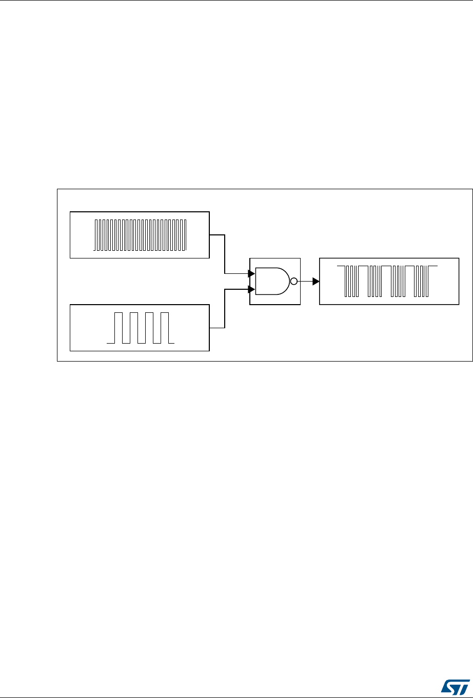
Infrared interface (IRTIM) RM0394
1012/1600 RM0394 Rev 4
31 Infrared interface (IRTIM)
An infrared interface (IRTIM) for remote control is available on the device. It can be used
with an infrared LED to perform remote control functions.
It uses internal connections with TIM15 and TIM16 as shown in Figure 345.
To generate the infrared remote control signals, the IR interface must be enabled and TIM15
channel 1 (TIM15_OC1) and TIM16 channel 1 (TIM16_OC1) must be properly configured to
generate correct waveforms.
The infrared receiver can be implemented easily through a basic input capture mode.
Figure 345. IRTIM internal hardware connections with TIM15 and TIM16
All standard IR pulse modulation modes can be obtained by programming the two timer
output compare channels.
TIM15 is used to generate the high frequency carrier signal, while TIM16 generates the
modulation envelope.
The infrared function is output on the IR_OUT pin. The activation of this function is done
through the GPIOx_AFRx register by enabling the related alternate function bit.
The high sink LED driver capability (only available on the PB9 pin) can be activated through
the I2C_PB9_FMP bit in the SYSCFG_CFGR1 register and used to sink the high current
needed to directly control an infrared LED.
06Y9
7,0B&+
7,0B&+
,57,0 ,5B287
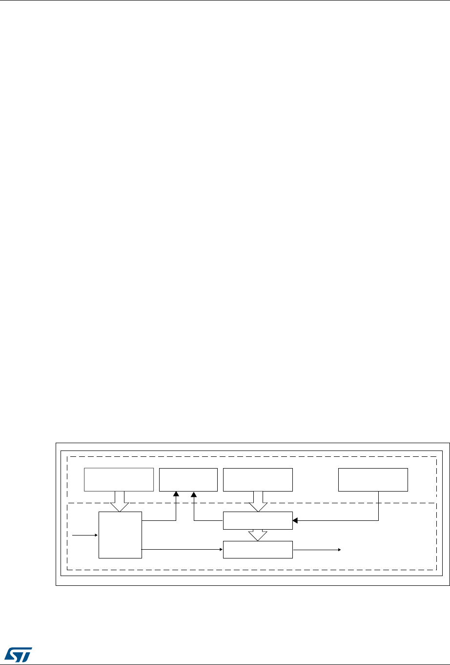
RM0394 Rev 4 1013/1600
RM0394 Independent watchdog (IWDG)
1021
32 Independent watchdog (IWDG)
32.1 Introduction
The devices feature an embedded watchdog peripheral that offers a combination of high
safety level, timing accuracy and flexibility of use. The Independent watchdog peripheral
detects and solves malfunctions due to software failure, and triggers system reset when the
counter reaches a given timeout value.
The independent watchdog (IWDG) is clocked by its own dedicated low-speed clock (LSI)
and thus stays active even if the main clock fails.
The IWDG is best suited for applications that require the watchdog to run as a totally
independent process outside the main application, but have lower timing accuracy
constraints. For further information on the window watchdog, refer to Section 33 on page
1022.
32.2 IWDG main features
•Free-running downcounter
•Clocked from an independent RC oscillator (can operate in Standby and Stop modes)
•Conditional Reset
– Reset (if watchdog activated) when the downcounter value becomes lower than
0x000
– Reset (if watchdog activated) if the downcounter is reloaded outside the window
32.3 IWDG functional description
32.3.1 IWDG block diagram
Figure 346 shows the functional blocks of the independent watchdog module.
Figure 346. Independent watchdog block diagram
1. The watchdog function is implemented in the VCORE voltage domain that is still functional in Stop and
Standby modes.
069
,:'*UHVHW
/6,
N+]
9&25(
9''YROWDJHGRPDLQ
3UHVFDOHUUHJLVWHU
,:'*B35
6WDWXVUHJLVWHU
,:'*B65
5HORDGUHJLVWHU
,:'*B5/5
.H\UHJLVWHU
,:'*B.5
ELWUHORDGYDOXH
ELWGRZQFRXQWHU
ELW
SUHVFDOHU

Independent watchdog (IWDG) RM0394
1014/1600 RM0394 Rev 4
When the independent watchdog is started by writing the value 0x0000 CCCC in the Key
register (IWDG_KR), the counter starts counting down from the reset value of 0xFFF. When
it reaches the end of count value (0x000) a reset signal is generated (IWDG reset).
Whenever the key value 0x0000 AAAA is written in the Key register (IWDG_KR), the
IWDG_RLR value is reloaded in the counter and the watchdog reset is prevented.
32.3.2 Window option
The IWDG can also work as a window watchdog by setting the appropriate window in the
Window register (IWDG_WINR).
If the reload operation is performed while the counter is greater than the value stored in the
Window register (IWDG_WINR), then a reset is provided.
The default value of the Window register (IWDG_WINR) is 0x0000 0FFF, so if it is not
updated, the window option is disabled.
As soon as the window value is changed, a reload operation is performed in order to reset
the downcounter to the Reload register (IWDG_RLR) value and ease the cycle number
calculation to generate the next reload.
Configuring the IWDG when the window option is enabled
1. Enable the IWDG by writing 0x0000 CCCC in the Key register (IWDG_KR).
2. Enable register access by writing 0x0000 5555 in the Key register (IWDG_KR).
3. Write the IWDG prescaler by programming Prescaler register (IWDG_PR) from 0 to 7.
4. Write the Reload register (IWDG_RLR).
5. Wait for the registers to be updated (IWDG_SR = 0x0000 0000).
6. Write to the Window register (IWDG_WINR). This automatically refreshes the counter
value in the Reload register (IWDG_RLR).
Note: Writing the window value allows to refresh the Counter value by the RLR when Status
register (IWDG_SR) is set to 0x0000 0000.
Configuring the IWDG when the window option is disabled
When the window option it is not used, the IWDG can be configured as follows:
1. Enable the IWDG by writing 0x0000 CCCC in the Key register (IWDG_KR).
2. Enable register access by writing 0x0000 5555 in the Key register (IWDG_KR).
3. Write the prescaler by programming the Prescaler register (IWDG_PR) from 0 to 7.
4. Write the Reload register (IWDG_RLR).
5. Wait for the registers to be updated (IWDG_SR = 0x0000 0000).
6. Refresh the counter value with IWDG_RLR (IWDG_KR = 0x0000 AAAA).

RM0394 Rev 4 1015/1600
RM0394 Independent watchdog (IWDG)
1021
32.3.3 Hardware watchdog
If the “Hardware watchdog” feature is enabled through the device option bits, the watchdog
is automatically enabled at power-on, and generates a reset unless the Key register
(IWDG_KR) is written by the software before the counter reaches end of count or if the
downcounter is reloaded inside the window.
32.3.4 Low-power freeze
Depending on the IWDG_STOP and IWDG_STBY options configuration, the IWDG can
continue counting or not during the Stop mode and the Standby mode respectively. If the
IWDG is kept running during Stop or Standby modes, it can wake up the device from this
mode. Refer to Section : User and read protection option bytes for more details.
32.3.5 Behavior in Stop and Standby modes
Once running, the IWDG cannot be stopped.
32.3.6 Register access protection
Write access to Prescaler register (IWDG_PR), Reload register (IWDG_RLR) and Window
register (IWDG_WINR) is protected. To modify them, the user must first write the code
0x0000 5555 in the Key register (IWDG_KR). A write access to this register with a different
value will break the sequence and register access will be protected again. This is the case
of the reload operation (writing 0x0000 AAAA).
A status register is available to indicate that an update of the prescaler or the down-counter
reload value or the window value is on going.
32.3.7 Debug mode
When the device enters Debug mode (core halted), the IWDG counter either continues to
work normally or stops, depending on DBG_IWDG_STOP configuration bit in DBG module.

Independent watchdog (IWDG) RM0394
1016/1600 RM0394 Rev 4
32.4 IWDG registers
Refer to Section 1.2 on page 60 for a list of abbreviations used in register descriptions.
The peripheral registers can be accessed by half-words (16-bit) or words (32-bit).
32.4.1 Key register (IWDG_KR)
Address offset: 0x00
Reset value: 0x0000 0000 (reset by Standby mode)
31 30 29 28 27 26 25 24 23 22 21 20 19 18 17 16
Res. Res. Res. Res. Res. Res. Res. Res. Res. Res. Res. Res. Res. Res. Res. Res.
1514131211109876543210
KEY[15:0]
wwwwwwwwwwwwwwww
Bits 31:16 Reserved, must be kept at reset value.
Bits 15:0 KEY[15:0]: Key value (write only, read 0x0000)
These bits must be written by software at regular intervals with the key value 0xAAAA,
otherwise the watchdog generates a reset when the counter reaches 0.
Writing the key value 0x5555 to enable access to the IWDG_PR, IWDG_RLR and
IWDG_WINR registers (see Section 32.3.6: Register access protection)
Writing the key value 0xCCCC starts the watchdog (except if the hardware watchdog option is
selected)

RM0394 Rev 4 1017/1600
RM0394 Independent watchdog (IWDG)
1021
32.4.2 Prescaler register (IWDG_PR)
Address offset: 0x04
Reset value: 0x0000 0000
31 30 29 28 27 26 25 24 23 22 21 20 19 18 17 16
Res. Res. Res. Res. Res. Res. Res. Res. Res. Res. Res. Res. Res. Res. Res. Res.
1514131211109876543210
Res. Res. Res. Res. Res. Res. Res. Res. Res. Res. Res. Res. Res. PR[2:0]
rw rw rw
Bits 31:3 Reserved, must be kept at reset value.
Bits 2:0 PR[2:0]: Prescaler divider
These bits are write access protected see Section 32.3.6: Register access protection. They are
written by software to select the prescaler divider feeding the counter clock. PVU bit of the
Status register (IWDG_SR) must be reset in order to be able to change the prescaler divider.
000: divider /4
001: divider /8
010: divider /16
011: divider /32
100: divider /64
101: divider /128
110: divider /256
111: divider /256
Note: Reading this register returns the prescaler value from the VDD voltage domain. This
value may not be up to date/valid if a write operation to this register is ongoing. For this
reason the value read from this register is valid only when the PVU bit in the Status
register (IWDG_SR) is reset.

Independent watchdog (IWDG) RM0394
1018/1600 RM0394 Rev 4
32.4.3 Reload register (IWDG_RLR)
Address offset: 0x08
Reset value: 0x0000 0FFF (reset by Standby mode)
31 30 29 28 27 26 25 24 23 22 21 20 19 18 17 16
Res. Res. Res. Res. Res. Res. Res. Res. Res. Res. Res. Res. Res. Res. Res. Res.
1514131211109876543210
Res. Res. Res. Res. RL[11:0]
rw rw rw rw rw rw rw rw rw rw rw rw
Bits 31:12 Reserved, must be kept at reset value.
Bits 11:0 RL[11:0]: Watchdog counter reload value
These bits are write access protected see Register access protection. They are written by
software to define the value to be loaded in the watchdog counter each time the value 0xAAAA
is written in the Key register (IWDG_KR). The watchdog counter counts down from this value.
The timeout period is a function of this value and the clock prescaler. Refer to the datasheet for
the timeout information.
The RVU bit in the Status register (IWDG_SR) must be reset to be able to change the reload
value.
Note: Reading this register returns the reload value from the VDD voltage domain. This value
may not be up to date/valid if a write operation to this register is ongoing on it. For this
reason the value read from this register is valid only when the RVU bit in the Status
register (IWDG_SR) is reset.

RM0394 Rev 4 1019/1600
RM0394 Independent watchdog (IWDG)
1021
32.4.4 Status register (IWDG_SR)
Address offset: 0x0C
Reset value: 0x0000 0000 (not reset by Standby mode)
Note: If several reload, prescaler, or window values are used by the application, it is mandatory to
wait until RVU bit is reset before changing the reload value, to wait until PVU bit is reset
before changing the prescaler value, and to wait until WVU bit is reset before changing the
window value. However, after updating the prescaler and/or the reload/window value it is not
necessary to wait until RVU or PVU or WVU is reset before continuing code execution
except in case of low-power mode entry.
31 30 29 28 27 26 25 24 23 22 21 20 19 18 17 16
Res. Res. Res. Res. Res. Res. Res. Res. Res. Res. Res. Res. Res. Res. Res. Res.
1514131211109876543210
Res. Res. Res. Res. Res. Res. Res. Res. Res. Res. Res. Res. Res. WVU RVU PVU
rrr
Bits 31:3 Reserved, must be kept at reset value.
Bit 2 WVU: Watchdog counter window value update
This bit is set by hardware to indicate that an update of the window value is ongoing. It is reset
by hardware when the reload value update operation is completed in the VDD voltage domain
(takes up to five LSI/Prescaler clock cycles).
Window value can be updated only when WVU bit is reset.
This bit is generated only if generic “window” = 1
Bit 1 RVU: Watchdog counter reload value update
This bit is set by hardware to indicate that an update of the reload value is ongoing. It is reset
by hardware when the reload value update operation is completed in the VDD voltage domain
(takes up to five LSI/Prescale clock cycles).
Reload value can be updated only when RVU bit is reset.
Bit 0 PVU: Watchdog prescaler value update
This bit is set by hardware to indicate that an update of the prescaler value is ongoing. It is
reset by hardware when the prescaler update operation is completed in the VDD voltage
domain (takes up to five LSI/Prescale clock cycles).
Prescaler value can be updated only when PVU bit is reset.

Independent watchdog (IWDG) RM0394
1020/1600 RM0394 Rev 4
32.4.5 Window register (IWDG_WINR)
Address offset: 0x10
Reset value: 0x0000 0FFF (reset by Standby mode)
31 30 29 28 27 26 25 24 23 22 21 20 19 18 17 16
Res. Res. Res. Res. Res. Res. Res. Res. Res. Res. Res. Res. Res. Res. Res. Res.
1514131211109876543210
Res. Res. Res. Res. WIN[11:0]
rw rw rw rw rw rw rw rw rw rw rw rw
Bits 31:12 Reserved, must be kept at reset value.
Bits 11:0 WIN[11:0]: Watchdog counter window value
These bits are write access protected, see Section 32.3.6, they contain the high limit of the
window value to be compared with the downcounter.
To prevent a reset, the downcounter must be reloaded when its value is lower than the window
register value and greater than 0x0
The WVU bit in the Status register (IWDG_SR) must be reset in order to be able to change the
reload value.
Note: Reading this register returns the reload value from the VDD voltage domain. This value
may not be valid if a write operation to this register is ongoing. For this reason the value
read from this register is valid only when the WVU bit in the Status register (IWDG_SR)
is reset.

RM0394 Rev 4 1021/1600
RM0394 Independent watchdog (IWDG)
1021
32.4.6 IWDG register map
The following table gives the IWDG register map and reset values.
Refer to Section 2.2.2 on page 67 for the register boundary addresses.
Table 153. IWDG register map and reset values
Offset Register
name
31
30
29
28
27
26
25
24
23
22
21
20
19
18
17
16
15
14
13
12
11
10
9
8
7
6
5
4
3
2
1
0
0x00
IWDG_KR
Res.
Res.
Res.
Res.
Res.
Res.
Res.
Res.
Res.
Res.
Res.
Res.
Res.
Res.
Res.
Res.
KEY[15:0]
Reset value 0000000000000000
0x04
IWDG_PR
Res.
Res.
Res.
Res.
Res.
Res.
Res.
Res.
Res.
Res.
Res.
Res.
Res.
Res.
Res.
Res.
Res.
Res.
Res.
Res.
Res.
Res.
Res.
Res.
Res.
Res.
Res.
Res.
Res.
PR[2:0]
Reset value 000
0x08
IWDG_RLR
Res.
Res.
Res.
Res.
Res.
Res.
Res.
Res.
Res.
Res.
Res.
Res.
Res.
Res.
Res.
Res.
Res.
Res.
Res.
Res.
RL[11:0]
Reset value 111111111111
0x0C
IWDG_SR
Res.
Res.
Res.
Res.
Res.
Res.
Res.
Res.
Res.
Res.
Res.
Res.
Res.
Res.
Res.
Res.
Res.
Res.
Res.
Res.
Res.
Res.
Res.
Res.
Res.
Res.
Res.
Res.
Res.
WVU
RVU
PVU
Reset value 000
0x10
IWDG_WINR
Res.
Res.
Res.
Res.
Res.
Res.
Res.
Res.
Res.
Res.
Res.
Res.
Res.
Res.
Res.
Res.
Res.
Res.
Res.
Res.
WIN[11:0]
Reset value 111111111111

System window watchdog (WWDG) RM0394
1022/1600 RM0394 Rev 4
33 System window watchdog (WWDG)
33.1 Introduction
The system window watchdog (WWDG) is used to detect the occurrence of a software fault,
usually generated by external interference or by unforeseen logical conditions, which
causes the application program to abandon its normal sequence. The watchdog circuit
generates an MCU reset on expiry of a programmed time period, unless the program
refreshes the contents of the downcounter before the T6 bit becomes cleared. An MCU
reset is also generated if the 7-bit downcounter value (in the control register) is refreshed
before the downcounter has reached the window register value. This implies that the
counter must be refreshed in a limited window.
The WWDG clock is prescaled from the APB clock and has a configurable time-window that
can be programmed to detect abnormally late or early application behavior.
The WWDG is best suited for applications which require the watchdog to react within an
accurate timing window.
33.2 WWDG main features
•Programmable free-running downcounter
•Conditional reset
– Reset (if watchdog activated) when the downcounter value becomes lower than
0x40
– Reset (if watchdog activated) if the downcounter is reloaded outside the window
(see Figure 348)
•Early wakeup interrupt (EWI): triggered (if enabled and the watchdog activated) when
the downcounter is equal to 0x40.
33.3 WWDG functional description
If the watchdog is activated (the WDGA bit is set in the WWDG_CR register) and when the
7-bit downcounter (T[6:0] bits) is decremented from 0x40 to 0x3F (T6 becomes cleared), it
initiates a reset. If the software reloads the counter while the counter is greater than the
value stored in the window register, then a reset is generated.
The application program must write in the WWDG_CR register at regular intervals during
normal operation to prevent an MCU reset. This operation must occur only when the counter
value is lower than the window register value and higher than 0x3F. The value to be stored
in the WWDG_CR register must be between 0xFF and 0xC0.
Refer to Figure 347 for the WWDG block diagram.
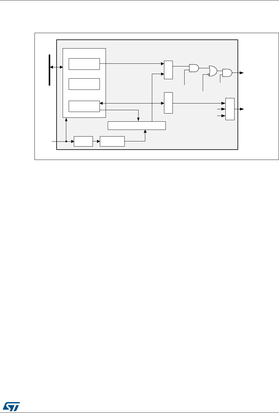
RM0394 Rev 4 1023/1600
RM0394 System window watchdog (WWDG)
1028
33.3.1 WWDG block diagram
Figure 347. Watchdog block diagram
33.3.2 Enabling the watchdog
The watchdog is always disabled after a reset. It is enabled by setting the WDGA bit in the
WWDG_CR register, then it cannot be disabled again except by a reset.
33.3.3 Controlling the downcounter
This downcounter is free-running, counting down even if the watchdog is disabled. When
the watchdog is enabled, the T6 bit must be set to prevent generating an immediate reset.
The T[5:0] bits contain the number of increments which represents the time delay before the
watchdog produces a reset. The timing varies between a minimum and a maximum value
due to the unknown status of the prescaler when writing to the WWDG_CR register (see
Figure 348). The Configuration register (WWDG_CFR) contains the high limit of the window:
To prevent a reset, the downcounter must be reloaded when its value is lower than the
window register value and greater than 0x3F. Figure 348 describes the window watchdog
process.
Note: The T6 bit can be used to generate a software reset (the WDGA bit is set and the T6 bit is
cleared).
33.3.4 Advanced watchdog interrupt feature
The early wakeup interrupt (EWI) can be used if specific safety operations or data logging
must be performed before the actual reset is generated. The EWI interrupt is enabled by
setting the EWI bit in the WWDG_CFR register. When the downcounter reaches the value
0x40, an EWI interrupt is generated and the corresponding interrupt service routine (ISR)
can be used to trigger specific actions (such as communications or data logging), before
resetting the device.
069
ELW'RZQ&RXQWHU&17
::'*
SFON
$3%EXV
· ·:'*7%
:ULWHWR::'*B&5
&03 ZKHQ
7>@!:>@
&03
7>@
SUHORDG
::'*B&5
ZZGJBRXWBUVW
ZZGJBLW
["
UHDGEDFN
::'*B&)5 :>@
FQWBRXW
5HJLVWHULQWHUIDFH
::'*B65
7
7>@
:'*$
(:,
/RJLF
(:,)
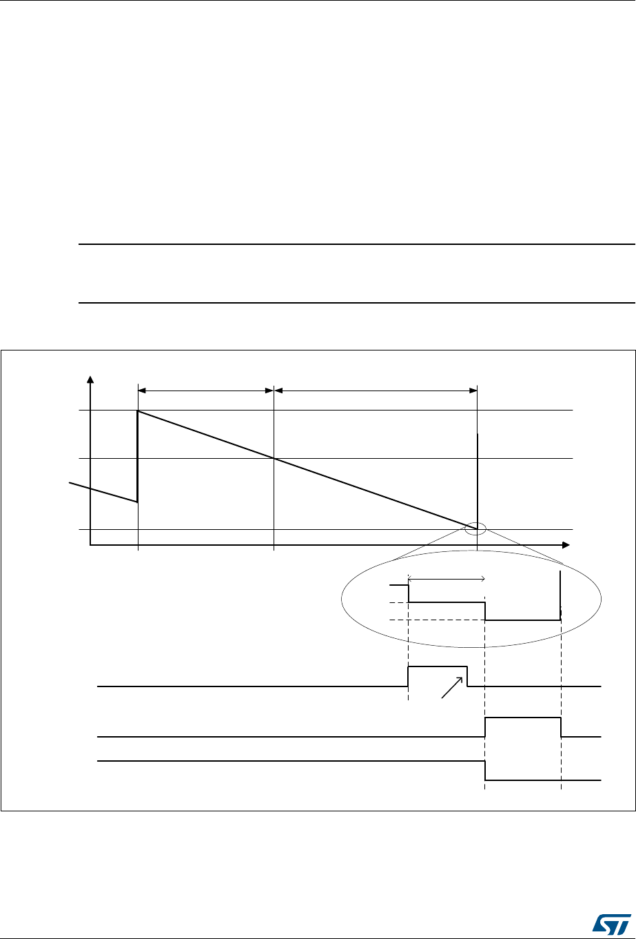
System window watchdog (WWDG) RM0394
1024/1600 RM0394 Rev 4
In some applications, the EWI interrupt can be used to manage a software system check
and/or system recovery/graceful degradation, without generating a WWDG reset. In this
case, the corresponding interrupt service routine (ISR) should reload the WWDG counter to
avoid the WWDG reset, then trigger the required actions.
The EWI interrupt is cleared by writing '0' to the EWIF bit in the WWDG_SR register.
Note: When the EWI interrupt cannot be served, e.g. due to a system lock in a higher priority task,
the WWDG reset is eventually generated.
33.3.5 How to program the watchdog timeout
Use the formula in Figure 348 to calculate the WWDG timeout.
Warning: When writing to the WWDG_CR register, always write 1 in the
T6 bit to avoid generating an immediate reset.
Figure 348. Window watchdog timing diagram
The formula to calculate the timeout value is given by:
069
:>@
[)
[
[
[)
ZZGJBHZLW
ZZGJBUVW
5HIUHVKQRWDOORZHG 5HIUHVKDOORZHG
7LPH
7>@
7SFON[[:'*7%
&17'RZQ&RXQWHU
7ELW
(:,)
tWWDG tPCLK 4096 2WDGTB[1:0] T5:0[]1+()×××=ms()

RM0394 Rev 4 1025/1600
RM0394 System window watchdog (WWDG)
1028
where:
tWWDG: WWDG timeout
tPCLK: APB clock period measured in ms
4096: value corresponding to internal divider
As an example, lets assume APB frequency is equal to 48 MHz, WDGTB[1:0] is set to 3 and
T[5:0] is set to 63:
Refer to the datasheet for the minimum and maximum values of the tWWDG
.
33.3.6 Debug mode
When the device enters debug mode (processor halted), the WWDG counter either
continues to work normally or stops, depending on the configuration bit in DBG module. For
more details refer to Section 46.16.2: Debug support for timers, RTC, watchdog, bxCAN
and I2C.
tWWDG 1 48000⁄()4096 23
×× 63 1+()×43.69ms==

System window watchdog (WWDG) RM0394
1026/1600 RM0394 Rev 4
33.4 WWDG registers
Refer to Section 1.2 on page 60 for a list of abbreviations used in register descriptions.
The peripheral registers can be accessed by half-words (16-bit) or words (32-bit).
33.4.1 Control register (WWDG_CR)
Address offset: 0x000
Reset value: 0x0000 007F
33.4.2 Configuration register (WWDG_CFR)
Address offset: 0x004
Reset value: 0x0000 007F
31 30 29 28 27 26 25 24 23 22 21 20 19 18 17 16
Res. Res. Res. Res. Res. Res. Res. Res. Res. Res. Res. Res. Res. Res. Res. Res.
1514131211109876543210
Res. Res. Res. Res. Res. Res. Res. Res. WDGA T[6:0]
rs rw rw rw rw rw rw rw
Bits 31:8 Reserved, must be kept at reset value.
Bit 7 WDGA: Activation bit
This bit is set by software and only cleared by hardware after a reset. When WDGA = 1, the
watchdog can generate a reset.
0: Watchdog disabled
1: Watchdog enabled
Bits 6:0 T[6:0]: 7-bit counter (MSB to LSB)
These bits contain the value of the watchdog counter, decremented every
(4096 x 2WDGTB[1:0]) PCLK cycles. A reset is produced when it is decremented from 0x40 to
0x3F (T6 becomes cleared).
31 30 29 28 27 26 25 24 23 22 21 20 19 18 17 16
Res. Res. Res. Res. Res. Res. Res. Res. Res. Res. Res. Res. Res. Res. Res. Res.
1514131211109876543210
Res. Res. Res. Res. Res. Res. EWI WDGTB[1:0] W[6:0]
rs rw rw rw rw rw rw rw rw rw
Bits 31:10 Reserved, must be kept at reset value.
Bit 9 EWI: Early wakeup interrupt
When set, an interrupt occurs whenever the counter reaches the value 0x40. This interrupt is
only cleared by hardware after a reset.

RM0394 Rev 4 1027/1600
RM0394 System window watchdog (WWDG)
1028
33.4.3 Status register (WWDG_SR)
Address offset: 0x008
Reset value: 0x0000 0000
Bits 8:7 WDGTB[1:0]: Timer base
The time base of the prescaler can be modified as follows:
00: CK Counter Clock (PCLK div 4096) div 1
01: CK Counter Clock (PCLK div 4096) div 2
10: CK Counter Clock (PCLK div 4096) div 4
11: CK Counter Clock (PCLK div 4096) div 8
Bits 6:0 W[6:0]: 7-bit window value
These bits contain the window value to be compared with the downcounter.
31 30 29 28 27 26 25 24 23 22 21 20 19 18 17 16
Res. Res. Res. Res. Res. Res. Res. Res. Res. Res. Res. Res. Res. Res. Res. Res.
1514131211109876543210
Res. Res. Res. Res. Res. Res. Res. Res. Res. Res. Res. Res. Res. Res. Res. EWIF
rc_w0
Bits 31:1 Reserved, must be kept at reset value.
Bit 0 EWIF: Early wakeup interrupt flag
This bit is set by hardware when the counter has reached the value 0x40. It must be cleared
by software by writing ‘0’. Writing ‘1’ has no effect. This bit is also set if the interrupt is not
enabled.

System window watchdog (WWDG) RM0394
1028/1600 RM0394 Rev 4
33.4.4 WWDG register map
The following table gives the WWDG register map and reset values.
Refer to Section 2.2.2 on page 67 for the register boundary addresses.
Table 154. WWDG register map and reset values
Offset Register
31
30
29
28
27
26
25
24
23
22
21
20
19
18
17
16
15
14
13
12
11
10
9
8
7
6
5
4
3
2
1
0
0x000 WWDG_CR
Res.
Res.
Res.
Res.
Res.
Res.
Res.
Res.
Res.
Res.
Res.
Res.
Res.
Res.
Res.
Res.
Res.
Res.
Res.
Res.
Res.
Res.
Res.
Res.
WDGA
T[6:0]
Reset value 01111111
0x004 WWDG_CFR
Res.
Res.
Res.
Res.
Res.
Res.
Res.
Res.
Res.
Res.
Res.
Res.
Res.
Res.
Res.
Res.
Res.
Res.
Res.
Res.
Res.
Res.
EWI
WDGTB1
WDGTB0
W[6:0]
Reset value 0001111111
0x008 WWDG_SR
Res.
Res.
Res.
Res.
Res.
Res.
Res.
Res.
Res.
Res.
Res.
Res.
Res.
Res.
Res.
Res.
Res.
Res.
Res.
Res.
Res.
Res.
Res.
Res.
Res.
Res.
Res.
Res.
Res.
Res.
Res.
EWIF
Reset value 0

RM0394 Rev 4 1029/1999
RM0394 Real-time clock (RTC) applied to STM32L41xxx and STM32L42xxx devices only
1081
34 Real-time clock (RTC) applied to
STM32L41xxx and STM32L42xxx devices only
34.1 Introduction
The RTC provides an automatic wakeup to manage all low-power modes.
The real-time clock (RTC) is an independent BCD timer/counter. The RTC provides a time-
of-day clock/calendar with programmable alarm interrupts.
As long as the supply voltage remains in the operating range, the RTC never stops,
regardless of the device status (Run mode, low-power mode or under reset).
The RTC is functional in VBAT mode.
34.2 RTC main features
The RTC supports the following features (see Figure 349: RTC block diagram):
•Calendar with subsecond, seconds, minutes, hours (12 or 24 format), week day, date,
month, year, in BCD (binary-coded decimal) format.
•Automatic correction for 28, 29 (leap year), 30, and 31 days of the month.
•Two programmable alarms.
•On-the-fly correction from 1 to 32767 RTC clock pulses. This can be used to
synchronize it with a master clock.
•Reference clock detection: a more precise second source clock (50 or 60 Hz) can be
used to enhance the calendar precision.
•Digital calibration circuit with 0.95 ppm resolution, to compensate for quartz crystal
inaccuracy.
•Timestamp feature which can be used to save the calendar content. This function can
be triggered by an event on the timestamp pin, or by a tamper event, or by a switch to
VBAT mode.
•17-bit auto-reload wakeup timer (WUT) for periodic events with programmable
resolution and period.
The RTC is supplied through a switch that takes power either from the VDD supply when
present or from the VBAT pin.
The RTC clock sources can be:
•A 32.768 kHz external crystal (LSE)
•An external resonator or oscillator (LSE)
•The internal low power RC oscillator (LSI, with typical frequency of 32 kHz)
•The high-speed external clock (HSE), divided by a prescaler in the RCC.
The RTC is functional in VBAT mode and in all low-power modes when it is clocked by the
LSE. When clocked by the LSI, the RTC is not functional in VBAT mode, but is functional in
all low-power modes except Shutdown mode.
All RTC events (Alarm, WakeUp Timer, Timestamp) can generate an interrupt and wakeup
the device from the low-power modes.

Real-time clock (RTC) applied to STM32L41xxx and STM32L42xxx devices only RM0394
1030/1999 RM0394 Rev 4
34.3 RTC functional description
34.3.1 RTC block diagram
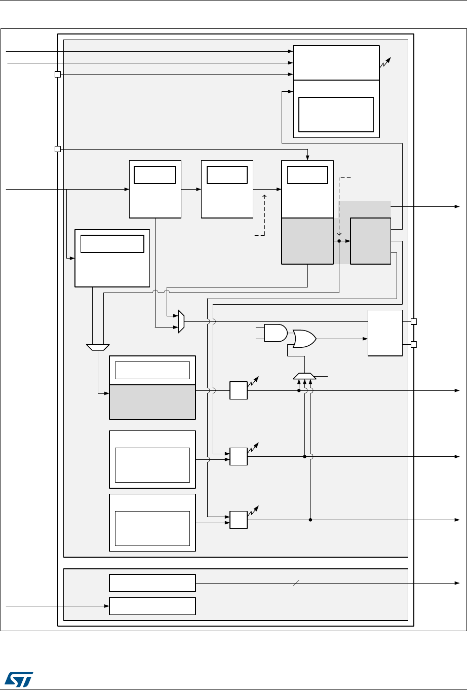
RM0394 Rev 4 1031/1999
RM0394 Real-time clock (RTC) applied to STM32L41xxx and STM32L42xxx devices only
1081
Figure 349. RTC block diagram
06Y9
UWFBDOUEBWUJ
$ODUP$
57&B$/50$5
57&B$/50$665
$ODUP%
57&B$/50%5
57&B$/50%665
UWFBZXWBWUJ
UWFBDOUDBWUJ
ELWZDNHXS
DXWRUHORDGWLPHU
57&B:875
6KDGRZ
UHJLVWHUV
57&B75
57&B'5
2XWSXW
FRQWURO
57&B287
57&B287
7$03
7$032(
6KDGRZUHJLVWHU
57&B665
&DOHQGDU
6\QFKURQRXV
SUHVFDOHU
GHIDXOW
57&B35(5
&$/,%
26(/>@
FNBDSUH
GHIDXOW+]
7$03$/$50
$/$50
UWFBWDPSBHYW
57&B5(),1
57&B76
7LPHVWDPSUHJLVWHUV
57&B7675
57&B76'5
57&B7665
7LPHVWDPSGHWHFWLRQ
UWFBLWV
UWFBNHUBFN
FNBVSUH
GHIDXOW+]
3UHVFDOHU
:8&.6(/>@
76)
UWFBFDORYI
FNBDSUHFORFNGRPDLQ
FNBZXWFORFNGRPDLQ
:87)
$/5$)
$/5%)
UWFBSFONFORFNGRPDLQ
5HJLVWHUVLQWHUIDFH
UWFBSFON
,54LQWHUIDFH
UWFBLW
FNBZXW
UWFBNHUBFNFORFNGRPDLQ
6PRRWK
FDOLEUDWLRQ
57&B&$/5
$V\QFKURQRXV
SUHVFDOHU
GHIDXOW
57&B35(5
Real-time clock (RTC) applied to STM32L41xxx and STM32L42xxx devices only RM0394
1032/1999 RM0394 Rev 4
34.3.2 RTC pins and internal signals
•RTC_OUT1 and RTC_OUT2 which selects one of the following two outputs:
– CALIB: 512 Hz or 1 Hz clock output (with an LSE frequency of 32.768 kHz). This
output is enabled by setting the COE bit in the RTC_CR register.
– TAMPALRM: This output is the OR between TAMP and ALARM outputs.
ALARM is enabled by configuring the OSEL[1:0] bits in the RTC_CR register which select
the alarm A, alarm B or wakeup outputs. TAMP is enabled by setting the TAMPOE bit in the
RTC_CR register which selects the tamper event outputs.
The RTC kernel clock is usually the LSE at 32.768 kHz although it is possible to select other
clock sources in the RCC (refer to RCC for more details). Some functions are not available
in some low-power modes or VBAT when the selected clock is not LSE. Refer to
Section 34.4: RTC low-power modes for more details.
Table 155. RTC input/output pins
Pin name Signal type Description
RTC_TS Input RTC timestamp input
RTC_REFIN Input RTC 50 or 60 Hz reference clock input
RTC_OUT1 Output RTC output 1
RTC_OUT2 Output RTC output 2
Table 156. RTC internal input/output signals
Internal signal name Signal type Description
rtc_ker_ck Input RTC kernel clock, also named RTCCLK in
this document
rtc_pclk Input RTC APB clock
rtc_its Input RTC internal timestamp event
rtc_tamp_evt Input Tamper event (external) detected in TAMP
peripheral
rtc_it Output RTC interrupts (refer to Section 34.5: RTC
interrupts for details)
rtc_alra_trg Output RTC alarm A event detection trigger
rtc_alrb_trg Output RTC alarm B event detection trigger
rtc_wut_trg Output RTC wakeup timer event detection trigger
Table 157. RTC interconnection
Signal name Source/destination
rtc_its From power controller (PWR): main power loss/switch to VBAT detection
output
rtc_tamp_evt From TAMP peripheral: tamp_evt

RM0394 Rev 4 1033/1999
RM0394 Real-time clock (RTC) applied to STM32L41xxx and STM32L42xxx devices only
1081
The triggers outputs can be used as triggers for other peripherals.
34.3.3 GPIOs controlled by the RTC and TAMP
The GPIOs included in the Battery Backup Domain (VBAT) are directly controlled by the
peripherals providing functions on these I/Os, whatever the GPIO configuration.
Both RTC and TAMP peripherals provide functions on these I/Os (refer to Section 35:
Tamper and backup registers (TAMP)).
RTC_OUT1, RTC_TS and TAMP_IN1 are mapped on the same pin (PC13). The RTC and
TAMP functions mapped on PC13 are available in all low-power modes and in VBAT mode.
The output mechanism follows the priority order shown in Table 158.
Table 158. PC13 configuration(1)
PC13 Pin function
OSEL[1:0]
(ALARM output enable)
TAMPOE
(TAMPER output enable)
COE
(CALIB output enable)
OUT2EN
TAMPALRM_TYPE
TAMPALRM_PU
TAMP1E
(TAMP_IN1 input enable)
TSE
(RTC_TS input enable)
TAMPALRM output
Push-Pull
01 or
10 or
11
0
Don’t
care
Don’t
care 00
Don’t
care
Don’t
care
00 1
01 or
10 or
11
1
TAMPALRM
output
Open-Drain
No pull
01 or
10 or
11
0
Don’t
care
Don’t
care 10
Don’t
care
Don’t
care
00 1
01 or
10 or
11
1
Internal
pull-up
01 or
10 or
11
0
Don’t
care
Don’t
care 11
Don’t
care
Don’t
care
00 1
01 or
10 or
11
1
CALIB output PP 00 0 1 0 Don’t
care
Don’t
care
Don’t
care
Don’t
care

Real-time clock (RTC) applied to STM32L41xxx and STM32L42xxx devices only RM0394
1034/1999 RM0394 Rev 4
In addition, it is possible to output RTC_OUT2 on PB2 pin thanks to OUT2EN bit. This
output is not available in VBAT mode. The different functions are mapped on RTC_OUT1 or
on RTC_OUT2 depending on OSEL, COE and OUT2EN configuration, as shown in table
Table 159.
TAMP_IN1 input floating
00 0 0 Don’t
care
Don’t
care
Don’t
care 1000 0 1
1
Don’t
care
Don’t
care 0
RTC_TS and TAMP_IN1
input floating
00 0 0 Don’t
care
Don’t
care
Don’t
care 1100 0 1
1
Don’t
care
Don’t
care 0
RTC_TS input floating
00 0 0 Don’t
care
Don’t
care
Don’t
care 0100 0 1
1
Don’t
care
Don’t
care 0
Wakeup pin or Standard
GPIO
00 0 0 Don’t
care
Don’t
care
Don’t
care 0000 0 1
1
Don’t
care
Don’t
care 0
1. OD: open drain; PP: push-pull.
Table 158. PC13 configuration(1) (continued)
PC13 Pin function
OSEL[1:0]
(ALARM output enable)
TAMPOE
(TAMPER output enable)
COE
(CALIB output enable)
OUT2EN
TAMPALRM_TYPE
TAMPALRM_PU
TAMP1E
(TAMP_IN1 input enable)
TSE
(RTC_TS input enable)

RM0394 Rev 4 1035/1999
RM0394 Real-time clock (RTC) applied to STM32L41xxx and STM32L42xxx devices only
1081
34.3.4 Clock and prescalers
The RTC clock source (RTCCLK) is selected through the clock controller among the LSE
clock, the LSI oscillator clock, and the HSE clock. For more information on the RTC clock
source configuration, refer to Section 6: Reset and clock control (RCC).
A programmable prescaler stage generates a 1 Hz clock which is used to update the
calendar. To minimize power consumption, the prescaler is split into 2 programmable
prescalers (see Figure 349: RTC block diagram):
•A 7-bit asynchronous prescaler configured through the PREDIV_A bits of the
RTC_PRER register.
•A 15-bit synchronous prescaler configured through the PREDIV_S bits of the
RTC_PRER register.
Note: When both prescalers are used, it is recommended to configure the asynchronous prescaler
to a high value to minimize consumption.
The asynchronous prescaler division factor is set to 128, and the synchronous division
factor to 256, to obtain an internal clock frequency of 1 Hz (ck_spre) with an LSE frequency
of 32.768 kHz.
The minimum division factor is 1 and the maximum division factor is 222.
This corresponds to a maximum input frequency of around 4 MHz.
fck_apre is given by the following formula:
The ck_apre clock is used to clock the binary RTC_SSR subseconds downcounter. When it
reaches 0, RTC_SSR is reloaded with the content of PREDIV_S.
fck_spre is given by the following formula:
Table 159. RTC_OUT mapping
OSEL[1:0] bits
ALARM
output enable)
COE bit (CALIB
output enable)
OUT2EN
bit
RTC_OUT1 on
PC13
RTC_OUT2 on
PB2
00 0
0
--
00 1 CALIB -
01 or 10 or 11 Don’t care TAMPALRM -
00 0
1
--
00 1 - CALIB
01 or 10 or 11 0 - TAMPALRM
01 or 10 or 11 1 TAMPALRM CALIB
fCK_APRE
fRTCCLK
PREDIV_A 1+
---------------------------------------=
fCK_SPRE
fRTCCLK
PREDIV_S 1+()PREDIV_A 1+()×
-----------------------------------------------------------------------------------------------=

Real-time clock (RTC) applied to STM32L41xxx and STM32L42xxx devices only RM0394
1036/1999 RM0394 Rev 4
The ck_spre clock can be used either to update the calendar or as timebase for the 16-bit
wakeup auto-reload timer. To obtain short timeout periods, the 16-bit wakeup auto-reload
timer can also run with the RTCCLK divided by the programmable 4-bit asynchronous
prescaler (see Section 34.3.8: Periodic auto-wakeup for details).
34.3.5 Real-time clock and calendar
The RTC calendar time and date registers are accessed through shadow registers which
are synchronized with PCLK (APB clock). They can also be accessed directly in order to
avoid waiting for the synchronization duration.
•RTC_SSR for the subseconds
•RTC_TR for the time
•RTC_DR for the date
Every RTCCLK periods, the current calendar value is copied into the shadow registers, and
the RSF bit of RTC_ICSR register is set (see Section 34.6.10: RTC shift control register
(RTC_SHIFTR)). The copy is not performed in Stop and Standby mode. When exiting these
modes, the shadow registers are updated after up to 4 RTCCLK periods.
When the application reads the calendar registers, it accesses the content of the shadow
registers. It is possible to make a direct access to the calendar registers by setting the
BYPSHAD control bit in the RTC_CR register. By default, this bit is cleared, and the user
accesses the shadow registers.
When reading the RTC_SSR, RTC_TR or RTC_DR registers in BYPSHAD = 0 mode, the
frequency of the APB clock (fAPB) must be at least 7 times the frequency of the RTC clock
(fRTCCLK).
The shadow registers are reset by system reset.
34.3.6 Calendar ultra-low power mode
It is possible to reduce drastically the RTC power consumption by setting the LPCAL bit in
the RTC_CALR register. In this configuration, the whole RTC is clocked by ck_apre instead
of RTCCLK or ck_apre. Consequently, some flags delays are longer, and the calibration
window is longer (refer to Section : Calibration ultra-low-power mode).
The LPCAL bit is ignored (assumed to be 0) when asynchronous prescaler division factor
(PREDIV_A+1) is not a power of 2.
Switching from LPCAL=0 to LPCAL=1 or from LPCAL=1 to LPCAL=0 is not immediate and
requires a few ck_apre periods to complete.
34.3.7 Programmable alarms
The RTC unit provides programmable alarm: alarm A and alarm B. The description below is
given for alarm A, but can be translated in the same way for alarm B.
The programmable alarm function is enabled through the ALRAE bit in the RTC_CR
register.
The ALRAF is set to 1 if the calendar subseconds, seconds, minutes, hours, date or day
match the values programmed in the alarm registers RTC_ALRMASSR and
RTC_ALRMAR. Each calendar field can be independently selected through the MSKx bits
of the RTC_ALRMAR register, and through the MASKSSx bits of the RTC_ALRMASSR
register.

RM0394 Rev 4 1037/1999
RM0394 Real-time clock (RTC) applied to STM32L41xxx and STM32L42xxx devices only
1081
The alarm interrupt is enabled through the ALRAIE bit in the RTC_CR register.
Caution: If the seconds field is selected (MSK1 bit reset in RTC_ALRMAR), the synchronous
prescaler division factor set in the RTC_PRER register must be at least 3 to ensure correct
behavior.
Alarm A and alarm B (if enabled by bits OSEL[1:0] in RTC_CR register) can be routed to the
TAMPALRM output. TAMPALRM output polarity can be configured through bit POL the
RTC_CR register.
34.3.8 Periodic auto-wakeup
The periodic wakeup flag is generated by a 16-bit programmable auto-reload down-counter.
The wakeup timer range can be extended to 17 bits.
The wakeup function is enabled through the WUTE bit in the RTC_CR register.
The wakeup timer clock input ck_wut can be:
•RTC clock (RTCCLK) divided by 2, 4, 8, or 16.
When RTCCLK is LSE (32.768 kHz), this allows to configure the wakeup interrupt
period from 122 µs to 32 s, with a resolution down to 61 µs.
•ck_spre (usually 1 Hz internal clock).
When ck_spre frequency is 1 Hz, this allows to achieve a wakeup time from 1 s to
around 36 hours with one-second resolution. This large programmable time range is
divided in 2 parts:
– from 1 s to 18 hours when WUCKSEL [2:1] = 10
– and from around 18 h to 36 h when WUCKSEL[2:1] = 11. In this last case 216 is
added to the 16-bit counter current value. When the initialization sequence is
complete (see Programming the wakeup timer on page 1039), the timer starts
counting down. When the wakeup function is enabled, the down-counting remains
active in low-power modes. In addition, when it reaches 0, the WUTF flag is set in
the RTC_SR register, and the wakeup counter is automatically reloaded with its
reload value (RTC_WUTR register value).
Depending on WUTOCLR in the RTC_WUTR register, the WUTF flag must either be
cleared by software (WUTOCLR = 0x0000), or the WUTF is automatically cleared by
hardware when the auto-reload down counter reaches WUTOCLR value
(0x0000<WUTOCLR<=WUT).
The wakeup flag is output on an internal signal rtc_wut that can be used by other
peripherals (refer to section Section 34.3.1: RTC block diagram).
When the periodic wakeup interrupt is enabled by setting the WUTIE bit in the RTC_CR
register, it can exit the device from low-power modes.
The periodic wakeup flag can be routed to the TAMPALRM output provided it has been
enabled through bits OSEL[1:0] of RTC_CR register. TAMPALRM output polarity can be
configured through the POL bit in the RTC_CR register.
System reset, as well as low-power modes (Sleep, Stop and Standby) have no influence on
the wakeup timer.

Real-time clock (RTC) applied to STM32L41xxx and STM32L42xxx devices only RM0394
1038/1999 RM0394 Rev 4
34.3.9 RTC initialization and configuration
RTC register access
The RTC registers are 32-bit registers. The APB interface introduces 2 wait-states in RTC
register accesses except on read accesses to calendar shadow registers when BYPSHAD
= 0.
RTC register write protection
After system reset, the RTC registers are protected against parasitic write access by
clearing the DBP bit in the PWR_CR1 register (refer to the power control section). DBP bit
must be set in order to enable RTC registers write access.
After Backup domain reset, some of the RTC registers are write-protected: RTC_TR,
RTC_DR, RTC_PRER, RTC_CALR, RTC_SHIFTR, the bit INIT in RTC_ICSR and the bits
FMT, SUB1H, ADD1H, REFCKON in RTC_CR.
The following steps are required to unlock the write protection on the protected RTC
registers.
1. Write 0xCA into the RTC_WPR register.
2. Write 0x53 into the RTC_WPR register.
Writing a wrong key reactivates the write protection.
The protection mechanism is not affected by system reset.
Calendar initialization and configuration
To program the initial time and date calendar values, including the time format and the
prescaler configuration, the following sequence is required:
1. Set INIT bit to 1 in the RTC_ICSR register to enter initialization mode. In this mode, the
calendar counter is stopped and its value can be updated.
2. Poll INITF bit of in the RTC_ICSR register. The initialization phase mode is entered
when INITF is set to 1.
If LPCAL=0: INITF is set around 2 RTCCLK cycles after INIT bit is set.
If LPCAL=1: INITF is set up to 2 ck_apre cycle after INIT bit is set.
3. To generate a 1 Hz clock for the calendar counter, program both the prescaler factors
in RTC_PRER register.
4. Load the initial time and date values in the shadow registers (RTC_TR and RTC_DR),
and configure the time format (12 or 24 hours) through the FMT bit in the RTC_CR
register.
5. Exit the initialization mode by clearing the INIT bit. The actual calendar counter value is
then automatically loaded.
If LPCAL=0: the counting restarts after 4 RTCCLK clock cycles.
If LPCAL=1: the counting restarts after up to 2 RTCCLK + 1 ck_apre.
When the initialization sequence is complete, the calendar starts counting.
RTC_SSR contains the value of the synchronous prescaler counter. This allows one to
calculate the exact time being maintained by the RTC down to a resolution of 1 /
(PREDIV_S + 1) seconds. As a consequence, the resolution can be improved by increasing
the synchronous prescaler value (PREDIV_S[14:0]). The maximum resolution allowed
(30.52 s with a 32768 Hz clock) is obtained with PREDIV_S set to 0x7FFF.

RM0394 Rev 4 1039/1999
RM0394 Real-time clock (RTC) applied to STM32L41xxx and STM32L42xxx devices only
1081
However, increasing PREDIV_S means that PREDIV_A must be decreased in order to
maintain the synchronous prescaler output at 1 Hz. In this way, the frequency of the
asynchronous prescaler output increases, which may increase the RTC dynamic
consumption. The RTC dynamic consumption is optimized for PREDIV_A+1 being a power
of 2.
Note: After a system reset, the application can read the INITS flag in the RTC_ICSR register to
check if the calendar has been initialized or not. If this flag equals 0, the calendar has not
been initialized since the year field is set at its Backup domain reset default value (0x00).
To read the calendar after initialization, the software must first check that the RSF flag is set
in the RTC_ICSR register.
Daylight saving time
The daylight saving time management is performed through bits SUB1H, ADD1H, and BKP
of the RTC_CR register.
Using SUB1H or ADD1H, the software can subtract or add one hour to the calendar in one
single operation without going through the initialization procedure.
In addition, the software can use the BKP bit to memorize this operation.
Programming the alarm
A similar procedure must be followed to program or update the programmable alarms. The
procedure below is given for alarm A but can be translated in the same way for alarm B.
1. Clear ALRAE in RTC_CR to disable alarm A.
2. Program the alarm A registers (RTC_ALRMASSR/RTC_ALRMAR).
3. Set ALRAE in the RTC_CR register to enable alarm A again.
Note: Each change of the RTC_CR register is taken into account after around 2 RTCCLK clock
cycles due to clock synchronization.
Programming the wakeup timer
The following sequence is required to configure or change the wakeup timer auto-reload
value (WUT[15:0] in RTC_WUTR):
1. Clear WUTE in RTC_CR to disable the wakeup timer.
2. Poll WUTWF until it is set in RTC_ICSR to make sure the access to wakeup auto-
reload counter and to WUCKSEL[2:0] bits is allowed. This step must be skipped in
calendar initialization mode.
If WUCKSEL[2] = 0: WUTWF is set around 1 ck_wut + 1 RTCCLK cycles after WUTE
bit is cleared.
If WUCKSEL[2] = 1: WUTWF is set up to 1 ck_apre + 1 RTCCLK cycles after WUTE bit
is cleared.
3. Program the wakeup auto-reload value WUT[15:0], WUTOCLR[15:0] and the wakeup
clock selection (WUCKSEL[2:0] bits in RTC_CR). Set WUTE in RTC_CR to enable the
timer again. The wakeup timer restarts down-counting.
If WUCKSEL[2] = 0: WUTWF is cleared around 1 ck_wut + 1 RTCCLK cycles after
WUTE bit is set.
If WUCKSEL[2] = 1: WUTWF is cleared up to 1 ck_apre + 1 RTCCLK cycles after
WUTE bit is set.

Real-time clock (RTC) applied to STM32L41xxx and STM32L42xxx devices only RM0394
1040/1999 RM0394 Rev 4
34.3.10 Reading the calendar
When BYPSHAD control bit is cleared in the RTC_CR register
To read the RTC calendar registers (RTC_SSR, RTC_TR and RTC_DR) properly, the APB1
clock frequency (fPCLK) must be equal to or greater than seven times the RTC clock
frequency (fRTCCLK). This ensures a secure behavior of the synchronization mechanism.
If the APB1 clock frequency is less than seven times the RTC clock frequency, the software
must read the calendar time and date registers twice. If the second read of the RTC_TR
gives the same result as the first read, this ensures that the data is correct. Otherwise a third
read access must be done. In any case the APB1 clock frequency must never be lower than
the RTC clock frequency.
The RSF bit is set in RTC_ICSR register each time the calendar registers are copied into
the RTC_SSR, RTC_TR and RTC_DR shadow registers. The copy is performed every
RTCCLK cycle. To ensure consistency between the 3 values, reading either RTC_SSR or
RTC_TR locks the values in the higher-order calendar shadow registers until RTC_DR is
read. In case the software makes read accesses to the calendar in a time interval smaller
than 1 RTCCLK periods: RSF must be cleared by software after the first calendar read, and
then the software must wait until RSF is set before reading again the RTC_SSR, RTC_TR
and RTC_DR registers.
After waking up from low-power mode (Stop or Standby), RSF must be cleared by software.
The software must then wait until it is set again before reading the RTC_SSR, RTC_TR and
RTC_DR registers.
The RSF bit must be cleared after wakeup and not before entering low-power mode.
After a system reset, the software must wait until RSF is set before reading the RTC_SSR,
RTC_TR and RTC_DR registers. Indeed, a system reset resets the shadow registers to
their default values.
After an initialization (refer to Calendar initialization and configuration on page 1038): the
software must wait until RSF is set before reading the RTC_SSR, RTC_TR and RTC_DR
registers.
After synchronization (refer to Section 34.3.12: RTC synchronization): the software must
wait until RSF is set before reading the RTC_SSR, RTC_TR and RTC_DR registers.
When the BYPSHAD control bit is set in the RTC_CR register (bypass shadow
registers)
Reading the calendar registers gives the values from the calendar counters directly, thus
eliminating the need to wait for the RSF bit to be set. This is especially useful after exiting
from low-power modes (Stop or Standby), since the shadow registers are not updated
during these modes.
When the BYPSHAD bit is set to 1, the results of the different registers might not be
coherent with each other if an RTCCLK edge occurs between two read accesses to the
registers. Additionally, the value of one of the registers may be incorrect if an RTCCLK edge
occurs during the read operation. The software must read all the registers twice, and then
compare the results to confirm that the data is coherent and correct. Alternatively, the
software can just compare the two results of the least-significant calendar register.
Note: While BYPSHAD = 1, instructions which read the calendar registers require one extra APB
cycle to complete.

RM0394 Rev 4 1041/1999
RM0394 Real-time clock (RTC) applied to STM32L41xxx and STM32L42xxx devices only
1081
34.3.11 Resetting the RTC
The calendar shadow registers (RTC_SSR, RTC_TR and RTC_DR) and some bits of the
RTC status register (RTC_ICSR) are reset to their default values by all available system
reset sources.
On the contrary, the following registers are reset to their default values by a Backup domain
reset and are not affected by a system reset: the RTC current calendar registers, the RTC
control register (RTC_CR), the prescaler register (RTC_PRER), the RTC calibration register
(RTC_CALR), the RTC shift register (RTC_SHIFTR), the RTC timestamp registers
(RTC_TSSSR, RTC_TSTR and RTC_TSDR), the wakeup timer register (RTC_WUTR), and
the alarm A and alarm B registers (RTC_ALRMASSR/RTC_ALRMAR and
RTC_ALRMBSSR/RTC_ALRMBR).
In addition, when clocked by LSE, the RTC keeps on running under system reset if the reset
source is different from the Backup domain reset one (refer to RCC for details about RTC
clock sources not affected by system reset). When a Backup domain reset occurs, the RTC
is stopped and all the RTC registers are set to their reset values.
34.3.12 RTC synchronization
The RTC can be synchronized to a remote clock with a high degree of precision. After
reading the sub-second field (RTC_SSR or RTC_TSSSR), a calculation can be made of the
precise offset between the times being maintained by the remote clock and the RTC. The
RTC can then be adjusted to eliminate this offset by “shifting” its clock by a fraction of a
second using RTC_SHIFTR.
The RTC can be finely adjusted using the RTC shift control register (RTC_SHIFTR). Writing
to RTC_SHIFTR can shift (either delay or advance) the clock with a resolution of 1 ck_apre
period.
The shift operation consists in adding the SUBFS[14:0] value to the synchronous prescaler
counter SS[15:0]: this will delay the clock.
If at the same time the ADD1S bit is set, this results in adding one second and at the same
time subtracting a fraction of second, so this will advance the clock.
As soon as a shift operation is initiated by a write to the RTC_SHIFTR register, the SHPF
flag is set by hardware to indicate that a shift operation is pending. This bit is cleared by
hardware as soon as the shift operation has completed.
Caution: Before initiating a shift operation, the user must check that SS[15] = 0 in order to ensure that
no overflow will occur.
Caution: This synchronization feature is not compatible with the reference clock detection feature:
firmware must not write to RTC_SHIFTR when REFCKON = 1.
34.3.13 RTC reference clock detection
The update of the RTC calendar can be synchronized to a reference clock, RTC_REFIN,
which is usually the mains frequency (50 or 60 Hz). The precision of the RTC_REFIN
reference clock should be higher than the 32.768 kHz LSE clock. When the RTC_REFIN
detection is enabled (REFCKON bit of RTC_CR set to 1), the calendar is still clocked by the
LSE, and RTC_REFIN is used to compensate for the imprecision of the calendar update
frequency (1 Hz).

Real-time clock (RTC) applied to STM32L41xxx and STM32L42xxx devices only RM0394
1042/1999 RM0394 Rev 4
Each 1 Hz clock edge is compared to the nearest RTC_REFIN clock edge (if one is found
within a given time window). In most cases, the two clock edges are properly aligned. When
the 1 Hz clock becomes misaligned due to the imprecision of the LSE clock, the RTC shifts
the 1 Hz clock a bit so that future 1 Hz clock edges are aligned. Thanks to this mechanism,
the calendar becomes as precise as the reference clock.
The RTC detects if the reference clock source is present by using the 256 Hz clock
(ck_apre) generated from the 32.768 kHz quartz. The detection is performed during a time
window around each of the calendar updates (every 1 s). The window equals 7 ck_apre
periods when detecting the first reference clock edge. A smaller window of 3 ck_apre
periods is used for subsequent calendar updates.
Each time the reference clock is detected in the window, the asynchronous prescaler which
outputs the ck_spre clock is forced to reload. This has no effect when the reference clock
and the 1 Hz clock are aligned because the prescaler is being reloaded at the same
moment. When the clocks are not aligned, the reload shifts future 1 Hz clock edges a little
for them to be aligned with the reference clock.
If the reference clock halts (no reference clock edge occurred during the 3 ck_apre window),
the calendar is updated continuously based solely on the LSE clock. The RTC then waits for
the reference clock using a large 7 ck_apre period detection window centered on the
ck_spre edge.
When the RTC_REFIN detection is enabled, PREDIV_A and PREDIV_S must be set to their
default values:
•PREDIV_A = 0x007F
•PREVID_S = 0x00FF
Note: RTC_REFIN clock detection is not available in Standby mode.
34.3.14 RTC smooth digital calibration
The RTC frequency can be digitally calibrated with a resolution of about 0.954 ppm with a
range from -487.1 ppm to +488.5 ppm. The correction of the frequency is performed using
series of small adjustments (adding and/or subtracting individual ck_cal pulses).
If LPCAL=0: ck_cal = RTCCLK
If LPCAL=1: ck_cal = ck_apre
These adjustments are fairly well distributed so that the RTC is well calibrated even when
observed over short durations of time.
Calibration ultra-low-power mode
The calibration consumption can be reduced by setting the LPCAL bit in the RTC calibration
register (RTC_CALR). In this case, the calibration mechanism is applied on ck_apre instead
of RTCCLK. The resulting accuracy is the same, but the calibration is performed during a
calibration cycle of about 220 x PREDIV_A x RTCCLK pulses instead of 220 RTCCLK pulses
when LPCAL=0.

RM0394 Rev 4 1043/1999
RM0394 Real-time clock (RTC) applied to STM32L41xxx and STM32L42xxx devices only
1081
Smooth calibration mechanism
The smooth calibration register (RTC_CALR) specifies the number of ck_cal clock cycles to
be masked during the calibration cycle:
•Setting the bit CALM[0] to 1 causes exactly one pulse to be masked during the
calibration cycle.
•Setting CALM[1] to 1 causes two additional cycles to be masked
•Setting CALM[2] to 1 causes four additional cycles to be masked
•and so on up to CALM[8] set to 1 which causes 256 clocks to be masked.
Note: CALM[8:0] (RTC_CALR) specifies the number of ck_cal pulses to be masked during the
calibration cycle. Setting the bit CALM[0] to 1 causes exactly one pulse to be masked during
the calibration cycle at the moment when cal_cnt[19:0] is 0x80000; CALM[1] = 1 causes two
other cycles to be masked (when cal_cnt is 0x40000 and 0xC0000); CALM[2] = 1 causes
four other cycles to be masked (cal_cnt = 0x20000/0x60000/0xA0000/ 0xE0000); and so on
up to CALM[8] = 1 which causes 256 clocks to be masked (cal_cnt = 0xXX800).
While CALM allows the RTC frequency to be reduced by up to 487.1 ppm with fine
resolution, the bit CALP can be used to increase the frequency by 488.5 ppm. Setting CALP
to 1 effectively inserts an extra ck_cal pulse every 211 ck_cal cycles, which means that 512
clocks are added during every calibration cycle.
Using CALM together with CALP, an offset ranging from -511 to +512 ck_cal cycles can be
added during the calibration cycle, which translates to a calibration range of -487.1 ppm to
+488.5 ppm with a resolution of about 0.954 ppm.
The formula to calculate the effective calibrated frequency (FCAL) given the input frequency
(FRTCCLK) is as follows:
FCAL = FRTCCLK x [1 + (CALP x 512 - CALM) / (220 + CALM - CALP x 512)]
Caution: PREDIV_A must be greater or equal to 3.
Calibration when PREDIV_A < 3
The CALP bit can not be set to 1 when the asynchronous prescaler value (PREDIV_A bits in
RTC_PRER register) is less than 3. If CALP was already set to 1 and PREDIV_A bits are
set to a value less than 3, CALP is ignored and the calibration operates as if CALP was
equal to 0.
It is however possible to perform a calibration with PREDIV_A less than 3, the synchronous
prescaler value (PREDIV_S) should be reduced so that each second is accelerated by 8
ck_cal clock cycles, which is equivalent to adding 256 clock cycles every calibration cycle.
As a result, between 255 and 256 clock pulses (corresponding to a calibration range from
243.3 to 244.1 ppm) can effectively be added during each calibration cycle using only the
CALM bits.
With a nominal RTCCLK frequency of 32768 Hz, when PREDIV_A equals 1 (division factor
of 2), PREDIV_S should be set to 16379 rather than 16383 (4 less). The only other
interesting case is when PREDIV_A equals 0, PREDIV_S should be set to 32759 rather
than 32767 (8 less).
If PREDIV_S is reduced in this way, the formula given the effective frequency of the
calibrated input clock is as follows:
FCAL = FRTCCLK x [1 + (256 - CALM) / (220 + CALM - 256)]

Real-time clock (RTC) applied to STM32L41xxx and STM32L42xxx devices only RM0394
1044/1999 RM0394 Rev 4
In this case, CALM[7:0] equals 0x100 (the midpoint of the CALM range) is the correct
setting if RTCCLK is exactly 32768.00 Hz.
Verifying the RTC calibration
It is recommended to verify the RTC calibration with LPCAL=0, in order to have a 32 second
calibration cycle.
RTC precision is ensured by measuring the precise frequency of RTCCLK and calculating
the correct CALM value and CALP values. An optional 1 Hz output is provided to allow
applications to measure and verify the RTC precision.
Measuring the precise frequency of the RTC over a limited interval can result in a
measurement error of up to 2 RTCCLK clock cycles over the measurement period,
depending on how the digital calibration cycle is aligned with the measurement period.
However, this measurement error can be eliminated if the measurement period is the same
length as the calibration cycle period. In this case, the only error observed is the error due to
the resolution of the digital calibration.
•By default, the calibration cycle period is 32 seconds.
Using this mode and measuring the accuracy of the 1 Hz output over exactly 32 seconds
guarantees that the measure is within 0.477 ppm (0.5 RTCCLK cycles over 32 seconds,
due to the limitation of the calibration resolution).
•CALW16 bit of the RTC_CALR register can be set to 1 to force a 16- second calibration
cycle period.
In this case, the RTC precision can be measured during 16 seconds with a maximum error
of 0.954 ppm (0.5 RTCCLK cycles over 16 seconds). However, since the calibration
resolution is reduced, the long term RTC precision is also reduced to 0.954 ppm: CALM[0]
bit is stuck at 0 when CALW16 is set to 1.
•CALW8 bit of the RTC_CALR register can be set to 1 to force a 8-second calibration
cycle period.
In this case, the RTC precision can be measured during 8 seconds with a maximum error of
1.907 ppm (0.5 RTCCLK cycles over 8 s). The long term RTC precision is also reduced to
1.907 ppm: CALM[1:0] bits are stuck at 00 when CALW8 is set to 1.
Re-calibration on-the-fly
The calibration register (RTC_CALR) can be updated on-the-fly while RTC_ICSR/INITF = 0,
by using the follow process:
1. Poll the RTC_ICSR/RECALPF (re-calibration pending flag).
2. If it is set to 0, write a new value to RTC_CALR, if necessary. RECALPF is then
automatically set to 1
3. Within three ck_apre cycles after the write operation to RTC_CALR, the new calibration
settings take effect.
34.3.15 Timestamp function
Timestamp is enabled by setting the TSE or ITSE bits of RTC_CR register to 1.
When TSE is set:
The calendar is saved in the timestamp registers (RTC_TSSSR, RTC_TSTR, RTC_TSDR)
when a timestamp event is detected on the RTC_TS pin.

RM0394 Rev 4 1045/1999
RM0394 Real-time clock (RTC) applied to STM32L41xxx and STM32L42xxx devices only
1081
When TAMPTS is set:
The calendar is saved in the timestamp registers (RTC_TSSSR, RTC_TSTR, RTC_TSDR)
when a tamper event is detected on the TAMP_INx pinx.
When ITSE is set:
The calendar is saved in the timestamp registers (RTC_TSSSR, RTC_TSTR, RTC_TSDR)
when an internal timestamp event is detected. The internal timestamp event is generated by
the switch to the VBAT supply.
When a timestamp event occurs, due to internal or external event, the timestamp flag bit
(TSF) in RTC_SR register is set. In case the event is internal, the ITSF flag is also set in
RTC_SR register.
By setting the TSIE bit in the RTC_CR register, an interrupt is generated when a timestamp
event occurs.
If a new timestamp event is detected while the timestamp flag (TSF) is already set, the
timestamp overflow flag (TSOVF) flag is set and the timestamp registers (RTC_TSTR and
RTC_TSDR) maintain the results of the previous event.
Note: TSF is set 2 ck_apre cycles after the timestamp event occurs due to synchronization
process.
There is no delay in the setting of TSOVF. This means that if two timestamp events are
close together, TSOVF can be seen as '1' while TSF is still '0'. As a consequence, it is
recommended to poll TSOVF only after TSF has been set.
Caution: If a timestamp event occurs immediately after the TSF bit is supposed to be cleared, then
both TSF and TSOVF bits are set. To avoid masking a timestamp event occurring at the
same moment, the application must not write 0 into TSF bit unless it has already read it to 1.
Optionally, a tamper event can cause a timestamp to be recorded. See the description of the
TAMPTS control bit in the RTC control register (RTC_CR).
34.3.16 Calibration clock output
When the COE bit is set to 1 in the RTC_CR register, a reference clock is provided on the
CALIB device output.
If the COSEL bit in the RTC_CR register is reset and PREDIV_A = 0x7F, the CALIB
frequency is fRTCCLK/64. This corresponds to a calibration output at 512 Hz for an RTCCLK
frequency at 32.768 kHz. The CALIB duty cycle is irregular: there is a light jitter on falling
edges. It is therefore recommended to use rising edges.
When COSEL is set and “PREDIV_S+1” is a non-zero multiple of 256 (i.e: PREDIV_S[7:0] =
0xFF), the CALIB frequency is fRTCCLK/(256 * (PREDIV_A+1)). This corresponds to a
calibration output at 1 Hz for prescaler default values (PREDIV_A = Ox7F, PREDIV_S =
0xFF), with an RTCCLK frequency at 32.768 kHz.
Note: When the CALIB output is selected, the RTC_OUT1 and RTC_OUT2 pins are automatically
configured.
When COSEL is cleared, the CALIB output is the output of the 6th stage of the
asynchronous prescaler. If LPCAL is changed from 0 to 1, the output can be irregular

Real-time clock (RTC) applied to STM32L41xxx and STM32L42xxx devices only RM0394
1046/1999 RM0394 Rev 4
(glitch...) during the LPCAL switch. If LPCAL = 1 this output is always available. If LPCAL =
0, no output is present if PREDIV_A is < 0x20.
When COSEL is set, the CALIB output is the output of the 8th stage of the synchronous
prescaler.
34.3.17 Tamper and alarm output
The OSEL[1:0] control bits in the RTC_CR register are used to activate the alarm output
TAMPALRM, and to select the function which is output. These functions reflect the contents
of the corresponding flags in the RTC_SR register.
When the TAMPOE control bit is set is the RTC_CR, all external tamper flags are ORed and
routed to the TAMPALRM output. If OSEL = 00 the TAMPALRM output reflects only the
tampers flags. If OSEL 00, the signal on TAMPALRM provides both tamper flags and
alarm A, B, or wakeup flag.
The polarity of the TAMPALRM output is determined by the POL control bit in RTC_CR so
that the opposite of the selected flags bit is output when POL is set to 1.
TAMPALRM output
The TAMPALRM pin can be configured in output open drain or output push-pull using the
control bit TAMPALRM_TYPE in the RTC_CR register. It is possible to apply the internal
pull-up in output mode thanks to TAMPALRM_PU in the RTC_CR.
Note: Once the TAMPALRM output is enabled, it has priority over CALIB on RTC_OUT1.
When the CALIB or TAMPALRM output is selected, the RTC_OUT1 and RTC_OUT2 pins
are automatically configured.
34.4 RTC low-power modes
The table below summarizes the RTC pins and functions capability in all modes.
Table 160. Effect of low-power modes on RTC
Mode Description
Sleep No effect
RTC interrupts cause the device to exit the Sleep mode.
Stop The RTC remains active when the RTC clock source is LSE or LSI. RTC interrupts
cause the device to exit the Stop mode.
Standby The RTC remains active when the RTC clock source is LSE or LSI. RTC interrupts
cause the device to exit the Standby mode.
Shutdown The RTC remains active when the RTC clock source is LSE. RTC interrupts cause the
device to exit the Shutdown mode.

RM0394 Rev 4 1047/1999
RM0394 Real-time clock (RTC) applied to STM32L41xxx and STM32L42xxx devices only
1081
34.5 RTC interrupts
The interrupt channel is set in the masked interrupt status register. The interrupt output is
also activated.
34.6 RTC registers
Refer to Section 1.2 on page 60 of the reference manual for a list of abbreviations used in
register descriptions.
The peripheral registers can be accessed by words (32-bit).
34.6.1 RTC time register (RTC_TR)
The RTC_TR is the calendar time shadow register. This register must be written in
initialization mode only. Refer to Calendar initialization and configuration on page 1038 and
Table 161. RTC pins functionality over modes
Functions
Functional in all low-
power modes except
Standby and Shutdown
modes
Functional in Standby
and Shutdown mode
Functional in VBAT
mode
RTC_TS Yes Yes Yes
RTC_REFIN Yes No No
RTC_OUT1 Yes Yes Ye s
RTC_OUT2 Yes No No
Table 162. Interrupt requests
Interrupt
acronym Interrupt event Event
flag(1)
Enable
control bit(2)
Interrupt
clear
method
Exit from
Sleep
mode
Exit from
Stop and
Standby
mode
Exit from
Shutdown
mode
RTC
Alarm A ALRAF ALRAIE write 1 in
CALRAF Yes Yes (3) Yes(4)
Alarm B ALRBF ALRBIE write 1 in
CALRBF Yes Yes (3) Yes(4)
Timestamp TSF TSIE write 1 in
CTSF Yes Yes(3) Yes(4)
Wakeup timer
interrupt WUTF WUTIE write 1 in
CWUTF Yes Yes (3) Yes(4)
1. The event flags are in the RTC_SR register.
2. The interrupt masked flags (resulting from event flags AND enable control bits) are in the RTC_MISR register.
3. Wakeup from Stop and Standby modes is possible only when the RTC clock source is LSE or LSI.
4. Wakeup from Shutdown modes is possible only when the RTC clock source is LSE.

Real-time clock (RTC) applied to STM32L41xxx and STM32L42xxx devices only RM0394
1048/1999 RM0394 Rev 4
Reading the calendar on page 1040.
This register is write protected. The write access procedure is described in RTC register
write protection on page 1038.
Address offset: 0x00
Backup domain reset value: 0x0000 0000
System reset: 0x0000 0000 when BYPSHAD = 0. Not affected when BYPSHAD = 1.
31 30 29 28 27 26 25 24 23 22 21 20 19 18 17 16
Res. Res. Res. Res. Res. Res. Res. Res. Res. PM HT[1:0] HU[3:0]
rw rw rw rw rw rw rw
1514131211109876543210
Res. MNT[2:0] MNU[3:0] Res. ST[2:0] SU[3:0]
rw rw rw rw rw rw rw rw rw rw rw rw rw rw
Bits 31:23 Reserved, must be kept at reset value.
Bit 22 PM: AM/PM notation
0: AM or 24-hour format
1: PM
Bits 21:20 HT[1:0]: Hour tens in BCD format
Bits 19:16 HU[3:0]: Hour units in BCD format
Bit 15 Reserved, must be kept at reset value.
Bits 14:12 MNT[2:0]: Minute tens in BCD format
Bits 11:8 MNU[3:0]: Minute units in BCD format
Bit 7 Reserved, must be kept at reset value.
Bits 6:4 ST[2:0]: Second tens in BCD format
Bits 3:0 SU[3:0]: Second units in BCD format

RM0394 Rev 4 1049/1999
RM0394 Real-time clock (RTC) applied to STM32L41xxx and STM32L42xxx devices only
1081
34.6.2 RTC date register (RTC_DR)
The RTC_DR is the calendar date shadow register. This register must be written in
initialization mode only. Refer to Calendar initialization and configuration on page 1038 and
Reading the calendar on page 1040.
This register is write protected. The write access procedure is described in RTC register
write protection on page 1038.
Address offset: 0x04
Backup domain reset value: 0x0000 2101
System reset: 0x0000 2101 when BYPSHAD = 0. Not affected when BYPSHAD = 1.
Note: The calendar is frozen when reaching the maximum value, and can’t roll over.
31 30 29 28 27 26 25 24 23 22 21 20 19 18 17 16
Res. Res. Res. Res. Res. Res. Res. Res. YT[3:0] YU[3:0]
rw rw rw rw rw rw rw rw
1514131211109876543210
WDU[2:0] MT MU[3:0] Res. Res. DT[1:0] DU[3:0]
rw rw rw rw rw rw rw rw rw rw rw rw rw rw
Bits 31:24 Reserved, must be kept at reset value.
Bits 23:20 YT[3:0]: Year tens in BCD format
Bits 19:16 YU[3:0]: Year units in BCD format
Bits 15:13 WDU[2:0]: Week day units
000: forbidden
001: Monday
...
111: Sunday
Bit 12 MT: Month tens in BCD format
Bits 11:8 MU[3:0]: Month units in BCD format
Bits 7:6 Reserved, must be kept at reset value.
Bits 5:4 DT[1:0]: Date tens in BCD format
Bits 3:0 DU[3:0]: Date units in BCD format

Real-time clock (RTC) applied to STM32L41xxx and STM32L42xxx devices only RM0394
1050/1999 RM0394 Rev 4
34.6.3 RTC sub second register (RTC_SSR)
Address offset: 0x08
Backup domain reset value: 0x0000 0000
System reset: 0x0000 0000 when BYPSHAD = 0. Not affected when BYPSHAD = 1.
34.6.4 RTC initialization control and status register (RTC_ICSR)
This register is write protected. The write access procedure is described in RTC register
write protection on page 1038.
Address offset: 0x0C
Backup domain reset value: 0x0000 0007
System reset: not affected except INIT, INITF, and RSF bits which are cleared to 0
31 30 29 28 27 26 25 24 23 22 21 20 19 18 17 16
Res. Res. Res. Res. Res. Res. Res. Res. Res. Res. Res. Res. Res. Res. Res. Res.
1514131211109876543210
SS[15:0]
rrrrrrrrrrrrrrrr
Bits 31:16 Reserved, must be kept at reset value.
Bits 15:0 SS[15:0]: Sub second value
SS[15:0] is the value in the synchronous prescaler counter. The fraction of a second is given
by the formula below:
Second fraction = (PREDIV_S - SS) / (PREDIV_S + 1)
Note: SS can be larger than PREDIV_S only after a shift operation. In that case, the correct
time/date is one second less than as indicated by RTC_TR/RTC_DR.
31 30 29 28 27 26 25 24 23 22 21 20 19 18 17 16
Res. Res. Res. Res. Res. Res. Res. Res. Res. Res. Res. Res. Res. Res. Res. RECAL
PF
r
1514131211109876543210
Res. Res. Res. Res. Res. Res. Res. Res. INIT INITF RSF INITS SHPF WUTW
FRes. Res.
rwrrc_w0rrr
Bits 31:17 Reserved, must be kept at reset value.
Bit 16 RECALPF: Recalibration pending Flag
The RECALPF status flag is automatically set to 1 when software writes to the RTC_CALR
register, indicating that the RTC_CALR register is blocked. When the new calibration settings
are taken into account, this bit returns to 0. Refer to Re-calibration on-the-fly.
Bits 15:8 Reserved, must be kept at reset value.

RM0394 Rev 4 1051/1999
RM0394 Real-time clock (RTC) applied to STM32L41xxx and STM32L42xxx devices only
1081
Bit 7 INIT: Initialization mode
0: Free running mode
1: Initialization mode used to program time and date register (RTC_TR and RTC_DR), and
prescaler register (RTC_PRER). Counters are stopped and start counting from the new
value when INIT is reset.
Bit 6 INITF: Initialization flag
When this bit is set to 1, the RTC is in initialization state, and the time, date and prescaler
registers can be updated.
0: Calendar registers update is not allowed
1: Calendar registers update is allowed
Bit 5 RSF: Registers synchronization flag
This bit is set by hardware each time the calendar registers are copied into the shadow
registers (RTC_SSRx, RTC_TRx and RTC_DRx). This bit is cleared by hardware in
initialization mode, while a shift operation is pending (SHPF = 1), or when in bypass shadow
register mode (BYPSHAD = 1). This bit can also be cleared by software.
It is cleared either by software or by hardware in initialization mode.
0: Calendar shadow registers not yet synchronized
1: Calendar shadow registers synchronized
Bit 4 INITS: Initialization status flag
This bit is set by hardware when the calendar year field is different from 0 (Backup domain
reset state).
0: Calendar has not been initialized
1: Calendar has been initialized
Bit 3 SHPF: Shift operation pending
This flag is set by hardware as soon as a shift operation is initiated by a write to the
RTC_SHIFTR register. It is cleared by hardware when the corresponding shift operation has
been executed. Writing to the SHPF bit has no effect.
0: No shift operation is pending
1: A shift operation is pending
Bit 2 WUTWF: Wakeup timer write flag
This bit is set by hardware when WUT value can be changed, after the WUTE bit has been
set to 0 in RTC_CR.
It is cleared by hardware in initialization mode.
0: Wakeup timer configuration update not allowed except in initialization mode
1: Wakeup timer configuration update allowed
Bits 1:0 Reserved, must be kept at reset value.

Real-time clock (RTC) applied to STM32L41xxx and STM32L42xxx devices only RM0394
1052/1999 RM0394 Rev 4
34.6.5 RTC prescaler register (RTC_PRER)
This register must be written in initialization mode only. The initialization must be performed
in two separate write accesses. Refer to Calendar initialization and configuration on
page 1038.
This register is write protected. The write access procedure is described in RTC register
write protection on page 1038.
Address offset: 0x10
Backup domain reset value: 0x007F 00FF
System reset: not affected
34.6.6 RTC wakeup timer register (RTC_WUTR)
This register can be written only when WUTWF is set to 1 in RTC_ICSR.
Address offset: 0x14
Backup domain reset value: 0x0000 FFFF
System reset: not affected
31 30 29 28 27 26 25 24 23 22 21 20 19 18 17 16
Res. Res. Res. Res. Res. Res. Res. Res. Res. PREDIV_A[6:0]
rw rw rw rw rw rw rw
1514131211109876543210
Res. PREDIV_S[14:0]
rw rw rw rw rw rw rw rw rw rw rw rw rw rw rw
Bits 31:23 Reserved, must be kept at reset value.
Bits 22:16 PREDIV_A[6:0]: Asynchronous prescaler factor
This is the asynchronous division factor:
ck_apre frequency = RTCCLK frequency/(PREDIV_A+1)
Bit 15 Reserved, must be kept at reset value.
Bits 14:0 PREDIV_S[14:0]: Synchronous prescaler factor
This is the synchronous division factor:
ck_spre frequency = ck_apre frequency/(PREDIV_S+1)
31 30 29 28 27 26 25 24 23 22 21 20 19 18 17 16
WUTOCLR[15:0]
rw rw rw rw rw rw rw rw rw rw rw rw rw rw rw rw
1514131211109876543210
WUT[15:0]
rw rw rw rw rw rw rw rw rw rw rw rw rw rw rw rw

RM0394 Rev 4 1053/1999
RM0394 Real-time clock (RTC) applied to STM32L41xxx and STM32L42xxx devices only
1081
34.6.7 RTC control register (RTC_CR)
This register is write protected. The write access procedure is described in RTC register
write protection on page 1038.
Address offset: 0x18
Backup domain reset value: 0x0000 0000
System reset: not affected
Bits 31:16 WUTOCLR[15:0]: Wakeup auto-reload output clear value
When WUTOCLR[15:0] is different from 0x0000, WUTF is set by hardware when the auto-
reload down-counter reaches 0 and is cleared by hardware when the auto-reload
downcounter reaches WUTOCLR[15:0].
When WUTOCLR[15:0] = 0x0000, WUTF is set by hardware when the WUT down-counter
reaches 0 and is cleared by software.
Bits 15:0 WUT[15:0]: Wakeup auto-reload value bits
When the wakeup timer is enabled (WUTE set to 1), the WUTF flag is set every
(WUT[15:0] + 1) ck_wut cycles. The ck_wut period is selected through WUCKSEL[2:0] bits
of the RTC_CR register.
When WUCKSEL[2] = 1, the wakeup timer becomes 17-bits and WUCKSEL[1] effectively
becomes WUT[16] the most-significant bit to be reloaded into the timer.
The first assertion of WUTF occurs between WUT and (WUT + 2) ck_wut cycles after WUTE
is set. Setting WUT[15:0] to 0x0000 with WUCKSEL[2:0] = 011 (RTCCLK/2) is forbidden.
31 30 29 28 27 26 25 24 23 22 21 20 19 18 17 16
OUT2
EN
TAMP
ALRM_
TYPE
TAMP
ALRM_
PU
Res. Res. TAMP
OE
TAMP
TS ITSE COE OSEL[1:0] POL COSEL BKP SUB1H ADD1H
rw rw rw rw rw rw rw rw rw rw rw rw w w
1514131211109876543210
TSIE WUTIE ALRB
IE
ALRA
IE TSE WUTE ALRBE ALRAE Res. FMT BYP
SHAD
REFCK
ON
TS
EDGE WUCKSEL[2:0]
rw rw rw rw rw rw rw rw rw rw rw rw rw rw rw
Bit 31 OUT2EN: RTC_OUT2 output enable
Setting this bit allows to remap the RTC outputs on RTC_OUT2 as follows:
OUT2EN = 0: RTC output 2 disable
If OSEL 00 or TAMPOE = 1: TAMPALRM is output on RTC_OUT1
If OSEL = 00 and TAMPOE = 0 and COE = 1: CALIB is output on RTC_OUT1
OUT2EN = 1: RTC output 2 enable
If (OSEL 00 or TAMPOE = 1) and COE = 0: TAMPALRM is output on RTC_OUT2
If OSEL = 00 and TAMPOE = 0 and COE = 1: CALIB is output on RTC_OUT2
If (OSEL 00 or TAMPOE = 1) and COE = 1: CALIB is output on RTC_OUT2 and
TAMPALRM is output on RTC_OUT1.
Bit 30 TAMPALRM_TYPE: TAMPALRM output type
0: TAMPALRM is push-pull output
1: TAMPALRM is open-drain output
Bit 29 TAMPALRM_PU: TAMPALRM pull-up enable
0: No pull-up is applied on TAMPALRM output
1: A pull-up is applied on TAMPALRM output

Real-time clock (RTC) applied to STM32L41xxx and STM32L42xxx devices only RM0394
1054/1999 RM0394 Rev 4
Bits 28:27 Reserved, must be kept at reset value.
Bit 26 TAMPOE: Tamper detection output enable on TAMPALRM
0: The tamper flag is not routed on TAMPALRM
1: The tamper flag is routed on TAMPALRM, combined with the signal provided by OSEL and
with the polarity provided by POL.
Bit 25 TAMPTS: Activate timestamp on tamper detection event
0: Tamper detection event does not cause a RTC timestamp to be saved
1: Save RTC timestamp on tamper detection event
TAMPTS is valid even if TSE = 0 in the RTC_CR register. Timestamp flag is set after the
tamper flags, therefore if TAMPTS and TSIE are set, it is recommended to disable the
tamper interrupts in order to avoid servicing 2 interrupts.
Bit 24 ITSE: timestamp on internal event enable
0: internal event timestamp disabled
1: internal event timestamp enabled
Bit 23 COE: Calibration output enable
This bit enables the CALIB output
0: Calibration output disabled
1: Calibration output enabled
Bits 22:21 OSEL[1:0]: Output selection
These bits are used to select the flag to be routed to TAMPALRM output.
00: Output disabled
01: Alarm A output enabled
10: Alarm B output enabled
11: Wakeup output enabled
Bit 20 POL: Output polarity
This bit is used to configure the polarity of TAMPALRM output.
0: The pin is high when ALRAF/ALRBF/WUTF is asserted (depending on OSEL[1:0]), or
when a TAMPxF/ITAMPxF is asserted (if TAMPOE = 1).
1: The pin is low when ALRAF/ALRBF/WUTF is asserted (depending on OSEL[1:0]), or
when a TAMPxF/ITAMPxF is asserted (if TAMPOE = 1).
Bit 19 COSEL: Calibration output selection
When COE = 1, this bit selects which signal is output on CALIB.
0: Calibration output is 512 Hz
1: Calibration output is 1 Hz
These frequencies are valid for RTCCLK at 32.768 kHz and prescalers at their default values
(PREDIV_A = 127 and PREDIV_S = 255). Refer to Section 34.3.16: Calibration clock output.
Bit 18 BKP: Backup
This bit can be written by the user to memorize whether the daylight saving time change has
been performed or not.
Bit 17 SUB1H: Subtract 1 hour (winter time change)
When this bit is set outside initialization mode, 1 hour is subtracted to the calendar time if the
current hour is not 0. This bit is always read as 0.
Setting this bit has no effect when current hour is 0.
0: No effect
1: Subtracts 1 hour to the current time. This can be used for winter time change.

RM0394 Rev 4 1055/1999
RM0394 Real-time clock (RTC) applied to STM32L41xxx and STM32L42xxx devices only
1081
Bit 16 ADD1H: Add 1 hour (summer time change)
When this bit is set outside initialization mode, 1 hour is added to the calendar time. This bit
is always read as 0.
0: No effect
1: Adds 1 hour to the current time. This can be used for summer time change
Bit 15 TSIE: Timestamp interrupt enable
0: Timestamp interrupt disable
1: Timestamp interrupt enable
Bit 14 WUTIE: Wakeup timer interrupt enable
0: Wakeup timer interrupt disabled
1: Wakeup timer interrupt enabled
Bit 13 ALRBIE: Alarm B interrupt enable
0: Alarm B interrupt disable
1: Alarm B interrupt enable
Bit 12 ALRAIE: Alarm A interrupt enable
0: Alarm A interrupt disabled
1: Alarm A interrupt enabled
Bit 11 TSE: timestamp enable
0: timestamp disable
1: timestamp enable
Bit 10 WUTE: Wakeup timer enable
0: Wakeup timer disabled
1: Wakeup timer enabled
Bit 9 ALRBE: Alarm B enable
0: Alarm B disabled
1: Alarm B enabled
Bit 8 ALRAE: Alarm A enable
0: Alarm A disabled
1: Alarm A enabled
Bit 7 Reserved, must be kept at reset value.
Bit 6 FMT: Hour format
0: 24 hour/day format
1: AM/PM hour format
Bit 5 BYPSHAD: Bypass the shadow registers
0: Calendar values (when reading from RTC_SSR, RTC_TR, and RTC_DR) are taken from
the shadow registers, which are updated once every two RTCCLK cycles.
1: Calendar values (when reading from RTC_SSR, RTC_TR, and RTC_DR) are taken
directly from the calendar counters.
Note: If the frequency of the APB1 clock is less than seven times the frequency of RTCCLK,
BYPSHAD must be set to 1.

Real-time clock (RTC) applied to STM32L41xxx and STM32L42xxx devices only RM0394
1056/1999 RM0394 Rev 4
Note: Bits 6 and 4 of this register can be written in initialization mode only (RTC_ICSR/INITF = 1).
WUT = wakeup unit counter value. WUT = (0x0000 to 0xFFFF) + 0x10000 added when
WUCKSEL[2:1 = 11].
Bits 2 to 0 of this register can be written only when RTC_CR WUTE bit = 0 and RTC_ICSR
WUTWF bit = 1.
It is recommended not to change the hour during the calendar hour increment as it could
mask the incrementation of the calendar hour.
ADD1H and SUB1H changes are effective in the next second.
34.6.8 RTC write protection register (RTC_WPR)
Address offset: 0x24
Reset value: 0x0000 0000
Bit 4 REFCKON: RTC_REFIN reference clock detection enable (50 or 60 Hz)
0: RTC_REFIN detection disabled
1: RTC_REFIN detection enabled
Note: PREDIV_S must be 0x00FF.
Bit 3 TSEDGE: Timestamp event active edge
0: RTC_TS input rising edge generates a timestamp event
1: RTC_TS input falling edge generates a timestamp event
TSE must be reset when TSEDGE is changed to avoid unwanted TSF setting.
Bits 2:0 WUCKSEL[2:0]: ck_wut wakeup clock selection
000: RTC/16 clock is selected
001: RTC/8 clock is selected
010: RTC/4 clock is selected
011: RTC/2 clock is selected
10x: ck_spre (usually 1 Hz) clock is selected.
11x: ck_spre (usually 1 Hz) clock is selected. Furthermore, 216 is added to the WUT counter
value.
31 30 29 28 27 26 25 24 23 22 21 20 19 18 17 16
Res. Res. Res. Res. Res. Res. Res. Res. Res. Res. Res. Res. Res. Res. Res. Res.
1514131211109876543210
Res. Res. Res. Res. Res. Res. Res. Res. KEY
wwwwwwww
Bits 31:8 Reserved, must be kept at reset value.
Bits 7:0 KEY: Write protection key
This byte is written by software.
Reading this byte always returns 0x00.
Refer to RTC register write protection for a description of how to unlock RTC register write
protection.

RM0394 Rev 4 1057/1999
RM0394 Real-time clock (RTC) applied to STM32L41xxx and STM32L42xxx devices only
1081
34.6.9 RTC calibration register (RTC_CALR)
This register is write protected. The write access procedure is described in RTC register
write protection on page 1038.
Address offset: 0x28
Backup domain reset value: 0x0000 0000
System reset: not affected
31 30 29 28 27 26 25 24 23 22 21 20 19 18 17 16
Res. Res. Res. Res. Res. Res. Res. Res. Res. Res. Res. Res. Res. Res. Res. Res.
1514131211109876543210
CALP CALW8 CALW
16 LPCAL Res. Res. Res. CALM[8:0]
rw rw rw rw rw rw rw rw rw rw rw rw rw
Bits 31:16 Reserved, must be kept at reset value.
Bit 15 CALP: Increase frequency of RTC by 488.5 ppm
0: No RTCCLK pulses are added.
1: One RTCCLK pulse is effectively inserted every 211 pulses (frequency increased by
488.5 ppm).
This feature is intended to be used in conjunction with CALM, which lowers the frequency of
the calendar with a fine resolution. if the input frequency is 32768 Hz, the number of
RTCCLK pulses added during a 32-second window is calculated as follows: (512 × CALP) -
CALM.
Refer to Section 34.3.14: RTC smooth digital calibration.
Note:
Bit 14 CALW8: Use an 8-second calibration cycle period
When CALW8 is set to 1, the 8-second calibration cycle period is selected.
Note: CALM[1:0] are stuck at 00 when CALW8 = 1. Refer to Section 34.3.14: RTC smooth
digital calibration.
Bit 13 CALW16: Use a 16-second calibration cycle period
When CALW16 is set to 1, the 16-second calibration cycle period is selected.This bit must
not be set to 1 if CALW8 = 1.
Note: CALM[0] is stuck at 0 when CALW16 = 1. Refer to Section 34.3.14: RTC smooth digital
calibration.
Bit 12 LPCAL: Calibration low-power mode
0:Calibration window is 220 RTCCLK, which is a high-consumption mode. This mode should
be set only when less than 32s calibration window is required.
1:Calibration window is 220 ck_apre, which is the required configuration for ultra-low
consumption mode.
Bits 11:9 Reserved, must be kept at reset value.
Bits 8:0 CALM[8:0]: Calibration minus
The frequency of the calendar is reduced by masking CALM out of 220 RTCCLK pulses (32
seconds if the input frequency is 32768 Hz). This decreases the frequency of the calendar
with a resolution of 0.9537 ppm.
To increase the frequency of the calendar, this feature should be used in conjunction with
CALP. See Section 34.3.14: RTC smooth digital calibration on page 1042.

Real-time clock (RTC) applied to STM32L41xxx and STM32L42xxx devices only RM0394
1058/1999 RM0394 Rev 4
34.6.10 RTC shift control register (RTC_SHIFTR)
This register is write protected. The write access procedure is described in RTC register
write protection on page 1038.
Address offset: 0x2C
Backup domain reset value: 0x0000 0000
System reset: not affected
31 30 29 28 27 26 25 24 23 22 21 20 19 18 17 16
ADD1S Res. Res. Res. Res. Res. Res. Res. Res. Res. Res. Res. Res. Res. Res. Res.
w
1514131211109876543210
Res. SUBFS[14:0]
wwwwwwwwwwwwwww
Bit 31 ADD1S: Add one second
0: No effect
1: Add one second to the clock/calendar
This bit is write only and is always read as zero. Writing to this bit has no effect when a shift
operation is pending (when SHPF = 1, in RTC_ICSR).
This function is intended to be used with SUBFS (see description below) in order to
effectively add a fraction of a second to the clock in an atomic operation.
Bits 30:15 Reserved, must be kept at reset value.
Bits 14:0 SUBFS[14:0]: Subtract a fraction of a second
These bits are write only and is always read as zero. Writing to this bit has no effect when a
shift operation is pending (when SHPF = 1, in RTC_ICSR).
The value which is written to SUBFS is added to the synchronous prescaler counter. Since
this counter counts down, this operation effectively subtracts from (delays) the clock by:
Delay (seconds) = SUBFS / (PREDIV_S + 1)
A fraction of a second can effectively be added to the clock (advancing the clock) when the
ADD1S function is used in conjunction with SUBFS, effectively advancing the clock by:
Advance (seconds) = (1 - (SUBFS / (PREDIV_S + 1))).
Note: Writing to SUBFS causes RSF to be cleared. Software can then wait until RSF = 1 to be
sure that the shadow registers have been updated with the shifted time.
RM0394 Rev 4 1059/1999
RM0394 Real-time clock (RTC) applied to STM32L41xxx and STM32L42xxx devices only
1081
34.6.11 RTC timestamp time register (RTC_TSTR)
The content of this register is valid only when TSF is set to 1 in RTC_SR. It is cleared when
TSF bit is reset.
Address offset: 0x30
Backup domain reset value: 0x0000 0000
System reset: not affected
34.6.12 RTC timestamp date register (RTC_TSDR)
The content of this register is valid only when TSF is set to 1 in RTC_SR. It is cleared when
TSF bit is reset.
Address offset: 0x34
Backup domain reset value: 0x0000 0000
System reset: not affected
31 30 29 28 27 26 25 24 23 22 21 20 19 18 17 16
Res. Res. Res. Res. Res. Res. Res. Res. Res. PM HT[1:0] HU[3:0]
rrrrrrr
1514131211109876543210
Res. MNT[2:0] MNU[3:0] Res. ST[2:0] SU[3:0]
rrrrrrr rrrrrrr
Bits 31:23 Reserved, must be kept at reset value.
Bit 22 PM: AM/PM notation
0: AM or 24-hour format
1: PM
Bits 21:20 HT[1:0]: Hour tens in BCD format.
Bits 19:16 HU[3:0]: Hour units in BCD format.
Bit 15 Reserved, must be kept at reset value.
Bits 14:12 MNT[2:0]: Minute tens in BCD format.
Bits 11:8 MNU[3:0]: Minute units in BCD format.
Bit 7 Reserved, must be kept at reset value.
Bits 6:4 ST[2:0]: Second tens in BCD format.
Bits 3:0 SU[3:0]: Second units in BCD format.
31 30 29 28 27 26 25 24 23 22 21 20 19 18 17 16
Res. Res. Res. Res. Res. Res. Res. Res. Res. Res. Res. Res. Res. Res. Res. Res.
1514131211109876543210
WDU[1:0] MT MU[3:0] Res. Res. DT[1:0] DU[3:0]
rrrrrrrr rrrrrr
Real-time clock (RTC) applied to STM32L41xxx and STM32L42xxx devices only RM0394
1060/1999 RM0394 Rev 4
34.6.13 RTC timestamp sub second register (RTC_TSSSR)
The content of this register is valid only when TSF is set to 1 in RTC_SR. It is cleared when
the TSF bit is reset.
Address offset: 0x38
Backup domain reset value: 0x0000 0000
System reset: not affected
34.6.14 RTC alarm A register (RTC_ALRMAR)
Address offset: 0x40
Backup domain reset value: 0x0000 0000
System reset: not affected
Bits 31:16 Reserved, must be kept at reset value.
Bits 15:13 WDU[1:0]: Week day units
Bit 12 MT: Month tens in BCD format
Bits 11:8 MU[3:0]: Month units in BCD format
Bits 7:6 Reserved, must be kept at reset value.
Bits 5:4 DT[1:0]: Date tens in BCD format
Bits 3:0 DU[3:0]: Date units in BCD format
31 30 29 28 27 26 25 24 23 22 21 20 19 18 17 16
Res. Res. Res. Res. Res. Res. Res. Res. Res. Res. Res. Res. Res. Res. Res. Res.
1514131211109876543210
SS[15:0]
rrrrrrrrrrrrrrrr
Bits 31:16 Reserved, must be kept at reset value.
Bits 15:0 SS[15:0]: Sub second value
SS[15:0] is the value of the synchronous prescaler counter when the timestamp event
occurred.
31 30 29 28 27 26 25 24 23 22 21 20 19 18 17 16
MSK4 WDSE
LDT[1:0] DU[3:0] MSK3 PM HT[1:0] HU[3:0]
rw rw rw rw rw rw rw rw rw rw rw rw rw rw rw rw
1514131211109876543210
MSK2 MNT[2:0] MNU[3:0] MSK1 ST[2:0] SU[3:0]
rw rw rw rw rw rw rw rw rw rw rw rw rw rw rw rw

RM0394 Rev 4 1061/1999
RM0394 Real-time clock (RTC) applied to STM32L41xxx and STM32L42xxx devices only
1081
34.6.15 RTC alarm A sub second register (RTC_ALRMASSR)
Address offset: 0x44
Backup domain reset value: 0x0000 0000
System reset: not affected
Bit 31 MSK4: Alarm A date mask
0: Alarm A set if the date/day match
1: Date/day don’t care in alarm A comparison
Bit 30 WDSEL: Week day selection
0: DU[3:0] represents the date units
1: DU[3:0] represents the week day. DT[1:0] is don’t care.
Bits 29:28 DT[1:0]: Date tens in BCD format
Bits 27:24 DU[3:0]: Date units or day in BCD format
Bit 23 MSK3: Alarm A hours mask
0: Alarm A set if the hours match
1: Hours don’t care in alarm A comparison
Bit 22 PM: AM/PM notation
0: AM or 24-hour format
1: PM
Bits 21:20 HT[1:0]: Hour tens in BCD format
Bits 19:16 HU[3:0]: Hour units in BCD format
Bit 15 MSK2: Alarm A minutes mask
0: Alarm A set if the minutes match
1: Minutes don’t care in alarm A comparison
Bits 14:12 MNT[2:0]: Minute tens in BCD format
Bits 11:8 MNU[3:0]: Minute units in BCD format
Bit 7 MSK1: Alarm A seconds mask
0: Alarm A set if the seconds match
1: Seconds don’t care in alarm A comparison
Bits 6:4 ST[2:0]: Second tens in BCD format.
Bits 3:0 SU[3:0]: Second units in BCD format.
31 30 29 28 27 26 25 24 23 22 21 20 19 18 17 16
Res. Res. Res. Res. MASKSS[3:0] Res. Res. Res. Res. Res. Res. Res. Res.
rw rw rw rw
1514131211109876543210
Res. SS[14:0]
rw rw rw rw rw rw rw rw rw rw rw rw w rw rw

Real-time clock (RTC) applied to STM32L41xxx and STM32L42xxx devices only RM0394
1062/1999 RM0394 Rev 4
34.6.16 RTC alarm B register (RTC_ALRMBR)
Address offset: 0x48
Backup domain reset value: 0x0000 0000
System reset: not affected
Bits 31:28 Reserved, must be kept at reset value.
Bits 27:24 MASKSS[3:0]: Mask the most-significant bits starting at this bit
0:No comparison on sub seconds for alarm A. The alarm is set when the seconds unit is
incremented (assuming that the rest of the fields match).
1:SS[14:1] are don’t care in alarm A comparison. Only SS[0] is compared.
2:SS[14:2] are don’t care in alarm A comparison. Only SS[1:0] are compared.
3:SS[14:3] are don’t care in alarm A comparison. Only SS[2:0] are compared.
...
12:SS[14:12] are don’t care in alarm A comparison. SS[11:0] are compared.
13:SS[14:13] are don’t care in alarm A comparison. SS[12:0] are compared.
14:SS[14] is don’t care in alarm A comparison. SS[13:0] are compared.
15:All 15 SS bits are compared and must match to activate alarm.
The overflow bits of the synchronous counter (bits 15) is never compared. This bit can be
different from 0 only after a shift operation.
Note: The overflow bits of the synchronous counter (bits 15) is never compared. This bit can
be different from 0 only after a shift operation.
Bits 23:15 Reserved, must be kept at reset value.
Bits 14:0 SS[14:0]: Sub seconds value
This value is compared with the contents of the synchronous prescaler counter to determine
if alarm A is to be activated. Only bits 0 up MASKSS-1 are compared.
31 30 29 28 27 26 25 24 23 22 21 20 19 18 17 16
MSK4 WD
SEL DT[1:0] DU[3:0] MSK3 PM HT[1:0] HU[3:0]
rw rw rw rw rw rw rw rw rw rw rw rw rw rw rw rw
1514131211109876543210
MSK2 MNT[2:0] MNU[3:0] MSK1 ST[2:0] SU[3:0]
rw rw rw rw rw rw rw rw rw rw rw rw rw rw rw rw
Bit 31 MSK4: Alarm B date mask
0: Alarm B set if the date and day match
1: Date and day don’t care in alarm B comparison
Bit 30 WDSEL: Week day selection
0: DU[3:0] represents the date units
1: DU[3:0] represents the week day. DT[1:0] is don’t care.
Bits 29:28 DT[1:0]: Date tens in BCD format
Bits 27:24 DU[3:0]: Date units or day in BCD format
Bit 23 MSK3: Alarm B hours mask
0: Alarm B set if the hours match
1: Hours don’t care in alarm B comparison

RM0394 Rev 4 1063/1999
RM0394 Real-time clock (RTC) applied to STM32L41xxx and STM32L42xxx devices only
1081
34.6.17 RTC alarm B sub second register (RTC_ALRMBSSR)
This register can be written only when ALRBE is reset in RTC_CR register, or in initialization
mode.
Address offset: 0x4C
Backup domain reset value: 0x0000 0000
System reset: not affected
Bit 22 PM: AM/PM notation
0: AM or 24-hour format
1: PM
Bits 21:20 HT[1:0]: Hour tens in BCD format
Bits 19:16 HU[3:0]: Hour units in BCD format
Bit 15 MSK2: Alarm B minutes mask
0: Alarm B set if the minutes match
1: Minutes don’t care in alarm B comparison
Bits 14:12 MNT[2:0]: Minute tens in BCD format
Bits 11:8 MNU[3:0]: Minute units in BCD format
Bit 7 MSK1: Alarm B seconds mask
0: Alarm B set if the seconds match
1: Seconds don’t care in alarm B comparison
Bits 6:4 ST[2:0]: Second tens in BCD format
Bits 3:0 SU[3:0]: Second units in BCD format
31 30 29 28 27 26 25 24 23 22 21 20 19 18 17 16
Res. Res. Res. Res. MASKSS[3:0] Res. Res. Res. Res. Res. Res. Res. Res.
rw rw rw rw
1514131211109876543210
Res. SS[14:0]
rw rw rw rw rw rw rw rw rw rw rw rw w rw rw

Real-time clock (RTC) applied to STM32L41xxx and STM32L42xxx devices only RM0394
1064/1999 RM0394 Rev 4
34.6.18 RTC status register (RTC_SR)
Address offset: 0x50
Backup domain reset value: 0x0000 0000
System reset: not affected
Bits 31:28 Reserved, must be kept at reset value.
Bits 27:24 MASKSS[3:0]: Mask the most-significant bits starting at this bit
0x0: No comparison on sub seconds for alarm B. The alarm is set when the seconds unit is
incremented (assuming that the rest of the fields match).
0x1: SS[14:1] are don’t care in alarm B comparison. Only SS[0] is compared.
0x2: SS[14:2] are don’t care in alarm B comparison. Only SS[1:0] are compared.
0x3: SS[14:3] are don’t care in alarm B comparison. Only SS[2:0] are compared.
...
0xC: SS[14:12] are don’t care in alarm B comparison. SS[11:0] are compared.
0xD: SS[14:13] are don’t care in alarm B comparison. SS[12:0] are compared.
0xE: SS[14] is don’t care in alarm B comparison. SS[13:0] are compared.
0xF: All 15 SS bits are compared and must match to activate alarm.
The overflow bits of the synchronous counter (bits 15) is never compared. This bit can be
different from 0 only after a shift operation.
Bits 23:15 Reserved, must be kept at reset value.
Bits 14:0 SS[14:0]: Sub seconds value
This value is compared with the contents of the synchronous prescaler counter to determine
if alarm B is to be activated. Only bits 0 up to MASKSS-1 are compared.
31 30 29 28 27 26 25 24 23 22 21 20 19 18 17 16
Res. Res. Res. Res. Res. Res. Res. Res. Res. Res. Res. Res. Res. Res. Res. Res.
1514131211109876543210
Res. Res. Res. Res. Res. Res. Res. Res. Res. Res. ITSF TSOVF TSF WUTF ALRBF ALRAF
rrrrrr
Bits 31:6 Reserved, must be kept at reset value.
Bit 5 ITSF: Internal timestamp flag
This flag is set by hardware when a timestamp on the internal event occurs.
Bit 4 TSOVF: Timestamp overflow flag
This flag is set by hardware when a timestamp event occurs while TSF is already set.
It is recommended to check and then clear TSOVF only after clearing the TSF bit. Otherwise,
an overflow might not be noticed if a timestamp event occurs immediately before the TSF bit
is cleared.
Bit 3 TSF: Timestamp flag
This flag is set by hardware when a timestamp event occurs.
If ITSF flag is set, TSF must be cleared together with ITSF.

RM0394 Rev 4 1065/1999
RM0394 Real-time clock (RTC) applied to STM32L41xxx and STM32L42xxx devices only
1081
Note: The bits of this register are cleared 2 APB clock cycles after setting their corresponding
clear bit in the RTC_SCR register.
34.6.19 RTC masked interrupt status register (RTC_MISR)
Address offset: 0x54
Backup domain reset value: 0x0000 0000
System reset: not affected
Bit 2 WUTF: Wakeup timer flag
This flag is set by hardware when the wakeup auto-reload counter reaches 0.
If WUTOCLR[15:0] is different from 0x0000, WUTF is cleared by hardware when the wakeup
auto-reload counter reaches WUTOCLR value.
If WUTOCLR[15:0] is 0x0000, WUTF must be cleared by software.
This flag must be cleared by software at least 1.5 RTCCLK periods before WUTF is set to 1
again.
Bit 1 ALRBF: Alarm B flag
This flag is set by hardware when the time/date registers (RTC_TR and RTC_DR) match the
alarm B register (RTC_ALRMBR).
Bit 0 ALRAF: Alarm A flag
This flag is set by hardware when the time/date registers (RTC_TR and RTC_DR) match the
alarm A register (RTC_ALRMAR).
31 30 29 28 27 26 25 24 23 22 21 20 19 18 17 16
Res. Res. Res. Res. Res. Res. Res. Res. Res. Res. Res. Res. Res. Res. Res. Res.
1514131211109876543210
Res. Res. Res. Res. Res. Res. Res. Res. Res. Res. ITS
MF
TSOV
MF
TS
MF
WUT
MF
ALRB
MF
ALRA
MF
rrrrrr
Bits 31:6 Reserved, must be kept at reset value.
Bit 5 ITSMF: Internal timestamp masked flag
This flag is set by hardware when a timestamp on the internal event occurs and
timestampinterrupt is raised.
Bit 4 TSOVMF: Timestamp overflow masked flag
This flag is set by hardware when a timestamp interrupt occurs while TSMF is already set.
It is recommended to check and then clear TSOVF only after clearing the TSF bit. Otherwise,
an overflow might not be noticed if a timestamp event occurs immediately before the TSF bit
is cleared.
Bit 3 TSMF: Timestamp masked flag
This flag is set by hardware when a timestamp interrupt occurs.
If ITSF flag is set, TSF must be cleared together with ITSF.

Real-time clock (RTC) applied to STM32L41xxx and STM32L42xxx devices only RM0394
1066/1999 RM0394 Rev 4
34.6.20 RTC status clear register (RTC_SCR)
Address offset: 0x5C
Backup domain reset value: 0x0000 0000
System reset: not affected
Bit 2 WUTMF: Wakeup timer masked flag
This flag is set by hardware when the wakeup timer interrupt occurs.
This flag must be cleared by software at least 1.5 RTCCLK periods before WUTF is set to 1
again.
Bit 1 ALRBMF: Alarm B masked flag
This flag is set by hardware when the alarm B interrupt occurs.
Bit 0 ALRAMF: Alarm A masked flag
This flag is set by hardware when the alarm A interrupt occurs.
31 30 29 28 27 26 25 24 23 22 21 20 19 18 17 16
Res. Res. Res. Res. Res. Res. Res. Res. Res. Res. Res. Res. Res. Res. Res. Res.
1514131211109876543210
Res. Res. Res. Res. Res. Res. Res. Res. Res. Res. CITS
F
CTSOV
F
CTS
F
CWUT
F
CALRB
F
CALRA
F
wwwwww
Bits 31:6 Reserved, must be kept at reset value.
Bit 5 CITSF: Clear internal timestamp flag
Writing 1 in this bit clears the ITSF bit in the RTC_SR register.
Bit 4 CTSOVF: Clear timestamp overflow flag
Writing 1 in this bit clears the TSOVF bit in the RTC_SR register.
It is recommended to check and then clear TSOVF only after clearing the TSF bit. Otherwise,
an overflow might not be noticed if a timestamp event occurs immediately before the TSF bit
is cleared.
Bit 3 CTSF: Clear timestamp flag
Writing 1 in this bit clears the TSOVF bit in the RTC_SR register.
If ITSF flag is set, TSF must be cleared together with ITSF by setting CRSF and CITSF.
Bit 2 CWUTF: Clear wakeup timer flag
Writing 1 in this bit clears the WUTF bit in the RTC_SR register.
Bit 1 CALRBF: Clear alarm B flag
Writing 1 in this bit clears the ALRBF bit in the RTC_SR register.
Bit 0 CALRAF: Clear alarm A flag
Writing 1 in this bit clears the ALRBF bit in the RTC_SR register.

RM0394 Rev 4 1067/1999
RM0394 Real-time clock (RTC) applied to STM32L41xxx and STM32L42xxx devices only
1081
34.6.21 RTC register map
Table 163. RTC register map and reset values
Offset Register
31
30
29
28
27
26
25
24
23
22
21
20
19
18
17
16
15
14
13
12
11
10
9
8
7
6
5
4
3
2
1
0
0x00 RTC_TR
Res.
Res.
Res.
Res.
Res.
Res.
Res.
Res.
Res.
PM
HT
[1:0] HU[3:0]
Res.
MNT[2:0] MNU[3:0]
Res.
ST[2:0] SU[3:0]
Reset value 0000000 0000000 0000000
0x04 RTC_DR
Res.
Res.
Res.
Res.
Res.
Res.
Res.
Res.
YT[3:0] YU[3:0] WDU[2:0]
MT
MU[3:0]
Res.
Res.
DT
[1:0] DU[3:0]
Reset value 0000000000100001 000001
0x08 RTC_SSR
Res.
Res.
Res.
Res.
Res.
Res.
Res.
Res.
Res.
Res.
Res.
Res.
Res.
Res.
Res.
Res.
SS[15:0]
Reset value 0000000000000000
0x0C RTC_ICSR
Res.
Res.
Res.
Res.
Res.
Res.
Res.
Res.
Res.
Res.
Res.
Res.
Res.
Res.
Res.
RECALPF
Res.
Res.
Res.
Res.
Res.
Res.
Res.
Res.
INIT
INITF
RSF
INITS
SHPF
WUT WF
Res.
Res.
Reset value 0 000001
0x10 RTC_PRER
Res.
Res.
Res.
Res.
Res.
Res.
Res.
Res.
Res.
PREDIV_A[6:0] PREDIV_S[14:0]
Reset value 11111110000000011111111
0x14 RTC_WUTR WUTOCLR[15:0] WUT[15:0]
Reset value 00000000000000001111111111111111
0x18 RTC_CR
OUT2EN
TAMPALRM_TYPE
TAMPALRM_PU
Res.
Res.
TAMPOE
TAMPTS
ITSE
COE
O
SEL
[1:0]
POL
COSEL
BKP
SUB1H
ADD1H
TSIE
WUTIE
ALRBIE
ALRAIE
TSE
WUTE
ALRBE
ALRAE
Res.
FMT
BYPSHAD
REFCKON
TSEDGE
WUCK
SEL[2:0]
Reset value 000 0000000000000000000 0000000
0x24 RTC_WPR
Res.
Res.
Res.
Res.
Res.
Res.
Res.
Res.
Res.
Res.
Res.
Res.
Res.
Res.
Res.
Res.
Res.
Res.
Res.
Res.
Res.
Res.
Res.
Res.
KEY[7:0]
Reset value 00000000
0x28 RTC_ CALR
Res.
Res.
Res.
Res.
Res.
Res.
Res.
Res.
Res.
Res.
Res.
Res.
Res.
Res.
Res.
Res.
CALP
CALW8
CALW16
LPCAL
Res.
Res.
Res.
CALM[8:0]
Reset value 0000 000000000
0x2C RTC_SHIFTR
ADD1S
Res.
Res.
Res.
Res.
Res.
Res.
Res.
Res.
Res.
Res.
Res.
Res.
Res.
Res.
Res.
Res.
SUBFS[14:0]
Reset value 0 000000000000000
0x30 RTC_TSTR
Res.
Res.
Res.
Res.
Res.
Res.
Res.
Res.
Res.
PM
HT[1:0]
HU[3:0]
Res.
MNT[2:0]
MNU[3:0]
Res.
ST[2:0] SU[3:0]
Reset value 0000000 0000000 0000000
0x34 RTC_TSDR
Res.
Res.
Res.
Res.
Res.
Res.
Res.
Res.
Res.
Res.
Res.
Res.
Res.
Res.
Res.
Res.
WDU[1:0]
MT
MU[3:0]
Res.
Res.
DT
[1:0] DU[3:0]
Reset value 00000000 000000
0x38 RTC_TSSSR
Res.
Res.
Res.
Res.
Res.
Res.
Res.
Res.
Res.
Res.
Res.
Res.
Res.
Res.
Res.
Res.
SS[15:0]
Reset value 0000000000000000
Real-time clock (RTC) applied to STM32L41xxx and STM32L42xxx devices only RM0394
1068/1999 RM0394 Rev 4
Refer to Section 2.2.2 on page 67 for the register boundary addresses.
0x40 RTC_ALRMAR
MSK4
WDSEL
DT
[1:0] DU[3:0]
MSK3
PM
HT
[1:0] HU[3:0]
MSK2
MNT[2:0] MNU[3:0]
MSK1
ST[2:0] SU[3:0]
Reset value 00000000000000000000000000000000
0x44
RTC_
ALRMASSR
Res.
Res.
Res.
Res.
MASKSS
[3:0]
Res.
Res.
Res.
Res.
Res.
Res.
Res.
Res.
Res.
SS[14:0]
Reset value 0000 000000000000000
0x48 RTC_ALRMBR
MSK4
WDSEL
DT
[1:0] DU[3:0]
MSK3
PM
HT
[1:0] HU[3:0]
MSK2
MNT[2:0] MNU[3:0]
MSK1
ST[2:0] SU[3:0]
Reset value 00000000000000000000000000000000
0x4C
RTC_
ALRMBSSR
Res.
Res.
Res.
Res.
MASKSS
[3:0]
Res.
Res.
Res.
Res.
Res.
Res.
Res.
Res.
Res.
SS[14:0]
Reset value 0000 000000000000000
0x50 RTC_SR
Res.
Res.
Res.
Res.
Res.
Res.
Res.
Res.
Res.
Res.
Res.
Res.
Res.
Res.
Res.
Res.
Res.
Res.
Res.
Res.
Res.
Res.
Res.
Res.
Res.
Res.
ITSF
TSOVF
TSF
WUTF
ALRBF
ALRAF
Reset value 000000
0x54 RTC_MISR
Res.
Res.
Res.
Res.
Res.
Res.
Res.
Res.
Res.
Res.
Res.
Res.
Res.
Res.
Res.
Res.
Res.
Res.
Res.
Res.
Res.
Res.
Res.
Res.
Res.
Res.
ITSMF
TSOVMF
TSMF
WUTMF
ALRBMF
ALRAMF
Reset value 000000
0x5C RTC_SCR
Res.
Res.
Res.
Res.
Res.
Res.
Res.
Res.
Res.
Res.
Res.
Res.
Res.
Res.
Res.
Res.
Res.
Res.
Res.
Res.
Res.
Res.
Res.
Res.
Res.
Res.
CITSF
CTSOVF
CTSF
CWUTF
CALRBF
CALRAF
Reset value 000000
Table 163. RTC register map and reset values (continued)
Offset Register
31
30
29
28
27
26
25
24
23
22
21
20
19
18
17
16
15
14
13
12
11
10
9
8
7
6
5
4
3
2
1
0

RM0394 Rev 4 1069/1999
RM0394 Tamper and backup registers (TAMP)
1081
35 Tamper and backup registers (TAMP)
35.1 Introduction
32 32-bit backup registers are retained in all low-power modes and also in VBAT mode. They
can be used to store sensitive data as their content is protected by an tamper detection
circuit. 2 tamper pins are available for anti-tamper detection. The external tamper pins can
be configured for edge detection, or level detection with or without filtering.
35.2 TAMP main features
•32 backup registers:
– the backup registers (TAMP_BKPxR) are implemented in the RTC domain that
remains powered-on by VBAT when the VDD power is switched off.
•2 external tamper detection events.
– External passive tampers with configurable filter and internal pull-up.
•Any tamper detection can generate a RTC timestamp event.
•Any tamper detection can erase the backup registers.
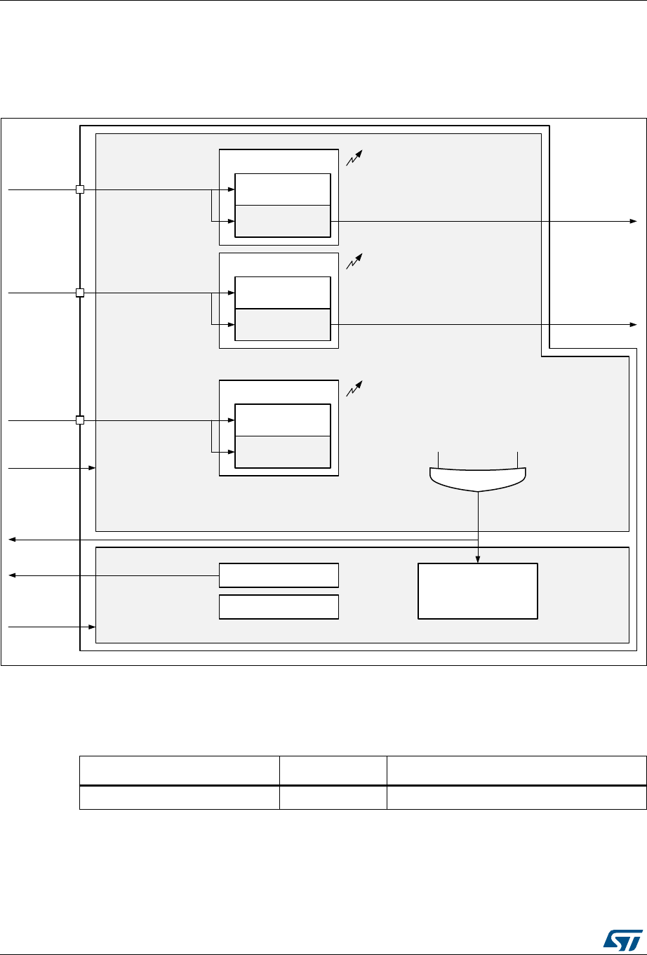
Tamper and backup registers (TAMP) RM0394
1070/1999 RM0394 Rev 4
35.3 TAMP functional description
35.3.1 TAMP block diagram
Figure 350. TAMP block diagram
1. The number of external tampers depends on products.
35.3.2 TAMP pins and internal signals
06Y9
7$03B,1
WDPSBSFONFORFNGRPDLQ
5HJLVWHUVLQWHUIDFH
WDPSBSFON
,54LQWHUIDFH
7$03)
7DPSHUGHWHFWLRQ
('*(GHWHFWLRQ
/(9(/GHWHFWLRQ
7$03)
7DPSHUGHWHFWLRQ
('*(GHWHFWLRQ
/(9(/GHWHFWLRQ
7$03[)
7DPSHUGHWHFWLRQ
('*(GHWHFWLRQ
/(9(/GHWHFWLRQ
7$03)
7$03[)
%DFNXSUHJLVWHUV
WDPSBLW
WDPSBHYW
WDPSBNHUBFN
WDPSBNHUBFNFORFNGRPDLQ
7$03B,1
7$03B,1[
WDPSBWUJ
WDPSBWUJ
Table 164. TAMP input/output pins
Pin name Signal type Description
TAMP_INx (x = pin index) Input Tamper input pin

RM0394 Rev 4 1071/1999
RM0394 Tamper and backup registers (TAMP)
1081
The TAMP kernel clock is usually the LSE at 32.768 kHz although it is possible to select
other clock sources in the RCC (refer to RCC for more details). Some detections modes are
not available in some low-power modes or VBAT when the selected clock is not LSE (refer to
Section 35.4: TAMP low-power modes for more details.
35.3.3 Tamper detection
The tamper detection can be configured for the following purposes:
•erase the backup registers (default configuration)
•generate an interrupt, capable to wakeup from Stop and Standby mode
•generate a hardware trigger for the low-power timers
TAMP backup registers
The backup registers (TAMP_BKPxR) are not reset by system reset or when the device
wakes up from Standby mode.
The backup registers are reset when a tamper detection event occurs or when the readout
protection of the flash is changed from level 1 to level 0 except if the TAMPxNOER bit is set,
or if the TAMPxMSK is set in the TAMP_CR2 register, or if the ITAMPxNOER bit is set in the
TAMP_CR3 register.
The backup registers can be reset by software by setting the BKERASE bit in the
TAMP_CR2 register.
Tamper detection initialization
Each input can be enabled by setting the corresponding TAMPxE bits to 1 in the TAMP_CR
register.
Each TAMP_INx tamper detection input is associated with a flag TAMPxF in the TAMP_SR
register.
When TAMPxMSK is cleared:
Table 165. TAMP internal input/output signals
Internal signal name Signal type Description
tamp_ker_ck Input TAMP kernel clock, connected to rtc_ker_ck
and also named RTCCLK in this document
tamp_pclk Input TAMP APB clock, connected to rtc_pclk
tamp_evt Output Tamper event detection (internal or external)
tamp_it Output TAMP interrupt (refer to Section 35.5: TAMP
interrupts for details)
tamp_trg[x]
(x = signal index) Output Tamper detection trigger
Table 166. TAMP interconnection
Signal name Source/Destination
tamp_evt rtc_tamp_evt used to generate a timestamp event

Tamper and backup registers (TAMP) RM0394
1072/1999 RM0394 Rev 4
The TAMPxF flag is asserted after the tamper event on the pin, with the latency provided
below:
•3 ck_apre cycles when TAMPFLT differs from 0x0 (level detection with filtering)
•3 ck_apre cycles when TAMPTS = 1 (timestamp on tamper event)
•No latency when TAMPFLT = 0x0 (edge detection) and TAMPTS = 0
A new tamper occurring on the same pin during this period and as long as TAMPxF is set
cannot be detected.
When TAMPxMSK is set:
A new tamper occurring on the same pin cannot be detected during the latency described
above and 2.5 ck_rtc additional cycles.
By setting the TAMPxIE bit in the TAMP_IER register, an interrupt is generated when a
tamper detection event occurs (when TAMPxF is set). Setting TAMPxIE is not allowed when
the corresponding TAMPxMSK is set.
Trigger output generation on tamper event
The tamper event detection can be used as trigger input by the low-power timers.
When TAMPxMSK bit in cleared in TAMP_CR register, the TAMPxF flag must be cleared by
software in order to allow a new tamper detection on the same pin.
When TAMPxMSK bit is set, the TAMPxF flag is masked, and kept cleared in TAMP_SR
register. This configuration allows to trig automatically the low-power timers in Stop mode,
without requiring the system wakeup to perform the TAMPxF clearing. In this case, the
backup registers are not cleared.
This feature is available only when the tamper is configured in the Level detection with
filtering on tamper inputs (passive mode) mode.
Timestamp on tamper event
With TAMPTS set to 1 in the RTC_CR, any tamper event causes a timestamp to occur. In
this case, either the TSF bit or the TSOVF bit is set in RTC_SR, in the same manner as if a
normal timestamp event occurs. The affected tamper flag register TAMPxF is set in the
TAMP_SR at the same time that TSF or TSOVF is set in the RTC_SR.
Edge detection on tamper inputs (passive mode)
If the TAMPFLT bits are 00, the TAMP_INx pins generate tamper detection events when
either a rising edge/high level or a falling edge/low level is observed depending on the
corresponding TAMPxTRG bit. The internal pull-up resistors on the TAMP_INx inputs are
deactivated when edge detection is selected.
Caution: When using the edge detection, it is recommended to check by software the tamper pin
level just after enabling the tamper detection (by reading the GPIO registers), and before
writing sensitive values in the backup registers, to ensure that an active edge did not occur
before enabling the tamper event detection.
When TAMPFLT = 00 and TAMPxTRG = 0 (rising edge detection), a tamper event may be
detected by hardware if the tamper input is already at high level before enabling the tamper
detection.
After a tamper event has been detected and cleared, the TAMP_INx should be disabled and
then re-enabled (TAMPxE set to 1) before re-programming the backup registers

RM0394 Rev 4 1073/1999
RM0394 Tamper and backup registers (TAMP)
1081
(TAMP_BKPxR). This prevents the application from writing to the backup registers while the
TAMP_INx input value still indicates a tamper detection. This is equivalent to a level
detection on the TAMP_INx input.
Note: Tamper detection is still active when VDD power is switched off. To avoid unwanted resetting
of the backup registers, the pin to which the TAMPx is mapped should be externally tied to
the correct level.
Level detection with filtering on tamper inputs (passive mode)
Level detection with filtering is performed by setting TAMPFLT to a non-zero value. A tamper
detection event is generated when either 2, 4, or 8 (depending on TAMPFLT) consecutive
samples are observed at the level designated by the TAMPxTRG bits.
The TAMP_INx inputs are precharged through the I/O internal pull-up resistance before its
state is sampled, unless disabled by setting TAMPPUDIS to 1. The duration of the
precharge is determined by the TAMPPRCH bits, allowing for larger capacitances on the
TAMP_INx inputs.
The trade-off between tamper detection latency and power consumption through the pull-up
can be optimized by using TAMPFREQ to determine the frequency of the sampling for level
detection.
Note: Refer to the microcontroller datasheet for the electrical characteristics of the pull-up
resistors.
35.4 TAMP low-power modes
35.5 TAMP interrupts
The interrupt channel is set in the interrupt status register. The interrupt output is also
activated.
Table 167. Effect of low-power modes on TAMP
Mode Description
Sleep No effect.
TAMP interrupts cause the device to exit the Sleep mode.
Stop
No effect on all features, except for level detection with filtering mode which remain
active only when the clock source is LSE or LSI.
Tamper events cause the device to exit the Stop mode.
Standby
No effect on all features, except for level detection with filtering mode which remain
active only when the clock source is LSE or LSI.Tamper events cause the device to exit
the Standby mode.
Shutdown
No effect on all features, except for level detection with filtering mode which remain
active only when the clock source is LSE. Tamper events cause the device to exit the
Shutdown mode.

Tamper and backup registers (TAMP) RM0394
1074/1999 RM0394 Rev 4
35.6 TAMP registers
Refer to Section 1.2 on page 60 of the reference manual for a list of abbreviations used in
register descriptions. The peripheral registers can be accessed by words (32-bit).
35.6.1 TAMP control register 1 (TAMP_CR1)
Address offset: 0x00
Backup domain reset value: 0xFFFF 0000
System reset: not affected
Table 168. Interrupt requests
Interrupt
acronym
Interrupt
event Event flag(1) Enable
control bit(2)
Interrupt
clear
method
Exit from
Sleep
mode
Exit from
Stop and
Standby
modes
Exit from
Shutdown
mode
TAMP Tamper x(3) TAMPxF TAMPxIE Write 1 in
CTAMPxF Yes Yes(4) Yes(5)
1. The event flags are in the TAMP_SR register.
2. The interrupt masked flags (resulting from event flags AND enable control bits) are in the TAMP_MISR register.
3. The number of tampers events depend on products.
4. In case of level detection with filtering passive tamper mode, wakeup from Stop and Standby modes is possible only when
the TAMP clock source is LSE or LSI.
5. In case of level detection with filtering passive tamper mode, wakeup from Shutdown modes is possible only when the
TAMP clock source is LSE.
31 30 29 28 27 26 25 24 23 22 21 20 19 18 17 16
Res. Res. Res. Res. Res. Res. Res. Res. Res. Res. Res. Res. Res. Res. Res. Res.
1514131211109876543210
Res. Res. Res. Res. Res. Res. Res. Res. Res. Res. Res. Res. Res. Res. TAMP2
E
TAMP1
E
rw rw
Bits 31:24 Reserved, must be kept at reset value.
Bit 23 Reserved, must be kept at reset value.
Bit 22 Reserved, must be kept at reset value.
Bit 21 Reserved, must be kept at reset value.
Bit 20 Reserved, must be kept at reset value.
Bit 19 Reserved, must be kept at reset value.
Bit 18 Reserved, must be kept at reset value.
Bit 17 Reserved, must be kept at reset value.
Bit 16 Reserved, must be kept at reset value.

RM0394 Rev 4 1075/1999
RM0394 Tamper and backup registers (TAMP)
1081
35.6.2 TAMP control register 2 (TAMP_CR2)
Address offset: 0x04
Backup domain reset value: 0x0000 0000
System reset: not affected
Bits 15:2 Reserved, must be kept at reset value.
Bit 1 TAMP2E: Tamper detection on TAMP_IN2 enable
0: Tamper detection on TAMP_IN2 is disabled.
1: Tamper detection on TAMP_IN2 is enabled.
Bit 0 TAMP1E: Tamper detection on TAMP_IN1 enable
0: Tamper detection on TAMP_IN1 is disabled.
1: Tamper detection on TAMP_IN1 is enabled.
31 30 29 28 27 26 25 24 23 22 21 20 19 18 17 16
Res. Res. Res. Res. Res. Res. TAMP2
TRG
TAMP1
TRG
BK
ERASE Res. Res. Res. Res. Res. TAMP2
MSK
TAMP1
MSK
rw rw wrw rw
1514131211109876543210
Res. Res. Res. Res. Res. Res. Res. Res. Res. Res. Res. Res. Res. Res. TAMP2
NOER
TAMP1
NOER
rw rw
Bits 31:26 Reserved, must be kept at reset value.
Bit 25 TAMP2TRG: Active level for tamper 2 input (active mode disabled)
if TAMPFLT 00
0: Tamper 2 input staying low triggers a tamper detection event.
1: Tamper 2 input staying high triggers a tamper detection event.
if TAMPFLT = 00
0: Tamper 2 input rising edge triggers a tamper detection event.
1: Tamper 2 input falling edge triggers a tamper detection event.
Bit 24 TAMP1TRG: Active level for tamper 1 input (active mode disabled)
If TAMPFLT 00
0: Tamper 1 input staying low triggers a tamper detection event.
1: Tamper 1 input staying high triggers a tamper detection event.
if TAMPFLT = 00
00: Tamper 1 input rising edge and high level triggers a tamper detection event.
01: Tamper 1 input falling edge and low level triggers a tamper detection event.
Bit 23 BKERASE: Backup registers erase
Writing ‘1’ to this bit reset the backup registers. Writing 0 has no effect. This bit is always
read as 0.
Bits 22:18 Reserved, must be kept at reset value.

Tamper and backup registers (TAMP) RM0394
1076/1999 RM0394 Rev 4
35.6.3 TAMP filter control register (TAMP_FLTCR)
Address offset: 0x0C
Backup domain reset value: 0x0000 0000
System reset: not affected
Bit 17 TAMP2MSK: Tamper 2 mask
0: Tamper 2 event generates a trigger event and TAMP2F must be cleared by software to
allow next tamper event detection.
1: Tamper 2 event generates a trigger event. TAMP2F is masked and internally cleared by
hardware. The backup registers are not erased.
The tamper 2 interrupt must not be enabled when TAMP2MSK is set.
Bit 16 TAMP1MSK: Tamper 1 mask
0: Tamper 1 event generates a trigger event and TAMP1F must be cleared by software to
allow next tamper event detection.
1: Tamper 1 event generates a trigger event. TAMP1F is masked and internally cleared by
hardware. The backup registers are not erased.
The tamper 1 interrupt must not be enabled when TAMP1MSK is set.
Bits 15:2 Reserved, must be kept at reset value.
Bit 1 TAMP2NOER: Tamper 2 no erase
0: Tamper 2 event erases the backup registers.
1: Tamper 2 event does not erase the backup registers.
Bit 0 TAMP1NOER: Tamper 1 no erase
0: Tamper 1 event erases the backup registers.
1: Tamper 1 event does not erase the backup registers.
31 30 29 28 27 26 25 24 23 22 21 20 19 18 17 16
Res. Res. Res. Res. Res. Res. Res. Res. Res. Res. Res. Res. Res. Res. Res. Res.
1514131211109876543210
Res. Res. Res. Res. Res. Res. Res. Res. TAMP
PUDIS
TAMPPR CH
[1:0]
TAMPFLT
[1:0]
TAMPFREQ
[2:0]
rw rw rw rw rw rw rw rw
Bits 31:8 Reserved, must be kept at reset value.
Bit 7 TAMPPUDIS: TAMP_INx pull-up disable
This bit determines if each of the TAMPx pins are precharged before each sample.
0: Precharge TAMP_INx pins before sampling (enable internal pull-up)
1: Disable precharge of TAMP_INx pins.

RM0394 Rev 4 1077/1999
RM0394 Tamper and backup registers (TAMP)
1081
Note: This register concerns only the tamper inputs in passive mode.
35.6.4 TAMP interrupt enable register (TAMP_IER)
Address offset: 0x2C
Backup domain reset value: 0x0000 0000
System reset: not affected
Bits 6:5 TAMPPRCH[1:0]: TAMP_INx precharge duration
These bit determines the duration of time during which the pull-up/is activated before each
sample. TAMPPRCH is valid for each of the TAMP_INx inputs.
0x0: 1 RTCCLK cycle
0x1: 2 RTCCLK cycles
0x2: 4 RTCCLK cycles
0x3: 8 RTCCLK cycles
Bits 4:3 TAMPFLT[1:0]: TAMP_INx filter count
These bits determines the number of consecutive samples at the specified level
(TAMP*TRG) needed to activate a tamper event. TAMPFLT is valid for each of the
TAMP_INx inputs.
0x0: Tamper event is activated on edge of TAMP_INx input transitions to the active level (no
internal pull-up on TAMP_INx input).
0x1: Tamper event is activated after 2 consecutive samples at the active level.
0x2: Tamper event is activated after 4 consecutive samples at the active level.
0x3: Tamper event is activated after 8 consecutive samples at the active level.
Bits 2:0 TAMPFREQ[2:0]: Tamper sampling frequency
Determines the frequency at which each of the TAMP_INx inputs are sampled.
0x0: RTCCLK / 32768 (1 Hz when RTCCLK = 32768 Hz)
0x1: RTCCLK / 16384 (2 Hz when RTCCLK = 32768 Hz)
0x2: RTCCLK / 8192 (4 Hz when RTCCLK = 32768 Hz)
0x3: RTCCLK / 4096 (8 Hz when RTCCLK = 32768 Hz)
0x4: RTCCLK / 2048 (16 Hz when RTCCLK = 32768 Hz)
0x5: RTCCLK / 1024 (32 Hz when RTCCLK = 32768 Hz)
0x6: RTCCLK / 512 (64 Hz when RTCCLK = 32768 Hz)
0x7: RTCCLK / 256 (128 Hz when RTCCLK = 32768 Hz)
31 30 29 28 27 26 25 24 23 22 21 20 19 18 17 16
Res. Res. Res. Res. Res. Res. Res. Res. Res. Res. Res. Res. Res. Res. Res. Res.
1514131211109876543210
Res. Res. Res. Res. Res. Res. Res. Res. Res. Res. Res. Res. Res. Res. TAMP
2IE
TAMP
1IE
rw rw
Bits 31:24 Reserved, must be kept at reset value.
Bit 23 Reserved, must be kept at reset value.
Bit 22 Reserved, must be kept at reset value.
Bit 21 Reserved, must be kept at reset value.
Bit 20 Reserved, must be kept at reset value.

Tamper and backup registers (TAMP) RM0394
1078/1999 RM0394 Rev 4
35.6.5 TAMP status register (TAMP_SR)
Address offset: 0x30
Backup domain reset value: 0x0000 0000
System reset: not affected
Bit 19 Reserved, must be kept at reset value.
Bit 18 Reserved, must be kept at reset value.
Bit 17 Reserved, must be kept at reset value.
Bit 16 Reserved, must be kept at reset value.
Bits 15:2 Reserved, must be kept at reset value.
Bit 1 TAMP2IE: Tamper 2 interrupt enable
0: Tamper 2 interrupt disabled.
1: Tamper 2 interrupt enabled.
Bit 0 TAMP1IE: Tamper 1 interrupt enable
0: Tamper 1 interrupt disabled.
1: Tamper 1 interrupt enabled.
31 30 29 28 27 26 25 24 23 22 21 20 19 18 17 16
Res. Res. Res. Res. Res. Res. Res. Res. Res. Res. Res. Res. Res. Res. Res. Res.
1514131211109876543210
Res. Res. Res. Res. Res. Res. Res. Res. Res. Res. Res. Res. Res. Res. TAMP
2F
TAMP
1F
rr
Bits 31:24 Reserved, must be kept at reset value.
Bit 23 Reserved, must be kept at reset value.
Bit 22 Reserved, must be kept at reset value.
Bit 21 Reserved, must be kept at reset value.
Bit 20 Reserved, must be kept at reset value.
Bit 19 Reserved, must be kept at reset value.
Bit 18 Reserved, must be kept at reset value.
Bit 17 Reserved, must be kept at reset value.
Bit 16 Reserved, must be kept at reset value.
Bits 15:2 Reserved, must be kept at reset value.
Bit 1 TAMP2F: TAMP2 detection flag
This flag is set by hardware when a tamper detection event is detected on the TAMP2 input.
Bit 0 TAMP1F: TAMP1 detection flag
This flag is set by hardware when a tamper detection event is detected on the TAMP1 input.

RM0394 Rev 4 1079/1999
RM0394 Tamper and backup registers (TAMP)
1081
35.6.6 TAMP masked interrupt status register (TAMP_MISR)
Address offset: 0x34
Backup domain reset value: 0x0000 0000
System reset: not affected
35.6.7 TAMP status clear register (TAMP_SCR)
Address offset: 0x3C
System reset value: 0x0000 0000
31 30 29 28 27 26 25 24 23 22 21 20 19 18 17 16
Res. Res. Res. Res. Res. Res. Res. Res. Res. Res. Res. Res. Res. Res. Res. Res.
r
1514131211109876543210
Res. Res. Res. Res. Res. Res. Res. Res. Res. Res. Res. Res. Res. Res. TAMP
2MF
TAMP
1MF
rr
Bits 31:24 Reserved, must be kept at reset value.
Bit 23 Reserved, must be kept at reset value.
Bit 22 Reserved, must be kept at reset value.
Bit 21 Reserved, must be kept at reset value.
Bit 20 Reserved, must be kept at reset value.
Bit 19 Reserved, must be kept at reset value.
Bit 18 Reserved, must be kept at reset value.
Bit 17 Reserved, must be kept at reset value.
Bit 16 Reserved, must be kept at reset value.
Bits 15:2 Reserved, must be kept at reset value.
Bit 1 TAMP2MF: TAMP2 interrupt masked flag
This flag is set by hardware when the tamper 2 interrupt is raised.
Bit 0 TAMP1MF: TAMP1 interrupt masked flag
This flag is set by hardware when the tamper 1 interrupt is raised.
31 30 29 28 27 26 25 24 23 22 21 20 19 18 17 16
Res. Res. Res. Res. Res. Res. Res. Res. Res. Res. Res. Res. Res. Res. Res. Res.
w
1514131211109876543210
Res. Res. Res. Res. Res. Res. Res. Res. Res. Res. Res. Res. Res. Res. CTAMP
2F
CTAMP
1F
ww

Tamper and backup registers (TAMP) RM0394
1080/1999 RM0394 Rev 4
35.6.8 TAMP backup x register (TAMP_BKPxR)
Address offset: 0x100 + 0x04 * x, (x = 0 to 31)
Backup domain reset value: 0x0000 0000
System reset: not affected
Bits 31:24 Reserved, must be kept at reset value.
Bit 23 Reserved, must be kept at reset value.
Bit 22 Reserved, must be kept at reset value.
Bit 21 Reserved, must be kept at reset value.
Bit 20 Reserved, must be kept at reset value.
Bit 19 Reserved, must be kept at reset value.
Bit 18 Reserved, must be kept at reset value.
Bit 17 Reserved, must be kept at reset value.
Bit 16 Reserved, must be kept at reset value.
Bits 15:2 Reserved, must be kept at reset value.
Bit 1 CTAMP2F: Clear TAMP2 detection flag
Writing 1 in this bit clears the TAMP2F bit in the TAMP_SR register.
Bit 0 CTAMP1F: Clear TAMP1 detection flag
Writing 1 in this bit clears the TAMP1F bit in the TAMP_SR register.
31 30 29 28 27 26 25 24 23 22 21 20 19 18 17 16
BKP[31:16]
rw rw rw rw rw rw rw rw rw rw rw rw rw rw rw rw
1514131211109876543210
BKP[15:0]
rw rw rw rw rw rw rw rw rw rw rw rw rw w rw rw
Bits 31:0 BKP[31:0]
The application can write or read data to and from these registers.
They are powered-on by VBAT when VDD is switched off, so that they are not reset by System
reset, and their contents remain valid when the device operates in low-power mode.
In the default configuration this register is reset on a tamper detection event. It is forced to
reset value as long as there is at least one external tamper flag being set. This register is
also reset when the readout protection (RDP) is disabled.

RM0394 Rev 4 1081/1999
RM0394 Tamper and backup registers (TAMP)
1081
35.6.9 TAMP register map
Refer to Section 2.2.2 on page 67 for the register boundary addresses.
Table 169. TAMP register map and reset values
Offset Register
31
30
29
28
27
26
25
24
23
22
21
20
19
18
17
16
15
14
13
12
11
10
9
8
7
6
5
4
3
2
1
0
0x00 TAMP_CR1
Res.
Res.
Res.
Res.
Res.
Res.
Res.
Res.
Res.
Res.
Res.
Res.
Res.
Res.
Res.
Res.
Res.
Res.
Res.
Res.
Res.
Res.
Res.
Res.
Res.
Res.
Res.
Res.
Res.
Res.
TAMP2E
TAMP1E
Reset value 00
0x04 TAMP_CR2
Res.
Res.
Res.
Res.
Res.
Res.
TAMP2TRG
TAMP1TRG
BKERASE
Res.
Res.
Res.
Res.
Res.
TAMP2MSK
TAMP1MSK
Res.
Res.
Res.
Res.
Res.
Res.
Res.
Res.
Res.
Res.
Res.
Res.
Res.
Res.
TAMP2NOER
TAMP1NOER
Reset value 0 0 0 0 0 0 0
0x0C TAMP_FLTCR
Res.
Res.
Res.
Res.
Res.
Res.
Res.
Res.
Res.
Res.
Res.
Res.
Res.
Res.
Res.
Res.
Res.
Res.
Res.
Res.
Res.
Res.
Res.
Res.
TAMPPUDIS
.TAMPPRCH[1:0]
.TAMPFLT[1:0]
TAMPFREQ[2:0]
Reset value 00000000
0x2C TAMP_IER
Res.
Res.
Res.
Res.
Res.
Res.
Res.
Res.
Res.
Res.
Res.
Res.
Res.
Res.
Res.
Res.
Res.
Res.
Res.
Res.
Res.
Res.
Res.
Res.
Res.
Res.
Res.
Res.
Res.
Res.
TAMP2IE
TAMP1IE
Reset value 00
0x30 TAMP_SR
Res.
Res.
Res.
Res.
Res.
Res.
Res.
Res.
Res.
Res.
Res.
Res.
Res.
Res.
Res.
Res.
Res.
Res.
Res.
Res.
Res.
Res.
Res.
Res.
Res.
Res.
Res.
Res.
Res.
Res.
TAMP2F
TAMP1F
Reset value 00
0x34 TAMP_MISR
Res.
Res.
Res.
Res.
Res.
Res.
Res.
Res.
Res.
Res.
Res.
Res.
Res.
Res.
Res.
Res.
Res.
Res.
Res.
Res.
Res.
Res.
Res.
Res.
Res.
Res.
Res.
Res.
Res.
Res.
TAMP2MF
TAMP1MF
Reset value 00
0x3C TAMP_SCR
Res.
Res.
Res.
Res.
Res.
Res.
Res.
Res.
Res.
Res.
Res.
Res.
Res.
Res.
Res.
Res.
Res.
Res.
Res.
Res.
Res.
Res.
Res.
Res.
Res.
Res.
Res.
Res.
Res.
Res.
CTAMP2F
CTAMP1F
Reset value 00
0x100 +
0x04*x,
(x=
0 to.31)
TAMP_BKPxR BKP[31:0]
Reset value 00000000000000000000000000000000

Real-time clock (RTC) applied to STM32L43x/44x/45x/46x devices only RM0394
1082/1600 RM0394 Rev 4
36 Real-time clock (RTC) applied to
STM32L43x/44x/45x/46x devices only
36.1 Introduction
The RTC provides an automatic wakeup to manage all low-power modes.
The real-time clock (RTC) is an independent BCD timer/counter. The RTC provides a time-
of-day clock/calendar with programmable alarm interrupts.
The RTC includes also a periodic programmable wakeup flag with interrupt capability.
Two 32-bit registers contain the seconds, minutes, hours (12- or 24-hour format), day (day
of week), date (day of month), month, and year, expressed in binary coded decimal format
(BCD). The sub-seconds value is also available in binary format.
Compensations for 28-, 29- (leap year), 30-, and 31-day months are performed
automatically. Daylight saving time compensation can also be performed.
Additional 32-bit registers contain the programmable alarm subseconds, seconds, minutes,
hours, day, and date.
A digital calibration feature is available to compensate for any deviation in crystal oscillator
accuracy.
After Backup domain reset, all RTC registers are protected against possible parasitic write
accesses.
As long as the supply voltage remains in the operating range, the RTC never stops,
regardless of the device status (Run mode, low-power mode or under reset).

RM0394 Rev 4 1083/1600
RM0394 Real-time clock (RTC) applied to STM32L43x/44x/45x/46x devices only
1126
36.2 RTC main features
The RTC unit main features are the following (see Figure 351: RTC block diagram):
•Calendar with subseconds, seconds, minutes, hours (12 or 24 format), day (day of
week), date (day of month), month, and year.
•Daylight saving compensation programmable by software.
•Programmable alarm with interrupt function. The alarm can be triggered by any
combination of the calendar fields.
•Automatic wakeup unit generating a periodic flag that triggers an automatic wakeup
interrupt.
•Reference clock detection: a more precise second source clock (50 or 60 Hz) can be
used to enhance the calendar precision.
•Accurate synchronization with an external clock using the subsecond shift feature.
•Digital calibration circuit (periodic counter correction): 0.95 ppm accuracy, obtained in a
calibration window of several seconds
•Time-stamp function for event saving
•Tamper detection event with configurable filter and internal pull-up
•Maskable interrupts/events:
–Alarm A
–Alarm B
– Wakeup interrupt
– Time-stamp
– Tamper detection
•32 backup registers.
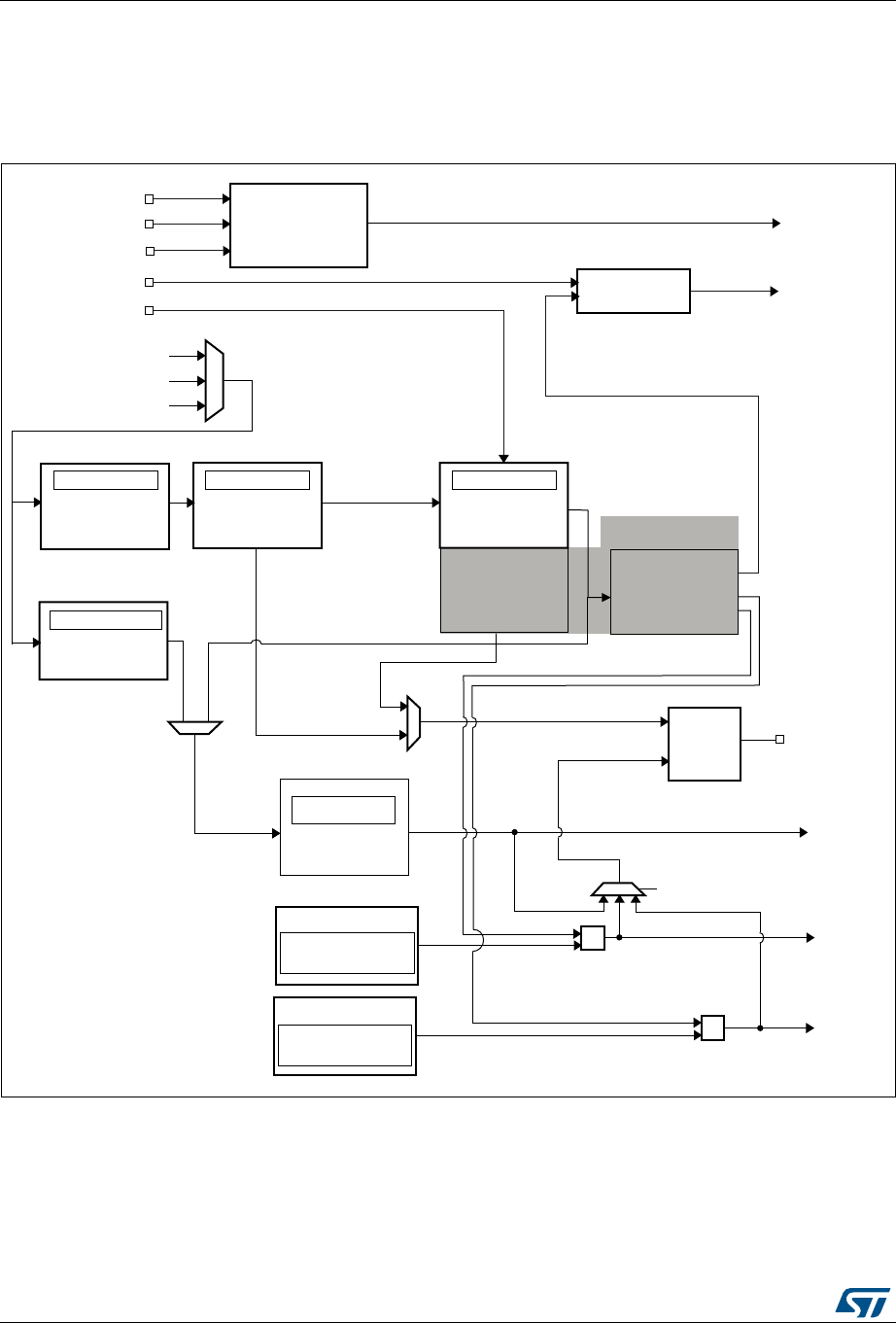
Real-time clock (RTC) applied to STM32L43x/44x/45x/46x devices only RM0394
1084/1600 RM0394 Rev 4
36.3 RTC functional description
36.3.1 RTC block diagram
Figure 351. RTC block diagram
&DOHQGDU
57&B$/$50
57&&/.
+6(
/6(+]
/6,
6\QFKURQRXV
ELWSUHVFDOHU
GHIDXOW
$/5$)
57&B35(5
%DFNXSUHJLVWHUV
DQG57&WDPSHU
FRQWUROUHJLVWHU
7$03[)
7LPHVWDPS
UHJLVWHUV 76)
2XWSXW
FRQWURO 57&B287
FDOLEUDWLRQ
57&B7$03
6PRRWK
FNBVSUH
GHIDXOW+]
57&B5(),1
57&B7$03
57&B76
$V\QFKURQRXV
ELWSUHVFDOHU
GHIDXOW
57&B35(557&B&$/5
6KDGRZUHJLVWHUV
57&B75
57&B'5
$ODUP$
57&B$/50$5
57&B$/50$665
FNBDSUH
GHIDXOW+]
57&B&$/,%
6KDGRZUHJLVWHU
57&B665
$ODUP%
$/5%)
:8&.6(/>@
3UHVFDOHU
ELWZDNHXS
DXWRUHORDGWLPHU
57&B:875
57&B7$03
:87)
26(/>@
57&B$/50%5
57&B$/50%665
06Y9

RM0394 Rev 4 1085/1600
RM0394 Real-time clock (RTC) applied to STM32L43x/44x/45x/46x devices only
1126
The RTC includes:
•Two alarms
•Three tamper events from I/Os
– Tamper detection erases the backup registers.
•One timestamp event from I/O
•Tamper event detection can generate a timestamp event
•Timestamp can be generated when a switch to VBAT occurs
•32 x 32-bit backup registers
– The backup registers (RTC_BKPxR) are implemented in the RTC domain that
remains powered-on by VBAT when the VDD power is switched off.
•Output functions: RTC_OUT which selects one of the following two outputs:
– RTC_CALIB: 512 Hz or 1Hz clock output (with an LSE frequency of 32.768 kHz).
This output is enabled by setting the COE bit in the RTC_CR register.
– RTC_ALARM: This output is enabled by configuring the OSEL[1:0] bits in the
RTC_CR register which select the Alarm A, Alarm B or Wakeup outputs.
•Input functions:
– RTC_TS: timestamp event
– RTC_TAMP1: tamper1 event detection
– RTC_TAMP2: tamper2 event detection
– RTC_TAMP3: tamper3 event detection
– RTC_REFIN: 50 or 60 Hz reference clock input
36.3.2 GPIOs controlled by the RTC
RTC_OUT, RTC_TS and RTC_TAMP1 are mapped on the same pin (PC13). PC13 pin
configuration is controlled by the RTC, whatever the PC13 GPIO configuration, except for
the RTC_ALARM output open-drain mode. In this particular case, the GPIO must be
configured as input. The RTC functions mapped on PC13 are available in all low-power
modes and in VBAT mode.
The output mechanism follows the priority order shown in Table 170.
Table 170. RTC pin PC13 configuration(1)
PC13 Pin
configuration
and function
OSEL[1:0]
bits
(RTC_ALARM
output
enable)
COE bit
(RTC_CALIB
output
enable)
RTC_OUT
_RMP
bit
RTC_ALARM
_TYPE
bit
TAMP1E bit
(RTC_TAMP1
input
enable)
TSE bit
(RTC_TS
input
enable)
RTC_ALARM
output OD 01 or 10 or 11 Don’t care
0
0 Don’t care Don’t care
1
RTC_ALARM
output PP 01 or 10 or 11 Don’t care
0
1 Don’t care Don’t care
1
RTC_CALIB
output PP 00 1 0 Don’t care Don’t care Don’t care

Real-time clock (RTC) applied to STM32L43x/44x/45x/46x devices only RM0394
1086/1600 RM0394 Rev 4
In addition, it is possible to remap RTC_OUT on PB2 pin thanks to RTC_OUT_RMP bit. In
this case it is mandatory to configure PB2 GPIO registers as alternate function with the
correct type. The remap functions are shown in Table 171.
The table below summarizes the RTC pins and functions capability in all modes.
RTC_TAMP1
input floating
00 0 Don’t care
Don’t care 1 000 1
1
01 or 10 or 11 0
RTC_TS and
RTC_TAMP1
input floating
00 0 Don’t care
Don’t care 1 100 1
1
01 or 10 or 11 0
RTC_TS input
floating
00 0 Don’t care
Don’t care 0 100 1
1
01 or 10 or 11 0
Wakeup pin or
Standard
GPIO
00 0 Don’t care
Don’t care 0 000 1
1
01 or 10 or 11 0
1. OD: open drain; PP: push-pull.
Table 170. RTC pin PC13 configuration(1) (continued)
PC13 Pin
configuration
and function
OSEL[1:0]
bits
(RTC_ALARM
output
enable)
COE bit
(RTC_CALIB
output
enable)
RTC_OUT
_RMP
bit
RTC_ALARM
_TYPE
bit
TAMP1E bit
(RTC_TAMP1
input
enable)
TSE bit
(RTC_TS
input
enable)
Table 171. RTC_OUT mapping
OSEL[1:0] bits
(RTC_ALARM
output enable)
COE bit
(RTC_CALIB
output enable)
RTC_OUT_RMP
bit
RTC_OUT on
PC13
RTC_OUT on
PB2
00 0
0
--
00 1 RTC_CALIB -
01 or 10 or 11 Don’t care RTC_ALARM -
00 0
1
--
00 1 - RTC_CALIB
01 or 10 or 11 0 - RTC_ALARM
01 or 10 or 11 1 RTC_ALARM RTC_CALIB

RM0394 Rev 4 1087/1600
RM0394 Real-time clock (RTC) applied to STM32L43x/44x/45x/46x devices only
1126
36.3.3 Clock and prescalers
The RTC clock source (RTCCLK) is selected through the clock controller among the LSE
clock, the LSI oscillator clock, and the HSE clock. For more information on the RTC clock
source configuration, refer to Section 6: Reset and clock control (RCC).
A programmable prescaler stage generates a 1 Hz clock which is used to update the
calendar. To minimize power consumption, the prescaler is split into 2 programmable
prescalers (see Figure 351: RTC block diagram):
•A 7-bit asynchronous prescaler configured through the PREDIV_A bits of the
RTC_PRER register.
•A 15-bit synchronous prescaler configured through the PREDIV_S bits of the
RTC_PRER register.
Note: When both prescalers are used, it is recommended to configure the asynchronous prescaler
to a high value to minimize consumption.
The asynchronous prescaler division factor is set to 128, and the synchronous division
factor to 256, to obtain an internal clock frequency of 1 Hz (ck_spre) with an LSE frequency
of 32.768 kHz.
The minimum division factor is 1 and the maximum division factor is 222.
This corresponds to a maximum input frequency of around 4 MHz.
fck_apre is given by the following formula:
The ck_apre clock is used to clock the binary RTC_SSR subseconds downcounter. When it
reaches 0, RTC_SSR is reloaded with the content of PREDIV_S.
fck_spre is given by the following formula:
Table 172. RTC functions over modes
Pin RTC functions
Functional in all low-
power modes except
Standby/Shutdown
modes
Functional in
Standby/Shutdown
mode
Functional in
VBAT mode
PC13
RTC_TAMP1
RTC_TS
RTC_OUT
YES YES YES
PA0 RTC_TAMP2 YES YES YES
PE6 RTC_TAMP3 YES YES YES
PB2 RTC_OUT YES NO NO
PB15 RTC_REFIN YES NO NO
fCK_APRE
fRTCCLK
PREDIV_A 1+
---------------------------------------
=
fCK_SPRE
fRTCCLK
PREDIV_S 1+()PREDIV_A 1+()×
-----------------------------------------------------------------------------------------------
=

Real-time clock (RTC) applied to STM32L43x/44x/45x/46x devices only RM0394
1088/1600 RM0394 Rev 4
The ck_spre clock can be used either to update the calendar or as timebase for the 16-bit
wakeup auto-reload timer. To obtain short timeout periods, the 16-bit wakeup auto-reload
timer can also run with the RTCCLK divided by the programmable 4-bit asynchronous
prescaler (see Section 36.3.6: Periodic auto-wakeup for details).
36.3.4 Real-time clock and calendar
The RTC calendar time and date registers are accessed through shadow registers which
are synchronized with PCLK (APB clock). They can also be accessed directly in order to
avoid waiting for the synchronization duration.
•RTC_SSR for the subseconds
•RTC_TR for the time
•RTC_DR for the date
Every RTCCLK period, the current calendar value is copied into the shadow registers, and
the RSF bit of RTC_ISR register is set (see Section 36.6.4: RTC initialization and status
register (RTC_ISR)). The copy is not performed in Stop and Standby mode. When exiting
these modes, the shadow registers are updated after up to 1 RTCCLK period.
When the application reads the calendar registers, it accesses the content of the shadow
registers. It is possible to make a direct access to the calendar registers by setting the
BYPSHAD control bit in the RTC_CR register. By default, this bit is cleared, and the user
accesses the shadow registers.
When reading the RTC_SSR, RTC_TR or RTC_DR registers in BYPSHAD=0 mode, the
frequency of the APB clock (fAPB) must be at least 7 times the frequency of the RTC clock
(fRTCCLK).
The shadow registers are reset by system reset.
36.3.5 Programmable alarms
The RTC unit provides programmable alarm: Alarm A and Alarm B. The description below is
given for Alarm A, but can be translated in the same way for Alarm B.
The programmable alarm function is enabled through the ALRAE bit in the RTC_CR
register. The ALRAF is set to 1 if the calendar subseconds, seconds, minutes, hours, date
or day match the values programmed in the alarm registers RTC_ALRMASSR and
RTC_ALRMAR. Each calendar field can be independently selected through the MSKx bits
of the RTC_ALRMAR register, and through the MASKSSx bits of the RTC_ALRMASSR
register. The alarm interrupt is enabled through the ALRAIE bit in the RTC_CR register.
Caution: If the seconds field is selected (MSK1 bit reset in RTC_ALRMAR), the synchronous
prescaler division factor set in the RTC_PRER register must be at least 3 to ensure correct
behavior.
Alarm A and Alarm B (if enabled by bits OSEL[1:0] in RTC_CR register) can be routed to the
RTC_ALARM output. RTC_ALARM output polarity can be configured through bit POL the
RTC_CR register.
36.3.6 Periodic auto-wakeup
The periodic wakeup flag is generated by a 16-bit programmable auto-reload down-counter.
The wakeup timer range can be extended to 17 bits.
The wakeup function is enabled through the WUTE bit in the RTC_CR register.

RM0394 Rev 4 1089/1600
RM0394 Real-time clock (RTC) applied to STM32L43x/44x/45x/46x devices only
1126
The wakeup timer clock input can be:
•RTC clock (RTCCLK) divided by 2, 4, 8, or 16.
When RTCCLK is LSE(32.768kHz), this allows to configure the wakeup interrupt period
from 122 µs to 32 s, with a resolution down to 61 µs.
•ck_spre (usually 1 Hz internal clock)
When ck_spre frequency is 1Hz, this allows to achieve a wakeup time from 1 s to
around 36 hours with one-second resolution. This large programmable time range is
divided in 2 parts:
– from 1s to 18 hours when WUCKSEL [2:1] = 10
– and from around 18h to 36h when WUCKSEL[2:1] = 11. In this last case 216 is
added to the 16-bit counter current value.When the initialization sequence is
complete (see Programming the wakeup timer on page 1090), the timer starts
counting down.When the wakeup function is enabled, the down-counting remains
active in low-power modes. In addition, when it reaches 0, the WUTF flag is set in
the RTC_ISR register, and the wakeup counter is automatically reloaded with its
reload value (RTC_WUTR register value).
The WUTF flag must then be cleared by software.
When the periodic wakeup interrupt is enabled by setting the WUTIE bit in the RTC_CR
register, it can exit the device from low-power modes.
The periodic wakeup flag can be routed to the RTC_ALARM output provided it has been
enabled through bits OSEL[1:0] of RTC_CR register. RTC_ALARM output polarity can be
configured through the POL bit in the RTC_CR register.
System reset, as well as low-power modes (Sleep, Stop and Standby) have no influence on
the wakeup timer.
36.3.7 RTC initialization and configuration
RTC register access
The RTC registers are 32-bit registers. The APB interface introduces 2 wait-states in RTC
register accesses except on read accesses to calendar shadow registers when
BYPSHAD=0.
RTC register write protection
After system reset, the RTC registers are protected against parasitic write access by
clearing the DBP bit in the PWR_CR1 register (refer to the power control section). DBP bit
must be set in order to enable RTC registers write access.
After Backup domain reset, all the RTC registers are write-protected. Writing to the RTC
registers is enabled by writing a key into the Write Protection register, RTC_WPR.
The following steps are required to unlock the write protection on all the RTC registers
except for RTC_TAMPCR, RTC_BKPxR, RTC_OR and RTC_ISR[13:8].
1. Write ‘0xCA’ into the RTC_WPR register.
2. Write ‘0x53’ into the RTC_WPR register.
Writing a wrong key reactivates the write protection.
The protection mechanism is not affected by system reset.

Real-time clock (RTC) applied to STM32L43x/44x/45x/46x devices only RM0394
1090/1600 RM0394 Rev 4
Calendar initialization and configuration
To program the initial time and date calendar values, including the time format and the
prescaler configuration, the following sequence is required:
1. Set INIT bit to 1 in the RTC_ISR register to enter initialization mode. In this mode, the
calendar counter is stopped and its value can be updated.
2. Poll INITF bit of in the RTC_ISR register. The initialization phase mode is entered when
INITF is set to 1. It takes around 2 RTCCLK clock cycles (due to clock synchronization).
3. To generate a 1 Hz clock for the calendar counter, program both the prescaler factors in
RTC_PRER register.
4. Load the initial time and date values in the shadow registers (RTC_TR and RTC_DR),
and configure the time format (12 or 24 hours) through the FMT bit in the RTC_CR
register.
5. Exit the initialization mode by clearing the INIT bit. The actual calendar counter value is
then automatically loaded and the counting restarts after 4 RTCCLK clock cycles.
When the initialization sequence is complete, the calendar starts counting.
Note: After a system reset, the application can read the INITS flag in the RTC_ISR register to
check if the calendar has been initialized or not. If this flag equals 0, the calendar has not
been initialized since the year field is set at its Backup domain reset default value (0x00).
To read the calendar after initialization, the software must first check that the RSF flag is set
in the RTC_ISR register.
Daylight saving time
The daylight saving time management is performed through bits SUB1H, ADD1H, and BKP
of the RTC_CR register.
Using SUB1H or ADD1H, the software can subtract or add one hour to the calendar in one
single operation without going through the initialization procedure.
In addition, the software can use the BKP bit to memorize this operation.
Programming the alarm
A similar procedure must be followed to program or update the programmable alarms. The
procedure below is given for Alarm A but can be translated in the same way for Alarm B.
1. Clear ALRAE in RTC_CR to disable Alarm A.
2. Program the Alarm A registers (RTC_ALRMASSR/RTC_ALRMAR).
3. Set ALRAE in the RTC_CR register to enable Alarm A again.
Note: Each change of the RTC_CR register is taken into account after around 2 RTCCLK clock
cycles due to clock synchronization.
Programming the wakeup timer
The following sequence is required to configure or change the wakeup timer auto-reload
value (WUT[15:0] in RTC_WUTR):

RM0394 Rev 4 1091/1600
RM0394 Real-time clock (RTC) applied to STM32L43x/44x/45x/46x devices only
1126
1. Clear WUTE in RTC_CR to disable the wakeup timer.
2. Poll WUTWF until it is set in RTC_ISR to make sure the access to wakeup auto-reload
counter and to WUCKSEL[2:0] bits is allowed. It takes around 2 RTCCLK clock cycles
(due to clock synchronization).
3. Program the wakeup auto-reload value WUT[15:0], and the wakeup clock selection
(WUCKSEL[2:0] bits in RTC_CR). Set WUTE in RTC_CR to enable the timer again.
The wakeup timer restarts down-counting. The WUTWF bit is cleared up to 2 RTCCLK
clock cycles after WUTE is cleared, due to clock synchronization.
36.3.8 Reading the calendar
When BYPSHAD control bit is cleared in the RTC_CR register
To read the RTC calendar registers (RTC_SSR, RTC_TR and RTC_DR) properly, the APB
clock frequency (fPCLK) must be equal to or greater than seven times the RTC clock
frequency (fRTCCLK). This ensures a secure behavior of the synchronization mechanism.
If the APB clock frequency is less than seven times the RTC clock frequency, the software
must read the calendar time and date registers twice. If the second read of the RTC_TR
gives the same result as the first read, this ensures that the data is correct. Otherwise a third
read access must be done. In any case the APB clock frequency must never be lower than
the RTC clock frequency.
The RSF bit is set in RTC_ISR register each time the calendar registers are copied into the
RTC_SSR, RTC_TR and RTC_DR shadow registers. The copy is performed every
RTCCLK cycles. To ensure consistency between the 3 values, reading either RTC_SSR or
RTC_TR locks the values in the higher-order calendar shadow registers until RTC_DR is
read. In case the software makes read accesses to the calendar in a time interval smaller
than 1 RTCCLK period: RSF must be cleared by software after the first calendar read, and
then the software must wait until RSF is set before reading again the RTC_SSR, RTC_TR
and RTC_DR registers.
After waking up from low-power mode (Stop or Standby), RSF must be cleared by software.
The software must then wait until it is set again before reading the RTC_SSR, RTC_TR and
RTC_DR registers.
The RSF bit must be cleared after wakeup and not before entering low-power mode.
After a system reset, the software must wait until RSF is set before reading the RTC_SSR,
RTC_TR and RTC_DR registers. Indeed, a system reset resets the shadow registers to
their default values.
After an initialization (refer to Calendar initialization and configuration on page 1090): the
software must wait until RSF is set before reading the RTC_SSR, RTC_TR and RTC_DR
registers.
After synchronization (refer to Section 36.3.10: RTC synchronization): the software must
wait until RSF is set before reading the RTC_SSR, RTC_TR and RTC_DR registers.
When the BYPSHAD control bit is set in the RTC_CR register (bypass shadow
registers)
Reading the calendar registers gives the values from the calendar counters directly, thus
eliminating the need to wait for the RSF bit to be set. This is especially useful after exiting

Real-time clock (RTC) applied to STM32L43x/44x/45x/46x devices only RM0394
1092/1600 RM0394 Rev 4
from low-power modes (STOP or Standby), since the shadow registers are not updated
during these modes.
When the BYPSHAD bit is set to 1, the results of the different registers might not be
coherent with each other if an RTCCLK edge occurs between two read accesses to the
registers. Additionally, the value of one of the registers may be incorrect if an RTCCLK edge
occurs during the read operation. The software must read all the registers twice, and then
compare the results to confirm that the data is coherent and correct. Alternatively, the
software can just compare the two results of the least-significant calendar register.
Note: While BYPSHAD=1, instructions which read the calendar registers require one extra APB
cycle to complete.
36.3.9 Resetting the RTC
The calendar shadow registers (RTC_SSR, RTC_TR and RTC_DR) and some bits of the
RTC status register (RTC_ISR) are reset to their default values by all available system reset
sources.
On the contrary, the following registers are reset to their default values by a Backup domain
reset and are not affected by a system reset: the RTC current calendar registers, the RTC
control register (RTC_CR), the prescaler register (RTC_PRER), the RTC calibration register
(RTC_CALR), the RTC shift register (RTC_SHIFTR), the RTC timestamp registers
(RTC_TSSSR, RTC_TSTR and RTC_TSDR), the RTC tamper configuration register
(RTC_TAMPCR), the RTC backup registers (RTC_BKPxR), the wakeup timer register
(RTC_WUTR), the Alarm A and Alarm B registers (RTC_ALRMASSR/RTC_ALRMAR and
RTC_ALRMBSSR/RTC_ALRMBR), and the Option register (RTC_OR).
In addition, when it is clocked by the LSE, the RTC keeps on running under system reset if
the reset source is different from the Backup domain reset one (refer to the RTC clock
section of the Reset and clock controller for details on the list of RTC clock sources not
affected by system reset). When a Backup domain reset occurs, the RTC is stopped and all
the RTC registers are set to their reset values.
36.3.10 RTC synchronization
The RTC can be synchronized to a remote clock with a high degree of precision. After
reading the sub-second field (RTC_SSR or RTC_TSSSR), a calculation can be made of the
precise offset between the times being maintained by the remote clock and the RTC. The
RTC can then be adjusted to eliminate this offset by “shifting” its clock by a fraction of a
second using RTC_SHIFTR.
RTC_SSR contains the value of the synchronous prescaler counter. This allows one to
calculate the exact time being maintained by the RTC down to a resolution of
1 / (PREDIV_S + 1) seconds. As a consequence, the resolution can be improved by
increasing the synchronous prescaler value (PREDIV_S[14:0]. The maximum resolution
allowed (30.52 s with a 32768 Hz clock) is obtained with PREDIV_S set to 0x7FFF.
However, increasing PREDIV_S means that PREDIV_A must be decreased in order to
maintain the synchronous prescaler output at 1 Hz. In this way, the frequency of the
asynchronous prescaler output increases, which may increase the RTC dynamic
consumption.
The RTC can be finely adjusted using the RTC shift control register (RTC_SHIFTR). Writing
to RTC_SHIFTR can shift (either delay or advance) the clock by up to a second with a
resolution of 1 / (PREDIV_S + 1) seconds. The shift operation consists of adding the

RM0394 Rev 4 1093/1600
RM0394 Real-time clock (RTC) applied to STM32L43x/44x/45x/46x devices only
1126
SUBFS[14:0] value to the synchronous prescaler counter SS[15:0]: this will delay the clock.
If at the same time the ADD1S bit is set, this results in adding one second and at the same
time subtracting a fraction of second, so this will advance the clock.
Caution: Before initiating a shift operation, the user must check that SS[15] = 0 in order to ensure that
no overflow will occur.
As soon as a shift operation is initiated by a write to the RTC_SHIFTR register, the SHPF
flag is set by hardware to indicate that a shift operation is pending. This bit is cleared by
hardware as soon as the shift operation has completed.
Caution: This synchronization feature is not compatible with the reference clock detection feature:
firmware must not write to RTC_SHIFTR when REFCKON=1.
36.3.11 RTC reference clock detection
The update of the RTC calendar can be synchronized to a reference clock, RTC_REFIN,
which is usually the mains frequency (50 or 60 Hz). The precision of the RTC_REFIN
reference clock should be higher than the 32.768 kHz LSE clock. When the RTC_REFIN
detection is enabled (REFCKON bit of RTC_CR set to 1), the calendar is still clocked by the
LSE, and RTC_REFIN is used to compensate for the imprecision of the calendar update
frequency (1 Hz).
Each 1 Hz clock edge is compared to the nearest RTC_REFIN clock edge (if one is found
within a given time window). In most cases, the two clock edges are properly aligned. When
the 1 Hz clock becomes misaligned due to the imprecision of the LSE clock, the RTC shifts
the 1 Hz clock a bit so that future 1 Hz clock edges are aligned. Thanks to this mechanism,
the calendar becomes as precise as the reference clock.
The RTC detects if the reference clock source is present by using the 256 Hz clock
(ck_apre) generated from the 32.768 kHz quartz. The detection is performed during a time
window around each of the calendar updates (every 1 s). The window equals 7 ck_apre
periods when detecting the first reference clock edge. A smaller window of 3 ck_apre
periods is used for subsequent calendar updates.
Each time the reference clock is detected in the window, the synchronous prescaler which
outputs the ck_spre clock is forced to reload. This has no effect when the reference clock
and the 1 Hz clock are aligned because the prescaler is being reloaded at the same
moment. When the clocks are not aligned, the reload shifts future 1 Hz clock edges a little
for them to be aligned with the reference clock.
If the reference clock halts (no reference clock edge occurred during the 3 ck_apre window),
the calendar is updated continuously based solely on the LSE clock. The RTC then waits for
the reference clock using a large 7 ck_apre period detection window centered on the
ck_spre edge.
When the RTC_REFIN detection is enabled, PREDIV_A and PREDIV_S must be set to their
default values:
•PREDIV_A = 0x007F
•PREVID_S = 0x00FF
Note: RTC_REFIN clock detection is not available in Standby mode.

Real-time clock (RTC) applied to STM32L43x/44x/45x/46x devices only RM0394
1094/1600 RM0394 Rev 4
36.3.12 RTC smooth digital calibration
The RTC frequency can be digitally calibrated with a resolution of about 0.954 ppm with a
range from -487.1 ppm to +488.5 ppm. The correction of the frequency is performed using
series of small adjustments (adding and/or subtracting individual RTCCLK pulses). These
adjustments are fairly well distributed so that the RTC is well calibrated even when observed
over short durations of time.
The smooth digital calibration is performed during a cycle of about 220 RTCCLK pulses, or
32 seconds when the input frequency is 32768 Hz. This cycle is maintained by a 20-bit
counter, cal_cnt[19:0], clocked by RTCCLK.
The smooth calibration register (RTC_CALR) specifies the number of RTCCLK clock cycles
to be masked during the 32-second cycle:
•Setting the bit CALM[0] to 1 causes exactly one pulse to be masked during the 32-
second cycle.
•Setting CALM[1] to 1 causes two additional cycles to be masked
•Setting CALM[2] to 1 causes four additional cycles to be masked
•and so on up to CALM[8] set to 1 which causes 256 clocks to be masked.
Note: CALM[8:0] (RTC_CALR) specifies the number of RTCCLK pulses to be masked during the
32-second cycle. Setting the bit CALM[0] to ‘1’ causes exactly one pulse to be masked
during the 32-second cycle at the moment when cal_cnt[19:0] is 0x80000; CALM[1]=1
causes two other cycles to be masked (when cal_cnt is 0x40000 and 0xC0000); CALM[2]=1
causes four other cycles to be masked (cal_cnt = 0x20000/0x60000/0xA0000/ 0xE0000);
and so on up to CALM[8]=1 which causes 256 clocks to be masked (cal_cnt = 0xXX800).
While CALM allows the RTC frequency to be reduced by up to 487.1 ppm with fine
resolution, the bit CALP can be used to increase the frequency by 488.5 ppm. Setting CALP
to ‘1’ effectively inserts an extra RTCCLK pulse every 211 RTCCLK cycles, which means
that 512 clocks are added during every 32-second cycle.
Using CALM together with CALP, an offset ranging from -511 to +512 RTCCLK cycles can
be added during the 32-second cycle, which translates to a calibration range of -487.1 ppm
to +488.5 ppm with a resolution of about 0.954 ppm.
The formula to calculate the effective calibrated frequency (FCAL) given the input frequency
(FRTCCLK) is as follows:
FCAL = FRTCCLK x [1 + (CALP x 512 - CALM) / (220 + CALM - CALP x 512)]
Calibration when PREDIV_A<3
The CALP bit can not be set to 1 when the asynchronous prescaler value (PREDIV_A bits in
RTC_PRER register) is less than 3. If CALP was already set to 1 and PREDIV_A bits are
set to a value less than 3, CALP is ignored and the calibration operates as if CALP was
equal to 0.
To perform a calibration with PREDIV_A less than 3, the synchronous prescaler value
(PREDIV_S) should be reduced so that each second is accelerated by 8 RTCCLK clock
cycles, which is equivalent to adding 256 clock cycles every 32 seconds. As a result,
between 255 and 256 clock pulses (corresponding to a calibration range from 243.3 to
244.1 ppm) can effectively be added during each 32-second cycle using only the CALM bits.
With a nominal RTCCLK frequency of 32768 Hz, when PREDIV_A equals 1 (division factor
of 2), PREDIV_S should be set to 16379 rather than 16383 (4 less). The only other

RM0394 Rev 4 1095/1600
RM0394 Real-time clock (RTC) applied to STM32L43x/44x/45x/46x devices only
1126
interesting case is when PREDIV_A equals 0, PREDIV_S should be set to 32759 rather
than 32767 (8 less).
If PREDIV_S is reduced in this way, the formula given the effective frequency of the
calibrated input clock is as follows:
FCAL = FRTCCLK x [1 + (256 - CALM) / (220 + CALM - 256)]
In this case, CALM[7:0] equals 0x100 (the midpoint of the CALM range) is the correct
setting if RTCCLK is exactly 32768.00 Hz.
Verifying the RTC calibration
RTC precision is ensured by measuring the precise frequency of RTCCLK and calculating
the correct CALM value and CALP values. An optional 1 Hz output is provided to allow
applications to measure and verify the RTC precision.
Measuring the precise frequency of the RTC over a limited interval can result in a
measurement error of up to 2 RTCCLK clock cycles over the measurement period,
depending on how the digital calibration cycle is aligned with the measurement period.
However, this measurement error can be eliminated if the measurement period is the same
length as the calibration cycle period. In this case, the only error observed is the error due to
the resolution of the digital calibration.
•By default, the calibration cycle period is 32 seconds.
Using this mode and measuring the accuracy of the 1 Hz output over exactly 32 seconds
guarantees that the measure is within 0.477 ppm (0.5 RTCCLK cycles over 32 seconds, due
to the limitation of the calibration resolution).
•CALW16 bit of the RTC_CALR register can be set to 1 to force a 16- second calibration
cycle period.
In this case, the RTC precision can be measured during 16 seconds with a maximum error
of 0.954 ppm (0.5 RTCCLK cycles over 16 seconds). However, since the calibration
resolution is reduced, the long term RTC precision is also reduced to 0.954 ppm: CALM[0]
bit is stuck at 0 when CALW16 is set to 1.
•CALW8 bit of the RTC_CALR register can be set to 1 to force a 8- second calibration
cycle period.
In this case, the RTC precision can be measured during 8 seconds with a maximum error of
1.907 ppm (0.5 RTCCLK cycles over 8s). The long term RTC precision is also reduced to
1.907 ppm: CALM[1:0] bits are stuck at 00 when CALW8 is set to 1.
Re-calibration on-the-fly
The calibration register (RTC_CALR) can be updated on-the-fly while RTC_ISR/INITF=0, by
using the follow process:
1. Poll the RTC_ISR/RECALPF (re-calibration pending flag).
2. If it is set to 0, write a new value to RTC_CALR, if necessary. RECALPF is then
automatically set to 1
3. Within three ck_apre cycles after the write operation to RTC_CALR, the new calibration
settings take effect.

Real-time clock (RTC) applied to STM32L43x/44x/45x/46x devices only RM0394
1096/1600 RM0394 Rev 4
36.3.13 Time-stamp function
Time-stamp is enabled by setting the TSE or ITSE bits of RTC_CR register to 1.
When TSE is set:
The calendar is saved in the time-stamp registers (RTC_TSSSR, RTC_TSTR, RTC_TSDR)
when a time-stamp event is detected on the RTC_TS pin.
When ITSE is set:
The calendar is saved in the time-stamp registers (RTC_TSSSR, RTC_TSTR, RTC_TSDR)
when an internal time-stamp event is detected. The internal timestamp event is generated
by the switch to the VBAT supply.
When a time-stamp event occurs, due to internal or external event, the time-stamp flag bit
(TSF) in RTC_ISR register is set. In case the event is internal, the ITSF flag is also set in
RTC_ISR register.
By setting the TSIE bit in the RTC_CR register, an interrupt is generated when a time-stamp
event occurs.
If a new time-stamp event is detected while the time-stamp flag (TSF) is already set, the
time-stamp overflow flag (TSOVF) flag is set and the time-stamp registers (RTC_TSTR and
RTC_TSDR) maintain the results of the previous event.
Note: TSF is set 2 ck_apre cycles after the time-stamp event occurs due to synchronization
process.
There is no delay in the setting of TSOVF. This means that if two time-stamp events are
close together, TSOVF can be seen as '1' while TSF is still '0'. As a consequence, it is
recommended to poll TSOVF only after TSF has been set.
Caution: If a time-stamp event occurs immediately after the TSF bit is supposed to be cleared, then
both TSF and TSOVF bits are set.To avoid masking a time-stamp event occurring at the
same moment, the application must not write ‘0’ into TSF bit unless it has already read it to
‘1’.
Optionally, a tamper event can cause a time-stamp to be recorded. See the description of
the TAMPTS control bit in Section 36.6.16: RTC tamper configuration register
(RTC_TAMPCR).
36.3.14 Tamper detection
The RTC_TAMPx input events can be configured either for edge detection, or for level
detection with filtering.
The tamper detection can be configured for the following purposes:
•erase the RTC backup registers (default configuration)
•generate an interrupt, capable to wakeup from Stop and Standby modes
•generate a hardware trigger for the low-power timers
RTC backup registers
The backup registers (RTC_BKPxR) are not reset by system reset or when the device
wakes up from Standby mode.
The backup registers are reset when a tamper detection event occurs (see Section 36.6.20:
RTC backup registers (RTC_BKPxR) and Tamper detection initialization on page 1097)

RM0394 Rev 4 1097/1600
RM0394 Real-time clock (RTC) applied to STM32L43x/44x/45x/46x devices only
1126
except if the TAMPxNOERASE bit is set, or if TAMPxMF is set in the RTC_TAMPCR
register.
Tamper detection initialization
Each input can be enabled by setting the corresponding TAMPxE bits to 1 in the
RTC_TAMPCR register.
Each RTC_TAMPx tamper detection input is associated with a flag TAMPxF in the RTC_ISR
register.
When TAMPxMF is cleared:
The TAMPxF flag is asserted after the tamper event on the pin, with the latency provided
below:
•3 ck_apre cycles when TAMPFLT differs from 0x0 (Level detection with filtering)
•3 ck_apre cycles when TAMPTS=1 (Timestamp on tamper event)
•No latency when TAMPFLT=0x0 (Edge detection) and TAMPTS=0
A new tamper occurring on the same pin during this period and as long as TAMPxF is set
cannot be detected.
When TAMPxMF is set:
A new tamper occurring on the same pin cannot be detected during the latency described
above and 2.5 ck_rtc additional cycles.
By setting the TAMPIE bit in the RTC_TAMPCR register, an interrupt is generated when a
tamper detection event occurs (when TAMPxF is set). Setting TAMPIE is not allowed when
one or more TAMPxMF is set.
When TAMPIE is cleared, each tamper pin event interrupt can be individually enabled by
setting the corresponding TAMPxIE bit in the RTC_TAMPCR register. Setting TAMPxIE is
not allowed when the corresponding TAMPxMF is set.
Trigger output generation on tamper event
The tamper event detection can be used as trigger input by the low-power timers.
When TAMPxMF bit in cleared in RTC_TAMPCR register, the TAMPxF flag must be cleared
by software in order to allow a new tamper detection on the same pin.
When TAMPxMF bit is set, the TAMPxF flag is masked, and kept cleared in RTC_ISR
register. This configuration allows to trig automatically the low-power timers in Stop mode,
without requiring the system wakeup to perform the TAMPxF clearing. In this case, the
backup registers are not cleared.
Timestamp on tamper event
With TAMPTS set to ‘1’, any tamper event causes a timestamp to occur. In this case, either
the TSF bit or the TSOVF bit are set in RTC_ISR, in the same manner as if a normal
timestamp event occurs. The affected tamper flag register TAMPxF is set at the same time
that TSF or TSOVF is set.
Edge detection on tamper inputs
If the TAMPFLT bits are “00”, the RTC_TAMPx pins generate tamper detection events when
either a rising edge or a falling edge is observed depending on the corresponding

Real-time clock (RTC) applied to STM32L43x/44x/45x/46x devices only RM0394
1098/1600 RM0394 Rev 4
TAMPxTRG bit. The internal pull-up resistors on the RTC_TAMPx inputs are deactivated
when edge detection is selected.
Caution: When using the edge detection, it is recommended to check by software the tamper pin
level just after enabling the tamper detection (by reading the GPIO registers), and before
writing sensitive values in the backup registers, to ensure that an active edge did not occur
before enabling the tamper event detection.
When TAMPFLT="00" and TAMPxTRG = 0 (rising edge detection), a tamper event may be
detected by hardware if the tamper input is already at high level before enabling the tamper
detection.
After a tamper event has been detected and cleared, the RTC_TAMPx should be disabled
and then re-enabled (TAMPxE set to 1) before re-programming the backup registers
(RTC_BKPxR). This prevents the application from writing to the backup registers while the
RTC_TAMPx input value still indicates a tamper detection. This is equivalent to a level
detection on the RTC_TAMPx input.
Note: Tamper detection is still active when VDD power is switched off. To avoid unwanted resetting
of the backup registers, the pin to which the RTC_TAMPx is mapped should be externally
tied to the correct level.
Level detection with filtering on RTC_TAMPx inputs
Level detection with filtering is performed by setting TAMPFLT to a non-zero value. A tamper
detection event is generated when either 2, 4, or 8 (depending on TAMPFLT) consecutive
samples are observed at the level designated by the TAMPxTRG bits.
The RTC_TAMPx inputs are precharged through the I/O internal pull-up resistance before
its state is sampled, unless disabled by setting TAMPPUDIS to 1,The duration of the
precharge is determined by the TAMPPRCH bits, allowing for larger capacitances on the
RTC_TAMPx inputs.
The trade-off between tamper detection latency and power consumption through the pull-up
can be optimized by using TAMPFREQ to determine the frequency of the sampling for level
detection.
Note: Refer to the datasheets for the electrical characteristics of the pull-up resistors.
36.3.15 Calibration clock output
When the COE bit is set to 1 in the RTC_CR register, a reference clock is provided on the
RTC_CALIB device output.
If the COSEL bit in the RTC_CR register is reset and PREDIV_A = 0x7F, the RTC_CALIB
frequency is fRTCCLK/64. This corresponds to a calibration output at 512 Hz for an RTCCLK
frequency at 32.768 kHz. The RTC_CALIB duty cycle is irregular: there is a light jitter on
falling edges. It is therefore recommended to use rising edges.
When COSEL is set and “PREDIV_S+1” is a non-zero multiple of 256 (i.e: PREDIV_S[7:0] =
0xFF), the RTC_CALIB frequency is fRTCCLK/(256 * (PREDIV_A+1)). This corresponds to a
calibration output at 1 Hz for prescaler default values (PREDIV_A = Ox7F, PREDIV_S =
0xFF), with an RTCCLK frequency at 32.768 kHz. The 1 Hz output is affected when a shift
operation is on going and may toggle during the shift operation (SHPF=1).

RM0394 Rev 4 1099/1600
RM0394 Real-time clock (RTC) applied to STM32L43x/44x/45x/46x devices only
1126
Note: When the RTC_CALIB or RTC_ALARM output is selected, the RTC_OUT pin is
automatically configured as output.
When COSEL bit is cleared, the RTC_CALIB output is the output of the 6th stage of the
asynchronous prescaler.
When COSEL bit is set, the RTC_CALIB output is the output of the 8th stage of the
synchronous prescaler.
36.3.16 Alarm output
The OSEL[1:0] control bits in the RTC_CR register are used to activate the alarm output
RTC_ALARM, and to select the function which is output. These functions reflect the
contents of the corresponding flags in the RTC_ISR register.
The polarity of the output is determined by the POL control bit in RTC_CR so that the
opposite of the selected flag bit is output when POL is set to 1.
Alarm output
The RTC_ALARM pin can be configured in output open drain or output push-pull using the
control bit RTC_ALARM_TYPE in the RTC_OR register.
Note: Once the RTC_ALARM output is enabled, it has priority over RTC_CALIB (COE bit is don't
care and must be kept cleared).
When the RTC_CALIB or RTC_ALARM output is selected, the RTC_OUT pin is
automatically configured as output.
36.4 RTC low-power modes
Table 173. Effect of low-power modes on RTC
Mode Description
Sleep No effect
RTC interrupts cause the device to exit the Sleep mode.
Low-power run No effect.
Low-power sleep No effect. RTC interrupts cause the device to exit the Low-power sleep mode.
Stop 0
Peripheral registers content is kept.Stop 1
Stop 2
Standby
The RTC remains active when the RTC clock source is LSE or LSI. RTC alarm,
RTC tamper event, RTC timestamp event, and RTC Wakeup cause the device to
exit the Standby mode.
Shutdown
The RTC remains active when the RTC clock source is LSE. RTC alarm, RTC
tamper event, RTC timestamp event, and RTC Wakeup cause the device to exit
the Shutdown mode.

Real-time clock (RTC) applied to STM32L43x/44x/45x/46x devices only RM0394
1100/1600 RM0394 Rev 4
36.5 RTC interrupts
All RTC interrupts are connected to the EXTI controller. Refer to Section 13: Extended
interrupts and events controller (EXTI).
To enable the RTC Alarm interrupt, the following sequence is required:
1. Configure and enable the EXTI line corresponding to the RTC Alarm event in interrupt
mode and select the rising edge sensitivity.
2. Configure and enable the RTC_ALARM IRQ channel in the NVIC.
3. Configure the RTC to generate RTC alarms.
To enable the RTC Tamper interrupt, the following sequence is required:
1. Configure and enable the EXTI line corresponding to the RTC Tamper event in interrupt
mode and select the rising edge sensitivity.
2. Configure and Enable the RTC_TAMP_STAMP IRQ channel in the NVIC.
3. Configure the RTC to detect the RTC tamper event.
To enable the RTC TimeStamp interrupt, the following sequence is required:
1. Configure and enable the EXTI line corresponding to the RTC TimeStamp event in
interrupt mode and select the rising edge sensitivity.
2. Configure and Enable the RTC_TAMP_STAMP IRQ channel in the NVIC.
3. Configure the RTC to detect the RTC time-stamp event.
To enable the Wakeup timer interrupt, the following sequence is required:
1. Configure and enable the EXTI line corresponding to the Wakeup timer even in
interrupt mode and select the rising edge sensitivity.
2. Configure and Enable the RTC_WKUP IRQ channel in the NVIC.
3. Configure the RTC to detect the RTC Wakeup timer event.
Table 174. Interrupt control bits
Interrupt event Event flag
Enable
control
bit
Exit from
Sleep
mode
Exit from
Stop
mode
Exit from
Standby
mode
Alarm A ALRAF ALRAIE yes yes(1)
1. Wakeup from STOP and Standby modes is possible only when the RTC clock source is LSE or LSI.
yes(1)
Alarm B ALRBF ALRBIE yes yes(1) yes(1)
RTC_TS input (timestamp) TSF TSIE yes yes(1) yes(1)
RTC_TAMP1 input detection TAMP1F TAMPIE yes yes(1) yes(1)
RTC_TAMP2 input detection TAMP2F TAMPIE yes yes(1) yes(1)
RTC_TAMP3 input detection TAMP3F TAMPIE yes yes(1) yes(1)
Wakeup timer interrupt WUTF WUTIE yes yes(1) yes(1)

RM0394 Rev 4 1101/1600
RM0394 Real-time clock (RTC) applied to STM32L43x/44x/45x/46x devices only
1126
36.6 RTC registers
Refer to Section 1.2 on page 60 of the reference manual for a list of abbreviations used in
register descriptions.
The peripheral registers can be accessed by words (32-bit).
36.6.1 RTC time register (RTC_TR)
The RTC_TR is the calendar time shadow register. This register must be written in
initialization mode only. Refer to Calendar initialization and configuration on page 1090 and
Reading the calendar on page 1091.
This register is write protected. The write access procedure is described in RTC register
write protection on page 1089.
Address offset: 0x00
Backup domain reset value: 0x0000 0000
System reset: 0x0000 0000 when BYPSHAD = 0. Not affected when BYPSHAD = 1.
31 30 29 28 27 26 25 24 23 22 21 20 19 18 17 16
Res. Res. Res. Res. Res. Res. Res. Res. Res. PM HT[1:0] HU[3:0]
rw rw rw rw rw rw rw
1514131211109876543210
Res. MNT[2:0] MNU[3:0] Res. ST[2:0] SU[3:0]
rw rw rw rw rw rw rw rw rw rw rw rw rw rw
Bits 31-23 Reserved, must be kept at reset value
Bit 22 PM: AM/PM notation
0: AM or 24-hour format
1: PM
Bits 21:20 HT[1:0]: Hour tens in BCD format
Bits 19:16 HU[3:0]: Hour units in BCD format
Bit 15 Reserved, must be kept at reset value.
Bits 14:12 MNT[2:0]: Minute tens in BCD format
Bits 11:8 MNU[3:0]: Minute units in BCD format
Bit 7 Reserved, must be kept at reset value.
Bits 6:4 ST[2:0]: Second tens in BCD format
Bits 3:0 SU[3:0]: Second units in BCD format

Real-time clock (RTC) applied to STM32L43x/44x/45x/46x devices only RM0394
1102/1600 RM0394 Rev 4
36.6.2 RTC date register (RTC_DR)
The RTC_DR is the calendar date shadow register. This register must be written in
initialization mode only. Refer to Calendar initialization and configuration on page 1090 and
Reading the calendar on page 1091.
This register is write protected. The write access procedure is described in RTC register
write protection on page 1089.
Address offset: 0x04
Backup domain reset value: 0x0000 2101
System reset: 0x0000 2101 when BYPSHAD = 0. Not affected when BYPSHAD = 1.
31 30 29 28 27 26 25 24 23 22 21 20 19 18 17 16
Res. Res. Res. Res. Res. Res. Res. Res. YT[3:0] YU[3:0]
rw rw rw rw rw rw rw rw
1514131211109876543210
WDU[2:0] MT MU[3:0] Res. Res. DT[1:0] DU[3:0]
rw rw rw rw rw rw rw rw rw rw rw rw rw rw
Bits 31:24 Reserved, must be kept at reset value
Bits 23:20 YT[3:0]: Year tens in BCD format
Bits 19:16 YU[3:0]: Year units in BCD format
Bits 15:13 WDU[2:0]: Week day units
000: forbidden
001: Monday
...
111: Sunday
Bit 12 MT: Month tens in BCD format
Bits 11:8 MU: Month units in BCD format
Bits 7:6 Reserved, must be kept at reset value.
Bits 5:4 DT[1:0]: Date tens in BCD format
Bits 3:0 DU[3:0]: Date units in BCD format

RM0394 Rev 4 1103/1600
RM0394 Real-time clock (RTC) applied to STM32L43x/44x/45x/46x devices only
1126
36.6.3 RTC control register (RTC_CR)
Address offset: 0x08
Backup domain reset value: 0x0000 0000
System reset: not affected
31 30 29 28 27 26 25 24 23 22 21 20 19 18 17 16
Res. Res. Res. Res. Res. Res. Res. ITSE COE OSEL[1:0] POL COSEL BKP SUB1H ADD1H
rw rw rw rw rw rw rw w w
15 14 13 12 11 10 9 8 7 6 5 4 3 2 1 0
TSIE WUTIE ALRBIE ALRAIE TSE WUTE ALRBE ALRAE Res. FMT BYPS
HAD REFCKON TSEDGE WUCKSEL[2:0]
rw rw rw rw rw rw rw rw rw rw rw rw rw rw rw
Bits 31:25 Reserved, must be kept at reset value.
Bit 24 ITSE: timestamp on internal event enable
0: internal event timestamp disabled
1: internal event timestamp enabled
Bit 23 COE: Calibration output enable
This bit enables the RTC_CALIB output
0: Calibration output disabled
1: Calibration output enabled
Bits 22:21 OSEL[1:0]: Output selection
These bits are used to select the flag to be routed to RTC_ALARM output
00: Output disabled
01: Alarm A output enabled
10: Alarm B output enabled
11: Wakeup output enabled
Bit 20 POL: Output polarity
This bit is used to configure the polarity of RTC_ALARM output
0: The pin is high when ALRAF/ALRBF/WUTF is asserted (depending on OSEL[1:0])
1: The pin is low when ALRAF/ALRBF/WUTF is asserted (depending on OSEL[1:0]).
Bit 19 COSEL: Calibration output selection
When COE=1, this bit selects which signal is output on RTC_CALIB.
0: Calibration output is 512 Hz (with default prescaler setting)
1: Calibration output is 1 Hz (with default prescaler setting)
These frequencies are valid for RTCCLK at 32.768 kHz and prescalers at their default values
(PREDIV_A=127 and PREDIV_S=255). Refer to Section 36.3.15: Calibration clock output
Bit 18 BKP: Backup
This bit can be written by the user to memorize whether the daylight saving time change has
been performed or not.

Real-time clock (RTC) applied to STM32L43x/44x/45x/46x devices only RM0394
1104/1600 RM0394 Rev 4
Bit 17 SUB1H: Subtract 1 hour (winter time change)
When this bit is set, 1 hour is subtracted to the calendar time if the current hour is not 0. This
bit is always read as 0.
Setting this bit has no effect when current hour is 0.
0: No effect
1: Subtracts 1 hour to the current time. This can be used for winter time change outside
initialization mode.
Bit 16 ADD1H: Add 1 hour (summer time change)
When this bit is set, 1 hour is added to the calendar time. This bit is always read as 0.
0: No effect
1: Adds 1 hour to the current time. This can be used for summer time change outside
initialization mode.
Bit 15 TSIE: Time-stamp interrupt enable
0: Time-stamp Interrupt disable
1: Time-stamp Interrupt enable
Bit 14 WUTIE: Wakeup timer interrupt enable
0: Wakeup timer interrupt disabled
1: Wakeup timer interrupt enabled
Bit 13 ALRBIE: Alarm B interrupt enable
0: Alarm B Interrupt disable
1: Alarm B Interrupt enable
Bit 12 ALRAIE: Alarm A interrupt enable
0: Alarm A interrupt disabled
1: Alarm A interrupt enabled
Bit 11 TSE: timestamp enable
0: timestamp disable
1: timestamp enable
Bit 10 WUTE: Wakeup timer enable
0: Wakeup timer disabled
1: Wakeup timer enabled
Note: When the wakeup timer is disabled, wait for WUTWF=1 before enabling it again.
Bit 9 ALRBE: Alarm B enable
0: Alarm B disabled
1: Alarm B enabled
Bit 8 ALRAE: Alarm A enable
0: Alarm A disabled
1: Alarm A enabled
Bit 7 Reserved, must be kept at reset value.
Bit 6 FMT: Hour format
0: 24 hour/day format
1: AM/PM hour format

RM0394 Rev 4 1105/1600
RM0394 Real-time clock (RTC) applied to STM32L43x/44x/45x/46x devices only
1126
Note: Bits 7, 6 and 4 of this register can be written in initialization mode only (RTC_ISR/INITF = 1).
WUT = Wakeup unit counter value. WUT = (0x0000 to 0xFFFF) + 0x10000 added when
WUCKSEL[2:1 = 11].
Bits 2 to 0 of this register can be written only when RTC_CR WUTE bit = 0 and RTC_ISR
WUTWF bit = 1.
It is recommended not to change the hour during the calendar hour increment as it could
mask the incrementation of the calendar hour.
ADD1H and SUB1H changes are effective in the next second.
This register is write protected. The write access procedure is described in RTC register
write protection on page 1089.
Caution: TSE must be reset when TSEDGE is changed to avoid spuriously setting of TSF.
Bit 5 BYPSHAD: Bypass the shadow registers
0: Calendar values (when reading from RTC_SSR, RTC_TR, and RTC_DR) are taken from
the shadow registers, which are updated once every two RTCCLK cycles.
1: Calendar values (when reading from RTC_SSR, RTC_TR, and RTC_DR) are taken
directly from the calendar counters.
Note: If the frequency of the APB clock is less than seven times the frequency of RTCCLK,
BYPSHAD must be set to ‘1’.
Bit 4 REFCKON: RTC_REFIN reference clock detection enable (50 or 60 Hz)
0: RTC_REFIN detection disabled
1: RTC_REFIN detection enabled
Note: PREDIV_S must be 0x00FF.
Bit 3 TSEDGE: Time-stamp event active edge
0: RTC_TS input rising edge generates a time-stamp event
1: RTC_TS input falling edge generates a time-stamp event
TSE must be reset when TSEDGE is changed to avoid unwanted TSF setting.
Bits 2:0 WUCKSEL[2:0]: Wakeup clock selection
000: RTC/16 clock is selected
001: RTC/8 clock is selected
010: RTC/4 clock is selected
011: RTC/2 clock is selected
10x: ck_spre (usually 1 Hz) clock is selected
11x: ck_spre (usually 1 Hz) clock is selected and 216 is added to the WUT counter value
(see note below)

Real-time clock (RTC) applied to STM32L43x/44x/45x/46x devices only RM0394
1106/1600 RM0394 Rev 4
36.6.4 RTC initialization and status register (RTC_ISR)
This register is write protected (except for RTC_ISR[13:8] bits). The write access procedure
is described in RTC register write protection on page 1089.
Address offset: 0x0C
Backup domain reset value: 0x0000 0007
System reset: not affected except INIT, INITF, and RSF bits which are cleared to ‘0’
31 30 29 28 27 26 25 24 23 22 21 20 19 18 17 16
Res. Res. Res. Res. Res. Res. Res. Res. Res. Res. Res. Res. Res. Res. ITSF RECALPF
rc_w0 r
15 14 13 12 11 10 9 8 7 6 5 4 3 2 1 0
TAMP3F TAMP2F TAMP1F TSOVF TSF WUTF ALRBF ALRAF INIT INITF RSF INITS SHPF WUTWF ALRB
WF ALRAWF
rc_w0 rc_w0 rc_w0 rc_w0 rc_w0 rc_w0 rc_w0 rc_w0 rw r rc_w0 r r r r r
Bits 31:18 Reserved, must be kept at reset value
Bit 17 ITSF: Internal tTime-stamp flag
This flag is set by hardware when a time-stamp on the internal event occurs.
This flag is cleared by software by writing 0, and must be cleared together with TSF bit by
writing 0 in both bits.
Bit 16 RECALPF: Recalibration pending Flag
The RECALPF status flag is automatically set to ‘1’ when software writes to the RTC_CALR
register, indicating that the RTC_CALR register is blocked. When the new calibration settings
are taken into account, this bit returns to ‘0’. Refer to Re-calibration on-the-fly.
Bit 15 TAMP3F: RTC_TAMP3 detection flag
This flag is set by hardware when a tamper detection event is detected on the RTC_TAMP3
input.
It is cleared by software writing 0
Bit 14 TAMP2F: RTC_TAMP2 detection flag
This flag is set by hardware when a tamper detection event is detected on the RTC_TAMP2
input.
It is cleared by software writing 0
Bit 13 TAMP1F: RTC_TAMP1 detection flag
This flag is set by hardware when a tamper detection event is detected on the RTC_TAMP1
input.
It is cleared by software writing 0
Bit 12 TSOVF: Time-stamp overflow flag
This flag is set by hardware when a time-stamp event occurs while TSF is already set.
This flag is cleared by software by writing 0. It is recommended to check and then clear
TSOVF only after clearing the TSF bit. Otherwise, an overflow might not be noticed if a time-
stamp event occurs immediately before the TSF bit is cleared.
Bit 11 TSF: Time-stamp flag
This flag is set by hardware when a time-stamp event occurs.
This flag is cleared by software by writing 0. If ITSF flag is set, TSF must be cleared together
with ITSF by writing 0 in both bits.

RM0394 Rev 4 1107/1600
RM0394 Real-time clock (RTC) applied to STM32L43x/44x/45x/46x devices only
1126
Bit 10 WUTF: Wakeup timer flag
This flag is set by hardware when the wakeup auto-reload counter reaches 0.
This flag is cleared by software by writing 0.
This flag must be cleared by software at least 1.5 RTCCLK periods before WUTF is set to 1
again.
Bit 9 ALRBF: Alarm B flag
This flag is set by hardware when the time/date registers (RTC_TR and RTC_DR) match the
Alarm B register (RTC_ALRMBR).
This flag is cleared by software by writing 0.
Bit 8 ALRAF: Alarm A flag
This flag is set by hardware when the time/date registers (RTC_TR and RTC_DR) match the
Alarm A register (RTC_ALRMAR).
This flag is cleared by software by writing 0.
Bit 7 INIT: Initialization mode
0: Free running mode
1: Initialization mode used to program time and date register (RTC_TR and RTC_DR), and
prescaler register (RTC_PRER). Counters are stopped and start counting from the new
value when INIT is reset.
Bit 6 INITF: Initialization flag
When this bit is set to 1, the RTC is in initialization state, and the time, date and prescaler
registers can be updated.
0: Calendar registers update is not allowed
1: Calendar registers update is allowed
Bit 5 RSF: Registers synchronization flag
This bit is set by hardware each time the calendar registers are copied into the shadow
registers (RTC_SSRx, RTC_TRx and RTC_DRx). This bit is cleared by hardware in
initialization mode, while a shift operation is pending (SHPF=1), or when in bypass shadow
register mode (BYPSHAD=1). This bit can also be cleared by software.
It is cleared either by software or by hardware in initialization mode.
0: Calendar shadow registers not yet synchronized
1: Calendar shadow registers synchronized
Bit 4 INITS: Initialization status flag
This bit is set by hardware when the calendar year field is different from 0 (Backup domain
reset state).
0: Calendar has not been initialized
1: Calendar has been initialized
Bit 3 SHPF: Shift operation pending
0: No shift operation is pending
1: A shift operation is pending
This flag is set by hardware as soon as a shift operation is initiated by a write to the
RTC_SHIFTR register. It is cleared by hardware when the corresponding shift operation has
been executed. Writing to the SHPF bit has no effect.

Real-time clock (RTC) applied to STM32L43x/44x/45x/46x devices only RM0394
1108/1600 RM0394 Rev 4
Note: The bits ALRAF, ALRBF, WUTF and TSF are cleared 2 APB clock cycles after programming
them to 0.
Bit 2 WUTWF: Wakeup timer write flag
This bit is set by hardware up to 2 RTCCLK cycles after the WUTE bit has been set to 0 in
RTC_CR, and is cleared up to 2 RTCCLK cycles after the WUTE bit has been set to 1. The
wakeup timer values can be changed when WUTE bit is cleared and WUTWF is set.
0: Wakeup timer configuration update not allowed
1: Wakeup timer configuration update allowed
Bit 1 ALRBWF: Alarm B write flag
This bit is set by hardware when Alarm B values can be changed, after the ALRBE bit has
been set to 0 in RTC_CR.
It is cleared by hardware in initialization mode.
0: Alarm B update not allowed
1: Alarm B update allowed
Bit 0 ALRAWF: Alarm A write flag
This bit is set by hardware when Alarm A values can be changed, after the ALRAE bit has
been set to 0 in RTC_CR.
It is cleared by hardware in initialization mode.
0: Alarm A update not allowed
1: Alarm A update allowed

RM0394 Rev 4 1109/1600
RM0394 Real-time clock (RTC) applied to STM32L43x/44x/45x/46x devices only
1126
36.6.5 RTC prescaler register (RTC_PRER)
This register must be written in initialization mode only. The initialization must be performed
in two separate write accesses. Refer to Calendar initialization and configuration on
page 1090.
This register is write protected. The write access procedure is described in RTC register
write protection on page 1089.
Address offset: 0x10
Backup domain reset value: 0x007F 00FF
System reset: not affected
31 30 29 28 27 26 25 24 23 22 21 20 19 18 17 16
Res. Res. Res. Res. Res. Res. Res. Res. Res. PREDIV_A[6:0]
rw rw rw rw rw rw rw
1514131211109876543210
Res. PREDIV_S[14:0]
rw rw rw rw rw rw rw rw rw rw rw rw rw rw rw
Bits 31:23 Reserved, must be kept at reset value
Bits 22:16 PREDIV_A[6:0]: Asynchronous prescaler factor
This is the asynchronous division factor:
ck_apre frequency = RTCCLK frequency/(PREDIV_A+1)
Bit 15 Reserved, must be kept at reset value.
Bits 14:0 PREDIV_S[14:0]: Synchronous prescaler factor
This is the synchronous division factor:
ck_spre frequency = ck_apre frequency/(PREDIV_S+1)

Real-time clock (RTC) applied to STM32L43x/44x/45x/46x devices only RM0394
1110/1600 RM0394 Rev 4
36.6.6 RTC wakeup timer register (RTC_WUTR)
This register can be written only when WUTWF is set to 1 in RTC_ISR.
This register is write protected. The write access procedure is described in RTC register
write protection on page 1089.
Address offset: 0x14
Backup domain reset value: 0x0000 FFFF
System reset: not affected
31 30 29 28 27 26 25 24 23 22 21 20 19 18 17 16
Res. Res. Res. Res. Res. Res. Res. Res. Res. Res. Res. Res. Res. Res. Res. Res.
1514131211109876543210
WUT[15:0]
rw rw rw rw rw rw rw rw rw rw rw rw rw rw rw rw
Bits 31:16 Reserved, must be kept at reset value
Bits 15:0 WUT[15:0]: Wakeup auto-reload value bits
When the wakeup timer is enabled (WUTE set to 1), the WUTF flag is set every (WUT[15:0]
+ 1) ck_wut cycles. The ck_wut period is selected through WUCKSEL[2:0] bits of the
RTC_CR register
When WUCKSEL[2] = 1, the wakeup timer becomes 17-bits and WUCKSEL[1] effectively
becomes WUT[16] the most-significant bit to be reloaded into the timer.
The first assertion of WUTF occurs (WUT+1) ck_wut cycles after WUTE is set. Setting
WUT[15:0] to 0x0000 with WUCKSEL[2:0] =011 (RTCCLK/2) is forbidden.

RM0394 Rev 4 1111/1600
RM0394 Real-time clock (RTC) applied to STM32L43x/44x/45x/46x devices only
1126
36.6.7 RTC alarm A register (RTC_ALRMAR)
This register can be written only when ALRAWF is set to 1 in RTC_ISR, or in initialization
mode.
This register is write protected. The write access procedure is described in RTC register
write protection on page 1089.
Address offset: 0x1C
Backup domain reset value: 0x0000 0000
System reset: not affected
31 30 29 28 27 26 25 24 23 22 21 20 19 18 17 16
MSK4 WDSEL DT[1:0] DU[3:0] MSK3 PM HT[1:0] HU[3:0]
rw rw rw rw rw rw rw rw rw rw rw rw rw rw rw rw
1514131211109876543210
MSK2 MNT[2:0] MNU[3:0] MSK1 ST[2:0] SU[3:0]
rw rw rw rw rw rw rw rw rw rw rw rw rw rw rw rw
Bit 31 MSK4: Alarm A date mask
0: Alarm A set if the date/day match
1: Date/day don’t care in Alarm A comparison
Bit 30 WDSEL: Week day selection
0: DU[3:0] represents the date units
1: DU[3:0] represents the week day. DT[1:0] is don’t care.
Bits 29:28 DT[1:0]: Date tens in BCD format.
Bits 27:24 DU[3:0]: Date units or day in BCD format.
Bit 23 MSK3: Alarm A hours mask
0: Alarm A set if the hours match
1: Hours don’t care in Alarm A comparison
Bit 22 PM: AM/PM notation
0: AM or 24-hour format
1: PM
Bits 21:20 HT[1:0]: Hour tens in BCD format.
Bits 19:16 HU[3:0]: Hour units in BCD format.
Bit 15 MSK2: Alarm A minutes mask
0: Alarm A set if the minutes match
1: Minutes don’t care in Alarm A comparison
Bits 14:12 MNT[2:0]: Minute tens in BCD format.
Bits 11:8 MNU[3:0]: Minute units in BCD format.
Bit 7 MSK1: Alarm A seconds mask
0: Alarm A set if the seconds match
1: Seconds don’t care in Alarm A comparison
Bits 6:4 ST[2:0]: Second tens in BCD format.
Bits 3:0 SU[3:0]: Second units in BCD format.

Real-time clock (RTC) applied to STM32L43x/44x/45x/46x devices only RM0394
1112/1600 RM0394 Rev 4
36.6.8 RTC alarm B register (RTC_ALRMBR)
This register can be written only when ALRBWF is set to 1 in RTC_ISR, or in initialization
mode.
This register is write protected. The write access procedure is described in RTC register
write protection on page 1089.
Address offset: 0x20
Backup domain reset value: 0x0000 0000
System reset: not affected
31 30 29 28 27 26 25 24 23 22 21 20 19 18 17 16
MSK4 WDSEL DT[1:0] DU[3:0] MSK3 PM HT[1:0] HU[3:0]
rw rw rw rw rw rw rw rw rw rw rw rw rw rw rw rw
1514131211109876543210
MSK2 MNT[2:0] MNU[3:0] MSK1 ST[2:0] SU[3:0]
rw rw rw rw rw rw rw rw rw rw rw rw rw rw rw rw
Bit 31 MSK4: Alarm B date mask
0: Alarm B set if the date and day match
1: Date and day don’t care in Alarm B comparison
Bit 30 WDSEL: Week day selection
0: DU[3:0] represents the date units
1: DU[3:0] represents the week day. DT[1:0] is don’t care.
Bits 29:28 DT[1:0]: Date tens in BCD format
Bits 27:24 DU[3:0]: Date units or day in BCD format
Bit 23 MSK3: Alarm B hours mask
0: Alarm B set if the hours match
1: Hours don’t care in Alarm B comparison
Bit 22 PM: AM/PM notation
0: AM or 24-hour format
1: PM
Bits 21:20 HT[1:0]: Hour tens in BCD format
Bits 19:16 HU[3:0]: Hour units in BCD format
Bit 15 MSK2: Alarm B minutes mask
0: Alarm B set if the minutes match
1: Minutes don’t care in Alarm B comparison
Bits 14:12 MNT[2:0]: Minute tens in BCD format
Bits 11:8 MNU[3:0]: Minute units in BCD format
Bit 7 MSK1: Alarm B seconds mask
0: Alarm B set if the seconds match
1: Seconds don’t care in Alarm B comparison
Bits 6:4 ST[2:0]: Second tens in BCD format
Bits 3:0 SU[3:0]: Second units in BCD format
RM0394 Rev 4 1113/1600
RM0394 Real-time clock (RTC) applied to STM32L43x/44x/45x/46x devices only
1126
36.6.9 RTC write protection register (RTC_WPR)
Address offset: 0x24
Reset value: 0x0000 0000
36.6.10 RTC sub second register (RTC_SSR)
Address offset: 0x28
Backup domain reset value: 0x0000 0000
System reset: 0x0000 0000 when BYPSHAD = 0. Not affected when BYPSHAD = 1.
31 30 29 28 27 26 25 24 23 22 21 20 19 18 17 16
Res. Res. Res. Res. Res. Res. Res. Res. Res. Res. Res. Res. Res. Res. Res. Res.
1514131211109876543210
Res. Res. Res. Res. Res. Res. Res. Res. KEY
wwwwwwww
Bits 31:8 Reserved, must be kept at reset value.
Bits 7:0 KEY: Write protection key
This byte is written by software.
Reading this byte always returns 0x00.
Refer to RTC register write protection for a description of how to unlock RTC register write
protection.
31 30 29 28 27 26 25 24 23 22 21 20 19 18 17 16
Res. Res. Res. Res. Res. Res. Res. Res. Res. Res. Res. Res. Res. Res. Res. Res.
1514131211109876543210
SS[15:0]
rrrrrrrrrrrrrrrr
Bits31:16 Reserved, must be kept at reset value
Bits 15:0 SS: Sub second value
SS[15:0] is the value in the synchronous prescaler counter. The fraction of a second is given by
the formula below:
Second fraction = (PREDIV_S - SS) / (PREDIV_S + 1)
Note: SS can be larger than PREDIV_S only after a shift operation. In that case, the correct
time/date is one second less than as indicated by RTC_TR/RTC_DR.

Real-time clock (RTC) applied to STM32L43x/44x/45x/46x devices only RM0394
1114/1600 RM0394 Rev 4
36.6.11 RTC shift control register (RTC_SHIFTR)
This register is write protected. The write access procedure is described in RTC register
write protection on page 1089.
Address offset: 0x2C
Backup domain reset value: 0x0000 0000
System reset: not affected
31 30 29 28 27 26 25 24 23 22 21 20 19 18 17 16
ADD1S Res. Res. Res. Res. Res. Res. Res. Res. Res. Res. Res. Res. Res. Res. Res.
w
1514131211109876543210
Res. SUBFS[14:0]
wwwwwwwwwwwwwww
Bit 31 ADD1S: Add one second
0: No effect
1: Add one second to the clock/calendar
This bit is write only and is always read as zero. Writing to this bit has no effect when a shift
operation is pending (when SHPF=1, in RTC_ISR).
This function is intended to be used with SUBFS (see description below) in order to effectively
add a fraction of a second to the clock in an atomic operation.
Bits 30:15 Reserved, must be kept at reset value
Bits 14:0 SUBFS: Subtract a fraction of a second
These bits are write only and is always read as zero. Writing to this bit has no effect when a
shift operation is pending (when SHPF=1, in RTC_ISR).
The value which is written to SUBFS is added to the synchronous prescaler counter. Since this
counter counts down, this operation effectively subtracts from (delays) the clock by:
Delay (seconds) = SUBFS / (PREDIV_S + 1)
A fraction of a second can effectively be added to the clock (advancing the clock) when the
ADD1S function is used in conjunction with SUBFS, effectively advancing the clock by:
Advance (seconds) = (1 - (SUBFS / (PREDIV_S + 1))).
Note: Writing to SUBFS causes RSF to be cleared. Software can then wait until RSF=1 to be
sure that the shadow registers have been updated with the shifted time.

RM0394 Rev 4 1115/1600
RM0394 Real-time clock (RTC) applied to STM32L43x/44x/45x/46x devices only
1126
36.6.12 RTC timestamp time register (RTC_TSTR)
The content of this register is valid only when TSF is set to 1 in RTC_ISR. It is cleared when
TSF bit is reset.
Address offset: 0x30
Backup domain reset value: 0x0000 0000
System reset: not affected
31 30 29 28 27 26 25 24 23 22 21 20 19 18 17 16
Res. Res. Res. Res. Res. Res. Res. Res. Res. PM HT[1:0] HU[3:0]
rrrrrrr
1514131211109876543210
Res. MNT[2:0] MNU[3:0] Res. ST[2:0] SU[3:0]
rrrrrrr rrrrrrr
Bits 31:23 Reserved, must be kept at reset value
Bit 22 PM: AM/PM notation
0: AM or 24-hour format
1: PM
Bits 21:20 HT[1:0]: Hour tens in BCD format.
Bits 19:16 HU[3:0]: Hour units in BCD format.
Bit 15 Reserved, must be kept at reset value
Bits 14:12 MNT[2:0]: Minute tens in BCD format.
Bits 11:8 MNU[3:0]: Minute units in BCD format.
Bit 7 Reserved, must be kept at reset value
Bits 6:4 ST[2:0]: Second tens in BCD format.
Bits 3:0 SU[3:0]: Second units in BCD format.

Real-time clock (RTC) applied to STM32L43x/44x/45x/46x devices only RM0394
1116/1600 RM0394 Rev 4
36.6.13 RTC timestamp date register (RTC_TSDR)
The content of this register is valid only when TSF is set to 1 in RTC_ISR. It is cleared when
TSF bit is reset.
Address offset: 0x34
Backup domain reset value: 0x0000 0000
System reset: not affected
31 30 29 28 27 26 25 24 23 22 21 20 19 18 17 16
Res. Res. Res. Res. Res. Res. Res. Res. Res. Res. Res. Res. Res. Res. Res. Res.
1514131211109876543210
WDU[1:0] MT MU[3:0] Res. Res. DT[1:0] DU[3:0]
rrrrrrrr rrrrrr
Bits 31:16 Reserved, must be kept at reset value
Bits 15:13 WDU[1:0]: Week day units
Bit 12 MT: Month tens in BCD format
Bits 11:8 MU[3:0]: Month units in BCD format
Bits 7:6 Reserved, must be kept at reset value
Bits 5:4 DT[1:0]: Date tens in BCD format
Bits 3:0 DU[3:0]: Date units in BCD format

RM0394 Rev 4 1117/1600
RM0394 Real-time clock (RTC) applied to STM32L43x/44x/45x/46x devices only
1126
36.6.14 RTC time-stamp sub second register (RTC_TSSSR)
The content of this register is valid only when RTC_ISR/TSF is set. It is cleared when the
RTC_ISR/TSF bit is reset.
Address offset: 0x38
Backup domain reset value: 0x0000 0000
System reset: not affected
31 30 29 28 27 26 25 24 23 22 21 20 19 18 17 16
Res. Res. Res. Res. Res. Res. Res. Res. Res. Res. Res. Res. Res. Res. Res. Res.
1514131211109876543210
SS[15:0]
rrrrrrrrrrrrrrrr
Bits 31:16 Reserved, must be kept at reset value
Bits 15:0 SS: Sub second value
SS[15:0] is the value of the synchronous prescaler counter when the timestamp event
occurred.

Real-time clock (RTC) applied to STM32L43x/44x/45x/46x devices only RM0394
1118/1600 RM0394 Rev 4
36.6.15 RTC calibration register (RTC_CALR)
This register is write protected. The write access procedure is described in RTC register
write protection on page 1089.
Address offset: 0x3C
Backup domain reset value: 0x0000 0000
System reset: not affected
31 30 29 28 27 26 25 24 23 22 21 20 19 18 17 16
Res. Res. Res. Res. Res. Res. Res. Res. Res. Res. Res. Res. Res. Res. Res. Res.
1514131211109876543210
CALP CALW8 CALW
16 Res. Res. Res. Res. CALM[8:0]
rw rw rw rw rw rw rw rw rw rw rw rw
Bits 31:16 Reserved, must be kept at reset value
Bit 15 CALP: Increase frequency of RTC by 488.5 ppm
0: No RTCCLK pulses are added.
1: One RTCCLK pulse is effectively inserted every 211 pulses (frequency increased by
488.5 ppm).
This feature is intended to be used in conjunction with CALM, which lowers the frequency of
the calendar with a fine resolution. if the input frequency is 32768 Hz, the number of RTCCLK
pulses added during a 32-second window is calculated as follows: (512 * CALP) - CALM.
Refer to Section 36.3.12: RTC smooth digital calibration.
Bit 14 CALW8: Use an 8-second calibration cycle period
When CALW8 is set to ‘1’, the 8-second calibration cycle period is selected.
Note: CALM[1:0] are stuck at “00” when CALW8=’1’. Refer to Section 36.3.12: RTC smooth
digital calibration.
Bit 13 CALW16: Use a 16-second calibration cycle period
When CALW16 is set to ‘1’, the 16-second calibration cycle period is selected.This bit must
not be set to ‘1’ if CALW8=1.
Note: CALM[0] is stuck at ‘0’ when CALW16=’1’. Refer to Section 36.3.12: RTC smooth
digital calibration.
Bits 12:9 Reserved, must be kept at reset value
Bits 8:0 CALM[8:0]: Calibration minus
The frequency of the calendar is reduced by masking CALM out of 220 RTCCLK pulses (32
seconds if the input frequency is 32768 Hz). This decreases the frequency of the calendar
with a resolution of 0.9537 ppm.
To increase the frequency of the calendar, this feature should be used in conjunction with
CALP. See Section 36.3.12: RTC smooth digital calibration on page 1094.

RM0394 Rev 4 1119/1600
RM0394 Real-time clock (RTC) applied to STM32L43x/44x/45x/46x devices only
1126
36.6.16 RTC tamper configuration register (RTC_TAMPCR)
Address offset: 0x40
Backup domain reset value: 0x0000 0000
System reset: not affected
31 30 29 28 27 26 25 24 23 22 21 20 19 18 17 16
Res. Res. Res. Res. Res. Res. Res. TAMP3
MF
TAMP3
NO
ERASE
TAMP3
IE
TAMP2
MF
TAMP2
NO
ERASE
TAMP2
IE
TAMP1
MF
TAMP1
NO
ERASE
TAMP1
IE
rw rw rw rw rw rw rw rw rw
1514131211109876543210
TAMP
PUDIS
TAMPPRCH
[1:0] TAMPFLT[1:0] TAMPFREQ[2:0] TAMP
TS
TAMP3
TRG
TAMP3
E
TAMP2
TRG
TAMP2
E
TAMPI
E
TAMP1
TRG
TAMP1
E
rw rw rw rw rw rw rw rw rw rw rw rw rw rw rw rw
Bits 31:25 Reserved, must be kept at reset value.
Bit 24 TAMP3MF: Tamper 3 mask flag
0: Tamper 3 event generates a trigger event and TAMP3F must be cleared by software to
allow next tamper event detection.
1: Tamper 3 event generates a trigger event. TAMP3F is masked and internally cleared by
hardware. The backup registers are not erased.
Note: The Tamper 3 interrupt must not be enabled when TAMP3MF is set.
Bit 23 TAMP3NOERASE: Tamper 3 no erase
0: Tamper 3 event erases the backup registers.
1: Tamper 3 event does not erase the backup registers.
Bit 22 TAMP3IE: Tamper 3 interrupt enable
0: Tamper 3 interrupt is disabled if TAMPIE = 0.
1: Tamper 3 interrupt enabled.
Bit 21 TAMP2MF: Tamper 2 mask flag
0: Tamper 2 event generates a trigger event and TAMP2F must be cleared by software to
allow next tamper event detection.
1: Tamper 2 event generates a trigger event. TAMP2F is masked and internally cleared by
hardware. The backup registers are not erased.
Note: The Tamper 2 interrupt must not be enabled when TAMP2MF is set.
Bit 20 TAMP2NOERASE: Tamper 2 no erase
0: Tamper 2 event erases the backup registers.
1: Tamper 2 event does not erase the backup registers.
Bit 19 TAMP2IE: Tamper 2 interrupt enable
0: Tamper 2 interrupt is disabled if TAMPIE = 0.
1: Tamper 2 interrupt enabled.
Bit 18 TAMP1MF: Tamper 1 mask flag
0: Tamper 1 event generates a trigger event and TAMP1F must be cleared by software to
allow next tamper event detection.
1: Tamper 1 event generates a trigger event. TAMP1F is masked and internally cleared by
hardware.The backup registers are not erased.
Note: The Tamper 1 interrupt must not be enabled when TAMP1MF is set.

Real-time clock (RTC) applied to STM32L43x/44x/45x/46x devices only RM0394
1120/1600 RM0394 Rev 4
Bit 17 TAMP1NOERASE: Tamper 1 no erase
0: Tamper 1 event erases the backup registers.
1: Tamper 1 event does not erase the backup registers.
Bit 16 TAMP1IE: Tamper 1 interrupt enable
0: Tamper 1 interrupt is disabled if TAMPIE = 0.
1: Tamper 1 interrupt enabled.
Bit 15 TAMPPUDIS: RTC_TAMPx pull-up disable
This bit determines if each of the RTC_TAMPx pins are precharged before each sample.
0: Precharge RTC_TAMPx pins before sampling (enable internal pull-up)
1: Disable precharge of RTC_TAMPx pins.
Bits 14:13 TAMPPRCH[1:0]: RTC_TAMPx precharge duration
These bit determines the duration of time during which the pull-up/is activated before each
sample. TAMPPRCH is valid for each of the RTC_TAMPx inputs.
0x0: 1 RTCCLK cycle
0x1: 2 RTCCLK cycles
0x2: 4 RTCCLK cycles
0x3: 8 RTCCLK cycles
Bits 12:11 TAMPFLT[1:0]: RTC_TAMPx filter count
These bits determines the number of consecutive samples at the specified level (TAMP*TRG)
needed to activate a Tamper event. TAMPFLT is valid for each of the RTC_TAMPx inputs.
0x0: Tamper event is activated on edge of RTC_TAMPx input transitions to the active level
(no internal pull-up on RTC_TAMPx input).
0x1: Tamper event is activated after 2 consecutive samples at the active level.
0x2: Tamper event is activated after 4 consecutive samples at the active level.
0x3: Tamper event is activated after 8 consecutive samples at the active level.
Bits 10:8 TAMPFREQ[2:0]: Tamper sampling frequency
Determines the frequency at which each of the RTC_TAMPx inputs are sampled.
0x0: RTCCLK / 32768 (1 Hz when RTCCLK = 32768 Hz)
0x1: RTCCLK / 16384 (2 Hz when RTCCLK = 32768 Hz)
0x2: RTCCLK / 8192 (4 Hz when RTCCLK = 32768 Hz)
0x3: RTCCLK / 4096 (8 Hz when RTCCLK = 32768 Hz)
0x4: RTCCLK / 2048 (16 Hz when RTCCLK = 32768 Hz)
0x5: RTCCLK / 1024 (32 Hz when RTCCLK = 32768 Hz)
0x6: RTCCLK / 512 (64 Hz when RTCCLK = 32768 Hz)
0x7: RTCCLK / 256 (128 Hz when RTCCLK = 32768 Hz)
Bit 7 TAMPTS: Activate timestamp on tamper detection event
0: Tamper detection event does not cause a timestamp to be saved
1: Save timestamp on tamper detection event
TAMPTS is valid even if TSE=0 in the RTC_CR register.
Bit 6 TAMP3TRG: Active level for RTC_TAMP3 input
if TAMPFLT 00:
0: RTC_TAMP3 input staying low triggers a tamper detection event.
1: RTC_TAMP3 input staying high triggers a tamper detection event.
if TAMPFLT = 00:
0: RTC_TAMP3 input rising edge triggers a tamper detection event.
1: RTC_TAMP3 input falling edge triggers a tamper detection event.

RM0394 Rev 4 1121/1600
RM0394 Real-time clock (RTC) applied to STM32L43x/44x/45x/46x devices only
1126
Caution: When TAMPFLT = 0, TAMPxE must be reset when TAMPxTRG is changed to avoid
spuriously setting TAMPxF.
Bit 5 TAMP3E: RTC_TAMP3 detection enable
0: RTC_TAMP3 input detection disabled
1: RTC_TAMP3 input detection enabled
Bit 4 TAMP2TRG: Active level for RTC_TAMP2 input
if TAMPFLT != 00:
0: RTC_TAMP2 input staying low triggers a tamper detection event.
1: RTC_TAMP2 input staying high triggers a tamper detection event.
if TAMPFLT = 00:
0: RTC_TAMP2 input rising edge triggers a tamper detection event.
1: RTC_TAMP2 input falling edge triggers a tamper detection event.
Bit 3 TAMP2E: RTC_TAMP2 input detection enable
0: RTC_TAMP2 detection disabled
1: RTC_TAMP2 detection enabled
Bit 2 TAMPIE: Tamper interrupt enable
0: Tamper interrupt disabled
1: Tamper interrupt enabled.
Note: This bit enables the interrupt for all tamper pins events, whatever TAMPxIE level. If this
bit is cleared, each tamper event interrupt can be individually enabled by setting
TAMPxIE.
Bit 1 TAMP1TRG: Active level for RTC_TAMP1 input
If TAMPFLT != 00
0: RTC_TAMP1 input staying low triggers a tamper detection event.
1: RTC_TAMP1 input staying high triggers a tamper detection event.
if TAMPFLT = 00:
0: RTC_TAMP1 input rising edge triggers a tamper detection event.
1: RTC_TAMP1 input falling edge triggers a tamper detection event.
Bit 0 TAMP1E: RTC_TAMP1 input detection enable
0: RTC_TAMP1 detection disabled
1: RTC_TAMP1 detection enabled

Real-time clock (RTC) applied to STM32L43x/44x/45x/46x devices only RM0394
1122/1600 RM0394 Rev 4
36.6.17 RTC alarm A sub second register (RTC_ALRMASSR)
This register can be written only when ALRAE is reset in RTC_CR register, or in initialization
mode.
This register is write protected. The write access procedure is described in RTC register
write protection on page 1089
Address offset: 0x44
Backup domain reset value: 0x0000 0000
System reset: not affected
31 30 29 28 27 26 25 24 23 22 21 20 19 18 17 16
Res. Res. Res. Res. MASKSS[3:0] Res. Res. Res. Res. Res. Res. Res. Res.
rw rw rw rw
1514131211109876543210
Res. SS[14:0]
rw rw rw rw rw rw rw rw rw rw rw rw w rw rw
Bits 31:28 Reserved, must be kept at reset value.
Bits 27:24 MASKSS[3:0]: Mask the most-significant bits starting at this bit
0: No comparison on sub seconds for Alarm A. The alarm is set when the seconds unit is
incremented (assuming that the rest of the fields match).
1: SS[14:1] are don’t care in Alarm A comparison. Only SS[0] is compared.
2: SS[14:2] are don’t care in Alarm A comparison. Only SS[1:0] are compared.
3: SS[14:3] are don’t care in Alarm A comparison. Only SS[2:0] are compared.
...
12: SS[14:12] are don’t care in Alarm A comparison. SS[11:0] are compared.
13: SS[14:13] are don’t care in Alarm A comparison. SS[12:0] are compared.
14: SS[14] is don’t care in Alarm A comparison. SS[13:0] are compared.
15: All 15 SS bits are compared and must match to activate alarm.
The overflow bits of the synchronous counter (bits 15) is never compared. This bit can be
different from 0 only after a shift operation.
Bits23:15 Reserved, must be kept at reset value.
Bits 14:0 SS[14:0]: Sub seconds value
This value is compared with the contents of the synchronous prescaler counter to determine if
Alarm A is to be activated. Only bits 0 up MASKSS-1 are compared.

RM0394 Rev 4 1123/1600
RM0394 Real-time clock (RTC) applied to STM32L43x/44x/45x/46x devices only
1126
36.6.18 RTC alarm B sub second register (RTC_ALRMBSSR)
This register can be written only when ALRBE is reset in RTC_CR register, or in initialization
mode.
This register is write protected.The write access procedure is described in Section : RTC
register write protection.
Address offset: 0x48
Backup domain reset value: 0x0000 0000
System reset: not affected
31 30 29 28 27 26 25 24 23 22 21 20 19 18 17 16
Res. Res. Res. Res. MASKSS[3:0] Res. Res. Res. Res. Res. Res. Res. Res.
rw rw rw rw
1514131211109876543210
Res. SS[14:0]
rw rw rw rw rw rw rw rw rw rw rw rw w rw rw
Bits 31:28 Reserved, must be kept at reset value.
Bits 27:24 MASKSS[3:0]: Mask the most-significant bits starting at this bit
0x0: No comparison on sub seconds for Alarm B. The alarm is set when the seconds unit is
incremented (assuming that the rest of the fields match).
0x1: SS[14:1] are don’t care in Alarm B comparison. Only SS[0] is compared.
0x2: SS[14:2] are don’t care in Alarm B comparison. Only SS[1:0] are compared.
0x3: SS[14:3] are don’t care in Alarm B comparison. Only SS[2:0] are compared.
...
0xC: SS[14:12] are don’t care in Alarm B comparison. SS[11:0] are compared.
0xD: SS[14:13] are don’t care in Alarm B comparison. SS[12:0] are compared.
0xE: SS[14] is don’t care in Alarm B comparison. SS[13:0] are compared.
0xF: All 15 SS bits are compared and must match to activate alarm.
The overflow bits of the synchronous counter (bits 15) is never compared. This bit can be
different from 0 only after a shift operation.
Bits 23:15 Reserved, must be kept at reset value.
Bits 14:0 SS[14:0]: Sub seconds value
This value is compared with the contents of the synchronous prescaler counter to determine
if Alarm B is to be activated. Only bits 0 up to MASKSS-1 are compared.

Real-time clock (RTC) applied to STM32L43x/44x/45x/46x devices only RM0394
1124/1600 RM0394 Rev 4
36.6.19 RTC option register (RTC_OR)
Address offset: 0x4C
Backup domain reset value: 0x0000 0000
System reset: not affected
36.6.20 RTC backup registers (RTC_BKPxR)
Address offset: 0x50 to 0xCC
Backup domain reset value: 0x0000 0000
System reset: not affected
31 30 29 28 27 26 25 24 23 22 21 20 19 18 17 16
Res. Res. Res. Res. Res. Res. Res. Res. Res. Res. Res. Res. Res. Res. Res. Res.
1514131211109876543210
Res. Res. Res. Res. Res. Res. Res. Res. Res. Res. Res. Res. Res. Res.
RTC_
OUT_
RMP
RTC_
ALARM
_TYPE
rw rw
Bits 31:2 Reserved, must be kept at reset value.
Bit 1 RTC_OUT_RMP: RTC_OUT remap
Setting this bit allows to remap the RTC outputs on PB2 as follows:
RTC_OUT_RMP = ‘0’:
If OSEL/= ‘00’: RTC_ALARM is output on PC13
If OSEL= ‘00’ and COE = ‘1’: RTC_CALIB is output on PC13
RTC_OUT_RMP = ‘1’:
If OSEL /= ‘00’ and COE = ‘0’: RTC_ALARM is output on PB2
If OSEL = ‘00’ and COE = ‘1’: RTC_CALIB is output on PB2
If OSEL /= ‘00’ and COE = ‘1’: RTC_CALIB is output on PB2 and RTC_ALARM is output on
PC13.
Bit 0 RTC_ALARM_TYPE: RTC_ALARM output type on PC13
This bit is set and cleared by software
0: RTC_ALARM, when mapped on PC13, is open-drain output
1: RTC_ALARM, when mapped on PC13, is push-pull output
31 30 29 28 27 26 25 24 23 22 21 20 19 18 17 16
BKP[31:16]
rw rw rw rw rw rw rw rw rw rw rw rw rw rw rw rw
1514131211109876543210
BKP[15:0]
rw rw rw rw rw rw rw rw rw rw rw rw rw w rw rw
Bits 31:0 BKP[31:0]
The application can write or read data to and from these registers.
They are powered-on by VBAT when VDD is switched off, so that they are not reset by
System reset, and their contents remain valid when the device operates in low-power mode.
This register is reset on a tamper detection event, as long as TAMPxF=1.

RM0394 Rev 4 1125/1600
RM0394 Real-time clock (RTC) applied to STM32L43x/44x/45x/46x devices only
1126
36.6.21 RTC register map
Table 175. RTC register map and reset values
Offset Register
name
31
30
29
28
27
26
25
24
23
22
21
20
19
18
17
16
15
14
13
12
11
10
9
8
7
6
5
4
3
2
1
0
0x00
RTC_TR
Res.
Res.
Res.
Res.
Res.
Res.
Res.
Res.
Res.
PM
HT[1:0]
HU[3:0]
Res.
MNT[2:0] MNU[3:0]
Res.
ST[2:0] SU[3:0]
Reset value 0000000 0 000000 0000000
0x04
RTC_DR
Res.
Res.
Res.
Res.
Res.
Res.
Res.
Res.
YT[3:0] YU[3:0] WDU[2:0]
MT
MU[3:0]
Res.
Res.
DT[1:0]
DU[3:0]
Reset value 0000000000100001 000001
0x08
RTC_CR
Res.
Res.
Res.
Res.
Res.
Res.
Res.
ITSE
COE
OSEL[1:0]
POL
COSEL
BKP
SUB1H
ADD1H
TSIE
WUTIE
ALRBIE
ALRAIE
TSE
WUTE
ALRBE
ALRAE
Res.
FMT
BYPSHAD
REFCKON
TSEDGE
WUCKSEL[2:0]
Reset value 00000 00000000000 0000000
0x0C
RTC_ISR
Res.
Res.
Res.
Res.
Res.
Res.
Res.
Res.
Res.
Res.
Res.
Res.
Res.
Res.
ITSF
RECALPF
TAMP3F
.TAMP2F
TAMP1F
TSOVF
TSF
WUTF
ALRBF
ALRAF
INIT
INITF
RSF
INITS
SHPF
WUT WF
ALRBWF
ALRAWF
Reset value 00 000000000000111
0x10
RTC_PRER
Res.
Res.
Res.
Res.
Res.
Res.
Res.
Res.
Res.
PREDIV_A[6:0] PREDIV_S[14:0]
Reset value 11111110000000011111111
0x14
RTC_WUTR
Res.
Res.
Res.
Res.
Res.
Res.
Res.
Res.
Res.
Res.
Res.
Res.
Res.
Res.
Res.
Res.
WUT[15:0]
Reset value 1111111111111111
0x1C RTC_ALRMAR
MSK4
WDSEL
DT[1:0]
DU[3:0]
MSK3
PM
HT[1:0]
HU[3:0]
MSK2
MNT[2:0] MNU[3:0]
MSK1
ST[2:0] SU[3:0]
Reset value 00000000000000000000000000000000
0x20 RTC_ALRMBR
MSK4
WDSEL
DT[1:0]
DU[3:0]
MSK3
PM
HT[1:0]
HU[3:0]
MSK2
MNT[2:0] MNU[3:0]
MSK2
ST[2:0] SU[3:0]
Reset value 00000000000000000000000000000000
0x24
RTC_WPR
Res.
Res.
Res.
Res.
Res.
Res.
Res.
Res.
Res.
Res.
Res.
Res.
Res.
Res.
Res.
Res.
Res.
Res.
Res.
Res.
Res.
Res.
Res.
Res.
KEY
Reset value 00000000
0x28
RTC_SSR
Res.
Res.
Res.
Res.
Res.
Res.
Res.
Res.
Res.
Res.
Res.
Res.
Res.
Res.
Res.
Res.
SS[15:0]
Reset value 0000000000000000
0x2C
RTC_SHIFTR
ADD1S
Res.
Res.
Res.
Res.
Res.
Res.
Res.
Res.
Res.
Res.
Res.
Res.
Res.
Res.
Res.
Res.
SUBFS[14:0]
Reset value 0 000000000000000
0x30
RTC_TSTR
Res.
Res.
Res.
Res.
Res.
Res.
Res.
Res.
Res.
PM
HT[1:0]
HU[3:0]
Res.
MNT[2:0]
MNU[3:0]
Res.
ST[2:0] SU[3:0]
Reset value 0000000 0 000000 0000000
Real-time clock (RTC) applied to STM32L43x/44x/45x/46x devices only RM0394
1126/1600 RM0394 Rev 4
Refer to Section 2.2.2 on page 67 for the register boundary addresses.
0x34
RTC_TSDR
Res.
Res.
Res.
Res.
Res.
Res.
Res.
Res.
Res.
Res.
Res.
Res.
Res.
Res.
Res.
Res.
WDU[1:0]
MT
MU[3:0]
Res.
Res.
DT[1:0]
DU[3:0]
Reset value 00000000 000000
0x38
RTC_TSSSR
Res.
Res.
Res.
Res.
Res.
Res.
Res.
Res.
Res.
Res.
Res.
Res.
Res.
Res.
Res.
Res.
SS[15:0]
Reset value 0000000000000000
0x3C
RTC_ CALR
Res.
Res.
Res.
Res.
Res.
Res.
Res.
Res.
Res.
Res.
Res.
Res.
Res.
Res.
Res.
Res.
CALP
CALW8
CALW16
Res.
Res.
Res.
Res.
CALM[8:0]
Reset value 000 000000000
0x40
RTC_TAMPCR
Res.
Res.
Res.
Res.
Res.
Res.
Res.
TAMP3MF
TAMP3NOERASE
TAMP3IE
TAMP2MF
TAMP2NOERASE
TAMP2IE
TAMP1MF
TAMP1NOERASE
TAMP1IE
TAMPPUDIS
TAMPPRCH[1:0]
TAMPFLT[1:0]
TAMPFREQ[2:0]
TAMPTS
TAMP3TRG
TAMP3E
TAMP2TRG
.TAMP2E
.TAMPIE
TAMP1TRG
TAMP1E
Reset value 00000000000 00000000000000
0x44
RTC_
ALRMASSR
Res.
Res.
Res.
Res.
MASKSS
[3:0]
Res.
Res.
Res.
Res.
Res.
Res.
Res.
Res.
Res.
SS[14:0]
Reset value 0000 000000000000000
0x48
RTC_
ALRMBSSR
Res.
Res.
Res.
Res.
MASKSS
[3:0]
Res.
Res.
Res.
Res.
Res.
Res.
Res.
Res.
Res.
SS[14:0]
Reset value 0000 000000000000000
0x4C
RTC_ OR
Res.
Res.
Res.
Res.
Res.
Res.
Res.
Res.
Res.
Res.
Res.
Res.
Res.
Res.
Res.
Res.
Res.
Res.
Res.
Res.
Res.
Res.
Res.
Res.
Res.
Res.
Res.
Res.
Res.
Res.
RTC_OUT_RMP
RTC_ALARM_TYPE
Reset value 00
0x50
to 0xCC
RTC_BKP0R BKP[31:0]
Reset value 00000000000000000000000000000000
to
RTC_BKP31R BKP[31:0]
Reset value 00000000000000000000000000000000
Table 175. RTC register map and reset values (continued)
Offset Register
name
31
30
29
28
27
26
25
24
23
22
21
20
19
18
17
16
15
14
13
12
11
10
9
8
7
6
5
4
3
2
1
0

RM0394 Rev 4 1127/1600
RM0394 Inter-integrated circuit (I2C) interface
1193
37 Inter-integrated circuit (I2C) interface
37.1 Introduction
The I2C (inter-integrated circuit) bus interface handles communications between the
microcontroller and the serial I2C bus. It provides multimaster capability, and controls all I2C
bus-specific sequencing, protocol, arbitration and timing. It supports Standard-mode (Sm),
Fast-mode (Fm) and Fast-mode Plus (Fm+).
It is also SMBus (system management bus) and PMBus (power management bus)
compatible.
DMA can be used to reduce CPU overload.
37.2 I2C main features
•I2C bus specification rev03 compatibility:
– Slave and master modes
– Multimaster capability
– Standard-mode (up to 100 kHz)
– Fast-mode (up to 400 kHz)
– Fast-mode Plus (up to 1 MHz)
– 7-bit and 10-bit addressing mode
– Multiple 7-bit slave addresses (2 addresses, 1 with configurable mask)
– All 7-bit addresses acknowledge mode
– General call
– Programmable setup and hold times
– Easy to use event management
– Optional clock stretching
– Software reset
•1-byte buffer with DMA capability
•Programmable analog and digital noise filters

Inter-integrated circuit (I2C) interface RM0394
1128/1600 RM0394 Rev 4
The following additional features are also available depending on the product
implementation (see Section 37.3: I2C implementation):
•SMBus specification rev 3.0 compatibility:
– Hardware PEC (Packet Error Checking) generation and verification with ACK
control
– Command and data acknowledge control
– Address resolution protocol (ARP) support
– Host and Device support
– SMBus alert
– Timeouts and idle condition detection
•PMBus rev 1.3 standard compatibility
•Independent clock: a choice of independent clock sources allowing the I2C
communication speed to be independent from the PCLK reprogramming
•Wakeup from Stop mode on address match.
37.3 I2C implementation
The STM32L41xxx/42xxx/43xxx/44xxx/45xxx/46xxx devices embed up to 4 I2C, supporting
the full set of features as shown in the following table, with the restriction that only I2C3 can
wake up from Stop 2 mode.
I2C4 interface is available on STM32L45xxx and STM32L46xxx devices only (see also
Table 1: Product specific features).
37.4 I2C functional description
In addition to receiving and transmitting data, this interface converts it from serial to parallel
format and vice versa. The interrupts are enabled or disabled by software. The interface is
connected to the I2C bus by a data pin (SDA) and by a clock pin (SCL). It can be connected
Table 176. I2C implementation
I2C features(1) I2C1 I2C2 I2C3 I2C4
7-bit addressing mode XXXX
10-bit addressing mode XXXX
Standard-mode (up to 100 kbit/s) XXXX
Fast-mode (up to 400 kbit/s) XXXX
Fast-mode Plus with 20mA output drive I/Os
(up to 1 Mbit/s) XXXX
Independent clock XXXX
Wakeup from Stop 1 mode XXXX
Wakeup from Stop 2 mode - - X -
SMBus/PMBus XXXX
1. X = supported.
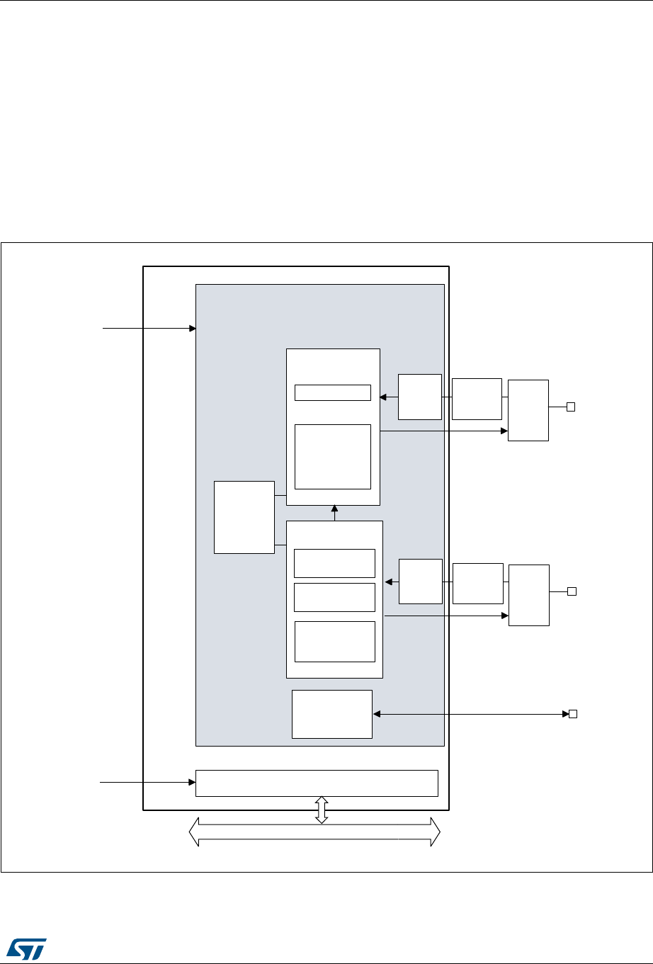
RM0394 Rev 4 1129/1600
RM0394 Inter-integrated circuit (I2C) interface
1193
with a standard (up to 100 kHz), Fast-mode (up to 400 kHz) or Fast-mode Plus (up to
1MHz) I
2C bus.
This interface can also be connected to a SMBus with the data pin (SDA) and clock pin
(SCL).
If SMBus feature is supported: the additional optional SMBus Alert pin (SMBA) is also
available.
37.4.1 I2C block diagram
The block diagram of the I2C interface is shown in Figure 352.
Figure 352. I2C block diagram
The I2C is clocked by an independent clock source which allows to the I2C to operate
independently from the PCLK frequency.
06Y9
,&&/.
:DNHXS
RQ
DGGUHVV
PDWFK
60%86
3(&
JHQHUDWLRQ
FKHFN
6KLIWUHJLVWHU
'DWDFRQWURO
60%XV
7LPHRXW
FKHFN
&ORFNFRQWURO
0DVWHUFORFN
JHQHUDWLRQ
6ODYHFORFN
VWUHWFKLQJ
60%XV$OHUW
FRQWURO
VWDWXV
'LJLWDO
QRLVH
ILOWHU ,&B6&/
,&B60%$
5HJLVWHUV
$3%EXV
*3,2
ORJLF
$QDORJ
QRLVH
ILOWHU
'LJLWDO
QRLVH
ILOWHU ,&B6'$
*3,2
ORJLF
$QDORJ
QRLVH
ILOWHU
,FBSFON
,FBNHUBFN
3&/.

Inter-integrated circuit (I2C) interface RM0394
1130/1600 RM0394 Rev 4
For I2C I/Os supporting 20 mA output current drive for Fast-mode Plus operation, the driving
capability is enabled through control bits in the system configuration controller (SYSCFG).
Refer to Section 37.3: I2C implementation.
37.4.2 I2C clock requirements
The I2C kernel is clocked by I2CCLK.
The I2CCLK period tI2CCLK must respect the following conditions:
tI2CCLK < (tLOW - tfilters) / 4 and tI2CCLK < tHIGH
with:
tLOW: SCL low time and tHIGH: SCL high time
tfilters: when enabled, sum of the delays brought by the analog filter and by the digital filter.
Analog filter delay is maximum 260 ns. Digital filter delay is DNF x tI2CCLK.
The PCLK clock period tPCLK must respect the following condition:
tPCLK < 4/3 tSCL
with tSCL: SCL period
Caution: When the I2C kernel is clocked by PCLK, this clock must respect the conditions for tI2CCLK.
37.4.3 Mode selection
The interface can operate in one of the four following modes:
•Slave transmitter
•Slave receiver
•Master transmitter
•Master receiver
By default, it operates in slave mode. The interface automatically switches from slave to
master when it generates a START condition, and from master to slave if an arbitration loss
or a STOP generation occurs, allowing multimaster capability.
Communication flow
In Master mode, the I2C interface initiates a data transfer and generates the clock signal. A
serial data transfer always begins with a START condition and ends with a STOP condition.
Both START and STOP conditions are generated in master mode by software.
In Slave mode, the interface is capable of recognizing its own addresses (7 or 10-bit), and
the General Call address. The General Call address detection can be enabled or disabled
by software. The reserved SMBus addresses can also be enabled by software.
Data and addresses are transferred as 8-bit bytes, MSB first. The first byte(s) following the
START condition contain the address (one in 7-bit mode, two in 10-bit mode). The address
is always transmitted in Master mode.
A 9th clock pulse follows the 8 clock cycles of a byte transfer, during which the receiver must
send an acknowledge bit to the transmitter. Refer to the following figure.
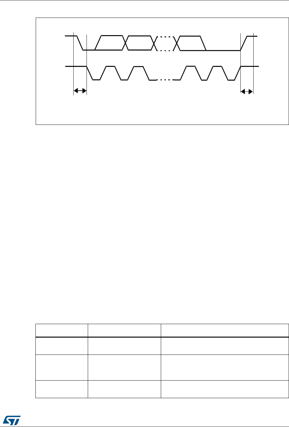
RM0394 Rev 4 1131/1600
RM0394 Inter-integrated circuit (I2C) interface
1193
Figure 353. I2C bus protocol
Acknowledge can be enabled or disabled by software. The I2C interface addresses can be
selected by software.
37.4.4 I2C initialization
Enabling and disabling the peripheral
The I2C peripheral clock must be configured and enabled in the clock controller.
Then the I2C can be enabled by setting the PE bit in the I2C_CR1 register.
When the I2C is disabled (PE=0), the I2C performs a software reset. Refer to
Section 37.4.5: Software reset for more details.
Noise filters
Before enabling the I2C peripheral by setting the PE bit in I2C_CR1 register, the user must
configure the noise filters, if needed. By default, an analog noise filter is present on the SDA
and SCL inputs. This analog filter is compliant with the I2C specification which requires the
suppression of spikes with a pulse width up to 50 ns in Fast-mode and Fast-mode Plus. The
user can disable this analog filter by setting the ANFOFF bit, and/or select a digital filter by
configuring the DNF[3:0] bit in the I2C_CR1 register.
When the digital filter is enabled, the level of the SCL or the SDA line is internally changed
only if it remains stable for more than DNF x I2CCLK periods. This allows to suppress
spikes with a programmable length of 1 to 15 I2CCLK periods.
069
6'$
6&/
6WDUW
FRQGLWLRQ
6WRS
FRQGLWLRQ
06% $&.
Table 177. Comparison of analog vs. digital filters
-Analog filter Digital filter
Pulse width of
suppressed spikes 50 ns Programmable length from 1 to 15 I2C peripheral
clocks
Benefits Available in Stop mode
– Programmable length: extra filtering capability
vs. standard requirements
– Stable length
Drawbacks Variation vs. temperature,
voltage, process
Wakeup from Stop mode on address match is not
available when digital filter is enabled
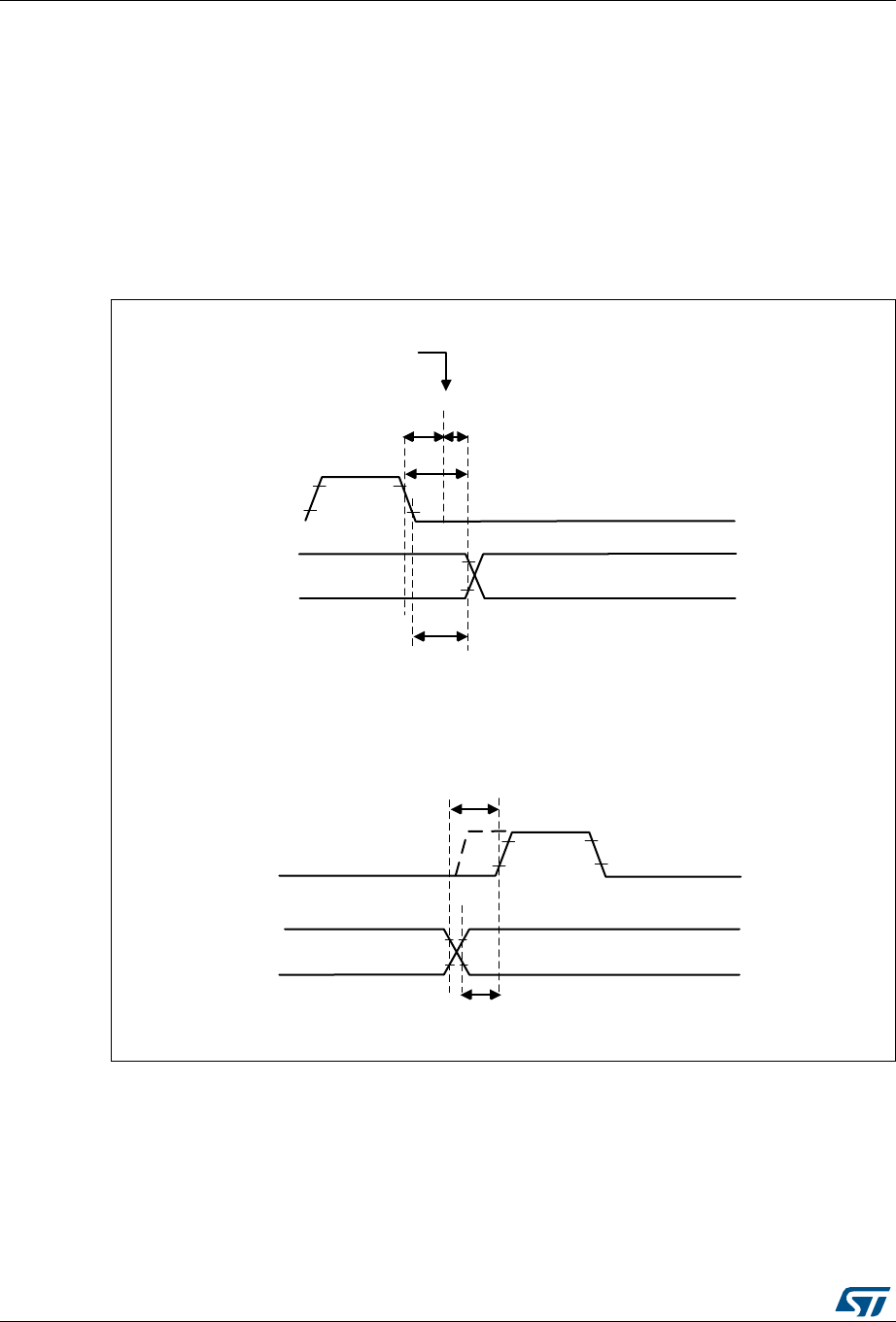
Inter-integrated circuit (I2C) interface RM0394
1132/1600 RM0394 Rev 4
Caution: Changing the filter configuration is not allowed when the I2C is enabled.
I2C timings
The timings must be configured in order to guarantee a correct data hold and setup time,
used in master and slave modes. This is done by programming the PRESC[3:0],
SCLDEL[3:0] and SDADEL[3:0] bits in the I2C_TIMINGR register.
The STM32CubeMX tool calculates and provides the I2C_TIMINGR content in the I2C
configuration window
Figure 354. Setup and hold timings
06Y9
W6<1&
6&/IDOOLQJHGJHLQWHUQDO
GHWHFWLRQ
6'$'(/6&/VWUHWFKHGORZE\WKH,&
6'$RXWSXWGHOD\
6&/
6'$
d,K>d/D
W+''$7
6&/'(/
6&/VWUHWFKHGORZE\WKH,&
6&/
6'$
d^dhWd/D
W6867$
'DWDKROGWLPHLQFDVHRIWUDQVPLVVLRQWKHGDWDLVVHQWRQ6'$RXWSXWDIWHU
WKH6'$'(/GHOD\LILWLVDOUHDG\DYDLODEOHLQ,&B7;'5
'DWDVHWXSWLPHLQFDVHRIWUDQVPLVVLRQWKH6&/'(/FRXQWHUVWDUWV
ZKHQWKHGDWDLVVHQWRQ6'$RXWSXW
069
W6<1&
6&/IDOOLQJHGJHLQWHUQDO
GHWHFWLRQ
6'$'(/6&/VWUHWFKHGORZE\WKH,&
6'$RXWSXWGHOD\
6&/
6'$
d,K>d/D
W+''$7
6&/'(/
6&/VWUHWFKHGORZE\WKH,&
6&/
6'$
d^dhWd/D
W68'$7
'DWDKROGWLPHLQFDVHRIWUDQVPLVVLRQWKHGDWDLVVHQWRQ6'$RXWSXWDIWHU
WKH6'$'(/GHOD\LILWLVDOUHDG\DYDLODEOHLQ,&B7;'5
'DWDVHWXSWLPHLQFDVHRIWUDQVPLVVLRQWKH6&/'(/FRXQWHUVWDUWV
ZKHQWKHGDWDLVVHQWRQ6'$RXWSXW

RM0394 Rev 4 1133/1600
RM0394 Inter-integrated circuit (I2C) interface
1193
•When the SCL falling edge is internally detected, a delay is inserted before sending
SDA output. This delay is tSDADEL = SDADEL x tPRESC + tI2CCLK where tPRESC = (PRESC+1)
x tI2CCLK.
TSDADEL impacts the hold time tHD;DAT.
The total SDA output delay is:
tSYNC1 + {[SDADEL x (PRESC+1) + 1] x tI2CCLK }
tSYNC1 duration depends on these parameters:
– SCL falling slope
– When enabled, input delay brought by the analog filter: tAF(min) < tAF < tAF(max)
– When enabled, input delay brought by the digital filter: tDNF = DNF x tI2CCLK
– Delay due to SCL synchronization to I2CCLK clock (2 to 3 I2CCLK periods)
In order to bridge the undefined region of the SCL falling edge, the user must program
SDADEL in such a way that:
{tf (max) +tHD;DAT (min) -tAF(min) - [(DNF +3) x tI2CCLK]} / {(PRESC +1) x tI2CCLK } SDADEL
SDADEL {tHD;DAT (max) -tAF(max) - [(DNF+4) x tI2CCLK]} / {(PRESC +1) x tI2CCLK }
Note: tAF(min) / tAF(max) are part of the equation only when the analog filter is enabled. Refer to
device datasheet for tAF values.
The maximum tHD;DAT can be 3.45 µs, 0.9 µs and 0.45 µs for Standard-mode, Fast-mode
and Fast-mode Plus, but must be less than the maximum of tVD;DAT by a transition time.
This maximum must only be met if the device does not stretch the LOW period (tLOW) of the
SCL signal. If the clock stretches the SCL, the data must be valid by the set-up time before
it releases the clock.
The SDA rising edge is usually the worst case, so in this case the previous equation
becomes:
SDADEL {tVD;DAT (max) -tr (max) -260 ns - [(DNF+4) x tI2CCLK]} / {(PRESC +1) x tI2CCLK }.
Note: This condition can be violated when NOSTRETCH=0, because the device stretches SCL
low to guarantee the set-up time, according to the SCLDEL value.
Refer to Table 178: I2C-SMBUS specification data setup and hold times for tf, tr, tHD;DAT and
tVD;DAT standard values.
•After tSDADEL delay, or after sending SDA output in case the slave had to stretch the
clock because the data was not yet written in I2C_TXDR register, SCL line is kept at
low level during the setup time. This setup time is tSCLDEL = (SCLDEL+1) x tPRESC where
tPRESC = (PRESC+1) x tI2CCLK.
tSCLDEL impacts the setup time tSU;DAT .
In order to bridge the undefined region of the SDA transition (rising edge usually worst
case), the user must program SCLDEL in such a way that:
{[tr (max) + tSU;DAT (min)] / [(PRESC+1)] x tI2CCLK]} - 1 <= SCLDEL
Refer to Table 178: I2C-SMBUS specification data setup and hold times for tr and tSU;DAT
standard values.
The SDA and SCL transition time values to be used are the ones in the application. Using
the maximum values from the standard increases the constraints for the SDADEL and
SCLDEL calculation, but ensures the feature whatever the application.

Inter-integrated circuit (I2C) interface RM0394
1134/1600 RM0394 Rev 4
Note: At every clock pulse, after SCL falling edge detection, the I2C master or slave stretches SCL
low during at least [(SDADEL+SCLDEL+1) x (PRESC+1) + 1] x tI2CCLK, in both transmission
and reception modes. In transmission mode, in case the data is not yet written in I2C_TXDR
when SDADEL counter is finished, the I2C keeps on stretching SCL low until the next data
is written. Then new data MSB is sent on SDA output, and SCLDEL counter starts,
continuing stretching SCL low to guarantee the data setup time.
If NOSTRETCH=1 in slave mode, the SCL is not stretched. Consequently the SDADEL
must be programmed in such a way to guarantee also a sufficient setup time.
Additionally, in master mode, the SCL clock high and low levels must be configured by
programming the PRESC[3:0], SCLH[7:0] and SCLL[7:0] bits in the I2C_TIMINGR register.
•When the SCL falling edge is internally detected, a delay is inserted before releasing
the SCL output. This delay is tSCLL = (SCLL+1) x tPRESC where tPRESC = (PRESC+1) x
tI2CCLK.
tSCLL impacts the SCL low time tLOW .
•When the SCL rising edge is internally detected, a delay is inserted before forcing the
SCL output to low level. This delay is tSCLH = (SCLH+1) x tPRESC where tPRESC =
(PRESC+1) x tI2CCLK. tSCLH impacts the SCL high time tHIGH .
Refer to I2C master initialization for more details.
Caution: Changing the timing configuration is not allowed when the I2C is enabled.
The I2C slave NOSTRETCH mode must also be configured before enabling the peripheral.
Refer to I2C slave initialization for more details.
Caution: Changing the NOSTRETCH configuration is not allowed when the I2C is enabled.
Table 178. I2C-SMBUS specification data setup and hold times
Symbol Parameter
Standard-mode
(Sm)
Fast-mode
(Fm)
Fast-mode Plus
(Fm+) SMBUS
Unit
Min. Max Min. Max Min. Max Min. Max
tHD;DAT Data hold time 0-0-0 -0.3-
µs
tVD;DAT Data valid time - 3.45 - 0.9 - 0.45 - -
tSU;DAT Data setup time 250 - 100 - 50 - 250 -
ns
tr
Rise time of both SDA
and SCL signals - 1000 - 300 - 120 - 1000
tf
Fall time of both SDA
and SCL signals - 300 - 300 - 120 - 300
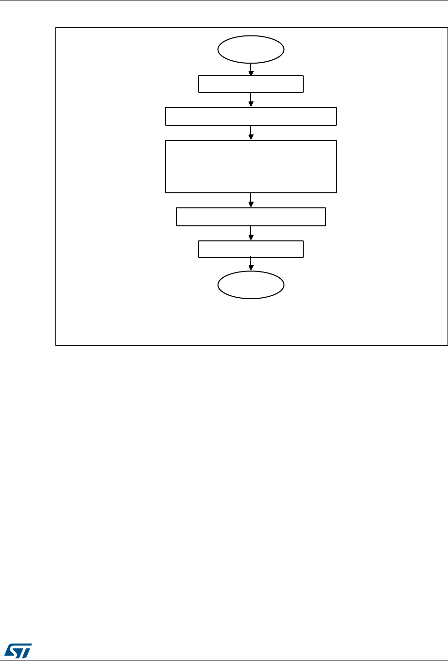
RM0394 Rev 4 1135/1600
RM0394 Inter-integrated circuit (I2C) interface
1193
Figure 355. I2C initialization flowchart
37.4.5 Software reset
A software reset can be performed by clearing the PE bit in the I2C_CR1 register. In that
case I2C lines SCL and SDA are released. Internal states machines are reset and
communication control bits, as well as status bits come back to their reset value. The
configuration registers are not impacted.
Here is the list of impacted register bits:
1. I2C_CR2 register: START, STOP, NACK
2. I2C_ISR register: BUSY, TXE, TXIS, RXNE, ADDR, NACKF, TCR, TC, STOPF, BERR,
ARLO, OVR
and in addition when the SMBus feature is supported:
1. I2C_CR2 register: PECBYTE
2. I2C_ISR register: PECERR, TIMEOUT, ALERT
PE must be kept low during at least 3 APB clock cycles in order to perform the software
reset. This is ensured by writing the following software sequence: - Write PE=0 - Check
PE=0 - Write PE=1.
D^ϭϵϴϰϳsϮ
&OHDU3(ELWLQ,&B&5
,QLWLDOVHWWLQJV
&RQILJXUH$1)2))DQG'1)>@LQ,&B&5
&RQILJXUH35(6&>@
6'$'(/>@6&/'(/>@6&/+>@
6&//>@LQ,&B7,0,1*5
&RQILJXUH12675(7&+LQ,&B&5
6HW3(ELWLQ,&B&5
(QG
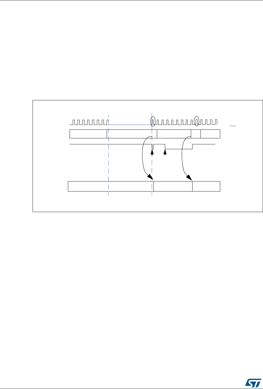
Inter-integrated circuit (I2C) interface RM0394
1136/1600 RM0394 Rev 4
37.4.6 Data transfer
The data transfer is managed through transmit and receive data registers and a shift
register.
Reception
The SDA input fills the shift register. After the 8th SCL pulse (when the complete data byte is
received), the shift register is copied into I2C_RXDR register if it is empty (RXNE=0). If
RXNE=1, meaning that the previous received data byte has not yet been read, the SCL line
is stretched low until I2C_RXDR is read. The stretch is inserted between the 8th and 9th
SCL pulse (before the Acknowledge pulse).
Figure 356. Data reception
[[
6KLIWUHJLVWHU GDWD
GDWD
[[ GDWD
5;1(
$&.SXOVH
GDWD GDWD
$&.SXOVH
[[
,&B5;'5
UGGDWDUGGDWD
6&/
OHJHQG
6&/
VWUHWFK
069
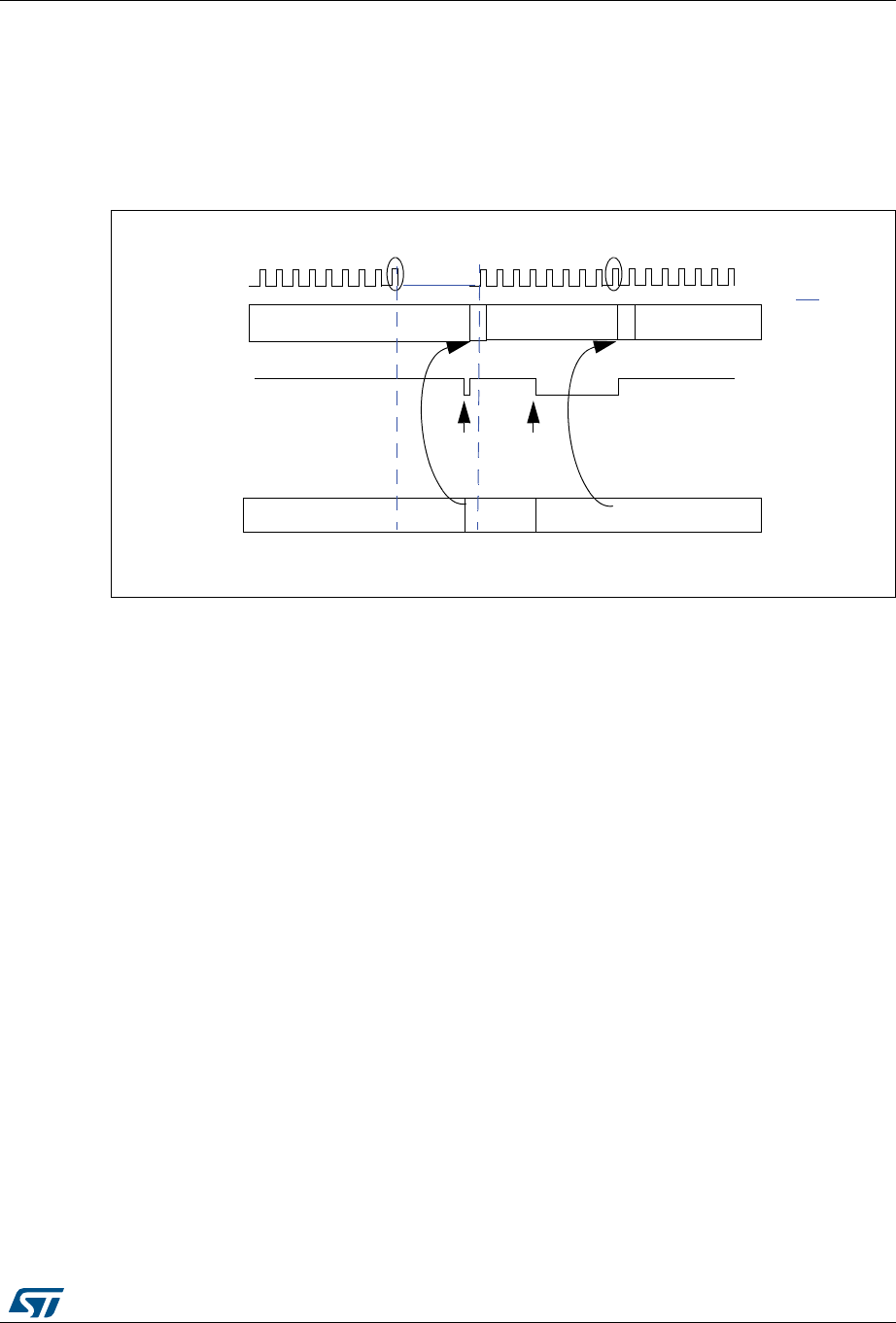
RM0394 Rev 4 1137/1600
RM0394 Inter-integrated circuit (I2C) interface
1193
Transmission
If the I2C_TXDR register is not empty (TXE=0), its content is copied into the shift register
after the 9th SCL pulse (the Acknowledge pulse). Then the shift register content is shifted
out on SDA line. If TXE=1, meaning that no data is written yet in I2C_TXDR, SCL line is
stretched low until I2C_TXDR is written. The stretch is done after the 9th SCL pulse.
Figure 357. Data transmission
Hardware transfer management
The I2C has a byte counter embedded in hardware in order to manage byte transfer and to
close the communication in various modes such as:
– NACK, STOP and ReSTART generation in master mode
– ACK control in slave receiver mode
– PEC generation/checking when SMBus feature is supported
The byte counter is always used in master mode. By default it is disabled in slave mode, but
it can be enabled by software by setting the SBC (Slave Byte Control) bit in the I2C_CR2
register.
The number of bytes to be transferred is programmed in the NBYTES[7:0] bit field in the
I2C_CR2 register. If the number of bytes to be transferred (NBYTES) is greater than 255, or
if a receiver wants to control the acknowledge value of a received data byte, the reload
mode must be selected by setting the RELOAD bit in the I2C_CR2 register. In this mode,
TCR flag is set when the number of bytes programmed in NBYTES has been transferred,
and an interrupt is generated if TCIE is set. SCL is stretched as long as TCR flag is set. TCR
is cleared by software when NBYTES is written to a non-zero value.
When the NBYTES counter is reloaded with the last number of bytes, RELOAD bit must be
cleared.
069
[[
6KLIWUHJLVWHU
GDWD
GDWD
[[
GDWD
7;(
$&.SXOVH
GDWD GDWD
$&.SXOVH
[[
,&B7;'5
ZUGDWD ZUGDWD
6&/ OHJHQG
6&/
VWUHWFK

Inter-integrated circuit (I2C) interface RM0394
1138/1600 RM0394 Rev 4
When RELOAD=0 in master mode, the counter can be used in 2 modes:
•Automatic end mode (AUTOEND = ‘1’ in the I2C_CR2 register). In this mode, the
master automatically sends a STOP condition once the number of bytes programmed
in the NBYTES[7:0] bit field has been transferred.
•Software end mode (AUTOEND = ‘0’ in the I2C_CR2 register). In this mode, software
action is expected once the number of bytes programmed in the NBYTES[7:0] bit field
has been transferred; the TC flag is set and an interrupt is generated if the TCIE bit is
set. The SCL signal is stretched as long as the TC flag is set. The TC flag is cleared by
software when the START or STOP bit is set in the I2C_CR2 register. This mode must
be used when the master wants to send a RESTART condition.
Caution: The AUTOEND bit has no effect when the RELOAD bit is set.
37.4.7 I2C slave mode
I2C slave initialization
In order to work in slave mode, the user must enable at least one slave address. Two
registers I2C_OAR1 and I2C_OAR2 are available in order to program the slave own
addresses OA1 and OA2.
•OA1 can be configured either in 7-bit mode (by default) or in 10-bit addressing mode by
setting the OA1MODE bit in the I2C_OAR1 register.
OA1 is enabled by setting the OA1EN bit in the I2C_OAR1 register.
•If additional slave addresses are required, the 2nd slave address OA2 can be
configured. Up to 7 OA2 LSB can be masked by configuring the OA2MSK[2:0] bits in
the I2C_OAR2 register. Therefore for OA2MSK configured from 1 to 6, only OA2[7:2],
OA2[7:3], OA2[7:4], OA2[7:5], OA2[7:6] or OA2[7] are compared with the received
address. As soon as OA2MSK is not equal to 0, the address comparator for OA2
excludes the I2C reserved addresses (0000 XXX and 1111 XXX), which are not
acknowledged. If OA2MSK=7, all received 7-bit addresses are acknowledged (except
reserved addresses). OA2 is always a 7-bit address.
These reserved addresses can be acknowledged if they are enabled by the specific
enable bit, if they are programmed in the I2C_OAR1 or I2C_OAR2 register with
OA2MSK=0.
OA2 is enabled by setting the OA2EN bit in the I2C_OAR2 register.
•The General Call address is enabled by setting the GCEN bit in the I2C_CR1 register.
When the I2C is selected by one of its enabled addresses, the ADDR interrupt status flag is
set, and an interrupt is generated if the ADDRIE bit is set.
Table 179. I2C configuration
Function SBC bit RELOAD bit AUTOEND bit
Master Tx/Rx NBYTES + STOP x 0 1
Master Tx/Rx + NBYTES + RESTART x 0 0
Slave Tx/Rx
all received bytes ACKed 0xx
Slave Rx with ACK control 1 1 x

RM0394 Rev 4 1139/1600
RM0394 Inter-integrated circuit (I2C) interface
1193
By default, the slave uses its clock stretching capability, which means that it stretches the
SCL signal at low level when needed, in order to perform software actions. If the master
does not support clock stretching, the I2C must be configured with NOSTRETCH=1 in the
I2C_CR1 register.
After receiving an ADDR interrupt, if several addresses are enabled the user must read the
ADDCODE[6:0] bits in the I2C_ISR register in order to check which address matched. DIR
flag must also be checked in order to know the transfer direction.
Slave clock stretching (NOSTRETCH = 0)
In default mode, the I2C slave stretches the SCL clock in the following situations:
•When the ADDR flag is set: the received address matches with one of the enabled
slave addresses. This stretch is released when the ADDR flag is cleared by software
setting the ADDRCF bit.
•In transmission, if the previous data transmission is completed and no new data is
written in I2C_TXDR register, or if the first data byte is not written when the ADDR flag
is cleared (TXE=1). This stretch is released when the data is written to the I2C_TXDR
register.
•In reception when the I2C_RXDR register is not read yet and a new data reception is
completed. This stretch is released when I2C_RXDR is read.
•When TCR = 1 in Slave Byte Control mode, reload mode (SBC=1 and RELOAD=1),
meaning that the last data byte has been transferred. This stretch is released when
then TCR is cleared by writing a non-zero value in the NBYTES[7:0] field.
•After SCL falling edge detection, the I2C stretches SCL low during
[(SDADEL+SCLDEL+1) x (PRESC+1) + 1] x tI2CCLK.
Slave without clock stretching (NOSTRETCH = 1)
When NOSTRETCH = 1 in the I2C_CR1 register, the I2C slave does not stretch the SCL
signal.
•The SCL clock is not stretched while the ADDR flag is set.
•In transmission, the data must be written in the I2C_TXDR register before the first SCL
pulse corresponding to its transfer occurs. If not, an underrun occurs, the OVR flag is
set in the I2C_ISR register and an interrupt is generated if the ERRIE bit is set in the
I2C_CR1 register. The OVR flag is also set when the first data transmission starts and
the STOPF bit is still set (has not been cleared). Therefore, if the user clears the
STOPF flag of the previous transfer only after writing the first data to be transmitted in
the next transfer, he ensures that the OVR status is provided, even for the first data to
be transmitted.
•In reception, the data must be read from the I2C_RXDR register before the 9th SCL
pulse (ACK pulse) of the next data byte occurs. If not an overrun occurs, the OVR flag
is set in the I2C_ISR register and an interrupt is generated if the ERRIE bit is set in the
I2C_CR1 register.
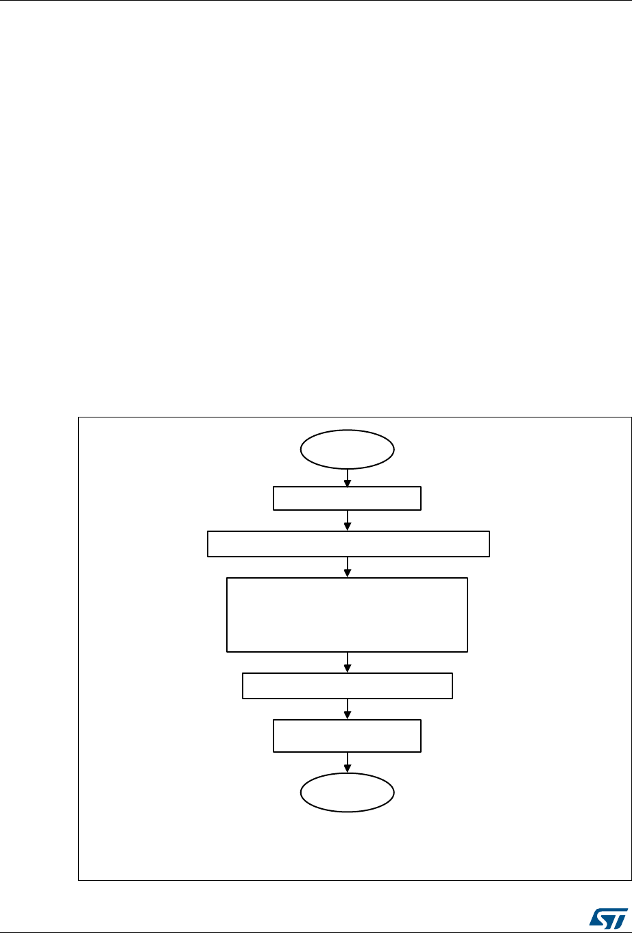
Inter-integrated circuit (I2C) interface RM0394
1140/1600 RM0394 Rev 4
Slave Byte Control mode
In order to allow byte ACK control in slave reception mode, Slave Byte Control mode must
be enabled by setting the SBC bit in the I2C_CR1 register. This is required to be compliant
with SMBus standards.
Reload mode must be selected in order to allow byte ACK control in slave reception mode
(RELOAD=1). To get control of each byte, NBYTES must be initialized to 0x1 in the ADDR
interrupt subroutine, and reloaded to 0x1 after each received byte. When the byte is
received, the TCR bit is set, stretching the SCL signal low between the 8th and 9th SCL
pulses. The user can read the data from the I2C_RXDR register, and then decide to
acknowledge it or not by configuring the ACK bit in the I2C_CR2 register. The SCL stretch is
released by programming NBYTES to a non-zero value: the acknowledge or not-
acknowledge is sent and next byte can be received.
NBYTES can be loaded with a value greater than 0x1, and in this case, the reception flow is
continuous during NBYTES data reception.
Note: The SBC bit must be configured when the I2C is disabled, or when the slave is not
addressed, or when ADDR=1.
The RELOAD bit value can be changed when ADDR=1, or when TCR=1.
Caution: Slave Byte Control mode is not compatible with NOSTRETCH mode. Setting SBC when
NOSTRETCH=1 is not allowed.
Figure 358. Slave initialization flowchart
069
,QLWLDOVHWWLQJV
6ODYH
LQLWLDOL]DWLRQ
&OHDU^2$(12$(1`LQ,&B2$5DQG,&B2$5
&RQILJXUH^2$>@2$02'(2$(1
2$>@2$06.>@2$(1*&(1`
&RQILJXUH6%&LQ,&B&5
(QDEOHLQWHUUXSWVDQGRU
'0$LQ,&B&5
(QG
6%&PXVWEHVHWWRVXSSRUW60%XVIHDWXUHV

RM0394 Rev 4 1141/1600
RM0394 Inter-integrated circuit (I2C) interface
1193
Slave transmitter
A transmit interrupt status (TXIS) is generated when the I2C_TXDR register becomes
empty. An interrupt is generated if the TXIE bit is set in the I2C_CR1 register.
The TXIS bit is cleared when the I2C_TXDR register is written with the next data byte to be
transmitted.
When a NACK is received, the NACKF bit is set in the I2C_ISR register and an interrupt is
generated if the NACKIE bit is set in the I2C_CR1 register. The slave automatically releases
the SCL and SDA lines in order to let the master perform a STOP or a RESTART condition.
The TXIS bit is not set when a NACK is received.
When a STOP is received and the STOPIE bit is set in the I2C_CR1 register, the STOPF
flag is set in the I2C_ISR register and an interrupt is generated. In most applications, the
SBC bit is usually programmed to ‘0’. In this case, If TXE = 0 when the slave address is
received (ADDR=1), the user can choose either to send the content of the I2C_TXDR
register as the first data byte, or to flush the I2C_TXDR register by setting the TXE bit in
order to program a new data byte.
In Slave Byte Control mode (SBC=1), the number of bytes to be transmitted must be
programmed in NBYTES in the address match interrupt subroutine (ADDR=1). In this case,
the number of TXIS events during the transfer corresponds to the value programmed in
NBYTES.
Caution: When NOSTRETCH=1, the SCL clock is not stretched while the ADDR flag is set, so the
user cannot flush the I2C_TXDR register content in the ADDR subroutine, in order to
program the first data byte. The first data byte to be sent must be previously programmed in
the I2C_TXDR register:
•This data can be the data written in the last TXIS event of the previous transmission
message.
•If this data byte is not the one to be sent, the I2C_TXDR register can be flushed by
setting the TXE bit in order to program a new data byte. The STOPF bit must be
cleared only after these actions, in order to guarantee that they are executed before the
first data transmission starts, following the address acknowledge.
If STOPF is still set when the first data transmission starts, an underrun error is
generated (the OVR flag is set).
If a TXIS event is needed, (Transmit Interrupt or Transmit DMA request), the user must
set the TXIS bit in addition to the TXE bit, in order to generate a TXIS event.
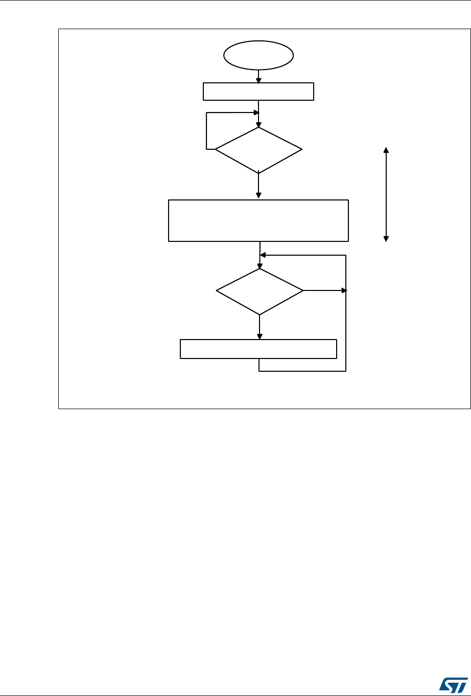
Inter-integrated circuit (I2C) interface RM0394
1142/1600 RM0394 Rev 4
Figure 359. Transfer sequence flowchart for I2C slave transmitter, NOSTRETCH=0
069
6ODYHLQLWLDOL]DWLRQ
6ODYH
WUDQVPLVVLRQ
5HDG$''&2'(DQG',5LQ,&B,65
2SWLRQDO6HW,&B,657;(
6HW,&B,&5$''5&)
:ULWH,&B7;'57;'$7$
,&B,65$''5
"
1R
<HV
,&B,657;,6
"
<HV
1R
6&/
VWUHWFKHG
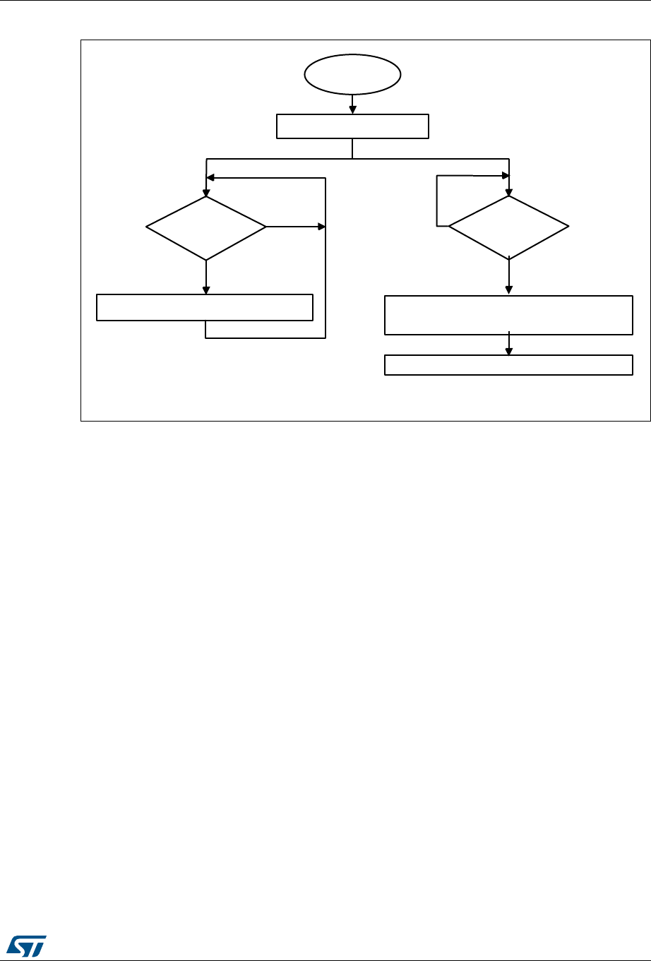
RM0394 Rev 4 1143/1600
RM0394 Inter-integrated circuit (I2C) interface
1193
Figure 360. Transfer sequence flowchart for I2C slave transmitter, NOSTRETCH=1
069
6ODYHLQLWLDOL]DWLRQ
6ODYH
WUDQVPLVVLRQ
2SWLRQDO6HW,&B,657;(
DQG,&B,657;,6
:ULWH,&B7;'57;'$7$
,&B,656723)
"
1R
<HV
,&B,657;,6
"
<HV
1R
6HW,&B,&56723&)
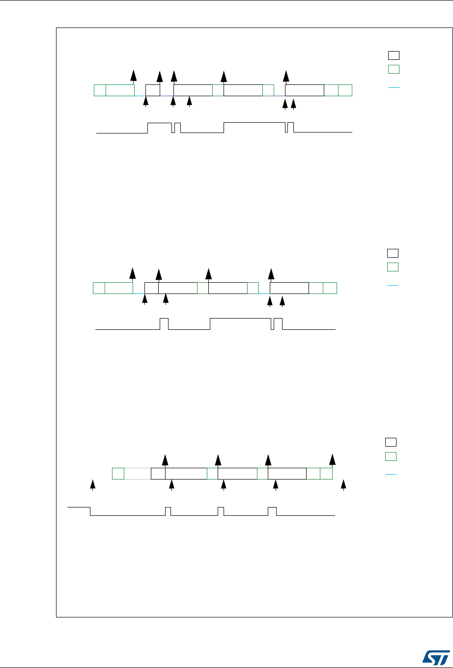
Inter-integrated circuit (I2C) interface RM0394
1144/1600 RM0394 Rev 4
Figure 361. Transfer bus diagrams for I2C slave transmitter
069
([DPSOH,&VODYHWUDQVPLWWHUE\WHVZLWKVWGDWDIOXVKHG
12675(7&+
(9$''5,65FKHFN$''&2'(DQG',5VHW7;(VHW$''5&)
(97;,6,65ZUGDWD
(97;,6,65ZUGDWD
(97;,6,65ZUGDWD
(97;,6,65ZUGDWDQRWVHQW
$''5
$
7;,6
$
7;,6
1$
7;,6
7;(
3
OHJHQG
WUDQVPLVVLRQ
UHFHSWLRQ
6&/VWUHWFK
(9 (9 (9 (9
([DPSOH,&VODYHWUDQVPLWWHUE\WHV12675(7&+
(9ZUGDWD
(97;,6,65ZUGDWD
(97;,6,65ZUGDWD
(97;,6,65ZUGDWDQRWVHQW
(96723),65RSWLRQDOVHW7;(DQG7;,6VHW6723&)
$
7;,6 7;,6
7;(
OHJHQG
WUDQVPLVVLRQ
UHFHSWLRQ
6&/VWUHWFK
(9 (9 (9
7;,6
(9
6723)
(9
([DPSOH,&VODYHWUDQVPLWWHUE\WHVZLWKRXWVWGDWDIOXVK
12675(7&+
(9$''5,65FKHFN$''&2'(DQG',5VHW$''5&)
(97;,6,65ZUGDWD
(97;,6,65ZUGDWD
(97;,6,65ZUGDWDQRWVHQW
$''5 7;,6 7;,6 7;,6
7;(
OHJHQG
WUDQVPLVVLRQ
UHFHSWLRQ
6&/VWUHWFK
(9 (9 (9 (9
7;,6
(9
6 $GGUHVV GDWD $ GDWD GDWD$1$3
6 $GGUHVV $ GDWD $ GDWD $ GDWD 1$ 3
6$GGUHVV $ GDWD
GDWD
GDWD
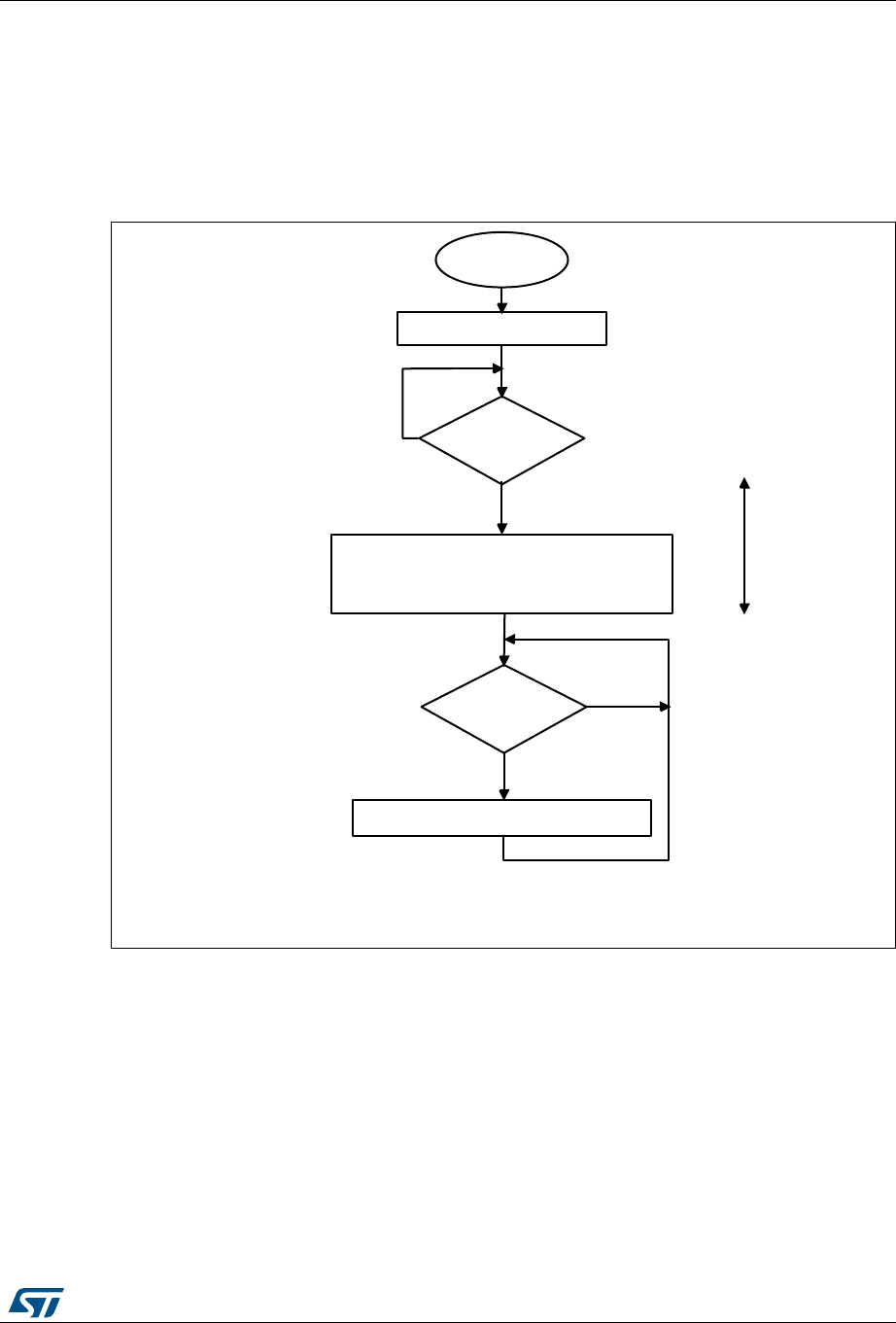
RM0394 Rev 4 1145/1600
RM0394 Inter-integrated circuit (I2C) interface
1193
Slave receiver
RXNE is set in I2C_ISR when the I2C_RXDR is full, and generates an interrupt if RXIE is
set in I2C_CR1. RXNE is cleared when I2C_RXDR is read.
When a STOP is received and STOPIE is set in I2C_CR1, STOPF is set in I2C_ISR and an
interrupt is generated.
Figure 362. Transfer sequence flowchart for slave receiver with NOSTRETCH=0
D^ϭϵϴϱϱsϮ
6ODYHLQLWLDOL]DWLRQ
6ODYHUHFHSWLRQ
5HDG$''&2'(DQG',5LQ,&B,65
6HW,&B,&5$''5&)
:ULWH,&B5;'55;'$7$
,&B,65$''5
"
1R
<HV
,&B,655;1(
"
<HV
1R
6&/
VWUHWFKHG
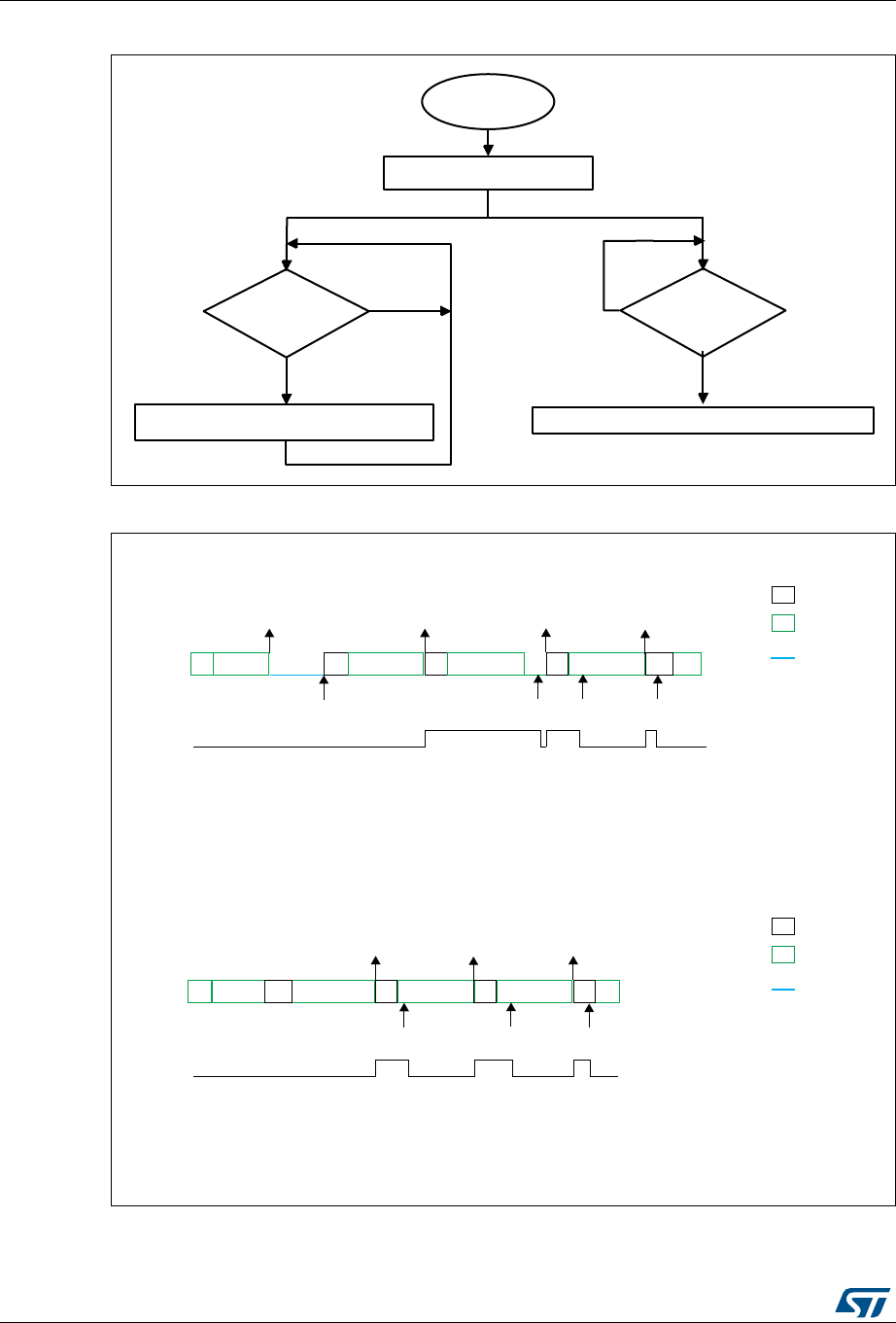
Inter-integrated circuit (I2C) interface RM0394
1146/1600 RM0394 Rev 4
Figure 363. Transfer sequence flowchart for slave receiver with NOSTRETCH=1
Figure 364. Transfer bus diagrams for I2C slave receiver
D^ϭϵϴϱϲsϮ
6ODYHLQLWLDOL]DWLRQ
6ODYHUHFHSWLRQ
5HDG,&B5;'55;'$7$
,&B,656723)
"
1R
<HV
,&B,655;1(
"
<HV
1R
6HW,&B,&56723&)
069
(9$''5,65FKHFN$''&2'(DQG',5VHW$''5&)
(95;1(,65UGGDWD
(95;1(,65UGGDWD
(95;1(,65UGGDWD
$
$''5
$$
5;1(
$
5;1(
5;1(
OHJHQG
WUDQVPLVVLRQ
UHFHSWLRQ
6&/VWUHWFK
(9 (9 (9
(95;1(,65UGGDWD
(95;1(,65UGGDWD
(95;1(,65UGGDWD
(96723),65VHW6723&)
$
$$ $
5;1(
OHJHQG
WUDQVPLVVLRQ
UHFHSWLRQ
6&/VWUHWFK
5;1(
(9
([DPSOH,&VODYHUHFHLYHUE\WHV12675(7&+
4$GGUHVV GDWD GDWD GDWD 1
([DPSOH,&VODYHUHFHLYHUE\WHV12675(7&+
4$GGUHVV GDWD GDWD GDWD
(9
(9
(9
5;1( 5;1( 5;1(

RM0394 Rev 4 1147/1600
RM0394 Inter-integrated circuit (I2C) interface
1193
37.4.8 I2C master mode
I2C master initialization
Before enabling the peripheral, the I2C master clock must be configured by setting the
SCLH and SCLL bits in the I2C_TIMINGR register.
The STM32CubeMX tool calculates and provides the I2C_TIMINGR content in the I2C
Configuration window.
A clock synchronization mechanism is implemented in order to support multi-master
environment and slave clock stretching.
In order to allow clock synchronization:
•The low level of the clock is counted using the SCLL counter, starting from the SCL low
level internal detection.
•The high level of the clock is counted using the SCLH counter, starting from the SCL
high level internal detection.
The I2C detects its own SCL low level after a tSYNC1 delay depending on the SCL falling
edge, SCL input noise filters (analog + digital) and SCL synchronization to the I2CxCLK
clock. The I2C releases SCL to high level once the SCLL counter reaches the value
programmed in the SCLL[7:0] bits in the I2C_TIMINGR register.
The I2C detects its own SCL high level after a tSYNC2 delay depending on the SCL rising
edge, SCL input noise filters (analog + digital) and SCL synchronization to I2CxCLK clock.
The I2C ties SCL to low level once the SCLH counter is reached reaches the value
programmed in the SCLH[7:0] bits in the I2C_TIMINGR register.
Consequently the master clock period is:
tSCL = tSYNC1 + tSYNC2 + {[(SCLH+1) + (SCLL+1)] x (PRESC+1) x tI2CCLK}
The duration of tSYNC1 depends on these parameters:
– SCL falling slope
– When enabled, input delay induced by the analog filter.
– When enabled, input delay induced by the digital filter: DNF x tI2CCLK
– Delay due to SCL synchronization with I2CCLK clock (2 to 3 I2CCLK periods)
The duration of tSYNC2 depends on these parameters:
– SCL rising slope
– When enabled, input delay induced by the analog filter.
– When enabled, input delay induced by the digital filter: DNF x tI2CCLK
– Delay due to SCL synchronization with I2CCLK clock (2 to 3 I2CCLK periods)
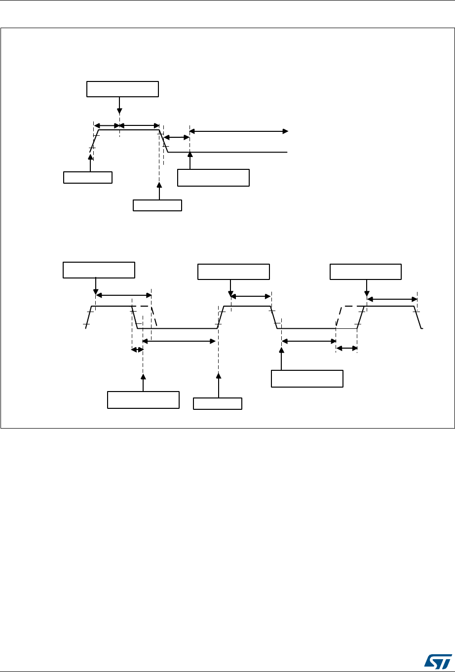
Inter-integrated circuit (I2C) interface RM0394
1148/1600 RM0394 Rev 4
Figure 365. Master clock generation
Caution: In order to be I2C or SMBus compliant, the master clock must respect the timings given
below:
069
W6<1&
6&/KLJKOHYHOGHWHFWHG
6&/+FRXQWHUVWDUWV
6&/+
6&/
6&/PDVWHUFORFNJHQHUDWLRQ
6&/UHOHDVHG 6&/ORZOHYHOGHWHFWHG
6&//FRXQWHUVWDUWV
6&/GULYHQORZ
6&//
W6<1&
6&/PDVWHUFORFNV\QFKURQL]DWLRQ
6&//
6&/GULYHQORZE\
DQRWKHUGHYLFH
6&/ORZOHYHOGHWHFWHG
6&//FRXQWHUVWDUWV 6&/UHOHDVHG
6&/+
6&/+
6&/KLJKOHYHOGHWHFWHG
6&/+FRXQWHUVWDUWV 6&/KLJKOHYHOGHWHFWHG
6&/+FRXQWHUVWDUWV
6&/ORZOHYHOGHWHFWHG
6&//FRXQWHUVWDUWV
6&//
6&/GULYHQORZE\
DQRWKHUGHYLFH
6&/+
6&/KLJKOHYHOGHWHFWHG
6&/+FRXQWHUVWDUWV
RM0394 Rev 4 1149/1600
RM0394 Inter-integrated circuit (I2C) interface
1193
Note: SCLL is also used to generate the tBUF and tSU:STA timings.
SCLH is also used to generate the tHD:STA and tSU:STO timings.
Refer to Section 37.4.9: I2C_TIMINGR register configuration examples for examples of
I2C_TIMINGR settings vs. I2CCLK frequency.
Master communication initialization (address phase)
In order to initiate the communication, the user must program the following parameters for
the addressed slave in the I2C_CR2 register:
•Addressing mode (7-bit or 10-bit): ADD10
•Slave address to be sent: SADD[9:0]
•Transfer direction: RD_WRN
•In case of 10-bit address read: HEAD10R bit. HEAD10R must be configure to indicate
if the complete address sequence must be sent, or only the header in case of a
direction change.
•The number of bytes to be transferred: NBYTES[7:0]. If the number of bytes is equal to
or greater than 255 bytes, NBYTES[7:0] must initially be filled with 0xFF.
The user must then set the START bit in I2C_CR2 register. Changing all the above bits is
not allowed when START bit is set.
Then the master automatically sends the START condition followed by the slave address as
soon as it detects that the bus is free (BUSY = 0) and after a delay of tBUF
.
In case of an arbitration loss, the master automatically switches back to slave mode and can
acknowledge its own address if it is addressed as a slave.
Note: The START bit is reset by hardware when the slave address has been sent on the bus,
whatever the received acknowledge value. The START bit is also reset by hardware if an
arbitration loss occurs.
In 10-bit addressing mode, when the Slave Address first 7 bits is NACKed by the slave, the
Table 180. I2C-SMBUS specification clock timings
Symbol Parameter
Standard-
mode (Sm)
Fast-mode
(Fm)
Fast-mode
Plus (Fm+) SMBUS
Unit
Min Max Min Max Min Max Min Max
fSCL SCL clock frequency - 100 - 400 - 1000 - 100 kHz
tHD:STA Hold time (repeated) START condition 4.0 - 0.6 - 0.26 - 4.0 - µs
tSU:STA
Set-up time for a repeated START
condition 4.7 - 0.6 - 0.26 - 4.7 - µs
tSU:STO Set-up time for STOP condition 4.0 - 0.6 - 0.26 - 4.0 - µs
tBUF
Bus free time between a STOP and
START condition 4.7 - 1.3 - 0.5 - 4.7 - µs
tLOW Low period of the SCL clock 4.7 - 1.3 - 0.5 - 4.7 - µs
tHIGH Period of the SCL clock 4.0 - 0.6 - 0.26 - 4.0 50 µs
tr Rise time of both SDA and SCL signals - 1000 - 300 - 120 - 1000 ns
tf Fall time of both SDA and SCL signals - 300 - 300 - 120 - 300 ns
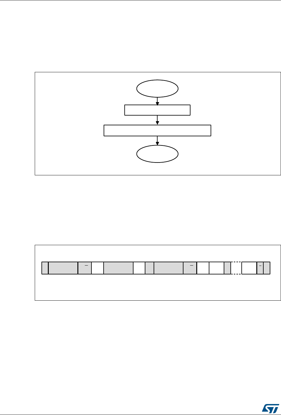
Inter-integrated circuit (I2C) interface RM0394
1150/1600 RM0394 Rev 4
master re-launches automatically the slave address transmission until ACK is received. In
this case ADDRCF must be set if a NACK is received from the slave, in order to stop
sending the slave address.
If the I2C is addressed as a slave (ADDR=1) while the START bit is set, the I2C switches to
slave mode and the START bit is cleared, when the ADDRCF bit is set.
Note: The same procedure is applied for a Repeated Start condition. In this case BUSY=1.
Figure 366. Master initialization flowchart
Initialization of a master receiver addressing a 10-bit address slave
•If the slave address is in 10-bit format, the user can choose to send the complete read
sequence by clearing the HEAD10R bit in the I2C_CR2 register. In this case the master
automatically sends the following complete sequence after the START bit is set:
(Re)Start + Slave address 10-bit header Write + Slave address 2nd byte + REStart +
Slave address 10-bit header Read
Figure 367. 10-bit address read access with HEAD10R=0
D^ϭϵϴϱϵsϮ
,QLWLDOVHWWLQJV
0DVWHU
LQLWLDOL]DWLRQ
(QDEOHLQWHUUXSWVDQGRU'0$LQ,&B&5
(QG
D^ǀϰϭϬϲϲsϭ
'$7$ $ 3$'$7$
6ODYHDGGUHVV
QGE\WH
6ODYHDGGUHVV
VWELWV
6U$$ 5:5:
6ODYHDGGUHVV
VWELWV
6 $
;;
;;
:ULWH 5HDG
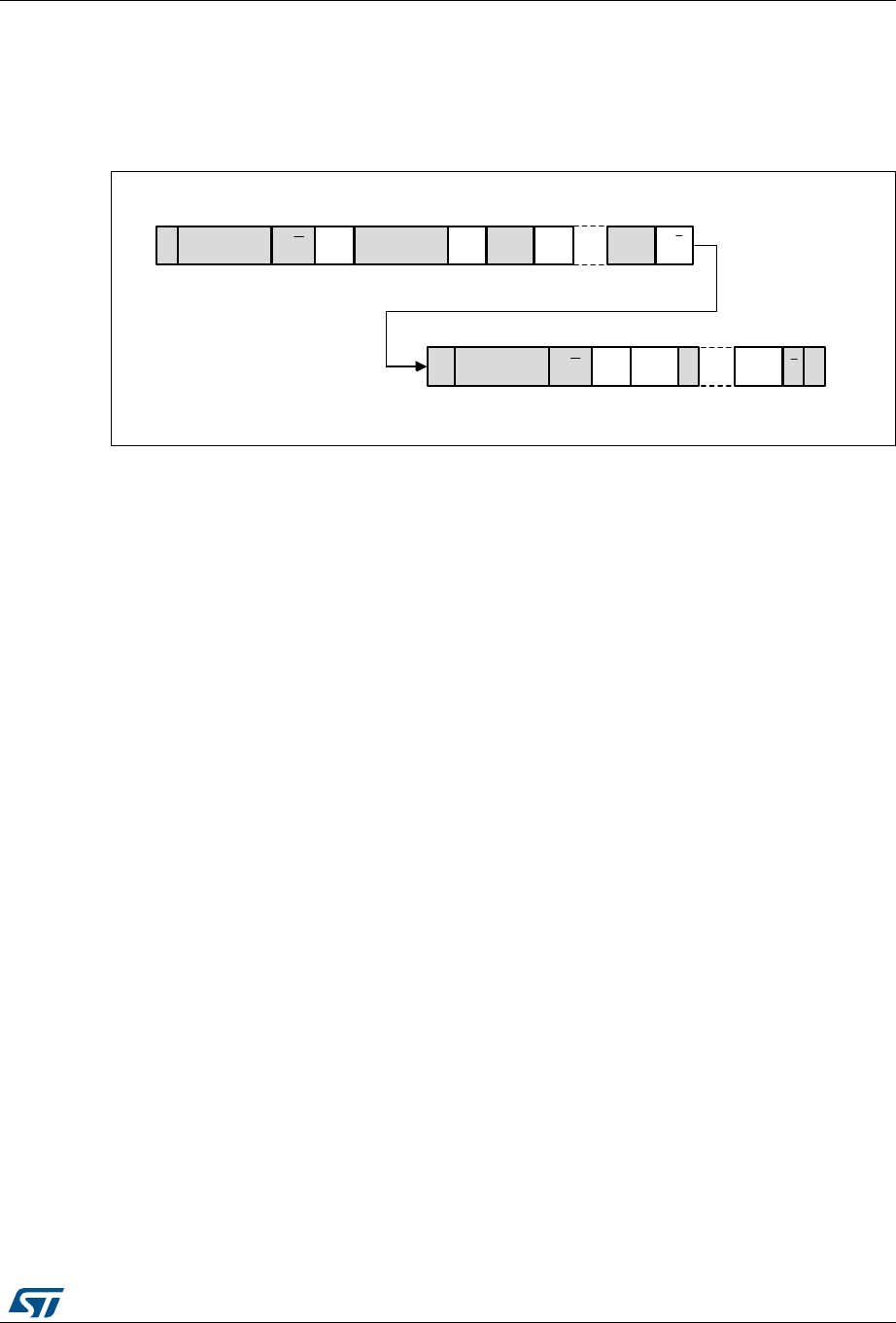
RM0394 Rev 4 1151/1600
RM0394 Inter-integrated circuit (I2C) interface
1193
•If the master addresses a 10-bit address slave, transmits data to this slave and then
reads data from the same slave, a master transmission flow must be done first. Then a
repeated start is set with the 10 bit slave address configured with HEAD10R=1. In this
case the master sends this sequence: ReStart + Slave address 10-bit header Read.
Figure 368. 10-bit address read access with HEAD10R=1
Master transmitter
In the case of a write transfer, the TXIS flag is set after each byte transmission, after the 9th
SCL pulse when an ACK is received.
A TXIS event generates an interrupt if the TXIE bit is set in the I2C_CR1 register. The flag is
cleared when the I2C_TXDR register is written with the next data byte to be transmitted.
The number of TXIS events during the transfer corresponds to the value programmed in
NBYTES[7:0]. If the total number of data bytes to be sent is greater than 255, reload mode
must be selected by setting the RELOAD bit in the I2C_CR2 register. In this case, when
NBYTES data have been transferred, the TCR flag is set and the SCL line is stretched low
until NBYTES[7:0] is written to a non-zero value.
The TXIS flag is not set when a NACK is received.
•When RELOAD=0 and NBYTES data have been transferred:
– In automatic end mode (AUTOEND=1), a STOP is automatically sent.
– In software end mode (AUTOEND=0), the TC flag is set and the SCL line is
stretched low in order to perform software actions:
A RESTART condition can be requested by setting the START bit in the I2C_CR2
register with the proper slave address configuration, and number of bytes to be
transferred. Setting the START bit clears the TC flag and the START condition is
sent on the bus.
A STOP condition can be requested by setting the STOP bit in the I2C_CR2
register. Setting the STOP bit clears the TC flag and the STOP condition is sent on
the bus.
•If a NACK is received: the TXIS flag is not set, and a STOP condition is automatically
sent after the NACK reception. the NACKF flag is set in the I2C_ISR register, and an
interrupt is generated if the NACKIE bit is set.
D^ϭϵϴϮϯsϭ
'$7$'$7$
6ODYHDGGUHVV
QGE\WH
6ODYHDGGUHVV
VWELWV
6U
$$
5:
6ODYHDGGUHVV
VWELWV
6 $
;;
;;
:ULWH
5HDG
'$7$ $ 3$'$7$$
$$5:
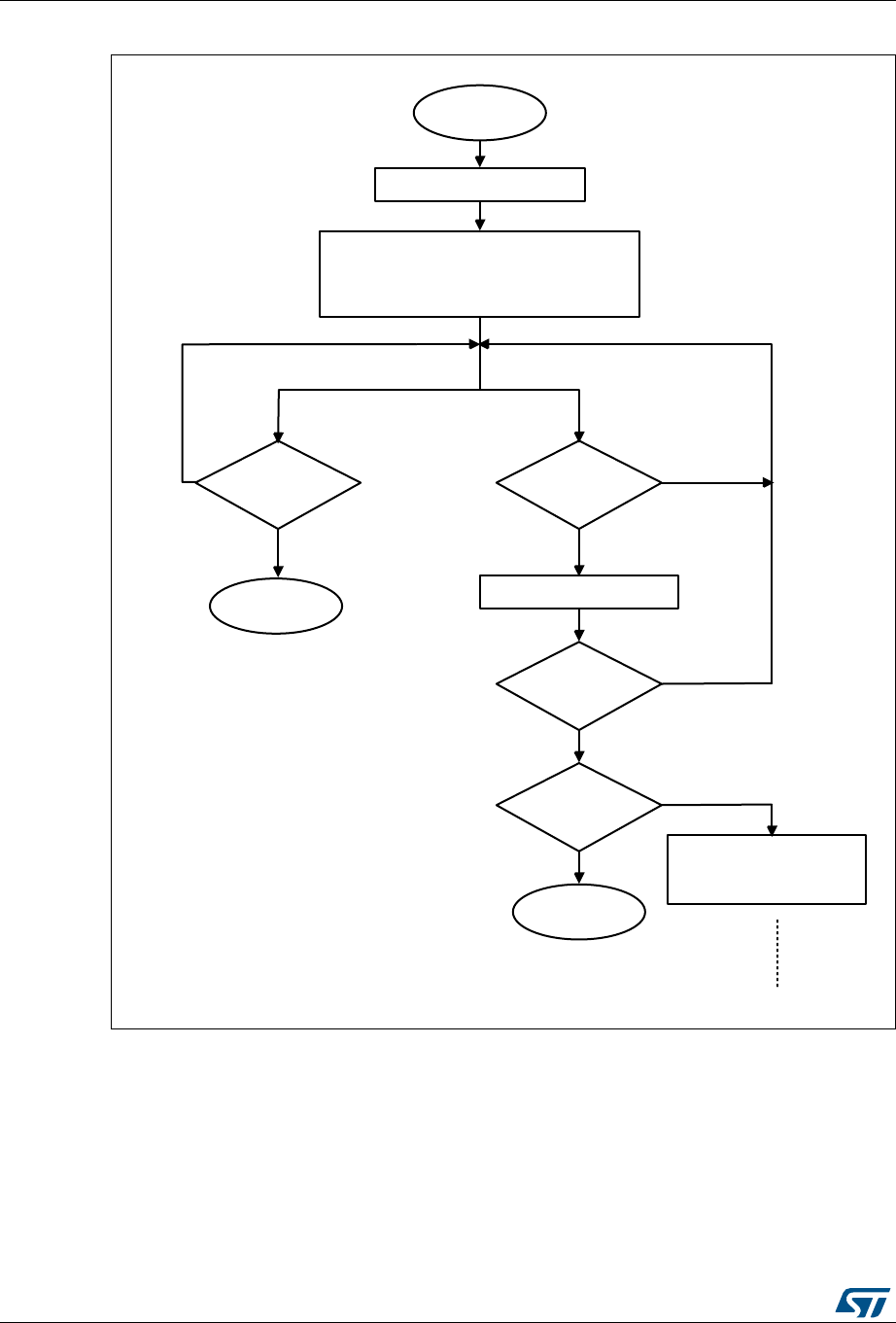
Inter-integrated circuit (I2C) interface RM0394
1152/1600 RM0394 Rev 4
Figure 369. Transfer sequence flowchart for I2C master transmitter for N≤255 bytes
D^ϭϵϴϲϬsϮ
0DVWHULQLWLDOL]DWLRQ
0DVWHU
WUDQVPLVVLRQ
:ULWH,&B7;'5
,&B,657;,6
"
1R
<HV
,&B,651$&.)
"
<HV
1R
1%<7(6 1
$872(1' IRU5(67$57IRU6723
&RQILJXUHVODYHDGGUHVV
6HW,&B&567$57
(QG
1%<7(6
WUDQVPLWWHG"
,&B,657&
"
<HV
(QG
1R
<HV
1R 6HW,&B&567$57ZLWK
VODYHDGGHVV1%<7(6
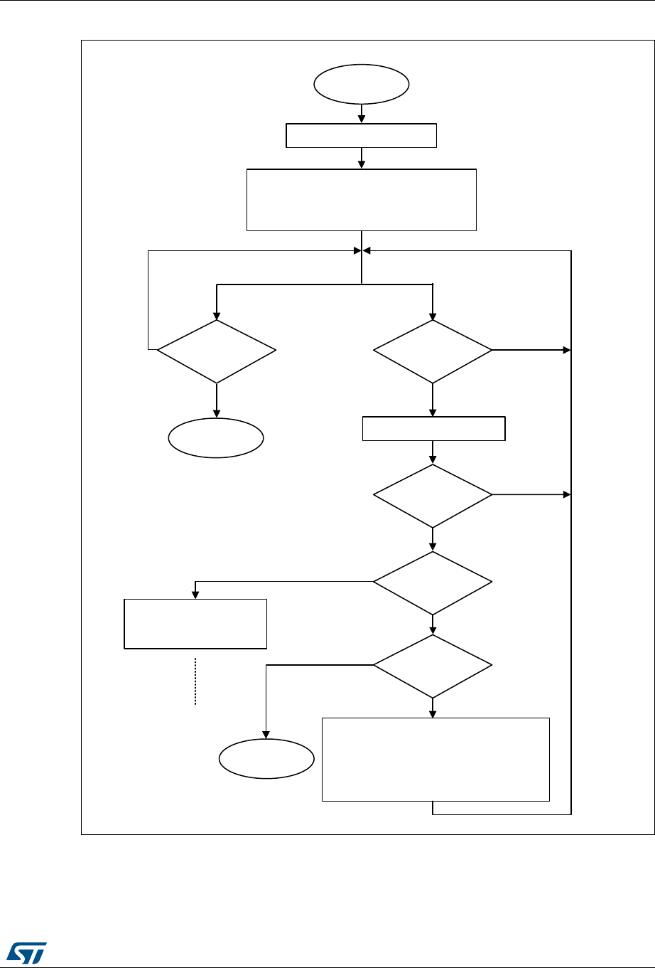
RM0394 Rev 4 1153/1600
RM0394 Inter-integrated circuit (I2C) interface
1193
Figure 370. Transfer sequence flowchart for I2C master transmitter for N>255 bytes
069
0DVWHULQLWLDOL]DWLRQ
0DVWHU
WUDQVPLVVLRQ
:ULWH,&B7;'5
,&B,657;,6
"
1R
<HV
,&B,651$&.)
"
<HV
1R
1%<7(6 [))1 1
5(/2$'
&RQILJXUHVODYHDGGUHVV
6HW,&B&567$57
(QG
1%<7(6
WUDQVPLWWHG "
,&B,657&
"
<HV
(QG
1R
<HV
1R
6HW,&B&567$57
ZLWKVODYHDGGHVV
1%<7(6
,&B,657&5
"
<HV
,)1
1%<7(6 11 5(/2$'
$872(1' IRU5(67$57IRU6723
(/6(
1%<7(6 [))1 1
5(/2$'
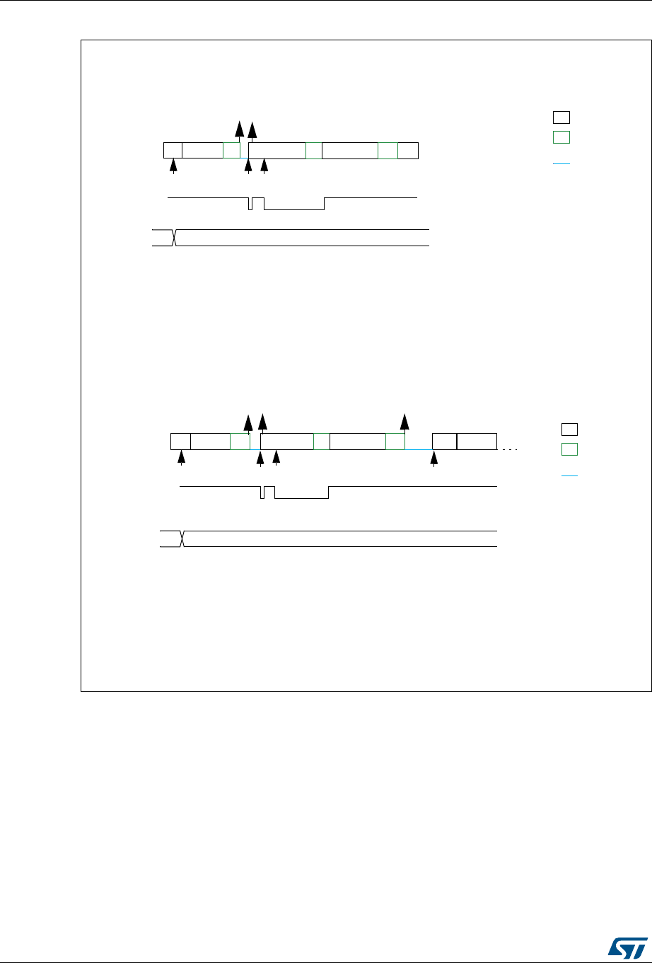
Inter-integrated circuit (I2C) interface RM0394
1154/1600 RM0394 Rev 4
Figure 371. Transfer bus diagrams for I2C master transmitter
069
([DPSOH,&PDVWHUWUDQVPLWWHUE\WHVDXWRPDWLFHQGPRGH6723
,1,7SURJUDP6ODYHDGGUHVVSURJUDP1%<7(6 $872(1' VHW67$57
(97;,6,65ZUGDWD
(97;,6,65ZUGDWD
7;,67;,6
OHJHQG
WUDQVPLVVLRQ
UHFHSWLRQ
6&/VWUHWFK
(9 (9
[[
,1,7
([DPSOH,&PDVWHUWUDQVPLWWHUE\WHVVRIWZDUHHQGPRGH5(67$57
,1,7SURJUDP6ODYHDGGUHVVSURJUDP1%<7(6 $872(1' VHW67$57
(97;,6,65ZUGDWD
(97;,6,65ZUGDWD
(97&,65SURJUDP6ODYHDGGUHVVSURJUDP1%<7(6 1VHW67$57
7;,6 7;,6 OHJHQG
WUDQVPLVVLRQ
UHFHSWLRQ
6&/VWUHWFK
(9 (9
,1,7
7&
7;(
7;(
(9
1%<7(6
1%<7(6
[[
6 $GGUHVV $ GDWD $ GDWD 5H6 $GGUHVV$
6 $GGUHVV $ GDWD $GDWD $3

RM0394 Rev 4 1155/1600
RM0394 Inter-integrated circuit (I2C) interface
1193
Master receiver
In the case of a read transfer, the RXNE flag is set after each byte reception, after the 8th
SCL pulse. An RXNE event generates an interrupt if the RXIE bit is set in the I2C_CR1
register. The flag is cleared when I2C_RXDR is read.
If the total number of data bytes to be received is greater than 255, reload mode must be
selected by setting the RELOAD bit in the I2C_CR2 register. In this case, when
NBYTES[7:0] data have been transferred, the TCR flag is set and the SCL line is stretched
low until NBYTES[7:0] is written to a non-zero value.
•When RELOAD=0 and NBYTES[7:0] data have been transferred:
– In automatic end mode (AUTOEND=1), a NACK and a STOP are automatically
sent after the last received byte.
– In software end mode (AUTOEND=0), a NACK is automatically sent after the last
received byte, the TC flag is set and the SCL line is stretched low in order to allow
software actions:
A RESTART condition can be requested by setting the START bit in the I2C_CR2
register with the proper slave address configuration, and number of bytes to be
transferred. Setting the START bit clears the TC flag and the START condition,
followed by slave address, are sent on the bus.
A STOP condition can be requested by setting the STOP bit in the I2C_CR2
register. Setting the STOP bit clears the TC flag and the STOP condition is sent on
the bus.
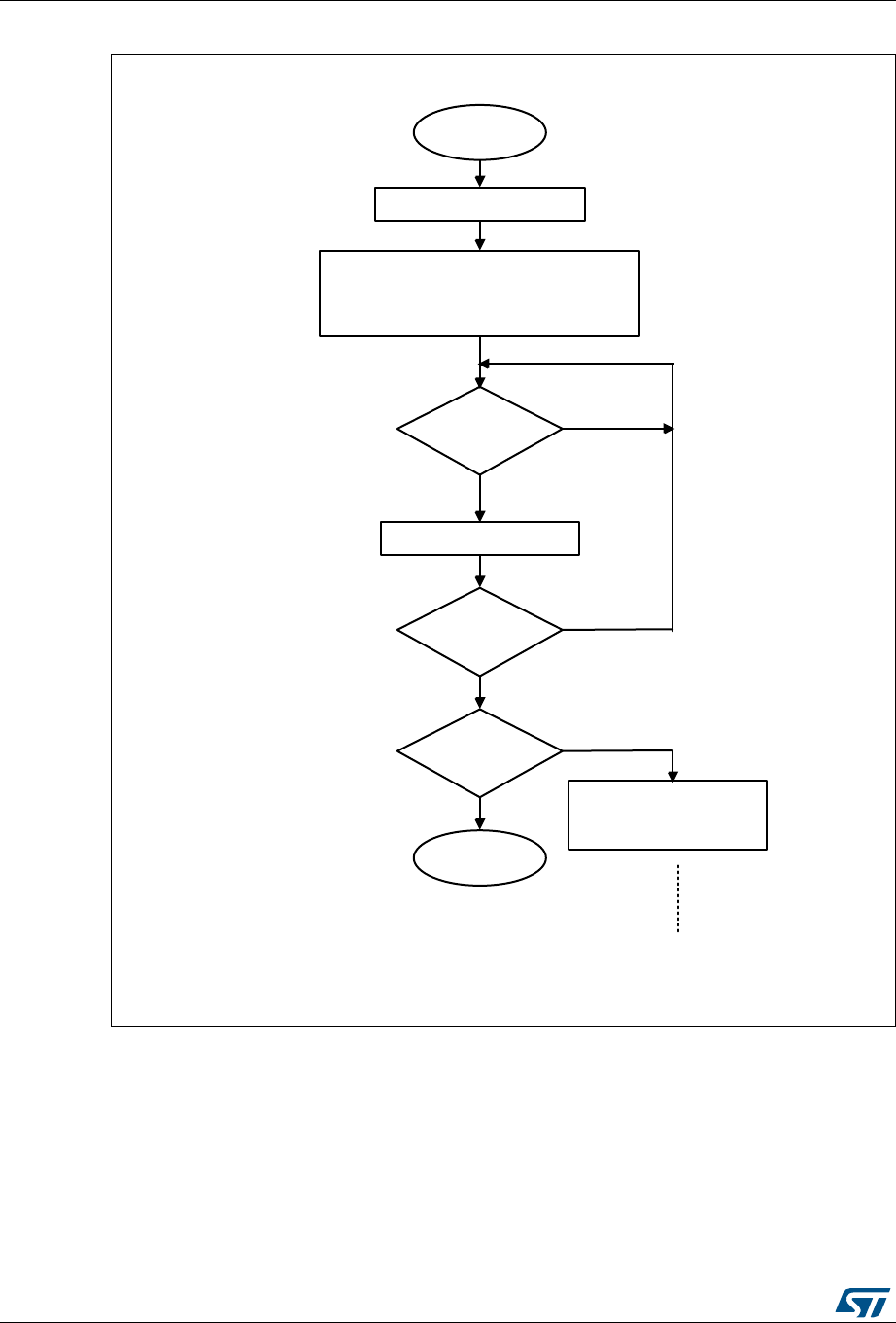
Inter-integrated circuit (I2C) interface RM0394
1156/1600 RM0394 Rev 4
Figure 372. Transfer sequence flowchart for I2C master receiver for N≤255 bytes
D^ϭϵϴϲϯsϮ
0DVWHULQLWLDOL]DWLRQ
0DVWHUUHFHSWLRQ
5HDG,&B5;'5
,&B,655;1(
"
1R
<HV
1%<7(6 1
$872(1' IRU5(67$57IRU6723
&RQILJXUHVODYHDGGUHVV
6HW,&B&567$57
1%<7(6
UHFHLYHG"
,&B,657&
"
<HV
(QG
1R
<HV
1R 6HW,&B&567$57ZLWK
VODYHDGGHVV1%<7(6
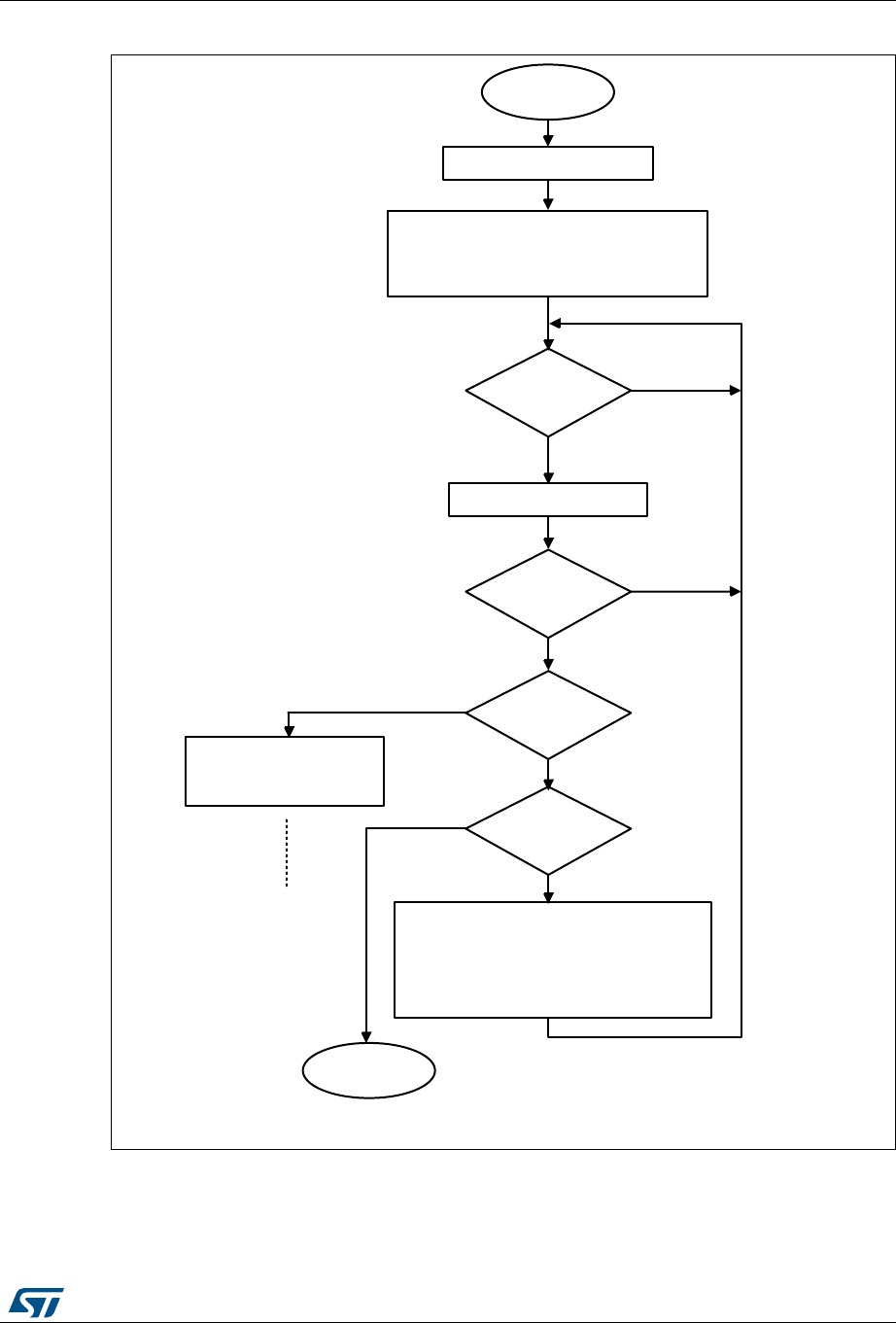
RM0394 Rev 4 1157/1600
RM0394 Inter-integrated circuit (I2C) interface
1193
Figure 373. Transfer sequence flowchart for I2C master receiver for N >255 bytes
D^ϭϵϴϲϰsϮ
0DVWHULQLWLDOL]DWLRQ
0DVWHUUHFHSWLRQ
5HDG,&B5;'5
,&B,655;1(
"
1R
<HV
1%<7(6 [))1 1
5(/2$'
&RQILJXUHVODYHDGGUHVV
6HW,&B&567$57
1%<7(6
UHFHLYHG"
,&B,657&
"
<HV
(QG
1R
<HV
1R
6HW,&B&567$57ZLWK
VODYHDGGHVV1%<7(6
,&B,657&5
"
<HV
,)1
1%<7(6 11 5(/2$'
$872(1' IRU5(67$57IRU6723
(/6(
1%<7(6 [))1 1
5(/2$'
1R
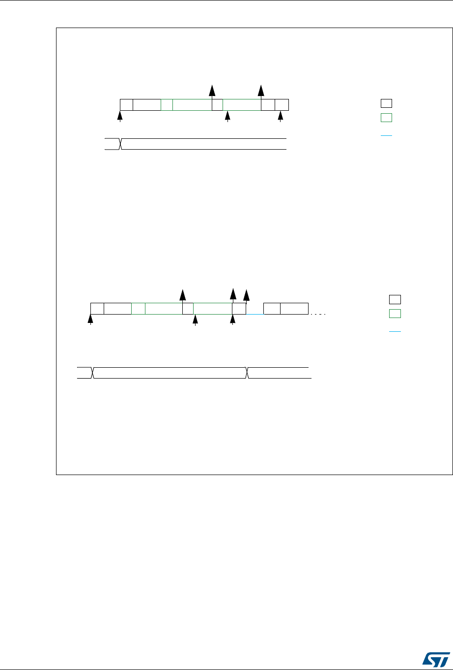
Inter-integrated circuit (I2C) interface RM0394
1158/1600 RM0394 Rev 4
Figure 374. Transfer bus diagrams for I2C master receiver
069
([DPSOH,&PDVWHUUHFHLYHUE\WHVDXWRPDWLFHQGPRGH6723
,1,7SURJUDP6ODYHDGGUHVVSURJUDP1%<7(6 $872(1' VHW67$57
(95;1(,65UGGDWD
(95;1(,65UGGDWD
$
5;1( 5;1(
1%<7(6
OHJHQG
WUDQVPLVVLRQ
UHFHSWLRQ
6&/VWUHWFK
(9
[[
,1,7
([DPSOH,&PDVWHUUHFHLYHUE\WHVVRIWZDUHHQGPRGH5(67$57
,1,7SURJUDP6ODYHDGGUHVVSURJUDP1%<7(6 $872(1' VHW67$57
(95;1(,65UGGDWD
(95;1(,65UHDGGDWD
(97&,65SURJUDP6ODYHDGGUHVVSURJUDP1%<7(6 1VHW67$57
$
5;1( 5;1(
1%<7(6
OHJHQG
WUDQVPLVVLRQ
UHFHSWLRQ
6&/VWUHWFK
(9 (9
[[
,1,7
1
(9
7&
$GGUHVV6 $ GDWD GDWD 1$ 5H6 $GGUHVV
6 $GGUHVV $GDWD GDWD 1$ 3
RM0394 Rev 4 1159/1600
RM0394 Inter-integrated circuit (I2C) interface
1193
37.4.9 I2C_TIMINGR register configuration examples
The tables below provide examples of how to program the I2C_TIMINGR to obtain timings
compliant with the I2C specification. In order to get more accurate configuration values, the
STM32CubeMX tool (I2C Configuration window) must be used.
Table 181. Examples of timing settings for fI2CCLK = 8 MHz
Parameter
Standard-mode (Sm) Fast-mode (Fm) Fast-mode Plus (Fm+)
10 kHz 100 kHz 400 kHz 500 kHz
PRESC 1 1 0 0
SCLL 0xC7 0x13 0x9 0x6
tSCLL 200x250 ns = 50 µs 20x250 ns = 5.0 µs 10x125 ns = 1250 ns 7x125 ns = 875 ns
SCLH 0xC3 0xF 0x3 0x3
tSCLH 196x250 ns = 49 µs 16x250 ns = 4.0µs 4x125ns = 500ns 4x125 ns = 500 ns
tSCL(1) ~100 µs(2) ~10 µs(2) ~2500 ns(3) ~2000 ns(4)
SDADEL 0x2 0x2 0x1 0x0
tSDADEL 2x250 ns = 500 ns 2x250 ns = 500 ns 1x125 ns = 125 ns 0 ns
SCLDEL 0x4 0x4 0x3 0x1
tSCLDEL 5x250 ns = 1250 ns 5x250 ns = 1250 ns 4x125 ns = 500 ns 2x125 ns = 250 ns
1. SCL period tSCL is greater than tSCLL + tSCLH due to SCL internal detection delay. Values provided for tSCL are examples
only.
2. tSYNC1 + tSYNC2 minimum value is 4 x tI2CCLK = 500 ns. Example with tSYNC1 + tSYNC2 = 1000 ns.
3. tSYNC1 + tSYNC2 minimum value is 4 x tI2CCLK = 500 ns. Example with tSYNC1 + tSYNC2 = 750 ns.
4. tSYNC1 + tSYNC2 minimum value is 4 x tI2CCLK = 500 ns. Example with tSYNC1 + tSYNC2 = 655 ns.
Table 182. Examples of timings settings for fI2CCLK = 16 MHz
Parameter
Standard-mode (Sm) Fast-mode (Fm) Fast-mode Plus (Fm+)
10 kHz 100 kHz 400 kHz 1000 kHz
PRESC 3 3 1 0
SCLL 0xC7 0x13 0x9 0x4
tSCLL 200 x 250 ns = 50 µs 20 x 250 ns = 5.0 µs 10 x 125 ns = 1250 ns 5 x 62.5 ns = 312.5 ns
SCLH 0xC3 0xF 0x3 0x2
tSCLH 196 x 250 ns = 49 µs 16 x 250 ns = 4.0 µs 4 x 125ns = 500 ns 3 x 62.5 ns = 187.5 ns
tSCL(1) ~100 µs(2) ~10 µs(2) ~2500 ns(3) ~1000 ns(4)
SDADEL 0x2 0x2 0x2 0x0
tSDADEL 2 x 250 ns = 500 ns 2 x 250 ns = 500 ns 2 x 125 ns = 250 ns 0 ns
SCLDEL 0x4 0x4 0x3 0x2
tSCLDEL 5 x 250 ns = 1250 ns 5 x 250 ns = 1250 ns 4 x 125 ns = 500 ns 3 x 62.5 ns = 187.5 ns
1. SCL period tSCL is greater than tSCLL + tSCLH due to SCL internal detection delay. Values provided for tSCL are examples
only.
Inter-integrated circuit (I2C) interface RM0394
1160/1600 RM0394 Rev 4
37.4.10 SMBus specific features
This section is relevant only when SMBus feature is supported. Refer to Section 37.3: I2C
implementation.
Introduction
The System Management Bus (SMBus) is a two-wire interface through which various
devices can communicate with each other and with the rest of the system. It is based on I2C
principles of operation. SMBus provides a control bus for system and power management
related tasks.
This peripheral is compatible with the SMBUS specification (http://smbus.org).
The System Management Bus Specification refers to three types of devices.
•A slave is a device that receives or responds to a command.
•A master is a device that issues commands, generates the clocks and terminates the
transfer.
•A host is a specialized master that provides the main interface to the system’s CPU. A
host must be a master-slave and must support the SMBus host notify protocol. Only
one host is allowed in a system.
This peripheral can be configured as master or slave device, and also as a host.
2. tSYNC1 + tSYNC2 minimum value is 4 x tI2CCLK = 250 ns. Example with tSYNC1 + tSYNC2 = 1000 ns.
3. tSYNC1 + tSYNC2 minimum value is 4 x tI2CCLK = 250 ns. Example with tSYNC1 + tSYNC2 = 750 ns.
4. tSYNC1 + tSYNC2 minimum value is 4 x tI2CCLK = 250 ns. Example with tSYNC1 + tSYNC2 = 500 ns.
Table 183. Examples of timings settings for fI2CCLK = 48 MHz
Parameter
Standard-mode (Sm) Fast-mode (Fm) Fast-mode Plus (Fm+)
10 kHz 100 kHz 400 kHz 1000 kHz
PRESC 0xB 0xB 5 5
SCLL 0xC7 0x13 0x9 0x3
tSCLL 200 x 250 ns = 50 µs 20 x 250 ns = 5.0 µs 10 x 125 ns = 1250 ns 4 x 125 ns = 500 ns
SCLH 0xC3 0xF 0x3 0x1
tSCLH 196 x 250 ns = 49 µs 16 x 250 ns = 4.0 µs 4 x 125 ns = 500 ns 2 x 125 ns = 250 ns
tSCL(1) ~100 µs(2) ~10 µs(2) ~2500 ns(3) ~875 ns(4)
SDADEL 0x2 0x2 0x3 0x0
tSDADEL 2 x 250 ns = 500 ns 2 x 250 ns = 500 ns 3 x 125 ns = 375 ns 0 ns
SCLDEL 0x4 0x4 0x3 0x1
tSCLDEL 5 x 250 ns = 1250 ns 5 x 250 ns = 1250 ns 4 x 125 ns = 500 ns 2 x 125 ns = 250 ns
1. The SCL period tSCL is greater than tSCLL + tSCLH due to the SCL internal detection delay. Values provided for tSCL are only
examples.
2. tSYNC1 + tSYNC2 minimum value is 4x tI2CCLK = 83.3 ns. Example with tSYNC1 + tSYNC2 = 1000 ns
3. tSYNC1 + tSYNC2 minimum value is 4x tI2CCLK = 83.3 ns. Example with tSYNC1 + tSYNC2 = 750 ns
4. tSYNC1 + tSYNC2 minimum value is 4x tI2CCLK = 83.3 ns. Example with tSYNC1 + tSYNC2 = 250 ns

RM0394 Rev 4 1161/1600
RM0394 Inter-integrated circuit (I2C) interface
1193
Bus protocols
There are eleven possible command protocols for any given device. A device may use any
or all of the eleven protocols to communicate. The protocols are Quick Command, Send
Byte, Receive Byte, Write Byte, Write Word, Read Byte, Read Word, Process Call, Block
Read, Block Write and Block Write-Block Read Process Call. These protocols should be
implemented by the user software.
For more details of these protocols, refer to SMBus specification (http://smbus.org).
Address resolution protocol (ARP)
SMBus slave address conflicts can be resolved by dynamically assigning a new unique
address to each slave device. In order to provide a mechanism to isolate each device for the
purpose of address assignment each device must implement a unique device identifier
(UDID). This 128-bit number is implemented by software.
This peripheral supports the Address Resolution Protocol (ARP). The SMBus Device
Default Address (0b1100 001) is enabled by setting SMBDEN bit in I2C_CR1 register. The
ARP commands should be implemented by the user software.
Arbitration is also performed in slave mode for ARP support.
For more details of the SMBus Address Resolution Protocol, refer to SMBus specification
(http://smbus.org).
Received Command and Data acknowledge control
A SMBus receiver must be able to NACK each received command or data. In order to allow
the ACK control in slave mode, the Slave Byte Control mode must be enabled by setting
SBC bit in I2C_CR1 register. Refer to Slave Byte Control mode on page 1140 for more
details.
Host Notify protocol
This peripheral supports the Host Notify protocol by setting the SMBHEN bit in the I2C_CR1
register. In this case the host acknowledges the SMBus Host address (0b0001 000).
When this protocol is used, the device acts as a master and the host as a slave.
SMBus alert
The SMBus ALERT optional signal is supported. A slave-only device can signal the host
through the SMBALERT# pin that it wants to talk. The host processes the interrupt and
simultaneously accesses all SMBALERT# devices through the Alert Response Address
(0b0001 100). Only the device(s) which pulled SMBALERT# low acknowledges the Alert
Response Address.
When configured as a slave device(SMBHEN=0), the SMBA pin is pulled low by setting the
ALERTEN bit in the I2C_CR1 register. The Alert Response Address is enabled at the same
time.
When configured as a host (SMBHEN=1), the ALERT flag is set in the I2C_ISR register
when a falling edge is detected on the SMBA pin and ALERTEN=1. An interrupt is
generated if the ERRIE bit is set in the I2C_CR1 register. When ALERTEN=0, the ALERT
line is considered high even if the external SMBA pin is low.
If the SMBus ALERT pin is not needed, the SMBA pin can be used as a standard GPIO if
ALERTEN=0.
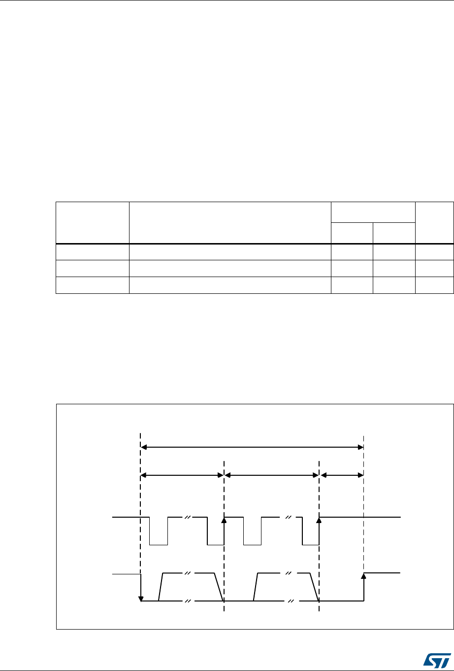
Inter-integrated circuit (I2C) interface RM0394
1162/1600 RM0394 Rev 4
Packet error checking
A packet error checking mechanism has been introduced in the SMBus specification to
improve reliability and communication robustness. Packet Error Checking is implemented
by appending a Packet Error Code (PEC) at the end of each message transfer. The PEC is
calculated by using the C(x) = x8 + x2 + x + 1 CRC-8 polynomial on all the message bytes
(including addresses and read/write bits).
The peripheral embeds a hardware PEC calculator and allows to send a Not Acknowledge
automatically when the received byte does not match with the hardware calculated PEC.
Timeouts
This peripheral embeds hardware timers in order to be compliant with the 3 timeouts defined
in SMBus specification.
Figure 375. Timeout intervals for tLOW:SEXT
, tLOW:MEXT
.
Table 184. SMBus timeout specifications
Symbol Parameter
Limits
Unit
Min Max
tTIMEOUT Detect clock low timeout 25 35 ms
tLOW:SEXT(1)
1. tLOW:SEXT is the cumulative time a given slave device is allowed to extend the clock cycles in one message
from the initial START to the STOP. It is possible that, another slave device or the master also extends the
clock causing the combined clock low extend time to be greater than tLOW:SEXT
. Therefore, this parameter is
measured with the slave device as the sole target of a full-speed master.
Cumulative clock low extend time (slave device) - 25 ms
tLOW:MEXT(2)
2. tLOW:MEXT is the cumulative time a master device is allowed to extend its clock cycles within each byte of a
message as defined from START-to-ACK, ACK-to-ACK, or ACK-to-STOP. It is possible that a slave device
or another master also extends the clock causing the combined clock low time to be greater than tLOW:MEXT
on a given byte. Therefore, this parameter is measured with a full speed slave device as the sole target of
the master.
Cumulative clock low extend time (master device) - 10 ms
069
6WDUW 6WRS
W/2:6(;7
W/2:0(;7 W/2:0(;7 W/2:0(;7
&ON$FN &ON$FN
60%&/.
60%'$7

RM0394 Rev 4 1163/1600
RM0394 Inter-integrated circuit (I2C) interface
1193
Bus idle detection
A master can assume that the bus is free if it detects that the clock and data signals have
been high for tIDLE greater than tHIGH,MAX. (refer to Table 178: I2C-SMBUS specification data
setup and hold times)
This timing parameter covers the condition where a master has been dynamically added to
the bus and may not have detected a state transition on the SMBCLK or SMBDAT lines. In
this case, the master must wait long enough to ensure that a transfer is not currently in
progress. The peripheral supports a hardware bus idle detection.
37.4.11 SMBus initialization
This section is relevant only when SMBus feature is supported. Refer to Section 37.3: I2C
implementation.
In addition to I2C initialization, some other specific initialization must be done in order to
perform SMBus communication:
Received Command and Data Acknowledge control (Slave mode)
A SMBus receiver must be able to NACK each received command or data. In order to allow
ACK control in slave mode, the Slave Byte Control mode must be enabled by setting the
SBC bit in the I2C_CR1 register. Refer to Slave Byte Control mode on page 1140 for more
details.
Specific address (Slave mode)
The specific SMBus addresses must be enabled if needed. Refer to Bus idle detection on
page 1163 for more details.
•The SMBus Device Default address (0b1100 001) is enabled by setting the SMBDEN
bit in the I2C_CR1 register.
•The SMBus Host address (0b0001 000) is enabled by setting the SMBHEN bit in the
I2C_CR1 register.
•The Alert Response Address (0b0001100) is enabled by setting the ALERTEN bit in the
I2C_CR1 register.
Packet error checking
PEC calculation is enabled by setting the PECEN bit in the I2C_CR1 register. Then the PEC
transfer is managed with the help of a hardware byte counter: NBYTES[7:0] in the I2C_CR2
register. The PECEN bit must be configured before enabling the I2C.
The PEC transfer is managed with the hardware byte counter, so the SBC bit must be set
when interfacing the SMBus in slave mode. The PEC is transferred after NBYTES-1 data
have been transferred when the PECBYTE bit is set and the RELOAD bit is cleared. If
RELOAD is set, PECBYTE has no effect.
Caution: Changing the PECEN configuration is not allowed when the I2C is enabled.

Inter-integrated circuit (I2C) interface RM0394
1164/1600 RM0394 Rev 4
Timeout detection
The timeout detection is enabled by setting the TIMOUTEN and TEXTEN bits in the
I2C_TIMEOUTR register. The timers must be programmed in such a way that they detect a
timeout before the maximum time given in the SMBus specification.
•tTIMEOUT check
In order to enable the tTIMEOUT check, the 12-bit TIMEOUTA[11:0] bits must be
programmed with the timer reload value in order to check the tTIMEOUT parameter. The
TIDLE bit must be configured to ‘0’ in order to detect the SCL low level timeout.
Then the timer is enabled by setting the TIMOUTEN in the I2C_TIMEOUTR register.
If SCL is tied low for a time greater than (TIMEOUTA+1) x 2048 x tI2CCLK, the TIMEOUT
flag is set in the I2C_ISR register.
Refer to Table 186: Examples of TIMEOUTA settings for various I2CCLK frequencies
(max tTIMEOUT = 25 ms).
Caution: Changing the TIMEOUTA[11:0] bits and TIDLE bit configuration is not allowed when the
TIMEOUTEN bit is set.
•tLOW:SEXT and tLOW:MEXT check
Depending on if the peripheral is configured as a master or as a slave, The 12-bit
TIMEOUTB timer must be configured in order to check tLOW:SEXT for a slave and
tLOW:MEXT for a master. As the standard specifies only a maximum, the user can choose
the same value for the both.
Then the timer is enabled by setting the TEXTEN bit in the I2C_TIMEOUTR register.
If the SMBus peripheral performs a cumulative SCL stretch for a time greater than
(TIMEOUTB+1) x 2048 x tI2CCLK, and in the timeout interval described in Bus idle
detection on page 1163 section, the TIMEOUT flag is set in the I2C_ISR register.
Refer to Table 187: Examples of TIMEOUTB settings for various I2CCLK frequencies
Caution: Changing the TIMEOUTB configuration is not allowed when the TEXTEN bit is set.
Bus Idle detection
In order to enable the tIDLE check, the 12-bit TIMEOUTA[11:0] field must be programmed
with the timer reload value in order to obtain the tIDLE parameter. The TIDLE bit must be
configured to ‘1 in order to detect both SCL and SDA high level timeout.
Then the timer is enabled by setting the TIMOUTEN bit in the I2C_TIMEOUTR register.
If both the SCL and SDA lines remain high for a time greater than (TIMEOUTA+1) x 4 x
tI2CCLK, the TIMEOUT flag is set in the I2C_ISR register.
Refer to Table 188: Examples of TIMEOUTA settings for various I2CCLK frequencies (max
tIDLE = 50 µs)
Table 185. SMBUS with PEC configuration
Mode SBC bit RELOAD bit AUTOEND bit PECBYTE bit
Master Tx/Rx NBYTES + PEC+ STOP x 0 1 1
Master Tx/Rx NBYTES + PEC + ReSTART x 0 0 1
Slave Tx/Rx with PEC 1 0 x 1
RM0394 Rev 4 1165/1600
RM0394 Inter-integrated circuit (I2C) interface
1193
Caution: Changing the TIMEOUTA and TIDLE configuration is not allowed when the TIMEOUTEN is
set.
37.4.12 SMBus: I2C_TIMEOUTR register configuration examples
This section is relevant only when SMBus feature is supported. Refer to Section 37.3: I2C
implementation.
•Configuring the maximum duration of tTIMEOUT to 25 ms:
•Configuring the maximum duration of tLOW:SEXT and tLOW:MEXT to 8 ms:
•Configuring the maximum duration of tIDLE to 50 µs
37.4.13 SMBus slave mode
This section is relevant only when SMBus feature is supported. Refer to Section 37.3: I2C
implementation.
In addition to I2C slave transfer management (refer to Section 37.4.7: I2C slave mode)
some additional software flowcharts are provided to support SMBus.
SMBus Slave transmitter
When the IP is used in SMBus, SBC must be programmed to ‘1’ in order to allow the PEC
transmission at the end of the programmed number of data bytes. When the PECBYTE bit
is set, the number of bytes programmed in NBYTES[7:0] includes the PEC transmission. In
Table 186. Examples of TIMEOUTA settings for various I2CCLK frequencies
(max tTIMEOUT = 25 ms)
fI2CCLK TIMEOUTA[11:0] bits TIDLE bit TIMEOUTEN bit tTIMEOUT
8 MHz 0x61 0 1 98 x 2048 x 125 ns = 25 ms
16 MHz 0xC3 0 1 196 x 2048 x 62.5 ns = 25 ms
48 MHz 0x249 0 1 586 x 2048 x 20.08 ns = 25 ms
Table 187. Examples of TIMEOUTB settings for various I2CCLK frequencies
fI2CCLK TIMEOUTB[11:0] bits TEXTEN bit tLOW:EXT
8 MHz 0x1F 1 32 x 2048 x 125 ns = 8 ms
16 MHz 0x3F 1 64 x 2048 x 62.5 ns = 8 ms
48 MHz 0xBB 1 188 x 2048 x 20.08 ns = 8 ms
Table 188. Examples of TIMEOUTA settings for various I2CCLK frequencies
(max tIDLE = 50 µs)
fI2CCLK TIMEOUTA[11:0] bits TIDLE bit TIMEOUTEN bit tTIDLE
8 MHz 0x63 1 1 100 x 4 x 125 ns = 50 µs
16 MHz 0xC7 1 1 200 x 4 x 62.5 ns = 50 µs
48 MHz 0x257 1 1 600 x 4 x 20.08 ns = 50 µs
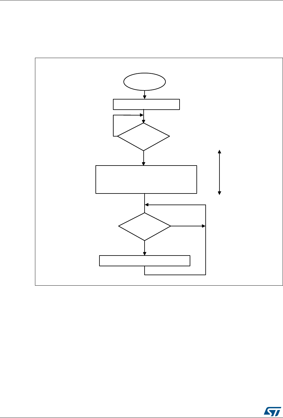
Inter-integrated circuit (I2C) interface RM0394
1166/1600 RM0394 Rev 4
that case the total number of TXIS interrupts is NBYTES-1 and the content of the
I2C_PECR register is automatically transmitted if the master requests an extra byte after the
NBYTES-1 data transfer.
Caution: The PECBYTE bit has no effect when the RELOAD bit is set.
Figure 376. Transfer sequence flowchart for SMBus slave transmitter N bytes + PEC
D^ϭϵϴϲϳsϮ
6ODYHLQLWLDOL]DWLRQ
60%XVVODYH
WUDQVPLVVLRQ
:ULWH,&B7;'57;'$7$
,&B,657;,6
"
1R
<HV
,&B,65$''5
"
<HV
1R
5HDG$''&2'(DQG',5LQ,&B,65
,&B&51%<7(6 1
3(&%<7(
6HW,&B,&5$''5&)
6&/
VWUHWFKHG
RM0394 Rev 4 1167/1600
RM0394 Inter-integrated circuit (I2C) interface
1193
Figure 377. Transfer bus diagrams for SMBus slave transmitter (SBC=1)
SMBus Slave receiver
When the I2C is used in SMBus mode, SBC must be programmed to ‘1’ in order to allow the
PEC checking at the end of the programmed number of data bytes. In order to allow the
ACK control of each byte, the reload mode must be selected (RELOAD=1). Refer to Slave
Byte Control mode on page 1140 for more details.
In order to check the PEC byte, the RELOAD bit must be cleared and the PECBYTE bit
must be set. In this case, after NBYTES-1 data have been received, the next received byte
is compared with the internal I2C_PECR register content. A NACK is automatically
generated if the comparison does not match, and an ACK is automatically generated if the
comparison matches, whatever the ACK bit value. Once the PEC byte is received, it is
copied into the I2C_RXDR register like any other data, and the RXNE flag is set.
In the case of a PEC mismatch, the PECERR flag is set and an interrupt is generated if the
ERRIE bit is set in the I2C_CR1 register.
If no ACK software control is needed, the user can program PECBYTE=1 and, in the same
write operation, program NBYTES with the number of bytes to be received in a continuous
flow. After NBYTES-1 are received, the next received byte is checked as being the PEC.
Caution: The PECBYTE bit has no effect when the RELOAD bit is set.
069
([DPSOH60%XVVODYHWUDQVPLWWHUE\WHV3(&
(9$''5,65FKHFN$''&2'(SURJUDP1%<7(6 VHW3(&%<7(VHW$''5&)
(97;,6,65ZUGDWD
(97;,6,65ZUGDWD
$''5
OHJHQG
WUDQVPLVVLRQ
UHFHSWLRQ
6&/VWUHWFK
(9 (9
7;,6 7;,6
(9
1%<7(6
6 $GGUHVV $ $GDWD GDWD 3(&
$1$ 3
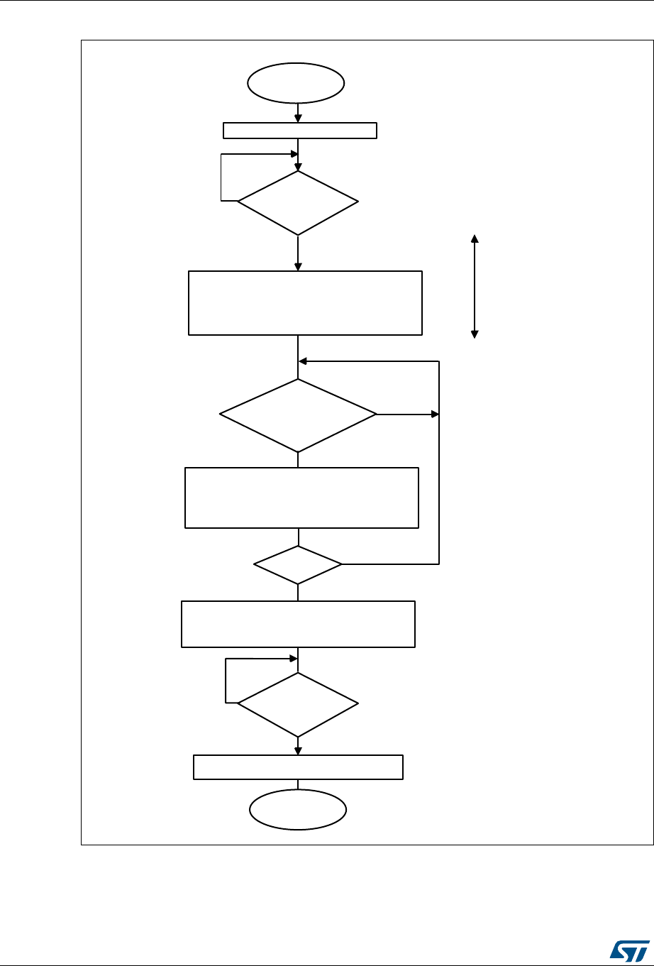
Inter-integrated circuit (I2C) interface RM0394
1168/1600 RM0394 Rev 4
Figure 378. Transfer sequence flowchart for SMBus slave receiver N Bytes + PEC
D^ϭϵϴϲϴsϮ
6ODYHLQLWLDOL]DWLRQ
60%XVVODYH
UHFHSWLRQ
5HDG,&B5;'55;'$7$
,&B,655;1( "
,&B,657&5 "
1R
<HV
,&B,65$''5
"
<HV
1R
5HDG$''&2'(DQG',5LQ,&B,65
,&B&51%<7(6 5(/2$'
3(&%<7(
6HW,&B,&5$''5&)
6&/
VWUHWFKHG
5HDG,&B5;'55;'$7$
3URJUDP,&B&51$&.
,&B&51%<7(6
1 1
1 "
5HDG,&B5;'55;'$7$
3URJUDP5(/2$'
1$&. DQG1%<7(6
,&B,655;1( "
1R
(QG
1R
<HV
<HV
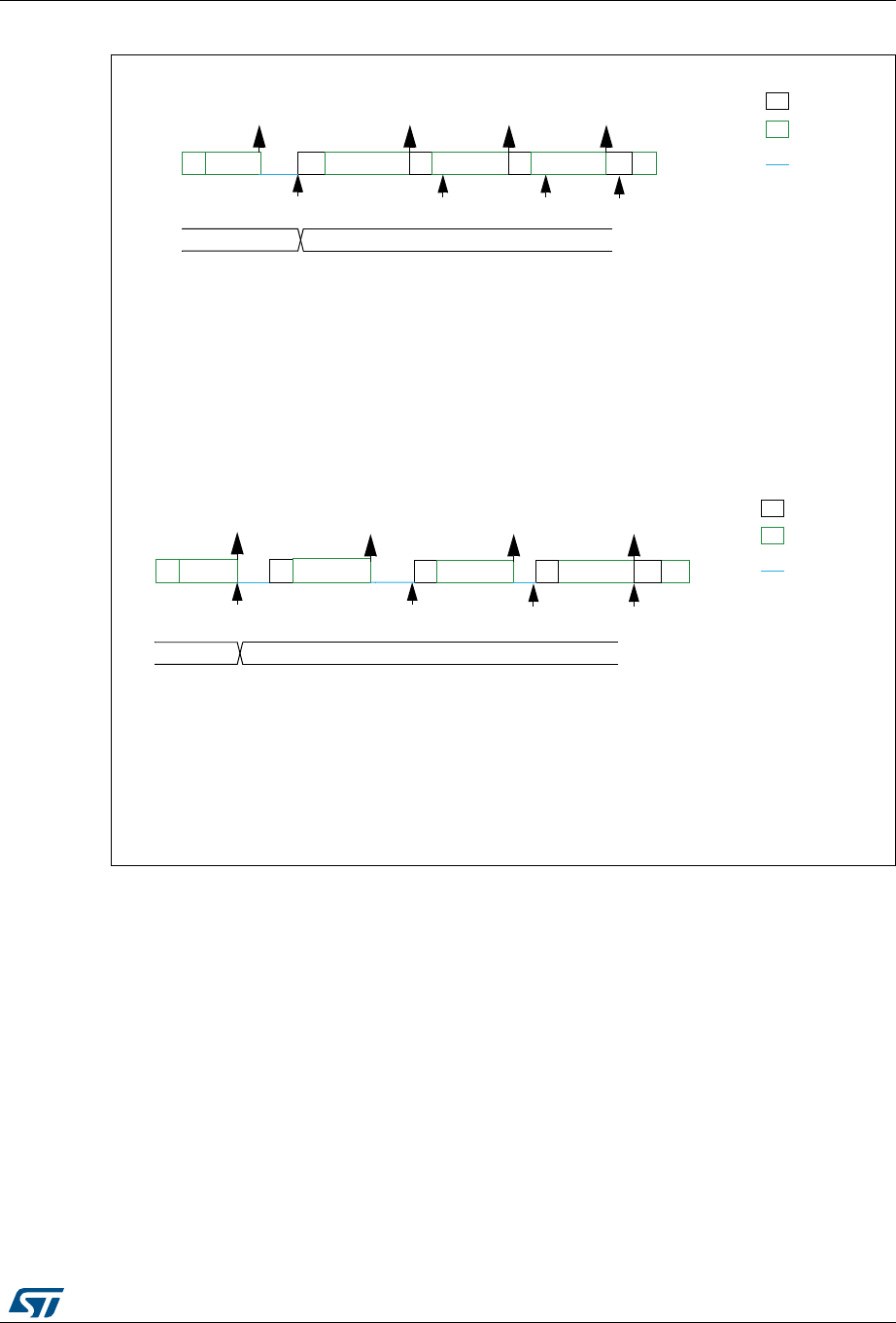
RM0394 Rev 4 1169/1600
RM0394 Inter-integrated circuit (I2C) interface
1193
Figure 379. Bus transfer diagrams for SMBus slave receiver (SBC=1)
This section is relevant only when SMBus feature is supported. Refer to Section 37.3: I2C
implementation.
In addition to I2C master transfer management (refer to Section 37.4.8: I2C master mode)
some additional software flowcharts are provided to support SMBus.
SMBus Master transmitter
When the SMBus master wants to transmit the PEC, the PECBYTE bit must be set and the
number of bytes must be programmed in the NBYTES[7:0] field, before setting the START
bit. In this case the total number of TXIS interrupts is NBYTES-1. So if the PECBYTE bit is
set when NBYTES=0x1, the content of the I2C_PECR register is automatically transmitted.
If the SMBus master wants to send a STOP condition after the PEC, automatic end mode
must be selected (AUTOEND=1). In this case, the STOP condition automatically follows the
PEC transmission.
069
([DPSOH60%XVVODYHUHFHLYHUE\WHV3(&
$GGUHVV
6
(9$''5,65FKHFN$''&2'(DQG',5SURJUDP1%<7(6 3(&%<7( 5(/2$' VHW$''5&)
(95;1(,65UGGDWD
(95;1(,65UGGDWD
(95;1(,65UG3(&
$
GDWD
$
GDWD
$
5;1(
3(&
$
5;1(
3
OHJHQG
WUDQVPLVVLRQ
UHFHSWLRQ
6&/VWUHWFK
(9 (9 (9 (9
$''5
5;1(
1%<7(6
([DPSOH60%XVVODYHUHFHLYHUE\WHV3(&ZLWK$&.FRQWURO
5(/2$'
$GGUHVV
6
(9$''5,65FKHFN$''&2'(DQG',5SURJUDP1%<7(6 3(&%<7( 5(/2$' VHW$''5&)
(95;1(7&5,65UGGDWDSURJUDP1$&. DQG1%<7(6
(95;1(7&5,65UGGDWDSURJUDP1$&. 1%<7(6 DQG5(/2$'
(95;1(7&5,65UG3(&
$
$''5
GDWD
$
GDWD
$
5;1(7&5
3(&
$
5;1(7&5
3
OHJHQG
WUDQVPLVVLRQ
UHFHSWLRQ
6&/VWUHWFK
9(9(9(
5;1(
(9
1%<7(6
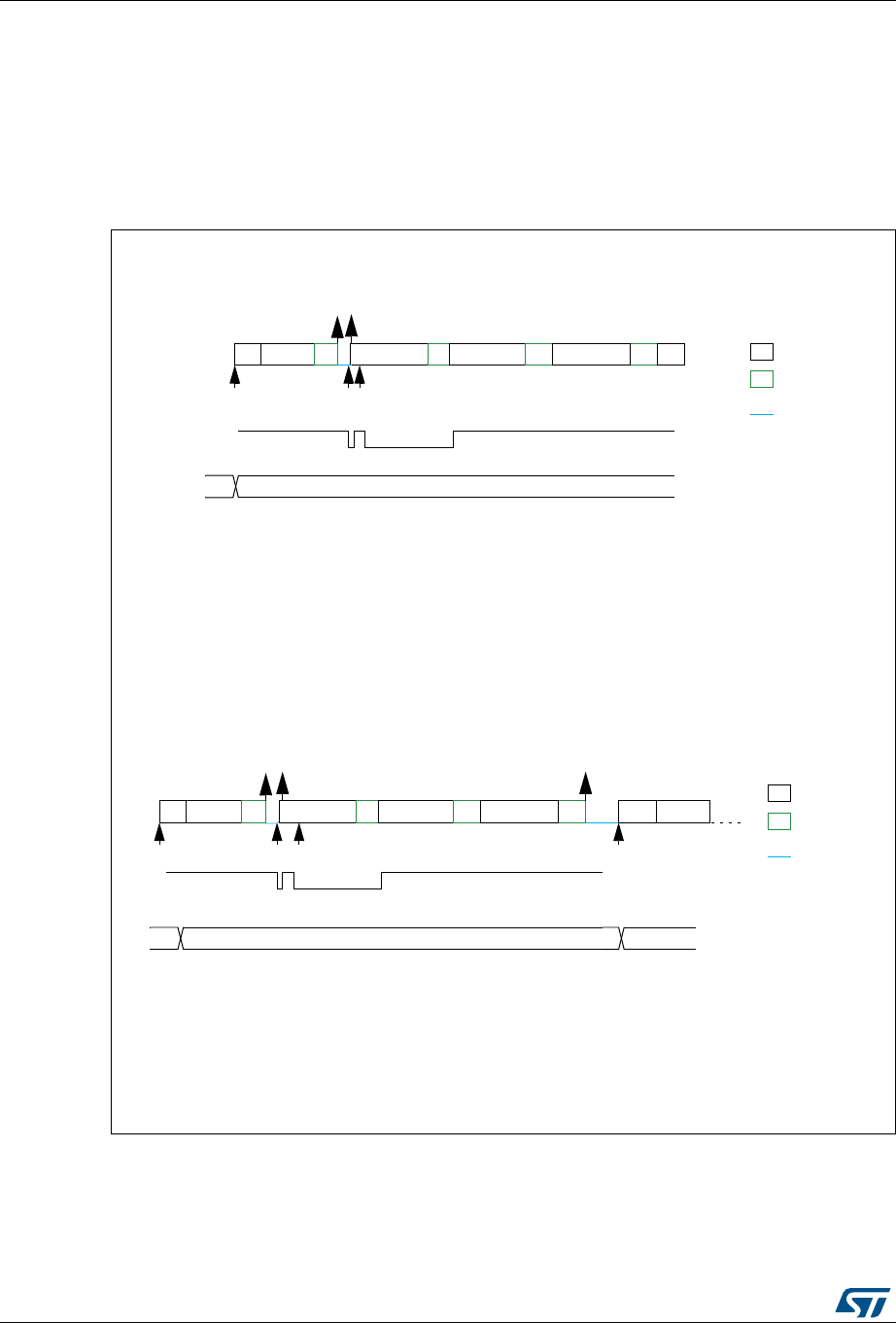
Inter-integrated circuit (I2C) interface RM0394
1170/1600 RM0394 Rev 4
When the SMBus master wants to send a RESTART condition after the PEC, software
mode must be selected (AUTOEND=0). In this case, once NBYTES-1 have been
transmitted, the I2C_PECR register content is transmitted and the TC flag is set after the
PEC transmission, stretching the SCL line low. The RESTART condition must be
programmed in the TC interrupt subroutine.
Caution: The PECBYTE bit has no effect when the RELOAD bit is set.
Figure 380. Bus transfer diagrams for SMBus master transmitter
069
([DPSOH60%XVPDVWHUWUDQVPLWWHUE\WHV3(&DXWRPDWLFHQGPRGH6723
$GGUHVV
6
,1,7SURJUDP6ODYHDGGUHVVSURJUDP1%<7(6 $872(1' VHW3(&%<7(VHW67$57
(97;,6,65ZUGDWD
(97;,6,65ZUGDWD
$
GDWD
$
7;,6 7;,6
GDWD
$
1%<7(6
$
OHJHQG
WUDQVPLVVLRQ
UHFHSWLRQ
6&/VWUHWFK
(9
[[
,1,7
([DPSOH60%XVPDVWHUWUDQVPLWWHUE\WHV3(&VRIWZDUHHQGPRGH5(67$57
,1,7SURJUDP6ODYHDGGUHVVSURJUDP1%<7(6 $872(1' VHW3(&%<7(VHW67$57
(97;,6,65ZUGDWD
(97;,6,65ZUGDWD
(97&,65SURJUDP6ODYHDGGUHVVSURJUDP1%<7(6 1VHW67$57
1%<7(6
5VWDUW
OHJHQG
WUDQVPLVVLRQ
UHFHSWLRQ
6&/VWUHWFK
[[
$GGUHVV
1
3(&
3
(9
$
7;(
$GGUHVV
6
$
GDWD
$
7;,6 7;,6
GDWD
$
(9
,1,7
3(&
(9
7&
(9

RM0394 Rev 4 1171/1600
RM0394 Inter-integrated circuit (I2C) interface
1193
SMBus Master receiver
When the SMBus master wants to receive the PEC followed by a STOP at the end of the
transfer, automatic end mode can be selected (AUTOEND=1). The PECBYTE bit must be
set and the slave address must be programmed, before setting the START bit. In this case,
after NBYTES-1 data have been received, the next received byte is automatically checked
versus the I2C_PECR register content. A NACK response is given to the PEC byte, followed
by a STOP condition.
When the SMBus master receiver wants to receive the PEC byte followed by a RESTART
condition at the end of the transfer, software mode must be selected (AUTOEND=0). The
PECBYTE bit must be set and the slave address must be programmed, before setting the
START bit. In this case, after NBYTES-1 data have been received, the next received byte is
automatically checked versus the I2C_PECR register content. The TC flag is set after the
PEC byte reception, stretching the SCL line low. The RESTART condition can be
programmed in the TC interrupt subroutine.
Caution: The PECBYTE bit has no effect when the RELOAD bit is set.
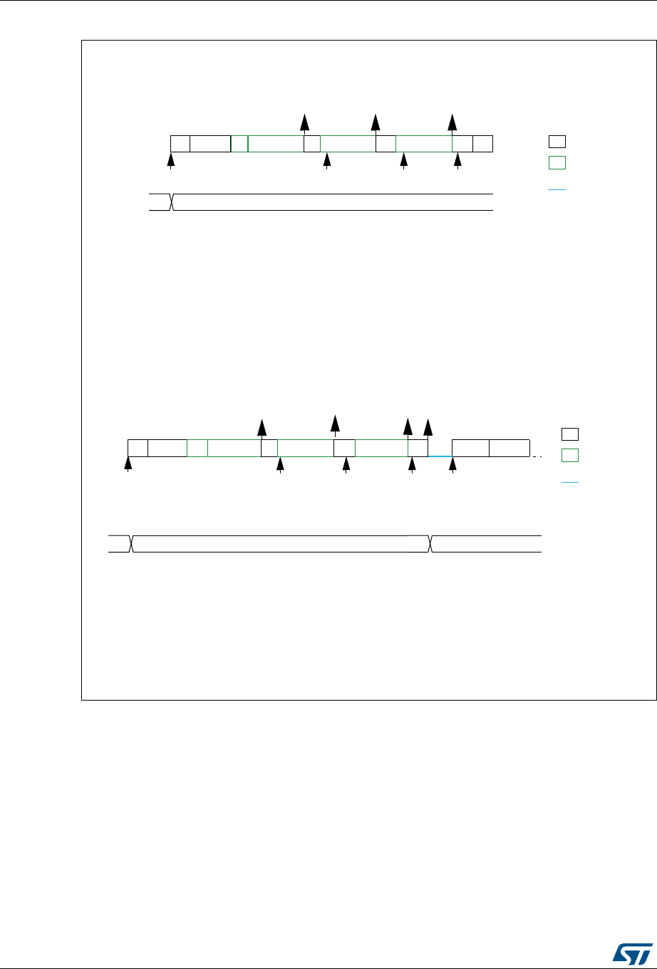
Inter-integrated circuit (I2C) interface RM0394
1172/1600 RM0394 Rev 4
Figure 381. Bus transfer diagrams for SMBus master receiver
069
([DPSOH60%XVPDVWHUUHFHLYHUE\WHV3(&DXWRPDWLFHQGPRGH6723
$GGUHVV
6
,1,7SURJUDP6ODYHDGGUHVVSURJUDP1%<7(6 $872(1' VHW3(&%<7(VHW67$57
(95;1(,65UGGDWD
(95;1(,65UGGDWD
(95;1(,65UG3(&
$
GDWD
$
5;1( 5;1(
GDWD
$
1%<7(6
1$
OHJHQG
WUDQVPLVVLRQ
UHFHSWLRQ
6&/VWUHWFK
9(9(
[[
,1,7
([DPSOH60%XVPDVWHUUHFHLYHUE\WHV3(&VRIWZDUHHQGPRGH5(67$57
$GGUHVV
6
,1,7SURJUDP6ODYHDGGUHVVSURJUDP1%<7(6 $872(1' VHW3(&%<7(VHW67$57
(95;1(,65UGGDWD
(95;1(,65UGGDWD
(95;1(,65UHDG3(&
(97&,65SURJUDP6ODYHDGGUHVVSURJUDP1%<7(6 1VHW67$57
$
GDWD
$
5;1( 5;1(
GDWD
$
1%<7(6
5HVWDUW
OHJHQG
WUDQVPLVVLRQ
UHFHSWLRQ
6&/VWUHWFK
(9 (9
[[
,1,7
$GGUHVV
1
3(&
3
5;1(
(9
1$
3(&
5;1(
(9
7&
(9

RM0394 Rev 4 1173/1600
RM0394 Inter-integrated circuit (I2C) interface
1193
37.4.14 Wakeup from Stop mode on address match
This section is relevant only when Wakeup from Stop mode feature is supported. Refer to
Section 37.3: I2C implementation.
The I2C is able to wakeup the MCU from Stop mode (APB clock is off), when it is
addressed. All addressing modes are supported.
Wakeup from Stop mode is enabled by setting the WUPEN bit in the I2C_CR1 register. The
HSI16 oscillator must be selected as the clock source for I2CCLK in order to allow wakeup
from Stop mode.
During Stop mode, the HSI16 is switched off. When a START is detected, the I2C interface
switches the HSI16 on, and stretches SCL low until HSI16 is woken up.
HSI16 is then used for the address reception.
In case of an address match, the I2C stretches SCL low during MCU wakeup time. The
stretch is released when ADDR flag is cleared by software, and the transfer goes on
normally.
If the address does not match, the HSI16 is switched off again and the MCU is not woken
up.
Note: If the I2C clock is the system clock, or if WUPEN = 0, the HSI16 is not switched on after a
START is received.
Only an ADDR interrupt can wakeup the MCU. Therefore do not enter Stop mode when the
I2C is performing a transfer as a master, or as an addressed slave after the ADDR flag is
set. This can be managed by clearing SLEEPDEEP bit in the ADDR interrupt routine and
setting it again only after the STOPF flag is set.
Caution: The digital filter is not compatible with the wakeup from Stop mode feature. If the DNF bit is
not equal to 0, setting the WUPEN bit has no effect.
Caution: This feature is available only when the I2C clock source is the HSI16 oscillator.
Caution: Clock stretching must be enabled (NOSTRETCH=0) to ensure proper operation of the
wakeup from Stop mode feature.
Caution: If wakeup from Stop mode is disabled (WUPEN=0), the I2C peripheral must be disabled
before entering Stop mode (PE=0).
37.4.15 Error conditions
The following are the error conditions which may cause communication to fail.
Bus error (BERR)
A bus error is detected when a START or a STOP condition is detected and is not located
after a multiple of 9 SCL clock pulses. A START or a STOP condition is detected when a
SDA edge occurs while SCL is high.
The bus error flag is set only if the I2C is involved in the transfer as master or addressed
slave (i.e not during the address phase in slave mode).
In case of a misplaced START or RESTART detection in slave mode, the I2C enters
address recognition state like for a correct START condition.
When a bus error is detected, the BERR flag is set in the I2C_ISR register, and an interrupt
is generated if the ERRIE bit is set in the I2C_CR1 register.

Inter-integrated circuit (I2C) interface RM0394
1174/1600 RM0394 Rev 4
Arbitration lost (ARLO)
An arbitration loss is detected when a high level is sent on the SDA line, but a low level is
sampled on the SCL rising edge.
•In master mode, arbitration loss is detected during the address phase, data phase and
data acknowledge phase. In this case, the SDA and SCL lines are released, the
START control bit is cleared by hardware and the master switches automatically to
slave mode.
•In slave mode, arbitration loss is detected during data phase and data acknowledge
phase. In this case, the transfer is stopped, and the SCL and SDA lines are released.
When an arbitration loss is detected, the ARLO flag is set in the I2C_ISR register, and an
interrupt is generated if the ERRIE bit is set in the I2C_CR1 register.
Overrun/underrun error (OVR)
An overrun or underrun error is detected in slave mode when NOSTRETCH=1 and:
•In reception when a new byte is received and the RXDR register has not been read yet.
The new received byte is lost, and a NACK is automatically sent as a response to the
new byte.
•In transmission:
– When STOPF=1 and the first data byte should be sent. The content of the
I2C_TXDR register is sent if TXE=0, 0xFF if not.
– When a new byte must be sent and the I2C_TXDR register has not been written
yet, 0xFF is sent.
When an overrun or underrun error is detected, the OVR flag is set in the I2C_ISR register,
and an interrupt is generated if the ERRIE bit is set in the I2C_CR1 register.
Packet Error Checking Error (PECERR)
This section is relevant only when the SMBus feature is supported. Refer to Section 37.3:
I2C implementation.
A PEC error is detected when the received PEC byte does not match with the I2C_PECR
register content. A NACK is automatically sent after the wrong PEC reception.
When a PEC error is detected, the PECERR flag is set in the I2C_ISR register, and an
interrupt is generated if the ERRIE bit is set in the I2C_CR1 register.
Timeout Error (TIMEOUT)
This section is relevant only when the SMBus feature is supported. Refer to Section 37.3:
I2C implementation.
A timeout error occurs for any of these conditions:
•TIDLE=0 and SCL remained low for the time defined in the TIMEOUTA[11:0] bits: this is
used to detect a SMBus timeout.
•TIDLE=1 and both SDA and SCL remained high for the time defined in the TIMEOUTA
[11:0] bits: this is used to detect a bus idle condition.
•Master cumulative clock low extend time reached the time defined in the
TIMEOUTB[11:0] bits (SMBus tLOW:MEXT parameter)
•Slave cumulative clock low extend time reached the time defined in TIMEOUTB[11:0]
bits (SMBus tLOW:SEXT parameter)

RM0394 Rev 4 1175/1600
RM0394 Inter-integrated circuit (I2C) interface
1193
When a timeout violation is detected in master mode, a STOP condition is automatically
sent.
When a timeout violation is detected in slave mode, SDA and SCL lines are automatically
released.
When a timeout error is detected, the TIMEOUT flag is set in the I2C_ISR register, and an
interrupt is generated if the ERRIE bit is set in the I2C_CR1 register.
Alert (ALERT)
This section is relevant only when the SMBus feature is supported. Refer to Section 37.3:
I2C implementation.
The ALERT flag is set when the I2C interface is configured as a Host (SMBHEN=1), the
alert pin detection is enabled (ALERTEN=1) and a falling edge is detected on the SMBA pin.
An interrupt is generated if the ERRIE bit is set in the I2C_CR1 register.
37.4.16 DMA requests
Transmission using DMA
DMA (Direct Memory Access) can be enabled for transmission by setting the TXDMAEN bit
in the I2C_CR1 register. Data is loaded from an SRAM area configured using the DMA
peripheral (see Section 11: Direct memory access controller (DMA) on page 295) to the
I2C_TXDR register whenever the TXIS bit is set.
Only the data are transferred with DMA.
•In master mode: the initialization, the slave address, direction, number of bytes and
START bit are programmed by software (the transmitted slave address cannot be
transferred with DMA). When all data are transferred using DMA, the DMA must be
initialized before setting the START bit. The end of transfer is managed with the
NBYTES counter. Refer to Master transmitter on page 1151.
•In slave mode:
– With NOSTRETCH=0, when all data are transferred using DMA, the DMA must be
initialized before the address match event, or in ADDR interrupt subroutine, before
clearing ADDR.
– With NOSTRETCH=1, the DMA must be initialized before the address match
event.
•For instances supporting SMBus: the PEC transfer is managed with NBYTES counter.
Refer to SMBus Slave transmitter on page 1165 and SMBus Master transmitter on
page 1169.
Note: If DMA is used for transmission, the TXIE bit does not need to be enabled.
Reception using DMA
DMA (Direct Memory Access) can be enabled for reception by setting the RXDMAEN bit in
the I2C_CR1 register. Data is loaded from the I2C_RXDR register to an SRAM area
configured using the DMA peripheral (refer to Section 11: Direct memory access controller
(DMA) on page 295) whenever the RXNE bit is set. Only the data (including PEC) are
transferred with DMA.
•In master mode, the initialization, the slave address, direction, number of bytes and
START bit are programmed by software. When all data are transferred using DMA, the

Inter-integrated circuit (I2C) interface RM0394
1176/1600 RM0394 Rev 4
DMA must be initialized before setting the START bit. The end of transfer is managed
with the NBYTES counter.
•In slave mode with NOSTRETCH=0, when all data are transferred using DMA, the
DMA must be initialized before the address match event, or in the ADDR interrupt
subroutine, before clearing the ADDR flag.
•If SMBus is supported (see Section 37.3: I2C implementation): the PEC transfer is
managed with the NBYTES counter. Refer to SMBus Slave receiver on page 1167 and
SMBus Master receiver on page 1171.
Note: If DMA is used for reception, the RXIE bit does not need to be enabled.
37.4.17 Debug mode
When the microcontroller enters debug mode (core halted), the SMBus timeout either
continues to work normally or stops, depending on the DBG_I2Cx_SMBUS_TIMEOUT
configuration bits in the DBG module.
37.5 I2C low-power modes
Table 189. Effect of low-power modes on the I2C
Mode Description
Sleep No effect. I2C interrupts cause the device to exit the Sleep mode.
Stop(1)(2)
1. The ADDR match event can wake-up the device from Stop mode only if the I2C instance supports the
Wakeup from Stop mode feature. Refer to I2C implementation table.
2. Only I2C3 supports wakeup from Stop 2 mode. The other I2C instances must be disabled before entering
Stop 2 mode.
The I2C registers content is kept. If WUPEN = 1 and I2C is clocked by an internal
oscillator (HSI16): the address recognition is functional. The I2C address match
condition causes the device to exit the Stop mode. If WUPEN=0: the I2C must be
disabled before entering Stop mode
Standby The I2C peripheral is powered down and must be reinitialized after exiting
Standby mode.

RM0394 Rev 4 1177/1600
RM0394 Inter-integrated circuit (I2C) interface
1193
37.6 I2C interrupts
The table below gives the list of I2C interrupt requests.
37.7 I2C registers
Refer to Section 1.2 on page 60 for a list of abbreviations used in register descriptions.
The peripheral registers are accessed by words (32-bit).
37.7.1 I2C control register 1 (I2C_CR1)
Address offset: 0x00
Reset value: 0x0000 0000
Access: No wait states, except if a write access occurs while a write access to this register is
ongoing. In this case, wait states are inserted in the second write access until the previous
one is completed. The latency of the second write access can be up to
2xPCLK1+6xI2CCLK.
Table 190. I2C Interrupt requests
Interrupt
acronym Interrupt event Event flag Enable
control bit
Interrupt clear
method
Exit the
Sleep mode
Exit the
Stop mode
I2C
I2C_EV
Receive buffer not
empty RXNE RXIE Read I2C_RXDR
register
Yes
No
Transmit buffer
interrupt status TXIS TXIE Write I2C_TXDR
register
Stop detection
interrupt flag STOPF STOPIE Write STOPCF=1
Transfer Complete
Reload TCR
TCIE
Write I2C_CR2
with NBYTES[7:0]
0
Transfer complete TC Write START=1 or
STOP=1
Address matched ADDR ADDRIE Write ADDRCF=1 Yes(1)
NACK reception NACKF NACKIE Write NACKCF=1 No
I2C_ER
Bus error BERR
ERRIE
Write BERRCF=1
Yes No
Arbitration loss ARLO Write ARLOCF=1
Overrun/Underrun OVR Write OVRCF=1
PEC error PECERR Write
PECERRCF=1
Timeout/tLOW error TIMEOUT Write
TIMEOUTCF=1
SMBus Alert ALERT Write ALERTCF=1
1. The ADDR match event can wake up the device from Stop mode only if the I2C instance supports the Wakeup from Stop
mode feature. Refer to Section 37.3: I2C implementation.

Inter-integrated circuit (I2C) interface RM0394
1178/1600 RM0394 Rev 4
31 30 29 28 27 26 25 24 23 22 21 20 19 18 17 16
Res. Res. Res. Res. Res. Res. Res. Res. PECEN ALERT
EN
SMBD
EN
SMBH
EN GCEN WUPE
N
NOSTR
ETCH SBC
rw rw rw rw rw rw rw rw
15141312111098 7 6543210
RXDMA
EN
TXDMA
EN Res. ANF
OFF DNF[3:0] ERRIE TCIE STOP
IE
NACK
IE
ADDR
IE RXIE TXIE PE
rw rw rw rw rw rw rw rw rw rw rw rw rw rw rw
Bits 31:24 Reserved, must be kept at reset value.
Bit 23 PECEN: PEC enable
0: PEC calculation disabled
1: PEC calculation enabled
Note: If the SMBus feature is not supported, this bit is reserved and forced by hardware to ‘0’.
Refer to Section 37.3: I2C implementation.
Bit 22 ALERTEN: SMBus alert enable
Device mode (SMBHEN=0):
0: Releases SMBA pin high and Alert Response Address Header disabled: 0001100x
followed by NACK.
1: Drives SMBA pin low and Alert Response Address Header enables: 0001100x followed by
ACK.
Host mode (SMBHEN=1):
0: SMBus Alert pin (SMBA) not supported.
1: SMBus Alert pin (SMBA) supported.
Note: When ALERTEN=0, the SMBA pin can be used as a standard GPIO.
If the SMBus feature is not supported, this bit is reserved and forced by hardware to ‘0’.
Refer to Section 37.3: I2C implementation.
Bit 21 SMBDEN: SMBus Device Default address enable
0: Device default address disabled. Address 0b1100001x is NACKed.
1: Device default address enabled. Address 0b1100001x is ACKed.
Note: If the SMBus feature is not supported, this bit is reserved and forced by hardware to ‘0’.
Refer to Section 37.3: I2C implementation.
Bit 20 SMBHEN: SMBus Host address enable
0: Host address disabled. Address 0b0001000x is NACKed.
1: Host address enabled. Address 0b0001000x is ACKed.
Note: If the SMBus feature is not supported, this bit is reserved and forced by hardware to ‘0’.
Refer to Section 37.3: I2C implementation.
Bit 19 GCEN: General call enable
0: General call disabled. Address 0b00000000 is NACKed.
1: General call enabled. Address 0b00000000 is ACKed.
Bit 18 WUPEN: Wakeup from Stop mode enable
0: Wakeup from Stop mode disable.
1: Wakeup from Stop mode enable.
Note: If the Wakeup from Stop mode feature is not supported, this bit is reserved and forced
by hardware to ‘0’. Refer to Section 37.3: I2C implementation.
Note: WUPEN can be set only when DNF = ‘0000’

RM0394 Rev 4 1179/1600
RM0394 Inter-integrated circuit (I2C) interface
1193
Bit 17 NOSTRETCH: Clock stretching disable
This bit is used to disable clock stretching in slave mode. It must be kept cleared in master
mode.
0: Clock stretching enabled
1: Clock stretching disabled
Note: This bit can only be programmed when the I2C is disabled (PE = 0).
Bit 16 SBC: Slave byte control
This bit is used to enable hardware byte control in slave mode.
0: Slave byte control disabled
1: Slave byte control enabled
Bit 15 RXDMAEN: DMA reception requests enable
0: DMA mode disabled for reception
1: DMA mode enabled for reception
Bit 14 TXDMAEN: DMA transmission requests enable
0: DMA mode disabled for transmission
1: DMA mode enabled for transmission
Bit 13 Reserved, must be kept at reset value.
Bit 12 ANFOFF: Analog noise filter OFF
0: Analog noise filter enabled
1: Analog noise filter disabled
Note: This bit can only be programmed when the I2C is disabled (PE = 0).
Bits 11:8 DNF[3:0]: Digital noise filter
These bits are used to configure the digital noise filter on SDA and SCL input. The digital
filter, filters spikes with a length of up to DNF[3:0] * tI2CCLK
0000: Digital filter disabled
0001: Digital filter enabled and filtering capability up to 1 tI2CCLK
...
1111: digital filter enabled and filtering capability up to15 tI2CCLK
Note: If the analog filter is also enabled, the digital filter is added to the analog filter.
This filter can only be programmed when the I2C is disabled (PE = 0).
Bit 7 ERRIE: Error interrupts enable
0: Error detection interrupts disabled
1: Error detection interrupts enabled
Note: Any of these errors generate an interrupt:
Arbitration Loss (ARLO)
Bus Error detection (BERR)
Overrun/Underrun (OVR)
Timeout detection (TIMEOUT)
PEC error detection (PECERR)
Alert pin event detection (ALERT)
Bit 6 TCIE: Transfer Complete interrupt enable
0: Transfer Complete interrupt disabled
1: Transfer Complete interrupt enabled
Note: Any of these events generate an interrupt:
Transfer Complete (TC)
Transfer Complete Reload (TCR)

Inter-integrated circuit (I2C) interface RM0394
1180/1600 RM0394 Rev 4
37.7.2 I2C control register 2 (I2C_CR2)
Address offset: 0x0C4
Reset value: 0x0000 0000
Access: No wait states, except if a write access occurs while a write access to this register is
ongoing. In this case, wait states are inserted in the second write access until the previous
one is completed. The latency of the second write access can be up to 2 x PCLK1 + 6 x
I2CCLK.
Bit 5 STOPIE: Stop detection Interrupt enable
0: Stop detection (STOPF) interrupt disabled
1: Stop detection (STOPF) interrupt enabled
Bit 4 NACKIE: Not acknowledge received Interrupt enable
0: Not acknowledge (NACKF) received interrupts disabled
1: Not acknowledge (NACKF) received interrupts enabled
Bit 3 ADDRIE: Address match Interrupt enable (slave only)
0: Address match (ADDR) interrupts disabled
1: Address match (ADDR) interrupts enabled
Bit 2 RXIE: RX Interrupt enable
0: Receive (RXNE) interrupt disabled
1: Receive (RXNE) interrupt enabled
Bit 1 TXIE: TX Interrupt enable
0: Transmit (TXIS) interrupt disabled
1: Transmit (TXIS) interrupt enabled
Bit 0 PE: Peripheral enable
0: Peripheral disable
1: Peripheral enable
Note: When PE=0, the I2C SCL and SDA lines are released. Internal state machines and
status bits are put back to their reset value. When cleared, PE must be kept low for at
least 3 APB clock cycles.
31 30 29 28 27 26 25 24 23 22 21 20 19 18 17 16
Res. Res. Res. Res. Res. PEC
BYTE
AUTOE
ND
RE
LOAD NBYTES[7:0]
rs rw rw rw rw rw rw rw rw rw rw
1514131211109876543210
NACK STOP START HEAD1
0R ADD10 RD_
WRN SADD[9:0]
rs rs rs rw rw rw rw rw rw rw rw rw rw rw rw rw

RM0394 Rev 4 1181/1600
RM0394 Inter-integrated circuit (I2C) interface
1193
Bits 31:27 Reserved, must be kept at reset value.
Bit 26 PECBYTE: Packet error checking byte
This bit is set by software, and cleared by hardware when the PEC is transferred, or when a
STOP condition or an Address matched is received, also when PE=0.
0: No PEC transfer.
1: PEC transmission/reception is requested
Note: Writing ‘0’ to this bit has no effect.
This bit has no effect when RELOAD is set.
This bit has no effect is slave mode when SBC=0.
If the SMBus feature is not supported, this bit is reserved and forced by hardware to ‘0’.
Refer to Section 37.3: I2C implementation.
Bit 25 AUTOEND: Automatic end mode (master mode)
This bit is set and cleared by software.
0: software end mode: TC flag is set when NBYTES data are transferred, stretching SCL low.
1: Automatic end mode: a STOP condition is automatically sent when NBYTES data are
transferred.
Note: This bit has no effect in slave mode or when the RELOAD bit is set.
Bit 24 RELOAD: NBYTES reload mode
This bit is set and cleared by software.
0: The transfer is completed after the NBYTES data transfer (STOP or RESTART follows).
1: The transfer is not completed after the NBYTES data transfer (NBYTES is reloaded). TCR
flag is set when NBYTES data are transferred, stretching SCL low.
Bits 23:16 NBYTES[7:0]: Number of bytes
The number of bytes to be transmitted/received is programmed there. This field is don’t care
in slave mode with SBC=0.
Note: Changing these bits when the START bit is set is not allowed.
Bit 15 NACK: NACK generation (slave mode)
The bit is set by software, cleared by hardware when the NACK is sent, or when a STOP
condition or an Address matched is received, or when PE=0.
0: an ACK is sent after current received byte.
1: a NACK is sent after current received byte.
Note: Writing ‘0’ to this bit has no effect.
This bit is used in slave mode only: in master receiver mode, NACK is automatically
generated after last byte preceding STOP or RESTART condition, whatever the NACK
bit value.
When an overrun occurs in slave receiver NOSTRETCH mode, a NACK is
automatically generated whatever the NACK bit value.
When hardware PEC checking is enabled (PECBYTE=1), the PEC acknowledge value
does not depend on the NACK value.
Bit 14 STOP: Stop generation (master mode)
The bit is set by software, cleared by hardware when a STOP condition is detected, or when
PE = 0.
In Master Mode:
0: No Stop generation.
1: Stop generation after current byte transfer.
Note: Writing ‘0’ to this bit has no effect.

Inter-integrated circuit (I2C) interface RM0394
1182/1600 RM0394 Rev 4
Bit 13 START: Start generation
This bit is set by software, and cleared by hardware after the Start followed by the address
sequence is sent, by an arbitration loss, by a timeout error detection, or when PE = 0. It can
also be cleared by software by writing ‘1’ to the ADDRCF bit in the I2C_ICR register.
0: No Start generation.
1: Restart/Start generation:
If the I2C is already in master mode with AUTOEND = 0, setting this bit generates a
Repeated Start condition when RELOAD=0, after the end of the NBYTES transfer.
Otherwise setting this bit generates a START condition once the bus is free.
Note: Writing ‘0’ to this bit has no effect.
The START bit can be set even if the bus is BUSY or I2C is in slave mode.
This bit has no effect when RELOAD is set.
Bit 12 HEAD10R: 10-bit address header only read direction (master receiver mode)
0: The master sends the complete 10 bit slave address read sequence: Start + 2 bytes 10bit
address in write direction + Restart + 1st 7 bits of the 10 bit address in read direction.
1: The master only sends the 1st 7 bits of the 10 bit address, followed by Read direction.
Note: Changing this bit when the START bit is set is not allowed.
Bit 11 ADD10: 10-bit addressing mode (master mode)
0: The master operates in 7-bit addressing mode,
1: The master operates in 10-bit addressing mode
Note: Changing this bit when the START bit is set is not allowed.
Bit 10 RD_WRN: Transfer direction (master mode)
0: Master requests a write transfer.
1: Master requests a read transfer.
Note: Changing this bit when the START bit is set is not allowed.
Bits 9:8 SADD[9:8]: Slave address bit 9:8 (master mode)
In 7-bit addressing mode (ADD10 = 0):
These bits are don’t care
In 10-bit addressing mode (ADD10 = 1):
These bits should be written with bits 9:8 of the slave address to be sent
Note: Changing these bits when the START bit is set is not allowed.
Bits 7:1 SADD[7:1]: Slave address bit 7:1 (master mode)
In 7-bit addressing mode (ADD10 = 0):
These bits should be written with the 7-bit slave address to be sent
In 10-bit addressing mode (ADD10 = 1):
These bits should be written with bits 7:1 of the slave address to be sent.
Note: Changing these bits when the START bit is set is not allowed.
Bit 0 SADD0: Slave address bit 0 (master mode)
In 7-bit addressing mode (ADD10 = 0):
This bit is don’t care
In 10-bit addressing mode (ADD10 = 1):
This bit should be written with bit 0 of the slave address to be sent
Note: Changing these bits when the START bit is set is not allowed.

RM0394 Rev 4 1183/1600
RM0394 Inter-integrated circuit (I2C) interface
1193
37.7.3 I2C own address 1 register (I2C_OAR1)
Address offset: 0x08
Reset value: 0x0000 0000
Access: No wait states, except if a write access occurs while a write access to this register is
ongoing. In this case, wait states are inserted in the second write access until the previous
one is completed. The latency of the second write access can be up to 2 x PCLK1 + 6 x
I2CCLK.
31 30 29 28 27 26 25 24 23 22 21 20 19 18 17 16
Res. Res. Res. Res. Res. Res. Res. Res. Res. Res. Res. Res. Res. Res. Res. Res.
1514131211109876543210
OA1EN Res. Res. Res. Res. OA1
MODE OA1[9:8] OA1[7:1] OA1[0]
rw rw rw rw rw rw rw rw rw rw rw rw
Bits 31:16 Reserved, must be kept at reset value.
Bit 15 OA1EN: Own Address 1 enable
0: Own address 1 disabled. The received slave address OA1 is NACKed.
1: Own address 1 enabled. The received slave address OA1 is ACKed.
Bits 14:11 Reserved, must be kept at reset value.
Bit 10 OA1MODE: Own Address 1 10-bit mode
0: Own address 1 is a 7-bit address.
1: Own address 1 is a 10-bit address.
Note: This bit can be written only when OA1EN=0.
Bits 9:8 OA1[9:8]: Interface address
7-bit addressing mode: do not care
10-bit addressing mode: bits 9:8 of address
Note: These bits can be written only when OA1EN=0.
Bits 7:1 OA1[7:1]: Interface address
7-bit addressing mode: 7-bit address
10-bit addressing mode: bits 7:1 of 10-bit address
Note: These bits can be written only when OA1EN=0.
Bit 0 OA1[0]: Interface address
7-bit addressing mode: do not care
10-bit addressing mode: bit 0 of address
Note: This bit can be written only when OA1EN=0.

Inter-integrated circuit (I2C) interface RM0394
1184/1600 RM0394 Rev 4
37.7.4 I2C own address 2 register (I2C_OAR2)
Address offset: 0x0C
Reset value: 0x0000 0000
Access: No wait states, except if a write access occurs while a write access to this register is
ongoing. In this case, wait states are inserted in the second write access until the previous
one is completed. The latency of the second write access can be up to 2 x PCLK1 + 6 x
I2CCLK.
31 30 29 28 27 26 25 24 23 22 21 20 19 18 17 16
Res. Res. Res. Res. Res. Res. Res. Res. Res. Res. Res. Res. Res. Res. Res. Res.
1514131211109876543210
OA2EN Res. Res. Res. Res. OA2MSK[2:0] OA2[7:1] Res.
rw rw rw rw rw rw rw rw rw rw rw
Bits 31:16 Reserved, must be kept at reset value.
Bit 15 OA2EN: Own Address 2 enable
0: Own address 2 disabled. The received slave address OA2 is NACKed.
1: Own address 2 enabled. The received slave address OA2 is ACKed.
Bits 14:11 Reserved, must be kept at reset value.
Bits 10:8 OA2MSK[2:0]: Own Address 2 masks
000: No mask
001: OA2[1] is masked and don’t care. Only OA2[7:2] are compared.
010: OA2[2:1] are masked and don’t care. Only OA2[7:3] are compared.
011: OA2[3:1] are masked and don’t care. Only OA2[7:4] are compared.
100: OA2[4:1] are masked and don’t care. Only OA2[7:5] are compared.
101: OA2[5:1] are masked and don’t care. Only OA2[7:6] are compared.
110: OA2[6:1] are masked and don’t care. Only OA2[7] is compared.
111: OA2[7:1] are masked and don’t care. No comparison is done, and all (except reserved)
7-bit received addresses are acknowledged.
Note: These bits can be written only when OA2EN=0.
As soon as OA2MSK is not equal to 0, the reserved I2C addresses (0b0000xxx and
0b1111xxx) are not acknowledged even if the comparison matches.
Bits 7:1 OA2[7:1]: Interface address
7-bit addressing mode: 7-bit address
Note: These bits can be written only when OA2EN=0.
Bit 0 Reserved, must be kept at reset value.

RM0394 Rev 4 1185/1600
RM0394 Inter-integrated circuit (I2C) interface
1193
37.7.5 I2C timing register (I2C_TIMINGR)
Address offset: 0x10
Reset value: 0x0000 0000
Access: No wait states
Note: This register must be configured when the I2C is disabled (PE = 0).
Note: The STM32CubeMX tool calculates and provides the I2C_TIMINGR content in the I2C
Configuration window.
31 30 29 28 27 26 25 24 23 22 21 20 19 18 17 16
PRESC[3:0] Res. Res. Res. Res. SCLDEL[3:0] SDADEL[3:0]
rw rw rw rw rw rw rw rw rw rw rw rw
15 14 13 12 11 10 9 8 7 6 5 4 3 2 1 0
SCLH[7:0] SCLL[7:0]
rw rw rw rw rw rw rw rw rw rw rw rw rw rw rw rw
Bits 31:28 PRESC[3:0]: Timing prescaler
This field is used to prescale I2CCLK in order to generate the clock period tPRESC used for
data setup and hold counters (refer to I2C timings on page 1132) and for SCL high and low
level counters (refer to I2C master initialization on page 1147).
tPRESC = (PRESC+1) x tI2CCLK
Bits 27:24 Reserved, must be kept at reset value.
Bits 23:20 SCLDEL[3:0]: Data setup time
This field is used to generate a delay tSCLDEL between SDA edge and SCL rising edge. In
master mode and in slave mode with NOSTRETCH = 0, the SCL line is stretched low during
tSCLDEL.
tSCLDEL = (SCLDEL+1) x tPRESC
Note: tSCLDEL is used to generate tSU:DAT timing.
Bits 19:16 SDADEL[3:0]: Data hold time
This field is used to generate the delay tSDADEL between SCL falling edge and SDA edge. In
master mode and in slave mode with NOSTRETCH = 0, the SCL line is stretched low during
tSDADEL.
tSDADEL= SDADEL x tPRESC
Note: SDADEL is used to generate tHD:DAT timing.
Bits 15:8 SCLH[7:0]: SCL high period (master mode)
This field is used to generate the SCL high period in master mode.
tSCLH = (SCLH+1) x tPRESC
Note: SCLH is also used to generate tSU:STO and tHD:STA timing.
Bits 7:0 SCLL[7:0]: SCL low period (master mode)
This field is used to generate the SCL low period in master mode.
tSCLL = (SCLL+1) x tPRESC
Note: SCLL is also used to generate tBUF and tSU:STA timings.

Inter-integrated circuit (I2C) interface RM0394
1186/1600 RM0394 Rev 4
37.7.6 I2C timeout register (I2C_TIMEOUTR)
Address offset: 0x14
Reset value: 0x0000 0000
Access: No wait states, except if a write access occurs while a write access to this register is
ongoing. In this case, wait states are inserted in the second write access until the previous
one is completed. The latency of the second write access can be up to 2 x PCLK1 + 6 x
I2CCLK.
Note: If the SMBus feature is not supported, this register is reserved and forced by hardware to
“0x00000000”. Refer to Section 37.3: I2C implementation.
31 30 29 28 27 26 25 24 23 22 21 20 19 18 17 16
TEXTEN Res. Res. Res. TIMEOUTB[11:0]
rw rw rw rw rw rw rw rw rw rw rw rw rw
15 14 13 12 11109876543210
TIMOUTEN Res. Res. TIDLE TIMEOUTA[11:0]
rw rw rw rw rw rw rw rw rw rw rw rw rw rw
Bit 31 TEXTEN: Extended clock timeout enable
0: Extended clock timeout detection is disabled
1: Extended clock timeout detection is enabled. When a cumulative SCL stretch for more
than tLOW:EXT is done by the I2C interface, a timeout error is detected (TIMEOUT=1).
Bits 30:28 Reserved, must be kept at reset value.
Bits 27:16 TIMEOUTB[11:0]: Bus timeout B
This field is used to configure the cumulative clock extension timeout:
In master mode, the master cumulative clock low extend time (tLOW:MEXT) is detected
In slave mode, the slave cumulative clock low extend time (tLOW:SEXT) is detected
tLOW:EXT= (TIMEOUTB+1) x 2048 x tI2CCLK
Note: These bits can be written only when TEXTEN=0.
Bit 15 TIMOUTEN: Clock timeout enable
0: SCL timeout detection is disabled
1: SCL timeout detection is enabled: when SCL is low for more than tTIMEOUT (TIDLE=0) or
high for more than tIDLE (TIDLE=1), a timeout error is detected (TIMEOUT=1).
Bits 14:13 Reserved, must be kept at reset value.
Bit 12 TIDLE: Idle clock timeout detection
0: TIMEOUTA is used to detect SCL low timeout
1: TIMEOUTA is used to detect both SCL and SDA high timeout (bus idle condition)
Note: This bit can be written only when TIMOUTEN=0.
Bits 11:0 TIMEOUTA[11:0]: Bus Timeout A
This field is used to configure:
The SCL low timeout condition tTIMEOUT when TIDLE=0
tTIMEOUT= (TIMEOUTA+1) x 2048 x tI2CCLK
The bus idle condition (both SCL and SDA high) when TIDLE=1
tIDLE= (TIMEOUTA+1) x 4 x tI2CCLK
Note: These bits can be written only when TIMOUTEN=0.

RM0394 Rev 4 1187/1600
RM0394 Inter-integrated circuit (I2C) interface
1193
37.7.7 I2C interrupt and status register (I2C_ISR)
Address offset: 0x18
Reset value: 0x0000 0001
Access: No wait states
31 30 29 28 27 26 25 24 23 22 21 20 19 18 17 16
Res. Res. Res. Res. Res. Res. Res. Res. ADDCODE[6:0] DIR
rrrrrrrr
1514131211109876543210
BUSY Res. ALERT TIME
OUT
PEC
ERR OVR ARLO BERR TCR TC STOPF NACKF ADDR RXNE TXIS TXE
r rrrrrrrrrrrrrsrs
Bits 31:24 Reserved, must be kept at reset value.
Bits 23:17 ADDCODE[6:0]: Address match code (Slave mode)
These bits are updated with the received address when an address match event occurs
(ADDR = 1).
In the case of a 10-bit address, ADDCODE provides the 10-bit header followed by the 2
MSBs of the address.
Bit 16 DIR: Transfer direction (Slave mode)
This flag is updated when an address match event occurs (ADDR=1).
0: Write transfer, slave enters receiver mode.
1: Read transfer, slave enters transmitter mode.
Bit 15 BUSY: Bus busy
This flag indicates that a communication is in progress on the bus. It is set by hardware
when a START condition is detected. It is cleared by hardware when a STOP condition is
detected, or when PE=0.
Bit 14 Reserved, must be kept at reset value.
Bit 13 ALERT: SMBus alert
This flag is set by hardware when SMBHEN=1 (SMBus host configuration), ALERTEN=1
and a SMBALERT event (falling edge) is detected on SMBA pin. It is cleared by software by
setting the ALERTCF bit.
Note: This bit is cleared by hardware when PE=0.
If the SMBus feature is not supported, this bit is reserved and forced by hardware to ‘0’.
Refer to Section 37.3: I2C implementation.
Bit 12 TIMEOUT: Timeout or tLOW detection flag
This flag is set by hardware when a timeout or extended clock timeout occurred. It is cleared
by software by setting the TIMEOUTCF bit.
Note: This bit is cleared by hardware when PE=0.
If the SMBus feature is not supported, this bit is reserved and forced by hardware to ‘0’.
Refer to Section 37.3: I2C implementation.

Inter-integrated circuit (I2C) interface RM0394
1188/1600 RM0394 Rev 4
Bit 11 PECERR: PEC Error in reception
This flag is set by hardware when the received PEC does not match with the PEC register
content. A NACK is automatically sent after the wrong PEC reception. It is cleared by
software by setting the PECCF bit.
Note: This bit is cleared by hardware when PE=0.
If the SMBus feature is not supported, this bit is reserved and forced by hardware to ‘0’.
Refer to Section 37.3: I2C implementation.
Bit 10 OVR: Overrun/Underrun (slave mode)
This flag is set by hardware in slave mode with NOSTRETCH=1, when an overrun/underrun
error occurs. It is cleared by software by setting the OVRCF bit.
Note: This bit is cleared by hardware when PE=0.
Bit 9 ARLO: Arbitration lost
This flag is set by hardware in case of arbitration loss. It is cleared by software by setting the
ARLOCF bit.
Note: This bit is cleared by hardware when PE=0.
Bit 8 BERR: Bus error
This flag is set by hardware when a misplaced Start or STOP condition is detected whereas
the peripheral is involved in the transfer. The flag is not set during the address phase in slave
mode. It is cleared by software by setting BERRCF bit.
Note: This bit is cleared by hardware when PE=0.
Bit 7 TCR: Transfer Complete Reload
This flag is set by hardware when RELOAD=1 and NBYTES data have been transferred. It is
cleared by software when NBYTES is written to a non-zero value.
Note: This bit is cleared by hardware when PE=0.
This flag is only for master mode, or for slave mode when the SBC bit is set.
Bit 6 TC: Transfer Complete (master mode)
This flag is set by hardware when RELOAD=0, AUTOEND=0 and NBYTES data have been
transferred. It is cleared by software when START bit or STOP bit is set.
Note: This bit is cleared by hardware when PE=0.
Bit 5 STOPF: Stop detection flag
This flag is set by hardware when a STOP condition is detected on the bus and the
peripheral is involved in this transfer:
– either as a master, provided that the STOP condition is generated by the peripheral.
– or as a slave, provided that the peripheral has been addressed previously during
this transfer.
It is cleared by software by setting the STOPCF bit.
Note: This bit is cleared by hardware when PE=0.
Bit 4 NACKF: Not Acknowledge received flag
This flag is set by hardware when a NACK is received after a byte transmission. It is cleared
by software by setting the NACKCF bit.
Note: This bit is cleared by hardware when PE=0.
Bit 3 ADDR: Address matched (slave mode)
This bit is set by hardware as soon as the received slave address matched with one of the
enabled slave addresses. It is cleared by software by setting ADDRCF bit.
Note: This bit is cleared by hardware when PE=0.

RM0394 Rev 4 1189/1600
RM0394 Inter-integrated circuit (I2C) interface
1193
37.7.8 I2C interrupt clear register (I2C_ICR)(
Address offset: 0x1C
Reset value: 0x0000 0000
Access: No wait states
Bit 2 RXNE: Receive data register not empty (receivers)
This bit is set by hardware when the received data is copied into the I2C_RXDR register, and
is ready to be read. It is cleared when I2C_RXDR is read.
Note: This bit is cleared by hardware when PE=0.
Bit 1 TXIS: Transmit interrupt status (transmitters)
This bit is set by hardware when the I2C_TXDR register is empty and the data to be
transmitted must be written in the I2C_TXDR register. It is cleared when the next data to be
sent is written in the I2C_TXDR register.
This bit can be written to ‘1’ by software when NOSTRETCH=1 only, in order to generate a
TXIS event (interrupt if TXIE=1 or DMA request if TXDMAEN=1).
Note: This bit is cleared by hardware when PE=0.
Bit 0 TXE: Transmit data register empty (transmitters)
This bit is set by hardware when the I2C_TXDR register is empty. It is cleared when the next
data to be sent is written in the I2C_TXDR register.
This bit can be written to ‘1’ by software in order to flush the transmit data register
I2C_TXDR.
Note: This bit is set by hardware when PE=0.
31 30 29 28 27 26 25 24 23 22 21 20 19 18 17 16
Res. Res. Res. Res. Res. Res. Res. Res. Res. Res. Res. Res. Res. Res. Res. Res.
1514131211109876543210
Res. Res. ALERT
CF
TIM
OUTCF PECCF OVRCF ARLO
CF
BERR
CF Res. Res. STOP
CF
NACK
CF
ADDR
CF Res. Res. Res.
wwwwww www
Bits 31:14 Reserved, must be kept at reset value.
Bit 13 ALERTCF: Alert flag clear
Writing 1 to this bit clears the ALERT flag in the I2C_ISR register.
Note: If the SMBus feature is not supported, this bit is reserved and forced by hardware to ‘0’.
Refer to Section 37.3: I2C implementation.
Bit 12 TIMOUTCF: Timeout detection flag clear
Writing 1 to this bit clears the TIMEOUT flag in the I2C_ISR register.
Note: If the SMBus feature is not supported, this bit is reserved and forced by hardware to ‘0’.
Refer to Section 37.3: I2C implementation.
Bit 11 PECCF: PEC Error flag clear
Writing 1 to this bit clears the PECERR flag in the I2C_ISR register.
Note: If the SMBus feature is not supported, this bit is reserved and forced by hardware to ‘0’.
Refer to Section 37.3: I2C implementation.

Inter-integrated circuit (I2C) interface RM0394
1190/1600 RM0394 Rev 4
37.7.9 I2C PEC register (I2C_PECR)
Address offset: 0x20
Reset value: 0x0000 0000
Access: No wait states
Note: If the SMBus feature is not supported, this register is reserved and forced by hardware to
“0x00000000”. Refer to Section 37.3: I2C implementation.
Bit 10 OVRCF: Overrun/Underrun flag clear
Writing 1 to this bit clears the OVR flag in the I2C_ISR register.
Bit 9 ARLOCF: Arbitration lost flag clear
Writing 1 to this bit clears the ARLO flag in the I2C_ISR register.
Bit 8 BERRCF: Bus error flag clear
Writing 1 to this bit clears the BERRF flag in the I2C_ISR register.
Bits 7:6 Reserved, must be kept at reset value.
Bit 5 STOPCF: STOP detection flag clear
Writing 1 to this bit clears the STOPF flag in the I2C_ISR register.
Bit 4 NACKCF: Not Acknowledge flag clear
Writing 1 to this bit clears the NACKF flag in I2C_ISR register.
Bit 3 ADDRCF: Address matched flag clear
Writing 1 to this bit clears the ADDR flag in the I2C_ISR register. Writing 1 to this bit also
clears the START bit in the I2C_CR2 register.
Bits 2:0 Reserved, must be kept at reset value.
31 30 29 28 27 26 25 24 23 22 21 20 19 18 17 16
Res. Res. Res. Res. Res. Res. Res. Res. Res. Res. Res. Res. Res. Res. Res. Res.
1514131211109876543210
Res. Res. Res. Res. Res. Res. Res. Res. PEC[7:0]
rrrrrrrr
Bits 31:8 Reserved, must be kept at reset value.
Bits 7:0 PEC[7:0] Packet error checking register
This field contains the internal PEC when PECEN=1.
The PEC is cleared by hardware when PE=0.
RM0394 Rev 4 1191/1600
RM0394 Inter-integrated circuit (I2C) interface
1193
37.7.10 I2C receive data register (I2C_RXDR)
Address offset: 0x24
Reset value: 0x0000 0000
Access: No wait states
37.7.11 I2C transmit data register (I2C_TXDR)
Address offset: 0x28
Reset value: 0x0000 0000
Access: No wait states
31 30 29 28 27 26 25 24 23 22 21 20 19 18 17 16
Res. Res. Res. Res. Res. Res. Res. Res. Res. Res. Res. Res. Res. Res. Res. Res.
1514131211109876543210
Res. Res. Res. Res. Res. Res. Res. Res. RXDATA[7:0]
rrrrrrrr
Bits 31:8 Reserved, must be kept at reset value.
Bits 7:0 RXDATA[7:0] 8-bit receive data
Data byte received from the I2C bus
31 30 29 28 27 26 25 24 23 22 21 20 19 18 17 16
Res. Res. Res. Res. Res. Res. Res. Res. Res. Res. Res. Res. Res. Res. Res. Res.
1514131211109876543210
Res. Res. Res. Res. Res. Res. Res. Res. TXDATA[7:0]
rw rw rw rw rw rw rw rw
Bits 31:8 Reserved, must be kept at reset value.
Bits 7:0 TXDATA[7:0] 8-bit transmit data
Data byte to be transmitted to the I2C bus
Note: These bits can be written only when TXE=1.

Inter-integrated circuit (I2C) interface RM0394
1192/1600 RM0394 Rev 4
37.7.12 I2C register map
The table below provides the I2C register map and reset values.
Table 191. I2C register map and reset values
Offset Register
name
31
30
29
28
27
26
25
24
23
22
21
20
19
18
17
16
15
14
13
12
11
10
9
8
7
6
5
4
3
2
1
0
0x0
I2C_CR1
Res.
Res.
Res.
Res.
Res.
Res.
Res.
Res.
PECEN
ALERTEN
SMBDEN
SMBHEN
GCEN
WUPEN
NOSTRETCH
SBC
RXDMAEN
TXDMAEN
Res.
ANFOFF
DNF[3:0]
ERRIE
TCIE
STOPIE
NACKIE
ADDRIE
RXIE
TXIE
PE
Reset value 0000000000 0000000000000
0x4
I2C_CR2
Res.
Res.
Res.
Res.
Res.
PECBYTE
AUTOEND
RELOAD
NBYTES[7:0]
NACK
STOP
START
HEAD10R
ADD10
RD_WRN
SADD[9:0]
Reset value 000000000000000000000000000
0x8
I2C_OAR1
Res.
Res.
Res.
Res.
Res.
Res.
Res.
Res.
Res.
Res.
Res.
Res.
Res.
Res.
Res.
Res.
OA1EN
Res.
Res.
Res.
Res.
OA1MODE
OA1[9:0]
Reset value 0 00000000000
0xC
I2C_OAR2
Res.
Res.
Res.
Res.
Res.
Res.
Res.
Res.
Res.
Res.
Res.
Res.
Res.
Res.
Res.
Res.
OA2EN
Res.
Res.
Res.
Res.
OA2MS
K [2:0] OA2[7:1]
Res.
Reset value 0 0000000000
0x10
I2C_
TIMINGR PRESC[3:0]
Res.
Res.
Res.
Res.
SCLDEL[3:0
]
SDADEL[3:
0] SCLH[7:0] SCLL[7:0]
Reset value 0000 000000000000000000000000
0x14
I2C_
TIMEOUTR
TEXTEN
Res.
Res.
Res.
TIMEOUTB[11:0]
TIMOUTEN
Res.
Res.
TIDLE
TIMEOUTA[11:0]
Reset value 0 0000000000000 0000000000000
0x18
I2C_ISR
Res.
Res.
Res.
Res.
Res.
Res.
Res.
Res.
ADDCODE[6:0]
DIR
BUSY
Res.
ALERT
TIMEOUT
PECERR
OVR
ARLO
BERR
TCR
TC
STOPF
NACKF
ADDR
RXNE
TXIS
TXE
Reset value 000000000 00000000000001
0x1C
I2C_ICR
Res.
Res.
Res.
Res.
Res.
Res.
Res.
Res.
Res.
Res.
Res.
Res.
Res.
Res.
Res.
Res.
Res.
Res.
ALERTCF
TIMOUTCF
PECCF
OVRCF
ARLOCF
BERRCF
Res.
Res.
STOPCF
NACKCF
ADDRCF
Res.
Res.
Res.
Reset value 000000 000
0x20
I2C_PECR
Res.
Res.
Res.
Res.
Res.
Res.
Res.
Res.
Res.
Res.
Res.
Res.
Res.
Res.
Res.
Res.
Res.
Res.
Res.
Res.
Res.
Res.
Res.
Res.
PEC[7:0]
Reset value 00000000
0x24
I2C_RXDR
Res.
Res.
Res.
Res.
Res.
Res.
Res.
Res.
Res.
Res.
Res.
Res.
Res.
Res.
Res.
Res.
Res.
Res.
Res.
Res.
Res.
Res.
Res.
Res.
RXDATA[7:0]
Reset value 00000000

RM0394 Rev 4 1193/1600
RM0394 Inter-integrated circuit (I2C) interface
1193
Refer to Section 2.2.2 on page 67 for the register boundary addresses.
0x28
I2C_TXDR
Res.
Res.
Res.
Res.
Res.
Res.
Res.
Res.
Res.
Res.
Res.
Res.
Res.
Res.
Res.
Res.
Res.
Res.
Res.
Res.
Res.
Res.
Res.
Res.
TXDATA[7:0]
Reset value 00000000
Table 191. I2C register map and reset values (continued)
Offset Register
name
31
30
29
28
27
26
25
24
23
22
21
20
19
18
17
16
15
14
13
12
11
10
9
8
7
6
5
4
3
2
1
0

Universal synchronous receiver transmitter (USART) /universal asynchronous receiver transmit-
1194/1600 RM0394 Rev 4
38 Universal synchronous receiver transmitter (USART)
/universal asynchronous receiver transmitter (UART)
38.1 Introduction
The universal synchronous asynchronous receiver transmitter (USART) offers a flexible
means of Full-duplex data exchange with external equipment requiring an industry standard
NRZ asynchronous serial data format. The USART offers a very wide range of baud rates
using a programmable baud rate generator.
It supports synchronous one-way communication and Half-duplex Single-wire
communication, as well as multiprocessor communications. It also supports the LIN (Local
Interconnect Network), Smartcard protocol and IrDA (Infrared Data Association) SIR
ENDEC specifications and Modem operations (CTS/RTS).
High speed data communication is possible by using the DMA (direct memory access) for
multibuffer configuration.
38.2 USART main features
•Full-duplex asynchronous communications
•NRZ standard format (mark/space)
•Configurable oversampling method by 16 or 8 to give flexibility between speed and
clock tolerance
•A common programmable transmit and receive baud rate of up to 10 Mbit/s when the
clock frequency is 80 MHz and oversampling is by 8
•Dual clock domain allowing:
– USART functionality and wakeup from Stop mode
– Convenient baud rate programming independent from the PCLK reprogramming
•Auto baud rate detection
•Programmable data word length (7, 8 or 9 bits)
•Programmable data order with MSB-first or LSB-first shifting
•Configurable stop bits (1 or 2 stop bits)
•Synchronous mode and clock output for synchronous communications
•Single-wire Half-duplex communications
•Continuous communications using DMA
•Received/transmitted bytes are buffered in reserved SRAM using centralized DMA
•Separate enable bits for transmitter and receiver
•Separate signal polarity control for transmission and reception
•Swappable Tx/Rx pin configuration
•Hardware flow control for modem and RS-485 transceiver

RM0394 Rev 4 1195/1600
RM0394 Universal synchronous receiver transmitter (USART) /universal asynchronous receiver
1303
•Communication control/error detection flags
•Parity control:
– Transmits parity bit
– Checks parity of received data byte
•Fourteen interrupt sources with flags
•Multiprocessor communications
The USART enters mute mode if the address does not match.
•Wakeup from mute mode (by idle line detection or address mark detection)
38.3 USART extended features
•LIN master synchronous break send capability and LIN slave break detection capability
– 13-bit break generation and 10/11-bit break detection when USART is hardware
configured for LIN
•IrDA SIR encoder decoder supporting 3/16 bit duration for normal mode
•Smartcard mode
– Supports the T=0 and T=1 asynchronous protocols for smartcards as defined in
the ISO/IEC 7816-3 standard
– 0.5 and 1.5 stop bits for smartcard operation
•Support for ModBus communication
– Timeout feature
– CR/LF character recognition
Universal synchronous receiver transmitter (USART) /universal asynchronous receiver transmit-
1196/1600 RM0394 Rev 4
38.4 USART implementation
The STM32L43xxx/44xxx/45xxx/46xxx devices embed up to 4 USARTs and 1 LPUART. The
Table 192 describes the features supported by each peripheral (see also Table 1: Product
specific features).
38.5 USART functional description
Any USART bidirectional communication requires a minimum of two pins: Receive data In
(RX) and Transmit data Out (TX):
•RX: Receive data Input.
This is the serial data input. Oversampling techniques are used for data recovery by
discriminating between valid incoming data and noise.
•TX: Transmit data Output.
When the transmitter is disabled, the output pin returns to its I/O port configuration.
When the transmitter is enabled and nothing is to be transmitted, the TX pin is at high
level. In Single-wire and Smartcard modes, this I/O is used to transmit and receive the
data.
Table 192. USART/LPUART implementation
USART modes/features(1) USART1 USART2 USART3 UART4 LPUART1
Hardware flow control for modem XXXX X
Continuous communication using DMA XXXX X
Multiprocessor communication XXXX X
Synchronous mode X X X - -
Smartcard mode X X X - -
Single-wire Half-duplex communication XXXX X
IrDA SIR ENDEC block XXXX -
LIN mode XXXX -
Dual clock domain and wakeup from Stop modeXXXX X
Receiver timeout interrupt XXXX -
Modbus communication XXXX -
Auto baud rate detection X (4 modes) -
Driver Enable XXXX X
LPUART/USART/UART data length 7(2), 8 and 9 bits
1. X = supported.
2. In 7-bit data length mode, Smartcard mode, LIN master mode and Auto baud rate (0x7F and 0x55 frames) detection are
not supported.

RM0394 Rev 4 1197/1600
RM0394 Universal synchronous receiver transmitter (USART) /universal asynchronous receiver
1303
Serial data are transmitted and received through these pins in normal USART mode. The
frames are comprised of:
•An Idle Line prior to transmission or reception
•A start bit
•A data word (7, 8 or 9 bits) least significant bit first
•0.5, 1, 1.5, 2 stop bits indicating that the frame is complete
•The USART interface uses a baud rate generator
•A status register (USART_ISR)
•Receive and transmit data registers (USART_RDR, USART_TDR)
•A baud rate register (USART_BRR)
•A guard-time register (USART_GTPR) in case of Smartcard mode.
Refer to Section 38.8: USART registers on page 1238 for the definitions of each bit.
The following pin is required to interface in synchronous mode and Smartcard mode:
•CK: Clock output. This pin outputs the transmitter data clock for synchronous
transmission corresponding to SPI master mode (no clock pulses on start bit and stop
bit, and a software option to send a clock pulse on the last data bit). In parallel, data
can be received synchronously on RX. This can be used to control peripherals that
have shift registers. The clock phase and polarity are software programmable. In
Smartcard mode, CK output can provide the clock to the smartcard.
The following pins are required in RS232 Hardware flow control mode:
•CTS: Clear To Send blocks the data transmission at the end of the current transfer
when high
•RTS: Request to send indicates that the USART is ready to receive data (when low).
The following pin is required in RS485 Hardware control mode:
•DE: Driver Enable activates the transmission mode of the external transceiver.
Note: DE and RTS share the same pin.
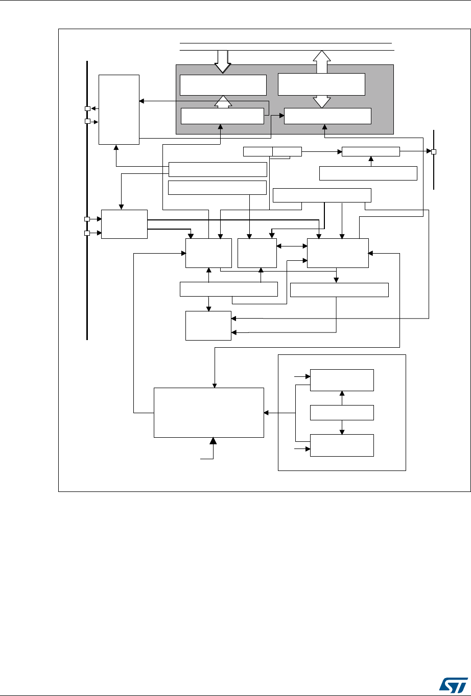
Universal synchronous receiver transmitter (USART) /universal asynchronous receiver transmit-
1198/1600 RM0394 Rev 4
Figure 382. USART block diagram
1. For details on coding USARTDIV in the USART_BRR register, refer to Section 38.5.4: USART baud rate
generation.
2. fCK can be fLSE, fHSI, fPCLK, fSYS.
069
5HFHLYHVKLIWUHJLVWHU
%55>@
:ULWH 5HDG '5GDWDUHJLVWHU
&38RU'0$ &38RU'0$
7UDQVPLWGDWDUHJLVWHU
7'5
3:'$7$ 35'$7$
5HFHLYHGDWDUHJLVWHU
5'5
7UDQVPLWVKLIWUHJLVWHU
86$57B&5UHJLVWHU
86$57B&5UHJLVWHU
576
'(
&76
+DUGZDUH
IORZ
FRQWUROOHU
,U'$
6,5
(1'(&
EORFN
7UDQVPLW
FRQWURO
86$57B&5UHJLVWHU
:DNHXS
XQLW
86$57B&5UHJLVWHU
86$57B*735UHJLVWHU
*7 36& &.FRQWURO
86$57B&5UHJLVWHU
5HFHLYHU
FRQWURO
5HFHLYHU
FORFN
86$57B,65UHJLVWHU
86$57
LQWHUUXSW
FRQWURO
86$57B%55UHJLVWHU
7UDQVPLWWHU
UDWHFRQWUROOHU
5HFHLYHUUDWH
FRQWUROOHU
86$57',9RU86$57',9
GHSHQGLQJRQWKH
RYHUVDPSOLQJPRGH
1RWH
I&.
7UDQVPLWWHU
FORFN
&RQYHQWLRQDOEDXGUDWHJHQHUDWRU
1RWH
7(
5(
&.
7;
5;

RM0394 Rev 4 1199/1600
RM0394 Universal synchronous receiver transmitter (USART) /universal asynchronous receiver
1303
38.5.1 USART character description
The word length can be selected as being either 7 or 8 or 9 bits by programming the M[1:0]
bits in the USART_CR1 register (see Figure 383).
•7-bit character length: M[1:0] = 10
•8-bit character length: M[1:0] = 00
•9-bit character length: M[1:0] = 01
Note: The 7-bit mode is supported only on some USARTs. In addition, not all modes are
supported in 7-bit data length mode. Refer to Section 38.4: USART implementation for
additional information.
By default, the signal (TX or RX) is in low state during the start bit. It is in high state during
the stop bit.
These values can be inverted, separately for each signal, through polarity configuration
control.
An Idle character is interpreted as an entire frame of “1”s (the number of “1”s includes the
number of stop bits).
A Break character is interpreted on receiving “0”s for a frame period. At the end of the
break frame, the transmitter inserts 2 stop bits.
Transmission and reception are driven by a common baud rate generator, the clock for each
is generated when the enable bit is set respectively for the transmitter and receiver.
The details of each block is given below.
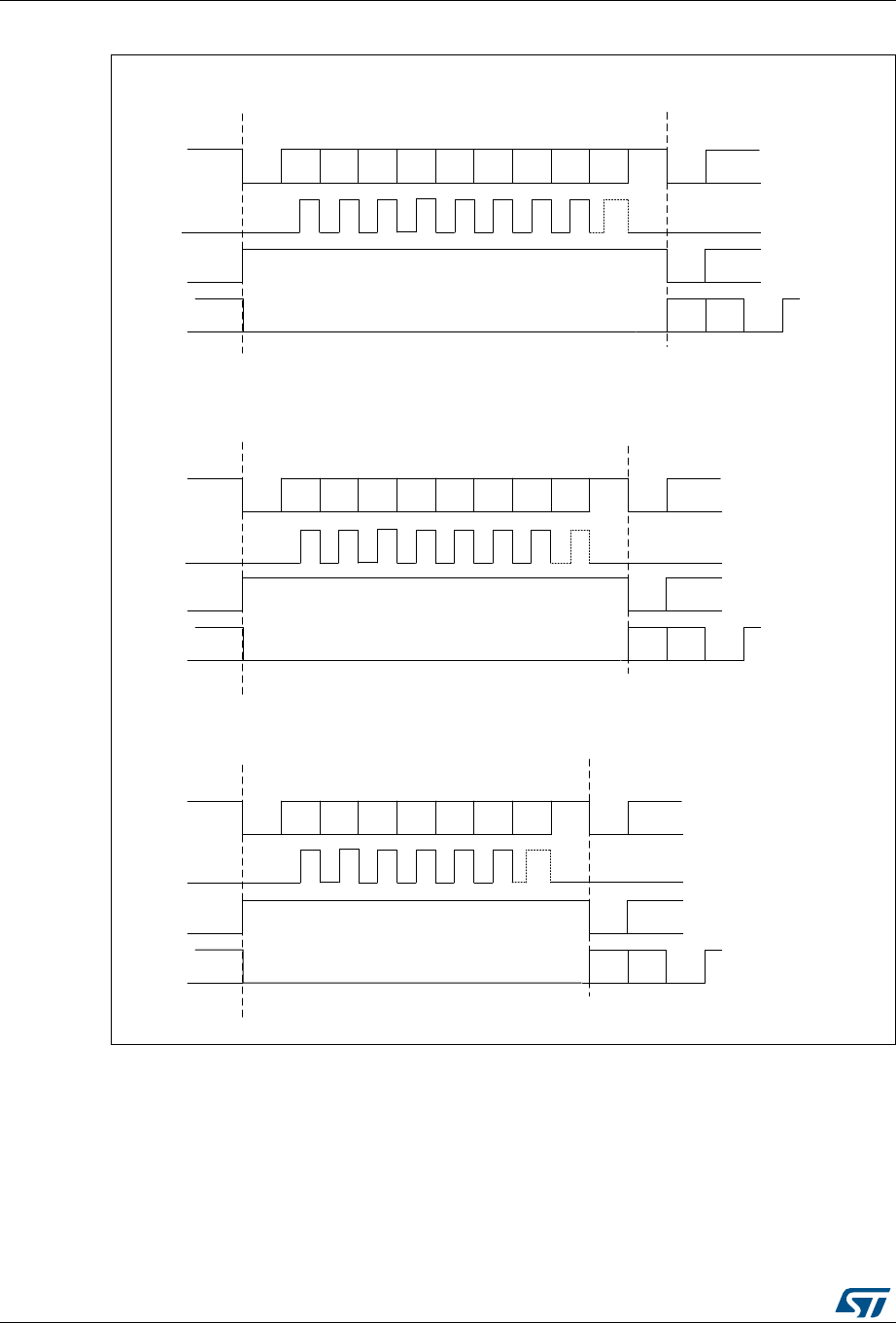
Universal synchronous receiver transmitter (USART) /universal asynchronous receiver transmit-
1200/1600 RM0394 Rev 4
Figure 383. Word length programming
069
%LW %LW %LW %LW %LW %LW %LW %LW %LW
6WDUW
ELW
6WRS
ELW
1H[W
6WDUW
ELW
,GOHIUDPH
ELWZRUGOHQJWK0 6WRSELW
3RVVLEOH
3DULW\
ELW
%UHDNIUDPH
'DWDIUDPH
&ORFN
6WDUW
ELW
6WRS
ELW
6WDUW
ELW
6WRS
ELW
%LW %LW %LW %LW %LW %LW %LW %LW
6WDUW
ELW
6WRS
ELW
1H[W
6WDUW
ELW
,GOHIUDPH
ELWZRUGOHQJWK0 6WRSELW
3RVVLEOH
3DULW\
ELW
%UHDNIUDPH
'DWDIUDPH
&ORFN
6WDUW
ELW
6WRS
ELW
6WDUW
ELW
6WRS
ELW
%LW %LW %LW %LW %LW %LW %LW
6WDUW
ELW
6WRS
ELW
1H[W
6WDUW
ELW
,GOHIUDPH
ELWZRUGOHQJWK0 6WRSELW
3RVVLEOH
3DULW\
ELW
%UHDNIUDPH
'DWDIUDPH
&ORFN
/%&/ELWFRQWUROVODVWGDWDFORFNSXOVH
6WDUW
ELW
6WRS
ELW
6WDUW
ELW
6WRS
ELW

RM0394 Rev 4 1201/1600
RM0394 Universal synchronous receiver transmitter (USART) /universal asynchronous receiver
1303
38.5.2 USART transmitter
The transmitter can send data words of either 7, 8 or 9 bits depending on the M bits status.
The Transmit Enable bit (TE) must be set in order to activate the transmitter function. The
data in the transmit shift register is output on the TX pin and the corresponding clock pulses
are output on the CK pin.
Character transmission
During an USART transmission, data shifts out least significant bit first (default
configuration) on the TX pin. In this mode, the USART_TDR register consists of a buffer
(TDR) between the internal bus and the transmit shift register (see Figure 382).
Every character is preceded by a start bit which is a logic level low for one bit period. The
character is terminated by a configurable number of stop bits.
The following stop bits are supported by USART: 0.5, 1, 1.5 and 2 stop bits.
Note: The TE bit must be set before writing the data to be transmitted to the USART_TDR.
The TE bit should not be reset during transmission of data. Resetting the TE bit during the
transmission will corrupt the data on the TX pin as the baud rate counters will get frozen.
The current data being transmitted will be lost.
An idle frame will be sent after the TE bit is enabled.
Configurable stop bits
The number of stop bits to be transmitted with every character can be programmed in
Control register 2, bits 13,12.
•1 stop bit: This is the default value of number of stop bits.
•2 stop bits: This will be supported by normal USART, Single-wire and Modem modes.
•1.5 stop bits: To be used in Smartcard mode.
•0.5 stop bit: To be used when receiving data in Smartcard mode.
An idle frame transmission will include the stop bits.
A break transmission will be 10 low bits (when M[1:0] = 00) or 11 low bits (when M[1:0] = 01)
or 9 low bits (when M[1:0] = 10) followed by 2 stop bits (see Figure 384). It is not possible to
transmit long breaks (break of length greater than 9/10/11 low bits).
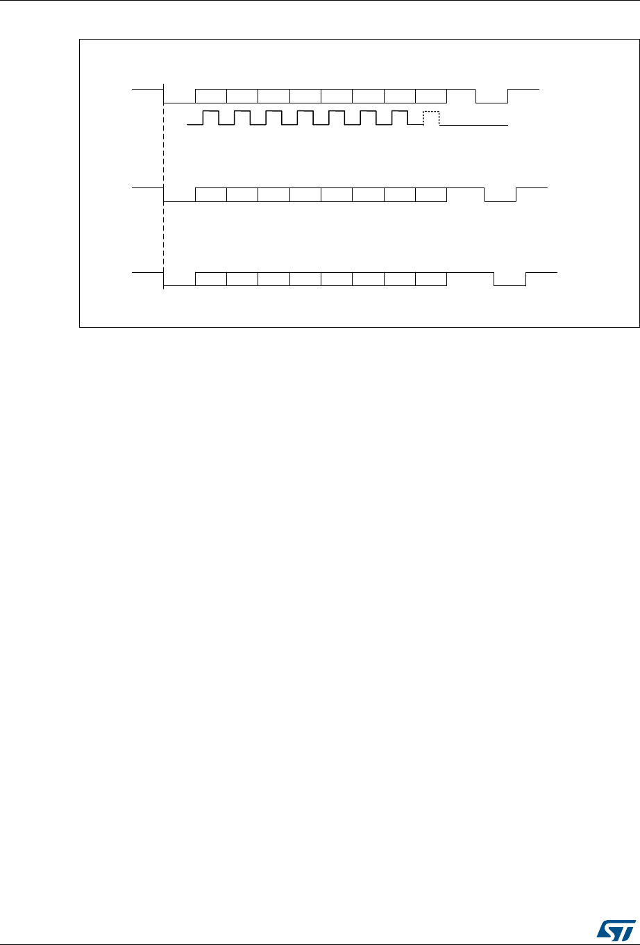
Universal synchronous receiver transmitter (USART) /universal asynchronous receiver transmit-
1202/1600 RM0394 Rev 4
Figure 384. Configurable stop bits
Character transmission procedure
1. Program the M bits in USART_CR1 to define the word length.
2. Select the desired baud rate using the USART_BRR register.
3. Program the number of stop bits in USART_CR2.
4. Enable the USART by writing the UE bit in USART_CR1 register to 1.
5. Select DMA enable (DMAT) in USART_CR3 if multibuffer communication is to take
place. Configure the DMA register as explained in multibuffer communication.
6. Set the TE bit in USART_CR1 to send an idle frame as first transmission.
7. Write the data to send in the USART_TDR register (this clears the TXE bit). Repeat this
for each data to be transmitted in case of single buffer.
8. After writing the last data into the USART_TDR register, wait until TC=1. This indicates
that the transmission of the last frame is complete. This is required for instance when
the USART is disabled or enters the Halt mode to avoid corrupting the last
transmission.
Single byte communication
Clearing the TXE bit is always performed by a write to the transmit data register.
The TXE bit is set by hardware and it indicates:
•The data has been moved from the USART_TDR register to the shift register and the
data transmission has started.
•The USART_TDR register is empty.
•The next data can be written in the USART_TDR register without overwriting the
previous data.
This flag generates an interrupt if the TXEIE bit is set.
When a transmission is taking place, a write instruction to the USART_TDR register stores
the data in the TDR register; next, the data is copied in the shift register at the end of the
currently ongoing transmission.
06Y9
/%&/ELWFRQWUROVODVWGDWDFORFNSXOVH
%LW6WDUWELW 6WRS
ELW
1H[W
VWDUW
ELW
3RVVLEOH
SDULW\ELW
'DWDIUDPH 1H[WGDWDIUDPH
&/2&.
1H[WGDWDIUDPH
ELWGDWD6WRSELW
ELWGDWD6WRSELWV
ELWGDWD6WRSELWV
%LW%LW%LW%LW%LW%LW%LW
%LW6WDUWELW
6WRS
ELWV
1H[W
VWDUW
ELW
3RVVLEOH
SDULW\ELW
'DWDIUDPH
%LW%LW%LW%LW%LW%LW%LW
1H[WGDWDIUDPH
%LW6WDUWELW
6WRS
ELWV
1H[W
VWDUW
ELW
3RVVLEOH
SDULW\ELW
'DWDIUDPH
%LW%LW%LW%LW%LW%LW%LW
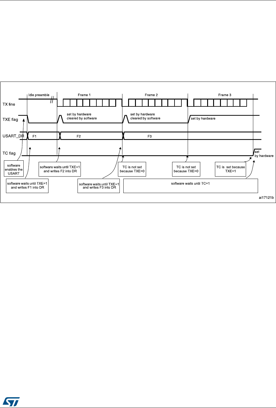
RM0394 Rev 4 1203/1600
RM0394 Universal synchronous receiver transmitter (USART) /universal asynchronous receiver
1303
When no transmission is taking place, a write instruction to the USART_TDR register places
the data in the shift register, the data transmission starts, and the TXE bit is set.
If a frame is transmitted (after the stop bit) and the TXE bit is set, the TC bit goes high. An
interrupt is generated if the TCIE bit is set in the USART_CR1 register.
After writing the last data in the USART_TDR register, it is mandatory to wait for TC=1
before disabling the USART or causing the microcontroller to enter the low-power mode
(see Figure 385: TC/TXE behavior when transmitting).
Figure 385. TC/TXE behavior when transmitting
Break characters
Setting the SBKRQ bit transmits a break character. The break frame length depends on the
M bits (see Figure 383).
If a ‘1’ is written to the SBKRQ bit, a break character is sent on the TX line after completing
the current character transmission. The SBKF bit is set by the write operation and it is reset
by hardware when the break character is completed (during the stop bits after the break
character). The USART inserts a logic 1 signal (STOP) for the duration of 2 bits at the end of
the break frame to guarantee the recognition of the start bit of the next frame.
In the case the application needs to send the break character following all previously
inserted data, including the ones not yet transmitted, the software should wait for the TXE
flag assertion before setting the SBKRQ bit.
Idle characters
Setting the TE bit drives the USART to send an idle frame before the first data frame.
38.5.3 USART receiver
The USART can receive data words of either 7, 8 or 9 bits depending on the M bits in the
USART_CR1 register.
Start bit detection
The start bit detection sequence is the same when oversampling by 16 or by 8.
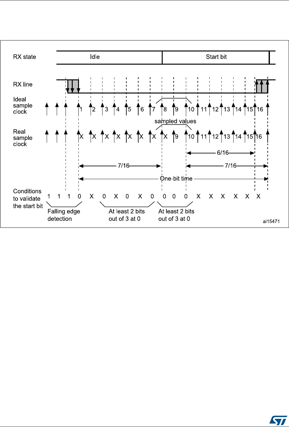
Universal synchronous receiver transmitter (USART) /universal asynchronous receiver transmit-
1204/1600 RM0394 Rev 4
In the USART, the start bit is detected when a specific sequence of samples is recognized.
This sequence is: 1 1 1 0 X 0 X 0X 0X 0 X 0X 0.
Figure 386. Start bit detection when oversampling by 16 or 8
Note: If the sequence is not complete, the start bit detection aborts and the receiver returns to the
idle state (no flag is set), where it waits for a falling edge.
The start bit is confirmed (RXNE flag set, interrupt generated if RXNEIE=1) if the 3 sampled
bits are at 0 (first sampling on the 3rd, 5th and 7th bits finds the 3 bits at 0 and second
sampling on the 8th, 9th and 10th bits also finds the 3 bits at 0).
The start bit is validated (RXNE flag set, interrupt generated if RXNEIE=1) but the NF noise
flag is set if,
a) for both samplings, 2 out of the 3 sampled bits are at 0 (sampling on the 3rd, 5th
and 7th bits and sampling on the 8th, 9th and 10th bits)
or
b) for one of the samplings (sampling on the 3rd, 5th and 7th bits or sampling on the
8th, 9th and 10th bits), 2 out of the 3 bits are found at 0.
If neither conditions a. or b. are met, the start detection aborts and the receiver returns to the
idle state (no flag is set).

RM0394 Rev 4 1205/1600
RM0394 Universal synchronous receiver transmitter (USART) /universal asynchronous receiver
1303
Character reception
During an USART reception, data shifts in least significant bit first (default configuration)
through the RX pin. In this mode, the USART_RDR register consists of a buffer (RDR)
between the internal bus and the receive shift register.
Character reception procedure
1. Program the M bits in USART_CR1 to define the word length.
2. Select the desired baud rate using the baud rate register USART_BRR
3. Program the number of stop bits in USART_CR2.
4. Enable the USART by writing the UE bit in USART_CR1 register to 1.
5. Select DMA enable (DMAR) in USART_CR3 if multibuffer communication is to take
place. Configure the DMA register as explained in multibuffer communication.
6. Set the RE bit USART_CR1. This enables the receiver which begins searching for a
start bit.
When a character is received:
•The RXNE bit is set to indicate that the content of the shift register is transferred to the
RDR. In other words, data has been received and can be read (as well as its
associated error flags).
•An interrupt is generated if the RXNEIE bit is set.
•The error flags can be set if a frame error, noise or an overrun error has been detected
during reception. PE flag can also be set with RXNE.
•In multibuffer, RXNE is set after every byte received and is cleared by the DMA read of
the Receive data Register.
•In single buffer mode, clearing the RXNE bit is performed by a software read to the
USART_RDR register. The RXNE flag can also be cleared by writing 1 to the RXFRQ
in the USART_RQR register. The RXNE bit must be cleared before the end of the
reception of the next character to avoid an overrun error.
Break character
When a break character is received, the USART handles it as a framing error.
Idle character
When an idle frame is detected, there is the same procedure as for a received data
character plus an interrupt if the IDLEIE bit is set.

Universal synchronous receiver transmitter (USART) /universal asynchronous receiver transmit-
1206/1600 RM0394 Rev 4
Overrun error
An overrun error occurs when a character is received when RXNE has not been reset. Data
can not be transferred from the shift register to the RDR register until the RXNE bit is
cleared.
The RXNE flag is set after every byte received. An overrun error occurs if RXNE flag is set
when the next data is received or the previous DMA request has not been serviced. When
an overrun error occurs:
•The ORE bit is set.
•The RDR content will not be lost. The previous data is available when a read to
USART_RDR is performed.
•The shift register will be overwritten. After that point, any data received during overrun
is lost.
•An interrupt is generated if either the RXNEIE bit is set or EIE bit is set.
•The ORE bit is reset by setting the ORECF bit in the ICR register.
Note: The ORE bit, when set, indicates that at least 1 data has been lost. There are two
possibilities:
- if RXNE=1, then the last valid data is stored in the receive register RDR and can be read,
- if RXNE=0, then it means that the last valid data has already been read and thus there is
nothing to be read in the RDR. This case can occur when the last valid data is read in the
RDR at the same time as the new (and lost) data is received.
Selecting the clock source and the proper oversampling method
The choice of the clock source is done through the Clock Control system (see Section Reset
and clock control (RCC))). The clock source must be chosen before enabling the USART
(by setting the UE bit).
The choice of the clock source must be done according to two criteria:
•Possible use of the USART in low-power mode
•Communication speed.
The clock source frequency is fCK.
When the dual clock domain with the wakeup from Stop mode is supported, the clock
source can be one of the following sources: PCLK (default), LSE, HSI16 or SYSCLK.
Otherwise, the USART clock source is PCLK.
Choosing LSE or HSI16 as clock source may allow the USART to receive data while the
MCU is in low-power mode. Depending on the received data and wakeup mode selection,
the USART wakes up the MCU, when needed, in order to transfer the received data by
software reading the USART_RDR register or by DMA.
For the other clock sources, the system must be active in order to allow USART
communication.
The communication speed range (specially the maximum communication speed) is also
determined by the clock source.
The receiver implements different user-configurable oversampling techniques for data
recovery by discriminating between valid incoming data and noise. This allows a trade-off
between the maximum communication speed and noise/clock inaccuracy immunity.

RM0394 Rev 4 1207/1600
RM0394 Universal synchronous receiver transmitter (USART) /universal asynchronous receiver
1303
The oversampling method can be selected by programming the OVER8 bit in the
USART_CR1 register and can be either 16 or 8 times the baud rate clock (Figure 387 and
Figure 388).
Depending on the application:
•Select oversampling by 8 (OVER8=1) to achieve higher speed (up to fCK/8). In this
case the maximum receiver tolerance to clock deviation is reduced (refer to
Section 38.5.5: Tolerance of the USART receiver to clock deviation on page 1212)
•Select oversampling by 16 (OVER8=0) to increase the tolerance of the receiver to
clock deviations. In this case, the maximum speed is limited to maximum fCK/16 where
fCK is the clock source frequency.
Programming the ONEBIT bit in the USART_CR3 register selects the method used to
evaluate the logic level. There are two options:
•The majority vote of the three samples in the center of the received bit. In this case,
when the 3 samples used for the majority vote are not equal, the NF bit is set
•A single sample in the center of the received bit
Depending on the application:
– select the three samples’ majority vote method (ONEBIT=0) when operating in a
noisy environment and reject the data when a noise is detected (refer to
Figure 193) because this indicates that a glitch occurred during the sampling.
– select the single sample method (ONEBIT=1) when the line is noise-free to
increase the receiver’s tolerance to clock deviations (see Section 38.5.5:
Tolerance of the USART receiver to clock deviation on page 1212). In this case
the NF bit will never be set.
When noise is detected in a frame:
•The NF bit is set at the rising edge of the RXNE bit.
•The invalid data is transferred from the Shift register to the USART_RDR register.
•No interrupt is generated in case of single byte communication. However this bit rises
at the same time as the RXNE bit which itself generates an interrupt. In case of
multibuffer communication an interrupt will be issued if the EIE bit is set in the
USART_CR3 register.
The NF bit is reset by setting NFCF bit in ICR register.
Note: Oversampling by 8 is not available in LIN, Smartcard and IrDA modes. In those modes, the
OVER8 bit is forced to ‘0’ by hardware.
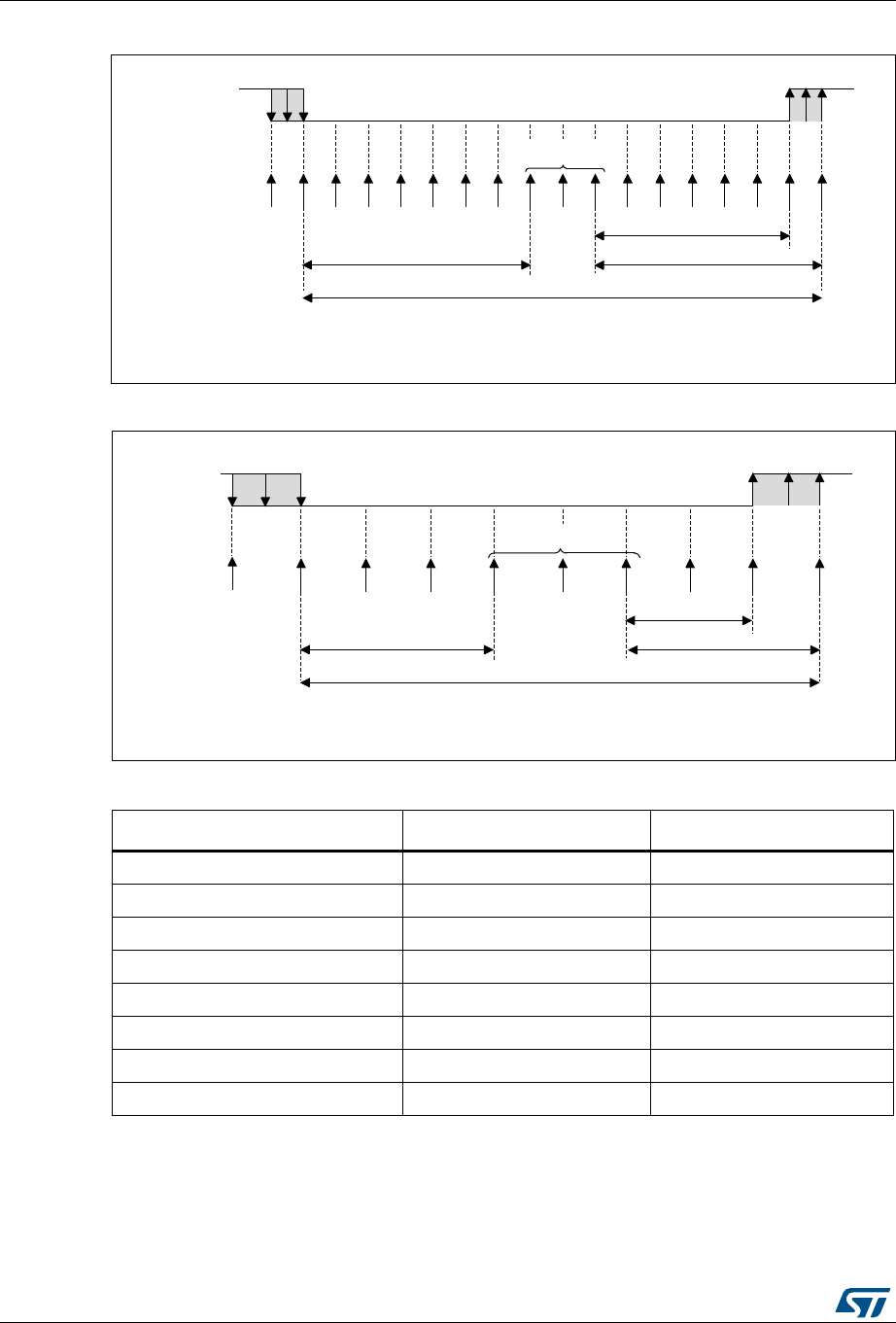
Universal synchronous receiver transmitter (USART) /universal asynchronous receiver transmit-
1208/1600 RM0394 Rev 4
Figure 387. Data sampling when oversampling by 16
Figure 388. Data sampling when oversampling by 8
Table 193. Noise detection from sampled data
Sampled value NE status Received bit value
000 0 0
001 1 0
010 1 0
011 1 1
100 1 0
101 1 1
110 1 1
111 0 1
06Y9
VDPSOHGYDOXHV
2QHELWWLPH
6DPSOHFORFN
5;OLQH
06Y9
VDPSOHGYDOXHV
2QHELWWLPH
6DPSOH
FORFN[
5;OLQH

RM0394 Rev 4 1209/1600
RM0394 Universal synchronous receiver transmitter (USART) /universal asynchronous receiver
1303
Framing error
A framing error is detected when the stop bit is not recognized on reception at the expected
time, following either a de-synchronization or excessive noise.
When the framing error is detected:
•The FE bit is set by hardware
•The invalid data is transferred from the Shift register to the USART_RDR register.
•No interrupt is generated in case of single byte communication. However this bit rises
at the same time as the RXNE bit which itself generates an interrupt. In case of
multibuffer communication an interrupt will be issued if the EIE bit is set in the
USART_CR3 register.
The FE bit is reset by writing 1 to the FECF in the USART_ICR register.
Configurable stop bits during reception
The number of stop bits to be received can be configured through the control bits of Control
Register 2 - it can be either 1 or 2 in normal mode and 0.5 or 1.5 in Smartcard mode.
•
0.5 stop bit (reception in Smartcard mode): No sampling is done for 0.5 stop bit. As
a consequence, no framing error and no break frame can be detected when 0.5 stop bit
is selected.
•1 stop bit: Sampling for 1 stop Bit is done on the 8th, 9th and 10th samples.
•1.5 stop bits (Smartcard mode): When transmitting in Smartcard mode, the device
must check that the data is correctly sent. Thus the receiver block must be enabled (RE
=1 in the USART_CR1 register) and the stop bit is checked to test if the smartcard has
detected a parity error. In the event of a parity error, the smartcard forces the data
signal low during the sampling - NACK signal-, which is flagged as a framing error.
Then, the FE flag is set with the RXNE at the end of the 1.5 stop bits. Sampling for 1.5
stop bits is done on the 16th, 17th and 18th samples (1 baud clock period after the
beginning of the stop bit). The 1.5 stop bits can be decomposed into 2 parts: one 0.5
baud clock period during which nothing happens, followed by 1 normal stop bit period
during which sampling occurs halfway through. Refer to Section 38.5.13: USART
Smartcard mode on page 1223 for more details.
•2 stop bits: Sampling for 2 stop bits is done on the 8th, 9th and 10th samples of the
first stop bit. If a framing error is detected during the first stop bit the framing error flag
will be set. The second stop bit is not checked for framing error. The RXNE flag will be
set at the end of the first stop bit.

Universal synchronous receiver transmitter (USART) /universal asynchronous receiver transmit-
1210/1600 RM0394 Rev 4
38.5.4 USART baud rate generation
The baud rate for the receiver and transmitter (Rx and Tx) are both set to the same value as
programmed in the USART_BRR register.
Equation 1: Baud rate for standard USART (SPI mode included) (OVER8 = 0 or 1)
In case of oversampling by 16, the equation is:
In case of oversampling by 8, the equation is:
Equation 2: Baud rate in Smartcard, LIN and IrDA modes (OVER8 = 0)
In Smartcard, LIN and IrDA modes, only Oversampling by 16 is supported:
USARTDIV is an unsigned fixed point number that is coded on the USART_BRR register.
•When OVER8 = 0, BRR = USARTDIV.
•When OVER8 = 1
– BRR[2:0] = USARTDIV[3:0] shifted 1 bit to the right.
– BRR[3] must be kept cleared.
– BRR[15:4] = USARTDIV[15:4]
Note: The baud counters are updated to the new value in the baud registers after a write operation
to USART_BRR. Hence the baud rate register value should not be changed during
communication.
In case of oversampling by 16 or 8, USARTDIV must be greater than or equal to 16d.
How to derive USARTDIV from USART_BRR register values
Example 1
To obtain 9600 baud with fCK = 8 MHz.
•In case of oversampling by 16:
USARTDIV = 8 000 000/9600
BRR = USARTDIV = 833d = 0341h
•In case of oversampling by 8:
USARTDIV = 2 * 8 000 000/9600
USARTDIV = 1666,66 (1667d = 683h)
BRR[3:0] = 3h << 1 = 1h
BRR = 0x681
Tx/Rx baud fCK
USARTDIV
--------------------------------
=
Tx/Rx baud 2f
CK
×
USARTDIV
--------------------------------
=
Tx/Rx baud fCK
USARTDIV
--------------------------------
=

RM0394 Rev 4 1211/1600
RM0394 Universal synchronous receiver transmitter (USART) /universal asynchronous receiver
1303
Example 2
To obtain 921.6 Kbaud with fCK = 48 MHz.
•In case of oversampling by 16:
USARTDIV = 48 000 000/921 600
BRR = USARTDIV = 52d = 34h
•In case of oversampling by 8:
USARTDIV = 2 * 48 000 000/921 600
USARTDIV = 104 (104d = 68h)
BRR[3:0] = USARTDIV[3:0] >> 1 = 8h >> 1 = 4h
BRR = 0x64
Table 194. Error calculation for programmed baud rates at fCK = 72MHz in both cases of
oversampling by 16 or by 8(1)
Baud rate Oversampling by 16 (OVER8 = 0) Oversampling by 8 (OVER8 = 1)
S.No Desired Actual BRR
% Error =
(Calculated -
Desired)B.Rate /
Desired B.Rate
Actual BRR % Error
1 2.4 KBps 2.4 KBps 0x7530 0 2.4 KBps 0xEA60 0
2 9.6 KBps 9.6 KBps 0x1D4C 0 9.6 KBps 0x3A94 0
3 19.2 KBps 19.2 KBps 0xEA6 0 19.2 KBps 0x1D46 0
4 38.4 KBps 38.4 KBps 0x753 0 38.4 KBps 0xEA3 0
5 57.6 KBps 57.6 KBps 0x4E2 0 57.6 KBps 0x9C2 0
6 115.2 KBps 115.2 KBps 0x271 0 115.2 KBps 0x4E1 0
7 230.4 KBps 230.03KBps 0x139 0.16 230.4 KBps 0x270 0
8 460.8 KBps 461.54KBps 0x9C 0.16 460.06KBps 0x134 0.16
9 921.6 KBps 923.08KBps 0x4E 0.16 923.07KBps 0x96 0.16
10 2 MBps 2 MBps 0x24 0 2 MBps 0x44 0
11 3 MBps 3 MBps 0x18 0 3 MBps 0x30 0
12 4MBps 4MBps 0x12 0 4MBps 0x22 0
13 5MBps N.A N.A N.A 4965.51KBps 0x16 0.69
14 6MBps N.A N.A N.A 6MBps 0x14 0
15 7MBps N.A N.A N.A 6857.14KBps 0x12 2
16 9MBps N.A N.A N.A 9MBps 0x10 0
1. The lower the CPU clock the lower the accuracy for a particular baud rate. The upper limit of the achievable baud rate can
be fixed with these data.

Universal synchronous receiver transmitter (USART) /universal asynchronous receiver transmit-
1212/1600 RM0394 Rev 4
38.5.5 Tolerance of the USART receiver to clock deviation
The asynchronous receiver of the USART works correctly only if the total clock system
deviation is less than the tolerance of the USART receiver. The causes which contribute to
the total deviation are:
•DTRA: Deviation due to the transmitter error (which also includes the deviation of the
transmitter’s local oscillator)
•DQUANT: Error due to the baud rate quantization of the receiver
•DREC: Deviation of the receiver’s local oscillator
•DTCL: Deviation due to the transmission line (generally due to the transceivers which
can introduce an asymmetry between the low-to-high transition timing and the high-to-
low transition timing)
where
DWU is the error due to sampling point deviation when the wakeup from Stop mode is
used.
when M[1:0] = 01:
when M[1:0] = 00:
when M[1:0] = 10:
tWUUSART is the time between:
1. The detection of start bit falling edge
2. The instant when clock (requested by the peripheral) is ready and reaching the
peripheral and regulator is ready.
The USART receiver can receive data correctly at up to the maximum tolerated
deviation specified in Table 195 and Table 195 depending on the following choices:
•9-, 10- or 11-bit character length defined by the M bits in the USART_CR1 register
•Oversampling by 8 or 16 defined by the OVER8 bit in the USART_CR1 register
•Bits BRR[3:0] of USART_BRR register are equal to or different from 0000.
•Use of 1 bit or 3 bits to sample the data, depending on the value of the ONEBIT bit in
the USART_CR3 register.
DTRA DQUANT DREC DTCL DWU++++USART receiver′s tolerance<
DWU tWUUSART
11 Tbit×
---------------------------
=
DWU tWUUSART
10 Tbit×
---------------------------
=
DWU tWUUSART
9Tbit×
---------------------------
=

RM0394 Rev 4 1213/1600
RM0394 Universal synchronous receiver transmitter (USART) /universal asynchronous receiver
1303
Note: The data specified in Table 195 and Table 196 may slightly differ in the special case when
the received frames contain some Idle frames of exactly 10-bit durations when M bits = 00
(11-bit durations when M bits =01 or 9- bit durations when M bits = 10).
38.5.6 USART auto baud rate detection
The USART is able to detect and automatically set the USART_BRR register value based
on the reception of one character. Automatic baud rate detection is useful under two
circumstances:
•The communication speed of the system is not known in advance
•The system is using a relatively low accuracy clock source and this mechanism allows
the correct baud rate to be obtained without measuring the clock deviation.
The clock source frequency must be compatible with the expected communication speed
(when oversampling by 16, the baud rate is between fCK/65535 and fCK/16. when
oversampling by 8, the baud rate is between fCK/65535 and fCK/8).
Before activating the auto baud rate detection, the auto baud rate detection mode must be
chosen. There are various modes based on different character patterns.
They can be chosen through the ABRMOD[1:0] field in the USART_CR2 register. In these
auto baud rate modes, the baud rate is measured several times during the synchronization
data reception and each measurement is compared to the previous one.
These modes are:
•Mode 0: Any character starting with a bit at 1. In this case the USART measures the
duration of the Start bit (falling edge to rising edge).
•Mode 1: Any character starting with a 10xx bit pattern. In this case, the USART
measures the duration of the Start and of the 1st data bit. The measurement is done
falling edge to falling edge, ensuring better accuracy in the case of slow signal slopes.
•Mode 2: A 0x7F character frame (it may be a 0x7F character in LSB first mode or a
0xFE in MSB first mode). In this case, the baud rate is updated first at the end of the
Table 195. Tolerance of the USART receiver when BRR [3:0] = 0000
M bits
OVER8 bit = 0 OVER8 bit = 1
ONEBIT=0 ONEBIT=1 ONEBIT=0 ONEBIT=1
00 3.75% 4.375% 2.50% 3.75%
01 3.41% 3.97% 2.27% 3.41%
10 4.16% 4.86% 2.77% 4.16%
Table 196. Tolerance of the USART receiver when BRR [3:0] is different from 0000
M bits
OVER8 bit = 0 OVER8 bit = 1
ONEBIT=0 ONEBIT=1 ONEBIT=0 ONEBIT=1
00 3.33% 3.88% 2% 3%
01 3.03% 3.53% 1.82% 2.73%
10 3.7% 4.31% 2.22% 3.33%

Universal synchronous receiver transmitter (USART) /universal asynchronous receiver transmit-
1214/1600 RM0394 Rev 4
start bit (BRs), then at the end of bit 6 (based on the measurement done from falling
edge to falling edge: BR6). Bit 0 to bit 6 are sampled at BRs while further bits of the
character are sampled at BR6.
•Mode 3: A 0x55 character frame. In this case, the baud rate is updated first at the end
of the start bit (BRs), then at the end of bit 0 (based on the measurement done from
falling edge to falling edge: BR0), and finally at the end of bit 6 (BR6). Bit 0 is sampled
at BRs, bit 1 to bit 6 are sampled at BR0, and further bits of the character are sampled
at BR6.
In parallel, another check is performed for each intermediate transition of RX line. An
error is generated if the transitions on RX are not sufficiently synchronized with the
receiver (the receiver being based on the baud rate calculated on bit 0).
Prior to activating auto baud rate detection, the USART_BRR register must be initialized by
writing a non-zero baud rate value.
The automatic baud rate detection is activated by setting the ABREN bit in the USART_CR2
register. The USART will then wait for the first character on the RX line. The auto baud rate
operation completion is indicated by the setting of the ABRF flag in the USART_ISR
register. If the line is noisy, the correct baud rate detection cannot be guaranteed. In this
case the BRR value may be corrupted and the ABRE error flag will be set. This also
happens if the communication speed is not compatible with the automatic baud rate
detection range (bit duration not between 16 and 65536 clock periods (oversampling by 16)
and not between 8 and 65536 clock periods (oversampling by 8)).
The RXNE interrupt will signal the end of the operation.
At any later time, the auto baud rate detection may be relaunched by resetting the ABRF
flag (by writing a 0).
Note: If the USART is disabled (UE=0) during an auto baud rate operation, the BRR value may be
corrupted.
38.5.7 Multiprocessor communication using USART
In multiprocessor communication, the following bits are to be kept cleared:
•LINEN bit in the USART_CR2 register,
•HDSEL, IREN and SCEN bits in the USART_CR3 register.
It is possible to perform multiprocessor communication with the USART (with several
USARTs connected in a network). For instance one of the USARTs can be the master, its TX
output connected to the RX inputs of the other USARTs. The others are slaves, their
respective TX outputs are logically ANDed together and connected to the RX input of the
master.
In multiprocessor configurations it is often desirable that only the intended message
recipient should actively receive the full message contents, thus reducing redundant USART
service overhead for all non addressed receivers.
The non addressed devices may be placed in mute mode by means of the muting function.
In order to use the mute mode feature, the MME bit must be set in the USART_CR1
register.
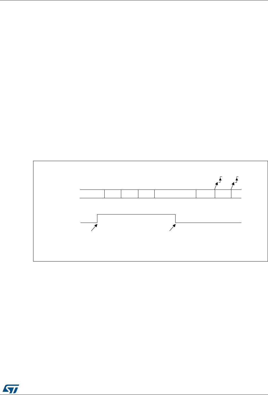
RM0394 Rev 4 1215/1600
RM0394 Universal synchronous receiver transmitter (USART) /universal asynchronous receiver
1303
In mute mode:
•None of the reception status bits can be set.
•All the receive interrupts are inhibited.
•The RWU bit in USART_ISR register is set to 1. RWU can be controlled automatically
by hardware or by software, through the MMRQ bit in the USART_RQR register, under
certain conditions.
The USART can enter or exit from mute mode using one of two methods, depending on the
WAKE bit in the USART_CR1 register:
•Idle Line detection if the WAKE bit is reset,
•Address Mark detection if the WAKE bit is set.
Idle line detection (WAKE=0)
The USART enters mute mode when the MMRQ bit is written to 1 and the RWU is
automatically set.
It wakes up when an Idle frame is detected. Then the RWU bit is cleared by hardware but
the IDLE bit is not set in the USART_ISR register. An example of mute mode behavior using
Idle line detection is given in Figure 389.
Figure 389. Mute mode using Idle line detection
Note: If the MMRQ is set while the IDLE character has already elapsed, mute mode will not be
entered (RWU is not set).
If the USART is activated while the line is IDLE, the idle state is detected after the duration
of one IDLE frame (not only after the reception of one character frame).
4-bit/7-bit address mark detection (WAKE=1)
In this mode, bytes are recognized as addresses if their MSB is a ‘1’ otherwise they are
considered as data. In an address byte, the address of the targeted receiver is put in the 4
or 7 LSBs. The choice of 7 or 4-bit address detection is done using the ADDM7 bit. This 4-
bit/7-bit word is compared by the receiver with its own address which is programmed in the
ADD bits in the USART_CR2 register.
Note: In 7-bit and 9-bit data modes, address detection is done on 6-bit and 8-bit addresses
(ADD[5:0] and ADD[7:0]) respectively.
06Y9
'DWD 'DWD ,'/('DWD 'DWD 'DWD
,GOHIUDPHGHWHFWHG0054ZULWWHQWR
5:8
5;
0XWHPRGH 1RUPDOPRGH
5;1( 5;1(
'DWD

Universal synchronous receiver transmitter (USART) /universal asynchronous receiver transmit-
1216/1600 RM0394 Rev 4
The USART enters mute mode when an address character is received which does not
match its programmed address. In this case, the RWU bit is set by hardware. The RXNE
flag is not set for this address byte and no interrupt or DMA request is issued when the
USART enters mute mode.
The USART also enters mute mode when the MMRQ bit is written to 1. The RWU bit is also
automatically set in this case.
The USART exits from mute mode when an address character is received which matches
the programmed address. Then the RWU bit is cleared and subsequent bytes are received
normally. The RXNE bit is set for the address character since the RWU bit has been
cleared.
An example of mute mode behavior using address mark detection is given in Figure 390.
Figure 390. Mute mode using address mark detection
38.5.8 Modbus communication using USART
The USART offers basic support for the implementation of Modbus/RTU and Modbus/ASCII
protocols. Modbus/RTU is a half duplex, block transfer protocol. The control part of the
protocol (address recognition, block integrity control and command interpretation) must be
implemented in software.
The USART offers basic support for the end of the block detection, without software
overhead or other resources.
Modbus/RTU
In this mode, the end of one block is recognized by a “silence” (idle line) for more than 2
character times. This function is implemented through the programmable timeout function.
The timeout function and interrupt must be activated, through the RTOEN bit in the
USART_CR2 register and the RTOIE in the USART_CR1 register. The value corresponding
to a timeout of 2 character times (for example 22 x bit duration) must be programmed in the
RTO register. when the receive line is idle for this duration, after the last stop bit is received,
an interrupt is generated, informing the software that the current block reception is
completed.
06Y9
,'/( $GGU 'DWD 'DWD ,'/( $GGU 'DWD 'DWD $GGU 'DWD
,QWKLVH[DPSOHWKHFXUUHQWDGGUHVVRIWKHUHFHLYHULV
SURJUDPPHGLQWKH86$57B&5UHJLVWHU
5;1(
1RQPDWFKLQJDGGUHVV0DWFKLQJDGGUHVV
1RQPDWFKLQJDGGUHVV
0054ZULWWHQWR
5;1(ZDVFOHDUHG
5:8
5;
0XWHPRGH 0XWHPRGH1RUPDOPRGH
5;1( 5;1(
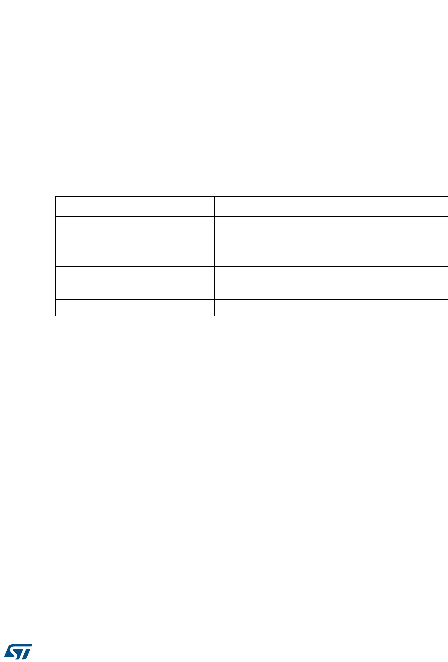
RM0394 Rev 4 1217/1600
RM0394 Universal synchronous receiver transmitter (USART) /universal asynchronous receiver
1303
Modbus/ASCII
In this mode, the end of a block is recognized by a specific (CR/LF) character sequence.
The USART manages this mechanism using the character match function.
By programming the LF ASCII code in the ADD[7:0] field and by activating the character
match interrupt (CMIE=1), the software is informed when a LF has been received and can
check the CR/LF in the DMA buffer.
38.5.9 USART parity control
Parity control (generation of parity bit in transmission and parity checking in reception) can
be enabled by setting the PCE bit in the USART_CR1 register. Depending on the frame
length defined by the M bits, the possible USART frame formats are as listed in Table 197.
Even parity
The parity bit is calculated to obtain an even number of “1s” inside the frame of the 6, 7 or 8
LSB bits (depending on M bits values) and the parity bit.
As an example, if data=00110101, and 4 bits are set, then the parity bit will be 0 if even
parity is selected (PS bit in USART_CR1 = 0).
Odd parity
The parity bit is calculated to obtain an odd number of “1s” inside the frame made of the 6, 7
or 8 LSB bits (depending on M bits values) and the parity bit.
As an example, if data=00110101 and 4 bits set, then the parity bit will be 1 if odd parity is
selected (PS bit in USART_CR1 = 1).
Parity checking in reception
If the parity check fails, the PE flag is set in the USART_ISR register and an interrupt is
generated if PEIE is set in the USART_CR1 register. The PE flag is cleared by software
writing 1 to the PECF in the USART_ICR register.
Table 197. Frame formats
M bits PCE bit USART frame(1)
1. Legends: SB: start bit, STB: stop bit, PB: parity bit. In the data register, the PB is always taking the MSB
position (9th, 8th or 7th, depending on the M bits value).
00 0 | SB | 8-bit data | STB |
00 1 | SB | 7-bit data | PB | STB |
01 0 | SB | 9-bit data | STB |
01 1 | SB | 8-bit data | PB | STB |
10 0 | SB | 7-bit data | STB |
10 1 | SB | 6-bit data | PB | STB |

Universal synchronous receiver transmitter (USART) /universal asynchronous receiver transmit-
1218/1600 RM0394 Rev 4
Parity generation in transmission
If the PCE bit is set in USART_CR1, then the MSB bit of the data written in the data register
is transmitted but is changed by the parity bit (even number of “1s” if even parity is selected
(PS=0) or an odd number of “1s” if odd parity is selected (PS=1)).
38.5.10 USART LIN (local interconnection network) mode
This section is relevant only when LIN mode is supported. Please refer to Section 38.4:
USART implementation on page 1196.
The LIN mode is selected by setting the LINEN bit in the USART_CR2 register. In LIN
mode, the following bits must be kept cleared:
•STOP[1:0] and CLKEN in the USART_CR2 register,
•SCEN, HDSEL and IREN in the USART_CR3 register.
LIN transmission
The procedure explained in Section 38.5.2: USART transmitter has to be applied for LIN
Master transmission. It must be the same as for normal USART transmission with the
following differences:
•Clear the M bits to configure 8-bit word length.
•Set the LINEN bit to enter LIN mode. In this case, setting the SBKRQ bit sends 13 ‘0’
bits as a break character. Then 2 bits of value ‘1’ are sent to allow the next start
detection.
LIN reception
When LIN mode is enabled, the break detection circuit is activated. The detection is totally
independent from the normal USART receiver. A break can be detected whenever it occurs,
during Idle state or during a frame.
When the receiver is enabled (RE=1 in USART_CR1), the circuit looks at the RX input for a
start signal. The method for detecting start bits is the same when searching break
characters or data. After a start bit has been detected, the circuit samples the next bits
exactly like for the data (on the 8th, 9th and 10th samples). If 10 (when the LBDL = 0 in
USART_CR2) or 11 (when LBDL=1 in USART_CR2) consecutive bits are detected as ‘0,
and are followed by a delimiter character, the LBDF flag is set in USART_ISR. If the LBDIE
bit=1, an interrupt is generated. Before validating the break, the delimiter is checked for as it
signifies that the RX line has returned to a high level.
If a ‘1’ is sampled before the 10 or 11 have occurred, the break detection circuit cancels the
current detection and searches for a start bit again.
If the LIN mode is disabled (LINEN=0), the receiver continues working as normal USART,
without taking into account the break detection.
If the LIN mode is enabled (LINEN=1), as soon as a framing error occurs (i.e. stop bit
detected at ‘0’, which will be the case for any break frame), the receiver stops until the break
detection circuit receives either a ‘1’, if the break word was not complete, or a delimiter
character if a break has been detected.
The behavior of the break detector state machine and the break flag is shown on the
Figure 391: Break detection in LIN mode (11-bit break length - LBDL bit is set) on
page 1219.
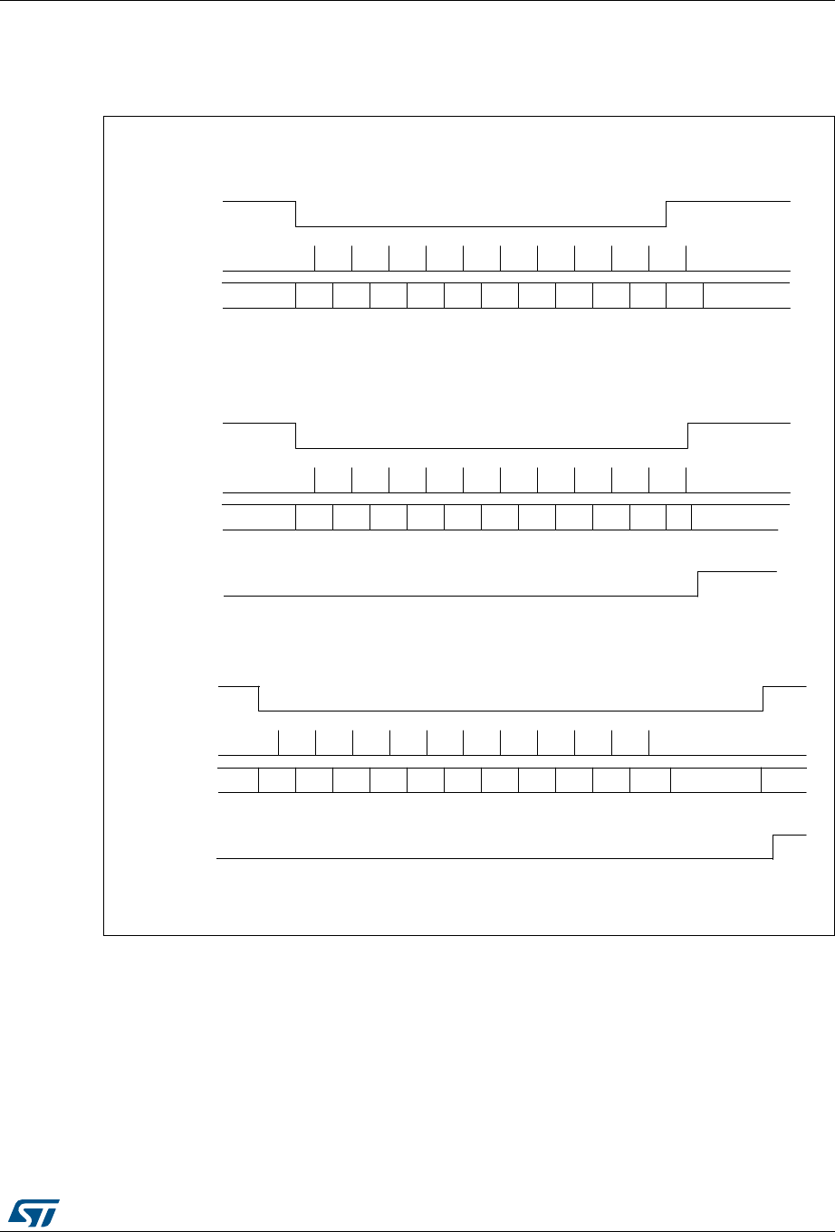
RM0394 Rev 4 1219/1600
RM0394 Universal synchronous receiver transmitter (USART) /universal asynchronous receiver
1303
Examples of break frames are given on Figure 392: Break detection in LIN mode vs.
Framing error detection on page 1220.
Figure 391. Break detection in LIN mode (11-bit break length - LBDL bit is set)
06Y9
,GOH %LW %LW %LW %LW %LW %LW %LW %LW %LW %LW %LW ,GOH
&DVHEUHDNVLJQDOQRWORQJHQRXJK !EUHDNGLVFDUGHG/%')LVQRWVHW
5;OLQH
&DSWXUHVWUREH
%UHDNVWDWH
PDFKLQH
5HDGVDPSOHV
,GOH %LW %LW %LW %LW %LW %LW %LW %LW %LW %LW % ,GOH
&DVHEUHDNVLJQDOMXVWORQJHQRXJK !EUHDNGHWHFWHG/%')LVVHW
5;OLQH
&DSWXUHVWUREH
%UHDNVWDWH
PDFKLQH
5HDGVDPSOHV
%UHDNIUDPH
%UHDNIUDPH
'HOLPLWHULVLPPHGLDWH
/%')
,GOH %LW %LW %LW %LW %LW %LW %LW %LW %LW %LW %LW ,GOH
&DVHEUHDNVLJQDOORQJHQRXJK !EUHDNGHWHFWHG/%')LVVHW
5;OLQH
&DSWXUHVWUREH
%UHDNVWDWH
PDFKLQH
5HDGVDPSOHV
%UHDNIUDPH
/%')
ZDLWGHOLPLWHU
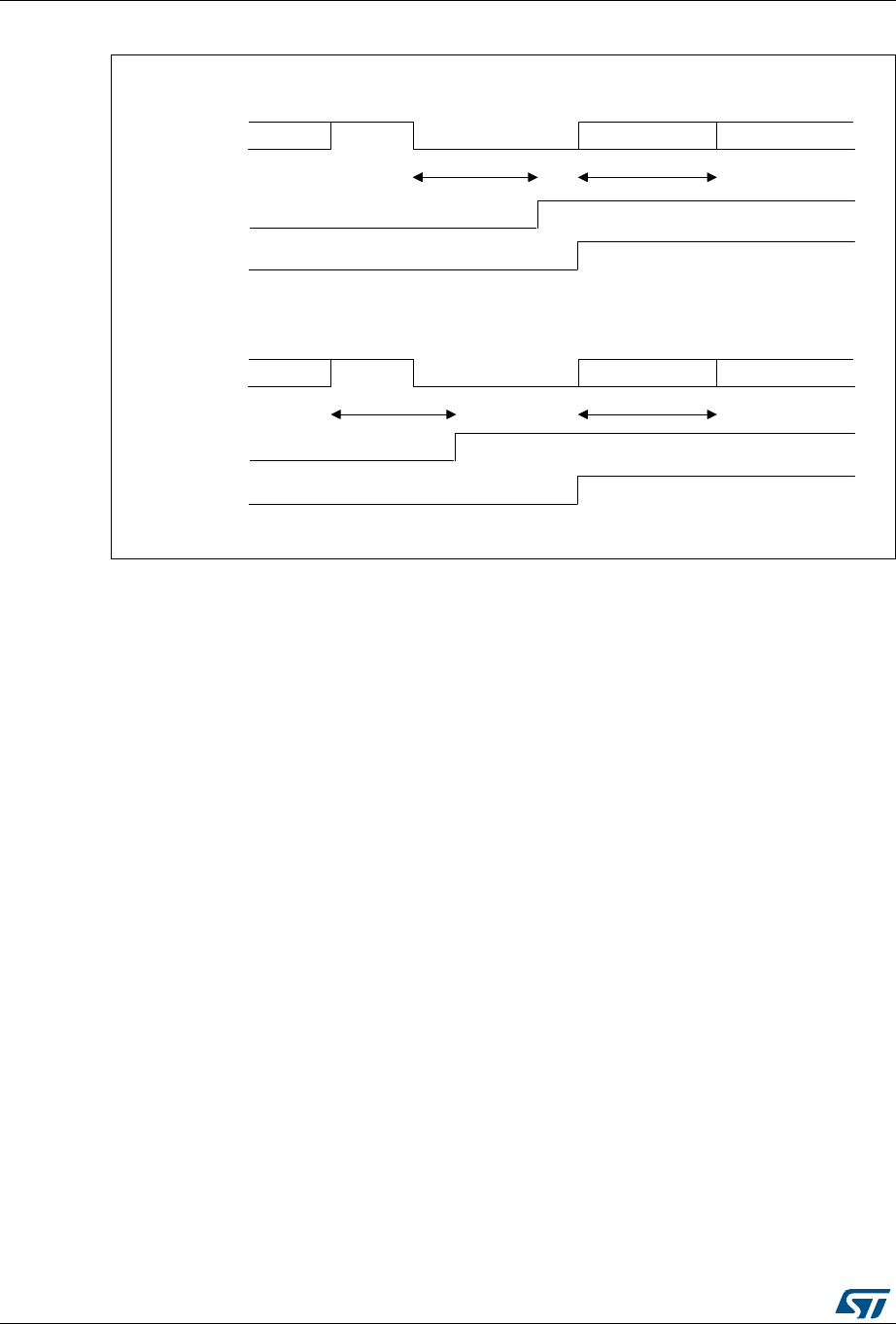
Universal synchronous receiver transmitter (USART) /universal asynchronous receiver transmit-
1220/1600 RM0394 Rev 4
Figure 392. Break detection in LIN mode vs. Framing error detection
38.5.11 USART synchronous mode
The synchronous mode is selected by writing the CLKEN bit in the USART_CR2 register to
1. In synchronous mode, the following bits must be kept cleared:
•LINEN bit in the USART_CR2 register,
•SCEN, HDSEL and IREN bits in the USART_CR3 register.
In this mode, the USART can be used to control bidirectional synchronous serial
communications in master mode. The CK pin is the output of the USART transmitter clock.
No clock pulses are sent to the CK pin during start bit and stop bit. Depending on the state
of the LBCL bit in the USART_CR2 register, clock pulses are, or are not, generated during
the last valid data bit (address mark). The CPOL bit in the USART_CR2 register is used to
select the clock polarity, and the CPHA bit in the USART_CR2 register is used to select the
phase of the external clock (see Figure 393, Figure 394 and Figure 395).
During the Idle state, preamble and send break, the external CK clock is not activated.
In synchronous mode the USART transmitter works exactly like in asynchronous mode. But
as CK is synchronized with TX (according to CPOL and CPHA), the data on TX is
synchronous.
In this mode the USART receiver works in a different manner compared to the
asynchronous mode. If RE=1, the data is sampled on CK (rising or falling edge, depending
on CPOL and CPHA), without any oversampling. A setup and a hold time must be
respected (which depends on the baud rate: 1/16 bit duration).
06Y9
GDWD ,'/( %5($. GDWD[ GDWDKHDGHU
GDWDWLPH GDWDWLPH
5;OLQH
5;1()(
/%')
&DVHEUHDNRFFXUULQJDIWHUDQ,GOH
GDWD GDWD %5($. GDWD[ GDWDKHDGHU
GDWDWLPH GDWDWLPH
5;OLQH
5;1()(
/%')
&DVHEUHDNRFFXUULQJZKLOHGDWDLVEHLQJUHFHLYHG
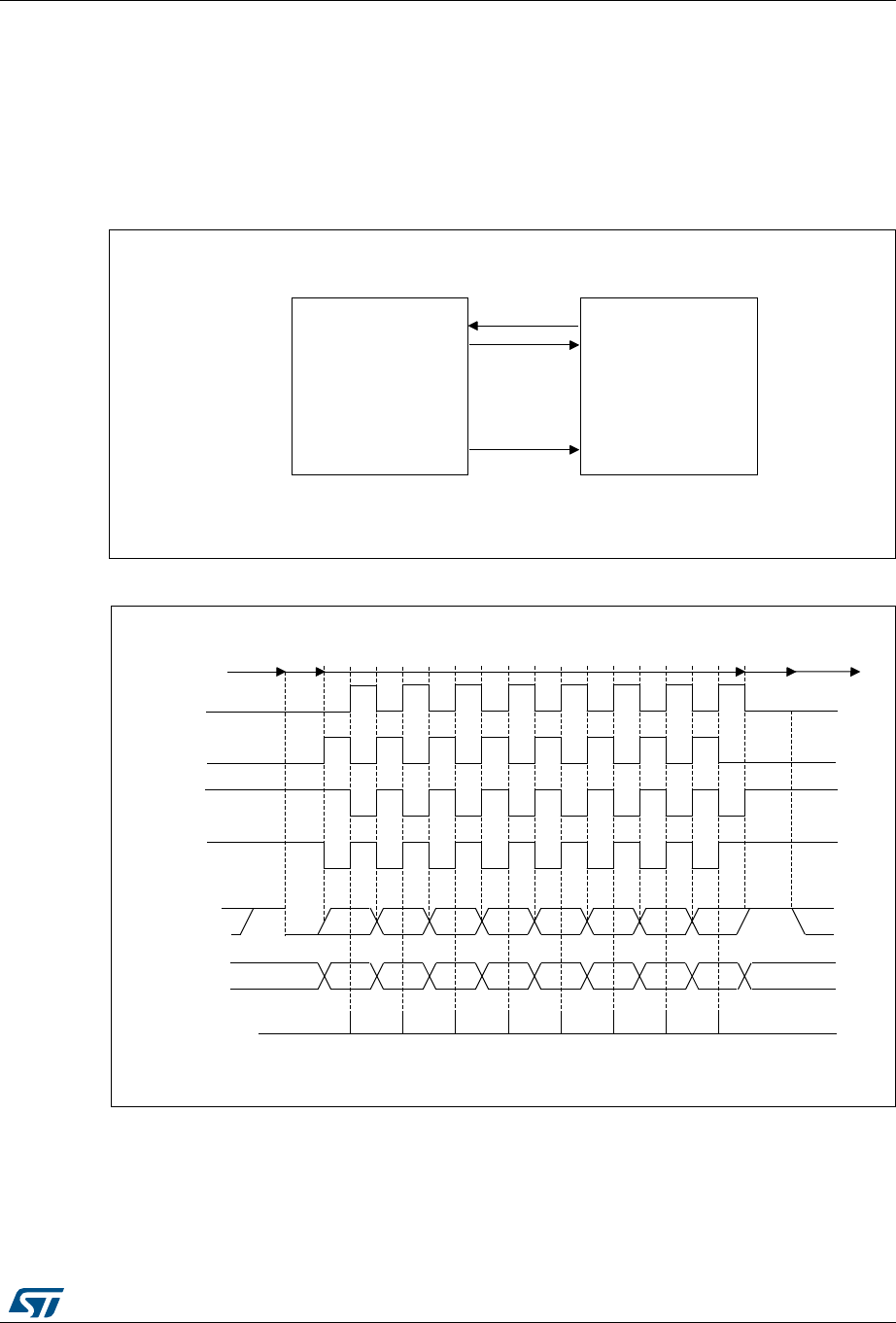
RM0394 Rev 4 1221/1600
RM0394 Universal synchronous receiver transmitter (USART) /universal asynchronous receiver
1303
Note: The CK pin works in conjunction with the TX pin. Thus, the clock is provided only if the
transmitter is enabled (TE=1) and data is being transmitted (the data register USART_TDR
written). This means that it is not possible to receive synchronous data without transmitting
data.
The LBCL, CPOL and CPHA bits have to be selected when the USART is disabled (UE=0)
to ensure that the clock pulses function correctly.
Figure 393. USART example of synchronous transmission
Figure 394. USART data clock timing diagram (M bits = 00)
06Y9
86$57 6\QFKURQRXVGHYLFH
HJVODYH63,
5;
7;
'DWDRXW
'DWDLQ
&ORFN
&.
06Y9
06%
06%
/6%
/6%
6WDUW
6WDUW 6WRS
,GOHRUSUHFHGLQJ
WUDQVPLVVLRQ
,GOHRUQH[W
WUDQVPLVVLRQ
/%&/ELWFRQWUROVODVWGDWDSXOVH
&DSWXUHVWUREH
'DWDRQ5;
IURPVODYH
'DWDRQ7;
IURPPDVWHU
&ORFN&32/ &3+$
&ORFN&32/ &3+$
&ORFN&32/ &3+$
&ORFN&32/ &3+$
6WRS
0ELWV GDWDELWV
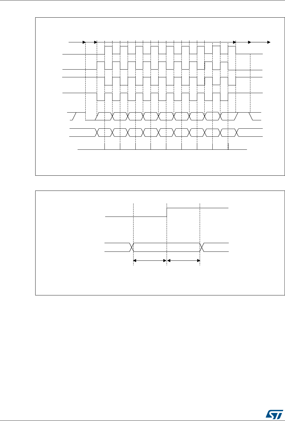
Universal synchronous receiver transmitter (USART) /universal asynchronous receiver transmit-
1222/1600 RM0394 Rev 4
Figure 395. USART data clock timing diagram (M bits = 01)
Figure 396. RX data setup/hold time
Note: The function of CK is different in Smartcard mode. Refer to Section 38.5.13: USART
Smartcard mode for more details.
06Y9
06%
06%
/6%
/6%6WDUW
6WDUW 6WRS
,GOHRU
SUHFHGLQJ
WUDQVPLVVLRQ
,GOHRUQH[W
WUDQVPLVVLRQ
/%&/ELWFRQWUROVODVWGDWDSXOVH
&DSWXUH
VWUREH
'DWDRQ5;
IURPVODYH
'DWDRQ7;
IURPPDVWHU
&ORFN&32/
&3+$
&ORFN&32/
&3+$
&ORFN&32/
&3+$
&ORFN&32/
&3+$
6WRS
0ELWV GDWDELWV
06Y9
'DWDRQ5;IURPVODYH
&.
FDSWXUHVWUREHRQ&.ULVLQJ
HGJHLQWKLVH[DPSOH
9DOLG'$7$ELW
W6(783 W+2/'
W6(783 W+2/'ELWWLPH

RM0394 Rev 4 1223/1600
RM0394 Universal synchronous receiver transmitter (USART) /universal asynchronous receiver
1303
38.5.12 USART Single-wire Half-duplex communication
Single-wire Half-duplex mode is selected by setting the HDSEL bit in the USART_CR3
register. In this mode, the following bits must be kept cleared:
•LINEN and CLKEN bits in the USART_CR2 register,
•SCEN and IREN bits in the USART_CR3 register.
The USART can be configured to follow a Single-wire Half-duplex protocol where the TX
and RX lines are internally connected. The selection between half- and Full-duplex
communication is made with a control bit HDSEL in USART_CR3.
As soon as HDSEL is written to 1:
•The TX and RX lines are internally connected
•The RX pin is no longer used
•The TX pin is always released when no data is transmitted. Thus, it acts as a standard
I/O in idle or in reception. It means that the I/O must be configured so that TX is
configured as alternate function open-drain with an external pull-up.
Apart from this, the communication protocol is similar to normal USART mode. Any conflicts
on the line must be managed by software (by the use of a centralized arbiter, for instance).
In particular, the transmission is never blocked by hardware and continues as soon as data
is written in the data register while the TE bit is set.
38.5.13 USART Smartcard mode
This section is relevant only when Smartcard mode is supported. Please refer to
Section 38.4: USART implementation on page 1196.
Smartcard mode is selected by setting the SCEN bit in the USART_CR3 register. In
Smartcard mode, the following bits must be kept cleared:
•LINEN bit in the USART_CR2 register,
•HDSEL and IREN bits in the USART_CR3 register.
Moreover, the CLKEN bit may be set in order to provide a clock to the smartcard.
The smartcard interface is designed to support asynchronous protocol for smartcards as
defined in the ISO 7816-3 standard. Both T=0 (character mode) and T=1 (block mode) are
supported.
The USART should be configured as:
•8 bits plus parity: where word length is set to 8 bits and PCE=1 in the USART_CR1
register
•1.5 stop bits when transmitting and receiving data: where STOP=11 in the
USART_CR2 register. It is also possible to choose 0.5 stop bit for receiving.
In T=0 (character) mode, the parity error is indicated at the end of each character during the
guard time period.
Figure 397 shows examples of what can be seen on the data line with and without parity
error.

Universal synchronous receiver transmitter (USART) /universal asynchronous receiver transmit-
1224/1600 RM0394 Rev 4
Figure 397. ISO 7816-3 asynchronous protocol
When connected to a smartcard, the TX output of the USART drives a bidirectional line that
is also driven by the smartcard. The TX pin must be configured as open drain.
Smartcard mode implements a single wire half duplex communication protocol.
•Transmission of data from the transmit shift register is guaranteed to be delayed by a
minimum of 1/2 baud clock. In normal operation a full transmit shift register starts
shifting on the next baud clock edge. In Smartcard mode this transmission is further
delayed by a guaranteed 1/2 baud clock.
•In transmission, if the smartcard detects a parity error, it signals this condition to the
USART by driving the line low (NACK). This NACK signal (pulling transmit line low for 1
baud clock) causes a framing error on the transmitter side (configured with 1.5 stop
bits). The USART can handle automatic re-sending of data according to the protocol.
The number of retries is programmed in the SCARCNT bit field. If the USART
continues receiving the NACK after the programmed number of retries, it stops
transmitting and signals the error as a framing error. The TXE bit can be set using the
TXFRQ bit in the USART_RQR register.
•Smartcard auto-retry in transmission: a delay of 2.5 baud periods is inserted between
the NACK detection by the USART and the start bit of the repeated character. The TC
bit is set immediately at the end of reception of the last repeated character (no guard-
time). If the software wants to repeat it again, it must insure the minimum 2 baud
periods required by the standard.
•If a parity error is detected during reception of a frame programmed with a 1.5 stop bits
period, the transmit line is pulled low for a baud clock period after the completion of the
receive frame. This is to indicate to the smartcard that the data transmitted to the
USART has not been correctly received. A parity error is NACKed by the receiver if the
NACK control bit is set, otherwise a NACK is not transmitted (to be used in T=1 mode).
If the received character is erroneous, the RXNE/receive DMA request is not activated.
According to the protocol specification, the smartcard must resend the same character.
If the received character is still erroneous after the maximum number of retries
specified in the SCARCNT bit field, the USART stops transmitting the NACK and
signals the error as a parity error.
•Smartcard auto-retry in reception: the BUSY flag remains set if the USART NACKs the
card but the card doesn’t repeat the character.
06Y9
:LWKRXW3DULW\HUURU
S
6
*XDUGWLPH
:LWK3DULW\HUURU
S
6
*XDUGWLPH
6WDUWELW
6WDUWELW /LQHSXOOHGORZE\UHFHLYHU
GXULQJVWRSLQFDVHRISDULW\HUURU
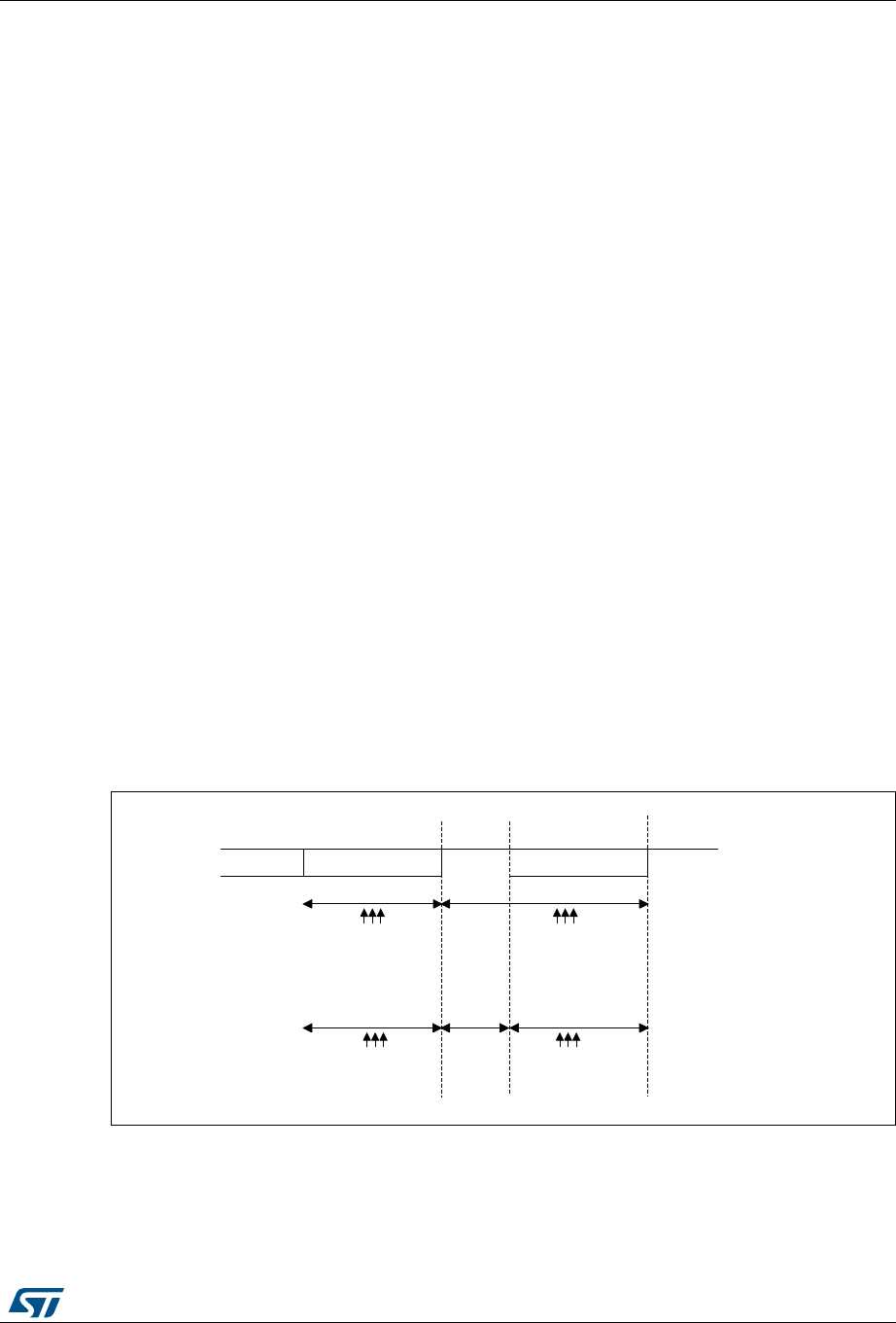
RM0394 Rev 4 1225/1600
RM0394 Universal synchronous receiver transmitter (USART) /universal asynchronous receiver
1303
•In transmission, the USART inserts the Guard Time (as programmed in the Guard Time
register) between two successive characters. As the Guard Time is measured after the
stop bit of the previous character, the GT[7:0] register must be programmed to the
desired CGT (Character Guard Time, as defined by the 7816-3 specification) minus 12
(the duration of one character).
•The assertion of the TC flag can be delayed by programming the Guard Time register.
In normal operation, TC is asserted when the transmit shift register is empty and no
further transmit requests are outstanding. In Smartcard mode an empty transmit shift
register triggers the Guard Time counter to count up to the programmed value in the
Guard Time register. TC is forced low during this time. When the Guard Time counter
reaches the programmed value TC is asserted high.
•The TCBGT flag can be used to detect the end of data transfer without waiting for
guard time completion. This flag is set just after the end of frame transmission and if no
NACK has been received from the card.
•The de-assertion of TC flag is unaffected by Smartcard mode.
•If a framing error is detected on the transmitter end (due to a NACK from the receiver),
the NACK is not detected as a start bit by the receive block of the transmitter.
According to the ISO protocol, the duration of the received NACK can be 1 or 2 baud
clock periods.
•On the receiver side, if a parity error is detected and a NACK is transmitted the receiver
does not detect the NACK as a start bit.
Note: A break character is not significant in Smartcard mode. A 0x00 data with a framing error is
treated as data and not as a break.
No Idle frame is transmitted when toggling the TE bit. The Idle frame (as defined for the
other configurations) is not defined by the ISO protocol.
Figure 398 details how the NACK signal is sampled by the USART. In this example the
USART is transmitting data and is configured with 1.5 stop bits. The receiver part of the
USART is enabled in order to check the integrity of the data and the NACK signal.
Figure 398. Parity error detection using the 1.5 stop bits
The USART can provide a clock to the smartcard through the CK output. In Smartcard
mode, CK is not associated to the communication but is simply derived from the internal
peripheral input clock through a 5-bit prescaler. The division ratio is configured in the
prescaler register USART_GTPR. CK frequency can be programmed from fCK/2 to fCK/62,
where fCK is the peripheral input clock.
06Y9
%LW 3DULW\ELW 6WRSELW
ELWWLPH ELWWLPH
ELWWLPH
6DPSOLQJDW
WKWKWK
6DPSOLQJDW
WKWKWK
6DPSOLQJDW
WKWKWK
6DPSOLQJDW
WKWKWK

Universal synchronous receiver transmitter (USART) /universal asynchronous receiver transmit-
1226/1600 RM0394 Rev 4
Block mode (T=1)
In T=1 (block) mode, the parity error transmission is deactivated, by clearing the NACK bit in
the UART_CR3 register.
When requesting a read from the smartcard, in block mode, the software must enable the
receiver Timeout feature by setting the RTOEN bit in the USART_CR2 register and program
the RTO bits field in the RTOR register to the BWT (block wait time) - 11 value. If no answer
is received from the card before the expiration of this period, the RTOF flag will be set and a
timeout interrupt will be generated (if RTOIE bit in the USART_CR1 register is set). If the
first character is received before the expiration of the period, it is signaled by the RXNE
interrupt.
Note: The RXNE interrupt must be enabled even when using the USART in DMA mode to read
from the smartcard in block mode. In parallel, the DMA must be enabled only after the first
received byte.
After the reception of the first character (RXNE interrupt), the RTO bit fields in the RTOR
register must be programmed to the CWT (character wait time) - 11 value, in order to allow
the automatic check of the maximum wait time between two consecutive characters. This
time is expressed in baudtime units. If the smartcard does not send a new character in less
than the CWT period after the end of the previous character, the USART signals this to the
software through the RTOF flag and interrupt (when RTOIE bit is set).
Note: The RTO counter starts counting:
- From the end of the stop bit in case STOP = 00.
- From the end of the second stop bit in case of STOP = 10.
- 1 bit duration after the beginning of the STOP bit in case STOP = 11.
- From the beginning of the STOP bit in case STOP = 01.
As in the Smartcard protocol definition, the BWT/CWT values are defined from the
beginning (start bit) of the last character. The RTO register must be programmed to BWT -
11 or CWT -11, respectively, taking into account the length of the last character itself.
A block length counter is used to count all the characters received by the USART. This
counter is reset when the USART is transmitting (TXE=0). The length of the block is
communicated by the smartcard in the third byte of the block (prologue field). This value
must be programmed to the BLEN field in the USART_RTOR register. when using DMA
mode, before the start of the block, this register field must be programmed to the minimum
value (0x0). with this value, an interrupt is generated after the 4th received character. The
software must read the LEN field (third byte), its value must be read from the receive buffer.
In interrupt driven receive mode, the length of the block may be checked by software or by
programming the BLEN value. However, before the start of the block, the maximum value of
BLEN (0xFF) may be programmed. The real value will be programmed after the reception of
the third character.
If the block is using the LRC longitudinal redundancy check (1 epilogue byte), the
BLEN=LEN. If the block is using the CRC mechanism (2 epilogue bytes), BLEN=LEN+1
must be programmed. The total block length (including prologue, epilogue and information
fields) equals BLEN+4. The end of the block is signaled to the software through the EOBF
flag and interrupt (when EOBIE bit is set).
In case of an error in the block length, the end of the block is signaled by the RTO interrupt
(Character wait Time overflow).

RM0394 Rev 4 1227/1600
RM0394 Universal synchronous receiver transmitter (USART) /universal asynchronous receiver
1303
Note: The error checking code (LRC/CRC) must be computed/verified by software.
Direct and inverse convention
The Smartcard protocol defines two conventions: direct and inverse.
The direct convention is defined as: LSB first, logical bit value of 1 corresponds to a H state
of the line and parity is even. In order to use this convention, the following control bits must
be programmed: MSBFIRST=0, DATAINV=0 (default values).
The inverse convention is defined as: MSB first, logical bit value 1 corresponds to an L state
on the signal line and parity is even. In order to use this convention, the following control bits
must be programmed: MSBFIRST=1, DATAINV=1.
Note: When logical data values are inverted (0=H, 1=L), the parity bit is also inverted in the same
way.
In order to recognize the card convention, the card sends the initial character, TS, as the
first character of the ATR (Answer To Reset) frame. The two possible patterns for the TS
are: LHHL LLL LLH and LHHL HHH LLH.
•(H) LHHL LLL LLH sets up the inverse convention: state L encodes value 1 and
moment 2 conveys the most significant bit (MSB first). when decoded by inverse
convention, the conveyed byte is equal to '3F'.
•(H) LHHL HHH LLH sets up the direct convention: state H encodes value 1 and
moment 2 conveys the least significant bit (LSB first). when decoded by direct
convention, the conveyed byte is equal to '3B'.
Character parity is correct when there is an even number of bits set to 1 in the nine
moments 2 to 10.
As the USART does not know which convention is used by the card, it needs to be able to
recognize either pattern and act accordingly. The pattern recognition is not done in
hardware, but through a software sequence. Moreover, supposing that the USART is
configured in direct convention (default) and the card answers with the inverse convention,
TS = LHHL LLL LLH => the USART received character will be ‘03’ and the parity will be odd.
Therefore, two methods are available for TS pattern recognition:
Method 1
The USART is programmed in standard Smartcard mode/direct convention. In this case, the
TS pattern reception generates a parity error interrupt and error signal to the card.
•The parity error interrupt informs the software that the card didn’t answer correctly in
direct convention. Software then reprograms the USART for inverse convention
•In response to the error signal, the card retries the same TS character, and it will be
correctly received this time, by the reprogrammed USART
Alternatively, in answer to the parity error interrupt, the software may decide to reprogram
the USART and to also generate a new reset command to the card, then wait again for the
TS.

Universal synchronous receiver transmitter (USART) /universal asynchronous receiver transmit-
1228/1600 RM0394 Rev 4
Method 2
The USART is programmed in 9-bit/no-parity mode, no bit inversion. In this mode it receives
any of the two TS patterns as:
(H) LHHL LLL LLH = 0x103 -> inverse convention to be chosen
(H) LHHL HHH LLH = 0x13B -> direct convention to be chosen
The software checks the received character against these two patterns and, if any of them
match, then programs the USART accordingly for the next character reception.
If none of the two is recognized, a card reset may be generated in order to restart the
negotiation.
38.5.14 USART IrDA SIR ENDEC block
This section is relevant only when IrDA mode is supported. Please refer to Section 38.4:
USART implementation on page 1196.
IrDA mode is selected by setting the IREN bit in the USART_CR3 register. In IrDA mode,
the following bits must be kept cleared:
•LINEN, STOP and CLKEN bits in the USART_CR2 register,
•SCEN and HDSEL bits in the USART_CR3 register.
The IrDA SIR physical layer specifies use of a Return to Zero, Inverted (RZI) modulation
scheme that represents logic 0 as an infrared light pulse (see Figure 399).
The SIR Transmit encoder modulates the Non Return to Zero (NRZ) transmit bit stream
output from USART. The output pulse stream is transmitted to an external output driver and
infrared LED. USART supports only bit rates up to 115.2 Kbps for the SIR ENDEC. In
normal mode the transmitted pulse width is specified as 3/16 of a bit period.
The SIR receive decoder demodulates the return-to-zero bit stream from the infrared
detector and outputs the received NRZ serial bit stream to the USART. The decoder input is
normally high (marking state) in the Idle state. The transmit encoder output has the opposite
polarity to the decoder input. A start bit is detected when the decoder input is low.
•IrDA is a half duplex communication protocol. If the Transmitter is busy (when the
USART is sending data to the IrDA encoder), any data on the IrDA receive line is
ignored by the IrDA decoder and if the Receiver is busy (when the USART is receiving
decoded data from the IrDA decoder), data on the TX from the USART to IrDA is not
encoded. while receiving data, transmission should be avoided as the data to be
transmitted could be corrupted.
•A 0 is transmitted as a high pulse and a 1 is transmitted as a 0. The width of the pulse
is specified as 3/16th of the selected bit period in normal mode (see Figure 400).
•The SIR decoder converts the IrDA compliant receive signal into a bit stream for
USART.
•The SIR receive logic interprets a high state as a logic one and low pulses as logic
zeros.
•The transmit encoder output has the opposite polarity to the decoder input. The SIR
output is in low state when Idle.
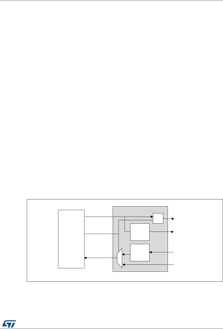
RM0394 Rev 4 1229/1600
RM0394 Universal synchronous receiver transmitter (USART) /universal asynchronous receiver
1303
•The IrDA specification requires the acceptance of pulses greater than 1.41 µs. The
acceptable pulse width is programmable. Glitch detection logic on the receiver end
filters out pulses of width less than 2 PSC periods (PSC is the prescaler value
programmed in the USART_GTPR). Pulses of width less than 1 PSC period are always
rejected, but those of width greater than one and less than two periods may be
accepted or rejected, those greater than 2 periods will be accepted as a pulse. The
IrDA encoder/decoder doesn’t work when PSC=0.
•The receiver can communicate with a low-power transmitter.
•In IrDA mode, the STOP bits in the USART_CR2 register must be configured to “1 stop
bit”.
IrDA low-power mode
Transmitter
In low-power mode the pulse width is not maintained at 3/16 of the bit period. Instead, the
width of the pulse is 3 times the low-power baud rate which can be a minimum of 1.42 MHz.
Generally, this value is 1.8432 MHz (1.42 MHz < PSC< 2.12 MHz). A low-power mode
programmable divisor divides the system clock to achieve this value.
Receiver
Receiving in low-power mode is similar to receiving in normal mode. For glitch detection the
USART should discard pulses of duration shorter than 1 PSC period. A valid low is accepted
only if its duration is greater than 2 periods of the IrDA low-power Baud clock (PSC value in
the USART_GTPR).
Note: A pulse of width less than two and greater than one PSC period(s) may or may not be
rejected.
The receiver set up time should be managed by software. The IrDA physical layer
specification specifies a minimum of 10 ms delay between transmission and reception (IrDA
is a half duplex protocol).
Figure 399. IrDA SIR ENDEC- block diagram
6,5(1
06Y9
86$57
25
6,5
7UDQVPLW
(QFRGHU
6,5
5HFHLYH
'(FRGHU
7;
5;
86$57B5;
,U'$B,1
,U'$B287
86$57B7;
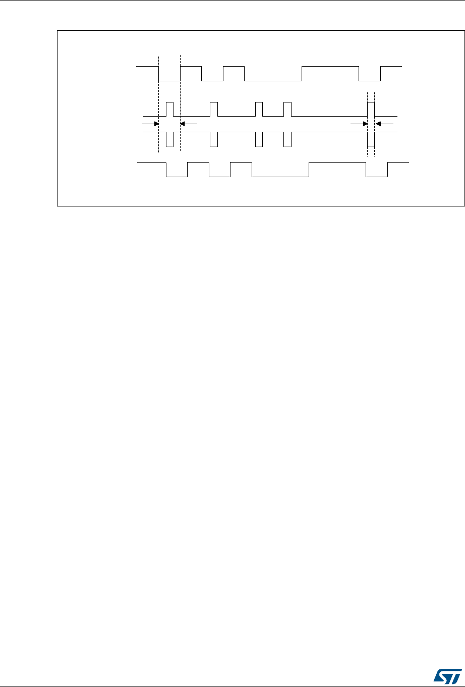
Universal synchronous receiver transmitter (USART) /universal asynchronous receiver transmit-
1230/1600 RM0394 Rev 4
Figure 400. IrDA data modulation (3/16) -Normal Mode
38.5.15 USART continuous communication in DMA mode
The USART is capable of performing continuous communication using the DMA. The DMA
requests for Rx buffer and Tx buffer are generated independently.
Note: Please refer to Section 38.4: USART implementation on page 1196 to determine if the DMA
mode is supported. If DMA is not supported, use the USART as explained in Section 38.5.2:
USART transmitter or Section 38.5.3: USART receiver. To perform continuous
communication, the user can clear the TXE/ RXNE flags In the USART_ISR register.
Transmission using DMA
DMA mode can be enabled for transmission by setting DMAT bit in the USART_CR3
register. Data is loaded from a SRAM area configured using the DMA peripheral (refer to
Section 11: Direct memory access controller (DMA) on page 295) to the USART_TDR
register whenever the TXE bit is set. To map a DMA channel for USART transmission, use
the following procedure (x denotes the channel number):
1. Write the USART_TDR register address in the DMA control register to configure it as
the destination of the transfer. The data is moved to this address from memory after
each TXE event.
2. Write the memory address in the DMA control register to configure it as the source of
the transfer. The data is loaded into the USART_TDR register from this memory area
after each TXE event.
3. Configure the total number of bytes to be transferred to the DMA control register.
4. Configure the channel priority in the DMA register
5. Configure DMA interrupt generation after half/ full transfer as required by the
application.
6. Clear the TC flag in the USART_ISR register by setting the TCCF bit in the
USART_ICR register.
7. Activate the channel in the DMA register.
When the number of data transfers programmed in the DMA Controller is reached, the DMA
controller generates an interrupt on the DMA channel interrupt vector.
In transmission mode, once the DMA has written all the data to be transmitted (the TCIF flag
is set in the DMA_ISR register), the TC flag can be monitored to make sure that the USART
06Y9
7;
6WDUW
ELW
6WRS
ELW
%LWSHULRG
,U'$B287
,U'$B,1
5;
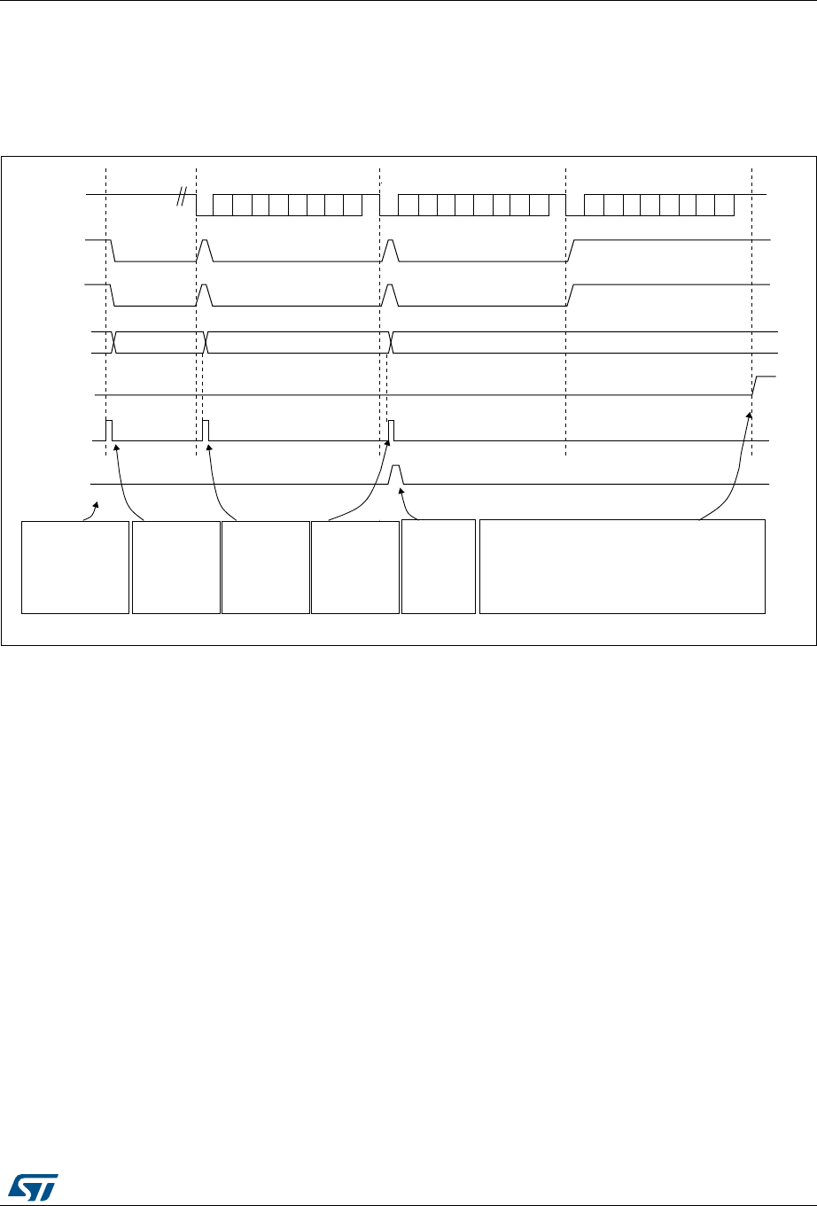
RM0394 Rev 4 1231/1600
RM0394 Universal synchronous receiver transmitter (USART) /universal asynchronous receiver
1303
communication is complete. This is required to avoid corrupting the last transmission before
disabling the USART or entering Stop mode. Software must wait until TC=1. The TC flag
remains cleared during all data transfers and it is set by hardware at the end of transmission
of the last frame.
Figure 401. Transmission using DMA
Reception using DMA
DMA mode can be enabled for reception by setting the DMAR bit in USART_CR3 register.
Data is loaded from the USART_RDR register to a SRAM area configured using the DMA
peripheral (refer to Section 11: Direct memory access controller (DMA) on page 295)
whenever a data byte is received. To map a DMA channel for USART reception, use the
following procedure:
1. Write the USART_RDR register address in the DMA control register to configure it as
the source of the transfer. The data is moved from this address to the memory after
each RXNE event.
2. Write the memory address in the DMA control register to configure it as the destination
of the transfer. The data is loaded from USART_RDR to this memory area after each
RXNE event.
3. Configure the total number of bytes to be transferred to the DMA control register.
4. Configure the channel priority in the DMA control register
5. Configure interrupt generation after half/ full transfer as required by the application.
6. Activate the channel in the DMA control register.
When the number of data transfers programmed in the DMA Controller is reached, the DMA
controller generates an interrupt on the DMA channel interrupt vector.
) ))
AIB
6RIWZDUH
FRQILJXUHV'0$
WRVHQGGDWD
EORFNVDQG
HQDEOHV86$57
7KH'0$
WUDQVIHULV
FRPSOHWH
7&,) LQ
'0$B,65
'0$ZULWHV
)LQWR
86$57B7'5
'0$ZULWHV
)LQWR
86$57B7'5
'0$ZULWHV
)LQWR
86$57B7'5
6RIWZDUHZDLWVXQWLO7&
6HWE\KDUGZDUH
&OHDUHG
E\
VRIWZDUH
6HWE\
KDUGZDUH
7;OLQH
7;(IODJ
86$57B7'5
'0$UHTXHVW
'0$ZULWHV
86$57B7'5
'0$7&,)IODJ
WUDQVIHU
FRPSOHWH
7&IODJ
)UDPH )UDPH )UDPH
,GOHSUHDPEOH
6HWE\KDUGZDUH
FOHDUHGE\'0$UHDG
6HWE\KDUGZDUH
FOHDUHGE\'0$UHDG 6HWE\KDUGZDUH
,JQRUHGE\WKH'0$EHFDXVH
WKHWUDQVIHULVFRPSOHWH
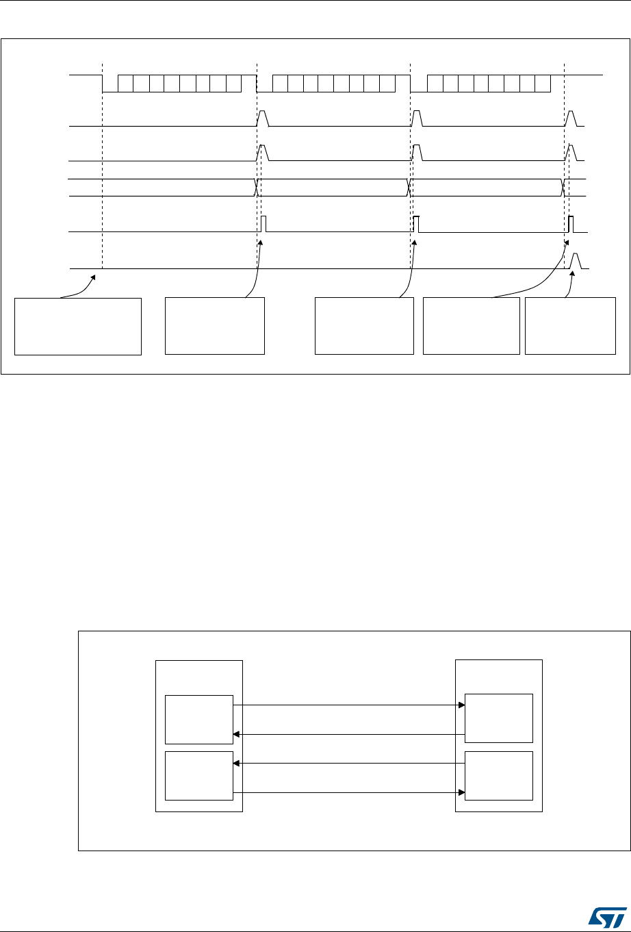
Universal synchronous receiver transmitter (USART) /universal asynchronous receiver transmit-
1232/1600 RM0394 Rev 4
Figure 402. Reception using DMA
Error flagging and interrupt generation in multibuffer communication
In multibuffer communication if any error occurs during the transaction the error flag is
asserted after the current byte. An interrupt is generated if the interrupt enable flag is set.
For framing error, overrun error and noise flag which are asserted with RXNE in single byte
reception, there is a separate error flag interrupt enable bit (EIE bit in the USART_CR3
register), which, if set, enables an interrupt after the current byte if any of these errors occur.
38.5.16 RS232 hardware flow control and RS485 driver enable
using USART
It is possible to control the serial data flow between 2 devices by using the CTS input and
the RTS output. The Figure 403 shows how to connect 2 devices in this mode:
Figure 403. Hardware flow control between 2 USARTs
7;OLQH
)UDPH
) )
6HWE\KDUGZDUH
FOHDUHGE\'0$UHDG
)
DLE
)UDPH )UDPH
5;1(IODJ
86$57B7'5
'0$UHTXHVW
'0$UHDGV
86$57B7'5
'0$7&,)IODJ
WUDQVIHUFRPSOHWH
6RIWZDUHFRQILJXUHVWKH
'0$WRUHFHLYHGDWD
EORFNVDQGHQDEOHV
WKH86$57
'0$UHDGV)
IURP86$57B7'5
7KH'0$WUDQVIHU
LVFRPSOHWH
7&,) LQ
'0$B,65
6HWE\KDUGZDUH
&OHDUHG
E\
VRIWZDUH
'0$UHDGV)
IURP86$57B7'5
'0$UHDGV)
IURP86$57B7'5
06Y9
7;FLUFXLW
86$57
7;
5;FLUFXLW
5;FLUFXLW
86$57
7;FLUFXLW
7;
&76
&76576
5;
576
5;
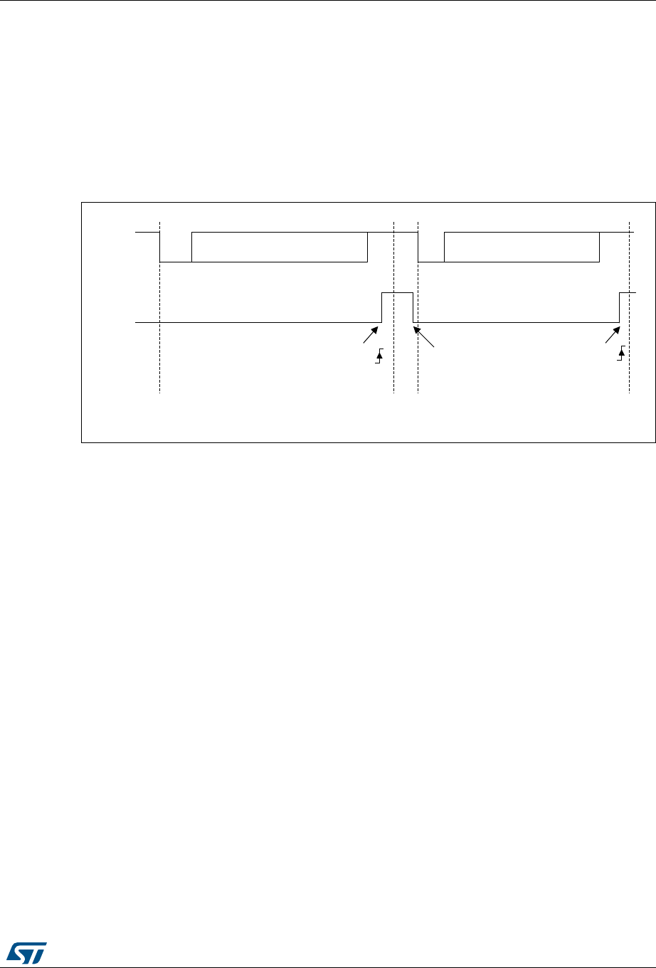
RM0394 Rev 4 1233/1600
RM0394 Universal synchronous receiver transmitter (USART) /universal asynchronous receiver
1303
RS232 RTS and CTS flow control can be enabled independently by writing the RTSE and
CTSE bits respectively to 1 (in the USART_CR3 register).
RS232 RTS flow control
If the RTS flow control is enabled (RTSE=1), then RTS is asserted (tied low) as long as the
USART receiver is ready to receive a new data. When the receive register is full, RTS is de-
asserted, indicating that the transmission is expected to stop at the end of the current frame.
Figure 404 shows an example of communication with RTS flow control enabled.
Figure 404. RS232 RTS flow control
RS232 CTS flow control
If the CTS flow control is enabled (CTSE=1), then the transmitter checks the CTS input
before transmitting the next frame. If CTS is asserted (tied low), then the next data is
transmitted (assuming that data is to be transmitted, in other words, if TXE=0), else the
transmission does not occur. when CTS is de-asserted during a transmission, the current
transmission is completed before the transmitter stops.
When CTSE=1, the CTSIF status bit is automatically set by hardware as soon as the CTS
input toggles. It indicates when the receiver becomes ready or not ready for communication.
An interrupt is generated if the CTSIE bit in the USART_CR3 register is set. Figure 405
shows an example of communication with CTS flow control enabled.
06Y9
6WDUW
ELW
6WDUW
ELW
6WRS
ELW ,GOH 6WRS
ELW
5;
576
'DWDUHDG
'DWDFDQQRZEHWUDQVPLWWHG
5;1( 5;1(
'DWD 'DWD

Universal synchronous receiver transmitter (USART) /universal asynchronous receiver transmit-
1234/1600 RM0394 Rev 4
Figure 405. RS232 CTS flow control
Note: For correct behavior, CTS must be asserted at least 3 USART clock source periods before
the end of the current character. In addition it should be noted that the CTSCF flag may not
be set for pulses shorter than 2 x PCLK periods.
RS485 Driver Enable
The driver enable feature is enabled by setting bit DEM in the USART_CR3 control register.
This allows the user to activate the external transceiver control, through the DE (Driver
Enable) signal. The assertion time is the time between the activation of the DE signal and
the beginning of the START bit. It is programmed using the DEAT [4:0] bit fields in the
USART_CR1 control register. The de-assertion time is the time between the end of the last
stop bit, in a transmitted message, and the de-activation of the DE signal. It is programmed
using the DEDT [4:0] bit fields in the USART_CR1 control register. The polarity of the DE
signal can be configured using the DEP bit in the USART_CR3 control register.
In USART, the DEAT and DEDT are expressed in sample time units (1/8 or 1/16 bit duration,
depending on the oversampling rate).
38.5.17 Wakeup from Stop mode using USART
The USART is able to wake up the MCU from Stop mode when the UESM bit is set and the
USART clock is set to HSI16 or LSE (refer to Section Reset and clock control (RCC)).
•USART source clock is HSI
If during stop mode the HSI clock is switched OFF, when a falling edge on the USART
receive line is detected, the USART interface requests the HSI clock to be switched
ON. The HSI clock is then used for the frame reception.
– If the wakeup event is verified, the MCU wakes up from low-power mode and data
reception goes on normally.
– If the wakeup event is not verified, the HSI clock is switched OFF again, the MCU
is not waken up and stays in low-power mode and the clock request is released.
•USART source clock is LSE
Same principle as described in case of USART source clock is HSI with the difference
that the LSE is ON in stop mode, but the LSE clock is not propagated to USART if the
06Y9
6WDUW
ELW
6WRS
ELW
7;
7'5
&76
'DWD
'DWD
6WRS
ELW ,GOH 6WDUW
ELW
'DWD 'DWD
'DWD
HPSW\ HPSW\
&76
&76
7UDQVPLWGDWDUHJLVWHU
:ULWLQJGDWDLQ7'5 7UDQVPLVVLRQRI'DWDLV
GHOD\HGXQWLO&76

RM0394 Rev 4 1235/1600
RM0394 Universal synchronous receiver transmitter (USART) /universal asynchronous receiver
1303
USART is not requesting it. The LSE clock is not OFF but there is a clock gating to
avoid useless consumption.
When the USART clock source is configured to be fLSE or fHSI, it is possible to keep enabled
this clock during STOP mode by setting the UCESM bit in USART_CR3 control register.
The MCU wakeup from Stop mode can be done using the standard RXNE interrupt. In this
case, the RXNEIE bit must be set before entering Stop mode.
Alternatively, a specific interrupt may be selected through the WUS bit fields.
In order to be able to wake up the MCU from Stop mode, the UESM bit in the USART_CR1
control register must be set prior to entering Stop mode.
When the wakeup event is detected, the WUF flag is set by hardware and a wakeup
interrupt is generated if the WUFIE bit is set.
Note: Before entering Stop mode, the user must ensure that the USART is not performing a
transfer. BUSY flag cannot ensure that Stop mode is never entered during a running
reception.
The WUF flag is set when a wakeup event is detected, independently of whether the MCU is
in Stop or in an active mode.
When entering Stop mode just after having initialized and enabled the receiver, the REACK
bit must be checked to ensure the USART is actually enabled.
When DMA is used for reception, it must be disabled before entering Stop mode and re-
enabled upon exit from Stop mode.
The wakeup from Stop mode feature is not available for all modes. For example it doesn’t
work in SPI mode because the SPI operates in master mode only.
Using Mute mode with Stop mode
If the USART is put into Mute mode before entering Stop mode:
•Wakeup from Mute mode on idle detection must not be used, because idle detection
cannot work in Stop mode.
•If the wakeup from Mute mode on address match is used, then the source of wake-up
from Stop mode must also be the address match. If the RXNE flag is set when entering
the Stop mode, the interface will remain in mute mode upon address match and wake
up from Stop.
•If the USART is configured to wake up the MCU from Stop mode on START bit
detection, the WUF flag is set, but the RXNE flag is not set.
Determining the maximum USART baud rate allowing to wakeup correctly
from Stop mode when the USART clock source is the HSI clock
The maximum baud rate allowing to wakeup correctly from stop mode depends on:
•the parameter tWUUSART provided in the device datasheet
•the USART receiver tolerance provided in the Section 38.5.5: Tolerance of the USART
receiver to clock deviation.
Let us take this example: OVER8 = 0, M bits = 10, ONEBIT = 1, BRR [3:0] = 0000.
In these conditions, according to Table 195: Tolerance of the USART receiver when BRR
[3:0] = 0000, the USART receiver tolerance is 4.86 %.
DTRA + DQUANT + DREC + DTCL + DWU < USART receiver's tolerance

Universal synchronous receiver transmitter (USART) /universal asynchronous receiver transmit-
1236/1600 RM0394 Rev 4
DWU max = tWUUSART / (11 x Tbit Min)
Tbit Min = tWUUSART / (9 x DWU max)
If we consider an ideal case where the parameters DTRA, DQUANT, DREC and DTCL are
at 0%, the DWU max is 4.86 %. In reality, we need to consider at least the HSI inaccuracy.
Let us consider the HSI inaccuracy = 1 %, tWUUSART = 1.7 s (in case of wakeup from Stop
mode 0).
DWU max = 4.86 % - 1 % = 3.86 %
Tbit min = 1.7 µs / (9 3.86 %) = 4.89 µs
In these conditions, the maximum baud rate allowing to wakeup correctly from Stop mode is
1/4.89 µs = 204 Kbaud.
38.6 USART low-power modes
38.7 USART interrupts
Table 198. Effect of low-power modes on the USART
Mode Description
Sleep No effect. USART interrupt causes the device to exit Sleep mode.
Low-power run No effect.
Low-power sleep No effect. USART interrupt causes the device to exit Low-power sleep
mode.
Stop 0 / Stop 1
The USART registers content is kept. The USART is able to wake up the
MCU from Stop 0 and Stop 1 modes when the UESM bit is set and the
USART clock is set to HSI16 or LSE.
The MCU wakeup from Stop 0 and Stop 1 modes can be done using either
a standard RXNE or a WUF interrupt.
Stop 2 The USART registers content is kept. The USART must either be disabled
or put in reset state.
Standby The USART is powered down and must be reinitialized when the device
has exited from Standby or Shutdown mode.
Shutdown
Table 199. USART interrupt requests
Interrupt event Event flag Enable Control
bit
Transmit data register empty TXE TXEIE
CTS interrupt CTSIF CTSIE
Transmission Complete TC TCIE
Receive data register not empty (data ready to be read) RXNE
RXNEIE
Overrun error detected ORE
Idle line detected IDLE IDLEIE
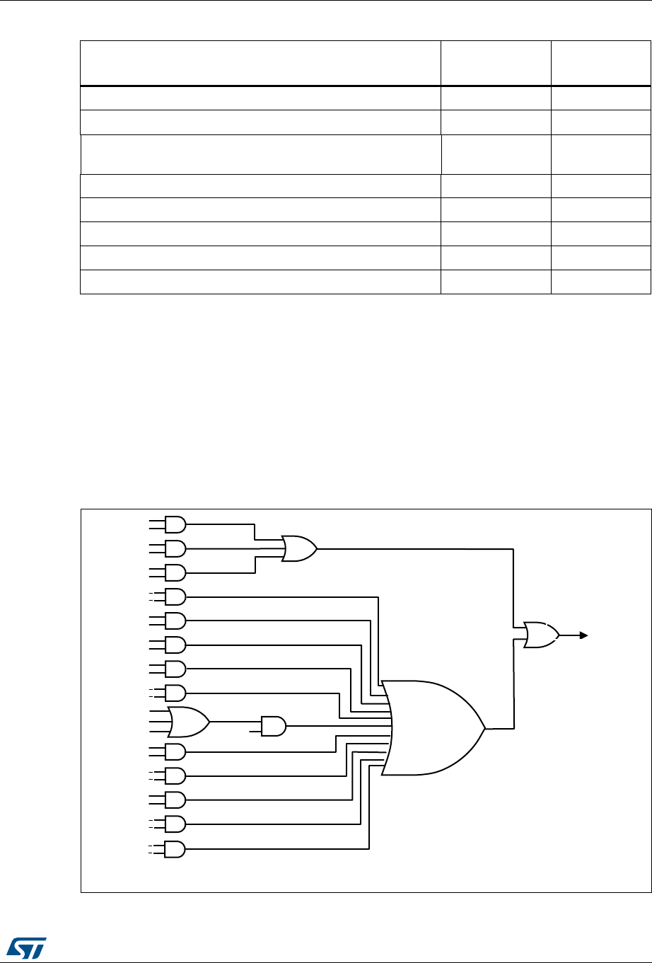
RM0394 Rev 4 1237/1600
RM0394 Universal synchronous receiver transmitter (USART) /universal asynchronous receiver
1303
The USART interrupt events are connected to the same interrupt vector (see Figure 406).
•During transmission: Transmission Complete, Transmission complete before guard
time, Clear to Send, Transmit data Register empty or Framing error (in Smartcard
mode) interrupt.
•During reception: Idle Line detection, Overrun error, Receive data register not empty,
Parity error, LIN break detection, Noise Flag, Framing Error, Character match, etc.
These events generate an interrupt if the corresponding Enable Control Bit is set.
Figure 406. USART interrupt mapping diagram
Parity error PE PEIE
LIN break LBDF LBDIE
Noise Flag, Overrun error and Framing Error in multibuffer
communication. NF or ORE or FE EIE
Character match CMF CMIE
Receiver timeout RTOF RTOIE
End of Block EOBF EOBIE
Wakeup from Stop mode WUF(1) WUFIE
Transmission complete before guard time TCBGT TCBGTIE
1. The WUF interrupt is active only in Stop mode.
Table 199. USART interrupt requests (continued)
Interrupt event Event flag Enable Control
bit
06Y9
7&
7&,(
7;(
7;(,(
&76,)
&76,(
,'/(
,'/(,(
5;1(,(
25(
5;1(,(
5;1(
3(
3(,(
/%')
/%',(
&0)
&0,(
(2%)
(2%,(
:8)
:8),(
)(
1)
25(
572)
572,(
(,(
86$57
LQWHUUXSW
7&%*7
7&%*7,(

Universal synchronous receiver transmitter (USART) /universal asynchronous receiver transmit-
1238/1600 RM0394 Rev 4
38.8 USART registers
Refer to Section 1.2 on page 60 for a list of abbreviations used in register descriptions.
38.8.1 Control register 1 (USART_CR1)
Address offset: 0x00
Reset value: 0x0000 0000
31 30 29 28 27 26 25 24 23 22 21 20 19 18 17 16
Res. Res. Res. M1 EOBIE RTOIE DEAT[4:0] DEDT[4:0]
rw rw rw rw rw rw rw rw rw rw rw rw rw
1514131211109876 5 43210
OVER8 CMIE MME M0 WAKE PCE PS PEIE TXEIE TCIE RXNEIE IDLEIE TE RE UESM UE
rw rw rw rw rw rw rw rw rw rw rw rw rw rw rw rw
Bits 31:29 Reserved, must be kept at reset value.
Bit 28 M1: Word length
This bit, with bit 12 (M0), determines the word length. It is set or cleared by software.
M[1:0] = 00: 1 Start bit, 8 data bits, n stop bits
M[1:0] = 01: 1 Start bit, 9 data bits, n stop bits
M[1:0] = 10: 1 Start bit, 7 data bits, n stop bits
This bit can only be written when the USART is disabled (UE=0).
Note: Not all modes are supported In 7-bit data length mode. Refer to Section 38.4: USART
implementation for details.
Bit 27 EOBIE: End of Block interrupt enable
This bit is set and cleared by software.
0: Interrupt is inhibited
1: A USART interrupt is generated when the EOBF flag is set in the USART_ISR register.
Note: If the USART does not support Smartcard mode, this bit is reserved and must be kept
at reset value. Please refer to Section 38.4: USART implementation on page 1196.
Bit 26 RTOIE: Receiver timeout interrupt enable
This bit is set and cleared by software.
0: Interrupt is inhibited
1: An USART interrupt is generated when the RTOF bit is set in the USART_ISR register.
Note: If the USART does not support the Receiver timeout feature, this bit is reserved and
must be kept at reset value. Section 38.4: USART implementation on page 1196.
Bits 25:21 DEAT[4:0]: Driver Enable assertion time
This 5-bit value defines the time between the activation of the DE (Driver Enable) signal and
the beginning of the start bit. It is expressed in sample time units (1/8 or 1/16 bit duration,
depending on the oversampling rate).
This bit field can only be written when the USART is disabled (UE=0).
Note: If the Driver Enable feature is not supported, this bit is reserved and must be kept at
reset value. Please refer to Section 38.4: USART implementation on page 1196.

RM0394 Rev 4 1239/1600
RM0394 Universal synchronous receiver transmitter (USART) /universal asynchronous receiver
1303
Bits 20:16 DEDT[4:0]: Driver Enable de-assertion time
This 5-bit value defines the time between the end of the last stop bit, in a transmitted
message, and the de-activation of the DE (Driver Enable) signal. It is expressed in sample
time units (1/8 or 1/16 bit duration, depending on the oversampling rate).
If the USART_TDR register is written during the DEDT time, the new data is transmitted only
when the DEDT and DEAT times have both elapsed.
This bit field can only be written when the USART is disabled (UE=0).
Note: If the Driver Enable feature is not supported, this bit is reserved and must be kept at
reset value. Please refer to Section 38.4: USART implementation on page 1196.
Bit 15 OVER8: Oversampling mode
0: Oversampling by 16
1: Oversampling by 8
This bit can only be written when the USART is disabled (UE=0).
Note: In LIN, IrDA and modes, this bit must be kept at reset value.
Bit 14 CMIE: Character match interrupt enable
This bit is set and cleared by software.
0: Interrupt is inhibited
1: A USART interrupt is generated when the CMF bit is set in the USART_ISR register.
Bit 13 MME: Mute mode enable
This bit activates the mute mode function of the USART. when set, the USART can switch
between the active and mute modes, as defined by the WAKE bit. It is set and cleared by
software.
0: Receiver in active mode permanently
1: Receiver can switch between mute mode and active mode.
Bit 12 M0: Word length
This bit, with bit 28 (M1), determines the word length. It is set or cleared by software. See Bit
28 (M1) description.
This bit can only be written when the USART is disabled (UE=0).
Bit 11 WAKE: Receiver wakeup method
This bit determines the USART wakeup method from Mute mode. It is set or cleared by
software.
0: Idle line
1: Address mark
This bit field can only be written when the USART is disabled (UE=0).
Bit 10 PCE: Parity control enable
This bit selects the hardware parity control (generation and detection). When the parity
control is enabled, the computed parity is inserted at the MSB position (9th bit if M=1; 8th bit
if M=0) and parity is checked on the received data. This bit is set and cleared by software.
Once it is set, PCE is active after the current byte (in reception and in transmission).
0: Parity control disabled
1: Parity control enabled
This bit field can only be written when the USART is disabled (UE=0).
Bit 9 PS: Parity selection
This bit selects the odd or even parity when the parity generation/detection is enabled (PCE
bit set). It is set and cleared by software. The parity will be selected after the current byte.
0: Even parity
1: Odd parity
This bit field can only be written when the USART is disabled (UE=0).

Universal synchronous receiver transmitter (USART) /universal asynchronous receiver transmit-
1240/1600 RM0394 Rev 4
Bit 8 PEIE: PE interrupt enable
This bit is set and cleared by software.
0: Interrupt is inhibited
1: A USART interrupt is generated whenever PE=1 in the USART_ISR register
Bit 7 TXEIE: interrupt enable
This bit is set and cleared by software.
0: Interrupt is inhibited
1: A USART interrupt is generated whenever TXE=1 in the USART_ISR register
Bit 6 TCIE: Transmission complete interrupt enable
This bit is set and cleared by software.
0: Interrupt is inhibited
1: A USART interrupt is generated whenever TC=1 in the USART_ISR register
Bit 5 RXNEIE: RXNE interrupt enable
This bit is set and cleared by software.
0: Interrupt is inhibited
1: A USART interrupt is generated whenever ORE=1 or RXNE=1 in the USART_ISR
register
Bit 4 IDLEIE: IDLE interrupt enable
This bit is set and cleared by software.
0: Interrupt is inhibited
1: A USART interrupt is generated whenever IDLE=1 in the USART_ISR register
Bit 3 TE: Transmitter enable
This bit enables the transmitter. It is set and cleared by software.
0: Transmitter is disabled
1: Transmitter is enabled
Note: During transmission, a “0” pulse on the TE bit (“0” followed by “1”) sends a preamble
(idle line) after the current word, except in Smartcard mode. In order to generate an idle
character, the TE must not be immediately written to 1. In order to ensure the required
duration, the software can poll the TEACK bit in the USART_ISR register.
In Smartcard mode, when TE is set there is a 1 bit-time delay before the transmission
starts.

RM0394 Rev 4 1241/1600
RM0394 Universal synchronous receiver transmitter (USART) /universal asynchronous receiver
1303
38.8.2 Control register 2 (USART_CR2)
Address offset: 0x04
Reset value: 0x0000 0000
Bit 2 RE: Receiver enable
This bit enables the receiver. It is set and cleared by software.
0: Receiver is disabled
1: Receiver is enabled and begins searching for a start bit
Bit 1 UESM: USART enable in Stop mode
When this bit is cleared, the USART is not able to wake up the MCU from Stop mode.
When this bit is set, the USART is able to wake up the MCU from Stop mode, provided that
the USART clock selection is HSI16 or LSE in the RCC.
This bit is set and cleared by software.
0: USART not able to wake up the MCU from Stop mode.
1: USART able to wake up the MCU from Stop mode. When this function is active, the clock
source for the USART must be HSI16 or LSE (see Section Reset and clock control
(RCC).
Note: It is recommended to set the UESM bit just before entering Stop mode and clear it on
exit from Stop mode.
If the USART does not support the wakeup from Stop feature, this bit is reserved and
must be kept at reset value. Please refer to Section 38.4: USART implementation on
page 1196.
Bit 0 UE: USART enable
When this bit is cleared, the USART prescalers and outputs are stopped immediately, and
current operations are discarded. The configuration of the USART is kept, but all the status
flags, in the USART_ISR are set to their default values. This bit is set and cleared by
software.
0: USART prescaler and outputs disabled, low-power mode
1: USART enabled
Note: In order to go into low-power mode without generating errors on the line, the TE bit
must be reset before and the software must wait for the TC bit in the USART_ISR to be
set before resetting the UE bit.
The DMA requests are also reset when UE = 0 so the DMA channel must be disabled
before resetting the UE bit.
31 30 29 28 27 26 25 24 23 22 21 20 19 18 17 16
ADD[7:4] ADD[3:0] RTOEN ABRMOD[1:0] ABREN MSBFI
RST DATAINV TXINV RXINV
rw rw rw rw rw rw rw rw rw rw rw rw rw rw rw rw
1514131211109876543 2 10
SWAP LINEN STOP[1:0] CLKEN CPOL CPHA LBCL Res. LBDIE LBDL ADDM7 Res. Res. Res. Res.
rw rw rw rw rw rw rw rw rw rw rw

Universal synchronous receiver transmitter (USART) /universal asynchronous receiver transmit-
1242/1600 RM0394 Rev 4
Bits 31:28 ADD[7:4]: Address of the USART node
This bit-field gives the address of the USART node or a character code to be recognized.
This is used in multiprocessor communication during Mute mode or Stop mode, for wakeup with 7-
bit address mark detection. The MSB of the character sent by the transmitter should be equal to 1.
It may also be used for character detection during normal reception, Mute mode inactive (for
example, end of block detection in ModBus protocol). In this case, the whole received character (8-
bit) is compared to the ADD[7:0] value and CMF flag is set on match.
This bit field can only be written when reception is disabled (RE = 0) or the USART is disabled
(UE=0)
Bits 27:24 ADD[3:0]: Address of the USART node
This bit-field gives the address of the USART node or a character code to be recognized.
This is used in multiprocessor communication during Mute mode or Stop mode, for wakeup with
address mark detection.
This bit field can only be written when reception is disabled (RE = 0) or the USART is disabled
(UE=0)
Bit 23 RTOEN: Receiver timeout enable
This bit is set and cleared by software.
0: Receiver timeout feature disabled.
1: Receiver timeout feature enabled.
When this feature is enabled, the RTOF flag in the USART_ISR register is set if the RX line is idle
(no reception) for the duration programmed in the RTOR (receiver timeout register).
Note: If the USART does not support the Receiver timeout feature, this bit is reserved and must be
kept at reset value. Please refer to Section 38.4: USART implementation on page 1196.
Bits 22:21 ABRMOD[1:0]: Auto baud rate mode
These bits are set and cleared by software.
00: Measurement of the start bit is used to detect the baud rate.
01: Falling edge to falling edge measurement. (the received frame must start with a single bit = 1 ->
Frame = Start10xxxxxx)
10: 0x7F frame detection.
11: 0x55 frame detection
This bit field can only be written when ABREN = 0 or the USART is disabled (UE=0).
Note: If DATAINV=1 and/or MSBFIRST=1 the patterns must be the same on the line, for example
0xAA for MSBFIRST)
If the USART does not support the auto baud rate feature, this bit is reserved and must be kept
at reset value. Please refer to Section 38.4: USART implementation on page 1196.
Bit 20 ABREN: Auto baud rate enable
This bit is set and cleared by software.
0: Auto baud rate detection is disabled.
1: Auto baud rate detection is enabled.
Note: If the USART does not support the auto baud rate feature, this bit is reserved and must be kept
at reset value. Please refer to Section 38.4: USART implementation on page 1196.
Bit 19 MSBFIRST: Most significant bit first
This bit is set and cleared by software.
0: data is transmitted/received with data bit 0 first, following the start bit.
1: data is transmitted/received with the MSB (bit 7/8/9) first, following the start bit.
This bit field can only be written when the USART is disabled (UE=0).

RM0394 Rev 4 1243/1600
RM0394 Universal synchronous receiver transmitter (USART) /universal asynchronous receiver
1303
Bit 18 DATAINV: Binary data inversion
This bit is set and cleared by software.
0: Logical data from the data register are send/received in positive/direct logic. (1=H, 0=L)
1: Logical data from the data register are send/received in negative/inverse logic. (1=L, 0=H). The
parity bit is also inverted.
This bit field can only be written when the USART is disabled (UE=0).
Bit 17 TXINV: TX pin active level inversion
This bit is set and cleared by software.
0: TX pin signal works using the standard logic levels (VDD =1/idle, Gnd=0/mark)
1: TX pin signal values are inverted. (VDD =0/mark, Gnd=1/idle).
This allows the use of an external inverter on the TX line.
This bit field can only be written when the USART is disabled (UE=0).
Bit 16 RXINV: RX pin active level inversion
This bit is set and cleared by software.
0: RX pin signal works using the standard logic levels (VDD =1/idle, Gnd=0/mark)
1: RX pin signal values are inverted. (VDD =0/mark, Gnd=1/idle).
This allows the use of an external inverter on the RX line.
This bit field can only be written when the USART is disabled (UE=0).
Bit 15 SWAP: Swap TX/RX pins
This bit is set and cleared by software.
0: TX/RX pins are used as defined in standard pinout
1: The TX and RX pins functions are swapped. This allows to work in the case of a cross-wired
connection to another USART.
This bit field can only be written when the USART is disabled (UE=0).
Bit 14 LINEN: LIN mode enable
This bit is set and cleared by software.
0: LIN mode disabled
1: LIN mode enabled
The LIN mode enables the capability to send LIN synchronous breaks (13 low bits) using the
SBKRQ bit in the USART_RQR register, and to detect LIN Sync breaks.
This bit field can only be written when the USART is disabled (UE=0).
Note: If the USART does not support LIN mode, this bit is reserved and must be kept at reset value.
Please refer to Section 38.4: USART implementation on page 1196.
Bits 13:12 STOP[1:0]: STOP bits
These bits are used for programming the stop bits.
00: 1 stop bit
01: 0.5 stop bit
10: 2 stop bits
11: 1.5 stop bits
This bit field can only be written when the USART is disabled (UE=0).

Universal synchronous receiver transmitter (USART) /universal asynchronous receiver transmit-
1244/1600 RM0394 Rev 4
Bit 11 CLKEN: Clock enable
This bit allows the user to enable the CK pin.
0: CK pin disabled
1: CK pin enabled
This bit can only be written when the USART is disabled (UE=0).
Note: If neither synchronous mode nor Smartcard mode is supported, this bit is reserved and must
be kept at reset value. Please refer to Section 38.4: USART implementation on page 1196.
In order to provide correctly the CK clock to the Smartcard when CK is always available When
CLKEN = 1, regardless of the UE bit value, the steps below must be respected:
- UE = 0
- SCEN = 1
- GTPR configuration (If PSC needs to be configured, it is recommended to configure PSC and
GT in a single access to USART_ GTPR register).
- CLKEN= 1
- UE = 1
Bit 10 CPOL: Clock polarity
This bit allows the user to select the polarity of the clock output on the CK pin in synchronous mode.
It works in conjunction with the CPHA bit to produce the desired clock/data relationship
0: Steady low value on CK pin outside transmission window
1: Steady high value on CK pin outside transmission window
This bit can only be written when the USART is disabled (UE=0).
Note: If synchronous mode is not supported, this bit is reserved and must be kept at reset value.
Please refer to Section 38.4: USART implementation on page 1196.
Bit 9 CPHA: Clock phase
This bit is used to select the phase of the clock output on the CK pin in synchronous mode. It works
in conjunction with the CPOL bit to produce the desired clock/data relationship (see Figure 394 and
Figure 395)
0: The first clock transition is the first data capture edge
1: The second clock transition is the first data capture edge
This bit can only be written when the USART is disabled (UE=0).
Note: If synchronous mode is not supported, this bit is reserved and must be kept at reset value.
Please refer to Section 38.4: USART implementation on page 1196.
Bit 8 LBCL: Last bit clock pulse
This bit is used to select whether the clock pulse associated with the last data bit transmitted (MSB)
has to be output on the CK pin in synchronous mode.
0: The clock pulse of the last data bit is not output to the CK pin
1: The clock pulse of the last data bit is output to the CK pin
Caution: The last bit is the 7th or 8th or 9th data bit transmitted depending on the 7 or 8 or 9 bit
format selected by the M bits in the USART_CR1 register.
This bit can only be written when the USART is disabled (UE=0).
Note: If synchronous mode is not supported, this bit is reserved and must be kept at reset value.
Please refer to Section 38.4: USART implementation on page 1196.
Bit 7 Reserved, must be kept at reset value.
Bit 6 LBDIE: LIN break detection interrupt enable
Break interrupt mask (break detection using break delimiter).
0: Interrupt is inhibited
1: An interrupt is generated whenever LBDF=1 in the USART_ISR register
Note: If LIN mode is not supported, this bit is reserved and must be kept at reset value. Please refer
to Section 38.4: USART implementation on page 1196.

RM0394 Rev 4 1245/1600
RM0394 Universal synchronous receiver transmitter (USART) /universal asynchronous receiver
1303
Note: The 3 bits (CPOL, CPHA, LBCL) should not be written while the transmitter is enabled.
38.8.3 Control register 3 (USART_CR3)
Address offset: 0x08
Reset value: 0x0000 0000
Bit 5 LBDL: LIN break detection length
This bit is for selection between 11 bit or 10 bit break detection.
0: 10-bit break detection
1: 11-bit break detection
This bit can only be written when the USART is disabled (UE=0).
Note: If LIN mode is not supported, this bit is reserved and must be kept at reset value. Please refer
to Section 38.4: USART implementation on page 1196.
Bit 4 ADDM7:7-bit Address Detection/4-bit Address Detection
This bit is for selection between 4-bit address detection or 7-bit address detection.
0: 4-bit address detection
1: 7-bit address detection (in 8-bit data mode)
This bit can only be written when the USART is disabled (UE=0)
Note: In 7-bit and 9-bit data modes, the address detection is done on 6-bit and 8-bit address
(ADD[5:0] and ADD[7:0]) respectively.
Bits 3:0 Reserved, must be kept at reset value.
31 30 29 28 27 26 25 24 23 22 21 20 19 18 17 16
Res. Res. Res. Res. Res. Res. Res. TCBGT
IE UCESM WUFIE WUS1 WUS0 SCARC
NT2
SCARC
NT1
SCARC
NT0 Res.
rw rw rw rw rw rw rw rw
15141312111098 7 6543210
DEP DEM DDRE OVRDI
S
ONEBI
TCTSIE CTSE RTSE DMAT DMAR SCEN NACK HDSEL IRLP IREN EIE
rw rw rw rw rw rw rw rw rw rw rw rw rw rw rw rw
Bits 31:25 Reserved, must be kept at reset value.
Bit 24 TCBGTIE: Transmission complete before guard time interrupt enable
This bit is set and cleared by software.
0: Interrupt is inhibited
1: An USART interrupt is generated whenever TCBGT=1 in the USART_ISR register.
Note: If Smartcard mode is not supported, this bit is reserved and must be kept at reset value
(see Section 38.4: USART implementation).
Bit 23 UCESM: USART Clock Enable in Stop mode.
This bit is set and cleared by software.
0: USART Clock is disabled in STOP mode.
1: USART Clock is enabled in STOP mode.

Universal synchronous receiver transmitter (USART) /universal asynchronous receiver transmit-
1246/1600 RM0394 Rev 4
Bit 22 WUFIE: Wakeup from Stop mode interrupt enable
This bit is set and cleared by software.
0: Interrupt is inhibited
1: An USART interrupt is generated whenever WUF=1 in the USART_ISR register
Note: WUFIE must be set before entering in Stop mode.
The WUF interrupt is active only in Stop mode.
If the USART does not support the wakeup from Stop feature, this bit is reserved and
must be kept at reset value.
Bits 21:20 WUS[1:0]: Wakeup from Stop mode interrupt flag selection
This bit-field specify the event which activates the WUF (wakeup from Stop mode flag).
00: WUF active on address match (as defined by ADD[7:0] and ADDM7)
01:Reserved.
10: WuF active on Start bit detection
11: WUF active on RXNE.
This bit field can only be written when the USART is disabled (UE=0).
Note: If the USART does not support the wakeup from Stop feature, this bit is reserved and
must be kept at reset value.
Bits 19:17 SCARCNT[2:0]: Smartcard auto-retry count
This bit-field specifies the number of retries in transmit and receive, in Smartcard mode.
In transmission mode, it specifies the number of automatic retransmission retries, before
generating a transmission error (FE bit set).
In reception mode, it specifies the number or erroneous reception trials, before generating a
reception error (RXNE and PE bits set).
This bit field must be programmed only when the USART is disabled (UE=0).
When the USART is enabled (UE=1), this bit field may only be written to 0x0, in order to stop
retransmission.
0x0: retransmission disabled - No automatic retransmission in transmit mode.
0x1 to 0x7: number of automatic retransmission attempts (before signaling error)
Note: If Smartcard mode is not supported, this bit is reserved and must be kept at reset
value. Please refer to Section 38.4: USART implementation on page 1196.
Bit 16 Reserved, must be kept at reset value.
Bit 15 DEP: Driver enable polarity selection
0: DE signal is active high.
1: DE signal is active low.
This bit can only be written when the USART is disabled (UE=0).
Note: If the Driver Enable feature is not supported, this bit is reserved and must be kept at
reset value. Please refer to Section 38.4: USART implementation on page 1196.
Bit 14 DEM: Driver enable mode
This bit allows the user to activate the external transceiver control, through the DE signal.
0: DE function is disabled.
1: DE function is enabled. The DE signal is output on the RTS pin.
This bit can only be written when the USART is disabled (UE=0).
Note: If the Driver Enable feature is not supported, this bit is reserved and must be kept at
reset value. Section 38.4: USART implementation on page 1196.

RM0394 Rev 4 1247/1600
RM0394 Universal synchronous receiver transmitter (USART) /universal asynchronous receiver
1303
Bit 13 DDRE: DMA Disable on Reception Error
0: DMA is not disabled in case of reception error. The corresponding error flag is set but
RXNE is kept 0 preventing from overrun. As a consequence, the DMA request is not
asserted, so the erroneous data is not transferred (no DMA request), but next correct
received data will be transferred (used for Smartcard mode).
1: DMA is disabled following a reception error. The corresponding error flag is set, as well as
RXNE. The DMA request is masked until the error flag is cleared. This means that the
software must first disable the DMA request (DMAR = 0) or clear RXNE before clearing the
error flag.
This bit can only be written when the USART is disabled (UE=0).
Note: The reception errors are: parity error, framing error or noise error.
Bit 12 OVRDIS: Overrun Disable
This bit is used to disable the receive overrun detection.
0: Overrun Error Flag, ORE, is set when received data is not read before receiving new data.
1: Overrun functionality is disabled. If new data is received while the RXNE flag is still set
the ORE flag is not set and the new received data overwrites the previous content of the
USART_RDR register.
This bit can only be written when the USART is disabled (UE=0).
Note: This control bit allows checking the communication flow without reading the data.
Bit 11 ONEBIT: One sample bit method enable
This bit allows the user to select the sample method. When the one sample bit method is
selected the noise detection flag (NF) is disabled.
0: Three sample bit method
1: One sample bit method
This bit can only be written when the USART is disabled (UE=0).
Note: ONEBIT feature applies only to data bits, It does not apply to Start bit.
Bit 10 CTSIE: CTS interrupt enable
0: Interrupt is inhibited
1: An interrupt is generated whenever CTSIF=1 in the USART_ISR register
Note: If the hardware flow control feature is not supported, this bit is reserved and must be
kept at reset value. Please refer to Section 38.4: USART implementation on
page 1196.
Bit 9 CTSE: CTS enable
0: CTS hardware flow control disabled
1: CTS mode enabled, data is only transmitted when the CTS input is asserted (tied to 0). If
the CTS input is de-asserted while data is being transmitted, then the transmission is
completed before stopping. If data is written into the data register while CTS is de-asserted,
the transmission is postponed until CTS is asserted.
This bit can only be written when the USART is disabled (UE=0)
Note: If the hardware flow control feature is not supported, this bit is reserved and must be
kept at reset value. Please refer to Section 38.4: USART implementation on
page 1196.

Universal synchronous receiver transmitter (USART) /universal asynchronous receiver transmit-
1248/1600 RM0394 Rev 4
Bit 8 RTSE: RTS enable
0: RTS hardware flow control disabled
1: RTS output enabled, data is only requested when there is space in the receive buffer. The
transmission of data is expected to cease after the current character has been transmitted.
The RTS output is asserted (pulled to 0) when data can be received.
This bit can only be written when the USART is disabled (UE=0).
Note: If the hardware flow control feature is not supported, this bit is reserved and must be
kept at reset value. Please refer to Section 38.4: USART implementation on
page 1196.
Bit 7 DMAT: DMA enable transmitter
This bit is set/reset by software
1: DMA mode is enabled for transmission
0: DMA mode is disabled for transmission
Bit 6 DMAR: DMA enable receiver
This bit is set/reset by software
1: DMA mode is enabled for reception
0: DMA mode is disabled for reception
Bit 5 SCEN: Smartcard mode enable
This bit is used for enabling Smartcard mode.
0: Smartcard Mode disabled
1: Smartcard Mode enabled
This bit field can only be written when the USART is disabled (UE=0).
Note: If the USART does not support Smartcard mode, this bit is reserved and must be kept
at reset value. Please refer to Section 38.4: USART implementation on page 1196.
Bit 4 NACK: Smartcard NACK enable
0: NACK transmission in case of parity error is disabled
1: NACK transmission during parity error is enabled
This bit field can only be written when the USART is disabled (UE=0).
Note: If the USART does not support Smartcard mode, this bit is reserved and must be kept
at reset value. Please refer to Section 38.4: USART implementation on page 1196.
Bit 3 HDSEL: Half-duplex selection
Selection of Single-wire Half-duplex mode
0: Half duplex mode is not selected
1: Half duplex mode is selected
This bit can only be written when the USART is disabled (UE=0).

RM0394 Rev 4 1249/1600
RM0394 Universal synchronous receiver transmitter (USART) /universal asynchronous receiver
1303
38.8.4 Baud rate register (USART_BRR)
This register can only be written when the USART is disabled (UE=0). It may be
automatically updated by hardware in auto baud rate detection mode.
Address offset: 0x0C
Reset value: 0x0000 0000
38.8.5 Guard time and prescaler register (USART_GTPR)
Address offset: 0x10
Reset value: 0x0000 0000
Bit 2 IRLP: IrDA low-power
This bit is used for selecting between normal and low-power IrDA modes
0: Normal mode
1: Low-power mode
This bit can only be written when the USART is disabled (UE=0).
Note: If IrDA mode is not supported, this bit is reserved and must be kept at reset value.
Please refer to Section 38.4: USART implementation on page 1196.
Bit 1 IREN: IrDA mode enable
This bit is set and cleared by software.
0: IrDA disabled
1: IrDA enabled
This bit can only be written when the USART is disabled (UE=0).
Note: If IrDA mode is not supported, this bit is reserved and must be kept at reset value.
Please refer to Section 38.4: USART implementation on page 1196.
Bit 0 EIE: Error interrupt enable
Error Interrupt Enable Bit is required to enable interrupt generation in case of a framing
error, overrun error or noise flag (FE=1 or ORE=1 or NF=1 in the USART_ISR register).
0: Interrupt is inhibited
1: An interrupt is generated when FE=1 or ORE=1 or NF=1 in the USART_ISR register.
31 30 29 28 27 26 25 24 23 22 21 20 19 18 17 16
Res. Res. Res. Res. Res. Res. Res. Res. Res. Res. Res. Res. Res. Res. Res. Res.
1514131211109876543210
BRR[15:0]
rw rw rw rw rw rw rw rw rw rw rw rw rw rw rw rw
Bits 31:16 Reserved, must be kept at reset value.
Bits 15:4 BRR[15:4]
BRR[15:4] = USARTDIV[15:4]
Bits 3:0 BRR[3:0]
When OVER8 = 0, BRR[3:0] = USARTDIV[3:0].
When OVER8 = 1:
BRR[2:0] = USARTDIV[3:0] shifted 1 bit to the right.
BRR[3] must be kept cleared.

Universal synchronous receiver transmitter (USART) /universal asynchronous receiver transmit-
1250/1600 RM0394 Rev 4
31 30 29 28 27 26 25 24 23 22 21 20 19 18 17 16
Res. Res. Res. Res. Res. Res. Res. Res. Res. Res. Res. Res. Res. Res. Res. Res.
1514131211109876543210
GT[7:0] PSC[7:0]
rw rw rw rw rw rw rw rw rw rw rw rw rw rw rw rw
Bits 31:16 Reserved, must be kept at reset value.
Bits 15:8 GT[7:0]: Guard time value
This bit-field is used to program the Guard time value in terms of number of baud clock
periods.
This is used in Smartcard mode. The Transmission Complete flag is set after this guard time
value.
This bit field can only be written when the USART is disabled (UE=0).
Note: If Smartcard mode is not supported, this bit is reserved and must be kept at reset value.
Please refer to Section 38.4: USART implementation on page 1196.
Bits 7:0 PSC[7:0]: Prescaler value
In IrDA Low-power and normal IrDA mode:
PSC[7:0] = IrDA Normal and Low-Power Baud Rate
Used for programming the prescaler for dividing the USART source clock to achieve the low-
power frequency:
The source clock is divided by the value given in the register (8 significant bits):
00000000: Reserved - do not program this value
00000001: divides the source clock by 1
00000010: divides the source clock by 2
...
In Smartcard mode:
PSC[4:0]: Prescaler value
Used for programming the prescaler for dividing the USART source clock to provide the
Smartcard clock.
The value given in the register (5 significant bits) is multiplied by 2 to give the division factor
of the source clock frequency:
00000: Reserved - do not program this value
00001: divides the source clock by 2
00010: divides the source clock by 4
00011: divides the source clock by 6
...
This bit field can only be written when the USART is disabled (UE=0).
Note: Bits [7:5] must be kept at reset value if Smartcard mode is used.
This bit field is reserved and must be kept at reset value when the Smartcard and IrDA
modes are not supported. Please refer to Section 38.4: USART implementation on
page 1196.

RM0394 Rev 4 1251/1600
RM0394 Universal synchronous receiver transmitter (USART) /universal asynchronous receiver
1303
38.8.6 Receiver timeout register (USART_RTOR)
Address offset: 0x14
Reset value: 0x0000 0000
Note: RTOR can be written on the fly. If the new value is lower than or equal to the counter, the
RTOF flag is set.
This register is reserved and forced by hardware to “0x00000000” when the Receiver
timeout feature is not supported. Please refer to Section 38.4: USART implementation on
page 1196.
31 30 29 28 27 26 25 24 23 22 21 20 19 18 17 16
BLEN[7:0] RTO[23:16]
rw rw rw rw rw rw rw rw rw rw rw rw rw rw rw rw
1514131211109876543210
RTO[15:0]
rw rw rw rw rw rw rw rw rw rw rw rw rw rw rw rw
Bits 31:24 BLEN[7:0]: Block Length
This bit-field gives the Block length in Smartcard T=1 Reception. Its value equals the number
of information characters + the length of the Epilogue Field (1-LEC/2-CRC) - 1.
Examples:
BLEN = 0 -> 0 information characters + LEC
BLEN = 1 -> 0 information characters + CRC
BLEN = 255 -> 254 information characters + CRC (total 256 characters))
In Smartcard mode, the Block length counter is reset when TXE=0.
This bit-field can be used also in other modes. In this case, the Block length counter is reset
when RE=0 (receiver disabled) and/or when the EOBCF bit is written to 1.
Note: This value can be programmed after the start of the block reception (using the data
from the LEN character in the Prologue Field). It must be programmed only once per
received block.
Bits 23:0 RTO[23:0]: Receiver timeout value
This bit-field gives the Receiver timeout value in terms of number of bit duration.
In standard mode, the RTOF flag is set if, after the last received character, no new start bit is
detected for more than the RTO value.
In Smartcard mode, this value is used to implement the CWT and BWT. See Smartcard
section for more details.
In this case, the timeout measurement is done starting from the Start Bit of the last received
character.
Note: This value must only be programmed once per received character.

Universal synchronous receiver transmitter (USART) /universal asynchronous receiver transmit-
1252/1600 RM0394 Rev 4
38.8.7 Request register (USART_RQR)
Address offset: 0x18
Reset value: 0x0000 0000
31 30 29 28 27 26 25 24 23 22 21 20 19 18 17 16
Res. Res. Res. Res. Res. Res. Res. Res. Res. Res. Res. Res. Res. Res. Res. Res.
151413121110987654321 0
Res. Res. Res. Res. Res. Res. Res. Res. Res. Res. Res. TXFRQ RXFRQ MMRQ SBKRQ ABRRQ
wwww w
Bits 31:5 Reserved, must be kept at reset value.
Bit 4 TXFRQ: Transmit data flush request
Writing 1 to this bit sets the TXE flag.
This allows to discard the transmit data. This bit must be used only in Smartcard mode,
when data has not been sent due to errors (NACK) and the FE flag is active in the
USART_ISR register.
If the USART does not support Smartcard mode, this bit is reserved and must be kept at
reset value. Please refer to Section 38.4: USART implementation on page 1196.
Bit 3 RXFRQ: Receive data flush request
Writing 1 to this bit clears the RXNE flag.
This allows to discard the received data without reading it, and avoid an overrun condition.
Bit 2 MMRQ: Mute mode request
Writing 1 to this bit puts the USART in mute mode and sets the RWU flag.
Bit 1 SBKRQ: Send break request
Writing 1 to this bit sets the SBKF flag and request to send a BREAK on the line, as soon as
the transmit machine is available.
Note: In the case the application needs to send the break character following all previously
inserted data, including the ones not yet transmitted, the software should wait for the
TXE flag assertion before setting the SBKRQ bit.
Bit 0 ABRRQ: Auto baud rate request
Writing 1 to this bit resets the ABRF flag in the USART_ISR and request an automatic baud
rate measurement on the next received data frame.
Note: If the USART does not support the auto baud rate feature, this bit is reserved and must
be kept at reset value. Please refer to Section 38.4: USART implementation on
page 1196.

RM0394 Rev 4 1253/1600
RM0394 Universal synchronous receiver transmitter (USART) /universal asynchronous receiver
1303
38.8.8 Interrupt and status register (USART_ISR)
Address offset: 0x1C
Reset value: 0x0200 00C0
31 30 29 28 27 26 25 24 23 22 21 20 19 18 17 16
Res. Res. Res. Res. Res. Res. TCBGT Res. Res. REACK TEACK WUF RWU SBKF CMF BUSY
r rrrrrrr
1514131211109876543210
ABRF ABRE Res. EOBF RTOF CTS CTSIF LBDF TXE TC RXNE IDLE ORE NF FE PE
rr rrrrrrrrrrrrr
Bits 31:26 Reserved, must be kept at reset value.
Bit 25 TCBGT: Transmission complete before guard time completion.
This bit is used in Smartcard mode. It is set by hardware if the transmission of a frame
containing data has completed successfully (no NACK received from the card) and before
the guard time has elapsed (contrary to the TC flag which is set when the guard time has
elapsed).
An interrupt is generated if TCBGTIE=1 in USART_CR3 register. It is cleared by software,
by writing 1 to TCBGTCF in USART_ICR or by writing to the USART_TDR register.
0: Transmission not complete or transmission completed with error (i.e. NACK received from
the card)
1: Transmission complete (before Guard time has elapsed and no NACK received from the
smartcard).
Note: If the USART does not support the Smartcard mode, this bit is reserved and must be
kept at reset value. If the USART supports the Smartcard mode and the Smartcard
mode is enabled, the TCBGT reset value is 1.
Bits 24:23 Reserved, must be kept at reset value.
Bit 22 REACK: Receive enable acknowledge flag
This bit is set/reset by hardware, when the Receive Enable value is taken into account by
the USART.
When the wakeup from Stop mode is supported, the REACK flag can be used to verify that
the USART is ready for reception before entering Stop mode.
Bit 21 TEACK: Transmit enable acknowledge flag
This bit is set/reset by hardware, when the Transmit Enable value is taken into account by
the USART.
It can be used when an idle frame request is generated by writing TE=0, followed by TE=1
in the USART_CR1 register, in order to respect the TE=0 minimum period.
Bit 20 WUF: Wakeup from Stop mode flag
This bit is set by hardware, when a wakeup event is detected. The event is defined by the
WUS bit field. It is cleared by software, writing a 1 to the WUCF in the USART_ICR register.
An interrupt is generated if WUFIE=1 in the USART_CR3 register.
Note: When UESM is cleared, WUF flag is also cleared.
The WUF interrupt is active only in Stop mode.
If the USART does not support the wakeup from Stop feature, this bit is reserved and
kept at reset value.

Universal synchronous receiver transmitter (USART) /universal asynchronous receiver transmit-
1254/1600 RM0394 Rev 4
Bit 19 RWU: Receiver wakeup from Mute mode
This bit indicates if the USART is in mute mode. It is cleared/set by hardware when a
wakeup/mute sequence is recognized. The mute mode control sequence (address or IDLE)
is selected by the WAKE bit in the USART_CR1 register.
When wakeup on IDLE mode is selected, this bit can only be set by software, writing 1 to the
MMRQ bit in the USART_RQR register.
0: Receiver in active mode
1: Receiver in mute mode
Bit 18 SBKF: Send break flag
This bit indicates that a send break character was requested. It is set by software, by writing
1 to the SBKRQ bit in the USART_RQR register. It is automatically reset by hardware during
the stop bit of break transmission.
0: No break character is transmitted
1: Break character will be transmitted
Bit 17 CMF: Character match flag
This bit is set by hardware, when the character defined by ADD[7:0] is received. It is cleared
by software, writing 1 to the CMCF in the USART_ICR register.
An interrupt is generated if CMIE=1in the USART_CR1 register.
0: No Character match detected
1: Character Match detected
Bit 16 BUSY: Busy flag
This bit is set and reset by hardware. It is active when a communication is ongoing on the
RX line (successful start bit detected). It is reset at the end of the reception (successful or
not).
0: USART is idle (no reception)
1: Reception on going
Bit 15 ABRF: Auto baud rate flag
This bit is set by hardware when the automatic baud rate has been set (RXNE will also be
set, generating an interrupt if RXNEIE = 1) or when the auto baud rate operation was
completed without success (ABRE=1) (ABRE, RXNE and FE are also set in this case)
It is cleared by software, in order to request a new auto baud rate detection, by writing 1 to
the ABRRQ in the USART_RQR register.
Note: If the USART does not support the auto baud rate feature, this bit is reserved and kept
at reset value.
Bit 14 ABRE: Auto baud rate error
This bit is set by hardware if the baud rate measurement failed (baud rate out of range or
character comparison failed)
It is cleared by software, by writing 1 to the ABRRQ bit in the USART_CR3 register.
Note: If the USART does not support the auto baud rate feature, this bit is reserved and kept
at reset value.
Bit 13 Reserved, must be kept at reset value.

RM0394 Rev 4 1255/1600
RM0394 Universal synchronous receiver transmitter (USART) /universal asynchronous receiver
1303
Bit 12 EOBF: End of block flag
This bit is set by hardware when a complete block has been received (for example T=1
Smartcard mode). The detection is done when the number of received bytes (from the start
of the block, including the prologue) is equal or greater than BLEN + 4.
An interrupt is generated if the EOBIE=1 in the USART_CR2 register.
It is cleared by software, writing 1 to the EOBCF in the USART_ICR register.
0: End of Block not reached
1: End of Block (number of characters) reached
Note: If Smartcard mode is not supported, this bit is reserved and kept at reset value. Please
refer to Section 38.4: USART implementation on page 1196.
Bit 11 RTOF: Receiver timeout
This bit is set by hardware when the timeout value, programmed in the RTOR register has
lapsed, without any communication. It is cleared by software, writing 1 to the RTOCF bit in
the USART_ICR register.
An interrupt is generated if RTOIE=1 in the USART_CR1 register.
In Smartcard mode, the timeout corresponds to the CWT or BWT timings.
0: Timeout value not reached
1: Timeout value reached without any data reception
Note: If a time equal to the value programmed in RTOR register separates 2 characters,
RTOF is not set. If this time exceeds this value + 2 sample times (2/16 or 2/8,
depending on the oversampling method), RTOF flag is set.
The counter counts even if RE = 0 but RTOF is set only when RE = 1. If the timeout has
already elapsed when RE is set, then RTOF will be set.
If the USART does not support the Receiver timeout feature, this bit is reserved and
kept at reset value.
Bit 10 CTS: CTS flag
This bit is set/reset by hardware. It is an inverted copy of the status of the CTS input pin.
0: CTS line set
1: CTS line reset
Note: If the hardware flow control feature is not supported, this bit is reserved and kept at
reset value.
Bit 9 CTSIF: CTS interrupt flag
This bit is set by hardware when the CTS input toggles, if the CTSE bit is set. It is cleared by
software, by writing 1 to the CTSCF bit in the USART_ICR register.
An interrupt is generated if CTSIE=1 in the USART_CR3 register.
0: No change occurred on the CTS status line
1: A change occurred on the CTS status line
Note: If the hardware flow control feature is not supported, this bit is reserved and kept at
reset value.
Bit 8 LBDF: LIN break detection flag
This bit is set by hardware when the LIN break is detected. It is cleared by software, by
writing 1 to the LBDCF in the USART_ICR.
An interrupt is generated if LBDIE = 1 in the USART_CR2 register.
0: LIN Break not detected
1: LIN break detected
Note: If the USART does not support LIN mode, this bit is reserved and kept at reset value.
Please refer to Section 38.4: USART implementation on page 1196.

Universal synchronous receiver transmitter (USART) /universal asynchronous receiver transmit-
1256/1600 RM0394 Rev 4
Bit 7 TXE: Transmit data register empty
This bit is set by hardware when the content of the USART_TDR register has been
transferred into the shift register. It is cleared by a write to the USART_TDR register.
The TXE flag can also be cleared by writing 1 to the TXFRQ in the USART_RQR register, in
order to discard the data (only in Smartcard T=0 mode, in case of transmission failure).
An interrupt is generated if the TXEIE bit =1 in the USART_CR1 register.
0: data is not transferred to the shift register
1: data is transferred to the shift register)
Note: This bit is used during single buffer transmission.
Bit 6 TC: Transmission complete
This bit is set by hardware if the transmission of a frame containing data is complete and if
TXE is set. An interrupt is generated if TCIE=1 in the USART_CR1 register. It is cleared by
software, writing 1 to the TCCF in the USART_ICR register or by a write to the USART_TDR
register.
An interrupt is generated if TCIE=1 in the USART_CR1 register.
0: Transmission is not complete
1: Transmission is complete
Note: If TE bit is reset and no transmission is on going, the TC bit will be set immediately.
Bit 5 RXNE: Read data register not empty
This bit is set by hardware when the content of the RDR shift register has been transferred
to the USART_RDR register. It is cleared by a read to the USART_RDR register. The RXNE
flag can also be cleared by writing 1 to the RXFRQ in the USART_RQR register.
An interrupt is generated if RXNEIE=1 in the USART_CR1 register.
0: data is not received
1: Received data is ready to be read.
Bit 4 IDLE: Idle line detected
This bit is set by hardware when an Idle Line is detected. An interrupt is generated if
IDLEIE=1 in the USART_CR1 register. It is cleared by software, writing 1 to the IDLECF in
the USART_ICR register.
0: No Idle line is detected
1: Idle line is detected
Note: The IDLE bit will not be set again until the RXNE bit has been set (i.e. a new idle line
occurs).
If mute mode is enabled (MME=1), IDLE is set if the USART is not mute (RWU=0),
whatever the mute mode selected by the WAKE bit. If RWU=1, IDLE is not set.
Bit 3 ORE: Overrun error
This bit is set by hardware when the data currently being received in the shift register is
ready to be transferred into the RDR register while RXNE=1. It is cleared by a software,
writing 1 to the ORECF, in the USART_ICR register.
An interrupt is generated if RXNEIE=1 or EIE = 1 in the USART_CR1 register.
0: No overrun error
1: Overrun error is detected
Note: When this bit is set, the RDR register content is not lost but the shift register is
overwritten. An interrupt is generated if the ORE flag is set during multibuffer
communication if the EIE bit is set.
This bit is permanently forced to 0 (no overrun detection) when the OVRDIS bit is set in
the USART_CR3 register.

RM0394 Rev 4 1257/1600
RM0394 Universal synchronous receiver transmitter (USART) /universal asynchronous receiver
1303
38.8.9 Interrupt flag clear register (USART_ICR)
Address offset: 0x20
Reset value: 0x0000 0000
Bit 2 NF: START bit Noise detection flag
This bit is set by hardware when noise is detected on a received frame. It is cleared by
software, writing 1 to the NFCF bit in the USART_ICR register.
0: No noise is detected
1: Noise is detected
Note: This bit does not generate an interrupt as it appears at the same time as the RXNE bit
which itself generates an interrupt. An interrupt is generated when the NF flag is set
during multibuffer communication if the EIE bit is set.
Note: When the line is noise-free, the NF flag can be disabled by programming the ONEBIT
bit to 1 to increase the USART tolerance to deviations (Refer to Section 38.5.5:
Tolerance of the USART receiver to clock deviation on page 1212).
Bit 1 FE: Framing error
This bit is set by hardware when a de-synchronization, excessive noise or a break character
is detected. It is cleared by software, writing 1 to the FECF bit in the USART_ICR register.
In Smartcard mode, in transmission, this bit is set when the maximum number of transmit
attempts is reached without success (the card NACKs the data frame).
An interrupt is generated if EIE = 1 in the USART_CR1 register.
0: No Framing error is detected
1: Framing error or break character is detected
Bit 0 PE: Parity error
This bit is set by hardware when a parity error occurs in receiver mode. It is cleared by
software, writing 1 to the PECF in the USART_ICR register.
An interrupt is generated if PEIE = 1 in the USART_CR1 register.
0: No parity error
1: Parity error
31 30 29 28 27 26 25 24 23 22 21 20 19 18 17 16
Res. Res. Res. Res. Res. Res. Res. Res. Res. Res. Res. WUCF Res. Res. CMCF Res.
rc_w1 rc_w1
1514131211109876543210
Res. Res. Res. EOBCF RTOCF Res. CTSCF LBDCF TCBGT
CF TCCF Res. IDLECF ORECF NCF FECF PECF
rc_w1 rc_w1 rc_w1 rc_w1 rc_w1 rc_w1 rc_w1 rc_w1 rc_w1 rc_w1 rc_w1
Bits 31:21 Reserved, must be kept at reset value.
Bit 20 WUCF: Wakeup from Stop mode clear flag
Writing 1 to this bit clears the WUF flag in the USART_ISR register.
Note: If the USART does not support the wakeup from Stop feature, this bit is reserved and
must be kept at reset value.
Bits 19:18 Reserved, must be kept at reset value.
Bit 17 CMCF: Character match clear flag
Writing 1 to this bit clears the CMF flag in the USART_ISR register.
Bits 16:13 Reserved, must be kept at reset value.

Universal synchronous receiver transmitter (USART) /universal asynchronous receiver transmit-
1258/1600 RM0394 Rev 4
Bit 12 EOBCF: End of block clear flag
Writing 1 to this bit clears the EOBF flag in the USART_ISR register.
Note: If the USART does not support Smartcard mode, this bit is reserved and must be kept
at reset value. Please refer to Section 38.4: USART implementation on page 1196.
Bit 11 RTOCF: Receiver timeout clear flag
Writing 1 to this bit clears the RTOF flag in the USART_ISR register.
Note: If the USART does not support the Receiver timeout feature, this bit is reserved and
must be kept at reset value. Please refer to Section 38.4: USART implementation on
page 1196.
Bit 10 Reserved, must be kept at reset value.
Bit 9 CTSCF: CTS clear flag
Writing 1 to this bit clears the CTSIF flag in the USART_ISR register.
Note: If the hardware flow control feature is not supported, this bit is reserved and must be
kept at reset value. Please refer to Section 38.4: USART implementation on
page 1196.
Bit 8 LBDCF: LIN break detection clear flag
Writing 1 to this bit clears the LBDF flag in the USART_ISR register.
Note: If LIN mode is not supported, this bit is reserved and must be kept at reset value.
Please refer to Section 38.4: USART implementation on page 1196.
Bit 7 TCBGTCF: Transmission completed before guard time clear flag
Writing 1 to this bit clears the TCBGT flag in the USART_ISR register.
Note: If the USART does not support SmartCard mode, this bit is reserved and forced by
hardware to 0. Please refer to Section 38.4: USART implementation on page 1196).
Bit 6 TCCF: Transmission complete clear flag
Writing 1 to this bit clears the TC flag in the USART_ISR register.
Bit 5 Reserved, must be kept at reset value.
Bit 4 IDLECF: Idle line detected clear flag
Writing 1 to this bit clears the IDLE flag in the USART_ISR register.
Bit 3 ORECF: Overrun error clear flag
Writing 1 to this bit clears the ORE flag in the USART_ISR register.
Bit 2 NCF: Noise detected clear flag
Writing 1 to this bit clears the NF flag in the USART_ISR register.
Bit 1 FECF: Framing error clear flag
Writing 1 to this bit clears the FE flag in the USART_ISR register.
Bit 0 PECF: Parity error clear flag
Writing 1 to this bit clears the PE flag in the USART_ISR register.

RM0394 Rev 4 1259/1600
RM0394 Universal synchronous receiver transmitter (USART) /universal asynchronous receiver
1303
38.8.10 Receive data register (USART_RDR)
Address offset: 0x24
Reset value: 0x0000 0000
38.8.11 Transmit data register (USART_TDR)
Address offset: 0x28
Reset value: 0x0000 0000
31 30 29 28 27 26 25 24 23 22 21 20 19 18 17 16
Res. Res. Res. Res. Res. Res. Res. Res. Res. Res. Res. Res. Res. Res. Res. Res.
1514131211109876543210
Res. Res. Res. Res. Res. Res. Res. RDR[8:0]
rrrrrrrrr
Bits 31:9 Reserved, must be kept at reset value.
Bits 8:0 RDR[8:0]: Receive data value
Contains the received data character.
The RDR register provides the parallel interface between the input shift register and the
internal bus (see Figure 382).
When receiving with the parity enabled, the value read in the MSB bit is the received parity
bit.
31 30 29 28 27 26 25 24 23 22 21 20 19 18 17 16
Res. Res. Res. Res. Res. Res. Res. Res. Res. Res. Res. Res. Res. Res. Res. Res.
1514131211109876543210
Res. Res. Res. Res. Res. Res. Res. TDR[8:0]
rw rw rw rw rw rw rw rw rw
Bits 31:9 Reserved, must be kept at reset value.
Bits 8:0 TDR[8:0]: Transmit data value
Contains the data character to be transmitted.
The TDR register provides the parallel interface between the internal bus and the output
shift register (see Figure 382).
When transmitting with the parity enabled (PCE bit set to 1 in the USART_CR1 register),
the value written in the MSB (bit 7 or bit 8 depending on the data length) has no effect
because it is replaced by the parity.
Note: This register must be written only when TXE=1.
Universal synchronous receiver transmitter (USART) /universal asynchronous receiver transmit-
1260/1600 RM0394 Rev 4
38.8.12 USART register map
The table below gives the USART register map and reset values.
Table 200. USART register map and reset values
Offset Register
31
30
29
28
27
26
25
24
23
22
21
20
19
18
17
16
15
14
13
12
11
10
9
8
7
6
5
4
3
2
1
0
0x00
USART_CR1
Res.
Res.
Res.
M1
EOBIE
RTOIE
DEAT4
DEAT3
DEAT2
DEAT1
DEAT0
DEDT4
DEDT3
DEDT2
DEDT1
DEDT0
OVER8
CMIE
MME
M0
WAKE
PCE
PS
PEIE
TXEIE
TCIE
RXNEIE
IDLEIE
TE
RE
UESM
UE
Reset value 0000000000000000 0 000000000000
0x04
USART_CR2 ADD[7:4] ADD[3:0]
RTOEN
ABRMOD1
ABRMOD0
ABREN
MSBFIRST
DATAINV
TXINV
RXINV
SWAP
LINEN
STOP
[1:0]
CLKEN
CPOL
CPHA
LBCL
Res.
LBDIE
LBDL
ADDM7
Res.
Res.
Res.
Res.
Reset value 0000000000000000000 0 0000 000
0x08
USART_CR3
Res.
Res.
Res.
Res.
Res.
Res.
Res.
TCBGTIE
UCESM
WUFIE
WUS
SCARCNT2:0]
Res.
DEP
DEM
DDRE
OVRDIS
ONEBIT
CTSIE
CTSE
RTSE
DMAT
DMAR
SCEN
NACK
HDSEL
IRLP
IREN
EIE
Reset value 00000000 000 0 000000000000
0x0C
USART_BRR
Res.
Res.
Res.
Res.
Res.
Res.
Res.
Res.
Res.
Res.
Res.
Res.
Res.
Res.
Res.
Res.
BRR[15:0]
Reset value 000 0000000000000
0x10
USART_GTPR
Res.
Res.
Res.
Res.
Res.
Res.
Res.
Res.
Res.
Res.
Res.
Res.
Res.
Res.
Res.
Res.
GT[7:0] PSC[7:0]
Reset value 000 0000000000000
0x14
USART_RTOR BLEN[7:0] RTO[23:0]
Reset value 0000000000000000000 0 000000000000
0x18
USART_RQR
Res.
Res.
Res.
Res.
Res.
Res.
Res.
Res.
Res.
Res.
Res.
Res.
Res.
Res.
Res.
Res.
Res.
Res.
Res.
Res.
Res.
Res.
Res.
Res.
Res.
Res.
Res.
TXFRQ
RXFRQ
MMRQ
SBKRQ
ABRRQ
Reset value 00000
0x1C
USART_ISR
Res.
Res.
Res.
Res.
Res.
Res.
TCBGT
Res.
Res.
REACK
TEACK
WUF
RWU
SBKF
CMF
BUSY
ABRF
ABRE
Res.
EOBF
RTOF
CTS
CTSIF
LBDF
TXE
TC
RXNE
IDLE
ORE
NF
FE
PE
Reset value 1 000000000 0 000011000000
0x20
USART_ICR
Res.
Res.
Res.
Res.
Res.
Res.
Res.
Res.
Res.
Res.
Res.
WUCF
Res.
Res.
CMCF
Res.
Res.
Res.
Res.
EOBCF
RTOCF
Res.
CTSCF
LBDCF
TCBGTCF
TCCF
Res.
IDLECF
ORECF
NCF
FECF
PECF
Reset value 0 0 0 0 0 0 0 0 0 0 0 0 0
0x24
USART_RDR
Res.
Res.
Res.
Res.
Res.
Res.
Res.
Res.
Res.
Res.
Res.
Res.
Res.
Res.
Res.
Res.
Res.
Res.
Res.
Res.
Res.
Res.
Res.
RDR[8:0]
Reset value XXXXXXXXX

RM0394 Rev 4 1261/1600
RM0394 Universal synchronous receiver transmitter (USART) /universal asynchronous receiver
1303
Refer to Section 2.2 on page 66 for the register boundary addresses.
0x28
USART_TDR
Res.
Res.
Res.
Res.
Res.
Res.
Res.
Res.
Res.
Res.
Res.
Res.
Res.
Res.
Res.
Res.
Res.
Res.
Res.
Res.
Res.
Res.
Res.
TDR[8:0]
Reset value XXXXXXXXX
Table 200. USART register map and reset values (continued)
Offset Register
31
30
29
28
27
26
25
24
23
22
21
20
19
18
17
16
15
14
13
12
11
10
9
8
7
6
5
4
3
2
1
0

Low-power universal asynchronous receiver transmitter (LPUART) RM0394
1262/1600 RM0394 Rev 4
39 Low-power universal asynchronous receiver
transmitter (LPUART)
39.1 Introduction
The low-power universal asynchronous receiver transmitted (LPUART) is an UART which
allows Full-duplex UART communications with a limited power consumption. Only
32.768 kHz LSE clock is required to allow UART communications up to 9600 baud/s. Higher
baud rates can be reached when the LPUART is clocked by clock sources different from the
LSE clock.
Even when the microcontroller is in Stop mode, the LPUART can wait for an incoming UART
frame while having an extremely low energy consumption. The LPUART includes all
necessary hardware support to make asynchronous serial communications possible with
minimum power consumption.
It supports Half-duplex Single-wire communications and Modem operations (CTS/RTS).
It also supports multiprocessor communications.
DMA (direct memory access) can be used for data transmission/reception.

RM0394 Rev 4 1263/1600
RM0394 Low-power universal asynchronous receiver transmitter (LPUART)
1303
39.2 LPUART main features
•Full-duplex asynchronous communications
•NRZ standard format (mark/space)
•Programmable baud rate from 300 baud/s to 9600 baud/s using a 32.768 kHz clock
source. Higher baud rates can be achieved by using a higher frequency clock source
•Dual clock domain allowing
– UART functionality and wakeup from Stop mode
– Convenient baud rate programming independent from the PCLK reprogramming
•Programmable data word length (7 or 8 or 9 bits)
•Programmable data order with MSB-first or LSB-first shifting
•Configurable stop bits (1 or 2 stop bits)
•Single-wire Half-duplex communications
•Continuous communications using DMA
•Received/transmitted bytes are buffered in reserved SRAM using centralized DMA.
•Separate enable bits for transmitter and receiver
•Separate signal polarity control for transmission and reception
•Swappable Tx/Rx pin configuration
•Hardware flow control for modem and RS-485 transceiver
•Transfer detection flags:
– Receive buffer full
– Transmit buffer empty
– Busy and end of transmission flags
•Parity control:
– Transmits parity bit
– Checks parity of received data byte
•Four error detection flags:
– Overrun error
– Noise detection
– Frame error
– Parity error
•Fourteen interrupt sources with flags
•Multiprocessor communications
The LPUART enters mute mode if the address does not match.
•Wakeup from mute mode (by idle line detection or address mark detection)
39.3 LPUART implementation
The STM32L41xxx/42xxx/43xxx/44xxx/45xxx/46xxx devices embed one LPUART. Refer to
Section 38.4: USART implementation for LPUART supported features.
Low-power universal asynchronous receiver transmitter (LPUART) RM0394
1264/1600 RM0394 Rev 4
39.4 LPUART functional description
Any LPUART bidirectional communication requires a minimum of two pins: Receive data In
(RX) and Transmit data Out (TX):
•RX: Receive data Input.
This is the serial data input.
•TX: Transmit data Output.
When the transmitter is disabled, the output pin returns to its I/O port configuration.
When the transmitter is enabled and nothing is to be transmitted, the TX pin is at high
level. In Single-wire mode, this I/O is used to transmit and receive the data.
Through these pins, serial data is transmitted and received in normal LPUART mode as
frames comprising:
•An Idle Line prior to transmission or reception
•A start bit
•A data word (7 or 8 or 9 bits) least significant bit first
•1, 2 stop bits indicating that the frame is complete
•The LPUART interface uses a baud rate generator
•A status register (LPUART_ISR)
•Receive and transmit data registers (LPUART_RDR, LPUART_TDR)
•A baud rate register (LPUART_BRR)
Refer to Section 39.7: LPUART registers for the definitions of each bit.
Table 201. USART/LPUART implementation
USART modes/features(1) USART1 USART2 USART3 UART4 LPUART1
Hardware flow control for modem XXXX X
Continuous communication using DMA XXXX X
Multiprocessor communication XXXX X
Synchronous mode X X X - -
Smartcard mode X X X - -
Single-wire Half-duplex communication XXXX X
IrDA SIR ENDEC block XXXX -
LIN mode XXXX -
Dual clock domain and wakeup from Stop modeXXXX X
Receiver timeout interrupt XXXX -
Modbus communication XXXX -
Auto baud rate detection X (4 modes) -
Driver Enable XXXX X
LPUART/USART/UART data length 7(2), 8 and 9 bits
1. X = supported.
2. In 7-bit data length mode, Smartcard mode, LIN master mode and Auto baud rate (0x7F and 0x55 frames) detection are
not supported.
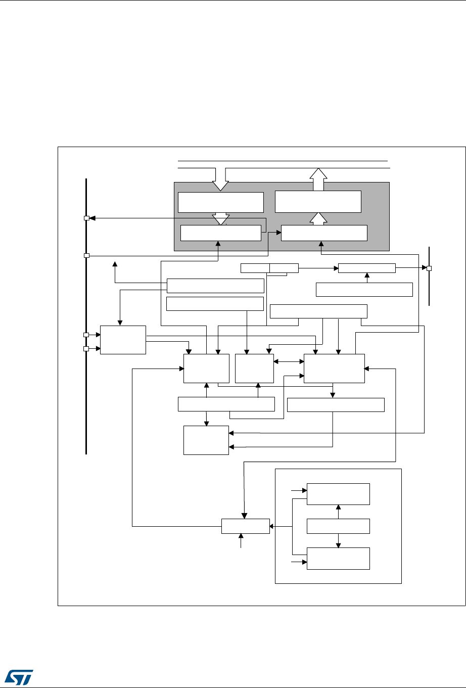
RM0394 Rev 4 1265/1600
RM0394 Low-power universal asynchronous receiver transmitter (LPUART)
1303
The following pins are required in RS232 Hardware flow control mode:
•CTS: Clear To Send blocks the data transmission at the end of the current transfer
when high
•RTS: Request to send indicates that the LPUART is ready to receive data (when low).
The following pin is required in RS485 Hardware control mode:
•DE: Driver Enable activates the transmission mode of the external transceiver.
Note: DE and RTS share the same pin.
Figure 407. LPUART block diagram
06Y9
%55>@
d
:ULWH 5HDG '5GDWDUHJLVWHU
&38RU'0$ &38RU'0$
3:'$7$ 35'$7$
7UDQVPLWVKLIWUHJLVWHU
/38$57[B&5UHJLVWHU
/38$57[B&5UHJLVWHU
576
'(
&76
+DUGZDUH
IORZ
FRQWUROOHU
7UDQVPLW
FRQWURO
/38$57[B&5UHJLVWHU
:DNHXS
XQLW
/38$57[B&5UHJLVWHU
/38$57B*735UHJLVWHU
*7 36& &.FRQWURO
/38$57[B&5UHJLVWHU
5HFHLYHU
FRQWURO
5HFHLYHU
FORFN
/38$57[B,65UHJLVWHU
/38$57
LQWHUUXSW
FRQWURO
/38$57[B%55UHJLVWHU
7UDQVPLWWHU
UDWHFRQWUROOHU
5HFHLYHUUDWH
FRQWUROOHU
/38$57',9
I&.I/6(I+6,
I3&/.RUI6<6
7UDQVPLWWHU
FORFN
&RQYHQWLRQDOEDXGUDWHJHQHUDWRU
&.
/38$57',9 %%5>@
7UDQVPLWGDWDUHJLVWHU
7'5
5HFHLYHGDWDUHJLVWHU
5'5
5HFHLYHVKLIWUHJLVWHU
Z
7;
5;

Low-power universal asynchronous receiver transmitter (LPUART) RM0394
1266/1600 RM0394 Rev 4
39.4.1 LPUART character description
Word length may be selected as being either 7 or 8 or 9 bits by programming the M[1:0] bits
in the LPUART_CR1 register (see Figure 408).
•7-bit character length: M[1:0] = 10
•8-bit character length: M[1:0] = 00
•9-bit character length: M[1:0] = 01
By default, the signal (TX or RX) is in low state during the start bit. It is in high state during
the stop bit.
These values can be inverted, separately for each signal, through polarity configuration
control.
An Idle character is interpreted as an entire frame of “1”s. (The number of “1”s includes the
number of stop bits).
A Break character is interpreted on receiving “0”s for a frame period. At the end of the
break frame, the transmitter inserts 2 stop bits.
Transmission and reception are driven by a common baud rate generator, the clock for each
is generated when the enable bit is set respectively for the transmitter and receiver.
The details of each block is given below.
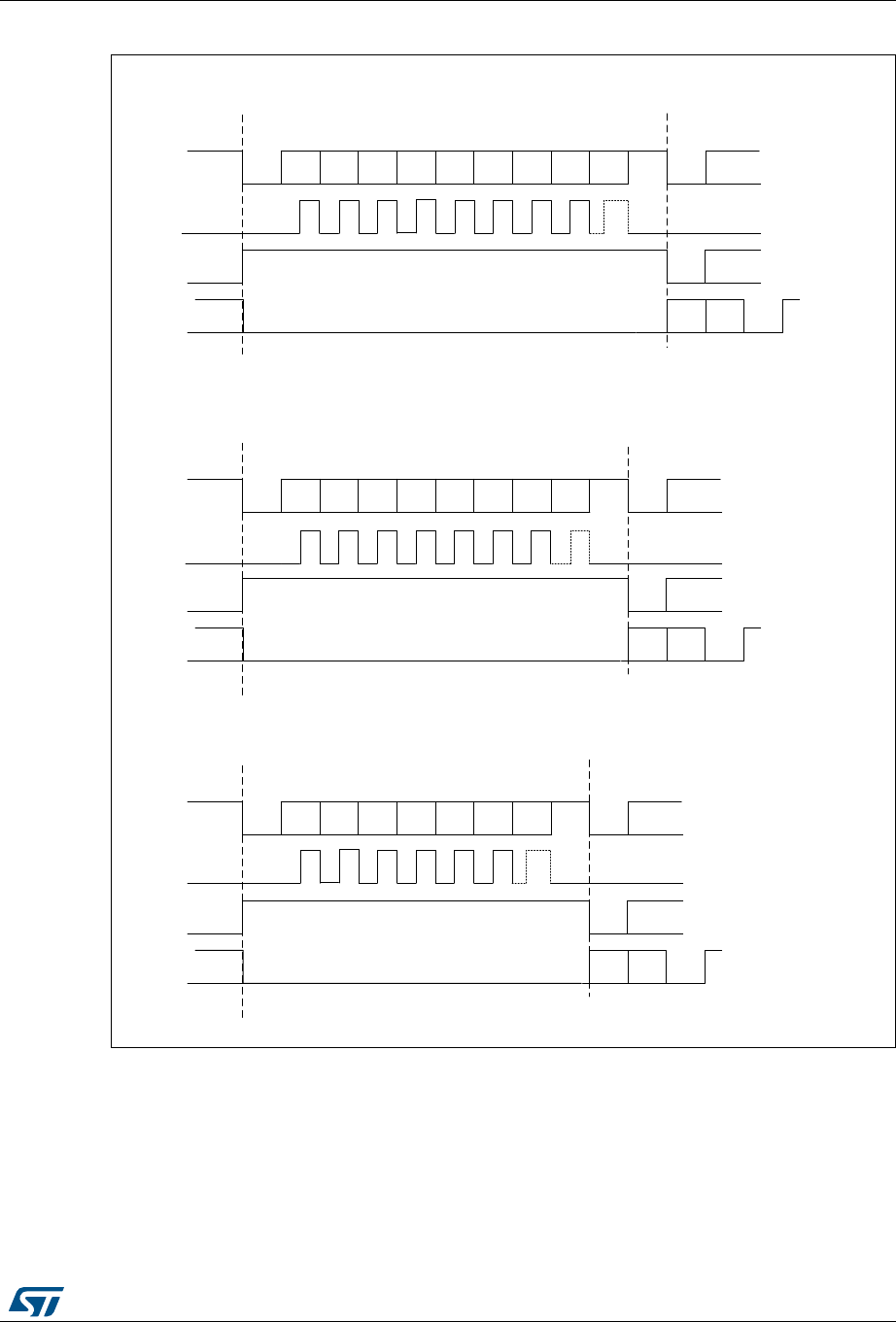
RM0394 Rev 4 1267/1600
RM0394 Low-power universal asynchronous receiver transmitter (LPUART)
1303
Figure 408. Word length programming
069
%LW %LW %LW %LW %LW %LW %LW %LW %LW
6WDUW
ELW
6WRS
ELW
1H[W
6WDUW
ELW
,GOHIUDPH
ELWZRUGOHQJWK0 6WRSELW
3RVVLEOH
3DULW\
ELW
%UHDNIUDPH
'DWDIUDPH
&ORFN
6WDUW
ELW
6WRS
ELW
6WDUW
ELW
6WRS
ELW
%LW %LW %LW %LW %LW %LW %LW %LW
6WDUW
ELW
6WRS
ELW
1H[W
6WDUW
ELW
,GOHIUDPH
ELWZRUGOHQJWK0 6WRSELW
3RVVLEOH
3DULW\
ELW
%UHDNIUDPH
'DWDIUDPH
&ORFN
6WDUW
ELW
6WRS
ELW
6WDUW
ELW
6WRS
ELW
%LW %LW %LW %LW %LW %LW %LW
6WDUW
ELW
6WRS
ELW
1H[W
6WDUW
ELW
,GOHIUDPH
ELWZRUGOHQJWK0 6WRSELW
3RVVLEOH
3DULW\
ELW
%UHDNIUDPH
'DWDIUDPH
&ORFN
/%&/ELWFRQWUROVODVWGDWDFORFNSXOVH
6WDUW
ELW
6WRS
ELW
6WDUW
ELW
6WRS
ELW
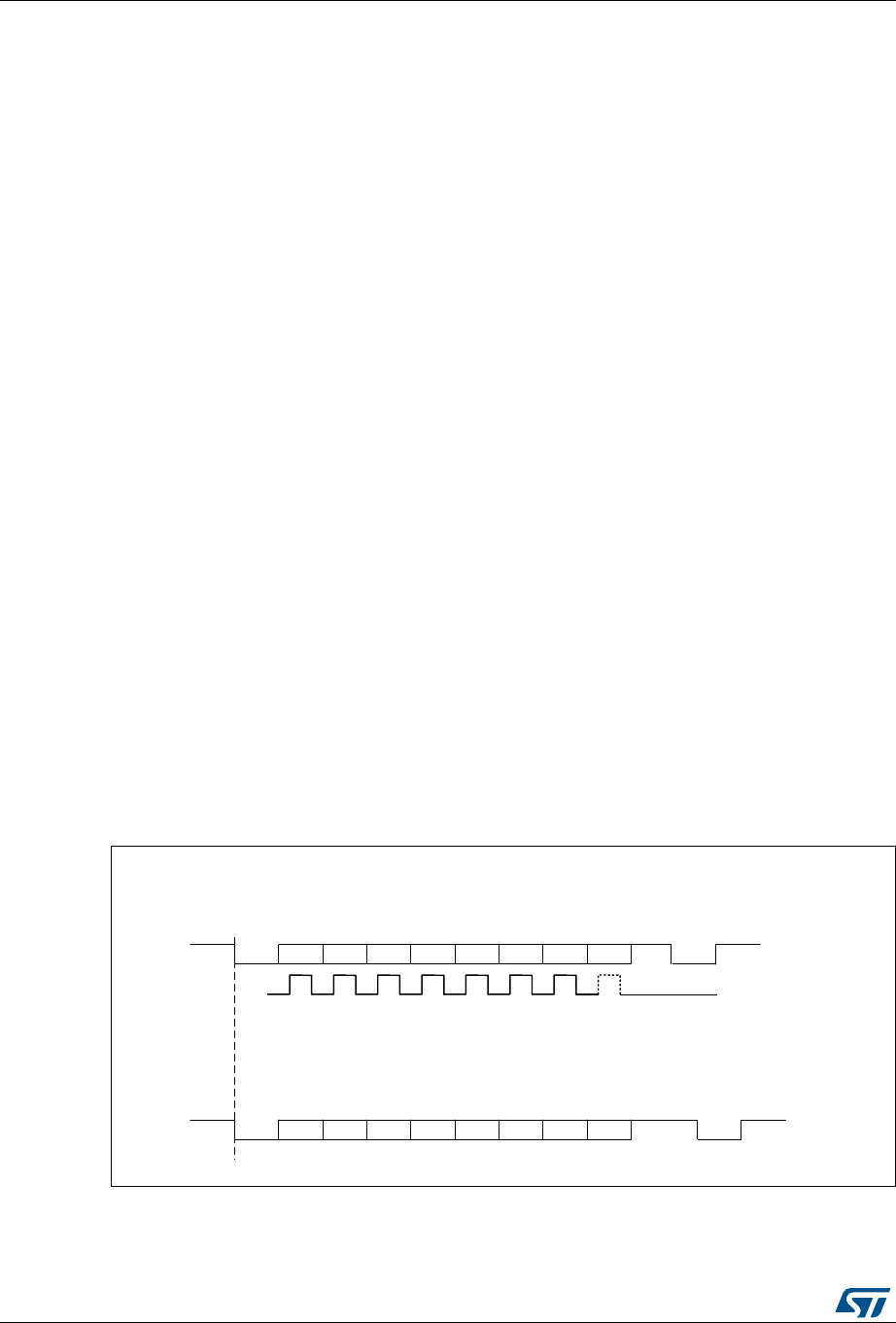
Low-power universal asynchronous receiver transmitter (LPUART) RM0394
1268/1600 RM0394 Rev 4
39.4.2 LPUART transmitter
The transmitter can send data words of either 7 or 8 or 9 bits depending on the M bits status.
The Transmit Enable bit (TE) must be set in order to activate the transmitter function. The
data in the transmit shift register is output on the TX pin.
Character transmission
During an LPUART transmission, data shifts out least significant bit first (default
configuration) on the TX pin. In this mode, the LPUART_TDR register consists of a buffer
(TDR) between the internal bus and the transmit shift register (see Figure 382).
Every character is preceded by a start bit which is a logic level low for one bit period. The
character is terminated by a configurable number of stop bits.
The following stop bits are supported by LPUART: 1 and 2 stop bits.
Note: The TE bit must be set before writing the data to be transmitted to the LPUART_TDR.
The TE bit should not be reset during transmission of data. Resetting the TE bit during the
transmission will corrupt the data on the TX pin as the baud rate counters will get frozen.
The current data being transmitted will be lost.
An idle frame will be sent after the TE bit is enabled.
Configurable stop bits
The number of stop bits to be transmitted with every character can be programmed in
Control register 2, bits 13,12.
•1 stop bit: This is the default value of number of stop bits.
•2 stop bits: This will be supported by normal LPUART, Single-wire and Modem
modes.
An idle frame transmission will include the stop bits.
A break transmission will be 10 low bits (when M[1:0] = 00) or 11 low bits (when M[1:0] = 01)
or 9 low bits (when M[1:0] = 10) followed by 2 stop bits. It is not possible to transmit long
breaks (break of length greater than 9/10/11 low bits).
Figure 409. Configurable stop bits
069
ELW:RUGOHQJWK0>@ ELWLVUHVHW
/%&/ELWFRQWUROVODVWGDWDFORFNSXOVH
%LW6WDUWELW 6WRS
ELW
1H[W
VWDUW
ELW
3RVVLEOH
SDULW\ELW
'DWDIUDPH 1H[WGDWDIUDPH
&/2&.
D6WRSELW
E6WRSELWV
%LW%LW%LW%LW%LW%LW%LW
1H[WGDWDIUDPH
%LW6WDUWELW
6WRS
ELWV
1H[W
VWDUW
ELW
3RVVLEOH
SDULW\ELW
'DWDIUDPH
%LW%LW%LW%LW%LW%LW%LW

RM0394 Rev 4 1269/1600
RM0394 Low-power universal asynchronous receiver transmitter (LPUART)
1303
Character transmission procedure
1. Program the M bits in LPUART_CR1 to define the word length.
2. Select the desired baud rate using the LPUART_BRR register.
3. Program the number of stop bits in LPUART_CR2.
4. Enable the LPUART by writing the UE bit in LPUART_CR1 register to 1.
5. Select DMA enable (DMAT) in LPUART_CR3 if multibuffer Communication is to take
place. Configure the DMA register as explained in multibuffer communication.
6. Set the TE bit in LPUART_CR1 to send an idle frame as first transmission.
7. Write the data to send in the LPUART_TDR register (this clears the TXE bit). Repeat
this for each data to be transmitted in case of single buffer.
8. After writing the last data into the LPUART_TDR register, wait until TC=1. This
indicates that the transmission of the last frame is complete. This is required for
instance when the LPUART is disabled or enters the Halt mode to avoid corrupting the
last transmission.
Single byte communication
Clearing the TXE bit is always performed by a write to the transmit data register.
The TXE bit is set by hardware and it indicates:
•The data has been moved from the LPUART_TDR register to the shift register and the
data transmission has started.
•The LPUART_TDR register is empty.
•The next data can be written in the LPUART_TDR register without overwriting the
previous data.
This flag generates an interrupt if the TXEIE bit is set.
When a transmission is taking place, a write instruction to the LPUART_TDR register stores
the data in the TDR register; next, the data is copied in the shift register at the end of the
currently ongoing transmission.
When no transmission is taking place, a write instruction to the LPUART_TDR register
places the data in the shift register, the data transmission starts, and the TXE bit is set.
If a frame is transmitted (after the stop bit) and the TXE bit is set, the TC bit goes high. An
interrupt is generated if the TCIE bit is set in the LPUART_CR1 register.
After writing the last data in the LPUART_TDR register, it is mandatory to wait for TC=1
before disabling the LPUART or causing the microcontroller to enter the low-power mode
(see Figure 385: TC/TXE behavior when transmitting).
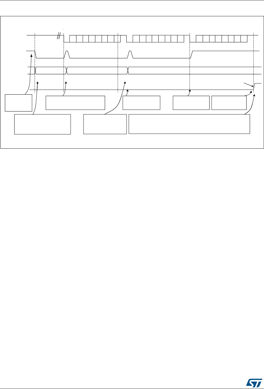
Low-power universal asynchronous receiver transmitter (LPUART) RM0394
1270/1600 RM0394 Rev 4
Figure 410. TC/TXE behavior when transmitting
Break characters
Setting the SBKRQ bit transmits a break character. The break frame length depends on the
M bits (see Figure 408).
If a ‘1’ is written to the SBKRQ bit, a break character is sent on the TX line after completing
the current character transmission. The SBKF bit is set by the write operation and it is reset
by hardware when the break character is completed (during the stop bits after the break
character). The LPUART inserts a logic 1 signal (STOP) for the duration of 2 bits at the end
of the break frame to guarantee the recognition of the start bit of the next frame.
In the case the application needs to send the break character following all previously
inserted data, including the ones not yet transmitted, the software should wait for the TXE
flag assertion before setting the SBKRQ bit.
Idle characters
Setting the TE bit drives the LPUART to send an idle frame before the first data frame.
39.4.3 LPUART receiver
The LPUART can receive data words of either 7 or 8 or 9 bits depending on the M bits in the
LPUART_CR1 register.
Start bit detection
In LPUART, for START bit detection, a falling edge should be detected first on the Rx line,
then a sample is taken in the middle of the start bit to confirm that it is still ‘0’. If the start
sample is at ‘1’, then the noise error flag (NF) is set, then the START bit is discarded and the
receiver waits for a new START bit. Else, the receiver continues to sample all incoming bits
normally.
7;OLQH
/38$57B'5
)UDPH
7;(IODJ
)
7&IODJ
)
)UDPH
6RIWZDUHZDLWVXQWLO7;(
DQGZULWHV)LQWR'5
6RIWZDUHZDLWVXQWLO
7;( DQGZULWHV
)LQWR'5
7&LVQRWVHW
EHFDXVH7;(
6RIWZDUHZDLWVXQWLO7&
)UDPH
7&LVVHW
EHFDXVH7;(
6HWE\KDUGZDUH
FOHDUHGE\VRIWZDUH
6HWE\KDUGZDUH
FOHDUHGE\VRIWZDUH 6HWE\KDUGZDUH
6HWE\KDUGZDUH
,GOHSUHDPEOH
)
6RIWZDUH
HQDEOHVWKH
/38$57
7&LVQRWVHW
EHFDXVH7;(
6RIWZDUHZDLWVXQWLO7;(
DQGZULWHV)LQWR'5
06Y9

RM0394 Rev 4 1271/1600
RM0394 Low-power universal asynchronous receiver transmitter (LPUART)
1303
Character reception
During an LPUART reception, data shifts in least significant bit first (default configuration)
through the RX pin. In this mode, the LPUART_RDR register consists of a buffer (RDR)
between the internal bus and the received shift register.
Character reception procedure
1. Program the M bits in LPUART_CR1 to define the word length.
2. Select the desired baud rate using the baud rate register LPUART_BRR
3. Program the number of stop bits in LPUART_CR2.
4. Enable the LPUART by writing the UE bit in LPUART_CR1 register to 1.
5. Select DMA enable (DMAR) in LPUART_CR3 if multibuffer communication is to take
place. Configure the DMA register as explained in multibuffer communication.
6. Set the RE bit LPUART_CR1. This enables the receiver which begins searching for a
start bit.
When a character is received
•The RXNE bit is set. It indicates that the content of the shift register is transferred to the
RDR. In other words, data has been received and can be read (as well as its
associated error flags).
•An interrupt is generated if the RXNEIE bit is set.
•The error flags can be set if a frame error, noise or an overrun error has been detected
during reception. PE flag can also be set with RXNE.
•In multibuffer, RXNE is set after every byte received and is cleared by the DMA read of
the Receive data Register.
•In single buffer mode, clearing the RXNE bit is performed by a software read to the
LPUART_RDR register. The RXNE flag can also be cleared by writing 1 to the RXFRQ
in the LPUART_RQR register. The RXNE bit must be cleared before the end of the
reception of the next character to avoid an overrun error.
Break character
When a break character is received, the LPUART handles it as a framing error.
Idle character
When an idle frame is detected, there is the same procedure as for a received data
character plus an interrupt if the IDLEIE bit is set.

Low-power universal asynchronous receiver transmitter (LPUART) RM0394
1272/1600 RM0394 Rev 4
Overrun error
An overrun error occurs when a character is received when RXNE has not been reset. Data
can not be transferred from the shift register to the RDR register until the RXNE bit is
cleared.
The RXNE flag is set after every byte received. An overrun error occurs if RXNE flag is set
when the next data is received or the previous DMA request has not been serviced. When
an overrun error occurs:
•The ORE bit is set.
•The RDR content will not be lost. The previous data is available when a read to
LPUART_RDR is performed.
•The shift register will be overwritten. After that point, any data received during overrun
is lost.
•An interrupt is generated if either the RXNEIE bit is set or EIE bit is set.
•The ORE bit is reset by setting the ORECF bit in the ICR register.
Note: The ORE bit, when set, indicates that at least 1 data has been lost. There are two
possibilities:
- if RXNE=1, then the last valid data is stored in the receive register RDR and can be read,
- if RXNE=0, then it means that the last valid data has already been read and thus there is
nothing to be read in the RDR. This case can occur when the last valid data is read in the
RDR at the same time as the new (and lost) data is received.
Selecting the clock source
The choice of the clock source is done through the Reset and Clock Control system (RCC).
The clock source must be chosen before enabling the LPUART (by setting the UE bit).
The choice of the clock source must be done according to two criteria:
•Possible use of the LPUART in low-power mode
•Communication speed.
The clock source frequency is fCK.
When the dual clock domain and the wakeup from Stop mode features are supported, the
clock source can be one of the following sources: fPCLK (default), fLSE, fHSI or fSYS.
Otherwise, the LPUART clock source is fPCLK .
Choosing fLSE, fHSI as clock source may allow the LPUART to receive data while the MCU is
in low-power mode. Depending on the received data and wakeup mode selection, the
LPUART wakes up the MCU, when needed, in order to transfer the received data by
software reading the LPUART_RDR register or by DMA.
For the other clock sources, the system must be active in order to allow LPUART
communication.
The communication speed range (specially the maximum communication speed) is also
determined by the clock source.
The receiver samples each incoming baud as close as possible to the middle of the baud-
period. Only a single sample is taken of each of the incoming bauds.
Note: There is no noise detection for data.

RM0394 Rev 4 1273/1600
RM0394 Low-power universal asynchronous receiver transmitter (LPUART)
1303
Framing error
A framing error is detected when the stop bit is not recognized on reception at the expected
time, following either a de-synchronization or excessive noise.
When the framing error is detected:
•The FE bit is set by hardware.
•The invalid data is transferred from the Shift register to the LPUART_RDR register.
•No interrupt is generated in case of single byte communication. However this bit rises
at the same time as the RXNE bit which itself generates an interrupt. In case of
multibuffer communication an interrupt will be issued if the EIE bit is set in the
LPUART_CR3 register.
The FE bit is reset by writing 1 to the FECF in the LPUART_ICR register.
Configurable stop bits during reception
The number of stop bits to be received can be configured through the control bits of Control
Register 2 - it can be either 1 or 2 in normal mode.
•1 stop bit: Sampling for 1 stop Bit is done on the 8th, 9th and 10th samples.
•2 stop bits: Sampling for the 2 stop bits is done in the middle of the second stop bit.
The RXNE and FE flags are set just after this sample i.e. during the second stop bit.
The first stop bit is not checked for framing error.
39.4.4 LPUART baud rate generation
The baud rate for the receiver and transmitter (Rx and Tx) are both set to the same value as
programmed in the LPUART_BRR register.
The baud rate for the receiver and transmitter (Rx and Tx) are both set to the same value as
programmed in the LPUART_BRR register.
LPUARTDIV is coded on the LPUART_BRR register.
Note: The baud counters are updated to the new value in the baud registers after a write operation
to LPUART_BRR. Hence the baud rate register value should not be changed during
communication.
It is forbidden to write values less than 0x300 in the LPUART_BRR register.
fck must be in the range [3 x baud rate, 4096 x baud rate].
The maximum baud rate that can be reached when the LPUART clock source is the LSE, is
9600 baud. Higher baud rates can be reached when the LPUART is clocked by clock
sources different than the LSE clock. For example, if the LPUART clock source is the
system clock (maximum is 80 MHz), the maximum baud rate that can be reached is
26 Mbaud.
Tx/Rx baud 256 f×CK
LPUARTDIV
------------------------------------
=
Low-power universal asynchronous receiver transmitter (LPUART) RM0394
1274/1600 RM0394 Rev 4
Table 202. Error calculation for programmed baud rates at fck = 32,768 KHz
Baud rate fCK = 32,768 KHz
S.No Desired Actual Value programmed in the baud
rate register
% Error = (Calculated - Desired)
B.rate / Desired B.rate
1 300 Bps 300 Bps 0x6D3A 0
2 600 Bps 600 Bps 0x369D 0
3 1200 Bps 1200.087 Bps 0x1B4E 0.007
4 2400 Bps 2400.17 Bps 0xDA7 0.007
5 4800 Bps 4801.72 Bps 0x6D3 0.035
6 9600 Bps 9608.94 Bps 0x369 0.093
Table 203. Error calculation for programmed baud rates at fck = 80 MHz
Desired Actual Value programmed in the
baud rate register
% Error = (Calculated -
Desired)
B.rate / Desired B.rate
38400 38400,02 82355 0,00006
57600 57600,09 56CE3 0,0001
115200 115200,50 2B671 0,0004
230400 230402,30 15B38 0,001
460800 460804,61 AD9C 0,001
921600 921609,22 56CE 0,001
4000000 4000000,00 1400 0
10000000 10000000,00 800 0
20000000 20000000,00 400 0
26000000 26022871,66 313 0,09

RM0394 Rev 4 1275/1600
RM0394 Low-power universal asynchronous receiver transmitter (LPUART)
1303
39.4.5 Tolerance of the LPUART receiver to clock deviation
The asynchronous receiver of the LPUART works correctly only if the total clock system
deviation is less than the tolerance of the LPUART receiver. The causes which contribute to
the total deviation are:
•DTRA: Deviation due to the transmitter error (which also includes the deviation of the
transmitter’s local oscillator)
•DQUANT: Error due to the baud rate quantization of the receiver
•DREC: Deviation of the receiver’s local oscillator
•DTCL: Deviation due to the transmission line (generally due to the transceivers which
can introduce an asymmetry between the low-to-high transition timing and the high-to-
low transition timing)
where
DWU is the error due to sampling point deviation when the wakeup from Stop mode is
used.
when M[1:0] = 01:
when M[1:0] = 00:
when M[1:0] = 10:
tWULPUART is the time between:
1. The detection of start bit falling edge
2. The instant when clock (requested by the peripheral) is ready and reaching the
peripheral and regulator is ready.
tWULPUART corresponds to tWUSTOP value provided in the datasheet.
The LPUART receiver can receive data correctly at up to the maximum tolerated deviation
specified in Table 204:
•7, 8 or 9-bit character length defined by the M bits in the LPUARTx_CR1 register
•1 or 2 stop bits
DTRA DQUANT DREC DTCL DWU++++LPUART receiver tolerance<
DWU tWULPUART
11 Tbit×
------------------------------
=
DWU tWULPUART
10 Tbit×
------------------------------
=
DWU tWULPUART
9Tbit×
------------------------------
=
Table 204. Tolerance of the LPUART receiver
M bits 768 BRR <1024 1024 BRR < 2048 2048 BRR < 4096 4096 BRR
8 bits (M=00), 1 stop bit 1.82% 2.56% 3.90% 4.42%
9 bits (M=01), 1 stop bit 1.69% 2.33% 2.53% 4.14%
7 bits (M=10), 1 stop bit 2.08% 2.86% 4.35% 4.42%

Low-power universal asynchronous receiver transmitter (LPUART) RM0394
1276/1600 RM0394 Rev 4
Note: The data specified in Table 204 may slightly differ in the special case when the received
frames contain some Idle frames of exactly 10-bit durations when M bits = 00 (11-bit
durations when M bits =01 or 9- bit durations when M bits = 10).
39.4.6 Multiprocessor communication using LPUART
It is possible to perform multiprocessor communication with the LPUART (with several
LPUARTs connected in a network). For instance one of the LPUARTs can be the master, its
TX output connected to the RX inputs of the other LPUARTs. The others are slaves, their
respective TX outputs are logically ANDed together and connected to the RX input of the
master.
In multiprocessor configurations it is often desirable that only the intended message
recipient should actively receive the full message contents, thus reducing redundant
LPUART service overhead for all non addressed receivers.
The non addressed devices may be placed in mute mode by means of the muting function.
In order to use the mute mode feature, the MME bit must be set in the LPUART_CR1
register.
In mute mode:
•None of the reception status bits can be set.
•All the receive interrupts are inhibited.
•The RWU bit in LPUART_ISR register is set to 1. RWU can be controlled automatically
by hardware or by software, through the MMRQ bit in the LPUART_RQR register,
under certain conditions.
The LPUART can enter or exit from mute mode using one of two methods, depending on
the WAKE bit in the LPUART_CR1 register:
•Idle Line detection if the WAKE bit is reset,
•Address Mark detection if the WAKE bit is set.
Idle line detection (WAKE=0)
The LPUART enters mute mode when the MMRQ bit is written to 1 and the RWU is
automatically set.
It wakes up when an Idle frame is detected. Then the RWU bit is cleared by hardware but
the IDLE bit is not set in the LPUART_ISR register. An example of mute mode behavior
using Idle line detection is given in Figure 389.
8 bits (M=00), 2 stop bit 2.08% 2.86% 4.35% 4.42%
9 bits (M=01), 2 stop bit 1.82% 2.56% 3.90% 4.42%
7 bits (M=10), 2stop bit 2.34% 3.23% 4.92% 4.42%
Table 204. Tolerance of the LPUART receiver (continued)
M bits 768 BRR <1024 1024 BRR < 2048 2048 BRR < 4096 4096 BRR

RM0394 Rev 4 1277/1600
RM0394 Low-power universal asynchronous receiver transmitter (LPUART)
1303
Figure 411. Mute mode using Idle line detection
Note: If the MMRQ is set while the IDLE character has already elapsed, mute mode will not be
entered (RWU is not set).
If the LPUART is activated while the line is IDLE, the idle state is detected after the duration
of one IDLE frame (not only after the reception of one character frame).
4-bit/7-bit address mark detection (WAKE=1)
In this mode, bytes are recognized as addresses if their MSB is a ‘1’ otherwise they are
considered as data. In an address byte, the address of the targeted receiver is put in the 4
or 7 LSBs. The choice of 7 or 4 bit address detection is done using the ADDM7 bit. This 4-
bit/7-bit word is compared by the receiver with its own address which is programmed in the
ADD bits in the LPUART_CR2 register.
Note: In 7-bit and 9-bit data modes, address detection is done on 6-bit and 8-bit addresses
(ADD[5:0] and ADD[7:0]) respectively.
The LPUART enters mute mode when an address character is received which does not
match its programmed address. In this case, the RWU bit is set by hardware. The RXNE
flag is not set for this address byte and no interrupt or DMA request is issued when the
LPUART enters mute mode.
The LPUART also enters mute mode when the MMRQ bit is written to 1. The RWU bit is
also automatically set in this case.
The LPUART exits from mute mode when an address character is received which matches
the programmed address. Then the RWU bit is cleared and subsequent bytes are received
normally. The RXNE bit is set for the address character since the RWU bit has been
cleared.
An example of mute mode behavior using address mark detection is given in Figure 390.
06Y9
'DWD 'DWD ,'/('DWD 'DWD 'DWD
,GOHIUDPHGHWHFWHG0054ZULWWHQWR
5:8
5;
0XWHPRGH 1RUPDOPRGH
5;1( 5;1(
'DWD
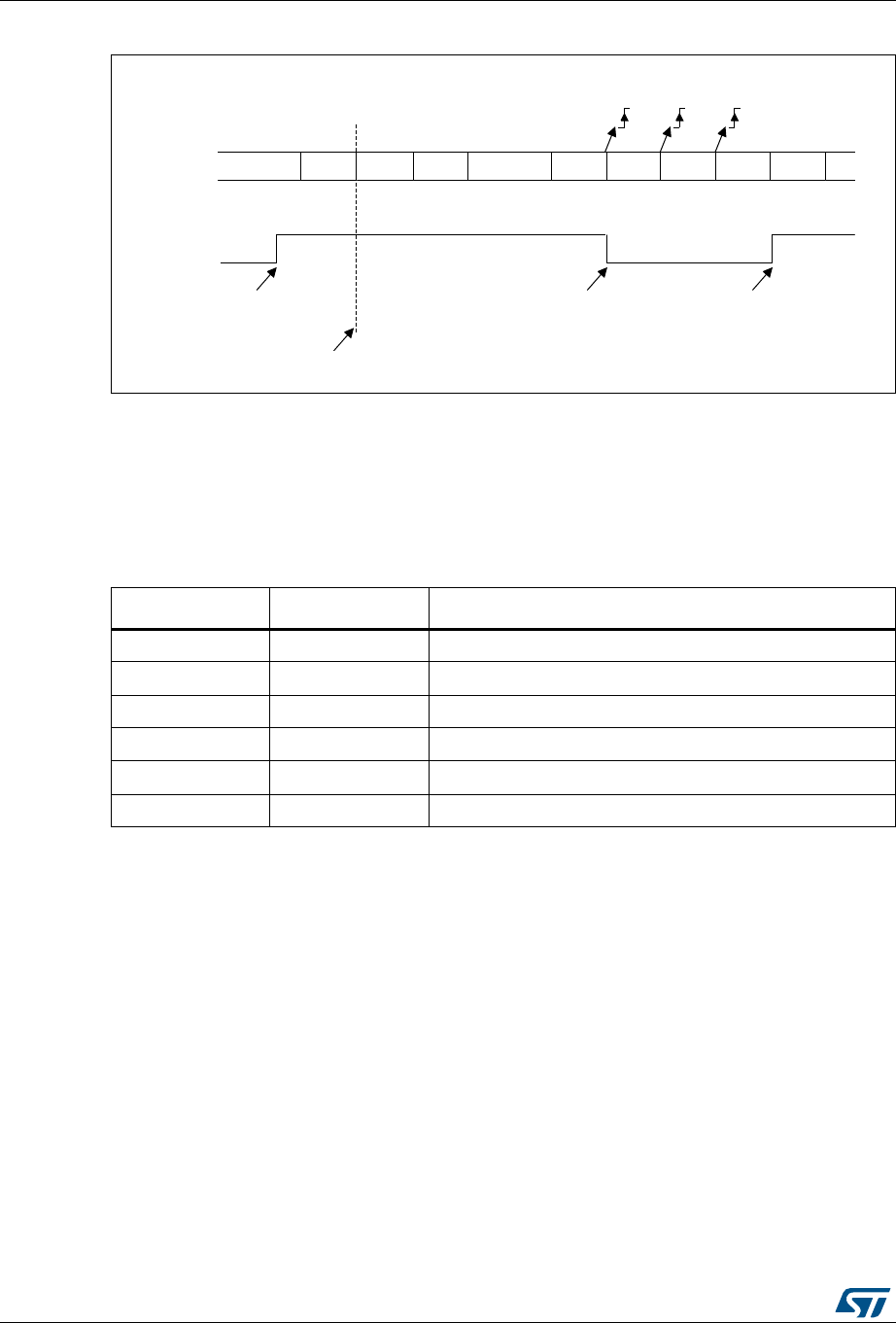
Low-power universal asynchronous receiver transmitter (LPUART) RM0394
1278/1600 RM0394 Rev 4
Figure 412. Mute mode using address mark detection
39.4.7 LPUART parity control
Parity control (generation of parity bit in transmission and parity checking in reception) can
be enabled by setting the PCE bit in the LPUART_CR1 register. Depending on the frame
length defined by the M bits, the possible LPUART frame formats are as listed in Table 197.
Even parity
The parity bit is calculated to obtain an even number of “1s” inside the frame which is made
of the 6, 7 or 8 LSB bits (depending on M bits values) and the parity bit.
As an example, if data=00110101, and 4 bits are set, then the parity bit will be 0 if even
parity is selected (PS bit in LPUART_CR1 = 0).
Odd parity
The parity bit is calculated to obtain an odd number of “1s” inside the frame made of the 6, 7
or 8 LSB bits (depending on M bits values) and the parity bit.
As an example, if data=00110101 and 4 bits set, then the parity bit will be 1 if odd parity is
selected (PS bit in LPUART_CR1 = 1).
06Y9
,'/( $GGU 'DWD 'DWD ,'/( $GGU 'DWD 'DWD $GGU 'DWD
,QWKLVH[DPSOHWKHFXUUHQWDGGUHVVRIWKHUHFHLYHULV
SURJUDPPHGLQWKH/38$57B&5UHJLVWHU
5;1(
1RQPDWFKLQJDGGUHVV0DWFKLQJDGGUHVV
1RQPDWFKLQJDGGUHVV
0054ZULWWHQWR
5;1(ZDVFOHDUHG
5:8
5;
0XWHPRGH 0XWHPRGH1RUPDOPRGH
5;1( 5;1(
Table 205. Frame formats
M bits PCE bit LPUART frame(1)
1. Legends: SB: start bit, STB: stop bit, PB: parity bit.
2. In the data register, the PB is always taking the MSB position (9th, 8th or 7th, depending on the M bits
value).
00 0 | SB | 8-bit data | STB |
00 1 | SB | 7-bit data | PB | STB |
01 0 | SB | 9-bit data | STB |
01 1 | SB | 8-bit data | PB | STB |
10 0 | SB | 7-bit data | STB |
10 1 | SB | 6-bit data | PB | STB |

RM0394 Rev 4 1279/1600
RM0394 Low-power universal asynchronous receiver transmitter (LPUART)
1303
Parity checking in reception
If the parity check fails, the PE flag is set in the LPUART_ISR register and an interrupt is
generated if PEIE is set in the LPUART_CR1 register. The PE flag is cleared by software
writing 1 to the PECF in the LPUART_ICR register.
Parity generation in transmission
If the PCE bit is set in LPUARTx_CR1, then the MSB bit of the data written in the data
register is transmitted but is changed by the parity bit (even number of “1s” if even parity is
selected (PS=0) or an odd number of “1s” if odd parity is selected (PS=1)).
39.4.8 Single-wire Half-duplex communication using LPUART
Single-wire Half-duplex mode is selected by setting the HDSEL bit in the LPUART_CR3
register. In this mode, the following bits must be kept cleared:
•LINEN and CLKEN bits in the LPUART_CR2 register,
•SCEN and IREN bits in the LPUART_CR3 register.
The LPUART can be configured to follow a Single-wire Half-duplex protocol where the TX
and RX lines are internally connected. The selection between half- and Full-duplex
communication is made with a control bit HDSEL in LPUART_CR3.
As soon as HDSEL is written to 1:
•The TX and RX lines are internally connected
•The RX pin is no longer used
•The TX pin is always released when no data is transmitted. Thus, it acts as a standard
I/O in idle or in reception. It means that the I/O must be configured so that TX is
configured as alternate function open-drain with an external pull-up.
Apart from this, the communication protocol is similar to normal LPUART mode. Any
conflicts on the line must be managed by software (by the use of a centralized arbiter, for
instance). In particular, the transmission is never blocked by hardware and continues as
soon as data is written in the data register while the TE bit is set.
Note: In LPUART, in the case of 1-stop bit configuration, the RXNE flag is set in the middle of the
stop bit.
39.4.9 Continuous communication in DMA mode using LPUART
The LPUART is capable of performing continuous communication using the DMA. The DMA
requests for Rx buffer and Tx buffer are generated independently.
Note: Use the LPUART as explained in Section 39.4.3. To perform continuous communication,
you can clear the TXE/ RXNE flags In the LPUART_ISR register.

Low-power universal asynchronous receiver transmitter (LPUART) RM0394
1280/1600 RM0394 Rev 4
Transmission using DMA
DMA mode can be enabled for transmission by setting DMAT bit in the LPUART_CR3
register. Data is loaded from a SRAM area configured using the DMA peripheral (refer to
Section 11: Direct memory access controller (DMA) on page 295) to the LPUART_TDR
register whenever the TXE bit is set. To map a DMA channel for LPUART transmission, use
the following procedure (x denotes the channel number):
1. Write the LPUART_TDR register address in the DMA control register to configure it as
the destination of the transfer. The data is moved to this address from memory after
each TXE event.
2. Write the memory address in the DMA control register to configure it as the source of
the transfer. The data is loaded into the LPUART_TDR register from this memory area
after each TXE event.
3. Configure the total number of bytes to be transferred to the DMA control register.
4. Configure the channel priority in the DMA register
5. Configure DMA interrupt generation after half/ full transfer as required by the
application.
6. Clear the TC flag in the LPUART_ISR register by setting the TCCF bit in the
LPUART_ICR register.
7. Activate the channel in the DMA register.
When the number of data transfers programmed in the DMA Controller is reached, the DMA
controller generates an interrupt on the DMA channel interrupt vector.
In transmission mode, once the DMA has written all the data to be transmitted (the TCIF flag
is set in the DMA_ISR register), the TC flag can be monitored to make sure that the
LPUART communication is complete. This is required to avoid corrupting the last
transmission before disabling the LPUART or entering Stop mode. Software must wait until
TC=1. The TC flag remains cleared during all data transfers and it is set by hardware at the
end of transmission of the last frame.
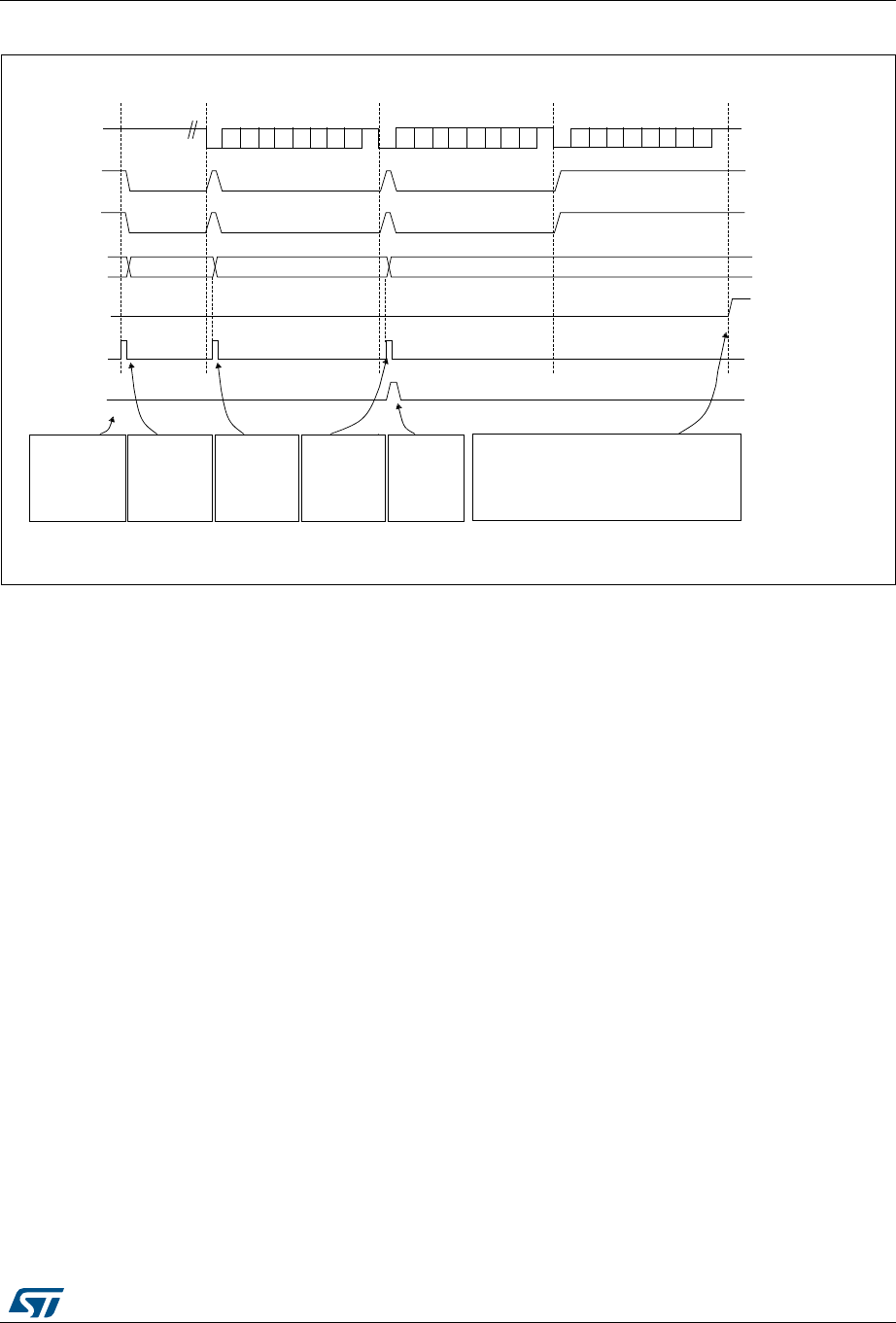
RM0394 Rev 4 1281/1600
RM0394 Low-power universal asynchronous receiver transmitter (LPUART)
1303
Figure 413. Transmission using DMA
Reception using DMA
DMA mode can be enabled for reception by setting the DMAR bit in LPUART_CR3 register.
Data is loaded from the LPUART_RDR register to a SRAM area configured using the DMA
peripheral (refer Section 11: Direct memory access controller (DMA) on page 295)
whenever a data byte is received. To map a DMA channel for LPUART reception, use the
following procedure:
1. Write the LPUART_RDR register address in the DMA control register to configure it as
the source of the transfer. The data is moved from this address to the memory after
each RXNE event.
2. Write the memory address in the DMA control register to configure it as the destination
of the transfer. The data is loaded from LPUART_RDR to this memory area after each
RXNE event.
3. Configure the total number of bytes to be transferred to the DMA control register.
4. Configure the channel priority in the DMA control register
5. Configure interrupt generation after half/ full transfer as required by the application.
6. Activate the channel in the DMA control register.
When the number of data transfers programmed in the DMA Controller is reached, the DMA
controller generates an interrupt on the DMA channel interrupt vector.
) ))
06Y9
6RIWZDUH
FRQILJXUHV
'0$WRVHQG
GDWDEORFNV
DQGHQDEOHV
/38$57
7KH'0$
WUDQVIHULV
FRPSOHWH
7&,) LQ
'0$B,65
'0$ZULWHV)
LQWR
/38$57B7'5
'0$ZULWHV)
LQWR
/38$57B7'5
6RIWZDUHZDLWVXQWLO7&
6HWE\KDUGZDUH
&OHDUHGE\VRIWZDUH
6HWE\KDUGZDUH
7;OLQH
7;(IODJ
/38$57B7'5
'0$UHTXHVW
'0$ZULWHV
/38$57B7'5
'0$7&,)IODJWUDQVIHUFRPSOHWH
7&IODJ
)UDPH )UDPH )UDPH
,GOHSUHDPEOH
6HWE\KDUGZDUHFOHDUHG
E\'0$UHDG
6HWE\KDUGZDUHFOHDUHGE\
'0$UHDG 6HWE\KDUGZDUH
,JQRUHGE\WKH'0$EHFDXVHWKHWUDQVIHU
LVFRPSOHWH
D
'0$ZULWHV)
LQWR
/38$57B7'5
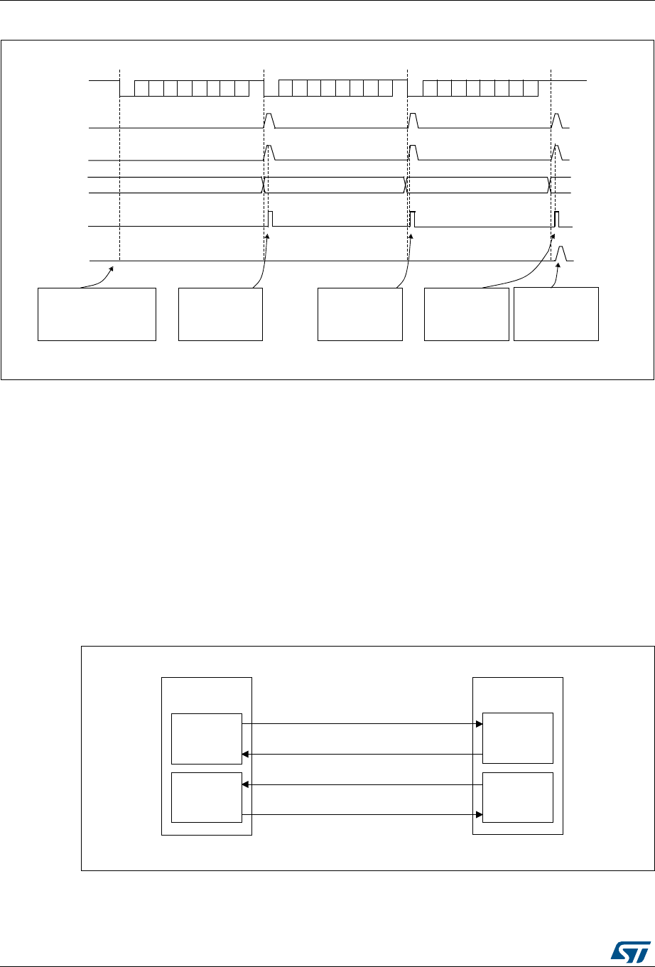
Low-power universal asynchronous receiver transmitter (LPUART) RM0394
1282/1600 RM0394 Rev 4
Figure 414. Reception using DMA
Error flagging and interrupt generation in multibuffer communication
In multibuffer communication if any error occurs during the transaction the error flag is
asserted after the current byte. An interrupt is generated if the interrupt enable flag is set.
For framing error, overrun error and noise flag which are asserted with RXNE in single byte
reception, there is a separate error flag interrupt enable bit (EIE bit in the LPUART_CR3
register), which, if set, enables an interrupt after the current byte if any of these errors occur.
39.4.10 RS232 Hardware flow control and RS485 Driver Enable
using LPUART
It is possible to control the serial data flow between 2 devices by using the CTS input and
the RTS output. The Figure 403 shows how to connect 2 devices in this mode:
Figure 415. Hardware flow control between 2 LPUARTs
RS232 RTS and CTS flow control can be enabled independently by writing the RTSE and
CTSE bits respectively to 1 (in the LPUART_CR3 register).
06Y9
7;OLQH
)UDPH
) )
6HWE\KDUGZDUHFOHDUHGE\
'0$UHDG
)
)UDPH )UDPH
5;1(IODJ
/38$57B7'5
'0$UHTXHVW
'0$UHDGV
/38$57B7'5
'0$7&,)IODJ
WUDQVIHUFRPSOHWH
6RIWZDUHFRQILJXUHV
WKH'0$WRUHFHLYH
GDWDEORFNVDQGHQDEOHV
WKH/38$57
'0$UHDGV)
IURP
/38$57B7'5
7KH'0$
WUDQVIHULV
FRPSOHWH
7&,) LQ
'0$B,65
6HWE\KDUGZDUH
&OHDUHGE\
VRIWZDUH
'0$UHDGV)
)URP
/38$57B7'5
'0$UHDGV
)IURP
/38$57B7'5
06Y9
7;FLUFXLW
/38$57
7;
5;FLUFXLW
5;FLUFXLW
/38$57
7;FLUFXLW
7;
&76
&76
576
5;
576
5;
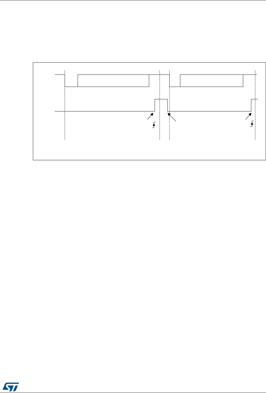
RM0394 Rev 4 1283/1600
RM0394 Low-power universal asynchronous receiver transmitter (LPUART)
1303
RS232 RTS flow control
If the RTS flow control is enabled (RTSE=1), then RTS is asserted (tied low) as long as the
LPUART receiver is ready to receive a new data. when the receive register is full, RTS is de-
asserted, indicating that the transmission is expected to stop at the end of the current frame.
Figure 404 shows an example of communication with RTS flow control enabled.
Figure 416. RS232 RTS flow control
RS232 CTS flow control
If the CTS flow control is enabled (CTSE=1), then the transmitter checks the CTS input
before transmitting the next frame. If CTS is asserted (tied low), then the next data is
transmitted (assuming that data is to be transmitted, in other words, if TXE=0), else the
transmission does not occur. When CTS is de-asserted during a transmission, the current
transmission is completed before the transmitter stops.
When CTSE=1, the CTSIF status bit is automatically set by hardware as soon as the CTS
input toggles. It indicates when the receiver becomes ready or not ready for communication.
An interrupt is generated if the CTSIE bit in the LPUART_CR3 register is set. Figure 405
shows an example of communication with CTS flow control enabled.
06Y9
6WDUW
ELW
6WDUW
ELW
6WRS
ELW ,GOH 6WRS
ELW
5;
576
'DWDUHDG
'DWDFDQQRZEHWUDQVPLWWHG
5;1( 5;1(
'DWD 'DWD
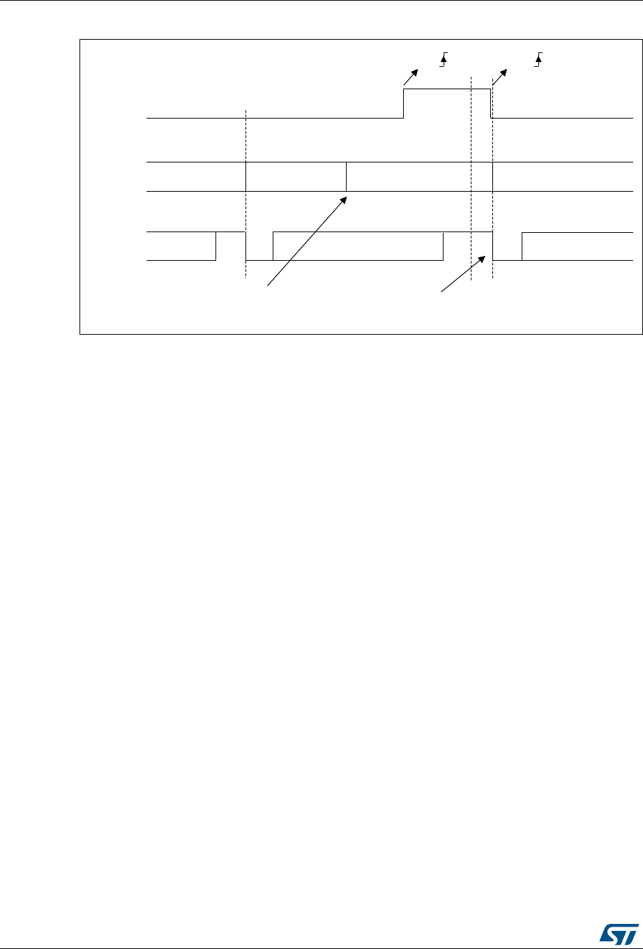
Low-power universal asynchronous receiver transmitter (LPUART) RM0394
1284/1600 RM0394 Rev 4
Figure 417. RS232 CTS flow control
Note: For correct behavior, CTS must be asserted at least 3 LPUART clock source periods before
the end of the current character. In addition it should be noted that the CTSCF flag may not
be set for pulses shorter than 2 x PCLK periods.
RS485 Driver Enable
The driver enable feature is enabled by setting bit DEM in the LPUART_CR3 control
register. This allows the user to activate the external transceiver control, through the DE
(Driver Enable) signal. The assertion time is the time between the activation of the DE signal
and the beginning of the START bit. It is programmed using the DEAT [4:0] bit fields in the
LPUART_CR1 control register. The de-assertion time is the time between the end of the last
stop bit, in a transmitted message, and the de-activation of the DE signal. It is programmed
using the DEDT [4:0] bit fields in the LPUART_CR1 control register. The polarity of the DE
signal can be configured using the DEP bit in the LPUART_CR3 control register.
In LPUART, the DEAT and DEDT are expressed in USART clock source (fCK) cycles:
•The Driver enable assertion time =
– (1 + (DEAT x P)) x fCK , if P <> 0
– (1 + DEAT) x fCK , if P = 0
•The Driver enable de-assertion time =
– (1 + (DEDT x P)) x fCK , if P <> 0
– (1 + DEDT) x fCK , if P = 0
With P = BRR[14:11]
06Y9
6WDUW
ELW
6WRS
ELW
7;
7'5
&76
'DWD
'DWD
6WRS
ELW ,GOH 6WDUW
ELW
'DWD 'DWD
'DWD
HPSW\ HPSW\
&76
&76
7UDQVPLWGDWDUHJLVWHU
:ULWLQJGDWDLQ7'5 7UDQVPLVVLRQRI'DWDLV
GHOD\HGXQWLO&76

RM0394 Rev 4 1285/1600
RM0394 Low-power universal asynchronous receiver transmitter (LPUART)
1303
39.4.11 Wakeup from Stop mode using LPUART
The LPUART is able to wake up the MCU from Stop mode when the UESM bit is set and the
LPUART clock is set to HSI16 or LSE (refer to the Reset and clock control (RCC) section.
•LPUART source clock is HSI
If during stop mode the HSI clock is switched OFF, when a falling edge on the LPUART
receive line is detected, the LPUART interface requests the HSI clock to be switched
ON. The HSI clock is then used for the frame reception.
– If the wakeup event is verified, the MCU wakes up from low-power mode and data
reception goes on normally.
– If the wakeup event is not verified, the HSI clock is switched OFF again, the MCU
is not waken up and stays in low-power mode and the clock request is released.
•LPUART source clock is LSE
Same principle as described in case of LPUART source clock is HSI with the difference
that the LSE is ON in stop mode, but the LSE clock is not propagated to LPUART if the
LPUART is not requesting it. The LSE clock is not OFF but there is a clock gating to
avoid useless consumption.
When the LPUART clock source is configured to be fLSE or fHSI, it is possible to keep
enabled this clock during STOP mode by setting the UCESM bit in LPUART_CR3 control
register.
Note: When LPUART is used to wakeup from stop with LSE is selected as LPUART clock source,
and desired baud rate is 9600 baud, the bit UCESM bit in LPUART_CR3 control register
must be set.
The MCU wakeup from Stop mode can be done using the standard RXNE interrupt. In this
case, the RXNEIE bit must be set before entering Stop mode.
Alternatively, a specific interrupt may be selected through the WUS bit fields.
In order to be able to wake up the MCU from Stop mode, the UESM bit in the LPUART_CR1
control register must be set prior to entering Stop mode.
When the wakeup event is detected, the WUF flag is set by hardware and a wakeup
interrupt is generated if the WUFIE bit is set.
Note: Before entering Stop mode, the user must ensure that the LPUART is not performing a
transfer. BUSY flag cannot ensure that Stop mode is never entered during a running
reception.
The WUF flag is set when a wakeup event is detected, independently of whether the MCU is
in Stop or in an active mode.
When entering Stop mode just after having initialized and enabled the receiver, the REACK
bit must be checked to ensure the LPUART is actually enabled.
When DMA is used for reception, it must be disabled before entering Stop mode and re-
enabled upon exit from Stop mode.
The wakeup from Stop mode feature is not available for all modes. For example it doesn’t
work in SPI mode because the SPI operates in master mode only.

Low-power universal asynchronous receiver transmitter (LPUART) RM0394
1286/1600 RM0394 Rev 4
Using Mute mode with Stop mode
If the LPUART is put into Mute mode before entering Stop mode:
•Wakeup from Mute mode on idle detection must not be used, because idle detection
cannot work in Stop mode.
•If the wakeup from Mute mode on address match is used, then the source of wake-up
from Stop mode must also be the address match. If the RXNE flag is set when entering
the Stop mode, the interface will remain in mute mode upon address match and wake
up from Stop.
•If the LPUART is configured to wake up the MCU from Stop mode on START bit
detection, the WUF flag is set, but the RXNE flag is not set.
Determining the maximum LPUART baud rate allowing to wakeup correctly
from Stop mode when the LPUART clock source is the HSI clock
The maximum baud rate allowing to wakeup correctly from stop mode depends on:
•the parameter tWULPUART (wakeup time from Stop mode) provided in the device
datasheet
•the LPUART receiver tolerance provided in the Section 39.4.5: Tolerance of the
LPUART receiver to clock deviation.
Let us take this example: M bits = 01, 2 stop bits, BRR 4096.
In these conditions, according to Table 204: Tolerance of the LPUART receiver, the
LPUART receiver tolerance is 4.42 %.
DTRA + DQUANT + DREC + DTCL + DWU < LPUART receiver tolerance
DWU max = tWULPUART / (11 x Tbit Min)
Tbit Min = tWULPUART / (11 x DWU max)
If we consider an ideal case where the parameters DTRA, DQUANT, DREC and DTCL are
at 0%, the DWU max is 4.42 %. In reality, we need to consider at least the HSI inaccuracy.
Let us consider the HSI inaccuracy = 1 %, tWULPUART = 1.7 s (in case of Stop mode with
main regulator in Run mode, Range 1 ):
DWU max = 4.42 % - 1 % = 3.42 %
Tbit min = 1.7 µs / (11 3.42 %) = 4.5 s.
In these conditions, the maximum baud rate allowing to wakeup correctly from Stop mode is
1/ 4.5 s = 220 Kbaud.
39.5 LPUART low-power mode
Table 206. Effect of low-power modes on the LPUART
Mode Description
Sleep No effect.
Low-power run No effect.
Low-power sleep No effect. USART interrupt causes the device to exit Low-power sleep
mode.
RM0394 Rev 4 1287/1600
RM0394 Low-power universal asynchronous receiver transmitter (LPUART)
1303
39.6 LPUART interrupts
The LPUART interrupt events are connected to the same interrupt vector (see Figure 406).
•During transmission: Transmission Complete, Clear to Send, Transmit data Register
empty or Framing error interrupt.
•During reception: Idle Line detection, Overrun error, Receive data register not empty,
Parity error, Noise Flag, Framing Error, Character match, etc.
These events generate an interrupt if the corresponding Enable Control Bit is set.
Stop 0, Stop 1 and Stop 2
The LPUART registers content is kept. The LPUART is able to wake up
the MCU from Stop 0, Stop 1 and Stop 2 modes when the UESM bit is set
and the LPUART clock is set to HSI16 or LSE.
The MCU wakeup from Stop 0, Stop 1 and 2 modes can be done using
either the standard RXNE or the WUF interrupt.
Standby The LPUART is powered down and must be reinitialized when the device
has exited from Standby or Shutdown mode.
Shutdown
Table 206. Effect of low-power modes on the LPUART (continued)
Mode Description
Table 207. LPUART interrupt requests
Interrupt event Event flag Enable
Control bit
Transmit data register empty TXE TXEIE
CTS interrupt CTSIF CTSIE
Transmission Complete TC TCIE
Receive data register not empty (data ready to be read) RXNE
RXNEIE
Overrun error detected ORE
Idle line detected IDLE IDLEIE
Parity error PE PEIE
Noise Flag, Overrun error and Framing Error in multibuffer
communication. NF or ORE or FE EIE
Character match CMF CMIE
Wakeup from Stop mode WUF(1)
1. The wUF interrupt is active only in Stop mode.
WUFIE
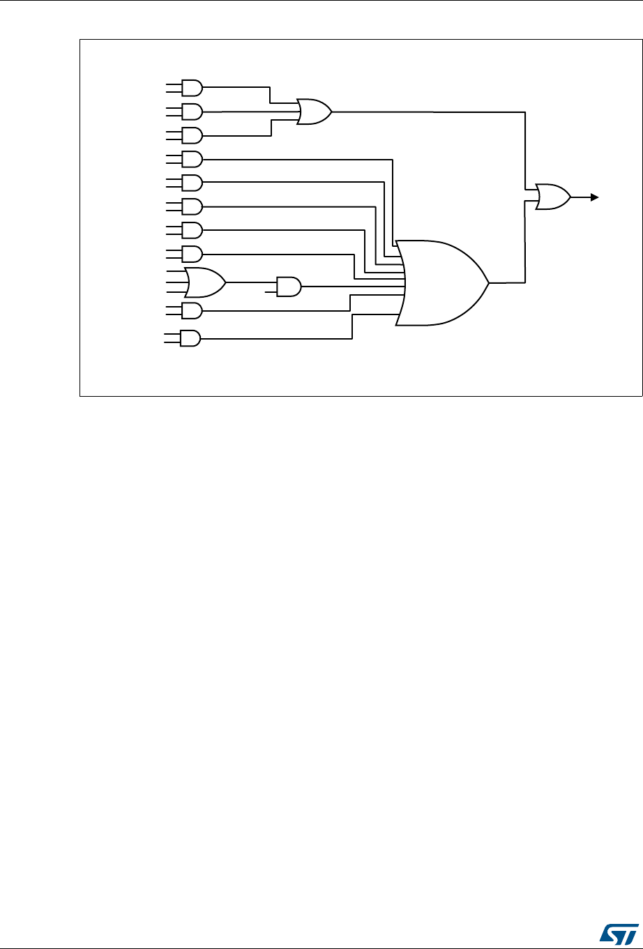
Low-power universal asynchronous receiver transmitter (LPUART) RM0394
1288/1600 RM0394 Rev 4
Figure 418. LPUART interrupt mapping diagram
069
7&
7&,(
7;(
7;(,(
&76,)
&76,(
,'/(
,'/(,(
5;1(,(
25(
5;1(,(
5;1(
3(
3(,(
/%')
/%',(
&0)
&0,(
)(
1)
25( (,(
/38$57
LQWHUUXSW
:8)
:8),(

RM0394 Rev 4 1289/1600
RM0394 Low-power universal asynchronous receiver transmitter (LPUART)
1303
39.7 LPUART registers
Refer to Section 1.2 on page 60 for a list of abbreviations used in register descriptions.
39.7.1 Control register 1 (LPUART_CR1)
Address offset: 0x00
Reset value: 0x0000
31 30 29 28 27 26 25 24 23 22 21 20 19 18 17 16
Res. Res. Res. M1 Res. Res. DEAT[4:0] DEDT[4:0]
rw rw rw rw rw rw rw rw rw rw rw
1514131211109876 5 43210
Res. CMIE MME M0 WAKE PCE PS PEIE TXEIE TCIE RXNEIE IDLEIE TE RE UESM UE
rw rw rw rw rw rw rw rw rw rw rw rw rw rw rw
Bits 31:29 Reserved, must be kept at reset value
Bit 28 M1: Word length
This bit, with bit 12 (M0) determines the word length. It is set or cleared by software.
M[1:0] = 00: 1 Start bit, 8 data bits, n stop bits
M[1:0] = 01: 1 Start bit, 9 data bits, n stop bits
M[1:0] = 10: 1 Start bit, 7 data bits, n stop bits
This bit can only be written when the LPUART is disabled (UE=0).
Bit 27 Reserved, must be kept at reset value
Bit 26 Reserved, must be kept at reset value
Bits 25:21 DEAT[4:0]: Driver Enable assertion time
This 5-bit value defines the time between the activation of the DE (Driver Enable) signal and
the beginning of the start bit. It is expressed in UCLK (USART clock) clock cycles. For more
details, refer to RS485 Driver Enable paragraph.
This bit field can only be written when the LPUART is disabled (UE=0).
Bits 20:16 DEDT[4:0]: Driver Enable de-assertion time
This 5-bit value defines the time between the end of the last stop bit, in a transmitted
message, and the de-activation of the DE (Driver Enable) signal. It is expressed in UCLK
(USART clock) clock cycles. For more details, refer to RS485 Driver Enable paragraph.
If the LPUART_TDR register is written during the DEDT time, the new data is transmitted
only when the DEDT and DEAT times have both elapsed.
This bit field can only be written when the LPUART is disabled (UE=0).
Bit 15 Reserved, must be kept at reset value
Bit 14 CMIE: Character match interrupt enable
This bit is set and cleared by software.
0: Interrupt is inhibited
1: A LPUART interrupt is generated when the CMF bit is set in the LPUART_ISR register.
Bit 13 MME: Mute mode enable
This bit activates the mute mode function of the LPUART. When set, the LPUART can switch
between the active and mute modes, as defined by the WAKE bit. It is set and cleared by
software.
0: Receiver in active mode permanently
1: Receiver can switch between mute mode and active mode.

Low-power universal asynchronous receiver transmitter (LPUART) RM0394
1290/1600 RM0394 Rev 4
Bit 12 M0: Word length
This bit, with bit 28 (M1) determines the word length. It is set or cleared by software. See Bit
28 (M1) description.
This bit can only be written when the LPUART is disabled (UE=0).
Bit 11 WAKE: Receiver wakeup method
This bit determines the LPUART wakeup method from Mute mode. It is set or cleared by
software.
0: Idle line
1: Address mark
This bit field can only be written when the LPUART is disabled (UE=0).
Bit 10 PCE: Parity control enable
This bit selects the hardware parity control (generation and detection). When the parity
control is enabled, the computed parity is inserted at the MSB position (9th bit if M=1; 8th bit
if M=0) and parity is checked on the received data. This bit is set and cleared by software.
Once it is set, PCE is active after the current byte (in reception and in transmission).
0: Parity control disabled
1: Parity control enabled
This bit field can only be written when the LPUART is disabled (UE=0).
Bit 9 PS: Parity selection
This bit selects the odd or even parity when the parity generation/detection is enabled (PCE
bit set). It is set and cleared by software. The parity will be selected after the current byte.
0: Even parity
1: Odd parity
This bit field can only be written when the LPUART is disabled (UE=0).
Bit 8 PEIE: PE interrupt enable
This bit is set and cleared by software.
0: Interrupt is inhibited
1: An LPUART interrupt is generated whenever PE=1 in the LPUART_ISR register
Bit 7 TXEIE: interrupt enable
This bit is set and cleared by software.
0: Interrupt is inhibited
1: An LPUART interrupt is generated whenever TXE=1 in the LPUART_ISR register
Bit 6 TCIE: Transmission complete interrupt enable
This bit is set and cleared by software.
0: Interrupt is inhibited
1: An LPUART interrupt is generated whenever TC=1 in the LPUART_ISR register
Bit 5 RXNEIE: RXNE interrupt enable
This bit is set and cleared by software.
0: Interrupt is inhibited
1: An LPUART interrupt is generated whenever ORE=1 or RXNE=1 in the LPUART_ISR
register
Bit 4 IDLEIE: IDLE interrupt enable
This bit is set and cleared by software.
0: Interrupt is inhibited
1: An LPUART interrupt is generated whenever IDLE=1 in the LPUART_ISR register

RM0394 Rev 4 1291/1600
RM0394 Low-power universal asynchronous receiver transmitter (LPUART)
1303
39.7.2 Control register 2 (LPUART_CR2)
Address offset: 0x04
Reset value: 0x0000
Bit 3 TE: Transmitter enable
This bit enables the transmitter. It is set and cleared by software.
0: Transmitter is disabled
1: Transmitter is enabled
Note: During transmission, a “0” pulse on the TE bit (“0” followed by “1”) sends a preamble
(idle line) after the current word. In order to generate an idle character, the TE must not
be immediately written to 1. In order to ensure the required duration, the software can
poll the TEACK bit in the LPUART_ISR register.
When TE is set there is a 1 bit-time delay before the transmission starts.
Bit 2 RE: Receiver enable
This bit enables the receiver. It is set and cleared by software.
0: Receiver is disabled
1: Receiver is enabled and begins searching for a start bit
Bit 1 UESM: LPUART enable in Stop mode
When this bit is cleared, the LPUART is not able to wake up the MCU from Stop mode.
When this bit is set, the LPUART is able to wake up the MCU from Stop mode, provided that
the LPUART clock selection is HSI or LSE in the RCC.
This bit is set and cleared by software.
0: LPUART not able to wake up the MCU from Stop mode.
1: LPUART able to wake up the MCU from Stop mode. When this function is active, the
clock source for the LPUART must be HSI or LSE (see Section Reset and clock control
(RCC)).
Note: It is recommended to set the UESM bit just before entering Stop mode and clear it on
exit from Stop mode.
Bit 0 UE: LPUART enable
When this bit is cleared, the LPUART prescalers and outputs are stopped immediately, and
current operations are discarded. The configuration of the LPUART is kept, but all the status
flags, in the LPUART_ISR are reset. This bit is set and cleared by software.
0: LPUART prescaler and outputs disabled, low-power mode
1: LPUART enabled
Note: In order to go into low-power mode without generating errors on the line, the TE bit
must be reset before and the software must wait for the TC bit in the LPUART_ISR to
be set before resetting the UE bit.
The DMA requests are also reset when UE = 0 so the DMA channel must be disabled
before resetting the UE bit.
31 30 29 28 27 26 25 24 23 22 21 20 19 18 17 16
ADD[7:4] ADD[3:0] Res. Res. Res. Res. MSBFI
RST DATAINV TXINV RXINV
rw rw rw rw rw rw rw rw rw rw rw rw
1514131211109876543 2 10
SWAP Res. STOP[1:0] Res. Res. Res. Res. Res. Res. Res. ADDM7 Res. Res. Res. Res.
rw rw rw rw

Low-power universal asynchronous receiver transmitter (LPUART) RM0394
1292/1600 RM0394 Rev 4
Bits 31:28 ADD[7:4]: Address of the LPUART node
This bit-field gives the address of the LPUART node or a character code to be recognized.
This is used in multiprocessor communication during Mute mode or Stop mode, for wakeup with 7-
bit address mark detection. The MSB of the character sent by the transmitter should be equal to 1.
It may also be used for character detection during normal reception, Mute mode inactive (for
example, end of block detection in Modbus protocol). In this case, the whole received character (8-
bit) is compared to the ADD[7:0] value and CMF flag is set on match.
This bit field can only be written when reception is disabled (RE = 0) or the LPUART is disabled
(UE=0)
Bits 27:24 ADD[3:0]: Address of the LPUART node
This bit-field gives the address of the LPUART node or a character code to be recognized.
This is used in multiprocessor communication during Mute mode or Stop mode, for wakeup with
address mark detection.
This bit field can only be written when reception is disabled (RE = 0) or the LPUART is disabled
(UE=0)
Bits 23:20 Reserved, must be kept at reset value
Bit 19 MSBFIRST: Most significant bit first
This bit is set and cleared by software.
0: data is transmitted/received with data bit 0 first, following the start bit.
1: data is transmitted/received with the MSB (bit 7/8/9) first, following the start bit.
This bit field can only be written when the LPUART is disabled (UE=0).
Bit 18 DATAINV: Binary data inversion
This bit is set and cleared by software.
0: Logical data from the data register are send/received in positive/direct logic. (1=H, 0=L)
1: Logical data from the data register are send/received in negative/inverse logic. (1=L, 0=H). The
parity bit is also inverted.
This bit field can only be written when the LPUART is disabled (UE=0).
Bit 17 TXINV: TX pin active level inversion
This bit is set and cleared by software.
0: TX pin signal works using the standard logic levels (VDD =1/idle, Gnd=0/mark)
1: TX pin signal values are inverted. (VDD =0/mark, Gnd=1/idle).
This allows the use of an external inverter on the TX line.
This bit field can only be written when the LPUART is disabled (UE=0).
Bit 16 RXINV: RX pin active level inversion
This bit is set and cleared by software.
0: RX pin signal works using the standard logic levels (VDD =1/idle, Gnd=0/mark)
1: RX pin signal values are inverted. ((VDD =0/mark, Gnd=1/idle).
This allows the use of an external inverter on the RX line.
This bit field can only be written when the LPUART is disabled (UE=0).
Bit 15 SWAP: Swap TX/RX pins
This bit is set and cleared by software.
0: TX/RX pins are used as defined in standard pinout
1: The TX and RX pins functions are swapped. This allows to work in the case of a cross-wired
connection to another UART.
This bit field can only be written when the LPUART is disabled (UE=0).
Bit 14 Reserved, must be kept at reset value

RM0394 Rev 4 1293/1600
RM0394 Low-power universal asynchronous receiver transmitter (LPUART)
1303
Bits 13:12 STOP[1:0]: STOP bits
These bits are used for programming the stop bits.
00: 1 stop bit
01: Reserved.
10: 2 stop bits
11: Reserved
This bit field can only be written when the LPUART is disabled (UE=0).
Bits 11:5 Reserved, must be kept at reset value
Bit 4 ADDM7:7-bit Address Detection/4-bit Address Detection
This bit is for selection between 4-bit address detection or 7-bit address detection.
0: 4-bit address detection
1: 7-bit address detection (in 8-bit data mode)
This bit can only be written when the LPUART is disabled (UE=0)
Note: In 7-bit and 9-bit data modes, the address detection is done on 6-bit and 8-bit address
(ADD[5:0] and ADD[7:0]) respectively.
Bits 3:0 Reserved, must be kept at reset value.

Low-power universal asynchronous receiver transmitter (LPUART) RM0394
1294/1600 RM0394 Rev 4
39.7.3 Control register 3 (LPUART_CR3)
Address offset: 0x08
Reset value: 0x0000
31 30 29 28 27 26 25 24 23 22 21 20 19 18 17 16
Res. Res. Res. Res. Res. Res. Res. Res. UCESM WUFIE WUS[2:0] Res. Res. Res. Res.
rw rw rw rw
15141312111098 7 6543210
DEP DEM DDRE OVR
DIS Res. CTSIE CTSE RTSE DMAT DMAR Res. Res. HD
SEL Res. Res. EIE
rw rw rw rw rw rw rw rw rw rw rw
Bits 31:24 Reserved, must be kept at reset value.
Bit 23 UCESM: LPUART Clock Enable in Stop mode.
This bit is set and cleared by software.
0: LPUART Clock is disabled in STOP mode.
1: LPUART Clock is enabled in STOP mode.
Note: In order to be able to wakeup the MCU from stop mode with LPUART at 9600 baud,
the UCESM bit must be set prior to entering the stop mode.
Bit 22 WUFIE: Wakeup from Stop mode interrupt enable
This bit is set and cleared by software.
0: Interrupt is inhibited
1: An LPUART interrupt is generated whenever WUF=1 in the LPUART_ISR register
Note: WUFIE must be set before entering in Stop mode.
The WUF interrupt is active only in Stop mode.
If the LPUART does not support the wakeup from Stop feature, this bit is reserved and
must be kept at reset value.
Bits 21:20 WUS[1:0]: Wakeup from Stop mode interrupt flag selection
This bit-field specify the event which activates the WUF (wakeup from Stop mode flag).
00: WUF active on address match (as defined by ADD[7:0] and ADDM7)
01:Reserved.
10: WUF active on Start bit detection
11: WUF active on RXNE.
This bit field can only be written when the LPUART is disabled (UE=0).
Note: If the LPUART does not support the wakeup from Stop feature, this bit is reserved and
must be kept at reset value.
Bits 19:16 Reserved, must be kept at reset value.
Bit 15 DEP: Driver enable polarity selection
0: DE signal is active high.
1: DE signal is active low.
This bit can only be written when the LPUART is disabled (UE=0).
Bit 14 DEM: Driver enable mode
This bit allows the user to activate the external transceiver control, through the DE signal.
0: DE function is disabled.
1: DE function is enabled. The DE signal is output on the RTS pin.
This bit can only be written when the LPUART is disabled (UE=0).

RM0394 Rev 4 1295/1600
RM0394 Low-power universal asynchronous receiver transmitter (LPUART)
1303
Bit 13 DDRE: DMA Disable on Reception Error
0: DMA is not disabled in case of reception error. The corresponding error flag is set but
RXNE is kept 0 preventing from overrun. As a consequence, the DMA request is not
asserted, so the erroneous data is not transferred (no DMA request), but next correct
received data will be transferred.
1: DMA is disabled following a reception error. The corresponding error flag is set, as well
as RXNE. The DMA request is masked until the error flag is cleared. This means that the
software must first disable the DMA request (DMAR = 0) or clear RXNE before clearing the
error flag.
This bit can only be written when the LPUART is disabled (UE=0).
Note: The reception errors are: parity error, framing error or noise error.
Bit 12 OVRDIS: Overrun Disable
This bit is used to disable the receive overrun detection.
0: Overrun Error Flag, ORE, is set when received data is not read before receiving new
data.
1: Overrun functionality is disabled. If new data is received while the RXNE flag is still set
the ORE flag is not set and the new received data overwrites the previous content of the
LPUART_RDR register.
This bit can only be written when the LPUART is disabled (UE=0).
Note: This control bit allows checking the communication flow without reading the data.
Bit 11 Reserved, must be kept at reset value.
Bit 10 CTSIE: CTS interrupt enable
0: Interrupt is inhibited
1: An interrupt is generated whenever CTSIF=1 in the LPUART_ISR register
Bit 9 CTSE: CTS enable
0: CTS hardware flow control disabled
1: CTS mode enabled, data is only transmitted when the CTS input is asserted (tied to 0). If
the CTS input is de-asserted while data is being transmitted, then the transmission is
completed before stopping. If data is written into the data register while CTS is de-asserted,
the transmission is postponed until CTS is asserted.
This bit can only be written when the LPUART is disabled (UE=0)
Bit 8 RTSE: RTS enable
0: RTS hardware flow control disabled
1: RTS output enabled, data is only requested when there is space in the receive buffer. The
transmission of data is expected to cease after the current character has been transmitted.
The RTS output is asserted (pulled to 0) when data can be received.
This bit can only be written when the LPUART is disabled (UE=0).
Bit 7 DMAT: DMA enable transmitter
This bit is set/reset by software
1: DMA mode is enabled for transmission
0: DMA mode is disabled for transmission
Bit 6 DMAR: DMA enable receiver
This bit is set/reset by software
1: DMA mode is enabled for reception
0: DMA mode is disabled for reception
Bits 5:4 Reserved, must be kept at reset value.

Low-power universal asynchronous receiver transmitter (LPUART) RM0394
1296/1600 RM0394 Rev 4
39.7.4 Baud rate register (LPUART_BRR)
This register can only be written when the LPUART is disabled (UE=0).
Address offset: 0x0C
Reset value: 0x0000
Note: It is forbidden to write values less than 0x300 in the LPUART_BRR register.
Provided that LPUARTx_BRR must be > = 0x300 and LPUART_BRR is 20-bit, a care
should be taken when generating high baud rates using high fck values. fck must be in the
range [3 x baud rate,.4096 x baud rate].
39.7.5 Request register (LPUART_RQR)
Address offset: 0x18
Reset value: 0x0000
Bit 3 HDSEL: Half-duplex selection
Selection of Single-wire Half-duplex mode
0: Half duplex mode is not selected
1: Half duplex mode is selected
This bit can only be written when the LPUART is disabled (UE=0).
Bits 2:1 Reserved, must be kept at reset value.
Bit 0 EIE: Error interrupt enable
Error Interrupt Enable Bit is required to enable interrupt generation in case of a framing
error, overrun error or noise flag (FE=1 or ORE=1 or NF=1 in the LPUART_ISR register).
0: Interrupt is inhibited
1: An interrupt is generated when FE=1 or ORE=1 or NF=1 in the LPUART_ISR register.
31 30 29 28 27 26 25 24 23 22 21 20 19 18 17 16
Res. Res. Res. Res. Res. Res. Res. Res. Res. Res. Res. Res. BRR[19:16]
rw rw rw rw
1514131211109876543210
BRR[15:0]
rw rw rw rw rw rw rw rw rw rw rw rw rw rw rw rw
Bits 31:20 Reserved, must be kept at reset value.
Bits 19:0 BRR[19:0]
31 30 29 28 27 26 25 24 23 22 21 20 19 18 17 16
Res. Res. Res. Res. Res. Res. Res. Res. Res. Res. Res. Res. Res. Res. Res. Res.
151413121110987654321 0
Res. Res. Res. Res. Res. Res. Res. Res. Res. Res. Res. Res. RXFRQ MMRQ SBKRQ Res.
www

RM0394 Rev 4 1297/1600
RM0394 Low-power universal asynchronous receiver transmitter (LPUART)
1303
39.7.6 Interrupt & status register (LPUART_ISR)
Address offset: 0x1C
Reset value: 0x00C0
Bits 31:4 Reserved, must be kept at reset value
Bit 3 RXFRQ: Receive data flush request
Writing 1 to this bit clears the RXNE flag.
This allows to discard the received data without reading it, and avoid an overrun condition.
Bit 2 MMRQ: Mute mode request
Writing 1 to this bit puts the LPUART in mute mode and resets the RWU flag.
Bit 1 SBKRQ: Send break request
Writing 1 to this bit sets the SBKF flag and request to send a BREAK on the line, as soon as
the transmit machine is available.
Note: In the case the application needs to send the break character following all previously
inserted data, including the ones not yet transmitted, the software should wait for the
TXE flag assertion before setting the SBKRQ bit.
Bit 0 Reserved, must be kept at reset value
31 30 29 28 27 26 25 24 23 22 21 20 19 18 17 16
Res. Res. Res. Res. Res. Res. Res. Res. Res. RE
ACK
TE
ACK WUF RWU SBKF CMF BUSY
rrrrrrr
1514131211109876543210
Res. Res. Res. Res. Res. CTS CTSIF Res. TXE TC RXNE IDLE ORE NF FE PE
rr rrrrrrrr
Bits 31:23 Reserved, must be kept at reset value.
Bit 22 REACK: Receive enable acknowledge flag
This bit is set/reset by hardware, when the Receive Enable value is taken into account by
the LPUART.
It can be used to verify that the LPUART is ready for reception before entering Stop mode.
Note: If the LPUART does not support the wakeup from Stop feature, this bit is reserved and
kept at reset value.
Bit 21 TEACK: Transmit enable acknowledge flag
This bit is set/reset by hardware, when the Transmit Enable value is taken into account by
the LPUART.
It can be used when an idle frame request is generated by writing TE=0, followed by TE=1
in the LPUART_CR1 register, in order to respect the TE=0 minimum period.
Bit 20 WUF: Wakeup from Stop mode flag
This bit is set by hardware, when a wakeup event is detected. The event is defined by the
WUS bit field. It is cleared by software, writing a 1 to the WUCF in the LPUART_ICR register.
An interrupt is generated if WUFIE=1 in the LPUART_CR3 register.
Note: When UESM is cleared, WUF flag is also cleared.
The WUF interrupt is active only in Stop mode.
If the LPUART does not support the wakeup from Stop feature, this bit is reserved and
kept at reset value.

Low-power universal asynchronous receiver transmitter (LPUART) RM0394
1298/1600 RM0394 Rev 4
Bit 19 RWU: Receiver wakeup from Mute mode
This bit indicates if the LPUART is in mute mode. It is cleared/set by hardware when a
wakeup/mute sequence is recognized. The mute mode control sequence (address or IDLE)
is selected by the WAKE bit in the LPUART_CR1 register.
When wakeup on IDLE mode is selected, this bit can only be set by software, writing 1 to the
MMRQ bit in the LPUART_RQR register.
0: Receiver in active mode
1: Receiver in mute mode
Bit 18 SBKF: Send break flag
This bit indicates that a send break character was requested. It is set by software, by writing
1 to the SBKRQ bit in the LPUART_CR3 register. It is automatically reset by hardware
during the stop bit of break transmission.
0: No break character is transmitted
1: Break character will be transmitted
Bit 17 CMF: Character match flag
This bit is set by hardware, when the character defined by ADD[7:0] is received. It is cleared
by software, writing 1 to the CMCF in the LPUART_ICR register.
An interrupt is generated if CMIE=1in the LPUART_CR1 register.
0: No Character match detected
1: Character Match detected
Bit 16 BUSY: Busy flag
This bit is set and reset by hardware. It is active when a communication is ongoing on the
RX line (successful start bit detected). It is reset at the end of the reception (successful or
not).
0: LPUART is idle (no reception)
1: Reception on going
Bits 15:11 Reserved, must be kept at reset value.
Bit 10 CTS: CTS flag
This bit is set/reset by hardware. It is an inverted copy of the status of the CTS input pin.
0: CTS line set
1: CTS line reset
Note: If the hardware flow control feature is not supported, this bit is reserved and kept at
reset value.
Bit 9 CTSIF: CTS interrupt flag
This bit is set by hardware when the CTS input toggles, if the CTSE bit is set. It is cleared by
software, by writing 1 to the CTSCF bit in the LPUART_ICR register.
An interrupt is generated if CTSIE=1 in the LPUART_CR3 register.
0: No change occurred on the CTS status line
1: A change occurred on the CTS status line
Note: If the hardware flow control feature is not supported, this bit is reserved and kept at
reset value.
Bit 8 Reserved, must be kept at reset value.

RM0394 Rev 4 1299/1600
RM0394 Low-power universal asynchronous receiver transmitter (LPUART)
1303
Bit 7 TXE: Transmit data register empty
This bit is set by hardware when the content of the LPUART_TDR register has been
transferred into the shift register. It is cleared by a write to the LPUART_TDR register.
An interrupt is generated if the TXEIE bit =1 in the LPUART_CR1 register.
0: data is not transferred to the shift register
1: data is transferred to the shift register)
Note: This bit is used during single buffer transmission.
Bit 6 TC: Transmission complete
This bit is set by hardware if the transmission of a frame containing data is complete and if
TXE is set. An interrupt is generated if TCIE=1 in the LPUART_CR1 register. It is cleared by
software, writing 1 to the TCCF in the LPUART_ICR register or by a write to the
LPUART_TDR register.
An interrupt is generated if TCIE=1 in the LPUART_CR1 register.
0: Transmission is not complete
1: Transmission is complete
Note: If TE bit is reset and no transmission is on going, the TC bit will be set immediately.
Bit 5 RXNE: Read data register not empty
This bit is set by hardware when the content of the RDR shift register has been transferred
to the LPUART_RDR register. It is cleared by a read to the LPUART_RDR register. The
RXNE flag can also be cleared by writing 1 to the RXFRQ in the LPUART_RQR register.
An interrupt is generated if RXNEIE=1 in the LPUART_CR1 register.
0: data is not received
1: Received data is ready to be read.
Bit 4 IDLE: Idle line detected
This bit is set by hardware when an Idle Line is detected. An interrupt is generated if
IDLEIE=1 in the LPUART_CR1 register. It is cleared by software, writing 1 to the IDLECF in
the LPUART_ICR register.
0: No Idle line is detected
1: Idle line is detected
Note: The IDLE bit will not be set again until the RXNE bit has been set (i.e. a new idle line
occurs).
If mute mode is enabled (MME=1), IDLE is set if the LPUART is not mute (RWU=0),
whatever the mute mode selected by the WAKE bit. If RWU=1, IDLE is not set.
Bit 3 ORE: Overrun error
This bit is set by hardware when the data currently being received in the shift register is
ready to be transferred into the RDR register while RXNE=1. It is cleared by a software,
writing 1 to the ORECF, in the LPUART_ICR register.
An interrupt is generated if RXNEIE=1 or EIE = 1 in the LPUART_CR1 register.
0: No overrun error
1: Overrun error is detected
Note: When this bit is set, the RDR register content is not lost but the shift register is
overwritten. An interrupt is generated if the ORE flag is set during multibuffer
communication if the EIE bit is set.
This bit is permanently forced to 0 (no overrun detection) when the OVRDIS bit is set in
the LPUART_CR3 register.

Low-power universal asynchronous receiver transmitter (LPUART) RM0394
1300/1600 RM0394 Rev 4
39.7.7 Interrupt flag clear register (LPUART_ICR)
Address offset: 0x20
Reset value: 0x0000
Bit 2 NF: START bit Noise detection flag
This bit is set by hardware when noise is detected on the START bit of a received frame. It is
cleared by software, writing 1 to the NFCF bit in the LPUART_ICR register.
0: No noise is detected
1: Noise is detected
Note: This bit does not generate an interrupt as it appears at the same time as the RXNE bit
which itself generates an interrupt. An interrupt is generated when the NF flag is set
during multibuffer communication if the EIE bit is set.
Bit 1 FE: Framing error
This bit is set by hardware when a de-synchronization, excessive noise or a break character
is detected. It is cleared by software, writing 1 to the FECF bit in the LPUART_ICR register.
An interrupt is generated if EIE = 1 in the LPUART_CR1 register.
0: No Framing error is detected
1: Framing error or break character is detected
Bit 0 PE: Parity error
This bit is set by hardware when a parity error occurs in receiver mode. It is cleared by
software, writing 1 to the PECF in the LPUART_ICR register.
An interrupt is generated if PEIE = 1 in the LPUART_CR1 register.
0: No parity error
1: Parity error
31 30 29 28 27 26 25 24 23 22 21 20 19 18 17 16
Res. Res. Res. Res. Res. Res. Res. Res. Res. Res. Res. WUCF Res. Res. CMCF Res.
ww
1514131211109876543210
Res. Res. Res. Res. Res. Res. CTSCF Res. Res. TCCF Res. IDLECF ORECF NCF FECF PECF
w w wwwww
Bits 31:21 Reserved, must be kept at reset value.
Bit 20 WUCF: Wakeup from Stop mode clear flag
Writing 1 to this bit clears the WUF flag in the LPUART_ISR register.
Note: If the LPUART does not support the wakeup from Stop feature, this bit is reserved and
kept at reset value.
Bits 19:18 Reserved, must be kept at reset value.
Bit 17 CMCF: Character match clear flag
Writing 1 to this bit clears the CMF flag in the LPUART_ISR register.
Bits 16:10 Reserved, must be kept at reset value.
Bit 9 CTSCF: CTS clear flag
Writing 1 to this bit clears the CTSIF flag in the LPUART_ISR register.
Bits 8:7 Reserved, must be kept at reset value.

RM0394 Rev 4 1301/1600
RM0394 Low-power universal asynchronous receiver transmitter (LPUART)
1303
39.7.8 Receive data register (LPUART_RDR)
Address offset: 0x24
Reset value: Undefined
39.7.9 Transmit data register (LPUART_TDR)
Address offset: 0x28
Reset value: Undefined
Bit 6 TCCF: Transmission complete clear flag
Writing 1 to this bit clears the TC flag in the LPUART_ISR register.
Bit 5 Reserved, must be kept at reset value.
Bit 4 IDLECF: Idle line detected clear flag
Writing 1 to this bit clears the IDLE flag in the LPUART_ISR register.
Bit 3 ORECF: Overrun error clear flag
Writing 1 to this bit clears the ORE flag in the LPUART_ISR register.
Bit 2 NCF: Noise detected clear flag
Writing 1 to this bit clears the NF flag in the LPUART_ISR register.
Bit 1 FECF: Framing error clear flag
Writing 1 to this bit clears the FE flag in the LPUART_ISR register.
Bit 0 PECF: Parity error clear flag
Writing 1 to this bit clears the PE flag in the LPUART_ISR register.
31 30 29 28 27 26 25 24 23 22 21 20 19 18 17 16
Res. Res. Res. Res. Res. Res. Res. Res. Res. Res. Res. Res. Res. Res. Res. Res.
1514131211109876543210
Res. Res. Res. Res. Res. Res. Res. RDR[8:0]
rrrrrrrrr
Bits 31:9 Reserved, must be kept at reset value.
Bits 8:0 RDR[8:0]: Receive data value
Contains the received data character.
The RDR register provides the parallel interface between the input shift register and the
internal bus (see Figure 382).
When receiving with the parity enabled, the value read in the MSB bit is the received parity
bit.
31 30 29 28 27 26 25 24 23 22 21 20 19 18 17 16
Res. Res. Res. Res. Res. Res. Res. Res. Res. Res. Res. Res. Res. Res. Res. Res.
1514131211109876543210
Res. Res. Res. Res. Res. Res. Res. TDR[8:0]
rw rw rw rw rw rw rw rw rw

Low-power universal asynchronous receiver transmitter (LPUART) RM0394
1302/1600 RM0394 Rev 4
Bits 31:9 Reserved, must be kept at reset value.
Bits 8:0 TDR[8:0]: Transmit data value
Contains the data character to be transmitted.
The TDR register provides the parallel interface between the internal bus and the output
shift register (see Figure 382).
When transmitting with the parity enabled (PCE bit set to 1 in the LPUART_CR1 register),
the value written in the MSB (bit 7 or bit 8 depending on the data length) has no effect
because it is replaced by the parity.
Note: This register must be written only when TXE=1.
RM0394 Rev 4 1303/1600
RM0394 Low-power universal asynchronous receiver transmitter (LPUART)
1303
39.7.10 LPUART register map
The table below gives the LPUART register map and reset values.
Refer to Section 2.2 on page 66 for the register boundary addresses.
Table 208. LPUART register map and reset values
Offset Register
31
30
29
28
27
26
25
24
23
22
21
20
19
18
17
16
15
14
13
12
11
10
9
8
7
6
5
4
3
2
1
0
0x00
LPUART_
CR1
Res.
Res.
Res.
M1
Res.
Res.
DEAT4
DEAT3
DEAT2
DEAT1
DEAT0
DEDT4
DEDT3
DEDT2
DEDT1
DEDT0
Res.
CMIE
MME
M
WAKE
PCE
PS
PEIE
TXEIE
TCIE
RXNEIE
IDLEIE
TE
RE
UESM
UE
Reset value 0 0000000000 00 0000000000000
0x04
LPUART_
CR2 ADD[7:4] ADD[3:0]
Res.
Res.
Res.
Res.
MSBFIRST
DATAINV
TXINV
RXINV
SWAP
Res.
STOP
[1:0]
Res.
Res.
Res.
Res.
Res.
Res.
Res.
ADDM7
Res.
Res.
Res.
Res.
Reset value 00000000 00000 0 0 0
0x08
LPUART_
CR3
Res.
Res.
Res.
Res.
Res.
Res.
Res.
Res.
UCESM
WUFIE
WUS
[1:0]
Res.
Res.
Res.
Res.
DEP
DEM
DDRE
OVRDIS
Res.
CTSIE
CTSE
RTSE
DMAT
DMAR
Res.
Res.
HDSEL
Res.
Res.
EIE
Reset value 0000 00 0 0 00000 0 0
0x0C
LPUART_
BRR
Res.
Res.
Res.
Res.
Res.
Res.
Res.
Res.
Res.
Res.
Res.
Res.
BRR[19:0]
Reset value 00 0000000000000
0x10-
0x14 Reserved
0x18
LPUART_
RQR
Res.
Res.
Res.
Res.
Res.
Res.
Res.
Res.
Res.
Res.
Res.
Res.
Res.
Res.
Res.
Res.
Res.
Res.
Res.
Res.
Res.
Res.
Res.
Res.
Res.
Res.
Res.
Res.
RXFRQ
MMRQ
SBKRQ
Res.
Reset value 000
0x1C
LPUART_ISR
Res.
Res.
Res.
Res.
Res.
Res.
Res.
Res.
Res.
REACK
TEACK
WUF
RWU
SBKF
CMF
BUSY
Res.
Res.
Res.
Res.
Res.
CTS
CTSIF
Res.
TXE
TC
RXNE
IDLE
ORE
NF
FE
PE
Reset value 0000000 00 11000000
0x20
LPUART_ICR
Res.
Res.
Res.
Res.
Res.
Res.
Res.
Res.
Res.
Res.
Res.
WUCF
Res.
Res.
CMCF
Res.
Res.
Res.
Res.
Res.
Res.
Res.
CTSCF
Res.
Res.
TCCF
Res.
Res.
ORECF
NCF
FECF
PECF
Reset value 0 0 0 0 0000
0x24
LPUART_
RDR
Res.
Res.
Res.
Res.
Res.
Res.
Res.
Res.
Res.
Res.
Res.
Res.
Res.
Res.
Res.
Res.
Res.
Res.
Res.
Res.
Res.
Res.
Res.
RDR[8:0]
Reset value XXXXXXXXX
0x28
LPUART_
TDR
Res.
Res.
Res.
Res.
Res.
Res.
Res.
Res.
Res.
Res.
Res.
Res.
Res.
Res.
Res.
Res.
Res.
Res.
Res.
Res.
Res.
Res.
Res.
TDR[8:0]
Reset value XXXXXXXXX

Serial peripheral interface (SPI) RM0394
1304/1600 RM0394 Rev 4
40 Serial peripheral interface (SPI)
40.1 Introduction
The SPI interface can be used to communicate with external devices using the SPI protocol.
SPI mode is selectable by software. SPI Motorola mode is selected by default after a device
reset.
The serial peripheral interface (SPI) protocol supports half-duplex, full-duplex and simplex
synchronous, serial communication with external devices. The interface can be configured
as master and in this case it provides the communication clock (SCK) to the external slave
device. The interface is also capable of operating in multimaster configuration.
40.2 SPI main features
•Master or slave operation
•Full-duplex synchronous transfers on three lines
•Half-duplex synchronous transfer on two lines (with bidirectional data line)
•Simplex synchronous transfers on two lines (with unidirectional data line)
•4-bit to 16-bit data size selection
•Multimaster mode capability
•8 master mode baud rate prescalers up to fPCLK/2
•Slave mode frequency up to fPCLK/2.
•NSS management by hardware or software for both master and slave: dynamic change
of master/slave operations
•Programmable clock polarity and phase
•Programmable data order with MSB-first or LSB-first shifting
•Dedicated transmission and reception flags with interrupt capability
•SPI bus busy status flag
•SPI Motorola support
•Hardware CRC feature for reliable communication:
– CRC value can be transmitted as last byte in Tx mode
– Automatic CRC error checking for last received byte
•Master mode fault, overrun flags with interrupt capability
•CRC Error flag
•Two 32-bit embedded Rx and Tx FIFOs with DMA capability
•SPI TI mode support
40.3 SPI implementation
The STM32L43xxx/44xxx/45xxx/46xxx devices embed up to 3 SPI (see Table 1: Product
specific features).
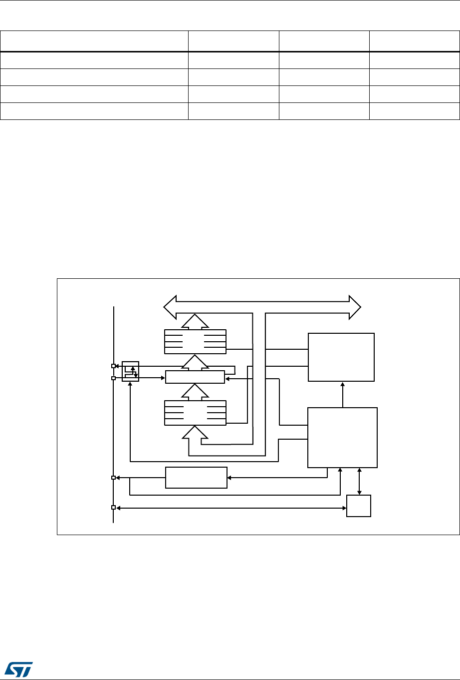
RM0394 Rev 4 1305/1600
RM0394 Serial peripheral interface (SPI)
1338
40.4 SPI functional description
40.4.1 General description
The SPI allows synchronous, serial communication between the MCU and external devices.
Application software can manage the communication by polling the status flag or using
dedicated SPI interrupt. The main elements of SPI and their interactions are shown in the
following block diagram Figure 419.
Figure 419. SPI block diagram
Table 209. SPI implementation
SPI Features(1) SPI1 SPI2 SPI3
Hardware CRC calculation X X X
Rx/Tx FIFO X X X
NSS pulse mode X X X
TI mode X X X
1. X = supported.
6KLIWUHJLVWHU
:ULWH
5HDG
$GGUHVVDQGGDWDEXV
&5&FRQWUROOHU
,QWHUQDO166
&5&(1
&5&1(;7
&5&/
5;21/<
&32/
&3+$
026,
0,62
6&.
166
5[
),)2
7[
),)2
%5>@
069
'6>@
%,',2(
&RPPXQLFDWLRQ
FRQWUROOHU
166
ORJLF
%DXGUDWH
JHQHUDWRU
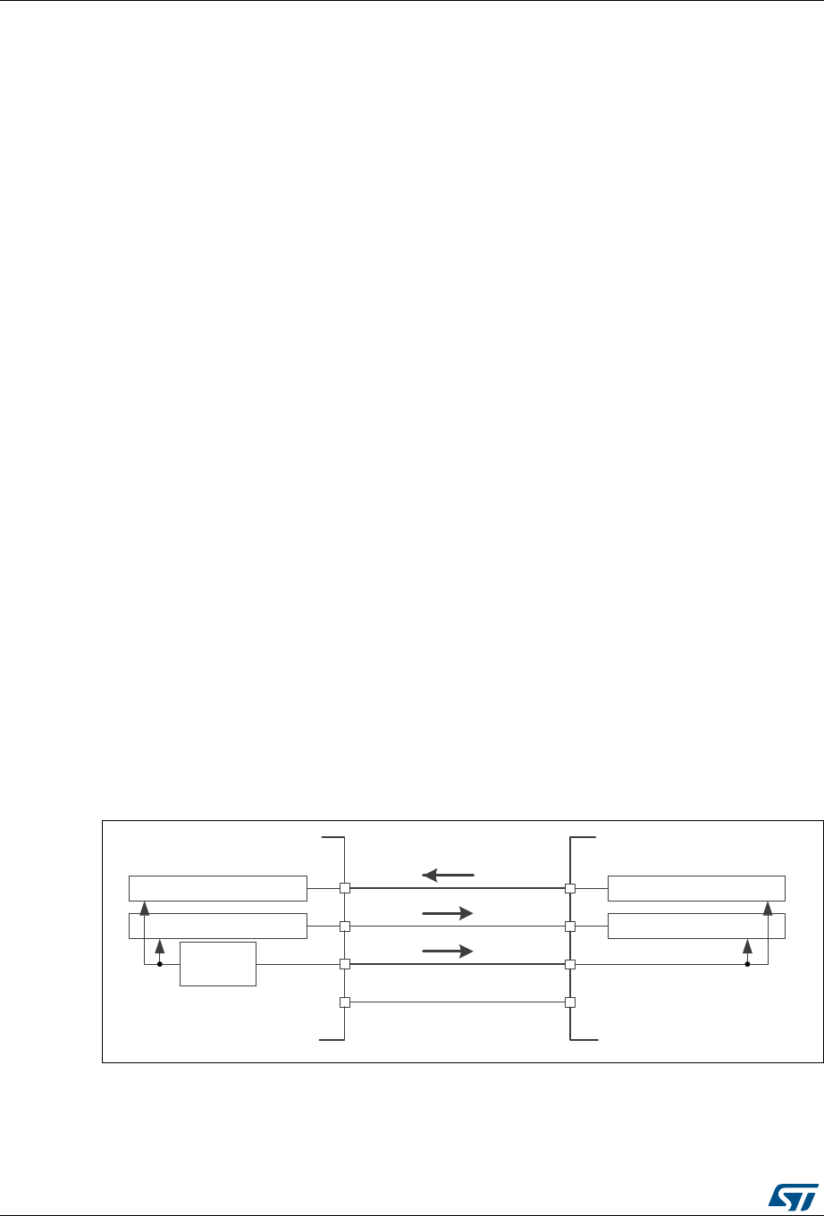
Serial peripheral interface (SPI) RM0394
1306/1600 RM0394 Rev 4
Four I/O pins are dedicated to SPI communication with external devices.
•MISO: Master In / Slave Out data. In the general case, this pin is used to transmit data
in slave mode and receive data in master mode.
•MOSI: Master Out / Slave In data. In the general case, this pin is used to transmit data
in master mode and receive data in slave mode.
•SCK: Serial Clock output pin for SPI masters and input pin for SPI slaves.
•NSS: Slave select pin. Depending on the SPI and NSS settings, this pin can be used to
either:
– select an individual slave device for communication
– synchronize the data frame or
– detect a conflict between multiple masters
See Section 40.4.5: Slave select (NSS) pin management for details.
The SPI bus allows the communication between one master device and one or more slave
devices. The bus consists of at least two wires - one for the clock signal and the other for
synchronous data transfer. Other signals can be added depending on the data exchange
between SPI nodes and their slave select signal management.
40.4.2 Communications between one master and one slave
The SPI allows the MCU to communicate using different configurations, depending on the
device targeted and the application requirements. These configurations use 2 or 3 wires
(with software NSS management) or 3 or 4 wires (with hardware NSS management).
Communication is always initiated by the master.
Full-duplex communication
By default, the SPI is configured for full-duplex communication. In this configuration, the
shift registers of the master and slave are linked using two unidirectional lines between the
MOSI and the MISO pins. During SPI communication, data is shifted synchronously on the
SCK clock edges provided by the master. The master transmits the data to be sent to the
slave via the MOSI line and receives data from the slave via the MISO line. When the data
frame transfer is complete (all the bits are shifted) the information between the master and
slave is exchanged.
Figure 420. Full-duplex single master/ single slave application
1. The NSS pins can be used to provide a hardware control flow between master and slave. Optionally, the
pins can be left unused by the peripheral. Then the flow has to be handled internally for both master and
slave. For more details see Section 40.4.5: Slave select (NSS) pin management.
5[VKLIWUHJLVWHU
7[VKLIWUHJLVWHU 5[VKLIWUHJLVWHU
7[VKLIWUHJLVWHU
63,FORFN
JHQHUDWRU
0DVWHU 6ODYH
0,62
026,
6&.
166
0,62
026,
6&.
166
06Y9
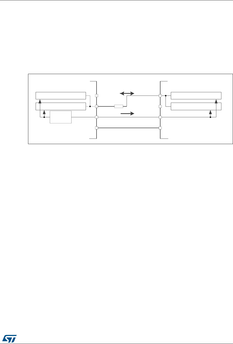
RM0394 Rev 4 1307/1600
RM0394 Serial peripheral interface (SPI)
1338
Half-duplex communication
The SPI can communicate in half-duplex mode by setting the BIDIMODE bit in the
SPIx_CR1 register. In this configuration, one single cross connection line is used to link the
shift registers of the master and slave together. During this communication, the data is
synchronously shifted between the shift registers on the SCK clock edge in the transfer
direction selected reciprocally by both master and slave with the BDIOE bit in their
SPIx_CR1 registers. In this configuration, the master’s MISO pin and the slave’s MOSI pin
are free for other application uses and act as GPIOs.
Figure 421. Half-duplex single master/ single slave application
1. The NSS pins can be used to provide a hardware control flow between master and slave. Optionally, the
pins can be left unused by the peripheral. Then the flow has to be handled internally for both master and
slave. For more details see Section 40.4.5: Slave select (NSS) pin management.
2. In this configuration, the master’s MISO pin and the slave’s MOSI pin can be used as GPIOs.
3. A critical situation can happen when communication direction is changed not synchronously between two
nodes working at bidirectionnal mode and new transmitter accesses the common data line while former
transmitter still keeps an opposite value on the line (the value depends on SPI configuration and
communication data). Both nodes then fight while providing opposite output levels on the common line
temporary till next node changes its direction settings correspondingly, too. It is suggested to insert a serial
resistance between MISO and MOSI pins at this mode to protect the outputs and limit the current blowing
between them at this situation.
Simplex communications
The SPI can communicate in simplex mode by setting the SPI in transmit-only or in receive-
only using the RXONLY bit in the SPIx_CR2 register. In this configuration, only one line is
used for the transfer between the shift registers of the master and slave. The remaining
MISO and MOSI pins pair is not used for communication and can be used as standard
GPIOs.
•Transmit-only mode (RXONLY=0): The configuration settings are the same as for full-
duplex. The application has to ignore the information captured on the unused input pin.
This pin can be used as a standard GPIO.
•Receive-only mode (RXONLY=1): The application can disable the SPI output function
by setting the RXONLY bit. In slave configuration, the MISO output is disabled and the
pin can be used as a GPIO. The slave continues to receive data from the MOSI pin
while its slave select signal is active (see 40.4.5: Slave select (NSS) pin management).
Received data events appear depending on the data buffer configuration. In the master
configuration, the MOSI output is disabled and the pin can be used as a GPIO. The
clock signal is generated continuously as long as the SPI is enabled. The only way to
stop the clock is to clear the RXONLY bit or the SPE bit and wait until the incoming
pattern from the MISO pin is finished and fills the data buffer structure, depending on its
configuration.
5[VKLIWUHJLVWHU
7[VKLIWUHJLVWHU 5[VKLIWUHJLVWHU
7[VKLIWUHJLVWHU
63,FORFN
JHQHUDWRU
0DVWHU 6ODYH
0,62
026,
6&.
166
0,62
026,
6&.
166
Nȍ
06Y9
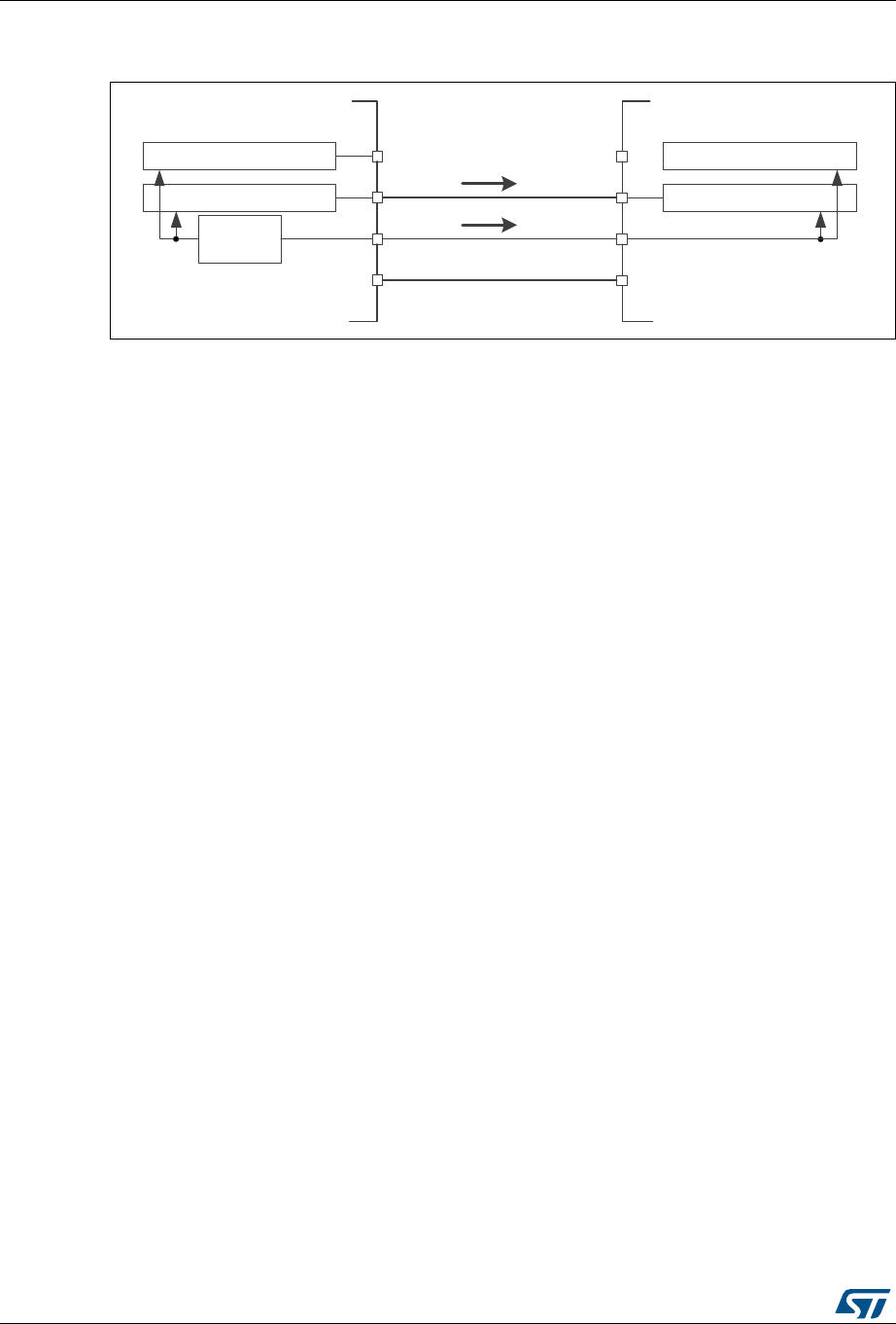
Serial peripheral interface (SPI) RM0394
1308/1600 RM0394 Rev 4
Figure 422. Simplex single master/single slave application (master in transmit-only/
slave in receive-only mode)
1. The NSS pins can be used to provide a hardware control flow between master and slave. Optionally, the
pins can be left unused by the peripheral. Then the flow has to be handled internally for both master and
slave. For more details see Section 40.4.5: Slave select (NSS) pin management.
2. An accidental input information is captured at the input of transmitter Rx shift register. All the events
associated with the transmitter receive flow must be ignored in standard transmit only mode (e.g. OVF
flag).
3. In this configuration, both the MISO pins can be used as GPIOs.
Note: Any simplex communication can be alternatively replaced by a variant of the half-duplex
communication with a constant setting of the transaction direction (bidirectional mode is
enabled while BDIO bit is not changed).
40.4.3 Standard multi-slave communication
In a configuration with two or more independent slaves, the master uses GPIO pins to
manage the chip select lines for each slave (see Figure 423.). The master must select one
of the slaves individually by pulling low the GPIO connected to the slave NSS input. When
this is done, a standard master and dedicated slave communication is established.
5[VKLIWUHJLVWHU
7[VKLIWUHJLVWHU 5[VKLIWUHJLVWHU
7[VKLIWUHJLVWHU
63,FORFN
JHQHUDWRU
0DVWHU ^ůĂǀĞ
0,62
026,
6&.
166
0,62
026,
6&.
166
06Y9
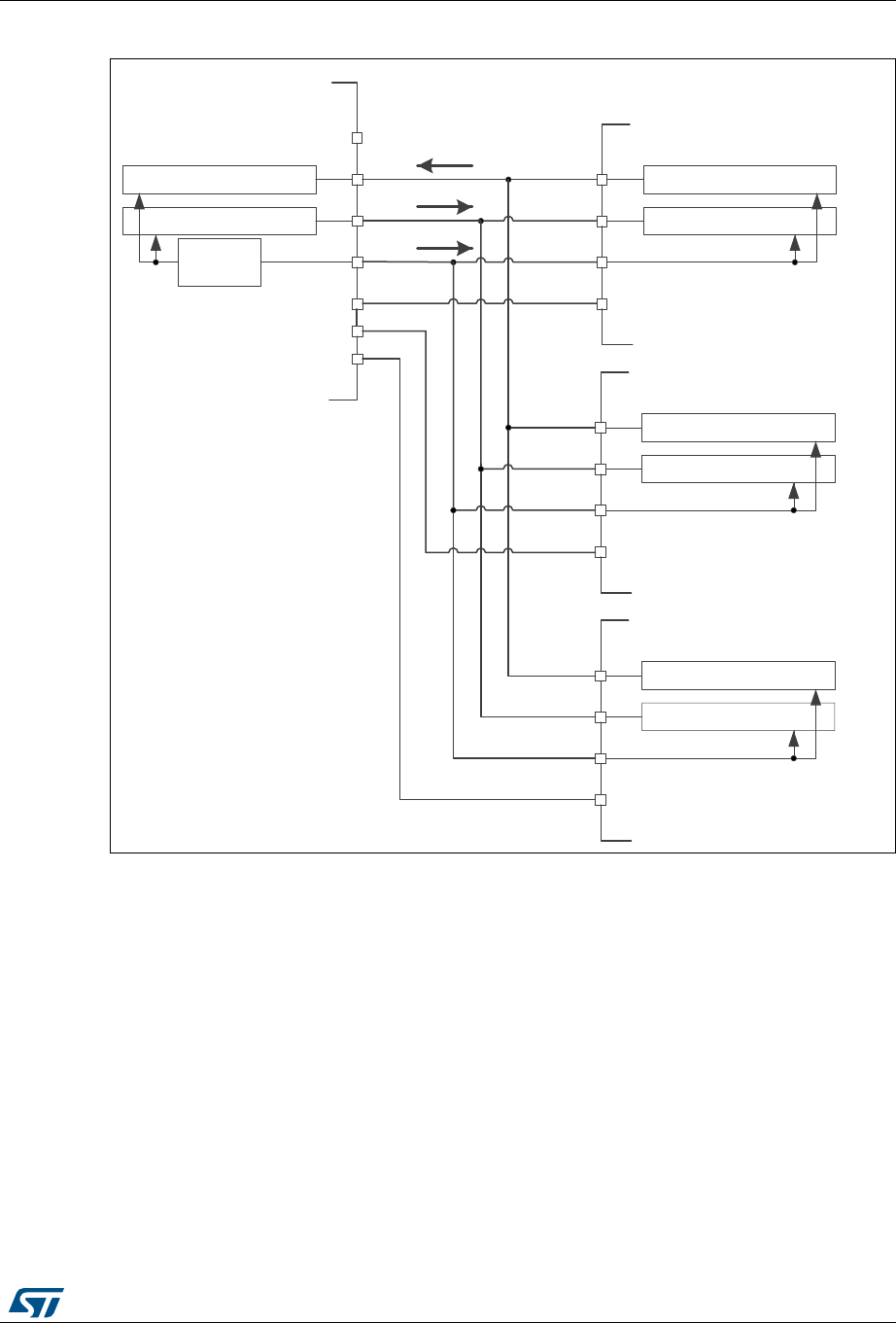
RM0394 Rev 4 1309/1600
RM0394 Serial peripheral interface (SPI)
1338
Figure 423. Master and three independent slaves
1. NSS pin is not used on master side at this configuration. It has to be managed internally (SSM=1, SSI=1) to
prevent any MODF error.
2. As MISO pins of the slaves are connected together, all slaves must have the GPIO configuration of their
MISO pin set as alternate function open-drain (see Section 8.3.7: I/O alternate function input/output.
40.4.4 Multi-master communication
Unless SPI bus is not designed for a multi-master capability primarily, the user can use build
in feature which detects a potential conflict between two nodes trying to master the bus at
the same time. For this detection, NSS pin is used configured at hardware input mode.
The connection of more than two SPI nodes working at this mode is impossible as only one
node can apply its output on a common data line at time.
When nodes are non active, both stay at slave mode by default. Once one node wants to
overtake control on the bus, it switches itself into master mode and applies active level on
the slave select input of the other node via dedicated GPIO pin. After the session is
completed, the active slave select signal is released and the node mastering the bus
temporary returns back to passive slave mode waiting for next session start.
5[VKLIWUHJLVWHU
7[VKLIWUHJLVWHU 5[VKLIWUHJLVWHU
7[VKLIWUHJLVWHU
63,FORFN
JHQHUDWRU
0DVWHU 6ODYH
0,62
026,
6&.
166
0,62
026,
6&.
166
5[VKLIWUHJLVWHU
7[VKLIWUHJLVWHU
6ODYH
5[VKLIWUHJLVWHU
7[VKLIWUHJLVWHU
6ODYH
,2
,2
,2
0,62
026,
6&.
166
0,62
026,
6&.
166
06Y9
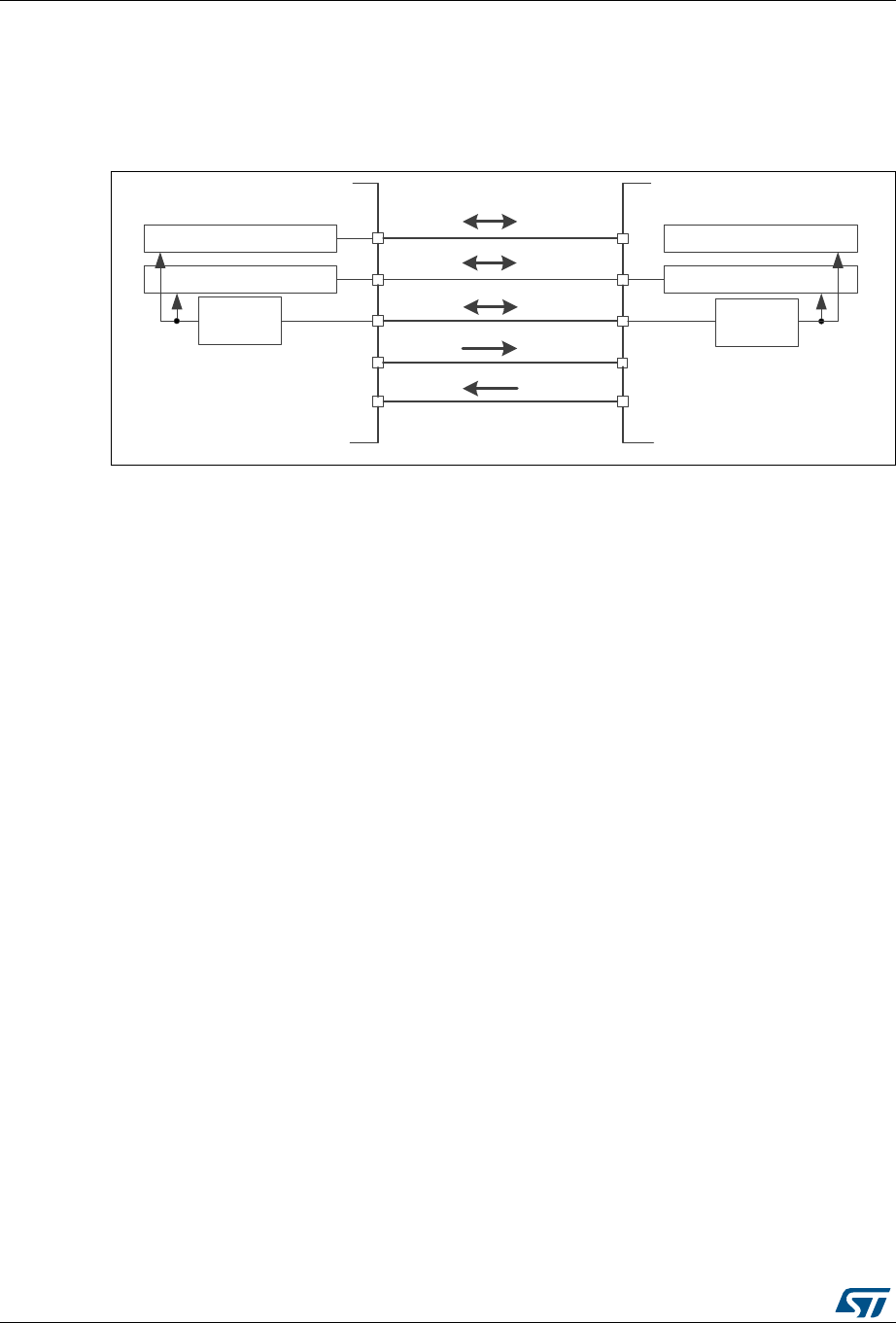
Serial peripheral interface (SPI) RM0394
1310/1600 RM0394 Rev 4
If potentially both nodes raised their mastering request at the same time a bus conflict event
appears (see mode fault MODF event). Then the user can apply some simple arbitration
process (e.g. to postpone next attempt by predefined different time-outs applied at both
nodes).
Figure 424. Multi-master application
1. The NSS pin is configured at hardware input mode at both nodes. Its active level enables the MISO line
output control as the passive node is configured as a slave.
40.4.5 Slave select (NSS) pin management
In slave mode, the NSS works as a standard “chip select” input and lets the slave
communicate with the master. In master mode, NSS can be used either as output or input.
As an input it can prevent multimaster bus collision, and as an output it can drive a slave
select signal of a single slave.
Hardware or software slave select management can be set using the SSM bit in the
SPIx_CR1 register:
•Software NSS management (SSM = 1): in this configuration, slave select information
is driven internally by the SSI bit value in register SPIx_CR1. The external NSS pin is
free for other application uses.
•Hardware NSS management (SSM = 0): in this case, there are two possible
configurations. The configuration used depends on the NSS output configuration
(SSOE bit in register SPIx_CR1).
–NSS output enable (SSM=0,SSOE = 1): this configuration is only used when the
MCU is set as master. The NSS pin is managed by the hardware. The NSS signal
is driven low as soon as the SPI is enabled in master mode (SPE=1), and is kept
low until the SPI is disabled (SPE =0). A pulse can be generated between
continuous communications if NSS pulse mode is activated (NSSP=1). The SPI
cannot work in multimaster configuration with this NSS setting.
–NSS output disable (SSM=0, SSOE = 0): if the microcontroller is acting as the
master on the bus, this configuration allows multimaster capability. If the NSS pin
is pulled low in this mode, the SPI enters master mode fault state and the device is
automatically reconfigured in slave mode. In slave mode, the NSS pin works as a
standard “chip select” input and the slave is selected while NSS line is at low level.
5[7[VKLIWUHJLVWHU
7[5[VKLIWUHJLVWHU 7[5[VKLIWUHJLVWHU
5[7[VKLIWUHJLVWHU
63,FORFN
JHQHUDWRU
0DVWHU
6ODYH
DĂƐƚĞƌ
;^ůĂǀĞͿ
0,62
026,
6&.
166
0,62
026,
6&.
166
06Y9
63,FORFN
JHQHUDWRU
*3,2
*3,2
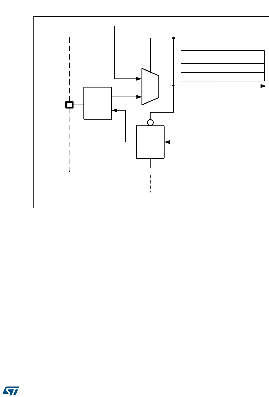
RM0394 Rev 4 1311/1600
RM0394 Serial peripheral interface (SPI)
1338
Figure 425. Hardware/software slave select management
40.4.6 Communication formats
During SPI communication, receive and transmit operations are performed simultaneously.
The serial clock (SCK) synchronizes the shifting and sampling of the information on the data
lines. The communication format depends on the clock phase, the clock polarity and the
data frame format. To be able to communicate together, the master and slaves devices must
follow the same communication format.
Clock phase and polarity controls
Four possible timing relationships may be chosen by software, using the CPOL and CPHA
bits in the SPIx_CR1 register. The CPOL (clock polarity) bit controls the idle state value of
the clock when no data is being transferred. This bit affects both master and slave modes. If
CPOL is reset, the SCK pin has a low-level idle state. If CPOL is set, the SCK pin has a
high-level idle state.
If the CPHA bit is set, the second edge on the SCK pin captures the first data bit transacted
(falling edge if the CPOL bit is reset, rising edge if the CPOL bit is set). Data are latched on
each occurrence of this clock transition type. If the CPHA bit is reset, the first edge on the
SCK pin captures the first data bit transacted (falling edge if the CPOL bit is set, rising edge
if the CPOL bit is reset). Data are latched on each occurrence of this clock transition type.
The combination of CPOL (clock polarity) and CPHA (clock phase) bits selects the data
capture clock edge.
166,QSXW
660FRQWUROELW
66,FRQWUROELW
662(FRQWUROELW
1662XWSXW
166
SLQ
XVHGLQ0DVWHUPRGHDQG166
+:PDQDJHPHQWRQO\
166
2XWSXW
&RQWURO
0DVWHU
PRGH 6ODYHPRGH
1RQDFWLYH2.9GG
166
,QS
$FWLYH&RQIOLFW9VV
166H[WHUQDOORJLF 166LQWHUQDOORJLF
*3,2
ORJLF
06Y9
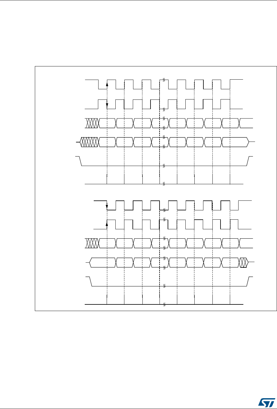
Serial peripheral interface (SPI) RM0394
1312/1600 RM0394 Rev 4
Figure 426, shows an SPI full-duplex transfer with the four combinations of the CPHA and
CPOL bits.
Note: Prior to changing the CPOL/CPHA bits the SPI must be disabled by resetting the SPE bit.
The idle state of SCK must correspond to the polarity selected in the SPIx_CR1 register (by
pulling up SCK if CPOL=1 or pulling down SCK if CPOL=0).
Figure 426. Data clock timing diagram
1. The order of data bits depends on LSBFIRST bit setting.
Data frame format
The SPI shift register can be set up to shift out MSB-first or LSB-first, depending on the
value of the LSBFIRST bit. The data frame size is chosen by using the DS bits. It can be set
from 4-bit up to 16-bit length and the setting applies for both transmission and reception.
Whatever the selected data frame size, read access to the FIFO must be aligned with the
FRXTH level. When the SPIx_DR register is accessed, data frames are always right-aligned
into either a byte (if the data fits into a byte) or a half-word (see Figure 427). During
communication, only bits within the data frame are clocked and transferred.
DLH
&3+$
&3+$
&32/
&32/
026,
0,62
166WRVODYH
&DSWXUHVWUREH
06%LW
06%LW
/6%LW
/6%LW
&32/
&32/
026,
0,62
166WRVODYH
&DSWXUHVWUREH
06%LW
06%LW
/6%LW
/6%LW

RM0394 Rev 4 1313/1600
RM0394 Serial peripheral interface (SPI)
1338
Figure 427. Data alignment when data length is not equal to 8-bit or 16-bit
Note: The minimum data length is 4 bits. If a data length of less than 4 bits is selected, it is forced
to an 8-bit data frame size.
40.4.7 Configuration of SPI
The configuration procedure is almost the same for master and slave. For specific mode
setups, follow the dedicated sections. When a standard communication is to be initialized,
perform these steps:
1. Write proper GPIO registers: Configure GPIO for MOSI, MISO and SCK pins.
2. Write to the SPI_CR1 register:
a) Configure the serial clock baud rate using the BR[2:0] bits (Note: 4).
b) Configure the CPOL and CPHA bits combination to define one of the four
relationships between the data transfer and the serial clock (CPHA must be
cleared in NSSP mode). (Note: 2 - except the case when CRC is enabled at TI
mode).
c) Select simplex or half-duplex mode by configuring RXONLY or BIDIMODE and
BIDIOE (RXONLY and BIDIMODE can't be set at the same time).
d) Configure the LSBFIRST bit to define the frame format (Note: 2).
e) Configure the CRCL and CRCEN bits if CRC is needed (while SCK clock signal is
at idle state).
f) Configure SSM and SSI (Notes: 2 & 3).
g) Configure the MSTR bit (in multimaster NSS configuration, avoid conflict state on
NSS if master is configured to prevent MODF error).
3. Write to SPI_CR2 register:
a) Configure the DS[3:0] bits to select the data length for the transfer.
b) Configure SSOE (Notes: 1 & 2 & 3).
c) Set the FRF bit if the TI protocol is required (keep NSSP bit cleared in TI mode).
d) Set the NSSP bit if the NSS pulse mode between two data units is required (keep
CHPA and TI bits cleared in NSSP mode).
e) Configure the FRXTH bit. The RXFIFO threshold must be aligned to the read
access size for the SPIx_DR register.
f) Initialize LDMA_TX and LDMA_RX bits if DMA is used in packed mode.
4. Write to SPI_CRCPR register: Configure the CRC polynomial if needed.
5. Write proper DMA registers: Configure DMA streams dedicated for SPI Tx and Rx in
DMA registers if the DMA streams are used.
069
;;;
'DWDIUDPH
'DWDIUDPH
;;
'DWDIUDPH
'DWDIUDPH
7;
5;
7;
5;
'6 ELWVGDWDLVULJKWDOLJQHGRQE\WH
([DPSOH'6 ELW
'6!ELWVGDWDLVULJKWDOLJQHGRQELW
([DPSOH'6 ELW

Serial peripheral interface (SPI) RM0394
1314/1600 RM0394 Rev 4
Note: (1) Step is not required in slave mode.
(2) Step is not required in TI mode.
(3) Step is not required in NSSP mode.
(4) The step is not required in slave mode except slave working at TI mode
40.4.8 Procedure for enabling SPI
It is recommended to enable the SPI slave before the master sends the clock. If not,
undesired data transmission might occur. The data register of the slave must already
contain data to be sent before starting communication with the master (either on the first
edge of the communication clock, or before the end of the ongoing communication if the
clock signal is continuous). The SCK signal must be settled at an idle state level
corresponding to the selected polarity before the SPI slave is enabled.
The master at full-duplex (or in any transmit-only mode) starts to communicate when the
SPI is enabled and TXFIFO is not empty, or with the next write to TXFIFO.
In any master receive only mode (RXONLY=1 or BIDIMODE=1 & BIDIOE=0), master starts
to communicate and the clock starts running immediately after SPI is enabled.
For handling DMA, follow the dedicated section.
40.4.9 Data transmission and reception procedures
RXFIFO and TXFIFO
All SPI data transactions pass through the 32-bit embedded FIFOs. This enables the SPI to
work in a continuous flow, and prevents overruns when the data frame size is short. Each
direction has its own FIFO called TXFIFO and RXFIFO. These FIFOs are used in all SPI
modes except for receiver-only mode (slave or master) with CRC calculation enabled (see
Section 40.4.14: CRC calculation).
The handling of FIFOs depends on the data exchange mode (duplex, simplex), data frame
format (number of bits in the frame), access size performed on the FIFO data registers (8-bit
or 16-bit), and whether or not data packing is used when accessing the FIFOs (see
Section 40.4.13: TI mode).
A read access to the SPIx_DR register returns the oldest value stored in RXFIFO that has
not been read yet. A write access to the SPIx_DR stores the written data in the TXFIFO at
the end of a send queue. The read access must be always aligned with the RXFIFO
threshold configured by the FRXTH bit in SPIx_CR2 register. FTLVL[1:0] and FRLVL[1:0]
bits indicate the current occupancy level of both FIFOs.
A read access to the SPIx_DR register must be managed by the RXNE event. This event is
triggered when data is stored in RXFIFO and the threshold (defined by FRXTH bit) is
reached. When RXNE is cleared, RXFIFO is considered to be empty. In a similar way, write
access of a data frame to be transmitted is managed by the TXE event. This event is
triggered when the TXFIFO level is less than or equal to half of its capacity. Otherwise TXE
is cleared and the TXFIFO is considered as full. In this way, RXFIFO can store up to four
data frames, whereas TXFIFO can only store up to three when the data frame format is not
greater than 8 bits. This difference prevents possible corruption of 3x 8-bit data frames
already stored in the TXFIFO when software tries to write more data in 16-bit mode into
TXFIFO. Both TXE and RXNE events can be polled or handled by interrupts. See
Figure 429 through Figure 432.

RM0394 Rev 4 1315/1600
RM0394 Serial peripheral interface (SPI)
1338
Another way to manage the data exchange is to use DMA (see Communication using DMA
(direct memory addressing)).
If the next data is received when the RXFIFO is full, an overrun event occurs (see
description of OVR flag at Section 40.4.10: SPI status flags). An overrun event can be
polled or handled by an interrupt.
The BSY bit being set indicates ongoing transaction of a current data frame. When the clock
signal runs continuously, the BSY flag stays set between data frames at master but
becomes low for a minimum duration of one SPI clock at slave between each data frame
transfer.
Sequence handling
A few data frames can be passed at single sequence to complete a message. When
transmission is enabled, a sequence begins and continues while any data is present in the
TXFIFO of the master. The clock signal is provided continuously by the master until TXFIFO
becomes empty, then it stops waiting for additional data.
In receive-only modes, half-duplex (BIDIMODE=1, BIDIOE=0) or simplex (BIDIMODE=0,
RXONLY=1) the master starts the sequence immediately when both SPI is enabled and
receive-only mode is activated. The clock signal is provided by the master and it does not
stop until either SPI or receive-only mode is disabled by the master. The master receives
data frames continuously up to this moment.
While the master can provide all the transactions in continuous mode (SCK signal is
continuous) it has to respect slave capability to handle data flow and its content at anytime.
When necessary, the master must slow down the communication and provide either a
slower clock or separate frames or data sessions with sufficient delays. Be aware there is no
underflow error signal for master or slave in SPI mode, and data from the slave is always
transacted and processed by the master even if the slave could not prepare it correctly in
time. It is preferable for the slave to use DMA, especially when data frames are shorter and
bus rate is high.
Each sequence must be encased by the NSS pulse in parallel with the multislave system to
select just one of the slaves for communication. In a single slave system it is not necessary
to control the slave with NSS, but it is often better to provide the pulse here too, to
synchronize the slave with the beginning of each data sequence. NSS can be managed by
both software and hardware (see Section 40.4.5: Slave select (NSS) pin management).
When the BSY bit is set it signifies an ongoing data frame transaction. When the dedicated
frame transaction is finished, the RXNE flag is raised. The last bit is just sampled and the
complete data frame is stored in the RXFIFO.
Procedure for disabling the SPI
When SPI is disabled, it is mandatory to follow the disable procedures described in this
paragraph. It is important to do this before the system enters a low-power mode when the
peripheral clock is stopped. Ongoing transactions can be corrupted in this case. In some
modes the disable procedure is the only way to stop continuous communication running.
Master in full-duplex or transmit only mode can finish any transaction when it stops
providing data for transmission. In this case, the clock stops after the last data transaction.
Special care must be taken in packing mode when an odd number of data frames are
transacted to prevent some dummy byte exchange (refer to Data packing section). Before
the SPI is disabled in these modes, the user must follow standard disable procedure. When

Serial peripheral interface (SPI) RM0394
1316/1600 RM0394 Rev 4
the SPI is disabled at the master transmitter while a frame transaction is ongoing or next
data frame is stored in TXFIFO, the SPI behavior is not guaranteed.
When the master is in any receive only mode, the only way to stop the continuous clock is to
disable the peripheral by SPE=0. This must occur in specific time window within last data
frame transaction just between the sampling time of its first bit and before its last bit transfer
starts (in order to receive a complete number of expected data frames and to prevent any
additional “dummy” data reading after the last valid data frame). Specific procedure must be
followed when disabling SPI in this mode.
Data received but not read remains stored in RXFIFO when the SPI is disabled, and must
be processed the next time the SPI is enabled, before starting a new sequence. To prevent
having unread data, ensure that RXFIFO is empty when disabling the SPI, by using the
correct disabling procedure, or by initializing all the SPI registers with a software reset via
the control of a specific register dedicated to peripheral reset (see the SPIiRST bits in the
RCC_APBiRSTR registers).
Standard disable procedure is based on pulling BSY status together with FTLVL[1:0] to
check if a transmission session is fully completed. This check can be done in specific cases,
too, when it is necessary to identify the end of ongoing transactions, for example:
•When NSS signal is managed by software and master has to provide proper end of
NSS pulse for slave, or
•When transactions’ streams from DMA or FIFO are completed while the last data frame
or CRC frame transaction is still ongoing in the peripheral bus.
The correct disable procedure is (except when receive only mode is used):
1. Wait until FTLVL[1:0] = 00 (no more data to transmit).
2. Wait until BSY=0 (the last data frame is processed).
3. Disable the SPI (SPE=0).
4. Read data until FRLVL[1:0] = 00 (read all the received data).
The correct disable procedure for certain receive only modes is:
1. Interrupt the receive flow by disabling SPI (SPE=0) in the specific time window while
the last data frame is ongoing.
2. Wait until BSY=0 (the last data frame is processed).
3. Read data until FRLVL[1:0] = 00 (read all the received data).
Note: If packing mode is used and an odd number of data frames with a format less than or equal
to 8 bits (fitting into one byte) has to be received, FRXTH must be set when FRLVL[1:0] =
01, in order to generate the RXNE event to read the last odd data frame and to keep good
FIFO pointer alignment.
Data packing
When the data frame size fits into one byte (less than or equal to 8 bits), data packing is
used automatically when any read or write 16-bit access is performed on the SPIx_DR
register. The double data frame pattern is handled in parallel in this case. At first, the SPI
operates using the pattern stored in the LSB of the accessed word, then with the other half
stored in the MSB. Figure 428 provides an example of data packing mode sequence
handling. Two data frames are sent after the single 16-bit access the SPIx_DR register of
the transmitter. This sequence can generate just one RXNE event in the receiver if the
RXFIFO threshold is set to 16 bits (FRXTH=0). The receiver then has to access both data
frames by a single 16-bit read of SPIx_DR as a response to this single RXNE event. The
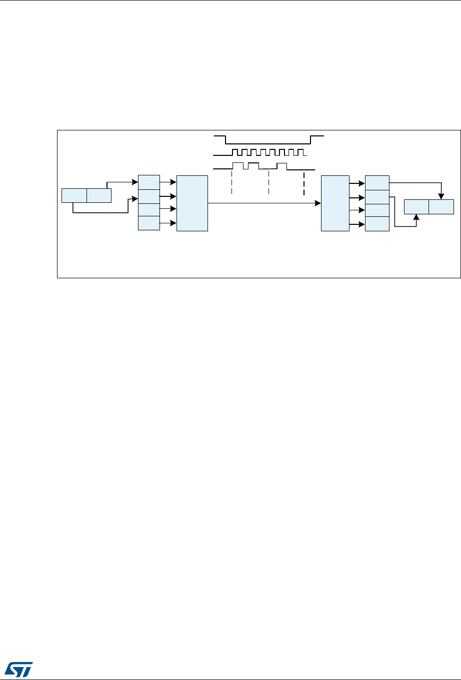
RM0394 Rev 4 1317/1600
RM0394 Serial peripheral interface (SPI)
1338
RxFIFO threshold setting and the following read access must be always kept aligned at the
receiver side, as data can be lost if it is not in line.
A specific problem appears if an odd number of such “fit into one byte” data frames must be
handled. On the transmitter side, writing the last data frame of any odd sequence with an 8-
bit access to SPIx_DR is enough. The receiver has to change the Rx_FIFO threshold level
for the last data frame received in the odd sequence of frames in order to generate the
RXNE event.
Figure 428. Packing data in FIFO for transmission and reception
Communication using DMA (direct memory addressing)
To operate at its maximum speed and to facilitate the data register read/write process
required to avoid overrun, the SPI features a DMA capability, which implements a simple
request/acknowledge protocol.
A DMA access is requested when the TXE or RXNE enable bit in the SPIx_CR2 register is
set. Separate requests must be issued to the Tx and Rx buffers.
•In transmission, a DMA request is issued each time TXE is set to 1. The DMA then
writes to the SPIx_DR register.
•In reception, a DMA request is issued each time RXNE is set to 1. The DMA then reads
the SPIx_DR register.
See Figure 429 through Figure 432.
When the SPI is used only to transmit data, it is possible to enable only the SPI Tx DMA
channel. In this case, the OVR flag is set because the data received is not read. When the
SPI is used only to receive data, it is possible to enable only the SPI Rx DMA channel.
In transmission mode, when the DMA has written all the data to be transmitted (the TCIF
flag is set in the DMA_ISR register), the BSY flag can be monitored to ensure that the SPI
communication is complete. This is required to avoid corrupting the last transmission before
disabling the SPI or entering the Stop mode. The software must first wait until
FTLVL[1:0]=00 and then until BSY=0.
When starting communication using DMA, to prevent DMA channel management raising
error events, these steps must be followed in order:
[ [$ 63,IVP
VKLIW
7;),)2
63,[B'5 [$
[
[$ [
63,IVP
VKLIW
[$
[
[ [$
63,[B'5
ELWDFFHVVZKHQZULWHWRGDWDUHJLVWHU ELWDFFHVVZKHQUHDGIURPGDWDUHJLVWHU
166
6&.
026, 5;),)2
069
63,B'5 [$ZKHQ7[( 63,B'5 [$ZKHQ5[1(

Serial peripheral interface (SPI) RM0394
1318/1600 RM0394 Rev 4
1. Enable DMA Rx buffer in the RXDMAEN bit in the SPI_CR2 register, if DMA Rx is
used.
2. Enable DMA streams for Tx and Rx in DMA registers, if the streams are used.
3. Enable DMA Tx buffer in the TXDMAEN bit in the SPI_CR2 register, if DMA Tx is used.
4. Enable the SPI by setting the SPE bit.
To close communication it is mandatory to follow these steps in order:
1. Disable DMA streams for Tx and Rx in the DMA registers, if the streams are used.
2. Disable the SPI by following the SPI disable procedure.
3. Disable DMA Tx and Rx buffers by clearing the TXDMAEN and RXDMAEN bits in the
SPI_CR2 register, if DMA Tx and/or DMA Rx are used.
Packing with DMA
If the transfers are managed by DMA (TXDMAEN and RXDMAEN set in the SPIx_CR2
register) packing mode is enabled/disabled automatically depending on the PSIZE value
configured for SPI TX and the SPI RX DMA channel. If the DMA channel PSIZE value is
equal to 16-bit and SPI data size is less than or equal to 8-bit, then packing mode is
enabled. The DMA then automatically manages the write operations to the SPIx_DR
register.
If data packing mode is used and the number of data to transfer is not a multiple of two, the
LDMA_TX/LDMA_RX bits must be set. The SPI then considers only one data for the
transmission or reception to serve the last DMA transfer (for more details refer to Data
packing on page 1316.)

RM0394 Rev 4 1319/1600
RM0394 Serial peripheral interface (SPI)
1338
Communication diagrams
Some typical timing schemes are explained in this section. These schemes are valid no
matter if the SPI events are handled by polling, interrupts or DMA. For simplicity, the
LSBFIRST=0, CPOL=0 and CPHA=1 setting is used as a common assumption here. No
complete configuration of DMA streams is provided.
The following numbered notes are common for Figure 429 on page 1320 through
Figure 432 on page 1323.
1. The slave starts to control MISO line as NSS is active and SPI is enabled, and is
disconnected from the line when one of them is released. Sufficient time must be
provided for the slave to prepare data dedicated to the master in advance before its
transaction starts.
At the master, the SPI peripheral takes control at MOSI and SCK signals (occasionally
at NSS signal as well) only if SPI is enabled. If SPI is disabled the SPI peripheral is
disconnected from GPIO logic, so the levels at these lines depends on GPIO setting
exclusively.
2. At the master, BSY stays active between frames if the communication (clock signal) is
continuous. At the slave, BSY signal always goes down for at least one clock cycle
between data frames.
3. The TXE signal is cleared only if TXFIFO is full.
4. The DMA arbitration process starts just after the TXDMAEN bit is set. The TXE
interrupt is generated just after the TXEIE is set. As the TXE signal is at an active level,
data transfers to TxFIFO start, until TxFIFO becomes full or the DMA transfer
completes.
5. If all the data to be sent can fit into TxFIFO, the DMA Tx TCIF flag can be raised even
before communication on the SPI bus starts. This flag always rises before the SPI
transaction is completed.
6. The CRC value for a package is calculated continuously frame by frame in the
SPIx_TXCRCR and SPIx_RXCRCR registers. The CRC information is processed after
the entire data package has completed, either automatically by DMA (Tx channel must
be set to the number of data frames to be processed) or by SW (the user must handle
CRCNEXT bit during the last data frame processing).
While the CRC value calculated in SPIx_TXCRCR is simply sent out by transmitter,
received CRC information is loaded into RxFIFO and then compared with the
SPIx_RXCRCR register content (CRC error flag can be raised here if any difference).
This is why the user must take care to flush this information from the FIFO, either by
software reading out all the stored content of RxFIFO, or by DMA when the proper
number of data frames is preset for Rx channel (number of data frames + number of
CRC frames) (see the settings at the example assumption).
7. In data packed mode, TxE and RxNE events are paired and each read/write access to
the FIFO is 16 bits wide until the number of data frames are even. If the TxFIFO is ¾
full FTLVL status stays at FIFO full level. That is why the last odd data frame cannot be
stored before the TxFIFO becomes ½ full. This frame is stored into TxFIFO with an 8-
bit access either by software or automatically by DMA when LDMA_TX control is set.
8. To receive the last odd data frame in packed mode, the Rx threshold must be changed
to 8-bit when the last data frame is processed, either by software setting FRXTH=1 or
automatically by a DMA internal signal when LDMA_RX is set.
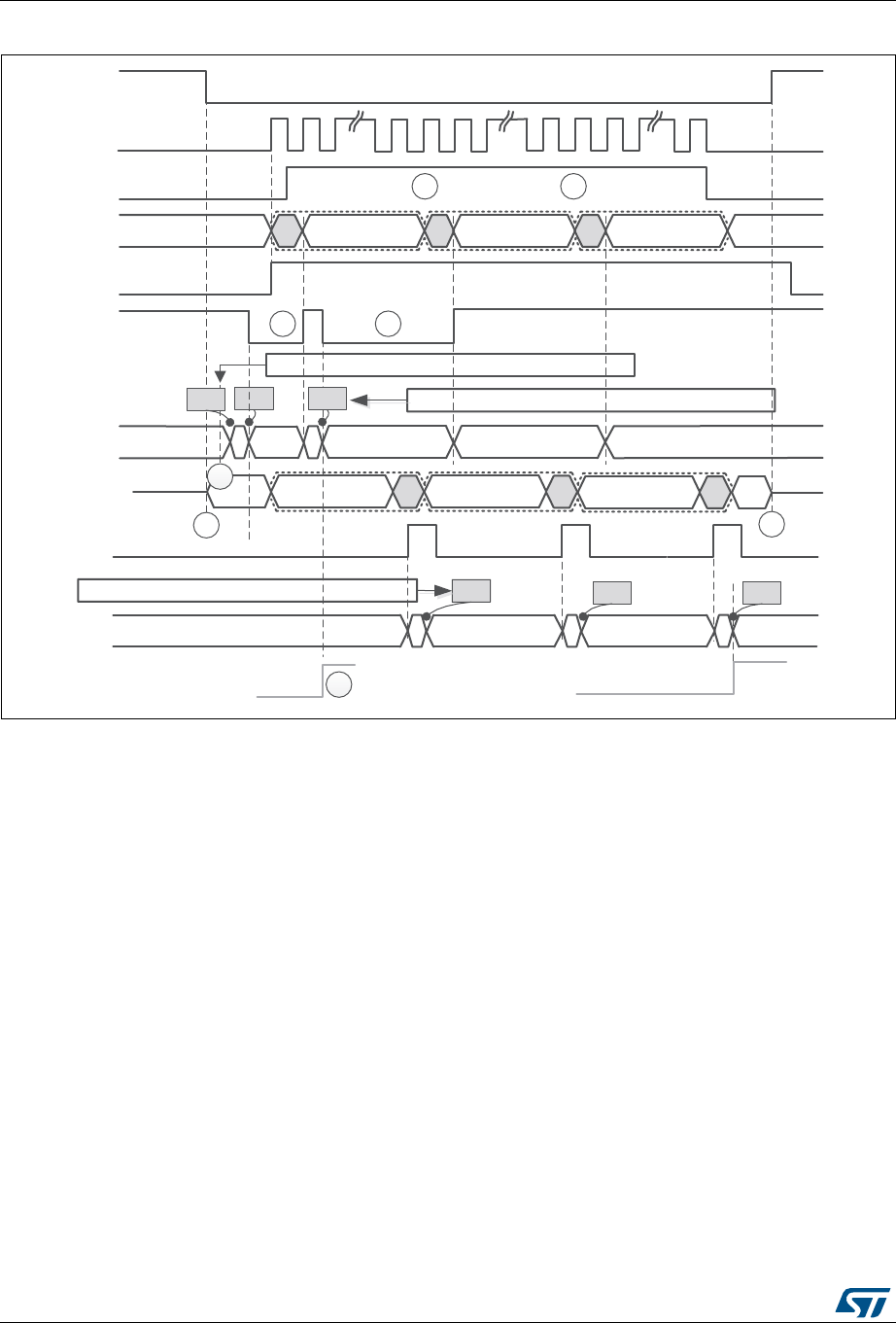
Serial peripheral interface (SPI) RM0394
1320/1600 RM0394 Rev 4
Figure 429. Master full-duplex communication
Assumptions for master full-duplex communication example:
•Data size > 8 bit
If DMA is used:
•Number of Tx frames transacted by DMA is set to 3
•Number of Rx frames transacted by DMA is set to 3
See also : Communication diagrams on page 1319 for details about common assumptions
and notes.
'7[
'5[
166
6&.
%6<
026, 06% 06% 06%
'7[ '7[
63(
7;(
)7/9/
'7[ '7[
/6% '5[ /6% '5[ /6%
5;1(
'5[ '5[ '5[
)5/9/
'0$7[7,&) '0$5[7,&)
(QDEOH7[5['0$RULQWHUUXSWV
'0$RUVRIWZDUHFRQWURODW7[HYHQWV
'0$RUVRIWZDUHFRQWURODW5[HYHQWV
'7[
0,62
06Y9
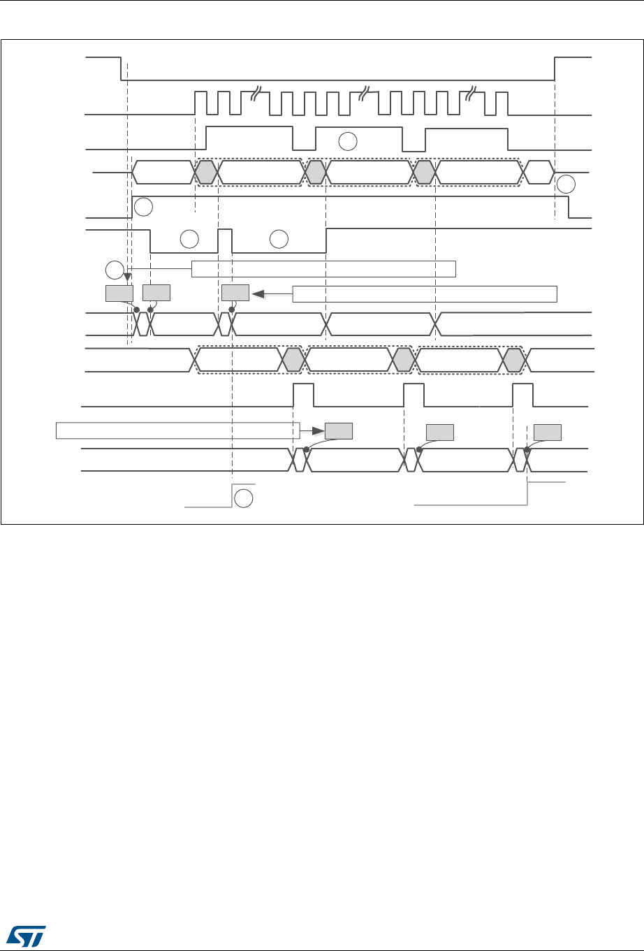
RM0394 Rev 4 1321/1600
RM0394 Serial peripheral interface (SPI)
1338
Figure 430. Slave full-duplex communication
Assumptions for slave full-duplex communication example:
•Data size > 8 bit
If DMA is used:
•Number of Tx frames transacted by DMA is set to 3
•Number of Rx frames transacted by DMA is set to 3
See also : Communication diagrams on page 1319 for details about common assumptions
and notes.
'7[
'5[
166
6&.
%6<
0,62 06% 06% 06%
'7[ '7[
63(
7;(
)7/9/
'7[ '7[
/6% '5[ /6% '5[ /6%
5;1(
'5[ '5[ '5[
)5/9/
'0$7[7,&) '0$5[7,&)
(QDEOH7[5['0$RULQWHUUXSWV
'0$RUVRIWZDUHFRQWURODW7[HYHQWV
'0$RUVRIWZDUHFRQWURODW5[HYHQWV
'7[
026,
06Y9
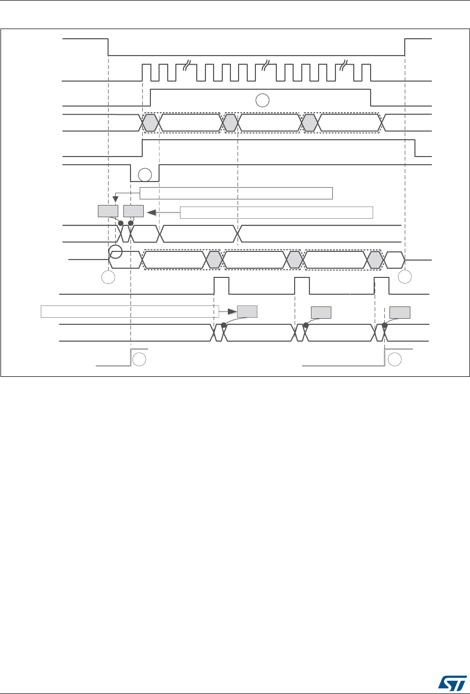
Serial peripheral interface (SPI) RM0394
1322/1600 RM0394 Rev 4
Figure 431. Master full-duplex communication with CRC
Assumptions for master full-duplex communication with CRC example:
•Data size = 16 bit
•CRC enabled
If DMA is used:
•Number of Tx frames transacted by DMA is set to 2
•Number of Rx frames transacted by DMA is set to 3
See also : Communication diagrams on page 1319 for details about common assumptions
and notes.
'7[
'5[
166
6&.
%6<
026,
06% 06% 06%
'7[ &5&
63(
7;(
)7/9/
'7[ '7[
/6% '5[ /6% &5& /6%
5;1(
'5[ '5[ '5[
)5/9/
'0$7[7,&) '0$5[7,&)
(QDEOH7[5['0$RULQWHUUXSWV
'0$RUVRIWZDUHFRQWURODW7[HYHQWV
'0$RUVRIWZDUHFRQWURODW5[HYHQWV
0,62
06Y9
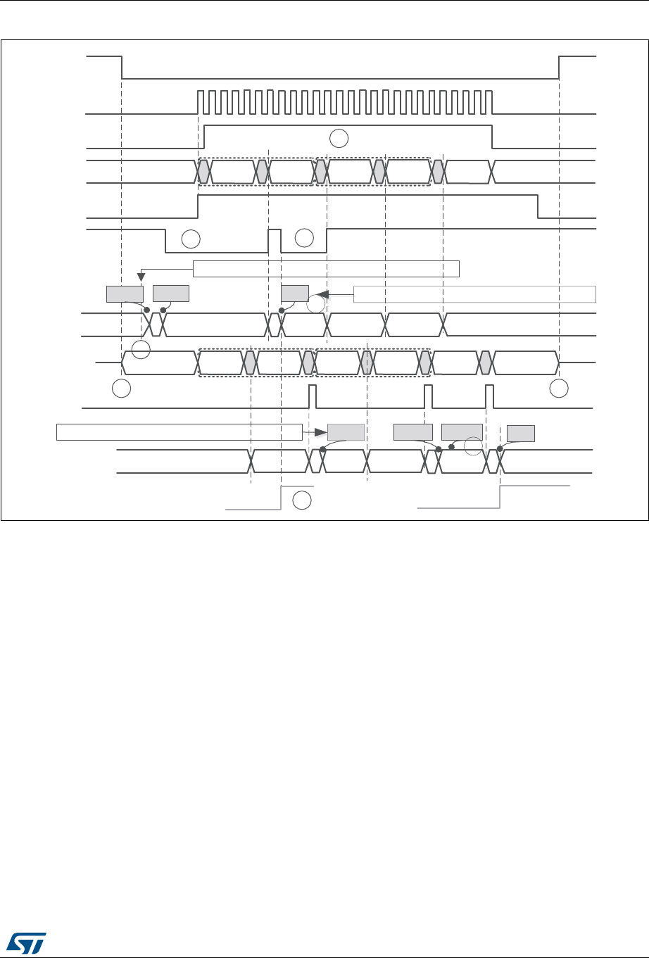
RM0394 Rev 4 1323/1600
RM0394 Serial peripheral interface (SPI)
1338
Figure 432. Master full-duplex communication in packed mode
Assumptions for master full-duplex communication in packed mode example:
•Data size = 5 bit
•Read/write FIFO is performed mostly by 16-bit access
•FRXTH=0
If DMA is used:
•Number of Tx frames to be transacted by DMA is set to 3
•Number of Rx frames to be transacted by DMA is set to 3
•PSIZE for both Tx and Rx DMA channel is set to 16-bit
•LDMA_TX=1 and LDMA_RX=1
See also : Communication diagrams on page 1319 for details about common assumptions
and notes.
166
6&.
%6<
026,
63(
7;(
)7/9/
'7[ '7[
5;1(
'5[ '5[ '5[
)5/9/
'0$7[7,&) '0$5[7,&)
(QDEOH7[5['0$RULQWHUUXSWV
'0$RUVRIWZDUHFRQWURODW7[HYHQWV
'0$RUVRIWZDUHFRQWURODW5[HYHQWV
'7[
'7[ '7[ '7[
0,62
'5[ '5[ '5[
)57+;
06Y9

Serial peripheral interface (SPI) RM0394
1324/1600 RM0394 Rev 4
40.4.10 SPI status flags
Three status flags are provided for the application to completely monitor the state of the SPI
bus.
Tx buffer empty flag (TXE)
The TXE flag is set when transmission TXFIFO has enough space to store data to send.
TXE flag is linked to the TXFIFO level. The flag goes high and stays high until the TXFIFO
level is lower or equal to 1/2 of the FIFO depth. An interrupt can be generated if the TXEIE
bit in the SPIx_CR2 register is set. The bit is cleared automatically when the TXFIFO level
becomes greater than 1/2.
Rx buffer not empty (RXNE)
The RXNE flag is set depending on the FRXTH bit value in the SPIx_CR2 register:
•If FRXTH is set, RXNE goes high and stays high until the RXFIFO level is greater or
equal to 1/4 (8-bit).
•If FRXTH is cleared, RXNE goes high and stays high until the RXFIFO level is greater
than or equal to 1/2 (16-bit).
An interrupt can be generated if the RXNEIE bit in the SPIx_CR2 register is set.
The RXNE is cleared by hardware automatically when the above conditions are no longer
true.
Busy flag (BSY)
The BSY flag is set and cleared by hardware (writing to this flag has no effect).
When BSY is set, it indicates that a data transfer is in progress on the SPI (the SPI bus is
busy).
The BSY flag can be used in certain modes to detect the end of a transfer so that the
software can disable the SPI or its peripheral clock before entering a low-power mode which
does not provide a clock for the peripheral. This avoids corrupting the last transfer.
The BSY flag is also useful for preventing write collisions in a multimaster system.
The BSY flag is cleared under any one of the following conditions:
•When the SPI is correctly disabled
•When a fault is detected in Master mode (MODF bit set to 1)
•In Master mode, when it finishes a data transmission and no new data is ready to be
sent
•In Slave mode, when the BSY flag is set to '0' for at least one SPI clock cycle between
each data transfer.
Note: When the next transmission can be handled immediately by the master (e.g. if the master is
in Receive-only mode or its Transmit FIFO is not empty), communication is continuous and
the BSY flag remains set to '1' between transfers on the master side. Although this is not the
case with a slave, it is recommended to use always the TXE and RXNE flags (instead of the
BSY flags) to handle data transmission or reception operations.

RM0394 Rev 4 1325/1600
RM0394 Serial peripheral interface (SPI)
1338
40.4.11 SPI error flags
An SPI interrupt is generated if one of the following error flags is set and interrupt is enabled
by setting the ERRIE bit.
Overrun flag (OVR)
An overrun condition occurs when data is received by a master or slave and the RXFIFO
has not enough space to store this received data. This can happen if the software or the
DMA did not have enough time to read the previously received data (stored in the RXFIFO)
or when space for data storage is limited e.g. the RXFIFO is not available when CRC is
enabled in receive only mode so in this case the reception buffer is limited into a single data
frame buffer (see Section 40.4.14: CRC calculation).
When an overrun condition occurs, the newly received value does not overwrite the
previous one in the RXFIFO. The newly received value is discarded and all data transmitted
subsequently is lost. Clearing the OVR bit is done by a read access to the SPI_DR register
followed by a read access to the SPI_SR register.
Mode fault (MODF)
Mode fault occurs when the master device has its internal NSS signal (NSS pin in NSS
hardware mode, or SSI bit in NSS software mode) pulled low. This automatically sets the
MODF bit. Master mode fault affects the SPI interface in the following ways:
•The MODF bit is set and an SPI interrupt is generated if the ERRIE bit is set.
•The SPE bit is cleared. This blocks all output from the device and disables the SPI
interface.
•The MSTR bit is cleared, thus forcing the device into slave mode.
Use the following software sequence to clear the MODF bit:
1. Make a read or write access to the SPIx_SR register while the MODF bit is set.
2. Then write to the SPIx_CR1 register.
To avoid any multiple slave conflicts in a system comprising several MCUs, the NSS pin
must be pulled high during the MODF bit clearing sequence. The SPE and MSTR bits can
be restored to their original state after this clearing sequence. As a security, hardware does
not allow the SPE and MSTR bits to be set while the MODF bit is set. In a slave device the
MODF bit cannot be set except as the result of a previous multimaster conflict.
CRC error (CRCERR)
This flag is used to verify the validity of the value received when the CRCEN bit in the
SPIx_CR1 register is set. The CRCERR flag in the SPIx_SR register is set if the value
received in the shift register does not match the receiver SPIx_RXCRCR value. The flag is
cleared by the software.
TI mode frame format error (FRE)
A TI mode frame format error is detected when an NSS pulse occurs during an ongoing
communication when the SPI is operating in slave mode and configured to conform to the TI
mode protocol. When this error occurs, the FRE flag is set in the SPIx_SR register. The SPI
is not disabled when an error occurs, the NSS pulse is ignored, and the SPI waits for the
next NSS pulse before starting a new transfer. The data may be corrupted since the error
detection may result in the loss of two data bytes.
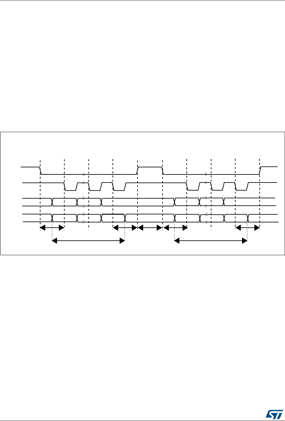
Serial peripheral interface (SPI) RM0394
1326/1600 RM0394 Rev 4
The FRE flag is cleared when SPIx_SR register is read. If the ERRIE bit is set, an interrupt
is generated on the NSS error detection. In this case, the SPI should be disabled because
data consistency is no longer guaranteed and communications should be reinitiated by the
master when the slave SPI is enabled again.
40.4.12 NSS pulse mode
This mode is activated by the NSSP bit in the SPIx_CR2 register and it takes effect only if
the SPI interface is configured as Motorola SPI master (FRF=0) with capture on the first
edge (SPIx_CR1 CPHA = 0, CPOL setting is ignored). When activated, an NSS pulse is
generated between two consecutive data frame transfers when NSS stays at high level for
the duration of one clock period at least. This mode allows the slave to latch data. NSSP
pulse mode is designed for applications with a single master-slave pair.
Figure 433 illustrates NSS pin management when NSSP pulse mode is enabled.
Figure 433. NSSP pulse generation in Motorola SPI master mode
Note: Similar behavior is encountered when CPOL = 0. In this case the sampling edge is the rising
edge of SCK, and NSS assertion and deassertion refer to this sampling edge.
40.4.13 TI mode
TI protocol in master mode
The SPI interface is compatible with the TI protocol. The FRF bit of the SPIx_CR2 register
can be used to configure the SPI to be compliant with this protocol.
The clock polarity and phase are forced to conform to the TI protocol requirements whatever
the values set in the SPIx_CR1 register. NSS management is also specific to the TI protocol
which makes the configuration of NSS management through the SPIx_CR1 and SPIx_CR2
registers (SSM, SSI, SSOE) impossible in this case.
In slave mode, the SPI baud rate prescaler is used to control the moment when the MISO
pin state changes to HiZ when the current transaction finishes (see Figure 434). Any baud
rate can be used, making it possible to determine this moment with optimal flexibility.
However, the baud rate is generally set to the external master clock baud rate. The delay for
the MISO signal to become HiZ (trelease) depends on internal resynchronization and on the
069
026,
RXWSXW
166
RXWSXW
6&.
RXWSXW
VDPSOLQJ
0,62
LQSXW 'RQRWFDUH
06%
06%
ELWVWRELWV
'RQRWFDUH
/6%
/6%
06%
06%
/6%
/6%
ELWVWRELWV
'RQRWFDUH
0DVWHUFRQWLQXRXVWUDQVIHU&32/ &3+$ 1663
VDPSOLQJ VDPSOLQJ VDPSOLQJ VDPSOLQJ VDPSOLQJ
W6&. W6&. W6&. W6&. W6&.
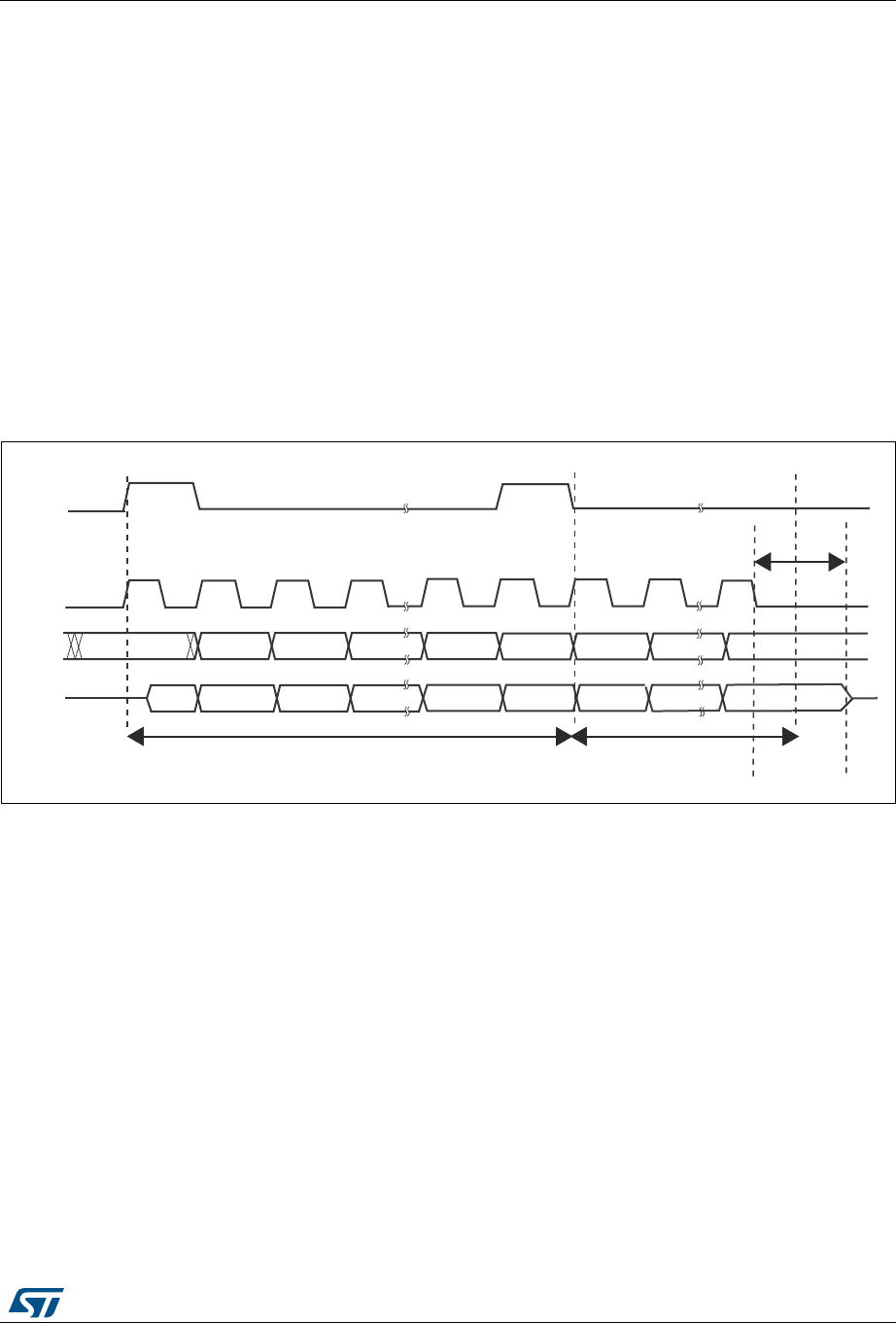
RM0394 Rev 4 1327/1600
RM0394 Serial peripheral interface (SPI)
1338
baud rate value set in through the BR[2:0] bits in the SPIx_CR1 register. It is given by the
formula:
If the slave detects a misplaced NSS pulse during a data frame transaction the TIFRE flag is
set.
If the data size is equal to 4-bits or 5-bits, the master in full-duplex mode or transmit-only
mode uses a protocol with one more dummy data bit added after LSB. TI NSS pulse is
generated above this dummy bit clock cycle instead of the LSB in each period.
This feature is not available for Motorola SPI communications (FRF bit set to 0).
Figure 434: TI mode transfer shows the SPI communication waveforms when TI mode is
selected.
Figure 434. TI mode transfer
40.4.14 CRC calculation
Two separate CRC calculators are implemented in order to check the reliability of
transmitted and received data. The SPI offers CRC8 or CRC16 calculation independently of
the frame data length, which can be fixed to 8-bit or 16-bit. For all the other data frame
lengths, no CRC is available.
CRC principle
CRC calculation is enabled by setting the CRCEN bit in the SPIx_CR1 register before the
SPI is enabled (SPE = 1). The CRC value is calculated using an odd programmable
polynomial on each bit. The calculation is processed on the sampling clock edge defined by
the CPHA and CPOL bits in the SPIx_CR1 register. The calculated CRC value is checked
automatically at the end of the data block as well as for transfer managed by CPU or by the
DMA. When a mismatch is detected between the CRC calculated internally on the received
data and the CRC sent by the transmitter, a CRCERR flag is set to indicate a data corruption
error. The right procedure for handling the CRC calculation depends on the SPI
configuration and the chosen transfer management.
tbaud_rate
2
----------------------4t
pclk
×+trelease
tbaud_rate
2
----------------------6t
pclk
×+<<
069
06%
0,62
166
6&.
WULJJHU
VDPSOLQJ
WULJJHU
VDPSOLQJ
WULJJHU
VDPSOLQJ
'RQRWFDUH /6%
026,
RU 06% /6%
06% /6%
06% /6%
)5$0( )5$0(
W
5(/($6(

Serial peripheral interface (SPI) RM0394
1328/1600 RM0394 Rev 4
Note: The polynomial value should only be odd. No even values are supported.
CRC transfer managed by CPU
Communication starts and continues normally until the last data frame has to be sent or
received in the SPIx_DR register. Then CRCNEXT bit has to be set in the SPIx_CR1
register to indicate that the CRC frame transaction will follow after the transaction of the
currently processed data frame. The CRCNEXT bit must be set before the end of the last
data frame transaction. CRC calculation is frozen during CRC transaction.
The received CRC is stored in the RXFIFO like a data byte or word. That is why in CRC
mode only, the reception buffer has to be considered as a single 16-bit buffer used to
receive only one data frame at a time.
A CRC-format transaction usually takes one more data frame to communicate at the end of
data sequence. However, when setting an 8-bit data frame checked by 16-bit CRC, two
more frames are necessary to send the complete CRC.
When the last CRC data is received, an automatic check is performed comparing the
received value and the value in the SPIx_RXCRC register. Software has to check the
CRCERR flag in the SPIx_SR register to determine if the data transfers were corrupted or
not. Software clears the CRCERR flag by writing '0' to it.
After the CRC reception, the CRC value is stored in the RXFIFO and must be read in the
SPIx_DR register in order to clear the RXNE flag.
CRC transfer managed by DMA
When SPI communication is enabled with CRC communication and DMA mode, the
transmission and reception of the CRC at the end of communication is automatic (with the
exception of reading CRC data in receive only mode). The CRCNEXT bit does not have to
be handled by the software. The counter for the SPI transmission DMA channel has to be
set to the number of data frames to transmit excluding the CRC frame. On the receiver side,
the received CRC value is handled automatically by DMA at the end of the transaction but
user must take care to flush out received CRC information from RXFIFO as it is always
loaded into it. In full-duplex mode, the counter of the reception DMA channel can be set to
the number of data frames to receive including the CRC, which means, for example, in the
specific case of an 8-bit data frame checked by 16-bit CRC:
DMA_RX = Numb_of_data + 2
In receive only mode, the DMA reception channel counter should contain only the amount of
data transferred, excluding the CRC calculation. Then based on the complete transfer from
DMA, all the CRC values must be read back by software from FIFO as it works as a single
buffer in this mode.
At the end of the data and CRC transfers, the CRCERR flag in the SPIx_SR register is set if
corruption occurred during the transfer.
If packing mode is used, the LDMA_RX bit needs managing if the number of data is odd.
Resetting the SPIx_TXCRC and SPIx_RXCRC values
The SPIx_TXCRC and SPIx_RXCRC values are cleared automatically when new data is
sampled after a CRC phase. This allows the use of DMA circular mode (not available in
receive-only mode) in order to transfer data without any interruption, (several data blocks
covered by intermediate CRC checking phases).

RM0394 Rev 4 1329/1600
RM0394 Serial peripheral interface (SPI)
1338
If the SPI is disabled during a communication the following sequence must be followed:
1. Disable the SPI
2. Clear the CRCEN bit
3. Enable the CRCEN bit
4. Enable the SPI
Note: When the SPI interface is configured as a slave, the NSS internal signal needs to be kept
low during transaction of the CRC phase once the CRCNEXT signal is released. That is why
the CRC calculation cannot be used at NSS Pulse mode when NSS hardware mode should
be applied at slave normally.
At TI mode, despite the fact that clock phase and clock polarity setting is fixed and
independent on SPIx_CR1 register, the corresponding setting CPOL=0 CPHA=1 has to be
kept at the SPIx_CR1 register anyway if CRC is applied. In addition, the CRC calculation
has to be reset between sessions by SPI disable sequence with re-enable the CRCEN bit
described above at both master and slave side, else CRC calculation can be corrupted at
this specific mode.
40.5 SPI interrupts
During SPI communication an interrupts can be generated by the following events:
•Transmit TXFIFO ready to be loaded
•Data received in Receive RXFIFO
•Master mode fault
•Overrun error
•TI frame format error
•CRC protocol error
Interrupts can be enabled and disabled separately.
Table 210. SPI interrupt requests
Interrupt event Event flag Enable Control bit
Transmit TXFIFO ready to be loaded TXE TXEIE
Data received in RXFIFO RXNE RXNEIE
Master Mode fault event MODF
ERRIE
Overrun error OVR
TI frame format error FRE
CRC protocol error CRCERR

Serial peripheral interface (SPI) RM0394
1330/1600 RM0394 Rev 4
40.6 SPI registers
The peripheral registers can be accessed by half-words (16-bit) or words (32-bit). SPI_DR
in addition can be accessed by 8-bit access.
40.6.1 SPI control register 1 (SPIx_CR1)
Address offset: 0x00
Reset value: 0x0000
1514131211109876543210
BIDIM
ODE BIDIOE CRCE
N
CRCN
EXT CRCL RXONL
YSSM SSI LSBFIR
ST SPE BR[2:0] MSTR CPOL CPHA
rw rw rw rw rw rw rw rw rw rw rw rw rw rw rw rw
Bit 15 BIDIMODE: Bidirectional data mode enable.
This bit enables half-duplex communication using common single bidirectional data line.
Keep RXONLY bit clear when bidirectional mode is active.
0: 2-line unidirectional data mode selected
1: 1-line bidirectional data mode selected
Bit 14 BIDIOE: Output enable in bidirectional mode
This bit combined with the BIDIMODE bit selects the direction of transfer in bidirectional
mode.
0: Output disabled (receive-only mode)
1: Output enabled (transmit-only mode)
Note: In master mode, the MOSI pin is used and in slave mode, the MISO pin is used.
Bit 13 CRCEN: Hardware CRC calculation enable
0: CRC calculation disabled
1: CRC calculation enabled
Note: This bit should be written only when SPI is disabled (SPE = ‘0’) for correct operation.
Bit 12 CRCNEXT: Transmit CRC next
0: Next transmit value is from Tx buffer.
1: Next transmit value is from Tx CRC register.
Note: This bit has to be written as soon as the last data is written in the SPIx_DR register.
Bit 11 CRCL: CRC length
This bit is set and cleared by software to select the CRC length.
0: 8-bit CRC length
1: 16-bit CRC length
Note: This bit should be written only when SPI is disabled (SPE = ‘0’) for correct operation.

RM0394 Rev 4 1331/1600
RM0394 Serial peripheral interface (SPI)
1338
Bit 10 RXONLY: Receive only mode enabled.
This bit enables simplex communication using a single unidirectional line to receive data
exclusively. Keep BIDIMODE bit clear when receive only mode is active.This bit is also
useful in a multislave system in which this particular slave is not accessed, the output from
the accessed slave is not corrupted.
0: Full-duplex (Transmit and receive)
1: Output disabled (Receive-only mode)
Bit 9 SSM: Software slave management
When the SSM bit is set, the NSS pin input is replaced with the value from the SSI bit.
0: Software slave management disabled
1: Software slave management enabled
Note: This bit is not used in SPI TI mode.
Bit 8 SSI: Internal slave select
This bit has an effect only when the SSM bit is set. The value of this bit is forced onto the
NSS pin and the I/O value of the NSS pin is ignored.
Note: This bit is not used in SPI TI mode.
Bit 7 LSBFIRST: Frame format
0: data is transmitted / received with the MSB first
1: data is transmitted / received with the LSB first
Note: 1. This bit should not be changed when communication is ongoing.
2. This bit is not used in SPI TI mode.
Bit 6 SPE: SPI enable
0: Peripheral disabled
1: Peripheral enabled
Note: When disabling the SPI, follow the procedure described in Procedure for disabling the
SPI on page 1315.
Bits 5:3 BR[2:0]: Baud rate control
000: fPCLK/2
001: fPCLK/4
010: fPCLK/8
011: fPCLK/16
100: fPCLK/32
101: fPCLK/64
110: fPCLK/128
111: fPCLK/256
Note: These bits should not be changed when communication is ongoing.
Bit 2 MSTR: Master selection
0: Slave configuration
1: Master configuration
Note: This bit should not be changed when communication is ongoing.

Serial peripheral interface (SPI) RM0394
1332/1600 RM0394 Rev 4
40.6.2 SPI control register 2 (SPIx_CR2)
Address offset: 0x04
Reset value: 0x0700
Bit 1 CPOL: Clock polarity
0: CK to 0 when idle
1: CK to 1 when idle
Note: This bit should not be changed when communication is ongoing.
This bit is not used in SPI TI mode except the case when CRC is applied at TI mode.
Bit 0 CPHA: Clock phase
0: The first clock transition is the first data capture edge
1: The second clock transition is the first data capture edge
Note: This bit should not be changed when communication is ongoing.
This bit is not used in SPI TI mode except the case when CRC is applied at TI mode.
15 14 13 12 11 10 9 8 7 6 5 4 3 2 1 0
Res. LDMA
_TX
LDMA
_RX
FRXT
HDS[3:0] TXEIE RXNEIE ERRIE FRF NSSP SSOE TXDMAEN RXDMAEN
rw rw rw rw rw rw rw rw rw rw rw rw rw rw rw
Bit 15 Reserved, must be kept at reset value.
Bit 14 LDMA_TX: Last DMA transfer for transmission
This bit is used in data packing mode, to define if the total number of data to transmit by DMA
is odd or even. It has significance only if the TXDMAEN bit in the SPIx_CR2 register is set
and if packing mode is used (data length =< 8-bit and write access to SPIx_DR is 16-bit
wide). It has to be written when the SPI is disabled (SPE = 0 in the SPIx_CR1 register).
0: Number of data to transfer is even
1: Number of data to transfer is odd
Note: Refer to Procedure for disabling the SPI on page 1315 if the CRCEN bit is set.
Bit 13 LDMA_RX: Last DMA transfer for reception
This bit is used in data packing mode, to define if the total number of data to receive by DMA
is odd or even. It has significance only if the RXDMAEN bit in the SPIx_CR2 register is set
and if packing mode is used (data length =< 8-bit and write access to SPIx_DR is 16-bit
wide). It has to be written when the SPI is disabled (SPE = 0 in the SPIx_CR1 register).
0: Number of data to transfer is even
1: Number of data to transfer is odd
Note: Refer to Procedure for disabling the SPI on page 1315 if the CRCEN bit is set.
Bit 12 FRXTH: FIFO reception threshold
This bit is used to set the threshold of the RXFIFO that triggers an RXNE event
0: RXNE event is generated if the FIFO level is greater than or equal to 1/2 (16-bit)
1: RXNE event is generated if the FIFO level is greater than or equal to 1/4 (8-bit)
Note:

RM0394 Rev 4 1333/1600
RM0394 Serial peripheral interface (SPI)
1338
Bits 11:8 DS[3:0]: Data size
These bits configure the data length for SPI transfers.
0000: Not used
0001: Not used
0010: Not used
0011: 4-bit
0100: 5-bit
0101: 6-bit
0110: 7-bit
0111: 8-bit
1000: 9-bit
1001: 10-bit
1010: 11-bit
1011: 12-bit
1100: 13-bit
1101: 14-bit
1110: 15-bit
1111: 16-bit
If software attempts to write one of the “Not used” values, they are forced to the value “0111”
(8-bit)
.
Bit 7 TXEIE: Tx buffer empty interrupt enable
0: TXE interrupt masked
1: TXE interrupt not masked. Used to generate an interrupt request when the TXE flag is set.
Bit 6 RXNEIE: RX buffer not empty interrupt enable
0: RXNE interrupt masked
1: RXNE interrupt not masked. Used to generate an interrupt request when the RXNE flag is
set.
Bit 5 ERRIE: Error interrupt enable
This bit controls the generation of an interrupt when an error condition occurs (CRCERR,
OVR, MODF in SPI mode, FRE at TI mode).
0: Error interrupt is masked
1: Error interrupt is enabled
Bit 4 FRF: Frame format
0: SPI Motorola mode
1 SPI TI mode
Note: This bit must be written only when the SPI is disabled (SPE=0).
Bit 3 NSSP: NSS pulse management
This bit is used in master mode only. it allows the SPI to generate an NSS pulse between two
consecutive data when doing continuous transfers. In the case of a single data transfer, it
forces the NSS pin high level after the transfer.
It has no meaning if CPHA = ’1’, or FRF = ’1’.
0: No NSS pulse
1: NSS pulse generated
Note: 1. This bit must be written only when the SPI is disabled (SPE=0).
2. This bit is not used in SPI TI mode.

Serial peripheral interface (SPI) RM0394
1334/1600 RM0394 Rev 4
40.6.3 SPI status register (SPIx_SR)
Address offset: 0x08
Reset value: 0x0002
Bit 2 SSOE: SS output enable
0: SS output is disabled in master mode and the SPI interface can work in multimaster
configuration
1: SS output is enabled in master mode and when the SPI interface is enabled. The SPI
interface cannot work in a multimaster environment.
Note: This bit is not used in SPI TI mode.
Bit 1 TXDMAEN: Tx buffer DMA enable
When this bit is set, a DMA request is generated whenever the TXE flag is set.
0: Tx buffer DMA disabled
1: Tx buffer DMA enabled
Bit 0 RXDMAEN: Rx buffer DMA enable
When this bit is set, a DMA request is generated whenever the RXNE flag is set.
0: Rx buffer DMA disabled
1: Rx buffer DMA enabled
15 14 13 12 11 10 9 8 7 6 5 4 3 2 1 0
Res. Res. Res. FTLVL[1:0] FRLVL[1:0] FRE BSY OVR MODF CRCE
RR Res. Res. TXE RXNE
rrrrrrrrrc_w0 rr
Bits 15:13 Reserved, must be kept at reset value.
Bits 12:11 FTLVL[1:0]: FIFO transmission level
These bits are set and cleared by hardware.
00: FIFO empty
01: 1/4 FIFO
10: 1/2 FIFO
11: FIFO full (considered as FULL when the FIFO threshold is greater than 1/2)
Bits 10:9 FRLVL[1:0]: FIFO reception level
These bits are set and cleared by hardware.
00: FIFO empty
01: 1/4 FIFO
10: 1/2 FIFO
11: FIFO full
Note: These bits are not used in SPI receive-only mode while CRC calculation is enabled.
Bit 8 FRE: Frame format error
This flag is used for SPI in TI slave mode. Refer to Section 40.4.11: SPI error flags.
This flag is set by hardware and reset when SPIx_SR is read by software.
0: No frame format error
1: A frame format error occurred

RM0394 Rev 4 1335/1600
RM0394 Serial peripheral interface (SPI)
1338
40.6.4 SPI data register (SPIx_DR)
Address offset: 0x0C
Reset value: 0x0000
Bit 7 BSY: Busy flag
0: SPI not busy
1: SPI is busy in communication or Tx buffer is not empty
This flag is set and cleared by hardware.
Note: The BSY flag must be used with caution: refer to Section 40.4.10: SPI status flags and
Procedure for disabling the SPI on page 1315.
Bit 6 OVR: Overrun flag
0: No overrun occurred
1: Overrun occurred
This flag is set by hardware and reset by a software sequence.
Bit 5 MODF: Mode fault
0: No mode fault occurred
1: Mode fault occurred
This flag is set by hardware and reset by a software sequence. Refer to Section : Mode fault
(MODF) on page 1325 for the software sequence.
Bit 4 CRCERR: CRC error flag
0: CRC value received matches the SPIx_RXCRCR value
1: CRC value received does not match the SPIx_RXCRCR value
Note: This flag is set by hardware and cleared by software writing 0.
Bits 3:2 Reserved, must be kept at reset value.
Bit 1 TXE: Transmit buffer empty
0: Tx buffer not empty
1: Tx buffer empty
Bit 0 RXNE: Receive buffer not empty
0: Rx buffer empty
1: Rx buffer not empty
1514131211109876543210
DR[15:0]
rw rw rw rw rw rw rw rw rw rw rw rw rw rw rw rw
Bits 15:0 DR[15:0]: Data register
Data received or to be transmitted
The data register serves as an interface between the Rx and Tx FIFOs. When the data
register is read, RxFIFO is accessed while the write to data register accesses TxFIFO (See
Section 40.4.9: Data transmission and reception procedures).
Note: Data is always right-aligned. Unused bits are ignored when writing to the register, and
read as zero when the register is read. The Rx threshold setting must always
correspond with the read access currently used.

Serial peripheral interface (SPI) RM0394
1336/1600 RM0394 Rev 4
40.6.5 SPI CRC polynomial register (SPIx_CRCPR)
Address offset: 0x10
Reset value: 0x0007
Note: The polynomial value should be odd only. No even value is supported.
40.6.6 SPI Rx CRC register (SPIx_RXCRCR)
Address offset: 0x14
Reset value: 0x0000
40.6.7 SPI Tx CRC register (SPIx_TXCRCR)
Address offset: 0x18
Reset value: 0x0000
1514131211109876543210
CRCPOLY[15:0]
rw rw rw rw rw rw rw rw rw rw rw rw rw rw rw rw
Bits 15:0 CRCPOLY[15:0]: CRC polynomial register
This register contains the polynomial for the CRC calculation.
The CRC polynomial (0x0007) is the reset value of this register. Another polynomial can be
configured as required.
1514131211109876543210
RXCRC[15:0]
rrrrrrrrrrrrrrrr
Bits 15:0 RXCRC[15:0]: Rx CRC register
When CRC calculation is enabled, the RXCRC[15:0] bits contain the computed CRC value of
the subsequently received bytes. This register is reset when the CRCEN bit in SPIx_CR1
register is written to 1. The CRC is calculated serially using the polynomial programmed in
the SPIx_CRCPR register.
Only the 8 LSB bits are considered when the CRC frame format is set to be 8-bit length
(CRCL bit in the SPIx_CR1 is cleared). CRC calculation is done based on any CRC8
standard.
The entire 16-bits of this register are considered when a 16-bit CRC frame format is selected
(CRCL bit in the SPIx_CR1 register is set). CRC calculation is done based on any CRC16
standard.
A read to this register when the BSY Flag is set could return an incorrect value.
1514131211109876543210
TXCRC[15:0]
rrrrrrrrrrrrrrrr

RM0394 Rev 4 1337/1600
RM0394 Serial peripheral interface (SPI)
1338
Bits 15:0 TXCRC[15:0]: Tx CRC register
When CRC calculation is enabled, the TXCRC[7:0] bits contain the computed CRC value of
the subsequently transmitted bytes. This register is reset when the CRCEN bit of SPIx_CR1
is written to 1. The CRC is calculated serially using the polynomial programmed in the
SPIx_CRCPR register.
Only the 8 LSB bits are considered when the CRC frame format is set to be 8-bit length
(CRCL bit in the SPIx_CR1 is cleared). CRC calculation is done based on any CRC8
standard.
The entire 16-bits of this register are considered when a 16-bit CRC frame format is selected
(CRCL bit in the SPIx_CR1 register is set). CRC calculation is done based on any CRC16
standard.
A read to this register when the BSY flag is set could return an incorrect value.
Serial peripheral interface (SPI) RM0394
1338/1600 RM0394 Rev 4
40.6.8 SPI register map
Table 211 shows the SPI register map and reset values.
Refer to Section 2.2.2 for the register boundary addresses.
Table 211. SPI register map and reset values
Offset Register
31
30
29
28
27
26
25
24
23
22
21
20
19
18
17
16
15
14
13
12
11
10
9
8
7
6
5
4
3
2
1
0
0x00
SPIx_CR1
Res.
Res.
Res.
Res.
Res.
Res.
Res.
Res.
Res.
Res.
Res.
Res.
Res.
Res.
Res.
Res.
BIDIMODE
BIDIOE
CRCEN
CRCNEXT
CRCL
RXONLY
SSM
SSI
LSBFIRST
SPE
BR [2:0]
MSTR
CPOL
CPHA
Reset value 0000000000000000
0x04
SPIx_CR2
Res.
Res.
Res.
Res.
Res.
Res.
Res.
Res.
Res.
Res.
Res.
Res.
Res.
Res.
Res.
Res.
Res.
LDMA_TX
LDMA_RX
FRXTH
DS[3:0]
TXEIE
RXNEIE
ERRIE
FRF
NSSP
SSOE
TXDMAEN
RXDMAEN
Reset value 000011100000000
0x08
SPIx_SR
Res.
Res.
Res.
Res.
Res.
Res.
Res.
Res.
Res.
Res.
Res.
Res.
Res.
Res.
Res.
Res.
Res.
Res.
Res.
FTLVL[1:0]
FRLVL[1:0]
FRE
BSY
OVR
MODF
CRCERR
Res.
Res.
TXE
RXNE
Reset value 000000000 10
0x0C
SPIx_DR
Res.
Res.
Res.
Res.
Res.
Res.
Res.
Res.
Res.
Res.
Res.
Res.
Res.
Res.
Res.
Res.
DR[15:0]
Reset value 0000000000000000
0x10
SPIx_CRCPR
Res.
Res.
Res.
Res.
Res.
Res.
Res.
Res.
Res.
Res.
Res.
Res.
Res.
Res.
Res.
Res.
CRCPOLY[15:0]
Reset value 0000000000000111
0x14
SPIx_RXCRCR
Res.
Res.
Res.
Res.
Res.
Res.
Res.
Res.
Res.
Res.
Res.
Res.
Res.
Res.
Res.
Res.
RXCRC[15:0]
Reset value 0000000000000000
0x18
SPIx_TXCRCR
Res.
Res.
Res.
Res.
Res.
Res.
Res.
Res.
Res.
Res.
Res.
Res.
Res.
Res.
Res.
Res.
TXCRC[15:0]
Reset value 0000000000000000

RM0394 Rev 4 1339/1600
RM0394 Serial audio interface (SAI)
1389
41 Serial audio interface (SAI)
41.1 Introduction
The SAI interface (Serial Audio Interface) offers a wide set of audio protocols due to its
flexibility and wide range of configurations. Many stereo or mono audio applications may be
targeted. I2S standards, LSB or MSB-justified, PCM/DSP, TDM, and AC’97 protocols may
be addressed for example. SPDIF output is offered when the audio block is configured as a
transmitter.
To bring this level of flexibility and reconfigurability, the SAI contains two independent audio
sub-blocks. Each block has it own clock generator and I/O line controller.
The SAI can work in master or slave configuration. The audio sub-blocks can be either
receiver or transmitter and can work synchronously or not (with respect to the other one).
41.2 SAI main features
•Two independent audio sub-blocks which can be transmitters or receivers with their
respective FIFO.
•8-word integrated FIFOs for each audio sub-block.
•Synchronous or asynchronous mode between the audio sub-blocks.
•Master or slave configuration independent for both audio sub-blocks.
•Clock generator for each audio block to target independent audio frequency sampling
when both audio sub-blocks are configured in master mode.
•Data size configurable: 8-, 10-, 16-, 20-, 24-, 32-bit.
•Audio protocol: I2S, LSB or MSB-justified, PCM/DSP, TDM, AC’97
•SPDIF output available if required.
•Up to 16 slots available with configurable size.
•Number of bits by frame can be configurable.
•Frame synchronization active level configurable (offset, bit length, level).
•First active bit position in the slot is configurable.
•LSB first or MSB first for data transfer.
•Mute mode.
•Stereo/Mono audio frame capability.
•Communication clock strobing edge configurable (SCK).
•Error flags with associated interrupts if enabled respectively.
– Overrun and underrun detection,
– Anticipated frame synchronization signal detection in slave mode,
– Late frame synchronization signal detection in slave mode,
– Codec not ready for the AC’97 mode in reception.
•Interruption sources when enabled:
–Errors,
– FIFO requests.
•2-channel DMA interface.

Serial audio interface (SAI) RM0394
1340/1600 RM0394 Rev 4
41.3 SAI implementation
Table 212. STM32L43xxx/44xxx/45xxx/46xxx SAI interfaces
Reference SAI1 SAI2
STM32L43xxx/44xxx/45xxx/46xxx X -
STM32L41xxx/42xxx - -
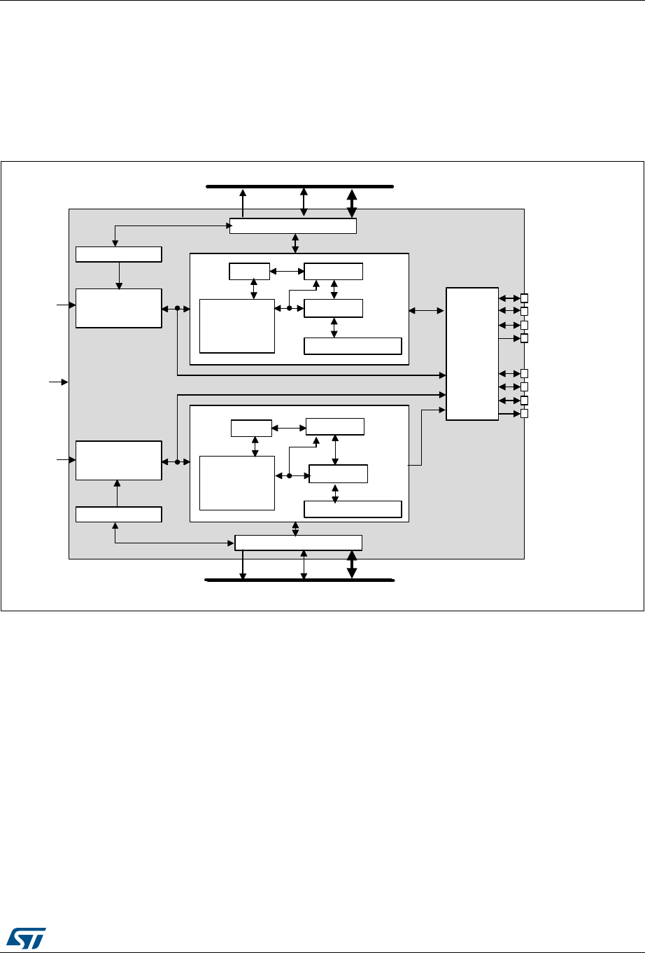
RM0394 Rev 4 1341/1600
RM0394 Serial audio interface (SAI)
1389
41.4 SAI functional description
41.4.1 SAI block diagram
Figure 435 shows the SAI block diagram while Table 213 and Table 214 list SAI internal and
external signals.
Figure 435. SAI functional block diagram
The SAI is mainly composed of two audio sub-blocks with their own clock generator. Each
audio block integrates a 32-bit shift register controlled by their own functional state machine.
Data are stored or read from the dedicated FIFO. FIFO may be accessed by the CPU, or by
DMA in order to leave the CPU free during the communication. Each audio block is
independent. They can be synchronous with each other.
An I/O line controller manages a set of 4 dedicated pins (SD, SCK, FS, MCLK) for a given
audio block in the SAI. Some of these pins can be shared if the two sub-blocks are declared
as synchronous to leave some free to be used as general purpose I/Os. The MCLK pin can
be output, or not, depending on the application, the decoder requirement and whether the
audio block is configured as the master.
If one SAI is configured to operate synchronously with another one, even more I/Os can be
freed (except for pins SD_x).
The functional state machine can be configured to address a wide range of audio protocols.
Some registers are present to set-up the desired protocols (audio frame waveform
generator).
06Y9
),)2 ),)2FWUO
&RQILJXUDWLRQ
DQGVWDWXV
UHJLVWHUV
)60
ELWVKLIWUHJLVWHU
$XGLREORFN$
),)2 ),)2FWUO
&RQILJXUDWLRQ
DQGVWDWXV
UHJLVWHUV
)60
ELWVKLIWUHJLVWHU
$XGLREORFN%
&ORFNJHQHUDWRU
$XGLREORFN$
6$,B$&5
6$,B%&5
&ORFNJHQHUDWRU
$XGLREORFN%
$3%,QWHUIDFH
$3%,QWHUIDFH
,2/LQH0DQDJHPHQW
6$,
)6B$
6'B$
6&.B$
0&/.B$
)6B%
6'B%
6&.B%
0&/.B%
ELW$3%EXV
ELW$3%EXV
VDLBDBJEOBLW
VDLBEBJEOBLW VDLBEBGPD
VDLBDBGPD
VDLBDB
NHUBFN
VDLBEB
NHUBFN
VDLBSFON
Serial audio interface (SAI) RM0394
1342/1600 RM0394 Rev 4
The audio sub-block can be a transmitter or receiver, in master or slave mode. The master
mode means the SCK_x bit clock and the frame synchronization signal are generated from
the SAI, whereas in slave mode, they come from another external or internal master. There
is a particular case for which the FS signal direction is not directly linked to the master or
slave mode definition. In AC’97 protocol, it will be an SAI output even if the SAI (link
controller) is set-up to consume the SCK clock (and so to be in Slave mode).
Note: For ease of reading of this section, the notation SAI_x refers to SAI_A or SAI_B, where ‘x’
represents the SAI A or B sub-block.
41.4.2 SAI pins and internal signals
41.4.3 Main SAI modes
Each audio sub-block of the SAI can be configured to be master or slave via MODE bits in
the SAI_xCR1 register of the selected audio block.
Master mode
In master mode, the SAI delivers the timing signals to the external connected device:
•The bit clock and the frame synchronization are output on pin SCK_x and FS_x,
respectively.
•If needed, the SAI can also generate a master clock on MCLK_x pin.
Both SCK_x, FS_x and MCLK_x are configured as outputs.
Table 213. SAI internal input/output signals
Internal signal name Signal type Description
sai_a_gbl_it/
sai_b_gbl_it Output Audio block A and B global interrupts.
sai_a_dma,
sai_b_dma Input/output Audio block A and B DMA acknowledges and requests.
sai_a_ker_ck/
sai_b_ker_ck Input Audio block A/B kernel clock.
sai_pclk Input APB clock.
Table 214. SAI input/output pins
Name Signal type Comments
SAI_SCK_A/B Input/output Audio block A/B bit clock.
SAI_MCLK_A/B Output Audio block A/B master clock.
SAI_SD_A/B Input/output Data line for block A/B.
SAI_FS_A/B Input/output Frame synchronization line for audio block A/B.

RM0394 Rev 4 1343/1600
RM0394 Serial audio interface (SAI)
1389
Slave mode
The SAI expects to receive timing signals from an external device.
•If the SAI sub-block is configured in asynchronous mode, then SCK_x and FS_x pins
are configured as inputs.
•If the SAI sub-block is configured to operate synchronously with the second audio sub-
block, the corresponding SCK_x and FS_x pins are left free to be used as general
purpose I/Os.
In slave mode, MCLK_x pin is not used and can be assigned to another function.
It is recommended to enable the slave device before enabling the master.
Configuring and enabling SAI modes
Each audio sub-block can be independently defined as a transmitter or receiver through the
MODE bit in the SAI_xCR1 register of the corresponding audio block. As a result, SAI_SD_x
pin will be respectively configured as an output or an input.
Two master audio blocks in the same SAI can be configured with two different MCLK and
SCK clock frequencies. In this case they have to be configured in asynchronous mode.
Each of the audio blocks in the SAI are enabled by SAIEN bit in the SAI_xCR1 register. As
soon as this bit is active, the transmitter or the receiver is sensitive to the activity on the
clock line, data line and synchronization line in slave mode.
In master TX mode, enabling the audio block immediately generates the bit clock for the
external slaves even if there is no data in the FIFO, However FS signal generation is
conditioned by the presence of data in the FIFO. After the FIFO receives the first data to
transmit, this data is output to external slaves. If there is no data to transmit in the FIFO, 0
values are then sent in the audio frame with an underrun flag generation.
In slave mode, the audio frame starts when the audio block is enabled and when a start of
frame is detected.
In Slave TX mode, no underrun event is possible on the first frame after the audio block is
enabled, because the mandatory operating sequence in this case is:
1. Write into the SAI_xDR (by software or by DMA).
2. Wait until the FIFO threshold (FLH) flag is different from 0b000 (FIFO empty).
3. Enable the audio block in slave transmitter mode.
41.4.4 SAI synchronization mode
SAI sub-clock A and B can be synchronized.
Internal synchronization
An audio sub-block can be configured to operate synchronously with the second audio sub-
block in the same SAI. In this case, the bit clock and the frame synchronization signals are
shared to reduce the number of external pins used for the communication. The audio block
configured in synchronous mode sees its own SCK_x, FS_x, and MCLK_x pins released
back as GPIOs while the audio block configured in asynchronous mode is the one for which
FS_x and SCK_x ad MCLK_x I/O pins are relevant (if the audio block is considered as
master).
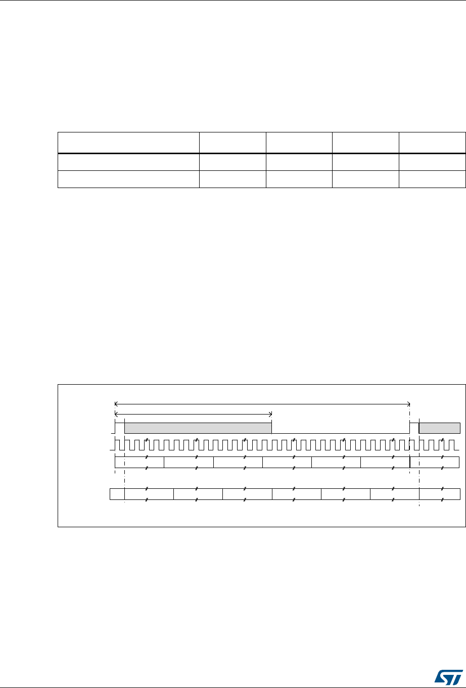
Serial audio interface (SAI) RM0394
1344/1600 RM0394 Rev 4
Typically, the audio block in synchronous mode can be used to configure the SAI in full
duplex mode. One of the two audio blocks can be configured as a master and the other as
slave, or both as slaves with one asynchronous block (corresponding SYNCEN[1:0] bits set
to 00 in SAI_xCR1) and one synchronous block (corresponding SYNCEN[1:0] bits set to 01
in the SAI_xCR1).
Note: Due to internal resynchronization stages, PCLK APB frequency must be higher than twice
the bit rate clock frequency.
41.4.5 Audio data size
The audio frame can target different data sizes by configuring bit DS[2:0] in the SAI_xCR1
register. The data sizes may be 8, 10, 16, 20, 24 or 32 bits. During the transfer, either the
MSB or the LSB of the data are sent first, depending on the configuration of bit LSBFIRST in
the SAI_xCR1 register.
41.4.6 Frame synchronization
The FS signal acts as the Frame synchronization signal in the audio frame (start of frame).
The shape of this signal is completely configurable in order to target the different audio
protocols with their own specificities concerning this Frame synchronization behavior. This
reconfigurability is done using register SAI_xFRCR. Figure 436 illustrates this flexibility.
Figure 436. Audio frame
In AC’97 mode or in SPDIF mode (bit PRTCFG[1:0] = 10 or PRTCFG[1:0] = 01 in the
SAI_xCR1 register), the frame synchronization shape is forced to match the AC’97 protocol.
The SAI_xFRCR register value is ignored.
Each audio block is independent and consequently each one requires a specific
configuration.
Table 215. External synchronization selection
Block instance SYNCIN= 3 SYNCIN= 2 SYNCIN= 1 SYNCIN= 0
SAI1 Res. Res. SAI2 sync Res.
SAI2 Res. Res. Res. SAI1 sync
06Y9
7KHIDOOLQJHGJHFDQRFFXULQWRWKLVDUHD
6&.
6ORW 6ORW 6ORW 6ORW 6ORW « 6ORW
)6
6'
)62))
)6/HQJWKXSWRELWV
)6DFWLYHXSWRELWV
6ORW 6ORW 6ORW 6ORW 6ORW « 6ORW
6'
)62))

RM0394 Rev 4 1345/1600
RM0394 Serial audio interface (SAI)
1389
Frame length
•Master mode
The audio frame length can be configured to up to 256 bit clock cycles, by setting
FRL[7:0] field in the SAI_xFRCR register.
If the frame length is greater than the number of declared slots for the frame, the
remaining bits to transmit will be extended to 0 or the SD line will be released to HI-z
depending the state of bit TRIS in the SAI_xCR2 register (refer to FS signal role). In
reception mode, the remaining bit is ignored.
If bit NODIV is cleared, (FRL+1) must be equal to a power of 2, from 8 to 256, to ensure
that an audio frame contains an integer number of MCLK pulses per bit clock cycle.
If bit NODIV is set, the (FRL+1) field can take any value from 8 to 256. Refer to
Section 41.4.8: SAI clock generator”.
•Slave mode
The audio frame length is mainly used to specify to the slave the number of bit clock
cycles per audio frame sent by the external master. It is used mainly to detect from the
master any anticipated or late occurrence of the Frame synchronization signal during
an on-going audio frame. In this case an error will be generated. For more details refer
to Section 41.4.13: Error flags.
In slave mode, there are no constraints on the FRL[7:0] configuration in the
SAI_xFRCR register.
The number of bits in the frame is equal to FRL[7:0] + 1.
The minimum number of bits to transfer in an audio frame is 8.
Frame synchronization polarity
FSPOL bit in the SAI_xFRCR register sets the active polarity of the FS pin from which a
frame is started. The start of frame is edge sensitive.
In slave mode, the audio block waits for a valid frame to start transmitting or receiving. Start
of frame is synchronized to this signal. It is effective only if the start of frame is not detected
during an ongoing communication and assimilated to an anticipated start of frame (refer to
Section 41.4.13: Error flags).
In master mode, the frame synchronization is sent continuously each time an audio frame is
complete until the SAIEN bit in the SAI_xCR1 register is cleared. If no data are present in
the FIFO at the end of the previous audio frame, an underrun condition will be managed as
described in Section 41.4.13: Error flags), but the audio communication flow will not be
interrupted.
Frame synchronization active level length
The FSALL[6:0] bits of the SAI_xFRCR register allow configuring the length of the active
level of the Frame synchronization signal. The length can be set from 1 to 128 bit clock
cycles.
As an example, the active length can be half of the frame length in I2S, LSB or MSB-justified
modes, or one-bit wide for PCM/DSP or TDM.
Frame synchronization offset
Depending on the audio protocol targeted in the application, the Frame synchronization
signal can be asserted when transmitting the last bit or the first bit of the audio frame (this is
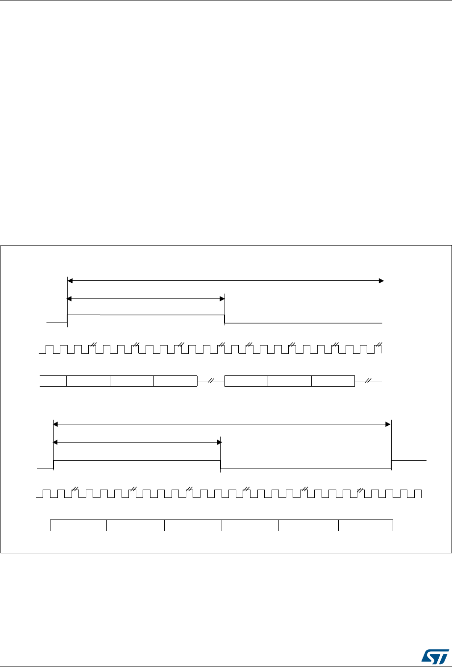
Serial audio interface (SAI) RM0394
1346/1600 RM0394 Rev 4
the case in I2S standard protocol and in MSB-justified protocol, respectively). FSOFF bit in
the SAI_xFRCR register allows to choose one of the two configurations.
FS signal role
The FS signal can have a different meaning depending on the FS function. FSDEF bit in the
SAI_xFRCR register selects which meaning it will have:
•0: start of frame, like for instance the PCM/DSP, TDM, AC’97, audio protocols,
•1: start of frame and channel side identification within the audio frame like for the I2S,
the MSB or LSB-justified protocols.
When the FS signal is considered as a start of frame and channel side identification within
the frame, the number of declared slots must be considered to be half the number for the left
channel and half the number for the right channel. If the number of bit clock cycles on half
audio frame is greater than the number of slots dedicated to a channel side, and TRIS = 0, 0
is sent for transmission for the remaining bit clock cycles in the SAI_xCR2 register.
Otherwise if TRIS = 1, the SD line is released to HI-Z. In reception mode, the remaining bit
clock cycles are not considered until the channel side changes.
Figure 437. FS role is start of frame + channel side identification (FSDEF = TRIS = 1)
1. The frame length should be even.
If FSDEF bit in SAI_xFRCR is kept clear, so FS signal is equivalent to a start of frame, and if
the number of slots defined in NBSLOT[3:0] in SAI_xSLOTR multiplied by the number of bits
by slot configured in SLOTSZ[1:0] in SAI_xSLOTR is less than the frame size (bit FRL[7:0]
in the SAI_xFRCR register), then:
VFN
VORW
$XGLRIUDPH
)6
+DOIRIIUDPH
$XGLRIUDPH
)6
+DOIRIIUDPH
1XPEHURIVORWVQRWDOLJQHGZLWKWKHDXGLRIUDPH
1XPEHURIVORWVDOLJQHGZLWKWKHDXGLRIUDPH
069
6ORW
VFN
VORW 6ORW 6ORW 6ORW 6ORW6ORW
6ORW21 6ORW2)) 6ORW21 6ORW21 6ORW2)) 6ORW21
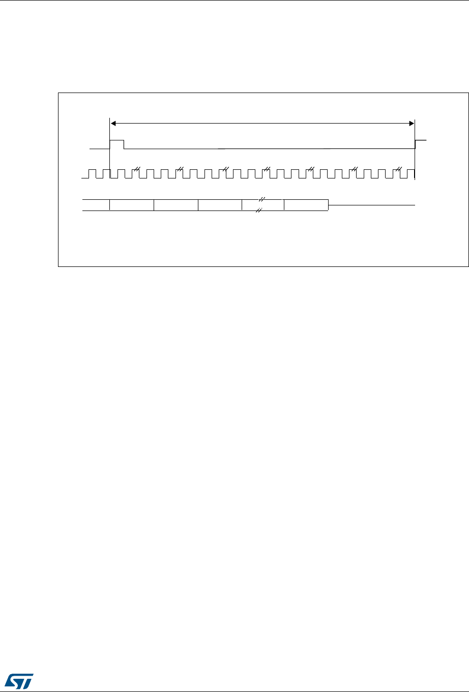
RM0394 Rev 4 1347/1600
RM0394 Serial audio interface (SAI)
1389
•if TRIS = 0 in the SAI_xCR2 register, the remaining bit after the last slot will be forced to
0 until the end of frame in case of transmitter,
•if TRIS = 1, the line will be released to HI-Z during the transfer of these remaining bits.
In reception mode, these bits are discarded.
Figure 438. FS role is start of frame (FSDEF = 0)
The FS signal is not used when the audio block in transmitter mode is configured to get the
SPDIF output on the SD line. The corresponding FS I/O will be released and left free for
other purposes.
41.4.7 Slot configuration
The slot is the basic element in the audio frame. The number of slots in the audio frame is
equal to NBSLOT[3:0] + 1.
The maximum number of slots per audio frame is fixed at 16.
For AC’97 protocol or SPDIF (when bit PRTCFG[1:0] = 10 or PRTCFG[1:0] = 01), the
number of slots is automatically set to target the protocol specification, and the value of
NBSLOT[3:0] is ignored.
Each slot can be defined as a valid slot, or not, by setting SLOTEN[15:0] bits of the
SAI_xSLOTR register.
When a invalid slot is transferred, the SD data line is either forced to 0 or released to HI-z
depending on TRIS bit configuration (refer to Output data line management on an inactive
slot) in transmitter mode. In receiver mode, the received value from the end of this slot is
ignored. Consequently, there will be no FIFO access and so no request to read or write the
FIFO linked to this inactive slot status.
The slot size is also configurable as shown in Figure 439. The size of the slots is selected by
setting SLOTSZ[1:0] bits in the SAI_xSLOTR register. The size is applied identically for
each slot in an audio frame.
$XGLRIUDPH
'DWD DIWHUVORWQLI75,6
6'RXWSXWUHOHDVHG+,=DIWHUVORWQLI75,6
069
VFN
VORW 6ORW 6ORW 6ORW 6ORWQ
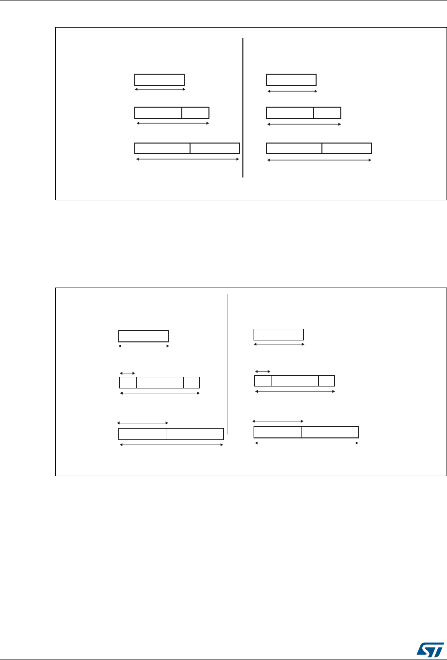
Serial audio interface (SAI) RM0394
1348/1600 RM0394 Rev 4
Figure 439. Slot size configuration with FBOFF = 0 in SAI_xSLOTR
It is possible to choose the position of the first data bit to transfer within the slots. This offset
is configured by FBOFF[4:0] bits in the SAI_xSLOTR register. 0 values will be injected in
transmitter mode from the beginning of the slot until this offset position is reached. In
reception, the bit in the offset phase is ignored. This feature targets the LSB justified
protocol (if the offset is equal to the slot size minus the data size).
Figure 440. First bit offset
It is mandatory to respect the following conditions to avoid bad SAI behavior:
FBOFF (SLOTSZ - DS),
DS SLOTSZ,
NBSLOT x SLOTSZ FRL (frame length),
The number of slots must be even when bit FSDEF in the SAI_xFRCR register is set.
In AC’97 and SPDIF protocol (bit PRTCFG[1:0] = 10 or PRTCFG[1:0] = 01), the slot size is
automatically set as defined in Section 41.4.10: AC’97 link controller.
069
;;
;; ;;
;GRQ¶WFDUH
$XGLREORFNLVWUDQVPLWWHU
6ORWVL]H GDWDVL]H
GDWDVL]H
GDWDVL]H
GDWDVL]H
GDWDVL]H
VORW[
VORW[
VORW[
ELW
ELW
$XGLREORFNLVUHFHLYHU
6ORWVL]H GDWDVL]H
GDWDVL]H
GDWDVL]H
GDWDVL]H
VORW[
VORW[
VORW[
ELW
ELW
GDWDVL]H
069
;;;;
;GRQ¶WFDUH
$XGLREORFNLVWUDQVPLWWHU
6ORWVL]H GDWDVL]H
GDWDVL]H
GDWDVL]H
GDWDVL]H
GDWDVL]H
VORW[
VORW[
VORW[
ELW
ELW
$XGLREORFNLVUHFHLYHU
)%2))
)%2)) 6/276='6
;;
6ORWVL]H GDWDVL]H
GDWDVL]H
GDWDVL]H
GDWDVL]H
GDWDVL]H
VORW[
VORW[
VORW[
ELW
ELW
;;
)%2))
)%2)) 6/276='6
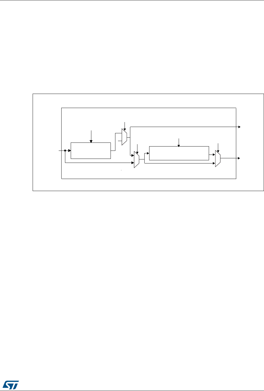
RM0394 Rev 4 1349/1600
RM0394 Serial audio interface (SAI)
1389
41.4.8 SAI clock generator
Each audio block has its own clock generator that makes these two blocks completely
independent. There is no difference in terms of functionality between these two clock
generators.
When the audio block is configured as Master, the clock generator provides the
communication clock (the bit clock) and the master clock for external decoders.
When the audio block is defined as slave, the clock generator is OFF.
Figure 441 illustrates the architecture of the audio block clock generator.
Figure 441. Audio block clock generator overview
Note: If NODIV is set to 1, the MCLK_x signal will be set at 0 level if this pin is configured as the
SAI pin in GPIO peripherals.
The clock source for the clock generator comes from the product clock controller. The
sai_x_ker_ck clock is equivalent to the master clock which can be divided for the external
decoders using bit MCKDIV[3:0]:
MCLK_x = sai_x_ker_ck / (MCKDIV[3:0] * 2), if MCKDIV[3:0] is not equal to 0000.
MCLK_x = sai_x_ker_ck, if MCKDIV[3:0] is equal to 0000.
MCLK_x signal is used only in Free protocol mode.
The division must be even in order to keep 50% on the Duty cycle on the MCLK output and
on the SCK_x clock. If bit MCKDIV[3:0] = 0000, division by one is applied to obtain MCLK_x
equal to sai_x_ker_ck.
In the SAI, the single ratio MCLK/FS = 256 is considered. Mostly, three frequency ranges
will be encountered as illustrated in Table 216.
06Y9
0&.',9>@
6&.B[
0&/.B[
12',9
12',9
12',9
VDLB[BNHU
BFN
)5/>@
%LWFORFNGLYLGHU
0DVWHUFORFN
GLYLGHU

Serial audio interface (SAI) RM0394
1350/1600 RM0394 Rev 4
The master clock can be generated externally on an I/O pad for external decoders if the
corresponding audio block is declared as master with bit NODIV = 0 in the SAI_xCR1
register. In slave, the value set in this last bit is ignored since the clock generator is OFF,
and the MCLK_x I/O pin is released for use as a general purpose I/O.
The bit clock is derived from the master clock. The bit clock divider sets the divider factor
between the bit clock (SCK_x) and the master clock (MCLK_x) following the formula:
SCK_x = MCLK x (FRL[7:0] +1) / 256
where:
256 is the fixed ratio between MCLK and the audio frequency sampling.
FRL[7:0] is the number of bit clock cycles- 1 in the audio frame, configured in the
SAI_xFRCR register.
In master mode it is mandatory that (FRL[7:0] +1) is equal to a number with a power of 2
(refer to Section 41.4.6: Frame synchronization) to obtain an even integer number of
MCLK_x pulses by bit clock cycle. The 50% duty cycle is guaranteed on the bit clock
(SCK_x).
The sai_x_ker_ck clock can also be equal to the bit clock frequency. In this case, NODIV bit
in the SAI_xCR1 register should be set and the value inside the MCKDIV divider and the bit
clock divider will be ignored. In this case, the number of bits per frame is fully configurable
without the need to be equal to a power of two.
The bit clock strobing edge on SCK can be configured by bit CKSTR in the SAI_xCR1
register.
Refer to Section 41.4.11: SPDIF output for details on clock generator programming in
SPDIF mode.
Table 216. Example of possible audio frequency sampling range
Input sai_x_ker_ck
clock frequency
Most usual audio frequency
sampling achievable MCKDIV[3:0]
192 kHz x 256
192 kHz MCKDIV[3:0] = 0000
96 kHz MCKDIV[3:0] = 0001
48 kHz MCKDIV[3:0] = 0010
16 kHz MCKDIV[3:0] = 0110
8 kHz MCKDIV[3:0] = 1100
44.1 kHz x 256
44.1 kHz MCKDIV[3:0] = 0000
22.05 kHz MCKDIV[3:0] = 0001
11.025 kHz MCKDIV[3:0] = 0010
sai_x_ker_ck =
MCLK(1)
1. This may happen when the product clock controller selects an external clock source, instead of PLL clock.
MCLK MCKDIV[3:0] = 0000

RM0394 Rev 4 1351/1600
RM0394 Serial audio interface (SAI)
1389
41.4.9 Internal FIFOs
Each audio block in the SAI has its own FIFO. Depending if the block is defined to be a
transmitter or a receiver, the FIFO can be written or read, respectively. There is therefore
only one FIFO request linked to FREQ bit in the SAI_xSR register.
An interrupt is generated if FREQIE bit is enabled in the SAI_xIM register. This depends on:
•FIFO threshold setting (FLVL bits in SAI_xCR2)
•Communication direction (transmitter or receiver). Refer to Interrupt generation in
transmitter mode and Interrupt generation in reception mode.
Interrupt generation in transmitter mode
The interrupt generation depends on the FIFO configuration in transmitter mode:
•When the FIFO threshold bits in SAI_xCR2 register are configured as FIFO empty
(FTH[2:0] set to 0b000), an interrupt is generated (FREQ bit set by hardware to 1 in
SAI_xSR register) if no data are available in SAI_xDR register (FLVL[2:0] bits in SAI_xSR
is less than 001b). This Interrupt (FREQ bit in SAI_xSR register) is cleared by hardware
when the FIFO is no more empty (FLVL[2:0] bits in SAI_xSR are different from 0b000) i.e
one or more data are stored in the FIFO.
•When the FIFO threshold bits in SAI_xCR2 register are configured as FIFO quarter full
(FTH[2:0] set to 001b), an interrupt is generated (FREQ bit set by hardware to 1 in
SAI_xSR register) if less than a quarter of the FIFO contains data (FLVL[2:0] bits in
SAI_xSR are less than 0b010). This Interrupt (FREQ bit in SAI_xSR register) is cleared
by hardware when at least a quarter of the FIFO contains data (FLVL[2:0] bits in SAI_xSR
are higher or equal to 0b010).
•When the FIFO threshold bits in SAI_xCR2 register are configured as FIFO half full
(FTH[2:0] set to 0b010), an interrupt is generated (FREQ bit set by hardware to 1 in
SAI_xSR register) if less than half of the FIFO contains data (FLVL[2:0] bits in SAI_xSR
are less than 011b). This Interrupt (FREQ bit in SAI_xSR register) is cleared by hardware
when at least half of the FIFO contains data (FLVL[2:0] bits in SAI_xSR are higher or
equal to 011b).
•When the FIFO threshold bits in SAI_xCR2 register are configured as FIFO three quarter
(FTH[2:0] set to 011b), an interrupt is generated (FREQ bit is set by hardware to 1 in
SAI_xSR register) if less than three quarters of the FIFO contain data (FLVL[2:0] bits in
SAI_xSR are less than 0b100). This Interrupt (FREQ bit in SAI_xSR register) is cleared
by hardware when at least three quarters of the FIFO contain data (FLVL[2:0] bits in
SAI_xSR are higher or equal to 0b100).
•When the FIFO threshold bits in SAI_xCR2 register are configured as FIFO full (FTH[2:0]
set to 0b100), an interrupt is generated (FREQ bit is set by hardware to 1 in SAI_xSR
register) if the FIFO is not full (FLVL[2:0] bits in SAI_xSR is less than 101b). This Interrupt
(FREQ bit in SAI_xSR register) is cleared by hardware when the FIFO is full (FLVL[2:0]
bits in SAI_xSR is equal to 101b value).
Interrupt generation in reception mode
The interrupt generation depends on the FIFO configuration in reception mode:
•When the FIFO threshold bits in SAI_xCR2 register are configured as FIFO empty
(FTH[2:0] set to 0b000), an interrupt is generated (FREQ bit is set by hardware to 1 in
SAI_xSR register) if at least one data is available in SAI_xDR register(FLVL[2:0] bits in
SAI_xSR is higher or equal to 001b). This Interrupt (FREQ bit in SAI_xSR register) is

Serial audio interface (SAI) RM0394
1352/1600 RM0394 Rev 4
cleared by hardware when the FIFO becomes empty (FLVL[2:0] bits in SAI_xSR is equal
to 0b000) i.e no data are stored in FIFO.
•When the FIFO threshold bits in SAI_xCR2 register are configured as FIFO quarter fully
(FTH[2:0] set to 001b), an interrupt is generated (FREQ bit is set by hardware to 1 in
SAI_xSR register) if at least one quarter of the FIFO data locations are available
(FLVL[2:0] bits in SAI_xSR is higher or equal to 0b010). This Interrupt (FREQ bit in
SAI_xSR register) is cleared by hardware when less than a quarter of the FIFO data
locations become available (FLVL[2:0] bits in SAI_xSR is less than 0b010).
•When the FIFO threshold bits in SAI_xCR2 register are configured as FIFO half fully
(FTH[2:0] set to 0b010 value), an interrupt is generated (FREQ bit is set by hardware to
1 in SAI_xSR register) if at least half of the FIFO data locations are available (FLVL[2:0]
bits in SAI_xSR is higher or equal to 011b). This Interrupt (FREQ bit in SAI_xSR register)
is cleared by hardware when less than half of the FIFO data locations become available
(FLVL[2:0] bits in SAI_xSR is less than 011b).
•When the FIFO threshold bits in SAI_xCR2 register are configured as FIFO three quarter
full(FTH[2:0] set to 011b value), an interrupt is generated (FREQ bit is set by hardware to
1 in SAI_xSR register) if at least three quarters of the FIFO data locations are available
(FLVL[2:0] bits in SAI_xSR is higher or equal to 0b100). This Interrupt (FREQ bit in
SAI_xSR register) is cleared by hardware when the FIFO has less than three quarters of
the FIFO data locations avalable(FLVL[2:0] bits in SAI_xSR is less than 0b100).
•When the FIFO threshold bits in SAI_xCR2 register are configured as FIFO full(FTH[2:0]
set to 0b100), an interrupt is generated (FREQ bit is set by hardware to 1 in SAI_xSR
register) if the FIFO is full (FLVL[2:0] bits in SAI_xSR is equal to 101b). This Interrupt
(FREQ bit in SAI_xSR register) is cleared by hardware when the FIFO is not full
(FLVL[2:0] bits in SAI_xSR is less than 101b).
Like interrupt generation, the SAI can use the DMA if DMAEN bit in the SAI_xCR1 register is
set. The FREQ bit assertion mechanism is the same as the interruption generation
mechanism described above for FREQIE.
Each FIFO is an 8-word FIFO. Each read or write operation from/to the FIFO targets one
word FIFO location whatever the access size. Each FIFO word contains one audio slot.
FIFO pointers are incremented by one word after each access to the SAI_xDR register.
Data should be right aligned when it is written in the SAI_xDR.
Data received will be right aligned in the SAI_xDR.
The FIFO pointers can be reinitialized when the SAI is disabled by setting bit FFLUSH in the
SAI_xCR2 register. If FFLUSH is set when the SAI is enabled the data present in the FIFO
will be lost automatically.
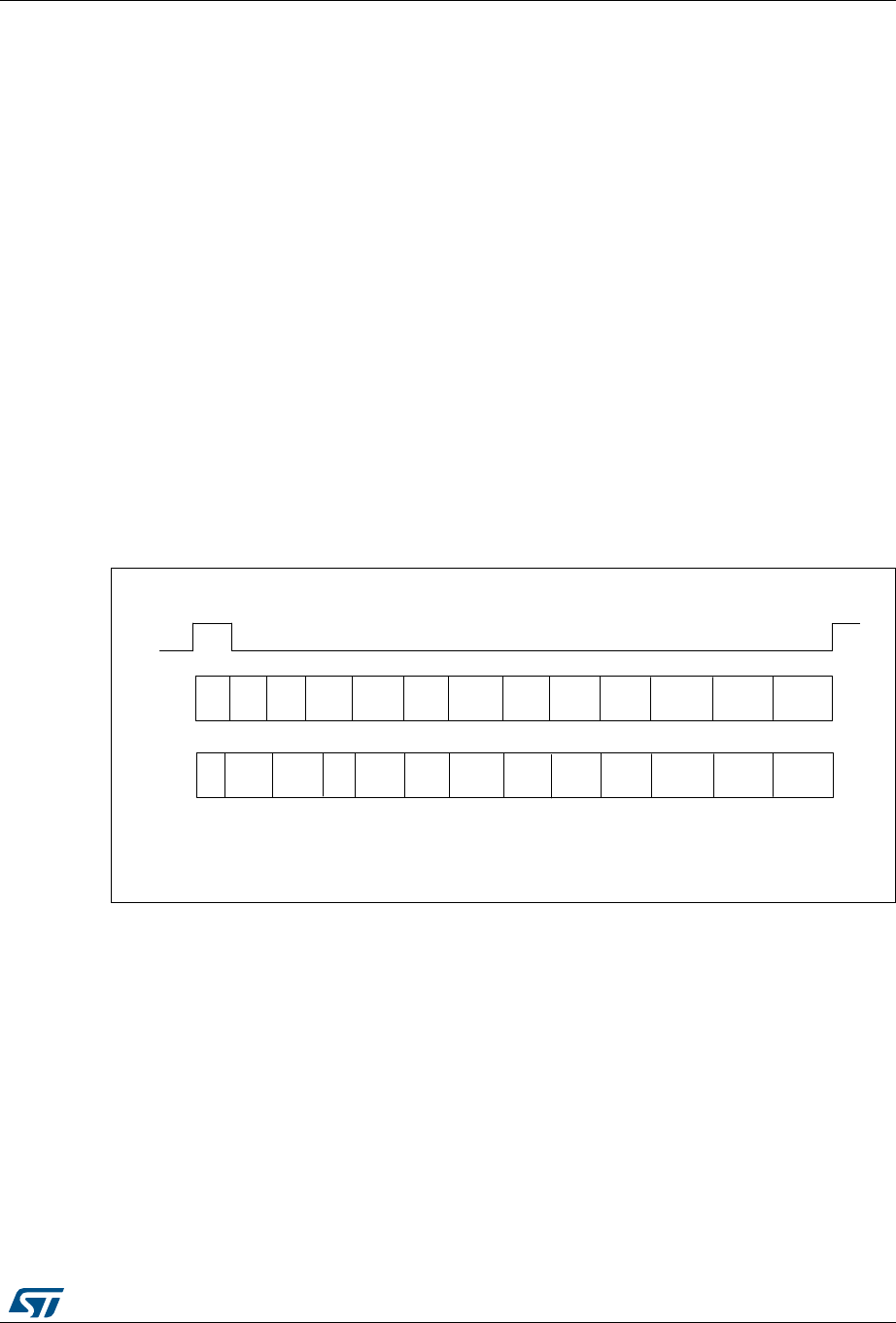
RM0394 Rev 4 1353/1600
RM0394 Serial audio interface (SAI)
1389
41.4.10 AC’97 link controller
The SAI is able to work as an AC’97 link controller. In this protocol:
•The slot number and the slot size are fixed.
•The frame synchronization signal is perfectly defined and has a fixed shape.
To select this protocol, set PRTCFG[1:0] bits in the SAI_xCR1 register to 10. When AC’97
mode is selected, only data sizes of 16 or 20 bits can be used, otherwise the SAI behavior is
not guaranteed.
•NBSLOT[3:0] and SLOTSZ[1:0] bits are consequently ignored.
•The number of slots is fixed to 13 slots. The first one is 16-bit wide and all the others
are 20-bit wide (data slots).
•FBOFF[4:0] bits in the SAI_xSLOTR register are ignored.
•The SAI_xFRCR register is ignored.
•The MCLK is not used.
The FS signal from the block defined as asynchronous is configured automatically as an
output, since the AC’97 controller link drives the FS signal whatever the master or slave
configuration.
Figure 442 shows an AC’97 audio frame structure.
Figure 442. AC’97 audio frame
Note: In AC’97 protocol, bit 2 of the tag is reserved (always 0), so bit 2 of the TAG is forced to 0
level whatever the value written in the SAI FIFO.
For more details about tag representation, refer to the AC’97 protocol standard.
One SAI can be used to target an AC’97 point-to-point communication.
In receiver mode, the SAI acting as an AC’97 link controller requires no FIFO request and so
no data storage in the FIFO when the Codec ready bit in the slot 0 is decoded low. If bit
CNRDYIE is enabled in the SAI_xIM register, flag CNRDY will be set in the SAI_xSR
register and an interrupt is generated. This flag is dedicated to the AC’97 protocol.
069
)6
6',
6'2
7DJ &0'
$''5
&0'
'$7$
/,1(
'$&
3&0
/)5217
3&0
5)5217
3&0
&(17(5
3&0
/6855
3&0
56855
3&0
/)(
/,1(
'$&
+6(7
'$&
,2
&75/
7DJ 67$786
$''5
67$786
'$7$
/,1(
$'&
3&0
/()7
3&0
5,*+7
3&0
0,&
565
9'
565
/9'
/,1(
$'& +6(7 ,2
67$786
565
9'
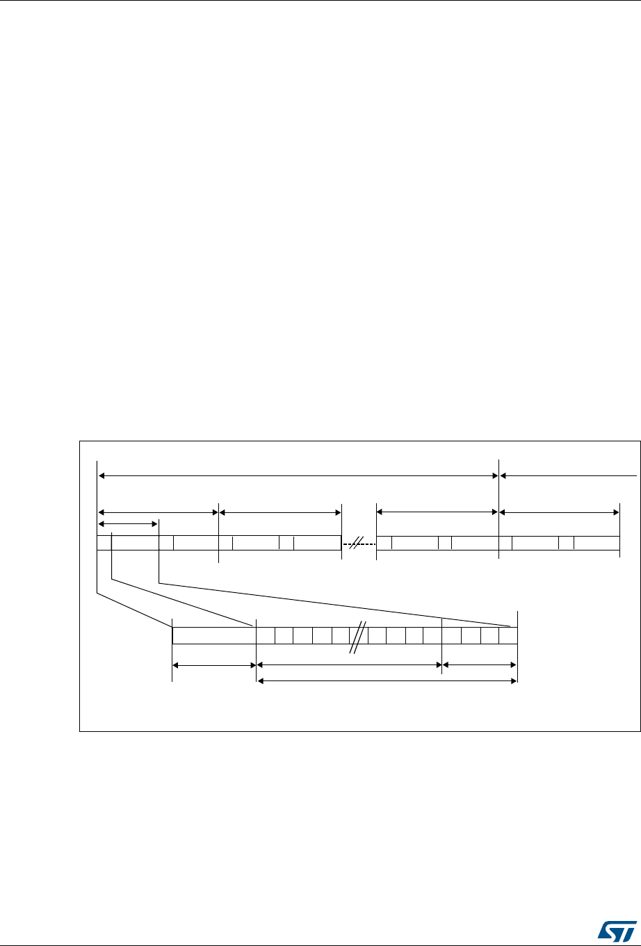
Serial audio interface (SAI) RM0394
1354/1600 RM0394 Rev 4
Clock generator programming in AC’97 mode
In AC’97 mode, the frame length is fixed at 256 bits, and its frequency shall be set to
48 kHz. The formulas given in Section 41.4.8: SAI clock generator shall be used with FRL =
255, in order to generate the proper frame rate (FFS_x).
41.4.11 SPDIF output
The SPDIF interface is available in transmitter mode only. It supports the audio IEC60958.
To select SPDIF mode, set PRTCFG[1:0] bit to 01 in the SAI_xCR1 register.
For SPDIF protocol:
•Only SD data line is enabled.
•FS, SCK, MCLK I/Os pins are left free.
•MODE[1] bit is forced to 0 to select the master mode in order to enable the clock
generator of the SAI and manage the data rate on the SD line.
•The data size is forced to 24 bits. The value set in DS[2:0] bits in the SAI_xCR1 register
is ignored.
•The clock generator must be configured to define the symbol-rate, knowing that the bit
clock should be twice the symbol-rate. The data is coded in Manchester protocol.
•The SAI_xFRCR and SAI_xSLOTR registers are ignored. The SAI is configured
internally to match the SPDIF protocol requirements as shown in Figure 443.
Figure 443. SPDIF format
A SPDIF block contains 192 frames. Each frame is composed of two 32-bit sub-frames,
generally one for the left channel and one for the right channel. Each sub-frame is
composed of a SOPD pattern (4-bit) to specify if the sub-frame is the start of a block (and so
is identifying a channel A) or if it is identifying a channel A somewhere in the block, or if it is
referring to channel B (see Table 217). The next 28 bits of channel information are
composed of 24 bits data + 4 status bits.
%
&RAME &RAME &RAME
6XEIUDPH
623' '' '' '' ' '' 93 &6
8
3/0$"-7
#HANNEL
"LOCK. "LOCK.
&RAME
BITDATA 3TATUSBIT
&KDQQHO$ :&KDQQHO% 0 &KDQQHO$ :&KDQQHO% 0&KDQQHO$ :&KDQQHO% % &KDQQHO$ :&KDQQHO%
-36
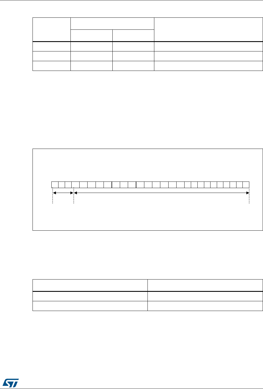
RM0394 Rev 4 1355/1600
RM0394 Serial audio interface (SAI)
1389
The data stored in SAI_xDR has to be filled as follows:
•SAI_xDR[26:24] contain the Channel status, User and Validity bits.
•SAI_xDR[23:0] contain the 24-bit data for the considered channel.
If the data size is 20 bits, then data shall be mapped on SAI_xDR[23:4].
If the data size is 16 bits, then data shall be mapped on SAI_xDR[23:8].
SAI_xDR[23] always represents the MSB.
Figure 444. SAI_xDR register ordering
Note: The transfer is performed always with LSB first.
The SAI first sends the adequate preamble for each sub-frame in a block. The SAI_xDR is
then sent on the SD line (manchester coded). The SAI ends the sub-frame by transferring
the Parity bit calculated as described in Table 218.
The underrun is the only error flag available in the SAI_xSR register for SPDIF mode since
the SAI can only operate in transmitter mode. As a result, the following sequence should be
Table 217. SOPD pattern
SOPD
Preamble coding
Description
last bit is 0 last bit is 1
B 11101000 00010111 Channel A data at the start of block
W 11100100 00011011 Channel B data somewhere in the block
M 11100010 00011101 Channel A data
06Y9
6$,B['5>@
' ' ' ' ' ' ' ' ' ' ' ' ' ' ' ' '&6 8 9
'DWD>@
6WDWXV
ELWV
' ' ' ' ' ''
Table 218. Parity bit calculation
SAI_xDR[26:0] Parity bit P value transferred
odd number of 0 0
odd number of 1 1
Serial audio interface (SAI) RM0394
1356/1600 RM0394 Rev 4
executed to recover from an underrun error detected via the underrun interrupt or the
underrun status bit:
1. Disable the DMA stream (via the DMA peripheral) if the DMA is used.
2. Disable the SAI and check that the peripheral is physically disabled by polling the
SAIEN bit in SAI_xCR1 register.
3. Clear the COVRUNDR flag in the SAI_xCLRFR register.
4. Flush the FIFO by setting the FFLUSH bit in SAI_xCR2.
The software needs to point to the address of the future data corresponding to a start of
new block (data for preamble B). If the DMA is used, the DMA source base address
pointer should be updated accordingly.
5. Enable again the DMA stream (DMA peripheral) if the DMA used to manage data
transfers according to the new source base address.
6. Enable again the SAI by setting SAIEN bit in SAI_xCR1 register.
Clock generator programming in SPDIF generator mode
For the SPDIF generator, the SAI shall provide a bit clock twice faster as the symbol-rate.
The table hereafter shows usual examples of symbol rates with respect to the audio
sampling rate.
More generally, the relationship between the audio sampling frequency (FS) and the bit
clock rate (FSCK_X) is given by the formula:
And the bit clock rate is obtained as follow:
Table 219. Audio sampling frequency versus symbol rates
Audio Sampling Frequencies (FS)Symbol-rate
44.1 kHz 2.8224 MHz
48 kHz 3.072 MHz
96 kHz 6.144 MHz
192 kHz 12.288 MHz
FS
FSCK_x
128
-----------------------
=
FSCK_x FSAI_CK_x
=

RM0394 Rev 4 1357/1600
RM0394 Serial audio interface (SAI)
1389
41.4.12 Specific features
The SAI interface embeds specific features which can be useful depending on the audio
protocol selected. These functions are accessible through specific bits of the SAI_xCR2
register.
Mute mode
The mute mode can be used when the audio sub-block is a transmitter or a receiver.
Audio sub-block in transmission mode
In transmitter mode, the mute mode can be selected at anytime. The mute mode is active
for entire audio frames. The MUTE bit in the SAI_xCR2 register enables the mute mode
when it is set during an ongoing frame.
The mute mode bit is strobed only at the end of the frame. If it is set at this time, the mute
mode is active at the beginning of the new audio frame and for a complete frame, until the
next end of frame. The bit is then strobed to determine if the next frame will still be a mute
frame.
If the number of slots set through NBSLOT[3:0] bits in the SAI_xSLOTR register is lower
than or equal to 2, it is possible to specify if the value sent in mute mode is 0 or if it is the last
value of each slot. The selection is done via MUTEVAL bit in the SAI_xCR2 register.
If the number of slots set in NBSLOT[3:0] bits in the SAI_xSLOTR register is greater than 2,
MUTEVAL bit in the SAI_xCR2 is meaningless as 0 values are sent on each bit on each
slot.
The FIFO pointers are still incremented in mute mode. This means that data present in the
FIFO and for which the mute mode is requested are discarded.
Audio sub-block in reception mode
In reception mode, it is possible to detect a mute mode sent from the external transmitter
when all the declared and valid slots of the audio frame receive 0 for a given consecutive
number of audio frames (MUTECNT[5:0] bits in the SAI_xCR2 register).
When the number of MUTE frames is detected, the MUTEDET flag in the SAI_xSR register
is set and an interrupt can be generated if MUTEDETIE bit is set in SAI_xCR2.
The mute frame counter is cleared when the audio sub-block is disabled or when a valid slot
receives at least one data in an audio frame. The interrupt is generated just once, when the
counter reaches the value specified in MUTECNT[5:0] bits. The interrupt event is then
reinitialized when the counter is cleared.
Note: The mute mode is not available for SPDIF audio blocks.
Mono/stereo mode
In transmitter mode, the mono mode can be addressed, without any data preprocessing in
memory, assuming the number of slots is equal to 2 (NBSLOT[3:0] = 0001 in SAI_xSLOTR).
In this case, the access time to and from the FIFO will be reduced by 2 since the data for
slot 0 is duplicated into data slot 1.
To enable the mono mode,
1. Set MONO bit to 1 in the SAI_xCR1 register.
2. Set NBSLOT to 1 and SLOTEN to 3 in SAI_xSLOTR.

Serial audio interface (SAI) RM0394
1358/1600 RM0394 Rev 4
In reception mode, the MONO bit can be set and is meaningful only if the number of slots is
equal to 2 as in transmitter mode. When it is set, only slot 0 data will be stored in the FIFO.
The data belonging to slot 1 will be discarded since, in this case, it is supposed to be the
same as the previous slot. If the data flow in reception mode is a real stereo audio flow with
a distinct and different left and right data, the MONO bit is meaningless. The conversion
from the output stereo file to the equivalent mono file is done by software.
Companding mode
Telecommunication applications can require to process the data to be transmitted or
received using a data companding algorithm.
Depending on the COMP[1:0] bits in the SAI_xCR2 register (used only when Free protocol
mode is selected), the application software can choose to process or not the data before
sending it on SD serial output line (compression) or to expand the data after the reception
on SD serial input line (expansion) as illustrated in Figure 445. The two companding modes
supported are the µ-Law and the A-Law log which are a part of the CCITT G.711
recommendation.
The companding standard used in the United States and Japan is the µ-Law. It supports 14
bits of dynamic range (COMP[1:0] = 10 in the SAI_xCR2 register).
The European companding standard is A-Law and supports 13 bits of dynamic range
(COMP[1:0] = 11 in the SAI_xCR2 register).
Both µ-Law or A-Law companding standard can be computed based on 1’s complement or
2’s complement representation depending on the CPL bit setting in the SAI_xCR2 register.
In µ-Law and A-Law standards, data are coded as 8 bits with MSB alignment. Companded
data are always 8-bit wide. For this reason, DS[2:0] bits in the SAI_xCR1 register will be
forced to 010 when the SAI audio block is enabled (SAIEN bit = 1 in the SAI_xCR1 register)
and when one of these two companding modes selected through the COMP[1:0] bits.
If no companding processing is required, COMP[1:0] bits should be kept clear.
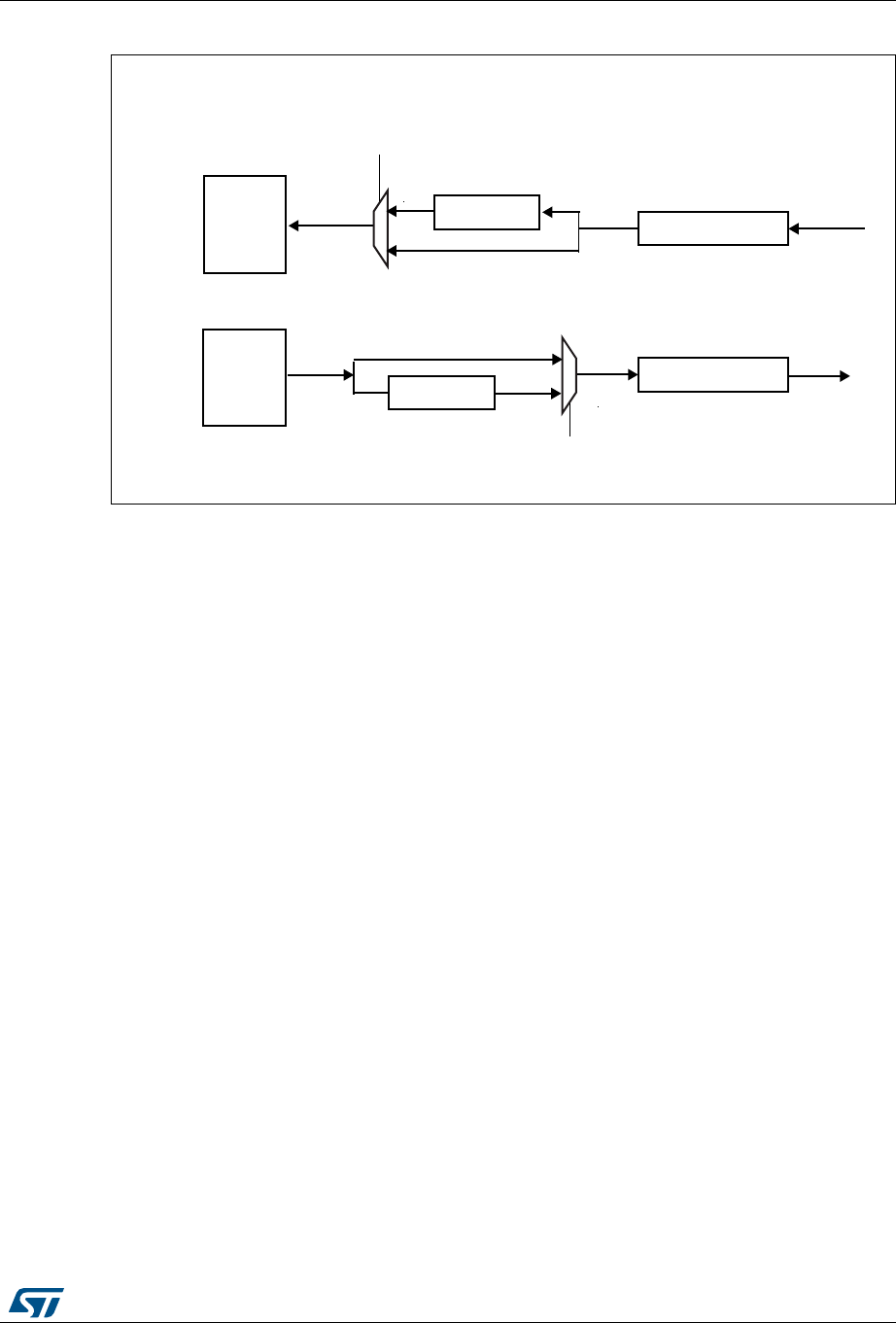
RM0394 Rev 4 1359/1600
RM0394 Serial audio interface (SAI)
1389
Figure 445. Data companding hardware in an audio block in the SAI
1. Not applicable when AC’97 or SPDIF are selected.
Expansion and compression mode are automatically selected through the SAI_xCR2:
•If the SAI audio block is configured to be a transmitter, and if the COMP[1] bit is set in
the SAI_xCR2 register, the compression mode will be applied.
•If the SAI audio block is declared as a receiver, the expansion algorithm will be applied.
Output data line management on an inactive slot
In transmitter mode, it is possible to choose the behavior of the SD line output when an
inactive slot is sent on the data line (via TRIS bit).
•Either the SAI forces 0 on the SD output line when an inactive slot is transmitted, or
•The line is released in HI-z state at the end of the last bit of data transferred, to release
the line for other transmitters connected to this node.
It is important to note that the two transmitters cannot attempt to drive the same SD output
pin simultaneously, which could result in a short circuit. To ensure a gap between
transmissions, if the data is lower than 32-bit, the data can be extended to 32-bit by setting
bit SLOTSZ[1:0] = 10 in the SAI_xSLOTR register. The SD output pin will then be tri-stated
at the end of the LSB of the active slot (during the padding to 0 phase to extend the data to
32-bit) if the following slot is declared inactive.
In addition, if the number of slots multiplied by the slot size is lower than the frame length,
the SD output line will be tri-stated when the padding to 0 is done to complete the audio
frame.
Figure 446 illustrates these behaviors.
H[SDQG
),)2
&203>@
&203>@
ELWVKLIWUHJLVWHU
6'
5HFHLYHUPRGHELW02'(>@ LQ6$,B[&5
7UDQVPLWWHUPRGHELW02'(>@ LQ6$,B[&5
069
ELWVKLIWUHJLVWHU
6'
FRPSUHVV
),)2
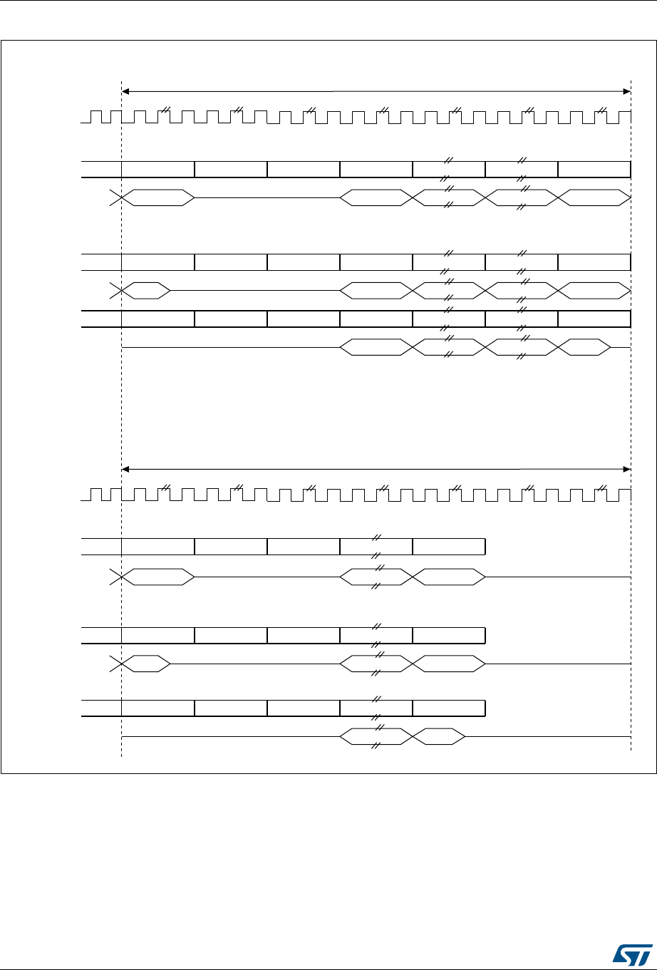
Serial audio interface (SAI) RM0394
1360/1600 RM0394 Rev 4
Figure 446. Tristate strategy on SD output line on an inactive slot
When the selected audio protocol uses the FS signal as a start of frame and a channel side
identification (bit FSDEF = 1 in the SAI_xFRCR register), the tristate mode is managed
according to Figure 447 (where bit TRIS in the SAI_xCR1 register = 1, and FSDEF=1, and
half frame length is higher than number of slots/2, and NBSLOT=6).
VORW
$XGLRIUDPH
%LW75,6 LQWKH6$,B[&5DQGIUDPHOHQJWK QXPEHURIVORWV
069
6ORWVL]H GDWDVL]H
6ORWVL]H!GDWDVL]H
%LW75,6 LQWKH6$,B[&5DQGIUDPHOHQJWK!QXPEHURIVORWV
6'RXWSXW
SCK
3LOT/. 3LOT/&& 3LOT/&& 3LOT/. /. /. 3LOTN/.
$ATA $ATA $ATAM
3LOT/. 3LOT/&& 3LOT/&& 3LOT/. /. /. 3LOTN/.
$ATA $ATA $ATAM
3LOT/. 3LOT/&& 3LOT/&& 3LOT/. /. /. 3LOTN/.
$ATA $ATAM
VORW
6'RXWSXW
VORW
6'RXWSXW
VORW
$XGLRIUDPH
6ORWVL]H GDWDVL]H
6'RXWSXW
SCK
3LOT/. 3LOT/&& 3LOT/&& /. 3LOTN/.
$ATA $ATAM
VORW
6ORWVL]H!GDWDVL]H
6'RXWSXW
3LOT/. 3LOT/&& 3LOT/&& /. 3LOTN/.
$ATAM
$ATA
VORW
6'RXWSXW
3LOT/. 3LOT/&& 3LOT/&& /.
$ATAM
/.
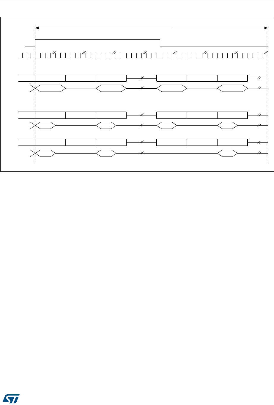
RM0394 Rev 4 1361/1600
RM0394 Serial audio interface (SAI)
1389
Figure 447. Tristate on output data line in a protocol like I2S
If the TRIS bit in the SAI_xCR2 register is cleared, all the High impedance states on the SD
output line on Figure 446 and Figure 447 are replaced by a drive with a value of 0.
41.4.13 Error flags
The SAI implements the following error flags:
•FIFO overrun/underrun
•Anticipated frame synchronization detection
•Late frame synchronization detection
•Codec not ready (AC’97 exclusively)
•Wrong clock configuration in master mode.
FIFO overrun/underrun (OVRUDR)
The FIFO overrun/underrun bit is called OVRUDR in the SAI_xSR register.
The overrun or underrun errors share the same bit since an audio block can be either
receiver or transmitter and each audio block in a given SAI has its own SAI_xSR register.
Overrun
When the audio block is configured as receiver, an overrun condition may appear if data are
received in an audio frame when the FIFO is full and not able to store the received data. In
this case, the received data are lost, the flag OVRUDR in the SAI_xSR register is set and an
interrupt is generated if OVRUDRIE bit is set in the SAI_xIM register. The slot number, from
which the overrun occurs, is stored internally. No more data will be stored into the FIFO until
it becomes free to store new data. When the FIFO has at least one data free, the SAI audio
block receiver will store new data (from new audio frame) from the slot number which was
stored internally when the overrun condition was detected. This avoids data slot de-
alignment in the destination memory (refer to Figure 448).
VORW
069
6ORWVL]H GDWDVL]H
6ORWVL]H!GDWDVL]H
6'RXWSXW
SCK
3LOT/. 3LOT/&& 3LOT/. 3LOT/. 3LOT/&& 3LOT/.
$ATA $ATA
3LOT/. 3LOT/&& 3LOT/.
$ATA
VORW
6'RXWSXW
$ATA $ATA
3LOT/. 3LOT/&& 3LOT/.
$ATA $ATA $ATA
3LOT/. 3LOT/&& 3LOT/.
$ATA
VORW
6'RXWSXW
3LOT/. 3LOT/&& 3LOT/.
$ATA $ATAM
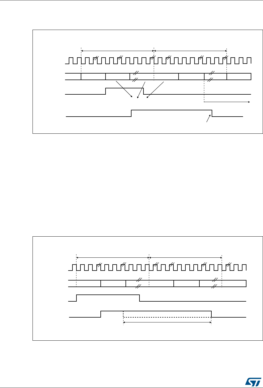
Serial audio interface (SAI) RM0394
1362/1600 RM0394 Rev 4
The OVRUDR flag is cleared when COVRUDR bit is set in the SAI_xCLRFR register.
Figure 448. Overrun detection error
Underrun
An underrun may occur when the audio block in the SAI is a transmitter and the FIFO is
empty when data need to be transmitted. If an underrun is detected, the slot number for
which the event occurs is stored and MUTE value (00) is sent until the FIFO is ready to
transmit the data corresponding to the slot for which the underrun was detected (refer to
Figure 449). This avoids desynchronization between the memory pointer and the slot in the
audio frame.
The underrun event sets the OVRUDR flag in the SAI_xSR register and an interrupt is
generated if the OVRUDRIE bit is set in the SAI_xIM register. To clear this flag, set
COVRUDR bit in the SAI_xCLRFR register.
The underrun event can occur when the audio sub-block is configured as master or slave.
Figure 449. FIFO underrun event
069
VFN
GDWD 6ORW21
([DPSOH),)2RYHUUXQRQ6ORW
$XGLRIUDPH $XGLRIUDPH
6ORWQ21
21
),)2IXOO
2958'5
6ORW21 3LOT/. 6ORW21 6ORW21
5HFHLYHGGDWDGLVFDUGHG 'DWDVWRUHGDJDLQLQ),)2
&2958'5
-36
VFN
GDWD 6ORW21 087(
3LOTSIZEDATASIZE
6'RXWSXW
([DPSOH),)2XQGHUUXQRQ6ORW
$XGLRIUDPH $XGLRIUDPH
087( 6ORW21 21 6ORW21
29581'
087(
),)2HPSW\
29581'

RM0394 Rev 4 1363/1600
RM0394 Serial audio interface (SAI)
1389
Anticipated frame synchronization detection (AFSDET)
The AFSDET flag is used only in slave mode. It is never asserted in master mode. It
indicates that a frame synchronization (FS) has been detected earlier than expected since
the frame length, the frame polarity, the frame offset are defined and known.
Anticipated frame detection sets the AFSDET flag in the SAI_xSR register.
This detection has no effect on the current audio frame which is not sensitive to the
anticipated FS. This means that “parasitic” events on signal FS are flagged without any
perturbation of the current audio frame.
An interrupt is generated if the AFSDETIE bit is set in the SAI_xIM register. To clear the
AFSDET flag, CAFSDET bit must be set in the SAI_xCLRFR register.
To resynchronize with the master after an anticipated frame detection error, four steps are
required:
1. Disable the SAI block by resetting SAIEN bit in SAI_xCR1 register. To make sure the
SAI is disabled, read back the SAIEN bit and check it is set to 0.
2. Flush the FIFO via FFLUS bit in SAI_xCR2 register.
3. Enable again the SAI peripheral (SAIEN bit set to 1).
4. The SAI block will wait for the assertion on FS to restart the synchronization with
master.
Note: The AFSDET flag is not asserted in AC’97 mode since the SAI audio block acts as a link
controller and generates the FS signal even when declared as slave. It has no meaning in
SPDIF mode since the FS signal is not used.
Late frame synchronization detection
The LFSDET flag in the SAI_xSR register can be set only when the SAI audio block
operates as a slave. The frame length, the frame polarity and the frame offset configuration
are known in register SAI_xFRCR.
If the external master does not send the FS signal at the expecting time thus generating the
signal too late, the LFSDET flag is set and an interrupt is generated if LFSDETIE bit is set in
the SAI_xIM register.
The LFSDET flag is cleared when CLFSDET bit is set in the SAI_xCLRFR register.
The late frame synchronization detection flag is set when the corresponding error is
detected. The SAI needs to be resynchronized with the master (see sequence described in
Anticipated frame synchronization detection (AFSDET)).
In a noisy environment, glitches on the SCK clock may be wrongly detected by the audio
block state machine and shift the SAI data at a wrong frame position. This event can be
detected by the SAI and reported as a late frame synchronization detection error.
There is no corruption if the external master is not managing the audio data frame transfer in
continuous mode, which should not be the case in most applications. In this case, the
LFSDET flag will be set.
Note: The LFSDET flag is not asserted in AC’97 mode since the SAI audio block acts as a link
controller and generates the FS signal even when declared as slave. It has no meaning in
SPDIF mode since the signal FS is not used by the protocol.

Serial audio interface (SAI) RM0394
1364/1600 RM0394 Rev 4
Codec not ready (CNRDY AC’97)
The CNRDY flag in the SAI_xSR register is relevant only if the SAI audio block is configured
to operate in AC’97 mode (PRTCFG[1:0] = 10 in the SAI_xCR1 register). If CNRDYIE bit is
set in the SAI_xIM register, an interrupt is generated when the CNRDY flag is set.
CNRDY is asserted when the Codec is not ready to communicate during the reception of
the TAG 0 (slot0) of the AC’97 audio frame. In this case, no data will be automatically stored
into the FIFO since the Codec is not ready, until the TAG 0 indicates that the Codec is ready.
All the active slots defined in the SAI_xSLOTR register will be captured when the Codec is
ready.
To clear CNRDY flag, CCNRDY bit must be set in the SAI_xCLRFR register.
Wrong clock configuration in master mode (with NODIV = 0)
When the audio block operates as a master (MODE[1] = 0) and NODIV bit is equal to 0, the
WCKCFG flag is set as soon as the SAI is enabled if the following conditions are met:
•(FRL+1) is not a power of 2, and
•(FRL+1) is not between 8 and 256.
MODE, NODIV, and SAIEN bits belong to SAI_xCR1 register and FRL to SAI_xFRCR
register.
If WCKCFGIE bit is set, an interrupt is generated when WCKCFG flag is set in the SAI_xSR
register. To clear this flag, set CWCKCFG bit in the SAI_xCLRFR register.
When WCKCFG bit is set, the audio block is automatically disabled, thus performing a
hardware clear of SAIEN bit.
41.4.14 Disabling the SAI
The SAI audio block can be disabled at any moment by clearing SAIEN bit in the SAI_xCR1
register. All the already started frames are automatically completed before the SAI is stops
working. SAIEN bit remains High until the SAI is completely switched-off at the end of the
current audio frame transfer.
If an audio block in the SAI operates synchronously with the other one, the one which is the
master must be disabled first.
41.4.15 SAI DMA interface
To free the CPU and to optimize bus bandwidth, each SAI audio block has an independent
DMA interface to read/write from/to the SAI_xDR register (to access the internal FIFO).
There is one DMA channel per audio sub-block supporting basic DMA request/acknowledge
protocol.
To configure the audio sub-block for DMA transfer, set DMAEN bit in the SAI_xCR1 register.
The DMA request is managed directly by the FIFO controller depending on the FIFO
threshold level (for more details refer to Section 41.4.9: Internal FIFOs). DMA transfer
direction is linked to the SAI audio sub-block configuration:
•If the audio block operates as a transmitter, the audio block FIFO controller outputs a
DMA request to load the FIFO with data written in the SAI_xDR register.
•If the audio block is operates as a receiver, the DMA request is related to read
operations from the SAI_xDR register.

RM0394 Rev 4 1365/1600
RM0394 Serial audio interface (SAI)
1389
Follow the sequence below to configure the SAI interface in DMA mode:
1. Configure SAI and FIFO threshold levels to specify when the DMA request will be
launched.
2. Configure SAI DMA channel.
3. Enable the DMA.
4. Enable the SAI interface.
Note: Before configuring the SAI block, the SAI DMA channel must be disabled.
41.5 SAI interrupts
The SAI supports 7 interrupt sources as shown in Table 220.
Follow the sequence below to enable an interrupt:
1. Disable SAI interrupt.
2. Configure SAI.
3. Configure SAI interrupt source.
4. Enable SAI.
Table 220. SAI interrupt sources
Interrupt
source
Interrupt
group Audio block mode Interrupt enable Interrupt clear
FREQ FREQ Master or slave
Receiver or transmitter
FREQIE in SAI_xIM
register
Depends on:
– FIFO threshold setting (FLVL bits in
SAI_xCR2)
– Communication direction (transmitter
or receiver)
For more details refer to
Section 41.4.9: Internal FIFOs
OVRUDR ERROR Master or slave
Receiver or transmitter
OVRUDRIE in
SAI_xIM register COVRUDR = 1 in SAI_xCLRFR register
AFSDET ERROR
Slave
(not used in AC’97 mode
and SPDIF mode)
AFSDETIE in
SAI_xIM register CAFSDET = 1 in SAI_xCLRFR register
LFSDET ERROR
Slave
(not used in AC’97 mode
and SPDIF mode)
LFSDETIE in
SAI_xIM register CLFSDET = 1 in SAI_xCLRFR register
CNRDY ERROR Slave
(only in AC’97 mode)
CNRDYIE in
SAI_xIM register CCNRDY = 1 in SAI_xCLRFR register
MUTEDET MUTE Master or slave
Receiver mode only
MUTEDETIE in
SAI_xIM register
CMUTEDET = 1 in SAI_xCLRFR
register
WCKCFG ERROR Master with NODIV = 0 in
SAI_xCR1 register
WCKCFGIE in
SAI_xIM register CWCKCFG = 1 in SAI_xCLRFR register

Serial audio interface (SAI) RM0394
1366/1600 RM0394 Rev 4
41.6 SAI registers
41.6.1 Configuration register 1 (SAI_ACR1)
Address offset: 0x004
Reset value: 0x0000 0040
31 30 29 28 27 26 25 24 23 22 21 20 19 18 17 16
Res. Res. Res. Res. Res. Res. Res. Res. MCKDIV[3:0] NODIV Res. DMAEN SAIEN
rw rw rw rw rw rw rw
15 14 13 12 11 10 9 8 7 6 5 4 3 2 1 0
Res. Res. OUTD
RIV MONO SYNCEN[1:0] CKSTR LSBFIRST DS[2:0] Res. PRTCFG[1:0] MODE[1:0]
rw rw rw rw rw rw rw rw rw rw rw rw rw
Bits 31:24 Reserved, must be kept at reset value.
Bits 23:20 MCKDIV[3:0]: Master clock divider
These bits are set and cleared by software. These bits are meaningless when the audio block
operates in slave mode. They have to be configured when the audio block is disabled.
0000: Divides by 1 the master clock input.
Others: the master clock frequency is calculated accordingly to the following formula:
Bit 19 NODIV: No divider
This bit is set and cleared by software.
0: Master clock generator is enabled
1: No divider used in the clock generator (in this case Master Clock Divider bit has no effect)
Bit 18 Reserved, must be kept at reset value.
Bit 17 DMAEN: DMA enable
This bit is set and cleared by software.
0: DMA disabled
1: DMA enabled
Note: Since the audio block defaults to operate as a transmitter after reset, the MODE[1:0] bits must
be configured before setting DMAEN to avoid a DMA request in receiver mode.
Bit 16 SAIEN: Audio block enable
This bit is set by software.
To switch off the audio block, the application software must program this bit to 0 and poll the bit till it
reads back 0, meaning that the block is completely disabled. Before setting this bit to 1, check that it
is set to 0, otherwise the enable command will not be taken into account.
This bit allows controlling the state of the SAI audio block. If it is disabled when an audio frame
transfer is ongoing, the ongoing transfer completes and the cell is fully disabled at the end of this
audio frame transfer.
0: SAI audio block disabled
1: SAI audio block enabled.
Note: When the SAI block (A or B) is configured in master mode, the clock must be present on the
SAI block input before setting SAIEN bit.
Bits 15:14 Reserved, must be kept at reset value.
FSCK_x
Fsai_x_ker_ck
MCKDIV 2×
--------------------------------------
=

RM0394 Rev 4 1367/1600
RM0394 Serial audio interface (SAI)
1389
Bit 13 OUTDRIV: Output drive
This bit is set and cleared by software.
0: Audio block output driven when SAIEN is set
1: Audio block output driven immediately after the setting of this bit.
Note: This bit has to be set before enabling the audio block and after the audio block configuration.
Bit 12 MONO: Mono mode
This bit is set and cleared by software. It is meaningful only when the number of slots is equal to 2.
When the mono mode is selected, slot 0 data are duplicated on slot 1 when the audio block operates
as a transmitter. In reception mode, the slot1 is discarded and only the data received from slot 0 are
stored. Refer to Section : Mono/stereo mode for more details.
0: Stereo mode
1: Mono mode.
Bits 11:10 SYNCEN[1:0]: Synchronization enable
These bits are set and cleared by software. They must be configured when the audio sub-block is
disabled.
00: audio sub-block in asynchronous mode.
01: audio sub-block is synchronous with the other internal audio sub-block. In this case, the audio
sub-block must be configured in slave mode
10: Reserved.
11: Reserved
Note: The audio sub-block should be configured as asynchronous when SPDIF mode is enabled.
Bit 9 CKSTR: Clock strobing edge
This bit is set and cleared by software. It must be configured when the audio block is disabled. This
bit has no meaning in SPDIF audio protocol.
0: Signals generated by the SAI change on SCK rising edge, while signals received by the SAI are
sampled on the SCK falling edge.
1: Signals generated by the SAI change on SCK falling edge, while signals received by the SAI are
sampled on the SCK rising edge.
Bit 8 LSBFIRST: Least significant bit first
This bit is set and cleared by software. It must be configured when the audio block is disabled. This
bit has no meaning in AC’97 audio protocol since AC’97 data are always transferred with the MSB
first. This bit has no meaning in SPDIF audio protocol since in SPDIF data are always transferred
with LSB first.
0: Data are transferred with MSB first
1: Data are transferred with LSB first
Bits 7:5 DS[2:0]: Data size
These bits are set and cleared by software. These bits are ignored when the SPDIF protocols are
selected (bit PRTCFG[1:0]), because the frame and the data size are fixed in such case. When the
companding mode is selected through COMP[1:0] bits, DS[1:0] are ignored since the data size is
fixed to 8 bits by the algorithm.
These bits must be configured when the audio block is disabled.
000: Reserved
001: Reserved
010: 8 bits
011: 10 bits
100: 16 bits
101: 20 bits
110: 24 bits
111: 32 bits

Serial audio interface (SAI) RM0394
1368/1600 RM0394 Rev 4
41.6.2 Configuration register 1 (SAI_BCR1)
Address offset: 0x024
Reset value: 0x0000 0040
Bit 4 Reserved, must be kept at reset value.
Bits 3:2 PRTCFG[1:0]: Protocol configuration
These bits are set and cleared by software. These bits have to be configured when the audio block is
disabled.
00: Free protocol. Free protocol allows to use the powerful configuration of the audio block to
address a specific audio protocol (such as I2S, LSB/MSB justified, TDM, PCM/DSP...) by setting
most of the configuration register bits as well as frame configuration register.
01: SPDIF protocol
10: AC’97 protocol
11: Reserved
Bits 1:0 MODE[1:0]: SAIx audio block mode
These bits are set and cleared by software. They must be configured when SAIx audio block is
disabled.
00: Master transmitter
01: Master receiver
10: Slave transmitter
11: Slave receiver
Note: When the audio block is configured in SPDIF mode, the master transmitter mode is forced
(MODE[1:0] = 00).
31 30 29 28 27 26 25 24 23 22 21 20 19 18 17 16
Res. Res. Res. Res. Res. Res. Res. Res. MCKDIV[3:0] NODIV Res. DMAEN SAIEN
rw rw rw rw rw rw rw
15 14 13 12 11 10 9 8 7 6 5 4 3 2 1 0
Res. Res. OUTD
RIV MONO SYNCEN[1:0] CKSTR LSBFIRST DS[2:0] Res. PRTCFG[1:0] MODE[1:0]
rw rw rw rw rw rw rw rw rw rw rw rw rw
Bits 31:24 Reserved, must be kept at reset value.
Bits 23:20 MCKDIV[3:0]: Master clock divider
These bits are set and cleared by software. These bits are meaningless when the audio block
operates in slave mode. They have to be configured when the audio block is disabled.
0000: Divides by 1 the master clock input.
Others: the master clock frequency is calculated accordingly to the following formula:
Bit 19 NODIV: No divider
This bit is set and cleared by software.
0: Master clock generator is enabled
1: No divider used in the clock generator (in this case Master Clock Divider bit has no effect)
Bit 18 Reserved, must be kept at reset value.
FSCK_x
Fsai_x_ker_ck
MCKDIV 2×
--------------------------------------
=

RM0394 Rev 4 1369/1600
RM0394 Serial audio interface (SAI)
1389
Bit 17 DMAEN: DMA enable
This bit is set and cleared by software.
0: DMA disabled
1: DMA enabled
Note: Since the audio block defaults to operate as a transmitter after reset, the MODE[1:0] bits must
be configured before setting DMAEN to avoid a DMA request in receiver mode.
Bit 16 SAIEN: Audio block enable
This bit is set by software.
To switch off the audio block, the application software must program this bit to 0 and poll the bit till it
reads back 0, meaning that the block is completely disabled. Before setting this bit to 1, check that it
is set to 0, otherwise the enable command will not be taken into account.
This bit allows controlling the state of the SAI audio block. If it is disabled when an audio frame
transfer is ongoing, the ongoing transfer completes and the cell is fully disabled at the end of this
audio frame transfer.
0: SAI audio block disabled
1: SAI audio block enabled.
Note: When the SAI block (A or B) is configured in master mode, the clock must be present on the
SAI block input before setting SAIEN bit.
Bits 15:14 Reserved, must be kept at reset value.
Bit 13 OUTDRIV: Output drive
This bit is set and cleared by software.
0: Audio block output driven when SAIEN is set
1: Audio block output driven immediately after the setting of this bit.
Note: This bit has to be set before enabling the audio block and after the audio block configuration.
Bit 12 MONO: Mono mode
This bit is set and cleared by software. It is meaningful only when the number of slots is equal to 2.
When the mono mode is selected, slot 0 data are duplicated on slot 1 when the audio block operates
as a transmitter. In reception mode, the slot1 is discarded and only the data received from slot 0 are
stored. Refer to Section : Mono/stereo mode for more details.
0: Stereo mode
1: Mono mode.
Bits 11:10 SYNCEN[1:0]: Synchronization enable
These bits are set and cleared by software. They must be configured when the audio sub-block is
disabled.
00: audio sub-block in asynchronous mode.
01: audio sub-block is synchronous with the other internal audio sub-block. In this case, the audio
sub-block must be configured in slave mode
10: Reserved.
11: Reserved
Note: The audio sub-block should be configured as asynchronous when SPDIF mode is enabled.
Bit 9 CKSTR: Clock strobing edge
This bit is set and cleared by software. It must be configured when the audio block is disabled. This
bit has no meaning in SPDIF audio protocol.
0: Signals generated by the SAI change on SCK rising edge, while signals received by the SAI are
sampled on the SCK falling edge.
1: Signals generated by the SAI change on SCK falling edge, while signals received by the SAI are
sampled on the SCK rising edge.

Serial audio interface (SAI) RM0394
1370/1600 RM0394 Rev 4
41.6.3 Configuration register 2 (SAI_ACR2)
Address offset: 0x008
Reset value: 0x0000 0000
Bit 8 LSBFIRST: Least significant bit first
This bit is set and cleared by software. It must be configured when the audio block is disabled. This
bit has no meaning in AC’97 audio protocol since AC’97 data are always transferred with the MSB
first. This bit has no meaning in SPDIF audio protocol since in SPDIF data are always transferred
with LSB first.
0: Data are transferred with MSB first
1: Data are transferred with LSB first
Bits 7:5 DS[2:0]: Data size
These bits are set and cleared by software. These bits are ignored when the SPDIF protocols are
selected (bit PRTCFG[1:0]), because the frame and the data size are fixed in such case. When the
companding mode is selected through COMP[1:0] bits, DS[1:0] are ignored since the data size is
fixed to 8 bits by the algorithm.
These bits must be configured when the audio block is disabled.
000: Reserved
001: Reserved
010: 8 bits
011: 10 bits
100: 16 bits
101: 20 bits
110: 24 bits
111: 32 bits
Bit 4 Reserved, must be kept at reset value.
Bits 3:2 PRTCFG[1:0]: Protocol configuration
These bits are set and cleared by software. These bits have to be configured when the audio block is
disabled.
00: Free protocol. Free protocol allows to use the powerful config uration of the audio block to
address a specific audio protocol (such as I2S, LSB/MSB justified, TDM, PCM/DSP...) by setting
most of the configuration register bits as well as frame configuration register.
01: SPDIF protocol
10: AC’97 protocol
11: Reserved
Bits 1:0 MODE[1:0]: SAIx audio block mode
These bits are set and cleared by software. They must be configured when SAIx audio block is
disabled.
00: Master transmitter
01: Master receiver
10: Slave transmitter
11: Slave receiver
Note: When the audio block is configured in SPDIF mode, the master transmitter mode is forced
(MODE[1:0] = 00). In Master transmitter mode, the audio block starts generating the FS and the
clocks immediately.

RM0394 Rev 4 1371/1600
RM0394 Serial audio interface (SAI)
1389
31 30 29 28 27 26 25 24 23 22 21 20 19 18 17 16
Res. Res. Res. Res. Res. Res. Res. Res. Res. Res. Res. Res. Res. Res. Res. Res.
15 14 13 12 11 10 9 8 7 6 5 4 3 2 1 0
COMP[1:0] CPL MUTECNT[5:0] MUTE
VAL MUTE TRIS F
FLUSH FTH[2:0]
rw rw rw rw rw rw rw rw rw rw rw rw w rw rw rw
Bits 31:16 Reserved, must be kept at reset value.
Bits 15:14 COMP[1:0]: Companding mode.
These bits are set and cleared by software. The µ-Law and the A-Law log are a part of the CCITT
G.711 recommendation, the type of complement that will be used depends on CPL bit.
The data expansion or data compression are determined by the state of bit MODE[0].
The data compression is applied if the audio block is configured as a transmitter.
The data expansion is automatically applied when the audio block is configured as a receiver.
Refer to Section : Companding mode for more details.
00: No companding algorithm
01: Reserved.
10: µ-Law algorithm
11: A-Law algorithm
Note: Companding mode is applicable only when Free protocol mode is selected.
Bit 13 CPL: Complement bit.
This bit is set and cleared by software.
It defines the type of complement to be used for companding mode
0: 1’s complement representation.
1: 2’s complement representation.
Note: This bit has effect only when the companding mode is µ-Law algorithm or A-Law algorithm.
Bits 12:7 MUTECNT[5:0]: Mute counter.
These bits are set and cleared by software. They are used only in reception mode.
The value set in these bits is compared to the number of consecutive mute frames detected in
reception. When the number of mute frames is equal to this value, the flag MUTEDET will be set and
an interrupt will be generated if bit MUTEDETIE is set.
Refer to Section : Mute mode for more details.
Bit 6 MUTEVAL: Mute value.
This bit is set and cleared by software.It must be written before enabling the audio block: SAIEN.
This bit is meaningful only when the audio block operates as a transmitter, the number of slots is
lower or equal to 2 and the MUTE bit is set.
If more slots are declared, the bit value sent during the transmission in mute mode is equal to 0,
whatever the value of MUTEVAL.
if the number of slot is lower or equal to 2 and MUTEVAL = 1, the MUTE value transmitted for each
slot is the one sent during the previous frame.
Refer to Section : Mute mode for more details.
0: Bit value 0 is sent during the mute mode.
1: Last values are sent during the mute mode.
Note: This bit is meaningless and should not be used for SPDIF audio blocks.

Serial audio interface (SAI) RM0394
1372/1600 RM0394 Rev 4
41.6.4 Configuration register 2 (SAI_BCR2)
Address offset: 0x028
Reset value: 0x0000 0000
Bit 5 MUTE: Mute.
This bit is set and cleared by software. It is meaningful only when the audio block operates as a
transmitter. The MUTE value is linked to value of MUTEVAL if the number of slots is lower or equal
to 2, or equal to 0 if it is greater than 2.
Refer to Section : Mute mode for more details.
0: No mute mode.
1: Mute mode enabled.
Note: This bit is meaningless and should not be used for SPDIF audio blocks.
Bit 4 TRIS: Tristate management on data line.
This bit is set and cleared by software. It is meaningful only if the audio block is configured as a
transmitter. This bit is not used when the audio block is configured in SPDIF mode. It should be
configured when SAI is disabled.
Refer to Section : Output data line management on an inactive slot for more details.
0: SD output line is still driven by the SAI when a slot is inactive.
1: SD output line is released (HI-Z) at the end of the last data bit of the last active slot if the next one
is inactive.
Bit 3 FFLUSH: FIFO flush.
This bit is set by software. It is always read as 0. This bit should be configured when the SAI is
disabled.
0: No FIFO flush.
1: FIFO flush. Programming this bit to 1 triggers the FIFO Flush. All the internal FIFO pointers (read
and write) are cleared. In this case data still present in the FIFO are lost (no more transmission or
received data lost). Before flushing, SAI DMA stream/interruption must be disabled
Bits 2:0 FTH[2:0]: FIFO threshold.
This bit is set and cleared by software.
000: FIFO empty
001: ¼ FIFO
010: ½ FIFO
011: ¾ FIFO
100: FIFO full
101: Reserved
110: Reserved
111: Reserved
31 30 29 28 27 26 25 24 23 22 21 20 19 18 17 16
Res. Res. Res. Res. Res. Res. Res. Res. Res. Res. Res. Res. Res. Res. Res. Res.
15 14 13 12 11 10 9 8 7 6 5 4 3 2 1 0
COMP[1:0] CPL MUTECNT[5:0] MUTE
VAL MUTE TRIS F
FLUSH FTH[2:0]
rw rw rw rw rw rw rw rw rw rw rw rw w rw rw rw

RM0394 Rev 4 1373/1600
RM0394 Serial audio interface (SAI)
1389
Bits 31:16 Reserved, must be kept at reset value.
Bits 15:14 COMP[1:0]: Companding mode.
These bits are set and cleared by software. The µ-Law and the A-Law log are a part of the CCITT
G.711 recommendation, the type of complement that will be used depends on CPL bit.
The data expansion or data compression are determined by the state of bit MODE[0].
The data compression is applied if the audio block is configured as a transmitter.
The data expansion is automatically applied when the audio block is configured as a receiver.
Refer to Section : Companding mode for more details.
00: No companding algorithm
01: Reserved.
10: µ-Law algorithm
11: A-Law algorithm
Note: Companding mode is applicable only when Free protocol mode is selected.
Bit 13 CPL: Complement bit.
This bit is set and cleared by software.
It defines the type of complement to be used for companding mode
0: 1’s complement representation.
1: 2’s complement representation.
Note: This bit has effect only when the companding mode is µ-Law algorithm or A-Law algorithm.
Bits 12:7 MUTECNT[5:0]: Mute counter.
These bits are set and cleared by software. They are used only in reception mode.
The value set in these bits is compared to the number of consecutive mute frames detected in
reception. When the number of mute frames is equal to this value, the flag MUTEDET will be set and
an interrupt will be generated if bit MUTEDETIE is set.
Refer to Section : Mute mode for more details.
Bit 6 MUTEVAL: Mute value.
This bit is set and cleared by software.It must be written before enabling the audio block: SAIEN.
This bit is meaningful only when the audio block operates as a transmitter, the number of slots is
lower or equal to 2 and the MUTE bit is set.
If more slots are declared, the bit value sent during the transmission in mute mode is equal to 0,
whatever the value of MUTEVAL.
if the number of slot is lower or equal to 2 and MUTEVAL = 1, the MUTE value transmitted for each
slot is the one sent during the previous frame.
Refer to Section : Mute mode for more details.
0: Bit value 0 is sent during the mute mode.
1: Last values are sent during the mute mode.
Note: This bit is meaningless and should not be used for SPDIF audio blocks.
Bit 5 MUTE: Mute.
This bit is set and cleared by software. It is meaningful only when the audio block operates as a
transmitter. The MUTE value is linked to value of MUTEVAL if the number of slots is lower or equal
to 2, or equal to 0 if it is greater than 2.
Refer to Section : Mute mode for more details.
0: No mute mode.
1: Mute mode enabled.
Note: This bit is meaningless and should not be used for SPDIF audio blocks.

Serial audio interface (SAI) RM0394
1374/1600 RM0394 Rev 4
41.6.5 Frame configuration register (SAI_AFRCR)
Address offset: 0x00C
Reset value: 0x0000 0007
Note: This register has no meaning in AC’97 and SPDIF audio protocol
Bit 4 TRIS: Tristate management on data line.
This bit is set and cleared by software. It is meaningful only if the audio block is configured as a
transmitter. This bit is not used when the audio block is configured in SPDIF mode. It should be
configured when SAI is disabled.
Refer to Section : Output data line management on an inactive slot for more details.
0: SD output line is still driven by the SAI when a slot is inactive.
1: SD output line is released (HI-Z) at the end of the last data bit of the last active slot if the next one
is inactive.
Bit 3 FFLUSH: FIFO flush.
This bit is set by software. It is always read as 0. This bit should be configured when the SAI is
disabled.
0: No FIFO flush.
1: FIFO flush. Programming this bit to 1 triggers the FIFO Flush. All the internal FIFO pointers (read
and write) are cleared. In this case data still present in the FIFO are lost (no more transmission or
received data lost). Before flushing, SAI DMA stream/interruption must be disabled
Bits 2:0 FTH[2:0]: FIFO threshold.
This bit is set and cleared by software.
000: FIFO empty
001: ¼ FIFO
010: ½ FIFO
011: ¾ FIFO
100: FIFO full
101: Reserved
110: Reserved
111: Reserved
31 30 29 28 27 26 25 24 23 22 21 20 19 18 17 16
Res. Res. Res. Res. Res. Res. Res. Res. Res. Res. Res. Res. Res. FSOFF FSPOL FSDEF
rw rw r
15 14 13 12 11 10 9 8 7 6 5 4 3 2 1 0
Res. FSALL[6:0] FRL[7:0]
rw rw rw rw rw rw rw rw rw rw rw rw rw rw rw

RM0394 Rev 4 1375/1600
RM0394 Serial audio interface (SAI)
1389
41.6.6 Frame configuration register (SAI_BFRCR)
Address offset: 0x02C
Reset value: 0x0000 0007
Bits 31:19 Reserved, must be kept at reset value.
Bit 18 FSOFF: Frame synchronization offset.
This bit is set and cleared by software. It is meaningless and is not used in AC’97 or SPDIF audio
block configuration. This bit must be configured when the audio block is disabled.
0: FS is asserted on the first bit of the slot 0.
1: FS is asserted one bit before the first bit of the slot 0.
Bit 17 FSPOL: Frame synchronization polarity.
This bit is set and cleared by software. It is used to configure the level of the start of frame on the FS
signal. It is meaningless and is not used in AC’97 or SPDIF audio block configuration.
This bit must be configured when the audio block is disabled.
0: FS is active low (falling edge)
1: FS is active high (rising edge)
Bit 16 FSDEF: Frame synchronization definition.
This bit is set and cleared by software.
0: FS signal is a start frame signal
1: FS signal is a start of frame signal + channel side identification
When the bit is set, the number of slots defined in the SAI_xSLOTR register has to be even. It
means that half of this number of slots will be dedicated to the left channel and the other slots for the
right channel (e.g: this bit has to be set for I2S or MSB/LSB-justified protocols...).
This bit is meaningless and is not used in AC’97 or SPDIF audio block configuration. It must be
configured when the audio block is disabled.
Bit 15 Reserved, must be kept at reset value.
Bits 14:8 FSALL[6:0]: Frame synchronization active level length.
These bits are set and cleared by software. They specify the length in number of bit clock
(SCK) + 1 (FSALL[6:0] + 1) of the active level of the FS signal in the audio frame
These bits are meaningless and are not used in AC’97 or SPDIF audio block configuration.
They must be configured when the audio block is disabled.
Bits 7:0 FRL[7:0]: Frame length.
These bits are set and cleared by software. They define the audio frame length expressed in number
of SCK clock cycles: the number of bits in the frame is equal to FRL[7:0] + 1.
The minimum number of bits to transfer in an audio frame must be equal to 8, otherwise the audio
block will behaves in an unexpected way. This is the case when the data size is 8 bits and only one
slot 0 is defined in NBSLOT[4:0] of SAI_xSLOTR register (NBSLOT[3:0] = 0000).
In master mode, if the master clock (available on MCLK_x pin) is used, the frame length should be
aligned with a number equal to a power of 2, ranging from 8 to 256. When the master clock is not
used (NODIV = 1), it is recommended to program the frame length to an value ranging from 8 to 256.
These bits are meaningless and are not used in AC’97 or SPDIF audio block configuration. They
must be configured when the audio block is disabled.

Serial audio interface (SAI) RM0394
1376/1600 RM0394 Rev 4
Note: This register has no meaning in AC’97 and SPDIF audio protocol
31 30 29 28 27 26 25 24 23 22 21 20 19 18 17 16
Res. Res. Res. Res. Res. Res. Res. Res. Res. Res. Res. Res. Res. FSOFF FSPOL FSDEF
rw rw r
15 14 13 12 11 10 9 8 7 6 5 4 3 2 1 0
Res. FSALL[6:0] FRL[7:0]
rw rw rw rw rw rw rw rw rw rw rw rw rw rw rw
Bits 31:19 Reserved, must be kept at reset value.
Bit 18 FSOFF: Frame synchronization offset.
This bit is set and cleared by software. It is meaningless and is not used in AC’97 or SPDIF audio
block configuration. This bit must be configured when the audio block is disabled.
0: FS is asserted on the first bit of the slot 0.
1: FS is asserted one bit before the first bit of the slot 0.
Bit 17 FSPOL: Frame synchronization polarity.
This bit is set and cleared by software. It is used to configure the level of the start of frame on the FS
signal. It is meaningless and is not used in AC’97 or SPDIF audio block configuration.
This bit must be configured when the audio block is disabled.
0: FS is active low (falling edge)
1: FS is active high (rising edge)
Bit 16 FSDEF: Frame synchronization definition.
This bit is set and cleared by software.
0: FS signal is a start frame signal
1: FS signal is a start of frame signal + channel side identification
When the bit is set, the number of slots defined in the SAI_xSLOTR register has to be even. It
means that half of this number of slots will be dedicated to the left channel and the other slots for the
right channel (e.g: this bit has to be set for I2S or MSB/LSB-justified protocols...).
This bit is meaningless and is not used in AC’97 or SPDIF audio block configuration. It must be
configured when the audio block is disabled.
Bit 15 Reserved, must be kept at reset value.
Bits 14:8 FSALL[6:0]: Frame synchronization active level length.
These bits are set and cleared by software. They specify the length in number of bit clock
(SCK) + 1 (FSALL[6:0] + 1) of the active level of the FS signal in the audio frame
These bits are meaningless and are not used in AC’97 or SPDIF audio block configuration.
They must be configured when the audio block is disabled.
Bits 7:0 FRL[7:0]: Frame length.
These bits are set and cleared by software. They define the audio frame length expressed in number
of SCK clock cycles: the number of bits in the frame is equal to FRL[7:0] + 1.
The minimum number of bits to transfer in an audio frame must be equal to 8, otherwise the audio
block will behaves in an unexpected way. This is the case when the data size is 8 bits and only one
slot 0 is defined in NBSLOT[4:0] of SAI_xSLOTR register (NBSLOT[3:0] = 0000).
In master mode, if the master clock (available on MCLK_x pin) is used, the frame length should be
aligned with a number equal to a power of 2, ranging from 8 to 256. When the master clock is not
used (NODIV = 1), it is recommended to program the frame length to an value ranging from 8 to 256.
These bits are meaningless and are not used in AC’97 or SPDIF audio block configuration.

RM0394 Rev 4 1377/1600
RM0394 Serial audio interface (SAI)
1389
41.6.7 Slot register (SAI_ASLOTR)
Address offset: 0x010
Reset value: 0x0000 0000
Note: This register has no meaning in AC’97 and SPDIF audio protocol
31 30 29 28 27 26 25 24 23 22 21 20 19 18 17 16
SLOTEN[15:0]
rw rw rw rw rw rw rw rw rw rw rw rw rw rw rw rw
15 14 13 12 11 10 9 8 7 6 5 4 3 2 1 0
Res. Res. Res. Res. NBSLOT[3:0] SLOTSZ[1:0] Res. FBOFF[4:0]
rw rw rw rw rw rw rw rw rw rw rw
Bits 31:16 SLOTEN[15:0]: Slot enable.
These bits are set and cleared by software.
Each SLOTEN bit corresponds to a slot position from 0 to 15 (maximum 16 slots).
0: Inactive slot.
1: Active slot.
The slot must be enabled when the audio block is disabled.
They are ignored in AC’97 or SPDIF mode.
Bits 15:12 Reserved, must be kept at reset value.
Bits 11:8 NBSLOT[3:0]: Number of slots in an audio frame.
These bits are set and cleared by software.
The value set in this bitfield represents the number of slots + 1 in the audio frame (including the
number of inactive slots). The maximum number of slots is 16.
The number of slots should be even if FSDEF bit in the SAI_xFRCR register is set.
The number of slots must be configured when the audio block is disabled.
They are ignored in AC’97 or SPDIF mode.
Bits 7:6 SLOTSZ[1:0]: Slot size
This bits is set and cleared by software.
The slot size must be higher or equal to the data size. If this condition is not respected, the behavior
of the SAI will be undetermined.
Refer to Section : Output data line management on an inactive slot for information on how to drive
SD line.
These bits must be set when the audio block is disabled.
They are ignored in AC’97 or SPDIF mode.
00: The slot size is equivalent to the data size (specified in DS[3:0] in the SAI_xCR1 register).
01: 16-bit
10: 32-bit
11: Reserved
Bit 5 Reserved, must be kept at reset value.
Bits 4:0 FBOFF[4:0]: First bit offset
These bits are set and cleared by software.
The value set in this bitfield defines the position of the first data transfer bit in the slot. It represents
an offset value. In transmission mode, the bits outside the data field are forced to 0. In reception
mode, the extra received bits are discarded.
These bits must be set when the audio block is disabled.
They are ignored in AC’97 or SPDIF mode.

Serial audio interface (SAI) RM0394
1378/1600 RM0394 Rev 4
41.6.8 Slot register (SAI_BSLOTR)
Address offset: 0x030
Reset value: 0x0000 0000
Note: This register has no meaning in AC’97 and SPDIF audio protocol
31 30 29 28 27 26 25 24 23 22 21 20 19 18 17 16
SLOTEN[15:0]
rw rw rw rw rw rw rw rw rw rw rw rw rw rw rw rw
15 14 13 12 11 10 9 8 7 6 5 4 3 2 1 0
Res. Res. Res. Res. NBSLOT[3:0] SLOTSZ[1:0] Res. FBOFF[4:0]
rw rw rw rw rw rw rw rw rw rw rw
Bits 31:16 SLOTEN[15:0]: Slot enable.
These bits are set and cleared by software.
Each SLOTEN bit corresponds to a slot position from 0 to 15 (maximum 16 slots).
0: Inactive slot.
1: Active slot.
The slot must be enabled when the audio block is disabled.
They are ignored in AC’97 or SPDIF mode.
Bits 15:12 Reserved, must be kept at reset value.
Bits 11:8 NBSLOT[3:0]: Number of slots in an audio frame.
These bits are set and cleared by software.
The value set in this bitfield represents the number of slots + 1 in the audio frame (including the
number of inactive slots). The maximum number of slots is 16.
The number of slots should be even if FSDEF bit in the SAI_xFRCR register is set.
The number of slots must be configured when the audio block is disabled.
They are ignored in AC’97 or SPDIF mode.
Bits 7:6 SLOTSZ[1:0]: Slot size
This bits is set and cleared by software.
The slot size must be higher or equal to the data size. If this condition is not respected, the behavior
of the SAI will be undetermined.
Refer to Section : Output data line management on an inactive slot for information on how to drive
SD line.
These bits must be set when the audio block is disabled.
They are ignored in AC’97 or SPDIF mode.
00: The slot size is equivalent to the data size (specified in DS[3:0] in the SAI_xCR1 register).
01: 16-bit
10: 32-bit
11: Reserved
Bit 5 Reserved, must be kept at reset value.
Bits 4:0 FBOFF[4:0]: First bit offset
These bits are set and cleared by software.
The value set in this bitfield defines the position of the first data transfer bit in the slot. It represents
an offset value. In transmission mode, the bits outside the data field are forced to 0. In reception
mode, the extra received bits are discarded.
These bits must be set when the audio block is disabled.
They are ignored in AC’97 or SPDIF mode.

RM0394 Rev 4 1379/1600
RM0394 Serial audio interface (SAI)
1389
41.6.9 Interrupt mask register (SAI_AIM)
Address offset: 0x014
Reset value: 0x0000 0000
31 30 29 28 27 26 25 24 23 22 21 20 19 18 17 16
Res. Res. Res. Res. Res. Res. Res. Res. Res. Res. Res. Res. Res. Res. Res. Res.
15 14 13 12 11 10 9 8 7 6 5 4 3 2 1 0
Res. Res. Res. Res. Res. Res. Res. Res. Res. LFSDET
IE
AFSDET
IE
CNRDY
IE
FREQ
IE
WCKCFG
IE
MUTEDET
IE
OVRUDR
IE
rw rw rw rw rw rw rw
Bits 31:7 Reserved, must be kept at reset value.
Bit 6 LFSDETIE: Late frame synchronization detection interrupt enable.
This bit is set and cleared by software.
0: Interrupt is disabled
1: Interrupt is enabled
When this bit is set, an interrupt will be generated if the LFSDET bit is set in the SAI_xSR register.
This bit is meaningless in AC’97, SPDIF mode or when the audio block operates as a master.
Bit 5 AFSDETIE: Anticipated frame synchronization detection interrupt enable.
This bit is set and cleared by software.
0: Interrupt is disabled
1: Interrupt is enabled
When this bit is set, an interrupt will be generated if the AFSDET bit in the SAI_xSR register is set.
This bit is meaningless in AC’97, SPDIF mode or when the audio block operates as a master.
Bit 4 CNRDYIE: Codec not ready interrupt enable (AC’97).
This bit is set and cleared by software.
0: Interrupt is disabled
1: Interrupt is enabled
When the interrupt is enabled, the audio block detects in the slot 0 (tag0) of the AC’97 frame if the
Codec connected to this line is ready or not. If it is not ready, the CNRDY flag in the SAI_xSR
register is set and an interruption i generated.
This bit has a meaning only if the AC’97 mode is selected through PRTCFG[1:0] bits and the audio
block is operates as a receiver.
Bit 3 FREQIE: FIFO request interrupt enable.
This bit is set and cleared by software.
0: Interrupt is disabled
1: Interrupt is enabled
When this bit is set, an interrupt is generated if the FREQ bit in the SAI_xSR register is set.
Since the audio block defaults to operate as a transmitter after reset, the MODE bit must be
configured before setting FREQIE to avoid a parasitic interruption in receiver mode,

Serial audio interface (SAI) RM0394
1380/1600 RM0394 Rev 4
41.6.10 Interrupt mask register (SAI_BIM)
Address offset: 0x034
Reset value: 0x0000 0000
Bit 2 WCKCFGIE: Wrong clock configuration interrupt enable.
This bit is set and cleared by software.
0: Interrupt is disabled
1: Interrupt is enabled
This bit is taken into account only if the audio block is configured as a master (MODE[1] = 0) and
NODIV = 0.
It generates an interrupt if the WCKCFG flag in the SAI_xSR register is set.
Note: This bit is used only in Free protocol mode and is meaningless in other modes.
Bit 1 MUTEDETIE: Mute detection interrupt enable.
This bit is set and cleared by software.
0: Interrupt is disabled
1: Interrupt is enabled
When this bit is set, an interrupt is generated if the MUTEDET bit in the SAI_xSR register is set.
This bit has a meaning only if the audio block is configured in receiver mode.
Bit 0 OVRUDRIE: Overrun/underrun interrupt enable.
This bit is set and cleared by software.
0: Interrupt is disabled
1: Interrupt is enabled
When this bit is set, an interrupt is generated if the OVRUDR bit in the SAI_xSR register is set.
31 30 29 28 27 26 25 24 23 22 21 20 19 18 17 16
Res. Res. Res. Res. Res. Res. Res. Res. Res. Res. Res. Res. Res. Res. Res. Res.
15 14 13 12 11 10 9 8 7 6 5 4 3 2 1 0
Res. Res. Res. Res. Res. Res. Res. Res. Res. LFSDET
IE
AFSDET
IE
CNRDY
IE
FREQ
IE
WCKCFG
IE
MUTEDET
IE
OVRUDR
IE
rw rw rw rw rw rw rw
Bits 31:7 Reserved, must be kept at reset value.
Bit 6 LFSDETIE: Late frame synchronization detection interrupt enable.
This bit is set and cleared by software.
0: Interrupt is disabled
1: Interrupt is enabled
When this bit is set, an interrupt will be generated if the LFSDET bit is set in the SAI_xSR register.
This bit is meaningless in AC’97, SPDIF mode or when the audio block operates as a master.
Bit 5 AFSDETIE: Anticipated frame synchronization detection interrupt enable.
This bit is set and cleared by software.
0: Interrupt is disabled
1: Interrupt is enabled
When this bit is set, an interrupt will be generated if the AFSDET bit in the SAI_xSR register is set.
This bit is meaningless in AC’97, SPDIF mode or when the audio block operates as a master.

RM0394 Rev 4 1381/1600
RM0394 Serial audio interface (SAI)
1389
41.6.11 Status register (SAI_ASR)
Address offset: 0x018
Reset value: 0x0000 0008
Bit 4 CNRDYIE: Codec not ready interrupt enable (AC’97).
This bit is set and cleared by software.
0: Interrupt is disabled
1: Interrupt is enabled
When the interrupt is enabled, the audio block detects in the slot 0 (tag0) of the AC’97 frame if the
Codec connected to this line is ready or not. If it is not ready, the CNRDY flag in the SAI_xSR
register is set and an interruption i generated.
This bit has a meaning only if the AC’97 mode is selected through PRTCFG[1:0] bits and the audio
block is operates as a receiver.
Bit 3 FREQIE: FIFO request interrupt enable.
This bit is set and cleared by software.
0: Interrupt is disabled
1: Interrupt is enabled
When this bit is set, an interrupt is generated if the FREQ bit in the SAI_xSR register is set.
Since the audio block defaults to operate as a transmitter after reset, the MODE bit must be
configured before setting FREQIE to avoid a parasitic interruption in receiver mode,
Bit 2 WCKCFGIE: Wrong clock configuration interrupt enable.
This bit is set and cleared by software.
0: Interrupt is disabled
1: Interrupt is enabled
This bit is taken into account only if the audio block is configured as a master (MODE[1] = 0) and
NODIV = 0.
It generates an interrupt if the WCKCFG flag in the SAI_xSR register is set.
Note: This bit is used only in Free protocol mode and is meaningless in other modes.
Bit 1 MUTEDETIE: Mute detection interrupt enable.
This bit is set and cleared by software.
0: Interrupt is disabled
1: Interrupt is enabled
When this bit is set, an interrupt is generated if the MUTEDET bit in the SAI_xSR register is set.
This bit has a meaning only if the audio block is configured in receiver mode.
Bit 0 OVRUDRIE: Overrun/underrun interrupt enable.
This bit is set and cleared by software.
0: Interrupt is disabled
1: Interrupt is enabled
When this bit is set, an interrupt is generated if the OVRUDR bit in the SAI_xSR register is set.
31 30 29 28 27 26 25 24 23 22 21 20 19 18 17 16
Res. Res. Res. Res. Res. Res. Res. Res. Res. Res. Res. Res. Res. FLVL[2:0]
rrr
15 14 13 12 11 10 9 8 7 6 5 4 3 2 1 0
Res. Res. Res. Res. Res. Res. Res. Res. Res. LFSDET AFSDET CNRDY FREQ WCKCFG MUTEDET OVRUDR
rr r r r r r

Serial audio interface (SAI) RM0394
1382/1600 RM0394 Rev 4
Bits 31:19 Reserved, must be kept at reset value.
Bits 18:16 FLVL[2:0]: FIFO level threshold.
This bit is read only. The FIFO level threshold flag is managed only by hardware and its setting
depends on SAI block configuration (transmitter or receiver mode).
If the SAI block is configured as transmitter:
000: FIFO empty
001: FIFO <= ¼ but not empty
010: ¼ < FIFO <= ½
011: ½ < FIFO <= ¾
100: ¾ < FIFO but not full
101: FIFO full
If SAI block is configured as receiver:
000: FIFO empty
001: FIFO < ¼ but not empty
010: ¼ <= FIFO < ½
011: ½ =< FIFO < ¾
100: ¾ =< FIFO but not full
101: FIFO full
Bits 15:7 Reserved, must be kept at reset value.
Bit 6 LFSDET: Late frame synchronization detection.
This bit is read only.
0: No error.
1: Frame synchronization signal is not present at the right time.
This flag can be set only if the audio block is configured in slave mode.
It is not used in AC’97 or SPDIF mode.
It can generate an interrupt if LFSDETIE bit is set in the SAI_xIM register.
This flag is cleared when the software sets bit CLFSDET in SAI_xCLRFR register
Bit 5 AFSDET: Anticipated frame synchronization detection.
This bit is read only.
0: No error.
1: Frame synchronization signal is detected earlier than expected.
This flag can be set only if the audio block is configured in slave mode.
It is not used in AC’97 or SPDIF mode.
It can generate an interrupt if AFSDETIE bit is set in SAI_xIM register.
This flag is cleared when the software sets CAFSDET bit in SAI_xCLRFR register.
Bit 4 CNRDY: Codec not ready.
This bit is read only.
0: External AC’97 Codec is ready
1: External AC’97 Codec is not ready
This bit is used only when the AC’97 audio protocol is selected in the SAI_xCR1 register and
configured in receiver mode.
It can generate an interrupt if CNRDYIE bit is set in SAI_xIM register.
This flag is cleared when the software sets CCNRDY bit in SAI_xCLRFR register.

RM0394 Rev 4 1383/1600
RM0394 Serial audio interface (SAI)
1389
41.6.12 Status register (SAI_BSR)
Address offset: 0x038
Reset value: 0x0000 0008
Bit 3 FREQ: FIFO request.
This bit is read only.
0: No FIFO request.
1: FIFO request to read or to write the SAI_xDR.
The request depends on the audio block configuration:
– If the block is configured in transmission mode, the FIFO request is related to a write request
operation in the SAI_xDR.
– If the block configured in reception, the FIFO request related to a read request operation from the
SAI_xDR.
This flag can generate an interrupt if FREQIE bit is set in SAI_xIM register.
Bit 2 WCKCFG: Wrong clock configuration flag.
This bit is read only.
0: Clock configuration is correct
1: Clock configuration does not respect the rule concerning the frame length specification defined in
Section 41.4.6: Frame synchronization (configuration of FRL[7:0] bit in the SAI_xFRCR register)
This bit is used only when the audio block operates in master mode (MODE[1] = 0) and NODIV = 0.
It can generate an interrupt if WCKCFGIE bit is set in SAI_xIM register.
This flag is cleared when the software sets CWCKCFG bit in SAI_xCLRFR register.
Bit 1 MUTEDET: Mute detection.
This bit is read only.
0: No MUTE detection on the SD input line
1: MUTE value detected on the SD input line (0 value) for a specified number of consecutive audio
frame
This flag is set if consecutive 0 values are received in each slot of a given audio frame and for a
consecutive number of audio frames (set in the MUTECNT bit in the SAI_xCR2 register).
It can generate an interrupt if MUTEDETIE bit is set in SAI_xIM register.
This flag is cleared when the software sets bit CMUTEDET in the SAI_xCLRFR register.
Bit 0 OVRUDR: Overrun / underrun.
This bit is read only.
0: No overrun/underrun error.
1: Overrun/underrun error detection.
The overrun and underrun conditions can occur only when the audio block is configured as a
receiver and a transmitter, respectively.
It can generate an interrupt if OVRUDRIE bit is set in SAI_xIM register.
This flag is cleared when the software sets COVRUDR bit in SAI_xCLRFR register.
31 30 29 28 27 26 25 24 23 22 21 20 19 18 17 16
Res. Res. Res. Res. Res. Res. Res. Res. Res. Res. Res. Res. Res. FLVL[2:0]
rrr
15 14 13 12 11 10 9 8 7 6 5 4 3 2 1 0
Res. Res. Res. Res. Res. Res. Res. Res. Res. LFSDET AFSDET CNRDY FREQ WCKCFG MUTEDET OVRUDR
rr r r r r r

Serial audio interface (SAI) RM0394
1384/1600 RM0394 Rev 4
Bits 31:19 Reserved, must be kept at reset value.
Bits 18:16 FLVL[2:0]: FIFO level threshold.
This bit is read only. The FIFO level threshold flag is managed only by hardware and its setting
depends on SAI block configuration (transmitter or receiver mode).
If the SAI block is configured as transmitter:
000: FIFO empty
001: FIFO <= ¼ but not empty
010: ¼ < FIFO <= ½
011: ½ < FIFO <= ¾
100: ¾ < FIFO but not full
101: FIFO full
If SAI block is configured as receiver:
000: FIFO empty
001: FIFO < ¼ but not empty
010: ¼ <= FIFO < ½
011: ½ =< FIFO < ¾
100: ¾ =< FIFO but not full
101: FIFO full
Bits 15:7 Reserved, must be kept at reset value.
Bit 6 LFSDET: Late frame synchronization detection.
This bit is read only.
0: No error.
1: Frame synchronization signal is not present at the right time.
This flag can be set only if the audio block is configured in slave mode.
It is not used in AC’97 or SPDIF mode.
It can generate an interrupt if LFSDETIE bit is set in the SAI_xIM register.
This flag is cleared when the software sets bit CLFSDET in SAI_xCLRFR register
Bit 5 AFSDET: Anticipated frame synchronization detection.
This bit is read only.
0: No error.
1: Frame synchronization signal is detected earlier than expected.
This flag can be set only if the audio block is configured in slave mode.
It is not used in AC’97 or SPDIF mode.
It can generate an interrupt if AFSDETIE bit is set in SAI_xIM register.
This flag is cleared when the software sets CAFSDET bit in SAI_xCLRFR register.
Bit 4 CNRDY: Codec not ready.
This bit is read only.
0: External AC’97 Codec is ready
1: External AC’97 Codec is not ready
This bit is used only when the AC’97 audio protocol is selected in the SAI_xCR1 register and
configured in receiver mode.
It can generate an interrupt if CNRDYIE bit is set in SAI_xIM register.
This flag is cleared when the software sets CCNRDY bit in SAI_xCLRFR register.

RM0394 Rev 4 1385/1600
RM0394 Serial audio interface (SAI)
1389
41.6.13 Clear flag register (SAI_ACLRFR)
Address offset: 0x01C
Reset value: 0x0000 0000
Bit 3 FREQ: FIFO request.
This bit is read only.
0: No FIFO request.
1: FIFO request to read or to write the SAI_xDR.
The request depends on the audio block configuration:
– If the block is configured in transmission mode, the FIFO request is related to a write request
operation in the SAI_xDR.
– If the block configured in reception, the FIFO request related to a read request operation from the
SAI_xDR.
This flag can generate an interrupt if FREQIE bit is set in SAI_xIM register.
Bit 2 WCKCFG: Wrong clock configuration flag.
This bit is read only.
0: Clock configuration is correct
1: Clock configuration does not respect the rule concerning the frame length specification defined in
Section 41.4.6: Frame synchronization (configuration of FRL[7:0] bit in the SAI_xFRCR register)
This bit is used only when the audio block operates in master mode (MODE[1] = 0) and NODIV = 0.
It can generate an interrupt if WCKCFGIE bit is set in SAI_xIM register.
This flag is cleared when the software sets CWCKCFG bit in SAI_xCLRFR register.
Bit 1 MUTEDET: Mute detection.
This bit is read only.
0: No MUTE detection on the SD input line
1: MUTE value detected on the SD input line (0 value) for a specified number of consecutive audio
frame
This flag is set if consecutive 0 values are received in each slot of a given audio frame and for a
consecutive number of audio frames (set in the MUTECNT bit in the SAI_xCR2 register).
It can generate an interrupt if MUTEDETIE bit is set in SAI_xIM register.
This flag is cleared when the software sets bit CMUTEDET in the SAI_xCLRFR register.
Bit 0 OVRUDR: Overrun / underrun.
This bit is read only.
0: No overrun/underrun error.
1: Overrun/underrun error detection.
The overrun and underrun conditions can occur only when the audio block is configured as a
receiver and a transmitter, respectively.
It can generate an interrupt if OVRUDRIE bit is set in SAI_xIM register.
This flag is cleared when the software sets COVRUDR bit in SAI_xCLRFR register.
31 30 29 28 27 26 25 24 23 22 21 20 19 18 17 16
Res. Res. Res. Res. Res. Res. Res. Res. Res. Res. Res. Res. Res. Res. Res. Res.
15 14 13 12 11 10 9 8 7 6 5 4 3 2 1 0
Res. Res. Res. Res. Res. Res. Res. Res. Res. CLFSDET CAFSDET CCNRDY Res. CWCKCFG CMUTE
DET
COVRUD
R
www www

Serial audio interface (SAI) RM0394
1386/1600 RM0394 Rev 4
41.6.14 Clear flag register (SAI_BCLRFR)
Address offset: 0x03C
Reset value: 0x0000 0000
Bits 31:7 Reserved, must be kept at reset value.
Bit 6 CLFSDET: Clear late frame synchronization detection flag.
This bit is write only.
Programming this bit to 1 clears the LFSDET flag in the SAI_xSR register.
This bit is not used in AC’97 or SPDIF mode
Reading this bit always returns the value 0.
Bit 5 CAFSDET: Clear anticipated frame synchronization detection flag.
This bit is write only.
Programming this bit to 1 clears the AFSDET flag in the SAI_xSR register.
It is not used in AC’97 or SPDIF mode.
Reading this bit always returns the value 0.
Bit 4 CCNRDY: Clear Codec not ready flag.
This bit is write only.
Programming this bit to 1 clears the CNRDY flag in the SAI_xSR register.
This bit is used only when the AC’97 audio protocol is selected in the SAI_xCR1 register.
Reading this bit always returns the value 0.
Bit 3 Reserved, must be kept at reset value.
Bit 2 CWCKCFG: Clear wrong clock configuration flag.
This bit is write only.
Programming this bit to 1 clears the WCKCFG flag in the SAI_xSR register.
This bit is used only when the audio block is set as master (MODE[1] = 0) and NODIV = 0 in the
SAI_xCR1 register.
Reading this bit always returns the value 0.
Bit 1 CMUTEDET: Mute detection flag.
This bit is write only.
Programming this bit to 1 clears the MUTEDET flag in the SAI_xSR register.
Reading this bit always returns the value 0.
Bit 0 COVRUDR: Clear overrun / underrun.
This bit is write only.
Programming this bit to 1 clears the OVRUDR flag in the SAI_xSR register.
Reading this bit always returns the value 0.
31 30 29 28 27 26 25 24 23 22 21 20 19 18 17 16
Res. Res. Res. Res. Res. Res. Res. Res. Res. Res. Res. Res. Res. Res. Res. Res.
15 14 13 12 11 10 9 8 7 6 5 4 3 2 1 0
Res. Res. Res. Res. Res. Res. Res. Res. Res. CLFSDET CAFSDET CCNRDY Res. CWCKCFG CMUTE
DET
COVRUD
R
www www

RM0394 Rev 4 1387/1600
RM0394 Serial audio interface (SAI)
1389
41.6.15 Data register (SAI_ADR)
Address offset: 0x020
Reset value: 0x0000 0000
Bits 31:7 Reserved, must be kept at reset value.
Bit 6 CLFSDET: Clear late frame synchronization detection flag.
This bit is write only.
Programming this bit to 1 clears the LFSDET flag in the SAI_xSR register.
This bit is not used in AC’97 or SPDIF mode
Reading this bit always returns the value 0.
Bit 5 CAFSDET: Clear anticipated frame synchronization detection flag.
This bit is write only.
Programming this bit to 1 clears the AFSDET flag in the SAI_xSR register.
It is not used in AC’97 or SPDIF mode.
Reading this bit always returns the value 0.
Bit 4 CCNRDY: Clear Codec not ready flag.
This bit is write only.
Programming this bit to 1 clears the CNRDY flag in the SAI_xSR register.
This bit is used only when the AC’97 audio protocol is selected in the SAI_xCR1 register.
Reading this bit always returns the value 0.
Bit 3 Reserved, must be kept at reset value.
Bit 2 CWCKCFG: Clear wrong clock configuration flag.
This bit is write only.
Programming this bit to 1 clears the WCKCFG flag in the SAI_xSR register.
This bit is used only when the audio block is set as master (MODE[1] = 0) and NODIV = 0 in the
SAI_xCR1 register.
Reading this bit always returns the value 0.
Bit 1 CMUTEDET: Mute detection flag.
This bit is write only.
Programming this bit to 1 clears the MUTEDET flag in the SAI_xSR register.
Reading this bit always returns the value 0.
Bit 0 COVRUDR: Clear overrun / underrun.
This bit is write only.
Programming this bit to 1 clears the OVRUDR flag in the SAI_xSR register.
Reading this bit always returns the value 0.
31 30 29 28 27 26 25 24 23 22 21 20 19 18 17 16
DATA[31:16]
rw rw rw rw rw rw rw rw rw rw rw rw rw rw rw rw
15 14 13 12 11 10 9 8 7 6 5 4 3 2 1 0
DATA[15:0]
rw rw rw rw rw rw rw rw rw rw rw rw rw rw rw rw

Serial audio interface (SAI) RM0394
1388/1600 RM0394 Rev 4
41.6.16 Data register (SAI_BDR)
Address offset: 0x040
Reset value: 0x0000 0000
Bits 31:0 DATA[31:0]: Data
A write to this register loads the FIFO provided the FIFO is not full.
A read from this register empties the FIFO if the FIFO is not empty.
31 30 29 28 27 26 25 24 23 22 21 20 19 18 17 16
DATA[31:16]
rw rw rw rw rw rw rw rw rw rw rw rw rw rw rw rw
15 14 13 12 11 10 9 8 7 6 5 4 3 2 1 0
DATA[15:0]
rw rw rw rw rw rw rw rw rw rw rw rw rw rw rw rw
Bits 31:0 DATA[31:0]: Data
A write to this register loads the FIFO provided the FIFO is not full.
A read from this register empties the FIFO if the FIFO is not empty.
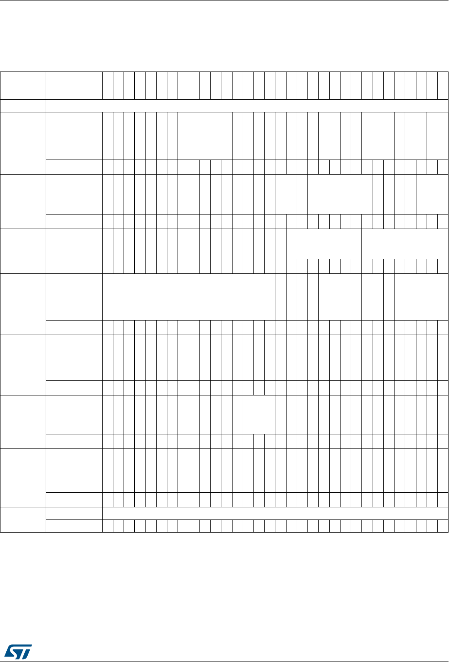
RM0394 Rev 4 1389/1600
RM0394 Serial audio interface (SAI)
1389
41.6.17 SAI register map
The following table summarizes the SAI registers.
Refer to Section 2.2 on page 66 for the register boundary addresses.
Table 221. SAI register map and reset values
Offset Register
name
31
30
29
28
27
26
25
24
23
22
21
20
19
18
17
16
15
14
13
12
11
10
9
8
7
6
5
4
3
2
1
0
0x0000 Reserved
0x0004
or
0x0024
SAI_xCR1
Res.
Res.
Res.
Res.
Res.
Res.
Res.
Res.
MCKDIV[3:0]
NODIV
Res.
DMAEN
SAIEN
Res.
Res.
OUTDRIV
MONO
SYNCEN[1:0]
CKSTR
LSBFIRST
DS[2:0]
Res.
PRTCFG[1:0]
MODE[1:0]
Reset value 00000 00 000000010 0000
0x0008 or
0x0028
SAI_xCR2
Res.
Res.
Res.
Res.
Res.
Res.
Res.
Res.
Res.
Res.
Res.
Res.
Res.
Res.
Res.
Res.
COMP[1:0]
CPL
MUTECN[5:0]
MUTE VAL
MUTE
TRIS
FFLUS
FTH[2:0]
Reset value 0000000000000000
0x000C or
0x002C
SAI_xFRCR
Res.
Res.
Res.
Res.
Res.
Res.
Res.
Res.
Res.
Res.
Res.
Res.
Res.
FSOFF
FSPOL
FSDEF
Res.
FSALL[6:0] FRL[7:0]
Reset value 000 000000000000111
0x0010 or
0x0030
SAI_xSLOTR SLOTEN[15:0]
Res.
Res.
Res.
Res.
NBSLOT[3:0]
SLOTSZ[1:0}
Res.
FBOFF[4:0]
Reset value 0000000000000000 000000 00000
0x0014 or
0x0034
SAI_xIM
Res.
Res.
Res.
Res.
Res.
Res.
Res.
Res.
Res.
Res.
Res.
Res.
Res.
Res.
Res.
Res.
Res.
Res.
Res.
Res.
Res.
Res.
Res.
Res.
Res.
LFSDETIE
AFSDETIE
CNRDYIE
FREQIE
WCKCFGIE
MUTEDETIE
OVRUDRIE
Reset value 0000000
0x0018 or
0x0038
SAI_xSR
Res.
Res.
Res.
Res.
Res.
Res.
Res.
Res.
Res.
Res.
Res.
Res.
Res.
FLVL[2:0]
Res.
Res.
Res.
Res.
Res.
Res.
Res.
Res.
Res.
LFSDET
AFSDET
CNRDY
FREQ
WCKCFG
MUTEDET
OVRUDR
Reset value 000 0000100
0x001C or
0x003C
SAI_xCLRFR
Res.
Res.
Res.
Res.
Res.
Res.
Res.
Res.
Res.
Res.
Res.
Res.
Res.
Res.
Res.
Res.
Res.
Res.
Res.
Res.
Res.
Res.
Res.
Res.
Res.
CLFSDET
CAFSDET
CCNRDY
Res.
CWCKCFG
CMUTEDET
COVRUDR
Reset value 000 000
0x0020 or
0x0040
SAI_xDR DATA[31:0]
Reset value 00000000000000000000000000000000
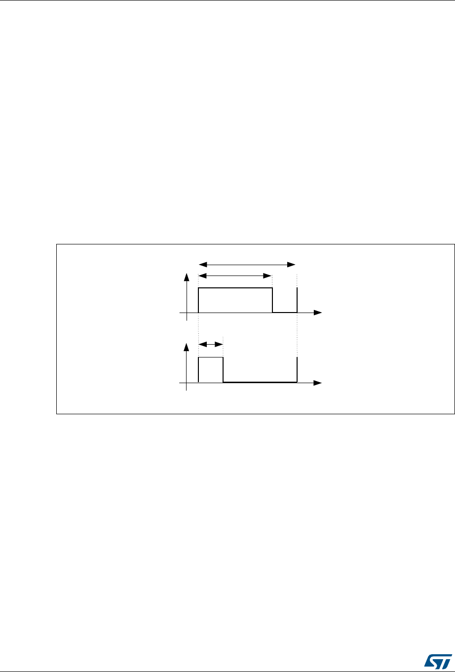
Single Wire Protocol Master Interface (SWPMI) RM0394
1390/1600 RM0394 Rev 4
42 Single Wire Protocol Master Interface (SWPMI)
This section applies to STM32L43xxx and STM32L44xxx devices only
42.1 Introduction
The Single Wire Protocol Master Interface (SWPMI) is the master interface corresponding to
the Contactless front-end (CLF) defined in the ETSI TS 102 613 technical specification.
The principle of the Single wire protocol (SWP) is based on the transmission of digital
information in full duplex mode:
•S1 signal (from Master to Slave) is transmitted by a digital modulation (L or H) in the
voltage domain (refer to Figure 450: S1 signal coding),
•S2 signal (from Slave to Master) is transmitted by a digital modulation (L or H) in the
current domain (refer to Figure 451: S2 signal coding).
Figure 450. S1 signal coding
069
/RJLFDO
7
7
W
9
9
7
/RJLFDODQGLGOHELW
W
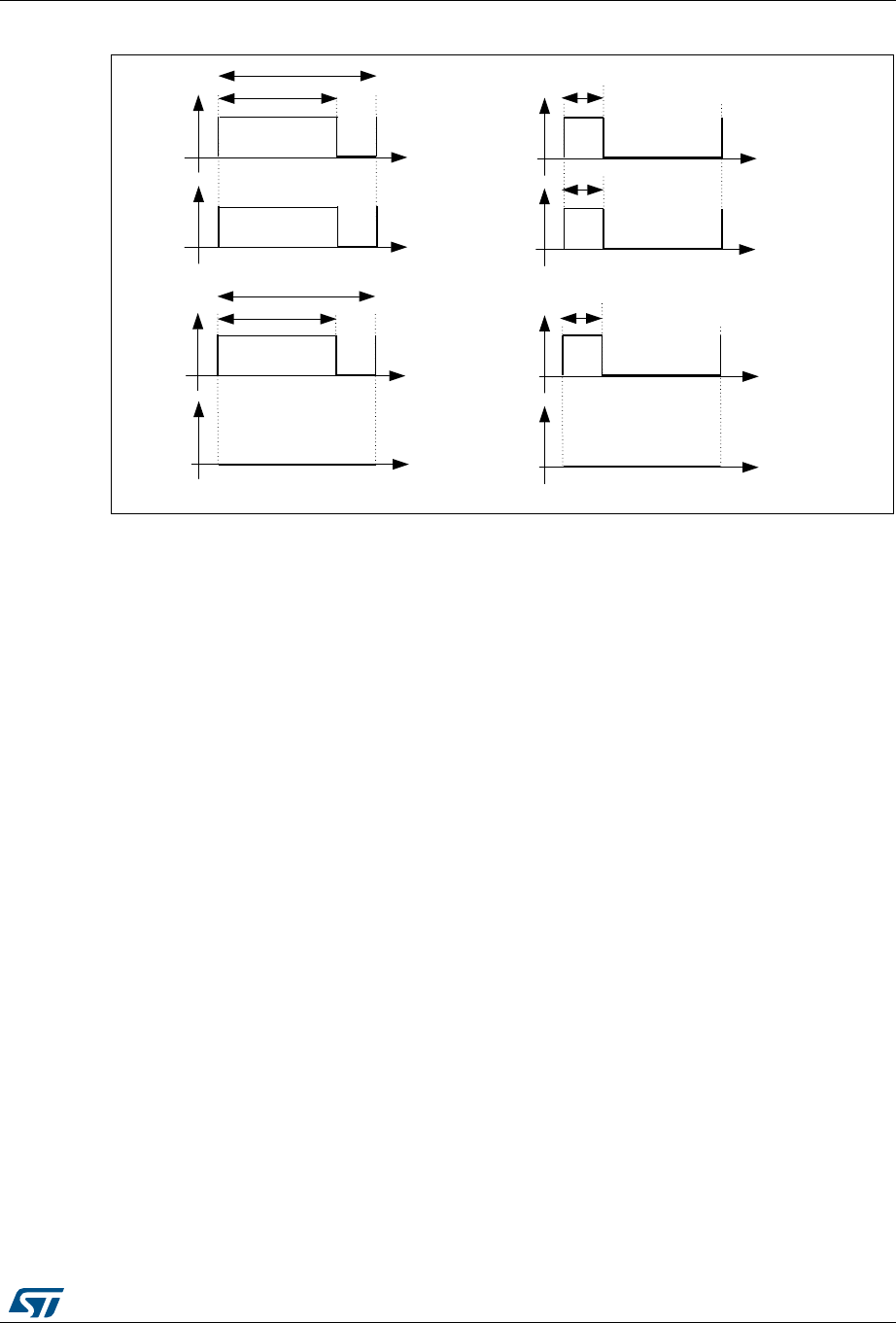
RM0394 Rev 4 1391/1600
RM0394 Single Wire Protocol Master Interface (SWPMI)
1416
Figure 451. S2 signal coding
42.2 SWPMI main features
The SWPMI module main features are the following (see Figure 42.3.3: SWP bus states):
•Full-duplex communication mode
•Automatic SWP bus state management
•Automatic handling of Start of frame (SOF)
•Automatic handling of End of frame (EOF)
•Automatic handling of stuffing bits
•Automatic CRC-16 calculation and generation in transmission
•Automatic CRC-16 calculation and checking in reception
•32-bit Transmit data register
•32-bit Receive data register
•Multi software buffer mode for efficient DMA implementation and multi frame buffering
•Configurable bit-rate up to 2 Mbit/s
•Configurable interrupts
•CRC error, underrun, overrun flags
•Frame reception and transmission complete flags
•Slave resume detection flag
•Loopback mode for test purpose
•Embedded SWPMI_IO transceiver compliant with ETSI TS 102 613 technical
specification
•Dedicated mode to output SWPMI_RX, SWPMI_TX and SWPMI_SUSPEND signals
on GPIOs, in case of external transceiver connection
D^ϯϯϯϰϯsϭ
ϯͬϰd ϭͬϰd
d
ƚ
ƚ
ss
>ŽŐŝĐĂůϭ
ƚ
/
>ŽŐŝĐĂůϭ
ϭͬϰd
ƚ
/
ϯͬϰd
d
ƚ
s
>ŽŐŝĐĂůϬ
ƚ
/
ϭͬϰd
ƚ
s
>ŽŐŝĐĂůϬ
/
^ϭ
^Ϯ
^ϭ
^Ϯ
^ϭ
^Ϯ
^ϭ
^Ϯ
ƚ
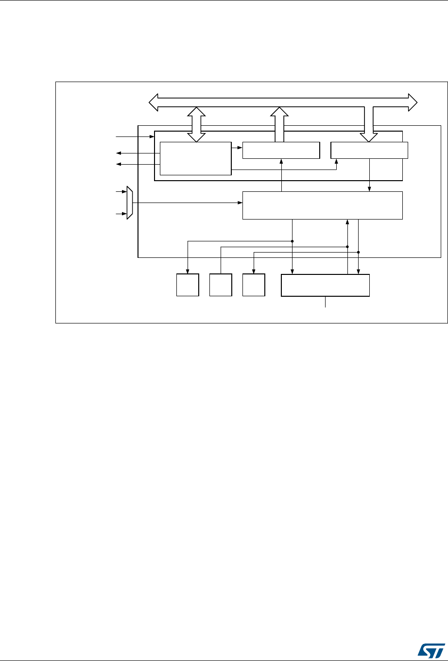
Single Wire Protocol Master Interface (SWPMI) RM0394
1392/1600 RM0394 Rev 4
42.3 SWPMI functional description
42.3.1 SWPMI block diagram
Figure 452. SWPMI block diagram
Refer to the bit SWPMI1SEL in Section 6.4.27: Peripherals independent clock configuration
register (RCC_CCIPR) to select the SWPCLK (SWPMI core clock source).
Note: In order to support the exit from Stop mode by a RESUME by slave, it is mandatory to select
HSI16 for SWPCLK. If this feature is not required, PCLK1 can be selected, and SWPMI
must be disabled before entering the Stop mode.
42.3.2 SWP initialization and activation
The initialization and activation will set the SWPMI_IO state from low to high.
For Class B, i.e. VDD is in the range [2.70 V to 3.30 V], the procedure is the following:
1. clear the SWP_CLASS bit in SWPMI_OR register,
2. configure SWPMI_IO as alternate function (refer to Section 8: General-purpose I/Os
(GPIO)) to enable the SWPMI_IO transceiver,
3. wait for tSWPSTART Max (refer to product datasheet),
4. set SWPACT bit in SWPMI_CR register to ACTIVATE the SWP i.e. to move from
DEACTIVATED to SUSPENDED.
For Class C, i.e. VDD is in the range [1.62 V to 1.98 V], the procedure is the following:
1. set the SWP_CLASS bit in SWPMI_OR register,
2. configure SWPMI_IO as alternate function (refer to Section 8: General-purpose I/Os
(GPIO)) to enable the SWPMI_IO transceiver,
3. set SWPACT bit in SWPMI_CR register to ACTIVATE the SWP i.e. to move from
DEACTIVATED to SUSPENDED.
069
6:30,FRUH
6:30,B,2
3&/.
6:3&/.
'0$UHTXHVWV
3&/.
+6,
&RQWURO6WDWXV
UHJLVWHUV
6:3EXV
6:30,
6:30,B7;6:30,B5;
,QWHUUXSW
6:30,B6863(1'
*3,2*3,2*3,2
ELW$3%EXV
6:30,B7'56:30,B5'5

RM0394 Rev 4 1393/1600
RM0394 Single Wire Protocol Master Interface (SWPMI)
1416
42.3.3 SWP bus states
The SWP bus can have the following states: DEACTIVATED, SUSPENDED, ACTIVATED.
Several transitions are possible:
•ACTIVATE: transition from DEACTIVATED to SUSPENDED state,
•SUSPEND: transition from ACTIVATED to SUSPENDED state,
•RESUME by master: transition from SUSPENDED to ACTIVATED state initiated by the
master,
•RESUME by slave: transition from SUSPENDED to ACTIVATED state initiated by the
slave,
•DEACTIVATE: transition from SUSPENDED to DEACTIVATED state.
ACTIVATE
During and just after reset, the SWPMI_IO is configured in analog mode. Refer to
Section 42.3.2: SWP initialization and activation to activate the SWP bus.
SUSPEND
The SWP bus stays in the ACTIVATED state as long as there is a communication with the
slave, either in transmission or in reception. The SWP bus switches back to the
SUSPENDED state as soon as there is no more transmission or reception activity, after 7
idle bits.
RESUME by master
Once the SWPMI is enabled, the user can request a SWPMI frame transmission. The
SWPMI first sends a transition sequence and 8 idle bits (RESUME by master) before
starting the frame transmission. The SWP moves from the SUSPENDED to ACTIVATED
state after the RESUME by master (refer to Figure 453: SWP bus states).
RESUME by slave
Once the SWPMI is enabled, the SWP can also move from the SUSPENDED to
ACTIVATED state if the SWPMI receives a RESUME from the slave. The RESUME by slave
sets the SRF flag in the SWPMI_ISR register.
DEACTIVATE
Deactivate request
If no more communication is required, and if SWP is in the SUSPENDED mode, the user
can request to switch the SWP to the DEACTIVATED mode by disabling the SWPMI
peripheral. The software must set DEACT bit in the SWPMI_CR register in order to request
the DEACTIVATED mode. If no RESUME by slave is detected by SWPMI, the DEACTF flag
is set in the SWPMI_ISR register and the SWPACT bit is cleared in the SWPMI_ICR
register. In case a RESUME by slave is detected by the SWPMI while the software is setting
DEACT bit, the SRF flag is set in the SWPMI_ISR register, DEACTF is kept cleared,
SWPACT is kept set and DEACT bit is cleared.
In order to activate SWP again, the software must clear DEACT bit in the SWPMI_CR
register before setting SWPACT bit.
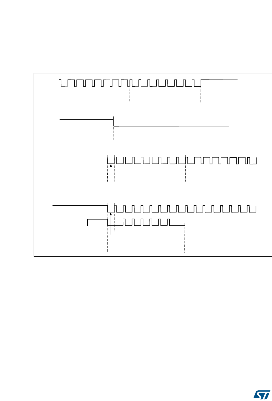
Single Wire Protocol Master Interface (SWPMI) RM0394
1394/1600 RM0394 Rev 4
Deactivate mode
In order to switch the SWP to the DEACTIVATED mode immediately, ignoring any possible
incoming RESUME by slave, the user must clear SWPACT bit in the SWPMI_CR register.
Note: In order to further reduce current consumption once SWPACT bit is cleared, configure the
SWPMI_IO port as output push pull low in GPIO controller (refer to Section 8: General-
purpose I/Os (GPIO)).
Figure 453. SWP bus states
42.3.4 SWPMI_IO (internal transceiver) bypass
A SWPMI_IO (transceiver), compliant with ETSI TS 102 613 technical specification, is
embedded in the microcontroller. Nevertheless, this is possible to bypass it by setting
SWP_TBYP bit in SWPMI_OR register. In this case, the SWPMI_IO is disabled and the
SWPMI_RX, SWPMI_TX and SWPMI_SUSPEND signals are available as alternate
functions on three GPIOs (refer to “Pinouts and pin description” in product datasheet). This
configuration is selected to connect an external transceiver.
42.3.5 SWPMI Bit rate
The bit rate must be set in the SWPMI_BRR register, according to the following formula:
FSWP = FSWPCLK / ((BR[5:0]+1)x4)
Note: The maximum bitrate is 2 Mbit/s.
069
6XVSHQGVHTXHQFHLGOHELWV$&7,9$7('PDVWHU(2) 6863(1'('
6863(1'(' '($&7,9$7('
$&7,9$7('PDVWHU62)5(680(E\PDVWHULGOHELWV6863(1'('
WUDQVLWLRQVHTXHQFH
6863(1'('
WUDQVLWLRQVHTXHQFH
6
6 5(680(
E\VODYH
$&7,9$7('VODYH62)
6
6
6

RM0394 Rev 4 1395/1600
RM0394 Single Wire Protocol Master Interface (SWPMI)
1416
42.3.6 SWPMI frame handling
The SWP frame is composed of a Start of frame (SOF), a Payload from 1 to 30 bytes, a 16-
bit CRC and an End of frame (EOF) (Refer to Figure 454: SWP frame structure).
Figure 454. SWP frame structure
The SWPMI embeds one 32-bit data register for transmission (SWPMI_TDR), and one 32-
bit data register for reception (SWPMI_RDR).
In transmission, the SOF insertion, the CRC calculation and insertion, and the EOF insertion
are managed automatically by the SWPMI. The user only has to provide the Payload
content and size. A frame transmission starts as soon as data is written into the
SWPMI_TDR register. Dedicated flags indicate an empty transmit data register and a
complete frame transmission event.
In reception, the SOF deletion, the CRC calculation and checking, and the EOF deletion are
managed automatically by the SWPMI. The user only has to read the Payload content and
size. Dedicated flags indicate a full receive data register, a complete frame reception and
possibly CRC error events.
The stuffing bits insertion (in transmission) and stuffing bits deletion (in reception) are
managed automatically by the SWPMI core. These operations are transparent for the user.
42.3.7 Transmission procedure
Before starting any frame transmission, the user must activate the SWP. Refer to
Section 42.3.2: SWP initialization and activation.
There are several possible software implementations for a frame transmission: No software
buffer mode, Single software buffer mode, and Multi software buffer mode.
The software buffer usage requires the use of a DMA channel to transfer data from the
software buffer in the RAM memory to the transmit data register in the SWPMI peripheral.
No software buffer mode
This mode does not require the use of DMA. The SWP frame transmission handling is done
by polling status flags in the main loop or inside the SWPMI interrupt routine. There is a 32-
bit transmit data register (SWPMI_TDR) in the SWPMI, thus writing to this register will
trigger the transmission of up to 4 bytes.
The No software buffer mode is selected by clearing TXDMA bit in the SWPMI_CR register.
The frame transmission is started by the first write to the SWPMI_TDR register. The low
significant byte of the first 32-bit word (bits [7:0]) written into the SWPMI_TDR register)
indicates the number of data bytes in the payload, and the 3 other bytes of this word must
069
62) (2)&5&E\WHV
3$</2$'XSWRE\WHV
62) (K E (2) )K E
' ' '
͘͘͘
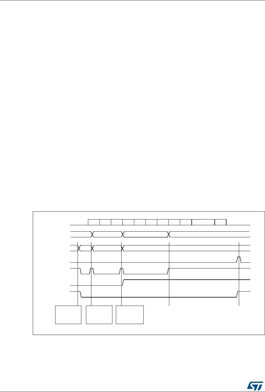
Single Wire Protocol Master Interface (SWPMI) RM0394
1396/1600 RM0394 Rev 4
contain the first 3 bytes of the payload (bits [15:8] contain the first byte of the payload, bits
[23:16] the second byte and bits [31:24] the third byte). Then, the following writes to the
SWPMI_TDR register will only contain the following payload data bytes, up to 4 for each
write.
Note: The low significant byte of the first 32-bit word written into the SWPMI_TDR register is
coding the number of data bytes in the payload. This number could be from 1 to 30. Any
other value in the low significant byte will be ignored and the transmission will not start.
Writing to the SWPMI_TDR register will induce the following actions:
•Send the transition sequence and 8 idle bits (RESUME by master) if the SWP bus state
is SUPENDED (this will not happen if the SWP bus state is already ACTIVATED),
•Send a Start of frame (SOF),
•Send the payload according to the SWPMI_TRD register content. If the number of
bytes in the payload is greater than 3, the SWPMI_TDR needs to be refilled by
software, each time the TXE flag in the SWPMI_ISR register is set, and as long as the
TXBEF flag is not set in the SWPMI_ISR register,
•Send the 16-bit CRC, automatically calculated by the SWPMI core,
•Send an End of frame (EOF).
The TXE flag is cleared automatically when the software is writing to the SWPMI_TDR
register.
Once the complete frame is sent, provided that no other frame transmission has been
requested (i.e. SWPMI_TDR has not been written again after the TXBEF flag setting), TCF
and SUSP flags are set in the SWPMI_ISR register 7 idle bits after the EOF transmission,
and an interrupt is generated if TCIE bit is set in the SWPMI_IER register (refer to
Figure 455: SWPMI No software buffer mode transmission).
Figure 455. SWPMI No software buffer mode transmission
If another frame transmission is requested before the end of the EOF transmission, the TCF
flag is not set and the frame will be consecutive to the previous one, with only one idle bit in
between (refer to Figure 456: SWPMI No software buffer mode transmission, consecutive
frames).
069
62) (2)&5&' ' ' ' ' ' ' '
6:3RXWSXW
7;(
6:30,B7'5
7;%()
VHWE\+:FOHDUHGE\6:RU'0$
'''' [[['
7&)
VHWE\+:FOHDUHGE\6:
''
'
VHWE\+:FOHDUHGE\6:
6863
6:ZULWHV'
''
LQ6:30,B7'5
6:ZULWHV
''''
LQ6:30,B7'5
6:ZULWHV
[[['
LQ6:30,B7'5
VHWE\+:
,QWHUQDOEXIIHU '''' [[['
'''
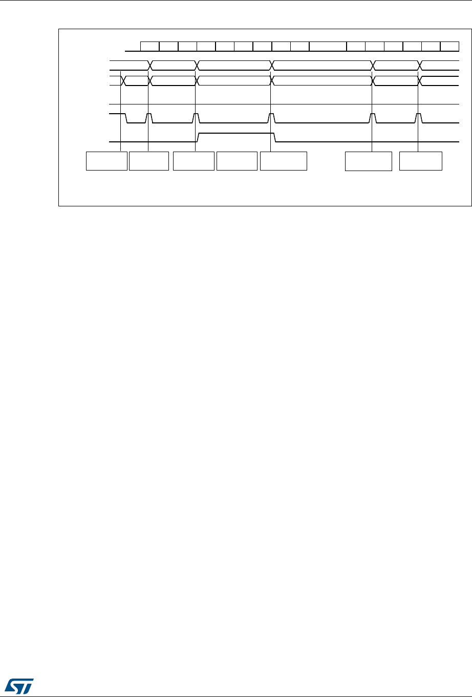
RM0394 Rev 4 1397/1600
RM0394 Single Wire Protocol Master Interface (SWPMI)
1416
Figure 456. SWPMI No software buffer mode transmission, consecutive frames
Single software buffer mode
This mode allows to transmit a complete SWP frame without a CPU intervention, using the
DMA. The DMA will refill the 32-bit SWPMI_TDR register, and the software can poll the end
of the frame transmission using the SWPMI_TXBEF flag.
The Single software buffer mode is selected by setting TXDMA bit and clearing TXMODE bit
in the SWPMI_CR register.
The DMA channel or stream must be configured in following mode (refer to DMA section):
•memory to memory mode disabled,
•memory increment mode enabled,
•memory size set to 32-bit,
•peripheral size set to 32-bit,
•peripheral increment mode disabled,
•circular mode disabled,
•data transfer direction set to read from memory.
•the number of words to be transfered must be set according to the SWP frame length,
•the source address is the SWP frame buffer in RAM,
•the destination address is the SWPMI_TDR register.
Then the user must:
1. Set TXDMA bit in the SWPMI_CR register,
2. Set TXBEIE bit in the SWPMI_IER register,
3. Fill the buffer in the RAM memory (with the number of data bytes in the payload on the
least significant byte of the first word),
4. Enable stream or channel in DMA module to start DMA transfer and frame
transmission.
A DMA request is issued by SWPMI when TXE flag in SWPMI_ISR is set. The TXE flag is
cleared automatically when the DMA is writing to the SWPMI_TDR register.
069
62) (2)&5&' ' ' ' ' ' ' '
6:3RXWSXW
7;(
6:30,B7'5
7;%()
VHWE\+:FOHDUHGE\6:RU'0$
''''
7&)
VHWE\+:FOHDUHGE\6:
''
'
' '62) ' '
6:ZULWHV
6:30,B7'5
6:ZULWHV
6:30,B7'5
'''
,QWHUQDOEXIIHU
6:ZULWHV
6:30,B7'5
6:ZULWHV
6:30,B7'5
6:ZULWHV
6:30,B7'5
6:ZULWHV
6:30,B7'5
''''
[[[' '''
''' ''''[[['
''''
6:ZULWHV
6:30,B7'5
''''

Single Wire Protocol Master Interface (SWPMI) RM0394
1398/1600 RM0394 Rev 4
In the SWPMI interrupt routine, the user must check TXBEF bit in the SWPMI_ISR register.
If it is set, and if another frame needs to be transmitted, the user must:
1. Disable stream or channel in DMA module
2. Update the buffer in the RAM memory with the content of the next frame to be sent
3. Configure the total number of words to be transferred in DMA module
4. Enable stream or channel in DMA module to start next frame transmission
5. Set CTXBEF bit in the SWPMI_ICR register to clear the TXBEF flag
Multi software buffer mode
This mode allows to work with several frame buffers in the RAM memory, in order to ensure
a continuous transmission, keeping a very low CPU load, and allowing more latency for
buffer update by software thanks to the DMA. The software can check the DMA counters at
any time and update SWP frames accordingly in the RAM memory.
The Multi software buffer mode must be used in combination with DMA in circular mode.
Each transmission buffer in the RAM memory must have a fixed length of eight 32-bit words,
whatever the number of bytes in the SWP frame payload. The transmission buffers in the
RAM memory must be filled by the software, keeping an offset of 8 between two
consecutive ones. The first data byte of the buffer is the number of bytes of the frame
payload. See the buffer example in Figure 457: SWPMI Multi software buffer mode
transmission
The Multi software buffer mode is selected by setting both TXDMA and TXMODE bits in
SWPMI_CR register.
For example, in order to work with 4 transmission buffers, the user must configure the DMA
as follows:
The DMA channel or stream must be configured in following mode (refer to DMA section):
•memory to memory mode disabled,
•memory increment mode enabled,
•memory size set to 32-bit,
•peripheral size set to 32-bit,
•peripheral increment mode disabled,
•circular mode enabled,
•data transfer direction set to read from memory,
•the number of words to be transfered must be set to 32 (8 words per buffer),
•the source address is the buffer1 in RAM,
•the destination address is the SWPMI_TDR register.
Then, the user must:
1. Set TXDMA in the SWPMI_CR register
2. Set TXBEIE in the SWPMI_IER register
3. Fill buffer1, buffer2, buffer3 and buffer4 in the RAM memory (with the number of data
bytes in the payload on the least significant byte of the first word)
4. Enable stream or channel in DMA module to start DMA.
RM0394 Rev 4 1399/1600
RM0394 Single Wire Protocol Master Interface (SWPMI)
1416
In the SWPMI interrupt routine, the user must check TXBEF bit in the SWPMI_ISR register.
If it is set, the user must set CTXBEF bit in SWPMI_ICR register to clear TXBEF flag and the
user can update buffer1 in the RAM memory.
In the next SWPMI interrupt routine occurrence, the user will update buffer2, and so on.
The Software can also read the DMA counter (number of data to transfer) in the DMA
registers in order to retrieve the frame which has already been transferred from the RAM
memory and transmitted. For example, if the software works with 4 transmission buffers,
and if the DMA counter equals 17, it means that two buffers are ready for updating in the
RAM area. This is useful in case several frames are sent before the software can handle the
SWPMI interrupt. If this happens, the software will have to update several buffers.
When there are no more frames to transmit, the user must disable the circular mode in the
DMA module. The transmission will stop at the end of the buffer4 transmission.
If the transmission needs to stop before (for example at the end of buffer2), the user must
set the low significant byte of the first word to 0 in buffer3 and buffer4.
TXDMA bit in the SWPMI_CR register will be cleared by hardware as soon as the number of
data bytes in the payload is read as 0 in the least significant byte of the first word.
Figure 457. SWPMI Multi software buffer mode transmission
069
5$0
' ' ' '
' ' ' '
' ' '
' ' ' 7)/
' ' ' '
' ' ' 7)/
' ' ' '
' ' ' '
' ' ' '
' ' ' '
' ' ' '
' ' ' '
' ' '
'
' ' ' 7)/
' ' ' '
' ' ' 7)/
' ' ' '
' ' ' '
' ' ' '
' ' '
'
'
)UDPH7)/
)UDPH7)/
)UDPH7)/
)UDPH7)/
'0$B&0$5
ELWZRUG

Single Wire Protocol Master Interface (SWPMI) RM0394
1400/1600 RM0394 Rev 4
42.3.8 Reception procedure
Before starting any frame reception, the user must activate the SWP (refer to
Section 42.3.2: SWP initialization and activation.
Once SWPACT bit is set in the SWPMI_CR register, a RESUME from slave state sets the
SRF flag in the SWPMI_ISR register and automatically enables the SWPMI for the frame
reception.
If the SWP bus is already in the ACTIVATED state (for example because a frame
transmission is ongoing), the SWPMI core does not need any RESUME by slave state, and
the reception can take place immediately.
There are several possible software implementations for a frame reception:
•No software buffer mode,
•Single software buffer mode,
•Multi software buffer mode.
The software buffer usage requires the use of a DMA channel to transfer data from the
receive data register in the SWPMI peripheral to the software buffer in the RAM memory.
No software buffer mode
This mode does not require the use of DMA. The SWP frame reception handling is done by
polling status flags in the main loop or inside the SWPMI interrupt routine. There is a 32-bit
receive data register (SWPMI_RDR) in the SWPMI, allowing to receive up to 4 bytes before
reading this register.
The No software buffer mode is selected by resetting RXDMA bit in the SWPMI_CR
register.
Once a Start of frame (SOF) is received, the following bytes (payload) are stored in the
SWPMI_RDR register. Once the SWPMI_RDR is full, the RXNE flag is set in SWPMI_ISR
and an interrupt is generated if RIE bit is set in SWPMI_IER register. The user can read the
SWPMI_RDR register and the RXNE flag is cleared automatically when the software is
reading the SWPMI_RDR register.
Once the complete frame has been received, including the CRC and the End of frame
(EOF), both RXNE and RXBFF flags are set in the SWPMI_ISR register. The user must
read the last byte(s) of the payload in the SWPMI_RDR register and set CRXBFF flag in
SWPMI_ICR in order to clear the RXBFF flag. The number of data bytes in the payload is
available in the SWPMI_RFL register. Again, the RXNE flag is reset automatically when the
software is reading the SWPMI_RDR register (refer to Figure 458: SWPMI No software
buffer mode reception).
Reading the SWPMI_RDR register while RXNE is cleared will return 0.
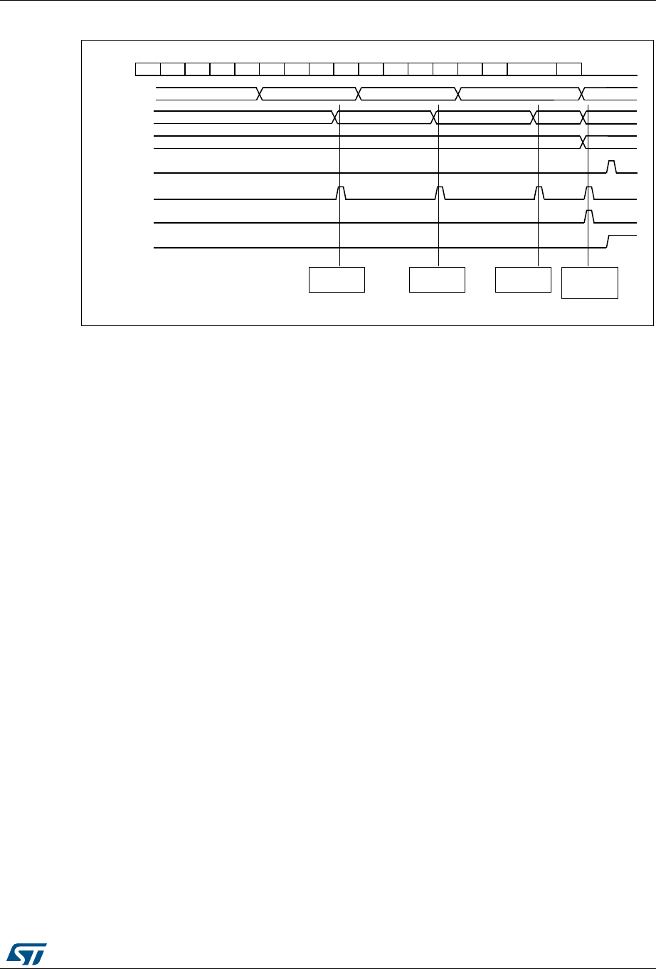
RM0394 Rev 4 1401/1600
RM0394 Single Wire Protocol Master Interface (SWPMI)
1416
Figure 458. SWPMI No software buffer mode reception
Single software buffer mode
This mode allows to receive a complete SWP frame without any CPU intervention using the
DMA. The DMA transfers received data from the 32-bit SWPMI_RDR register to the RAM
memory, and the software can poll the end of the frame reception using the SWPMI_RBFF
flag.
The Single software buffer mode is selected by setting RXDMA bit and clearing RXMODE
bit in the SWPMI_CR register.
The DMA must be configured as follows:
The DMA channel or stream must be configured in following mode (refer to DMA section):
•memory to memory mode disabled,
•memory increment mode enabled,
•memory size set to 32-bit,
•peripheral size set to 32-bit,
•peripheral increment mode disabled,
•circular mode disabled,
•data transfer direction set to read from peripheral,
•the number of words to be transfered must be set to 8,
•the source address is the SWPMI_RDR register,
•the destination address is the SWP frame buffer in RAM.
Then the user must:
1. Set RXDMA bit in the SWPMI_CR register
2. Set RXBFIE bit in the SWPMI_IER register
3. Enable stream or channel in DMA module.
A DMA request is issued by SWPMI when RXNE flag is set in SWPMI_ISR. The RXNE flag
is cleared automatically when the DMA is reading the SWPMI_RDR register.
In the SWPMI interrupt routine, the user must check RXBFF bit in the SWPMI_ISR register.
If it is set, the user must:
069
62) (2)&5&' ' ' ' ' ' ' ' ' ' ' ' '
6:3
LQSXW
5;1(
6:30,B5'5
5;%))
VHWE\+:FOHDUHGE\6:RU'0$
'''' '''' ''
''
[[''
[[[[
džG
6:30,B5)/
'
VHWE\+:FOHDUHGE\6:
6863(1'
6:UHDGV
6:30,B5'5
7&) VHWE\+:FOHDUHGE\6:
6:UHDGV
6:30,B5'5
6:UHDGV
6:30,B5'5
6:UHDGV
6:30,B5'5
DQG6:,B5)/
VHWE\+:
,QWHUQDOEXIIHU '''' '''' ''''
[[[[ [[''
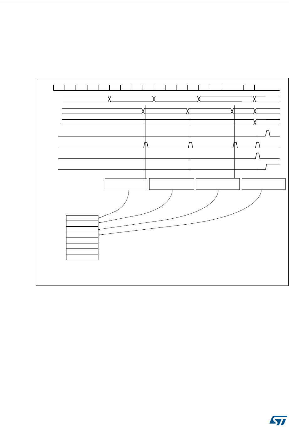
Single Wire Protocol Master Interface (SWPMI) RM0394
1402/1600 RM0394 Rev 4
1. Disable stream or channel in DMA module
2. Read the number of bytes in the received frame payload in the SWPMI_RFL register
3. Read the frame payload in the RAM buffer
4. Enable stream or channel in DMA module
5. Set CRXBFF bit in the SWPMI_ICR register to clear RXBFF flag (refer to Figure 459:
SWPMI single software buffer mode reception).
Figure 459. SWPMI single software buffer mode reception
Multi software buffer mode
This mode allows to work with several frame buffers in the RAM memory, in order to ensure
a continuous reception, keeping a very low CPU load, using the DMA. The frame payloads
are stored in the RAM memory, together with the frame status flags. The software can check
the DMA counters and status flags at any time to handle the received SWP frames in the
RAM memory.
The Multi software buffer mode must be used in combination with the DMA in circular mode.
The Multi software buffer mode is selected by setting both RXDMA and RXMODE bits in
SWPMI_CR register.
D^ϯϯϯϱϭsϭ
^K& K&ZϬ ϭ Ϯ ϯ ϰ ϱ ϲ ϳ ϴ ϵ ϭϬ ϭϭ ϭϮ
^tW
ŝŶƉƵƚ
ZyE
^tWD/ͺZZ
Zy&&
ƐĞƚďLJ,t͕ĐůĞĂƌĞĚďLJD
ϯͲϮͲϭͲϬ ϳͲϲͲϱͲϰ ϭϭͲϭϬͲϵͲ
ϴ
džͲdžͲϭϯͲϭϮ
džͲdžͲdžͲdž
dž ϭϰĚ
^tWD/ͺZ&>
ϭϯ
ƐĞƚďLJ,t͕ĐůĞĂƌĞĚďLJ^t
^h^WE
DƚƌĂŶƐĨĞƌƐĚĂƚĂĨƌŽŵ
^tWD/ͺZZƚŽZD
d&
ƐĞƚďLJ,t͕ĐůĞĂƌĞĚďLJ^t
ƐĞƚďLJ,t
ϯͲϮͲϭͲϬ
ϳͲϲͲϱͲϰ
ϭϭͲϭϬͲϵͲϴ
DƚƌĂŶƐĨĞƌƐĚĂƚĂĨƌŽŵ
^tWD/ͺZZƚŽZD
DƚƌĂŶƐĨĞƌƐĚĂƚĂĨƌŽŵ
^tWD/ͺZZƚŽZD
DƚƌĂŶƐĨĞƌƐĚĂƚĂĨƌŽŵ
^tWD/ͺZZƚŽZD
džͲdžͲϭϯͲϭϮ
ZD
/ŶƚĞƌŶĂůďƵĨĨĞƌ ϯͲϮͲϭͲϬ ϳͲϲͲϱͲϰ ϭϭͲϭϬͲϵͲϴ
džͲdžͲdžͲdž džͲdžͲϭϯͲϭϮ

RM0394 Rev 4 1403/1600
RM0394 Single Wire Protocol Master Interface (SWPMI)
1416
In order to work with n reception buffers in RAM, the DMA channel or stream must be
configured in following mode (refer to DMA section):
•memory to memory mode disabled,
•memory increment mode enabled,
•memory size set to 32-bit,
•peripheral size set to 32-bit,
•peripheral increment mode disabled,
•circular mode enabled,
•data transfer direction set to read from peripheral,
•the number of words to be transfered must be set to 8 x n (8 words per buffer),
•the source address is the SWPMI_TDR register,
•the destination address is the buffer1 address in RAM
Then the user must:
1. Set RXDMA in the SWPMI_CR register
2. Set RXBFIE in the SWPMI_IER register
3. Enable stream or channel in the DMA module.
In the SWPMI interrupt routine, the user must check RXBFF in the SWPMI_ISR register. If it
is set, the user must set CRXBFF bit in the SWPMI_ICR register to clear RXBFF flag and
the user can read the first frame payload received in the first buffer (at the RAM address set
in DMA2_CMAR1).
The number of data bytes in the payload is available in bits [23:16] of the last 8th word.
In the next SWPMI interrupt routine occurrence, the user will read the second frame
received in the second buffer (address set in DMA2_CMAR1 + 8), and so on (refer to
Figure 460: SWPMI Multi software buffer mode reception).
In case the application software cannot ensure to handle the SMPMI interrupt before the
next frame reception, each buffer status is available in the most significant byte of the 8th
buffer word:
•The CRC error flag (equivalent to RXBERF flag in the SWPMI_ISR register) is
available in bit 24 of the 8th word. Refer to Section 42.3.9: Error management for an
CRC error description.
•The receive overrun flag (equivalent to RXOVRF flag in the SWPMI_ISR register) is
available in bit 25 of the 8th word. Refer to Section 42.3.9: Error management for an
overrun error description.
•The receive buffer full flag (equivalent to RXBFF flag in the SWPMI_ISR register) is
available in bit 26 of the 8th word.
In case of a CRC error, both RXBFF and RXBERF flags are set, thus bit 24 and bit 26 are
set.
In case of an overrun, an overrun flag is set, thus bit 25 is set. The receive buffer full flag is
set only in case of an overrun during the last word reception; then, both bit 25 and bit 26 are
set for the current and the next frame reception.
The software can also read the DMA counter (number of data to transfer) in the DMA
registers in order to retrieve the frame which has already been received and transferred into
the RAM memory through DMA. For example, if the software works with 4 reception buffers,
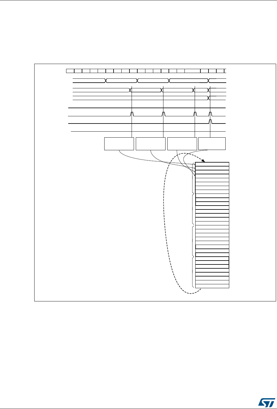
Single Wire Protocol Master Interface (SWPMI) RM0394
1404/1600 RM0394 Rev 4
and if the DMA counter equals 17, it means that two buffers are ready for reading in the
RAM area.
In Multi software buffer reception mode, if the software is reading bits 24, 25 and 26 of the
8th word, it does not need to clear RXBERF, RXOVRF and RXBFF flags after each frame
reception.
Figure 460. SWPMI Multi software buffer mode reception
42.3.9 Error management
Underrun during payload transmission
During the transmission of the frame payload, a transmit underrun is indicated by the
TXUNRF flag in the SWPMI_ISR register. An interrupt is generated if TXBUNREIE bit is set
in the SWPMI_IER register.
If a transmit underrun occurs, the SWPMI stops the payload transmission and sends a
corrupted CRC (the first bit of the first CRC byte sent is inverted), followed by an EOF. If
DMA is used, TXDMA bit in the SWPMI_CR register is automatically cleared.
D^ϯϯϯϱϮsϭ
^K& K&ZϬ ϭ Ϯ ϯ ϰ ϱ ϲ ϳ ϴ ϵ ϭϬ ϭϭ ϭϮ
^tW
ŝŶƉƵƚ
ZyE
^tWD/ͺZZ
Zy&&
ƐĞƚďLJ,t͕ĐůĞĂƌĞĚďLJD
ϯͲϮͲϭͲϬ ϳͲϲͲϱͲϰ
ϭϭͲϭϬͲ
ϵͲϴ
džͲdžͲϭϯͲϭϮdžͲdžͲdžͲdž
dž ϭϰĚ
^tWD/ͺZ&>
ϭϯ
ƐĞƚďLJ,t͕ĐůĞĂƌĞĚďLJ^t
^h^WE
DƚƌĂŶƐĨĞƌƐĚĂƚĂ
ĨƌŽŵ^tWD/ͺZZ
ƚŽZD
d&
ƐĞƚďLJ,t
ϯͲϮͲϭͲϬ
ϳͲϲͲϱͲϰ
ϭϭͲϭϬͲϵͲϴ
DƚƌĂŶƐĨĞƌƐĚĂƚĂ
ĨƌŽŵ^tWD/ͺZZƚŽ
ZD
DƚƌĂŶƐĨĞƌƐĚĂƚĂ
ĨƌŽŵ^tWD/ͺZZ
ƚŽZD
DƚƌĂŶƐĨĞƌƐĚĂƚĂ
ĨƌŽŵ^tWD/ͺZZƚŽ
ZD
džͲdžͲϭϯͲϭϮ
ϯͲϮͲϭͲϬ
ϳͲϲͲϱͲϰ
&ƌĂŵĞϮ
džͲdžͲdžͲdž
džͲdžͲdžͲdž
džͲdžͲdžͲdž
džͲϭϰͲdžͲdž
džͲdžͲdžͲdž
džͲdžͲdžͲdž
džͲdžͲdžͲdž
džͲϴͲdžͲdž
džͲdžͲdžͲdž
džͲdžͲdžͲdž
&ƌĂŵĞϭ
ϯͲϮͲϭͲϬ
ϳͲϲͲϱͲϰ
ϭϭͲϭϬͲϵͲϴ
ϭϱͲϭϰͲϭϯͲϭϮ
ϯͲϮͲϭͲϬ
ϳͲϲͲϱͲϰ
&ƌĂŵĞϰ
džͲdžͲdžͲϮϬ
džͲdžͲdžͲdž
džͲϮϭͲdžͲdž
džͲϮϵͲdžͲϮϴ
&ƌĂŵĞϯ ϭϵͲϭϴͲϭϳͲϭϲ
ϭϭͲϭϬͲϵͲϴ
ϭϱͲϭϰͲϭϯͲϭϮ
ϭϵͲϭϴͲϭϳͲϭϲ
ϮϯͲϮϮͲϮϭͲϮϬ
ϮϳͲϮϲͲϮϱͲϮϰ
^K& Ϭ
ZD
^tWD/ͺZZ ϯͲϮͲϭͲϬ ϳͲϲͲϱͲϰ ϭϭͲϭϬͲϵͲϴ džͲdžͲϭϯͲϭϮdžͲdžͲdžͲdž
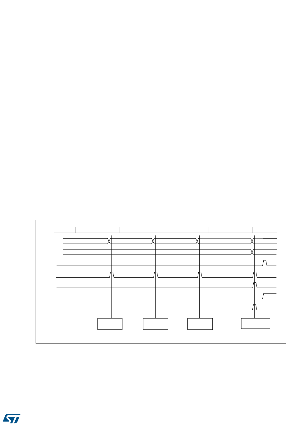
RM0394 Rev 4 1405/1600
RM0394 Single Wire Protocol Master Interface (SWPMI)
1416
Any further write to the SWPMI_TDR register while TXUNRF is set will be ignored. The user
must set CTXUNRF bit in the SWPMI_ICR register to clear TXUNRF flag.
Overrun during payload reception
During the reception of the frame payload, a receive overrun is indicated by RXOVRF flag in
the SWPMI_ISR register. If a receive overrun occurs, the SWPMI does not update
SWPMI_RDR with the incoming data. The incoming data will be lost.
The reception carries on up to the EOF and, if the overrun condition disappears, the RXBFF
flag is set. When RXBFF flag is set, the user can check the RXOVRF flag. The user must
set CRXOVRF bit in the SWPMI_ICR register to clear RXBOVRF flag.
If the user wants to detect the overrun immediately, RXBOVREIE bit in the SWPMI_IER
register can be set in order to generate an interrupt as soon as the overrun occurs.
The RXOVRF flag is set at the same time as the RXNE flag, two SWPMI_RDR reads after
the overrun event occurred. It indicates that at least one received byte was lost, and the
loaded word in SWPMI_RDR contains the bytes received just before the overrun.
In Multi software buffer mode, if RXOVRF flag is set for the last word of the received frame,
then the overrun bit (bit 25 of the 8th word) is set for both the current and the next frame.
CRC error during payload reception
Once the two CRC bytes have been received, if the CRC is wrong, the RXBERF flag in the
SWPMI_ISR register is set after the EOF reception. An interrupt is generated if RXBEIE bit
in the SWPMI_IER register is set (refer toFigure 461: SWPMI single buffer mode reception
with CRC error).The user must set CRXBERF bit in SWPMI_ICR to clear RXBERF flag.
Figure 461. SWPMI single buffer mode reception with CRC error
Missing or corrupted stuffing bit during payload reception
When a stuffing bit is missing or is corrupted in the payload, RXBERF and RXBFF flags are
set in SWPMI_ISR after the EOF reception.
069
^K& K&ZϬ ϭ Ϯ ϯ ϰ ϱ ϲ ϳ ϴ ϵ ϭϬ ϭϭ ϭϮ
^tW
ŝŶƉƵƚ
ZyE
^tWD/ͺZZ
Zy&&
ϯͲϮͲϭͲϬ ϳͲϲͲϱͲϰ ϭϭͲϭϬͲϵͲϴ džͲdžͲϭϯͲϭϮ
džͲdžͲdžͲdž
dž ϭϰĚ
^tWD/ͺZ&>
ϭϯ
^h^WE
^tƌĞĂĚƐ
^tWD/ͺZZ
d&
^tĚĞƚĞĐƚƐĞƌƌŽƌ
ǁŝƚŚZyZ&ĨůĂŐ
ZyZ&
^tƌĞĂĚƐ
^tWD/ͺZZ
^tƌĞĂĚƐ
^tWD/ͺZZ
VHWE\+:FOHDUHGE\6:
VHWE\+:
VHWE\+:FOHDUHGE\6:
VHWE\+:FOHDUHGE\6:RU'0$
VHWE\+:FOHDUHGE\6:

Single Wire Protocol Master Interface (SWPMI) RM0394
1406/1600 RM0394 Rev 4
Corrupted EOF reception
Once an SOF has been received, the SWPMI accumulates the received bytes until the
reception of an EOF (ignoring any possible SOF). Once an EOF has been received, the
SWPMI is ready to start a new frame reception and waits for an SOF.
In case of a corrupted EOF, RXBERF and RXBFF flags will bet set in the SWPMI_ISR
register after the next EOF reception.
Note: In case of a corrupted EOF reception, the payload reception carries on, thus the number of
bytes in the payload might get the value 31 if the number of received bytes is greater than
30. The number of bytes in the payload is read in the SWPMI_RFL register or in bits [23:16]
of the 8th word of the buffer in the RAM memory, depending on the operating mode.
42.3.10 Loopback mode
The loopback mode can be used for test purposes. The user must set LPBK bit in the
SWPMI_CR register in order to enable the loopback mode.
When the loopback mode is enabled, SWPMI_TX and SWPMI_RX signals are connected
together. As a consequence, all frames sent by the SWPMI will be received back.
42.4 SWPMI low-power modes
Table 222. Effect of low-power modes on SWPMI
Mode Description
Sleep No effect. SWPMI interrupts cause the device to exit the Sleep mode.
Low-power run No effect.
Low-power sleep No effect. SWPMI interrupts cause the device to exit the Low-power sleep
mode.
Stop 0 / Stop 1
SWPMI registers content is kept. A RESUME from SUSPENDED mode issued
by the slave can wake up the device from Stop 0 and Stop 1 modes if the
SWPCLK is HSI16 (refer to Section 42.3.1: SWPMI block diagram).
Stop 2 SWPMI registers content is kept. SWPMI must be disabled before entering
Stop 2.
Standby The SWPMI peripheral is powered down and must be reinitialized after exiting
Standby or Shutdown mode.
Shutdown

RM0394 Rev 4 1407/1600
RM0394 Single Wire Protocol Master Interface (SWPMI)
1416
42.5 SWPMI interrupts
All SWPMI interrupts are connected to the NVIC.
To enable the SWPMI interrupt, the following sequence is required:
1. Configure and enable the SWPMI interrupt channel in the NVIC
2. Configure the SWPMI to generate SWPMI interrupts (refer to the SWPMI_IER
register).
Table 223. Interrupt control bits
Interrupt event Event flag Enable
control bit
Exit the
Sleep
mode
Exit the
Stop
mode
Exit the
Standby
mode
Receive buffer full RXBFF RXBFIE yes no no
Transmit buffer empty TXBEF TXBEIE yes no no
Receive buffer error (CRC error) RXBERF RXBEIE yes no no
Receive buffer overrun RXOVRF RXBOVEREIE yes no no
Transmit buffer underrun TXUNRF TXBUNREIE yes no no
Receive data register not empty RXNE RIE yes no no
Transmit data register full TXE TIE yes no no
Transfer complete flag TCF TCIE yes no no
Slave resume flag SRF SRIE yes yes (1)
1. If HSI16 is selected for SWPCLK.
no

Single Wire Protocol Master Interface (SWPMI) RM0394
1408/1600 RM0394 Rev 4
42.6 SWPMI registers
Refer to Section 1.2 of the reference manual for a list of abbreviations used in register
descriptions.
The peripheral registers can be accessed by words (32-bit).
42.6.1 SWPMI Configuration/Control register (SWPMI_CR)
Address offset: 0x00
Reset value: 0x0000 0000
31 30 29 28 27 26 25 24 23 22 21 20 19 18 17 16
Res. Res. Res. Res. Res. Res. Res. Res. Res. Res. Res. Res. Res. Res. Res. Res.
1514131211109876543210
Res. Res. Res. Res. Res. DEACT Res. Res. Res. Res. SWP
ACT LPBK TXMOD
E
RXMO
DE TXDMA RXDMA
rw rw rw rw rw rw rw
Bits 31:11 Reserved, must be kept at reset value.
Bit 10 DEACT: Single wire protocol master interface deactivate
This bit is used to request the SWP DEACTIVATED state. Setting this bit has the same effect
as clearing the SWPACT, except that a possible incoming RESUME by slave will keep the
SWP in the ACTIVATED state.
Bits 9:6 Reserved, must be kept at reset value.
Bit 5 SWPACT: Single wire protocol master interface activate
This bit is used to activate the SWP bus (refer to Section 42.3.2: SWP initialization and
activation).
0: SWPMI_IO is pulled down to ground, SWP bus is switched to DEACTIVATED state
1: SWPMI_IO is released, SWP bus is switched to SUSPENDED state
To be able to set SWPACT bit, DEACT bit must be have been cleared previously.
Bit 4 LPBK: Loopback mode enable
This bit is used to enable the loopback mode
0: Loopback mode is disabled
1: Loopback mode is enabled
Note: This bit cannot be written while SWPACT bit is set.
Bit 3 TXMODE: Transmission buffering mode
This bit is used to choose the transmission buffering mode. This bit is relevant only when
TXDMA bit is set (refer to Table 224: Buffer modes selection for transmission/reception).
0: SWPMI is configured in Single software buffer mode for transmission
1: SWPMI is configured in Multi software buffer mode for transmission.
Note: This bit cannot be written while SWPACT bit is set.
RM0394 Rev 4 1409/1600
RM0394 Single Wire Protocol Master Interface (SWPMI)
1416
42.6.2 SWPMI Bitrate register (SWPMI_BRR)
Address offset: 0x04
Reset value: 0x0000 0001
Bit 2 RXMODE: Reception buffering mode
This bit is used to choose the reception buffering mode. This bit is relevant only when
TXDMA bit is set (refer to Table 224: Buffer modes selection for transmission/reception).
0: SWPMI is configured in Single software buffer mode for reception
1: SWPMI is configured in Multi software buffer mode for reception.
Note: This bit cannot be written while SWPACT bit is set.
Bit 1 TXDMA: Transmission DMA enable
This bit is used to enable the DMA mode in transmission
0: DMA is disabled for transmission
1: DMA is enabled for transmission
Note: TXDMA is automatically cleared if the payload size of the transmitted frame is given as
0x00 (in the least significant byte of TDR for the first word of a frame). TXDMA is also
automatically cleared on underrun events (when TXUNRF flag is set in the SWP_ISR
register)
Bit 0 RXDMA: Reception DMA enable
This bit is used to enable the DMA mode in reception
0: DMA is disabled for reception
1: DMA is enabled for reception
Table 224. Buffer modes selection for transmission/reception
Buffer mode No software buffer Single software buffer Multi software buffer
RXMODE/TXMODE x 0 1
RXDMA/TXDMA 0 1 1
31 30 29 28 27 26 25 24 23 22 21 20 19 18 17 16
Res. Res. Res. Res. Res. Res. Res. Res. Res. Res. Res. Res. Res. Res. Res. Res.
1514131211109876543210
Res. Res. Res. Res. Res. Res. Res. Res. Res. Res. BR[5:0]
rw rw rw rw rw rw
Bits 31:6 Reserved, must be kept at reset value.
Bits 5:0 BR[5:0]: Bitrate prescaler
This field must be programmed to set SWP bus bitrate, taking into account the FSWPCLK
programmed in the RCC (Reset and Clock Control), according to the following formula:
FSWP= FSWPCLK / ((BR[5:0]+1)x4)
Note: The programmed bitrate must stay within the following range: from 100 kbit/s up to
2Mbit/s.
BR[5:0] cannot be written while SWPACT bit is set in the SWPMI_CR register.

Single Wire Protocol Master Interface (SWPMI) RM0394
1410/1600 RM0394 Rev 4
42.6.3 SWPMI Interrupt and Status register (SWPMI_ISR)
Address offset: 0x0C
Reset value: 0x0000 02C2
31 30 29 28 27 26 25 24 23 22 21 20 19 18 17 16
Res. Res. Res. Res. Res. Res. Res. Res. Res. Res. Res. Res. Res. Res. Res. Res.
1514131211109876543210
Res. Res. Res. Res. Res. DEACT
FSUSP SRF TCF TXE RXNE TXUNR
F
RXOVR
F
RXBER
FTXBEF RXBFF
rrrrrrrrrrr
Bits 31:11 Reserved, must be kept at reset value.
Bit 10 DEACTF: DEACTIVATED flag
This bit is a status flag, acknowledging the request to enter the DEACTIVATED mode.
0: SWP bus is in ACTIVATED or SUSPENDED state
1: SWP bus is in DEACTIVATED state
If a RESUME by slave state is detected by the SWPMI while DEACT bit is set by software,
the SRF flag will be set, DEACTF will not be set and SWP will move in ACTIVATED state.
Bit 9 SUSP: SUSPEND flag
This bit is a status flag, reporting the SWP bus state
0: SWP bus is in ACTIVATED state
1: SWP bus is in SUSPENDED or DEACTIVATED state
Bit 8 SRF: Slave resume flag
This bit is set by hardware to indicate a RESUME by slave detection. It is cleared by
software, writing 1 to CSRF bit in the SWPMI_ICR register.
0: No Resume by slave state detected
1: A Resume by slave state has been detected during the SWP bus SUSPENDED state
Bit 7 TCF: Transfer complete flag
This flag is set by hardware as soon as both transmission and reception are completed and
SWP is switched to the SUSPENDED state. It is cleared by software, writing 1 to CTCF bit in
the SWPMI_ICR register.
0: Transmission or reception is not completed
1: Both transmission and reception are completed and SWP is switched to the SUSPENDED
state
Bit 6 TXE: Transmit data register empty
This flag indicates the transmit data register status
0: Data written in transmit data register SWPMI_TDR is not transmitted yet
1: Data written in transmit data register SWPMI_TDR has been transmitted and
SWPMI_TDR can be written to again
Bit 5 RXNE: Receive data register not empty
This flag indicates the receive data register status
0: Data is not received in the SWPMI_RDR register
1: Received data is ready to be read in the SWPMI_RDR register

RM0394 Rev 4 1411/1600
RM0394 Single Wire Protocol Master Interface (SWPMI)
1416
42.6.4 SWPMI Interrupt Flag Clear register (SWPMI_ICR)
Address offset: 0x10
Reset value: 0x0000 0000
Bit 4 TXUNRF: Transmit underrun error flag
This flag is set by hardware to indicate an underrun during the payload transmission i.e.
SWPMI_TDR has not been written in time by the software or the DMA. It is cleared by
software, writing 1 to the CTXUNRF bit in the SWPMI_ICR register.
0: No underrun error in transmission
1: Underrun error in transmission detected
Bit 3 RXOVRF: Receive overrun error flag
This flag is set by hardware to indicate an overrun during the payload reception, i.e.
SWPMI_RDR has not be read in time by the software or the DMA. It is cleared by software,
writing 1 to CRXOVRF bit in the SWPMI_ICR register.
0: No overrun in reception
1: Overrun in reception detected
Bit 2 RXBERF: Receive CRC error flag
This flag is set by hardware to indicate a CRC error in the received frame. It is set
synchronously with RXBFF flag. It is cleared by software, writing 1 to CRXBERF bit in the
SWPMI_ICR register.
0: No CRC error in reception
1: CRC error in reception detected
Bit 1 TXBEF: Transmit buffer empty flag
This flag is set by hardware to indicate that no more SWPMI_TDR update is required to
complete the current frame transmission. It is cleared by software, writing 1 to CTXBEF bit in
the SWPMI_ICR register.
0: Frame transmission buffer no yet emptied
1: Frame transmission buffer has been emptied
Bit 0 RXBFF: Receive buffer full flag
This flag is set by hardware when the final word for the frame under reception is available in
SWPMI_RDR. It is cleared by software, writing 1 to CRXBFF bit in the SWPMI_ICR register.
0: The last word of the frame under reception has not yet arrived in SWPMI_RDR
1: The last word of the frame under reception has arrived in SWPMI_RDR
31 30 29 28 27 26 25 24 23 22 21 20 19 18 17 16
Res. Res. Res. Res. Res. Res. Res. Res. Res. Res. Res. Res. Res. Res. Res. Res.
1514131211109876543210
Res. Res. Res. Res. Res. Res. Res. CSRF CTCF Res. Res. CTXUN
RF
CRXOV
RF
CRXBE
RF
CTXBE
F
CRXBF
F
rc_w1 rc_w1 rc_w1 rc_w1 rc_w1 rc_w1 rc_w1

Single Wire Protocol Master Interface (SWPMI) RM0394
1412/1600 RM0394 Rev 4
42.6.5 SWPMI Interrupt Enable register (SMPMI_IER)
Address offset: 0x14
Reset value: 0x0000 0000
Bits 31:9 Reserved, must be kept at reset value
Bit 8 CSRF: Clear slave resume flag
Writing 1 to this bit clears the SRF flag in the SWPMI_ISR register
Writing 0 to this bit does not have any effect
Bit 7 CTCF: Clear transfer complete flag
Writing 1 to this bit clears the TCF flag in the SWPMI_ISR register
Writing 0 to this bit does not have any effect
Bits 6:5 Reserved, must be kept at reset value.
Bit 4 CTXUNRF: Clear transmit underrun error flag
Writing 1 to this bit clears the TXUNRF flag in the SWPMI_ISR register
Writing 0 to this bit does not have any effect
Bit 3 CRXOVRF: Clear receive overrun error flag
Writing 1 to this bit clears the RXBOCREF flag in the SWPMI_ISR register
Writing 0 to this bit does not have any effect
Bit 2 CRXBERF: Clear receive CRC error flag
Writing 1 to this bit clears the RXBERF flag in the SWPMI_ISR register
Writing 0 to this bit does not have any effect
Bit 1 CTXBEF: Clear transmit buffer empty flag
Writing 1 to this bit clears the TXBEF flag in the SWPMI_ISR register
Writing 0 to this bit does not have any effect
Bit 0 CRXBFF: Clear receive buffer full flag
Writing 1 to this bit clears the RXBFF flag in the SWPMI_ISR register
Writing 0 to this bit does not have any effect
31 30 29 28 27 26 25 24 23 22 21 20 19 18 17 16
Res. Res. Res. Res. Res. Res. Res. Res. Res. Res. Res. Res. Res. Res. Res. Res.
1514131211109876543210
Res. Res. Res. Res. Res. Res. Res. SRIE TCIE TIE RIE TXUNR
EIE
RXOVR
EIE
RXBEI
E
TXBERI
ERXBFIE
rw rw rw rw rw rw rw rw rw
Bits 31:9 Reserved, must be kept at reset value
Bit 8 SRIE: Slave resume interrupt enable
0: Interrupt is inhibited
1: An SWPMI interrupt is generated whenever SRF flag is set in the SWPMI_ISR register
Bit 7 TCIE: Transmit complete interrupt enable
0: Interrupt is inhibited
1: An SWPMI interrupt is generated whenever TCF flag is set in the SWPMI_ISR register

RM0394 Rev 4 1413/1600
RM0394 Single Wire Protocol Master Interface (SWPMI)
1416
42.6.6 SWPMI Receive Frame Length register (SWPMI_RFL)
Address offset: 0x18
Reset value: 0x0000 0000
Bit 6 TIE: Transmit interrupt enable
0: Interrupt is inhibited
1: An SWPMI interrupt is generated whenever TXE flag is set in the SWPMI_ISR register
Bit 5 RIE: Receive interrupt enable
0: Interrupt is inhibited
1: An SWPMI interrupt is generated whenever RXNE flag is set in the SWPMI_ISR register
Bit 4 TXUNRIE: Transmit underrun error interrupt enable
0: Interrupt is inhibited
1: An SWPMI interrupt is generated whenever TXBUNRF flag is set in the SWPMI_ISR
register
Bit 3 RXOVRIE: Receive overrun error interrupt enable
0: Interrupt is inhibited
1: An SWPMI interrupt is generated whenever RXBOVRF flag is set in the SWPMI_ISR
register
Bit 2 RXBERIE: Receive CRC error interrupt enable
0: Interrupt is inhibited
1: An SWPMI interrupt is generated whenever RXBERF flag is set in the SWPMI_ISR
register
Bit 1 TXBEIE: Transmit buffer empty interrupt enable
0: Interrupt is inhibited
1: An SWPMI interrupt is generated whenever TXBEF flag is set in the SWPMI_ISR register
Bit 0 RXBFIE: Receive buffer full interrupt enable
0: Interrupt is inhibited
1: An SWPMI interrupt is generated whenever RXBFF flag is set in the SWPMI_ISR register
31 30 29 28 27 26 25 24 23 22 21 20 19 18 17 16
Res. Res. Res. Res. Res. Res. Res. Res. Res. Res. Res. Res. Res. Res. Res. Res.
1514131211109876543210
Res. Res. Res. Res. Res. Res. Res. Res. Res. Res. Res. RFL[4:0]
rrrrr
Bits 31:5 Reserved, must be kept at reset value.
Bits 4:0 RFL[4:0]: Receive frame length
RFL[4:0] is the number of data bytes in the payload of the received frame. The two least
significant bits RFL[1:0] give the number of relevant bytes for the last SWPMI_RDR register
read.
Single Wire Protocol Master Interface (SWPMI) RM0394
1414/1600 RM0394 Rev 4
42.6.7 SWPMI Transmit data register (SWPMI_TDR)
Address offset: 0x1C
Reset value: 0x0000 0000
42.6.8 SWPMI Receive data register (SWPMI_RDR)
Address offset: 0x20
Reset value: 0x0000 0000
42.6.9 SWPMI Option register (SWPMI_OR)
Address offset: 0x24
Reset value: 0x0000 0000
31 30 29 28 27 26 25 24 23 22 21 20 19 18 17 16
TD[31:16]
wwwwww w w w w w w w w w w
1514131211109876543210
TD[15:0]
wwwwww w w w w w w w w w w
Bits 31:0 TD[31:0]: Transmit data
Contains the data to be transmitted.
Writing to this register triggers the SOF transmission or the next payload data transmission,
and clears the TXE flag.
31 30 29 28 27 26 25 24 23 22 21 20 19 18 17 16
RD[31:16]
rrrrrr r r r r rrrrrr
1514131211109876543210
RD[15:0]
rrrrrr r r r r rrrrrr
Bits 31:0 RD[31:0]: received data
Contains the received data
Reading this register is clearing the RXNE flag.
31 30 29 28 27 26 25 24 23 22 21 20 19 18 17 16
Res. Res. Res. Res. Res. Res. Res. Res. Res. Res. Res. Res. Res. Res. Res. Res.
1514131211109876543210
SWP_
CLASS
SWP_
TBYP
rw rw

RM0394 Rev 4 1415/1600
RM0394 Single Wire Protocol Master Interface (SWPMI)
1416
Bits 31:2 Reserved, must be kept at reset value
Bit 1 SWP_CLASS: SWP class selection
This bit is used to select the SWP class (refer to Section 42.3.2: SWP initialization and
activation).
0: Class C: SWPMI_IO uses directly VDD voltage to operate in class C.
This configuration must be selected when VDD is in the range [1.62 V to 1.98 V]
1: Class B: SWPMI_IO uses an internal voltage regulator to operate in class B.
This configuration must be selected when VDD is in the range [2.70 V to 3.30 V]
Bit 0 SWP_TBYP: SWP transceiver bypass
This bit is used to bypass the internal transceiver (SWPMI_IO), and connect an external
transceiver.
0: Internal transceiver is enabled. The external interface for SWPMI is SWPMI_IO
(SWPMI_RX, SWPMI_TX and SWPMI_SUSPEND signals are not available on GPIOs)
1: Internal transceiver is disabled. SWPMI_RX, SWPMI_TX and SWPMI_SUSPEND signals
are available as alternate function on GPIOs. This configuration is selected to connect an
external transceiver
Single Wire Protocol Master Interface (SWPMI) RM0394
1416/1600 RM0394 Rev 4
42.6.10 SWPMI register map and reset value table
Refer to Section 2.2.2 on page 67 for the register boundary addresses.
Table 225. SWPMI register map and reset values
Offset Register name
31
30
29
28
27
26
25
24
23
22
21
20
19
18
17
16
15
14
13
12
11
10
9
8
7
6
5
4
3
2
1
0
0x00 SWPMI_CR
Res.
Res.
Res.
Res.
Res.
Res.
Res.
Res.
Res.
Res.
Res.
Res.
Res.
Res.
Res.
Res.
Res.
Res.
Res.
Res.
Res.
DEACT
Res.
Res.
Res.
Res.
SWPACT
LPBK
TXMODE
RXMODE
TXDMA
RXDMA
Reset value 0 000000
0x04 SWPMI_BRR
Res.
Res.
Res.
Res.
Res.
Res.
Res.
Res.
Res.
Res.
Res.
Res.
Res.
Res.
Res.
Res.
Res.
Res.
Res.
Res.
Res.
Res.
Res.
Res.
Res.
Res.
BRR[5:0]
Reset value 000001
0x08 RESERVED
Res.
Res.
Res.
Res.
Res.
Res.
Res.
Res.
Res.
Res.
Res.
Res.
Res.
Res.
Res.
Res.
Res.
Res.
Res.
Res.
Res.
Res.
Res.
Res.
Res.
Res.
Res.
Res.
Res.
Res.
Res.
Res.
Reset value
0x0C SWPMI_ISR
Res.
Res.
Res.
Res.
Res.
Res.
Res.
Res.
Res.
Res.
Res.
Res.
Res.
Res.
Res.
Res.
Res.
Res.
Res.
Res.
Res.
DEACTF
SUSP.
SRF
TCF
TXE.
RXNE.
TXUNRF
RXOVRF
RXBERF
TXBEF
RXBFF
Reset value 01011000010
0x10 SWPMI_ICR
Res.
Res.
Res.
Res.
Res.
Res.
Res.
Res.
Res.
Res.
Res.
Res.
Res.
Res.
Res.
Res.
Res.
Res.
Res.
Res.
Res.
Res.
Res.
CSRF
CTCF
Res.
Res.
CTXUNRF
CRXOVRF
CRXBERF
CTXBEF
CRXBFF
Reset value 00 00000
0x14 SWPMI_IER
Res.
Res.
Res.
Res.
Res.
Res.
Res.
Res.
Res.
Res.
Res.
Res.
Res.
Res.
Res.
Res.
Res.
Res.
Res.
Res.
Res.
Res.
Res.
SRIE
TCIE
TIE
RIE
TXUNRIE
RXOVRIE
RXBERIE
TXBEIE
RXBFIE
Reset value 000000000
0x18
SWPMI_RFL
Res.
Res.
Res.
Res.
Res.
Res.
Res.
Res.
Res.
Res.
Res.
Res.
Res.
Res.
Res.
Res.
Res.
Res.
Res.
Res.
Res.
Res.
Res.
Res.
Res.
Res.
Res.
RFL[4:0]
Reset value 00000
0x1C SWPMI_TDR TD[31:0]
Reset value 00000000000000000000000000000000
0x20 SWPMI_RDR RD[31:0]
Reset value 00000000000000000000000000000000
0x24 SWPMI_OR
Res.
Res.
Res.
Res.
Res.
Res.
Res.
Res.
Res.
Res.
Res.
Res.
Res.
Res.
Res.
Res.
Res.
Res.
Res.
Res.
Res.
Res.
Res.
Res.
Res.
Res.
Res.
Res.
Res.
Res.
SWP_ CLASS
SWP_ TBYP
Reset value 00

RM0394 Rev 4 1417/1600
RM0394 SD/SDIO/MMC card host interface (SDMMC)
1475
43 SD/SDIO/MMC card host interface (SDMMC)
This section does not apply toSTM32L41xxx, STM32L42xxx, STM32L432xx and
STM32L442xx devices.
43.1 SDMMC main features
The SD/SDIO MMC card host interface (SDMMC) provides an interface between the APB2
peripheral bus and MultiMediaCards (MMCs), SD memory cards and SDIO cards.
The MultiMediaCard system specifications are available through the MultiMediaCard
Association website, published by the MMCA technical committee.
SD memory card and SD I/O card system specifications are available through the SD card
Association website.
The SDMMC features include the following:
•Full compliance with MultiMediaCard System Specification Version 4.2. Card support
for three different databus modes: 1-bit (default), 4-bit and 8-bit
•Full compatibility with previous versions of MultiMediaCards (forward compatibility)
•Full compliance with SD Memory Card Specifications Version 2.0
•Full compliance with SD I/O Card Specification Version 2.0: card support for two
different databus modes: 1-bit (default) and 4-bit
•Data transfer up to 50 MHz for the 8 bit mode
•Data and command output enable signals to control external bidirectional drivers.
Note: 1 The SDMMC does not have an SPI-compatible communication mode.
2 The SD memory card protocol is a superset of the MultiMediaCard protocol as defined in the
MultiMediaCard system specification V2.11. Several commands required for SD memory
devices are not supported by either SD I/O-only cards or the I/O portion of combo cards.
Some of these commands have no use in SD I/O devices, such as erase commands, and
thus are not supported in the SDIO protocol. In addition, several commands are different
between SD memory cards and SD I/O cards and thus are not supported in the SDIO
protocol. For details refer to SD I/O card Specification Version 1.0.
The MultiMediaCard/SD bus connects cards to the controller.
The current version of the SDMMC supports only one SD/SDIO/MMC4.2 card at any one
time and a stack of MMC4.1 or previous.
43.2 SDMMC bus topology
Communication over the bus is based on command and data transfers.
The basic transaction on the MultiMediaCard/SD/SD I/O bus is the command/response
transaction. These types of bus transaction transfer their information directly within the
command or response structure. In addition, some operations have a data token.
Data transfers to/from SD/SDIO memory cards are done in data blocks. Data transfers
to/from MMC are done data blocks or streams.
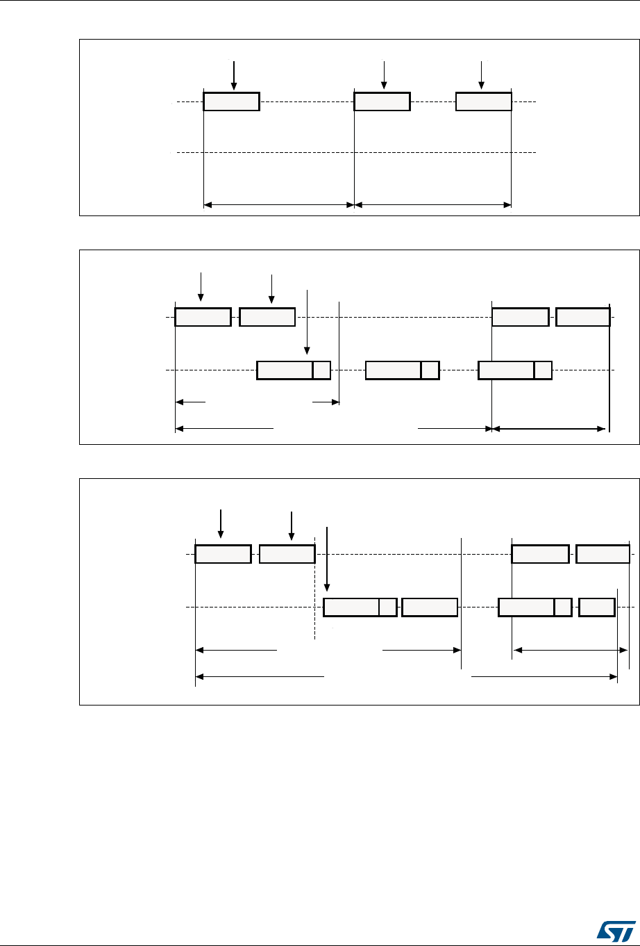
SD/SDIO/MMC card host interface (SDMMC) RM0394
1418/1600 RM0394 Rev 4
Figure 462. “No response” and “no data” operations
Figure 463. (Multiple) block read operation
Figure 464. (Multiple) block write operation
Note: The SDMMC will not send any data as long as the Busy signal is asserted (SDMMC_D0
pulled low).
DLE
2SHUDWLRQQRUHVSRQVH 2SHUDWLRQQRGDWD
6'00&B&0'
6'00&B'
)URPKRVWWRFDUGV )URPKRVWWRFDUG )URPFDUGWRKRVW
5HVSRQVH&RPPDQG &RPPDQG
DLE
&RPPDQG 5HVSRQVH
'DWDEORFN FUF 'DWDEORFN FUF 'DWDEORFN FUF
%ORFNUHDGRSHUDWLRQ
0XOWLSOHEORFNUHDGRSHUDWLRQ 'DWDVWRSRSHUDWLRQ
)URPKRVWWRFDUG )URPFDUGWRKRVW
GDWDIURPFDUGWRKRVW 6WRSFRPPDQG
VWRSVGDWDWUDQVIHU
&RPPDQG 5HVSRQVH
6'00&B&0'
6'00&B'
DLE
&RPPDQG 5HVSRQVH
'DWDEORFN FUF 'DWDEORFN FUF
'DWDVWRSRSHUDWLRQ
)URPKRVWWRFDUG )URPFDUGWRKRVW
GDWDIURPKRVWWRFDUG 6WRSFRPPDQG
VWRSVGDWDWUDQVIHU
&RPPDQG 5HVSRQVH
6'00&B&0'
6'00&B' %XV\
%ORFNZULWHRSHUDWLRQ
%XV\
0XOWLSOHEORFNZULWHRSHUDWLRQ
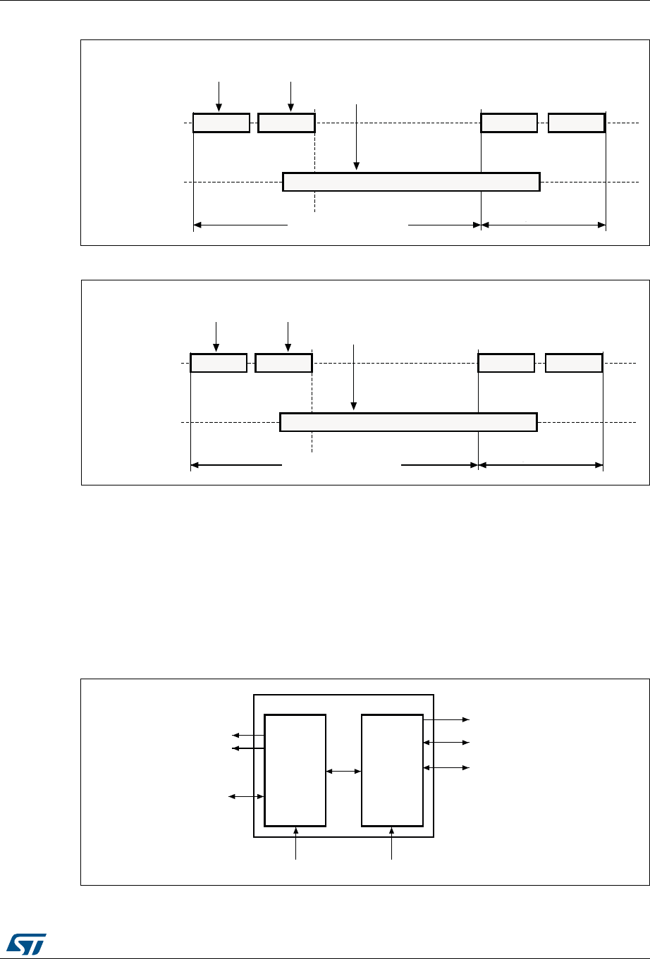
RM0394 Rev 4 1419/1600
RM0394 SD/SDIO/MMC card host interface (SDMMC)
1475
Figure 465. Sequential read operation
Figure 466. Sequential write operation
43.3 SDMMC functional description
The SDMMC consists of two parts:
•The SDMMC adapter block provides all functions specific to the MMC/SD/SD I/O card
such as the clock generation unit, command and data transfer.
•The APB2 interface accesses the SDMMC adapter registers, and generates interrupt
and DMA request signals.
Figure 467. SDMMC block diagram
DLE
'DWDVWRSRSHUDWLRQ
)URPFDUGWRKRVW 6WRSFRPPDQG
VWRSVGDWDWUDQVIHU
&RPPDQG 5HVSRQVH &RPPDQG 5HVSRQVH
'DWDVWUHDP
'DWDWUDQVIHURSHUDWLRQ
)URPKRVWWR
FDUGV
'DWDIURPFDUGWRKRVW
6'00&B&0'
6'00&B'
DLE
'DWDVWRSRSHUDWLRQ
)URPFDUGWRKRVW 6WRSFRPPDQG
VWRSVGDWDWUDQVIHU
5HVSRQVH&RPPDQG 5HVSRQVH&RPPDQG
'DWDVWUHDP
'DWDWUDQVIHURSHUDWLRQ
)URPKRVWWR
FDUGV
'DWDIURPKRVWWRFDUG
6'00&B&0'
6'00&B'
DLE
$3%EXV
$3%
,QWHUUXSWVDQG
3&/.
6'00&B&.
LQWHUIDFH
'0$UHTXHVW
6'00&&/.
6'00&B'>@
6'00&B&0'
6'00&
6'00&
DGDSWHU
SD/SDIO/MMC card host interface (SDMMC) RM0394
1420/1600 RM0394 Rev 4
By default SDMMC_D0 is used for data transfer. After initialization, the host can change the
databus width.
If a MultiMediaCard is connected to the bus, SDMMC_D0, SDMMC_D[3:0] or
SDMMC_D[7:0] can be used for data transfer. MMC V3.31 or previous, supports only 1 bit of
data so only SDMMC_D0 can be used.
If an SD or SD I/O card is connected to the bus, data transfer can be configured by the host
to use SDMMC_D0 or SDMMC_D[3:0]. All data lines are operating in push-pull mode.
SDMMC_CMD has two operational modes:
•Open-drain for initialization (only for MMCV3.31 or previous)
•Push-pull for command transfer (SD/SD I/O card MMC4.2 use push-pull drivers also for
initialization)
SDMMC_CK is the clock to the card: one bit is transferred on both command and data lines
with each clock cycle.
The SDMMC uses two clock signals:
•SDMMC adapter clock SDMMCCLK = 50 MHz)
•APB2 bus clock (PCLK2)
PCLK2 and SDMMC_CK clock frequencies must respect the following condition:
The signals shown in Table 226 are used on the MultiMediaCard/SD/SD I/O card bus.
Table 226. SDMMC I/O definitions
Pin Direction Description
SDMMC_CK Output MultiMediaCard/SD/SDIO card clock. This pin is the clock from
host to card.
SDMMC_CMD Bidirectional MultiMediaCard/SD/SDIO card command. This pin is the
bidirectional command/response signal.
SDMMC_D[7:0] Bidirectional MultiMediaCard/SD/SDIO card data. These pins are the
bidirectional databus.
Frequenc PCLK2()3xWidth()32⁄()Frequency SDMMC_CK()×>
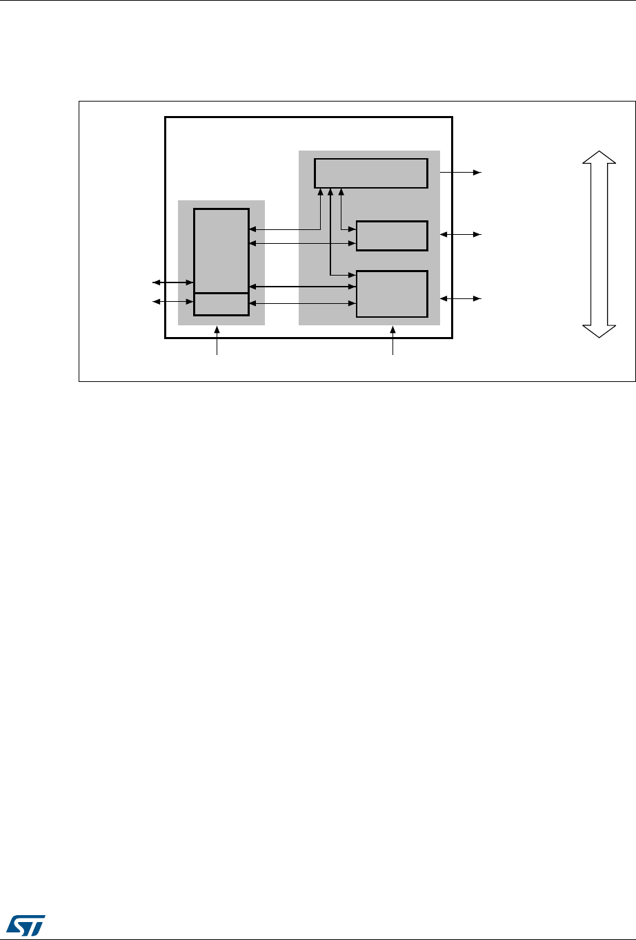
RM0394 Rev 4 1421/1600
RM0394 SD/SDIO/MMC card host interface (SDMMC)
1475
43.3.1 SDMMC adapter
Figure 468 shows a simplified block diagram of an SDMMC adapter.
Figure 468. SDMMC adapter
The SDMMC adapter is a multimedia/secure digital memory card bus master that provides
an interface to a multimedia card stack or to a secure digital memory card. It consists of five
subunits:
•Adapter register block
•Control unit
•Command path
•Data path
•Data FIFO
Note: The adapter registers and FIFO use the APB2 bus clock domain (PCLK2). The control unit,
command path and data path use the SDMMC adapter clock domain (SDMMCCLK).
Adapter register block
The adapter register block contains all system registers. This block also generates the
signals that clear the static flags in the multimedia card. The clear signals are generated
when 1 is written into the corresponding bit location in the SDMMC Clear register.
Control unit
The control unit contains the power management functions and the clock divider for the
memory card clock.
There are three power phases:
•power-off
•power-up
•power-on
DLE
7R$3%
LQWHUIDFH
&RQWUROXQLW
&RPPDQG
SDWK
'DWDSDWK
$GDSWHU
UHJLVWHUV
6'00&B&.
6'00&B&0'
6'00&B'>@
6'00&DGDSWHU
3&/. 6'00&&/.
),)2
&DUGEXV
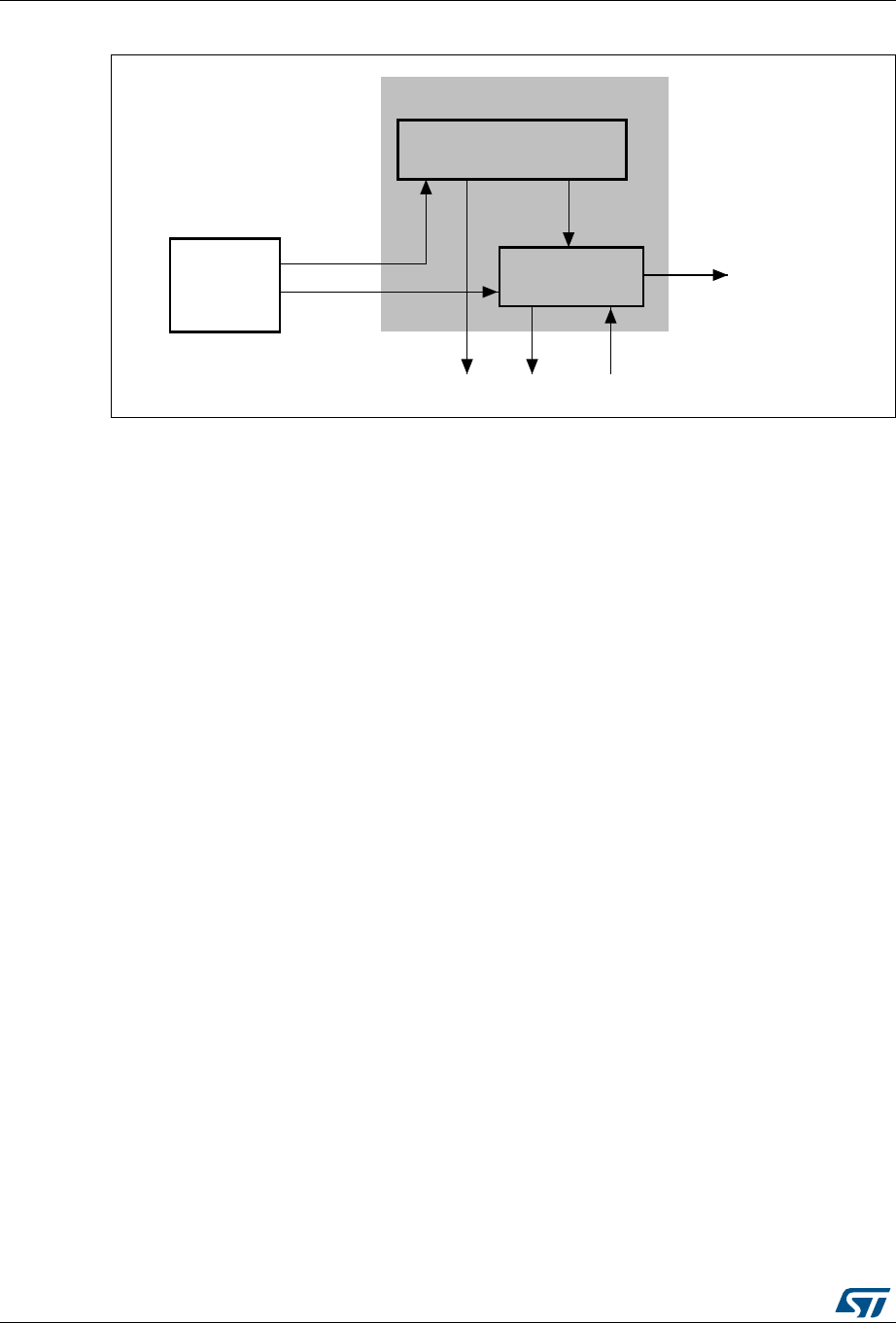
SD/SDIO/MMC card host interface (SDMMC) RM0394
1422/1600 RM0394 Rev 4
Figure 469. Control unit
The control unit is illustrated in Figure 469. It consists of a power management subunit and
a clock management subunit.
The power management subunit disables the card bus output signals during the power-off
and power-up phases.
The clock management subunit generates and controls the SDMMC_CK signal. The
SDMMC_CK output can use either the clock divide or the clock bypass mode. The clock
output is inactive:
•after reset
•during the power-off or power-up phases
•if the power saving mode is enabled and the card bus is in the Idle state (eight clock
periods after both the command and data path subunits enter the Idle phase)
The clock management subunit controls SDMMC_CK dephasing. When not in bypass mode
the SDMMC command and data output are generated on the SDMMCCLK falling edge
succeeding the rising edge of SDMMC_CK. (SDMMC_CK rising edge occurs on
SDMMCCLK rising edge) when SDMMC_CLKCR[13] bit is reset (NEGEDGE = 0). When
SDMMC_CLKCR[13] bit is set (NEGEDGE = 1) SDMMC command and data changed on
the SDMMC_CK falling edge.
When SDMMC_CLKCR[10] is set (BYPASS = 1), SDMMC_CK rising edge occurs on
SDMMCCLK rising edge. The data and the command change on SDMMCCLK falling edge
whatever NEGEDGE value.
The data and command responses are latched using SDMMC_CK rising edge.
DLE
&RQWUROXQLW
3RZHUPDQDJHPHQW
&ORFNPDQDJHPHQW
$GDSWHU
UHJLVWHUV
6'00&B&.
7RFRPPDQGDQGGDWDSDWK
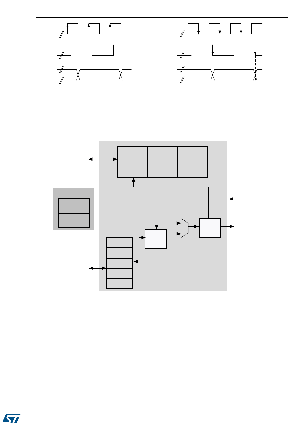
RM0394 Rev 4 1423/1600
RM0394 SD/SDIO/MMC card host interface (SDMMC)
1475
Figure 470. SDMMC_CK clock dephasing (BYPASS = 0)
Command path
The command path unit sends commands to and receives responses from the cards.
Figure 471. SDMMC adapter command path
•Command path state machine (CPSM)
– When the command register is written to and the enable bit is set, command
transfer starts. When the command has been sent, the command path state
machine (CPSM) sets the status flags and enters the Idle state if a response is not
required. If a response is required, it waits for the response (see Figure 472 on
page 1424). When the response is received, the received CRC code and the
internally generated code are compared, and the appropriate status flags are set.
06Y9
6'00&&/.
6'00&B&.
1(*('*( 1(*('*(
&0''DWD
RXWSXW
DLE
$GDSWHUUHJLVWHUV
&0'
6WDWXV
IODJ
&5&
6KLIW
UHJLVWHU
&0'
7RFRQWUROXQLW
6'00&B&0'LQ
6'00&B&0'RXW
7R$3%LQWHUIDFH
&RQWURO
ORJLF
&RPPDQG
WLPHU
$UJXPHQW
5HVSRQVH
UHJLVWHUV
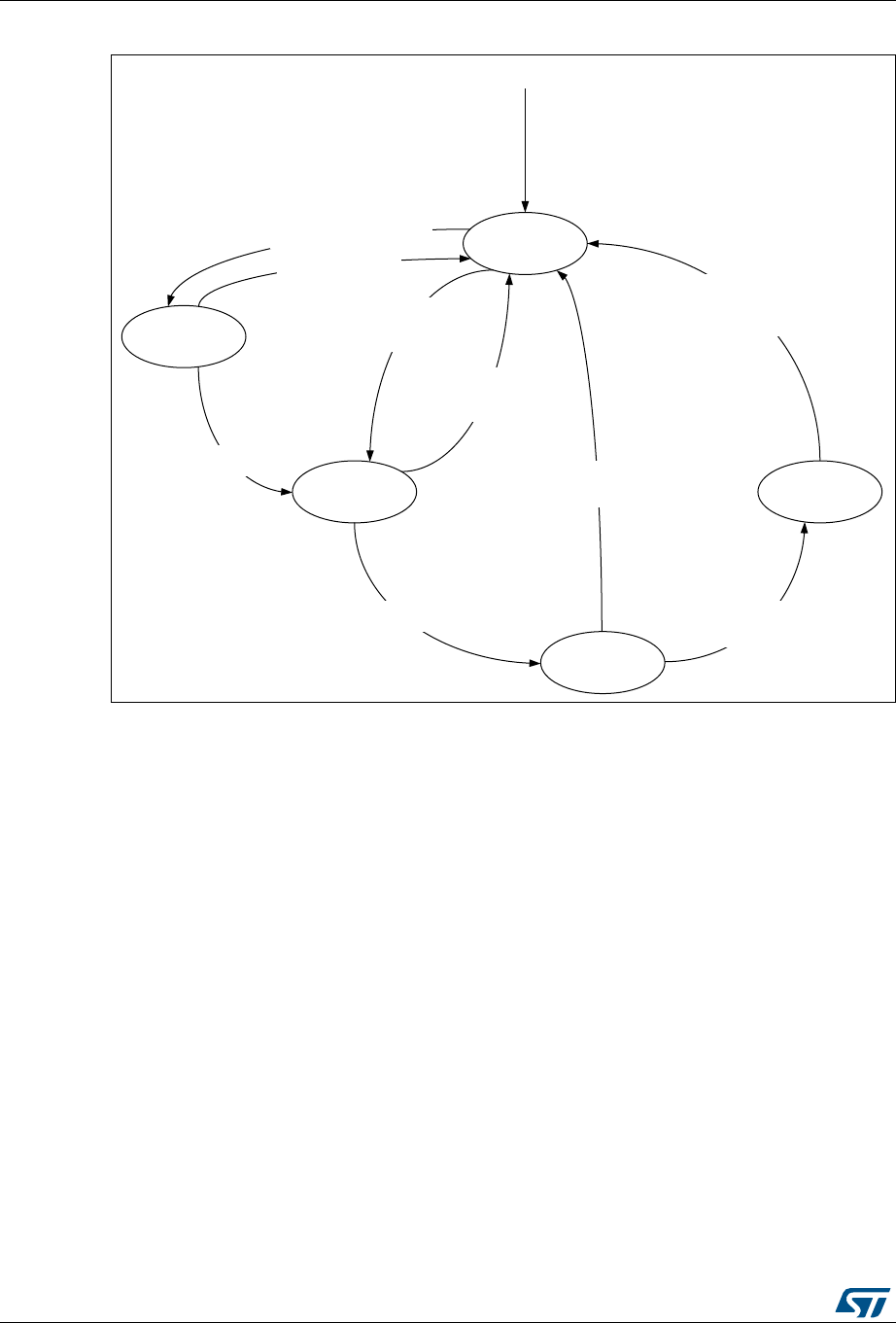
SD/SDIO/MMC card host interface (SDMMC) RM0394
1424/1600 RM0394 Rev 4
Figure 472. Command path state machine (SDMMC)
When the Wait state is entered, the command timer starts running. If the timeout is reached
before the CPSM moves to the Receive state, the timeout flag is set and the Idle state is
entered.
Note: The command timeout has a fixed value of 64 SDMMC_CK clock periods.
If the interrupt bit is set in the command register, the timer is disabled and the CPSM waits
for an interrupt request from one of the cards. If a pending bit is set in the command register,
the CPSM enters the Pend state, and waits for a CmdPend signal from the data path
subunit. When CmdPend is detected, the CPSM moves to the Send state. This enables the
data counter to trigger the stop command transmission.
Note: The CPSM remains in the Idle state for at least eight SDMMC_CK periods to meet the NCC
and NRC timing constraints. NCC is the minimum delay between two host commands, and
NRC is the minimum delay between the host command and the card response.
069
,GOH
5HFHLYH
3HQG
6HQG
:DLW
5HVSRQVHUHFHLYHGRU
GLVDEOHGRUFRPPDQG
&5&IDLOHG
5HVSRQVH
VWDUWHG
&360GLVDEOHG
RUQRUHVSRQVH
(QDEOHGDQG
FRPPDQGVWDUW
&360HQDEOHGDQG
SHQGLQJFRPPDQG
/DVWGDWD
2QUHVHW
:DLWIRUUHVSRQVH
&360GLVDEOHGRU
FRPPDQGWLPHRXW
&360GLVDEOHG
RM0394 Rev 4 1425/1600
RM0394 SD/SDIO/MMC card host interface (SDMMC)
1475
Figure 473. SDMMC command transfer
•Command format
– Command: a command is a token that starts an operation. Command are sent
from the host either to a single card (addressed command) or to all connected
cards (broadcast command are available for MMC V3.31 or previous). Commands
are transferred serially on the CMD line. All commands have a fixed length of 48
bits. The general format for a command token for MultiMediaCards, SD-Memory
cards and SDIO-Cards is shown in Table 227.
The command path operates in a half-duplex mode, so that commands and
responses can either be sent or received. If the CPSM is not in the Send state, the
SDMMC_CMD output is in the Hi-Z state, as shown in Figure 473 on page 1425.
Data on SDMMC_CMD are synchronous with the rising edge of SDMMC_CK.
Table 227 shows the command format.
– Response: a response is a token that is sent from an addressed card (or
synchronously from all connected cards for MMC V3.31 or previous), to the host
as an answer to a previously received command. Responses are transferred
serially on the CMD line.
The SDMMC supports two response types. Both use CRC error checking:
•48 bit short response
•136 bit long response
Note: If the response does not contain a CRC (CMD1 response), the device driver must ignore the
CRC failed status.
Table 227. Command format
Bit position Width Value Description
47 1 0 Start bit
46 1 1 Transmission bit
[45:40] 6 - Command index
[39:8] 32 - Argument
[7:1] 7 - CRC7
011End bit
DLE
6'00&B&.
6'00&B&0'
&RPPDQG 5HVSRQVH &RPPDQG
6WDWH ,GOH 6HQG :DLW 5HFHLYH ,GOH 6HQG
+L= &RQWUROOHUGULYHV +L= &DUGGULYHV +L= &RQWUROOHUGULYHV
DWOHDVW6'00&B&.
F\FOHV
SD/SDIO/MMC card host interface (SDMMC) RM0394
1426/1600 RM0394 Rev 4
The command register contains the command index (six bits sent to a card) and the
command type. These determine whether the command requires a response, and whether
the response is 48 or 136 bits long (see Section 43.8.4 on page 1461). The command path
implements the status flags shown in Table 230:
The CRC generator calculates the CRC checksum for all bits before the CRC code. This
includes the start bit, transmitter bit, command index, and command argument (or card
status). The CRC checksum is calculated for the first 120 bits of CID or CSD for the long
response format. Note that the start bit, transmitter bit and the six reserved bits are not used
in the CRC calculation.
The CRC checksum is a 7-bit value:
CRC[6:0] = Remainder [(M(x) * x7) / G(x)]
G(x) = x7 + x3 + 1
M(x) = (start bit) * x39 + ... + (last bit before CRC) * x0, or
M(x) = (start bit) * x119 + ... + (last bit before CRC) * x0
Table 228. Short response format
Bit position Width Value Description
47 1 0 Start bit
46 1 0 Transmission bit
[45:40] 6 - Command index
[39:8] 32 - Argument
[7:1] 7 - CRC7(or 1111111)
011End bit
Table 229. Long response format
Bit position Width Value Description
135 1 0 Start bit
134 1 0 Transmission bit
[133:128] 6 111111 Reserved
[127:1] 127 - CID or CSD (including internal CRC7)
0 1 1 End bit
Table 230. Command path status flags
Flag Description
CMDREND Set if response CRC is OK.
CCRCFAIL Set if response CRC fails.
CMDSENT Set when command (that does not require response) is sent
CTIMEOUT Response timeout.
CMDACT Command transfer in progress.
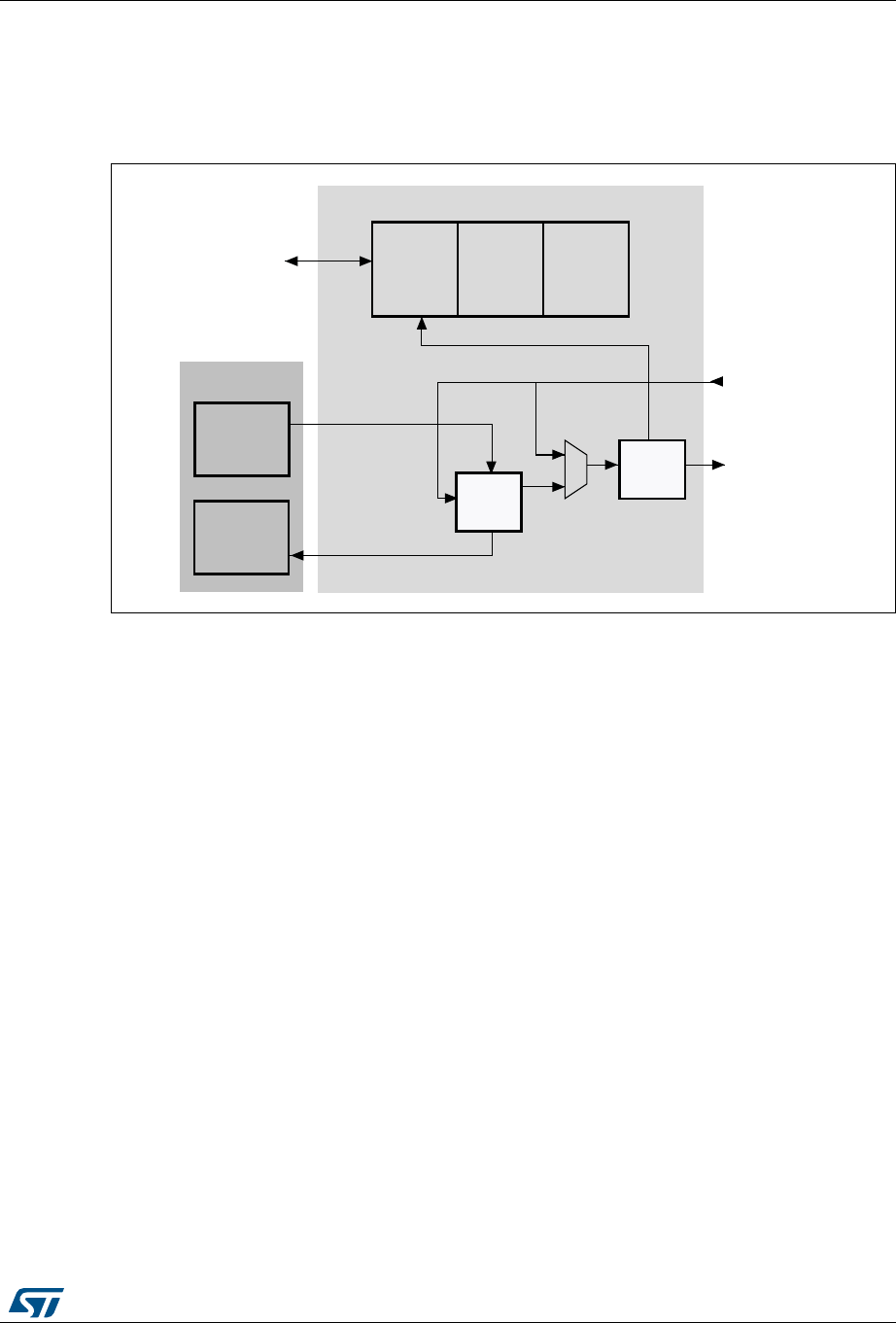
RM0394 Rev 4 1427/1600
RM0394 SD/SDIO/MMC card host interface (SDMMC)
1475
Data path
The data path subunit transfers data to and from cards. Figure 474 shows a block diagram
of the data path.
Figure 474. Data path
The card databus width can be programmed using the clock control register. If the 4-bit wide
bus mode is enabled, data is transferred at four bits per clock cycle over all four data signals
(SDMMC_D[3:0]). If the 8-bit wide bus mode is enabled, data is transferred at eight bits per
clock cycle over all eight data signals (SDMMC_D[7:0]). If the wide bus mode is not
enabled, only one bit per clock cycle is transferred over SDMMC_D0.
Depending on the transfer direction (send or receive), the data path state machine (DPSM)
moves to the Wait_S or Wait_R state when it is enabled:
•Send: the DPSM moves to the Wait_S state. If there is data in the transmit FIFO, the
DPSM moves to the Send state, and the data path subunit starts sending data to a
card.
•Receive: the DPSM moves to the Wait_R state and waits for a start bit. When it
receives a start bit, the DPSM moves to the Receive state, and the data path subunit
starts receiving data from a card.
Data path state machine (DPSM)
The DPSM operates at SDMMC_CK frequency. Data on the card bus signals is
synchronous to the rising edge of SDMMC_CK. The DPSM has six states, as shown in
Figure 475: Data path state machine (DPSM).
DLE
'DWDSDWK
'DWD),)2
7UDQVPLW
6WDWXV
IODJ
&5&
6KLIW
UHJLVWHU
7RFRQWUROXQLW
6'00&B'LQ>@
6'00&B'RXW>@
5HFHLYH
&RQWURO
ORJLF
'DWD
WLPHU
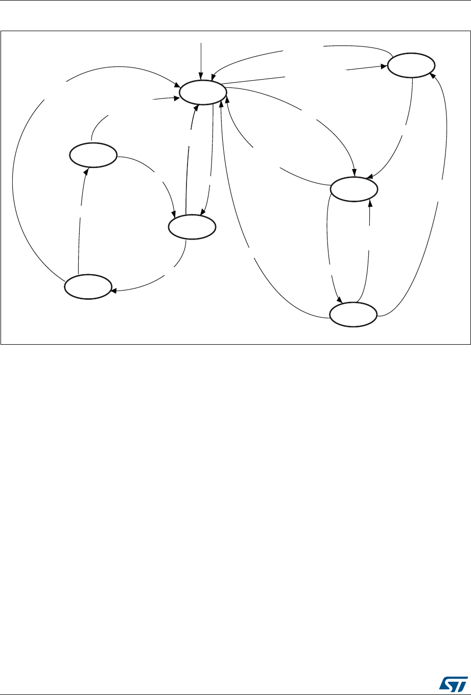
SD/SDIO/MMC card host interface (SDMMC) RM0394
1428/1600 RM0394 Rev 4
Figure 475. Data path state machine (DPSM)
•Idle: the data path is inactive, and the SDMMC_D[7:0] outputs are in Hi-Z. When the
data control register is written and the enable bit is set, the DPSM loads the data
counter with a new value and, depending on the data direction bit, moves to either the
Wait_S or the Wait_R state.
•Wait_R: if the data counter equals zero, the DPSM moves to the Idle state when the
receive FIFO is empty. If the data counter is not zero, the DPSM waits for a start bit on
SDMMC_D. The DPSM moves to the Receive state if it receives a start bit before a
timeout, and loads the data block counter. If it reaches a timeout before it detects a
start bit, it moves to the Idle state and sets the timeout status flag.
•Receive: serial data received from a card is packed in bytes and written to the data
FIFO. Depending on the transfer mode bit in the data control register, the data transfer
mode can be either block or stream:
– In block mode, when the data block counter reaches zero, the DPSM waits until it
receives the CRC code. If the received code matches the internally generated
CRC code, the DPSM moves to the Wait_R state. If not, the CRC fail status flag is
set and the DPSM moves to the Idle state.
– In stream mode, the DPSM receives data while the data counter is not zero. When
the counter is zero, the remaining data in the shift register is written to the data
FIFO, and the DPSM moves to the Wait_R state.
If a FIFO overrun error occurs, the DPSM sets the FIFO error flag and moves to the
Idle state:
•Wait_S: the DPSM moves to the Idle state if the data counter is zero. If not, it waits until
the data FIFO empty flag is deasserted, and moves to the Send state.
)DLE
"USY
3END
7AIT?2
2ECEIVE
%NDOFPACKET
$ISABLEDOR#2#FAIL
ORTIMEOUT
.OTBUSY
$ISABLEDOR
ENDOFDATA
$ATAREADY
%NDOFPACKETOR
ENDOFDATAOR
&)&/OVERRUN
%NABLEANDNOTSEND
$ISABLEDOR
2X&)&/EMPTYORTIMEOUTOR
STARTBITERROR
$ISABLEDOR&)&/UNDERRUNOR
ENDOFDATAOR#2#FAIL
AIB
7AIT?3
3TARTBIT
/NRESET
$ISABLEDOR#2#FAIL
%NABLEANDSEND
$03-DISABLED
2EAD7AIT
$03-ENABLEDAND
2EAD7AIT3TARTED
AND3$)/MODEENABLED
2EAD7AIT3TOP
$ATARECEIVEDAND
2EAD7AIT3TARTEDAND
3$)/MODEENABLED

RM0394 Rev 4 1429/1600
RM0394 SD/SDIO/MMC card host interface (SDMMC)
1475
Note: The DPSM remains in the Wait_S state for at least two clock periods to meet the NWR timing
requirements, where NWR is the number of clock cycles between the reception of the card
response and the start of the data transfer from the host.
•Send: the DPSM starts sending data to a card. Depending on the transfer mode bit in
the data control register, the data transfer mode can be either block or stream:
– In block mode, when the data block counter reaches zero, the DPSM sends an
internally generated CRC code and end bit, and moves to the Busy state.
– In stream mode, the DPSM sends data to a card while the enable bit is high and
the data counter is not zero. It then moves to the Idle state.
If a FIFO underrun error occurs, the DPSM sets the FIFO error flag and moves to the
Idle state.
•Busy: the DPSM waits for the CRC status flag:
– If it does not receive a positive CRC status, it moves to the Idle state and sets the
CRC fail status flag.
– If it receives a positive CRC status, it moves to the Wait_S state if SDMMC_D0 is
not low (the card is not busy).
If a timeout occurs while the DPSM is in the Busy state, it sets the data timeout flag and
moves to the Idle state.
The data timer is enabled when the DPSM is in the Wait_R or Busy state, and
generates the data timeout error:
– When transmitting data, the timeout occurs if the DPSM stays in the Busy state for
longer than the programmed timeout period
– When receiving data, the timeout occurs if the end of the data is not true, and if the
DPSM stays in the Wait_R state for longer than the programmed timeout period.
•Data: data can be transferred from the card to the host or vice versa. Data is
transferred via the data lines. They are stored in a FIFO of 32 words, each word is 32
bits wide.
Table 231. Data token format
Description Start bit Data CRC16 End bit
Block Data 0 - yes 1
Stream Data 0 - no 1

SD/SDIO/MMC card host interface (SDMMC) RM0394
1430/1600 RM0394 Rev 4
DPSM Flags
The status of the data path subunit transfer is reported by several status flags
Table 232. DPSM flags
Data FIFO
The data FIFO (first-in-first-out) subunit is a data buffer with a transmit and receive unit.
The FIFO contains a 32-bit wide, 32-word deep data buffer, and transmit and receive logic.
Because the data FIFO operates in the APB2 clock domain (PCLK2), all signals from the
subunits in the SDMMC clock domain (SDMMCCLK) are resynchronized.
Depending on the TXACT and RXACT flags, the FIFO can be disabled, transmit enabled, or
receive enabled. TXACT and RXACT are driven by the data path subunit and are mutually
exclusive:
– The transmit FIFO refers to the transmit logic and data buffer when TXACT is
asserted
– The receive FIFO refers to the receive logic and data buffer when RXACT is
asserted
•Transmit FIFO:
Data can be written to the transmit FIFO through the APB2 interface when the SDMMC
is enabled for transmission.
The transmit FIFO is accessible via 32 sequential addresses. The transmit FIFO
contains a data output register that holds the data word pointed to by the read pointer.
When the data path subunit has loaded its shift register, it increments the read pointer
and drives new data out.
If the transmit FIFO is disabled, all status flags are deasserted. The data path subunit
asserts TXACT when it transmits data.
Flag Description
DBCKEND
Set to high when data block send/receive CRC check is passed.
In SDIO multibyte transfer mode this flag is set at the end of the transfer (a
multibyte transfer is considered as a single block transfer by the host).
DATAEND Set to high when SDMMC_DCOUNT register decrements and reaches 0.
DATAEND indicates the end of a transfer on SDMMC data line.
DTIMEOUT
Set to high when data timeout period is reached.
When data timer reaches zero while DPSM is in Wait_R or Busy state, timeout is
set. DTIMEOUT can be set after DATAEND if DPSM remains in busy state for
longer than the programmed period.
DCRCFAIL Set to high when data block send/receive CRC check fails.

RM0394 Rev 4 1431/1600
RM0394 SD/SDIO/MMC card host interface (SDMMC)
1475
•Receive FIFO
When the data path subunit receives a word of data, it drives the data on the write
databus. The write pointer is incremented after the write operation completes. On the
read side, the contents of the FIFO word pointed to by the current value of the read
pointer is driven onto the read databus. If the receive FIFO is disabled, all status flags
are deasserted, and the read and write pointers are reset. The data path subunit
asserts RXACT when it receives data. Table 234 lists the receive FIFO status flags.
The receive FIFO is accessible via 32 sequential addresses.
Table 233. Transmit FIFO status flags
Flag Description
TXFIFOF Set to high when all 32 transmit FIFO words contain valid data.
TXFIFOE Set to high when the transmit FIFO does not contain valid data.
TXFIFOHE Set to high when 8 or more transmit FIFO words are empty. This flag can be used
as a DMA request.
TXDAVL Set to high when the transmit FIFO contains valid data. This flag is the inverse of
the TXFIFOE flag.
TXUNDERR
Set to high when an underrun error occurs. This flag is cleared by writing to the
SDMMC Clear register.
Note: In case of TXUNDERR, and DMA is used to fill SDMMC FIFO, user
software should disable DMA stream, and then write DMAEN bit in
SDMMC_DCTRL with ‘0’ (to disable DMA request generation).
Table 234. Receive FIFO status flags
Flag Description
RXFIFOF Set to high when all 32 receive FIFO words contain valid data
RXFIFOE Set to high when the receive FIFO does not contain valid data.
RXFIFOHF Set to high when 8 or more receive FIFO words contain valid data. This flag can be
used as a DMA request.
RXDAVL Set to high when the receive FIFO is not empty. This flag is the inverse of the
RXFIFOE flag.
RXOVERR
Set to high when an overrun error occurs. This flag is cleared by writing to the
SDMMC Clear register.
Note: In case of RXOVERR, and DMA is used to read SDMMC FIFO, user
software should disable DMA stream, and then write DMAEN bit in
SDMMC_DCTRL with ‘0’ (to disable DMA request generation).

SD/SDIO/MMC card host interface (SDMMC) RM0394
1432/1600 RM0394 Rev 4
43.3.2 SDMMC APB2 interface
The APB2 interface generates the interrupt and DMA requests, and accesses the SDMMC
adapter registers and the data FIFO. It consists of a data path, register decoder, and
interrupt/DMA logic.
SDMMC interrupts
The interrupt logic generates an interrupt request signal that is asserted when at least one
of the selected status flags is high. A mask register is provided to allow selection of the
conditions that will generate an interrupt. A status flag generates the interrupt request if a
corresponding mask flag is set.
SDMMC/DMA interface
SDMMC APB interface controls all subunit to perform transfers between the host and card
Example of read procedure using DMA
Send CMD17 (READ_BLOCK) as follows:
a) Program the SDMMC data length register (SDMMC data timer register should be
already programmed before the card identification process)
b) Program DMA channel (refer to DMA configuration for SDMMC controller)
c) Program the SDMMC data control register: DTEN with ‘1’ (SDMMC card host
enabled to send data); DTDIR with ‘1’ (from card to controller); DTMODE with ‘0’
(block data transfer); DMAEN with ‘1’ (DMA enabled); DBLOCKSIZE with 0x9
(512 bytes). Other fields are don’t care.
d) Program the SDMMC argument register with the address location of the card from
where data is to be transferred
e) Program the SDMMC command register: CmdIndex with 17(READ_BLOCK);
WaitResp with ‘1’ (SDMMC card host waits for a response); CPSMEN with ‘1’
(SDMMC card host enabled to send a command). Other fields are at their reset
value.
f) Wait for SDMMC_STA[6] = CMDREND interrupt, (CMDREND is set if there is no
error on command path).
g) Wait for SDMMC_STA[10] = DBCKEND, (DBCKEND is set in case of no errors
until the CRC check is passed)
h) Wait until the FIFO is empty, when FIFO is empty the SDMMC_STA[5] =
RXOVERR value has to be check to guarantee that read succeeded
Note: When FIFO overrun error occurs with last 1-4 bytes, it may happens that RXOVERR flag is
set 2 APB clock cycles after DATAEND flag is set. To guarantee success of read operation
RXOVERR must be cheked after FIFO is empty.

RM0394 Rev 4 1433/1600
RM0394 SD/SDIO/MMC card host interface (SDMMC)
1475
Example of write procedure using DMA
Send CMD24 (WRITE_BLOCK) as follows:
a) Program the SDMMC data length register (SDMMC data timer register should be
already programmed before the card identification process)
b) Program DMA channel (refer to DMA configuration for SDMMC controller)
c) Program the SDMMC argument register with the address location of the card from
where data is to be transferred
d) Program the SDMMC command register: CmdIndex with 24(WRITE_BLOCK);
WaitResp with ‘1’ (SDMMC card host waits for a response); CPSMEN with ‘1’
(SDMMC card host enabled to send a command). Other fields are at their reset
value.
e) Wait for SDMMC_STA[6] = CMDREND interrupt, then Program the SDMMC data
control register: DTEN with ‘1’ (SDMMC card host enabled to send data); DTDIR
with ‘0’ (from controller to card); DTMODE with ‘0’ (block data transfer); DMAEN
with ‘1’ (DMA enabled); DBLOCKSIZE with 0x9 (512 bytes). Other fields are don’t
care.
f) Wait for SDMMC_STA[10] = DBCKEND, (DBCKEND is set in case of no errors)
DMA configuration for SDMMC controller
a) Enable DMA2 controller and clear any pending interrupts
b) Program the DMA2_Channel4 (or DMA2_Channel5) source address register with
the memory location base address and DMA2_Channel4 (or DMA2_Channel5)
destination address register with the SDMMC_FIFO register address
c) Program DMA2_Channel4 (or DMA2_Channel5) control register (memory
increment, not peripheral increment, peripheral and source width is word size)
d) Enable DMA2_Channel4 (or DMA2_Channel5)
43.4 Card functional description
43.4.1 Card identification mode
While in card identification mode the host resets all cards, validates the operation voltage
range, identifies cards and sets a relative card address (RCA) for each card on the bus. All
data communications in the card identification mode use the command line (CMD) only.
43.4.2 Card reset
The GO_IDLE_STATE command (CMD0) is the software reset command and it puts the
MultiMediaCard and SD memory in the Idle state. The IO_RW_DIRECT command (CMD52)
resets the SD I/O card. After power-up or CMD0, all cards output bus drivers are in the high-
impedance state and the cards are initialized with a default relative card address
(RCA=0x0001) and with a default driver stage register setting (lowest speed, highest driving
current capability).

SD/SDIO/MMC card host interface (SDMMC) RM0394
1434/1600 RM0394 Rev 4
43.4.3 Operating voltage range validation
All cards can communicate with the SDMMC card host using any operating voltage within
the specification range. The supported minimum and maximum VDD values are defined in
the operation conditions register (OCR) on the card.
Cards that store the card identification number (CID) and card specific data (CSD) in the
payload memory are able to communicate this information only under data-transfer VDD
conditions. When the SDMMC card host module and the card have incompatible VDD
ranges, the card is not able to complete the identification cycle and cannot send CSD data.
For this purpose, the special commands, SEND_OP_COND (CMD1), SD_APP_OP_COND
(ACMD41 for SD Memory), and IO_SEND_OP_COND (CMD5 for SD I/O), are designed to
provide a mechanism to identify and reject cards that do not match the VDD range desired
by the SDMMC card host. The SDMMC card host sends the required VDD voltage window
as the operand of these commands. Cards that cannot perform data transfer in the specified
range disconnect from the bus and go to the inactive state.
By using these commands without including the voltage range as the operand, the SDMMC
card host can query each card and determine the common voltage range before placing out-
of-range cards in the inactive state. This query is used when the SDMMC card host is able
to select a common voltage range or when the user requires notification that cards are not
usable.
43.4.4 Card identification process
The card identification process differs for MultiMediaCards and SD cards. For
MultiMediaCard cards, the identification process starts at clock rate Fod. The SDMMC_CMD
line output drivers are open-drain and allow parallel card operation during this process. The
registration process is accomplished as follows:
1. The bus is activated.
2. The SDMMC card host broadcasts SEND_OP_COND (CMD1) to receive operation
conditions.
3. The response is the wired AND operation of the operation condition registers from all
cards.
4. Incompatible cards are placed in the inactive state.
5. The SDMMC card host broadcasts ALL_SEND_CID (CMD2) to all active cards.
6. The active cards simultaneously send their CID numbers serially. Cards with outgoing
CID bits that do not match the bits on the command line stop transmitting and must wait
for the next identification cycle. One card successfully transmits a full CID to the
SDMMC card host and enters the Identification state.
7. The SDMMC card host issues SET_RELATIVE_ADDR (CMD3) to that card. This new
address is called the relative card address (RCA); it is shorter than the CID and
addresses the card. The assigned card changes to the Standby state, it does not react
to further identification cycles, and its output switches from open-drain to push-pull.
8. The SDMMC card host repeats steps 5 through 7 until it receives a timeout condition.
For the SD card, the identification process starts at clock rate Fod, and the SDMMC_CMD
line output drives are push-pull drivers instead of open-drain. The registration process is
accomplished as follows:

RM0394 Rev 4 1435/1600
RM0394 SD/SDIO/MMC card host interface (SDMMC)
1475
1. The bus is activated.
2. The SDMMC card host broadcasts SD_APP_OP_COND (ACMD41).
3. The cards respond with the contents of their operation condition registers.
4. The incompatible cards are placed in the inactive state.
5. The SDMMC card host broadcasts ALL_SEND_CID (CMD2) to all active cards.
6. The cards send back their unique card identification numbers (CIDs) and enter the
Identification state.
7. The SDMMC card host issues SET_RELATIVE_ADDR (CMD3) to an active card with
an address. This new address is called the relative card address (RCA); it is shorter
than the CID and addresses the card. The assigned card changes to the Standby state.
The SDMMC card host can reissue this command to change the RCA. The RCA of the
card is the last assigned value.
8. The SDMMC card host repeats steps 5 through 7 with all active cards.
For the SD I/O card, the registration process is accomplished as follows:
1. The bus is activated.
2. The SDMMC card host sends IO_SEND_OP_COND (CMD5).
3. The cards respond with the contents of their operation condition registers.
4. The incompatible cards are set to the inactive state.
5. The SDMMC card host issues SET_RELATIVE_ADDR (CMD3) to an active card with
an address. This new address is called the relative card address (RCA); it is shorter
than the CID and addresses the card. The assigned card changes to the Standby state.
The SDMMC card host can reissue this command to change the RCA. The RCA of the
card is the last assigned value.
43.4.5 Block write
During block write (CMD24 - 27) one or more blocks of data are transferred from the host to
the card with a CRC appended to the end of each block by the host. A card supporting block
write is always able to accept a block of data defined by WRITE_BL_LEN. If the CRC fails,
the card indicates the failure on the SDMMC_D line and the transferred data are discarded
and not written, and all further transmitted blocks (in multiple block write mode) are ignored.
If the host uses partial blocks whose accumulated length is not block aligned and, block
misalignment is not allowed (CSD parameter WRITE_BLK_MISALIGN is not set), the card
will detect the block misalignment error before the beginning of the first misaligned block.
(ADDRESS_ERROR error bit is set in the status register). The write operation will also be
aborted if the host tries to write over a write-protected area. In this case, however, the card
will set the WP_VIOLATION bit.
Programming of the CID and CSD registers does not require a previous block length setting.
The transferred data is also CRC protected. If a part of the CSD or CID register is stored in
ROM, then this unchangeable part must match the corresponding part of the receive buffer.
If this match fails, then the card reports an error and does not change any register contents.
Some cards may require long and unpredictable times to write a block of data. After
receiving a block of data and completing the CRC check, the card begins writing and holds
the SDMMC_D line low if its write buffer is full and unable to accept new data from a new
WRITE_BLOCK command. The host may poll the status of the card with a SEND_STATUS
command (CMD13) at any time, and the card will respond with its status. The
READY_FOR_DATA status bit indicates whether the card can accept new data or whether
the write process is still in progress. The host may deselect the card by issuing CMD7 (to

SD/SDIO/MMC card host interface (SDMMC) RM0394
1436/1600 RM0394 Rev 4
select a different card), which will place the card in the Disconnect state and release the
SDMMC_D line(s) without interrupting the write operation. When reselecting the card, it will
reactivate busy indication by pulling SDMMC_D to low if programming is still in progress and
the write buffer is unavailable.
43.4.6 Block read
In Block read mode the basic unit of data transfer is a block whose maximum size is defined
in the CSD (READ_BL_LEN). If READ_BL_PARTIAL is set, smaller blocks whose start and
end addresses are entirely contained within one physical block (as defined by
READ_BL_LEN) may also be transmitted. A CRC is appended to the end of each block,
ensuring data transfer integrity. CMD17 (READ_SINGLE_BLOCK) initiates a block read and
after completing the transfer, the card returns to the Transfer state.
CMD18 (READ_MULTIPLE_BLOCK) starts a transfer of several consecutive blocks.
The host can abort reading at any time, within a multiple block operation, regardless of its
type. Transaction abort is done by sending the stop transmission command.
If the card detects an error (for example, out of range, address misalignment or internal
error) during a multiple block read operation (both types) it stops the data transmission and
remains in the data state. The host must than abort the operation by sending the stop
transmission command. The read error is reported in the response to the stop transmission
command.
If the host sends a stop transmission command after the card transmits the last block of a
multiple block operation with a predefined number of blocks, it is responded to as an illegal
command, since the card is no longer in the data state. If the host uses partial blocks whose
accumulated length is not block-aligned and block misalignment is not allowed, the card
detects a block misalignment error condition at the beginning of the first misaligned block
(ADDRESS_ERROR error bit is set in the status register).
43.4.7 Stream access, stream write and stream read
(MultiMediaCard only)
In stream mode, data is transferred in bytes and no CRC is appended at the end of each
block.
Stream write (MultiMediaCard only)
WRITE_DAT_UNTIL_STOP (CMD20) starts the data transfer from the SDMMC card host to
the card, beginning at the specified address and continuing until the SDMMC card host
issues a stop command. When partial blocks are allowed (CSD parameter
WRITE_BL_PARTIAL is set), the data stream can start and stop at any address within the
card address space, otherwise it can only start and stop at block boundaries. Because the
amount of data to be transferred is not determined in advance, a CRC cannot be used.
When the end of the memory range is reached while sending data and no stop command is
sent by the SDMMC card host, any additional transferred data are discarded.

RM0394 Rev 4 1437/1600
RM0394 SD/SDIO/MMC card host interface (SDMMC)
1475
The maximum clock frequency for a stream write operation is given by the following
equation fields of the card-specific data register:
•Maximumspeed = maximum write frequency
•TRANSPEED = maximum data transfer rate
•writebllen = maximum write data block length
•NSAC = data read access time 2 in CLK cycles
•TAAC = data read access time 1
•R2WFACTOR = write speed factor
If the host attempts to use a higher frequency, the card may not be able to process the data
and stop programming, set the OVERRUN error bit in the status register, and while ignoring
all further data transfer, wait (in the receive data state) for a stop command. The write
operation is also aborted if the host tries to write over a write-protected area. In this case,
however, the card sets the WP_VIOLATION bit.
Stream read (MultiMediaCard only)
READ_DAT_UNTIL_STOP (CMD11) controls a stream-oriented data transfer.
This command instructs the card to send its data, starting at a specified address, until the
SDMMC card host sends STOP_TRANSMISSION (CMD12). The stop command has an
execution delay due to the serial command transmission and the data transfer stops after
the end bit of the stop command. When the end of the memory range is reached while
sending data and no stop command is sent by the SDMMC card host, any subsequent data
sent are considered undefined.
The maximum clock frequency for a stream read operation is given by the following
equation and uses fields of the card specific data register.
•Maximumspeed = maximum read frequency
•TRANSPEED = maximum data transfer rate
•readbllen = maximum read data block length
•writebllen = maximum write data block length
•NSAC = data read access time 2 in CLK cycles
•TAAC = data read access time 1
•R2WFACTOR = write speed factor
If the host attempts to use a higher frequency, the card is not able to sustain data transfer. If
this happens, the card sets the UNDERRUN error bit in the status register, aborts the
transmission and waits in the data state for a stop command.
Maximumspeed MIN TRANSPEED 82
writebllen
×()NSAC–()
TAAC R2WFACTOR×
-------------------------------------------------------------------------(, )=
Maximumspeed MIN TRANSPEED 82
readbllen
×()NSAC–()
TAAC R2WFACTOR×
------------------------------------------------------------------------(, )=

SD/SDIO/MMC card host interface (SDMMC) RM0394
1438/1600 RM0394 Rev 4
43.4.8 Erase: group erase and sector erase
The erasable unit of the MultiMediaCard is the erase group. The erase group is measured in
write blocks, which are the basic writable units of the card. The size of the erase group is a
card-specific parameter and defined in the CSD.
The host can erase a contiguous range of Erase Groups. Starting the erase process is a
three-step sequence.
First the host defines the start address of the range using the ERASE_GROUP_START
(CMD35) command, next it defines the last address of the range using the
ERASE_GROUP_END (CMD36) command and, finally, it starts the erase process by
issuing the ERASE (CMD38) command. The address field in the erase commands is an
Erase Group address in byte units. The card ignores all LSBs below the Erase Group size,
effectively rounding the address down to the Erase Group boundary.
If an erase command is received out of sequence, the card sets the ERASE_SEQ_ERROR
bit in the status register and resets the whole sequence.
If an out-of-sequence (neither of the erase commands, except SEND_STATUS) command
received, the card sets the ERASE_RESET status bit in the status register, resets the erase
sequence and executes the last command.
If the erase range includes write protected blocks, they are left intact and only nonprotected
blocks are erased. The WP_ERASE_SKIP status bit in the status register is set.
The card indicates that an erase is in progress by holding SDMMC_D low. The actual erase
time may be quite long, and the host may issue CMD7 to deselect the card.
43.4.9 Wide bus selection or deselection
Wide bus (4-bit bus width) operation mode is selected or deselected using
SET_BUS_WIDTH (ACMD6). The default bus width after power-up or GO_IDLE_STATE
(CMD0) is 1 bit. SET_BUS_WIDTH (ACMD6) is only valid in a transfer state, which means
that the bus width can be changed only after a card is selected by
SELECT/DESELECT_CARD (CMD7).
43.4.10 Protection management
Three write protection methods for the cards are supported in the SDMMC card host
module:
1. internal card write protection (card responsibility)
2. mechanical write protection switch (SDMMC card host module responsibility only)
3. password-protected card lock operation
Internal card write protection
Card data can be protected against write and erase. By setting the permanent or temporary
write-protect bits in the CSD, the entire card can be permanently write-protected by the
manufacturer or content provider. For cards that support write protection of groups of
sectors by setting the WP_GRP_ENABLE bit in the CSD, portions of the data can be
protected, and the write protection can be changed by the application. The write protection
is in units of WP_GRP_SIZE sectors as specified in the CSD. The SET_WRITE_PROT and
CLR_WRITE_PROT commands control the protection of the addressed group. The
SEND_WRITE_PROT command is similar to a single block read command. The card sends

RM0394 Rev 4 1439/1600
RM0394 SD/SDIO/MMC card host interface (SDMMC)
1475
a data block containing 32 write protection bits (representing 32 write protect groups starting
at the specified address) followed by 16 CRC bits. The address field in the write protect
commands is a group address in byte units.
The card ignores all LSBs below the group size.
Mechanical write protect switch
A mechanical sliding tab on the side of the card allows the user to set or clear the write
protection on a card. When the sliding tab is positioned with the window open, the card is
write-protected, and when the window is closed, the card contents can be changed. A
matched switch on the socket side indicates to the SDMMC card host module that the card
is write-protected. The SDMMC card host module is responsible for protecting the card. The
position of the write protect switch is unknown to the internal circuitry of the card.
Password protect
The password protection feature enables the SDMMC card host module to lock and unlock
a card with a password. The password is stored in the 128-bit PWD register and its size is
set in the 8-bit PWD_LEN register. These registers are nonvolatile so that a power cycle
does not erase them. Locked cards respond to and execute certain commands. This means
that the SDMMC card host module is allowed to reset, initialize, select, and query for status,
however it is not allowed to access data on the card. When the password is set (as indicated
by a nonzero value of PWD_LEN), the card is locked automatically after power-up. As with
the CSD and CID register write commands, the lock/unlock commands are available in the
transfer state only. In this state, the command does not include an address argument and
the card must be selected before using it. The card lock/unlock commands have the
structure and bus transaction types of a regular single-block write command. The
transferred data block includes all of the required information for the command (the
password setting mode, the PWD itself, and card lock/unlock). The command data block
size is defined by the SDMMC card host module before it sends the card lock/unlock
command, and has the structure shown in Table 248.
The bit settings are as follows:
•ERASE: setting it forces an erase operation. All other bits must be zero, and only the
command byte is sent
•LOCK_UNLOCK: setting it locks the card. LOCK_UNLOCK can be set simultaneously
with SET_PWD, however not with CLR_PWD
•CLR_PWD: setting it clears the password data
•SET_PWD: setting it saves the password data to memory
•PWD_LEN: it defines the length of the password in bytes
•PWD: the password (new or currently used, depending on the command)
The following sections list the command sequences to set/reset a password, lock/unlock the
card, and force an erase.
Setting the password
1. Select a card (SELECT/DESELECT_CARD, CMD7), if none is already selected.
2. Define the block length (SET_BLOCKLEN, CMD16) to send, given by the 8-bit card
lock/unlock mode, the 8-bit PWD_LEN, and the number of bytes of the new password.

SD/SDIO/MMC card host interface (SDMMC) RM0394
1440/1600 RM0394 Rev 4
When a password replacement is done, the block size must take into account that both
the old and the new passwords are sent with the command.
3. Send LOCK/UNLOCK (CMD42) with the appropriate data block size on the data line
including the 16-bit CRC. The data block indicates the mode (SET_PWD = 1), the
length (PWD_LEN), and the password (PWD) itself. When a password replacement is
done, the length value (PWD_LEN) includes the length of both passwords, the old and
the new one, and the PWD field includes the old password (currently used) followed by
the new password.
4. When the password is matched, the new password and its size are saved into the PWD
and PWD_LEN fields, respectively. When the old password sent does not correspond
(in size and/or content) to the expected password, the LOCK_UNLOCK_FAILED error
bit is set in the card status register, and the password is not changed.
The password length field (PWD_LEN) indicates whether a password is currently set. When
this field is nonzero, there is a password set and the card locks itself after power-up. It is
possible to lock the card immediately in the current power session by setting the
LOCK_UNLOCK bit (while setting the password) or sending an additional command for card
locking.
Resetting the password
1. Select a card (SELECT/DESELECT_CARD, CMD7), if none is already selected.
2. Define the block length (SET_BLOCKLEN, CMD16) to send, given by the 8-bit card
lock/unlock mode, the 8-bit PWD_LEN, and the number of bytes in the currently used
password.
3. Send LOCK/UNLOCK (CMD42) with the appropriate data block size on the data line
including the 16-bit CRC. The data block indicates the mode (CLR_PWD = 1), the
length (PWD_LEN) and the password (PWD) itself. The LOCK_UNLOCK bit is ignored.
4. When the password is matched, the PWD field is cleared and PWD_LEN is set to 0.
When the password sent does not correspond (in size and/or content) to the expected
password, the LOCK_UNLOCK_FAILED error bit is set in the card status register, and
the password is not changed.
Locking a card
1. Select a card (SELECT/DESELECT_CARD, CMD7), if none is already selected.
2. Define the block length (SET_BLOCKLEN, CMD16) to send, given by the 8-bit card
lock/unlock mode (byte 0 in Table 248), the 8-bit PWD_LEN, and the number of bytes
of the current password.
3. Send LOCK/UNLOCK (CMD42) with the appropriate data block size on the data line
including the 16-bit CRC. The data block indicates the mode (LOCK_UNLOCK = 1), the
length (PWD_LEN), and the password (PWD) itself.
4. When the password is matched, the card is locked and the CARD_IS_LOCKED status
bit is set in the card status register. When the password sent does not correspond (in
size and/or content) to the expected password, the LOCK_UNLOCK_FAILED error bit
is set in the card status register, and the lock fails.
It is possible to set the password and to lock the card in the same sequence. In this case,
the SDMMC card host module performs all the required steps for setting the password (see
Setting the password on page 1439), however it is necessary to set the LOCK_UNLOCK bit
in Step 3 when the new password command is sent.

RM0394 Rev 4 1441/1600
RM0394 SD/SDIO/MMC card host interface (SDMMC)
1475
When the password is previously set (PWD_LEN is not 0), the card is locked automatically
after power on reset. An attempt to lock a locked card or to lock a card that does not have a
password fails and the LOCK_UNLOCK_FAILED error bit is set in the card status register.
Unlocking the card
1. Select a card (SELECT/DESELECT_CARD, CMD7), if none is already selected.
2. Define the block length (SET_BLOCKLEN, CMD16) to send, given by the 8-bit
cardlock/unlock mode (byte 0 in Table 248), the 8-bit PWD_LEN, and the number of
bytes of the current password.
3. Send LOCK/UNLOCK (CMD42) with the appropriate data block size on the data line
including the 16-bit CRC. The data block indicates the mode (LOCK_UNLOCK = 0), the
length (PWD_LEN), and the password (PWD) itself.
4. When the password is matched, the card is unlocked and the CARD_IS_LOCKED
status bit is cleared in the card status register. When the password sent is not correct in
size and/or content and does not correspond to the expected password, the
LOCK_UNLOCK_FAILED error bit is set in the card status register, and the card
remains locked.
The unlocking function is only valid for the current power session. When the PWD field is not
clear, the card is locked automatically on the next power-up.
An attempt to unlock an unlocked card fails and the LOCK_UNLOCK_FAILED error bit is set
in the card status register.
Forcing erase
If the user has forgotten the password (PWD content), it is possible to access the card after
clearing all the data on the card. This forced erase operation erases all card data and all
password data.
1. Select a card (SELECT/DESELECT_CARD, CMD7), if none is already selected.
2. Set the block length (SET_BLOCKLEN, CMD16) to 1 byte. Only the 8-bit card
lock/unlock byte (byte 0 in Table 248) is sent.
3. Send LOCK/UNLOCK (CMD42) with the appropriate data byte on the data line
including the 16-bit CRC. The data block indicates the mode (ERASE = 1). All other bits
must be zero.
4. When the ERASE bit is the only bit set in the data field, all card contents are erased,
including the PWD and PWD_LEN fields, and the card is no longer locked. When any
other bits are set, the LOCK_UNLOCK_FAILED error bit is set in the card status
register and the card retains all of its data, and remains locked.
An attempt to use a force erase on an unlocked card fails and the LOCK_UNLOCK_FAILED
error bit is set in the card status register.

SD/SDIO/MMC card host interface (SDMMC) RM0394
1442/1600 RM0394 Rev 4
43.4.11 Card status register
The response format R1 contains a 32-bit field named card status. This field is intended to
transmit the card status information (which may be stored in a local status register) to the
host. If not specified otherwise, the status entries are always related to the previously issued
command.
Table 235 defines the different entries of the status. The type and clear condition fields in
the table are abbreviated as follows:
Type:
•E: error bit
•S: status bit
•R: detected and set for the actual command response
•X: detected and set during command execution. The SDMMC card host must poll the
card by issuing the status command to read these bits.
Clear condition:
•A: according to the card current state
•B: always related to the previous command. Reception of a valid command clears it
(with a delay of one command)
•C: clear by read
Table 235. Card status
Bits Identifier Type Value Description Clear
condition
31 ADDRESS_
OUT_OF_RANGE E R X ’0’= no error
’1’= error
The command address argument was out
of the allowed range for this card.
A multiple block or stream read/write
operation is (although started in a valid
address) attempting to read or write
beyond the card capacity.
C
30 ADDRESS_MISALIGN - ’0’= no error
’1’= error
The commands address argument (in
accordance with the currently set block
length) positions the first data block
misaligned to the card physical blocks.
A multiple block read/write operation
(although started with a valid
address/block-length combination) is
attempting to read or write a data block
which is not aligned with the physical
blocks of the card.
C
29 BLOCK_LEN_ERROR - ’0’= no error
’1’= error
Either the argument of a
SET_BLOCKLEN command exceeds the
maximum value allowed for the card, or
the previously defined block length is
illegal for the current command (e.g. the
host issues a write command, the current
block length is smaller than the maximum
allowed value for the card and it is not
allowed to write partial blocks)
C

RM0394 Rev 4 1443/1600
RM0394 SD/SDIO/MMC card host interface (SDMMC)
1475
28 ERASE_SEQ_ERROR - ’0’= no error
’1’= error
An error in the sequence of erase
commands occurred. C
27 ERASE_PARAM E X ’0’= no error
’1’= error
An invalid selection of erase groups for
erase occurred. C
26 WP_VIOLATION E X ’0’= no error
’1’= error
Attempt to program a write-protected
block. C
25 CARD_IS_LOCKED S R
‘0’ = card
unlocked
‘1’ = card locked
When set, signals that the card is locked
by the host A
24 LOCK_UNLOCK_
FAILED E X ’0’= no error
’1’= error
Set when a sequence or password error
has been detected in lock/unlock card
command
C
23 COM_CRC_ERROR E R ’0’= no error
’1’= error
The CRC check of the previous command
failed. B
22 ILLEGAL_COMMAND E R ’0’= no error
’1’= error Command not legal for the card state B
21 CARD_ECC_FAILED E X ’0’= success
’1’= failure
Card internal ECC was applied but failed
to correct the data. C
20 CC_ERROR E R ’0’= no error
’1’= error
(Undefined by the standard) A card error
occurred, which is not related to the host
command.
C
19 ERROR E X ’0’= no error
’1’= error
(Undefined by the standard) A generic
card error related to the (and detected
during) execution of the last host
command (e.g. read or write failures).
C
18 Reserved
17 Reserved
16 CID/CSD_OVERWRITE E X ’0’= no error ‘1’=
error
Can be either of the following errors:
– The CID register has already been
written and cannot be overwritten
– The read-only section of the CSD does
not match the card contents
– An attempt to reverse the copy (set as
original) or permanent WP
(unprotected) bits was made
C
15 WP_ERASE_SKIP E X ’0’= not protected
’1’= protected
Set when only partial address space
was erased due to existing write C
14 CARD_ECC_DISABLED S X ’0’= enabled
’1’= disabled
The command has been executed without
using the internal ECC. A
Table 235. Card status (continued)
Bits Identifier Type Value Description Clear
condition

SD/SDIO/MMC card host interface (SDMMC) RM0394
1444/1600 RM0394 Rev 4
13 ERASE_RESET - ’0’= cleared
’1’= set
An erase sequence was cleared before
executing because an out of erase
sequence command was received
(commands other than CMD35, CMD36,
CMD38 or CMD13)
C
12:9 CURRENT_STATE S R
0 = Idle
1 = Ready
2 = Ident
3 = Stby
4 = Tran
5 = Data
6 = Rcv
7 = Prg
8 = Dis
9 = Btst
10-15 = reserved
The state of the card when receiving the
command. If the command execution
causes a state change, it will be visible to
the host in the response on the next
command. The four bits are interpreted as
a binary number between 0 and 15.
B
8 READY_FOR_DATA S R ’0’= not ready
‘1’ = ready
Corresponds to buffer empty signalling on
the bus -
7 SWITCH_ERROR E X ’0’= no error
’1’= switch error
If set, the card did not switch to the
expected mode as requested by the
SWITCH command
B
6 Reserved
5 APP_CMD S R ‘0’ = Disabled
‘1’ = Enabled
The card will expect ACMD, or an
indication that the command has been
interpreted as ACMD
C
4 Reserved for SD I/O Card
3 AKE_SEQ_ERROR E R ’0’= no error
’1’= error
Error in the sequence of the
authentication process C
2 Reserved for application specific commands
1
Reserved for manufacturer test mode
0
Table 235. Card status (continued)
Bits Identifier Type Value Description Clear
condition

RM0394 Rev 4 1445/1600
RM0394 SD/SDIO/MMC card host interface (SDMMC)
1475
43.4.12 SD status register
The SD status contains status bits that are related to the SD memory card proprietary
features and may be used for future application-specific usage. The size of the SD Status is
one data block of 512 bits. The contents of this register are transmitted to the SDMMC card
host if ACMD13 is sent (CMD55 followed with CMD13). ACMD13 can be sent to a card in
transfer state only (card is selected).
Table 236 defines the different entries of the SD status register. The type and clear condition
fields in the table are abbreviated as follows:
Type:
•E: error bit
•S: status bit
•R: detected and set for the actual command response
•X: detected and set during command execution. The SDMMC card Host must poll the
card by issuing the status command to read these bits
Clear condition:
•A: according to the card current state
•B: always related to the previous command. Reception of a valid command clears it
(with a delay of one command)
•C: clear by read
Table 236. SD status
Bits Identifier Type Value Description Clear
condition
511: 510 DAT_BUS_WIDTH S R
’00’= 1 (default)
‘01’= reserved
‘10’= 4 bit width
‘11’= reserved
Shows the currently defined
databus width that was
defined by
SET_BUS_WIDTH
command
A
509 SECURED_MODE S R ’0’= Not in the mode
’1’= In Secured Mode
Card is in Secured Mode of
operation (refer to the “SD
Security Specification”).
A
508: 496 Reserved
495: 480 SD_CARD_TYPE S R
’00xxh’= SD Memory Cards as
defined in Physical Spec Ver1.01-
2.00 (’x’= don’t care). The
following cards are currently
defined:
’0000’= Regular SD RD/WR Card.
’0001’= SD ROM Card
In the future, the 8 LSBs will
be used to define different
variations of an SD memory
card (each bit will define
different SD types). The 8
MSBs will be used to define
SD Cards that do not comply
with current SD physical
layer specification.
A
479: 448 SIZE_OF_PROTE
CT ED_AREA S R Size of protected area (See
below) (See below) A
447: 440 SPEED_CLASS S R Speed Class of the card (See
below) (See below) A
SD/SDIO/MMC card host interface (SDMMC) RM0394
1446/1600 RM0394 Rev 4
SIZE_OF_PROTECTED_AREA
Setting this field differs between standard- and high-capacity cards. In the case of a
standard-capacity card, the capacity of protected area is calculated as follows:
Protected area = SIZE_OF_PROTECTED_AREA_* MULT * BLOCK_LEN.
SIZE_OF_PROTECTED_AREA is specified by the unit in MULT*BLOCK_LEN.
In the case of a high-capacity card, the capacity of protected area is specified in this field:
Protected area = SIZE_OF_PROTECTED_AREA
SIZE_OF_PROTECTED_AREA is specified by the unit in bytes.
SPEED_CLASS
This 8-bit field indicates the speed class and the value can be calculated by PW/2 (where
PW is the write performance).
439: 432 PERFORMANCE_
MOVE S R
Performance of move indicated by
1 [MB/s] step.
(See below)
(See below) A
431:428 AU_SIZE S R Size of AU
(See below) (See below) A
427:424 Reserved
423:408 ERASE_SIZE S R Number of AUs to be erased at a
time (See below) A
407:402 ERASE_TIMEOUT S R
Timeout value for erasing areas
specified by
UNIT_OF_ERASE_AU
(See below) A
401:400 ERASE_OFFSET S R Fixed offset value added to erase
time. (See below) A
399:312 Reserved
311:0 Reserved for Manufacturer
Table 236. SD status (continued)
Bits Identifier Type Value Description Clear
condition
Table 237. Speed class code field
SPEED_CLASS Value definition
00h Class 0
01h Class 2
02h Class 4
03h Class 6
04h – FFh Reserved
RM0394 Rev 4 1447/1600
RM0394 SD/SDIO/MMC card host interface (SDMMC)
1475
PERFORMANCE_MOVE
This 8-bit field indicates Pm (performance move) and the value can be set by 1 [MB/sec]
steps. If the card does not move used RUs (recording units), Pm should be considered as
infinity. Setting the field to FFh means infinity.
AU_SIZE
This 4-bit field indicates the AU size and the value can be selected in the power of 2 base
from 16 KB.
The maximum AU size, which depends on the card capacity, is defined in Table 240. The
card can be set to any AU size between RU size and maximum AU size.
Table 238. Performance move field
PERFORMANCE_MOVE Value definition
00h Not defined
01h 1 [MB/sec]
02h 02h 2 [MB/sec]
--------- ---------
FEh 254 [MB/sec]
FFh Infinity
Table 239. AU_SIZE field
AU_SIZE Value definition
00h Not defined
01h 16 KB
02h 32 KB
03h 64 KB
04h 128 KB
05h 256 KB
06h 512 KB
07h 1 MB
08h 2 MB
09h 4 MB
Ah – Fh Reserved
Table 240. Maximum AU size
Capacity 16 MB-64 MB 128 MB-256 MB 512 MB 1 GB-32 GB
Maximum AU Size 512 KB 1 MB 2 MB 4 MB
SD/SDIO/MMC card host interface (SDMMC) RM0394
1448/1600 RM0394 Rev 4
ERASE_SIZE
This 16-bit field indicates NERASE. When NERASE numbers of AUs are erased, the timeout
value is specified by ERASE_TIMEOUT (Refer to ERASE_TIMEOUT). The host should
determine the proper number of AUs to be erased in one operation so that the host can
show the progress of the erase operation. If this field is set to 0, the erase timeout
calculation is not supported.
ERASE_TIMEOUT
This 6-bit field indicates TERASE and the value indicates the erase timeout from offset when
multiple AUs are being erased as specified by ERASE_SIZE. The range of
ERASE_TIMEOUT can be defined as up to 63 seconds and the card manufacturer can
choose any combination of ERASE_SIZE and ERASE_TIMEOUT depending on the
implementation. Determining ERASE_TIMEOUT determines the ERASE_SIZE.
ERASE_OFFSET
This 2-bit field indicates TOFFSET and one of four values can be selected. This field is
meaningless if the ERASE_SIZE and ERASE_TIMEOUT fields are set to 0.
Table 241. Erase size field
ERASE_SIZE Value definition
0000h Erase timeout calculation is not supported.
0001h 1 AU
0002h 2 AU
0003h 3 AU
--------- ---------
FFFFh 65535 AU
Table 242. Erase timeout field
ERASE_TIMEOUT Value definition
00 Erase timeout calculation is not supported.
01 1 [sec]
02 2 [sec]
03 3 [sec]
--------- ---------
63 63 [sec]
Table 243. Erase offset field
ERASE_OFFSET Value definition
0h 0 [sec]
1h 1 [sec]

RM0394 Rev 4 1449/1600
RM0394 SD/SDIO/MMC card host interface (SDMMC)
1475
43.4.13 SD I/O mode
SD I/O interrupts
To allow the SD I/O card to interrupt the MultiMediaCard/SD module, an interrupt function is
available on a pin on the SD interface. Pin 8, used as SDMMC_D1 when operating in the 4-
bit SD mode, signals the cards interrupt to the MultiMediaCard/SD module. The use of the
interrupt is optional for each card or function within a card. The SD I/O interrupt is level-
sensitive, which means that the interrupt line must be held active (low) until it is either
recognized and acted upon by the MultiMediaCard/SD module or deasserted due to the end
of the interrupt period. After the MultiMediaCard/SD module has serviced the interrupt, the
interrupt status bit is cleared via an I/O write to the appropriate bit in the SD I/O card’s
internal registers. The interrupt output of all SD I/O cards is active low and the application
must provide pull-up resistors externally on all data lines (SDMMC_D[3:0]). The
MultiMediaCard/SD module samples the level of pin 8 (SDMMC_D/IRQ) into the interrupt
detector only during the interrupt period. At all other times, the MultiMediaCard/SD module
ignores this value.
The interrupt period is applicable for both memory and I/O operations. The definition of the
interrupt period for operations with single blocks is different from the definition for multiple-
block data transfers.
SD I/O suspend and resume
Within a multifunction SD I/O or a card with both I/O and memory functions, there are
multiple devices (I/O and memory) that share access to the MMC/SD bus. To share access
to the MMC/SD module among multiple devices, SD I/O and combo cards optionally
implement the concept of suspend/resume. When a card supports suspend/resume, the
MMC/SD module can temporarily halt a data transfer operation to one function or memory
(suspend) to free the bus for a higher-priority transfer to a different function or memory. After
this higher-priority transfer is complete, the original transfer is resumed (restarted) where it
left off. Support of suspend/resume is optional on a per-card basis. To perform the
suspend/resume operation on the MMC/SD bus, the MMC/SD module performs the
following steps:
1. Determines the function currently using the SDMMC_D [3:0] line(s)
2. Requests the lower-priority or slower transaction to suspend
3. Waits for the transaction suspension to complete
4. Begins the higher-priority transaction
5. Waits for the completion of the higher priority transaction
6. Restores the suspended transaction
SD I/O ReadWait
The optional ReadWait (RW) operation is defined only for the SD 1-bit and 4-bit modes. The
ReadWait operation allows the MMC/SD module to signal a card that it is reading multiple
2h 2 [sec]
3h 3 [sec]
Table 243. Erase offset field (continued)
ERASE_OFFSET Value definition

SD/SDIO/MMC card host interface (SDMMC) RM0394
1450/1600 RM0394 Rev 4
registers (IO_RW_EXTENDED, CMD53) to temporarily stall the data transfer while allowing
the MMC/SD module to send commands to any function within the SD I/O device. To
determine when a card supports the ReadWait protocol, the MMC/SD module must test
capability bits in the internal card registers. The timing for ReadWait is based on the
interrupt period.
43.4.14 Commands and responses
Application-specific and general commands
The SDMMC card host module system is designed to provide a standard interface for a
variety of applications types. In this environment, there is a need for specific
customer/application features. To implement these features, two types of generic
commands are defined in the standard: application-specific commands (ACMD) and general
commands (GEN_CMD).
When the card receives the APP_CMD (CMD55) command, the card expects the next
command to be an application-specific command. ACMDs have the same structure as
regular MultiMediaCard commands and can have the same CMD number. The card
recognizes it as ACMD because it appears after APP_CMD (CMD55). When the command
immediately following the APP_CMD (CMD55) is not a defined application-specific
command, the standard command is used. For example, when the card has a definition for
SD_STATUS (ACMD13), and receives CMD13 immediately following APP_CMD (CMD55),
this is interpreted as SD_STATUS (ACMD13). However, when the card receives CMD7
immediately following APP_CMD (CMD55) and the card does not have a definition for
ACMD7, this is interpreted as the standard (SELECT/DESELECT_CARD) CMD7.
To use one of the manufacturer-specific ACMDs the SD card Host must perform the
following steps:
1. Send APP_CMD (CMD55)
The card responds to the MultiMediaCard/SD module, indicating that the APP_CMD bit
is set and an ACMD is now expected.
2. Send the required ACMD
The card responds to the MultiMediaCard/SD module, indicating that the APP_CMD bit
is set and that the accepted command is interpreted as an ACMD. When a nonACMD
is sent, it is handled by the card as a normal MultiMediaCard command and the
APP_CMD bit in the card status register stays clear.
When an invalid command is sent (neither ACMD nor CMD) it is handled as a standard
MultiMediaCard illegal command error.
The bus transaction for a GEN_CMD is the same as the single-block read or write
commands (WRITE_BLOCK, CMD24 or READ_SINGLE_BLOCK,CMD17). In this case, the
argument denotes the direction of the data transfer rather than the address, and the data
block has vendor-specific format and meaning.
The card must be selected (in transfer state) before sending GEN_CMD (CMD56). The data
block size is defined by SET_BLOCKLEN (CMD16). The response to GEN_CMD (CMD56)
is in R1b format.

RM0394 Rev 4 1451/1600
RM0394 SD/SDIO/MMC card host interface (SDMMC)
1475
Command types
Both application-specific and general commands are divided into the four following types:
•broadcast command (BC): sent to all cards; no responses returned.
•broadcast command with response (BCR): sent to all cards; responses received
from all cards simultaneously.
•addressed (point-to-point) command (AC): sent to the card that is selected; does
not include a data transfer on the SDMMC_D line(s).
•addressed (point-to-point) data transfer command (ADTC): sent to the card that is
selected; includes a data transfer on the SDMMC_D line(s).
Command formats
See Table 227 on page 1425 for command formats.
Commands for the MultiMediaCard/SD module
Table 244. Block-oriented write commands
CMD
index Type Argument Response
format Abbreviation Description
CMD23 ac
[31:16] set to 0
[15:0] number
of blocks
R1 SET_BLOCK_COUNT
Defines the number of blocks which
are going to be transferred in the
multiple-block read or write command
that follows.
CMD24 adtc [31:0] data
address R1 WRITE_BLOCK Writes a block of the size selected by
the SET_BLOCKLEN command.
CMD25 adtc [31:0] data
address R1 WRITE_MULTIPLE_BLOCK
Continuously writes blocks of data
until a STOP_TRANSMISSION
follows or the requested number of
blocks has been received.
CMD26 adtc [31:0] stuff bits R1 PROGRAM_CID
Programming of the card identification
register. This command must be
issued only once per card. The card
contains hardware to prevent this
operation after the first programming.
Normally this command is reserved
for manufacturer.
CMD27 adtc [31:0] stuff bits R1 PROGRAM_CSD Programming of the programmable
bits of the CSD.

SD/SDIO/MMC card host interface (SDMMC) RM0394
1452/1600 RM0394 Rev 4
Table 245. Block-oriented write protection commands
CMD
index Type Argument Response
format Abbreviation Description
CMD28 ac [31:0] data
address R1b SET_WRITE_PROT
If the card has write protection features,
this command sets the write protection bit
of the addressed group. The properties of
write protection are coded in the card-
specific data (WP_GRP_SIZE).
CMD29 ac [31:0] data
address R1b CLR_WRITE_PROT
If the card provides write protection
features, this command clears the write
protection bit of the addressed group.
CMD30 adtc
[31:0] write
protect data
address
R1 SEND_WRITE_PROT
If the card provides write protection
features, this command asks the card to
send the status of the write protection
bits.
CMD31 Reserved
Table 246. Erase commands
CMD
index Type Argument Response
format Abbreviation Description
CMD32
...
CMD34
Reserved. These command indexes cannot be used in order to maintain backward compatibility with older
versions of the MultiMediaCard.
CMD35 ac [31:0] data address R1 ERASE_GROUP_START
Sets the address of the first erase
group within a range to be selected
for erase.
CMD36 ac [31:0] data address R1 ERASE_GROUP_END
Sets the address of the last erase
group within a continuous range to be
selected for erase.
CMD37 Reserved. This command index cannot be used in order to maintain backward compatibility with older
versions of the MultiMediaCards
CMD38 ac [31:0] stuff bits R1 ERASE Erases all previously selected write
blocks.
Table 247. I/O mode commands
CMD
index Type Argument Response
format Abbreviation Description
CMD39 ac
[31:16] RCA
[15:15] register
write flag
[14:8] register
address
[7:0] register data
R4 FAST_IO
Used to write and read 8-bit (register) data
fields. The command addresses a card and a
register and provides the data for writing if
the write flag is set. The R4 response
contains data read from the addressed
register. This command accesses
application-dependent registers that are not
defined in the MultiMediaCard standard.

RM0394 Rev 4 1453/1600
RM0394 SD/SDIO/MMC card host interface (SDMMC)
1475
43.5 Response formats
All responses are sent via the SDMMC command line SDMMC_CMD. The response
transmission always starts with the left bit of the bit string corresponding to the response
code word. The code length depends on the response type.
A response always starts with a start bit (always 0), followed by the bit indicating the
direction of transmission (card = 0). A value denoted by x in the tables below indicates a
variable entry. All responses, except for the R3 response type, are protected by a CRC.
Every command code word is terminated by the end bit (always 1).
There are five types of responses. Their formats are defined as follows:
CMD40 bcr [31:0] stuff bits R5 GO_IRQ_STATE Places the system in the interrupt mode.
CMD41 Reserved
Table 247. I/O mode commands (continued)
CMD
index Type Argument Response
format Abbreviation Description
Table 248. Lock card
CMD
index Type Argument Response
format Abbreviation Description
CMD42 adtc [31:0] stuff bits R1b LOCK_UNLOCK
Sets/resets the password or locks/unlocks
the card. The size of the data block is set
by the SET_BLOCK_LEN command.
CMD43
...
CMD54
Reserved
Table 249. Application-specific commands
CMD
index Type Argument Response
format Abbreviation Description
CMD55 ac [31:16] RCA
[15:0] stuff bits R1 APP_CMD
Indicates to the card that the next command
bits is an application specific command rather
than a standard command
CMD56 adtc [31:1] stuff bits
[0]: RD/WR --
Used either to transfer a data block to the card
or to get a data block from the card for general
purpose/application-specific commands. The
size of the data block shall be set by the
SET_BLOCK_LEN command.
CMD57
...
CMD59
Reserved.
CMD60
...
CMD63
Reserved for manufacturer.
SD/SDIO/MMC card host interface (SDMMC) RM0394
1454/1600 RM0394 Rev 4
43.5.1 R1 (normal response command)
Code length = 48 bits. The 45:40 bits indicate the index of the command to be responded to,
this value being interpreted as a binary-coded number (between 0 and 63). The status of the
card is coded in 32 bits.
43.5.2 R1b
It is identical to R1 with an optional busy signal transmitted on the data line. The card may
become busy after receiving these commands based on its state prior to the command
reception.
43.5.3 R2 (CID, CSD register)
Code length = 136 bits. The contents of the CID register are sent as a response to the
CMD2 and CMD10 commands. The contents of the CSD register are sent as a response to
CMD9. Only the bits [127...1] of the CID and CSD are transferred, the reserved bit [0] of
these registers is replaced by the end bit of the response. The card indicates that an erase
is in progress by holding SDMMC_D0 low. The actual erase time may be quite long, and the
host may issue CMD7 to deselect the card.
Table 250. R1 response
Bit position Width (bits Value Description
47 1 0 Start bit
46 1 0 Transmission bit
[45:40] 6 X Command index
[39:8] 32 X Card status
[7:1] 7 X CRC7
011 End bit
Table 251. R2 response
Bit position Width (bits Value Description
135 1 0 Start bit
134 1 0 Transmission bit
[133:128] 6 ‘111111’ Command index
[127:1] 127 X Card status
011 End bit
RM0394 Rev 4 1455/1600
RM0394 SD/SDIO/MMC card host interface (SDMMC)
1475
43.5.4 R3 (OCR register)
Code length: 48 bits. The contents of the OCR register are sent as a response to CMD1.
The level coding is as follows: restricted voltage windows = low, card busy = low.
43.5.5 R4 (Fast I/O)
Code length: 48 bits. The argument field contains the RCA of the addressed card, the
register address to be read out or written to, and its content.
43.5.6 R4b
For SD I/O only: an SDIO card receiving the CMD5 will respond with a unique SDIO
response R4. The format is:
Table 252. R3 response
Bit position Width (bits Value Description
47 1 0 Start bit
46 1 0 Transmission bit
[45:40] 6 ‘111111’ Reserved
[39:8] 32 X OCR register
[7:1] 7 ‘1111111’ Reserved
011 End bit
Table 253. R4 response
Bit position Width (bits Value Description
47 1 0 Start bit
46 1 0 Transmission bit
[45:40] 6 ‘100111’ CMD39
[39:8] Argument field
[31:16] 16 X RCA
[15:8] 8 X register address
[7:0] 8 X read register contents
[7:1] 7 X CRC7
0 1 1 End bit
Table 254. R4b response
Bit position Width (bits Value Description
47 1 0 Start bit
46 1 0 Transmission bit
[45:40] 6 X Reserved
SD/SDIO/MMC card host interface (SDMMC) RM0394
1456/1600 RM0394 Rev 4
Once an SD I/O card has received a CMD5, the I/O portion of that card is enabled to
respond normally to all further commands. This I/O enable of the function within the I/O card
will remain set until a reset, power cycle or CMD52 with write to I/O reset is received by the
card. Note that an SD memory-only card may respond to a CMD5. The proper response for
a memory-only card would be Present memory = 1 and Number of I/O functions = 0. A
memory-only card built to meet the SD Memory Card specification version 1.0 would detect
the CMD5 as an illegal command and not respond. The I/O aware host will send CMD5. If
the card responds with response R4, the host determines the card’s configuration based on
the data contained within the R4 response.
43.5.7 R5 (interrupt request)
Only for MultiMediaCard. Code length: 48 bits. If the response is generated by the host, the
RCA field in the argument will be 0x0.
43.5.8 R6
Only for SD I/O. The normal response to CMD3 by a memory device. It is shown in
Table 256.
[39:8] Argument field
39 16 X Card is ready
[38:36] 3 X Number of I/O functions
35 1 X Present memory
[34:32] 3 X Stuff bits
[31:8] 24 X I/O ORC
[7:1] 7 X Reserved
0 1 1 End bit
Table 254. R4b response (continued)
Bit position Width (bits Value Description
Table 255. R5 response
Bit position Width (bits Value Description
47 1 0 Start bit
46 1 0 Transmission bit
[45:40] 6 ‘101000’ CMD40
[39:8] Argument field
[31:16] 16 X RCA [31:16] of winning
card or of the host
[15:0] 16 X Not defined. May be used
for IRQ data
[7:1] 7 X CRC7
0 1 1 End bit

RM0394 Rev 4 1457/1600
RM0394 SD/SDIO/MMC card host interface (SDMMC)
1475
The card [23:8] status bits are changed when CMD3 is sent to an I/O-only card. In this case,
the 16 bits of response are the SD I/O-only values:
•Bit [15] COM_CRC_ERROR
•Bit [14] ILLEGAL_COMMAND
•Bit [13] ERROR
•Bits [12:0] Reserved
43.6 SDIO I/O card-specific operations
The following features are SD I/O-specific operations:
•SDIO read wait operation by SDMMC_D2 signalling
•SDIO read wait operation by stopping the clock
•SDIO suspend/resume operation (write and read suspend)
•SDIO interrupts
The SDMMC supports these operations only if the SDMMC_DCTRL[11] bit is set, except for
read suspend that does not need specific hardware implementation.
43.6.1 SDIO I/O read wait operation by SDMMC_D2 signalling
It is possible to start the readwait interval before the first block is received: when the data
path is enabled (SDMMC_DCTRL[0] bit set), the SDIO-specific operation is enabled
(SDMMC_DCTRL[11] bit set), read wait starts (SDMMC_DCTRL[10] =0 and
SDMMC_DCTRL[8] =1) and data direction is from card to SDMMC (SDMMC_DCTRL[1] =
1), the DPSM directly moves from Idle to Readwait. In Readwait the DPSM drives
SDMMC_D2 to 0 after 2 SDMMC_CK clock cycles. In this state, when you set the RWSTOP
bit (SDMMC_DCTRL[9]), the DPSM remains in Wait for two more SDMMC_CK clock cycles
to drive SDMMC_D2 to 1 for one clock cycle (in accordance with SDIO specification). The
DPSM then starts waiting again until it receives data from the card. The DPSM will not start
a readwait interval while receiving a block even if read wait start is set: the readwait interval
will start after the CRC is received. The RWSTOP bit has to be cleared to start a new read
wait operation. During the readwait interval, the SDMMC can detect SDIO interrupts on
SDMMC_D1.
Table 256. R6 response
Bit position Width (bits) Value Description
47 1 0 Start bit
46 1 0 Transmission bit
[45:40] 6 ‘101000’ CMD40
[39:8] Argument
field
[31:16] 16 X RCA [31:16] of winning card or of the host
[15:0] 16 X Not defined. May be used for IRQ data
[7:1] 7 X CRC7
0 1 1 End bit

SD/SDIO/MMC card host interface (SDMMC) RM0394
1458/1600 RM0394 Rev 4
43.6.2 SDIO read wait operation by stopping SDMMC_CK
If the SDIO card does not support the previous read wait method, the SDMMC can perform
a read wait by stopping SDMMC_CK (SDMMC_DCTRL is set just like in the method
presented in Section 43.6.1, but SDMMC_DCTRL[10] =1): DSPM stops the clock two
SDMMC_CK cycles after the end bit of the current received block and starts the clock again
after the read wait start bit is set.
As SDMMC_CK is stopped, any command can be issued to the card. During a read/wait
interval, the SDMMC can detect SDIO interrupts on SDMMC_D1.
43.6.3 SDIO suspend/resume operation
While sending data to the card, the SDMMC can suspend the write operation. the
SDMMC_CMD[11] bit is set and indicates to the CPSM that the current command is a
suspend command. The CPSM analyzes the response and when the ACK is received from
the card (suspend accepted), it acknowledges the DPSM that goes Idle after receiving the
CRC token of the current block.
The hardware does not save the number of the remaining block to be sent to complete the
suspended operation (resume).
The write operation can be suspended by software, just by disabling the DPSM
(SDMMC_DCTRL[0] =0) when the ACK of the suspend command is received from the card.
The DPSM enters then the Idle state.
To suspend a read: the DPSM waits in the Wait_r state as the function to be suspended
sends a complete packet just before stopping the data transaction. The application
continues reading RxFIFO until the FIF0 is empty, and the DPSM goes Idle automatically.
43.6.4 SDIO interrupts
SDIO interrupts are detected on the SDMMC_D1 line once the SDMMC_DCTRL[11] bit is
set.
When SDIO interrupt is detected, SDMMC_STA[22] (SDIOIT) bit is set. This static bit can be
cleared with clear bit SDMMC_ICR[22] (SDIOITC). An interrupt can be generated when
SDIOIT status bit is set. Separated interrupt enable SDMMC_MASK[22] bit (SDIOITE) is
available to enable and disable interrupt request.
When SD card interrupt occurs (SDMMC_STA[22] bit set), host software follows below
steps to handle it.
1. Disable SDIOIT interrupt signaling by clearing SDIOITE bit (SDMMC_MASK[22] = ‘0’),
2. Serve card interrupt request, and clear the source of interrupt on the SD card,
3. Clear SDIOIT bit by writing ‘1’ to SDIOITC bit (SDMMC_ICR[22] = ‘1’),
4. Enable SDIOIT interrupt signaling by writing ‘1’ to SDIOITE bit (SDMMC_MASK[22] =
‘1’).
Steps 2 to 4 can be executed out of the SDIO interrupt service routine.
43.7 HW flow control
The HW flow control functionality is used to avoid FIFO underrun (TX mode) and overrun
(RX mode) errors.

RM0394 Rev 4 1459/1600
RM0394 SD/SDIO/MMC card host interface (SDMMC)
1475
The behavior is to stop SDMMC_CK and freeze SDMMC state machines. The data transfer
is stalled while the FIFO is unable to transmit or receive data. Only state machines clocked
by SDMMCCLK are frozen, the APB2 interface is still alive. The FIFO can thus be filled or
emptied even if flow control is activated.
To enable HW flow control, the SDMMC_CLKCR[14] register bit must be set to 1. After reset
Flow Control is disabled.
43.8 SDMMC registers
The device communicates to the system via 32-bit-wide control registers accessible via
APB2.
43.8.1 SDMMC power control register (SDMMC_POWER)
Address offset: 0x00
Reset value: 0x0000 0000
Note: At least seven PCLK2 clock periods are needed between two write accesses to this register.
Note: After a data write, data cannot be written to this register for three SDMMCCLK clock periods
plus two PCLK2 clock periods.
43.8.2 SDMMC clock control register (SDMMC_CLKCR)
Address offset: 0x04
Reset value: 0x0000 0000
The SDMMC_CLKCR register controls the SDMMC_CK output clock.
31 30 29 28 27 26 25 24 23 22 21 20 19 18 17 16
Res. Res. Res. Res. Res. Res. Res. Res. Res. Res. Res. Res. Res. Res. Res. Res.
1514131211109876543210
Res. Res. Res. Res. Res. Res. Res. Res. Res. Res. Res. Res. Res. Res. PWRCTRL
rw rw
Bits 31:2 Reserved, must be kept at reset value.
[1:0] PWRCTRL: Power supply control bits.
These bits are used to define the current functional state of the card clock:
00: Power-off: the clock to card is stopped.
01: Reserved
10: Reserved power-up
11: Power-on: the card is clocked.

SD/SDIO/MMC card host interface (SDMMC) RM0394
1460/1600 RM0394 Rev 4
Note: 1 While the SD/SDIO card or MultiMediaCard is in identification mode, the SDMMC_CK
frequency must be less than 400 kHz.
2 The clock frequency can be changed to the maximum card bus frequency when relative
card addresses are assigned to all cards.
3 After a data write, data cannot be written to this register for three SDMMCCLK clock periods
plus two PCLK2 clock periods. SDMMC_CK can also be stopped during the read wait
interval for SD I/O cards: in this case the SDMMC_CLKCR register does not control
SDMMC_CK.
31 30 29 28 27 26 25 24 23 22 21 20 19 18 17 16
Res. Res. Res. Res. Res. Res. Res. Res. Res. Res. Res. Res. Res. Res. Res. Res.
1514131211109876543210
Res. HWFC
_EN
NEGE
DGE
WID
BUS
BYPAS
S
PWRS
AV CLKEN CLKDIV
rw rw rw rw rw rw rw rw rw rw rw rw rw rw rw
Bits 31:15 Reserved, must be kept at reset value.
Bit 14 HWFC_EN: HW Flow Control enable
0b: HW Flow Control is disabled
1b: HW Flow Control is enabled
When HW Flow Control is enabled, the meaning of the TXFIFOE and RXFIFOF interrupt
signals, see SDMMC Status register definition in Section 43.8.11.
Bit 13 NEGEDGE: SDMMC_CK dephasing selection bit
0b: Command and Data changed on the SDMMCCLK falling edge succeeding the rising
edge of SDMMC_CK. (SDMMC_CK rising edge occurs on SDMMCCLK rising edge).
1b: Command and Data changed on the SDMMC_CK falling edge.
When BYPASS is active, the data and the command change on SDMMCCLK falling edge
whatever NEGEDGE value.
Bits 12:11 WIDBUS: Wide bus mode enable bit
00: Default bus mode: SDMMC_D0 used
01: 4-wide bus mode: SDMMC_D[3:0] used
10: 8-wide bus mode: SDMMC_D[7:0] used
Bit 10 BYPASS: Clock divider bypass enable bit
0: Disable bypass: SDMMCCLK is divided according to the CLKDIV value before driving the
SDMMC_CK output signal.
1: Enable bypass: SDMMCCLK directly drives the SDMMC_CK output signal.
Bit 9 PWRSAV: Power saving configuration bit
For power saving, the SDMMC_CK clock output can be disabled when the bus is idle by
setting PWRSAV:
0: SDMMC_CK clock is always enabled
1: SDMMC_CK is only enabled when the bus is active
Bit 8 CLKEN: Clock enable bit
0: SDMMC_CK is disabled
1: SDMMC_CK is enabled
Bits 7:0 CLKDIV: Clock divide factor
This field defines the divide factor between the input clock (SDMMCCLK) and the output
clock (SDMMC_CK): SDMMC_CK frequency = SDMMCCLK / [CLKDIV + 2].

RM0394 Rev 4 1461/1600
RM0394 SD/SDIO/MMC card host interface (SDMMC)
1475
43.8.3 SDMMC argument register (SDMMC_ARG)
Address offset: 0x08
Reset value: 0x0000 0000
The SDMMC_ARG register contains a 32-bit command argument, which is sent to a card as
part of a command message.
43.8.4 SDMMC command register (SDMMC_CMD)
Address offset: 0x0C
Reset value: 0x0000 0000
The SDMMC_CMD register contains the command index and command type bits. The
command index is sent to a card as part of a command message. The command type bits
control the command path state machine (CPSM).
31 30 29 28 27 26 25 24 23 22 21 20 19 18 17 16
CMDARG[31:16]
rw rw rw rw rw rw rw rw rw rw rw rw rw rw rw rw
1514131211109876543210
CMDARG[15:0]
rw rw rw rw rw rw rw rw rw rw rw rw rw rw rw rw
Bits 31:0 CMDARG: Command argument
Command argument sent to a card as part of a command message. If a command contains
an argument, it must be loaded into this register before writing a command to the command
register.
31 30 29 28 27 26 25 24 23 22 21 20 19 18 17 16
Res. Res. Res. Res. Res. Res. Res. Res. Res. Res. Res. Res. Res. Res. Res. Res.
1514131211109876543210
Res. Res. Res. Res. SDIO
Suspend
CPSM
EN
WAIT
PEND
WAIT
INT WAITRESP CMDINDEX
rw rw rw rw rw rw rw rw rw rw rw rw
Bits 31:12 Reserved, must be kept at reset value.
Bit 11 SDIOSuspend: SD I/O suspend command
If this bit is set, the command to be sent is a suspend command (to be used only with SDIO
card).
Bit 10 CPSMEN: Command path state machine (CPSM) Enable bit
If this bit is set, the CPSM is enabled.
Bit 9 WAITPEND: CPSM Waits for ends of data transfer (CmdPend internal signal).
If this bit is set, the CPSM waits for the end of data transfer before it starts sending a
command. This feature is available only with Stream data transfer mode
SDMMC_DCTRL[2] = 1.

SD/SDIO/MMC card host interface (SDMMC) RM0394
1462/1600 RM0394 Rev 4
Note: 1 After a data write, data cannot be written to this register for three SDMMCCLK clock periods
plus two PCLK2 clock periods.
2 MultiMediaCards can send two kinds of response: short responses, 48 bits long, or long
responses,136 bits long. SD card and SD I/O card can send only short responses, the
argument can vary according to the type of response: the software will distinguish the type
of response according to the sent command.
43.8.5 SDMMC command response register (SDMMC_RESPCMD)
Address offset: 0x10
Reset value: 0x0000 0000
The SDMMC_RESPCMD register contains the command index field of the last command
response received. If the command response transmission does not contain the command
index field (long or OCR response), the RESPCMD field is unknown, although it must
contain 111111b (the value of the reserved field from the response).
43.8.6 SDMMC response 1..4 register (SDMMC_RESPx)
Address offset: (0x10 + (4 × x)); x = 1..4
Reset value: 0x0000 0000
The SDMMC_RESP1/2/3/4 registers contain the status of a card, which is part of the
received response.
Bit 8 WAITINT: CPSM waits for interrupt request
If this bit is set, the CPSM disables command timeout and waits for an interrupt request.
Bits 7:6 WAITRESP: Wait for response bits
They are used to configure whether the CPSM is to wait for a response, and if yes, which
kind of response.
00: No response, expect CMDSENT flag
01: Short response, expect CMDREND or CCRCFAIL flag
10: No response, expect CMDSENT flag
11: Long response, expect CMDREND or CCRCFAIL flag
Bits 5:0 CMDINDEX: Command index
The command index is sent to the card as part of a command message.
31 30 29 28 27 26 25 24 23 22 21 20 19 18 17 16
Res. Res. Res. Res. Res. Res. Res. Res. Res. Res. Res. Res. Res. Res. Res. Res.
1514131211109876543210
Res. Res. Res. Res. Res. Res. Res. Res. Res. Res. RESPCMD
rrrrrr
Bits 31:6 Reserved, must be kept at reset value.
Bits 5:0 RESPCMD: Response command index
Read-only bit field. Contains the command index of the last command response received.
RM0394 Rev 4 1463/1600
RM0394 SD/SDIO/MMC card host interface (SDMMC)
1475
The Card Status size is 32 or 127 bits, depending on the response type.
The most significant bit of the card status is received first. The SDMMC_RESP4 register
LSB is always 0b.
43.8.7 SDMMC data timer register (SDMMC_DTIMER)
Address offset: 0x24
Reset value: 0x0000 0000
The SDMMC_DTIMER register contains the data timeout period, in card bus clock periods.
A counter loads the value from the SDMMC_DTIMER register, and starts decrementing
when the data path state machine (DPSM) enters the Wait_R or Busy state. If the timer
reaches 0 while the DPSM is in either of these states, the timeout status flag is set.
Note: A data transfer must be written to the data timer register and the data length register before
being written to the data control register.
31 30 29 28 27 26 25 24 23 22 21 20 19 18 17 16
CARDSTATUSx[31:16]
rrrrrrrrrrrrrrrr
1514131211109876543210
CARDSTATUSx[15:0]
rrrrrrrrrrrrrrrr
Bits 31:0 CARDSTATUSx: see Table 257.
Table 257. Response type and SDMMC_RESPx registers
Register Short response Long response
SDMMC_RESP1 Card Status[31:0] Card Status [127:96]
SDMMC_RESP2 Unused Card Status [95:64]
SDMMC_RESP3 Unused Card Status [63:32]
SDMMC_RESP4 Unused Card Status [31:1]0b
31 30 29 28 27 26 25 24 23 22 21 20 19 18 17 16
DATATIME[31:16]
rw rw rw rw rw rw rw rw rw rw rw rw rw rw rw rw
1514131211109876543210
DATATIME[15:0]
rw rw rw rw rw rw rw rw rw rw rw rw rw rw rw rw
Bits 31:0 DATATIME: Data timeout period
Data timeout period expressed in card bus clock periods.
SD/SDIO/MMC card host interface (SDMMC) RM0394
1464/1600 RM0394 Rev 4
43.8.8 SDMMC data length register (SDMMC_DLEN)
Address offset: 0x28
Reset value: 0x0000 0000
The SDMMC_DLEN register contains the number of data bytes to be transferred. The value
is loaded into the data counter when data transfer starts.
Note: For a block data transfer, the value in the data length register must be a multiple of the block
size (see SDMMC_DCTRL). Before being written to the data control register a timeout must
be written to the data timer register and the data length register.
In case of IO_RW_EXTENDED (CMD53):
- If the Stream or SDIO multibyte data transfer is selected the value in the data length
register must be between 1 and 512.
- If the Block data transfer is selected the value in the data length register must be between
1*Data block size and 512*Data block size.
43.8.9 SDMMC data control register (SDMMC_DCTRL)
Address offset: 0x2C
Reset value: 0x0000 0000
The SDMMC_DCTRL register control the data path state machine (DPSM).
31 30 29 28 27 26 25 24 23 22 21 20 19 18 17 16
Res. Res. Res. Res. Res. Res. Res. DATALENGTH[24:16]
rw rw rw rw rw rw rw rw rw
1514131211109876543210
DATALENGTH[15:0]
rw rw rw rw rw rw rw rw rw rw rw rw rw rw rw rw
Bits 31:25 Reserved, must be kept at reset value.
Bits 24:0 DATALENGTH: Data length value
Number of data bytes to be transferred.
31 30 29 28 27 26 25 24 23 22 21 20 19 18 17 16
Res. Res. Res. Res. Res. Res. Res. Res. Res. Res. Res. Res. Res. Res. Res. Res.
1514131211109876543210
Res. Res. Res. Res. SDIO
EN
RW
MOD
RW
STOP
RW
START DBLOCKSIZE DMA
EN
DT
MODE DTDIR DTEN
rw rw rw rw rw rw rw rw rw rw rw rw

RM0394 Rev 4 1465/1600
RM0394 SD/SDIO/MMC card host interface (SDMMC)
1475
Bits 31:12 Reserved, must be kept at reset value.
Bit 11 SDIOEN: SD I/O enable functions
If this bit is set, the DPSM performs an SD I/O-card-specific operation.
Bit 10 RWMOD: Read wait mode
0: Read Wait control stopping SDMMC_D2
1: Read Wait control using SDMMC_CK
Bit 9 RWSTOP: Read wait stop
0: Read wait in progress if RWSTART bit is set
1: Enable for read wait stop if RWSTART bit is set
Bit 8 RWSTART: Read wait start
If this bit is set, read wait operation starts.
Bits 7:4 DBLOCKSIZE: Data block size
Define the data block length when the block data transfer mode is selected:
0000: (0 decimal) lock length = 20 = 1 byte
0001: (1 decimal) lock length = 21 = 2 bytes
0010: (2 decimal) lock length = 22 = 4 bytes
0011: (3 decimal) lock length = 23 = 8 bytes
0100: (4 decimal) lock length = 24 = 16 bytes
0101: (5 decimal) lock length = 25 = 32 bytes
0110: (6 decimal) lock length = 26 = 64 bytes
0111: (7 decimal) lock length = 27 = 128 bytes
1000: (8 decimal) lock length = 28 = 256 bytes
1001: (9 decimal) lock length = 29 = 512 bytes
1010: (10 decimal) lock length = 210 = 1024 bytes
1011: (11 decimal) lock length = 211 = 2048 bytes
1100: (12 decimal) lock length = 212 = 4096 bytes
1101: (13 decimal) lock length = 213 = 8192 bytes
1110: (14 decimal) lock length = 214 = 16384 bytes
1111: (15 decimal) reserved
Bit 3 DMAEN: DMA enable bit
0: DMA disabled.
1: DMA enabled.
Bit 2 DTMODE: Data transfer mode selection 1: Stream or SDIO multibyte data transfer.
0: Block data transfer
1: Stream or SDIO multibyte data transfer
Bit 1 DTDIR: Data transfer direction selection
0: From controller to card.
1: From card to controller.
[0] DTEN: Data transfer enabled bit
Data transfer starts if 1b is written to the DTEN bit. Depending on the direction bit, DTDIR,
the DPSM moves to the Wait_S, Wait_R state or Readwait if RW Start is set immediately at
the beginning of the transfer. It is not necessary to clear the enable bit after the end of a data
transfer but the SDMMC_DCTRL must be updated to enable a new data transfer

SD/SDIO/MMC card host interface (SDMMC) RM0394
1466/1600 RM0394 Rev 4
Note: After a data write, data cannot be written to this register for three SDMMCCLK (48 MHz)
clock periods plus two PCLK2 clock periods.
The meaning of the DTMODE bit changes according to the value of the SDIOEN bit. When
SDIOEN=0 and DTMODE=1, the MultiMediaCard stream mode is enabled, and when
SDIOEN=1 and DTMODE=1, the peripheral enables an SDIO multibyte transfer.

RM0394 Rev 4 1467/1600
RM0394 SD/SDIO/MMC card host interface (SDMMC)
1475
43.8.10 SDMMC data counter register (SDMMC_DCOUNT)
Address offset: 0x30
Reset value: 0x0000 0000
The SDMMC_DCOUNT register loads the value from the data length register (see
SDMMC_DLEN) when the DPSM moves from the Idle state to the Wait_R or Wait_S state.
As data is transferred, the counter decrements the value until it reaches 0. The DPSM then
moves to the Idle state and the data status end flag, DATAEND, is set.
Note: This register should be read only when the data transfer is complete.
43.8.11 SDMMC status register (SDMMC_STA)
Address offset: 0x34
Reset value: 0x0000 0000
The SDMMC_STA register is a read-only register. It contains two types of flag:
•Static flags (bits [23:22,10:0]): these bits remain asserted until they are cleared by
writing to the SDMMC Interrupt Clear register (see SDMMC_ICR)
•Dynamic flags (bits [21:11]): these bits change state depending on the state of the
underlying logic (for example, FIFO full and empty flags are asserted and deasserted
as data while written to the FIFO)
31 30 29 28 27 26 25 24 23 22 21 20 19 18 17 16
Res. Res. Res. Res. Res. Res. Res. DATACOUNT[24:16]
rrrrrrrrr
1514131211109876543210
DATACOUNT[15:0]
rrrrrrrrrrrrrrrr
Bits 31:25 Reserved, must be kept at reset value.
Bits 24:0 DATACOUNT: Data count value
When this bit is read, the number of remaining data bytes to be transferred is returned. Write
has no effect.
31 30 29 28 27 26 25 24 23 22 21 20 19 18 17 16
Res. Res. Res. Res. Res. Res. Res. Res. Res. SDIOIT RXD
AVL
TXD
AVL
RX
FIFOE
TX
FIFOE
RX
FIFOF
TX
FIFOF
r r rrrrr
1514131211109876 5 43210
RX
FIFO
HF
TX
FIFO
HE
RXACT TXACT CMD
ACT
DBCK
END Res. DATA
END
CMDS
ENT
CMDR
END
RX
OVERR
TXUND
ERR
DTIME
OUT
CTIME
OUT
DCRC
FAIL
CCRC
FAIL
rrrrrr rrr r rrrrr
Bits 31:23 Reserved, must be kept at reset value.
Bit 22 SDIOIT: SDIO interrupt received
Bit 21 RXDAVL: Data available in receive FIFO

SD/SDIO/MMC card host interface (SDMMC) RM0394
1468/1600 RM0394 Rev 4
43.8.12 SDMMC interrupt clear register (SDMMC_ICR)
Address offset: 0x38
Reset value: 0x0000 0000
The SDMMC_ICR register is a write-only register. Writing a bit with 1b clears the
corresponding bit in the SDMMC_STA Status register.
Bit 20 TXDAVL: Data available in transmit FIFO
Bit 19 RXFIFOE: Receive FIFO empty
Bit 18 TXFIFOE: Transmit FIFO empty
When HW Flow Control is enabled, TXFIFOE signals becomes activated when the FIFO
contains 2 words.
Bit 17 RXFIFOF: Receive FIFO full
When HW Flow Control is enabled, RXFIFOF signals becomes activated 2 words before the
FIFO is full.
Bit 16 TXFIFOF: Transmit FIFO full
Bit 15 RXFIFOHF: Receive FIFO half full: there are at least 8 words in the FIFO
Bit 14 TXFIFOHE: Transmit FIFO half empty: at least 8 words can be written into the FIFO
Bit 13 RXACT: Data receive in progress
Bit 12 TXACT: Data transmit in progress
Bit 11 CMDACT: Command transfer in progress
Bit 10 DBCKEND: Data block sent/received (CRC check passed)
Bit 9 Reserved, must be kept at reset value.
Bit 8 DATAEND: Data end (data counter, SDIDCOUNT, is zero)
Bit 7 CMDSENT: Command sent (no response required)
Bit 6 CMDREND: Command response received (CRC check passed)
Bit 5 RXOVERR: Received FIFO overrun error
Note: If DMA is used to read SDMMC FIFO (DMAEN bit is set in SDMMC_DCTRL register),
user software should disable DMA stream, and then write with ‘0’ (to disable DMA
request generation).
Bit 4 TXUNDERR: Transmit FIFO underrun error
Note: If DMA is used to fill SDMMC FIFO (DMAEN bit is set in SDMMC_DCTRL register),
user software should disable DMA stream, and then write DMAEN with ‘0’ (to disable
DMA request generation).
Bit 3 DTIMEOUT: Data timeout
Bit 2 CTIMEOUT: Command response timeout
The Command TimeOut period has a fixed value of 64 SDMMC_CK clock periods.
Bit 1 DCRCFAIL: Data block sent/received (CRC check failed)
Bit 0 CCRCFAIL: Command response received (CRC check failed)

RM0394 Rev 4 1469/1600
RM0394 SD/SDIO/MMC card host interface (SDMMC)
1475
31 30 29 28 27 26 25 24 23 22 21 20 19 18 17 16
Res. Res. Res. Res. Res. Res. Res. Res. Res. SDIO
ITC Res. Res. Res. Res. Res. Res.
rw
1514131211109876 5 4 3210
Res. Res. Res. Res. Res. DBCK
ENDC Res. DATA
ENDC
CMD
SENTC
CMD
REND
C
RX
OVERR
C
TX
UNDERR
C
DTIME
OUTC
CTIME
OUTC
DCRC
FAILC
CCRC
FAILC
rw rw rw rw rw rw rw rw rw rw
Bits 31:23 Reserved, must be kept at reset value.
Bit 22 SDIOITC: SDIOIT flag clear bit
Set by software to clear the SDIOIT flag.
0: SDIOIT not cleared
1: SDIOIT cleared
Bits 21:11 Reserved, must be kept at reset value.
Bit 10 DBCKENDC: DBCKEND flag clear bit
Set by software to clear the DBCKEND flag.
0: DBCKEND not cleared
1: DBCKEND cleared
Bit 9 Reserved, must be kept at reset value.
Bit 8 DATAENDC: DATAEND flag clear bit
Set by software to clear the DATAEND flag.
0: DATAEND not cleared
1: DATAEND cleared
Bit 7 CMDSENTC: CMDSENT flag clear bit
Set by software to clear the CMDSENT flag.
0: CMDSENT not cleared
1: CMDSENT cleared
Bit 6 CMDRENDC: CMDREND flag clear bit
Set by software to clear the CMDREND flag.
0: CMDREND not cleared
1: CMDREND cleared
Bit 5 RXOVERRC: RXOVERR flag clear bit
Set by software to clear the RXOVERR flag.
0: RXOVERR not cleared
1: RXOVERR cleared
Bit 4 TXUNDERRC: TXUNDERR flag clear bit
Set by software to clear TXUNDERR flag.
0: TXUNDERR not cleared
1: TXUNDERR cleared
Bit 3 DTIMEOUTC: DTIMEOUT flag clear bit
Set by software to clear the DTIMEOUT flag.
0: DTIMEOUT not cleared
1: DTIMEOUT cleared

SD/SDIO/MMC card host interface (SDMMC) RM0394
1470/1600 RM0394 Rev 4
43.8.13 SDMMC mask register (SDMMC_MASK)
Address offset: 0x3C
Reset value: 0x0000 0000
The interrupt mask register determines which status flags generate an interrupt request by
setting the corresponding bit to 1b.
Bit 2 CTIMEOUTC: CTIMEOUT flag clear bit
Set by software to clear the CTIMEOUT flag.
0: CTIMEOUT not cleared
1: CTIMEOUT cleared
Bit 1 DCRCFAILC: DCRCFAIL flag clear bit
Set by software to clear the DCRCFAIL flag.
0: DCRCFAIL not cleared
1: DCRCFAIL cleared
Bit 0 CCRCFAILC: CCRCFAIL flag clear bit
Set by software to clear the CCRCFAIL flag.
0: CCRCFAIL not cleared
1: CCRCFAIL cleared
31 30 29 28 27 26 25 24 23 22 21 20 19 18 17 16
Res. Res. Res. Res. Res. Res. Res. Res. Res. SDIO
ITIE
RXD
AVLIE
TXD
AVLIE
RX
FIFO
EIE
TX
FIFO
EIE
RX
FIFO
FIE
TX
FIFO
FIE
rw rw rw rw rw rw rw
1514131211109876 5 4 3210
RX
FIFO
HFIE
TX
FIFO
HEIE
RX
ACTIE
TX
ACTIE
CMD
ACTIE
DBCK
ENDIE Res. DATA
ENDIE
CMD
SENT
IE
CMD
REND
IE
RX
OVERR
IE
TX
UNDERR
IE
DTIME
OUTIE
CTIME
OUTIE
DCRC
FAILIE
CCRC
FAILIE
rw rw rw rw rw rw rw rw rw rw rw rw rw rw rw
Bits 31:23 Reserved, must be kept at reset value.
Bit 22 SDIOITIE: SDIO mode interrupt received interrupt enable
Set and cleared by software to enable/disable the interrupt generated when receiving the
SDIO mode interrupt.
0: SDIO Mode Interrupt Received interrupt disabled
1: SDIO Mode Interrupt Received interrupt enabled
Bit 21 RXDAVLIE: Data available in Rx FIFO interrupt enable
Set and cleared by software to enable/disable the interrupt generated by the presence of
data available in Rx FIFO.
0: Data available in Rx FIFO interrupt disabled
1: Data available in Rx FIFO interrupt enabled
Bit 20 TXDAVLIE: Data available in Tx FIFO interrupt enable
Set and cleared by software to enable/disable the interrupt generated by the presence of
data available in Tx FIFO.
0: Data available in Tx FIFO interrupt disabled
1: Data available in Tx FIFO interrupt enabled

RM0394 Rev 4 1471/1600
RM0394 SD/SDIO/MMC card host interface (SDMMC)
1475
Bit 19 RXFIFOEIE: Rx FIFO empty interrupt enable
Set and cleared by software to enable/disable interrupt caused by Rx FIFO empty.
0: Rx FIFO empty interrupt disabled
1: Rx FIFO empty interrupt enabled
Bit 18 TXFIFOEIE: Tx FIFO empty interrupt enable
Set and cleared by software to enable/disable interrupt caused by Tx FIFO empty.
0: Tx FIFO empty interrupt disabled
1: Tx FIFO empty interrupt enabled
Bit 17 RXFIFOFIE: Rx FIFO full interrupt enable
Set and cleared by software to enable/disable interrupt caused by Rx FIFO full.
0: Rx FIFO full interrupt disabled
1: Rx FIFO full interrupt enabled
Bit 16 TXFIFOFIE: Tx FIFO full interrupt enable
Set and cleared by software to enable/disable interrupt caused by Tx FIFO full.
0: Tx FIFO full interrupt disabled
1: Tx FIFO full interrupt enabled
Bit 15 RXFIFOHFIE: Rx FIFO half full interrupt enable
Set and cleared by software to enable/disable interrupt caused by Rx FIFO half full.
0: Rx FIFO half full interrupt disabled
1: Rx FIFO half full interrupt enabled
Bit 14 TXFIFOHEIE: Tx FIFO half empty interrupt enable
Set and cleared by software to enable/disable interrupt caused by Tx FIFO half empty.
0: Tx FIFO half empty interrupt disabled
1: Tx FIFO half empty interrupt enabled
Bit 13 RXACTIE: Data receive acting interrupt enable
Set and cleared by software to enable/disable interrupt caused by data being received (data
receive acting).
0: Data receive acting interrupt disabled
1: Data receive acting interrupt enabled
Bit 12 TXACTIE: Data transmit acting interrupt enable
Set and cleared by software to enable/disable interrupt caused by data being transferred
(data transmit acting).
0: Data transmit acting interrupt disabled
1: Data transmit acting interrupt enabled
Bit 11 CMDACTIE: Command acting interrupt enable
Set and cleared by software to enable/disable interrupt caused by a command being
transferred (command acting).
0: Command acting interrupt disabled
1: Command acting interrupt enabled
Bit 10 DBCKENDIE: Data block end interrupt enable
Set and cleared by software to enable/disable interrupt caused by data block end.
0: Data block end interrupt disabled
1: Data block end interrupt enabled
Bit 9 Reserved, must be kept at reset value.

SD/SDIO/MMC card host interface (SDMMC) RM0394
1472/1600 RM0394 Rev 4
43.8.14 SDMMC FIFO counter register (SDMMC_FIFOCNT)
Address offset: 0x48
Reset value: 0x0000 0000
The SDMMC_FIFOCNT register contains the remaining number of words to be written to or
read from the FIFO. The FIFO counter loads the value from the data length register (see
SDMMC_DLEN) when the data transfer enable bit, DTEN, is set in the data control register
(SDMMC_DCTRL register) and the DPSM is at the Idle state. If the data length is not word-
aligned (multiple of 4), the remaining 1 to 3 bytes are regarded as a word.
Bit 8 DATAENDIE: Data end interrupt enable
Set and cleared by software to enable/disable interrupt caused by data end.
0: Data end interrupt disabled
1: Data end interrupt enabled
Bit 7 CMDSENTIE: Command sent interrupt enable
Set and cleared by software to enable/disable interrupt caused by sending command.
0: Command sent interrupt disabled
1: Command sent interrupt enabled
Bit 6 CMDRENDIE: Command response received interrupt enable
Set and cleared by software to enable/disable interrupt caused by receiving command
response.
0: Command response received interrupt disabled
1: command Response Received interrupt enabled
Bit 5 RXOVERRIE: Rx FIFO overrun error interrupt enable
Set and cleared by software to enable/disable interrupt caused by Rx FIFO overrun error.
0: Rx FIFO overrun error interrupt disabled
1: Rx FIFO overrun error interrupt enabled
Bit 4 TXUNDERRIE: Tx FIFO underrun error interrupt enable
Set and cleared by software to enable/disable interrupt caused by Tx FIFO underrun error.
0: Tx FIFO underrun error interrupt disabled
1: Tx FIFO underrun error interrupt enabled
Bit 3 DTIMEOUTIE: Data timeout interrupt enable
Set and cleared by software to enable/disable interrupt caused by data timeout.
0: Data timeout interrupt disabled
1: Data timeout interrupt enabled
Bit 2 CTIMEOUTIE: Command timeout interrupt enable
Set and cleared by software to enable/disable interrupt caused by command timeout.
0: Command timeout interrupt disabled
1: Command timeout interrupt enabled
Bit 1 DCRCFAILIE: Data CRC fail interrupt enable
Set and cleared by software to enable/disable interrupt caused by data CRC failure.
0: Data CRC fail interrupt disabled
1: Data CRC fail interrupt enabled
Bit 0 CCRCFAILIE: Command CRC fail interrupt enable
Set and cleared by software to enable/disable interrupt caused by command CRC failure.
0: Command CRC fail interrupt disabled
1: Command CRC fail interrupt enabled
RM0394 Rev 4 1473/1600
RM0394 SD/SDIO/MMC card host interface (SDMMC)
1475
43.8.15 SDMMC data FIFO register (SDMMC_FIFO)
Address offset: 0x80
Reset value: 0x0000 0000
The receive and transmit FIFOs can be read or written as 32-bit wide registers. The FIFOs
contain 32 entries on 32 sequential addresses. This allows the CPU to use its load and store
multiple operands to read from/write to the FIFO.
31 30 29 28 27 26 25 24 23 22 21 20 19 18 17 16
Res. Res. Res. Res. Res. Res. Res. Res. FIFOCOUNT[23:16]
rrrrrrrr
1514131211109876543210
FIFOCOUNT[15:0]
rrrrrrrrrrrrrrrr
Bits 31:24 Reserved, must be kept at reset value.
Bits 23:0 FIFOCOUNT: Remaining number of words to be written to or read from the FIFO.
31 30 29 28 27 26 25 24 23 22 21 20 19 18 17 16
FIF0Data[31:16]
rw rw rw rw rw rw rw rw rw rw rw rw rw rw rw rw
1514131211109876543210
FIF0Data[15:0]
rw rw rw rw rw rw rw rw rw rw rw rw rw rw rw rw
bits 31:0 FIFOData: Receive and transmit FIFO data
The FIFO data occupies 32 entries of 32-bit words, from address:
SDMMC base + 0x080 to SDMMC base + 0xFC.
SD/SDIO/MMC card host interface (SDMMC) RM0394
1474/1600 RM0394 Rev 4
43.8.16 SDMMC register map
The following table summarizes the SDMMC registers.
Table 258. SDMMC register map
Offset Register
31
30
29
28
27
26
25
24
23
22
21
20
19
18
17
16
15
14
13
12
11
10
9
8
7
6
5
4
3
2
1
0
0x00
SDMMC_
POWER
Res.
Res.
Res.
Res.
Res.
Res.
Res.
Res.
Res.
Res.
Res.
Res.
Res.
Res.
Res.
Res.
Res.
Res.
Res.
Res.
Res.
Res.
Res.
Res.
Res.
Res.
Res.
Res.
Res.
Res.
PWRCTRL
Reset value 00
0x04
SDMMC_
CLKCR
Res.
Res.
Res.
Res.
Res.
Res.
Res.
Res.
Res.
Res.
Res.
Res.
Res.
Res.
Res.
Res.
Res.
HWFC_EN
NEGEDGE
WIDBUS
BYPASS
PWRSAV
CLKEN
CLKDIV
Reset value 000000000000000
0x08 SDMMC_ARG CMDARG
Reset value 0000000000 0 0 00000000000000000000
0x0C
SDMMC_CMD
Res.
Res.
Res.
Res.
Res.
Res.
Res.
Res.
Res.
Res.
Res.
Res.
Res.
Res.
Res.
Res.
Res.
Res.
Res.
Res.
SDIOSuspend
CPSMEN
WAITPEND
WAITINT
WAITRESP
CMDINDEX
Reset value 000000000000
0x10
SDMMC_
RESPCMD
Res.
Res.
Res.
Res.
Res.
Res.
Res.
Res.
Res.
Res.
Res.
Res.
Res.
Res.
Res.
Res.
Res.
Res.
Res.
Res.
Res.
Res.
Res.
Res.
Res.
Res.
RESPCMD
Reset value 000000
0x14
SDMMC_
RESP1 CARDSTATUS1
Reset value 0000000000 0 0 00000000000000000000
0x18
SDMMC_
RESP2 CARDSTATUS2
Reset value 0000000000 0 0 00000000000000000000
0x1C
SDMMC_
RESP3 CARDSTATUS3
Reset value 0000000000 0 0 00000000000000000000
0x20
SDMMC_
RESP4 CARDSTATUS4
Reset value 0000000000 0 0 00000000000000000000
0x24
SDMMC_
DTIMER DATATIME
Reset value 0000000000 0 0 00000000000000000000
0x28
SDMMC_
DLEN
Res.
Res.
Res.
Res.
Res.
Res.
Res.
DATALENGTH
Reset value 0000000000000000000000000
0x2C
SDMMC_
DCTRL
Res.
Res.
Res.
Res.
Res.
Res.
Res.
Res.
Res.
Res.
Res.
Res.
Res.
Res.
Res.
Res.
Res.
Res.
Res.
Res.
SDIOEN
RWMOD
RWSTOP
RWSTART
DBLOCKSIZE
DMAEN
DTMODE
DTDIR
DTEN
Reset value 000000000000
RM0394 Rev 4 1475/1600
RM0394 SD/SDIO/MMC card host interface (SDMMC)
1475
Refer to Section 2.2.2: Memory map and register boundary addresses for the register
boundary addresses.
0x30
SDMMC_
DCOUNT
Res.
Res.
Res.
Res.
Res.
Res.
Res.
DATACOUNT
Reset value 0000000000000000000000000
0x34
SDMMC_STA
Res.
Res.
Res.
Res.
Res.
Res.
Res.
Res.
Res.
SDIOIT
RXDAVL
TXDAVL
RXFIFOE
TXFIFOE
RXFIFOF
TXFIFOF
RXFIFOHF
TXFIFOHE
RXACT
TXACT
CMDACT
DBCKEND
Res.
DATAEND
CMDSENT
CMDREND
RXOVERR
TXUNDERR
DTIMEOUT
CTIMEOUT
DCRCFAIL
CCRCFAIL
Reset value 0000000000000 000000000
0x38
SDMMC_ICR
Res.
Res.
Res.
Res.
Res.
Res.
Res.
Res.
Res.
SDIOITC
Res.
Res.
Res.
Res.
Res.
Res.
Res.
Res.
Res.
Res.
Res.
DBCKENDC
Res.
DATAENDC
CMDSENTC
CMDRENDC
RXOVERRC
TXUNDERRC
DTIMEOUTC
CTIMEOUTC
DCRCFAILC
CCRCFAILC
Reset value 0 0 000000000
0x3C
SDMMC_
MASK
Res.
Res.
Res.
Res.
Res.
Res.
Res.
Res.
Res.
SDIOITIE
RXDAVLIE
TXDAVLIE
RXFIFOEIE
TXFIFOEIE
RXFIFOFIE
TXFIFOFIE
RXFIFOHFIE
TXFIFOHEIE
RXACTIE
TXACTIE
CMDACTIE
DBCKENDIE
Res.
DATAENDIE
CMDSENTIE
CMDRENDIE
RXOVERRIE
TXUNDERRIE
DTIMEOUTIE
CTIMEOUTIE
DCRCFAILIE
CCRCFAILIE
Reset value 0000000000000 000000000
0x48
SDMMC_
FIFOCNT
Res.
Res.
Res.
Res.
Res.
Res.
Res.
Res.
FIFOCOUNT
Reset value 000000000000000000000000
0x80 SDMMC_FIFO FIF0Data
Reset value 0000000000 0 0 00000000000000000000
Table 258. SDMMC register map (continued)
Offset Register
31
30
29
28
27
26
25
24
23
22
21
20
19
18
17
16
15
14
13
12
11
10
9
8
7
6
5
4
3
2
1
0

Controller area network (bxCAN) RM0394
1476/1600 RM0394 Rev 4
44 Controller area network (bxCAN)
This section does not apply to STM32L41xxx and STM32L42xxx devices.
44.1 Introduction
The Basic Extended CAN peripheral, named bxCAN, interfaces the CAN network. It
supports the CAN protocols version 2.0A and B. It has been designed to manage a high
number of incoming messages efficiently with a minimum CPU load. It also meets the
priority requirements for transmit messages.
For safety-critical applications, the CAN controller provides all hardware functions for
supporting the CAN Time Triggered Communication option.
44.2 bxCAN main features
•Supports CAN protocol version 2.0 A, B Active
•Bit rates up to 1 Mbit/s
•Supports the Time Triggered Communication option
Transmission
•Three transmit mailboxes
•Configurable transmit priority
•Time Stamp on SOF transmission
Reception
•Two receive FIFOs with three stages
•Scalable filter banks:
– 14 filter banks for single CAN
•Identifier list feature
•Configurable FIFO overrun
•Time Stamp on SOF reception
Time-triggered communication option
•Disable automatic retransmission mode
•16-bit free running timer
•Time Stamp sent in last two data bytes
Management
•Maskable interrupts
•Software-efficient mailbox mapping at a unique address space
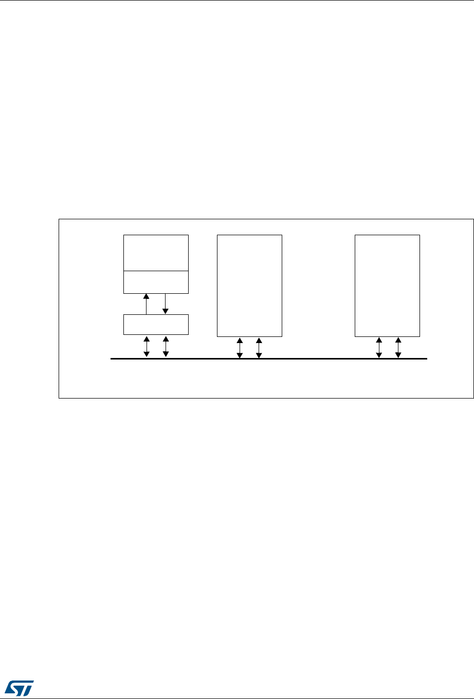
RM0394 Rev 4 1477/1600
RM0394 Controller area network (bxCAN)
1519
44.3 bxCAN general description
In today CAN applications, the number of nodes in a network is increasing and often several
networks are linked together via gateways. Typically the number of messages in the system
(to be handled by each node) has significantly increased. In addition to the application
messages, Network Management and Diagnostic messages have been introduced.
•An enhanced filtering mechanism is required to handle each type of message.
Furthermore, application tasks require more CPU time, therefore real-time constraints
caused by message reception have to be reduced.
•A receive FIFO scheme allows the CPU to be dedicated to application tasks for a long
time period without losing messages.
The standard HLP (Higher Layer Protocol) based on standard CAN drivers requires an
efficient interface to the CAN controller.
Figure 476. CAN network topology
44.3.1 CAN 2.0B active core
The bxCAN module handles the transmission and the reception of CAN messages fully
autonomously. Standard identifiers (11-bit) and extended identifiers (29-bit) are fully
supported by hardware.
44.3.2 Control, status and configuration registers
The application uses these registers to:
•Configure CAN parameters, e.g. baud rate
•Request transmissions
•Handle receptions
•Manage interrupts
•Get diagnostic information
44.3.3 Tx mailboxes
Three transmit mailboxes are provided to the software for setting up messages. The
transmission Scheduler decides which mailbox has to be transmitted first.
&$1QRGH
&$1QRGH
&$1QRGHQ
&$1
&$1
+LJK /RZ
&$1
&$1
5[ 7[
&$1
7UDQVFHLYHU
&$1
&RQWUROOHU
0&8
&$1%XV
$SSOLFDWLRQ
069
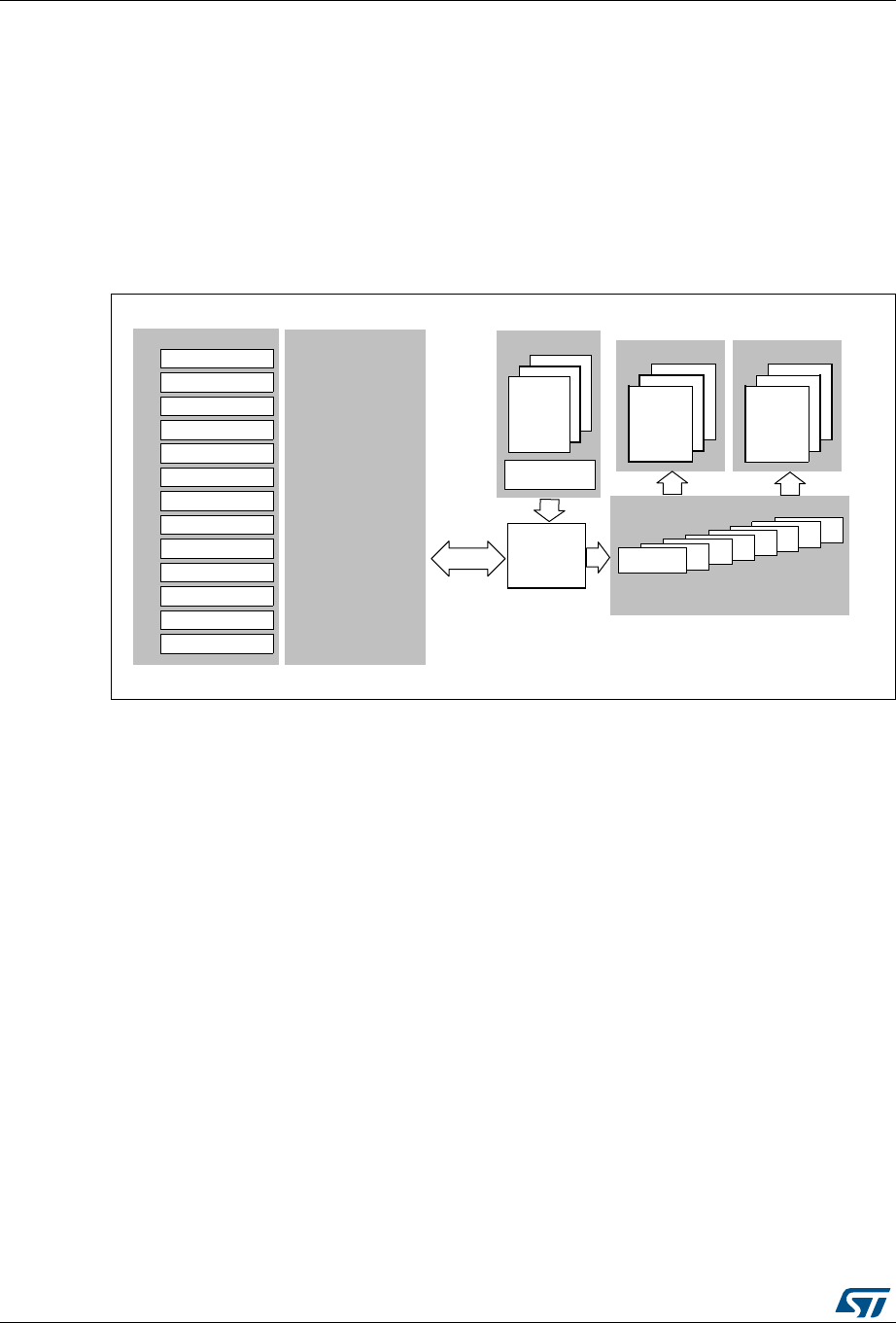
Controller area network (bxCAN) RM0394
1478/1600 RM0394 Rev 4
44.3.4 Acceptance filters
The bxCAN provides up to 14 scalable/configurable identifier filter banks in single CAN
configuration, for selecting the incoming messages, that the software needs and discarding
the others.
Receive FIFO
Two receive FIFOs are used by hardware to store the incoming messages. Three complete
messages can be stored in each FIFO. The FIFOs are managed completely by hardware.
Figure 477. Single-CAN block diagram
44.4 bxCAN operating modes
bxCAN has three main operating modes: initialization, normal and Sleep. After a
hardware reset, bxCAN is in Sleep mode to reduce power consumption and an internal pull-
up is active on CANTX. The software requests bxCAN to enter initialization or Sleep mode
by setting the INRQ or SLEEP bits in the CAN_MCR register. Once the mode has been
entered, bxCAN confirms it by setting the INAK or SLAK bits in the CAN_MSR register and
the internal pull-up is disabled. When neither INAK nor SLAK are set, bxCAN is in normal
mode. Before entering normal mode bxCAN always has to synchronize on the CAN bus.
To synchronize, bxCAN waits until the CAN bus is idle, this means 11 consecutive recessive
bits have been monitored on CANRX.
44.4.1 Initialization mode
The software initialization can be done while the hardware is in Initialization mode. To enter
this mode the software sets the INRQ bit in the CAN_MCR register and waits until the
hardware has confirmed the request by setting the INAK bit in the CAN_MSR register.
To leave Initialization mode, the software clears the INQR bit. bxCAN has left Initialization
mode once the INAK bit has been cleared by hardware.
While in Initialization Mode, all message transfers to and from the CAN bus are stopped and
the status of the CAN bus output CANTX is recessive (high).
06Y9
ϭϮ
͘͘
ĐĐĞƉƚĂŶĐĞ &ŝůƚĞƌƐ
͘͘
ϯ
Ϯ
ϭ
&ŝůƚĞƌ Ϭ
ϭϯ
DĂŝůďŽdž Ϭ
ϭ
Ϯ
ZĞĐĞŝǀĞ &/&K ϭ
DĂŝůďŽ dž Ϭ
ϭ
Ϯ
ZĞ Đ Ğŝ ǀĞ & /& K Ϭ
DĂŝůďŽ dž Ϭ
ϭ
Ϯ
ddž DĂŝůďŽ dž ĞƐ
DĞŵ ŽƌLJ
ĐĐĞƐƐ
ŽŶƚƌŽůůĞƌ
ŽŶƚƌŽů
^ƚĂƚƵƐ
Zdž &/&K Ϭ ^ƚĂƚƵƐ
Zdž &/&K ϭ ^ƚĂƚƵƐ
ƌƌŽƌ ^ƚĂƚƵƐ
ŝƚ dŝŵŝŶŐ
&ŝůƚĞƌ DŽĚ Ğ
&ŝ ůƚĞƌ ^Đ Ă ůĞ
/ŶƚĞƌƌƵƉ ƚ ŶĂďů Ğ
ŽŶ ƚƌŽů ͬ^ ƚĂ ƚƵƐ ͬ ŽŶ Ĩŝ ŐƵƌĂ ƚŝŽ Ŷ
ddž ^ƚĂƚƵƐ
&ŝůƚĞƌ &/&K ƐƐŝŐŶ
&ŝůƚĞƌ DĂ ƐƚĞƌ
&ŝ ůƚĞƌ Đ ƚŝ ǀĂƚŝŽ Ŷ
E Ϯ͘Ϭ Đ ƚŝǀĞ Žƌ Ğ
EϱϭϮďLJƚĞƐ^ZD
DĂƐƚĞƌ
ƌĞƚƐĂDƌĞƚƐĂD
D ĂƐ ƚĞ ƌ &ŝů ƚĞ ƌ Ɛ ^ ůĂ ǀ Ğ & ŝůƚ ĞƌƐ
;Ϭ ƚŽ Ϯϳ Ϳ
;Ϭ ƚŽ ϮϳͿ
dƌĂŶƐŵŝƐƐŝŽŶ
ƐĐŚĞĚƵůĞƌ

RM0394 Rev 4 1479/1600
RM0394 Controller area network (bxCAN)
1519
Entering Initialization Mode does not change any of the configuration registers.
To initialize the CAN Controller, software has to set up the Bit Timing (CAN_BTR) and CAN
options (CAN_MCR) registers.
To initialize the registers associated with the CAN filter banks (mode, scale, FIFO
assignment, activation and filter values), software has to set the FINIT bit (CAN_FMR). Filter
initialization also can be done outside the initialization mode.
Note: When FINIT=1, CAN reception is deactivated.
The filter values also can be modified by deactivating the associated filter activation bits (in
the CAN_FA1R register).
If a filter bank is not used, it is recommended to leave it non active (leave the corresponding
FACT bit cleared).
44.4.2 Normal mode
Once the initialization is complete, the software must request the hardware to enter Normal
mode to be able to synchronize on the CAN bus and start reception and transmission.
The request to enter Normal mode is issued by clearing the INRQ bit in the CAN_MCR
register. The bxCAN enters Normal mode and is ready to take part in bus activities when it
has synchronized with the data transfer on the CAN bus. This is done by waiting for the
occurrence of a sequence of 11 consecutive recessive bits (Bus Idle state). The switch to
Normal mode is confirmed by the hardware by clearing the INAK bit in the CAN_MSR
register.
The initialization of the filter values is independent from Initialization Mode but must be done
while the filter is not active (corresponding FACTx bit cleared). The filter scale and mode
configuration must be configured before entering Normal Mode.
44.4.3 Sleep mode (low-power)
To reduce power consumption, bxCAN has a low-power mode called Sleep mode. This
mode is entered on software request by setting the SLEEP bit in the CAN_MCR register. In
this mode, the bxCAN clock is stopped, however software can still access the bxCAN
mailboxes.
If software requests entry to initialization mode by setting the INRQ bit while bxCAN is in
Sleep mode, it must also clear the SLEEP bit.
bxCAN can be woken up (exit Sleep mode) either by software clearing the SLEEP bit or on
detection of CAN bus activity.
On CAN bus activity detection, hardware automatically performs the wakeup sequence by
clearing the SLEEP bit if the AWUM bit in the CAN_MCR register is set. If the AWUM bit is
cleared, software has to clear the SLEEP bit when a wakeup interrupt occurs, in order to exit
from Sleep mode.
Note: If the wakeup interrupt is enabled (WKUIE bit set in CAN_IER register) a wakeup interrupt
will be generated on detection of CAN bus activity, even if the bxCAN automatically
performs the wakeup sequence.
After the SLEEP bit has been cleared, Sleep mode is exited once bxCAN has synchronized
with the CAN bus, refer to Figure 478: bxCAN operating modes. The Sleep mode is exited
once the SLAK bit has been cleared by hardware.
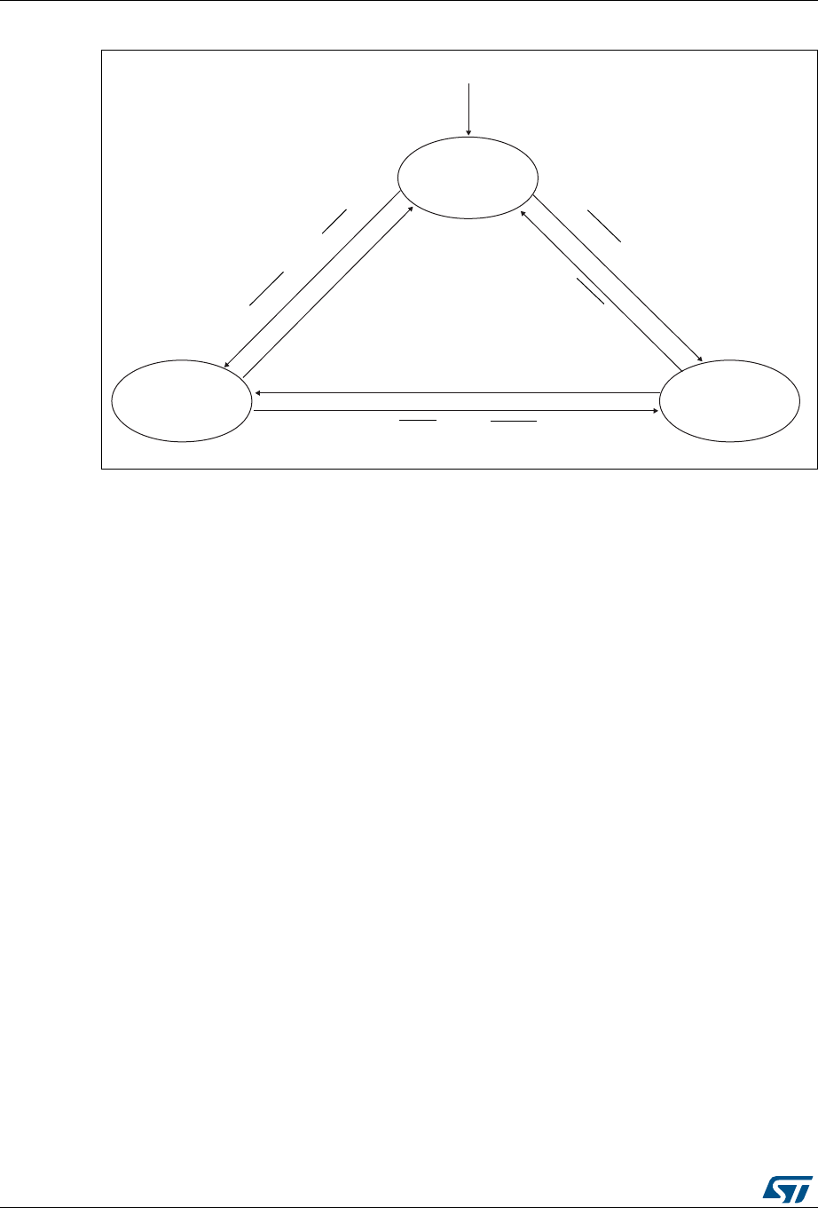
Controller area network (bxCAN) RM0394
1480/1600 RM0394 Rev 4
Figure 478. bxCAN operating modes
1. ACK = The wait state during which hardware confirms a request by setting the INAK or SLAK bits in the
CAN_MSR register
2. SYNC = The state during which bxCAN waits until the CAN bus is idle, meaning 11 consecutive recessive
bits have been monitored on CANRX
44.5 Test mode
Test mode can be selected by the SILM and LBKM bits in the CAN_BTR register. These bits
must be configured while bxCAN is in Initialization mode. Once test mode has been
selected, the INRQ bit in the CAN_MCR register must be reset to enter Normal mode.
44.5.1 Silent mode
The bxCAN can be put in Silent mode by setting the SILM bit in the CAN_BTR register.
In Silent mode, the bxCAN is able to receive valid data frames and valid remote frames, but
it sends only recessive bits on the CAN bus and it cannot start a transmission. If the bxCAN
has to send a dominant bit (ACK bit, overload flag, active error flag), the bit is rerouted
internally so that the CAN Core monitors this dominant bit, although the CAN bus may
remain in recessive state. Silent mode can be used to analyze the traffic on a CAN bus
without affecting it by the transmission of dominant bits (Acknowledge Bits, Error Frames).
6OHHS
1RUPDO
5HVHW
,1546<1&6/((3
DL
6/$.
,1$.
6/$.
,1$.
6/$.
,1$.
,154$&.
6/((3,154$&.
6/((3,154$&.
6/((3$&.
6/((36<1&,154
,QLWLDOL]DWLRQ
RM0394 Rev 4 1481/1600
RM0394 Controller area network (bxCAN)
1519
Figure 479. bxCAN in silent mode
44.5.2 Loop back mode
The bxCAN can be set in Loop Back Mode by setting the LBKM bit in the CAN_BTR
register. In Loop Back Mode, the bxCAN treats its own transmitted messages as received
messages and stores them (if they pass acceptance filtering) in a Receive mailbox.
Figure 480. bxCAN in loop back mode
This mode is provided for self-test functions. To be independent of external events, the CAN
Core ignores acknowledge errors (no dominant bit sampled in the acknowledge slot of a
data / remote frame) in Loop Back Mode. In this mode, the bxCAN performs an internal
feedback from its Tx output to its Rx input. The actual value of the CANRX input pin is
disregarded by the bxCAN. The transmitted messages can be monitored on the CANTX pin.
44.5.3 Loop back combined with silent mode
It is also possible to combine Loop Back mode and Silent mode by setting the LBKM and
SILM bits in the CAN_BTR register. This mode can be used for a “Hot Selftest”, meaning the
bxCAN can be tested like in Loop Back mode but without affecting a running CAN system
connected to the CANTX and CANRX pins. In this mode, the CANRX pin is disconnected
from the bxCAN and the CANTX pin is held recessive.
E[&$1
&$17; &$15;
7[ 5[
069
E[&$1
&$17; &$15;
7[ 5[
069
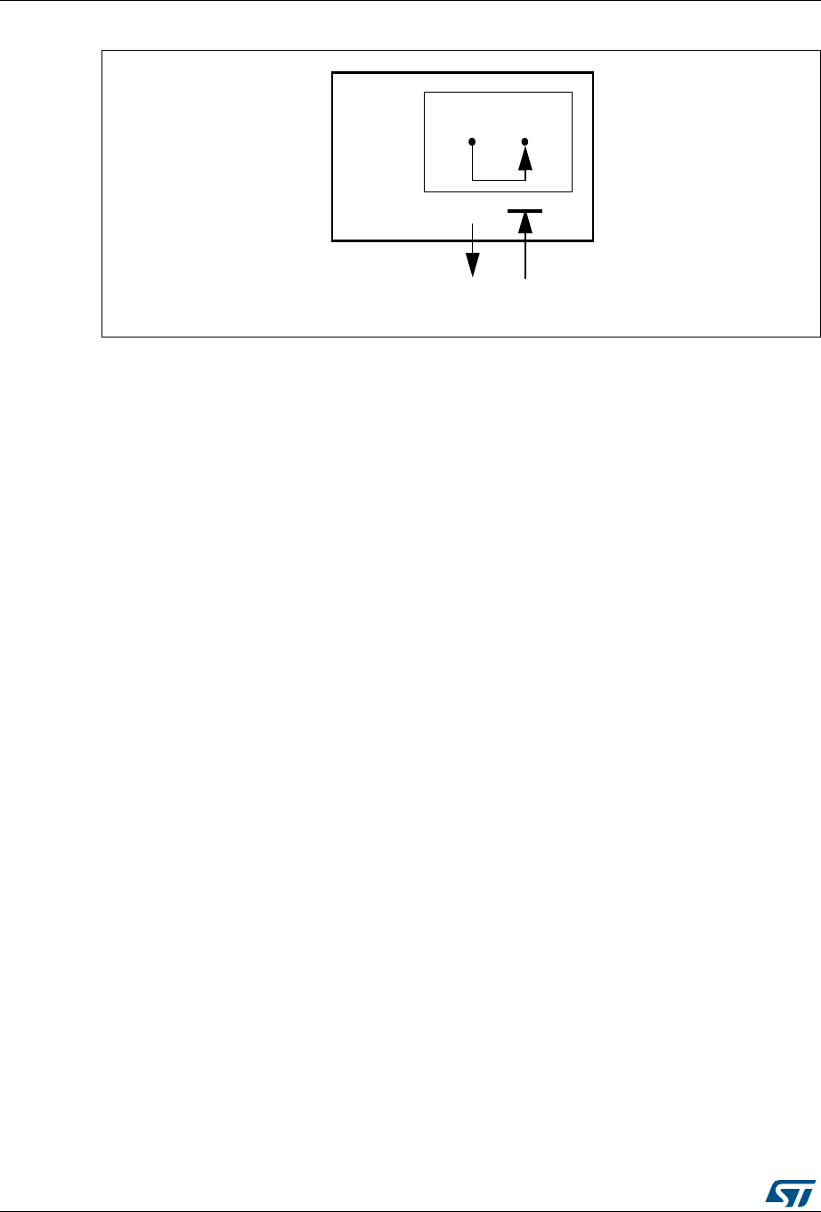
Controller area network (bxCAN) RM0394
1482/1600 RM0394 Rev 4
Figure 481. bxCAN in combined mode
44.6 Behavior in debug mode
When the microcontroller enters the debug mode (Cortex®-M4 core halted), the bxCAN
continues to work normally or stops, depending on:
•the DBG_CAN1_STOP bit in the DBG module for the single mode.
•the DBF bit in CAN_MCR. For more details, refer to Section 44.9.2: CAN control and
status registers.
44.7 bxCAN functional description
44.7.1 Transmission handling
In order to transmit a message, the application must select one empty transmit mailbox, set
up the identifier, the data length code (DLC) and the data before requesting the transmission
by setting the corresponding TXRQ bit in the CAN_TIxR register. Once the mailbox has left
empty state, the software no longer has write access to the mailbox registers. Immediately
after the TXRQ bit has been set, the mailbox enters pending state and waits to become the
highest priority mailbox, see Transmit Priority. As soon as the mailbox has the highest
priority it will be scheduled for transmission. The transmission of the message of the
scheduled mailbox will start (enter transmit state) when the CAN bus becomes idle. Once
the mailbox has been successfully transmitted, it will become empty again. The hardware
indicates a successful transmission by setting the RQCP and TXOK bits in the CAN_TSR
register.
If the transmission fails, the cause is indicated by the ALST bit in the CAN_TSR register in
case of an Arbitration Lost, and/or the TERR bit, in case of transmission error detection.
Transmit priority
By identifier
When more than one transmit mailbox is pending, the transmission order is given by the
identifier of the message stored in the mailbox. The message with the lowest identifier value
has the highest priority according to the arbitration of the CAN protocol. If the identifier
values are equal, the lower mailbox number will be scheduled first.
E[&$1
&$17; &$15;
7[ 5[
069
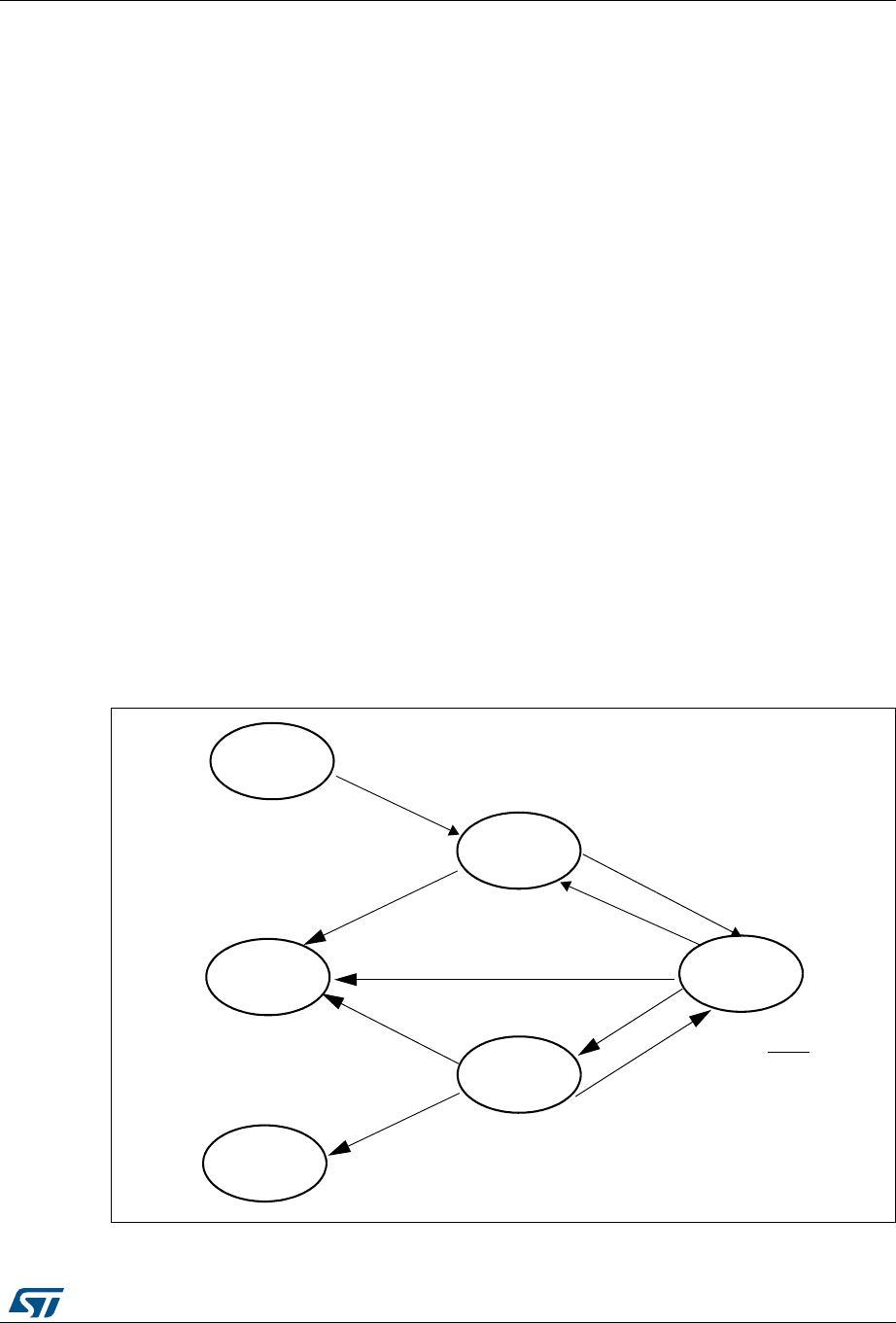
RM0394 Rev 4 1483/1600
RM0394 Controller area network (bxCAN)
1519
By transmit request order
The transmit mailboxes can be configured as a transmit FIFO by setting the TXFP bit in the
CAN_MCR register. In this mode the priority order is given by the transmit request order.
This mode is very useful for segmented transmission.
Abort
A transmission request can be aborted by the user setting the ABRQ bit in the CAN_TSR
register. In pending or scheduled state, the mailbox is aborted immediately. An abort
request while the mailbox is in transmit state can have two results. If the mailbox is
transmitted successfully the mailbox becomes empty with the TXOK bit set in the
CAN_TSR register. If the transmission fails, the mailbox becomes scheduled, the
transmission is aborted and becomes empty with TXOK cleared. In all cases the mailbox
will become empty again at least at the end of the current transmission.
Non automatic retransmission mode
This mode has been implemented in order to fulfill the requirement of the Time Triggered
Communication option of the CAN standard. To configure the hardware in this mode the
NART bit in the CAN_MCR register must be set.
In this mode, each transmission is started only once. If the first attempt fails, due to an
arbitration loss or an error, the hardware will not automatically restart the message
transmission.
At the end of the first transmission attempt, the hardware considers the request as
completed and sets the RQCP bit in the CAN_TSR register. The result of the transmission is
indicated in the CAN_TSR register by the TXOK, ALST and TERR bits.
Figure 482. Transmit mailbox states
(037<
7;54
54&3 ;
7;2. ;
3(1',1*
54&3
7;2.
6&+('8/('
54&3
7;2.
0DLOER[KDV
75$160,7
54&3
7;2.
&$1%XV ,'/(
7UDQVPLWIDLOHG1$57
7UDQVPLWVXFFHHGHG
0DLOER[GRHVQRW
(037<
54&3
7;2.
KLJKHVWSULRULW\
KDYHKLJKHVWSULRULW\
(037<
54&3
7;2.
$%54
$%54
7UDQVPLWIDLOHG1$57
70(
70(
70(
70(
70(
70(
069
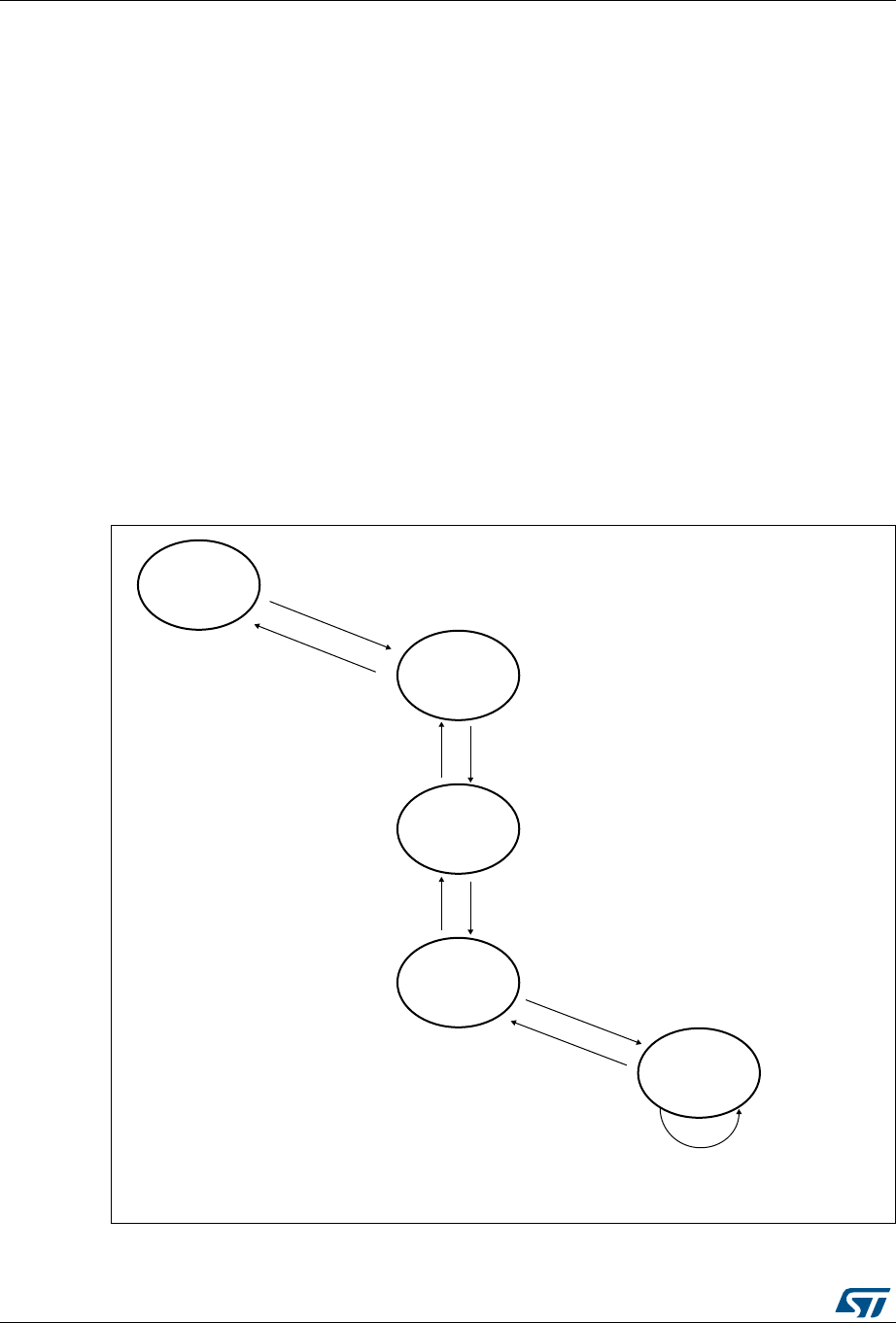
Controller area network (bxCAN) RM0394
1484/1600 RM0394 Rev 4
44.7.2 Time triggered communication mode
In this mode, the internal counter of the CAN hardware is activated and used to generate the
Time Stamp value stored in the CAN_RDTxR/CAN_TDTxR registers, respectively (for Rx
and Tx mailboxes). The internal counter is incremented each CAN bit time (refer to
Section 44.7.7: Bit timing). The internal counter is captured on the sample point of the Start
Of Frame bit in both reception and transmission.
44.7.3 Reception handling
For the reception of CAN messages, three mailboxes organized as a FIFO are provided. In
order to save CPU load, simplify the software and guarantee data consistency, the FIFO is
managed completely by hardware. The application accesses the messages stored in the
FIFO through the FIFO output mailbox.
Valid message
A received message is considered as valid when it has been received correctly according to
the CAN protocol (no error until the last but one bit of the EOF field) and It passed through
the identifier filtering successfully, see Section 44.7.4: Identifier filtering.
Figure 483. Receive FIFO states
%-049
6ALID-ESSAGE
&-0X
&/62
0%.$).'?
&-0X
&/62
2ECEIVED
0%.$).'?
&-0X
&/62
0%.$).'?
&-0X
&/62
6ALID-ESSAGE
2ECEIVED
2ELEASE
/6%225.
&-0X
&/62
-AILBOX
2ELEASE
-AILBOX
6ALID-ESSAGE
2ECEIVED
6ALID-ESSAGE
2ECEIVED
2ELEASE
-AILBOX
2ELEASE
-AILBOX
6ALID-ESSAGE
2ECEIVED
2&/-
2&/-
2&/-
-36

RM0394 Rev 4 1485/1600
RM0394 Controller area network (bxCAN)
1519
FIFO management
Starting from the empty state, the first valid message received is stored in the FIFO which
becomes pending_1. The hardware signals the event setting the FMP[1:0] bits in the
CAN_RFR register to the value 01b. The message is available in the FIFO output mailbox.
The software reads out the mailbox content and releases it by setting the RFOM bit in the
CAN_RFR register. The FIFO becomes empty again. If a new valid message has been
received in the meantime, the FIFO stays in pending_1 state and the new message is
available in the output mailbox.
If the application does not release the mailbox, the next valid message will be stored in the
FIFO which enters pending_2 state (FMP[1:0] = 10b). The storage process is repeated for
the next valid message putting the FIFO into pending_3 state (FMP[1:0] = 11b). At this
point, the software must release the output mailbox by setting the RFOM bit, so that a
mailbox is free to store the next valid message. Otherwise the next valid message received
will cause a loss of message.
Refer also to Section 44.7.5: Message storage
Overrun
Once the FIFO is in pending_3 state (i.e. the three mailboxes are full) the next valid
message reception will lead to an overrun and a message will be lost. The hardware
signals the overrun condition by setting the FOVR bit in the CAN_RFR register. Which
message is lost depends on the configuration of the FIFO:
•If the FIFO lock function is disabled (RFLM bit in the CAN_MCR register cleared) the
last message stored in the FIFO will be overwritten by the new incoming message. In
this case the latest messages will be always available to the application.
•If the FIFO lock function is enabled (RFLM bit in the CAN_MCR register set) the most
recent message will be discarded and the software will have the three oldest messages
in the FIFO available.
Reception related interrupts
Once a message has been stored in the FIFO, the FMP[1:0] bits are updated and an
interrupt request is generated if the FMPIE bit in the CAN_IER register is set.
When the FIFO becomes full (i.e. a third message is stored) the FULL bit in the CAN_RFR
register is set and an interrupt is generated if the FFIE bit in the CAN_IER register is set.
On overrun condition, the FOVR bit is set and an interrupt is generated if the FOVIE bit in
the CAN_IER register is set.
44.7.4 Identifier filtering
In the CAN protocol the identifier of a message is not associated with the address of a node
but related to the content of the message. Consequently a transmitter broadcasts its
message to all receivers. On message reception a receiver node decides - depending on
the identifier value - whether the software needs the message or not. If the message is
needed, it is copied into the SRAM. If not, the message must be discarded without
intervention by the software.
To fulfill this requirement the bxCAN Controller provides 14 configurable and scalable filter
banks (13-0) to the application, in order to receive only the messages the software needs.

Controller area network (bxCAN) RM0394
1486/1600 RM0394 Rev 4
This hardware filtering saves CPU resources which would be otherwise needed to perform
filtering by software. Each filter bank x consists of two 32-bit registers, CAN_FxR0 and
CAN_FxR1.
Scalable width
To optimize and adapt the filters to the application needs, each filter bank can be scaled
independently. Depending on the filter scale a filter bank provides:
•One 32-bit filter for the STDID[10:0], EXTID[17:0], IDE and RTR bits.
•Two 16-bit filters for the STDID[10:0], RTR, IDE and EXTID[17:15] bits.
Refer to Figure 484.
Furthermore, the filters can be configured in mask mode or in identifier list mode.
Mask mode
In mask mode the identifier registers are associated with mask registers specifying which
bits of the identifier are handled as “must match” or as “don’t care”.
Identifier list mode
In identifier list mode, the mask registers are used as identifier registers. Thus instead of
defining an identifier and a mask, two identifiers are specified, doubling the number of single
identifiers. All bits of the incoming identifier must match the bits specified in the filter
registers.
Filter bank scale and mode configuration
The filter banks are configured by means of the corresponding CAN_FMR register. To
configure a filter bank it must be deactivated by clearing the FACT bit in the CAN_FAR
register. The filter scale is configured by means of the corresponding FSCx bit in the
CAN_FS1R register, refer to Figure 484. The identifier list or identifier mask mode for the
corresponding Mask/Identifier registers is configured by means of the FBMx bits in the
CAN_FMR register.
To filter a group of identifiers, configure the Mask/Identifier registers in mask mode.
To select single identifiers, configure the Mask/Identifier registers in identifier list mode.
Filters not used by the application should be left deactivated.
Each filter within a filter bank is numbered (called the Filter Number) from 0 to a maximum
dependent on the mode and the scale of each of the filter banks.
Concerning the filter configuration, refer to Figure 484.
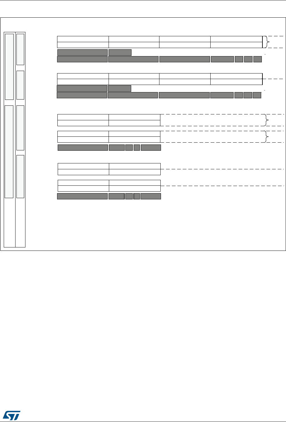
RM0394 Rev 4 1487/1600
RM0394 Controller area network (bxCAN)
1519
Figure 484. Filter bank scale configuration - register organization
Filter match index
Once a message has been received in the FIFO it is available to the application. Typically,
application data is copied into SRAM locations. To copy the data to the right location the
application has to identify the data by means of the identifier. To avoid this, and to ease the
access to the SRAM locations, the CAN controller provides a Filter Match Index.
This index is stored in the mailbox together with the message according to the filter priority
rules. Thus each received message has its associated filter match index.
The Filter Match index can be used in two ways:
•Compare the Filter Match index with a list of expected values.
•Use the Filter Match Index as an index on an array to access the data destination
location.
For non masked filters, the software no longer has to compare the identifier.
If the filter is masked the software reduces the comparison to the masked bits only.
The index value of the filter number does not take into account the activation state of the
filter banks. In addition, two independent numbering schemes are used, one for each FIFO.
06Y9
2QH%LW)LOWHU,GHQWLILHU0DVN
[ ILOWHUEDQNQXPEHU
)6&[ )6&[
7KHVHELWVDUHORFDWHGLQWKH&$1B)65UHJLVWHU
)LOWHU%DQN6FDOH
,'
0DVN
,'
67,'>@
0DSSLQJ67','
,'
,'
,'
,'
,'
,'
,'
Q
Q
Q
Q
&RQILJ%LWV
,' ,GHQWLILHU
)%0[ )%0[
)%0[
)%0[
)LOWHU%DQN0RGH
7ZR%LW)LOWHUV,GHQWLILHU/LVW
7ZR%LW)LOWHUV,GHQWLILHU0DVN
)RXU%LW)LOWHUV,GHQWLILHU/LVW
0DSSLQJ
0DSSLQJ
&$1B)[5>@
&$1B)[5>@ &$1B)[5>@
&$1B)[5>@ &$1B)[5>@
&$1B)[5>@
&$1B)[5>@
&$1B)[5>@
&$1B)[5>@
&$1B)[5>@ &$1B)[5>@
&$1B)[5>@ &$1B)[5>@
&$1B)[5>@
&$1B)[5>@
&$1B)[5>@
&$1B)[5>@
&$1B)[5>@
&$1B)[5>@
&$1B)[5>@
&$1B)[5>@
&$1B)[5>@
&$1B)[5>@
&$1B)[5>@
&$1B)[5>@
&$1B)[5>@
&$1B)[5>@
&$1B)[5>@
&$1B)[5>@
&$1B)[5>@
&$1B)[5>@
&$1B)[5>@
7KHVHELWVDUHORFDWHGLQWKH&$1B)05UHJLVWHU
Q
Q
Q
Q
Q
)LOWHU
1XP
0DVN
0DVN
67,'>@
(;,'>@,'(57567,'>@67,'>@
(;,'>@
,'(
575
67,'>@
67,'>@
(;7,'>@
0DSSLQJ([W,'
(;,'>@ (;,'>@ (;,'>@ ,'( 575
67,'>@
0DSSLQJ67',' 67,'>@
(;7,'>@
0DSSLQJ([W,'
(;,'>@ (;,'>@ (;,'>@ ,'( 575
Controller area network (bxCAN) RM0394
1488/1600 RM0394 Rev 4
Refer to Figure 485 for an example.
Figure 485. Example of filter numbering
Filter priority rules
Depending on the filter combination it may occur that an identifier passes successfully
through several filters. In this case the filter match value stored in the receive mailbox is
chosen according to the following priority rules:
•A 32-bit filter takes priority over a 16-bit filter.
•For filters of equal scale, priority is given to the Identifier List mode over the Identifier
Mask mode
•For filters of equal scale and mode, priority is given by the filter number (the lower the
number, the higher the priority).
,'/LVWELW
,'0DVNELW
,'/LVWELW
,'/LVWELW
'HDFWLYDWHG
,'0DVNELW
,'/LVWELW
)LOWHU
,'0DVNELW
),)2 )LOWHU
,'0DVNELW
,'/LVWELW
,'0DVNELW
,'/LVWELW
'HDFWLYDWHG
,'0DVNELW
,'/LVWELW
)LOWHU
,'0DVNELW
),)2 )LOWHU
'HDFWLYDWHG
1XP 1XP%DQN%DQN
069
,' ,GHQWLILHU
RM0394 Rev 4 1489/1600
RM0394 Controller area network (bxCAN)
1519
Figure 486. Filtering mechanism - example
The example above shows the filtering principle of the bxCAN. On reception of a message,
the identifier is compared first with the filters configured in identifier list mode. If there is a
match, the message is stored in the associated FIFO and the index of the matching filter is
stored in the Filter Match Index. As shown in the example, the identifier matches with
Identifier #2 thus the message content and FMI 2 is stored in the FIFO.
If there is no match, the incoming identifier is then compared with the filters configured in
mask mode.
If the identifier does not match any of the identifiers configured in the filters, the message is
discarded by hardware without disturbing the software.
44.7.5 Message storage
The interface between the software and the hardware for the CAN messages is
implemented by means of mailboxes. A mailbox contains all information related to a
message; identifier, data, control, status and time stamp information.
Transmit mailbox
The software sets up the message to be transmitted in an empty transmit mailbox. The
status of the transmission is indicated by hardware in the CAN_TSR register.
,GHQWLILHU/LVW
0HVVDJH'LVFDUGHG
,GHQWLILHU0DVN
,GHQWLILHU
,GHQWLILHU
,GHQWLILHU
,GHQWLILHU
,GHQWLILHU
0DVN
,GHQWLILHU
0DVN
,GHQWLILHU
0HVVDJH5HFHLYHG
&WUO 'DWD
,GHQWLILHU0DWFK
0HVVDJH
6WRUHG
5HFHLYH),)2
1R0DWFK
)RXQG
)LOWHUQXPEHUVWRUHGLQWKH
)LOWHU0DWFK,QGH[ILHOG
ZLWKLQWKH&$1B5'7[5
UHJLVWHU
)0,
)LOWHUEDQN
([DPSOHRIILOWHUEDQNVLQELWXQLGHQWLILHGPRGHDQG
1XP
WKHUHPDLQLQJLQELWLGHQWLILHUPDVNPRGH
069
Controller area network (bxCAN) RM0394
1490/1600 RM0394 Rev 4
Receive mailbox
When a message has been received, it is available to the software in the FIFO output
mailbox. Once the software has handled the message (e.g. read it) the software must
release the FIFO output mailbox by means of the RFOM bit in the CAN_RFR register to
make the next incoming message available. The filter match index is stored in the MFMI
field of the CAN_RDTxR register. The 16-bit time stamp value is stored in the TIME[15:0]
field of CAN_RDTxR.
Figure 487. CAN error state diagram
Table 259. Transmit mailbox mapping
Offset to transmit mailbox base address Register name
0CAN_TIxR
4 CAN_TDTxR
8CAN_TDLxR
12 CAN_TDHxR
Table 260. Receive mailbox mapping
Offset to receive mailbox base
address (bytes) Register name
0CAN_RIxR
4 CAN_RDTxR
8 CAN_RDLxR
12 CAN_RDHxR
(5525$&7,9(
DL
(55253$66,9(
%862))
:KHQ7(&DQG5(&
:KHQ7(&RU5(&!
:KHQ7(&!:KHQUHFHVVLYHELWVRFFXU

RM0394 Rev 4 1491/1600
RM0394 Controller area network (bxCAN)
1519
44.7.6 Error management
The error management as described in the CAN protocol is handled entirely by hardware
using a Transmit Error Counter (TEC value, in CAN_ESR register) and a Receive Error
Counter (REC value, in the CAN_ESR register), which get incremented or decremented
according to the error condition. For detailed information about TEC and REC management,
refer to the CAN standard.
Both of them may be read by software to determine the stability of the network.
Furthermore, the CAN hardware provides detailed information on the current error status in
CAN_ESR register. By means of the CAN_IER register (ERRIE bit, etc.), the software can
configure the interrupt generation on error detection in a very flexible way.
Bus-Off recovery
The Bus-Off state is reached when TEC is greater than 255, this state is indicated by BOFF
bit in CAN_ESR register. In Bus-Off state, the bxCAN is no longer able to transmit and
receive messages.
Depending on the ABOM bit in the CAN_MCR register bxCAN will recover from Bus-Off
(become error active again) either automatically or on software request. But in both cases
the bxCAN has to wait at least for the recovery sequence specified in the CAN standard
(128 occurrences of 11 consecutive recessive bits monitored on CANRX).
If ABOM is set, the bxCAN will start the recovering sequence automatically after it has
entered Bus-Off state.
If ABOM is cleared, the software must initiate the recovering sequence by requesting
bxCAN to enter and to leave initialization mode.
Note: In initialization mode, bxCAN does not monitor the CANRX signal, therefore it cannot
complete the recovery sequence. To recover, bxCAN must be in normal mode.
44.7.7 Bit timing
The bit timing logic monitors the serial bus-line and performs sampling and adjustment of
the sample point by synchronizing on the start-bit edge and resynchronizing on the following
edges.
Its operation may be explained simply by splitting nominal bit time into three segments as
follows:
•Synchronization segment (SYNC_SEG): a bit change is expected to occur within this
time segment. It has a fixed length of one time quantum (1 x tq).
•Bit segment 1 (BS1): defines the location of the sample point. It includes the
PROP_SEG and PHASE_SEG1 of the CAN standard. Its duration is programmable
between 1 and 16 time quanta but may be automatically lengthened to compensate for
positive phase drifts due to differences in the frequency of the various nodes of the
network.
•Bit segment 2 (BS2): defines the location of the transmit point. It represents the
PHASE_SEG2 of the CAN standard. Its duration is programmable between 1 and 8
time quanta but may also be automatically shortened to compensate for negative
phase drifts.
The resynchronization Jump Width (SJW) defines an upper bound to the amount of
lengthening or shortening of the bit segments. It is programmable between 1 and 4 time
quanta.
Controller area network (bxCAN) RM0394
1492/1600 RM0394 Rev 4
A valid edge is defined as the first transition in a bit time from dominant to recessive bus
level provided the controller itself does not send a recessive bit.
If a valid edge is detected in BS1 instead of SYNC_SEG, BS1 is extended by up to SJW so
that the sample point is delayed.
Conversely, if a valid edge is detected in BS2 instead of SYNC_SEG, BS2 is shortened by
up to SJW so that the transmit point is moved earlier.
As a safeguard against programming errors, the configuration of the Bit Timing Register
(CAN_BTR) is only possible while the device is in Standby mode.
Note: For a detailed description of the CAN bit timing and resynchronization mechanism, refer to
the ISO 11898 standard.
Figure 488. Bit timing
6<1&B6(* %,76(*0(17%6 %,76(*0(17%6
120,1$/%,77,0(
[WTW%6 W%6
6$03/(32,17 75$160,732,17
1RPLQDO%LW7LPH ;WTW%6 W%6
ZLWK
W%6 WT[76>@
W%6 WT[76>@
WT %53>@[W3&/.
W3&/. WLPHSHULRGRIWKH$3%FORFN
%53>@76>@DQG76>@DUHGHILQHGLQWKH&$1B%755HJLVWHU
%DXG 5DWH
1RPLQDO%LW7LPH
ZKHUHWTUHIHUVWRWKH7LPHTXDQWXP
069
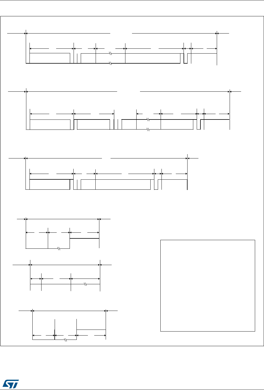
RM0394 Rev 4 1493/1600
RM0394 Controller area network (bxCAN)
1519
Figure 489. CAN frames
DLE
,QWHU)UDPH6SDFH
6XVSHQG
7UDQVPLVVLRQ %XV,GOH
$Q\)UDPH
,QWHUPLVVLRQ
'DWD)UDPHRU
5HPRWH)UDPH
'DWD)UDPHRU
5HPRWH)UDPH (UURU)UDPH ,QWHU)UDPH6SDFH
RU2YHUORDG)UDPH
(UURU
'HOLPLWHU
)ODJ(FKR
(UURU
)ODJ
,QWHU)UDPH6SDFH
$&.
U
U
575
'/& &5& (2)
,'(
655
1
62)
,'
&5&)LHOG $&.)LHOG&WUO)LHOG$UELWUDWLRQ)LHOG$UELWUDWLRQ)LHOG 'DWD)LHOG
'DWD)UDPH([WHQGHG,GHQWLILHU
1
,QWHU)UDPH6SDFH
RU2YHUORDG)UDPH
,QWHU)UDPH6SDFH
1
$UELWUDWLRQ)LHOG &WUO)LHOG 'DWD)LHOG &5&)LHOG $&.)LHOG
,QWHU)UDPH6SDFH
RU2YHUORDG)UDPH
'DWD)UDPH6WDQGDUG,GHQWLILHU
1
'/& &5& (2)
$&.
,'
62)
575
,'(
U
,QWHU)UDPH6SDFH
62)
575
,'(
U
$&.
(2),' '/& &5&
$UELWUDWLRQ)LHOG &WUO)LHOG &5&)LHOG $&.)LHOG
,QWHU)UDPH6SDFH
RU2YHUORDG)UDPH
5HPRWH)UDPH
,QWHU)UDPH6SDFH
RU(UURU)UDPH
2YHUORDG)UDPH
(QGRI)UDPHRU
(UURU'HOLPLWHURU
2YHUORDG'HOLPLWHU
2YHUORDG
)ODJ
2YHUORDG
(FKR
2YHUORDG
'HOLPLWHU
1RWHV
1
62) 6WDUW2I)UDPH
,' ,GHQWLILHU
575 5HPRWH7UDQVPLVVLRQ5HTXHVW
,'( ,GHQWLILHU([WHQVLRQ%LW
U 5HVHUYHG%LW
'/& 'DWD/HQJWK&RGH
&5& &\FOLF5HGXQGDQF\&RGH
(UURUIODJGRPLQDQWELWVLIQRGHLVHUURU
DFWLYHHOVHUHFHVVLYHELWV
6XVSHQGWUDQVPLVVLRQDSSOLHVWRHUURU
SDVVLYHQRGHVRQO\
(2) (QGRI)UDPH
$&. $FNQRZOHGJHELW
&WUO &RQWURO
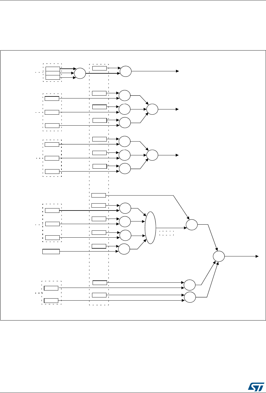
Controller area network (bxCAN) RM0394
1494/1600 RM0394 Rev 4
44.8 bxCAN interrupts
Four interrupt vectors are dedicated to bxCAN. Each interrupt source can be independently
enabled or disabled by means of the CAN Interrupt Enable Register (CAN_IER).
Figure 490. Event flags and interrupt generation
54&3
54&3
)03
&$1B765 70(,(
&$1B,(5
75$160,7
)03,(
)8//
)),(
)295
)29,(
&$1B5)5
),)2
(:*)
(:*,(
(39)
(39,(
%2))
%2),(
/(&
/(&,(
&$1B(65
(55,(
,17(55837
,17(55837
)03
)03,(
)8//
)),(
)295
)29,(
&$1B5)5
),)2
,17(55837
54&3
:.8,
:.8,(
&$1B065
,17(55837
(5525
67$786 &+$1*(
(55,
6/$.,
6/.,(
&$1B065
069

RM0394 Rev 4 1495/1600
RM0394 Controller area network (bxCAN)
1519
•The transmit interrupt can be generated by the following events:
– Transmit mailbox 0 becomes empty, RQCP0 bit in the CAN_TSR register set.
– Transmit mailbox 1 becomes empty, RQCP1 bit in the CAN_TSR register set.
– Transmit mailbox 2 becomes empty, RQCP2 bit in the CAN_TSR register set.
•The FIFO 0 interrupt can be generated by the following events:
– Reception of a new message, FMP0 bits in the CAN_RF0R register are not ‘00’.
– FIFO0 full condition, FULL0 bit in the CAN_RF0R register set.
– FIFO0 overrun condition, FOVR0 bit in the CAN_RF0R register set.
•The FIFO 1 interrupt can be generated by the following events:
– Reception of a new message, FMP1 bits in the CAN_RF1R register are not ‘00’.
– FIFO1 full condition, FULL1 bit in the CAN_RF1R register set.
– FIFO1 overrun condition, FOVR1 bit in the CAN_RF1R register set.
•The error and status change interrupt can be generated by the following events:
– Error condition, for more details on error conditions refer to the CAN Error Status
register (CAN_ESR).
– Wakeup condition, SOF monitored on the CAN Rx signal.
– Entry into Sleep mode.
44.9 CAN registers
The peripheral registers have to be accessed by words (32 bits).
44.9.1 Register access protection
Erroneous access to certain configuration registers can cause the hardware to temporarily
disturb the whole CAN network. Therefore the CAN_BTR register can be modified by
software only while the CAN hardware is in initialization mode.
Although the transmission of incorrect data will not cause problems at the CAN network
level, it can severely disturb the application. A transmit mailbox can be only modified by
software while it is in empty state, refer to Figure 482: Transmit mailbox states.
The filter values can be modified either deactivating the associated filter banks or by setting
the FINIT bit. Moreover, the modification of the filter configuration (scale, mode and FIFO
assignment) in CAN_FMxR, CAN_FSxR and CAN_FFAR registers can only be done when
the filter initialization mode is set (FINIT=1) in the CAN_FMR register.
44.9.2 CAN control and status registers
Refer to Section 1.2 for a list of abbreviations used in register descriptions.
CAN master control register (CAN_MCR)
Address offset: 0x00
Reset value: 0x0001 0002

Controller area network (bxCAN) RM0394
1496/1600 RM0394 Rev 4
31 30 29 28 27 26 25 24 23 22 21 20 19 18 17 16
Res. Res. Res. Res. Res. Res. Res. Res. Res. Res. Res. Res. Res. Res. Res. DBF
rw
1514131211109876543210
RESET Res. Res. Res. Res. Res. Res. Res. TTCM ABOM AWUM NART RFLM TXFP SLEEP INRQ
rs rw rw rw rw rw rw rw rw
Bits 31:17 Reserved, must be kept at reset value.
Bit 16 DBF: Debug freeze
0: CAN working during debug
1: CAN reception/transmission frozen during debug. Reception FIFOs can still be
accessed/controlled normally.
Bit 15 RESET: bxCAN software master reset
0: Normal operation.
1: Force a master reset of the bxCAN -> Sleep mode activated after reset (FMP bits and
CAN_MCR register are initialized to the reset values). This bit is automatically reset to 0.
Bits 14:8 Reserved, must be kept at reset value.
Bit 7 TTCM: Time triggered communication mode
0: Time Triggered Communication mode disabled.
1: Time Triggered Communication mode enabled
Note: For more information on Time Triggered Communication mode, refer to Section 44.7.2:
Time triggered communication mode.
Bit 6 ABOM: Automatic bus-off management
This bit controls the behavior of the CAN hardware on leaving the Bus-Off state.
0: The Bus-Off state is left on software request, once 128 occurrences of 11 recessive bits
have been monitored and the software has first set and cleared the INRQ bit of the
CAN_MCR register.
1: The Bus-Off state is left automatically by hardware once 128 occurrences of 11 recessive
bits have been monitored.
For detailed information on the Bus-Off state refer to Section 44.7.6: Error management.
Bit 5 AWUM: Automatic wakeup mode
This bit controls the behavior of the CAN hardware on message reception during Sleep
mode.
0: The Sleep mode is left on software request by clearing the SLEEP bit of the CAN_MCR
register.
1: The Sleep mode is left automatically by hardware on CAN message detection.
The SLEEP bit of the CAN_MCR register and the SLAK bit of the CAN_MSR register are
cleared by hardware.
Bit 4 NART
: No automatic retransmission
0: The CAN hardware will automatically retransmit the message until it has been
successfully transmitted according to the CAN standard.
1: A message will be transmitted only once, independently of the transmission result
(successful, error or arbitration lost).

RM0394 Rev 4 1497/1600
RM0394 Controller area network (bxCAN)
1519
CAN master status register (CAN_MSR)
Address offset: 0x04
Reset value: 0x0000 0C02
Bit 3 RFLM: Receive FIFO locked mode
0: Receive FIFO not locked on overrun. Once a receive FIFO is full the next incoming
message will overwrite the previous one.
1: Receive FIFO locked against overrun. Once a receive FIFO is full the next incoming
message will be discarded.
Bit 2 TXFP: Transmit FIFO priority
This bit controls the transmission order when several mailboxes are pending at the same
time.
0: Priority driven by the identifier of the message
1: Priority driven by the request order (chronologically)
Bit 1 SLEEP: Sleep mode request
This bit is set by software to request the CAN hardware to enter the Sleep mode. Sleep
mode will be entered as soon as the current CAN activity (transmission or reception of a
CAN frame) has been completed.
This bit is cleared by software to exit Sleep mode.
This bit is cleared by hardware when the AWUM bit is set and a SOF bit is detected on the
CAN Rx signal.
This bit is set after reset - CAN starts in Sleep mode.
Bit 0 INRQ: Initialization request
The software clears this bit to switch the hardware into normal mode. Once 11 consecutive
recessive bits have been monitored on the Rx signal the CAN hardware is synchronized and
ready for transmission and reception. Hardware signals this event by clearing the INAK bit in
the CAN_MSR register.
Software sets this bit to request the CAN hardware to enter initialization mode. Once
software has set the INRQ bit, the CAN hardware waits until the current CAN activity
(transmission or reception) is completed before entering the initialization mode. Hardware
signals this event by setting the INAK bit in the CAN_MSR register.
31 30 29 28 27 26 25 24 23 22 21 20 19 18 17 16
Res. Res. Res. Res. Res. Res. Res. Res. Res. Res. Res. Res. Res. Res. Res. Res.
1514131211109876543210
Res. Res. Res. Res. RX SAMP RXM TXM Res. Res. Res. SLAKI WKUI ERRI SLAK INAK
rrrr rc_w1rc_w1rc_w1rr
Bits 31:12 Reserved, must be kept at reset value.
Bit 11 RX: CAN Rx signal
Monitors the actual value of the CAN_RX Pin.
Bit 10 SAMP: Last sample point
The value of RX on the last sample point (current received bit value).
Bit 9 RXM: Receive mode
The CAN hardware is currently receiver.

Controller area network (bxCAN) RM0394
1498/1600 RM0394 Rev 4
CAN transmit status register (CAN_TSR)
Address offset: 0x08
Reset value: 0x1C00 0000
Bit 8 TXM: Transmit mode
The CAN hardware is currently transmitter.
Bits 7:5 Reserved, must be kept at reset value.
Bit 4 SLAKI: Sleep acknowledge interrupt
When SLKIE=1, this bit is set by hardware to signal that the bxCAN has entered Sleep
Mode. When set, this bit generates a status change interrupt if the SLKIE bit in the
CAN_IER register is set.
This bit is cleared by software or by hardware, when SLAK is cleared.
Note: When SLKIE=0, no polling on SLAKI is possible. In this case the SLAK bit can be
polled.
Bit 3 WKUI: Wakeup interrupt
This bit is set by hardware to signal that a SOF bit has been detected while the CAN
hardware was in Sleep mode. Setting this bit generates a status change interrupt if the
WKUIE bit in the CAN_IER register is set.
This bit is cleared by software.
Bit 2 ERRI: Error interrupt
This bit is set by hardware when a bit of the CAN_ESR has been set on error detection and
the corresponding interrupt in the CAN_IER is enabled. Setting this bit generates a status
change interrupt if the ERRIE bit in the CAN_IER register is set.
This bit is cleared by software.
Bit 1 SLAK: Sleep acknowledge
This bit is set by hardware and indicates to the software that the CAN hardware is now in
Sleep mode. This bit acknowledges the Sleep mode request from the software (set SLEEP
bit in CAN_MCR register).
This bit is cleared by hardware when the CAN hardware has left Sleep mode (to be
synchronized on the CAN bus). To be synchronized the hardware has to monitor a
sequence of 11 consecutive recessive bits on the CAN RX signal.
Note: The process of leaving Sleep mode is triggered when the SLEEP bit in the CAN_MCR
register is cleared. Refer to the AWUM bit of the CAN_MCR register description for
detailed information for clearing SLEEP bit
Bit 0 INAK: Initialization acknowledge
This bit is set by hardware and indicates to the software that the CAN hardware is now in
initialization mode. This bit acknowledges the initialization request from the software (set
INRQ bit in CAN_MCR register).
This bit is cleared by hardware when the CAN hardware has left the initialization mode (to
be synchronized on the CAN bus). To be synchronized the hardware has to monitor a
sequence of 11 consecutive recessive bits on the CAN RX signal.
31 30 29 28 27 26 25 24 23 22 21 20 19 18 17 16
LOW2 LOW1 LOW0 TME2 TME1 TME0 CODE[1:0] ABRQ2 Res. Res. Res. TERR2 ALST2 TXOK2 RQCP2
r r r r r r r r rs rc_w1 rc_w1 rc_w1 rc_w1
15 14 13 12 11 10 9 8 7 6 5 4 3 2 1 0
ABRQ1 Res. Res. Res. TERR1 ALST1 TXOK1 RQCP1 ABRQ0 Res. Res. Res. TERR0 ALST0 TXOK0 RQCP0
rs rc_w1 rc_w1 rc_w1 rc_w1 rs rc_w1 rc_w1 rc_w1 rc_w1

RM0394 Rev 4 1499/1600
RM0394 Controller area network (bxCAN)
1519
Bit 31 LOW2: Lowest priority flag for mailbox 2
This bit is set by hardware when more than one mailbox are pending for transmission and
mailbox 2 has the lowest priority.
Bit 30 LOW1: Lowest priority flag for mailbox 1
This bit is set by hardware when more than one mailbox are pending for transmission and
mailbox 1 has the lowest priority.
Bit 29 LOW0: Lowest priority flag for mailbox 0
This bit is set by hardware when more than one mailbox are pending for transmission and
mailbox 0 has the lowest priority.
Note: The LOW[2:0] bits are set to zero when only one mailbox is pending.
Bit 28 TME2: Transmit mailbox 2 empty
This bit is set by hardware when no transmit request is pending for mailbox 2.
Bit 27 TME1: Transmit mailbox 1 empty
This bit is set by hardware when no transmit request is pending for mailbox 1.
Bit 26 TME0: Transmit mailbox 0 empty
This bit is set by hardware when no transmit request is pending for mailbox 0.
Bits 25:24 CODE[1:0]: Mailbox code
In case at least one transmit mailbox is free, the code value is equal to the number of the
next transmit mailbox free.
In case all transmit mailboxes are pending, the code value is equal to the number of the
transmit mailbox with the lowest priority.
Bit 23 ABRQ2: Abort request for mailbox 2
Set by software to abort the transmission request for the corresponding mailbox.
Cleared by hardware when the mailbox becomes empty.
Setting this bit has no effect when the mailbox is not pending for transmission.
Bits 22:20 Reserved, must be kept at reset value.
Bit 19 TERR2: Transmission error of mailbox 2
This bit is set when the previous TX failed due to an error.
Bit 18 ALST2: Arbitration lost for mailbox 2
This bit is set when the previous TX failed due to an arbitration lost.
Bit 17 TXOK2: Transmission OK of mailbox 2
The hardware updates this bit after each transmission attempt.
0: The previous transmission failed
1: The previous transmission was successful
This bit is set by hardware when the transmission request on mailbox 2 has been completed
successfully. Refer to Figure 482.
Bit 16 RQCP2: Request completed mailbox2
Set by hardware when the last request (transmit or abort) has been performed.
Cleared by software writing a “1” or by hardware on transmission request (TXRQ2 set in
CAN_TMID2R register).
Clearing this bit clears all the status bits (TXOK2, ALST2 and TERR2) for Mailbox 2.
Bit 15 ABRQ1: Abort request for mailbox 1
Set by software to abort the transmission request for the corresponding mailbox.
Cleared by hardware when the mailbox becomes empty.
Setting this bit has no effect when the mailbox is not pending for transmission.
Bits 14:12 Reserved, must be kept at reset value.

Controller area network (bxCAN) RM0394
1500/1600 RM0394 Rev 4
CAN receive FIFO 0 register (CAN_RF0R)
Address offset: 0x0C
Reset value: 0x0000 0000
Bit 11 TERR1: Transmission error of mailbox1
This bit is set when the previous TX failed due to an error.
Bit 10 ALST1: Arbitration lost for mailbox1
This bit is set when the previous TX failed due to an arbitration lost.
Bit 9 TXOK1: Transmission OK of mailbox1
The hardware updates this bit after each transmission attempt.
0: The previous transmission failed
1: The previous transmission was successful
This bit is set by hardware when the transmission request on mailbox 1 has been completed
successfully. Refer to Figure 482
Bit 8 RQCP1: Request completed mailbox1
Set by hardware when the last request (transmit or abort) has been performed.
Cleared by software writing a “1” or by hardware on transmission request (TXRQ1 set in
CAN_TI1R register).
Clearing this bit clears all the status bits (TXOK1, ALST1 and TERR1) for Mailbox 1.
Bit 7 ABRQ0: Abort request for mailbox0
Set by software to abort the transmission request for the corresponding mailbox.
Cleared by hardware when the mailbox becomes empty.
Setting this bit has no effect when the mailbox is not pending for transmission.
Bits 6:4 Reserved, must be kept at reset value.
Bit 3 TERR0: Transmission error of mailbox0
This bit is set when the previous TX failed due to an error.
Bit 2 ALST0: Arbitration lost for mailbox0
This bit is set when the previous TX failed due to an arbitration lost.
Bit 1 TXOK0: Transmission OK of mailbox0
The hardware updates this bit after each transmission attempt.
0: The previous transmission failed
1: The previous transmission was successful
This bit is set by hardware when the transmission request on mailbox 1 has been completed
successfully. Refer to Figure 482
Bit 0 RQCP0: Request completed mailbox0
Set by hardware when the last request (transmit or abort) has been performed.
Cleared by software writing a “1” or by hardware on transmission request (TXRQ0 set in
CAN_TI0R register).
Clearing this bit clears all the status bits (TXOK0, ALST0 and TERR0) for Mailbox 0.
31 30 29 28 27 26 25 24 23 22 21 20 19 18 17 16
Res. Res. Res. Res. Res. Res. Res. Res. Res. Res. Res. Res. Res. Res. Res. Res.
1514131211109876 5 43210
Res. Res. Res. Res. Res. Res. Res. Res. Res. Res. RFOM0 FOVR0 FULL0 Res. FMP0[1:0]
rs rc_w1 rc_w1 r r

RM0394 Rev 4 1501/1600
RM0394 Controller area network (bxCAN)
1519
CAN receive FIFO 1 register (CAN_RF1R)
Address offset: 0x10
Reset value: 0x0000 0000
Bits 31:6 Reserved, must be kept at reset value.
Bit 5 RFOM0: Release FIFO 0 output mailbox
Set by software to release the output mailbox of the FIFO. The output mailbox can only be
released when at least one message is pending in the FIFO. Setting this bit when the FIFO
is empty has no effect. If at least two messages are pending in the FIFO, the software has to
release the output mailbox to access the next message.
Cleared by hardware when the output mailbox has been released.
Bit 4 FOVR0: FIFO 0 overrun
This bit is set by hardware when a new message has been received and passed the filter
while the FIFO was full.
This bit is cleared by software.
Bit 3 FULL0: FIFO 0 full
Set by hardware when three messages are stored in the FIFO.
This bit is cleared by software.
Bit 2 Reserved, must be kept at reset value.
Bits 1:0 FMP0[1:0]: FIFO 0 message pending
These bits indicate how many messages are pending in the receive FIFO.
FMP is increased each time the hardware stores a new message in to the FIFO. FMP is
decreased each time the software releases the output mailbox by setting the RFOM0 bit.
31 30 29 28 27 26 25 24 23 22 21 20 19 18 17 16
Res. Res. Res. Res. Res. Res. Res. Res. Res. Res. Res. Res. Res. Res. Res. Res.
1514131211109876 5 43210
Res. Res. Res. Res. Res. Res. Res. Res. Res. Res. RFOM1 FOVR1 FULL1 Res. FMP1[1:0]
rs rc_w1 rc_w1 r r
Bits 31:6 Reserved, must be kept at reset value.
Bit 5 RFOM1: Release FIFO 1 output mailbox
Set by software to release the output mailbox of the FIFO. The output mailbox can only be
released when at least one message is pending in the FIFO. Setting this bit when the FIFO
is empty has no effect. If at least two messages are pending in the FIFO, the software has to
release the output mailbox to access the next message.
Cleared by hardware when the output mailbox has been released.
Bit 4 FOVR1: FIFO 1 overrun
This bit is set by hardware when a new message has been received and passed the filter
while the FIFO was full.
This bit is cleared by software.

Controller area network (bxCAN) RM0394
1502/1600 RM0394 Rev 4
CAN interrupt enable register (CAN_IER)
Address offset: 0x14
Reset value: 0x0000 0000
Bit 3 FULL1: FIFO 1 full
Set by hardware when three messages are stored in the FIFO.
This bit is cleared by software.
Bit 2 Reserved, must be kept at reset value.
Bits 1:0 FMP1[1:0]: FIFO 1 message pending
These bits indicate how many messages are pending in the receive FIFO1.
FMP1 is increased each time the hardware stores a new message in to the FIFO1. FMP is
decreased each time the software releases the output mailbox by setting the RFOM1 bit.
31 30 29 28 27 26 25 24 23 22 21 20 19 18 17 16
Res. Res. Res. Res. Res. Res. Res. Res. Res. Res. Res. Res. Res. Res. SLKIE WKUIE
rw rw
151413121110987654321 0
ERRIE Res. Res. Res. LEC
IE
BOF
IE
EPV
IE
EWG
IE Res. FOV
IE1
FF
IE1
FMP
IE1
FOV
IE0
FF
IE0
FMP
IE0
TME
IE
rw rw rw rw rw rw rw rw rw rw rw rw
Bits 31:18 Reserved, must be kept at reset value.
Bit 17 SLKIE: Sleep interrupt enable
0: No interrupt when SLAKI bit is set.
1: Interrupt generated when SLAKI bit is set.
Bit 16 WKUIE: Wakeup interrupt enable
0: No interrupt when WKUI is set.
1: Interrupt generated when WKUI bit is set.
Bit 15 ERRIE: Error interrupt enable
0: No interrupt will be generated when an error condition is pending in the CAN_ESR.
1: An interrupt will be generation when an error condition is pending in the CAN_ESR.
Bits 14:12 Reserved, must be kept at reset value.
Bit 11 LECIE: Last error code interrupt enable
0: ERRI bit will not be set when the error code in LEC[2:0] is set by hardware on error
detection.
1: ERRI bit will be set when the error code in LEC[2:0] is set by hardware on error detection.
Bit 10 BOFIE: Bus-off interrupt enable
0: ERRI bit will not be set when BOFF is set.
1: ERRI bit will be set when BOFF is set.
Bit 9 EPVIE: Error passive interrupt enable
0: ERRI bit will not be set when EPVF is set.
1: ERRI bit will be set when EPVF is set.

RM0394 Rev 4 1503/1600
RM0394 Controller area network (bxCAN)
1519
CAN error status register (CAN_ESR)
Address offset: 0x18
Reset value: 0x0000 0000
Bit 8 EWGIE: Error warning interrupt enable
0: ERRI bit will not be set when EWGF is set.
1: ERRI bit will be set when EWGF is set.
Bit 7 Reserved, must be kept at reset value.
Bit 6 FOVIE1: FIFO overrun interrupt enable
0: No interrupt when FOVR is set.
1: Interrupt generation when FOVR is set.
Bit 5 FFIE1: FIFO full interrupt enable
0: No interrupt when FULL bit is set.
1: Interrupt generated when FULL bit is set.
Bit 4 FMPIE1: FIFO message pending interrupt enable
0: No interrupt generated when state of FMP[1:0] bits are not 00b.
1: Interrupt generated when state of FMP[1:0] bits are not 00b.
Bit 3 FOVIE0: FIFO overrun interrupt enable
0: No interrupt when FOVR bit is set.
1: Interrupt generated when FOVR bit is set.
Bit 2 FFIE0: FIFO full interrupt enable
0: No interrupt when FULL bit is set.
1: Interrupt generated when FULL bit is set.
Bit 1 FMPIE0: FIFO message pending interrupt enable
0: No interrupt generated when state of FMP[1:0] bits are not 00b.
1: Interrupt generated when state of FMP[1:0] bits are not 00b.
Bit 0 TMEIE: Transmit mailbox empty interrupt enable
0: No interrupt when RQCPx bit is set.
1: Interrupt generated when RQCPx bit is set.
Note: Refer to Section 44.8: bxCAN interrupts.
31 30 29 28 27 26 25 24 23 22 21 20 19 18 17 16
REC[7:0] TEC[7:0]
rrrrrrrrrrrrrrrr
1514131211109876543210
Res. Res. Res. Res. Res. Res. Res. Res. Res. LEC[2:0] Res. BOFF EPVF EWGF
rw rw rw r r r

Controller area network (bxCAN) RM0394
1504/1600 RM0394 Rev 4
CAN bit timing register (CAN_BTR)
Address offset: 0x1C
Reset value: 0x0123 0000
This register can only be accessed by the software when the CAN hardware is in
initialization mode.
Bits 31:24 REC[7:0]: Receive error counter
The implementing part of the fault confinement mechanism of the CAN protocol. In case of
an error during reception, this counter is incremented by 1 or by 8 depending on the error
condition as defined by the CAN standard. After every successful reception the counter is
decremented by 1 or reset to 120 if its value was higher than 128. When the counter value
exceeds 127, the CAN controller enters the error passive state.
Bits 23:16 TEC[7:0]: Least significant byte of the 9-bit transmit error counter
The implementing part of the fault confinement mechanism of the CAN protocol.
Bits 15:7 Reserved, must be kept at reset value.
Bits 6:4 LEC[2:0]: Last error code
This field is set by hardware and holds a code which indicates the error condition of the last
error detected on the CAN bus. If a message has been transferred (reception or
transmission) without error, this field will be cleared to ‘0’.
The LEC[2:0] bits can be set to value 0b111 by software. They are updated by hardware to
indicate the current communication status.
000: No Error
001: Stuff Error
010: Form Error
011: Acknowledgment Error
100: Bit recessive Error
101: Bit dominant Error
110: CRC Error
111: Set by software
Bit 3 Reserved, must be kept at reset value.
Bit 2 BOFF: Bus-off flag
This bit is set by hardware when it enters the bus-off state. The bus-off state is entered on
TEC overflow, greater than 255, refer to Section 44.7.6 on page 1491.
Bit 1 EPVF: Error passive flag
This bit is set by hardware when the Error Passive limit has been reached (Receive Error
Counter or Transmit Error Counter>127).
Bit 0 EWGF: Error warning flag
This bit is set by hardware when the warning limit has been reached
(Receive Error Counter or Transmit Error Counter96).
31 30 29 28 27 26 25 24 23 22 21 20 19 18 17 16
SILM LBKM Res. Res. Res. Res. SJW[1:0] Res. TS2[2:0] TS1[3:0]
rw rw rw rw rw rw rw rw rw rw rw
1514131211109876543210
Res. Res. Res. Res. Res. Res. BRP[9:0]
rw rw rw rw rw rw rw rw rw rw

RM0394 Rev 4 1505/1600
RM0394 Controller area network (bxCAN)
1519
44.9.3 CAN mailbox registers
This chapter describes the registers of the transmit and receive mailboxes. Refer to
Section 44.7.5: Message storage on page 1489 for detailed register mapping.
Transmit and receive mailboxes have the same registers except:
•The FMI field in the CAN_RDTxR register.
•A receive mailbox is always write protected.
•A transmit mailbox is write-enabled only while empty, corresponding TME bit in the
CAN_TSR register set.
There are 3 TX Mailboxes and 2 RX Mailboxes. Each RX Mailbox allows access to a 3 level
depth FIFO, the access being offered only to the oldest received message in the FIFO.
Each mailbox consist of 4 registers.
Bit 31 SILM: Silent mode (debug)
0: Normal operation
1: Silent Mode
Bit 30 LBKM: Loop back mode (debug)
0: Loop Back Mode disabled
1: Loop Back Mode enabled
Bits 29:26 Reserved, must be kept at reset value.
Bits 25:24 SJW[1:0]: Resynchronization jump width
These bits define the maximum number of time quanta the CAN hardware is allowed to
lengthen or shorten a bit to perform the resynchronization.
tRJW = tq x (SJW[1:0] + 1)
Bit 23 Reserved, must be kept at reset value.
Bits 22:20 TS2[2:0]: Time segment 2
These bits define the number of time quanta in Time Segment 2.
tBS2 = tq x (TS2[2:0] + 1)
Bits 19:16 TS1[3:0]: Time segment 1
These bits define the number of time quanta in Time Segment 1
tBS1 = tq x (TS1[3:0] + 1)
For more information on bit timing, refer to Section 44.7.7: Bit timing on page 1491.
Bits 15:10 Reserved, must be kept at reset value.
Bits 9:0 BRP[9:0]: Baud rate prescaler
These bits define the length of a time quanta.
tq = (BRP[9:0]+1) x tPCLK
Controller area network (bxCAN) RM0394
1506/1600 RM0394 Rev 4
Figure 491. CAN mailbox registers
CAN TX mailbox identifier register (CAN_TIxR) (x = 0..2)
Address offsets: 0x180, 0x190, 0x1A0
Reset value: 0xXXXX XXXX (except bit 0, TXRQ = 0)
All TX registers are write protected when the mailbox is pending transmission (TMEx reset).
This register also implements the TX request control (bit 0) - reset value 0.
&$1B5,5
&$1B5'75
&$1B5/5
&$1B5+5
&$1B7,5
&$1B7'75
&$1B7'/5
&$1B7'+5
),)2 7KUHH7[0DLOER[HV
&$1B5,5
&$1B5'75
&$1B5/5
&$1B5+5
),)2
&$1B7,5
&$1B7'75
&$1B7'/5
&$1B7'+5
&$1B7,5
&$1B7'75
&$1B7'/5
&$1B7'+5
069
31 30 29 28 27 26 25 24 23 22 21 20 19 18 17 16
STID[10:0]/EXID[28:18] EXID[17:13]
rw rw rw rw rw rw rw rw rw rw rw rw rw rw rw rw
1514131211109876543210
EXID[12:0] IDE RTR TXRQ
rw rw rw rw rw rw rw rw rw rw rw rw rw rw rw rw
Bits 31:21 STID[10:0]/EXID[28:18]: Standard identifier or extended identifier
The standard identifier or the MSBs of the extended identifier (depending on the IDE bit
value).
Bit 20:3 EXID[17:0]: Extended identifier
The LSBs of the extended identifier.
Bit 2 IDE: Identifier extension
This bit defines the identifier type of message in the mailbox.
0: Standard identifier.
1: Extended identifier.
Bit 1 RTR: Remote transmission request
0: Data frame
1: Remote frame
Bit 0 TXRQ: Transmit mailbox request
Set by software to request the transmission for the corresponding mailbox.
Cleared by hardware when the mailbox becomes empty.

RM0394 Rev 4 1507/1600
RM0394 Controller area network (bxCAN)
1519
CAN mailbox data length control and time stamp register
(CAN_TDTxR) (x = 0..2)
All bits of this register are write protected when the mailbox is not in empty state.
Address offsets: 0x184, 0x194, 0x1A4
Reset value: 0xXXXX XXXX
31 30 29 28 27 26 25 24 23 22 21 20 19 18 17 16
TIME[15:0]
rw rw rw rw rw rw rw rw rw rw rw rw rw rw rw rw
1514131211109876543210
Res. Res. Res. Res. Res. Res. Res. Res. Res. Res. Res. Res. DLC[3:0]
rw rw rw rw
Bits 31:16 TIME[15:0]: Message time stamp
This field contains the 16-bit timer value captured at the SOF transmission.
Bits 15:9 Reserved, must be kept at reset value.
Bit 8 TGT
: Transmit global time
This bit is active only when the hardware is in the Time Trigger Communication mode,
TTCM bit of the CAN_MCR register is set.
0: Time stamp TIME[15:0] is not sent.
1: Time stamp TIME[15:0] value is sent in the last two data bytes of the 8-byte message:
TIME[7:0] in data byte 7 and TIME[15:8] in data byte 6, replacing the data written in
CAN_TDHxR[31:16] register (DATA6[7:0] and DATA7[7:0]). DLC must be programmed as 8
in order these two bytes to be sent over the CAN bus.
Bits 7:4 Reserved, must be kept at reset value.
Bits 3:0 DLC[3:0]: Data length code
This field defines the number of data bytes a data frame contains or a remote frame request.
A message can contain from 0 to 8 data bytes, depending on the value in the DLC field.

Controller area network (bxCAN) RM0394
1508/1600 RM0394 Rev 4
CAN mailbox data low register (CAN_TDLxR) (x = 0..2)
All bits of this register are write protected when the mailbox is not in empty state.
Address offsets: 0x188, 0x198, 0x1A8
Reset value: 0xXXXX XXXX
CAN mailbox data high register (CAN_TDHxR) (x = 0..2)
All bits of this register are write protected when the mailbox is not in empty state.
Address offsets: 0x18C, 0x19C, 0x1AC
Reset value: 0xXXXX XXXX
31 30 29 28 27 26 25 24 23 22 21 20 19 18 17 16
DATA3[7:0] DATA2[7:0]
rw rw rw rw rw rw rw rw rw rw rw rw rw rw rw rw
1514131211109876543210
DATA1[7:0] DATA0[7:0]
rw rw rw rw rw rw rw rw rw rw rw rw rw rw rw rw
Bits 31:24 DATA3[7:0]: Data byte 3
Data byte 3 of the message.
Bits 23:16 DATA2[7:0]: Data byte 2
Data byte 2 of the message.
Bits 15:8 DATA1[7:0]: Data byte 1
Data byte 1 of the message.
Bits 7:0 DATA0[7:0]: Data byte 0
Data byte 0 of the message.
A message can contain from 0 to 8 data bytes and starts with byte 0.
31 30 29 28 27 26 25 24 23 22 21 20 19 18 17 16
DATA7[7:0] DATA6[7:0]
rw rw rw rw rw rw rw rw rw rw rw rw rw rw rw rw
1514131211109876543210
DATA5[7:0] DATA4[7:0]
rw rw rw rw rw rw rw rw rw rw rw rw rw rw rw rw

RM0394 Rev 4 1509/1600
RM0394 Controller area network (bxCAN)
1519
CAN receive FIFO mailbox identifier register (CAN_RIxR) (x = 0..1)
Address offsets: 0x1B0, 0x1C0
Reset value: 0xXXXX XXXX
All RX registers are write protected.
Bits 31:24 DATA7[7:0]: Data byte 7
Data byte 7 of the message.
Note: If TGT of this message and TTCM are active, DATA7 and DATA6 will be replaced by
the TIME stamp value.
Bits 23:16 DATA6[7:0]: Data byte 6
Data byte 6 of the message.
Bits 15:8 DATA5[7:0]: Data byte 5
Data byte 5 of the message.
Bits 7:0 DATA4[7:0]: Data byte 4
Data byte 4 of the message.
31 30 29 28 27 26 25 24 23 22 21 20 19 18 17 16
STID[10:0]/EXID[28:18] EXID[17:13]
rrrrrrrrrrrrrrrr
1514131211109876543210
EXID[12:0] IDE RTR Res
rrrrrrrrrrrrrrr
Bits 31:21 STID[10:0]/EXID[28:18]: Standard identifier or extended identifier
The standard identifier or the MSBs of the extended identifier (depending on the IDE bit
value).
Bits 20:3 EXID[17:0]: Extended identifier
The LSBs of the extended identifier.
Bit 2 IDE: Identifier extension
This bit defines the identifier type of message in the mailbox.
0: Standard identifier.
1: Extended identifier.
Bit 1 RTR: Remote transmission request
0: Data frame
1: Remote frame
Bit 0 Reserved, must be kept at reset value.

Controller area network (bxCAN) RM0394
1510/1600 RM0394 Rev 4
CAN receive FIFO mailbox data length control and time stamp register
(CAN_RDTxR) (x = 0..1)
Address offsets: 0x1B4, 0x1C4
Reset value: 0xXXXX XXXX
All RX registers are write protected.
31 30 29 28 27 26 25 24 23 22 21 20 19 18 17 16
TIME[15:0]
rrrrrrrrrrrrrrrr
1514131211109876543210
FMI[7:0] Res. Res. Res. Res. DLC[3:0]
rrrrrrrr rrrr
Bits 31:16 TIME[15:0]: Message time stamp
This field contains the 16-bit timer value captured at the SOF detection.
Bits 15:8 FMI[7:0]: Filter match index
This register contains the index of the filter the message stored in the mailbox passed
through. For more details on identifier filtering refer to Section 44.7.4: Identifier filtering on
page 1485 - Filter Match Index paragraph.
Bits 7:4 Reserved, must be kept at reset value.
Bits 3:0 DLC[3:0]: Data length code
This field defines the number of data bytes a data frame contains (0 to 8). It is 0 in the case
of a remote frame request.

RM0394 Rev 4 1511/1600
RM0394 Controller area network (bxCAN)
1519
CAN receive FIFO mailbox data low register (CAN_RDLxR) (x = 0..1)
All bits of this register are write protected when the mailbox is not in empty state.
Address offsets: 0x1B8, 0x1C8
Reset value: 0xXXXX XXXX
All RX registers are write protected.
CAN receive FIFO mailbox data high register (CAN_RDHxR) (x = 0..1)
Address offsets: 0x1BC, 0x1CC
Reset value: 0xXXXX XXXX
All RX registers are write protected.
31 30 29 28 27 26 25 24 23 22 21 20 19 18 17 16
DATA3[7:0] DATA2[7:0]
rrrrrrrrrrrrrrrr
1514131211109876543210
DATA1[7:0] DATA0[7:0]
rrrrrrrrrrrrrrrr
Bits 31:24 DATA3[7:0]: Data Byte 3
Data byte 3 of the message.
Bits 23:16 DATA2[7:0]: Data Byte 2
Data byte 2 of the message.
Bits 15:8 DATA1[7:0]: Data Byte 1
Data byte 1 of the message.
Bits 7:0 DATA0[7:0]: Data Byte 0
Data byte 0 of the message.
A message can contain from 0 to 8 data bytes and starts with byte 0.
31 30 29 28 27 26 25 24 23 22 21 20 19 18 17 16
DATA7[7:0] DATA6[7:0]
rrrrrrrrrrrrrrrr
1514131211109876543210
DATA5[7:0] DATA4[7:0]
rrrrrrrrrrrrrrrr
Bits 31:24 DATA7[7:0]: Data Byte 7
Data byte 3 of the message.

Controller area network (bxCAN) RM0394
1512/1600 RM0394 Rev 4
44.9.4 CAN filter registers
CAN filter master register (CAN_FMR)
Address offset: 0x200
Reset value: 0x2A1C 0E01
All bits of this register are set and cleared by software.
CAN filter mode register (CAN_FM1R)
Address offset: 0x204
Reset value: 0x0000 0000
This register can be written only when the filter initialization mode is set (FINIT=1) in the
CAN_FMR register.
Note: Refer to Figure 484: Filter bank scale configuration - register organization on page 1487.
Bits 23:16 DATA6[7:0]: Data Byte 6
Data byte 2 of the message.
Bits 15:8 DATA5[7:0]: Data Byte 5
Data byte 1 of the message.
Bits 7:0 DATA4[7:0]: Data Byte 4
Data byte 0 of the message.
31 30 29 28 27 26 25 24 23 22 21 20 19 18 17 16
Res. Res. Res. Res. Res. Res. Res. Res. Res. Res. Res. Res. Res. Res. Res. Res.
1514131211109876543210
Res. Res. Res. Res. Res. Res. Res. Res. Res. Res. Res. Res. Res. Res. Res. FINIT
rw
Bits 31:1 Reserved, must be kept at reset value.
Bit 0 FINIT
: Filter initialization mode
Initialization mode for filter banks
0: Active filters mode.
1: Initialization mode for the filters.
31 30 29 28 27 26 25 24 23 22 21 20 19 18 17 16
Res. Res. Res. Res. Res. Res. Res. Res. Res. Res. Res. Res. Res. Res. Res. Res.
1514131211109876543210
Res. Res. FBM13 FBM12 FBM11 FBM10 FBM9 FBM8 FBM7 FBM6 FBM5 FBM4 FBM3 FBM2 FBM1 FBM0
rw rw rw rw rw rw rw rw rw rw rw rw rw rw

RM0394 Rev 4 1513/1600
RM0394 Controller area network (bxCAN)
1519
CAN filter scale register (CAN_FS1R)
Address offset: 0x20C
Reset value: 0x0000 0000
This register can be written only when the filter initialization mode is set (FINIT=1) in the
CAN_FMR register.
Note: Refer to Figure 484: Filter bank scale configuration - register organization on page 1487.
CAN filter FIFO assignment register (CAN_FFA1R)
Address offset: 0x214
Reset value: 0x0000 0000
This register can be written only when the filter initialization mode is set (FINIT=1) in the
CAN_FMR register.
Bits 31:14 Reserved, must be kept at reset value.
Bits 13:0 FBMx: Filter mode
Mode of the registers of Filter x.
0: Two 32-bit registers of filter bank x are in Identifier Mask mode.
1: Two 32-bit registers of filter bank x are in Identifier List mode.
31 30 29 28 27 26 25 24 23 22 21 20 19 18 17 16
Res Res Res Res Res Res Res Res Res Res Res Res Res Res Res Res
1514131211109876543210
Res Res FSC13 FSC12 FSC11 FSC10 FSC9 FSC8 FSC7 FSC6 FSC5 FSC4 FSC3 FSC2 FSC1 FSC0
rw rw rw rw rw rw rw rw rw rw rw rw rw rw
Bits 31:14 Reserved, must be kept at reset value.
Bits 13:0 FSCx: Filter scale configuration
These bits define the scale configuration of Filters 13-0.
0: Dual 16-bit scale configuration
1: Single 32-bit scale configuration
31 30 29 28 27 26 25 24 23 22 21 20 19 18 17 16
Res Res Res Res Res Res Res Res Res Res Res Res Res Res Res Res
1514131211109876543210
Res Res FFA13 FFA12 FFA11 FFA10 FFA9 FFA8 FFA7 FFA6 FFA5 FFA4 FFA3 FFA2 FFA1 FFA0
rw rw rw rw rw rw rw rw rw rw rw rw rw rw
Bits 31:14 Reserved, must be kept at reset value.
Bits 13:0 FFAx: Filter FIFO assignment for filter x
The message passing through this filter will be stored in the specified FIFO.
0: Filter assigned to FIFO 0
1: Filter assigned to FIFO 1

Controller area network (bxCAN) RM0394
1514/1600 RM0394 Rev 4
CAN filter activation register (CAN_FA1R)
Address offset: 0x21C
Reset value: 0x0000 0000
31 30 29 28 27 26 25 24 23 22 21 20 19 18 17 16
Res Res Res Res Res Res Res Res Res Res Res Res Res Res Res Res
1514131211109876543210
Res Res FACT1
3
FACT1
2
FACT1
1
FACT1
0FACT9 FACT8 FACT7 FACT6 FACT5 FACT4 FACT3 FACT2 FACT1 FACT0
rw rw rw rw rw rw rw rw rw rw rw rw rw rw
Bits 31:14 Reserved, must be kept at reset value.
Bits 13:0 FACTx: Filter active
The software sets this bit to activate Filter x. To modify the Filter x registers (CAN_FxR[0:7]),
the FACTx bit must be cleared or the FINIT bit of the CAN_FMR register must be set.
0: Filter x is not active
1: Filter x is active

RM0394 Rev 4 1515/1600
RM0394 Controller area network (bxCAN)
1519
Filter bank i register x (CAN_FiRx) (i = 0..13, x = 1, 2)
Address offsets: 0x240 to 0x2AC
Reset value: 0xXXXX XXXX
There are 14 filter banks, i= 0 to 13. Each filter bank i is composed of two 32-bit registers,
CAN_FiR[2:1].
This register can only be modified when the FACTx bit of the CAN_FAxR register is cleared
or when the FINIT bit of the CAN_FMR register is set.
In all configurations:
Note: Depending on the scale and mode configuration of the filter the function of each register can
differ. For the filter mapping, functions description and mask registers association, refer to
Section 44.7.4: Identifier filtering on page 1485.
A Mask/Identifier register in mask mode has the same bit mapping as in identifier list
mode.
For the register mapping/addresses of the filter banks refer to Table 261 on page 1516.
31 30 29 28 27 26 25 24 23 22 21 20 19 18 17 16
FB31 FB30 FB29 FB28 FB27 FB26 FB25 FB24 FB23 FB22 FB21 FB20 FB19 FB18 FB17 FB16
rw rw rw rw rw rw rw rw rw rw rw rw rw rw rw rw
1514131211109876543210
FB15 FB14 FB13 FB12 FB11 FB10 FB9 FB8 FB7 FB6 FB5 FB4 FB3 FB2 FB1 FB0
rw rw rw rw rw rw rw rw rw rw rw rw rw rw rw rw
Bits 31:0 FB[31:0]: Filter bits
Identifier
Each bit of the register specifies the level of the corresponding bit of the expected identifier.
0: Dominant bit is expected
1: Recessive bit is expected
Mask
Each bit of the register specifies whether the bit of the associated identifier register must
match with the corresponding bit of the expected identifier or not.
0: Do not care, the bit is not used for the comparison
1: Must match, the bit of the incoming identifier must have the same level has specified in
the corresponding identifier register of the filter.
Controller area network (bxCAN) RM0394
1516/1600 RM0394 Rev 4
44.9.5 bxCAN register map
Refer to Section 2.2.2 on page 67 for the register boundary addresses.
Table 261. bxCAN register map and reset values
Offset Register
31
30
29
28
27
26
25
24
23
22
21
20
19
18
17
16
15
14
13
12
11
10
9
8
7
6
5
4
3
2
1
0
0x000
CAN_MCR
Res.
Res.
Res.
Res.
Res.
Res.
Res.
Res.
Res.
Res.
Res.
Res.
Res.
Res.
Res.
DBF
RESET
Res.
Res.
Res.
Res.
Res.
Res.
Res.
TTCM
ABOM
AWUM
NART
RFLM
TXFP
SLEEP
INRQ
Reset value 10 00000010
0x004
CAN_MSR
Res.
Res.
Res.
Res.
Res.
Res.
Res.
Res.
Res.
Res.
Res.
Res.
Res.
Res.
Res.
Res.
Res.
Res.
Res.
Res.
RX
SAMP
RXM
TXM
Res.
Res.
Res.
SLAKI
WKUI
ERRI
SLAK
INAK
Reset value 1100 00010
0x008
CAN_TSR
LOW[2:0]
TME[2:0]
CODE[1:0]
ABRQ2
Res.
Res.
Res.
TERR2
ALST2
TXOK2
RQCP2
ABRQ1
Res.
Res.
Res.
TERR1
ALST1
TXOK1
RQCP1
ABRQ0
Res.
Res.
Res.
TERR0
ALST0
TXOK0
RQCP0
Reset value 000111000 00000 00000 0000
0x00C
CAN_RF0R
Res.
Res.
Res.
Res.
Res.
Res.
Res.
Res.
Res.
Res.
Res.
Res.
Res.
Res.
Res.
Res.
Res.
Res.
Res.
Res.
Res.
Res.
Res.
Res.
Res.
Res.
RFOM0
FOVR0
FULL0
Res.
FMP0[1:0]
Reset value 000 00
0x010
CAN_RF1R
Res.
Res.
Res.
Res.
Res.
Res.
Res.
Res.
Res.
Res.
Res.
Res.
Res.
Res.
Res.
Res.
Res.
Res.
Res.
Res.
Res.
Res.
Res.
Res.
Res.
Res.
RFOM1
FOVR1
FULL1
Res.
FMP1[1:0]
Reset value 000 00
0x014
CAN_IER
Res.
Res.
Res.
Res.
Res.
Res.
Res.
Res.
Res.
Res.
Res.
Res.
Res.
Res.
SLKIE
WKUIE
ERRIE
Res.
Res.
Res.
LECIE
BOFIE
EPVIE
EWGIE
Res.
FOVIE1
FFIE1
FMPIE1
FOVIE0
FFIE0
FMPIE0
TMEIE
Reset value 000 0000 0000000
0x018
CAN_ESR REC[7:0] TEC[7:0]
Res.
Res.
Res.
Res.
Res.
Res.
Res.
Res.
Res.
LEC[2:0]
Res.
BOFF
EPVF
EWGF
Reset value 0000000000000000 000 000
0x01C
CAN_BTR
SILM
LBKM
Res.
Res.
Res.
Res.
SJW[1:0]
Res.
TS2[2:0] TS1[3:0]
Res.
Res.
Res.
Res.
Res.
Res.
BRP[9:0]
Reset value 00 00 0100011 0000000000
0x020-
0x17F -
Res.
Res.
Res.
Res.
Res.
Res.
Res.
Res.
Res.
Res.
Res.
Res.
Res.
Res.
Res.
Res.
Res.
Res.
Res.
Res.
Res.
Res.
Res.
Res.
Res.
Res.
Res.
Res.
Res.
Res.
Res.
Res.
0x180
CAN_TI0R STID[10:0]/EXID[28:18] EXID[17:0]
IDE
RTR
TXRQ
Reset value xxxxxxxxxxxxxxxxxxxxxxxxxxxxxxx0
RM0394 Rev 4 1517/1600
RM0394 Controller area network (bxCAN)
1519
0x184
CAN_TDT0R TIME[15:0]
Res.
Res.
Res.
Res.
Res.
Res.
Res.
TGT
Res.
Res.
Res.
Res.
DLC[3:0]
Reset value xxxxxxxxxxxxxxxx-------x----xxxx
0x188
CAN_TDL0R DATA3[7:0] DATA2[7:0] DATA1[7:0] DATA0[7:0]
Reset value xxxxxxxxxxxxxxxxxxxxxxxxxxxxxxxx
0x18C
CAN_TDH0R DATA7[7:0] DATA6[7:0] DATA5[7:0] DATA4[7:0]
Reset value xxxxxxxxxxxxxxxxxxxxxxxxxxxxxxxx
0x190
CAN_TI1R STID[10:0]/EXID[28:18] EXID[17:0]
IDE
RTR
TXRQ
Reset value xxxxxxxxxxxxxxxxxxxxxxxxxxxxxxx0
0x194
CAN_TDT1R TIME[15:0]
Res.
Res.
Res.
Res.
Res.
Res.
Res.
TGT
Res.
Res.
Res.
Res.
DLC[3:0]
Reset value xxxxxxxxxxxxxxxx-------x----xxxx
0x198
CAN_TDL1R DATA3[7:0] DATA2[7:0] DATA1[7:0] DATA0[7:0]
Reset value xxxxxxxxxxxxxxxxxxxxxxxxxxxxxxxx
0x19C
CAN_TDH1R DATA7[7:0] DATA6[7:0] DATA5[7:0] DATA4[7:0]
Reset value xxxxxxxxxxxxxxxxxxxxxxxxxxxxxxxx
0x1A0
CAN_TI2R STID[10:0]/EXID[28:18] EXID[17:0]
IDE
RTR
TXRQ
Reset value xxxxxxxxxxxxxxxxxxxxxxxxxxxxxxx0
0x1A4
CAN_TDT2R TIME[15:0]
Res.
Res.
Res.
Res.
Res.
Res.
Res.
TGT
Res.
Res.
Res.
Res.
DLC[3:0]
Reset value xxxxxxxxxxxxxxxx-------x----xxxx
0x1A8
CAN_TDL2R DATA3[7:0] DATA2[7:0] DATA1[7:0] DATA0[7:0]
Reset value xxxxxxxxxxxxxxxxxxxxxxxxxxxxxxxx
0x1AC
CAN_TDH2R DATA7[7:0] DATA6[7:0] DATA5[7:0] DATA4[7:0]
Reset value xxxxxxxxxxxxxxxxxxxxxxxxxxxxxxxx
0x1B0
CAN_RI0R STID[10:0]/EXID[28:18] EXID[17:0]
IDE
RTR
Res.
Reset value xxxxxxxxxxxxxxxxxxxxxxxxxxxxxxx-
Table 261. bxCAN register map and reset values (continued)
Offset Register
31
30
29
28
27
26
25
24
23
22
21
20
19
18
17
16
15
14
13
12
11
10
9
8
7
6
5
4
3
2
1
0
Controller area network (bxCAN) RM0394
1518/1600 RM0394 Rev 4
0x1B4
CAN_RDT0R TIME[15:0] FMI[7:0]
Res.
Res.
Res.
Res.
DLC[3:0]
Reset value xxxxxxxxxxxxxxxxxxxxxxxx----xxxx
0x1B8
CAN_RDL0R DATA3[7:0] DATA2[7:0] DATA1[7:0] DATA0[7:0]
Reset value xxxxxxxxxxxxxxxxxxxxxxxxxxxxxxxx
0x1BC
CAN_RDH0R DATA7[7:0] DATA6[7:0] DATA5[7:0] DATA4[7:0]
Reset value xxxxxxxxxxxxxxxxxxxxxxxxxxxxxxxx
0x1C0
CAN_RI1R STID[10:0]/EXID[28:18] EXID[17:0]
IDE
RTR
Res.
Reset value xxxxxxxxxxxxxxxxxxxxxxxxxxxxxxx-
0x1C4
CAN_RDT1R TIME[15:0] FMI[7:0]
Res.
Res.
Res.
Res.
DLC[3:0]
Reset value xxxxxxxxxxxxxxxxxxxxxxxx----xxxx
0x1C8
CAN_RDL1R DATA3[7:0] DATA2[7:0] DATA1[7:0] DATA0[7:0]
Reset value xxxxxxxxxxxxxxxxxxxxxxxxxxxxxxxx
0x1CC
CAN_RDH1R DATA7[7:0] DATA6[7:0] DATA5[7:0] DATA4[7:0]
Reset value xxxxxxxxxxxxxxxxxxxxxxxxxxxxxxxx
0x1D0-
0x1FF -
Res.
Res.
Res.
Res.
Res.
Res.
Res.
Res.
Res.
Res.
Res.
Res.
Res.
Res.
Res.
Res.
Res.
Res.
Res.
Res.
Res.
Res.
Res.
Res.
Res.
Res.
Res.
Res.
Res.
Res.
Res.
Res.
0x200
CAN_FMR
Res.
Res.
Res.
Res.
Res.
Res.
Res.
Res.
Res.
Res.
Res.
Res.
Res.
Res.
Res.
Res.
Res.
Res.
Res.
Res.
Res.
Res.
Res.
Res.
Res.
Res.
Res.
Res.
Res.
Res.
Res.
FINIT
Reset value 1
0x204
CAN_FM1R
Res.
Res.
Res.
Res.
Res.
Res.
Res.
Res.
Res.
Res.
Res.
Res.
Res.
Res.
Res.
Res.
Res.
Res.
FBM[13:0]
Reset value 00000000000000
0x208
-
Res.
Res.
Res.
Res.
Res.
Res.
Res.
Res.
Res.
Res.
Res.
Res.
Res.
Res.
Res.
Res.
Res.
Res.
Res.
Res.
Res.
Res.
Res.
Res.
Res.
Res.
Res.
Res.
Res.
Res.
Res.
Res.
-
0x20C
CAN_FS1R
Res.
Res.
Res.
Res.
Res.
Res.
Res.
Res.
Res.
Res.
Res.
Res.
Res.
Res.
Res.
Res.
Res.
Res.
FSC[13:0]
Reset value 00000000000000
0x210 -
Res.
Res.
Res.
Res.
Res.
Res.
Res.
Res.
Res.
Res.
Res.
Res.
Res.
Res.
Res.
Res.
Res.
Res.
Res.
Res.
Res.
Res.
Res.
Res.
Res.
Res.
Res.
Res.
Res.
Res.
Res.
Res.
Table 261. bxCAN register map and reset values (continued)
Offset Register
31
30
29
28
27
26
25
24
23
22
21
20
19
18
17
16
15
14
13
12
11
10
9
8
7
6
5
4
3
2
1
0
RM0394 Rev 4 1519/1600
RM0394 Controller area network (bxCAN)
1519
0x214
CAN_FFA1R
Res.
Res.
Res.
Res.
Res.
Res.
Res.
Res.
Res.
Res.
Res.
Res.
Res.
Res.
Res.
Res.
Res.
Res.
FFA[13:0]
Reset value 00000000000000
0x218 -
Res.
Res.
Res.
Res.
Res.
Res.
Res.
Res.
Res.
Res.
Res.
Res.
Res.
Res.
Res.
Res.
Res.
Res.
Res.
Res.
Res.
Res.
Res.
Res.
Res.
Res.
Res.
Res.
Res.
Res.
Res.
Res.
0x21C
CAN_FA1R
Res.
Res.
Res.
Res.
Res.
Res.
Res.
Res.
Res.
Res.
Res.
Res.
Res.
Res.
Res.
Res.
Res.
Res.
FACT[13:0]
Reset value 00000000000000
0x220 -
Res.
Res.
Res.
Res.
Res.
Res.
Res.
Res.
Res.
Res.
Res.
Res.
Res.
Res.
Res.
Res.
Res.
Res.
Res.
Res.
Res.
Res.
Res.
Res.
Res.
Res.
Res.
Res.
Res.
Res.
Res.
Res.
0x224-
0x23F -
Res.
Res.
Res.
Res.
Res.
Res.
Res.
Res.
Res.
Res.
Res.
Res.
Res.
Res.
Res.
Res.
Res.
Res.
Res.
Res.
Res.
Res.
Res.
Res.
Res.
Res.
Res.
Res.
Res.
Res.
Res.
Res.
0x240
CAN_F0R1 FB[31:0]
Reset value xxxxxxxxxxxxxxxxxxxxxxxxxxxxxxxx
0x244
CAN_F0R2 FB[31:0]
Reset value xxxxxxxxxxxxxxxxxxxxxxxxxxxxxxxx
0x248
CAN_F1R1 FB[31:0]
Reset value xxxxxxxxxxxxxxxxxxxxxxxxxxxxxxxx
0x24C
CAN_F1R2 FB[31:0]
Reset value xxxxxxxxxxxxxxxxxxxxxxxxxxxxxxxx
.
.
.
.
.
.
.
.
.
.
.
.
0x318
CAN_F27R1 FB[31:0]
Reset value xxxxxxxxxxxxxxxxxxxxxxxxxxxxxxxx
0x31C
CAN_F27R2 FB[31:0]
Reset value xxxxxxxxxxxxxxxxxxxxxxxxxxxxxxxx
Table 261. bxCAN register map and reset values (continued)
Offset Register
31
30
29
28
27
26
25
24
23
22
21
20
19
18
17
16
15
14
13
12
11
10
9
8
7
6
5
4
3
2
1
0

Universal serial bus full-speed device interface (USB) RM0394
1520/1600 RM0394 Rev 4
45 Universal serial bus full-speed device interface (USB)
This section applies to STM32L4x2xx and STM32L4x3xx devices only.
45.1 Introduction
The USB peripheral implements an interface between a full-speed USB 2.0 bus and the
APB bus.
USB suspend/resume are supported, which allows to stop the device clocks for low-power
consumption.
45.2 USB main features
•USB specification version 2.0 full-speed compliant
•Configurable number of endpoints from 1 to 8
•Dedicated packet buffer memory (SRAM) of 1024 bytes
•Cyclic redundancy check (CRC) generation/checking, Non-return-to-zero Inverted
(NRZI) encoding/decoding and bit-stuffing
•Isochronous transfers support
•Double-buffered bulk/isochronous endpoint support
•USB Suspend/Resume operations
•Frame locked clock pulse generation
•USB 2.0 Link Power Management support
•Battery Charging Specification Revision 1.2 support
•USB connect / disconnect capability (controllable embedded pull-up resistor on
USB_DP line)
45.3 USB implementation
Table 262 describes the USB implementation in the devices.
Table 262. STM32L41xxx/42xxx/43xxx/44xxx/45xxx/46xxx USB implementation
USB features(1)
1. X= supported
USB
Number of endpoints 8
Size of dedicated packet buffer memory SRAM 1024 bytes
Dedicated packet buffer memory SRAM access scheme 2 x 16 bits / word
USB 2.0 Link Power Management (LPM) support X
Battery Charging Detection (BCD) support X
Embedded pull-up resistor on USB_DP line X
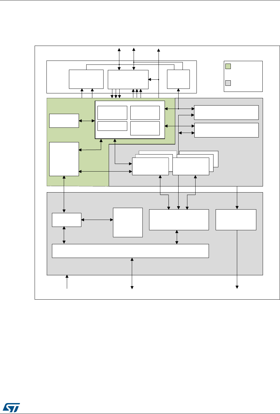
RM0394 Rev 4 1521/1600
RM0394 Universal serial bus full-speed device interface (USB)
1552
45.4 USB functional description
Figure 492 shows the block diagram of the USB peripheral.
Figure 492. USB peripheral block diagram
The USB peripheral provides an USB-compliant connection between the host PC and the
function implemented by the microcontroller. Data transfer between the host PC and the
system memory occurs through a dedicated packet buffer memory accessed directly by the
USB peripheral. This dedicated memory size is 1024 bytes, and up to 16 mono-directional
or 8 bidirectional endpoints can be used. The USB peripheral interfaces with the USB host,
detecting token packets, handling data transmission/reception, and processing handshake
packets as required by the USB standard. Transaction formatting is performed by the
hardware, including CRC generation and checking.
Each endpoint is associated with a buffer description block indicating where the
endpoint-related memory area is located, how large it is or how many bytes must be
transmitted. When a token for a valid function/endpoint pair is recognized by the USB
peripheral, the related data transfer (if required and if the endpoint is configured) takes
&RQWURO
06Y9
6,(
86%FORFN
0+]
'3
86%3+<
5HJLVWHU
PDSSHU
$3%LQWHUIDFH
3&/. $3%EXV ,54VWR19,&
$UELWHU 3DFNHW
EXIIHU
PHPRU\
5HJLVWHU
PDSSHU
&RQWURO
UHJLVWHUVDQGORJLF
,QWHUUXSW
UHJLVWHUVDQGORJLF
(QGSRLQW
UHJLVWHUV
(QGSRLQW
UHJLVWHUV
(QGSRLQW
VHOHFWLRQ
&ORFN
UHFRYHU\
5;7;
6XVSHQG
WLPHU
3DFNHW
EXIIHU
LQWHUIDFH
$QDORJ
WUDQVFHLYHU
'0
,QWHUUXSW
PDSSHU
$3%ZUDSSHU
%&'
(PEHGGHG
SXOOXS
12(
3&/.

Universal serial bus full-speed device interface (USB) RM0394
1522/1600 RM0394 Rev 4
place. The data buffered by the USB peripheral is loaded in an internal 16-bit register and
memory access to the dedicated buffer is performed. When all the data has been
transferred, if needed, the proper handshake packet over the USB is generated or expected
according to the direction of the transfer.
At the end of the transaction, an endpoint-specific interrupt is generated, reading status
registers and/or using different interrupt response routines. The microcontroller can
determine:
•which endpoint has to be served,
•which type of transaction took place, if errors occurred (bit stuffing, format, CRC,
protocol, missing ACK, over/underrun, etc.).
Special support is offered to isochronous transfers and high throughput bulk transfers,
implementing a double buffer usage, which allows to always have an available buffer for the
USB peripheral while the microcontroller uses the other one.
The unit can be placed in low-power mode (SUSPEND mode), by writing in the control
register, whenever required. At this time, all static power dissipation is avoided, and the USB
clock can be slowed down or stopped. The detection of activity at the USB inputs, while in
low-power mode, wakes the device up asynchronously. A special interrupt source can be
connected directly to a wakeup line to allow the system to immediately restart the normal
clock generation and/or support direct clock start/stop.
45.4.1 Description of USB blocks
The USB peripheral implements all the features related to USB interfacing, which include
the following blocks:
•USB Physical Interface (USB PHY): This block is maintaining the electrical interface to
an external USB host. It contains the differential analog transceiver itself, controllable
embedded pull-up resistor (connected to USB_DP line) and support for Battery
Charging Detection (BCD), multiplexed on same USB_DP and USB_DM lines. The
output enable control signal of the analog transceiver (active low) is provided externally
on USB_NOE. It can be used to drive some activity LED or to provide information about
the actual communication direction to some other circuitry.
•Serial Interface Engine (SIE): The functions of this block include: synchronization
pattern recognition, bit-stuffing, CRC generation and checking, PID
verification/generation, and handshake evaluation. It must interface with the USB
transceivers and uses the virtual buffers provided by the packet buffer interface for
local data storage. This unit also generates signals according to USB peripheral
events, such as Start of Frame (SOF), USB_Reset, Data errors etc. and to Endpoint
related events like end of transmission or correct reception of a packet; these signals
are then used to generate interrupts.
•Timer: This block generates a start-of-frame locked clock pulse and detects a global
suspend (from the host) when no traffic has been received for 3 ms.
•Packet Buffer Interface: This block manages the local memory implementing a set of
buffers in a flexible way, both for transmission and reception. It can choose the proper
buffer according to requests coming from the SIE and locate them in the memory
addresses pointed by the Endpoint registers. It increments the address after each
exchanged byte until the end of packet, keeping track of the number of exchanged
bytes and preventing the buffer to overrun the maximum capacity.

RM0394 Rev 4 1523/1600
RM0394 Universal serial bus full-speed device interface (USB)
1552
•Endpoint-Related Registers: Each endpoint has an associated register containing the
endpoint type and its current status. For mono-directional/single-buffer endpoints, a
single register can be used to implement two distinct endpoints. The number of
registers is 8, allowing up to 16 mono-directional/single-buffer or up to 7 double-buffer
endpoints in any combination. For example the USB peripheral can be programmed to
have 4 double buffer endpoints and 8 single-buffer/mono-directional endpoints.
•Control Registers: These are the registers containing information about the status of
the whole USB peripheral and used to force some USB events, such as resume and
power-down.
•Interrupt Registers: These contain the Interrupt masks and a record of the events. They
can be used to inquire an interrupt reason, the interrupt status or to clear the status of a
pending interrupt.
Note: * Endpoint 0 is always used for control transfer in single-buffer mode.
The USB peripheral is connected to the APB bus through an APB interface, containing the
following blocks:
•Packet Memory: This is the local memory that physically contains the Packet Buffers. It
can be used by the Packet Buffer interface, which creates the data structure and can
be accessed directly by the application software. The size of the Packet Memory is
1024 bytes, structured as 512 half-words of 16 bits.
•Arbiter: This block accepts memory requests coming from the APB bus and from the
USB interface. It resolves the conflicts by giving priority to APB accesses, while always
reserving half of the memory bandwidth to complete all USB transfers. This time-duplex
scheme implements a virtual dual-port SRAM that allows memory access, while an
USB transaction is happening. Multiword APB transfers of any length are also allowed
by this scheme.
•Register Mapper: This block collects the various byte-wide and bit-wide registers of the
USB peripheral in a structured 16-bit wide half-word set addressed by the APB.
•APB Wrapper: This provides an interface to the APB for the memory and register. It
also maps the whole USB peripheral in the APB address space.
•Interrupt Mapper: This block is used to select how the possible USB events can
generate interrupts and map them to the NVIC.
45.5 Programming considerations
In the following sections, the expected interactions between the USB peripheral and the
application program are described, in order to ease application software development.
45.5.1 Generic USB device programming
This part describes the main tasks required of the application software in order to obtain
USB compliant behavior. The actions related to the most general USB events are taken into
account and paragraphs are dedicated to the special cases of double-buffered endpoints
and Isochronous transfers. Apart from system reset, action is always initiated by the USB
peripheral, driven by one of the USB events described below.

Universal serial bus full-speed device interface (USB) RM0394
1524/1600 RM0394 Rev 4
45.5.2 System and power-on reset
Upon system and power-on reset, the first operation the application software should perform
is to provide all required clock signals to the USB peripheral and subsequently de-assert its
reset signal so to be able to access its registers. The whole initialization sequence is
hereafter described.
As a first step application software needs to activate register macrocell clock and de-assert
macrocell specific reset signal using related control bits provided by device clock
management logic.
After that, the analog part of the device related to the USB transceiver must be switched on
using the PDWN bit in CNTR register, which requires a special handling. This bit is intended
to switch on the internal voltage references that supply the port transceiver. This circuit has
a defined startup time (tSTARTUP specified in the datasheet) during which the behavior of the
USB transceiver is not defined. It is thus necessary to wait this time, after setting the PDWN
bit in the CNTR register, before removing the reset condition on the USB part (by clearing
the FRES bit in the CNTR register). Clearing the ISTR register then removes any spurious
pending interrupt before any other macrocell operation is enabled.
At system reset, the microcontroller must initialize all required registers and the packet
buffer description table, to make the USB peripheral able to properly generate interrupts and
data transfers. All registers not specific to any endpoint must be initialized according to the
needs of application software (choice of enabled interrupts, chosen address of packet
buffers, etc.). Then the process continues as for the USB reset case (see further
paragraph).
USB reset (RESET interrupt)
When this event occurs, the USB peripheral is put in the same conditions it is left by the
system reset after the initialization described in the previous paragraph: communication is
disabled in all endpoint registers (the USB peripheral will not respond to any packet). As a
response to the USB reset event, the USB function must be enabled, having as USB
address 0, implementing only the default control endpoint (endpoint address is 0 too). This
is accomplished by setting the Enable Function (EF) bit of the USB_DADDR register and
initializing the EP0R register and its related packet buffers accordingly. During USB
enumeration process, the host assigns a unique address to this device, which must be
written in the ADD[6:0] bits of the USB_DADDR register, and configures any other
necessary endpoint.
When a RESET interrupt is received, the application software is responsible to enable again
the default endpoint of USB function 0 within 10 ms from the end of reset sequence which
triggered the interrupt.
Structure and usage of packet buffers
Each bidirectional endpoint may receive or transmit data from/to the host. The received data
is stored in a dedicated memory buffer reserved for that endpoint, while another memory
buffer contains the data to be transmitted by the endpoint. Access to this memory is
performed by the packet buffer interface block, which delivers a memory access request
and waits for its acknowledgment. Since the packet buffer memory has to be accessed by
the microcontroller also, an arbitration logic takes care of the access conflicts, using half
APB cycle for microcontroller access and the remaining half for the USB peripheral access.
In this way, both the agents can operate as if the packet memory is a dual-port SRAM,
without being aware of any conflict even when the microcontroller is performing back-to-
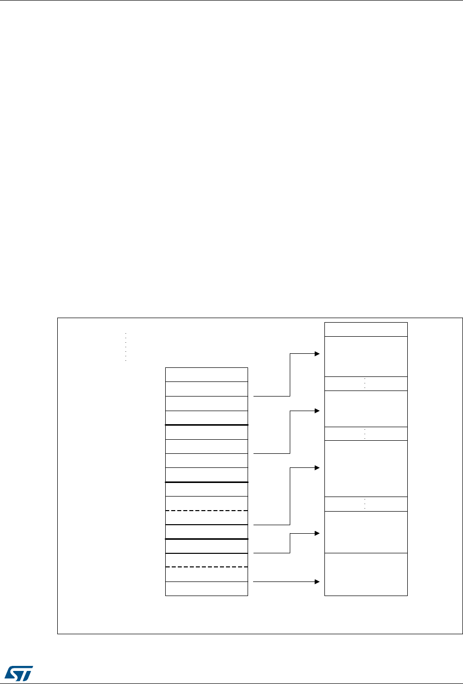
RM0394 Rev 4 1525/1600
RM0394 Universal serial bus full-speed device interface (USB)
1552
back accesses. The USB peripheral logic uses a dedicated clock. The frequency of this
dedicated clock is fixed by the requirements of the USB standard at 48 MHz, and this can be
different from the clock used for the interface to the APB bus. Different clock configurations
are possible where the APB clock frequency can be higher or lower than the USB peripheral
one.
Note: Due to USB data rate and packet memory interface requirements, the APB clock must have
a minimum frequency of 10 MHz to avoid data overrun/underrun problems.
Each endpoint is associated with two packet buffers (usually one for transmission and the
other one for reception). Buffers can be placed anywhere inside the packet memory
because their location and size is specified in a buffer description table, which is also
located in the packet memory at the address indicated by the USB_BTABLE register. Each
table entry is associated to an endpoint register and it is composed of four 16-bit half-words
so that table start address must always be aligned to an 8-byte boundary (the lowest three
bits of USB_BTABLE register are always “000”). Buffer descriptor table entries are
described in the Section 45.6.2: Buffer descriptor table. If an endpoint is unidirectional and it
is neither an Isochronous nor a double-buffered bulk, only one packet buffer is required (the
one related to the supported transfer direction). Other table locations related to unsupported
transfer directions or unused endpoints, are available to the user. Isochronous and double-
buffered bulk endpoints have special handling of packet buffers (Refer to Section 45.5.4:
Isochronous transfers and Section 45.5.3: Double-buffered endpoints respectively). The
relationship between buffer description table entries and packet buffer areas is depicted in
Figure 493.
Figure 493. Packet buffer areas with examples of buffer description table locations
06Y9
B( &2817B7;B
$''5B7;B
&2817B7;B
$''5B7;B
&2817B5;B
$''5B5;B
&2817B5;B
$''5B5;B
&2817B5;
$''5B5;
&2817B7;
$''5B7;
&2817B5;
$''5B5;
&2817B7;
$''5B7;
B&
B$
B
B
B
B
B
B(
B&
B$
B
B
B
B
B
%XIIHUGHVFULSWLRQWDEOHORFDWLRQV
%XIIHUIRU
GRXEOHEXIIHUHG
,1(QGSRLQW
%XIIHUIRU
GRXEOHEXIIHUHG
287(QGSRLQW
7UDQVPLVVLRQ
EXIIHUIRU
VLQJOHEXIIHUHG
(QGSRLQW
5HFHSWLRQEXIIHU
IRU
(QGSRLQW
7UDQVPLVVLRQ
EXIIHUIRU
(QGSRLQW
3DFNHWEXIIHUV

Universal serial bus full-speed device interface (USB) RM0394
1526/1600 RM0394 Rev 4
Each packet buffer is used either during reception or transmission starting from the bottom.
The USB peripheral will never change the contents of memory locations adjacent to the
allocated memory buffers; if a packet bigger than the allocated buffer length is received
(buffer overrun condition) the data will be copied to the memory only up to the last available
location.
Endpoint initialization
The first step to initialize an endpoint is to write appropriate values to the
ADDRn_TX/ADDRn_RX registers so that the USB peripheral finds the data to be
transmitted already available and the data to be received can be buffered. The EP_TYPE
bits in the USB_EPnR register must be set according to the endpoint type, eventually using
the EP_KIND bit to enable any special required feature. On the transmit side, the endpoint
must be enabled using the STAT_TX bits in the USB_EPnR register and COUNTn_TX must
be initialized. For reception, STAT_RX bits must be set to enable reception and
COUNTn_RX must be written with the allocated buffer size using the BL_SIZE and
NUM_BLOCK fields. Unidirectional endpoints, except Isochronous and double-buffered bulk
endpoints, need to initialize only bits and registers related to the supported direction. Once
the transmission and/or reception are enabled, register USB_EPnR and locations
ADDRn_TX/ADDRn_RX, COUNTn_TX/COUNTn_RX (respectively), should not be modified
by the application software, as the hardware can change their value on the fly. When the
data transfer operation is completed, notified by a CTR interrupt event, they can be
accessed again to re-enable a new operation.
IN packets (data transmission)
When receiving an IN token packet, if the received address matches a configured and valid
endpoint, the USB peripheral accesses the contents of ADDRn_TX and COUNTn_TX
locations inside the buffer descriptor table entry related to the addressed endpoint. The
content of these locations is stored in its internal 16 bit registers ADDR and COUNT (not
accessible by software). The packet memory is accessed again to read the first byte to be
transmitted (Refer to Structure and usage of packet buffers on page 1524) and starts
sending a DATA0 or DATA1 PID according to USB_EPnR bit DTOG_TX. When the PID is
completed, the first byte, read from buffer memory, is loaded into the output shift register to
be transmitted on the USB bus. After the last data byte is transmitted, the computed CRC is
sent. If the addressed endpoint is not valid, a NAK or STALL handshake packet is sent
instead of the data packet, according to STAT_TX bits in the USB_EPnR register.
The ADDR internal register is used as a pointer to the current buffer memory location while
COUNT is used to count the number of remaining bytes to be transmitted. Each half-word
read from the packet buffer memory is transmitted over the USB bus starting from the least
significant byte. Transmission buffer memory is read starting from the address pointed by
ADDRn_TX for COUNTn_TX/2 half-words. If a transmitted packet is composed of an odd
number of bytes, only the lower half of the last half-word accessed will be used.
On receiving the ACK receipt by the host, the USB_EPnR register is updated in the
following way: DTOG_TX bit is toggled, the endpoint is made invalid by setting
STAT_TX=10 (NAK) and bit CTR_TX is set. The application software must first identify the
endpoint, which is requesting microcontroller attention by examining the EP_ID and DIR bits
in the USB_ISTR register. Servicing of the CTR_TX event starts clearing the interrupt bit;
the application software then prepares another buffer full of data to be sent, updates the
COUNTn_TX table location with the number of byte to be transmitted during the next
transfer, and finally sets STAT_TX to ‘11 (VALID) to re-enable transmissions. While the
STAT_TX bits are equal to ‘10 (NAK), any IN request addressed to that endpoint is NAKed,

RM0394 Rev 4 1527/1600
RM0394 Universal serial bus full-speed device interface (USB)
1552
indicating a flow control condition: the USB host will retry the transaction until it succeeds. It
is mandatory to execute the sequence of operations in the above mentioned order to avoid
losing the notification of a second IN transaction addressed to the same endpoint
immediately following the one which triggered the CTR interrupt.
OUT and SETUP packets (data reception)
These two tokens are handled by the USB peripheral more or less in the same way; the
differences in the handling of SETUP packets are detailed in the following paragraph about
control transfers. When receiving an OUT/SETUP PID, if the address matches a valid
endpoint, the USB peripheral accesses the contents of the ADDRn_RX and COUNTn_RX
locations inside the buffer descriptor table entry related to the addressed endpoint. The
content of the ADDRn_RX is stored directly in its internal register ADDR. While COUNT is
now reset and the values of BL_SIZE and NUM_BLOCK bit fields, which are read within
COUNTn_RX content are used to initialize BUF_COUNT, an internal 16 bit counter, which is
used to check the buffer overrun condition (all these internal registers are not accessible by
software). Data bytes subsequently received by the USB peripheral are packed in half-
words (the first byte received is stored as least significant byte) and then transferred to the
packet buffer starting from the address contained in the internal ADDR register while
BUF_COUNT is decremented and COUNT is incremented at each byte transfer. When the
end of DATA packet is detected, the correctness of the received CRC is tested and only if no
errors occurred during the reception, an ACK handshake packet is sent back to the
transmitting host.
In case of wrong CRC or other kinds of errors (bit-stuff violations, frame errors, etc.), data
bytes are still copied in the packet memory buffer, at least until the error detection point, but
ACK packet is not sent and the ERR bit in USB_ISTR register is set. However, there is
usually no software action required in this case: the USB peripheral recovers from reception
errors and remains ready for the next transaction to come. If the addressed endpoint is not
valid, a NAK or STALL handshake packet is sent instead of the ACK, according to bits
STAT_RX in the USB_EPnR register and no data is written in the reception memory buffers.
Reception memory buffer locations are written starting from the address contained in the
ADDRn_RX for a number of bytes corresponding to the received data packet length, CRC
included (i.e. data payload length + 2), or up to the last allocated memory location, as
defined by BL_SIZE and NUM_BLOCK, whichever comes first. In this way, the USB
peripheral never writes beyond the end of the allocated reception memory buffer area. If the
length of the data packet payload (actual number of bytes used by the application) is greater
than the allocated buffer, the USB peripheral detects a buffer overrun condition. in this case,
a STALL handshake is sent instead of the usual ACK to notify the problem to the host, no
interrupt is generated and the transaction is considered failed.
When the transaction is completed correctly, by sending the ACK handshake packet, the
internal COUNT register is copied back in the COUNTn_RX location inside the buffer
description table entry, leaving unaffected BL_SIZE and NUM_BLOCK fields, which
normally do not require to be re-written, and the USB_EPnR register is updated in the
following way: DTOG_RX bit is toggled, the endpoint is made invalid by setting STAT_RX =
‘10 (NAK) and bit CTR_RX is set. If the transaction has failed due to errors or buffer overrun
condition, none of the previously listed actions take place. The application software must
first identify the endpoint, which is requesting microcontroller attention by examining the
EP_ID and DIR bits in the USB_ISTR register. The CTR_RX event is serviced by first
determining the transaction type (SETUP bit in the USB_EPnR register); the application
software must clear the interrupt flag bit and get the number of received bytes reading the
COUNTn_RX location inside the buffer description table entry related to the endpoint being

Universal serial bus full-speed device interface (USB) RM0394
1528/1600 RM0394 Rev 4
processed. After the received data is processed, the application software should set the
STAT_RX bits to ‘11 (Valid) in the USB_EPnR, enabling further transactions. While the
STAT_RX bits are equal to ‘10 (NAK), any OUT request addressed to that endpoint is
NAKed, indicating a flow control condition: the USB host will retry the transaction until it
succeeds. It is mandatory to execute the sequence of operations in the above mentioned
order to avoid losing the notification of a second OUT transaction addressed to the same
endpoint following immediately the one which triggered the CTR interrupt.
Control transfers
Control transfers are made of a SETUP transaction, followed by zero or more data stages,
all of the same direction, followed by a status stage (a zero-byte transfer in the opposite
direction). SETUP transactions are handled by control endpoints only and are very similar to
OUT ones (data reception) except that the values of DTOG_TX and DTOG_RX bits of the
addressed endpoint registers are set to 1 and 0 respectively, to initialize the control transfer,
and both STAT_TX and STAT_RX are set to ‘10 (NAK) to let software decide if subsequent
transactions must be IN or OUT depending on the SETUP contents. A control endpoint must
check SETUP bit in the USB_EPnR register at each CTR_RX event to distinguish normal
OUT transactions from SETUP ones. A USB device can determine the number and
direction of data stages by interpreting the data transferred in the SETUP stage, and is
required to STALL the transaction in the case of errors. To do so, at all data stages before
the last, the unused direction should be set to STALL, so that, if the host reverses the
transfer direction too soon, it gets a STALL as a status stage.
While enabling the last data stage, the opposite direction should be set to NAK, so that, if
the host reverses the transfer direction (to perform the status stage) immediately, it is kept
waiting for the completion of the control operation. If the control operation completes
successfully, the software will change NAK to VALID, otherwise to STALL. At the same time,
if the status stage will be an OUT, the STATUS_OUT (EP_KIND in the USB_EPnR register)
bit should be set, so that an error is generated if a status transaction is performed with not-
zero data. When the status transaction is serviced, the application clears the STATUS_OUT
bit and sets STAT_RX to VALID (to accept a new command) and STAT_TX to NAK (to delay
a possible status stage immediately following the next setup).
Since the USB specification states that a SETUP packet cannot be answered with a
handshake different from ACK, eventually aborting a previously issued command to start
the new one, the USB logic doesn’t allow a control endpoint to answer with a NAK or STALL
packet to a SETUP token received from the host.
When the STAT_RX bits are set to ‘01 (STALL) or ‘10 (NAK) and a SETUP token is
received, the USB accepts the data, performing the required data transfers and sends back
an ACK handshake. If that endpoint has a previously issued CTR_RX request not yet
acknowledged by the application (i.e. CTR_RX bit is still set from a previously completed
reception), the USB discards the SETUP transaction and does not answer with any
handshake packet regardless of its state, simulating a reception error and forcing the host to
send the SETUP token again. This is done to avoid losing the notification of a SETUP
transaction addressed to the same endpoint immediately following the transaction, which
triggered the CTR_RX interrupt.

RM0394 Rev 4 1529/1600
RM0394 Universal serial bus full-speed device interface (USB)
1552
45.5.3 Double-buffered endpoints
All different endpoint types defined by the USB standard represent different traffic models,
and describe the typical requirements of different kind of data transfer operations. When
large portions of data are to be transferred between the host PC and the USB function, the
bulk endpoint type is the most suited model. This is because the host schedules bulk
transactions so as to fill all the available bandwidth in the frame, maximizing the actual
transfer rate as long as the USB function is ready to handle a bulk transaction addressed to
it. If the USB function is still busy with the previous transaction when the next one arrives, it
will answer with a NAK handshake and the host PC will issue the same transaction again
until the USB function is ready to handle it, reducing the actual transfer rate due to the
bandwidth occupied by re-transmissions. For this reason, a dedicated feature called
‘double-buffering’ can be used with bulk endpoints.
When ‘double-buffering’ is activated, data toggle sequencing is used to select, which buffer
is to be used by the USB peripheral to perform the required data transfers, using both
‘transmission’ and ‘reception’ packet memory areas to manage buffer swapping on each
successful transaction in order to always have a complete buffer to be used by the
application, while the USB peripheral fills the other one. For example, during an OUT
transaction directed to a ‘reception’ double-buffered bulk endpoint, while one buffer is being
filled with new data coming from the USB host, the other one is available for the
microcontroller software usage (the same would happen with a ‘transmission’ double-
buffered bulk endpoint and an IN transaction).
Since the swapped buffer management requires the usage of all 4 buffer description table
locations hosting the address pointer and the length of the allocated memory buffers, the
USB_EPnR registers used to implement double-buffered bulk endpoints are forced to be
used as unidirectional ones. Therefore, only one STAT bit pair must be set at a value
different from ‘00 (Disabled): STAT_RX if the double-buffered bulk endpoint is enabled for
reception, STAT_TX if the double-buffered bulk endpoint is enabled for transmission. In
case it is required to have double-buffered bulk endpoints enabled both for reception and
transmission, two USB_EPnR registers must be used.
To exploit the double-buffering feature and reach the highest possible transfer rate, the
endpoint flow control structure, described in previous chapters, has to be modified, in order
to switch the endpoint status to NAK only when a buffer conflict occurs between the USB
peripheral and application software, instead of doing it at the end of each successful
transaction. The memory buffer which is currently being used by the USB peripheral is
defined by the DTOG bit related to the endpoint direction: DTOG_RX (bit 14 of USB_EPnR
register) for ‘reception’ double-buffered bulk endpoints or DTOG_TX (bit 6 of USB_EPnR
register) for ‘transmission’ double-buffered bulk endpoints. To implement the new flow
control scheme, the USB peripheral should know which packet buffer is currently in use by
the application software, so to be aware of any conflict. Since in the USB_EPnR register,
there are two DTOG bits but only one is used by USB peripheral for data and buffer
sequencing (due to the unidirectional constraint required by double-buffering feature) the
other one can be used by the application software to show which buffer it is currently using.
This new buffer flag is called SW_BUF. In the following table the correspondence between
USB_EPnR register bits and DTOG/SW_BUF definition is explained, for the cases of
‘transmission’ and ‘reception’ double-buffered bulk endpoints.
Universal serial bus full-speed device interface (USB) RM0394
1530/1600 RM0394 Rev 4
The memory buffer which is currently being used by the USB peripheral is defined by DTOG
buffer flag, while the buffer currently in use by application software is identified by SW_BUF
buffer flag. The relationship between the buffer flag value and the used packet buffer is the
same in both cases, and it is listed in the following table.
Double-buffering feature for a bulk endpoint is activated by:
•Writing EP_TYPE bit field at ‘00 in its USB_EPnR register, to define the endpoint as a
bulk, and
•Setting EP_KIND bit at ‘1 (DBL_BUF), in the same register.
The application software is responsible for DTOG and SW_BUF bits initialization according
to the first buffer to be used; this has to be done considering the special toggle-only property
that these two bits have. The end of the first transaction occurring after having set
DBL_BUF, triggers the special flow control of double-buffered bulk endpoints, which is used
for all other transactions addressed to this endpoint until DBL_BUF remain set. At the end of
each transaction the CTR_RX or CTR_TX bit of the addressed endpoint USB_EPnR
register is set, depending on the enabled direction. At the same time, the affected DTOG bit
in the USB_EPnR register is hardware toggled making the USB peripheral buffer swapping
completely software independent. Unlike common transactions, and the first one after
Table 263. Double-buffering buffer flag definition
Buffer flag ‘Transmission’ endpoint ‘Reception’ endpoint
DTOG DTOG_TX (USB_EPnR bit 6) DTOG_RX (USB_EPnR bit 14)
SW_BUF USB_EPnR bit 14 USB_EPnR bit 6
Table 264. Bulk double-buffering memory buffers usage
Endpoint
type DTOG SW_BUF Packet buffer used by
USB peripheral
Packet buffer used by
Application Software
IN
01
ADDRn_TX_0 / COUNTn_TX_0
Buffer description table locations.
ADDRn_TX_1 / COUNTn_TX_1
Buffer description table locations.
10
ADDRn_TX_1 / COUNTn_TX_1
Buffer description table locations
ADDRn_TX_0 / COUNTn_TX_0
Buffer description table locations.
0 0 None (1)
1. Endpoint in NAK Status.
ADDRn_TX_0 / COUNTn_TX_0
Buffer description table locations.
1 1 None (1) ADDRn_TX_0 / COUNTn_TX_0
Buffer description table locations.
OUT
01
ADDRn_RX_0 / COUNTn_RX_0
Buffer description table locations.
ADDRn_RX_1 / COUNTn_RX_1
Buffer description table locations.
10
ADDRn_RX_1 / COUNTn_RX_1
Buffer description table locations.
ADDRn_RX_0 / COUNTn_RX_0
Buffer description table locations.
0 0 None (1) ADDRn_RX_0 / COUNTn_RX_0
Buffer description table locations.
1 1 None (1) ADDRn_RX_1 / COUNTn_RX_1
Buffer description table locations.

RM0394 Rev 4 1531/1600
RM0394 Universal serial bus full-speed device interface (USB)
1552
DBL_BUF setting, STAT bit pair is not affected by the transaction termination and its value
remains ‘11 (Valid). However, as the token packet of a new transaction is received, the
actual endpoint status will be masked as ‘10 (NAK) when a buffer conflict between the USB
peripheral and the application software is detected (this condition is identified by DTOG and
SW_BUF having the same value, see Table 264 on page 1530). The application software
responds to the CTR event notification by clearing the interrupt flag and starting any
required handling of the completed transaction. When the application packet buffer usage is
over, the software toggles the SW_BUF bit, writing ‘1 to it, to notify the USB peripheral about
the availability of that buffer. In this way, the number of NAKed transactions is limited only by
the application elaboration time of a transaction data: if the elaboration time is shorter than
the time required to complete a transaction on the USB bus, no re-transmissions due to flow
control will take place and the actual transfer rate will be limited only by the host PC.
The application software can always override the special flow control implemented for
double-buffered bulk endpoints, writing an explicit status different from ‘11 (Valid) into the
STAT bit pair of the related USB_EPnR register. In this case, the USB peripheral will always
use the programmed endpoint status, regardless of the buffer usage condition.
45.5.4 Isochronous transfers
The USB standard supports full speed peripherals requiring a fixed and accurate data
production/consume frequency, defining this kind of traffic as ‘Isochronous’. Typical
examples of this data are: audio samples, compressed video streams, and in general any
sort of sampled data having strict requirements for the accuracy of delivered frequency.
When an endpoint is defined to be ‘isochronous’ during the enumeration phase, the host
allocates in the frame the required bandwidth and delivers exactly one IN or OUT packet
each frame, depending on endpoint direction. To limit the bandwidth requirements, no re-
transmission of failed transactions is possible for Isochronous traffic; this leads to the fact
that an isochronous transaction does not have a handshake phase and no ACK packet is
expected or sent after the data packet. For the same reason, Isochronous transfers do not
support data toggle sequencing and always use DATA0 PID to start any data packet.
The Isochronous behavior for an endpoint is selected by setting the EP_TYPE bits at ‘10 in
its USB_EPnR register; since there is no handshake phase the only legal values for the
STAT_RX/STAT_TX bit pairs are ‘00 (Disabled) and ‘11 (Valid), any other value will produce
results not compliant to USB standard. Isochronous endpoints implement double-buffering
to ease application software development, using both ‘transmission’ and ‘reception’ packet
memory areas to manage buffer swapping on each successful transaction in order to have
always a complete buffer to be used by the application, while the USB peripheral fills the
other.
The memory buffer which is currently used by the USB peripheral is defined by the DTOG
bit related to the endpoint direction (DTOG_RX for ‘reception’ isochronous endpoints,
DTOG_TX for ‘transmission’ isochronous endpoints, both in the related USB_EPnR
register) according to Table 265.

Universal serial bus full-speed device interface (USB) RM0394
1532/1600 RM0394 Rev 4
As it happens with double-buffered bulk endpoints, the USB_EPnR registers used to
implement Isochronous endpoints are forced to be used as unidirectional ones. In case it is
required to have Isochronous endpoints enabled both for reception and transmission, two
USB_EPnR registers must be used.
The application software is responsible for the DTOG bit initialization according to the first
buffer to be used; this has to be done considering the special toggle-only property that these
two bits have. At the end of each transaction, the CTR_RX or CTR_TX bit of the addressed
endpoint USB_EPnR register is set, depending on the enabled direction. At the same time,
the affected DTOG bit in the USB_EPnR register is hardware toggled making buffer
swapping completely software independent. STAT bit pair is not affected by transaction
completion; since no flow control is possible for Isochronous transfers due to the lack of
handshake phase, the endpoint remains always ‘11 (Valid). CRC errors or buffer-overrun
conditions occurring during Isochronous OUT transfers are anyway considered as correct
transactions and they always trigger an CTR_RX event. However, CRC errors will anyway
set the ERR bit in the USB_ISTR register to notify the software of the possible data
corruption.
45.5.5 Suspend/Resume events
The USB standard defines a special peripheral state, called SUSPEND, in which the
average current drawn from the USB bus must not be greater than 2.5 mA. This
requirement is of fundamental importance for bus-powered devices, while self-powered
devices are not required to comply to this strict power consumption constraint. In suspend
mode, the host PC sends the notification by not sending any traffic on the USB bus for more
than 3 ms: since a SOF packet must be sent every 1 ms during normal operations, the USB
peripheral detects the lack of 3 consecutive SOF packets as a suspend request from the
host PC and set the SUSP bit to ‘1 in USB_ISTR register, causing an interrupt if enabled.
Once the device is suspended, its normal operation can be restored by a so called
RESUME sequence, which can be started from the host PC or directly from the peripheral
itself, but it is always terminated by the host PC. The suspended USB peripheral must be
anyway able to detect a RESET sequence, reacting to this event as a normal USB reset
event.
Table 265. Isochronous memory buffers usage
Endpoint
Type
DTOG bit
value
Packet buffer used by the
USB peripheral
Packet buffer used by the
application software
IN
0
ADDRn_TX_0 / COUNTn_TX_0
buffer description table
locations.
ADDRn_TX_1 / COUNTn_TX_1
buffer description table
locations.
1
ADDRn_TX_1 / COUNTn_TX_1
buffer description table
locations.
ADDRn_TX_0 / COUNTn_TX_0
buffer description table
locations.
OUT
0
ADDRn_RX_0 / COUNTn_RX_0
buffer description table
locations.
ADDRn_RX_1 / COUNTn_RX_1
buffer description table
locations.
1
ADDRn_RX_1 / COUNTn_RX_1
buffer description table
locations.
ADDRn_RX_0 / COUNTn_RX_0
buffer description table
locations.

RM0394 Rev 4 1533/1600
RM0394 Universal serial bus full-speed device interface (USB)
1552
The actual procedure used to suspend the USB peripheral is device dependent since
according to the device composition, different actions may be required to reduce the total
consumption.
A brief description of a typical suspend procedure is provided below, focused on the USB-
related aspects of the application software routine responding to the SUSP notification of
the USB peripheral:
1. Set the FSUSP bit in the USB_CNTR register to 1. This action activates the suspend
mode within the USB peripheral. As soon as the suspend mode is activated, the check
on SOF reception is disabled to avoid any further SUSP interrupts being issued while
the USB is suspended.
2. Remove or reduce any static power consumption in blocks different from the USB
peripheral.
3. Set LP_MODE bit in USB_CNTR register to 1 to remove static power consumption in
the analog USB transceivers but keeping them able to detect resume activity.
4. Optionally turn off external oscillator and device PLL to stop any activity inside the
device.
When an USB event occurs while the device is in SUSPEND mode, the RESUME
procedure must be invoked to restore nominal clocks and regain normal USB behavior.
Particular care must be taken to insure that this process does not take more than 10 ms
when the wakening event is an USB reset sequence (See “Universal Serial Bus
Specification” for more details). The start of a resume or reset sequence, while the USB
peripheral is suspended, clears the LP_MODE bit in USB_CNTR register asynchronously.
Even if this event can trigger an WKUP interrupt if enabled, the use of an interrupt response
routine must be carefully evaluated because of the long latency due to system clock restart;
to have the shorter latency before re-activating the nominal clock it is suggested to put the
resume procedure just after the end of the suspend one, so its code is immediately
executed as soon as the system clock restarts. To prevent ESD discharges or any other kind
of noise from waking-up the system (the exit from suspend mode is an asynchronous
event), a suitable analog filter on data line status is activated during suspend; the filter width
is about 70 ns.
The following is a list of actions a resume procedure should address:
1. Optionally turn on external oscillator and/or device PLL.
2. Clear FSUSP bit of USB_CNTR register.
3. If the resume triggering event has to be identified, bits RXDP and RXDM in the
USB_FNR register can be used according to Table 266, which also lists the intended
software action in all the cases. If required, the end of resume or reset sequence can
be detected monitoring the status of the above mentioned bits by checking when they
reach the “10” configuration, which represent the Idle bus state; moreover at the end of
a reset sequence the RESET bit in USB_ISTR register is set to 1, issuing an interrupt if
enabled, which should be handled as usual.

Universal serial bus full-speed device interface (USB) RM0394
1534/1600 RM0394 Rev 4
A device may require to exit from suspend mode as an answer to particular events not
directly related to the USB protocol (e.g. a mouse movement wakes up the whole system).
In this case, the resume sequence can be started by setting the RESUME bit in the
USB_CNTR register to ‘1 and resetting it to 0 after an interval between 1 ms and 15 ms (this
interval can be timed using ESOF interrupts, occurring with a 1 ms period when the system
clock is running at nominal frequency). Once the RESUME bit is clear, the resume
sequence will be completed by the host PC and its end can be monitored again using the
RXDP and RXDM bits in the USB_FNR register.
Note: The RESUME bit must be anyway used only after the USB peripheral has been put in
suspend mode, setting the FSUSP bit in USB_CNTR register to 1.
Table 266. Resume event detection
[RXDP,RXDM] status Wakeup event Required resume software action
“00” Root reset None
“10” None (noise on bus) Go back in Suspend mode
“01” Root resume None
“11” Not allowed (noise on bus) Go back in Suspend mode

RM0394 Rev 4 1535/1600
RM0394 Universal serial bus full-speed device interface (USB)
1552
45.6 USB and USB SRAM registers
The USB peripheral registers can be divided into the following groups:
•Common Registers: Interrupt and Control registers
•Endpoint Registers: Endpoint configuration and status
The USB SRAM registers cover:
•Buffer Descriptor Table: Location of packet memory used to locate data buffers
All register addresses are expressed as offsets with respect to the USB peripheral registers
base address, except the buffer descriptor table locations, which starts at the USB SRAM
base address offset by the value specified in the USB_BTABLE register.
Refer to Section 1.2 on page 60 for a list of abbreviations used in register descriptions.
The peripheral registers can be accessed by half-words (16-bit) or words (32-bit).
45.6.1 Common registers
These registers affect the general behavior of the USB peripheral defining operating mode,
interrupt handling, device address and giving access to the current frame number updated
by the host PC.
USB control register (USB_CNTR)
Address offset: 0x40
Reset value: 0x0003
15 14 13 12 11 10 9 8 7 6 5 4 3 2 1 0
CTR
M
PMAOVR
M
ERR
M
WKUP
M
SUSP
M
RESET
M
SOF
M
ESOF
M
L1REQ
M
Res
.
L1RESU
ME
RE
SUME
F
SUSP
LP_
MODE
PDW
N
F
RES
rw rw rw rw rw rw rw rw rw rw rw rw rw rw rw
Bit 15 CTRM: Correct transfer interrupt mask
0: Correct Transfer (CTR) Interrupt disabled.
1: CTR Interrupt enabled, an interrupt request is generated when the corresponding bit in the
USB_ISTR register is set.
Bit 14 PMAOVRM: Packet memory area over / underrun interrupt mask
0: PMAOVR Interrupt disabled.
1: PMAOVR Interrupt enabled, an interrupt request is generated when the corresponding bit
in the USB_ISTR register is set.
Bit 13 ERRM: Error interrupt mask
0: ERR Interrupt disabled.
1: ERR Interrupt enabled, an interrupt request is generated when the corresponding bit in
the USB_ISTR register is set.
Bit 12 WKUPM: Wakeup interrupt mask
0: WKUP Interrupt disabled.
1: WKUP Interrupt enabled, an interrupt request is generated when the corresponding bit in
the USB_ISTR register is set.

Universal serial bus full-speed device interface (USB) RM0394
1536/1600 RM0394 Rev 4
Bit 11 SUSPM: Suspend mode interrupt mask
0: Suspend Mode Request (SUSP) Interrupt disabled.
1: SUSP Interrupt enabled, an interrupt request is generated when the corresponding bit in
the USB_ISTR register is set.
Bit 10 RESETM: USB reset interrupt mask
0: RESET Interrupt disabled.
1: RESET Interrupt enabled, an interrupt request is generated when the corresponding bit in
the USB_ISTR register is set.
Bit 9 SOFM: Start of frame interrupt mask
0: SOF Interrupt disabled.
1: SOF Interrupt enabled, an interrupt request is generated when the corresponding bit in the
USB_ISTR register is set.
Bit 8 ESOFM: Expected start of frame interrupt mask
0: Expected Start of Frame (ESOF) Interrupt disabled.
1: ESOF Interrupt enabled, an interrupt request is generated when the corresponding bit in
the USB_ISTR register is set.
Bit 7 L1REQM: LPM L1 state request interrupt mask
0: LPM L1 state request (L1REQ) Interrupt disabled.
1: L1REQ Interrupt enabled, an interrupt request is generated when the corresponding bit in
the USB_ISTR register is set.
Bit 6 Reserved.
Bit 5 L1RESUME: LPM L1 Resume request
The microcontroller can set this bit to send a LPM L1 Resume signal to the host. After the
signaling ends, this bit is cleared by hardware.
Bit 4 RESUME: Resume request
The microcontroller can set this bit to send a Resume signal to the host. It must be activated,
according to USB specifications, for no less than 1 ms and no more than 15 ms after which
the Host PC is ready to drive the resume sequence up to its end.
Bit 3 FSUSP: Force suspend
Software must set this bit when the SUSP interrupt is received, which is issued when no
traffic is received by the USB peripheral for 3 ms.
0: No effect.
1: Enter suspend mode. Clocks and static power dissipation in the analog transceiver are left
unaffected. If suspend power consumption is a requirement (bus-powered device), the
application software should set the LP_MODE bit after FSUSP as explained below.
Bit 2 LP_MODE: Low-power mode
This mode is used when the suspend-mode power constraints require that all static power
dissipation is avoided, except the one required to supply the external pull-up resistor. This
condition should be entered when the application is ready to stop all system clocks, or
reduce their frequency in order to meet the power consumption requirements of the USB
suspend condition. The USB activity during the suspend mode (WKUP event)
asynchronously resets this bit (it can also be reset by software).
0: No Low-power mode.
1: Enter Low-power mode.

RM0394 Rev 4 1537/1600
RM0394 Universal serial bus full-speed device interface (USB)
1552
USB interrupt status register (USB_ISTR)
Address offset: 0x44
Reset value: 0x0000 0000
This register contains the status of all the interrupt sources allowing application software to
determine, which events caused an interrupt request.
The upper part of this register contains single bits, each of them representing a specific
event. These bits are set by the hardware when the related event occurs; if the
corresponding bit in the USB_CNTR register is set, a generic interrupt request is generated.
The interrupt routine, examining each bit, will perform all necessary actions, and finally it will
clear the serviced bits. If any of them is not cleared, the interrupt is considered to be still
pending, and the interrupt line will be kept high again. If several bits are set simultaneously,
only a single interrupt will be generated.
Endpoint transaction completion can be handled in a different way to reduce interrupt
response latency. The CTR bit is set by the hardware as soon as an endpoint successfully
completes a transaction, generating a generic interrupt request if the corresponding bit in
USB_CNTR is set. An endpoint dedicated interrupt condition is activated independently
from the CTRM bit in the USB_CNTR register. Both interrupt conditions remain active until
software clears the pending bit in the corresponding USB_EPnR register (the CTR bit is
actually a read only bit). For endpoint-related interrupts, the software can use the Direction
of Transaction (DIR) and EP_ID read-only bits to identify, which endpoint made the last
interrupt request and called the corresponding interrupt service routine.
The user can choose the relative priority of simultaneously pending USB_ISTR events by
specifying the order in which software checks USB_ISTR bits in an interrupt service routine.
Only the bits related to events, which are serviced, are cleared. At the end of the service
routine, another interrupt will be requested, to service the remaining conditions.
To avoid spurious clearing of some bits, it is recommended to clear them with a load
instruction where all bits which must not be altered are written with 1, and all bits to be
cleared are written with ‘0 (these bits can only be cleared by software). Read-modify-write
cycles should be avoided because between the read and the write operations another bit
Bit 1 PDWN: Power down
This bit is used to completely switch off all USB-related analog parts if it is required to
completely disable the USB peripheral for any reason. When this bit is set, the USB
peripheral is disconnected from the transceivers and it cannot be used.
0: Exit Power Down.
1: Enter Power down mode.
Bit 0 FRES: Force USB Reset
0: Clear USB reset.
1: Force a reset of the USB peripheral, exactly like a RESET signaling on the USB. The USB
peripheral is held in RESET state until software clears this bit. A “USB-RESET” interrupt is
generated, if enabled.
15 14 13 12 11 10 9 8 7 6 5 4 3 2 1 0
CTR PMA
OVR ERR WKUP SUSP RESET SOF ESOF L1REQ Res. Res. DIR EP_ID[3:0]
r rc_w0 rc_w0 rc_w0 rc_w0 rc_w0 rc_w0 rc_w0 rc_w0 r r r r r

Universal serial bus full-speed device interface (USB) RM0394
1538/1600 RM0394 Rev 4
could be set by the hardware and the next write will clear it before the microprocessor has
the time to serve the event.
The following describes each bit in detail:
Bit 15 CTR: Correct transfer
This bit is set by the hardware to indicate that an endpoint has successfully completed a
transaction; using DIR and EP_ID bits software can determine which endpoint requested the
interrupt. This bit is read-only.
Bit 14 PMAOVR: Packet memory area over / underrun
This bit is set if the microcontroller has not been able to respond in time to an USB memory
request. The USB peripheral handles this event in the following way: During reception an
ACK handshake packet is not sent, during transmission a bit-stuff error is forced on the
transmitted stream; in both cases the host will retry the transaction. The PMAOVR interrupt
should never occur during normal operations. Since the failed transaction is retried by the
host, the application software has the chance to speed-up device operations during this
interrupt handling, to be ready for the next transaction retry; however this does not happen
during Isochronous transfers (no isochronous transaction is anyway retried) leading to a loss
of data in this case. This bit is read/write but only ‘0 can be written and writing ‘1 has no
effect.
Bit 13 ERR: Error
This flag is set whenever one of the errors listed below has occurred:
NANS: No ANSwer. The timeout for a host response has expired.
CRC: Cyclic Redundancy Check error. One of the received CRCs, either in the token or in
the data, was wrong.
BST: Bit Stuffing error. A bit stuffing error was detected anywhere in the PID, data, and/or
CRC.
FVIO: Framing format Violation. A non-standard frame was received (EOP not in the right
place, wrong token sequence, etc.).
The USB software can usually ignore errors, since the USB peripheral and the PC host
manage retransmission in case of errors in a fully transparent way. This interrupt can be
useful during the software development phase, or to monitor the quality of transmission over
the USB bus, to flag possible problems to the user (e.g. loose connector, too noisy
environment, broken conductor in the USB cable and so on). This bit is read/write but only ‘0
can be written and writing ‘1 has no effect.
Bit 12 WKUP: Wakeup
This bit is set to 1 by the hardware when, during suspend mode, activity is detected that
wakes up the USB peripheral. This event asynchronously clears the LP_MODE bit in the
CTLR register and activates the USB_WAKEUP line, which can be used to notify the rest of
the device (e.g. wakeup unit) about the start of the resume process. This bit is read/write but
only ‘0 can be written and writing ‘1 has no effect.
Bit 11 SUSP: Suspend mode request
This bit is set by the hardware when no traffic has been received for 3 ms, indicating a
suspend mode request from the USB bus. The suspend condition check is enabled
immediately after any USB reset and it is disabled by the hardware when the suspend mode
is active (FSUSP=1) until the end of resume sequence. This bit is read/write but only ‘0 can
be written and writing ‘1 has no effect.

RM0394 Rev 4 1539/1600
RM0394 Universal serial bus full-speed device interface (USB)
1552
Bit 10 RESET: USB reset request
Set when the USB peripheral detects an active USB RESET signal at its inputs. The USB
peripheral, in response to a RESET, just resets its internal protocol state machine, generating
an interrupt if RESETM enable bit in the USB_CNTR register is set. Reception and
transmission are disabled until the RESET bit is cleared. All configuration registers do not
reset: the microcontroller must explicitly clear these registers (this is to ensure that the
RESET interrupt can be safely delivered, and any transaction immediately followed by a
RESET can be completed). The function address and endpoint registers are reset by an USB
reset event.
This bit is read/write but only ‘0 can be written and writing ‘1 has no effect.
Bit 9 SOF: Start of frame
This bit signals the beginning of a new USB frame and it is set when a SOF packet arrives
through the USB bus. The interrupt service routine may monitor the SOF events to have a
1 ms synchronization event to the USB host and to safely read the USB_FNR register which
is updated at the SOF packet reception (this could be useful for isochronous applications).
This bit is read/write but only ‘0 can be written and writing ‘1 has no effect.
Bit 8 ESOF: Expected start of frame
This bit is set by the hardware when an SOF packet is expected but not received. The host
sends an SOF packet each 1 ms, but if the hub does not receive it properly, the Suspend
Timer issues this interrupt. If three consecutive ESOF interrupts are generated (i.e. three
SOF packets are lost) without any traffic occurring in between, a SUSP interrupt is
generated. This bit is set even when the missing SOF packets occur while the Suspend
Timer is not yet locked. This bit is read/write but only ‘0 can be written and writing ‘1 has no
effect.
Bit 7 L1REQ: LPM L1 state request
This bit is set by the hardware when LPM command to enter the L1 state is successfully
received and acknowledged. This bit is read/write but only ‘0 can be written and writing ‘1 has
no effect.

Universal serial bus full-speed device interface (USB) RM0394
1540/1600 RM0394 Rev 4
USB frame number register (USB_FNR)
Address offset: 0x48
Reset value: 0x0XXX where X is undefined
Bits 6:5 Reserved.
Bit 4 DIR: Direction of transaction
This bit is written by the hardware according to the direction of the successful transaction,
which generated the interrupt request.
If DIR bit=0, CTR_TX bit is set in the USB_EPnR register related to the interrupting endpoint.
The interrupting transaction is of IN type (data transmitted by the USB peripheral to the host
PC).
If DIR bit=1, CTR_RX bit or both CTR_TX/CTR_RX are set in the USB_EPnR register
related to the interrupting endpoint. The interrupting transaction is of OUT type (data
received by the USB peripheral from the host PC) or two pending transactions are waiting to
be processed.
This information can be used by the application software to access the USB_EPnR bits
related to the triggering transaction since it represents the direction having the interrupt
pending. This bit is read-only.
Bits 3:0 EP_ID[3:0]: Endpoint Identifier
These bits are written by the hardware according to the endpoint number, which generated
the interrupt request. If several endpoint transactions are pending, the hardware writes the
endpoint identifier related to the endpoint having the highest priority defined in the following
way: Two endpoint sets are defined, in order of priority: Isochronous and double-buffered
bulk endpoints are considered first and then the other endpoints are examined. If more than
one endpoint from the same set is requesting an interrupt, the EP_ID bits in USB_ISTR
register are assigned according to the lowest requesting endpoint register, EP0R having the
highest priority followed by EP1R and so on. The application software can assign a register
to each endpoint according to this priority scheme, so as to order the concurring endpoint
requests in a suitable way. These bits are read only.
151413121110987654321 0
RXDP RXDM LCK LSOF[1:0] FN[10:0]
rrr r r rrrrrrrrrr r
Bit 15 RXDP: Receive data + line status
This bit can be used to observe the status of received data plus upstream port data line. It
can be used during end-of-suspend routines to help determining the wakeup event.
Bit 14 RXDM: Receive data - line status
This bit can be used to observe the status of received data minus upstream port data line. It
can be used during end-of-suspend routines to help determining the wakeup event.

RM0394 Rev 4 1541/1600
RM0394 Universal serial bus full-speed device interface (USB)
1552
USB device address (USB_DADDR)
Address offset: 0x4C
Reset value: 0x0000
Buffer table address (USB_BTABLE)
Address offset: 0x50
Reset value: 0x0000
Bit 13 LCK: Locked
This bit is set by the hardware when at least two consecutive SOF packets have been
received after the end of an USB reset condition or after the end of an USB resume
sequence. Once locked, the frame timer remains in this state until an USB reset or USB
suspend event occurs.
Bits 12:11 LSOF[1:0]: Lost SOF
These bits are written by the hardware when an ESOF interrupt is generated, counting the
number of consecutive SOF packets lost. At the reception of an SOF packet, these bits are
cleared.
Bits 10:0 FN[10:0]: Frame number
This bit field contains the 11-bits frame number contained in the last received SOF packet.
The frame number is incremented for every frame sent by the host and it is useful for
Isochronous transfers. This bit field is updated on the generation of an SOF interrupt.
15 14 13 12 11 10 9 8 7 6 5 4 3 2 1 0
Res. Res. Res. Res. Res. Res. Res. Res. EF ADD6 ADD5 ADD4 ADD3 ADD2 ADD1 ADD0
rw rw rw rw rw rw rw rw
Bits 15:8 Reserved
Bit 7 EF: Enable function
This bit is set by the software to enable the USB device. The address of this device is
contained in the following ADD[6:0] bits. If this bit is at ‘0 no transactions are handled,
irrespective of the settings of USB_EPnR registers.
Bits 6:0 ADD[6:0]: Device address
These bits contain the USB function address assigned by the host PC during the
enumeration process. Both this field and the Endpoint Address (EA) field in the associated
USB_EPnR register must match with the information contained in a USB token in order to
handle a transaction to the required endpoint.
1514131211109876543210
BTABLE[15:3] Res. Res. Res.
rw rw rw rw rw rw rw rw rw rw rw rw rw

Universal serial bus full-speed device interface (USB) RM0394
1542/1600 RM0394 Rev 4
LPM control and status register (USB_LPMCSR)
Address offset: 0x54
Reset value: 0x0000
Battery charging detector (USB_BCDR)
Address offset: 0x58
Reset value: 0x0000
Bits 15:3 BTABLE[15:3]: Buffer table
These bits contain the start address of the buffer allocation table inside the dedicated packet
memory. This table describes each endpoint buffer location and size and it must be aligned
to an 8 byte boundary (the 3 least significant bits are always ‘0). At the beginning of every
transaction addressed to this device, the USB peripheral reads the element of this table
related to the addressed endpoint, to get its buffer start location and the buffer size (Refer to
Structure and usage of packet buffers on page 1524).
Bits 2:0 Reserved, forced by hardware to 0.
1514131211109876543210
Res. Res. Res. Res. Res. Res. Res. Res. BESL[3:0] REM
WAKE Res. LPM
ACK
LPM
EN
r r rw rw
Bits 15:8 Reserved.
Bits 7:4 BESL[3:0]: BESL value
These bits contain the BESL value received with last ACKed LPM Token
Bit 3 REMWAKE: bRemoteWake value
This bit contains the bRemoteWake value received with last ACKed LPM Token
Bit 2 Reserved
Bit 1 LPMACK: LPM Token acknowledge enable
0: the valid LPM Token will be NYET.
1: the valid LPM Token will be ACK.
The NYET/ACK will be returned only on a successful LPM transaction:
No errors in both the EXT token and the LPM token (else ERROR)
A valid bLinkState = 0001B (L1) is received (else STALL)
Bit 0 LPMEN: LPM support enable
This bit is set by the software to enable the LPM support within the USB device. If this bit is
at ‘0 no LPM transactions are handled.
1514131211109876543210
DPPU Res. Res. Res. Res. Res. Res. Res. PS2
DET SDET PDET DC
DET SDEN PDEN DCD
EN
BCD
EN
rw r r r r rw rw rw rw

RM0394 Rev 4 1543/1600
RM0394 Universal serial bus full-speed device interface (USB)
1552
Endpoint-specific registers
The number of these registers varies according to the number of endpoints that the USB
peripheral is designed to handle. The USB peripheral supports up to 8 bidirectional
endpoints. Each USB device must support a control endpoint whose address (EA bits) must
be set to 0. The USB peripheral behaves in an undefined way if multiple endpoints are
enabled having the same endpoint number value. For each endpoint, an USB_EPnR
register is available to store the endpoint specific information.
Bit 15 DPPU: DP pull-up control
This bit is set by software to enable the embedded pull-up on the DP line. Clearing it to ‘0’
can be used to signalize disconnect to the host when needed by the user software.
Bits 14:8 Reserved.
Bit 7 PS2DET: DM pull-up detection status
This bit is active only during PD and gives the result of comparison between DM voltage
level and VLGC threshold. In normal situation, the DM level should be below this threshold. If
it is above, it means that the DM is externally pulled high. This can be caused by connection
to a PS2 port (which pulls-up both DP and DM lines) or to some proprietary charger not
following the BCD specification.
0: Normal port detected (connected to SDP, ACA, CDP or DCP).
1: PS2 port or proprietary charger detected.
Bit 6 SDET: Secondary detection (SD) status
This bit gives the result of SD.
0: CDP detected.
1: DCP detected.
Bit 5 PDET: Primary detection (PD) status
This bit gives the result of PD.
0: no BCD support detected (connected to SDP or proprietary device).
1: BCD support detected (connected to ACA, CDP or DCP).
Bit 4 DCDET: Data contact detection (DCD) status
This bit gives the result of DCD.
0: data lines contact not detected.
1: data lines contact detected.
Bit 3 SDEN: Secondary detection (SD) mode enable
This bit is set by the software to put the BCD into SD mode. Only one detection mode (DCD,
PD, SD or OFF) should be selected to work correctly.
Bit 2 PDEN: Primary detection (PD) mode enable
This bit is set by the software to put the BCD into PD mode. Only one detection mode (DCD,
PD, SD or OFF) should be selected to work correctly.
Bit 1 DCDEN: Data contact detection (DCD) mode enable
This bit is set by the software to put the BCD into DCD mode. Only one detection mode
(DCD, PD, SD or OFF) should be selected to work correctly.
Bit 0 BCDEN: Battery charging detector (BCD) enable
This bit is set by the software to enable the BCD support within the USB device. When
enabled, the USB PHY is fully controlled by BCD and cannot be used for normal
communication. Once the BCD discovery is finished, the BCD should be placed in OFF
mode by clearing this bit to ‘0 in order to allow the normal USB operation.

Universal serial bus full-speed device interface (USB) RM0394
1544/1600 RM0394 Rev 4
USB endpoint n register (USB_EPnR), n=[0..7]
Address offset: 0x00 to 0x1C
Reset value: 0x0000
They are also reset when an USB reset is received from the USB bus or forced through bit
FRES in the CTLR register, except the CTR_RX and CTR_TX bits, which are kept
unchanged to avoid missing a correct packet notification immediately followed by an USB
reset event. Each endpoint has its USB_EPnR register where n is the endpoint identifier.
Read-modify-write cycles on these registers should be avoided because between the read
and the write operations some bits could be set by the hardware and the next write would
modify them before the CPU has the time to detect the change. For this purpose, all bits
affected by this problem have an ‘invariant’ value that must be used whenever their
modification is not required. It is recommended to modify these registers with a load
instruction where all the bits, which can be modified only by the hardware, are written with
their ‘invariant’ value.
1514131211109876543210
CTR_
RX
DTOG
_RX STAT_RX[1:0] SETUP EP
TYPE[1:0]
EP_
KIND
CTR_
TX
DTOG_
TX STAT_TX[1:0] EA[3:0]
rc_w0t t t r rwrwrwrc_w0t t t rwrwrwrw
Bit 15 CTR_RX: Correct Transfer for reception
This bit is set by the hardware when an OUT/SETUP transaction is successfully completed
on this endpoint; the software can only clear this bit. If the CTRM bit in USB_CNTR register
is set accordingly, a generic interrupt condition is generated together with the endpoint
related interrupt condition, which is always activated. The type of occurred transaction, OUT
or SETUP, can be determined from the SETUP bit described below.
A transaction ended with a NAK or STALL handshake does not set this bit, since no data is
actually transferred, as in the case of protocol errors or data toggle mismatches.
This bit is read/write but only ‘0 can be written, writing 1 has no effect.
Bit 14 DTOG_RX: Data Toggle, for reception transfers
If the endpoint is not Isochronous, this bit contains the expected value of the data toggle bit
(0=DATA0, 1=DATA1) for the next data packet to be received. Hardware toggles this bit,
when the ACK handshake is sent to the USB host, following a data packet reception having
a matching data PID value; if the endpoint is defined as a control one, hardware clears this
bit at the reception of a SETUP PID addressed to this endpoint.
If the endpoint is using the double-buffering feature this bit is used to support packet buffer
swapping too (Refer to Section 45.5.3: Double-buffered endpoints).
If the endpoint is Isochronous, this bit is used only to support packet buffer swapping since
no data toggling is used for this sort of endpoints and only DATA0 packet are transmitted
(Refer to Section 45.5.4: Isochronous transfers). Hardware toggles this bit just after the end
of data packet reception, since no handshake is used for isochronous transfers.
This bit can also be toggled by the software to initialize its value (mandatory when the
endpoint is not a control one) or to force specific data toggle/packet buffer usage. When the
application software writes ‘0, the value of DTOG_RX remains unchanged, while writing ‘1
makes the bit value toggle. This bit is read/write but it can be only toggled by writing 1.

RM0394 Rev 4 1545/1600
RM0394 Universal serial bus full-speed device interface (USB)
1552
Bits 13:12 STAT_RX [1:0]: Status bits, for reception transfers
These bits contain information about the endpoint status, which are listed in Table 267:
Reception status encoding on page 1546.These bits can be toggled by software to initialize
their value. When the application software writes ‘0, the value remains unchanged, while
writing ‘1 makes the bit value toggle. Hardware sets the STAT_RX bits to NAK when a
correct transfer has occurred (CTR_RX=1) corresponding to a OUT or SETUP (control only)
transaction addressed to this endpoint, so the software has the time to elaborate the
received data before it acknowledge a new transaction
Double-buffered bulk endpoints implement a special transaction flow control, which control
the status based upon buffer availability condition (Refer to Section 45.5.3: Double-buffered
endpoints).
If the endpoint is defined as Isochronous, its status can be only “VALID” or “DISABLED”, so
that the hardware cannot change the status of the endpoint after a successful transaction. If
the software sets the STAT_RX bits to ‘STALL’ or ‘NAK’ for an Isochronous endpoint, the
USB peripheral behavior is not defined. These bits are read/write but they can be only
toggled by writing ‘1.
Bit 11 SETUP: Setup transaction completed
This bit is read-only and it is set by the hardware when the last completed transaction is a
SETUP. This bit changes its value only for control endpoints. It must be examined, in the
case of a successful receive transaction (CTR_RX event), to determine the type of
transaction occurred. To protect the interrupt service routine from the changes in SETUP
bits due to next incoming tokens, this bit is kept frozen while CTR_RX bit is at 1; its state
changes when CTR_RX is at 0. This bit is read-only.
Bits 10:9 EP_TYPE[1:0]: Endpoint type
These bits configure the behavior of this endpoint as described in Table 268: Endpoint type
encoding on page 1547. Endpoint 0 must always be a control endpoint and each USB
function must have at least one control endpoint which has address 0, but there may be
other control endpoints if required. Only control endpoints handle SETUP transactions,
which are ignored by endpoints of other kinds. SETUP transactions cannot be answered
with NAK or STALL. If a control endpoint is defined as NAK, the USB peripheral will not
answer, simulating a receive error, in the receive direction when a SETUP transaction is
received. If the control endpoint is defined as STALL in the receive direction, then the
SETUP packet will be accepted anyway, transferring data and issuing the CTR interrupt.
The reception of OUT transactions is handled in the normal way, even if the endpoint is a
control one.
Bulk and interrupt endpoints have very similar behavior and they differ only in the special
feature available using the EP_KIND configuration bit.
The usage of Isochronous endpoints is explained in Section 45.5.4: Isochronous transfers
Bit 8 EP_KIND: Endpoint kind
The meaning of this bit depends on the endpoint type configured by the EP_TYPE bits.
Table 269 summarizes the different meanings.
DBL_BUF: This bit is set by the software to enable the double-buffering feature for this bulk
endpoint. The usage of double-buffered bulk endpoints is explained in Section 45.5.3:
Double-buffered endpoints.
STATUS_OUT: This bit is set by the software to indicate that a status out transaction is
expected: in this case all OUT transactions containing more than zero data bytes are
answered ‘STALL’ instead of ‘ACK’. This bit may be used to improve the robustness of the
application to protocol errors during control transfers and its usage is intended for control
endpoints only. When STATUS_OUT is reset, OUT transactions can have any number of
bytes, as required.

Universal serial bus full-speed device interface (USB) RM0394
1546/1600 RM0394 Rev 4
Bit 7 CTR_TX: Correct Transfer for transmission
This bit is set by the hardware when an IN transaction is successfully completed on this
endpoint; the software can only clear this bit. If the CTRM bit in the USB_CNTR register is
set accordingly, a generic interrupt condition is generated together with the endpoint related
interrupt condition, which is always activated.
A transaction ended with a NAK or STALL handshake does not set this bit, since no data is
actually transferred, as in the case of protocol errors or data toggle mismatches.
This bit is read/write but only ‘0 can be written.
Bit 6 DTOG_TX: Data Toggle, for transmission transfers
If the endpoint is non-isochronous, this bit contains the required value of the data toggle bit
(0=DATA0, 1=DATA1) for the next data packet to be transmitted. Hardware toggles this bit
when the ACK handshake is received from the USB host, following a data packet
transmission. If the endpoint is defined as a control one, hardware sets this bit to 1 at the
reception of a SETUP PID addressed to this endpoint.
If the endpoint is using the double buffer feature, this bit is used to support packet buffer
swapping too (Refer to Section 45.5.3: Double-buffered endpoints)
If the endpoint is Isochronous, this bit is used to support packet buffer swapping since no
data toggling is used for this sort of endpoints and only DATA0 packet are transmitted (Refer
to Section 45.5.4: Isochronous transfers). Hardware toggles this bit just after the end of data
packet transmission, since no handshake is used for Isochronous transfers.
This bit can also be toggled by the software to initialize its value (mandatory when the
endpoint is not a control one) or to force a specific data toggle/packet buffer usage. When
the application software writes ‘0, the value of DTOG_TX remains unchanged, while writing
‘1 makes the bit value toggle. This bit is read/write but it can only be toggled by writing 1.
Bits 5:4 STAT_TX [1:0]: Status bits, for transmission transfers
These bits contain the information about the endpoint status, listed in Table 270. These bits
can be toggled by the software to initialize their value. When the application software writes
‘0, the value remains unchanged, while writing ‘1 makes the bit value toggle. Hardware sets
the STAT_TX bits to NAK, when a correct transfer has occurred (CTR_TX=1) corresponding
to a IN or SETUP (control only) transaction addressed to this endpoint. It then waits for the
software to prepare the next set of data to be transmitted.
Double-buffered bulk endpoints implement a special transaction flow control, which controls
the status based on buffer availability condition (Refer to Section 45.5.3: Double-buffered
endpoints).
If the endpoint is defined as Isochronous, its status can only be “VALID” or “DISABLED”.
Therefore, the hardware cannot change the status of the endpoint after a successful
transaction. If the software sets the STAT_TX bits to ‘STALL’ or ‘NAK’ for an Isochronous
endpoint, the USB peripheral behavior is not defined. These bits are read/write but they can
be only toggled by writing ‘1.
Bits 3:0 EA[3:0]: Endpoint address
Software must write in this field the 4-bit address used to identify the transactions directed to
this endpoint. A value must be written before enabling the corresponding endpoint.
Table 267. Reception status encoding
STAT_RX[1:0] Meaning
00 DISABLED: all reception requests addressed to this endpoint are ignored.
01 STALL: the endpoint is stalled and all reception requests result in a STALL
handshake.
10 NAK: the endpoint is naked and all reception requests result in a NAK handshake.
11 VALID: this endpoint is enabled for reception.

RM0394 Rev 4 1547/1600
RM0394 Universal serial bus full-speed device interface (USB)
1552
Table 268. Endpoint type encoding
EP_TYPE[1:0] Meaning
00 BULK
01 CONTROL
10 ISO
11 INTERRUPT
Table 269. Endpoint kind meaning
EP_TYPE[1:0] EP_KIND meaning
00 BULK DBL_BUF
01 CONTROL STATUS_OUT
10 ISO Not used
11 INTERRUPT Not used
Table 270. Transmission status encoding
STAT_TX[1:0] Meaning
00 DISABLED: all transmission requests addressed to this endpoint are ignored.
01 STALL: the endpoint is stalled and all transmission requests result in a STALL
handshake.
10 NAK: the endpoint is naked and all transmission requests result in a NAK
handshake.
11 VALID: this endpoint is enabled for transmission.

Universal serial bus full-speed device interface (USB) RM0394
1548/1600 RM0394 Rev 4
45.6.2 Buffer descriptor table
Note: The buffer descriptor table is located inside the packet buffer memory in the separate "USB
SRAM" address space.
Although the buffer descriptor table is located inside the packet buffer memory ("USB
SRAM" area), its entries can be considered as additional registers used to configure the
location and size of the packet buffers used to exchange data between the USB macro cell
and the device.
The first packet memory location is located at 0x4000 6000. The buffer descriptor table
entry associated with the USB_EPnR registers is described below. The packet memory
should be accessed only by byte (8-bit) or half-word (16-bit) accesses. Word (32-bit)
accesses are not allowed.
A thorough explanation of packet buffers and the buffer descriptor table usage can be found
in Structure and usage of packet buffers on page 1524.
Transmission buffer address n (USB_ADDRn_TX)
Address offset: [USB_BTABLE] + n*8
Note: In case of double-buffered or isochronous endpoints in the IN direction, this address location
is referred to as USB_ADDRn_TX_0.
In case of double-buffered or isochronous endpoints in the OUT direction, this address
location is used for USB_ADDRn_RX_0.
Transmission byte count n (USB_COUNTn_TX)
Address offset: [USB_BTABLE] + n*8 + 2
Note: In case of double-buffered or isochronous endpoints in the IN direction, this address location
is referred to as USB_COUNTn_TX_0.
In case of double-buffered or isochronous endpoints in the OUT direction, this address
location is used for USB_COUNTn_RX_0.
15 14 13 12 11 10 9 8 7 6 5 4 3 2 1 0
ADDRn_TX[15:1] -
rw rw rw rw rw rw rw rw rw rw rw rw rw rw rw -
Bits 15:1 ADDRn_TX[15:1]: Transmission buffer address
These bits point to the starting address of the packet buffer containing data to be transmitted
by the endpoint associated with the USB_EPnR register at the next IN token addressed to it.
Bit 0 Must always be written as ‘0 since packet memory is half-word wide and all packet buffers
must be half-word aligned.
151413121110987654321 0
Res. Res. Res. Res. Res. Res. COUNTn_TX[9:0]
rw rw rw rw rw rw rw rw rw rw

RM0394 Rev 4 1549/1600
RM0394 Universal serial bus full-speed device interface (USB)
1552
Reception buffer address n (USB_ADDRn_RX)
Address offset: [USB_BTABLE] + n*8 + 4
Note: In case of double-buffered or isochronous endpoints in the OUT direction, this address
location is referred to as USB_ADDRn_RX_1.
In case of double-buffered or isochronous endpoints in the IN direction, this address location
is used for USB_ADDRn_TX_1.
Reception byte count n (USB_COUNTn_RX)
Address offset: [USB_BTABLE] + n*8 + 6
Note: In case of double-buffered or isochronous endpoints in the OUT direction, this address
location is referred to as USB_COUNTn_RX_1.
In case of double-buffered or isochronous endpoints in the IN direction, this address location
is used for USB_COUNTn_TX_1.
This table location is used to store two different values, both required during packet
reception. The most significant bits contains the definition of allocated buffer size, to allow
buffer overflow detection, while the least significant part of this location is written back by the
USB peripheral at the end of reception to give the actual number of received bytes. Due to
the restrictions on the number of available bits, buffer size is represented using the number
of allocated memory blocks, where block size can be selected to choose the trade-off
between fine-granularity/small-buffer and coarse-granularity/large-buffer. The size of
allocated buffer is a part of the endpoint descriptor and it is normally defined during the
Bits 15:10 These bits are not used since packet size is limited by USB specifications to 1023 bytes. Their
value is not considered by the USB peripheral.
Bits 9:0 COUNTn_TX[9:0]: Transmission byte count
These bits contain the number of bytes to be transmitted by the endpoint associated with the
USB_EPnR register at the next IN token addressed to it.
1514131211109876543210
ADDRn_RX[15:1] -
rw rw rw rw rw rw rw rw rw rw rw rw rw rw rw -
Bits 15:1 ADDRn_RX[15:1]: Reception buffer address
These bits point to the starting address of the packet buffer, which will contain the data
received by the endpoint associated with the USB_EPnR register at the next OUT/SETUP
token addressed to it.
Bit 0 This bit must always be written as ‘0 since packet memory is half-word wide and all packet
buffers must be half-word aligned.
151413121110987654321 0
BLSIZE NUM_BLOCK[4:0] COUNTn_RX[9:0]
rwrwrwrwrwrwrrrrrrrrr r
Universal serial bus full-speed device interface (USB) RM0394
1550/1600 RM0394 Rev 4
enumeration process according to its maxPacketSize parameter value (See “Universal
Serial Bus Specification”).
Bit 15 BL_SIZE: Block size
This bit selects the size of memory block used to define the allocated buffer area.
– If BL_SIZE=0, the memory block is 2-byte large, which is the minimum block
allowed in a half-word wide memory. With this block size the allocated buffer size
ranges from 2 to 62 bytes.
– If BL_SIZE=1, the memory block is 32-byte large, which allows to reach the
maximum packet length defined by USB specifications. With this block size the
allocated buffer size theoretically ranges from 32 to 1024 bytes, which is the longest
packet size allowed by USB standard specifications. However, the applicable size is
limited by the available buffer memory.
Bits 14:10 NUM_BLOCK[4:0]: Number of blocks
These bits define the number of memory blocks allocated to this packet buffer. The actual
amount of allocated memory depends on the BL_SIZE value as illustrated in Table 271.
Bits 9:0 COUNTn_RX[9:0]: Reception byte count
These bits contain the number of bytes received by the endpoint associated with the
USB_EPnR register during the last OUT/SETUP transaction addressed to it.
Table 271. Definition of allocated buffer memory
Value of
NUM_BLOCK[4:0]
Memory allocated
when BL_SIZE=0
Memory allocated
when BL_SIZE=1
0 (‘00000) Not allowed 32 bytes
1 (‘00001) 2 bytes 64 bytes
2 (‘00010) 4 bytes 96 bytes
3 (‘00011) 6 bytes 128 bytes
... ... ...
14 (‘01110) 28 bytes 480 bytes
15 (‘01111) 30 bytes
16 (‘10000) 32 bytes
... ... ...
29 (‘11101) 58 bytes
30 (‘11110) 60 bytes
31 (‘11111) 62 bytes N/A
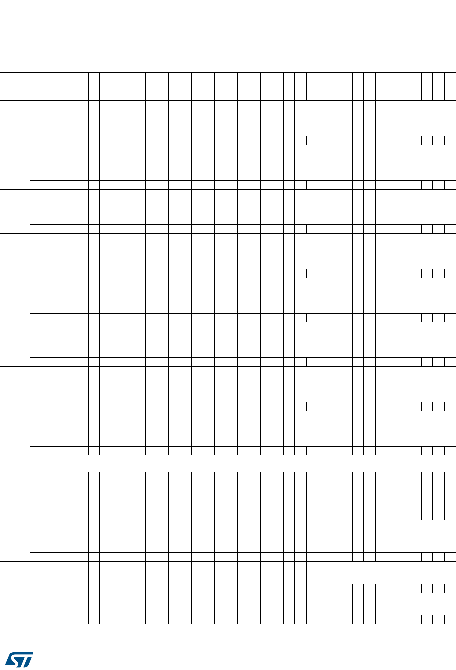
RM0394 Rev 4 1551/1600
RM0394 Universal serial bus full-speed device interface (USB)
1552
45.6.3 USB register map
The table below provides the USB register map and reset values.
Table 272. USB register map and reset values
Offset Register
31
30
29
28
27
26
25
24
23
22
21
20
19
18
17
16
15
14
13
12
11
10
9
8
7
6
5
4
3
2
1
0
0x00 USB_EP0R
Res.
Res.
Res.
Res.
Res.
Res.
Res.
Res.
Res.
Res.
Res.
Res.
Res.
Res.
Res.
Res.
CTR_RX
DTOG_RX
STAT_
RX
[1:0]
SETUP
EP
TYPE
[1:0]
EP_KIND
CTR_TX
DTOG_TX
STAT_
TX
[1:0]
EA[3:0]
Reset value 0000000000000000
0x04 USB_EP1R
Res.
Res.
Res.
Res.
Res.
Res.
Res.
Res.
Res.
Res.
Res.
Res.
Res.
Res.
Res.
Res.
CTR_RX
DTOG_RX
STAT_
RX
[1:0]
SETUP
EP
TYPE
[1:0]
EP_KIND
CTR_TX
DTOG_TX
STAT_
TX
[1:0]
EA[3:0]
Reset value 0000000000000000
0x08 USB_EP2R
Res.
Res.
Res.
Res.
Res.
Res.
Res.
Res.
Res.
Res.
Res.
Res.
Res.
Res.
Res.
Res.
CTR_RX
DTOG_RX
STAT_
RX
[1:0]
SETUP
EP
TYPE
[1:0]
EP_KIND
CTR_TX
DTOG_TX
STAT_
TX
[1:0]
EA[3:0]
Reset value 0000000000000000
0x0C USB_EP3R
Res.
Res.
Res.
Res.
Res.
Res.
Res.
Res.
Res.
Res.
Res.
Res.
Res.
Res.
Res.
Res.
CTR_RX
DTOG_RX
STAT_
RX
[1:0]
SETUP
EP
TYPE
[1:0]
EP_KIND
CTR_TX
DTOG_TX
STAT_
TX
[1:0]
EA[3:0]
Reset value 0000000000000000
0x10 USB_EP4R
Res.
Res.
Res.
Res.
Res.
Res.
Res.
Res.
Res.
Res.
Res.
Res.
Res.
Res.
Res.
Res.
CTR_RX
DTOG_RX
STAT_
RX
[1:0]
SETUP
EP
TYPE
[1:0]
EP_KIND
CTR_TX
DTOG_TX
STAT_
TX
[1:0]
EA[3:0]
Reset value 0000000000000000
0x14 USB_EP5R
Res.
Res.
Res.
Res.
Res.
Res.
Res.
Res.
Res.
Res.
Res.
Res.
Res.
Res.
Res.
Res.
CTR_RX
DTOG_RX
STAT_
RX
[1:0]
SETUP
EP
TYPE
[1:0]
EP_KIND
CTR_TX
DTOG_TX
STAT_
TX
[1:0]
EA[3:0]
Reset value 0000000000000000
0x18 USB_EP6R
Res.
Res.
Res.
Res.
Res.
Res.
Res.
Res.
Res.
Res.
Res.
Res.
Res.
Res.
Res.
Res.
CTR_RX
DTOG_RX
STAT_
RX
[1:0]
SETUP
EP
TYPE
[1:0]
EP_KIND
CTR_TX
DTOG_TX
STAT_
TX
[1:0]
EA[3:0]
Reset value 0000000000000000
0x1C USB_EP7R
Res.
Res.
Res.
Res.
Res.
Res.
Res.
Res.
Res.
Res.
Res.
Res.
Res.
Res.
Res.
Res.
CTR_RX
DTOG_RX
STAT_
RX
[1:0]
SETUP
EP
TYPE
[1:0]
EP_KIND
CTR_TX
DTOG_TX
STAT_
TX
[1:0]
EA[3:0]
Reset value 0000000000000000
0x20-
0x3F Reserved
0x40 USB_CNTR
Res.
Res.
Res.
Res.
Res.
Res.
Res.
Res.
Res.
Res.
Res.
Res.
Res.
Res.
Res.
Res.
CTRM
PMAOVRM
ERRM
WKUPM
SUSPM
RESETM
SOFM
ESOFM
L1REQM
Res.
L1RESUME
RESUME
FSUSP
LP_MODE
PDWN
FRES
Reset value 000000000 000011
0x44 USB_ISTR
Res.
Res.
Res.
Res.
Res.
Res.
Res.
Res.
Res.
Res.
Res.
Res.
Res.
Res.
Res.
Res.
CTR
PMAOVR
ERR
WKUP
SUSP
RESET
SOF
ESOF
L1REQ
Res.
Res.
DIR
EP_ID[3:0]
Reset value 000000000 00000
0x48 USB_FNR
Res.
Res.
Res.
Res.
Res.
Res.
Res.
Res.
Res.
Res.
Res.
Res.
Res.
Res.
Res.
Res.
RXDP
RXDM
LCK
LSOF
[1:0] FN[10:0]
Reset value 00000xxxxxxxxxxx
0x4C USB_DADDR
Res.
Res.
Res.
Res.
Res.
Res.
Res.
Res.
Res.
Res.
Res.
Res.
Res.
Res.
Res.
Res.
Res.
Res.
Res.
Res.
Res.
Res.
Res.
Res.
EF ADD[6:0]
Reset value 00000000

Universal serial bus full-speed device interface (USB) RM0394
1552/1600 RM0394 Rev 4
Refer to Section 2.2.2 on page 67 for the register boundary addresses.
0x50 USB_BTABLE
Res.
Res.
Res.
Res.
Res.
Res.
Res.
Res.
Res.
Res.
Res.
Res.
Res.
Res.
Res.
Res.
BTABLE[15:3]
Res.
Res.
Res.
Reset value 0000000000000
0x54 USB_LPMCSR
Res.
Res.
Res.
Res.
Res.
Res.
Res.
Res.
Res.
Res.
Res.
Res.
Res.
Res.
Res.
Res.
Res.
Res.
Res.
Res.
Res.
Res.
Res.
Res.
BESL[3:0]
REMWAKE
Res.
LPMACK
LPMEN
Reset value 00000 00
0x58 USB_BCDR
Res.
Res.
Res.
Res.
Res.
Res.
Res.
Res.
Res.
Res.
Res.
Res.
Res.
Res.
Res.
Res.
DPPU
Res.
Res.
Res.
Res.
Res.
Res.
Res.
PS2DET
SDET
PDET
DCDET
SDEN
PDEN
DCDEN
BCDEN
Reset value 0 00000000
Table 272. USB register map and reset values (continued)
Offset Register
31
30
29
28
27
26
25
24
23
22
21
20
19
18
17
16
15
14
13
12
11
10
9
8
7
6
5
4
3
2
1
0
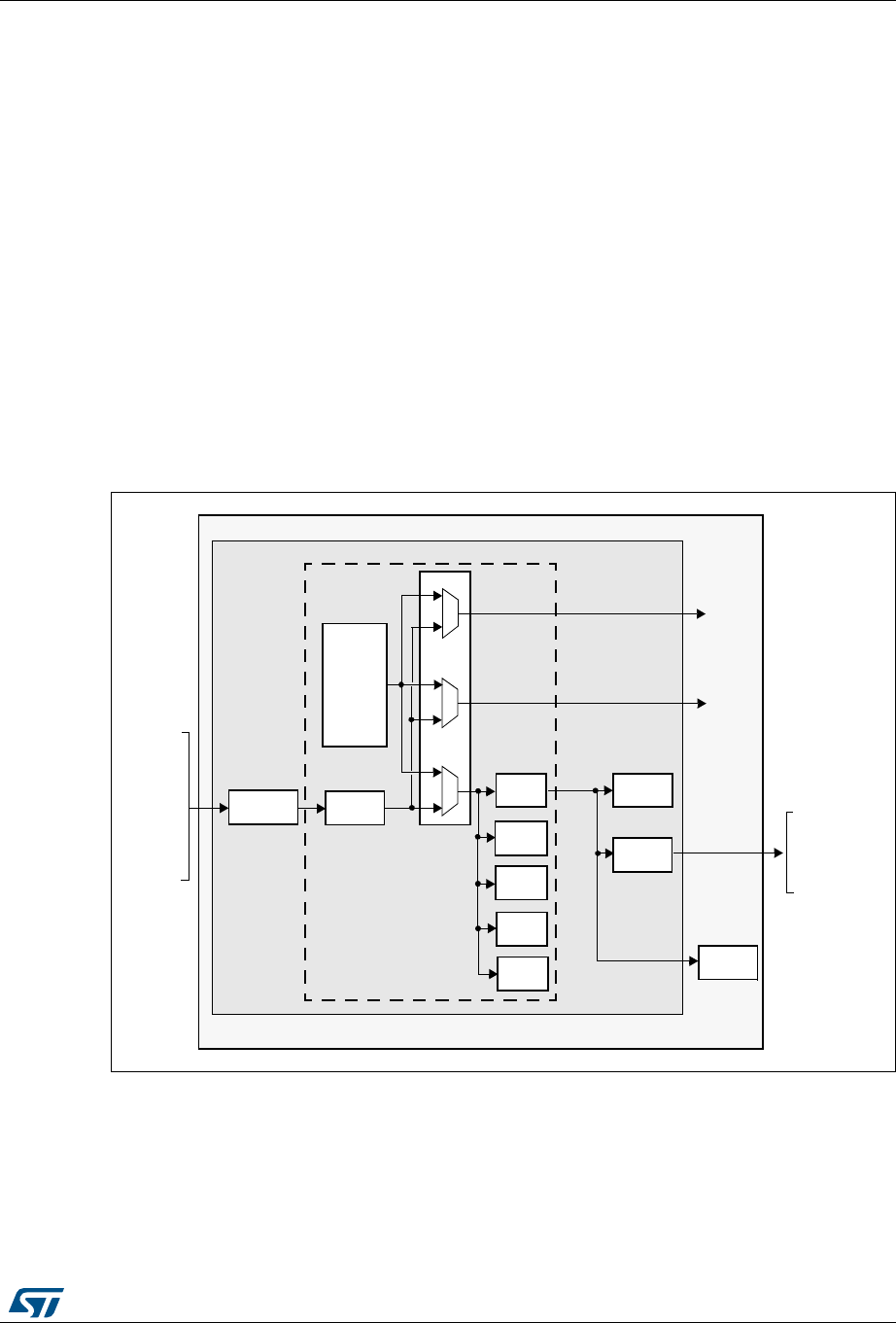
RM0394 Rev 4 1553/1600
RM0394 Debug support (DBG)
1584
46 Debug support (DBG)
46.1 Overview
The STM32L41xxx/42xxx/43xxx/44xxx/45xxx/46xxx devices are built around a Cortex®-M4
core which contains hardware extensions for advanced debugging features. The debug
extensions allow the core to be stopped either on a given instruction fetch (breakpoint) or
data access (watchpoint). When stopped, the core’s internal state and the system’s external
state may be examined. Once examination is complete, the core and the system may be
restored and program execution resumed.
The debug features are used by the debugger host when connecting to and debugging the
STM32L41xxx/42xxx/43xxx/44xxx/45xxx/46xxx MCUs.
Two interfaces for debug are available:
•Serial wire
•JTAG debug port
Figure 494. Block diagram of STM32 MCU and Cortex®-M4-level debug support
Note: The debug features embedded in the Cortex®-M4 core are a subset of the Arm® CoreSight
Design Kit.
#ORTEX-
#ORE
37*$0 !("!0
"RIDGE
.6)#
$74
&0"
)4-
%4-
$#ODE
INTERFACE
3YSTEM
INTERFACE
)NTERNALPRIVATE
PERIPHERALBUS00"
%XTERNALPRIVATE
PERIPHERALBUS00"
"USMATRIX
$ATA
4RACEPORT
$"'-#5
34--#5DEBUGSUPPORT
#ORTEX-DEBUGSUPPORT
*4-3
*4$)
*4$/
.*4234
*4#+
37$)/
37#,+
42!#%37/
42!#%37/
42!#%#+
42!#%$;=
40)5
-36

Debug support (DBG) RM0394
1554/1600 RM0394 Rev 4
The Arm® Cortex®-M4 core provides integrated on-chip debug support. It is comprised of:
•SWJ-DP: Serial wire / JTAG debug port
•AHP-AP: AHB access port
•ITM: Instrumentation trace macrocell
•FPB: Flash patch breakpoint
•DWT: Data watchpoint trigger
•TPUI: Trace port unit interface (available on larger packages, where the corresponding
pins are mapped)
•ETM: Embedded Trace Macrocell (available only on
STM32L41xxx/42xxx/43xxx/44xxx/45xxx/46xxx devices larger packages, where the
corresponding pins are mapped)
It also includes debug features dedicated to the
STM32L41xxx/42xxx/43xxx/44xxx/45xxx/46xxx:
•Flexible debug pinout assignment
•MCU debug box (support for low-power modes, control over peripheral clocks, etc.)
Note: For further information on debug functionality supported by the Arm® Cortex®-M4 core, refer
to the Cortex®-M4-r0p1 Technical Reference Manual and to the CoreSight Design Kit-r0p1
TRM (see Section 46.2: Reference Arm® documentation).
46.2 Reference Arm® documentation
•Cortex®-M4 r0p1 Technical Reference Manual (TRM),
search for “Cortex®-M4 Technical Reference Manual” at http://infocenter.arm.com
•Arm® Debug Interface V5
•Arm® CoreSight Design Kit revision r0p1 Technical Reference Manual
46.3 SWJ debug port (serial wire and JTAG)
The STM32L41xxx/42xxx/43xxx/44xxx/45xxx/46xxx core integrates the Serial Wire / JTAG
Debug Port (SWJ-DP). It is an Arm® standard CoreSight debug port that combines a JTAG-
DP (5-pin) interface and a SW-DP (2-pin) interface.
•The JTAG Debug Port (JTAG-DP) provides a 5-pin standard JTAG interface to the
AHP-AP port.
•The Serial Wire Debug Port (SW-DP) provides a 2-pin (clock + data) interface to the
AHP-AP port.
In the SWJ-DP, the two JTAG pins of the SW-DP are multiplexed with some of the five JTAG
pins of the JTAG-DP.
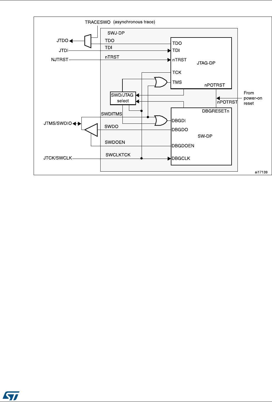
RM0394 Rev 4 1555/1600
RM0394 Debug support (DBG)
1584
Figure 495. SWJ debug port
Figure 495 shows that the asynchronous TRACE output (TRACESWO) is multiplexed with
TDO. This means that the asynchronous trace can only be used with SW-DP, not JTAG-DP.
46.3.1 Mechanism to select the JTAG-DP or the SW-DP
By default, the JTAG-Debug Port is active.
If the debugger host wants to switch to the SW-DP, it must provide a dedicated JTAG
sequence on TMS/TCK (respectively mapped to SWDIO and SWCLK) which disables the
JTAG-DP and enables the SW-DP. This way it is possible to activate the SWDP using only
the SWCLK and SWDIO pins.
This sequence is:
1. Send more than 50 TCK cycles with TMS (SWDIO) =1
2. Send the 16-bit sequence on TMS (SWDIO) = 0111100111100111 (MSB transmitted
first)
3. Send more than 50 TCK cycles with TMS (SWDIO) =1
46.4 Pinout and debug port pins
The STM32L41xxx/42xxx/43xxx/44xxx/45xxx/46xxx MCUs are available in various
packages with different numbers of available pins. As a result, some functionalities (ETM)
related to pin availability may differ between packages.
Debug support (DBG) RM0394
1556/1600 RM0394 Rev 4
46.4.1 SWJ debug port pins
Five pins are used as outputs from the STM32L41xxx/42xxx/43xxx/44xxx/45xxx/46xxx for
the SWJ-DP as alternate functions of general-purpose I/Os. These pins are available on all
packages.
46.4.2 Flexible SWJ-DP pin assignment
After RESET (SYSRESETn or PORESETn), all five pins used for the SWJ-DP are assigned
as dedicated pins immediately usable by the debugger host (note that the trace outputs are
not assigned except if explicitly programmed by the debugger host).
However, the STM32L41xxx/42xxx/43xxx/44xxx/45xxx/46xxx MCUs offer the possibility of
disabling some or all of the SWJ-DP ports, and therefore the possibility of releasing the
associated pins for general-purpose I/O (GPIO) usage. For more details on how to disable
SWJ-DP port pins, please refer to Section 8.3.2: I/O pin alternate function multiplexer and
mapping.
Table 273. SWJ debug port pins
SWJ-DP pin name
JTAG debug port SW debug port Pin
assign
ment
Type Description Type Debug assignment
JTMS/SWDIO I JTAG Test Mode
Selection IO Serial Wire Data
Input/Output PA13
JTCK/SWCLK I JTAG Test Clock I Serial Wire Clock PA14
JTDI I JTAG Test Data Input - - PA15
JTDO/TRACESWO O JTAG Test Data Output -
TRACESWO if
asynchronous trace is
enabled
PB3
NJTRST I JTAG Test nReset - - PB4
Table 274. Flexible SWJ-DP pin assignment
Available debug ports
SWJ IO pin assigned
PA13 /
JTMS/
SWDIO
PA14 /
JTCK/
SWCLK
PA15 /
JTDI
PB3 /
JTDO
PB4/
NJTRST
Full SWJ (JTAG-DP + SW-DP) - Reset State X X X X X
Full SWJ (JTAG-DP + SW-DP) but without NJTRST X X X X
JTAG-DP disabled and SW-DP enabled X X
JTAG-DP disabled and SW-DP disabled Released

RM0394 Rev 4 1557/1600
RM0394 Debug support (DBG)
1584
Note: When the APB bridge write buffer is full, it takes one extra APB cycle when writing the
AFIO_MAPR register. This is because the deactivation of the JTAGSW pins is done in two
cycles to guarantee a clean level on the nTRST and TCK input signals of the core.
•Cycle 1: the JTAGSW input signals to the core are tied to 1 or 0 (to 1 for nTRST, TDI
and TMS, to 0 for TCK)
•Cycle 2: the GPIO controller takes the control signals of the SWJTAG IO pins (like
controls of direction, pull-up/down, Schmitt trigger activation, etc.).
46.4.3 Internal pull-up and pull-down on JTAG pins
It is necessary to ensure that the JTAG input pins are not floating since they are directly
connected to flip-flops to control the debug mode features. Special care must be taken with
the SWCLK/TCK pin which is directly connected to the clock of some of these flip-flops.
To avoid any uncontrolled IO levels, the device embeds internal pull-ups and pull-downs on
the JTAG input pins:
•NJTRST: internal pull-up
•JTDI: internal pull-up
•JTMS/SWDIO: internal pull-up
•TCK/SWCLK: internal pull-down
Once a JTAG IO is released by the user software, the GPIO controller takes control again.
The reset states of the GPIO control registers put the I/Os in the equivalent state:
•NJTRST: input pull-up
•JTDI: input pull-up
•JTMS/SWDIO: input pull-up
•JTCK/SWCLK: input pull-down
•JTDO: input floating
The software can then use these I/Os as standard GPIOs.
Note: The JTAG IEEE standard recommends to add pull-ups on TDI, TMS and nTRST but there is
no special recommendation for TCK. However, for JTCK, the device needs an integrated
pull-down.
Having embedded pull-ups and pull-downs removes the need to add external resistors.

Debug support (DBG) RM0394
1558/1600 RM0394 Rev 4
46.4.4 Using serial wire and releasing the unused debug pins as GPIOs
To use the serial wire DP to release some GPIOs, the user software must change the GPIO
(PA15, PB3 and PB4) configuration mode in the GPIO_MODER register.This releases
PA15, PB3 and PB4 which now become available as GPIOs.
When debugging, the host performs the following actions:
•Under system reset, all SWJ pins are assigned (JTAG-DP + SW-DP).
•Under system reset, the debugger host sends the JTAG sequence to switch from the
JTAG-DP to the SW-DP.
•Still under system reset, the debugger sets a breakpoint on vector reset.
•The system reset is released and the Core halts.
•All the debug communications from this point are done using the SW-DP. The other
JTAG pins can then be reassigned as GPIOs by the user software.
Note: For user software designs, note that:
To release the debug pins, remember that they will be first configured either in input-pull-up
(nTRST, TMS, TDI) or pull-down (TCK) or output tristate (TDO) for a certain duration after
reset until the instant when the user software releases the pins.
When debug pins (JTAG or SW or TRACE) are mapped, changing the corresponding IO pin
configuration in the IOPORT controller has no effect.
46.5 STM32L41xxx/42xxx/43xxx/44xxx/45xxx/46xxx JTAG TAP
connection
The STM32L41xxx/42xxx/43xxx/44xxx/45xxx/46xxx MCUs integrate two serially connected
JTAG TAPs, the boundary scan TAP (IR is 5-bit wide) and the Cortex®-M4 TAP (IR is 4-bit
wide).
To access the TAP of the Cortex®-M4 for debug purposes:
1. First, it is necessary to shift the BYPASS instruction of the boundary scan TAP.
2. Then, for each IR shift, the scan chain contains 9 bits (=5+4) and the unused TAP
instruction must be shifted by using the BYPASS instruction.
3. For each data shift, the unused TAP, which is in BYPASS mode, adds 1 extra data bit in
the data scan chain.
Note: Important: Once Serial-Wire is selected using the dedicated Arm® JTAG sequence, the
boundary scan TAP is automatically disabled (JTMS forced high).
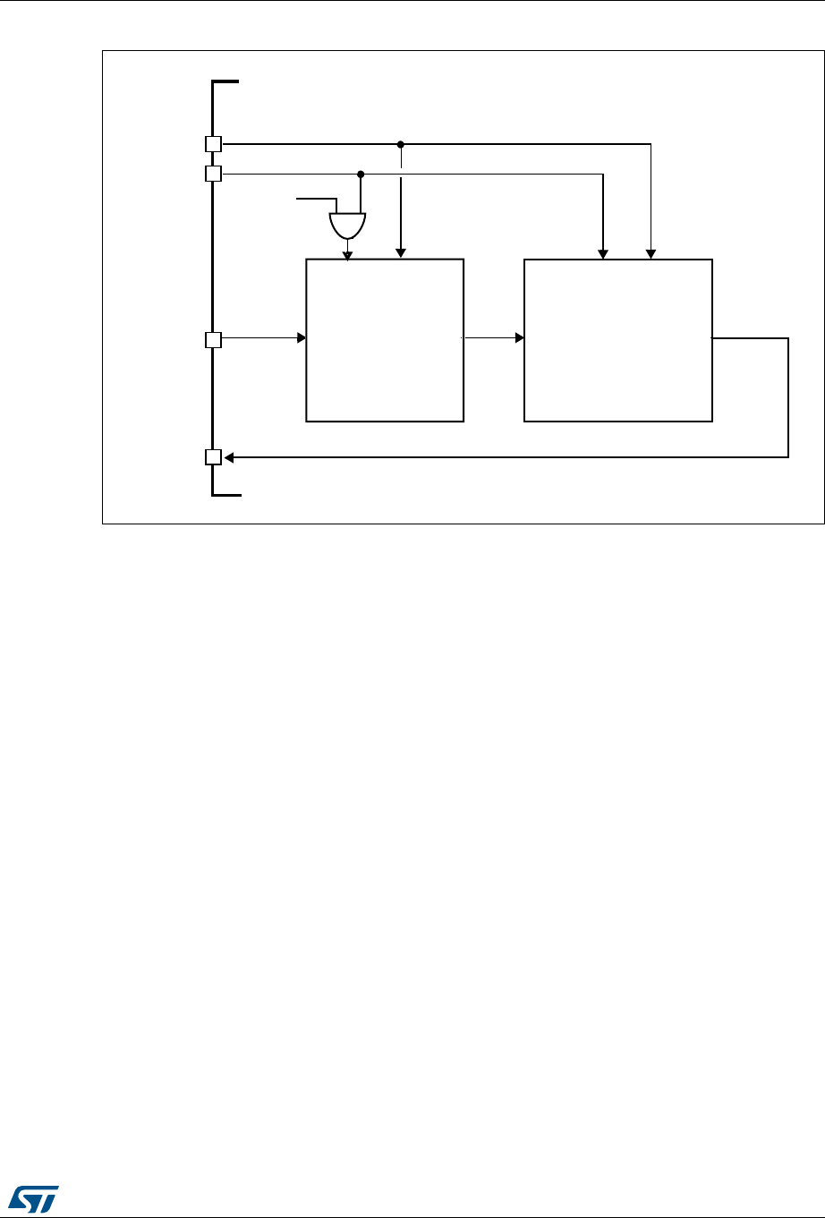
RM0394 Rev 4 1559/1600
RM0394 Debug support (DBG)
1584
Figure 496. JTAG TAP connections
46.6 ID codes and locking mechanism
There are several ID codes inside the STM32L41xxx/42xxx/43xxx/44xxx/45xxx/46xxx
MCUs. ST strongly recommends tools designers to lock their debuggers using the MCU
DEVICE ID code located in the external PPB memory map at address 0xE0042000.
%RXQGDU\VFDQ
7$3
1-7567
&RUWH [07$3
-706
706 Q7567706 Q7567
-7',
-7'2
7', 7'2 7', 7'2
6:'3
6700&8
6HOHFWHG
,5LVELWZLGH ,5LVELWZLGH
DLF

Debug support (DBG) RM0394
1560/1600 RM0394 Rev 4
46.6.1 MCU device ID code
The STM32L41xxx/42xxx/43xxx/44xxx/45xxx/46xxx MCUs integrate an MCU ID code. This
ID identifies the ST MCU part-number and the die revision. It is part of the DBG_MCU
component and is mapped on the external PPB bus (see Section 46.16 on page 1572). This
code is accessible using the JTAG debug port (4 to 5 pins) or the SW debug port (two pins)
or by the user software. It is even accessible while the MCU is under system reset.
Only the DEV_ID(11:0) should be used for identification by the debugger/programmer tools.
DBGMCU_IDCODE
Address: 0xE004 2000
Only 32-bits access supported. Read-only
46.6.2 Boundary scan TAP
JTAG ID code
The TAP of the STM32L41xxx/42xxx/43xxx/44xxx/45xxx/46xxx BSC (boundary scan)
integrates a JTAG ID code equal to 0x06435041.
46.6.3 Cortex®-M4 TAP
The TAP of the Arm® Cortex®-M4 integrates a JTAG ID code. This ID code is the Arm®
default one and has not been modified. This code is only accessible by the JTAG Debug
Port.
This code is 0x4BA00477 (corresponds to Cortex®-M4 r0p1, see Section 46.2: Reference
Arm® documentation).
31 30 29 28 27 26 25 24 23 22 21 20 19 18 17 16
REV_ID
rrrrrr r r r r rrrrrr
1514131211109876543210
Res. Res. Res. Res. DEV_ID
rrrrrrrrrrrr
Bits 31:16 REV_ID[15:0] Revision identifier
This field indicates the revision of the device.
0x1000: Rev A
0x1001: Rev Z
0x2001: Rev Y
Others: Reserved
Bits 15:12 Reserved, must be kept at reset value.
Bits 11:0 DEV_ID[11:0]: Device identifier
The device ID is:
– 0x435 for STM32L43xxx and STM32L44xxx devices
– 0x462 for STM32L45xxx and STM32L46xxx devices
– ox464 for STM32L41xxx and STM32L42xxx devices

RM0394 Rev 4 1561/1600
RM0394 Debug support (DBG)
1584
46.6.4 Cortex®-M4 JEDEC-106 ID code
The Arm® Cortex®-M4 integrates a JEDEC-106 ID code. It is located in the 4KB ROM table
mapped on the internal PPB bus at address 0xE00FF000_0xE00FFFFF.
This code is accessible by the JTAG Debug Port (4 to 5 pins) or by the SW Debug Port (two
pins) or by the user software.
46.7 JTAG debug port
A standard JTAG state machine is implemented with a 4-bit instruction register (IR) and five
data registers (for full details, refer to the Cortex®-M4 with FPU r0p1 Technical Reference
Manual (TRM), for references, please see Section 46.2: Reference Arm® documentation).
Table 275. JTAG debug port data registers
IR(3:0) Data register Details
1111 BYPASS
[1 bit] -
1110 IDCODE
[32 bits]
ID CODE
0x3BA00477 (Arm® Cortex®-M4 r0p1-01rel0 ID Code)
1010 DPACC
[35 bits]
Debug port access register
This initiates a debug port and allows access to a debug port register.
– When transferring data IN:
Bits 34:3= DATA[31:0] = 32-bit data to transfer for a write request
Bits 2:1 = A[3:2] = 2-bit address of a debug port register.
Bit 0 = RnW = Read request (1) or write request (0).
– When transferring data OUT:
Bits 34:3 = DATA[31:0] = 32-bit data which is read following a read
request
Bits 2:0 = ACK[2:0] = 3-bit Acknowledge:
010 = OK/FAULT
001 = WAIT
OTHER = reserved
Refer to Table 276 for a description of the A(3:2) bits

Debug support (DBG) RM0394
1562/1600 RM0394 Rev 4
1011 APACC
[35 bits]
Access port access register
Initiates an access port and allows access to an access port register.
– When transferring data IN:
Bits 34:3 = DATA[31:0] = 32-bit data to shift in for a write request
Bits 2:1 = A[3:2] = 2-bit address (sub-address AP registers).
Bit 0 = RnW= Read request (1) or write request (0).
– When transferring data OUT:
Bits 34:3 = DATA[31:0] = 32-bit data which is read following a read
request
Bits 2:0 = ACK[2:0] = 3-bit Acknowledge:
010 = OK/FAULT
001 = WAIT
OTHER = reserved
There are many AP Registers (see AHB-AP) addressed as the
combination of:
– The shifted value A[3:2]
– The current value of the DP SELECT register
1000 ABORT
[35 bits]
Abort register
– Bits 31:1 = Reserved
– Bit 0 = DAPABORT: write 1 to generate a DAP abort.
Table 276. 32-bit debug port registers addressed through the shifted value A[3:2]
Address A(3:2) value Description
0x0 00 Reserved, must be kept at reset value.
0x4 01
DP CTRL/STAT register. Used to:
– Request a system or debug power-up
– Configure the transfer operation for AP accesses
– Control the pushed compare and pushed verify operations
– Read some status flags (overrun, power-up acknowledges)
0x8 10
DP SELECT register. Used to select the current access port and the
active 4-words register window.
– Bits 31:24: APSEL: select the current AP
– Bits 23:8: reserved
– Bits 7:4: APBANKSEL: select the active 4-words register window on the
current AP
– Bits 3:0: reserved
0xC 11
DP RDBUFF register: Used to allow the debugger to get the final result
after a sequence of operations (without requesting new JTAG-DP
operation)
Table 275. JTAG debug port data registers (continued)
IR(3:0) Data register Details

RM0394 Rev 4 1563/1600
RM0394 Debug support (DBG)
1584
46.8 SW debug port
46.8.1 SW protocol introduction
This synchronous serial protocol uses two pins:
•SWCLK: clock from host to target
•SWDIO: bidirectional
The protocol allows two banks of registers (DPACC registers and APACC registers) to be
read and written to.
Bits are transferred LSB-first on the wire.
For SWDIO bidirectional management, the line must be pulled-up on the board (100 k
recommended by Arm®).
Each time the direction of SWDIO changes in the protocol, a turnaround time is inserted
where the line is not driven by the host nor the target. By default, this turnaround time is one
bit time, however this can be adjusted by configuring the SWCLK frequency.
46.8.2 SW protocol sequence
Each sequence consist of three phases:
1. Packet request (8 bits) transmitted by the host
2. Acknowledge response (3 bits) transmitted by the target
3. Data transfer phase (33 bits) transmitted by the host or the target
Refer to the Cortex®-M4 r0p1 TRM for a detailed description of DPACC and APACC
registers.
The packet request is always followed by the turnaround time (default 1 bit) where neither
the host nor target drive the line.
Table 277. Packet request (8-bits)
Bit Name Description
0 Start Must be “1”
1 APnDP 0: DP Access
1: AP Access
2RnW 0: Write Request
1: Read Request
4:3 A(3:2) Address field of the DP or AP registers (refer to Table 276)
5 Parity Single bit parity of preceding bits
6Stop 0
7Park Not driven by the host. Must be read as “1” by the target because of
the pull-up

Debug support (DBG) RM0394
1564/1600 RM0394 Rev 4
The ACK Response must be followed by a turnaround time only if it is a READ transaction
or if a WAIT or FAULT acknowledge has been received.
The DATA transfer must be followed by a turnaround time only if it is a READ transaction.
46.8.3 SW-DP state machine (reset, idle states, ID code)
The State Machine of the SW-DP has an internal ID code which identifies the SW-DP. It
follows the JEP-106 standard. This ID code is the default Arm® one and is set to
0x1BA01477 (corresponding to Cortex®-M4 r0p1).
Note: Note that the SW-DP state machine is inactive until the target reads this ID code.
•The SW-DP state machine is in RESET STATE either after power-on reset, or after the
DP has switched from JTAG to SWD or after the line is high for more than 50 cycles
•The SW-DP state machine is in IDLE STATE if the line is low for at least two cycles
after RESET state.
•After RESET state, it is mandatory to first enter into an IDLE state AND to perform a
READ access of the DP-SW ID CODE register. Otherwise, the target will issue a
FAULT acknowledge response on another transactions.
Further details of the SW-DP state machine can be found in the Cortex®-M4 r0p1 TRM and
the CoreSight Design Kit r0p1 TRM.
46.8.4 DP and AP read/write accesses
•Read accesses to the DP are not posted: the target response can be immediate (if
ACK=OK) or can be delayed (if ACK=WAIT).
•Read accesses to the AP are posted. This means that the result of the access is
returned on the next transfer. If the next access to be done is NOT an AP access, then
the DP-RDBUFF register must be read to obtain the result.
The READOK flag of the DP-CTRL/STAT register is updated on every AP read access
or RDBUFF read request to know if the AP read access was successful.
•The SW-DP implements a write buffer (for both DP or AP writes), that enables it to
accept a write operation even when other transactions are still outstanding. If the write
buffer is full, the target acknowledge response is “WAIT”. With the exception of
Table 278. ACK response (3 bits)
Bit Name Description
0..2 ACK
001: FAULT
010: WAIT
100: OK
Table 279. DATA transfer (33 bits)
Bit Name Description
0..31 WDATA or RDATA Write or Read data
32 Parity Single parity of the 32 data bits

RM0394 Rev 4 1565/1600
RM0394 Debug support (DBG)
1584
IDCODE read or CTRL/STAT read or ABORT write which are accepted even if the write
buffer is full.
•Because of the asynchronous clock domains SWCLK and HCLK, two extra SWCLK
cycles are needed after a write transaction (after the parity bit) to make the write
effective internally. These cycles should be applied while driving the line low (IDLE
state)
This is particularly important when writing the CTRL/STAT for a power-up request. If the
next transaction (requiring a power-up) occurs immediately, it will fail.
46.8.5 SW-DP registers
Access to these registers are initiated when APnDP=0
Table 280. SW-DP registers
A(3:2) R/W
CTRLSEL bit
of SELECT
register
Register Notes
00 Read - IDCODE The manufacturer code is not set to ST code
0x2BA01477 (identifies the SW-DP)
00 Write - ABORT -
01 Read/Write 0 DP-
CTRL/STAT
Purpose is to:
– request a system or debug power-up
– configure the transfer operation for AP
accesses
– control the pushed compare and pushed
verify operations.
– read some status flags (overrun, power-
up acknowledges)
01 Read/Write 1 WIRE
CONTROL
Purpose is to configure the physical serial
port protocol (like the duration of the
turnaround time)
10 Read - READ
RESEND
Enables recovery of the read data from a
corrupted debugger transfer, without
repeating the original AP transfer.
10 Write - SELECT The purpose is to select the current access
port and the active 4-words register window
11 Read/Write - READ
BUFFER
This read buffer is useful because AP
accesses are posted (the result of a read AP
request is available on the next AP
transaction).
This read buffer captures data from the AP,
presented as the result of a previous read,
without initiating a new transaction

Debug support (DBG) RM0394
1566/1600 RM0394 Rev 4
46.8.6 SW-AP registers
Access to these registers are initiated when APnDP=1
There are many AP Registers (see AHB-AP) addressed as the combination of:
•The shifted value A[3:2]
•The current value of the DP SELECT register
46.9 AHB-AP (AHB access port) - valid for both JTAG-DP
and SW-DP
Features:
•System access is independent of the processor status.
•Either SW-DP or JTAG-DP accesses AHB-AP.
•The AHB-AP is an AHB master into the Bus Matrix. Consequently, it can access all the
data buses (Dcode Bus, System Bus, internal and external PPB bus) but the ICode
bus.
•Bitband transactions are supported.
•AHB-AP transactions bypass the FPB.
The address of the 32-bits AHP-AP resisters are 6-bits wide (up to 64 words or 256 bytes)
and consists of:
e) Bits [7:4] = the bits [7:4] APBANKSEL of the DP SELECT register
f) Bits [3:2] = the 2 address bits of A(3:2) of the 35-bit packet request for SW-DP.
The AHB-AP of the Cortex®-M4 includes 9 x 32-bits registers:
Refer to the Cortex®-M4 r0p1 TRM for further details.
Table 281. Cortex®-M4 AHB-AP registers
Address
offset Register name Notes
0x00 AHB-AP Control and Status
Word
Configures and controls transfers through the AHB
interface (size, hprot, status on current transfer, address
increment type
0x04 AHB-AP Transfer Address -
0x0C AHB-AP Data Read/Write -
0x10 AHB-AP Banked Data 0
Directly maps the 4 aligned data words without rewriting
the Transfer Address Register.
0x14 AHB-AP Banked Data 1
0x18 AHB-AP Banked Data 2
0x1C AHB-AP Banked Data 3
0xF8 AHB-AP Debug ROM Address Base Address of the debug interface
0xFC AHB-AP ID Register -

RM0394 Rev 4 1567/1600
RM0394 Debug support (DBG)
1584
46.10 Core debug
Core debug is accessed through the core debug registers. Debug access to these registers
is by means of the Advanced High-performance Bus (AHB-AP) port. The processor can
access these registers directly over the internal Private Peripheral Bus (PPB).
It consists of 4 registers:
Note: Important: these registers are not reset by a system reset. They are only reset by a power-
on reset.
Refer to the Cortex®-M4 r0p1 TRM for further details.
To Halt on reset, it is necessary to:
•enable the bit0 (VC_CORRESET) of the Debug and Exception Monitor Control
Register
•enable the bit0 (C_DEBUGEN) of the Debug Halting Control and Status Register.
46.11 Capability of the debugger host to connect under system
reset
The STM32L41xxx/42xxx/43xxx/44xxx/45xxx/46xxx MCUs’ reset system comprises the
following reset sources:
•POR (power-on reset) which asserts a RESET at each power-up
•Internal watchdog reset
•Software reset
•External reset.
The Cortex®-M4 differentiates the reset of the debug part (generally PORRESETn) and the
other one (SYSRESETn).
This way, it is possible for the debugger to connect under System Reset, programming the
Core Debug Registers to halt the core when fetching the reset vector. Then the host can
release the system reset and the core will immediately halt without having executed any
instructions. In addition, it is possible to program any debug features under System Reset.
Table 282. Core debug registers
Register Description
DHCSR
The 32-bit Debug Halting Control and Status Register:
This provides status information about the state of the processor enable core debug
halt and step the processor.
DCRSR The 17-bit Debug Core Register Selector Register:
This selects the processor register to transfer data to or from.
DCRDR
The 32-bit Debug Core Register Data Register:
This holds data for reading and writing registers to and from the processor selected
by the DCRSR (Selector) register.
DEMCR
The 32-bit Debug Exception and Monitor Control Register:
This provides Vector Catching and Debug Monitor Control. This register contains a
bit named TRCENA which enable the use of a TRACE.

Debug support (DBG) RM0394
1568/1600 RM0394 Rev 4
Note: It is highly recommended for the debugger host to connect (set a breakpoint in the reset
vector) under system reset.
46.12 FPB (Flash patch breakpoint)
The FPB unit:
•implements hardware breakpoints
•patches code and data from code space to system space. This feature gives the
possibility to correct software bugs located in the Code Memory Space.
The use of a Software Patch or a Hardware Breakpoint is exclusive.
The FPB consists of:
•2 literal comparators for matching against literal loads from Code Space and remapping
to a corresponding area in the System Space
•6 instruction comparators for matching against instruction fetches from Code Space.
They can be used either to remap to a corresponding area in the System Space or to
generate a Breakpoint Instruction to the core.
46.13 DWT (data watchpoint trigger)
The DWT unit consists of four comparators. They are configurable as:
•a hardware watchpoint or
•a trigger to an ETM or
•a PC sampler or
•a data address sampler
The DWT also provides some means to give some profiling informations. For this, some
counters are accessible to give the number of:
•Clock cycle
•Folded instructions
•Load store unit (LSU) operations
•Sleep cycles
•CPI (clock per instructions)
•Interrupt overhead

RM0394 Rev 4 1569/1600
RM0394 Debug support (DBG)
1584
46.14 ITM (instrumentation trace macrocell)
46.14.1 General description
The ITM is an application-driven trace source that supports printf style debugging to trace
Operating System (OS) and application events, and emits diagnostic system information.
The ITM emits trace information as packets which can be generated as:
•Software trace. Software can write directly to the ITM stimulus registers to emit
packets.
•Hardware trace. The DWT generates these packets, and the ITM emits them.
•Time stamping. Timestamps are emitted relative to packets. The ITM contains a 21-bit
counter to generate the timestamp. The Cortex®-M4 clock or the bit clock rate of the
Serial Wire Viewer (SWV) output clocks the counter.
The packets emitted by the ITM are output to the TPIU (Trace Port Interface Unit). The
formatter of the TPIU adds some extra packets (refer to TPIU) and then output the complete
packets sequence to the debugger host.
The bit TRCEN of the Debug Exception and Monitor Control Register must be enabled
before you program or use the ITM.
46.14.2 Time stamp packets, synchronization and overflow packets
Time stamp packets encode time stamp information, generic control and synchronization. It
uses a 21-bit timestamp counter (with possible prescalers) which is reset at each time
stamp packet emission. This counter can be either clocked by the CPU clock or the SWV
clock.
A synchronization packet consists of 6 bytes equal to 0x80_00_00_00_00_00 which is
emitted to the TPIU as 00 00 00 00 00 80 (LSB emitted first).
A synchronization packet is a timestamp packet control. It is emitted at each DWT trigger.
For this, the DWT must be configured to trigger the ITM: the bit CYCCNTENA (bit0) of the
DWT Control Register must be set. In addition, the bit2 (SYNCENA) of the ITM Trace
Control Register must be set.
Note: If the SYNENA bit is not set, the DWT generates Synchronization triggers to the TPIU which
will send only TPIU synchronization packets and not ITM synchronization packets.
An overflow packet consists is a special timestamp packets which indicates that data has
been written but the FIFO was full.
Table 283. Main ITM registers
Address Register Details
@E0000FB0 ITM lock access Write 0xC5ACCE55 to unlock Write Access to the other ITM
registers

Debug support (DBG) RM0394
1570/1600 RM0394 Rev 4
Example of configuration
To output a simple value to the TPIU:
•Configure the TPIU and assign TRACE I/Os by configuring the DBGMCU_CR (refer to
Section 46.17.2: TRACE pin assignment and Section 46.16.3: Debug MCU
configuration register (DBGMCU_CR))
•Write 0xC5ACCE55 to the ITM Lock Access Register to unlock the write access to the
ITM registers
•Write 0x00010005 to the ITM Trace Control Register to enable the ITM with
Synchronous enabled and an ATB ID different from 0x00
•Write 0x1 to the ITM Trace Enable Register to enable the Stimulus Port 0
•Write 0x1 to the ITM Trace Privilege Register to unmask Stimulus Ports 7:0
•Write the value to output in the Stimulus Port Register 0: this can be done by software
(using a printf function)
@E0000E80 ITM trace control
Bits 31-24 = Always 0
Bits 23 = Busy
Bits 22-16 = 7-bits ATB ID which identifies the source of the
trace data
Bits 15-10 = Always 0
Bits 9:8 = TSPrescale = Time Stamp Prescaler
Bits 7-5 = Reserved
Bit 4 = SWOENA = Enable SWV behavior (to clock the
timestamp counter by the SWV clock)
Bit 3 = DWTENA: Enable the DWT Stimulus
Bit 2 = SYNCENA: this bit must be to 1 to enable the DWT to
generate synchronization triggers so that the TPIU can then
emit the synchronization packets
Bit 1 = TSENA (Timestamp Enable)
Bit 0 = ITMENA: Global Enable Bit of the ITM
@E0000E40 ITM trace privilege
Bit 3: mask to enable tracing ports31:24
Bit 2: mask to enable tracing ports23:16
Bit 1: mask to enable tracing ports15:8
Bit 0: mask to enable tracing ports7:0
@E0000E00 ITM trace enable Each bit enables the corresponding Stimulus port to generate
trace
@E0000000-
E000007C
Stimulus port
registers 0-31
Write the 32-bits data on the selected Stimulus Port (32
available) to be traced out
Table 283. Main ITM registers (continued)
Address Register Details

RM0394 Rev 4 1571/1600
RM0394 Debug support (DBG)
1584
46.15 ETM (Embedded trace macrocell)
46.15.1 General description
The ETM enables the reconstruction of program execution. Data are traced using the Data
Watchpoint and Trace (DWT) component or the Instruction Trace Macrocell (ITM) whereas
instructions are traced using the Embedded Trace Macrocell (ETM).
The ETM transmits information as packets and is triggered by embedded resources. These
resources must be programmed independently and the trigger source is selected using the
Trigger Event Register (0xE0041008). An event could be a simple event (address match
from an address comparator) or a logic equation between 2 events. The trigger source is
one of the four comparators of the DWT module, The following events can be monitored:
•Clock cycle matching
•Data address matching
For more informations on the trigger resources refer to Section 46.13: DWT (data
watchpoint trigger).
The packets transmitted by the ETM are output to the TPIU (Trace Port Interface Unit). The
formatter of the TPIU adds some extra packets (refer to Section 46.17: TPIU (trace port
interface unit)) and then outputs the complete packet sequence to the debugger host.
46.15.2 Signal protocol, packet types
This part is described in the section 7 ETMv3 Signal Protocol of the Arm® IHI 0014N
document.
46.15.3 Main ETM registers
For more information on registers refer to the chapter 3 of the Arm® IHI 0014N specification.
Table 284. Main ETM registers
Address Register Details
0xE0041FB0 ETM Lock Access Write 0xC5ACCE55 to unlock the write access to the
other ETM registers.
0xE0041000 ETM Control This register controls the general operation of the ETM,
for instance how tracing is enabled.
0xE0041010 ETM Status This register provides information about the current status
of the trace and trigger logic.
0xE0041008 ETM Trigger Event This register defines the event that will control trigger.
0xE004101C ETM Trace Enable
Control This register defines which comparator is selected.
0xE0041020 ETM Trace Enable Event This register defines the trace enabling event.
0xE0041024 ETM Trace Start/Stop This register defines the traces used by the trigger source
to start and stop the trace, respectively.

Debug support (DBG) RM0394
1572/1600 RM0394 Rev 4
46.15.4 Configuration example
To output a simple value to the TPIU:
•Configure the TPIU and enable the I/IO_TRACEN to assign TRACE I/Os in the
STM32L41xxx/42xxx/43xxx/44xxx/45xxx/46xxx debug configuration register
•Write 0xC5ACCE55 to the ETM Lock Access Register to unlock the write access to the
ITM registers
•Write 0x00001D1E to the control register (configure the trace)
•Write 0000406F to the Trigger Event register (define the trigger event)
•Write 0000006F to the Trace Enable Event register (define an event to start/stop)
•Write 00000001 to the Trace Start/stop register (enable the trace)
•Write 0000191E to the ETM Control Register (end of configuration)
46.16 MCU debug component (DBGMCU)
The MCU debug component helps the debugger provide support for:
•Low-power modes
•Clock control for timers, watchdog, I2C and bxCAN during a breakpoint
•Control of the trace pins assignment
46.16.1 Debug support for low-power modes
To enter low-power mode, the instruction WFI or WFE must be executed.
The MCU implements several low-power modes which can either deactivate the CPU clock
or reduce the power of the CPU.
The core does not allow FCLK or HCLK to be turned off during a debug session. As these
are required for the debugger connection, during a debug, they must remain active. The
MCU integrates special means to allow the user to debug software in low-power modes.
For this, the debugger host must first set some debug configuration registers to change the
low-power mode behavior:
•In Sleep mode, DBG_SLEEP bit of DBGMCU_CR register must be previously set by
the debugger. This will feed HCLK with the same clock that is provided to FCLK
(system clock previously configured by the software).
•In Stop mode, the bit DBG_STOP must be previously set by the debugger. This will
enable the internal RC oscillator clock to feed FCLK and HCLK in Stop mode.
•In Standby mode, the bit DBG_STANDBY must be previously set by the debugger. This
will keep the regulators on, and enable the internal RC oscillator clock to feed FCLK
and HCLK in Standby mode. A system reset is generated internally so that exiting from
Standby is identical than fetching from reset.
The DBGMCU_CR register can be written by the debugger under system reset. If the
debugger host does not support these features, it is still possible to write this register by
software.

RM0394 Rev 4 1573/1600
RM0394 Debug support (DBG)
1584
46.16.2 Debug support for timers, RTC, watchdog, bxCAN and I2C
During a breakpoint, it is necessary to choose how the counter of timers,RTC and watchdog
should behave:
•They can continue to count inside a breakpoint. This is usually required when a PWM is
controlling a motor, for example.
•They can stop to count inside a breakpoint. This is required for watchdog purposes.
For the bxCAN, the user can choose to block the update of the receive register during a
breakpoint.
For the I2C, the user can choose to block the SMBUS timeout during a breakpoint.
The DBGMCU freeze registers can be written by the debugger under system reset. If the
debugger host does not support these features, it is still possible to write these registers by
software.
46.16.3 Debug MCU configuration register (DBGMCU_CR)
Address: 0xE004 2004
Power-on reset: 0x0000 0000
System reset: not affected
Access: Only 32-bit access supported
31 30 29 28 27 26 25 24 23 22 21 20 19 18 17 16
Res. Res. Res. Res. Res. Res. Res. Res. Res. Res. Res. Res. Res. Res. Res. Res.
15 14 13 12 11 10 9 8 7 6 5 4 3 2 1 0
Res. Res. Res. Res. Res. Res. Res. Res.
TRACE_
MODE
[1:0]
TRACE
_
IOEN
Res. Res.
DBG_
STAND
BY
DBG_
STOP
DBG_
SLEEP
rw rw rw rw rw rw
Bits 31:8 Reserved, must be kept at reset value.
Bits 7:5 TRACE_MODE[1:0] and TRACE_IOEN: Trace pin assignment control
– With TRACE_IOEN=0:
TRACE_MODE=xx: TRACE pins not assigned (default state)
– With TRACE_IOEN=1:
– TRACE_MODE=00: TRACE pin assignment for Asynchronous Mode
– TRACE_MODE=01: TRACE pin assignment for Synchronous Mode with a
TRACEDATA size of 1
– TRACE_MODE=10: TRACE pin assignment for Synchronous Mode with a
TRACEDATA size of 2
– TRACE_MODE=11: TRACE pin assignment for Synchronous Mode with a
TRACEDATA size of 4
Bits 4:3 Reserved, must be kept at reset value.

Debug support (DBG) RM0394
1574/1600 RM0394 Rev 4
46.16.4 Debug MCU APB1 freeze register1(DBGMCU_APB1FZR1)
Address: 0xE004 2008
Power on reset (POR): 0x0000 0000
System reset: not affected
Access: Only 32-bit access are supported.
Bit 2 DBG_STANDBY: Debug Standby mode
0: (FCLK=Off, HCLK=Off) The whole digital part is unpowered.
From software point of view, exiting from Standby is identical than fetching reset vector
(except a few status bit indicated that the MCU is resuming from Standby)
1: (FCLK=On, HCLK=On) In this case, the digital part is not unpowered and FCLK and
HCLK are provided by the internal RC oscillator which remains active. In addition, the MCU
generate a system reset during Standby mode so that exiting from Standby is identical than
fetching from reset.
Bit 1 DBG_STOP: Debug Stop mode
0: (FCLK=Off, HCLK=Off) In STOP mode, the clock controller disables all clocks (including
HCLK and FCLK). When exiting from STOP mode, the clock configuration is identical to the
one after RESET (CPU clocked by the 8 MHz internal RC oscillator (HSI16)). Consequently,
the software must reprogram the clock controller to enable the PLL, the Xtal, etc.
1: (FCLK=On, HCLK=On) In this case, when entering STOP mode, FCLK and HCLK are
provided by the internal RC oscillator which remains active in STOP mode. When exiting
STOP mode, the software must reprogram the clock controller to enable the PLL, the Xtal,
etc. (in the same way it would do in case of DBG_STOP=0)
Bit 0 DBG_SLEEP: Debug Sleep mode
0: (FCLK=On, HCLK=Off) In Sleep mode, FCLK is clocked by the system clock as
previously configured by the software while HCLK is disabled.
In Sleep mode, the clock controller configuration is not reset and remains in the previously
programmed state. Consequently, when exiting from Sleep mode, the software does not
need to reconfigure the clock controller.
1: (FCLK=On, HCLK=On) In this case, when entering Sleep mode, HCLK is fed by the same
clock that is provided to FCLK (system clock as previously configured by the software).
31 30 29 28 27 26 25 24 23 22 21 20 19 18 17 16
LPTIM1_
STOP Res. Res. Res. Res. Res.
DBG_
CAN1_
STOP
Res.
DBG_
I2C3_
STOP
DBG_
I2C2_
STOP
DBG_
I2C1_
STOP
Res. Res. Res. Res. Res.
rw rw rw rw rw
15 14 13 12 11 10 9 8 7 65432 1 0
Res. Res. Res.
DBG_
IWDG_
STOP
DBG_
WWDG
_STOP
DBG_
RTC_
STOP
Res. Res. Res. Res.
DBG_
TIM7
_STO
P
DBG_
TIM6
_STO
P
Res. Res. Res.
DBG_
TIM2_
STOP
rw rw rw rw rw rw

RM0394 Rev 4 1575/1600
RM0394 Debug support (DBG)
1584
46.16.5 Debug MCU APB1 freeze register 2 (DBGMCU_APB1FZR2)
Address: 0xE004 200C
Power on reset (POR): 0x0000 0000
System reset: not affected
Bit 31 DBG_LPTIM1_STOP: LPTIM1 counter stopped when core is halted
0: The counter clock of LPTIM1 is fed even if the core is halted
1: The counter clock of LPTIM1 is stopped when the core is halted
Bits 30:26 Reserved, must be kept at reset value.
Bit 25 DBG_CAN1_STOP: bxCAN stopped when core is halted
0: Same behavior as in normal mode
1: The bxCAN receive registers are frozen
Bit 24 Reserved, must be kept at reset value.
Bit 23 DBG_I2C3_STOP: I2C3 SMBUS timeout counter stopped when core is halted
0: Same behavior as in normal mode
1: The I2C3 SMBus timeout is frozen
Bit 22 DBG_I2C2_STOP: I2C2 SMBUS timeout counter stopped when core is halted
0: Same behavior as in normal mode
1: The I2C2 SMBus timeout is frozen
Bit 21 DBG_I2C1_STOP: I2C1 SMBUS timeout counter stopped when core is halted
0: Same behavior as in normal mode
1: The I2C1 SMBus timeout is frozen
Bits 20:13 Reserved, must be kept at reset value.
Bit 12 DBG_IWDG_STOP: Independent watchdog counter stopped when core is halted
0: The independent watchdog counter clock continues even if the core is halted
1: The independent watchdog counter clock is stopped when the core is halted
Bit 11 DBG_WWDG_STOP: Window watchdog counter stopped when core is halted
0: The window watchdog counter clock continues even if the core is halted
1: The window watchdog counter clock is stopped when the core is halted
Bit 10 DBG_RTC_STOP: RTC counter stopped when core is halted
0: The clock of the RTC counter is fed even if the core is halted
1: The clock of the RTC counter is stopped when the core is halted
Bits 9:6 Reserved, must be kept at reset value.
Bit 5 DBG_TIM7_STOP: TIM7 counter stopped when core is halted
0: The counter clock of TIM7 is fed even if the core is halted
1: The counter clock of TIM7 is stopped when the core is halted
Bit 4 DBG_TIM6_STOP: TIM6 counter stopped when core is halted
0: The counter clock of TIM6 is fed even if the core is halted
1: The counter clock of TIM6 is stopped when the core is halted
Bits 3:1 Reserved, must be kept at reset value.
Bit 0 DBG_TIM2_STOP: TIM2 counter stopped when core is halted
0: The counter clock of TIM2 is fed even if the core is halted
1: The counter clock of TIM2 is stopped when the core is halted

Debug support (DBG) RM0394
1576/1600 RM0394 Rev 4
Access: Only 32-bit access are supported.
46.16.6 Debug MCU APB2 freeze register (DBGMCU_APB2FZR)
Address: 0xE004 2010
Power on reset (POR): 0x0000 0000
System reset: not affected
Access: Only 32-bit access are supported.
31 30 29 28 27 26 25 24 23 22 21 20 19 18 17 16
Res. Res. Res. Res. Res. Res. Res. Res. Res. Res. Res. Res. Res. Res. Res. Res.
1514131211109876543210
Res. Res. Res. Res. Res. Res. Res. Res. Res. Res.
DBG_
LPTIM2
_STOP
Res. Res. Res. Res. Res.
rw
Bits 31:6 Reserved, must be kept at reset value.
Bit 5 DBG_LPTIM2_STOP: LPTIM2 counter stopped when core is halted
0: The counter clock of LPTIM2 is fed even if the core is halted
1: The counter clock of LPTIM2 is stopped when the core is halted
Bits 4:0 Reserved, must be kept at reset value.
31 30 29 28 27 26 25 24 23 22 21 20 19 18 17 16
Res. Res. Res. Res. Res. Res. Res. Res. Res. Res. Res. Res. Res. Res.
DBG_TI
M16_ST
OP
DBG_TI
M15_ST
OP
rw rw
1514131211109876543 2 1 0
Res. Res. Res. Res.
DBG_
TIM1_
STOP
Res. Res. Res. Res. Res. Res. Res. Res. Res. Res. Res.
rw
Bits 31:18 Reserved, must be kept at reset value.
Bit 17 DBG_TIM16_STOP: TIM16 counter stopped when core is halted
0: The clock of the TIM16 counter is fed even if the core is halted
1: The clock of the TIM16 counter is stopped when the core is halted
Bit 16 DBG_TIM15_STOP: TIM15 counter stopped when core is halted
0: The clock of the TIM15 counter is fed even if the core is halted
1: The clock of the TIM15 counter is stopped when the core is halted
Bits 15:12 Reserved, must be kept at reset value.
Bit 11 DBG_TIM1_STOP: TIM1 counter stopped when core is halted
0: The clock of the TIM1 counter is fed even if the core is halted
1: The clock of the TIM1 counter is stopped when the core is halted
Bits 10:0 Reserved, must be kept at reset value.
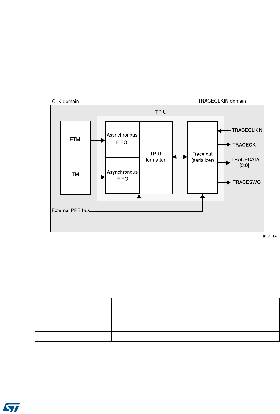
RM0394 Rev 4 1577/1600
RM0394 Debug support (DBG)
1584
46.17 TPIU (trace port interface unit)
46.17.1 Introduction
The TPIU acts as a bridge between the on-chip trace data from the ITM and the ETM.
The output data stream encapsulates the trace source ID, that is then captured by a trace
port analyzer (TPA).
The core embeds a simple TPIU, especially designed for low-cost debug (consisting of a
special version of the CoreSight TPIU).
Figure 497. TPIU block diagram
46.17.2 TRACE pin assignment
•Asynchronous mode
The asynchronous mode requires 1 extra pin and is available on all packages. It is only
available if using Serial Wire mode (not in JTAG mode).
•Synchronous mode
The synchronous mode requires from 2 to 6 extra pins depending on the data trace
size and is only available in the larger packages. In addition it is available in JTAG
mode and in Serial Wire mode and provides better bandwidth output capabilities than
asynchronous trace.
Table 285. Asynchronous TRACE pin assignment
TPUI pin name
Trace synchronous mode STM32L41xxx/42x
xx/43xxx/44xxx/45
xxx/46xxx pin
assignment
Type Description
TRACESWO O TRACE Asynchronous Data Output PB3

Debug support (DBG) RM0394
1578/1600 RM0394 Rev 4
TPUI TRACE pin assignment
By default, these pins are NOT assigned. They can be assigned by setting the
TRACE_IOEN and TRACE_MODE bits in the Debug MCU configuration register
(DBGMCU_CR). This configuration has to be done by the debugger host.
In addition, the number of pins to assign depends on the trace configuration (asynchronous
or synchronous).
•Asynchronous mode: 1 extra pin is needed
•Synchronous mode: from 2 to 5 extra pins are needed depending on the size of the
data trace port register (1, 2 or 4) :
– TRACECK
– TRACED(0) if port size is configured to 1, 2 or 4
– TRACED(1) if port size is configured to 2 or 4
– TRACED(2) if port size is configured to 4
– TRACED(3) if port size is configured to 4
To assign the TRACE pin, the debugger host must program the bits TRACE_IOEN and
TRACE_MODE[1:0] of the Debug MCU configuration register (DBGMCU_CR). By default
the TRACE pins are not assigned.
This register is mapped on the external PPB and is reset by the PORESET (and not by the
SYSTEM reset). It can be written by the debugger under SYSTEM reset.
Table 286. Synchronous TRACE pin assignment
TPUI pin name
Trace synchronous mode STM32L41xxx/42x
xx/43xxx/44xxx/45
xxx/46xxx pin
assignment
Type Description
TRACECK O TRACE Clock PE2
TRACED[3:0] O TRACE Synchronous Data Outputs
Can be 1, 2 or 4. PE[6:3]
Table 287. Flexible TRACE pin assignment
DBGMCU_CR
register
Pins
assigned for:
TRACE IO pin assigned
TRACE
_IOEN
TRACE
_MODE
[1:0]
PB3 / JTDO/
TRACESWO
PE2 /
TRACECK
PE3 /
TRACED[0]
PE4 /
TRACED[1]
PE5 /
TRACED[2]
PE6 /
TRACED[3]
0XX
No Trace
(default state) Released (1) -
100
Asynchronous
Trace TRACESWO - - Released
(usable as GPIO)

RM0394 Rev 4 1579/1600
RM0394 Debug support (DBG)
1584
Note: By default, the TRACECLKIN input clock of the TPIU is tied to GND. It is assigned to HCLK
two clock cycles after the bit TRACE_IOEN has been set.
The debugger must then program the Trace Mode by writing the PROTOCOL[1:0] bits in the
SPP_R (Selected Pin Protocol) register of the TPIU.
•PROTOCOL=00: Trace Port Mode (synchronous)
•PROTOCOL=01 or 10: Serial Wire (Manchester or NRZ) Mode (asynchronous mode).
Default state is 01
It then also configures the TRACE port size by writing the bits [3:0] in the CPSPS_R
(Current Synchronous Port Size Register) of the TPIU:
•0x1 for 1 pin (default state)
•0x2 for 2 pins
•0x8 for 4 pins
46.17.3 TPUI formatter
The formatter protocol outputs data in 16-byte frames:
•seven bytes of data
•eight bytes of mixed-use bytes consisting of:
– 1 bit (LSB) to indicate it is a DATA byte (‘0) or an ID byte (‘1).
– 7 bits (MSB) which can be data or change of source ID trace.
•one byte of auxiliary bits where each bit corresponds to one of the eight mixed-use
bytes:
– if the corresponding byte was a data, this bit gives bit0 of the data.
– if the corresponding byte was an ID change, this bit indicates when that ID change
takes effect.
Note: Refer to the Arm® CoreSight Architecture Specification v1.0 (Arm IHI 0029B) for further
information
101
Synchronous
Trace 1 bit
Released (1)
TRACECK TRACED[0] - - -
110
Synchronous
Trace 2 bit TRACECK TRACED[0] TRACED[1] - -
111
Synchronous
Trace 4 bit TRACECK TRACED[0] TRACED[1] TRACED[2] TRACED[3]
1. When Serial Wire mode is used, it is released, but when JTAG is used, it is assigned to JTDO.
Table 287. Flexible TRACE pin assignment (continued)
DBGMCU_CR
register
Pins
assigned for:
TRACE IO pin assigned
TRACE
_IOEN
TRACE
_MODE
[1:0]
PB3 / JTDO/
TRACESWO
PE2 /
TRACECK
PE3 /
TRACED[0]
PE4 /
TRACED[1]
PE5 /
TRACED[2]
PE6 /
TRACED[3]

Debug support (DBG) RM0394
1580/1600 RM0394 Rev 4
46.17.4 TPUI frame synchronization packets
The TPUI can generate two types of synchronization packets:
•The Frame Synchronization packet (or Full Word Synchronization packet)
It consists of the word: 0x7F_FF_FF_FF (LSB emitted first). This sequence can not
occur at any other time provided that the ID source code 0x7F has not been used.
It is output periodically between frames.
In continuous mode, the TPA must discard all these frames once a synchronization
frame has been found.
•The Half-Word Synchronization packet
It consists of the half word: 0x7F_FF (LSB emitted first).
It is output periodically between or within frames.
These packets are only generated in continuous mode and enable the TPA to detect
that the TRACE port is in IDLE mode (no TRACE to be captured). When detected by
the TPA, it must be discarded.
46.17.5 Transmission of the synchronization frame packet
There is no Synchronization Counter register implemented in the TPIU of the core.
Consequently, the synchronization trigger can only be generated by the DWT. Refer to the
registers DWT Control Register (bits SYNCTAP[11:10]) and the DWT Current PC Sampler
Cycle Count Register.
The TPUI Frame synchronization packet (0x7F_FF_FF_FF) is emitted:
•after each TPIU reset release. This reset is synchronously released with the rising
edge of the TRACECLKIN clock. This means that this packet is transmitted when the
TRACE_IOEN bit in the DBGMCU_CFG register is set. In this case, the word
0x7F_FF_FF_FF is not followed by any formatted packet.
•at each DWT trigger (assuming DWT has been previously configured). Two cases
occur:
– If the bit SYNENA of the ITM is reset, only the word 0x7F_FF_FF_FF is emitted
without any formatted stream which follows.
– If the bit SYNENA of the ITM is set, then the ITM synchronization packets will
follow (0x80_00_00_00_00_00), formatted by the TPUI (trace source ID added).
46.17.6 Synchronous mode
The trace data output size can be configured to 4, 2 or 1 pin: TRACED(3:0)
The output clock is output to the debugger (TRACECK)
Here, TRACECLKIN is driven internally and is connected to HCLK only when TRACE is
used.
Note: In this synchronous mode, it is not required to provide a stable clock frequency.
The TRACE I/Os (including TRACECK) are driven by the rising edge of TRACLKIN (equal
to HCLK). Consequently, the output frequency of TRACECK is equal to HCLK/2.

RM0394 Rev 4 1581/1600
RM0394 Debug support (DBG)
1584
46.17.7 Asynchronous mode
This is a low cost alternative to output the trace using only 1 pin: this is the asynchronous
output pin TRACESWO. Obviously there is a limited bandwidth.
TRACESWO is multiplexed with JTDO when using the SW-DP pin. This way, this
functionality is available in all STM32L41xxx/42xxx/43xxx/44xxx/45xxx/46xxx packages.
This asynchronous mode requires a constant frequency for TRACECLKIN. For the standard
UART (NRZ) capture mechanism, 5% accuracy is needed. The Manchester encoded
version is tolerant up to 10%.
46.17.8 TRACECLKIN connection inside the
STM32L41xxx/42xxx/43xxx/44xxx/45xxx/46xxx
In the STM32L41xxx/42xxx/43xxx/44xxx/45xxx/46xxx, this TRACECLKIN input is internally
connected to HCLK. This means that when in asynchronous trace mode, the application is
restricted to use time frames where the CPU frequency is stable.
Note: Important: when using asynchronous trace: it is important to be aware that:
The default clock of the STM32L41xxx/42xxx/43xxx/44xxx/45xxx/46xxx MCUs is the
internal RC oscillator. Its frequency under reset is different from the one after reset release.
This is because the RC calibration is the default one under system reset and is updated at
each system reset release.
Consequently, the trace port analyzer (TPA) should not enable the trace (with the
TRACE_IOEN bit) under system reset, because a Synchronization Frame Packet will be
issued with a different bit time than trace packets which will be transmitted after reset
release.

Debug support (DBG) RM0394
1582/1600 RM0394 Rev 4
46.17.9 TPIU registers
The TPIU APB registers can be read and written only if the bit TRCENA of the Debug
Exception and Monitor Control Register (DEMCR) is set. Otherwise, the registers are read
as zero (the output of this bit enables the PCLK of the TPIU).
Table 288. Important TPIU registers
Address Register Description
0xE0040004 Current port size
Allows the trace port size to be selected:
Bit 0: Port size = 1
Bit 1: Port size = 2
Bit 2: Port size = 3, not supported
Bit 3: Port Size = 4
Only 1 bit must be set. By default, the port size is one bit.
(0x00000001)
0xE00400F0 Selected pin
protocol
Allows the Trace Port Protocol to be selected:
Bit1:0 =
00: Synchronous Trace Port Mode
01: Serial Wire Output - manchester (default value)
10: Serial Wire Output - NRZ
11: reserved
0xE0040304 Formatter and
flush control
Bit 31-9 = always ‘0’
Bit 8 = TrigIn = always ‘1’ to indicate that triggers are indicated
Bit 7-4 = always 0
Bit 3-2 = always 0
Bit 1 = EnFCont. In Synchronous Trace mode
(Select_Pin_Protocol register bit1:0 = 00), this bit is forced to
‘1’: the formatter is automatically enabled in continuous mode.
In asynchronous mode (Select_Pin_Protocol register bit1:0 <>
00), this bit can be written to activate or not the formatter.
Bit 0 = always ‘0’
The resulting default value is 0x102
Note: In synchronous mode, because the TRACECTL pin is not
mapped outside the chip, the formatter is always enabled in
continuous mode; this way the formatter inserts some control
packets to identify the source of the trace packets).
0xE0040300 Formatter and
flush status Not used in Cortex®-M4, always read as 0x00000008

RM0394 Rev 4 1583/1600
RM0394 Debug support (DBG)
1584
46.17.10 Example of configuration
•Set the bit TRCENA in the Debug Exception and Monitor Control Register (DEMCR)
•Write the TPIU Current Port Size Register to the desired value (default is 0x1 for a 1-bit
port size)
•Write TPIU Formatter and Flush Control Register to 0x102 (default value)
•Write the TPIU Select Pin Protocol to select the synchronous or asynchronous mode.
Example: 0x2 for asynchronous NRZ mode (UART like)
•Write the DBGMCU control register to 0x20 (bit IO_TRACEN) to assign TRACE I/Os
for asynchronous mode. A TPIU Synchronous packet is emitted at this time
(FF_FF_FF_7F)
•Configure the ITM and write the ITM Stimulus register to output a value

Debug support (DBG) RM0394
1584/1600 RM0394 Rev 4
46.18 DBG register map
The following table summarizes the Debug registers
. Table 289. DBG register map and reset values
Addr. Register
31
30
29
28
27
26
25
24
23
22
21
20
19
18
17
16
15
14
13
12
11
10
9
8
7
6
5
4
3
2
1
0
0xE0042000
DBGMCU_
IDCODE REV_ID
Res.
Res.
Res.
Res.
DEV_ID
Reset value(1) XXXXXXXXXXXXXXXX XXXXXXXXXXXX
0xE0042004
DBGMCU_CR
Res.
Res.
Res.
Res.
Res.
Res.
Res.
Res.
Res.
Res.
Res.
Res.
Res.
Res.
Res.
Res.
Res.
Res.
Res.
Res.
Res.
Res.
Res.
Res.
TRACE_MODE[1:0]
TRACE_IOEN
Res.
Res.
DBG_STANDBY
DBG_STOP
DBG_SLEEP
Reset value 000 000
0xE004 2008
DBGMCU_
APB1FZR1
DBG_LPTIM1_STOP
Res.
Res.
Res.
Res.
Res.
DBG_CAN1_STOP
Res.
DBG_I2C3_STOP
DBG_I2C2_STOP
DBG_I2C1_STOP
Res.
Res.
Res.
Res.
Res.
Res.
Res.
Res.
DBG_IWDG_STOP
DBG_WWDG_STOP
DBG_RTC_STOP
Res.
Res.
Res.
Res.
DBG_TIM7_STOP
DBG_TIM6_STOP
Res.
Res.
Res.
DBG_TIM2_STOP
Reset value 0 0 000 000 00 0
0xE004 200C
DBGMCU_
APB1FZR2
Res.
Res.
Res.
Res.
Res.
Res.
Res.
Res.
Res.
Res.
Res.
Res.
Res.
Res.
Res.
Res.
Res.
Res.
Res.
Res.
Res.
Res.
Res.
Res.
Res.
Res.
DBG_LPTIM2_STOP
Res.
Res.
Res.
Res.
Res.
Reset value 0
0xE004 2010
DBGMCU_
APB2FZR
Res.
Res.
Res.
Res.
Res.
Res.
Res.
Res.
Res.
Res.
Res.
Res.
Res.
Res.
DBG_TIM16_STOP
DBG_TIM15_STOP
Res.
Res.
Res.
Res.
DBG_TIM1_STOP
Res.
Res.
Res.
Res.
Res.
Res.
Res.
Res.
Res.
Res.
Res.
Reset value 0 0 0
1. The reset value is product dependent. For more information, refer to Section 46.6.1: MCU device ID code.
RM0394 Rev 4 1585/1600
RM0394 Device electronic signature
1587
47 Device electronic signature
The device electronic signature is stored in the System memory area of the Flash memory
module, and can be read using the debug interface or by the CPU. It contains factory-
programmed identification and calibration data that allow the user firmware or other external
devices to automatically match to the characteristics of the
STM32L41xxx/42xxx/43xxx/44xxx/45xxx/46xxx microcontroller.
47.1 Unique device ID register (96 bits)
The unique device identifier is ideally suited:
•for use as serial numbers (for example USB string serial numbers or other end
applications)
•for use as part of the security keys in order to increase the security of code in Flash
memory while using and combining this unique ID with software cryptographic
primitives and protocols before programming the internal Flash memory
•to activate secure boot processes, etc.
The 96-bit unique device identifier provides a reference number which is unique for any
device and in any context. These bits cannot be altered by the user.
Base address: 0x1FFF 7590
Address offset: 0x00
Read only = 0xXXXX XXXX where X is factory-programmed
31 30 29 28 27 26 25 24 23 22 21 20 19 18 17 16
UID[31:16]
rrrrrrrrrrrrrrrr
15 14 13 12 11 10 9 8 7 6 5 4 3 2 1 0
UID[15:0]
rrrrrrrrrrrrrrrr
Bits 31:0 UID[31:0]: X and Y coordinates on the wafer
Device electronic signature RM0394
1586/1600 RM0394 Rev 4
Address offset: 0x04
Read only = 0xXXXX XXXX where X is factory-programmed
Address offset: 0x08
Read only = 0xXXXX XXXX where X is factory-programmed
47.2 Flash size data register
Base address: 0x1FFF 75E0
Address offset: 0x00
Read only = 0xXXXX where X is factory-programmed
31 30 29 28 27 26 25 24 23 22 21 20 19 18 17 16
UID[63:48]
rrrrrrrrrrrrrrrr
15 14 13 12 11 10 9 8 7 6 5 4 3 2 1 0
UID[47:32]
rrrrrrrrrrrrrrrr
Bits 31:8 UID[63:40]: LOT_NUM[23:0]
Lot number (ASCII encoded)
Bits 7:0 UID[39:32]: WAF_NUM[7:0]
Wafer number (8-bit unsigned number)
31 30 29 28 27 26 25 24 23 22 21 20 19 18 17 16
UID[95:80]
rrrrrrrrrrrrrrrr
15 14 13 12 11 10 9 8 7 6 5 4 3 2 1 0
UID[79:64]
rrrrrrrrrrrrrrrr
Bits 31:0 UID[95:64]: LOT_NUM[55:24]
Lot number (ASCII encoded)
1514131211109876543210
FLASH_SIZE
rrrrrrrrrrrrrrrr
Bits 15:0 FLASH_SIZE[15:0]: Flash memory size
This bitfield indicates the size of the device Flash memory expressed in Kbytes.
As an example, 0x040 corresponds to 64 Kbytes.

RM0394 Rev 4 1587/1600
RM0394 Device electronic signature
1587
47.3 Package data register
Base address: 0x1FFF 7500
Address offset: 0x00
Read only = 0xXXXX where X is factory-programmed
1514131211109876543210
Res. Res. Res. Res. Res. Res. Res. Res. Res. Res. Res. PKG[4:0]
rrrrr
Bits 15:5 Reserved, must be kept at reset value
Bits 4:0 PKG[4:0]: Package type
00000: LQFP64
00001: WLCSP64
00010: LQFP100
00101: WLCSP36
01000: UFQFPN32
01001: LQFP32
01010: UFQFPN48
01011: LQFP48
01100: WLCSP49
01101: UFBGA64
01110: UFBGA100
01111: WLCSP36 with external SMPS(1)
10110: LQFP64 with external SMPS(1)
Others: reserved
1. Separate package type for devices with external SMPS is supported on STM32L41xxx and STM32L422xxx
devices only.

Revision history RM0394
1588/1600 RM0394 Rev 4
48 Revision history
Table 290. Document revision history
Date Revision Changes
06-Apr-2016 1 Initial release.
30-Jun-2016 2
Added support for STM32L431xx.
FW:
Updated LENG bitfield in Section 4.4.6: Volatile data segment length
(FW_VDSL).
PWR:
Updated Section : Entering Stop 2 mode.
RCC:
Updated Section 6.2.11: Clock security system on LSE.
GPIO:
Updated reset values in Section 6.4.4: GPIO port pull-up/pull-down
register (GPIOx_PUPDR) (x = A..G).
DMA:
Updated Table 40: Programmable data width & endianness (when bits
PINC = MINC = 1).
Updated Section 11.5.2: DMA interrupt flag clear register (DMA_IFCR).
Updated NDT bit description in Section 11.5.4: DMA channel x number
of data register (DMA_CNDTRx) (x = 1..7, where x = channel number).
CRC:
Added Section 13.3.2: CRC internal signals.
Updated Section 13.4.2: Independent data register (CRC_IDR).
ADC:
Updated Section 18.4.8: Calibration (ADCAL, ADCALDIF,
ADCx_CALFACT).
Updated Section 18.4.9: ADC on-off control (ADEN, ADDIS, ADRDY).
TIM1:
Updated Section 21.3.28: DMA burst mode.
Updated Section 21.3.29: Debug mode.
Updated Table 207: Output control bits for complementary OCx and
OCxN channels with break feature.
Updated Section 21.4.20: TIM1 DMA address for full transfer
(TIM1_DMAR).
Updated Section 26.4.25: TIM1 option register 2 (TIM1_OR2).

RM0394 Rev 4 1589/1600
RM0394 Revision history
1594
30-Jun-2016 2
(continued)
TIM2:
Updated Section 27.3.20: DMA burst mode.
Updated Section 27.4.20: TIM2 option register 2 (TIM2_OR2).
TIM15/TIM16:
Updated Section 28.5.22: Debug mode.
Updated Table 135: TIMx Internal trigger connection.
Updated Table 138: Output control bits for complementary OCx and
OCxN channels with break feature (TIM16/17).
RTC2:
Updated Section 36.3.15: Calibration clock output.
Added Caution at the end of Section 36.6.3: RTC control register
(RTC_CR).
I2C:
Updated Notes at the end of Section 31.4.8: I2C master mode.
Updated START bit description in Section 31.7.2: Control register 2
(I2C_CR2).
USART:
Updated Section 38.5.17: Wakeup from Stop mode using USART.
Added UCESM bit in Section 38.8.3: Control register 3 (USART_CR3).
Updated Section 39.4.11: Wakeup from Stop mode using LPUART.
Added UCESM bit in Section 39.7.3: Control register 3 (LPUART_CR3).
20-Apr-2017 3
Complete re-manipulation of the document in order to support all the
following product RPNs:
– STM32L43xxx
– STM32L44xxx
– STM32L45xxx
– STM32L46xxx
Table 290. Document revision history (continued)
Date Revision Changes

Revision history RM0394
1590/1600 RM0394 Rev 4
03-Oct-2018 4
Updated:
Document convention:
Section 1.1: General information, Table 1: Product specific features
Memory organization:
Section 2.2.2: Memory map and register boundary
addresses,Section 2.4: Embedded SRAM, Tabl e 2:
STM32L41xxx/42xxx/43xxx/44xxx/45xxx/46xxx memory map and
peripheral register boundary addresses, Table 3: SRAM2 organization
Added Table 4: SRAM2 organization (continuation for
STM32L43x/44x/45x/46x devices only)
Embedded Flash memory:
Section 3.2: FLASH main features, Section 3.3.7: Flash main memory
programming sequences, Section : Programming errors, Section : WRP
Area B address option bytes, Section 3.7.8: Flash option register
(FLASH_OPTR), Section 3.7.9: Flash PCROP Start address register
(FLASH_PCROP1SR), Section 3.7.10: Flash PCROP End address
register (FLASH_PCROP1ER), Section 3.7.11: Flash WRP area A
address register (FLASH_WRP1AR)
FIREWALL:
Section 4.3.2: Functional requirements, Table 16: Segment accesses
according to the Firewall state
PWR:
Section 5.1: Power supplies, Section 5.1.1: Independent analog
peripherals supply, Section 5.2.2: Programmable voltage detector
(PVD), Section 5.3.6: Stop 0 mode, Section 5.3.9: Standby mode,
Section 5.3.10: Shutdown mode, Section 5.4.3: Power control register 3
(PWR_CR3), Section 5.4.8: Power Port A pull-up control register
(PWR_PUCRA), Section 5.4.10: Power Port B pull-up control register
(PWR_PUCRB), Section 5.4.11: Power Port B pull-down control register
(PWR_PDCRB), Section 5.4.13: Power Port C pull-down control register
(PWR_PDCRC), Section 5.4.16: Power Port E pull-up control register
(PWR_PUCRE), Section 5.4.18: Power Port H pull-up control register
(PWR_PUCRH)
Added notes (12,13 and 14) in Table 21: Functionalities depending on
the working mode
RCC:
Section 6.1.2: System reset, Section 6.2: Clocks, Figure 13: Clock tree,
Section 6.2.1: HSE clock, Table 31: Clock source frequency,
Section 6.2.18: Peripheral clock enable register (RCC_AHBxENR,
RCC_APBxENRy), Figure 16: Frequency measurement with TIM16 in
capture mode
Table 290. Document revision history (continued)
Date Revision Changes

RM0394 Rev 4 1591/1600
RM0394 Revision history
1594
03-Oct-2018 4
(continued)
CRS:
Section 7.6.1: CRS control register (CRS_CR)
DMA:
Updated Section 11.1: Introduction, Section 11.2: DMA main features,
Section 11.4: DMA functional description, Figure 27: DMA block
diagram, Section 11.4.2: DMA transfers, Section 11.4.3: DMA
arbitration, Section 11.4.4: DMA channels, Section 11.4.5: DMA data
width, alignment and endianness, Section 11.4.6: DMA error
management, Section 11.5: DMA interrupts, Section 11.6.1: DMA
interrupt status register (DMA_ISR), Section 11.6.2: DMA interrupt flag
clear register (DMA_IFCR), Section 11.6.3: DMA channel x configuration
register (DMA_CCRx), Section 11.6.4: DMA channel x number of data to
transfer register (DMA_CNDTRx), Section 11.6.5: DMA channel x
peripheral address register (DMA_CPARx), Section 11.6.6: DMA
channel x memory address register (DMA_CMARx)
Added Section 11.3.1: DMA1 and DMA2, Section 11.3.2: DMA request
mapping
Removed Section 11.4.7: DMA request mapping, Section 11.6.8: DMA2
channel selection register (DMA2_CSELR).
INTERRUPTS:
Updated Section 12.2: SysTick calibration value register
Added note 1 in Table 46:
STM32L41xxx/42xxx/43xxx/44xxx/45xxx/46xxx vector table, note 6 in
Table 47: EXTI lines connections
ADC:
Updated Section 16.2: ADC main features, Figure 39: ADC block
diagram, Table 55: ADC internal input/output signals, Table 56: ADC
input/output pins, Section 16.4.3: Clocks, Figure 41: ADC1 connectivity,
Section 16.4.7: Single-ended and differential input channels,
Section 16.4.8: Calibration (ADCAL, ADCALDIF, ADC_CALFACT),
Section 16.4.11: Channel selection (SQRx, JSQRx), Section 16.4.12:
Channel-wise programmable sampling time (SMPR1, SMPR2),
Section 16.4.32: Temperature sensor, Figure 108: VREFINT channel
block diagram, Section 16.6.17: ADC offset y register (ADC_OFRy),
Section 16.6.18: ADC injected channel y data register (ADC_JDRy),
Section 16.7.2: ADC common control register (ADC_CCR)
DAC:
Updated Section 17.2: DAC main features, Section 17.3: DAC
implementation, Figure 109: Dual-channel DAC block diagram,
Figure 117: DAC Sample and Hold mode phase diagram,
Section 17.4.12: Dual DAC channel conversion (if available),
Section 17.7.1: DAC control register (DAC_CR), Section 17.7.17: DAC
channel 1 sample and hold sample time register (DAC_SHSR1),
Section 17.7.18: DAC channel 2 sample and hold sample time register
(DAC_SHSR2), Table 80: DAC register map and reset values
VREFBUF:
Updated Section 18.2: VREFBUF functional description
Table 290. Document revision history (continued)
Date Revision Changes

Revision history RM0394
1592/1600 RM0394 Rev 4
03-Oct-2018 4
(continued)
DFSDM:
Updated Section 21.4.3: DFSDM reset and clocks, Section 21.8.1:
DFSDM filter x control register 1 (DFSDM_FLTxCR1), Section 21.8.5:
DFSDM filter x injected channel group selection register
(DFSDM_FLTxJCHGR), Section 21.8.7: DFSDM filter x data register for
injected group (DFSDM_FLTxJDATAR), Section 21.8.8: DFSDM filter x
data register for the regular channel (DFSDM_FLTxRDATAR),
Section 21.8.9: DFSDM filter x analog watchdog high threshold register
(DFSDM_FLTxAWHTR), Section 21.8.10: DFSDM filter x analog
watchdog low threshold register (DFSDM_FLTxAWLTR),
Section 21.8.11: DFSDM filter x analog watchdog status register
(DFSDM_FLTxAWSR), Section 21.8.12: DFSDM filter x analog
watchdog clear flag register (DFSDM_FLTxAWCFR), Section 21.8.13:
DFSDM filter x extremes detector maximum register
(DFSDM_FLTxEXMAX),Section 21.8.14: DFSDM filter x extremes
detector minimum register (DFSDM_FLTxEXMIN), Section 21.8.15:
DFSDM filter x conversion timer register (DFSDM_FLTxCNVTIMR)
RNG:
Updated Section 24.3.3: Random number generation, Section 24.8.1:
RNG control register (RNG_CR), Table 117: RNG register map and
reset map
AES:
Updated Section 25.1: Introduction, Section 25.2: AES main features,
Section 25.4: AES functional description, Figure 153: AES block
diagram, Figure 154: ECB encryption and decryption principle,
Figure 155: CBC encryption and decryption principle, Figure 156: CTR
encryption and decryption principle, Figure 157: GCM encryption and
authentication principle, Figure 158: GMAC authentication principle,
Section 25.4.16: AES DMA interface, Section 25.5: AES interrupts,
Section 25.7.2: AES status register (AES_SR), Section 25.4.10: AES
Galois/counter mode (GCM), Section 25.7.4: AES data output register
(AES_DOUTR), Section 25.7.5: AES key register 0 (AES_KEYR0),
Section 25.7.9: AES initialization vector register 0 (AES_IVR0),
Section 25.7.10: AES initialization vector register 1 (AES_IVR1),
Section 25.7.11: AES initialization vector register 2 (AES_IVR2),
Section 25.7.12: AES initialization vector register 3 (AES_IVR3)
Added Figure 159: CCM encryption and authentication principle,
Section 25.4.4: AES procedure to perform a cipher operation,
Section 25.4.5: AES decryption key preparation, Section 25.4.6: AES
ciphertext stealing and data padding, Section 25.4.7: AES task suspend
and resume, Section 25.4.8: AES basic chaining modes (ECB, CBC),
Section 25.4.9: AES counter (CTR) mode, Section 25.4.10: AES
Galois/counter mode (GCM), Section 25.4.11: AES Galois message
authentication code (GMAC), Section 25.4.12: AES counter with CBC-
MAC (CCM), Section 25.4.13: .AES data registers and data swapping,
Section 25.4.14: AES key registers, Section 25.4.15: AES initialization
vector registers, Section 25.4.17: AES error management
Table 290. Document revision history (continued)
Date Revision Changes

RM0394 Rev 4 1593/1600
RM0394 Revision history
1594
03-Oct-2018 4
(continued)
ADVANCED CONTROL TIMER (TIM1):
Updated Figure 197: Counter timing diagram, internal clock divided by 1,
TIMx_ARR = 0x6
GENERAL PURPOUSE TIMER(TIM2/TIM3):
Updated Section 27.1: TIM2/TIM3 introduction, Figure 248: Counter
timing diagram, internal clock divided by 4
GENERAL PURPOUSE TIMER(TIM15/TIM16):
Added Section 28.5.15: Retriggerable one pulse mode (OPM) (TIM15
only), Section 28.6.11: TIM15 auto-reload register (TIM15_ARR),
Section 28.7.4: TIM16 status register (TIM16_SR), Section 28.7.10:
TIM16 auto-reload register (TIM16_ARR), Section 28.7.16: TIM16
option register 1 (TIM16_OR1)
LPTIMER:
Added Figure 335: Low-power timer block diagram for
STM32L43xxx/44xxx/45xxx/46xxx, Section 30.4.2: LPTIM trigger
mapping, Section 30.4.3: LPTIM reset and clocks, Figure 339: LPTIM
output waveform, single counting mode configuration when repetition
register content is different than zero (with PRELOAD = 1),
Section 30.4.13: Timer counter reset, Section 30.4.15: Repetition
Counter, Table 151: Interrupt events
Updated Section 30.4.7: Operating mode, Figure 338: LPTIM output
waveform, single counting mode configuration, Figure 340: LPTIM
output waveform, Single counting mode configuration and Set-once
mode activated (WAVE bit is set), Figure 341: LPTIM output waveform,
Continuous counting mode configuration, Section 30.4.10: Register
update, Section 30.4.11: Counter mode, Section 30.5: LPTIM low-power
modes, Section 30.7.1: LPTIM interrupt and status register
(LPTIM_ISR), Section 30.7.2: LPTIM interrupt clear register
(LPTIM_ICR), Section 30.7.3: LPTIM interrupt enable register
(LPTIM_IER), Section 30.7.4: LPTIM configuration register
(LPTIM_CFGR), Section 30.7.5: LPTIM control register (LPTIM_CR)
WWDG:
Updated Figure 347: Watchdog block diagram, Figure 348: Window
watchdog timing diagram
RTC:
Added Section 34: Real-time clock (RTC) applied to STM32L41xxx and
STM32L42xxx devices only and Section 35: Tamper and backup
registers (TAMP)
Updated Figure 351: RTC block diagram, Section 36.3.6: Periodic auto-
wakeup, Section 36.3.7: RTC initialization and configuration,
Section 36.3.11: RTC reference clock detection
I2C: Updated Figure 352: I2C block diagram, Section 37.6: I2C
interrupts
Table 290. Document revision history (continued)
Date Revision Changes

Revision history RM0394
1594/1600 RM0394 Rev 4
03-Oct-2018 4
(continued)
SAI:
Updated Figure 435: SAI functional block diagram, Table 213: SAI
internal input/output signals, Table 214: SAI input/output pins,
Section 41.6.1: Configuration register 1 (SAI_ACR1), Section 41.6.2:
Configuration register 1 (SAI_BCR1), Section 41.6.3: Configuration
register 2 (SAI_ACR2), Section 41.6.4: Configuration register 2
(SAI_BCR2), Section 41.6.5: Frame configuration register
(SAI_AFRCR), Section 41.6.6: Frame configuration register
(SAI_BFRCR), Section 41.6.7: Slot register (SAI_ASLOTR),
Section 41.6.6: Frame configuration register (SAI_BFRCR),
Section 41.6.7: Slot register (SAI_ASLOTR), Section 41.6.8: Slot
register (SAI_BSLOTR), Section 41.6.9: Interrupt mask register
(SAI_AIM), Section 41.6.10: Interrupt mask register (SAI_BIM),
Section 41.6.11: Status register (SAI_ASR), Section 41.6.12: Status
register (SAI_BSR), Section 41.6.13: Clear flag register (SAI_ACLRFR),
Section 41.6.14: Clear flag register (SAI_BCLRFR), Section 41.6.15:
Data register (SAI_ADR), Section 41.6.16: Data register (SAI_BDR),
Table 221: SAI register map and reset values
Replace “TDM mode” with ‘free protocol mode”.
SWPMI:
Added Section 42.1: Introduction, Section 42.2: SWPMI main features
BXCAN:
Added Figure 477: Single-CAN block diagram
Updated Figure 479: bxCAN in silent mode, Figure 480: bxCAN in loop
back mode, Figure 481: bxCAN in combined mode, Figure 482:
Transmit mailbox states, Figure 483: Receive FIFO states, Figure 484:
Filter bank scale configuration - register organization, Figure 485:
Example of filter numbering, Figure 486: Filtering mechanism - example,
Figure 488: Bit timing, Figure 489: CAN frames, Figure 490: Event flags
and interrupt generation, Figure 491: CAN mailbox registers, Table 261:
bxCAN register map and reset values
DEVICE SIGNATURE:
Updated Section 47.3: Package data register
Table 290. Document revision history (continued)
Date Revision Changes

RM0394 Index
RM0394 Rev 4 1595/1600
Index
A
ADC_AWD2CR . . . . . . . . . . . . . . . . . . . . . . .475
ADC_AWD3CR . . . . . . . . . . . . . . . . . . . . . . .475
ADC_CALFACT . . . . . . . . . . . . . . . . . . . . . . .476
ADC_CCR . . . . . . . . . . . . . . . . . . . . . . . . . . .479
ADC_CDR . . . . . . . . . . . . . . . . . . . . . . . . . . .482
ADC_CFGR . . . . . . . . . . . . . . . . . . . . . . . . . .458
ADC_CFGR2 . . . . . . . . . . . . . . . . . . . . . . . . .462
ADC_CR . . . . . . . . . . . . . . . . . . . . . . . . . . . .455
ADC_CSR . . . . . . . . . . . . . . . . . . . . . . . . . . .477
ADC_DIFSEL . . . . . . . . . . . . . . . . . . . . . . . . .476
ADC_DR . . . . . . . . . . . . . . . . . . . . . . . . . . . .471
ADC_IER . . . . . . . . . . . . . . . . . . . . . . . . . . . .453
ADC_ISR . . . . . . . . . . . . . . . . . . . . . . . . . . . .451
ADC_JDRy . . . . . . . . . . . . . . . . . . . . . . . . . . .474
ADC_JSQR . . . . . . . . . . . . . . . . . . . . . . . . . .472
ADC_OFRy . . . . . . . . . . . . . . . . . . . . . . . . . .473
ADC_SMPR1 . . . . . . . . . . . . . . . . . . . . . . . . .464
ADC_SMPR2 . . . . . . . . . . . . . . . . . . . . . . . . .465
ADC_SQR1 . . . . . . . . . . . . . . . . . . . . . . . . . .468
ADC_SQR2 . . . . . . . . . . . . . . . . . . . . . . . . . .469
ADC_SQR3 . . . . . . . . . . . . . . . . . . . . . . . . . .470
ADC_SQR4 . . . . . . . . . . . . . . . . . . . . . . . . . .471
ADC_TR1 . . . . . . . . . . . . . . . . . . . . . . . . . . . .465
ADC_TR2 . . . . . . . . . . . . . . . . . . . . . . . . . . . .466
ADC_TR3 . . . . . . . . . . . . . . . . . . . . . . . . . . . .467
AES_CR . . . . . . . . . . . . . . . . . . . . . . . . . . . . .705
AES_DINR . . . . . . . . . . . . . . . . . . . . . . . . . . .709
AES_DOUTR . . . . . . . . . . . . . . . . . . . . . . . . .710
AES_IVR . . . . . . . . . . . . . . . . . . . . . . . . . . . .712
AES_KEYRx . . . . . . . . . . . . . . . . . . . . . . . . .710
AES_SR . . . . . . . . . . . . . . . . . . . . . . . . . . . . .708
C
CAN_BTR . . . . . . . . . . . . . . . . . . . . . . . . . .1504
CAN_ESR . . . . . . . . . . . . . . . . . . . . . . . . . .1503
CAN_FA1R . . . . . . . . . . . . . . . . . . . . . . . . .1514
CAN_FFA1R . . . . . . . . . . . . . . . . . . . . . . . .1513
CAN_FiRx . . . . . . . . . . . . . . . . . . . . . . . . . .1515
CAN_FM1R . . . . . . . . . . . . . . . . . . . . . . . . .1512
CAN_FMR . . . . . . . . . . . . . . . . . . . . . . . . . .1512
CAN_FS1R . . . . . . . . . . . . . . . . . . . . . . . . .1513
CAN_IER . . . . . . . . . . . . . . . . . . . . . . . . . . .1502
CAN_MCR . . . . . . . . . . . . . . . . . . . . . . . . . .1495
CAN_MSR . . . . . . . . . . . . . . . . . . . . . . . . . .1497
CAN_RDHxR . . . . . . . . . . . . . . . . . . . . . . . .1511
CAN_RDLxR . . . . . . . . . . . . . . . . . . . . . . . .1511
CAN_RDTxR . . . . . . . . . . . . . . . . . . . . . . . . 1510
CAN_RF0R . . . . . . . . . . . . . . . . . . . . . . . . . 1500
CAN_RF1R . . . . . . . . . . . . . . . . . . . . . . . . . 1501
CAN_RIxR . . . . . . . . . . . . . . . . . . . . . . . . . . 1509
CAN_TDHxR . . . . . . . . . . . . . . . . . . . . . . . . 1508
CAN_TDLxR . . . . . . . . . . . . . . . . . . . . . . . . 1508
CAN_TDTxR . . . . . . . . . . . . . . . . . . . . . . . . 1507
CAN_TIxR . . . . . . . . . . . . . . . . . . . . . . . . . . 1506
CAN_TSR . . . . . . . . . . . . . . . . . . . . . . . . . . 1498
COMP1_CSR . . . . . . . . . . . . . . . . . . . . . . . . 532
COMP2_CSR . . . . . . . . . . . . . . . . . . . . . . . . 534
CRC_CR . . . . . . . . . . . . . . . . . . . . . . . . . . . . 342
CRC_DR . . . . . . . . . . . . . . . . . . . . . . . . . . . . 341
CRC_IDR . . . . . . . . . . . . . . . . . . . . . . . . . . . 341
CRC_INIT . . . . . . . . . . . . . . . . . . . . . . . . . . . 342
CRC_POL . . . . . . . . . . . . . . . . . . . . . . . . . . . 343
CRS_CFGR . . . . . . . . . . . . . . . . . . . . . . . . . . 253
CRS_CR . . . . . . . . . . . . . . . . . . . . . . . . . . . . 252
CRS_ICR . . . . . . . . . . . . . . . . . . . . . . . . . . . . 256
CRS_ISR . . . . . . . . . . . . . . . . . . . . . . . . . . . . 254
D
DAC_CCR . . . . . . . . . . . . . . . . . . . . . . . . . . . 515
DAC_CR . . . . . . . . . . . . . . . . . . . . . . . . . . . . 505
DAC_DHR12L1 . . . . . . . . . . . . . . . . . . . . . . . 509
DAC_DHR12L2 . . . . . . . . . . . . . . . . . . . . . . . 510
DAC_DHR12LD . . . . . . . . . . . . . . . . . . . . . . 511
DAC_DHR12R1 . . . . . . . . . . . . . . . . . . . . . . 508
DAC_DHR12R2 . . . . . . . . . . . . . . . . . . . . . . 510
DAC_DHR12RD . . . . . . . . . . . . . . . . . . . . . . 511
DAC_DHR8R1 . . . . . . . . . . . . . . . . . . . . . . . 509
DAC_DHR8R2 . . . . . . . . . . . . . . . . . . . . . . . 510
DAC_DHR8RD . . . . . . . . . . . . . . . . . . . . . . . 512
DAC_DOR1 . . . . . . . . . . . . . . . . . . . . . . . . . . 512
DAC_DOR2 . . . . . . . . . . . . . . . . . . . . . . . . . . 513
DAC_MCR . . . . . . . . . . . . . . . . . . . . . . . . . . . 515
DAC_SHHR . . . . . . . . . . . . . . . . . . . . . . . . . . 518
DAC_SHRR . . . . . . . . . . . . . . . . . . . . . . . . . . 518
DAC_SHSR1 . . . . . . . . . . . . . . . . . . . . . . . . . 517
DAC_SHSR2 . . . . . . . . . . . . . . . . . . . . . . . . . 517
DAC_SR . . . . . . . . . . . . . . . . . . . . . . . . . . . . 513
DAC_SWTRGR . . . . . . . . . . . . . . . . . . . . . . . 508
DBGMCU_APB1FZR1 . . . . . . . . . . . . . . . . 1574
DBGMCU_APB1FZR2 . . . . . . . . . . . . . . . . 1575
DBGMCU_APB2FZR . . . . . . . . . . . . . . . . . 1576
DBGMCU_CR . . . . . . . . . . . . . . . . . . . . . . . 1573
DBGMCU_IDCODE . . . . . . . . . . . . . . . . . . 1560
DFSDM_CHyAWSCDR . . . . . . . . . . . . . . . . . 580

Index RM0394
1596/1600 RM0394 Rev 4
DFSDM_CHyCFGR1 . . . . . . . . . . . . . . . . . . .577
DFSDM_CHyCFGR2 . . . . . . . . . . . . . . . . . . .580
DFSDM_CHyDATINR . . . . . . . . . . . . . . . . . .582
DFSDM_CHyWDATR . . . . . . . . . . . . . . . . . .581
DFSDM_FLTxAWCFR . . . . . . . . . . . . . . . . . .594
DFSDM_FLTxAWHTR . . . . . . . . . . . . . . . . . .592
DFSDM_FLTxAWLTR . . . . . . . . . . . . . . . . . .593
DFSDM_FLTxAWSR . . . . . . . . . . . . . . . . . . .594
DFSDM_FLTxCNVTIMR . . . . . . . . . . . . . . . .596
DFSDM_FLTxCR1 . . . . . . . . . . . . . . . . . . . . .583
DFSDM_FLTxCR2 . . . . . . . . . . . . . . . . . . . . .585
DFSDM_FLTxEXMAX . . . . . . . . . . . . . . . . . .595
DFSDM_FLTxEXMIN . . . . . . . . . . . . . . . . . . .595
DFSDM_FLTxFCR . . . . . . . . . . . . . . . . . . . . .590
DFSDM_FLTxICR . . . . . . . . . . . . . . . . . . . . .588
DFSDM_FLTxISR . . . . . . . . . . . . . . . . . . . . .587
DFSDM_FLTxJCHGR . . . . . . . . . . . . . . . . . .589
DFSDM_FLTxJDATAR . . . . . . . . . . . . . . . . .591
DFSDM_FLTxRDATAR . . . . . . . . . . . . . . . . .592
DMA_CCRx . . . . . . . . . . . . . . . . . . . . . . . . . .312
DMA_CMARx . . . . . . . . . . . . . . . . . . . . . . . . .316
DMA_CNDTRx . . . . . . . . . . . . . . . . . . . . . . . .315
DMA_CPARx . . . . . . . . . . . . . . . . . . . . . . . . .315
DMA_IFCR . . . . . . . . . . . . . . . . . . . . . . . . . . .311
DMA_ISR . . . . . . . . . . . . . . . . . . . . . . . . . . . .308
DMA1_CSELR . . . . . . . . . . . . . . . . . . . . . . . .317
E
EXTI_EMR1 . . . . . . . . . . . . . . . . . . . . . . . . . .330
EXTI_EMR2 . . . . . . . . . . . . . . . . . . . . . . . . . .334
EXTI_FTSR1 . . . . . . . . . . . . . . . . . . . . . . . . .331
EXTI_FTSR2 . . . . . . . . . . . . . . . . . . . . . . . . .335
EXTI_IMR1 . . . . . . . . . . . . . . . . . . . . . . . . . . .330
EXTI_IMR2 . . . . . . . . . . . . . . . . . . . . . . . . . . .333
EXTI_PR1 . . . . . . . . . . . . . . . . . . . . . . . . . . .333
EXTI_PR2 . . . . . . . . . . . . . . . . . . . . . . . . . . .336
EXTI_RTSR1 . . . . . . . . . . . . . . . . . . . . . . . . .331
EXTI_RTSR2 . . . . . . . . . . . . . . . . . . . . . . . . .334
EXTI_SWIER1 . . . . . . . . . . . . . . . . . . . . . . . .332
EXTI_SWIER2 . . . . . . . . . . . . . . . . . . . . . . . .335
F
FLASH_ACR . . . . . . . . . . . . . . . . . . . . . . . . .100
FLASH_CR . . . . . . . . . . . . . . . . . . . . . . . . . .104
FLASH_ECCR . . . . . . . . . . . . . . . . . . . . . . . .106
FLASH_KEYR . . . . . . . . . . . . . . . . . . . . . . . .101
FLASH_OPTKEYR . . . . . . . . . . . . . . . . . . . .102
FLASH_OPTR . . . . . . . . . . . . . . . . . . . . . . . .107
FLASH_PCROP1ER . . . . . . . . . . . . . . . . . . .109
FLASH_PCROP1SR . . . . . . . . . . . . . . . . . . .109
FLASH_PDKEYR . . . . . . . . . . . . . . . . . . . . . .101
FLASH_SR . . . . . . . . . . . . . . . . . . . . . . . . . . 102
FLASH_WRP1AR . . . . . . . . . . . . . . . . . . . . . 110
FLASH_WRP1BR . . . . . . . . . . . . . . . . . . . . . 110
FW_CR . . . . . . . . . . . . . . . . . . . . . . . . . . . . . 124
FW_CSL . . . . . . . . . . . . . . . . . . . . . . . . . . . . 121
FW_CSSA . . . . . . . . . . . . . . . . . . . . . . . . . . . 121
FW_NVDSL . . . . . . . . . . . . . . . . . . . . . . . . . . 122
FW_NVDSSA . . . . . . . . . . . . . . . . . . . . . . . . 122
FW_VDSL . . . . . . . . . . . . . . . . . . . . . . . . . . . 123
FW_VDSSA . . . . . . . . . . . . . . . . . . . . . . . . . . 123
G
GPIOx_AFRH . . . . . . . . . . . . . . . . . . . . . . . . 272
GPIOx_AFRL . . . . . . . . . . . . . . . . . . . . . . . . 271
GPIOx_BRR . . . . . . . . . . . . . . . . . . . . . . . . . 273
GPIOx_BSRR . . . . . . . . . . . . . . . . . . . . . . . . 270
GPIOx_IDR . . . . . . . . . . . . . . . . . . . . . . . . . . 269
GPIOx_LCKR . . . . . . . . . . . . . . . . . . . . . . . . 270
GPIOx_MODER . . . . . . . . . . . . . . . . . . . . . . 267
GPIOx_ODR . . . . . . . . . . . . . . . . . . . . . . . . . 269
GPIOx_OSPEEDR . . . . . . . . . . . . . . . . . . . . 268
GPIOx_OTYPER . . . . . . . . . . . . . . . . . . . . . . 268
GPIOx_PUPDR . . . . . . . . . . . . . . . . . . . . . . . 268
I
I2C_CR1 . . . . . . . . . . . . . . . . . . . . . . . . . . . 1177
I2C_CR2 . . . . . . . . . . . . . . . . . . . . . . . . . . . 1180
I2C_ICR . . . . . . . . . . . . . . . . . . . . . . . . . . . . 1189
I2C_ISR . . . . . . . . . . . . . . . . . . . . . . . . . . . . 1187
I2C_OAR1 . . . . . . . . . . . . . . . . . . . . . . . . . . 1183
I2C_OAR2 . . . . . . . . . . . . . . . . . . . . . . . . . . 1184
I2C_PECR . . . . . . . . . . . . . . . . . . . . . . . . . . 1190
I2C_RXDR . . . . . . . . . . . . . . . . . . . . . . . . . . 1191
I2C_TIMEOUTR . . . . . . . . . . . . . . . . . . . . . 1186
I2C_TIMINGR . . . . . . . . . . . . . . . . . . . . . . . 1185
I2C_TXDR . . . . . . . . . . . . . . . . . . . . . . . . . . 1191
I2Cx_CR2 . . . . . . . . . . . . . . . . . . 121-124, 1180
IWDG_KR . . . . . . . . . . . . . . . . . . . . . . . . . . 1016
IWDG_PR . . . . . . . . . . . . . . . . . . . . . . . . . . 1017
IWDG_RLR . . . . . . . . . . . . . . . . . . . . . . . . . 1018
IWDG_SR . . . . . . . . . . . . . . . . . . . . . . . . . . 1019
IWDG_WINR . . . . . . . . . . . . . . . . . . . . . . . . 1020
L
LCD_CLR . . . . . . . . . . . . . . . . . . . . . . . . . . . 630
LCD_CR . . . . . . . . . . . . . . . . . . . . . . . . . . . . 625
LCD_RAM . . . . . . . . . . . . . . . . . . . . . . . . . . . 630
LPTIM_ARR . . . . . . . . . . . . . . . . . . . . . . . . 1006
LPTIM_CFGR . . . . . . . . . . . . . . . . . . . . . . . 1002
LPTIM_CFGR2 . . . . . . . . . . . . . . . . . . . . . . 1008

RM0394 Index
RM0394 Rev 4 1597/1600
LPTIM_CMP . . . . . . . . . . . . . . . . . . . . . . . . .1006
LPTIM_CNT . . . . . . . . . . . . . . . . . . . . . . . . .1007
LPTIM_CR . . . . . . . . . . . . . . . . . . . . . . . . . .1004
LPTIM_ICR . . . . . . . . . . . . . . . . . . . . . . . . . .999
LPTIM_IER . . . . . . . . . . . . . . . . . . . . . . . . . .1000
LPTIM_ISR . . . . . . . . . . . . . . . . . . . . . . . . . . .997
LPTIM_RCR . . . . . . . . . . . . . . . . . . . . . . . . .1009
LPTIM1_OR . . . . . . . . . . . . . . . . . . . . . . . . .1007
LPTIM2_OR . . . . . . . . . . . . . . . . . . . . . . . . .1008
LPUART_BRR . . . . . . . . . . . . . . . . . . . . . . .1296
LPUART_CR1 . . . . . . . . . . . . . . . . . . . . . . .1289
LPUART_CR2 . . . . . . . . . . . . . . . . . . . . . . .1291
LPUART_CR3 . . . . . . . . . . . . . . . . . . . . . . .1294
LPUART_ICR . . . . . . . . . . . . . . . . . . . . . . . .1300
LPUART_ISR . . . . . . . . . . . . . . . . . . . . . . . .1297
LPUART_RDR . . . . . . . . . . . . . . . . . . . . . . .1301
LPUART_RQR . . . . . . . . . . . . . . . . . . . . . . .1296
LPUART_TDR . . . . . . . . . . . . . . . . . . . . . . .1301
O
OPAMP1_CSR . . . . . . . . . . . . . . . . . . . . . . . .546
OPAMP1_LPOTR . . . . . . . . . . . . . . . . . . . . .547
OPAMP1_OTR . . . . . . . . . . . . . . . . . . . . . . . .547
P
purpose . . . . . . . . . . . . . . . . . . . . . . . . . . . . .887
PWR_CR1 . . . . . . . . . . . . . . . . . . . . . . . . . . .158
PWR_CR2 . . . . . . . . . . . . . . . . . . . . . . . . . . .159
PWR_CR3 . . . . . . . . . . . . . . . . . . . . . . . . . . .160
PWR_CR4 . . . . . . . . . . . . . . . . . . . . . . . . . . .161
PWR_PDCRA . . . . . . . . . . . . . . . . . . . . . . . .166
PWR_PDCRB . . . . . . . . . . . . . . . . . . . . . . . .167
PWR_PDCRC . . . . . . . . . . . . . . . . . . . . . . . .168
PWR_PDCRD . . . . . . . . . . . . . . . . . . . . . . . .169
PWR_PDCRE . . . . . . . . . . . . . . . . . . . . . . . .170
PWR_PDCRH . . . . . . . . . . . . . . . . . . . . . . . .171
PWR_PUCRA . . . . . . . . . . . . . . . . . . . . . . . .166
PWR_PUCRB . . . . . . . . . . . . . . . . . . . . . . . .167
PWR_PUCRC . . . . . . . . . . . . . . . . . . . . . . . .168
PWR_PUCRD . . . . . . . . . . . . . . . . . . . . . . . .169
PWR_PUCRE . . . . . . . . . . . . . . . . . . . . . . . .170
PWR_PUCRH . . . . . . . . . . . . . . . . . . . . . . . .171
PWR_SCR . . . . . . . . . . . . . . . . . . . . . . . . . . .165
PWR_SR1 . . . . . . . . . . . . . . . . . . . . . . . . . . .163
PWR_SR2 . . . . . . . . . . . . . . . . . . . . . . . . . . .164
Q
QUADSPI _PIR . . . . . . . . . . . . . . . . . . . . . . .371
QUADSPI _PSMAR . . . . . . . . . . . . . . . . . . . .370
QUADSPI _PSMKR . . . . . . . . . . . . . . . . . . . .370
QUADSPI_ABR . . . . . . . . . . . . . . . . . . . . . . . 369
QUADSPI_AR . . . . . . . . . . . . . . . . . . . . . . . . 368
QUADSPI_CCR . . . . . . . . . . . . . . . . . . . . . . 366
QUADSPI_CR . . . . . . . . . . . . . . . . . . . . . . . . 360
QUADSPI_DCR . . . . . . . . . . . . . . . . . . . . . . 363
QUADSPI_DLR . . . . . . . . . . . . . . . . . . . . . . . 365
QUADSPI_DR . . . . . . . . . . . . . . . . . . . . . . . . 369
QUADSPI_FCR . . . . . . . . . . . . . . . . . . . . . . . 365
QUADSPI_LPTR . . . . . . . . . . . . . . . . . . . . . . 371
QUADSPI_SR . . . . . . . . . . . . . . . . . . . . . . . . 364
R
RCC_AHB1ENR . . . . . . . . . . . . . . . . . . . . . . 216
RCC_AHB1RSTR . . . . . . . . . . . . . . . . . . . . . 208
RCC_AHB1SMENR . . . . . . . . . . . . . . . . . . . 225
RCC_AHB2ENR . . . . . . . . . . . . . . . . . . . . . . 218
RCC_AHB2RSTR . . . . . . . . . . . . . . . . . . . . . 209
RCC_AHB2SMENR . . . . . . . . . . . . . . . . . . . 226
RCC_AHB3ENR . . . . . . . . . . . . . . . . . . . . . . 219
RCC_AHB3RSTR . . . . . . . . . . . . . . . . . . . . . 211
RCC_AHB3SMENR . . . . . . . . . . . . . . . . . . . 228
RCC_APB1ENR1 . . . . . . . . . . . . . . . . . . . . . 220
RCC_APB1ENR2 . . . . . . . . . . . . . . . . . . . . . 222
RCC_APB1RSTR1 . . . . . . . . . . . . . . . . . . . . 211
RCC_APB1RSTR2 . . . . . . . . . . . . . . . . . . . . 214
RCC_APB1SMENR1 . . . . . . . . . . . . . . . . . . 228
RCC_APB1SMENR2 . . . . . . . . . . . . . . . . . . 231
RCC_APB2ENR . . . . . . . . . . . . . . . . . . . . . . 224
RCC_APB2RSTR . . . . . . . . . . . . . . . . . . . . . 215
RCC_APB2SMENR . . . . . . . . . . . . . . . . . . . 233
RCC_BDCR . . . . . . . . . . . . . . . . . . . . . . . . . 237
RCC_CCIPR . . . . . . . . . . . . . . . . . . . . . . . . . 234
RCC_CFGR . . . . . . . . . . . . . . . . . . . . . . . . . 196
RCC_CICR . . . . . . . . . . . . . . . . . . . . . . . . . . 207
RCC_CIER . . . . . . . . . . . . . . . . . . . . . . . . . . 204
RCC_CIFR . . . . . . . . . . . . . . . . . . . . . . . . . . 206
RCC_CR . . . . . . . . . . . . . . . . . . . . . . . . . . . . 193
RCC_CRRCR . . . . . . . . . . . . . . . . . . . . . . . . 241
RCC_CSR . . . . . . . . . . . . . . . . . . . . . . . . . . . 239
RCC_ICSCR . . . . . . . . . . . . . . . . . . . . . . . . . 196
RCC_PLLCFGR . . . . . . . . . . . . . . . . . . . . . . 198
RCC_PLLSAI1CFGR . . . . . . . . . . . . . . . . . . 201
RNG_CR . . . . . . . . . . . . . . . . . . . . . . . . . . . . 661
RNG_DR . . . . . . . . . . . . . . . . . . . . . . . . . . . . 663
RNG_SR . . . . . . . . . . . . . . . . . . . . . . . . . . . . 662
RTC_ALRMAR . . . . . . . . . . . . . . . . . 1060, 1111
RTC_ALRMBR . . . . . . . . . . . . . . . . . 1062, 1112
RTC_ALRMBSSR . . . . . . . . . . . . . . . 1063, 1123
RTC_BKPxR . . . . . . . . . . . . . . . . . . . . . . . . 1124
RTC_CALR . . . . . . . . . . . . . . . . . . . . 1057, 1118
RTC_CR . . . . . . . . . . . . . . . . . . . . . . 1053, 1103

Index RM0394
1598/1600 RM0394 Rev 4
RTC_DR . . . . . . . . . . . . . . . . . . . . . . .1049, 1102
RTC_ICSR . . . . . . . . . . . . . . . . . . . . . . . . . .1050
RTC_ISR . . . . . . . . . . . . . . . . . . . . . . . . . . .1106
RTC_MISR . . . . . . . . . . . . . . . . . . . . . . . . . .1065
RTC_OR . . . . . . . . . . . . . . . . . . . . . . . . . . .1124
RTC_PRER . . . . . . . . . . . . . . . . . . . .1052, 1109
RTC_SCR . . . . . . . . . . . . . . . . . . . . . . . . . .1066
RTC_SHIFTR . . . . . . . . . . . . . . . . . . .1058, 1114
RTC_SR . . . . . . . . . . . . . . . . . . . . . . . . . . . .1064
RTC_SSR . . . . . . . . . . . . . . . . . . . . .1050, 1113
RTC_TR . . . . . . . . . . . . . . . . . . . . . . .1047, 1101
RTC_TSDR . . . . . . . . . . . . . . . . . . . .1059, 1116
RTC_TSSSR . . . . . . . . . . . . . . . . . . .1060, 1117
RTC_TSTR . . . . . . . . . . . . . . . . . . . .1059, 1115
RTC_WPR . . . . . . . . . . . . . . . . . . . . .1056, 1113
RTC_WUTR . . . . . . . . . . . . . . . . . . . .1052, 1110
S
SAI_ACLRFR . . . . . . . . . . . . . . . . . . . . . . . .1385
SAI_ACR1 . . . . . . . . . . . . . . . . . . . . . . . . . .1366
SAI_ACR2 . . . . . . . . . . . . . . . . . . . . . . . . . .1370
SAI_ADR . . . . . . . . . . . . . . . . . . . . . . . . . . .1387
SAI_AFRCR . . . . . . . . . . . . . . . . . . . . . . . . .1374
SAI_AIM . . . . . . . . . . . . . . . . . . . . . . . . . . . .1379
SAI_ASLOTR . . . . . . . . . . . . . . . . . . . . . . . .1377
SAI_ASR . . . . . . . . . . . . . . . . . . . . . . . . . . .1381
SAI_BCLRFR . . . . . . . . . . . . . . . . . . . . . . . .1386
SAI_BCR1 . . . . . . . . . . . . . . . . . . . . . . . . . .1368
SAI_BCR2 . . . . . . . . . . . . . . . . . . . . . . . . . .1372
SAI_BDR . . . . . . . . . . . . . . . . . . . . . . . . . . .1388
SAI_BFRCR . . . . . . . . . . . . . . . . . . . . . . . . .1375
SAI_BIM . . . . . . . . . . . . . . . . . . . . . . . . . . . .1380
SAI_BSLOTR . . . . . . . . . . . . . . . . . . . . . . . .1378
SAI_BSR . . . . . . . . . . . . . . . . . . . . . . . . . . .1383
SDMMC_ARG . . . . . . . . . . . . . . . . . . . . . . .1461
SDMMC_CLKCR . . . . . . . . . . . . . . . . . . . . .1459
SDMMC_DCOUNT . . . . . . . . . . . . . . . . . . .1467
SDMMC_DCTRL . . . . . . . . . . . . . . . . . . . . .1464
SDMMC_DLEN . . . . . . . . . . . . . . . . . . . . . .1464
SDMMC_DTIMER . . . . . . . . . . . . . . . . . . . .1463
SDMMC_FIFO . . . . . . . . . . . . . . . . . . . . . . .1473
SDMMC_ICR . . . . . . . . . . . . . . . . . . . . . . . .1468
SDMMC_MASK . . . . . . . . . . . . . . . . . . . . . .1470
SDMMC_POWER . . . . . . . . . . . . . . . . . . . .1459
SDMMC_RESPCMD . . . . . . . . . . . . . . . . . .1462
SDMMC_RESPx . . . . . . . . . . . . . . . . . . . . .1462
SDMMC_STA . . . . . . . . . . . . . . . . . . . . . . . .1467
SMPMI_IER . . . . . . . . . . . . . . . . . . . . . . . . .1412
SPIx_CR1 . . . . . . . . . . . . . . . . . . . . . . . . . .1330
SPIx_CR2 . . . . . . . . . . . . . . . . . . . . . . . . . .1332
SPIx_CRCPR . . . . . . . . . . . . . . . . . . . . . . . .1336
SPIx_DR . . . . . . . . . . . . . . . . . . . . . . . . . . . 1335
SPIx_RXCRCR . . . . . . . . . . . . . . . . . . . . . . 1336
SPIx_SR . . . . . . . . . . . . . . . . . . . . . . . . . . . 1334
SPIx_TXCRCR . . . . . . . . . . . . . . . . . . . . . . 1336
SWPMI_BRR . . . . . . . . . . . . . . . . . . . . . . . . 1409
SWPMI_CR . . . . . . . . . . . . . . . . . . . . . . . . . 1408
SWPMI_ICR . . . . . . . . . . . . . . . . . . . . . . . . 1411
SWPMI_ISR . . . . . . . . . . . . . . . . . . . . . . . . 1410
SWPMI_OR . . . . . . . . . . . . . . . . . . . . . . . . . 1414
SWPMI_RDR . . . . . . . . . . . . . . . . . . . . . . . 1414
SWPMI_RFL . . . . . . . . . . . . . . . . . . . . . . . . 1413
SWPMI_TDR . . . . . . . . . . . . . . . . . . . . . . . . 1414
SYSCFG_CFGR1 . . . . . . . . . . . . . . . . . . . . . 277
SYSCFG_CFGR2 . . . . . . . . . . . . . . . . . . . . . 285
SYSCFG_EXTICR1 . . . . . . . . . . . . . . . . . . . 278
SYSCFG_EXTICR2 . . . . . . . . . . . . . . . . . . . 280
SYSCFG_EXTICR3 . . . . . . . . . . . . . . . . . . . 281
SYSCFG_EXTICR4 . . . . . . . . . . . . . . . . . . . 283
SYSCFG_MEMRMP . . . . . . . . . . . . . . . . . . . 276
SYSCFG_SCSR . . . . . . . . . . . . . . . . . . . . . . 284
SYSCFG_SKR . . . . . . . . . . . . . . . . . . . . . . . 286
SYSCFG_SWPR . . . . . . . . . . . . . . . . . . . . . . 286
T
TAMP_BKPxR . . . . . . . . . . . . . . . . . . . . . . . 1080
TIM1_ARR . . . . . . . . . . . . . . . . . . . . . . . . . . . 800
TIM1_BDTR . . . . . . . . . . . . . . . . . . . . . . . . . 803
TIM1_CCER . . . . . . . . . . . . . . . . . . . . . . . . . 797
TIM1_CCMR1 . . . . . . . . . . . . . . . . . . . . 790-791
TIM1_CCMR2 . . . . . . . . . . . . . . . . . . . . 794-795
TIM1_CCMR3 . . . . . . . . . . . . . . . . . . . . . . . . 808
TIM1_CCR1 . . . . . . . . . . . . . . . . . . . . . . . . . 801
TIM1_CCR3 . . . . . . . . . . . . . . . . . . . . . . . . . 802
TIM1_CCR5 . . . . . . . . . . . . . . . . . . . . . . . . . 809
TIM1_CCR6 . . . . . . . . . . . . . . . . . . . . . . . . . 810
TIM1_CNT . . . . . . . . . . . . . . . . . . . . . . . . . . . 800
TIM1_CR1 . . . . . . . . . . . . . . . . . . . . . . . . . . . 779
TIM1_CR2 . . . . . . . . . . . . . . . . . . . . . . . . . . . 780
TIM1_DCR . . . . . . . . . . . . . . . . . . . . . . . . . . 806
TIM1_DIER . . . . . . . . . . . . . . . . . . . . . . . . . . 785
TIM1_DMAR . . . . . . . . . . . . . . . . . . . . . . . . . 807
TIM1_EGR . . . . . . . . . . . . . . . . . . . . . . . . . . 789
TIM1_OR1 . . . . . . . . . . . . . . . . . . . . . . . . . . . 808
TIM1_OR2 . . . . . . . . . . . . . . . . . . . . . . . . . . . 811
TIM1_OR3 . . . . . . . . . . . . . . . . . . . . . . . . . . . 812
TIM1_PSC . . . . . . . . . . . . . . . . . . . . . . . . . . . 800
TIM1_RCR . . . . . . . . . . . . . . . . . . . . . . . . . . 801
TIM1_SMCR . . . . . . . . . . . . . . . . . . . . . . . . . 783
TIM1_SR . . . . . . . . . . . . . . . . . . . . . . . . . . . . 787
TIM15_ARR . . . . . . . . . . . . . . . . . . . . . . . . . . 939
TIM15_BDTR . . . . . . . . . . . . . . . . . . . . . . . . 941

RM0394 Index
RM0394 Rev 4 1599/1600
TIM15_CCER . . . . . . . . . . . . . . . . . . . . . . . . .936
TIM15_CCMR1 . . . . . . . . . . . . . . . . . . . . . . .932
TIM15_CCR1 . . . . . . . . . . . . . . . . . . . . . . . . .940
TIM15_CCR2 . . . . . . . . . . . . . . . . . . . . . . . . .941
TIM15_CNT . . . . . . . . . . . . . . . . . . . . . . . . . .939
TIM15_CR1 . . . . . . . . . . . . . . . . . . . . . . . . . .924
TIM15_CR2 . . . . . . . . . . . . . . . . . . . . . . . . . .925
TIM15_DCR . . . . . . . . . . . . . . . . . . . . . . . . . .943
TIM15_DIER . . . . . . . . . . . . . . . . . . . . . . . . .928
TIM15_DMAR . . . . . . . . . . . . . . . . . . . . . . . .944
TIM15_EGR . . . . . . . . . . . . . . . . . . . . . . . . . .931
TIM15_OR1 . . . . . . . . . . . . . . . . . . . . . . . . . .944
TIM15_OR2 . . . . . . . . . . . . . . . . . . . . . . . . . .945
TIM15_PSC . . . . . . . . . . . . . . . . . . . . . . . . . .939
TIM15_RCR . . . . . . . . . . . . . . . . . . . . . . . . . .940
TIM15_SMCR . . . . . . . . . . . . . . . . . . . . . . . .927
TIM15_SR . . . . . . . . . . . . . . . . . . . . . . . . . . .929
TIM16_ARR . . . . . . . . . . . . . . . . . . . . . . . . . .959
TIM16_BDTR . . . . . . . . . . . . . . . . . . . . . . . . .961
TIM16_CCER . . . . . . . . . . . . . . . . . . . . . . . . .956
TIM16_CCMR1 . . . . . . . . . . . . . . . . . . . . . . .954
TIM16_CCR1 . . . . . . . . . . . . . . . . . . . . . . . . .960
TIM16_CNT . . . . . . . . . . . . . . . . . . . . . . . . . .958
TIM16_CR2 . . . . . . . . . . . . . . . . . . . . . . . . . .950
TIM16_DCR . . . . . . . . . . . . . . . . . . . . . . . . . .963
TIM16_DIER . . . . . . . . . . . . . . . . . . . . . . . . .951
TIM16_DMAR . . . . . . . . . . . . . . . . . . . . . . . .963
TIM16_EGR . . . . . . . . . . . . . . . . . . . . . . . . . .953
TIM16_OR1 . . . . . . . . . . . . . . . . . . . . . . . . . .964
TIM16_OR2 . . . . . . . . . . . . . . . . . . . . . . . . . .964
TIM16_PSC . . . . . . . . . . . . . . . . . . . . . . . . . .959
TIM16_RCR . . . . . . . . . . . . . . . . . . . . . . . . . .960
TIM16_SR . . . . . . . . . . . . . . . . . . . . . . . . . . .952
TIM2_CCR2 . . . . . . . . . . . . . . . . . . . . . . . . . .802
TIM2_OR1 . . . . . . . . . . . . . . . . . . . . . . . . . . .883
TIM2_OR2 . . . . . . . . . . . . . . . . . . . . . . . . . . .883
TIMx_ARR . . . . . . . . . . . . . . . . . . . . . . .879, 979
TIMx_CCER . . . . . . . . . . . . . . . . . . . . . . . . . .877
TIMx_CCMR1 . . . . . . . . . . . . . . . . . . . . . . . .871
TIMx_CCMR2 . . . . . . . . . . . . . . . . . . . . . . . .875
TIMx_CCR1 . . . . . . . . . . . . . . . . . . . . . . . . . .880
TIMx_CCR2 . . . . . . . . . . . . . . . . . . . . . . . . . .880
TIMx_CCR3 . . . . . . . . . . . . . . . . . . . . . . . . . .881
TIMx_CCR4 . . . . . . . . . . . . . . . . . . . . . .803, 881
TIMx_CNT . . . . . . . . . . . . . . . . . . . . . . .878, 978
TIMx_CR1 . . . . . . . . . . . . . . . . . . . . . . .862, 975
TIMx_CR2 . . . . . . . . . . . . . . . . . . . . . . .863, 977
TIMx_DCR . . . . . . . . . . . . . . . . . . . . . . . . . . .882
TIMx_DIER . . . . . . . . . . . . . . . . . . . . . . .868, 977
TIMx_DMAR . . . . . . . . . . . . . . . . . . . . . . . . . .882
TIMx_EGR . . . . . . . . . . . . . . . . . . . . . . .870, 978
TIMx_PSC . . . . . . . . . . . . . . . . . . . . . . .879, 979
TIMx_SMCR . . . . . . . . . . . . . . . . . . . . . . . . . 865
TIMx_SR . . . . . . . . . . . . . . . . . . . . . . . . 869, 978
TSC_CR . . . . . . . . . . . . . . . . . . . . . . . . . . . . 643
TSC_ICR . . . . . . . . . . . . . . . . . . . . . . . . . . . . 646
TSC_IER . . . . . . . . . . . . . . . . . . . . . . . . . . . . 645
TSC_IOASCR . . . . . . . . . . . . . . . . . . . . . . . . 648
TSC_IOCCR . . . . . . . . . . . . . . . . . . . . . . . . . 649
TSC_IOGCSR . . . . . . . . . . . . . . . . . . . . . . . . 649
TSC_IOGxCR . . . . . . . . . . . . . . . . . . . . . . . . 650
TSC_IOHCR . . . . . . . . . . . . . . . . . . . . . . . . . 647
TSC_IOSCR . . . . . . . . . . . . . . . . . . . . . . . . . 648
TSC_ISR . . . . . . . . . . . . . . . . . . . . . . . . . . . . 647
U
USART_BRR . . . . . . . . . . . . . . . . . . . . . . . . 1249
USART_CR1 . . . . . . . . . . . . . . . . . . . . . . . . 1238
USART_CR2 . . . . . . . . . . . . . . . . . . . . . . . . 1241
USART_CR3 . . . . . . . . . . . . . . . . . . . . . . . . 1245
USART_GTPR . . . . . . . . . . . . . . . . . . . . . . 1249
USART_ICR . . . . . . . . . . . . . . . . . . . . . . . . 1257
USART_ISR . . . . . . . . . . . . . . . . . . . . . . . . 1253
USART_RDR . . . . . . . . . . . . . . . . . . . . . . . 1259
USART_RQR . . . . . . . . . . . . . . . . . . . . . . . 1252
USART_RTOR . . . . . . . . . . . . . . . . . . . . . . 1251
USART_TDR . . . . . . . . . . . . . . . . . . . . . . . . 1259
USB_ADDRn_RX . . . . . . . . . . . . . . . . . . . . 1549
USB_ADDRn_TX . . . . . . . . . . . . . . . . . . . . 1548
USB_BCDR . . . . . . . . . . . . . . . . . . . . . . . . . 1542
USB_BTABLE . . . . . . . . . . . . . . . . . . . . . . . 1541
USB_CNTR . . . . . . . . . . . . . . . . . . . . . . . . . 1535
USB_COUNTn_RX . . . . . . . . . . . . . . . . . . . 1549
USB_COUNTn_TX . . . . . . . . . . . . . . . . . . . 1548
USB_DADDR . . . . . . . . . . . . . . . . . . . . . . . 1541
USB_EPnR . . . . . . . . . . . . . . . . . . . . . . . . . 1544
USB_FNR . . . . . . . . . . . . . . . . . . . . . . . . . . 1540
USB_ISTR . . . . . . . . . . . . . . . . . . . . . . . . . . 1537
USB_LPMCSR . . . . . . . . . . . . . . . . . . . . . . 1542
V
VREFBUF_CCR . . . . . . . . . . . . . . . . . . . . . . 524
VREFBUF_CSR . . . . . . . . . . . . . . . . . . . . . . 523
W
WWDG_CFR . . . . . . . . . . . . . . . . . . . . . . . . 1026
WWDG_CR . . . . . . . . . . . . . . . . . . . . . . . . . 1026
WWDG_SR . . . . . . . . . . . . . . . . . . . . . . . . . 1027

RM0394
1600/1600 RM0394 Rev 4
IMPORTANT NOTICE – PLEASE READ CAREFULLY
STMicroelectronics NV and its subsidiaries (“ST”) reserve the right to make changes, corrections, enhancements, modifications, and
improvements to ST products and/or to this document at any time without notice. Purchasers should obtain the latest relevant information on
ST products before placing orders. ST products are sold pursuant to ST’s terms and conditions of sale in place at the time of order
acknowledgement.
Purchasers are solely responsible for the choice, selection, and use of ST products and ST assumes no liability for application assistance or
the design of Purchasers’ products.
No license, express or implied, to any intellectual property right is granted by ST herein.
Resale of ST products with provisions different from the information set forth herein shall void any warranty granted by ST for such product.
ST and the ST logo are trademarks of ST. All other product or service names are the property of their respective owners.
Information in this document supersedes and replaces information previously supplied in any prior versions of this document.
© 2018 STMicroelectronics – All rights reserved
