Efr32xg13 Reference Manual
User Manual:
Open the PDF directly: View PDF ![]() .
.
Page Count: 1237 [warning: Documents this large are best viewed by clicking the View PDF Link!]
- Table of Contents
- 1. About This Document
- 2. System Overview
- 2.1 Introduction
- 2.2 Block Diagrams
- 2.3 MCU Features overview
- 2.4 Oscillators and Clocks
- 2.5 RF Frequency Synthesizer
- 2.6 Modulation Modes
- 2.7 Transmit Mode
- 2.8 Receive Mode
- 2.9 Data Buffering
- 2.10 Unbuffered Data Transfer
- 2.11 Frame Format Support
- 2.12 Hardware CRC Support
- 2.13 Convolutional Encoding / Decoding
- 2.14 Binary Block Encoding / Decoding
- 2.15 Data Encryption and Authentication
- 2.16 Timers
- 2.17 RF Test Modes
- 3. System Processor
- 4. Memory and Bus System
- 4.1 Introduction
- 4.2 Functional Description
- 4.3 Access to Low Energy Peripherals (Asynchronous Registers)
- 4.4 Flash
- 4.5 SRAM
- 4.6 DI Page Entry Map
- 4.7 DI Page Entry Description
- 4.7.1 CAL - CRC of DI-page and calibration temperature
- 4.7.2 EXTINFO - External Component description
- 4.7.3 EUI48L - EUI48 OUI and Unique identifier
- 4.7.4 EUI48H - OUI
- 4.7.5 CUSTOMINFO - Custom information
- 4.7.6 MEMINFO - Flash page size and misc. chip information
- 4.7.7 UNIQUEL - Low 32 bits of device unique number
- 4.7.8 UNIQUEH - High 32 bits of device unique number
- 4.7.9 MSIZE - Flash and SRAM Memory size in kB
- 4.7.10 PART - Part description
- 4.7.11 DEVINFOREV - Device information page revision
- 4.7.12 EMUTEMP - EMU Temperature Calibration Information
- 4.7.13 ADC0CAL0 - ADC0 calibration register 0
- 4.7.14 ADC0CAL1 - ADC0 calibration register 1
- 4.7.15 ADC0CAL2 - ADC0 calibration register 2
- 4.7.16 ADC0CAL3 - ADC0 calibration register 3
- 4.7.17 HFRCOCAL0 - HFRCO Calibration Register (4 MHz)
- 4.7.18 HFRCOCAL3 - HFRCO Calibration Register (7 MHz)
- 4.7.19 HFRCOCAL6 - HFRCO Calibration Register (13 MHz)
- 4.7.20 HFRCOCAL7 - HFRCO Calibration Register (16 MHz)
- 4.7.21 HFRCOCAL8 - HFRCO Calibration Register (19 MHz)
- 4.7.22 HFRCOCAL10 - HFRCO Calibration Register (26 MHz)
- 4.7.23 HFRCOCAL11 - HFRCO Calibration Register (32 MHz)
- 4.7.24 HFRCOCAL12 - HFRCO Calibration Register (38 MHz)
- 4.7.25 AUXHFRCOCAL0 - AUXHFRCO Calibration Register (4 MHz)
- 4.7.26 AUXHFRCOCAL3 - AUXHFRCO Calibration Register (7 MHz)
- 4.7.27 AUXHFRCOCAL6 - AUXHFRCO Calibration Register (13 MHz)
- 4.7.28 AUXHFRCOCAL7 - AUXHFRCO Calibration Register (16 MHz)
- 4.7.29 AUXHFRCOCAL8 - AUXHFRCO Calibration Register (19 MHz)
- 4.7.30 AUXHFRCOCAL10 - AUXHFRCO Calibration Register (26 MHz)
- 4.7.31 AUXHFRCOCAL11 - AUXHFRCO Calibration Register (32 MHz)
- 4.7.32 AUXHFRCOCAL12 - AUXHFRCO Calibration Register (38 MHz)
- 4.7.33 VMONCAL0 - VMON Calibration Register 0
- 4.7.34 VMONCAL1 - VMON Calibration Register 1
- 4.7.35 VMONCAL2 - VMON Calibration Register 2
- 4.7.36 IDAC0CAL0 - IDAC0 Calibration Register 0
- 4.7.37 IDAC0CAL1 - IDAC0 Calibration Register 1
- 4.7.38 DCDCLNVCTRL0 - DCDC Low-noise VREF Trim Register 0
- 4.7.39 DCDCLPVCTRL0 - DCDC Low-power VREF Trim Register 0
- 4.7.40 DCDCLPVCTRL1 - DCDC Low-power VREF Trim Register 1
- 4.7.41 DCDCLPVCTRL2 - DCDC Low-power VREF Trim Register 2
- 4.7.42 DCDCLPVCTRL3 - DCDC Low-power VREF Trim Register 3
- 4.7.43 DCDCLPCMPHYSSEL0 - DCDC LPCMPHYSSEL Trim Register 0
- 4.7.44 DCDCLPCMPHYSSEL1 - DCDC LPCMPHYSSEL Trim Register 1
- 4.7.45 VDAC0MAINCAL - VDAC0 Cals for Main Path
- 4.7.46 VDAC0ALTCAL - VDAC0 Cals for Alternate Path
- 4.7.47 VDAC0CH1CAL - VDAC0 CH1 Error Cal
- 4.7.48 OPA0CAL0 - OPA0 Calibration Register for DRIVESTRENGTH 0, INCBW=1
- 4.7.49 OPA0CAL1 - OPA0 Calibration Register for DRIVESTRENGTH 1, INCBW=1
- 4.7.50 OPA0CAL2 - OPA0 Calibration Register for DRIVESTRENGTH 2, INCBW=1
- 4.7.51 OPA0CAL3 - OPA0 Calibration Register for DRIVESTRENGTH 3, INCBW=1
- 4.7.52 OPA1CAL0 - OPA1 Calibration Register for DRIVESTRENGTH 0, INCBW=1
- 4.7.53 OPA1CAL1 - OPA1 Calibration Register for DRIVESTRENGTH 1, INCBW=1
- 4.7.54 OPA1CAL2 - OPA1 Calibration Register for DRIVESTRENGTH 2, INCBW=1
- 4.7.55 OPA1CAL3 - OPA1 Calibration Register for DRIVESTRENGTH 3, INCBW=1
- 4.7.56 OPA2CAL0 - OPA2 Calibration Register for DRIVESTRENGTH 0, INCBW=1
- 4.7.57 OPA2CAL1 - OPA2 Calibration Register for DRIVESTRENGTH 1, INCBW=1
- 4.7.58 OPA2CAL2 - OPA2 Calibration Register for DRIVESTRENGTH 2, INCBW=1
- 4.7.59 OPA2CAL3 - OPA2 Calibration Register for DRIVESTRENGTH 3, INCBW=1
- 4.7.60 CSENGAINCAL - Cap Sense Gain Adjustment
- 4.7.61 OPA0CAL4 - OPA0 Calibration Register for DRIVESTRENGTH 0, INCBW=0
- 4.7.62 OPA0CAL5 - OPA0 Calibration Register for DRIVESTRENGTH 1, INCBW=0
- 4.7.63 OPA0CAL6 - OPA0 Calibration Register for DRIVESTRENGTH 2, INCBW=0
- 4.7.64 OPA0CAL7 - OPA0 Calibration Register for DRIVESTRENGTH 3, INCBW=0
- 4.7.65 OPA1CAL4 - OPA1 Calibration Register for DRIVESTRENGTH 0, INCBW=0
- 4.7.66 OPA1CAL5 - OPA1 Calibration Register for DRIVESTRENGTH 1, INCBW=0
- 4.7.67 OPA1CAL6 - OPA1 Calibration Register for DRIVESTRENGTH 2, INCBW=0
- 4.7.68 OPA1CAL7 - OPA1 Calibration Register for DRIVESTRENGTH 3, INCBW=0
- 4.7.69 OPA2CAL4 - OPA2 Calibration Register for DRIVESTRENGTH 0, INCBW=0
- 4.7.70 OPA2CAL5 - OPA2 Calibration Register for DRIVESTRENGTH 1, INCBW=0
- 4.7.71 OPA2CAL6 - OPA2 Calibration Register for DRIVESTRENGTH 2, INCBW=0
- 4.7.72 OPA2CAL7 - OPA2 Calibration Register for DRIVESTRENGTH 3, INCBW=0
- 5. Serial Flash
- 5.1 Introduction
- 5.2 Features
- 5.3 Functional Description
- 5.3.1 Memory Organization
- 5.3.2 Serial Interface
- 5.3.3 Instruction Set
- 5.3.4 Registers
- 5.3.5 Reading Memory
- 5.3.6 Programming and Erasing Memory
- 5.3.6.1 Program/Erase Suspend and Resume
- 5.3.6.2 Write Enable (WREN, 0x06)
- 5.3.6.3 Write Disable (WRDI, 0x04)
- 5.3.6.4 Page Program (PP, 0x02)
- 5.3.6.5 Sector Erase (SER, 0xD7 / 0x20)
- 5.3.6.6 Block Erase 32k (BER32, 0x52)
- 5.3.6.7 Block Erase 64k (BER64, 0xD8)
- 5.3.6.8 Chip Erase (CER, 0xC7 / 0x60)
- 5.3.6.9 Program/Erase Suspend (PERSUS, 0x75 / 0xB0)
- 5.3.6.10 Program/Erase Resume (PERRSM, 0x7A / 0x30)
- 5.3.7 Write Protection
- 5.3.8 Security Information Row and Unique ID
- 5.3.9 Power Down
- 5.3.10 Software Reset
- 6. Radio Transceiver
- 7. DBG - Debug Interface
- 7.1 Introduction
- 7.2 Features
- 7.3 Functional Description
- 7.4 Register Map
- 7.5 Register Description
- 7.5.1 AAP_CMD - Command Register
- 7.5.2 AAP_CMDKEY - Command Key Register
- 7.5.3 AAP_STATUS - Status Register
- 7.5.4 AAP_CTRL - Control Register
- 7.5.5 AAP_CRCCMD - CRC Command Register
- 7.5.6 AAP_CRCSTATUS - CRC Status Register
- 7.5.7 AAP_CRCADDR - CRC Address Register
- 7.5.8 AAP_CRCRESULT - CRC Result Register
- 7.5.9 AAP_IDR - AAP Identification Register
- 8. MSC - Memory System Controller
- 8.1 Introduction
- 8.2 Features
- 8.3 Functional Description
- 8.3.1 User Data (UD) Page Description
- 8.3.2 Lock Bits (LB) Page Description
- 8.3.3 Device Information (DI) Page
- 8.3.4 Bootloader
- 8.3.5 Device Revision
- 8.3.6 Post-reset Behavior
- 8.3.7 Flash Startup
- 8.3.8 Wait-states
- 8.3.9 Suppressed Conditional Branch Target Prefetch (SCBTP)
- 8.3.10 Cortex-M4 If-Then Block Folding
- 8.3.11 Instruction Cache
- 8.3.12 Low Voltage Flash Read
- 8.3.13 Erase and Write Operations
- 8.4 Register Map
- 8.5 Register Description
- 8.5.1 MSC_CTRL - Memory System Control Register
- 8.5.2 MSC_READCTRL - Read Control Register
- 8.5.3 MSC_WRITECTRL - Write Control Register
- 8.5.4 MSC_WRITECMD - Write Command Register
- 8.5.5 MSC_ADDRB - Page Erase/Write Address Buffer
- 8.5.6 MSC_WDATA - Write Data Register
- 8.5.7 MSC_STATUS - Status Register
- 8.5.8 MSC_IF - Interrupt Flag Register
- 8.5.9 MSC_IFS - Interrupt Flag Set Register
- 8.5.10 MSC_IFC - Interrupt Flag Clear Register
- 8.5.11 MSC_IEN - Interrupt Enable Register
- 8.5.12 MSC_LOCK - Configuration Lock Register
- 8.5.13 MSC_CACHECMD - Flash Cache Command Register
- 8.5.14 MSC_CACHEHITS - Cache Hits Performance Counter
- 8.5.15 MSC_CACHEMISSES - Cache Misses Performance Counter
- 8.5.16 MSC_MASSLOCK - Mass Erase Lock Register
- 8.5.17 MSC_STARTUP - Startup Control
- 8.5.18 MSC_CMD - Command Register
- 8.5.19 MSC_BOOTLOADERCTRL - Bootloader read and write enable, write once register
- 8.5.20 MSC_AAPUNLOCKCMD - Software Unlock AAP Command Register
- 8.5.21 MSC_CACHECONFIG0 - Cache Configuration Register 0
- 9. LDMA - Linked DMA Controller
- 9.1 Introduction
- 9.2 Block Diagram
- 9.3 Functional Description
- 9.4 Examples
- 9.5 Register Map
- 9.6 Register Description
- 9.6.1 LDMA_CTRL - DMA Control Register
- 9.6.2 LDMA_STATUS - DMA Status Register
- 9.6.3 LDMA_SYNC - DMA Synchronization Trigger Register (Single-Cycle RMW)
- 9.6.4 LDMA_CHEN - DMA Channel Enable Register (Single-Cycle RMW)
- 9.6.5 LDMA_CHBUSY - DMA Channel Busy Register
- 9.6.6 LDMA_CHDONE - DMA Channel Linking Done Register (Single-Cycle RMW)
- 9.6.7 LDMA_DBGHALT - DMA Channel Debug Halt Register
- 9.6.8 LDMA_SWREQ - DMA Channel Software Transfer Request Register
- 9.6.9 LDMA_REQDIS - DMA Channel Request Disable Register
- 9.6.10 LDMA_REQPEND - DMA Channel Requests Pending Register
- 9.6.11 LDMA_LINKLOAD - DMA Channel Link Load Register
- 9.6.12 LDMA_REQCLEAR - DMA Channel Request Clear Register
- 9.6.13 LDMA_IF - Interrupt Flag Register
- 9.6.14 LDMA_IFS - Interrupt Flag Set Register
- 9.6.15 LDMA_IFC - Interrupt Flag Clear Register
- 9.6.16 LDMA_IEN - Interrupt Enable register
- 9.6.17 LDMA_CHx_REQSEL - Channel Peripheral Request Select Register
- 9.6.18 LDMA_CHx_CFG - Channel Configuration Register
- 9.6.19 LDMA_CHx_LOOP - Channel Loop Counter Register
- 9.6.20 LDMA_CHx_CTRL - Channel Descriptor Control Word Register
- 9.6.21 LDMA_CHx_SRC - Channel Descriptor Source Data Address Register
- 9.6.22 LDMA_CHx_DST - Channel Descriptor Destination Data Address Register
- 9.6.23 LDMA_CHx_LINK - Channel Descriptor Link Structure Address Register
- 10. RMU - Reset Management Unit
- 11. EMU - Energy Management Unit
- 11.1 Introduction
- 11.2 Features
- 11.3 Functional Description
- 11.3.1 Energy Modes
- 11.3.2 Entering Low Energy Modes
- 11.3.3 Exiting a Low Energy Mode
- 11.3.4 Power Configurations
- 11.3.5 DC-to-DC Interface
- 11.3.6 Analog Peripheral Power Selection
- 11.3.7 Digital LDO Power Selection
- 11.3.8 IOVDD Connection
- 11.3.9 Voltage Scaling
- 11.3.10 EM23 Peripheral Retention Disable
- 11.3.11 Brown Out Detector (BOD)
- 11.3.12 Voltage Monitor (VMON)
- 11.3.13 Powering off SRAM blocks
- 11.3.14 Temperature Sensor
- 11.3.15 Registers latched in EM4
- 11.3.16 Register Resets
- 11.4 Register Map
- 11.5 Register Description
- 11.5.1 EMU_CTRL - Control Register
- 11.5.2 EMU_STATUS - Status Register
- 11.5.3 EMU_LOCK - Configuration Lock Register
- 11.5.4 EMU_RAM0CTRL - Memory Control Register
- 11.5.5 EMU_CMD - Command Register
- 11.5.6 EMU_EM4CTRL - EM4 Control Register
- 11.5.7 EMU_TEMPLIMITS - Temperature limits for interrupt generation
- 11.5.8 EMU_TEMP - Value of last temperature measurement
- 11.5.9 EMU_IF - Interrupt Flag Register
- 11.5.10 EMU_IFS - Interrupt Flag Set Register
- 11.5.11 EMU_IFC - Interrupt Flag Clear Register
- 11.5.12 EMU_IEN - Interrupt Enable Register
- 11.5.13 EMU_PWRLOCK - Regulator and Supply Lock Register
- 11.5.14 EMU_PWRCTRL - Power Control Register.
- 11.5.15 EMU_DCDCCTRL - DCDC Control
- 11.5.16 EMU_DCDCMISCCTRL - DCDC Miscellaneous Control Register
- 11.5.17 EMU_DCDCZDETCTRL - DCDC Power Train NFET Zero Current Detector Control Register
- 11.5.18 EMU_DCDCCLIMCTRL - DCDC Power Train PFET Current Limiter Control Register
- 11.5.19 EMU_DCDCLNCOMPCTRL - DCDC Low Noise Compensator Control Register
- 11.5.20 EMU_DCDCLNVCTRL - DCDC Low Noise Voltage Register
- 11.5.21 EMU_DCDCLPVCTRL - DCDC Low Power Voltage Register
- 11.5.22 EMU_DCDCLPCTRL - DCDC Low Power Control Register
- 11.5.23 EMU_DCDCLNFREQCTRL - DCDC Low Noise Controller Frequency Control
- 11.5.24 EMU_DCDCSYNC - DCDC Read Status Register
- 11.5.25 EMU_VMONAVDDCTRL - VMON AVDD Channel Control
- 11.5.26 EMU_VMONALTAVDDCTRL - Alternate VMON AVDD Channel Control
- 11.5.27 EMU_VMONDVDDCTRL - VMON DVDD Channel Control
- 11.5.28 EMU_VMONIO0CTRL - VMON IOVDD0 Channel Control
- 11.5.29 EMU_RAM1CTRL - Memory Control Register
- 11.5.30 EMU_RAM2CTRL - Memory Control Register
- 11.5.31 EMU_DCDCLPEM01CFG - Configuration bits for low power mode to be applied during EM01, this field is only relevant if LP mode is used in EM01.
- 11.5.32 EMU_EM23PERNORETAINCMD - Clears corresponding bits in EM23PERNORETAINSTATUS unlocking access to peripheral
- 11.5.33 EMU_EM23PERNORETAINSTATUS - Status indicating if peripherals were powered down in EM23, subsequently locking access to it.
- 11.5.34 EMU_EM23PERNORETAINCTRL - When set corresponding peripherals may get powered down in EM23
- 12. CMU - Clock Management Unit
- 12.1 Introduction
- 12.2 Features
- 12.3 Functional Description
- 12.3.1 System Clocks
- 12.3.1.1 HFCLK - High Frequency Clock
- 12.3.1.2 HFCORECLK - High Frequency Core Clock
- 12.3.1.3 HFBUSCLK - High Frequency Bus Clock
- 12.3.1.4 HFPERCLK - High Frequency Peripheral Clock
- 12.3.1.5 HFRADIOCLK - High Frequency Radio Clock
- 12.3.1.6 ADCnCLK - ADC Core Clock
- 12.3.1.7 LFACLK - Low Frequency A Clock
- 12.3.1.8 LFBCLK - Low Frequency B Clock
- 12.3.1.9 LFECLK - Low Frequency E Clock
- 12.3.1.10 PCNTnCLK - Pulse Counter n Clock
- 12.3.1.11 WDOGnCLK - Watchdog Timer Clock
- 12.3.1.12 CRYOCLK - Cryotimer Clock
- 12.3.1.13 RFSENSECLK - RFSENSE Clock
- 12.3.1.14 AUXCLK - Auxiliary Clock
- 12.3.1.15 Debug Trace Clock
- 12.3.2 Oscillators
- 12.3.3 Configuration For Operating Frequencies
- 12.3.4 Energy Modes
- 12.3.5 Clock Output on a Pin
- 12.3.6 Clock Input from a Pin
- 12.3.7 Clock Output on PRS
- 12.3.8 Error Handling
- 12.3.9 Interrupts
- 12.3.10 Wake-up
- 12.3.11 Protection
- 12.3.12 Digital Phase-Locked Loop
- 12.3.13 Precision Low Frequency Oscillator
- 12.3.1 System Clocks
- 12.4 Register Map
- 12.5 Register Description
- 12.5.1 CMU_CTRL - CMU Control Register
- 12.5.2 CMU_HFRCOCTRL - HFRCO Control Register
- 12.5.3 CMU_AUXHFRCOCTRL - AUXHFRCO Control Register
- 12.5.4 CMU_LFRCOCTRL - LFRCO Control Register
- 12.5.5 CMU_HFXOCTRL - HFXO Control Register
- 12.5.6 CMU_HFXOSTARTUPCTRL - HFXO Startup Control
- 12.5.7 CMU_HFXOSTEADYSTATECTRL - HFXO Steady State control
- 12.5.8 CMU_HFXOTIMEOUTCTRL - HFXO Timeout Control
- 12.5.9 CMU_LFXOCTRL - LFXO Control Register
- 12.5.10 CMU_DPLLCTRL - DPLL Control Register
- 12.5.11 CMU_DPLLCTRL1 - DPLL Control Register
- 12.5.12 CMU_CALCTRL - Calibration Control Register
- 12.5.13 CMU_CALCNT - Calibration Counter Register
- 12.5.14 CMU_OSCENCMD - Oscillator Enable/Disable Command Register
- 12.5.15 CMU_CMD - Command Register
- 12.5.16 CMU_DBGCLKSEL - Debug Trace Clock Select
- 12.5.17 CMU_HFCLKSEL - High Frequency Clock Select Command Register
- 12.5.18 CMU_LFACLKSEL - Low Frequency A Clock Select Register
- 12.5.19 CMU_LFBCLKSEL - Low Frequency B Clock Select Register
- 12.5.20 CMU_LFECLKSEL - Low Frequency E Clock Select Register
- 12.5.21 CMU_STATUS - Status Register
- 12.5.22 CMU_HFCLKSTATUS - HFCLK Status Register
- 12.5.23 CMU_HFXOTRIMSTATUS - HFXO Trim Status
- 12.5.24 CMU_IF - Interrupt Flag Register
- 12.5.25 CMU_IFS - Interrupt Flag Set Register
- 12.5.26 CMU_IFC - Interrupt Flag Clear Register
- 12.5.27 CMU_IEN - Interrupt Enable Register
- 12.5.28 CMU_HFBUSCLKEN0 - High Frequency Bus Clock Enable Register 0
- 12.5.29 CMU_HFPERCLKEN0 - High Frequency Peripheral Clock Enable Register 0
- 12.5.30 CMU_HFRADIOALTCLKEN0 - High Frequency Alternate Radio Peripheral Clock Enable Register 0
- 12.5.31 CMU_LFACLKEN0 - Low Frequency A Clock Enable Register 0 (Async Reg)
- 12.5.32 CMU_LFBCLKEN0 - Low Frequency B Clock Enable Register 0 (Async Reg)
- 12.5.33 CMU_LFECLKEN0 - Low Frequency E Clock Enable Register 0 (Async Reg)
- 12.5.34 CMU_HFPRESC - High Frequency Clock Prescaler Register
- 12.5.35 CMU_HFCOREPRESC - High Frequency Core Clock Prescaler Register
- 12.5.36 CMU_HFPERPRESC - High Frequency Peripheral Clock Prescaler Register
- 12.5.37 CMU_HFRADIOPRESC - High Frequency Radio Peripheral Clock Prescaler Register
- 12.5.38 CMU_HFEXPPRESC - High Frequency Export Clock Prescaler Register
- 12.5.39 CMU_LFAPRESC0 - Low Frequency A Prescaler Register 0 (Async Reg)
- 12.5.40 CMU_LFBPRESC0 - Low Frequency B Prescaler Register 0 (Async Reg)
- 12.5.41 CMU_LFEPRESC0 - Low Frequency E Prescaler Register 0 (Async Reg). When waking up from EM4 make sure EM4UNLATCH in EMU_CMD is set for this to take effect
- 12.5.42 CMU_HFRADIOALTPRESC - High Frequency Alternate Radio Peripheral Clock Prescaler Register
- 12.5.43 CMU_SYNCBUSY - Synchronization Busy Register
- 12.5.44 CMU_FREEZE - Freeze Register
- 12.5.45 CMU_PCNTCTRL - PCNT Control Register
- 12.5.46 CMU_ADCCTRL - ADC Control Register
- 12.5.47 CMU_ROUTEPEN - I/O Routing Pin Enable Register
- 12.5.48 CMU_ROUTELOC0 - I/O Routing Location Register
- 12.5.49 CMU_ROUTELOC1 - I/O Routing Location Register
- 12.5.50 CMU_LOCK - Configuration Lock Register
- 12.5.51 CMU_HFRCOSS - HFRCO Spread Spectrum Register
- 13. SMU - Security Management Unit
- 13.1 Introduction
- 13.2 Features
- 13.3 Functional Description
- 13.4 Register Map
- 13.5 Register Description
- 13.5.1 SMU_IF - Interrupt Flag Register
- 13.5.2 SMU_IFS - Interrupt Flag Set Register
- 13.5.3 SMU_IFC - Interrupt Flag Clear Register
- 13.5.4 SMU_IEN - Interrupt Enable Register
- 13.5.5 SMU_PPUCTRL - PPU Control Register
- 13.5.6 SMU_PPUPATD0 - PPU Privilege Access Type Descriptor 0
- 13.5.7 SMU_PPUPATD1 - PPU Privilege Access Type Descriptor 1
- 13.5.8 SMU_PPUFS - PPU Fault Status
- 14. RTCC - Real Time Counter and Calendar
- 14.1 Introduction
- 14.2 Features
- 14.3 Functional Description
- 14.4 Register Map
- 14.5 Register Description
- 14.5.1 RTCC_CTRL - Control Register (Async Reg)
- 14.5.2 RTCC_PRECNT - Pre-Counter Value Register (Async Reg)
- 14.5.3 RTCC_CNT - Counter Value Register (Async Reg)
- 14.5.4 RTCC_COMBCNT - Combined Pre-Counter and Counter Value Register
- 14.5.5 RTCC_TIME - Time of day register (Async Reg)
- 14.5.6 RTCC_DATE - Date register (Async Reg)
- 14.5.7 RTCC_IF - RTCC Interrupt Flags
- 14.5.8 RTCC_IFS - Interrupt Flag Set Register
- 14.5.9 RTCC_IFC - Interrupt Flag Clear Register
- 14.5.10 RTCC_IEN - Interrupt Enable Register
- 14.5.11 RTCC_STATUS - Status register
- 14.5.12 RTCC_CMD - Command Register
- 14.5.13 RTCC_SYNCBUSY - Synchronization Busy Register
- 14.5.14 RTCC_POWERDOWN - Retention RAM power-down register (Async Reg)
- 14.5.15 RTCC_LOCK - Configuration Lock Register (Async Reg)
- 14.5.16 RTCC_EM4WUEN - Wake Up Enable
- 14.5.17 RTCC_CCx_CTRL - CC Channel Control Register (Async Reg)
- 14.5.18 RTCC_CCx_CCV - Capture/Compare Value Register (Async Reg)
- 14.5.19 RTCC_CCx_TIME - Capture/Compare Time Register (Async Reg)
- 14.5.20 RTCC_CCx_DATE - Capture/Compare Date Register (Async Reg)
- 14.5.21 RTCC_RETx_REG - Retention register
- 15. WDOG - Watchdog Timer
- 15.1 Introduction
- 15.2 Features
- 15.3 Functional Description
- 15.4 Register Map
- 15.5 Register Description
- 15.5.1 WDOG_CTRL - Control Register (Async Reg)
- 15.5.2 WDOG_CMD - Command Register (Async Reg)
- 15.5.3 WDOG_SYNCBUSY - Synchronization Busy Register
- 15.5.4 WDOGn_PCHx_PRSCTRL - PRS Control Register (Async Reg)
- 15.5.5 WDOG_IF - Watchdog Interrupt Flags
- 15.5.6 WDOG_IFS - Interrupt Flag Set Register
- 15.5.7 WDOG_IFC - Interrupt Flag Clear Register
- 15.5.8 WDOG_IEN - Interrupt Enable Register
- 16. PRS - Peripheral Reflex System
- 16.1 Introduction
- 16.2 Features
- 16.3 Functional Description
- 16.4 Register Map
- 16.5 Register Description
- 16.5.1 PRS_SWPULSE - Software Pulse Register
- 16.5.2 PRS_SWLEVEL - Software Level Register
- 16.5.3 PRS_ROUTEPEN - I/O Routing Pin Enable Register
- 16.5.4 PRS_ROUTELOC0 - I/O Routing Location Register
- 16.5.5 PRS_ROUTELOC1 - I/O Routing Location Register
- 16.5.6 PRS_ROUTELOC2 - I/O Routing Location Register
- 16.5.7 PRS_CTRL - Control Register
- 16.5.8 PRS_DMAREQ0 - DMA Request 0 Register
- 16.5.9 PRS_DMAREQ1 - DMA Request 1 Register
- 16.5.10 PRS_PEEK - PRS Channel Values
- 16.5.11 PRS_CHx_CTRL - Channel Control Register
- 17. PCNT - Pulse Counter
- 17.1 Introduction
- 17.2 Features
- 17.3 Functional Description
- 17.4 Register Map
- 17.5 Register Description
- 17.5.1 PCNTn_CTRL - Control Register (Async Reg)
- 17.5.2 PCNTn_CMD - Command Register (Async Reg)
- 17.5.3 PCNTn_STATUS - Status Register
- 17.5.4 PCNTn_CNT - Counter Value Register
- 17.5.5 PCNTn_TOP - Top Value Register
- 17.5.6 PCNTn_TOPB - Top Value Buffer Register (Async Reg)
- 17.5.7 PCNTn_IF - Interrupt Flag Register
- 17.5.8 PCNTn_IFS - Interrupt Flag Set Register
- 17.5.9 PCNTn_IFC - Interrupt Flag Clear Register
- 17.5.10 PCNTn_IEN - Interrupt Enable Register
- 17.5.11 PCNTn_ROUTELOC0 - I/O Routing Location Register
- 17.5.12 PCNTn_FREEZE - Freeze Register
- 17.5.13 PCNTn_SYNCBUSY - Synchronization Busy Register
- 17.5.14 PCNTn_AUXCNT - Auxiliary Counter Value Register
- 17.5.15 PCNTn_INPUT - PCNT Input Register
- 17.5.16 PCNTn_OVSCFG - Oversampling Config Register (Async Reg)
- 18. I2C - Inter-Integrated Circuit Interface
- 18.1 Introduction
- 18.2 Features
- 18.3 Functional Description
- 18.3.1 I2C-Bus Overview
- 18.3.2 Enable and Reset
- 18.3.3 Safely Disabling and Changing Slave Configuration
- 18.3.4 Clock Generation
- 18.3.5 Arbitration
- 18.3.6 Buffers
- 18.3.7 Master Operation
- 18.3.8 Bus States
- 18.3.9 Slave Operation
- 18.3.10 Transfer Automation
- 18.3.11 Using 10-bit Addresses
- 18.3.12 Error Handling
- 18.3.13 DMA Support
- 18.3.14 Interrupts
- 18.3.15 Wake-up
- 18.4 Register Map
- 18.5 Register Description
- 18.5.1 I2Cn_CTRL - Control Register
- 18.5.2 I2Cn_CMD - Command Register
- 18.5.3 I2Cn_STATE - State Register
- 18.5.4 I2Cn_STATUS - Status Register
- 18.5.5 I2Cn_CLKDIV - Clock Division Register
- 18.5.6 I2Cn_SADDR - Slave Address Register
- 18.5.7 I2Cn_SADDRMASK - Slave Address Mask Register
- 18.5.8 I2Cn_RXDATA - Receive Buffer Data Register (Actionable Reads)
- 18.5.9 I2Cn_RXDOUBLE - Receive Buffer Double Data Register (Actionable Reads)
- 18.5.10 I2Cn_RXDATAP - Receive Buffer Data Peek Register
- 18.5.11 I2Cn_RXDOUBLEP - Receive Buffer Double Data Peek Register
- 18.5.12 I2Cn_TXDATA - Transmit Buffer Data Register
- 18.5.13 I2Cn_TXDOUBLE - Transmit Buffer Double Data Register
- 18.5.14 I2Cn_IF - Interrupt Flag Register
- 18.5.15 I2Cn_IFS - Interrupt Flag Set Register
- 18.5.16 I2Cn_IFC - Interrupt Flag Clear Register
- 18.5.17 I2Cn_IEN - Interrupt Enable Register
- 18.5.18 I2Cn_ROUTEPEN - I/O Routing Pin Enable Register
- 18.5.19 I2Cn_ROUTELOC0 - I/O Routing Location Register
- 19. USART - Universal Synchronous Asynchronous Receiver/Transmitter
- 19.1 Introduction
- 19.2 Features
- 19.3 Functional Description
- 19.3.1 Modes of Operation
- 19.3.2 Asynchronous Operation
- 19.3.2.1 Frame Format
- 19.3.2.2 Parity bit Calculation and Handling
- 19.3.2.3 Clock Generation
- 19.3.2.4 Auto Baud Detection
- 19.3.2.5 Data Transmission
- 19.3.2.6 Transmit Buffer Operation
- 19.3.2.7 Frame Transmission Control
- 19.3.2.8 Data Reception
- 19.3.2.9 Receive Buffer Operation
- 19.3.2.10 Blocking Incoming Data
- 19.3.2.11 Clock Recovery and Filtering
- 19.3.2.12 Parity Error
- 19.3.2.13 Framing Error and Break Detection
- 19.3.2.14 Local Loopback
- 19.3.2.15 Asynchronous Half Duplex Communication
- 19.3.2.16 Single Data-link
- 19.3.2.17 Single Data-link with External Driver
- 19.3.2.18 Two Data-links
- 19.3.2.19 Large Frames
- 19.3.2.20 Multi-Processor Mode
- 19.3.2.21 Collision Detection
- 19.3.2.22 SmartCard Mode
- 19.3.3 Synchronous Operation
- 19.3.4 Hardware Flow Control
- 19.3.5 Debug Halt
- 19.3.6 PRS-triggered Transmissions
- 19.3.7 PRS RX Input
- 19.3.8 PRS CLK Input
- 19.3.9 DMA Support
- 19.3.10 Timer
- 19.3.11 Interrupts
- 19.3.12 IrDA Modulator/ Demodulator
- 19.4 Register Map
- 19.5 Register Description
- 19.5.1 USARTn_CTRL - Control Register
- 19.5.2 USARTn_FRAME - USART Frame Format Register
- 19.5.3 USARTn_TRIGCTRL - USART Trigger Control register
- 19.5.4 USARTn_CMD - Command Register
- 19.5.5 USARTn_STATUS - USART Status Register
- 19.5.6 USARTn_CLKDIV - Clock Control Register
- 19.5.7 USARTn_RXDATAX - RX Buffer Data Extended Register (Actionable Reads)
- 19.5.8 USARTn_RXDATA - RX Buffer Data Register (Actionable Reads)
- 19.5.9 USARTn_RXDOUBLEX - RX Buffer Double Data Extended Register (Actionable Reads)
- 19.5.10 USARTn_RXDOUBLE - RX FIFO Double Data Register (Actionable Reads)
- 19.5.11 USARTn_RXDATAXP - RX Buffer Data Extended Peek Register
- 19.5.12 USARTn_RXDOUBLEXP - RX Buffer Double Data Extended Peek Register
- 19.5.13 USARTn_TXDATAX - TX Buffer Data Extended Register
- 19.5.14 USARTn_TXDATA - TX Buffer Data Register
- 19.5.15 USARTn_TXDOUBLEX - TX Buffer Double Data Extended Register
- 19.5.16 USARTn_TXDOUBLE - TX Buffer Double Data Register
- 19.5.17 USARTn_IF - Interrupt Flag Register
- 19.5.18 USARTn_IFS - Interrupt Flag Set Register
- 19.5.19 USARTn_IFC - Interrupt Flag Clear Register
- 19.5.20 USARTn_IEN - Interrupt Enable Register
- 19.5.21 USARTn_IRCTRL - IrDA Control Register
- 19.5.22 USARTn_INPUT - USART Input Register
- 19.5.23 USARTn_I2SCTRL - I2S Control Register
- 19.5.24 USARTn_TIMING - Timing Register
- 19.5.25 USARTn_CTRLX - Control Register Extended
- 19.5.26 USARTn_TIMECMP0 - Used to generate interrupts and various delays
- 19.5.27 USARTn_TIMECMP1 - Used to generate interrupts and various delays
- 19.5.28 USARTn_TIMECMP2 - Used to generate interrupts and various delays
- 19.5.29 USARTn_ROUTEPEN - I/O Routing Pin Enable Register
- 19.5.30 USARTn_ROUTELOC0 - I/O Routing Location Register
- 19.5.31 USARTn_ROUTELOC1 - I/O Routing Location Register
- 20. LEUART - Low Energy Universal Asynchronous Receiver/Transmitter
- 20.1 Introduction
- 20.2 Features
- 20.3 Functional Description
- 20.4 Register Map
- 20.5 Register Description
- 20.5.1 LEUARTn_CTRL - Control Register (Async Reg)
- 20.5.2 LEUARTn_CMD - Command Register (Async Reg)
- 20.5.3 LEUARTn_STATUS - Status Register
- 20.5.4 LEUARTn_CLKDIV - Clock Control Register (Async Reg)
- 20.5.5 LEUARTn_STARTFRAME - Start Frame Register (Async Reg)
- 20.5.6 LEUARTn_SIGFRAME - Signal Frame Register (Async Reg)
- 20.5.7 LEUARTn_RXDATAX - Receive Buffer Data Extended Register (Actionable Reads)
- 20.5.8 LEUARTn_RXDATA - Receive Buffer Data Register (Actionable Reads)
- 20.5.9 LEUARTn_RXDATAXP - Receive Buffer Data Extended Peek Register
- 20.5.10 LEUARTn_TXDATAX - Transmit Buffer Data Extended Register (Async Reg)
- 20.5.11 LEUARTn_TXDATA - Transmit Buffer Data Register (Async Reg)
- 20.5.12 LEUARTn_IF - Interrupt Flag Register
- 20.5.13 LEUARTn_IFS - Interrupt Flag Set Register
- 20.5.14 LEUARTn_IFC - Interrupt Flag Clear Register
- 20.5.15 LEUARTn_IEN - Interrupt Enable Register
- 20.5.16 LEUARTn_PULSECTRL - Pulse Control Register (Async Reg)
- 20.5.17 LEUARTn_FREEZE - Freeze Register
- 20.5.18 LEUARTn_SYNCBUSY - Synchronization Busy Register
- 20.5.19 LEUARTn_ROUTEPEN - I/O Routing Pin Enable Register
- 20.5.20 LEUARTn_ROUTELOC0 - I/O Routing Location Register
- 20.5.21 LEUARTn_INPUT - LEUART Input Register
- 21. TIMER/WTIMER - Timer/Counter
- 21.1 Introduction
- 21.2 Features
- 21.3 Functional Description
- 21.3.1 Counter Modes
- 21.3.1.1 Events
- 21.3.1.2 Operation
- 21.3.1.3 Clock Source
- 21.3.1.4 Peripheral Clock (HFPERCLK)
- 21.3.1.5 Compare/ Capture Channel 1 Input
- 21.3.1.6 Underflow/Overflow from Neighboring Timer
- 21.3.1.7 One-Shot Mode
- 21.3.1.8 Top Value Buffer
- 21.3.1.9 Quadrature Decoder
- 21.3.1.10 X2 Decoding Mode
- 21.3.1.11 X4 Decoding Mode
- 21.3.1.12 TIMER/WTIMER Rotational Position
- 21.3.2 Compare/Capture Channels
- 21.3.2.1 Input Pin Logic
- 21.3.2.2 Compare/Capture Registers
- 21.3.2.3 Input Capture
- 21.3.2.4 Period/Pulse-Width Capture
- 21.3.2.5 Compare
- 21.3.2.6 Compare Mode Registers
- 21.3.2.7 Frequency Generation (FRG)
- 21.3.2.8 Pulse-Width Modulation (PWM)
- 21.3.2.9 Up-count (Single-slope) PWM
- 21.3.2.10 2x Count Mode (Up-count)
- 21.3.2.11 Up/Down-count (Dual-slope) PWM
- 21.3.2.12 2x Count Mode (Up/Down-count)
- 21.3.2.13 Timer Configuration Lock
- 21.3.3 Dead-Time Insertion Unit
- 21.3.4 Debug Mode
- 21.3.5 Interrupts, DMA and PRS Output
- 21.3.6 GPIO Input/Output
- 21.3.1 Counter Modes
- 21.4 Register Map
- 21.5 Register Description
- 21.5.1 TIMERn_CTRL - Control Register
- 21.5.2 TIMERn_CMD - Command Register
- 21.5.3 TIMERn_STATUS - Status Register
- 21.5.4 TIMERn_IF - Interrupt Flag Register
- 21.5.5 TIMERn_IFS - Interrupt Flag Set Register
- 21.5.6 TIMERn_IFC - Interrupt Flag Clear Register
- 21.5.7 TIMERn_IEN - Interrupt Enable Register
- 21.5.8 TIMERn_TOP - Counter Top Value Register
- 21.5.9 TIMERn_TOPB - Counter Top Value Buffer Register
- 21.5.10 TIMERn_CNT - Counter Value Register
- 21.5.11 TIMERn_LOCK - TIMER Configuration Lock Register
- 21.5.12 TIMERn_ROUTEPEN - I/O Routing Pin Enable Register
- 21.5.13 TIMERn_ROUTELOC0 - I/O Routing Location Register
- 21.5.14 TIMERn_ROUTELOC2 - I/O Routing Location Register
- 21.5.15 TIMERn_CCx_CTRL - CC Channel Control Register
- 21.5.16 TIMERn_CCx_CCV - CC Channel Value Register (Actionable Reads)
- 21.5.17 TIMERn_CCx_CCVP - CC Channel Value Peek Register
- 21.5.18 TIMERn_CCx_CCVB - CC Channel Buffer Register
- 21.5.19 TIMERn_DTCTRL - DTI Control Register
- 21.5.20 TIMERn_DTTIME - DTI Time Control Register
- 21.5.21 TIMERn_DTFC - DTI Fault Configuration Register
- 21.5.22 TIMERn_DTOGEN - DTI Output Generation Enable Register
- 21.5.23 TIMERn_DTFAULT - DTI Fault Register
- 21.5.24 TIMERn_DTFAULTC - DTI Fault Clear Register
- 21.5.25 TIMERn_DTLOCK - DTI Configuration Lock Register
- 22. LETIMER - Low Energy Timer
- 22.1 Introduction
- 22.2 Features
- 22.3 Functional Description
- 22.4 Register Map
- 22.5 Register Description
- 22.5.1 LETIMERn_CTRL - Control Register (Async Reg)
- 22.5.2 LETIMERn_CMD - Command Register
- 22.5.3 LETIMERn_STATUS - Status Register
- 22.5.4 LETIMERn_CNT - Counter Value Register
- 22.5.5 LETIMERn_COMP0 - Compare Value Register 0 (Async Reg)
- 22.5.6 LETIMERn_COMP1 - Compare Value Register 1 (Async Reg)
- 22.5.7 LETIMERn_REP0 - Repeat Counter Register 0 (Async Reg)
- 22.5.8 LETIMERn_REP1 - Repeat Counter Register 1 (Async Reg)
- 22.5.9 LETIMERn_IF - Interrupt Flag Register
- 22.5.10 LETIMERn_IFS - Interrupt Flag Set Register
- 22.5.11 LETIMERn_IFC - Interrupt Flag Clear Register
- 22.5.12 LETIMERn_IEN - Interrupt Enable Register
- 22.5.13 LETIMERn_SYNCBUSY - Synchronization Busy Register
- 22.5.14 LETIMERn_ROUTEPEN - I/O Routing Pin Enable Register
- 22.5.15 LETIMERn_ROUTELOC0 - I/O Routing Location Register
- 22.5.16 LETIMERn_PRSSEL - PRS Input Select Register
- 23. CRYOTIMER - Ultra Low Energy Timer/Counter
- 23.1 Introduction
- 23.2 Features
- 23.3 Functional Description
- 23.4 Register Map
- 23.5 Register Description
- 23.5.1 CRYOTIMER_CTRL - Control Register
- 23.5.2 CRYOTIMER_PERIODSEL - Interrupt Duration
- 23.5.3 CRYOTIMER_CNT - Counter Value
- 23.5.4 CRYOTIMER_EM4WUEN - Wake Up Enable
- 23.5.5 CRYOTIMER_IF - Interrupt Flag Register
- 23.5.6 CRYOTIMER_IFS - Interrupt Flag Set Register
- 23.5.7 CRYOTIMER_IFC - Interrupt Flag Clear Register
- 23.5.8 CRYOTIMER_IEN - Interrupt Enable Register
- 24. VDAC - Digital to Analog Converter
- 24.1 Introduction
- 24.2 Features
- 24.3 Functional Description
- 24.3.1 Enabling and Disabling a Channel
- 24.3.2 Conversions
- 24.3.3 Reference Selection
- 24.3.4 Warmup Time and Initial Conversion
- 24.3.5 Analog Output
- 24.3.6 Output Mode
- 24.3.7 Async Mode
- 24.3.8 Refresh Timer
- 24.3.9 Clock Prescaling
- 24.3.10 High Speed
- 24.3.11 Sine Generation Mode
- 24.3.12 Interrupt Flags
- 24.3.13 PRS Outputs
- 24.3.14 DMA Request
- 24.3.15 LESENSE Trigger Mode
- 24.3.16 Opamps
- 24.3.17 Calibration
- 24.3.18 Warmup Mode
- 24.4 Register Map
- 24.5 Register Description
- 24.5.1 VDACn_CTRL - Control Register
- 24.5.2 VDACn_STATUS - Status Register
- 24.5.3 VDACn_CH0CTRL - Channel 0 Control Register
- 24.5.4 VDACn_CH1CTRL - Channel 1 Control Register
- 24.5.5 VDACn_CMD - Command Register
- 24.5.6 VDACn_IF - Interrupt Flag Register
- 24.5.7 VDACn_IFS - Interrupt Flag Set Register
- 24.5.8 VDACn_IFC - Interrupt Flag Clear Register
- 24.5.9 VDACn_IEN - Interrupt Enable Register
- 24.5.10 VDACn_CH0DATA - Channel 0 Data Register
- 24.5.11 VDACn_CH1DATA - Channel 1 Data Register
- 24.5.12 VDACn_COMBDATA - Combined Data Register
- 24.5.13 VDACn_CAL - Calibration Register
- 24.5.14 VDACn_OPAx_APORTREQ - Operational Amplifier APORT Request Status Register
- 24.5.15 VDACn_OPAx_APORTCONFLICT - Operational Amplifier APORT Conflict Status Register
- 24.5.16 VDACn_OPAx_CTRL - Operational Amplifier Control Register
- 24.5.17 VDACn_OPAx_TIMER - Operational Amplifier Timer Control Register
- 24.5.18 VDACn_OPAx_MUX - Operational Amplifier Mux Configuration Register
- 24.5.19 VDACn_OPAx_OUT - Operational Amplifier Output Configuration Register
- 24.5.20 VDACn_OPAx_CAL - Operational Amplifier Calibration Register
- 25. OPAMP - Operational Amplifier
- 25.1 Introduction
- 25.2 Features
- 25.3 Functional Description
- 25.3.1 Opamp Configuration
- 25.3.1.1 Enable Sources
- 25.3.1.2 Warmup Time
- 25.3.1.3 Settle Time
- 25.3.1.4 Startup Delay
- 25.3.1.5 Input Configuration
- 25.3.1.6 Output Configuration
- 25.3.1.7 Gain Programming
- 25.3.1.8 Offset Calibration
- 25.3.1.9 Disabling of Rail-to-Rail Operation
- 25.3.1.10 Unity Gain Bandwidth Scaling
- 25.3.1.11 Opamp Output Scaling
- 25.3.2 Interrupts and PRS Output
- 25.3.3 APORT Request and Conflict Status
- 25.3.4 Opamp Modes
- 25.3.4.1 General Opamp Mode
- 25.3.4.2 Voltage Follower Unity Gain
- 25.3.4.3 Inverting input PGA
- 25.3.4.4 Non-inverting PGA
- 25.3.4.5 Cascaded Inverting PGA
- 25.3.4.6 Cascaded Non-inverting PGA
- 25.3.4.7 Two Opamp Differential Amplifier
- 25.3.4.8 Three Opamp Differential Amplifier
- 25.3.4.9 Instrumentation Amplifier
- 25.3.4.10 Common Reference
- 25.3.4.11 Dual Buffer ADC Driver
- 25.3.5 Opamp VDAC Combination
- 25.3.1 Opamp Configuration
- 25.4 Register Map
- 25.5 Register Description
- 26. ACMP - Analog Comparator
- 26.1 Introduction
- 26.2 Features
- 26.3 Functional Description
- 26.4 Register Map
- 26.5 Register Description
- 26.5.1 ACMPn_CTRL - Control Register
- 26.5.2 ACMPn_INPUTSEL - Input Selection Register
- 26.5.3 ACMPn_STATUS - Status Register
- 26.5.4 ACMPn_IF - Interrupt Flag Register
- 26.5.5 ACMPn_IFS - Interrupt Flag Set Register
- 26.5.6 ACMPn_IFC - Interrupt Flag Clear Register
- 26.5.7 ACMPn_IEN - Interrupt Enable Register
- 26.5.8 ACMPn_APORTREQ - APORT Request Status Register
- 26.5.9 ACMPn_APORTCONFLICT - APORT Conflict Status Register
- 26.5.10 ACMPn_HYSTERESIS0 - Hysteresis 0 Register
- 26.5.11 ACMPn_HYSTERESIS1 - Hysteresis 1 Register
- 26.5.12 ACMPn_ROUTEPEN - I/O Routing Pine Enable Register
- 26.5.13 ACMPn_ROUTELOC0 - I/O Routing Location Register
- 26.5.14 ACMPn_EXTIFCTRL - External override interface control
- 27. ADC - Analog to Digital Converter
- 27.1 Introduction
- 27.2 Features
- 27.3 Functional Description
- 27.3.1 Clock Selection
- 27.3.2 Conversions
- 27.3.3 ADC Modes
- 27.3.4 Warm-up Time
- 27.3.5 Input Selection
- 27.3.6 Reference Selection and Input Range Definition
- 27.3.7 Programming of Bias Current
- 27.3.8 Feature Set
- 27.3.9 Interrupts, PRS Output
- 27.3.10 DMA Request
- 27.3.11 Calibration
- 27.3.12 EM2 Deep Sleep or EM3 Stop Operation
- 27.3.13 ASYNC ADC_CLK Usage Restrictions and Benefits
- 27.3.14 Window Compare Function
- 27.3.15 ADC Programming Model
- 27.4 Register Map
- 27.5 Register Description
- 27.5.1 ADCn_CTRL - Control Register
- 27.5.2 ADCn_CMD - Command Register
- 27.5.3 ADCn_STATUS - Status Register
- 27.5.4 ADCn_SINGLECTRL - Single Channel Control Register
- 27.5.5 ADCn_SINGLECTRLX - Single Channel Control Register continued
- 27.5.6 ADCn_SCANCTRL - Scan Control Register
- 27.5.7 ADCn_SCANCTRLX - Scan Control Register continued
- 27.5.8 ADCn_SCANMASK - Scan Sequence Input Mask Register
- 27.5.9 ADCn_SCANINPUTSEL - Input Selection register for Scan mode
- 27.5.10 ADCn_SCANNEGSEL - Negative Input select register for Scan
- 27.5.11 ADCn_CMPTHR - Compare Threshold Register
- 27.5.12 ADCn_BIASPROG - Bias Programming Register for various analog blocks used in ADC operation.
- 27.5.13 ADCn_CAL - Calibration Register
- 27.5.14 ADCn_IF - Interrupt Flag Register
- 27.5.15 ADCn_IFS - Interrupt Flag Set Register
- 27.5.16 ADCn_IFC - Interrupt Flag Clear Register
- 27.5.17 ADCn_IEN - Interrupt Enable Register
- 27.5.18 ADCn_SINGLEDATA - Single Conversion Result Data (Actionable Reads)
- 27.5.19 ADCn_SCANDATA - Scan Conversion Result Data (Actionable Reads)
- 27.5.20 ADCn_SINGLEDATAP - Single Conversion Result Data Peek Register
- 27.5.21 ADCn_SCANDATAP - Scan Sequence Result Data Peek Register
- 27.5.22 ADCn_SCANDATAX - Scan Sequence Result Data + Data Source Register (Actionable Reads)
- 27.5.23 ADCn_SCANDATAXP - Scan Sequence Result Data + Data Source Peek Register
- 27.5.24 ADCn_APORTREQ - APORT Request Status Register
- 27.5.25 ADCn_APORTCONFLICT - APORT Conflict Status Register
- 27.5.26 ADCn_SINGLEFIFOCOUNT - Single FIFO Count Register
- 27.5.27 ADCn_SCANFIFOCOUNT - Scan FIFO Count Register
- 27.5.28 ADCn_SINGLEFIFOCLEAR - Single FIFO Clear Register
- 27.5.29 ADCn_SCANFIFOCLEAR - Scan FIFO Clear Register
- 27.5.30 ADCn_APORTMASTERDIS - APORT Bus Master Disable Register
- 28. IDAC - Current Digital to Analog Converter
- 28.1 Introduction
- 28.2 Features
- 28.3 Functional Description
- 28.4 Register Map
- 28.5 Register Description
- 28.5.1 IDAC_CTRL - Control Register
- 28.5.2 IDAC_CURPROG - Current Programming Register
- 28.5.3 IDAC_DUTYCONFIG - Duty Cycle Configuration Register
- 28.5.4 IDAC_STATUS - Status Register
- 28.5.5 IDAC_IF - Interrupt Flag Register
- 28.5.6 IDAC_IFS - Interrupt Flag Set Register
- 28.5.7 IDAC_IFC - Interrupt Flag Clear Register
- 28.5.8 IDAC_IEN - Interrupt Enable Register
- 28.5.9 IDAC_APORTREQ - APORT Request Status Register
- 28.5.10 IDAC_APORTCONFLICT - APORT Request Status Register
- 29. LESENSE - Low Energy Sensor Interface
- 29.1 Introduction
- 29.2 Features
- 29.3 Functional description
- 29.3.1 Channel Configuration
- 29.3.2 Scan Sequence
- 29.3.3 Sensor Timing
- 29.3.4 Sensor Interaction
- 29.3.5 Sensor Sampling
- 29.3.6 Sensor Evaluation
- 29.3.7 Decoder
- 29.3.8 Measurement Results
- 29.3.9 VDAC Interface
- 29.3.10 ACMP Interface
- 29.3.11 ACMP and VDAC Duty Cycling
- 29.3.12 ADC Interface
- 29.3.13 DMA Requests
- 29.3.14 PRS Output
- 29.3.15 RAM
- 29.3.16 Application Examples
- 29.4 Register Map
- 29.5 Register Description
- 29.5.1 LESENSE_CTRL - Control Register (Async Reg)
- 29.5.2 LESENSE_TIMCTRL - Timing Control Register (Async Reg)
- 29.5.3 LESENSE_PERCTRL - Peripheral Control Register (Async Reg)
- 29.5.4 LESENSE_DECCTRL - Decoder control Register (Async Reg)
- 29.5.5 LESENSE_BIASCTRL - Bias Control Register (Async Reg)
- 29.5.6 LESENSE_EVALCTRL - LESENSE evaluation control (Async Reg)
- 29.5.7 LESENSE_PRSCTRL - PRS control register (Async Reg)
- 29.5.8 LESENSE_CMD - Command Register
- 29.5.9 LESENSE_CHEN - Channel enable Register (Async Reg)
- 29.5.10 LESENSE_SCANRES - Scan result register (Async Reg)
- 29.5.11 LESENSE_STATUS - Status Register (Async Reg)
- 29.5.12 LESENSE_PTR - Result buffer pointers (Async Reg)
- 29.5.13 LESENSE_BUFDATA - Result buffer data register (Async Reg) (Actionable Reads)
- 29.5.14 LESENSE_CURCH - Current channel index (Async Reg)
- 29.5.15 LESENSE_DECSTATE - Current decoder state (Async Reg)
- 29.5.16 LESENSE_SENSORSTATE - Decoder input register (Async Reg)
- 29.5.17 LESENSE_IDLECONF - GPIO Idle phase configuration (Async Reg)
- 29.5.18 LESENSE_ALTEXCONF - Alternative excite pin configuration (Async Reg)
- 29.5.19 LESENSE_IF - Interrupt Flag Register
- 29.5.20 LESENSE_IFS - Interrupt Flag Set Register
- 29.5.21 LESENSE_IFC - Interrupt Flag Clear Register
- 29.5.22 LESENSE_IEN - Interrupt Enable Register
- 29.5.23 LESENSE_SYNCBUSY - Synchronization Busy Register
- 29.5.24 LESENSE_ROUTEPEN - I/O Routing Register (Async Reg)
- 29.5.25 LESENSE_STx_TCONFA - State transition configuration A (Async Reg)
- 29.5.26 LESENSE_STx_TCONFB - State transition configuration B (Async Reg)
- 29.5.27 LESENSE_BUFx_DATA - Scan results (Async Reg)
- 29.5.28 LESENSE_CHx_TIMING - Scan configuration (Async Reg)
- 29.5.29 LESENSE_CHx_INTERACT - Scan configuration (Async Reg)
- 29.5.30 LESENSE_CHx_EVAL - Scan configuration (Async Reg)
- 30. GPCRC - General Purpose Cyclic Redundancy Check
- 30.1 Introduction
- 30.2 Features
- 30.3 Functional Description
- 30.4 Register Map
- 30.5 Register Description
- 30.5.1 GPCRC_CTRL - Control Register
- 30.5.2 GPCRC_CMD - Command Register
- 30.5.3 GPCRC_INIT - CRC Init Value
- 30.5.4 GPCRC_POLY - CRC Polynomial Value
- 30.5.5 GPCRC_INPUTDATA - Input 32-bit Data Register
- 30.5.6 GPCRC_INPUTDATAHWORD - Input 16-bit Data Register
- 30.5.7 GPCRC_INPUTDATABYTE - Input 8-bit Data Register
- 30.5.8 GPCRC_DATA - CRC Data Register
- 30.5.9 GPCRC_DATAREV - CRC Data Reverse Register
- 30.5.10 GPCRC_DATABYTEREV - CRC Data Byte Reverse Register
- 31. TRNG - True Random Number Generator
- 31.1 Introduction
- 31.2 Features
- 31.3 Functional Description
- 31.4 Register Map
- 31.5 Register Description
- 31.5.1 TRNGn_CONTROL - Main Control Register
- 31.5.2 TRNGn_FIFOLEVEL - FIFO Level Register (Actionable Reads)
- 31.5.3 TRNGn_FIFODEPTH - FIFO Depth Register
- 31.5.4 TRNGn_KEY0 - Key Register 0
- 31.5.5 TRNGn_KEY1 - Key Register 1
- 31.5.6 TRNGn_KEY2 - Key Register 2
- 31.5.7 TRNGn_KEY3 - Key Register 3
- 31.5.8 TRNGn_TESTDATA - Test Data Register
- 31.5.9 TRNGn_STATUS - Status Register
- 31.5.10 TRNGn_INITWAITVAL - Initial Wait Counter
- 31.5.11 TRNGn_FIFO - FIFO Data (Actionable Reads)
- 32. CRYPTO - Crypto Accelerator
- 32.1 Introduction
- 32.2 Features
- 32.3 Usage and Programming Interface
- 32.4 Functional Description
- 32.5 Register Map
- 32.6 Register Description
- 32.6.1 CRYPTO_CTRL - Control Register
- 32.6.2 CRYPTO_WAC - Wide Arithmetic Configuration
- 32.6.3 CRYPTO_CMD - Command Register
- 32.6.4 CRYPTO_STATUS - Status Register
- 32.6.5 CRYPTO_DSTATUS - Data Status Register
- 32.6.6 CRYPTO_CSTATUS - Control Status Register
- 32.6.7 CRYPTO_KEY - KEY Register Access (No Bit Access) (Actionable Reads)
- 32.6.8 CRYPTO_KEYBUF - KEY Buffer Register Access (No Bit Access) (Actionable Reads)
- 32.6.9 CRYPTO_SEQCTRL - Sequence Control
- 32.6.10 CRYPTO_SEQCTRLB - Sequence Control B
- 32.6.11 CRYPTO_IF - AES Interrupt Flags
- 32.6.12 CRYPTO_IFS - Interrupt Flag Set Register
- 32.6.13 CRYPTO_IFC - Interrupt Flag Clear Register
- 32.6.14 CRYPTO_IEN - Interrupt Enable Register
- 32.6.15 CRYPTO_SEQ0 - Sequence register 0
- 32.6.16 CRYPTO_SEQ1 - Sequence Register 1
- 32.6.17 CRYPTO_SEQ2 - Sequence Register 2
- 32.6.18 CRYPTO_SEQ3 - Sequence Register 3
- 32.6.19 CRYPTO_SEQ4 - Sequence Register 4
- 32.6.20 CRYPTO_DATA0 - DATA0 Register Access (No Bit Access) (Actionable Reads)
- 32.6.21 CRYPTO_DATA1 - DATA1 Register Access (No Bit Access) (Actionable Reads)
- 32.6.22 CRYPTO_DATA2 - DATA2 Register Access (No Bit Access) (Actionable Reads)
- 32.6.23 CRYPTO_DATA3 - DATA3 Register Access (No Bit Access) (Actionable Reads)
- 32.6.24 CRYPTO_DATA0XOR - DATA0XOR Register Access (No Bit Access) (Actionable Reads)
- 32.6.25 CRYPTO_DATA0BYTE - DATA0 Register Byte Access (No Bit Access) (Actionable Reads)
- 32.6.26 CRYPTO_DATA1BYTE - DATA1 Register Byte Access (No Bit Access) (Actionable Reads)
- 32.6.27 CRYPTO_DATA0XORBYTE - DATA0 Register Byte XOR Access (No Bit Access) (Actionable Reads)
- 32.6.28 CRYPTO_DATA0BYTE12 - DATA0 Register Byte 12 Access (No Bit Access)
- 32.6.29 CRYPTO_DATA0BYTE13 - DATA0 Register Byte 13 Access (No Bit Access)
- 32.6.30 CRYPTO_DATA0BYTE14 - DATA0 Register Byte 14 Access (No Bit Access)
- 32.6.31 CRYPTO_DATA0BYTE15 - DATA0 Register Byte 15 Access (No Bit Access)
- 32.6.32 CRYPTO_DDATA0 - DDATA0 Register Access (No Bit Access) (Actionable Reads)
- 32.6.33 CRYPTO_DDATA1 - DDATA1 Register Access (No Bit Access) (Actionable Reads)
- 32.6.34 CRYPTO_DDATA2 - DDATA2 Register Access (No Bit Access) (Actionable Reads)
- 32.6.35 CRYPTO_DDATA3 - DDATA3 Register Access (No Bit Access) (Actionable Reads)
- 32.6.36 CRYPTO_DDATA4 - DDATA4 Register Access (No Bit Access) (Actionable Reads)
- 32.6.37 CRYPTO_DDATA0BIG - DDATA0 Register Big Endian Access (No Bit Access) (Actionable Reads)
- 32.6.38 CRYPTO_DDATA0BYTE - DDATA0 Register Byte Access (No Bit Access) (Actionable Reads)
- 32.6.39 CRYPTO_DDATA1BYTE - DDATA1 Register Byte Access (No Bit Access) (Actionable Reads)
- 32.6.40 CRYPTO_DDATA0BYTE32 - DDATA0 Register Byte 32 access. (No Bit Access)
- 32.6.41 CRYPTO_QDATA0 - QDATA0 Register Access (No Bit Access) (Actionable Reads)
- 32.6.42 CRYPTO_QDATA1 - QDATA1 Register Access (No Bit Access) (Actionable Reads)
- 32.6.43 CRYPTO_QDATA1BIG - QDATA1 Register Big Endian Access (No Bit Access) (Actionable Reads)
- 32.6.44 CRYPTO_QDATA0BYTE - QDATA0 Register Byte Access (No Bit Access) (Actionable Reads)
- 32.6.45 CRYPTO_QDATA1BYTE - QDATA1 Register Byte Access (No Bit Access) (Actionable Reads)
- 33. GPIO - General Purpose Input/Output
- 33.1 Introduction
- 33.2 Features
- 33.3 Functional Description
- 33.4 Register Map
- 33.5 Register Description
- 33.5.1 GPIO_Px_CTRL - Port Control Register
- 33.5.2 GPIO_Px_MODEL - Port Pin Mode Low Register
- 33.5.3 GPIO_Px_MODEH - Port Pin Mode High Register
- 33.5.4 GPIO_Px_DOUT - Port Data Out Register
- 33.5.5 GPIO_Px_DOUTTGL - Port Data Out Toggle Register
- 33.5.6 GPIO_Px_DIN - Port Data In Register
- 33.5.7 GPIO_Px_PINLOCKN - Port Unlocked Pins Register
- 33.5.8 GPIO_Px_OVTDIS - Over Voltage Disable for all modes
- 33.5.9 GPIO_EXTIPSELL - External Interrupt Port Select Low Register
- 33.5.10 GPIO_EXTIPSELH - External Interrupt Port Select High Register
- 33.5.11 GPIO_EXTIPINSELL - External Interrupt Pin Select Low Register
- 33.5.12 GPIO_EXTIPINSELH - External Interrupt Pin Select High Register
- 33.5.13 GPIO_EXTIRISE - External Interrupt Rising Edge Trigger Register
- 33.5.14 GPIO_EXTIFALL - External Interrupt Falling Edge Trigger Register
- 33.5.15 GPIO_EXTILEVEL - External Interrupt Level Register
- 33.5.16 GPIO_IF - Interrupt Flag Register
- 33.5.17 GPIO_IFS - Interrupt Flag Set Register
- 33.5.18 GPIO_IFC - Interrupt Flag Clear Register
- 33.5.19 GPIO_IEN - Interrupt Enable Register
- 33.5.20 GPIO_EM4WUEN - EM4 wake up Enable Register
- 33.5.21 GPIO_ROUTEPEN - I/O Routing Pin Enable Register
- 33.5.22 GPIO_ROUTELOC0 - I/O Routing Location Register
- 33.5.23 GPIO_ROUTELOC1 - I/O Routing Location Register 1
- 33.5.24 GPIO_INSENSE - Input Sense Register
- 33.5.25 GPIO_LOCK - Configuration Lock Register
- 34. APORT - Analog Port
- 35. CSEN - Capacitive Sense Module
- 35.1 Introduction
- 35.2 Features
- 35.3 Timing
- 35.4 Conversion Types
- 35.5 Input Configuration
- 35.6 Converison Modes
- 35.7 Output Data
- 35.8 Low Frequency Noise Filter (Chopping)
- 35.9 Wake on Threshold and Exponential Moving Average
- 35.10 Analog Adjustments
- 35.11 DMA Interface
- 35.12 Register Map
- 35.13 Register Description
- 35.13.1 CSEN_CTRL - Control
- 35.13.2 CSEN_TIMCTRL - Timing Control
- 35.13.3 CSEN_CMD - Command
- 35.13.4 CSEN_STATUS - Status
- 35.13.5 CSEN_PRSSEL - PRS Select
- 35.13.6 CSEN_DATA - Output Data
- 35.13.7 CSEN_SCANMASK0 - Scan Channel Mask 0
- 35.13.8 CSEN_SCANINPUTSEL0 - Scan Input Selection 0
- 35.13.9 CSEN_SCANMASK1 - Scan Channel Mask 1
- 35.13.10 CSEN_SCANINPUTSEL1 - Scan Input Selection 1
- 35.13.11 CSEN_APORTREQ - APORT Request Status
- 35.13.12 CSEN_APORTCONFLICT - APORT Request Conflict
- 35.13.13 CSEN_CMPTHR - Comparator Threshold
- 35.13.14 CSEN_EMA - Exponential Moving Average
- 35.13.15 CSEN_EMACTRL - Exponential Moving Average Control
- 35.13.16 CSEN_SINGLECTRL - Single Conversion Control
- 35.13.17 CSEN_DMBASELINE - Delta Modulation Baseline
- 35.13.18 CSEN_DMCFG - Delta Modulation Configuration
- 35.13.19 CSEN_ANACTRL - Analog Control
- 35.13.20 CSEN_IF - Interrupt Flag
- 35.13.21 CSEN_IFS - Interrupt Flag Set
- 35.13.22 CSEN_IFC - Interrupt Flag Clear
- 35.13.23 CSEN_IEN - Interrupt Enable
- 36. Revision History
- Appendix 1. Abbreviations
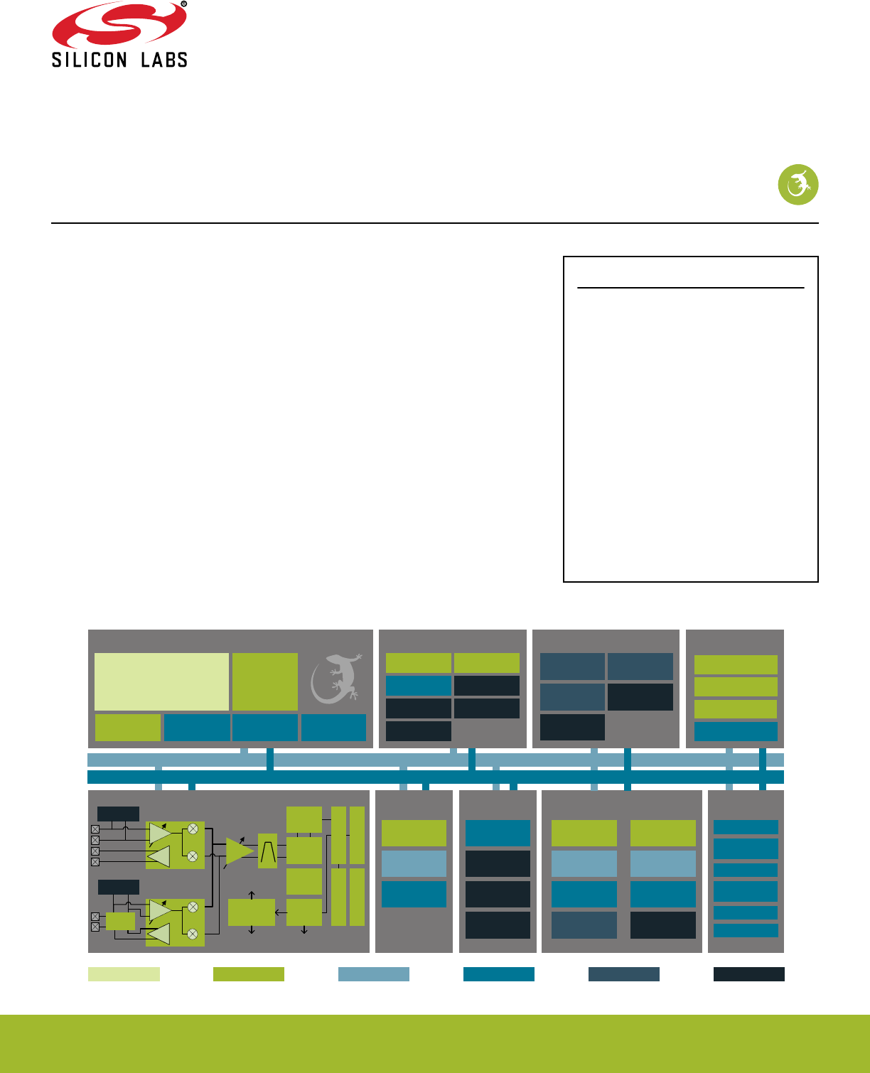
EFR32xG13 Wireless Gecko
Reference Manual
The Wireless Gecko portfolio of SoCs (EFR32) include Mighty
Gecko (EFR32MG13), Blue Gecko (EFR32BG13), and Flex
Gecko (EFR32FG13) families. With support for Zigbee®, Thread,
Bluetooth Low Energy (BLE) and proprietary protocols, the Wire-
less Gecko portfolio is ideal for enabling energy-friendly wireless
networking for IoT devices.
The single-die solution provides industry-leading energy efficiency, ultra-fast wakeup
times, a scalable high-power amplifier, an integrated balun and no-compromise MCU
features.
KEY FEATURES
• 32-bit ARM® Cortex-M4 core with 40 MHz
maximum operating frequency
• Scalable Memory and Radio configuration
options available in several footprint
compatible QFN packages
•12-channel Peripheral Reflex System
enabling autonomous interaction of MCU
peripherals
• Autonomous Hardware Crypto Accelerator
and True Random Number Generator
• Integrated balun for 2.4 GHz and
integrated PA with up to 19 dBm transmit
power for 2.4 GHz and 20 dBm transmit
power for Sub-GHz radios
• Integrated DC-DC with RF noise mitigation
• Integrated PLFRCO eliminates external 32
kHz crystal for BLE applications
Timers and Triggers
32-bit bus
Peripheral Reflex System
Serial
Interfaces
I/O Ports Analog I/F
Lowest power mode with peripheral operational:
USART
Low Energy
UARTTM
I2C
External
Interrupts
General
Purpose I/O
Pin Reset
Pin Wakeup
ADC
VDAC
Analog
Comparator
EM3—StopEM2—Deep SleepEM1—Sleep EM4—Hibernate EM4—ShutoffEM0—Active
Energy Management
Brown-Out
Detector
DC-DC
Converter
Voltage
Regulator Voltage Monitor
Power-On Reset
OtherClock Management
H-F Crystal
Oscillator
L-F Crystal
Oscillator
L-F
RC Oscillator
H-F
RC Oscillator
Precision L-F
RC Oscillator
Auxiliary H-F RC
Oscillator
Capacitive
Touch
Op-Amp
IDAC
Radio Transceiver
DEMOD
AGC
IFADC
CRC
BUFC
RFSENSE
MOD
FRC
RAC
Frequency
Synthesizer
PGA
PA
I
Q
RF Frontend
LNA
RFSENSE
PA
I
Q
RF Frontend
LNA
To 2.4 GHz receive
I/Q mixers and PA
To Sub GHz
receive I/Q
mixers and PA
To Sub GHz
and 2.4 GHz PA
Sub GHz
2.4 GHz
BALUN
CRYPTO
CRC
True Random
Number Generator
SMU
Ultra L-F RC
Oscillator
Core / Memory
ARM CortexTM M4 processor
with DSP extensions, FPU and MPU
ETM Debug Interface RAM Memory LDMA
Controller
Flash Program
Memory
Real Time
Counter and
Calendar
Cryotimer
Timer/Counter
Low Energy
Timer
Pulse Counter Watchdog Timer
Protocol Timer
Low Energy
Sensor Interface
silabs.com | Smart. Connected. Energy-friendly. Preliminary Rev. 0.5
This information applies to a product under development. Its characteristics and specifications are subject to change without notice.

Table of Contents
1. About This Document ............................
1
1.1 Introduction...............................1
1.2 Conventions ..............................2
1.3 Related Documentation ..........................3
2. System Overview ..............................4
2.1 Introduction...............................5
2.2 Block Diagrams .............................6
2.3 MCU Features overview ..........................7
2.4 Oscillators and Clocks ...........................9
2.5 RF Frequency Synthesizer .........................9
2.6 Modulation Modes ............................9
2.7 Transmit Mode .............................10
2.8 Receive Mode ..............................10
2.9 Data Buffering ..............................10
2.10 Unbuffered Data Transfer .........................10
2.11 Frame Format Support ..........................11
2.12 Hardware CRC Support ..........................11
2.13 Convolutional Encoding / Decoding ......................11
2.14 Binary Block Encoding / Decoding ......................11
2.15 Data Encryption and Authentication ......................12
2.16 Timers ................................13
2.17 RF Test Modes .............................13
3. System Processor ............................ 14
3.1 Introduction...............................14
3.2 Features................................15
3.3 Functional Description ...........................15
3.3.1 Interrupt Operation ...........................16
3.3.1.1 Avoiding Extraneous Interrupts .......................16
3.3.1.2 IFC Read-clear Operation ........................16
3.3.2 Interrupt Request Lines (IRQ) ........................17
4. Memory and Bus System .......................... 19
4.1 Introduction...............................20
4.2 Functional Description ...........................21
4.2.1 Peripheral non-word access behavior .....................23
4.2.2 Bit-banding ..............................23
4.2.3 Peripheral Bit Set and Clear ........................24
4.2.4 Peripherals ..............................25
silabs.com | Smart. Connected. Energy-friendly. Preliminary Rev. 0.5
This information applies to a product under development. Its characteristics and specifications are subject to change without notice.

4.2.5 Bus Matrix ..............................26
4.2.5.1 Arbitration ..............................26
4.2.5.2 Peripheral access Performance ......................26
4.2.5.3 Bus Faults ..............................29
4.3 Access to Low Energy Peripherals (Asynchronous Registers) ..............29
4.3.1 Writing................................29
4.3.1.1 Delayed Synchronization .........................30
4.3.1.2 Immediate Synchronization ........................30
4.3.2 Reading ...............................31
4.3.3 FREEZE Register ............................31
4.4 Flash .................................31
4.5 SRAM ................................32
4.6 DI Page Entry Map ............................33
4.7 DI Page Entry Description ..........................35
4.7.1 CAL - CRC of DI-page and calibration temperature ................35
4.7.2 EXTINFO - External Component description ..................36
4.7.3 EUI48L - EUI48 OUI and Unique identifier ...................37
4.7.4 EUI48H - OUI .............................37
4.7.5 CUSTOMINFO - Custom information .....................37
4.7.6 MEMINFO - Flash page size and misc. chip information ..............38
4.7.7 UNIQUEL - Low 32 bits of device unique number .................39
4.7.8 UNIQUEH - High 32 bits of device unique number ................39
4.7.9 MSIZE - Flash and SRAM Memory size in kB ..................39
4.7.10 PART - Part description .........................40
4.7.11 DEVINFOREV - Device information page revision ................42
4.7.12 EMUTEMP - EMU Temperature Calibration Information ..............43
4.7.13 ADC0CAL0 - ADC0 calibration register 0 ...................43
4.7.14 ADC0CAL1 - ADC0 calibration register 1 ...................44
4.7.15 ADC0CAL2 - ADC0 calibration register 2 ...................45
4.7.16 ADC0CAL3 - ADC0 calibration register 3 ...................45
4.7.17 HFRCOCAL0 - HFRCO Calibration Register (4 MHz) ...............46
4.7.18 HFRCOCAL3 - HFRCO Calibration Register (7 MHz) ...............47
4.7.19 HFRCOCAL6 - HFRCO Calibration Register (13 MHz) ..............48
4.7.20 HFRCOCAL7 - HFRCO Calibration Register (16 MHz) ..............49
4.7.21 HFRCOCAL8 - HFRCO Calibration Register (19 MHz) ..............50
4.7.22 HFRCOCAL10 - HFRCO Calibration Register (26 MHz) ..............51
4.7.23 HFRCOCAL11 - HFRCO Calibration Register (32 MHz) ..............52
4.7.24 HFRCOCAL12 - HFRCO Calibration Register (38 MHz) ..............53
4.7.25 AUXHFRCOCAL0 - AUXHFRCO Calibration Register (4 MHz) ............54
4.7.26 AUXHFRCOCAL3 - AUXHFRCO Calibration Register (7 MHz) ............55
4.7.27 AUXHFRCOCAL6 - AUXHFRCO Calibration Register (13 MHz) ...........56
4.7.28 AUXHFRCOCAL7 - AUXHFRCO Calibration Register (16 MHz) ...........57
4.7.29 AUXHFRCOCAL8 - AUXHFRCO Calibration Register (19 MHz) ...........58
4.7.30 AUXHFRCOCAL10 - AUXHFRCO Calibration Register (26 MHz) ...........59
4.7.31 AUXHFRCOCAL11 - AUXHFRCO Calibration Register (32 MHz) ...........60
4.7.32 AUXHFRCOCAL12 - AUXHFRCO Calibration Register (38 MHz) ...........61
4.7.33 VMONCAL0 - VMON Calibration Register 0 ..................62
silabs.com | Smart. Connected. Energy-friendly. Preliminary Rev. 0.5
This information applies to a product under development. Its characteristics and specifications are subject to change without notice.

4.7.34 VMONCAL1 - VMON Calibration Register 1 ..................63
4.7.35 VMONCAL2 - VMON Calibration Register 2 ..................64
4.7.36 IDAC0CAL0 - IDAC0 Calibration Register 0 ..................65
4.7.37 IDAC0CAL1 - IDAC0 Calibration Register 1 ..................66
4.7.38 DCDCLNVCTRL0 - DCDC Low-noise VREF Trim Register 0 ............66
4.7.39 DCDCLPVCTRL0 - DCDC Low-power VREF Trim Register 0 ............67
4.7.40 DCDCLPVCTRL1 - DCDC Low-power VREF Trim Register 1 ............68
4.7.41 DCDCLPVCTRL2 - DCDC Low-power VREF Trim Register 2 ............69
4.7.42 DCDCLPVCTRL3 - DCDC Low-power VREF Trim Register 3 ............70
4.7.43 DCDCLPCMPHYSSEL0 - DCDC LPCMPHYSSEL Trim Register 0 ..........71
4.7.44 DCDCLPCMPHYSSEL1 - DCDC LPCMPHYSSEL Trim Register 1 ..........71
4.7.45 VDAC0MAINCAL - VDAC0 Cals for Main Path .................72
4.7.46 VDAC0ALTCAL - VDAC0 Cals for Alternate Path ................73
4.7.47 VDAC0CH1CAL - VDAC0 CH1 Error Cal ...................74
4.7.48 OPA0CAL0 - OPA0 Calibration Register for DRIVESTRENGTH 0, INCBW=1 .......75
4.7.49 OPA0CAL1 - OPA0 Calibration Register for DRIVESTRENGTH 1, INCBW=1 .......76
4.7.50 OPA0CAL2 - OPA0 Calibration Register for DRIVESTRENGTH 2, INCBW=1 .......77
4.7.51 OPA0CAL3 - OPA0 Calibration Register for DRIVESTRENGTH 3, INCBW=1 .......78
4.7.52 OPA1CAL0 - OPA1 Calibration Register for DRIVESTRENGTH 0, INCBW=1 .......79
4.7.53 OPA1CAL1 - OPA1 Calibration Register for DRIVESTRENGTH 1, INCBW=1 .......80
4.7.54 OPA1CAL2 - OPA1 Calibration Register for DRIVESTRENGTH 2, INCBW=1 .......81
4.7.55 OPA1CAL3 - OPA1 Calibration Register for DRIVESTRENGTH 3, INCBW=1 .......82
4.7.56 OPA2CAL0 - OPA2 Calibration Register for DRIVESTRENGTH 0, INCBW=1 .......83
4.7.57 OPA2CAL1 - OPA2 Calibration Register for DRIVESTRENGTH 1, INCBW=1 .......84
4.7.58 OPA2CAL2 - OPA2 Calibration Register for DRIVESTRENGTH 2, INCBW=1 .......85
4.7.59 OPA2CAL3 - OPA2 Calibration Register for DRIVESTRENGTH 3, INCBW=1 .......86
4.7.60 CSENGAINCAL - Cap Sense Gain Adjustment .................87
4.7.61 OPA0CAL4 - OPA0 Calibration Register for DRIVESTRENGTH 0, INCBW=0 .......88
4.7.62 OPA0CAL5 - OPA0 Calibration Register for DRIVESTRENGTH 1, INCBW=0 .......89
4.7.63 OPA0CAL6 - OPA0 Calibration Register for DRIVESTRENGTH 2, INCBW=0 .......90
4.7.64 OPA0CAL7 - OPA0 Calibration Register for DRIVESTRENGTH 3, INCBW=0 .......91
4.7.65 OPA1CAL4 - OPA1 Calibration Register for DRIVESTRENGTH 0, INCBW=0 .......92
4.7.66 OPA1CAL5 - OPA1 Calibration Register for DRIVESTRENGTH 1, INCBW=0 .......93
4.7.67 OPA1CAL6 - OPA1 Calibration Register for DRIVESTRENGTH 2, INCBW=0 .......94
4.7.68 OPA1CAL7 - OPA1 Calibration Register for DRIVESTRENGTH 3, INCBW=0 .......95
4.7.69 OPA2CAL4 - OPA2 Calibration Register for DRIVESTRENGTH 0, INCBW=0 .......96
4.7.70 OPA2CAL5 - OPA2 Calibration Register for DRIVESTRENGTH 1, INCBW=0 .......97
4.7.71 OPA2CAL6 - OPA2 Calibration Register for DRIVESTRENGTH 2, INCBW=0 .......98
4.7.72 OPA2CAL7 - OPA2 Calibration Register for DRIVESTRENGTH 3, INCBW=0 .......99
5. Serial Flash ...............................100
5.1 Introduction..............................100
5.2 Features...............................100
5.3 Functional Description ..........................101
5.3.1 Memory Organization..........................102
5.3.2 Serial Interface ............................103
5.3.2.1 USART1 Configuration ........................103
5.3.2.2 Timing ..............................104
silabs.com | Smart. Connected. Energy-friendly. Preliminary Rev. 0.5
This information applies to a product under development. Its characteristics and specifications are subject to change without notice.

5.3.2.3 Hold Operation ...........................105
5.3.2.4 Power Up and Power Down .......................106
5.3.3 Instruction Set ............................107
5.3.4 Registers ..............................107
5.3.4.1 Read Status Register (RDSR, 0x05) ....................110
5.3.4.2 Write Status Register (WRSR, 0x01) ....................110
5.3.4.3 Read Function Register (RDFR, 0x48) ...................110
5.3.4.4 Write Function Register (WRFR, 0x42) ...................111
5.3.5 Reading Memory ...........................111
5.3.5.1 Read Data (RD, 0x03) .........................111
5.3.5.2 Fast Read Data (FR, 0x0B) .......................112
5.3.6 Programming and Erasing Memory .....................112
5.3.6.1 Program/Erase Suspend and Resume ...................113
5.3.6.2 Write Enable (WREN, 0x06) .......................114
5.3.6.3 Write Disable (WRDI, 0x04) .......................114
5.3.6.4 Page Program (PP, 0x02)........................114
5.3.6.5 Sector Erase (SER, 0xD7 / 0x20) .....................115
5.3.6.6 Block Erase 32k (BER32, 0x52) .....................115
5.3.6.7 Block Erase 64k (BER64, 0xD8) .....................115
5.3.6.8 Chip Erase (CER, 0xC7 / 0x60)......................116
5.3.6.9 Program/Erase Suspend (PERSUS, 0x75 / 0xB0) ...............116
5.3.6.10 Program/Erase Resume (PERRSM, 0x7A / 0x30) ...............116
5.3.7 Write Protection ...........................117
5.3.7.1 Sector Unlock (SECUNLOCK, 0x26) ....................118
5.3.7.2 Sector Lock (SECLOCK, 0x24) ......................118
5.3.8 Security Information Row and Unique ID ...................118
5.3.8.1 Information Row Program (IRP, 0x62) ...................120
5.3.8.2 Information Row Read (IRRD, 0x68) ....................120
5.3.8.3 Read Unique ID Number (RDUID, 0x4B) ..................120
5.3.9 Power Down.............................121
5.3.9.1 Deep Power Down (DP, 0xB9) ......................121
5.3.9.2 Release Deep Power Down (RDPD, 0xAB)..................121
5.3.10 Software Reset ...........................122
5.3.10.1 Reset Enable (RSTEN, 0x66) ......................122
5.3.10.2 Reset (RST, 0x99)..........................122
6. Radio Transceiver ............................123
6.1 Introduction..............................124
7. DBG - Debug Interface ...........................125
7.1 Introduction..............................125
7.2 Features...............................125
7.3 Functional Description ..........................125
7.3.1 Debug Pins .............................126
7.3.2 Embedded Trace Macrocell v3.5 (ETM) ...................126
7.3.3 Debug and EM2 Deep Sleep/EM3 Stop ...................126
7.3.4 Authentication Access Point .......................126
7.3.4.1 Command Key ...........................126
7.3.4.2 Device Erase ............................126
7.3.4.3 System Reset ...........................126
7.3.4.4 System Bus Stall ..........................127
silabs.com | Smart. Connected. Energy-friendly. Preliminary Rev. 0.5
This information applies to a product under development. Its characteristics and specifications are subject to change without notice.

7.3.4.5 User Flash Page CRC .........................127
7.3.5 Debug Lock .............................127
7.3.6 AAP Lock..............................127
7.3.7 Debugger reads of actionable registers....................128
7.3.8 Debug Recovery ...........................128
7.4 Register Map .............................128
7.5 Register Description ...........................129
7.5.1 AAP_CMD - Command Register .....................129
7.5.2 AAP_CMDKEY - Command Key Register ..................129
7.5.3 AAP_STATUS - Status Register ......................130
7.5.4 AAP_CTRL - Control Register ......................130
7.5.5 AAP_CRCCMD - CRC Command Register ..................131
7.5.6 AAP_CRCSTATUS - CRC Status Register ..................131
7.5.7 AAP_CRCADDR - CRC Address Register ..................132
7.5.8 AAP_CRCRESULT - CRC Result Register ..................132
7.5.9 AAP_IDR - AAP Identification Register ...................133
8. MSC - Memory System Controller ......................134
8.1 Introduction..............................134
8.2 Features...............................135
8.3 Functional Description ..........................136
8.3.1 User Data (UD) Page Description .....................136
8.3.2 Lock Bits (LB) Page Description ......................137
8.3.3 Device Information (DI) Page .......................137
8.3.4 Bootloader .............................138
8.3.5 Device Revision ...........................138
8.3.6 Post-reset Behavior ..........................138
8.3.7 Flash Startup ............................139
8.3.8 Wait-states .............................139
8.3.8.1 One Wait-state Access ........................139
8.3.8.2 Zero Wait-state Access ........................139
8.3.8.3 Operation Above ..........................139
8.3.9 Suppressed Conditional Branch Target Prefetch (SCBTP) .............140
8.3.10 Cortex-M4 If-Then Block Folding .....................140
8.3.11 Instruction Cache...........................141
8.3.12 Low Voltage Flash Read ........................142
8.3.13 Erase and Write Operations .......................142
8.3.13.1 Mass erase ............................142
8.4 Register Map .............................143
8.5 Register Description ...........................144
8.5.1 MSC_CTRL - Memory System Control Register ................144
8.5.2 MSC_READCTRL - Read Control Register ..................145
8.5.3 MSC_WRITECTRL - Write Control Register ..................146
8.5.4 MSC_WRITECMD - Write Command Register .................147
8.5.5 MSC_ADDRB - Page Erase/Write Address Buffer ................148
8.5.6 MSC_WDATA - Write Data Register ....................148
8.5.7 MSC_STATUS - Status Register .....................149
silabs.com | Smart. Connected. Energy-friendly. Preliminary Rev. 0.5
This information applies to a product under development. Its characteristics and specifications are subject to change without notice.

8.5.8 MSC_IF - Interrupt Flag Register .....................150
8.5.9 MSC_IFS - Interrupt Flag Set Register ...................151
8.5.10 MSC_IFC - Interrupt Flag Clear Register ..................152
8.5.11 MSC_IEN - Interrupt Enable Register ...................153
8.5.12 MSC_LOCK - Configuration Lock Register ..................154
8.5.13 MSC_CACHECMD - Flash Cache Command Register .............155
8.5.14 MSC_CACHEHITS - Cache Hits Performance Counter .............155
8.5.15 MSC_CACHEMISSES - Cache Misses Performance Counter ...........156
8.5.16 MSC_MASSLOCK - Mass Erase Lock Register ................157
8.5.17 MSC_STARTUP - Startup Control ....................158
8.5.18 MSC_CMD - Command Register .....................159
8.5.19 MSC_BOOTLOADERCTRL - Bootloader read and write enable, write once register ....159
8.5.20 MSC_AAPUNLOCKCMD - Software Unlock AAP Command Register ........160
8.5.21 MSC_CACHECONFIG0 - Cache Configuration Register 0 ............161
9. LDMA - Linked DMA Controller........................162
9.1 Introduction..............................162
9.1.1 Features ..............................163
9.2 Block Diagram.............................164
9.3 Functional Description ..........................165
9.3.1 Channel Descriptor ..........................165
9.3.1.1 DMA Transfer Size ..........................165
9.3.1.2 Source/Destination Increments ......................165
9.3.1.3 Block Size .............................166
9.3.1.4 Transfer Count ...........................166
9.3.1.5 Descriptor List ...........................166
9.3.1.6 Addresses .............................166
9.3.1.7 Addressing Modes ..........................166
9.3.1.8 Byte Swap.............................167
9.3.1.9 DMA Size and Source/Destination Increment Programming ............168
9.3.2 Channel Configuration .........................170
9.3.2.1 Address Increment/Decrement ......................170
9.3.2.2 Loop Counter ............................170
9.3.3 Channel Select Configuration .......................170
9.3.4 Starting a transfer ...........................170
9.3.4.1 Peripheral Transfer Requests ......................171
9.3.5 Managing Transfer Errors ........................171
9.3.6 Arbitration .............................171
9.3.6.1 Arbitration Priority ..........................171
9.3.6.2 DMA Transfer Arbitration ........................173
9.3.7 Channel descriptor data structure .....................174
9.3.7.1 XFER descriptor structure .......................174
9.3.7.2 SYNC descriptor structure .......................175
9.3.7.3 WRI descriptor structure ........................176
9.3.8 Interaction with the EMU ........................176
9.3.9 Interrupts ..............................177
9.3.10 Debugging .............................177
9.4 Examples ..............................177
9.4.1 Single Direct Register DMA Transfer ....................177
silabs.com | Smart. Connected. Energy-friendly. Preliminary Rev. 0.5
This information applies to a product under development. Its characteristics and specifications are subject to change without notice.

9.4.2 Descriptor Linked List .........................178
9.4.3 Single Descriptor Looped Transfer .....................180
9.4.4 Descriptor List with Looping .......................181
9.4.5 Simple Inter-Channel Synchronization ....................182
9.4.6 2D Copy ..............................184
9.4.7 Ping-Pong .............................186
9.4.8 Scatter-Gather ............................187
9.5 Register Map .............................188
9.6 Register Description ...........................189
9.6.1 LDMA_CTRL - DMA Control Register ....................189
9.6.2 LDMA_STATUS - DMA Status Register ...................190
9.6.3 LDMA_SYNC - DMA Synchronization Trigger Register (Single-Cycle RMW) .......191
9.6.4 LDMA_CHEN - DMA Channel Enable Register (Single-Cycle RMW) .........191
9.6.5 LDMA_CHBUSY - DMA Channel Busy Register ................192
9.6.6 LDMA_CHDONE - DMA Channel Linking Done Register (Single-Cycle RMW) ......192
9.6.7 LDMA_DBGHALT - DMA Channel Debug Halt Register ..............193
9.6.8 LDMA_SWREQ - DMA Channel Software Transfer Request Register .........193
9.6.9 LDMA_REQDIS - DMA Channel Request Disable Register ............194
9.6.10 LDMA_REQPEND - DMA Channel Requests Pending Register ..........194
9.6.11 LDMA_LINKLOAD - DMA Channel Link Load Register ..............195
9.6.12 LDMA_REQCLEAR - DMA Channel Request Clear Register ...........195
9.6.13 LDMA_IF - Interrupt Flag Register ....................196
9.6.14 LDMA_IFS - Interrupt Flag Set Register ..................196
9.6.15 LDMA_IFC - Interrupt Flag Clear Register ..................197
9.6.16 LDMA_IEN - Interrupt Enable register ...................197
9.6.17 LDMA_CHx_REQSEL - Channel Peripheral Request Select Register ........198
9.6.18 LDMA_CHx_CFG - Channel Configuration Register ..............202
9.6.19 LDMA_CHx_LOOP - Channel Loop Counter Register ..............203
9.6.20 LDMA_CHx_CTRL - Channel Descriptor Control Word Register ..........204
9.6.21 LDMA_CHx_SRC - Channel Descriptor Source Data Address Register ........207
9.6.22 LDMA_CHx_DST - Channel Descriptor Destination Data Address Register .......207
9.6.23 LDMA_CHx_LINK - Channel Descriptor Link Structure Address Register .......208
10. RMU - Reset Management Unit .......................209
10.1 Introduction .............................209
10.2 Features ..............................209
10.3 Functional Description .........................210
10.3.1 Reset levels ............................211
10.3.2 RMU_RSTCAUSE Register .......................212
10.3.3 Power-On Reset (POR) ........................213
10.3.4 Brown-Out Detector (BOD) .......................213
10.3.5 RESETn pin Reset ..........................214
10.3.6 Watchdog Reset ...........................214
10.3.7 Lockup Reset ............................214
10.3.8 System Reset Request.........................214
10.3.9 Reset state.............................214
10.3.10 Register reset signals .........................214
silabs.com | Smart. Connected. Energy-friendly. Preliminary Rev. 0.5
This information applies to a product under development. Its characteristics and specifications are subject to change without notice.

10.3.10.1 Registers with alternate reset .....................215
10.4 Register Map.............................216
10.5 Register Description ..........................217
10.5.1 RMU_CTRL - Control Register ......................217
10.5.2 RMU_RSTCAUSE - Reset Cause Register .................219
10.5.3 RMU_CMD - Command Register .....................220
10.5.4 RMU_RST - Reset Control Register ....................220
10.5.5 RMU_LOCK - Configuration Lock Register ..................221
11. EMU - Energy Management Unit .......................222
11.1 Introduction .............................222
11.2 Features ..............................223
11.3 Functional Description..........................224
11.3.1 Energy Modes............................225
11.3.1.1 EM0 Active ............................227
11.3.1.2 EM1 Sleep ............................227
11.3.1.3 EM2 Deep Sleep ..........................228
11.3.1.4 EM3 Stop ............................228
11.3.1.5 EM4 Hibernate ..........................229
11.3.1.6 EM4 Shutoff ...........................229
11.3.2 Entering Low Energy Modes .......................229
11.3.2.1 Entry into EM1 Sleep ........................229
11.3.2.2 Entry into EM2 Deep Sleep or EM3 Stop ..................230
11.3.2.3 Entry into EM4 Hibernate or EM4 Shutoff ..................230
11.3.3 Exiting a Low Energy Mode .......................231
11.3.4 Power Configurations .........................232
11.3.4.1 Power Configuration 0: Unconfigured ...................233
11.3.4.2 Power Configuration 1: No DC-DC ....................234
11.3.4.3 Power Configuration 2: DC-DC .....................235
11.3.5 DC-to-DC Interface ..........................236
11.3.5.1 Bypass Mode ...........................236
11.3.5.2 Low Power (LP) Mode ........................237
11.3.5.3 Low Noise (LN) Mode ........................237
11.3.5.4 DC-to-DC Programming Guidelines ....................237
11.3.6 Analog Peripheral Power Selection.....................238
11.3.7 Digital LDO Power Selection .......................238
11.3.8 IOVDD Connection ..........................238
11.3.9 Voltage Scaling ...........................239
11.3.9.1 EM01 Voltage Scaling ........................239
11.3.9.2 EM23 Voltage Scaling ........................240
11.3.9.3 EM4H Voltage Scaling ........................240
11.3.9.4 Voltage Scaling Recommended Use ...................240
11.3.10 EM23 Peripheral Retention Disable ....................241
11.3.11 Brown Out Detector (BOD) .......................241
11.3.11.1 AVDD BOD............................241
11.3.11.2 DVDD and DECOUPLE BOD .....................241
11.3.12 Voltage Monitor (VMON) ........................242
11.3.13 Powering off SRAM blocks .......................243
11.3.14 Temperature Sensor .........................243
silabs.com | Smart. Connected. Energy-friendly. Preliminary Rev. 0.5
This information applies to a product under development. Its characteristics and specifications are subject to change without notice.

11.3.15 Registers latched in EM4........................244
11.3.16 Register Resets ...........................244
11.4 Register Map .............................245
11.5 Register Description ..........................247
11.5.1 EMU_CTRL - Control Register ......................247
11.5.2 EMU_STATUS - Status Register .....................249
11.5.3 EMU_LOCK - Configuration Lock Register ..................251
11.5.4 EMU_RAM0CTRL - Memory Control Register ................252
11.5.5 EMU_CMD - Command Register .....................253
11.5.6 EMU_EM4CTRL - EM4 Control Register ..................254
11.5.7 EMU_TEMPLIMITS - Temperature limits for interrupt generation ..........255
11.5.8 EMU_TEMP - Value of last temperature measurement ..............255
11.5.9 EMU_IF - Interrupt Flag Register .....................256
11.5.10 EMU_IFS - Interrupt Flag Set Register ...................258
11.5.11 EMU_IFC - Interrupt Flag Clear Register ..................260
11.5.12 EMU_IEN - Interrupt Enable Register ...................262
11.5.13 EMU_PWRLOCK - Regulator and Supply Lock Register .............264
11.5.14 EMU_PWRCTRL - Power Control Register. .................265
11.5.15 EMU_DCDCCTRL - DCDC Control ....................266
11.5.16 EMU_DCDCMISCCTRL - DCDC Miscellaneous Control Register .........267
11.5.17 EMU_DCDCZDETCTRL - DCDC Power Train NFET Zero Current Detector Control Register 269
11.5.18 EMU_DCDCCLIMCTRL - DCDC Power Train PFET Current Limiter Control Register ...270
11.5.19 EMU_DCDCLNCOMPCTRL - DCDC Low Noise Compensator Control Register ....271
11.5.20 EMU_DCDCLNVCTRL - DCDC Low Noise Voltage Register ...........272
11.5.21 EMU_DCDCLPVCTRL - DCDC Low Power Voltage Register ...........273
11.5.22 EMU_DCDCLPCTRL - DCDC Low Power Control Register ............274
11.5.23 EMU_DCDCLNFREQCTRL - DCDC Low Noise Controller Frequency Control .....275
11.5.24 EMU_DCDCSYNC - DCDC Read Status Register ...............275
11.5.25 EMU_VMONAVDDCTRL - VMON AVDD Channel Control ............276
11.5.26 EMU_VMONALTAVDDCTRL - Alternate VMON AVDD Channel Control .......277
11.5.27 EMU_VMONDVDDCTRL - VMON DVDD Channel Control ............278
11.5.28 EMU_VMONIO0CTRL - VMON IOVDD0 Channel Control ............279
11.5.29 EMU_RAM1CTRL - Memory Control Register ................280
11.5.30 EMU_RAM2CTRL - Memory Control Register ................281
11.5.31 EMU_DCDCLPEM01CFG - Configuration bits for low power mode to be applied during EM01,
this field is only relevant if LP mode is used in EM01. ...............282
11.5.32 EMU_EM23PERNORETAINCMD - Clears corresponding bits in EM23PERNORETAINSTATUS
unlocking access to peripheral .......................283
11.5.33 EMU_EM23PERNORETAINSTATUS - Status indicating if peripherals were powered down in
EM23, subsequently locking access to it. ....................285
11.5.34 EMU_EM23PERNORETAINCTRL - When set corresponding peripherals may get powered down
in EM23 ...............................287
12. CMU - Clock Management Unit .......................289
12.1 Introduction .............................289
12.2 Features ..............................290
12.3 Functional Description .........................291
12.3.1 System Clocks ...........................292
silabs.com | Smart. Connected. Energy-friendly. Preliminary Rev. 0.5
This information applies to a product under development. Its characteristics and specifications are subject to change without notice.

12.3.1.1 HFCLK - High Frequency Clock .....................293
12.3.1.2 HFCORECLK - High Frequency Core Clock .................293
12.3.1.3 HFBUSCLK - High Frequency Bus Clock ..................293
12.3.1.4 HFPERCLK - High Frequency Peripheral Clock ................293
12.3.1.5 HFRADIOCLK - High Frequency Radio Clock ................294
12.3.1.6 ADCnCLK - ADC Core Clock ......................294
12.3.1.7 LFACLK - Low Frequency A Clock ....................294
12.3.1.8 LFBCLK - Low Frequency B Clock ....................294
12.3.1.9 LFECLK - Low Frequency E Clock ....................295
12.3.1.10 PCNTnCLK - Pulse Counter n Clock ...................295
12.3.1.11 WDOGnCLK - Watchdog Timer Clock...................295
12.3.1.12 CRYOCLK - Cryotimer Clock .....................295
12.3.1.13 RFSENSECLK - RFSENSE Clock ....................295
12.3.1.14 AUXCLK - Auxiliary Clock.......................295
12.3.1.15 Debug Trace Clock ........................295
12.3.2 Oscillators .............................295
12.3.2.1 Enabling and Disabling ........................296
12.3.2.2 Oscillator Start-up Time and Time-out ...................300
12.3.2.3 Switching Clock Source ........................301
12.3.2.4 HFXO Configuration .........................303
12.3.2.5 LFXO Configuration .........................306
12.3.2.6 HFRCO and AUXHFRCO Configuration ..................307
12.3.2.7 LFRCO Configuration ........................307
12.3.2.8 RC Oscillator Calibration .......................308
12.3.2.9 Automatic HFXO Start ........................310
12.3.3 Configuration For Operating Frequencies ..................313
12.3.4 Energy Modes............................314
12.3.5 Clock Output on a Pin .........................315
12.3.6 Clock Input from a Pin .........................315
12.3.7 Clock Output on PRS .........................315
12.3.8 Error Handling............................315
12.3.9 Interrupts .............................315
12.3.10 Wake-up .............................316
12.3.11 Protection .............................316
12.3.12 Digital Phase-Locked Loop .......................316
12.3.12.1 Enabling and Disabling .......................316
12.3.12.2 Lock Modes ...........................316
12.3.12.3 Configurations ..........................316
12.3.12.4 Lock Detection ..........................317
12.3.12.5 Spectrum Spreading ........................317
12.3.13 Precision Low Frequency Oscillator ....................317
12.4 Register Map.............................318
12.5 Register Description ..........................320
12.5.1 CMU_CTRL - CMU Control Register ....................320
12.5.2 CMU_HFRCOCTRL - HFRCO Control Register ................322
12.5.3 CMU_AUXHFRCOCTRL - AUXHFRCO Control Register .............324
12.5.4 CMU_LFRCOCTRL - LFRCO Control Register ................325
12.5.5 CMU_HFXOCTRL - HFXO Control Register .................327
12.5.6 CMU_HFXOSTARTUPCTRL - HFXO Startup Control ..............329
12.5.7 CMU_HFXOSTEADYSTATECTRL - HFXO Steady State control ..........330
silabs.com | Smart. Connected. Energy-friendly. Preliminary Rev. 0.5
This information applies to a product under development. Its characteristics and specifications are subject to change without notice.

12.5.8 CMU_HFXOTIMEOUTCTRL - HFXO Timeout Control ..............331
12.5.9 CMU_LFXOCTRL - LFXO Control Register .................334
12.5.10 CMU_DPLLCTRL - DPLL Control Register .................336
12.5.11 CMU_DPLLCTRL1 - DPLL Control Register .................337
12.5.12 CMU_CALCTRL - Calibration Control Register ................338
12.5.13 CMU_CALCNT - Calibration Counter Register ................340
12.5.14 CMU_OSCENCMD - Oscillator Enable/Disable Command Register .........341
12.5.15 CMU_CMD - Command Register ....................342
12.5.16 CMU_DBGCLKSEL - Debug Trace Clock Select ...............343
12.5.17 CMU_HFCLKSEL - High Frequency Clock Select Command Register ........343
12.5.18 CMU_LFACLKSEL - Low Frequency A Clock Select Register ...........344
12.5.19 CMU_LFBCLKSEL - Low Frequency B Clock Select Register ...........345
12.5.20 CMU_LFECLKSEL - Low Frequency E Clock Select Register ...........346
12.5.21 CMU_STATUS - Status Register .....................347
12.5.22 CMU_HFCLKSTATUS - HFCLK Status Register ...............349
12.5.23 CMU_HFXOTRIMSTATUS - HFXO Trim Status ...............350
12.5.24 CMU_IF - Interrupt Flag Register ....................351
12.5.25 CMU_IFS - Interrupt Flag Set Register ..................354
12.5.26 CMU_IFC - Interrupt Flag Clear Register ..................356
12.5.27 CMU_IEN - Interrupt Enable Register ...................359
12.5.28 CMU_HFBUSCLKEN0 - High Frequency Bus Clock Enable Register 0 ........361
12.5.29 CMU_HFPERCLKEN0 - High Frequency Peripheral Clock Enable Register 0 .....362
12.5.30 CMU_HFRADIOALTCLKEN0 - High Frequency Alternate Radio Peripheral Clock Enable Register
0 .................................363
12.5.31 CMU_LFACLKEN0 - Low Frequency A Clock Enable Register 0 (Async Reg) .....363
12.5.32 CMU_LFBCLKEN0 - Low Frequency B Clock Enable Register 0 (Async Reg) .....364
12.5.33 CMU_LFECLKEN0 - Low Frequency E Clock Enable Register 0 (Async Reg) .....364
12.5.34 CMU_HFPRESC - High Frequency Clock Prescaler Register ...........365
12.5.35 CMU_HFCOREPRESC - High Frequency Core Clock Prescaler Register .......366
12.5.36 CMU_HFPERPRESC - High Frequency Peripheral Clock Prescaler Register .....366
12.5.37 CMU_HFRADIOPRESC - High Frequency Radio Peripheral Clock Prescaler Register ..367
12.5.38 CMU_HFEXPPRESC - High Frequency Export Clock Prescaler Register .......367
12.5.39 CMU_LFAPRESC0 - Low Frequency A Prescaler Register 0 (Async Reg) .......368
12.5.40 CMU_LFBPRESC0 - Low Frequency B Prescaler Register 0 (Async Reg) ......369
12.5.41 CMU_LFEPRESC0 - Low Frequency E Prescaler Register 0 (Async Reg). When waking up from
EM4 make sure EM4UNLATCH in EMU_CMD is set for this to take effect ........370
12.5.42 CMU_HFRADIOALTPRESC - High Frequency Alternate Radio Peripheral Clock Prescaler Regis-
ter .................................370
12.5.43 CMU_SYNCBUSY - Synchronization Busy Register ..............371
12.5.44 CMU_FREEZE - Freeze Register ....................374
12.5.45 CMU_PCNTCTRL - PCNT Control Register .................375
12.5.46 CMU_ADCCTRL - ADC Control Register ..................376
12.5.47 CMU_ROUTEPEN - I/O Routing Pin Enable Register .............377
12.5.48 CMU_ROUTELOC0 - I/O Routing Location Register ..............378
12.5.49 CMU_ROUTELOC1 - I/O Routing Location Register ..............379
12.5.50 CMU_LOCK - Configuration Lock Register .................380
12.5.51 CMU_HFRCOSS - HFRCO Spread Spectrum Register .............381
13. SMU - Security Management Unit ......................382
silabs.com | Smart. Connected. Energy-friendly. Preliminary Rev. 0.5
This information applies to a product under development. Its characteristics and specifications are subject to change without notice.

13.1 Introduction .............................382
13.2 Features ..............................382
13.3 Functional Description .........................383
13.3.1 PPU - Peripheral Protection Unit .....................383
13.3.2 Programming Model..........................384
13.3.2.1 Interrupt Control/Status ........................385
13.3.2.2 PPU Control............................385
13.4 Register Map.............................385
13.5 Register Description ..........................386
13.5.1 SMU_IF - Interrupt Flag Register .....................386
13.5.2 SMU_IFS - Interrupt Flag Set Register ...................386
13.5.3 SMU_IFC - Interrupt Flag Clear Register ..................387
13.5.4 SMU_IEN - Interrupt Enable Register ...................387
13.5.5 SMU_PPUCTRL - PPU Control Register ..................388
13.5.6 SMU_PPUPATD0 - PPU Privilege Access Type Descriptor 0 ...........389
13.5.7 SMU_PPUPATD1 - PPU Privilege Access Type Descriptor 1 ...........391
13.5.8 SMU_PPUFS - PPU Fault Status .....................393
14. RTCC - Real Time Counter and Calendar ...................395
14.1 Introduction .............................395
14.2 Features ..............................396
14.3 Functional Description .........................396
14.3.1 Counter ..............................397
14.3.1.1 Normal Mode ...........................398
14.3.1.2 Calendar Mode...........................399
14.3.1.3 RTCC Initialization .........................400
14.3.2 Capture/Compare Channels .......................401
14.3.3 Interrupts and PRS Output .......................404
14.3.3.1 Main Counter Tick PRS Output .....................404
14.3.4 Energy Mode Availability ........................404
14.3.5 Register Lock ............................404
14.3.6 Oscillator Failure Detection .......................404
14.3.7 Retention Registers ..........................404
14.3.8 Debug Session ...........................405
14.4 Register Map.............................405
14.5 Register Description ..........................406
14.5.1 RTCC_CTRL - Control Register (Async Reg) .................406
14.5.2 RTCC_PRECNT - Pre-Counter Value Register (Async Reg) ............408
14.5.3 RTCC_CNT - Counter Value Register (Async Reg) ...............408
14.5.4 RTCC_COMBCNT - Combined Pre-Counter and Counter Value Register .......409
14.5.5 RTCC_TIME - Time of day register (Async Reg) ................410
14.5.6 RTCC_DATE - Date register (Async Reg) ..................411
14.5.7 RTCC_IF - RTCC Interrupt Flags .....................412
14.5.8 RTCC_IFS - Interrupt Flag Set Register ...................413
14.5.9 RTCC_IFC - Interrupt Flag Clear Register ..................414
14.5.10 RTCC_IEN - Interrupt Enable Register ..................415
14.5.11 RTCC_STATUS - Status register ....................416
silabs.com | Smart. Connected. Energy-friendly. Preliminary Rev. 0.5
This information applies to a product under development. Its characteristics and specifications are subject to change without notice.

14.5.12 RTCC_CMD - Command Register ....................416
14.5.13 RTCC_SYNCBUSY - Synchronization Busy Register ..............416
14.5.14 RTCC_POWERDOWN - Retention RAM power-down register (Async Reg) ......417
14.5.15 RTCC_LOCK - Configuration Lock Register (Async Reg) ............417
14.5.16 RTCC_EM4WUEN - Wake Up Enable ...................418
14.5.17 RTCC_CCx_CTRL - CC Channel Control Register (Async Reg) ..........419
14.5.18 RTCC_CCx_CCV - Capture/Compare Value Register (Async Reg) .........421
14.5.19 RTCC_CCx_TIME - Capture/Compare Time Register (Async Reg) .........422
14.5.20 RTCC_CCx_DATE - Capture/Compare Date Register (Async Reg) .........423
14.5.21 RTCC_RETx_REG - Retention register ..................423
15. WDOG - Watchdog Timer .........................424
15.1 Introduction .............................424
15.2 Features ..............................424
15.3 Functional Description .........................424
15.3.1 Clock Source ............................425
15.3.2 Debug Functionality ..........................425
15.3.3 Energy Mode Handling .........................425
15.3.4 Register access ...........................425
15.3.5 Warning Interrupt...........................425
15.3.6 Window Interrupt ...........................426
15.3.7 PRS as Watchdog Clear ........................427
15.3.8 PRS Rising Edge Monitoring .......................427
15.4 Register Map.............................428
15.5 Register Description ..........................429
15.5.1 WDOG_CTRL - Control Register (Async Reg) ................429
15.5.2 WDOG_CMD - Command Register (Async Reg) ................432
15.5.3 WDOG_SYNCBUSY - Synchronization Busy Register ..............433
15.5.4 WDOGn_PCHx_PRSCTRL - PRS Control Register (Async Reg) ..........434
15.5.5 WDOG_IF - Watchdog Interrupt Flags ...................435
15.5.6 WDOG_IFS - Interrupt Flag Set Register ..................436
15.5.7 WDOG_IFC - Interrupt Flag Clear Register .................437
15.5.8 WDOG_IEN - Interrupt Enable Register ...................438
16. PRS - Peripheral Reflex System .......................439
16.1 Introduction .............................439
16.2 Features ..............................439
16.3 Functional Description .........................440
16.3.1 Channel Functions ..........................440
16.3.1.1 Operational Mode ..........................440
16.3.1.2 Edge Detection and Clock Domains ....................441
16.3.1.3 Configurable PRS Logic........................441
16.3.2 Producers .............................441
16.3.3 Consumers.............................442
16.3.4 Event on PRS ............................443
16.3.5 DMA Request on PRS .........................443
16.3.6 Example .............................444
silabs.com | Smart. Connected. Energy-friendly. Preliminary Rev. 0.5
This information applies to a product under development. Its characteristics and specifications are subject to change without notice.

16.4 Register Map.............................444
16.5 Register Description ..........................445
16.5.1 PRS_SWPULSE - Software Pulse Register .................445
16.5.2 PRS_SWLEVEL - Software Level Register .................446
16.5.3 PRS_ROUTEPEN - I/O Routing Pin Enable Register ..............447
16.5.4 PRS_ROUTELOC0 - I/O Routing Location Register ..............448
16.5.5 PRS_ROUTELOC1 - I/O Routing Location Register ..............451
16.5.6 PRS_ROUTELOC2 - I/O Routing Location Register ..............453
16.5.7 PRS_CTRL - Control Register ......................455
16.5.8 PRS_DMAREQ0 - DMA Request 0 Register .................456
16.5.9 PRS_DMAREQ1 - DMA Request 1 Register .................457
16.5.10 PRS_PEEK - PRS Channel Values ....................458
16.5.11 PRS_CHx_CTRL - Channel Control Register ................459
17. PCNT - Pulse Counter ..........................466
17.1 Introduction .............................466
17.2 Features ..............................466
17.3 Functional Description .........................467
17.3.1 Pulse Counter Modes .........................467
17.3.1.1 Single Input Oversampling Mode .....................467
17.3.1.2 Externally Clocked Single Input Counter Mode ................467
17.3.1.3 Quadrature decoder modes ......................468
17.3.1.4 Externally Clocked Quadrature Decoder Mode ................469
17.3.1.5 Oversampling Quadrature Decoder Mode ..................471
17.3.2 Hysteresis .............................474
17.3.3 Auxiliary counter ...........................475
17.3.4 Triggered compare and clear.......................476
17.3.5 Register Access ...........................477
17.3.6 Clock Sources............................477
17.3.7 Input Filter .............................477
17.3.8 Edge Polarity ............................478
17.3.9 PRS and PCNTn_S0IN,PCNTn_S1IN Inputs .................478
17.3.10 Interrupts .............................478
17.3.10.1 Underflow and Overflow Interrupts ....................478
17.3.10.2 Direction Change Interrupt ......................479
17.3.11 Cascading Pulse Counters .......................480
17.4 Register Map.............................481
17.5 Register Description ..........................482
17.5.1 PCNTn_CTRL - Control Register (Async Reg) ................482
17.5.2 PCNTn_CMD - Command Register (Async Reg) ...............486
17.5.3 PCNTn_STATUS - Status Register ....................486
17.5.4 PCNTn_CNT - Counter Value Register ...................487
17.5.5 PCNTn_TOP - Top Value Register ....................487
17.5.6 PCNTn_TOPB - Top Value Buffer Register (Async Reg) .............488
17.5.7 PCNTn_IF - Interrupt Flag Register ....................488
17.5.8 PCNTn_IFS - Interrupt Flag Set Register ..................489
17.5.9 PCNTn_IFC - Interrupt Flag Clear Register .................490
17.5.10 PCNTn_IEN - Interrupt Enable Register ..................491
silabs.com | Smart. Connected. Energy-friendly. Preliminary Rev. 0.5
This information applies to a product under development. Its characteristics and specifications are subject to change without notice.

17.5.11 PCNTn_ROUTELOC0 - I/O Routing Location Register .............492
17.5.12 PCNTn_FREEZE - Freeze Register ...................494
17.5.13 PCNTn_SYNCBUSY - Synchronization Busy Register .............495
17.5.14 PCNTn_AUXCNT - Auxiliary Counter Value Register ..............495
17.5.15 PCNTn_INPUT - PCNT Input Register ..................496
17.5.16 PCNTn_OVSCFG - Oversampling Config Register (Async Reg) ..........497
18. I2C - Inter-Integrated Circuit Interface.....................498
18.1 Introduction .............................498
18.2 Features ..............................498
18.3 Functional Description .........................499
18.3.1 I2C-Bus Overview ..........................500
18.3.1.1 START and STOP Conditions ......................501
18.3.1.2 Bus Transfer ...........................502
18.3.1.3 Addresses ............................503
18.3.1.4 10-bit Addressing ..........................503
18.3.1.5 Arbitration, Clock Synchronization, Clock Stretching ..............504
18.3.2 Enable and Reset ..........................504
18.3.3 Safely Disabling and Changing Slave Configuration ...............504
18.3.4 Clock Generation...........................505
18.3.5 Arbitration .............................505
18.3.6 Buffers ..............................505
18.3.6.1 Transmit Buffer and Shift Register ....................506
18.3.6.2 Receive Buffer and Shift Register ....................507
18.3.7 Master Operation...........................508
18.3.7.1 Master State Machine ........................509
18.3.7.2 Interactions ............................510
18.3.7.3 Automatic ACK Interaction .......................511
18.3.7.4 Reset State ............................511
18.3.7.5 Master Transmitter .........................512
18.3.7.6 Master Receiver ..........................514
18.3.8 Bus States .............................516
18.3.9 Slave Operation ...........................516
18.3.9.1 Slave State Machine .........................517
18.3.9.2 Address Recognition .........................517
18.3.9.3 Slave Transmitter ..........................518
18.3.9.4 Slave Receiver ...........................520
18.3.10 Transfer Automation .........................520
18.3.10.1 DMA ..............................521
18.3.10.2 Automatic ACK ..........................521
18.3.10.3 Automatic STOP ..........................521
18.3.11 Using 10-bit Addresses ........................521
18.3.12 Error Handling ...........................521
18.3.12.1 ABORT Command .........................521
18.3.12.2 Bus Reset ............................521
18.3.12.3 I2C-Bus Errors ..........................522
18.3.12.4 Bus Lockup ...........................522
18.3.12.5 Bus Idle Timeout ..........................522
18.3.12.6 Clock Low Timeout .........................522
18.3.12.7 Clock Low Error ..........................523
18.3.13 DMA Support ...........................523
silabs.com | Smart. Connected. Energy-friendly. Preliminary Rev. 0.5
This information applies to a product under development. Its characteristics and specifications are subject to change without notice.

18.3.14 Interrupts .............................523
18.3.15 Wake-up .............................523
18.4 Register Map.............................524
18.5 Register Description ..........................525
18.5.1 I2Cn_CTRL - Control Register ......................525
18.5.2 I2Cn_CMD - Command Register .....................528
18.5.3 I2Cn_STATE - State Register ......................529
18.5.4 I2Cn_STATUS - Status Register .....................530
18.5.5 I2Cn_CLKDIV - Clock Division Register ...................531
18.5.6 I2Cn_SADDR - Slave Address Register ..................531
18.5.7 I2Cn_SADDRMASK - Slave Address Mask Register ..............532
18.5.8 I2Cn_RXDATA - Receive Buffer Data Register (Actionable Reads) .........532
18.5.9 I2Cn_RXDOUBLE - Receive Buffer Double Data Register (Actionable Reads) ......533
18.5.10 I2Cn_RXDATAP - Receive Buffer Data Peek Register .............533
18.5.11 I2Cn_RXDOUBLEP - Receive Buffer Double Data Peek Register .........534
18.5.12 I2Cn_TXDATA - Transmit Buffer Data Register ................534
18.5.13 I2Cn_TXDOUBLE - Transmit Buffer Double Data Register ............535
18.5.14 I2Cn_IF - Interrupt Flag Register ....................536
18.5.15 I2Cn_IFS - Interrupt Flag Set Register ...................538
18.5.16 I2Cn_IFC - Interrupt Flag Clear Register ..................540
18.5.17 I2Cn_IEN - Interrupt Enable Register ...................542
18.5.18 I2Cn_ROUTEPEN - I/O Routing Pin Enable Register ..............543
18.5.19 I2Cn_ROUTELOC0 - I/O Routing Location Register ..............544
19. USART - Universal Synchronous Asynchronous Receiver/Transmitter ........547
19.1 Introduction .............................547
19.2 Features ..............................548
19.3 Functional Description .........................549
19.3.1 Modes of Operation ..........................550
19.3.2 Asynchronous Operation ........................550
19.3.2.1 Frame Format ...........................551
19.3.2.2 Parity bit Calculation and Handling ....................552
19.3.2.3 Clock Generation ..........................553
19.3.2.4 Auto Baud Detection .........................554
19.3.2.5 Data Transmission .........................554
19.3.2.6 Transmit Buffer Operation .......................555
19.3.2.7 Frame Transmission Control ......................556
19.3.2.8 Data Reception...........................556
19.3.2.9 Receive Buffer Operation .......................557
19.3.2.10 Blocking Incoming Data .......................558
19.3.2.11 Clock Recovery and Filtering......................559
19.3.2.12 Parity Error............................560
19.3.2.13 Framing Error and Break Detection ...................560
19.3.2.14 Local Loopback ..........................561
19.3.2.15 Asynchronous Half Duplex Communication .................561
19.3.2.16 Single Data-link ..........................561
19.3.2.17 Single Data-link with External Driver ...................562
19.3.2.18 Two Data-links ..........................562
19.3.2.19 Large Frames ...........................563
silabs.com | Smart. Connected. Energy-friendly. Preliminary Rev. 0.5
This information applies to a product under development. Its characteristics and specifications are subject to change without notice.

19.3.2.20 Multi-Processor Mode ........................565
19.3.2.21 Collision Detection .........................565
19.3.2.22 SmartCard Mode..........................566
19.3.3 Synchronous Operation ........................567
19.3.3.1 Frame Format ...........................567
19.3.3.2 Clock Generation ..........................568
19.3.3.3 Master Mode ...........................569
19.3.3.4 Operation of USn_CS Pin .......................569
19.3.3.5 AUTOTX .............................570
19.3.3.6 Slave Mode ............................570
19.3.3.7 Synchronous Half Duplex Communication .................570
19.3.3.8 I2S ...............................570
19.3.3.9 Word Format ...........................571
19.3.3.10 Major Modes ...........................572
19.3.3.11 Using I2S Mode ..........................574
19.3.4 Hardware Flow Control.........................574
19.3.5 Debug Halt .............................574
19.3.6 PRS-triggered Transmissions ......................574
19.3.7 PRS RX Input ...........................574
19.3.8 PRS CLK Input ...........................575
19.3.9 DMA Support ............................575
19.3.10 Timer ..............................576
19.3.10.1 Response Timeout .........................578
19.3.10.2 RX Timeout ...........................579
19.3.10.3 Break Detect ...........................579
19.3.10.4 TX Start Delay ..........................580
19.3.10.5 Inter-Character Space ........................580
19.3.10.6 TX Chip Select End Delay ......................580
19.3.10.7 Response Delay ..........................580
19.3.10.8 Combined TX and RX Example .....................581
19.3.10.9 Combined TX delay and RX break detect .................581
19.3.10.10 Other Stop Conditions .......................581
19.3.11 Interrupts .............................581
19.3.12 IrDA Modulator/ Demodulator ......................582
19.4 Register Map.............................583
19.5 Register Description ..........................584
19.5.1 USARTn_CTRL - Control Register ....................584
19.5.2 USARTn_FRAME - USART Frame Format Register ..............589
19.5.3 USARTn_TRIGCTRL - USART Trigger Control register .............591
19.5.4 USARTn_CMD - Command Register ...................593
19.5.5 USARTn_STATUS - USART Status Register .................594
19.5.6 USARTn_CLKDIV - Clock Control Register .................595
19.5.7 USARTn_RXDATAX - RX Buffer Data Extended Register (Actionable Reads) ......596
19.5.8 USARTn_RXDATA - RX Buffer Data Register (Actionable Reads) ..........596
19.5.9 USARTn_RXDOUBLEX - RX Buffer Double Data Extended Register (Actionable Reads) ..597
19.5.10 USARTn_RXDOUBLE - RX FIFO Double Data Register (Actionable Reads) ......598
19.5.11 USARTn_RXDATAXP - RX Buffer Data Extended Peek Register ..........598
19.5.12 USARTn_RXDOUBLEXP - RX Buffer Double Data Extended Peek Register ......599
19.5.13 USARTn_TXDATAX - TX Buffer Data Extended Register ............600
19.5.14 USARTn_TXDATA - TX Buffer Data Register ................601
silabs.com | Smart. Connected. Energy-friendly. Preliminary Rev. 0.5
This information applies to a product under development. Its characteristics and specifications are subject to change without notice.

19.5.15 USARTn_TXDOUBLEX - TX Buffer Double Data Extended Register ........602
19.5.16 USARTn_TXDOUBLE - TX Buffer Double Data Register ............603
19.5.17 USARTn_IF - Interrupt Flag Register ...................604
19.5.18 USARTn_IFS - Interrupt Flag Set Register .................606
19.5.19 USARTn_IFC - Interrupt Flag Clear Register ................608
19.5.20 USARTn_IEN - Interrupt Enable Register ..................610
19.5.21 USARTn_IRCTRL - IrDA Control Register .................612
19.5.22 USARTn_INPUT - USART Input Register .................614
19.5.23 USARTn_I2SCTRL - I2S Control Register .................616
19.5.24 USARTn_TIMING - Timing Register ...................618
19.5.25 USARTn_CTRLX - Control Register Extended ................620
19.5.26 USARTn_TIMECMP0 - Used to generate interrupts and various delays .......621
19.5.27 USARTn_TIMECMP1 - Used to generate interrupts and various delays .......623
19.5.28 USARTn_TIMECMP2 - Used to generate interrupts and various delays .......625
19.5.29 USARTn_ROUTEPEN - I/O Routing Pin Enable Register ............627
19.5.30 USARTn_ROUTELOC0 - I/O Routing Location Register .............629
19.5.31 USARTn_ROUTELOC1 - I/O Routing Location Register .............634
20. LEUART - Low Energy Universal Asynchronous Receiver/Transmitter ........637
20.1 Introduction .............................637
20.2 Features ..............................638
20.3 Functional Description .........................639
20.3.1 Frame Format ............................640
20.3.1.1 Parity Bit Calculation and Handling ....................640
20.3.2 Clock Source ............................640
20.3.3 Clock Generation...........................641
20.3.4 Data Transmission ..........................641
20.3.4.1 Transmit Buffer Operation .......................642
20.3.4.2 Frame Transmission Control ......................642
20.3.5 Data Reception ...........................643
20.3.5.1 Receive Buffer Operation .......................643
20.3.5.2 Blocking Incoming Data ........................644
20.3.5.3 Data Sampling ...........................644
20.3.5.4 Parity Error ............................644
20.3.5.5 Framing Error and Break Detection ....................645
20.3.5.6 Programmable Start Frame ......................645
20.3.5.7 Programmable Signal Frame ......................645
20.3.5.8 Multi-Processor Mode ........................646
20.3.6 Loopback .............................646
20.3.7 Half Duplex Communication .......................646
20.3.7.1 Single Data-link ..........................647
20.3.7.2 Single Data-link with External Driver ...................647
20.3.7.3 Two Data-links ...........................647
20.3.8 Transmission Delay ..........................647
20.3.9 PRS RX Input ...........................648
20.3.10 DMA Support ...........................648
20.3.11 Pulse Generator/ Pulse Extender .....................649
20.3.11.1 Interrupts ............................649
20.3.12 Register access...........................649
silabs.com | Smart. Connected. Energy-friendly. Preliminary Rev. 0.5
This information applies to a product under development. Its characteristics and specifications are subject to change without notice.

20.4 Register Map.............................650
20.5 Register Description ..........................651
20.5.1 LEUARTn_CTRL - Control Register (Async Reg) ...............651
20.5.2 LEUARTn_CMD - Command Register (Async Reg) ...............654
20.5.3 LEUARTn_STATUS - Status Register ...................655
20.5.4 LEUARTn_CLKDIV - Clock Control Register (Async Reg) ............656
20.5.5 LEUARTn_STARTFRAME - Start Frame Register (Async Reg) ...........656
20.5.6 LEUARTn_SIGFRAME - Signal Frame Register (Async Reg) ...........657
20.5.7 LEUARTn_RXDATAX - Receive Buffer Data Extended Register (Actionable Reads) ....657
20.5.8 LEUARTn_RXDATA - Receive Buffer Data Register (Actionable Reads) ........658
20.5.9 LEUARTn_RXDATAXP - Receive Buffer Data Extended Peek Register ........658
20.5.10 LEUARTn_TXDATAX - Transmit Buffer Data Extended Register (Async Reg) .....659
20.5.11 LEUARTn_TXDATA - Transmit Buffer Data Register (Async Reg) .........660
20.5.12 LEUARTn_IF - Interrupt Flag Register ...................661
20.5.13 LEUARTn_IFS - Interrupt Flag Set Register .................662
20.5.14 LEUARTn_IFC - Interrupt Flag Clear Register ................663
20.5.15 LEUARTn_IEN - Interrupt Enable Register .................664
20.5.16 LEUARTn_PULSECTRL - Pulse Control Register (Async Reg) ..........665
20.5.17 LEUARTn_FREEZE - Freeze Register ..................666
20.5.18 LEUARTn_SYNCBUSY - Synchronization Busy Register ............667
20.5.19 LEUARTn_ROUTEPEN - I/O Routing Pin Enable Register ............668
20.5.20 LEUARTn_ROUTELOC0 - I/O Routing Location Register ............669
20.5.21 LEUARTn_INPUT - LEUART Input Register .................672
21. TIMER/WTIMER - Timer/Counter .......................673
21.1 Introduction .............................673
21.2 Features ..............................674
21.3 Functional Description .........................675
21.3.1 Counter Modes ...........................675
21.3.1.1 Events .............................676
21.3.1.2 Operation ............................676
21.3.1.3 Clock Source ...........................677
21.3.1.4 Peripheral Clock (HFPERCLK) .....................677
21.3.1.5 Compare/ Capture Channel 1 Input ....................677
21.3.1.6 Underflow/Overflow from Neighboring Timer .................677
21.3.1.7 One-Shot Mode ..........................677
21.3.1.8 Top Value Buffer ..........................678
21.3.1.9 Quadrature Decoder .........................679
21.3.1.10 X2 Decoding Mode .........................680
21.3.1.11 X4 Decoding Mode .........................680
21.3.1.12 TIMER/WTIMER Rotational Position ...................681
21.3.2 Compare/Capture Channels .......................681
21.3.2.1 Input Pin Logic ...........................681
21.3.2.2 Compare/Capture Registers ......................681
21.3.2.3 Input Capture ...........................682
21.3.2.4 Period/Pulse-Width Capture ......................683
21.3.2.5 Compare .............................684
21.3.2.6 Compare Mode Registers .......................685
21.3.2.7 Frequency Generation (FRG) ......................686
21.3.2.8 Pulse-Width Modulation (PWM) .....................686
silabs.com | Smart. Connected. Energy-friendly. Preliminary Rev. 0.5
This information applies to a product under development. Its characteristics and specifications are subject to change without notice.

21.3.2.9 Up-count (Single-slope) PWM ......................687
21.3.2.10 2x Count Mode (Up-count) ......................689
21.3.2.11 Up/Down-count (Dual-slope) PWM....................690
21.3.2.12 2x Count Mode (Up/Down-count) ....................691
21.3.2.13 Timer Configuration Lock .......................691
21.3.3 Dead-Time Insertion Unit ........................692
21.3.3.1 Output Polarity ...........................695
21.3.3.2 PRS Channel as a Source .......................695
21.3.3.3 Fault Handling ...........................696
21.3.3.4 Action on Fault ...........................696
21.3.3.5 Exiting Fault State..........................696
21.3.3.6 DTI Configuration Lock ........................696
21.3.4 Debug Mode ............................696
21.3.5 Interrupts, DMA and PRS Output .....................697
21.3.6 GPIO Input/Output ..........................697
21.4 Register Map.............................698
21.5 Register Description ..........................699
21.5.1 TIMERn_CTRL - Control Register ....................699
21.5.2 TIMERn_CMD - Command Register ....................702
21.5.3 TIMERn_STATUS - Status Register ....................703
21.5.4 TIMERn_IF - Interrupt Flag Register ....................706
21.5.5 TIMERn_IFS - Interrupt Flag Set Register ..................707
21.5.6 TIMERn_IFC - Interrupt Flag Clear Register .................708
21.5.7 TIMERn_IEN - Interrupt Enable Register ..................710
21.5.8 TIMERn_TOP - Counter Top Value Register .................711
21.5.9 TIMERn_TOPB - Counter Top Value Buffer Register ..............711
21.5.10 TIMERn_CNT - Counter Value Register ..................712
21.5.11 TIMERn_LOCK - TIMER Configuration Lock Register .............712
21.5.12 TIMERn_ROUTEPEN - I/O Routing Pin Enable Register ............713
21.5.13 TIMERn_ROUTELOC0 - I/O Routing Location Register .............714
21.5.14 TIMERn_ROUTELOC2 - I/O Routing Location Register .............719
21.5.15 TIMERn_CCx_CTRL - CC Channel Control Register ..............723
21.5.16 TIMERn_CCx_CCV - CC Channel Value Register (Actionable Reads) ........726
21.5.17 TIMERn_CCx_CCVP - CC Channel Value Peek Register ............726
21.5.18 TIMERn_CCx_CCVB - CC Channel Buffer Register ..............727
21.5.19 TIMERn_DTCTRL - DTI Control Register ..................728
21.5.20 TIMERn_DTTIME - DTI Time Control Register ................730
21.5.21 TIMERn_DTFC - DTI Fault Configuration Register ..............732
21.5.22 TIMERn_DTOGEN - DTI Output Generation Enable Register ...........734
21.5.23 TIMERn_DTFAULT - DTI Fault Register ..................735
21.5.24 TIMERn_DTFAULTC - DTI Fault Clear Register ...............736
21.5.25 TIMERn_DTLOCK - DTI Configuration Lock Register .............737
22. LETIMER - Low Energy Timer ........................738
22.1 Introduction .............................738
22.2 Features ..............................738
22.3 Functional Description .........................739
22.3.1 Timer...............................739
silabs.com | Smart. Connected. Energy-friendly. Preliminary Rev. 0.5
This information applies to a product under development. Its characteristics and specifications are subject to change without notice.

22.3.2 Compare Registers ..........................739
22.3.3 Top Value .............................740
22.3.3.1 Buffered Top Value .........................740
22.3.3.2 Repeat Modes ...........................740
22.3.3.3 Free-Running Mode .........................741
22.3.3.4 One-shot Mode...........................742
22.3.3.5 Buffered Mode ...........................743
22.3.3.6 Double Mode ...........................744
22.3.3.7 Clock Source ...........................744
22.3.3.8 PRS Input Triggers .........................745
22.3.3.9 Debug..............................745
22.3.4 Underflow Output Action ........................746
22.3.5 PRS Output ............................748
22.3.6 Examples .............................748
22.3.6.1 Triggered Output Generation ......................749
22.3.6.2 Continuous Output Generation .....................750
22.3.6.3 PWM Output ...........................751
22.3.6.4 Interrupts.............................751
22.3.7 Register access ...........................752
22.4 Register Map.............................752
22.5 Register Description ..........................753
22.5.1 LETIMERn_CTRL - Control Register (Async Reg) ...............753
22.5.2 LETIMERn_CMD - Command Register ...................755
22.5.3 LETIMERn_STATUS - Status Register ...................755
22.5.4 LETIMERn_CNT - Counter Value Register ..................756
22.5.5 LETIMERn_COMP0 - Compare Value Register 0 (Async Reg) ...........756
22.5.6 LETIMERn_COMP1 - Compare Value Register 1 (Async Reg) ...........757
22.5.7 LETIMERn_REP0 - Repeat Counter Register 0 (Async Reg) ...........757
22.5.8 LETIMERn_REP1 - Repeat Counter Register 1 (Async Reg) ...........758
22.5.9 LETIMERn_IF - Interrupt Flag Register ...................758
22.5.10 LETIMERn_IFS - Interrupt Flag Set Register ................759
22.5.11 LETIMERn_IFC - Interrupt Flag Clear Register ................760
22.5.12 LETIMERn_IEN - Interrupt Enable Register .................761
22.5.13 LETIMERn_SYNCBUSY - Synchronization Busy Register ............761
22.5.14 LETIMERn_ROUTEPEN - I/O Routing Pin Enable Register ...........762
22.5.15 LETIMERn_ROUTELOC0 - I/O Routing Location Register ............763
22.5.16 LETIMERn_PRSSEL - PRS Input Select Register ...............766
23. CRYOTIMER - Ultra Low Energy Timer/Counter .................769
23.1 Introduction .............................769
23.2 Features ..............................769
23.3 Functional Description .........................769
23.3.1 Block Diagram ...........................770
23.3.2 Operation .............................771
23.3.3 Debug Mode ............................771
23.3.4 Energy Mode availability ........................772
23.4 Register Map.............................772
23.5 Register Description ..........................773
silabs.com | Smart. Connected. Energy-friendly. Preliminary Rev. 0.5
This information applies to a product under development. Its characteristics and specifications are subject to change without notice.

23.5.1 CRYOTIMER_CTRL - Control Register ...................773
23.5.2 CRYOTIMER_PERIODSEL - Interrupt Duration ................774
23.5.3 CRYOTIMER_CNT - Counter Value ....................775
23.5.4 CRYOTIMER_EM4WUEN - Wake Up Enable .................775
23.5.5 CRYOTIMER_IF - Interrupt Flag Register ..................776
23.5.6 CRYOTIMER_IFS - Interrupt Flag Set Register ................776
23.5.7 CRYOTIMER_IFC - Interrupt Flag Clear Register ...............777
23.5.8 CRYOTIMER_IEN - Interrupt Enable Register ................777
24. VDAC - Digital to Analog Converter .....................778
24.1 Introduction .............................778
24.2 Features ..............................779
24.3 Functional Description .........................779
24.3.1 Enabling and Disabling a Channel .....................780
24.3.2 Conversions ............................780
24.3.2.1 Continuous Mode ..........................780
24.3.2.2 Sample/Off Mode ..........................780
24.3.2.3 Conversion Trigger .........................780
24.3.2.4 PRS Triggers ...........................780
24.3.3 Reference Selection..........................781
24.3.4 Warmup Time and Initial Conversion ....................781
24.3.5 Analog Output............................781
24.3.6 Output Mode ............................781
24.3.6.1 Single Ended Output .........................782
24.3.6.2 Differential Output ..........................782
24.3.7 Async Mode ............................782
24.3.8 Refresh Timer ............................782
24.3.9 Clock Prescaling ...........................782
24.3.10 High Speed ............................783
24.3.11 Sine Generation Mode ........................783
24.3.12 Interrupt Flags ...........................784
24.3.12.1 Conversion Done .........................784
24.3.12.2 Buffer Level ...........................784
24.3.12.3 Overflow/Underflow .........................784
24.3.12.4 EM2/3 Sleep Error .........................784
24.3.13 PRS Outputs............................784
24.3.14 DMA Request ...........................784
24.3.15 LESENSE Trigger Mode ........................784
24.3.16 Opamps .............................785
24.3.17 Calibration ............................785
24.3.17.1 Channel 1 Calibration ........................785
24.3.17.2 Manual Calibration .........................785
24.3.18 Warmup Mode ...........................785
24.4 Register Map.............................786
24.5 Register Description ..........................787
24.5.1 VDACn_CTRL - Control Register .....................787
24.5.2 VDACn_STATUS - Status Register ....................790
24.5.3 VDACn_CH0CTRL - Channel 0 Control Register ...............792
silabs.com | Smart. Connected. Energy-friendly. Preliminary Rev. 0.5
This information applies to a product under development. Its characteristics and specifications are subject to change without notice.

24.5.4 VDACn_CH1CTRL - Channel 1 Control Register ...............794
24.5.5 VDACn_CMD - Command Register ....................796
24.5.6 VDACn_IF - Interrupt Flag Register ....................797
24.5.7 VDACn_IFS - Interrupt Flag Set Register ..................799
24.5.8 VDACn_IFC - Interrupt Flag Clear Register .................801
24.5.9 VDACn_IEN - Interrupt Enable Register ..................803
24.5.10 VDACn_CH0DATA - Channel 0 Data Register ................804
24.5.11 VDACn_CH1DATA - Channel 1 Data Register ................805
24.5.12 VDACn_COMBDATA - Combined Data Register ...............805
24.5.13 VDACn_CAL - Calibration Register ....................806
24.5.14 VDACn_OPAx_APORTREQ - Operational Amplifier APORT Request Status Register ..807
24.5.15 VDACn_OPAx_APORTCONFLICT - Operational Amplifier APORT Conflict Status Register 808
24.5.16 VDACn_OPAx_CTRL - Operational Amplifier Control Register ..........809
24.5.17 VDACn_OPAx_TIMER - Operational Amplifier Timer Control Register ........812
24.5.18 VDACn_OPAx_MUX - Operational Amplifier Mux Configuration Register .......813
24.5.19 VDACn_OPAx_OUT - Operational Amplifier Output Configuration Register ......816
24.5.20 VDACn_OPAx_CAL - Operational Amplifier Calibration Register ..........818
25. OPAMP - Operational Amplifier .......................820
25.1 Introduction .............................820
25.2 Features ..............................820
25.3 Functional Description .........................821
25.3.1 Opamp Configuration .........................822
25.3.1.1 Enable Sources ..........................822
25.3.1.2 Warmup Time ...........................822
25.3.1.3 Settle Time ............................823
25.3.1.4 Startup Delay ...........................823
25.3.1.5 Input Configuration .........................823
25.3.1.6 Output Configuration .........................823
25.3.1.7 Gain Programming .........................824
25.3.1.8 Offset Calibration ..........................824
25.3.1.9 Disabling of Rail-to-Rail Operation ....................825
25.3.1.10 Unity Gain Bandwidth Scaling .....................825
25.3.1.11 Opamp Output Scaling ........................825
25.3.2 Interrupts and PRS Output .......................825
25.3.3 APORT Request and Conflict Status ....................825
25.3.4 Opamp Modes ...........................825
25.3.4.1 General Opamp Mode ........................825
25.3.4.2 Voltage Follower Unity Gain ......................826
25.3.4.3 Inverting input PGA .........................826
25.3.4.4 Non-inverting PGA .........................827
25.3.4.5 Cascaded Inverting PGA .......................827
25.3.4.6 Cascaded Non-inverting PGA ......................828
25.3.4.7 Two Opamp Differential Amplifier.....................829
25.3.4.8 Three Opamp Differential Amplifier ....................830
25.3.4.9 Instrumentation Amplifier .......................831
25.3.4.10 Common Reference ........................831
25.3.4.11 Dual Buffer ADC Driver .......................831
25.3.5 Opamp VDAC Combination .......................832
25.4 Register Map.............................832
silabs.com | Smart. Connected. Energy-friendly. Preliminary Rev. 0.5
This information applies to a product under development. Its characteristics and specifications are subject to change without notice.

25.5 Register Description ..........................832
26. ACMP - Analog Comparator ........................833
26.1 Introduction .............................833
26.2 Features ..............................834
26.3 Functional Description .........................835
26.3.1 Warm-up Time ...........................836
26.3.2 Response Time ...........................836
26.3.3 Hysteresis .............................837
26.3.4 Input Selection ...........................838
26.3.5 Capacitive Sense Mode ........................839
26.3.6 Interrupts and PRS Output .......................841
26.3.7 Output to GPIO ...........................841
26.3.8 APORT Conflicts ..........................841
26.3.9 Supply Voltage Monitoring .......................841
26.3.10 External override interface .......................842
26.4 Register Map.............................842
26.5 Register Description ..........................843
26.5.1 ACMPn_CTRL - Control Register .....................843
26.5.2 ACMPn_INPUTSEL - Input Selection Register ................846
26.5.3 ACMPn_STATUS - Status Register ....................851
26.5.4 ACMPn_IF - Interrupt Flag Register ....................852
26.5.5 ACMPn_IFS - Interrupt Flag Set Register ..................852
26.5.6 ACMPn_IFC - Interrupt Flag Clear Register .................853
26.5.7 ACMPn_IEN - Interrupt Enable Register ..................854
26.5.8 ACMPn_APORTREQ - APORT Request Status Register .............855
26.5.9 ACMPn_APORTCONFLICT - APORT Conflict Status Register ...........856
26.5.10 ACMPn_HYSTERESIS0 - Hysteresis 0 Register ...............858
26.5.11 ACMPn_HYSTERESIS1 - Hysteresis 1 Register ...............859
26.5.12 ACMPn_ROUTEPEN - I/O Routing Pine Enable Register ............860
26.5.13 ACMPn_ROUTELOC0 - I/O Routing Location Register .............861
26.5.14 ACMPn_EXTIFCTRL - External override interface control ............863
27. ADC - Analog to Digital Converter ......................865
27.1 Introduction .............................865
27.2 Features ..............................866
27.3 Functional Description .........................867
27.3.1 Clock Selection ...........................868
27.3.2 Conversions ............................868
27.3.3 ADC Modes ............................869
27.3.3.1 Single Channel Mode ........................869
27.3.3.2 Scan Mode ............................869
27.3.4 Warm-up Time ...........................870
27.3.5 Input Selection ...........................872
27.3.5.1 Configuring ADC Inputs in Single Channel Mode ...............873
27.3.5.2 Configuring ADC Inputs in Scan Mode ...................874
27.3.5.3 APORT Conflicts ..........................876
silabs.com | Smart. Connected. Energy-friendly. Preliminary Rev. 0.5
This information applies to a product under development. Its characteristics and specifications are subject to change without notice.

27.3.6 Reference Selection and Input Range Definition ................876
27.3.6.1 Basic Full-Scale Voltage Configuration ...................877
27.3.6.2 Advanced Full-Scale Voltage Configuration .................878
27.3.7 Programming of Bias Current ......................880
27.3.8 Feature Set ............................880
27.3.8.1 Conversion Tailgating ........................880
27.3.8.2 Repetitive Mode ..........................881
27.3.8.3 Conversion Trigger .........................882
27.3.8.4 Output Results ...........................884
27.3.8.5 Resolution ............................884
27.3.8.6 Oversampling ...........................885
27.3.8.7 Adjustment ............................885
27.3.8.8 Channel Connection .........................886
27.3.8.9 Temperature Measurement.......................886
27.3.8.10 ADC as a Random Number Generator ..................886
27.3.9 Interrupts, PRS Output .........................887
27.3.10 DMA Request ...........................887
27.3.11 Calibration ............................887
27.3.11.1 Offset Calibration..........................887
27.3.11.2 Gain Calibration ..........................888
27.3.12 EM2 Deep Sleep or EM3 Stop Operation ..................888
27.3.13 ASYNC ADC_CLK Usage Restrictions and Benefits ..............889
27.3.14 Window Compare Function .......................889
27.3.15 ADC Programming Model .......................890
27.4 Register Map.............................891
27.5 Register Description ..........................892
27.5.1 ADCn_CTRL - Control Register .....................892
27.5.2 ADCn_CMD - Command Register ....................895
27.5.3 ADCn_STATUS - Status Register .....................896
27.5.4 ADCn_SINGLECTRL - Single Channel Control Register .............898
27.5.5 ADCn_SINGLECTRLX - Single Channel Control Register continued .........903
27.5.6 ADCn_SCANCTRL - Scan Control Register .................906
27.5.7 ADCn_SCANCTRLX - Scan Control Register continued .............909
27.5.8 ADCn_SCANMASK - Scan Sequence Input Mask Register ............912
27.5.9 ADCn_SCANINPUTSEL - Input Selection register for Scan mode ..........914
27.5.10 ADCn_SCANNEGSEL - Negative Input select register for Scan ..........917
27.5.11 ADCn_CMPTHR - Compare Threshold Register ...............919
27.5.12 ADCn_BIASPROG - Bias Programming Register for various analog blocks used in ADC opera-
tion. ................................920
27.5.13 ADCn_CAL - Calibration Register ....................921
27.5.14 ADCn_IF - Interrupt Flag Register ....................923
27.5.15 ADCn_IFS - Interrupt Flag Set Register ..................925
27.5.16 ADCn_IFC - Interrupt Flag Clear Register .................927
27.5.17 ADCn_IEN - Interrupt Enable Register ...................929
27.5.18 ADCn_SINGLEDATA - Single Conversion Result Data (Actionable Reads) ......930
27.5.19 ADCn_SCANDATA - Scan Conversion Result Data (Actionable Reads) .......930
27.5.20 ADCn_SINGLEDATAP - Single Conversion Result Data Peek Register .......931
27.5.21 ADCn_SCANDATAP - Scan Sequence Result Data Peek Register .........931
silabs.com | Smart. Connected. Energy-friendly. Preliminary Rev. 0.5
This information applies to a product under development. Its characteristics and specifications are subject to change without notice.

27.5.22 ADCn_SCANDATAX - Scan Sequence Result Data + Data Source Register (Actionable Reads)
..................................932
27.5.23 ADCn_SCANDATAXP - Scan Sequence Result Data + Data Source Peek Register ...932
27.5.24 ADCn_APORTREQ - APORT Request Status Register .............933
27.5.25 ADCn_APORTCONFLICT - APORT Conflict Status Register ...........934
27.5.26 ADCn_SINGLEFIFOCOUNT - Single FIFO Count Register ............935
27.5.27 ADCn_SCANFIFOCOUNT - Scan FIFO Count Register .............935
27.5.28 ADCn_SINGLEFIFOCLEAR - Single FIFO Clear Register ............936
27.5.29 ADCn_SCANFIFOCLEAR - Scan FIFO Clear Register .............936
27.5.30 ADCn_APORTMASTERDIS - APORT Bus Master Disable Register .........937
28. IDAC - Current Digital to Analog Converter...................940
28.1 Introduction .............................940
28.2 Features ..............................940
28.3 Functional Description .........................941
28.3.1 Current Programming .........................941
28.3.2 IDAC Enable and Warm-up .......................941
28.3.3 Output Control ...........................942
28.3.4 APORT Configuration .........................942
28.3.5 Interrupts .............................942
28.3.6 Minimizing Output Transition .......................942
28.3.7 Duty Cycle Configuration ........................942
28.3.8 Calibration .............................942
28.3.9 PRS Triggered Charge Injection .....................943
28.4 Register Map.............................943
28.5 Register Description ..........................944
28.5.1 IDAC_CTRL - Control Register .....................944
28.5.2 IDAC_CURPROG - Current Programming Register ...............946
28.5.3 IDAC_DUTYCONFIG - Duty Cycle Configuration Register ............947
28.5.4 IDAC_STATUS - Status Register .....................947
28.5.5 IDAC_IF - Interrupt Flag Register .....................948
28.5.6 IDAC_IFS - Interrupt Flag Set Register ...................948
28.5.7 IDAC_IFC - Interrupt Flag Clear Register ..................949
28.5.8 IDAC_IEN - Interrupt Enable Register ...................949
28.5.9 IDAC_APORTREQ - APORT Request Status Register .............950
28.5.10 IDAC_APORTCONFLICT - APORT Request Status Register ...........950
29. LESENSE - Low Energy Sensor Interface ...................951
29.1 Introduction .............................952
29.2 Features ..............................952
29.3 Functional description ..........................953
29.3.1 Channel Configuration .........................954
29.3.2 Scan Sequence ...........................955
29.3.3 Sensor Timing............................956
29.3.4 Sensor Interaction ..........................958
29.3.5 Sensor Sampling ...........................959
29.3.6 Sensor Evaluation ..........................960
silabs.com | Smart. Connected. Energy-friendly. Preliminary Rev. 0.5
This information applies to a product under development. Its characteristics and specifications are subject to change without notice.

29.3.6.1 Threshold comparison ........................960
29.3.6.2 Sliding window ...........................961
29.3.6.3 Step detection ...........................961
29.3.7 Decoder..............................962
29.3.8 Measurement Results .........................965
29.3.9 VDAC Interface ...........................966
29.3.10 ACMP Interface ...........................966
29.3.11 ACMP and VDAC Duty Cycling .....................966
29.3.12 ADC Interface ...........................967
29.3.13 DMA Requests ...........................967
29.3.14 PRS Output ............................967
29.3.15 RAM ..............................967
29.3.16 Application Examples .........................967
29.3.16.1 Capacitive Sense .........................968
29.3.16.2 LC sensor ............................969
29.3.16.3 LESENSE Decoder 1 ........................971
29.3.16.4 LESENSE Decoder 2 ........................972
29.4 Register Map.............................973
29.5 Register Description ..........................975
29.5.1 LESENSE_CTRL - Control Register (Async Reg) ...............975
29.5.2 LESENSE_TIMCTRL - Timing Control Register (Async Reg) ...........978
29.5.3 LESENSE_PERCTRL - Peripheral Control Register (Async Reg) ..........980
29.5.4 LESENSE_DECCTRL - Decoder control Register (Async Reg) ...........983
29.5.5 LESENSE_BIASCTRL - Bias Control Register (Async Reg) ............986
29.5.6 LESENSE_EVALCTRL - LESENSE evaluation control (Async Reg) .........986
29.5.7 LESENSE_PRSCTRL - PRS control register (Async Reg) ............987
29.5.8 LESENSE_CMD - Command Register ...................988
29.5.9 LESENSE_CHEN - Channel enable Register (Async Reg) ............988
29.5.10 LESENSE_SCANRES - Scan result register (Async Reg) ............989
29.5.11 LESENSE_STATUS - Status Register (Async Reg) ..............990
29.5.12 LESENSE_PTR - Result buffer pointers (Async Reg) ..............991
29.5.13 LESENSE_BUFDATA - Result buffer data register (Async Reg) (Actionable Reads) ...991
29.5.14 LESENSE_CURCH - Current channel index (Async Reg) ............992
29.5.15 LESENSE_DECSTATE - Current decoder state (Async Reg) ...........992
29.5.16 LESENSE_SENSORSTATE - Decoder input register (Async Reg) .........993
29.5.17 LESENSE_IDLECONF - GPIO Idle phase configuration (Async Reg) ........994
29.5.18 LESENSE_ALTEXCONF - Alternative excite pin configuration (Async Reg) ......998
29.5.19 LESENSE_IF - Interrupt Flag Register ...................1001
29.5.20 LESENSE_IFS - Interrupt Flag Set Register .................1003
29.5.21 LESENSE_IFC - Interrupt Flag Clear Register ................1005
29.5.22 LESENSE_IEN - Interrupt Enable Register .................1007
29.5.23 LESENSE_SYNCBUSY - Synchronization Busy Register ............1008
29.5.24 LESENSE_ROUTEPEN - I/O Routing Register (Async Reg) ...........1009
29.5.25 LESENSE_STx_TCONFA - State transition configuration A (Async Reg) .......1011
29.5.26 LESENSE_STx_TCONFB - State transition configuration B (Async Reg) .......1013
29.5.27 LESENSE_BUFx_DATA - Scan results (Async Reg) ..............1014
29.5.28 LESENSE_CHx_TIMING - Scan configuration (Async Reg) ...........1015
29.5.29 LESENSE_CHx_INTERACT - Scan configuration (Async Reg) ..........1016
silabs.com | Smart. Connected. Energy-friendly. Preliminary Rev. 0.5
This information applies to a product under development. Its characteristics and specifications are subject to change without notice.

29.5.30 LESENSE_CHx_EVAL - Scan configuration (Async Reg) ............1018
30. GPCRC - General Purpose Cyclic Redundancy Check ..............1020
30.1 Introduction .............................1020
30.2 Features ..............................1020
30.3 Functional Description .........................1021
30.3.1 Polynomial Specification ........................1022
30.3.2 Input and Output Specification ......................1022
30.3.3 Initialization ............................1022
30.3.4 DMA Usage ............................1022
30.3.5 Byte-Level Bit Reversal and Byte Reordering .................1023
30.4 Register Map.............................1025
30.5 Register Description ..........................1026
30.5.1 GPCRC_CTRL - Control Register .....................1026
30.5.2 GPCRC_CMD - Command Register ....................1027
30.5.3 GPCRC_INIT - CRC Init Value ......................1027
30.5.4 GPCRC_POLY - CRC Polynomial Value ..................1028
30.5.5 GPCRC_INPUTDATA - Input 32-bit Data Register ...............1028
30.5.6 GPCRC_INPUTDATAHWORD - Input 16-bit Data Register ............1029
30.5.7 GPCRC_INPUTDATABYTE - Input 8-bit Data Register .............1029
30.5.8 GPCRC_DATA - CRC Data Register ....................1030
30.5.9 GPCRC_DATAREV - CRC Data Reverse Register ...............1030
30.5.10 GPCRC_DATABYTEREV - CRC Data Byte Reverse Register ...........1031
31. TRNG - True Random Number Generator ...................1032
31.1 Introduction .............................1032
31.2 Features ..............................1032
31.3 Functional Description .........................1033
31.3.1 Built-In Tests ............................1033
31.3.2 FIFO Interface............................1033
31.3.3 Data Format - Byte Ordering .......................1034
31.3.4 TRNG Usage ............................1034
31.3.4.1 Checking the Conditioning Function ....................1035
31.3.4.2 Checking the Entropy Source ......................1036
31.3.4.3 Programming a Random Key ......................1036
31.3.4.4 Reading Samples ..........................1036
31.4 Register Map.............................1036
31.5 Register Description ..........................1037
31.5.1 TRNGn_CONTROL - Main Control Register .................1037
31.5.2 TRNGn_FIFOLEVEL - FIFO Level Register (Actionable Reads) ..........1039
31.5.3 TRNGn_FIFODEPTH - FIFO Depth Register .................1039
31.5.4 TRNGn_KEY0 - Key Register 0 .....................1040
31.5.5 TRNGn_KEY1 - Key Register 1 .....................1040
31.5.6 TRNGn_KEY2 - Key Register 2 .....................1041
31.5.7 TRNGn_KEY3 - Key Register 3 .....................1041
31.5.8 TRNGn_TESTDATA - Test Data Register ..................1042
31.5.9 TRNGn_STATUS - Status Register ....................1043
silabs.com | Smart. Connected. Energy-friendly. Preliminary Rev. 0.5
This information applies to a product under development. Its characteristics and specifications are subject to change without notice.

31.5.10 TRNGn_INITWAITVAL - Initial Wait Counter .................1044
31.5.11 TRNGn_FIFO - FIFO Data (Actionable Reads) ................1044
32. CRYPTO - Crypto Accelerator........................1045
32.1 Introduction .............................1045
32.2 Features ..............................1046
32.3 Usage and Programming Interface .....................1046
32.4 Functional Description .........................1047
32.4.1 Data and Key Registers ........................1048
32.4.1.1 DATA0 Zero ............................1049
32.4.1.2 DDATA0 and DDATA1 Quick Observation ..................1050
32.4.1.3 Result Width ...........................1050
32.4.2 Instructions and Execution .......................1050
32.4.2.1 Sequences ............................1051
32.4.2.2 Available Instructions.........................1052
32.4.2.3 MULx Details ...........................1054
32.4.2.4 DATA1INC and DATA1INCCLR Instructions .................1054
32.4.2.5 BBSWAP128 Instruction .......................1054
32.4.2.6 Carry ..............................1055
32.4.3 Repeated Sequence .........................1055
32.4.4 AES ...............................1056
32.4.5 SHA ...............................1058
32.4.6 ECC ...............................1058
32.4.7 GCM and GMAC ...........................1059
32.4.8 DMA ...............................1059
32.4.8.1 DMA Initial Bytes Skip ........................1060
32.4.8.2 DMA Unaligned Read/Write ......................1060
32.4.9 BUFC Data Transfer .........................1061
32.4.10 Debugging ............................1062
32.4.11 Example: Cipher Block Chaining (CBC) ...................1062
32.4.11.1 CBC Encryption ..........................1063
32.4.11.2 CBC Decryption ..........................1064
32.5 Register Map.............................1065
32.6 Register Description ..........................1067
32.6.1 CRYPTO_CTRL - Control Register ....................1067
32.6.2 CRYPTO_WAC - Wide Arithmetic Configuration ................1070
32.6.3 CRYPTO_CMD - Command Register ...................1072
32.6.4 CRYPTO_STATUS - Status Register ....................1077
32.6.5 CRYPTO_DSTATUS - Data Status Register .................1078
32.6.6 CRYPTO_CSTATUS - Control Status Register ................1079
32.6.7 CRYPTO_KEY - KEY Register Access (No Bit Access) (Actionable Reads) ......1080
32.6.8 CRYPTO_KEYBUF - KEY Buffer Register Access (No Bit Access) (Actionable Reads) ...1081
32.6.9 CRYPTO_SEQCTRL - Sequence Control ..................1082
32.6.10 CRYPTO_SEQCTRLB - Sequence Control B ................1083
32.6.11 CRYPTO_IF - AES Interrupt Flags ....................1084
32.6.12 CRYPTO_IFS - Interrupt Flag Set Register .................1085
32.6.13 CRYPTO_IFC - Interrupt Flag Clear Register ................1086
32.6.14 CRYPTO_IEN - Interrupt Enable Register .................1087
silabs.com | Smart. Connected. Energy-friendly. Preliminary Rev. 0.5
This information applies to a product under development. Its characteristics and specifications are subject to change without notice.

32.6.15 CRYPTO_SEQ0 - Sequence register 0 ..................1087
32.6.16 CRYPTO_SEQ1 - Sequence Register 1 ..................1088
32.6.17 CRYPTO_SEQ2 - Sequence Register 2 ..................1088
32.6.18 CRYPTO_SEQ3 - Sequence Register 3 ..................1089
32.6.19 CRYPTO_SEQ4 - Sequence Register 4 ..................1089
32.6.20 CRYPTO_DATA0 - DATA0 Register Access (No Bit Access) (Actionable Reads) ....1090
32.6.21 CRYPTO_DATA1 - DATA1 Register Access (No Bit Access) (Actionable Reads) ....1090
32.6.22 CRYPTO_DATA2 - DATA2 Register Access (No Bit Access) (Actionable Reads) ....1091
32.6.23 CRYPTO_DATA3 - DATA3 Register Access (No Bit Access) (Actionable Reads) ....1091
32.6.24 CRYPTO_DATA0XOR - DATA0XOR Register Access (No Bit Access) (Actionable Reads) 1092
32.6.25 CRYPTO_DATA0BYTE - DATA0 Register Byte Access (No Bit Access) (Actionable Reads) 1092
32.6.26 CRYPTO_DATA1BYTE - DATA1 Register Byte Access (No Bit Access) (Actionable Reads) 1093
32.6.27 CRYPTO_DATA0XORBYTE - DATA0 Register Byte XOR Access (No Bit Access) (Actionable
Reads) ...............................1093
32.6.28 CRYPTO_DATA0BYTE12 - DATA0 Register Byte 12 Access (No Bit Access) .....1094
32.6.29 CRYPTO_DATA0BYTE13 - DATA0 Register Byte 13 Access (No Bit Access) .....1094
32.6.30 CRYPTO_DATA0BYTE14 - DATA0 Register Byte 14 Access (No Bit Access) .....1095
32.6.31 CRYPTO_DATA0BYTE15 - DATA0 Register Byte 15 Access (No Bit Access) .....1095
32.6.32 CRYPTO_DDATA0 - DDATA0 Register Access (No Bit Access) (Actionable Reads) ...1096
32.6.33 CRYPTO_DDATA1 - DDATA1 Register Access (No Bit Access) (Actionable Reads) ...1096
32.6.34 CRYPTO_DDATA2 - DDATA2 Register Access (No Bit Access) (Actionable Reads) ...1097
32.6.35 CRYPTO_DDATA3 - DDATA3 Register Access (No Bit Access) (Actionable Reads) ...1097
32.6.36 CRYPTO_DDATA4 - DDATA4 Register Access (No Bit Access) (Actionable Reads) ...1098
32.6.37 CRYPTO_DDATA0BIG - DDATA0 Register Big Endian Access (No Bit Access) (Actionable
Reads) ...............................1098
32.6.38 CRYPTO_DDATA0BYTE - DDATA0 Register Byte Access (No Bit Access) (Actionable Reads)
..................................1099
32.6.39 CRYPTO_DDATA1BYTE - DDATA1 Register Byte Access (No Bit Access) (Actionable Reads)
..................................1099
32.6.40 CRYPTO_DDATA0BYTE32 - DDATA0 Register Byte 32 access. (No Bit Access) ....1100
32.6.41 CRYPTO_QDATA0 - QDATA0 Register Access (No Bit Access) (Actionable Reads) ...1100
32.6.42 CRYPTO_QDATA1 - QDATA1 Register Access (No Bit Access) (Actionable Reads) ...1101
32.6.43 CRYPTO_QDATA1BIG - QDATA1 Register Big Endian Access (No Bit Access) (Actionable
Reads) ...............................1101
32.6.44 CRYPTO_QDATA0BYTE - QDATA0 Register Byte Access (No Bit Access) (Actionable Reads)
..................................1102
32.6.45 CRYPTO_QDATA1BYTE - QDATA1 Register Byte Access (No Bit Access) (Actionable Reads)
..................................1102
33. GPIO - General Purpose Input/Output.....................1103
33.1 Introduction .............................1103
33.2 Features ..............................1104
33.3 Functional Description .........................1105
33.3.1 Pin Configuration...........................1106
33.3.1.1 Over Voltage Tolerance ........................1108
33.3.1.2 Alternate Port Control ........................1108
33.3.1.3 Drive Strength ...........................1108
33.3.1.4 Slewrate .............................1108
33.3.1.5 Input Disable ...........................1108
silabs.com | Smart. Connected. Energy-friendly. Preliminary Rev. 0.5
This information applies to a product under development. Its characteristics and specifications are subject to change without notice.

33.3.1.6 Configuration Lock .........................1109
33.3.2 EM4 Wake-up ............................1109
33.3.3 EM4 Retention ...........................1110
33.3.4 Alternate Functions ..........................1110
33.3.4.1 Analog Connections .........................1110
33.3.4.2 Debug Connections .........................1110
33.3.5 Interrupt Generation..........................1111
33.3.5.1 Edge Interrupt Generation .......................1111
33.3.5.2 Level Interrupt Generation .......................1112
33.3.6 Output to PRS............................1112
33.3.7 Synchronization ...........................1112
33.4 Register Map.............................1113
33.5 Register Description ..........................1115
33.5.1 GPIO_Px_CTRL - Port Control Register ..................1115
33.5.2 GPIO_Px_MODEL - Port Pin Mode Low Register ...............1117
33.5.3 GPIO_Px_MODEH - Port Pin Mode High Register ...............1122
33.5.4 GPIO_Px_DOUT - Port Data Out Register ..................1127
33.5.5 GPIO_Px_DOUTTGL - Port Data Out Toggle Register ..............1127
33.5.6 GPIO_Px_DIN - Port Data In Register ...................1128
33.5.7 GPIO_Px_PINLOCKN - Port Unlocked Pins Register ..............1128
33.5.8 GPIO_Px_OVTDIS - Over Voltage Disable for all modes .............1129
33.5.9 GPIO_EXTIPSELL - External Interrupt Port Select Low Register ..........1130
33.5.10 GPIO_EXTIPSELH - External Interrupt Port Select High Register .........1133
33.5.11 GPIO_EXTIPINSELL - External Interrupt Pin Select Low Register .........1136
33.5.12 GPIO_EXTIPINSELH - External Interrupt Pin Select High Register .........1139
33.5.13 GPIO_EXTIRISE - External Interrupt Rising Edge Trigger Register .........1141
33.5.14 GPIO_EXTIFALL - External Interrupt Falling Edge Trigger Register .........1142
33.5.15 GPIO_EXTILEVEL - External Interrupt Level Register .............1143
33.5.16 GPIO_IF - Interrupt Flag Register ....................1144
33.5.17 GPIO_IFS - Interrupt Flag Set Register ..................1144
33.5.18 GPIO_IFC - Interrupt Flag Clear Register ..................1145
33.5.19 GPIO_IEN - Interrupt Enable Register ...................1145
33.5.20 GPIO_EM4WUEN - EM4 wake up Enable Register ..............1146
33.5.21 GPIO_ROUTEPEN - I/O Routing Pin Enable Register .............1147
33.5.22 GPIO_ROUTELOC0 - I/O Routing Location Register ..............1148
33.5.23 GPIO_ROUTELOC1 - I/O Routing Location Register 1 .............1149
33.5.24 GPIO_INSENSE - Input Sense Register ..................1150
33.5.25 GPIO_LOCK - Configuration Lock Register .................1151
34. APORT - Analog Port ...........................1152
34.1 Introduction .............................1152
34.2 Features ..............................1152
34.3 Functional Description .........................1153
34.3.1 APORT ABUS Naming .........................1154
34.3.2 Managing ABUSes ..........................1157
35. CSEN - Capacitive Sense Module ......................1159
35.1 Introduction .............................1159
silabs.com | Smart. Connected. Energy-friendly. Preliminary Rev. 0.5
This information applies to a product under development. Its characteristics and specifications are subject to change without notice.

35.2 Features ..............................1160
35.3 Timing ...............................1160
35.3.1 Clocks ..............................1160
35.3.2 Conversion Triggers..........................1160
35.3.3 Shutdown and Warmup ........................1161
35.4 Conversion Types ...........................1161
35.4.1 SAR Conversion Type .........................1161
35.4.2 Delta Modulation Conversion Type .....................1162
35.5 Input Configuration ...........................1164
35.6 Converison Modes ...........................1164
35.6.1 Single Channel Conversions .......................1165
35.6.2 Scan Conversions ..........................1166
35.6.3 Bonded Channel Conversions ......................1167
35.7 Output Data .............................1168
35.8 Low Frequency Noise Filter (Chopping) ....................1169
35.9 Wake on Threshold and Exponential Moving Average ...............1170
35.10 Analog Adjustments ..........................1171
35.10.1 Current Reference and Gain ......................1171
35.10.2 Current Drive ...........................1171
35.10.3 Reset (Discharge) Timing .......................1171
35.11 DMA Interface ............................1172
35.12 Register Map ............................1173
35.13 Register Description ..........................1174
35.13.1 CSEN_CTRL - Control ........................1174
35.13.2 CSEN_TIMCTRL - Timing Control ....................1178
35.13.3 CSEN_CMD - Command .......................1179
35.13.4 CSEN_STATUS - Status .......................1179
35.13.5 CSEN_PRSSEL - PRS Select .....................1180
35.13.6 CSEN_DATA - Output Data ......................1181
35.13.7 CSEN_SCANMASK0 - Scan Channel Mask 0 ................1181
35.13.8 CSEN_SCANINPUTSEL0 - Scan Input Selection 0 ..............1182
35.13.9 CSEN_SCANMASK1 - Scan Channel Mask 1 ................1184
35.13.10 CSEN_SCANINPUTSEL1 - Scan Input Selection 1 ..............1185
35.13.11 CSEN_APORTREQ - APORT Request Status ...............1187
35.13.12 CSEN_APORTCONFLICT - APORT Request Conflict .............1188
35.13.13 CSEN_CMPTHR - Comparator Threshold .................1189
35.13.14 CSEN_EMA - Exponential Moving Average ................1189
35.13.15 CSEN_EMACTRL - Exponential Moving Average Control ............1190
35.13.16 CSEN_SINGLECTRL - Single Conversion Control ..............1191
35.13.17 CSEN_DMBASELINE - Delta Modulation Baseline ..............1192
35.13.18 CSEN_DMCFG - Delta Modulation Configuration ..............1193
35.13.19 CSEN_ANACTRL - Analog Control ...................1194
35.13.20 CSEN_IF - Interrupt Flag .......................1195
35.13.21 CSEN_IFS - Interrupt Flag Set .....................1196
35.13.22 CSEN_IFC - Interrupt Flag Clear ....................1197
silabs.com | Smart. Connected. Energy-friendly. Preliminary Rev. 0.5
This information applies to a product under development. Its characteristics and specifications are subject to change without notice.

35.13.23 CSEN_IEN - Interrupt Enable .....................1198
36. Revision History.............................1199
36.1 Revision 0.5 .............................1199
36.2 Revision 0.1 .............................1199
Appendix 1. Abbreviations ..........................1200
silabs.com | Smart. Connected. Energy-friendly. Preliminary Rev. 0.5
This information applies to a product under development. Its characteristics and specifications are subject to change without notice.

1. About This Document
1.1 Introduction
This document contains reference material for the EFR32xG13 Wireless Gecko devices. All modules and peripherals in the
EFR32xG13 Wireless Gecko devices are described in general terms. Not all modules are present in all devices and the feature set for
each device might vary. Such differences, including pinout, are covered in the device data sheets.
Reference Manual
About This Document
silabs.com | Smart. Connected. Energy-friendly. Preliminary Rev. 0.5 | 1

1.2 Conventions
Register Names
Register names are given with a module name prefix followed by the short register name:
TIMERn_CTRL - Control Register
The "n" denotes the module number for modules which can exist in more than one instance.
Some registers are grouped which leads to a group name following the module prefix:
GPIO_Px_DOUT - Port Data Out Register
The "x" denotes the different ports.
Bit Fields
Registers contain one or more bit fields which can be 1 to 32 bits wide. Bit fields wider than 1 bit are given with start (x) and stop (y) bit
[y:x].
Bit fields containing more than one bit are unsigned integers unless otherwise is specified.
Unspecified bit field settings must not be used, as this may lead to unpredictable behaviour.
Address
The address for each register can be found by adding the base address of the module found in the Memory Map (see Figure 4.2 Sys-
tem Address Space with Core and Code Space Listing on page 21), and the offset address for the register (found in module Register
Map).
Access Type
The register access types used in the register descriptions are explained in Table 1.1 Register Access Types on page 2.
Table 1.1. Register Access Types
Access Type Description
R Read only. Writes are ignored
RW Readable and writable
RW1 Readable and writable. Only writes to 1 have effect
(R)W1 Sometimes readable. Only writes to 1 have effect. Currently only
used for IFC registers (see 3.3.1.2 IFC Read-clear Operation)
W1 Read value undefined. Only writes to 1 have effect
W Write only. Read value undefined.
RWH Readable, writable, and updated by hardware
RW(nB), RWH(nB), etc. "(nB)" suffix indicates that register explicitly does not support pe-
ripheral bit set or clear (see 4.2.3 Peripheral Bit Set and Clear)
RW(a), R(a), etc. "(a)" suffix indicates that register has actionable reads (see
7.3.7 Debugger reads of actionable registers)
Number format
0x prefix is used for hexadecimal numbers
0b prefix is used for binary numbers
Numbers without prefix are in decimal representation.
Reserved
Registers and bit fields marked with reserved are reserved for future use. These should be written to 0 unless otherwise stated in the
Register Description. Reserved bits might be read as 1 in future devices.
Reference Manual
About This Document
silabs.com | Smart. Connected. Energy-friendly. Preliminary Rev. 0.5 | 2

Reset Value
The reset value denotes the value after reset.
Registers denoted with X have unknown value out of reset and need to be initialized before use. Note that read-modify-write operations
on these registers before they are initialized results in undefined register values.
Pin Connections
Pin connections are given with a module prefix followed by a short pin name:
CMU_CLKOUT1 (Clock management unit, clock output pin number 1)
The location for the pin names given in the module documentation can be found in the device-specific datasheet.
1.3 Related Documentation
Further documentation on the EFR32xG13 Wireless Gecko devices and the ARM Cortex-M4 can be found at the Silicon Labs and ARM
web pages:
www.silabs.com
www.arm.com
Reference Manual
About This Document
silabs.com | Smart. Connected. Energy-friendly. Preliminary Rev. 0.5 | 3

2. System Overview
0 1 2 3 4
Quick Facts
What?
The EFR32 Wireless Gecko is a highly integrated,
configurable and low power wireless System-on-
Chip (SoC) with a robust set of MCU and radio pe-
ripherals.
Why?
The radio enables support for zigbee, Thread, Blue-
tooth Low Energy (BLE) and proprietary protocols in
2.4 GHz and sub-GHz frequency bands while the
MCU system allows customized protocols and appli-
cations to run efficiently.
How?
Dynamic or fixed packet lengths, optional address
recognition, and flexible CRC and crypto schemes
makes the EFR32xG13 Wireless Gecko ideal for
many low power wireless IoT applications. High per-
formance analog and digital peripherals allows com-
plete applications to run on the EFR32xG13 Wire-
less Gecko SoC.
Reference Manual
System Overview
silabs.com | Smart. Connected. Energy-friendly. Preliminary Rev. 0.5 | 4

2.1 Introduction
The high level features of EFR32xG13 Wireless Gecko include:
• High performance radio transceiver
• Dual-band operation
• Low power consumption in transmit, receive, and standby modes
• Excellent receiver performance, including sensitivity, selectivity and blocking
• Excellent transmitter performance, including programmable output power, low phase noise and PA ramping
• Ultra Low Energy RF Detection for wake-up from any Energy Mode, through RFSENSE
• Configurable protocol support, including standards and customer developed protocols
• Preamble and frame synchronization insertion in transmit and recovery in receive
• Flexible CRC support, including configurable polynomial and multiple CRCs for single data frames
• Basic address filtering performed in hardware
• High performance, low power MCU system
• High Performance 32-bit ARM Cortex-M4 CPU
• Flexible and efficient energy management
• Complete set of digital peripherals
• Peripheral Reflex System (PRS)
• Precision analog interfaces
• Low external component count
• Fully integrated 2.4 GHz BALUN
• Integrated tunable crystal loading capacitors
A further introduction to the MCU and radio system is included in the following sections.
Note:
Detailed performance numbers, current consumption, pinout etc. is available in the device datasheet.
Reference Manual
System Overview
silabs.com | Smart. Connected. Energy-friendly. Preliminary Rev. 0.5 | 5
2.2 Block Diagrams
The block diagram for the EFR32xG13 Wireless Gecko System-On-Chip series is shown in (Figure 2.1 EFR32xG13 Wireless Gecko
System-On-Chip Block Diagram on page 6).
Timers and Triggers
32-bit bus
Peripheral Reflex System
Serial
Interfaces
I/O Ports Analog I/F
Lowest power mode with peripheral operational:
USART
Low Energy
UARTTM
I2C
External
Interrupts
General
Purpose I/O
Pin Reset
Pin Wakeup
ADC
VDAC
Analog
Comparator
EM3—StopEM2—Deep SleepEM1—Sleep EM4—Hibernate EM4—ShutoffEM0—Active
Energy Management
Brown-Out
Detector
DC-DC
Converter
Voltage
Regulator Voltage Monitor
Power-On Reset
OtherClock Management
H-F Crystal
Oscillator
L-F Crystal
Oscillator
L-F
RC Oscillator
H-F
RC Oscillator
Precision L-F
RC Oscillator
Auxiliary H-F RC
Oscillator
Capacitive
Touch
Op-Amp
IDAC
Radio Transceiver
DEMOD
AGC
IFADC
CRC
BUFC
RFSENSE
MOD
FRC
RAC
Frequency
Synthesizer
PGA
PA
I
Q
RF Frontend
LNA
RFSENSE
PA
I
Q
RF Frontend
LNA
To 2.4 GHz receive
I/Q mixers and PA
To Sub GHz
receive I/Q
mixers and PA
To Sub GHz
and 2.4 GHz PA
Sub GHz
2.4 GHz
BALUN
CRYPTO
CRC
True Random
Number Generator
SMU
Ultra L-F RC
Oscillator
Core / Memory
ARM CortexTM M4 processor
with DSP extensions, FPU and MPU
ETM Debug Interface RAM Memory LDMA
Controller
Flash Program
Memory
Real Time
Counter and
Calendar
Cryotimer
Timer/Counter
Low Energy
Timer
Pulse Counter Watchdog Timer
Protocol Timer
Low Energy
Sensor Interface
Figure 2.1. EFR32xG13 Wireless Gecko System-On-Chip Block Diagram
Reference Manual
System Overview
silabs.com | Smart. Connected. Energy-friendly. Preliminary Rev. 0.5 | 6

2.3 MCU Features overview
•ARM Cortex-M4 CPU platform
• High Performance 32-bit processor @ up to 40 MHz
• Memory Protection Unit
• Wake-up Interrupt Controller
•Flexible Energy Management System
• 5 Energy Modes from EM0 to EM4 provide flexibility between higher performance and low power
• Power routing configurations including DCDC control
• Voltage Monitoring and Brown Out Detection
• State Retention
•Up to 512 KB Flash
•Up to 64 KB RAM
•Up to 31 General Purpose I/O pins
• Configurable push-pull, open-drain, pull-up/down, input filter, drive strength
• Configurable peripheral I/O locations
• 16 asynchronous external interrupts
• Output state retention and wake-up from Shutoff Mode
•8 Channel DMA Controller
• Alternate/primary descriptors with scatter-gather/ping-pong operation
•12 Channel Peripheral Reflex System
• Autonomous inter-peripheral signaling enables smart operation in low energy modes
•CRYPTO Advanced Encryption Standard Accelerator
• AES encryption / decryption, with 128 or 256 bit keys
• Multiple AES modes of operation, including Counter (CTR), Galois/Counter Mode (GCM), Cipher Block Chaining (CBC), Cipher
Feedback (CFB) and Output Feedback (OFB).
• Accelerated SHA-1 and SHA-2 (SHA-224 / SHA-256)
• Accelerated Elliptic Curve Cryptography (ECC), with binary or prime fields
• Flexible 256-bit ALU and sequencer
•True Random Number Generator (TRNG)
•General Purpose Cyclic Redundancy Check
• Programmable 16-bit polynomial, fixed 32-bit polynomial
• The General Purpose Cyclic Redundancy Check (GPCRC) module comes in addition to the radio CRC
•Communication interfaces
• 3 Universal Synchronous/Asynchronous Receiver/Transmitter
• UART/SPI/SmartCard (ISO 7816)/IrDA/I2S
• Triple buffered full/half-duplex operation
• Hardware flow control
• 4-16 data bits
• 1 Low Energy UART
• Autonomous operation with DMA in Deep Sleep Mode
•2 I2C Interface with SMBus support
• Address recognition in Stop Mode
•Timers/Counters
• 2 16-bit Timer/Counter
• 3 or 4 Compare/Capture/PWM channels
• Dead-Time Insertion on TIMER0
• 1 32-bit Timer/Counter
• 3 or 4 Compare/Capture/PWM channels
• Dead-Time Insertion on WTIMER0
• 16-bit Low Energy Timer
• 32-bit Ultra Low Energy Timer/Counter (CRYOTIMER) for periodic wake-up from any Energy Mode
• 32-bit Real-Time Counter and Calendar
Reference Manual
System Overview
silabs.com | Smart. Connected. Energy-friendly. Preliminary Rev. 0.5 | 7

• 16+16+32 bit Protocol Timer
• 16-bit Pulse Counter
•Asynchronous pulse counting/quadrature decoding
• 2 Watchdog Timers with dedicated RC oscillator
•Ultra low power precision analog peripherals
• 12-bit 1 Msamples/s Analog to Digital Converter
• All APORT input channels available
• On-chip temperature sensor
• Single ended or differential operation
• Conversion tailgating for predictable latency
• 12-bit 500 ksps Digital to Analog Converter
• 2 single ended channels/1 differential channel
• Up to 3 Operational Amplifiers
• Supports rail-to-rail inputs and outputs
• Programmable gain
• Current Digital to Analog Converter
• Source or sink a configurable constant current
• 2 Analog Comparator
• Programmable speed/current
• Capacitive Sense Module
• Supports multi-channel scan and multi-channel gang conversions
• Low power, fast response times
• Analog Port
•Low-energy sensor interface
• Autonomous sensor monitoring in deep sleep mode
• Wide range of supported sensors, including LC sensors and capacitive touch switches
•Ultra efficient Power-on Reset and Brown-Out Detector
•Debug Interface
• 4-pin Joint Test Action Group (JTAG) interface
• 2-pin serial-wire debug (SWD) interface
• Embedded Trace Macrocell (ETM)
Reference Manual
System Overview
silabs.com | Smart. Connected. Energy-friendly. Preliminary Rev. 0.5 | 8

2.4 Oscillators and Clocks
EFR32xG13 Wireless Gecko has six different oscillators integrated, as shown in Table 2.1 EFR32xG13 Wireless Gecko Oscillators on
page 9.
Table 2.1. EFR32xG13 Wireless Gecko Oscillators
Oscillator Frequency Optional? External
components
Description
HFXO 38 MHz - 40 MHz No Crystal High accuracy, low jitter high frequency crystal oscillator. Tun-
able crystal loading capacitors are fully integrated. The HFXO
is required for all types of RF communication to be active.
HFRCO 1 MHz - 38 MHz No - Medium accuracy RC oscillator, typically used for timing dur-
ing startup of the HFXO and as a clock source as long as no
RF communication is active.
AUXHFRCO 1 MHz - 38 MHz No - Medium accuracy RC oscillator, typically used as alternative
clock source for Analog to Digital Converter or Debug Trace.
PLFRCO 32.768 kHz No - Self-Calibrating RC oscillator, typically used for RTCC and
BLE sleep timing.
LFRCO 32768 Hz No - Medium accuracy frequency reference typically used for medi-
um accuracy RTCC timing.
LFXO 32768 Hz Yes Crystal High accuracy frequency reference typically used for high ac-
curacy RTCC timing. Tunable crystal loading capacitors are
fully integrated.
ULFRCO 1000 Hz No - Ultra low frequency oscillator typically used for the watchdog
timer.
The RC oscillators can be calibrated against either of the crystal oscillators in order to compensate for temperature and voltage supply
variations. Hardware support is included to measure the frequency of various oscillators against each other. The PLFRCO oscillator
automatically recalibrates itself against an available HFXO clock for highest precision.
Oscillator and clock management is available through the Clock Management Unit (CMU), see section 12. CMU - Clock Management
Unit for details.
2.5 RF Frequency Synthesizer
The Fractional-N RF Frequency Synthesizer (SYNTH) provides a low phase noise LO signal to be used in both receive and transmit
modes.
The capabilities of the SYNTH include:
• High performance, low phase noise
• Fast frequency settling
• Fast and fully automated calibration
• Sub 100 Hz frequency resolution across the supported frequency bands
2.6 Modulation Modes
EFR32xG13 Wireless Gecko supports a wide range of modulation modes in transmit and receive:
• 2-FSK, 2-GFSK, 4-FSK, 4-GFSK, MSK, GMSK, O-QPSK with half-sine shaping, ASK / OOK, DBPSK TX
• NRZ or Manchester support
• UART mode over air for legacy protocols
• Data rates ranging from 600 bps up to 2 Mbps
• Configurable frequency deviation
• Configurable Direct Sequence Spread Spectrum (DSSS), with spread sequences up to 32 chips encoding up to 4 information bits
• Configurable 4-FSK symbol encoding
Reference Manual
System Overview
silabs.com | Smart. Connected. Energy-friendly. Preliminary Rev. 0.5 | 9

2.7 Transmit Mode
In transmit mode EFR32xG13 Wireless Gecko performs the following functionality:
•Automatic PA power ramping during the start and end of a frame transmit
• Programmable output power
• Optional preamble and synchronization word insertion
• Accurate transmit frame timing to support time synchronized radio protocols
• Optional Carrier Sense Multiple Access - Collision Avoidance (CSMA-CA) or Listen Before Talk (LBT) hardware support
• Integrated transmit test modes, as described in 2.17 RF Test Modes
2.8 Receive Mode
In receive mode EFR32xG13 Wireless Gecko performs the following functionality:
• A single-ended (2.4 GHz) or differential (Sub-GHz) LNA amplifies the input RF signal. The amplified signal is then mixed to a low-IF
signal through the quadrature down-coversion mixer. Further signal filtering is performed before conversion to a digital signal
through the I/Q ADC.
• Digitally configurable receiver bandwidth from 100 Hz to 2.5 MHz
• Timing recovery on received data, including simultaneous support for two different frame synchronization words
• Automatic frequency offset compensation, to compensate for carrier frequency offset between the transmitter and receiver
• Support for a wide range of modulation formats as described in section 2.6 Modulation Modes
2.9 Data Buffering
EFR32xG13 Wireless Gecko supports buffered transmit and receive modes through its buffer controller (BUFC), with four individually
configurable buffers. The BUFC uses the system RAM as storage, and each buffer can be individually configured with parameters such
as:
• Buffer size
• Buffer interrupt thresholds
• Buffer RAM location
• Overflow and underflow detection
In receive mode, data following frame synchronization is moved directly from the demodulator to the buffer storage.
In transmit mode, data following the inserted preamble and synchronization word is moved directly from the buffer storage to the modu-
lator.
2.10 Unbuffered Data Transfer
For most system designs it is recommended to use the data buffering within EFR32xG13 Wireless Gecko to provide a convenient user
interface.
In cases where data buffering within EFR32xG13 Wireless Gecko is not desired, it is possible to set up direct unbuffered data transfers
using a single-pin or two-pin interface on EFR32xG13 Wireless Gecko. A bit clock output is provided on the Serial Clock (SC) output
pin, and a serial bitstream is provided to EFR32xG13 Wireless Gecko in a transmit mode and from EFR32xG13 Wireless Gecko in a
receive mode.
In unbuffered data transfer modes the hardware support provided by EFR32xG13 Wireless Gecko to perform preamble and frame syn-
chronization insertion in transmit mode and detection in receive mode can still optionally be used.
Reference Manual
System Overview
silabs.com | Smart. Connected. Energy-friendly. Preliminary Rev. 0.5 | 10

2.11 Frame Format Support
EFR32xG13 Wireless Gecko has an extensive support for frame handling in transmit and receive modes, which allows effective han-
dling of even advanced protocols. The support includes:
• Preamble and frame synchronization inserted into transmitted frames
• Full frame synchronization of received frames
• Simple address matching of received frames in hardware, further configurable address and frame filtering supported through se-
quencer
• Support for variable length frames
• Automated CRC calculation and verification
• Configurable bit ordering, with the most or least significant bit transmitted and received first
The frame format support is controlled by the Frame Controller (FRC).
2.12 Hardware CRC Support
EFR32xG13 Wireless Gecko supports a configurable CRC generation in transmit and verification in receive mode:
• 8, 16, 24 or 32 bit CRC value
• Configurable polynomial and initialization value
• Optional inversion of CRC value over air
• Configurable CRC byte ordering
• Support for multiple CRC values calculated and verified per transmitted or received frame
• The CRC module is typically controlled by the Frame Controller (FRC) for in-line operations in transmit and receive modes. Alterna-
tively, the CRC module may be accessed directly from software to calculate and verify CRC data.
2.13 Convolutional Encoding / Decoding
EFR32xG13 Wireless Gecko includes hardware support for convolutional encoding and decoding, for forward error correction (FEC).
This feature is performed by the Frame Controller (FRC) module:
• Constraint length configurable up to 7, for the highest robustness
• Configurable puncturing, to achieve rates between 1/2 rate and full rate
• Configurable soft decision or hard decision decoding
• Convolutional coding may be used together with the symbol interleaver to improve robustness against burst errors
2.14 Binary Block Encoding / Decoding
EFR32xG13 Wireless Gecko includes hardware support for binary block encoding and decoding, both performed real-time in the the
transmit and receive path. This is performed in the Frame Controller (FRC) module:
The block coding works on blocks of up to 16 bits of data and adds parity bits to be capable of single or multiple bit corrections by the
receiver.
• One or more parity bits can be added and verified
• Bit error correction
• Lookup-codes can be used to implement virtually any block coding scheme
Reference Manual
System Overview
silabs.com | Smart. Connected. Energy-friendly. Preliminary Rev. 0.5 | 11

2.15 Data Encryption and Authentication
EFR32xG13 Wireless Gecko has hardware support for AES encryption, decryption and authentication modes. These security opera-
tions can be performed on data in RAM or any data buffer, without further CPU intervention. The key size is 128 bits.
AES modes of operations directly supported by the EFR32xG13 Wireless Gecko hardware are listed in Table 2.2 AES modes of opera-
tion with hardware support on page 12. In addition to these modes, other modes can also be implemented by using combinations of
modes. For example, the CCM mode can be implemented using the CTR and CBC-MAC modes in combination.
Table 2.2. AES modes of operation with hardware support
AES Mode Encryption / Decryption Authentication Comment
ECB Yes - Electronic Code Book
CTR Yes - Counter mode
CCM Yes Yes Counter with CBC-MAC
CCM* Yes Yes CCM with encryption-only and
integrity-only capabilities
GCM Yes Yes Galois Counter Mode
CBC Yes - Cipher Block Chaining
CBC-MAC - Yes Cipher Block Chaining, Mes-
sage Authentication Code
CMAC - Yes Cipher-based MAC
CFB Yes - Cipher Feedback
OFB Yes - Output Feedback
The CRYPTO module can operate directly on data buffers provided by the BUFC module. It is also possible to provide data directly
from the embedded Cortex-M4 or via DMA.
A True Random Number Generator (TRNG) module is also included for additional security. The TRNG is a non-deterministic random
number generator based on a full hardware solution, and is suitable for cryptographic key generation.
Reference Manual
System Overview
silabs.com | Smart. Connected. Energy-friendly. Preliminary Rev. 0.5 | 12

2.16 Timers
EFR32xG13 Wireless Gecko includes multiple timers, as can be seen from Table 2.3 EFR32xG13 Wireless Gecko Timers Overview on
page 13.
Table 2.3. EFR32xG13 Wireless Gecko Timers Overview
Timer Number of instances Typical clock source Overview
RTCC 1 (2) Low frequency (LFXO or
LFRCO)
32 bit Real Time Counter and
Calendar, typically used to ena-
ble wakeup on compare match.
A second RTC module is used
by the radio software drivers for
accurately timing inactive peri-
ods in the radio communication
protocol.
PROTIMER 1 High frequency (HFXO or
HFRCO)
16+16+32 bit Protocol Timer,
typically used to accurately con-
trol detailed RF protocol timing
in transmit and receive modes.
TIMER 2 High frequency (HFXO or
HFRCO)
16 bit general purpose timer.
WTIMER 1 High frequency (HFXO or
HFRCO)
32 bit general purpose timer.
Systick timer 1 High frequency (HFXO or
HFRCO)
32 bit systick timer integrated in
the Cortex-M4. Typically used
as an Operating System timer.
WDOG 1 Low frequency (LFXO, LFRCO
or ULFRCO)
Watch dog timer. Once enabled,
this module must be periodically
accessed. If not, this is consid-
ered an error and the
EFR32xG13 Wireless Gecko is
reset in order to recover the
system.
LETIMER 1 Low frequency (LFXO, LFRCO
or ULFRCO)
Low energy general purpose
timer.
Advanced interconnect features allows synchronization between timers. This includes:
• Start / stop any high frequency timer synchronized with the RTCC
• Trigger RSM state transitions based on compare timer compare match, for instance to provide clock cycle accuracy on frame trans-
mit timing
2.17 RF Test Modes
EFR32xG13 Wireless Gecko supports a wide range of RF test modes typically used for characterization and regulation compliance
testing, including:
• Unmodulated carrier transmit
• Modulated carrier transmit, with internal configurable pseudo random data generator
• Continuous data reception for Bit Error Rate (BER) measurements
• Storing of raw receiver data to RAM
• Transmit of raw frequency data from RAM
Reference Manual
System Overview
silabs.com | Smart. Connected. Energy-friendly. Preliminary Rev. 0.5 | 13
3. System Processor
0 1 2 3 4
CM4 Core
32-bit ALU
Control Logic DSP extensions
Instruction Interface Data Interface
NVIC Interface
Single cycle
32-bit multiplier
Hardware divider
Memory Protection Unit
Floating-Point Unit Thumb & Thumb-2
Decode
Quick Facts
What?
The industry leading Cortex-M4 processor from
ARM is the CPU in the EFR32xG13 Wireless Gecko
devices.
Why?
The ARM Cortex-M4 is designed for exceptionally
short response time, high code density, and high 32-
bit throughput while maintaining a strict cost and
power consumption budget.
How?
Combined with the ultra low energy peripherals
available in EFR32xG13 Wireless Gecko devices,
the Cortex-M4 processor's Harvard architecture, 3
stage pipeline, single cycle instructions, Thumb-2 in-
struction set support, and fast interrupt handling
make it perfect for 8-bit, 16-bit, and 32-bit applica-
tions.
3.1 Introduction
The ARM Cortex-M4 32-bit RISC processor provides outstanding computational performance and exceptional system response to inter-
rupts while meeting low cost requirements and low power consumption.
The ARM Cortex-M4 implemented is revision r0p1.
Reference Manual
System Processor
silabs.com | Smart. Connected. Energy-friendly. Preliminary Rev. 0.5 | 14

3.2 Features
• Harvard architecture
•Separate data and program memory buses (No memory bottleneck as in a single bus system)
• 3-stage pipeline
• Thumb-2 instruction set
• Enhanced levels of performance, energy efficiency, and code density
• Single cycle multiply and hardware divide instructions
• 32-bit multiplication in a single cycle
• Signed and unsigned divide operations between 2 and 12 cycles
• Atomic bit manipulation with bit banding
• Direct access to single bits of data
• Two 1MB bit banding regions for memory and peripherals mapping to 32MB alias regions
• Atomic operation, cannot be interrupted by other bus activities
• 1.25 DMIPS/MHz
• Memory Protection Unit
• Up to 8 protected memory regions
• 24 bits System Tick Timer for Real Time OS
• Excellent 32-bit migration choice for 8/16 bit architecture based designs
• Simplified stack-based programmer's model is compatible with traditional ARM architecture and retains the programming simplici-
ty of legacy 8-bit and 16-bit architectures
• Alligned or unaligned data storage and access
• Contiguous storage of data requiring different byte lengths
• Data access in a single core access cycle
• Integrated power modes
• Sleep Now mode for immediate transfer to low power state
• Sleep on Exit mode for entry into low power state after the servicing of an interrupt
• Ability to extend power savings to other system components
• Optimized for low latency, nested interrupts
3.3 Functional Description
For a full functional description of the ARM Cortex-M4 implementation in the EFR32xG13 Wireless Gecko family, the reader is referred
to the ARM Cortex-M4 documentation.
Reference Manual
System Processor
silabs.com | Smart. Connected. Energy-friendly. Preliminary Rev. 0.5 | 15
3.3.1 Interrupt Operation
Module Cortex-M NVIC
IEN[n]
IF[n]
set clear
IFS[n] IFC[n]
Interrupt
condition
IRQ
SETENA[n]/CLRENA[n]
Interrupt
request
SETPEND[n]/CLRPEND[n]
set clear
Active interrupt
Software generated interrupt
Figure 3.1. Interrupt Operation
The interrupt request (IRQ) lines are connected to the Cortex-M4. Each of these lines (shown in Table 3.1 Interrupt Request Lines (IRQ)
on page 17) is connected to one or more interrupt flags in one or more modules. The interrupt flags are set by hardware on an inter-
rupt condition. It is also possible to set/clear the interrupt flags through the IFS/IFC registers. Each interrupt flag is then qualified with its
own interrupt enable bit (IEN register), before being OR'ed with the other interrupt flags to generate the IRQ. A high IRQ line will set the
corresponding pending bit (can also be set/cleared with the SETPEND/CLRPEND bits in ISPR0/ICPR0) in the Cortex-M4 NVIC. The
pending bit is then qualified with an enable bit (set/cleared with SETENA/CLRENA bits in ISER0/ICER0) before generating an interrupt
request to the core. Figure 3.1 Interrupt Operation on page 16 illustrates the interrupt system. For more information on how the inter-
rupts are handled inside the Cortex-M4, the reader is referred to the ARM Cortex-M4 Technical Reference Manual.
3.3.1.1 Avoiding Extraneous Interrupts
There can be latencies in the system such that clearing an interrupt flag could take longer than leaving an Interrupt Service Routine
(ISR). This can lead to the ISR being re-entered as the interrupt flag has yet to clear immediately after leaving the ISR. To avoid this,
when clearing an interrupt flag at the end of an ISR, the user should execute ARM's Data Synchronization Barrier (DSB) instruction.
Another approach is to clear the interrupt flag immediately after identifying the interrupt source and then service the interrupt as shown
in the pseudo-code below. The ISR typically is sufficiently long to more than cover the few cycles it may take to clear the interrupt sta-
tus, and also allows the status to be checked for further interrupts before exiting the ISR.
irqXServiceRoutine() {
do {
clearIrqXStatus();
serviceIrqX();
} while(irqXStatusIsActive());
}
3.3.1.2 IFC Read-clear Operation
In addition to the normal interrupt setting and clearing operations via the IFS/IFC registers, there is an additional atomic Read-clear
operation that can be enabled by setting IFCREADCLEAR=1 in the MSC_CTRL register. When enabled, reads of peripheral IFC regis-
ters will return the interrupt vector (mirroring the IF register), while at the same time clearing whichever interrupt flags are set. This oper-
ation is functionally equivalent to reading the IF register and then writing the result immediately back to the IFC register.
Reference Manual
System Processor
silabs.com | Smart. Connected. Energy-friendly. Preliminary Rev. 0.5 | 16

3.3.2 Interrupt Request Lines (IRQ)
Table 3.1. Interrupt Request Lines (IRQ)
IRQ # Source(s)
0 EMU
2 WDOG0
3 WDOG1
9 LDMA
10 GPIO_EVEN
11 TIMER0
12 USART0_RX
13 USART0_TX
14 ACMP0
ACMP1
15 ADC0
16 IDAC0
17 I2C0
18 GPIO_ODD
19 TIMER1
20 USART1_RX
21 USART1_TX
22 LEUART0
23 PCNT0
24 CMU
25 MSC
26 CRYPTO0
27 LETIMER0
31 RTCC
33 CRYOTIMER
35 FPUEH
36 SMU
37 WTIMER0
38 USART2_RX
39 USART2_TX
40 I2C1
41 VDAC0
42 CSEN
43 LESENSE
Reference Manual
System Processor
silabs.com | Smart. Connected. Energy-friendly. Preliminary Rev. 0.5 | 17

IRQ # Source(s)
44 CRYPTO1
45 TRNG0
Reference Manual
System Processor
silabs.com | Smart. Connected. Energy-friendly. Preliminary Rev. 0.5 | 18
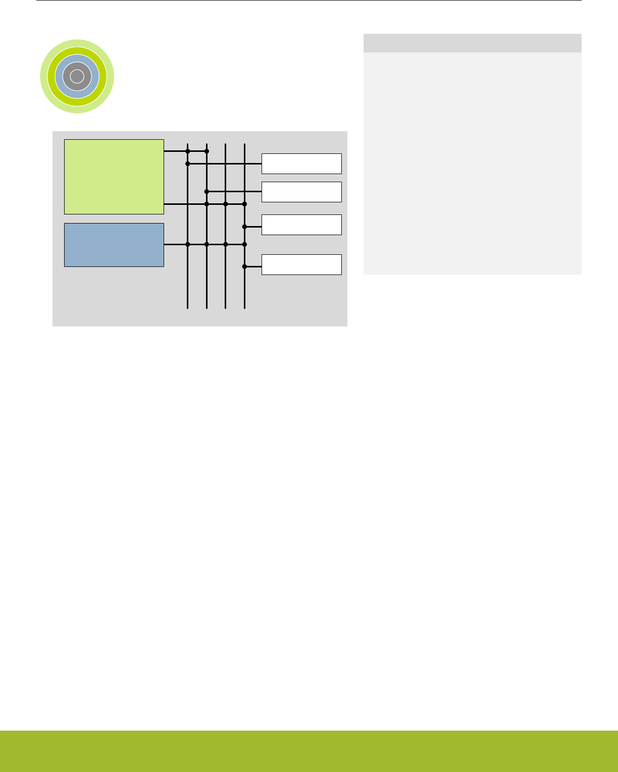
4. Memory and Bus System
0 1 2 3 4
ARM Cortex-M
DMA Controller
RAM
Peripherals
Flash
Radio
Quick Facts
What?
A low latency memory system including low energy
Flash and RAM with data retention which makes the
energy modes attractive.
Why?
RAM retention reduces the need for storing data in
Flash and enables frequent use of the ultra low en-
ergy modes EM2 Deep Sleep and EM3 Stop.
How?
Low energy and non-volatile Flash memory stores
program and application data in all energy modes
and can easily be reprogrammed in system. Low
leakage RAM with data retention in EM0 Active to
EM3 Stop removes the data restore time penalty,
and the DMA ensures fast autonomous transfers
with predictable response time.
Reference Manual
Memory and Bus System
silabs.com | Smart. Connected. Energy-friendly. Preliminary Rev. 0.5 | 19
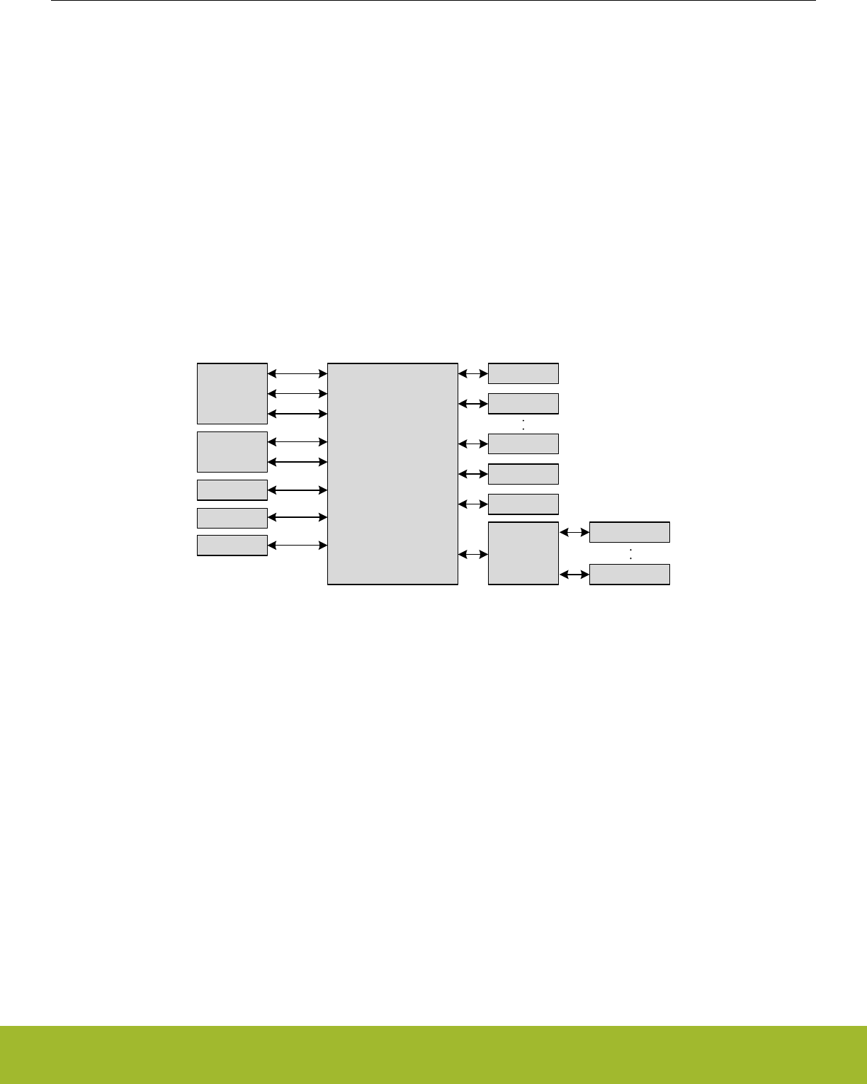
4.1 Introduction
The EFR32xG13 Wireless Gecko contains an AMBA AHB Bus system to allow bus masters to access the memory mapped address
space. A multilayer AHB bus matrix connects the 5 master bus interfaces to the AHB slaves (Figure 4.1 EFR32xG13 Wireless Gecko
Bus System on page 20). The bus matrix allows several AHB slaves to be accessed simultaneously. An AMBA APB interface is used
for the peripherals, which are accessed through an AHB-to-APB bridge connected to the AHB bus matrix. The 5 AHB bus masters are:
•Cortex-M4 ICode: Used for instruction fetches from Code memory (valid address range: 0x00000000 - 0x1FFFFFFF)
•Cortex-M4 DCode: Used for debug and data access to Code memory (valid address range: 0x00000000 - 0x1FFFFFFF)
•Cortex-M4 System: Used for data and debug access to system space. It can access entire memory space except Code memory
(valid address range: 0x20000000 - 0xFFFFFFFF)
•DMA: Can access the entire memory space except the internal core memory region and the DMEM code region
•Sequencer Code: Used for instruction fetches and data accesses. Instruction fetches still come from data memory. (valid address
range: 0x00000000 - 0x0FFFFFFF, 0x20000000 - 0x3FFFFFFF)
•Sequencer System: Can access entire memory space except internal core memory region and RAM code space (valid address
range: 0x00000000 - 0x0FFFFFFF, 0x20000000 - 0xDFFFFFFF)
•BUFC: Can access general purpose SRAM (valid address range: 0x20000000 - 0x20FFFFFF)
•FRC: Can access general purpose SRAM (valid address range: 0x20000000 - 0x20FFFFFF)
Cortex-M AHB Multilayer
Bus Matrix
DCode
System
ICode
DMA
Sequencer Code
System
FRC
BUFC
Flash
RAM0
AHB/APB
Bridge
CRYPTO
Peripheral n
RAMn
SEQ_RAM
Peripheral 0
Figure 4.1. EFR32xG13 Wireless Gecko Bus System
Reference Manual
Memory and Bus System
silabs.com | Smart. Connected. Energy-friendly. Preliminary Rev. 0.5 | 20
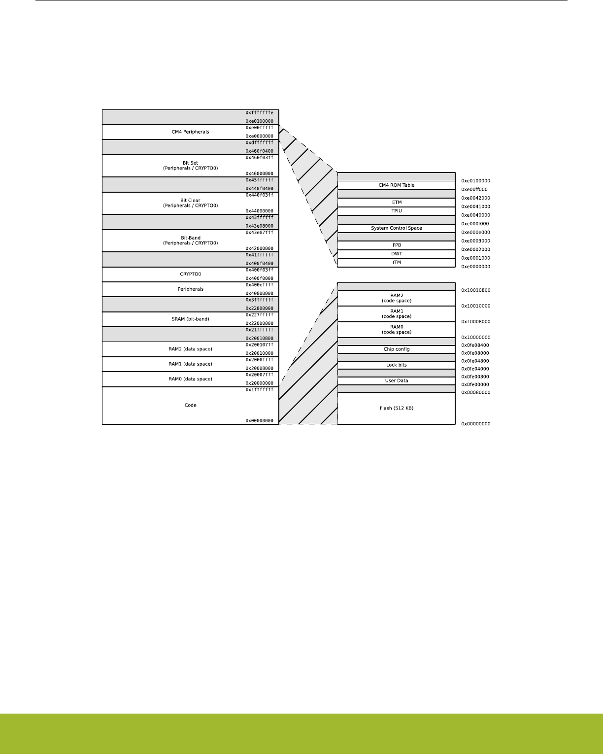
4.2 Functional Description
The memory segments are mapped together with the internal segments of the Cortex-M4 into the system memory map shown by Fig-
ure 4.2 System Address Space with Core and Code Space Listing on page 21.
Figure 4.2. System Address Space with Core and Code Space Listing
Additionally, the peripheral address map is detailed by Figure 4.3 System Address Space with Peripheral Listing on page 22.
Reference Manual
Memory and Bus System
silabs.com | Smart. Connected. Energy-friendly. Preliminary Rev. 0.5 | 21
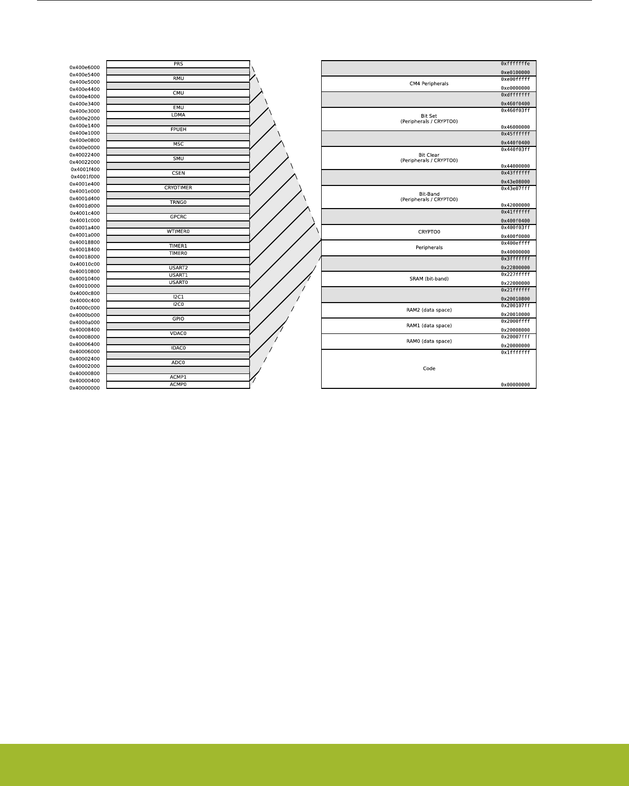
Figure 4.3. System Address Space with Peripheral Listing
The embedded SRAM is located at address 0x20000000 in the memory map of the EFR32xG13 Wireless Gecko. When running code
located in SRAM starting at this address, the Cortex-M4 uses the System bus interface to fetch instructions. This results in reduced
performance as the Cortex-M4 accesses stack, other data in SRAM and peripherals using the System bus interface. To be able to run
code from SRAM efficiently, the SRAM is also mapped in the code space at address 0x10000000.
When running code from this space, the Cortex-M4 fetches instructions through the I/D-Code bus interface, leaving the System bus
interface for data access.
The SRAM mapped into the code space can however only be accessed by the CPU and not any other bus masters, e.g. DMA. See
4.5 SRAM for more detailed info on the system SRAM.
The Sequencer RAM is used by the Sequencer for both instructions and data. This RAM is also available for general use by most AHB
masters.
Reference Manual
Memory and Bus System
silabs.com | Smart. Connected. Energy-friendly. Preliminary Rev. 0.5 | 22

4.2.1 Peripheral non-word access behavior
When writing to peripheral registers, all accesses are treated as 32-bit accesses. This means that writes to a register need to be large
enough to cover all bits of register, otherwise, any uncovered bits may become corrupted from the partial-word transfer. Thus, the safest
practice is to always do 32-bit writes to peripheral registers.
When reading, there is generally no issue with partial word accesses, however, note that any read action (e.g. FIFO popping) will be
triggered regardless of whether the actual FIFO bit-field was included in the transfer size.
Note: The implementation of bit-banding in the core is such that bit-band accesses forward the transfer size info into the actual bus
transfer size, so the same restrictions apply to bit-band accesses as apply to normal read/write accesses.
4.2.2 Bit-banding
The SRAM bit-band alias and peripheral bit-band alias regions are located at 0x22000000 and 0x42000000 respectively. Read and
write operations to these regions are converted into masked single-bit reads and atomic single-bit writes to the embedded SRAM and
peripherals of the EFR32xG13 Wireless Gecko.
Note: Bit-banding is only available through the CPU. No other AHB masters (e.g. DMA) can perform Bit-banding operations.
Using a standard approach to modify a single register or SRAM bit in the aliased regions, would require software to read the value of
the byte, half-word or word containing the bit, modify the bit, and then write the byte, half-word or word back to the register or SRAM
address. Using bit-banding, this can be done in a single operation, consuming only two bus cycles. As read-writeback, bit-masking and
bit-shift operations are not necessary in software, code size is reduced and execution speed improved.
The bit-band regions allow each bit in the SRAM and Peripheral areas of the memory map to be addressed. To set or clear a bit in the
embedded SRAM, write a 1 or a 0 to the following address:
bit_address = 0x22000000 + (address – 0x20000000) ∙ 32 + bit ∙ 4
where address is the address of the 32-bit word containing the bit to modify, and bit is the index of the bit in the 32-bit word.
To modify a bit in the Peripheral area, use the following address:
bit_address = 0x42000000 + (address – 0x40000000) ∙ 32 + bit ∙ 4
Reference Manual
Memory and Bus System
silabs.com | Smart. Connected. Energy-friendly. Preliminary Rev. 0.5 | 23

4.2.3 Peripheral Bit Set and Clear
The EFR32xG13 Wireless Gecko supports bit set and bit clear access to all peripherals except those listed in Table 4.1 Peripherals that
Do Not Support Bit Set and Bit Clear on page 24. The bit set and bit clear functionality (also called Bit Access) enables modification of
bit fields (single bit or multiple bit wide) without the need to perform a read-modify-write (though it is functionally equivalent). Also, the
operation is contained within a single bus access (for HF peripherals), unlike the Bit-banding operation described in section 4.2.2 Bit-
banding which consumes two bus accesses per operation. All AHB masters can utilize this feature.
The bit clear aliasing region starts at 0x44000000 and the bit set aliasing region starts at 0x46000000. Thus, to apply a bit set or clear
operation, write the bit set or clear mask to the following addresses:
bit_clear_address = address + 0x04000000
bit_set_address = address + 0x06000000
For bit set operations, bit locations that are 1 in the bit mask will be set in the destination register:
register = (register OR mask)
For bit clear operations, bit locations that are 1 in the bit mask will be cleared in the destination register:
register = (register AND (NOT mask))
Note: It is possible to combine bit clear and bit set operations in order to arbitrarily modify multi-bit register fields, without affecting other
fields in the same register. In this case, care should be taken to ensure that the field does not have intermediate values that can lead to
erroneous behavior. For example, if bit clear and bit set operations are used to change an analog tuning register field from 25 to 26, the
field would initially take on a value of zero. If the analog module is active at the time, this could lead to undesired behavior.
The peripherals listed in Table 4.1 Peripherals that Do Not Support Bit Set and Bit Clear on page 24 do not support Bit Access for any
registers. All other peripherals do support Bit Access, however, there may be cases of certain registers that do not support it. Such
registers have a note regarding this lack of support.
Table 4.1. Peripherals that Do Not Support Bit Set and Bit Clear
Module
EMU
RMU
CRYOTIMER
TRNG0
Reference Manual
Memory and Bus System
silabs.com | Smart. Connected. Energy-friendly. Preliminary Rev. 0.5 | 24

4.2.4 Peripherals
The peripherals are mapped into the peripheral memory segment, each with a fixed size address range according to Table 4.2 Periph-
erals on page 25, Table 4.3 Low Energy Peripherals on page 25 , and Table 4.4 Core Peripherals on page 26.
Table 4.2. Peripherals
Address Range Module Name
0x400E6000 - 0x400E6400 PRS
0x40022000 - 0x40022400 SMU
0x4001F000 - 0x4001F400 CSEN
0x4001E000 - 0x4001E400 CRYOTIMER
0x4001D000 - 0x4001D400 TRNG0
0x4001C000 - 0x4001C400 GPCRC
0x4001A000 - 0x4001A400 WTIMER0
0x40018400 - 0x40018800 TIMER1
0x40018000 - 0x40018400 TIMER0
0x40010800 - 0x40010C00 USART2
0x40010400 - 0x40010800 USART1
0x40010000 - 0x40010400 USART0
0x4000C400 - 0x4000C800 I2C1
0x4000C000 - 0x4000C400 I2C0
0x4000A000 - 0x4000B000 GPIO
0x40008000 - 0x40008400 VDAC0
0x40006000 - 0x40006400 IDAC0
0x40002000 - 0x40002400 ADC0
0x40000400 - 0x40000800 ACMP1
0x40000000 - 0x40000400 ACMP0
Table 4.3. Low Energy Peripherals
Address Range Module Name
0x40055000 - 0x40055400 LESENSE
0x40052400 - 0x40052800 WDOG1
0x40052000 - 0x40052400 WDOG0
0x4004E000 - 0x4004E400 PCNT0
0x4004A000 - 0x4004A400 LEUART0
0x40046000 - 0x40046400 LETIMER0
0x40042000 - 0x40042400 RTCC
Reference Manual
Memory and Bus System
silabs.com | Smart. Connected. Energy-friendly. Preliminary Rev. 0.5 | 25

Table 4.4. Core Peripherals
Address Range Module Name
0xE0041000 - 0xE0081000 ETM
0xE0000000 - 0xE0040000 CM4
0x400F0400 - 0x400F0800 CRYPTO1
0x400F0000 - 0x400F0400 CRYPTO0
0x400E2000 - 0x400E3000 LDMA
0x400E1000 - 0x400E1400 FPUEH
0x400E0000 - 0x400E0800 MSC
4.2.5 Bus Matrix
The Bus Matrix connects the memory segments to the bus masters as detailed in 4.1 Introduction.
4.2.5.1 Arbitration
The Bus Matrix uses a round-robin arbitration algorithm which enables high throughput and low latency, while starvation of simultane-
ous accesses to the same bus slave are eliminated. Round-robin does not assign a fixed priority to each bus master. The arbiter does
not insert any bus wait-states during peak interaction. However, one wait state is inserted for master accesses occurring after a pro-
longed inactive time. This wait state allows for increased power efficiency during master idle time.
4.2.5.2 Peripheral access Performance
The Bus Matrix is a multi-layer energy optimized AMBA AHB compliant bus with an internal bandwidth of 5x a single AHB interface.
The Cortex-M4, DMA Controller, and peripherals (not peripherals in the low frequency clock domain) run on clocks which can be pre-
scaled separately. Clocks and prescaling are described in more detail in 12. CMU - Clock Management Unit . This section describes the
expected bus wait states for a peripheral based on its frequency relative to the HFCLK frequency. For this discussion, PERCLK refers
to a selected peripheral's clock frequency, which is some integer division of the HFCLK frequency.
Another factor that effects the cycle latency of peripheral accesses is the Peripheral Access Wait Mode (WAITMODE in MSC_CTRL)
configuration, which is present in some parts in the EFR32 series. For instance, when set to WS0, a higher throughput (in terms of
HFCLK cycles) is possible than with a higher wait state setting. However, this family of parts does not have configurable wait states.
Instead, refer to the access performance information for WS0 for this device family.
Reference Manual
Memory and Bus System
silabs.com | Smart. Connected. Energy-friendly. Preliminary Rev. 0.5 | 26

4.2.5.2.1 WS0 mode
In general, when accessing a peripheral, the latency in number of HFCLK cycles, not including master arbitration, is given by:
Nbus cycles = Nslave cycles ∙ fHFCLK/fPERCLK, best-case write accesses
Nbus cycles = Nslave cycles ∙ fHFCLK/fPERCLK + 1, best-case read accesses
Nbus cycles = (Nslave cycles + 1) ∙ fHFCLK/fPERCLK - 1, worst-case write accesses
Nbus cycles = (Nslave cycles + 1) ∙ fHFCLK/fPERCLK, worst-case read accesses
where Nslave cycles is the throughput of the slave's bus interface in number of PERCLK cycles per transfer, including any wait cycles
introduced by the slave.
Figure 4.4. Bus Access Latency (General Case)
Note that a latency of 1 cycle corresponds to 0 wait states.
Additionally, for back-to-back accesses to the same peripheral, the throughput in number of cycles per transfer is given by:
Nbus cycles = Nslave cycles ∙ fHFCLK/fPERCLK, write accesses
Nbus cycles = (Nslave cycles + 1) ∙ fHFCLK/fPERCLK, read accesses
Figure 4.5. Bus Access Throughput (Back-to-Back Transfers)
Lastly, in the highest performing case, where PERCLK equals HFCLK and the slave does not introduce any additional wait states, the
access latency in number of cycles is given by:
Nbus cycles = 1, write accesses
Nbus cycles = 2, read accesses
Figure 4.6. Bus Access Latency (Max Performance)
Reference Manual
Memory and Bus System
silabs.com | Smart. Connected. Energy-friendly. Preliminary Rev. 0.5 | 27

4.2.5.2.2 WS1 mode
In general, when accessing a peripheral, the latency in number of HFCLK cycles, not including master arbitration, is given by:
Nbus cycles = Nslave cycles ∙ fHFCLK/fPERCLK + 2, best-case write accesses
Nbus cycles = Nslave cycles ∙ fHFCLK/fPERCLK + 1, best-case read accesses
Nbus cycles = (Nslave cycles + 1) ∙ fHFCLK/fPERCLK + 1, worst-case write accesses
Nbus cycles = (Nslave cycles + 1) ∙ fHFCLK/fPERCLK, worst-case read accesses
where Nslave cycles is the throughput of the slave's bus interface in number of PERCLK cycles per transfer, including any wait cycles
introduced by the slave.
Figure 4.7. Bus Access Latency (General Case)
Note that a latency of 1 cycle corresponds to 0 wait states.
Additionally, for back-to-back accesses to the same peripheral, the throughput in number of cycles per transfer is given by:
Nbus cycles = max{fHFCLK/fPERCLK, 2} + Nslave cycles ∙ fHFCLK/fPERCLK, write accesses
Nbus cycles = (Nslave cycles + 1) ∙ fHFCLK/fPERCLK, read accesses
Figure 4.8. Bus Access Throughput (Back-to-Back Transfers)
Lastly, in the highest performing case, where PERCLK equals HFCLK and the slave does not introduce any additional wait states, the
access latency in number of cycles is given by:
Nbus cycles = 3, write accesses
Nbus cycles = 2, read accesses
Figure 4.9. Bus Access Latency (Max Performance)
4.2.5.2.3 Core Access Latency
Note that the cycle counts in the equations above is in terms of the HFCLK. When the core is prescaled from the bus clock, the core will
see a reduced number of latency cycles given by:
Ncore cycles = ceiling( Nbus cycles ∙ fHFCORECLK/fHFCLK )
where master arbitration is not included.
Figure 4.10. Core Access Latency
Reference Manual
Memory and Bus System
silabs.com | Smart. Connected. Energy-friendly. Preliminary Rev. 0.5 | 28
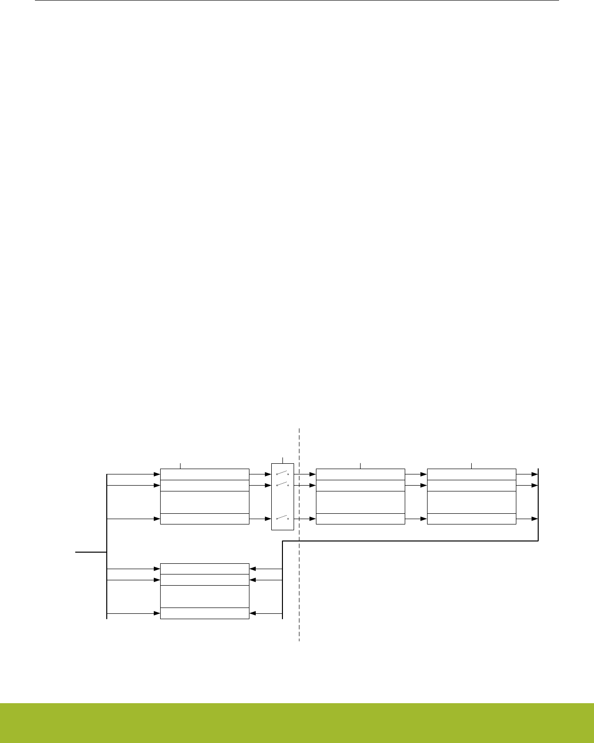
4.2.5.3 Bus Faults
System accesses from the core can receive a bus fault in the following condition(s):
• The core attempts to access an address that is not assigned to any peripheral or other system device. These faults can be enabled
or disabled by setting the ADDRFAULTEN bit appropriately in MSC_CTRL.
• The core attempts to access a peripheral or system device that has its clock disabled. These faults can be enabled or disabled by
setting the CLKDISFAULTEN bit appropriately in MSC_CTRL.
• The bus times out during an access. For example, this could happen while trying to synchronize volatile read data during an LE
peripheral access. See 12.3.1.1 HFCLK - High Frequency Clock. These faults can be enabled or disabled by setting the TIMEOUT-
FAULTEN bit appropriately in MSC_CTRL.
In addition to any condition-specific bus fault control bits, the bus fault interrupt itself can be enabled or disabled in the same way as all
other internal core interrupts.
4.3 Access to Low Energy Peripherals (Asynchronous Registers)
The Low Energy Peripherals are capable of running when the high frequency oscillator and core system is powered off, i.e. in energy
mode EM2 Deep Sleep and in some cases also EM3 Stop. This enables the peripherals to perform tasks while the system energy con-
sumption is minimal.
The Low Energy Peripherals are listed in Table 4.3 Low Energy Peripherals on page 25.
All Low Energy Peripherals are memory mapped, with automatic data synchronization. Because the Low Energy Peripherals are run-
ning on clocks asynchronous to the high frequency system clock, there are some constraints on how register accesses are performed,
as described in the following sections.
4.3.1 Writing
Every Low Energy Peripheral has one or more registers with data that needs to be synchronized into the Low Energy clock domain to
maintain data consistency and predictable operation. There are two different synchronization mechanisms on the EFR32, immediate
synchronization, and delayed synchronization. Immediate synchronization is available for the RTCC, LESENSE and LETIMER, and re-
sults in an immediate update of the target registers. Delayed synchronization is used for the remaining Low Energy Peripherals, and for
these peripherals, a write operation requires 3 positive edges of the clock on the Low Energy Peripheral being accessed. Registers
requiring synchronization are marked "Async Reg" in their description header.
Note: On the Gecko series of devices, all LE peripherals are subject to delayed synchronization.
Register 0
Register 1
.
.
.
Register n
Synchronizer 0
Synchronizer 1
.
.
.
Synchronizer n
Register 0 Sync
Register 1 Sync
.
.
.
Register n Sync
Write request [0:n]
Syncbusy Register 0
Syncbusy Register 1
.
.
.
Syncbusy Register n
Set 0
Set 1
Set n
Freeze
Synchronization Done
Clear 0
Clear 1
Clear n
High Frequency Clock Low Frequency Clock Low Frequency Clock
High Frequency Clock Domain Low Frequency Clock Domain
Write request 0
Write request 1
Write request n
Figure 4.11. Write operation to Low Energy Peripherals
Reference Manual
Memory and Bus System
silabs.com | Smart. Connected. Energy-friendly. Preliminary Rev. 0.5 | 29
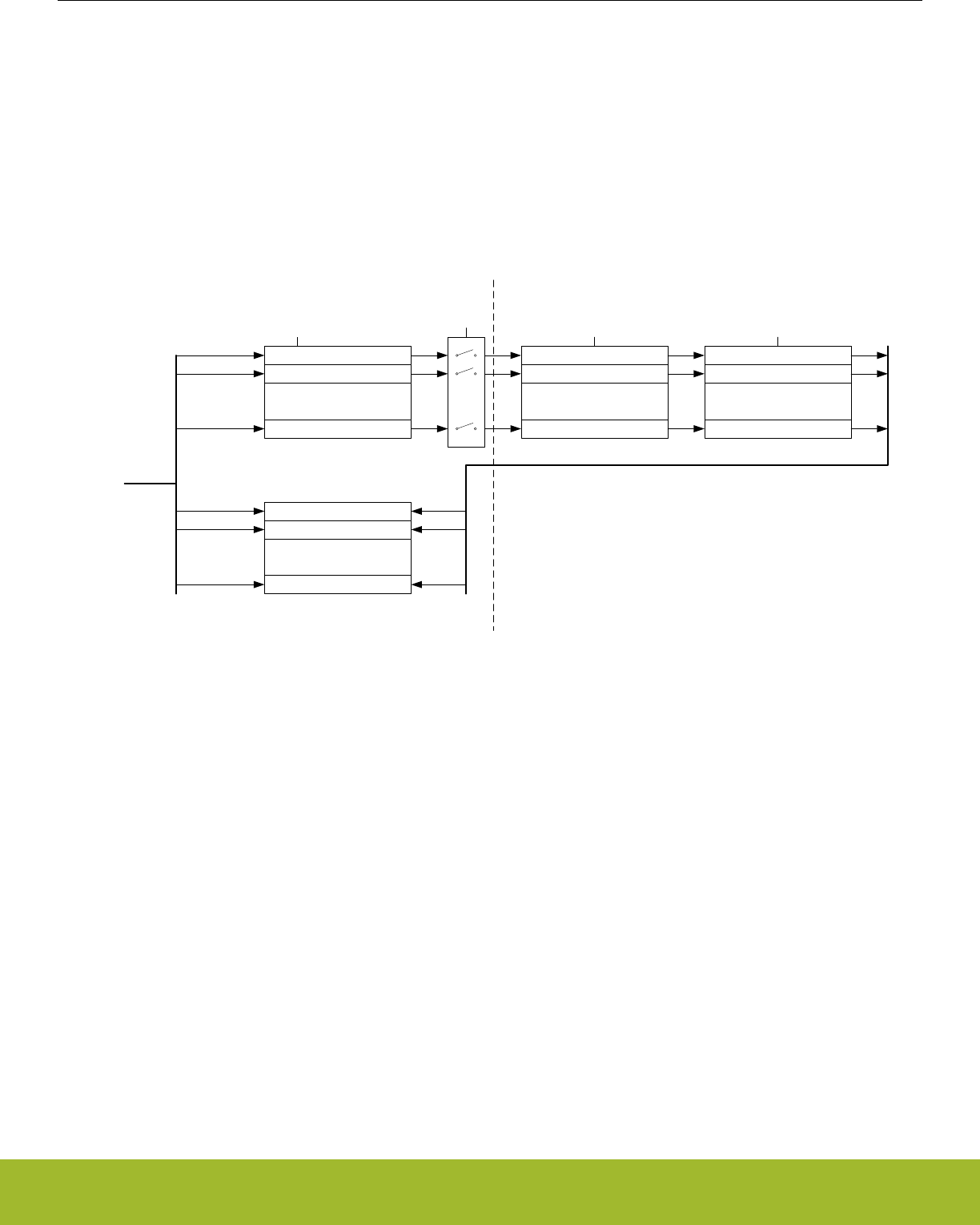
4.3.1.1 Delayed Synchronization
After writing data to a register which value is to be synchronized into the Low Energy Peripheral using delayed synchronization, a corre-
sponding busy flag in the <module_name>_SYNCBUSY register (e.g. LETIMER_SYNCBUSY) is set. This flag is set as long as syn-
chronization is in progress and is cleared upon completion.
Note: Subsequent writes to the same register before the corresponding busy flag is cleared is not supported. Write before the busy flag
is cleared may result in undefined behavior. In general the SYNCBUSY register only needs to be observed if there is a risk of multiple
write access to a register (which must be prevented). It is not required to wait until the relevant flag in the SYNCBUSY register is
cleared after writing a register. E.g., EM2 Deep Sleep can be entered directly after writing a register.
See Figure 4.12 Write operation to Low Energy Peripherals on page 30 for an overview of the writing mechanism operation.
Register 0
Register 1
.
.
.
Register n
Synchronizer 0
Synchronizer 1
.
.
.
Synchronizer n
Register 0 Sync
Register 1 Sync
.
.
.
Register n Sync
Write request [0:n]
Syncbusy Register 0
Syncbusy Register 1
.
.
.
Syncbusy Register n
Set 0
Set 1
Set n
Freeze
Synchronization Done
Clear 0
Clear 1
Clear n
High Frequency Clock Low Frequency Clock Low Frequency Clock
High Frequency Clock Domain Low Frequency Clock Domain
Write request 0
Write request 1
Write request n
Figure 4.12. Write operation to Low Energy Peripherals
4.3.1.2 Immediate Synchronization
In contrast to the peripherals with delayed synchronization, peripherals with immediate synchronization do not experience a delay from
a value is written to it takes effect in the peripheral. They are updated immediately on the peripheral write access. If such a write is done
close to an edge on the clock of the peripheral, the write is delayed to after the clock edge. This will introduce wait-states on the periph-
eral access.
Peripherals with immediate synchronization each have a SYNCBUSY register. Commands written to a peripheral with immediate syn-
chronization are not executed before the first peripheral clock after the write. In this period, the SYNCBUSY flag for the command regis-
ter is set, indicating that the command has not yet been performed. Secondly, to maintain compatibility with the Gecko series, the rest
of the SYNCBUSY registers are also present, but these are always 0, indicating that register writes are always safe.
Note: If compatibility with the Gecko series is a requirement for a given application, the rules that apply to delayed synchronization with
respect to SYNCBUSY should also be followed for the peripherals that support immediate synchronization.
Reference Manual
Memory and Bus System
silabs.com | Smart. Connected. Energy-friendly. Preliminary Rev. 0.5 | 30
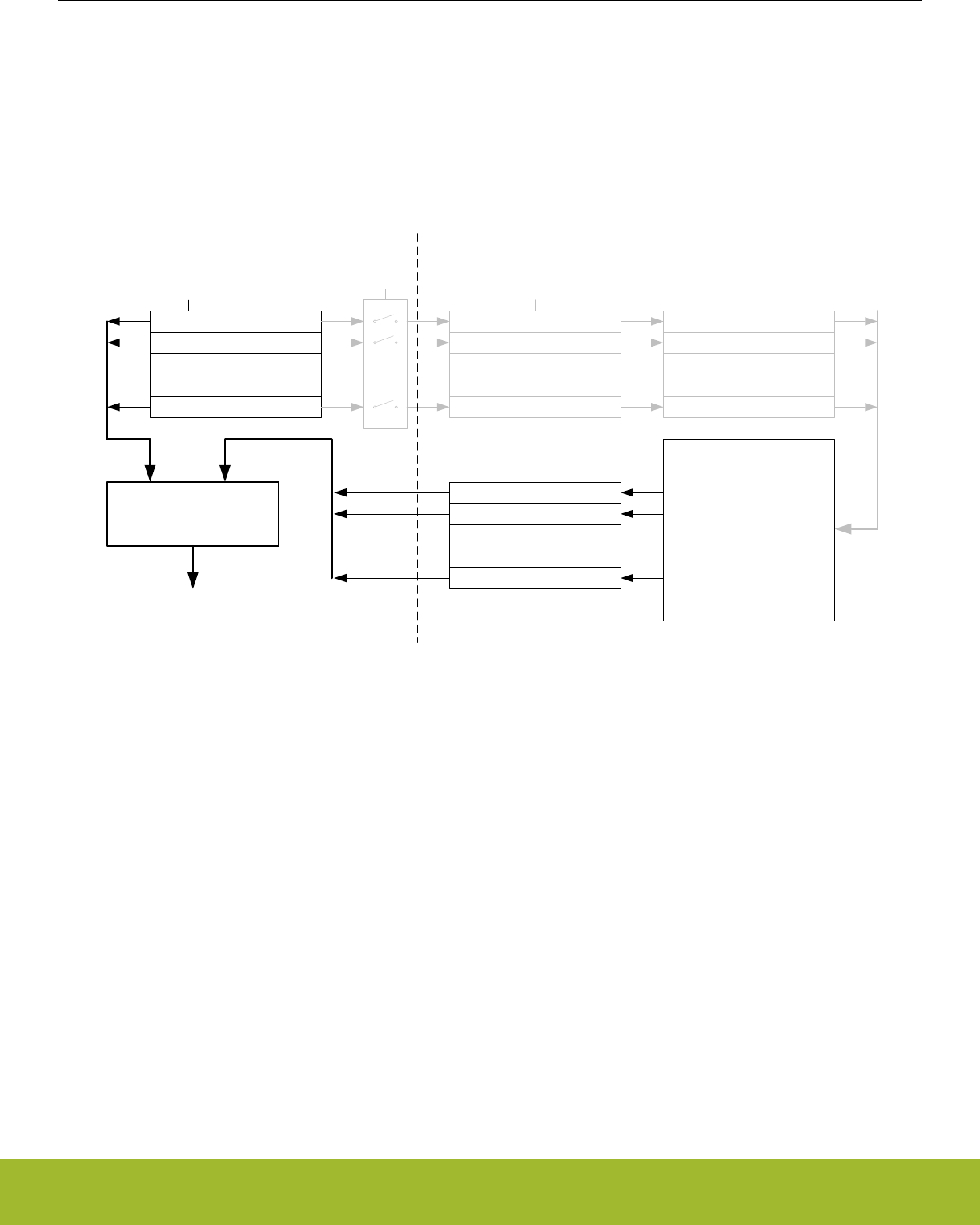
4.3.2 Reading
When reading from a Low Energy Peripheral, the data read is synchronized regardless if it originates in the Low Energy clock domain
or High Frequency clock domain. See Figure 4.13 Read operation from Low Energy Peripherals on page 31 for an overview of the
reading operation.
Note: Writing a register and then immediately reading the new value of the register may give the impression that the write operation is
complete. This may not be the case. Please refer to the SYNCBUSY register for correct status of the write operation to the Low Energy
Peripheral.
Register 0
Register 1
.
.
.
Register n
Synchronizer 0
Synchronizer 1
.
.
.
Synchronizer n
Register 0 Sync
Register 1 Sync
.
.
.
Register n Sync
Freeze
High Frequency Clock Low Frequency Clock Low Frequency Clock
High Frequency Clock Domain Low Frequency Clock Domain
Low Energy
Peripheral
Main
Function
HW Status Register 0
HW Status Register 1
.
.
.
HW Status Register m
Read
Synchronizer
Read Data
Figure 4.13. Read operation from Low Energy Peripherals
4.3.3 FREEZE Register
In all Low Energy Peripheral with delayed synchronization there is a <module_name>_FREEZE register (e.g. RTCC_FREEZE). The
register contains a bit named REGFREEZE. If precise control of the synchronization process is required, this bit may be utilized. When
REGFREEZE is set, the synchronization process is halted allowing the software to write multiple Low Energy registers before starting
the synchronization process, thus providing precise control of the module update process. The synchronization process is started by
clearing the REGFREEZE bit.
Note: The FREEZE register is also present on peripherals with immediate synchronization, but there it has no effect
4.4 Flash
The Flash retains data in any state and typically stores the application code, special user data and security information. The Flash
memory is typically programmed through the debug interface, but can also be erased and written to from software.
• Up to 512 KB of memory
• Page size of 2 KB (minimum erase unit)
• Minimum 10K erase cycles endurance
• Greater than 10 years data retention at 85°C
• Lock-bits for memory protection
• Data retention in any state
Reference Manual
Memory and Bus System
silabs.com | Smart. Connected. Energy-friendly. Preliminary Rev. 0.5 | 31

4.5 SRAM
The primary task of the SRAM memory is to store application data. Additionally, it is possible to execute instructions from SRAM, and
the DMA may be set up to transfer data between the SRAM, Flash and peripherals.
• Up to 64 KB of memory
• Bit-band access support
• Set of RAM blocks may be powered down when not in use
• Data retention of the entire memory in EM0 Active to EM3 Stop
Note: The individual RAM sections may be smaller on some parts, however, the RAM AHB slaves maintain a contiguous address map.
For example, if RAM0 is half-size on a part, then RAM1 is relocated to begin immediately after RAM0's last address. Using the provided
software header files and linker scripts allows handling of this remapping in an autonomous manner.
Reference Manual
Memory and Bus System
silabs.com | Smart. Connected. Energy-friendly. Preliminary Rev. 0.5 | 32

4.6 DI Page Entry Map
The DI page contains production calibration data as well as device identification information. See the peripheral chapters for how each
calibration value is to be used with the associated peripheral.
The offset address is relative to the start address of the DI page.(see 8.3 Functional Description)
Offset Name Type Description
0x000 CAL RO CRC of DI-page and calibration temperature
0x020 EXTINFO RO External Component description
0x028 EUI48L RO EUI48 OUI and Unique identifier
0x02C EUI48H RO OUI
0x030 CUSTOMINFO RO Custom information
0x034 MEMINFO RO Flash page size and misc. chip information
0x040 UNIQUEL RO Low 32 bits of device unique number
0x044 UNIQUEH RO High 32 bits of device unique number
0x048 MSIZE RO Flash and SRAM Memory size in kB
0x04C PART RO Part description
0x050 DEVINFOREV RO Device information page revision
0x054 EMUTEMP RO EMU Temperature Calibration Information
0x060 ADC0CAL0 RO ADC0 calibration register 0
0x064 ADC0CAL1 RO ADC0 calibration register 1
0x068 ADC0CAL2 RO ADC0 calibration register 2
0x06C ADC0CAL3 RO ADC0 calibration register 3
0x080 HFRCOCAL0 RO HFRCO Calibration Register (4 MHz)
0x08C HFRCOCAL3 RO HFRCO Calibration Register (7 MHz)
0x098 HFRCOCAL6 RO HFRCO Calibration Register (13 MHz)
0x09C HFRCOCAL7 RO HFRCO Calibration Register (16 MHz)
0x0A0 HFRCOCAL8 RO HFRCO Calibration Register (19 MHz)
0x0A8 HFRCOCAL10 RO HFRCO Calibration Register (26 MHz)
0x0AC HFRCOCAL11 RO HFRCO Calibration Register (32 MHz)
0x0B0 HFRCOCAL12 RO HFRCO Calibration Register (38 MHz)
0x0E0 AUXHFRCOCAL0 RO AUXHFRCO Calibration Register (4 MHz)
0x0EC AUXHFRCOCAL3 RO AUXHFRCO Calibration Register (7 MHz)
0x0F8 AUXHFRCOCAL6 RO AUXHFRCO Calibration Register (13 MHz)
0x0FC AUXHFRCOCAL7 RO AUXHFRCO Calibration Register (16 MHz)
0x100 AUXHFRCOCAL8 RO AUXHFRCO Calibration Register (19 MHz)
0x108 AUXHFRCOCAL10 RO AUXHFRCO Calibration Register (26 MHz)
0x10C AUXHFRCOCAL11 RO AUXHFRCO Calibration Register (32 MHz)
0x110 AUXHFRCOCAL12 RO AUXHFRCO Calibration Register (38 MHz)
0x140 VMONCAL0 RO VMON Calibration Register 0
Reference Manual
Memory and Bus System
silabs.com | Smart. Connected. Energy-friendly. Preliminary Rev. 0.5 | 33

Offset Name Type Description
0x144 VMONCAL1 RO VMON Calibration Register 1
0x148 VMONCAL2 RO VMON Calibration Register 2
0x158 IDAC0CAL0 RO IDAC0 Calibration Register 0
0x15C IDAC0CAL1 RO IDAC0 Calibration Register 1
0x168 DCDCLNVCTRL0 RO DCDC Low-noise VREF Trim Register 0
0x16C DCDCLPVCTRL0 RO DCDC Low-power VREF Trim Register 0
0x170 DCDCLPVCTRL1 RO DCDC Low-power VREF Trim Register 1
0x174 DCDCLPVCTRL2 RO DCDC Low-power VREF Trim Register 2
0x178 DCDCLPVCTRL3 RO DCDC Low-power VREF Trim Register 3
0x17C DCDCLPCMPHYSSEL0 RO DCDC LPCMPHYSSEL Trim Register 0
0x180 DCDCLPCMPHYSSEL1 RO DCDC LPCMPHYSSEL Trim Register 1
0x184 VDAC0MAINCAL RO VDAC0 Cals for Main Path
0x188 VDAC0ALTCAL RO VDAC0 Cals for Alternate Path
0x18C VDAC0CH1CAL RO VDAC0 CH1 Error Cal
0x190 OPA0CAL0 RO OPA0 Calibration Register for DRIVESTRENGTH 0, INCBW=1
0x194 OPA0CAL1 RO OPA0 Calibration Register for DRIVESTRENGTH 1, INCBW=1
0x198 OPA0CAL2 RO OPA0 Calibration Register for DRIVESTRENGTH 2, INCBW=1
0x19C OPA0CAL3 RO OPA0 Calibration Register for DRIVESTRENGTH 3, INCBW=1
0x1A0 OPA1CAL0 RO OPA1 Calibration Register for DRIVESTRENGTH 0, INCBW=1
0x1A4 OPA1CAL1 RO OPA1 Calibration Register for DRIVESTRENGTH 1, INCBW=1
0x1A8 OPA1CAL2 RO OPA1 Calibration Register for DRIVESTRENGTH 2, INCBW=1
0x1AC OPA1CAL3 RO OPA1 Calibration Register for DRIVESTRENGTH 3, INCBW=1
0x1B0 OPA2CAL0 RO OPA2 Calibration Register for DRIVESTRENGTH 0, INCBW=1
0x1B4 OPA2CAL1 RO OPA2 Calibration Register for DRIVESTRENGTH 1, INCBW=1
0x1B8 OPA2CAL2 RO OPA2 Calibration Register for DRIVESTRENGTH 2, INCBW=1
0x1BC OPA2CAL3 RO OPA2 Calibration Register for DRIVESTRENGTH 3, INCBW=1
0x1C0 CSENGAINCAL RO Cap Sense Gain Adjustment
0x1D0 OPA0CAL4 RO OPA0 Calibration Register for DRIVESTRENGTH 0, INCBW=0
0x1D4 OPA0CAL5 RO OPA0 Calibration Register for DRIVESTRENGTH 1, INCBW=0
0x1D8 OPA0CAL6 RO OPA0 Calibration Register for DRIVESTRENGTH 2, INCBW=0
0x1DC OPA0CAL7 RO OPA0 Calibration Register for DRIVESTRENGTH 3, INCBW=0
0x1E0 OPA1CAL4 RO OPA1 Calibration Register for DRIVESTRENGTH 0, INCBW=0
0x1E4 OPA1CAL5 RO OPA1 Calibration Register for DRIVESTRENGTH 1, INCBW=0
0x1E8 OPA1CAL6 RO OPA1 Calibration Register for DRIVESTRENGTH 2, INCBW=0
0x1EC OPA1CAL7 RO OPA1 Calibration Register for DRIVESTRENGTH 3, INCBW=0
0x1F0 OPA2CAL4 RO OPA2 Calibration Register for DRIVESTRENGTH 0, INCBW=0
0x1F4 OPA2CAL5 RO OPA2 Calibration Register for DRIVESTRENGTH 1, INCBW=0
Reference Manual
Memory and Bus System
silabs.com | Smart. Connected. Energy-friendly. Preliminary Rev. 0.5 | 34

Offset Name Type Description
0x1F8 OPA2CAL6 RO OPA2 Calibration Register for DRIVESTRENGTH 2, INCBW=0
0x1FC OPA2CAL7 RO OPA2 Calibration Register for DRIVESTRENGTH 3, INCBW=0
4.7 DI Page Entry Description
4.7.1 CAL - CRC of DI-page and calibration temperature
Offset Bit Position
0x000
31
30
29
28
27
26
25
24
23
22
21
20
19
18
17
16
15
14
13
12
11
10
9
8
7
6
5
4
3
2
1
0
Access
RO
RO
Name
TEMP
CRC
Bit Name Access Description
31:24 Reserved Reserved for future use
23:16 TEMP RO Calibration temperature as an usigned int in DegC
(25 = 25DegC)
15:0 CRC RO CRC of DI-page (CRC-16-CCITT)
Reference Manual
Memory and Bus System
silabs.com | Smart. Connected. Energy-friendly. Preliminary Rev. 0.5 | 35

4.7.2 EXTINFO - External Component description
Offset Bit Position
0x020
31
30
29
28
27
26
25
24
23
22
21
20
19
18
17
16
15
14
13
12
11
10
9
8
7
6
5
4
3
2
1
0
Access
RO
RO
RO
Name
REV
CONNECTION
TYPE
Bit Name Access Description
31:24 Reserved Reserved for future use
23:16 REV RO MCM Revision
Value Mode Description
1 REV1 Revision 1
255 NONE No external component present
15:8 CONNECTION RO Connection protocal to external interface
Value Mode Description
1 SPI SPI control interface
255 NONE None
7:0 TYPE RO
External Component
Value Mode Description
1 IS25LQ040B IS25LQ040B-JWLE1 512kB Serial Flash
2 AT25S041 AT25S041-DWFHT 512kB Serial Flash
255 NONE None
Reference Manual
Memory and Bus System
silabs.com | Smart. Connected. Energy-friendly. Preliminary Rev. 0.5 | 36

4.7.3 EUI48L - EUI48 OUI and Unique identifier
Offset Bit Position
0x028
31
30
29
28
27
26
25
24
23
22
21
20
19
18
17
16
15
14
13
12
11
10
9
8
7
6
5
4
3
2
1
0
Access
RO
RO
Name
OUI48L
UNIQUEID
Bit Name Access Description
31:24 OUI48L RO Lower Octet of EUI48 Organizationally Unique Identi-
fier
23:0 UNIQUEID RO Unique identifier
4.7.4 EUI48H - OUI
Offset Bit Position
0x02C
31
30
29
28
27
26
25
24
23
22
21
20
19
18
17
16
15
14
13
12
11
10
9
8
7
6
5
4
3
2
1
0
Access
RO
Name
OUI48H
Bit Name Access Description
31:16 Reserved Reserved for future use
15:0 OUI48H RO Upper two Octets of EUI48 Organizationally Unique
Identifier
4.7.5 CUSTOMINFO - Custom information
Offset Bit Position
0x030
31
30
29
28
27
26
25
24
23
22
21
20
19
18
17
16
15
14
13
12
11
10
9
8
7
6
5
4
3
2
1
0
Access
RO
Name
PARTNO
Bit Name Access Description
31:16 PARTNO RO Custom part identifier as unsigned integer (e.g. 903)
65535 for standard product
15:0 Reserved Reserved for future use
Reference Manual
Memory and Bus System
silabs.com | Smart. Connected. Energy-friendly. Preliminary Rev. 0.5 | 37

4.7.6 MEMINFO - Flash page size and misc. chip information
Offset Bit Position
0x034
31
30
29
28
27
26
25
24
23
22
21
20
19
18
17
16
15
14
13
12
11
10
9
8
7
6
5
4
3
2
1
0
Access
RO
RO
RO
RO
Name
FLASH_PAGE_SIZE
PINCOUNT
PKGTYPE
TEMPGRADE
Bit Name Access Description
31:24 FLASH_PAGE_SIZE RO Flash page size in bytes coded as 2 ^ ((MEM_IN-
FO_PAGE_SIZE + 10) & 0xFF). Ie. the value 0xFF
= 512 bytes.
23:16 PINCOUNT RO Device pin count as unsigned integer (eg. 48)
15:8 PKGTYPE RO Package Identifier as character
Value Mode Description
74 WLCSP WLCSP package
76 BGA BGA package
77 QFN QFN package
81 QFP QFP package
7:0 TEMPGRADE RO Temperature Grade of product as unsigned inte-
ger enumeration
Value Mode Description
0 N40TO85 -40 to 85degC
1 N40TO125 -40 to 125degC
2 N40TO105 -40 to 105degC
3 N0TO70 0 to 70degC
Reference Manual
Memory and Bus System
silabs.com | Smart. Connected. Energy-friendly. Preliminary Rev. 0.5 | 38

4.7.7 UNIQUEL - Low 32 bits of device unique number
Offset Bit Position
0x040
31
30
29
28
27
26
25
24
23
22
21
20
19
18
17
16
15
14
13
12
11
10
9
8
7
6
5
4
3
2
1
0
Access
RO
Name
UNIQUEL
Bit Name Access Description
31:0 UNIQUEL RO Low 32 bits of device unique number
4.7.8 UNIQUEH - High 32 bits of device unique number
Offset Bit Position
0x044
31
30
29
28
27
26
25
24
23
22
21
20
19
18
17
16
15
14
13
12
11
10
9
8
7
6
5
4
3
2
1
0
Access
RO
Name
UNIQUEH
Bit Name Access Description
31:0 UNIQUEH RO High 32 bits of device unique number
4.7.9 MSIZE - Flash and SRAM Memory size in kB
Offset Bit Position
0x048
31
30
29
28
27
26
25
24
23
22
21
20
19
18
17
16
15
14
13
12
11
10
9
8
7
6
5
4
3
2
1
0
Access
RO
RO
Name
SRAM
FLASH
Bit Name Access Description
31:16 SRAM RO Ram size, kbyte count as unsigned integer (eg. 16)
15:0 FLASH RO Flash size, kbyte count as unsigned integer (eg. 128)
Reference Manual
Memory and Bus System
silabs.com | Smart. Connected. Energy-friendly. Preliminary Rev. 0.5 | 39

4.7.10 PART - Part description
Offset Bit Position
0x04C
31
30
29
28
27
26
25
24
23
22
21
20
19
18
17
16
15
14
13
12
11
10
9
8
7
6
5
4
3
2
1
0
Access
RO
RO
RO
Name
PROD_REV
DEVICE_FAMILY
DEVICE_NUMBER
Bit Name Access Description
31:24 PROD_REV RO Production revision as unsigned integer
23:16 DEVICE_FAMILY RO Device Family
Value Mode Description
16 EFR32MG1P EFR32 Mighty Gecko Family Series 1 Device Config
1
17 EFR32MG1B EFR32 Mighty Gecko Family Series 1 Device Config
1
18 EFR32MG1V EFR32 Mighty Gecko Family Series 1 Device Config
1
19 EFR32BG1P EFR32 Blue Gecko Family Series 1 Device Config 1
20 EFR32BG1B EFR32 Blue Gecko Family Series 1 Device Config 1
21 EFR32BG1V EFR32 Blue Gecko Family Series 1 Device Config 1
25 EFR32FG1P EFR32 Flex Gecko Family Series 1 Device Config 1
26 EFR32FG1B EFR32 Flex Gecko Family Series 1 Device Config 1
27 EFR32FG1V EFR32 Flex Gecko Family Series 1 Device Config 1
28 EFR32MG12P EFR32 Mighty Gecko Family Series 1 Device Config
2
29 EFR32MG12B EFR32 Mighty Gecko Family Series 1 Device Config
2
30 EFR32MG12V EFR32 Mighty Gecko Family Series 1 Device Config
2
31 EFR32BG12P EFR32 Blue Gecko Family Series 1 Device Config 2
32 EFR32BG12B EFR32 Blue Gecko Family Series 1 Device Config 2
33 EFR32BG12V EFR32 Blue Gecko Family Series 1 Device Config 2
37 EFR32FG12P EFR32 Flex Gecko Family Series 1 Device Config 2
38 EFR32FG12B EFR32 Flex Gecko Family Series 1 Device Config 2
39 EFR32FG12V EFR32 Flex Gecko Family Series 1 Device Config 2
40 EFR32MG13P EFR32 Mighty Gecko Family Series 1 Device Config
3
Reference Manual
Memory and Bus System
silabs.com | Smart. Connected. Energy-friendly. Preliminary Rev. 0.5 | 40

Bit Name Access Description
41 EFR32MG13B EFR32 Mighty Gecko Family Series 1 Device Config
3
42 EFR32MG13V EFR32 Mighty Gecko Family Series 1 Device Config
3
43 EFR32BG13P EFR32 Blue Gecko Family Series 1 Device Config 3
44 EFR32BG13B EFR32 Blue Gecko Family Series 1 Device Config 3
45 EFR32BG13V EFR32 Blue Gecko Family Series 1 Device Config 3
49 EFR32FG13P EFR32 Flex Gecko Family Series 1 Device Config 3
50 EFR32FG13B EFR32 Flex Gecko Family Series 1 Device Config 3
51 EFR32FG13V EFR32 Flex Gecko Family Series 1 Device Config 3
52 EFR32MG14P EFR32 Mighty Gecko Family Series 1 Device Config
4
53 EFR32MG14B EFR32 Mighty Gecko Family Series 1 Device Config
4
54 EFR32MG14V EFR32 Mighty Gecko Family Series 1 Device Config
4
55 EFR32BG14P EFR32 Blue Gecko Family Series 1 Device Config 4
56 EFR32BG14B EFR32 Blue Gecko Family Series 1 Device Config 4
57 EFR32BG14V EFR32 Blue Gecko Family Series 1 Device Config 4
61 EFR32FG14P EFR32 Flex Gecko Family Series 1 Device Config 4
62 EFR32FG14B EFR32 Flex Gecko Family Series 1 Device Config 4
63 EFR32FG14V EFR32 Flex Gecko Family Series 1 Device Config 4
71 EFM32G EFM32 Gecko Device Family
71 G EFM32 Gecko Device Family
72 EFM32GG EFM32 Giant Gecko Device Family
72 GG EFM32 Giant Gecko Device Family
73 TG EFM32 Tiny Gecko Device Family
73 EFM32TG EFM32 Tiny Gecko Device Family
74 EFM32LG EFM32 Leopard Gecko Device Family
74 LG EFM32 Leopard Gecko Device Family
75 EFM32WG EFM32 Wonder Gecko Device Family
75 WG EFM32 Wonder Gecko Device Family
76 ZG EFM32 Zero Gecko Device Family
76 EFM32ZG EFM32 Zero Gecko Device Family
77 HG EFM32 Happy Gecko Device Family
77 EFM32HG EFM32 Happy Gecko Device Family
81 EFM32PG1B EFM32 Pearl Gecko Family Series 1 Device Config
1
83 EFM32JG1B EFM32 Jade Gecko Family Series 1 Device Config
1
Reference Manual
Memory and Bus System
silabs.com | Smart. Connected. Energy-friendly. Preliminary Rev. 0.5 | 41

Bit Name Access Description
85 EFM32PG12B EFM32 Pearl Gecko Family Series 1 Device Config
2
87 EFM32JG12B EFM32 Jade Gecko Family Series 1 Device Config
2
89 EFM32PG13B EFM32 Pearl Gecko Family Series 1 Device Config
3
91 EFM32JG13B EFM32 Jade Gecko Family Series 1 Device Config
3
100 EFM32GG11B EFM32 Giant Gecko Family Series 1 Device Config
1
103 EFM32TG11B EFM32 Tiny Gecko Family Series 1 Device Config 1
120 EZR32LG EZR32 Leopard Gecko Device Family
121 EZR32WG EZR32 Wonder Gecko Device Family
122 EZR32HG EZR32 Happy Gecko Device Family
15:0 DEVICE_NUMBER RO Part number as unsigned integer (e.g. 233 for
EFR32BG1P233F256GM48-B0)
4.7.11 DEVINFOREV - Device information page revision
Offset Bit Position
0x050
31
30
29
28
27
26
25
24
23
22
21
20
19
18
17
16
15
14
13
12
11
10
9
8
7
6
5
4
3
2
1
0
Access
RO
Name
DEVINFOREV
Bit Name Access Description
31:8 Reserved Reserved for future use
7:0 DEVINFOREV RO DEVINFO layout revision as unsigned integer (initial-
ly 1)
Reference Manual
Memory and Bus System
silabs.com | Smart. Connected. Energy-friendly. Preliminary Rev. 0.5 | 42

4.7.12 EMUTEMP - EMU Temperature Calibration Information
Offset Bit Position
0x054
31
30
29
28
27
26
25
24
23
22
21
20
19
18
17
16
15
14
13
12
11
10
9
8
7
6
5
4
3
2
1
0
Access
RO
Name
EMUTEMPROOM
Bit Name Access Description
31:8 Reserved Reserved for future use
7:0 EMUTEMPROOM RO EMU_TEMP temperature reading at room
4.7.13 ADC0CAL0 - ADC0 calibration register 0
Offset Bit Position
0x060
31
30
29
28
27
26
25
24
23
22
21
20
19
18
17
16
15
14
13
12
11
10
9
8
7
6
5
4
3
2
1
0
Access
RO
RO
RO
RO
RO
RO
Name
GAIN2V5
NEGSEOFFSET2V5
OFFSET2V5
GAIN1V25
NEGSEOFFSET1V25
OFFSET1V25
Bit Name Access Description
31 Reserved Reserved for future use
30:24 GAIN2V5 RO Gain for 2.5V reference
23:20 NEGSEOFFSET2V5 RO Negative single ended offset for 2.5V reference
19:16 OFFSET2V5 RO Offset for 2.5V reference
15 Reserved Reserved for future use
14:8 GAIN1V25 RO Gain for 1.25V reference
7:4 NEGSEOFFSET1V25 RO Negative single ended offset for 1.25V reference
3:0 OFFSET1V25 RO Offset for 1.25V reference
Reference Manual
Memory and Bus System
silabs.com | Smart. Connected. Energy-friendly. Preliminary Rev. 0.5 | 43

4.7.14 ADC0CAL1 - ADC0 calibration register 1
Offset Bit Position
0x064
31
30
29
28
27
26
25
24
23
22
21
20
19
18
17
16
15
14
13
12
11
10
9
8
7
6
5
4
3
2
1
0
Access
RO
RO
RO
RO
RO
RO
Name
GAIN5VDIFF
NEGSEOFFSET5VDIFF
OFFSET5VDIFF
GAINVDD
NEGSEOFFSETVDD
OFFSETVDD
Bit Name Access Description
31 Reserved Reserved for future use
30:24 GAIN5VDIFF RO Gain for for 5V differential reference
23:20 NEGSEOFFSET5VDIFF RO Negative single ended offset with for 5V differential
reference
19:16 OFFSET5VDIFF RO Offset for 5V differential reference
15 Reserved Reserved for future use
14:8 GAINVDD RO Gain for VDD reference
7:4 NEGSEOFFSETVDD RO Negative single ended offset for VDD reference
3:0 OFFSETVDD RO Offset for VDD reference
Reference Manual
Memory and Bus System
silabs.com | Smart. Connected. Energy-friendly. Preliminary Rev. 0.5 | 44

4.7.15 ADC0CAL2 - ADC0 calibration register 2
Offset Bit Position
0x068
31
30
29
28
27
26
25
24
23
22
21
20
19
18
17
16
15
14
13
12
11
10
9
8
7
6
5
4
3
2
1
0
Access
RO
RO
Name
NEGSEOFFSET2XVDD
OFFSET2XVDD
Bit Name Access Description
31 Reserved Reserved for future use
30:24 Reserved Reserved for future use
23:20 Reserved Reserved for future use
19:16 Reserved Reserved for future use
15:8 Reserved Reserved for future use
7:4 NEGSEOFFSET2XVDD RO Negative single ended offset for 2XVDD reference
3:0 OFFSET2XVDD RO Offset for 2XVDD reference
4.7.16 ADC0CAL3 - ADC0 calibration register 3
Offset Bit Position
0x06C
31
30
29
28
27
26
25
24
23
22
21
20
19
18
17
16
15
14
13
12
11
10
9
8
7
6
5
4
3
2
1
0
Access
RO
Name
TEMPREAD1V25
Bit Name Access Description
31:16 Reserved Reserved for future use
15:4 TEMPREAD1V25 RO Temperature reading at 1V25 reference
3:0 Reserved Reserved for future use
Reference Manual
Memory and Bus System
silabs.com | Smart. Connected. Energy-friendly. Preliminary Rev. 0.5 | 45

4.7.17 HFRCOCAL0 - HFRCO Calibration Register (4 MHz)
Offset Bit Position
0x080
31
30
29
28
27
26
25
24
23
22
21
20
19
18
17
16
15
14
13
12
11
10
9
8
7
6
5
4
3
2
1
0
Access
RO
RO
RO
RO
RO
RO
RO
RO
Name
VREFTC
FINETUNINGEN
CLKDIV
LDOHP
CMPBIAS
FREQRANGE
FINETUNING
TUNING
Bit Name Access Description
31:28 VREFTC RO HFRCO Temperature Coefficient Trim on Comparator
Reference
27 FINETUNINGEN RO HFRCO enable reference for fine tuning
26:25 CLKDIV RO HFRCO Clock Output Divide
24 LDOHP RO HFRCO LDO High Power Mode
23:21 CMPBIAS RO HFRCO Comparator Bias Current
20:16 FREQRANGE RO HFRCO Frequency Range
15:14 Reserved Reserved for future use
13:8 FINETUNING RO HFRCO Fine Tuning Value
7 Reserved Reserved for future use
6:0 TUNING RO HFRCO Tuning Value
Reference Manual
Memory and Bus System
silabs.com | Smart. Connected. Energy-friendly. Preliminary Rev. 0.5 | 46

4.7.18 HFRCOCAL3 - HFRCO Calibration Register (7 MHz)
Offset Bit Position
0x08C
31
30
29
28
27
26
25
24
23
22
21
20
19
18
17
16
15
14
13
12
11
10
9
8
7
6
5
4
3
2
1
0
Access
RO
RO
RO
RO
RO
RO
RO
RO
Name
VREFTC
FINETUNINGEN
CLKDIV
LDOHP
CMPBIAS
FREQRANGE
FINETUNING
TUNING
Bit Name Access Description
31:28 VREFTC RO HFRCO Temperature Coefficient Trim on Comparator
Reference
27 FINETUNINGEN RO HFRCO enable reference for fine tuning
26:25 CLKDIV RO HFRCO Clock Output Divide
24 LDOHP RO HFRCO LDO High Power Mode
23:21 CMPBIAS RO HFRCO Comparator Bias Current
20:16 FREQRANGE RO HFRCO Frequency Range
15:14 Reserved Reserved for future use
13:8 FINETUNING RO HFRCO Fine Tuning Value
7 Reserved Reserved for future use
6:0 TUNING RO HFRCO Tuning Value
Reference Manual
Memory and Bus System
silabs.com | Smart. Connected. Energy-friendly. Preliminary Rev. 0.5 | 47

4.7.19 HFRCOCAL6 - HFRCO Calibration Register (13 MHz)
Offset Bit Position
0x098
31
30
29
28
27
26
25
24
23
22
21
20
19
18
17
16
15
14
13
12
11
10
9
8
7
6
5
4
3
2
1
0
Access
RO
RO
RO
RO
RO
RO
RO
RO
Name
VREFTC
FINETUNINGEN
CLKDIV
LDOHP
CMPBIAS
FREQRANGE
FINETUNING
TUNING
Bit Name Access Description
31:28 VREFTC RO HFRCO Temperature Coefficient Trim on Comparator
Reference
27 FINETUNINGEN RO HFRCO enable reference for fine tuning
26:25 CLKDIV RO HFRCO Clock Output Divide
24 LDOHP RO HFRCO LDO High Power Mode
23:21 CMPBIAS RO HFRCO Comparator Bias Current
20:16 FREQRANGE RO HFRCO Frequency Range
15:14 Reserved Reserved for future use
13:8 FINETUNING RO HFRCO Fine Tuning Value
7 Reserved Reserved for future use
6:0 TUNING RO HFRCO Tuning Value
Reference Manual
Memory and Bus System
silabs.com | Smart. Connected. Energy-friendly. Preliminary Rev. 0.5 | 48

4.7.20 HFRCOCAL7 - HFRCO Calibration Register (16 MHz)
Offset Bit Position
0x09C
31
30
29
28
27
26
25
24
23
22
21
20
19
18
17
16
15
14
13
12
11
10
9
8
7
6
5
4
3
2
1
0
Access
RO
RO
RO
RO
RO
RO
RO
RO
Name
VREFTC
FINETUNINGEN
CLKDIV
LDOHP
CMPBIAS
FREQRANGE
FINETUNING
TUNING
Bit Name Access Description
31:28 VREFTC RO HFRCO Temperature Coefficient Trim on Comparator
Reference
27 FINETUNINGEN RO HFRCO enable reference for fine tuning
26:25 CLKDIV RO HFRCO Clock Output Divide
24 LDOHP RO HFRCO LDO High Power Mode
23:21 CMPBIAS RO HFRCO Comparator Bias Current
20:16 FREQRANGE RO HFRCO Frequency Range
15:14 Reserved Reserved for future use
13:8 FINETUNING RO HFRCO Fine Tuning Value
7 Reserved Reserved for future use
6:0 TUNING RO HFRCO Tuning Value
Reference Manual
Memory and Bus System
silabs.com | Smart. Connected. Energy-friendly. Preliminary Rev. 0.5 | 49

4.7.21 HFRCOCAL8 - HFRCO Calibration Register (19 MHz)
Offset Bit Position
0x0A0
31
30
29
28
27
26
25
24
23
22
21
20
19
18
17
16
15
14
13
12
11
10
9
8
7
6
5
4
3
2
1
0
Access
RO
RO
RO
RO
RO
RO
RO
RO
Name
VREFTC
FINETUNINGEN
CLKDIV
LDOHP
CMPBIAS
FREQRANGE
FINETUNING
TUNING
Bit Name Access Description
31:28 VREFTC RO HFRCO Temperature Coefficient Trim on Comparator
Reference
27 FINETUNINGEN RO HFRCO enable reference for fine tuning
26:25 CLKDIV RO HFRCO Clock Output Divide
24 LDOHP RO HFRCO LDO High Power Mode
23:21 CMPBIAS RO HFRCO Comparator Bias Current
20:16 FREQRANGE RO HFRCO Frequency Range
15:14 Reserved Reserved for future use
13:8 FINETUNING RO HFRCO Fine Tuning Value
7 Reserved Reserved for future use
6:0 TUNING RO HFRCO Tuning Value
Reference Manual
Memory and Bus System
silabs.com | Smart. Connected. Energy-friendly. Preliminary Rev. 0.5 | 50

4.7.22 HFRCOCAL10 - HFRCO Calibration Register (26 MHz)
Offset Bit Position
0x0A8
31
30
29
28
27
26
25
24
23
22
21
20
19
18
17
16
15
14
13
12
11
10
9
8
7
6
5
4
3
2
1
0
Access
RO
RO
RO
RO
RO
RO
RO
RO
Name
VREFTC
FINETUNINGEN
CLKDIV
LDOHP
CMPBIAS
FREQRANGE
FINETUNING
TUNING
Bit Name Access Description
31:28 VREFTC RO HFRCO Temperature Coefficient Trim on Comparator
Reference
27 FINETUNINGEN RO HFRCO enable reference for fine tuning
26:25 CLKDIV RO HFRCO Clock Output Divide
24 LDOHP RO HFRCO LDO High Power Mode
23:21 CMPBIAS RO HFRCO Comparator Bias Current
20:16 FREQRANGE RO HFRCO Frequency Range
15:14 Reserved Reserved for future use
13:8 FINETUNING RO HFRCO Fine Tuning Value
7 Reserved Reserved for future use
6:0 TUNING RO HFRCO Tuning Value
Reference Manual
Memory and Bus System
silabs.com | Smart. Connected. Energy-friendly. Preliminary Rev. 0.5 | 51

4.7.23 HFRCOCAL11 - HFRCO Calibration Register (32 MHz)
Offset Bit Position
0x0AC
31
30
29
28
27
26
25
24
23
22
21
20
19
18
17
16
15
14
13
12
11
10
9
8
7
6
5
4
3
2
1
0
Access
RO
RO
RO
RO
RO
RO
RO
RO
Name
VREFTC
FINETUNINGEN
CLKDIV
LDOHP
CMPBIAS
FREQRANGE
FINETUNING
TUNING
Bit Name Access Description
31:28 VREFTC RO HFRCO Temperature Coefficient Trim on Comparator
Reference
27 FINETUNINGEN RO HFRCO enable reference for fine tuning
26:25 CLKDIV RO HFRCO Clock Output Divide
24 LDOHP RO HFRCO LDO High Power Mode
23:21 CMPBIAS RO HFRCO Comparator Bias Current
20:16 FREQRANGE RO HFRCO Frequency Range
15:14 Reserved Reserved for future use
13:8 FINETUNING RO HFRCO Fine Tuning Value
7 Reserved Reserved for future use
6:0 TUNING RO HFRCO Tuning Value
Reference Manual
Memory and Bus System
silabs.com | Smart. Connected. Energy-friendly. Preliminary Rev. 0.5 | 52

4.7.24 HFRCOCAL12 - HFRCO Calibration Register (38 MHz)
Offset Bit Position
0x0B0
31
30
29
28
27
26
25
24
23
22
21
20
19
18
17
16
15
14
13
12
11
10
9
8
7
6
5
4
3
2
1
0
Access
RO
RO
RO
RO
RO
RO
RO
RO
Name
VREFTC
FINETUNINGEN
CLKDIV
LDOHP
CMPBIAS
FREQRANGE
FINETUNING
TUNING
Bit Name Access Description
31:28 VREFTC RO HFRCO Temperature Coefficient Trim on Comparator
Reference
27 FINETUNINGEN RO HFRCO enable reference for fine tuning
26:25 CLKDIV RO HFRCO Clock Output Divide
24 LDOHP RO HFRCO LDO High Power Mode
23:21 CMPBIAS RO HFRCO Comparator Bias Current
20:16 FREQRANGE RO HFRCO Frequency Range
15:14 Reserved Reserved for future use
13:8 FINETUNING RO HFRCO Fine Tuning Value
7 Reserved Reserved for future use
6:0 TUNING RO HFRCO Tuning Value
Reference Manual
Memory and Bus System
silabs.com | Smart. Connected. Energy-friendly. Preliminary Rev. 0.5 | 53

4.7.25 AUXHFRCOCAL0 - AUXHFRCO Calibration Register (4 MHz)
Offset Bit Position
0x0E0
31
30
29
28
27
26
25
24
23
22
21
20
19
18
17
16
15
14
13
12
11
10
9
8
7
6
5
4
3
2
1
0
Access
RO
RO
RO
RO
RO
RO
RO
RO
Name
VREFTC
FINETUNINGEN
CLKDIV
LDOHP
CMPBIAS
FREQRANGE
FINETUNING
TUNING
Bit Name Access Description
31:28 VREFTC RO AUXHFRCO Temperature Coefficient Trim on Compa-
rator Reference
27 FINETUNINGEN RO AUXHFRCO enable reference for fine tuning
26:25 CLKDIV RO AUXHFRCO Clock Output Divide
24 LDOHP RO AUXHFRCO LDO High Power Mode
23:21 CMPBIAS RO AUXHFRCO Comparator Bias Current
20:16 FREQRANGE RO AUXHFRCO Frequency Range
15:14 Reserved Reserved for future use
13:8 FINETUNING RO AUXHFRCO Fine Tuning Value
7 Reserved Reserved for future use
6:0 TUNING RO AUXHFRCO Tuning Value
Reference Manual
Memory and Bus System
silabs.com | Smart. Connected. Energy-friendly. Preliminary Rev. 0.5 | 54

4.7.26 AUXHFRCOCAL3 - AUXHFRCO Calibration Register (7 MHz)
Offset Bit Position
0x0EC
31
30
29
28
27
26
25
24
23
22
21
20
19
18
17
16
15
14
13
12
11
10
9
8
7
6
5
4
3
2
1
0
Access
RO
RO
RO
RO
RO
RO
RO
RO
Name
VREFTC
FINETUNINGEN
CLKDIV
LDOHP
CMPBIAS
FREQRANGE
FINETUNING
TUNING
Bit Name Access Description
31:28 VREFTC RO AUXHFRCO Temperature Coefficient Trim on Compa-
rator Reference
27 FINETUNINGEN RO AUXHFRCO enable reference for fine tuning
26:25 CLKDIV RO AUXHFRCO Clock Output Divide
24 LDOHP RO AUXHFRCO LDO High Power Mode
23:21 CMPBIAS RO AUXHFRCO Comparator Bias Current
20:16 FREQRANGE RO AUXHFRCO Frequency Range
15:14 Reserved Reserved for future use
13:8 FINETUNING RO AUXHFRCO Fine Tuning Value
7 Reserved Reserved for future use
6:0 TUNING RO AUXHFRCO Tuning Value
Reference Manual
Memory and Bus System
silabs.com | Smart. Connected. Energy-friendly. Preliminary Rev. 0.5 | 55

4.7.27 AUXHFRCOCAL6 - AUXHFRCO Calibration Register (13 MHz)
Offset Bit Position
0x0F8
31
30
29
28
27
26
25
24
23
22
21
20
19
18
17
16
15
14
13
12
11
10
9
8
7
6
5
4
3
2
1
0
Access
RO
RO
RO
RO
RO
RO
RO
RO
Name
VREFTC
FINETUNINGEN
CLKDIV
LDOHP
CMPBIAS
FREQRANGE
FINETUNING
TUNING
Bit Name Access Description
31:28 VREFTC RO AUXHFRCO Temperature Coefficient Trim on Compa-
rator Reference
27 FINETUNINGEN RO AUXHFRCO enable reference for fine tuning
26:25 CLKDIV RO AUXHFRCO Clock Output Divide
24 LDOHP RO AUXHFRCO LDO High Power Mode
23:21 CMPBIAS RO AUXHFRCO Comparator Bias Current
20:16 FREQRANGE RO AUXHFRCO Frequency Range
15:14 Reserved Reserved for future use
13:8 FINETUNING RO AUXHFRCO Fine Tuning Value
7 Reserved Reserved for future use
6:0 TUNING RO AUXHFRCO Tuning Value
Reference Manual
Memory and Bus System
silabs.com | Smart. Connected. Energy-friendly. Preliminary Rev. 0.5 | 56

4.7.28 AUXHFRCOCAL7 - AUXHFRCO Calibration Register (16 MHz)
Offset Bit Position
0x0FC
31
30
29
28
27
26
25
24
23
22
21
20
19
18
17
16
15
14
13
12
11
10
9
8
7
6
5
4
3
2
1
0
Access
RO
RO
RO
RO
RO
RO
RO
RO
Name
VREFTC
FINETUNINGEN
CLKDIV
LDOHP
CMPBIAS
FREQRANGE
FINETUNING
TUNING
Bit Name Access Description
31:28 VREFTC RO AUXHFRCO Temperature Coefficient Trim on Compa-
rator Reference
27 FINETUNINGEN RO AUXHFRCO enable reference for fine tuning
26:25 CLKDIV RO AUXHFRCO Clock Output Divide
24 LDOHP RO AUXHFRCO LDO High Power Mode
23:21 CMPBIAS RO AUXHFRCO Comparator Bias Current
20:16 FREQRANGE RO AUXHFRCO Frequency Range
15:14 Reserved Reserved for future use
13:8 FINETUNING RO AUXHFRCO Fine Tuning Value
7 Reserved Reserved for future use
6:0 TUNING RO AUXHFRCO Tuning Value
Reference Manual
Memory and Bus System
silabs.com | Smart. Connected. Energy-friendly. Preliminary Rev. 0.5 | 57

4.7.29 AUXHFRCOCAL8 - AUXHFRCO Calibration Register (19 MHz)
Offset Bit Position
0x100
31
30
29
28
27
26
25
24
23
22
21
20
19
18
17
16
15
14
13
12
11
10
9
8
7
6
5
4
3
2
1
0
Access
RO
RO
RO
RO
RO
RO
RO
RO
Name
VREFTC
FINETUNINGEN
CLKDIV
LDOHP
CMPBIAS
FREQRANGE
FINETUNING
TUNING
Bit Name Access Description
31:28 VREFTC RO AUXHFRCO Temperature Coefficient Trim on Compa-
rator Reference
27 FINETUNINGEN RO AUXHFRCO enable reference for fine tuning
26:25 CLKDIV RO AUXHFRCO Clock Output Divide
24 LDOHP RO AUXHFRCO LDO High Power Mode
23:21 CMPBIAS RO AUXHFRCO Comparator Bias Current
20:16 FREQRANGE RO AUXHFRCO Frequency Range
15:14 Reserved Reserved for future use
13:8 FINETUNING RO AUXHFRCO Fine Tuning Value
7 Reserved Reserved for future use
6:0 TUNING RO AUXHFRCO Tuning Value
Reference Manual
Memory and Bus System
silabs.com | Smart. Connected. Energy-friendly. Preliminary Rev. 0.5 | 58

4.7.30 AUXHFRCOCAL10 - AUXHFRCO Calibration Register (26 MHz)
Offset Bit Position
0x108
31
30
29
28
27
26
25
24
23
22
21
20
19
18
17
16
15
14
13
12
11
10
9
8
7
6
5
4
3
2
1
0
Access
RO
RO
RO
RO
RO
RO
RO
RO
Name
VREFTC
FINETUNINGEN
CLKDIV
LDOHP
CMPBIAS
FREQRANGE
FINETUNING
TUNING
Bit Name Access Description
31:28 VREFTC RO AUXHFRCO Temperature Coefficient Trim on Compa-
rator Reference
27 FINETUNINGEN RO AUXHFRCO enable reference for fine tuning
26:25 CLKDIV RO AUXHFRCO Clock Output Divide
24 LDOHP RO AUXHFRCO LDO High Power Mode
23:21 CMPBIAS RO AUXHFRCO Comparator Bias Current
20:16 FREQRANGE RO AUXHFRCO Frequency Range
15:14 Reserved Reserved for future use
13:8 FINETUNING RO AUXHFRCO Fine Tuning Value
7 Reserved Reserved for future use
6:0 TUNING RO AUXHFRCO Tuning Value
Reference Manual
Memory and Bus System
silabs.com | Smart. Connected. Energy-friendly. Preliminary Rev. 0.5 | 59

4.7.31 AUXHFRCOCAL11 - AUXHFRCO Calibration Register (32 MHz)
Offset Bit Position
0x10C
31
30
29
28
27
26
25
24
23
22
21
20
19
18
17
16
15
14
13
12
11
10
9
8
7
6
5
4
3
2
1
0
Access
RO
RO
RO
RO
RO
RO
RO
RO
Name
VREFTC
FINETUNINGEN
CLKDIV
LDOHP
CMPBIAS
FREQRANGE
FINETUNING
TUNING
Bit Name Access Description
31:28 VREFTC RO AUXHFRCO Temperature Coefficient Trim on Compa-
rator Reference
27 FINETUNINGEN RO AUXHFRCO enable reference for fine tuning
26:25 CLKDIV RO AUXHFRCO Clock Output Divide
24 LDOHP RO AUXHFRCO LDO High Power Mode
23:21 CMPBIAS RO AUXHFRCO Comparator Bias Current
20:16 FREQRANGE RO AUXHFRCO Frequency Range
15:14 Reserved Reserved for future use
13:8 FINETUNING RO AUXHFRCO Fine Tuning Value
7 Reserved Reserved for future use
6:0 TUNING RO AUXHFRCO Tuning Value
Reference Manual
Memory and Bus System
silabs.com | Smart. Connected. Energy-friendly. Preliminary Rev. 0.5 | 60

4.7.32 AUXHFRCOCAL12 - AUXHFRCO Calibration Register (38 MHz)
Offset Bit Position
0x110
31
30
29
28
27
26
25
24
23
22
21
20
19
18
17
16
15
14
13
12
11
10
9
8
7
6
5
4
3
2
1
0
Access
RO
RO
RO
RO
RO
RO
RO
RO
Name
VREFTC
FINETUNINGEN
CLKDIV
LDOHP
CMPBIAS
FREQRANGE
FINETUNING
TUNING
Bit Name Access Description
31:28 VREFTC RO AUXHFRCO Temperature Coefficient Trim on Compa-
rator Reference
27 FINETUNINGEN RO AUXHFRCO enable reference for fine tuning
26:25 CLKDIV RO AUXHFRCO Clock Output Divide
24 LDOHP RO AUXHFRCO LDO High Power Mode
23:21 CMPBIAS RO AUXHFRCO Comparator Bias Current
20:16 FREQRANGE RO AUXHFRCO Frequency Range
15:14 Reserved Reserved for future use
13:8 FINETUNING RO AUXHFRCO Fine Tuning Value
7 Reserved Reserved for future use
6:0 TUNING RO AUXHFRCO Tuning Value
Reference Manual
Memory and Bus System
silabs.com | Smart. Connected. Energy-friendly. Preliminary Rev. 0.5 | 61

4.7.33 VMONCAL0 - VMON Calibration Register 0
Offset Bit Position
0x140
31
30
29
28
27
26
25
24
23
22
21
20
19
18
17
16
15
14
13
12
11
10
9
8
7
6
5
4
3
2
1
0
Access
RO
RO
RO
RO
RO
RO
RO
RO
Name
ALTAVDD2V98THRESCOARSE
ALTAVDD2V98THRESFINE
ALTAVDD1V86THRESCOARSE
ALTAVDD1V86THRESFINE
AVDD2V98THRESCOARSE
AVDD2V98THRESFINE
AVDD1V86THRESCOARSE
AVDD1V86THRESFINE
Bit Name Access Description
31:28 ALTAVDD2V98THRESCOARSE RO ALTAVDD 2.98 V Coarse Threshold Adjust
27:24 ALTAVDD2V98THRESFINE RO ALTAVDD 2.98 V Fine Threshold Adjust
23:20 ALTAVDD1V86THRESCOARSE RO ALTAVDD 1.86 V Coarse Threshold Adjust
19:16 ALTAVDD1V86THRESFINE RO ALTAVDD 1.86 V Fine Threshold Adjust
15:12 AVDD2V98THRESCOARSE RO AVDD 2.98 V Coarse Threshold Adjust
11:8 AVDD2V98THRESFINE RO AVDD 2.98 V Fine Threshold Adjust
7:4 AVDD1V86THRESCOARSE RO AVDD 1.86 V Coarse Threshold Adjust
3:0 AVDD1V86THRESFINE RO AVDD 1.86 V Fine Threshold Adjust
Reference Manual
Memory and Bus System
silabs.com | Smart. Connected. Energy-friendly. Preliminary Rev. 0.5 | 62

4.7.34 VMONCAL1 - VMON Calibration Register 1
Offset Bit Position
0x144
31
30
29
28
27
26
25
24
23
22
21
20
19
18
17
16
15
14
13
12
11
10
9
8
7
6
5
4
3
2
1
0
Access
RO
RO
RO
RO
RO
RO
RO
RO
Name
IO02V98THRESCOARSE
IO02V98THRESFINE
IO01V86THRESCOARSE
IO01V86THRESFINE
DVDD2V98THRESCOARSE
DVDD2V98THRESFINE
DVDD1V86THRESCOARSE
DVDD1V86THRESFINE
Bit Name Access Description
31:28 IO02V98THRESCOARSE RO IO0 2.98 V Coarse Threshold Adjust
27:24 IO02V98THRESFINE RO IO0 2.98 V Fine Threshold Adjust
23:20 IO01V86THRESCOARSE RO IO0 1.86 V Coarse Threshold Adjust
19:16 IO01V86THRESFINE RO IO0 1.86 V Fine Threshold Adjust
15:12 DVDD2V98THRESCOARSE RO DVDD 2.98 V Coarse Threshold Adjust
11:8 DVDD2V98THRESFINE RO DVDD 2.98 V Fine Threshold Adjust
7:4 DVDD1V86THRESCOARSE RO DVDD 1.86 V Coarse Threshold Adjust
3:0 DVDD1V86THRESFINE RO DVDD 1.86 V Fine Threshold Adjust
Reference Manual
Memory and Bus System
silabs.com | Smart. Connected. Energy-friendly. Preliminary Rev. 0.5 | 63

4.7.35 VMONCAL2 - VMON Calibration Register 2
Offset Bit Position
0x148
31
30
29
28
27
26
25
24
23
22
21
20
19
18
17
16
15
14
13
12
11
10
9
8
7
6
5
4
3
2
1
0
Access
RO
RO
RO
RO
RO
RO
RO
RO
Name
FVDD2V98THRESCOARSE
FVDD2V98THRESFINE
FVDD1V86THRESCOARSE
FVDD1V86THRESFINE
PAVDD2V98THRESCOARSE
PAVDD2V98THRESFINE
PAVDD1V86THRESCOARSE
PAVDD1V86THRESFINE
Bit Name Access Description
31:28 FVDD2V98THRESCOARSE RO FVDD 2.98 V Coarse Threshold Adjust
27:24 FVDD2V98THRESFINE RO FVDD 2.98 V Fine Threshold Adjust
23:20 FVDD1V86THRESCOARSE RO FVDD 1.86 V Coarse Threshold Adjust
19:16 FVDD1V86THRESFINE RO FVDD 1.86 V Fine Threshold Adjust
15:12 PAVDD2V98THRESCOARSE RO PAVDD 2.98 V Coarse Threshold Adjust
11:8 PAVDD2V98THRESFINE RO PAVDD 2.98 V Fine Threshold Adjust
7:4 PAVDD1V86THRESCOARSE RO PAVDD 1.86 V Coarse Threshold Adjust
3:0 PAVDD1V86THRESFINE RO PAVDD 1.86 V Fine Threshold Adjust
Reference Manual
Memory and Bus System
silabs.com | Smart. Connected. Energy-friendly. Preliminary Rev. 0.5 | 64

4.7.36 IDAC0CAL0 - IDAC0 Calibration Register 0
Offset Bit Position
0x158
31
30
29
28
27
26
25
24
23
22
21
20
19
18
17
16
15
14
13
12
11
10
9
8
7
6
5
4
3
2
1
0
Access
RO
RO
RO
RO
Name
SOURCERANGE3TUNING
SOURCERANGE2TUNING
SOURCERANGE1TUNING
SOURCERANGE0TUNING
Bit Name Access Description
31:24 SOURCERANGE3TUNING RO Calibrated middle step (16) of current source mode
range 3
23:16 SOURCERANGE2TUNING RO Calibrated middle step (16) of current source mode
range 2
15:8 SOURCERANGE1TUNING RO Calibrated middle step (16) of current source mode
range 1
7:0 SOURCERANGE0TUNING RO Calibrated middle step (16) of current source mode
range 0
Reference Manual
Memory and Bus System
silabs.com | Smart. Connected. Energy-friendly. Preliminary Rev. 0.5 | 65

4.7.37 IDAC0CAL1 - IDAC0 Calibration Register 1
Offset Bit Position
0x15C
31
30
29
28
27
26
25
24
23
22
21
20
19
18
17
16
15
14
13
12
11
10
9
8
7
6
5
4
3
2
1
0
Access
RO
RO
RO
RO
Name
SINKRANGE3TUNING
SINKRANGE2TUNING
SINKRANGE1TUNING
SINKRANGE0TUNING
Bit Name Access Description
31:24 SINKRANGE3TUNING RO Calibrated middle step (16) of current sink mode
range 3
23:16 SINKRANGE2TUNING RO Calibrated middle step (16) of current sink mode
range 2
15:8 SINKRANGE1TUNING RO Calibrated middle step (16) of current sink mode
range 1
7:0 SINKRANGE0TUNING RO Calibrated middle step (16) of current sink mode
range 0
4.7.38 DCDCLNVCTRL0 - DCDC Low-noise VREF Trim Register 0
Offset Bit Position
0x168
31
30
29
28
27
26
25
24
23
22
21
20
19
18
17
16
15
14
13
12
11
10
9
8
7
6
5
4
3
2
1
0
Access
RO
RO
RO
RO
Name
3V0LNATT1
1V8LNATT1
1V8LNATT0
1V2LNATT0
Bit Name Access Description
31:24 3V0LNATT1 RO DCDC LNVREF Trim for 3.0V output, LNATT=1
23:16 1V8LNATT1 RO DCDC LNVREF Trim for 1.8V output, LNATT=1
15:8 1V8LNATT0 RO DCDC LNVREF Trim for 1.8V output, LNATT=0
7:0 1V2LNATT0 RO DCDC LNVREF Trim for 1.2V output, LNATT=0
Reference Manual
Memory and Bus System
silabs.com | Smart. Connected. Energy-friendly. Preliminary Rev. 0.5 | 66

4.7.39 DCDCLPVCTRL0 - DCDC Low-power VREF Trim Register 0
Offset Bit Position
0x16C
31
30
29
28
27
26
25
24
23
22
21
20
19
18
17
16
15
14
13
12
11
10
9
8
7
6
5
4
3
2
1
0
Access
RO
RO
RO
RO
Name
1V8LPATT0LPCMPBIAS1
1V2LPATT0LPCMPBIAS1
1V8LPATT0LPCMPBIAS0
1V2LPATT0LPCMPBIAS0
Bit Name Access Description
31:24 1V8LPATT0LPCMPBIAS1 RO DCDC LPVREF Trim for 1.8V output, LPATT=0,
LPCMPBIAS=1
23:16 1V2LPATT0LPCMPBIAS1 RO DCDC LPVREF Trim for 1.2V output, LPATT=0,
LPCMPBIAS=1
15:8 1V8LPATT0LPCMPBIAS0 RO DCDC LPVREF Trim for 1.8V output, LPATT=0,
LPCMPBIAS=0
7:0 1V2LPATT0LPCMPBIAS0 RO DCDC LPVREF Trim for 1.2V output, LPATT=0,
LPCMPBIAS=0
Reference Manual
Memory and Bus System
silabs.com | Smart. Connected. Energy-friendly. Preliminary Rev. 0.5 | 67

4.7.40 DCDCLPVCTRL1 - DCDC Low-power VREF Trim Register 1
Offset Bit Position
0x170
31
30
29
28
27
26
25
24
23
22
21
20
19
18
17
16
15
14
13
12
11
10
9
8
7
6
5
4
3
2
1
0
Access
RO
RO
RO
RO
Name
1V8LPATT0LPCMPBIAS3
1V2LPATT0LPCMPBIAS3
1V8LPATT0LPCMPBIAS2
1V2LPATT0LPCMPBIAS2
Bit Name Access Description
31:24 1V8LPATT0LPCMPBIAS3 RO DCDC LPVREF Trim for 1.8V output, LPATT=0,
LPCMPBIAS=3
23:16 1V2LPATT0LPCMPBIAS3 RO DCDC LPVREF Trim for 1.2V output, LPATT=0,
LPCMPBIAS=3
15:8 1V8LPATT0LPCMPBIAS2 RO DCDC LPVREF Trim for 1.8V output, LPATT=0,
LPCMPBIAS=2
7:0 1V2LPATT0LPCMPBIAS2 RO DCDC LPVREF Trim for 1.2V output, LPATT=0,
LPCMPBIAS=2
Reference Manual
Memory and Bus System
silabs.com | Smart. Connected. Energy-friendly. Preliminary Rev. 0.5 | 68

4.7.41 DCDCLPVCTRL2 - DCDC Low-power VREF Trim Register 2
Offset Bit Position
0x174
31
30
29
28
27
26
25
24
23
22
21
20
19
18
17
16
15
14
13
12
11
10
9
8
7
6
5
4
3
2
1
0
Access
RO
RO
RO
RO
Name
3V0LPATT1LPCMPBIAS1
1V8LPATT1LPCMPBIAS1
3V0LPATT1LPCMPBIAS0
1V8LPATT1LPCMPBIAS0
Bit Name Access Description
31:24 3V0LPATT1LPCMPBIAS1 RO DCDC LPVREF Trim for 3.0V output, LPATT=1,
LPCMPBIAS=1
23:16 1V8LPATT1LPCMPBIAS1 RO DCDC LPVREF Trim for 1.8V output, LPATT=1,
LPCMPBIAS=1
15:8 3V0LPATT1LPCMPBIAS0 RO DCDC LPVREF Trim for 3.0V output, LPATT=1,
LPCMPBIAS=0
7:0 1V8LPATT1LPCMPBIAS0 RO DCDC LPVREF Trim for 1.8V output, LPATT=1,
LPCMPBIAS=0
Reference Manual
Memory and Bus System
silabs.com | Smart. Connected. Energy-friendly. Preliminary Rev. 0.5 | 69

4.7.42 DCDCLPVCTRL3 - DCDC Low-power VREF Trim Register 3
Offset Bit Position
0x178
31
30
29
28
27
26
25
24
23
22
21
20
19
18
17
16
15
14
13
12
11
10
9
8
7
6
5
4
3
2
1
0
Access
RO
RO
RO
RO
Name
3V0LPATT1LPCMPBIAS3
1V8LPATT1LPCMPBIAS3
3V0LPATT1LPCMPBIAS2
1V8LPATT1LPCMPBIAS2
Bit Name Access Description
31:24 3V0LPATT1LPCMPBIAS3 RO DCDC LPVREF Trim for 3.0V output, LPATT=1,
LPCMPBIAS=3
23:16 1V8LPATT1LPCMPBIAS3 RO DCDC LPVREF Trim for 1.8V output, LPATT=1,
LPCMPBIAS=3
15:8 3V0LPATT1LPCMPBIAS2 RO DCDC LPVREF Trim for 3.0V output, LPATT=1,
LPCMPBIAS=3
7:0 1V8LPATT1LPCMPBIAS2 RO DCDC LPVREF Trim for 1.8V output, LPATT=1,
LPCMPBIAS=2
Reference Manual
Memory and Bus System
silabs.com | Smart. Connected. Energy-friendly. Preliminary Rev. 0.5 | 70

4.7.43 DCDCLPCMPHYSSEL0 - DCDC LPCMPHYSSEL Trim Register 0
Offset Bit Position
0x17C
31
30
29
28
27
26
25
24
23
22
21
20
19
18
17
16
15
14
13
12
11
10
9
8
7
6
5
4
3
2
1
0
Access
RO
RO
Name
LPCMPHYSSELLPATT1
LPCMPHYSSELLPATT0
Bit Name Access Description
31:16 Reserved Reserved for future use
15:8 LPCMPHYSSELLPATT1 RO DCDC LPCMPHYSSEL Trim, LPATT=1
7:0 LPCMPHYSSELLPATT0 RO DCDC LPCMPHYSSEL Trim, LPATT=0
4.7.44 DCDCLPCMPHYSSEL1 - DCDC LPCMPHYSSEL Trim Register 1
Offset Bit Position
0x180
31
30
29
28
27
26
25
24
23
22
21
20
19
18
17
16
15
14
13
12
11
10
9
8
7
6
5
4
3
2
1
0
Access
RO
RO
RO
RO
Name
LPCMPHYSSELLPCMPBIAS3
LPCMPHYSSELLPCMPBIAS2
LPCMPHYSSELLPCMPBIAS1
LPCMPHYSSELLPCMPBIAS0
Bit Name Access Description
31:24 LPCMPHYSSELLPCMPBIAS3 RO DCDC LPCMPHYSSEL Trim, LPCMPBIAS=3
23:16 LPCMPHYSSELLPCMPBIAS2 RO DCDC LPCMPHYSSEL Trim, LPCMPBIAS=2
15:8 LPCMPHYSSELLPCMPBIAS1 RO DCDC LPCMPHYSSEL Trim, LPCMPBIAS=1
7:0 LPCMPHYSSELLPCMPBIAS0 RO DCDC LPCMPHYSSEL Trim, LPCMPBIAS=0
Reference Manual
Memory and Bus System
silabs.com | Smart. Connected. Energy-friendly. Preliminary Rev. 0.5 | 71

4.7.45 VDAC0MAINCAL - VDAC0 Cals for Main Path
Offset Bit Position
0x184
31
30
29
28
27
26
25
24
23
22
21
20
19
18
17
16
15
14
13
12
11
10
9
8
7
6
5
4
3
2
1
0
Access
RO
RO
RO
RO
RO
Name
GAINERRTRIMVDDANAEXTPIN
GAINERRTRIM2V5
GAINERRTRIM1V25
GAINERRTRIM2V5LN
GAINERRTRIM1V25LN
Bit Name Access Description
31:30 Reserved Reserved for future use
29:24 GAINERRTRIMVDDANAEXTPIN RO Gain Error Trim Value for DAC main output using ref-
erences VDDANA and EXTPIN
23:18 GAINERRTRIM2V5 RO Gain Error Trim Value for DAC main output using ref-
erence 2V5
17:12 GAINERRTRIM1V25 RO Gain Error Trim Value for DAC main output using ref-
erence 1V25
11:6 GAINERRTRIM2V5LN RO Gain Error Trim Value for DAC main output using ref-
erence 2V5LN
5:0 GAINERRTRIM1V25LN RO Gain Error Trim Value for DAC main output using ref-
erence 1V25LN
Reference Manual
Memory and Bus System
silabs.com | Smart. Connected. Energy-friendly. Preliminary Rev. 0.5 | 72

4.7.46 VDAC0ALTCAL - VDAC0 Cals for Alternate Path
Offset Bit Position
0x188
31
30
29
28
27
26
25
24
23
22
21
20
19
18
17
16
15
14
13
12
11
10
9
8
7
6
5
4
3
2
1
0
Access
RO
RO
RO
RO
RO
Name
GAINERRTRIMVDDANAEXTPINALT
GAINERRTRIM2V5ALT
GAINERRTRIM1V25ALT
GAINERRTRIM2V5LNALT
GAINERRTRIM1V25LNALT
Bit Name Access Description
31:30 Reserved Reserved for future use
29:24 GAINERRTRIMVDDANAEXTPI-
NALT
RO Gain Error Trim Value for DAC alternative output us-
ing references VDDANA and EXTPIN
23:18 GAINERRTRIM2V5ALT RO Gain Error Trim Value for DAC alternative output us-
ing reference 2V5
17:12 GAINERRTRIM1V25ALT RO Gain Error Trim Value for DAC alternative output us-
ing reference 1V25
11:6 GAINERRTRIM2V5LNALT RO Gain Error Trim Value for DAC alternative output us-
ing reference 2V5LN
5:0 GAINERRTRIM1V25LNALT RO Gain Error Trim Value for DAC alternative output us-
ing reference 1V25LN
Reference Manual
Memory and Bus System
silabs.com | Smart. Connected. Energy-friendly. Preliminary Rev. 0.5 | 73

4.7.47 VDAC0CH1CAL - VDAC0 CH1 Error Cal
Offset Bit Position
0x18C
31
30
29
28
27
26
25
24
23
22
21
20
19
18
17
16
15
14
13
12
11
10
9
8
7
6
5
4
3
2
1
0
Access
RO
RO
RO
Name
GAINERRTRIMCH1B
GAINERRTRIMCH1A
OFFSETTRIM
Bit Name Access Description
31:12 Reserved Reserved for future use
11:8 GAINERRTRIMCH1B RO Gain Error Trim Value for Channel 1 for references
2V5LN, 2V5
7:4 GAINERRTRIMCH1A RO Gain Error Trim Value for Channel 1 for references
1V25LN, 1V25, VDDANA, EXTPIN
3 Reserved Reserved for future use
2:0 OFFSETTRIM RO Input Buffer Offset Calibration Value for all DAC ref-
erences
Reference Manual
Memory and Bus System
silabs.com | Smart. Connected. Energy-friendly. Preliminary Rev. 0.5 | 74

4.7.48 OPA0CAL0 - OPA0 Calibration Register for DRIVESTRENGTH 0, INCBW=1
Offset Bit Position
0x190
31
30
29
28
27
26
25
24
23
22
21
20
19
18
17
16
15
14
13
12
11
10
9
8
7
6
5
4
3
2
1
0
Access
RO
RO
RO
RO
RO
RO
RO
Name
OFFSETN
OFFSETP
GM3
GM
CM3
CM2
CM1
Bit Name Access Description
31 Reserved Reserved for future use
30:26 OFFSETN RO OPA Inverting Input Offset Configuration Value.
25 Reserved Reserved for future use
24:20 OFFSETP RO OPA Non-Inverting Input Offset Configuration Value.
19 Reserved Reserved for future use
18:17 GM3 RO Gm3 Trim Value
16 Reserved Reserved for future use
15:13 GM RO Gm Trim Value
12 Reserved Reserved for future use
11:10 CM3 RO Compensation cap Cm3 trim value
9 Reserved Reserved for future use
8:5 CM2 RO Compensation cap Cm2 trim value
4 Reserved Reserved for future use
3:0 CM1 RO Compensation cap Cm1 trim value
Reference Manual
Memory and Bus System
silabs.com | Smart. Connected. Energy-friendly. Preliminary Rev. 0.5 | 75

4.7.49 OPA0CAL1 - OPA0 Calibration Register for DRIVESTRENGTH 1, INCBW=1
Offset Bit Position
0x194
31
30
29
28
27
26
25
24
23
22
21
20
19
18
17
16
15
14
13
12
11
10
9
8
7
6
5
4
3
2
1
0
Access
RO
RO
RO
RO
RO
RO
RO
Name
OFFSETN
OFFSETP
GM3
GM
CM3
CM2
CM1
Bit Name Access Description
31 Reserved Reserved for future use
30:26 OFFSETN RO OPA Inverting Input Offset Configuration Value.
25 Reserved Reserved for future use
24:20 OFFSETP RO OPA Non-Inverting Input Offset Configuration Value.
19 Reserved Reserved for future use
18:17 GM3 RO Gm3 Trim Value
16 Reserved Reserved for future use
15:13 GM RO Gm Trim Value
12 Reserved Reserved for future use
11:10 CM3 RO Compensation cap Cm3 trim value
9 Reserved Reserved for future use
8:5 CM2 RO Compensation cap Cm2 trim value
4 Reserved Reserved for future use
3:0 CM1 RO Compensation cap Cm1 trim value
Reference Manual
Memory and Bus System
silabs.com | Smart. Connected. Energy-friendly. Preliminary Rev. 0.5 | 76

4.7.50 OPA0CAL2 - OPA0 Calibration Register for DRIVESTRENGTH 2, INCBW=1
Offset Bit Position
0x198
31
30
29
28
27
26
25
24
23
22
21
20
19
18
17
16
15
14
13
12
11
10
9
8
7
6
5
4
3
2
1
0
Access
RO
RO
RO
RO
RO
RO
RO
Name
OFFSETN
OFFSETP
GM3
GM
CM3
CM2
CM1
Bit Name Access Description
31 Reserved Reserved for future use
30:26 OFFSETN RO OPA Inverting Input Offset Configuration Value.
25 Reserved Reserved for future use
24:20 OFFSETP RO OPA Non-Inverting Input Offset Configuration Value.
19 Reserved Reserved for future use
18:17 GM3 RO Gm3 Trim Value
16 Reserved Reserved for future use
15:13 GM RO Gm Trim Value
12 Reserved Reserved for future use
11:10 CM3 RO Compensation cap Cm3 trim value
9 Reserved Reserved for future use
8:5 CM2 RO Compensation cap Cm2 trim value
4 Reserved Reserved for future use
3:0 CM1 RO Compensation cap Cm1 trim value
Reference Manual
Memory and Bus System
silabs.com | Smart. Connected. Energy-friendly. Preliminary Rev. 0.5 | 77

4.7.51 OPA0CAL3 - OPA0 Calibration Register for DRIVESTRENGTH 3, INCBW=1
Offset Bit Position
0x19C
31
30
29
28
27
26
25
24
23
22
21
20
19
18
17
16
15
14
13
12
11
10
9
8
7
6
5
4
3
2
1
0
Access
RO
RO
RO
RO
RO
RO
RO
Name
OFFSETN
OFFSETP
GM3
GM
CM3
CM2
CM1
Bit Name Access Description
31 Reserved Reserved for future use
30:26 OFFSETN RO OPA Inverting Input Offset Configuration Value.
25 Reserved Reserved for future use
24:20 OFFSETP RO OPA Non-Inverting Input Offset Configuration Value.
19 Reserved Reserved for future use
18:17 GM3 RO Gm3 Trim Value
16 Reserved Reserved for future use
15:13 GM RO Gm Trim Value
12 Reserved Reserved for future use
11:10 CM3 RO Compensation cap Cm3 trim value
9 Reserved Reserved for future use
8:5 CM2 RO Compensation cap Cm2 trim value
4 Reserved Reserved for future use
3:0 CM1 RO Compensation cap Cm1 trim value
Reference Manual
Memory and Bus System
silabs.com | Smart. Connected. Energy-friendly. Preliminary Rev. 0.5 | 78

4.7.52 OPA1CAL0 - OPA1 Calibration Register for DRIVESTRENGTH 0, INCBW=1
Offset Bit Position
0x1A0
31
30
29
28
27
26
25
24
23
22
21
20
19
18
17
16
15
14
13
12
11
10
9
8
7
6
5
4
3
2
1
0
Access
RO
RO
RO
RO
RO
RO
RO
Name
OFFSETN
OFFSETP
GM3
GM
CM3
CM2
CM1
Bit Name Access Description
31 Reserved Reserved for future use
30:26 OFFSETN RO OPA Inverting Input Offset Configuration Value.
25 Reserved Reserved for future use
24:20 OFFSETP RO OPA Non-Inverting Input Offset Configuration Value.
19 Reserved Reserved for future use
18:17 GM3 RO Gm3 Trim Value
16 Reserved Reserved for future use
15:13 GM RO Gm Trim Value
12 Reserved Reserved for future use
11:10 CM3 RO Compensation cap Cm3 trim value
9 Reserved Reserved for future use
8:5 CM2 RO Compensation cap Cm2 trim value
4 Reserved Reserved for future use
3:0 CM1 RO Compensation cap Cm1 trim value
Reference Manual
Memory and Bus System
silabs.com | Smart. Connected. Energy-friendly. Preliminary Rev. 0.5 | 79

4.7.53 OPA1CAL1 - OPA1 Calibration Register for DRIVESTRENGTH 1, INCBW=1
Offset Bit Position
0x1A4
31
30
29
28
27
26
25
24
23
22
21
20
19
18
17
16
15
14
13
12
11
10
9
8
7
6
5
4
3
2
1
0
Access
RO
RO
RO
RO
RO
RO
RO
Name
OFFSETN
OFFSETP
GM3
GM
CM3
CM2
CM1
Bit Name Access Description
31 Reserved Reserved for future use
30:26 OFFSETN RO OPA Inverting Input Offset Configuration Value.
25 Reserved Reserved for future use
24:20 OFFSETP RO OPA Non-Inverting Input Offset Configuration Value.
19 Reserved Reserved for future use
18:17 GM3 RO Gm3 Trim Value
16 Reserved Reserved for future use
15:13 GM RO Gm Trim Value
12 Reserved Reserved for future use
11:10 CM3 RO Compensation cap Cm3 trim value
9 Reserved Reserved for future use
8:5 CM2 RO Compensation cap Cm2 trim value
4 Reserved Reserved for future use
3:0 CM1 RO Compensation cap Cm1 trim value
Reference Manual
Memory and Bus System
silabs.com | Smart. Connected. Energy-friendly. Preliminary Rev. 0.5 | 80

4.7.54 OPA1CAL2 - OPA1 Calibration Register for DRIVESTRENGTH 2, INCBW=1
Offset Bit Position
0x1A8
31
30
29
28
27
26
25
24
23
22
21
20
19
18
17
16
15
14
13
12
11
10
9
8
7
6
5
4
3
2
1
0
Access
RO
RO
RO
RO
RO
RO
RO
Name
OFFSETN
OFFSETP
GM3
GM
CM3
CM2
CM1
Bit Name Access Description
31 Reserved Reserved for future use
30:26 OFFSETN RO OPA Inverting Input Offset Configuration Value.
25 Reserved Reserved for future use
24:20 OFFSETP RO OPA Non-Inverting Input Offset Configuration Value.
19 Reserved Reserved for future use
18:17 GM3 RO Gm3 Trim Value
16 Reserved Reserved for future use
15:13 GM RO Gm Trim Value
12 Reserved Reserved for future use
11:10 CM3 RO Compensation cap Cm3 trim value
9 Reserved Reserved for future use
8:5 CM2 RO Compensation cap Cm2 trim value
4 Reserved Reserved for future use
3:0 CM1 RO Compensation cap Cm1 trim value
Reference Manual
Memory and Bus System
silabs.com | Smart. Connected. Energy-friendly. Preliminary Rev. 0.5 | 81

4.7.55 OPA1CAL3 - OPA1 Calibration Register for DRIVESTRENGTH 3, INCBW=1
Offset Bit Position
0x1AC
31
30
29
28
27
26
25
24
23
22
21
20
19
18
17
16
15
14
13
12
11
10
9
8
7
6
5
4
3
2
1
0
Access
RO
RO
RO
RO
RO
RO
RO
Name
OFFSETN
OFFSETP
GM3
GM
CM3
CM2
CM1
Bit Name Access Description
31 Reserved Reserved for future use
30:26 OFFSETN RO OPA Inverting Input Offset Configuration Value.
25 Reserved Reserved for future use
24:20 OFFSETP RO OPA Non-Inverting Input Offset Configuration Value.
19 Reserved Reserved for future use
18:17 GM3 RO Gm3 Trim Value
16 Reserved Reserved for future use
15:13 GM RO Gm Trim Value
12 Reserved Reserved for future use
11:10 CM3 RO Compensation cap Cm3 trim value
9 Reserved Reserved for future use
8:5 CM2 RO Compensation cap Cm2 trim value
4 Reserved Reserved for future use
3:0 CM1 RO Compensation cap Cm1 trim value
Reference Manual
Memory and Bus System
silabs.com | Smart. Connected. Energy-friendly. Preliminary Rev. 0.5 | 82

4.7.56 OPA2CAL0 - OPA2 Calibration Register for DRIVESTRENGTH 0, INCBW=1
Offset Bit Position
0x1B0
31
30
29
28
27
26
25
24
23
22
21
20
19
18
17
16
15
14
13
12
11
10
9
8
7
6
5
4
3
2
1
0
Access
RO
RO
RO
RO
RO
RO
RO
Name
OFFSETN
OFFSETP
GM3
GM
CM3
CM2
CM1
Bit Name Access Description
31 Reserved Reserved for future use
30:26 OFFSETN RO OPA Inverting Input Offset Configuration Value.
25 Reserved Reserved for future use
24:20 OFFSETP RO OPA Non-Inverting Input Offset Configuration Value.
19 Reserved Reserved for future use
18:17 GM3 RO Gm3 Trim Value
16 Reserved Reserved for future use
15:13 GM RO Gm Trim Value
12 Reserved Reserved for future use
11:10 CM3 RO Compensation cap Cm3 trim value
9 Reserved Reserved for future use
8:5 CM2 RO Compensation cap Cm2 trim value
4 Reserved Reserved for future use
3:0 CM1 RO Compensation cap Cm1 trim value
Reference Manual
Memory and Bus System
silabs.com | Smart. Connected. Energy-friendly. Preliminary Rev. 0.5 | 83

4.7.57 OPA2CAL1 - OPA2 Calibration Register for DRIVESTRENGTH 1, INCBW=1
Offset Bit Position
0x1B4
31
30
29
28
27
26
25
24
23
22
21
20
19
18
17
16
15
14
13
12
11
10
9
8
7
6
5
4
3
2
1
0
Access
RO
RO
RO
RO
RO
RO
RO
Name
OFFSETN
OFFSETP
GM3
GM
CM3
CM2
CM1
Bit Name Access Description
31 Reserved Reserved for future use
30:26 OFFSETN RO OPA Inverting Input Offset Configuration Value.
25 Reserved Reserved for future use
24:20 OFFSETP RO OPA Non-Inverting Input Offset Configuration Value.
19 Reserved Reserved for future use
18:17 GM3 RO Gm3 Trim Value
16 Reserved Reserved for future use
15:13 GM RO Gm Trim Value
12 Reserved Reserved for future use
11:10 CM3 RO Compensation cap Cm3 trim value
9 Reserved Reserved for future use
8:5 CM2 RO Compensation cap Cm2 trim value
4 Reserved Reserved for future use
3:0 CM1 RO Compensation cap Cm1 trim value
Reference Manual
Memory and Bus System
silabs.com | Smart. Connected. Energy-friendly. Preliminary Rev. 0.5 | 84

4.7.58 OPA2CAL2 - OPA2 Calibration Register for DRIVESTRENGTH 2, INCBW=1
Offset Bit Position
0x1B8
31
30
29
28
27
26
25
24
23
22
21
20
19
18
17
16
15
14
13
12
11
10
9
8
7
6
5
4
3
2
1
0
Access
RO
RO
RO
RO
RO
RO
RO
Name
OFFSETN
OFFSETP
GM3
GM
CM3
CM2
CM1
Bit Name Access Description
31 Reserved Reserved for future use
30:26 OFFSETN RO OPA Inverting Input Offset Configuration Value.
25 Reserved Reserved for future use
24:20 OFFSETP RO OPA Non-Inverting Input Offset Configuration Value.
19 Reserved Reserved for future use
18:17 GM3 RO Gm3 Trim Value
16 Reserved Reserved for future use
15:13 GM RO Gm Trim Value
12 Reserved Reserved for future use
11:10 CM3 RO Compensation cap Cm3 trim value
9 Reserved Reserved for future use
8:5 CM2 RO Compensation cap Cm2 trim value
4 Reserved Reserved for future use
3:0 CM1 RO Compensation cap Cm1 trim value
Reference Manual
Memory and Bus System
silabs.com | Smart. Connected. Energy-friendly. Preliminary Rev. 0.5 | 85

4.7.59 OPA2CAL3 - OPA2 Calibration Register for DRIVESTRENGTH 3, INCBW=1
Offset Bit Position
0x1BC
31
30
29
28
27
26
25
24
23
22
21
20
19
18
17
16
15
14
13
12
11
10
9
8
7
6
5
4
3
2
1
0
Access
RO
RO
RO
RO
RO
RO
RO
Name
OFFSETN
OFFSETP
GM3
GM
CM3
CM2
CM1
Bit Name Access Description
31 Reserved Reserved for future use
30:26 OFFSETN RO OPA Inverting Input Offset Configuration Value.
25 Reserved Reserved for future use
24:20 OFFSETP RO OPA Non-Inverting Input Offset Configuration Value.
19 Reserved Reserved for future use
18:17 GM3 RO Gm3 Trim Value
16 Reserved Reserved for future use
15:13 GM RO Gm Trim Value
12 Reserved Reserved for future use
11:10 CM3 RO Compensation cap Cm3 trim value
9 Reserved Reserved for future use
8:5 CM2 RO Compensation cap Cm2 trim value
4 Reserved Reserved for future use
3:0 CM1 RO Compensation cap Cm1 trim value
Reference Manual
Memory and Bus System
silabs.com | Smart. Connected. Energy-friendly. Preliminary Rev. 0.5 | 86

4.7.60 CSENGAINCAL - Cap Sense Gain Adjustment
Offset Bit Position
0x1C0
31
30
29
28
27
26
25
24
23
22
21
20
19
18
17
16
15
14
13
12
11
10
9
8
7
6
5
4
3
2
1
0
Access
RO
Name
GAINCAL
Bit Name Access Description
31:8 Reserved Reserved for future use
7:0 GAINCAL RO Gain Adjustment for Cap Sense. Gain should be
scaled by GAINCAL/128
Reference Manual
Memory and Bus System
silabs.com | Smart. Connected. Energy-friendly. Preliminary Rev. 0.5 | 87

4.7.61 OPA0CAL4 - OPA0 Calibration Register for DRIVESTRENGTH 0, INCBW=0
Offset Bit Position
0x1D0
31
30
29
28
27
26
25
24
23
22
21
20
19
18
17
16
15
14
13
12
11
10
9
8
7
6
5
4
3
2
1
0
Access
RO
RO
RO
RO
RO
RO
RO
Name
OFFSETN
OFFSETP
GM3
GM
CM3
CM2
CM1
Bit Name Access Description
31 Reserved Reserved for future use
30:26 OFFSETN RO OPA Inverting Input Offset Configuration Value.
25 Reserved Reserved for future use
24:20 OFFSETP RO OPA Non-Inverting Input Offset Configuration Value.
19 Reserved Reserved for future use
18:17 GM3 RO Gm3 Trim Value
16 Reserved Reserved for future use
15:13 GM RO Gm Trim Value
12 Reserved Reserved for future use
11:10 CM3 RO Compensation cap Cm3 trim value
9 Reserved Reserved for future use
8:5 CM2 RO Compensation cap Cm2 trim value
4 Reserved Reserved for future use
3:0 CM1 RO Compensation cap Cm1 trim value
Reference Manual
Memory and Bus System
silabs.com | Smart. Connected. Energy-friendly. Preliminary Rev. 0.5 | 88

4.7.62 OPA0CAL5 - OPA0 Calibration Register for DRIVESTRENGTH 1, INCBW=0
Offset Bit Position
0x1D4
31
30
29
28
27
26
25
24
23
22
21
20
19
18
17
16
15
14
13
12
11
10
9
8
7
6
5
4
3
2
1
0
Access
RO
RO
RO
RO
RO
RO
RO
Name
OFFSETN
OFFSETP
GM3
GM
CM3
CM2
CM1
Bit Name Access Description
31 Reserved Reserved for future use
30:26 OFFSETN RO OPA Inverting Input Offset Configuration Value.
25 Reserved Reserved for future use
24:20 OFFSETP RO OPA Non-Inverting Input Offset Configuration Value.
19 Reserved Reserved for future use
18:17 GM3 RO Gm3 Trim Value
16 Reserved Reserved for future use
15:13 GM RO Gm Trim Value
12 Reserved Reserved for future use
11:10 CM3 RO Compensation cap Cm3 trim value
9 Reserved Reserved for future use
8:5 CM2 RO Compensation cap Cm2 trim value
4 Reserved Reserved for future use
3:0 CM1 RO Compensation cap Cm1 trim value
Reference Manual
Memory and Bus System
silabs.com | Smart. Connected. Energy-friendly. Preliminary Rev. 0.5 | 89

4.7.63 OPA0CAL6 - OPA0 Calibration Register for DRIVESTRENGTH 2, INCBW=0
Offset Bit Position
0x1D8
31
30
29
28
27
26
25
24
23
22
21
20
19
18
17
16
15
14
13
12
11
10
9
8
7
6
5
4
3
2
1
0
Access
RO
RO
RO
RO
RO
RO
RO
Name
OFFSETN
OFFSETP
GM3
GM
CM3
CM2
CM1
Bit Name Access Description
31 Reserved Reserved for future use
30:26 OFFSETN RO OPA Inverting Input Offset Configuration Value.
25 Reserved Reserved for future use
24:20 OFFSETP RO OPA Non-Inverting Input Offset Configuration Value.
19 Reserved Reserved for future use
18:17 GM3 RO Gm3 Trim Value
16 Reserved Reserved for future use
15:13 GM RO Gm Trim Value
12 Reserved Reserved for future use
11:10 CM3 RO Compensation cap Cm3 trim value
9 Reserved Reserved for future use
8:5 CM2 RO Compensation cap Cm2 trim value
4 Reserved Reserved for future use
3:0 CM1 RO Compensation cap Cm1 trim value
Reference Manual
Memory and Bus System
silabs.com | Smart. Connected. Energy-friendly. Preliminary Rev. 0.5 | 90

4.7.64 OPA0CAL7 - OPA0 Calibration Register for DRIVESTRENGTH 3, INCBW=0
Offset Bit Position
0x1DC
31
30
29
28
27
26
25
24
23
22
21
20
19
18
17
16
15
14
13
12
11
10
9
8
7
6
5
4
3
2
1
0
Access
RO
RO
RO
RO
RO
RO
RO
Name
OFFSETN
OFFSETP
GM3
GM
CM3
CM2
CM1
Bit Name Access Description
31 Reserved Reserved for future use
30:26 OFFSETN RO OPA Inverting Input Offset Configuration Value.
25 Reserved Reserved for future use
24:20 OFFSETP RO OPA Non-Inverting Input Offset Configuration Value.
19 Reserved Reserved for future use
18:17 GM3 RO Gm3 Trim Value
16 Reserved Reserved for future use
15:13 GM RO Gm Trim Value
12 Reserved Reserved for future use
11:10 CM3 RO Compensation cap Cm3 trim value
9 Reserved Reserved for future use
8:5 CM2 RO Compensation cap Cm2 trim value
4 Reserved Reserved for future use
3:0 CM1 RO Compensation cap Cm1 trim value
Reference Manual
Memory and Bus System
silabs.com | Smart. Connected. Energy-friendly. Preliminary Rev. 0.5 | 91

4.7.65 OPA1CAL4 - OPA1 Calibration Register for DRIVESTRENGTH 0, INCBW=0
Offset Bit Position
0x1E0
31
30
29
28
27
26
25
24
23
22
21
20
19
18
17
16
15
14
13
12
11
10
9
8
7
6
5
4
3
2
1
0
Access
RO
RO
RO
RO
RO
RO
RO
Name
OFFSETN
OFFSETP
GM3
GM
CM3
CM2
CM1
Bit Name Access Description
31 Reserved Reserved for future use
30:26 OFFSETN RO OPA Inverting Input Offset Configuration Value.
25 Reserved Reserved for future use
24:20 OFFSETP RO OPA Non-Inverting Input Offset Configuration Value.
19 Reserved Reserved for future use
18:17 GM3 RO Gm3 Trim Value
16 Reserved Reserved for future use
15:13 GM RO Gm Trim Value
12 Reserved Reserved for future use
11:10 CM3 RO Compensation cap Cm3 trim value
9 Reserved Reserved for future use
8:5 CM2 RO Compensation cap Cm2 trim value
4 Reserved Reserved for future use
3:0 CM1 RO Compensation cap Cm1 trim value
Reference Manual
Memory and Bus System
silabs.com | Smart. Connected. Energy-friendly. Preliminary Rev. 0.5 | 92

4.7.66 OPA1CAL5 - OPA1 Calibration Register for DRIVESTRENGTH 1, INCBW=0
Offset Bit Position
0x1E4
31
30
29
28
27
26
25
24
23
22
21
20
19
18
17
16
15
14
13
12
11
10
9
8
7
6
5
4
3
2
1
0
Access
RO
RO
RO
RO
RO
RO
RO
Name
OFFSETN
OFFSETP
GM3
GM
CM3
CM2
CM1
Bit Name Access Description
31 Reserved Reserved for future use
30:26 OFFSETN RO OPA Inverting Input Offset Configuration Value.
25 Reserved Reserved for future use
24:20 OFFSETP RO OPA Non-Inverting Input Offset Configuration Value.
19 Reserved Reserved for future use
18:17 GM3 RO Gm3 Trim Value
16 Reserved Reserved for future use
15:13 GM RO Gm Trim Value
12 Reserved Reserved for future use
11:10 CM3 RO Compensation cap Cm3 trim value
9 Reserved Reserved for future use
8:5 CM2 RO Compensation cap Cm2 trim value
4 Reserved Reserved for future use
3:0 CM1 RO Compensation cap Cm1 trim value
Reference Manual
Memory and Bus System
silabs.com | Smart. Connected. Energy-friendly. Preliminary Rev. 0.5 | 93

4.7.67 OPA1CAL6 - OPA1 Calibration Register for DRIVESTRENGTH 2, INCBW=0
Offset Bit Position
0x1E8
31
30
29
28
27
26
25
24
23
22
21
20
19
18
17
16
15
14
13
12
11
10
9
8
7
6
5
4
3
2
1
0
Access
RO
RO
RO
RO
RO
RO
RO
Name
OFFSETN
OFFSETP
GM3
GM
CM3
CM2
CM1
Bit Name Access Description
31 Reserved Reserved for future use
30:26 OFFSETN RO OPA Inverting Input Offset Configuration Value.
25 Reserved Reserved for future use
24:20 OFFSETP RO OPA Non-Inverting Input Offset Configuration Value.
19 Reserved Reserved for future use
18:17 GM3 RO Gm3 Trim Value
16 Reserved Reserved for future use
15:13 GM RO Gm Trim Value
12 Reserved Reserved for future use
11:10 CM3 RO Compensation cap Cm3 trim value
9 Reserved Reserved for future use
8:5 CM2 RO Compensation cap Cm2 trim value
4 Reserved Reserved for future use
3:0 CM1 RO Compensation cap Cm1 trim value
Reference Manual
Memory and Bus System
silabs.com | Smart. Connected. Energy-friendly. Preliminary Rev. 0.5 | 94

4.7.68 OPA1CAL7 - OPA1 Calibration Register for DRIVESTRENGTH 3, INCBW=0
Offset Bit Position
0x1EC
31
30
29
28
27
26
25
24
23
22
21
20
19
18
17
16
15
14
13
12
11
10
9
8
7
6
5
4
3
2
1
0
Access
RO
RO
RO
RO
RO
RO
RO
Name
OFFSETN
OFFSETP
GM3
GM
CM3
CM2
CM1
Bit Name Access Description
31 Reserved Reserved for future use
30:26 OFFSETN RO OPA Inverting Input Offset Configuration Value.
25 Reserved Reserved for future use
24:20 OFFSETP RO OPA Non-Inverting Input Offset Configuration Value.
19 Reserved Reserved for future use
18:17 GM3 RO Gm3 Trim Value
16 Reserved Reserved for future use
15:13 GM RO Gm Trim Value
12 Reserved Reserved for future use
11:10 CM3 RO Compensation cap Cm3 trim value
9 Reserved Reserved for future use
8:5 CM2 RO Compensation cap Cm2 trim value
4 Reserved Reserved for future use
3:0 CM1 RO Compensation cap Cm1 trim value
Reference Manual
Memory and Bus System
silabs.com | Smart. Connected. Energy-friendly. Preliminary Rev. 0.5 | 95

4.7.69 OPA2CAL4 - OPA2 Calibration Register for DRIVESTRENGTH 0, INCBW=0
Offset Bit Position
0x1F0
31
30
29
28
27
26
25
24
23
22
21
20
19
18
17
16
15
14
13
12
11
10
9
8
7
6
5
4
3
2
1
0
Access
RO
RO
RO
RO
RO
RO
RO
Name
OFFSETN
OFFSETP
GM3
GM
CM3
CM2
CM1
Bit Name Access Description
31 Reserved Reserved for future use
30:26 OFFSETN RO OPA Inverting Input Offset Configuration Value.
25 Reserved Reserved for future use
24:20 OFFSETP RO OPA Non-Inverting Input Offset Configuration Value.
19 Reserved Reserved for future use
18:17 GM3 RO Gm3 Trim Value
16 Reserved Reserved for future use
15:13 GM RO Gm Trim Value
12 Reserved Reserved for future use
11:10 CM3 RO Compensation cap Cm3 trim value
9 Reserved Reserved for future use
8:5 CM2 RO Compensation cap Cm2 trim value
4 Reserved Reserved for future use
3:0 CM1 RO Compensation cap Cm1 trim value
Reference Manual
Memory and Bus System
silabs.com | Smart. Connected. Energy-friendly. Preliminary Rev. 0.5 | 96

4.7.70 OPA2CAL5 - OPA2 Calibration Register for DRIVESTRENGTH 1, INCBW=0
Offset Bit Position
0x1F4
31
30
29
28
27
26
25
24
23
22
21
20
19
18
17
16
15
14
13
12
11
10
9
8
7
6
5
4
3
2
1
0
Access
RO
RO
RO
RO
RO
RO
RO
Name
OFFSETN
OFFSETP
GM3
GM
CM3
CM2
CM1
Bit Name Access Description
31 Reserved Reserved for future use
30:26 OFFSETN RO OPA Inverting Input Offset Configuration Value.
25 Reserved Reserved for future use
24:20 OFFSETP RO OPA Non-Inverting Input Offset Configuration Value.
19 Reserved Reserved for future use
18:17 GM3 RO Gm3 Trim Value
16 Reserved Reserved for future use
15:13 GM RO Gm Trim Value
12 Reserved Reserved for future use
11:10 CM3 RO Compensation cap Cm3 trim value
9 Reserved Reserved for future use
8:5 CM2 RO Compensation cap Cm2 trim value
4 Reserved Reserved for future use
3:0 CM1 RO Compensation cap Cm1 trim value
Reference Manual
Memory and Bus System
silabs.com | Smart. Connected. Energy-friendly. Preliminary Rev. 0.5 | 97

4.7.71 OPA2CAL6 - OPA2 Calibration Register for DRIVESTRENGTH 2, INCBW=0
Offset Bit Position
0x1F8
31
30
29
28
27
26
25
24
23
22
21
20
19
18
17
16
15
14
13
12
11
10
9
8
7
6
5
4
3
2
1
0
Access
RO
RO
RO
RO
RO
RO
RO
Name
OFFSETN
OFFSETP
GM3
GM
CM3
CM2
CM1
Bit Name Access Description
31 Reserved Reserved for future use
30:26 OFFSETN RO OPA Inverting Input Offset Configuration Value.
25 Reserved Reserved for future use
24:20 OFFSETP RO OPA Non-Inverting Input Offset Configuration Value.
19 Reserved Reserved for future use
18:17 GM3 RO Gm3 Trim Value
16 Reserved Reserved for future use
15:13 GM RO Gm Trim Value
12 Reserved Reserved for future use
11:10 CM3 RO Compensation cap Cm3 trim value
9 Reserved Reserved for future use
8:5 CM2 RO Compensation cap Cm2 trim value
4 Reserved Reserved for future use
3:0 CM1 RO Compensation cap Cm1 trim value
Reference Manual
Memory and Bus System
silabs.com | Smart. Connected. Energy-friendly. Preliminary Rev. 0.5 | 98

4.7.72 OPA2CAL7 - OPA2 Calibration Register for DRIVESTRENGTH 3, INCBW=0
Offset Bit Position
0x1FC
31
30
29
28
27
26
25
24
23
22
21
20
19
18
17
16
15
14
13
12
11
10
9
8
7
6
5
4
3
2
1
0
Access
RO
RO
RO
RO
RO
RO
RO
Name
OFFSETN
OFFSETP
GM3
GM
CM3
CM2
CM1
Bit Name Access Description
31 Reserved Reserved for future use
30:26 OFFSETN RO OPA Inverting Input Offset Configuration Value.
25 Reserved Reserved for future use
24:20 OFFSETP RO OPA Non-Inverting Input Offset Configuration Value.
19 Reserved Reserved for future use
18:17 GM3 RO Gm3 Trim Value
16 Reserved Reserved for future use
15:13 GM RO Gm Trim Value
12 Reserved Reserved for future use
11:10 CM3 RO Compensation cap Cm3 trim value
9 Reserved Reserved for future use
8:5 CM2 RO Compensation cap Cm2 trim value
4 Reserved Reserved for future use
3:0 CM1 RO Compensation cap Cm1 trim value
Reference Manual
Memory and Bus System
silabs.com | Smart. Connected. Energy-friendly. Preliminary Rev. 0.5 | 99
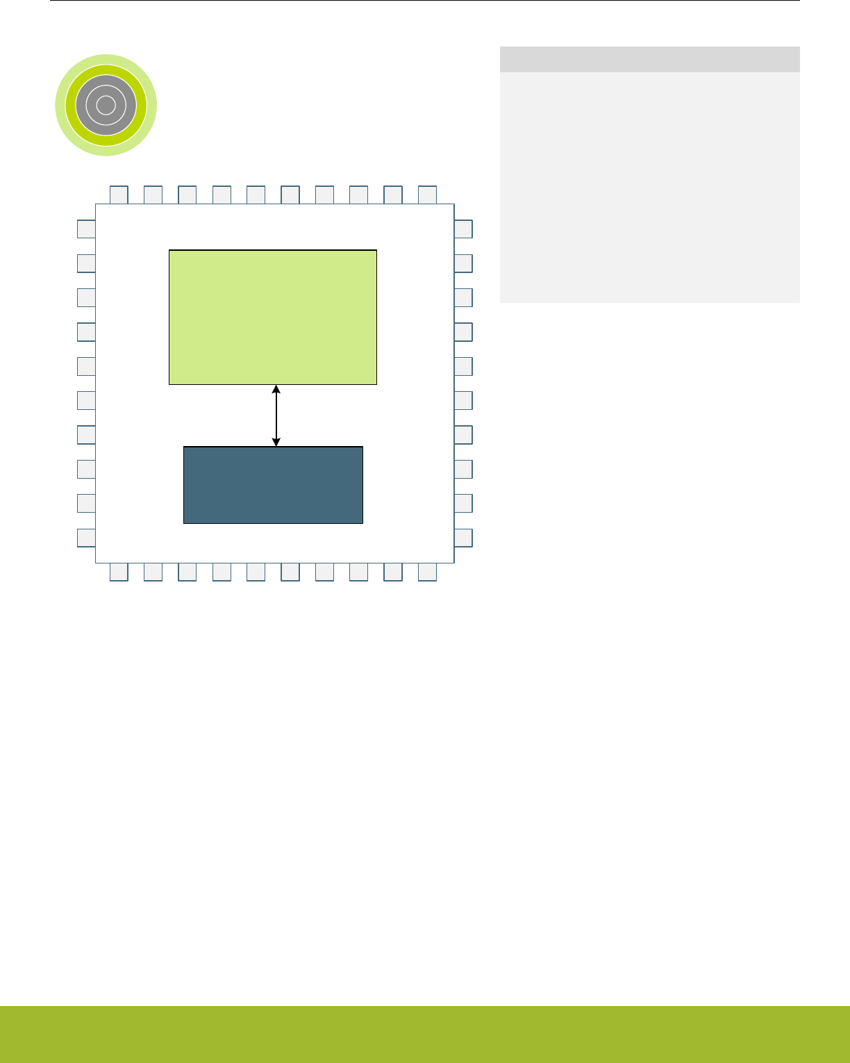
5. Serial Flash
0 1 2 3 4
SoC Radio +
Microcontroller
Serial Flash
Quick Facts
What?
A 512 kB serial flash memory is included in the
package for certain part numbers.
Why?
The serial flash memory extends the non-volatile
storage capabilites of the device while maintaining a
small PCB footprint.
How?
The serial flash may be read and written in EM0 or
EM1, and placed in a low power state when not
used.
5.1 Introduction
The serial flash memory adds 512 kB of non-volatile storage space for applications with larger memory requirements. It is fully internal
to the package, and requires no additional board space or GPIO resources. Software drivers provided by Silicon Labs offer a simple
API interface to the serial flash. Low-level access is also possible, via the USART1 peripheral.
5.2 Features
• 512 kB of memory
• 4 kB sectors, can be erased individually or in 32 kB or 64 kB blocks
• 1 - 256 byte page write
• 100,000 write/erase cycle endurance
• 20 year data retention
• SPI interface
• Write protection
• 4 x 256 byte dedicated security area with user-lockable bits, one-time programmable
Reference Manual
Serial Flash
silabs.com | Smart. Connected. Energy-friendly. Preliminary Rev. 0.5 | 100

5.3 Functional Description
The serial flash is powered from IOVDD and bonded to internal GPIO which are not available externally. USART1 is connected to the
associated GPIO pins and functions as a SPI interface to the flash. It is recommended to use the software libraries supplied by Silicon
Laboratories for interfacing to the serial flash. The information in this section is reference for users who choose to write their own low-
level software drivers.
Note: The EXTINFO entry in the DI page identifies the specific serial flash part number included in the package. Software should verify
this field before initiating any serial flash operations.
Reference Manual
Serial Flash
silabs.com | Smart. Connected. Energy-friendly. Preliminary Rev. 0.5 | 101

5.3.1 Memory Organization
The memory array of the serial flash is divided into uniform 4 kB sectors or uniform 32/64 kB blocks consisting of eight or sixteen adja-
cent sectors, respectively. Table 5.1 Block and Sector Addresses on page 102 diagrams the organization of this memory space.
Table 5.1. Block and Sector Addresses
64 kB Block Number 32 kB Block Number 4 kB Sector Number Address Range
0 0 0 0x000000 - 0x000FFF
: :
1 : :
15 0x00F000 - 0x00FFFF
1 2 16 0x010000 - 0x010FFF
: :
3 : :
31 0x01F000 - 0x01FFFF
2 4 32 0x020000 - 0x020FFF
: :
5 : :
47 0x02F000 - 0x02FFFF
3 6 48 0x030000 - 0x030FFF
: :
7 : :
63 0x03F000 - 0x03FFFF
4 8 64 0x040000 - 0x040FFF
: :
9 : :
79 0x04F000 - 0x04FFFF
5 10 80 0x050000 - 0x050FFF
: :
11 : :
95 0x05F000 - 0x05FFFF
6 12 96 0x060000 - 0x060FFF
: :
13 : :
111 0x06F000 - 0x06FFFF
7 14 112 0x070000 - 0x070FFF
: :
15 : :
127 0x07F000 - 0x07FFFF
Reference Manual
Serial Flash
silabs.com | Smart. Connected. Energy-friendly. Preliminary Rev. 0.5 | 102
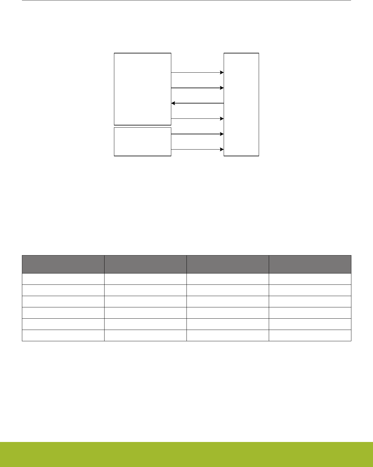
5.3.2 Serial Interface
Serial flash operations are controlled through a SPI interface on the flash. Internal to the package, the flash interface I/O are connected
to GPIO on the MCU. USART1 may be routed to the serial interface for hardware-controlled bus writes and reads.
GPIO Name Serial FlashUSART1 (SPI Mode 0)
US1_CS PC8 CEn
US1_SCK PF4 SCK
US1_TX PF5 SI
US1_RX PC9 SO
PF6 WPn
Direct GPIO Control PA5 HOLDn
Figure 5.1. Serial Flash Connections
5.3.2.1 USART1 Configuration
All of the serial flash I/O connections are bonded to standard port pins internal to the packaging. The USART1 peripheral may be direct-
ly routed to the SPI interface signals (SI, SO, SCK, and CEn), while the remaining signals (WPn and HOLDn) can be controlled as
GPIO. Table 5.2 Serial Flash I/O Connections on page 103 shows the GPIO connections for each signal, as well as the recommended
GPIO configurations and USART1 routing locations.
Table 5.2. Serial Flash I/O Connections
Serial Flash Signal GPIO Recommended Configuration
and initial state
USART1_ROUTELOC0 Set-
tings
SI (Serial Data Input) PF5 Output, High TXLOC = LOC29
WPn (Active-Low Write Protect) PF6 Output, Low n/a
SCK (Serial Clock Input) PF4 Output, Low CLKLOC = LOC26
HOLDn (Active-Low Hold) PA5 Output, High n/a
SO (Serial Data Output) PC9 Input RXLOC = LOC13
CEn (Active-Low Chip Enable) PC8 Output, High CSLOC = LOC10
To function properly with the serial flash, USART1 should be configured for synchronous master operation in SPI mode 0, with a maxi-
mum baud rate of 8 MHz. The CEn pin may be controlled manually by software, or automatically by the US1_CS pin. If using the
US1_CS option, the CS output signal should be configured for active-low operation.
If CEn is controlled manually as a GPIO pin, it should be cleared to a logic low state by software before any data transfer is initiated,
and set back to logic high after the final byte of data has been transferred. If US1_CS is configured to automatically drive the CEn pin,
software or DMA must continue to keep the USART1 buffer full for the duration of each transfer so that CEn remains low during the
operation and returns high only when data transfer is complete.
Refer to 19. USART - Universal Synchronous Asynchronous Receiver/Transmitter for more detailed information about USART opera-
tion and configuration.
Reference Manual
Serial Flash
silabs.com | Smart. Connected. Energy-friendly. Preliminary Rev. 0.5 | 103
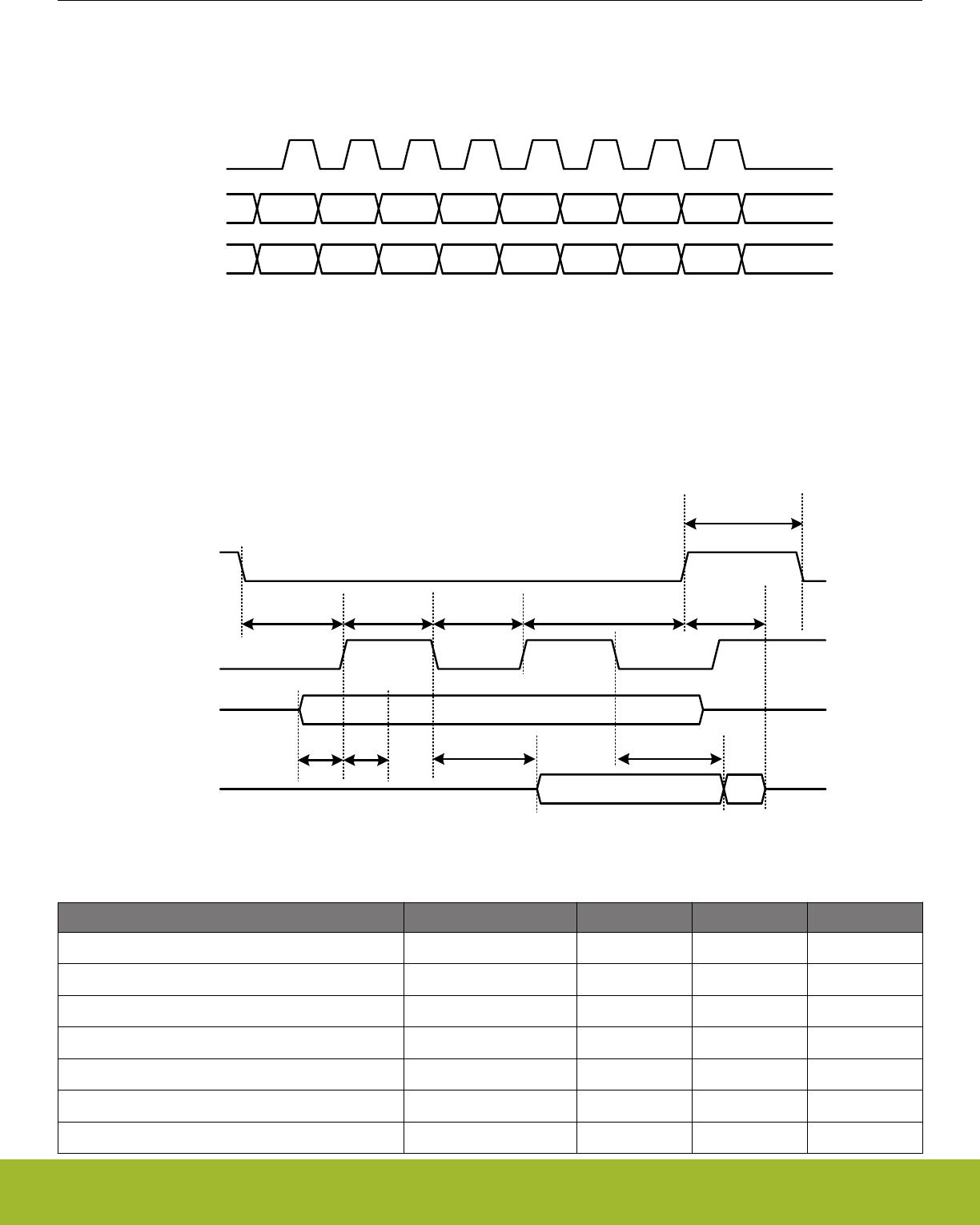
5.3.2.2 Timing
All data is shifted into and out of the serial flash MSB-first. Data is shifted on the falling edge of SCK and latched on the rising edge of
SCK. Transfer format for a single byte is shown in Figure 5.2 Serial Interface Data Format on page 104.
-- DI 7 DI 6 DI 5 DI 4 DI 3 DI 2 DI 1 DI 0 --SI
SCK
-- DO 7 DO 6 DO 5 DO 4 DO 3 DO 2 DO 1 DO 0 --SO
Figure 5.2. Serial Interface Data Format
When USART1 is configured as described in 5.3.2.1 USART1 Configuration, at no greater than an 8 MHz serial clock rate and automat-
ic US1_CS control, all serial flash timing parameters for CEn, SCK, SI, and SO will be met across the temperature and supply range.
This is the recommended configuration for communicating with the serial flash memory. For other configurations, it is important to en-
sure that the serial flash timing is not violated. Refer to Figure 5.3 Serial Flash IO Timing on page 104.
SCK
CEn
Valid Data In
SI
Valid Data OutSO
tV
tCS tCKH tCKL tCH
tCEH
tOH
tDIS
tDS tDH
Figure 5.3. Serial Flash IO Timing
Parameter Symbol Min Max Units
SCK High Time tCKH 4 ns
SCK Low Time tCKL 4 ns
CEn High Time tCEH 7 ns
CEn Setup Time tCS 10 ns
CEn Hold Time tCH 5 ns
Data In Setup Time tDS 2 ns
Data In Hold Time tDH 2 ns
Reference Manual
Serial Flash
silabs.com | Smart. Connected. Energy-friendly. Preliminary Rev. 0.5 | 104
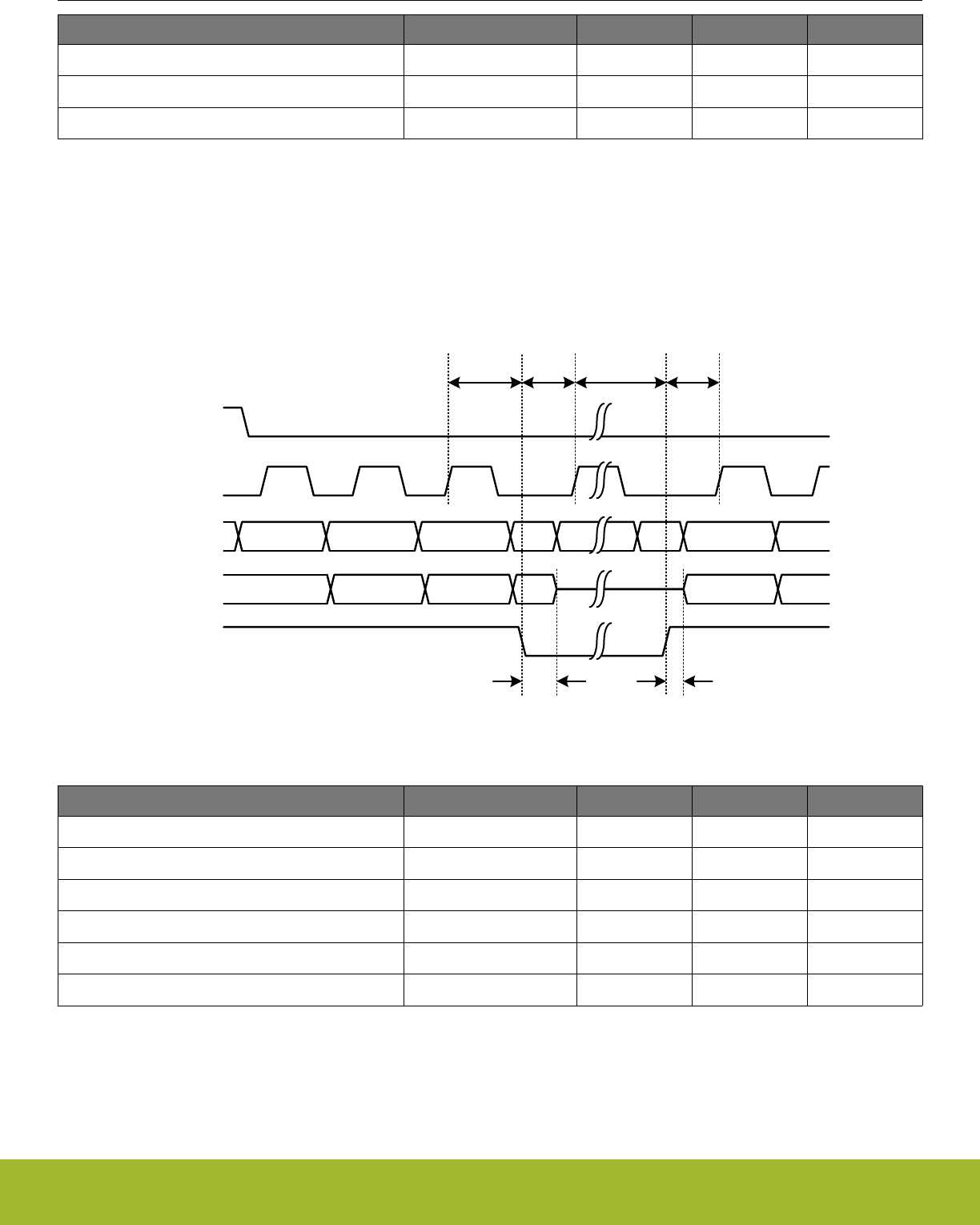
Parameter Symbol Min Max Units
Output Valid tV8 ns
Output Hold Time tOH 2 ns
Output Disable Time tDIS 8 ns
5.3.2.3 Hold Operation
When the device is selected with CEn and a serial sequence is underway, HOLDn can be used to pause the serial communication with
the master device without resetting the serial sequence. To pause, bring the HOLDn signal low while the SCK signal is low. When
HOLDn is asserted, inputs to SI will be ignored, and SO will be high impedance. To resume serial communication, bring HOLDn high
while the SCK signal is low. Communication with the serial flash will resume at the clock where it was halted.
Figure 5.4. Serial Flash HOLDn Timing
SCK
CEn
SI
SO
HOLDn
tHZ tLZ
tCHHL tHLCH tCHHH tHHCH
Parameter Symbol Min Max Units
HOLDn Low to SCK tHLCH 5 ns
SCK to HOLDn High tCHHH 5 ns
HOLDn High to SCK tHHCH 5 ns
SCK to HOLDn Low tCHHL 5 ns
HOLDn Low to Output High-Z tHZ 12 ns
HOLDn High to Output Driven tLZ 12 ns
Reference Manual
Serial Flash
silabs.com | Smart. Connected. Energy-friendly. Preliminary Rev. 0.5 | 105
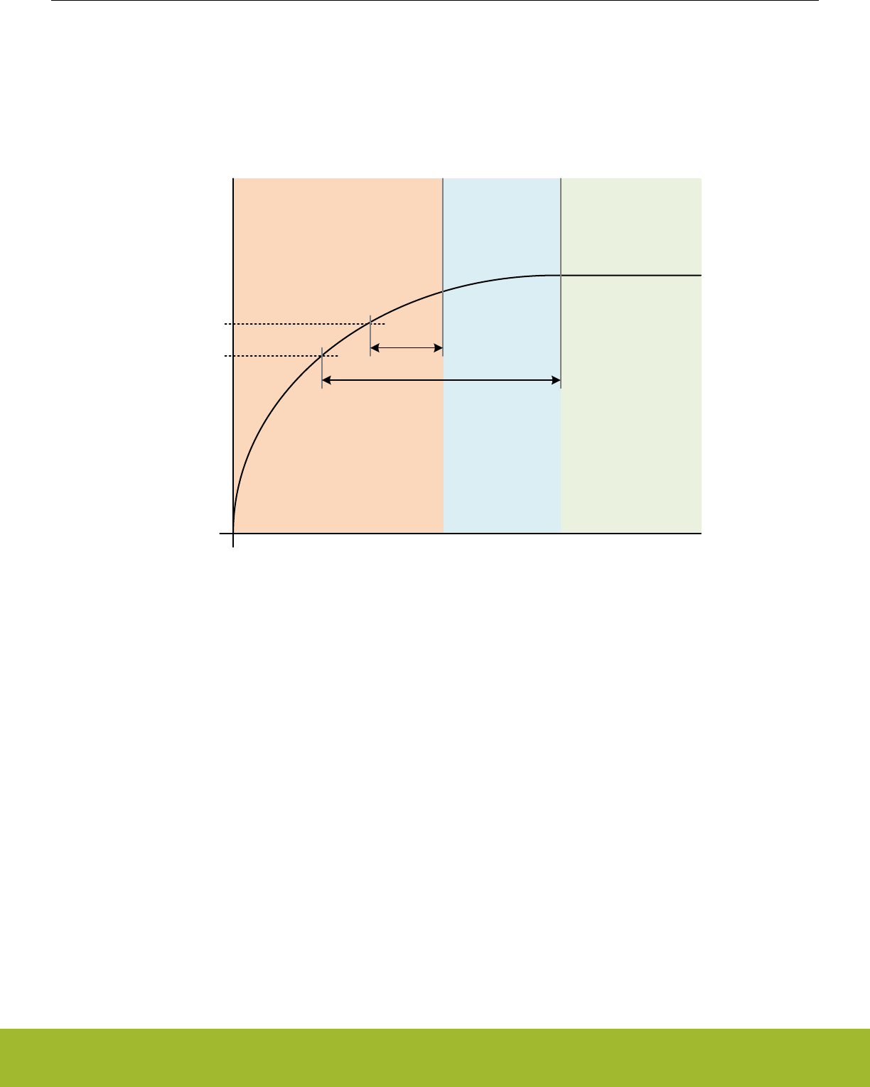
5.3.2.4 Power Up and Power Down
The serial flash is powered by the IOVDD supply pin, and will inhibit certain operations while it is powering on. Software should not
attempt to access the serial flash for at least 1 ms after IOVDD reaches 2.3 V. Additionally, program and erase operations will be rejec-
ted for up to 10 ms from the time IOVDD reaches 2.1 V. All program and erase operations are inhibited if the IOVDD supply voltage
drops below 2.1 V.
Figure 5.5. Serial Flash Power Up
All Operations
Allowed
Read Access
Allowed
No Operations Allowed
VIOVDD
Time
2.1 V
2.3 V
1ms
10ms
Reference Manual
Serial Flash
silabs.com | Smart. Connected. Energy-friendly. Preliminary Rev. 0.5 | 106

5.3.3 Instruction Set
The serial flash utilizes an 8-bit instruction register. See Table 5.3 Instruction Set Summary on page 107 for details on instructions and
instruction codes. All instructions, addresses, and data are shifted in with the most significant bit (MSB) first on the Serial Data Input
(SI). The input data on SI is latched on the rising edge of Serial Clock (SCK) after Chip Enable (CEn) is driven low. Every instruction
sequence starts with a one-byte instruction code and is followed by address bytes, data bytes, or both address bytes and data bytes,
depending on the type of instruction. CEn must be driven high after the last bit of the instruction sequence has been shifted in to end
the operation.
Table 5.3. Instruction Set Summary
Name Instruction Code Operation Available During Suspend
RD 0x03 Read Data Yes
FR 0x0B Fast Read Data Yes
PP 0x02 Page Program No
SER 0xD7 / 0x20 Sector Erase No
BER32 0x52 Block Erase 32 kB No
BER64 0xD8 Block Erase 64 kB No
CER 0xC7 / 0x60 Chip Erase No
WREN 0x06 Write Enable No
WRDI 0x04 Write Disable No
RDSR 0x05 Read Status Register Yes
WRSR 0x01 Write Status Register No
RDFR 0x48 Read Funciton Register Yes
WRFR 0x42 Write Function Register No
PERSUS 0x75 / 0xB0 Program/Erase Suspend No
PERRSM 0x7A / 0x30 Program/Erase Resume Yes
DP 0xB9 Deep Power Down No
RDUID 0x4B Read Unique ID Yes
RSTEN 0x66 Reset Enable Yes
RST 0x99 Reset Yes
IRP 0x62 Program Information Row No
IRRD 0x68 Read Information Row Yes
SECUNLOCK 0x26 Sector Unlock No
SECLOCK 0x24 Sector Lock No
5.3.4 Registers
The serial flash has two 8-bit registers to communicate status and apply write protection to different regions of the memory array, the
STATUS register and the FUNCTION register.
The STATUS register is read with the RDSR command and written with the WRSR command. The FUNCTION register is read with the
RDFR command and written with the WRFR command.
Reference Manual
Serial Flash
silabs.com | Smart. Connected. Energy-friendly. Preliminary Rev. 0.5 | 107

STATUS - Serial Flash Status Register
Bit76543210
Default 0 0 0x0 0 0
Access R/W
Non-Volatile
R/W
Non-Volatile
R/W
Non-Volatile
R
Volatile
R
Volatile
Name SRWD Reserved BP WEL WIP
Bit Name Default Access Description
7 SRWD 0 R/W
Non-Vol-
atile
Status Register Write Disable.
The SRWD bit operates in conjunction with the Write Protection (WPn) signal to provide a hardware protection mode. When
SRWD is cleared to 0, the STATUS register is not write-protected. When SRWD is set to 1 and WPn is pulled low, the STA-
TUS register becomes read-only, and any WRSR instruction will be ignored. If SRWD is set to 1 and WPn is pulled high,
the STATUS register can be changed by a WRSR instruction.
6 Reserved This bit must always be written to 0.
5:2 BP 0x0 R/W
Non-Vol-
atile
Block Protection.
The Block Protection field is used to define the portion of the memory area to be protected. Refer to Table 5.4 64 kB Block
Write Protection on page 117 for the Block Protection (BP) settings. When a defined value of BP is set, the corresponding
area of serial flash memory is protected. Any program or erase operation to that area will be inhibited. A Chip Erase (CER)
instruction will be ignored unless BP is 0x0.
1 WEL 0 R
Volatile
Write Enable Latch.
WEL indicates the status of the internal write enable latch. When WEL is 0, the write enable latch is disabled and all write
or erase operations are inhibited. When WEL is 1, write operations are allowed. The WEL bit is set by a Write Enable
(WREN) instruction. Each STATUS or FUNCTION register write, program, or erase instruction must be preceded by a
WREN instruction. The WEL bit can be reset by software a Write Disable (WRDI) instruction. It will automatically be reset
after the completion of any write or erase operation.
0 WIP 0 R
Volatile
Write In Progress.
WIP indicates the progress or completion of a program or erase operation. When the WIP bit is 0, the serial flash will ac-
cept any new register write, program, or erase operation. When WIP is 1, the serial flash is busy, and new register write,
program, and erase instructions will be ignored.
Reference Manual
Serial Flash
silabs.com | Smart. Connected. Energy-friendly. Preliminary Rev. 0.5 | 108

FUNCTION - Serial Flash Function Register
Bit76543210
Default 0 0 0 0 0 0 0x0
Access R/W
OTP
R/W
OTP
R/W
OTP
R/W
OTP
R
Volatile
R
Volatile
R
Name IRL3 IRL2 IRL1 IRL0 ESUS PSUS Reserved
Bit Name Default Access Description
7 IRL3 0 R/W
OTP
Information Row 3 Lock.
This bit is used to lock information row 3. When set to 1, information row 3 cannot be programmed. This bit is one-time
programmable (OTP). Once it is set to 1, it cannot be modified.
6 IRL2 0 R/W
OTP
Information Row 2 Lock.
This bit is used to lock information row 2. When set to 1, information row 2 cannot be programmed. This bit is one-time
programmable (OTP). Once it is set to 1, it cannot be modified.
5 IRL1 0 R/W
OTP
Information Row 1 Lock.
This bit is used to lock information row 1. When set to 1, information row 1 cannot be programmed. This bit is one-time
programmable (OTP). Once it is set to 1, it cannot be modified.
4 IRL0 0 R/W
OTP
Information Row 0 Lock.
This bit is used to lock information row 0. When set to 1, information row 0 cannot be programmed. This bit is one-time
programmable (OTP). Once it is set to 1, it cannot be modified.
3 ESUS 0 R
Volatile
Erase Suspend.
ESUS indicates when an erase operation has been suspended. The ESUS bit is 1 after a suspend command is issued dur-
ing any erase operation. Once the suspended erase operation resumes, the ESUS bit is reset to 0.
2PSUS 0 R
Volatile
Program Suspend.
PSUS indicates when a program operation has been suspended. The PSUS bit is 1 after a suspend command is issued
during any program operation. Once the suspended program operation resumes, the PSUS bit is reset to 0.
1:0 Reserved These bits always read 0x0.
Reference Manual
Serial Flash
silabs.com | Smart. Connected. Energy-friendly. Preliminary Rev. 0.5 | 109
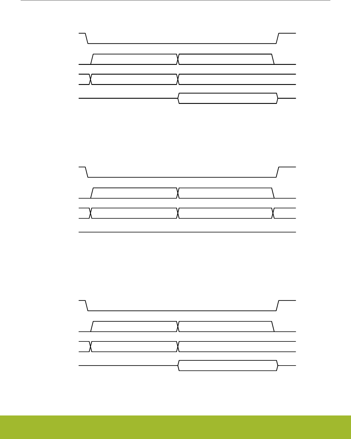
5.3.4.1 Read Status Register (RDSR, 0x05)
SCK
CEn
-- 0x05 --
SI
Read DataSO
8 clocks 8 clocks
Figure 5.6. RDSR Instruction Format
5.3.4.2 Write Status Register (WRSR, 0x01)
SCK
CEn
-- 0x01 Write Data --
SI
SO
8 clocks 8 clocks
Figure 5.7. WRSR Instruction Format
5.3.4.3 Read Function Register (RDFR, 0x48)
SCK
CEn
-- 0x48 --
SI
Read DataSO
8 clocks 8 clocks
Figure 5.8. RDFR Instruction Format
Reference Manual
Serial Flash
silabs.com | Smart. Connected. Energy-friendly. Preliminary Rev. 0.5 | 110

5.3.4.4 Write Function Register (WRFR, 0x42)
SCK
CEn
-- 0x42 Write Data --
SI
SO
8 clocks 8 clocks
Figure 5.9. WRFR Instruction Format
5.3.5 Reading Memory
Reads of the serial flash memory space are performed with either the Read Data (RD) or Fast Read (FR) instruction. The Fast Read
command is intended to allow for higher serial clock frequencies to be used for reading the serial flash data. In this co-packaged config-
uration however, both commands are limited to the overall maximum SCK rate of 8 MHz, and either may be used to read flash contents.
To initiate a memory read using the RD instruction, software should send the RD instruction code (one byte), followed by the first mem-
ory location to be read (three bytes, MSB-first). Data will be shifted out of the serial flash beginning with the next serial clock.
To initiate a memory read using the FR instruction, software should send the FR instruction code (one byte), followed by the first memo-
ry location to be read (three bytes, MSB-first), followed by a dummy byte (one byte). Data will be shifted out of the serial flash beginning
with the next serial clock.
Data is shifted out on the SO line, MSB first. Any number of bytes can be read out in one RD or FR instruction. The address is automat-
ically incremented after each byte of data is shifted out. When the highest address is reached, the address counter will roll over to
0x000000, allowing the entire memory to be read in one continuous instruction. The operation is terminated when CEn is driven high.
If an RD or FR instruction is issued while an Erase, Program or Write cycle is in process (WIP=1) the instruction is ignored and will not
have any effect on the current operation.
5.3.5.1 Read Data (RD, 0x03)
SCK
CEn
-- 0x03 Address (3 bytes)
SI
Read N data bytesSO
--
8 clocks 24 clocks N x 8 clocks
Figure 5.10. RD Instruction Format
Reference Manual
Serial Flash
silabs.com | Smart. Connected. Energy-friendly. Preliminary Rev. 0.5 | 111

5.3.5.2 Fast Read Data (FR, 0x0B)
SCK
CEn
-- 0x0B Address (3 bytes) Dummy --
SI
Read N data bytesSO
8 clocks 24 clocks 8 clocks N x 8 clocks
Figure 5.11. FR Instruction Format
5.3.6 Programming and Erasing Memory
The serial flash memory can be programmed (clearing bits to 0) in 1 to 256-byte pages. The entire 512 kB memory array may be
erased (setting bits to 1) with a single command, or memory may be erased in defined 4 kB, 32 kB, or 64 kB blocks. Program or erase
operations (other than full chip erase) may be suspended and resumed as needed in order to allow time-critical read operations.
Note: A program operation changes 1's to 0's in the flash memory array. An erase operation is required to change 0's to 1's. A byte
cannot be reprogrammed with new information without first erasing the whole sector or block.
Programming Sequence
The Page Program instruction allows up to 256 bytes data to be programmed into memory in a single operation. The procedure to pro-
gram data bytes is as follows:
1. Set the Write Enable Latch (WEL) by sending a Write Enable (WREN) instruction.
2. Send the Page Program (PP) instruction code (one byte), followed by the first memory location to be programmed (three bytes,
MSB-first), and then shift the data to be programmed (1 to 256 bytes) into the flash.
3. Send Read Status Register (RDSR) instructions to the device to poll the STATUS register until the WIP bit is 0.
The write operation will start immediately after CEn is brought high in step 2. The PP instruction will not be executed until CEn goes
high. The internal control logic automatically handles programming voltages and timing. During a program operation, the WIP bit in
STATUS will be set to 1 and all instructions will be ignored except the RDSR instruction and the PERSUS instruction. Upon completion
of the program operation, the Write Enable Latch (WEL) will also be cleared.
The starting byte can be anywhere within the page. When the end of the page is reached during a PP instruction (address ends in
0xFF), the address counter rolls over to the beginning of the page. If more than 256 bytes are receive during a PP instruction, only the
last 256 bytes received are programmed into the page. If the data to be programmed are less than a full page, the data of all other
bytes on the same page will remain unchanged.
Note: The destination of the memory to be programmed must be outside the protected memory area set by the BP field in the STATUS
register. Any PP instruction which attempts to program into a page that is write-protected will be ignored, unless the sector containing
that page has been unlocked with a SECUNLOCK instruction.
Reference Manual
Serial Flash
silabs.com | Smart. Connected. Energy-friendly. Preliminary Rev. 0.5 | 112

Erase Sequence
The memory array of the serial flash is organized into uniform 4Kbyte sectors or 32/64Kbyte uniform blocks (a block consists of eight/
sixteen adjacent sectors respectively). Before a byte is reprogrammed, the sector or block that contains the byte must be erased (eras-
ing sets bits to 1). In order to erase the serial flash, there are four erase instructions available: Sector Erase (SER), 32 kB Block Erase
(BER32), 64 kB Block Erase (BER64) and Chip Erase (CER). A sector erase operation allows any individual sector to be erased with-
out affecting the data in other sectors. A block erase operation erases any individual block. A chip erase operation erases the whole
memory array of the serial flash.
To perform a sector or block erase:
1. Set the Write Enable Latch (WEL) by sending a Write Enable (WREN) instruction.
2. Send the SER, BER32 or BER64 instruction code (one byte), followed by the first address of the sector or block to be erased (three
bytes, MSB-first).
3. Send Read Status Register (RDSR) instructions to the device to poll the STATUS register until the WIP bit is 0.
To perform a chip erase:
1. Set the Write Enable Latch (WEL) by sending a Write Enable (WREN) instruction.
2. Send the CER instruction code.
3. Send Read Status Register (RDSR) instructions to the device to poll the STATUS register until the WIP bit is 0.
The erase operation will start immediately after CEn is brought high for the erase instruction. The internal control logic automatically
handles erase voltages and timing. During an erase operation, the WIP bit in STATUS will be set to 1 and all instructions will be ignored
except the RDSR instruction and the PERSUS instruction. Upon completion of the erase operation, the Write Enable Latch (WEL) will
also be cleared.
Note: The destination of the memory to be erased must be outside the protected memory area set by the BP field in the STATUS regis-
ter. Any erase instruction which attempts to program into an area that is write-protected will be ignored, unless the sectors to be erased
have been unlocked with a SECUNLOCK instruction. For a chip erase operation to execute, the entire memory array must be unlocked
according to the BP field.
5.3.6.1 Program/Erase Suspend and Resume
The device allows the interruption of SER, BER32, BER64, and PP operations to conduct other operations. To suspend a program or
erase operation, the Program/Erase Suspend (PERSUS) instruction is used. When the PERSUS instruction is issued, the serial flash
will suspend the program or erase operation within a maximum of 100 μs after CEn is driven high. The WIP bit in the STATUS register
may also be polled by software to determine when the flash is ready to accept new commands. When a program or erase operation is
suspended, the flash will respond to a limited set of other operations. Details on which instructions are allowed during suspend are
found in Table 5.3 Instruction Set Summary on page 107.
When a program operation has been suspended, the PSUS bit in the FUNCTION register will read back 1. If an erase operation has
been suspended, the ESUS bit in the FUNCTION register will read back 1.
To resume the suspended program or erase operation, the Program/Erase Resume (PERRSM) operation is used. When the PERRSM
instruction is issued, the serial flash will resume the program or erase operation after CEn is driven high. The WIP bit in the STATUS
register may be polled by software to determine when the program or erase operation is complete.
Note: If multiple suspend/resume operations are used, software must wait for a minimum of 400 μs after sending a resume command
befor initiating a new suspend operation.
Reference Manual
Serial Flash
silabs.com | Smart. Connected. Energy-friendly. Preliminary Rev. 0.5 | 113
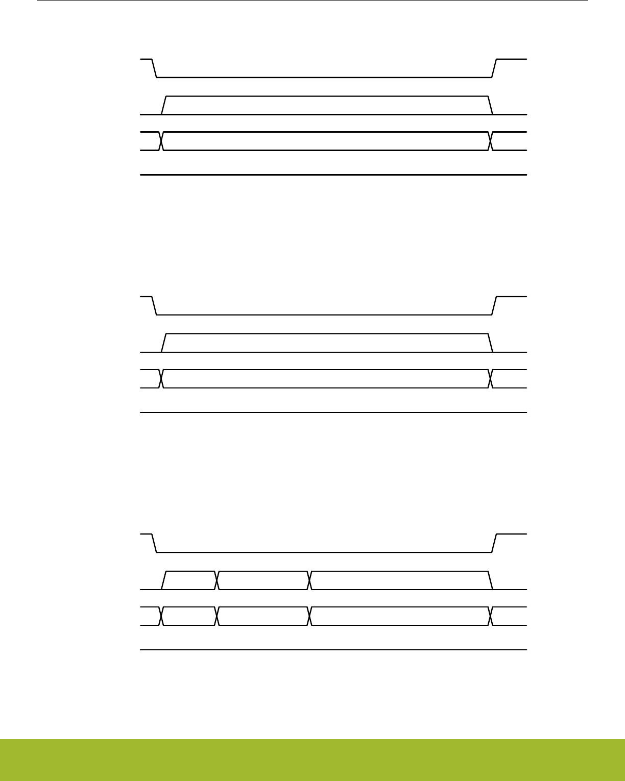
5.3.6.2 Write Enable (WREN, 0x06)
SCK
CEn
-- 0x06 --
SI
SO
8 clocks
Figure 5.12. WREN Instruction Format
5.3.6.3 Write Disable (WRDI, 0x04)
SCK
CEn
-- 0x04 --
SI
SO
8 clocks
Figure 5.13. WRDI Instruction Format
5.3.6.4 Page Program (PP, 0x02)
SCK
CEn
-- 0x02 Address (3 bytes) Write N data bytes --
SI
SO
8 clocks 24 clocks N x 8 clocks
Figure 5.14. PP Instruction Format
Reference Manual
Serial Flash
silabs.com | Smart. Connected. Energy-friendly. Preliminary Rev. 0.5 | 114
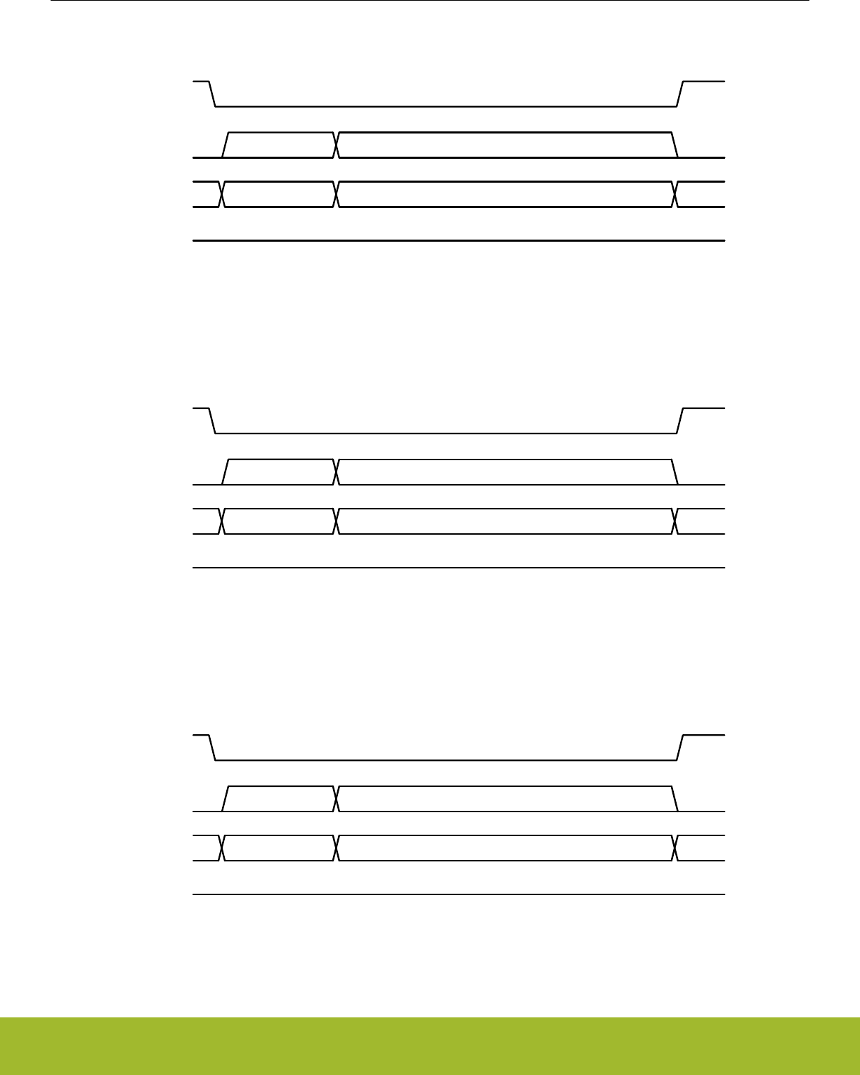
5.3.6.5 Sector Erase (SER, 0xD7 / 0x20)
SCK
CEn
-- 0xD7 or 0x20 Address (3 bytes) --
SI
SO
8 clocks 24 clocks
Figure 5.15. SER Instruction Format
5.3.6.6 Block Erase 32k (BER32, 0x52)
SCK
CEn
-- 0x52 Address (3 bytes) --
SI
SO
8 clocks 24 clocks
Figure 5.16. BER32 Instruction Format
5.3.6.7 Block Erase 64k (BER64, 0xD8)
SCK
CEn
-- 0xD8 Address (3 bytes) --
SI
SO
8 clocks 24 clocks
Figure 5.17. BER64 Instruction Format
Reference Manual
Serial Flash
silabs.com | Smart. Connected. Energy-friendly. Preliminary Rev. 0.5 | 115

5.3.6.8 Chip Erase (CER, 0xC7 / 0x60)
SCK
CEn
-- 0xC7 or 0x60 --
SI
SO
8 clocks
Figure 5.18. CER Instruction Format
5.3.6.9 Program/Erase Suspend (PERSUS, 0x75 / 0xB0)
SCK
CEn
-- 0x75 or 0xB0 --
SI
SO
8 clocks
Figure 5.19. PERSUS Instruction Format
5.3.6.10 Program/Erase Resume (PERRSM, 0x7A / 0x30)
SCK
CEn
-- 0x7A or 0x30 --
SI
SO
8 clocks
Figure 5.20. PERRSM Instruction Format
Reference Manual
Serial Flash
silabs.com | Smart. Connected. Energy-friendly. Preliminary Rev. 0.5 | 116

5.3.7 Write Protection
The serial flash supports both hardware and software write protection mechanisms to prevent accidental program or erasure. The block
protect (BP) field in the STATUS register allows part or all of the memory area to be designated as write-protected. If a block is write-
protected, no program or erase operations will affect the memory contents, unless a SECUNLOCK command is issued to first unlock
the target sector. Table 5.4 64 kB Block Write Protection on page 117 details the areas protected by each BP setting.
Table 5.4. 64 kB Block Write Protection
BP field in STATUS Register (binary) Write-Protected 64 kB Blocks
0000 None
0001 Block 7
0010 Blocks 6 and 7
0011 Blocks 4, 5, 6, and 7
0100 - 1011 All Blocks
1100 Blocks 0, 1, 2 and 3
1101 Blocks 0 and 1
1110 Block 1
1111 None
The Sector Unlock (SECUNLOCK) and Sector Lock (SECLOCK) commands are used to unlock and re-lock individual protected sectors
as-needed when erasing and writing the memory. Only one sector may be unlocked with the SECUNLOCK command at a time, protect-
ing the rest of the memory array from corruption. To unlock a sector, software should write the SECUNLOCK command (one byte),
followed by the starting address of the target sector (3 bytes). The sector is locked again when a SECLOCK command is issued, or
when a subsequent SECUNLOCK command unlocks a different sector. Because only one sector may be locked at a time, the SE-
CLOCK command only requires the command byte to be sent, and does not accept an address.
Additionally, the WPn signal, in conjunction with the SRWD bit in the STATUS register, provides a means of preventing writes to the
STATUS register where the software block protect (BP) field is located. Table 5.5 Hardware STATUS Register Write Protection on page
117 shows how the STATUS register may be protected.
Table 5.5. Hardware STATUS Register Write Protection
SRWD bit in STATUS Register WPn Signal Status Register
0 Low Writeable
1 Low Protected
0 High Writeable
1 High Writeable
Reference Manual
Serial Flash
silabs.com | Smart. Connected. Energy-friendly. Preliminary Rev. 0.5 | 117
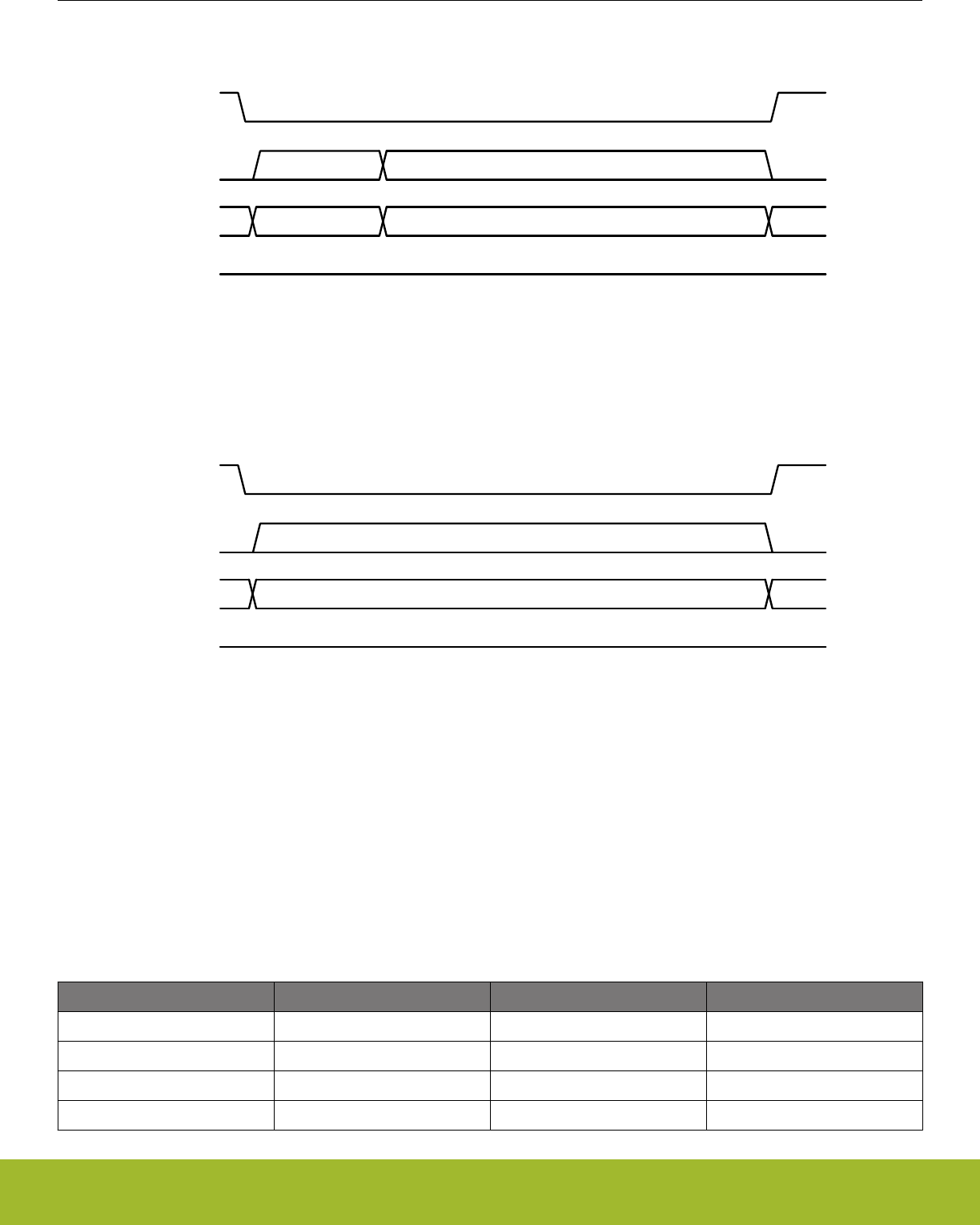
5.3.7.1 Sector Unlock (SECUNLOCK, 0x26)
SCK
CEn
-- 0x26 Address (3 bytes) --
SI
SO
8 clocks 24 clocks
Figure 5.21. SECUNLOCK Instruction Format
5.3.7.2 Sector Lock (SECLOCK, 0x24)
SCK
CEn
-- 0x24 --
SI
SO
8 clocks
Figure 5.22. SECLOCK Instruction Format
5.3.8 Security Information Row and Unique ID
The serial flash has some additional storage outside of the general memory array: one 16-byte pre-programmed, read-only Unique ID
space, and a Security Information Row space comprised of an additional 4 x 256 bytes of one-time programmable information.
The bits in the security information row can be written by the user, but not erased. Any program security instruction issued while pro-
gram cycle is in progress is rejected without having any effect on the cycle that is in progress. The IRL0, IRL1, IRL2, and IRL3 bits in
the FUNCTION regsiter may be used to permanently lock the security information row data in 256-byte sections. When the correspond-
ing IRL bit is et to 1, the 256 bytes in that section become read-only.
Table 5.6. Information Row Addressing
Information Row Lock A[23:16] A[15:8] A[7:0]
IRL0 0x00 0x00 Byte Address
IRL1 0x00 0x10 Byte Address
IRL2 0x00 0x20 Byte Address
IRL3 0x00 0x30 Byte Address
Reference Manual
Serial Flash
silabs.com | Smart. Connected. Energy-friendly. Preliminary Rev. 0.5 | 118

Reading the Information Rows
The Information Row Read (IRRD) instruction is used to read data stored in the securiy information rows. The IRRD instruction oper-
ates like the FR instruction, but targets the information row space.
, with each bit latched-in during the rising edge of SCK. Then the first data byte addressed is shifted out on the SO line, with each bit
shifted out at a maximum frequency fCT, during the falling edge of SCK. The address is automatically incremented by one after each
byte of data is shifted out. Once the address reaches the last address of each 256 byte Information Row, the next address will not be
valid and the data of the address will be garbage data. It is recommended to repeat four times IRRD operation that reads 256 byte with
a valid starting address of each Information Row in order to read all data in the 4 x 256 byte Information Row array. The IRRD instruc-
tion is terminated by driving CE# high (VIH). If a IRRD instruction is issued while an Erase, Program or Write cycle is in process
(WIP=1) the instruction is ignored and will not have any effects on the current cycle. The sequence of IRRD instruction is same as
FAST READ except for the instruction code
To initiate a memory read using the IRRD instruction, software should send the IRRD instruction code (one byte), followed by the first
memory location to be read (three bytes, MSB-first), followed by a dummy byte (one byte). Data will be shifted out of the serial flash
beginning with the next serial clock.
Data is shifted out on the SO line, MSB first. Any number of bytes can be read out in one IRRD instruction. The address is automatically
incremented after each byte of data is shifted out. Once the address reaches the last address of the information row, the next address
will not be valid and the data read will be garbage data. If the entire information space is to be read, it is recommended to repeat the
IRRD operation four times, with the starting address of each information row. The operation is terminated when CEn is driven high.
If an IRRD instruction is issued while an Erase, Program or Write cycle is in process (WIP=1) the instruction is ignored and will not have
any effect on the current operation.
Programming the Information Rows
The Information Row Program (IRP) instruction allows up to 256 bytes data to be programmed into the information row memory in a
single operation. An IRP instruction operates exactly like the Page Program instruction, but targets the information row space.
The procedure to program data bytes in an information row is as follows:
1. Set the Write Enable Latch (WEL) by sending a Write Enable (WREN) instruction.
2. Send the Information Row Program (IRP) instruction code (one byte), followed by the first information row location to be program-
med (three bytes, MSB-first), and then shift the data to be programmed (1 to 256 bytes) into the flash.
3. Send Read Status Register (RDSR) instructions to the device to poll the STATUS register until the WIP bit is 0.
The write operation will start immediately after CEn is brought high. The IRP instruction will not be executed until CEn goes high. The
internal control logic automatically handles programming voltages and timing. During a program operation, the WIP bit in STATUS will
be set to 1 and all instructions will be ignored except the RDSR instruction and the PERSUS instruction. Upon completion of the pro-
gram operation, the Write Enable Latch (WEL) will also be cleared.
The starting byte can be anywhere within the page. When the end of the row is reached during a IRP instruction (address ends in
0xFF), the address counter rolls over to the beginning of the row. If more than 256 bytes are receive during an IRP instruction, only the
last 256 bytes received are programmed into the row. If the data to be programmed are less than a full row, the data of all other bytes
on the same row will remain unchanged.
Note: The data in the security information rows is non-programmable. Once an information row is programmed, the bits cannot be
erased. The information row lock bit associated with the row may be used to prevent subsequent IRP instructions from programming
additional bits to 0.
Reading the Unique ID
The Read Unique ID Number (RDUID) instruction accesses a factory-set read-only 16-byte number that is unique to the device. The ID
number can be used in conjunction with user software methods to help prevent copying or cloning of a system. The RDUID instruction
operates similar to the FR instruction. To read the Unique ID, issue the RDUID command (one byte), followed by an address (3 bytes),
followed by a dummy byte, and then read 16 bytes of data. Because the Unique ID is 16 bytes in length, only the four LSBs of the
address are used. If more than 16 bytes of data are read during the operation, the Unique ID will repeat.
Reference Manual
Serial Flash
silabs.com | Smart. Connected. Energy-friendly. Preliminary Rev. 0.5 | 119
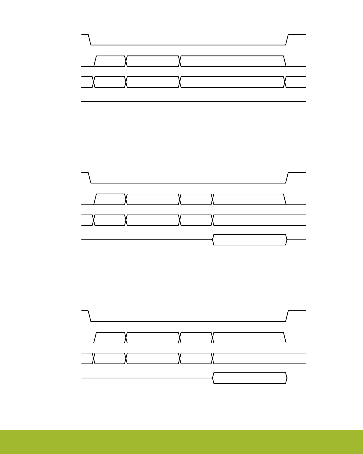
5.3.8.1 Information Row Program (IRP, 0x62)
SCK
CEn
-- 0x62 Address (3 bytes) Write N data bytes --
SI
SO
8 clocks 24 clocks N x 8 clocks
Figure 5.23. IRP Instruction Format
5.3.8.2 Information Row Read (IRRD, 0x68)
SCK
CEn
-- 0x68 Address (3 bytes) Dummy --
SI
Read N data bytesSO
8 clocks 24 clocks 8 clocks N x 8 clocks
Figure 5.24. IRRD Instruction Format
5.3.8.3 Read Unique ID Number (RDUID, 0x4B)
SCK
CEn
-- 0x4B Address (3 bytes) Dummy --
SI
Read 16 bytesSO
8 clocks 24 clocks 8 clocks 16 x 8 clocks
Figure 5.25. RDUID Instruction Format
Reference Manual
Serial Flash
silabs.com | Smart. Connected. Energy-friendly. Preliminary Rev. 0.5 | 120
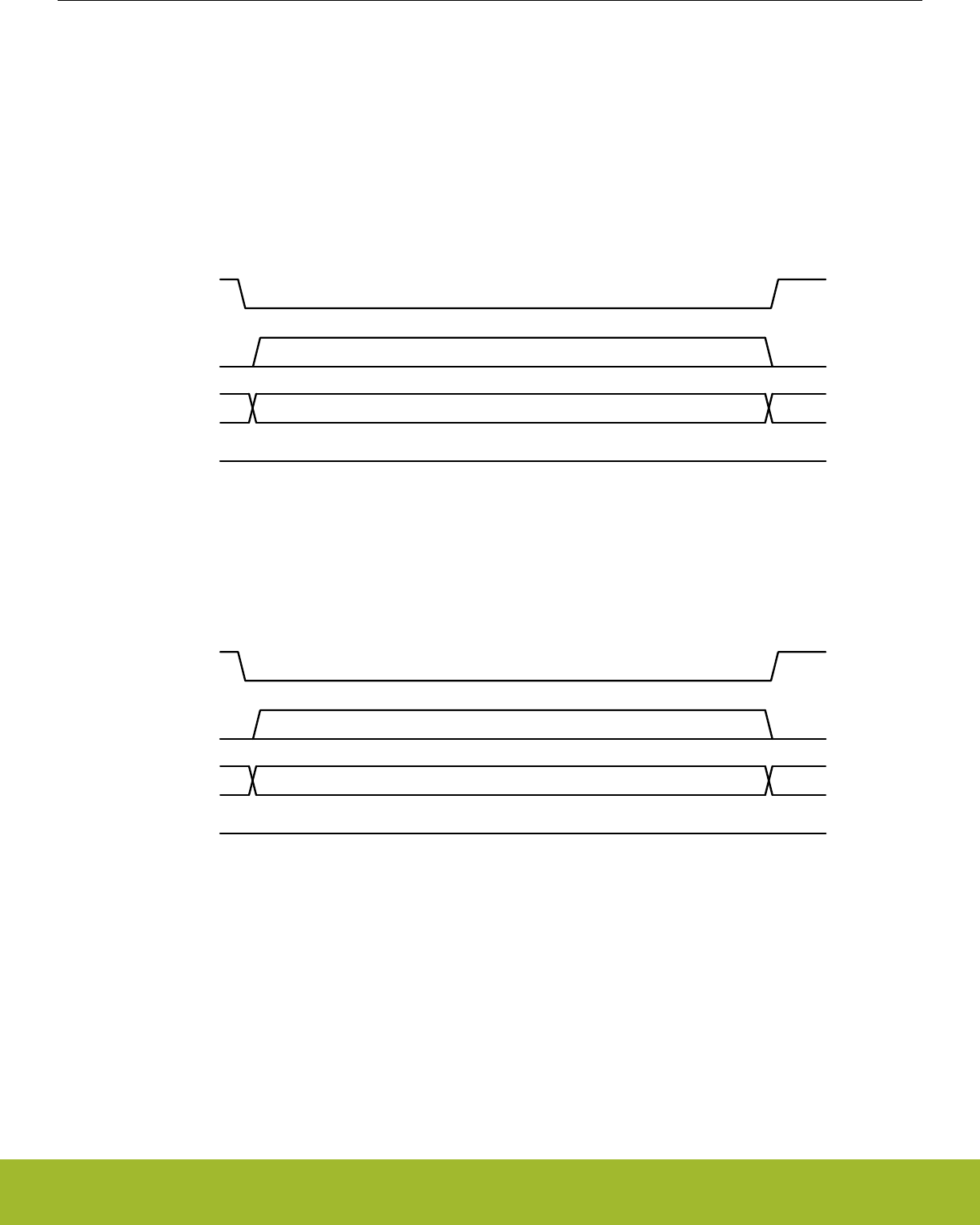
5.3.9 Power Down
The serial flash may be put into a low-power state using the Deep Power-down (DP) instruction. When a DP instruction is issued, the
power-down state will be entered within a maximum of 3 μs after CEn is driven high.
To wake the serial flash and ready it for new instructions, the Release Deep Power Down (RDPD) is used. When an RDPD instruction
is issued, the serial flash will resume normal operation within a maximum of 3 μs after CEn is driven high. CEn must remain high during
this time.
During the power-down mode, the device is not active and all instructions other than RDPD instruction are ignored.
5.3.9.1 Deep Power Down (DP, 0xB9)
SCK
CEn
-- 0xB9 --
SI
SO
8 clocks
Figure 5.26. DP Instruction Format
5.3.9.2 Release Deep Power Down (RDPD, 0xAB)
SCK
CEn
-- 0xAB --
SI
SO
8 clocks
Figure 5.27. RDPD Instruction Format
Reference Manual
Serial Flash
silabs.com | Smart. Connected. Energy-friendly. Preliminary Rev. 0.5 | 121

5.3.10 Software Reset
The Reset operation is used as a system (software) reset that puts the device in normal operating mode. This operation consists of two
commands: Reset-Enable (RSTEN) and Reset (RST). To initiate a reset operation, software must send the Reset-Enable command
followed by the Reset command. Any command other than the Reset command after the Reset-Enable command will disable the reset.
Issuing a software reset during an active program or erase operation aborts the operation, which can result in corrupting or losing the
data of the targeted address range. Depending on the prior operation, the reset timing may vary. Recovery from a write operation re-
quires more latency time than recovery from other operations.
Note:
The Status and Function Registers remain unaffected.
5.3.10.1 Reset Enable (RSTEN, 0x66)
SCK
CEn
-- 0x66 --
SI
SO
8 clocks
Figure 5.28. RSTEN Instruction Format
5.3.10.2 Reset (RST, 0x99)
SCK
CEn
-- 0x99 --
SI
SO
8 clocks
Figure 5.29. RST Instruction Format
Reference Manual
Serial Flash
silabs.com | Smart. Connected. Energy-friendly. Preliminary Rev. 0.5 | 122

6. Radio Transceiver
0 1 2 3 4
Quick Facts
What?
The Radio Transceiver provides access to transmit
and receive data, radio settings and control inter-
face.
Why?
The Radio Transceiver enables the user to commu-
nicate using a wide range of data rates, modulation
and frame formats.
How?
Dynamic or fixed frame lengths, optional address
recognition, flexible CRC and crypto schemes
makes the EFR32 perfectly suit any application us-
ing low or medium data rate radio communication.
Reference Manual
Radio Transceiver
silabs.com | Smart. Connected. Energy-friendly. Preliminary Rev. 0.5 | 123
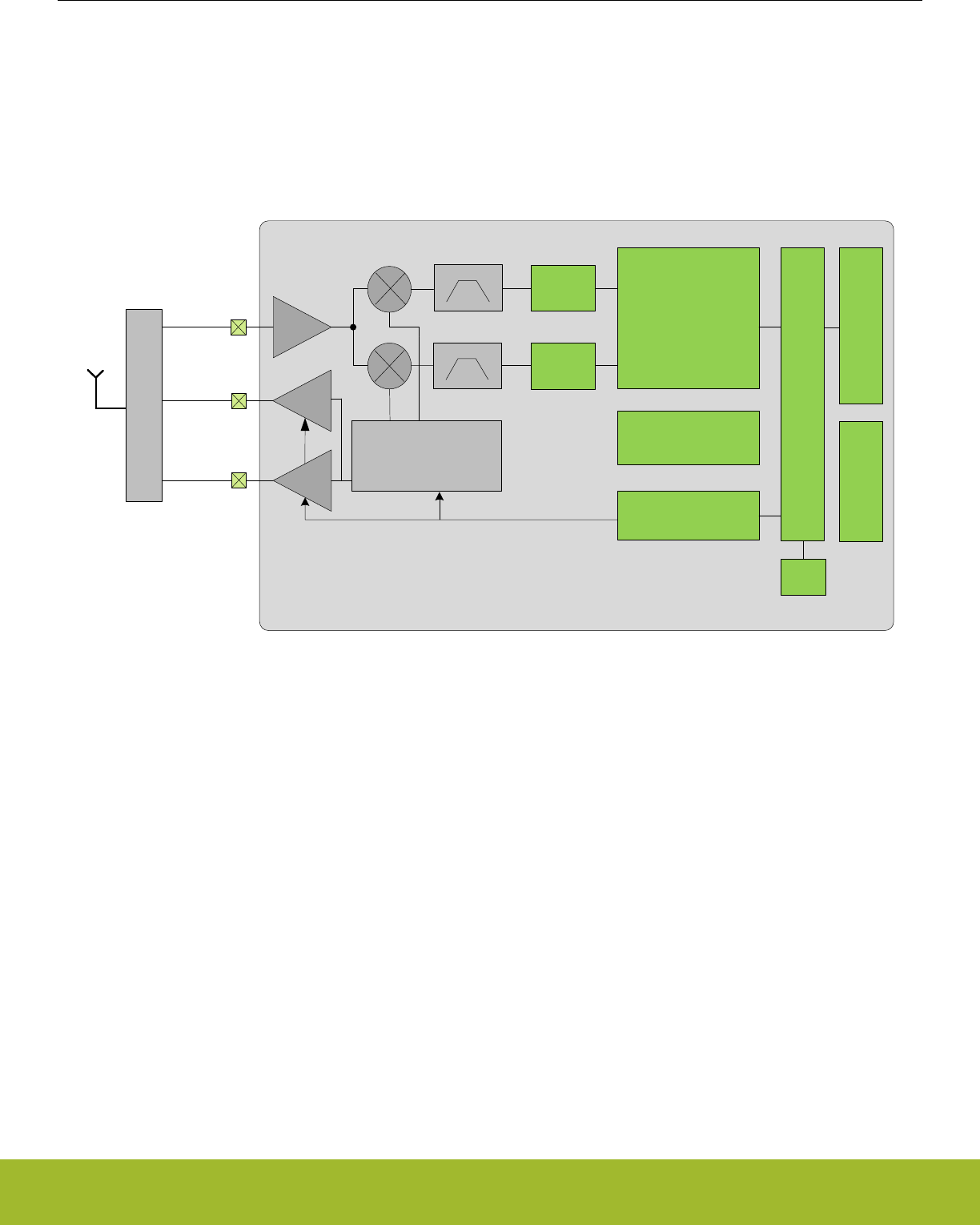
6.1 Introduction
The Radio Transceiver of the EFR32 enables the user to control a wide range of settings and options for tailoring radio operation pre-
cisely to the users need. It provides access to the transmit and receive data buffers and supports both dynamic and static frame
lengths, as well as automatic address filtering and CRC insertion/verification.
As seen in the Radio Overview illustration (Figure 6.1 Radio Overview on page 124), the radio consists of several modules all respon-
sible for specific tasks. Please refer to the abbreviations section (Appendix 1. Abbreviations) for a comprehensive description of acro-
nyms.
LNA
PA1
IFADC
IFADC
Demodulator
(DEMOD)
Fractional-N
Frequency
Synthesizer
Modulator
(MOD)
Frame Controller
(FRC)
Buffer Controller
(BUFC)
MATCH / FILTER
RFOUT1
Automatic
Gain Control
(AGC)
Radio Controller
(RAC)
PA0
RFOUT0
RFIN
Radio Transceiver
CRC
Figure 6.1. Radio Overview
During transmission (TX), the Radio Controller enables the SYNTH, Modulator and PA. The Modulator requests data from the Frame
Controller, which reads data from a buffer. Based upon modulation format and data to send, the Modulator manipulates the SYNTH to
output the correct frequency and phase. When the whole frame has been transmitted, the radio can automatically switch to receive
mode.
In receive mode (RX), the radio controller enables the LNA, SYNTH, Mixer, ADC and Demodulator. The Demodulator searches for valid
frames according to modulation format and data rate. If a frame is detected, the demodulated data is handed to the Frame Controller,
which stores the data in the Buffer. When the complete frame has been received (determined by the Frame Controller), it is possible to
either go to TX or stay in RX to search for a new frame.
The Radio Transceiver interface is accessible through software drivers provided by Silicon Labs.
Reference Manual
Radio Transceiver
silabs.com | Smart. Connected. Energy-friendly. Preliminary Rev. 0.5 | 124
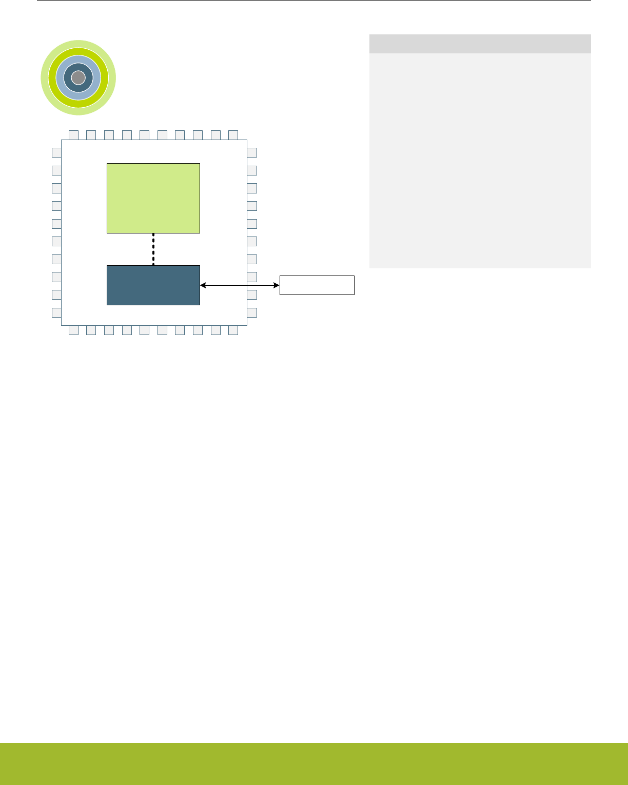
7. DBG - Debug Interface
0 1 2 3 4
ARM Cortex-M
DBG Debug Data
Quick Facts
What?
The Debug Interface is used to program and debug
EFR32xG13 Wireless Gecko devices.
Why?
The Debug Interface makes it easy to re-program
and update the system in the field, and allows de-
bugging with minimal I/O pin usage.
How?
The Cortex-M4 supports advanced debugging fea-
tures. EFR32xG13 Wireless Gecko devices can use
a minimum of two port pins for debugging or pro-
gramming. The internal and external state of the
system can be examined with debug extensions
supporting instruction or data access break and
watch points.
7.1 Introduction
The EFR32xG13 Wireless Gecko devices include hardware debug support through a 2-pin serial-wire debug (SWD) interface or a 4-pin
Joint Test Action Group (JTAG) interface , as well as an Embedded Trace Module (ETM) for data/instruction tracing.
For more technical information about the debug interface the reader is referred to:
• ARM Cortex-M4 Technical Reference Manual
• ARM CoreSight Components Technical Reference Manual
• ARM Debug Interface v5 Architecture Specification
• IEEE Standard for Test Access Port and Boundary-Scan Architecture, IEEE 1149.1-2013
7.2 Features
• Debug Access Port Serial Wire JTAG (DAPSWJ)
• Implements the ADIv5 debug interface
• Authentication Access Point (AAP)
• Implements various user commands
• Flash Patch and Breakpoint (FPB) unit
• Implement breakpoints and code patches
• Data Watch point and Trace (DWT) unit
• Implement watch points, trigger resources and system profiling
• Instrumentation Trace Macrocell (ITM)
• Application-driven trace source that supports printf style debugging
• Embedded Trace Macrocell v3.5 (ETM)
• Real time instruction and data trace information of the processor
7.3 Functional Description
Reference Manual
DBG - Debug Interface
silabs.com | Smart. Connected. Energy-friendly. Preliminary Rev. 0.5 | 125

7.3.1 Debug Pins
The following pins are the debug connections for the device:
• Serial Wire Clock Input and Test Clock Input (SWCLKTCK) : This pin is enabled after power-up and has a built-in pull down.
• Serial Wire Data Input/Output and Test Mode Select Input (SWDIOTMS) : This pin is enabled after power-up and has a built-in pull-
up.
• Test Data Output (TDO): This pin is assigned to JTAG functionality after power-up. However, it remains in high-Z state until the first
valid JTAG command is received.
• Test Data Input (TDI): This pin is assigned to JTAG functionality after power-up. However, it remains in high-Z state until the first
valid JTAG command is received. Once enabled, the pin has a built-in pull-up.
The debug pins have pull-down and pull-up enabled by default, so leaving them enabled may increase the current consumption if left
connected to supply or ground. The debug pins can be enabled and disabled through GPIO_ROUTE_PEN, see 33.3.4.2.3 Disabling
Debug Connections. Please remember that upon disabling the debug pins, debug contact with the device is lost once the DAPSWJ
power request bits are deasserted. By default after power cycle the part is debug pins are in JTAG mode. If during debugging session it
is switched to SWD mode, a power cycle is needed to bring it back to JTAG mode.
7.3.2 Embedded Trace Macrocell v3.5 (ETM)
The ETM makes it possible to trace both instruction and data from the processor in real time. The trace can be controlled through a set
of triggering and filtering resources. The resources include 4 address comparators, 2 data value comparators, 2 counters, a context ID
comparator and a sequencer. Before enabling the ETM, the AUXHFRCO clock needs to be enabled by setting AUXHFRCOEN in
CMU_OSCENCMD. The trace can be exported through a set of trace pins, which include:
• Trace Clock (TCLK): Functions as a sample clock for the trace. This pin is disabled after reset.
• Trace Data 0 - Trace Data 3 (TD0-TD3): The data pins provide the compressed trace stream. These pins are disabled after reset.
For information on how to configure the ETM, see the ARM Embedded Trace Macrocell Architecture Specification. The Trace Clock and
Trace Data pins can be enabled through the GPIO. For more information on how to enable the ETM Trace pins, the reader is referred to
33.3.4.2.4 ETM Trace Connections.
7.3.3 Debug and EM2 Deep Sleep/EM3 Stop
Leaving the debugger connected when issuing a WFI or WFE to enter EM2 Deep Sleep or EM3 Stop will make the system enter a
special EM2 Deep Sleep. This mode differs from regular EM2 Deep Sleep and EM3 Stop in that the high frequency clocks are still
enabled, and certain core functionality is still powered in order to maintain debug-functionality. Because of this, the current consumption
in this mode is closer to EM1 Sleep and it is therefore important to deassert the power requests in the DAPSWJ and disconnect the
debugger before doing current consumption measurements.
7.3.4 Authentication Access Point
The Authentication Acces Point (AAP) is a set of registers that provide a minimal amount of debugging and system level commands.
The AAP registers contain commands to issue a FLASH erase, a system reset, a CRC of user code pages, and stalling the system bus.
The user must program the APSEL bit field to 255 inside of the ARM DAPSWJ Debug Port SELECT register to access the AAP. The
AAP is only accessible from a debugger and not from the core.
7.3.4.1 Command Key
The AAP uses a command key to enable the DEVICEERASE and SYSRESETREQ AAP commands. The command key must be writ-
ten with the correct key in order for the commands to execute.
7.3.4.2 Device Erase
The device can be erased by writing AAP_CMDKEY followed by writing the DEVICEERASE register bit. Upon writing the command bit,
the ERASEBUSY bit is asserted. The ERASEBUSY bit will be de-asserted once the erase is complete. The SYSRESETREQ bit must
then be set to resume a normal debugger session. The DEVICEERASE register is available at all times through the AAP once the
CMDKEY is enetered.
7.3.4.3 System Reset
The system can be reset by writing AAP_CMDKEY followed by writing the SYSRESTREQ register bit. This must be done after assert-
ing DEVICEERASE or CRCREQ. Depending on the reset level setting for system reset, asserting SYSRESETREQ will either reset the
entire AAP register space or just the SYSRESETREQ bit. See 10.3.1 Reset levels for more details on reset levels. The SYSRESE-
TREQ register is available at all times through the AAP once the CMDKEY is enetered.
Reference Manual
DBG - Debug Interface
silabs.com | Smart. Connected. Energy-friendly. Preliminary Rev. 0.5 | 126
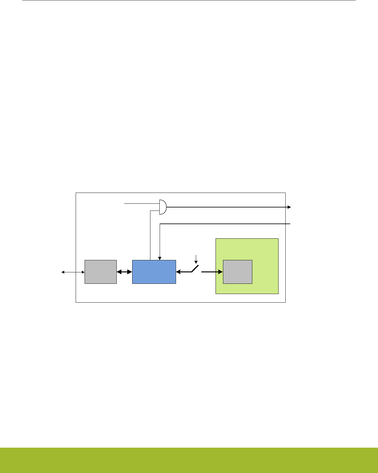
7.3.4.4 System Bus Stall
The system bus can be stalled at any time using the SYSBUSSTALL register bit. Once the SYSBUSSTALL is set, the system bus will
remain stalled until SYSBUSSTALL is cleared. While the system bus is stalled, only the registers inside the Cortex-M4, AAP and the
debugger can be accessed. The SYSBUSSTALL register is available at all times through the AAP.
7.3.4.5 User Flash Page CRC
The CRCREQ command initiates a CRC calculation on a given Flash Page. The CRC is only available on the Main, User Data, and
Lock Bit pages. It is highly recommended that the system bus is stalled before any CRCREQ commands are issued. The CRC calcula-
tion uses the on chip CRC block configured in 32 bit CRC mode. The Flash Page address for the CRCREQ command is written to the
CRCADDR register. After issuing the CRCREQ, the CRCBUSY flag is asserted. Once the CRCBUSY flag is de-asserted, the resulting
page CRC can be found in the CRCRESULT register. Once issuing a CRC command, the CPU is stalled and remains stalled until a
system reset occurs. Multiple CRC requests can occur before resetting the system. However, a CRC request that occurs while the
CRCBUSY flag is asserted will be ignored. The CRC registers are available at all times through the AAP.
7.3.5 Debug Lock
The debug access to the Cortex-M4 is locked by clearing the Debug Lock Word (DLW) and resetting the device, see 8.3.2 Lock Bits
(LB) Page Description.
When debug access is locked, the debugger can access the DAPSWJ and AAP registers. However, the connection to the Cortex-M4
core and the whole bus-system is blocked. This mechanism is controlled by the Authentication Access Port (AAP) as illustrated by
Figure 7.1 AAP - Authentication Access Port on page 127.
SW-DP AHB-AP
Cortex
SerialWire
debug
interface
DEVICEERASE
Authentication
Access Port
(AAP)
ERASEBUSY
ALW[3:0] == 0xF
DLW[3:0] == 0xF
Figure 7.1. AAP - Authentication Access Port
If the DLW is cleared, the device is locked. If the device is locked and the the AAP Lock Word (ALW) has not been cleared, it can be
unlocked by writing a valid key to the AAP_CMDKEY register and then setting the DEVICEERASE bit of the AAP_CMD register via the
debug interface. This operation erases the main block of flash, clears all lock bits, and debug access to the Cortex-M4 and bus-system
is enabled. The operation takes tens of mili seconds to complete. Note that the SRAM contents will also be deleted during a device
erase, while the UD-page is not erased.
The debugger may read the status of the device erase from the AAP_STATUS register. When the ERASEBUSY bit is set low after
DEVICEERASE of the AAP_CMD register is set, the debugger may set the SYSRESETREQ bit in the AAP_CMD register. After reset,
the debugger may resume a normal debug session through the AHB-AP.
7.3.6 AAP Lock
Take extreme caution when using this feature. Once the AAP has been locked, the state of the FLASH can not be changed via the
debugger.
Reference Manual
DBG - Debug Interface
silabs.com | Smart. Connected. Energy-friendly. Preliminary Rev. 0.5 | 127

7.3.7 Debugger reads of actionable registers
Some peripheral registers cause particular actions when read, e.g FIFOs which pop and IFC registers which clear the IF flags when
read. This can cause problems when debugging and the user wants to read the value without triggering the read action. For this rea-
son, by default, the peripherals will not execute these triggered actions when an attached debugger is performing the read accesses
through the AAP. To override this behavior, the debugger can configure the MASTERTYPE bitfield of the Cortex-M4 AHB Access Port
CSW register in order to emulate a core access when performing system bus transfers.
Note: Registers with actionable reads are noted in their register descriptions. Please refer to Table 1.1 Register Access Types on page
2 .
Note: The following peripherals do not respect the debugger master override, and so may still cause their triggered actions to occur
(e.g., when reading IFC):
7.3.8 Debug Recovery
Debug recovery is the ability to stall the system bus before the Cortex-M4 executes code. For example, the first few instructions may
disconnect the debugger pins. When this occurs it is difficult to connect the debugger and halt the Cortex-M4 before the Cortex-M4
starts to execute. By holding down pin reset, issuing the System Bus Stall AAP instruction, then releasing pin reset, the debugger can
stall the system bus before the Cortex-M4 has a chance to execute. Because the system is under reset during this procedure the De-
bugger can not look for ACK's from the part. Once the system bus is stalled, the FLASH can be erased by issuing the AAP_CMDKEY
and then the writting the DEVICEERASE in the AAP_CMD register.
7.4 Register Map
The offset register address is relative to the registers base address.
Offset Name Type Description
0x000 AAP_CMD W1 Command Register
0x004 AAP_CMDKEY W1 Command Key Register
0x008 AAP_STATUS RStatus Register
0x00C AAP_CTRL RW Control Register
0x010 AAP_CRCCMD W1 CRC Command Register
0x014 AAP_CRCSTATUS RCRC Status Register
0x018 AAP_CRCADDR RW CRC Address Register
0x01C AAP_CRCRESULT RCRC Result Register
0x0FC AAP_IDR RAAP Identification Register
Reference Manual
DBG - Debug Interface
silabs.com | Smart. Connected. Energy-friendly. Preliminary Rev. 0.5 | 128

7.5 Register Description
7.5.1 AAP_CMD - Command Register
Offset Bit Position
0x000
31
30
29
28
27
26
25
24
23
22
21
20
19
18
17
16
15
14
13
12
11
10
9
8
7
6
5
4
3
2
1
0
Reset
0
0
Access
W1
W1
Name
SYSRESETREQ
DEVICEERASE
Bit Name Reset Access Description
31:2 Reserved To ensure compatibility with future devices, always write bits to 0. More information in 1.2 Conven-
tions
1 SYSRESETREQ 0 W1 System Reset Request
A system reset request is generated when set to 1. This register is write enabled from the AAP_CMDKEY register.
0 DEVICEERASE 0 W1 Erase the Flash Main Block, SRAM and Lock Bits
When set, all data and program code in the main block is erased, the SRAM is cleared and then the Lock Bit (LB) page is
erased. This also includes the Debug Lock Word (DLW), causing debug access to be enabled after the next reset. The in-
formation block User Data page (UD) is left unchanged, but the User data page Lock Word (ULW) is erased. This register is
write enabled from the AAP_CMDKEY register.
7.5.2 AAP_CMDKEY - Command Key Register
Offset Bit Position
0x004
31
30
29
28
27
26
25
24
23
22
21
20
19
18
17
16
15
14
13
12
11
10
9
8
7
6
5
4
3
2
1
0
Reset
0x00000000
Access
W1
Name
WRITEKEY
Bit Name Reset Access Description
31:0 WRITEKEY 0x00000000 W1 CMD Key Register
The key value must be written to this register to write enable the AAP_CMD register.
Value Mode Description
0xCFACC118 WRITEEN Enable write to AAP_CMD
Reference Manual
DBG - Debug Interface
silabs.com | Smart. Connected. Energy-friendly. Preliminary Rev. 0.5 | 129

7.5.3 AAP_STATUS - Status Register
Offset Bit Position
0x008
31
30
29
28
27
26
25
24
23
22
21
20
19
18
17
16
15
14
13
12
11
10
9
8
7
6
5
4
3
2
1
0
Reset
0
0
Access
R
R
Name
LOCKED
ERASEBUSY
Bit Name Reset Access Description
31:2 Reserved To ensure compatibility with future devices, always write bits to 0. More information in 1.2 Conven-
tions
1 LOCKED 0 R AAP Locked
Set when the AAP is locked, .e.g the AAP Lock Word AAP lsb bits are not 0xF
0 ERASEBUSY 0 R Device Erase Command Status
This bit is set when a device erase is executing.
7.5.4 AAP_CTRL - Control Register
Offset Bit Position
0x00C
31
30
29
28
27
26
25
24
23
22
21
20
19
18
17
16
15
14
13
12
11
10
9
8
7
6
5
4
3
2
1
0
Reset
0
Access
RW
Name
SYSBUSSTALL
Bit Name Reset Access Description
31:1 Reserved To ensure compatibility with future devices, always write bits to 0. More information in 1.2 Conven-
tions
0 SYSBUSSTALL 0 RW Stall the System Bus
When this bit is set, the system bus is stalled. Only the Cortex registers are accessible
Reference Manual
DBG - Debug Interface
silabs.com | Smart. Connected. Energy-friendly. Preliminary Rev. 0.5 | 130

7.5.5 AAP_CRCCMD - CRC Command Register
Offset Bit Position
0x010
31
30
29
28
27
26
25
24
23
22
21
20
19
18
17
16
15
14
13
12
11
10
9
8
7
6
5
4
3
2
1
0
Reset
0
Access
W1
Name
CRCREQ
Bit Name Reset Access Description
31:1 Reserved To ensure compatibility with future devices, always write bits to 0. More information in 1.2 Conven-
tions
0 CRCREQ 0 W1 CRC Request
A CRC request is generated when set to 1. This command is not available if debug access or AAP is locked.
7.5.6 AAP_CRCSTATUS - CRC Status Register
Offset Bit Position
0x014
31
30
29
28
27
26
25
24
23
22
21
20
19
18
17
16
15
14
13
12
11
10
9
8
7
6
5
4
3
2
1
0
Reset
0
Access
R
Name
CRCBUSY
Bit Name Reset Access Description
31:1 Reserved To ensure compatibility with future devices, always write bits to 0. More information in 1.2 Conven-
tions
0 CRCBUSY 0 R CRC Calculation is busy
Set when the CRC calculation is executing. Will transition from 1 to 0 on valid data.
Reference Manual
DBG - Debug Interface
silabs.com | Smart. Connected. Energy-friendly. Preliminary Rev. 0.5 | 131

7.5.7 AAP_CRCADDR - CRC Address Register
Offset Bit Position
0x018
31
30
29
28
27
26
25
24
23
22
21
20
19
18
17
16
15
14
13
12
11
10
9
8
7
6
5
4
3
2
1
0
Reset
0x00000000
Access
RW
Name
CRCADDR
Bit Name Reset Access Description
31:0 CRCADDR 0x00000000 RW Starting Page Address for CRC Execution
Set this to the address the CRC executes on.
7.5.8 AAP_CRCRESULT - CRC Result Register
Offset Bit Position
0x01C
31
30
29
28
27
26
25
24
23
22
21
20
19
18
17
16
15
14
13
12
11
10
9
8
7
6
5
4
3
2
1
0
Reset
0x00000000
Access
R
Name
CRCRESULT
Bit Name Reset Access Description
31:0 CRCRESULT 0x00000000 R CRC Result of the CRCADDRESS
Result of the CRC calculation using the CRCADDRESS.
Reference Manual
DBG - Debug Interface
silabs.com | Smart. Connected. Energy-friendly. Preliminary Rev. 0.5 | 132

7.5.9 AAP_IDR - AAP Identification Register
Offset Bit Position
0x0FC
31
30
29
28
27
26
25
24
23
22
21
20
19
18
17
16
15
14
13
12
11
10
9
8
7
6
5
4
3
2
1
0
Reset
0x26E60011
Access
R
Name
ID
Bit Name Reset Access Description
31:0 ID 0x26E60011 R AAP Identification Register
Access port identification register in compliance with the ARM ADI v5 specification (JEDEC Manufacturer ID) .
Reference Manual
DBG - Debug Interface
silabs.com | Smart. Connected. Energy-friendly. Preliminary Rev. 0.5 | 133

8. MSC - Memory System Controller
0 1 2 3 4
01000101011011100110010101110010
01100111011110010010000001001101
01101001011000110111001001101111
00100000011100100111010101101100
01100101011100110010000001110100
01101000011001010010000001110111
01101111011100100110110001100100
00100000011011110110011000100000
01101100011011110111011100101101
01100101011011100110010101110010
01100111011110010010000001101101
01101001011000110111001001101111
01100011011011110110111001110100
01110010011011110110110001101100
01100101011100100010000001100100
01100101011100110110100101100111
01101110001000010100010101101110
Quick Facts
What?
The user can perform Flash memory read, read con-
figuration and write operations through the Memory
System Controller (MSC) .
Why?
The MSC allows the application code, user data and
flash lock bits to be stored in non-volatile Flash
memory. Certain memory system functions, such as
program memory wait-states and bus faults are also
configured from the MSC peripheral register inter-
face, giving the developer the ability to dynamically
customize the memory system performance, securi-
ty level, energy consumption and error handling ca-
pabilities to the requirements at hand.
How?
The MSC integrates a low-energy Flash IP with a
charge pump, enabling minimum energy consump-
tion while eliminating the need for external program-
ming voltage to erase the memory. An easy to use
write and erase interface is supported by an internal,
fixed-frequency oscillator and autonomous flash tim-
ing and control reduces software complexity while
not using other timer resources.
Application code may dynamically scale between
high energy optimization and high code execution
performance through advanced read modes.
A highly efficient low energy instruction cache re-
duces the number of flash reads significantly, thus
saving energy. Performance is also improved when
wait-states are used, since many of the wait-states
are eliminated. Built-in performance counters can be
used to measure the efficiency of the instruction
cache.
8.1 Introduction
The Memory System Controller (MSC) is the program memory unit of the EFR32xG13 Wireless Gecko microcontroller. The flash mem-
ory is readable and writable from both the Cortex-M4 and DMA. The flash memory is divided into two blocks; the main block and the
information block. Program code is normally written to the main block. Additionally, the information block is available for special user
data and flash lock bits. There is also a read-only page in the information block containing system and device calibration data. Read
and write operations are supported in the energy modes EM0 Active and EM1 Sleep.
Reference Manual
MSC - Memory System Controller
silabs.com | Smart. Connected. Energy-friendly. Preliminary Rev. 0.5 | 134

8.2 Features
• AHB read interface
•Scalable access performance to optimize the Cortex-M4 code interface
• Zero wait-state access up to 26 MHz
• Advanced energy optimization functionality
• Conditional branch target prefetch suppression
• Cortex-M4 disfolding of if-then (IT) blocks
• Instruction Cache
• DMA read support in EM0 Active and EM1 Sleep
• Command and status interface
• Flash write and erase
• Accessible from Cortex-M4 in EM0 Active
• DMA write support in EM0 Active and EM1 Sleep
• Core clock independent Flash timing
• Internal oscillator and internal timers for precise and autonomous Flash timing
• General purpose timers are not occupied during Flash erase and write operations
• Configurable interrupt erase abort
• Improved interrupt predictability
• Memory and bus fault control
• Security features
• Lockable debug access
• Page lock bits
• SW Mass erase Lock bits
• Authentication Access Port (AAP) lock bits
• End-of-write and end-of-erase interrupts
Reference Manual
MSC - Memory System Controller
silabs.com | Smart. Connected. Energy-friendly. Preliminary Rev. 0.5 | 135

8.3 Functional Description
The size of the main block is device dependent. The largest size available is 512 KB (256 pages). The information block has 2 KB
available for user data. The information block also contains chip configuration data located in a reserved area. The main block is map-
ped to address 0x00000000 and the information block is mapped to address 0x0FE00000. Table 8.1 MSC Flash Memory Mapping on
page 136 outlines how the Flash is mapped in the memory space. All Flash memory is organized into 2 KB pages.
Table 8.1. MSC Flash Memory Mapping
Block Page Base address Write/Erase by... Software reada-
ble?
Purpose/Name Size
Main10 0x00000000 Software, debug Yes User code and data 32 KB - 512 KB
... Software, debug Yes
255 0x0007F800 Software, debug Yes
Reserved - 0x00080000 - - Reserved for flash ex-
pansion
~24 MB
Information 0 0x0FE00000 Software, debug Yes User Data (UD) 2KB
- 0x0FE00800 - - Reserved -
1 0x0FE04000 Write: Software,
debug
Erase: Debug only
Yes Lock Bits (LB) 2KB
- 0x0FE04800 - - Reserved -
2 0x0FE081B0 - Yes Device Information (DI) 1KB
- 0x0FE08400 - - Reserved -
2 0x0FE0C000 - - 1KB
- 0x0FE0C400 - - Reserved -
3 0x0FE10000 - Yes Bootloader (BL) 16 KB
... - -
10 0x0FE13800 - -
Reserved - 0x0FE14000 - Reserved for flash
expansion
Rest of code space -
1 Block/page erased by a device erase
8.3.1 User Data (UD) Page Description
This is the user data page in the information block. The page can be erased and written by software. The page is erased by the ERA-
SEPAGE command of the MSC_WRITECMD register. Note that the page is not erased by a device erase operation. The device erase
operation is described in 7.3.4 Authentication Access Point.
Reference Manual
MSC - Memory System Controller
silabs.com | Smart. Connected. Energy-friendly. Preliminary Rev. 0.5 | 136

8.3.2 Lock Bits (LB) Page Description
This page contains the following information:
• Main block Page Lock Words (PLWs)
• User data page Lock Word (ULWs)
• Debug Lock Word (DLW)
• Mass erase Lock Word (MLW)
• Authentication Access Port (AAP) lock word (ALW)
• Bootloader enable (CLW0)
• Pin reset soft (CLW0)
The words in this page are organized as shown in Table 8.2 Lock Bits Page Structure on page 137:
Table 8.2. Lock Bits Page Structure
127 DLW
126 ULW
125 MLW
124 ALW
122 CLW0
N PLW[N]
… …
1 PLW[1]
0 PLW[0]
There are 32 page lock bits per page lock word (PLW). Bit 0 refers to the first page and bit 31 refers to the last page within a PLW.
Thus, PLW[0] contains lock bits for page 0-31 in the main block, PLW[1] contains lock bits for page 32-63 etc. A page is locked when
the bit is 0. A locked page cannot be erased or written.
Word 127 is the debug lock word (DLW). The four LSBs of this word are the debug lock bits. If these bits are 0xF, then debug access is
enabled. Debug access to the core is disabled from power-on reset until the DLW is evaluated immediately before the Cortex-M4 starts
execution of the user application code. If the bits are not 0xF, then debug access to the core remains blocked.
Word 126 is the user page lock word (ULW). Bit 0 of this word is the User Data Page lock bit. Bit 1 in this word locks the Lock Bits
Page. The lock bits can be reset by a device erase operation initiated from the Authentication Access Port (AAP) registers. The AAP is
described in more detail in 7.3.4 Authentication Access Point. Note that the AAP is only accessible from the debug interface, and can-
not be accessed from the Cortex-M4 core.
Word 125 is the mass erase lock word (MLW). Bit 0 locks the entire flash. The mass erase lock bits will not have any effect on device
erases initiated from the Authenitcation Access Port (AAP) registers. The AAP is described in more detail in 7.3.4 Authentication Ac-
cess Point.
Word 124 is the Authentication Access Port (AAP) lock word (ALW) and the four LSBs of this word are the lock bits. If these bits are
0xF, then AAP access is enabled. If the bits are not 0xF, AAP is disabled and it is impossible to access the device through the AAP. Bit
31 of the ALW may be used to allow AAP access under controlled conditions. If bit 31 is set to 1, software running on the device can
unlock AAP access using the MSC_AAPUNLOCKCMD register. If bit 31 is cleared to 0, software will not be able to use MSC_AAPUN-
LOCKCMD to unlock AAP access. NOTE - locking the AAP completely (including the LSBs and bit 31) is irreversible. Once the
AAP is locked, it will be impossible to perform an external mass erase and the AAP lock cannot be reset. The only way to pro-
gram the device when the AAP is locked is through a boot loader or by SW already loaded into the FLASH.
Word 122 is configuration word Zero. Bit 2 is the pinresetsoft bit. Bit 1 is the bootloader enable bit.
8.3.3 Device Information (DI) Page
This read-only page holds oscillator and ADC calibration data from the production test as well as an unique device ID. The page is
further described in .
Reference Manual
MSC - Memory System Controller
silabs.com | Smart. Connected. Energy-friendly. Preliminary Rev. 0.5 | 137

8.3.4 Bootloader
The memory space includes an area for custom-programmed bootloaders. The available bootloader area is 16 KB for this device family.
By default, the system is configured to boot directly into user software after system reset, and there is not a pre-programmed bootloader
in the device. If a custom bootloader which follows Silicon Labs' bootloader recommendations outlined in AN0003: UART Bootloader
(www.silabs.com/32bit-appnotes) is programmed into the bootloader area, the system can be redirected to boot from this area by set-
ting bit 1 in config lock word 0 (CLW0) at word 122 of the lockbit (LB) page.
After any device reset, the bootloader area is inaccessible to both software reads and writes. Reading and writing of this area may be
enabled with the MSC_BOOTLOADERCTRL register. Note that this register is write-once, so after writing the register, a reset of the
system is required in order to change permissions again.
Note: Software should never erase "Reserved" pages when bootloader write/erase is enabled. Doing so may cause the device to be-
come non-functional and irrevocably locked.
8.3.5 Device Revision
Family, FamilyAlt, RevMajor, RevMajorAlt, RevMinor can be accessed through ROM Table. The Revision number is extracted from the
PID2 and PID3 registers, as illustrated in Table 8.3 Revision Number Extraction on page 138.The Rev[7:4] and Rev[3:0] must be com-
bined to form the complete revision number Revision[7:0].
Table 8.3. Revision Number Extraction
PID2 (0xE00FFFE8) PID3 (0xE00FFFEC)
31:8 7:4 3:0 31:8 7:4 3:0
Rev[7:4] Rev[3:0]
The Revision number is to be interpreted according to Table 8.4 Revision Number Interpretation on page 138.
Table 8.4. Revision Number Interpretation
Revision[7:0] Revision
0x00 A
8.3.6 Post-reset Behavior
Calibration values are automatically written to registers by the MSC before application code startup. The values are also available to
read from the DI page for later reference by software. Other information such as the device ID and production date is also stored in the
DI page and is readable from software.
If the bootloader is not bypassed, the system will boot up from the bootloader at address 0x0FE10000.
Reference Manual
MSC - Memory System Controller
silabs.com | Smart. Connected. Energy-friendly. Preliminary Rev. 0.5 | 138

8.3.7 Flash Startup
On transitions from EM2/3 to EM0, the flash must be powered up. The time this takes depends on the current operating conditions. To
have a deterministic startup-time, set STDLY0 in MSC_STARTUP to 0x64 and clear STDLY1, ASTWAIT, STWSEN and STWS. This will
result in a 10 us delay before the flash is ready. The system will wake up before this, but the Cortex will stall on the first access to the
flash until it is ready. Execute code from RAM or cache to get a quicker startup
To get the fastest possible startup when wakeup, i.e. a startup that depends on the current operating conditions, set STDLY0 to 0x28
and set ASTWAIT in MSC_STARTUP. When configured this way, the system will poll the flash to determine when it is ready, and then
start execution.
For even quicker startup, run code in beginning with a set of wait-states. Set STDLY0 to 0x32, STDLY1 to 0x32, and set ASTWAIT and
STWSEN. Then configure STWS in MSC_STARTUP to the number of waitstates to run with. With this setup, sampling will begin with
the given number of waitstates after 5 us, and the system will run with this number of waitstates for the remaining 5 us before returning
to normal operation
A recommended setting for MSC_STARTUP register is to set STDLY0 to 0x32 for wait 5us and set ASTWAIT to one for active sampling
Set STWSEN to zero to bypass second delay period.
Flash wakeup on demand is supported when wakeup from EM2/3 to EM0. Set bit PWRUPONDEMAND of register MSC_CTRL to one
to enable the power up on demand. When enabled during powerup, flash will enter sleep mode and waiting for either pending flash
read transaction or software command to MSC_CMD.PWRUP bit. If software command wakeup, and interrupt of MSC_IF.PWRUPF will
be flaged if the MSC_IEN.PWRUPF is set
8.3.8 Wait-states
Table 8.5. Flash Wait-States
Wait-States Frequency
WS0 no more than 25 MHz
WS1 above 25 MHz and no more than 40 MHz
8.3.8.1 One Wait-state Access
After reset, the HFCORECLK is normally 19 MHz from the HFRCO and the MODE field of the MSC_READCTRL register is set to WS1
(one wait-state). The reset value must be WS1 as an uncalibrated HFRCO may produce a frequency higher than 26 MHz. Software
must not select a zero wait-state mode unless the clock is guaranteed to be 26 MHz or below, otherwise the resulting behavior is unde-
fined. If a HFCORECLK frequency above 26 MHz is to be set by software, the MODE field of the MSC_READCTRL register must be
set to WS1 or WS1SCBTP before the core clock is switched to the higher frequency clock source.
When changing to a lower frequency, the MODE field of the MSC_READCTRL register must be set to WS0 or WS0SCBTP only after
the frequency transition has completed. If the HFRCO is used, wait until the oscillator is stable on the new frequency. Otherwise, the
behavior is unpredictable.
To run at a frequency higher than 40 MHz, WS2 or WS2SCBTP must be selected to insert two wait-states for every flash access.
8.3.8.2 Zero Wait-state Access
At 26 MHz and below, read operations from flash may be performed without any wait-states. Zero wait-state access greatly improves
code execution performance at frequencies from 26 MHz and below. By default, the Cortex-M4 uses speculative prefetching and If-
Then block folding to maximize code execution performance at the cost of additional flash accesses and energy consumption.
8.3.8.3 Operation Above
To run at frequencies higher than 26 MHz, MODE in MSC_READCTRL must be set to WS1 or WS1SCBTP.
Reference Manual
MSC - Memory System Controller
silabs.com | Smart. Connected. Energy-friendly. Preliminary Rev. 0.5 | 139

8.3.9 Suppressed Conditional Branch Target Prefetch (SCBTP)
MSC offers a special instruction fetch mode which optimizes energy consumption by cancelling Cortex-M4 conditional branch target
prefetches. Normally, the Cortex-M4 core prefetches both the next sequential instruction and the instruction at the branch target ad-
dress when a conditional branch instruction reaches the pipeline decode stage. This prefetch scheme improves performance while one
extra instruction is fetched from memory at each conditional branch, regardless of whether the branch is taken or not. To optimize for
low energy, the MSC can be configured to cancel these speculative branch target prefetches. With this configuration, energy consump-
tion is more optimal, as the branch target instruction fetch is delayed until the branch condition is evaluated.
The performance penalty with this mode enabled is source code dependent, but is normally less than 1% for core frequencies from 26
MHz and below. To enable the mode at frequencies from 26 MHz and below write WS0SCBTP to the MODE field of the
MSC_READCTRL register. For frequencies above 26 MHz, use the WS1SCBTP mode, and for frequencies above 40 MHz, use the
WS2SCBTP mode. An increased performance penalty per clock cycle must be expected compared to WS0SCBTP mode. The perform-
ance penalty in WS1SCBTP/WS2SCBTP mode depends greatly on the density and organization of conditional branch instructions in
the code.
8.3.10 Cortex-M4 If-Then Block Folding
The Cortex-M4 offers a mechanism known as if-then block folding. This is a form of speculative prefetching where small if-then blocks
are collapsed in the prefetch buffer if the condition evaluates to false. The instructions in the block then appear to execute in zero cy-
cles. With this scheme, performance is optimized at the cost of higher energy consumption as the processor fetches more instructions
from memory than it actually executes. To disable the mode, write a 1 to the DISFOLD bit in the NVIC Auxiliary Control Register; see
the Cortex-M4 Technical Reference Manual for details. Normally, it is expected that this feature is most efficient at core frequencies
above 26 MHz. Folding is enabled by default.
Reference Manual
MSC - Memory System Controller
silabs.com | Smart. Connected. Energy-friendly. Preliminary Rev. 0.5 | 140
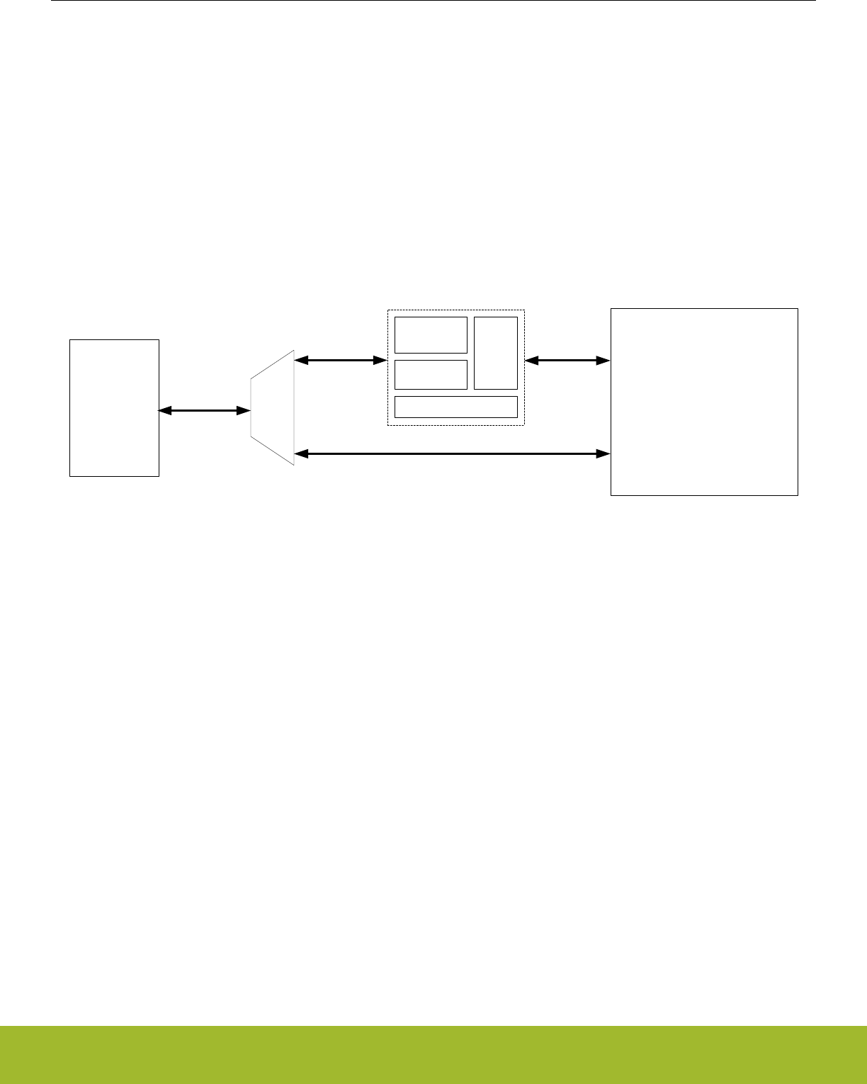
8.3.11 Instruction Cache
The MSC includes an instruction cache. The instruction cache for the internal flash memory is enabled by default, but can be disabled
by setting IFCDIS in MSC_READCTRL. When enabled, the instruction cache typically reduces the number of flash reads significantly,
thus saving energy. In most cases a cache hit-rate of more than 70 % is achievable. When a 32-bit instruction fetch hits in the cache the
data is returned to the processor in one clock cycle. Thus, performance is also improved when wait-states are used (i.e. running at
frequencies above 26 MHz).
The instruction cache is connected directly to the ICODE bus on the ARM core and functions as a memory access filter between the
processor and the memory system, as illustrated in Figure 8.1 Instruction Cache on page 141. The cache consists of an access filter,
lookup logic, SRAM, and two performance counters. The access filter checks that the address for the access is to on-chip flash memory
(instructions in RAM are not cached). If the address matches, the cache lookup logic and SRAM is enabled. Otherwise, the cache is
bypassed and the access is forwarded to the memory system. The cache is then updated when the memory access completes. The
access filter also disables cache updates for interrupt context accesses if caching in interrupt context is disabled. The performance
counters, when enabled, keep track of the number of cache hits and misses. The cachelines are filled up continuously one word at a
time as the individual words are requested by the processor. Thus, not all words of a cacheline might be valid at a given time.
ARM Core
SRAM
Access
Filter
Cache
Look-up Logic
ICODE
AHB-Lite Bus
ICODE
AHB-Lite Bus
CODE
Memory Space
Instruction Cache
Performance Counters
IDCODE
MUX
DCODE
AHB-Lite Bus
IDCODE
AHB-Lite Bus
Figure 8.1. Instruction Cache
By default, the instruction cache is automatically invalidated when the contents of the flash is changed (i.e. written or erased). In many
cases, however, the application only makes changes to data in the flash, not code. In this case, the automatic invalidate feature can be
disabled by setting AIDIS in MSC_READCTRL. The cache can (independent of the AIDIS setting) be manually invalidated by writing 1
to INVCACHE in MSC_CMD.
In general it is highly recommended to keep the cache enabled all the time. However, for some sections of code with very low cache hit-
rate more energy-efficient execution can be achieved by disabling the cache temporarily. To measure the hit-rate of a code-section, the
built-in performance counters can be used. Before the section, start the performance counters by writing 1 to STARTPC in MSC_CMD.
This starts the performance counters, counting from 0. At the end of the section, stop the performance counters by writing 1 to
STOPPC in MSC_CMD. The number of cache hits and cache misses for that section can then be read from MSC_CACHEHITS and
MSC_CACHEMISSES respectively. The total number of 32-bit instruction fetches will be MSC_CACHEHITS + MSC_CACHEMISSES.
Thus, the cache hit-ratio can be calculated as MSC_CACHEHITS / (MSC_CACHEHITS + MSC_CACHEMISSES). When MSC_CA-
CHEHITS overflows the CHOF interrupt flag is set. When MSC_CACHEMISSES overflows the CMOF interrupt flag is set. These flags
must be cleared explicitly by software. The range of the performance counters can thus be extended by increasing a counter in the
MSC interrupt routine. The performance counters only count when a cache lookup is performed. If the lookup fails, MSC_CACHEMISS-
ES is increased. If the lookup is successful, MSC_CACHEHITS is increased. For example, a cache lookup is not performed if the cache
is disabled or the code is executed from RAM.
Note: When caching of vector fetches and instructions in interrupt routines is disabled (ICCDIS in MSC_READCTRL is set), the per-
formance counters do not count when these types of fetches occur (i.e. while in interrupt context).
By default, interrupt vector fetches and instructions in interrupt routines are also cached. Some applications may get better cache uti-
lization by not caching instructions in interrupt context. This is done by setting ICCDIS in MSC_READCTRL. You should only set this bit
based on the results from a cache hit ratio measurement. In general, it is recommended to keep the ICCDIS bit cleared. Note that look-
ups in the cache are still performed, regardless of the ICCDIS setting - but instructions are not cached when cache misses occur inside
the interrupt routine. So, for example, if a cached function is called from the interrupt routine, the instructions for that function will be
taken from the cache.
Reference Manual
MSC - Memory System Controller
silabs.com | Smart. Connected. Energy-friendly. Preliminary Rev. 0.5 | 141

The cache content is not retained in EM2, EM3 and EM4. The cache is therefore invalidated regardless of the setting of AIDIS in
MSC_READCTRL when entering these energy modes. Applications that switch frequently between EM0 and EM2/3 and executes the
very same non-looping code almost every time will most likely benefit from putting this code in RAM. The interrupt vectors can also be
put in RAM to reduce current consumption even further.
8.3.12 Low Voltage Flash Read
The devices support low voltage flash reads. Because it takes a longer time to read from flash with a lower voltage supply
MSC_READCTRL.MODE should be programmed accordingly. It is recommended that software should follow certain sequences for
supply voltage scaling up and down. See the EMU chapter for details.
Flash write/erase is not supported in low voltage mode. Any write/erase command will be ignored if flash is operated in a low voltage
mode and the interrupt flag MSC_IF.LVEWRITE will be set.
8.3.13 Erase and Write Operations
Both page erase and write operations require that the address is written into the MSC_ADDRB register. For erase operations, the ad-
dress may be any within the page to be erased. Load the address by writing 1 to the LADDRIM bit in the MSC_WRITECMD register.
The LADDRIM bit only has to be written once when loading the first address. After each word is written the internal address register
ADDR will be incremented automatically by 4. The INVADDR bit of the MSC_STATUS register is set if the loaded address is outside the
flash and the LOCKED bit of the MSC_STATUS register is set if the page addressed is locked. Any attempts to command erase of or
write to the page are ignored if INVADDR or the LOCKED bits of the MSC_STATUS register are set. To abort an ongoing erase, set the
ERASEABORT bit in the MSC_WRITECMD register.
When a word is written to the MSC_WDATA register, the WDATAREADY bit of the MSC_STATUS register is cleared. When this status
bit is set, software or DMA may write the next word.
A single word write is commanded by setting the WRITEONCE bit of the MSC_WRITECMD register. The operation is complete when
the BUSY bit of the MSC_STATUS register is cleared and control of the flash is handed back to the AHB interface, allowing application
code to resume execution.
For a DMA write the software must write the first word to the MSC_WDATA register and then set the WRITETRIG bit of the
MSC_WRITECMD register. DMA triggers when the WDATAREADY bit of the MSC_STATUS register is set.
It is possible to write words twice between each erase by keeping at 1 the bits that are not to be changed. Let us take as an example
writing two 16 bit values, 0xAAAA and 0x5555. To safely write them in the same flash word this method can be used:
• Write 0xFFFFAAAA (word in flash becomes 0xFFFFAAAA)
• Write 0x5555FFFF (word in flash becomes 0x5555AAAA)
Note that there is a maximum of two writes to the same word between each erase due to a physical limitation of the flash.
Note:
Flash write/erase is not supported in low voltage mode. Any write/erase command will be ignored if flash is operated in a low voltage
mode and the interrupt flag MSC_IF.LVEWRITE will be set.
Note:
During a write or erase, flash read accesses will be stalled, effectively halting code execution from flash. Code execution continues
upon write/erase completion. Code residing in RAM may be executed during a write/erase operation.
8.3.13.1 Mass erase
A mass erase can be initiated from software using ERASEMAIN0 MSC_WRITECMD. This command will start a mass erase of the en-
tire flash. Prior to initiating a mass erase, MSC_MASSLOCK must be unlocked by writing 0x631A to it. After a mass erase has been
started, this register can be locked again to prevent runaway code from accidentally triggering a mass erase.
The regular flash page lock bits will not prevent a mass erase. To prevent software from initiating mass erases, use the mass erase lock
bits in the mass erase lock word (MLW).
Reference Manual
MSC - Memory System Controller
silabs.com | Smart. Connected. Energy-friendly. Preliminary Rev. 0.5 | 142

8.4 Register Map
The offset register address is relative to the registers base address.
Offset Name Type Description
0x000 MSC_CTRL RWH Memory System Control Register
0x004 MSC_READCTRL RWH Read Control Register
0x008 MSC_WRITECTRL RW Write Control Register
0x00C MSC_WRITECMD W1 Write Command Register
0x010 MSC_ADDRB RW Page Erase/Write Address Buffer
0x018 MSC_WDATA RW Write Data Register
0x01C MSC_STATUS RStatus Register
0x030 MSC_IF RInterrupt Flag Register
0x034 MSC_IFS W1 Interrupt Flag Set Register
0x038 MSC_IFC (R)W1 Interrupt Flag Clear Register
0x03C MSC_IEN RW Interrupt Enable Register
0x040 MSC_LOCK RWH Configuration Lock Register
0x044 MSC_CACHECMD W1 Flash Cache Command Register
0x048 MSC_CACHEHITS RCache Hits Performance Counter
0x04C MSC_CACHEMISSES RCache Misses Performance Counter
0x054 MSC_MASSLOCK RWH Mass Erase Lock Register
0x05C MSC_STARTUP RW Startup Control
0x074 MSC_CMD W1 Command Register
0x090 MSC_BOOTLOADERCTRL RW Bootloader read and write enable, write once register
0x094 MSC_AAPUNLOCKCMD W1 Software Unlock AAP Command Register
0x098 MSC_CACHECONFIG0 RW Cache Configuration Register 0
Reference Manual
MSC - Memory System Controller
silabs.com | Smart. Connected. Energy-friendly. Preliminary Rev. 0.5 | 143

8.5 Register Description
8.5.1 MSC_CTRL - Memory System Control Register
Offset Bit Position
0x000
31
30
29
28
27
26
25
24
23
22
21
20
19
18
17
16
15
14
13
12
11
10
9
8
7
6
5
4
3
2
1
0
Reset
0
0
0
0
1
Access
RW
RW
RW
RW
RW
Name
TIMEOUTFAULTEN
IFCREADCLEAR
PWRUPONDEMAND
CLKDISFAULTEN
ADDRFAULTEN
Bit Name Reset Access Description
31:5 Reserved To ensure compatibility with future devices, always write bits to 0. More information in 1.2 Conven-
tions
4 TIMEOUTFAULTEN 0 RW Timeout Bus Fault Response Enable
When this bit is set, bus faults are generated when the bus system times out during an access, e.g., when reading a regis-
ter from an LE peripheral that is changing too fast to get a stable value
3 IFCREADCLEAR 0 RW IFC Read Clears IF
This bit controls what happens when an IFC register in a module is read.
Value Description
0 IFC register reads 0. No side-effect when reading.
1 IFC register reads the same value as IF, and the corresponding inter-
rupt flags are cleared.
2 PWRUPONDEMAND 0 RW Power Up On Demand During Wake Up
When set, during wake up, pending AHB transfer will cause MSC to issue power up request to CMU. If not set, will always
issue power up request if PWRUPONCMD is not set either.
1CLKDISFAULTEN 0 RW Clock-disabled Bus Fault Response Enable
When this bit is set, busfaults are generated on accesses to peripherals/system devices with clocks disabled
0 ADDRFAULTEN 1 RW Invalid Address Bus Fault Response Enable
When this bit is set, busfaults are generated on accesses to unmapped parts of system and code address space
Reference Manual
MSC - Memory System Controller
silabs.com | Smart. Connected. Energy-friendly. Preliminary Rev. 0.5 | 144

8.5.2 MSC_READCTRL - Read Control Register
Offset Bit Position
0x004
31
30
29
28
27
26
25
24
23
22
21
20
19
18
17
16
15
14
13
12
11
10
9
8
7
6
5
4
3
2
1
0
Reset
0
0x1
0
1
0
0
0
Access
RW
RWH
RW
RW
RW
RW
RW
Name
SCBTP
MODE
USEHPROT
PREFETCH
ICCDIS
AIDIS
IFCDIS
Bit Name Reset Access Description
31:29 Reserved To ensure compatibility with future devices, always write bits to 0. More information in 1.2 Conven-
tions
28 SCBTP 0 RW Suppress Conditional Branch Target Perfetch
Enable suppressed Conditional Branch Target Prefetch (SCBTP) function. SCBTP saves energy by delaying Cortex-M con-
ditional branch target prefetches until the conditional branch instruction is in the execute stage. When the instruction rea-
ches this stage, the evaluation of the branch condition is completed and the core does not perform a speculative prefetch of
both the branch target address and the next sequential address. With the SCBTP function enabled, one instruction fetch is
saved for each branch not taken, with a negligible performance penalty.
27:26 Reserved To ensure compatibility with future devices, always write bits to 0. More information in 1.2 Conven-
tions
25:24 MODE 0x1 RWH Read Mode
After reset, the core clock is 19 MHz from the HFRCO and the MODE field of MSC_READCTRL register is set to WS1. The
reset value is WS1 because the HFRCO may produce a frequency above 19 MHz before it is calibrated. A large wait states
is associated with high frequency. When changing to a higher frequency, this register must be set to a large wait states first
before the core clock is switched to the higher frequency. When changing to a lower frequency, this register should be set
to lower wait states after the frequency transition has been completed. If the HFRCO is used as clock source, wait until the
oscillator is stable on the new frequency to avoid unpredictable behavior.See Flash Wait-States table for the corresponding
threshold for different wait-states.
Value Mode Description
0 WS0 Zero wait-states inserted in fetch or read transfers
1 WS1 One wait-state inserted for each fetch or read transfer. See Flash Wait-
States table for details
2 WS2 Two wait-states inserted for eatch fetch or read transfer. See Flash
Wait-States table for details
3 WS3 Three wait-states inserted for eatch fetch or read transfer. See Flash
Wait-States table for details
23:10 Reserved To ensure compatibility with future devices, always write bits to 0. More information in 1.2 Conven-
tions
9 USEHPROT 0 RW AHB_HPROT Mode
Use ahb_hrpot to determine if the instruction is cacheable or not
8 PREFETCH 1 RW Prefetch Mode
Set to configure level of prefetching.
7:6 Reserved To ensure compatibility with future devices, always write bits to 0. More information in 1.2 Conven-
tions
Reference Manual
MSC - Memory System Controller
silabs.com | Smart. Connected. Energy-friendly. Preliminary Rev. 0.5 | 145

Bit Name Reset Access Description
5 ICCDIS 0 RW Interrupt Context Cache Disable
Set this bit to automatically disable caching of vector fetches and instruction fetches in interrupt context. Cache lookup will
still be performed in interrupt context. When set, the performance counters will not count when these types of fetches occur.
4 AIDIS 0 RW Automatic Invalidate Disable
When this bit is set the cache is not automatically invalidated when a write or page erase is performed.
3 IFCDIS 0 RW Internal Flash Cache Disable
Disable instruction cache for internal flash memory.
2:0 Reserved To ensure compatibility with future devices, always write bits to 0. More information in 1.2 Conven-
tions
8.5.3 MSC_WRITECTRL - Write Control Register
Offset Bit Position
0x008
31
30
29
28
27
26
25
24
23
22
21
20
19
18
17
16
15
14
13
12
11
10
9
8
7
6
5
4
3
2
1
0
Reset
0
0
Access
RW
RW
Name
IRQERASEABORT
WREN
Bit Name Reset Access Description
31:2 Reserved To ensure compatibility with future devices, always write bits to 0. More information in 1.2 Conven-
tions
1 IRQERASEABORT 0 RW Abort Page Erase on Interrupt
When this bit is set to 1, any Cortex-M interrupt aborts any current page erase operation. Executing that interrupt vector
from Flash will halt the CPU.
0 WREN 0 RW Enable Write/Erase Controller
When this bit is set, the MSC write and erase functionality is enabled
Reference Manual
MSC - Memory System Controller
silabs.com | Smart. Connected. Energy-friendly. Preliminary Rev. 0.5 | 146

8.5.4 MSC_WRITECMD - Write Command Register
Offset Bit Position
0x00C
31
30
29
28
27
26
25
24
23
22
21
20
19
18
17
16
15
14
13
12
11
10
9
8
7
6
5
4
3
2
1
0
Reset
0
0
0
0
0
0
0
0
Access
W1
W1
W1
W1
W1
W1
W1
W1
Name
CLEARWDATA
ERASEMAIN0
ERASEABORT
WRITETRIG
WRITEONCE
WRITEEND
ERASEPAGE
LADDRIM
Bit Name Reset Access Description
31:13 Reserved To ensure compatibility with future devices, always write bits to 0. More information in 1.2 Conven-
tions
12 CLEARWDATA 0 W1 Clear WDATA state
Will set WDATAREADY and DMA request. Should only be used when no write is active.
11:9 Reserved To ensure compatibility with future devices, always write bits to 0. More information in 1.2 Conven-
tions
8 ERASEMAIN0 0 W1 Mass erase region 0
Initiate mass erase of region 0. Before use MSC_MASSLOCK must be unlocked. To completely prevent access from soft-
ware, clear bit 0 in the mass erase lock-word (MLW)
7:6 Reserved To ensure compatibility with future devices, always write bits to 0. More information in 1.2 Conven-
tions
5 ERASEABORT 0 W1 Abort erase sequence
Writing to this bit will abort an ongoing erase sequence.
4 WRITETRIG 0 W1 Word Write Sequence Trigger
Start write of the first word written to MSC_WDATA, then add 4 to ADDR and write the next word if available within a 30us
timeout. When ADDR is incremented past the page boundary, ADDR is set to the base of the page. If WDOUBLE is set,
two words are required every time, and ADDR is incremented by 8.
3 WRITEONCE 0 W1 Word Write-Once Trigger
Write the word in MSC_WDATA to ADDR. Flash access is returned to the AHB interface as soon as the write operation
completes. The WREN bit in the MSC_WRITECTRL register must be set in order to use this command. Only a single word
is written, but the internal address is also incremented to allow a direct write of a new word without loading a new address
2 WRITEEND 0 W1 End Write Mode
Write 1 to end write mode when using the WRITETRIG command.
1 ERASEPAGE 0 W1 Erase Page
Erase any user defined page selected by the MSC_ADDRB register. The WREN bit in the MSC_WRITECTRL register must
be set in order to use this command.
0 LADDRIM 0 W1 Load MSC_ADDRB into ADDR
Load the internal write address register ADDR from the MSC_ADDRB register. The internal address register ADDR is incre-
mented automatically by 4 after each word is written. When ADDR is incremented past the page boundary, ADDR is set to
the base of the page.
Reference Manual
MSC - Memory System Controller
silabs.com | Smart. Connected. Energy-friendly. Preliminary Rev. 0.5 | 147

8.5.5 MSC_ADDRB - Page Erase/Write Address Buffer
Offset Bit Position
0x010
31
30
29
28
27
26
25
24
23
22
21
20
19
18
17
16
15
14
13
12
11
10
9
8
7
6
5
4
3
2
1
0
Reset
0x00000000
Access
RW
Name
ADDRB
Bit Name Reset Access Description
31:0 ADDRB 0x00000000 RW Page Erase or Write Address Buffer
This register holds the page address for the erase or write operation. This register is loaded into the internal MSC_ADDR
register when the LADDRIM field in MSC_CMD is set.
8.5.6 MSC_WDATA - Write Data Register
Offset Bit Position
0x018
31
30
29
28
27
26
25
24
23
22
21
20
19
18
17
16
15
14
13
12
11
10
9
8
7
6
5
4
3
2
1
0
Reset
0x00000000
Access
RW
Name
WDATA
Bit Name Reset Access Description
31:0 WDATA 0x00000000 RW Write Data
The data to be written to the address in MSC_ADDR. This register must be written when the WDATAREADY bit of
MSC_STATUS is set.
Reference Manual
MSC - Memory System Controller
silabs.com | Smart. Connected. Energy-friendly. Preliminary Rev. 0.5 | 148

8.5.7 MSC_STATUS - Status Register
Offset Bit Position
0x01C
31
30
29
28
27
26
25
24
23
22
21
20
19
18
17
16
15
14
13
12
11
10
9
8
7
6
5
4
3
2
1
0
Reset
0x0
0x0
0
0
0
1
0
0
0
Access
R
R
R
R
R
R
R
R
R
Name
PWRUPCKBDFAILCOUNT
WDATAVALID
PCRUNNING
ERASEABORTED
WORDTIMEOUT
WDATAREADY
INVADDR
LOCKED
BUSY
Bit Name Reset Access Description
31:28 PWRUPCKBDFAIL-
COUNT
0x0 R Flash power up checkerboard pattern check fail count
This field tells how many times checkboard pattern check fail occured after a reset sequence.
27:24 WDATAVALID 0x0 R Write data buffer valid flag
This field tells how many valid data in the write buffer, each bit indicates one buffer entry
23:7 Reserved To ensure compatibility with future devices, always write bits to 0. More information in 1.2 Conven-
tions
6 PCRUNNING 0 R Performance Counters Running
This bit is set while the performance counters are running. When one performance counter reaches the maximum value,
this bit is cleared.
5 ERASEABORTED 0 R The Current Flash Erase Operation Aborted
When set, the current erase operation was aborted by interrupt.
4 WORDTIMEOUT 0 R Flash Write Word Timeout
When this bit is set, MSC_WDATA was not written within the timeout. The flash write operation timed out and access to the
flash is returned to the AHB interface. This bit is cleared when the ERASEPAGE, WRITETRIG or WRITEONCE commands
in MSC_WRITECMD are triggered.
3WDATAREADY 1 R WDATA Write Ready
When this bit is set, the content of MSC_WDATA is read by MSC Flash Write Controller and the register may be updated
with the next 32-bit word to be written to flash. This bit is cleared when writing to MSC_WDATA.
2 INVADDR 0 R Invalid Write Address or Erase Page
Set when software attempts to load an invalid (unmapped) address into ADDR
1 LOCKED 0 R Access Locked
When set, the last erase or write is aborted due to erase/write access constraints
0 BUSY 0 R Erase/Write Busy
When set, an erase or write operation is in progress and new commands are ignored
Reference Manual
MSC - Memory System Controller
silabs.com | Smart. Connected. Energy-friendly. Preliminary Rev. 0.5 | 149

8.5.8 MSC_IF - Interrupt Flag Register
Offset Bit Position
0x030
31
30
29
28
27
26
25
24
23
22
21
20
19
18
17
16
15
14
13
12
11
10
9
8
7
6
5
4
3
2
1
0
Reset
0
0
0
0
0
0
0
0
Access
R
R
R
R
R
R
R
R
Name
LVEWRITE
WDATAOV
ICACHERR
PWRUPF
CMOF
CHOF
WRITE
ERASE
Bit Name Reset Access Description
31:9 Reserved To ensure compatibility with future devices, always write bits to 0. More information in 1.2 Conven-
tions
8 LVEWRITE 0 R Flash LVE Write Error Flag
If one, flash controller write command received while in LVE mode
7 Reserved To ensure compatibility with future devices, always write bits to 0. More information in 1.2 Conven-
tions
6 WDATAOV 0 R Flash controller write buffer overflow
If one, flash controller write buffer overflow detected
5 ICACHERR 0 R iCache RAM Parity Error Flag
If one, iCache RAM parity Error detected
4 PWRUPF 0 R Flash Power Up Sequence Complete Flag
Set after MSC_CMD.PWRUP received, flash powered up complete and ready for read/write
3 CMOF 0 R Cache Misses Overflow Interrupt Flag
Set when MSC_CACHEMISSES overflows
2 CHOF 0 R Cache Hits Overflow Interrupt Flag
Set when MSC_CACHEHITS overflows
1 WRITE 0 R Write Done Interrupt Read Flag
Set when a write is done
0 ERASE 0 R Erase Done Interrupt Read Flag
Set when erase is done
Reference Manual
MSC - Memory System Controller
silabs.com | Smart. Connected. Energy-friendly. Preliminary Rev. 0.5 | 150

8.5.9 MSC_IFS - Interrupt Flag Set Register
Offset Bit Position
0x034
31
30
29
28
27
26
25
24
23
22
21
20
19
18
17
16
15
14
13
12
11
10
9
8
7
6
5
4
3
2
1
0
Reset
0
0
0
0
0
0
0
0
Access
W1
W1
W1
W1
W1
W1
W1
W1
Name
LVEWRITE
WDATAOV
ICACHERR
PWRUPF
CMOF
CHOF
WRITE
ERASE
Bit Name Reset Access Description
31:9 Reserved To ensure compatibility with future devices, always write bits to 0. More information in 1.2 Conven-
tions
8 LVEWRITE 0 W1 Set LVEWRITE Interrupt Flag
Write 1 to set the LVEWRITE interrupt flag
7 Reserved To ensure compatibility with future devices, always write bits to 0. More information in 1.2 Conven-
tions
6 WDATAOV 0 W1 Set WDATAOV Interrupt Flag
Write 1 to set the WDATAOV interrupt flag
5 ICACHERR 0 W1 Set ICACHERR Interrupt Flag
Write 1 to set the ICACHERR interrupt flag
4 PWRUPF 0 W1 Set PWRUPF Interrupt Flag
Write 1 to set the PWRUPF interrupt flag
3 CMOF 0 W1 Set CMOF Interrupt Flag
Write 1 to set the CMOF interrupt flag
2 CHOF 0 W1 Set CHOF Interrupt Flag
Write 1 to set the CHOF interrupt flag
1 WRITE 0 W1 Set WRITE Interrupt Flag
Write 1 to set the WRITE interrupt flag
0 ERASE 0 W1 Set ERASE Interrupt Flag
Write 1 to set the ERASE interrupt flag
Reference Manual
MSC - Memory System Controller
silabs.com | Smart. Connected. Energy-friendly. Preliminary Rev. 0.5 | 151

8.5.10 MSC_IFC - Interrupt Flag Clear Register
Offset Bit Position
0x038
31
30
29
28
27
26
25
24
23
22
21
20
19
18
17
16
15
14
13
12
11
10
9
8
7
6
5
4
3
2
1
0
Reset
0
0
0
0
0
0
0
0
Access
(R)W1
(R)W1
(R)W1
(R)W1
(R)W1
(R)W1
(R)W1
(R)W1
Name
LVEWRITE
WDATAOV
ICACHERR
PWRUPF
CMOF
CHOF
WRITE
ERASE
Bit Name Reset Access Description
31:9 Reserved To ensure compatibility with future devices, always write bits to 0. More information in 1.2 Conven-
tions
8 LVEWRITE 0 (R)W1 Clear LVEWRITE Interrupt Flag
Write 1 to clear the LVEWRITE interrupt flag. Reading returns the value of the IF and clears the corresponding interrupt
flags (This feature must be enabled globally in MSC.).
7 Reserved To ensure compatibility with future devices, always write bits to 0. More information in 1.2 Conven-
tions
6 WDATAOV 0 (R)W1 Clear WDATAOV Interrupt Flag
Write 1 to clear the WDATAOV interrupt flag. Reading returns the value of the IF and clears the corresponding interrupt
flags (This feature must be enabled globally in MSC.).
5 ICACHERR 0 (R)W1 Clear ICACHERR Interrupt Flag
Write 1 to clear the ICACHERR interrupt flag. Reading returns the value of the IF and clears the corresponding interrupt
flags (This feature must be enabled globally in MSC.).
4 PWRUPF 0 (R)W1 Clear PWRUPF Interrupt Flag
Write 1 to clear the PWRUPF interrupt flag. Reading returns the value of the IF and clears the corresponding interrupt flags
(This feature must be enabled globally in MSC.).
3 CMOF 0 (R)W1 Clear CMOF Interrupt Flag
Write 1 to clear the CMOF interrupt flag. Reading returns the value of the IF and clears the corresponding interrupt flags
(This feature must be enabled globally in MSC.).
2 CHOF 0 (R)W1 Clear CHOF Interrupt Flag
Write 1 to clear the CHOF interrupt flag. Reading returns the value of the IF and clears the corresponding interrupt flags
(This feature must be enabled globally in MSC.).
1 WRITE 0 (R)W1 Clear WRITE Interrupt Flag
Write 1 to clear the WRITE interrupt flag. Reading returns the value of the IF and clears the corresponding interrupt flags
(This feature must be enabled globally in MSC.).
0 ERASE 0 (R)W1 Clear ERASE Interrupt Flag
Write 1 to clear the ERASE interrupt flag. Reading returns the value of the IF and clears the corresponding interrupt flags
(This feature must be enabled globally in MSC.).
Reference Manual
MSC - Memory System Controller
silabs.com | Smart. Connected. Energy-friendly. Preliminary Rev. 0.5 | 152

8.5.11 MSC_IEN - Interrupt Enable Register
Offset Bit Position
0x03C
31
30
29
28
27
26
25
24
23
22
21
20
19
18
17
16
15
14
13
12
11
10
9
8
7
6
5
4
3
2
1
0
Reset
0
0
0
0
0
0
0
0
Access
RW
RW
RW
RW
RW
RW
RW
RW
Name
LVEWRITE
WDATAOV
ICACHERR
PWRUPF
CMOF
CHOF
WRITE
ERASE
Bit Name Reset Access Description
31:9 Reserved To ensure compatibility with future devices, always write bits to 0. More information in 1.2 Conven-
tions
8 LVEWRITE 0 RW LVEWRITE Interrupt Enable
Enable/disable the LVEWRITE interrupt
7 Reserved To ensure compatibility with future devices, always write bits to 0. More information in 1.2 Conven-
tions
6 WDATAOV 0 RW WDATAOV Interrupt Enable
Enable/disable the WDATAOV interrupt
5 ICACHERR 0 RW ICACHERR Interrupt Enable
Enable/disable the ICACHERR interrupt
4 PWRUPF 0 RW PWRUPF Interrupt Enable
Enable/disable the PWRUPF interrupt
3 CMOF 0 RW CMOF Interrupt Enable
Enable/disable the CMOF interrupt
2 CHOF 0 RW CHOF Interrupt Enable
Enable/disable the CHOF interrupt
1 WRITE 0 RW WRITE Interrupt Enable
Enable/disable the WRITE interrupt
0 ERASE 0 RW ERASE Interrupt Enable
Enable/disable the ERASE interrupt
Reference Manual
MSC - Memory System Controller
silabs.com | Smart. Connected. Energy-friendly. Preliminary Rev. 0.5 | 153

8.5.12 MSC_LOCK - Configuration Lock Register
Offset Bit Position
0x040
31
30
29
28
27
26
25
24
23
22
21
20
19
18
17
16
15
14
13
12
11
10
9
8
7
6
5
4
3
2
1
0
Reset
0x0000
Access
RWH
Name
LOCKKEY
Bit Name Reset Access Description
31:16 Reserved To ensure compatibility with future devices, always write bits to 0. More information in 1.2 Conven-
tions
15:0 LOCKKEY 0x0000 RWH Configuration Lock
Write any other value than the unlock code to lock access to MSC_CTRL, MSC_READCTRL, MSC_WRITECMD,
MSC_STARTUP and MSC_AAPUNLOCKCMD. Write the unlock code to enable access. When reading the register, bit 0 is
set when the lock is enabled.
Mode Value Description
Read Operation
UNLOCKED 0 MSC registers are unlocked
LOCKED 1 MSC registers are locked
Write Operation
LOCK 0 Lock MSC registers
UNLOCK 0x1B71 Unlock MSC registers
Reference Manual
MSC - Memory System Controller
silabs.com | Smart. Connected. Energy-friendly. Preliminary Rev. 0.5 | 154

8.5.13 MSC_CACHECMD - Flash Cache Command Register
Offset Bit Position
0x044
31
30
29
28
27
26
25
24
23
22
21
20
19
18
17
16
15
14
13
12
11
10
9
8
7
6
5
4
3
2
1
0
Reset
0
0
0
Access
W1
W1
W1
Name
STOPPC
STARTPC
INVCACHE
Bit Name Reset Access Description
31:3 Reserved To ensure compatibility with future devices, always write bits to 0. More information in 1.2 Conven-
tions
2 STOPPC 0 W1 Stop Performance Counters
Use this commant bit to stop the performance counters.
1 STARTPC 0 W1 Start Performance Counters
Use this command bit to start the performance counters. The performance counters always start counting from 0.
0 INVCACHE 0 W1 Invalidate Instruction Cache
Use this register to invalidate the instruction cache.
8.5.14 MSC_CACHEHITS - Cache Hits Performance Counter
Offset Bit Position
0x048
31
30
29
28
27
26
25
24
23
22
21
20
19
18
17
16
15
14
13
12
11
10
9
8
7
6
5
4
3
2
1
0
Reset
0x00000
Access
R
Name
CACHEHITS
Bit Name Reset Access Description
31:20 Reserved To ensure compatibility with future devices, always write bits to 0. More information in 1.2 Conven-
tions
19:0 CACHEHITS 0x00000 R Cache hits since last performance counter start command.
Use to measure cache performance for a particular code section.
Reference Manual
MSC - Memory System Controller
silabs.com | Smart. Connected. Energy-friendly. Preliminary Rev. 0.5 | 155

8.5.15 MSC_CACHEMISSES - Cache Misses Performance Counter
Offset Bit Position
0x04C
31
30
29
28
27
26
25
24
23
22
21
20
19
18
17
16
15
14
13
12
11
10
9
8
7
6
5
4
3
2
1
0
Reset
0x00000
Access
R
Name
CACHEMISSES
Bit Name Reset Access Description
31:20 Reserved To ensure compatibility with future devices, always write bits to 0. More information in 1.2 Conven-
tions
19:0 CACHEMISSES 0x00000 R Cache misses since last performance counter start command.
Use to measure cache performance for a particular code section.
Reference Manual
MSC - Memory System Controller
silabs.com | Smart. Connected. Energy-friendly. Preliminary Rev. 0.5 | 156

8.5.16 MSC_MASSLOCK - Mass Erase Lock Register
Offset Bit Position
0x054
31
30
29
28
27
26
25
24
23
22
21
20
19
18
17
16
15
14
13
12
11
10
9
8
7
6
5
4
3
2
1
0
Reset
0x0001
Access
RWH
Name
LOCKKEY
Bit Name Reset Access Description
31:16 Reserved To ensure compatibility with future devices, always write bits to 0. More information in 1.2 Conven-
tions
15:0 LOCKKEY 0x0001 RWH Mass Erase Lock
Write any other value than the unlock code to lock access the the ERASEMAINn commands. Write the unlock code 631A to
enable access. When reading the register, bit 0 is set when the lock is enabled. Locked by default.
Mode Value Description
Read Operation
UNLOCKED 0 Mass erase unlocked
LOCKED 1 Mass erase locked
Write Operation
LOCK 0 Lock mass erase
UNLOCK 0x631A Unlock mass erase
Reference Manual
MSC - Memory System Controller
silabs.com | Smart. Connected. Energy-friendly. Preliminary Rev. 0.5 | 157

8.5.17 MSC_STARTUP - Startup Control
Offset Bit Position
0x05C
31
30
29
28
27
26
25
24
23
22
21
20
19
18
17
16
15
14
13
12
11
10
9
8
7
6
5
4
3
2
1
0
Reset
0x1
0
1
1
0x001
0x04D
Access
RW
RW
RW
RW
RW
RW
Name
STWS
STWSAEN
STWSEN
ASTWAIT
STDLY1
STDLY0
Bit Name Reset Access Description
31 Reserved To ensure compatibility with future devices, always write bits to 0. More information in 1.2 Conven-
tions
30:28 STWS 0x1 RW Startup Waitstates
Active wait for flash startup startup after SDLY0.
27 Reserved To ensure compatibility with future devices, always write bits to 0. More information in 1.2 Conven-
tions
26 STWSAEN 0 RW Startup Waitstates Always Enable
Use the number of waitstates given by STWS during startup always.
25 STWSEN 1 RW Startup Waitstates Enable
Use the number of waitstates given by STWS during startup. During the optional STDLY1 timeout.
24 ASTWAIT 1 RW Active Startup Wait
Active wait for flash startup startup after SDLY0.
23:22 Reserved To ensure compatibility with future devices, always write bits to 0. More information in 1.2 Conven-
tions
21:12 STDLY1 0x001 RW Startup Delay 0
Number of cycles with startup waitstates, and also the maximum number of cycles startup sampling will be attempted be-
fore starting up system.
11:10 Reserved To ensure compatibility with future devices, always write bits to 0. More information in 1.2 Conven-
tions
9:0 STDLY0 0x04D RW Startup Delay 0
Number of idle cycles from exiting sleep mode.
Reference Manual
MSC - Memory System Controller
silabs.com | Smart. Connected. Energy-friendly. Preliminary Rev. 0.5 | 158

8.5.18 MSC_CMD - Command Register
Offset Bit Position
0x074
31
30
29
28
27
26
25
24
23
22
21
20
19
18
17
16
15
14
13
12
11
10
9
8
7
6
5
4
3
2
1
0
Reset
0
Access
W1
Name
PWRUP
Bit Name Reset Access Description
31:1 Reserved To ensure compatibility with future devices, always write bits to 0. More information in 1.2 Conven-
tions
0 PWRUP 0 W1 Flash Power Up Command
Write to this bit to power up the Flash. IRQ PWRUPF will be fired when power up sequence completed.
8.5.19 MSC_BOOTLOADERCTRL - Bootloader read and write enable, write once register
Offset Bit Position
0x090
31
30
29
28
27
26
25
24
23
22
21
20
19
18
17
16
15
14
13
12
11
10
9
8
7
6
5
4
3
2
1
0
Reset
0
0
Access
RW
RW
Name
BLWDIS
BLRDIS
Bit Name Reset Access Description
31:2 Reserved To ensure compatibility with future devices, always write bits to 0. More information in 1.2 Conven-
tions
1 BLWDIS 0 RW Flash Bootloader Write/Erase Eanble
Enable the erase and program flash bootloader pages
0 BLRDIS 0 RW Flash Bootloader Read Enable
Enable the read access of flash bootloader pages
Reference Manual
MSC - Memory System Controller
silabs.com | Smart. Connected. Energy-friendly. Preliminary Rev. 0.5 | 159

8.5.20 MSC_AAPUNLOCKCMD - Software Unlock AAP Command Register
Offset Bit Position
0x094
31
30
29
28
27
26
25
24
23
22
21
20
19
18
17
16
15
14
13
12
11
10
9
8
7
6
5
4
3
2
1
0
Reset
0
Access
W1
Name
UNLOCKAAP
Bit Name Reset Access Description
31:1 Reserved To ensure compatibility with future devices, always write bits to 0. More information in 1.2 Conven-
tions
0 UNLOCKAAP 0 W1 Software unlock AAP command
Write to this bit to unlock AAP. This is only possible when bit 31 of the AAP Lock Word (ALW) in flash is set to 1. If bit 31 of
the ALW has been cleared to 0, this command has no effect. Register is writable only when MSC_LOCK is unlocked
Reference Manual
MSC - Memory System Controller
silabs.com | Smart. Connected. Energy-friendly. Preliminary Rev. 0.5 | 160

8.5.21 MSC_CACHECONFIG0 - Cache Configuration Register 0
Offset Bit Position
0x098
31
30
29
28
27
26
25
24
23
22
21
20
19
18
17
16
15
14
13
12
11
10
9
8
7
6
5
4
3
2
1
0
Reset
0x3
Access
RW
Name
CACHELPLEVEL
Bit Name Reset Access Description
31:2 Reserved To ensure compatibility with future devices, always write bits to 0. More information in 1.2 Conven-
tions
1:0 CACHELPLEVEL 0x3 RW Instruction Cache Low-Power Level
Use this to set the low-power level of the cache. In general, the default setting is best for most applications.
Value Mode Description
0 BASE Base instruction cache functionality.
1 ADVANCED Advanced buffering mode, where the cache uses the fetch pattern to
predict highly accessed data and store it in low-energy memory.
3 MINACTIVITY Minimum activity mode, which allows the cache to minimize activity in
logic that it predicts has a low probability being used. This mode can
introduce wait-states into the instruction fetch stream when the cache
exits one of its low-activity states. The number of wait-states introduced
is small, but users running with 0-wait-state memory and wishing to re-
duce the variability that the cache might introduce with additional wait-
states may wish to lower the cache low-power level. Note, this mode
includes the advanced buffering mode functionality.
Reference Manual
MSC - Memory System Controller
silabs.com | Smart. Connected. Energy-friendly. Preliminary Rev. 0.5 | 161
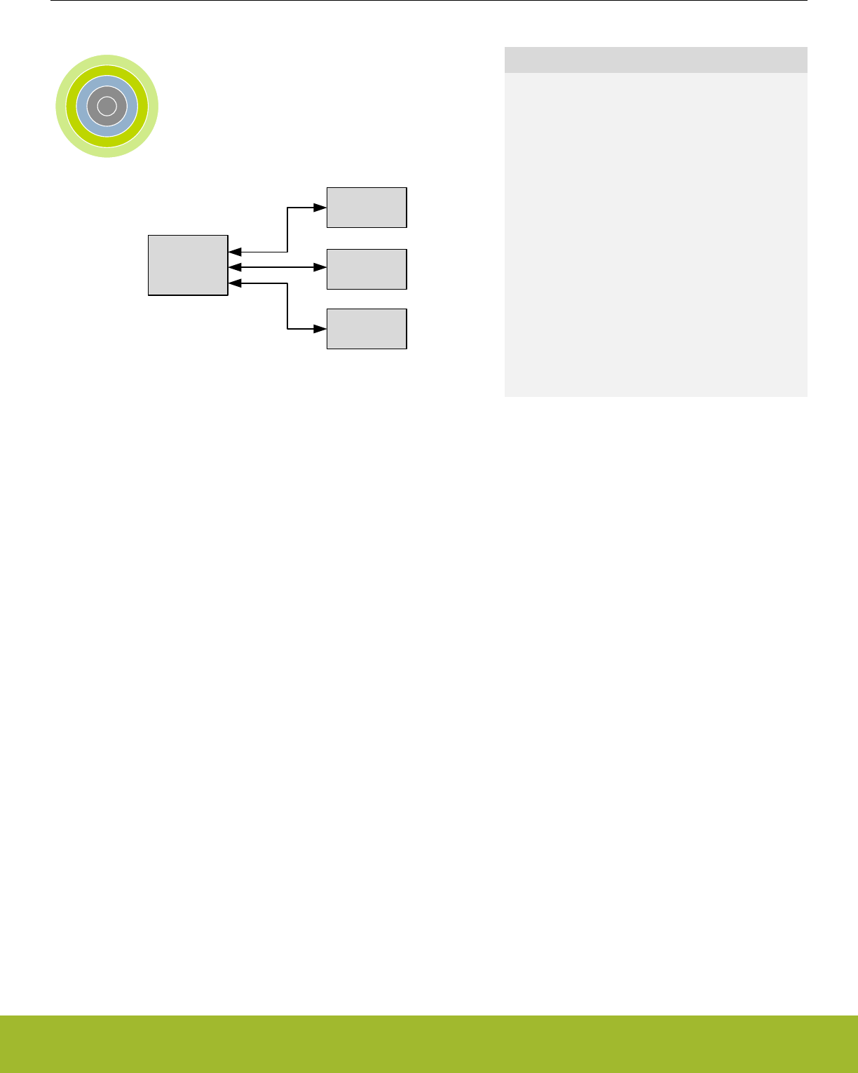
9. LDMA - Linked DMA Controller
0 1 2 3 4
DMA
controller
Flash
RAM
Peripherals
Quick Facts
What?
The LDMA controller can move data without CPU in-
tervention, effectively reducing the energy consump-
tion for a data transfer.
Why?
The LDMA can perform data transfers more energy
efficiently than the CPU and allows autonomous op-
eration in low energy modes. For example the
LEUART can provide full UART communication in
EM2 Deep Sleep, consuming only a few µA by using
the LDMA to move data between the LEUART and
RAM.
How?
The LDMA controller has multiple highly configura-
ble, prioritized DMA channels. A linked list of flexible
descriptors makes it possible to tailor the controller
to the specific needs of an application.
9.1 Introduction
The Linked Direct Memory Access (LDMA) controller performs memory transfer operations independently of the CPU. This has the
benefit of reducing the energy consumption and the workload of the CPU, and enables the system to stay in low energy modes while
still routing data to memory and peripherals. For example, moving data from the LEUART to memory or memory to LEUART. Each of
the DMA channels on the EFR32 can be connected to any of the EFR32 peripherals.
Reference Manual
LDMA - Linked DMA Controller
silabs.com | Smart. Connected. Energy-friendly. Preliminary Rev. 0.5 | 162

9.1.1 Features
• Flexible Source and Destination transfers
•Memory-to-memory
• Memory-to-peripheral
• Peripheral-to-memory
• Peripheral-to-peripheral
• DMA transfers triggered by peripherals, software, or linked list
• Single or multiple data transfers for each peripheral or software request
• Inter-channel and hardware event synchronization via trigger and wait functions
• Supports single or multiple descriptors
• Single descriptor
• Linked list of descriptors
• Circular and ping-pong buffers
• Scatter-Gather
• Looping
• Pause and restart triggered by other channels
• Sophisticated flow control which can function without CPU interaction
• Channel arbitration includes:
• Fixed priority
• Simple round robin
• Round robin with programmable multiple interleaved entries for higher priority requesters
• Programmable data size and source and destination address strides
• Programmable interrupt generation at the end of each DMA descriptor execution
• Little-endian/big-endian conversion
• DMA write-immediate function
Reference Manual
LDMA - Linked DMA Controller
silabs.com | Smart. Connected. Energy-friendly. Preliminary Rev. 0.5 | 163
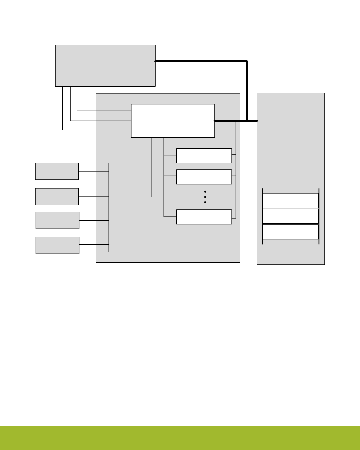
9.2 Block Diagram
An overview of the LDMA and the modules it interacts with is shown in Figure 9.1 LDMA Block Diagram on page 164.
LDMA
LDMA Core
Cortex
Error
Interrupts
Channel
done
Peripheral
Peripheral
Channel
select
Peripheral
Peripheral
Channel 0
Channel 1
Channel N
ACK/
REQ
AHB
RAM
Descriptor A
Descriptor B
Descriptor C
Figure 9.1. LDMA Block Diagram
The Linked DMA Controller consists of three main parts
• A DMA core that executes transfers and communicates status to the core
• A channel select block that routes peripheral DMA requests and acknowledge signals to the DMA
• A set of internal channel configuration registers for tracking the progress of each DMA channel
The DMA has access to all system memory through the AHB bus and the AHB->APB bridge. It can load channel descriptors from mem-
ory with no CPU intervention.
Reference Manual
LDMA - Linked DMA Controller
silabs.com | Smart. Connected. Energy-friendly. Preliminary Rev. 0.5 | 164

9.3 Functional Description
The Linked DMA Controller is highly flexible. It is capable of transferring data between peripherals and memory without involvement
from the processor core. This can be used to increase system performance by off-loading the processor from copying large amounts of
data or avoiding frequent interrupts to service peripherals needing more data or having available data. It can also be used to reduce the
system energy consumption by making the LDMA work autonomously with some EM2/3 peripherals for data transfer without having to
wake up the processor core from sleep.
The Linked DMA Controller has 8 independent channels. Each of these channels can be connected to any of the available peripheral
DMA transfer request input sources by writing to the channel configuration registers, see 9.3.2 Channel Configuration. In addition, each
channel can also be triggered directly by software, which is useful for memory-to-memory transfers.
The channel descriptors determine what the Linked DMA Controller will do when it receives DMA transfer request. The initial descriptor
is written directly to the LDMA's channel registers. If desired, the initial descriptor can link to additional linked descriptors stored in mem-
ory (RAM or Flash). Alternatively, software may also load the initial descriptor by writing the descriptor address to the LDMA_CHx_LINK
register and then setting the corresponding bit the LDMA_LINKLOAD register.
Before enabling a channel, the software must take care to properly configure the channel registers including the link address and any
linked descriptors. When a channel is triggered, the Linked DMA Controller will perform the memory transfers as specified by the de-
scriptors. A descriptor contains the memory address to read from, the memory address to write to, link address of the next descriptor,
the number of bytes to be transferred, etc. The channel descriptor is described in detail in 9.3.7 Channel descriptor data structure.
The Linked DMA Controller supports both fixed priority and round robin arbitration. The number of fixed and round robin channels is
programmable. For round robin channels, the number of arbitration slots requested for each channel is programmable. Using this
scheme, it is possible to ensure that timing-critical transfers are serviced on time.
DMA transfers take place by reading a block of data at a time from the source, storing it in the LDMA’s local FIFO, then writing the block
out to the destination from the FIFO. Interrupts may optionally be signaled to the CPU’s interrupt controller at the end of any DMA trans-
fer or at the completion of a descriptor if the DONEIFSEN bit is set. An AHB error will always generate an interrupt.
9.3.1 Channel Descriptor
Each DMA channel has descriptor registers. A transfer can be initialized by software writing to the registers or by the DMA itself copying
a descriptor from RAM to memory. When using a linked list of descriptors the first descriptor should be initialized by the CPU. The DMA
itself will then copy linked descriptors to its descriptor registers as required. In addition to manually initializing the first transfer, software
may also cause the LDMA to load the initial descriptor by writing the descriptor address to the LDMA_CHx_LINK register and then set-
ting the corresponding bit the LDMA_LINKLOAD register.
The contents of the descriptor registers are dynamically updated during the DMA transfer. The contents of descriptors in memory are
not edited by the controller.
Some descriptor field values are only used for linked descriptors. For example, the SRCMODE and DSTMODE bits of the
LDMA_CHx_CTRL registers determine if a linked descriptor is using relative or absolute addressing. Software writes to the address
registers will always use absolute addressing and never set these bits. Therefore, these bits are read only.
9.3.1.1 DMA Transfer Size
A DMA transfer is the smallest unit of data that can be transfered by the LDMA. The LDMA supports byte, half-word and word sized
transfers. The SIZE field in the LDMA_CHx_CTRL register specifies the data width of one DMA transfer.
9.3.1.2 Source/Destination Increments
The SRCINC and DSTINC in the LDMA_CHx_CTRL register determines the increment between DMA transfers. The increment is in
units of DMA transfers and using an increment size of 1 will transfer contiguous bytes, half-words, or words depending on the value of
the SIZE field. Multiple unit increments are useful for transferring or packing/unpacking alligned data. For example using an increment
of 4 with a size of BYTE will transfer word aligned bytes. An increment of 2 units with a size of HALFWORD is suitable for the transfer
of word aligned half-word data. The LDMA can also pack or unpack data by using a different increment size for source and destination.
For example - to convert from word aligned byte data (unpacked) to contiguous byte data (packed), set the SIZE to BYTE, SRCINC to
4, and DSTINC to 1.
SIZE may also be set to NONE which will cause the LDMA to read or write the same location for every DMA transfer. This is usefull for
accessing peripheral FIFO or data registers.
Reference Manual
LDMA - Linked DMA Controller
silabs.com | Smart. Connected. Energy-friendly. Preliminary Rev. 0.5 | 165

9.3.1.3 Block Size
The block size defines the amount of data transferred in one arbitration. It consists of one or more DMA transfers. See 9.3.6.1 Arbitra-
tion Priority for more details.
9.3.1.4 Transfer Count
The descriptor transfer count defines how many DMA transfers to perform. The number of bytes transferred by the descripter will de-
pend on both the transfer count XFERCNT and the SIZE field settings. TOTAL_BYTES = XFERCNT * SIZE
9.3.1.5 Descriptor List
A descriptor list consists of one or more descriptors which are executed in serially. This list may be a simple sequence of descriptors, a
loop of descriptors, or a combination of the two.
Each descriptor in the list can be one of several types.
• Single Transfer descriptor: Transfers TOTAL_BYTES of data and then stops.
• Linked Transfer descriptor: Transfers TOTAL_BYTES of data and then loads the next linked descriptor.
• Loop Transfer descriptor: Transfers TOTAL_BYTES of data and performs loop control (see 9.3.2.2 Loop Counter).
• Sync descriptor: Handle synchronization of the list with other entities (see 9.3.7.2 SYNC descriptor structure).
• WRI descriptor: Writes a value to a location in memory (see 9.3.7.3 WRI descriptor structure).
9.3.1.6 Addresses
Before initiating a transfer, software should write the source address, destination address, and if applicable the link address to the de-
scriptor registers. Alternatively, software may load a descriptor from memory by writing the descriptor address to the LDMA_CHx_LINK
register and setting the corresponding bit in the LDMA_LINKLOAD register.
During a DMA transfer, the DMA source and destination address registers are pointers to the next transfer address. The LDMA will
update the SRC and DST addresses after each transfer. If software halts a DMA transfer by clearing the enable bit, the SRC and DST
addresses will indicate the next transfer address.
When a desriptor is finished the DMA will either halt or load the next (linked) descriptor depending on the value of the LINK field in the
LDMA_Chx_LINK register. After loading a linked descriptor, the descriptor registers will reflect the content of the loaded descriptor. Note
that the linked descriptor must be word aligned in memory. The two least significant bits of the LDMA_CHx_LINK register are used by
the LINK and LINKMODE bits. The two least significant bits of the link address are always zero.
9.3.1.7 Addressing Modes
The DMA descriptors support absolute addressing or relative addressing. When using relative addressing, the offset is relative to the
current contents of the respective address registers. Regardless of the descriptor addressing modes, the address registers always indi-
cate the absolute address. For example, when loading a descriptor using relative SRC addressing, the LDMA will add the descriptor
source address (offset) to the contents of the SRCADDR register (base address). After loading, the SRCADDR register will indicate the
absolute address of the loaded descriptor.
The initial descriptor must use absolute addressing. The LDMA will ignore the DSTMODE, SRCMODE, and LINKMODE bits for the
initial descriptor and interpret the addresses as an absolute addresses.
Relative addressing is most useful for the link address. The initial descriptor will indicate the absolute address of the linked descriptors
in memory. The linked descriptors might be an array of structures. In this case the offset between descriptors is constant and is always
4 words or 16 bytes (each descriptor has 4 words). The LINK address is not incremented or decremented after each transfer. Thus, a
relative offset of 0x10 may be used for all linked descriptors.
The source and destination addresses also support relative addressing. When using relative addressing with the source or destination
address registers, the LDMA adds the relative offset to the current contents of the respective address register. Since the source and
destination addresses are normally incremented after each transfer, the final address will point to one unit past the last transfer. Thus,
an offset of zero will give the next sequential data address.
See the example 9.4.6 2D Copy for an common use of relative addressing.
Reference Manual
LDMA - Linked DMA Controller
silabs.com | Smart. Connected. Energy-friendly. Preliminary Rev. 0.5 | 166
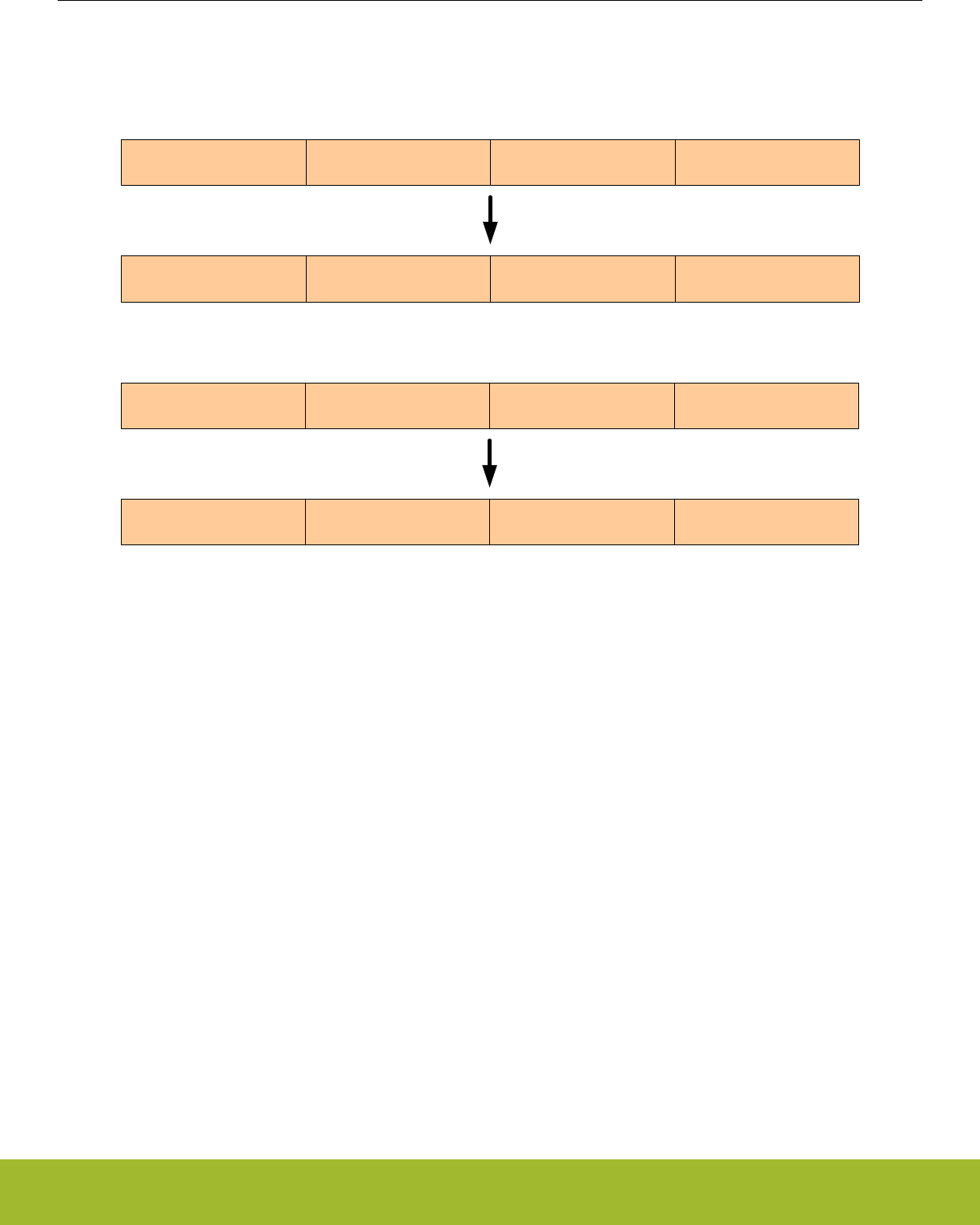
9.3.1.8 Byte Swap
Enabling byte swap reverses the endianness of the incoming source data read into the LDMA’s FIFO. Byte swap is only valid for trans-
fer sizes of word and half-word. Note that linked structure reads are not byte swapped.
B3 B2 B1 B0
B3b7 B3b0 B2b7 B2b0 B1b7 B1b0 B0b7 B0b0
B3B2B1B0 B3b7 B3b0B2b7 B2b0B1b7 B1b0B0b7 B0b0
BYTESWAP=1
SIZE=WORD
B1 B0
B3b7 B3b0 B2b7 B2b0 B1b7 B1b0 B0b7 B0b0
B1B0
B3b7 B3b0B2b7 B2b0 B1b7 B1b0B0b7 B0b0
BYTESWAP=1
SIZE=HALF
Figure 9.2. Word and Half-Word Endian Byte Swap Examples
Reference Manual
LDMA - Linked DMA Controller
silabs.com | Smart. Connected. Energy-friendly. Preliminary Rev. 0.5 | 167
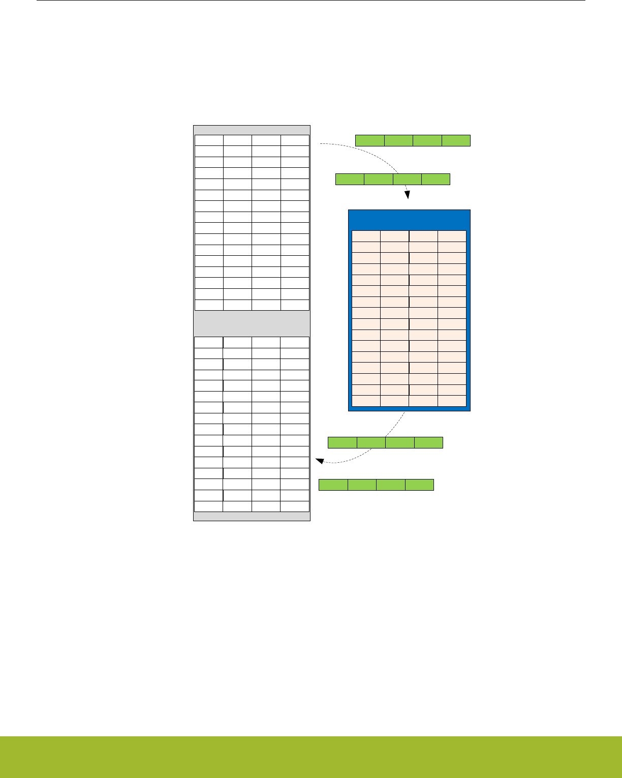
9.3.1.9 DMA Size and Source/Destination Increment Programming
The DMA channels’ SIZE, SRCINC, and DSTINC bit-fields are programmed to best utilize memory resources. They provide a means
for memory packing and unpacking, as well as for matching the size of data being transmitted to or received from an IO peripheral. The
following figure shows how 32-bit words of data are read from a memory source into the DMA’s internal transfer FIFO, and then written
out to the memory destination. The memory organization in bytes is shown as well as the first read to and write from the DMA’s FIFO.
size[1:0] = WORD
src_inc[1:0 ]= WORD
dst_inc[1:0 ]= WORD
0x200
0x400
source
destination
Memory
DMA Controller FIFO
kB3 kB2 kB1 kB0
First read transmit data=
kB3 kB2 kB1 kB0
First write transmit data=
kB3 kB2 kB1 kB0
xB3 xB2 xB1 xB0
yB3 yB2 yB1 yB0
zB3 zB2 zB1 zB0
wB3 wB2 wB1 wB0
lB3 lB2 lB1 lB0
mB3 mB2 mB1 mB0
nB3 nB2 nB1 nB0
oB3 oB2 oB1 oB0
pB3 pB2 pB1 pB0
qB3 qB2 qB1 qB0
rB3 rB2 rB1 rB0
sB3 sB2 sB1 sB0
tB3 tB2 tB1 tB0
uB3 uB2 uB1 uB0
vB3 vB2 vB1 vB0
kB3 kB2 kB1 kB0
lB3 lB2 lB1 lB0
mB3 mB2 mB1 mB0
kB3 kB2 kB1 kB0
lB3 lB2 lB1 lB0
mB3 mB2 mB1 mB0
nB3 nB2 nB1 nB0
Next read data=
oB3 opB2 oB1 oB0
Next write data=
nB3 nB2 nB1 nB0
Figure 9.3. Memory-to-Memory Transfer WORD Size Example
The next example shows four variations of half-word sized transfers, with all possible combinations of half- and full-word source and
destination increments. Note that when the size and source/destination increments are all configured for half-word, the resulting DMA
transfer organization is equivalent to the full-word sized transfer in the previous example. The difference is that the half-word configura-
tion requires twice as many DMA transfers.
Reference Manual
LDMA - Linked DMA Controller
silabs.com | Smart. Connected. Energy-friendly. Preliminary Rev. 0.5 | 168
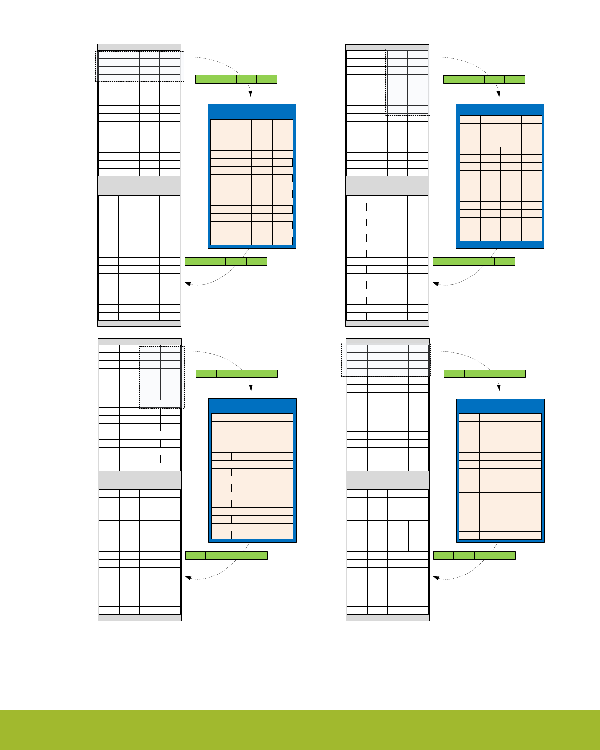
size[1:0] = HALF
src_inc[1:0] = HALF
dst_inc[1:0] = HALF
0x200
0x400
source
destination
Memory
DMA Controller FIFO
kB3 kB2 kB1 kB0
First read transmit data=
kB1 kB0
First write transmit data=
kB1 kB0
xB3 xB2 xB1 xB0
yB3 yB2 yB1 yB0
zB3 zB2 zB1 zB0
wB3 wB2 wB1 wB0
lB3 lB2 lB1 lB0
mB3 mB2 mB1 mB0
nB3 nB2 nB1 nB0
oB3 oB2 oB1 oB0
pB3 pB2 pB1 pB0
qB3 qB2 qB1 qB0
rB3 rB2 rB1 rB0
sB3 sB2 sB1 sB0
tB3 tB2 tB1 tB0
uB3 uB2 uB1 uB0
vB3 vB2 vB1 vB0
kB3 kB2 kB1 kB0
lB3 lB2 lB1 lB0
mB3 mB2 mB1 mB0
nB3 nB2 nB1 nB0
kB3 kB2 kB1 kB0
lB3 lB2 lB1 lB0
mB3 mB2 mB1 mB0
nB3 nB2 nB1 nB0
0x200
0x400
source
destination
Memory
DMA Controller FIFO
kB3 kB2 kB1 kB0
First read transmit data=
kB1 kB0
First write transmit data=
kB1 kB0
xB3 xB2 xB1 xB0
yB3 yB2 yB1 yB0
zB3 zB2 zB1 zB0
wB3 wB2 wB1 wB0
lB3 lB2 lB1 lB0
mB3 mB2 mB1 mB0
nB3 nB2 nB1 nB0
oB3 oB2 oB1 oB0
pB3 pB2 pB1 pB0
qB3 qB2 qB1 qB0
rB3 rB2 rB1 rB0
sB3 sB2 sB1 sB0
tB3 tB2 tB1 tB0
uB3 uB2 uB1 uB0
vB3 vB2 vB1 vB0
kB1 kB0
lB1 lB0
mB1 mB0
nB1 nB0
oB1 oB0
pB1 pB0
qB1 qB0
rB1 rB0
0x200
0x400
source
destination
Memory
DMA Controller FIFO
kB3 kB2 kB1 kB0
First read transmit data=
kB1 kB0
First write transmit data=
kB1 kB0
xB3 xB2 xB1 xB0
yB3 yB2 yB1 yB0
zB3 zB2 zB1 zB0
wB3 wB2 wB1 wB0
lB3 lB2 lB1 lB0
mB3 mB2 mB1 mB0
nB3 nB2 nB1 nB0
oB3 oB2 oB1 oB0
pB3 pB2 pB1 pB0
qB3 qB2 qB1 qB0
rB3 rB2 rB1 rB0
sB3 sB2 sB1 sB0
tB3 tB2 tB1 tB0
uB3 uB2 uB1 uB0
vB3 vB2 vB1 vB0
lB1 lB0 kB1 kB0
nB1 nB0 mB1 mB0
pB1 pB0 oB1 oB0
rB1 rB0 qB1 qB0
kB1 kB0lB1 lB0
mB1 mB0nB1 nB0
0x200
0x400
source
destination
Memory
DMA Controller FIFO
kB3 kB2 kB1 kB0
First read transmit data=
kB1 kB0
First write transmit data=
kB1 kB0
xB3 xB2 xB1 xB0
yB3 yB2 yB1 yB0
zB3 zB2 zB1 zB0
wB3 wB2 wB1 wB0
lB3 lB2 lB1 lB0
mB3 mB2 mB1 mB0
nB3 nB2 nB1 nB0
oB3 oB2 oB1 oB0
pB3 pB2 pB1 pB0
qB3 qB2 qB1 qB0
rB3 rB2 rB1 rB0
sB3 sB2 sB1 sB0
tB3 tB2 tB1 tB0
uB3 uB2 uB1 uB0
vB3 vB2 vB1 vB0
kB1 kB0
kB3 kB2
lB1 lB0
lB3 lB2
kB3 kB2 kB1 kB0
lB3 lB2 lB1 lB0
mB3 mB2 mB1 mB0
nB3 nB2 nB1 nB0
mB1 mB0
mB3 mB4
nB1 nB0
nB3 nB2
oB1 oB0pB1 pB0
qB1 qB0rB1 rB0
kB1 kB0lB1 lB0
mB1 mB0nB1 nB0
oB1 oB0pB1 pB0
qB1 qB0rB1 rB0
size[1:0] = HALF
src_inc[1:0] = WORD
dst_inc[1:0] = WORD
size[1:0] = HALF
src_inc[1:0] = WORD
dst_inc[1:0] = HALF
size[1:0] = HALF
src_inc[1:0] = HALF
dst_inc[1:0] = WORD
Figure 9.4. Memory-to-Memory Transfer HALF Size Examples
Fields SRCINCSIGN and DSTINCSIGN allow for address decrement. These can be used to mirror an image, for example, in the pixel
copy application.
Reference Manual
LDMA - Linked DMA Controller
silabs.com | Smart. Connected. Energy-friendly. Preliminary Rev. 0.5 | 169

9.3.2 Channel Configuration
Each DMA channel has associated configuration and loop counter registers for controlling direction of address increment , arbitration
slots, and descriptor looping.
9.3.2.1 Address Increment/Decrement
Normally DMA transfers increment the source and destination addresses after each DMA transfer. Each channel is also capable of dec-
rementing the source and/or destination addresses after each DMA transfer. This may be useful for flipping an array or copying data
from tail to head. For example, a data packet might be prepared as an array of data with increasing addresses and then transmitted
from the highest address to the lowest address, from tail to head.
After reset the SRCINCSIGN and DSTINCSIGN bits in the LDMA_CHx_CFG register are cleared causing the source and destination
addresses to increment after each transfer. If the SRCINCSIGN bit is set , the DMA will decrement the source address after each trans-
fer. If the DSTINCSIGN bit in the LDMA_CHx_CFG register is set , the DMA will decrement the destination address after each transfer.
Setting only one of these bits will flip the data. Setting both bits will copy from tail to head, but will not flip the data.
The SRCINCSIGN and DSTINCSIGN bits apply to all descriptors used by that channel. Software should take care to set the starting
source and/or destination address to the highest data address when decrementing.
9.3.2.2 Loop Counter
Each channel has a LDMA_CHx_LOOP register that includes a loop counter field. To use looping, software should initialize the loop
counter with the desired number of repetitions before enabling the transfer. A descriptor with the DECLOOPCNT bit set to TRUE will
repeat the loop and decrement the loop counter until LOOPCNT = 0.
For a looping descriptor, with DECLOOPCNT=1, the LINK address in the LDMA_CHx_LINK register is used as the loop address. While
LOOPCNT is greater than zero, the descriptor will execute and then the LDMA will load the next descriptor using the address specified
in the LDMA_CHx_LINK register. This feature enables looping of multiple descriptors. To repeat a single descriptor, the LINK address of
the descriptor should point to itself.
After LOOPCNT reaches zero, if the LINK bit in the descriptor LINK word is clear the transfer stops. If the LINK bit is set, the LDMA will
load the next sequential descriptor located immediately following the looping descriptor. The behavior of the LINK bit is different for a
looping descriptor. This is necessary because the LINK address is re-purposed as the loop address for a looping descriptor.
Note that LOOPCNT sets the number of repeats, not the number of iterations. The total number of loop iterations will be LOOPCNT
plus 1. Normally, the LOOPCNT should be set to one or more repeats.
Also note that because there is only one LOOPCNT per channel, software intervention is required to update the LOOPCNT if a se-
quence of transfers contains multiple loops. It is also possible to use a write immediate DMA data transfer to update the
LDMA_CHx_LOOP register.
9.3.3 Channel Select Configuration
The channel select block determines which peripheral request signal connects to each DMA channel.
This configuration is done by software through the SOURCESEL and SIGSEL fields of the LDMA_CHn_REQSEL register. SOURCE-
SEL selects the peripheral and SIGSEL picks which DMA request signals to use from the selected peripheral.
9.3.4 Starting a transfer
A transfer may be started by software, a peripheral request, or a descriptor load.
Software may initiate a transfer by setting the bit for the desired channel in the LDMA_SREQ register. In this case the channel should
set SOURCESEL to NONE to prevent unintentional triggering of the channel by a peripheral.
A peripheral may trigger the channel by configuring the peripheral source and signal as described in 9.3.3 Channel Select Configuration
The LDMA may also be configured to begin a transfer immediately after a new descriptor is loaded by setting the STRUCTREQ field of
the LDMA_CHx_CTRL register or descriptor word.
This configuration is done by software through the SOURCESEL and SIGSEL fields of the LDMA_CHn_REQSEL register. SOURCE-
SEL selects the peripheral and SIGSEL picks which DMA request signals to use from the selected peripheral.
Reference Manual
LDMA - Linked DMA Controller
silabs.com | Smart. Connected. Energy-friendly. Preliminary Rev. 0.5 | 170

9.3.4.1 Peripheral Transfer Requests
By default peripherals issue a Single Request (SREQ) when any data is present. For peripherals with a data buffer or FIFO this occurs
any time the FIFO is not empty. Upon receiving an SREQ the LDMA will perform one DMA transfer and stop till another request is
made.
It is generally more efficient to wait for a peripheral to accumulate data and transfer in a burst. This both reduces overhead of the DMA
engine and allows EM2 peripherals to save power by using the LDMA less often. To enable this set the IGNORESREQ bit in the
LDMA_CHx_CTRL register (or descriptor) which will cause the LDMA to ignore SREQ's and wait for a full Request (REQ) signal. When
the REQ is received the entire descriptor will be executed. For most peripherals with a FIFO the REQ signal is set when the FIFO is full,
or a predetermined threshold has been reached. See the individual peripheral chapters for more information.
9.3.5 Managing Transfer Errors
LDMA transfer errors are normally managed using interrupts. Software should clear the ERROR flag in the bit in the LDMA_IF register
and enable error interrupts by setting the ERROR bit in the LDMA_IEN register before initiating a DMA transfer.
The LDMA interrupt handler should check the ERROR flag bit in the LDMA_IF register. If the ERROR flag bit is set, it should then read
the CHERROR field in the LDMA_STATUS register to determine the errant channel. The interrupt handler should reset the channel and
clear the ERROR flag bit in the LDMA_IF register before returning.
9.3.6 Arbitration
While multiple channels are configured simultaneously the LDMA engine can only be actively copying data for one channel at a time.
Arbitration determines which channel is being serviced at any point in time. The LDMA will choose a channel through arbitration, trans-
fer BLOCK_SIZE elements of that channel and then arbitrate again choosing another channel to service. This allows high priority chan-
nels to be serviced while lower priority channels are in the middle of a transfer.
9.3.6.1 Arbitration Priority
There are two modes in determining priority when the controller arbitrates: fixed priority and round robin priority.
In fixed priority mode, channel 0 has the highest priority. As the channel number increases, the priority decreases. When the LDMA
controller is idle or when a transfer completes, the highest priority channel with an active request is granted the transfer. This mode
guarantees smallest latency for the highest priority requesters. It is best suited for systems where peak bandwidth is well below LDMA
controller’s maximum ability to serve. The drawback of this mode is the possibility of starvation for lowest priority requesters.
In the round robin priority mode, each active requesting channel is serviced in the order of priority. A late arriving request on a higher
priority channel will not get serviced until the next round. This mode minimizes the risk of starving low-priority latency-tolerant reques-
ters. The drawback of this mode is higher risk of starving low-latency requesters.
The NUMFIXED field in the LDMA_CTRL register determines which channels are fixed priority and which are round robin. Channels
lower than NUMFIXED are fixed priority while those above it are round robin. A value of 0x0 implies all channels are round robin. A
value of 0x4 implies channels 0 through 3 are fixed priority and 4 through 7 are round robin. A value of 7 implies that channels 0
through 6 are fixed and channel 7 is round robin. This is functionally equivalent to having 8 fixed priority channels.
Fixed priority channels always take priority over round robin. As long as NUMFIXED is greater than 0, there is a possibility that a higher
priority channel can starve the remaining channels.
To address the drawbacks of using fixed priority or round robin priority the LDMA implements the concept of arbitration slots. This al-
lows for channels to have high bandwidth and low latency while preventing starvation of latency tolerant low priority channels.
Each channel has a two bit ARBSLOT field in its LDM_CHx_CFG register. This field only applies to channels marked as round robin
(determined by NUMFIXED). The channels in the same arbitration slot are treated equally with round robin scheduling. Channels
marked with a higher arbitration slot will get serviced more frequently. By default all channels are placed in arbitration slot 1.
Every time the channels in slot 1 get serviced the channels in slot 2 get serviced twice, those in slot 4 get serviced 4 times, and those in
slot 8 get serviced 7 times. The specific arbitration allocation can be seen by the following table. The highest arbitration slot is serviced
every other arbitration cycle, allowing for low latency response. If there are no requests from channels in arbitration slot then that slot is
immediately skipped.
Reference Manual
LDMA - Linked DMA Controller
silabs.com | Smart. Connected. Energy-friendly. Preliminary Rev. 0.5 | 171

Table 9.1. Arbitration Slot Order
Arbslot order 8 4 8 2 8 4 8 1 8 4 8 2 8 4
Arbslot1 1
Arbslot2 1 1
Arbslot4 1 1 1 1
Arbslot8 1 1 1 1 1 1 1
The top row shows the order at which the arbitration slots are executed. The remaining part of the table shows a more visual interpreta-
tion of the arbitration order.
For example, if we have one low latency channel (CHNL0) and two latency tolerant channels (CHNL1 and CHNL2). We could use the
following settings.
LDMA_CTRL.NUMFIXED = 0; set round robin for all channels.
CHNL0_CFG.ARBSLOTS = TWO;
CHNL1_CFG.ARBSLOTS = ONE;
CHNL2_CFG.ARBSLOTS = ONE;
If all channels are constantly requesting transfers, then the arbitration order is: CHNL0, CHNL1, CHNL0, CHNL2, CHNL0, CHNL1,
CHNL0, CHNL2, CHNL0, etc
Note, there are no channels assigned to arbitration slot four or eight in this example, so those slots are skipped and the final sequence
is ARBSLOT2, ARBSLOT1, ARBSLOT2, ARBSLOT1, etc...
Channel 1 and Channel 2 are selected in round robin order when arbitration slot 1 is executed.
If we replace the ARBSLOTS value for channel 0 with EIGHT, then the sequence would look like the following:
CHNL0, CHNL0, CHNL0, CHNL0, CHNL1, CHNL0, CHNL0, CHNL0, CHNL2, CHNL0, CHNL0, CHNL0, CHNL0, CHNL1, etc.
Reference Manual
LDMA - Linked DMA Controller
silabs.com | Smart. Connected. Energy-friendly. Preliminary Rev. 0.5 | 172

9.3.6.2 DMA Transfer Arbitration
In addition to the inter channel arbitration, software can configure when the controller arbitrates during a DMA transfer. This provides
reduced latency to higher priority channels when configuring low priority transfers with more arbitration cycles.
The LDMA provides four bits that configure how many DMA transfers occur before it re-arbitrates. These bits are known as the BLOCK-
SIZE bits and they map to the arbitration rate as shown below. For example, if BLOCKSIZE = 4 then the arbitration rate is 6, that is, the
controller arbitrates every 6 DMA transfers.
Table 9.2 AHB bus transfer arbitration interval on page 173 lists the arbitration rates.
Table 9.2. AHB bus transfer arbitration interval
BLOCKSIZE Arbitrate After x DMA transfers
0 x = 1
1 x = 2
2 x = 3
3 x = 4
4 x = 6
5 x = 8
6 x = 12
7 x = 16
8 x = 24
9 x = 32
10 x = 64
11 x = 128
12 x = 256
13 x = 512
14 x = 1024
15 x = lock
Note:
Software must take care not to assign a low-priority channel with a large BLOCKSIZE because this prevents the controller from servic-
ing high-priority requests, until it re-arbitrates.
The number of DMA transfers that need to be done is specified by the user in XFERCNT. When XFERCNT > BLOCKSIZE and is not an
integer multiple of BLOCKSIZE then the controller always performs sequences of BLOCKSIZE transfers until XFERCNT < BLOCKSIZE
remain to be transferred. The controller performs the remaining XFERCNT transfers at the end of the DMA cycle.
Software must store the value of the BLOCKSIZE bits in the channel control data structure. See 9.3.7.1 XFER descriptor structure for
more information about the location of the BLOCKSIZE bits in the data structure.
Reference Manual
LDMA - Linked DMA Controller
silabs.com | Smart. Connected. Energy-friendly. Preliminary Rev. 0.5 | 173

9.3.7 Channel descriptor data structure
Each channel descriptor consists of four 32-bit words:
• CTRL - control word contains information like transfer count and block size.
•SRC - source address points to where to copy data from
• DST - destination address points to where to copy data to
• LINK - link address points to where to load the next linked descriptor
These words map directly to the LDMA_CHx_CTRL, LDMA_CHx_SRC, LDMA_CHx_DST, and LDMA_CHx_LINK registers. The usage
of the SRC and DST fields may differ depending on the structure type
There are three different types of descriptor data structures: XFER, SYNC, and WRI
9.3.7.1 XFER descriptor structure
This descriptor defines a typical data transfer which may be a Normal, Link, or Loop transfer.
Only this structure type can be written directly into LDMA's registers by the CPU. All descriptors may be linked to. Please refer to the
register descriptions for additional information.
For specifying XFER structure type, set STRUCTTYPE to 0. Please see the peripheral register descriptions for information on the fields
in this structure.
Name
Bit Position
31
30
29
28
27
26
25
24
23
22
21
20
19
18
17
16
15
14
13
12
11
10
9
8
7
6
5
4
3
2
1
0
CTRL
DSTMODE
SRCMODE
DSTINC
SIZE
SRCINC
IGNORESREQ
DECLOOPCNT
REQMODE
DONEIFSEN
BLOCKSIZE
BYTESWAP
XFERCNT
STRUCTREQ
STRUCTTYPE
SRC
SRCADDR
DST
DSTADDR
LINK
LINKADDR
LINK
LINKMODE
Reference Manual
LDMA - Linked DMA Controller
silabs.com | Smart. Connected. Energy-friendly. Preliminary Rev. 0.5 | 174

9.3.7.2 SYNC descriptor structure
This descriptor defines an intra-channel synchronizing structure. It allows the channel to wait for some external stimulus before continu-
ing on to the next descriptor. This structure is also used to provide stimulus to another channel to indicate that it may continue.
For example channel 1 may be configured to transfer a header into a buffer while channel 2 is simultaneously transferring data into the
same structure. When channel 1 has completed it can wait for a sync signal from channel 2 before transferring the now complete buffer
to a peripheral.
Synch descriptors do nothing until a condition is met. The condition is formed by the SYNCTRIG field in the LDMA_SYNC register and
the MATCHEN and MATCHVAL fields of the descriptor. When (SYNCTRIG & MATCHEN) == (MATCHVAL & MATCHEN) the next de-
scriptor is loaded. In addition to waiting for the condition a Link descriptor can set or clear bits in SYNCTRIG to meet the conditions of
another channel and cause it to continue. The CPU also has the ability to set and clear the SYNCTRIG bits from software.
This structure type can only be linked in from memory.
For specifying SYNC structure type, set STRUCTTYPE to 1.
Name
Bit Position
31
30
29
28
27
26
25
24
23
22
21
20
19
18
17
16
15
14
13
12
11
10
9
8
7
6
5
4
3
2
1
0
CTRL
DONEIFSEN
STRUCTTYPE
SRC
SYNCCLR SYNCSET
DST
MATCHEN MATCHVAL
LINK
LINKADDR
LINK
LINKMODE
Bit Name Description
1:0 STRUCTTYPE Descriptor Type
This field indicates which type of descriptor this is. It must be 1 for a SYNC descriptor.
20 DONEIFSEN Done if Set indicator
If set the interrupt flag will be set when descriptor completes.
15:8 SYNCCLR Sync Trigger Clear
This bit-field is used to clear corresponding bits within the SYNCTRIG field of the SYNC LDMA_SYNC register. To clear
a given bit, a one should be loaded to the corresponding bit. Set is given priority over clear if both corresponding bits
are loaded with a one. The sync trigger clear function can only be used when loaded from a linked structure. Alternate-
ly, the user can directly write the SYNCTRIG bit-field if required.
7:0 SYNCSET Sync Trigger Set
This bit-field is used to set corresponding bits within the SYNCTRIG bit-field. To set a given bit, a one should be loaded
to the corresponding bit. Set is given priority over clear if both corresponding bits are loaded with a one. The sync trig-
ger set function can only be used when loaded from a linked structure. Alternately, the user can directly write the SYN-
CTRIG bit-field if required.
15:8 MATCHEN Sync Trigger Match Enable
This bit-field serves as the SYNCTRIG match enable. A sync match triggers the load of the next linked DMA structure
as specified by link_mode, when: (SYNCTRIG & MATCHEN) == (MATCHVAL & MATCHEN).
7:0 MATCHVAL Sync Trigger Match Value
Reference Manual
LDMA - Linked DMA Controller
silabs.com | Smart. Connected. Energy-friendly. Preliminary Rev. 0.5 | 175

Bit Name Description
This bit-field serves as the SYNCTRIG match value. A sync match triggers the load of the next linked DMA structure as
specified by link_mode, when: (SYNCTRIG & MATCHEN) == (MATCHVAL & MATCHEN).
9.3.7.3 WRI descriptor structure
This descriptor defines a write-immediate structure. This allows a list of descriptors to write a value to a register or memory location. For
example, if a channel wishes to perform two loops in a descriptor sequence a WRI may be used to program the loop count for the
second loop.
This structure type can only be linked in from memory.
For specifying WRI structure type, set STRUCTTYPE to 2.
Name
Bit Position
31
30
29
28
27
26
25
24
23
22
21
20
19
18
17
16
15
14
13
12
11
10
9
8
7
6
5
4
3
2
1
0
CTRL
DONEIFSEN
STRUCTTYPE
SRC
IMMVAL
DST
DSTADDR
LINK
LINKADDR
LINK
LINKMODE
Bit Name Description
1:0 STRUCTTYPE Descriptor Type
This field indicates which type of descriptor this is. It must be 2 for a WRI descriptor.
20 DONEIFSEN Done if Set indicator
If set the interrupt flag will be set when descriptor completes.
31:0 IMMVAL Immediate Value for Write
This bit-field specifies the immediate data value that is to be written to the address pointed to by DSTADDR. Only one
write occurs for WRI structures.
31:0 DSTADDR Address to write
This bit-field specifies the address the immediate data should be written to.
9.3.8 Interaction with the EMU
The LDMA interacts with the Energy Management Unit (EMU) to allow transfers from a low energy peripheral while in EM2 Deep Sleep.
For example, when using the LEUART in EM2 Deep Sleep the EMU can wake up the LDMA sufficiently long to allow data transfers to
occur. See section "DMA Support" in the LEUART documentation.
Similarly, when using the ADC in EM2 Deep Sleep or EM3 Stop the EMU can wake up the LDMA as needed to allow data transfers to
occur.
Reference Manual
LDMA - Linked DMA Controller
silabs.com | Smart. Connected. Energy-friendly. Preliminary Rev. 0.5 | 176

9.3.9 Interrupts
The LDMA_IF Interrupt flag register contains one DONE bit for each channel and one combined ERROR bit. When enabled, these in-
terrupts are available as interrupts to the Cortex-M4 core. They are combined into one interrupt vector, DMA_INT. If the interrupt for the
DMA is enabled in the ARM Cortex-M4 core, an interrupt will be made if one or more of the interrupt flags in LDMA_IF and their corre-
sponding bits in LDMA_IEN are set.
When a descriptor finishes execution the interrupt flag for that channel will be set if the DONEIFSEN field of the LDMA_CHx_LOOP
register is set. If LINK and DONEIFSEN are both set when the descriptor completes the interrupt and the linked descriptor will be imme-
diatly loaded. When the final descriptor in a linked list (LINK = 0) is finished the interrupt flag is always set regardless of the state of
DONEIFSEN.
9.3.10 Debugging
For a peripheral request DMA transfer, if software sets a bit for a channel in the LDMA_DBGHALT register then the DMA will halt dur-
ring a debug halt and the SRC and DST registers in the debug window will show the transfer in progress. Otherwise, during debug halt
the DMA will continue to run and complete the entire transfer causing the descriptor registers to indicate the transfer has completed.
9.4 Examples
This section provides examples of common LDMA usage. All examples assume the LDMA is in the reset state with the channel being
configured disabled and LDAM_CHx_CFG, LDMA_CHx_LOOP, and LDMA_CHx_LINK cleared.
9.4.1 Single Direct Register DMA Transfer
This simple example uses only the Channel Descriptor registers directly and does not use linking. Software writes directly to the LDMA
channel registers. This example does not use a memory based descriptor list.
This example is suitable for most simple transfers that are limited to transferring one block of data. It supports anything that can be
done using a single descriptor. This includes endian conversion and packing/unpacking data. Channel 0 is used for this example.
The LDMA will be used to copy 127 contiguous half words (254 bytes) from 0x0 to 0x1000. It will allow arbitration every 4 transfers and
is triggered by a CPU write to the LDMA_SWREQ register. The CH0 interrupt flag will be set when the transfer completes since the
descriptor does not link to another descriptor.
• Configure LDMA_CH0_CTRL
• DSTMODE = 0 (absolute)
• SRCMODE = 0 (absolute)
• SIZE = HALFWORD (16 bits)
• DSTINC = 0 (1 half-word)
• SRCINC = 0 (1 half-word)
• DECLOOPCNT=0 (unused)
• REQMODE = 1 (one request transfers all data)
• BLOCKSIZE = 3 (4 transfers)
• BYTESWAP=0 (no byte swap)
• XFERCNT=127 (transfer 127 half words)
• STRUCTTPYE=0 (TRANSFER)
• Write source address to LDMA_CH0_SRC register
• Write destination address to LDMA_CH0_DST register
• Configure the LDMA_CH0REQSEL register for the desired peripheral or select none for a memory-to-memory transfer
• Clear and enable interrupts.
• Write a 1 to bit 0 of the LDMA_IFC register to clear the CH0 DONE flag
• Write a 1 to bit 0 of the LDMA_IEN register to enable the CH0 interrupt
• Write a 1 to bit 0 of the LDMA_CHEN register to enable CH0
The REQMODE field is normally cleared to zero for a peripheral request transfer and will transfer the specified block size for each pe-
ripheral request. The REQMODE may be set to 1 for a memory-to-memory transfer or any time it is desired for a single DMA request to
initiate complete transfer.
Reference Manual
LDMA - Linked DMA Controller
silabs.com | Smart. Connected. Energy-friendly. Preliminary Rev. 0.5 | 177

9.4.2 Descriptor Linked List
This example shows how to use a Linked List of descriptors. Each descriptor has a link address which points to the next descriptor in
the list. A descriptor may be removed from the Linked list by altering the Link address of the one before it to point to the one after it.
Descriptor Linked lists are useful when handling an array of buffers for communication data. For example, a bad packet can be re-
moved from a receiver queue by simply removing the descriptor from the linked list.
Software loads the first descriptor into the DMA by writing the descriptor address to LDMA_CHx_LINK and setting the bit for that chan-
nel in the LDMA_LINKLOAD register. This method is preferred when using a linked list in memory since it treats the first descriptor just
like all the others. However, it is also allowed for software to write the first descriptor directly to the LDMA registers.
In this example 4 descriptors are executed in series. the interrupt flag is set after the 2nd and 4th (last) descriptors have completed.
• Prepare a list of descriptors using the XFER structure type in RAM
• Initialize the CTRL, SRC, and DST members as desired
• Setting STRUCTREQ in the CTRL word for descritpors 2-4 will cause them to begin transfering data as soon as they are loaded.
• Write 0x00000013 to the LINK member of all but the last descriptor
• LINKMODE = 1 (relative addressing)
• LINK = 1 (Link to the next descriptor)
• LINKADDR = 0x00000010 (size of descriptor)
• Set the DONEIFSEN bit in the CTRL member of the 2nd structure so that the interrupt flag will be set when it completes
• Write 0x00000000 to the LINK member of the last descriptor
• LINK = 0 (Do not link to the next descriptor)
• LINKMODE = 0 (don't care)
• LINKADDR = 0x00000000 (don't care)
Each descriptor now points to the start of the next descriptor as shown on the left in Figure 9.5 Descriptor Linked List on page 179. To
remove a descriptor from the linked list modify the LINK address of the descriptor of the one before to point to the one after. For exam-
ple to remove the third descriptor, add 0x00000010 to the LINK register of the second descriptor. The second descriptor will now point
to the forth descriptor and skip over the third descriptor as shown on the right in Figure 9.5 Descriptor Linked List on page 179.
Reference Manual
LDMA - Linked DMA Controller
silabs.com | Smart. Connected. Energy-friendly. Preliminary Rev. 0.5 | 178
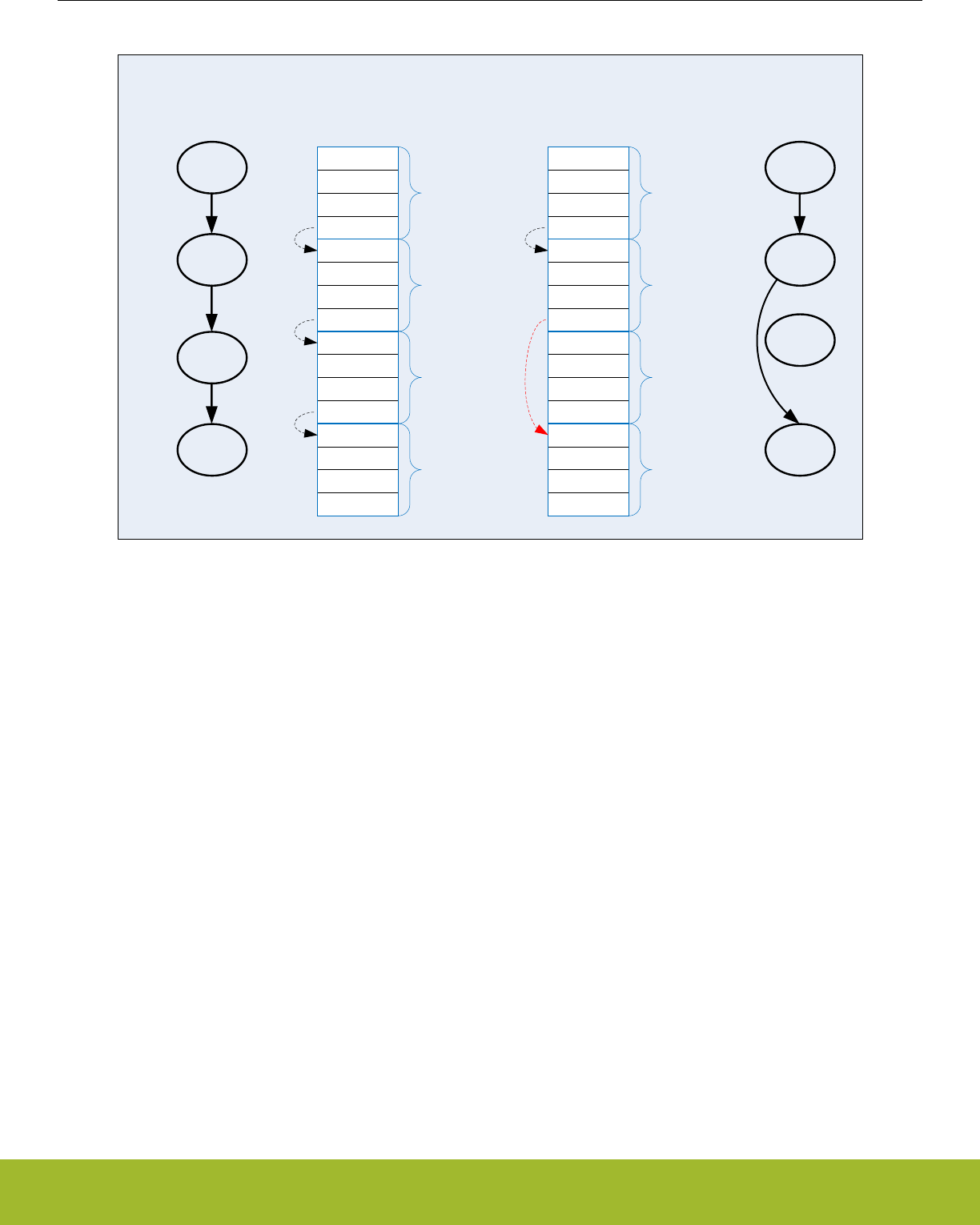
B
C
A
Ctrl
Src
Dst
Link
Ctrl
Src
Dst
Link
Ctrl
Src
Dst
Link
Ctrl
Src
Dst
Link
D
0x00000013
0x00000013
0x00000013
0x00000000
B
C
A
Ctrl
Src
Dst
Link
Ctrl
Src
Dst
Link
Ctrl
Src
Dst
Link
Ctrl
Src
Dst
Link
D
0x00000013
0x00000023
0x00000013
0x00000000
Linked
List
Third
Descriptor
Deleted
A
B
C
D
A
B
C
D
Figure 9.5. Descriptor Linked List
To start execution of the linked list of descriptors:
•Write the absolute address of the first descriptor to the LINKADR field of the LDMA_CH0_LINK register
• Set the LINK bit of LDMA_CH0_LINK register.
• Configure the LDMA_CH0REQSEL register for the desired peripheral or select none for memory-to-memory
• Clear and enable interrupts as desired
• Set bit 0 in the LDMA_LINKLOAD register to initiate loading and execution of the first descriptor
Alternativley, software can manually copy the first descriptor contents to the LDMA_CH0_CTRL, LDMA_CH0_SRC, LDMA_CH0_DST,
and LDMA_CH0_LINK registers and then enable the channel in the LDMA_CHEN register.
Reference Manual
LDMA - Linked DMA Controller
silabs.com | Smart. Connected. Energy-friendly. Preliminary Rev. 0.5 | 179

9.4.3 Single Descriptor Looped Transfer
This example demonstrates how to use looping using a single descriptor. This method allows a single DMA transfer to be repeated a
specified number of times. The looping descriptor is stored in memory and reloaded by hardware. After a specified number of iterations,
the transfer stops.
CH0 is setup to copy 4 words from the ADC FIFO into a 15 word buffer at 0x1000. It repeats 4 times to fill the entire 16 word buffer. An
interrupt will fire when the entire 16 words have been transfered.
Initialize the Linked descriptor in memory as follows:
• Configure CTRL member
• DSTMODE = 0 (absolute)
• SRCMODE = 0 (absolute)
• SIZE = WORD
• DSTINC = 0 (1 WORD)
• SRCINC = 3 (0 WORDS)
• DECLOOPCNT=1 (decrement loop count)
• REQMODE=1 (Use XFERCNT)
• BLOCKSIZE = 4 (4 words)
• BYTESWAP=0 (no swap)
• XFERCNT= 4 (4 words)
• STRUCTTPYE=0 (TRANSFER)
• IGNORESREQ=1 (ignore single requests)
• Write the address ADC0_SINGLEDATA register to the SRC member
• Write 0x1000 address to DST member
• Configure the LINKLink member
• LINK = 0 (stop after loop)
• MODE = 1 (relative link address)
• LINKADDR = 0 (point to ourself)
• Configure the Channel
• Write the desired number of repeats to the LDMA_CH0_LOOP register
• SOURCESEL in LDMA_CH0REQSEL = ADC0 (select the ADC)
• SIG in LDMA_CH0REQSEL = ADC0SCAN (select the scan conversion request)
• Clear and enable interrupts
• Load the descriptor using LINKLOAD as described in 9.4.2 Descriptor Linked List
Ctrl
Src
Dst
Link
A
Memory
0x00
link_addr->A
A
LINKADDR->A
DECLOOPCNT=1
LINK=0
Figure 9.6. Single Descriptor Looped Transfer
Note that the looping descriptor must be stored in memory, because it must load itself from the link address in memory on each itera-
tion.
Reference Manual
LDMA - Linked DMA Controller
silabs.com | Smart. Connected. Energy-friendly. Preliminary Rev. 0.5 | 180
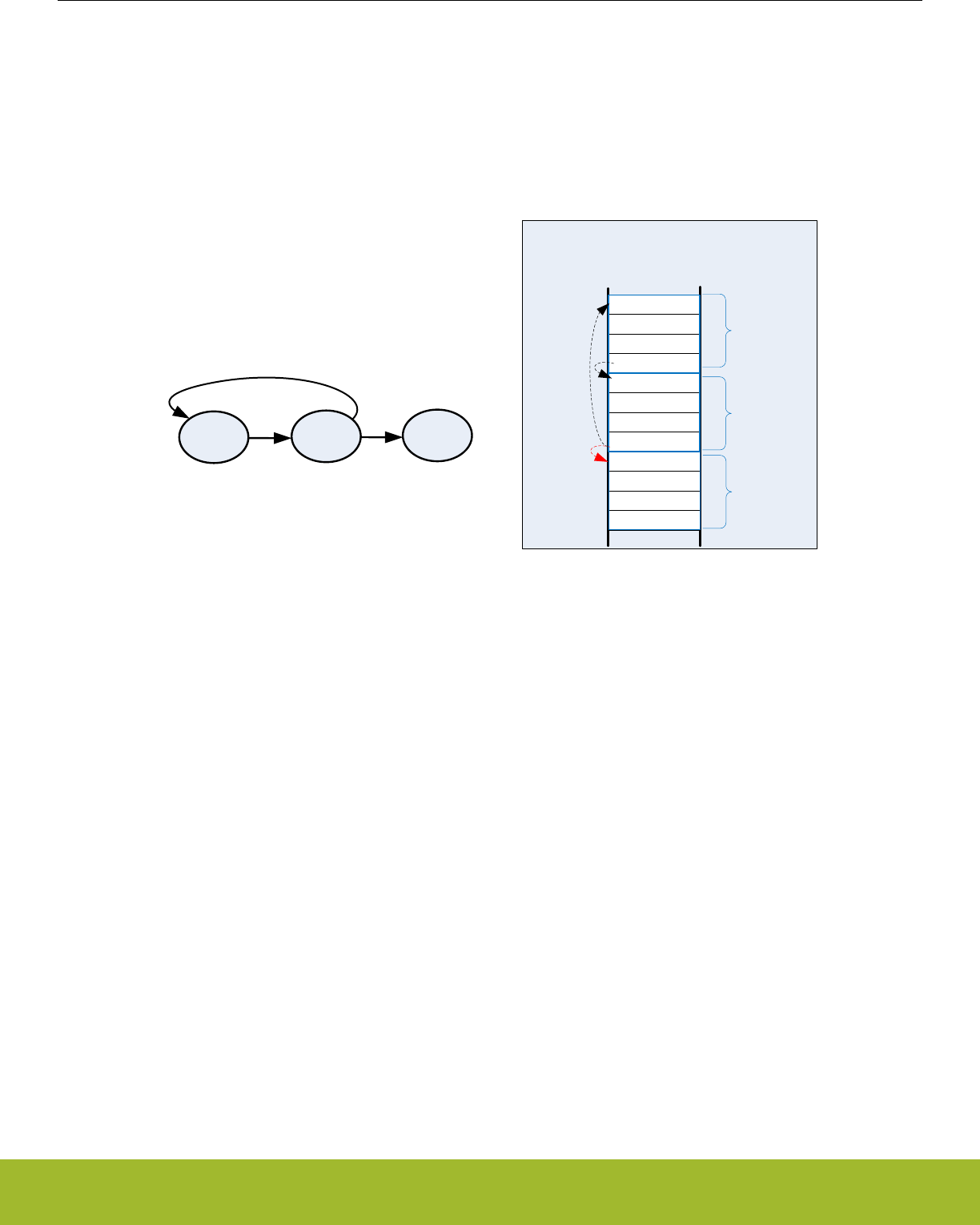
9.4.4 Descriptor List with Looping
This example uses a descriptor list in memory with looping over multiple descriptors. This example also uses the looping feature and
continues on with the next sequential descriptor after looping completes.
The descriptor list in memory is shown in figure Figure 9.7 Descriptor List with Looping on page 181. Descriptor A links to descriptor B.
Descriptor B has the DECLOOPCNT bit enabled and loops back to the start of descriptor A. The LINK address of descriptor B is used
for the loop address. The LINK bit is set to indicate that execution will continue after completion of looping. Once the LOOPCNT rea-
ches zero, the LDMA will load descriptor C. Descriptor C must be located immediately following descriptor B.
Ctrl
Src
Dst
Link
A
B
Ctrl
Src
Dst
Link
Memory
0x00
0x10
link_addr->B
link_addr=NA
C
Ctrl
Src
Dst
Link
0x20
link_addr->A
Alternate link
AB
LINKADDR->A
DECLOOPCNT=1
C
LINK=0LINKADDR->B
Figure 9.7. Descriptor List with Looping
Initialization is similar to the single looping descriptor with the following modifications.
• Set the LINK bit in descriptors A and B
•write the address of descriptor A into the LIKADDRESS of descriptor B
• write the address of descriptor B into the LIKADDRESS of descriptor A
• Descriptor C must be located immediately after descriptor B in memory
Reference Manual
LDMA - Linked DMA Controller
silabs.com | Smart. Connected. Energy-friendly. Preliminary Rev. 0.5 | 181

9.4.5 Simple Inter-Channel Synchronization
The LDMA controller features synchronization structures which allow differing channels and/or hardware events to pause a DMA se-
quence, and wait for a synchronizing event to restart it.
In this example DMA channel 0 and 1 are tasked with the transfer of different sets of data. Channel 0 has two transfer structures, and
channel 1 just one, but channel 0 must wait until channel 1 has completed its transfer before it starts its second transfer structure.
Pausing channel 0 is accomplished by inserting a sync wait structure between the two transfer structures. This sync structure waits on
SYNCTRIG[7] to be set by a sync set/clear structure which is controlled by channel 1. Sync structures do not transfer data, they can
only set, clear, or wait to match the SYNCTRIG[7:0] bits. Note that sync structures cannot decrement loop counter.
LDMA_SYNC
SYNCTRIG=0x0 (at time 0)
LDMA_CH0
Structure A @ 0x00 Structure B @ 0x10 Structure C @ 0x20
CTRL CTRL CTRL
STRUCTTYPE=XFER STRUCTTYPE=SYNC STRUCTTYPE=XFER
LINK LINK LINK
LINKADDR[29:0]=0x00000004 LINKADDR[29:0]=0x00000008 LINKADDR[29:0]=NA
LINK=1 LINK=1 LINK=0
DST
MATCHEN=0x80
MATCHVAL=0x80 (waits for SYNCTRIG[7]=1)
LDMA_CH1
Structure Y @ 0x30 Structure Z @ 0x40
CTRL CTRL
STRUCTTYPE=XFER STRUCTTYPE=SYNC
LINK LINK
LINKADDR[29:0]=0x00000010 LINKADDR=NA
LINK=1 LINK=0
SRC
SRCCLR=0x0
SRCSET=0x80 (sets SYNCTRIG[7])
Reference Manual
LDMA - Linked DMA Controller
silabs.com | Smart. Connected. Energy-friendly. Preliminary Rev. 0.5 | 182
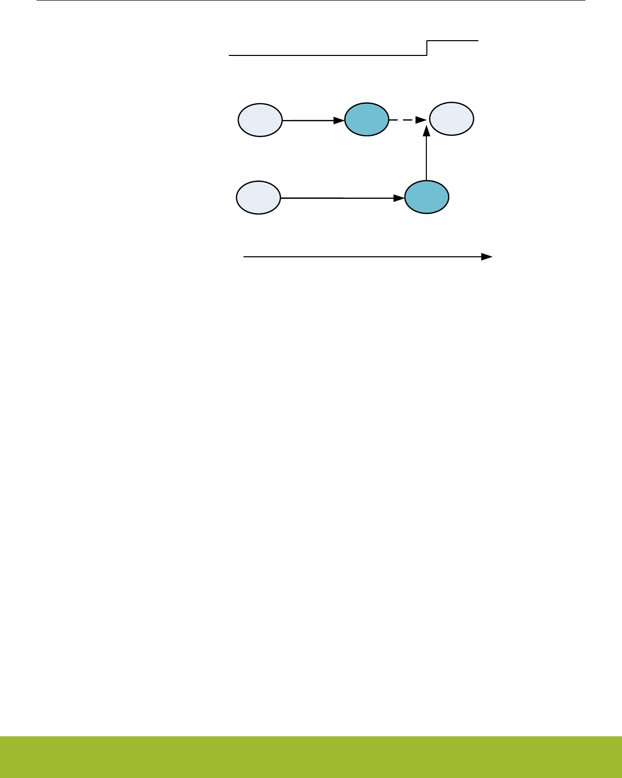
AB
STRUCTTYPE=XFER
STRUCTTYPE=-SYNC
wait SYNCTRIG[7]=1
CH0
CH1 Y
STRUCTTYPE=XFER
Z
STRUCTTYPE=SYNC
set SYNC[7]
Time
C
SYNC[7]
STRUCTTYPE=XFER
C not fetched until
sync_trig[7] is set
Figure 9.8. Simple Intra-channel Synchronization Example
Both A and Y effectively start at the same time. A finishes earlier, then it links to B, which waits for the SYNCTRIG[7] bit to be set before
loading C. Y finishes after B is loaded, and it links to sync structure Z, which sets the SYNCTRIG[7] bit. Channel 0 responds to the
trigger set by loading C for the final data transfer.
Reference Manual
LDMA - Linked DMA Controller
silabs.com | Smart. Connected. Energy-friendly. Preliminary Rev. 0.5 | 183
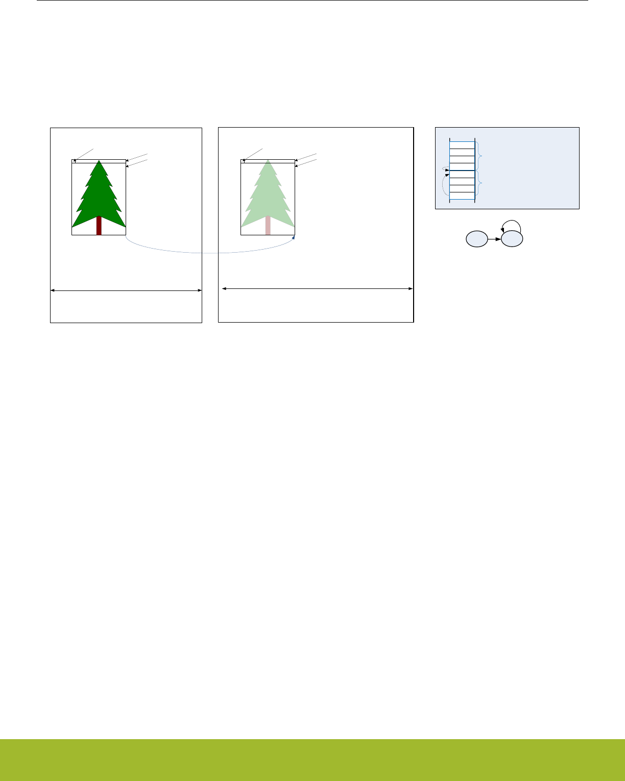
9.4.6 2D Copy
The LDMA can easily perform a 2D copy using a descriptor list with looping. This set up is visualized in Figure 9.9 2D copy on page
184.
For an application working with graphics, this would mean the ability to copy a rectangle of a given width and height from one picture to
another.
2D Copy Descriptors in Memory
B
Source Buffer Destination Buffer
SRCSTRIDE DSTSTRIDE
WIDTH
HEIGHT
HEIGHT
Source
Address
Destination
Address
A
CTRL
SRC
DST
LINK
CTRL
SRC
DST
LINK
Descriptor A
Descriptor B
WIDTH
Destination
Address Descriptor A
Descriptor B
XFERCNT = WIDTH - 1
SRCMD = DSTMD = 0
SRC = SRCADDR
DST = DSTADDR
LINK = 0x00000013
XFERCNT = WIDTH - 1
SRCMD = DSTMD = 1
SRCADDR = SRCSTRIDE - WIDTH
DSTADDR = DSTSTRIDE - WIDTH
LINK = 0x00000001
AB
LINKADDR->B
DECLOOPCNT=1
LINK=0
LINKADDR->B
Figure 9.9. 2D copy
The first descriptor will use absolute addressing mode and the source and destination addresses should point to the desired target ad-
dresses. The first descriptor will copy only the first row. The XFERCNT of the first descriptor is set to the desired width minus one.
• CTRL
• XFERCNT = WIDTH - 1
• SRCMD = 0 (absolute)
• DSTMD = 0 (absolute)
• SRCADDR = target source address
• DSTADDR = target destination address
• LINK = 0x00000013
• LINK=1
• LINKMD=1
• LINKADDR=0x00000010 (point to next descriptor)
The second descriptor will use relative addressing and the source and destination addresses are set to the desired offset. After the
completion of the first descriptor, the address registers will point to the last address transferred. Thus, the width must be subtracted
from the stride to get the offset. The second descriptor uses looping and the link register has not offset.
• CTRL
• XFERCNT = WIDTH - 1
• SRCMD = 1 (relative)
• DSTMD = 1 (relative)
• DECLOOPCNT = 1
• SRCADDR = desired source offset (SRCSTRIDE-WIDTH)
• DSTADDR = desired destination offset (DSTSTRIDE-WIDTH)
• LINK = 0x00000001
• LINK=0
• LINKMD=1 (relative)
• LINKADDR=0x000000000 (no offset)
Reference Manual
LDMA - Linked DMA Controller
silabs.com | Smart. Connected. Energy-friendly. Preliminary Rev. 0.5 | 184

Because the first descriptor already transferred one row, the number of looping repeats should be the desired height minus two. There-
fore, LOOPCNT should be set to HEIGHT minus two before initiating the transfer.
This same method is easily extended to copy multiple rectangles by linking descriptors together. To initialize the LDMA_CHx_LOOP
register, precede each descriptor pair described above with a write immediate descriptor which writes the desired value to the
LOOPCNT field of the LDMA_CHx_LOOP register.
Reference Manual
LDMA - Linked DMA Controller
silabs.com | Smart. Connected. Energy-friendly. Preliminary Rev. 0.5 | 185
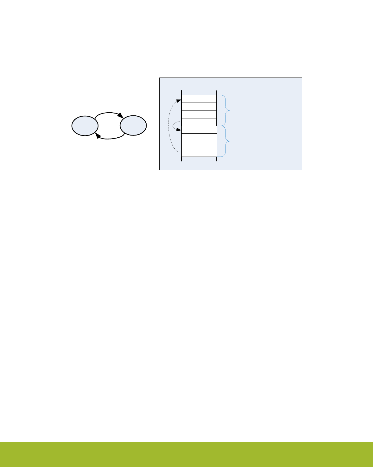
9.4.7 Ping-Pong
Communication peripherals often use ping-pong buffers. Ping-pong buffers allow the CPU to process data in one buffer while a periph-
eral transmits or receives data in the other buffer.
Both transmit and receive ping-pong buffers are easily implemented using the LDMA. In either case, this requires two descriptors as
shown in Figure 9.10 Infinite Ping-Pong Example on page 186. The LINKADDR field of the LINK member should point to the other
descriptor. Using two adjacent descriptors and relative link addressing ensures the descriptors are easily reloadable.
CTRL
SRC
DST
LINK
A
Memory
LINKADDR = 0x00000010
LINKMD = 1
ABCTRL
SRC
DST
LINK
B
LINKADDR = 0xFFFFFFF0
LINKMD = 1
Figure 9.10. Infinite Ping-Pong Example
A receiver ping-pong buffer controller consists of two buffers and two descriptors stored in memory that point to the two buffers. Once
initialized, as the peripheral receives data, it will fill the first buffer. Once the first buffer is full, it will link automatically to the second
buffer and generate an interrupt. Software will then process the data in the first buffer while the LDMA is transferring data to the second
buffer. For a receiver ping-pong buffer each descriptor should link to the other descriptor. The link bit should be set to provide infinite
ping pong between the two buffers. The DONIFS bit in each descriptor should be set to generate an interrupt on the completion of each
descriptor.
• Descriptor A
• CTRL
• DONEIFS = 1
• other settings as desired
• SRCADDR = peripheral source address
• DSTADDR = memory destination address
• LINK = 0x00000013
• LINKADDR = 0x00000010 (next descriptor)
• LINK = 1 (link to next descriptor)
• LINKMD = 1 (relative addressing)
• Descriptor B
• CTRL
• DONEIFS = 1
• other settings as desired
• SRCADDR = peripheral source address
• DSTADDR = memory destination address
• LINK = 0xFFFFFFF3
• LINKADDR = 0xFFFFFFF0 (previous descriptor)
• LINK = 1 (link to previous descriptor)
• LINKMD = 1 (relative addressing)
For transmitter ping-pong buffer, software will fill the first buffer and then initiate the DMA transfer. The LDMA will transmit the first
buffer data while software is filling the second buffer. In this case, the two descriptors should point to each other, but not automatically
Reference Manual
LDMA - Linked DMA Controller
silabs.com | Smart. Connected. Energy-friendly. Preliminary Rev. 0.5 | 186

continue to the second buffer. The LINK bit should be cleared to zero. Once software has loaded the first buffer, it will use the LINK-
LOAD bit to load the first descriptor and transmit the data. The DONIFS need not be set in each descriptor. The DMA will stop and then
generate an interrupt at the completion of each descriptor.
• Descriptor A
• CTRL
• DONEIFS = 0
• other settings as desired
• SRCADDR = memory source address
• DSTADDR = peripheral destination address
• LINK = 0x00000013
• LINKADDR = 0x00000010 (next descriptor)
• LINK = 0 (link to next descriptor)
• LINKMD = 1 (relative addressing)
• Descriptor B
• CTRL
• DONEIFS = 0
• other settings as desired
• SRCADDR = memory source address
• DSTADDR = peripheral destination address
• LINK = 0xFFFFFFF3
• LINKADDR = 0xFFFFFFF0 (previous descriptor)
• LINK = 0 (link to previous descriptor)
• LINKMD = 1 (relative addressing)
9.4.8 Scatter-Gather
Scatter-Gather in general refers to a process that copies data from multiple locations scattered in memory and gathers the data to a
single location in memory, or vice versa. A simple descriptor list allows data gathering. For example, data from a discontiguous list of
buffers might be copied to a contiguous sequential array of buffers. The inverse is also possible when a sequential array of buffers is
scattered to a discontiguous list of available buffers. See section 9.4.2 Descriptor Linked List.
Some DMAs which only have two descriptors implement scatter-gather by using one descriptor to modify the other descriptor. While it is
possible to implement this same behavior using the LDMA, it is much more straight-forward to just use a simple descriptor list.
Reference Manual
LDMA - Linked DMA Controller
silabs.com | Smart. Connected. Energy-friendly. Preliminary Rev. 0.5 | 187

9.5 Register Map
The offset register address is relative to the registers base address.
Offset Name Type Description
0x000 LDMA_CTRL RW DMA Control Register
0x004 LDMA_STATUS RDMA Status Register
0x008 LDMA_SYNC RWH DMA Synchronization Trigger Register (Single-Cycle RMW)
0x020 LDMA_CHEN RWH DMA Channel Enable Register (Single-Cycle RMW)
0x024 LDMA_CHBUSY RDMA Channel Busy Register
0x028 LDMA_CHDONE RWH DMA Channel Linking Done Register (Single-Cycle RMW)
0x02C LDMA_DBGHALT RW DMA Channel Debug Halt Register
0x030 LDMA_SWREQ W1 DMA Channel Software Transfer Request Register
0x034 LDMA_REQDIS RW DMA Channel Request Disable Register
0x038 LDMA_REQPEND RDMA Channel Requests Pending Register
0x03C LDMA_LINKLOAD W1 DMA Channel Link Load Register
0x040 LDMA_REQCLEAR W1 DMA Channel Request Clear Register
0x060 LDMA_IF RInterrupt Flag Register
0x064 LDMA_IFS W1 Interrupt Flag Set Register
0x068 LDMA_IFC (R)W1 Interrupt Flag Clear Register
0x06C LDMA_IEN RW Interrupt Enable register
0x080 LDMA_CH0_REQSEL RW Channel Peripheral Request Select Register
0x084 LDMA_CH0_CFG RW Channel Configuration Register
0x088 LDMA_CH0_LOOP RWH Channel Loop Counter Register
0x08C LDMA_CH0_CTRL RWH Channel Descriptor Control Word Register
0x090 LDMA_CH0_SRC RWH Channel Descriptor Source Data Address Register
0x094 LDMA_CH0_DST RWH Channel Descriptor Destination Data Address Register
0x098 LDMA_CH0_LINK RWH Channel Descriptor Link Structure Address Register
... LDMA_CHx_REQSEL RW Channel Peripheral Request Select Register
... LDMA_CHx_CFG RW Channel Configuration Register
... LDMA_CHx_LOOP RWH Channel Loop Counter Register
... LDMA_CHx_CTRL RWH Channel Descriptor Control Word Register
... LDMA_CHx_SRC RWH Channel Descriptor Source Data Address Register
... LDMA_CHx_DST RWH Channel Descriptor Destination Data Address Register
... LDMA_CHx_LINK RWH Channel Descriptor Link Structure Address Register
0x1D0 LDMA_CH7_REQSEL RW Channel Peripheral Request Select Register
0x1D4 LDMA_CH7_CFG RW Channel Configuration Register
0x1D8 LDMA_CH7_LOOP RWH Channel Loop Counter Register
0x1DC LDMA_CH7_CTRL RWH Channel Descriptor Control Word Register
0x1E0 LDMA_CH7_SRC RWH Channel Descriptor Source Data Address Register
Reference Manual
LDMA - Linked DMA Controller
silabs.com | Smart. Connected. Energy-friendly. Preliminary Rev. 0.5 | 188

Offset Name Type Description
0x1E4 LDMA_CH7_DST RWH Channel Descriptor Destination Data Address Register
0x1E8 LDMA_CH7_LINK RWH Channel Descriptor Link Structure Address Register
9.6 Register Description
9.6.1 LDMA_CTRL - DMA Control Register
Offset Bit Position
0x000
31
30
29
28
27
26
25
24
23
22
21
20
19
18
17
16
15
14
13
12
11
10
9
8
7
6
5
4
3
2
1
0
Reset
0x7
0x00
0x00
Access
RW
RW
RW
Name
NUMFIXED
SYNCPRSCLREN
SYNCPRSSETEN
Bit Name Reset Access Description
31:27 Reserved To ensure compatibility with future devices, always write bits to 0. More information in 1.2 Conven-
tions
26:24 NUMFIXED 0x7 RW Number of Fixed Priority Channels
This field defines the number of Fixed Priority Arbitration channels. Channels CH0 though CH(n-1) are fixed, and channels
CH(n) through CH7 are round robin, where n is the field value. The reset value will give all fixed channels.
23:16 Reserved To ensure compatibility with future devices, always write bits to 0. More information in 1.2 Conven-
tions
15:8 SYNCPRSCLREN 0x00 RW Synchronization PRS Clear Enable
Setting a bit in this field will enable the corresponding PRS input to clear the respective bit in the SYNCTRIG field of the
LDMA_SYNC register. Refer to the PRS section for a list of the PRS inputs.
7:0 SYNCPRSSETEN 0x00 RW Synchronization PRS Set Enable
Setting a bit in this field will enable the corresponding PRS input to set the respective bit in the SYNCTRIG field of the
LDMA_SYNC register. Refer to the PRS section for a list of the PRS inputs.
Reference Manual
LDMA - Linked DMA Controller
silabs.com | Smart. Connected. Energy-friendly. Preliminary Rev. 0.5 | 189

9.6.2 LDMA_STATUS - DMA Status Register
Offset Bit Position
0x004
31
30
29
28
27
26
25
24
23
22
21
20
19
18
17
16
15
14
13
12
11
10
9
8
7
6
5
4
3
2
1
0
Reset
0x08
0x10
0x0
0x0
0
0
Access
R
R
R
R
R
R
Name
CHNUM
FIFOLEVEL
CHERROR
CHGRANT
ANYREQ
ANYBUSY
Bit Name Reset Access Description
31:29 Reserved To ensure compatibility with future devices, always write bits to 0. More information in 1.2 Conven-
tions
28:24 CHNUM 0x08 R Number of Channels
The value of CHNUM always reads the total number of channels present for this instance of the DMA controller module.
23:21 Reserved To ensure compatibility with future devices, always write bits to 0. More information in 1.2 Conven-
tions
20:16 FIFOLEVEL 0x10 R FIFO Level
The value of FIFOLEVEL indicates the number of entries currently in the FIFO. (Note when all channels are disabled, this
register will read the total number of entries in the FIFO.)
15:11 Reserved To ensure compatibility with future devices, always write bits to 0. More information in 1.2 Conven-
tions
10:8 CHERROR 0x0 R Errant Channel Number
When the ERROR flag is set in the LDMA_IF register, the CHERROR field will indicate the most recent channel to have a
transfer error.
7:6 Reserved To ensure compatibility with future devices, always write bits to 0. More information in 1.2 Conven-
tions
5:3 CHGRANT 0x0 R Granted Channel Number
The value of this field indicates the currently active channel or last active channel. Note that the reset value for this field is
zero.
2 Reserved To ensure compatibility with future devices, always write bits to 0. More information in 1.2 Conven-
tions
1 ANYREQ 0 R Any DMA Channel Request Pending
The value of this bit will be TRUE (1) if any requests are pending
0 ANYBUSY 0 R Any DMA Channel Busy
The value of this bit will be TRUE (1) if one or more DMA channels are actively transferring data
Reference Manual
LDMA - Linked DMA Controller
silabs.com | Smart. Connected. Energy-friendly. Preliminary Rev. 0.5 | 190

9.6.3 LDMA_SYNC - DMA Synchronization Trigger Register (Single-Cycle RMW)
Offset Bit Position
0x008
31
30
29
28
27
26
25
24
23
22
21
20
19
18
17
16
15
14
13
12
11
10
9
8
7
6
5
4
3
2
1
0
Reset
0x00
Access
RWH
Name
SYNCTRIG
Bit Name Reset Access Description
31:8 Reserved To ensure compatibility with future devices, always write bits to 0. More information in 1.2 Conven-
tions
7:0 SYNCTRIG 0x00 RWH Synchronization Trigger
The SYNC trigger field allows a transfer to pause until a specified trigger bit is set or cleared. The SYNC trigger bits may be
set and cleared by a SYNC descriptor, PRS signal, or software. Note: software requires to use single-cycle read-modify-
write, detailed in 4.2.3 Peripheral Bit Set and Clear
9.6.4 LDMA_CHEN - DMA Channel Enable Register (Single-Cycle RMW)
Offset Bit Position
0x020
31
30
29
28
27
26
25
24
23
22
21
20
19
18
17
16
15
14
13
12
11
10
9
8
7
6
5
4
3
2
1
0
Reset
0x00
Access
RWH
Name
CHEN
Bit Name Reset Access Description
31:8 Reserved To ensure compatibility with future devices, always write bits to 0. More information in 1.2 Conven-
tions
7:0 CHEN 0x00 RWH Channel Enables
Setting one of these bits will enable the respective DMA channel. If cleared while a transfer is in progress, the current trans-
fer block will complete. The remaining blocks will pause until resumed later by setting this bit again. Note: software requires
to use single-cycle read-modify-write, detailed in 4.2.3 Peripheral Bit Set and Clear
Reference Manual
LDMA - Linked DMA Controller
silabs.com | Smart. Connected. Energy-friendly. Preliminary Rev. 0.5 | 191

9.6.5 LDMA_CHBUSY - DMA Channel Busy Register
Offset Bit Position
0x024
31
30
29
28
27
26
25
24
23
22
21
20
19
18
17
16
15
14
13
12
11
10
9
8
7
6
5
4
3
2
1
0
Reset
0x00
Access
R
Name
BUSY
Bit Name Reset Access Description
31:8 Reserved To ensure compatibility with future devices, always write bits to 0. More information in 1.2 Conven-
tions
7:0 BUSY 0x00 R Channels Busy
The bits of this field read 1 when the corresponding channel is busy.
9.6.6 LDMA_CHDONE - DMA Channel Linking Done Register (Single-Cycle RMW)
Offset Bit Position
0x028
31
30
29
28
27
26
25
24
23
22
21
20
19
18
17
16
15
14
13
12
11
10
9
8
7
6
5
4
3
2
1
0
Reset
0x00
Access
RWH
Name
CHDONE
Bit Name Reset Access Description
31:8 Reserved To ensure compatibility with future devices, always write bits to 0. More information in 1.2 Conven-
tions
7:0 CHDONE 0x00 RWH DMA Channel Linking or Done
Each DMA channel sets the corresponding bit in this register when the entire transfer is done. The interrupt service routine
should clear these bits. Enabling a DMA channel will also clear the corresponding LINKDONE bit. Note: software requires
to use single-cycle read-modify-write, detailed in 4.2.3 Peripheral Bit Set and Clear
Reference Manual
LDMA - Linked DMA Controller
silabs.com | Smart. Connected. Energy-friendly. Preliminary Rev. 0.5 | 192

9.6.7 LDMA_DBGHALT - DMA Channel Debug Halt Register
Offset Bit Position
0x02C
31
30
29
28
27
26
25
24
23
22
21
20
19
18
17
16
15
14
13
12
11
10
9
8
7
6
5
4
3
2
1
0
Reset
0x00
Access
RW
Name
DBGHALT
Bit Name Reset Access Description
31:8 Reserved To ensure compatibility with future devices, always write bits to 0. More information in 1.2 Conven-
tions
7:0 DBGHALT 0x00 RW DMA Debug Halt
Setting one of these bits will mask the corresponding DMA channel's peripheral request when debugging and the CPU is
halted. This may be useful for debugging DMA software.
9.6.8 LDMA_SWREQ - DMA Channel Software Transfer Request Register
Offset Bit Position
0x030
31
30
29
28
27
26
25
24
23
22
21
20
19
18
17
16
15
14
13
12
11
10
9
8
7
6
5
4
3
2
1
0
Reset
0x00
Access
W1
Name
SWREQ
Bit Name Reset Access Description
31:8 Reserved To ensure compatibility with future devices, always write bits to 0. More information in 1.2 Conven-
tions
7:0 SWREQ 0x00 W1 Software Transfer Requests
Setting one of these bits will trigger a DMA transfer for the corresponding channel. Writing zeros has no effect.
Reference Manual
LDMA - Linked DMA Controller
silabs.com | Smart. Connected. Energy-friendly. Preliminary Rev. 0.5 | 193

9.6.9 LDMA_REQDIS - DMA Channel Request Disable Register
Offset Bit Position
0x034
31
30
29
28
27
26
25
24
23
22
21
20
19
18
17
16
15
14
13
12
11
10
9
8
7
6
5
4
3
2
1
0
Reset
0x00
Access
RW
Name
REQDIS
Bit Name Reset Access Description
31:8 Reserved To ensure compatibility with future devices, always write bits to 0. More information in 1.2 Conven-
tions
7:0 REQDIS 0x00 RW DMA Request Disables
Setting one of these bits will disable peripheral requests for the corresponding channel. When cleared any pending periph-
eral requests will be serviced.
9.6.10 LDMA_REQPEND - DMA Channel Requests Pending Register
Offset Bit Position
0x038
31
30
29
28
27
26
25
24
23
22
21
20
19
18
17
16
15
14
13
12
11
10
9
8
7
6
5
4
3
2
1
0
Reset
0x00
Access
R
Name
REQPEND
Bit Name Reset Access Description
31:8 Reserved To ensure compatibility with future devices, always write bits to 0. More information in 1.2 Conven-
tions
7:0 REQPEND 0x00 R DMA Requests Pending
When a DMA channel has a pending peripheral request the corresponding REQPEND bit will read 1.
Reference Manual
LDMA - Linked DMA Controller
silabs.com | Smart. Connected. Energy-friendly. Preliminary Rev. 0.5 | 194

9.6.11 LDMA_LINKLOAD - DMA Channel Link Load Register
Offset Bit Position
0x03C
31
30
29
28
27
26
25
24
23
22
21
20
19
18
17
16
15
14
13
12
11
10
9
8
7
6
5
4
3
2
1
0
Reset
0x00
Access
W1
Name
LINKLOAD
Bit Name Reset Access Description
31:8 Reserved To ensure compatibility with future devices, always write bits to 0. More information in 1.2 Conven-
tions
7:0 LINKLOAD 0x00 W1 DMA Link Loads
Setting one of these bits will force the corresponding DMA channel to load the next DMA structure and enable the channel.
This empowers software to step through a sequence of descriptors.
9.6.12 LDMA_REQCLEAR - DMA Channel Request Clear Register
Offset Bit Position
0x040
31
30
29
28
27
26
25
24
23
22
21
20
19
18
17
16
15
14
13
12
11
10
9
8
7
6
5
4
3
2
1
0
Reset
0x00
Access
W1
Name
REQCLEAR
Bit Name Reset Access Description
31:8 Reserved To ensure compatibility with future devices, always write bits to 0. More information in 1.2 Conven-
tions
7:0 REQCLEAR 0x00 W1 DMA Request Clear
Setting one of these bits will clear any internally registered transfer requests for the corresponding channel.
Reference Manual
LDMA - Linked DMA Controller
silabs.com | Smart. Connected. Energy-friendly. Preliminary Rev. 0.5 | 195

9.6.13 LDMA_IF - Interrupt Flag Register
Offset Bit Position
0x060
31
30
29
28
27
26
25
24
23
22
21
20
19
18
17
16
15
14
13
12
11
10
9
8
7
6
5
4
3
2
1
0
Reset
0
0x00
Access
R
R
Name
ERROR
DONE
Bit Name Reset Access Description
31 ERROR 0 R Transfer Error Interrupt Flag
The ERRORIF flag is set when a read or write error occurs. The CHERROR field in the LDMA_STATUS register reflects the
number of the channel which had the last error.
30:8 Reserved To ensure compatibility with future devices, always write bits to 0. More information in 1.2 Conven-
tions
7:0 DONE 0x00 R DMA Structure Operation Done Interrupt Flag
When a channel completes a transfer or sync operation, the corresponding DONE bit is set in the LDMA_IF register.
9.6.14 LDMA_IFS - Interrupt Flag Set Register
Offset Bit Position
0x064
31
30
29
28
27
26
25
24
23
22
21
20
19
18
17
16
15
14
13
12
11
10
9
8
7
6
5
4
3
2
1
0
Reset
0
0x00
Access
W1
W1
Name
ERROR
DONE
Bit Name Reset Access Description
31 ERROR 0 W1 Set ERROR Interrupt Flag
Write 1 to set the ERROR interrupt flag
30:8 Reserved To ensure compatibility with future devices, always write bits to 0. More information in 1.2 Conven-
tions
7:0 DONE 0x00 W1 Set DONE Interrupt Flag
Write 1 to set the DONE interrupt flag
Reference Manual
LDMA - Linked DMA Controller
silabs.com | Smart. Connected. Energy-friendly. Preliminary Rev. 0.5 | 196

9.6.15 LDMA_IFC - Interrupt Flag Clear Register
Offset Bit Position
0x068
31
30
29
28
27
26
25
24
23
22
21
20
19
18
17
16
15
14
13
12
11
10
9
8
7
6
5
4
3
2
1
0
Reset
0
0x00
Access
(R)W1
(R)W1
Name
ERROR
DONE
Bit Name Reset Access Description
31 ERROR 0 (R)W1 Clear ERROR Interrupt Flag
Write 1 to clear the ERROR interrupt flag. Reading returns the value of the IF and clears the corresponding interrupt flags
(This feature must be enabled globally in MSC.).
30:8 Reserved To ensure compatibility with future devices, always write bits to 0. More information in 1.2 Conven-
tions
7:0 DONE 0x00 (R)W1 Clear DONE Interrupt Flag
Write 1 to clear the DONE interrupt flag. Reading returns the value of the IF and clears the corresponding interrupt flags
(This feature must be enabled globally in MSC.).
9.6.16 LDMA_IEN - Interrupt Enable register
Offset Bit Position
0x06C
31
30
29
28
27
26
25
24
23
22
21
20
19
18
17
16
15
14
13
12
11
10
9
8
7
6
5
4
3
2
1
0
Reset
0
0x00
Access
RW
RW
Name
ERROR
DONE
Bit Name Reset Access Description
31 ERROR 0 RW ERROR Interrupt Enable
Enable/disable the ERROR interrupt
30:8 Reserved To ensure compatibility with future devices, always write bits to 0. More information in 1.2 Conven-
tions
7:0 DONE 0x00 RW DONE Interrupt Enable
Enable/disable the DONE interrupt
Reference Manual
LDMA - Linked DMA Controller
silabs.com | Smart. Connected. Energy-friendly. Preliminary Rev. 0.5 | 197

9.6.17 LDMA_CHx_REQSEL - Channel Peripheral Request Select Register
Offset Bit Position
0x080
31
30
29
28
27
26
25
24
23
22
21
20
19
18
17
16
15
14
13
12
11
10
9
8
7
6
5
4
3
2
1
0
Reset
0x00
0x0
Access
RW
RW
Name
SOURCESEL
SIGSEL
Bit Name Reset Access Description
31:22 Reserved To ensure compatibility with future devices, always write bits to 0. More information in 1.2 Conven-
tions
21:16 SOURCESEL 0x00 RW Source Select
Select input source to DMA channel.
Value Mode Description
0b000000 NONE No source selected
0b000001 PRS Peripheral Reflex System
0b001000 ADC0 Analog to Digital Converter 0
0b001010 VDAC0 Digital to Analog Converter 0
0b001100 USART0 Universal Synchronous/Asynchronous Receiver/Transmitter 0
0b001101 USART1 Universal Synchronous/Asynchronous Receiver/Transmitter 1
0b001110 USART2 Universal Synchronous/Asynchronous Receiver/Transmitter 2
0b010000 LEUART0 Low Energy UART 0
0b010100 I2C0 I2C 0
0b010101 I2C1 I2C 1
0b011000 TIMER0 Timer 0
0b011001 TIMER1 Timer 1
0b011010 WTIMER0 Wide Timer 0
0b110000 MSC Memory System Controller
0b110001 CRYPTO0 Advanced Encryption Standard Accelerator 0
0b110010 CSEN Capacitive touch sense module
0b110011 LESENSE Low Energy Sensor Interface
0b110100 CRYPTO1 Advanced Encryption Standard Accelerator 1
15:4 Reserved To ensure compatibility with future devices, always write bits to 0. More information in 1.2 Conven-
tions
3:0 SIGSEL 0x0 RW Signal Select
Select input signal to DMA channel.
Reference Manual
LDMA - Linked DMA Controller
silabs.com | Smart. Connected. Energy-friendly. Preliminary Rev. 0.5 | 198

Bit Name Reset Access Description
Value Mode Description
SOURCESEL =
0b000000 (NONE)
0bxxxx OFF Channel input selection is turned off
SOURCESEL =
0b000001 (PRS)
0b0000 PRSREQ0 PRSREQ0
0b0001 PRSREQ1 PRSREQ1
SOURCESEL =
0b001000 (ADC0)
0b0000 ADC0SINGLE ADC0SINGLE REQ/SREQ
0b0001 ADC0SCAN ADC0SCAN REQ/SREQ
SOURCESEL =
0b001010 (VDAC0)
0b0000 VDAC0CH0 VDAC0CH0
0b0001 VDAC0CH1 VDAC0CH1
SOURCESEL =
0b001100 (USART0)
0b0000 USART0RXDATAV USART0RXDATAV REQ/SREQ
0b0001 USART0TXBL USART0TXBL REQ/SREQ
0b0010 USART0TXEMPTY USART0TXEMPTY
SOURCESEL =
0b001101 (USART1)
0b0000 USART1RXDATAV USART1RXDATAV REQ/SREQ
0b0001 USART1TXBL USART1TXBL REQ/SREQ
0b0010 USART1TXEMPTY USART1TXEMPTY
0b0011 USART1RXDATAV-
RIGHT
USART1RXDATAVRIGHT REQ/SREQ
0b0100 USART1TXBLRIGHT USART1TXBLRIGHT REQ/SREQ
SOURCESEL =
0b001110 (USART2)
0b0000 USART2RXDATAV USART2RXDATAV REQ/SREQ
0b0001 USART2TXBL USART2TXBL REQ/SREQ
0b0010 USART2TXEMPTY USART2TXEMPTY
SOURCESEL =
0b010000
(LEUART0)
0b0000 LEUART0RXDATAV LEUART0RXDATAV
0b0001 LEUART0TXBL LEUART0TXBL
0b0010 LEUART0TXEMPTY LEUART0TXEMPTY
SOURCESEL =
0b010100 (I2C0)
Reference Manual
LDMA - Linked DMA Controller
silabs.com | Smart. Connected. Energy-friendly. Preliminary Rev. 0.5 | 199

Bit Name Reset Access Description
0b0000 I2C0RXDATAV I2C0RXDATAV REQ/SREQ
0b0001 I2C0TXBL I2C0TXBL REQ/SREQ
SOURCESEL =
0b010101 (I2C1)
0b0000 I2C1RXDATAV I2C1RXDATAV REQ/SREQ
0b0001 I2C1TXBL I2C1TXBL REQ/SREQ
SOURCESEL =
0b011000 (TIMER0)
0b0000 TIMER0UFOF TIMER0UFOF
0b0001 TIMER0CC0 TIMER0CC0
0b0010 TIMER0CC1 TIMER0CC1
0b0011 TIMER0CC2 TIMER0CC2
SOURCESEL =
0b011001 (TIMER1)
0b0000 TIMER1UFOF TIMER1UFOF
0b0001 TIMER1CC0 TIMER1CC0
0b0010 TIMER1CC1 TIMER1CC1
0b0011 TIMER1CC2 TIMER1CC2
0b0100 TIMER1CC3 TIMER1CC3
SOURCESEL =
0b011010 (WTI-
MER0)
0b0000 WTIMER0UFOF WTIMER0UFOF
0b0001 WTIMER0CC0 WTIMER0CC0
0b0010 WTIMER0CC1 WTIMER0CC1
0b0011 WTIMER0CC2 WTIMER0CC2
SOURCESEL =
0b110000 (MSC)
0b0000 MSCWDATA MSCWDATA REQ/SREQ
SOURCESEL =
0b110001 (CRYP-
TO0)
0b0000 CRYPTO0DATA0WR CRYPTO0DATA0WR
0b0001 CRYPTO0DATA0XWR CRYPTO0DATA0XWR
0b0010 CRYPTO0DATA0RD CRYPTO0DATA0RD
0b0011 CRYPTO0DATA1WR CRYPTO0DATA1WR
0b0100 CRYPTO0DATA1RD CRYPTO0DATA1RD
SOURCESEL =
0b110010 (CSEN)
0b0000 CSENDATA CSENDATA
0b0001 CSENBSLN CSENBSLN
Reference Manual
LDMA - Linked DMA Controller
silabs.com | Smart. Connected. Energy-friendly. Preliminary Rev. 0.5 | 200

Bit Name Reset Access Description
SOURCESEL =
0b110011 (LE-
SENSE)
0b0000 LESENSEBUFDATAV LESENSEBUFDATAV REQ/SREQ
SOURCESEL =
0b110100 (CRYP-
TO1)
0b0000 CRYPTO1DATA0WR CRYPTO1DATA0WR
0b0001 CRYPTO1DATA0XWR CRYPTO1DATA0XWR
0b0010 CRYPTO1DATA0RD CRYPTO1DATA0RD
0b0011 CRYPTO1DATA1WR CRYPTO1DATA1WR
0b0100 CRYPTO1DATA1RD CRYPTO1DATA1RD
Reference Manual
LDMA - Linked DMA Controller
silabs.com | Smart. Connected. Energy-friendly. Preliminary Rev. 0.5 | 201

9.6.18 LDMA_CHx_CFG - Channel Configuration Register
Offset Bit Position
0x084
31
30
29
28
27
26
25
24
23
22
21
20
19
18
17
16
15
14
13
12
11
10
9
8
7
6
5
4
3
2
1
0
Reset
0
0
0x0
Access
RW
RW
RW
Name
DSTINCSIGN
SRCINCSIGN
ARBSLOTS
Bit Name Reset Access Description
31:22 Reserved To ensure compatibility with future devices, always write bits to 0. More information in 1.2 Conven-
tions
21 DSTINCSIGN 0 RW Destination Address Increment Sign
Value Mode Description
0 POSITIVE Increment destination address
1 NEGATIVE Decrement destination address
20 SRCINCSIGN 0 RW Source Address Increment Sign
Value Mode Description
0 POSITIVE Increment source address
1 NEGATIVE Decrement source address
19:18 Reserved To ensure compatibility with future devices, always write bits to 0. More information in 1.2 Conven-
tions
17:16 ARBSLOTS 0x0 RW Arbitration Slot Number Select
For channels using round robin arbitration, this bit-field is used to select the number of slots in the round robin queue.
Value Mode Description
0 ONE One arbitration slot selected
1 TWO Two arbitration slots selected
2 FOUR Four arbitration slots selected
3 EIGHT Eight arbitration slots selected
15:0 Reserved To ensure compatibility with future devices, always write bits to 0. More information in 1.2 Conven-
tions
Reference Manual
LDMA - Linked DMA Controller
silabs.com | Smart. Connected. Energy-friendly. Preliminary Rev. 0.5 | 202

9.6.19 LDMA_CHx_LOOP - Channel Loop Counter Register
Offset Bit Position
0x088
31
30
29
28
27
26
25
24
23
22
21
20
19
18
17
16
15
14
13
12
11
10
9
8
7
6
5
4
3
2
1
0
Reset
0x00
Access
RWH
Name
LOOPCNT
Bit Name Reset Access Description
31:8 Reserved To ensure compatibility with future devices, always write bits to 0. More information in 1.2 Conven-
tions
7:0 LOOPCNT 0x00 RWH Linked Structure Sequence Loop Counter
This bit-field specifies the number of iterations when using looping descriptors. Software should write to LOOPCNT before
using a looping descriptor.
Reference Manual
LDMA - Linked DMA Controller
silabs.com | Smart. Connected. Energy-friendly. Preliminary Rev. 0.5 | 203

9.6.20 LDMA_CHx_CTRL - Channel Descriptor Control Word Register
Offset Bit Position
0x08C
31
30
29
28
27
26
25
24
23
22
21
20
19
18
17
16
15
14
13
12
11
10
9
8
7
6
5
4
3
2
1
0
Reset
0
0
0x0
0x0
0x0
0
0
0
0
0x0
0
0x000
0
0x0
Access
R
R
RWH
RWH
RWH
RWH
RWH
RWH
RWH
RWH
RWH
RWH
W1
R
Name
DSTMODE
SRCMODE
DSTINC
SIZE
SRCINC
IGNORESREQ
DECLOOPCNT
REQMODE
DONEIFSEN
BLOCKSIZE
BYTESWAP
XFERCNT
STRUCTREQ
STRUCTTYPE
Bit Name Reset Access Description
31 DSTMODE 0 R Destination Addressing Mode
This field specifies the destination addressing mode of linked descriptors. After loading a linked descriptor, reading this field
will indicate the destination addressing mode of the linked descriptor. Note that the first descriptor always uses absolute
addressing mode.
Value Mode Description
0 ABSOLUTE The DSTADDR field of LDMA_CHx_DST contains the absolute ad-
dress of the destination data.
1 RELATIVE The DSTADDR field of LDMA_CHx_DST contains the relative offset of
the destination data.
30 SRCMODE 0 R Source Addressing Mode
This field specifies the source addressing mode of linked descriptors. After loading a linked descriptor, reading this field will
indicate the source addressing mode of the linked descriptor. Note that the first descriptor always uses absolute addressing
mode.
Value Mode Description
0 ABSOLUTE The SRCADDR field of LDMA_CHx_SRC contains the absolute ad-
dress of the source data.
1 RELATIVE The SRCADDR field of LDMA_CHx_SRC contains the relative offset of
the source data.
29:28 DSTINC 0x0 RWH Destination Address Increment Size
This bit-field specifies the stride or number of unit data addresses to increment the destination address after each unit of
data is transferred. The unit data width is controlled by the SIZE bit-field and can be a byte, half-word or word.
Value Mode Description
0 ONE Increment destination address by one unit data size after each write
1 TWO Increment destination address by two unit data sizes after each write
2 FOUR Increment destination address by four unit data sizes after each write
3 NONE Do not increment the destination address. Writes are made to a fixed
destination address, for example writing to a FIFO.
Reference Manual
LDMA - Linked DMA Controller
silabs.com | Smart. Connected. Energy-friendly. Preliminary Rev. 0.5 | 204

Bit Name Reset Access Description
27:26 SIZE 0x0 RWH Unit Data Transfer Size
This field specifies the size of data transferred.
Value Mode Description
0 BYTE Each unit transfer is a byte
1 HALFWORD Each unit transfer is a half-word
2 WORD Each unit transfer is a word
25:24 SRCINC 0x0 RWH Source Address Increment Size
This bit-field specifies the stride or number of unit data addresses to increment the source address after each unit of data is
transferred. The unit data width is controlled by the SIZE bit-field and can be a byte, half-word or word.
Value Mode Description
0 ONE Increment source address by one unit data size after each read
1 TWO Increment source address by two unit data sizes after each read
2 FOUR Increment source address by four unit data sizes after each read
3 NONE Do not increment the source address. In this mode reads are made
from a fixed source address, for example reading FIFO.
23 IGNORESREQ 0 RWH Ignore Sreq
The channel arbiter will ignore single requests (SREQ) and only respond to multiple requests (REQ) when this bit is set.
22 DECLOOPCNT 0 RWH Decrement Loop Count
When using looping, setting this bit will decrement the LOOPCNT field in the LDMA_CHx_LOOP register after each de-
scriptor execution.
21 REQMODE 0 RWH DMA Request Transfer Mode Select
Value Mode Description
0 BLOCK The LDMA transfers one BLOCKSIZE per transfer request.
1 ALL One transfer request transfers all units as defined by the XFRCNT
field.
20 DONEIFSEN 0 RWH DMA Operation Done Interrupt Flag Set Enable
Setting this bit will set the interrupt flag when the transfer is done, or linked in the case where the LINK bit is set, or
synchronized in the case of a SYNC transfer.
19:16 BLOCKSIZE 0x0 RWH Block Transfer Size
This bit-field controls the number of unit data transfers per arbitration cycle
Value Mode Description
0 UNIT1 One unit transfer per arbitration
1 UNIT2 Two unit transfers per arbitration
2 UNIT3 Three unit transfers per arbitration
3 UNIT4 Four unit transfers per arbitration
4 UNIT6 Six unit transfers per arbitration
Reference Manual
LDMA - Linked DMA Controller
silabs.com | Smart. Connected. Energy-friendly. Preliminary Rev. 0.5 | 205

Bit Name Reset Access Description
5 UNIT8 Eight unit transfers per arbitration
7 UNIT16 Sixteen unit transfers per arbitration
9 UNIT32 32 unit transfers per arbitration
10 UNIT64 64 unit transfers per arbitration
11 UNIT128 128 unit transfers per arbitration
12 UNIT256 256 unit transfers per arbitration
13 UNIT512 512 unit transfers per arbitration
14 UNIT1024 1024 unit transfers per arbitration
15 ALL Transfer all units as specified by the XFRCNT field
15 BYTESWAP 0 RWH Endian Byte Swap
For word and half-word transfers, setting this bit will swap all bytes of each word or half-word.
14:4 XFERCNT 0x000 RWH DMA Unit Data Transfer Count
Specifies number of unit data (words, half-words, or bytes) to transfer, as determined by the SIZE field. The value written
should be one less than the desired transfer count.
3 STRUCTREQ 0 W1 Structure DMA Transfer Request
When a linked descriptor is loaded with this bit set, it will immediately trigger a transfer.
2 Reserved To ensure compatibility with future devices, always write bits to 0. More information in 1.2 Conven-
tions
1:0 STRUCTTYPE 0x0 R DMA Structure Type
Value Mode Description
0 TRANSFER DMA transfer structure type selected.
1 SYNCHRONIZE Synchronization structure type selected.
2 WRITE Write immediate value structure type selected.
Reference Manual
LDMA - Linked DMA Controller
silabs.com | Smart. Connected. Energy-friendly. Preliminary Rev. 0.5 | 206

9.6.21 LDMA_CHx_SRC - Channel Descriptor Source Data Address Register
Offset Bit Position
0x090
31
30
29
28
27
26
25
24
23
22
21
20
19
18
17
16
15
14
13
12
11
10
9
8
7
6
5
4
3
2
1
0
Reset
0x00000000
Access
RWH
Name
SRCADDR
Bit Name Reset Access Description
31:0 SRCADDR 0x00000000 RWH Source Data Address
Writing to this register sets the source address. Reading from this register during a DMA transfer will indicate the next
source read address. The value of this register is incremented or decremented with each source read.
9.6.22 LDMA_CHx_DST - Channel Descriptor Destination Data Address Register
Offset Bit Position
0x094
31
30
29
28
27
26
25
24
23
22
21
20
19
18
17
16
15
14
13
12
11
10
9
8
7
6
5
4
3
2
1
0
Reset
0x00000000
Access
RWH
Name
DSTADDR
Bit Name Reset Access Description
31:0 DSTADDR 0x00000000 RWH Destination Data Address
Writing to this register sets the destination address. Reading from this register during a DMA transfer will indicate the next
destination write address. This value of this register is incremented or decremented with each destination write.
Reference Manual
LDMA - Linked DMA Controller
silabs.com | Smart. Connected. Energy-friendly. Preliminary Rev. 0.5 | 207

9.6.23 LDMA_CHx_LINK - Channel Descriptor Link Structure Address Register
Offset Bit Position
0x098
31
30
29
28
27
26
25
24
23
22
21
20
19
18
17
16
15
14
13
12
11
10
9
8
7
6
5
4
3
2
1
0
Reset
0x00000000
0
0
Access
RWH
RWH
R
Name
LINKADDR
LINK
LINKMODE
Bit Name Reset Access Description
31:2 LINKADDR 0x00000000 RWH Link Structure Address
To use linking, write the address of the the first linked descriptor to this register. When a linked descriptor is loaded, it may
also be linked to another descriptor. Reading this register will reflect the address of the next linked descriptor.
1LINK 0 RWH Link Next Structure
After completing the initial transfer, if this bit is set, the DMA will load the next linked descriptor. If the next linked descriptor
also has this bit set, the DMA will load the next linked descriptor.
0LINKMODE 0 R Link Structure Addressing Mode
This field specifies the addressing mode of linked descriptors. After loading a linked descriptor, reading this field will indi-
cate the addressing mode of the loaded linked descriptor. Note that the first descriptor always uses absolute addressing
mode.
Value Mode Description
0 ABSOLUTE The LINKADDR field of LDMA_CHx_LINK contains the absolute ad-
dress of the linked descriptor.
1 RELATIVE The LINKADDR field of LDMA_CHx_LINK contains the relative offset of
the linked descriptor.
Reference Manual
LDMA - Linked DMA Controller
silabs.com | Smart. Connected. Energy-friendly. Preliminary Rev. 0.5 | 208
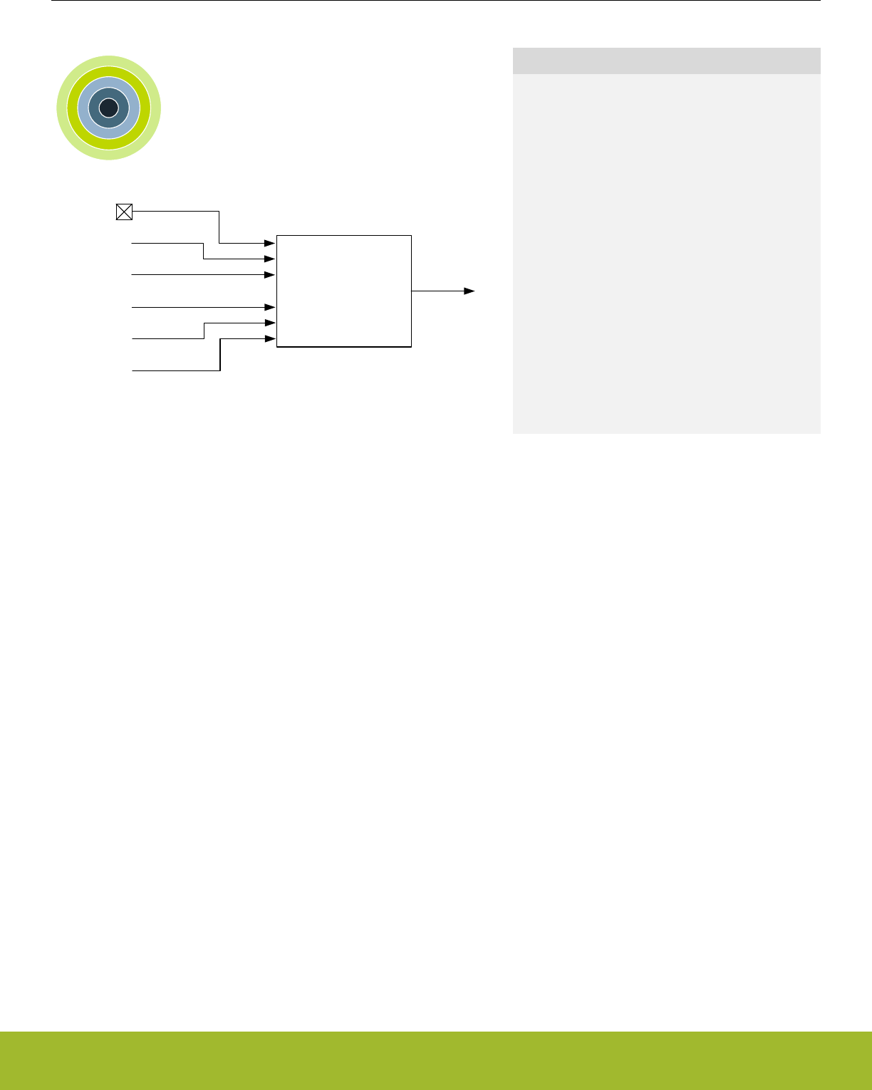
10. RMU - Reset Management Unit
0 1 2 3 4
SYSRESETREQ
WATCHDOG
BROWNOUT
POWERON
Reset Management Unit RESET
LOCKUP
RESETn
Quick Facts
What?
The RMU ensures correct reset operation. It is re-
sponsible for connecting the different reset sources
to the reset lines of the EFR32xG13 Wireless
Gecko.
Why?
A correct reset sequence is needed to ensure safe
and synchronous startup of the EFR32xG13 Wire-
less Gecko. In the case of error situations such as
power supply glitches or software crash, the RMU
provides proper reset and startup of the EFR32xG13
Wireless Gecko.
How?
The Power-on Reset and Brown-out Detector of the
EFR32xG13 Wireless Gecko provides power line
monitoring with exceptionally low power consump-
tion. The cause of the reset may be read from a reg-
ister, thus providing software with information about
the cause of the reset.
10.1 Introduction
The RMU is responsible for handling the reset functionality of the EFR32xG13 Wireless Gecko.
10.2 Features
• Reset sources
• Power-on Reset (POR)
• Brown-out Detection (BOD) on the following power domains:
• Analog Unregulated Power Domain AVDD
• Digital Unregulated Power Domain DVDD
• Regulated Digital Domain DECOUPLE (DEC)
• RESETn pin reset
• Watchdog reset
• Software triggered reset (SYSRESETREQ)
• Core LOCKUP condition
• EM4 Hibernate/Shutoff Detection
• EM4 Hibernate/Shutoff wakeup reset from GPIO pin
• Configurable reset levels
• A software readable register indicates the cause of the last reset
Reference Manual
RMU - Reset Management Unit
silabs.com | Smart. Connected. Energy-friendly. Preliminary Rev. 0.5 | 209
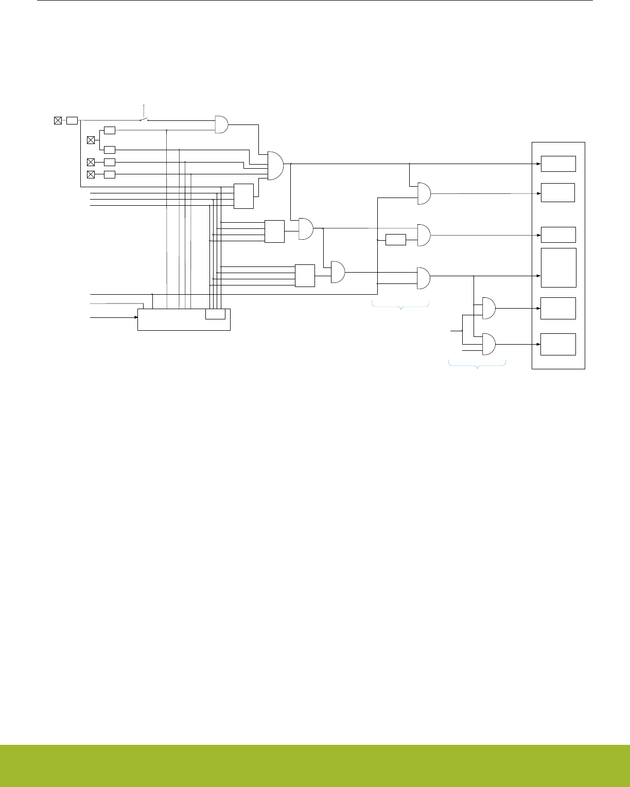
10.3 Functional Description
The RMU monitors each of the reset sources of the EFR32xG13 Wireless Gecko. If one or more reset sources go active, the RMU
applies reset to the EFR32xG13 Wireless Gecko. When the reset sources go inactive the EFR32xG13 Wireless Gecko starts up. At
startup the EFR32xG13 Wireless Gecko loads the stack pointer and program entry point from memory, and starts execution. Figure
10.1 RMU Reset Input Sources and Connections on page 210 shows an overview of the reset system on EFR32xG13 Wireless Gecko.
SYSREQRST
WDOGRST
Reset Management Unit
SYSRESETn
LOCKUPRST
EXTRSTTn
Debug Interface
CORE,
CMU*,
EMU*,
RMU*
and
Peripherals
AVDDBODn
RCCLR
PAD_RESETn
DVDDBODn
AVDD
EM4H/EM4S
Wakeup Resetn
DVDD
PORSTn
POR
DEC
BOD
BOD
BOD
DECBODn
EXRST
FULLRESETn
EM4 Pin Wakeup cause
Enable
Full
Reset
Enable
Extended
Reset
Enable
Limited
Reset
CRYOTIMER,
RFSENSE,
LFOSC Ctrl
RTCC
VMON
EXTENDEDRESETn
SYSREQRST
WDOGRST
LOCKUPRST
EXTRST
SYSREQRST
WDOGRST
LOCKUPRST
EXTRST
LIMITEDRESETn
DEBUGRESETn
RMU_RSTCAUSE
EM4S
only
SYSEXTENDEDRESETn
CACHE
SYSNORETRESETn
EM4H/EM4S
Wakeup Resetn
RADIO
EM23 Wakeup
Resetn
RADIORESETn
RADIORSTn
Enabled
Reset
Filter PORESETn
FULLRESTn
EM4
EM23 and
Subsystem
Lockbit
* Contains some registers with
alternate reset signal. Refer to
separate table for complete
overview.
Figure 10.1. RMU Reset Input Sources and Connections
Reference Manual
RMU - Reset Management Unit
silabs.com | Smart. Connected. Energy-friendly. Preliminary Rev. 0.5 | 210

10.3.1 Reset levels
The reset sources on EFR32xG13 Wireless Gecko can be divided in two main groups; Hard resets and Soft resets.
The soft resets can be configured to be either DISABLED, LIMITED, EXTENDED or FULL. The reset level for soft reset sources is
configured in the xxxRMODE bitfields in RMU_CTRL.
Table 10.1. Reset levels
RMU_CTRL_xxxRMODE Parts of system reset
DISABLED Nothing is reset, request will not be registered in
RMU_RSTCAUSE
LIMITED Everything reset, with exception of CRYOTIMER, RFSENSE, DE-
BUGGER, RTCC, VMON and parts of CMU, RMU and EMU.
EXTENDED Everything reset, with exception of CRYOTIMER, RFSENSE, DE-
BUGGER, and parts of CMU, RMU and EMU.
FULL Everything reset, with exception of some registers in RMU and
EMU.
The reset sources resulting in a soft reset are:
• Watchdog reset
• Lockup reset
• System reset request
•Pin reset1
1 Pin reset can be configured to be either a soft or a hard reset, see 10.3.5 RESETn pin Reset for details
Note: LIMITED and EXTENDED resets are synchronized to HFSRCCLK. If HFSRCCLK is slow, there will be latency on reset assertion.
If HFSRCCLK is not running, reset will be asserted after a timeout.
Hard resets will reset the entire chip, the reset sources resulting in a hard reset are:
• Power-on reset
• Brown-out reset
•Pin reset1
Reference Manual
RMU - Reset Management Unit
silabs.com | Smart. Connected. Energy-friendly. Preliminary Rev. 0.5 | 211

10.3.2 RMU_RSTCAUSE Register
Whenever a reset source is active, the corresponding bit in the RMU_RSTCAUSE register is set. At startup the program code may
investigate this register in order to determine the cause of the reset. The register is cleared upon POR and software write to
RMU_CMD_RCCLR. The register should be cleared after the value has been read at startup, otherwise the register may indicate multi-
ple causes for the reset at next startup.
RMU_RSTCAUSE should be interpreted according to Table 10.2 RMU Reset Cause Register Interpretation on page 212. In Table
10.2 RMU Reset Cause Register Interpretation on page 212, the reset causes are ordered by severity from right to left. A reset cause
bit is invalidated (i.e. can not be trusted) if one of the bits to the right of it does not match the table. X bits are don't care.
Note:
Notice that it is possible to have multiple reset causes. For example, an external reset and a watchdog reset may happen simultaneous-
ly.
Table 10.2. RMU Reset Cause Register Interpretation
RMU_RSTCAUSE Reset cause
EM4RST
WDOGRST
SYSREQRST
LOCKUPRST
EXTRST
DECBOD
DVDDBOD
AVDDBOD
PORST
X X X X X X X X 1 Power on reset
X X X X X X X 1 0 Brown-out on AVDD power
X X X X X X 1 X 0 Brown-out on DVDD power
X X X X X 1 X X 0 Brown-out on DEC power
X X X X 1 X X X 0 Pin reset
X X X 1 0/X10 0 0 0 Lockup reset
X X 1 X 0/X10 0 0 0 System reset request
X 1 X X 0/X10 0 0 0 Watchdog reset
1 X X X 0/X10 0 0 0 System has been in EM4
1 Pin reset configured as hard/soft
Reference Manual
RMU - Reset Management Unit
silabs.com | Smart. Connected. Energy-friendly. Preliminary Rev. 0.5 | 212
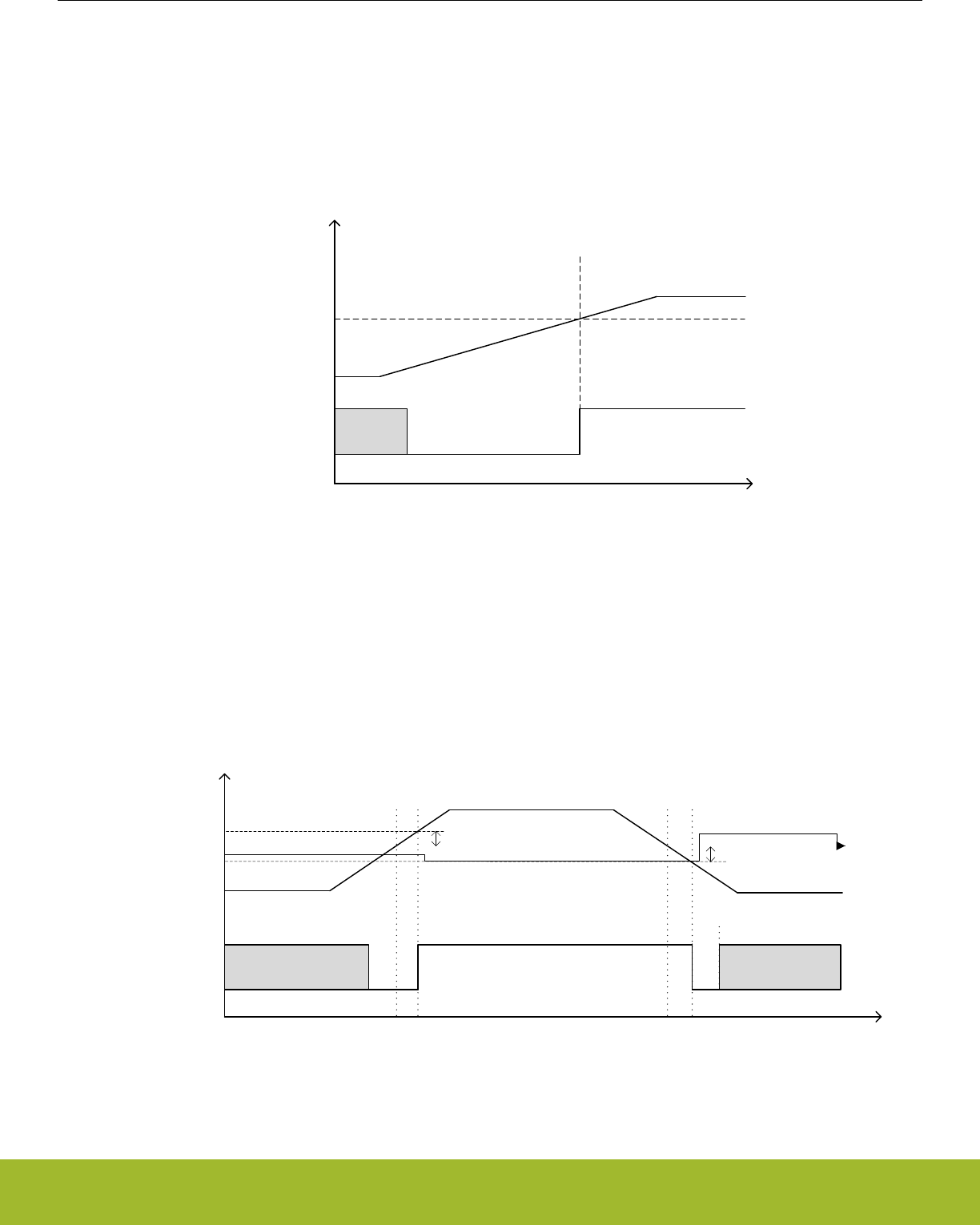
10.3.3 Power-On Reset (POR)
The POR ensures that the EFR32xG13 Wireless Gecko does not start up before the supply voltage VDD has reached the threshold
voltage VPORthr (see Device Datasheet Electrical Characteristics for details). Before the threshold voltage is reached, the EFR32xG13
Wireless Gecko is kept in reset state. The operation of the POR is illustrated in Figure 10.2 RMU Power-on Reset Operation on page
213, with the active low POWERONn reset signal. The reason for the “unknown” region is that the corresponding supply voltage is too
low for any reliable operation.
POWERONn
VDD
time
V
Unknown
VPORthr
Figure 10.2. RMU Power-on Reset Operation
10.3.4 Brown-Out Detector (BOD)
The EFR32xG13 Wireless Gecko The BODs also include hysteresis, which prevents instability in the corresponding BROWNOUTn line
when the supply is crossing the VBODthr limit or the AVDD bods drops below decouple pin (DEC). The operation of the BOD is illustra-
ted in Figure 10.3 RMU Brown-out Detector Operation on page 213. The “unknown” regions are handled by the POR module.
Unknown
BROWNOUTn
VDD
time
V
Unknown
VBODthr VBODhyst
VBODhyst
Figure 10.3. RMU Brown-out Detector Operation
Reference Manual
RMU - Reset Management Unit
silabs.com | Smart. Connected. Energy-friendly. Preliminary Rev. 0.5 | 213

10.3.5 RESETn pin Reset
The pin reset on EFR32xG13 Wireless Gecko can be configured to be either hard or soft. By default, pin reset is configured as a soft
reset source. To configure it as a hard reset, clear the PINRESETSOFT bit in CLW0 in the Lock bit page, see 8.3.2 Lock Bits (LB) Page
Description for details. Forcing the RESETn pin low generates a reset of the EFR32xG13 Wireless Gecko. The RESETn pin includes
an on-chip pull-up resistor, and can therefore be left unconnected if no external reset source is needed. Also connected to the RESETn
line is a filter which prevents glitches from resetting the EFR32xG13 Wireless Gecko.
10.3.6 Watchdog Reset
The Watchdog circuit is a timer which (when enabled) must be cleared by software regularly. If software does not clear it, a Watchdog
reset is activated. This functionality provides recovery from a software stalemate. Refer to the Watchdog section for specifications and
description. The Watchdog reset can be configured to cause different levels of reset as determined by WDOGRMODE in the
RMU_CTRL register.
10.3.7 Lockup Reset
A Cortex-M4 lockup is the result of the core being locked up because of an unrecoverable exception following the activation of the pro-
cessor’s built-in system state protection hardware.
A Cortex-M4 lockup gives immediate indication of seriously errant kernel software. This is the result of the core being locked up due to
an unrecoverable exception following the activation of the processor’s built in system state protection hardware. For more information
about the Cortex-M4 lockup conditions see the ARMv7-M Architecture Reference Manual. The Lockup reset does not reset the Debug
Interface, unless configured as a FULL reset. The Lockup reset can be configured to cause different levels of reset as determined by
the LOCKUPRMODE bits in the RMU_CTRL register. This includes disabling the reset.
10.3.8 System Reset Request
Software may initiate a reset (e.g. if it finds itself in a non-recoverable state). By asserting the SYSRESETREQ in the Application Inter-
rupt and Reset Control Register, a reset is issued. The SYSRESETREQ does not reset the Debug Interface, unless configured as a
FULL reset. The SYSRESTREQ reset can be configured to cause different levels of reset as determined by SYSRESETRMODE bits in
the RMU_CTRL register. This includes disabling the reset.
10.3.9 Reset state
The RESETSTATE bitfield in RMU_CTRL is a read-write register intended for software use only, and can be used to keep track of state
throughout a reset. This bitfield if only reset by POR and hard pin reset.
10.3.10 Register reset signals
Figure 10.1 RMU Reset Input Sources and Connections on page 210 shows an overview of how the different parts of the design are
affected by the different levels of reset. For RMU, EMU and CMU there are some exceptions. These are given in the following tables.
Reference Manual
RMU - Reset Management Unit
silabs.com | Smart. Connected. Energy-friendly. Preliminary Rev. 0.5 | 214

10.3.10.1 Registers with alternate reset
Alternate reset for registers in RMU
RMU reset levels
POR and hard pin reset RMU_CTRL_WDOGRMODE
RMU_CTRL_LOCKUPRMODE
RMU_CTRL_SYSRMODE
RMU_CTRL_PINRMODE
RMU_CTRL_RESETSTATE
FULL reset RMU_LOCK_LOCKKEY
Alternate reset for registers in CMU
CMU reset levels
FULL reset CMU_LFRCOCTRL
CMU_LFXOCTRL
EXTENDED reset CMU_LFECLKSEL
CMU_LFECLKEN0
CMU_LFEPRESC0
Alternate reset for registers in EMU
EMU reset levels
POR, BOD, and hard pin reset EMU_BIASCONF_LSBIAS_SEL
POR, BOD, and hard pin reset EMU_DCDCLNVCTRL
POR and hard pin reset EMU_CTRL_EM2BODDIS
POR, BOD, and hard pin reset EMU_PWRCTRL
EMU_DCDCCTRL
EMU_DCDCMISCCTRL
EMU_DCDCZDETCTRL
EMU_DCDCCLIMCTRL
EMU_DCDCLNCOMPCTRL
EMU_DCDCLPVCTRL
EMU_DCDCLPCTRL
EMU_DCDCLNFREQCTRL
EMU_DCDCLPEM01CFG
EXTENDED reset EMU_VMONAVDDCTRL
EMU_VMONALTAVDDCTRL
EMU_VMONDVDDCTRL
EMU_VMONIO0CTRL
FULL reset EMU_EM4CTRL
Reference Manual
RMU - Reset Management Unit
silabs.com | Smart. Connected. Energy-friendly. Preliminary Rev. 0.5 | 215

10.4 Register Map
The offset register address is relative to the registers base address.
Offset Name Type Description
0x000 RMU_CTRL RW Control Register
0x004 RMU_RSTCAUSE RReset Cause Register
0x008 RMU_CMD W1 Command Register
0x00C RMU_RST RW Reset Control Register
0x010 RMU_LOCK RWH Configuration Lock Register
Reference Manual
RMU - Reset Management Unit
silabs.com | Smart. Connected. Energy-friendly. Preliminary Rev. 0.5 | 216

10.5 Register Description
10.5.1 RMU_CTRL - Control Register
Offset Bit Position
0x000
31
30
29
28
27
26
25
24
23
22
21
20
19
18
17
16
15
14
13
12
11
10
9
8
7
6
5
4
3
2
1
0
Reset
0x0
0x4
0x2
0x0
0x4
Access
RW
RW
RW
RW
RW
Name
RESETSTATE
PINRMODE
SYSRMODE
LOCKUPRMODE
WDOGRMODE
Bit Name Reset Access Description
31:26 Reserved To ensure compatibility with future devices, always write bits to 0. More information in 1.2 Conven-
tions
25:24 RESETSTATE 0x0 RW System Software Reset State
Bit-field for software use only. This field has no effect on the RMU and is reset by power-on reset and hard pin reset only.
23:15 Reserved To ensure compatibility with future devices, always write bits to 0. More information in 1.2 Conven-
tions
14:12 PINRMODE 0x4 RW PIN Reset Mode
Controls the reset level for Pin reset request. These settings only apply when PINRESETSOFT in CLW0 in the Lock bit
page is set.
Value Mode Description
0 DISABLED Reset request is blocked.
1 LIMITED The CRYOTIMER, DEBUGGER, RTCC, are not reset.
2 EXTENDED The CRYOTIMER, DEBUGGER are not reset. RTCC is reset.
4 FULL The entire device is reset except some EMU and RMU registers.
11 Reserved To ensure compatibility with future devices, always write bits to 0. More information in 1.2 Conven-
tions
10:8 SYSRMODE 0x2 RW Core Sysreset Reset Mode
Controls the reset level for Core SYSREST reset request.
Value Mode Description
0 DISABLED Reset request is blocked.
1 LIMITED The CRYOTIMER, DEBUGGER, RTCC, are not reset.
2 EXTENDED The CRYOTIMER, DEBUGGER are not reset. RTCC is reset.
4 FULL The entire device is reset except some EMU and RMU registers.
7 Reserved To ensure compatibility with future devices, always write bits to 0. More information in 1.2 Conven-
tions
Reference Manual
RMU - Reset Management Unit
silabs.com | Smart. Connected. Energy-friendly. Preliminary Rev. 0.5 | 217

Bit Name Reset Access Description
6:4 LOCKUPRMODE 0x0 RW Core LOCKUP Reset Mode
Controls the reset level for Core LOCKUP reset request.
Value Mode Description
0 DISABLED Reset request is blocked.
1 LIMITED The CRYOTIMER, DEBUGGER, RTCC, are not reset.
2 EXTENDED The CRYOTIMER, DEBUGGER are not reset. RTCC is reset.
4 FULL The entire device is reset except some EMU and RMU registers.
3 Reserved To ensure compatibility with future devices, always write bits to 0. More information in 1.2 Conven-
tions
2:0 WDOGRMODE 0x4 RW WDOG Reset Mode
Controls the reset level for WDOG reset request.
Value Mode Description
0 DISABLED Reset request is blocked. This disable bit is redundant with enable/
disable bit in WDOG
1 LIMITED The CRYOTIMER, DEBUGGER, RTCC, are not reset.
2 EXTENDED The CRYOTIMER, DEBUGGER are not reset. RTCC is reset.
4 FULL The entire device is reset except some EMU and RMU registers.
Reference Manual
RMU - Reset Management Unit
silabs.com | Smart. Connected. Energy-friendly. Preliminary Rev. 0.5 | 218

10.5.2 RMU_RSTCAUSE - Reset Cause Register
Offset Bit Position
0x004
31
30
29
28
27
26
25
24
23
22
21
20
19
18
17
16
15
14
13
12
11
10
9
8
7
6
5
4
3
2
1
0
Reset
0
0
0
0
0
0
0
0
0
Access
R
R
R
R
R
R
R
R
R
Name
EM4RST
WDOGRST
SYSREQRST
LOCKUPRST
EXTRST
DECBOD
DVDDBOD
AVDDBOD
PORST
Bit Name Reset Access Description
31:17 Reserved To ensure compatibility with future devices, always write bits to 0. More information in 1.2 Conven-
tions
16 EM4RST 0 R EM4 Reset
Set if the system has been in EM4. Must be cleared by software. Please see Table 10.2 RMU Reset Cause Register Inter-
pretation on page 212 for details on how to interpret this bit.
15:12 Reserved To ensure compatibility with future devices, always write bits to 0. More information in 1.2 Conven-
tions
11 WDOGRST 0 R Watchdog Reset
Set if a watchdog reset has been performed. Must be cleared by software. Please see Table 10.2 RMU Reset Cause Regis-
ter Interpretation on page 212 for details on how to interpret this bit.
10 SYSREQRST 0 R System Request Reset
Set if a system request reset has been performed. Must be cleared by software. Please see Table 10.2 RMU Reset Cause
Register Interpretation on page 212 for details on how to interpret this bit.
9 LOCKUPRST 0 R LOCKUP Reset
Set if a LOCKUP reset has been requested. Must be cleared by software. Please see Table 10.2 RMU Reset Cause Regis-
ter Interpretation on page 212 for details on how to interpret this bit.
8 EXTRST 0 R External Pin Reset
Set if an external pin reset has been performed. Must be cleared by software. Please see Table 10.2 RMU Reset Cause
Register Interpretation on page 212 for details on how to interpret this bit.
7:5 Reserved To ensure compatibility with future devices, always write bits to 0. More information in 1.2 Conven-
tions
4 DECBOD 0 R Brown Out Detector Decouple Domain Reset
Set if a regulated domain brown out detector reset has been performed. Must be cleared by software. Please see Table
10.2 RMU Reset Cause Register Interpretation on page 212 for details on how to interpret this bit.
3 DVDDBOD 0 R Brown Out Detector DVDD Reset
Set if a unregulated domain brown out detector reset has been performed. Must be cleared by software. Please see Table
10.2 RMU Reset Cause Register Interpretation on page 212 for details on how to interpret this bit.
2 AVDDBOD 0 R Brown Out Detector AVDD Reset
Set if a unregulated domain brown out detector reset has been performed. Must be cleared by software. Please see Table
10.2 RMU Reset Cause Register Interpretation on page 212 for details on how to interpret this bit.
1 Reserved To ensure compatibility with future devices, always write bits to 0. More information in 1.2 Conven-
tions
Reference Manual
RMU - Reset Management Unit
silabs.com | Smart. Connected. Energy-friendly. Preliminary Rev. 0.5 | 219

Bit Name Reset Access Description
0 PORST 0 R Power On Reset
Set if a power on reset has been performed. Must be cleared by software. Please see Table 10.2 RMU Reset Cause Regis-
ter Interpretation on page 212 for details on how to interpret this bit.
10.5.3 RMU_CMD - Command Register
Offset Bit Position
0x008
31
30
29
28
27
26
25
24
23
22
21
20
19
18
17
16
15
14
13
12
11
10
9
8
7
6
5
4
3
2
1
0
Reset
0
Access
W1
Name
RCCLR
Bit Name Reset Access Description
31:1 Reserved To ensure compatibility with future devices, always write bits to 0. More information in 1.2 Conven-
tions
0 RCCLR 0 W1 Reset Cause Clear
Set this bit to clear the RSTCAUSE register.
10.5.4 RMU_RST - Reset Control Register
Offset Bit Position
0x00C
31
30
29
28
27
26
25
24
23
22
21
20
19
18
17
16
15
14
13
12
11
10
9
8
7
6
5
4
3
2
1
0
Reset
Access
Name
Bit Name Reset Access Description
31:0 Reserved To ensure compatibility with future devices, always write bits to 0. More information in 1.2 Conven-
tions
Reference Manual
RMU - Reset Management Unit
silabs.com | Smart. Connected. Energy-friendly. Preliminary Rev. 0.5 | 220

10.5.5 RMU_LOCK - Configuration Lock Register
Offset Bit Position
0x010
31
30
29
28
27
26
25
24
23
22
21
20
19
18
17
16
15
14
13
12
11
10
9
8
7
6
5
4
3
2
1
0
Reset
0x0000
Access
RWH
Name
LOCKKEY
Bit Name Reset Access Description
31:16 Reserved To ensure compatibility with future devices, always write bits to 0. More information in 1.2 Conven-
tions
15:0 LOCKKEY 0x0000 RWH Configuration Lock Key
Write any other value than the unlock code to lock RMU_CTRL and RMU_RST from editing. Write the unlock code to un-
lock. When reading the register, bit 0 is set when the lock is enabled.
Mode Value Description
Read Operation
UNLOCKED 0 RMU registers are unlocked
LOCKED 1 RMU registers are locked
Write Operation
LOCK 0 Lock RMU registers
UNLOCK 0xE084 Unlock RMU registers
Reference Manual
RMU - Reset Management Unit
silabs.com | Smart. Connected. Energy-friendly. Preliminary Rev. 0.5 | 221

11. EMU - Energy Management Unit
0 1 2 3 4
Quick Facts
What?
The EMU (Energy Management Unit) handles the
different low energy modes in EFR32xG13 Wireless
Gecko
Why?
The need for performance and peripheral functions
varies over time in most applications. By efficiently
scaling the available resources in real time to match
the demands of the application, the energy con-
sumption can be kept at a minimum.
How?
With a broad selection of energy modes, a high
number of low-energy peripherals available even in
EM2 Deep Sleep, and short wake-up time (3 µs from
EM2 Deep Sleep and EM3 Stop), applications can
dynamically minimize energy consumption during
program execution.
11.1 Introduction
The Energy Management Unit (EMU) manages all the low energy modes (EM) in EFR32xG13 Wireless Gecko. Each energy mode
manages whether the CPU and the various peripherals are available. The energy modes range from EM0 Active to EM4 Shutoff. EM0
Active mode provides the highest amount of features, enabling the CPU, Radio, and peripherals with the highest clock frequency. EM4
Shutoff Mode provides the lowest power state, allowing the part to return to EM0 Active on a wake-up condition. The EMU also controls
the various power routing configurations, internal regulators settings, and voltage monitoring needed for optimal power configuration
and protection.
Reference Manual
EMU - Energy Management Unit
silabs.com | Smart. Connected. Energy-friendly. Preliminary Rev. 0.5 | 222

11.2 Features
The primary features of the EMU are listed below:
• Energy Modes control
•Entry into EM4 Hibernate or EM4 Shutoff
• Configuration of regulators and clocks for each Energy Mode
• Configuration of various EM4 Hibernate/Shutoff wake-up conditions
• Configuration of RAM power and retention settings
• Configuration of GPIO retention settings
• Power routing configurations
• DCDC control
• Internal power switches allowing for extensible system power architecture
• Temperature measurement control and status
• Brown Out Detection
• Voltage Monitoring
• Four dedicated continuous monitor channels
• Optional monitor features include interrupt generation and low power mode wake-up
• State Retention
• Voltage Scaling
• EM01 voltage scaling
• EM23 voltage scaling
• EM4H voltage scaling
Reference Manual
EMU - Energy Management Unit
silabs.com | Smart. Connected. Energy-friendly. Preliminary Rev. 0.5 | 223
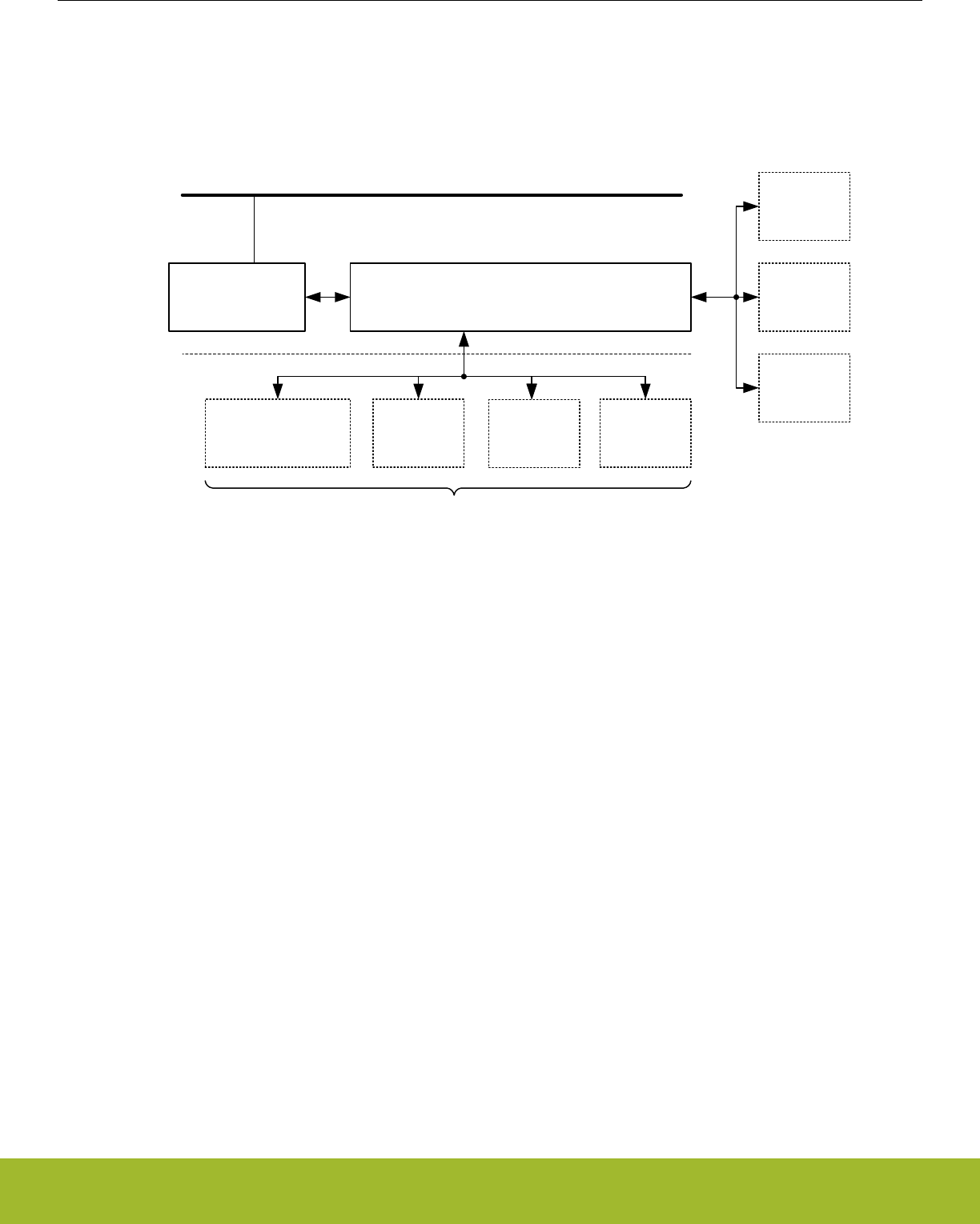
11.3 Functional Description
The EMU is responsible for managing the wide range of energy modes available in EFR32xG13 Wireless Gecko. The block works in
harmony with the entire platform to easily transition between energy modes in the most efficient manner possible. The following dia-
gram Figure 11.1 EMU Overview on page 224, shows the relative connectivity to the various blocks in the system.
Peripheral bus
Control and
Status Registers
Energy Management Unit
State Machine & Control
Radio
Voltage
Regulators
Oscillators
Memory
System
Interrupt
Handler
CPU Core
(Not all devices) PRS
The combined state of these modules
defines the required energy mode
Figure 11.1. EMU Overview
The EMU is available on the peripheral bus. The energy management state machine controls the internal voltage regulators, oscillators,
memories, and interrupt system. Events, interrupts, and resets can trigger the energy management state machine to return to the active
state. This is further described in the following sections.
The power architecture is highly configurable to meet system power performance needs. Several external power configurations are
supported. The EMU allows flexible control of internal DCDC, Digital LDO Regulator, and internal power switching.
Reference Manual
EMU - Energy Management Unit
silabs.com | Smart. Connected. Energy-friendly. Preliminary Rev. 0.5 | 224

11.3.1 Energy Modes
EFR32xG13 Wireless Gecko features six main energy modes, referred to as Energy Mode 0 (EM0 Active) through Energy Mode 4
(EM4 Shutoff). The Cortex-M4 is only available for program execution in EM0 Active. In EM0 Active/EM1 Sleep any peripheral function
can be enabled. EM2 Deep Sleep through EM4 Shutoff, also referred to as low energy modes, provide a significantly reduced energy
consumption while still allowing a rich set of peripheral functionality. The following Table 11.1 table on page 225 shows the possible
transitions between different energy modes.
Table 11.1. Energy Mode Transitions
Current Mode EM Transition Action
Enter EM0 Ac-
tive
Enter EM1
Sleep
Enter EM2
Deep Sleep
EnterEM3
Stop
EnterEM4 Hi-
bernate
Enter EM4
Shutoff
EM0 Active Sleep (WFI,
WFE)
Deep Sleep
(WFI, WFE)
Deep Sleep
(WFI, WFE)
EM4 Entry EM4 Entry
EM1 Sleep IRQ Peripheral
wake up done1
Peripheral
wake up done1
EM2 Deep Sleep IRQ Peripheral
wake up req1
EM3 Stop IRQ Peripheral
wake up req1
EM4 Hibernate Wake Up
EM4 Shutoff Wake Up
1 Peripheral wake-up from EM2/3 to EM1 and then automatically back to EM2/3 when done.
The CSEN, LESENSE, ADC, RAC, and LEUART have the ability to temporarily wake up the part from either EM2 Deep Sleep or EM3
Stop to EM1 Sleep in order to transfer data. Once completed, the part is automatically placed back into the EM2 Deep Sleep or EM3
Stop mode.
The Core can always request to go to EM1 Sleep with the WFI or WFE command during EM0 Active. The core will be prevented from
entering EM2 Deep Sleep or EM3 Stop if the RAC is transferring data or if Flash is programming or erasing.
An overview of supported energy modes and available functionality is shown in Table 11.2 EMU Energy Mode Overview on page 225.
For each energy mode, the system will typically default to its lowest power configuration, with non-essential clocks and peripherals disa-
bled. Functionality may be then selectively enabled by software.
Table 11.2. EMU Energy Mode Overview
EM0
Active/EM1
Sleep
EM2 Deep
Sleep
EM3 Stop EM4 Hiber-
nate
EM4 Shutoff
Wake-up time to EM0 Active/EM1 Sleep - 3 µs 13 µs 1160 µs 1160 µs 1
Core Active Yes, in EM0
only
----
Debug Available See Note2See Note2- -
Digital logic and system RAM retained Yes Yes Yes - -
Flash Memory Access Available - - - -
LDMA (Linked DMA Controller) Available Available3Available3- -
RAC (Radio Controller) Available Available4---
Reference Manual
EMU - Energy Management Unit
silabs.com | Smart. Connected. Energy-friendly. Preliminary Rev. 0.5 | 225

EM0
Active/EM1
Sleep
EM2 Deep
Sleep
EM3 Stop EM4 Hiber-
nate
EM4 Shutoff
RFSENSE (Ultra Low Energy RF Detection) Available Available Available Available Available
High Frequency Oscillators (HFRCO, HFXO) and
Clocks (HFSRCLK, HFCLK, HFCORECLK,
HFBUSCLK, HFPERCLK, HFRADIOCLK,
HFCLKLE)
Available - - - -
Auxiliary High Frequency Oscillator (AUXHFR-
CO) and Clock (AUXCLK)
Available Available5Available5- -
Low Frequency Oscillators (LFRCO, LFXO) Available Available - Available Available
Low Energy Clocks A and B (LFACLK, LFBCLK) Available Available Available7- -
Low Energy Clock E (LFECLK) Available Available Available7Available -
ULFRCO (Ultra Low Frequency Oscillator) On On On On Available
CRYPTO (Crypto Accelerator) Available - - - -
TRNG (True Random Number Generator) Available - - - -
GPCRC (Cyclic Redundancy Check) Available - - - -
RTCC (Real Time Counter and Calendar) Available Available Available7Available -
RTCC Memory Retained Yes Yes Yes Yes -
USART (USART/SPI) Available - - - -
LEUART (Low Energy UART) Available Available3---
I2CAvailable Available6Available6- -
TIMER (Timer/Counter) Available - - - -
LETIMER (Low Energy Timer) Available Available Available7- -
CRYOTIMER (Ultra Low Energy Timer/Counter) Available Available Available7Available Available
WDOG (Watchdog) Available Available Available7- -
PCNT (Pulse Counter) Available Available Available - -
CSEN (Capacitive Sense) Available Available3---
ACMP (Analog Comparator) Available Available8Available8- -
ADC (Analog to Digital Converter) Available Available3,5 Available3,5 - -
IDAC (Current Digital to Analog Converter) Available Available Available - -
VDAC (Voltage Digital to Analog Converter) Available Available Available - -
OPAMP (Operational Amplifier) Available Available Available - -
LESENSE (Low Energy Sensor) Available Available3---
EMU Temperature Sensor Available Available Available Available -
DC-DC Converter Available Available Available Available -
VMON Wake-up or Reset Available Available Available Available -
Brown-Out Detect/Power-on Reset Available Available Available Available Available
Pin Reset Available Available Available Available Available
Reference Manual
EMU - Energy Management Unit
silabs.com | Smart. Connected. Energy-friendly. Preliminary Rev. 0.5 | 226

EM0
Active/EM1
Sleep
EM2 Deep
Sleep
EM3 Stop EM4 Hiber-
nate
EM4 Shutoff
GPIO Pin Interrupts Available Available Available Available9Available9
GPIO Pin State Retention Yes Yes Yes Yes Yes
1 Approximate time. Refer to datasheet
2Leaving the debugger connected when in EM2 or EM3 will cause the system to enter a higher power EM2 mode in which the high
frequency clocks are still enabled and certain core functionality is still powered-up in order to maintain debug-functionality.
3 The LDMA can be used with some low power peripherals (e.g., ADC, LEUART, LESENSE, CSEN) in EM2/3. Features required
by the LDMA which are not supported in EM2/3 (e.g., HFCLK), will be automatically enabled prior to the LDMA transfer and then
automatically disabled afterwards.
4 The RAC can be woken via a PRS interrupt to EM1 to transfer data. Once complete, the system will return to EM2.
5 While in EM2/3, an asynchronous event can be routed through PRS (e.g. GPIO IRQ or ACMP output) to wake up the ADC. Fea-
tures required by the ADC which are not supported in EM2/3 (e.g., AUXHFRCO) will be automatically enabled to allow the ADC to
convert a sample, and then automatically disabled afterwards.
6 I2C functionality limited to receive address recognition
7 Must be using ULFRCO
8 ACMP functionality in EM2/3 limited to edge interrupt
9 Pin wake-up in EM4 supported only on GPIO_EM4WUx pins. Consult datasheet for complete list of pins.
The different Energy Modes are summarized in the following sections.
11.3.1.1 EM0 Active
EM0 Active provides all system features.
• Cortex-M4 is executing code
• Radio functionality is available
• High and low frequency clock trees are active
• All oscillators are available
• All peripheral functionality is available
11.3.1.2 EM1 Sleep
EM1 Sleep disables the core but leaves the remaining system fully available.
• Cortex-M4 is in sleep mode. Clocks to the core are off
• Radio functionality is available
• High and low frequency clock trees are active
• All oscillators are available
• All peripheral functionality is available
Reference Manual
EMU - Energy Management Unit
silabs.com | Smart. Connected. Energy-friendly. Preliminary Rev. 0.5 | 227

11.3.1.3 EM2 Deep Sleep
This is the first level into the low power energy modes. Most of the high frequency peripherals are disabled or have reduced functionali-
ty. Memory and registers retain their values.
• Cortex-M4 is in sleep mode. Clocks to the core are off.
• RFSENSE available. Radio inactive
• High frequency clock tree is inactive
• Low frequency clock tree is active
• The following oscillators are available
• LFRCO, LFXO, ULFRCO, AUXHFRCO (on demand, if used by the ADC)
• The following low frequency peripherals are available
• RTCC, WDOG, LEUART, LETIMER, PCNT, CRYOTIMER
• The following analog peripherals are available (with potential limitations on functionality)
• ADC, IDAC, VDAC, OPAMP, CSEN
• Wake-up to EM0 Active through
• Peripheral interrupt, reset pin, power on reset, asynchronous pin interrupt, I2C address recognition, or ACMP edge interrupt
• Wake-up to EM1 Sleep through
• RAC data transfer request
• Part returns to EM2 Deep Sleep when transfers are complete
• RAM and register values are preserved
• RAM blocks may be optionally powered down for lower power
• GPIO pin state is retained
• RTCC memory is retained
• The DC-DC converter can be configured to remain on in Low Power mode.
11.3.1.4 EM3 Stop
This low energy mode has both high frequency and low frequency clocks stopped. Most peripherals are disabled or have reduced func-
tionality. Memory and registers retain their values.
• Cortex-M4 is in sleep mode. Clocks to the core are off.
• RFSENSE available. Radio inactive
• High frequency clock tree is inactive
• Low frequency clock tree is inactive
• The following oscillators are available
• ULFRCO, AUXHFRCO (on demand, if used by the ADC)
• The following low frequency peripherals are available if clocked by the ULFRCO
• RTCC, WDOG, CRYOTIMER
• The following analog peripherals are available (with potential limitations on functionality)
• ADC, IDAC, VDAC, OPAMP, CSEN
• Wake-up to EM0 Active through
• Peripheral interrupt, reset pin, power on reset, asynchronous pin interrupt, I2C address recognition, or ACMP edge interrupt
• Wake-up to EM1 Sleep through
• RAC data transfer request
• Part returns to EM3 Stop when transfers are complete
• RAM and register values are preserved
• RAM blocks may be optionally powered down for lower power
• GPIO pin state is retained
• RTCC memory is retained
• The DC-DC converter can be configured to remain on in Low Power mode.
Reference Manual
EMU - Energy Management Unit
silabs.com | Smart. Connected. Energy-friendly. Preliminary Rev. 0.5 | 228

11.3.1.5 EM4 Hibernate
The majority of peripherals are shutoff to reduce leakage power. A few selected peripherals are available. System memory and regis-
ters do not retain values. GPIO PAD state and RTCC RAM are retained. Wake-up from EM4 Hibernate requires a reset to the system,
returning it back to EM0 Active
• Cortex-M4 is off
• RFSENSE available. Radio is off.
• High frequency clock tree is off
• Low frequency clock tree may be active
• The following oscillators are available
• LFRCO, LFXO, ULFRCO
• The following low frequency peripherals are available
• RTCC, CRYOTIMER
• Wake-up to EM0 Active through
• VMON, EMU Temperature Sensor, RTCC, RFSENSE, CRYOTIMER, reset pin, power on reset, asynchronous pin interrupt (on
GPIO_EM4WUx pins only)
• GPIO pin state is retained
• RTCC memory is retained
• The DC-DC converter can be configured to remain on in Low Power mode.
11.3.1.6 EM4 Shutoff
EM4 Shutoff is the lowest energy mode of the part. There is no retention except for GPIO PAD state. Wake-up from EM4 Shutoff re-
quires a reset to the system, returning it back to EM0 Active
• Cortex-M4 is off
• RFSENSE available. Radio is off.
• High frequency clock tree is off
• Low frequency clock tree may be active
• The following oscillators are available
• LFRCO, LFXO, ULFRCO
• The following low frequency peripherals are available
• CRYOTIMER
• Wake-up to EM0 Active through
• RFSENSE, CRYOTIMER, reset pin, power on reset, asynchronous pin interrupt (on GPIO_EM4WUx pins only)
• GPIO pin state is retained
• The DC-DC converter configuration is reset to its default Unconfigured configuration (DC-DC converter disabled and bypass switch
is off)
11.3.2 Entering Low Energy Modes
The following sections describe the requirements for entering the various Energy Modes.
Note: If Voltage scaling is being used to save system energy, it is important to ensure the proper conditions for entry and exit of EM2
Deep Sleep, EM3 Stop or EM4 Hibernate be met. See 11.3.9.2.1 EM23 Voltage Scaling Guidelines and 11.3.9.3.1 EM4H Voltage Scal-
ing Guidelines for details.
11.3.2.1 Entry into EM1 Sleep
Energy mode EM1 Sleep is entered when the Cortex-M4 executes the Wait For Interrupt (WFI) or Wait For Event (WFE) instruction
while the SLEEPDEEP bit the Cortex-M4 System Control Register is cleared. The MCU can re-enter sleep automatically out of an Inter-
rupt Service Routine (ISR) if the SLEEPONEXIT bit in the Cortex-M4 System Control Register is set. Refer to ARM documentation on
entering Sleep modes.
Alternately, EM1 Sleep can be entered from either EM2 Deep Sleep or EM3 Stop from a Peripheral Wake-up Request allowing trans-
fers from the Peripheral to System RAM. On EFR32, the RAC, ADC, or LEUART peripherals can request this wake-up event. Please
refer to their respective register specification to enable this option. The system will return back to EM2 DeepSleep or EM3 Stop once
the RAC, ADC, or LEUART have completed its transfers and processing.
During Peripheral Wake-Up Request, additional system resources such as FLASH and other Peripherals can be enabled for access.
Reference Manual
EMU - Energy Management Unit
silabs.com | Smart. Connected. Energy-friendly. Preliminary Rev. 0.5 | 229

11.3.2.2 Entry into EM2 Deep Sleep or EM3 Stop
Energy mode EM2 Deep Sleep or EM3 Stop may be entered when all of the following conditions are true:
• Radio RAC state machine is in OFF state
• IDAC is currently not updating output.
• Cortex-M4 (if present) is in DEEPSLEEP state
• Flash Program/Erase Inactive
• DMA done with all current requests
• A debugger is not currently connected.
Entry into EM2 Deep Sleep and EM3 Stop can be blocked by setting the EMU_CTRL->EM2BLOCK bit.
Note: When EM2 Deep Sleep or EM3 Stop entry is blocked, the part is not able to enter a lower energy state. The core will be in a
sleep state, similar to EM1, where it is waiting for a proper interrupt of other valid wake-up event. Once the blocking conditions are
removed, then the part will automatically enter a lower energy state.
Energy mode EM2 Deep Sleep is entered from EM0 Active when the Cortex-M4 executes the Wait For Interrupt (WFI) or Wait For
Event (WFE) instruction while the SLEEPDEEP bit in the Cortex-M4 System Control Register is set. The MCU can re-enter DeepSleep
automatically out of an Interrupt Service Routine (ISR) if the SLEEPONEXIT bit in the Cortex-M4 System Control Register is set. Refer
to ARM documentation on entering Sleep modes.
Alternately, EM2 Deep Sleep or EM3 Stop is entered from EM1 Sleep upon the completion of a Peripheral Wake-Up Request from the
RAC if no EM0 Active wake-up happens in the meantime.
11.3.2.3 Entry into EM4 Hibernate or EM4 Shutoff
Energy mode EM4 Hibernate and EM4 Shutoff is entered through register access.
Software must ensure no modules are active,such as RAC, when entering EM4 Hibernate/Shutoff. EM4CTRL->EM4STATE field must
be configured to select either Hibernate (EM4H) or Shutoff (EM4S) mode prior to entering EM4.
Software may enter EM4 Hibernate/Shutoff from EM0 Active by writing the sequence 2,3,2,3,2,3,2,3,2 to EM4CTRL->EM4ENTRY bit
field. If the EM4BLOCK bit in WDOGn_CTRL is set, the CPU will be prevented from entering EM4 Hibernate/Shutoff by software re-
quest.
An active debugger connection will prevent entry into EM4 Hibernate/Shutoff.
Note that upon entry into EM4 Shutoff, the DC-DC converter configuration is reset to its default (i.e. Unconfigured) configuration. In the
Unconfigured configuration, the DC-DC converter will be disabled and the bypass switch will be turned off.
Reference Manual
EMU - Energy Management Unit
silabs.com | Smart. Connected. Energy-friendly. Preliminary Rev. 0.5 | 230

11.3.3 Exiting a Low Energy Mode
A system in EM2 Deep Sleep and EM3 Stop can be woken up to EM0 Active through regular interrupt requests from active peripherals.
Since state and RAM retention is available, the EFR32 is fully restored and can continue to operate as before it went into the Low Ener-
gy Mode.
Wake-Up from EM4 Hibernate or EM4 Shutoff is performed through reset. Wake-Up from a specific module must be enabled in that
module’s EM4WUEN register.
Enabled interrupts that can cause wake-up from a low energy mode are shown in Table 11.3 EMU Wake-Up Triggers from Low Energy
Modes on page 231. The wake-up triggers always return the EFR32 to EM0 Active/EM1 Sleep. Additionally, any reset source will re-
turn to EM0 Active. VMON-based EM4 Hibernate wake-ups also set the corresponding rise or fall interrupt flag. These flags serve as
the wake-up source for EM4 Hibernate and must be cleared by software on EM4 Hibernate exit. Not doing so will result in an immediate
wake-up after next EM4 Hibernate entry.
Table 11.3. EMU Wake-Up Triggers from Low Energy Modes
Peripheral Wake-Up Trigger EM2 Deep
Sleep
EM3 Stop EM4 Hiber-
nate
EM4 Shut-
off
LEUART (Low Energy UART) Receive / transmit Yes - - -
LETIMER Any enabled interrupt Yes - - -
LESENSE Any enabled interrupt Yes - - -
LFXO Ready Interrupt Yes - - -
LFRCO Ready Interrupt Yes - - -
I2CReceive address recognition Yes Yes - -
ACMP Any enabled edge interrupt Yes Yes - -
PCNT Any enabled interrupt Yes Yes1- -
RTCC Any enabled interrupt Yes Yes Yes2
VMON Rising or falling edge on any moni-
tored power
Yes Yes Yes2-
EMU Temperature Sensor Measured temperature outside the de-
fined limits
Yes Yes Yes2-
CRYOTIMER Timeout Yes Yes Yes2Yes2
Pin Interrupts Transition Yes Yes Yes23 Yes23
RFSENSE RF signal detected Yes Yes Yes2Yes2
Reset Pin Assertion Yes Yes Yes Yes
Power Cycle Off/On Yes Yes Yes Yes
1 When using an external clock
2 Corresponding bit in the module's EM4WUEN must be set.
3 Only available on a subset of the pins. Please refer to the Data Sheet for details.
Reference Manual
EMU - Energy Management Unit
silabs.com | Smart. Connected. Energy-friendly. Preliminary Rev. 0.5 | 231

11.3.4 Power Configurations
The EFR32xG13 Wireless Gecko allows several power configurations with additional options giving flexible power architecture selec-
tion.
In order to provide the lowest power consuming radio solutions, the EFR32xG13 Wireless Gecko comes with a DC-DC module to pow-
er internal circuits. The DC-DC requires an external inductor and capacitor (please refer to the Data Sheet for recommended values).
The EFR32xG13 Wireless Gecko has multiple internal power domains: IO Supply (IOVDD), Analog & Flash (AVDD), RF Analog Supply
(RFVDD), RF Power Amplifier Supply (PAVDD), Input to Digital LDO (DVDD), and Low Voltage Digital Supply (DECOUPLE). Additional
detail for each configuration and option is given in the following sections.
When assigning supply sources, the following requirement must be adhered to:
• VREGVDD = AVDD (Must be the highest voltage in the system)
• VREGVDD >= DVDD
• VREGVDD >= PAVDD
• VREGVDD >= RFVDD
• VREGVDD >= IOVDD
Reference Manual
EMU - Energy Management Unit
silabs.com | Smart. Connected. Energy-friendly. Preliminary Rev. 0.5 | 232
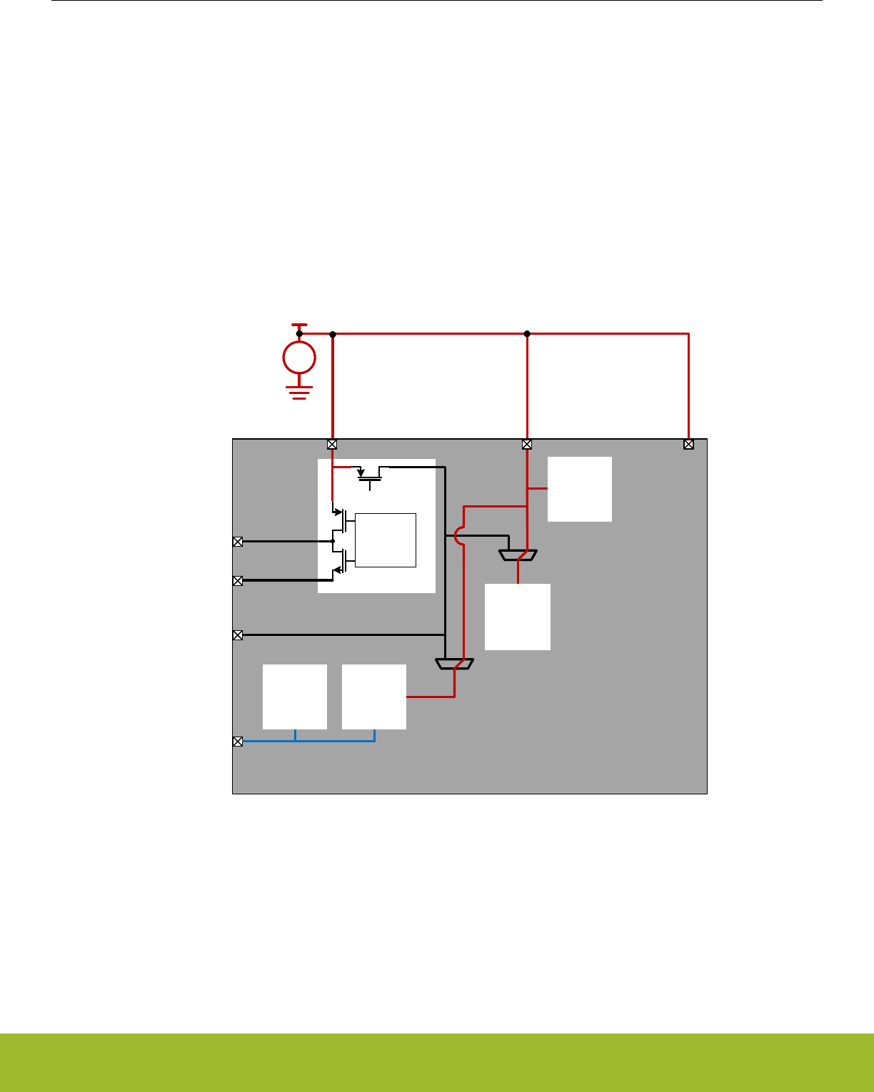
11.3.4.1 Power Configuration 0: Unconfigured
Upon power-on reset (POR) or entry into EM4 Shutoff, the system is configured in a safe state that supports all of the available Power
Configurations. The Unconfigured Configuration is shown in the simplified diagram below.
In the Unconfigured Configuration:
• The DC-DC converter's Bypass switch is OFF.
• The internal digital LDO is powered from the AVDD pin (i.e. REGPWRSEL=0 in EMU_PWRCTRL). Note the maximum allowable
current into the LDO when REGPWRSEL=0 is 20 mA. For this reason, immediately after startup firmware should configure RE-
GPWRSEL=1 to power the digital LDO from DVDD.
• The analog blocks are powered from the AVDD supply pin (i.e., ANASW=0 in EMU_PWRCTRL).
After power on, firmware can configure the device to based on the external hardware configuration. Note that the PWRCFG register can
only be written once to a valid value and is then locked. This should be done immediately out of boot to select the proper power config-
uration. The DC-DC and PWRCTRL registers will be locked until the PWRCFG register is configured.
Main
Supply
DC-DC
DC-DC
Driver
Bypass
Switch
OFF FLASH
+
–
VDD
DECOUPLE
DVDD
AVDD
VREGSW
VREGVSS
IOVDD
VREGVDD
ANASW
0
1
REGPWRSEL
0
1
Analog
Blocks
Digital
Logic
Digital
LDO
Figure 11.2. Unconfigured Power Configuration
Reference Manual
EMU - Energy Management Unit
silabs.com | Smart. Connected. Energy-friendly. Preliminary Rev. 0.5 | 233
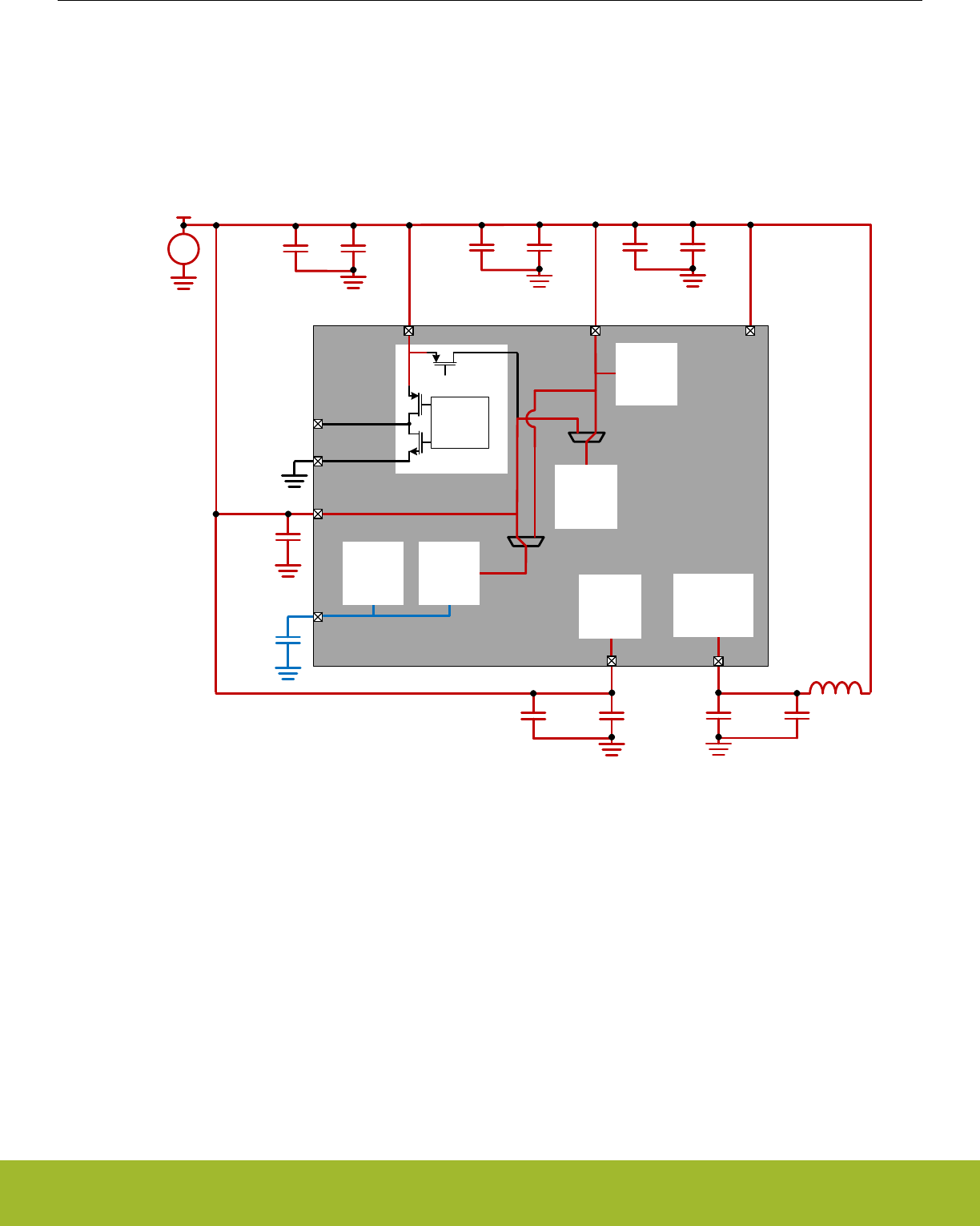
11.3.4.2 Power Configuration 1: No DC-DC
In Power Configuration 1, the DC-DC converter is programmed in Off mode and the Bypass switch is Off. The DVDD pin must be pow-
ered externally - typically, DVDD is connected to the main supply. DVDD powers the internal Digital LDO (i.e., REGPWRSEL=1) which
powers the digital circuits. IOVDD and AVDD are powered from the main supply as well. RFVDD and PAVDD, which power the radio,
are shorted to the main supply as well.
VREGSW must be left disconnected in this configuration.
DECOUPLE
DVDD
AVDD
VREGSW
Main
Supply
VREGVSS
IOVDD
VREGVDD
+
–
VDD
DC-DC
DC-DC
Driver
Bypass
Switch
OFF FLASH
DECOUPLE
DVDD
AVDD
VREGSW
VREGVSS
IOVDD
VREGVDD
ANASW
0
1
REGPWRSEL
0
1
Analog
Blocks
Digital
Logic
Digital
LDO
PAVDD
RFVDD
RF
Analog
RF
Power
Amplifier
Figure 11.3. DC-DC Off Power Configuration
Reference Manual
EMU - Energy Management Unit
silabs.com | Smart. Connected. Energy-friendly. Preliminary Rev. 0.5 | 234
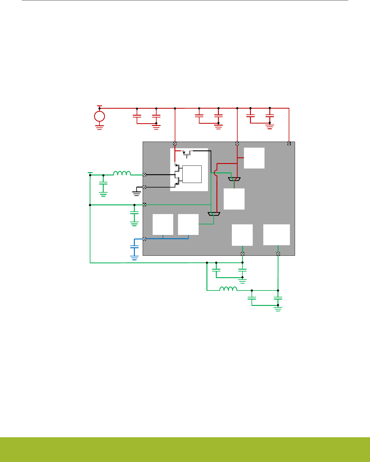
11.3.4.3 Power Configuration 2: DC-DC
For the lowest power applications, the DC-DC converter can be used to power the DVDD supply, as well as RFVDD and PAVDD.
In Power Configuration 2, the DC-DC Output (VDCDC) is connected to DVDD. DVDD powers the internal Digital LDO (i.e., RE-
GPWRSEL=1) which powers the digital circuits. AVDD is connected to the main supply voltage. The internal analog blocks may be
powered from AVDD or DVDD, depending on the ANASW configuration. RFVDD and PAVDD are powered from VDCDC as well.
IOVDD could be connected to either the main supply (as shown below) or to VDCDC, depending on the system IO requirements. Be-
cause VDCDC will be unpowered (i.e., floating) at startup, if IOVDD is powered from the DC-DC converter then any circuit attached to
IOVDD will not be powered until the DC-DC is configured (or the bypass switch is enabled).
DECOUPLE
DVDD
AVDD
VREGSW
Main
Supply
VREGVSS
IOVDD
VREGVDD
+
–
VDD
DC-DC
DC-DC
Driver
Bypass
Switch
OFF FLASH
DECOUPLE
DVDD
AVDD
VREGSW
VREGVSS
IOVDD
VREGVDD
ANASW
0
1
REGPWRSEL
0
1
Digital
Logic
PAVDD
RFVDD
RF
Analog
VDCDC
Analog
Blocks
Digital
LDO RF
Power
Amplifier
Figure 11.4. DC-DC Standard Power Configuration
As the Main Supply voltage approaches the DC-DC output voltage, it eventually reaches a point where becomes inefficient (or impossi-
ble) for the DC-DC module to regulate VDCDC. At this point, firmware can enable bypass mode, which effectively disables the DC-DC
and shorts the Main Supply voltage directly to the DC-DC output. If and when sufficient voltage margin on the Main Supply returns, the
system can be switched back into DC-DC regulation mode.
An alternate "High RF Power" DC-DC configuration has the external Main Supply connected directly to the PAVDD. This configuration
supports a higher transmit power (e.g., >13 dBm) required for some radio protocol specifications. No additional software setting is re-
quired for this mode. The following diagram shows an example of connecting PAVDD to the Main Supply while DVDD and RFVDD are
connected to the filtered VDCDC.
Reference Manual
EMU - Energy Management Unit
silabs.com | Smart. Connected. Energy-friendly. Preliminary Rev. 0.5 | 235
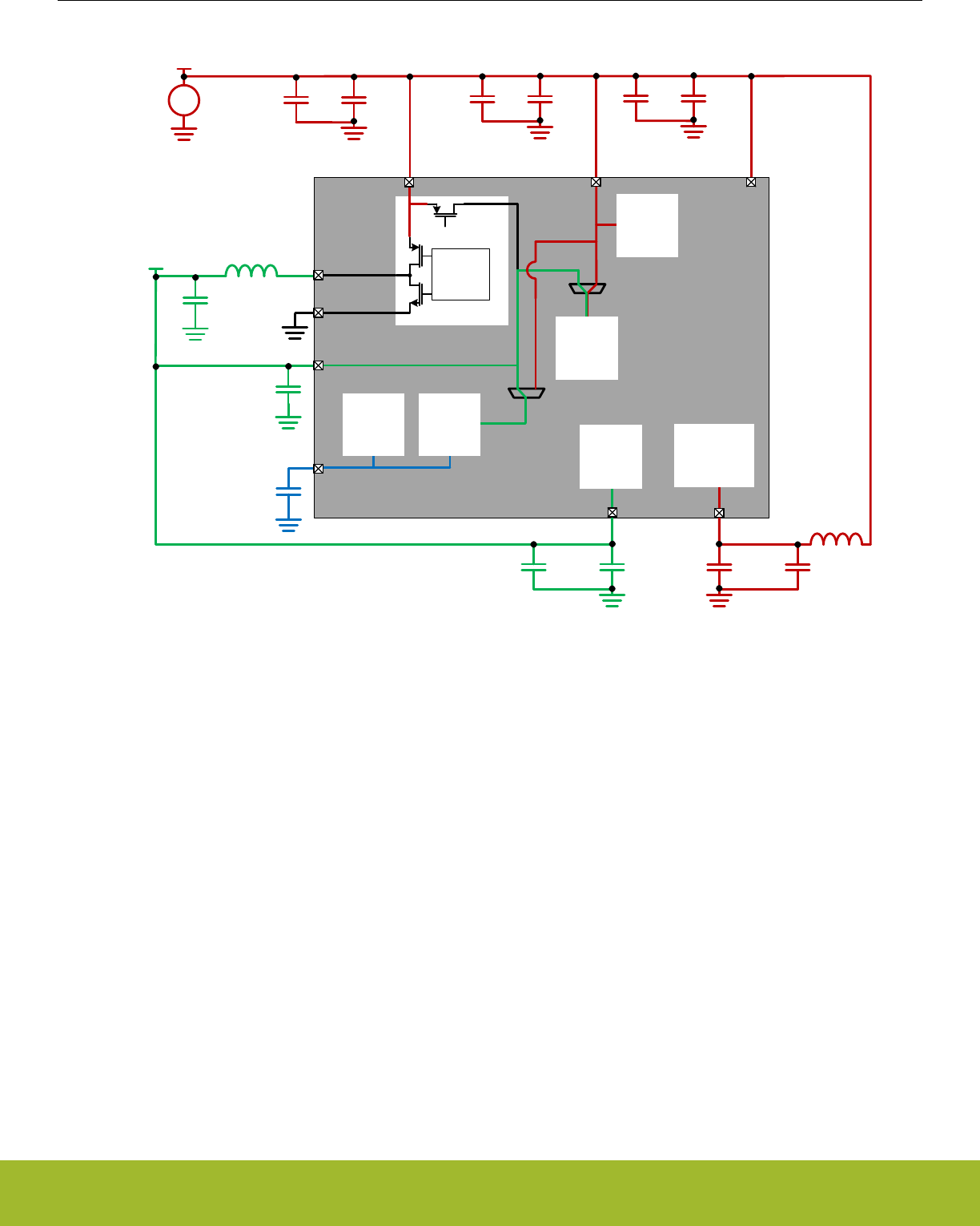
DECOUPLE
DVDD
AVDD
VREGSW
Main
Supply
VREGVSS
IOVDD
VREGVDD
+
–
VDD
DC-DC
DC-DC
Driver
Bypass
Switch
OFF FLASH
DECOUPLE
DVDD
AVDD
VREGSW
VREGVSS
IOVDD
VREGVDD
ANASW
0
1
REGPWRSEL
0
1
Digital
Logic
PAVDD
RFVDD
RF
Analog
VDCDC
Analog
Blocks
Digital
LDO RF
Power
Amplifier
Figure 11.5. DC-DC High RF Power Configuration
11.3.5 DC-to-DC Interface
The EFR32xG13 Wireless Gecko devices feature a DC-DC buck converter which requires a single external inductor and a single exter-
nal capacitor. The converter takes the VREGVDD input voltage and converts it down to an output voltage between VREGVDD and 1.8
V with a peak efficiency of approximately 90% in Low Noise (LN) mode and 85% in Low Power (LP) mode. Refer to datasheet for full
DC-DC specifications.
The DC-DC converter operates in either Low Noise (LN) or Low Power (LP) mode. LN mode is intended for higher current operation
(e.g., >= 10 mA), whereas LP mode is intended for very low current operation (e.g., < 10 mA).
In addition, the DC-DC converter supports an unregulated Bypass mode, in which the input voltage is directly shorted to the DC-DC
output.
11.3.5.1 Bypass Mode
In Bypass mode, the VREGVDD input voltage is directly shorted to the DC-DC converter output through an internal switch. Consult the
datasheet for the Bypass switch impedance specification.
The Bypass Current Limit limits the maximum current drawn from the main supply in Bypass mode. This current limit is enabled by
setting the BYPLIMEN bit in the EMU_DCDCCLIMCTRL register, and the limit value may be adjusted between 20 mA and 320 mA
using the BYPLIMSEL bitfield in the EMU_DCDCMISCCTRL register.
Reference Manual
EMU - Energy Management Unit
silabs.com | Smart. Connected. Energy-friendly. Preliminary Rev. 0.5 | 236

11.3.5.2 Low Power (LP) Mode
The Low Power (LP) controller operates in a hysteretic mode to keep the output voltage within a defined voltage band. Once the DC-
DC output voltage drops below a programmable internal reference, the LP controller generates a pulse train to control the powertrain
PFET switch, which charges up the DC-DC output capacitor. When the output voltage is at the programmed upper level, the powertrain
PFET is turned off. The output ripple voltage may be quite large (>100 mV) in LP mode.
The LP controller supports load currents up to approximately 10 mA, making it suitable for light loads in EM0 and EM1, as well as EM2,
EM3, or EM4 low energy modes.
11.3.5.3 Low Noise (LN) Mode
The Low Noise (LN) controller continuously switches the powertrain NFET and PFET switches to maintain a constant programmed volt-
age at the DVDD pin. The LN controller supports load current from sub-mA up to 200 mA.
The LN controller switching frequency is programmable using the RCOBAND bitfield in the EMU_DCDCLNFREQCTRL register. See
below for recommended RCOBAND settings for each mode.
The DC-DC Low Noise controller operates in one of two modes:
1. Continuous Conduction Mode (CCM)
2. Discontinuous Conduction Mode (DCM)
11.3.5.3.1 Low Noise (LN) Continuous Conduction Mode (CCM)
CCM operation is configured by setting the LNFORCECCM bit in the EMU_DCDCMISCCTRL register. CCM can be used to improve
the DC-DC converter's output transient response time to quick load current changes, which minimizes voltage transients on the DC-DC
output.
Note that all references to CCM in the documentation actually refer to Forced Continuous Conduction Mode (FCCM) - that is, if the
LNFORCECCM bit is set and the output load current is very low, the DC-DC will be forced to operated in CCM. In this case, the current
through the inductor may be negative and current may flow back into the battery.
CCM is required for radio or Wireless Gecko systems because, unlike DCM, it allows use of the radio's interference minimization fea-
tures.In CCM, the recommended DC-DC converter switching frequency is 6.4 MHz (RCOBAND = 4). Note that when the radio's inter-
ference minimization features are enabled, RCOBAND = 4 corresponds to a DC-DC converter switching frequency of 7 MHz.
11.3.5.3.2 Low Noise (LN) Discontinuous Conduction Mode (DCM)
To enable DCM, the LNFORCECCM bit in EMU_DCDCMISCCTRL must be cleared before entering LN. Typically, this configuration
would occur while the part was in Bypass mode. Once DCM is enabled, the DC-DC should operate in DCM at light load currents. How-
ever, as the load current increases, the DC-DC will automatically transition into CCM without software intervention.
The advantage of DCM is improved efficiency for light load currents. However, in DCM the DC-DC has poorer dynamic response to
changes in load current, leading to potentially larger changes in the regulated output voltage. In addition, DCM increases the potential
RF switching interference, because in DCM the DC-DC switching events are load dependent and can no longer be synchronized with
radio operation. For these reasons, DCM is not recommended for radio applications or for non-radio applications that expect large in-
stantaneous load current steps. For example, if the DC-DC is in DCM, firmware may need to increment the core clock frequency in
small steps to prevent a large sudden load increase.
In DCM, the recommended DC-DC converter switching frequency is 3 MHz (RCOBAND = 0).
11.3.5.4 DC-to-DC Programming Guidelines
Note: Refer to Application Note AN0948: EFM32 and EFR32 Series 1 Power Configurations and DC-DCfor detailed information on pro-
gramming the DC-DC. Application Notes can be found on the Silicon Labs website (www.silabs.com/32bit-appnotes) or using the [Ap-
plication Notes] tile in Simplicity Studio.
Reference Manual
EMU - Energy Management Unit
silabs.com | Smart. Connected. Energy-friendly. Preliminary Rev. 0.5 | 237

11.3.6 Analog Peripheral Power Selection
The analog peripherals (e.g., ULFRCO, LFRCO, LFXO, HFRCO, AUXHFRCO, VMON, IDAC, ADC) may be powered from one of two
supply pins, depending on the configuration of the ANASW bit in the EMU_PWRCTRL register: Changes to the ANASW setting should
be made immediately out of reset (i.e., in the Unconfigured Configuration) before all clocks (with the exception of HFRCO and ULFR-
CO) are enabled. If the DCDC converter is used and ANASW is set to 1, the switch will not take effect until after the DCDC output
voltage has reached its target level. To prevent supply transients, firmware should configure and enable the DCDC, configure ANASW,
and then enable clocks. If DCDC converter is not used IMMEDIATEPWRSWITCH should be set prior to setting ANASW so hardware
can immediately apply the switch without waiting for DCDC to settle.
Once ANASW is configured it should not be changed. Note that the flash is always powered from the AVDD pin, regardless of the state
of the ANASW bit.
Table 11.4. Analog Peripheral Power Configuration
ANASW Analog Peripheral Power Source Comments
0 (default) AVDD pin This configuration may provide a quieter supply to the analog mod-
ules, but is less efficient as AVDD is typically at a higher voltage than
DVDD.
1 DVDD pin This configuration may provide a noisier supply to the analog mod-
ules, but is more efficient.
11.3.7 Digital LDO Power Selection
The digital LDO may be powered from one of two supply pins, depending on the configuration of the REGPWRSEL bit in the
EMU_PWRCTRL register. At startup, the digital is powered from the AVDD pin. When powered from AVDD, the LDO current is limited
to 20 mA. Out of startup, firmware should configure and enable the DCDC (if desired) and then set REGPWRSEL=1 before increasing
the core clock frequency.
Table 11.5. Digital LDO Power Configuration
REGPWRSEL Digital LDO Power Source Comments
0 (default) AVDD pin Maximum LDO current in this configuration is 20 mA. Firmware
should configure REGPWRSEL to 1 after startup.
1 DVDD pin This configuration supports all core frequencies, and should be used
after startup.
11.3.8 IOVDD Connection
The IOVDD supply(s) must be less than or equal to AVDD. IOVDD will typically be connected to either the DC-DC Output (VDCDC) or
the main supply.
Because VDCDC will be unpowered (i.e., floating) at startup, if IOVDD is powered from the DC-DC converter then any circuit attached to
IOVDD will not be powered until the DC-DC is configured (or the bypass switch is enabled). Likewise, upon entry into EM4 Shutoff, the
DC-DC converter configuration is reset to its default (Unconfigured) configuration. If IOVDD = VDCDC, then any circuits attached to
IOVDD will remain unpowered until the system is reset to exit EM4 Shutoff, and the DC-DC is configured (or the bypass switch is ena-
bled).
Any application with powering external loads from the DC-DC converter must take into consideration the maximum allowable DC-DC
load current. Refer to datasheet for DC-DC load current specification.
Reference Manual
EMU - Energy Management Unit
silabs.com | Smart. Connected. Energy-friendly. Preliminary Rev. 0.5 | 238

11.3.9 Voltage Scaling
The voltage scaling feature allows for a tradeoff between power and performance. Voltage scaling applies an adjustment to the supply
voltage for the on-chip digital logic and memories. For EM0 and EM1 operation, full device performance is supported when the Voltage
Scale Level is set to its highest value. The Voltage Scale Level may be set lower when operating the system at slower clock speeds to
save power. Voltage scaling does not affect the input or output range for analog peripherals or digital I/O logic levels. For more informa-
tion about max system frequency supported for different voltage scaling levels please refer to the CMU chapter and the datasheet
specification tables.
Note: Flash write/erase is only supported at Voltage Scale Level 2.
Note: Radio operation and radio module register access is only supported at Voltage Scale Level 2. When using any other Voltage
Scale Level access to all radio peripherals is locked out. Thus, firmware may only use Voltage Scale Level 0 during periods when radio
operations or radio register accesses are not required.
Separate voltage scaling controls are available for the different energy modes. These are as follows:
• EM01 Voltage Scaling
• EM23 Voltage Scaling
• EM4H Voltage Scaling
11.3.9.1 EM01 Voltage Scaling
In EM01 energy mode, the user can dynamically scale voltages between Voltage Scale Level 2 and Voltage Scale Level 0 using
EM01VSCALE2 and EM01VSCALE0 bitfields in EMU_CMD register. A lower Voltage Scale Level corresponds to lower processor fre-
quency and lower power consumption. Once these commands are issued, hardware begins the process of voltage scaling and when
done, the VSCALEDONE interrupt is triggered. Users can also poll VSCALEBUSY in EMU_STATUS which indicates that hardware is
busy changing the voltage scale setting when set. VSCALE in EMU_STATUS shows the current voltage the system is in at any time.
Note: If more than one voltage scaling command is issued in EMU_CMD simultaneously, the lower voltage scaling level has higher
priority. e.g. priority order: EM01VSCALE0 > EM01VSCALE2.
Note: The reset value of VSCALE for EM0 and EM1 operation is Voltage Scale Level 2.
When voltage scaling up or down, the user should follow the following sequences in order to ensure proper scaling.
• Voltage Scale Down
1. Decrease system clock frequency to the target frequency
2. Update the wait states of Flash or RAM for the target frequency
3. Issue voltage scaling command by setting EM01VSCALE2 or EM01VSCALE0 in EMU_CMD
4. Once Hardware completes voltage scaling up, VSCALEDONE interrupt is set.
• Voltage Scale Up
1. Issue voltage scaling command by setting EM01VSCALE2 or EM01VSCALE0 in EMU_CMD
2. Wait for hardware to complete voltage scaling. When done, VSCALEDONE interrupt is set.
3. Update the wait states of Flash or RAM for the target frequency
4. Increase system clock frequency to the target frequency
Multiple voltage scaling commands are allowed to be issued even when the current voltage scaling is not yet completed. In such a
case, the current scaling will be aborted and the last command will be executed. VSCALEDONE interrupt will be issued for every volt-
age scaling command.
Note: When a software reset is issued in the middle of voltage scaling process, the minimum voltage scale level indicated by VSCALE
or EM01VSCALE2 , EM01VSCALE0 that was issued using EMU_CMD will be implemented by the system.
Reference Manual
EMU - Energy Management Unit
silabs.com | Smart. Connected. Energy-friendly. Preliminary Rev. 0.5 | 239

11.3.9.2 EM23 Voltage Scaling
The EM23VSCALE bitfield in EMU_CTRL allows user to independently setup the voltage scaling value for EM23 energy mode. The
EM23VSCALE in EMU_CTRL should be programmed to a level which is less than or equal to VSCALE in EMU_STATUS. This means
that EM23 voltage scaling is always a voltage scaling down process. If EM23VSCALE level in EMU_CTRL is greater than VSCALE
level in EMU_STATUS, the VSCALE level will be implemented in EM23 instead of EM23VSCALE. Upon EM23 entry, the system will
scale down the voltage to a smaller level between VSCALE or EM23VSCALE.
Note: The reset value of EM23VSCALE is Voltage Scale Level 2. Therefore, if user scales EM01 voltage to Voltage Scale Level 0 (re-
flected in VSCALE in EMU_STATUS) and enters EM23, this VSCALE voltage of Voltage Scale Level 0 is maintained in EM23 as well
since this is smaller level between VSCALE and EM23VSCALE.
11.3.9.2.1 EM23 Voltage Scaling Guidelines
Note that when using EM23VSCALE in EMU_CTRL to scale down EM23, the scaled down voltage in EM23 is maintained after waking
from EM23 to EM01. For example, if VSCALE was at Voltage Scale Level 2 prior to EM23 entry, and EM23VSCALE was set to Voltage
Scale Level 0, the system will scale down to Voltage Scale Level 0 on EM23 entry. When waking up to EM01, the system maintains its
voltage at Voltage Scale Level 0. Therefore, user must ensure the system clock frequency and Flash or Ram wait states are program-
med to correct values to support waking up to EM01 at the lower voltages prior to EM23 entry.
EM23VSCALEAUTOWSEN bitfield in EMU_CTRL enables hardware to automatically configure the system clock frequency and Flash
and RAM wait-states to support low voltage operation when waking up to EM01 from EM23. Therefore, this obviates the need for user
to setup the clock frequency and Flash or RAM wait states prior to EM23 entry with EM23VSCALE.
11.3.9.3 EM4H Voltage Scaling
EM4HVSCALE bitfield in EMU_CTRL allows user to independently setup the voltage scaling levels for EM4H energy mode. The
EM4HVSCALE in EMU_CTRL should be programmed to a level which is smaller than or equal to VSCALE level in EMU_STATUS or
EM23VSCALE in EMU_CTRL. This means that EM4H voltage scaling is always a voltage scaling down process. If EM4HVSCALE level
in EMU_CTRL is greater than level of VSCALE in EMU_STATUS or level of EM23VSCALE in EMU_CTRL, the smaller of VSCALE,
EM23VSCALE or EM4HVSCALE levels will be implemented in EM4H.
Note: The reset level of EM4HVSCALE is Voltage Scale Level 2. Therefore, if user scales EM01 voltage to Voltage Scale Level 0 (re-
flected in VSCALE in EMU_STATUS) and enters EM4H, this VSCALE voltage of Voltage Scale Level 0 is maintained in EM23 as well
since this is minimum of VSCALE and EM23VSCALE.
11.3.9.3.1 EM4H Voltage Scaling Guidelines
Note that when using EM4HVSCALE in EMU_CTRL to scale down voltage in EM4H, the scaled down voltage in EM4H is maintained
after waking from EM4H to EM01. For example prior to EM4H entry, if VSCALE was at Voltage Scale Level 2 and EM4HVSCALE was
set to Voltage Scale Level 0, the system will scale down to Voltage Scale Level 0 on EM4H entry. When waking up to EM01, the system
maintains its voltage at Voltage Scale Level 0.
11.3.9.4 Voltage Scaling Recommended Use
Please refer to Datasheet for the maximum supported system frequencies for different Voltage Scaling Levels. Use of the lowest volt-
age scaling level is recommended for maximum power savings. For any voltage scaling level, it is recommend to use the highest fre-
quency for performance benefits.
Voltage can then be scaled to higher voltage scale levels only when higher system clock frequency is required by the application for a
period of time after which user can dynamically scale the voltage back to lower voltage scale levels to continue saving power.
Reference Manual
EMU - Energy Management Unit
silabs.com | Smart. Connected. Energy-friendly. Preliminary Rev. 0.5 | 240

11.3.10 EM23 Peripheral Retention Disable
Peripherals that are available in EM2 Deep Sleep or EM3 Stop can optionally be powered down during EM2 Deep Sleep or EM3 Stop.
This allows lower energy consumption in these energy modes. However, when powering down, these peripherals are independently
reset so the registers lose their configuration values. Therefore, they will have to be reconfigured upon wake-up to EM0 Active if they
were previously configured to non reset values.
EMU_EM23PERNORETAINCTRL register can be used to setup unused peripherals for powering down prior to EM23 entry. Once set-
up, upon EM23 entry, all peripherals in the power-down domain will get powered down if all of them are setup to be disabled.
Note: User must ensure that the peripherals being powered down should have their clocks disabled in CMU prior to EM23 entry.
On waking up from EM23, EMU_EM23PERNORETAINSTATUS register indicates if the peripherals were powered down by the system
and subsequently locked out from register access. Locking out peripherals prevents users from accidentally using peripherals with con-
figurations at their reset state. EMU_EM23PERNORETAINCMD allows user to unlock these peripherals and hence grant access to
their registers for updating their configurations.
11.3.11 Brown Out Detector (BOD)
11.3.11.1 AVDD BOD
The EFR32xG13 Wireless Gecko has a fast response Brown Out Detector (BOD) on AVDD that is always active. This BOD ensures the
minimal supply is provided to the AVDD supply (typically also connected to VREGVDD). Once triggered, the BOD will cause the system
to reset.
Note: In EM4 Hibernate/Shutoff a low power version of the AVDD BOD, called EM4BOD, is available to trigger a reset at level lower
than in other energy modes. All other BOD's are disabled during EM4 Hibernate/Shutoff
11.3.11.2 DVDD and DECOUPLE BOD
Additional BODs will monitor DVDD and DECOUPLE during EM0 Active through EM3 Stop. This can cause a reset to the internal logic,
but will not cause a power-on reset or reset the EMU or RTCC.
Reference Manual
EMU - Energy Management Unit
silabs.com | Smart. Connected. Energy-friendly. Preliminary Rev. 0.5 | 241

11.3.12 Voltage Monitor (VMON)
The EFR32 features an extremely low energy Voltage Monitor (VMON) capable of running down to EM4 Hibernate. Trigger points are
preloaded but may be reconfigured.
• AVDD X 2
• DVDD
• IOVDD0
Table 11.6. VMON Events
Feature Condition AVDD DVDD IOVDD
Hysteresis (separate rise and fall triggers) - Yes - -
Interrupt Fall or Rise Yes Yes Yes
Wake-Up from EM4 Hibernate Fall or Rise Yes Yes Yes
The status of the VMON is reflected in the EMU_STATUS register.
The status of the sticky interrupt can be found at EMU_IF. These interrupt flags also serve as the wake-up source of EM4H when the
associated RISEWU and FALLWU bits are set. This means that if these flags are set, EM4H entry will result in an immediate wake-up.
To prevent this, these must be cleared by software before EM4H entry.
VMON channels are calibrated at two voltages: 1.86 V and 2.98 V. The calibration results (coarse thresholds and fine thresholds for
1.86 V and 2.98 V) are placed in the VMONCAL registers in the DI page. Using these thresholds it is possible to calculate thresholds for
the entire supported VMON VDD range, i.e., 1.62 V to 3.4 V. Using the values given in VMONCAL registers, one can calculate T1.86,
T2.98, Va and Vb.
T1.86 = (10 x VMONCALX_XVDD1V86THRESCOARSE) + VMONCALX_XVDD1V86THRESFINE,
T2.98 = (10 x VMONCALX_XVDD2V98THRESCOARSE) + VMONCALX_XVDD2V98THRESFINE,
Va = (1.12) / (T2.98 - T1.86),
Vb = 1.86 - (Va x T1.86),
Figure 11.6. VMON Calibration Equations
Now if it is required to find the coarse and fine thresholds for a certain voltage Y, following equation can be used:
ThresY = (Y - Vb) / Va,
Ycalib = (ThresY x Va) + Vb,
Figure 11.7. VMON Threshold Equations
ThresY should be rounded to the nearest integer. The least significant digit of the rounded ThresY gives the fine threshold and remain-
ing digits give the coarse threshold for Y. These can now be programmed in the relevant EMU_VMONXVDDCTRL register as the
coarse and fine thresholds. It may not be possible to set threshold exactly for Y. In that case the closest possible voltage is used. Ycalib
gives the value of this closest possible voltage.
Consider the example where it is required to set the AVDD rise threshold to 2.2 V (so Y=2.2 V). This means that the EMU_VMO-
NAVDDCTRL_RISETHRESCOARSE and EMU_VMONAVDDCTRL_RISETHRESFINE need to be programmed. Here are the steps
that should be followed:
• Check VMONCAL0 register. It has the VMON AVDD channel calibrated thresholds for 1.86 V and 2.98 V. Lets assume that the fol-
lowing values are present in the associated bitfields:
• AVDD1V86THRESCOARSE = 3
• AVDD1V86THRESFINE = 5
• AVDD2V98THRESCOARSE = 8
• AVDD2V98THRESFINE = 7
Reference Manual
EMU - Energy Management Unit
silabs.com | Smart. Connected. Energy-friendly. Preliminary Rev. 0.5 | 242

• Using the above numbers and the VMON calibration equations:
• T1.86 = 35
•T2.98 = 87
• Va = 21.53 mV
• Vb = 1.106 V
• Using the VMON threshold equations (with Y=2.2 V), ThresY = 51 (rounded from 50.8) and Ycalib = 2.204 V
EMU_VMONAVDDCTRL_RISETHRESCOARSE should be programmed to 5 and EMU_VMONAVDDCTRL_RISETHRESFINE should
be programmed to 1 (since ThresY = 51). With these programmed values, VMON AVDD rise threshold is set for Ycalib = 2.204 V, which
is the closest programmable threshold.
11.3.13 Powering off SRAM blocks
SRAM blocks may be powered off using the EMU->RAM0CTRL POWERDOWN fields. One SRAM block will always be powered on for
proper system functionality. The stack must be located in retained memory.
11.3.14 Temperature Sensor
EMU provides low energy periodic temperature measurement. A temperature measurement is taken every 250 ms, with the 8-bit result
stored in EMU->TEMP register.
Note: The EMU temperature sensor is always running (except in EM4 Shutoff) and is independent from ADC temperature sensor.
The EMU provides the following features around temperature changes
• Wake-Up from EM4 Hibernate on Temperature Change
• Interrupt from High Level Trip
• Interrupt from Low Level Trip
During production test, the EMU temperature sensor for each device is calibrated at room temperature, with the corresponding calibra-
tion temperature and reading stored off in the DI page as follows:
• DEVINFO->CAL.TEMP : This bitfield contains the temperature in degrees C at calibration
• DEVINFO->EMUTEMP : This register contains the EMU->TEMP reading at the calibration temperature stored in DEVINFO-
>CAL.TEMP
The current calibrated EMU temperature sensor result from EMU->TEMP may be converted to degrees C using the following equation:
TJ_EMU [°C] = ( DEVINFO->CAL.TEMP ) + (TEMPCOEMxx) * [ (DEVINFO->EMUTEMP) - (EMU->TEMP) ]
Figure 11.8. Temperature Calculation
TEMPCOEMxx is a temperature coefficient that varies based on the energy mode at the time of the EMU temperature sensor reading:
• TEMPCOEM01 = 0.278 + (DEVINFO->EMUTEMP) / 100
• TEMPCOEM234 = 0.268 + (DEVINFO->EMUTEMP) / 100
For maximum accuracy when using the high/low level temperature interrupts, firmware should ensure that TEMPCOEM234 is used to set
the temperature thresholds in EMU->TEMPLIMITS before entering EM2/3/4. Similarly, when exiting EM2/3/4, the temperature thresh-
olds should be updated using TEMPCOEM01.
Note that an increasing reading in EMU->TEMP corresponds to a decreasing temperature, and vice-versa. If enabled, the TEMPHIGH
High Level Limit in EMU-> TEMPLIMITS causes an interrupt flag on a increasing EMU->TEMP reading (i.e., decreasing temperature).
Similarly, the TEMPLOW Low Level Limit causes a interrupt flag on a decreasing EMU->TEMP reading (i.e., increasing temperature).
The EMU temperature sensor accuracy is approximately ±10°C over most of the useable temperature range, but may be +15°C at high-
er temperatures. Accordingly, any use of the EMU temperature sensor should include margin to account for that accuracy.
Reference Manual
EMU - Energy Management Unit
silabs.com | Smart. Connected. Energy-friendly. Preliminary Rev. 0.5 | 243

11.3.15 Registers latched in EM4
The following registers will be latched when entering EM4. After wake-up from EM4, these registers will be reset and require reprog-
ramming prior to writing the EMU_CMD_EM4UNLATCH command.
• CMU_LFRCOCTRL
• CMU_LFXOCTRL
• CMU_LFECLKSEL
• CMU_LFECLKEN0
• CMU_LFEPRESC0
11.3.16 Register Resets
Each EMU register requires retaining state in various energy modes and power transitions and will consequently need to be reset with a
different condition. The following reset conditions will apply to the appropriate set of registers as marked in the Register Description
table.
• Reset with POR or Hard Pin Reset
• Reset with POR, Hard Pin Reset, or any BOD reset
• Reset with SYSEXTENDEDRESETn
• Reset with FULLRESETn (default)
If a register field is not marked with a specific reset condition then it is assumed to be reset with FULLRESETn.
Reference Manual
EMU - Energy Management Unit
silabs.com | Smart. Connected. Energy-friendly. Preliminary Rev. 0.5 | 244

11.4 Register Map
The offset register address is relative to the registers base address.
Offset Name Type Description
0x000 EMU_CTRL RW Control Register
0x004 EMU_STATUS RStatus Register
0x008 EMU_LOCK RWH Configuration Lock Register
0x00C EMU_RAM0CTRL RW Memory Control Register
0x010 EMU_CMD W1 Command Register
0x018 EMU_EM4CTRL RW EM4 Control Register
0x01C EMU_TEMPLIMITS RW Temperature limits for interrupt generation
0x020 EMU_TEMP RValue of last temperature measurement
0x024 EMU_IF RInterrupt Flag Register
0x028 EMU_IFS W1 Interrupt Flag Set Register
0x02C EMU_IFC (R)W1 Interrupt Flag Clear Register
0x030 EMU_IEN RW Interrupt Enable Register
0x034 EMU_PWRLOCK RW Regulator and Supply Lock Register
0x03C EMU_PWRCTRL RW Power Control Register.
0x040 EMU_DCDCCTRL RW DCDC Control
0x04C EMU_DCDCMISCCTRL RW DCDC Miscellaneous Control Register
0x050 EMU_DCDCZDETCTRL RW DCDC Power Train NFET Zero Current Detector Control Register
0x054 EMU_DCDCCLIMCTRL RW DCDC Power Train PFET Current Limiter Control Register
0x058 EMU_DCDCLNCOMPCTRL RW DCDC Low Noise Compensator Control Register
0x05C EMU_DCDCLNVCTRL RWH DCDC Low Noise Voltage Register
0x064 EMU_DCDCLPVCTRL RW DCDC Low Power Voltage Register
0x06C EMU_DCDCLPCTRL RW DCDC Low Power Control Register
0x070 EMU_DCDCLNFREQCTRL RW DCDC Low Noise Controller Frequency Control
0x078 EMU_DCDCSYNC RDCDC Read Status Register
0x090 EMU_VMONAVDDCTRL RW VMON AVDD Channel Control
0x094 EMU_VMONALTAVDDCTRL RW Alternate VMON AVDD Channel Control
0x098 EMU_VMONDVDDCTRL RW VMON DVDD Channel Control
0x09C EMU_VMONIO0CTRL RW VMON IOVDD0 Channel Control
0x0B0 EMU_RAM1CTRL RW Memory Control Register
0x0B4 EMU_RAM2CTRL RW Memory Control Register
0x0E0 EMU_DCDCLPEM01CFG RW Configuration bits for low power mode to be applied during EM01, this
field is only relevant if LP mode is used in EM01.
0x0F4 EMU_EM23PERNORETAINCMD W1 Clears corresponding bits in EM23PERNORETAINSTATUS unlocking
access to peripheral
0x0F8 EMU_EM23PERNORETAINSTA-
TUS
RStatus indicating if peripherals were powered down in EM23, subse-
quently locking access to it.
Reference Manual
EMU - Energy Management Unit
silabs.com | Smart. Connected. Energy-friendly. Preliminary Rev. 0.5 | 245


11.5 Register Description
11.5.1 EMU_CTRL - Control Register
Offset Bit Position
0x000
31
30
29
28
27
26
25
24
23
22
21
20
19
18
17
16
15
14
13
12
11
10
9
8
7
6
5
4
3
2
1
0
Reset
0x0
0x0
0
0
0
0
Access
RW
RW
RW
RW
RW
RW
Name
EM4HVSCALE
EM23VSCALE
EM23VSCALEAUTOWSEN
EM01LD
EM2BODDIS
EM2BLOCK
Bit Name Reset Access Description
31:18 Reserved To ensure compatibility with future devices, always write bits to 0. More information in 1.2 Conven-
tions
17:16 EM4HVSCALE 0x0 RW EM4H Voltage Scale
Set EM4H voltage. Entry to EM4H will trigger voltage scaling to this voltage if voltage scale level in EM4HVSCALE is less
than that of VSCALE
Value Mode Description
0 VSCALE2 Voltage Scale Level 2
2 VSCALE0 Voltage Scale Level 0
3 RESV RESV
15:10 Reserved To ensure compatibility with future devices, always write bits to 0. More information in 1.2 Conven-
tions
9:8 EM23VSCALE 0x0 RW EM23 Voltage Scale
Set EM23 voltage. Entry to EM2/3 will trigger voltage scaling to this voltage if voltage scale level in EM23VSCALE is lesser
than that of VSCALE
Value Mode Description
0 VSCALE2 Voltage Scale Level 2
2 VSCALE0 Voltage Scale Level 0
3 RESV RESV
7:5 Reserved To ensure compatibility with future devices, always write bits to 0. More information in 1.2 Conven-
tions
4 EM23VSCALEAU-
TOWSEN
0 RWAutomatically configures Flash, Ram and Frequency to wakeup
from EM2 or EM3 at low voltage
With voltage scaling on EM2/3 entry, wakeup to EM0/1 will be at the same voltage as EM2. When this bit is set the RAM,
Flash wait states, and CMU clock frequency are automatically configured to safe value without needing software to config-
ure it prior to EM2/3 entry.
Reference Manual
EMU - Energy Management Unit
silabs.com | Smart. Connected. Energy-friendly. Preliminary Rev. 0.5 | 247

Bit Name Reset Access Description
3 EM01LD 0 RW Reserved for internal use. Do not change.
Reserved for internal use. Do not change.
2 EM2BODDIS 0 RW Disable BOD in EM2
This bit is used to disable BODs to minimize current in EM2. Reset with POR or Hard Pin Reset
1 EM2BLOCK 0 RW Energy Mode 2 Block
This bit is used to prevent the MCU from entering Energy Mode 2 or 3.
0 Reserved To ensure compatibility with future devices, always write bits to 0. More information in 1.2 Conven-
tions
Reference Manual
EMU - Energy Management Unit
silabs.com | Smart. Connected. Energy-friendly. Preliminary Rev. 0.5 | 248

11.5.2 EMU_STATUS - Status Register
Offset Bit Position
0x004
31
30
29
28
27
26
25
24
23
22
21
20
19
18
17
16
15
14
13
12
11
10
9
8
7
6
5
4
3
2
1
0
Reset
0
0
0
0
0x0
0
0
0
0
0
0
Access
R
R
R
R
R
R
R
R
R
R
R
Name
TEMPACTIVE
RACACTIVE
EM4IORET
VSCALEBUSY
VSCALE
VMONFVDD
VMONIO0
VMONDVDD
VMONALTAVDD
VMONAVDD
VMONRDY
Bit Name Reset Access Description
31:27 Reserved To ensure compatibility with future devices, always write bits to 0. More information in 1.2 Conven-
tions
26 TEMPACTIVE 0 R Temperature Measurement Active
This signal is set during EMU Temperature measurement
25 RACACTIVE 0 R Radio Controller Active
This bit indicates the status of the RAC state machine. System can not enter EM2 or lower if set.
Value Description
0 RAC is in OFF state
1 RAC is not in OFF state
24:21 Reserved To ensure compatibility with future devices, always write bits to 0. More information in 1.2 Conven-
tions
20 EM4IORET 0 R IO Retention Status
The status of IO retention. Will be set upon EM4 entry based on EM4IORETMODE in EMU_EM4CTRL. Cleared by setting
EM4UNLATCH in EMU_CMD, and can also be cleared in EM4H by the VMON.
Value Mode Description
0 DISABLED IO retention is disabled.
1 ENABLED IO retention is enbled.
19 Reserved To ensure compatibility with future devices, always write bits to 0. More information in 1.2 Conven-
tions
18 VSCALEBUSY 0 R System is busy Scaling Voltage
Indicates that the system is busy scaling voltage in EM0/1. Writing EM01VSCALE0 or EM01VSCALE2 in EMU_CMD regis-
ter while this is set will abort the current voltage scaling process and initiate a new one
17:16 VSCALE 0x0 R Current Voltage Scale Value
This shows the current system voltage value. This gets updated after VSCALEDONE interrupt or on EM23 exit or EM4H
exit
Value Mode Description
0 VSCALE2 Voltage Scale Level 2
2 VSCALE0 Voltage Scale Level 0
Reference Manual
EMU - Energy Management Unit
silabs.com | Smart. Connected. Energy-friendly. Preliminary Rev. 0.5 | 249

Bit Name Reset Access Description
3 RESV RESV
15:9 Reserved To ensure compatibility with future devices, always write bits to 0. More information in 1.2 Conven-
tions
8 VMONFVDD 0 R VMON VDDFLASH Channel.
Indicates the status of the VDDFLASH channel of the VMON.
7:5 Reserved To ensure compatibility with future devices, always write bits to 0. More information in 1.2 Conven-
tions
4 VMONIO0 0 R VMON IOVDD0 Channel.
Indicates the status of the IOVDD0 channel of the VMON.
3 VMONDVDD 0 R VMON DVDD Channel.
Indicates the status of the DVDD channel of the VMON.
2 VMONALTAVDD 0 R Alternate VMON AVDD Channel.
Indicates the status of the Alternate AVDD channel of the VMON.
1 VMONAVDD 0 R VMON AVDD Channel.
Indicates the status of the AVDD channel of the VMON.
0 VMONRDY 0 R VMON ready
VMON status. When high, this bit indicates that all the enabled channels are ready. When low, it indicates that one or more
of the enabled channels are not ready.
Reference Manual
EMU - Energy Management Unit
silabs.com | Smart. Connected. Energy-friendly. Preliminary Rev. 0.5 | 250

11.5.3 EMU_LOCK - Configuration Lock Register
Offset Bit Position
0x008
31
30
29
28
27
26
25
24
23
22
21
20
19
18
17
16
15
14
13
12
11
10
9
8
7
6
5
4
3
2
1
0
Reset
0x0000
Access
RWH
Name
LOCKKEY
Bit Name Reset Access Description
31:16 Reserved To ensure compatibility with future devices, always write bits to 0. More information in 1.2 Conven-
tions
15:0 LOCKKEY 0x0000 RWH Configuration Lock Key
Write any other value than the unlock code to lock all EMU registers, except the interrupt registers and regulator control
registers, from editing. Write the unlock code to unlock. When reading the register, bit 0 is set when the lock is enabled.
Mode Value Description
Read Operation
UNLOCKED 0 EMU registers are unlocked
LOCKED 1 EMU registers are locked
Write Operation
LOCK 0 Lock EMU registers
UNLOCK 0xADE8 Unlock EMU registers
Reference Manual
EMU - Energy Management Unit
silabs.com | Smart. Connected. Energy-friendly. Preliminary Rev. 0.5 | 251

11.5.4 EMU_RAM0CTRL - Memory Control Register
Offset Bit Position
0x00C
31
30
29
28
27
26
25
24
23
22
21
20
19
18
17
16
15
14
13
12
11
10
9
8
7
6
5
4
3
2
1
0
Reset
0x0
Access
RW
Name
RAMPOWERDOWN
Bit Name Reset Access Description
31:1 Reserved To ensure compatibility with future devices, always write bits to 0. More information in 1.2 Conven-
tions
0:0 RAMPOWERDOWN 0x0 RW RAM0 blockset power-down
RAM blockset power-down in EM23 with full access in EM01. Block 0 may never be powered down.
Value Mode Description
0 NONE None of the RAM blocks powered down
1 BLK1 Power down RAM block 1
Reference Manual
EMU - Energy Management Unit
silabs.com | Smart. Connected. Energy-friendly. Preliminary Rev. 0.5 | 252

11.5.5 EMU_CMD - Command Register
Offset Bit Position
0x010
31
30
29
28
27
26
25
24
23
22
21
20
19
18
17
16
15
14
13
12
11
10
9
8
7
6
5
4
3
2
1
0
Reset
0
0
0
Access
W1
W1
W1
Name
EM01VSCALE2
EM01VSCALE0
EM4UNLATCH
Bit Name Reset Access Description
31:7 Reserved To ensure compatibility with future devices, always write bits to 0. More information in 1.2 Conven-
tions
6 EM01VSCALE2 0 W1 EM01 Voltage Scale Command to scale to Voltage Scale Level 2
Start EM01 voltage scaling to Voltage Scale Level 2. Write to this register will trigger voltage scaling to Voltage Scale Level
2 followed by an VSCALEDONE interrupt
5 Reserved To ensure compatibility with future devices, always write bits to 0. More information in 1.2 Conven-
tions
4 EM01VSCALE0 0 W1 EM01 Voltage Scale Command to scale to Voltage Scale Level 0
Start EM01 voltage scaling to Voltage Scale Level 0. Write to this register will trigger voltage scaling to Voltage Scale Level
0 followed by an VSCALEDONE interrupt
3:1 Reserved To ensure compatibility with future devices, always write bits to 0. More information in 1.2 Conven-
tions
0 EM4UNLATCH 0 W1 EM4 Unlatch
When entering EM4, several registers will be latched in order to maintain constant functionality throughout EM4. Upon
wakeup, these registers will be reset and can have contradictory values to the latched values. To ensure a seamless transi-
tion from EM4 to EM0, the unlatch command should be given after properly reconfiguring these latched registers. The un-
latch command can be executed after any reset condition but is only needed after EM4 wakeup.
Reference Manual
EMU - Energy Management Unit
silabs.com | Smart. Connected. Energy-friendly. Preliminary Rev. 0.5 | 253

11.5.6 EMU_EM4CTRL - EM4 Control Register
Offset Bit Position
0x018
31
30
29
28
27
26
25
24
23
22
21
20
19
18
17
16
15
14
13
12
11
10
9
8
7
6
5
4
3
2
1
0
Reset
0x0
0x0
0
0
0
0
Access
W1
RW
RW
RW
RW
RW
Name
EM4ENTRY
EM4IORETMODE
RETAINULFRCO
RETAINLFXO
RETAINLFRCO
EM4STATE
Bit Name Reset Access Description
31:18 Reserved To ensure compatibility with future devices, always write bits to 0. More information in 1.2 Conven-
tions
17:16 EM4ENTRY 0x0 W1 Energy Mode 4 Entry
This register is used to enter the Energy Mode 4 sequence. Writing the sequence 2,3,2,3,2,3,2,3,2 will enter the part into
Energy Mode 4.
15:6 Reserved To ensure compatibility with future devices, always write bits to 0. More information in 1.2 Conven-
tions
5:4 EM4IORETMODE 0x0 RW EM4 IO Retention Disable
Determine when IO retention will be applied and removed.
Value Mode Description
0 DISABLE No Retention: Pads enter reset state when entering EM4
1 EM4EXIT Retention through EM4: Pads enter reset state when exiting EM4
2 SWUNLATCH Retention through EM4 and Wakeup: software writes UNLATCH regis-
ter to remove retention
3 RETAINULFRCO 0 RW ULFRCO Retain during EM4S
Retain the ULFRCO upon EM4S entry. If set to 1, an already running ULFRCO will be retained in its running state in EM4.
ULFRCO will always be retained if EM4STATE is in EM4H.
2 RETAINLFXO 0 RW LFXO Retain during EM4
Retain the LFXO upon EM4(SH/H) entry. If set to 1, an already running LFXO will be retained in its running state in EM4.
1 RETAINLFRCO 0 RW LFRCO Retain during EM4
Retain the LFRCO upon EM4(S/H) entry. If set to 1, an already running LFRCO will be retained in its running state in EM4.
0 EM4STATE 0 RW Energy Mode 4 State
When set, the system will enter Hibernate state (EM4H) when entering EM4. In EM4H, the regulator will be on in reduced
mode allowing for RTCC. Otherwise, when entering in EM4, the regulator will be disabled allowing for lowest power mode,
Shutoff state (EM4S). Only reset with POR or Hard Pin Reset
Value Mode Description
0 EM4S EM4S Shutoff state
1 EM4H EM4H Hibernate state
Reference Manual
EMU - Energy Management Unit
silabs.com | Smart. Connected. Energy-friendly. Preliminary Rev. 0.5 | 254

11.5.7 EMU_TEMPLIMITS - Temperature limits for interrupt generation
Offset Bit Position
0x01C
31
30
29
28
27
26
25
24
23
22
21
20
19
18
17
16
15
14
13
12
11
10
9
8
7
6
5
4
3
2
1
0
Reset
0
0xFF
0x00
Access
RW
RW
RW
Name
EM4WUEN
TEMPHIGH
TEMPLOW
Bit Name Reset Access Description
31:17 Reserved To ensure compatibility with future devices, always write bits to 0. More information in 1.2 Conven-
tions
16 EM4WUEN 0 RW Enable EM4 Wakeup due to low/high temperature
Enable EM4 wakeup from low or high temperature from EM4H
15:8 TEMPHIGH 0xFF RW Temperature High Limit
The TEMPHIGH interrupt flag is set when a periodic temperature measurement is equal to or higher than this value. If the
high limit is changed during a temperature measurement (TEMPACTIVE=1), the limit update will be delayed until the end of
the temperature measurement.
7:0 TEMPLOW 0x00 RW Temperature Low Limit
The TEMPLOW interrupt flag is set when a periodic temperature measurement is equal to or lower than this value. If the
low limit is changed during a temperature measurement (TEMPACTIVE=1), the limit update will be delayed until the end of
the temperature measurement.
11.5.8 EMU_TEMP - Value of last temperature measurement
Offset Bit Position
0x020
31
30
29
28
27
26
25
24
23
22
21
20
19
18
17
16
15
14
13
12
11
10
9
8
7
6
5
4
3
2
1
0
Reset
0xXX
Access
R
Name
TEMP
Bit Name Reset Access Description
31:8 Reserved To ensure compatibility with future devices, always write bits to 0. More information in 1.2 Conven-
tions
7:0 TEMP 0xXX R Temperature Measurement
Value of last periodic temperature measurement. Value is asynchronously updated. Value is stable for 250 ms after a tem-
perature-based interrupt (TEMPHIGH, TEMPLOW, or TEMP) and can be read with a single read operation. If register is
read not in response to a temperature-based interrupt, multiple readings should be taken until two consecutive values are
the same.
Reference Manual
EMU - Energy Management Unit
silabs.com | Smart. Connected. Energy-friendly. Preliminary Rev. 0.5 | 255

11.5.9 EMU_IF - Interrupt Flag Register
Offset Bit Position
0x024
31
30
29
28
27
26
25
24
23
22
21
20
19
18
17
16
15
14
13
12
11
10
9
8
7
6
5
4
3
2
1
0
Reset
0
0
0
0
0
0
0
0
0
0
0
0
0
0
0
0
0
0
0
0
Access
R
R
R
R
R
R
R
R
R
R
R
R
R
R
R
R
R
R
R
R
Name
TEMPHIGH
TEMPLOW
TEMP
VSCALEDONE
EM23WAKEUP
DCDCINBYPASS
DCDCLNRUNNING
DCDCLPRUNNING
NFETOVERCURRENTLIMIT
PFETOVERCURRENTLIMIT
VMONFVDDRISE
VMONFVDDFALL
VMONIO0RISE
VMONIO0FALL
VMONDVDDRISE
VMONDVDDFALL
VMONALTAVDDRISE
VMONALTAVDDFALL
VMONAVDDRISE
VMONAVDDFALL
Bit Name Reset Access Description
31 TEMPHIGH 0 R Temperature High Limit Reached
Set when the value of a periodic temperature measurement is higher or equal than TEMPHIGH in EMU_TEMPLIMITS
30 TEMPLOW 0 R Temperature Low Limit Reached
Set when the value of a periodic temperature measurement is lower or equal than TEMPHIGH in EMU_TEMPLIMITS
29 TEMP 0 R New Temperature Measurement Valid
Set when a new periodic temperature measurement is available
28:26 Reserved To ensure compatibility with future devices, always write bits to 0. More information in 1.2 Conven-
tions
25 VSCALEDONE 0 R Voltage Scale Steps Done IRQ
Will be set when all the steps needed for voltage scaling is done. For voltage upgrade, the software can start increasing
clock frequency after this interrupt. For voltage downgrade, this will indicate that hardware has finished all the steps includ-
ing updating of BOD levels and regultor controls, but voltage drop may take lot longer due to load current
24 EM23WAKEUP 0 R Wakeup IRQ from EM2 and EM3
Will be set when the system wakes up from EM2 and EM3. This interrupt can be used to run initialization code need to
reconfigure the system when returning from EM2 and EM3.
23:21 Reserved To ensure compatibility with future devices, always write bits to 0. More information in 1.2 Conven-
tions
20 DCDCINBYPASS 0 R DCDC is in bypass
DCDC is in bypass
19 DCDCLNRUNNING 0 R LN mode is running
This flag is set once the DCDC regulator has started to run in LN mode
18 DCDCLPRUNNING 0 R LP mode is running
This flag is set once the DCDC regulator has started to run in LP mode
17 NFETOVERCUR-
RENTLIMIT
0 R NFET current limit hit
Reserved for internal use.
Reference Manual
EMU - Energy Management Unit
silabs.com | Smart. Connected. Energy-friendly. Preliminary Rev. 0.5 | 256

Bit Name Reset Access Description
16 PFETOVERCUR-
RENTLIMIT
0 R PFET current limit hit
Reserved for internal use.
15 VMONFVDDRISE 0 R VMON VDDFLASH Channel Rise
A rising edge on VMON VDDFLASH channel has been detected.
14 VMONFVDDFALL 0 R VMON VDDFLASH Channel Fall
A falling edge on VMON VDDFLASH channel has been detected.
13:8 Reserved To ensure compatibility with future devices, always write bits to 0. More information in 1.2 Conven-
tions
7 VMONIO0RISE 0 R VMON IOVDD0 Channel Rise
A rising edge on VMON IOVDD0 channel has been detected.
6 VMONIO0FALL 0 R VMON IOVDD0 Channel Fall
A falling edge on VMON IOVDD0 channel has been detected.
5 VMONDVDDRISE 0 R VMON DVDD Channel Rise
A rising edge on VMON DVDD channel has been detected.
4 VMONDVDDFALL 0 R VMON DVDD Channel Fall
A falling edge on VMON DVDD channel has been detected.
3 VMONALTAVDDRISE 0 R Alternate VMON AVDD Channel Rise
A rising edge on Alternate VMON AVDD channel has been detected.
2 VMONALTAVDDFALL 0 R Alternate VMON AVDD Channel Fall
A falling edge on Alternate VMON AVDD channel has been detected.
1 VMONAVDDRISE 0 R VMON AVDD Channel Rise
A rising edge on VMON AVDD channel has been detected.
0 VMONAVDDFALL 0 R VMON AVDD Channel Fall
A falling edge on VMON AVDD channel has been detected.
Reference Manual
EMU - Energy Management Unit
silabs.com | Smart. Connected. Energy-friendly. Preliminary Rev. 0.5 | 257

11.5.10 EMU_IFS - Interrupt Flag Set Register
Offset Bit Position
0x028
31
30
29
28
27
26
25
24
23
22
21
20
19
18
17
16
15
14
13
12
11
10
9
8
7
6
5
4
3
2
1
0
Reset
0
0
0
0
0
0
0
0
0
0
0
0
0
0
0
0
0
0
0
0
Access
W1
W1
W1
W1
W1
W1
W1
W1
W1
W1
W1
W1
W1
W1
W1
W1
W1
W1
W1
W1
Name
TEMPHIGH
TEMPLOW
TEMP
VSCALEDONE
EM23WAKEUP
DCDCINBYPASS
DCDCLNRUNNING
DCDCLPRUNNING
NFETOVERCURRENTLIMIT
PFETOVERCURRENTLIMIT
VMONFVDDRISE
VMONFVDDFALL
VMONIO0RISE
VMONIO0FALL
VMONDVDDRISE
VMONDVDDFALL
VMONALTAVDDRISE
VMONALTAVDDFALL
VMONAVDDRISE
VMONAVDDFALL
Bit Name Reset Access Description
31 TEMPHIGH 0 W1 Set TEMPHIGH Interrupt Flag
Write 1 to set the TEMPHIGH interrupt flag
30 TEMPLOW 0 W1 Set TEMPLOW Interrupt Flag
Write 1 to set the TEMPLOW interrupt flag
29 TEMP 0 W1 Set TEMP Interrupt Flag
Write 1 to set the TEMP interrupt flag
28:26 Reserved To ensure compatibility with future devices, always write bits to 0. More information in 1.2 Conven-
tions
25 VSCALEDONE 0 W1 Set VSCALEDONE Interrupt Flag
Write 1 to set the VSCALEDONE interrupt flag
24 EM23WAKEUP 0 W1 Set EM23WAKEUP Interrupt Flag
Write 1 to set the EM23WAKEUP interrupt flag
23:21 Reserved To ensure compatibility with future devices, always write bits to 0. More information in 1.2 Conven-
tions
20 DCDCINBYPASS 0 W1 Set DCDCINBYPASS Interrupt Flag
Write 1 to set the DCDCINBYPASS interrupt flag
19 DCDCLNRUNNING 0 W1 Set DCDCLNRUNNING Interrupt Flag
Write 1 to set the DCDCLNRUNNING interrupt flag
18 DCDCLPRUNNING 0 W1 Set DCDCLPRUNNING Interrupt Flag
Write 1 to set the DCDCLPRUNNING interrupt flag
17 NFETOVERCUR-
RENTLIMIT
0 W1 Set NFETOVERCURRENTLIMIT Interrupt Flag
Write 1 to set the NFETOVERCURRENTLIMIT interrupt flag
16 PFETOVERCUR-
RENTLIMIT
0 W1 Set PFETOVERCURRENTLIMIT Interrupt Flag
Write 1 to set the PFETOVERCURRENTLIMIT interrupt flag
Reference Manual
EMU - Energy Management Unit
silabs.com | Smart. Connected. Energy-friendly. Preliminary Rev. 0.5 | 258

Bit Name Reset Access Description
15 VMONFVDDRISE 0 W1 Set VMONFVDDRISE Interrupt Flag
Write 1 to set the VMONFVDDRISE interrupt flag
14 VMONFVDDFALL 0 W1 Set VMONFVDDFALL Interrupt Flag
Write 1 to set the VMONFVDDFALL interrupt flag
13:8 Reserved To ensure compatibility with future devices, always write bits to 0. More information in 1.2 Conven-
tions
7 VMONIO0RISE 0 W1 Set VMONIO0RISE Interrupt Flag
Write 1 to set the VMONIO0RISE interrupt flag
6 VMONIO0FALL 0 W1 Set VMONIO0FALL Interrupt Flag
Write 1 to set the VMONIO0FALL interrupt flag
5 VMONDVDDRISE 0 W1 Set VMONDVDDRISE Interrupt Flag
Write 1 to set the VMONDVDDRISE interrupt flag
4 VMONDVDDFALL 0 W1 Set VMONDVDDFALL Interrupt Flag
Write 1 to set the VMONDVDDFALL interrupt flag
3 VMONALTAVDDRISE 0 W1 Set VMONALTAVDDRISE Interrupt Flag
Write 1 to set the VMONALTAVDDRISE interrupt flag
2 VMONALTAVDDFALL 0 W1 Set VMONALTAVDDFALL Interrupt Flag
Write 1 to set the VMONALTAVDDFALL interrupt flag
1 VMONAVDDRISE 0 W1 Set VMONAVDDRISE Interrupt Flag
Write 1 to set the VMONAVDDRISE interrupt flag
0 VMONAVDDFALL 0 W1 Set VMONAVDDFALL Interrupt Flag
Write 1 to set the VMONAVDDFALL interrupt flag
Reference Manual
EMU - Energy Management Unit
silabs.com | Smart. Connected. Energy-friendly. Preliminary Rev. 0.5 | 259

11.5.11 EMU_IFC - Interrupt Flag Clear Register
Offset Bit Position
0x02C
31
30
29
28
27
26
25
24
23
22
21
20
19
18
17
16
15
14
13
12
11
10
9
8
7
6
5
4
3
2
1
0
Reset
0
0
0
0
0
0
0
0
0
0
0
0
0
0
0
0
0
0
0
0
Access
(R)W1
(R)W1
(R)W1
(R)W1
(R)W1
(R)W1
(R)W1
(R)W1
(R)W1
(R)W1
(R)W1
(R)W1
(R)W1
(R)W1
(R)W1
(R)W1
(R)W1
(R)W1
(R)W1
(R)W1
Name
TEMPHIGH
TEMPLOW
TEMP
VSCALEDONE
EM23WAKEUP
DCDCINBYPASS
DCDCLNRUNNING
DCDCLPRUNNING
NFETOVERCURRENTLIMIT
PFETOVERCURRENTLIMIT
VMONFVDDRISE
VMONFVDDFALL
VMONIO0RISE
VMONIO0FALL
VMONDVDDRISE
VMONDVDDFALL
VMONALTAVDDRISE
VMONALTAVDDFALL
VMONAVDDRISE
VMONAVDDFALL
Bit Name Reset Access Description
31 TEMPHIGH 0 (R)W1 Clear TEMPHIGH Interrupt Flag
Write 1 to clear the TEMPHIGH interrupt flag. Reading returns the value of the IF and clears the corresponding interrupt
flags (This feature must be enabled globally in MSC.).
30 TEMPLOW 0 (R)W1 Clear TEMPLOW Interrupt Flag
Write 1 to clear the TEMPLOW interrupt flag. Reading returns the value of the IF and clears the corresponding interrupt
flags (This feature must be enabled globally in MSC.).
29 TEMP 0 (R)W1 Clear TEMP Interrupt Flag
Write 1 to clear the TEMP interrupt flag. Reading returns the value of the IF and clears the corresponding interrupt flags
(This feature must be enabled globally in MSC.).
28:26 Reserved To ensure compatibility with future devices, always write bits to 0. More information in 1.2 Conven-
tions
25 VSCALEDONE 0 (R)W1 Clear VSCALEDONE Interrupt Flag
Write 1 to clear the VSCALEDONE interrupt flag. Reading returns the value of the IF and clears the corresponding interrupt
flags (This feature must be enabled globally in MSC.).
24 EM23WAKEUP 0 (R)W1 Clear EM23WAKEUP Interrupt Flag
Write 1 to clear the EM23WAKEUP interrupt flag. Reading returns the value of the IF and clears the corresponding interrupt
flags (This feature must be enabled globally in MSC.).
23:21 Reserved To ensure compatibility with future devices, always write bits to 0. More information in 1.2 Conven-
tions
20 DCDCINBYPASS 0 (R)W1 Clear DCDCINBYPASS Interrupt Flag
Write 1 to clear the DCDCINBYPASS interrupt flag. Reading returns the value of the IF and clears the corresponding inter-
rupt flags (This feature must be enabled globally in MSC.).
19 DCDCLNRUNNING 0 (R)W1 Clear DCDCLNRUNNING Interrupt Flag
Write 1 to clear the DCDCLNRUNNING interrupt flag. Reading returns the value of the IF and clears the corresponding
interrupt flags (This feature must be enabled globally in MSC.).
18 DCDCLPRUNNING 0 (R)W1 Clear DCDCLPRUNNING Interrupt Flag
Write 1 to clear the DCDCLPRUNNING interrupt flag. Reading returns the value of the IF and clears the corresponding in-
terrupt flags (This feature must be enabled globally in MSC.).
Reference Manual
EMU - Energy Management Unit
silabs.com | Smart. Connected. Energy-friendly. Preliminary Rev. 0.5 | 260

Bit Name Reset Access Description
17 NFETOVERCUR-
RENTLIMIT
0 (R)W1 Clear NFETOVERCURRENTLIMIT Interrupt Flag
Write 1 to clear the NFETOVERCURRENTLIMIT interrupt flag. Reading returns the value of the IF and clears the corre-
sponding interrupt flags (This feature must be enabled globally in MSC.).
16 PFETOVERCUR-
RENTLIMIT
0 (R)W1 Clear PFETOVERCURRENTLIMIT Interrupt Flag
Write 1 to clear the PFETOVERCURRENTLIMIT interrupt flag. Reading returns the value of the IF and clears the corre-
sponding interrupt flags (This feature must be enabled globally in MSC.).
15 VMONFVDDRISE 0 (R)W1 Clear VMONFVDDRISE Interrupt Flag
Write 1 to clear the VMONFVDDRISE interrupt flag. Reading returns the value of the IF and clears the corresponding inter-
rupt flags (This feature must be enabled globally in MSC.).
14 VMONFVDDFALL 0 (R)W1 Clear VMONFVDDFALL Interrupt Flag
Write 1 to clear the VMONFVDDFALL interrupt flag. Reading returns the value of the IF and clears the corresponding inter-
rupt flags (This feature must be enabled globally in MSC.).
13:8 Reserved To ensure compatibility with future devices, always write bits to 0. More information in 1.2 Conven-
tions
7 VMONIO0RISE 0 (R)W1 Clear VMONIO0RISE Interrupt Flag
Write 1 to clear the VMONIO0RISE interrupt flag. Reading returns the value of the IF and clears the corresponding interrupt
flags (This feature must be enabled globally in MSC.).
6 VMONIO0FALL 0 (R)W1 Clear VMONIO0FALL Interrupt Flag
Write 1 to clear the VMONIO0FALL interrupt flag. Reading returns the value of the IF and clears the corresponding interrupt
flags (This feature must be enabled globally in MSC.).
5 VMONDVDDRISE 0 (R)W1 Clear VMONDVDDRISE Interrupt Flag
Write 1 to clear the VMONDVDDRISE interrupt flag. Reading returns the value of the IF and clears the corresponding inter-
rupt flags (This feature must be enabled globally in MSC.).
4 VMONDVDDFALL 0 (R)W1 Clear VMONDVDDFALL Interrupt Flag
Write 1 to clear the VMONDVDDFALL interrupt flag. Reading returns the value of the IF and clears the corresponding inter-
rupt flags (This feature must be enabled globally in MSC.).
3 VMONALTAVDDRISE 0 (R)W1 Clear VMONALTAVDDRISE Interrupt Flag
Write 1 to clear the VMONALTAVDDRISE interrupt flag. Reading returns the value of the IF and clears the corresponding
interrupt flags (This feature must be enabled globally in MSC.).
2 VMONALTAVDDFALL 0 (R)W1 Clear VMONALTAVDDFALL Interrupt Flag
Write 1 to clear the VMONALTAVDDFALL interrupt flag. Reading returns the value of the IF and clears the corresponding
interrupt flags (This feature must be enabled globally in MSC.).
1 VMONAVDDRISE 0 (R)W1 Clear VMONAVDDRISE Interrupt Flag
Write 1 to clear the VMONAVDDRISE interrupt flag. Reading returns the value of the IF and clears the corresponding inter-
rupt flags (This feature must be enabled globally in MSC.).
0 VMONAVDDFALL 0 (R)W1 Clear VMONAVDDFALL Interrupt Flag
Write 1 to clear the VMONAVDDFALL interrupt flag. Reading returns the value of the IF and clears the corresponding inter-
rupt flags (This feature must be enabled globally in MSC.).
Reference Manual
EMU - Energy Management Unit
silabs.com | Smart. Connected. Energy-friendly. Preliminary Rev. 0.5 | 261

11.5.12 EMU_IEN - Interrupt Enable Register
Offset Bit Position
0x030
31
30
29
28
27
26
25
24
23
22
21
20
19
18
17
16
15
14
13
12
11
10
9
8
7
6
5
4
3
2
1
0
Reset
0
0
0
0
0
0
0
0
0
0
0
0
0
0
0
0
0
0
0
0
Access
RW
RW
RW
RW
RW
RW
RW
RW
RW
RW
RW
RW
RW
RW
RW
RW
RW
RW
RW
RW
Name
TEMPHIGH
TEMPLOW
TEMP
VSCALEDONE
EM23WAKEUP
DCDCINBYPASS
DCDCLNRUNNING
DCDCLPRUNNING
NFETOVERCURRENTLIMIT
PFETOVERCURRENTLIMIT
VMONFVDDRISE
VMONFVDDFALL
VMONIO0RISE
VMONIO0FALL
VMONDVDDRISE
VMONDVDDFALL
VMONALTAVDDRISE
VMONALTAVDDFALL
VMONAVDDRISE
VMONAVDDFALL
Bit Name Reset Access Description
31 TEMPHIGH 0 RW TEMPHIGH Interrupt Enable
Enable/disable the TEMPHIGH interrupt
30 TEMPLOW 0 RW TEMPLOW Interrupt Enable
Enable/disable the TEMPLOW interrupt
29 TEMP 0 RW TEMP Interrupt Enable
Enable/disable the TEMP interrupt
28:26 Reserved To ensure compatibility with future devices, always write bits to 0. More information in 1.2 Conven-
tions
25 VSCALEDONE 0 RW VSCALEDONE Interrupt Enable
Enable/disable the VSCALEDONE interrupt
24 EM23WAKEUP 0 RW EM23WAKEUP Interrupt Enable
Enable/disable the EM23WAKEUP interrupt
23:21 Reserved To ensure compatibility with future devices, always write bits to 0. More information in 1.2 Conven-
tions
20 DCDCINBYPASS 0 RW DCDCINBYPASS Interrupt Enable
Enable/disable the DCDCINBYPASS interrupt
19 DCDCLNRUNNING 0 RW DCDCLNRUNNING Interrupt Enable
Enable/disable the DCDCLNRUNNING interrupt
18 DCDCLPRUNNING 0 RW DCDCLPRUNNING Interrupt Enable
Enable/disable the DCDCLPRUNNING interrupt
17 NFETOVERCUR-
RENTLIMIT
0 RW NFETOVERCURRENTLIMIT Interrupt Enable
Enable/disable the NFETOVERCURRENTLIMIT interrupt
16 PFETOVERCUR-
RENTLIMIT
0 RW PFETOVERCURRENTLIMIT Interrupt Enable
Enable/disable the PFETOVERCURRENTLIMIT interrupt
Reference Manual
EMU - Energy Management Unit
silabs.com | Smart. Connected. Energy-friendly. Preliminary Rev. 0.5 | 262

Bit Name Reset Access Description
15 VMONFVDDRISE 0 RW VMONFVDDRISE Interrupt Enable
Enable/disable the VMONFVDDRISE interrupt
14 VMONFVDDFALL 0 RW VMONFVDDFALL Interrupt Enable
Enable/disable the VMONFVDDFALL interrupt
13:8 Reserved To ensure compatibility with future devices, always write bits to 0. More information in 1.2 Conven-
tions
7 VMONIO0RISE 0 RW VMONIO0RISE Interrupt Enable
Enable/disable the VMONIO0RISE interrupt
6 VMONIO0FALL 0 RW VMONIO0FALL Interrupt Enable
Enable/disable the VMONIO0FALL interrupt
5 VMONDVDDRISE 0 RW VMONDVDDRISE Interrupt Enable
Enable/disable the VMONDVDDRISE interrupt
4 VMONDVDDFALL 0 RW VMONDVDDFALL Interrupt Enable
Enable/disable the VMONDVDDFALL interrupt
3 VMONALTAVDDRISE 0 RW VMONALTAVDDRISE Interrupt Enable
Enable/disable the VMONALTAVDDRISE interrupt
2 VMONALTAVDDFALL 0 RW VMONALTAVDDFALL Interrupt Enable
Enable/disable the VMONALTAVDDFALL interrupt
1 VMONAVDDRISE 0 RW VMONAVDDRISE Interrupt Enable
Enable/disable the VMONAVDDRISE interrupt
0 VMONAVDDFALL 0 RW VMONAVDDFALL Interrupt Enable
Enable/disable the VMONAVDDFALL interrupt
Reference Manual
EMU - Energy Management Unit
silabs.com | Smart. Connected. Energy-friendly. Preliminary Rev. 0.5 | 263

11.5.13 EMU_PWRLOCK - Regulator and Supply Lock Register
Offset Bit Position
0x034
31
30
29
28
27
26
25
24
23
22
21
20
19
18
17
16
15
14
13
12
11
10
9
8
7
6
5
4
3
2
1
0
Reset
0x0000
Access
RW
Name
LOCKKEY
Bit Name Reset Access Description
31:16 Reserved To ensure compatibility with future devices, always write bits to 0. More information in 1.2 Conven-
tions
15:0 LOCKKEY 0x0000 RW Regulator and Supply Configuration Lock Key
Write any other value than the unlock code to lock all regulator control registers, from editing. Write the unlock code to un-
lock. When reading the register, bit 0 is set when the lock is enabled. Registers that are locked: PWRCFG, PWRCTRL and
DCDC* registers.
Mode Value Description
Read Operation
UNLOCKED 0 EMU Regulator registers are unlocked
LOCKED 1 EMU Regulator registers are locked
Write Operation
LOCK 0 Lock EMU Regulator registers
UNLOCK 0xADE8 Unlock EMU Regulator registers
Reference Manual
EMU - Energy Management Unit
silabs.com | Smart. Connected. Energy-friendly. Preliminary Rev. 0.5 | 264

11.5.14 EMU_PWRCTRL - Power Control Register.
Offset Bit Position
0x03C
31
30
29
28
27
26
25
24
23
22
21
20
19
18
17
16
15
14
13
12
11
10
9
8
7
6
5
4
3
2
1
0
Reset
0
0
0
Access
RW
RW
RW
Name
IMMEDIATEPWRSWITCH
REGPWRSEL
ANASW
Bit Name Reset Access Description
31:14 Reserved To ensure compatibility with future devices, always write bits to 0. More information in 1.2 Conven-
tions
13 IMMEDIATEPWRS-
WITCH
0 RW Allows immeditate switching of ANASW and REGPWRSEL bit-
fields
When set, allows immediate ANASW/REGPWRSEL switching. When cleared, Hardware protects switching of ANASW/
REGPWRSEL and switching is applied by hardware only when DCDC is stable
12:11 Reserved To ensure compatibility with future devices, always write bits to 0. More information in 1.2 Conven-
tions
10 REGPWRSEL 0 RW This field selects the input supply pin for the Digital LDO.
Determines the power supply input used by the Digital LDO. Firmware should select DVDD as the input after startup. If
DCDC is not configured to drive DVDD, IMMEDIATEPWRSWITCH needs to be set to prior to setting this bit to immediately
make the switch. If DCDC is configured to drive DVDD, hardware will make the switch to DVDD only when DCDC is stable
Value Mode Description
0 AVDD The AVDD pin is the supply for the digital LDO. LDO current is limited
to 20 mA in this configuration.
1 DVDD The DVDD pin is the supply for the digital LDO. Firmware should set
REGPWRSEL=1 after startup, before increasing the core clock fre-
quency.
9:6 Reserved To ensure compatibility with future devices, always write bits to 0. More information in 1.2 Conven-
tions
5 ANASW 0 RW Analog Switch Selection
Determines the power supply routed to the analog supply (VDDX_ANA) used by the analog peripherals (e.g., ULFRCO,
LFRCO, LFXO, HFRCO, AUXHFRCO, VMON, IDAC, and ADC). Reset with POR, Hard Pin Reset, or BOD Reset. If DCDC
is not configured to drive DVDD, IMMEDIATEPWRSWITCH needs to be set to prior to setting this bit to immediately make
the switch. If DCDC is configured to drive DVDD, hardware will make the switch to DVDD only when DCDC is stable
Value Mode Description
0 AVDD Select AVDD as the analog power supply
1 DVDD Select DVDD as the analog power supply
4:0 Reserved To ensure compatibility with future devices, always write bits to 0. More information in 1.2 Conven-
tions
Reference Manual
EMU - Energy Management Unit
silabs.com | Smart. Connected. Energy-friendly. Preliminary Rev. 0.5 | 265

11.5.15 EMU_DCDCCTRL - DCDC Control
Offset Bit Position
0x040
31
30
29
28
27
26
25
24
23
22
21
20
19
18
17
16
15
14
13
12
11
10
9
8
7
6
5
4
3
2
1
0
Reset
1
1
0x3
Access
RW
RW
RW
Name
DCDCMODEEM4
DCDCMODEEM23
DCDCMODE
Bit Name Reset Access Description
31:6 Reserved To ensure compatibility with future devices, always write bits to 0. More information in 1.2 Conven-
tions
5 DCDCMODEEM4 1 RW DCDC Mode EM4H
Determines the DCDC mode in EM4H. Reset with POR, Hard Pin Reset, or BOD Reset.
Value Mode Description
0 EM4SW DCDC mode is according to DCDCMODE field.
1 EM4LOWPOWER DCDC mode is low power.
4 DCDCMODEEM23 1 RW DCDC Mode EM23
Determines the DCDC mode in EM2 and EM3. Reset with POR, Hard Pin Reset, or BOD Reset.
Value Mode Description
0 EM23SW DCDC mode is according to DCDCMODE field.
1 EM23LOWPOWER DCDC mode is low power.
3:2 Reserved To ensure compatibility with future devices, always write bits to 0. More information in 1.2 Conven-
tions
1:0 DCDCMODE 0x3 RW Regulator Mode
Determines the operating mode of the DCDC regulator. Reset with POR, Hard Pin Reset, or BOD Reset.
Value Mode Description
0 BYPASS DCDC regulator is operating in bypass mode. Prior to configuring
DCDCMODE=BYPASS, software must set EMU_DCDCCLIMCTRL.BY-
PLIMEN=1 to prevent excessive current between VREGVDD and
DVDD supplies.
1 LOWNOISE DCDC regulator is operating in low noise mode.
2 LOWPOWER DCDC regulator is operating in low power mode.
3 OFF DCDC regulator is off and the bypass switch is off. Note: DVDD must
be supplied externally
Reference Manual
EMU - Energy Management Unit
silabs.com | Smart. Connected. Energy-friendly. Preliminary Rev. 0.5 | 266

11.5.16 EMU_DCDCMISCCTRL - DCDC Miscellaneous Control Register
Offset Bit Position
0x04C
31
30
29
28
27
26
25
24
23
22
21
20
19
18
17
16
15
14
13
12
11
10
9
8
7
6
5
4
3
2
1
0
Reset
0x0
0x3
0x1
0x0
0x7
0x7
0
1
1
0
Access
RW
RW
RW
RW
RW
RW
RW
RW
RW
RW
Name
LPCMPBIASEM234H
LNCLIMILIMSEL
LPCLIMILIMSEL
BYPLIMSEL
NFETCNT
PFETCNT
LNFORCECCMIMM
LPCMPHYSHI
LPCMPHYSDIS
LNFORCECCM
Bit Name Reset Access Description
31:30 Reserved To ensure compatibility with future devices, always write bits to 0. More information in 1.2 Conven-
tions
29:28 LPCMPBIASEM234H 0x0 RW LP mode comparator bias selection for EM23 or EM4H
LP mode comparator bias selection. Reset with POR, Hard Pin Reset, or BOD Reset.
Value Mode Description
0 BIAS0 Maximum load current less than 75uA.
1 BIAS1 Maximum load current less than 500uA.
2 BIAS2 Maximum load current less than 2.5mA.
3 BIAS3 Maximum load current less than 10mA.
27 Reserved To ensure compatibility with future devices, always write bits to 0. More information in 1.2 Conven-
tions
26:24 LNCLIMILIMSEL 0x3 RW Current limit level selection for current limiter in LN mode
High-side current limiter’s current limit level selection in low noise mode. The recommended setting is calculated by LNCLI-
MILIMSEL=(I_MAX+40mA)*1.5/(5mA*(PFETCNT+1))-1, where I_MAX is the maximum average current allowed to the load,
and 40mA represents the current ripple with some margin, and the factor of 1.5 accounts for detecting error and other varia-
tions. For strong (i.e., low internal impedance) battery, it is recommended to have I_MAX=200mA. I_MAX should never be
set higher than 200mA to avoid reliability issues. Reset with POR, Hard Pin Reset, or BOD reset.
23 Reserved To ensure compatibility with future devices, always write bits to 0. More information in 1.2 Conven-
tions
22:20 LPCLIMILIMSEL 0x1 RW Current limit level selection for current limiter in LP mode
Sets high-side current limit in low power mode, with maxixum current equal to 40 mA*(1+LPCLIMILIMSEL). Recommend
setting LPCLIMILIMSEL=1, corresponding to a maximum current of 80 mA for optimal efficiency and to support up to 10
mA loads when LPCMPBIASEM234H=0x3. Reset with POR, Hard Pin Reset, or BOD reset.
19:16 BYPLIMSEL 0x0 RW Current Limit In Bypass Mode
Set current limit in bypass mode when BYPLIMEN equals one. The limit is from 20mA to 320mA, with 20mA/step. Reset
with POR, Hard Pin Reset, or BOD Reset.
15:12 NFETCNT 0x7 RW NFET switch number selection
Low Noise mode NFET power switch count number. The selected number of switches are NFETCNT+1. This may cause a
very momentary efficiency hit. Reset with POR, Hard Pin Reset, or BOD Reset.
Reference Manual
EMU - Energy Management Unit
silabs.com | Smart. Connected. Energy-friendly. Preliminary Rev. 0.5 | 267

Bit Name Reset Access Description
11:8 PFETCNT 0x7 RW PFET switch number selection
Low Noise mode PFET power switch count number. The selected number of switches are PFETCNT+1. Reset with POR,
Hard Pin Reset, or BOD Reset.
7:6 Reserved To ensure compatibility with future devices, always write bits to 0. More information in 1.2 Conven-
tions
5 LNFORCECCMIMM 0 RW Force DCDC into CCM mode immediately, based on LNFOR-
CECCM
When set, this bit allows software to change LNFORCECCM bit and have the change take effect while DCDC is running.
Otherwise, LNFORCECCM must be programmed prior to enabling the DCDC.
4:3 Reserved To ensure compatibility with future devices, always write bits to 0. More information in 1.2 Conven-
tions
2 LPCMPHYSHI 1 RW Comparator threshold on the high side
Reserved for internal use. Should always be set to 1.
1 LPCMPHYSDIS 1 RW Disable LP mode hysteresis in the state machine control
Reserved for internal use. Should always be set to 1.
0 LNFORCECCM 0 RW Force DCDC into CCM mode in low noise operation
When this bit is set to 0 in low noise mode, the zero detector is configured as zero-crossing detector and the DCDC will be
in forced CCM mode. The threshold set by ZDETILIMSEL will be ignored. When this bit is set to 1 in low noise mode, the
zero detector is configured as reverse-current limiter and the DCDC will be in DCM mode. The reverse current limit level is
set by ZDETILIMSEL. In low power mode, the zero detector is always configured as zero-crossing detector. Reset with
POR, Hard Pin Reset, or BOD reset.
Reference Manual
EMU - Energy Management Unit
silabs.com | Smart. Connected. Energy-friendly. Preliminary Rev. 0.5 | 268

11.5.17 EMU_DCDCZDETCTRL - DCDC Power Train NFET Zero Current Detector Control Register
Offset Bit Position
0x050
31
30
29
28
27
26
25
24
23
22
21
20
19
18
17
16
15
14
13
12
11
10
9
8
7
6
5
4
3
2
1
0
Reset
0x1
0x5
Access
RW
RW
Name
ZDETBLANKDLY
ZDETILIMSEL
Bit Name Reset Access Description
31:10 Reserved To ensure compatibility with future devices, always write bits to 0. More information in 1.2 Conven-
tions
9:8 ZDETBLANKDLY 0x1 RW Reserved for internal use. Do not change.
Reserved for internal use. Do not change.
7 Reserved To ensure compatibility with future devices, always write bits to 0. More information in 1.2 Conven-
tions
6:4 ZDETILIMSEL 0x5 RW Reverse current limit level selection for zero detector
Zero detector is reconfigured as low-side reverse current limiter when LNFORCECCM=1 in LN mode. The configuration of
this register is calculated by the allowed average reverse current I_RMAX through the equation: ZDETILIMSEL=(I_RMAX
+40mA)*1.5/(2.5mA*(NFETCNT+1)), where 40mA represents the current ripple with some margin, and the factor of 1.5 ac-
counts for detecting error and other variations. When the battery can tolerate large reverse current, it is recommended to
have I_RMAX=160mA to maximize ZDETILIMSEL to 7 with NFETCNT=15. Note that when LNFORCECCM=1 but ZDETI-
LIMSEL=0, the DCDC’s behavior will be very similar to when LNFORCECCM=0 - that is, the DCDC will be in DCM mode.
When LNFORCECCM=0, the zero detector will only detect zero-crossings (reverse-current limit=0 mA) and this register is
ignored. Reset with POR, Hard Pin Reset, or BOD reset.
3:0 Reserved To ensure compatibility with future devices, always write bits to 0. More information in 1.2 Conven-
tions
Reference Manual
EMU - Energy Management Unit
silabs.com | Smart. Connected. Energy-friendly. Preliminary Rev. 0.5 | 269

11.5.18 EMU_DCDCCLIMCTRL - DCDC Power Train PFET Current Limiter Control Register
Offset Bit Position
0x054
31
30
29
28
27
26
25
24
23
22
21
20
19
18
17
16
15
14
13
12
11
10
9
8
7
6
5
4
3
2
1
0
Reset
0
0x1
Access
RW
RW
Name
BYPLIMEN
CLIMBLANKDLY
Bit Name Reset Access Description
31:14 Reserved To ensure compatibility with future devices, always write bits to 0. More information in 1.2 Conven-
tions
13 BYPLIMEN 0 RW Bypass Current Limit Enable
Bypass current limit enable. Setting this bit limits maximum current drawn from DCDC input supply while DCDC is in BY-
PASS mode. Reset with POR, Hard Pin Reset, or BOD Reset.
12:10 Reserved To ensure compatibility with future devices, always write bits to 0. More information in 1.2 Conven-
tions
9:8 CLIMBLANKDLY 0x1 RW Reserved for internal use. Do not change.
Reserved for internal use. Do not change.
7:0 Reserved To ensure compatibility with future devices, always write bits to 0. More information in 1.2 Conven-
tions
Reference Manual
EMU - Energy Management Unit
silabs.com | Smart. Connected. Energy-friendly. Preliminary Rev. 0.5 | 270

11.5.19 EMU_DCDCLNCOMPCTRL - DCDC Low Noise Compensator Control Register
Offset Bit Position
0x058
31
30
29
28
27
26
25
24
23
22
21
20
19
18
17
16
15
14
13
12
11
10
9
8
7
6
5
4
3
2
1
0
Reset
0x5
0x7
0x2
0x4
0x07
0x7
Access
RW
RW
RW
RW
RW
RW
Name
COMPENC3
COMPENC2
COMPENC1
COMPENR3
COMPENR2
COMPENR1
Bit Name Reset Access Description
31:28 COMPENC3 0x5 RW Low Noise Mode Compensator C3 Trim Value
LN mode compensator C3 trim, 0.5pF-8pF in 0.5pF steps. Reset with POR, Hard Pin Reset, or BOD Reset.
27 Reserved To ensure compatibility with future devices, always write bits to 0. More information in 1.2 Conven-
tions
26:24 COMPENC2 0x7 RW Low Noise Mode Compensator C2 Trim Value
LN mode compensator C2 trim, 1pF-8pF in 1pF steps. Reset with POR, Hard Pin Reset, or BOD Reset.
23:22 Reserved To ensure compatibility with future devices, always write bits to 0. More information in 1.2 Conven-
tions
21:20 COMPENC1 0x2 RW Low Noise Mode Compensator C1 Trim Value
LN mode compensator C1 trim, 0.15pF-0.60pF in 0.15pF step. Reset with POR, Hard Pin Reset, or BOD Reset.
19:16 Reserved To ensure compatibility with future devices, always write bits to 0. More information in 1.2 Conven-
tions
15:12 COMPENR3 0x4 RW Low Noise Mode Compensator R3 Trim Value
LN mode compensator r3 trim, 5-80KOhm in 5Khom steps. Reset with POR, Hard Pin Reset, or BOD Reset.
11:9 Reserved To ensure compatibility with future devices, always write bits to 0. More information in 1.2 Conven-
tions
8:4 COMPENR2 0x07 RW Low Noise Mode Compensator R2 Trim Value
LN mode compensator r2 trim, 50-1600KOhm, in 50KOhm steps. Reset with POR, Hard Pin Reset, or BOD Reset.
3 Reserved To ensure compatibility with future devices, always write bits to 0. More information in 1.2 Conven-
tions
2:0 COMPENR1 0x7 RW Low Noise Mode Compensator R1 Trim Value
LN mode compensator r1 trim, 500-1200kOhm, in 100KOhm steps. Reset with POR, Hard Pin Reset, or BOD Reset.
Reference Manual
EMU - Energy Management Unit
silabs.com | Smart. Connected. Energy-friendly. Preliminary Rev. 0.5 | 271

11.5.20 EMU_DCDCLNVCTRL - DCDC Low Noise Voltage Register
Offset Bit Position
0x05C
31
30
29
28
27
26
25
24
23
22
21
20
19
18
17
16
15
14
13
12
11
10
9
8
7
6
5
4
3
2
1
0
Reset
0x71
0
Access
RWH
RW
Name
LNVREF
LNATT
Bit Name Reset Access Description
31:15 Reserved To ensure compatibility with future devices, always write bits to 0. More information in 1.2 Conven-
tions
14:8 LNVREF 0x71 RWH Low Noise Mode VREF Trim
Low noise mode Vref trim. LNATT and LNVREF set the output of the DCDC to 3*(1+LNATT)*(235.48+3.226*LNVREF).
Customers should use the emlib functions for configuring this field. Reset with POR, Hard Pin Reset, or BOD Reset.
7:2 Reserved To ensure compatibility with future devices, always write bits to 0. More information in 1.2 Conven-
tions
1 LNATT 0 RW Low Noise Mode Feedback Attenuation
Low noise mode feedback attenuation. Customers should use the emlib functions for configuring this field. Reset with POR,
Hard Pin Reset, or BOD Reset.
Value Mode Description
0 DIV3 Feedback Ratio is 1/3
1 DIV6 Feedback Ratio is 1/6
0 Reserved To ensure compatibility with future devices, always write bits to 0. More information in 1.2 Conven-
tions
Reference Manual
EMU - Energy Management Unit
silabs.com | Smart. Connected. Energy-friendly. Preliminary Rev. 0.5 | 272

11.5.21 EMU_DCDCLPVCTRL - DCDC Low Power Voltage Register
Offset Bit Position
0x064
31
30
29
28
27
26
25
24
23
22
21
20
19
18
17
16
15
14
13
12
11
10
9
8
7
6
5
4
3
2
1
0
Reset
0xB4
0
Access
RW
RW
Name
LPVREF
LPATT
Bit Name Reset Access Description
31:9 Reserved To ensure compatibility with future devices, always write bits to 0. More information in 1.2 Conven-
tions
8:1 LPVREF 0xB4 RW LP mode reference selection for EM23 and EM4H
Select Vref level. Maximum available code is 8'b11100111. LPATT and LPVREFSEL set the output of the DCDC to
4*(1+LPATT)*(30+LPVREF)*2.2mV. Customers should use the emlib functions for configuring this field. Reset with POR,
Hard Pin Reset, or BOD Reset.
0 LPATT 0 RW Low power feedback attenuation
Low power feedback attenuation select. Customers should use the emlib functions for configuring this field. Reset with
POR, Hard Pin Reset, or BOD Reset.
Value Mode Description
0 DIV4 Feedback Ratio is 1/4
1 DIV8 Feedback Ratio is 1/8
Reference Manual
EMU - Energy Management Unit
silabs.com | Smart. Connected. Energy-friendly. Preliminary Rev. 0.5 | 273

11.5.22 EMU_DCDCLPCTRL - DCDC Low Power Control Register
Offset Bit Position
0x06C
31
30
29
28
27
26
25
24
23
22
21
20
19
18
17
16
15
14
13
12
11
10
9
8
7
6
5
4
3
2
1
0
Reset
0x1
1
0x0
Access
RW
RW
RW
Name
LPBLANK
LPVREFDUTYEN
LPCMPHYSSELEM234H
Bit Name Reset Access Description
31:27 Reserved To ensure compatibility with future devices, always write bits to 0. More information in 1.2 Conven-
tions
26:25 LPBLANK 0x1 RW Reserved for internal use. Do not change.
Reserved for internal use. Do not change.
24 LPVREFDUTYEN 1 RW LP mode duty cycling enable
Allow duty cycling of the bias. This is to minimize DC bias. Reset with POR, Hard Pin Reset, or BOD Reset.
23:16 Reserved To ensure compatibility with future devices, always write bits to 0. More information in 1.2 Conven-
tions
15:12 LPCMPHYSSE-
LEM234H
0x0 RW LP mode hysteresis selection for EM23 and EM4H
User-programmable hysteresis level for the low power comparator. Hysteresis voltage at the output is
4*(1+LPATT)*LPCMPHYSSEL*3.13mv. Customers should use the emlib functions for configuring this field. Reset with
POR, Hard Pin Reset, or BOD Reset.
11:0 Reserved To ensure compatibility with future devices, always write bits to 0. More information in 1.2 Conven-
tions
Reference Manual
EMU - Energy Management Unit
silabs.com | Smart. Connected. Energy-friendly. Preliminary Rev. 0.5 | 274

11.5.23 EMU_DCDCLNFREQCTRL - DCDC Low Noise Controller Frequency Control
Offset Bit Position
0x070
31
30
29
28
27
26
25
24
23
22
21
20
19
18
17
16
15
14
13
12
11
10
9
8
7
6
5
4
3
2
1
0
Reset
0x10
0x0
Access
RW
RW
Name
RCOTRIM
RCOBAND
Bit Name Reset Access Description
31:29 Reserved To ensure compatibility with future devices, always write bits to 0. More information in 1.2 Conven-
tions
28:24 RCOTRIM 0x10 RW Reserved for internal use. Do not change.
Reserved for internal use. Do not change.
23:3 Reserved To ensure compatibility with future devices, always write bits to 0. More information in 1.2 Conven-
tions
2:0 RCOBAND 0x0 RW LN mode RCO frequency band selection
Low noise mode RCO frequency selection. 0~7: 3~8.95MHz, approximately 0.85MHz/step when the radio is disabled.
3~10MHz, 1MHz/step when the radio is enabled to match the clock frequency from the radio. Reset with POR, Hard Pin
Reset, or BOD Reset.
11.5.24 EMU_DCDCSYNC - DCDC Read Status Register
Offset Bit Position
0x078
31
30
29
28
27
26
25
24
23
22
21
20
19
18
17
16
15
14
13
12
11
10
9
8
7
6
5
4
3
2
1
0
Reset
0
Access
R
Name
DCDCCTRLBUSY
Bit Name Reset Access Description
31:1 Reserved To ensure compatibility with future devices, always write bits to 0. More information in 1.2 Conven-
tions
0 DCDCCTRLBUSY 0 R DCDC CTRL Register Transfer Busy.
Indicates the status of the DCDCCTRL transfer to the EMU OSC clock domain. Software cannot re-write the DCDCCTRL
register until this signal goes low.
Reference Manual
EMU - Energy Management Unit
silabs.com | Smart. Connected. Energy-friendly. Preliminary Rev. 0.5 | 275

11.5.25 EMU_VMONAVDDCTRL - VMON AVDD Channel Control
Offset Bit Position
0x090
31
30
29
28
27
26
25
24
23
22
21
20
19
18
17
16
15
14
13
12
11
10
9
8
7
6
5
4
3
2
1
0
Reset
0x0
0x0
0x0
0x0
0
0
0
Access
RW
RW
RW
RW
RW
RW
RW
Name
RISETHRESCOARSE
RISETHRESFINE
FALLTHRESCOARSE
FALLTHRESFINE
FALLWU
RISEWU
EN
Bit Name Reset Access Description
31:24 Reserved To ensure compatibility with future devices, always write bits to 0. More information in 1.2 Conven-
tions
23:20 RISETHRES-
COARSE
0x0 RW Rising Threshold Coarse Adjust
Check VMON section for programming the threshold value. Reset with SYSEXTENDEDRESETn.
19:16 RISETHRESFINE 0x0 RW Rising Threshold Fine Adjust
Check VMON section for programming the threshold value. Reset with SYSEXTENDEDRESETn.
15:12 FALLTHRES-
COARSE
0x0 RW Falling Threshold Coarse Adjust
Check VMON section for programming the threshold value. Reset with SYSEXTENDEDRESETn.
11:8 FALLTHRESFINE 0x0 RW Falling Threshold Fine Adjust
Check VMON section for programming the threshold value. Reset with SYSEXTENDEDRESETn.
7:4 Reserved To ensure compatibility with future devices, always write bits to 0. More information in 1.2 Conven-
tions
3 FALLWU 0 RW Fall Wakeup
When set, a wakeup from EM4H will take place upon a falling edge. Reset with SYSEXTENDEDRESETn.
2 RISEWU 0 RW Rise Wakeup
When set, a wakeup from EM4H will take place upon a rising edge. Reset with SYSEXTENDEDRESETn.
1 Reserved To ensure compatibility with future devices, always write bits to 0. More information in 1.2 Conven-
tions
0 EN 0 RW Enable
Set this bit to enable the AVDD VMON. Reset with SYSEXTENDEDRESETn.
Reference Manual
EMU - Energy Management Unit
silabs.com | Smart. Connected. Energy-friendly. Preliminary Rev. 0.5 | 276

11.5.26 EMU_VMONALTAVDDCTRL - Alternate VMON AVDD Channel Control
Offset Bit Position
0x094
31
30
29
28
27
26
25
24
23
22
21
20
19
18
17
16
15
14
13
12
11
10
9
8
7
6
5
4
3
2
1
0
Reset
0x0
0x0
0
0
0
Access
RW
RW
RW
RW
RW
Name
THRESCOARSE
THRESFINE
FALLWU
RISEWU
EN
Bit Name Reset Access Description
31:16 Reserved To ensure compatibility with future devices, always write bits to 0. More information in 1.2 Conven-
tions
15:12 THRESCOARSE 0x0 RW Threshold Coarse Adjust
Check VMON section for programming the threshold value. Reset with SYSEXTENDEDRESETn.
11:8 THRESFINE 0x0 RW Threshold Fine Adjust
Check VMON section for programming the threshold value. Reset with SYSEXTENDEDRESETn.
7:4 Reserved To ensure compatibility with future devices, always write bits to 0. More information in 1.2 Conven-
tions
3 FALLWU 0 RW Fall Wakeup
When set, a wakeup from EM4H will take place upon a falling edge. Reset with SYSEXTENDEDRESETn.
2 RISEWU 0 RW Rise Wakeup
When set, a wakeup from EM4H will take place upon a rising edge. Reset with SYSEXTENDEDRESETn.
1 Reserved To ensure compatibility with future devices, always write bits to 0. More information in 1.2 Conven-
tions
0 EN 0 RW Enable
Set this bit to enable the ALTAVDD VMON. Reset with SYSEXTENDEDRESETn.
Reference Manual
EMU - Energy Management Unit
silabs.com | Smart. Connected. Energy-friendly. Preliminary Rev. 0.5 | 277

11.5.27 EMU_VMONDVDDCTRL - VMON DVDD Channel Control
Offset Bit Position
0x098
31
30
29
28
27
26
25
24
23
22
21
20
19
18
17
16
15
14
13
12
11
10
9
8
7
6
5
4
3
2
1
0
Reset
0x0
0x0
0
0
0
Access
RW
RW
RW
RW
RW
Name
THRESCOARSE
THRESFINE
FALLWU
RISEWU
EN
Bit Name Reset Access Description
31:16 Reserved To ensure compatibility with future devices, always write bits to 0. More information in 1.2 Conven-
tions
15:12 THRESCOARSE 0x0 RW Threshold Coarse Adjust
Check VMON section for programming the threshold value. Reset with SYSEXTENDEDRESETn.
11:8 THRESFINE 0x0 RW Threshold Fine Adjust
Check VMON section for programming the threshold value. Reset with SYSEXTENDEDRESETn.
7:4 Reserved To ensure compatibility with future devices, always write bits to 0. More information in 1.2 Conven-
tions
3 FALLWU 0 RW Fall Wakeup
When set, a wakeup from EM4H will take place upon a falling edge. Reset with SYSEXTENDEDRESETn.
2 RISEWU 0 RW Rise Wakeup
When set, a wakeup from EM4H will take place upon a rising edge. Reset with SYSEXTENDEDRESETn.
1 Reserved To ensure compatibility with future devices, always write bits to 0. More information in 1.2 Conven-
tions
0 EN 0 RW Enable
Set this bit to enable the DVDD VMON. Reset with SYSEXTENDEDRESETn.
Reference Manual
EMU - Energy Management Unit
silabs.com | Smart. Connected. Energy-friendly. Preliminary Rev. 0.5 | 278

11.5.28 EMU_VMONIO0CTRL - VMON IOVDD0 Channel Control
Offset Bit Position
0x09C
31
30
29
28
27
26
25
24
23
22
21
20
19
18
17
16
15
14
13
12
11
10
9
8
7
6
5
4
3
2
1
0
Reset
0x0
0x0
0
0
0
0
Access
RW
RW
RW
RW
RW
RW
Name
THRESCOARSE
THRESFINE
RETDIS
FALLWU
RISEWU
EN
Bit Name Reset Access Description
31:16 Reserved To ensure compatibility with future devices, always write bits to 0. More information in 1.2 Conven-
tions
15:12 THRESCOARSE 0x0 RW Threshold Coarse Adjust
Check VMON section for programming the threshold value. Reset with SYSEXTENDEDRESETn.
11:8 THRESFINE 0x0 RW Threshold Fine Adjust
Check VMON section for programming the threshold value. Reset with SYSEXTENDEDRESETn.
7:5 Reserved To ensure compatibility with future devices, always write bits to 0. More information in 1.2 Conven-
tions
4 RETDIS 0 RW EM4 IO0 Retention disable
When set, the IO0 Retention will be disabled when this IO0 voltage drops below the threshold set. Reset with SYSEXTEN-
DEDRESETn.
3 FALLWU 0 RW Fall Wakeup
When set, a wakeup from EM4H will take place upon a falling edge. Reset with SYSEXTENDEDRESETn.
2 RISEWU 0 RW Rise Wakeup
When set, a wakeup from EM4H will take place upon a rising edge. Reset with SYSEXTENDEDRESETn.
1 Reserved To ensure compatibility with future devices, always write bits to 0. More information in 1.2 Conven-
tions
0 EN 0 RW Enable
Set this bit to enable the IO0 VMON. Reset with SYSEXTENDEDRESETn.
Reference Manual
EMU - Energy Management Unit
silabs.com | Smart. Connected. Energy-friendly. Preliminary Rev. 0.5 | 279

11.5.29 EMU_RAM1CTRL - Memory Control Register
Offset Bit Position
0x0B0
31
30
29
28
27
26
25
24
23
22
21
20
19
18
17
16
15
14
13
12
11
10
9
8
7
6
5
4
3
2
1
0
Reset
0x0
Access
RW
Name
RAMPOWERDOWN
Bit Name Reset Access Description
31:2 Reserved To ensure compatibility with future devices, always write bits to 0. More information in 1.2 Conven-
tions
1:0 RAMPOWERDOWN 0x0 RW RAM1 blockset power-down
RAM blockset power-down in EM23 with full access in EM01.
Value Mode Description
0 NONE None of the RAM blocks powered down
2 BLK1 Power down RAM block 1 (address range 0x20030000-0x2003FFFF)
3 BLK0TO1 Power down RAM blocks 0-1 (address range
0x20020000-0x2003FFFF)
Reference Manual
EMU - Energy Management Unit
silabs.com | Smart. Connected. Energy-friendly. Preliminary Rev. 0.5 | 280

11.5.30 EMU_RAM2CTRL - Memory Control Register
Offset Bit Position
0x0B4
31
30
29
28
27
26
25
24
23
22
21
20
19
18
17
16
15
14
13
12
11
10
9
8
7
6
5
4
3
2
1
0
Reset
0x0
Access
RW
Name
RAMPOWERDOWN
Bit Name Reset Access Description
31:1 Reserved To ensure compatibility with future devices, always write bits to 0. More information in 1.2 Conven-
tions
0:0 RAMPOWERDOWN 0x0 RW RAM2 blockset power-down
RAM blockset power-down in EM23 with full access in EM01.
Value Mode Description
0 NONE None of the RAM blocks powered down
1 BLK Power down RAM blocks 0-3 (address range
0x20040000-0x200407FF)
Reference Manual
EMU - Energy Management Unit
silabs.com | Smart. Connected. Energy-friendly. Preliminary Rev. 0.5 | 281

11.5.31 EMU_DCDCLPEM01CFG - Configuration bits for low power mode to be applied during EM01, this field is only relevant
if LP mode is used in EM01.
Offset Bit Position
0x0E0
31
30
29
28
27
26
25
24
23
22
21
20
19
18
17
16
15
14
13
12
11
10
9
8
7
6
5
4
3
2
1
0
Reset
0x0
0x3
Access
RW
RW
Name
LPCMPHYSSELEM01
LPCMPBIASEM01
Bit Name Reset Access Description
31:16 Reserved To ensure compatibility with future devices, always write bits to 0. More information in 1.2 Conven-
tions
15:12 LPCMPHYSSE-
LEM01
0x0 RW LP mode hysteresis selection for EM01
LP mode hysteresis voltage in at the output is 4*(1+LPATT)*LPCMPHYSSEL*3.13mV. Customers should use the emlib
functions for configuring this field.
11:10 Reserved To ensure compatibility with future devices, always write bits to 0. More information in 1.2 Conven-
tions
9:8 LPCMPBIASEM01 0x3 RW LP mode comparator bias selection for EM01
Reserved for internal use. Do not change.
Value Mode Description
0 BIAS0 Maximum load current less than 75uA.
1 BIAS1 Maximum load current less than 500uA.
2 BIAS2 Maximum load current less than 2.5mA.
3 BIAS3 Maximum load current less than 10mA.
7:0 Reserved To ensure compatibility with future devices, always write bits to 0. More information in 1.2 Conven-
tions
Reference Manual
EMU - Energy Management Unit
silabs.com | Smart. Connected. Energy-friendly. Preliminary Rev. 0.5 | 282

11.5.32 EMU_EM23PERNORETAINCMD - Clears corresponding bits in EM23PERNORETAINSTATUS unlocking access to pe-
ripheral
Offset Bit Position
0x0F4
31
30
29
28
27
26
25
24
23
22
21
20
19
18
17
16
15
14
13
12
11
10
9
8
7
6
5
4
3
2
1
0
Reset
0
0
0
0
0
0
0
0
0
0
0
0
0
0
Access
W1
W1
W1
W1
W1
W1
W1
W1
W1
W1
W1
W1
W1
W1
Name
LEUART0UNLOCK
CSENUNLOCK
LESENSE0UNLOCK
WDOG1UNLOCK
WDOG0UNLOCK
LETIMER0UNLOCK
ADC0UNLOCK
IDAC0UNLOCK
DAC0UNLOCK
I2C1UNLOCK
I2C0UNLOCK
PCNT0UNLOCK
ACMP1UNLOCK
ACMP0UNLOCK
Bit Name Reset Access Description
31:16 Reserved To ensure compatibility with future devices, always write bits to 0. More information in 1.2 Conven-
tions
15 LEUART0UNLOCK 0 W1 Clears status bit of LEUART0 and unlocks access to it
clears status bit of LEUART0 and unlocks access to it
14 CSENUNLOCK 0 W1 Clears status bit of CSEN and unlocks access to it
clears status bit of CSEN and unlocks access to it
13 LESENSE0UNLOCK 0 W1 Clears status bit of LESENSE0 and unlocks access to it
clears status bit of LESENSE0 and unlocks access to it
12 WDOG1UNLOCK 0 W1 Clears status bit of WDOG1 and unlocks access to it
clears status bit of WDOG1 and unlocks access to it
11 WDOG0UNLOCK 0 W1 Clears status bit of WDOG0 and unlocks access to it
clears status bit of WDOG0 and unlocks access to it
10 LETIMER0UNLOCK 0 W1 Clears status bit of LETIMER0 and unlocks access to it
clears status bit of LETIMER0 and unlocks access to it
9 ADC0UNLOCK 0 W1 Clears status bit of ADC0 and unlocks access to it
clears status bit of ADC0 and unlocks access to it
8 IDAC0UNLOCK 0 W1 Clears status bit of IDAC0 and unlocks access to it
clears status bit of IDAC0 and unlocks access to it
7 DAC0UNLOCK 0 W1 Clears status bit of DAC0 and unlocks access to it
clears status bit of DAC0 and unlocks access to it
6 I2C1UNLOCK 0 W1 Clears status bit of I2C1 and unlocks access to it
clears status bit of I2C1 and unlocks access to it
5 I2C0UNLOCK 0 W1 Clears status bit of I2C0 and unlocks access to it
clears status bit of I2C0 and unlocks access to it
4:3 Reserved To ensure compatibility with future devices, always write bits to 0. More information in 1.2 Conven-
tions
Reference Manual
EMU - Energy Management Unit
silabs.com | Smart. Connected. Energy-friendly. Preliminary Rev. 0.5 | 283

Bit Name Reset Access Description
2 PCNT0UNLOCK 0 W1 Clears status bit of PCNT0 and unlocks access to it
clears status bit of PCNT0 and unlocks access to it
1 ACMP1UNLOCK 0 W1 Clears status bit of ACMP1 and unlocks access to it
clears status bit of ACMP1 and unlocks access to it
0 ACMP0UNLOCK 0 W1 Clears status bit of ACMP0 and unlocks access to it
clears status bit of ACMP0 and unlocks access to it
Reference Manual
EMU - Energy Management Unit
silabs.com | Smart. Connected. Energy-friendly. Preliminary Rev. 0.5 | 284

11.5.33 EMU_EM23PERNORETAINSTATUS - Status indicating if peripherals were powered down in EM23, subsequently lock-
ing access to it.
Offset Bit Position
0x0F8
31
30
29
28
27
26
25
24
23
22
21
20
19
18
17
16
15
14
13
12
11
10
9
8
7
6
5
4
3
2
1
0
Reset
0
0
0
0
0
0
0
0
0
0
0
0
0
0
Access
R
R
R
R
R
R
R
R
R
R
R
R
R
R
Name
LEUART0LOCKED
CSENLOCKED
LESENSE0LOCKED
WDOG1LOCKED
WDOG0LOCKED
LETIMER0LOCKED
ADC0LOCKED
IDAC0LOCKED
DAC0LOCKED
I2C1LOCKED
I2C0LOCKED
PCNT0LOCKED
ACMP1LOCKED
ACMP0LOCKED
Bit Name Reset Access Description
31:16 Reserved To ensure compatibility with future devices, always write bits to 0. More information in 1.2 Conven-
tions
15 LEUART0LOCKED 0 R Indicates if LEUART0 powered down during EM23. Access to this
peripheral locked until this bit cleared using EM23PERNORE-
TAINCMD
Indicates if LEUART0 powered down during EM23. Access to this peripheral locked until this bit cleared using EM23PER-
NORETAINCMD
14 CSENLOCKED 0 R Indicates if CSEN powered down during EM23. Access to this pe-
ripheral locked until this bit cleared using EM23PERNORE-
TAINCMD
Indicates if CSEN powered down during EM23. Access to this peripheral locked until this bit cleared using EM23PERNOR-
ETAINCMD
13 LESENSE0LOCKED 0 R Indicates if LESENSE0 powered down during EM23. Access to
this peripheral locked until this bit cleared using EM23PERNORE-
TAINCMD
Indicates if LESENSE0 powered down during EM23. Access to this peripheral locked until this bit cleared using EM23PER-
NORETAINCMD
12 WDOG1LOCKED 0 R Indicates if WDOG1 powered down during EM23. Access to this
peripheral locked until this bit cleared using EM23PERNORE-
TAINCMD
Indicates if WDOG1 powered down during EM23. Access to this peripheral locked until this bit cleared using EM23PER-
NORETAINCMD
11 WDOG0LOCKED 0 R Indicates if WDOG0 powered down during EM23. Access to this
peripheral locked until this bit cleared using EM23PERNORE-
TAINCMD
Indicates if WDOG0 powered down during EM23. Access to this peripheral locked until this bit cleared using EM23PER-
NORETAINCMD
10 LETIMER0LOCKED 0 R Indicates if LETIMER0 powered down during EM23. Access to this
peripheral locked until this bit cleared using EM23PERNORE-
TAINCMD
Indicates if LETIMER0 powered down during EM23. Access to this peripheral locked until this bit cleared using EM23PER-
NORETAINCMD
Reference Manual
EMU - Energy Management Unit
silabs.com | Smart. Connected. Energy-friendly. Preliminary Rev. 0.5 | 285

Bit Name Reset Access Description
9 ADC0LOCKED 0 R Indicates if ADC0 powered down during EM23. Access to this pe-
ripheral locked until this bit cleared using EM23PERNORE-
TAINCMD
Indicates if ADC0 powered down during EM23. Access to this peripheral locked until this bit cleared using EM23PERNOR-
ETAINCMD
8IDAC0LOCKED 0 R Indicates if IDAC0 powered down during EM23. Access to this pe-
ripheral locked until this bit cleared using EM23PERNORE-
TAINCMD
Indicates if IDAC0 powered down during EM23. Access to this peripheral locked until this bit cleared using EM23PERNOR-
ETAINCMD
7DAC0LOCKED 0 R Indicates if DAC0 powered down during EM23. Access to this pe-
ripheral locked until this bit cleared using EM23PERNORE-
TAINCMD
Indicates if DAC0 powered down during EM23. Access to this peripheral locked until this bit cleared using EM23PERNOR-
ETAINCMD
6I2C1LOCKED 0 R Indicates if I2C1 powered down during EM23. Access to this pe-
ripheral locked until this bit cleared using EM23PERNORE-
TAINCMD
Indicates if I2C1 powered down during EM23. Access to this peripheral locked until this bit cleared using EM23PERNORE-
TAINCMD
5I2C0LOCKED 0 R Indicates if I2C0 powered down during EM23. Access to this pe-
ripheral locked until this bit cleared using EM23PERNORE-
TAINCMD
Indicates if I2C0 powered down during EM23. Access to this peripheral locked until this bit cleared using EM23PERNORE-
TAINCMD
4:3 Reserved To ensure compatibility with future devices, always write bits to 0. More information in 1.2 Conven-
tions
2 PCNT0LOCKED 0 R Indicates if PCNT0 powered down during EM23. Access to this pe-
ripheral locked until this bit cleared using EM23PERNORE-
TAINCMD
Indicates if PCNT0 powered down during EM23. Access to this peripheral locked until this bit cleared using EM23PER-
NORETAINCMD
1ACMP1LOCKED 0 R Indicates if ACMP1 powered down during EM23. Access to this
peripheral locked until this bit cleared using EM23PERNORE-
TAINCMD
Indicates if ACMP1 powered down during EM23. Access to this peripheral locked until this bit cleared using EM23PER-
NORETAINCMD
0ACMP0LOCKED 0 R Indicates if ACMP0 powered down during EM23. Access to this
peripheral locked until this bit cleared using EM23PERNORE-
TAINCMD
Indicates if ACMP0 powered down during EM23. Access to this peripheral locked until this bit cleared using EM23PER-
NORETAINCMD
Reference Manual
EMU - Energy Management Unit
silabs.com | Smart. Connected. Energy-friendly. Preliminary Rev. 0.5 | 286

11.5.34 EMU_EM23PERNORETAINCTRL - When set corresponding peripherals may get powered down in EM23
Offset Bit Position
0x0FC
31
30
29
28
27
26
25
24
23
22
21
20
19
18
17
16
15
14
13
12
11
10
9
8
7
6
5
4
3
2
1
0
Reset
0
0
0
0
0
0
0
0
0
0
0
0
0
0
Access
RW
RW
RW
RW
RW
RW
RW
RW
RW
RW
RW
RW
RW
RW
Name
LEUART0DIS
CSENDIS
LESENSE0DIS
WDOG1DIS
WDOG0DIS
LETIMER0DIS
ADC0DIS
IDAC0DIS
DAC0DIS
I2C1DIS
I2C0DIS
PCNT0DIS
ACMP1DIS
ACMP0DIS
Bit Name Reset Access Description
31:16 Reserved To ensure compatibility with future devices, always write bits to 0. More information in 1.2 Conven-
tions
15 LEUART0DIS 0 RW Allow power down of LEUART0 during EM23
Allow power down of LEUART0 during EM23
14 CSENDIS 0 RW Allow power down of CSEN during EM23
Allow power down of CSEN during EM23
13 LESENSE0DIS 0 RW Allow power down of LESENSE0 during EM23
Allow power down of LESENSE0 during EM23
12 WDOG1DIS 0 RW Allow power down of WDOG1 during EM23
Allow power down of WDOG1 during EM23
11 WDOG0DIS 0 RW Allow power down of WDOG0 during EM23
Allow power down of WDOG0 during EM23
10 LETIMER0DIS 0 RW Allow power down of LETIMER0 during EM23
Allow power down of LETIMER0 during EM23
9 ADC0DIS 0 RW Allow power down of ADC0 during EM23
Allow power down of ADC0 during EM23
8 IDAC0DIS 0 RW Allow power down of IDAC0 during EM23
Allow power down of IDAC0 during EM23
7 DAC0DIS 0 RW Allow power down of DAC0 during EM23
Allow power down of DAC0 during EM23
6 I2C1DIS 0 RW Allow power down of I2C1 during EM23
Allow power down of I2C1 during EM23
5 I2C0DIS 0 RW Allow power down of I2C0 during EM23
Allow power down of I2C0 during EM23
4:3 Reserved To ensure compatibility with future devices, always write bits to 0. More information in 1.2 Conven-
tions
2 PCNT0DIS 0 RW Allow power down of PCNT0 during EM23
Allow power down of PCNT0 during EM23
Reference Manual
EMU - Energy Management Unit
silabs.com | Smart. Connected. Energy-friendly. Preliminary Rev. 0.5 | 287

Bit Name Reset Access Description
1 ACMP1DIS 0 RW Allow power down of ACMP1 during EM23
Allow power down of ACMP1 during EM23
0 ACMP0DIS 0 RW Allow power down of ACMP0 during EM23
Allow power down of ACMP0 during EM23
Reference Manual
EMU - Energy Management Unit
silabs.com | Smart. Connected. Energy-friendly. Preliminary Rev. 0.5 | 288
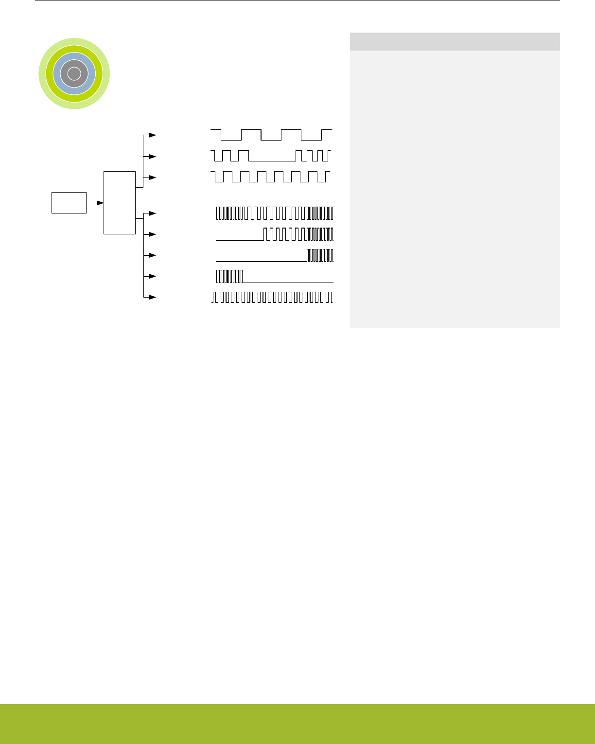
12. CMU - Clock Management Unit
0 1 2 3 4
Oscillators CMU
WDOG clock
LETIMER clock
LEUART clock
Peripheral A clock
Peripheral B clock
Peripheral C clock
Peripheral D clock
CPU clock
Quick Facts
What?
The CMU controls oscillators and clocks.
EFR32xG13 Wireless Gecko supports 6 different os-
cillators with minimized power consumption and
short start-up time. The CMU has HW support for
calibration of RC oscillators.
Why?
Oscillators and clocks contribute significantly to the
power consumption of an MCU. Low power oscilla-
tors combined with a flexible clock control scheme
make it possible to minimize the energy consump-
tion in any given application.
How?
The CMU can configure different clock sources, ena-
ble/disable clocks to peripherals on an individual ba-
sis and set the prescaler for the different clocks. The
short oscillator start-up times makes duty-cycling be-
tween active mode and the different low energy
modes (EM2 Deep Sleep, EM3 Stop, and EM4 Hi-
bernate/Shutoff) very efficient. The calibration fea-
ture ensures high accuracy RC oscillators. Several
interrupts are available to avoid CPU polling of flags.
12.1 Introduction
The Clock Management Unit (CMU) is responsible for controlling the oscillators and clocks in the EFR32xG13 Wireless Gecko. The
CMU provides the capability to turn on and off the clock on an individual basis to all peripheral modules in addition to enable/disable
and configure the available oscillators. The high degree of flexibility enables software to minimize energy consumption in any specific
application by not wasting power on peripherals and oscillators that do not need to be active.
Reference Manual
CMU - Clock Management Unit
silabs.com | Smart. Connected. Energy-friendly. Preliminary Rev. 0.5 | 289

12.2 Features
• Multiple clock sources available:
•38 MHz - 40 MHz High Frequency Crystal Oscillator (HFXO)
• 1 MHz - 38 MHz High Frequency RC Oscillator (HFRCO)
• 1 MHz - 38 MHz Auxiliary High Frequency RC Oscillator (AUXHFRCO)
• 32768 Hz Low Frequency Crystal Oscillator (LFXO)
• 32768 Hz Low Frequency RC Oscillator (LFRCO)
• 1000 Hz Ultra Low Frequency RC Oscillator (ULFRCO)
• 32768 Hz Precision Low Frequency Oscillator (PLFRCO)
• All oscillator sources are low power.
• Fast start-up times.
• Spectrum-Spreading Digital Phase-Locked Loop.
• Separate prescalers for High Frequency Core Clocks (HFCORECLK), Radio Clocks (HFRADIOCLK), and Peripheral Clocks
(HFPERCLK).
• Individual clock prescaler selection for each Low Energy Peripheral.
• Clock gating on an individual basis to core modules and all peripherals.
• Selectable clock output to external pins and/or PRS.
• Wakeup interrupt for LFRCO or LFXO ready allows entry into EM2 Deep Sleep while waiting for low-frequency oscillator startup.
This avoids the need for software polling and saves power during oscillator startup.
• Auxiliary 1 MHz - 38 MHz RC oscillator (AUXHFRCO), which is asynchronous to the HFSRCCLK system clock, can be selected for
ADC operation, LESENSE timing and debug trace.
Reference Manual
CMU - Clock Management Unit
silabs.com | Smart. Connected. Energy-friendly. Preliminary Rev. 0.5 | 290
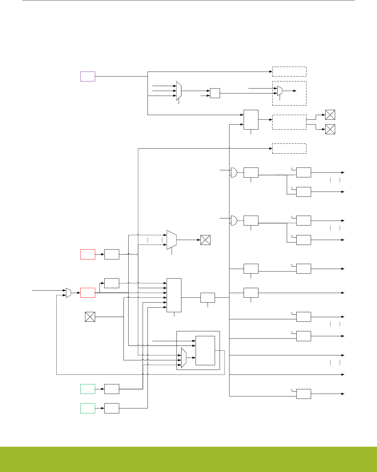
12.3 Functional Description
An overview of the high frequency portion of the CMU is shown in Figure 12.1 CMU Overview - High Frequency Portion on page 291.
An overview of the low frequency portion is shown in Figure 12.2 CMU Overview - Low Frequency Portion on page 292. These figures
show the CMU for the largest device in the EFR32 family. Please refer to the Configuration Summary in the Device Datasheet to see
which core, radio, and peripheral modules, and therefore clock connections, are present in a specific device.
TUNING
HFRCO
HFXO Timeout
HFCLK
clock
switch
CMU_HFPRESC.PRESC
HFSRCCLK
CMU_HFRCOCTRL.TUNING
Fref
DPLL
core
PCLK
FEEDBACK
DPLL
HFPERCLKCMU
HFXO
CLKIN0
prescaler
CMU_HFCLKSEL.HF
LFXO
LFRCO
Timeout
Timeout
CMU_HFPERCLKEN0.USARTn
HFPERCLKUSARTn
CMU_HFPERCLKEN0.TIMERn
HFPERCLKTIMERn
Clock
Gate
Clock
Gate
HFPERCLK
CMU_HFPERPRESC.PRESC
prescaler
CMU_CTRL.HFPERCLKEN
HFCORECLKCORTEX
EM0
HFCORECLK
CMU_HFCOREPRESC.PRESC
AUXCLK
CMU_DBGCLKSEL.DBG
HFBUSCLKDMEM
CMU_HFBUSCLKEN0.GPIO
HFBUSCLKGPIO
HFBUSCLKBUSMATRIX
50% duty
prescaler
HFEXPCLK
CMU_HFEXPPRESC.PRESC
HFBUSCLKLDMA
CMU_HFBUSCLKEN0.LDMA
DBGCLK
AUX
HFRCO
CMU_ADCCTRL.ADCnCLKINV
CMU_ADCCTRL.ADCnCLKSEL
ADC_CLK
ADCCLKMODE
Availability of oscillators and clocks in Energy Modes:
· Available in EM0/EM1
· Available in EM0/EM1/EM2
· Available in EM0/EM1/EM2/EM3
· Available in EM0/EM1/EM2/EM3/EM4H
· Available in EM0/EM1/EM2/EM4H/EM4S
· Available in EM0/EM1/EM2/EM3/EM4H/EM4S
prescaler Clock
Gate
Clock
Gate
Clock
Gate
HFBUSCLKLE
CMU_HFBUSCLKEN0.LE
Clock
Gate
Debug Trace
clock
switch
xor ADC
HFPERCLKADCn
HFSRCCLK
CLKIN0
LFXO
HFRCO
LFRCO
LFXO
CLKIN0
HFRCO
HFXO
HFCLK
LESENSE
(High frequency timing)
AUXCLK
AUXCLK
AUXCLK
HFRCODIV2
CLKOUTn
CMU_CTRL.CLKOUTSELn
HFRCO
HFXO
50% duty
/2
HFXO
Radio Transceiver
CMU_HFRADIOCLKEN0.SYNTH
HFRADIOCLKSYNTH
CMU_HFRADIOCLKEN0.MODEM
HFRADIOCLKMODEM
Clock
Gate
Clock
Gate
HFRADIOCLK
CMU_HFRADIOPRESC.PRESC
prescaler
CMU_CTRL.HFRADIOCLKEN
HFXO
Figure 12.1. CMU Overview - High Frequency Portion
Reference Manual
CMU - Clock Management Unit
silabs.com | Smart. Connected. Energy-friendly. Preliminary Rev. 0.5 | 291
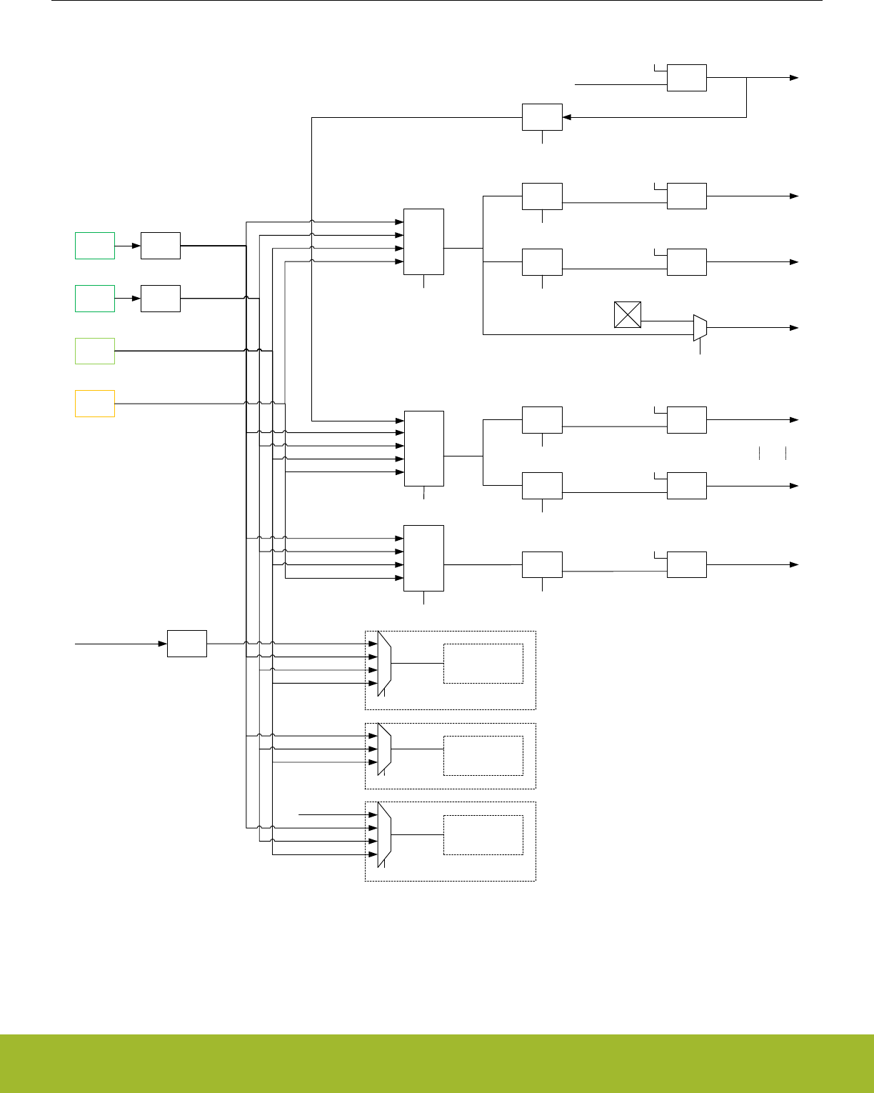
HFCLK
LFXO
LFRCO
Timeout
Timeout
CMU_LFECLKEN0.RTCC
LFECLKRTCC
LFACLK
CMU_LFBCLKEN0.LEUART0
LFBCLKLEUART0
LFBCLK
WDOG
WDOG_CTRL.CLKSEL
CMU_LFBCLKSEL.LFB
CMU_LFACLKSEL.LFA
CMU_LFBPRESC0.LEUART0
WDOGCLK
HFCLKLE
CMU_HFPRESC.HFCLKLEPRESC
ULFRCO
CRYOTIMER_CTRL.OSCSEL
CRYOCLK
LFECLK
CMU_LFECLKSEL.LFE
Availability of oscillators and clocks in Energy Modes:
· Available in EM0/EM1
· Available in EM0/EM1/EM2
· Available in EM0/EM1/EM2/EM3
· Available in EM0/EM1/EM2/EM3/EM4H
· Available in EM0/EM1/EM2/EM4H/EM4S
· Available in EM0/EM1/EM2/EM3/EM4H/EM4S
HFBUSCLKLE
CMU_HFBUSCLKEN0.LE
Clock
Gate
50% duty
prescaler
(/2, /4)
clock
switch
CMU_LFACLKEN0.LETIMER0
LFACLKLETIMER0
PCNTnCLK
PCNTn_S0
CMU_LFAPRESC0.LETIMER0
CMU_PCNTCTRL.PCNTnCLKSEL
LFACLKLESENSE
CMU_LFAPRESC0.LESENSE
CMU_LFACLKEN0.LESENSE
Clock
Gate
Clock
Gate
prescaler
prescaler
Clock
Gate
Clock
Gate
prescaler
prescaler
CMU_LFBPRESC0.CSEN
CMU_LFBCLKEN0.CSEN
LFBCLKCSEN
Clock
Gate
CRYOTIMER
prescaler
(/1024)
HFCORECLKCORTEX
prescaler
CMU_LFEPRESC0.RTCC
LFXO
LFRCO
ULFRCO
HFCLKLE
LFXO
LFRCO
ULFRCO
LFXO
LFRCO
ULFRCO
LFXO
LFRCO
ULFRCO
LFXO
LFRCO
ULFRCO
RFSENSE
RFSENSE_CTRL.OSCSEL
LFXO
LFRCO
ULFRCO
RFSENSE
CLK
RF Detector Clock
PLFRCO
PLFRCO
clock
switch
PLFRCO
clock
switch
PLFRCO
Figure 12.2. CMU Overview - Low Frequency Portion
12.3.1 System Clocks
Reference Manual
CMU - Clock Management Unit
silabs.com | Smart. Connected. Energy-friendly. Preliminary Rev. 0.5 | 292

12.3.1.1 HFCLK - High Frequency Clock
HFSRCCLK is the selected High Frequency Source Clock. HFCLK is an optionally prescaled version of HFSRCCLK. The HFSRCCLK,
and therefore HFCLK, can be driven by a high-frequency oscillator, such as HFRCO, HFRCODIV2 (see DPLL 12.3.12.1 Enabling and
Disabling) or HFXO, or one of the low-frequency oscillators (LFRCO or LFXO). Additionally, HFSRCCLK can also be driven from a pin
(CLKIN0) described in 12.3.6 Clock Input from a Pin. By default the HFRCO is selected. In most applications, one of the high frequency
oscillators will be the preferred choice. To change the selected clock source, write to the HF bitfield in CMU_HFCLKSEL. The high fre-
quency clock source can also be changed automatically by hardware as explained in 12.3.2.9 Automatic HFXO Start. The currently
selected source for HFSRCCLK and HFCLK can be read from CMU_HFCLKSTATUS. The HFSRCCLK is running in EM0 Active and
EM1 Sleep and is automatically stopped in EM2 Deep Sleep. During Voltage Scaling (see 11.3.9 Voltage Scaling), if a fixed frequency
oscillator source (i.e. HFXO or CLKIN0) exceeds the maximum system frequency supported, it must be disabled or not selected. Like-
wise, an adjustable oscillator source (i.e. HFRCO or AUXHFRCO) must be configured to not exceed the maximum system frequency
supported before voltage scaling is applied.
Note:
If a low frequency clock (i.e. LFRCO or LFXO) is selected as source clock for HFSRCCLK via the HF bitfield in CMU_HFCLKSEL, then
no register reads should be performed from Low Energy Peripherals for registers which can change value every clock cycle (e.g. a
counter register). In addition to the peripherals on LFACLK, LFBCLK and LFECLK, this restriction applies in general to any low frequen-
cy peripheral, which is not directly or indirectly clocked from HFSRCCLK (e.g. WDOGn).
HFCLK can optionally be prescaled by setting PRESC in CMU_HFPRESC to a non-zero value. This prescales HFCLK to all high fre-
quency components and is typically used to save energy in applications where the system is not required to run at the highest frequen-
cy. The prescaler setting can be changed dynamically and the new setting takes effect immediately. HFCLK is used by the CMU and
drives the prescalers that generate HFCORECLK, HFRADIOCLK and HFPERCLK allowing for flexible clock prescaling. The
HFBUSCLK, used in for example the bus and memory system, is equal to HFCLK.
The HFXO clock is fed directly to the Radio Transceiver. The clock received by the Radio Transceiver is therefore not affected by the
selected clock source for HFSRCCLK nor by any clock prescaler.
12.3.1.2 HFCORECLK - High Frequency Core Clock
HFCORECLK is a prescaled version of HFCLK. This clock drives the Core Modules, which consists of the CPU and modules that are
tightly coupled to the CPU, e.g. the cache. The prescale factor for prescaling HFCLK into HFCORECLK is set using the CMU_HFCOR-
EPRESC register. The setting can be changed dynamically and the new setting takes effect immediately.
Note:
If HFPERCLK or HFRADIOCLK runs faster than HFCORECLK, the number of clock cycles for each bus-access to (radio) peripheral
modules will increase with the ratio between the clocks. Please refer to 4.2.5 Bus Matrix for more details.
12.3.1.3 HFBUSCLK - High Frequency Bus Clock
HFBUSCLK is equal to HFCLK. This clock drives the Bus and Memory System. HFBUSCLK is also used to drive the bus interface to
the Low Energy Peripherals as described further in 12.3.1.7 LFACLK - Low Frequency A Clock, 12.3.1.8 LFBCLK - Low Frequency B
Clock and 12.3.1.9 LFECLK - Low Frequency E Clock. Some of the modules that are driven by this clock can be clock gated completely
when not in use. This is done by clearing the clock enable bit for the specific module in CMU_HFBUSCLKEN0. The frequency of
HFBUSCLK is equal to the frequency of HFCLK and can therefore only be prescaled by using the PRESC bitfield in CMU_HFPRESC.
12.3.1.4 HFPERCLK - High Frequency Peripheral Clock
Like HFCORECLK, HFPERCLK is a prescaled version of HFCLK. This clock drives the High-Frequency Peripherals. All the peripherals
that are driven by this clock can be clock gated individually when not in use. This is done by clearing the clock enable bit for the specific
peripheral in CMU_HFPERCLKEN0. All high frequency peripheral clocks can be universally and simultaneously gated by clearing the
HFPERCLKEN bit in the CMU_CTRL register. The prescale factor for prescaling HFCLK into HFPERCLK is set using the
CMU_HFPERPRESC register. The setting can be changed dynamically and the new setting takes effect immediately.
Note:
If HFPERCLK runs faster than HFCORECLK, the number of clock cycles for each bus-access to peripheral modules will increase with
the ratio between the clocks. E.g. if a bus-access normally takes three cycles, it will take 9 cycles of HFCORECLK if HFPERCLK runs
three times as fast as HFCORECLK.
Reference Manual
CMU - Clock Management Unit
silabs.com | Smart. Connected. Energy-friendly. Preliminary Rev. 0.5 | 293

12.3.1.5 HFRADIOCLK - High Frequency Radio Clock
HFRADIOCLK is a prescaled version of HFCLK which drives the High-Frequency Radio Peripherals. All the radio peripherals that are
driven by this clock can be clock gated completely when not in use. This is done by clearing the clock enable bit for the specific periph-
eral in CMU_HFRADIOCLKEN0. The radio peripherals can also be gated simultaneously by clearing the HFRADIOCLKEN bit in the
CMU_CTRL register. The prescale factor for prescaling HFCLK into HFRADIOCLK is set using the CMU_HFRADIOPRESC register.
The setting can be changed dynamically and the new setting takes effect immediately.
Note:
If HFRADIOCLK runs faster than HFCORECLK, the number of clock cycles for each bus-access to radio peripheral modules will in-
crease with the ratio between the clocks. E.g. if a bus-access normally takes three cycles, it will take 9 cycles if HFRADIOCLK runs
three times as fast as the HFCORECLK.
12.3.1.6 ADCnCLK - ADC Core Clock
ADCnCLK is a selectable core clock for ADCn. There are three selectable sources for ADCnCLK: HFSRCCLK, HFXO and AUXHFR-
CO. In addition, the ADCnCLK can be disabled, which is the default setting. The selection is configured using the ADCnCLKSEL field in
CMU_ADCCTRL. The ADCnCLKINV bit in CMU_ADCCTRL can be used to invert ADCnCLK. The ADCnCLKDIV bitfield in
CMU_ADCCTRL can be used to prescale ADCnCLK. The bus interface of ADCn is clocked with HFBUSCLK.
12.3.1.7 LFACLK - Low Frequency A Clock
LFACLK is the selected clock for the Low Energy A Peripherals. There are several selectable sources for LFACLK: LFRCO, LFXO,
PLFRCO and ULFRCO. In addition, the LFACLK can be disabled, which is the default setting. The selection is configured using the LFA
field in CMU_LFACLKSEL.
The bus interface to the Low Energy A Peripherals is clocked by HFBUSCLKLE and this clock therefore needs to be enabled when
programming a Low Energy (LE) peripheral.
Each Low Energy Peripheral that is clocked by LFACLK has its own prescaler setting and enable bit. The prescaler settings are config-
ured using CMU_LFAPRESC0 and the clock enable bits can be found in CMU_LFACLKEN0.
When operating in oversampling mode, the pulse counters are clocked by LFACLK. This is configured for each pulse counter (n) indi-
vidually by setting PCNTnCLKSEL in CMU_PCNTCTRL.
12.3.1.8 LFBCLK - Low Frequency B Clock
LFBCLK is the selected clock for the Low Energy B Peripherals. There are several selectable sources for LFBCLK: LFRCO, LFXO,
HFCLKLE, PLFRCO and ULFRCO. In addition, the LFBCLK can be disabled, which is the default setting. The selection is configured
using the LFB field in CMU_LFBCLKSEL. The HFCLKLE setting allows the Low Energy B Peripherals to be used as high-frequency
peripherals.
The bus interface to the Low Energy B Peripherals is clocked by HFBUSCLKLE and this clock therefore needs to be enabled when
programming a LE peripheral.
Note:
If HFCLKLE is selected as LFBCLK, the clock will stop in EM2 Deep Sleep and EM3 Stop.
Each Low Energy Peripheral that is clocked by LFBCLK has its own prescaler setting and enable bit. The prescaler settings are config-
ured using CMU_LFBPRESC0 and the clock enable bits can be found in CMU_LFBCLKEN0.
Reference Manual
CMU - Clock Management Unit
silabs.com | Smart. Connected. Energy-friendly. Preliminary Rev. 0.5 | 294

12.3.1.9 LFECLK - Low Frequency E Clock
LFECLK is the selected clock for the Low Energy E Peripherals. There are several selectable sources for LFECLK: LFRCO, LFXO,
PLFRCO and ULFRCO. In addition, the LFECLK can be disabled, which is the default setting. The selection is configured using the
LFE field in CMU_LFECLKSEL.
The bus interface to the Low Energy E Peripherals is clocked by HFBUSCLKLE and this clock therefore needs to be enabled when
programming a LE peripheral.
Note:
LFECLK is in a different power domain than LFACLK and LFBCLK, which makes it available all the way down to EM4 Hibernate.
Each Low Energy Peripheral that is clocked by LFECLK has its own prescaler setting and enable bit. The prescaler settings are config-
ured using CMU_LFEPRESC0 and the clock enable bits can be found in CMU_LFECLKEN0.
12.3.1.10 PCNTnCLK - Pulse Counter n Clock
Each available pulse counter is driven by its own clock, PCNTnCLK where n is the pulse counter instance number. Each pulse counter
can be configured to use an external pin (PCNTn_S0) or LFACLK as PCNTnCLK.
12.3.1.11 WDOGnCLK - Watchdog Timer Clock
The Watchdog Timer (WDOGn) can be configured to use one of many different clock sources. Refer to CLKSEL field in WDOGn_CTRL
for a complete list.
12.3.1.12 CRYOCLK - Cryotimer Clock
The Cryotimer clock can be configured to use one of many different clock sources. Refer to OSCSEL field in CRYOTIMER_CTRL for a
complete list. The Cryotimer can also run in EM4 Hibernate/Shutoff provided that its selected clock is kept enabled as configured in
EMU_EM4CTRL.
12.3.1.13 RFSENSECLK - RFSENSE Clock
The RFSENSE clock can be configured to use one of four different clock sources: LFRCO, LFXO, ULFRCO or the RF Detector Clock.
The RFSENSE module can also run in EM4 Hibernate/Shutoff provided that its selected clock is kept enabled as configured in
EMU_EM4CTRL.
12.3.1.14 AUXCLK - Auxiliary Clock
AUXCLK is a 1 MHz - 38 MHz clock driven by a separate RC oscillator, the AUXHFRCO. This clock can be used for ADC operation,
LESENSE operation and Serial Wire Output (SWO). When the AUXHFRCO is selected as the ADCn clock via the ADCnCLKSEL bit-
field in the CMU_ADCCTRL register, or if needed by LESENSE, this clock will become active automatically when needed. Even if the
AUXHFRCO has not been enabled explicitly by software, the ADC or LESENSE can automatically start and stop it. The AUXHFRCO is
explicitly enabled by writing a 1 to AUXHFRCOEN in CMU_OSCENCMD. This explicit enabling is required when selecting the AUXCLK
for SWO operation.
12.3.1.15 Debug Trace Clock
The CMU selects the clock used for debug trace via the DBGCLKSEL register. The user can useAUXHFRCO or the HFCLK. The selec-
ted debug trace clock will be used to run the Cortex-M4 trace logic.
Note:
When using AUXHFRCO as the debug trace clock, it must be stopped before entering EM2 or EM3.
12.3.2 Oscillators
Reference Manual
CMU - Clock Management Unit
silabs.com | Smart. Connected. Energy-friendly. Preliminary Rev. 0.5 | 295

12.3.2.1 Enabling and Disabling
The different oscillators can typically be enabled and disabled via both hardware and software mechanisms. Enabling via software is
done by setting the corresponding enable bit in the CMU_OSCENCMD register. Disabling via software is done by setting the
corresponding disable bit in CMU_OSCENCMD. Enabling via hardware can be performed by various peripherals and varies per oscilla-
tor. Disabling via hardware is typically performed on entry of low energy modes. The enable and disable mechanisms for each of the
oscillators are summarized in Table 12.1 Software based and Hardware based Enabling and Disabling of Oscillators on page 296 and
described in more detail below.
Table 12.1. Software based and Hardware based Enabling and Disabling of Oscillators
Oscillator SW Enable SW Disable HW Enable HW Disable
ULFRCO - - Enabled when in
EM0/EM1/EM2/EM3/
EM4H.
EM4S entry depending
on configuration in
EMU_EM4CTRL.
LFRCO Via LFRCOEN in
CMU_OSCENCMD.
Via LFRCODIS in
CMU_OSCENCMD.
Via WDOGn if it is config-
ured to use LFRCO as its
clock source via the
CLKSEL bitfield in
WDOGn_CTRL while
SWOSCBLOCK is set.
EM3 entry. EM4 entry de-
pending on configuration
in EMU_EM4CTRL.
PLFRCO Via PLFRCOEN in
CMU_OSCENCMD.
Via PLFRCODIS in
CMU_OSCENCMD.
Software enable only. Software disable only.
LFXO Via LFXOEN in
CMU_OSCENCMD.
Via LFXODIS in
CMU_OSCENCMD.
Via WDOGn if it is config-
ured to use LFXO as its
clock source via the
CLKSEL bitfield in
WDOGn_CTRL while
SWOSCBLOCK is set.
EM3 entry. EM4 entry de-
pending on configuration
in EMU_EM4CTRL.
HFRCO Via HFRCOEN in
CMU_OSCENCMD.
Via HFRCODIS in
CMU_OSCENCMD.
Reset exit. EM2/EM3 ex-
it. Automatic control by
LEUART RX/TX DMA
wake-up as configured in
LEUARTn_CTRL.
EM2/EM3/EM4 entry. Au-
tomatic control by
LEUART RX/TX DMA
wake-up as configured in
LEUARTn_CTRL. Auto-
matic start and selection
of HFXO causes HFRCO
disable.
AUXHFRCO Via AUXHFRCOEN in
CMU_OSCENCMD.
Via AUXHFRCODIS in
CMU_OSCENCMD.
Automatic control by
ADC and LESENSE.
EM2/EM3/EM4 entry. Au-
tomatic control by ADC
and LESENSE even in
EM2/EM3.
HFXO Via HFXOEN in
CMU_OSCENCMD.
Via HFXODIS in
CMU_OSCENCMD.
Automatic start by Radio
Controller (RAC) or
EM0/EM1 entry as con-
figured in
CMU_HFXOCTRL.
EM2/EM3/EM4 entry.
Reference Manual
CMU - Clock Management Unit
silabs.com | Smart. Connected. Energy-friendly. Preliminary Rev. 0.5 | 296

12.3.2.1.1 LFRCO and LFXO
The LFXO and LFRCO can be enabled and disabled by software via the CMU_OSCENCMD register. WDOGn can be configured to
force the LFXO or LFRCO to become (and remain) enabled when such an oscillator is selected as its clock source via the CLKSEL
bitfield in the WDOGn_CTRL register while SWOSCBLOCK is set. In that case LFXODIS and LFRCODIS commands are blocked.
They are automatically disabled when entering EM3. Upon EM4 entry they are default turned off, but they can optionally be retained
depending on the EMU_EM4CTRL configuration. Retaining of the LFXO or LFRCO in EM4 is needed if such an oscillator is required by
a specific peripheral in EM4. Retaining can also be used to guarantee quick oscillator availability after EM4 exit.
The oscillators should never be retained in case they are off before entering EM4. The following are the valid ways of using the LFXO/
LFRCO retention mechanism:
• Turn on LFXO/LFRCO always (even in EM4):
1. POR
2. Enable LFXO/LFRCO
3. Enable RETAINLFXO/RETAINLFRCO
4. EM4 entry
5. LFXO/LFRCO are retained and remain running in EM4
6. EM4 wakeup
7. Enable LFXO/LFRCO
8. Set EM4UNLATCH in EMU_CMD
• Turn off LFXO/LFRCO in EM4:
1. POR
2. Disable RETAINLFXO/RETAINLFRCO (default)
3. Enable LFXO/LFRCO
4. EM4 entry
5. LFXO/LFRCO are off in EM4
6. EM4 wakeup
7. Enable LFXO/LFRCO
8. Set EM4UNLATCH in EMU_CMD
• Turn on LFXO/LFRCO after EM4 exit:
1. POR
2. Disable RETAINLFXO/RETAINLFRCO (default)
3. Enable LFXO/LFRCO
4. EM4 entry
5. LFXO/LFRCO are off in EM4
6. EM4 wakeup
7. Enable LFXO/LFRCO
8. Set EM4UNLATCH in EMU_CMD
9. Enable RETAINLFXO/RETAINLFRCO
In summary RETAINLFXO/RETAINLFRCO should either be changed once after POR and kept static, or they can be changed on-the-fly
only after asserting EM4UNLATCH.
Note:
In order to support usage of LFRCO and LFXO in EM4, their settings are automatically latched upon EM4 entry. These settings remain
latched upon wake-up from EM4 to EM0 although the related registers (CMU_LFRCOCTRL, CMU_LFXOCTRL, CMU_LFECLKSEL,
CMU_LFECLKEN0 and CMU_LEEPRESC0) will have been reset. The registers can be rewritten by software, but they will only affect
the LFRCO and LFXO after unlatching their settings by setting EM4UNLATCH in the EMU_CMD register.
Note:
Turning off the LFRCO and LFXO upon EM4 Hibernate/Shutoff entry is most easily done by using the RETAINLFRCO and RETAINLF-
XO bitfields from the EMU_EM4CTRL register, which are default such that the LFRCO and LFXO are turned off automatically upon
EM4 Hibernate/Shutoff entry. Alternatively the LFRCO and LFXO can be disabled via the CMU_OSCENCMD register, in which case
software should wait for the oscillators to be properly disabled before executing the EM4 Hibernate/Shutoff entry routine.
After enabling the LFRCO (or LFXO), it should not be disabled before it has been signaled to be ready. Similarly, after disabling the
LFRCO (or LFXO), it should not be re-enabled before it has been signaled to be non-ready. Before entering EM4, software should
Reference Manual
CMU - Clock Management Unit
silabs.com | Smart. Connected. Energy-friendly. Preliminary Rev. 0.5 | 297

check that the LFRCO (or LFXO) is signaled to be ready before allowing or initiating the EM4 entry if that oscillator is required in EM4.
Also, to guarantee latching the latest settings, no control write should be ongoing upon EM4 entry as can be checked via the
CMU_SYNCBUSY register. Typical enable and disable sequences are as follows:
CMU->OSCENCMD = CMU_OSCENCMD_LFRCOEN;
while ((CMU->STATUS & CMU_STATUS_LFRCORDY) != CMU_STATUS_LFRCORDY);
CMU->OSCENCMD = CMU_OSCENCMD_LFRCODIS;
while ((CMU->STATUS & CMU_STATUS_LFRCORDY) == CMU_STATUS_LFRCORDY);
When the LFXO is disabled, the interface to the LFXTAL_N and LFXTAL_P pins are set in a high-Z state. The XTAL oscillations will not
stop immediately when LFXO is disabled, but typically die out gradually over some 100 ms. If the LFXO is enabled before XTAL oscilla-
tions have had time to reach zero amplitude, startup time can be significantly shorter.
Note:
The LFRCORDY and LFXORDY interrupts can be used to wake up the system from EM2 Deep Sleep. In this way busy waiting for the
LFRCO or LFXO to become ready can be avoided by going into EM2 after enabling these oscillators and sleeping until the interrupt
causes a wakeup.
12.3.2.1.2 ULFRCO
The ULFRCO is automatically enabled in EM0, EM1, EM2, EM3, and EM4H and cannot be controlled via CMU_OSCENCMD. It is auto-
matically disabled upon entering EM4S unless prevented by the configuration in EMU_EM4CTRL.
12.3.2.1.3 HFRCO
The HFRCO can be enabled and disabled by software via the CMU_OSCENCMD register. The HFRCO is disabled automatically when
entering EM2, EM3, or EM4. Further hardware based enabling and disabling can be performed by the LEUART when using automatic
RX/TX DMA wakeup as controlled by the RXDMAWU and TXDMAWU bits in the LEUARTn_CTRL register. An automatic start and se-
lection of the HFXO will lead to an automatic HFRCO disabling. Since HFRCO also serves as the local oscillator for DPLL
(12.3.12 Digital Phase-Locked Loop), it is enabled/disabled when DPLL is enabled/disabled.
The supported HFRCO frequency range is from 1 MHz to 38 MHz. The default HFRCO frequency is 19 MHz
12.3.2.1.4 HFXO
The HFXO can be enabled and disabled by software via the CMU_OSCENCMD register. The HFXO is disabled automatically when
entering EM2, EM3, or EM4. Hardware based HFXO enabling can be initiated by various peripherals as configured via the AUTOS-
TARTRDYSELRAC, AUTOSTARTEM0EM1, and AUTOSTARTSELEM0EM1 bits in the CMU_HFXOCTRL register. The interaction be-
tween hardware based and software based control of the HFXO is further explained in 12.3.2.9 Automatic HFXO Start.
The supported HFXO frequency range is from 38 MHz to 40 MHz.
After enabling the HFXO, it should not be disabled before it has been signaled to be enabled. Similarly, after disabling the HFXO it
should not be re-enabled before it has been signaled to be non-enabled. Typical enable and disable sequences are as follows:
CMU->OSCENCMD = CMU_OSCENCMD_HFXOEN;
while ((CMU->STATUS & CMU_STATUS_HFXOENS) != CMU_STATUS_HFXOENS);
CMU->OSCENCMD = CMU_OSCENCMD_HFXODIS;
while ((CMU->STATUS & CMU_STATUS_HFXOENS) == CMU_STATUS_HFXOENS);
Reference Manual
CMU - Clock Management Unit
silabs.com | Smart. Connected. Energy-friendly. Preliminary Rev. 0.5 | 298

12.3.2.1.5 AUXHFRCO
The AUXHFRCO can be enabled and disabled by software via the CMU_OSCENCMD register. The AUXHFRCO is disabled automati-
cally when entering EM2, EM3, or EM4. Hardware based AUXHFRCO enabling and disabling is however performed by the ADC mod-
ule when AUXCLK is selected for its operation and by the LESENSE module making it available even when being in EM2/EM3.
The supported AUXHFRCO frequency range is from 1 MHz to 38 MHz. The default AUXHFRCO frequency is 19 MHz
After enabling the AUXHFRCO, it should not be disabled before it has been signaled to be enabled. Similarly, after disabling the
AUXHFRCO, it should not be re-enabled before it has been signaled to be non-enabled. Typical enable and disable sequences are as
follows:
CMU->OSCENCMD = CMU_OSCENCMD_AUXHFRCOEN;
while ((CMU->STATUS & CMU_STATUS_AUXHFRCOENS) != CMU_STATUS_AUXHFRCOENS);
CMU->OSCENCMD = CMU_OSCENCMD_AUXHFRCODIS;
while ((CMU->STATUS & CMU_STATUS_AUXHFRCOENS) == CMU_STATUS_AUXHFRCOENS);
Note:
When using AUXHFRCO as the debug trace clock (as selected in CMU_DBGCLKSEL), it must be stopped before entering EM2 or
EM3.
Reference Manual
CMU - Clock Management Unit
silabs.com | Smart. Connected. Energy-friendly. Preliminary Rev. 0.5 | 299
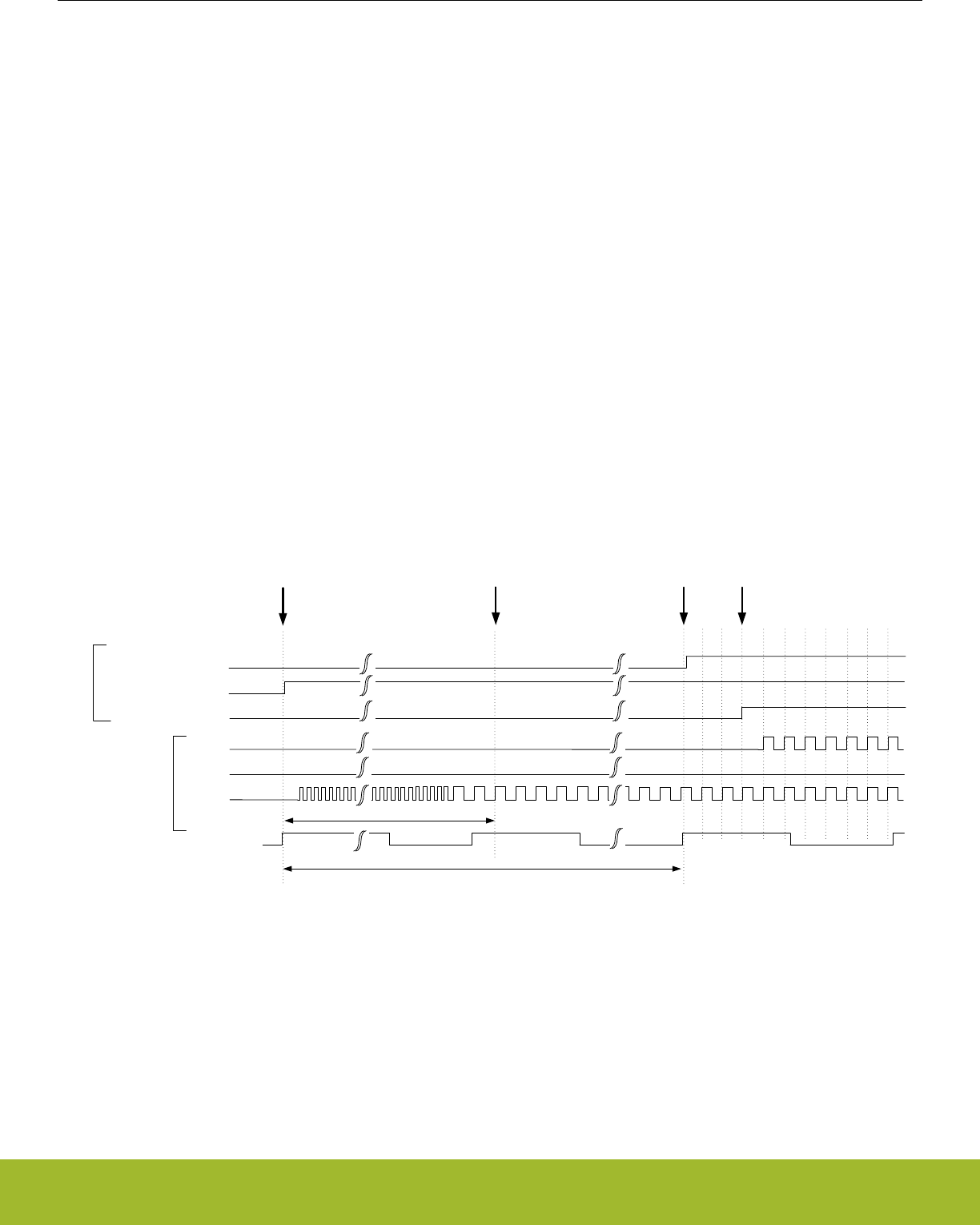
12.3.2.2 Oscillator Start-up Time and Time-out
The start-up time differs per oscillator and the usage of an oscillator clock can further be delayed by a time-out. The LFRCO, LFXO and
the HFXO have a configurable time-out which is set by software in the (various) TIMEOUT bitfields of the CMU_LFRCOCTRL,
CMU_LFXOCTRL and CMU_HFXOTIMEOUTCTRL registers respectively. The time-out delays the assertion of the READY signal for
LFRCO, LFXO and HFXO and should allow for enough time for the oscillator to stabilize. The time-out can be optimized for the chosen
crystal (for LFXO and HFXO) used in the application. In case LFRCO and/or LFXO has been retained throughout EM4 Hibernate/Shut-
off, such retained oscillators can be quickly restarted for use as LFACLK, LFBCLK or LFECLK by using the minimum TIMEOUT settings
for them. For the other RC oscillators (HFRCO, AUXHFRCO, and ULFRCO), the start-up time is known and a fixed time-out is used.
There are individual bits in the CMU_STATUS register for each oscillator indicating the status of the oscillator:
• ENABLED - Indicates that the oscillator is enabled
• READY - Start-up time including time-out is exceeded
These status bits are located in the CMU_STATUS register.
Additionaly, the HFXO has a second time-out counter which can be used to achieve deterministic start-up time based on timing from the
LFXO, ULFRCO, or LFRCO. This second counter runs off LFECLK and can be programmed via the LFTIMEOUT bitfield in the
CMU_HFXOCTRL register. It can be used when waking up from EM2 when either ULFRCO, LFRCO or LFXO is already running and
stable. In this case the HFXO ready assertion can be delayed with the number of LFECLK cycles as programmed in LFTIMEOUT. The
HFXO ready signal is asserted when both the TIMEOUT counter (configured via the CMU_HFXOTIMEOUTCTRL register) and the
LFTIMEOUT counter (configured via CMU_HFXOCTRL register) have timed out as shown in Figure 12.3 CMU Deterministic HFXO
startup using LFTIMEOUT on page 300. The TIMEOUT should cover the actual crystal startup time. Typically the time base used for
the TIMEOUT counter is not as accurate as the time base accuracy that can be achieved for the LFTIMEOUT counter, specifically if
that one is based on the LFXO timing. If LFTIMEOUT is triggered before TIMEOUT is triggered, then the LFTIMEOUTERR bitfield in
CMU_IF will be set to 1. Note that use of LFTIMEOUT requires that the peripheral causing the wake-up is on the LFECLK domain. The
intended use scenario is for example to wake up from EM2 by the RTCC triggering RAC wake-up via the PRS, which in turn can wake
up the entire system. The RAC wake-up causes an automatic start of the HFXO in case the AUTOSTARTRDYSELRAC bit in
CMU_HFXOCTRL is set to 1. Assertion of the HFXO ready signal, and therefore the radio start timing, can then be made deterministic
by using LFTIMEOUT.
HFXO
CMU_STATUS.HFXORDY
CMU_STATUS.HFXOENS
CMU_HFCLKSEL.HF = HFXO
HFRCO
HFCLK
clocks
status
Automatic switch to HFXO and disable of HFRCOWake-up from EM2 with automatic HFXO start
LFTIMEOUT (counting LFECLK cycles)
LFECLK
HFXO ready (deterministic)
HFXO stable (non-deterministic)
TIMEOUT (based on CMU_HFXOTIMEOUTCTRL)
Figure 12.3. CMU Deterministic HFXO startup using LFTIMEOUT
The startup behavior of the HFXO also depends on how and how long the HFXO is disabled. This can be controlled by configuring the
XTI2GND, and XTO2GND bitfields in the CMU_HFXOCTRL register.
Reference Manual
CMU - Clock Management Unit
silabs.com | Smart. Connected. Energy-friendly. Preliminary Rev. 0.5 | 300
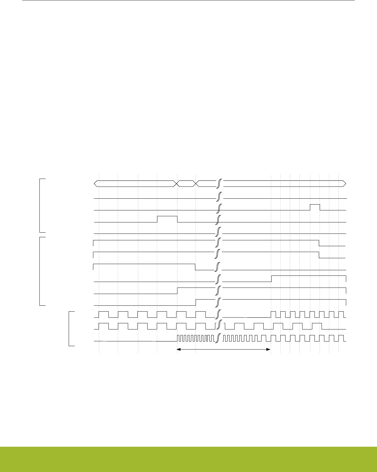
12.3.2.3 Switching Clock Source
The HFRCO oscillator is a low energy oscillator with extremely short start-up time. Therefore, this oscillator is always chosen by hard-
ware as the clock source for HFCLK when the device starts up (e.g. after reset and after waking up from EM2 Deep Sleep and EM3
Stop). After reset, the HFRCO frequency is 19 MHz.
Software can switch between the different clock sources at run-time. For example, when the HFRCO is the clock source, software can
switch to HFXO by writing the field HF in the CMU_HFCLKSEL command register. See Figure 12.4 CMU Switching from HFRCO to
HFXO before HFXO is ready on page 301 for a description of the sequence of events for this specific operation.
Note:
Before switching the HFCLKSRC to HFXO via the HF bitfield in CMU_HFCLKSEL it is important to first enable the HFXO. Switching to
a disabled oscillator will effectively stop HFSRCCLK and only a reset can recover the system.
When selecting an oscillator which has been enabled, but which is not ready yet, the HFSRCCLK will stop for the duration of the oscilla-
tor start-up time since the oscillator driving it is not ready. This effectively stalls the Core Modules and the High-Frequency Peripherals.
It is possible to avoid this by first enabling the target oscillator (e.g. HFXO) and then waiting for that oscillator to become ready before
switching the clock source. This way, the system continues to run on the HFRCO until the target oscillator (e.g. HFXO) has timed out
and provides a reliable clock. This sequence of events is shown in Figure 12.5 CMU Switching from HFRCO to HFXO after HFXO is
ready on page 302.
A separate flag is set when the oscillator is ready. This flag can also be configured to generate an interrupt.
HFXO
CMU_STATUS..HFXORDY
CMU_STATUS.HFXOENS
CMU_STATUS.HFXOSEL
HFRCO
HFCLK
HFXO time-out period
CMU_STATUS.HFRCORDY
CMU_STATUS.HFRCOENS
CMU_STATUS.HFRCOSEL
CMU_OSCENCMD.HFXOEN
CMU_OSCENCMD.HFXODIS
clocks
CMU_CMD.HFCLKSEL
CMU_OSCENCMD.HFRCOEN
CMU_OSCENCMD.HFRCODIS
command
status
00 HFXO 00
Figure 12.4. CMU Switching from HFRCO to HFXO before HFXO is ready
Reference Manual
CMU - Clock Management Unit
silabs.com | Smart. Connected. Energy-friendly. Preliminary Rev. 0.5 | 301
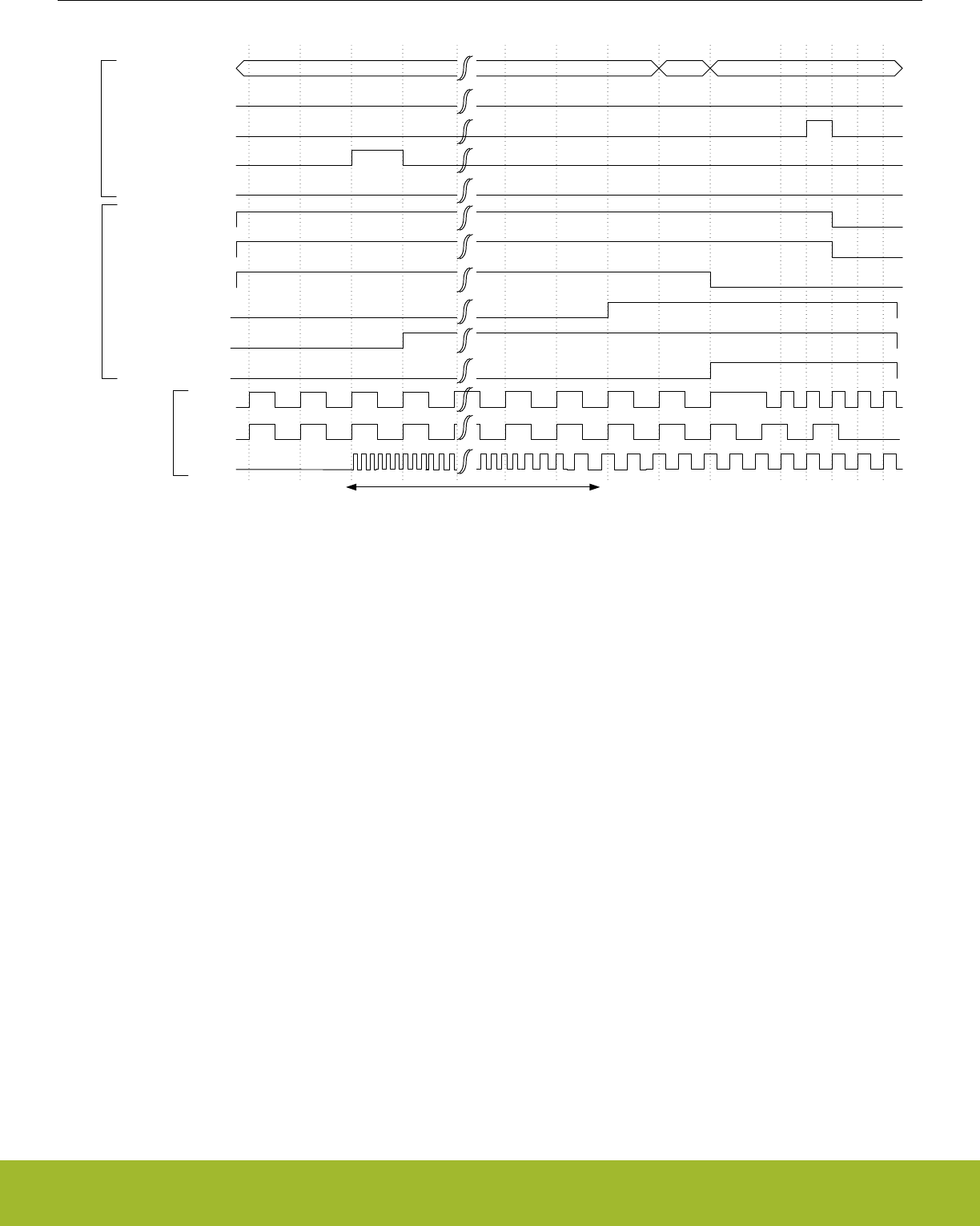
00 HFXO 00
HFXO
CMU_STATUS.HFXORDY
CMU_STATUS.HFXOENS
CMU_STATUS.HFXOSEL
HFRCO
HFCLK
HFXO time-out period
CMU_STATUS.HFRCORDY
CMU_STATUS.HFRCOENS
CMU_STATUS.HFRCOSEL
CMU_OSCENCMD.HFXOEN
CMU_OSCENCMD.HFXODIS
clocks
CMU_CMD.HFCLKSEL
CMU_OSCENCMD.HFRCOEN
CMU_OSCENCMD.HFRCODIS
command
status
Figure 12.5. CMU Switching from HFRCO to HFXO after HFXO is ready
Switching clock source for LFACLK, LFBCLK, and LFECLK is done by setting the LFA, LFB and LFE bitfields in CMU_LFACLKSEL,
CMU_LFBCLKSEL and CMU_LFECLKSEL respectively. To ensure no stalls in the Low Energy Peripherals, the clock source should be
ready before switching to it.
Note:
To save energy, remember to turn off all oscillators not in use.
Reference Manual
CMU - Clock Management Unit
silabs.com | Smart. Connected. Energy-friendly. Preliminary Rev. 0.5 | 302
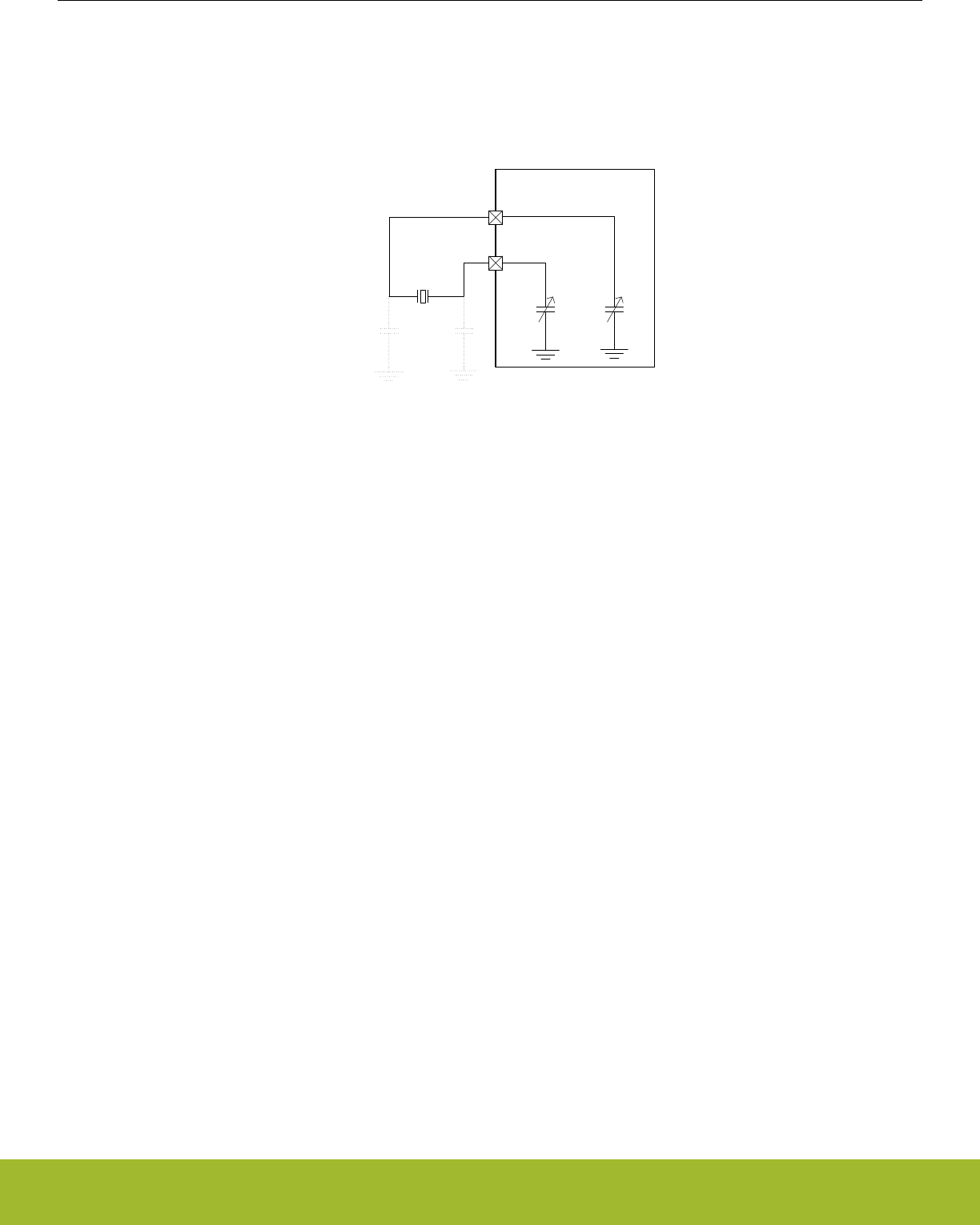
12.3.2.4 HFXO Configuration
The High Frequency Crystal Oscillator needs to be configured to ensure safe startup for the given crystal. Refer to the Device Data-
sheet and application notes for guidelines in selecting correct components and crystals as well as for configuration trade-offs.
The HFXO crystal is connected to the HFXTAL_N/HFXTAL_P pins as shown in Figure 12.6 HFXO Pin Connection on page 303
HFXTAL_N
HFXTAL_P
CL1
CTUNE CTUNE
Gecko Device
CL2
38.0 – 40.0
MHz
Figure 12.6. HFXO Pin Connection
By default the HFXO is started in crystal mode, but it is possible to connect an active external sine wave or square wave clock source to
the HFXTAL_N pin of the HFXO. By configuring the MODE field in CMU_HFXOCTRL to EXTCLK, the HFXO can be bypassed and the
source clock can be provided through the HFXTAL_N pin.
Upon enabling the HFXO, a hardware state machine sequentially applies the configurable startup state and steady state control set-
tings from the CMU_HFXOSTARTUPCTRL and CMU_HFXOSTEADYSTATECTRL registers. Configuration is required for both the
startup state and the steady state of the HFXO. After reaching the steady operation state of the HFXO, further optimization can option-
ally be performed to optimize the HFXO for noise and current consumption. Optimization for noise can be performed by an automatic
Peak Detection Algorithm (PDA). Optimization for current can be performed by an automatic Shunt Current Optimization algorithm
(SCO). HFXO operation is possible without PDA and SCO at the cost of higher noise and current consumption than required.
Upon fully disabling the HFXO, the HFXTAL_N and HFXTAL_P pins can optionally be automatically pulled to ground as configured via
the XTI2GND and XTO2GND bits respectively from the CMU_HFXOCTRL register. Do not set XTI2GND to 1 when the HFXO is in
EXTCLK mode and an external wave is connected.
Reference Manual
CMU - Clock Management Unit
silabs.com | Smart. Connected. Energy-friendly. Preliminary Rev. 0.5 | 303
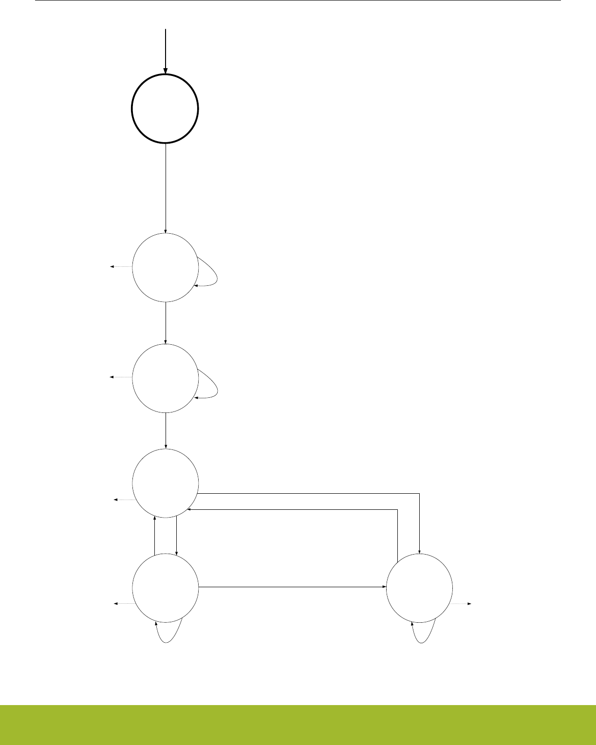
OFF
STARTUP
STEADY
READY
CMU->OSCENCMD = CMU_OSCENCMD_HFXOEN
Startup state configuration from CMU->HFXOSTARTUPCTRL:
· IBTRIMXOCORE
· CTUNE
· REGISH
· LOWPOWER
Timeout configuration from CMU->HFXOTIMEOUTCTRL:
· STARTUPTIMEOUT
Steady state configuration from CMU->HFXOSTEADYSTATECTRL:
· IBTRIMXOCORE
· CTUNE
· REGISH
HFXO major mode configuration from CMU->HFXOCTRL:
· MODE
· LOWPOWER
Timeout configuration from CMU->HFXOTIMEOUTCTRL:
· STEADYTIMEOUT
Reset ||
EM2/EM3 entry ||
(CMU->OSCENCMD = CMU_OSCENCMD_HFXODIS)
OFF
OFF
OFF
PDA
(Peak
Detection
Algorithm)
SCO
(Shunt Current
Optimization)
PEAKDETSHUNTOPTMODE = AUTOCMD
PEAKDETSHUNTOPTMODE = AUTOCMD ||
CMU->CMD = CMU_CMD_HFXOPEAKDETSTART && PEAKDETSHUNTOPTMODE = CMD
CMU->CMD = CMU_CMD_HFXOSHUNTOPTSTART && PEAKDETSHUNTOPTMODE = CMD
OFFOFF
Timeout configuration from CMU->HFXOTIMEOUTCTRL:
· SHUNTOPTTIMEOUT
Timeout configuration from CMU->HFXOTIMEOUTCTRL:
· PEAKDETTIMEOUT
HFXORDY = 1
HFXOPEAKDETRDY = 1
HFXOPEAKDETRDY = 1
PEAKDETSHUNTOPTMODE = CMD
HFXOSHUNTOPTRDY = 1
Figure 12.7. CMU HFXO control state machine
Reference Manual
CMU - Clock Management Unit
silabs.com | Smart. Connected. Energy-friendly. Preliminary Rev. 0.5 | 304

Refer to the Device Datasheet to find the configuration values for a given crystal. The startup state configuration needs to be written
into the IBTRIMXOCORE and CTUNE bitfields of the CMU_HFXOSTARTUPCTRL register. The duration of the startup phase is config-
ured in the STARTUPTIMEOUT bitfield of the CMU_HFXOTIMEOUTCTRL register. Similarly, the Device Datasheet provides the steady
state configuration depending on the crystal's CL, RESR and oscillation frequency. This configuration is programmed into the IBTRIM-
XOCORE, REGISH and CTUNE bitfields of the CMU_HFXOSTEADYSTATECTRL register. The duration of the steady phase is config-
ured in the STEADYTIMEOUT bitfield of the CMU_HFXOTIMEOUTCTRL register.
All HFXO configuration needs to be performed prior to enabling the HFXO via HFXOEN in CMU_OSCENCMD unless noted otherwise.
The HFXOENS flag in CMU_STATUS indicates if the HFXO has been successfully enabled. Once the HFXO startup time (STARTUPTI-
MEOUT plus STEADYTIMEOUT) has exceeded, the HFXO is ready for use as indicated by the HFXORDY flag in CMU_STATUS. If
PDA and SCO are enabled, the HFXOPEAKDETRDY and HFXOSHUNTOPTRDY flags in the CMU_STATUS register indicate when
these algorithms are ready and it is advised to also wait for these flags before using the HFXO.
The HFXO crystal bias current may be optimized and set to a value which decreases output phase noise without sacrificing PSR. This
is done by programming the recommended IBTRIMXOCORE value into the CMU_HFXOSTEADYSTATECTRL register. The built-in
Peak Detector Algorithm (PDA) performs further optimization to accommodate for process variations. Once PDA is ready as indicated
by the HFXOPEAKDETRDY flag, the found optimal bias current setting is available in the IBTRIMXOCORE bitfield of the CMU_HFXO-
TRIMSTATUS register. This IBTRIMXOCORE setting should be saved and can be applied directly during a future HFXO startup as a
low noise setting by programming it into the corresponding bitfield in CMU_HFXOSTEADYSTATECTRL while the HFXO is off.
If low noise is not required, the same PDA algorithm can be configured to optimize the HFXO for low current consumption by enabling
LOWPOWER in the CMU_HFXOCTRL register before starting up the HFXO. The found IBTRIMXOCORE setting can be saved as a
future low current setting.
Default PDA is started automatically once the HFXO has become ready. Repeated PDA can be triggered by writing HFXOPEAKDET-
START to 1 in the CMU_CMD register. PDA can also be triggered only by the command register by configuring PEAKDETSHUNTOPT-
MODE to CMD in the CMU_HFXOCTRL register before starting the HFXO. For PDA to work correctly, the REGISHUPPER bitfield of
CMU_HFXOSTEADYSTATECTRL should be programmed to the value of the steady state REGISH + 3. The PEAKDETTIMEOUT bit-
field in the CMU_HFXOTIMEOUTCTRL register is used to time the PDA steps and needs to be configured according to the Device
Datasheet for the given crystal. The PEAKDETEN bitfield of the CMU_HFXOSTEADYSTATECTRL register is only used during manual
(i.e. fully software controlled) peak detection and is ignored during automatic or command based triggering of the PDA. Note that the
manual PDA mode is not recommended for general usage and therefore it is not further described. PDA should not be used when using
an external wave as clock source.
Current consumption can be (further) reduced by running Shunt Current Optimization (SCO) after PDA. Once SCO is ready as indica-
ted by the HFXOSHUNTOPTRDY flag, the found optimal regulator output current setting is available in the REGISH bitfield of the
CMU_HFXOTRIMSTATUS register. This REGISH setting should be saved and can be applied directly during a future HFXO startup as
a low current setting by programming it into the corresponding bitfield in CMU_HFXOSTEADYSTATECTRL while the HFXO is off. Nor-
mally SCO is run only for initial HFXO start up. The amplitude of the oscillator is not strongly dependent on temperature, but further
optimization may be done each time that the temperature changes significantly. In that case, run SCO again by writing HFXOSHUN-
TOPTSTART to 1 in the CMU_CMD register. SCO depends on the LOWPOWER setting in the CMU_HFXOCTRL and needs to be re-
run if that value has been changed. SCO should not be run when the HFXO is in use by the Radio Transceiver.
Default SCO is started automatically once the HFXO has become ready and PDA has finished. Repeated SCO can be triggered by
writing HFXOSHUNTOPTSTART to 1 in the CMU_CMD register. SCO can also be triggered only by the command register by configur-
ing PEAKDETSHUNTOPTMODE to CMD in the CMU_HFXOCTRL register before starting the HFXO. For SCO to work correctly, the
REGISHUPPER bitfield of CMU_HFXOSTEADYSTATECTRL should be programmed to the value of the steady state REGISH + 3. The
SHUNTOPTTIMEOUT bitfield in the CMU_HFXOTIMEOUTCTRL register is used to time the SCO steps and needs to be configured
according to the Device Datasheet for the given crystal. The REGSELILOW bitfield of the CMU_HFXOSTEADYSTATECTRL register is
only used during manual (i.e. fully software controlled) shunt current optimization and is ignored during automatic or command based
triggering of the SCO. Note that the manual SCO mode is not recommended for general usage and therefore it is not further described.
Reference Manual
CMU - Clock Management Unit
silabs.com | Smart. Connected. Energy-friendly. Preliminary Rev. 0.5 | 305
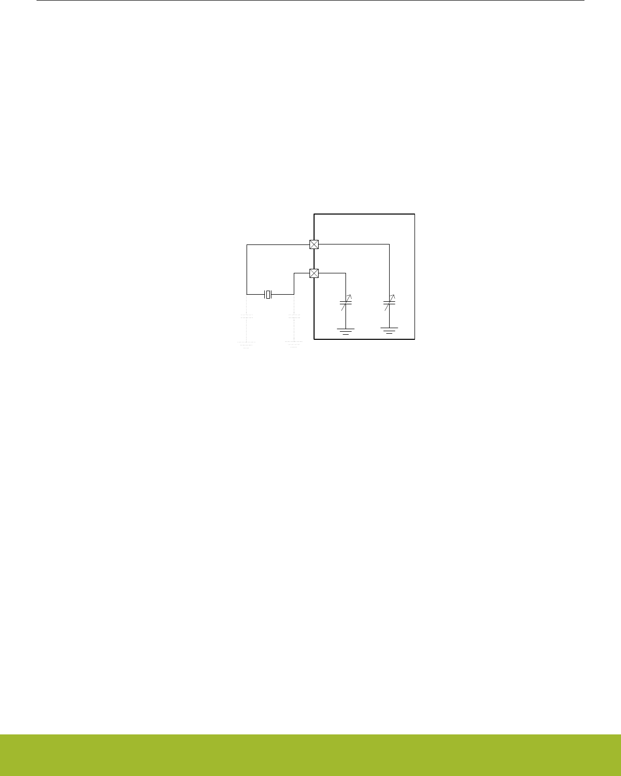
12.3.2.5 LFXO Configuration
The Low Frequency Crystal Oscillator (LFXO) is default configured to ensure safe startup for all crystals. In order to optimize startup
time and power consumption for a given crystal, it is possible to adjust the startup gain in the oscillator by programming the GAIN field
in CMU_LFXOCTRL. Refer to the Device Datasheet and application notes for guidelines in selecting correct components and crystals
as well as for configuration trade-offs.
The LFXO can be retained on in EM4 Hibernate/Shutoff. In that case its required configuration is latched/retained throughout EM4 even
though the CMU_LFXOCTRL register itself will be reset. Upon EM4 exit, the CMU_LFXOCTRL register therefore needs to be reconfig-
ured to its original settings and the LFXO needs to be restarted via CMU_OSCENCMD, before optionally unlatching the retained LFXO
configuration by writing 1 to EM4UNLATCH in the EMU_CMD register. The LFXO startup time is configured via the TIMEOUT bitfield of
the CMU_LFXOCTRL register. If the LFXO has been retained throughout EM4 Hibernate/Shutoff, it can be quickly restarted for use as
LFACLK, LFBCLK or LFECLK by using its minimum TIMEOUT setting. While retained, the LFXO can be used down to EM4 Hibernate
as source for LFECLK and down to EM4 Shutoff as source for RFSENSECLK and CRYOCLK.
The LFXO crystal is connected to the LFXTAL_N/LFXTAL_P pins as shown in Figure 12.8 LFXO Pin Connection on page 306
LFXTAL_N
LFXTAL_P
32.768kHz
CL1
CTUNING CTUNING
Gecko Device
CL2
Figure 12.8. LFXO Pin Connection
By configuring the MODE field in CMU_LFXOCTRL, the LFXO can be bypassed, and an external clock source can be connected to the
LFXTAL_N pin of the LFXO oscillator. If MODE is set to BUFEXTCLK, an external active sine source can be used as clock source. If
MODE is set to DIGEXTCLK, an external active CMOS source can be used as clock source.
The LFXO includes on-chip tunable capacitance, which can replace external load capacitors. The TUNING bitfield of the
CMU_LFXOCTRL register is used to tune the internal load capacitance connected between LFXTAL_P and ground and LFXTAL_N and
ground symmetrically. The capacitance range and step size information is available in the device datasheets. Use the formula below to
calculate the TUNING bitfield:
TUNING = ((desiredTotalLoadCap * 2 - Min(CLFXO_T)) / CLFXO_TS)
Figure 12.9. CMU LFXO Tuning Capacitance Equation
These tunable capacitors can also be used to compensate for temperature drift of the XTAL in software. Crystals normally have a tem-
perature dependency which is given by a parabolic function. The crystal has highest frequency at its turnover temperature, normally
25C. The frequency is reduced following a parabola for higher and lower temperatures. The LFXO offers a mechanism to internally add
capacitance on the LFXTAL_N and LFXTAL_P pins (in parallel to an optional external load capacitance). The variation in frequency as
a function of temperature can therefore be compensated by adjusting the load capacitance. When the temperature compensation
scheme is used, the maximum internal capacitance should be used to obtain good frequency matching at the turnover temperature. For
higher and lower temperatures software then has the maximum range available to adjust the tuning. The external load capacitance
must then of course be reduced accordingly. Note that the ADC0 (27. ADC - Analog to Digital Converter) includes an embedded tem-
perature sensor and that the EMU (11. EMU - Energy Management Unit) offers a temperature management interface, both of which can
be used in combination with this LFXO temperature compensation scheme.
The XTAL oscillation amplitude can be controlled via the HIGHAMPL bitfield in CMU_LFXOCTRL. Setting HIGHAMPL to 1 will result in
higher amplitude, which in turn provides safer operation, somewhat improved duty cycle, and lower sensitivity to noise at the cost of
increased current consumption.
Reference Manual
CMU - Clock Management Unit
silabs.com | Smart. Connected. Energy-friendly. Preliminary Rev. 0.5 | 306

The AGC bit of the CMU_LFXOCTRL register is used to turn on or off the Automatic Gain Control module that adjusts the amplitude of
the XTAL. When disabled, the LFXO will run at the startup current and the XTAL will oscillate rail to rail, again providing safer operation,
improved duty cycle, and lower sensitivity to noise at the cost of increased current consumption.
12.3.2.6 HFRCO and AUXHFRCO Configuration
It is possible to calibrate the HFRCO and AUXHFRCO to achieve higher accuracy (see the device datasheets for details on accuracy).
The frequency is adjusted by changing the TUNING and FINETUNING bitfields in CMU_HFRCOCTRL and CMU_AUXHFRCOCTRL.
Changing to a higher value will result in a lower frequency. Please refer to the datasheet for stepsize details.
The HFRCO can be set to one of several different frequency bands from 1 MHz to 38 MHz by setting the FREQRANGE field in
CMU_HFRCOCTRL. Similarly the AUXHFRCO can be set to one of several different frequency bands from 1 MHz to 38 MHz by setting
the FREQRANGE field in CMU_AUXHFRCOCTRL. The HFRCO and AUXHFRCO frequency bands are calibrated during production
test, and the production tested calibration values can be read from the Device Information (DI) page. The DI page contains separate
tuning values for various frequency bands. During reset, HFRCO and AUXHFRCO tuning values are set to the production calibrated
values for the 19 MHz band, which is the default frequency band. When changing to a different HFRCO or AUXHFRCO band, make
sure to also update the TUNING value and other bitfields in the CMU_HFRCOCTRL and CMU_AUXHFRCOCTRL registers. Typically
the entire register is written with a value obtained from the Device Information (DI) page. Please refer to for information on which fre-
quency band settings are stored in the DI page.
The frequency can be tuned more accurately via the FINETUNING bitfield if fine tuning has been enabled via the FINETUNINGEN bit.
Note that there will be a slight increase in the oscillator current consumption when fine tuning is enabled. The HFRCO and AUXHFRCO
contain a local prescaler, which can be used in combination with any FREQRANGE setting. These prescalers allow the output clocks to
be divided by 1, 2, or 4 as configured in the CLKDIV bitfield.
When using 12.3.2.8 RC Oscillator Calibration to tune HFRCO and AUXHFRCO to the desired frequency, linear search must be used
to avoid over clocking the calibration counters. Before changing the FREQRANGE field in CMU_HFRCOCTRL, TUNING and FINE-
TUNING fields should initially be set to the highest value (slowest frequency). After changing the FREQRANGE, linearly step TUNING
value until desired frequency is reached. Likewise, before changing the TUNING field, FINETUNING field should initially be set to the
highest value (lowest frequency). After changing the TUNING field, linearly step FINETUNING until accuracy is reached.
12.3.2.7 LFRCO Configuration
It is possible to calibrate the LFRCO to achieve higher accuracy (see the device datasheets for details on accuracy). The frequency is
adjusted by changing the TUNING bitfield in CMU_LFRCOCTRL. Changing to a higher value will result in a lower frequency. Please
refer to the datasheet for stepsize details.
The LFRCO can be retained on in EM4 Hibernate/Shutoff. In that case its required configuration is latched/retained throughout EM4
even though the CMU_LFRCOCTRL register itself will be reset. Upon EM4 exit the CMU_LFRCOCTRL register therefore needs to be
reconfigured to its original settings and the LFRCO needs to be restarted via CMU_OSCENCMD, before optionally unlatching the re-
tained LFRCO configuration by writing 1 to EM4UNLATCH in the EMU_CMD register. The LFRCO startup time is configured via the
TIMEOUT bitfield of the CMU_LFRCOCTRL register. Default its 16 cycle startup should be used. However, in case the LFRCO has
been retained throughout EM4 Hibernate/Shutoff, it can be quickly restarted for use as LFACLK or LFBCLK by using its minimum TIME-
OUT setting. While retained, the LFRCO can be used down to EM4 Hibernate as source for LFECLK and down to EM4 Shutoff as
source for RFSENSECLK and CRYOCLK.
The LFRCO is also calibrated in production and its TUNING values are set to the correct value during reset.
The LFRCO can be put in duty cycle mode by setting the ENVREF bit in CMU_LFRCOCTRL to 1 before starting the LFRCO. This will
reduce current consumption, but will result in slightly worse accuracy especially at high temperatures. Setting the ENCHOP and/or EN-
DEM bitfields to 1 in the CMU_LFRCOCTRL register will improve the average LFRCO frequency accuracy at the cost of a worse cycle-
to-cycle accuracy.
Reference Manual
CMU - Clock Management Unit
silabs.com | Smart. Connected. Energy-friendly. Preliminary Rev. 0.5 | 307
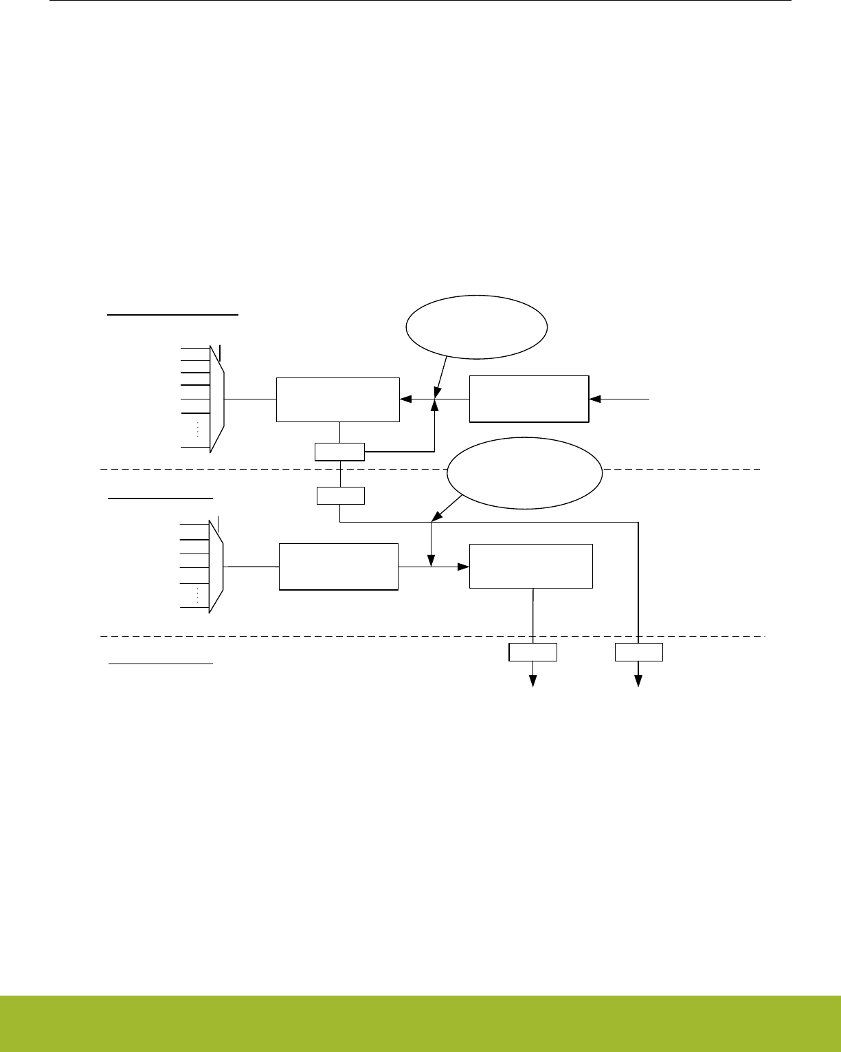
12.3.2.8 RC Oscillator Calibration
The CMU has built-in HW support to efficiently calibrate the RC oscillators (LFRCO, HFRCO, AUXHFRCO, etc) at run-time. For a com-
plete list of supported oscillators, refer to DOWNSEL and UPSEL fields in CMU_CALCTRL. See Figure 12.10 HW-support for RC Oscil-
lator Calibration on page 308 for an illustration of this circuit. The concept is to select a reference and compare the RC frequency with
the reference frequency. When the calibration circuit is started, one down-counter running on a selectable clock (DOWNSEL in
CMU_CALCTRL) and one up-counter running on a selectable clock (UPSEL in CMU_CALCTRL) are started simultaneously. The top
value for the down-counter must be written to CMU_CALCNT before calibration is started. The down-counter counts for CMU_CALCNT
+1 cycles. When the down-counter has reached 0, the up-counter is sampled and the CALRDY interrupt flag is set. If CONT in
CMU_CALCTRL is cleared, the counters are stopped after finishing the ongoing calibration. If continuous mode is selected by setting
CONT in CMU_CALCTRL the down-counter reloads the top value and continues counting and the up-counter restarts from 0. Software
can then read out the sampled up-counter value from CMU_CALCNT. The up-counter has counted (the sampled value)+1 cycles. The
ratio between the reference and the oscillator subject to the calibration can easily be found using top+1 and sample+1. Overflows of the
up-counter will not occur. If the up-counter reaches its top value before the down-counter reaches 0, the up-counter stays at its top
value. Calibration can be stopped by writing CALSTOP in CMU_CMD. With this HW support, it is simple to write efficient calibration
algorithms in software.
CMU_CALCTRL.UPSEL
AUXHFRCO
HFRCO
LFRCO
HFXO
LFXO
20-bit up-counter
CMU_CALCTRL.DOWNSEL
AUXHFRCO
HFRCO
LFRCO
HFXO
LFXO TOP
Write top-value using
CMU_CALCNT before
starting calibration.
DOWNCLK Domain
UPCLK Domain
HFCLK Domain
= 0 ?
SYNC
(Default) HFCLK
SYNC
20-bit up-counter
buffer
SYNC
20-bit down-counter
Set CMU_IF.CALRDY
CMU_CALCNT
DOWNCLK
UPCLK
Reload down-counter with
top value in continuous
mode.
Take snapshot of up-counter
in up-counter bufffer. If in
continuous mode, restart up-
counter from 0.
PRS[PRSUPSEL]
PRS[PRSDOWNSEL]
Figure 12.10. HW-support for RC Oscillator Calibration
The counter operation for single and continuous mode are shown in Figure 12.11 Single Calibration (CONT=0) on page 309 and Figure
12.12 Continuous Calibration (CONT=1) on page 309 respectively.
Reference Manual
CMU - Clock Management Unit
silabs.com | Smart. Connected. Energy-friendly. Preliminary Rev. 0.5 | 308
TOP
0
Calibration Started Calibration Stopped
(counters stopped)
0
Down-counter
Up-counter
Up-counter sampled and CALRDY
interrupt flag set.
Sampled value available in
CMU_CALCNT.
Figure 12.11. Single Calibration (CONT=0)
TOP
0
Calibration Started
0
Down-counter
Up-counter
Up-counter sampled and CALRDY
interrupt flag set.
Sampled value available in
CMU_CALCNT.
Up-counter sampled and CALRDY
interrupt flag set.
Sampled value available in
CMU_CALCNT.
Figure 12.12. Continuous Calibration (CONT=1)
Reference Manual
CMU - Clock Management Unit
silabs.com | Smart. Connected. Energy-friendly. Preliminary Rev. 0.5 | 309

12.3.2.9 Automatic HFXO Start
The enabling of the HFXO and its selection as HFSRCCLK source can be performed automatically by hardware. Automatic HFXO ena-
ble and select can for example be used upon wake-up of the Radio Controller (RAC). Automatic control of the HFXO is controlled via
the AUTOSTARTRDYSELRAC, AUTOSTARTSELEM0EM1 and AUTOSTARTEM0EM1 bits in the CMU_HFXOCTRL register. It further
depends on the energy mode of the EFR32 and on the status of the RAC .
The HFXO autostart functionality is typically used when the RAC is used. The RAC module always requires the HFXO for its operation.
The hardware requirement from RAC for an HFXO based HFSRCCLK is indicated in the HFXOREQ bitfield of the CMU_STATUS regis-
ter. This requirement in itself does not lead to an automatic enable or select of the HFXO.
An automatic HFXO enable is performed only if any of the following conditions are met:
• EFR32 is in EM0/EM1 and AUTOSTARTEM0EM1 or AUTOSTARTSELEM0EM1 are set to 1.
• RAC is awake and AUTOSTARTRDYSELRAC is set to 1.
An automatic HFXO select is performed only if any of the following conditions is met:
• EFR32 is in EM0/EM1 and AUTOSTARTSELEM0EM1 is set to 1.
• RAC is awake, HFXO is ready, and AUTOSTARTRDYSELRAC is set to 1.
Whenever any of the conditions for automatic HFXO enable is met, software is not allowed to disable the HFXO. An attempt to do so
(e.g. by writing 1 to the HFXODIS bit) is ignored and causes the HFXODISERR bit in the CMU_IF register to be set to 1. Similarly,
whenever any of the conditions for automatic HFXO selection is met, software is not allowed to deselect the HFXO as clock source for
HFSRCCLK. An attempt to do so (e.g. by selecting another clock source via CMU_HFCLKSEL) is ignored and causes the HFXODI-
SERR bit in the CMU_IF register to be set to 1. Note that CMUERR is not implied by HFXODISERR. CMUERR will not get set to 1 for
the above scenarios in which HFXODISERR gets set.
Software can only disable or deselect the HFXO after removing all of the HFXO automatic enable or select reasons. Note that if the
autostart functionality is not used, software can always disable or deselect the HFXO even if hardware requires the HFXO as indicated
via HFXOREQ bitfield in CMU_STATUS. The HFXODISERR flag will not get set in that case. The HFXO is only disabled by hardware
upon EM2, EM3 or EM4 entry.
In case that AUTOSTARTSELEM0EM1 is set to 1 in EM0/EM1 (irrespective of the other autostart bits), the HFXO select will occur im-
mediately, even if HFXO is not ready yet. Upon wake-up into EM0/EM1 this can therefore lead to a relatively long startup time as the
system will not start operating from the HFRCO as it would otherwise do. In case of an automatic select triggered by the RAC (while
AUTOSTARTSELEM0EM1 is set to 0), such a select will only occur upon the HFXO becoming ready and software can select and use
another clock source in the mean time.
A typical use scenario of the AUTOSTARTRDYSELRAC bit is as follows. Set the AUTOSTARTRDYSELRAC bit in the
CMU_HFXOCTRL register to 1 and set up the RTCC to periodically generate a compare match. Setup a PRS channel which uses this
RTCC compare match as its source and allow the PRS channel to cause a wake-up into EM1. Setup the RAC to use the PRS channel
as its source for TXEN or RXEN. Now, when the EFR32 is in EM2 and the RTCC generates a compare match, a wake-up into EM1 will
occur and the HFXO will automatically start and become selected after which the RAC can perform its work and trigger a transition back
into EM2 when done. The system started, used, and stopped the HFXO without ever being in EM0.
Note that the user should take care that the settings in the MSC_READCTRL and CMU_CTRL registers, as described in 12.3.3 Config-
uration For Operating Frequencies, are compatible with 40 MHz HFXO operation before enabling the HFXO automatic startup feature.
A basic automatic HFXO start scenario is shown in Figure 12.13 CMU Automatic startup and selection of HFXO on page 311.
Reference Manual
CMU - Clock Management Unit
silabs.com | Smart. Connected. Energy-friendly. Preliminary Rev. 0.5 | 310
HFXO
CMU_STATUS.HFXORDY
CMU_STATUS.HFXOENS
CMU_HFCLKSTATUS.HF = HFXO
HFRCO
HFCLK
CMU_STATUS.HFRCORDY
CMU_STATUS.HFRCOENS
CMU_HFCLKSTATUS.HF = HFRCO
clocks
status
HFXO ready Automatic switch to HFXO (and disable of HFRCO)
RAC wake-up with CMU_HFXOCTRL.AUTOSTARTRDYSELRAC = 1
||
EM0/EM1 entry with CMU_HFXOCTRL.AUTOSTARTSELEM0EM1 = 1
Figure 12.13. CMU Automatic startup and selection of HFXO
If an automatic selection of HFXO is performed, which switches the clock source used for HFSRCCLK, then the HFXOAUTOSW bit in
CMU_IF is set to 1. After automatic enable and selection of the HFXO, the HFRCO is automatically disabled in case it is running. The
disabling of a running HFRCO is signalled via the HFRCODIS bit in CMU_IF. This only applies to the HFRCO. If for example the LFXO
was used as HFSRCCLK at the time of automatic selection of the HFXO, the LFXO remains unaffected.
The interaction between automatic HFXO startup and selection with startup and selection of HFRCO is shown in Figure 12.14 CMU
HFRCO startup/selection while awaiting automatic HFXO startup/selection on page 312 and Figure 12.15 CMU Automatic HFXO start-
up/selection while HFRCO started/selected on page 312.
Reference Manual
CMU - Clock Management Unit
silabs.com | Smart. Connected. Energy-friendly. Preliminary Rev. 0.5 | 311
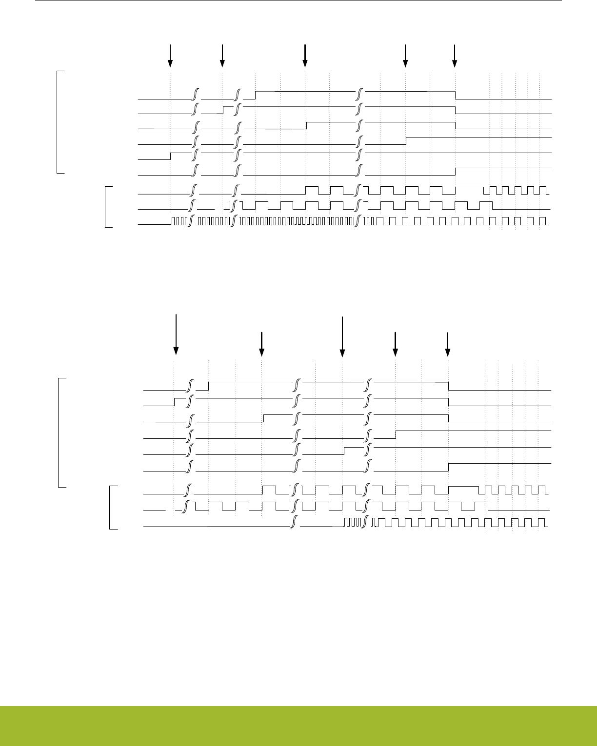
HFXO
CMU_STATUS.HFXORDY
CMU_STATUS.HFXOENS
CMU_HFCLKSTATUS.HF = HFXO
HFRCO
HFCLK
CMU_STATUS.HFRCORDY
CMU_STATUS.HFRCOENS
CMU_HFCLKSTATUS.HF = HFRCO
clocks
status
HFXO ready
RAC wake-up with CMU_HFXOCTRL.AUTOSTARTRDYSELRAC = 1
||
EM0/EM1 entry with CMU_HFXOCTRL.AUTOSTARTSELEM0EM1 = 0 Automatic switch to HFXO and disable of HFRCOHFRCO selected
EM0/EM1 Entry
&&
CMU_HFXOCTRL.AUTOSTARTSELEM0EM1 = 0
Figure 12.14. CMU HFRCO startup/selection while awaiting automatic HFXO startup/selection
HFXO
CMU_STATUS.HFXORDY
CMU_STATUS.HFXOENS
CMU_HFCLKSTATUS.HF = HFXO
HFRCO
HFCLK
CMU_STATUS.HFRCORDY
CMU_STATUS.HFRCOENS
CMU_HFCLKSTATUS.HF = HFRCO
clocks
status
HFXO ready
EM0/EM1 Entry
&&
CMU_HFXOCTRL.AUTOSTARTSELEM0EM1 = 0
Automatic switch to HFXO and disable of HFRCO
HFRCO selected
RAC wake-up with CMU_HFXOCTRL.AUTOSTARTRDYSELRAC = 1
Figure 12.15. CMU Automatic HFXO startup/selection while HFRCO started/selected
Reference Manual
CMU - Clock Management Unit
silabs.com | Smart. Connected. Energy-friendly. Preliminary Rev. 0.5 | 312

12.3.3 Configuration For Operating Frequencies
The HFXO is capable of frequencies up to 40 MHz, which allows the EFR32 to run at up to this frequency. However the Memory Sys-
tem Controller (MSC) and the Low Energy Peripheral Interface need to be configured correctly to allow operation at higher frequencies
as explained below.
The MODE bitfield in MSC_READCTRL makes sure the flash is able to operate at the given HFCLK frequency by inserting wait states
for flash accesses. The required settings for controlling flash wait states are shown in Table 12.2 MSC Configuration For Operating
Frequencies, at 1.2V: Flash Wait States on page 313. The WSHFLE bitfield in CMU_CTRL is used to ensure that the Low Energy
Peripheral Interface is able to operate at the given HFBUSCLKLE frequency by inserting wait states when using this interface. The re-
quired settings are shown in Table 12.4 LE Configuration For Operating Frequencies: Low Energy Peripheral Interface on page 313.
Before going to a high frequency, make sure the registers in the table have the correct values. When going down in frequency, make
sure to keep the registers at the values required by the higher frequency until after the switch has been done.
Table 12.2. MSC Configuration For Operating Frequencies, at 1.2V: Flash Wait States
Condition MODE in MSC_READCTRL
HFCLK <= 25 MHz WS0 or above
25 MHz < HFCLK <= 40 MHz WS1 or above
Table 12.3. MSC Configuration For Operating Frequencies, at 1.0V: Flash Wait States
Condition MODE in MSC_READCTRL
HFCLK <= 7 MHz WS0 or above
7 MHz < HFCLK <= 14 MHz WS1 or above
14 MHz < HFCLK <= 20 MHz WS2
Table 12.4. LE Configuration For Operating Frequencies: Low Energy Peripheral Interface
Condition WSHFLE in CMU_CTRL
HFBUSCLKLE <= 32 MHz 0 / 1
HFBUSCLKLE > 32 MHz 1
Reference Manual
CMU - Clock Management Unit
silabs.com | Smart. Connected. Energy-friendly. Preliminary Rev. 0.5 | 313

12.3.4 Energy Modes
The availability of oscillators and system clocks depends on the chosen energy mode. Default the high frequency oscillators (HFRCO,
AUXHFRCO, and HFXO) and high frequency clocks (HFSRCLK, HFCLK, HFCORECLK, HFBUSCLK, HFPERCLK, HFRADIOCLK,
HFCLKLE) are available downto EM1 Sleep. From EM2 Deep Sleep onwards these oscillators and clocks are normally off, although
special cases exist as summarized in Table 12.5 Oscillator and clock availability in Energy Modes on page 314 and Table 11.2 EMU
Energy Mode Overview on page 225. The CMU overview figure in Figure 12.1 CMU Overview - High Frequency Portion on page 291
and Figure 12.2 CMU Overview - Low Frequency Portion on page 292 also indicate which oscillators and clocks can be used in what
energy modes.
The low frequency oscillators (LFRCO and LFXO) are available in all energy modes except in EM3 Stop when they are off by definition.
Default these oscillators are also off in EM4 Hibernate and EM4 Shutoff, but they can be retained on in these states as well if needed.
The ultra low frequency oscillator (ULFRCO) is default on in all energy modes, except for EM4 Shutoff, but it can be retained on in that
mode as well if needed. The low frequency clocks (LFACLK, LFBCLK, LFECLK, WDOGnCLK, RFSENSECLK, and CRYOCLK) are in
various power domains and therefore their availability not only depends on the chosen clock source, but also on the chosen energy
mode as indicated in Table 12.5 Oscillator and clock availability in Energy Modes on page 314.
Table 12.5. Oscillator and clock availability in Energy Modes
EM0 Active/EM1
Sleep
EM2 Deep Sleep EM3 Stop EM4 Hibernate EM4 Shutoff
HFRCO On1Off Off Off Off
HFXO On1Off Off Off Off
AUXHFRCO On1On2On2Off Off
LFRCO, LFXO On1On1Off Retained on3Retained on3
ULFRCO On On On On Retained on3
HFSRCLK, HFCLK,
HFCORECLK,
HFBUSCLK,
HFPERCLK, HFRA-
DIOCLK, HFCLKLE
On1Off Off Off Off
AUXCLK On1On2On2Off Off
ADCnCLK On1On4On4Off Off
LFACLK, LFBCLK On1On1On5Off Off
LFECLK On1On1On5Retained on3Off
WDOGnCLK On1On1On5Off Off
CRYOCLK On1On1On5Retained on3Retained on3
1 Under software control.
2Default off, but kept active if used by the ADC.
3 Default off, but can be retained on.
4 Will be kept on if AUXHFRCO is selected as clock source.
5 On only if ULFRCO is used as clock source.
Reference Manual
CMU - Clock Management Unit
silabs.com | Smart. Connected. Energy-friendly. Preliminary Rev. 0.5 | 314

12.3.5 Clock Output on a Pin
It is possible to configure the CMU to output clocks on the CMU_CLK0, CMU_CLK1 and CMU_CLK2 pins. This clock selection is done
using the CLKOUTSEL0, CLKOUTSEL1 and CLKOUTSEL2 bitfields respectively in CMU_CTRL. The required output pins must be en-
abled in the CMU_ROUTEPEN register and the pin locations can be configured in the CMU_ROUTELOC0 register. The following
clocks can be output on a pin:
• HFSRCCLK and HFEXPCLK. The HFSRCCLK is the high frequency clock before any prescaling has been applied. The HFEXPCLK
is a prescaled version of HFCLK as controlled by the HFEXPPRESC bitfield in the CMU_HFPRESC register.
• The unqualified clock output from any of the oscillators (ULFRCO, LFRCO, LFXO, HFXO). Note that these unqualified clocks can
exhibit glitches or skewed duty-cycle during startup and therefore these clock outputs are normally not used before observing the
related ready flag being set to 1 in CMU_STATUS.
• The qualified clock from any of the oscillators (ULFRCO, LFRCO, LFXO, HFXO, HFRCO, AUXHFRCO). A qualified clock will not
have any glitches or skewed duty-cycle during startup. For LFRCO, LFXO and HFXO correct configuration of the TIMEOUT bit-
field(s) in CMU_LFRCOCTRL, CMU_LFXOCTRL and CMU_HFXOTIMEOUTCTRL respectively is required to guarantee a properly
qualified clock.
• The qualified HFXO clock divided by 2 (HFXODIV2Q).
HFCLK will not have a 50-50 duty cycle when any other division factor than 1 is used in CMU_HFPRESC (i.e. if PRESC is not equal to
0). In such a case, the exported HFEXPCLK will therefore also not be 50-50 when its division factor is not set to an even number in
CMU_HFEXPPRESC.
12.3.6 Clock Input from a Pin
It is possible to configure the CMU to input a clock from the CMU_CLKI0. This clock can be selected to drive HFSRCCLK and DPLL
reference using CMU_HFCLKSEL and CMU_DPLLCTRL respectively. The required input pin must be enabled in the CMU_ROUTEP-
EN register and the pin location can be configured in the CMU_ROUTELOC1 register.
12.3.7 Clock Output on PRS
The CMU can be used as a PRS producer. It can output clocks onto PRS which can be selected by a consumer as CMUCLKOUT0,
CMUCLKOUT1 and CMUCLKOUT2. The clocks which can be produced via CMUCLKOUT0, CMUCLKOUT1 and CMUCLKOUT2 are
selected via the CLKOUTSEL0, CLKOUTSEL1 and CLKOUTSEL2 fields respectively in CMU_CTRL.
Note that the CLKOUTSEL0 and CLKOUTSEL1 fields are also used for selecting which clock is output onto a pin as described in
12.3.5 Clock Output on a Pin. In contrast with clock output on a pin however, output of a clock onto PRS does not depend on any
configuration of the CMU_ROUTEPEN and CMU_ROUTELOC0 registers.
12.3.8 Error Handling
Certain restrictions apply to how and when the CMU registers can be configured as is described for the respective registers. Not adher-
ing to these restrictions can lead to unpredictable and non-defined behaviour. Some of these software restrictions are checked in hard-
ware and not adhering to them will cause the CMUERR interrupt flag in CMU_IF to be set to 1. The restrictions impacting CMUERR are
as follows:
• CMU_HFRCOCTRL should not be written while HFRCOBSY in the CMU_SYNCBUSY register is set to 1.
• CMU_AUXHFRCOCTRL should not be written while AUXHFRCOBSY in the CMU_SYNCBUSY register is set to 1.
• CMU_HFXOSTARTUPCTRL, CMU_HFXOSTEADYSTATECTRL and CMU_HFXOTIMEOUTCTRL should not be written while
HFXOBSY in the CMU_SYNCBUSY register is set to 1. Note that writes to CMU_HFXOCTRL do not impact CMUERR. Although
most of its bitfields need to be configured before enabling the HFXO, it it allowed to change the AUTOSTART bits (i.e. AUTOS-
TARTRDYSELRAC, AUTOSTARTSELEM0EM1 and AUTOSTARTEM0EM1) at any time.
• HFXO should not be enabled before it has been properly disabled (so only enable HFXO when HFXOENS=0 or HFXOBSY=0). Like-
wise, HFXO should not be disabled before it has been properly enabled (so only disable HFXO when HFXOENS=1 or HFXOB-
SY=0).
• CMU_LFRCOCTRL should not be written while LFRCOBSY in the CMU_SYNCBUSY register is set to 1. The GMCCURTUNE bit-
field should not be written with a differing value while the LFRCOVREFBSY flag is set to 1.
• CMU_LFXOCTRL should not be written while LFXOBSY in the CMU_SYNCBUSY register is set to 1.
12.3.9 Interrupts
The interrupts generated by the CMU module are combined into one interrupt vector. If CMU interrupts are enabled, an interrupt will be
made if one or more of the interrupt flags in CMU_IF and their corresponding bits in CMU_IEN are set.
Reference Manual
CMU - Clock Management Unit
silabs.com | Smart. Connected. Energy-friendly. Preliminary Rev. 0.5 | 315

12.3.10 Wake-up
The CMU can be (partially) active all the way down to EM4 Shutoff. It can wake up the CPU from EM2 upon LFRCO or LFXO becoming
ready as LFRCORDY and LFXORDY can be used as wake-up interrupt.
12.3.11 Protection
It is possible to lock the control- and command registers to prevent unintended software writes to critical clock settings. This is control-
led by the CMU_LOCK register.
12.3.12 Digital Phase-Locked Loop
The Digital Phase-Locked Loop (DPLL) generates a clock as a ratio of a reference clock source. It provides the following features:
• Frequency-lock mode. Only the output frequency is controlled, phase error is allowed to accumulate between the output and refer-
ence clock.
• Phase-lock mode. Both the output frequency and phase are controlled.
• Output frequency = FREF*(N+1)/(M+1), where N and M are 12-bit values
• Very fast lock time.
• Very fast transient tracking.
• Low output jitter.
• Lock detection with an interrupt.
• Lock fail detection with interrupts.
• Output spectrum-spreading. The DPLL can randomize the generated output period by a configurable amount of spread.
12.3.12.1 Enabling and Disabling
The DPLL can be enabled and disabled by software via the CMU_OSCENCMD register. The DPLL is disabled automatically when en-
tering EM2, EM3, or EM4. Before enabling DPLL, all switches selecting HFRCO should be switched to HFRCODIV2 temporarily until
DPLL is locked to avoid over-clocking due to overshoot. And the FINETUNINGEN bit in the CMU_HFRCOCTRL must be set to make
DPLL work.
12.3.12.2 Lock Modes
DPLL provides two lock modes, referred to as frequency-lock loop mode (FREQLL) and phase-lock loop mode (PHASELL). FREQLL
mode keeps the DCO frequency-locked to the reference clock, which means the DCO frequency will be accurate. But the phase error
can accumulate over time and cause the average frequency error non-zero. FREQLL mode also provide better jitter and transient per-
formance. PHASELL mode keeps the DCO phase-locked to the reference clock, which means the phase error does not accumulate
over time and make the average frequency error zero. FREQLL mode should be used unless specific phase requirement exists.
12.3.12.3 Configurations
Output frequency = FREF*(n+1)/(m+1). User should calculate n and m to achieve the target frequency. Note that with n increases, the
DCO lock time would increase and DCO jitter would decrease. Both directions are approximately linear. This relationship can be used
to select n for a given application to strike a compromise between lock time and output jitter. For example, assume N = n + 1 and M = m
+ 1, if an N/M ratio of 3 is desired, the DPLL could be configured as {N=300, M=100} for high jitter but fast lock time, or as {N=3000,
M=1000} for lower jitter and longer lock time. For a good balance, n is suggested to be larger than 300 unless specific lock time is
required.
Note:
All configuration setting should be done before enabling the DPLL. They should not be changed when DPLL is running. The final tun-
ning values can be read back from TUNING and FINETUNING in CMU_HFRCOCTRL, after DPLL is disabled and DPLLENS in
CMU_STATUS is low.
Reference Manual
CMU - Clock Management Unit
silabs.com | Smart. Connected. Energy-friendly. Preliminary Rev. 0.5 | 316

12.3.12.4 Lock Detection
The DPLL has 3 different types of output event: ready, lock fail due to period underflow and lock fail due to period overflow. Each of the
event has its own interrupt flag. DPLLRDY is set when DPLL successfully locks to the reference clock based on user’s configuration.
DPLLLOCKFAILLOW is set when DPLL fails to lock because the period lower boundary is hit. DPLLLOCKFAILHIGH is set when DPLL
fail to lock because the period upper boundary is hit. If the interrupt flags are set and the corresponding interrupt enable bits in
CMU_IEN are set, the CMU will send out an interrupt request. Based on different interrupt sequence, user should take different actions:
• If DPLLRDY interrupt is received first, it means target clock is ready and it is safe to switch to use DCO’s output.
• If DPLLLOCKFAILLOW interrupt is received first, it indicates the RANGE in CMU_HFRCOCTRL is too small. User should disable
DPLL and write a larger value to RANGE, then enable DPLL again to lock.
• If DPLLLOCKFAILHIGH interrupt is received first, it indicates the RANGE in CMU_HFRCOCTRL is too large. User should disable
DPLL and write a smaller value to RANGE, then enable DPLL again to lock.
• If DPLLRDY interrupt is received first and then DPLLLOCKFAILLOW or DPLLLOCKFAILHIGH is received later, it means reference
clock drifted over 2% and made DPLL lost its locked status.
• If AUTORECOVER in CMU_DPLLCTRL is not set, user should disable DPLL and enable DPLL again to lock.
• If AUTORECOVER in CMU_DPLLCTRL is set, hardware would re-lock automatically. When the target frequency is near the
boundary of a range, the drift may cause underflow or overflow. In this case the fail interrupt would still be received. User should
disable DPLL and modify RANGE in CMU_HFRCOCTRL in corresponding direction like the second and third cases. Then enable
DPLL again to lock.
12.3.12.5 Spectrum Spreading
Spreading of the DCO output spectrum is accomplished by driving a dedicated 5-bit DCO trim control with a digitally-generated, pseu-
do-random value. A centered, uniform, random spreading algorithm was selected.The spectrum-spreading pattern is generated by a
single 10-bit linear feedback shift register (LFSR). To avoid high correlation between nearby values, a 5-step leap-forward LFSR update
method is employed in the DPLL. The DCO output period can be randomized with a peak-to-peak amplitude given approximately by:
2^((SSAMP-1))*0.2%, where SSAMP is a register field in CMU_HFRCOSS. The generated random values are applied at regular inter-
vals given by: 4*T_DCO*(SSINV+1), where T_DCO is DCO period and SSINV is a register field in CMU_HFRCOSS.
12.3.13 Precision Low Frequency Oscillator
The PLFRCO, Precision Low Frequency RC Oscillator, is a 500ppm RC oscillator that eliminates the need for a 32.768kHz crystal by
automatically recalibrating itself against the HFXO. The PLFRCO can support energy modes EM0/1/2/3. Do not use the PLFRCO for
any peripheral that can run in EM4H or EM4S since the PLFRCO will be powered down in EM4H and EM4S.
Several times a second the PLFRCO will check for a relative change in temperature. If the temperature change is large enough, the
PLFRCO will start up the HFXO and recalibrate to maintain 500ppm. The temperature checking is also performed in EM2/3 modes, and
the PLFRCO can wake up from EM2/3, go to EM1, start the HFXO, recalibrate, and go back to EM2/3 automatically without any soft-
ware interaction.
To enable the PLFRCO set PLFRCOEN in CMU_OSCENCMD. After being enabled the PLFRCO will perform a one time base calibra-
tion to determine the minimum and maximum frequencies of the oscillator, perform a calibration to adjust its finetrim tuning, and take a
relative temperature measurement. The temperature measurement is not correlated to a specific temperature in degrees centigrade.
The temperature measurement is a part specific measurement allowing the PLFRCO to determine when the temperature has changed
by a small amount. Once a large enough temperature change has occured, the PLFRCO will recalibrate against the HFXO. The default
settings assume an HFXO frequency of 38.4MHz.
Starting the HFXO uses more power, so the PLFRCO's use of a temperature change detection significantly reduces the power usage
by only recalibrating when the temperature has actually changed.
Once the initial base calibration has completed, the PLFRCORDY in CMU_STATUS will go high to indicate that the 32768 Hz clock is
ready to use. Disabling the PLFRCO is done by setting PLFRCODIS in CMU_OSCENCMD. PLFRCOENS in CMU_STATUS shows the
status of the PLFRCOEN and PLFRCODIS commands. When the PLFRCO is disabled, there will be a few more additional low frequen-
cy cycles before the PLFRCO shuts down and disables the PLFRCO clock. The PLFRCORDY can be used to determine when the
PLFRCO clock is ready to use and when the PLFRCO has completed shutting down. Do not set the PLFRCOEN until after PLFRCOR-
DY has gone low.
PLFRCOHFXODNSERR in CMU_IF indicates some error conditions such as the HFXO has not been configured properly or stopped
running, or an HFXO crystal other than 38.4MHz was used.
Reference Manual
CMU - Clock Management Unit
silabs.com | Smart. Connected. Energy-friendly. Preliminary Rev. 0.5 | 317

12.4 Register Map
The offset register address is relative to the registers base address.
Offset Name Type Description
0x000 CMU_CTRL RW CMU Control Register
0x010 CMU_HFRCOCTRL RWH HFRCO Control Register
0x018 CMU_AUXHFRCOCTRL RW AUXHFRCO Control Register
0x020 CMU_LFRCOCTRL RW LFRCO Control Register
0x024 CMU_HFXOCTRL RW HFXO Control Register
0x02C CMU_HFXOSTARTUPCTRL RW HFXO Startup Control
0x030 CMU_HFXOSTEADYSTATECTRL RW HFXO Steady State control
0x034 CMU_HFXOTIMEOUTCTRL RW HFXO Timeout Control
0x038 CMU_LFXOCTRL RW LFXO Control Register
0x040 CMU_DPLLCTRL RW DPLL Control Register
0x044 CMU_DPLLCTRL1 RW DPLL Control Register
0x050 CMU_CALCTRL RW Calibration Control Register
0x054 CMU_CALCNT RWH Calibration Counter Register
0x060 CMU_OSCENCMD W1 Oscillator Enable/Disable Command Register
0x064 CMU_CMD W1 Command Register
0x070 CMU_DBGCLKSEL RW Debug Trace Clock Select
0x074 CMU_HFCLKSEL W1 High Frequency Clock Select Command Register
0x080 CMU_LFACLKSEL RW Low Frequency A Clock Select Register
0x084 CMU_LFBCLKSEL RW Low Frequency B Clock Select Register
0x088 CMU_LFECLKSEL RW Low Frequency E Clock Select Register
0x090 CMU_STATUS RStatus Register
0x094 CMU_HFCLKSTATUS RHFCLK Status Register
0x09C CMU_HFXOTRIMSTATUS RHFXO Trim Status
0x0A0 CMU_IF RInterrupt Flag Register
0x0A4 CMU_IFS W1 Interrupt Flag Set Register
0x0A8 CMU_IFC (R)W1 Interrupt Flag Clear Register
0x0AC CMU_IEN RW Interrupt Enable Register
0x0B0 CMU_HFBUSCLKEN0 RW High Frequency Bus Clock Enable Register 0
0x0C0 CMU_HFPERCLKEN0 RW High Frequency Peripheral Clock Enable Register 0
0x0CC CMU_HFRADIOALTCLKEN0 RW High Frequency Alternate Radio Peripheral Clock Enable Register 0
0x0E0 CMU_LFACLKEN0 RW Low Frequency A Clock Enable Register 0 (Async Reg)
0x0E8 CMU_LFBCLKEN0 RW Low Frequency B Clock Enable Register 0 (Async Reg)
0x0F0 CMU_LFECLKEN0 RW Low Frequency E Clock Enable Register 0 (Async Reg)
0x100 CMU_HFPRESC RW High Frequency Clock Prescaler Register
0x108 CMU_HFCOREPRESC RW High Frequency Core Clock Prescaler Register
Reference Manual
CMU - Clock Management Unit
silabs.com | Smart. Connected. Energy-friendly. Preliminary Rev. 0.5 | 318

Offset Name Type Description
0x10C CMU_HFPERPRESC RW High Frequency Peripheral Clock Prescaler Register
0x110 CMU_HFRADIOPRESC RW High Frequency Radio Peripheral Clock Prescaler Register
0x114 CMU_HFEXPPRESC RW High Frequency Export Clock Prescaler Register
0x120 CMU_LFAPRESC0 RW Low Frequency A Prescaler Register 0 (Async Reg)
0x128 CMU_LFBPRESC0 RW Low Frequency B Prescaler Register 0 (Async Reg)
0x130 CMU_LFEPRESC0 RW Low Frequency E Prescaler Register 0 (Async Reg). When waking up
from EM4 make sure EM4UNLATCH in EMU_CMD is set for this to
take effect
0x138 CMU_HFRADIOALTPRESC RW High Frequency Alternate Radio Peripheral Clock Prescaler Register
0x140 CMU_SYNCBUSY RSynchronization Busy Register
0x144 CMU_FREEZE RW Freeze Register
0x150 CMU_PCNTCTRL RWH PCNT Control Register
0x15C CMU_ADCCTRL RWH ADC Control Register
0x170 CMU_ROUTEPEN RW I/O Routing Pin Enable Register
0x174 CMU_ROUTELOC0 RW I/O Routing Location Register
0x178 CMU_ROUTELOC1 RW I/O Routing Location Register
0x180 CMU_LOCK RWH Configuration Lock Register
0x184 CMU_HFRCOSS RW HFRCO Spread Spectrum Register
Reference Manual
CMU - Clock Management Unit
silabs.com | Smart. Connected. Energy-friendly. Preliminary Rev. 0.5 | 319

12.5 Register Description
12.5.1 CMU_CTRL - CMU Control Register
Offset Bit Position
0x000
31
30
29
28
27
26
25
24
23
22
21
20
19
18
17
16
15
14
13
12
11
10
9
8
7
6
5
4
3
2
1
0
Reset
1
1
0
0x00
0x00
Access
RW
RW
RW
RW
RW
Name
HFRADIOCLKEN
HFPERCLKEN
WSHFLE
CLKOUTSEL1
CLKOUTSEL0
Bit Name Reset Access Description
31:22 Reserved To ensure compatibility with future devices, always write bits to 0. More information in 1.2 Conven-
tions
21 HFRADIOCLKEN 1 RW HFRADIOCLK Enable
Set to enable the HFRADIOCLK.
20 HFPERCLKEN 1 RW HFPERCLK Enable
Set to enable the HFPERCLK.
19:17 Reserved To ensure compatibility with future devices, always write bits to 0. More information in 1.2 Conven-
tions
16 WSHFLE 0 RW Wait State for High-Frequency LE Interface
Set to allow access to LE peripherals when running HFBUSCLKLE at frequencies higher than 32 MHz
15:10 Reserved To ensure compatibility with future devices, always write bits to 0. More information in 1.2 Conven-
tions
9:5 CLKOUTSEL1 0x00 RW Clock Output Select 1
Controls the clock output 1 multiplexer. To actually output on the pin, set CLKOUT1PEN in CMU_ROUTE.
Value Mode Description
0 DISABLED Disabled
1 ULFRCO ULFRCO (directly from oscillator)
2 LFRCO LFRCO (directly from oscillator)
3 LFXO LFXO (directly from oscillator)
6 HFXO HFXO (directly from oscillator)
7 HFEXPCLK HFEXPCLK
9 ULFRCOQ ULFRCO (qualified)
10 LFRCOQ LFRCO (qualified)
11 LFXOQ LFXO (qualified)
12 HFRCOQ HFRCO (qualified)
13 AUXHFRCOQ AUXHFRCO (qualified)
Reference Manual
CMU - Clock Management Unit
silabs.com | Smart. Connected. Energy-friendly. Preliminary Rev. 0.5 | 320

Bit Name Reset Access Description
14 HFXOQ HFXO (qualified)
15 HFSRCCLK HFSRCCLK
16 PLFRCO PLFRCO (directly from oscillator)
17 PLFRCOQ PLFRCO (qualified)
4:0 CLKOUTSEL0 0x00 RW Clock Output Select 0
Controls the clock output multiplexer. To actually output on the pin, set CLKOUT0PEN in CMU_ROUTE.
Value Mode Description
0 DISABLED Disabled
1 ULFRCO ULFRCO (directly from oscillator)
2 LFRCO LFRCO (directly from oscillator)
3 LFXO LFXO (directly from oscillator)
6 HFXO HFXO (directly from oscillator)
7 HFEXPCLK HFEXPCLK
9 ULFRCOQ ULFRCO (qualified)
10 LFRCOQ LFRCO (qualified)
11 LFXOQ LFXO (qualified)
12 HFRCOQ HFRCO (qualified)
13 AUXHFRCOQ AUXHFRCO (qualified)
14 HFXOQ HFXO (qualified)
15 HFSRCCLK HFSRCCLK
16 PLFRCO PLFRCO (directly from oscillator)
17 PLFRCOQ PLFRCO (qualified)
Reference Manual
CMU - Clock Management Unit
silabs.com | Smart. Connected. Energy-friendly. Preliminary Rev. 0.5 | 321

12.5.2 CMU_HFRCOCTRL - HFRCO Control Register
Write this register to set the frequency band in which the HFRCO is to operate. Always update all fields in this register at once by writ-
ing the value for the desired band, which has been obtained from the Device Information page entry for that band. The TUNING, FINE-
TUNING, FINETUNINGEN and CLKDIV bitfields can be used to tune a specific band (FREQRANGE) of the oscillator to a non-precon-
figured frequency. When changing this setting there will be no glitches on the HFRCO output, hence it is safe to change this setting
even while the system is running on the HFRCO. Only write CMU_HFRCOCTRL when it is ready for an update as indicated by
HFRCOBSY=0 in CMU_SYNCBUSY.
Offset Bit Position
0x010
31
30
29
28
27
26
25
24
23
22
21
20
19
18
17
16
15
14
13
12
11
10
9
8
7
6
5
4
3
2
1
0
Reset
0xB
0
0x0
1
0x2
0x08
0x1F
0x7F
Access
RWH
RWH
RWH
RWH
RWH
RWH
RWH
RWH
Reference Manual
CMU - Clock Management Unit
silabs.com | Smart. Connected. Energy-friendly. Preliminary Rev. 0.5 | 322

Offset Bit Position
Name
VREFTC
FINETUNINGEN
CLKDIV
LDOHP
CMPBIAS
FREQRANGE
FINETUNING
TUNING
Bit Name Reset Access Description
31:28 VREFTC 0xB RWH HFRCO Temperature Coefficient Trim on Comparator Reference
Writing this field adjusts the temperature coefficient trim on comparator reference.
27 FINETUNINGEN 0 RWH Enable reference for fine tuning
Settings this bit enables HFRCO fine tuning.
26:25 CLKDIV 0x0 RWH Locally divide HFRCO Clock Output
Writing this field configures the HFRCO clock output divider.
Value Mode Description
0 DIV1 Divide by 1.
1 DIV2 Divide by 2.
2 DIV4 Divide by 4.
24 LDOHP 1 RWH HFRCO LDO High Power Mode
Settings this bit puts the HFRCO LDO in high power mode.
23:21 CMPBIAS 0x2 RWH HFRCO Comparator Bias Current
Writing this field adjusts the HFRCO comparator bias current.
20:16 FREQRANGE 0x08 RWH HFRCO Frequency Range
Writing this field adjusts the HFRCO frequency range.
15:14 Reserved To ensure compatibility with future devices, always write bits to 0. More information in 1.2 Conven-
tions
13:8 FINETUNING 0x1F RWH HFRCO Fine Tuning Value
Writing this field adjusts the HFRCO fine tuning value. Higher value means lower frequency. Fine tuning is only enabled
when FINETUNINGEN is set.
7 Reserved To ensure compatibility with future devices, always write bits to 0. More information in 1.2 Conven-
tions
6:0 TUNING 0x7F RWH HFRCO Tuning Value
Writing this field adjusts the HFRCO tuning value. Higher value means lower frequency.
Reference Manual
CMU - Clock Management Unit
silabs.com | Smart. Connected. Energy-friendly. Preliminary Rev. 0.5 | 323

12.5.3 CMU_AUXHFRCOCTRL - AUXHFRCO Control Register
Write this register with the production calibrated values from the Device Info pages. The TUNING, FINETUNING, FINETUNINGEN and
CLKDIV bitfields can be used to tune a specific band (FREQRANGE) of the oscillator to a non-preconfigured frequency. Only write
CMU_AUXHFRCOCTRL when it is ready for an update as indicated by AUXHFRCOBSY=0 in CMU_SYNCBUSY.
Offset Bit Position
0x018
31
30
29
28
27
26
25
24
23
22
21
20
19
18
17
16
15
14
13
12
11
10
9
8
7
6
5
4
3
2
1
0
Reset
0xB
0
0x0
1
0x2
0x08
0x1F
0x7F
Access
RW
RW
RW
RW
RW
RW
RW
RW
Name
VREFTC
FINETUNINGEN
CLKDIV
LDOHP
CMPBIAS
FREQRANGE
FINETUNING
TUNING
Bit Name Reset Access Description
31:28 VREFTC 0xB RW AUXHFRCO Temperature Coefficient Trim on Comparator Refer-
ence
Writing this field adjusts the temperature coefficient trim on comparator reference.
27 FINETUNINGEN 0 RW Enable reference for fine tuning
Settings this bit enables AUXHFRCO fine tuning.
26:25 CLKDIV 0x0 RW Locally divide AUXHFRCO Clock Output
Writing this field configures the AUXHFRCO clock output divider.
Value Mode Description
0 DIV1 Divide by 1.
1 DIV2 Divide by 2.
2 DIV4 Divide by 4.
24 LDOHP 1 RW AUXHFRCO LDO High Power Mode
Settings this bit puts the AUXHFRCO LDO in high power mode.
23:21 CMPBIAS 0x2 RW AUXHFRCO Comparator Bias Current
Writing this field adjusts the AUXHFRCO comparator bias current.
20:16 FREQRANGE 0x08 RW AUXHFRCO Frequency Range
Writing this field adjusts the AUXHFRCO frequency range.
15:14 Reserved To ensure compatibility with future devices, always write bits to 0. More information in 1.2 Conven-
tions
13:8 FINETUNING 0x1F RW AUXHFRCO Fine Tuning Value
Writing this field adjusts the AUXHFRCO fine tuning value. Higher value means lower frequency. Fine tuning is only ena-
bled when FINETUNINGEN is set.
7 Reserved To ensure compatibility with future devices, always write bits to 0. More information in 1.2 Conven-
tions
6:0 TUNING 0x7F RW AUXHFRCO Tuning Value
Writing this field adjusts the AUXHFRCO tuning value. Higher value means lower frequency.
Reference Manual
CMU - Clock Management Unit
silabs.com | Smart. Connected. Energy-friendly. Preliminary Rev. 0.5 | 324

12.5.4 CMU_LFRCOCTRL - LFRCO Control Register
Offset Bit Position
0x020
31
30
29
28
27
26
25
24
23
22
21
20
19
18
17
16
15
14
13
12
11
10
9
8
7
6
5
4
3
2
1
0
Reset
0x8
0x1
0x0
1
1
0
0x100
Access
RW
RW
RW
RW
RW
RW
RW
Name
GMCCURTUNE
TIMEOUT
VREFUPDATE
ENDEM
ENCHOP
ENVREF
TUNING
Bit Name Reset Access Description
31:28 GMCCURTUNE 0x8 RW Tuning of gmc current
Set to tune GMC current. This field is updated with the production calibrated value during reset, and the reset value might
therefore vary between devices.
27:26 Reserved To ensure compatibility with future devices, always write bits to 0. More information in 1.2 Conven-
tions
25:24 TIMEOUT 0x1 RW LFRCO Timeout
Configures the start-up delay for LFRCO. Do not change while LFRCO is enabled. When starting up the LFRCO after it has
been completely turned off, use TIMEOUT=16cycles. If the LFRCO has been retained on in EM4, then the TIMEOUT=2cy-
cles configuration is also allowed when re-enabling the LFRCO after EM4 exit (as it is still running).
Value Mode Description
0 2CYCLES Timeout period of 2 cycles
1 16CYCLES Timeout period of 16 cycles
2 32CYCLES Timeout period of 32 cycles
23:22 Reserved To ensure compatibility with future devices, always write bits to 0. More information in 1.2 Conven-
tions
21:20 VREFUPDATE 0x0 RW Control Vref update rate
Specify Vref update rate. This field can be updated with the production test value during reset, and the reset value might
therefore differ.
Value Mode Description
0 32CYCLES 32 clocks.
1 64CYCLES 64 clocks.
2 128CYCLES 128 clocks.
3 256CYCLES 256 clocks.
19 Reserved To ensure compatibility with future devices, always write bits to 0. More information in 1.2 Conven-
tions
18 ENDEM 1 RW Enable dynamic element matching
Set to enable dynamic element matching. This improves average frequency accuracy at the cost of increased jitter.
Reference Manual
CMU - Clock Management Unit
silabs.com | Smart. Connected. Energy-friendly. Preliminary Rev. 0.5 | 325

Bit Name Reset Access Description
17 ENCHOP 1 RW Enable comparator chopping
Set to enable comparator chopping. This improves average frequency accuracy at the cost of increased jitter.
16 ENVREF 0 RW Enable duty cycling of vref
Set to enable duty cycling of vref. Clear during calibration of LFRCO. Only change when LFRCO is off.
15:9 Reserved To ensure compatibility with future devices, always write bits to 0. More information in 1.2 Conven-
tions
8:0 TUNING 0x100 RW LFRCO Tuning Value
Writing this field adjusts the LFRCO frequency (the higher the value, the lower the frequency). This field is updated with the
production calibrated value during reset, and the reset value might therefore vary between devices.
Reference Manual
CMU - Clock Management Unit
silabs.com | Smart. Connected. Energy-friendly. Preliminary Rev. 0.5 | 326

12.5.5 CMU_HFXOCTRL - HFXO Control Register
Offset Bit Position
0x024
31
30
29
28
27
26
25
24
23
22
21
20
19
18
17
16
15
14
13
12
11
10
9
8
7
6
5
4
3
2
1
0
Reset
0
0
0
0x0
0
0
0
0x0
0
Access
RW
RW
RW
RW
RW
RW
RW
RW
RW
Name
AUTOSTARTRDYSELRAC
AUTOSTARTSELEM0EM1
AUTOSTARTEM0EM1
LFTIMEOUT
XTO2GND
XTI2GND
LOWPOWER
PEAKDETSHUNTOPTMODE
MODE
Bit Name Reset Access Description
31 Reserved To ensure compatibility with future devices, always write bits to 0. More information in 1.2 Conven-
tions
30 AUTOSTARTRDY-
SELRAC
0 RW Automatically start HFXO on RAC wake-up and select it upon
HFXO Ready
This bit enables automatic HFXO start-up and HFXO selection when ready on RAC wake-up. Allowed to change at any
time.
29 AUTOSTARTSE-
LEM0EM1
0 RW Automatically start and select of HFXO upon EM0/EM1 entry from
EM2/EM3
This bit enables automatic start-up and immediate selection of the HFXO when in EM0/EM1 (also after entry from EM2/
EM3). Note that setting this bit to 1 will stall HFSRCCLK until HFXO becomes ready. Allowed to change at any time.
28 AUTOSTAR-
TEM0EM1
0 RW Automatically start of HFXO upon EM0/EM1 entry from EM2/EM3
This bit enables automatic start-up of the HFXO when in EM0/EM1 (also after entry from EM2/EM3) without causing an
automatic HFXO selection. Allowed to change at any time.
27 Reserved To ensure compatibility with future devices, always write bits to 0. More information in 1.2 Conven-
tions
26:24 LFTIMEOUT 0x0 RW HFXO Low Frequency Timeout
Configures the start-up delay for HFXO measured in LFECLK cycles. Only change when both HFXO and LFECLK are off.
Value Mode Description
0 0CYCLES Timeout period of 0 cycles (disabled)
1 2CYCLES Timeout period of 2 cycles
2 4CYCLES Timeout period of 4 cycles
3 16CYCLES Timeout period of 16 cycles
4 32CYCLES Timeout period of 32 cycles
5 64CYCLES Timeout period of 64 cycles
6 1KCYCLES Timeout period of 1024 cycles
7 4KCYCLES Timeout period of 4096 cycles
Reference Manual
CMU - Clock Management Unit
silabs.com | Smart. Connected. Energy-friendly. Preliminary Rev. 0.5 | 327

Bit Name Reset Access Description
23:11 Reserved To ensure compatibility with future devices, always write bits to 0. More information in 1.2 Conven-
tions
10 XTO2GND 0 RW Clamp HFXTAL_P pin to ground when HFXO oscillator is off.
Set to enable grounding of HFXTAL_P pin when HFXO oscillator is off
9 XTI2GND 0 RW Clamp HFXTAL_N pin to ground when HFXO oscillator is off.
Set to enable grounding of HFXTAL_N pin when HFXO oscillator is off. Do not enable if MODE=EXTCLK and an external
source is supplied.
8 LOWPOWER 0 RW Low power mode control. PSR performance is reduced to enable
low current consumption.
Set LOWPOWER=0 for RF performance. Set LOWPOWER=1 for non RF performance (not compatible with Radio opera-
tion).
7:6 Reserved To ensure compatibility with future devices, always write bits to 0. More information in 1.2 Conven-
tions
5:4 PEAKDETSHUN-
TOPTMODE
0x0 RW HFXO Automatic Peak Detection and shunt current optimization
mode
Set to AUTOCMD to allow automatic HFXO peak detection and shunt current optimization (MANUAL mode provides direct
control of IBTRIMXOCORE, REGISH, PEAKDETEN, REGSELILOW).
Value Mode Description
0 AUTOCMD Automatic control of HFXO peak detection and shunt optimization se-
quences. CMU_CMD HFXOPEAKDETSTART and HFXOSHUNTOPT-
START can also be used.
1 CMD CMU_CMD HFXOPEAKDETSTART and HFXOSHUNTOPTSTART can
be used to trigger peak detection and shunt optimization sequences.
2 MANUAL CMU_HFXOSTEADYSTATECTRL IBTRIMXOCORE, REGISH, RE-
GSELILOW, and PEAKDETEN are under full software control and are
allowed to be changed once HFXO is ready.
3:1 Reserved To ensure compatibility with future devices, always write bits to 0. More information in 1.2 Conven-
tions
0 MODE 0 RW HFXO Mode
Set this to configure the external source for the HFXO. The oscillator setting takes effect when 1 is written to HFXOEN in
CMU_OSCENCMD.
Value Mode Description
0 XTAL 38 MHz - 40 MHz crystal oscillator
1 EXTCLK External clock can be supplied (square or wave) on HFXTAL_N pin.
Reference Manual
CMU - Clock Management Unit
silabs.com | Smart. Connected. Energy-friendly. Preliminary Rev. 0.5 | 328

12.5.6 CMU_HFXOSTARTUPCTRL - HFXO Startup Control
Offset Bit Position
0x02C
31
30
29
28
27
26
25
24
23
22
21
20
19
18
17
16
15
14
13
12
11
10
9
8
7
6
5
4
3
2
1
0
Reset
0x0A0
0x20
Access
RW
RW
Name
CTUNE
IBTRIMXOCORE
Bit Name Reset Access Description
31:20 Reserved To ensure compatibility with future devices, always write bits to 0. More information in 1.2 Conven-
tions
19:11 CTUNE 0x0A0 RW Sets oscillator tuning capacitance. Capacitance on HFXTAL_N and
HFXTAL_P (pF) = Ctune = Cpar + CTUNE<8:0> x 40fF. Max Ctune
25pF (CLmax ~12.5pF). CL(DNLmax)=50fF ~ 0.6ppm (12.5ppm/pF)
This CTUNE value is applied during the startup phase of the HFXO
10:7 Reserved To ensure compatibility with future devices, always write bits to 0. More information in 1.2 Conven-
tions
6:0 IBTRIMXOCORE 0x20 RW Sets the startup oscillator core bias current. Current (uA) = IB-
TRIMXOCORE x 40uA. Bits 6 and 5 may only be high in the crystal
oscillator startup phase
This IBTRIMXOCORE value is applied during the startup phase of the HFXO
Reference Manual
CMU - Clock Management Unit
silabs.com | Smart. Connected. Energy-friendly. Preliminary Rev. 0.5 | 329

12.5.7 CMU_HFXOSTEADYSTATECTRL - HFXO Steady State control
Offset Bit Position
0x030
31
30
29
28
27
26
25
24
23
22
21
20
19
18
17
16
15
14
13
12
11
10
9
8
7
6
5
4
3
2
1
0
Reset
0xA
0
0x3
0x168
0xA
0x07
Access
RW
RW
RW
RW
RW
RW
Name
REGISHUPPER
PEAKDETEN
REGSELILOW
CTUNE
REGISH
IBTRIMXOCORE
Bit Name Reset Access Description
31:28 REGISHUPPER 0xA RW Set regulator output current level (shunt regulator). Ish = 120uA +
REGISHUPPER x 120uA
Set to steady state value of REGISH + 3.
27 Reserved To ensure compatibility with future devices, always write bits to 0. More information in 1.2 Conven-
tions
26 PEAKDETEN 0 RW Enables oscillator peak detectors
Direct control allowed when PEAKDETSHUNTOPTMODE=MANUAL and HFXO is ready.
25:24 REGSELILOW 0x3 RW Controls regulator minimum shunt current detection relative to
nominal
Steady state used during HFXO FSM. Direct control allowed when PEAKDETSHUNTOPTMODE=MANUAL and HFXO is
ready.
23:20 Reserved To ensure compatibility with future devices, always write bits to 0. More information in 1.2 Conven-
tions
19:11 CTUNE 0x168 RW Sets oscillator tuning capacitance. Capacitance on HFXTAL_N and
HFXTAL_P (pF) = Ctune = Cpar + CTUNE<8:0> x 40fF. Max Ctune
25pF (CLmax ~12.5pF). CL(DNLmax)=50fF ~ 0.6ppm (12.5ppm/pF)
This CTUNE value is applied during the steady state phase of the HFXO (as well as during the peak detection and shunt
current optimization algorithms)
10:7 REGISH 0xA RW Sets the steady state regulator output current level (shunt regula-
tor). Ish = 120uA + REGISH x 120uA
This REGISH value is applied during the steady state phase of the HFXO. Direct control allowed when PEAKDETSHUN-
TOPTMODE=MANUAL and HFXO is ready.
6:0 IBTRIMXOCORE 0x07 RW Sets the steady state oscillator core bias current. Current (uA) =
IBTRIMXOCORE x 40uA. Bits 6 and 5 may only be high in the crys-
tal oscillator startup phase.
This IBTRIMXOCORE value is applied during the steady state phase of the HFXO. It is also used as the initial value during
the peak detection algorithm. Direct control allowed when PEAKDETSHUNTOPTMODE=MANUAL and HFXO is ready.
Reference Manual
CMU - Clock Management Unit
silabs.com | Smart. Connected. Energy-friendly. Preliminary Rev. 0.5 | 330

12.5.8 CMU_HFXOTIMEOUTCTRL - HFXO Timeout Control
Offset Bit Position
0x034
31
30
29
28
27
26
25
24
23
22
21
20
19
18
17
16
15
14
13
12
11
10
9
8
7
6
5
4
3
2
1
0
Reset
0x2
0xA
0x6
0x7
Access
RW
RW
RW
RW
Name
SHUNTOPTTIMEOUT
PEAKDETTIMEOUT
STEADYTIMEOUT
STARTUPTIMEOUT
Bit Name Reset Access Description
31:20 Reserved To ensure compatibility with future devices, always write bits to 0. More information in 1.2 Conven-
tions
19:16 SHUNTOPTTIME-
OUT
0x2 RW Wait duration in HFXO shunt current optimization wait state
Wait duration depends on the chosen XTAL (expected value is around 1 us). Program the desired duration measured in
cycles of (at least) 83 ns.
Value Mode Description
0 2CYCLES Timeout period of 2 cycles
1 4CYCLES Timeout period of 4 cycles
2 16CYCLES Timeout period of 16 cycles
3 32CYCLES Timeout period of 32 cycles
4 256CYCLES Timeout period of 256 cycles
5 1KCYCLES Timeout period of 1024 cycles
6 2KCYCLES Timeout period of 2048 cycles
7 4KCYCLES Timeout period of 4096 cycles
8 8KCYCLES Timeout period of 8192 cycles
9 16KCYCLES Timeout period of 16384 cycles
10 32KCYCLES Timeout period of 32768 cycles
15:12 PEAKDETTIMEOUT 0xA RW Wait duration in HFXO peak detection wait state
Wait duration depends on the chosen XTAL (expected value is between 25 us and 200 us). Program the desired duration
measured in cycles of (at least) 83 ns.
Value Mode Description
0 2CYCLES Timeout period of 2 cycles
1 4CYCLES Timeout period of 4 cycles
2 16CYCLES Timeout period of 16 cycles
3 32CYCLES Timeout period of 32 cycles
Reference Manual
CMU - Clock Management Unit
silabs.com | Smart. Connected. Energy-friendly. Preliminary Rev. 0.5 | 331

Bit Name Reset Access Description
4 256CYCLES Timeout period of 256 cycles
5 1KCYCLES Timeout period of 1024 cycles
6 2KCYCLES Timeout period of 2048 cycles
7 4KCYCLES Timeout period of 4096 cycles
8 8KCYCLES Timeout period of 8192 cycles
9 16KCYCLES Timeout period of 16384 cycles
10 32KCYCLES Timeout period of 32768 cycles
11:8 Reserved To ensure compatibility with future devices, always write bits to 0. More information in 1.2 Conven-
tions
7:4 STEADYTIMEOUT 0x6 RW Wait duration in HFXO startup steady wait state
Wait duration depends on the chosen XTAL (expected value is around 100 us). Program the desired duration measured in
cycles of (at least) 83 ns.
Value Mode Description
0 2CYCLES Timeout period of 2 cycles
1 4CYCLES Timeout period of 4 cycles
2 16CYCLES Timeout period of 16 cycles
3 32CYCLES Timeout period of 32 cycles
4 256CYCLES Timeout period of 256 cycles
5 1KCYCLES Timeout period of 1024 cycles
6 2KCYCLES Timeout period of 2048 cycles
7 4KCYCLES Timeout period of 4096 cycles
8 8KCYCLES Timeout period of 8192 cycles
9 16KCYCLES Timeout period of 16384 cycles
10 32KCYCLES Timeout period of 32768 cycles
3:0 STARTUPTIMEOUT 0x7 RW Wait duration in HFXO startup enable wait state
Wait duration depends on the chosen XTAL (expected value is between 100 us and 1600 us). Program the desired duration
measured in cycles of (at least) 83 ns.
Value Mode Description
0 2CYCLES Timeout period of 2 cycles
1 4CYCLES Timeout period of 4 cycles
2 16CYCLES Timeout period of 16 cycles
3 32CYCLES Timeout period of 32 cycles
4 256CYCLES Timeout period of 256 cycles
5 1KCYCLES Timeout period of 1024 cycles
6 2KCYCLES Timeout period of 2048 cycles
7 4KCYCLES Timeout period of 4096 cycles
8 8KCYCLES Timeout period of 8192 cycles
Reference Manual
CMU - Clock Management Unit
silabs.com | Smart. Connected. Energy-friendly. Preliminary Rev. 0.5 | 332

Bit Name Reset Access Description
9 16KCYCLES Timeout period of 16384 cycles
10 32KCYCLES Timeout period of 32768 cycles
Reference Manual
CMU - Clock Management Unit
silabs.com | Smart. Connected. Energy-friendly. Preliminary Rev. 0.5 | 333

12.5.9 CMU_LFXOCTRL - LFXO Control Register
Offset Bit Position
0x038
31
30
29
28
27
26
25
24
23
22
21
20
19
18
17
16
15
14
13
12
11
10
9
8
7
6
5
4
3
2
1
0
Reset
0x7
0
0x0
1
0
0x2
0x0
0x00
Access
RW
RW
RW
RW
RW
RW
RW
RW
Name
TIMEOUT
BUFCUR
CUR
AGC
HIGHAMPL
GAIN
MODE
TUNING
Bit Name Reset Access Description
31:27 Reserved To ensure compatibility with future devices, always write bits to 0. More information in 1.2 Conven-
tions
26:24 TIMEOUT 0x7 RW LFXO Timeout
Configures the start-up delay for LFXO. Do not change while LFXO is enabled. When starting up the LFXO after it has been
completely turned off, use the TIMEOUT setting required by the XTAL. If the LFXO has been retained on in EM4, then the
TIMEOUT=2cycles configuration is also allowed when re-enabling the LFXO after EM4 exit (as it is still running).
Value Mode Description
0 2CYCLES Timeout period of 2 cycles
1 256CYCLES Timeout period of 256 cycles
2 1KCYCLES Timeout period of 1024 cycles
3 2KCYCLES Timeout period of 2048 cycles
4 4KCYCLES Timeout period of 4096 cycles
5 8KCYCLES Timeout period of 8192 cycles
6 16KCYCLES Timeout period of 16384 cycles
7 32KCYCLES Timeout period of 32768 cycles
23:21 Reserved To ensure compatibility with future devices, always write bits to 0. More information in 1.2 Conven-
tions
20 BUFCUR 0 RW LFXO Buffer Bias Current
The default value is intended to cover all use cases and reprogramming is not recommended. Do not change while LFXO is
enabled.
19:18 Reserved To ensure compatibility with future devices, always write bits to 0. More information in 1.2 Conven-
tions
17:16 CUR 0x0 RW LFXO Current Trim
The default value is intended to cover all use cases and reprogramming is not recommended. Do not change while LFXO is
enabled.
15 AGC 1 RW LFXO AGC Enable
Set this bit to enable automatic gain control which limits XTAL oscillation amplitude. Do not change while LFXO is enabled.
14 HIGHAMPL 0 RW LFXO High XTAL Oscillation Amplitude Enable
Set this bit to enable high XTAL oscillation amplitude. Do not change while LFXO is enabled.
13 Reserved To ensure compatibility with future devices, always write bits to 0. More information in 1.2 Conven-
tions
Reference Manual
CMU - Clock Management Unit
silabs.com | Smart. Connected. Energy-friendly. Preliminary Rev. 0.5 | 334

Bit Name Reset Access Description
12:11 GAIN 0x2 RW LFXO Startup Gain
The optimal value for maximum startup margin depends on the chosen XTAL. Please refer to the Device Datasheet or Sim-
plicity Studio for more information.
10 Reserved To ensure compatibility with future devices, always write bits to 0. More information in 1.2 Conven-
tions
9:8 MODE 0x0 RW LFXO Mode
Set this to configure the external source for the LFXO. Do not change while LFXO is enabled. The oscillator setting takes
effect when 1 is written to LFXOEN in CMU_OSCENCMD. The oscillator setting is reset to default when 1 is written to
LFXODIS in CMU_OSCENCMD.
Value Mode Description
0 XTAL 32768 Hz crystal oscillator
1 BUFEXTCLK An AC coupled buffer is coupled in series with LFXTAL_N pin, suitable
for external sinus wave (32768 Hz).
2 DIGEXTCLK Digital external clock on LFXTAL_N pin. Oscillator is effectively by-
passed.
7 Reserved To ensure compatibility with future devices, always write bits to 0. More information in 1.2 Conven-
tions
6:0 TUNING 0x00 RW LFXO Internal Capacitor Array Tuning Value
Writing this field adjusts the internal load capacitance connected between LFXTAL_P and ground and LFXTAL_N and
ground symmetrically (the higher the value, the higher the capacitance, the lower the frequency). Only increment or decre-
ment by 1 LSB at a time.
Reference Manual
CMU - Clock Management Unit
silabs.com | Smart. Connected. Energy-friendly. Preliminary Rev. 0.5 | 335

12.5.10 CMU_DPLLCTRL - DPLL Control Register
Offset Bit Position
0x040
31
30
29
28
27
26
25
24
23
22
21
20
19
18
17
16
15
14
13
12
11
10
9
8
7
6
5
4
3
2
1
0
Reset
0x0
0
0
0
Access
RW
RW
RW
RW
Name
REFSEL
AUTORECOVER
EDGESEL
MODE
Bit Name Reset Access Description
31:5 Reserved To ensure compatibility with future devices, always write bits to 0. More information in 1.2 Conven-
tions
4:3 REFSEL 0x0 RW Reference Clock Selection Control
This field selects which clock as the reference clock
Value Mode Description
0 HFXO HFXO selected
1 LFXO LFXO selected
3 CLKIN0 CLKIN0 selected
2 AUTORECOVER 0 RW automatic recovery ctrl
Set to enable automatic recovery function.
1 EDGESEL 0 RW Reference Edge Select
This bit controls which edge of reference is detected
Value Mode Description
0 FALL Falling edge
1 RISE Rising edge
0 MODE 0 RW Operating Mode Control
This bit controls which mode DPLL is operating when enabled
Value Mode Description
0 FREQLL DPLL operates in frequency-lock mode.
1 PHASELL DPLL operates in phase-lock mode.
Reference Manual
CMU - Clock Management Unit
silabs.com | Smart. Connected. Energy-friendly. Preliminary Rev. 0.5 | 336

12.5.11 CMU_DPLLCTRL1 - DPLL Control Register
Offset Bit Position
0x044
31
30
29
28
27
26
25
24
23
22
21
20
19
18
17
16
15
14
13
12
11
10
9
8
7
6
5
4
3
2
1
0
Reset
0x000
0x000
Access
RW
RW
Name
N
M
Bit Name Reset Access Description
31:28 Reserved To ensure compatibility with future devices, always write bits to 0. More information in 1.2 Conven-
tions
27:16 N 0x000 RW Factor N
The locked DCO frequency is given by: Fdco = Fref * (N + 1) / (M + 1). N is required to be larger than 32.
15:12 Reserved To ensure compatibility with future devices, always write bits to 0. More information in 1.2 Conven-
tions
11:0 M 0x000 RW Factor M
The locked DCO frequency is given by: Fdco = Fref * (N + 1) / (M + 1). M can be any value.
Reference Manual
CMU - Clock Management Unit
silabs.com | Smart. Connected. Energy-friendly. Preliminary Rev. 0.5 | 337

12.5.12 CMU_CALCTRL - Calibration Control Register
Offset Bit Position
0x050
31
30
29
28
27
26
25
24
23
22
21
20
19
18
17
16
15
14
13
12
11
10
9
8
7
6
5
4
3
2
1
0
Reset
0x0
0x0
0
0x0
0x0
Access
RW
RW
RW
RW
RW
Name
PRSDOWNSEL
PRSUPSEL
CONT
DOWNSEL
UPSEL
Bit Name Reset Access Description
31:28 Reserved To ensure compatibility with future devices, always write bits to 0. More information in 1.2 Conven-
tions
27:24 PRSDOWNSEL 0x0 RW PRS Select for PRS Input when selected in DOWNSEL
Select PRS input for PRS based calibration. Only change when calibration circuit is off.
Value Mode Description
0 PRSCH0 PRS Channel 0 selected as input
1 PRSCH1 PRS Channel 1 selected as input
2 PRSCH2 PRS Channel 2 selected as input
3 PRSCH3 PRS Channel 3 selected as input
4 PRSCH4 PRS Channel 4 selected as input
5 PRSCH5 PRS Channel 5 selected as input
6 PRSCH6 PRS Channel 6 selected as input
7 PRSCH7 PRS Channel 7 selected as input
8 PRSCH8 PRS Channel 8 selected as input
9 PRSCH9 PRS Channel 9 selected as input
10 PRSCH10 PRS Channel 10 selected as input
11 PRSCH11 PRS Channel 11 selected as input
23:20 Reserved To ensure compatibility with future devices, always write bits to 0. More information in 1.2 Conven-
tions
19:16 PRSUPSEL 0x0 RW PRS Select for PRS Input when selected in UPSEL
Select PRS input for PRS based calibration. Only change when calibration circuit is off.
Value Mode Description
0 PRSCH0 PRS Channel 0 selected as input
1 PRSCH1 PRS Channel 1 selected as input
2 PRSCH2 PRS Channel 2 selected as input
3 PRSCH3 PRS Channel 3 selected as input
4 PRSCH4 PRS Channel 4 selected as input
Reference Manual
CMU - Clock Management Unit
silabs.com | Smart. Connected. Energy-friendly. Preliminary Rev. 0.5 | 338

Bit Name Reset Access Description
5 PRSCH5 PRS Channel 5 selected as input
6 PRSCH6 PRS Channel 6 selected as input
7 PRSCH7 PRS Channel 7 selected as input
8 PRSCH8 PRS Channel 8 selected as input
9 PRSCH9 PRS Channel 9 selected as input
10 PRSCH10 PRS Channel 10 selected as input
11 PRSCH11 PRS Channel 11 selected as input
15:9 Reserved To ensure compatibility with future devices, always write bits to 0. More information in 1.2 Conven-
tions
8 CONT 0 RW Continuous Calibration
Set this bit to enable continuous calibration
7:4 DOWNSEL 0x0 RW Calibration Down-counter Select
Selects clock source for the calibration down-counter. Only change when calibration circuit is off.
Value Mode Description
0 HFCLK Select HFCLK for down-counter
1 HFXO Select HFXO for down-counter
2 LFXO Select LFXO for down-counter
3 HFRCO Select HFRCO for down-counter
4 LFRCO Select LFRCO for down-counter
5 AUXHFRCO Select AUXHFRCO for down-counter
6 PRS Select PRS input selected by PRSDOWNSEL as down-counter
9 PLFRCO Select PLFRCO for down-counter
3:0 UPSEL 0x0 RW Calibration Up-counter Select
Selects clock source for the calibration up-counter. Only change when calibration circuit is off.
Value Mode Description
0 HFXO Select HFXO as up-counter
1 LFXO Select LFXO as up-counter
2 HFRCO Select HFRCO as up-counter
3 LFRCO Select LFRCO as up-counter
4 AUXHFRCO Select AUXHFRCO as up-counter
5 PRS Select PRS input selected by PRSUPSEL as up-counter
8 PLFRCO Select PLFRCO as up-counter
Reference Manual
CMU - Clock Management Unit
silabs.com | Smart. Connected. Energy-friendly. Preliminary Rev. 0.5 | 339

12.5.13 CMU_CALCNT - Calibration Counter Register
Offset Bit Position
0x054
31
30
29
28
27
26
25
24
23
22
21
20
19
18
17
16
15
14
13
12
11
10
9
8
7
6
5
4
3
2
1
0
Reset
0x00000
Access
RWH
Name
CALCNT
Bit Name Reset Access Description
31:20 Reserved To ensure compatibility with future devices, always write bits to 0. More information in 1.2 Conven-
tions
19:0 CALCNT 0x00000 RWH Calibration Counter
Write top value before calibration. Read calibration result from this register when Calibration Ready flag has been set.
Reference Manual
CMU - Clock Management Unit
silabs.com | Smart. Connected. Energy-friendly. Preliminary Rev. 0.5 | 340

12.5.14 CMU_OSCENCMD - Oscillator Enable/Disable Command Register
Offset Bit Position
0x060
31
30
29
28
27
26
25
24
23
22
21
20
19
18
17
16
15
14
13
12
11
10
9
8
7
6
5
4
3
2
1
0
Reset
0
0
0
0
0
0
0
0
0
0
0
0
0
0
Access
W1
W1
W1
W1
W1
W1
W1
W1
W1
W1
W1
W1
W1
W1
Name
PLFRCODIS
PLFRCOEN
DPLLDIS
DPLLEN
LFXODIS
LFXOEN
LFRCODIS
LFRCOEN
AUXHFRCODIS
AUXHFRCOEN
HFXODIS
HFXOEN
HFRCODIS
HFRCOEN
Bit Name Reset Access Description
31:16 Reserved To ensure compatibility with future devices, always write bits to 0. More information in 1.2 Conven-
tions
15 PLFRCODIS 0 W1 PLFRCO Disable
Disables the PLFRCO. PLFRCOEN has higher priority if written simultaneously.
14 PLFRCOEN 0 W1 PLFRCO Enable
Enables the PLFRCO.
13 DPLLDIS 0 W1 DPLL Disable
Disables the DPLL.
12 DPLLEN 0 W1 DPLL Enable
Enables the DPLL.
11:10 Reserved To ensure compatibility with future devices, always write bits to 0. More information in 1.2 Conven-
tions
9 LFXODIS 0 W1 LFXO Disable
Disables the LFXO. LFXOEN has higher priority if written simultaneously. WARNING: Do not disable the LFXO if this oscil-
lator is selected as the source for HFCLK. When waking up from EM4 make sure EM4UNLATCH in EMU_CMD is set for
this to take effect
8 LFXOEN 0 W1 LFXO Enable
Enables the LFXO. When waking up from EM4 make sure EM4UNLATCH in EMU_CMD is set for this to take effect
7 LFRCODIS 0 W1 LFRCO Disable
Disables the LFRCO. LFRCOEN has higher priority if written simultaneously. WARNING: Do not disable the LFRCO if this
oscillator is selected as the source for HFCLK. When waking up from EM4 make sure EM4UNLATCH in EMU_CMD is set
for this to take effect
6 LFRCOEN 0 W1 LFRCO Enable
Enables the LFRCO. When waking up from EM4 make sure EM4UNLATCH in EMU_CMD is set for this to take effect
5 AUXHFRCODIS 0 W1 AUXHFRCO Disable
Disables the AUXHFRCO. AUXHFRCOEN has higher priority if written simultaneously.
4 AUXHFRCOEN 0 W1 AUXHFRCO Enable
Enables the AUXHFRCO.
Reference Manual
CMU - Clock Management Unit
silabs.com | Smart. Connected. Energy-friendly. Preliminary Rev. 0.5 | 341

Bit Name Reset Access Description
3 HFXODIS 0 W1 HFXO Disable
Disables the HFXO. HFXOEN has higher priority if written simultaneously. WARNING: Do not disable the HFXO if this oscil-
lator is selected as the source for HFCLK.
2 HFXOEN 0 W1 HFXO Enable
Enables the HFXO.
1 HFRCODIS 0 W1 HFRCO Disable
Disables the HFRCO. HFRCOEN has higher priority if written simultaneously. WARNING: Do not disable the HFRCO if this
oscillator is selected as the source for HFCLK.
0 HFRCOEN 0 W1 HFRCO Enable
Enables the HFRCO.
12.5.15 CMU_CMD - Command Register
Offset Bit Position
0x064
31
30
29
28
27
26
25
24
23
22
21
20
19
18
17
16
15
14
13
12
11
10
9
8
7
6
5
4
3
2
1
0
Reset
0
0
0
0
Access
W1
W1
W1
W1
Name
HFXOSHUNTOPTSTART
HFXOPEAKDETSTART
CALSTOP
CALSTART
Bit Name Reset Access Description
31:6 Reserved To ensure compatibility with future devices, always write bits to 0. More information in 1.2 Conven-
tions
5 HFXOSHUNTOPT-
START
0 W1 HFXO Shunt Current Optimization Start
Starts the HFXO Shunt Current Optimization and runs it one time.
4 HFXOPEAKDET-
START
0 W1 HFXO Peak Detection Start
Starts the HFXO peak detection and runs it one time.
3:2 Reserved To ensure compatibility with future devices, always write bits to 0. More information in 1.2 Conven-
tions
1 CALSTOP 0 W1 Calibration Stop
Stops the calibration counters.
0 CALSTART 0 W1 Calibration Start
Starts the calibration, effectively loading the CMU_CALCNT into the down-counter and start decrementing.
Reference Manual
CMU - Clock Management Unit
silabs.com | Smart. Connected. Energy-friendly. Preliminary Rev. 0.5 | 342

12.5.16 CMU_DBGCLKSEL - Debug Trace Clock Select
Offset Bit Position
0x070
31
30
29
28
27
26
25
24
23
22
21
20
19
18
17
16
15
14
13
12
11
10
9
8
7
6
5
4
3
2
1
0
Reset
0x0
Access
RW
Name
DBG
Bit Name Reset Access Description
31:1 Reserved To ensure compatibility with future devices, always write bits to 0. More information in 1.2 Conven-
tions
0:0 DBG 0x0 RW Debug Trace Clock
Select clock used for debug trace.
Value Mode Description
0 AUXHFRCO AUXHFRCO is the debug trace clock
1 HFCLK HFCLK is the debug trace clock
12.5.17 CMU_HFCLKSEL - High Frequency Clock Select Command Register
Offset Bit Position
0x074
31
30
29
28
27
26
25
24
23
22
21
20
19
18
17
16
15
14
13
12
11
10
9
8
7
6
5
4
3
2
1
0
Reset
0x0
Access
W1
Name
HF
Bit Name Reset Access Description
31:3 Reserved To ensure compatibility with future devices, always write bits to 0. More information in 1.2 Conven-
tions
2:0 HF 0x0 W1 HFCLK Select
Selects the clock source for HFCLK. Note that selecting an oscillator that is disabled will cause the system clock to stop.
Check the status register and confirm that oscillator is ready before switching. If the system can deal with a temporarily
stopped system clock, then it is okay to switch to an oscillator as soon as the status register indicates that the oscillator has
been enabled successfully.
Value Mode Description
1 HFRCO Select HFRCO as HFCLK
2 HFXO Select HFXO as HFCLK
3 LFRCO Select LFRCO as HFCLK
4 LFXO Select LFXO as HFCLK
5 HFRCODIV2 Select HFRCO divided by 2 as HFCLK
7 CLKIN0 Select CLKIN0 as HFCLK
Reference Manual
CMU - Clock Management Unit
silabs.com | Smart. Connected. Energy-friendly. Preliminary Rev. 0.5 | 343

12.5.18 CMU_LFACLKSEL - Low Frequency A Clock Select Register
Offset Bit Position
0x080
31
30
29
28
27
26
25
24
23
22
21
20
19
18
17
16
15
14
13
12
11
10
9
8
7
6
5
4
3
2
1
0
Reset
0x0
Access
RW
Name
LFA
Bit Name Reset Access Description
31:3 Reserved To ensure compatibility with future devices, always write bits to 0. More information in 1.2 Conven-
tions
2:0 LFA 0x0 RW Clock Select for LFA
Selects the clock source for LFACLK.
Value Mode Description
0 DISABLED LFACLK is disabled
1 LFRCO LFRCO selected as LFACLK
2 LFXO LFXO selected as LFACLK
4 ULFRCO ULFRCO selected as LFACLK
5 PLFRCO PLFRCO selected as LFACLK
Reference Manual
CMU - Clock Management Unit
silabs.com | Smart. Connected. Energy-friendly. Preliminary Rev. 0.5 | 344

12.5.19 CMU_LFBCLKSEL - Low Frequency B Clock Select Register
Offset Bit Position
0x084
31
30
29
28
27
26
25
24
23
22
21
20
19
18
17
16
15
14
13
12
11
10
9
8
7
6
5
4
3
2
1
0
Reset
0x0
Access
RW
Name
LFB
Bit Name Reset Access Description
31:3 Reserved To ensure compatibility with future devices, always write bits to 0. More information in 1.2 Conven-
tions
2:0 LFB 0x0 RW Clock Select for LFB
Selects the clock source for LFBCLK.
Value Mode Description
0 DISABLED LFBCLK is disabled
1 LFRCO LFRCO selected as LFBCLK
2 LFXO LFXO selected as LFBCLK
3 HFCLKLE HFCLK divided by two/four is selected as LFBCLK
4 ULFRCO ULFRCO selected as LFBCLK
5 PLFRCO PLFRCO selected as LFBCLK
Reference Manual
CMU - Clock Management Unit
silabs.com | Smart. Connected. Energy-friendly. Preliminary Rev. 0.5 | 345

12.5.20 CMU_LFECLKSEL - Low Frequency E Clock Select Register
Offset Bit Position
0x088
31
30
29
28
27
26
25
24
23
22
21
20
19
18
17
16
15
14
13
12
11
10
9
8
7
6
5
4
3
2
1
0
Reset
0x0
Access
RW
Name
LFE
Bit Name Reset Access Description
31:3 Reserved To ensure compatibility with future devices, always write bits to 0. More information in 1.2 Conven-
tions
2:0 LFE 0x0 RW Clock Select for LFE
Selects the clock source for LFECLK. When waking up from EM4 make sure EM4UNLATCH in EMU_CMD is set for this to
take effect
Value Mode Description
0 DISABLED LFECLK is disabled
1 LFRCO LFRCO selected as LFECLK
2 LFXO LFXO selected as LFECLK
4 ULFRCO ULFRCO selected as LFECLK
5 PLFRCO PLFRCO selected as LFECLK
Reference Manual
CMU - Clock Management Unit
silabs.com | Smart. Connected. Energy-friendly. Preliminary Rev. 0.5 | 346

12.5.21 CMU_STATUS - Status Register
Offset Bit Position
0x090
31
30
29
28
27
26
25
24
23
22
21
20
19
18
17
16
15
14
13
12
11
10
9
8
7
6
5
4
3
2
1
0
Reset
0
0
0
0
0
0
0
0
0
0
1
0
0
0
0
0
0
0
0
0
0
0
0
1
1
Access
R
R
R
R
R
R
R
R
R
R
R
R
R
R
R
R
R
R
R
R
R
R
R
R
R
Name
PLFRCOPHASE
ULFRCOPHASE
LFRCOPHASE
LFXOPHASE
HFXOREGILOW
HFXOAMPLOW
HFXOAMPHIGH
HFXOSHUNTOPTRDY
HFXOPEAKDETRDY
HFXOREQ
CALRDY
PLFRCORDY
PLFRCOENS
DPLLRDY
DPLLENS
LFXORDY
LFXOENS
LFRCORDY
LFRCOENS
AUXHFRCORDY
AUXHFRCOENS
HFXORDY
HFXOENS
HFRCORDY
HFRCOENS
Bit Name Reset Access Description
31 Reserved To ensure compatibility with future devices, always write bits to 0. More information in 1.2 Conven-
tions
30 PLFRCOPHASE 0 R PLFRCO clock phase
Used to determine if PLFRCO is in high or low phase.
29 ULFRCOPHASE 0 R ULFRCO clock phase
Used to determine if ULFRCO is in high or low phase.
28 LFRCOPHASE 0 R LFRCO clock phase
Used to determine if LFRCO is in high or low phase.
27 LFXOPHASE 0 R LFXO clock phase
Used to determine if LFXO is in high or low phase.
26 HFXOREGILOW 0 R HFXO regulator shunt current too low
HFXO regulator shunt current too low. When using PEAKDETSHUNTOPTMODE=MANUAL, the REGISH value in
CMU_HFXOSTEADYSTATECTRL should be tuned up by 1 LSB.
25 HFXOAMPLOW 0 R HFXO amplitude tuning value too low
HFXO oscillation amplitude is too low. When using PEAKDETSHUNTOPTMODE=MANUAL, the IBTRIMXOCORE value in
CMU_HFXOSTEADYSTATECTRL should be tuned up by 1 LSB.
24 HFXOAMPHIGH 0 R HFXO oscillation amplitude is too high
HFXO oscillation amplitude is too high. When using PEAKDETSHUNTOPTMODE=MANUAL, the IBTRIMXOCORE value in
CMU_HFXOSTEADYSTATECTRL should be tuned down by 1 LSB.
23 HFXOSHUNTOPTR-
DY
0 R HFXO Shunt Current Optimization ready
HFXO shunt current optimization is ready.
22 HFXOPEAKDETRDY 0 R HFXO Peak Detection Ready
HFXO peak detection is ready.
21 HFXOREQ 0 R HFXO is Required by Hardware (e.g. RAC)
HFXO is required by hardware (e.g. RAC) and HFXO should typically not be disabled or deselected. Whether disabling or
deselecting of the HFXO can be performed and whether this leads to setting of HFXODISERR depends on whether the
HFXO enable/select conditions are met.
Reference Manual
CMU - Clock Management Unit
silabs.com | Smart. Connected. Energy-friendly. Preliminary Rev. 0.5 | 347

Bit Name Reset Access Description
20:17 Reserved To ensure compatibility with future devices, always write bits to 0. More information in 1.2 Conven-
tions
16 CALRDY 1 R Calibration Ready
Calibration is Ready (0 when calibration is ongoing).
15 PLFRCORDY 0 R PLFRCO Ready
PLFRCO is enabled and start-up time has exceeded.
14 PLFRCOENS 0 R PLFRCO Enable Status
PLFRCO is enabled (shows disabled status if EM4 repaint is required).
13 DPLLRDY 0 R DPLL Ready
DPLL is enabled and locked
12 DPLLENS 0 R DPLL Enable Status
DPLL is enabled
11:10 Reserved To ensure compatibility with future devices, always write bits to 0. More information in 1.2 Conven-
tions
9 LFXORDY 0 R LFXO Ready
LFXO is enabled and start-up time has exceeded.
8 LFXOENS 0 R LFXO Enable Status
LFXO is enabled (shows disabled status if EM4 repaint is required).
7 LFRCORDY 0 R LFRCO Ready
LFRCO is enabled and start-up time has exceeded.
6 LFRCOENS 0 R LFRCO Enable Status
LFRCO is enabled (shows disabled status if EM4 repaint is required).
5 AUXHFRCORDY 0 R AUXHFRCO Ready
AUXHFRCO is enabled and start-up time has exceeded.
4 AUXHFRCOENS 0 R AUXHFRCO Enable Status
AUXHFRCO is enabled.
3 HFXORDY 0 R HFXO Ready
HFXO is enabled and start-up time has exceeded.
2 HFXOENS 0 R HFXO Enable Status
HFXO is enabled.
1 HFRCORDY 1 R HFRCO Ready
HFRCO is enabled and start-up time has exceeded.
0 HFRCOENS 1 R HFRCO Enable Status
HFRCO is enabled.
Reference Manual
CMU - Clock Management Unit
silabs.com | Smart. Connected. Energy-friendly. Preliminary Rev. 0.5 | 348

12.5.22 CMU_HFCLKSTATUS - HFCLK Status Register
Offset Bit Position
0x094
31
30
29
28
27
26
25
24
23
22
21
20
19
18
17
16
15
14
13
12
11
10
9
8
7
6
5
4
3
2
1
0
Reset
0x1
Access
R
Name
SELECTED
Bit Name Reset Access Description
31:3 Reserved To ensure compatibility with future devices, always write bits to 0. More information in 1.2 Conven-
tions
2:0 SELECTED 0x1 R HFCLK Selected
Clock selected as HFCLK clock source.
Value Mode Description
1 HFRCO HFRCO is selected as HFCLK clock source
2 HFXO HFXO is selected as HFCLK clock source
3 LFRCO LFRCO is selected as HFCLK clock source
4 LFXO LFXO is selected as HFCLK clock source
5 HFRCODIV2 HFRCO divided by 2 is selected as HFCLK clock source
7 CLKIN0 CLKIN0 is selected as HFCLK clock source
Reference Manual
CMU - Clock Management Unit
silabs.com | Smart. Connected. Energy-friendly. Preliminary Rev. 0.5 | 349

12.5.23 CMU_HFXOTRIMSTATUS - HFXO Trim Status
Offset Bit Position
0x09C
31
30
29
28
27
26
25
24
23
22
21
20
19
18
17
16
15
14
13
12
11
10
9
8
7
6
5
4
3
2
1
0
Reset
0xA
0x00
Access
R
R
Name
REGISH
IBTRIMXOCORE
Bit Name Reset Access Description
31:11 Reserved To ensure compatibility with future devices, always write bits to 0. More information in 1.2 Conven-
tions
10:7 REGISH 0xA R Value of REGISH found by automatic HFXO shunt current optimi-
zation algorithm. Can be used as initial value for REGISH value in
the CMU_HFXOSTEADYSTATECTRL register if HFXO is to be star-
ted again.
6:0 IBTRIMXOCORE 0x00 R Value of IBTRIMXOCORE found by automatic HFXO peak detec-
tion algorithm. Can be used as initial value for IBTRIMXOCORE in
the CMU_HFXOSTEADYSTATECTRL register if HFXO is to be star-
ted again.
Reference Manual
CMU - Clock Management Unit
silabs.com | Smart. Connected. Energy-friendly. Preliminary Rev. 0.5 | 350

12.5.24 CMU_IF - Interrupt Flag Register
Offset Bit Position
0x0A0
31
30
29
28
27
26
25
24
23
22
21
20
19
18
17
16
15
14
13
12
11
10
9
8
7
6
5
4
3
2
1
0
Reset
0
0
0
0
0
0
0
0
0
0
0
0
0
0
0
0
0
0
0
0
0
0
0
0
0
0
1
Access
R
R
R
R
R
R
R
R
R
R
R
R
R
R
R
R
R
R
R
R
R
R
R
R
R
R
R
Name
CMUERR
PLFRCOEDGE
ULFRCOEDGE
LFRCOEDGE
LFXOEDGE
PLFRCOTIMERDONE
PLFRCOTEMPCHKDONE
PLFRCOHFXODNSERR
PLFRCORDY
PLFRCOCALDONE
DPLLLOCKFAILHIGH
DPLLLOCKFAILLOW
DPLLRDY
LFTIMEOUTERR
HFRCODIS
HFXOSHUNTOPTRDY
HFXOPEAKDETRDY
HFXOPEAKDETERR
HFXOAUTOSW
HFXODISERR
CALOF
CALRDY
AUXHFRCORDY
LFXORDY
LFRCORDY
HFXORDY
HFRCORDY
Bit Name Reset Access Description
31 CMUERR 0 R CMU Error Interrupt Flag
Set upon illegal CMU write attempt (e.g. writing CMU_LFRCOCTRL while LFRCOBSY is set).
30 PLFRCOEDGE 0 R PLFRCO Clock Edge Detected Interrupt Flag
Sets when PLFRCO clock switches phases.
29 ULFRCOEDGE 0 R ULFRCO Clock Edge Detected Interrupt Flag
Sets when ULFRCO clock switches phases.
28 LFRCOEDGE 0 R LFRCO Clock Edge Detected Interrupt Flag
Sets when LFRCO clock switches phases.
27 LFXOEDGE 0 R LFXO Clock Edge Detected Interrupt Flag
Sets when LFXO clock switches phases.
26:23 Reserved To ensure compatibility with future devices, always write bits to 0. More information in 1.2 Conven-
tions
22 PLFRCOTIMER-
DONE
0 R Timer done Interrupt Flag
Sets when the recalibration timer has expired.
21 PLFRCOTEMPCHK-
DONE
0 R Temperature check done Interrupt Flag
Sets when the temperature check is done.
20 PLFRCOHFXODN-
SERR
0 R Error due to HFXO not starting Interrupt Flag
The HFXO did not start. AUTOCALTEMPCHG, AUTOCALTIMER, and CALSTART will attempt a second recalibration be-
fore reporting an error.
19 PLFRCORDY 0 R PLFRCO Ready Interrupt Flag
The PLFRCO is ready to use.
18 PLFRCOCALDONE 0 R Calibration Interrupt Flag
Either the base calibration or the recalibration is done.
Reference Manual
CMU - Clock Management Unit
silabs.com | Smart. Connected. Energy-friendly. Preliminary Rev. 0.5 | 351

Bit Name Reset Access Description
17 DPLLLOCKFAIL-
HIGH
0 R DPLL Lock Failure Low Interrupt Flag
Set when DPLL fail to lock because of period overflow.
16 DPLLLOCKFAILLOW 0 R DPLL Lock Failure Low Interrupt Flag
Set when DPLL fail to lock because of period underflow.
15 DPLLRDY 0 R DPLL Lock Interrupt Flag
Set when DPLL achieve the lock.
14 LFTIMEOUTERR 0 R Low Frequency Timeout Error Interrupt Flag
Set when LFTIMEOUT of CMU_HFXOCTRL triggers before the combined STARTUPTIMEOUT plus STEADYTIMEOUT of
the CMU_HFXOTIMEOUTCTRL register triggers.
13 HFRCODIS 0 R HFRCO Disable Interrupt Flag
Set when a running HFRCO is disabled because of automatic HFXO start and selection.
12 HFXOSHUNTOPTR-
DY
0 R HFXO Automatic Shunt Current Optimization Ready Interrupt Flag
Set when automatic HFXO shunt current optimization is ready.
11 HFXOPEAKDETRDY 0 R HFXO Automatic Peak Detection Ready Interrupt Flag
Set when automatic HFXO peak detection is ready.
10 HFXOPEAKDETERR 0 R HFXO Automatic Peak Detection Error Interrupt Flag
Set when automatic HFXO peak detection failed.
9 HFXOAUTOSW 0 R HFXO Automatic Switch Interrupt Flag
Set when automatic selection of HFXO causes a switch of the source clock used for HFCLKSRC.
8 HFXODISERR 0 R HFXO Disable Error Interrupt Flag
Set when software tries to disable/deselect the HFXO in case the automatic enable/select reason is met. The HFXO was
not disabled/deselected.
7 Reserved To ensure compatibility with future devices, always write bits to 0. More information in 1.2 Conven-
tions
6 CALOF 0 R Calibration Overflow Interrupt Flag
Set when calibration overflow has occurred (i.e. if a new calibration completes before CMU_CALCNT has been read).
5 CALRDY 0 R Calibration Ready Interrupt Flag
Set when calibration is completed.
4 AUXHFRCORDY 0 R AUXHFRCO Ready Interrupt Flag
Set when AUXHFRCO is ready (start-up time exceeded).
3 LFXORDY 0 R LFXO Ready Interrupt Flag
Set when LFXO is ready (start-up time exceeded). LFXORDY can be used as wake-up interrupt.
2 LFRCORDY 0 R LFRCO Ready Interrupt Flag
Set when LFRCO is ready (start-up time exceeded). LFRCORDY can be used as wake-up interrupt.
1 HFXORDY 0 R HFXO Ready Interrupt Flag
Set when HFXO is ready (start-up time exceeded).
Reference Manual
CMU - Clock Management Unit
silabs.com | Smart. Connected. Energy-friendly. Preliminary Rev. 0.5 | 352

Bit Name Reset Access Description
0 HFRCORDY 1 R HFRCO Ready Interrupt Flag
Set when HFRCO is ready (start-up time exceeded).
Reference Manual
CMU - Clock Management Unit
silabs.com | Smart. Connected. Energy-friendly. Preliminary Rev. 0.5 | 353

12.5.25 CMU_IFS - Interrupt Flag Set Register
Offset Bit Position
0x0A4
31
30
29
28
27
26
25
24
23
22
21
20
19
18
17
16
15
14
13
12
11
10
9
8
7
6
5
4
3
2
1
0
Reset
0
0
0
0
0
0
0
0
0
0
0
0
0
0
0
0
0
0
0
0
0
0
0
0
0
0
0
Access
W1
W1
W1
W1
W1
W1
W1
W1
W1
W1
W1
W1
W1
W1
W1
W1
W1
W1
W1
W1
W1
W1
W1
W1
W1
W1
W1
Name
CMUERR
PLFRCOEDGE
ULFRCOEDGE
LFRCOEDGE
LFXOEDGE
PLFRCOTIMERDONE
PLFRCOTEMPCHKDONE
PLFRCOHFXODNSERR
PLFRCORDY
PLFRCOCALDONE
DPLLLOCKFAILHIGH
DPLLLOCKFAILLOW
DPLLRDY
LFTIMEOUTERR
HFRCODIS
HFXOSHUNTOPTRDY
HFXOPEAKDETRDY
HFXOPEAKDETERR
HFXOAUTOSW
HFXODISERR
CALOF
CALRDY
AUXHFRCORDY
LFXORDY
LFRCORDY
HFXORDY
HFRCORDY
Bit Name Reset Access Description
31 CMUERR 0 W1 Set CMUERR Interrupt Flag
Write 1 to set the CMUERR interrupt flag
30 PLFRCOEDGE 0 W1 Set PLFRCOEDGE Interrupt Flag
Write 1 to set the PLFRCOEDGE interrupt flag
29 ULFRCOEDGE 0 W1 Set ULFRCOEDGE Interrupt Flag
Write 1 to set the ULFRCOEDGE interrupt flag
28 LFRCOEDGE 0 W1 Set LFRCOEDGE Interrupt Flag
Write 1 to set the LFRCOEDGE interrupt flag
27 LFXOEDGE 0 W1 Set LFXOEDGE Interrupt Flag
Write 1 to set the LFXOEDGE interrupt flag
26:23 Reserved To ensure compatibility with future devices, always write bits to 0. More information in 1.2 Conven-
tions
22 PLFRCOTIMER-
DONE
0 W1 Set PLFRCOTIMERDONE Interrupt Flag
Write 1 to set the PLFRCOTIMERDONE interrupt flag
21 PLFRCOTEMPCHK-
DONE
0 W1 Set PLFRCOTEMPCHKDONE Interrupt Flag
Write 1 to set the PLFRCOTEMPCHKDONE interrupt flag
20 PLFRCOHFXODN-
SERR
0 W1 Set PLFRCOHFXODNSERR Interrupt Flag
Write 1 to set the PLFRCOHFXODNSERR interrupt flag
19 PLFRCORDY 0 W1 Set PLFRCORDY Interrupt Flag
Write 1 to set the PLFRCORDY interrupt flag
18 PLFRCOCALDONE 0 W1 Set PLFRCOCALDONE Interrupt Flag
Write 1 to set the PLFRCOCALDONE interrupt flag
Reference Manual
CMU - Clock Management Unit
silabs.com | Smart. Connected. Energy-friendly. Preliminary Rev. 0.5 | 354

Bit Name Reset Access Description
17 DPLLLOCKFAIL-
HIGH
0 W1 Set DPLLLOCKFAILHIGH Interrupt Flag
Write 1 to set the DPLLLOCKFAILHIGH interrupt flag
16 DPLLLOCKFAILLOW 0 W1 Set DPLLLOCKFAILLOW Interrupt Flag
Write 1 to set the DPLLLOCKFAILLOW interrupt flag
15 DPLLRDY 0 W1 Set DPLLRDY Interrupt Flag
Write 1 to set the DPLLRDY interrupt flag
14 LFTIMEOUTERR 0 W1 Set LFTIMEOUTERR Interrupt Flag
Write 1 to set the LFTIMEOUTERR interrupt flag
13 HFRCODIS 0 W1 Set HFRCODIS Interrupt Flag
Write 1 to set the HFRCODIS interrupt flag
12 HFXOSHUNTOPTR-
DY
0 W1 Set HFXOSHUNTOPTRDY Interrupt Flag
Write 1 to set the HFXOSHUNTOPTRDY interrupt flag
11 HFXOPEAKDETRDY 0 W1 Set HFXOPEAKDETRDY Interrupt Flag
Write 1 to set the HFXOPEAKDETRDY interrupt flag
10 HFXOPEAKDETERR 0 W1 Set HFXOPEAKDETERR Interrupt Flag
Write 1 to set the HFXOPEAKDETERR interrupt flag
9 HFXOAUTOSW 0 W1 Set HFXOAUTOSW Interrupt Flag
Write 1 to set the HFXOAUTOSW interrupt flag
8 HFXODISERR 0 W1 Set HFXODISERR Interrupt Flag
Write 1 to set the HFXODISERR interrupt flag
7 Reserved To ensure compatibility with future devices, always write bits to 0. More information in 1.2 Conven-
tions
6 CALOF 0 W1 Set CALOF Interrupt Flag
Write 1 to set the CALOF interrupt flag
5 CALRDY 0 W1 Set CALRDY Interrupt Flag
Write 1 to set the CALRDY interrupt flag
4 AUXHFRCORDY 0 W1 Set AUXHFRCORDY Interrupt Flag
Write 1 to set the AUXHFRCORDY interrupt flag
3 LFXORDY 0 W1 Set LFXORDY Interrupt Flag
Write 1 to set the LFXORDY interrupt flag
2 LFRCORDY 0 W1 Set LFRCORDY Interrupt Flag
Write 1 to set the LFRCORDY interrupt flag
1 HFXORDY 0 W1 Set HFXORDY Interrupt Flag
Write 1 to set the HFXORDY interrupt flag
0 HFRCORDY 0 W1 Set HFRCORDY Interrupt Flag
Write 1 to set the HFRCORDY interrupt flag
Reference Manual
CMU - Clock Management Unit
silabs.com | Smart. Connected. Energy-friendly. Preliminary Rev. 0.5 | 355

12.5.26 CMU_IFC - Interrupt Flag Clear Register
Offset Bit Position
0x0A8
31
30
29
28
27
26
25
24
23
22
21
20
19
18
17
16
15
14
13
12
11
10
9
8
7
6
5
4
3
2
1
0
Reset
0
0
0
0
0
0
0
0
0
0
0
0
0
0
0
0
0
0
0
0
0
0
0
0
0
0
0
Access
(R)W1
(R)W1
(R)W1
(R)W1
(R)W1
(R)W1
(R)W1
(R)W1
(R)W1
(R)W1
(R)W1
(R)W1
(R)W1
(R)W1
(R)W1
(R)W1
(R)W1
(R)W1
(R)W1
(R)W1
(R)W1
(R)W1
(R)W1
(R)W1
(R)W1
(R)W1
(R)W1
Name
CMUERR
PLFRCOEDGE
ULFRCOEDGE
LFRCOEDGE
LFXOEDGE
PLFRCOTIMERDONE
PLFRCOTEMPCHKDONE
PLFRCOHFXODNSERR
PLFRCORDY
PLFRCOCALDONE
DPLLLOCKFAILHIGH
DPLLLOCKFAILLOW
DPLLRDY
LFTIMEOUTERR
HFRCODIS
HFXOSHUNTOPTRDY
HFXOPEAKDETRDY
HFXOPEAKDETERR
HFXOAUTOSW
HFXODISERR
CALOF
CALRDY
AUXHFRCORDY
LFXORDY
LFRCORDY
HFXORDY
HFRCORDY
Bit Name Reset Access Description
31 CMUERR 0 (R)W1 Clear CMUERR Interrupt Flag
Write 1 to clear the CMUERR interrupt flag. Reading returns the value of the IF and clears the corresponding interrupt flags
(This feature must be enabled globally in MSC.).
30 PLFRCOEDGE 0 (R)W1 Clear PLFRCOEDGE Interrupt Flag
Write 1 to clear the PLFRCOEDGE interrupt flag. Reading returns the value of the IF and clears the corresponding interrupt
flags (This feature must be enabled globally in MSC.).
29 ULFRCOEDGE 0 (R)W1 Clear ULFRCOEDGE Interrupt Flag
Write 1 to clear the ULFRCOEDGE interrupt flag. Reading returns the value of the IF and clears the corresponding interrupt
flags (This feature must be enabled globally in MSC.).
28 LFRCOEDGE 0 (R)W1 Clear LFRCOEDGE Interrupt Flag
Write 1 to clear the LFRCOEDGE interrupt flag. Reading returns the value of the IF and clears the corresponding interrupt
flags (This feature must be enabled globally in MSC.).
27 LFXOEDGE 0 (R)W1 Clear LFXOEDGE Interrupt Flag
Write 1 to clear the LFXOEDGE interrupt flag. Reading returns the value of the IF and clears the corresponding interrupt
flags (This feature must be enabled globally in MSC.).
26:23 Reserved To ensure compatibility with future devices, always write bits to 0. More information in 1.2 Conven-
tions
22 PLFRCOTIMER-
DONE
0 (R)W1 Clear PLFRCOTIMERDONE Interrupt Flag
Write 1 to clear the PLFRCOTIMERDONE interrupt flag. Reading returns the value of the IF and clears the corresponding
interrupt flags (This feature must be enabled globally in MSC.).
21 PLFRCOTEMPCHK-
DONE
0 (R)W1 Clear PLFRCOTEMPCHKDONE Interrupt Flag
Write 1 to clear the PLFRCOTEMPCHKDONE interrupt flag. Reading returns the value of the IF and clears the correspond-
ing interrupt flags (This feature must be enabled globally in MSC.).
20 PLFRCOHFXODN-
SERR
0 (R)W1 Clear PLFRCOHFXODNSERR Interrupt Flag
Write 1 to clear the PLFRCOHFXODNSERR interrupt flag. Reading returns the value of the IF and clears the correspond-
ing interrupt flags (This feature must be enabled globally in MSC.).
Reference Manual
CMU - Clock Management Unit
silabs.com | Smart. Connected. Energy-friendly. Preliminary Rev. 0.5 | 356

Bit Name Reset Access Description
19 PLFRCORDY 0 (R)W1 Clear PLFRCORDY Interrupt Flag
Write 1 to clear the PLFRCORDY interrupt flag. Reading returns the value of the IF and clears the corresponding interrupt
flags (This feature must be enabled globally in MSC.).
18 PLFRCOCALDONE 0 (R)W1 Clear PLFRCOCALDONE Interrupt Flag
Write 1 to clear the PLFRCOCALDONE interrupt flag. Reading returns the value of the IF and clears the corresponding
interrupt flags (This feature must be enabled globally in MSC.).
17 DPLLLOCKFAIL-
HIGH
0 (R)W1 Clear DPLLLOCKFAILHIGH Interrupt Flag
Write 1 to clear the DPLLLOCKFAILHIGH interrupt flag. Reading returns the value of the IF and clears the corresponding
interrupt flags (This feature must be enabled globally in MSC.).
16 DPLLLOCKFAILLOW 0 (R)W1 Clear DPLLLOCKFAILLOW Interrupt Flag
Write 1 to clear the DPLLLOCKFAILLOW interrupt flag. Reading returns the value of the IF and clears the corresponding
interrupt flags (This feature must be enabled globally in MSC.).
15 DPLLRDY 0 (R)W1 Clear DPLLRDY Interrupt Flag
Write 1 to clear the DPLLRDY interrupt flag. Reading returns the value of the IF and clears the corresponding interrupt flags
(This feature must be enabled globally in MSC.).
14 LFTIMEOUTERR 0 (R)W1 Clear LFTIMEOUTERR Interrupt Flag
Write 1 to clear the LFTIMEOUTERR interrupt flag. Reading returns the value of the IF and clears the corresponding inter-
rupt flags (This feature must be enabled globally in MSC.).
13 HFRCODIS 0 (R)W1 Clear HFRCODIS Interrupt Flag
Write 1 to clear the HFRCODIS interrupt flag. Reading returns the value of the IF and clears the corresponding interrupt
flags (This feature must be enabled globally in MSC.).
12 HFXOSHUNTOPTR-
DY
0 (R)W1 Clear HFXOSHUNTOPTRDY Interrupt Flag
Write 1 to clear the HFXOSHUNTOPTRDY interrupt flag. Reading returns the value of the IF and clears the corresponding
interrupt flags (This feature must be enabled globally in MSC.).
11 HFXOPEAKDETRDY 0 (R)W1 Clear HFXOPEAKDETRDY Interrupt Flag
Write 1 to clear the HFXOPEAKDETRDY interrupt flag. Reading returns the value of the IF and clears the corresponding
interrupt flags (This feature must be enabled globally in MSC.).
10 HFXOPEAKDETERR 0 (R)W1 Clear HFXOPEAKDETERR Interrupt Flag
Write 1 to clear the HFXOPEAKDETERR interrupt flag. Reading returns the value of the IF and clears the corresponding
interrupt flags (This feature must be enabled globally in MSC.).
9 HFXOAUTOSW 0 (R)W1 Clear HFXOAUTOSW Interrupt Flag
Write 1 to clear the HFXOAUTOSW interrupt flag. Reading returns the value of the IF and clears the corresponding inter-
rupt flags (This feature must be enabled globally in MSC.).
8 HFXODISERR 0 (R)W1 Clear HFXODISERR Interrupt Flag
Write 1 to clear the HFXODISERR interrupt flag. Reading returns the value of the IF and clears the corresponding interrupt
flags (This feature must be enabled globally in MSC.).
7 Reserved To ensure compatibility with future devices, always write bits to 0. More information in 1.2 Conven-
tions
6 CALOF 0 (R)W1 Clear CALOF Interrupt Flag
Write 1 to clear the CALOF interrupt flag. Reading returns the value of the IF and clears the corresponding interrupt flags
(This feature must be enabled globally in MSC.).
Reference Manual
CMU - Clock Management Unit
silabs.com | Smart. Connected. Energy-friendly. Preliminary Rev. 0.5 | 357

Bit Name Reset Access Description
5 CALRDY 0 (R)W1 Clear CALRDY Interrupt Flag
Write 1 to clear the CALRDY interrupt flag. Reading returns the value of the IF and clears the corresponding interrupt flags
(This feature must be enabled globally in MSC.).
4 AUXHFRCORDY 0 (R)W1 Clear AUXHFRCORDY Interrupt Flag
Write 1 to clear the AUXHFRCORDY interrupt flag. Reading returns the value of the IF and clears the corresponding inter-
rupt flags (This feature must be enabled globally in MSC.).
3 LFXORDY 0 (R)W1 Clear LFXORDY Interrupt Flag
Write 1 to clear the LFXORDY interrupt flag. Reading returns the value of the IF and clears the corresponding interrupt
flags (This feature must be enabled globally in MSC.).
2 LFRCORDY 0 (R)W1 Clear LFRCORDY Interrupt Flag
Write 1 to clear the LFRCORDY interrupt flag. Reading returns the value of the IF and clears the corresponding interrupt
flags (This feature must be enabled globally in MSC.).
1 HFXORDY 0 (R)W1 Clear HFXORDY Interrupt Flag
Write 1 to clear the HFXORDY interrupt flag. Reading returns the value of the IF and clears the corresponding interrupt
flags (This feature must be enabled globally in MSC.).
0 HFRCORDY 0 (R)W1 Clear HFRCORDY Interrupt Flag
Write 1 to clear the HFRCORDY interrupt flag. Reading returns the value of the IF and clears the corresponding interrupt
flags (This feature must be enabled globally in MSC.).
Reference Manual
CMU - Clock Management Unit
silabs.com | Smart. Connected. Energy-friendly. Preliminary Rev. 0.5 | 358

12.5.27 CMU_IEN - Interrupt Enable Register
Offset Bit Position
0x0AC
31
30
29
28
27
26
25
24
23
22
21
20
19
18
17
16
15
14
13
12
11
10
9
8
7
6
5
4
3
2
1
0
Reset
0
0
0
0
0
0
0
0
0
0
0
0
0
0
0
0
0
0
0
0
0
0
0
0
0
0
0
Access
RW
RW
RW
RW
RW
RW
RW
RW
RW
RW
RW
RW
RW
RW
RW
RW
RW
RW
RW
RW
RW
RW
RW
RW
RW
RW
RW
Name
CMUERR
PLFRCOEDGE
ULFRCOEDGE
LFRCOEDGE
LFXOEDGE
PLFRCOTIMERDONE
PLFRCOTEMPCHKDONE
PLFRCOHFXODNSERR
PLFRCORDY
PLFRCOCALDONE
DPLLLOCKFAILHIGH
DPLLLOCKFAILLOW
DPLLRDY
LFTIMEOUTERR
HFRCODIS
HFXOSHUNTOPTRDY
HFXOPEAKDETRDY
HFXOPEAKDETERR
HFXOAUTOSW
HFXODISERR
CALOF
CALRDY
AUXHFRCORDY
LFXORDY
LFRCORDY
HFXORDY
HFRCORDY
Bit Name Reset Access Description
31 CMUERR 0 RW CMUERR Interrupt Enable
Enable/disable the CMUERR interrupt
30 PLFRCOEDGE 0 RW PLFRCOEDGE Interrupt Enable
Enable/disable the PLFRCOEDGE interrupt
29 ULFRCOEDGE 0 RW ULFRCOEDGE Interrupt Enable
Enable/disable the ULFRCOEDGE interrupt
28 LFRCOEDGE 0 RW LFRCOEDGE Interrupt Enable
Enable/disable the LFRCOEDGE interrupt
27 LFXOEDGE 0 RW LFXOEDGE Interrupt Enable
Enable/disable the LFXOEDGE interrupt
26:23 Reserved To ensure compatibility with future devices, always write bits to 0. More information in 1.2 Conven-
tions
22 PLFRCOTIMER-
DONE
0 RW PLFRCOTIMERDONE Interrupt Enable
Enable/disable the PLFRCOTIMERDONE interrupt
21 PLFRCOTEMPCHK-
DONE
0 RW PLFRCOTEMPCHKDONE Interrupt Enable
Enable/disable the PLFRCOTEMPCHKDONE interrupt
20 PLFRCOHFXODN-
SERR
0 RW PLFRCOHFXODNSERR Interrupt Enable
Enable/disable the PLFRCOHFXODNSERR interrupt
19 PLFRCORDY 0 RW PLFRCORDY Interrupt Enable
Enable/disable the PLFRCORDY interrupt
18 PLFRCOCALDONE 0 RW PLFRCOCALDONE Interrupt Enable
Enable/disable the PLFRCOCALDONE interrupt
Reference Manual
CMU - Clock Management Unit
silabs.com | Smart. Connected. Energy-friendly. Preliminary Rev. 0.5 | 359

Bit Name Reset Access Description
17 DPLLLOCKFAIL-
HIGH
0 RW DPLLLOCKFAILHIGH Interrupt Enable
Enable/disable the DPLLLOCKFAILHIGH interrupt
16 DPLLLOCKFAILLOW 0 RW DPLLLOCKFAILLOW Interrupt Enable
Enable/disable the DPLLLOCKFAILLOW interrupt
15 DPLLRDY 0 RW DPLLRDY Interrupt Enable
Enable/disable the DPLLRDY interrupt
14 LFTIMEOUTERR 0 RW LFTIMEOUTERR Interrupt Enable
Enable/disable the LFTIMEOUTERR interrupt
13 HFRCODIS 0 RW HFRCODIS Interrupt Enable
Enable/disable the HFRCODIS interrupt
12 HFXOSHUNTOPTR-
DY
0 RW HFXOSHUNTOPTRDY Interrupt Enable
Enable/disable the HFXOSHUNTOPTRDY interrupt
11 HFXOPEAKDETRDY 0 RW HFXOPEAKDETRDY Interrupt Enable
Enable/disable the HFXOPEAKDETRDY interrupt
10 HFXOPEAKDETERR 0 RW HFXOPEAKDETERR Interrupt Enable
Enable/disable the HFXOPEAKDETERR interrupt
9 HFXOAUTOSW 0 RW HFXOAUTOSW Interrupt Enable
Enable/disable the HFXOAUTOSW interrupt
8 HFXODISERR 0 RW HFXODISERR Interrupt Enable
Enable/disable the HFXODISERR interrupt
7 Reserved To ensure compatibility with future devices, always write bits to 0. More information in 1.2 Conven-
tions
6 CALOF 0 RW CALOF Interrupt Enable
Enable/disable the CALOF interrupt
5 CALRDY 0 RW CALRDY Interrupt Enable
Enable/disable the CALRDY interrupt
4 AUXHFRCORDY 0 RW AUXHFRCORDY Interrupt Enable
Enable/disable the AUXHFRCORDY interrupt
3 LFXORDY 0 RW LFXORDY Interrupt Enable
Enable/disable the LFXORDY interrupt
2 LFRCORDY 0 RW LFRCORDY Interrupt Enable
Enable/disable the LFRCORDY interrupt
1 HFXORDY 0 RW HFXORDY Interrupt Enable
Enable/disable the HFXORDY interrupt
0 HFRCORDY 0 RW HFRCORDY Interrupt Enable
Enable/disable the HFRCORDY interrupt
Reference Manual
CMU - Clock Management Unit
silabs.com | Smart. Connected. Energy-friendly. Preliminary Rev. 0.5 | 360

12.5.28 CMU_HFBUSCLKEN0 - High Frequency Bus Clock Enable Register 0
Offset Bit Position
0x0B0
31
30
29
28
27
26
25
24
23
22
21
20
19
18
17
16
15
14
13
12
11
10
9
8
7
6
5
4
3
2
1
0
Reset
0
0
0
0
0
0
0
Access
RW
RW
RW
RW
RW
RW
RW
Name
GPCRC
LDMA
PRS
GPIO
LE
CRYPTO1
CRYPTO0
Bit Name Reset Access Description
31:7 Reserved To ensure compatibility with future devices, always write bits to 0. More information in 1.2 Conven-
tions
6 GPCRC 0 RW General Purpose CRC Clock Enable
Set to enable the clock for GPCRC.
5 LDMA 0 RW Linked Direct Memory Access Controller Clock Enable
Set to enable the clock for LDMA.
4 PRS 0 RW Peripheral Reflex System Clock Enable
Set to enable the clock for PRS.
3 GPIO 0 RW General purpose Input/Output Clock Enable
Set to enable the clock for GPIO.
2 LE 0 RW Low Energy Peripheral Interface Clock Enable
Set to enable the clock for LE. Interface used for bus access to Low Energy peripherals.
1 CRYPTO1 0 RW Advanced Encryption Standard Accelerator 1 Clock Enable
Set to enable the clock for CRYPTO1.
0 CRYPTO0 0 RW Advanced Encryption Standard Accelerator 0 Clock Enable
Set to enable the clock for CRYPTO0.
Reference Manual
CMU - Clock Management Unit
silabs.com | Smart. Connected. Energy-friendly. Preliminary Rev. 0.5 | 361

12.5.29 CMU_HFPERCLKEN0 - High Frequency Peripheral Clock Enable Register 0
Offset Bit Position
0x0C0
31
30
29
28
27
26
25
24
23
22
21
20
19
18
17
16
15
14
13
12
11
10
9
8
7
6
5
4
3
2
1
0
Reset
0
0
0
0
0
0
0
0
0
0
0
0
0
0
0
0
Access
RW
RW
RW
RW
RW
RW
RW
RW
RW
RW
RW
RW
RW
RW
RW
RW
Name
TRNG0
IDAC0
CSEN
VDAC0
ADC0
CRYOTIMER
ACMP1
ACMP0
I2C1
I2C0
USART2
USART1
USART0
WTIMER0
TIMER1
TIMER0
Bit Name Reset Access Description
31:16 Reserved To ensure compatibility with future devices, always write bits to 0. More information in 1.2 Conven-
tions
15 TRNG0 0 RW True Random Number Generator 0 Clock Enable
Set to enable the clock for TRNG0.
14 IDAC0 0 RW Current Digital to Analog Converter 0 Clock Enable
Set to enable the clock for IDAC0.
13 CSEN 0 RW Capacitive touch sense module Clock Enable
Set to enable the clock for CSEN.
12 VDAC0 0 RW Digital to Analog Converter 0 Clock Enable
Set to enable the clock for VDAC0.
11 ADC0 0 RW Analog to Digital Converter 0 Clock Enable
Set to enable the clock for ADC0.
10 CRYOTIMER 0 RW CryoTimer Clock Enable
Set to enable the clock for CRYOTIMER.
9 ACMP1 0 RW Analog Comparator 1 Clock Enable
Set to enable the clock for ACMP1.
8 ACMP0 0 RW Analog Comparator 0 Clock Enable
Set to enable the clock for ACMP0.
7 I2C1 0 RW I2C 1 Clock Enable
Set to enable the clock for I2C1.
6 I2C0 0 RW I2C 0 Clock Enable
Set to enable the clock for I2C0.
5 USART2 0 RW Universal Synchronous/Asynchronous Receiver/Transmitter 2
Clock Enable
Set to enable the clock for USART2.
4 USART1 0 RW Universal Synchronous/Asynchronous Receiver/Transmitter 1
Clock Enable
Set to enable the clock for USART1.
Reference Manual
CMU - Clock Management Unit
silabs.com | Smart. Connected. Energy-friendly. Preliminary Rev. 0.5 | 362

Bit Name Reset Access Description
3 USART0 0 RW Universal Synchronous/Asynchronous Receiver/Transmitter 0
Clock Enable
Set to enable the clock for USART0.
2 WTIMER0 0 RW Wide Timer 0 Clock Enable
Set to enable the clock for WTIMER0.
1 TIMER1 0 RW Timer 1 Clock Enable
Set to enable the clock for TIMER1.
0 TIMER0 0 RW Timer 0 Clock Enable
Set to enable the clock for TIMER0.
12.5.30 CMU_HFRADIOALTCLKEN0 - High Frequency Alternate Radio Peripheral Clock Enable Register 0
Offset Bit Position
0x0CC
31
30
29
28
27
26
25
24
23
22
21
20
19
18
17
16
15
14
13
12
11
10
9
8
7
6
5
4
3
2
1
0
Reset
Access
Name
Bit Name Reset Access Description
31:0 Reserved To ensure compatibility with future devices, always write bits to 0. More information in 1.2 Conven-
tions
12.5.31 CMU_LFACLKEN0 - Low Frequency A Clock Enable Register 0 (Async Reg)
Offset Bit Position
0x0E0
31
30
29
28
27
26
25
24
23
22
21
20
19
18
17
16
15
14
13
12
11
10
9
8
7
6
5
4
3
2
1
0
Reset
0
0
Access
RW
RW
Name
LESENSE
LETIMER0
Bit Name Reset Access Description
31:2 Reserved To ensure compatibility with future devices, always write bits to 0. More information in 1.2 Conven-
tions
1 LESENSE 0 RW Low Energy Sensor Interface Clock Enable
Set to enable the clock for LESENSE.
0 LETIMER0 0 RW Low Energy Timer 0 Clock Enable
Set to enable the clock for LETIMER0.
Reference Manual
CMU - Clock Management Unit
silabs.com | Smart. Connected. Energy-friendly. Preliminary Rev. 0.5 | 363

12.5.32 CMU_LFBCLKEN0 - Low Frequency B Clock Enable Register 0 (Async Reg)
Offset Bit Position
0x0E8
31
30
29
28
27
26
25
24
23
22
21
20
19
18
17
16
15
14
13
12
11
10
9
8
7
6
5
4
3
2
1
0
Reset
0
0
0
Access
RW
RW
RW
Name
CSEN
LEUART0
SYSTICK
Bit Name Reset Access Description
31:3 Reserved To ensure compatibility with future devices, always write bits to 0. More information in 1.2 Conven-
tions
2 CSEN 0 RW Capacitive touch sense module Clock Enable
Set to enable the clock for CSEN.
1 LEUART0 0 RW Low Energy UART 0 Clock Enable
Set to enable the clock for LEUART0.
0 SYSTICK 0 RW Clock Enable
Set to enable the clock for SYSTICK.
12.5.33 CMU_LFECLKEN0 - Low Frequency E Clock Enable Register 0 (Async Reg)
Offset Bit Position
0x0F0
31
30
29
28
27
26
25
24
23
22
21
20
19
18
17
16
15
14
13
12
11
10
9
8
7
6
5
4
3
2
1
0
Reset
0
Access
RW
Name
RTCC
Bit Name Reset Access Description
31:1 Reserved To ensure compatibility with future devices, always write bits to 0. More information in 1.2 Conven-
tions
0 RTCC 0 RW Real-Time Counter and Calendar Clock Enable
Set to enable the clock for RTCC.
Reference Manual
CMU - Clock Management Unit
silabs.com | Smart. Connected. Energy-friendly. Preliminary Rev. 0.5 | 364

12.5.34 CMU_HFPRESC - High Frequency Clock Prescaler Register
Offset Bit Position
0x100
31
30
29
28
27
26
25
24
23
22
21
20
19
18
17
16
15
14
13
12
11
10
9
8
7
6
5
4
3
2
1
0
Reset
0x0
0x00
Access
RW
RW
Name
HFCLKLEPRESC
PRESC
Bit Name Reset Access Description
31:25 Reserved To ensure compatibility with future devices, always write bits to 0. More information in 1.2 Conven-
tions
24:24 HFCLKLEPRESC 0x0 RW HFCLKLE prescaler
Specifies the clock divider for HFCLKLE.
Value Mode Description
0 DIV2 HFCLKLE is HFBUSCLKLE divided by 2.
1 DIV4 HFCLKLE is HFBUSCLKLE divided by 4.
23:13 Reserved To ensure compatibility with future devices, always write bits to 0. More information in 1.2 Conven-
tions
12:8 PRESC 0x00 RW HFCLK Prescaler
Specifies the clock divider for HFCLK (relative to HFSRCCLK).
Value Description
PRESC Clock division factor of
PRESC+1.
7:0 Reserved To ensure compatibility with future devices, always write bits to 0. More information in 1.2 Conven-
tions
Reference Manual
CMU - Clock Management Unit
silabs.com | Smart. Connected. Energy-friendly. Preliminary Rev. 0.5 | 365

12.5.35 CMU_HFCOREPRESC - High Frequency Core Clock Prescaler Register
Offset Bit Position
0x108
31
30
29
28
27
26
25
24
23
22
21
20
19
18
17
16
15
14
13
12
11
10
9
8
7
6
5
4
3
2
1
0
Reset
0x000
Access
RW
Name
PRESC
Bit Name Reset Access Description
31:17 Reserved To ensure compatibility with future devices, always write bits to 0. More information in 1.2 Conven-
tions
16:8 PRESC 0x000 RW HFCORECLK Prescaler
Specifies the clock divider for HFCORECLK (relative to HFCLK).
Value Description
PRESC Clock division factor of
PRESC+1.
7:0 Reserved To ensure compatibility with future devices, always write bits to 0. More information in 1.2 Conven-
tions
12.5.36 CMU_HFPERPRESC - High Frequency Peripheral Clock Prescaler Register
Offset Bit Position
0x10C
31
30
29
28
27
26
25
24
23
22
21
20
19
18
17
16
15
14
13
12
11
10
9
8
7
6
5
4
3
2
1
0
Reset
0x000
Access
RW
Name
PRESC
Bit Name Reset Access Description
31:17 Reserved To ensure compatibility with future devices, always write bits to 0. More information in 1.2 Conven-
tions
16:8 PRESC 0x000 RW HFPERCLK Prescaler
Specifies the clock divider for the HFPERCLK (relative to HFCLK).
Value Description
PRESC Clock division factor of
PRESC+1.
7:0 Reserved To ensure compatibility with future devices, always write bits to 0. More information in 1.2 Conven-
tions
Reference Manual
CMU - Clock Management Unit
silabs.com | Smart. Connected. Energy-friendly. Preliminary Rev. 0.5 | 366

12.5.37 CMU_HFRADIOPRESC - High Frequency Radio Peripheral Clock Prescaler Register
Offset Bit Position
0x110
31
30
29
28
27
26
25
24
23
22
21
20
19
18
17
16
15
14
13
12
11
10
9
8
7
6
5
4
3
2
1
0
Reset
0x000
Access
RW
Name
PRESC
Bit Name Reset Access Description
31:17 Reserved To ensure compatibility with future devices, always write bits to 0. More information in 1.2 Conven-
tions
16:8 PRESC 0x000 RW HFRADIOCLK Prescaler
Specifies the clock divider for the HFRADIOCLK (relative to HFCLK).
Value Description
PRESC Clock division factor of
PRESC+1.
7:0 Reserved To ensure compatibility with future devices, always write bits to 0. More information in 1.2 Conven-
tions
12.5.38 CMU_HFEXPPRESC - High Frequency Export Clock Prescaler Register
Offset Bit Position
0x114
31
30
29
28
27
26
25
24
23
22
21
20
19
18
17
16
15
14
13
12
11
10
9
8
7
6
5
4
3
2
1
0
Reset
0x00
Access
RW
Name
PRESC
Bit Name Reset Access Description
31:13 Reserved To ensure compatibility with future devices, always write bits to 0. More information in 1.2 Conven-
tions
12:8 PRESC 0x00 RW HFEXPCLK Prescaler
Specifies the clock divider for HFEXPCLK (relative to HFCLK).
Value Description
PRESC Clock division factor of
PRESC+1.
7:0 Reserved To ensure compatibility with future devices, always write bits to 0. More information in 1.2 Conven-
tions
Reference Manual
CMU - Clock Management Unit
silabs.com | Smart. Connected. Energy-friendly. Preliminary Rev. 0.5 | 367

12.5.39 CMU_LFAPRESC0 - Low Frequency A Prescaler Register 0 (Async Reg)
Offset Bit Position
0x120
31
30
29
28
27
26
25
24
23
22
21
20
19
18
17
16
15
14
13
12
11
10
9
8
7
6
5
4
3
2
1
0
Reset
0x0
0x0
Access
RW
RW
Name
LESENSE
LETIMER0
Bit Name Reset Access Description
31:6 Reserved To ensure compatibility with future devices, always write bits to 0. More information in 1.2 Conven-
tions
5:4 LESENSE 0x0 RW Low Energy Sensor Interface Prescaler
Configure Low Energy Sensor Interface prescaler
Value Mode Description
0 DIV1 LFACLKLESENSE = LFACLK
1 DIV2 LFACLKLESENSE = LFACLK/2
2 DIV4 LFACLKLESENSE = LFACLK/4
3 DIV8 LFACLKLESENSE = LFACLK/8
3:0 LETIMER0 0x0 RW Low Energy Timer 0 Prescaler
Configure Low Energy Timer 0 prescaler
Value Mode Description
0 DIV1 LFACLKLETIMER0 = LFACLK
1 DIV2 LFACLKLETIMER0 = LFACLK/2
2 DIV4 LFACLKLETIMER0 = LFACLK/4
3 DIV8 LFACLKLETIMER0 = LFACLK/8
4 DIV16 LFACLKLETIMER0 = LFACLK/16
5 DIV32 LFACLKLETIMER0 = LFACLK/32
6 DIV64 LFACLKLETIMER0 = LFACLK/64
7 DIV128 LFACLKLETIMER0 = LFACLK/128
8 DIV256 LFACLKLETIMER0 = LFACLK/256
9 DIV512 LFACLKLETIMER0 = LFACLK/512
10 DIV1024 LFACLKLETIMER0 = LFACLK/1024
11 DIV2048 LFACLKLETIMER0 = LFACLK/2048
12 DIV4096 LFACLKLETIMER0 = LFACLK/4096
13 DIV8192 LFACLKLETIMER0 = LFACLK/8192
Reference Manual
CMU - Clock Management Unit
silabs.com | Smart. Connected. Energy-friendly. Preliminary Rev. 0.5 | 368

Bit Name Reset Access Description
14 DIV16384 LFACLKLETIMER0 = LFACLK/16384
15 DIV32768 LFACLKLETIMER0 = LFACLK/32768
12.5.40 CMU_LFBPRESC0 - Low Frequency B Prescaler Register 0 (Async Reg)
Offset Bit Position
0x128
31
30
29
28
27
26
25
24
23
22
21
20
19
18
17
16
15
14
13
12
11
10
9
8
7
6
5
4
3
2
1
0
Reset
0x0
0x0
0x0
Access
RW
RW
Name
CSEN
LEUART0
SYSTICK
Bit Name Reset Access Description
31:10 Reserved To ensure compatibility with future devices, always write bits to 0. More information in 1.2 Conven-
tions
9:8 CSEN 0x0 RW Capacitive touch sense module Prescaler
Configure Capacitive touch sense module prescaler
Value Mode Description
0 DIV16 LFBCLKCSEN = LFBCLK/16
1 DIV32 LFBCLKCSEN = LFBCLK/32
2 DIV64 LFBCLKCSEN = LFBCLK/64
3 DIV128 LFBCLKCSEN = LFBCLK/128
7:6 Reserved To ensure compatibility with future devices, always write bits to 0. More information in 1.2 Conven-
tions
5:4 LEUART0 0x0 RW Low Energy UART 0 Prescaler
Configure Low Energy UART 0 prescaler
Value Mode Description
0 DIV1 LFBCLKLEUART0 = LFBCLK
1 DIV2 LFBCLKLEUART0 = LFBCLK/2
2 DIV4 LFBCLKLEUART0 = LFBCLK/4
3 DIV8 LFBCLKLEUART0 = LFBCLK/8
3:0 SYSTICK 0x0 Prescaler
Configure prescaler
Value Mode Description
0 DIV1 LFBCLKSYSTICK = LFBCLK
Reference Manual
CMU - Clock Management Unit
silabs.com | Smart. Connected. Energy-friendly. Preliminary Rev. 0.5 | 369

12.5.41 CMU_LFEPRESC0 - Low Frequency E Prescaler Register 0 (Async Reg). When waking up from EM4 make sure
EM4UNLATCH in EMU_CMD is set for this to take effect
Offset Bit Position
0x130
31
30
29
28
27
26
25
24
23
22
21
20
19
18
17
16
15
14
13
12
11
10
9
8
7
6
5
4
3
2
1
0
Reset
0x0
Access
RW
Name
RTCC
Bit Name Reset Access Description
31:2 Reserved To ensure compatibility with future devices, always write bits to 0. More information in 1.2 Conven-
tions
1:0 RTCC 0x0 RW Real-Time Counter and Calendar Prescaler
Configure Real-Time Counter and Calendar prescaler
Value Mode Description
0 DIV1 LFECLKRTCC = LFECLK
1 DIV2 LFECLKRTCC = LFECLK/2
2 DIV4 LFECLKRTCC = LFECLK/4
12.5.42 CMU_HFRADIOALTPRESC - High Frequency Alternate Radio Peripheral Clock Prescaler Register
Offset Bit Position
0x138
31
30
29
28
27
26
25
24
23
22
21
20
19
18
17
16
15
14
13
12
11
10
9
8
7
6
5
4
3
2
1
0
Reset
0x000
Access
RW
Name
PRESC
Bit Name Reset Access Description
31:17 Reserved To ensure compatibility with future devices, always write bits to 0. More information in 1.2 Conven-
tions
16:8 PRESC 0x000 RW HFRADIOALTCLK Prescaler
Specifies the clock divider for the HFRADIOALTCLK (relative to HFCLK).
Value Description
PRESC Clock division factor of
PRESC+1.
7:0 Reserved To ensure compatibility with future devices, always write bits to 0. More information in 1.2 Conven-
tions
Reference Manual
CMU - Clock Management Unit
silabs.com | Smart. Connected. Energy-friendly. Preliminary Rev. 0.5 | 370

12.5.43 CMU_SYNCBUSY - Synchronization Busy Register
Offset Bit Position
0x140
31
30
29
28
27
26
25
24
23
22
21
20
19
18
17
16
15
14
13
12
11
10
9
8
7
6
5
4
3
2
1
0
Reset
0
0
0
0
0
0
0
0
0
0
0
0
Access
R
R
R
R
R
R
R
R
R
R
R
R
Name
LFXOBSY
HFXOBSY
LFRCOVREFBSY
LFRCOBSY
AUXHFRCOBSY
HFRCOBSY
LFEPRESC0
LFECLKEN0
LFBPRESC0
LFBCLKEN0
LFAPRESC0
LFACLKEN0
Bit Name Reset Access Description
31:30 Reserved To ensure compatibility with future devices, always write bits to 0. More information in 1.2 Conven-
tions
29 LFXOBSY 0 R LFXO Busy
Used to check the synchronization status of CMU_LFXOCTRL.
Value Description
0 CMU_LFXOCTRL is ready for update
1 CMU_LFXOCTRL is busy synchronizing new value
28 HFXOBSY 0 R HFXO Busy
Used to check the synchronization status of CMU_HFXOCTRL, CMU_HFXOSTARTUPCTRL, CMU_HFXOSTEADYSTA-
TECTRL, CMU_HFXOTIMEOUTCTRL, CMU_HFXOCTRL1.
Value Description
0 CMU_HFXOCTRL, CMU_HFXOSTARTUPCTRL, CMU_HFXOSTEA-
DYSTATECTRL, CMU_HFXOTIMEOUTCTRL, CMU_HFXOCTRL1 are
ready for update
1 CMU_HFXOCTRL, CMU_HFXOSTARTUPCTRL, CMU_HFXOSTEA-
DYSTATECTRL, CMU_HFXOTIMEOUTCTRL, CMU_HFXOCTRL1 are
busy synchronizing new value. HFXO is also BUSY when these regis-
ters are actively being used (e.g. when HFXOENS=1).
27 LFRCOVREFBSY 0 R LFRCO VREF Busy
Used to check the synchronization status of GMCCURTUNE.
Value Description
0 CMU_LFRCOCTRL GMCCURTUNE bitfield is ready for update
1 CMU_LFRCOCTRL GMCCURTUNE bitfield is busy synchronizing new
value
26 LFRCOBSY 0 R LFRCO Busy
Used to check the synchronization status of CMU_LFRCOCTRL.
Value Description
0 CMU_LFRCOCTRL is ready for update
Reference Manual
CMU - Clock Management Unit
silabs.com | Smart. Connected. Energy-friendly. Preliminary Rev. 0.5 | 371

Bit Name Reset Access Description
1 CMU_LFRCOCTRL is busy synchronizing new value
25 AUXHFRCOBSY 0 R AUXHFRCO Busy
Used to check the synchronization status of CMU_AUXHFRCOCTRL.
Value Description
0 CMU_AUXHFRCOCTRL is ready for update
1 CMU_AUXHFRCOCTRL is busy synchronizing new value
24 HFRCOBSY 0 R HFRCO Busy
Used to check the synchronization status of CMU_HFRCOCTRL.
Value Description
0 CMU_HFRCOCTRL is ready for update
1 CMU_HFRCOCTRL is busy synchronizing new value
23:19 Reserved To ensure compatibility with future devices, always write bits to 0. More information in 1.2 Conven-
tions
18 LFEPRESC0 0 R Low Frequency E Prescaler 0 Busy
Used to check the synchronization status of CMU_LFEPRESC0.
Value Description
0 CMU_LFEPRESC0 is ready for update
1 CMU_LFEPRESC0 is busy synchronizing new value
17 Reserved To ensure compatibility with future devices, always write bits to 0. More information in 1.2 Conven-
tions
16 LFECLKEN0 0 R Low Frequency E Clock Enable 0 Busy
Used to check the synchronization status of CMU_LFECLKEN0.
Value Description
0 CMU_LFECLKEN0 is ready for update
1 CMU_LFECLKEN0 is busy synchronizing new value
15:7 Reserved To ensure compatibility with future devices, always write bits to 0. More information in 1.2 Conven-
tions
6 LFBPRESC0 0 R Low Frequency B Prescaler 0 Busy
Used to check the synchronization status of CMU_LFBPRESC0.
Value Description
0 CMU_LFBPRESC0 is ready for update
1 CMU_LFBPRESC0 is busy synchronizing new value
5 Reserved To ensure compatibility with future devices, always write bits to 0. More information in 1.2 Conven-
tions
Reference Manual
CMU - Clock Management Unit
silabs.com | Smart. Connected. Energy-friendly. Preliminary Rev. 0.5 | 372

Bit Name Reset Access Description
4 LFBCLKEN0 0 R Low Frequency B Clock Enable 0 Busy
Used to check the synchronization status of CMU_LFBCLKEN0.
Value Description
0 CMU_LFBCLKEN0 is ready for update
1 CMU_LFBCLKEN0 is busy synchronizing new value
3 Reserved To ensure compatibility with future devices, always write bits to 0. More information in 1.2 Conven-
tions
2 LFAPRESC0 0 R Low Frequency A Prescaler 0 Busy
Used to check the synchronization status of CMU_LFAPRESC0.
Value Description
0 CMU_LFAPRESC0 is ready for update
1 CMU_LFAPRESC0 is busy synchronizing new value
1 Reserved To ensure compatibility with future devices, always write bits to 0. More information in 1.2 Conven-
tions
0 LFACLKEN0 0 R Low Frequency A Clock Enable 0 Busy
Used to check the synchronization status of CMU_LFACLKEN0.
Value Description
0 CMU_LFACLKEN0 is ready for update
1 CMU_LFACLKEN0 is busy synchronizing new value
Reference Manual
CMU - Clock Management Unit
silabs.com | Smart. Connected. Energy-friendly. Preliminary Rev. 0.5 | 373

12.5.44 CMU_FREEZE - Freeze Register
Offset Bit Position
0x144
31
30
29
28
27
26
25
24
23
22
21
20
19
18
17
16
15
14
13
12
11
10
9
8
7
6
5
4
3
2
1
0
Reset
0
Access
RW
Name
REGFREEZE
Bit Name Reset Access Description
31:1 Reserved To ensure compatibility with future devices, always write bits to 0. More information in 1.2 Conven-
tions
0 REGFREEZE 0 RW Register Update Freeze
When set, the update of the Low Frequency clock control registers is postponed until this bit is cleared. Use this bit to up-
date several registers simultaneously.
Value Mode Description
0 UPDATE Each write access to a Low Frequency clock control register is updated
into the Low Frequency domain as soon as possible.
1 FREEZE The LE Clock Control registers are not updated with the new written
value.
Reference Manual
CMU - Clock Management Unit
silabs.com | Smart. Connected. Energy-friendly. Preliminary Rev. 0.5 | 374

12.5.45 CMU_PCNTCTRL - PCNT Control Register
Offset Bit Position
0x150
31
30
29
28
27
26
25
24
23
22
21
20
19
18
17
16
15
14
13
12
11
10
9
8
7
6
5
4
3
2
1
0
Reset
0
0
Access
RWH
RWH
Name
PCNT0CLKSEL
PCNT0CLKEN
Bit Name Reset Access Description
31:2 Reserved To ensure compatibility with future devices, always write bits to 0. More information in 1.2 Conven-
tions
1 PCNT0CLKSEL 0 RWH PCNT0 Clock Select
This bit controls which clock that is used for the PCNT.
Value Mode Description
0 LFACLK LFACLK is clocking PCNT0
1 PCNT0S0 External pin PCNT0_S0 is clocking PCNT0
0 PCNT0CLKEN 0 RWH PCNT0 Clock Enable
This bit enables/disables the clock to the PCNT.
Reference Manual
CMU - Clock Management Unit
silabs.com | Smart. Connected. Energy-friendly. Preliminary Rev. 0.5 | 375

12.5.46 CMU_ADCCTRL - ADC Control Register
Offset Bit Position
0x15C
31
30
29
28
27
26
25
24
23
22
21
20
19
18
17
16
15
14
13
12
11
10
9
8
7
6
5
4
3
2
1
0
Reset
0
0x0
Access
RWH
RWH
Name
ADC0CLKINV
ADC0CLKSEL
Bit Name Reset Access Description
31:9 Reserved To ensure compatibility with future devices, always write bits to 0. More information in 1.2 Conven-
tions
8 ADC0CLKINV 0 RWH Invert clock selected by ADC0CLKSEL
This bit enables inverting the selected clock to ADC0.
7:6 Reserved To ensure compatibility with future devices, always write bits to 0. More information in 1.2 Conven-
tions
5:4 ADC0CLKSEL 0x0 RWH ADC0 Clock Select
This bit controls which clock is used for ADC0 in case ADCCLKMODE in ADCn_CTRL is set to ASYNC. It should only be
changed when ADCCLKMODE in ADCn_CTRL is set to SYNC. HFXO should never be selected as clock source for ADC0
when disabling the HFXO (e.g. because of EM2 entry).
Value Mode Description
0 DISABLED ADC0 is not clocked
1 AUXHFRCO AUXHFRCO is clocking ADC0
2 HFXO HFXO is clocking ADC0
3 HFSRCCLK HFSRCCLK is clocking ADC0
3:0 Reserved To ensure compatibility with future devices, always write bits to 0. More information in 1.2 Conven-
tions
Reference Manual
CMU - Clock Management Unit
silabs.com | Smart. Connected. Energy-friendly. Preliminary Rev. 0.5 | 376

12.5.47 CMU_ROUTEPEN - I/O Routing Pin Enable Register
Offset Bit Position
0x170
31
30
29
28
27
26
25
24
23
22
21
20
19
18
17
16
15
14
13
12
11
10
9
8
7
6
5
4
3
2
1
0
Reset
0
0
0
Access
RW
RW
RW
Name
CLKIN0PEN
CLKOUT1PEN
CLKOUT0PEN
Bit Name Reset Access Description
31:29 Reserved To ensure compatibility with future devices, always write bits to 0. More information in 1.2 Conven-
tions
28 CLKIN0PEN 0 RW CLKIN0 Pin Enable
When set, the CLKIN0 pin is enabled.
27:2 Reserved To ensure compatibility with future devices, always write bits to 0. More information in 1.2 Conven-
tions
1 CLKOUT1PEN 0 RW CLKOUT1 Pin Enable
When set, the CLKOUT1 pin is enabled.
0 CLKOUT0PEN 0 RW CLKOUT0 Pin Enable
When set, the CLKOUT0 pin is enabled.
Reference Manual
CMU - Clock Management Unit
silabs.com | Smart. Connected. Energy-friendly. Preliminary Rev. 0.5 | 377

12.5.48 CMU_ROUTELOC0 - I/O Routing Location Register
Offset Bit Position
0x174
31
30
29
28
27
26
25
24
23
22
21
20
19
18
17
16
15
14
13
12
11
10
9
8
7
6
5
4
3
2
1
0
Reset
0x00
0x00
Access
RW
RW
Name
CLKOUT1LOC
CLKOUT0LOC
Bit Name Reset Access Description
31:14 Reserved To ensure compatibility with future devices, always write bits to 0. More information in 1.2 Conven-
tions
13:8 CLKOUT1LOC 0x00 RW I/O Location
Decides the location of the CLKOUT1.
Value Mode Description
0 LOC0 Location 0
1 LOC1 Location 1
2 LOC2 Location 2
3 LOC3 Location 3
4 LOC4 Location 4
5 LOC5 Location 5
6 LOC6 Location 6
7 LOC7 Location 7
7:6 Reserved To ensure compatibility with future devices, always write bits to 0. More information in 1.2 Conven-
tions
5:0 CLKOUT0LOC 0x00 RW I/O Location
Decides the location of the CMU CLKOUT0.
Value Mode Description
0 LOC0 Location 0
1 LOC1 Location 1
2 LOC2 Location 2
3 LOC3 Location 3
4 LOC4 Location 4
5 LOC5 Location 5
6 LOC6 Location 6
7 LOC7 Location 7
Reference Manual
CMU - Clock Management Unit
silabs.com | Smart. Connected. Energy-friendly. Preliminary Rev. 0.5 | 378

12.5.49 CMU_ROUTELOC1 - I/O Routing Location Register
Offset Bit Position
0x178
31
30
29
28
27
26
25
24
23
22
21
20
19
18
17
16
15
14
13
12
11
10
9
8
7
6
5
4
3
2
1
0
Reset
0x00
Access
RW
Name
CLKIN0LOC
Bit Name Reset Access Description
31:6 Reserved To ensure compatibility with future devices, always write bits to 0. More information in 1.2 Conven-
tions
5:0 CLKIN0LOC 0x00 RW I/O Location
Decides the location of the CLKIN0.
Value Mode Description
0 LOC0 Location 0
1 LOC1 Location 1
2 LOC2 Location 2
3 LOC3 Location 3
4 LOC4 Location 4
Reference Manual
CMU - Clock Management Unit
silabs.com | Smart. Connected. Energy-friendly. Preliminary Rev. 0.5 | 379

12.5.50 CMU_LOCK - Configuration Lock Register
Offset Bit Position
0x180
31
30
29
28
27
26
25
24
23
22
21
20
19
18
17
16
15
14
13
12
11
10
9
8
7
6
5
4
3
2
1
0
Reset
0x0000
Access
RWH
Name
LOCKKEY
Bit Name Reset Access Description
31:16 Reserved To ensure compatibility with future devices, always write bits to 0. More information in 1.2 Conven-
tions
15:0 LOCKKEY 0x0000 RWH Configuration Lock Key
Write any other value than the unlock code to lock CMU_CTRL, CMU_ROUTEPEN, CMU_ROUTELOC0, CMU_ROUTE-
LOC1, CMU_HFRCOCTRL, CMU_AUXHFRCOCTRL, CMU_LFRCOCTRL, CMU_ULFRCOCTRL, CMU_HFXOCTRL,
CMU_HFXOCTRL1, CMU_HFXOSTARTUPCTRL, CMU_HFXOSTEADYSTATECTRL, CMU_HFXOTIMEOUTCTRL,
CMU_LFXOCTRL, CMU_OSCENCMD, CMU_CMD, CMU_DBGCLKSEL, CMU_HFCLKSEL, CMU_LFACLKSEL,
CMU_LFBCLKSEL, CMU_LFECLKSEL, CMU_LFRCLKSEL, CMU_HFBUSCLKEN0, CMU_HFUNDIVCLKEN0,
CMU_HFPERCLKEN0, CMU_HFRADIOCLKEN0, CMU_HFRADIOALTCLKEN0, CMU_HFPRESC, CMU_HFCORE-
PRESC, CMU_HFPERPRESC, CMU_HFRADIOPRESC, CMU_HFRADIOALTPRESC, CMU_HFEXPPRESC,
CMU_LFACLKEN0, CMU_LFBCLKEN0, CMU_LFECLKEN0, CMU_LFRCLKEN0, CMU_LFAPRESC0, CMU_LFBPRESC0,
CMU_LFEPRESC0, CMU_LFRPRESC0, CMU_ADCCTRL CMU_LVDSCTRL, and CMU_PCNTCTRL from editing. Write
the unlock code to unlock. When reading the register, bit 0 is set when the lock is enabled.
Mode Value Description
Read Operation
UNLOCKED 0 CMU registers are unlocked
LOCKED 1 CMU registers are locked
Write Operation
LOCK 0 Lock CMU registers
UNLOCK 0x580E Unlock CMU registers
Reference Manual
CMU - Clock Management Unit
silabs.com | Smart. Connected. Energy-friendly. Preliminary Rev. 0.5 | 380

12.5.51 CMU_HFRCOSS - HFRCO Spread Spectrum Register
Offset Bit Position
0x184
31
30
29
28
27
26
25
24
23
22
21
20
19
18
17
16
15
14
13
12
11
10
9
8
7
6
5
4
3
2
1
0
Reset
0x00
0x0
Access
RW
RW
Name
SSINV
SSAMP
Bit Name Reset Access Description
31:13 Reserved To ensure compatibility with future devices, always write bits to 0. More information in 1.2 Conven-
tions
12:8 SSINV 0x00 RW Spread Spectrum Update Interval
This value sets the update rate of the DCO period for spectrum spreading.
7:3 Reserved To ensure compatibility with future devices, always write bits to 0. More information in 1.2 Conven-
tions
2:0 SSAMP 0x0 RW Spread Spectrum Amplitude
Randomize DCO output period with a peak-to-peak amplitude. Clear SSAMP would disable spectrum spreading.
Reference Manual
CMU - Clock Management Unit
silabs.com | Smart. Connected. Energy-friendly. Preliminary Rev. 0.5 | 381

13. SMU - Security Management Unit
0 1 2 3 4
Quick Facts
What?
The Security Management Unit (SMU) forms the
control and status/reporting component of bus-level
security in the EFR32xG13 Wireless Gecko.
Why?
Enables a robust and low-energy security solution at
the system level
How?
Hardware context switching and access control pro-
vided via BLS components.
13.1 Introduction
The Security Management Unit (SMU) peripheral adds hardware access control over all of the MCU peripherals that are managed by
low level firmware integrated into a Real Timer Operating System (RTOS). The SMU is used in conjuntion with the Cortex-M operating
modes (privileged and non-privileged) and the Memory Protection Unit (MPU). The EFR32xG13 Wireless Gecko MCUs include the
ARM v7-M MPU that defines configurable access parameters to regions within the entire CPU memory map. The MPU is not covered in
detail in this reference manual. For a complete description of the MPU registers etc, consult the ARM v7-M Architecture Reference
Manual. The MPU can define up to 8 regions of varying sizes within the memory map, with each region also being able to be split into 8
equal sub-regions. Using these regions, firmware can define rules that enforce privileged and non-privileged accesses to different mem-
ory locations. For example, sections of flash can be marked as priviliged access, whereas other areas within the flash can be marked
as having non-privileged mode acess. Only privileged mode regions can access other privileged mode regions. Accesses attempted by
a non-privileged region to a privileged region will cause a fault. The access permissions can be extended across the entire memory
map including the peripheral region.
The Cortex-M starts up in privileged mode and the MPU is disabled after reset which means all regions in the memory map are access-
ble to the running application code. For many applications this is sufficient and the MPU remains disabled. However, when using a
RTOS the kernel requires protection from user code and will switch to privileged mode and create tasks in non-privileged or thread
mode. In addition, security is also a concern, so MCU peripherals should be protected to avoid security holes. Adding peripheral securi-
ty to systems requires an increased number of MPU regions to protect areas such as the peripheral registers, including bit set/clear and
bit banding regions. The defined regions are also dynamic based on the task requirements and in many cases the number of regions
required exceeds the number of regions that can be enabled by the MPU.
The SMU is used to extend the access controls of each peripheral beyond the number of regions available using the MPU. The SMU
peripheral registers provide the configuration and status bits for the Peripheral Protection Unit (PPU) to the CPU. The PPU is the under-
lying hardware component that operates on the low level bus interfaces within the SoC to derive the status for each peripheral .
13.2 Features
The main features of the SMU are as follows:
• Contains control and status registers for hardware bus level component instances (e.g., the PPU)
• Simplifies RTOS context switching
• Hardware to complement any software context switching enabled by an MPU
• Hardware-enforced access control extends capability of the v7-M MPU regions
• One bit control per peripheral reduces software overhead while dynamically modifying access permissions
• A configurable interrupt line that can be triggered from peripheral access fault events
Reference Manual
SMU - Security Management Unit
silabs.com | Smart. Connected. Energy-friendly. Preliminary Rev. 0.5 | 382
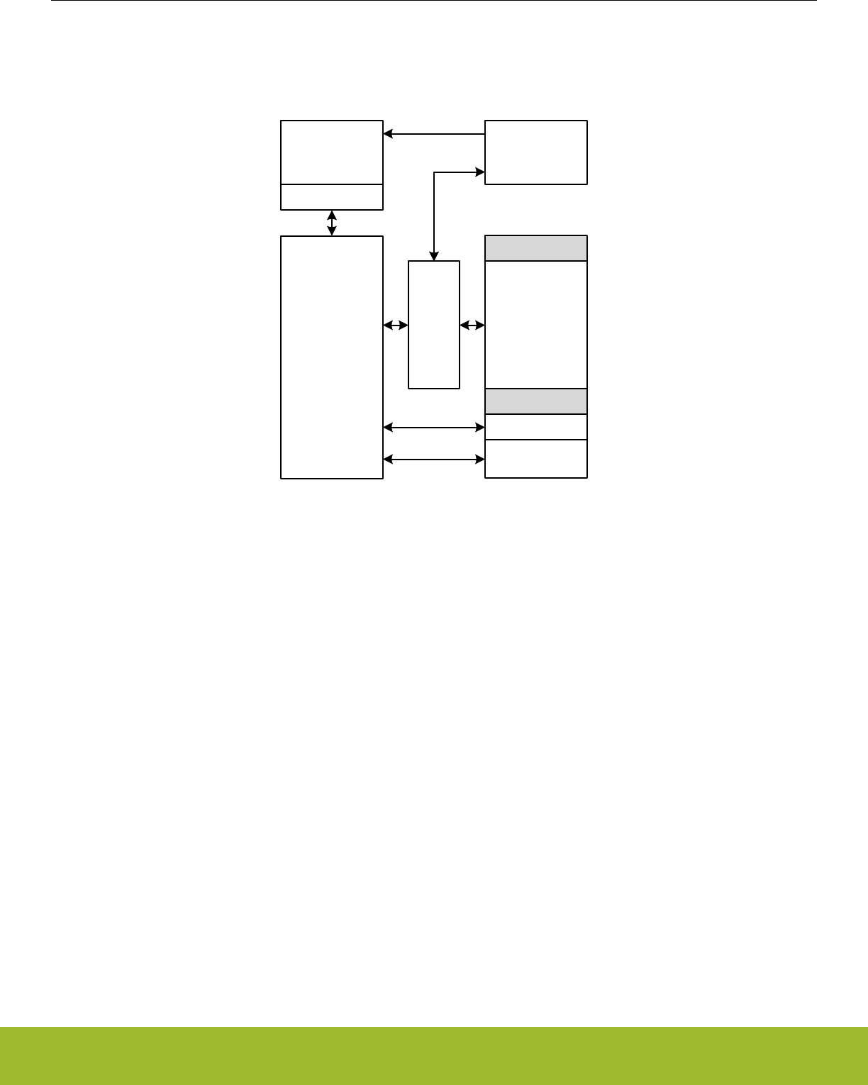
13.3 Functional Description
An overview of the SMU module within the system is shown in Figure 13.1 Bus-Level Security System View on page 383.
Bus Matrix
ARM Core
Code
SRAM
Peripherals
MPU
PPU
Memory Space
SMU
IRQs
Control/Status
Figure 13.1. Bus-Level Security System View
13.3.1 PPU - Peripheral Protection Unit
The number of peripheral memory regions on the device exceeds the number of configurable regions available using the MPU. While it
is possible to manage finer granularity of memory security through software, the PPU provides a hardware solution for fine-grained pe-
ripheral-level protection to eliminate the performance degradation associated with a partially software-managed solution.
The PPU provides a hardware access barrier to any peripheral that is configured to be protected. When an attempt is made to access a
peripheral without the required privilege level, the PPU detects the fault and intercepts the access. No write or read of the peripheral
register space occurs, and an all-zero value is returned if the access is a read. See 13.3.2.2 PPU Control for more details on how ac-
cess faults are reported to the CPU.
Note: The CPU is the only system bus master in the EFR32xG13 Wireless Gecko that can trigger access faults. All other masters are
given full access privileges and have no configurable context switching enabled.
Reference Manual
SMU - Security Management Unit
silabs.com | Smart. Connected. Energy-friendly. Preliminary Rev. 0.5 | 383
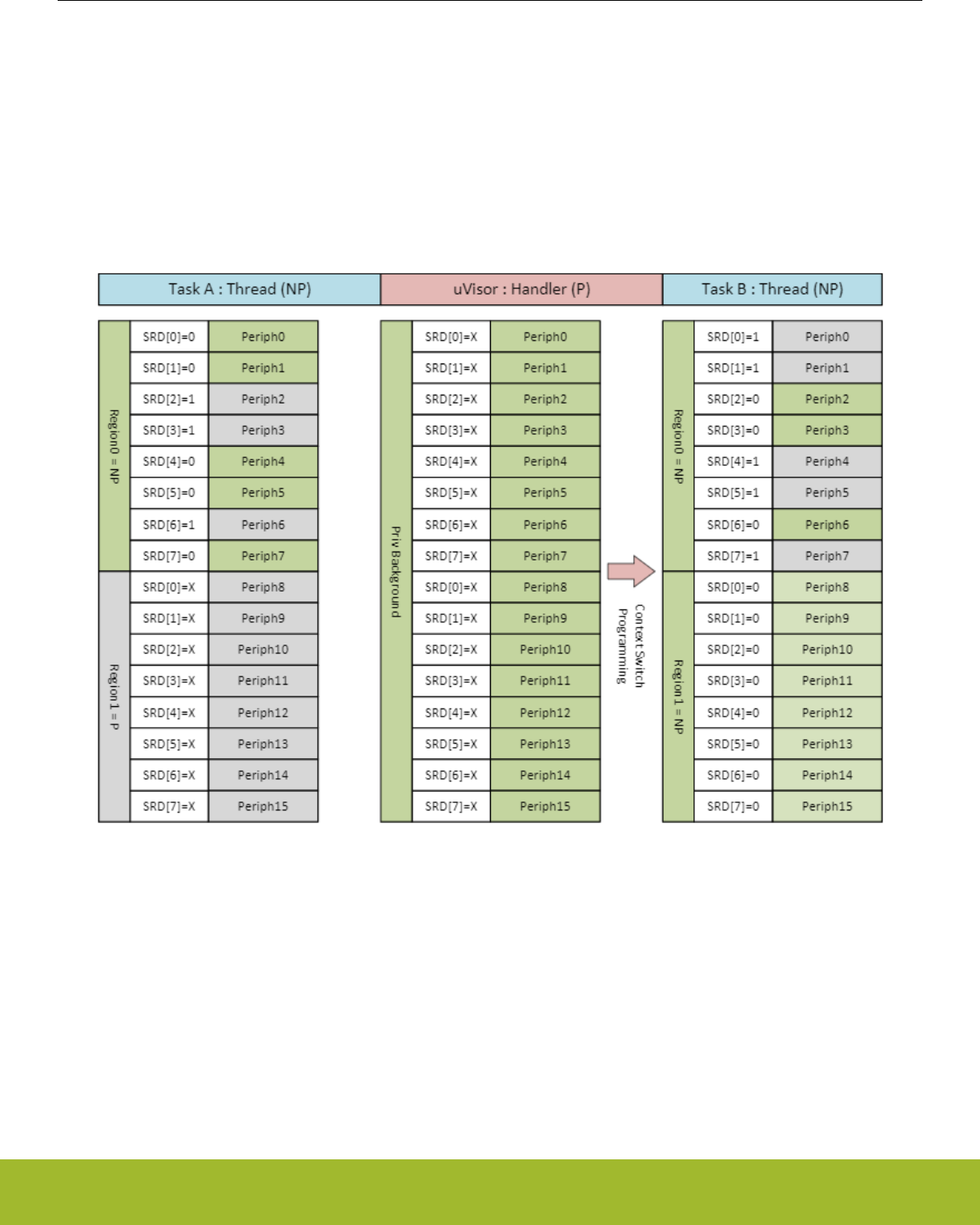
13.3.2 Programming Model
The SMU does not provide any access control out of reset and needs to be configured by software. SMU access controls should be
configured along with the MPU configuration. This is typically performed in a bootloader or other low level RTOS kernel/supervisor code
prior to user code or other non-privileged code execution. At least one MPU region will be allocated to the entire peripheral region as a
full access region (0x4000_0000 - 0x4006_FFFF). An RTOS kernel/supervisor can dynamically allocate peripheral accessibility by
maintaining the hardware and software contexts available to each task. In the chart below there are mutiple tasks and the system
switches between Task A and Task B via the RTOS handler. There are 16 peripherals shown in the example split between two regions.
Task A has rights to access peripherals 0, 1, 4, 5 and 7, whereas task B has rights to access the complement of A (2, 3, and 6). After a
Task B IRQ, the privileged OS handler is entered which signals the supervisor to reprogram the regions using the SMU based on an
access control list. Control is then handed to Task B in non-privileged mode.
Figure 13.2. Peripheral Access Control Example
All hardware protections happen immediately in response to SMU configuration register writes without any latency cycles. However,
since software instructions may be optimized or pipelined, it is important to make sure that software memory barrier instructions are
used as needed after any SMU re-configuration before moving on or changing contexts. This ensures that the hardware context switch
has taken full effect.
For the remainder of this section, the programming model is split into general SMU controls and component-specific controls (e.g.,
PPU).
Reference Manual
SMU - Security Management Unit
silabs.com | Smart. Connected. Energy-friendly. Preliminary Rev. 0.5 | 384

13.3.2.1 Interrupt Control/Status
The SMU follows the standard EFR32xG13 Wireless Gecko interrupt programming model with SMU_IF/IFS/IFC/IEN registers.
There is one interrupt bit PPUPRIV that will trigger on privilege faults detected by the PPU. Such fault mechanisms are configured as
specified in 13.3.2.2 PPU Control
13.3.2.2 PPU Control
The PPU_CTRL register provides an ENABLE bit that allows bypassing all PPU checking when set to 0. In this case, the rest of the
PPU registers have no effect, and no access faults will occur. This is the reset state of the SMU.
When the ENABLE bit of PPU_CTRL register is asserted, access protection is configured on a peripheral-by-peripheral basis using the
SMU_PPUPATDx register(s). Setting a bit in the SMU_PPUPATDx register to one configures the corresponding peripheral controlled by
that bit to privileged access only. The single bit mode control for each peripheral provides fast hardware context switching for peripheral
sharing, while still supporting fast software context switches for task-based CPU context switching.
Note: The SMU itself is a peripheral which has protection afforded by the PPU. A proper security/privilege context configuration re-
quires setting of the SMU's access control bits properly at startup so that only a top-level task (e.g., a uVisor from ARM) can perform
security/privilege context switches.
When a peripheral has access protection configured and the peripheral is accessed with invalid privilege credentials, then an access
fault occurs. The corresponding interrupt flag in SMU_IF is asserted and the ID of the peripheral for which an unpriviliged access was
attempted is captured in the PERIPHID bit-field of the PPU Fault Status register (SMU_PPUFS). This peripheral ID is held stable until
all PPU interrupt flags are cleared to ensure that the first unprivileged access that caused the fault is not overwritten due to subsequent
faults before being acknowledged by software.
Note: In the case of simultaneously occurring faults (which may be possible in some systems), only one of the faults' peripheral IDs will
be captured. There is no inherent peripheral priority defined that would result in one peripheral being recognized before another.
13.4 Register Map
The offset register address is relative to the registers base address.
Offset Name Type Description
0x00C SMU_IF RInterrupt Flag Register
0x010 SMU_IFS W1 Interrupt Flag Set Register
0x014 SMU_IFC (R)W1 Interrupt Flag Clear Register
0x018 SMU_IEN RW Interrupt Enable Register
0x040 SMU_PPUCTRL RW PPU Control Register
0x050 SMU_PPUPATD0 RW PPU Privilege Access Type Descriptor 0
0x054 SMU_PPUPATD1 RW PPU Privilege Access Type Descriptor 1
0x090 SMU_PPUFS RPPU Fault Status
Reference Manual
SMU - Security Management Unit
silabs.com | Smart. Connected. Energy-friendly. Preliminary Rev. 0.5 | 385

13.5 Register Description
13.5.1 SMU_IF - Interrupt Flag Register
Offset Bit Position
0x00C
31
30
29
28
27
26
25
24
23
22
21
20
19
18
17
16
15
14
13
12
11
10
9
8
7
6
5
4
3
2
1
0
Reset
0
Access
R
Name
PPUPRIV
Bit Name Reset Access Description
31:1 Reserved To ensure compatibility with future devices, always write bits to 0. More information in 1.2 Conven-
tions
0 PPUPRIV 0 R PPU Privilege Interrupt Flag
Triggered when a privilege fault occurs in the Peripheral Protection Unit
13.5.2 SMU_IFS - Interrupt Flag Set Register
Offset Bit Position
0x010
31
30
29
28
27
26
25
24
23
22
21
20
19
18
17
16
15
14
13
12
11
10
9
8
7
6
5
4
3
2
1
0
Reset
0
Access
W1
Name
PPUPRIV
Bit Name Reset Access Description
31:1 Reserved To ensure compatibility with future devices, always write bits to 0. More information in 1.2 Conven-
tions
0 PPUPRIV 0 W1 Set PPUPRIV Interrupt Flag
Write 1 to set the PPUPRIV interrupt flag
Reference Manual
SMU - Security Management Unit
silabs.com | Smart. Connected. Energy-friendly. Preliminary Rev. 0.5 | 386

13.5.3 SMU_IFC - Interrupt Flag Clear Register
Offset Bit Position
0x014
31
30
29
28
27
26
25
24
23
22
21
20
19
18
17
16
15
14
13
12
11
10
9
8
7
6
5
4
3
2
1
0
Reset
0
Access
(R)W1
Name
PPUPRIV
Bit Name Reset Access Description
31:1 Reserved To ensure compatibility with future devices, always write bits to 0. More information in 1.2 Conven-
tions
0 PPUPRIV 0 (R)W1 Clear PPUPRIV Interrupt Flag
Write 1 to clear the PPUPRIV interrupt flag. Reading returns the value of the IF and clears the corresponding interrupt flags
(This feature must be enabled globally in MSC.).
13.5.4 SMU_IEN - Interrupt Enable Register
Offset Bit Position
0x018
31
30
29
28
27
26
25
24
23
22
21
20
19
18
17
16
15
14
13
12
11
10
9
8
7
6
5
4
3
2
1
0
Reset
0
Access
RW
Name
PPUPRIV
Bit Name Reset Access Description
31:1 Reserved To ensure compatibility with future devices, always write bits to 0. More information in 1.2 Conven-
tions
0 PPUPRIV 0 RW PPUPRIV Interrupt Enable
Enable/disable the PPUPRIV interrupt
Reference Manual
SMU - Security Management Unit
silabs.com | Smart. Connected. Energy-friendly. Preliminary Rev. 0.5 | 387

13.5.5 SMU_PPUCTRL - PPU Control Register
Offset Bit Position
0x040
31
30
29
28
27
26
25
24
23
22
21
20
19
18
17
16
15
14
13
12
11
10
9
8
7
6
5
4
3
2
1
0
Reset
0
Access
RW
Name
ENABLE
Bit Name Reset Access Description
31:1 Reserved To ensure compatibility with future devices, always write bits to 0. More information in 1.2 Conven-
tions
0 ENABLE 0 RW
Set to enable checking of peripheral access
Value Description
0 Privilege/Security-level checking completely bypassed in the PPU
1 Behavior controlled by PPU_PATD
Reference Manual
SMU - Security Management Unit
silabs.com | Smart. Connected. Energy-friendly. Preliminary Rev. 0.5 | 388

13.5.6 SMU_PPUPATD0 - PPU Privilege Access Type Descriptor 0
Set peripheral bits to 1 to mark as privileged access only
Offset Bit Position
0x050
31
30
29
28
27
26
25
24
23
22
21
20
19
18
17
16
15
14
13
12
11
10
9
8
7
6
5
4
3
2
1
0
Reset
0
0
0
0
0
0
0
0
0
0
0
0
0
0
0
0
0
0
0
0
0
0
0
Access
RW
RW
RW
RW
RW
RW
RW
RW
RW
RW
RW
RW
RW
RW
RW
RW
RW
RW
RW
RW
RW
RW
RW
Name
PCNT0
LEUART0
LETIMER0
LESENSE
LDMA
MSC
IDAC0
I2C1
I2C0
GPIO
GPCRC
FPUEH
EMU
PRS
VDAC0
CSEN
CRYPTO1
CRYPTO0
CRYOTIMER
CMU
ADC0
ACMP1
ACMP0
Bit Name Reset Access Description
31:28 Reserved To ensure compatibility with future devices, always write bits to 0. More information in 1.2 Conven-
tions
27 PCNT0 0 RW Pulse Counter 0 access control bit
Access control only for PCNT0
26 Reserved To ensure compatibility with future devices, always write bits to 0. More information in 1.2 Conven-
tions
25 LEUART0 0 RW Low Energy UART 0 access control bit
Access control only for LEUART0
24 LETIMER0 0 RW Low Energy Timer 0 access control bit
Access control only for LETIMER0
23 LESENSE 0 RW Low Energy Sensor Interface access control bit
Access control only for LESENSE
22 LDMA 0 RW Linked Direct Memory Access Controller access control bit
Access control only for LDMA
21 MSC 0 RW Memory System Controller access control bit
Access control only for MSC
20 IDAC0 0 RW Current Digital to Analog Converter 0 access control bit
Access control only for IDAC0
19 I2C1 0 RW I2C 1 access control bit
Access control only for I2C1
18 I2C0 0 RW I2C 0 access control bit
Access control only for I2C0
17 GPIO 0 RW General purpose Input/Output access control bit
Access control only for GPIO
16 GPCRC 0 RW General Purpose CRC access control bit
Access control only for GPCRC
15 Reserved To ensure compatibility with future devices, always write bits to 0. More information in 1.2 Conven-
tions
Reference Manual
SMU - Security Management Unit
silabs.com | Smart. Connected. Energy-friendly. Preliminary Rev. 0.5 | 389

Bit Name Reset Access Description
14 FPUEH 0 RW FPU Exception Handler access control bit
Access control only for FPUEH
13 EMU 0 RW Energy Management Unit access control bit
Access control only for EMU
12 PRS 0 RW Peripheral Reflex System access control bit
Access control only for PRS
11 VDAC0 0 RW Digital to Analog Converter 0 access control bit
Access control only for VDAC0
10 CSEN 0 RW Capacitive touch sense module access control bit
Access control only for CSEN
9 CRYPTO1 0 RW Advanced Encryption Standard Accelerator 1 access control bit
Access control only for CRYPTO1
8 CRYPTO0 0 RW Advanced Encryption Standard Accelerator 0 access control bit
Access control only for CRYPTO0
7 CRYOTIMER 0 RW CryoTimer access control bit
Access control only for CRYOTIMER
6 Reserved To ensure compatibility with future devices, always write bits to 0. More information in 1.2 Conven-
tions
5 CMU 0 RW Clock Management Unit access control bit
Access control only for CMU
4:3 Reserved To ensure compatibility with future devices, always write bits to 0. More information in 1.2 Conven-
tions
2 ADC0 0 RW Analog to Digital Converter 0 access control bit
Access control only for ADC0
1 ACMP1 0 RW Analog Comparator 1 access control bit
Access control only for ACMP1
0 ACMP0 0 RW Analog Comparator 0 access control bit
Access control only for ACMP0
Reference Manual
SMU - Security Management Unit
silabs.com | Smart. Connected. Energy-friendly. Preliminary Rev. 0.5 | 390

13.5.7 SMU_PPUPATD1 - PPU Privilege Access Type Descriptor 1
Set peripheral bits to 1 to mark as privileged access only
Offset Bit Position
0x054
31
30
29
28
27
26
25
24
23
22
21
20
19
18
17
16
15
14
13
12
11
10
9
8
7
6
5
4
3
2
1
0
Reset
0
0
0
0
0
0
0
0
0
0
0
0
Access
RW
RW
RW
RW
RW
RW
RW
RW
RW
RW
RW
RW
Name
WTIMER0
WDOG1
WDOG0
USART2
USART1
USART0
TRNG0
TIMER1
TIMER0
SMU
RTCC
RMU
Bit Name Reset Access Description
31:13 Reserved To ensure compatibility with future devices, always write bits to 0. More information in 1.2 Conven-
tions
12 WTIMER0 0 RW Wide Timer 0 access control bit
Access control only for WTIMER0
11 WDOG1 0 RW Watchdog 1 access control bit
Access control only for WDOG1
10 WDOG0 0 RW Watchdog 0 access control bit
Access control only for WDOG0
9 USART2 0 RW Universal Synchronous/Asynchronous Receiver/Transmitter 2 ac-
cess control bit
Access control only for USART2
8 USART1 0 RW Universal Synchronous/Asynchronous Receiver/Transmitter 1 ac-
cess control bit
Access control only for USART1
7 USART0 0 RW Universal Synchronous/Asynchronous Receiver/Transmitter 0 ac-
cess control bit
Access control only for USART0
6 TRNG0 0 RW True Random Number Generator 0 access control bit
Access control only for TRNG0
5 TIMER1 0 RW Timer 1 access control bit
Access control only for TIMER1
4 TIMER0 0 RW Timer 0 access control bit
Access control only for TIMER0
3 Reserved To ensure compatibility with future devices, always write bits to 0. More information in 1.2 Conven-
tions
2 SMU 0 RW Security Management Unit access control bit
Access control only for SMU
1 RTCC 0 RW Real-Time Counter and Calendar access control bit
Access control only for RTCC
Reference Manual
SMU - Security Management Unit
silabs.com | Smart. Connected. Energy-friendly. Preliminary Rev. 0.5 | 391

Bit Name Reset Access Description
0 RMU 0 RW Reset Management Unit access control bit
Access control only for RMU
Reference Manual
SMU - Security Management Unit
silabs.com | Smart. Connected. Energy-friendly. Preliminary Rev. 0.5 | 392

13.5.8 SMU_PPUFS - PPU Fault Status
Offset Bit Position
0x090
31
30
29
28
27
26
25
24
23
22
21
20
19
18
17
16
15
14
13
12
11
10
9
8
7
6
5
4
3
2
1
0
Reset
0x00
Access
R
Name
PERIPHID
Bit Name Reset Access Description
31:7 Reserved To ensure compatibility with future devices, always write bits to 0. More information in 1.2 Conven-
tions
6:0 PERIPHID 0x00 R
Holds the peripheral ID of the first peripheral that was accessed resulting in an access fault. This ID is not valid unless one
of the PPU interrupt flags is set. Any other access faults that occur are not captured until all the PPU interrupt flags are
cleared
Value Mode Description
0 ACMP0 Analog Comparator 0
1 ACMP1 Analog Comparator 1
2 ADC0 Analog to Digital Converter 0
5 CMU Clock Management Unit
7 CRYOTIMER CryoTimer
8 CRYPTO0 Advanced Encryption Standard Accelerator 0
9 CRYPTO1 Advanced Encryption Standard Accelerator 1
10 CSEN Capacitive touch sense module
11 VDAC0 Digital to Analog Converter 0
12 PRS Peripheral Reflex System
13 EMU Energy Management Unit
14 FPUEH FPU Exception Handler
16 GPCRC General Purpose CRC
17 GPIO General purpose Input/Output
18 I2C0 I2C 0
19 I2C1 I2C 1
20 IDAC0 Current Digital to Analog Converter 0
21 MSC Memory System Controller
22 LDMA Linked Direct Memory Access Controller
23 LESENSE Low Energy Sensor Interface
24 LETIMER0 Low Energy Timer 0
25 LEUART0 Low Energy UART 0
Reference Manual
SMU - Security Management Unit
silabs.com | Smart. Connected. Energy-friendly. Preliminary Rev. 0.5 | 393

Bit Name Reset Access Description
27 PCNT0 Pulse Counter 0
32 RMU Reset Management Unit
33 RTCC Real-Time Counter and Calendar
34 SMU Security Management Unit
36 TIMER0 Timer 0
37 TIMER1 Timer 1
38 TRNG0 True Random Number Generator 0
39 USART0 Universal Synchronous/Asynchronous Receiver/Transmitter 0
40 USART1 Universal Synchronous/Asynchronous Receiver/Transmitter 1
41 USART2 Universal Synchronous/Asynchronous Receiver/Transmitter 2
42 WDOG0 Watchdog 0
43 WDOG1 Watchdog 1
44 WTIMER0 Wide Timer 0
Reference Manual
SMU - Security Management Unit
silabs.com | Smart. Connected. Energy-friendly. Preliminary Rev. 0.5 | 394
14. RTCC - Real Time Counter and Calendar
0 1 2 3 4
0 1 2 3 4
Quick Facts
What?
The Real Time Counter and Calendar (RTCC) is a
32-bit counter ensuring timekeeping in low energy
modes. The RTCC also includes a calendar mode
for easy time and date keeping. In addition, the
RTCC includes 128 bytes of general purpose reten-
tion data, allowing persistent data storage in all en-
ergy modes except EM4 Shutoff.
Why?
Timekeeping over long time periods while using as
little power as possible is required in many low pow-
er applications.
How?
A low frequency oscillator is used as clock signal
and the RTCC has three different Capture/Compare
channels which can trigger wake-up, generate PRS
signalling, or capture system events. 32-bit resolu-
tion and selectable prescaling allow the system to
stay in low energy modes for long periods of time
and still maintain reliable timekeeping.
14.1 Introduction
The Real Time Counter and Calendar (RTCC) contains a 32-bit counter/calendar in combination with a 15-bit pre-counter to allow flexi-
ble prescaling of the main counter. The RTCC is available in all energy modes except EM4 Shutoff.
Three individually configurable Capture/Compare channels are available in the RTCC. These can be used to trigger interrupts, generate
PRS signals, capture system events, and to wake the device up from a low energy mode. The RTCC also includes 128 bytes of general
purpose storage and a Binary Coded Decimal (BCD) calendar mode, enabling easy time and date keeping.
Reference Manual
RTCC - Real Time Counter and Calendar
silabs.com | Smart. Connected. Energy-friendly. Preliminary Rev. 0.5 | 395
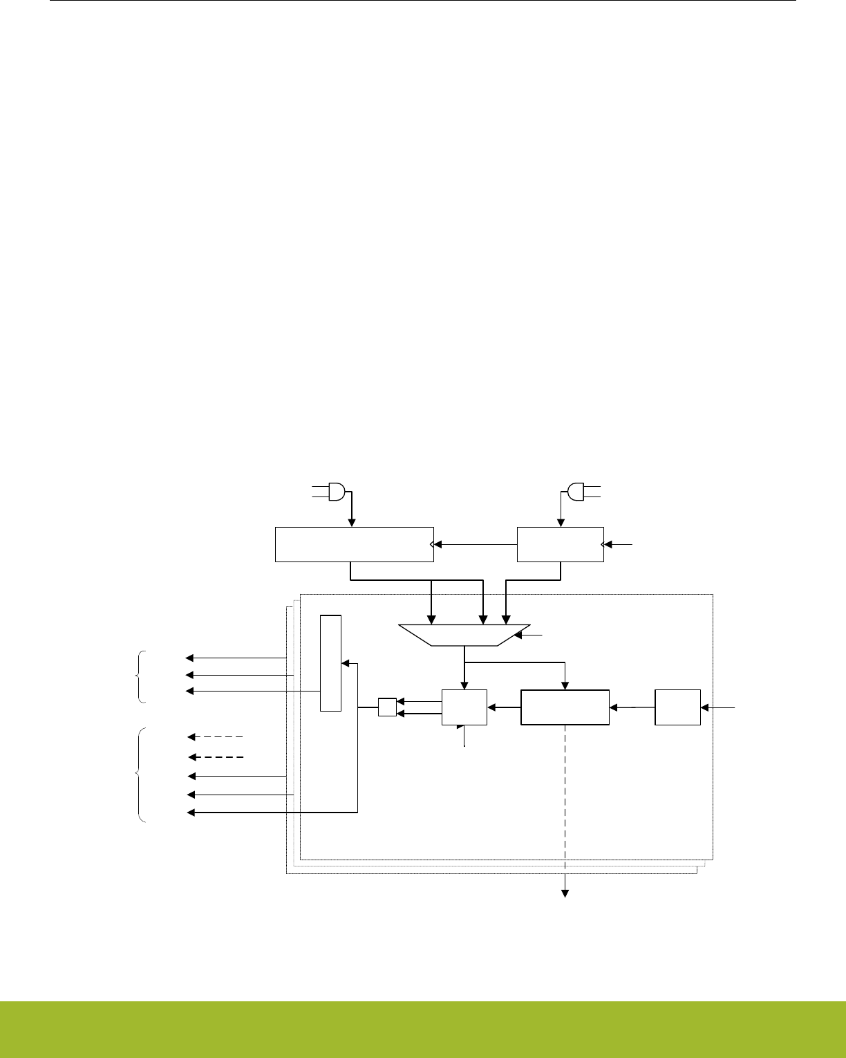
14.2 Features
• 32-bit Real Time Counter.
• 15-bit pre-counter, for flexible frequency scaling or for use as an independent counter.
• EM4 Hibernate operation and wakeup.
• 128 byte general purpose retention data.
• Oscillator failure detection.
• Can continue through system reset; only reset by power loss, pin, or software reset.
• Calendar mode.
• BCD encoding.
• Three programmable alarms.
• Leap year correction.
• Three Capture/Compare registers.
• Capture of PRS events from other parts of the system.
• Compare match or input capture can trigger interrupts.
• Compare register 1, RTCC_CC1_CCV can be used as a top value for the main counter.
• Compare register 0, RTCC_CC0_CCV can be used as a top value for the pre-counter.
• Compare match events are available to other peripherals through the Peripheral Reflex System (PRS).
14.3 Functional Description
The RTCC is a 32-bit up-counter with three Capture/Compare channels. In addition, the RTCC includes a 15-bit pre-counter which can
be used as an independent counter or to prescale the main counter. An overview of the RTCC module is shown in Figure 14.1 RTCC
Overview on page 396.
Counter
RTCC_CNT /
RTCC_TIME, RTCC_DATE
Capture / Compare Channel n
n = {0, 1, 2}
Capture
logic n
CC0
Capture/Compare
RTCC_CCx_CCV
=
CC1
CC2
Capture PRS
Inputs
Interrupt
generation
OF
RTCC_CC_CTRL_CMOA
CC0
CC1
CC2
CNT Overflow
RTCC_CC2_CCV output to FRC
RTCC_CTRL_COMP1TOP
Clear
CC1 compare match
LFCLKRTCC
Pre-Counter
RTCC_PRECNT
RTCC_CC_CTRL_COMPBASE
RTCC_CC_CTRL_COMPMASK
Mask
RTCC_CTRL_CNTTICK = CCV0MATCH
Clear RTCC_PRECNT = RTCC_CC0_CCV[14:0]
CNT PRECNT
PRS output
Oscillator failure
OSCFAIL
[31:0] [14:0][16:0]
Figure 14.1. RTCC Overview
Reference Manual
RTCC - Real Time Counter and Calendar
silabs.com | Smart. Connected. Energy-friendly. Preliminary Rev. 0.5 | 396
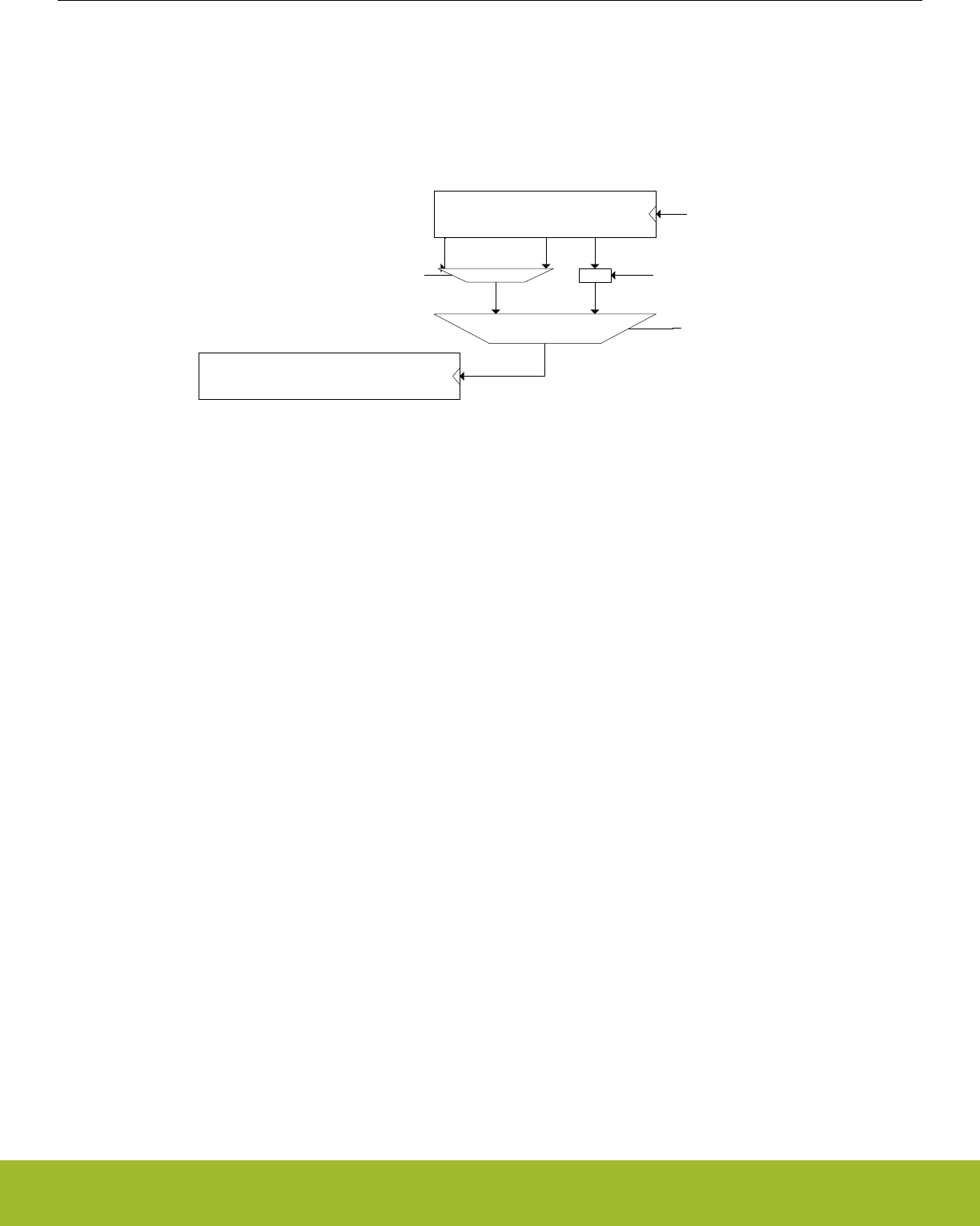
14.3.1 Counter
The RTCC consists of two counters; the 32-bit main counter, RTCC_CNT (RTCC_TIME and RTCC_DATE in calendar mode), and a 15-
bit pre-counter, RTCC_PRECNT. The pre-counter can be used as an independent counter or to generate a specific frequency for the
main counter. In both configurations, the pre-counter can be used to generate compare match events or be captured in the Capture/
Compare channels as a result of an external PRS event. Refer to 14.3.2 Capture/Compare Channels for details on how to configure the
Capture/Compare channels for use with the pre-counter.
RTCC_PRECNT
RTCC_CNT /
RTCC_TIME, RTCC_DATE
LFCLKRTCC
RTCC_CTRL_CNTTICK
=
.........................
RTCC_CC0_CCV[14:0]
RTCC_CTRL_CNTPRESC
PRESC CCV0MATCH
Figure 14.2. RTCC counters
The RTCC is enabled by setting the ENABLE bit in RTCC_CTRL. When the RTCC is enabled, the pre-counter (RTCC_PRECNT) incre-
ments upon each positive clock edge of LFCLKRTCC. If CNTTICK in RTCC_CTRL is set to PRESC, the pre-counter will continue to
count up, wrapping around to zero when it overflows. If CNTTICK in RTCC_CTRL is set to CCV0MATCH, the pre-counter will wrap
around when it hits the value configured in RTCC_CC0_CCV.
The main counter of the RTCC, RTCC_CNT, has two modes; normal mode and calendar mode. In normal mode, the main counter is
available in RTCC_CNT and increments upon each tick given from the pre-counter. Refer to 14.3.1.1 Normal Mode for a description on
how to configure the frequency of these ticks. In calendar mode, the counter value is available in RTCC_TIME and RTCC_DATE, keep-
ing track of seconds, minutes, hours, day of month, day of week, months, and years, all encoded in BCD format. Refer to
14.3.1.2 Calendar Mode for details on this mode. The mode of the main counter is configured in CNTMODE in RTCC_CTRL. The differ-
ences between the two modes are summarized below.
•Normal mode
• Incremental counter, RTCC_CNT.
• RTCC_CCx_CCV used for Capture/Compare value.
•Calendar mode
• BCD counters, RTCC_DATE, RTCC_TIME.
• RTCC_CCx_TIME and RTCC_CCx_DATE used for Capture/Compare value.
Note: The mode of the RTCC must be configured for CALENDAR mode in RTCC_CTRL_CNTMODE before writing to the mode de-
pendent registers, RTCC_TIME, RTCC_DATE, RTCC_CCx_TIME, and RTCC_CCx_DATE. Writes to these registers when in NORMAL
mode will be ignored.
Reference Manual
RTCC - Real Time Counter and Calendar
silabs.com | Smart. Connected. Energy-friendly. Preliminary Rev. 0.5 | 397

14.3.1.1 Normal Mode
The main counter can receive a tick based on different tappings from the pre-counter, allowing the ticks to be power of 2 divisions of the
LFCLKRTCC. For more accurate configuration of the tick frequency, RTCC_CC0_CCV[14:0] can be used as a top value for
RTCC_PRECNT. When reaching the top value, the main counter receives a tick and the pre-counter wraps around. Table 14.1 RTCC
Resolution vs Overflow, FLFCLK = 32768 Hz on page 398 summarizes the resolutions available when using a 32768 Hz oscillator as
source for LFCLKRTCC.
Table 14.1. RTCC Resolution vs Overflow, FLFCLK = 32768 Hz
RTCC_CTRL_CNTTICK RTCC_CTRL_CNTPRESC Main counter period, TCNT Overflow
CCV0MATCH Don't care (RTCC_CC0_CCV + 1)/FLFCLK s 232*TCNT seconds
PRESC
DIV1 30.5 µs 36.4 hours
DIV2 61 µs 72.8 hours
DIV4 122 µs 145.6 hours
DIV8 244 µs 12 days
DIV16 488 µs 24 days
DIV32 977 µs 48 days
DIV64 1.95 ms 97 days
DIV128 3.91 ms 194 days
DIV256 7.81 ms 388 days
DIV512 15.6 ms 776 days
DIV1024 31.25 ms 4.2 years
DIV2048 62.5 ms 8.5 years
DIV4096 0.125 s 17 years
DIV8192 0.25 s 34 years
DIV16384 0.5 s 68 years
DIV32768 1 s 136 years
By default, the counter will keep counting until it reaches the top value, 0xFFFFFFFF, before it wraps around and continues counting
from zero. By setting CCV1TOP in RTCC_CTRL, a Capture/Compare channel 1 compare match will result in the main counter wrap-
ping to 0. The timer will then wrap around on a channel 1 compare match (RTCC_CNT = RTCC_CC1_CCV). Before using the
CCV1TOP setting, make sure to set this bit prior to or at the same time the RTCC is enabled. Setting CCV1TOP after enabling the
RTCC (RTCC_CTRL_MODE != DISABLED) may cause unintended operation (e.g. if RTCC_CNT > RTCC_CC1_CCV, RTCC_CNT will
wrap when reaching 0xFFFFFFFF rather than RTCC_CC1_CCV).
Note:
If the RTCC is being reconfigured, and capture compare channel 1 has previously been used, a CCV1TOP wrap event might be pend-
ing. This would lead to the first tick of the main counter being a wrap to 0. To clear any pending wrap events, use the following proce-
dure before reconfiguring the RTCC:
1. RTCC->CC[1].CTRL = RTCC_CC_CTRL_MODE_OFF;
2. RTCC->CTRL = RTCC_CTRL_CNTTICK_PRESC | RTCC_CTRL_CNTMODE_NORMAL | RTCC_CTRL_ENABLE;
3. rtcc_cnt_pre = RTCC->CNT;
4. while(RTCC->CNT == rtcc_cnt_pre);
5. Reconfigure the RTCC
Reference Manual
RTCC - Real Time Counter and Calendar
silabs.com | Smart. Connected. Energy-friendly. Preliminary Rev. 0.5 | 398

14.3.1.2 Calendar Mode
The RTCC includes a calendar mode which implements time and date decoding in hardware. Calendar mode is enabled by configuring
CNTMODE in RTCC_CTRL to CALENDAR. When in calendar mode, the counter value is available in RTCC_TIME and RTCC_DATE.
RTCC_TIME shows seconds, minutes, and hours while RTCC_DATE shows day of month, month, year, and day of week. RTCC_TIME
and RTCC_DATE are encoded in BCD format. In calendar mode, the pre-counter should be configured to give ticks with a period of one
second, i.e. RTCC_CTRL_CNTTICK should be set to PRESC, and the CNTPRESC bitfield of the RTCC_CTRL register should be set
to DIV32768 if a 32768 Hz clock source is used.
In calendar mode, the time and date registers of the capture compare channels, RTCC_CCx_TIME and RTCC_CCx_DATE, are used to
set compare values. Compare values can be set on seconds, minutes, hours, days, and months. Whether day of week or day of month
is used for a Capture/Compare channel, it is configured in RTCC_CCx_CTRL_DAYCC of the respective Capture/Compare channel.
The RTCC will automatically compensate for 28-, 29- (leap year), 30-, and 31-day months. The day of week counter,
RTCC_DATE_DAYOW, is a three bit counter incrementing when RTCC_TIME_HOURT overflows, wrapping around every seventh day.
Automatic leap year correction, extending the month of February from 28 to 29 days every fourth year is by default enabled, but can be
disabled by setting the LYEARCORRDIS bit in RTCC_CTRL. The pseudo-code for leap year correction is as follows:
if RTCC_DATE_YEART modulo 2 = 0:
if RTCC_DATE_YEARU modulo 4 = 0:
leap_year = true
else:
leap_year = false
else:
if (RTCC_DATE_YEARU + 2) modulo 4 = 0:
leap_year = true
else:
leap_year = false
The seconds, minute, hour segments are represented in 24-hour BCD format. The month segments are enumerated as shown in Table
14.2 RTCC calendar enumeration on page 399.
Table 14.2. RTCC calendar enumeration
Month RTCC_DATE_MONTHT RTCC_DATE_MONTHU
January 0b0 0b0001
February 0b0 0b0010
March 0b0 0b0011
April 0b0 0b0100
May 0b0 0b0101
June 0b0 0b0110
July 0b0 0b0111
August 0b0 0b1000
September 0b0 0b1001
October 0b1 0b0000
November 0b1 0b0001
December 0b1 0b0010
Reference Manual
RTCC - Real Time Counter and Calendar
silabs.com | Smart. Connected. Energy-friendly. Preliminary Rev. 0.5 | 399

14.3.1.3 RTCC Initialization
The counters of the RTCC, RTCC_CNT (RTCC_TIME and RTCC_DATE in calendar mode) and RTCC_PRECNT, can at any time be
written by software, as long as the registers are not locked using RTCC_LOCKKEY. All RTCC registers use the immediate synchroniza-
tion scheme, described in 4.3.1 Writing.
Note: Writing to the RTCC_PRECNT register may alter the frequency of the ticks for the RTCC_CNT register.
Reference Manual
RTCC - Real Time Counter and Calendar
silabs.com | Smart. Connected. Energy-friendly. Preliminary Rev. 0.5 | 400
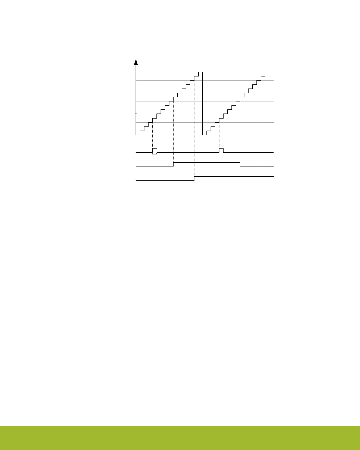
14.3.2 Capture/Compare Channels
Three capture/compare channels are available in the RTCC. Each channel can be configured as input capture or output compare, by
setting the corresponding MODE in the RTCC_CCx_CTRL register.
RTCC_CC1_CCV
0
RTCC_CNT
RTCC_CC0_CCV
RTCC_CC2_CCV
CC2 PRS output,
CMOA=PULSE
CC1 PRS output,
CMOA=TOGGLE
CC0 PRS output,
CMOA=SET
1 LFCLKRTCC cycle
Figure 14.3. RTCC Compare match and PRS output illustration
In input capture mode the RTCC_CNT (RTCC_TIME and RTCC_DATE in calendar mode) register is captured into the
RTCC_CCx_CCV (RTCC_CCx_TIME and RTCC_CCx_DATE in calendar mode) register when an edge is detected on the selected
PRS input channel. The active capture edge is configured in the ICEDGE control bits.
In output compare mode the compare values are set by writing to the RTCC compare channel registers RTCC_CCx_CCV
(RTCC_CCx_TIME and RTCC_CCx_DATE in calendar mode). These values will be compared to the main counter, RTCC_CNT
(RTCC_TIME and RTCC_DATE in calendar mode), or a mixture of the main counter and the pre-counter, as illustrated in Figure
14.4 RTCC Compare base illustration on page 402. Compare base for the capture compare channels is set by configuring COMP-
BASE in RTCC_CCx_CTRL.
Reference Manual
RTCC - Real Time Counter and Calendar
silabs.com | Smart. Connected. Energy-friendly. Preliminary Rev. 0.5 | 401
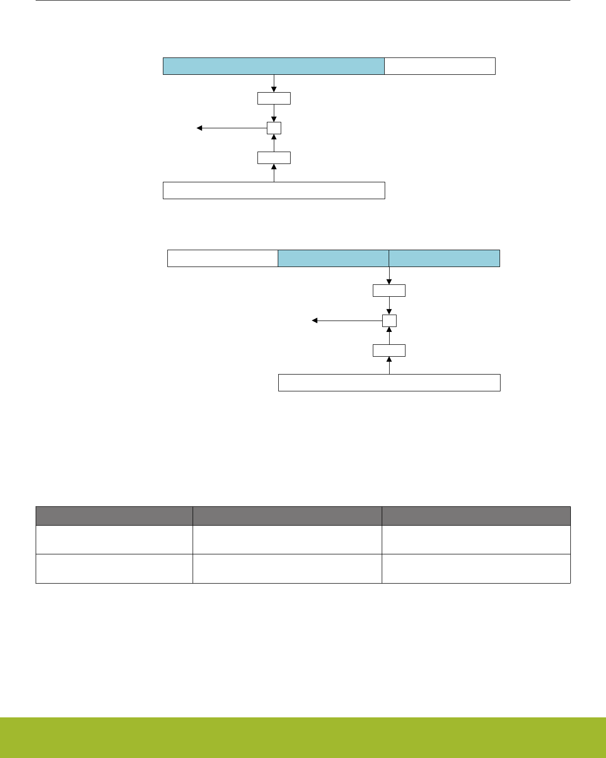
RTCC_CCx_CTRL_COMPBASE = CNT
CNT PRECNT
RTCC_CCx_CTRL_COMPBASE = PRECNT
PRECNT
CCx_CCV
=
CNT
Compare match
16 0 14 0
MASK
MASK
CCx_CCV
=
Compare match
MASK
MASK
Figure 14.4. RTCC Compare base illustration
Table 14.3 RTCC Capture/Compare subjects on page 402 summarizes which registers being subject to comparison for different config-
urations of RTCC_CTRL_CNTMODE and RTCC_CCx_CTRL_COMPBASE.
Table 14.3. RTCC Capture/Compare subjects
RTCC_CTRL_CNTMODE NORMAL CALENDAR
RTCC_CCx_CTRL_COMPBASE =
CNT RTCC_CNT vs. RTCC_CCx_CCV RTCC_TIME vs. RTCC_CCx_TIME and
RTCC_DATE vs. RTCC_CCx_DATE
RTCC_CCx_CTRL_COMPBASE =
PRECNT
{RTCC_CNT[16:0],RTCC_PRECNT[14:0]} vs.
RTCC_CCx_CCV RTCC_PRECNT vs. RTCC_CCx_CCV[14:0]
Figure 14.5 RTCC Compare in calendar mode, COMPBASE = CNT on page 403 illustrates how the compare events are evaluated
when in calendar mode with RTCC_CCx_CTRL_COMPBASE = CNT. The SECU, SECT, MINU, MINT, HOURU, HOURT, MONTHU,
and MONTHT bitfields in RTCC_CCx_TIME and RTCC_CCx_DATE are compared to the corresponding bitfields in RTCC_DATE and
RTCC_TIME. The DAYU and DAYT bitfields in RTCC_CCx_DATE will be compared to {RTCC_DATE_DAYOMT, RTCC_DATE_DAYO-
MU} if DAYCC in RTCC_CCx_CTRL is set to MONTH. If DAYCC in RTCC_CCx_CTRL is set to WEEK, the DAYU and DAYT bitfields in
RTCC_CCx_DATE will be compared to {0b000, RTCC_DATE_DAYOW}.
Reference Manual
RTCC - Real Time Counter and Calendar
silabs.com | Smart. Connected. Energy-friendly. Preliminary Rev. 0.5 | 402
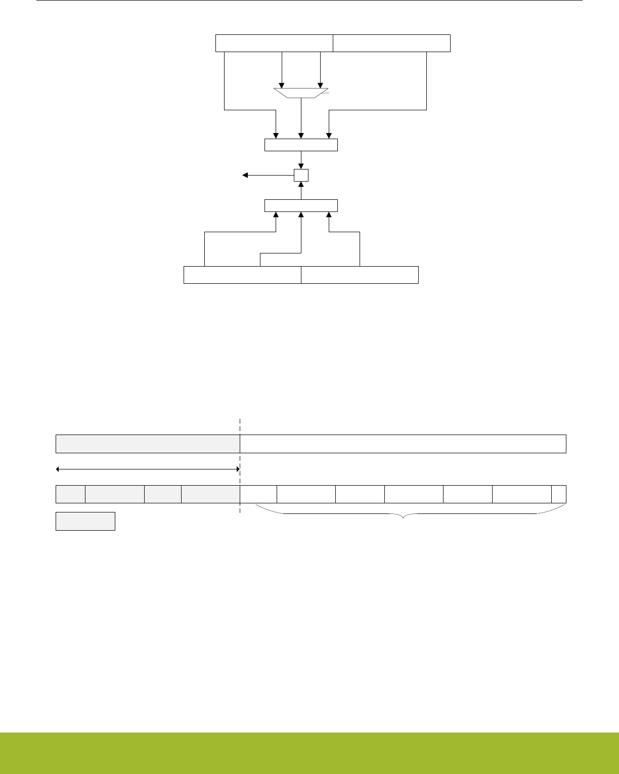
=
Compare match
MASK
RTCC_TIMERTCC_DATE
RTCC_CCx_TIMERTCC_CCx_DATE
RTCC_CCx_CTRL_DAYCC
[0b000,
DAYOW]
[DAYOMT,
DAYOMU]
[MONTHT,MONTHU]
MASK
[MONTHT,MONTHU]
[DAYT,DAYU]
Figure 14.5. RTCC Compare in calendar mode, COMPBASE = CNT
To generate periodically recurring events, it is possible to mask out parts of the compare match values. By configuring COMPMASK in
RTCC_CCx_CTRL, parts of the compare values will be masked out, limiting which part of the compare register being subject to com-
parison with the counter. Figure 14.6 RTCC Compare mask illustration, COMPMASK=11 on page 403 illustrates the effect of COMP-
MASK when in normal mode and calendar mode.
SECUSECTMINUMINTHOURUHOURTDAYUDAYTMONTHUMONTHT
145781112141518192021242526273031
CCV
CC_CTRL_COMPMASK
031
MASKED
Subject to comparison
2021
0
Figure 14.6. RTCC Compare mask illustration, COMPMASK=11
Upon a compare match, the respective Capture/Compare interrupt flag CCx is set. Additionally, the event selected by the CMOA setting
is generated on the corresponding PRS output. This is illustrated in Figure 14.3 RTCC Compare match and PRS output illustration on
page 401.
Reference Manual
RTCC - Real Time Counter and Calendar
silabs.com | Smart. Connected. Energy-friendly. Preliminary Rev. 0.5 | 403

14.3.3 Interrupts and PRS Output
The RTCC has one interrupt for each of its 3 Capture/Compare channels, CC0, CC1, and CC2. Each Capture/Compare channel has a
PRS output with configurable actions upon compare match.
The interrupt flag CNTTICK is set each time the main counter receives a tick (each second in calendar mode). In calendar mode, there
are also interrupt flags being set each minute, hour, day, week, and month.
Upon oscillator failure detection, the OSCFAIL flag will be set.
14.3.3.1 Main Counter Tick PRS Output
To output the ticks for the main counter on PRS, it is possible to use a Capture/Compare channel and mask all the bits, i.e.
RTCC_CCx_CTRL_COMPBASE=CNT and RTCC_CCx_CTRL_COMPMASK=31. PRS output of main counter ticks does not work if
the main counter is not prescaled.
Note:
To be able to mask all bits in the main counter, RTCC_CTRL_CNTMODE has to be set to CALENDAR. In NORMAL mode, the least
significant bit can not be masked out.
14.3.4 Energy Mode Availability
The RTCC is available in all Energy Modes except EM4 Shutoff. To enable RTCC operation in EM4 Hibernate, the EMU_EM4CTRL
register in the EMU has to be configured. Any enabled RTCC interrupt will wake the system up from EM4 Hibernate; if EM4WU in
RTCC_EM4WUEN is set. Refer to 11. EMU - Energy Management Unit for details on how to configure the EMU.
14.3.5 Register Lock
To prevent accidental writes to the RTCC registers, the RTCC_LOCKKEY register can be written to any value other than the unlock
value. To unlock the register, write the unlock value to RTCC_LOCKKEY. Registers affected by this lock are:
• RTCC_CTRL
• RTCC_PRECNT
• RTCC_CNT
• RTCC_TIME
• RTCC_DATE
• RTCC_IEN
• RTCC_POWERDOWN
• RTCC_CCx_CTRL
• RTCC_CCx_CCV
• RTCC_CCx_TIME
• RTCC_CCx_DATE
14.3.6 Oscillator Failure Detection
To be able to detect OSC failure, the RTCC includes a security mechanism ensuring that at least three OSC cycles are detected within
one period of the ULFRCO. If no OSC cycles are detected, the OSCFAIL interrupt flag is set. OSC failure detection is enabled by set-
ting the OSCFDETEN bit in RTCC_CTRL.
14.3.7 Retention Registers
The RTCC includes 32 x 32 bit registers which can be retained in all energy modes except EM4 Shutoff. The registers are accessible
through the RETx_REG registers. Retention is by default enabled in EM0 Active through EM4 Hibernate/Shutoff. The registers can be
shut off to save power by setting the RAM bit in RTCC_POWERDOWN.
Note:
The retention registers are mapped to a RAM instance and have undefined state out of reset.
Reference Manual
RTCC - Real Time Counter and Calendar
silabs.com | Smart. Connected. Energy-friendly. Preliminary Rev. 0.5 | 404

14.3.8 Debug Session
By default, the RTCC is halted when code execution is halted from the debugger. By setting the DEBUGRUN bit in the RTCC_CTRL
register, the RTCC will continue to run even when the debugger has halted the system.
14.4 Register Map
The offset register address is relative to the registers base address.
Offset Name Type Description
0x000 RTCC_CTRL RW Control Register
0x004 RTCC_PRECNT RWH Pre-Counter Value Register
0x008 RTCC_CNT RWH Counter Value Register
0x00C RTCC_COMBCNT RCombined Pre-Counter and Counter Value Register
0x010 RTCC_TIME RWH Time of day register
0x014 RTCC_DATE RWH Date register
0x018 RTCC_IF RRTCC Interrupt Flags
0x01C RTCC_IFS W1 Interrupt Flag Set Register
0x020 RTCC_IFC (R)W1 Interrupt Flag Clear Register
0x024 RTCC_IEN RW Interrupt Enable Register
0x028 RTCC_STATUS RStatus register
0x02C RTCC_CMD W1 Command Register
0x030 RTCC_SYNCBUSY RSynchronization Busy Register
0x034 RTCC_POWERDOWN RW Retention RAM power-down register
0x038 RTCC_LOCK RWH Configuration Lock Register
0x03C RTCC_EM4WUEN RW Wake Up Enable
0x040 RTCC_CC0_CTRL RW CC Channel Control Register
0x044 RTCC_CC0_CCV RWH Capture/Compare Value Register
0x048 RTCC_CC0_TIME RWH Capture/Compare Time Register
0x04C RTCC_CC0_DATE RWH Capture/Compare Date Register
0x050 RTCC_CC1_CTRL RW CC Channel Control Register
0x054 RTCC_CC1_CCV RWH Capture/Compare Value Register
0x058 RTCC_CC1_TIME RWH Capture/Compare Time Register
0x05C RTCC_CC1_DATE RWH Capture/Compare Date Register
0x060 RTCC_CC2_CTRL RW CC Channel Control Register
0x064 RTCC_CC2_CCV RWH Capture/Compare Value Register
0x068 RTCC_CC2_TIME RWH Capture/Compare Time Register
0x06C RTCC_CC2_DATE RWH Capture/Compare Date Register
0x104 RTCC_RET0_REG RW Retention register
... RTCC_RETx_REG RW Retention register
0x180 RTCC_RET31_REG RW Retention register
Reference Manual
RTCC - Real Time Counter and Calendar
silabs.com | Smart. Connected. Energy-friendly. Preliminary Rev. 0.5 | 405

14.5 Register Description
14.5.1 RTCC_CTRL - Control Register (Async Reg)
For more information about asynchronous registers please see 4.3 Access to Low Energy Peripherals (Asynchronous Registers).
Offset Bit Position
0x000
31
30
29
28
27
26
25
24
23
22
21
20
19
18
17
16
15
14
13
12
11
10
9
8
7
6
5
4
3
2
1
0
Reset
0
0
0
0
0x0
0
0
0
0
Access
RW
RW
RW
RW
RW
RW
RW
RW
RW
Name
LYEARCORRDIS
CNTMODE
OSCFDETEN
CNTTICK
CNTPRESC
CCV1TOP
PRECCV0TOP
DEBUGRUN
ENABLE
Bit Name Reset Access Description
31:18 Reserved To ensure compatibility with future devices, always write bits to 0. More information in 1.2 Conven-
tions
17 LYEARCORRDIS 0 RW Leap year correction disabled.
When cleared, February has 29 days in leap years. When set, February always has 28 days.
16 CNTMODE 0 RW Main counter mode
Configure count mode for the main counter.
Value Mode Description
0 NORMAL The main counter is incremented with 1 for each tick.
1 CALENDAR The main counter is in calendar mode.
15 OSCFDETEN 0 RW Oscillator failure detection enable
When set, the OSCFAIL interrupt flag will be set if no ticks are detected on LFCLKRTCC within one ULFRCO cycle.
14:13 Reserved To ensure compatibility with future devices, always write bits to 0. More information in 1.2 Conven-
tions
12 CNTTICK 0 RW Counter prescaler mode.
Select whether the main counter should tick on RTCC_CC0_CCV[14:0] compare match with the pre-counter or tick on a
pre-counter tap selected in CNTPRESC bitfield in the RTCC_CTRL register.
Value Mode Description
0 PRESC CNT register ticks according to configuration in CNTPRESC.
1 CCV0MATCH CNT register ticks when PRECNT matches RTCC_CC0_CCV[14:0]
11:8 CNTPRESC 0x0 RW Counter prescaler value.
Configure counting frequency of the CNT register.
Value Mode Description
0 DIV1 CLKCNT = LFECLKRTCC/1
1 DIV2 CLKCNT = LFECLKRTCC/2
Reference Manual
RTCC - Real Time Counter and Calendar
silabs.com | Smart. Connected. Energy-friendly. Preliminary Rev. 0.5 | 406

Bit Name Reset Access Description
2 DIV4 CLKCNT = LFECLKRTCC/4
3 DIV8 CLKCNT = LFECLKRTCC/8
4 DIV16 CLKCNT = LFECLKRTCC/16
5 DIV32 CLKCNT = LFECLKRTCC/32
6 DIV64 CLKCNT = LFECLKRTCC/64
7 DIV128 CLKCNT = LFECLKRTCC/128
8 DIV256 CLKCNT = LFECLKRTCC/256
9 DIV512 CLKCNT = LFECLKRTCC/512
10 DIV1024 CLKCNT = LFECLKRTCC/1024
11 DIV2048 CLKCNT = LFECLKRTCC/2048
12 DIV4096 CLKCNT = LFECLKRTCC/4096
13 DIV8192 CLKCNT = LFECLKRTCC/8192
14 DIV16384 CLKCNT = LFECLKRTCC/16384
15 DIV32768 CLKCNT = LFECLKRTCC/32768
7:6 Reserved To ensure compatibility with future devices, always write bits to 0. More information in 1.2 Conven-
tions
5 CCV1TOP 0 RW CCV1 top value enable
When set, the counter wraps around on a CC1 event.
4 PRECCV0TOP 0 RW Pre-counter CCV0 top value enable.
When set, the pre-counter wraps around when PRECNT equals RTCC_CC0_CCV[14:0].
3 Reserved To ensure compatibility with future devices, always write bits to 0. More information in 1.2 Conven-
tions
2 DEBUGRUN 0 RW Debug Mode Run Enable
Set this bit to keep the RTCC running during a debug halt.
Value Description
0 RTCC is frozen in debug mode
1 RTCC is running in debug mode
1 Reserved To ensure compatibility with future devices, always write bits to 0. More information in 1.2 Conven-
tions
0 ENABLE 0 RW RTCC Enable
Enable the RTCC.
Reference Manual
RTCC - Real Time Counter and Calendar
silabs.com | Smart. Connected. Energy-friendly. Preliminary Rev. 0.5 | 407

14.5.2 RTCC_PRECNT - Pre-Counter Value Register (Async Reg)
For more information about asynchronous registers please see 4.3 Access to Low Energy Peripherals (Asynchronous Registers).
Offset Bit Position
0x004
31
30
29
28
27
26
25
24
23
22
21
20
19
18
17
16
15
14
13
12
11
10
9
8
7
6
5
4
3
2
1
0
Reset
0x0000
Access
RWH
Name
PRECNT
Bit Name Reset Access Description
31:15 Reserved To ensure compatibility with future devices, always write bits to 0. More information in 1.2 Conven-
tions
14:0 PRECNT 0x0000 RWH Pre-Counter Value
Gives access to the Pre-counter value of the RTCC.
14.5.3 RTCC_CNT - Counter Value Register (Async Reg)
For more information about asynchronous registers please see 4.3 Access to Low Energy Peripherals (Asynchronous Registers).
Offset Bit Position
0x008
31
30
29
28
27
26
25
24
23
22
21
20
19
18
17
16
15
14
13
12
11
10
9
8
7
6
5
4
3
2
1
0
Reset
0x00000000
Access
RWH
Name
CNT
Bit Name Reset Access Description
31:0 CNT 0x00000000 RWH Counter Value
Gives access to the main counter value of the RTCC. Register can not be written and will be read as zero when
RTCC_CTRL_CNTMODE = CALENDAR.
Reference Manual
RTCC - Real Time Counter and Calendar
silabs.com | Smart. Connected. Energy-friendly. Preliminary Rev. 0.5 | 408

14.5.4 RTCC_COMBCNT - Combined Pre-Counter and Counter Value Register
Offset Bit Position
0x00C
31
30
29
28
27
26
25
24
23
22
21
20
19
18
17
16
15
14
13
12
11
10
9
8
7
6
5
4
3
2
1
0
Reset
0x00000
0x0000
Access
R
R
Name
CNTLSB
PRECNT
Bit Name Reset Access Description
31:15 CNTLSB 0x00000 R Counter Value
Gives access to the 17 LSBs of the main counter, CNT. Register will be read as zero when RTCC_CTRL_CNTMODE =
CALENDAR.
14:0 PRECNT 0x0000 R Pre-Counter Value
Gives access to the pre-counter, PRECNT. Register will be read as zero when RTCC_CTRL_CNTMODE = CALENDAR.
Reference Manual
RTCC - Real Time Counter and Calendar
silabs.com | Smart. Connected. Energy-friendly. Preliminary Rev. 0.5 | 409

14.5.5 RTCC_TIME - Time of day register (Async Reg)
For more information about asynchronous registers please see 4.3 Access to Low Energy Peripherals (Asynchronous Registers).
Offset Bit Position
0x010
31
30
29
28
27
26
25
24
23
22
21
20
19
18
17
16
15
14
13
12
11
10
9
8
7
6
5
4
3
2
1
0
Reset
0x0
0x0
0x0
0x0
0x0
0x0
Access
RWH
RWH
RWH
RWH
RWH
RWH
Name
HOURT
HOURU
MINT
MINU
SECT
SECU
Bit Name Reset Access Description
31:22 Reserved To ensure compatibility with future devices, always write bits to 0. More information in 1.2 Conven-
tions
21:20 HOURT 0x0 RWH Hours, tens.
Shows the tens part of the hour counter. Register can not be written and will be read as zero when
RTCC_CTRL_CNTMODE = NORMAL.
19:16 HOURU 0x0 RWH Hours, units.
Shows the unit part of the hour counter. Register can not be written and will be read as zero when
RTCC_CTRL_CNTMODE = NORMAL.
15 Reserved To ensure compatibility with future devices, always write bits to 0. More information in 1.2 Conven-
tions
14:12 MINT 0x0 RWH Minutes, tens.
Shows the tens part of the minute counter. Register can not be written and will be read as zero when
RTCC_CTRL_CNTMODE = NORMAL.
11:8 MINU 0x0 RWH Minutes, units.
Shows the unit part of the minute counter. Register can not be written and will be read as zero when
RTCC_CTRL_CNTMODE = NORMAL.
7Reserved To ensure compatibility with future devices, always write bits to 0. More information in 1.2 Conven-
tions
6:4 SECT 0x0 RWH Seconds, tens.
Shows the tens part of the second counter. Register can not be written and will be read as zero when
RTCC_CTRL_CNTMODE = NORMAL.
3:0 SECU 0x0 RWH Seconds, units.
Shows the unit part of the second counter. Register can not be written and will be read as zero when
RTCC_CTRL_CNTMODE = NORMAL.
Reference Manual
RTCC - Real Time Counter and Calendar
silabs.com | Smart. Connected. Energy-friendly. Preliminary Rev. 0.5 | 410

14.5.6 RTCC_DATE - Date register (Async Reg)
For more information about asynchronous registers please see 4.3 Access to Low Energy Peripherals (Asynchronous Registers).
Offset Bit Position
0x014
31
30
29
28
27
26
25
24
23
22
21
20
19
18
17
16
15
14
13
12
11
10
9
8
7
6
5
4
3
2
1
0
Reset
0x0
0x0
0x0
0
0x0
0x0
0x0
Access
RWH
RWH
RWH
RWH
RWH
RWH
RWH
Name
DAYOW
YEART
YEARU
MONTHT
MONTHU
DAYOMT
DAYOMU
Bit Name Reset Access Description
31:27 Reserved To ensure compatibility with future devices, always write bits to 0. More information in 1.2 Conven-
tions
26:24 DAYOW 0x0 RWH Day of week.
Shows the day of week counter. Register can not be written and will be read as zero when RTCC_CTRL_CNTMODE =
NORMAL.
23:20 YEART 0x0 RWH Year, tens.
Shows the tens part of the year counter. Register can not be written and will be read as zero when
RTCC_CTRL_CNTMODE = NORMAL.
19:16 YEARU 0x0 RWH Year, units.
Shows the unit part of the year counter. Register can not be written and will be read as zero when
RTCC_CTRL_CNTMODE = NORMAL.
15:13 Reserved To ensure compatibility with future devices, always write bits to 0. More information in 1.2 Conven-
tions
12 MONTHT 0 RWH Month, tens.
Shows the tens part of the month counter. Register can not be written and will be read as zero when
RTCC_CTRL_CNTMODE = NORMAL.
11:8 MONTHU 0x0 RWH Month, units.
Shows the unit part of the month counter. Register can not be written and will be read as zero when
RTCC_CTRL_CNTMODE = NORMAL.
7:6 Reserved To ensure compatibility with future devices, always write bits to 0. More information in 1.2 Conven-
tions
5:4 DAYOMT 0x0 RWH Day of month, tens.
Shows the tens part of the day of month counter. Register can not be written and will be read as zero when
RTCC_CTRL_CNTMODE = NORMAL.
3:0 DAYOMU 0x0 RWH Day of month, units.
Shows the unit part of the day of month counter. Register can not be written and will be read as zero when
RTCC_CTRL_CNTMODE = NORMAL.
Reference Manual
RTCC - Real Time Counter and Calendar
silabs.com | Smart. Connected. Energy-friendly. Preliminary Rev. 0.5 | 411

14.5.7 RTCC_IF - RTCC Interrupt Flags
Offset Bit Position
0x018
31
30
29
28
27
26
25
24
23
22
21
20
19
18
17
16
15
14
13
12
11
10
9
8
7
6
5
4
3
2
1
0
Reset
0
0
0
0
0
0
0
0
0
0
0
Access
R
R
R
R
R
R
R
R
R
R
R
Name
MONTHTICK
DAYOWOF
DAYTICK
HOURTICK
MINTICK
CNTTICK
OSCFAIL
CC2
CC1
CC0
OF
Bit Name Reset Access Description
31:11 Reserved To ensure compatibility with future devices, always write bits to 0. More information in 1.2 Conven-
tions
10 MONTHTICK 0 R Month tick
Set each time the month counter increments.
9 DAYOWOF 0 R Day of week overflow
Set each time the day of week counter overflows.
8 DAYTICK 0 R Day tick
Set each time the day counter increments.
7 HOURTICK 0 R Hour tick
Set each time the hour counter increments.
6 MINTICK 0 R Minute tick
Set each time the minute counter increments.
5 CNTTICK 0 R Main counter tick
Set each time the main counter is updated.
4 OSCFAIL 0 R Oscillator failure Interrupt Flag
Set when an oscillator failure has been detected.
3 CC2 0 R Channel 2 Interrupt Flag
Set when a channel 2 event has occurred.
2 CC1 0 R Channel 1 Interrupt Flag
Set when a channel 1 event has occurred.
1 CC0 0 R Channel 0 Interrupt Flag
Set when a channel 0 event has occurred.
0 OF 0 R Overflow Interrupt Flag
Set when a RTCC overflow has occurred.
Reference Manual
RTCC - Real Time Counter and Calendar
silabs.com | Smart. Connected. Energy-friendly. Preliminary Rev. 0.5 | 412

14.5.8 RTCC_IFS - Interrupt Flag Set Register
Offset Bit Position
0x01C
31
30
29
28
27
26
25
24
23
22
21
20
19
18
17
16
15
14
13
12
11
10
9
8
7
6
5
4
3
2
1
0
Reset
0
0
0
0
0
0
0
0
0
0
0
Access
W1
W1
W1
W1
W1
W1
W1
W1
W1
W1
W1
Name
MONTHTICK
DAYOWOF
DAYTICK
HOURTICK
MINTICK
CNTTICK
OSCFAIL
CC2
CC1
CC0
OF
Bit Name Reset Access Description
31:11 Reserved To ensure compatibility with future devices, always write bits to 0. More information in 1.2 Conven-
tions
10 MONTHTICK 0 W1 Set MONTHTICK Interrupt Flag
Write 1 to set the MONTHTICK interrupt flag
9 DAYOWOF 0 W1 Set DAYOWOF Interrupt Flag
Write 1 to set the DAYOWOF interrupt flag
8 DAYTICK 0 W1 Set DAYTICK Interrupt Flag
Write 1 to set the DAYTICK interrupt flag
7 HOURTICK 0 W1 Set HOURTICK Interrupt Flag
Write 1 to set the HOURTICK interrupt flag
6 MINTICK 0 W1 Set MINTICK Interrupt Flag
Write 1 to set the MINTICK interrupt flag
5 CNTTICK 0 W1 Set CNTTICK Interrupt Flag
Write 1 to set the CNTTICK interrupt flag
4 OSCFAIL 0 W1 Set OSCFAIL Interrupt Flag
Write 1 to set the OSCFAIL interrupt flag
3 CC2 0 W1 Set CC2 Interrupt Flag
Write 1 to set the CC2 interrupt flag
2 CC1 0 W1 Set CC1 Interrupt Flag
Write 1 to set the CC1 interrupt flag
1 CC0 0 W1 Set CC0 Interrupt Flag
Write 1 to set the CC0 interrupt flag
0 OF 0 W1 Set OF Interrupt Flag
Write 1 to set the OF interrupt flag
Reference Manual
RTCC - Real Time Counter and Calendar
silabs.com | Smart. Connected. Energy-friendly. Preliminary Rev. 0.5 | 413

14.5.9 RTCC_IFC - Interrupt Flag Clear Register
Offset Bit Position
0x020
31
30
29
28
27
26
25
24
23
22
21
20
19
18
17
16
15
14
13
12
11
10
9
8
7
6
5
4
3
2
1
0
Reset
0
0
0
0
0
0
0
0
0
0
0
Access
(R)W1
(R)W1
(R)W1
(R)W1
(R)W1
(R)W1
(R)W1
(R)W1
(R)W1
(R)W1
(R)W1
Name
MONTHTICK
DAYOWOF
DAYTICK
HOURTICK
MINTICK
CNTTICK
OSCFAIL
CC2
CC1
CC0
OF
Bit Name Reset Access Description
31:11 Reserved To ensure compatibility with future devices, always write bits to 0. More information in 1.2 Conven-
tions
10 MONTHTICK 0 (R)W1 Clear MONTHTICK Interrupt Flag
Write 1 to clear the MONTHTICK interrupt flag. Reading returns the value of the IF and clears the corresponding interrupt
flags (This feature must be enabled globally in MSC.).
9 DAYOWOF 0 (R)W1 Clear DAYOWOF Interrupt Flag
Write 1 to clear the DAYOWOF interrupt flag. Reading returns the value of the IF and clears the corresponding interrupt
flags (This feature must be enabled globally in MSC.).
8 DAYTICK 0 (R)W1 Clear DAYTICK Interrupt Flag
Write 1 to clear the DAYTICK interrupt flag. Reading returns the value of the IF and clears the corresponding interrupt flags
(This feature must be enabled globally in MSC.).
7 HOURTICK 0 (R)W1 Clear HOURTICK Interrupt Flag
Write 1 to clear the HOURTICK interrupt flag. Reading returns the value of the IF and clears the corresponding interrupt
flags (This feature must be enabled globally in MSC.).
6 MINTICK 0 (R)W1 Clear MINTICK Interrupt Flag
Write 1 to clear the MINTICK interrupt flag. Reading returns the value of the IF and clears the corresponding interrupt flags
(This feature must be enabled globally in MSC.).
5 CNTTICK 0 (R)W1 Clear CNTTICK Interrupt Flag
Write 1 to clear the CNTTICK interrupt flag. Reading returns the value of the IF and clears the corresponding interrupt flags
(This feature must be enabled globally in MSC.).
4 OSCFAIL 0 (R)W1 Clear OSCFAIL Interrupt Flag
Write 1 to clear the OSCFAIL interrupt flag. Reading returns the value of the IF and clears the corresponding interrupt flags
(This feature must be enabled globally in MSC.).
3 CC2 0 (R)W1 Clear CC2 Interrupt Flag
Write 1 to clear the CC2 interrupt flag. Reading returns the value of the IF and clears the corresponding interrupt flags (This
feature must be enabled globally in MSC.).
2 CC1 0 (R)W1 Clear CC1 Interrupt Flag
Write 1 to clear the CC1 interrupt flag. Reading returns the value of the IF and clears the corresponding interrupt flags (This
feature must be enabled globally in MSC.).
1 CC0 0 (R)W1 Clear CC0 Interrupt Flag
Write 1 to clear the CC0 interrupt flag. Reading returns the value of the IF and clears the corresponding interrupt flags (This
feature must be enabled globally in MSC.).
Reference Manual
RTCC - Real Time Counter and Calendar
silabs.com | Smart. Connected. Energy-friendly. Preliminary Rev. 0.5 | 414

Bit Name Reset Access Description
0 OF 0 (R)W1 Clear OF Interrupt Flag
Write 1 to clear the OF interrupt flag. Reading returns the value of the IF and clears the corresponding interrupt flags (This
feature must be enabled globally in MSC.).
14.5.10 RTCC_IEN - Interrupt Enable Register
Offset Bit Position
0x024
31
30
29
28
27
26
25
24
23
22
21
20
19
18
17
16
15
14
13
12
11
10
9
8
7
6
5
4
3
2
1
0
Reset
0
0
0
0
0
0
0
0
0
0
0
Access
RW
RW
RW
RW
RW
RW
RW
RW
RW
RW
RW
Name
MONTHTICK
DAYOWOF
DAYTICK
HOURTICK
MINTICK
CNTTICK
OSCFAIL
CC2
CC1
CC0
OF
Bit Name Reset Access Description
31:11 Reserved To ensure compatibility with future devices, always write bits to 0. More information in 1.2 Conven-
tions
10 MONTHTICK 0 RW MONTHTICK Interrupt Enable
Enable/disable the MONTHTICK interrupt
9 DAYOWOF 0 RW DAYOWOF Interrupt Enable
Enable/disable the DAYOWOF interrupt
8 DAYTICK 0 RW DAYTICK Interrupt Enable
Enable/disable the DAYTICK interrupt
7 HOURTICK 0 RW HOURTICK Interrupt Enable
Enable/disable the HOURTICK interrupt
6 MINTICK 0 RW MINTICK Interrupt Enable
Enable/disable the MINTICK interrupt
5 CNTTICK 0 RW CNTTICK Interrupt Enable
Enable/disable the CNTTICK interrupt
4 OSCFAIL 0 RW OSCFAIL Interrupt Enable
Enable/disable the OSCFAIL interrupt
3 CC2 0 RW CC2 Interrupt Enable
Enable/disable the CC2 interrupt
2 CC1 0 RW CC1 Interrupt Enable
Enable/disable the CC1 interrupt
1 CC0 0 RW CC0 Interrupt Enable
Enable/disable the CC0 interrupt
0 OF 0 RW OF Interrupt Enable
Enable/disable the OF interrupt
Reference Manual
RTCC - Real Time Counter and Calendar
silabs.com | Smart. Connected. Energy-friendly. Preliminary Rev. 0.5 | 415

14.5.11 RTCC_STATUS - Status register
Offset Bit Position
0x028
31
30
29
28
27
26
25
24
23
22
21
20
19
18
17
16
15
14
13
12
11
10
9
8
7
6
5
4
3
2
1
0
Reset
Access
Name
Bit Name Reset Access Description
31:0 Reserved To ensure compatibility with future devices, always write bits to 0. More information in 1.2 Conven-
tions
14.5.12 RTCC_CMD - Command Register
Offset Bit Position
0x02C
31
30
29
28
27
26
25
24
23
22
21
20
19
18
17
16
15
14
13
12
11
10
9
8
7
6
5
4
3
2
1
0
Reset
0
Access
W1
Name
CLRSTATUS
Bit Name Reset Access Description
31:1 Reserved To ensure compatibility with future devices, always write bits to 0. More information in 1.2 Conven-
tions
0 CLRSTATUS 0 W1 Clear RTCC_STATUS register.
Write a 1 to clear the RTCC_STATUS register.
14.5.13 RTCC_SYNCBUSY - Synchronization Busy Register
Offset Bit Position
0x030
31
30
29
28
27
26
25
24
23
22
21
20
19
18
17
16
15
14
13
12
11
10
9
8
7
6
5
4
3
2
1
0
Reset
0
Access
R
Name
CMD
Bit Name Reset Access Description
31:6 Reserved To ensure compatibility with future devices, always write bits to 0. More information in 1.2 Conven-
tions
5 CMD 0 R CMD Register Busy
Set when the value written to CMD is being synchronized.
4:0 Reserved To ensure compatibility with future devices, always write bits to 0. More information in 1.2 Conven-
tions
Reference Manual
RTCC - Real Time Counter and Calendar
silabs.com | Smart. Connected. Energy-friendly. Preliminary Rev. 0.5 | 416

14.5.14 RTCC_POWERDOWN - Retention RAM power-down register (Async Reg)
For more information about asynchronous registers please see 4.3 Access to Low Energy Peripherals (Asynchronous Registers).
Offset Bit Position
0x034
31
30
29
28
27
26
25
24
23
22
21
20
19
18
17
16
15
14
13
12
11
10
9
8
7
6
5
4
3
2
1
0
Reset
0
Access
RW
Name
RAM
Bit Name Reset Access Description
31:1 Reserved To ensure compatibility with future devices, always write bits to 0. More information in 1.2 Conven-
tions
0 RAM 0 RW Retention RAM power-down
Shut off power to the Retention RAM. Once it is powered down, it cannot be powered up again
14.5.15 RTCC_LOCK - Configuration Lock Register (Async Reg)
For more information about asynchronous registers please see 4.3 Access to Low Energy Peripherals (Asynchronous Registers).
Offset Bit Position
0x038
31
30
29
28
27
26
25
24
23
22
21
20
19
18
17
16
15
14
13
12
11
10
9
8
7
6
5
4
3
2
1
0
Reset
0x0000
Access
RWH
Name
LOCKKEY
Bit Name Reset Access Description
31:16 Reserved To ensure compatibility with future devices, always write bits to 0. More information in 1.2 Conven-
tions
15:0 LOCKKEY 0x0000 RWH Configuration Lock Key
Write any other value than the unlock code to lock RTCC_CTRL, RTCC_PRECNT, RTCC_CNT, RTCC_TIME,
RTCC_DATE, RTCC_IEN, RTCC_POWERDOWN, and RTCC_CCx_XXX registers from editing. Write the unlock code to
unlock. When reading the register, bit 0 is set when the lock is enabled.
Mode Value Description
Read Operation
UNLOCKED 0 All registers are unlocked
LOCKED 1 Registers are locked
Write Operation
LOCK 0 Lock registers
UNLOCK 0xAEE8 Unlock all RTCC registers
Reference Manual
RTCC - Real Time Counter and Calendar
silabs.com | Smart. Connected. Energy-friendly. Preliminary Rev. 0.5 | 417

14.5.16 RTCC_EM4WUEN - Wake Up Enable
Offset Bit Position
0x03C
31
30
29
28
27
26
25
24
23
22
21
20
19
18
17
16
15
14
13
12
11
10
9
8
7
6
5
4
3
2
1
0
Reset
0
Access
RW
Name
EM4WU
Bit Name Reset Access Description
31:1 Reserved To ensure compatibility with future devices, always write bits to 0. More information in 1.2 Conven-
tions
0 EM4WU 0 RW EM4 Wake-up enable
Write 1 to enable wake-up request, write 0 to disable wake-up request.
Reference Manual
RTCC - Real Time Counter and Calendar
silabs.com | Smart. Connected. Energy-friendly. Preliminary Rev. 0.5 | 418

14.5.17 RTCC_CCx_CTRL - CC Channel Control Register (Async Reg)
For more information about asynchronous registers please see 4.3 Access to Low Energy Peripherals (Asynchronous Registers).
Offset Bit Position
0x040
31
30
29
28
27
26
25
24
23
22
21
20
19
18
17
16
15
14
13
12
11
10
9
8
7
6
5
4
3
2
1
0
Reset
0
0x00
0
0x0
0x0
0x0
0x0
Access
RW
RW
RW
RW
RW
RW
RW
Name
DAYCC
COMPMASK
COMPBASE
PRSSEL
ICEDGE
CMOA
MODE
Bit Name Reset Access Description
31:18 Reserved To ensure compatibility with future devices, always write bits to 0. More information in 1.2 Conven-
tions
17 DAYCC 0 RW Day Capture/Compare selection
Select whether day of week, or day of month is subject for Capture/Compare.
Value Mode Description
0 MONTH Day of month is selected for Capture/Compare.
1 WEEK Day of week is selected for Capture/Compare.
16:12 COMPMASK 0x00 RW Capture compare channel comparison mask.
The COMPMASK most significant bits of the compare value will not be subject to comparison.
11 COMPBASE 0 RW Capture compare channel comparison base.
Configure comparison base for compare channel
Value Mode Description
0 CNT RTCC_CCx_CCV is compared with RTCC_CNT register.
RTCC_CCx_TIME/DATE compare with RTCC_TIME/DATE in calendar
mode.
1 PRECNT Least significant bits of RTCC_CCx_CCV are compared with PRECNT.
10 Reserved To ensure compatibility with future devices, always write bits to 0. More information in 1.2 Conven-
tions
9:6 PRSSEL 0x0 RW Compare/Capture Channel PRS Input Channel Selection
Select PRS input channel for Compare/Capture channel.
Value Mode Description
0 PRSCH0 PRS Channel 0 selected as input
1 PRSCH1 PRS Channel 1 selected as input
2 PRSCH2 PRS Channel 2 selected as input
3 PRSCH3 PRS Channel 3 selected as input
4 PRSCH4 PRS Channel 4 selected as input
5 PRSCH5 PRS Channel 5 selected as input
Reference Manual
RTCC - Real Time Counter and Calendar
silabs.com | Smart. Connected. Energy-friendly. Preliminary Rev. 0.5 | 419

Bit Name Reset Access Description
6 PRSCH6 PRS Channel 6 selected as input
7 PRSCH7 PRS Channel 7 selected as input
8 PRSCH8 PRS Channel 8 selected as input
9 PRSCH9 PRS Channel 9 selected as input
10 PRSCH10 PRS Channel 10 selected as input
11 PRSCH11 PRS Channel 11 selected as input
5:4 ICEDGE 0x0 RW Input Capture Edge Select
These bits control which edges the PRS edge detector triggers on.
Value Mode Description
0 RISING Rising edges detected
1 FALLING Falling edges detected
2 BOTH Both edges detected
3 NONE No edge detection, signal is left as it is
3:2 CMOA 0x0 RW Compare Match Output Action
Select output action on compare match.
Value Mode Description
0 PULSE A single clock cycle pulse is generated on output
1 TOGGLE Toggle output on compare match
2 CLEAR Clear output on compare match
3 SET Set output on compare match
1:0 MODE 0x0 RW CC Channel Mode
These bits select the mode for Compare/Capture channel.
Value Mode Description
0 OFF Compare/Capture channel turned off
1 INPUTCAPTURE Input capture
2 OUTPUTCOMPARE Output compare
Reference Manual
RTCC - Real Time Counter and Calendar
silabs.com | Smart. Connected. Energy-friendly. Preliminary Rev. 0.5 | 420

14.5.18 RTCC_CCx_CCV - Capture/Compare Value Register (Async Reg)
For more information about asynchronous registers please see 4.3 Access to Low Energy Peripherals (Asynchronous Registers).
Offset Bit Position
0x044
31
30
29
28
27
26
25
24
23
22
21
20
19
18
17
16
15
14
13
12
11
10
9
8
7
6
5
4
3
2
1
0
Reset
0x00000000
Access
RWH
Name
CCV
Bit Name Reset Access Description
31:0 CCV 0x00000000 RWH Capture/Compare Value
Shows the Capture/Compare Value for the channel. Register can not be written and will be read as zero when
RTCC_CTRL_CNTMODE = CALENDAR.
Reference Manual
RTCC - Real Time Counter and Calendar
silabs.com | Smart. Connected. Energy-friendly. Preliminary Rev. 0.5 | 421

14.5.19 RTCC_CCx_TIME - Capture/Compare Time Register (Async Reg)
For more information about asynchronous registers please see 4.3 Access to Low Energy Peripherals (Asynchronous Registers).
Offset Bit Position
0x048
31
30
29
28
27
26
25
24
23
22
21
20
19
18
17
16
15
14
13
12
11
10
9
8
7
6
5
4
3
2
1
0
Reset
0x0
0x0
0x0
0x0
0x0
0x0
Access
RWH
RWH
RWH
RWH
RWH
RWH
Name
HOURT
HOURU
MINT
MINU
SECT
SECU
Bit Name Reset Access Description
31:22 Reserved To ensure compatibility with future devices, always write bits to 0. More information in 1.2 Conven-
tions
21:20 HOURT 0x0 RWH Hours, tens.
Shows the tens part of the Capture/Compare value for hours. Register can not be written and will be read as zero when
RTCC_CTRL_CNTMODE = NORMAL.
19:16 HOURU 0x0 RWH Hours, units.
Shows the unit part of the Capture/Compare value for hours. Register can not be written and will be read as zero when
RTCC_CTRL_CNTMODE = NORMAL.
15 Reserved To ensure compatibility with future devices, always write bits to 0. More information in 1.2 Conven-
tions
14:12 MINT 0x0 RWH Minutes, tens.
Shows the tens part of the Capture/Compare value for minutes. Register can not be written and will be read as zero when
RTCC_CTRL_CNTMODE = NORMAL.
11:8 MINU 0x0 RWH Minutes, units.
Shows the unit part of the Capture/Compare value for minutes. Register can not be written and will be read as zero when
RTCC_CTRL_CNTMODE = NORMAL.
7Reserved To ensure compatibility with future devices, always write bits to 0. More information in 1.2 Conven-
tions
6:4 SECT 0x0 RWH Seconds, tens.
Shows the tens part of the Capture/Compare value for seconds. Register can not be written and will be read as zero when
RTCC_CTRL_CNTMODE = NORMAL.
3:0 SECU 0x0 RWH Seconds, units.
Shows the unit part of the Capture/Compare value for seconds. Register can not be written and will be read as zero when
RTCC_CTRL_CNTMODE = NORMAL.
Reference Manual
RTCC - Real Time Counter and Calendar
silabs.com | Smart. Connected. Energy-friendly. Preliminary Rev. 0.5 | 422

14.5.20 RTCC_CCx_DATE - Capture/Compare Date Register (Async Reg)
For more information about asynchronous registers please see 4.3 Access to Low Energy Peripherals (Asynchronous Registers).
Offset Bit Position
0x04C
31
30
29
28
27
26
25
24
23
22
21
20
19
18
17
16
15
14
13
12
11
10
9
8
7
6
5
4
3
2
1
0
Reset
0
0x0
0x0
0x0
Access
RWH
RWH
RWH
RWH
Name
MONTHT
MONTHU
DAYT
DAYU
Bit Name Reset Access Description
31:13 Reserved To ensure compatibility with future devices, always write bits to 0. More information in 1.2 Conven-
tions
12 MONTHT 0 RWH Month, tens.
Shows the tens part of the Capture/Compare value for months. Register can not be written and will be read as zero when
RTCC_CTRL_CNTMODE = NORMAL.
11:8 MONTHU 0x0 RWH Month, units.
Shows the unit part of the Capture/Compare value for months. Register can not be written and will be read as zero when
RTCC_CTRL_CNTMODE = NORMAL.
7:6 Reserved To ensure compatibility with future devices, always write bits to 0. More information in 1.2 Conven-
tions
5:4 DAYT 0x0 RWH Day of month/week, tens.
Shows the tens part of the Capture/Compare value for days. Register can not be written and will be read as zero when
RTCC_CTRL_CNTMODE = NORMAL.
3:0 DAYU 0x0 RWH Day of month/week, units.
Shows the unit part of the Capture/Compare value for days. Register can not be written and will be read as zero when
RTCC_CTRL_CNTMODE = NORMAL.
14.5.21 RTCC_RETx_REG - Retention register
Offset Bit Position
0x104
31
30
29
28
27
26
25
24
23
22
21
20
19
18
17
16
15
14
13
12
11
10
9
8
7
6
5
4
3
2
1
0
Reset
0xXXXXXXXX
Access
RW
Name
REG
Bit Name Reset Access Description
31:0 REG 0xXXXXXXX
X
RW General Purpose Retention Register
Reference Manual
RTCC - Real Time Counter and Calendar
silabs.com | Smart. Connected. Energy-friendly. Preliminary Rev. 0.5 | 423

15. WDOG - Watchdog Timer
0 1 2 3 4
Timeout period
Counter value
Time
Watchdog clear System reset
Quick Facts
What?
The WDOG (Watchdog Timer) resets the system in
case of a fault condition, and can be enabled in all
energy modes as long as the low frequency clock
source is available.
Why?
If a software failure or external event renders the
MCU unresponsive, a Watchdog timeout will reset
the system to a known, safe state.
How?
An enabled Watchdog Timer implements a configu-
rable timeout period. If the CPU fails to re-start the
Watchdog Timer before it times out, a full system re-
set will be triggered. The Watchdog consumes insig-
nificant power, and allows the device to remain safe-
ly in low energy modes for up to 256 seconds at a
time.
15.1 Introduction
The purpose of the watchdog timer is to generate a reset in case of a system failure to increase application reliability. The failure can be
caused by a variety of events, such as an ESD pulse or a software failure.
15.2 Features
• Clock input from selectable oscillators
• Internal 32 kHz LFRCO oscillator
• Internal 1 kHz ULFRCO oscillator
• External 32.768 kHz LFXO XTAL oscillator
• Configurable timeout period from 9 to 256k watchdog clock cycles
• Individual selection to keep running or freeze when entering EM2 Deep Sleep or EM3 Stop
• Selection to keep running or freeze when entering debug mode
• Selection to block the CPU from entering Energy Mode 4
• Selection to block the CMU from disabling the selected watchdog clock
• Configurable warning interrupt at 25%,50%, or 75% of the timeout period
• Configurable window interrupt at 12.5%,25%,37.5%,50%,62.5%,75%,87.5% of the timeout period
• Timeout interrupt
• PRS as a watchdog clear
• Interrupt for the event where a PRS rising edge is absent before a software reset
15.3 Functional Description
The watchdog is enabled by setting the EN bit in WDOGn_CTRL. When enabled, the watchdog counts up to the period value config-
ured through the PERSEL field in WDOGn_CTRL. If the watchdog timer is not cleared to 0 (by writing a 1 to the CLEAR bit in
WDOGn_CMD) before the period is reached, the chip is reset. If a timely clear command is issued, the timer starts counting up from 0
again. The watchdog can optionally be locked by writing the LOCK bit in WDOGn_CTRL. Once locked, it cannot be disabled or recon-
figured by software.
When the EN bit in WDOGn_CTRL is cleared to 0, the watchdog counter is reset.
Reference Manual
WDOG - Watchdog Timer
silabs.com | Smart. Connected. Energy-friendly. Preliminary Rev. 0.5 | 424

15.3.1 Clock Source
Three clock sources are available for use with the watchdog, through the CLKSEL field in WDOGn_CTRL. The corresponding clocks
must be enabled in the CMU. The SWOSCBLOCK bit in WDOGn_CTRL can be written to prevent accidental disabling of the selected
clocks. Also, setting this bit will automatically start the selected oscillator source when the watchdog is enabled. The PERSEL field in
WDOGn_CTRL is used to divide the selected watchdog clock, and the timeout for the watchdog timer can be calculated with the formu-
la:
TTIMEOUT = (23+PERSEL + 1) / f
where f is the frequency of the selected clock.
When the watchdog is enabled, it is recommended to clear the watchdog before changing PERSEL.
To use this module, the LE interface clock must be enabled in CMU_HFBUSCLKEN0.
15.3.2 Debug Functionality
The watchdog timer can either keep running or be frozen when the device is halted by a debugger. This configuration is done through
the DEBUGRUN bit in WDOGn_CTRL. When code execution is resumed, the watchdog will continue counting where it left off.
15.3.3 Energy Mode Handling
The watchdog timer can be configured to either keep on running or freeze when entering EM2 Deep Sleep or EM3 Stop. The configura-
tion is done individually for each energy mode in the EM2RUN and EM3RUN bits in WDOGn_CTRL. When the watchdog has been
frozen and is re-entering an energy mode where it is running, the watchdog timer will continue counting where it left off. For the watch-
dog there is no difference between EM0 Active and EM1 Sleep. The watchdog does not run in EM4 Hibernate/Shutoff. If EM4BLOCK in
WDOGn_CTRL is set, the CPU will be prevented from entering EM4 Hibernate/Shutoff by software request.
Note:
If the WDOG is clocked by the LFXO or LFRCO, writing the SWOSCBLOCK bit will prevent the CPU from entering EM3 Stop. When
running from the ULFRCO, writing the SWOSCBLOCK bit will prevent the CPU from entering EM4 Hibernate/Shutoff.
15.3.4 Register access
Since this module is a Low Energy Peripheral, and runs off a clock which is asynchronous to the HFCORECLK, special considerations
must be taken when accessing registers. Please refer to 4.3 Access to Low Energy Peripherals (Asynchronous Registers) for a descrip-
tion on how to perform register accesses to Low Energy Peripherals. Note that clearing the EN bit in WDOGn_CTRL will reset the
WDOG module, which will halt any ongoing register synchronization.
Note:
Never write to the WDOG registers when it is disabled, except to enable the watchdog by setting the EN bitfield in WDOGn_CTRL.
15.3.5 Warning Interrupt
The watchdog implements a warning interrupt which can be configured to occur at approximately 25%, 50%, or 75% of the timeout
period through the WARNSEL field of the WDOGn_CTRL register. This interrupt can be used to wake up the cpu for clearing the watch-
dog. The warning point for the watchdog timer can be calculated with the formula:
TWARNING = (23+PERSEL) * (WARNSEL / 4) + 1) / f,
where f is the frequency of the selected clock.
When the watchdog is enabled, it is recommended to clear the watchdog before changing WARNSEL.
Reference Manual
WDOG - Watchdog Timer
silabs.com | Smart. Connected. Energy-friendly. Preliminary Rev. 0.5 | 425

15.3.6 Window Interrupt
This interrupt occurs when the watchdog is cleared below a certain threshold. This threshold is given by the formula:
TWARNING = (23+PERSEL) * (WINSEL/8) + 1)/f,
where f is the frequency of the selected clock.
This value will be approximately 12.5%, 25%, 37.5%, 50%, 62.5%, 75%, or 87.5% of the timeout value based on the WINSEL field of
the WDOGn_CTRL. Figure 15.2 WDOG Warning, Window, and Timeout on page 426 illustrates the warning, the window, and the time-
out interrupts. Also, it shows where the prs rising edge needs to happen. The prs edge detection feature is discussed later.
Timeout period
Counter value
Time
Watchdog clear System reset
Warning Irq
Legal Window
PRS Event
Figure 15.2. WDOG Warning, Window, and Timeout
When the watchdog is enabled, it is recommended to clear the watchdog before changing WINSEL.
Reference Manual
WDOG - Watchdog Timer
silabs.com | Smart. Connected. Energy-friendly. Preliminary Rev. 0.5 | 426
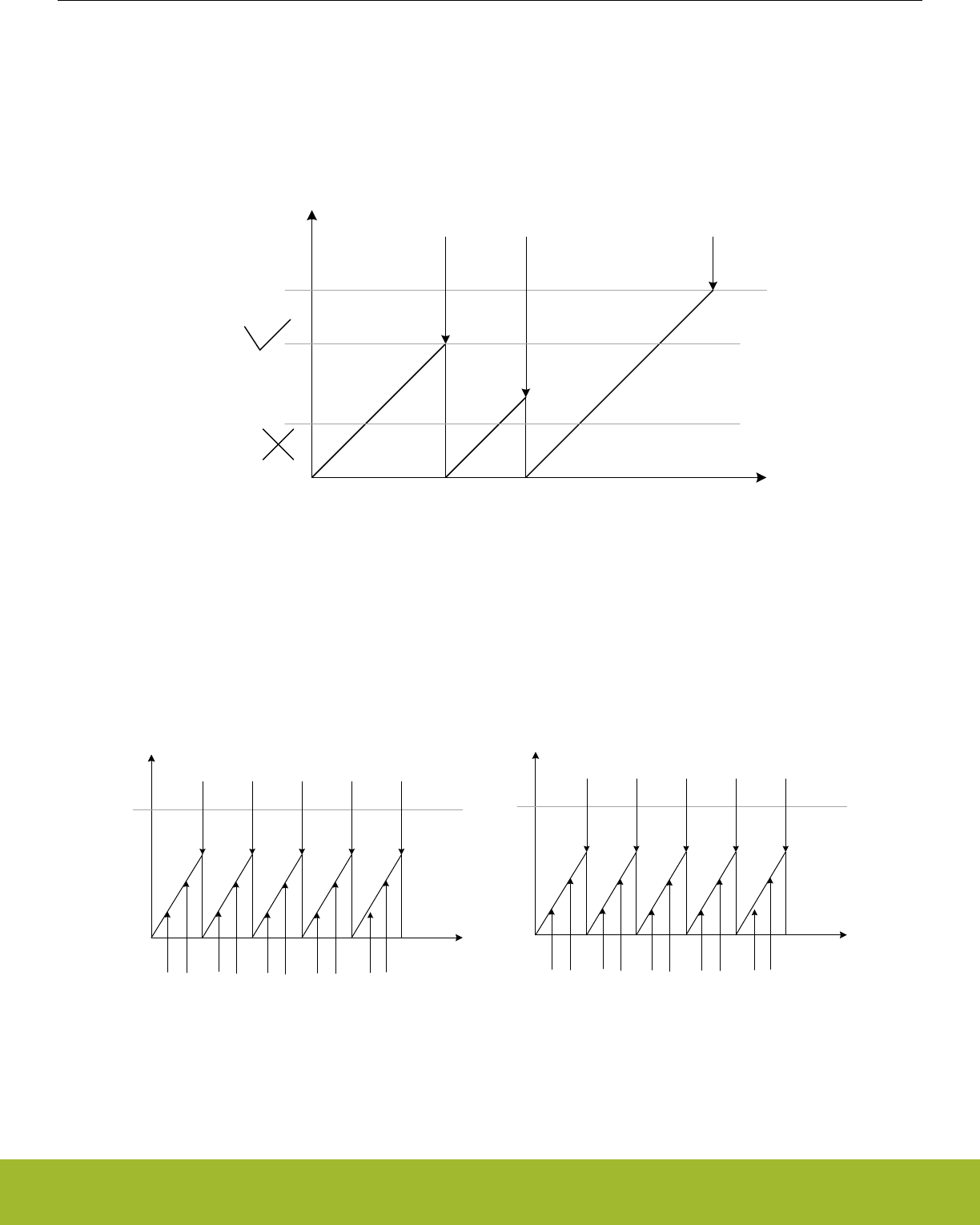
15.3.7 PRS as Watchdog Clear
The first PRS channel (selected by register WDOGn_PCH0_PRSCTRL) can be used to clear the watchdog counter. To enable this fea-
ture, CLRSRC must be set to 1. Figure 15.2 PRS Clearing WDOG on page 427 shows how the PRS channel takes over the WDOG
clear function. Clearing the WDOG with the PRS is mutually exclusive of clearing the WDT by software.
Timeout period
Counter value
Time
PRS clear Timeout Irq
Warning Irq
Legal Window
Figure 15.2. PRS Clearing WDOG
15.3.8 PRS Rising Edge Monitoring
PRS channels can be used to monitor multiple processes. If enabled, every time the watch dog timer is cleared the PRS channels are
checked and any channel which has not seen an event can trigger an interrupt.
Counter value
Time
wdog clear
PRS[0] PRS[1]
Time
PRS[0]
PRS[1] PRS[2]
Figure 15.3. PRS Edge Monitoring in WDOG
Reference Manual
WDOG - Watchdog Timer
silabs.com | Smart. Connected. Energy-friendly. Preliminary Rev. 0.5 | 427

15.4 Register Map
The offset register address is relative to the registers base address.
Offset Name Type Description
0x000 WDOG_CTRL RW Control Register
0x004 WDOG_CMD W1 Command Register
0x008 WDOG_SYNCBUSY RSynchronization Busy Register
0x00C WDOGn_PCH0_PRSCTRL RW PRS Control Register
0x010 WDOGn_PCH1_PRSCTRL RW PRS Control Register
0x01C WDOG_IF RWatchdog Interrupt Flags
0x020 WDOG_IFS W1 Interrupt Flag Set Register
0x024 WDOG_IFC (R)W1 Interrupt Flag Clear Register
0x028 WDOG_IEN RW Interrupt Enable Register
Reference Manual
WDOG - Watchdog Timer
silabs.com | Smart. Connected. Energy-friendly. Preliminary Rev. 0.5 | 428

15.5 Register Description
15.5.1 WDOG_CTRL - Control Register (Async Reg)
For more information about asynchronous registers please see 4.3 Access to Low Energy Peripherals (Asynchronous Registers).
Offset Bit Position
0x000
31
30
29
28
27
26
25
24
23
22
21
20
19
18
17
16
15
14
13
12
11
10
9
8
7
6
5
4
3
2
1
0
Reset
0
0
0x0
0x0
0x0
0xF
0
0
0
0
0
0
0
Access
RW
RW
RW
RW
RW
RW
RW
RW
RW
RW
RW
RW
RW
Name
WDOGRSTDIS
CLRSRC
WINSEL
WARNSEL
CLKSEL
PERSEL
SWOSCBLOCK
EM4BLOCK
LOCK
EM3RUN
EM2RUN
DEBUGRUN
EN
Bit Name Reset Access Description
31 WDOGRSTDIS 0 RW Watchdog Reset Disable
Disable watchdog reset output.
Value Mode Description
0 EN A timeout will cause a watchdog reset
1 DIS A timeout will not cause a watchdog reset
30 CLRSRC 0 RW Watchdog Clear Source
Select watchdog clear source.
Value Mode Description
0 SW A write to the clear bit will clear the watchdog counter
1 PCH0 A rising edge on the PRS Channel0 will clear the watchdog counter
29:27 Reserved To ensure compatibility with future devices, always write bits to 0. More information in 1.2 Conven-
tions
26:24 WINSEL 0x0 RW Watchdog Illegal Window Select
Select watchdog illegal limit.
Value Description
0 Disabled.
1 Window limit is 12.5% of the Timeout.
2 Window limit is 25.0% of the Timeout.
3 Window limit is 37.5% of the Timeout.
4 Window limit is 50.0% of the Timeout.
5 Window limit is 62.5% of the Timeout.
6 Window limit is 75.0% of the Timeout.
7 Window limit is 87.5% of the Timeout.
Reference Manual
WDOG - Watchdog Timer
silabs.com | Smart. Connected. Energy-friendly. Preliminary Rev. 0.5 | 429

Bit Name Reset Access Description
23:18 Reserved To ensure compatibility with future devices, always write bits to 0. More information in 1.2 Conven-
tions
17:16 WARNSEL 0x0 RW Watchdog Timeout Period Select
Select watchdog warning timeout period.
Value Description
0 Disabled.
1 Warning timeout is 25% of the Timeout.
2 Warning timeout is 50% of the Timeout.
3 Warning timeout is 75% of the Timeout.
15:14 Reserved To ensure compatibility with future devices, always write bits to 0. More information in 1.2 Conven-
tions
13:12 CLKSEL 0x0 RW Watchdog Clock Select
Selects the WDOG oscillator, i.e. the clock on which the watchdog will run.
Value Mode Description
0 ULFRCO ULFRCO
1 LFRCO LFRCO
2 LFXO LFXO
3 HFCORECLK HFCORECLK
11:8 PERSEL 0xF RW Watchdog Timeout Period Select
Select watchdog timeout period.
Value Description
0 Timeout period of 9 watchdog clock cycles.
1 Timeout period of 17 watchdog clock cycles.
2 Timeout period of 33 watchdog clock cycles.
3 Timeout period of 65 watchdog clock cycles.
4 Timeout period of 129 watchdog clock cycles.
5 Timeout period of 257 watchdog clock cycles.
6 Timeout period of 513 watchdog clock cycles.
7 Timeout period of 1k watchdog clock cycles.
8 Timeout period of 2k watchdog clock cycles.
9 Timeout period of 4k watchdog clock cycles.
10 Timeout period of 8k watchdog clock cycles.
11 Timeout period of 16k watchdog clock cycles.
12 Timeout period of 32k watchdog clock cycles.
13 Timeout period of 64k watchdog clock cycles.
14 Timeout period of 128k watchdog clock cycles.
Reference Manual
WDOG - Watchdog Timer
silabs.com | Smart. Connected. Energy-friendly. Preliminary Rev. 0.5 | 430

Bit Name Reset Access Description
15 Timeout period of 256k watchdog clock cycles.
7 Reserved To ensure compatibility with future devices, always write bits to 0. More information in 1.2 Conven-
tions
6 SWOSCBLOCK 0 RW Software Oscillator Disable Block
Set to disallow disabling of the selected WDOG oscillator. Writing this bit to 1 will turn on the selected WDOG oscillator if it
is not already running.
Value Description
0 Software is allowed to disable the selected WDOG oscillator. See CMU
for detailed description. Note that also CMU registers are lockable.
1 Software is not allowed to disable the selected WDOG oscillator.
5 EM4BLOCK 0 RW Energy Mode 4 Block
Set to disallow EM4 entry by software.
Value Description
0 EM4 can be entered by software. See EMU for detailed description.
1 EM4 cannot be entered by software.
4 LOCK 0 RW Configuration lock
Set to lock the watchdog configuration. This bit can only be cleared by reset.
Value Description
0 Watchdog configuration can be changed.
1 Watchdog configuration cannot be changed.
3 EM3RUN 0 RW Energy Mode 3 Run Enable
Set to keep watchdog running in EM3.
Value Description
0 Watchdog timer is frozen in EM3.
1 Watchdog timer is running in EM3.
2 EM2RUN 0 RW Energy Mode 2 Run Enable
Set to keep watchdog running in EM2.
Value Description
0 Watchdog timer is frozen in EM2.
1 Watchdog timer is running in EM2.
1 DEBUGRUN 0 RW Debug Mode Run Enable
Set to keep watchdog running in debug mode.
Value Description
0 Watchdog timer is frozen in debug mode.
1 Watchdog timer is running in debug mode.
Reference Manual
WDOG - Watchdog Timer
silabs.com | Smart. Connected. Energy-friendly. Preliminary Rev. 0.5 | 431

Bit Name Reset Access Description
0 EN 0 RW Watchdog Timer Enable
Set to enabled watchdog timer.
15.5.2 WDOG_CMD - Command Register (Async Reg)
For more information about asynchronous registers please see 4.3 Access to Low Energy Peripherals (Asynchronous Registers).
Offset Bit Position
0x004
31
30
29
28
27
26
25
24
23
22
21
20
19
18
17
16
15
14
13
12
11
10
9
8
7
6
5
4
3
2
1
0
Reset
0
Access
W1
Name
CLEAR
Bit Name Reset Access Description
31:1 Reserved To ensure compatibility with future devices, always write bits to 0. More information in 1.2 Conven-
tions
0 CLEAR 0 W1 Watchdog Timer Clear
Clear watchdog timer. The bit must be written 4 watchdog cycles before the timeout.
Value Mode Description
0 UNCHANGED Watchdog timer is unchanged.
1 CLEARED Watchdog timer is cleared to 0.
Reference Manual
WDOG - Watchdog Timer
silabs.com | Smart. Connected. Energy-friendly. Preliminary Rev. 0.5 | 432

15.5.3 WDOG_SYNCBUSY - Synchronization Busy Register
Offset Bit Position
0x008
31
30
29
28
27
26
25
24
23
22
21
20
19
18
17
16
15
14
13
12
11
10
9
8
7
6
5
4
3
2
1
0
Reset
0
0
0
0
Access
R
R
R
R
Name
PCH1_PRSCTRL
PCH0_PRSCTRL
CMD
CTRL
Bit Name Reset Access Description
31:4 Reserved To ensure compatibility with future devices, always write bits to 0. More information in 1.2 Conven-
tions
3 PCH1_PRSCTRL 0 R PCH1_PRSCTRL Register Busy
Set when the value written to PCH1_PRSCTRL is being synchronized.
2 PCH0_PRSCTRL 0 R PCH0_PRSCTRL Register Busy
Set when the value written to PCH0_PRSCTRL is being synchronized.
1 CMD 0 R CMD Register Busy
Set when the value written to CMD is being synchronized.
0 CTRL 0 R CTRL Register Busy
Set when the value written to CTRL is being synchronized.
Reference Manual
WDOG - Watchdog Timer
silabs.com | Smart. Connected. Energy-friendly. Preliminary Rev. 0.5 | 433

15.5.4 WDOGn_PCHx_PRSCTRL - PRS Control Register (Async Reg)
For more information about asynchronous registers please see 4.3 Access to Low Energy Peripherals (Asynchronous Registers).
Offset Bit Position
0x00C
31
30
29
28
27
26
25
24
23
22
21
20
19
18
17
16
15
14
13
12
11
10
9
8
7
6
5
4
3
2
1
0
Reset
0
0x0
Access
RW
RW
Name
PRSMISSRSTEN
PRSSEL
Bit Name Reset Access Description
31:9 Reserved To ensure compatibility with future devices, always write bits to 0. More information in 1.2 Conven-
tions
8 PRSMISSRSTEN 0 RW PRS missing event will trigger a watchdog reset
When set, a PRS missing event will trigger a watchdog reset.
7:4 Reserved To ensure compatibility with future devices, always write bits to 0. More information in 1.2 Conven-
tions
3:0 PRSSEL 0x0 RW PRS Channel PRS Select
These bits select the PRS input for the PRS channel.
Value Mode Description
0 PRSCH0 PRS Channel 0 selected as input
1 PRSCH1 PRS Channel 1 selected as input
2 PRSCH2 PRS Channel 2 selected as input
3 PRSCH3 PRS Channel 3 selected as input
4 PRSCH4 PRS Channel 4 selected as input
5 PRSCH5 PRS Channel 5 selected as input
6 PRSCH6 PRS Channel 6 selected as input
7 PRSCH7 PRS Channel 7 selected as input
8 PRSCH8 PRS Channel 8 selected as input
9 PRSCH9 PRS Channel 9 selected as input
10 PRSCH10 PRS Channel 10 selected as input
11 PRSCH11 PRS Channel 11 selected as input
Reference Manual
WDOG - Watchdog Timer
silabs.com | Smart. Connected. Energy-friendly. Preliminary Rev. 0.5 | 434

15.5.5 WDOG_IF - Watchdog Interrupt Flags
Offset Bit Position
0x01C
31
30
29
28
27
26
25
24
23
22
21
20
19
18
17
16
15
14
13
12
11
10
9
8
7
6
5
4
3
2
1
0
Reset
0
0
0
0
0
Access
R
R
R
R
R
Name
PEM1
PEM0
WIN
WARN
TOUT
Bit Name Reset Access Description
31:5 Reserved To ensure compatibility with future devices, always write bits to 0. More information in 1.2 Conven-
tions
4 PEM1 0 R PRS Channel One Event Missing Interrupt Flag
Set when a WDOG clear happens before a prs event has been detected on PRS channel one.
3 PEM0 0 R PRS Channel Zero Event Missing Interrupt Flag
Set when a WDOG clear happens before a prs event has been detected on PRS channel zero.
2 WIN 0 R WDOG Window Interrupt Flag
Set when a WDOG clear happens below the window limit value.
1 WARN 0 R WDOG Warning Timeout Interrupt Flag
Set when a WDOG warning timeout has occurred.
0 TOUT 0 R WDOG Timeout Interrupt Flag
Set when a WDOG timeout has occurred.
Reference Manual
WDOG - Watchdog Timer
silabs.com | Smart. Connected. Energy-friendly. Preliminary Rev. 0.5 | 435

15.5.6 WDOG_IFS - Interrupt Flag Set Register
Offset Bit Position
0x020
31
30
29
28
27
26
25
24
23
22
21
20
19
18
17
16
15
14
13
12
11
10
9
8
7
6
5
4
3
2
1
0
Reset
0
0
0
0
0
Access
W1
W1
W1
W1
W1
Name
PEM1
PEM0
WIN
WARN
TOUT
Bit Name Reset Access Description
31:5 Reserved To ensure compatibility with future devices, always write bits to 0. More information in 1.2 Conven-
tions
4 PEM1 0 W1 Set PEM1 Interrupt Flag
Write 1 to set the PEM1 interrupt flag
3 PEM0 0 W1 Set PEM0 Interrupt Flag
Write 1 to set the PEM0 interrupt flag
2 WIN 0 W1 Set WIN Interrupt Flag
Write 1 to set the WIN interrupt flag
1 WARN 0 W1 Set WARN Interrupt Flag
Write 1 to set the WARN interrupt flag
0 TOUT 0 W1 Set TOUT Interrupt Flag
Write 1 to set the TOUT interrupt flag
Reference Manual
WDOG - Watchdog Timer
silabs.com | Smart. Connected. Energy-friendly. Preliminary Rev. 0.5 | 436

15.5.7 WDOG_IFC - Interrupt Flag Clear Register
Offset Bit Position
0x024
31
30
29
28
27
26
25
24
23
22
21
20
19
18
17
16
15
14
13
12
11
10
9
8
7
6
5
4
3
2
1
0
Reset
0
0
0
0
0
Access
(R)W1
(R)W1
(R)W1
(R)W1
(R)W1
Name
PEM1
PEM0
WIN
WARN
TOUT
Bit Name Reset Access Description
31:5 Reserved To ensure compatibility with future devices, always write bits to 0. More information in 1.2 Conven-
tions
4 PEM1 0 (R)W1 Clear PEM1 Interrupt Flag
Write 1 to clear the PEM1 interrupt flag. Reading returns the value of the IF and clears the corresponding interrupt flags
(This feature must be enabled globally in MSC.).
3 PEM0 0 (R)W1 Clear PEM0 Interrupt Flag
Write 1 to clear the PEM0 interrupt flag. Reading returns the value of the IF and clears the corresponding interrupt flags
(This feature must be enabled globally in MSC.).
2 WIN 0 (R)W1 Clear WIN Interrupt Flag
Write 1 to clear the WIN interrupt flag. Reading returns the value of the IF and clears the corresponding interrupt flags (This
feature must be enabled globally in MSC.).
1 WARN 0 (R)W1 Clear WARN Interrupt Flag
Write 1 to clear the WARN interrupt flag. Reading returns the value of the IF and clears the corresponding interrupt flags
(This feature must be enabled globally in MSC.).
0 TOUT 0 (R)W1 Clear TOUT Interrupt Flag
Write 1 to clear the TOUT interrupt flag. Reading returns the value of the IF and clears the corresponding interrupt flags
(This feature must be enabled globally in MSC.).
Reference Manual
WDOG - Watchdog Timer
silabs.com | Smart. Connected. Energy-friendly. Preliminary Rev. 0.5 | 437

15.5.8 WDOG_IEN - Interrupt Enable Register
Offset Bit Position
0x028
31
30
29
28
27
26
25
24
23
22
21
20
19
18
17
16
15
14
13
12
11
10
9
8
7
6
5
4
3
2
1
0
Reset
0
0
0
0
0
Access
RW
RW
RW
RW
RW
Name
PEM1
PEM0
WIN
WARN
TOUT
Bit Name Reset Access Description
31:5 Reserved To ensure compatibility with future devices, always write bits to 0. More information in 1.2 Conven-
tions
4 PEM1 0 RW PEM1 Interrupt Enable
Enable/disable the PEM1 interrupt
3 PEM0 0 RW PEM0 Interrupt Enable
Enable/disable the PEM0 interrupt
2 WIN 0 RW WIN Interrupt Enable
Enable/disable the WIN interrupt
1 WARN 0 RW WARN Interrupt Enable
Enable/disable the WARN interrupt
0 TOUT 0 RW TOUT Interrupt Enable
Enable/disable the TOUT interrupt
Reference Manual
WDOG - Watchdog Timer
silabs.com | Smart. Connected. Energy-friendly. Preliminary Rev. 0.5 | 438
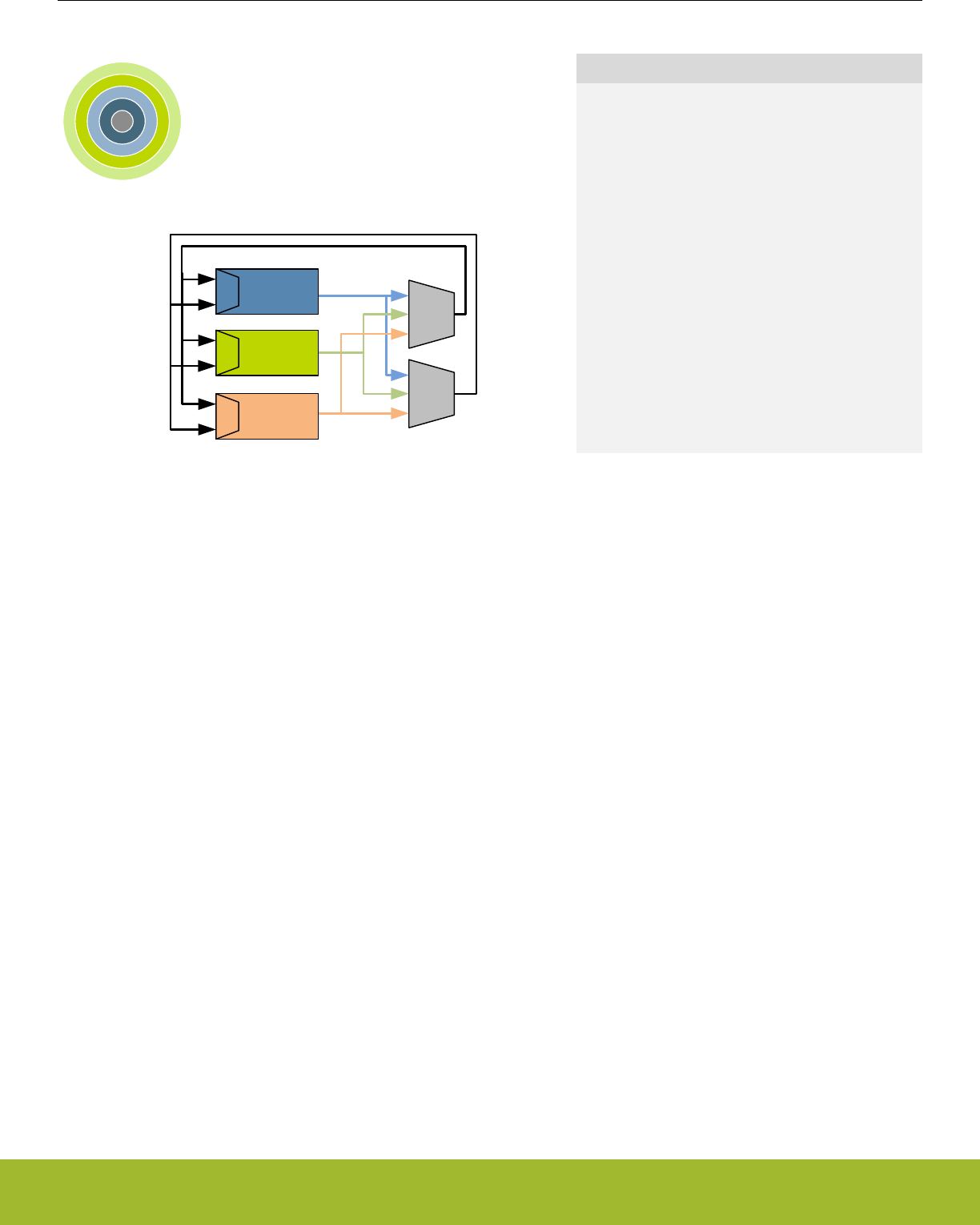
16. PRS - Peripheral Reflex System
0 1 2 3 4
Timer
ADC
DMA
PRS
Ch
PRS
Ch
Quick Facts
What?
The PRS (Peripheral Reflex System) allows configu-
rable, fast, and autonomous communication be-
tween peripherals.
Why?
Events and signals from one peripheral can be used
as input signals or triggered by other peripherals.
Besides, PRS reduces latency and ensures predict-
able timing by reducing software overhead and thus
current consumption.
How?
Without CPU intervention the peripherals can send
Reflex signals (both pulses and level) to each other
in single- or chained steps. The peripherals can be
set up to perform actions based on the incoming Re-
flex signals. This results in improved system per-
formance and reduced energy consumption.
16.1 Introduction
The Peripheral Reflex System (PRS) is a network allowing direct communication between different peripheral modules without involving
the CPU. Peripheral modules which send out Reflex signals are called producers. The PRS routes these Reflex signals through Reflex
channels to consumer peripherals which perform actions depending on the Reflex signals received. The format for the Reflex signals is
not given, but edge triggers and other functionality can be applied by the PRS.
16.2 Features
• 12 Configurable Reflex Channels
• Each channel can be connected to any producing peripheral, including the PRS channels
• Consumers can choose which channel to listen to
• Selectable edge detector (Rising, falling and both edges)
• Configurable AND and OR between channels
• Optional channel invert
• PRS can generate event to CPU
• Two independent DMA requests based on PRS channels
• Software controlled channel output
• Configurable level
• Triggered pulses
Reference Manual
PRS - Peripheral Reflex System
silabs.com | Smart. Connected. Energy-friendly. Preliminary Rev. 0.5 | 439
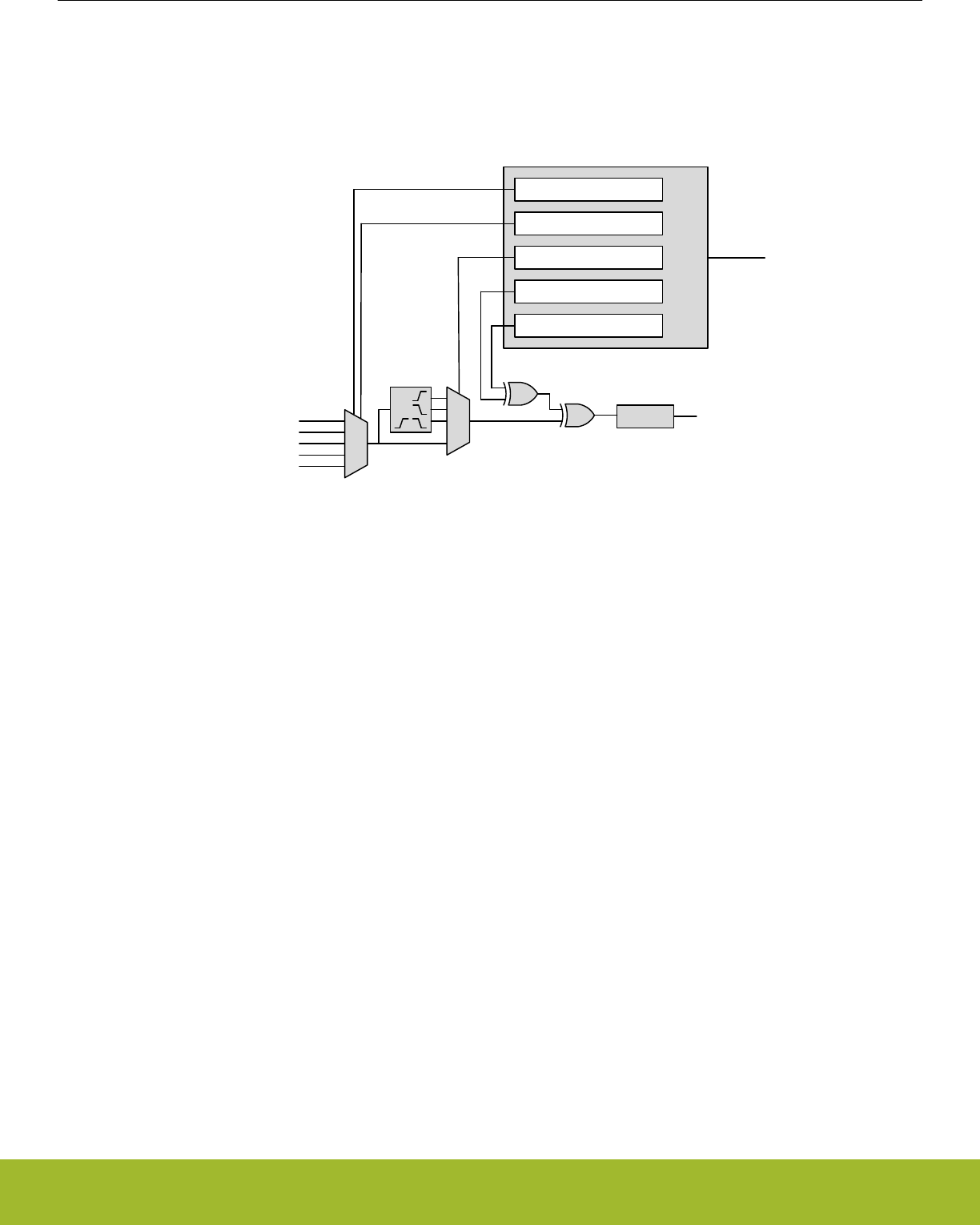
16.3 Functional Description
An overview of the PRS module is shown in Figure 16.1 PRS Overview on page 440. The PRS contains 12 Reflex channels. All chan-
nels can select any Reflex signal offered by the producers. The consumers can choose which PRS channel to listen to and perform
actions based on the Reflex signals routed through that channel. The Reflex signals can be both edge signals and level signals.
APB Interface
Reg
SIGSEL[2:0]
EDSEL[1:0] APB bus
Signals from
producer
peripherals
Signals to
consumer
peripherals
SWPULSE[n]
SWLEVEL[n]
SOURCESEL[5:0]
Figure 16.1. PRS Overview
16.3.1 Channel Functions
Different functions can be applied to a Reflex signal within the PRS. Each channel includes an edge detector to enable generation of
pulse signals from level signals. The PRS channels can also be manually triggered by writing to PRS_SWPULSE or PRS_SWLEVEL.
SWLEVEL[n] is a programmable level for each channel and holds the value it is programmed to. Setting SWPULSE[n] will cause the
PRS channel to output a high pulse that is one HFCLK cycle wide. The SWLEVEL[n] and SWPULSE[n] signals are then XOR'ed with
the selected input from the producers to form the output signal sent to the consumers listening to the channel. For example, when
SWLEVEL[n] is set, if a producer produces a signal of 1, this will cause a channel output of 0.
16.3.1.1 Operational Mode
Reflex channels can operate in two modes, synchronous or asynchronous. In synchronous mode Reflex signals are clocked on the
HFCLK, and can be used by any Reflex consumer. However, this will not work in EM2/EM3, since the HFCLK will be turned off.
Asynchronous Reflex channels are not clocked on HFCLK, and can be used even in EM2/EM3. However, the asynchronous mode can
only be used by a subset of the Reflex consumers.
The asynchronous Reflex signals generated by the producers are indicated in the SIGSEL field of PRS_CHx_CTRL register. The con-
sumers capable of utilizing asynchronous Reflex signals include the LEUART and the PCNT. The USART can also utilize some particu-
lar asynchronous signals. Please refer to the respective modules for details on how to configure them to use the PRS.
Note: If a Reflex channel with ASYNC field of PRS_CHx_CTRL register set to '1' is used in a consumer not supporting asynchronous
reflexes, the behaviour is undefined
Reference Manual
PRS - Peripheral Reflex System
silabs.com | Smart. Connected. Energy-friendly. Preliminary Rev. 0.5 | 440

16.3.1.2 Edge Detection and Clock Domains
Using EDSEL in PRS_CHx_CTRL, edge detection can be applied to a PRS signal. When edge detection is enabled, changes in the
PRS input will result in a pulse on the PRS channel. This requires that the ASYNC bit in PRS_CHx_CTRL is cleared. Signals on the
PRS input must be at least one HFCLK period wide in order to be detected properly. This applies to all cases when ASYNC is not used
in the PRS.
For communication between peripherals on different prescaled clocks (e.g. between peripherals on HFCLK and HFPERCLK), there are
two options. One option is to use level signals. No additional action is needed for level signals, but software must make sure that the
level signals are held long enough for the destination domain to detect them. The other option is to use pulse signals. For pulse signals,
edge detection should be enabled (by configuring EDSEL in PRS_CHx_CTRL to positive edge, negative edge, or both) and STRETCH
in PRS_CHx_CTRL should be set. When edge detection and stretch are enabled on a PRS source, the output on the PRS channel is
held long enough for the destination domain to detect the pulse. This also works if there are multiple destination domains running at
different frequencies.
16.3.1.3 Configurable PRS Logic
Each PRS channel has three logic functions that can be used by themselves or in combination. The selected PRS source can be
AND'ed with the next PRS channel output, OR'ed with the previous PRS channel output and inverted. This is shown in Figure 16.1 PRS
Overview on page 440. The order of the functions is important. If OR and AND are enabled at the same time, AND is applied first, and
then OR.
Signals from
producer
peripherals
PRS[i-1]
PRS[i+1]
PRS[0]
PRS[N-1]
ANDNEXT
ORPREV INV
PRS[i]
Figure 16.2. Configurable PRS Logic
In addition to the logic functions that can combine a PRS channel with one of its neighbors, a PRS channel can also select any other
PRS channel as input. This can allow relatively complex logic functions to be created.
16.3.2 Producers
Through SOURCESEL in PRS_CHx_CTRL, each PRS channel selects signal producers. Each producer outputs one or more signals
which can be selected by setting the SIGSEL field in PRS_CHx_CTRL. Setting the SOURCESEL bits to 0 (Off) leads to a constant 0
output from the input mux. An overview of the available producers can be found in the SOURCESEL and SIGSEL fields in
PRS_CHx_CTRL.
Reference Manual
PRS - Peripheral Reflex System
silabs.com | Smart. Connected. Energy-friendly. Preliminary Rev. 0.5 | 441

16.3.3 Consumers
Consumer peripherals (Listed in Table 16.1 Reflex Consumers on page 442) can be set to listen to a PRS channel and perform an
action based on the signal received on that channel. While most consumers can handle either only pulse input or only level input, some
can handle both pulse and level inputs.
Table 16.1. Reflex Consumers
Module Reflex Input Input Format
TIMER Compare/Capture Channel Pulse / Level
Alternate Input for DTI
(Available only in specific TIMERs
Please check datasheet for details)
Level
Alternate Input for DTI Fault 0
(Available only in specific TIMERs
Please check datasheet for details)
Level
Alternate Input for DTI Fault 1
(Available only in specific TIMERs
Please check datasheet for details)
Level
WTIMER Compare/Capture Channel Pulse / Level
Alternate Input for DTI
(Available only in specific WTIMERs
Please check datasheet for details)
Level
Alternate Input for DTI Fault 0
(Available only in specific WTIMERs
Please check datasheet for details)
Level
Alternate Input for DTI Fault 1
(Available only in specific WTIMERs
Please check datasheet for details)
Level
USART RX/TX Trigger Pulse
Alternate Input for IrDA Level
Alternate Input for RX Level
Alternate Input for CLK Level
VDAC Channel 0 Trigger Pulse
Channel 1 Trigger Pulse
ADC Single Sample Trigger Pulse
Scan Sequence Trigger Pulse
IDAC Alternate Input for OUTMODE Level
CMU Alternate Input for Calibration Up-Counter Level
Alternate Input for Calibration Down-Coun-
ter
Level
LEUART Alternate Input for RX Level
PCNT Compare/Clear Trigger Pulse/Level
Alternate Input for S0IN Level
Alternate Input for S1IN Level
Reference Manual
PRS - Peripheral Reflex System
silabs.com | Smart. Connected. Energy-friendly. Preliminary Rev. 0.5 | 442

Module Reflex Input Input Format
LESENSE Scan Start Pulse
LESENSE Decoder Bit 0 Level
LESENSE Decoder Bit 1 Level
LESENSE Decoder Bit 2 Level
LESENSE Decoder Bit 3 Level
WDOG Peripheral Watchdog Pulse
LETIMER Start LETIMER Pulse
Stop LETIMER Pulse
Clear LETIMER Pulse
RTCC Compare/Capture Channel Pulse/Level
PRS Set Event Pulse
DMA Request 0 Pulse
DMA Request 1 Pulse
CAPSENSE Start Conversion Pulse
16.3.4 Event on PRS
The PRS can be used to send events to the MCU. This is very useful in combination with the Wait For Event (WFE) instruction. A single
PRS channel can be selected for this using SEVONPRSSEL in PRS_CTRL, and the feature is enabled by setting SEVONPRS in the
same register.
Using SEVONPRS, one can e.g. set up a timer to trigger an event to the MCU periodically, every time letting the MCU pass through a
WFE instruction in its program. This can help in performance-critical sections where timing is known, and the goal is to wait for an
event, then execute some code, then wait for an event, then execute some code and so on.
16.3.5 DMA Request on PRS
Up to two independent DMA requests can be generated by the PRS. The PRS signals triggering the DMA requests are selected with
the DMAREQxSEL fields in DMA_CTRL. The DMA requests are cleared on write to the DMAREQxSEL fields and when the DMA serv-
ices the requests. The requests are set whenever the selected PRS signals are high.
The selected PRS signals must have ASYNC cleared when they are used as inputs to the DMA. Edge detection in the PRS can be
enabled to only trigger transfers on edges.
Reference Manual
PRS - Peripheral Reflex System
silabs.com | Smart. Connected. Energy-friendly. Preliminary Rev. 0.5 | 443

16.3.6 Example
The example below (illustrated in Figure 16.3 TIMER0 overflow starting ADC0 single conversions through PRS channel 5. on page
444) shows how to set up ADC0 to start single conversions every time TIMER0 overflows (one HFPERCLK cycle high pulse), using
PRS channel 5:
• Set SOURCESEL in PRS_CH5_CTRL to TIMER0 as input to PRS channel 5.
• Set SIGSEL in PRS_CH5_CTRL to select the overflow signal (TIMER0OF from TIMER0).
• Configure ADC0 with the desired conversion set-up.
• Set SINGLEPRSEN in ADC0_SINGLECTRL to 1 to enable single conversions to be started by a high PRS input signal.
• Set SINGLEPRSSEL in ADC0_SINGLECTRL to 0x5 to select PRS channel 5 as input to start the single conversion.
• Start TIMER0 with the desired TOP value, an overflow PRS signal is output automatically on overflow.
Note that the ADC results needs to be fetched either by the CPU or DMA.
PRS
TIMER0 ADC0
ch0
ch1
ch2
ch3
ch4
ch5
ch6
ch7
Start single conv.Overflow
Figure 16.3. TIMER0 overflow starting ADC0 single conversions through PRS channel 5.
16.4 Register Map
The offset register address is relative to the registers base address.
Offset Name Type Description
0x000 PRS_SWPULSE W1 Software Pulse Register
0x004 PRS_SWLEVEL RW Software Level Register
0x008 PRS_ROUTEPEN RW I/O Routing Pin Enable Register
0x010 PRS_ROUTELOC0 RW I/O Routing Location Register
0x014 PRS_ROUTELOC1 RW I/O Routing Location Register
0x018 PRS_ROUTELOC2 RW I/O Routing Location Register
0x030 PRS_CTRL RW Control Register
0x034 PRS_DMAREQ0 RW DMA Request 0 Register
0x038 PRS_DMAREQ1 RW DMA Request 1 Register
0x040 PRS_PEEK RPRS Channel Values
0x050 PRS_CH0_CTRL RW Channel Control Register
... PRS_CHx_CTRL RW Channel Control Register
0x07C PRS_CH11_CTRL RW Channel Control Register
Reference Manual
PRS - Peripheral Reflex System
silabs.com | Smart. Connected. Energy-friendly. Preliminary Rev. 0.5 | 444

16.5 Register Description
16.5.1 PRS_SWPULSE - Software Pulse Register
Offset Bit Position
0x000
31
30
29
28
27
26
25
24
23
22
21
20
19
18
17
16
15
14
13
12
11
10
9
8
7
6
5
4
3
2
1
0
Reset
0
0
0
0
0
0
0
0
0
0
0
0
Access
W1
W1
W1
W1
W1
W1
W1
W1
W1
W1
W1
W1
Name
CH11PULSE
CH10PULSE
CH9PULSE
CH8PULSE
CH7PULSE
CH6PULSE
CH5PULSE
CH4PULSE
CH3PULSE
CH2PULSE
CH1PULSE
CH0PULSE
Bit Name Reset Access Description
31:12 Reserved To ensure compatibility with future devices, always write bits to 0. More information in 1.2 Conven-
tions
11 CH11PULSE 0 W1 Channel 11 Pulse Generation
See bit 0.
10 CH10PULSE 0 W1 Channel 10 Pulse Generation
See bit 0.
9 CH9PULSE 0 W1 Channel 9 Pulse Generation
See bit 0.
8 CH8PULSE 0 W1 Channel 8 Pulse Generation
See bit 0.
7 CH7PULSE 0 W1 Channel 7 Pulse Generation
See bit 0.
6 CH6PULSE 0 W1 Channel 6 Pulse Generation
See bit 0.
5 CH5PULSE 0 W1 Channel 5 Pulse Generation
See bit 0.
4 CH4PULSE 0 W1 Channel 4 Pulse Generation
See bit 0.
3 CH3PULSE 0 W1 Channel 3 Pulse Generation
See bit 0.
2 CH2PULSE 0 W1 Channel 2 Pulse Generation
See bit 0.
1 CH1PULSE 0 W1 Channel 1 Pulse Generation
See bit 0.
0 CH0PULSE 0 W1 Channel 0 Pulse Generation
Write to 1 to generate one HFCLK cycle high pulse. This pulse is XOR'ed with the corresponding bit in the SWLEVEL regis-
ter and the selected PRS input signal to generate the channel output.
Reference Manual
PRS - Peripheral Reflex System
silabs.com | Smart. Connected. Energy-friendly. Preliminary Rev. 0.5 | 445

16.5.2 PRS_SWLEVEL - Software Level Register
Offset Bit Position
0x004
31
30
29
28
27
26
25
24
23
22
21
20
19
18
17
16
15
14
13
12
11
10
9
8
7
6
5
4
3
2
1
0
Reset
0
0
0
0
0
0
0
0
0
0
0
0
Access
RW
RW
RW
RW
RW
RW
RW
RW
RW
RW
RW
RW
Name
CH11LEVEL
CH10LEVEL
CH9LEVEL
CH8LEVEL
CH7LEVEL
CH6LEVEL
CH5LEVEL
CH4LEVEL
CH3LEVEL
CH2LEVEL
CH1LEVEL
CH0LEVEL
Bit Name Reset Access Description
31:12 Reserved To ensure compatibility with future devices, always write bits to 0. More information in 1.2 Conven-
tions
11 CH11LEVEL 0 RW Channel 11 Software Level
See bit 0.
10 CH10LEVEL 0 RW Channel 10 Software Level
See bit 0.
9 CH9LEVEL 0 RW Channel 9 Software Level
See bit 0.
8 CH8LEVEL 0 RW Channel 8 Software Level
See bit 0.
7 CH7LEVEL 0 RW Channel 7 Software Level
See bit 0.
6 CH6LEVEL 0 RW Channel 6 Software Level
See bit 0.
5 CH5LEVEL 0 RW Channel 5 Software Level
See bit 0.
4 CH4LEVEL 0 RW Channel 4 Software Level
See bit 0.
3 CH3LEVEL 0 RW Channel 3 Software Level
See bit 0.
2 CH2LEVEL 0 RW Channel 2 Software Level
See bit 0.
1 CH1LEVEL 0 RW Channel 1 Software Level
See bit 0.
0 CH0LEVEL 0 RW Channel 0 Software Level
The value in this register is XOR'ed with the corresponding bit in the SWPULSE register and the selected PRS input signal
to generate the channel output.
Reference Manual
PRS - Peripheral Reflex System
silabs.com | Smart. Connected. Energy-friendly. Preliminary Rev. 0.5 | 446

16.5.3 PRS_ROUTEPEN - I/O Routing Pin Enable Register
Offset Bit Position
0x008
31
30
29
28
27
26
25
24
23
22
21
20
19
18
17
16
15
14
13
12
11
10
9
8
7
6
5
4
3
2
1
0
Reset
0
0
0
0
0
0
0
0
0
0
0
0
Access
RW
RW
RW
RW
RW
RW
RW
RW
RW
RW
RW
RW
Name
CH11PEN
CH10PEN
CH9PEN
CH8PEN
CH7PEN
CH6PEN
CH5PEN
CH4PEN
CH3PEN
CH2PEN
CH1PEN
CH0PEN
Bit Name Reset Access Description
31:12 Reserved To ensure compatibility with future devices, always write bits to 0. More information in 1.2 Conven-
tions
11 CH11PEN 0 RW CH11 Pin Enable
When set, GPIO output from PRS channel 11 is enabled
10 CH10PEN 0 RW CH10 Pin Enable
When set, GPIO output from PRS channel 10 is enabled
9 CH9PEN 0 RW CH9 Pin Enable
When set, GPIO output from PRS channel 9 is enabled
8 CH8PEN 0 RW CH8 Pin Enable
When set, GPIO output from PRS channel 8 is enabled
7 CH7PEN 0 RW CH7 Pin Enable
When set, GPIO output from PRS channel 7 is enabled
6 CH6PEN 0 RW CH6 Pin Enable
When set, GPIO output from PRS channel 6 is enabled
5 CH5PEN 0 RW CH5 Pin Enable
When set, GPIO output from PRS channel 5 is enabled
4 CH4PEN 0 RW CH4 Pin Enable
When set, GPIO output from PRS channel 4 is enabled
3 CH3PEN 0 RW CH3 Pin Enable
When set, GPIO output from PRS channel 3 is enabled
2 CH2PEN 0 RW CH2 Pin Enable
When set, GPIO output from PRS channel 2 is enabled
1 CH1PEN 0 RW CH1 Pin Enable
When set, GPIO output from PRS channel 1 is enabled
0 CH0PEN 0 RW CH0 Pin Enable
When set, GPIO output from PRS channel 0 is enabled
Reference Manual
PRS - Peripheral Reflex System
silabs.com | Smart. Connected. Energy-friendly. Preliminary Rev. 0.5 | 447

16.5.4 PRS_ROUTELOC0 - I/O Routing Location Register
Offset Bit Position
0x010
31
30
29
28
27
26
25
24
23
22
21
20
19
18
17
16
15
14
13
12
11
10
9
8
7
6
5
4
3
2
1
0
Reset
0x00
0x00
0x00
0x00
Access
RW
RW
RW
RW
Name
CH3LOC
CH2LOC
CH1LOC
CH0LOC
Bit Name Reset Access Description
31:30 Reserved To ensure compatibility with future devices, always write bits to 0. More information in 1.2 Conven-
tions
29:24 CH3LOC 0x00 RW I/O Location
Decides the location of the channel I/O pin
Value Mode Description
0 LOC0 Location 0
1 LOC1 Location 1
2 LOC2 Location 2
3 LOC3 Location 3
4 LOC4 Location 4
5 LOC5 Location 5
6 LOC6 Location 6
7 LOC7 Location 7
8 LOC8 Location 8
9 LOC9 Location 9
10 LOC10 Location 10
11 LOC11 Location 11
12 LOC12 Location 12
13 LOC13 Location 13
14 LOC14 Location 14
23:22 Reserved To ensure compatibility with future devices, always write bits to 0. More information in 1.2 Conven-
tions
21:16 CH2LOC 0x00 RW I/O Location
Decides the location of the channel I/O pin
Value Mode Description
0 LOC0 Location 0
1 LOC1 Location 1
2 LOC2 Location 2
Reference Manual
PRS - Peripheral Reflex System
silabs.com | Smart. Connected. Energy-friendly. Preliminary Rev. 0.5 | 448

Bit Name Reset Access Description
3 LOC3 Location 3
4 LOC4 Location 4
5 LOC5 Location 5
6 LOC6 Location 6
7 LOC7 Location 7
15:14 Reserved To ensure compatibility with future devices, always write bits to 0. More information in 1.2 Conven-
tions
13:8 CH1LOC 0x00 RW I/O Location
Decides the location of the channel I/O pin
Value Mode Description
0 LOC0 Location 0
1 LOC1 Location 1
2 LOC2 Location 2
3 LOC3 Location 3
4 LOC4 Location 4
5 LOC5 Location 5
6 LOC6 Location 6
7 LOC7 Location 7
7:6 Reserved To ensure compatibility with future devices, always write bits to 0. More information in 1.2 Conven-
tions
5:0 CH0LOC 0x00 RW I/O Location
Decides the location of the channel I/O pin
Value Mode Description
0 LOC0 Location 0
1 LOC1 Location 1
2 LOC2 Location 2
3 LOC3 Location 3
4 LOC4 Location 4
5 LOC5 Location 5
6 LOC6 Location 6
7 LOC7 Location 7
8 LOC8 Location 8
9 LOC9 Location 9
10 LOC10 Location 10
11 LOC11 Location 11
12 LOC12 Location 12
13 LOC13 Location 13
Reference Manual
PRS - Peripheral Reflex System
silabs.com | Smart. Connected. Energy-friendly. Preliminary Rev. 0.5 | 449

Bit Name Reset Access Description
Reference Manual
PRS - Peripheral Reflex System
silabs.com | Smart. Connected. Energy-friendly. Preliminary Rev. 0.5 | 450

16.5.5 PRS_ROUTELOC1 - I/O Routing Location Register
Offset Bit Position
0x014
31
30
29
28
27
26
25
24
23
22
21
20
19
18
17
16
15
14
13
12
11
10
9
8
7
6
5
4
3
2
1
0
Reset
0x00
0x00
0x00
0x00
Access
RW
RW
RW
RW
Name
CH7LOC
CH6LOC
CH5LOC
CH4LOC
Bit Name Reset Access Description
31:30 Reserved To ensure compatibility with future devices, always write bits to 0. More information in 1.2 Conven-
tions
29:24 CH7LOC 0x00 RW I/O Location
Decides the location of the channel I/O pin
Value Mode Description
0 LOC0 Location 0
1 LOC1 Location 1
2 LOC2 Location 2
3 LOC3 Location 3
4 LOC4 Location 4
5 LOC5 Location 5
6 LOC6 Location 6
7 LOC7 Location 7
8 LOC8 Location 8
9 LOC9 Location 9
10 LOC10 Location 10
23:22 Reserved To ensure compatibility with future devices, always write bits to 0. More information in 1.2 Conven-
tions
21:16 CH6LOC 0x00 RW I/O Location
Decides the location of the channel I/O pin
Value Mode Description
0 LOC0 Location 0
1 LOC1 Location 1
2 LOC2 Location 2
3 LOC3 Location 3
4 LOC4 Location 4
5 LOC5 Location 5
6 LOC6 Location 6
Reference Manual
PRS - Peripheral Reflex System
silabs.com | Smart. Connected. Energy-friendly. Preliminary Rev. 0.5 | 451

Bit Name Reset Access Description
7 LOC7 Location 7
8 LOC8 Location 8
9 LOC9 Location 9
10 LOC10 Location 10
11 LOC11 Location 11
12 LOC12 Location 12
13 LOC13 Location 13
14 LOC14 Location 14
15 LOC15 Location 15
16 LOC16 Location 16
17 LOC17 Location 17
15:14 Reserved To ensure compatibility with future devices, always write bits to 0. More information in 1.2 Conven-
tions
13:8 CH5LOC 0x00 RW I/O Location
Decides the location of the channel I/O pin
Value Mode Description
0 LOC0 Location 0
1 LOC1 Location 1
2 LOC2 Location 2
3 LOC3 Location 3
4 LOC4 Location 4
5 LOC5 Location 5
6 LOC6 Location 6
7:6 Reserved To ensure compatibility with future devices, always write bits to 0. More information in 1.2 Conven-
tions
5:0 CH4LOC 0x00 RW I/O Location
Decides the location of the channel I/O pin
Value Mode Description
0 LOC0 Location 0
1 LOC1 Location 1
2 LOC2 Location 2
3 LOC3 Location 3
4 LOC4 Location 4
5 LOC5 Location 5
6 LOC6 Location 6
Reference Manual
PRS - Peripheral Reflex System
silabs.com | Smart. Connected. Energy-friendly. Preliminary Rev. 0.5 | 452

16.5.6 PRS_ROUTELOC2 - I/O Routing Location Register
Offset Bit Position
0x018
31
30
29
28
27
26
25
24
23
22
21
20
19
18
17
16
15
14
13
12
11
10
9
8
7
6
5
4
3
2
1
0
Reset
0x00
0x00
0x00
0x00
Access
RW
RW
RW
RW
Name
CH11LOC
CH10LOC
CH9LOC
CH8LOC
Bit Name Reset Access Description
31:30 Reserved To ensure compatibility with future devices, always write bits to 0. More information in 1.2 Conven-
tions
29:24 CH11LOC 0x00 RW I/O Location
Decides the location of the channel I/O pin
Value Mode Description
0 LOC0 Location 0
1 LOC1 Location 1
2 LOC2 Location 2
3 LOC3 Location 3
4 LOC4 Location 4
5 LOC5 Location 5
23:22 Reserved To ensure compatibility with future devices, always write bits to 0. More information in 1.2 Conven-
tions
21:16 CH10LOC 0x00 RW I/O Location
Decides the location of the channel I/O pin
Value Mode Description
0 LOC0 Location 0
1 LOC1 Location 1
2 LOC2 Location 2
3 LOC3 Location 3
4 LOC4 Location 4
5 LOC5 Location 5
15:14 Reserved To ensure compatibility with future devices, always write bits to 0. More information in 1.2 Conven-
tions
13:8 CH9LOC 0x00 RW I/O Location
Decides the location of the channel I/O pin
Value Mode Description
0 LOC0 Location 0
Reference Manual
PRS - Peripheral Reflex System
silabs.com | Smart. Connected. Energy-friendly. Preliminary Rev. 0.5 | 453

Bit Name Reset Access Description
1 LOC1 Location 1
2 LOC2 Location 2
3 LOC3 Location 3
4 LOC4 Location 4
5 LOC5 Location 5
6 LOC6 Location 6
7 LOC7 Location 7
8 LOC8 Location 8
9 LOC9 Location 9
10 LOC10 Location 10
11 LOC11 Location 11
12 LOC12 Location 12
13 LOC13 Location 13
14 LOC14 Location 14
15 LOC15 Location 15
16 LOC16 Location 16
7:6 Reserved To ensure compatibility with future devices, always write bits to 0. More information in 1.2 Conven-
tions
5:0 CH8LOC 0x00 RW I/O Location
Decides the location of the channel I/O pin
Value Mode Description
0 LOC0 Location 0
1 LOC1 Location 1
2 LOC2 Location 2
3 LOC3 Location 3
4 LOC4 Location 4
5 LOC5 Location 5
6 LOC6 Location 6
7 LOC7 Location 7
8 LOC8 Location 8
9 LOC9 Location 9
10 LOC10 Location 10
Reference Manual
PRS - Peripheral Reflex System
silabs.com | Smart. Connected. Energy-friendly. Preliminary Rev. 0.5 | 454

16.5.7 PRS_CTRL - Control Register
Offset Bit Position
0x030
31
30
29
28
27
26
25
24
23
22
21
20
19
18
17
16
15
14
13
12
11
10
9
8
7
6
5
4
3
2
1
0
Reset
0x0
0
Access
RW
RW
Name
SEVONPRSSEL
SEVONPRS
Bit Name Reset Access Description
31:5 Reserved To ensure compatibility with future devices, always write bits to 0. More information in 1.2 Conven-
tions
4:1 SEVONPRSSEL 0x0 RW SEVONPRS PRS Channel Select
Selects PRS channel for SEVONPRS
Value Mode Description
0 PRSCH0 PRS Channel 0 selected
1 PRSCH1 PRS Channel 1 selected
2 PRSCH2 PRS Channel 2 selected
3 PRSCH3 PRS Channel 3 selected
4 PRSCH4 PRS Channel 4 selected
5 PRSCH5 PRS Channel 5 selected
6 PRSCH6 PRS Channel 6 selected
7 PRSCH7 PRS Channel 7 selected
8 PRSCH8 PRS Channel 8 selected
9 PRSCH9 PRS Channel 9 selected
10 PRSCH10 PRS Channel 10 selected
11 PRSCH11 PRS Channel 11 selected
0 SEVONPRS 0 RW Set Event on PRS
When set, an event is generated to the CPU when the PRS channel selected by SEVONPRSSEL is high
Reference Manual
PRS - Peripheral Reflex System
silabs.com | Smart. Connected. Energy-friendly. Preliminary Rev. 0.5 | 455

16.5.8 PRS_DMAREQ0 - DMA Request 0 Register
Offset Bit Position
0x034
31
30
29
28
27
26
25
24
23
22
21
20
19
18
17
16
15
14
13
12
11
10
9
8
7
6
5
4
3
2
1
0
Reset
0x0
Access
RW
Name
PRSSEL
Bit Name Reset Access Description
31:10 Reserved To ensure compatibility with future devices, always write bits to 0. More information in 1.2 Conven-
tions
9:6 PRSSEL 0x0 RW DMA Request 0 PRS Channel Select
Selects PRS channel for DMA request 0 from the PRS. Request is cleared on DMAREQ0 write
Value Mode Description
0 PRSCH0 PRS Channel 0 selected
1 PRSCH1 PRS Channel 1 selected
2 PRSCH2 PRS Channel 2 selected
3 PRSCH3 PRS Channel 3 selected
4 PRSCH4 PRS Channel 4 selected
5 PRSCH5 PRS Channel 5 selected
6 PRSCH6 PRS Channel 6 selected
7 PRSCH7 PRS Channel 7 selected
8 PRSCH8 PRS Channel 8 selected
9 PRSCH9 PRS Channel 9 selected
10 PRSCH10 PRS Channel 10 selected
11 PRSCH11 PRS Channel 11 selected
5:0 Reserved To ensure compatibility with future devices, always write bits to 0. More information in 1.2 Conven-
tions
Reference Manual
PRS - Peripheral Reflex System
silabs.com | Smart. Connected. Energy-friendly. Preliminary Rev. 0.5 | 456

16.5.9 PRS_DMAREQ1 - DMA Request 1 Register
Offset Bit Position
0x038
31
30
29
28
27
26
25
24
23
22
21
20
19
18
17
16
15
14
13
12
11
10
9
8
7
6
5
4
3
2
1
0
Reset
0x0
Access
RW
Name
PRSSEL
Bit Name Reset Access Description
31:10 Reserved To ensure compatibility with future devices, always write bits to 0. More information in 1.2 Conven-
tions
9:6 PRSSEL 0x0 RW DMA Request 1 PRS Channel Select
Selects PRS channel for DMA request 1 from the PRS. Request is cleared on DMAREQ1 write
Value Mode Description
0 PRSCH0 PRS Channel 0 selected
1 PRSCH1 PRS Channel 1 selected
2 PRSCH2 PRS Channel 2 selected
3 PRSCH3 PRS Channel 3 selected
4 PRSCH4 PRS Channel 4 selected
5 PRSCH5 PRS Channel 5 selected
6 PRSCH6 PRS Channel 6 selected
7 PRSCH7 PRS Channel 7 selected
8 PRSCH8 PRS Channel 8 selected
9 PRSCH9 PRS Channel 9 selected
10 PRSCH10 PRS Channel 10 selected
11 PRSCH11 PRS Channel 11 selected
5:0 Reserved To ensure compatibility with future devices, always write bits to 0. More information in 1.2 Conven-
tions
Reference Manual
PRS - Peripheral Reflex System
silabs.com | Smart. Connected. Energy-friendly. Preliminary Rev. 0.5 | 457

16.5.10 PRS_PEEK - PRS Channel Values
Offset Bit Position
0x040
31
30
29
28
27
26
25
24
23
22
21
20
19
18
17
16
15
14
13
12
11
10
9
8
7
6
5
4
3
2
1
0
Reset
0
0
0
0
0
0
0
0
0
0
0
0
Access
R
R
R
R
R
R
R
R
R
R
R
R
Name
CH11VAL
CH10VAL
CH9VAL
CH8VAL
CH7VAL
CH6VAL
CH5VAL
CH4VAL
CH3VAL
CH2VAL
CH1VAL
CH0VAL
Bit Name Reset Access Description
31:12 Reserved To ensure compatibility with future devices, always write bits to 0. More information in 1.2 Conven-
tions
11 CH11VAL 0 R Channel 11 Current Value
See bit 0.
10 CH10VAL 0 R Channel 10 Current Value
See bit 0.
9 CH9VAL 0 R Channel 9 Current Value
See bit 0.
8 CH8VAL 0 R Channel 8 Current Value
See bit 0.
7 CH7VAL 0 R Channel 7 Current Value
See bit 0.
6 CH6VAL 0 R Channel 6 Current Value
See bit 0.
5 CH5VAL 0 R Channel 5 Current Value
See bit 0.
4 CH4VAL 0 R Channel 4 Current Value
See bit 0.
3 CH3VAL 0 R Channel 3 Current Value
See bit 0.
2 CH2VAL 0 R Channel 2 Current Value
See bit 0.
1 CH1VAL 0 R Channel 1 Current Value
See bit 0.
0 CH0VAL 0 R Channel 0 Current Value
When ASYNC = 0, sample the current output value of channel 0. Any enabled edge detection will not be visible. This value
may be one or two clock delayed. When ASYNC = 1, no value is returned
Reference Manual
PRS - Peripheral Reflex System
silabs.com | Smart. Connected. Energy-friendly. Preliminary Rev. 0.5 | 458

16.5.11 PRS_CHx_CTRL - Channel Control Register
Offset Bit Position
0x050
31
30
29
28
27
26
25
24
23
22
21
20
19
18
17
16
15
14
13
12
11
10
9
8
7
6
5
4
3
2
1
0
Reset
0
0
0
0
0
0x0
0x00
0x0
Access
RW
RW
RW
RW
RW
RW
RW
RW
Name
ASYNC
ANDNEXT
ORPREV
INV
STRETCH
EDSEL
SOURCESEL
SIGSEL
Bit Name Reset Access Description
31 Reserved To ensure compatibility with future devices, always write bits to 0. More information in 1.2 Conven-
tions
30 ASYNC 0 RW Asynchronous reflex
Set to enable asynchronous mode of this reflex signal
29 Reserved To ensure compatibility with future devices, always write bits to 0. More information in 1.2 Conven-
tions
28 ANDNEXT 0 RW And Next
If set, channel output is AND'ed with the next channel output
27 ORPREV 0 RW Or Previous
If set, channel output is OR'ed with the previous channel output
26 INV 0 RW Invert Channel
If set, channel output is inverted
25 STRETCH 0 RW Stretch Channel Output
If set, stretches channel output to ensure that the target clock domain sees it.
24:22 Reserved To ensure compatibility with future devices, always write bits to 0. More information in 1.2 Conven-
tions
21:20 EDSEL 0x0 RW Edge Detect Select
Select edge detection.
Value Mode Description
0 OFF Signal is left as it is
1 POSEDGE A one HFCLK cycle pulse is generated for every positive edge of the
incoming signal
2 NEGEDGE A one HFCLK clock cycle pulse is generated for every negative edge of
the incoming signal
3 BOTHEDGES A one HFCLK clock cycle pulse is generated for every edge of the in-
coming signal
19:15 Reserved To ensure compatibility with future devices, always write bits to 0. More information in 1.2 Conven-
tions
Reference Manual
PRS - Peripheral Reflex System
silabs.com | Smart. Connected. Energy-friendly. Preliminary Rev. 0.5 | 459

Bit Name Reset Access Description
14:8 SOURCESEL 0x00 RW Source Select
Select input source to PRS channel.
Value Mode Description
0b0000000 NONE No source selected
0b0000001 PRSL Peripheral Reflex System
0b0000010 PRSH Peripheral Reflex System
0b0000011 ACMP0 Analog Comparator 0
0b0000100 ACMP1 Analog Comparator 1
0b0000101 ADC0 Analog to Digital Converter 0
0b0000111 LESENSEL Low Energy Sensor Interface
0b0001000 LESENSEH Low Energy Sensor Interface
0b0001001 LESENSED Low Energy Sensor Interface
0b0001010 LESENSE Low Energy Sensor Interface
0b0001011 RTCC Real-Time Counter and Calendar
0b0001100 GPIOL General purpose Input/Output
0b0001101 GPIOH General purpose Input/Output
0b0001110 LETIMER0 Low Energy Timer 0
0b0001111 PCNT0 Pulse Counter 0
0b0010010 CMU Clock Management Unit
0b0011000 VDAC0 Digital to Analog Converter 0
0b0011010 CRYOTIMER CryoTimer
0b0110000 USART0 Universal Synchronous/Asynchronous Receiver/Transmitter 0
0b0110001 USART1 Universal Synchronous/Asynchronous Receiver/Transmitter 1
0b0110010 USART2 Universal Synchronous/Asynchronous Receiver/Transmitter 2
0b0111100 TIMER0 Timer 0
0b0111101 TIMER1 Timer 1
0b0111110 WTIMER0 Wide Timer 0
0b1000011 CM4
7:3 Reserved To ensure compatibility with future devices, always write bits to 0. More information in 1.2 Conven-
tions
2:0 SIGSEL 0x0 RW Signal Select
Select signal input to PRS channel.
Value Mode Description
SOURCESEL =
0b000000 (NONE)
0bxxx OFF Channel input selection is turned off
Reference Manual
PRS - Peripheral Reflex System
silabs.com | Smart. Connected. Energy-friendly. Preliminary Rev. 0.5 | 460

Bit Name Reset Access Description
SOURCESEL =
0b0000001 (PRS)
0b000 PRSCH0 PRS channel 0 PRSCH0 (Asynchronous)
0b001 PRSCH1 PRS channel 1 PRSCH1 (Asynchronous)
0b010 PRSCH2 PRS channel 2 PRSCH2 (Asynchronous)
0b011 PRSCH3 PRS channel 3 PRSCH3 (Asynchronous)
0b100 PRSCH4 PRS channel 4 PRSCH4 (Asynchronous)
0b101 PRSCH5 PRS channel 5 PRSCH5 (Asynchronous)
0b110 PRSCH6 PRS channel 6 PRSCH6 (Asynchronous)
0b111 PRSCH7 PRS channel 7 PRSCH7 (Asynchronous)
SOURCESEL =
0b0000010 (PRS)
0b000 PRSCH8 PRS channel 8 PRSCH8 (Asynchronous)
0b001 PRSCH9 PRS channel 9 PRSCH9 (Asynchronous)
0b010 PRSCH10 PRS channel 10 PRSCH10 (Asynchronous)
0b011 PRSCH11 PRS channel 11 PRSCH11 (Asynchronous)
SOURCESEL =
0b0000011 (ACMP0)
0b000 ACMP0OUT Analog comparator output ACMP0OUT (Asynchronous)
SOURCESEL =
0b0000100 (ACMP1)
0b000 ACMP1OUT Analog comparator output ACMP1OUT (Asynchronous)
SOURCESEL =
0b0000101 (ADC0)
0b000 ADC0SINGLE ADC single conversion done ADC0SINGLE (Asynchronous)
0b001 ADC0SCAN ADC scan conversion done ADC0SCAN (Asynchronous)
SOURCESEL =
0b0000111 (LE-
SENSE)
0b000 LESENSESCANRES0 LESENSE SCANRES register, bit 0 LESENSESCANRES0 (Asynchro-
nous)
0b001 LESENSESCANRES1 LESENSE SCANRES register, bit 1 LESENSESCANRES1 (Asynchro-
nous)
0b010 LESENSESCANRES2 LESENSE SCANRES register, bit 2 LESENSESCANRES2 (Asynchro-
nous)
0b011 LESENSESCANRES3 LESENSE SCANRES register, bit 3 LESENSESCANRES3 (Asynchro-
nous)
0b100 LESENSESCANRES4 LESENSE SCANRES register, bit 4 LESENSESCANRES4 (Asynchro-
nous)
0b101 LESENSESCANRES5 LESENSE SCANRES register, bit 5 LESENSESCANRES5 (Asynchro-
nous)
0b110 LESENSESCANRES6 LESENSE SCANRES register, bit 6 LESENSESCANRES6 (Asynchro-
nous)
Reference Manual
PRS - Peripheral Reflex System
silabs.com | Smart. Connected. Energy-friendly. Preliminary Rev. 0.5 | 461

Bit Name Reset Access Description
0b111 LESENSESCANRES7 LESENSE SCANRES register, bit 7 LESENSESCANRES7 (Asynchro-
nous)
SOURCESEL =
0b0001000 (LE-
SENSE)
0b000 LESENSESCANRES8 LESENSE SCANRES register, bit 8 LESENSESCANRES8 (Asynchro-
nous)
0b001 LESENSESCANRES9 LESENSE SCANRES register, bit 9 LESENSESCANRES9 (Asynchro-
nous)
0b010 LESENSESCANRES10 LESENSE SCANRES register, bit 10 LESENSESCANRES10 (Asyn-
chronous)
0b011 LESENSESCANRES11 LESENSE SCANRES register, bit 11 LESENSESCANRES11 (Asyn-
chronous)
0b100 LESENSESCANRES12 LESENSE SCANRES register, bit 12 LESENSESCANRES12 (Asyn-
chronous)
0b101 LESENSESCANRES13 LESENSE SCANRES register, bit 13 LESENSESCANRES13 (Asyn-
chronous)
0b110 LESENSESCANRES14 LESENSE SCANRES register, bit 14 LESENSESCANRES14 (Asyn-
chronous)
0b111 LESENSESCANRES15 LESENSE SCANRES register, bit 15 LESENSESCANRES15 (Asyn-
chronous)
SOURCESEL =
0b0001001 (LE-
SENSE)
0b000 LESENSEDEC0 LESENSE Decoder PRS out 0 LESENSEDEC0 (Asynchronous)
0b001 LESENSEDEC1 LESENSE Decoder PRS out 1 LESENSEDEC1 (Asynchronous)
0b010 LESENSEDEC2 LESENSE Decoder PRS out 2 LESENSEDEC2 (Asynchronous)
0b011 LESENSEDECCMP LESENSE Decoder PRS compare value match channel LESENSE-
DECCMP (Asynchronous)
SOURCESEL =
0b0001010 (LE-
SENSE)
0b000 LESENSEMEASACT LESENSE Measurement active LESENSEMEASACT (Asynchronous)
SOURCESEL =
0b0001011 (RTCC)
0b001 RTCCCCV0 RTCC Compare 0 RTCCCCV0 (Asynchronous)
0b010 RTCCCCV1 RTCC Compare 1 RTCCCCV1 (Asynchronous)
0b011 RTCCCCV2 RTCC Compare 2 RTCCCCV2 (Asynchronous)
SOURCESEL =
0b0001100 (GPIO)
0b000 GPIOPIN0 GPIO pin 0 GPIOPIN0 (Asynchronous)
0b001 GPIOPIN1 GPIO pin 1 GPIOPIN1 (Asynchronous)
0b010 GPIOPIN2 GPIO pin 2 GPIOPIN2 (Asynchronous)
0b011 GPIOPIN3 GPIO pin 3 GPIOPIN3 (Asynchronous)
Reference Manual
PRS - Peripheral Reflex System
silabs.com | Smart. Connected. Energy-friendly. Preliminary Rev. 0.5 | 462

Bit Name Reset Access Description
0b100 GPIOPIN4 GPIO pin 4 GPIOPIN4 (Asynchronous)
0b101 GPIOPIN5 GPIO pin 5 GPIOPIN5 (Asynchronous)
0b110 GPIOPIN6 GPIO pin 6 GPIOPIN6 (Asynchronous)
0b111 GPIOPIN7 GPIO pin 7 GPIOPIN7 (Asynchronous)
SOURCESEL =
0b0001101 (GPIO)
0b000 GPIOPIN8 GPIO pin 8 GPIOPIN8 (Asynchronous)
0b001 GPIOPIN9 GPIO pin 9 GPIOPIN9 (Asynchronous)
0b010 GPIOPIN10 GPIO pin 10 GPIOPIN10 (Asynchronous)
0b011 GPIOPIN11 GPIO pin 11 GPIOPIN11 (Asynchronous)
0b100 GPIOPIN12 GPIO pin 12 GPIOPIN12 (Asynchronous)
0b101 GPIOPIN13 GPIO pin 13 GPIOPIN13 (Asynchronous)
0b110 GPIOPIN14 GPIO pin 14 GPIOPIN14 (Asynchronous)
0b111 GPIOPIN15 GPIO pin 15 GPIOPIN15 (Asynchronous)
SOURCESEL =
0b0001110 (LETIM-
ER0)
0b000 LETIMER0CH0 LETIMER CH0 Out LETIMER0CH0 (Asynchronous)
0b001 LETIMER0CH1 LETIMER CH1 Out LETIMER0CH1 (Asynchronous)
SOURCESEL =
0b0001111 (PCNT0)
0b000 PCNT0TCC PCNT0 Triggered compare match PCNT0TCC (Asynchronous)
0b001 PCNT0UFOF PCNT0 Counter overflow or underflow PCNT0UFOF (Asynchronous)
0b010 PCNT0DIR PCNT0 Counter direction PCNT0DIR (Asynchronous)
SOURCESEL =
0b0010010 (CMU)
0b000 CMUCLKOUT0 Clock Output 0 CMUCLKOUT0 (Asynchronous)
0b001 CMUCLKOUT1 Clock Output 1 CMUCLKOUT1 (Asynchronous)
SOURCESEL =
0b0011000 (VDAC0)
0b000 VDAC0CH0 DAC ch0 conversion done VDAC0CH0
0b001 VDAC0CH1 DAC ch1 conversion done VDAC0CH1
0b010 VDAC0OPA0 OPA0 warmedup or outputvalid based on OPA0PRSOUTMODE mode
in OPACTRL. VDAC0OPA0 (Asynchronous)
0b011 VDAC0OPA1 OPA1 warmedup or outputvalid based on OPA1PRSOUTMODE mode
in OPACTRL. VDAC0OPA1 (Asynchronous)
0b100 VDAC0OPA2 OPA2 warmedup or outputvalid based on OPA2PRSOUTMODE mode
in OPACTRL. VDAC0OPA2 (Asynchronous)
SOURCESEL =
0b0011010 (CRYO-
TIMER)
0b000 CRYOTIMERPERIOD CRYOTIMER Output CRYOTIMERPERIOD (Asynchronous)
Reference Manual
PRS - Peripheral Reflex System
silabs.com | Smart. Connected. Energy-friendly. Preliminary Rev. 0.5 | 463

Bit Name Reset Access Description
SOURCESEL =
0b0110000
(USART0)
0b000 USART0IRTX USART 0 IRDA out USART0IRTX
0b001 USART0TXC USART 0 TX complete USART0TXC
0b010 USART0RXDATAV USART 0 RX Data Valid USART0RXDATAV
0b011 USART0RTS USART 0 RTS USART0RTS
0b101 USART0TX USART 0 TX USART0TX
0b110 USART0CS USART 0 CS USART0CS
SOURCESEL =
0b0110001
(USART1)
0b001 USART1TXC USART 1 TX complete USART1TXC
0b010 USART1RXDATAV USART 1 RX Data Valid USART1RXDATAV
0b011 USART1RTS USART 1 RTS USART1RTS
0b101 USART1TX USART 1 TX USART1TX
0b110 USART1CS USART 1 CS USART1CS
SOURCESEL =
0b0110010
(USART2)
0b000 USART2IRTX USART 2 IRDA out USART2IRTX (Asynchronous)
0b001 USART2TXC USART 2 TX complete USART2TXC
0b010 USART2RXDATAV USART 2 RX Data Valid USART2RXDATAV
0b011 USART2RTS USART 2 RTS USART2RTS
0b101 USART2TX USART 2 TX USART2TX
0b110 USART2CS USART 2 CS USART2CS
SOURCESEL =
0b0111100 (TIMER0)
0b000 TIMER0UF Timer 0 Underflow TIMER0UF
0b001 TIMER0OF Timer 0 Overflow TIMER0OF
0b010 TIMER0CC0 Timer 0 Compare/Capture 0 TIMER0CC0
0b011 TIMER0CC1 Timer 0 Compare/Capture 1 TIMER0CC1
0b100 TIMER0CC2 Timer 0 Compare/Capture 2 TIMER0CC2
SOURCESEL =
0b0111101 (TIMER1)
0b000 TIMER1UF Timer 1 Underflow TIMER1UF
0b001 TIMER1OF Timer 1 Overflow TIMER1OF
0b010 TIMER1CC0 Timer 1 Compare/Capture 0 TIMER1CC0
0b011 TIMER1CC1 Timer 1 Compare/Capture 1 TIMER1CC1
0b100 TIMER1CC2 Timer 1 Compare/Capture 2 TIMER1CC2
Reference Manual
PRS - Peripheral Reflex System
silabs.com | Smart. Connected. Energy-friendly. Preliminary Rev. 0.5 | 464

Bit Name Reset Access Description
0b101 TIMER1CC3 Timer 1 Compare/Capture 3 TIMER1CC3
SOURCESEL =
0b0111110 (WTI-
MER0)
0b000 WTIMER0UF Timer 2 Underflow WTIMER0UF
0b001 WTIMER0OF Timer 2 Overflow WTIMER0OF
0b010 WTIMER0CC0 Timer 2 Compare/Capture 0 WTIMER0CC0
0b011 WTIMER0CC1 Timer 2 Compare/Capture 1 WTIMER0CC1
0b100 WTIMER0CC2 Timer 2 Compare/Capture 2 WTIMER0CC2
SOURCESEL =
0b1000011 (CM4)
0b000 CM4TXEV CM4TXEV
0b001 CM4ICACHEPCHIT-
SOF
CM4ICACHEPCHITSOF
0b010 CM4ICACHEPCMISSE-
SOF
CM4ICACHEPCMISSESOF
Reference Manual
PRS - Peripheral Reflex System
silabs.com | Smart. Connected. Energy-friendly. Preliminary Rev. 0.5 | 465
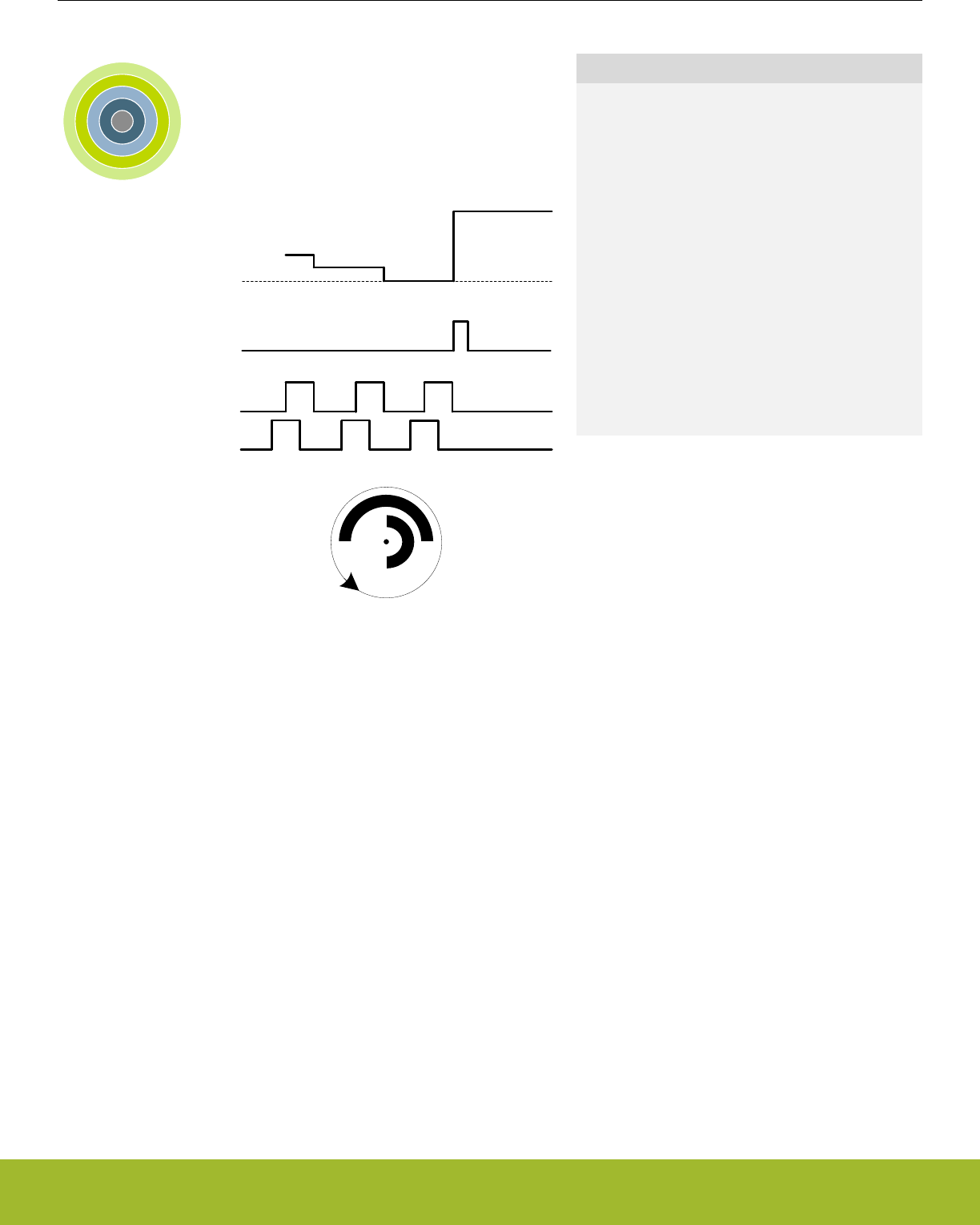
17. PCNT - Pulse Counter
0 1 2 3 4
Reload value
Interrupt
Quadrature code
0
Quick Facts
What?
The Pulse Counter (PCNT) decodes incoming pul-
ses. The module has a quadrature mode which may
be used to decode the speed and direction of a me-
chanical shaft. PCNT can operate in EM0 Active
down to EM3 Stop.
Why?
The PCNT generates an interrupt after a specific
number of pulses (or rotations), eliminating the need
for timing- or I/O interrupts and CPU processing to
measure pulse widths, etc.
How?
PCNT uses the LFACLK or may be externally
clocked from a pin. The module incorporates an 16-
bit up/down-counter to keep track of incoming pulses
or rotations.
17.1 Introduction
The Pulse Counter (PCNT) can be used for counting incoming pulses on a single input or to decode quadrature encoded inputs in EM0
Active down to EM3 Stop. It can run from the internal LFACLK while counting pulses on the PCNTn_S0IN pin. Or, alternately, the
PCNTn_S0IN pin may be used as an external clock source that runs both the PCNT counter and register access.
17.2 Features
• 16-bit counter with reload register
• Auxiliary counter for counting a single direction
• Single input oversampling up/down counter mode
• Externally clocked single input pulse up/down counter mode
• Quadrature decoder modes
• Externally clocked quadrature decoder 1X mode
• Oversampling quadrature decoder 1X, 2X and 4X modes
• Interrupt on counter underflow and overflow
• Interrupt when a direction change is detected (quadrature decoder mode only)
• Optional pulse width filter
• Optional input inversion/edge detect select
• Optional inputs from PRS
• Asynchronously triggered compare and clear
Reference Manual
PCNT - Pulse Counter
silabs.com | Smart. Connected. Energy-friendly. Preliminary Rev. 0.5 | 466
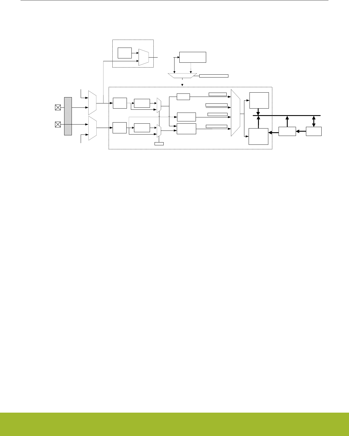
17.3 Functional Description
An overview of the PCNT module is shown in Figure 17.1 PCNT Overview on page 467.
Peripheral bus
CNT
PCNTn_S0IN
Inverter &
Input logic
PCNTn_S1IN
Count
Enable
1
LFACLK
Clock
switch
CMU (conceptual)
TOPB
Pulse Width
Filter
Edge
detector
OVR_SINGLE
EXTCLK_SINGLE
EXTCLK_QUAD
TOP
S0PRS Input
Analog de-glitch filter
S1PRS Input
Triggered compare
and clear control
PCNTnCLK
CLKPCNT
TCCMODE != DISABLED
0 1
Pulse Width
Filter
ExtClk
Quad decoder
OverSampling
Clk
Quad decoder
OVR_QUADDEC
Inverter &
Input logic
FILT
AUXCNT
Count
Enable
Figure 17.1. PCNT Overview
17.3.1 Pulse Counter Modes
The pulse counter can operate in single input oversampling mode (OVSSINGLE), externally clocked single input counter mode (EX-
TCLKSINGLE), externally clocked quadrature decoder mode (EXTCLKQUAD) and oversampling quadrature decoder modes(OVS-
QUAD1X, OVSQUAD2X and OVSQUAD4X). The following sections describe operation of each of these modes and how they are ena-
bled. Input timing constraints are described in 17.3.6 Clock Sources and 17.3.7 Input Filter.
17.3.1.1 Single Input Oversampling Mode
This mode is enabled by writing OVSSINGLE to the MODE field in the PCNTn_CTRL register and disabled by writing DISABLE to the
same field. The LFACLK clock source to the pulse counter is configured by clearing PCNT0CLKSEL in the CMU_PCNTCTRL in the
Clock Management Unit (CMU), 12. CMU - Clock Management Unit .
The optional pulse width filter is enabled by setting the FILT bit in the PCNTn_CTRL register. Additionally, the PCNTn_S0IN input may
be inverted, so that falling edges are counted, by setting the EDGE bit in the PCNTn_CTRL register.
If S1CDIR in the PCNTn_CTRL register is cleared, PCNTn_S0IN is the only observed input in this mode. The PCNTn_S0IN input is
sampled by the LFACLK and the number of detected positive or negative edges on PCNTn_S0IN appears in PCNTn_CNT. The counter
may be configured to count down by setting the CNTDIR bit in PCNTn_CTRL. Default is to count up.
The counting direction can also be controlled externally in this mode by setting S1CDIR. This will make the input value on PCNTn_S1IN
decide the direction counted on a PCNTn_S0IN edge. If PCNTn_S1IN is high, the count is done according to CNTDIR in
PCNTn_CTRL. If low, the count direction is opposite.
17.3.1.2 Externally Clocked Single Input Counter Mode
This mode is enabled by writing EXTCLKSINGLE to the MODE field in the PCNTn_CTRL register and disabled by writing DISABLE to
the same field. The external pin clock source is configured by setting PCNT0CLKSEL in the CMU_PCNTCTRL register (12. CMU -
Clock Management Unit ).
Positive edges on PCNTn_S0IN are used to clock the counter. Similar to the oversampled mode, PCNTn_S1IN is used to determine
the count direction if S1CDIR is set. If not, CNTDIR in PCNTn_CTRL solely defines count direction.
The digital pulse width filter is not available in this mode. The analog de-glitch filter in the GPIO pads is capable of removing some
unwanted noise. However, this mode may be susceptible to spikes and unintended pulses from devices such as mechanical switches,
and is therefore most suited to take input from electronic sensors etc. that generate single wire pulses.
Reference Manual
PCNT - Pulse Counter
silabs.com | Smart. Connected. Energy-friendly. Preliminary Rev. 0.5 | 467

17.3.1.3 Quadrature decoder modes
Two different types of quadrature decoding is supported in the pulse counter: the externally clocked (Asynchronous) quadrature decod-
ing and the oversampling (Synchronous) quadrature decoding. The externally clocked mode supports 1X quadrature decoding whereas
the oversampling mode supports 1X, 2X and 4X quadrature decoding. These modes are described in detail in 17.3.1.4 Externally
Clocked Quadrature Decoder Mode and 17.3.1.5 Oversampling Quadrature Decoder Mode .
Reference Manual
PCNT - Pulse Counter
silabs.com | Smart. Connected. Energy-friendly. Preliminary Rev. 0.5 | 468
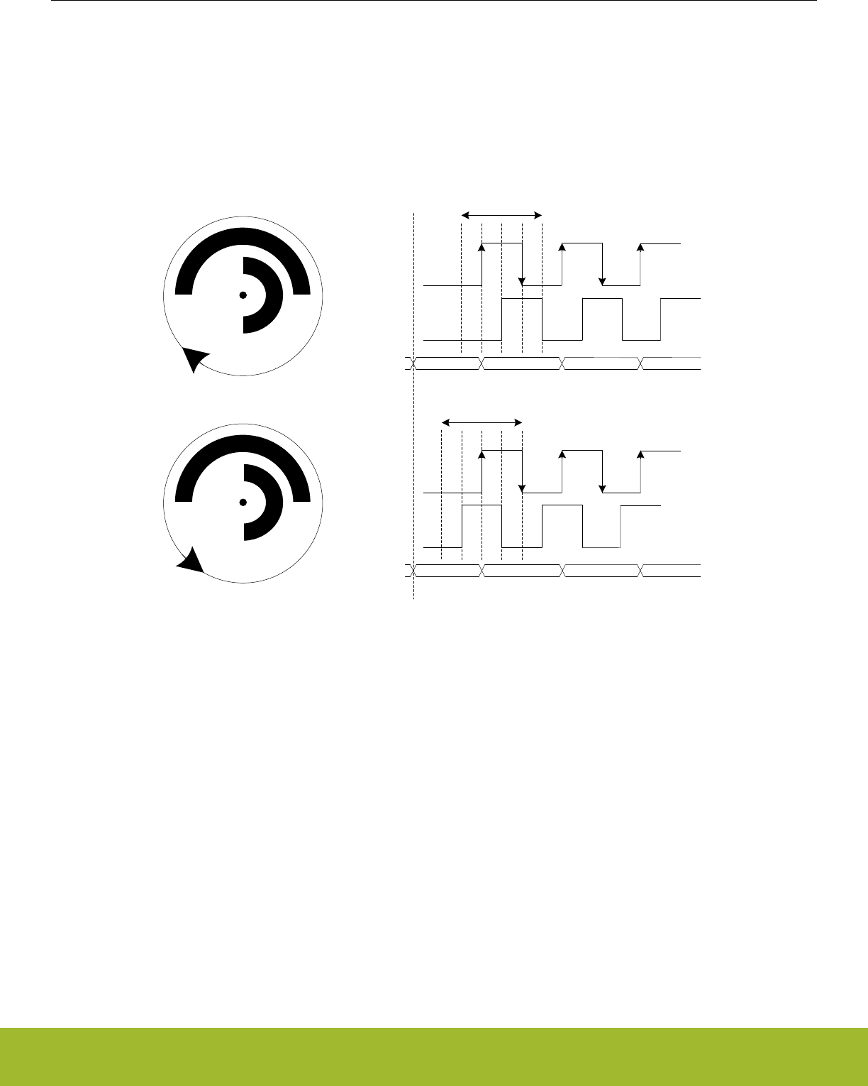
17.3.1.4 Externally Clocked Quadrature Decoder Mode
This mode is enabled by writing EXTCLKQUAD to the MODE field in PCNTn_CTRL and disabled by writing DISABLE to the same field.
The external pin clock source is configured by setting PCNT0CLKSEL in the CMU_PCNTCTRL register (12. CMU - Clock Management
Unit ).
In this mode, both edges on PCNTn_S0IN pin are used to sample PCNTn_S1IN pin, in order to decode the quadrature code. A quadra-
ture coded signal contains information about the relative speed and direction of a rotating shaft as illustrated by Figure 17.2 PCNT
Quadrature Coding on page 469, hence the direction of the counter register PCNTn_CNT is controlled automatically.
X X
1 cycle/sector, 4 states
01 11 10
00
X X
1 cycle/sector, 4 states
00 10 11 01
X = sensor position
Clockwise direction
Counter clockwise
direction
PCNTn_S0IN
PCNTn_S1IN
PCNTn_S0IN
PCNTn_S1IN
PCNTn_CNT
Reset
0 0 12
PCNTn_CNT 0 0 PCNTn_TOP PCNTn_TOP-1
Figure 17.2. PCNT Quadrature Coding
If PCNTn_S0IN leads PCNTn_S1IN in phase, the direction is clockwise, and if it lags in phase the direction is counter-clockwise. De-
fault behavior is illustrated by Figure 17.2 PCNT Quadrature Coding on page 469.
The counter direction may be read from the DIR bit in the PCNTn_STATUS register. Additionally, the DIRCNG interrupt in the
PCNTn_IF register is generated when a direction change is detected. When a change is detected, the DIR bit in the PCNTn_STATUS
register must be read to determine the current new direction.
Note:
The sector disc illustrated in the figure may be finer grained in some systems. Typically, they may generate 2-4 PCNTn_S0IN wave
periods per 360° rotation.
The direction of the quadrature code and control of the counter is generated by the simple binary function outlined by Table 17.1 PCNT
QUAD Mode Counter Control Function on page 470. Note that this function also filters some invalid inputs that may occur when the
shaft changes direction or temporarily toggles direction.
Reference Manual
PCNT - Pulse Counter
silabs.com | Smart. Connected. Energy-friendly. Preliminary Rev. 0.5 | 469

Table 17.1. PCNT QUAD Mode Counter Control Function
Inputs Control/Status
S1IN posedge S1IN negedge Count Enable CNTDIR status bit
0000
0110
1011
1100
Note:
PCNTn_S1IN is sampled on both edges of PCNTn_S0IN.
Reference Manual
PCNT - Pulse Counter
silabs.com | Smart. Connected. Energy-friendly. Preliminary Rev. 0.5 | 470

17.3.1.5 Oversampling Quadrature Decoder Mode
There are three Oversampling Quadrature Decoder Modes supported: 1X , 2X and 4X. These modes are enabled by writing OVS-
QUAD1X, OVSQUAD2X and OVSQUAD4X, respectively, to the MODE field in PCNTn_CTRL and disabled by writing DISABLE to the
same field. The LFACLK clock source to the pulse counter must be configured by clearing PCNT0CLKSEL in the CMU_PCNTCTRL in
the Clock Management Unit (CMU), 12. CMU - Clock Management Unit .
The optional pulse width filter is enabled by setting the FILT bit in the PCNTn_CTRL register. The filter applies to both inputs
PCNTn_S0IN and PCNTn_S1IN. The filter length is configured by FILTLEN in PCNTn_OVSCFG register.
Based on the modes selected, the decoder updates the counter on different events. In the OVSQUAD1X mode, the counter is updated
on the rising edge of the PCNTn_S0IN input when counting up, and on the negedge of the PCNTn_S0IN input when counting down. In
the OVSQUAD2X mode, the counter is updated on both edges of PCNTn_S0IN input. In the OVSQUAD4X mode the counter is upda-
ted on both edges of both inputs PCNTn_S0IN and PCNTn_S1IN. Table 17.2 PCNT OVSQUAD 1X, 2X and 4X Mode Counter Control
Function on page 471 outlines the increment or decrement of the counter based on the Quadrature Mode selected.
Note:
The decoding behavior of OVSQUAD1X mode is slightly different compared to EXTCLKQUAD mode(also 1X mode). In the EX-
TCLKQUAD mode, the counter is updated only on the posedge of S0IN input. However, in the OVSQUAD1X mode, the counter is up-
dated on the posedge of S0IN when counting up and on the negedge of S0IN when counting down.
Table 17.2. PCNT OVSQUAD 1X, 2X and 4X Mode Counter Control Function
Direction Previous State Next State OVSQUAD MODE
S1IN S0IN S1IN S0IN 1X 2X 4X
Clockwise
0 0 0 1 +1 +1 +1
0 1 1 1 +1
1 1 1 0 +1 +1
1 0 0 0 +1
Counter Clock-
wise
1 0 1 1 -1 -1
1 1 0 1 -1
0 1 0 0 -1 -1 -1
0 0 1 0 -1
Figure 17.3 PCNT State transitions for different Oversampling Quadrature Decoder Modes on page 472 illustrates the different states
of the quadrature input and the state transitions that updates the counter for the different modes. Each cycle of the input states results
in 1 update, 2 updates and 4 updates of the counter for OVSQUAD1X, OVSQUAD2X and OVSQUAD4X modes respectively.
Reference Manual
PCNT - Pulse Counter
silabs.com | Smart. Connected. Energy-friendly. Preliminary Rev. 0.5 | 471
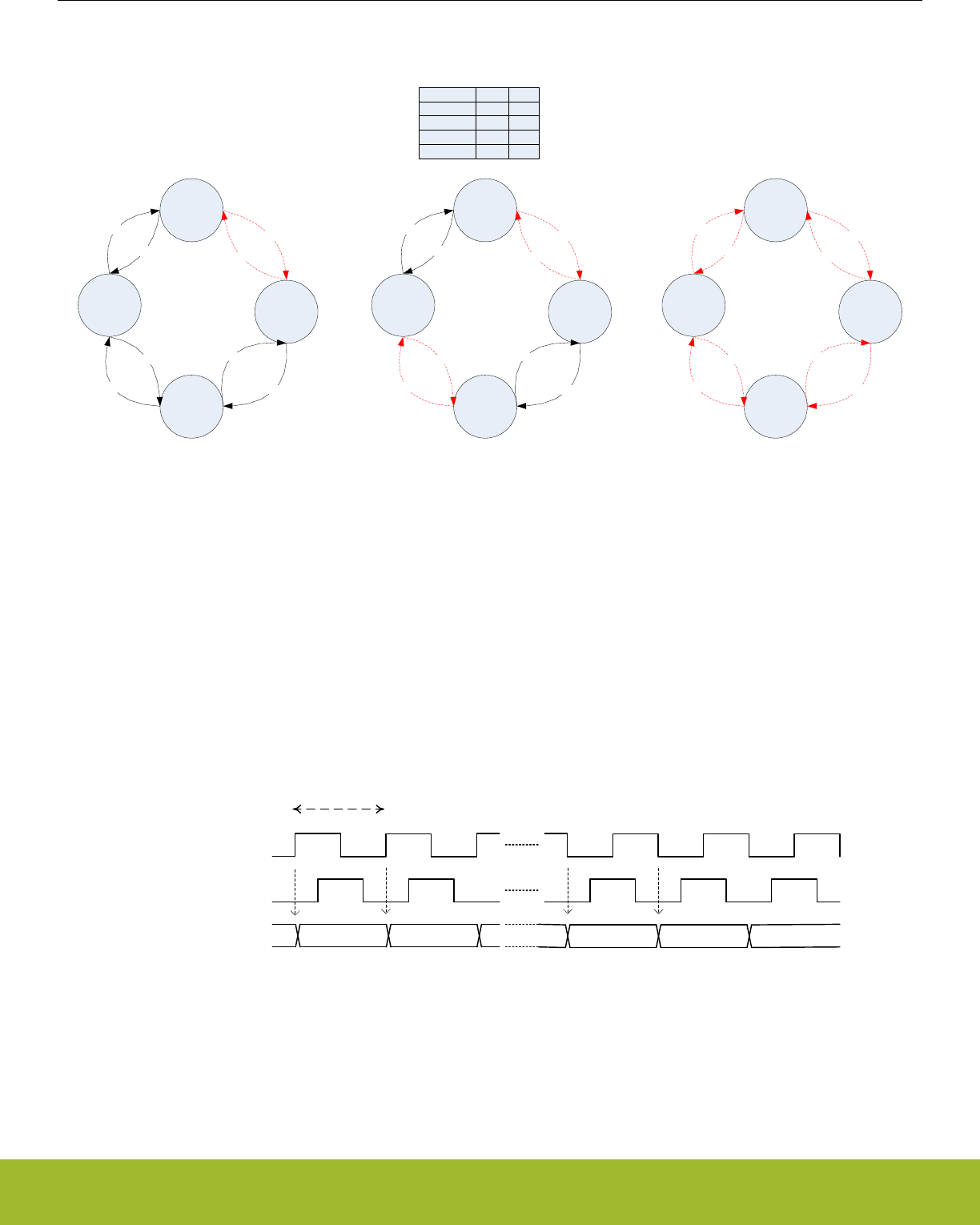
S0
‘b00
S1
‘b01
S2
‘b11
S3
‘b10
+1 +1
+1
+1
-1
-1 -1
-1
S0
‘b00
S1
‘b01
S2
‘b11
S3
‘b10
+1 +1
+1
+1
-1
-1 -1
-1
S0
‘b00
S1
‘b01
S2
‘b11
S3
‘b10
+1 +1
+1
+1
-1
-1 -1
-1
STATE
S0
S1
S2
S3
S1IN
0
0
1
1
S0IN
0
1
1
0
Relationship between inputs and its state
OVSQUAD1X mode
Transitions between States S0
and S1 updates the counter
OVSQUAD2X mode
Transitions between States S0
and S1 and between S3 and S2
updates the counter
OVSQUAD4X mode
All state transitions updates the
counter
Figure 17.3. PCNT State transitions for different Oversampling Quadrature Decoder Modes
The counter direction can be read from the DIR bit in PCNTn_STATUS register. Additionally, the DIRCNG interrupt in the PCNTn_IF is
generated when the direction change is detected. When a change is detected, the DIR bit in the PCNTn_STATUS register must be read
to determine the new direction.
In the oversampling quadrature decoder modes, the maximum input toggle frequency supported is 8KHz. For frequencies of 8KHz and
higher, incorrect decoding occurs. The different decoding modes and the counter updates are further illustrated by Figure 17.4 PCNT
Oversampling Quadrature Decoder 1X mode on page 472, Figure 17.5 PCNT Oversampling Quadrature Decoder 2X mode on page
473 and Figure 17.6 PCNT Oversampling Quadrature Decoder 4X mode on page 473.
S0IN
S1IN
CNT 34 5 646 53
Period > 125 us
Figure 17.4. PCNT Oversampling Quadrature Decoder 1X mode
Reference Manual
PCNT - Pulse Counter
silabs.com | Smart. Connected. Energy-friendly. Preliminary Rev. 0.5 | 472
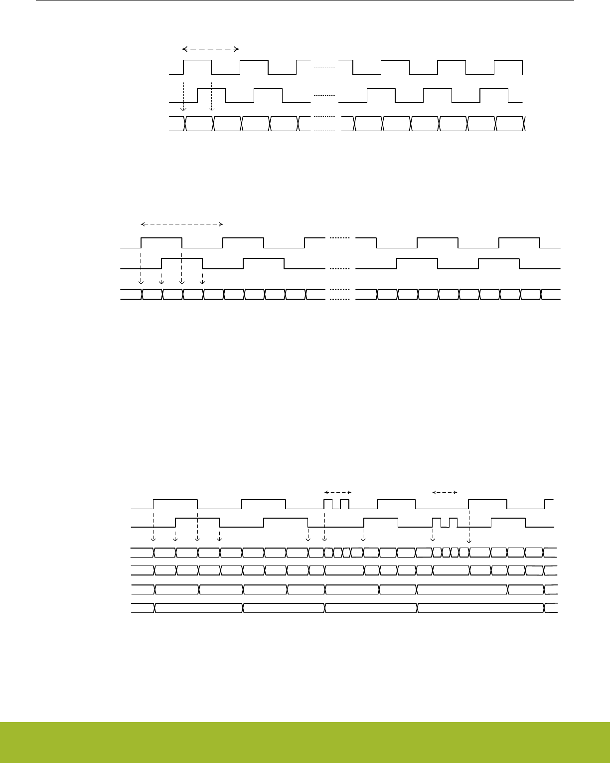
S0IN
S1IN
CNT 34 5 6 7 834567 28
Period > 125 us
Figure 17.5. PCNT Oversampling Quadrature Decoder 2X mode
S0IN
S1IN
34567891011
3 4 5 6 7 8 9 10 11 2
2
CNT
Period > 125 us
Figure 17.6. PCNT Oversampling Quadrature Decoder 4X mode
The above modes, by default are prone to flutter effects in the inputs PCNTn_S0IN and PCNTn_S1IN. When this occurs, the counter
changes directions rapidly causing DIRCNG interrupts and unnecessarily waking the core. To prevent this, set FLUTTERRM in
PCNTn_OVSCFG register. When enabled, flutter is removed, thus preventing unnecessary wakeup of the core. The flutter removal log-
ic works by preventing update of the counter value if the wheel keeps changing direction as a result of flutter. The counter is only upda-
ted if the current and previous state transition of the rotation are in the same direction. These state transitions are quadrature decoder
mode specific. The highlighted state transitions in Figure 17.3 PCNT State transitions for different Oversampling Quadrature Decoder
Modes on page 472 are the ones considered for the different quadrature decoder modes. Figure 17.7 PCNT Oversampling Quadrature
Decoder with Flutter Removal on page 473 shows how the counter is updated for the different quadrature decoder modes with flutter
removal FLUTTERRM enabled in PCNTn_OVSCFG.
S0IN
S1IN
1 2 3 4 5 6 7 89
0
CNTQUAD4X 865 4 5 6 78
1 2 3 4
054 3 4 5
1 20 3 2 3
S0IN Flutter S1IN Flutter
CNTQUAD2X
CNTQUAD1X
79
S0
STATES S1 S2 S3 S0 S1 S2 S3 S0 S1 S3
S0 S1 S0 S2S3 S1 S0 S0 S3 S0 S2 S3S1 S0 S1
Figure 17.7. PCNT Oversampling Quadrature Decoder with Flutter Removal
Reference Manual
PCNT - Pulse Counter
silabs.com | Smart. Connected. Energy-friendly. Preliminary Rev. 0.5 | 473
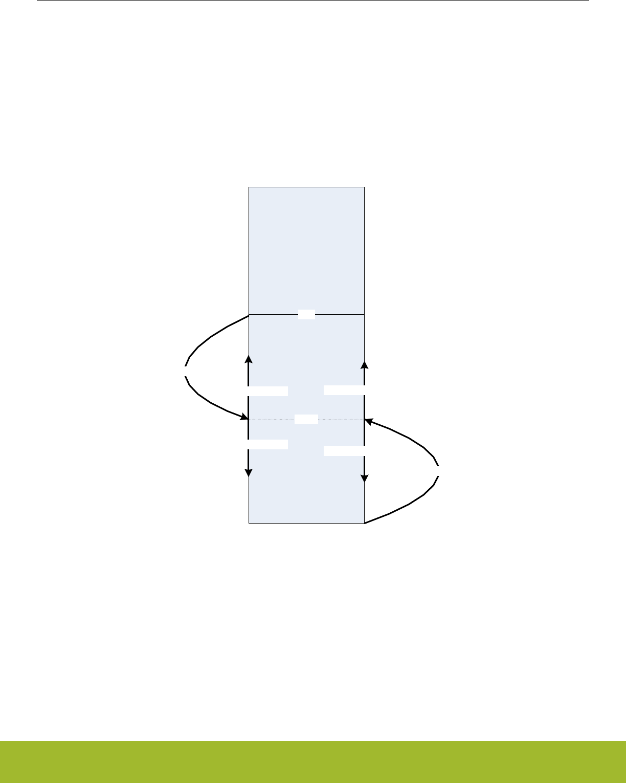
17.3.2 Hysteresis
By default the pulse counter wraps to 0 when passing the configured top value, and wraps to the top value when counting down from 0.
On these events, a system will likely want to wake up to store and track the overflow count. This is fine if the pulse counter is tracking a
monotonic value or a value that does not change directions frequently. In the latter scenario, if the counter changes directions around
the overflow/underflow point, the system will have to wake up frequently to keep track of the rotations, resulting in higher current con-
sumption.
To solve this, the pulse counter has a way of introducing hysteresis to the counter. When HYST in PCNTn_CTRL is set, the pulse coun-
ter will always wrap to TOP/2 on underflows and overflows. This takes the counter away from the area where it might overflow or under-
flow, removing the problem. Figure 17.8 PCNT Hysteresis behavior of Counter on page 474 illustrates the hysteresis behavior.
TOP
TOP/2
Overflow wrap
Overflow continue cnt
Underflow warp
underflow continue cnt
COUNTER
MIN VAL
MAX VAL
Overflow continue cnt
underflow continue cnt
Figure 17.8. PCNT Hysteresis behavior of Counter
Given a starting value of 0 for the counter, the absolute count value when hysteresis is enabled can be calculated with the equations
Figure 17.9 Absolute position with hysteresis and even TOP value on page 474 or Figure 17.10 Absolute position with hysteresis and
odd TOP value on page 475, depending on whether the TOP value is even or odd.
CNTabs = CNT - UFCNT x (TOP/2+1) + OFCNT x (TOP/2+1)
Figure 17.9. Absolute position with hysteresis and even TOP value
Reference Manual
PCNT - Pulse Counter
silabs.com | Smart. Connected. Energy-friendly. Preliminary Rev. 0.5 | 474

CNTabs = CNT - UFCNT x (TOP/2+1) + OFCNT x (TOP/2+2)
Figure 17.10. Absolute position with hysteresis and odd TOP value
17.3.3 Auxiliary counter
To be able to keep explicit track of counting in one direction in addition to the regular counter which counts both up and down, the
auxiliary counter can be used. The pulse counter can, for instance, be configured to keep track of the absolute rotation of the wheel,
while at the same time the auxiliary counter can keep track of how much the wheel has reversed.
The auxiliary counter is enabled by configuring AUXCNTEV in PCNTn_CTRL. It will always count up, but it can be configured whether it
should count up on up-events, down-events or both, keeping track of rotation either way or general movement. The value of the auxili-
ary counter can be read from the PCNTn_AUXCNT register.
Overflows on the auxiliary counter happen when the auxiliary counter passes the top value of the pulse counter, configured in
PCNTn_TOP. In that event, the AUXOF interrupt flag is set, and the auxiliary counter wraps to 0.
As the auxiliary counter, the main counter can be configured to count only on certain events. This is done through CNTEV in
PCNTn_CTRL, and it is possible like for the auxiliary counter, to make the main counter count on only up and down events. The differ-
ence between the counters is that where the auxiliary counter will only count up, the main counter will count up or down depending on
the direction of the count event.
Reference Manual
PCNT - Pulse Counter
silabs.com | Smart. Connected. Energy-friendly. Preliminary Rev. 0.5 | 475
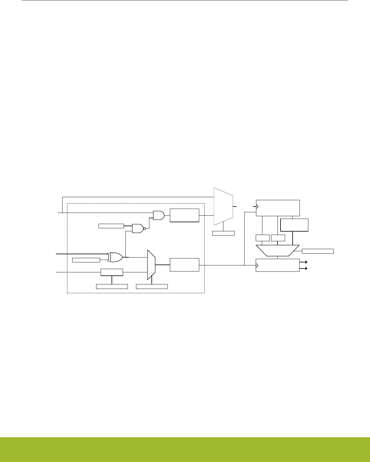
17.3.4 Triggered compare and clear
The pulse counter features triggered compare and clear. When enabled, a configurable trigger will induce a comparison between the
main counter, PCNTn_CNT, and the top value, PCNTn_TOP. After the comparison, the counter is cleared. The trigger for a compare
and clear event is configured in the TCCMODE bit-field in PCNTn_CTRL. There are two options, LFA and PRS. If LFA is selected, the
pulse counter will be compared with the top value, and cleared every 2N LFA clock cycle (where N is the value of TCCPRESC in
PCNTn_CTRL). If a PRS trigger is selected, the active PRS channel is configured in TCCPRSSEL in PCNTn_CTRL. The PRS input
can be inverted by setting TCCPRSPOL, triggering the compare and clear on the negative edge of the PRS input. The PRS input can
also be used as a gate for the pulse counter clock. This is enabled by setting PRSGATEEN in PCNTn_CTRL.
Note:
When PRSGATEEN is set, the clock to the entire pulse counter will be gated by the PRS input, meaning that register writes will not take
effect while the gated clock is inactive.
Comparison with PCNTn_TOP can be performed in three ways: range, greater than or equal, and less than or equal. TCCCOMP in
PCNTn_CTRL configures comparison mode. Upon a compare match, the TCC interrupt is set, and the PRS output from the pulse
counter is set. The PRS output will remain set until the next compare and clear event. Triggered compare and clear is intended for use
when the pulse counter is configured to count up. In this mode, PCNTn_CNT will not wrap to 0 when hitting PCNTn_TOP, it will keep
counting. In addition, the counter will not overflow, it will rather stop counting, just setting the overflow interrupt flag.
Figure 17.11 PCNT Triggered compare and clear on page 476 shows an overview of the control circuitry for triggered compare and
clear. The control circuitry includes two positive edge detectors (PED) and glitch filters, used to generate clocks for the pulse counter.
The two clock outputs are mutually exclusive: If both edge detectors receive a pulse at the same time, the output pulse from one of
them will be postponed until the other edge detectors output pulse has completed.
CNT
TCCPRSPOL
PRS in
PRSGATEEN
PCNTnCLK PED and glitch
filter
CLKPCNT
TCCMODE
LFACLK
Compare match
clear
TCCCOMP
<=TOP
LTOE GTOE RANGE
>=TOP
>=TOP[7:0]
&&
<= TOP[15:8]
PRS
LFA
TCC PRS out
TCC interrupt
Prescaler
TCCPRESC
Triggered compare and clear control
TCCMODE
DISABLED
LFA or PRS
PED and glitch
filter
Figure 17.11. PCNT Triggered compare and clear
Note:
TCCMODE, TCCPRESC, PRSGATEEN, TCCPRSPOL, and TCCPRSSEL in PCNTn_CTRL should only be altered when RSTEN in
PCNTn_CTRL is set.
Reference Manual
PCNT - Pulse Counter
silabs.com | Smart. Connected. Energy-friendly. Preliminary Rev. 0.5 | 476

17.3.5 Register Access
The counter-clock domain may be clocked externally. To update the counter-clock domain registers from software in this mode, 2-3
clock pulses on the external clock are needed to synchronize accesses to the externally clocked domain. Clock source switching is
controlled from the registers in the CMU (12. CMU - Clock Management Unit ).
When the RSTEN bit in the PCNTn_CTRL register is set, the PCNT clock domain is asynchronously held in reset. The reset is synchro-
nously released two PCNT clock edges after the RSTEN bit in the PCNTn_CTRL register is cleared by software. This asynchronous
reset restores the reset values in PCNTn_TOP, PCNTn_CNT and other control registers in the PCNT clock domain.
CNTRSTEN works in a similar manner as RSTEN, but only resetting the counter, CNT. Note that the counter is also reset by RSTEN.
AUXCNTRSTEN works in a similar manner as RSTEN, but only resetting the auxiliary counter, PCNTn_AUXCNT. Note that the auxili-
ary counter is also reset by RSTEN.
Since this module is a Low Energy Peripheral, and runs off a clock which is asynchronous to the HFCORECLK, special considerations
must be taken when accessing registers. Please refer to 4.3 Access to Low Energy Peripherals (Asynchronous Registers) for a descrip-
tion on how to perform register accesses to Low Energy Peripherals.
Note:
PCNTn_TOP and PCNTn_CNT are read-only registers. When writing to PCNTn_TOPB, make sure that the counter value,
PCNTn_CNT, can not exceed the value written to PCNTn_TOPB within two clock cycles.
17.3.6 Clock Sources
The pulse counter may be clocked from two possible clock sources: LFACLK or an external clock. The clock selection is configured by
the PCNT0CLKSEL bit in the CMU_PCNTCTRL in the Clock Management Unit (CMU), 12. CMU - Clock Management Unit . The de-
fault clock source is the LFACLK.
This PCNT module may also use PCNTn_S0IN as an external clock to clock the counter (EXTCLKSINGLE mode) and to sample
PCNTn_S1IN (EXTCLKQUAD mode). Setup, hold and max frequency constraints for PCNTn_S0IN and PCNTn_S1IN for these modes
are specified in the device datasheet.
To use this module, the LE interface clock must be enabled in CMU_HFBUSCLKEN0, in addition to the module clock in
CMU_PCNTCTRL.
Note:
PCNT Clock Domain Reset, RSTEN, should be set when changing clock source for PCNT. If changing to an external clock source, the
clock pin has to be enabled as input prior to de-asserting RSTEN. Changing clock source without asserting RSTEN results in undefined
behaviour.
17.3.7 Input Filter
An optional pulse width filter is available in OVSSINGLE and OVSQUAD modes, when LFACLK is selected as a clock source for the
Pulse Counter in CMU 12. CMU - Clock Management Unit . The filter is enabled by writing 1 to the FILT bit in the PCNTn_CTRL regis-
ter. When enabled, the high and low periods of PCNTn_S0IN and PCNTn_S1IN must be stable for a programmable number of consec-
utive clock cycles before the edge is passed to the edge detector. The filter length should be programmed in FILTLEN field of the
PCNTn_OVSCFG register.
The filter length is given by Figure 17.12 PCNT Input Filter length Equation on page 477:
Filter length = (FILTLEN + 5) LFACLK cycles
Figure 17.12. PCNT Input Filter length Equation
The maximum filter length configured is 260 LFACLK cycles.
In EXTCLKSINGLE and EXTCLKQUAD mode, there is no digital pulse width filter available.
Reference Manual
PCNT - Pulse Counter
silabs.com | Smart. Connected. Energy-friendly. Preliminary Rev. 0.5 | 477

17.3.8 Edge Polarity
The edge polarity can be set by configuring the EDGE bit in the PCNTn_CTRL register. When this bit is cleared, the pulse counter
counts positive edges of PCNTn_S0IN input. When this bit is set, the pulse counter counts negative edges in OVSSINGLE mode. Also,
when the EDGE bit is set in the OVSSINGLE and EXTCLKSINGLE modes, the PCNTn_S1IN input is inverted. In OVSQUAD 1X-4X
modes the EDGE bit inverts both inputs.
Note:
The EDGE bit in PCNTn_CTRL has no effect in EXTCLKQUAD mode.
17.3.9 PRS and PCNTn_S0IN,PCNTn_S1IN Inputs
It is possible to receive input from PRS on both PCNTn_S0IN (or PCNTn_S1IN) by setting S0PRSEN (or S1PRSEN) in PCNTn_INPUT.
The PRS channel used can be selected using S0PRSSEL (or S1PRSSEL) in PCNTn_INPUT.
In the Oversampling quadrature decoder modes, the input frequency should be less than 8KHz to ensure correct functionality.
PCNT module generates three PRS outputs the TCC PRS output, the CNT OF/UF PRS output and the CNT DIR PRS output. The TCC
PRS is generated on compare match of TCC event. The CNT OF/UF combined PRS is generated when the counter overflow or under-
flows. The CNT DIR PRS is a level PRS and indicates the current direction of count of counter CNT
Note:
S0PRSEN,S1PRSEN,S0PRSSEL,S1PRSSEL should only be altered when RSTEN in PCNTn_CTRL is set.
17.3.10 Interrupts
The interrupt generated by PCNT uses the PCNTn_INT interrupt vector. Software must read the PCNTn_IF register to determine which
module interrupt that generated the vector invocation.
17.3.10.1 Underflow and Overflow Interrupts
The underflow interrupt flag (UF) is set when the counter counts down from 0. I.e. when the value of the counter is 0 and a new pulse is
received. The PCNTn_CNT register is loaded with the PCNTn_TOP value after this event.
The overflow interrupt flag (OF) is set when the counter counts up from the PCNTn_TOP (reload) value. I.e. if PCNTn_CNT =
PCNTn_TOP and a new pulse is received. The PCNTn_CNT register is loaded with the value 0 after this event.
Reference Manual
PCNT - Pulse Counter
silabs.com | Smart. Connected. Energy-friendly. Preliminary Rev. 0.5 | 478

17.3.10.2 Direction Change Interrupt
The PCNTn_PCNT module sets the DIRCNG interrupt flag (PCNTn_IF register) for EXTCLKQUAD and OVSQUAD1X-4X modes when
the direction of the quadrature code changes. The behavior of this interrupt in the EXTCLKQUAD mode is illustrated by Figure
17.13 PCNT Direction Change Interrupt (DIRCNG) Generation on page 479.
Standard async
handshake
interface
PCNTn_S0IN
PCNTn_S1IN
Interrupt
X X
Invalid pulse generated when
the shaft changes direction
n+1 n+2 n+3 n+2
PCNTn_CNT n
Delay from the shaft physically
changed direction until the
counter direction is changed
and the interrupt is generated
Figure 17.13. PCNT Direction Change Interrupt (DIRCNG) Generation
Reference Manual
PCNT - Pulse Counter
silabs.com | Smart. Connected. Energy-friendly. Preliminary Rev. 0.5 | 479
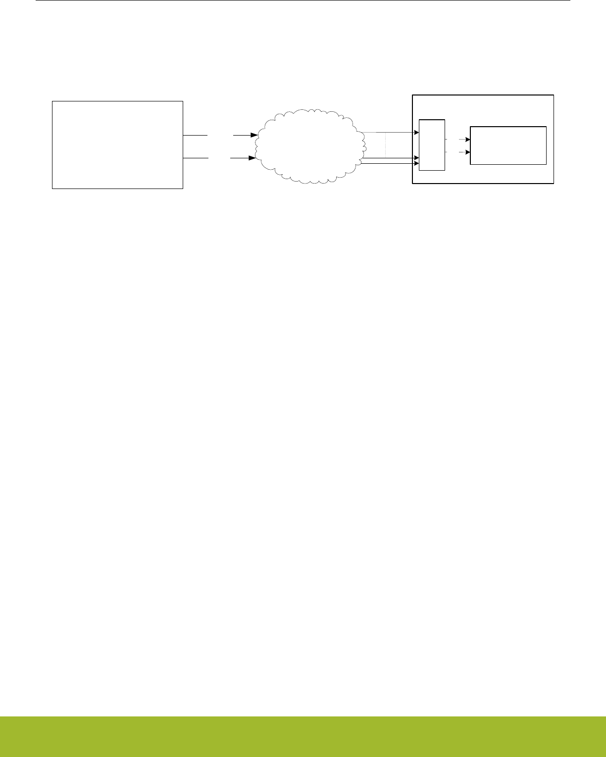
17.3.11 Cascading Pulse Counters
When two or more Pulse Counters are available, it is possible to cascade them. For example two 16-bit Pulse Counters can be casca-
ded to form a 32-bit pulse counter. This can be done with the help of the CNT UF/OF PRS and CNT DIR PRS ouputs. The figure Figure
17.14 PCNT Cascading to two 16-bit PCNT to form a 32-bit PCNT on page 480 illustrates this structure.
PCNT0(LSB)
[15:0
OVSSINGLE MODE /
EXTCLKSINGLE MODE /
EXTCLKQUAD MODE /
OVSQUAD1X /
OVSQUAD2X /
OVSQUAD4X
PCNT1(MSB)
[31:16]
EXTCLK SINLGE MODE
PRS
Combinational
Matrix
prs_ufof
prs_dir
PRS
enable
and
input
select
PCNT Core
S0IN
S1IN
PRS CHANNELS
Figure 17.14. PCNT Cascading to two 16-bit PCNT to form a 32-bit PCNT
For cascading of Pulse Counters to work, the PCNT1 according to the figure Figure 17.14 PCNT Cascading to two 16-bit PCNT to form
a 32-bit PCNT on page 480 should be programmed in EXTCLKSINGLE mode and its S0IN and S1IN inputs should be configured to
prs_ufof and prs_dir of PCNT0 respectively. In addition to this, a strict programming sequence needs to be followed to ensure both
PCNTs are in sync with each other.
• Configure PCNT0 registers. eg. PCNT0_INPUT,PCNT0_CTRL,PCNT0_OVSCFG etc.
• Wait for PCNT0_SYCNBUSY to be cleared to ensure the registers are synchronized to the asynchronous clock domain.
• Hold PCNT0 in sw reset by setting PCNT0_CTRL_RSTEN.
• Configure PCNT1_CTRL to EXTCLKSINLE mode with S1CDIR and CNTDIR bit set. Configure INPUT to accept "prs_ufof" and
"prs_dir" of PCNT0 on S0IN and S1IN respectively.
• Wait for PCNTn_SYCNBUSY to be cleared to ensure the registers are synchronized to the asynchronous clock domain. Use three
PRS_SWPULSE on the S0IN prs channel to ensure this synchronization.
• Hold PCNT1 in sw reset by setting PCNT1_CTRL_RSTEN.
• Clear PCNT1_CTRL_RSTEN and synchronize it by asserting two PRS_SWPULSE on the S0IN input.
• Finally clear PCNT0_CTRL_RSTEN and start counting.
Note:
When RSTEN in PCNTn_CTRL is set, the TOP value in the Pulse Counter gets cleared. Therefore, in order to update the TOP value
while RSTEN is set, assert TOPBHFEN bit in PCNTn_CTRL. This will update the TOP value with the TOPB value even without having
to synchronize the TOPB value. This only works if TOPBHFEN and TOPB are configured while RSTEN in PCNTn_CTRL is set.
Reference Manual
PCNT - Pulse Counter
silabs.com | Smart. Connected. Energy-friendly. Preliminary Rev. 0.5 | 480

17.4 Register Map
The offset register address is relative to the registers base address.
Offset Name Type Description
0x000 PCNTn_CTRL RW Control Register
0x004 PCNTn_CMD W1 Command Register
0x008 PCNTn_STATUS RStatus Register
0x00C PCNTn_CNT RCounter Value Register
0x010 PCNTn_TOP RTop Value Register
0x014 PCNTn_TOPB RW Top Value Buffer Register
0x018 PCNTn_IF RInterrupt Flag Register
0x01C PCNTn_IFS W1 Interrupt Flag Set Register
0x020 PCNTn_IFC (R)W1 Interrupt Flag Clear Register
0x024 PCNTn_IEN RW Interrupt Enable Register
0x02C PCNTn_ROUTELOC0 RW I/O Routing Location Register
0x040 PCNTn_FREEZE RW Freeze Register
0x044 PCNTn_SYNCBUSY RSynchronization Busy Register
0x064 PCNTn_AUXCNT RAuxiliary Counter Value Register
0x068 PCNTn_INPUT RW PCNT Input Register
0x06C PCNTn_OVSCFG RW Oversampling Config Register
Reference Manual
PCNT - Pulse Counter
silabs.com | Smart. Connected. Energy-friendly. Preliminary Rev. 0.5 | 481

17.5 Register Description
17.5.1 PCNTn_CTRL - Control Register (Async Reg)
For more information about asynchronous registers please see 4.3 Access to Low Energy Peripherals (Asynchronous Registers).
Offset Bit Position
0x000
31
30
29
28
27
26
25
24
23
22
21
20
19
18
17
16
15
14
13
12
11
10
9
8
7
6
5
4
3
2
1
0
Reset
0
0x0
0
0
0x0
0x0
0x0
0
0
0x0
0x0
0
0
0
0
0
0
0
0x0
Access
RW
RW
RW
RW
RW
RW
RW
RW
RW
RW
RW
RW
RW
RW
RW
RW
RW
RW
RW
Name
TOPBHFSEL
TCCPRSSEL
TCCPRSPOL
PRSGATEEN
TCCCOMP
TCCPRESC
TCCMODE
EDGE
CNTDIR
AUXCNTEV
CNTEV
S1CDIR
HYST
DEBUGHALT
AUXCNTRSTEN
CNTRSTEN
RSTEN
FILT
MODE
Bit Name Reset Access Description
31 TOPBHFSEL 0 RW TOPB High frequency value select
Apply High frequency value of TOPB to TOP register. Should be used only when RSTEN in PCNTn_CTRL is set
30 Reserved To ensure compatibility with future devices, always write bits to 0. More information in 1.2 Conven-
tions
29:26 TCCPRSSEL 0x0 RW TCC PRS Channel Select
Select PRS channel used as compare and clear trigger.
Value Mode Description
0 PRSCH0 PRS Channel 0 selected.
1 PRSCH1 PRS Channel 1 selected.
2 PRSCH2 PRS Channel 2 selected.
3 PRSCH3 PRS Channel 3 selected.
4 PRSCH4 PRS Channel 4 selected.
5 PRSCH5 PRS Channel 5 selected.
6 PRSCH6 PRS Channel 6 selected.
7 PRSCH7 PRS Channel 7 selected.
8 PRSCH8 PRS Channel 8 selected.
9 PRSCH9 PRS Channel 9 selected.
10 PRSCH10 PRS Channel 10 selected.
11 PRSCH11 PRS Channel 11 selected.
25 TCCPRSPOL 0 RW TCC PRS polarity select
Configure which edge on the PRS input is used to trigger a compare and clear event
Value Mode Description
0 RISING Rising edge on PRS trigger compare and clear event.
1 FALLING Falling edge on PRS trigger compare and clear event.
Reference Manual
PCNT - Pulse Counter
silabs.com | Smart. Connected. Energy-friendly. Preliminary Rev. 0.5 | 482

Bit Name Reset Access Description
24 PRSGATEEN 0 RW PRS gate enable
When set, the clock input to the pulse counter will be gated when the selected PRS input is the inverse of TCCPRSPOL.
23:22 TCCCOMP 0x0 RW Triggered compare and clear compare mode
Selects the mode for comparison upon a compare and clear event.
Value Mode Description
0 LTOE Compare match if PCNT_CNT is less than, or equal to PCNT_TOP.
1 GTOE Compare match if PCNT_CNT is greater than or equal to PCNT_TOP.
2 RANGE Compare match if PCNT_CNT is less than, or equal to
PCNT_TOP[15:8]], and greater than, or equal to PCNT_TOP[7:0].
21 Reserved To ensure compatibility with future devices, always write bits to 0. More information in 1.2 Conven-
tions
20:19 TCCPRESC 0x0 RW Set the LFA prescaler for triggered compare and clear
Selects the prescaler value for LFA compare and clear events
Value Mode Description
0 DIV1 Compare and clear event each LFA cycle.
1 DIV2 Compare and clear performed on every other LFA cycle.
2 DIV4 Compare and clear performed on every 4th LFA cycle.
3 DIV8 Compare and clear performed on every 8th LFA cycle.
18 Reserved To ensure compatibility with future devices, always write bits to 0. More information in 1.2 Conven-
tions
17:16 TCCMODE 0x0 RW Sets the mode for triggered compare and clear
Selects whether compare and clear should be triggered on each LFA clock, or from PRS
Value Mode Description
0 DISABLED Triggered compare and clear not enabled.
1 LFA Compare and clear performed on each (optionally prescaled) LFA clock
cycle.
2 PRS Compare and clear performed on positive PRS edges.
15 EDGE 0 RW Edge Select
Determines the polarity of the incoming edges. This bit should be written when PCNT is in DISABLE mode, otherwise the
behavior is unpredictable. This bit used only in OVSSINGLE, EXTCLKSINGLE and OVSQUAD1X-4X modes.
Value Mode Description
0 POS Positive edges on the PCNTn_S0IN inputs are counted in OVSSINGLE
mode. Does not invert PCNTn_S1IN input in OVSSINGLE and EX-
TCLKSINGLE modes
1 NEG Negative edges on the PCNTn_S0IN inputs are counted in OVSSIN-
GLE mode. Inverts the PCNTn_S1IN input in OVSSINGLE and EX-
TCLKSINGLE modes
Reference Manual
PCNT - Pulse Counter
silabs.com | Smart. Connected. Energy-friendly. Preliminary Rev. 0.5 | 483

Bit Name Reset Access Description
14 CNTDIR 0 RW Non-Quadrature Mode Counter Direction Control
The direction of the counter must be set in the OVSSINGLE and EXTCLKSINGLE modes. This bit is ignored in EX-
TCLKQUAD mode as the direction is automatically detected.
Value Mode Description
0 UP Up counter mode.
1 DOWN Down counter mode.
13:12 AUXCNTEV 0x0 RW Controls when the auxiliary counter counts
Selects whether the auxiliary counter responds to up-count events, down-count events or both
Value Mode Description
0 NONE Never counts.
1 UP Counts up on up-count events.
2 DOWN Counts up on down-count events.
3 BOTH Counts up on both up-count and down-count events.
11:10 CNTEV 0x0 RW Controls when the counter counts
Selects whether the regular counter responds to up-count events, down-count events or both
Value Mode Description
0 BOTH Counts up on up-count and down on down-count events.
1 UP Only counts up on up-count events.
2 DOWN Only counts down on down-count events.
3 NONE Never counts.
9 S1CDIR 0 RW Count direction determined by S1
S1 gives the direction of counting when in the OVSSINGLE or EXTCLKSINGLE modes. When S1 is high, the count direc-
tion is given by CNTDIR, and when S1 is low, the count direction is the opposite
8HYST 0 RW Enable Hysteresis
When hysteresis is enabled, the PCNT will always overflow and underflow to TOP/2.
7 DEBUGHALT 0 RW Debug Mode Halt Enable
Set to halt the PCNT in debug mode only in OVSSINGLE and OVSQUAD modes. When in EXTCLKSINGLE or EX-
TCLKQUAD modes, DEBUGHALT does not halt the Pulse Counter.
Value Description
0 PCNT is running in debug mode.
1 PCNT is frozen in debug mode.
6 AUXCNTRSTEN 0 RW Enable AUXCNT Reset
The auxiliary counter, AUXCNT, is asynchronously held in reset when this bit is set. The reset is synchronously released
two PCNT clock edges after this bit is cleared. If an external clock is used, the reset should be performed by setting and
clearing the bit without pending for SYNCBUSY bit.
Reference Manual
PCNT - Pulse Counter
silabs.com | Smart. Connected. Energy-friendly. Preliminary Rev. 0.5 | 484

Bit Name Reset Access Description
5 CNTRSTEN 0 RW Enable CNT Reset
The counter, CNT, is asynchronously held in reset when this bit is set. The reset is synchronously released two PCNT clock
edges after this bit is cleared. If an external clock is used, the reset should be performed by setting and clearing the bit
without pending for SYNCBUSY bit. This action clears the counter to its reset value
4 RSTEN 0 RW Enable PCNT Clock Domain Reset
The PCNT clock domain is asynchronously held in reset when this bit is set. The reset is synchronously released two PCNT
clock edges after this bit is cleared. If an external clock is used, the reset should be performed by setting and clearing the
bit without pending for SYNCBUSY bit.
3 FILT 0 RW Enable Digital Pulse Width Filter
The filter passes all high and low periods that are at least (FILTLEN+5) clock cycles wide. This filter is only available in
OVSSINGLE,OVSQUAD1X-4X modes.
2:0 MODE 0x0 RW Mode Select
Selects the mode of operation. The corresponding clock source must be selected from the CMU.
Value Mode Description
0 DISABLE The module is disabled.
1 OVSSINGLE Single input LFACLK oversampling mode (available in EM0-EM3).
2 EXTCLKSINGLE Externally clocked single input counter mode (available in EM0-EM3).
3 EXTCLKQUAD Externally clocked quadrature decoder mode (available in EM0-EM3).
4 OVSQUAD1X LFACLK oversampling quadrature decoder 1X mode (available in EM0-
EM3).
5 OVSQUAD2X LFACLK oversampling quadrature decoder 2X mode (available in EM0-
EM3).
6 OVSQUAD4X LFACLK oversampling quadrature decoder 4X mode (available in EM0-
EM3).
Reference Manual
PCNT - Pulse Counter
silabs.com | Smart. Connected. Energy-friendly. Preliminary Rev. 0.5 | 485

17.5.2 PCNTn_CMD - Command Register (Async Reg)
For more information about asynchronous registers please see 4.3 Access to Low Energy Peripherals (Asynchronous Registers).
Offset Bit Position
0x004
31
30
29
28
27
26
25
24
23
22
21
20
19
18
17
16
15
14
13
12
11
10
9
8
7
6
5
4
3
2
1
0
Reset
0
0
Access
W1
W1
Name
LTOPBIM
LCNTIM
Bit Name Reset Access Description
31:2 Reserved To ensure compatibility with future devices, always write bits to 0. More information in 1.2 Conven-
tions
1 LTOPBIM 0 W1 Load TOPB Immediately
This bit has no effect since TOPB is not buffered and it is loaded directly into TOP.
0 LCNTIM 0 W1 Load CNT Immediately
Load PCNTn_TOP into PCNTn_CNT on the next counter clock cycle.
17.5.3 PCNTn_STATUS - Status Register
Offset Bit Position
0x008
31
30
29
28
27
26
25
24
23
22
21
20
19
18
17
16
15
14
13
12
11
10
9
8
7
6
5
4
3
2
1
0
Reset
0
Access
R
Name
DIR
Bit Name Reset Access Description
31:1 Reserved To ensure compatibility with future devices, always write bits to 0. More information in 1.2 Conven-
tions
0 DIR 0 R Current Counter Direction
Current direction status of the counter. This bit is valid in EXTCLKQUAD mode only.
Value Mode Description
0 UP Up counter mode (clockwise in EXTCLKQUAD mode with the EDGE
bit in PCNTn_CTRL set to 0).
1 DOWN Down counter mode.
Reference Manual
PCNT - Pulse Counter
silabs.com | Smart. Connected. Energy-friendly. Preliminary Rev. 0.5 | 486

17.5.4 PCNTn_CNT - Counter Value Register
Offset Bit Position
0x00C
31
30
29
28
27
26
25
24
23
22
21
20
19
18
17
16
15
14
13
12
11
10
9
8
7
6
5
4
3
2
1
0
Reset
0x0000
Access
R
Name
CNT
Bit Name Reset Access Description
31:16 Reserved To ensure compatibility with future devices, always write bits to 0. More information in 1.2 Conven-
tions
15:0 CNT 0x0000 R Counter Value
Gives read access to the counter.
17.5.5 PCNTn_TOP - Top Value Register
Offset Bit Position
0x010
31
30
29
28
27
26
25
24
23
22
21
20
19
18
17
16
15
14
13
12
11
10
9
8
7
6
5
4
3
2
1
0
Reset
0x00FF
Access
R
Name
TOP
Bit Name Reset Access Description
31:16 Reserved To ensure compatibility with future devices, always write bits to 0. More information in 1.2 Conven-
tions
15:0 TOP 0x00FF R Counter Top Value
When counting down, this value is reloaded into PCNTn_CNT when counting past 0. When counting up, 0 is written to the
PCNTn_CNT register when counting past this value.
Reference Manual
PCNT - Pulse Counter
silabs.com | Smart. Connected. Energy-friendly. Preliminary Rev. 0.5 | 487

17.5.6 PCNTn_TOPB - Top Value Buffer Register (Async Reg)
For more information about asynchronous registers please see 4.3 Access to Low Energy Peripherals (Asynchronous Registers).
Offset Bit Position
0x014
31
30
29
28
27
26
25
24
23
22
21
20
19
18
17
16
15
14
13
12
11
10
9
8
7
6
5
4
3
2
1
0
Reset
0x00FF
Access
RW
Name
TOPB
Bit Name Reset Access Description
31:16 Reserved To ensure compatibility with future devices, always write bits to 0. More information in 1.2 Conven-
tions
15:0 TOPB 0x00FF RW Counter Top Buffer
Loaded automatically to TOP when written.
17.5.7 PCNTn_IF - Interrupt Flag Register
Offset Bit Position
0x018
31
30
29
28
27
26
25
24
23
22
21
20
19
18
17
16
15
14
13
12
11
10
9
8
7
6
5
4
3
2
1
0
Reset
0
0
0
0
0
0
Access
R
R
R
R
R
R
Name
OQSTERR
TCC
AUXOF
DIRCNG
OF
UF
Bit Name Reset Access Description
31:6 Reserved To ensure compatibility with future devices, always write bits to 0. More information in 1.2 Conven-
tions
5 OQSTERR 0 R Oversampling Quadrature State Error Interrupt
Set in the Oversampling Quadrature Mode when incorrect state transition occurs
4 TCC 0 R Triggered compare Interrupt Read Flag
Set upon triggered compare match
3 AUXOF 0 R Auxiliary Overflow Interrupt Read Flag
Set when an Auxiliary CNT overflow occurs
2 DIRCNG 0 R Direction Change Detect Interrupt Flag
Set when the count direction changes. Set in EXTCLKQUAD mode only.
1 OF 0 R Overflow Interrupt Read Flag
Set when a CNT overflow occurs
0 UF 0 R Underflow Interrupt Read Flag
Set when a CNT underflow occurs
Reference Manual
PCNT - Pulse Counter
silabs.com | Smart. Connected. Energy-friendly. Preliminary Rev. 0.5 | 488

17.5.8 PCNTn_IFS - Interrupt Flag Set Register
Offset Bit Position
0x01C
31
30
29
28
27
26
25
24
23
22
21
20
19
18
17
16
15
14
13
12
11
10
9
8
7
6
5
4
3
2
1
0
Reset
0
0
0
0
0
0
Access
W1
W1
W1
W1
W1
W1
Name
OQSTERR
TCC
AUXOF
DIRCNG
OF
UF
Bit Name Reset Access Description
31:6 Reserved To ensure compatibility with future devices, always write bits to 0. More information in 1.2 Conven-
tions
5 OQSTERR 0 W1 Set OQSTERR Interrupt Flag
Write 1 to set the OQSTERR interrupt flag
4 TCC 0 W1 Set TCC Interrupt Flag
Write 1 to set the TCC interrupt flag
3 AUXOF 0 W1 Set AUXOF Interrupt Flag
Write 1 to set the AUXOF interrupt flag
2 DIRCNG 0 W1 Set DIRCNG Interrupt Flag
Write 1 to set the DIRCNG interrupt flag
1 OF 0 W1 Set OF Interrupt Flag
Write 1 to set the OF interrupt flag
0 UF 0 W1 Set UF Interrupt Flag
Write 1 to set the UF interrupt flag
Reference Manual
PCNT - Pulse Counter
silabs.com | Smart. Connected. Energy-friendly. Preliminary Rev. 0.5 | 489

17.5.9 PCNTn_IFC - Interrupt Flag Clear Register
Offset Bit Position
0x020
31
30
29
28
27
26
25
24
23
22
21
20
19
18
17
16
15
14
13
12
11
10
9
8
7
6
5
4
3
2
1
0
Reset
0
0
0
0
0
0
Access
(R)W1
(R)W1
(R)W1
(R)W1
(R)W1
(R)W1
Name
OQSTERR
TCC
AUXOF
DIRCNG
OF
UF
Bit Name Reset Access Description
31:6 Reserved To ensure compatibility with future devices, always write bits to 0. More information in 1.2 Conven-
tions
5 OQSTERR 0 (R)W1 Clear OQSTERR Interrupt Flag
Write 1 to clear the OQSTERR interrupt flag. Reading returns the value of the IF and clears the corresponding interrupt
flags (This feature must be enabled globally in MSC.).
4 TCC 0 (R)W1 Clear TCC Interrupt Flag
Write 1 to clear the TCC interrupt flag. Reading returns the value of the IF and clears the corresponding interrupt flags (This
feature must be enabled globally in MSC.).
3 AUXOF 0 (R)W1 Clear AUXOF Interrupt Flag
Write 1 to clear the AUXOF interrupt flag. Reading returns the value of the IF and clears the corresponding interrupt flags
(This feature must be enabled globally in MSC.).
2 DIRCNG 0 (R)W1 Clear DIRCNG Interrupt Flag
Write 1 to clear the DIRCNG interrupt flag. Reading returns the value of the IF and clears the corresponding interrupt flags
(This feature must be enabled globally in MSC.).
1 OF 0 (R)W1 Clear OF Interrupt Flag
Write 1 to clear the OF interrupt flag. Reading returns the value of the IF and clears the corresponding interrupt flags (This
feature must be enabled globally in MSC.).
0 UF 0 (R)W1 Clear UF Interrupt Flag
Write 1 to clear the UF interrupt flag. Reading returns the value of the IF and clears the corresponding interrupt flags (This
feature must be enabled globally in MSC.).
Reference Manual
PCNT - Pulse Counter
silabs.com | Smart. Connected. Energy-friendly. Preliminary Rev. 0.5 | 490

17.5.10 PCNTn_IEN - Interrupt Enable Register
Offset Bit Position
0x024
31
30
29
28
27
26
25
24
23
22
21
20
19
18
17
16
15
14
13
12
11
10
9
8
7
6
5
4
3
2
1
0
Reset
0
0
0
0
0
0
Access
RW
RW
RW
RW
RW
RW
Name
OQSTERR
TCC
AUXOF
DIRCNG
OF
UF
Bit Name Reset Access Description
31:6 Reserved To ensure compatibility with future devices, always write bits to 0. More information in 1.2 Conven-
tions
5 OQSTERR 0 RW OQSTERR Interrupt Enable
Enable/disable the OQSTERR interrupt
4 TCC 0 RW TCC Interrupt Enable
Enable/disable the TCC interrupt
3 AUXOF 0 RW AUXOF Interrupt Enable
Enable/disable the AUXOF interrupt
2 DIRCNG 0 RW DIRCNG Interrupt Enable
Enable/disable the DIRCNG interrupt
1 OF 0 RW OF Interrupt Enable
Enable/disable the OF interrupt
0 UF 0 RW UF Interrupt Enable
Enable/disable the UF interrupt
Reference Manual
PCNT - Pulse Counter
silabs.com | Smart. Connected. Energy-friendly. Preliminary Rev. 0.5 | 491

17.5.11 PCNTn_ROUTELOC0 - I/O Routing Location Register
Offset Bit Position
0x02C
31
30
29
28
27
26
25
24
23
22
21
20
19
18
17
16
15
14
13
12
11
10
9
8
7
6
5
4
3
2
1
0
Reset
0x00
0x00
Access
RW
RW
Name
S1INLOC
S0INLOC
Bit Name Reset Access Description
31:14 Reserved To ensure compatibility with future devices, always write bits to 0. More information in 1.2 Conven-
tions
13:8 S1INLOC 0x00 RW I/O Location
Defines the location of the PCNT S1IN input pin.
Value Mode Description
0 LOC0 Location 0
1 LOC1 Location 1
2 LOC2 Location 2
3 LOC3 Location 3
4 LOC4 Location 4
5 LOC5 Location 5
6 LOC6 Location 6
7 LOC7 Location 7
8 LOC8 Location 8
9 LOC9 Location 9
10 LOC10 Location 10
11 LOC11 Location 11
12 LOC12 Location 12
13 LOC13 Location 13
14 LOC14 Location 14
15 LOC15 Location 15
16 LOC16 Location 16
17 LOC17 Location 17
18 LOC18 Location 18
19 LOC19 Location 19
20 LOC20 Location 20
21 LOC21 Location 21
22 LOC22 Location 22
Reference Manual
PCNT - Pulse Counter
silabs.com | Smart. Connected. Energy-friendly. Preliminary Rev. 0.5 | 492

Bit Name Reset Access Description
23 LOC23 Location 23
24 LOC24 Location 24
25 LOC25 Location 25
26 LOC26 Location 26
27 LOC27 Location 27
28 LOC28 Location 28
29 LOC29 Location 29
30 LOC30 Location 30
31 LOC31 Location 31
7:6 Reserved To ensure compatibility with future devices, always write bits to 0. More information in 1.2 Conven-
tions
5:0 S0INLOC 0x00 RW I/O Location
Defines the location of the PCNT S0IN input pin.
Value Mode Description
0 LOC0 Location 0
1 LOC1 Location 1
2 LOC2 Location 2
3 LOC3 Location 3
4 LOC4 Location 4
5 LOC5 Location 5
6 LOC6 Location 6
7 LOC7 Location 7
8 LOC8 Location 8
9 LOC9 Location 9
10 LOC10 Location 10
11 LOC11 Location 11
12 LOC12 Location 12
13 LOC13 Location 13
14 LOC14 Location 14
15 LOC15 Location 15
16 LOC16 Location 16
17 LOC17 Location 17
18 LOC18 Location 18
19 LOC19 Location 19
20 LOC20 Location 20
21 LOC21 Location 21
22 LOC22 Location 22
Reference Manual
PCNT - Pulse Counter
silabs.com | Smart. Connected. Energy-friendly. Preliminary Rev. 0.5 | 493

Bit Name Reset Access Description
23 LOC23 Location 23
24 LOC24 Location 24
25 LOC25 Location 25
26 LOC26 Location 26
27 LOC27 Location 27
28 LOC28 Location 28
29 LOC29 Location 29
30 LOC30 Location 30
31 LOC31 Location 31
17.5.12 PCNTn_FREEZE - Freeze Register
Offset Bit Position
0x040
31
30
29
28
27
26
25
24
23
22
21
20
19
18
17
16
15
14
13
12
11
10
9
8
7
6
5
4
3
2
1
0
Reset
0
Access
RW
Name
REGFREEZE
Bit Name Reset Access Description
31:1 Reserved To ensure compatibility with future devices, always write bits to 0. More information in 1.2 Conven-
tions
0 REGFREEZE 0 RW Register Update Freeze
When set, the update of the PCNT clock domain is postponed until this bit is cleared. Use this bit to update several regis-
ters simultaneously.
Value Mode Description
0 UPDATE Each write access to a PCNT register is updated into the Low Frequen-
cy domain as soon as possible.
1 FREEZE The PCNT clock domain is not updated with the new written value.
Reference Manual
PCNT - Pulse Counter
silabs.com | Smart. Connected. Energy-friendly. Preliminary Rev. 0.5 | 494

17.5.13 PCNTn_SYNCBUSY - Synchronization Busy Register
Offset Bit Position
0x044
31
30
29
28
27
26
25
24
23
22
21
20
19
18
17
16
15
14
13
12
11
10
9
8
7
6
5
4
3
2
1
0
Reset
0
0
0
0
Access
R
R
R
R
Name
OVSCFG
TOPB
CMD
CTRL
Bit Name Reset Access Description
31:4 Reserved To ensure compatibility with future devices, always write bits to 0. More information in 1.2 Conven-
tions
3 OVSCFG 0 R OVSCFG Register Busy
Set when the value written to OVSCFG is being synchronized.
2 TOPB 0 R TOPB Register Busy
Set when the value written to TOPB is being synchronized.
1 CMD 0 R CMD Register Busy
Set when the value written to CMD is being synchronized.
0 CTRL 0 R CTRL Register Busy
Set when the value written to CTRL is being synchronized.
17.5.14 PCNTn_AUXCNT - Auxiliary Counter Value Register
Offset Bit Position
0x064
31
30
29
28
27
26
25
24
23
22
21
20
19
18
17
16
15
14
13
12
11
10
9
8
7
6
5
4
3
2
1
0
Reset
0x0000
Access
R
Name
AUXCNT
Bit Name Reset Access Description
31:16 Reserved To ensure compatibility with future devices, always write bits to 0. More information in 1.2 Conven-
tions
15:0 AUXCNT 0x0000 R Auxiliary Counter Value
Gives read access to the auxiliary counter.
Reference Manual
PCNT - Pulse Counter
silabs.com | Smart. Connected. Energy-friendly. Preliminary Rev. 0.5 | 495

17.5.15 PCNTn_INPUT - PCNT Input Register
Offset Bit Position
0x068
31
30
29
28
27
26
25
24
23
22
21
20
19
18
17
16
15
14
13
12
11
10
9
8
7
6
5
4
3
2
1
0
Reset
0
0x0
0
0x0
Access
RW
RW
RW
RW
Name
S1PRSEN
S1PRSSEL
S0PRSEN
S0PRSSEL
Bit Name Reset Access Description
31:12 Reserved To ensure compatibility with future devices, always write bits to 0. More information in 1.2 Conven-
tions
11 S1PRSEN 0 RW S1IN PRS Enable
When set, the PRS channel is selected as input to S1IN.
10 Reserved To ensure compatibility with future devices, always write bits to 0. More information in 1.2 Conven-
tions
9:6 S1PRSSEL 0x0 RW S1IN PRS Channel Select
Select PRS channel as input to S1IN.
Value Mode Description
0 PRSCH0 PRS Channel 0 selected.
1 PRSCH1 PRS Channel 1 selected.
2 PRSCH2 PRS Channel 2 selected.
3 PRSCH3 PRS Channel 3 selected.
4 PRSCH4 PRS Channel 4 selected.
5 PRSCH5 PRS Channel 5 selected.
6 PRSCH6 PRS Channel 6 selected.
7 PRSCH7 PRS Channel 7 selected.
8 PRSCH8 PRS Channel 8 selected.
9 PRSCH9 PRS Channel 9 selected.
10 PRSCH10 PRS Channel 10 selected.
11 PRSCH11 PRS Channel 11 selected.
5 S0PRSEN 0 RW S0IN PRS Enable
When set, the PRS channel is selected as input to S0IN.
4 Reserved To ensure compatibility with future devices, always write bits to 0. More information in 1.2 Conven-
tions
3:0 S0PRSSEL 0x0 RW S0IN PRS Channel Select
Select PRS channel as input to S0IN.
Value Mode Description
Reference Manual
PCNT - Pulse Counter
silabs.com | Smart. Connected. Energy-friendly. Preliminary Rev. 0.5 | 496

Bit Name Reset Access Description
0 PRSCH0 PRS Channel 0 selected.
1 PRSCH1 PRS Channel 1 selected.
2 PRSCH2 PRS Channel 2 selected.
3 PRSCH3 PRS Channel 3 selected.
4 PRSCH4 PRS Channel 4 selected.
5 PRSCH5 PRS Channel 5 selected.
6 PRSCH6 PRS Channel 6 selected.
7 PRSCH7 PRS Channel 7 selected.
8 PRSCH8 PRS Channel 8 selected.
9 PRSCH9 PRS Channel 9 selected.
10 PRSCH10 PRS Channel 10 selected.
11 PRSCH11 PRS Channel 11 selected.
17.5.16 PCNTn_OVSCFG - Oversampling Config Register (Async Reg)
For more information about asynchronous registers please see 4.3 Access to Low Energy Peripherals (Asynchronous Registers).
Offset Bit Position
0x06C
31
30
29
28
27
26
25
24
23
22
21
20
19
18
17
16
15
14
13
12
11
10
9
8
7
6
5
4
3
2
1
0
Reset
0
0x00
Access
RW
RW
Name
FLUTTERRM
FILTLEN
Bit Name Reset Access Description
31:13 Reserved To ensure compatibility with future devices, always write bits to 0. More information in 1.2 Conven-
tions
12 FLUTTERRM 0 RW Flutter Remove
When set, removes flutter from Quaddecoder inputs S0IN and S1IN. Available only in OVSQUAD1X-4X modes
11:8 Reserved To ensure compatibility with future devices, always write bits to 0. More information in 1.2 Conven-
tions
7:0 FILTLEN 0x00 RW Configure filter length for inputs S0IN and S1IN
Used only in OVSINGLE,OVSQUAD1X-4X modes. To use this first enable FILT in PCNTn_CTRL register. Filter length =
(FILTLEN + 5) LFACLK cycles
Reference Manual
PCNT - Pulse Counter
silabs.com | Smart. Connected. Energy-friendly. Preliminary Rev. 0.5 | 497
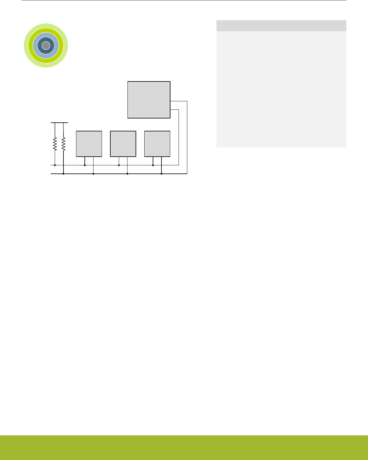
18. I2C - Inter-Integrated Circuit Interface
0 1 2 3 4
Gecko Device
I2C master/slave
Other I2C
master
Other I2C
slave
VDD
I2C
EEPROM
SDA
SCL
Quick Facts
What?
The I2C interface allows communication on I2C-
buses with the lowest energy consumption possible.
Why?
I2C is a popular serial bus that enables communica-
tion with a number of external devices using only
two I/O pins.
How?
With the help of DMA, the I2C interface allows I2C
communication with minimal CPU intervention. Ad-
dress recognition is available in all energy modes
(except EM4), allowing the MCU to wait for data on
the I2C-bus with sub-µA current consumption.
18.1 Introduction
The I2C module provides an interface between the MCU and a serial I2C-bus. It is capable of acting as both a master and a slave and
supports multi-master buses. Standard-mode, fast-mode and fast-mode plus speeds are supported, allowing transmission rates all the
way from 10 kbit/s up to 1 Mbit/s. Slave arbitration and timeouts are also provided to allow implementation of an SMBus compliant sys-
tem. The interface provided to software by the I2C module allows precise control of the transmission process and highly automated
transfers. Automatic recognition of slave addresses is provided in all energy modes (except EM4).
18.2 Features
• True multi-master capability
• Support for different bus speeds
• Standard-mode (Sm) bit rate up to 100 kbit/s
• Fast-mode (Fm) bit rate up to 400 kbit/s
• Fast-mode Plus (Fm+) bit rate up to 1 Mbit/s
• Arbitration for both master and slave (allows SMBus ARP)
• Clock synchronization and clock stretching
• Hardware address recognition
• 7-bit masked address
• General call address
• Active in all energy modes (except EM4)
• 10-bit address support
• Error handling
• Clock low timeout
• Clock high timeout
• Arbitration lost
• Bus error detection
• Separate receive/ transmit 2-level buffers, with additional separate shift registers
• Full DMA support
Reference Manual
I2C - Inter-Integrated Circuit Interface
silabs.com | Smart. Connected. Energy-friendly. Preliminary Rev. 0.5 | 498
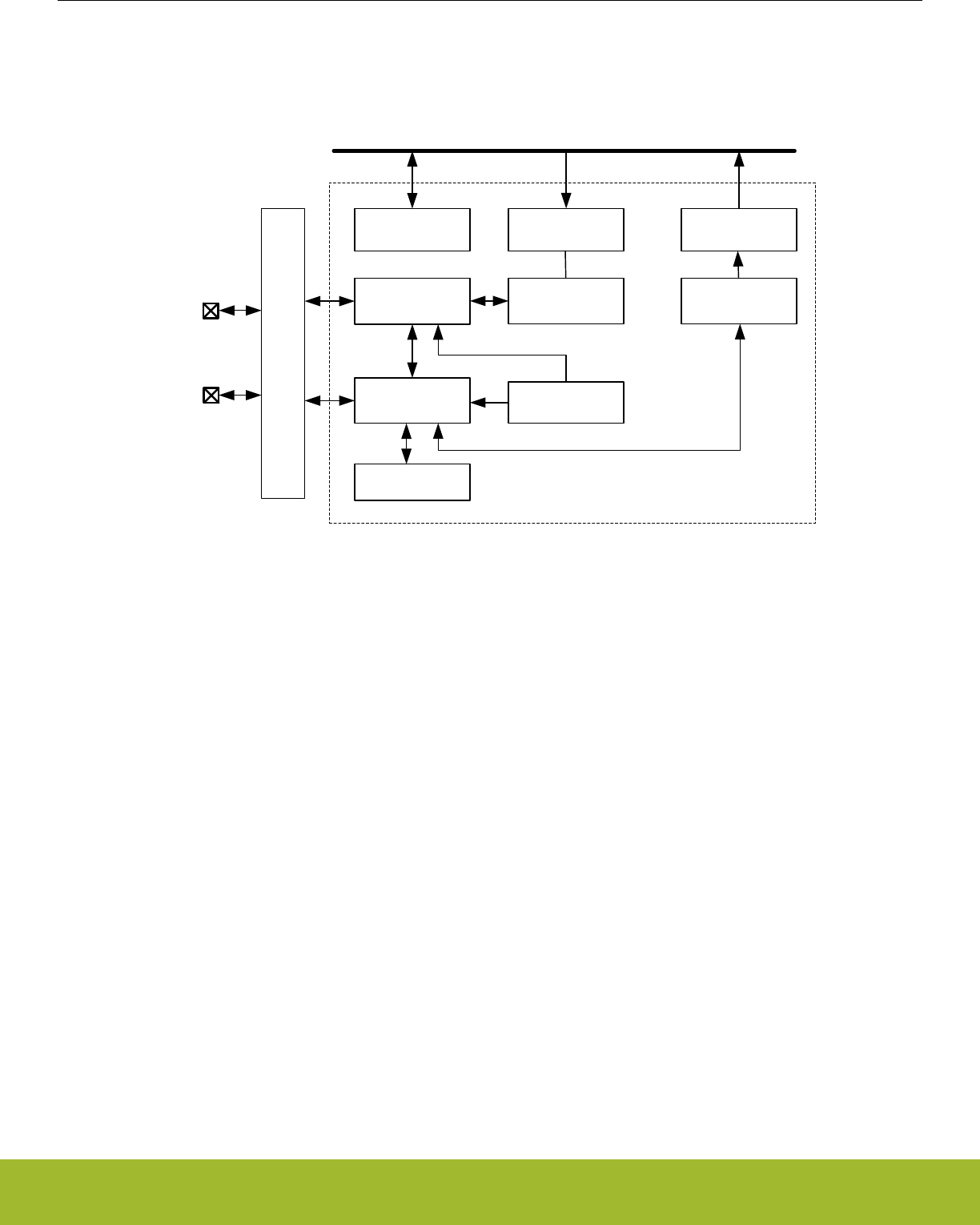
18.3 Functional Description
An overview of the I2C module is shown in Figure 18.1 I2C Overview on page 499.
Transmit Buffer
(2-level FIFO)
Transmit
Shift Register
I2Cn_SDA
Receive Buffer
(2-level FIFO)
Receive
Shift Register
I2C Control and
Status
Peripheral Bus
I2Cn_SCL
Pin
Ctrl
Symbol
Generator
Receive
Controller Clock Generator
Address
Recognizer
Figure 18.1. I2C Overview
Reference Manual
I2C - Inter-Integrated Circuit Interface
silabs.com | Smart. Connected. Energy-friendly. Preliminary Rev. 0.5 | 499
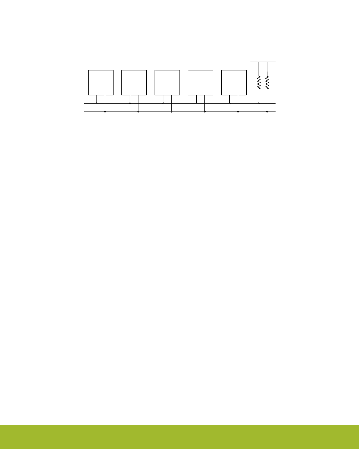
18.3.1 I2C-Bus Overview
The I2C-bus uses two wires for communication; a serial data line (SDA) and a serial clock line (SCL) as shown in Figure 18.2 I2C-Bus
Example on page 500. As a true multi-master bus it includes collision detection and arbitration to resolve situations where multiple
masters transmit data at the same time without data loss.
I2C master
#1
I2C master
#2
I2C slave
#1
I2C slave
#2
I2C slave
#3
SDA
SCL
VDD
Rp
Figure 18.2. I2C-Bus Example
Each device on the bus is addressable by a unique address, and an I2C master can address all the devices on the bus, including other
masters.
Both the bus lines are open-drain. The maximum value of the pull-up resistor can be calculated as a function of the maximal rise-time tr
for the given bus speed, and the estimated bus capacitance Cb as shown in Figure 18.3 I2C Pull-up Resistor Equation on page 500.
Rp(max) = (tr/0.8473) x Cb
Figure 18.3. I2C Pull-up Resistor Equation
The maximal rise times for 100 kHz, 400 kHz and 1 MHz I2C are 1 µs, 300 ns and 120 ns respectively.
Note:
The GPIO drive strength can be used to control slew rate.
Note:
If Vdd drops below the voltage on SCL and SDA lines, the MCU could become back powered and pull the SCL and SDA lines low.
Reference Manual
I2C - Inter-Integrated Circuit Interface
silabs.com | Smart. Connected. Energy-friendly. Preliminary Rev. 0.5 | 500
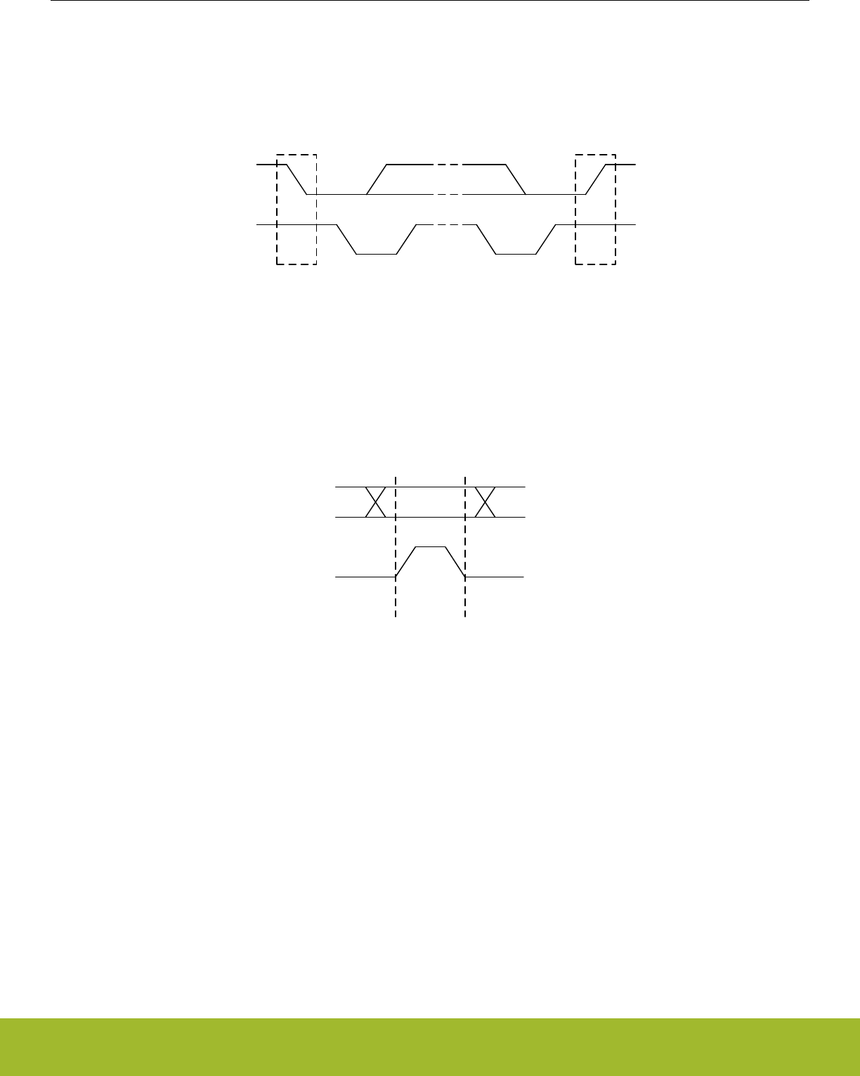
18.3.1.1 START and STOP Conditions
START and STOP conditions are used to initiate and stop transactions on the I2C-bus. All transactions on the bus begin with a START
condition (S) and end with a STOP condition (P). As shown in Figure 18.4 I2C START and STOP Conditions on page 501, a START
condition is generated by pulling the SDA line low while SCL is high, and a STOP condition is generated by pulling the SDA line high
while SCL is high.
SCL
SDA
S P
START condition STOP condition
Figure 18.4. I2C START and STOP Conditions
The START and STOP conditions are easily identifiable bus events as they are the only conditions on the bus where a transition is
allowed on SDA while SCL is high. During the actual data transmission, SDA is only allowed to change while SCL is low, and must be
stable while SCL is high. One bit is transferred per clock pulse on the I2C-bus as shown in Figure 18.5 I2C Bit Transfer on I2C-Bus on
page 501.
SCL
SDA
Data stable Data change
allowed
Data change
allowed
Figure 18.5. I2C Bit Transfer on I2C-Bus
Reference Manual
I2C - Inter-Integrated Circuit Interface
silabs.com | Smart. Connected. Energy-friendly. Preliminary Rev. 0.5 | 501

18.3.1.2 Bus Transfer
When a master wants to initiate a transfer on the bus, it waits until the bus is idle and transmits a START condition on the bus. The
master then transmits the address of the slave it wishes to interact with and a single R/W bit telling whether it wishes to read from the
slave (R/W bit set to 1) or write to the slave (R/W bit set to 0).
After the 7-bit address and the R/W bit, the master releases the bus, allowing the slave to acknowledge the request. During the next bit-
period, the slave pulls SDA low (ACK) if it acknowledges the request, or keeps it high if it does not acknowledge it (NACK).
Following the address acknowledge, either the slave or master transmits data, depending on the value of the R/W bit. After every 8 bits
(one byte) transmitted on the SDA line, the transmitter releases the line to allow the receiver to transmit an ACK or a NACK. Both the
data and the address are transmitted with the most significant bit first.
The number of bytes in a bus transfer is unrestricted. The master ends the transmission after a (N)ACK by sending a STOP condition
on the bus. After a STOP condition, any master wishing to initiate a transfer on the bus can try to gain control of it. If the current master
wishes to make another transfer immediately after the current, it can start a new transfer directly by transmitting a repeated START
condition (Sr) instead of a STOP followed by a START.
Examples of I2C transfers are shown in Figure 18.6 I2C Single Byte Write to Slave on page 502, Figure 18.7 I2C Double Byte Read
from Slave on page 502, and Figure 18.8 I2C Single Byte Write, then Repeated Start and Single Byte Read on page 502. The iden-
tifiers used are:
• ADDR - Address
• DATA - Data
• S - Start bit
• Sr - Repeated start bit
• P - Stop bit
• W/R - Read(1)/Write(0)
• A - ACK
• N - NACK
WS ADDR DATA AA P
Figure 18.6. I2C Single Byte Write to Slave
RS ADDR DATAA DATA NA P
Figure 18.7. I2C Double Byte Read from Slave
RSr ADDR DATAA N PWS ADDR DATAA A
Figure 18.8. I2C Single Byte Write, then Repeated Start and Single Byte Read
Reference Manual
I2C - Inter-Integrated Circuit Interface
silabs.com | Smart. Connected. Energy-friendly. Preliminary Rev. 0.5 | 502
18.3.1.3 Addresses
I2C supports both 7-bit and 10-bit addresses. When using 7-bit addresses, the first byte transmitted after the START-condition contains
the address of the slave that the master wants to contact. In the 7-bit address space, several addresses are reserved. These addresses
are summarized in Table 18.1 I2C Reserved I2C Addresses on page 503, and include a General Call address which can be used to
broadcast a message to all slaves on the I2C-bus.
Table 18.1. I2C Reserved I2C Addresses
I2C Address R/W Description
0000-000 0 General Call address
0000-000 1 START byte
0000-001 X Reserved for the C-Bus format
0000-010 X Reserved for a different bus format
0000-011 X Reserved for future purposes
0000-1XX X Reserved for future purposes
1111-1XX X Reserved for future purposes
1111-0XX X 10 Bit slave addressing mode
18.3.1.4 10-bit Addressing
To address a slave using a 10-bit address, two bytes are required to specify the address instead of one. The seven first bits of the first
byte must then be 1111 0XX, where XX are the two most significant bits of the 10-bit address. As with 7-bit addresses, the eighth bit of
the first byte determines whether the master wishes to read from or write to the slave. The second byte contains the eight least signifi-
cant bits of the slave address.
When a slave receives a 10-bit address, it must acknowledge both the address bytes if they match the address of the slave.
When performing a master transmitter operation, the master transmits the two address bytes and then the remaining data, as shown in
Figure 18.9 I2C Master Transmitter/Slave Receiver with 10-bit Address on page 503.
WS A A DATA A PAddr (2nd byte)ADDR (1st 7 bits)
Figure 18.9. I2C Master Transmitter/Slave Receiver with 10-bit Address
When performing a master receiver operation however, the master first transmits the two address bytes in a master transmitter opera-
tion, then sends a repeated START followed by the first address byte and then receives data from the addressed slave. The slave ad-
dressed by the 10-bit address in the first two address bytes must remember that it was addressed, and respond with data if the address
transmitted after the repeated start matches its own address. An example of this (with one byte transmitted) is shown in Figure
18.10 I2C Master Receiver/Slave Transmitter with 10-bit Address on page 503.
R
Sr DATAA N PWS A AADDR (1st 7 bits) Addr (2nd byte) ADDR (1st 7 bits)
Figure 18.10. I2C Master Receiver/Slave Transmitter with 10-bit Address
Reference Manual
I2C - Inter-Integrated Circuit Interface
silabs.com | Smart. Connected. Energy-friendly. Preliminary Rev. 0.5 | 503

18.3.1.5 Arbitration, Clock Synchronization, Clock Stretching
Arbitration and clock synchronization are features aimed at allowing multi-master buses. Arbitration occurs when two devices try to
drive the bus at the same time. If one device drives it low, while the other drives it high, the one attempting to drive it high will not be
able to do so due to the open-drain bus configuration. Both devices sample the bus, and the one that was unable to drive the bus in the
desired direction detects the collision and backs off, letting the other device continue communication on the bus undisturbed.
Clock synchronization is a means of synchronizing the clock outputs from several masters driving the bus at once, and is a requirement
for effective arbitration.
Slaves on the bus are allowed to force the clock output on the bus low in order to pause the communication on the bus and give them-
selves time to process data or perform any real-time tasks they might have. This is called clock stretching.
Arbitration is supported by the I2C module for both masters and slaves. Clock synchronization and clock stretching is also supported.
18.3.2 Enable and Reset
The I2C is enabled by setting the EN bit in the I2Cn_CTRL register. Whenever this bit is cleared, the internal state of the I2C is reset,
terminating any ongoing transfers.
Note:
When enabling the I2C, the ABORT command or the Bus Idle Timeout feature must be applied prior to use even if the BUSY flag is not
set.
18.3.3 Safely Disabling and Changing Slave Configuration
The I2C slave is partially asynchronous, and some precautions are necessary to always ensure a safe slave disable or slave configura-
tion change. These measures should be taken, if (while the slave is enabled) the user cannot guarantee that an address match will not
occur at the exact time of slave disable or slave configuration change.
Worst case consequences for an address match while disabling slave or changing configuration is that the slave may end up in an
undefined state. To reset the slave back to a known state, the EN bit in I2Cn_CTRL must be reset. This should be done regardless of
whether the slave is going to be re-enabled or not.
Reference Manual
I2C - Inter-Integrated Circuit Interface
silabs.com | Smart. Connected. Energy-friendly. Preliminary Rev. 0.5 | 504

18.3.4 Clock Generation
The SCL signal generated by the I2C master determines the maximum transmission rate on the bus. The clock is generated as a divi-
sion of the peripheral clock, and is given by the following equation:
fSCL = fHFPERCLK/(((Nlow + Nhigh) x (DIV + 1)) + 8),
Figure 18.11. I2C Maximum Transmission Rate
Nlow and Nhigh in combination with the synchronization cycles (discussed below) specify the number of prescaled clock cycles in the low
and high periods of the clock signal respectively. The worst case low and high periods of the signal are:
Thigh >= ((Nhigh) x (DIV + 1) + 4)/fHFPERCLK,
Tlow >= (Nlow x (DIV + 1) + 4)/fHFPERCLK.
Figure 18.12. I2C High and Low Cycles Equations
In worst case, Thigh and Tlow can be 1 fHFPERCLK cycle longer than the number found by above equations due to synchronization uncer-
tainity (i.e., if the synchronization takes 3 fHFPERCLK cycles instead of 2). Similarly, in the worst case the number 8 in the denominator in
fSCL equation can be 9 (if the synchronization cycles were 3 instead of 2 in Thigh or Tlow) or 10 (if synchronization cycles were 3 in both
Thigh and Tlow). The values of Nlow and Nhigh and thus the ratio between the high and low parts of the clock signal is controlled by
CLHR in the I2Cn_CTRL register.
Note:
DIV must be set to 1 during slave mode operation.
18.3.5 Arbitration
Arbitration is enabled by default, but can be disabled by setting the ARBDIS bit in I2Cn_CTRL. When arbitration is enabled, the value
on SDA is sensed every time the I2C module attempts to change its value. If the sensed value is different than the value the I2C module
tried to output, it is interpreted as a simultaneous transmission by another device, and that the I2C module has lost arbitration.
Whenever arbitration is lost, the ARBLOST interrupt flag in I2Cn_IF is set, any lines held are released, and the I2C device goes idle. If
an I2C master loses arbitration during the transmission of an address, another master may be trying to address it. The master therefore
receives the rest of the address, and if the address matches the slave address of the master, the master goes into either slave transmit-
ter or slave receiver mode.
Note:
Arbitration can be lost both when operating as a master and when operating as a slave.
18.3.6 Buffers
Reference Manual
I2C - Inter-Integrated Circuit Interface
silabs.com | Smart. Connected. Energy-friendly. Preliminary Rev. 0.5 | 505
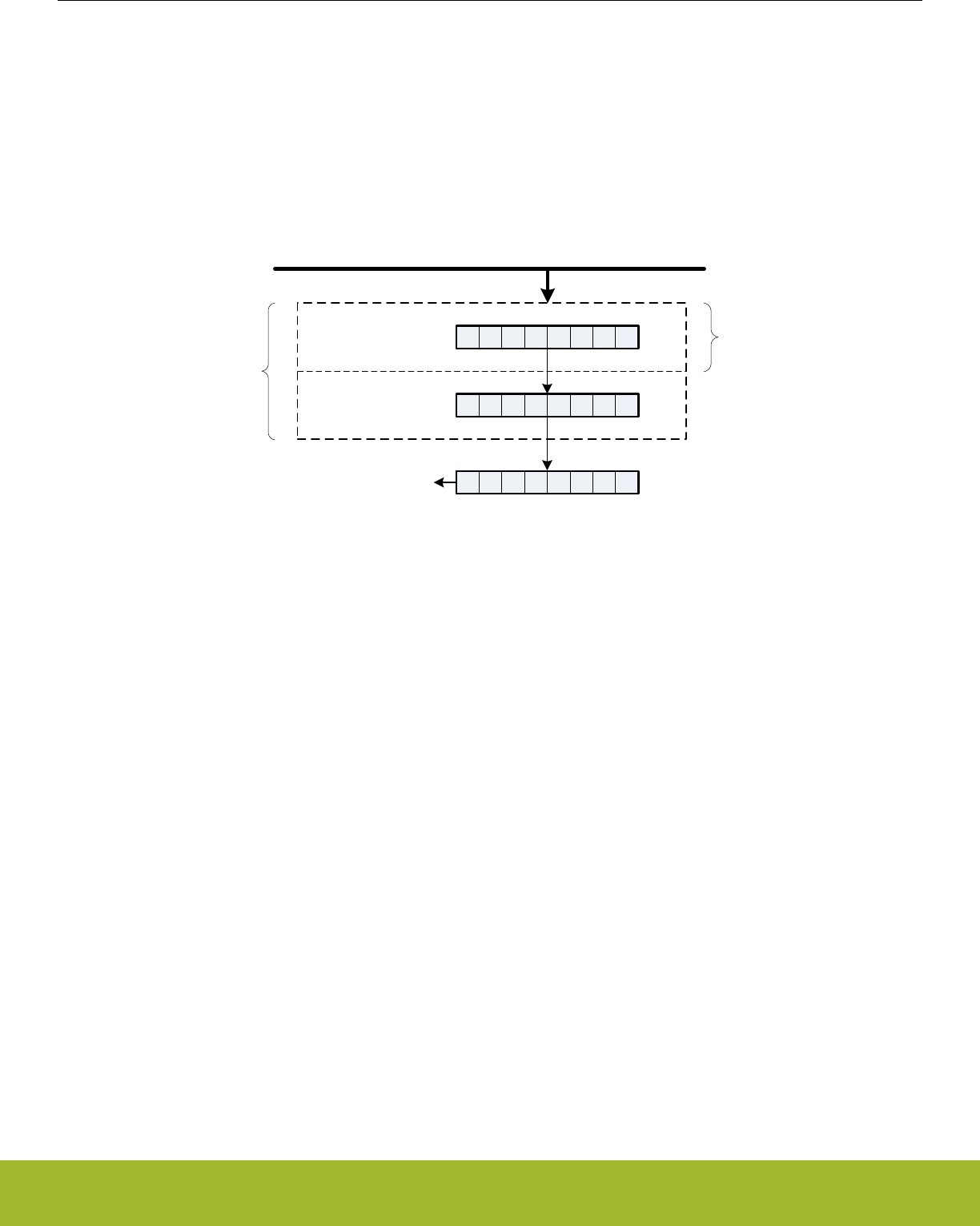
18.3.6.1 Transmit Buffer and Shift Register
The I2C transmitter has a 2-level FIFO transmit buffer and a transmit shift register as shown in Figure 18.1 I2C Overview on page 499.
A byte is loaded into the transmit buffer by writing to I2Cn_TXDATA or 2 bytes can be loaded simultaneously in the transmit buffer by
writing to I2Cn_TXDOUBLE. Figure 18.13 I2C Transmit Buffer Operation on page 506 shows the basics of the transmit buffer. When
the transmit shift register is empty and ready for new data, the byte from the transmit buffer is then loaded into the shift register. The
byte is then kept in the shift register until it is transmitted. When a byte has been transmitted, a new byte is loaded into the shift register
(if available in the transmit buffer). If the transmit buffer is empty, then the shift register also remains empty. The TXC flag in I2Cn_STA-
TUS and the TXC interrupt flags in I2Cn_IF are then set, signaling that the transmit shift register is out of data. TXC is cleared when
new data becomes available, but the TXC interrupt flag must be cleared by software.
TX buffer element 1
TX buffer element 0
Shift register
Peripheral bus
TXDOUBLE
TXDATA
Figure 18.13. I2C Transmit Buffer Operation
The TXBL flags in the I2Cn_STATUS and I2Cn_IF are used to indicate the level of the transmit buffer. TXBIL in I2Cn_CTRL controls the
level at which these flag bits are set. If TXBIL is cleared, the flags are set whenever the transmit buffer becomes empty (used when
transmitting using I2Cn_TXDOUBLE). If TXBIL is set, the flags are set whenever the transmit buffer goes from full to half-empty or emp-
ty (used when transmitting with I2Cn_TXDATA). Both the TXBL status flag and the TXBL interrupt flag are cleared automatically when
the condition becomes false.
If an attempt is made to write more bytes to the transmit buffer than the space available, the TXOF interrupt flag in I2Cn_IF is set,
indicating the overflow. The data already in the buffer remains preserved, and no new data is written.
The transmit buffer and the transmit shift register can be cleared by setting command bit CLEARTX in I2Cn_CMD. This will prevent the
I2C module from transmitting the data in the buffer and the shift register, and will make them available for new data. Any byte currently
being transmitted will not be aborted. Transmission of this byte will be completed.
Reference Manual
I2C - Inter-Integrated Circuit Interface
silabs.com | Smart. Connected. Energy-friendly. Preliminary Rev. 0.5 | 506
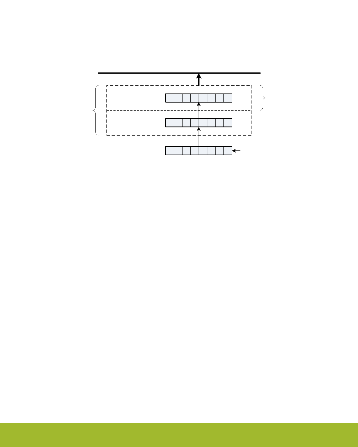
18.3.6.2 Receive Buffer and Shift Register
The I2C receiver uses a 2-level FIFO receive buffer and a receive shift register as shown in Figure 18.14 I2C Receive Buffer Operation
on page 507. When a byte has been fully received by the receive shift register, it is loaded into the receive buffer if there is room for it,
making the shift register empty to receive another byte. Otherwise, the byte waits in the shift register until space becomes available in
the buffer.
RX buffer element 0
RX buffer element 1
Shift register
Peripheral bus
RXDOUBLE
RXDATA
Figure 18.14. I2C Receive Buffer Operation
When a byte becomes available in the receive buffer, the RXDATAV in I2Cn_STATUS and RXDATAV interrupt flag in I2Cn_IF are set.
When the buffer becomes full, RXFULL in the I2Cn_STATUS and I2Cn_IF are set. The status flags RXDATAV and RXFULL are auto-
matically cleared by hardware when their condition is no longer true. This also goes for the RXDATAV interrupt flag, but the RXFULL
interrupt flag must be cleared by software. When the RXFULL flag is set, notifying that the buffer is full, space is still available in the
receive shift register for one more byte.
The data can be fetched from the buffer in two ways. I2Cn_RXDATA gives access to the received byte (if two bytes are received then
the one received first is fetched first). I2Cn_RXDOUBLE makes it possible to read the two received bytes simultaneously. If an attempt
is made to read more bytes from the buffer than available, the RXUF interrupt flag in I2Cn_IF is set to signal the underflow, and the data
read from the buffer is undefined.
When using I2Cn_RXDOUBLE to pick data, AUTOACK in I2Cn_CTRL should be set to 1. This ensures that an ACK is automatically
sent out after the first byte is received so that the reception of the next byte can begin. In order to stop receiving data bytes, a NACK
must be sent out through the I2Cn_CMD register.
I2Cn_RXDATAP and I2Cn_RXDOUBLEP can be used to read data from the receive buffer without removing it from the buffer. The
RXUF interrupt flag in I2Cn_IF will never be set as a result of reading from I2Cn_RXDATAP and I2Cn_RXDOUBLEP, but the data read
through I2Cn_RXDATAP when the receive buffer is empty is still undefined.
Once a transaction is complete (STOP sent or received), the receive buffer needs to be flushed (all received data must be read) before
starting a new transaction.
Reference Manual
I2C - Inter-Integrated Circuit Interface
silabs.com | Smart. Connected. Energy-friendly. Preliminary Rev. 0.5 | 507

18.3.7 Master Operation
A bus transaction is initiated by transmitting a START condition (S) on the bus. This is done by setting the START bit in I2Cn_CMD. The
command schedules a START condition, and makes the I2C module generate a start condition whenever the bus becomes free.
The I2C-bus is considered busy whenever another device on the bus transmits a START condition. Until a STOP condition is detected,
the bus is owned by the master issuing the START condition. The bus is considered free when a STOP condition is transmitted on the
bus. After a STOP is detected, all masters that have data to transmit send a START condition and begin transmitting data. Arbitration
ensures that collisions are avoided.
When the START condition has been transmitted, the master must transmit a slave address (ADDR) with an R/W bit on the bus. If this
address is available in the transmit buffer, the master transmits it immediately, but if the buffer is empty, the master holds the I2C-bus
while waiting for software to write the address to the transmit buffer.
After the address has been transmitted, a sequence of bytes can be read from or written to the slave, depending on the value of the
R/W bit (bit 0 in the address byte). If the bit was cleared, the master has entered a master transmitter role, where it now transmits data
to the slave. If the bit was set, it has entered a master receiver role, where it now should receive data from the slave. In either case, an
unlimited number of bytes can be transferred in one direction during the transmission.
At the end of the transmission, the master either transmits a repeated START condition (Sr) if it wishes to continue with another trans-
fer, or transmits a STOP condition (P) if it wishes to release the bus. When operating in the master mode, HFPERCLK frequency must
be higher than 2 MHz for Standard-mode, 9 MHz for Fast-mode, and 20 MHz for Fast-mode Plus.
Reference Manual
I2C - Inter-Integrated Circuit Interface
silabs.com | Smart. Connected. Energy-friendly. Preliminary Rev. 0.5 | 508
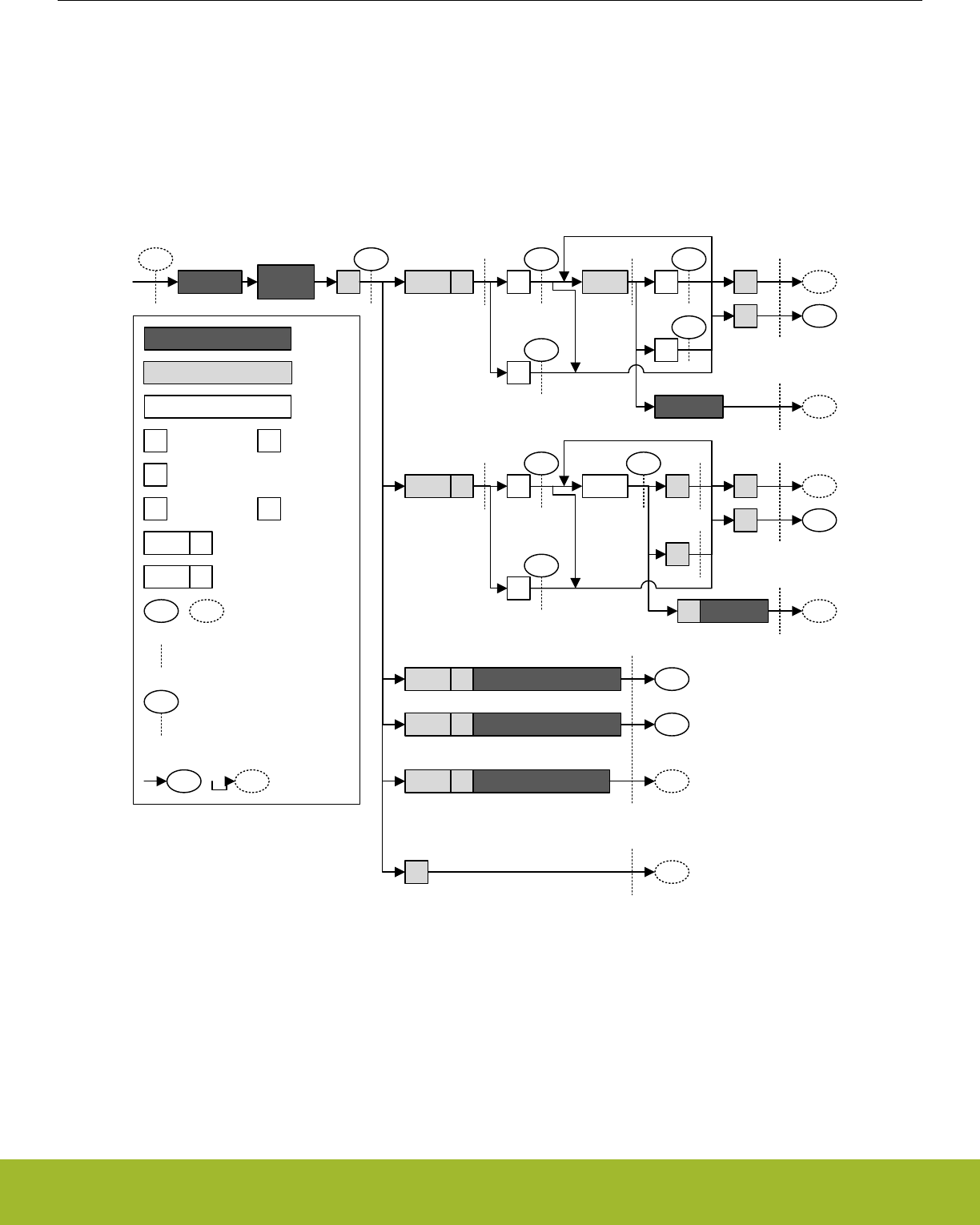
18.3.7.1 Master State Machine
The master state machine is shown in Figure 18.15 I2C Master State Machine on page 509. A master operation starts in the far left of
the state machine, and follows the solid lines through the state machine, ending the operation or continuing with a new operation when
arriving at the right side of the state machine.
Branches in the path through the state machine are the results of bus events and choices made by software, either directly or indirectly.
The dotted lines show where I2C-specific interrupt flags are set along the path and the full-drawn circles show places where interaction
may be required by software to let the transmission proceed.
Waiting
for idle
Idle/busy
57
B3
9B
0
57
S
ADDR R A
N
ADDR W
A
N
DATA P
Sr
XArb. lost 1
97 D7
DF
9F
A
N
A
N
DATA P
Sr
Arb. lost
ADDR R Arb. lost, ADDR match
ADDR W Arb. lost, ADDR match
ADDR X Arb. lost, no match 1
71
Master receiver
Master transmitter
Arbitration lost
Slave transmitter
Slave receiver
0
57
1
93
0/1
Bus state/event
Transmitted by self
Received from slave
START
condition
Interrupt flag set
Interaction required. Wait-
states inserted until manual
or automatic interaction has
been performed
Go to state
A
S P
N
Sr
ACK
STOP
condition
NACK
Repeated START condition
ADDR R
ADDR W
Slave address + read
(R/W bit set)
Slave address + write
(R/W bit cleared)
Bus state (STATE)
73
0P
Bus reset
Figure 18.15. I2C Master State Machine
Reference Manual
I2C - Inter-Integrated Circuit Interface
silabs.com | Smart. Connected. Energy-friendly. Preliminary Rev. 0.5 | 509

18.3.7.2 Interactions
Whenever the I2C module is waiting for interaction from software, it holds the bus clock SCL low, freezing all bus activities, and the
BUSHOLD interrupt flag in I2Cn_IF is set. The action(s) required by software depends on the current state the of the I2C module. This
state can be read from the I2Cn_STATE register.
As an example, Table 18.3 I2C Master Transmitter on page 512 shows the different states the I2C goes through when operating as a
Master Transmitter, i.e., a master that transmits data to a slave. As seen in the table, when a start condition has been transmitted, a
requirement is that there is an address and an R/W bit in the transmit buffer. If the transmit buffer is empty, then the BUSHOLD interrupt
flag is set, and the bus is held until data becomes available in the buffer. While waiting for the address, I2Cn_STATE has a value 0x57,
which can be used to identify exactly what the I2C module is waiting for.
Note:
The bus would never stop at state 0x57 if the address was available in the transmit buffer.
The different interactions used by the I2C module are listed in Table 18.2 I2C Interactions in Prioritized Order on page 510 in a priori-
tized order. If the I2C module is in such a state that multiple courses of action are possible, then the action chosen is the one that has
the highest priority. For example, after sending out a START, if an address is present in the buffer and a STOP is also pending, then the
I2C will send out the STOP since it has the higher priority.
Table 18.2. I2C Interactions in Prioritized Order
Interaction Priority Software action Automatically continues if
STOP* 1 Set the STOP command bit in
I2Cn_CMD
PSTOP is set (STOP pending)
in I2Cn_STATUS
ABORT 2 Set the ABORT command bit in
I2Cn_CMD
Never, the transmission is abor-
ted
CONT* 3 Set the CONT command bit in
I2Cn_CMD
PCONT is set in I2Cn_STATUS
(CONT pending)
NACK* 4 Set the NACK command bit in
I2Cn_CMD
PNACK is set in I2Cn_STATUS
(NACK pending)
ACK* 5 Set the ACK command bit in
I2Cn_CMD
AUTOACK is set in I2Cn_CTRL
or PACK is set in I2Cn_STATUS
(ACK pending)
ADDR+W -> TXDATA 6 Write an address to the transmit
buffer with the R/W bit set
Address is available in transmit
buffer with R/W bit set
ADDR+R -> TXDATA 7 Write an address to the transmit
buffer with the R/W bit cleared
Address is available in transmit
buffer with R/W bit cleared
START* 8 Set the START command bit in
I2Cn_CMD
PSTART is set in I2Cn_STATUS
(START pending)
TXDATA/ TXDOUBLE 9 Write data to the transmit buffer Data is available in transmit buf-
fer
RXDATA/ RXDOUBLE 10 Read data from receive buffer Space is available in receive
buffer
None 11 No interaction is required
The commands marked with a * in Table 18.2 I2C Interactions in Prioritized Order on page 510 can be issued before an interaction is
required. When such a command is issued before it can be used/consumed by the I2C module, the command is set in a pending state,
which can be read from the STATUS register. A pending START command can for instance be identified by PSTART having a high
value.
Whenever the I2C module requires an interaction, it checks the pending commands. If one or a combination of these can fulfill an inter-
action, they are consumed by the module and the transmission continues without setting the BUSHOLD interrupt flag in I2Cn_IF to get
an interaction from software. The pending status of a command goes low when it is consumed.
Reference Manual
I2C - Inter-Integrated Circuit Interface
silabs.com | Smart. Connected. Energy-friendly. Preliminary Rev. 0.5 | 510

When several interactions are possible from a set of pending commands, the interaction with the highest priority, i.e., the interaction
closest to the top of Table 18.2 I2C Interactions in Prioritized Order on page 510 is applied to the bus.
Pending commands can be cleared by setting the CLEARPC command bit in I2Cn_CMD.
18.3.7.3 Automatic ACK Interaction
When receiving addresses and data, an ACK command in I2Cn_CMD is normally required after each received byte. When AUTOACK
is set in I2Cn_CTRL, an ACK is always pending, and the ACK-pending bit PACK in I2Cn_STATUS is thus always set, even after an
ACK has been consumed. This is used when data is picked using I2Cn_RXDOUBLE and can also be used with I2Cn_RXDATA in order
to reduce the amount of software interaction required during a transfer.
18.3.7.4 Reset State
After a reset, the state of the I2C-bus is unknown. To avoid interrupting transfers on the I2C-bus after a reset of the I2C module or the
entire MCU, the I2C-bus is assumed to be busy when coming out of a reset, and the BUSY flag in I2Cn_STATUS is thus set. To be able
to carry through master operations on the I2C-bus, the bus must be idle.
The bus goes idle when a STOP condition is detected on the bus, but on buses with little activity, the time before the I2C module de-
tects that the bus is idle can be significant. There are two ways of assuring that the I2C module gets out of the busy state.
•Use the ABORT command in I2Cn_CMD. When the ABORT command is issued, the I2C module is instructed that the bus is idle.
The I2C module can then initiate master operations.
• Use the Bus Idle Timeout. When SCL has been high for a long period of time, it is very likely that the bus is idle. Set BITO in
I2Cn_CTRL to an appropriate timeout period and set GIBITO in I2Cn_CTRL. If activity has not been detected on the bus within the
timeout period, the bus is then automatically assumed idle, and master operations can be initiated.
Note:
If operating in slave mode, the above approach is not necessary.
Reference Manual
I2C - Inter-Integrated Circuit Interface
silabs.com | Smart. Connected. Energy-friendly. Preliminary Rev. 0.5 | 511

18.3.7.5 Master Transmitter
To transmit data to a slave, the master must operate as a master transmitter. Table 18.3 I2C Master Transmitter on page 512 shows
the states the I2C module goes through while acting as a master transmitter. Every state where an interaction is required has the possi-
ble interactions listed, along with the result of the interactions. The table also shows which interrupt flags are set in the different states.
The interrupt flags enclosed in parenthesis may be set. If the BUSHOLD interrupt in I2Cn_IF is set, the module is waiting for an interac-
tion, and the bus is frozen. The value of I2Cn_STATE will be equal to the values given in the table when the BUSHOLD interrupt flag is
set, and can be used to determine which interaction is required to make the transmission continue.
The interrupt flag START in I2Cn_IF is set when the I2C module transmits the START.
A master operation is started by issuing a START command by setting START in I2Cn_CMD. ADDR+W, i.e., the address of the slave +
the R/W bit is then required by the I2C module. If this is not available in the transmit buffer, then the bus is held and the BUSHOLD
interrupt flag is set. The value of I2Cn_STATE will then be 0x57. As seen in the table, the I2C module also stops in this state if the
address is not available after a repeated start condition.
To continue, write a byte to I2Cn_TXDATA with the address of the slave in the 7 most significant bits and the least significant bit cleared
(ADDR+W). This address will then be transmitted, and the slave will reply with an ACK or a NACK. If no slave replies to the address,
the response will also be NACK. If the address was acknowledged, the master now has four choices. It can send data by placing it in
I2Cn_TXDATA/ I2Cn_TXDOUBLE (the master should check the TXBL interrupt flag before writing to the transmit buffer), this data is
then transmitted. The master can also stop the transmission by sending a STOP, it can send a repeated start by sending START, or it
can send a STOP and then a START as soon as possible. If the master wishes to make another transfer immediately after the current,
the preferred way is to start a new transfer directly by transmitting a repeated START instead of a STOP followed by a START. This is
so because if a STOP is sent out, then any master wishing to initiate a transfer on the bus can try to gain control of it.
If a NACK was received, the master has to issue a CONT command in addition to providing data in order to continue transmission. This
is not standard I2C, but is provided for flexibility. The rest of the options are similar to when an ACK was received.
If a new byte was transmitted, an ACK or NACK is received after the transmission of the byte, and the master has the same options as
for when the address was sent.
The master may lose arbitration at any time during transmission. In this case, the ARBLOST interrupt flag in I2Cn_IF is set. If the arbi-
tration was lost during the transfer of an address, and SLAVE in I2Cn_CTRL is set, the master then checks which address was trans-
mitted. If it was the address of the master, then the master goes to slave mode.
After a master has transmitted a START and won any arbitration, it owns the bus until it transmits a STOP. After a STOP, the bus is
released, and arbitration decides which bus master gains the bus next. The MSTOP interrupt flag in I2Cn_IF is set when a STOP condi-
tion is transmitted by the master.
Table 18.3. I2C Master Transmitter
I2Cn_STATE Description I2Cn_IF Required in-
teraction
Response
0x57 Start transmitted START interrupt flag
(BUSHOLD interrupt
flag)
ADDR+W ->
TXDATA
ADDR+W will be sent
STOP STOP will be sent and bus released.
STOP +
START
STOP will be sent and bus released. Then a
START will be sent when bus becomes idle.
0x57 Repeated start trans-
mitted
START interrupt flag
(BUSHOLD interrupt
flag)
ADDR+W ->
TXDATA
ADDR+W will be sent
STOP STOP will be sent and bus released.
STOP +
START
STOP will be sent and bus released. Then a
START will be sent when bus becomes idle.
- ADDR+W transmitted TXBL interrupt flag
(TXC interrupt flag)
None
Reference Manual
I2C - Inter-Integrated Circuit Interface
silabs.com | Smart. Connected. Energy-friendly. Preliminary Rev. 0.5 | 512

I2Cn_STATE Description I2Cn_IF Required in-
teraction
Response
0x97 ADDR+W transmitted,
ACK received
ACK interrupt flag
(BUSHOLD interrupt
flag)
TXDATA DATA will be sent
STOP STOP will be sent. Bus will be released
START Repeated start condition will be sent
STOP +
START
STOP will be sent and the bus released. Then a
START will be sent when the bus becomes idle
0x9F ADDR+W transmit-
ted,NACK received
NACK (BUSHOLD in-
terrupt flag)
CONT +
TXDATA
DATA will be sent
STOP STOP will be sent. Bus will be released
START Repeated start condition will be sent
STOP +
START
STOP will be sent and the bus released. Then a
START will be sent when the bus becomes idle
- Data transmitted TXBL interrupt flag
(TXC interrupt flag)
None
0xD7 Data transmitted,ACK
received
ACK interrupt flag
(BUSHOLD interrupt
flag)
TXDATA DATA will be sent
STOP STOP will be sent. Bus will be released
START Repeated start condition will be sent
STOP +
START
STOP will be sent and the bus released. Then a
START will be sent when the bus becomes idle
0xDF Data transmitted,NACK
received
NACK(BUSHOLD inter-
rupt flag)
CONT +
TXDATA
DATA will be sent
STOP STOP will be sent. Bus will be released
START Repeated start condition will be sent
STOP +
START
STOP will be sent and the bus released. Then a
START will be sent when the bus becomes idle
- Stop transmitted MSTOP interrupt flag None
START START will be sent when bus becomes idle
- Arbitration lost ARBLOST interrupt flag None
START START will be sent when bus becomes idle
Reference Manual
I2C - Inter-Integrated Circuit Interface
silabs.com | Smart. Connected. Energy-friendly. Preliminary Rev. 0.5 | 513

18.3.7.6 Master Receiver
To receive data from a slave, the master must operate as a master receiver, see Table 18.4 I2C Master Receiver on page 514. This is
done by transmitting ADDR+R as the address byte instead of ADDR+W, which is transmitted to become a master transmitter. The ad-
dress byte loaded into the data register thus has to contain the 7-bit slave address in the 7 most significant bits of the byte, and have
the least significant bit set.
When the address has been transmitted, the master receives an ACK or a NACK. If an ACK is received, the ACK interrupt flag in
I2Cn_IF is set, and if space is available in the receive shift register, reception of a byte from the slave begins. If the receive buffer and
shift register is full however, the bus is held until data is read from the receive buffer or another interaction is made. Note that the STOP
and START interactions have a higher priority than the data-available interaction, so if a STOP or START command is pending, the
highest priority interaction will be performed, and data will not be received from the slave.
If a NACK was received, the CONT command in I2Cn_CMD has to be issued in order to continue receiving data, even if there is space
available in the receive buffer and/or shift register.
After a data byte has been received the master must ACK or NACK the received byte. If an ACK is pending or AUTOACK in
I2Cn_CTRL is set, an ACK is sent automatically and reception continues if space is available in the receive buffer.
If a NACK is sent, the CONT command must be used in order to continue transmission. If an ACK or NACK is issued along with a
START or STOP or both, then the ACK/NACK is transmitted and the reception is ended. If START in I2Cn_CMD is set alone, a repea-
ted start condition is transmitted after the ACK/NACK. If STOP in I2Cn_CMD is set, a stop condition is sent regardless of whether
START is set. If START is set in this case, it is set as pending.
As when operating as a master transmitter, arbitration can be lost as a master receiver. When this happens the ARBLOST interrupt flag
in I2Cn_IF is set, and the master has a possibility of being selected as a slave given the correct conditions.
Table 18.4. I2C Master Receiver
I2Cn_STATE Description I2Cn_IF Required in-
teraction
Response
0x57 START transmitted START interrupt flag
(BUSHOLD interrupt
flag)
ADDR+R ->
TXDATA
ADDR+R will be sent
STOP STOP will be sent and bus released.
STOP +
START
STOP will be sent and bus released. Then a
START will be sent when bus becomes idle.
0x57 Repeated START trans-
mitted
START interrupt
flag(BUSHOLD inter-
rupt flag)
ADDR+R ->
TXDATA
ADDR+R will be sent
STOP STOP will be sent and bus released.
STOP +
START
STOP will be sent and bus released. Then a
START will be sent when bus becomes idle.
- ADDR+R transmitted TXBL interrupt flag
(TXC interrupt flag)
None
0x93 ADDR+R transmitted,
ACK received
ACK interrupt flag(BUS-
HOLD)
RXDATA Start receiving
STOP STOP will be sent and the bus released
START Repeated START will be sent
STOP +
START
STOP will be sent and the bus released. Then a
START will be sent when the bus becomes idle
0x9B ADDR+R transmit-
ted,NACK received
NACK(BUSHOLD) CONT +
RXDATA
Continue, start receiving
STOP STOP will be sent and the bus released
START Repeated START will be sent
STOP +
START
STOP will be sent and the bus released. Then a
START will be sent when the bus becomes idle
Reference Manual
I2C - Inter-Integrated Circuit Interface
silabs.com | Smart. Connected. Energy-friendly. Preliminary Rev. 0.5 | 514

I2Cn_STATE Description I2Cn_IF Required in-
teraction
Response
0xB3 Data received RXDATA interrupt
flag(BUSHOLD inter-
rupt flag)
ACK + RXDA-
TA
ACK will be transmitted, reception continues
NACK +
CONT +
RXDATA
NACK will be transmitted, reception continues
ACK/NACK +
STOP
ACK/NACK will be sent and the bus will be re-
leased.
ACK/NACK +
START
ACK/NACK will be sent, and then a repeated
start condition.
ACK/NACK +
STOP +
START
ACK/NACK will be sent and the bus will be re-
leased. Then a START will be sent when the bus
becomes idle
- Stop received MSTOP interrupt flag None
START START will be sent when bus becomes idle
- Arbitration lost ARBLOST interrupt flag None
START START will be sent when bus becomes idle
Reference Manual
I2C - Inter-Integrated Circuit Interface
silabs.com | Smart. Connected. Energy-friendly. Preliminary Rev. 0.5 | 515

18.3.8 Bus States
The I2Cn_STATE register can be used to determine which state the I2C module and the I2C bus are in at a given time. The register
consists of the STATE bit-field, which shows which state the I2C module is at in any ongoing transmission, and a set of single-bits,
which reveal the transmission mode, whether the bus is busy or idle, and whether the bus is held by this I2C module waiting for a soft-
ware response.
The possible values of the STATE field are summarized in Table 18.5 I2C STATE Values on page 516. When this field is cleared, the
I2C module is not a part of any ongoing transmission. The remaining status bits in the I2Cn_STATE register are listed in Table 18.6 I2C
Transmission Status on page 516.
Table 18.5. I2C STATE Values
Mode Value Description
IDLE 0 No transmission is being performed by this module.
WAIT 1 Waiting for idle. Will send a start condition as soon as the bus is idle.
START 2 Start being transmitted
ADDR 3 Address being transmitted or has been received
ADDRACK 4 Address ACK/NACK being transmitted or received
DATA 5 Data being transmitted or received
DATAACK 6 Data ACK/NACK being transmitted or received
Table 18.6. I2C Transmission Status
Bit Description
BUSY Set whenever there is activity on the bus. Whether or not this module is responsible for
the activity cannot be determined by this byte.
MASTER Set when operating as a master. Cleared at all other times.
TRANSMITTER Set when operating as a transmitter; either a master transmitter or a slave transmitter.
Cleared at all other times
BUSHOLD Set when the bus is held by this I2C module because an action is required by software.
NACK Only valid when bus is held and STATE is ADDRACK or DATAACK. In that case it is set
if a NACK was received. In all other cases, the bit is cleared.
Note:
I2Cn_STATE reflects the internal state of the I2C module, and therefore only held constant as long as the bus is held, i.e., as long as
BUSHOLD in I2Cn_STATUS is set.
18.3.9 Slave Operation
The I2C module operates in master mode by default. To enable slave operation, i.e., to allow the device to be addressed as an I2C
slave, the SLAVE bit in I2Cn_CTRL must be set. In this case the I2C module operates in a mixed mode, both capable of starting trans-
missions as a master, and being addressed as a slave. When operating in the slave mode, HFPERCLK frequency must be higher than
2 MHz for Standard-mode, 5 MHz for Fast-mode, and 14 MHz for Fast-mode Plus.
Reference Manual
I2C - Inter-Integrated Circuit Interface
silabs.com | Smart. Connected. Energy-friendly. Preliminary Rev. 0.5 | 516
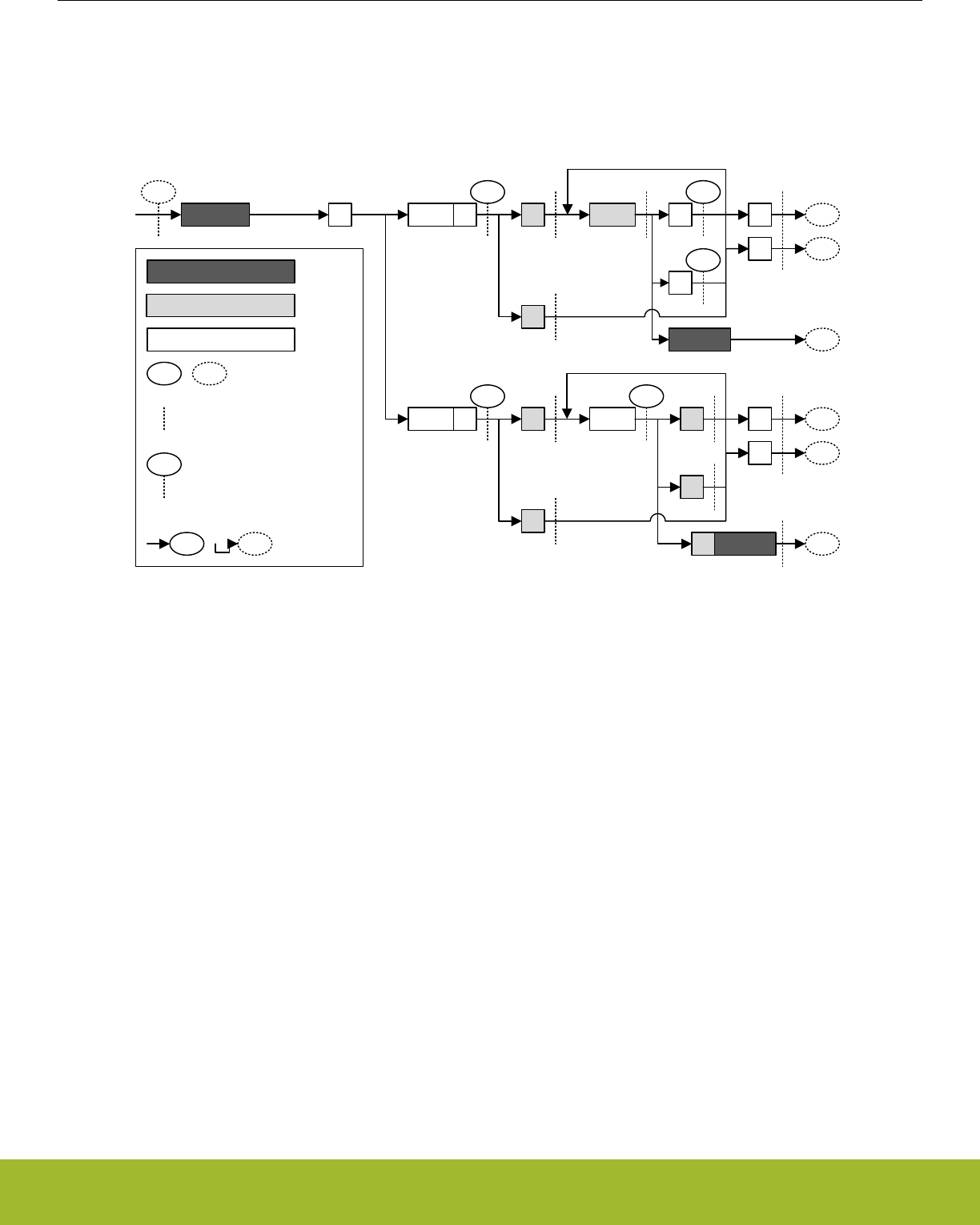
18.3.9.1 Slave State Machine
The slave state machine is shown in Figure 18.16 I2C Slave State Machine on page 517. The dotted lines show where I2C-specific
interrupt flags are set. The full-drawn circles show places where interaction may be required by software to let the transmission pro-
ceed.
73 D5
DD
0
41
S ADDR R A
N
ADDR W
A
N
DATA P
Sr
Arb. lost 1
71 B1
0
41
A
N
A
N
DATA P
Sr
Slave transmitter
Slave receiver
XArb. lost 1
Idle/busy
0/1
Bus state/event
Transmitted by self
Received from master
Bus state (STATE)
Interrupt flag set
Interaction required. Clock-
stretching applied until
manual or automatic
interaction has been
performed
Go to state
Figure 18.16. I2C Slave State Machine
18.3.9.2 Address Recognition
The I2C module provides automatic address recognition for 7-bit addresses. 10-bit address recognition is not fully automatic, but can be
assisted by the 7-bit address comparator as shown in 18.3.11 Using 10-bit Addresses. Address recognition is supported in all energy
modes (except EM4).
The slave address, i.e., the address which the I2C module should be addressed with, is defined in the I2Cn_SADDR register. In addition
to the address, a mask must be specified, telling the address comparator which bits of an incoming address to compare with the ad-
dress defined in I2Cn_SADDR. The mask is defined in I2Cn_SADDRMASK, and for every zero in the mask, the corresponding bit in the
slave address is treated as a don’t-care, i.e., the 0-masked bits are ignored.
An incoming address that fails address recognition is automatically replied to with a NACK. Since only the bits defined by the mask are
checked, a mask with a value 0x00 will result in all addresses being accepted. A mask with a value 0x7F will only match the exact
address defined in I2Cn_SADDR, while a mask 0x70 will match all addresses where the three most significant bits in I2Cn_SADDR and
the incoming address are equal.
If GCAMEN in I2Cn_CTRL is not set, the start-byte, i.e., the general call address with the R/W bit set is ignored unless it is included in
the defined slave address and and the address mask.
When an address is accepted by the address comparator, the decision of whether to ACK or NACK the address is passed to software.
Reference Manual
I2C - Inter-Integrated Circuit Interface
silabs.com | Smart. Connected. Energy-friendly. Preliminary Rev. 0.5 | 517

18.3.9.3 Slave Transmitter
When SLAVE in I2Cn_CTRL is set, the RSTART interrupt flag in I2Cn_IF will be set when repeated START conditions are detected.
After a START or repeated START condition, the bus master will transmit an address along with an R/W bit. If there is no room in the
receive shift register for the address, the bus will be held by the slave until room is available in the shift register. Transmission then
continues and the address is loaded into the shift register. If this address does not pass address recognition, it is automatically
NACK’ed by the slave, and the slave goes to an idle state. The address byte is in this case discarded, making the shift register ready
for a new address. It is not loaded into the receive buffer.
If the address was accepted and the R/W bit was set (R), indicating that the master wishes to read from the slave, the slave now goes
into the slave transmitter mode. Software interaction is now required to decide whether the slave wants to acknowledge the request or
not. The accepted address byte is loaded into the receive buffer like a regular data byte. If no valid interaction is pending, the bus is
held until the slave responds with a command. The slave can reject the request with a single NACK command.
The slave will in that case go to an idle state, and wait for the next start condition. To continue the transmission, the slave must make
sure data is loaded into the transmit buffer and send an ACK. The loaded data will then be transmitted to the master, and an ACK or
NACK will be received from the master.
Data transmission can also continue after a NACK if a CONT command is issued along with the NACK. This is not standard I2C howev-
er.
If the master responds with an ACK, it may expect another byte of data, and data should be made available in the transmit buffer. If
data is not available, the bus is held until data is available.
If the response is a NACK however, this is an indication of that the master has received enough bytes and wishes to end the transmis-
sion. The slave now automatically goes idle, unless CONT in I2Cn_CMD is set and data is available for transmission. The latter is not
standard I2C.
The master ends the transmission by sending a STOP or a repeated START. The SSTOP interrupt flag in I2Cn_IF is set when the mas-
ter transmits a STOP condition. If the transmission is ended with a repeated START, then the SSTOP interrupt flag is not set.
Note:
The SSTOP interrupt flag in I2Cn_IF will be set regardless of whether the slave is participating in the transmission or not, as long as
SLAVE in I2Cn_CTRL is set and a STOP condition is detected
If arbitration is lost at any time during transmission, the ARBLOST interrupt flag in I2Cn_IF is set, the bus is released and the slave
goes idle.
See Table 18.7 I2C Slave Transmitter on page 518 for more information.
Table 18.7. I2C Slave Transmitter
I2Cn_STATE Description I2Cn_IF Required in-
teraction
Response
0x41 Repeated START re-
ceived
RSTART interrupt flag
(BUSHOLD interrupt
flag)
RXDATA Receive and compare address
0x75 ADDR + R received ADDR interrupt flag ACK + TXDA-
TA
ACK will be sent, then DATA
RXDATA interrupt flag NACK NACK will be sent, slave goes idle
(BUSHOLD interrupt
flag)
NACK +
CONT +
TXDATA
NACK will be sent, then DATA.
- Data transmitted TXBL interrupt flag
(TXC interrupt flag)
None
0xD5 Data transmitted, ACK
received
ACK interrupt flag
(BUSHOLD interrupt
flag)
TXDATA DATA will be transmitted
Reference Manual
I2C - Inter-Integrated Circuit Interface
silabs.com | Smart. Connected. Energy-friendly. Preliminary Rev. 0.5 | 518

I2Cn_STATE Description I2Cn_IF Required in-
teraction
Response
0xDD Data transmitted, NACK
received
NACK interrupt flag None The slave goes idle
(BUSHOLD interrupt
flag)
CONT +
TXDATA
DATA will be transmitted
- Stop received SSTOP interrupt flag None The slave goes idle
START START will be sent when bus becomes idle
- Arbitration lost ARBLOST interrupt flag None The slave goes idle
START START will be sent when the bus becomes idle
Reference Manual
I2C - Inter-Integrated Circuit Interface
silabs.com | Smart. Connected. Energy-friendly. Preliminary Rev. 0.5 | 519

18.3.9.4 Slave Receiver
A slave receiver operation is started in the same way as a slave transmitter operation, with the exception that the address transmitted
by the master has the R/W bit cleared (W), indicating that the master wishes to write to the slave. The slave then goes into slave receiv-
er mode.
To receive data from the master, the slave should respond to the address with an ACK and make sure space is available in the receive
buffer. Transmission will then continue, and the slave will receive a byte from the master.
If a NACK is sent without a CONT, the transmission is ended for the slave, and it goes idle. If the slave issues both the NACK and
CONT commands and has space available in the receive buffer, it will be open for continuing reception from the master.
When a byte has been received from the master, the slave must ACK or NACK the byte. The responses here are the same as for the
reception of the address byte.
The master ends the transmission by sending a STOP or a repeated START. The SSTOP interrupt flag is set when the master transmits
a STOP condition. If the transmission is ended with a repeated START, then the SSTOP interrupt flag in I2Cn_IF is not set.
Note:
The SSTOP interrupt flag in I2Cn_IF will be set regardless of whether the slave is participating in the transmission or not, as long as
SLAVE in I2Cn_CTRL is set and a STOP condition is detected
If arbitration is lost at any time during transmission, the ARBLOST interrupt flag in I2Cn_IF is set, the bus is released and the slave
goes idle.
See Table 18.8 I2C - Slave Receiver on page 520 for more information.
Table 18.8. I2C - Slave Receiver
I2Cn_STATE Description I2Cn_IF Required in-
teraction
Response
- Repeated START re-
ceived
RSTART interrupt flag
(BUSHOLD interrupt
flag)
RXDATA Receive and compare address
0x71 ADDR + W received ADDR interrupt flag
RXDATA interrupt flag
(BUSHOLD interrupt
flag)
ACK +
RXDATA
ACK will be sent and data will be received
NACK NACK will be sent, slave goes idle
NACK +
CONT +
RXDATA
NACK will be sent and DATA will be received.
0xB1 Data received RXDATA interrupt flag
(BUSHOLD interrupt
flag)
ACK +
RXDATA
ACK will be sent and data will be received
NACK NACK will be sent and slave will go idle
NACK +
CONT +
RXDATA
NACK will be sent and data will be received
- Stop received SSTOP interrupt flag None The slave goes idle
START START will be sent when bus becomes idle
- Arbitration lost ARBLOST interrupt flag None The slave goes idle
START START will be sent when the bus becomes idle
18.3.10 Transfer Automation
The I2C can be set up to complete transfers with a minimal amount of interaction.
Reference Manual
I2C - Inter-Integrated Circuit Interface
silabs.com | Smart. Connected. Energy-friendly. Preliminary Rev. 0.5 | 520

18.3.10.1 DMA
DMA can be used to automatically load data into the transmit buffer and load data out from the receive buffer. When using DMA, soft-
ware is thus relieved of moving data to and from memory after each transferred byte.
18.3.10.2 Automatic ACK
When AUTOACK in I2Cn_CTRL is set, an ACK is sent automatically whenever an ACK interaction is possible and no higher priority
interactions are pending.
18.3.10.3 Automatic STOP
A STOP can be generated automatically on two conditions. These apply only to the master transmitter.
If AUTOSN in I2Cn_CTRL is set, the I2C module ends a transmission by transmitting a STOP condition when operating as a master
transmitter and a NACK is received.
If AUTOSE in I2Cn_CTRL is set, the I2C module always ends a transmission when there is no more data in the transmit buffer. If data
has been transmitted on the bus, the transmission is ended after the (N)ACK has been received by the slave. If a START is sent when
no data is available in the transmit buffer and AUTOSE is set, then the STOP condition is sent immediately following the START. Soft-
ware must thus make sure data is available in the transmit buffer before the START condition has been fully transmitted if data is to be
transferred.
18.3.11 Using 10-bit Addresses
When using 10-bit addresses in slave mode, set the I2Cn_SADDR register to 1111 0XX where XX are the two most significant bits of
the 10-bit address, and set I2Cn_SADDRMASK to 0xFF. Address matches will now be given on all 10-bit addresses where the two
most significant bits are correct.
When receiving an address match, the slave must acknowledge the address and receive the first data byte. This byte contains the sec-
ond part of the 10-bit address. If it matches the address of the slave, the slave should ACK the byte to continue the transmission, and if
it does not match, the slave should NACK it.
When the master is operating as a master transmitter, the data bytes will follow after the second address byte. When the master is
operating as a master receiver however, a repeated START condition is sent after the second address byte. The address sent after this
repeated START is equal to the first of the address bytes transmitted previously, but now with the R/W byte set, and only the slave that
found a match on the entire 10-bit address in the previous message should ACK this address. The repeated start should take the mas-
ter into a master receiver mode, and after the single address byte sent this time around, the slave begins transmission to the master.
18.3.12 Error Handling
Note:
The setting of GCAMEN and SLAVE fields in the I2Cn_CTRL register and the registers I2Cn_SADDR and I2Cn_ROUTELOC0 are con-
sidered static. This means that these need to be set before an I2C transaction starts and need to stay stable during the entire transac-
tion.
18.3.12.1 ABORT Command
Some bus errors may require software intervention to be resolved. The I2C module provides an ABORT command, which can be set in
I2Cn_CMD, to help resolve bus errors.
When the bus for some reason is locked up and the I2C module is in the middle of a transmission it cannot get out of, or for some other
reason the I2C wants to abort a transmission, the ABORT command can be used.
Setting the ABORT command will make the I2C module discard any data currently being transmitted or received, release the SDA and
SCL lines and go to an idle mode. ABORT effectively makes the I2C module forget about any ongoing transfers.
18.3.12.2 Bus Reset
A bus reset can be performed by setting the START and STOP commands in I2Cn_CMD while the transmit buffer is empty. A START
condition will then be transmitted, immediately followed by a STOP condition. A bus reset can also be performed by transmitting a
START command with the transmit buffer empty and AUTOSE set.
Reference Manual
I2C - Inter-Integrated Circuit Interface
silabs.com | Smart. Connected. Energy-friendly. Preliminary Rev. 0.5 | 521

18.3.12.3 I2C-Bus Errors
An I2C-bus error occurs when a START or STOP condition is misplaced, which happens when the value on SDA changes while SCL is
high during bit-transmission on the I2C-bus. If the I2C module is part of the current transmission when a bus error occurs, any data
currently being transmitted or received is discarded, SDA and SCL are released, the BUSERR interrupt flag in I2Cn_IF is set to indicate
the error, and the module automatically takes a course of action as defined in Table 18.9 I2C Bus Error Response on page 522.
Table 18.9. I2C Bus Error Response
Misplaced START Misplaced STOP
In a master/slave operation Treated as START. Receive address. Go idle. Perform any pending actions.
18.3.12.4 Bus Lockup
A lockup occurs when a master or slave on the I2C-bus has locked the SDA or SCL at a low value, preventing other devices from put-
ting high values on the bus, and thus making communication on the bus impossible.
Many slave-only devices operating on an I2C-bus are not capable of driving SCL low, but in the rare case that SCL is stuck LOW, the
advice is to apply a hardware reset signal to the slaves on the bus. If this does not work, cycle the power to the devices in order to
make them release SCL.
When SDA is stuck low and SCL is free, a master should send 9 clock pulses on SCL while tristating the SDA. This procedure is per-
formed in the GPIO module after clearing the I2C_ROUTE register and disabling the I2C module. The device that held the bus low
should release it sometime within those 9 clocks. If not, use the same approach as for when SCL is stuck, resetting and possibly cycling
power to the slaves.
Lockup of SDA can be detected by keeping count of the number of continuous arbitration losses during address transmission. If arbitra-
tion is also lost during the transmission of a general call address, i.e., during the transmission of the STOP condition, which should
never happen during normal operation, this is a good indication of SDA lockup.
Detection of SCL lockups can be done using the timeout functionality defined in 18.3.12.6 Clock Low Timeout
18.3.12.5 Bus Idle Timeout
When SCL has been high for a significant amount of time, this is a good indication of that the bus is idle. On an SMBus system, the bus
is only allowed to be in this state for a maximum of 50 µs before the bus is considered idle.
The bus idle timeout BITO in I2Cn_CTRL can be used to detect situations where the bus goes idle in the middle of a transmission. The
timeout can be configured in BITO, and when the bus has been idle for the given amount of time, the BITO interrupt flag in I2Cn_IF is
set. The bus can also be set idle automatically on a bus idle timeout. This is enabled by setting GIBITO in I2Cn_CTRL.
When the bus idle timer times out, it wraps around and continues counting as long as its condition is true. If the bus is not set idle using
GIBITO or the ABORT command in I2Cn_CMD, this will result in periodic timeouts.
Note:
This timeout will be generated even if SDA is held low.
The bus idle timeout is active as long as the bus is busy, i.e., BUSY in I2Cn_STATUS is set. The timeout can be used to get the I2C
module out of the busy-state it enters when reset, see 18.3.7.4 Reset State.
18.3.12.6 Clock Low Timeout
The clock timeout, which can be configured in CLTO in I2Cn_CTRL, starts counting whenever SCL goes low, and times out if SCL does
not go high within the configured timeout. A clock low timeout results in CLTOIF in I2Cn_IF being set, allowing software to take action.
When the timer times out, it wraps around and continues counting as long as SCL is low. An SCL lockup will thus result in periodic clock
low timeouts as long as SCL is low.
Reference Manual
I2C - Inter-Integrated Circuit Interface
silabs.com | Smart. Connected. Energy-friendly. Preliminary Rev. 0.5 | 522

18.3.12.7 Clock Low Error
The I2C module can continue transmission in parallel with another device for the entire transaction, as long as the two communications
are identical. A case may arise when (before an arbitration has been decided upon) the I2C module decides to send out a repeated
START or a STOP condition while the other device is still sending data. In the I2C protocol specifications, such a combination results in
an undefined condition. The I2C deals with this by generating a clock low error. This means that if the I2C is transmitting a repeated
START or a STOP condition and another device (another master or a misbehaving slave) pulls SCL low before the I2C sends out the
START/STOP condition on SDA, a clock low error is generated. The CLERR interrupt flag is then set in the I2Cn_IF register, any held
lines are released and the I2C device goes to idle.
18.3.13 DMA Support
The I2C module has full DMA support. A request for the DMA controller to write to the I2C transmit buffer can come from TXBL (transmit
buffer has room for more data). The DMA controller can write to the transmit buffer using the I2Cn_TXDATA or the I2Cn_TXDOUBLE
register. In order to write to the I2Cn_TXDOUBLE register (i.e., transferring 2 bytes simultaneously to the transmit buffer using the
DMA), DMA_USEBURSTS needs to be set to 1 for the selected DMA channel. This ensures that the transfer is made to the transmit
buffer only when both buffer elements are empty. For performing a DMA write to the I2Cn_TXDATA register, DMA_USEBURSTC needs
to be set to 1 for the selected DMA channel. This ensures that a DMA transfer is made even when the transmit buffer is half-empty.
A request for the DMA controller to read from the I2C receive buffer can come from RXDATAV (data available in the receive buffer). To
receive from I2Cn_RXDOUBLE (i.e., receive only when both buffer elements are full), DMA_USEBURSTS needs to be set to 1 for the
selected DMA channel. In order to receive from I2Cn_RXDATA through the DMA, DMA_USEBURSTC needs to be set to 1. This en-
sures that the data gets picked up even when the receive buffer is half-full.
18.3.14 Interrupts
The interrupts generated by the I2C module are combined into one interrupt vector, I2C_INT. If I2C interrupts are enabled, an interrupt
will be made if one or more of the interrupt flags in I2Cn_IF and their corresponding bits in I2Cn_IEN are set.
18.3.15 Wake-up
The I2C receive section can be active all the way down to energy mode EM3 Stop, and can wake up the CPU on address interrupt. All
address match modes are supported.
Reference Manual
I2C - Inter-Integrated Circuit Interface
silabs.com | Smart. Connected. Energy-friendly. Preliminary Rev. 0.5 | 523

18.4 Register Map
The offset register address is relative to the registers base address.
Offset Name Type Description
0x000 I2Cn_CTRL RW Control Register
0x004 I2Cn_CMD W1 Command Register
0x008 I2Cn_STATE RState Register
0x00C I2Cn_STATUS RStatus Register
0x010 I2Cn_CLKDIV RW Clock Division Register
0x014 I2Cn_SADDR RW Slave Address Register
0x018 I2Cn_SADDRMASK RW Slave Address Mask Register
0x01C I2Cn_RXDATA R(a) Receive Buffer Data Register
0x020 I2Cn_RXDOUBLE R(a) Receive Buffer Double Data Register
0x024 I2Cn_RXDATAP RReceive Buffer Data Peek Register
0x028 I2Cn_RXDOUBLEP RReceive Buffer Double Data Peek Register
0x02C I2Cn_TXDATA WTransmit Buffer Data Register
0x030 I2Cn_TXDOUBLE WTransmit Buffer Double Data Register
0x034 I2Cn_IF RInterrupt Flag Register
0x038 I2Cn_IFS W1 Interrupt Flag Set Register
0x03C I2Cn_IFC (R)W1 Interrupt Flag Clear Register
0x040 I2Cn_IEN RW Interrupt Enable Register
0x044 I2Cn_ROUTEPEN RW I/O Routing Pin Enable Register
0x048 I2Cn_ROUTELOC0 RW I/O Routing Location Register
Reference Manual
I2C - Inter-Integrated Circuit Interface
silabs.com | Smart. Connected. Energy-friendly. Preliminary Rev. 0.5 | 524

18.5 Register Description
18.5.1 I2Cn_CTRL - Control Register
Offset Bit Position
0x000
31
30
29
28
27
26
25
24
23
22
21
20
19
18
17
16
15
14
13
12
11
10
9
8
7
6
5
4
3
2
1
0
Reset
0x0
0
0x0
0x0
0
0
0
0
0
0
0
0
Access
RW
RW
RW
RW
RW
RW
RW
RW
RW
RW
RW
RW
Name
CLTO
GIBITO
BITO
CLHR
TXBIL
GCAMEN
ARBDIS
AUTOSN
AUTOSE
AUTOACK
SLAVE
EN
Bit Name Reset Access Description
31:19 Reserved To ensure compatibility with future devices, always write bits to 0. More information in 1.2 Conven-
tions
18:16 CLTO 0x0 RW Clock Low Timeout
Use to generate a timeout when CLK has been low for the given amount of time. Wraps around and continues counting
when the timeout is reached. The timeout value can be calculated by
timeout = PCC/(fSCL x (Nlow + Nhigh))
Value Mode Description
0 OFF Timeout disabled
1 40PCC Timeout after 40 prescaled clock cycles. In standard mode at 100 kHz,
this results in a 50us timeout.
2 80PCC Timeout after 80 prescaled clock cycles. In standard mode at 100 kHz,
this results in a 100us timeout.
3 160PCC Timeout after 160 prescaled clock cycles. In standard mode at 100
kHz, this results in a 200us timeout.
4 320PCC Timeout after 320 prescaled clock cycles. In standard mode at 100
kHz, this results in a 400us timeout.
5 1024PCC Timeout after 1024 prescaled clock cycles. In standard mode at 100
kHz, this results in a 1280us timeout.
15 GIBITO 0 RW Go Idle on Bus Idle Timeout
When set, the bus automatically goes idle on a bus idle timeout, allowing new transfers to be initiated.
Value Description
0 A bus idle timeout has no effect on the bus state.
1A bus idle timeout tells the I2C module that the bus is idle, allowing new
transfers to be initiated.
14 Reserved To ensure compatibility with future devices, always write bits to 0. More information in 1.2 Conven-
tions
Reference Manual
I2C - Inter-Integrated Circuit Interface
silabs.com | Smart. Connected. Energy-friendly. Preliminary Rev. 0.5 | 525

Bit Name Reset Access Description
13:12 BITO 0x0 RW Bus Idle Timeout
Use to generate a timeout when SCL has been high for a given amount time between a START and STOP condition. When
in a bus transaction, i.e. the BUSY flag is set, a timer is started whenever SCL goes high. When the timer reaches the value
defined by BITO, it sets the BITO interrupt flag. The BITO interrupt flag will then be set periodically as long as SCL remains
high. The bus idle timeout is active as long as BUSY is set. It is thus stopped automatically on a timeout if GIBITO is set. It
is also stopped a STOP condition is detected and when the ABORT command is issued. The timeout is activated whenever
the bus goes BUSY, i.e. a START condition is detected. The timeout value can be calculated by
timeout = PCC/(fSCL x (Nlow + Nhigh))
Value Mode Description
0 OFF Timeout disabled
1 40PCC Timeout after 40 prescaled clock cycles. In standard mode at 100 kHz,
this results in a 50us timeout.
2 80PCC Timeout after 80 prescaled clock cycles. In standard mode at 100 kHz,
this results in a 100us timeout.
3 160PCC Timeout after 160 prescaled clock cycles. In standard mode at 100
kHz, this results in a 200us timeout.
11:10 Reserved To ensure compatibility with future devices, always write bits to 0. More information in 1.2 Conven-
tions
9:8 CLHR 0x0 RW Clock Low High Ratio
Determines the ratio between the low and high parts of the clock signal generated on SCL as master.
Value Mode Description
0 STANDARD The ratio between low period and high period counters (Nlow:Nhigh) is
4:4
1 ASYMMETRIC The ratio between low period and high period counters (Nlow:Nhigh) is
6:3
2 FAST The ratio between low period and high period counters (Nlow:Nhigh) is
11:6
7 TXBIL 0 RW TX Buffer Interrupt Level
Determines the interrupt and status level of the transmit buffer.
Value Mode Description
0 EMPTY TXBL status and the TXBL interrupt flag are set when the transmit buf-
fer becomes empty. TXBL is cleared when the buffer becomes non-
empty.
1 HALFFULL TXBL status and the TXBL interrupt flag are set when the transmit buf-
fer goes from full to half-full or empty. TXBL is cleared when the buffer
becomes full.
6 GCAMEN 0 RW General Call Address Match Enable
Set to enable address match on general call in addition to the programmed slave address.
Value Description
Reference Manual
I2C - Inter-Integrated Circuit Interface
silabs.com | Smart. Connected. Energy-friendly. Preliminary Rev. 0.5 | 526

Bit Name Reset Access Description
0 General call address will be NACK'ed if it is not included by the slave
address and address mask.
1 When a general call address is received, a software response is re-
quired.
5 ARBDIS 0 RW Arbitration Disable
A master or slave will not release the bus upon losing arbitration.
Value Description
0 When a device loses arbitration, the ARB interrupt flag is set and the
bus is released.
1 When a device loses arbitration, the ARB interrupt flag is set, but com-
munication proceeds.
4 AUTOSN 0 RW Automatic STOP on NACK
Write to 1 to make a master transmitter send a STOP when a NACK is received from a slave.
Value Description
0 Stop is not automatically sent if a NACK is received from a slave.
1 The master automatically sends a STOP if a NACK is received from a
slave.
3 AUTOSE 0 RW Automatic STOP when Empty
Write to 1 to make a master transmitter send a STOP when no more data is available for transmission.
Value Description
0 A stop must be sent manually when no more data is to be transmitted.
1 The master automatically sends a STOP when no more data is availa-
ble for transmission.
2 AUTOACK 0 RW Automatic Acknowledge
Set to enable automatic acknowledges.
Value Description
0 Software must give one ACK command for each ACK transmitted on
the I2C bus.
1 Addresses that are not automatically NACK'ed, and all data is automat-
ically acknowledged.
1 SLAVE 0 RW Addressable as Slave
Set this bit to allow the device to be selected as an I2C slave.
Value Description
0 All addresses will be responded to with a NACK
1 Addresses matching the programmed slave address or the general call
address (if enabled) require a response from software. Other address-
es are automatically responded to with a NACK.
Reference Manual
I2C - Inter-Integrated Circuit Interface
silabs.com | Smart. Connected. Energy-friendly. Preliminary Rev. 0.5 | 527

Bit Name Reset Access Description
0 EN 0 RW I2C Enable
Use this bit to enable or disable the I2C module.
Value Description
0The I2C module is disabled. And its internal state is cleared
1The I2C module is enabled.
18.5.2 I2Cn_CMD - Command Register
Offset Bit Position
0x004
31
30
29
28
27
26
25
24
23
22
21
20
19
18
17
16
15
14
13
12
11
10
9
8
7
6
5
4
3
2
1
0
Reset
0
0
0
0
0
0
0
0
Access
W1
W1
W1
W1
W1
W1
W1
W1
Name
CLEARPC
CLEARTX
ABORT
CONT
NACK
ACK
STOP
START
Bit Name Reset Access Description
31:8 Reserved To ensure compatibility with future devices, always write bits to 0. More information in 1.2 Conven-
tions
7 CLEARPC 0 W1 Clear Pending Commands
Set to clear pending commands.
6 CLEARTX 0 W1 Clear TX
Set to clear transmit buffer and shift register. Will not abort ongoing transfer.
5 ABORT 0 W1 Abort transmission
Abort the current transmission making the bus go idle. When used in combination with STOP, a STOP condition is sent as
soon as possible before aborting the transmission. The stop condition is subject to clock synchronization.
4 CONT 0 W1 Continue transmission
Set to continue transmission after a NACK has been received.
3 NACK 0 W1 Send NACK
Set to transmit a NACK the next time an acknowledge is required.
2 ACK 0 W1 Send ACK
Set to transmit an ACK the next time an acknowledge is required.
1 STOP 0 W1 Send stop condition
Set to send stop condition as soon as possible.
0 START 0 W1 Send start condition
Set to send start condition as soon as possible. If a transmission is ongoing and not owned, the start condition will be sent
as soon as the bus is idle. If the current transmission is owned by this module, a repeated start condition will be sent. Use
in combination with a STOP command to automatically send a STOP, then a START when the bus becomes idle.
Reference Manual
I2C - Inter-Integrated Circuit Interface
silabs.com | Smart. Connected. Energy-friendly. Preliminary Rev. 0.5 | 528

18.5.3 I2Cn_STATE - State Register
Offset Bit Position
0x008
31
30
29
28
27
26
25
24
23
22
21
20
19
18
17
16
15
14
13
12
11
10
9
8
7
6
5
4
3
2
1
0
Reset
0x0
0
0
0
0
1
Access
R
R
R
R
R
R
Name
STATE
BUSHOLD
NACKED
TRANSMITTER
MASTER
BUSY
Bit Name Reset Access Description
31:8 Reserved To ensure compatibility with future devices, always write bits to 0. More information in 1.2 Conven-
tions
7:5 STATE 0x0 R Transmission State
The state of any current transmission. Cleared if the I2C module is idle.
Value Mode Description
0 IDLE No transmission is being performed.
1 WAIT Waiting for idle. Will send a start condition as soon as the bus is idle.
2 START Start transmitted or received
3 ADDR Address transmitted or received
4 ADDRACK Address ack/nack transmitted or received
5 DATA Data transmitted or received
6 DATAACK Data ack/nack transmitted or received
4 BUSHOLD 0 R Bus Held
Set if the bus is currently being held by this I2C module.
3 NACKED 0 R Nack Received
Set if a NACK was received and STATE is ADDRACK or DATAACK.
2 TRANSMITTER 0 R Transmitter
Set when operating as a master transmitter or a slave transmitter. When cleared, the system may be operating as a master
receiver, a slave receiver or the current mode is not known.
1MASTER 0 R Master
Set when operating as an I2C master. When cleared, the system may be operating as an I2C slave.
0 BUSY 1 R Bus Busy
Set when the bus is busy. Whether the I2C module is in control of the bus or not has no effect on the value of this bit. When
the MCU comes out of reset, the state of the bus is not known, and thus BUSY is set. Use the ABORT command or a bus
idle timeout to force the I2C module out of the BUSY state.
Reference Manual
I2C - Inter-Integrated Circuit Interface
silabs.com | Smart. Connected. Energy-friendly. Preliminary Rev. 0.5 | 529

18.5.4 I2Cn_STATUS - Status Register
Offset Bit Position
0x00C
31
30
29
28
27
26
25
24
23
22
21
20
19
18
17
16
15
14
13
12
11
10
9
8
7
6
5
4
3
2
1
0
Reset
0
0
1
0
0
0
0
0
0
0
Access
R
R
R
R
R
R
R
R
R
R
Name
RXFULL
RXDATAV
TXBL
TXC
PABORT
PCONT
PNACK
PACK
PSTOP
PSTART
Bit Name Reset Access Description
31:10 Reserved To ensure compatibility with future devices, always write bits to 0. More information in 1.2 Conven-
tions
9 RXFULL 0 R RX FIFO Full
Set when the receive buffer is full. Cleared when the receive buffer is no longer full. When this bit is set, there is still room
for one more frame in the receive shift register.
8RXDATAV 0 R RX Data Valid
Set when data is available in the receive buffer. Cleared when the receive buffer is empty.
7 TXBL 1 R TX Buffer Level
Indicates the level of the transmit buffer. Set when the transmit buffer is empty, and cleared when it is full.
6 TXC 0 R TX Complete
Set when a transmission has completed and no more data is available in the transmit buffer. Cleared when a new transmis-
sion starts.
5 PABORT 0 R Pending abort
An abort is pending and will be transmitted as soon as possible.
4 PCONT 0 R Pending continue
A continue is pending and will be transmitted as soon as possible.
3 PNACK 0 R Pending NACK
A not-acknowledge is pending and will be transmitted as soon as possible.
2 PACK 0 R Pending ACK
An acknowledge is pending and will be transmitted as soon as possible.
1 PSTOP 0 R Pending STOP
A stop condition is pending and will be transmitted as soon as possible.
0 PSTART 0 R Pending START
A start condition is pending and will be transmitted as soon as possible.
Reference Manual
I2C - Inter-Integrated Circuit Interface
silabs.com | Smart. Connected. Energy-friendly. Preliminary Rev. 0.5 | 530

18.5.5 I2Cn_CLKDIV - Clock Division Register
Offset Bit Position
0x010
31
30
29
28
27
26
25
24
23
22
21
20
19
18
17
16
15
14
13
12
11
10
9
8
7
6
5
4
3
2
1
0
Reset
0x000
Access
RW
Name
DIV
Bit Name Reset Access Description
31:9 Reserved To ensure compatibility with future devices, always write bits to 0. More information in 1.2 Conven-
tions
8:0 DIV 0x000 RW Clock Divider
Specifies the clock divider for the I2C. Note that DIV must be 1 or higher when slave is enabled.
18.5.6 I2Cn_SADDR - Slave Address Register
Offset Bit Position
0x014
31
30
29
28
27
26
25
24
23
22
21
20
19
18
17
16
15
14
13
12
11
10
9
8
7
6
5
4
3
2
1
0
Reset
0x00
Access
RW
Name
ADDR
Bit Name Reset Access Description
31:8 Reserved To ensure compatibility with future devices, always write bits to 0. More information in 1.2 Conven-
tions
7:1 ADDR 0x00 RW Slave address
Specifies the slave address of the device.
0 Reserved To ensure compatibility with future devices, always write bits to 0. More information in 1.2 Conven-
tions
Reference Manual
I2C - Inter-Integrated Circuit Interface
silabs.com | Smart. Connected. Energy-friendly. Preliminary Rev. 0.5 | 531

18.5.7 I2Cn_SADDRMASK - Slave Address Mask Register
Offset Bit Position
0x018
31
30
29
28
27
26
25
24
23
22
21
20
19
18
17
16
15
14
13
12
11
10
9
8
7
6
5
4
3
2
1
0
Reset
0x00
Access
RW
Name
MASK
Bit Name Reset Access Description
31:8 Reserved To ensure compatibility with future devices, always write bits to 0. More information in 1.2 Conven-
tions
7:1 MASK 0x00 RW Slave Address Mask
Specifies the significant bits of the slave address. Setting the mask to 0x00 will match all addresses, while setting it to 0x7F
will only match the exact address specified by ADDR.
0 Reserved To ensure compatibility with future devices, always write bits to 0. More information in 1.2 Conven-
tions
18.5.8 I2Cn_RXDATA - Receive Buffer Data Register (Actionable Reads)
Offset Bit Position
0x01C
31
30
29
28
27
26
25
24
23
22
21
20
19
18
17
16
15
14
13
12
11
10
9
8
7
6
5
4
3
2
1
0
Reset
0x00
Access
R
Name
RXDATA
Bit Name Reset Access Description
31:8 Reserved To ensure compatibility with future devices, always write bits to 0. More information in 1.2 Conven-
tions
7:0 RXDATA 0x00 R RX Data
Use this register to read from the receive buffer. Buffer is emptied on read access.
Reference Manual
I2C - Inter-Integrated Circuit Interface
silabs.com | Smart. Connected. Energy-friendly. Preliminary Rev. 0.5 | 532

18.5.9 I2Cn_RXDOUBLE - Receive Buffer Double Data Register (Actionable Reads)
Offset Bit Position
0x020
31
30
29
28
27
26
25
24
23
22
21
20
19
18
17
16
15
14
13
12
11
10
9
8
7
6
5
4
3
2
1
0
Reset
0x00
0x00
Access
R
R
Name
RXDATA1
RXDATA0
Bit Name Reset Access Description
31:16 Reserved To ensure compatibility with future devices, always write bits to 0. More information in 1.2 Conven-
tions
15:8 RXDATA1 0x00 R RX Data 1
Second byte read from buffer. Buffer is emptied on read access.
7:0 RXDATA0 0x00 R RX Data 0
First byte read from buffer. Buffer is emptied on read access.
18.5.10 I2Cn_RXDATAP - Receive Buffer Data Peek Register
Offset Bit Position
0x024
31
30
29
28
27
26
25
24
23
22
21
20
19
18
17
16
15
14
13
12
11
10
9
8
7
6
5
4
3
2
1
0
Reset
0x00
Access
R
Name
RXDATAP
Bit Name Reset Access Description
31:8 Reserved To ensure compatibility with future devices, always write bits to 0. More information in 1.2 Conven-
tions
7:0 RXDATAP 0x00 R RX Data Peek
Use this register to read from the receive buffer. Buffer is not emptied on read access.
Reference Manual
I2C - Inter-Integrated Circuit Interface
silabs.com | Smart. Connected. Energy-friendly. Preliminary Rev. 0.5 | 533

18.5.11 I2Cn_RXDOUBLEP - Receive Buffer Double Data Peek Register
Offset Bit Position
0x028
31
30
29
28
27
26
25
24
23
22
21
20
19
18
17
16
15
14
13
12
11
10
9
8
7
6
5
4
3
2
1
0
Reset
0x00
0x00
Access
R
R
Name
RXDATAP1
RXDATAP0
Bit Name Reset Access Description
31:16 Reserved To ensure compatibility with future devices, always write bits to 0. More information in 1.2 Conven-
tions
15:8 RXDATAP1 0x00 R RX Data 1 Peek
Second byte read from buffer. Buffer is not emptied on read access.
7:0 RXDATAP0 0x00 R RX Data 0 Peek
First byte read from buffer. Buffer is not emptied on read access.
18.5.12 I2Cn_TXDATA - Transmit Buffer Data Register
Offset Bit Position
0x02C
31
30
29
28
27
26
25
24
23
22
21
20
19
18
17
16
15
14
13
12
11
10
9
8
7
6
5
4
3
2
1
0
Reset
0x00
Access
W
Name
TXDATA
Bit Name Reset Access Description
31:8 Reserved To ensure compatibility with future devices, always write bits to 0. More information in 1.2 Conven-
tions
7:0 TXDATA 0x00 W TX Data
Use this register to write a byte to the transmit buffer.
Reference Manual
I2C - Inter-Integrated Circuit Interface
silabs.com | Smart. Connected. Energy-friendly. Preliminary Rev. 0.5 | 534

18.5.13 I2Cn_TXDOUBLE - Transmit Buffer Double Data Register
Offset Bit Position
0x030
31
30
29
28
27
26
25
24
23
22
21
20
19
18
17
16
15
14
13
12
11
10
9
8
7
6
5
4
3
2
1
0
Reset
0x00
0x00
Access
W
W
Name
TXDATA1
TXDATA0
Bit Name Reset Access Description
31:16 Reserved To ensure compatibility with future devices, always write bits to 0. More information in 1.2 Conven-
tions
15:8 TXDATA1 0x00 W TX Data
Second byte to write to buffer.
7:0 TXDATA0 0x00 W TX Data
First byte to write to buffer.
Reference Manual
I2C - Inter-Integrated Circuit Interface
silabs.com | Smart. Connected. Energy-friendly. Preliminary Rev. 0.5 | 535

18.5.14 I2Cn_IF - Interrupt Flag Register
Offset Bit Position
0x034
31
30
29
28
27
26
25
24
23
22
21
20
19
18
17
16
15
14
13
12
11
10
9
8
7
6
5
4
3
2
1
0
Reset
0
0
0
0
0
0
0
0
0
0
0
0
0
0
1
0
0
0
0
Access
R
R
R
R
R
R
R
R
R
R
R
R
R
R
R
R
R
R
R
Name
CLERR
RXFULL
SSTOP
CLTO
BITO
RXUF
TXOF
BUSHOLD
BUSERR
ARBLOST
MSTOP
NACK
ACK
RXDATAV
TXBL
TXC
ADDR
RSTART
START
Bit Name Reset Access Description
31:19 Reserved To ensure compatibility with future devices, always write bits to 0. More information in 1.2 Conven-
tions
18 CLERR 0 R Clock Low Error Interrupt Flag
Set when the clock is pulled low before a START or a STOP condition could be transmitted.
17 RXFULL 0 R Receive Buffer Full Interrupt Flag
Set when the receive buffer becomes full.
16 SSTOP 0 R Slave STOP condition Interrupt Flag
Set when a STOP condition has been received. Will be set regardless of the slave being involved in the transaction or not.
15 CLTO 0 R Clock Low Timeout Interrupt Flag
Set on each clock low timeout. The timeout value can be set in CLTO bit field in the I2Cn_CTRL register.
14 BITO 0 R Bus Idle Timeout Interrupt Flag
Set on each bus idle timeout. The timeout value can be set in the BITO bit field in the I2Cn_CTRL register.
13 RXUF 0 R Receive Buffer Underflow Interrupt Flag
Set when data is read from the receive buffer through the I2Cn_RXDATA register while the receive buffer is empty. It is also
set when data is read through the I2Cn_RXDOUBLE while the buffer is not full.
12 TXOF 0 R Transmit Buffer Overflow Interrupt Flag
Set when data is written to the transmit buffer while the transmit buffer is full.
11 BUSHOLD 0 R Bus Held Interrupt Flag
Set when the bus becomes held by the I2C module.
10 BUSERR 0 R Bus Error Interrupt Flag
Set when a bus error is detected. The bus error is resolved automatically, but the current transfer is aborted.
9 ARBLOST 0 R Arbitration Lost Interrupt Flag
Set when arbitration is lost.
8 MSTOP 0 R Master STOP Condition Interrupt Flag
Set when a STOP condition has been successfully transmitted. If arbitration is lost during the transmission of the STOP
condition, then the MSTOP interrupt flag is not set.
7NACK 0 R Not Acknowledge Received Interrupt Flag
Set when a NACK has been received.
6 ACK 0 R Acknowledge Received Interrupt Flag
Set when an ACK has been received.
Reference Manual
I2C - Inter-Integrated Circuit Interface
silabs.com | Smart. Connected. Energy-friendly. Preliminary Rev. 0.5 | 536

Bit Name Reset Access Description
5 RXDATAV 0 R Receive Data Valid Interrupt Flag
Set when data is available in the receive buffer. Cleared automatically when the receive buffer is read.
4 TXBL 1 R Transmit Buffer Level Interrupt Flag
Set when the transmit buffer becomes empty. Cleared automatically when new data is written to the transmit buffer.
3 TXC 0 R Transfer Completed Interrupt Flag
Set when the transmit shift register becomes empty and there is no more data in the transmit buffer.
2 ADDR 0 R Address Interrupt Flag
Set when incoming address is accepted, i.e. own address or general call address is received.
1 RSTART 0 R Repeated START condition Interrupt Flag
Set when a repeated start condition is detected.
0 START 0 R START condition Interrupt Flag
Set when a start condition is successfully transmitted.
Reference Manual
I2C - Inter-Integrated Circuit Interface
silabs.com | Smart. Connected. Energy-friendly. Preliminary Rev. 0.5 | 537

18.5.15 I2Cn_IFS - Interrupt Flag Set Register
Offset Bit Position
0x038
31
30
29
28
27
26
25
24
23
22
21
20
19
18
17
16
15
14
13
12
11
10
9
8
7
6
5
4
3
2
1
0
Reset
0
0
0
0
0
0
0
0
0
0
0
0
0
0
0
0
0
Access
W1
W1
W1
W1
W1
W1
W1
W1
W1
W1
W1
W1
W1
W1
W1
W1
W1
Name
CLERR
RXFULL
SSTOP
CLTO
BITO
RXUF
TXOF
BUSHOLD
BUSERR
ARBLOST
MSTOP
NACK
ACK
TXC
ADDR
RSTART
START
Bit Name Reset Access Description
31:19 Reserved To ensure compatibility with future devices, always write bits to 0. More information in 1.2 Conven-
tions
18 CLERR 0 W1 Set CLERR Interrupt Flag
Write 1 to set the CLERR interrupt flag
17 RXFULL 0 W1 Set RXFULL Interrupt Flag
Write 1 to set the RXFULL interrupt flag
16 SSTOP 0 W1 Set SSTOP Interrupt Flag
Write 1 to set the SSTOP interrupt flag
15 CLTO 0 W1 Set CLTO Interrupt Flag
Write 1 to set the CLTO interrupt flag
14 BITO 0 W1 Set BITO Interrupt Flag
Write 1 to set the BITO interrupt flag
13 RXUF 0 W1 Set RXUF Interrupt Flag
Write 1 to set the RXUF interrupt flag
12 TXOF 0 W1 Set TXOF Interrupt Flag
Write 1 to set the TXOF interrupt flag
11 BUSHOLD 0 W1 Set BUSHOLD Interrupt Flag
Write 1 to set the BUSHOLD interrupt flag
10 BUSERR 0 W1 Set BUSERR Interrupt Flag
Write 1 to set the BUSERR interrupt flag
9 ARBLOST 0 W1 Set ARBLOST Interrupt Flag
Write 1 to set the ARBLOST interrupt flag
8 MSTOP 0 W1 Set MSTOP Interrupt Flag
Write 1 to set the MSTOP interrupt flag
7 NACK 0 W1 Set NACK Interrupt Flag
Write 1 to set the NACK interrupt flag
6 ACK 0 W1 Set ACK Interrupt Flag
Write 1 to set the ACK interrupt flag
5:4 Reserved To ensure compatibility with future devices, always write bits to 0. More information in 1.2 Conven-
tions
Reference Manual
I2C - Inter-Integrated Circuit Interface
silabs.com | Smart. Connected. Energy-friendly. Preliminary Rev. 0.5 | 538

Bit Name Reset Access Description
3 TXC 0 W1 Set TXC Interrupt Flag
Write 1 to set the TXC interrupt flag
2 ADDR 0 W1 Set ADDR Interrupt Flag
Write 1 to set the ADDR interrupt flag
1 RSTART 0 W1 Set RSTART Interrupt Flag
Write 1 to set the RSTART interrupt flag
0 START 0 W1 Set START Interrupt Flag
Write 1 to set the START interrupt flag
Reference Manual
I2C - Inter-Integrated Circuit Interface
silabs.com | Smart. Connected. Energy-friendly. Preliminary Rev. 0.5 | 539

18.5.16 I2Cn_IFC - Interrupt Flag Clear Register
Offset Bit Position
0x03C
31
30
29
28
27
26
25
24
23
22
21
20
19
18
17
16
15
14
13
12
11
10
9
8
7
6
5
4
3
2
1
0
Reset
0
0
0
0
0
0
0
0
0
0
0
0
0
0
0
0
0
Access
(R)W1
(R)W1
(R)W1
(R)W1
(R)W1
(R)W1
(R)W1
(R)W1
(R)W1
(R)W1
(R)W1
(R)W1
(R)W1
(R)W1
(R)W1
(R)W1
(R)W1
Name
CLERR
RXFULL
SSTOP
CLTO
BITO
RXUF
TXOF
BUSHOLD
BUSERR
ARBLOST
MSTOP
NACK
ACK
TXC
ADDR
RSTART
START
Bit Name Reset Access Description
31:19 Reserved To ensure compatibility with future devices, always write bits to 0. More information in 1.2 Conven-
tions
18 CLERR 0 (R)W1 Clear CLERR Interrupt Flag
Write 1 to clear the CLERR interrupt flag. Reading returns the value of the IF and clears the corresponding interrupt flags
(This feature must be enabled globally in MSC.).
17 RXFULL 0 (R)W1 Clear RXFULL Interrupt Flag
Write 1 to clear the RXFULL interrupt flag. Reading returns the value of the IF and clears the corresponding interrupt flags
(This feature must be enabled globally in MSC.).
16 SSTOP 0 (R)W1 Clear SSTOP Interrupt Flag
Write 1 to clear the SSTOP interrupt flag. Reading returns the value of the IF and clears the corresponding interrupt flags
(This feature must be enabled globally in MSC.).
15 CLTO 0 (R)W1 Clear CLTO Interrupt Flag
Write 1 to clear the CLTO interrupt flag. Reading returns the value of the IF and clears the corresponding interrupt flags
(This feature must be enabled globally in MSC.).
14 BITO 0 (R)W1 Clear BITO Interrupt Flag
Write 1 to clear the BITO interrupt flag. Reading returns the value of the IF and clears the corresponding interrupt flags
(This feature must be enabled globally in MSC.).
13 RXUF 0 (R)W1 Clear RXUF Interrupt Flag
Write 1 to clear the RXUF interrupt flag. Reading returns the value of the IF and clears the corresponding interrupt flags
(This feature must be enabled globally in MSC.).
12 TXOF 0 (R)W1 Clear TXOF Interrupt Flag
Write 1 to clear the TXOF interrupt flag. Reading returns the value of the IF and clears the corresponding interrupt flags
(This feature must be enabled globally in MSC.).
11 BUSHOLD 0 (R)W1 Clear BUSHOLD Interrupt Flag
Write 1 to clear the BUSHOLD interrupt flag. Reading returns the value of the IF and clears the corresponding interrupt
flags (This feature must be enabled globally in MSC.).
10 BUSERR 0 (R)W1 Clear BUSERR Interrupt Flag
Write 1 to clear the BUSERR interrupt flag. Reading returns the value of the IF and clears the corresponding interrupt flags
(This feature must be enabled globally in MSC.).
9 ARBLOST 0 (R)W1 Clear ARBLOST Interrupt Flag
Write 1 to clear the ARBLOST interrupt flag. Reading returns the value of the IF and clears the corresponding interrupt flags
(This feature must be enabled globally in MSC.).
Reference Manual
I2C - Inter-Integrated Circuit Interface
silabs.com | Smart. Connected. Energy-friendly. Preliminary Rev. 0.5 | 540

Bit Name Reset Access Description
8 MSTOP 0 (R)W1 Clear MSTOP Interrupt Flag
Write 1 to clear the MSTOP interrupt flag. Reading returns the value of the IF and clears the corresponding interrupt flags
(This feature must be enabled globally in MSC.).
7 NACK 0 (R)W1 Clear NACK Interrupt Flag
Write 1 to clear the NACK interrupt flag. Reading returns the value of the IF and clears the corresponding interrupt flags
(This feature must be enabled globally in MSC.).
6 ACK 0 (R)W1 Clear ACK Interrupt Flag
Write 1 to clear the ACK interrupt flag. Reading returns the value of the IF and clears the corresponding interrupt flags (This
feature must be enabled globally in MSC.).
5:4 Reserved To ensure compatibility with future devices, always write bits to 0. More information in 1.2 Conven-
tions
3 TXC 0 (R)W1 Clear TXC Interrupt Flag
Write 1 to clear the TXC interrupt flag. Reading returns the value of the IF and clears the corresponding interrupt flags (This
feature must be enabled globally in MSC.).
2 ADDR 0 (R)W1 Clear ADDR Interrupt Flag
Write 1 to clear the ADDR interrupt flag. Reading returns the value of the IF and clears the corresponding interrupt flags
(This feature must be enabled globally in MSC.).
1 RSTART 0 (R)W1 Clear RSTART Interrupt Flag
Write 1 to clear the RSTART interrupt flag. Reading returns the value of the IF and clears the corresponding interrupt flags
(This feature must be enabled globally in MSC.).
0 START 0 (R)W1 Clear START Interrupt Flag
Write 1 to clear the START interrupt flag. Reading returns the value of the IF and clears the corresponding interrupt flags
(This feature must be enabled globally in MSC.).
Reference Manual
I2C - Inter-Integrated Circuit Interface
silabs.com | Smart. Connected. Energy-friendly. Preliminary Rev. 0.5 | 541

18.5.17 I2Cn_IEN - Interrupt Enable Register
Offset Bit Position
0x040
31
30
29
28
27
26
25
24
23
22
21
20
19
18
17
16
15
14
13
12
11
10
9
8
7
6
5
4
3
2
1
0
Reset
0
0
0
0
0
0
0
0
0
0
0
0
0
0
0
0
0
0
0
Access
RW
RW
RW
RW
RW
RW
RW
RW
RW
RW
RW
RW
RW
RW
RW
RW
RW
RW
RW
Name
CLERR
RXFULL
SSTOP
CLTO
BITO
RXUF
TXOF
BUSHOLD
BUSERR
ARBLOST
MSTOP
NACK
ACK
RXDATAV
TXBL
TXC
ADDR
RSTART
START
Bit Name Reset Access Description
31:19 Reserved To ensure compatibility with future devices, always write bits to 0. More information in 1.2 Conven-
tions
18 CLERR 0 RW CLERR Interrupt Enable
Enable/disable the CLERR interrupt
17 RXFULL 0 RW RXFULL Interrupt Enable
Enable/disable the RXFULL interrupt
16 SSTOP 0 RW SSTOP Interrupt Enable
Enable/disable the SSTOP interrupt
15 CLTO 0 RW CLTO Interrupt Enable
Enable/disable the CLTO interrupt
14 BITO 0 RW BITO Interrupt Enable
Enable/disable the BITO interrupt
13 RXUF 0 RW RXUF Interrupt Enable
Enable/disable the RXUF interrupt
12 TXOF 0 RW TXOF Interrupt Enable
Enable/disable the TXOF interrupt
11 BUSHOLD 0 RW BUSHOLD Interrupt Enable
Enable/disable the BUSHOLD interrupt
10 BUSERR 0 RW BUSERR Interrupt Enable
Enable/disable the BUSERR interrupt
9 ARBLOST 0 RW ARBLOST Interrupt Enable
Enable/disable the ARBLOST interrupt
8 MSTOP 0 RW MSTOP Interrupt Enable
Enable/disable the MSTOP interrupt
7 NACK 0 RW NACK Interrupt Enable
Enable/disable the NACK interrupt
6 ACK 0 RW ACK Interrupt Enable
Enable/disable the ACK interrupt
Reference Manual
I2C - Inter-Integrated Circuit Interface
silabs.com | Smart. Connected. Energy-friendly. Preliminary Rev. 0.5 | 542

Bit Name Reset Access Description
5 RXDATAV 0 RW RXDATAV Interrupt Enable
Enable/disable the RXDATAV interrupt
4 TXBL 0 RW TXBL Interrupt Enable
Enable/disable the TXBL interrupt
3 TXC 0 RW TXC Interrupt Enable
Enable/disable the TXC interrupt
2 ADDR 0 RW ADDR Interrupt Enable
Enable/disable the ADDR interrupt
1 RSTART 0 RW RSTART Interrupt Enable
Enable/disable the RSTART interrupt
0 START 0 RW START Interrupt Enable
Enable/disable the START interrupt
18.5.18 I2Cn_ROUTEPEN - I/O Routing Pin Enable Register
Offset Bit Position
0x044
31
30
29
28
27
26
25
24
23
22
21
20
19
18
17
16
15
14
13
12
11
10
9
8
7
6
5
4
3
2
1
0
Reset
0
0
Access
RW
RW
Name
SCLPEN
SDAPEN
Bit Name Reset Access Description
31:2 Reserved To ensure compatibility with future devices, always write bits to 0. More information in 1.2 Conven-
tions
1 SCLPEN 0 RW SCL Pin Enable
When set, the SCL pin of the I2C is enabled.
0 SDAPEN 0 RW SDA Pin Enable
When set, the SDA pin of the I2C is enabled.
Reference Manual
I2C - Inter-Integrated Circuit Interface
silabs.com | Smart. Connected. Energy-friendly. Preliminary Rev. 0.5 | 543

18.5.19 I2Cn_ROUTELOC0 - I/O Routing Location Register
Offset Bit Position
0x048
31
30
29
28
27
26
25
24
23
22
21
20
19
18
17
16
15
14
13
12
11
10
9
8
7
6
5
4
3
2
1
0
Reset
0x00
0x00
Access
RW
RW
Name
SCLLOC
SDALOC
Bit Name Reset Access Description
31:14 Reserved To ensure compatibility with future devices, always write bits to 0. More information in 1.2 Conven-
tions
13:8 SCLLOC 0x00 RW I/O Location
Decides the location of the I2C SCL pin.
Value Mode Description
0 LOC0 Location 0
1 LOC1 Location 1
2 LOC2 Location 2
3 LOC3 Location 3
4 LOC4 Location 4
5 LOC5 Location 5
6 LOC6 Location 6
7 LOC7 Location 7
8 LOC8 Location 8
9 LOC9 Location 9
10 LOC10 Location 10
11 LOC11 Location 11
12 LOC12 Location 12
13 LOC13 Location 13
14 LOC14 Location 14
15 LOC15 Location 15
16 LOC16 Location 16
17 LOC17 Location 17
18 LOC18 Location 18
19 LOC19 Location 19
20 LOC20 Location 20
21 LOC21 Location 21
22 LOC22 Location 22
Reference Manual
I2C - Inter-Integrated Circuit Interface
silabs.com | Smart. Connected. Energy-friendly. Preliminary Rev. 0.5 | 544

Bit Name Reset Access Description
23 LOC23 Location 23
24 LOC24 Location 24
25 LOC25 Location 25
26 LOC26 Location 26
27 LOC27 Location 27
28 LOC28 Location 28
29 LOC29 Location 29
30 LOC30 Location 30
31 LOC31 Location 31
7:6 Reserved To ensure compatibility with future devices, always write bits to 0. More information in 1.2 Conven-
tions
5:0 SDALOC 0x00 RW I/O Location
Decides the location of the I2C SDA pin.
Value Mode Description
0 LOC0 Location 0
1 LOC1 Location 1
2 LOC2 Location 2
3 LOC3 Location 3
4 LOC4 Location 4
5 LOC5 Location 5
6 LOC6 Location 6
7 LOC7 Location 7
8 LOC8 Location 8
9 LOC9 Location 9
10 LOC10 Location 10
11 LOC11 Location 11
12 LOC12 Location 12
13 LOC13 Location 13
14 LOC14 Location 14
15 LOC15 Location 15
16 LOC16 Location 16
17 LOC17 Location 17
18 LOC18 Location 18
19 LOC19 Location 19
20 LOC20 Location 20
21 LOC21 Location 21
22 LOC22 Location 22
Reference Manual
I2C - Inter-Integrated Circuit Interface
silabs.com | Smart. Connected. Energy-friendly. Preliminary Rev. 0.5 | 545

Bit Name Reset Access Description
23 LOC23 Location 23
24 LOC24 Location 24
25 LOC25 Location 25
26 LOC26 Location 26
27 LOC27 Location 27
28 LOC28 Location 28
29 LOC29 Location 29
30 LOC30 Location 30
31 LOC31 Location 31
Reference Manual
I2C - Inter-Integrated Circuit Interface
silabs.com | Smart. Connected. Energy-friendly. Preliminary Rev. 0.5 | 546
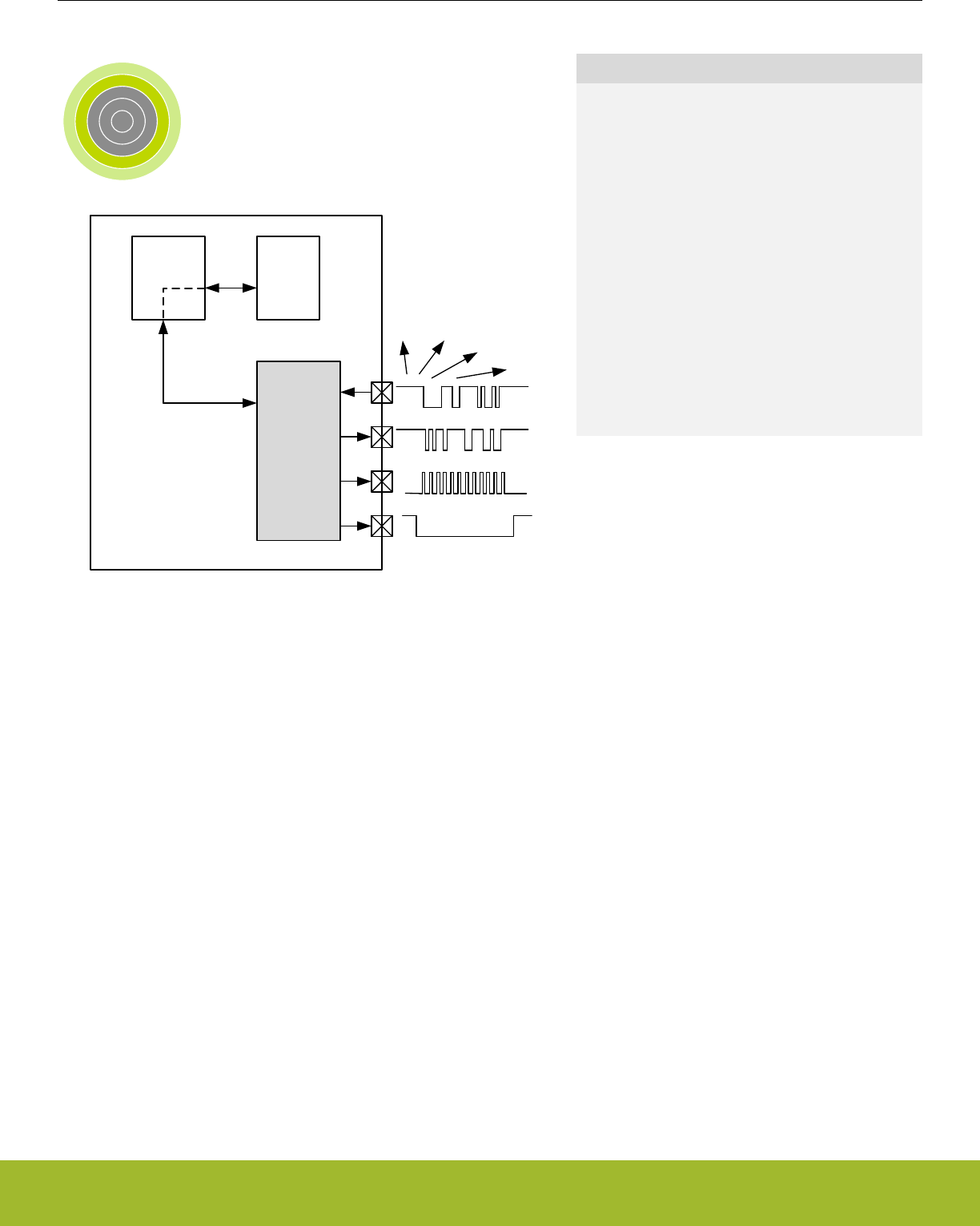
19. USART - Universal Synchronous Asynchronous Receiver/Transmitter
0 1 2 3 4
USARTRX/
MISO
TX/
MOSI
DMA
controller
RAM
CLK
CS
SPI
USART
SmartCards
IrDA
µC
Quick Facts
What?
The USART handles high-speed UART, SPI-bus,
SmartCards, and IrDA communication.
Why?
Serial communication is frequently used in embed-
ded systems and the USART allows efficient com-
munication with a wide range of external devices.
How?
The USART has a wide selection of operating
modes, frame formats and baud rates. The multi-
processor mode allows the USART to remain idle
when not addressed. Triple buffering and DMA sup-
port makes high data-rates possible with minimal
CPU intervention and it is possible to transmit and
receive large frames while the MCU remains in EM1
Sleep.
19.1 Introduction
The Universal Synchronous Asynchronous serial Receiver and Transmitter (USART) is a very flexible serial I/O module. It supports full
duplex asynchronous UART communication as well as RS-485, SPI, MicroWire and 3-wire. It can also interface with ISO7816 Smart-
Cards, and IrDA devices.
Reference Manual
USART - Universal Synchronous Asynchronous Receiver/Transmitter
silabs.com | Smart. Connected. Energy-friendly. Preliminary Rev. 0.5 | 547

19.2 Features
• Asynchronous and synchronous (SPI) communication
•Full duplex and half duplex
• Separate TX/RX enable
• Separate receive / transmit multiple entry buffers, with additional separate shift registers
• Programmable baud rate, generated as an fractional division from the peripheral clock (HFPERCLKUSARTn)
• Max bit-rate
• SPI master mode, peripheral clock rate/2
• SPI slave mode, peripheral clock rate/8
• UART mode, peripheral clock rate/16, 8, 6, or 4
• Asynchronous mode supports
• Majority vote baud-reception
• False start-bit detection
• Break generation/detection
• Multi-processor mode
• Synchronous mode supports
• All 4 SPI clock polarity/phase configurations
• Master and slave mode
• Data can be transmitted LSB first or MSB first
• Configurable number of data bits, 4-16 (plus the parity bit, if enabled)
• HW parity bit generation and check
• Configurable number of stop bits in asynchronous mode: 0.5, 1, 1.5, 2
• HW collision detection
• Multi-processor mode
• IrDA modulator
• SmartCard (ISO7816) mode
• I2S mode
• Separate interrupt vectors for receive and transmit interrupts
• Loopback mode
• Half duplex communication
• Communication debugging
• PRS RX input
• 8 bit Timer
• Hardware Flow Control
• Automatic Baud Rate Detection
Reference Manual
USART - Universal Synchronous Asynchronous Receiver/Transmitter
silabs.com | Smart. Connected. Energy-friendly. Preliminary Rev. 0.5 | 548
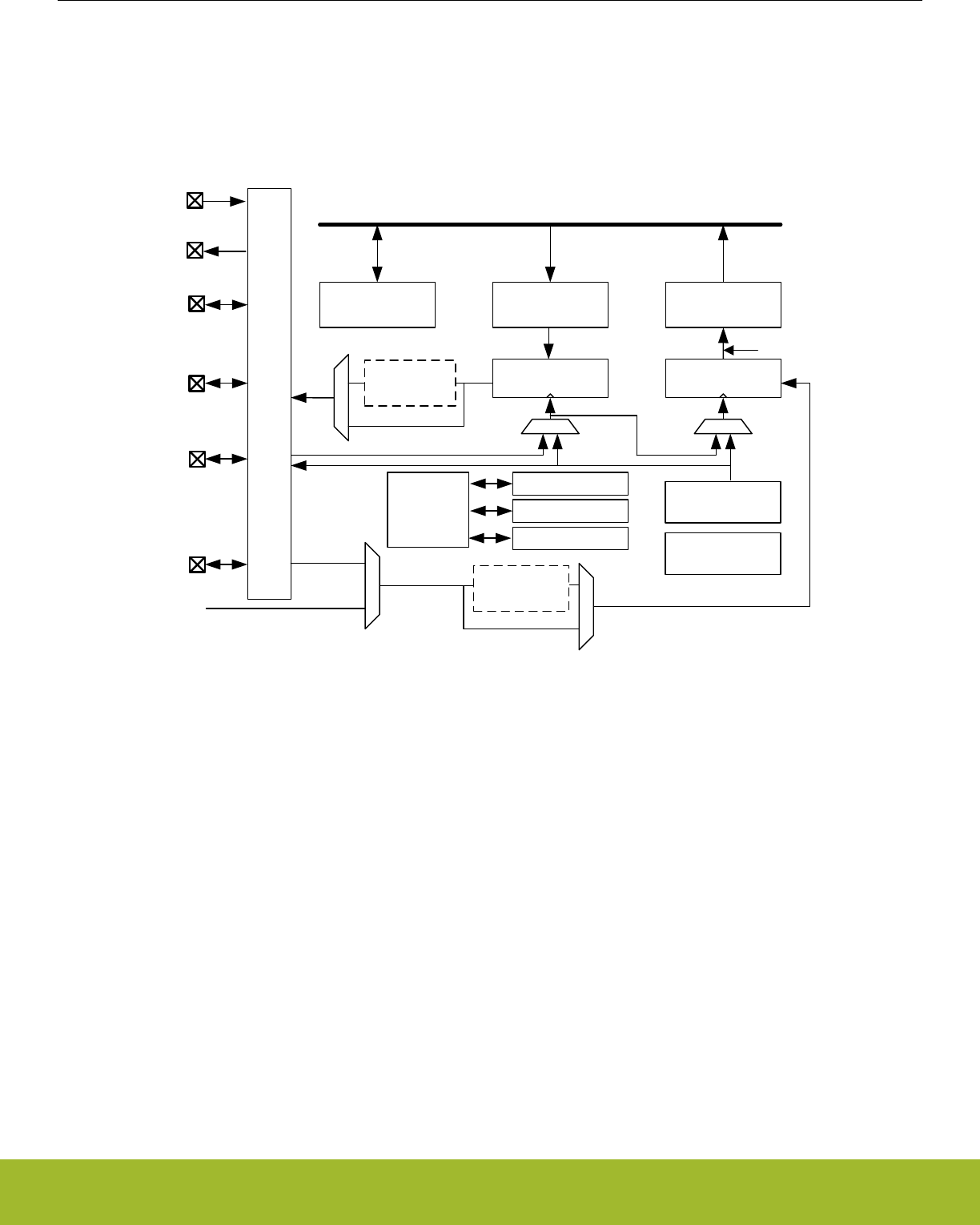
19.3 Functional Description
An overview of the USART module is shown in Figure 19.1 USART Overview on page 549.
This section describes all possible USART features. Please refer to the Device Datasheet to see what features a specific USART in-
stance supports.
TX Buffer
(2-level FIFO)
TX Shift Register
U(S)n_TX
RX Buffer
(2-level FIFO)
RX Shift Register
UART Control
and status
Peripheral Bus
Baud rate
generator
USn_CLK
Pin
ctrl
USn_CS
U(S)n_RX
IrDA
modulator
IrDA
demodulator
!RXBLOCK
PRS inputs
USn_CTS
USn_RTS
TIMECMP2
Timer TIMECMP1
TIMECMP0
Auto Baud
Detection
Figure 19.1. USART Overview
Reference Manual
USART - Universal Synchronous Asynchronous Receiver/Transmitter
silabs.com | Smart. Connected. Energy-friendly. Preliminary Rev. 0.5 | 549

19.3.1 Modes of Operation
The USART operates in either asynchronous or synchronous mode.
In synchronous mode, a separate clock signal is transmitted with the data. This clock signal is generated by the bus master, and both
the master and slave sample and transmit data according to this clock. Both master and slave modes are supported by the USART. The
synchronous communication mode is compatible with the Serial Peripheral Interface Bus (SPI) standard.
In asynchronous mode, no separate clock signal is transmitted with the data on the bus. The USART receiver thus has to determine
where to sample the data on the bus from the actual data. To make this possible, additional synchronization bits are added to the data
when operating in asynchronous mode, resulting in a slight overhead.
Asynchronous or synchronous mode can be selected by configuring SYNC in USARTn_CTRL. The options are listed with supported
protocols in Table 19.1 USART Asynchronous vs. Synchronous Mode on page 550. Full duplex and half duplex communication is
supported in both asynchronous and synchronous mode.
Table 19.1. USART Asynchronous vs. Synchronous Mode
SYNC Communication Mode Supported Protocols
0 Asynchronous RS-232, RS-485 (w/external driver), IrDA, ISO 7816
1 Synchronous SPI, MicroWire, 3-wire
Table 19.2 USART Pin Usage on page 550 explains the functionality of the different USART pins when the USART operates in differ-
ent modes. Pin functionality enclosed in square brackets is optional, and depends on additional configuration parameters. LOOPBK and
MASTER are discussed in 19.3.2.14 Local Loopback and 19.3.3.3 Master Mode respectively.
Table 19.2. USART Pin Usage
SYNC LOOPBK MASTER
Pin functionality
U(S)n_TX (MOSI) U(S)n_RX (MISO) USn_CLK USn_CS
0 0 x Data out Data in - [Driver enable]
0 1 x Data out/in - - [Driver enable]
1 0 0 Data in Data out Clock in Slave select
1 0 1 Data out Data in Clock out [Auto slave select]
1 1 0 Data out/in - Clock in Slave select
1 1 1 Data out/in - Clock out [Auto slave select]
19.3.2 Asynchronous Operation
Reference Manual
USART - Universal Synchronous Asynchronous Receiver/Transmitter
silabs.com | Smart. Connected. Energy-friendly. Preliminary Rev. 0.5 | 550

19.3.2.1 Frame Format
The frame format used in asynchronous mode consists of a set of data bits in addition to bits for synchronization and optionally a parity
bit for error checking. A frame starts with one start-bit (S), where the line is driven low for one bit-period. This signals the start of a
frame, and is used for synchronization. Following the start bit are 4 to 16 data bits and an optional parity bit. Finally, a number of stop-
bits, where the line is driven high, end the frame. An example frame is shown in Figure 19.2 USART Asynchronous Frame Format on
page 551.
S 0 1 2 34 [5] [6] [7] [8] [P] Stop
Start or idleStop or idle
Frame
Figure 19.2. USART Asynchronous Frame Format
The number of data bits in a frame is set by DATABITS in USARTn_FRAME, see Table 19.3 USART Data Bits on page 551, and the
number of stop-bits is set by STOPBITS in USARTn_FRAME, see Table 19.4 USART Stop Bits on page 551. Whether or not a parity
bit should be included, and whether it should be even or odd is defined by PARITY, also in USARTn_FRAME. For communication to be
possible, all parties of an asynchronous transfer must agree on the frame format being used.
Table 19.3. USART Data Bits
DATA BITS [3:0] Number of Data bits
0001 4
0010 5
0011 6
0100 7
0101 8 (Default)
0110 9
0111 10
1000 11
1001 12
1010 13
1011 14
1100 15
1101 16
Table 19.4. USART Stop Bits
STOP BITS [1:0] Number of Stop bits
00 0.5
01 1 (Default)
10 1.5
11 2
Reference Manual
USART - Universal Synchronous Asynchronous Receiver/Transmitter
silabs.com | Smart. Connected. Energy-friendly. Preliminary Rev. 0.5 | 551

The order in which the data bits are transmitted and received is defined by MSBF in USARTn_CTRL. When MSBF is cleared, data in a
frame is sent and received with the least significant bit first. When it is set, the most significant bit comes first.
The frame format used by the transmitter can be inverted by setting TXINV in USARTn_CTRL, and the format expected by the receiver
can be inverted by setting RXINV in USARTn_CTRL. These bits affect the entire frame, not only the data bits. An inverted frame has a
low idle state, a high start-bit, inverted data and parity bits, and low stop-bits.
19.3.2.2 Parity bit Calculation and Handling
When parity bits are enabled, hardware automatically calculates and inserts any parity bits into outgoing frames, and verifies the re-
ceived parity bits in incoming frames. This is true for both asynchronous and synchronous modes, even though it is mostly used in
asynchronous communication. The possible parity modes are defined in Table 19.5 USART Parity Bits on page 552. When even pari-
ty is chosen, a parity bit is inserted to make the number of high bits (data + parity) even. If odd parity is chosen, the parity bit makes the
total number of high bits odd.
Table 19.5. USART Parity Bits
PARITY BITS [1:0] Description
00 No parity bit (Default)
01 Reserved
10 Even parity
11 Odd parity
Reference Manual
USART - Universal Synchronous Asynchronous Receiver/Transmitter
silabs.com | Smart. Connected. Energy-friendly. Preliminary Rev. 0.5 | 552

19.3.2.3 Clock Generation
The USART clock defines the transmission and reception data rate. When operating in asynchronous mode, the baud rate (bit-rate) is
given by Figure 19.3 USART Baud Rate on page 553.
br = fHFPERCLK/(oversample x (1 + USARTn_CLKDIV/256))
Figure 19.3. USART Baud Rate
where fHFPERCLK is the peripheral clock (HFPERCLKUSARTn) frequency and oversample is the oversampling rate as defined by OVS in
USARTn_CTRL, see Table 19.6 USART Oversampling on page 553.
Table 19.6. USART Oversampling
OVS [1:0] oversample
00 16
01 8
10 6
11 4
The USART has a fractional clock divider to allow the USART clock to be controlled more accurately than what is possible with a stand-
ard integral divider.
The clock divider used in the USART is a 20-bit value, with a 15-bit integral part and an 5-bit fractional part. The fractional part is config-
ured in the lower 5 bits of DIV in USART_CLKDIV.
Fractional clock division is implemented by distributing the selected fraction over thirty two baud periods. The fractional part of the divid-
er tells how many of these periods should be extended by one peripheral clock cycle.
Given a desired baud rate brdesired, the clock divider USARTn_CLKDIV can be calculated by using Figure 19.4 USART Desired Baud
Rate on page 553:
USARTn_CLKDIV = 256 x (fHFPERCLK/(oversample x brdesired) - 1)
Figure 19.4. USART Desired Baud Rate
Table 19.7 USART Baud Rates @ 4MHz Peripheral Clock with 20 bit CLKDIV on page 553 shows a set of desired baud rates and
how accurately the USART is able to generate these baud rates when running at a 4 MHz peripheral clock, using 16x or 8x oversam-
pling.
Table 19.7. USART Baud Rates @ 4MHz Peripheral Clock with 20 bit CLKDIV
Desired baud
rate [baud/s]
USARTn_OVS =00 USARTn_OVS =01
USARTn_CLKDIV/256
(to 32nd position)
Actual baud rate
[baud/s] Error % USARTn_CLKDIV/256
(to 32nd position)
Actual baud rate
[baud/s] Error %
600 415,6563 600,015 0,003 832,3438 599,9925 -0,001
1200 207,3438 1199,94 -0,005 415,6563 1200,03 0,003
2400 103,1563 2400,24 0,010 207,3438 2399,88 -0,005
4800 51,09375 4799,04 -0,020 103,1563 4800,48 0,010
9600 25,03125 9603,842 0,040 51,09375 9598,08 -0,020
14400 16,375 14388,49 -0,080 33,71875 14401,44 0,010
19200 12,03125 19184,65 -0,080 25,03125 19207,68 0,040
Reference Manual
USART - Universal Synchronous Asynchronous Receiver/Transmitter
silabs.com | Smart. Connected. Energy-friendly. Preliminary Rev. 0.5 | 553

Desired baud
rate [baud/s]
USARTn_OVS =00 USARTn_OVS =01
USARTn_CLKDIV/256
(to 32nd position)
Actual baud rate
[baud/s] Error % USARTn_CLKDIV/256
(to 32nd position)
Actual baud rate
[baud/s] Error %
28800 7,6875 28776,98 -0,080 16,375 28776,98 -0,080
38400 5,5 38461,54 0,160 12,03125 38369,3 -0,080
57600 3,34375 57553,96 -0,080 7,6875 57553,96 -0,080
76800 2,25 76923,08 0,160 5,5 76923,08 0,160
115200 1,15625 115942 0,644 3,34375 115107,9 -0,080
230400 0,09375 228571,4 -0,794 1,15625 231884,1 0,644
19.3.2.4 Auto Baud Detection
Setting AUTOBAUDEN in USARTn_CLKDIV uses the first frame received to automatically set the baud rate provided that it contains
0x55 (IrDA uses 0x00). AUTOBAUDEN can be used in a simple LIN configuration to auto detect the SYNC byte. The receiver will
measure the number of local clock cycles between the beginning of the START bit and the beginning of the 8th data bit. The DIV field in
USARTn_CLKDIV will be overwritten with the new value. The OVS in USARTn_CTRL and the +1 count of the Baud Rate equation are
already factored into the result that gets written into the DIV field. To restart autobaud detection, clear AUTOBAUDEN and set it high
again. Since the auto baud detection is done over 8 baud times, only the upper 3 bits of the fractional part of the clock divider are
populated.
19.3.2.5 Data Transmission
Asynchronous data transmission is initiated by writing data to the transmit buffer using one of the methods described in 19.3.2.6 Trans-
mit Buffer Operation. When the transmission shift register is empty and ready for new data, a frame from the transmit buffer is loaded
into the shift register, and if the transmitter is enabled, transmission begins. When the frame has been transmitted, a new frame is loa-
ded into the shift register if available, and transmission continues. If the transmit buffer is empty, the transmitter goes to an idle state,
waiting for a new frame to become available.
Transmission is enabled through the command register USARTn_CMD by setting TXEN, and disabled by setting TXDIS in the same
command register. When the transmitter is disabled using TXDIS, any ongoing transmission is aborted, and any frame currently being
transmitted is discarded. When disabled, the TX output goes to an idle state, which by default is a high value. Whether or not the trans-
mitter is enabled at a given time can be read from TXENS in USARTn_STATUS.
When the USART transmitter is enabled and there is no data in the transmit shift register or transmit buffer, the TXC flag in
USARTn_STATUS and the TXC interrupt flag in USARTn_IF are set, signaling that the transmission is complete. The TXC status flag is
cleared when a new frame becomes available for transmission, but the TXC interrupt flag must be cleared by software.
Reference Manual
USART - Universal Synchronous Asynchronous Receiver/Transmitter
silabs.com | Smart. Connected. Energy-friendly. Preliminary Rev. 0.5 | 554
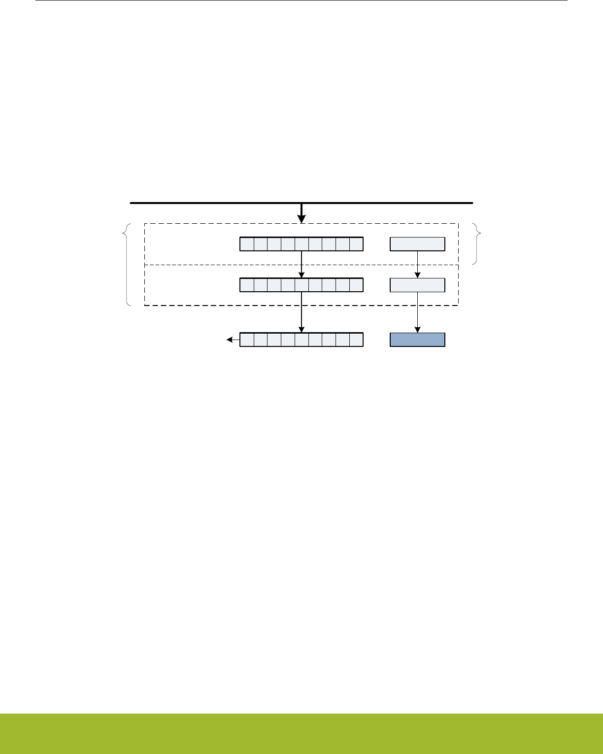
19.3.2.6 Transmit Buffer Operation
The transmit-buffer is a multiple entry FIFO buffer. A frame can be loaded into the buffer by writing to USARTn_TXDATA,
USARTn_TXDATAX, USARTn_TXDOUBLE or USARTn_TXDOUBLEX. Using USARTn_TXDATA allows 8 bits to be written to the buf-
fer, while using USARTn_TXDOUBLE will write 2 frames of 8 bits to the buffer. If 9-bit frames are used, the 9th bit of the frames will in
these cases be set to the value of BIT8DV in USARTn_CTRL.
To set the 9th bit directly and/or use transmission control, USARTn_TXDATAX and USARTn_TXDOUBLEX must be used.
USARTn_TXDATAX allows 9 data bits to be written, as well as a set of control bits regarding the transmission of the written frame.
Every frame in the buffer is stored with 9 data bits and additional transmission control bits. USARTn_TXDOUBLEX allows two frames,
complete with control bits to be written at once. When data is written to the transmit buffer using USARTn_TXDATAX and
USARTn_TXDOUBLEX, the 9th bit(s) written to these registers override the value in BIT8DV in USARTn_CTRL, and alone define the
9th bits that are transmitted if 9-bit frames are used. Figure 19.5 USART Transmit Buffer Operation on page 555 shows the basics of
the transmit buffer when DATABITS in USARTn_FRAME is configured to less than 10 bits.
Write CTRL
Write CTRL
TX buffer element 1
TX buffer element 0
Shift register
Peripheral Bus
Write CTRL
TXDOUBLE,
TXDOUBLEX
TXDATA,
TXDATAX
Figure 19.5. USART Transmit Buffer Operation
When writing more frames to the transmit buffer than there is free space for, the TXOF interrupt flag in USARTn_IF will be set, indicat-
ing the overflow. The data already in the transmit buffer is preserved in this case, and no data is written.
In addition to the interrupt flag TXC in USARTn_IF and status flag TXC in USARTn_STATUS which are set when the transmission is
complete, TXBL in USARTn_STATUS and the TXBL interrupt flag in USARTn_IF are used to indicate the level of the transmit buffer.
TXBIL in USARTn_CTRL controls the level at which these bits are set. If TXBIL is cleared, they are set whenever the transmit buffer
becomes empty, and if TXBIL is set, they are set whenever the transmit buffer goes from full to half-full or empty. Both the TXBL status
flag and the TXBL interrupt flag are cleared automatically when their condition becomes false.
There is a TXIDLE status bit in USARTn_STATUS to provide an indication of when the transmitter is idle. The combined count of TX
buffer element 0, TX buffer element 1, and TX shift register is called TXBUFCNT in USARTn_STATUS. For large frames, the count is
only of TX buffer entry 0 and the TX shifter register.
The transmit buffer, including the transmit shift register can be cleared by setting CLEARTX in USARTn_CMD. This will prevent the
USART from transmitting the data in the buffer and shift register, and will make them available for new data. Any frame currently being
transmitted will not be aborted. Transmission of this frame will be completed.
Reference Manual
USART - Universal Synchronous Asynchronous Receiver/Transmitter
silabs.com | Smart. Connected. Energy-friendly. Preliminary Rev. 0.5 | 555

19.3.2.7 Frame Transmission Control
The transmission control bits, which can be written using USARTn_TXDATAX and USARTn_TXDOUBLEX, affect the transmission of
the written frame. The following options are available:
• Generate break: By setting TXBREAK, the output will be held low during the stop-bit period to generate a framing error. A receiver
that supports break detection detects this state, allowing it to be used e.g. for framing of larger data packets. The line is driven high
before the next frame is transmitted so the next start condition can be identified correctly by the recipient. Continuous breaks lasting
longer than a USART frame are thus not supported by the USART. GPIO can be used for this.
• Disable transmitter after transmission: If TXDISAT is set, the transmitter is disabled after the frame has been fully transmitted.
• Enable receiver after transmission: If RXENAT is set, the receiver is enabled after the frame has been fully transmitted. It is enabled
in time to detect a start-bit directly after the last stop-bit has been transmitted.
• Unblock receiver after transmission: If UBRXAT is set, the receiver is unblocked and RXBLOCK is cleared after the frame has been
fully transmitted.
• Tristate transmitter after transmission: If TXTRIAT is set, TXTRI is set after the frame has been fully transmitted, tristating the trans-
mitter output. Tristating of the output can also be performed automatically by setting AUTOTRI. If AUTOTRI is set TXTRI is always
read as 0.
Note:
When in SmartCard mode with repeat enabled, none of the actions, except generate break, will be performed until the frame is trans-
mitted without failure. Generation of a break in SmartCard mode with repeat enabled will cause the USART to detect a NACK on every
frame.
19.3.2.8 Data Reception
Data reception is enabled by setting RXEN in USARTn_CMD. When the receiver is enabled, it actively samples the input looking for a
transition from high to low indicating the start baud of a new frame. When a start baud is found, reception of the new frame begins if the
receive shift register is empty and ready for new data. When the frame has been received, it is pushed into the receive buffer, making
the shift register ready for another frame of data, and the receiver starts looking for another start baud. If the receive buffer is full, the
received frame remains in the shift register until more space in the receive buffer is available. If an incoming frame is detected while
both the receive buffer and the receive shift register are full, the data in the shift register is overwritten, and the RXOF interrupt flag in
USARTn_IF is set to indicate the buffer overflow.
The receiver can be disabled by setting the command bit RXDIS in USARTn_CMD. Any frame currently being received when the re-
ceiver is disabled is discarded. Whether or not the receiver is enabled at a given time can be read out from RXENS in USARTn_STA-
TUS.
Reference Manual
USART - Universal Synchronous Asynchronous Receiver/Transmitter
silabs.com | Smart. Connected. Energy-friendly. Preliminary Rev. 0.5 | 556
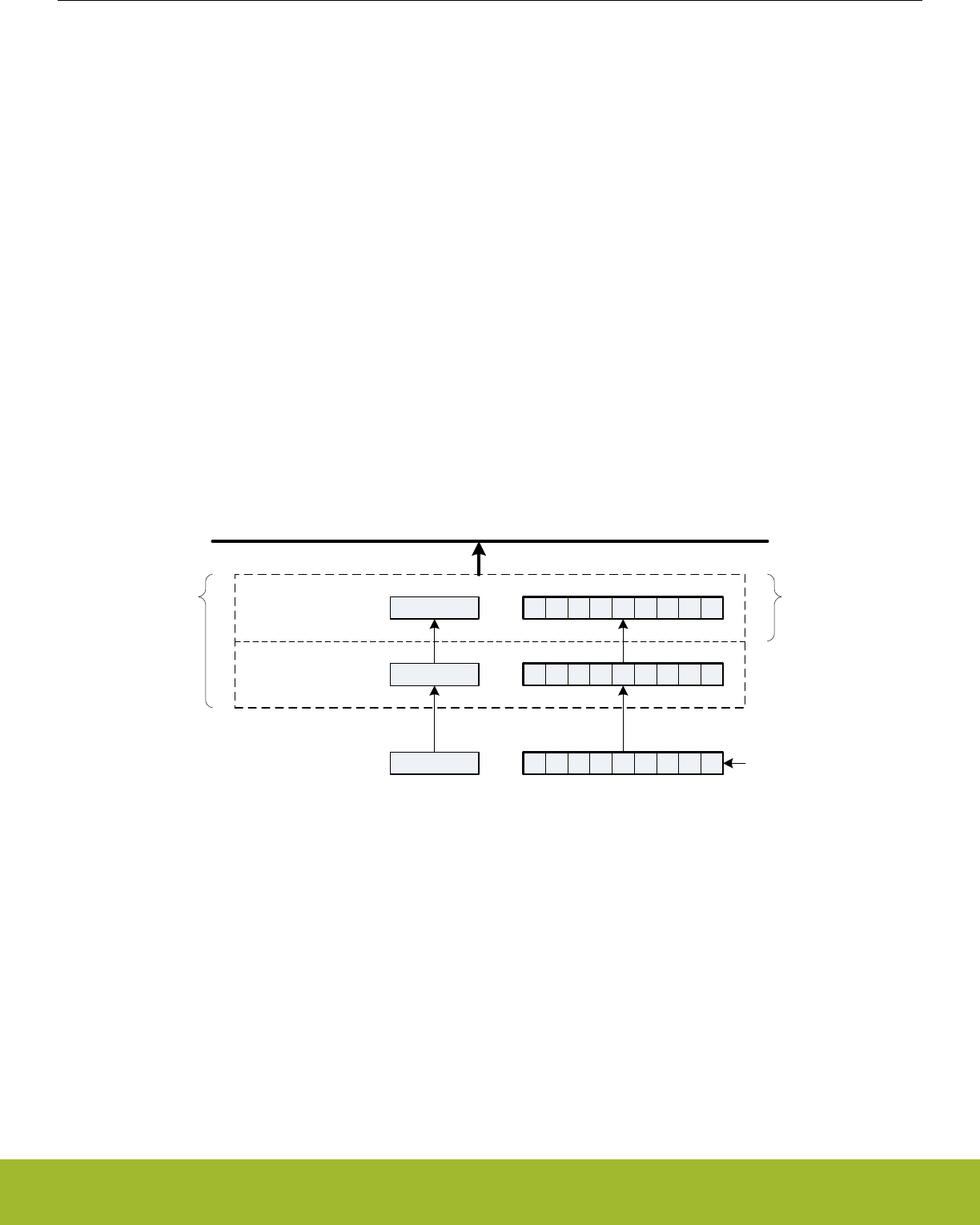
19.3.2.9 Receive Buffer Operation
When data becomes available in the receive buffer, the RXDATAV flag in USARTn_STATUS, and the RXDATAV interrupt flag in
USARTn_IF are set, and when the buffer becomes full, RXFULL in USARTn_STATUS and the RXFULL interrupt flag in USARTn_IF are
set. The status flags RXDATAV and RXFULL are automatically cleared by hardware when their condition is no longer true. This also
goes for the RXDATAV interrupt flag, but the RXFULL interrupt flag must be cleared by software. When the RXFULL flag is set, notifying
that the buffer is full, space is still available in the receive shift register for one more frame.
Data can be read from the receive buffer in a number of ways. USARTn_RXDATA gives access to the 8 least significant bits of the
received frame, and USARTn_RXDOUBLE makes it possible to read the 8 least significant bits of two frames at once, pulling two
frames from the buffer. To get access to the 9th, most significant bit, USARTn_RXDATAX must be used. This register also contains
status information regarding the frame. USARTn_RXDOUBLEX can be used to get two frames complete with the 9th bits and status
bits.
When a frame is read from the receive buffer using USARTn_RXDATA or USARTn_RXDATAX, the frame is pulled out of the buffer,
making room for a new frame. USARTn_RXDOUBLE and USARTn_RXDOUBLEX pull two frames out of the buffer. If an attempt is
done to read more frames from the buffer than what is available, the RXUF interrupt flag in USARTn_IF is set to signal the underflow,
and the data read from the buffer is undefined.
Frames can be read from the receive buffer without removing the data by using USARTn_RXDATAXP and USARTn_RXDOUBLEXP.
USARTn_RXDATAXP gives access the first frame in the buffer with status bits, while USARTn_RXDOUBLEXP gives access to both
frames with status bits. The data read from these registers when the receive buffer is empty is undefined. If the receive buffer contains
one valid frame, the first frame in USARTn_RXDOUBLEXP will be valid. No underflow interrupt is generated by a read using these
registers, i.e. RXUF in USARTn_IF is never set as a result of reading from USARTn_RXDATAXP or USARTn_RXDOUBLEXP.
The basic operation of the receive buffer when DATABITS in USARTn_FRAME is configured to less than 10 bits is shown in Figure
19.6 USART Receive Buffer Operation on page 557.
Status
RX buffer element 0
RX buffer element 1
Shift register
Peripheral Bus
Status
Status
RXDOUBLE
RXDOUBLEX
RXDOUBLEXP
RXDATA,
RXDATAX,
RXDATAXP
Figure 19.6. USART Receive Buffer Operation
The receive buffer, including the receive shift register can be cleared by setting CLEARRX in USARTn_CMD. Any frame currently being
received will not be discarded.
Reference Manual
USART - Universal Synchronous Asynchronous Receiver/Transmitter
silabs.com | Smart. Connected. Energy-friendly. Preliminary Rev. 0.5 | 557

19.3.2.10 Blocking Incoming Data
When using hardware frame recognition, as detailed in 19.3.2.20 Multi-Processor Mode and 19.3.2.21 Collision Detection, it is necessa-
ry to be able to let the receiver sample incoming frames without passing the frames to software by loading them into the receive buffer.
This is accomplished by blocking incoming data.
Incoming data is blocked as long as RXBLOCK in USARTn_STATUS is set. When blocked, frames received by the receiver will not be
loaded into the receive buffer, and software is not notified by the RXDATAV flag in USARTn_STATUS or the RXDATAV interrupt flag in
USARTn_IF at their arrival. For data to be loaded into the receive buffer, RXBLOCK must be cleared in the instant a frame is fully re-
ceived by the receiver. RXBLOCK is set by setting RXBLOCKEN in USARTn_CMD and disabled by setting RXBLOCKDIS also in
USARTn_CMD. There is one exception where data is loaded into the receive buffer even when RXBLOCK is set. This is when an ad-
dress frame is received when operating in multi-processor mode. See 19.3.2.20 Multi-Processor Mode for more information.
Frames received containing framing or parity errors will not result in the FERR and PERR interrupt flags in USARTn_IF being set while
RXBLOCK in USARTn_STATUS is set. Hardware recognition is not applied to these erroneous frames, and they are silently discarded.
Note:
If a frame is received while RXBLOCK in USARTn_STATUS is cleared, but stays in the receive shift register because the receive buffer
is full, the received frame will be loaded into the receive buffer when space becomes available even if RXBLOCK is set at that time.
The overflow interrupt flag RXOF in USARTn_IF will be set if a frame in the receive shift register, waiting to be loaded into the receive
buffer is overwritten by an incoming frame even though RXBLOCK in USARTn_STATUS is set.
Reference Manual
USART - Universal Synchronous Asynchronous Receiver/Transmitter
silabs.com | Smart. Connected. Energy-friendly. Preliminary Rev. 0.5 | 558
19.3.2.11 Clock Recovery and Filtering
The receiver samples the incoming signal at a rate 16, 8, 6 or 4 times higher than the given baud rate, depending on the oversampling
mode given by OVS in USARTn_CTRL. Lower oversampling rates make higher baud rates possible, but give less room for errors.
When a high-to-low transition is registered on the input while the receiver is idle, this is recognized as a start-bit, and the baud rate
generator is synchronized with the incoming frame.
For oversampling modes 16, 8 and 6, every bit in the incoming frame is sampled three times to gain a level of noise immunity. These
samples are aimed at the middle of the bit-periods, as visualized in Figure 19.7 USART Sampling of Start and Data Bits on page 559.
With OVS=0 in USARTn_CTRL, the start and data bits are thus sampled at locations 8, 9 and 10 in the figure, locations 4, 5 and 6 for
OVS=1 and locations 3, 4, and 5 for OVS=2. The value of a sampled bit is determined by majority vote. If two or more of the three bit-
samples are high, the resulting bit value is high. If the majority is low, the resulting bit value is low.
Majority vote is used for all oversampling modes except 4x oversampling. In this mode, a single sample is taken at position 3 as shown
in Figure 19.7 USART Sampling of Start and Data Bits on page 559.
Majority vote can be disabled by setting MVDIS in USARTn_CTRL.
If the value of the start bit is found to be high, the reception of the frame is aborted, filtering out false start bits possibly generated by
noise on the input.
0 0 1 2 3 4 5 6 7 8 9 10 11 12 13 14 15 16 1 2 3 4 5 6 7 8 9 10 11
Idle Start bit Bit 0
0 1 2 3 4 5 6 7 8 1 2 3 4 5 6
13
7
12
OVS = 0OVS = 1
0
1 2 3 4 5 6 1
OVS = 2
12341234
OVS = 3
2 3 4 50
Figure 19.7. USART Sampling of Start and Data Bits
If the baud rate of the transmitter and receiver differ, the location each bit is sampled will be shifted towards the previous or next bit in
the frame. This is acceptable for small errors in the baud rate, but for larger errors, it will result in transmission errors.
When the number of stop bits is 1 or more, stop bits are sampled like the start and data bits as seen in Figure 19.8 USART Sampling of
Stop Bits when Number of Stop Bits are 1 or More on page 560. When a stop bit has been detected by sampling at positions 8, 9 and
10 for normal mode, or 4, 5 and 6 for smart mode, the USART is ready for a new start bit. As seen in Figure 19.8 USART Sampling of
Stop Bits when Number of Stop Bits are 1 or More on page 560, a stop-bit of length 1 normally ends at c, but the next frame will be
received correctly as long as the start-bit comes after position a for OVS=0 and OVS=3, and b for OVS=1 and OVS=2.
Reference Manual
USART - Universal Synchronous Asynchronous Receiver/Transmitter
silabs.com | Smart. Connected. Energy-friendly. Preliminary Rev. 0.5 | 559
5
13 14 15 16 1 2 3 4 5 6 7 8 9 10 0/1
1 stop bit
7 8 1 2 3 4 5 6
X
0/1
X
OVS = 0OVS = 1
X X X
X
n’th bit
a b c
Idle or start bit
0/1
OVS = 2
4 1 2 3 0/1
OVS = 3
2 3 46 1 1
1
Figure 19.8. USART Sampling of Stop Bits when Number of Stop Bits are 1 or More
When working with stop bit lengths of half a baud period, the above sampling scheme no longer suffices. In this case, the stop-bit is not
sampled, and no framing error is generated in the receiver if the stop-bit is not generated. The line must still be driven high before the
next start bit however for the USART to successfully identify the start bit.
19.3.2.12 Parity Error
When parity bits are enabled, a parity check is automatically performed on incoming frames. When a parity error is detected in an in-
coming frame, the data parity error bit PERR in the frame is set, as well as the interrupt flag PERR in USARTn_IF. Frames with parity
errors are loaded into the receive buffer like regular frames.
PERR can be accessed by reading the frame from the receive buffer using the USARTn_RXDATAX, USARTn_RXDATAXP,
USARTn_RXDOUBLEX or USARTn_RXDOUBLEXP registers.
If ERRSTX in USARTn_CTRL is set, the transmitter is disabled on received parity and framing errors. If ERRSRX in USARTn_CTRL is
set, the receiver is disabled on parity and framing errors.
19.3.2.13 Framing Error and Break Detection
A framing error is the result of an asynchronous frame where the stop bit was sampled to a value of 0. This can be the result of noise
and baud rate errors, but can also be the result of a break generated by the transmitter on purpose.
When a framing error is detected in an incoming frame, the framing error bit FERR in the frame is set. The interrupt flag FERR in
USARTn_IF is also set. Frames with framing errors are loaded into the receive buffer like regular frames.
FERR can be accessed by reading the frame from the receive buffer using the USARTn_RXDATAX, USARTn_RXDATAXP,
USARTn_RXDOUBLEX or USARTn_RXDOUBLEXP registers.
If ERRSTX in USARTn_CTRL is set, the transmitter is disabled on parity and framing errors. If ERRSRX in USARTn_CTRL is set, the
receiver is disabled on parity and framing errors.
Reference Manual
USART - Universal Synchronous Asynchronous Receiver/Transmitter
silabs.com | Smart. Connected. Energy-friendly. Preliminary Rev. 0.5 | 560

19.3.2.14 Local Loopback
The USART receiver samples U(S)n_RX by default, and the transmitter drives U(S)n_TX by default. This is not the only option howev-
er. When LOOPBK in USARTn_CTRL is set, the receiver is connected to the U(S)n_TX pin as shown in Figure 19.9 USART Local
Loopback on page 561. This is useful for debugging, as the USART can receive the data it transmits, but it is also used to allow the
USART to read and write to the same pin, which is required for some half duplex communication modes. In this mode, the U(S)n_TX
pin must be enabled as an output in the GPIO.
USART
RX U(S)n_RX
TX U(S)n_TX
LOOBPK = 0
µC
USART
RX U(S)n_RX
TX U(S)n_TX
LOOBPK = 1
µC
Figure 19.9. USART Local Loopback
19.3.2.15 Asynchronous Half Duplex Communication
When doing full duplex communication, two data links are provided, making it possible for data to be sent and received at the same
time. In half duplex mode, data is only sent in one direction at a time. There are several possible half duplex setups, as described in the
following sections.
19.3.2.16 Single Data-link
In this setup, the USART both receives and transmits data on the same pin. This is enabled by setting LOOPBK in USARTn_CTRL,
which connects the receiver to the transmitter output. Because they are both connected to the same line, it is important that the USART
transmitter does not drive the line when receiving data, as this would corrupt the data on the line.
When communicating over a single data-link, the transmitter must thus be tristated whenever not transmitting data. This is done by
setting the command bit TXTRIEN in USARTn_CMD, which tristates the transmitter. Before transmitting data, the command bit TXTRI-
DIS, also in USARTn_CMD, must be set to enable transmitter output again. Whether or not the output is tristated at a given time can be
read from TXTRI in USARTn_STATUS. If TXTRI is set when transmitting data, the data is shifted out of the shift register, but is not put
out on U(S)n_TX.
When operating a half duplex data bus, it is common to have a bus master, which first transmits a request to one of the bus slaves, then
receives a reply. In this case, the frame transmission control bits, which can be set by writing to USARTn_TXDATAX, can be used to
make the USART automatically disable transmission, tristate the transmitter and enable reception when the request has been transmit-
ted, making it ready to receive a response from the slave.
The timer, 19.3.10 Timer, can also be used to add delay between the RX and TX frames so that the interrupt service routine has time to
process data that was just received before transmitting more data. Also hardware flow control is another method to insert time for pro-
cessing the frame. RTS and CTS can be used to halt either the link partner's transmitter or the local transmitter. See the section on
hardware flow control,19.3.4 Hardware Flow Control, for more details.
Tristating the transmitter can also be performed automatically by the USART by using AUTOTRI in USARTn_CTRL. When AUTOTRI is
set, the USART automatically tristates U(S)n_TX whenever the transmitter is idle, and enables transmitter output when the transmitter
goes active. If AUTOTRI is set TXTRI is always read as 0.
Note:
Another way to tristate the transmitter is to enable wired-and or wired-or mode in GPIO. For wired-and mode, outputting a 1 will be the
same as tristating the output, and for wired-or mode, outputting a 0 will be the same as tristating the output. This can only be done on
buses with a pull-up or pull-down resistor respectively.
Reference Manual
USART - Universal Synchronous Asynchronous Receiver/Transmitter
silabs.com | Smart. Connected. Energy-friendly. Preliminary Rev. 0.5 | 561
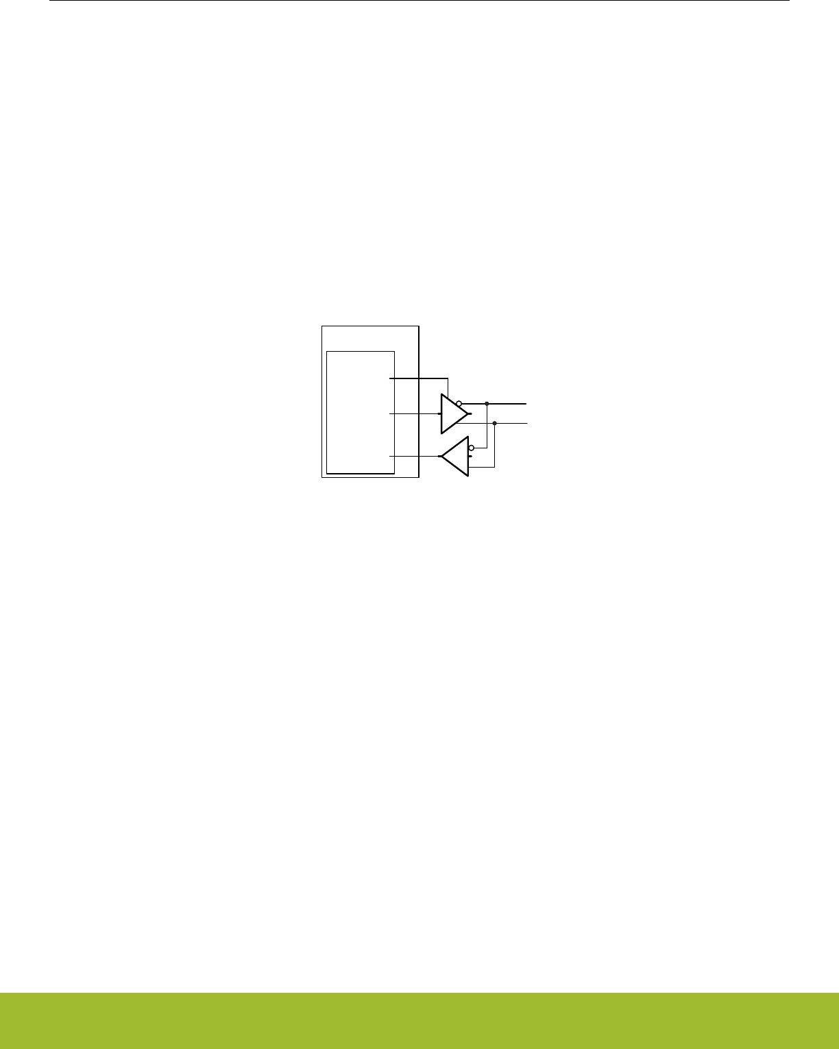
19.3.2.17 Single Data-link with External Driver
Some communication schemes, such as RS-485 rely on an external driver. Here, the driver has an extra input which enables it, and
instead of tristating the transmitter when receiving data, the external driver must be disabled.
This can be done manually by assigning a GPIO to turn the driver on or off, or it can be handled automatically by the USART. If AU-
TOCS in USARTn_CTRL is set, the USn_CS output is automatically activated a configurable number of baud periods before the trans-
mitter starts transmitting data, and deactivated a configurable number of baud periods after the last bit has been transmitted and there
is no more data in the transmit buffer to transmit. The number of baud periods are controlled by CSSETUP and CSHOLD in
USARTn_TIMING. This feature can be used to turn the external driver on when transmitting data, and turn it off when the data has been
transmitted.
The timer, 19.3.10 Timer, can also be used to configure CSSETUP and CSHOLD values between 1 to 256 baud-times by using
TCMPVAL0, TCMPVAL1, or TCMPVAL2 for the TX sequencer.
USn_CS is immediately deasserted when the transmitter becomes disabled.
Figure 19.10 USART Half Duplex Communication with External Driver on page 562 shows an example configuration where USn_CS
is used to automatically enable and disable an external driver.
USART
RX
TX
µC
CS
Figure 19.10. USART Half Duplex Communication with External Driver
The USn_CS output is active low by default, but its polarity can be changed with CSINV in USARTn_CTRL. AUTOCS works regardless
of which mode the USART is in, so this functionality can also be used for automatic chip/slave select when in synchronous mode (e.g.
SPI).
19.3.2.18 Two Data-links
Some limited devices only support half duplex communication even though two data links are available. In this case software is respon-
sible for making sure data is not transmitted when incoming data is expected.
TXARXnEN in USARTn_TRIGCTRL may be used to automatically start transmission after the end of the RX frame plus any TXSTDE-
LAY and CSSETUP delay in USARTn_TIMING. For enabling the receiver either use RXENAT in USARTn_TXDATAX or RXATXnEN in
USARTn_TRIGCTRL.
Reference Manual
USART - Universal Synchronous Asynchronous Receiver/Transmitter
silabs.com | Smart. Connected. Energy-friendly. Preliminary Rev. 0.5 | 562
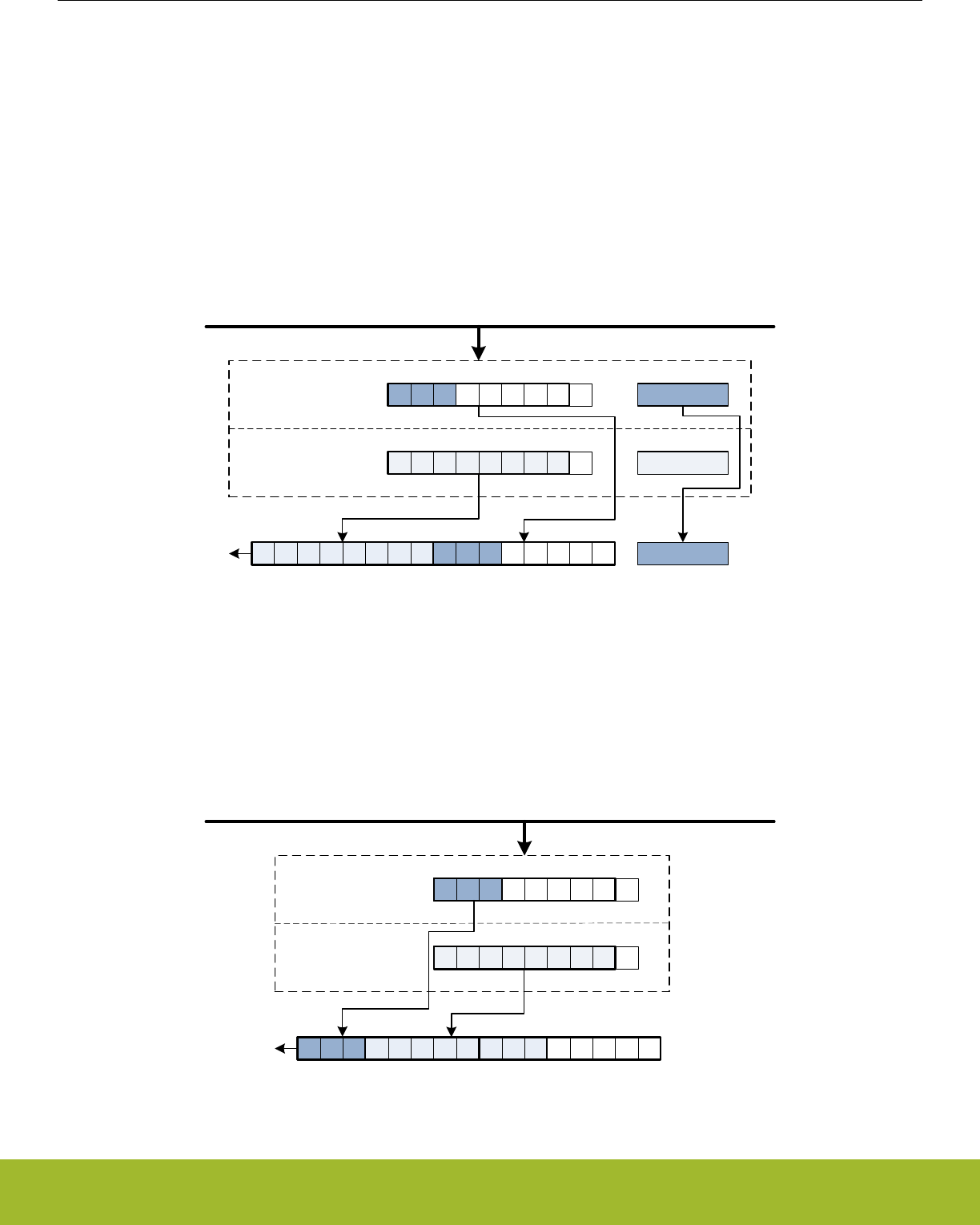
19.3.2.19 Large Frames
As each frame in the transmit and receive buffers holds a maximum of 9 bits, both the elements in the buffers are combined when
working with USART-frames of 10 or more data bits.
To transmit such a frame, at least two elements must be available in the transmit buffer. If only one element is available, the USART will
wait for the second element before transmitting the combined frame. Both the elements making up the frame are consumed when
transmitting such a frame.
When using large frames, the 9th bits in the buffers are unused. For an 11 bit frame, the 8 least significant bits are thus taken from the
first element in the buffer, and the 3 remaining bits are taken from the second element as shown in Figure 19.11 USART Transmission
of Large Frames on page 563. The first element in the transmit buffer, i.e. element 0 in Figure 19.11 USART Transmission of Large
Frames on page 563 is the first element written to the FIFO, or the least significant byte when writing two bytes at a time using
USARTn_TXDOUBLE.
Write CTRL
Write CTRL
Write CTRL
TX buffer element 1
TX buffer element 0
Shift register
Peripheral Bus
0 1 2 3 4 5 6 7 0 1 2
0 1 2
0 1 2 3 4 5 6 7
Figure 19.11. USART Transmission of Large Frames
As shown in Figure 19.11 USART Transmission of Large Frames on page 563, frame transmission control bits are taken from the sec-
ond element in FIFO.
The two buffer elements can be written at the same time using the USARTn_TXDOUBLE or USARTn_TXDOUBLEX register. The
TXDATAX0 bitfield then refers to buffer element 0, and TXDATAX1 refers to buffer element 1.
TX buffer element 1
TX buffer element 0
Shift register
Peripheral Bus
2 1 0 7 6 5 4 3 2 1 0
0 1 2 3 4 5 6 7
0 1 2
Figure 19.12. USART Transmission of Large Frames, MSBF
Reference Manual
USART - Universal Synchronous Asynchronous Receiver/Transmitter
silabs.com | Smart. Connected. Energy-friendly. Preliminary Rev. 0.5 | 563
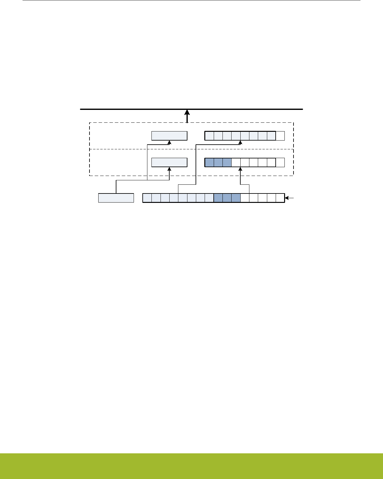
Figure 19.12 USART Transmission of Large Frames, MSBF on page 563 illustrates the order of the transmitted bits when an 11 bit
frame is transmitted with MSBF set. If MSBF is set and the frame is smaller than 10 bits, only the contents of transmit buffer 0 will be
transmitted.
When receiving a large frame, BYTESWAP in USARTn_CTRL determines the order the way the large frame is split into the two buffer
elements. If BYTESWAP is cleared, the least significant 8 bits of the received frame are loaded into the first element of the receive
buffer, and the remaining bits are loaded into the second element, as shown in Figure 19.13 USART Reception of Large Frames on
page 564. The first byte read from the buffer thus contains the 8 least significant bits. Set BYTESWAP to reverse the order.
The status bits are loaded into both elements of the receive buffer. The frame is not moved from the receive shift register before there
are two free spaces in the receive buffer.
Status
RX buffer element 0
RX buffer element 1
Shift register
Peripheral Bus
Status
Status
0 1 2 3 4 5 6 7 0 1 2
0 1 2
0 1 2 3 4 5 6 7
Figure 19.13. USART Reception of Large Frames
The two buffer elements can be read at the same time using the USARTn_RXDOUBLE or USARTn_RXDOUBLEX register. RXDATA0
then refers to buffer element 0 and RXDATA1 refers to buffer element 1.
Large frames can be used in both asynchronous and synchronous modes.
Reference Manual
USART - Universal Synchronous Asynchronous Receiver/Transmitter
silabs.com | Smart. Connected. Energy-friendly. Preliminary Rev. 0.5 | 564

19.3.2.20 Multi-Processor Mode
To simplify communication between multiple processors, the USART supports a special multi-processor mode. In this mode the 9th da-
ta bit in each frame is used to indicate whether the content of the remaining 8 bits is data or an address.
When multi-processor mode is enabled, an incoming 9-bit frame with the 9th bit equal to the value of MPAB in USARTn_CTRL is identi-
fied as an address frame. When an address frame is detected, the MPAF interrupt flag in USARTn_IF is set, and the address frame is
loaded into the receive register. This happens regardless of the value of RXBLOCK in USARTn_STATUS.
Multi-processor mode is enabled by setting MPM in USARTn_CTRL, and the value of the 9th bit in address frames can be set in MPAB.
Note that the receiver must be enabled for address frames to be detected. The receiver can be blocked however, preventing data from
being loaded into the receive buffer while looking for address frames.
Figure 19.14 USART Multi-processor Mode Example on page 565 explains basic usage of the multi-processor mode:
1. All slaves enable multi-processor mode and, enable and block the receiver. They will now not receive data unless it is an address
frame. MPAB in USARTn_CTRL is set to identify frames with the 9th bit high as address frames.
2. The master sends a frame containing the address of a slave and with the 9th bit set
3. All slaves receive the address frame and get an interrupt. They can read the address from the receive buffer. The selected slave
unblocks the receiver to start receiving data from the master.
4. The master sends data with the 9th bit cleared
5. Only the slave with RX enabled receives the data. When transmission is complete, the slave blocks the receiver and waits for a
new address frame.
Figure 19.14. USART Multi-processor Mode Example
When a slave has received an address frame and wants to receive the following data, it must make sure the receiver is unblocked
before the next frame has been completely received in order to prevent data loss.
BIT8DV in USARTn_CTRL can be used to specify the value of the 9th bit without writing to the transmit buffer with USARTn_TXDATAX
or USARTn_TXDOUBLEX, giving higher efficiency in multi-processor mode, as the 9th bit is only set when writing address frames, and
8-bit writes to the USART can be used when writing the data frames.
19.3.2.21 Collision Detection
The USART supports a basic form of collision detection. When the receiver is connected to the output of the transmitter, either by using
the LOOPBK bit in USARTn_CTRL or through an external connection, this feature can be used to detect whether data transmitted on
the bus by the USART did get corrupted by a simultaneous transmission by another device on the bus.
For collision detection to be enabled, CCEN in USARTn_CTRL must be set, and the receiver enabled. The data sampled by the receiv-
er is then continuously compared with the data output by the transmitter. If they differ, the CCF interrupt flag in USARTn_IF is set. The
collision check includes all bits of the transmitted frames. The CCF interrupt flag is set once for each bit sampled by the receiver that
differs from the bit output by the transmitter. When the transmitter output is disabled, i.e. the transmitter is tristated, collisions are not
registered.
Reference Manual
USART - Universal Synchronous Asynchronous Receiver/Transmitter
silabs.com | Smart. Connected. Energy-friendly. Preliminary Rev. 0.5 | 565
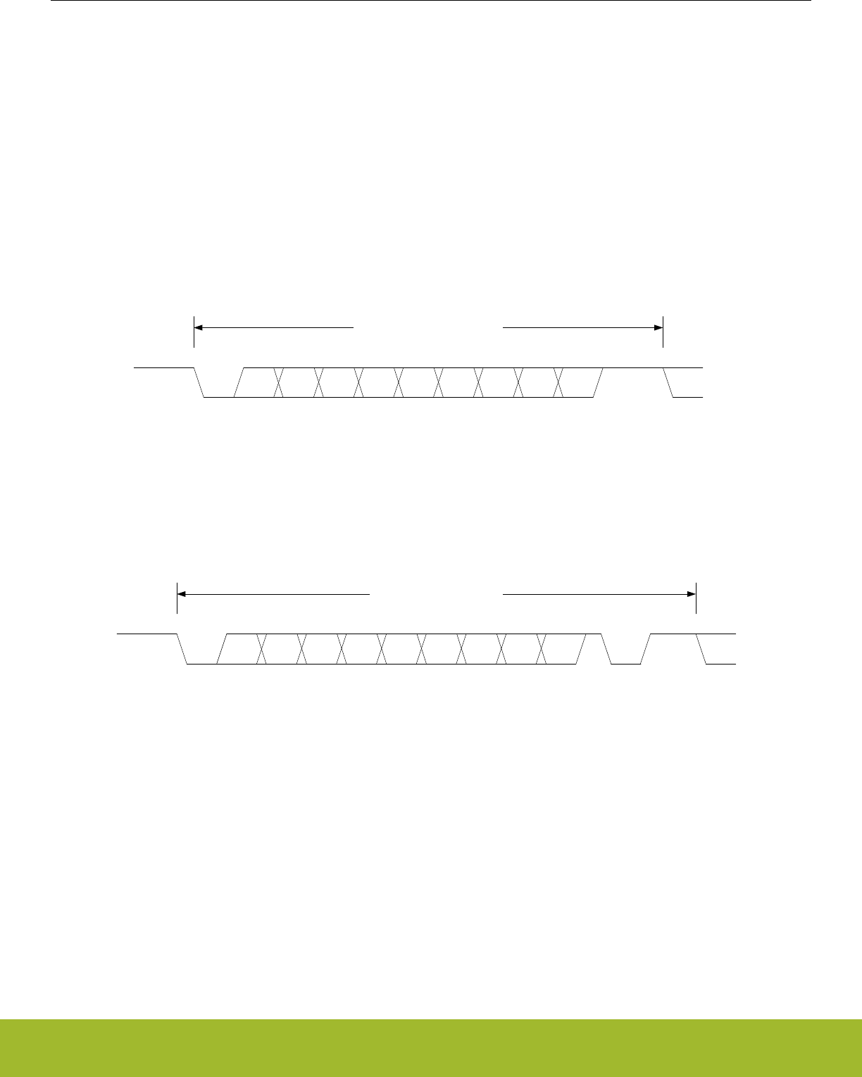
19.3.2.22 SmartCard Mode
In SmartCard mode, the USART supports the ISO 7816 I/O line T0 mode. With exception of the stop-bits (guard time), the 7816 data
frame is equal to the regular asynchronous frame. In this mode, the receiver pulls the line low for one baud, half a baud into the guard
time to indicate a parity error. This NAK can for instance be used by the transmitter to re-transmit the frame. SmartCard mode is a half
duplex asynchronous mode, so the transmitter must be tristated whenever not transmitting data.
To enable SmartCard mode, set SCMODE in USARTn_CTRL, set the number of databits in a frame to 8, and configure the number of
stopbits to 1.5 by writing to STOPBITS in USARTn_FRAME.
The SmartCard mode relies on half duplex communication on a single line, so for it to work, both the receiver and transmitter must work
on the same line. This can be achieved by setting LOOPBK in USARTn_CTRL or through an external connection. The TX output
should be configured as open-drain in the GPIO module.
When no parity error is identified by the receiver, the data frame is as shown in Figure 19.15 USART ISO 7816 Data Frame Without
Error on page 566. The frame consists of 8 data bits, a parity bit, and 2 stop bits. The transmitter does not drive the output line during
the guard time.
S 0 1 2 34 5 6 7 PStop
Start or idleStop or idle
ISO 7816 Frame without error
Figure 19.15. USART ISO 7816 Data Frame Without Error
If a parity error is detected by the receiver, it pulls the line I/O line low after half a stop bit, see Figure 19.16 USART ISO 7816 Data
Frame With Error on page 566. It holds the line low for one bit-period before it releases the line. In this case, the guard time is exten-
ded by one bit period before a new transmission can start, resulting in a total of 3 stop bits.
S 0 1 2 34 5 6 7 PStop
Start or idle
Stop or idle
ISO 7816 Frame with error
Stop
NAK
Figure 19.16. USART ISO 7816 Data Frame With Error
On a parity error, the NAK is generated by hardware. The NAK generated by the receiver is sampled as the stop-bit of the frame. Be-
cause of this, parity errors when in SmartCard mode are reported with both a parity error and a framing error.
When transmitting a T0 frame, the USART receiver on the transmitting side samples position 16, 17 and 18 in the stop-bit to detect the
error signal when in 16x oversampling mode as shown in Figure 19.17 USART SmartCard Stop Bit Sampling on page 567. Sampling
at this location places the stop-bit sample in the middle of the bit-period used for the error signal (NAK).
If a NAK is transmitted by the receiver, it will thus appear as a framing error at the transmitter, and the FERR interrupt flag in
USARTn_IF will be set. If SCRETRANS USARTn_CTRL is set, the transmitter will automatically retransmit a NACK’ed frame. The
transmitter will retransmit the frame until it is ACK’ed by the receiver. This only works when the number of databits in a frame is config-
ured to 8.
Set SKIPPERRF in USARTn_CTRL to make the receiver discard frames with parity errors. The PERR interrupt flag in USARTn_IF is
set when a frame is discarded because of a parity error.
Reference Manual
USART - Universal Synchronous Asynchronous Receiver/Transmitter
silabs.com | Smart. Connected. Energy-friendly. Preliminary Rev. 0.5 | 566

13 14 15 16 1 2 3 4 5 6 7 8 9 10 11
1/2 stop bit
7 8 1 2 3 4 5 6
13
7
12
OVS = 0OVS = 1
14 15 16
8
PNAK or stop
17 18 X
9 10
X
X
X X X X
X
Stop
1 2 3 4 5 6 7
OVS = 2
12345x
OVS = 3
8 x6
4
Figure 19.17. USART SmartCard Stop Bit Sampling
For communication with a SmartCard, a clock signal needs to be generated for the card. This clock output can be generated using one
of the timers. See the ISO 7816 specification for more info on this clock signal.
SmartCard T1 mode is also supported. The T1 frame format used is the same as the asynchronous frame format with parity bit enabled
and one stop bit. The USART must then be configured to operate in asynchronous half duplex mode.
19.3.3 Synchronous Operation
Most of the features in asynchronous mode are available in synchronous mode. Multi-processor mode can be enabled for 9-bit frames,
loopback is available and collision detection can be performed.
19.3.3.1 Frame Format
The frames used in synchronous mode need no start and stop bits since a single clock is available to all parts participating in the com-
munication. Parity bits cannot be used in synchronous mode.
The USART supports frame lengths of 4 to 16 bits per frame. Larger frames can be simulated by transmitting multiple smaller frames,
i.e. a 22 bit frame can be sent using two 11-bit frames, and a 21 bit frame can be generated by transmitting three 7-bit frames. The
number of bits in a frame is set using DATABITS in USARTn_FRAME.
The frames in synchronous mode are by default transmitted with the least significant bit first like in asynchronous mode. The bit-order
can be reversed by setting MSBF in USARTn_CTRL.
The frame format used by the transmitter can be inverted by setting TXINV in USARTn_CTRL, and the format expected by the receiver
can be inverted by setting RXINV, also in USARTn_CTRL.
Reference Manual
USART - Universal Synchronous Asynchronous Receiver/Transmitter
silabs.com | Smart. Connected. Energy-friendly. Preliminary Rev. 0.5 | 567

19.3.3.2 Clock Generation
The bit-rate in synchronous mode is given by Figure 19.18 USART Synchronous Mode Bit Rate on page 568. As in the case of asyn-
chronous operation, the clock division factor have a 15-bit integral part and a 5-bit fractional part.
br = fHFPERCLK/(2 x (1 + USARTn_CLKDIV/256))
Figure 19.18. USART Synchronous Mode Bit Rate
Given a desired baud rate brdesired, the clock divider USARTn_CLKDIV can be calculated using Figure 19.19 USART Synchronous
Mode Clock Division Factor on page 568
USARTn_CLKDIV = 256 x (fHFPERCLK/(2 x brdesired) - 1)
Figure 19.19. USART Synchronous Mode Clock Division Factor
When the USART operates in master mode, the highest possible bit rate is half the peripheral clock rate. When operating in slave mode
however, the highest bit rate is an eighth of the peripheral clock:
• Master mode: brmax = fHFPERCLK/2
• Slave mode: brmax = fHFPERCLK/8
On every clock edge data on the data lines, MOSI and MISO, is either set up or sampled. When CLKPHA in USARTn_CTRL is cleared,
data is sampled on the leading clock edge and set-up is done on the trailing edge. If CLKPHA is set however, data is set-up on the
leading clock edge, and sampled on the trailing edge. In addition to this, the polarity of the clock signal can be changed by setting
CLKPOL in USARTn_CTRL, which also defines the idle state of the clock. This results in four different modes which are summarized in
Table 19.8 USART SPI Modes on page 568. Figure 19.20 USART SPI Timing on page 569 shows the resulting timing of data set-up
and sampling relative to the bus clock.
Table 19.8. USART SPI Modes
SPI mode CLKPOL CLKPHA Leading edge Trailing edge
0 0 0 Rising, sample Falling, set-up
1 0 1 Rising, set-up Falling, sample
2 1 0 Falling, sample Rising, set-up
3 1 1 Falling, set-up Rising, sample
Reference Manual
USART - Universal Synchronous Asynchronous Receiver/Transmitter
silabs.com | Smart. Connected. Energy-friendly. Preliminary Rev. 0.5 | 568
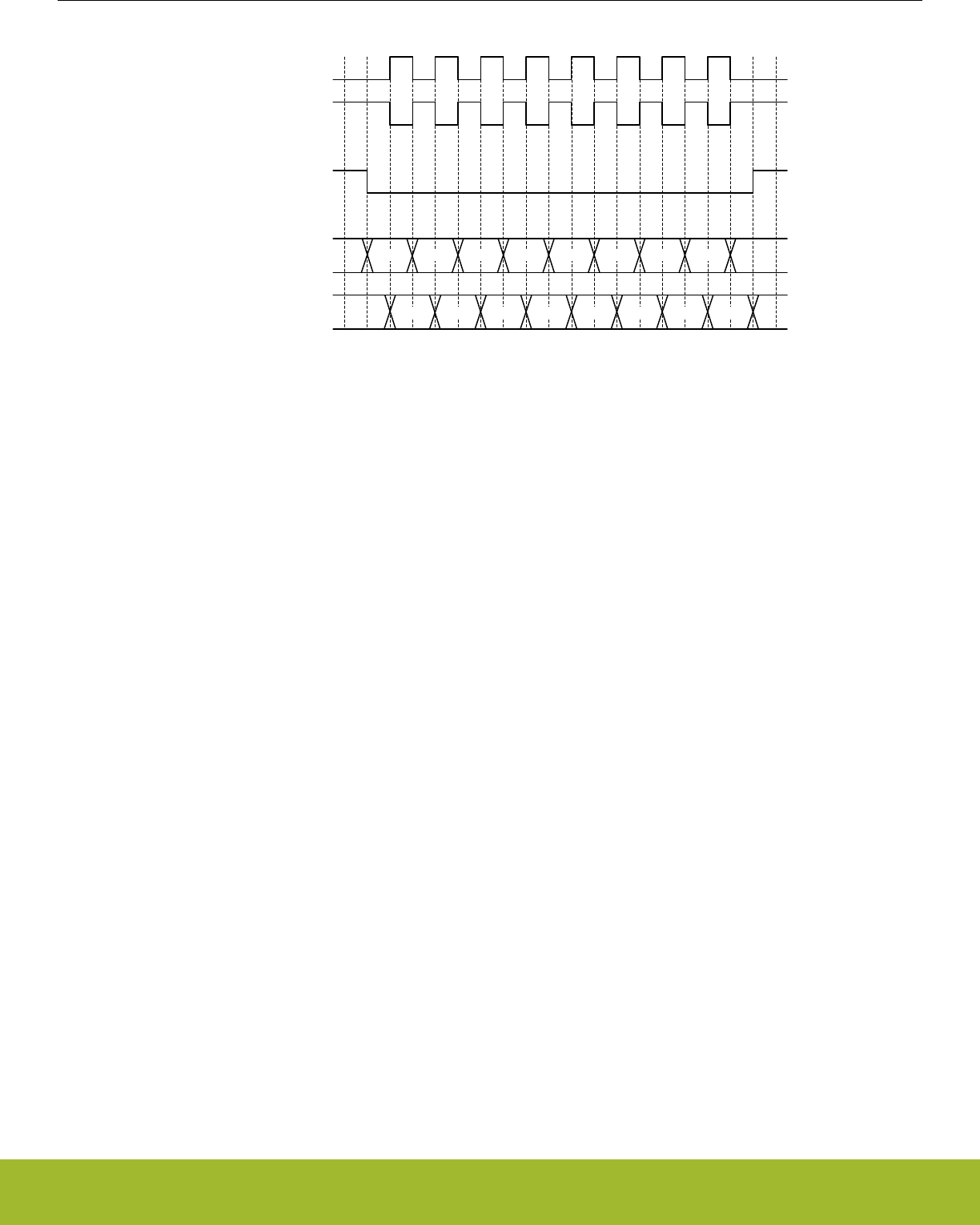
0 1 2 3 4 5 6 7
0 1 2 3 4 5 6 7
USn_CLK
USn_CS
USn_TX/
USn_RX
CLKPOL = 0
CLKPOL = 1
CLKPHA = 0
CLKPHA = 1 X
X X
X
Figure 19.20. USART SPI Timing
If CPHA=1, the TX underflow flag, TXUF, will be set on the first setup clock edge of a frame in slave mode if TX data is not available. If
CPHA=0, TXUF is set if data is not available in the transmit buffer three HFPERCLK cycles prior to the first sample clock edge. The
RXDATAV flag is updated on the last sample clock edge of a transfer, while the RX overflow interrupt flag, RXOF, is set on the first
sample clock edge if the receive buffer overflows. When a transfer has been performed, interrupt flags TXBL and TXC are updated on
the first setup clock edge of the succeeding frame, or when CS is deasserted.
19.3.3.3 Master Mode
When in master mode, the USART is in full control of the data flow on the synchronous bus. When operating in full duplex mode, the
slave cannot transmit data to the master without the master transmitting to the slave. The master outputs the bus clock on USn_CLK.
Communication starts whenever there is data in the transmit buffer and the transmitter is enabled. The USART clock then starts, and
the master shifts bits out from the transmit shift register using the internal clock.
When there are no more frames in the transmit buffer and the transmit shift register is empty, the clock stops, and communication ends.
When the receiver is enabled, it samples data using the internal clock when the transmitter transmits data. Operation of the RX and TX
buffers is as in asynchronous mode.
19.3.3.4 Operation of USn_CS Pin
When operating in master mode, the USn_CS pin can have one of two functions, or it can be disabled.
If USn_CS is configured as an output, it can be used to automatically generate a chip select for a slave by setting AUTOCS in
USARTn_CTRL. If AUTOCS is set, USn_CS is activated before a transmission begins, and deactivated after the last bit has been trans-
mitted and there is no more data in the transmit buffer.
The time between when CS is asserted and the first bit is transmitted can be controlled using the USART Timer and with CSSETUP in
USARTn_TIMING. Any of the three comparators can be used to set this delay. If new data is ready for transmission before CS is deas-
serted, the data is sent without deasserting CS in between. CSHOLD in USARTn_TIMING keeps CS asserted after the end of frame for
the number of baud-times specified.
By default, USn_CS is active low, but its polarity can be inverted by setting CSINV in USARTn_CTRL.
When USn_CS is configured as an input, it can be used by another master that wants control of the bus to make the USART release it.
When USn_CS is driven low, or high if CSINV is set, the interrupt flag SSM in USARTn_IF is set, and if CSMA in USARTn_CTRL is set,
the USART goes to slave mode.
Reference Manual
USART - Universal Synchronous Asynchronous Receiver/Transmitter
silabs.com | Smart. Connected. Energy-friendly. Preliminary Rev. 0.5 | 569

19.3.3.5 AUTOTX
A synchronous master is required to transmit data to a slave in order to receive data from the slave. In some cases, only a few words
are transmitted and a lot of data is then received from the slave. In that case, one solution is to keep feeding the TX with data to trans-
mit, but that consumes system bandwidth. Instead AUTOTX can be used.
When AUTOTX in USARTn_CTRL is set, the USART transmits data as long as there is available space in the RX shift register for the
chosen frame size. This happens even though there is no data in the TX buffer. The TX underflow interrupt flag TXUF in USARTn_IF is
set on the first word that is transmitted which does not contain valid data.
During AUTOTX the USART will always send the previous sent bit, thus reducing the number of transitions on the TX output. So if the
last bit sent was a 0, 0's will be sent during AUTOTX and if the last bit sent was a 1, 1's will be sent during AUTOTX.
19.3.3.6 Slave Mode
When the USART is in slave mode, data transmission is not controlled by the USART, but by an external master. The USART is there-
fore not able to initiate a transmission, and has no control over the number of bytes written to the master.
The output and input to the USART are also swapped when in slave mode, making the receiver take its input from USn_TX (MOSI) and
the transmitter drive USn_RX (MISO).
To transmit data when in slave mode, the slave must load data into the transmit buffer and enable the transmitter. The data will remain
in the USART until the master starts a transmission by pulling the USn_CS input of the slave low and transmitting data. For every frame
the master transmits to the slave, a frame is transferred from the slave to the master. After a transmission, MISO remains in the same
state as the last bit transmitted. This also applies if the master transmits to the slave and the slave TX buffer is empty.
If the transmitter is enabled in synchronous slave mode and the master starts transmission of a frame, the underflow interrupt flag
TXUF in USARTn_IF will be set if no data is available for transmission to the master.
If the slave needs to control its own chip select signal, this can be achieved by clearing CSPEN in the ROUTE register. The internal
chip select signal can then be controlled through CSINV in the CTRL register. The chip select signal will be CSINV inverted, i.e. if
CSINV is cleared, the chip select is active and vice versa.
19.3.3.7 Synchronous Half Duplex Communication
Half duplex communication in synchronous mode is very similar to half duplex communication in asynchronous mode as detailed in
19.3.2.15 Asynchronous Half Duplex Communication. The main difference is that in this mode, the master must generate the bus clock
even when it is not transmitting data, i.e. it must provide the slave with a clock to receive data. To generate the bus clock, the master
should transmit data with the transmitter tristated, i.e. TXTRI in USARTn_STATUS set, when receiving data. If 2 bytes are expected
from the slave, then transmit 2 bytes with the transmitter tristated, and the slave uses the generated bus clock to transmit data to the
master. TXTRI can be set by setting the TXTRIEN command bit in USARTn_CMD.
Note:
When operating as SPI slave in half duplex mode, TX has to be tristated (not disabled) during data reception if the slave is to transmit
data in the current transfer.
19.3.3.8 I2S
I2S is a synchronous format for transmission of audio data. The frame format is 32-bit, but since data is always transmitted with MSB
first, an I2S device operating with 16-bit audio may choose to only process the 16 msb of the frame, and only transmit data in the 16
msb of the frame.
In addition to the bit clock used for regular synchronous transfers, I2S mode uses a separate word clock. When operating in mono
mode, with only one channel of data, the word clock pulses once at the start of each new word. In stereo mode, the word clock toggles
at the start of new words, and also gives away whether the transmitted word is for the left or right audio channel; A word transmitted
while the word clock is low is for the left channel, and a word transmitted while the word clock is high is for the right.
When operating in I2S mode, the CS pin is used as a the word clock. In master mode, this is automatically driven by the USART, and in
slave mode, the word clock is expected from an external master.
Reference Manual
USART - Universal Synchronous Asynchronous Receiver/Transmitter
silabs.com | Smart. Connected. Energy-friendly. Preliminary Rev. 0.5 | 570

19.3.3.9 Word Format
The general I2S word format is 32 bits wide, but the USART also supports 16-bit and 8-bit words. In addition to this, it can be specified
how many bits of the word should actually be used by the USART. These parameters are given by FORMAT in USARTn_I2SCTRL.
As an example, configuring FORMAT to using a 32-bit word with 16-bit data will make each word on the I2S bus 32-bits wide, but when
receiving data through the USART, only the 16 most significant bits of each word can be read out of the USART. Similarly, only the 16
most significant bits have to be written to the USART when transmitting. The rest of the bits will be transmitted as zeroes.
Reference Manual
USART - Universal Synchronous Asynchronous Receiver/Transmitter
silabs.com | Smart. Connected. Energy-friendly. Preliminary Rev. 0.5 | 571
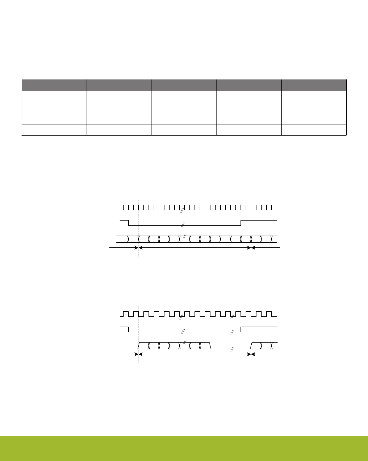
19.3.3.10 Major Modes
The USART supports a set of different I2S formats as shown in Table 19.9 USART I2S Modes on page 572, but it is not limited to
these modes. MONO, JUSTIFY and DELAY in USARTn_I2SCTRL can be mixed and matched to create an appropriate format. MONO
enables mono mode, i.e. one data stream instead of two which is the default. JUSTIFY aligns data within a word on the I2S bus, either
left or right which can bee seen in figures Figure 19.23 USART Left-justified I2S waveform on page 573 and Figure 19.24 USART
Right-justified I2S waveform on page 573. Finally, DELAY specifies whether a new I2S word should be started directly on the edge of
the word-select signal, or one bit-period after the edge.
Table 19.9. USART I2S Modes
Mode MONO JUSTIFY DELAY CLKPOL
Regular I2S 0 0 1 0
Left-Justified 0 0 0 1
Right-Justified 0 1 0 1
Mono 1 0 0 0
The regular I2S waveform is shown in Figure 19.21 USART Standard I2S waveform on page 572 and Figure 19.22 USART Standard
I2S waveform (reduced accuracy) on page 572. The first figure shows a waveform transmitted with full accuracy. The wordlength can
be configured to 32-bit, 16-bit or 8-bit using FORMAT in USARTn_I2SCTRL. In the second figure, I2S data is transmitted with reduced
accuracy, i.e. the data transmitted has less bits than what is possible in the bus format.
Note that the msb of a word transmitted in regular I2S mode is delayed by one cycle with respect to word select
USn_CLK
USn_CS
(word select)
USn_TX/
USn_RX MSB
Left channelRight channel Right channel
LSB MSBLSB
Figure 19.21. USART Standard I2S waveform
USn_CLK
USn_CS
(word select)
USn_TX/
USn_RX MSB
Left channelRight channel Right channel
LSB MSB
Figure 19.22. USART Standard I2S waveform (reduced accuracy)
A left-justified stream is shown in Figure 19.23 USART Left-justified I2S waveform on page 573. Note that the MSB comes directly
after the edge on the word-select signal in contradiction to the regular I2S waveform where it comes one bit-period after.
Reference Manual
USART - Universal Synchronous Asynchronous Receiver/Transmitter
silabs.com | Smart. Connected. Energy-friendly. Preliminary Rev. 0.5 | 572
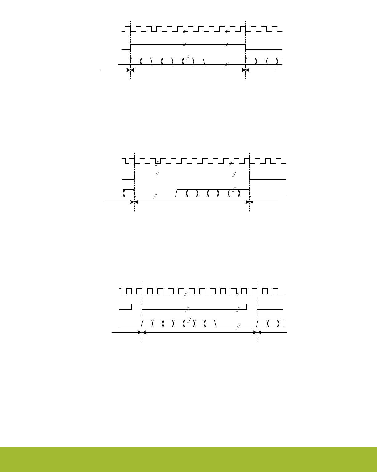
USn_CLK
USn_CS
(word select)
USn_TX/
USn_RX MSB
Right channel
LSB MSB
Left channel Left channel
Figure 19.23. USART Left-justified I2S waveform
A right-justified stream is shown in Figure 19.24 USART Right-justified I2S waveform on page 573. The left and right justified streams
are equal when the data-size is equal to the word-width.
USn_CLK
USn_TX/
USn_RX MSB LSBLSB
USn_CS
(word select)
Right channelLeft channel Left channel
Figure 19.24. USART Right-justified I2S waveform
In mono-mode, the word-select signal pulses at the beginning of each word instead of toggling for each word. Mono I2S waveform is
shown in Figure 19.25 USART Mono I2S waveform on page 573.
USn_CLK
USn_CS
(word select)
USn_TX/
USn_RX MSB
Left channelRight channel Right channel
LSB MSB
Figure 19.25. USART Mono I2S waveform
Reference Manual
USART - Universal Synchronous Asynchronous Receiver/Transmitter
silabs.com | Smart. Connected. Energy-friendly. Preliminary Rev. 0.5 | 573

19.3.3.11 Using I2S Mode
When using the USART in I2S mode, DATABITS in USARTn_FRAME must be set to 8 or 16 data-bits. 8 databits can be used in all
modes, and 16 can be used in the modes where the number of bytes in the I2S word is even. In addition to this, MSBF in
USARTn_CTRL should be set, and CLKPOL and CLKPHA in USARTn_CTRL should be cleared.
The USART does not have separate TX and RX buffers for left and right data, so when using I2S in stereo mode, the application must
keep track of whether the buffers contain left or right data. This can be done by observing TXBLRIGHT, RXDATAVRIGHT and RXFULL-
RIGHT in USARTn_STATUS. TXBLRIGHT tells whether TX is expecting data for the left or right channel. It will be set with TXBL if right
data is expected. The receiver will set RXDATAVRIGHT if there is at least one right element in the buffer, and RXFULLRIGHT if the
buffer is full of right elements.
When using I2S with DMA, separate DMA requests can be used for left and right data by setting DMASPLIT in USARTn_I2SCTRL.
In both master and slave mode the USART always starts transmitting on the LEFT channel after being enabled. In master mode, the
transmission will stop if TX becomes empty. In that case, TXC is set. Continuing the transmission in this case will make the data-stream
continue where it left off. To make the USART start on the LEFT channel after going empty, disable and re-enable TX.
19.3.4 Hardware Flow Control
Hardware flow control can be used to hold off the link partner's transmission until RX buffer space is available. Use RTSPEN and
CTSPEN in USARTn_ROUTEPEN to allocate the hardware flow control to GPIOs. RTS is an out going signal which indicates that RX
buffer space is available to receive a frame. The link partner is being requested to send its data when RTS is asserted. CTS is an in-
coming signal to stop the next TX data from going out. When CTS is negated, the frame currently being transmitted is completed before
stopping. CTS indicates that the link partner has RX buffer space available, and the local transmitter is clear to send. Also use CTSEN
in USARTn_CTLX to enable the CTS input into the TX sequencer. For debug use set DBGHALT in USARTn_CTRLX which will force
the RTS to request one frame from the link partner when the CPU core single steps.
19.3.5 Debug Halt
When DBGHALT in USART_CTRLX is clear, RTS is only dependent on the RX buffer having space available to receive data. Incoming
data is always received until both the RX buffer is full and the RX shift register is full regardless of the state of DBGHALT or chip halt.
Additional incoming data is discarded. When DBGHALT is set, RTS deasserts on RX buffer full or when chip halt is high. However, a
low pulse detected on chip halt will keep RTS asserted when no frame is being received. At the start of frame reception, RTS will deas-
sert if chip halt is high and DBGHALT is set. This behavior allows single stepping to pulse the chip halt low for a cycle, and receive the
next frame. The link partner must stop transmitting when RTS is deasserted, or the RX buffer could overflow. All data in the transmit
buffer is sent out even when chip halt is asserted; therefore, the DMA will need to be set to stop sending the USART TX data during
chip halt.
19.3.6 PRS-triggered Transmissions
If a transmission must be started on an event with very little delay, the PRS system can be used to trigger the transmission. The PRS
channel to use as a trigger can be selected using TSEL in USARTn_TRIGCTRL. When a positive edge is detected on this signal, the
receiver is enabled if RXTEN in USARTn_TRIGCTRL is set, and the transmitter is enabled if TXTEN in USARTn_TRIGCTRL is set.
Only one signal input is supported by the USART.
The AUTOTX feature can also be enabled via PRS. If an external SPI device sets a pin high when there is data to be read from the
device, this signal can be routed to the USART through the PRS system and be used to make the USART clock data out of the external
device. If AUTOTXTEN in USARTn_TRIGCTRL is set, the USART will transmit data whenever the PRS signal selected by TSEL is high
given that there is enough room in the RX buffer for the chosen frame size. Note that if there is no data in the TX buffer when using
AUTOTX, the TX underflow interrupt will be set.
AUTOTXTEN can also be combined with TXTEN to make the USART transmit a command to the external device prior to clocking out
data. To do this, disable TX using the TXDIS command, load the TX buffer with the command and enable AUTOTXTEN and TXTEN.
When the selected PRS input goes high, the USART will now transmit the loaded command, and then continue clocking out while both
the PRS input is high and there is room in the RX buffer
19.3.7 PRS RX Input
The USART can be configured to receive data directly from a PRS channel by setting RXPRS in USARTn_INPUT. The PRS channel
used is selected using RXPRSSEL in USARTn_INPUT. This way, for example, a differential RX signal can be input to the ACMP and
the output routed via PRS to the USART.
Reference Manual
USART - Universal Synchronous Asynchronous Receiver/Transmitter
silabs.com | Smart. Connected. Energy-friendly. Preliminary Rev. 0.5 | 574

19.3.8 PRS CLK Input
The USART can be configured to receive clock directly from a PRS channel by setting CLKPRS in USARTn_INPUT. The PRS channel
used is selected using CLKPRSSEL in USARTn_INPUT. This is useful in synchronous slave mode and can together with RX PRS input
be used to input data from PRS.
19.3.9 DMA Support
The USART has full DMA support. The DMA controller can write to the transmit buffer using the registers USARTn_TXDATA,
USARTn_TXDATAX, USARTn_TXDOUBLE and USARTn_TXDOUBLEX, and it can read from the receive buffer using the registers
USARTn_RXDATA, USARTn_RXDATAX, USARTn_RXDOUBLE and USARTn_RXDOUBLEX. This enables single byte transfers, 9 bit
data + control/status bits, double byte and double byte + control/status transfers both to and from the USART.
A request for the DMA controller to read from the USART receive buffer can come from the following source:
• Data available in the receive buffer
• Data available in the receive buffer and data is for the RIGHT I2S channel. Only used in I2S mode.
A write request can come from one of the following sources:
• Transmit buffer and shift register empty. No data to send.
• Transmit buffer has room for more data. This does not check the TXBIL for half full. For DMA use, it is either full or empty.
• Transmit buffer has room for RIGHT I2S data. Only used in I2S mode
Even though there are two sources for write requests to the DMA, only one should be used at a time, since the requests from both
sources are cleared even though only one of the requests are used.
In some cases, it may be sensible to temporarily stop DMA access to the USART when an error such as a framing error has occurred.
This is enabled by setting ERRSDMA in USARTn_CTRL.
Note: For Synchronous mode full duplex operation, if both receive buffer and transmit buffer are served by DMA, to make sure receive
buffer is not overflowed the settings below should be followed.
• The DMA channel that serves receive buffer should have higher priority than the DMA channel that serves transmit buffer.
• TXBL should be used as write request for transmit buffer DMA channel.
• IGNORESREQ should be set for both DMA channel.
Reference Manual
USART - Universal Synchronous Asynchronous Receiver/Transmitter
silabs.com | Smart. Connected. Energy-friendly. Preliminary Rev. 0.5 | 575

19.3.10 Timer
In addition to the TX sequence timer, there is a versatile 8 bit timer that can generate up to three event pulses. These pulses can be
used to create timing for a variety of uses such as RX timeout, break detection, response timeout, and RX enable delay. Transmission
delay, CS setup, inter-character spacing, and CS hold use the TX sequence counter. The TX sequencer counter can use the three 8 bit
compare values or preset values for delays. There is one general counter with three comparators. Each comparator has a start source,
a stop source, a restart enable, and a timer compare value. The start source enables the comparator, resets the counter, and starts the
counter. If the counter is already running, the start source will reset the counter and restart it.
Any comparator could start the counter using the same start source but have different timing events programmed into TCMPVALn in
USARTn_TIMECMPn. The TCMP0, TCMP1, or TCMP2 events can be preempted by using the comparator stop source to disable the
comparator before the counter reaches TCMPVAL0, TCMPVAL1, or TCMPVAL2. If one comparator gets disabled while the other com-
parator is still enabled, the counter continues counting. By default the counter will count up to 256 and stop unless a RESTARTEN is set
in one of the USARTn_TIMECMPn registers. By using RESTARTEN and an interval programmed into TCMPVAL, an interval timer can
be set up. The TSTART field needs to be changed to DISABLE to stop the interval timer. The timer stops running once all of the compa-
rators are disabled. If a comparator's start and stop sources both trigger the same cycle, the TCMPn event triggers, the comparator
stays enabled, and the counter begins counting from zero.
The TXDELAY, CSSETUP, ICS, and CSHOLD in USARTn_TIMING are used to program start of transmission delay, chip select setup
delay, inter-character space, and chip select hold delay. Either a preset value of 0, 1, 2, 3, or 7 can be used for any of these delays; or
the value in TCMPVALn may be used to set the delay. Using the preset values leaves the TCMPVALn free for other uses. The same
TCMPVALn may be used for multiple events that require the same timing. The transmit sequencer's counter can run in parallel with the
timer's counter. The counters and controls are shown in Figure 19.26 USART Timer Block Diagram on page 577.
Reference Manual
USART - Universal Synchronous Asynchronous Receiver/Transmitter
silabs.com | Smart. Connected. Energy-friendly. Preliminary Rev. 0.5 | 576
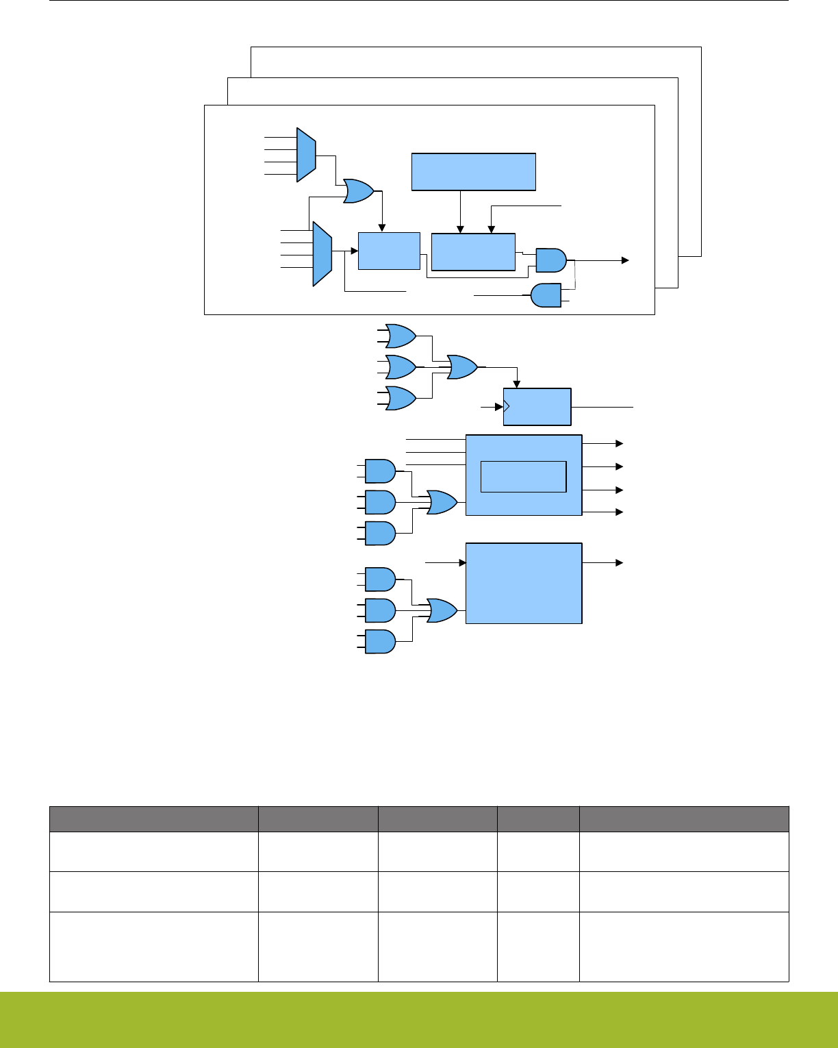
8 bit
Counter
start
event
bit time
TSTART
TCMPVALn
TCMP
enable TCMPn
Compare
TXEOF
RXEOF
TCMPn
RXACT
TXST
RXACTN
TSTOP
clear
TXC
RXACT
DISABLE
RESTARTEN
START_A2
START_An
TIMECMP0
TIMECMP1
TIMECMP2
START_B2
START_A1
START_B1
START_A0
START_B0
START_Bn
GP_CNT[7:0]
GP_CNT[7:0]
TXSEQ
TX Counter
TXENS
TXARX2EN
TCMP2
TXARX1EN
TCMP1
TXARX0EN
TCMP0
TXEOF
TXC
TXST
RXSEQ
RXENS
RXATX2EN
TCMP2
RXATX1EN
TCMP1
RXATX0EN
TCMP0
RXEOF
TX
RX
TCMPVAL2
TCMPVAL1
TCMPVAL0
Figure 19.26. USART Timer Block Diagram
The following sections will go into more details on programming the various usage cases.
Table 19.10. USART Application Settings for USARTn_TIMING and USARTn_TIMECMPn
Application TSTARTn TSTOPn TCMPVALn Other
Response Timeout TSTART0 = TXEOF TSTOP0 = RXACT TCMPVAL0
= 0x08
TCMP0 in USARTn_IEN
Receiver Timeout TSTART1 = RXEOF TSTOP1 = RXACT TCMPVAL1
= 0x08
TCMP1 in USARTn_IEN
Large Receiver Timeout TSTART1 =
RXEOF, TCMP1
TSTOP1 = RXACT TCMPVAL1
= 0xFF
TCMP1 in USARTn_IEN; TIME-
RRESTARTED in USARTn_STA-
TUS; RESTART1EN in
USARTn_TIMECMP1
Reference Manual
USART - Universal Synchronous Asynchronous Receiver/Transmitter
silabs.com | Smart. Connected. Energy-friendly. Preliminary Rev. 0.5 | 577

Application TSTARTn TSTOPn TCMPVALn Other
Break Detect TSTART1 = RXACT TSTOP1 =
RXACTN
TCMPVAL1
= 0x0C
TCMP1 in USARTn_IEN
TX delayed start of transmission and
CS setup
TSTART0 = DISA-
BLE, TSTART1 =
DISABLE
TSTOP0 = TCMP0,
TSTOP1 = TCMP1
TCMPVAL0
= 0x04,
TCMPVAL1
= 0x02
TXDELAY = TCMP0, CSSETUP =
TCMP1 in USARTn_TIMING; AU-
TOCS in USARTn_CTRL
TX inter-character spacing TSTART2 = DISA-
BLE
TSTOP2 = TCMP2 TCMPVAL2
= 0x03
ICS = TCMP2 in USARTn_TIMING;
AUTOCS in USARTn_CTRL
TX Chip Select End Delay TSTART1 = DISA-
BLE
TSTOP1 = TCMP1 TCMPVAL1
= 0x04
CSHOLD = TCMP1 in
USARTn_TIMING; AUTOCS in
USARTn_CTRL
Response Delay TSTART1 = RXEOF TSTOP1 = TCMP1 TCMPVAL1
= 0x08
TXARX1EN in USARTn_TRIGCTRL
Combined TX and RX Example TSTART1 =
RXEOF, TSTART0
= TXEOF
TSTOP1 = TCMP1,
TSTOP0 = TCMP0
TCMPVAL1
= 0x1C,
TCMPVAL0
= 0x10
TXARX1EN, RXATX0EN in
USARTn_TRIGCTRL; CSSETUP =
0x7, CSHOLD = 0x3 in
USARTn_TIMING
Combined Delayed TX and Receiver
Timeout Example
TSTART0 =
TCMPVAL0,
TSTART1 = RXEOF
TSTOP0 =
RXACTN, TSTOP1
= RXACT
TCMPVAL0
= 0x20,
TCMPVAL1
= 0x0C
TXARX0EN in
USARTn_TRIGCTRL; TCMP0 in
USARTn_IEN
Table 19.10 USART Application Settings for USARTn_TIMING and USARTn_TIMECMPn on page 577 shows some examples of how
the USART timer can be programmed for various applications. The following sections will describe more details for each applications
shown in the table.
19.3.10.1 Response Timeout
Response Timeout is when a UART master sends a frame and expects the slave to respond within a certain number of baud-times.
Refer to Table 19.10 USART Application Settings for USARTn_TIMING and USARTn_TIMECMPn on page 577 for specific register set-
tings. Comparator 0 will be looking for TX end of frame to use as the timer start source. For this example, a receiver start of frame
RXACT has not been detected for 8 baud-times, and the TCMP0 interrupt in USARTn_IF is set. If an RX start bit is detected before the
8 baud-times, comparator 0 is disabled before the TCMP0 event can trigger.
TX
RX
RESPONSE TIMEOUT
TCMPnINT
Figure 19.27. USART Response Timeout
Reference Manual
USART - Universal Synchronous Asynchronous Receiver/Transmitter
silabs.com | Smart. Connected. Energy-friendly. Preliminary Rev. 0.5 | 578

19.3.10.2 RX Timeout
A receiver timeout function can be implemented by using the RX end of frame to start comparator 1 and look for the RX start bit RXACT
to disable the comparator. See Table 19.10 USART Application Settings for USARTn_TIMING and USARTn_TIMECMPn on page 577
for details on setting up this example. As long as the next RX start bit occurs before the counter reaches the comparator 1 value
TCMPVAL1, the interrupt will not get set. In this example the RX Timeout was set to 8 baud-times. To get an RX timeout larger than 256
baud-times, RESTART1EN in USARTn_TIMER can used to restart the counter when it reaches TCMPVAL1. By setting TCMPVAL1 in
USARTn_TIMING to 0xFF, an interrupt will be generated after 256 baud-times. An interrupt service routine can then increment a memo-
ry location until the desired timeout is reached. Once the RX start bit is detected, comparator 1 will be disabled. If TIMERRESTARTED
in USARTn_STATUS is clear, the TCMP1 interrupt is the first interrupt after RXEOF.
RX RX
RECEIVER TIMEOUT
TCMPnINT
Figure 19.28. USART RX Timeout
19.3.10.3 Break Detect
LIN bus and half-duplex UARTs can take advantage of the timer configured for break detection where RX is held low for a number of
baud-times to indicate a break condition. Table 19.10 USART Application Settings for USARTn_TIMING and USARTn_TIMECMPn on
page 577 shows the settings for this mode. Each time RX is active (default of low) such as for a start bit, the timer begins counting. If
the counter reaches 12 baud-times before RX goes to inactive RXACTN (default of high), an interrupt is asserted.
RX
BREAK DETECT
TCMPnINT
Figure 19.29. USART Break Detection
Reference Manual
USART - Universal Synchronous Asynchronous Receiver/Transmitter
silabs.com | Smart. Connected. Energy-friendly. Preliminary Rev. 0.5 | 579

19.3.10.4 TX Start Delay
Some applications may require a delay before the start of transmission. This example in Figure 19.30 USART TXSEQ Timing on page
580 shows the TXSEQ timer used to delay the start of transmission by 4 baud times before the start of CS, and by 2 baud times with
CS asserted. See Table 19.10 USART Application Settings for USARTn_TIMING and USARTn_TIMECMPn on page 577 for details on
how to configure this mode. The TX sequencer could be enabled on PRS and start the TXSEQ counter running for 4 baud times as
programmed in TCMPVAL0. Then CS is asserted for 2 baud times before the transmitter begins sending TX data. TXDELAY in
USARTn_TIMING is the initial delay before any CS assertion, and CSSETUP is the delay during CS assertion. There are several small
preset timing values such as 1, 2, 3, or 7 that can be used for some of the TX sequencer timing which leaves TCMPVAL0, TCMPVAL1,
and TCMPVAL2 free for other uses.
TX TX
ICS
SETUP HOLD
TX
CS
TX_DELAY
Figure 19.30. USART TXSEQ Timing
19.3.10.5 Inter-Character Space
In addition to delaying the start of frame transmission, it is sometimes necessary to also delay the time between each transmit character
(inter-character space). After the first transmission, the inter-character space will delay the start of all subsequent transmissions until
the transmit buffer is empty. See Table 19.10 USART Application Settings for USARTn_TIMING and USARTn_TIMECMPn on page 577
for details on setting up this example. For this example in Figure 19.30 USART TXSEQ Timing on page 580 ICS is set to TCMP2 in
USARTn_TIMING. To keep CS asserted during the inter-character space, set AUTOCS in USARTn_CTRL. There are a few small pre-
set timing values provided for TX sequence timing. Using these preset timing values can free up the TCMPVALn for other uses. For this
example, the inter-character space is set to 0x03 and a preset value could be used.
19.3.10.6 TX Chip Select End Delay
The assertion of CS can be extended after the final character of the frame by using CSHOLD in USARTn_TIMING. See Table
19.10 USART Application Settings for USARTn_TIMING and USARTn_TIMECMPn on page 577 for details on setting up this example.
AUTOCS in USARTn_CTRL needs to be set to extend the CS assertion after the last TX character is transmitted as shown in Figure
19.30 USART TXSEQ Timing on page 580.
19.3.10.7 Response Delay
A response delay can be used to hold off the transmitter until a certain number of baud-times after the RX frame. See Table
19.10 USART Application Settings for USARTn_TIMING and USARTn_TIMECMPn on page 577 for details on setting up this example.
TXARX1EN in USARTn_TRIGCTRL tells the TX sequencer to trigger after RX EOF plus tcmp1val baud times.
RX
TX
RESPONSE DELAY
TXENS
Figure 19.31. USART Response Delay
Reference Manual
USART - Universal Synchronous Asynchronous Receiver/Transmitter
silabs.com | Smart. Connected. Energy-friendly. Preliminary Rev. 0.5 | 580

19.3.10.8 Combined TX and RX Example
This example describes how to alternate between TX and RX frames. This has a 28 baud-time space after RX and a 16 baud-time
space after TX. The TSTART1 in USARTn_TIMECMP1 is set to RXEOF which uses the the receiver end of frame to start the timer. The
TSTOP1 is set to TCMP1 to generate an event after 28 baud times. Set TXARX1EN in USARTn_TRIGCTRL, and the transmitter is
held off until 28 baud times. TCMPVAL in USARTn_TIMECMP1 is set to 0x1C for 28 baud times. By setting TSTART0 in
USARTn_TIMECMP0 to TXEOF, the timer will be started after the transmission has completed. RXATX0EN in USARTn_TRIGCTRL is
used to delay enabling of the receiver until 16 baud times after the transmitter has completed. Write 0x10 into TCMPVAL of
USARTn_TIMECMP0 for a 16 baud time delay. CS is also asserted 7 baud-times before start of transmission by setting CSSETUP to
0x7 in USARTn_TIMING. To keep CS asserted for 3 baud-times after transmission completes, CSHOLD is set to 0x3 in USARTn_TIM-
ING. See Table 19.10 USART Application Settings for USARTn_TIMING and USARTn_TIMECMPn on page 577 for details on setting
up this example.
19.3.10.9 Combined TX delay and RX break detect
This example describes how to delay TX transmission after an RX frame and how to have a break condition signal an interrupt. See
Table 19.10 USART Application Settings for USARTn_TIMING and USARTn_TIMECMPn on page 577 for details on setting up this ex-
ample. The TX delay is set up by using transmit after RX, TXARX0EN in USARTn_TRIGCTRL to start the timer. TSTART0 in
USARTn_TIMECMP0 is set to RXEOF which enables the transitter of the timer delay. For this example TCMPVAL in
USARTn_TIMECMP0 is set to 0x20 to create a 32 baud-time delay between the end of the RX frame and the start of the TX frame. The
break detect is configured by setting TSTART1 to RXACT to detect the start bit, and setting TSTOP1 to RXACTN to detect RX going
high. In this case the interrupt asserts after RX stays low for 12 baud-times, so TCMPVAL1 is set to 0x0C.
19.3.10.10 Other Stop Conditions
There is also a timer stop on TX start using the TXST setting in TSTOP of USARTn_TIMECMPn. This can be used to see that the DMA
has not written to the TXBUFFER for a given time.
19.3.11 Interrupts
The interrupts generated by the USART are combined into two interrupt vectors. Interrupts related to reception are assigned to one
interrupt vector, and interrupts related to transmission are assigned to the other. Separating the interrupts in this way allows different
priorities to be set for transmission and reception interrupts.
The transmission interrupt vector groups the transmission-related interrupts generated by the following interrupt flags:
• TXC
• TXBL
• TXOF
• CCF
• TXIDLE
The reception interrupt on the other hand groups the reception-related interrupts, triggered by the following interrupt flags:
• RXDATAV
• RXFULL
• RXOF
• RXUF
• PERR
• FERR
• MPAF
• SSM
• TCMPn
If USART interrupts are enabled, an interrupt will be made if one or more of the interrupt flags in USART_IF and their corresponding bits
in USART_IEN are set.
Reference Manual
USART - Universal Synchronous Asynchronous Receiver/Transmitter
silabs.com | Smart. Connected. Energy-friendly. Preliminary Rev. 0.5 | 581
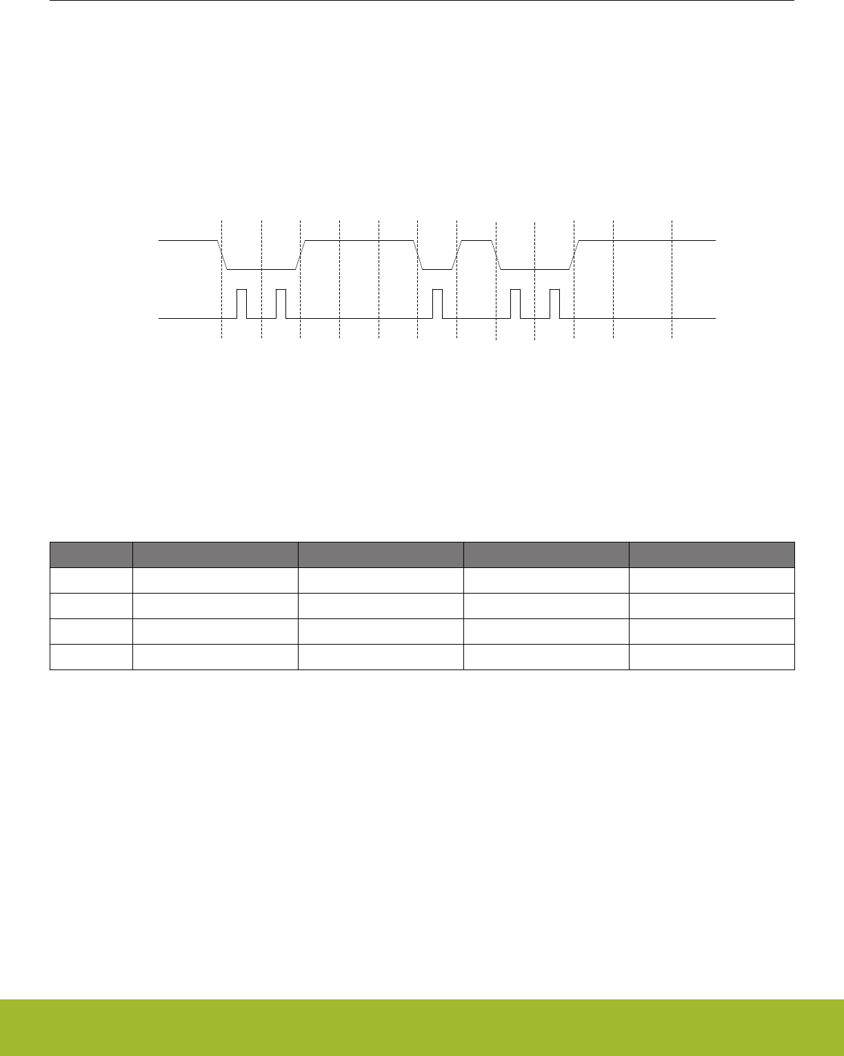
19.3.12 IrDA Modulator/ Demodulator
The IrDA modulator implements the physical layer of the IrDA specification, which is necessary for communication over IrDA. The mod-
ulator takes the signal output from the USART module, and modulates it before it leaves the USART. In the same way, the input signal
is demodulated before it enters the actual USART module. The modulator implements the original Rev. 1.0 physical layer and one high
speed extension which supports speeds from 2.4 kbps to 1.152 Mbps.
The data from and to the USART is represented in a NRZ (Non Return to Zero) format, where the signal value is at the same level
through the entire bit period. For IrDA, the required format is RZI (Return to Zero Inverted), a format where a “1” is signalled by holding
the line low, and a “0” is signalled by a short high pulse. An example is given in Figure 19.32 USART Example RZI Signal for a given
Asynchronous USART Frame on page 582.
S 0 1 2 34 5 6 7 PStop
IdleIdle
USART
(NRZ)
IrDA
(RZI)
Figure 19.32. USART Example RZI Signal for a given Asynchronous USART Frame
The IrDA module is enabled by setting IREN. The USART transmitter output and receiver input is then routed through the IrDA modula-
tor.
The width of the pulses generated by the IrDA modulator is set by configuring IRPW in USARTn_IRCTRL. Four pulse widths are availa-
ble, each defined relative to the configured bit period as listed in Table 19.11 USART IrDA Pulse Widths on page 582.
Table 19.11. USART IrDA Pulse Widths
IRPW Pulse width OVS=0 Pulse width OVS=1 Pulse width OVS=2 Pulse width OVS=3
00 1/16 1/8 1/6 1/4
01 2/16 2/8 2/6 N/A
10 3/16 3/8 N/A N/A
11 4/16 N/A N/A N/A
By default, no filter is enabled in the IrDA demodulator. A filter can be enabled by setting IRFILT in USARTn_IRCTRL. When the filter is
enabled, an incoming pulse has to last for 4 consecutive clock cycles to be detected by the IrDA demodulator.
Note that by default, the idle value of the USART data signal is high. This means that the IrDA modulator generates negative pulses,
and the IrDA demodulator expects negative pulses. To make the IrDA module use RZI signalling, both TXINV and RXINV in
USARTn_CTRL must be set.
The IrDA module can also modulate a signal from the PRS system, and transmit a modulated signal to the PRS system. To use a PRS
channel as transmitter source instead of the USART, set IRPRSEN in USARTn_IRCTRL high. The channel is selected by configuring
IRPRSSEL in USARTn_IRCTRL.
Reference Manual
USART - Universal Synchronous Asynchronous Receiver/Transmitter
silabs.com | Smart. Connected. Energy-friendly. Preliminary Rev. 0.5 | 582

19.4 Register Map
The offset register address is relative to the registers base address.
Offset Name Type Description
0x000 USARTn_CTRL RW Control Register
0x004 USARTn_FRAME RW USART Frame Format Register
0x008 USARTn_TRIGCTRL RW USART Trigger Control register
0x00C USARTn_CMD W1 Command Register
0x010 USARTn_STATUS RUSART Status Register
0x014 USARTn_CLKDIV RWH Clock Control Register
0x018 USARTn_RXDATAX R(a) RX Buffer Data Extended Register
0x01C USARTn_RXDATA R(a) RX Buffer Data Register
0x020 USARTn_RXDOUBLEX R(a) RX Buffer Double Data Extended Register
0x024 USARTn_RXDOUBLE R(a) RX FIFO Double Data Register
0x028 USARTn_RXDATAXP RRX Buffer Data Extended Peek Register
0x02C USARTn_RXDOUBLEXP RRX Buffer Double Data Extended Peek Register
0x030 USARTn_TXDATAX WTX Buffer Data Extended Register
0x034 USARTn_TXDATA WTX Buffer Data Register
0x038 USARTn_TXDOUBLEX WTX Buffer Double Data Extended Register
0x03C USARTn_TXDOUBLE WTX Buffer Double Data Register
0x040 USARTn_IF RInterrupt Flag Register
0x044 USARTn_IFS W1 Interrupt Flag Set Register
0x048 USARTn_IFC (R)W1 Interrupt Flag Clear Register
0x04C USARTn_IEN RW Interrupt Enable Register
0x050 USARTn_IRCTRL RW IrDA Control Register
0x058 USARTn_INPUT RW USART Input Register
0x05C USARTn_I2SCTRL RW I2S Control Register
0x060 USARTn_TIMING RW Timing Register
0x064 USARTn_CTRLX RW Control Register Extended
0x068 USARTn_TIMECMP0 RW Used to generate interrupts and various delays
0x06C USARTn_TIMECMP1 RW Used to generate interrupts and various delays
0x070 USARTn_TIMECMP2 RW Used to generate interrupts and various delays
0x074 USARTn_ROUTEPEN RW I/O Routing Pin Enable Register
0x078 USARTn_ROUTELOC0 RW I/O Routing Location Register
0x07C USARTn_ROUTELOC1 RW I/O Routing Location Register
Reference Manual
USART - Universal Synchronous Asynchronous Receiver/Transmitter
silabs.com | Smart. Connected. Energy-friendly. Preliminary Rev. 0.5 | 583

19.5 Register Description
19.5.1 USARTn_CTRL - Control Register
Offset Bit Position
0x000
31
30
29
28
27
26
25
24
23
22
21
20
19
18
17
16
15
14
13
12
11
10
9
8
7
6
5
4
3
2
1
0
Reset
0
0
0
0
0
0
0
0
0
0
0
0
0
0
0
0
0
0
0
0
0
0
0x0
0
0
0
0
0
Access
RW
RW
RW
RW
RW
RW
RW
RW
RW
RW
RW
RW
RW
RW
RW
RW
RW
RW
RW
RW
RW
RW
RW
RW
RW
RW
RW
RW
Name
SMSDELAY
MVDIS
AUTOTX
BYTESWAP
SSSEARLY
ERRSTX
ERRSRX
ERRSDMA
BIT8DV
SKIPPERRF
SCRETRANS
SCMODE
AUTOTRI
AUTOCS
CSINV
TXINV
RXINV
TXBIL
CSMA
MSBF
CLKPHA
CLKPOL
OVS
MPAB
MPM
CCEN
LOOPBK
SYNC
Bit Name Reset Access Description
31 SMSDELAY 0 RW Synchronous Master Sample Delay
Delay Synchronous Master sample point to the next setup edge to improve timing and allow communication at higher
speeds
30 MVDIS 0 RW Majority Vote Disable
Disable majority vote for 16x, 8x and 6x oversampling modes.
29 AUTOTX 0 RW Always Transmit When RX Not Full
Transmits as long as RX is not full. If TX is empty, underflows are generated.
28 BYTESWAP 0 RW Byteswap In Double Accesses
Set to switch the order of the bytes in double accesses.
Value Description
0 Normal byte order
1 Byte order swapped
27:26 Reserved To ensure compatibility with future devices, always write bits to 0. More information in 1.2 Conven-
tions
25 SSSEARLY 0 RW Synchronous Slave Setup Early
Setup data on sample edge in synchronous slave mode to improve MOSI setup time
24 ERRSTX 0 RW Disable TX On Error
When set, the transmitter is disabled on framing and parity errors (asynchronous mode only) in the receiver.
Value Description
0 Received framing and parity errors have no effect on transmitter
1 Received framing and parity errors disable the transmitter
23 ERRSRX 0 RW Disable RX On Error
When set, the receiver is disabled on framing and parity errors (asynchronous mode only).
Value Description
0 Framing and parity errors have no effect on receiver
Reference Manual
USART - Universal Synchronous Asynchronous Receiver/Transmitter
silabs.com | Smart. Connected. Energy-friendly. Preliminary Rev. 0.5 | 584

Bit Name Reset Access Description
1 Framing and parity errors disable the receiver
22 ERRSDMA 0 RW Halt DMA On Error
When set, DMA requests will be cleared on framing and parity errors (asynchronous mode only).
Value Description
0 Framing and parity errors have no effect on DMA requests from the
USART
1 DMA requests from the USART are blocked while the PERR or FERR
interrupt flags are set
21 BIT8DV 0 RW Bit 8 Default Value
The default value of the 9th bit. If 9-bit frames are used, and an 8-bit write operation is done, leaving the 9th bit unspecified,
the 9th bit is set to the value of BIT8DV.
20 SKIPPERRF 0 RW Skip Parity Error Frames
When set, the receiver discards frames with parity errors (asynchronous mode only). The PERR interrupt flag is still set.
19 SCRETRANS 0 RW SmartCard Retransmit
When in SmartCard mode, a NACK'ed frame will be kept in the shift register and retransmitted if the transmitter is still ena-
bled.
18 SCMODE 0 RW SmartCard Mode
Use this bit to enable or disable SmartCard mode.
17 AUTOTRI 0 RW Automatic TX Tristate
When enabled, TXTRI is set by hardware whenever the transmitter is idle, and TXTRI is cleared by hardware when trans-
mission starts.
Value Description
0 The output on U(S)n_TX when the transmitter is idle is defined by
TXINV
1 U(S)n_TX is tristated whenever the transmitter is idle
16 AUTOCS 0 RW Automatic Chip Select
When enabled, the output on USn_CS will be activated one baud-period before transmission starts, and deactivated when
transmission ends.
15 CSINV 0 RW Chip Select Invert
Default value is active low. This affects both the selection of external slaves, as well as the selection of the microcontroller
as a slave.
Value Description
0 Chip select is active low
1 Chip select is active high
14 TXINV 0 RW Transmitter output Invert
The output from the USART transmitter can optionally be inverted by setting this bit.
Value Description
0 Output from the transmitter is passed unchanged to U(S)n_TX
Reference Manual
USART - Universal Synchronous Asynchronous Receiver/Transmitter
silabs.com | Smart. Connected. Energy-friendly. Preliminary Rev. 0.5 | 585

Bit Name Reset Access Description
1 Output from the transmitter is inverted before it is passed to U(S)n_TX
13 RXINV 0 RW Receiver Input Invert
Setting this bit will invert the input to the USART receiver.
Value Description
0 Input is passed directly to the receiver
1 Input is inverted before it is passed to the receiver
12 TXBIL 0 RW TX Buffer Interrupt Level
Determines the interrupt and status level of the transmit buffer.
Value Mode Description
0 EMPTY TXBL and the TXBL interrupt flag are set when the transmit buffer be-
comes empty. TXBL is cleared when the buffer becomes nonempty.
1 HALFFULL TXBL and TXBLIF are set when the transmit buffer goes from full to
half-full or empty. TXBL is cleared when the buffer becomes full.
11 CSMA 0 RW Action On Slave-Select In Master Mode
This register determines the action to be performed when slave-select is configured as an input and driven low while in
master mode.
Value Mode Description
0 NOACTION No action taken
1 GOTOSLAVEMODE Go to slave mode
10 MSBF 0 RW Most Significant Bit First
Decides whether data is sent with the least significant bit first, or the most significant bit first.
Value Description
0 Data is sent with the least significant bit first
1 Data is sent with the most significant bit first
9 CLKPHA 0 RW Clock Edge For Setup/Sample
Determines where data is set-up and sampled according to the bus clock when in synchronous mode.
Value Mode Description
0 SAMPLELEADING Data is sampled on the leading edge and set-up on the trailing edge of
the bus clock in synchronous mode
1 SAMPLETRAILING Data is set-up on the leading edge and sampled on the trailing edge of
the bus clock in synchronous mode
8 CLKPOL 0 RW Clock Polarity
Determines the clock polarity of the bus clock used in synchronous mode.
Value Mode Description
0 IDLELOW The bus clock used in synchronous mode has a low base value
Reference Manual
USART - Universal Synchronous Asynchronous Receiver/Transmitter
silabs.com | Smart. Connected. Energy-friendly. Preliminary Rev. 0.5 | 586

Bit Name Reset Access Description
1 IDLEHIGH The bus clock used in synchronous mode has a high base value
7 Reserved To ensure compatibility with future devices, always write bits to 0. More information in 1.2 Conven-
tions
6:5 OVS 0x0 RW Oversampling
Sets the number of clock periods in a UART bit-period. More clock cycles gives better robustness, while less clock cycles
gives better performance.
Value Mode Description
0 X16 Regular UART mode with 16X oversampling in asynchronous mode
1 X8 Double speed with 8X oversampling in asynchronous mode
2 X6 6X oversampling in asynchronous mode
3 X4 Quadruple speed with 4X oversampling in asynchronous mode
4 MPAB 0 RW Multi-Processor Address-Bit
Defines the value of the multi-processor address bit. An incoming frame with its 9th bit equal to the value of this bit marks
the frame as a multi-processor address frame.
3 MPM 0 RW Multi-Processor Mode
Multi-processor mode uses the 9th bit of the USART frames to tell whether the frame is an address frame or a data frame.
Value Description
0 The 9th bit of incoming frames has no special function
1 An incoming frame with the 9th bit equal to MPAB will be loaded into
the receive buffer regardless of RXBLOCK and will result in the MPAB
interrupt flag being set
2 CCEN 0 RW Collision Check Enable
Enables collision checking on data when operating in half duplex modus.
Value Description
0 Collision check is disabled
1 Collision check is enabled. The receiver must be enabled for the check
to be performed
1 LOOPBK 0 RW Loopback Enable
Allows the receiver to be connected directly to the USART transmitter for loopback and half duplex communication.
Value Description
0 The receiver is connected to and receives data from U(S)n_RX
1 The receiver is connected to and receives data from U(S)n_TX
0 SYNC 0 RW USART Synchronous Mode
Determines whether the USART is operating in asynchronous or synchronous mode.
Value Description
0 The USART operates in asynchronous mode
Reference Manual
USART - Universal Synchronous Asynchronous Receiver/Transmitter
silabs.com | Smart. Connected. Energy-friendly. Preliminary Rev. 0.5 | 587

Bit Name Reset Access Description
1 The USART operates in synchronous mode
Reference Manual
USART - Universal Synchronous Asynchronous Receiver/Transmitter
silabs.com | Smart. Connected. Energy-friendly. Preliminary Rev. 0.5 | 588

19.5.2 USARTn_FRAME - USART Frame Format Register
Offset Bit Position
0x004
31
30
29
28
27
26
25
24
23
22
21
20
19
18
17
16
15
14
13
12
11
10
9
8
7
6
5
4
3
2
1
0
Reset
0x1
0x0
0x5
Access
RW
RW
RW
Name
STOPBITS
PARITY
DATABITS
Bit Name Reset Access Description
31:14 Reserved To ensure compatibility with future devices, always write bits to 0. More information in 1.2 Conven-
tions
13:12 STOPBITS 0x1 RW Stop-Bit Mode
Determines the number of stop-bits used.
Value Mode Description
0 HALF The transmitter generates a half stop bit. Stop-bits are not verified by
receiver
1 ONE One stop bit is generated and verified
2 ONEANDAHALF The transmitter generates one and a half stop bit. The receiver verifies
the first stop bit
3 TWO The transmitter generates two stop bits. The receiver checks the first
stop-bit only
11:10 Reserved To ensure compatibility with future devices, always write bits to 0. More information in 1.2 Conven-
tions
9:8 PARITY 0x0 RW Parity-Bit Mode
Determines whether parity bits are enabled, and whether even or odd parity should be used. Only available in asynchro-
nous mode.
Value Mode Description
0 NONE Parity bits are not used
2 EVEN Even parity are used. Parity bits are automatically generated and
checked by hardware.
3 ODD Odd parity is used. Parity bits are automatically generated and checked
by hardware.
7:4 Reserved To ensure compatibility with future devices, always write bits to 0. More information in 1.2 Conven-
tions
3:0 DATABITS 0x5 RW Data-Bit Mode
This register sets the number of data bits in a USART frame.
Value Mode Description
1 FOUR Each frame contains 4 data bits
2 FIVE Each frame contains 5 data bits
Reference Manual
USART - Universal Synchronous Asynchronous Receiver/Transmitter
silabs.com | Smart. Connected. Energy-friendly. Preliminary Rev. 0.5 | 589

Bit Name Reset Access Description
3 SIX Each frame contains 6 data bits
4 SEVEN Each frame contains 7 data bits
5 EIGHT Each frame contains 8 data bits
6 NINE Each frame contains 9 data bits
7 TEN Each frame contains 10 data bits
8 ELEVEN Each frame contains 11 data bits
9 TWELVE Each frame contains 12 data bits
10 THIRTEEN Each frame contains 13 data bits
11 FOURTEEN Each frame contains 14 data bits
12 FIFTEEN Each frame contains 15 data bits
13 SIXTEEN Each frame contains 16 data bits
Reference Manual
USART - Universal Synchronous Asynchronous Receiver/Transmitter
silabs.com | Smart. Connected. Energy-friendly. Preliminary Rev. 0.5 | 590

19.5.3 USARTn_TRIGCTRL - USART Trigger Control register
Offset Bit Position
0x008
31
30
29
28
27
26
25
24
23
22
21
20
19
18
17
16
15
14
13
12
11
10
9
8
7
6
5
4
3
2
1
0
Reset
0x0
0
0
0
0
0
0
0
0
0
Access
RW
RW
RW
RW
RW
RW
RW
RW
RW
RW
Name
TSEL
RXATX2EN
RXATX1EN
RXATX0EN
TXARX2EN
TXARX1EN
TXARX0EN
AUTOTXTEN
TXTEN
RXTEN
Bit Name Reset Access Description
31:20 Reserved To ensure compatibility with future devices, always write bits to 0. More information in 1.2 Conven-
tions
19:16 TSEL 0x0 RW Trigger PRS Channel Select
Select USART PRS trigger channel. The PRS signal can enable RX and/or TX, depending on the setting of RXTEN and
TXTEN.
Value Mode Description
0 PRSCH0 PRS Channel 0 selected
1 PRSCH1 PRS Channel 1 selected
2 PRSCH2 PRS Channel 2 selected
3 PRSCH3 PRS Channel 3 selected
4 PRSCH4 PRS Channel 4 selected
5 PRSCH5 PRS Channel 5 selected
6 PRSCH6 PRS Channel 6 selected
7 PRSCH7 PRS Channel 7 selected
8 PRSCH8 PRS Channel 8 selected
9 PRSCH9 PRS Channel 9 selected
10 PRSCH10 PRS Channel 10 selected
11 PRSCH11 PRS Channel 11 selected
15:13 Reserved To ensure compatibility with future devices, always write bits to 0. More information in 1.2 Conven-
tions
12 RXATX2EN 0 RW Enable Receive Trigger after TX end of frame plus TCMPVAL2
baud-times
When set, a TX end of frame will trigger the receiver after a TCMPVAL2 baud-time delay
11 RXATX1EN 0 RW Enable Receive Trigger after TX end of frame plus TCMPVAL1
baud-times
When set, a TX end of frame will trigger the receiver after a TCMPVAL1 baud-time delay
10 RXATX0EN 0 RW Enable Receive Trigger after TX end of frame plus TCMPVAL0
baud-times
When set, a TX end of frame will trigger the receiver after a TCMPVAL0 baud-time delay
Reference Manual
USART - Universal Synchronous Asynchronous Receiver/Transmitter
silabs.com | Smart. Connected. Energy-friendly. Preliminary Rev. 0.5 | 591

Bit Name Reset Access Description
9 TXARX2EN 0 RW Enable Transmit Trigger after RX End of Frame plus TCMP2VAL
When set, an RX end of frame will trigger the transmitter after TCMP2VAL bit times to force a minimum response delay
8 TXARX1EN 0 RW Enable Transmit Trigger after RX End of Frame plus TCMP1VAL
When set, an RX end of frame will trigger the transmitter after TCMP1VAL bit times to force a minimum response delay
7 TXARX0EN 0 RW Enable Transmit Trigger after RX End of Frame plus TCMP0VAL
When set, an RX end of frame will trigger the transmitter after TCMP0VAL bit times to force a minimum response delay
6 AUTOTXTEN 0 RW AUTOTX Trigger Enable
When set, AUTOTX is enabled as long as the PRS channel selected by TSEL has a high value
5 TXTEN 0 RW Transmit Trigger Enable
When set, the PRS channel selected by TSEL sets TXEN, enabling the transmitter on positive trigger edges.
4 RXTEN 0 RW Receive Trigger Enable
When set, the PRS channel selected by TSEL sets RXEN, enabling the receiver on positive trigger edges.
3:0 Reserved To ensure compatibility with future devices, always write bits to 0. More information in 1.2 Conven-
tions
Reference Manual
USART - Universal Synchronous Asynchronous Receiver/Transmitter
silabs.com | Smart. Connected. Energy-friendly. Preliminary Rev. 0.5 | 592

19.5.4 USARTn_CMD - Command Register
Offset Bit Position
0x00C
31
30
29
28
27
26
25
24
23
22
21
20
19
18
17
16
15
14
13
12
11
10
9
8
7
6
5
4
3
2
1
0
Reset
0
0
0
0
0
0
0
0
0
0
0
0
Access
W1
W1
W1
W1
W1
W1
W1
W1
W1
W1
W1
W1
Name
CLEARRX
CLEARTX
TXTRIDIS
TXTRIEN
RXBLOCKDIS
RXBLOCKEN
MASTERDIS
MASTEREN
TXDIS
TXEN
RXDIS
RXEN
Bit Name Reset Access Description
31:12 Reserved To ensure compatibility with future devices, always write bits to 0. More information in 1.2 Conven-
tions
11 CLEARRX 0 W1 Clear RX
Set to clear receive buffer and the RX shift register.
10 CLEARTX 0 W1 Clear TX
Set to clear transmit buffer and the TX shift register.
9 TXTRIDIS 0 W1 Transmitter Tristate Disable
Disables tristating of the transmitter output.
8 TXTRIEN 0 W1 Transmitter Tristate Enable
Tristates the transmitter output.
7 RXBLOCKDIS 0 W1 Receiver Block Disable
Set to clear RXBLOCK, resulting in all incoming frames being loaded into the receive buffer.
6 RXBLOCKEN 0 W1 Receiver Block Enable
Set to set RXBLOCK, resulting in all incoming frames being discarded.
5 MASTERDIS 0 W1 Master Disable
Set to disable master mode, clearing the MASTER status bit and putting the USART in slave mode.
4 MASTEREN 0 W1 Master Enable
Set to enable master mode, setting the MASTER status bit. Master mode should not be enabled while TXENS is set to 1.
To enable both master and TX mode, write MASTEREN before TXEN, or enable them both in the same write operation.
3TXDIS 0 W1 Transmitter Disable
Set to disable transmission.
2 TXEN 0 W1 Transmitter Enable
Set to enable data transmission.
1 RXDIS 0 W1 Receiver Disable
Set to disable data reception. If a frame is under reception when the receiver is disabled, the incoming frame is discarded.
0 RXEN 0 W1 Receiver Enable
Set to activate data reception on U(S)n_RX.
Reference Manual
USART - Universal Synchronous Asynchronous Receiver/Transmitter
silabs.com | Smart. Connected. Energy-friendly. Preliminary Rev. 0.5 | 593

19.5.5 USARTn_STATUS - USART Status Register
Offset Bit Position
0x010
31
30
29
28
27
26
25
24
23
22
21
20
19
18
17
16
15
14
13
12
11
10
9
8
7
6
5
4
3
2
1
0
Reset
0x0
0
1
0
0
0
0
0
0
1
0
0
0
0
0
0
Access
R
R
R
R
R
R
R
R
R
R
R
R
R
R
R
R
Name
TXBUFCNT
TIMERRESTARTED
TXIDLE
RXFULLRIGHT
RXDATAVRIGHT
TXBSRIGHT
TXBDRIGHT
RXFULL
RXDATAV
TXBL
TXC
TXTRI
RXBLOCK
MASTER
TXENS
RXENS
Bit Name Reset Access Description
31:18 Reserved To ensure compatibility with future devices, always write bits to 0. More information in 1.2 Conven-
tions
17:16 TXBUFCNT 0x0 R TX Buffer Count
Count of TX buffer entry 0, entry 1, and TX shift register. For large frames, the count is only of TX buffer entry 0 and the TX
shifter register.
15 Reserved To ensure compatibility with future devices, always write bits to 0. More information in 1.2 Conven-
tions
14 TIMERRESTARTED 0 R The USART Timer restarted itself
When the timer is restarting itself on each TCMP event, a TIMERRESTARTED value of 0x0 indicates the first TCMP event
in the sequence of multiple TCMP events. Any non TCMP timer start events will clear TIMERRESTARTED. When there is a
TCMP interrupt and TIMERRESTARTED is 0x0, an interrupt service routine can set a TCMP event counter variable in
memory to 0x1 to indicate the first TCMP interrupt of the sequence.
13 TXIDLE 1 R TX Idle
Set when TX idle
12 RXFULLRIGHT 0 R RX Full of Right Data
When set, the entire RX buffer contains right data. Only used in I2S mode
11 RXDATAVRIGHT 0 R RX Data Right
When set, reading RXDATA or RXDATAX gives right data. Else left data is read. Only used in I2S mode
10 TXBSRIGHT 0 R TX Buffer Expects Single Right Data
When set, the TX buffer expects at least a single right data. Else it expects left data. Only used in I2S mode
9 TXBDRIGHT 0 R TX Buffer Expects Double Right Data
When set, the TX buffer expects double right data. Else it may expect a single right data or left data. Only used in I2S mode
8 RXFULL 0 R RX FIFO Full
Set when the RXFIFO is full. Cleared when the receive buffer is no longer full. When this bit is set, there is still room for one
more frame in the receive shift register.
7RXDATAV 0 R RX Data Valid
Set when data is available in the receive buffer. Cleared when the receive buffer is empty.
6 TXBL 1 R TX Buffer Level
Indicates the level of the transmit buffer. If TXBIL is 0x0, TXBL is set whenever the transmit buffer is completely empty.
Otherwise TXBL is set whenever the TX Buffer becomes half full.
Reference Manual
USART - Universal Synchronous Asynchronous Receiver/Transmitter
silabs.com | Smart. Connected. Energy-friendly. Preliminary Rev. 0.5 | 594

Bit Name Reset Access Description
5 TXC 0 R TX Complete
Set when a transmission has completed and no more data is available in the transmit buffer and shift register. Cleared
when data is written to the transmit buffer.
4 TXTRI 0 R Transmitter Tristated
Set when the transmitter is tristated, and cleared when transmitter output is enabled. If AUTOTRI in USARTn_CTRL is set
this bit is always read as 0.
3 RXBLOCK 0 R Block Incoming Data
When set, the receiver discards incoming frames. An incoming frame will not be loaded into the receive buffer if this bit is
set at the instant the frame has been completely received.
2 MASTER 0 R SPI Master Mode
Set when the USART operates as a master. Set using the MASTEREN command and clear using the MASTERDIS com-
mand.
1 TXENS 0 R Transmitter Enable Status
Set when the transmitter is enabled.
0 RXENS 0 R Receiver Enable Status
Set when the receiver is enabled.
19.5.6 USARTn_CLKDIV - Clock Control Register
Offset Bit Position
0x014
31
30
29
28
27
26
25
24
23
22
21
20
19
18
17
16
15
14
13
12
11
10
9
8
7
6
5
4
3
2
1
0
Reset
0
0x00000
Access
RW
RWH
Name
AUTOBAUDEN
DIV
Bit Name Reset Access Description
31 AUTOBAUDEN 0 RW AUTOBAUD detection enable
Detects the baud rate based on receiving a 0x55 frame (0x00 for IrDA). This is used in Asynchronous mode.
30:23 Reserved To ensure compatibility with future devices, always write bits to 0. More information in 1.2 Conven-
tions
22:3 DIV 0x00000 RWH Fractional Clock Divider
Specifies the fractional clock divider for the USART. Setting AUTOBAUDEN in USARTn_CLKDIV will overwrite the DIV
field.
2:0 Reserved To ensure compatibility with future devices, always write bits to 0. More information in 1.2 Conven-
tions
Reference Manual
USART - Universal Synchronous Asynchronous Receiver/Transmitter
silabs.com | Smart. Connected. Energy-friendly. Preliminary Rev. 0.5 | 595

19.5.7 USARTn_RXDATAX - RX Buffer Data Extended Register (Actionable Reads)
Offset Bit Position
0x018
31
30
29
28
27
26
25
24
23
22
21
20
19
18
17
16
15
14
13
12
11
10
9
8
7
6
5
4
3
2
1
0
Reset
0
0
0x000
Access
R
R
R
Name
FERR
PERR
RXDATA
Bit Name Reset Access Description
31:16 Reserved To ensure compatibility with future devices, always write bits to 0. More information in 1.2 Conven-
tions
15 FERR 0 R Data Framing Error
Set if data in buffer has a framing error. Can be the result of a break condition.
14 PERR 0 R Data Parity Error
Set if data in buffer has a parity error (asynchronous mode only).
13:9 Reserved To ensure compatibility with future devices, always write bits to 0. More information in 1.2 Conven-
tions
8:0 RXDATA 0x000 R RX Data
Use this register to access data read from the USART. Buffer is cleared on read access.
19.5.8 USARTn_RXDATA - RX Buffer Data Register (Actionable Reads)
Offset Bit Position
0x01C
31
30
29
28
27
26
25
24
23
22
21
20
19
18
17
16
15
14
13
12
11
10
9
8
7
6
5
4
3
2
1
0
Reset
0x00
Access
R
Name
RXDATA
Bit Name Reset Access Description
31:8 Reserved To ensure compatibility with future devices, always write bits to 0. More information in 1.2 Conven-
tions
7:0 RXDATA 0x00 R RX Data
Use this register to access data read from USART. Buffer is cleared on read access. Only the 8 LSB can be read using this
register.
Reference Manual
USART - Universal Synchronous Asynchronous Receiver/Transmitter
silabs.com | Smart. Connected. Energy-friendly. Preliminary Rev. 0.5 | 596

19.5.9 USARTn_RXDOUBLEX - RX Buffer Double Data Extended Register (Actionable Reads)
Offset Bit Position
0x020
31
30
29
28
27
26
25
24
23
22
21
20
19
18
17
16
15
14
13
12
11
10
9
8
7
6
5
4
3
2
1
0
Reset
0
0
0x000
0
0
0x000
Access
R
R
R
R
R
R
Name
FERR1
PERR1
RXDATA1
FERR0
PERR0
RXDATA0
Bit Name Reset Access Description
31 FERR1 0 R Data Framing Error 1
Set if data in buffer has a framing error. Can be the result of a break condition.
30 PERR1 0 R Data Parity Error 1
Set if data in buffer has a parity error (asynchronous mode only).
29:25 Reserved To ensure compatibility with future devices, always write bits to 0. More information in 1.2 Conven-
tions
24:16 RXDATA1 0x000 R RX Data 1
Second frame read from buffer.
15 FERR0 0 R Data Framing Error 0
Set if data in buffer has a framing error. Can be the result of a break condition.
14 PERR0 0 R Data Parity Error 0
Set if data in buffer has a parity error (asynchronous mode only).
13:9 Reserved To ensure compatibility with future devices, always write bits to 0. More information in 1.2 Conven-
tions
8:0 RXDATA0 0x000 R RX Data 0
First frame read from buffer.
Reference Manual
USART - Universal Synchronous Asynchronous Receiver/Transmitter
silabs.com | Smart. Connected. Energy-friendly. Preliminary Rev. 0.5 | 597

19.5.10 USARTn_RXDOUBLE - RX FIFO Double Data Register (Actionable Reads)
Offset Bit Position
0x024
31
30
29
28
27
26
25
24
23
22
21
20
19
18
17
16
15
14
13
12
11
10
9
8
7
6
5
4
3
2
1
0
Reset
0x00
0x00
Access
R
R
Name
RXDATA1
RXDATA0
Bit Name Reset Access Description
31:16 Reserved To ensure compatibility with future devices, always write bits to 0. More information in 1.2 Conven-
tions
15:8 RXDATA1 0x00 R RX Data 1
Second frame read from buffer.
7:0 RXDATA0 0x00 R RX Data 0
First frame read from buffer.
19.5.11 USARTn_RXDATAXP - RX Buffer Data Extended Peek Register
Offset Bit Position
0x028
31
30
29
28
27
26
25
24
23
22
21
20
19
18
17
16
15
14
13
12
11
10
9
8
7
6
5
4
3
2
1
0
Reset
0
0
0x000
Access
R
R
R
Name
FERRP
PERRP
RXDATAP
Bit Name Reset Access Description
31:16 Reserved To ensure compatibility with future devices, always write bits to 0. More information in 1.2 Conven-
tions
15 FERRP 0 R Data Framing Error Peek
Set if data in buffer has a framing error. Can be the result of a break condition.
14 PERRP 0 R Data Parity Error Peek
Set if data in buffer has a parity error (asynchronous mode only).
13:9 Reserved To ensure compatibility with future devices, always write bits to 0. More information in 1.2 Conven-
tions
8:0 RXDATAP 0x000 R RX Data Peek
Use this register to access data read from the USART.
Reference Manual
USART - Universal Synchronous Asynchronous Receiver/Transmitter
silabs.com | Smart. Connected. Energy-friendly. Preliminary Rev. 0.5 | 598

19.5.12 USARTn_RXDOUBLEXP - RX Buffer Double Data Extended Peek Register
Offset Bit Position
0x02C
31
30
29
28
27
26
25
24
23
22
21
20
19
18
17
16
15
14
13
12
11
10
9
8
7
6
5
4
3
2
1
0
Reset
0
0
0x000
0
0
0x000
Access
R
R
R
R
R
R
Name
FERRP1
PERRP1
RXDATAP1
FERRP0
PERRP0
RXDATAP0
Bit Name Reset Access Description
31 FERRP1 0 R Data Framing Error 1 Peek
Set if data in buffer has a framing error. Can be the result of a break condition.
30 PERRP1 0 R Data Parity Error 1 Peek
Set if data in buffer has a parity error (asynchronous mode only).
29:25 Reserved To ensure compatibility with future devices, always write bits to 0. More information in 1.2 Conven-
tions
24:16 RXDATAP1 0x000 R RX Data 1 Peek
Second frame read from FIFO.
15 FERRP0 0 R Data Framing Error 0 Peek
Set if data in buffer has a framing error. Can be the result of a break condition.
14 PERRP0 0 R Data Parity Error 0 Peek
Set if data in buffer has a parity error (asynchronous mode only).
13:9 Reserved To ensure compatibility with future devices, always write bits to 0. More information in 1.2 Conven-
tions
8:0 RXDATAP0 0x000 R RX Data 0 Peek
First frame read from FIFO.
Reference Manual
USART - Universal Synchronous Asynchronous Receiver/Transmitter
silabs.com | Smart. Connected. Energy-friendly. Preliminary Rev. 0.5 | 599

19.5.13 USARTn_TXDATAX - TX Buffer Data Extended Register
Offset Bit Position
0x030
31
30
29
28
27
26
25
24
23
22
21
20
19
18
17
16
15
14
13
12
11
10
9
8
7
6
5
4
3
2
1
0
Reset
0
0
0
0
0
0x000
Access
W
W
W
W
W
W
Name
RXENAT
TXDISAT
TXBREAK
TXTRIAT
UBRXAT
TXDATAX
Bit Name Reset Access Description
31:16 Reserved To ensure compatibility with future devices, always write bits to 0. More information in 1.2 Conven-
tions
15 RXENAT 0 W Enable RX After Transmission
Set to enable reception after transmission.
14 TXDISAT 0 W Clear TXEN After Transmission
Set to disable transmitter and release data bus directly after transmission.
13 TXBREAK 0 W Transmit Data As Break
Set to send data as a break. Recipient will see a framing error or a break condition depending on its configuration and the
value of TXDATA.
12 TXTRIAT 0 W Set TXTRI After Transmission
Set to tristate transmitter by setting TXTRI after transmission.
11 UBRXAT 0 W Unblock RX After Transmission
Set to clear RXBLOCK after transmission, unblocking the receiver.
10:9 Reserved To ensure compatibility with future devices, always write bits to 0. More information in 1.2 Conven-
tions
8:0 TXDATAX 0x000 W TX Data
Use this register to write data to the USART. If TXEN is set, a transfer will be initiated at the first opportunity.
Reference Manual
USART - Universal Synchronous Asynchronous Receiver/Transmitter
silabs.com | Smart. Connected. Energy-friendly. Preliminary Rev. 0.5 | 600

19.5.14 USARTn_TXDATA - TX Buffer Data Register
Offset Bit Position
0x034
31
30
29
28
27
26
25
24
23
22
21
20
19
18
17
16
15
14
13
12
11
10
9
8
7
6
5
4
3
2
1
0
Reset
0x00
Access
W
Name
TXDATA
Bit Name Reset Access Description
31:8 Reserved To ensure compatibility with future devices, always write bits to 0. More information in 1.2 Conven-
tions
7:0 TXDATA 0x00 W TX Data
This frame will be added to TX buffer. Only 8 LSB can be written using this register. 9th bit and control bits will be cleared.
Reference Manual
USART - Universal Synchronous Asynchronous Receiver/Transmitter
silabs.com | Smart. Connected. Energy-friendly. Preliminary Rev. 0.5 | 601

19.5.15 USARTn_TXDOUBLEX - TX Buffer Double Data Extended Register
Offset Bit Position
0x038
31
30
29
28
27
26
25
24
23
22
21
20
19
18
17
16
15
14
13
12
11
10
9
8
7
6
5
4
3
2
1
0
Reset
0
0
0
0
0
0x000
0
0
0
0
0
0x000
Access
W
W
W
W
W
W
W
W
W
W
W
W
Name
RXENAT1
TXDISAT1
TXBREAK1
TXTRIAT1
UBRXAT1
TXDATA1
RXENAT0
TXDISAT0
TXBREAK0
TXTRIAT0
UBRXAT0
TXDATA0
Bit Name Reset Access Description
31 RXENAT1 0 W Enable RX After Transmission
Set to enable reception after transmission.
30 TXDISAT1 0 W Clear TXEN After Transmission
Set to disable transmitter and release data bus directly after transmission.
29 TXBREAK1 0 W Transmit Data As Break
Set to send data as a break. Recipient will see a framing error or a break condition depending on its configuration and the
value of USARTn_TXDATA.
28 TXTRIAT1 0 W Set TXTRI After Transmission
Set to tristate transmitter by setting TXTRI after transmission.
27 UBRXAT1 0 W Unblock RX After Transmission
Set clear RXBLOCK after transmission, unblocking the receiver.
26:25 Reserved To ensure compatibility with future devices, always write bits to 0. More information in 1.2 Conven-
tions
24:16 TXDATA1 0x000 W TX Data
Second frame to write to FIFO.
15 RXENAT0 0 W Enable RX After Transmission
Set to enable reception after transmission.
14 TXDISAT0 0 W Clear TXEN After Transmission
Set to disable transmitter and release data bus directly after transmission.
13 TXBREAK0 0 W Transmit Data As Break
Set to send data as a break. Recipient will see a framing error or a break condition depending on its configuration and the
value of TXDATA.
12 TXTRIAT0 0 W Set TXTRI After Transmission
Set to tristate transmitter by setting TXTRI after transmission.
11 UBRXAT0 0 W Unblock RX After Transmission
Set clear RXBLOCK after transmission, unblocking the receiver.
10:9 Reserved To ensure compatibility with future devices, always write bits to 0. More information in 1.2 Conven-
tions
8:0 TXDATA0 0x000 W TX Data
First frame to write to buffer.
Reference Manual
USART - Universal Synchronous Asynchronous Receiver/Transmitter
silabs.com | Smart. Connected. Energy-friendly. Preliminary Rev. 0.5 | 602

19.5.16 USARTn_TXDOUBLE - TX Buffer Double Data Register
Offset Bit Position
0x03C
31
30
29
28
27
26
25
24
23
22
21
20
19
18
17
16
15
14
13
12
11
10
9
8
7
6
5
4
3
2
1
0
Reset
0x00
0x00
Access
W
W
Name
TXDATA1
TXDATA0
Bit Name Reset Access Description
31:16 Reserved To ensure compatibility with future devices, always write bits to 0. More information in 1.2 Conven-
tions
15:8 TXDATA1 0x00 W TX Data
Second frame to write to buffer.
7:0 TXDATA0 0x00 W TX Data
First frame to write to buffer.
Reference Manual
USART - Universal Synchronous Asynchronous Receiver/Transmitter
silabs.com | Smart. Connected. Energy-friendly. Preliminary Rev. 0.5 | 603

19.5.17 USARTn_IF - Interrupt Flag Register
Offset Bit Position
0x040
31
30
29
28
27
26
25
24
23
22
21
20
19
18
17
16
15
14
13
12
11
10
9
8
7
6
5
4
3
2
1
0
Reset
0
0
0
0
0
0
0
0
0
0
0
0
0
0
0
1
0
Access
R
R
R
R
R
R
R
R
R
R
R
R
R
R
R
R
R
Name
TCMP2
TCMP1
TCMP0
TXIDLE
CCF
SSM
MPAF
FERR
PERR
TXUF
TXOF
RXUF
RXOF
RXFULL
RXDATAV
TXBL
TXC
Bit Name Reset Access Description
31:17 Reserved To ensure compatibility with future devices, always write bits to 0. More information in 1.2 Conven-
tions
16 TCMP2 0 R Timer comparator 2 Interrupt Flag
Set when the timer reaches the comparator 2 value, TCMP2.
15 TCMP1 0 R Timer comparator 1 Interrupt Flag
Set when the timer reaches the comparator 1 value, TCMP1.
14 TCMP0 0 R Timer comparator 0 Interrupt Flag
Set when the Timer reaches the comparator 0 value, TCMP0.
13 TXIDLE 0 R TX Idle Interrupt Flag
Set when TX goes idle. At this point, transmission has ended
12 CCF 0 R Collision Check Fail Interrupt Flag
Set when a collision check notices an error in the transmitted data.
11 SSM 0 R Slave-Select In Master Mode Interrupt Flag
Set when the device is selected as a slave when in master mode.
10 MPAF 0 R Multi-Processor Address Frame Interrupt Flag
Set when a multi-processor address frame is detected.
9 FERR 0 R Framing Error Interrupt Flag
Set when a frame with a framing error is received while RXBLOCK is cleared.
8 PERR 0 R Parity Error Interrupt Flag
Set when a frame with a parity error (asynchronous mode only) is received while RXBLOCK is cleared.
7 TXUF 0 R TX Underflow Interrupt Flag
Set when operating as a synchronous slave, no data is available in the transmit buffer when the master starts transmission
of a new frame.
6 TXOF 0 R TX Overflow Interrupt Flag
Set when a write is done to the transmit buffer while it is full. The data already in the transmit buffer is preserved.
5 RXUF 0 R RX Underflow Interrupt Flag
Set when trying to read from the receive buffer when it is empty.
4 RXOF 0 R RX Overflow Interrupt Flag
Set when data is incoming while the receive shift register is full. The data previously in the shift register is lost.
Reference Manual
USART - Universal Synchronous Asynchronous Receiver/Transmitter
silabs.com | Smart. Connected. Energy-friendly. Preliminary Rev. 0.5 | 604

Bit Name Reset Access Description
3 RXFULL 0 R RX Buffer Full Interrupt Flag
Set when the receive buffer becomes full.
2 RXDATAV 0 R RX Data Valid Interrupt Flag
Set when data becomes available in the receive buffer.
1 TXBL 1 R TX Buffer Level Interrupt Flag
Set when buffer becomes empty if buffer level is set to 0x0, or when the number of empty TX buffer elements equals speci-
fied buffer level.
0TXC 0 R TX Complete Interrupt Flag
This interrupt is set after a transmission when both the TX buffer and shift register are empty.
Reference Manual
USART - Universal Synchronous Asynchronous Receiver/Transmitter
silabs.com | Smart. Connected. Energy-friendly. Preliminary Rev. 0.5 | 605

19.5.18 USARTn_IFS - Interrupt Flag Set Register
Offset Bit Position
0x044
31
30
29
28
27
26
25
24
23
22
21
20
19
18
17
16
15
14
13
12
11
10
9
8
7
6
5
4
3
2
1
0
Reset
0
0
0
0
0
0
0
0
0
0
0
0
0
0
0
Access
W1
W1
W1
W1
W1
W1
W1
W1
W1
W1
W1
W1
W1
W1
W1
Name
TCMP2
TCMP1
TCMP0
TXIDLE
CCF
SSM
MPAF
FERR
PERR
TXUF
TXOF
RXUF
RXOF
RXFULL
TXC
Bit Name Reset Access Description
31:17 Reserved To ensure compatibility with future devices, always write bits to 0. More information in 1.2 Conven-
tions
16 TCMP2 0 W1 Set TCMP2 Interrupt Flag
Write 1 to set the TCMP2 interrupt flag
15 TCMP1 0 W1 Set TCMP1 Interrupt Flag
Write 1 to set the TCMP1 interrupt flag
14 TCMP0 0 W1 Set TCMP0 Interrupt Flag
Write 1 to set the TCMP0 interrupt flag
13 TXIDLE 0 W1 Set TXIDLE Interrupt Flag
Write 1 to set the TXIDLE interrupt flag
12 CCF 0 W1 Set CCF Interrupt Flag
Write 1 to set the CCF interrupt flag
11 SSM 0 W1 Set SSM Interrupt Flag
Write 1 to set the SSM interrupt flag
10 MPAF 0 W1 Set MPAF Interrupt Flag
Write 1 to set the MPAF interrupt flag
9 FERR 0 W1 Set FERR Interrupt Flag
Write 1 to set the FERR interrupt flag
8 PERR 0 W1 Set PERR Interrupt Flag
Write 1 to set the PERR interrupt flag
7 TXUF 0 W1 Set TXUF Interrupt Flag
Write 1 to set the TXUF interrupt flag
6 TXOF 0 W1 Set TXOF Interrupt Flag
Write 1 to set the TXOF interrupt flag
5 RXUF 0 W1 Set RXUF Interrupt Flag
Write 1 to set the RXUF interrupt flag
4 RXOF 0 W1 Set RXOF Interrupt Flag
Write 1 to set the RXOF interrupt flag
3 RXFULL 0 W1 Set RXFULL Interrupt Flag
Write 1 to set the RXFULL interrupt flag
Reference Manual
USART - Universal Synchronous Asynchronous Receiver/Transmitter
silabs.com | Smart. Connected. Energy-friendly. Preliminary Rev. 0.5 | 606

Bit Name Reset Access Description
2:1 Reserved To ensure compatibility with future devices, always write bits to 0. More information in 1.2 Conven-
tions
0 TXC 0 W1 Set TXC Interrupt Flag
Write 1 to set the TXC interrupt flag
Reference Manual
USART - Universal Synchronous Asynchronous Receiver/Transmitter
silabs.com | Smart. Connected. Energy-friendly. Preliminary Rev. 0.5 | 607

19.5.19 USARTn_IFC - Interrupt Flag Clear Register
Offset Bit Position
0x048
31
30
29
28
27
26
25
24
23
22
21
20
19
18
17
16
15
14
13
12
11
10
9
8
7
6
5
4
3
2
1
0
Reset
0
0
0
0
0
0
0
0
0
0
0
0
0
0
0
Access
(R)W1
(R)W1
(R)W1
(R)W1
(R)W1
(R)W1
(R)W1
(R)W1
(R)W1
(R)W1
(R)W1
(R)W1
(R)W1
(R)W1
(R)W1
Name
TCMP2
TCMP1
TCMP0
TXIDLE
CCF
SSM
MPAF
FERR
PERR
TXUF
TXOF
RXUF
RXOF
RXFULL
TXC
Bit Name Reset Access Description
31:17 Reserved To ensure compatibility with future devices, always write bits to 0. More information in 1.2 Conven-
tions
16 TCMP2 0 (R)W1 Clear TCMP2 Interrupt Flag
Write 1 to clear the TCMP2 interrupt flag. Reading returns the value of the IF and clears the corresponding interrupt flags
(This feature must be enabled globally in MSC.).
15 TCMP1 0 (R)W1 Clear TCMP1 Interrupt Flag
Write 1 to clear the TCMP1 interrupt flag. Reading returns the value of the IF and clears the corresponding interrupt flags
(This feature must be enabled globally in MSC.).
14 TCMP0 0 (R)W1 Clear TCMP0 Interrupt Flag
Write 1 to clear the TCMP0 interrupt flag. Reading returns the value of the IF and clears the corresponding interrupt flags
(This feature must be enabled globally in MSC.).
13 TXIDLE 0 (R)W1 Clear TXIDLE Interrupt Flag
Write 1 to clear the TXIDLE interrupt flag. Reading returns the value of the IF and clears the corresponding interrupt flags
(This feature must be enabled globally in MSC.).
12 CCF 0 (R)W1 Clear CCF Interrupt Flag
Write 1 to clear the CCF interrupt flag. Reading returns the value of the IF and clears the corresponding interrupt flags (This
feature must be enabled globally in MSC.).
11 SSM 0 (R)W1 Clear SSM Interrupt Flag
Write 1 to clear the SSM interrupt flag. Reading returns the value of the IF and clears the corresponding interrupt flags (This
feature must be enabled globally in MSC.).
10 MPAF 0 (R)W1 Clear MPAF Interrupt Flag
Write 1 to clear the MPAF interrupt flag. Reading returns the value of the IF and clears the corresponding interrupt flags
(This feature must be enabled globally in MSC.).
9 FERR 0 (R)W1 Clear FERR Interrupt Flag
Write 1 to clear the FERR interrupt flag. Reading returns the value of the IF and clears the corresponding interrupt flags
(This feature must be enabled globally in MSC.).
8 PERR 0 (R)W1 Clear PERR Interrupt Flag
Write 1 to clear the PERR interrupt flag. Reading returns the value of the IF and clears the corresponding interrupt flags
(This feature must be enabled globally in MSC.).
7 TXUF 0 (R)W1 Clear TXUF Interrupt Flag
Write 1 to clear the TXUF interrupt flag. Reading returns the value of the IF and clears the corresponding interrupt flags
(This feature must be enabled globally in MSC.).
Reference Manual
USART - Universal Synchronous Asynchronous Receiver/Transmitter
silabs.com | Smart. Connected. Energy-friendly. Preliminary Rev. 0.5 | 608

Bit Name Reset Access Description
6 TXOF 0 (R)W1 Clear TXOF Interrupt Flag
Write 1 to clear the TXOF interrupt flag. Reading returns the value of the IF and clears the corresponding interrupt flags
(This feature must be enabled globally in MSC.).
5 RXUF 0 (R)W1 Clear RXUF Interrupt Flag
Write 1 to clear the RXUF interrupt flag. Reading returns the value of the IF and clears the corresponding interrupt flags
(This feature must be enabled globally in MSC.).
4 RXOF 0 (R)W1 Clear RXOF Interrupt Flag
Write 1 to clear the RXOF interrupt flag. Reading returns the value of the IF and clears the corresponding interrupt flags
(This feature must be enabled globally in MSC.).
3 RXFULL 0 (R)W1 Clear RXFULL Interrupt Flag
Write 1 to clear the RXFULL interrupt flag. Reading returns the value of the IF and clears the corresponding interrupt flags
(This feature must be enabled globally in MSC.).
2:1 Reserved To ensure compatibility with future devices, always write bits to 0. More information in 1.2 Conven-
tions
0 TXC 0 (R)W1 Clear TXC Interrupt Flag
Write 1 to clear the TXC interrupt flag. Reading returns the value of the IF and clears the corresponding interrupt flags (This
feature must be enabled globally in MSC.).
Reference Manual
USART - Universal Synchronous Asynchronous Receiver/Transmitter
silabs.com | Smart. Connected. Energy-friendly. Preliminary Rev. 0.5 | 609

19.5.20 USARTn_IEN - Interrupt Enable Register
Offset Bit Position
0x04C
31
30
29
28
27
26
25
24
23
22
21
20
19
18
17
16
15
14
13
12
11
10
9
8
7
6
5
4
3
2
1
0
Reset
0
0
0
0
0
0
0
0
0
0
0
0
0
0
0
0
0
Access
RW
RW
RW
RW
RW
RW
RW
RW
RW
RW
RW
RW
RW
RW
RW
RW
RW
Name
TCMP2
TCMP1
TCMP0
TXIDLE
CCF
SSM
MPAF
FERR
PERR
TXUF
TXOF
RXUF
RXOF
RXFULL
RXDATAV
TXBL
TXC
Bit Name Reset Access Description
31:17 Reserved To ensure compatibility with future devices, always write bits to 0. More information in 1.2 Conven-
tions
16 TCMP2 0 RW TCMP2 Interrupt Enable
Enable/disable the TCMP2 interrupt
15 TCMP1 0 RW TCMP1 Interrupt Enable
Enable/disable the TCMP1 interrupt
14 TCMP0 0 RW TCMP0 Interrupt Enable
Enable/disable the TCMP0 interrupt
13 TXIDLE 0 RW TXIDLE Interrupt Enable
Enable/disable the TXIDLE interrupt
12 CCF 0 RW CCF Interrupt Enable
Enable/disable the CCF interrupt
11 SSM 0 RW SSM Interrupt Enable
Enable/disable the SSM interrupt
10 MPAF 0 RW MPAF Interrupt Enable
Enable/disable the MPAF interrupt
9 FERR 0 RW FERR Interrupt Enable
Enable/disable the FERR interrupt
8 PERR 0 RW PERR Interrupt Enable
Enable/disable the PERR interrupt
7 TXUF 0 RW TXUF Interrupt Enable
Enable/disable the TXUF interrupt
6 TXOF 0 RW TXOF Interrupt Enable
Enable/disable the TXOF interrupt
5 RXUF 0 RW RXUF Interrupt Enable
Enable/disable the RXUF interrupt
4 RXOF 0 RW RXOF Interrupt Enable
Enable/disable the RXOF interrupt
Reference Manual
USART - Universal Synchronous Asynchronous Receiver/Transmitter
silabs.com | Smart. Connected. Energy-friendly. Preliminary Rev. 0.5 | 610

Bit Name Reset Access Description
3 RXFULL 0 RW RXFULL Interrupt Enable
Enable/disable the RXFULL interrupt
2 RXDATAV 0 RW RXDATAV Interrupt Enable
Enable/disable the RXDATAV interrupt
1 TXBL 0 RW TXBL Interrupt Enable
Enable/disable the TXBL interrupt
0 TXC 0 RW TXC Interrupt Enable
Enable/disable the TXC interrupt
Reference Manual
USART - Universal Synchronous Asynchronous Receiver/Transmitter
silabs.com | Smart. Connected. Energy-friendly. Preliminary Rev. 0.5 | 611

19.5.21 USARTn_IRCTRL - IrDA Control Register
Offset Bit Position
0x050
31
30
29
28
27
26
25
24
23
22
21
20
19
18
17
16
15
14
13
12
11
10
9
8
7
6
5
4
3
2
1
0
Reset
0x0
0
0
0x0
0
Access
RW
RW
RW
RW
RW
Name
IRPRSSEL
IRPRSEN
IRFILT
IRPW
IREN
Bit Name Reset Access Description
31:12 Reserved To ensure compatibility with future devices, always write bits to 0. More information in 1.2 Conven-
tions
11:8 IRPRSSEL 0x0 RW IrDA PRS Channel Select
A PRS can be used as input to the pulse modulator instead of TX. This value selects the channel to use.
Value Mode Description
0 PRSCH0 PRS Channel 0 selected
1 PRSCH1 PRS Channel 1 selected
2 PRSCH2 PRS Channel 2 selected
3 PRSCH3 PRS Channel 3 selected
4 PRSCH4 PRS Channel 4 selected
5 PRSCH5 PRS Channel 5 selected
6 PRSCH6 PRS Channel 6 selected
7 PRSCH7 PRS Channel 7 selected
8 PRSCH8 PRS Channel 8 selected
9 PRSCH9 PRS Channel 9 selected
10 PRSCH10 PRS Channel 10 selected
11 PRSCH11 PRS Channel 11 selected
7 IRPRSEN 0 RW IrDA PRS Channel Enable
Enable the PRS channel selected by IRPRSSEL as input to IrDA module instead of TX.
6:4 Reserved To ensure compatibility with future devices, always write bits to 0. More information in 1.2 Conven-
tions
3 IRFILT 0 RW IrDA RX Filter
Set to enable filter on IrDA demodulator.
Value Description
0 No filter enabled
1 Filter enabled. IrDA pulse must be high for at least 4 consecutive clock
cycles to be detected
Reference Manual
USART - Universal Synchronous Asynchronous Receiver/Transmitter
silabs.com | Smart. Connected. Energy-friendly. Preliminary Rev. 0.5 | 612

Bit Name Reset Access Description
2:1 IRPW 0x0 RW IrDA TX Pulse Width
Configure the pulse width generated by the IrDA modulator as a fraction of the configured USART bit period.
Value Mode Description
0 ONE IrDA pulse width is 1/16 for OVS=0 and 1/8 for OVS=1
1 TWO IrDA pulse width is 2/16 for OVS=0 and 2/8 for OVS=1
2 THREE IrDA pulse width is 3/16 for OVS=0 and 3/8 for OVS=1
3 FOUR IrDA pulse width is 4/16 for OVS=0 and 4/8 for OVS=1
0 IREN 0 RW Enable IrDA Module
Enable IrDA module and rout USART signals through it.
Reference Manual
USART - Universal Synchronous Asynchronous Receiver/Transmitter
silabs.com | Smart. Connected. Energy-friendly. Preliminary Rev. 0.5 | 613

19.5.22 USARTn_INPUT - USART Input Register
Offset Bit Position
0x058
31
30
29
28
27
26
25
24
23
22
21
20
19
18
17
16
15
14
13
12
11
10
9
8
7
6
5
4
3
2
1
0
Reset
0
0x0
0
0x0
Access
RW
RW
RW
RW
Name
CLKPRS
CLKPRSSEL
RXPRS
RXPRSSEL
Bit Name Reset Access Description
31:16 Reserved To ensure compatibility with future devices, always write bits to 0. More information in 1.2 Conven-
tions
15 CLKPRS 0 RW PRS CLK Enable
When set, the PRS channel selected as input to CLK.
14:12 Reserved To ensure compatibility with future devices, always write bits to 0. More information in 1.2 Conven-
tions
11:8 CLKPRSSEL 0x0 RW CLK PRS Channel Select
Select PRS channel as input to CLK.
Value Mode Description
0 PRSCH0 PRS Channel 0 selected
1 PRSCH1 PRS Channel 1 selected
2 PRSCH2 PRS Channel 2 selected
3 PRSCH3 PRS Channel 3 selected
4 PRSCH4 PRS Channel 4 selected
5 PRSCH5 PRS Channel 5 selected
6 PRSCH6 PRS Channel 6 selected
7 PRSCH7 PRS Channel 7 selected
8 PRSCH8 PRS Channel 8 selected
9 PRSCH9 PRS Channel 9 selected
10 PRSCH10 PRS Channel 10 selected
11 PRSCH11 PRS Channel 11 selected
7 RXPRS 0 RW PRS RX Enable
When set, the PRS channel selected as input to RX.
6:4 Reserved To ensure compatibility with future devices, always write bits to 0. More information in 1.2 Conven-
tions
3:0 RXPRSSEL 0x0 RW RX PRS Channel Select
Select PRS channel as input to RX.
Value Mode Description
Reference Manual
USART - Universal Synchronous Asynchronous Receiver/Transmitter
silabs.com | Smart. Connected. Energy-friendly. Preliminary Rev. 0.5 | 614

Bit Name Reset Access Description
0 PRSCH0 PRS Channel 0 selected
1 PRSCH1 PRS Channel 1 selected
2 PRSCH2 PRS Channel 2 selected
3 PRSCH3 PRS Channel 3 selected
4 PRSCH4 PRS Channel 4 selected
5 PRSCH5 PRS Channel 5 selected
6 PRSCH6 PRS Channel 6 selected
7 PRSCH7 PRS Channel 7 selected
8 PRSCH8 PRS Channel 8 selected
9 PRSCH9 PRS Channel 9 selected
10 PRSCH10 PRS Channel 10 selected
11 PRSCH11 PRS Channel 11 selected
Reference Manual
USART - Universal Synchronous Asynchronous Receiver/Transmitter
silabs.com | Smart. Connected. Energy-friendly. Preliminary Rev. 0.5 | 615

19.5.23 USARTn_I2SCTRL - I2S Control Register
Offset Bit Position
0x05C
31
30
29
28
27
26
25
24
23
22
21
20
19
18
17
16
15
14
13
12
11
10
9
8
7
6
5
4
3
2
1
0
Reset
0x0
0
0
0
0
0
Access
RW
RW
RW
RW
RW
RW
Name
FORMAT
DELAY
DMASPLIT
JUSTIFY
MONO
EN
Bit Name Reset Access Description
31:11 Reserved To ensure compatibility with future devices, always write bits to 0. More information in 1.2 Conven-
tions
10:8 FORMAT 0x0 RW I2S Word Format
Configure the data-width used internally for I2S data
Value Mode Description
0 W32D32 32-bit word, 32-bit data
1 W32D24M 32-bit word, 32-bit data with 8 lsb masked
2 W32D24 32-bit word, 24-bit data
3 W32D16 32-bit word, 16-bit data
4 W32D8 32-bit word, 8-bit data
5 W16D16 16-bit word, 16-bit data
6 W16D8 16-bit word, 8-bit data
7 W8D8 8-bit word, 8-bit data
7:5 Reserved To ensure compatibility with future devices, always write bits to 0. More information in 1.2 Conven-
tions
4 DELAY 0 RW Delay on I2S data
Set to add a one-cycle delay between a transition on the word-clock and the start of the I2S word. Should be set for stand-
ard I2S format
3 DMASPLIT 0 RW Separate DMA Request For Left/Right Data
When set DMA requests for right-channel data are put on the TXBLRIGHT and RXDATAVRIGHT DMA requests.
2 JUSTIFY 0 RW Justification of I2S Data
Determines whether the I2S data is left or right justified
Value Mode Description
0 LEFT Data is left-justified
1 RIGHT Data is right-justified
1 MONO 0 RW Stero or Mono
Switch between stereo and mono mode. Set for mono
Reference Manual
USART - Universal Synchronous Asynchronous Receiver/Transmitter
silabs.com | Smart. Connected. Energy-friendly. Preliminary Rev. 0.5 | 616

Bit Name Reset Access Description
0 EN 0 RW Enable I2S Mode
Set the U(S)ART in I2S mode.
Reference Manual
USART - Universal Synchronous Asynchronous Receiver/Transmitter
silabs.com | Smart. Connected. Energy-friendly. Preliminary Rev. 0.5 | 617

19.5.24 USARTn_TIMING - Timing Register
Offset Bit Position
0x060
31
30
29
28
27
26
25
24
23
22
21
20
19
18
17
16
15
14
13
12
11
10
9
8
7
6
5
4
3
2
1
0
Reset
0x0
0x0
0x0
0x0
Access
RW
RW
RW
RW
Name
CSHOLD
ICS
CSSETUP
TXDELAY
Bit Name Reset Access Description
31 Reserved To ensure compatibility with future devices, always write bits to 0. More information in 1.2 Conven-
tions
30:28 CSHOLD 0x0 RW Chip Select Hold
Chip Select will be asserted after the end of frame transmission. When using TCMPn, normally set TIMECMPn_TSTART to
DISABLE to stop general timer and to prevent unwanted interrupts.
Value Mode Description
0 ZERO Disable CS being asserted after the end of transmission
1 ONE CS is asserted for 1 baud-times after the end of transmission
2 TWO CS is asserted for 2 baud-times after the end of transmission
3 THREE CS is asserted for 3 baud-times after the end of transmission
4 SEVEN CS is asserted for 7 baud-times after the end of transmission
5 TCMP0 CS is asserted after the end of transmission for TCMPVAL0 baud-times
6 TCMP1 CS is asserted after the end of transmission for TCMPVAL1 baud-times
7 TCMP2 CS is asserted after the end of transmission for TCMPVAL2 baud-times
27 Reserved To ensure compatibility with future devices, always write bits to 0. More information in 1.2 Conven-
tions
26:24 ICS 0x0 RW Inter-character spacing
Inter-character spacing after each TX frame while the TX buffer is not empty. When using USART_TIMECMPn, normally
set TSTART to DISABLE to stop general timer and to prevent unwanted interrupts.
Value Mode Description
0 ZERO There is no space between charcters
1 ONE Create a space of 1 baud-times before start of transmission
2 TWO Create a space of 2 baud-times before start of transmission
3 THREE Create a space of 3 baud-times before start of transmission
4 SEVEN Create a space of 7 baud-times before start of transmission
5 TCMP0 Create a space of before the start of transmission for TCMPVAL0
baud-times
6 TCMP1 Create a space of before the start of transmission for TCMPVAL1
baud-times
Reference Manual
USART - Universal Synchronous Asynchronous Receiver/Transmitter
silabs.com | Smart. Connected. Energy-friendly. Preliminary Rev. 0.5 | 618

Bit Name Reset Access Description
7 TCMP2 Create a space of before the start of transmission for TCMPVAL2
baud-times
23 Reserved To ensure compatibility with future devices, always write bits to 0. More information in 1.2 Conven-
tions
22:20 CSSETUP 0x0 RW Chip Select Setup
Chip Select will be asserted before the start of frame transmission. When using USART_TIMECMPn, normally set TSTART
to DISABLE to stop general timer and to prevent unwanted interrupts.
Value Mode Description
0 ZERO CS is not asserted before start of transmission
1 ONE CS is asserted for 1 baud-times before start of transmission
2 TWO CS is asserted for 2 baud-times before start of transmission
3 THREE CS is asserted for 3 baud-times before start of transmission
4 SEVEN CS is asserted for 7 baud-times before start of transmission
5 TCMP0 CS is asserted before the start of transmission for TCMPVAL0 baud-
times
6 TCMP1 CS is asserted before the start of transmission for TCMPVAL1 baud-
times
7 TCMP2 CS is asserted before the start of transmission for TCMPVAL2 baud-
times
19 Reserved To ensure compatibility with future devices, always write bits to 0. More information in 1.2 Conven-
tions
18:16 TXDELAY 0x0 RW TX frame start delay
Number of baud-times to delay the start of frame transmission. When using USART_TIMECMPn, normally set TSTART to
DISABLE to stop general timer and to prevent unwanted interrupts.
Value Mode Description
0 DISABLE Disable - TXDELAY in USARTn_CTRL can be used for legacy
1 ONE Start of transmission is delayed for 1 baud-times
2 TWO Start of transmission is delayed for 2 baud-times
3 THREE Start of transmission is delayed for 3 baud-times
4 SEVEN Start of transmission is delayed for 7 baud-times
5 TCMP0 Start of transmission is delayed for TCMPVAL0 baud-times
6 TCMP1 Start of transmission is delayed for TCMPVAL1 baud-times
7 TCMP2 Start of transmission is delayed for TCMPVAL2 baud-times
15:0 Reserved To ensure compatibility with future devices, always write bits to 0. More information in 1.2 Conven-
tions
Reference Manual
USART - Universal Synchronous Asynchronous Receiver/Transmitter
silabs.com | Smart. Connected. Energy-friendly. Preliminary Rev. 0.5 | 619

19.5.25 USARTn_CTRLX - Control Register Extended
Offset Bit Position
0x064
31
30
29
28
27
26
25
24
23
22
21
20
19
18
17
16
15
14
13
12
11
10
9
8
7
6
5
4
3
2
1
0
Reset
0
0
0
0
Access
RW
RW
RW
RW
Name
RTSINV
CTSEN
CTSINV
DBGHALT
Bit Name Reset Access Description
31:4 Reserved To ensure compatibility with future devices, always write bits to 0. More information in 1.2 Conven-
tions
3 RTSINV 0 RW RTS Pin Inversion
When set, the RTS pin polarity is inverted.
Value Description
0 The USn_RTS pin is low true
1 The USn_RTS pin is high true
2 CTSEN 0 RW CTS Function enabled
When set, frames in the TXBUFn will not be sent until link partner asserts CTS. Any data in the TX shift register will contin-
ue transmitting, the next TXBUFn data will not load into the TX shift register
Value Description
0 Ingore CTS
1 Stop transmitting when CTS is negated
1 CTSINV 0 RW CTS Pin Inversion
When set, the CTS pin polarity is inverted.
Value Description
0 The USn_CTS pin is low true
1 The USn_CTS pin is high true
0 DBGHALT 0 RW Debug halt
.
Value Description
0 Continue to transmit until TX buffer is empty
1 Complete the transmission in the shift register and then halt transmis-
sion; also negate RTS to stop link partner's transmission during debug
HALT. NOTE** The core clock should be equal to or faster than the pe-
ripheral clock; otherwise, each single step could transmit multiple
frames instead of just transmitting one frame.
Reference Manual
USART - Universal Synchronous Asynchronous Receiver/Transmitter
silabs.com | Smart. Connected. Energy-friendly. Preliminary Rev. 0.5 | 620

19.5.26 USARTn_TIMECMP0 - Used to generate interrupts and various delays
Offset Bit Position
0x068
31
30
29
28
27
26
25
24
23
22
21
20
19
18
17
16
15
14
13
12
11
10
9
8
7
6
5
4
3
2
1
0
Reset
0
0x0
0x0
0x00
Access
RW
RW
RW
RW
Name
RESTARTEN
TSTOP
TSTART
TCMPVAL
Bit Name Reset Access Description
31:25 Reserved To ensure compatibility with future devices, always write bits to 0. More information in 1.2 Conven-
tions
24 RESTARTEN 0 RW Restart Timer on TCMP0
Each TCMP0 event will reset and restart the timer
Value Description
0 Disable the timer restarting on TCMP0
1 Enable the timer restarting on TCMP0
23 Reserved To ensure compatibility with future devices, always write bits to 0. More information in 1.2 Conven-
tions
22:20 TSTOP 0x0 RW Source used to disable comparator 0
Select the source which disables comparator 0
Value Mode Description
0 TCMP0 Comparator 0 is disabled when the counter equals TCMPVAL and trig-
gers a TCMP0 event
1 TXST Comparator 0 is disabled at the start of transmission
2 RXACT Comparator 0 is disabled on RX going going Active (default: low)
3 RXACTN Comparator 0 is disabled on RX going Inactive
19 Reserved To ensure compatibility with future devices, always write bits to 0. More information in 1.2 Conven-
tions
18:16 TSTART 0x0 RW Timer start source
Source used to start comparator 0 and timer
Value Mode Description
0 DISABLE Comparator 0 is disabled
1 TXEOF Comparator 0 and timer are started at TX end of frame
2 TXC Comparator 0 and timer are started at TX Complete
3 RXACT Comparator 0 and timer are started at RX going Active (default: low)
4 RXEOF Comparator 0 and timer are started at RX end of frame
Reference Manual
USART - Universal Synchronous Asynchronous Receiver/Transmitter
silabs.com | Smart. Connected. Energy-friendly. Preliminary Rev. 0.5 | 621

Bit Name Reset Access Description
15:8 Reserved To ensure compatibility with future devices, always write bits to 0. More information in 1.2 Conven-
tions
7:0 TCMPVAL 0x00 RW Timer comparator 0.
When the timer equals TCMPVAL, this signals a TCMP0 event and sets the TCMP0 flag. This event can also be used to
enable various USART functionality. A value of 0x00 represents 256 baud times.
Reference Manual
USART - Universal Synchronous Asynchronous Receiver/Transmitter
silabs.com | Smart. Connected. Energy-friendly. Preliminary Rev. 0.5 | 622

19.5.27 USARTn_TIMECMP1 - Used to generate interrupts and various delays
Offset Bit Position
0x06C
31
30
29
28
27
26
25
24
23
22
21
20
19
18
17
16
15
14
13
12
11
10
9
8
7
6
5
4
3
2
1
0
Reset
0
0x0
0x0
0x00
Access
RW
RW
RW
RW
Name
RESTARTEN
TSTOP
TSTART
TCMPVAL
Bit Name Reset Access Description
31:25 Reserved To ensure compatibility with future devices, always write bits to 0. More information in 1.2 Conven-
tions
24 RESTARTEN 0 RW Restart Timer on TCMP1
Each TCMP1 event will reset and restart the timer
Value Description
0 Disable the timer restarting on TCMP1
1 Enable the timer restarting on TCMP1
23 Reserved To ensure compatibility with future devices, always write bits to 0. More information in 1.2 Conven-
tions
22:20 TSTOP 0x0 RW Source used to disable comparator 1
Select the source which disables comparator 1
Value Mode Description
0 TCMP1 Comparator 1 is disabled when the counter equals TCMPVAL and trig-
gers a TCMP1 event
1 TXST Comparator 1 is disabled at TX start TX Engine
2 RXACT Comparator 1 is disabled on RX going going Active (default: low)
3 RXACTN Comparator 1 is disabled on RX going Inactive
19 Reserved To ensure compatibility with future devices, always write bits to 0. More information in 1.2 Conven-
tions
18:16 TSTART 0x0 RW Timer start source
Source used to start comparator 1 and timer
Value Mode Description
0 DISABLE Comparator 1 is disabled
1 TXEOF Comparator 1 and timer are started at TX end of frame
2 TXC Comparator 1 and timer are started at TX Complete
3 RXACT Comparator 1 and timer are started at RX going going Active (default:
low)
4 RXEOF Comparator 1 and timer are started at RX end of frame
Reference Manual
USART - Universal Synchronous Asynchronous Receiver/Transmitter
silabs.com | Smart. Connected. Energy-friendly. Preliminary Rev. 0.5 | 623

Bit Name Reset Access Description
15:8 Reserved To ensure compatibility with future devices, always write bits to 0. More information in 1.2 Conven-
tions
7:0 TCMPVAL 0x00 RW Timer comparator 1.
When the timer equals TCMPVAL, this signals a TCMP1 event and sets the TCMP1 flag. This event can also be used to
enable various USART functionality. A value of 0x00 represents 256 baud times.
Reference Manual
USART - Universal Synchronous Asynchronous Receiver/Transmitter
silabs.com | Smart. Connected. Energy-friendly. Preliminary Rev. 0.5 | 624

19.5.28 USARTn_TIMECMP2 - Used to generate interrupts and various delays
Offset Bit Position
0x070
31
30
29
28
27
26
25
24
23
22
21
20
19
18
17
16
15
14
13
12
11
10
9
8
7
6
5
4
3
2
1
0
Reset
0
0x0
0x0
0x00
Access
RW
RW
RW
RW
Name
RESTARTEN
TSTOP
TSTART
TCMPVAL
Bit Name Reset Access Description
31:25 Reserved To ensure compatibility with future devices, always write bits to 0. More information in 1.2 Conven-
tions
24 RESTARTEN 0 RW Restart Timer on TCMP2
Each TCMP2 event will reset and restart the timer
Value Description
0 Disable the timer restarting on TCMP2
1 Enable the timer restarting on TCMP2
23 Reserved To ensure compatibility with future devices, always write bits to 0. More information in 1.2 Conven-
tions
22:20 TSTOP 0x0 RW Source used to disable comparator 2
Select the source which disables comparator 2
Value Mode Description
0 TCMP2 Comparator 2 is disabled when the counter equals TCMPVAL and trig-
gers a TCMP2 event
1 TXST Comparator 2 is disabled at TX start TX Engine
2 RXACT Comparator 2 is disabled on RX going going Active (default: low)
3 RXACTN Comparator 2 is disabled on RX going Inactive
19 Reserved To ensure compatibility with future devices, always write bits to 0. More information in 1.2 Conven-
tions
18:16 TSTART 0x0 RW Timer start source
Source used to start comparator 2 and timer
Value Mode Description
0 DISABLE Comparator 2 is disabled
1 TXEOF Comparator 2 and timer are started at TX end of frame
2 TXC Comparator 2 and timer are started at TX Complete
3 RXACT Comparator 2 and timer are started at RX going going Active (default:
low)
4 RXEOF Comparator 2 and timer are started at RX end of frame
Reference Manual
USART - Universal Synchronous Asynchronous Receiver/Transmitter
silabs.com | Smart. Connected. Energy-friendly. Preliminary Rev. 0.5 | 625

Bit Name Reset Access Description
15:8 Reserved To ensure compatibility with future devices, always write bits to 0. More information in 1.2 Conven-
tions
7:0 TCMPVAL 0x00 RW Timer comparator 2.
When the timer equals TCMPVAL, this signals a TCMP2 event and sets the TCMP2 flag. This event can also be used to
enable various USART functionality. A value of 0x00 represents 256 baud times.
Reference Manual
USART - Universal Synchronous Asynchronous Receiver/Transmitter
silabs.com | Smart. Connected. Energy-friendly. Preliminary Rev. 0.5 | 626

19.5.29 USARTn_ROUTEPEN - I/O Routing Pin Enable Register
Offset Bit Position
0x074
31
30
29
28
27
26
25
24
23
22
21
20
19
18
17
16
15
14
13
12
11
10
9
8
7
6
5
4
3
2
1
0
Reset
0
0
0
0
0
0
Access
RW
RW
RW
RW
RW
RW
Name
RTSPEN
CTSPEN
CLKPEN
CSPEN
TXPEN
RXPEN
Bit Name Reset Access Description
31:6 Reserved To ensure compatibility with future devices, always write bits to 0. More information in 1.2 Conven-
tions
5 RTSPEN 0 RW RTS Pin Enable
When set, the RTS pin of the USART is enabled.
Value Description
0 The USn_RTS pin is disabled
1 The USn_RTS pin is enabled
4 CTSPEN 0 RW CTS Pin Enable
When set, the CTS pin of the USART is enabled.
Value Description
0 The USn_CTS pin is disabled
1 The USn_CTS pin is enabled
3 CLKPEN 0 RW CLK Pin Enable
When set, the CLK pin of the USART is enabled.
Value Description
0 The USn_CLK pin is disabled
1 The USn_CLK pin is enabled
2 CSPEN 0 RW CS Pin Enable
When set, the CS pin of the USART is enabled.
Value Description
0 The USn_CS pin is disabled
1 The USn_CS pin is enabled
1 TXPEN 0 RW TX Pin Enable
When set, the TX/MOSI pin of the USART is enabled
Value Description
0 The U(S)n_TX (MOSI) pin is disabled
1 The U(S)n_TX (MOSI) pin is enabled
Reference Manual
USART - Universal Synchronous Asynchronous Receiver/Transmitter
silabs.com | Smart. Connected. Energy-friendly. Preliminary Rev. 0.5 | 627

Bit Name Reset Access Description
0 RXPEN 0 RW RX Pin Enable
When set, the RX/MISO pin of the USART is enabled.
Value Description
0 The U(S)n_RX (MISO) pin is disabled
1 The U(S)n_RX (MISO) pin is enabled
Reference Manual
USART - Universal Synchronous Asynchronous Receiver/Transmitter
silabs.com | Smart. Connected. Energy-friendly. Preliminary Rev. 0.5 | 628

19.5.30 USARTn_ROUTELOC0 - I/O Routing Location Register
Offset Bit Position
0x078
31
30
29
28
27
26
25
24
23
22
21
20
19
18
17
16
15
14
13
12
11
10
9
8
7
6
5
4
3
2
1
0
Reset
0x00
0x00
0x00
0x00
Access
RW
RW
RW
RW
Name
CLKLOC
CSLOC
TXLOC
RXLOC
Bit Name Reset Access Description
31:30 Reserved To ensure compatibility with future devices, always write bits to 0. More information in 1.2 Conven-
tions
29:24 CLKLOC 0x00 RW I/O Location
Decides the location of the USART CLK pin.
Value Mode Description
0 LOC0 Location 0
1 LOC1 Location 1
2 LOC2 Location 2
3 LOC3 Location 3
4 LOC4 Location 4
5 LOC5 Location 5
6 LOC6 Location 6
7 LOC7 Location 7
8 LOC8 Location 8
9 LOC9 Location 9
10 LOC10 Location 10
11 LOC11 Location 11
12 LOC12 Location 12
13 LOC13 Location 13
14 LOC14 Location 14
15 LOC15 Location 15
16 LOC16 Location 16
17 LOC17 Location 17
18 LOC18 Location 18
19 LOC19 Location 19
20 LOC20 Location 20
21 LOC21 Location 21
22 LOC22 Location 22
23 LOC23 Location 23
Reference Manual
USART - Universal Synchronous Asynchronous Receiver/Transmitter
silabs.com | Smart. Connected. Energy-friendly. Preliminary Rev. 0.5 | 629

Bit Name Reset Access Description
24 LOC24 Location 24
25 LOC25 Location 25
26 LOC26 Location 26
27 LOC27 Location 27
28 LOC28 Location 28
29 LOC29 Location 29
30 LOC30 Location 30
31 LOC31 Location 31
23:22 Reserved To ensure compatibility with future devices, always write bits to 0. More information in 1.2 Conven-
tions
21:16 CSLOC 0x00 RW I/O Location
Decides the location of the USART CS pin.
Value Mode Description
0 LOC0 Location 0
1 LOC1 Location 1
2 LOC2 Location 2
3 LOC3 Location 3
4 LOC4 Location 4
5 LOC5 Location 5
6 LOC6 Location 6
7 LOC7 Location 7
8 LOC8 Location 8
9 LOC9 Location 9
10 LOC10 Location 10
11 LOC11 Location 11
12 LOC12 Location 12
13 LOC13 Location 13
14 LOC14 Location 14
15 LOC15 Location 15
16 LOC16 Location 16
17 LOC17 Location 17
18 LOC18 Location 18
19 LOC19 Location 19
20 LOC20 Location 20
21 LOC21 Location 21
22 LOC22 Location 22
23 LOC23 Location 23
Reference Manual
USART - Universal Synchronous Asynchronous Receiver/Transmitter
silabs.com | Smart. Connected. Energy-friendly. Preliminary Rev. 0.5 | 630

Bit Name Reset Access Description
24 LOC24 Location 24
25 LOC25 Location 25
26 LOC26 Location 26
27 LOC27 Location 27
28 LOC28 Location 28
29 LOC29 Location 29
30 LOC30 Location 30
31 LOC31 Location 31
15:14 Reserved To ensure compatibility with future devices, always write bits to 0. More information in 1.2 Conven-
tions
13:8 TXLOC 0x00 RW I/O Location
Decides the location of the USART TX pin.
Value Mode Description
0 LOC0 Location 0
1 LOC1 Location 1
2 LOC2 Location 2
3 LOC3 Location 3
4 LOC4 Location 4
5 LOC5 Location 5
6 LOC6 Location 6
7 LOC7 Location 7
8 LOC8 Location 8
9 LOC9 Location 9
10 LOC10 Location 10
11 LOC11 Location 11
12 LOC12 Location 12
13 LOC13 Location 13
14 LOC14 Location 14
15 LOC15 Location 15
16 LOC16 Location 16
17 LOC17 Location 17
18 LOC18 Location 18
19 LOC19 Location 19
20 LOC20 Location 20
21 LOC21 Location 21
22 LOC22 Location 22
23 LOC23 Location 23
Reference Manual
USART - Universal Synchronous Asynchronous Receiver/Transmitter
silabs.com | Smart. Connected. Energy-friendly. Preliminary Rev. 0.5 | 631

Bit Name Reset Access Description
24 LOC24 Location 24
25 LOC25 Location 25
26 LOC26 Location 26
27 LOC27 Location 27
28 LOC28 Location 28
29 LOC29 Location 29
30 LOC30 Location 30
31 LOC31 Location 31
7:6 Reserved To ensure compatibility with future devices, always write bits to 0. More information in 1.2 Conven-
tions
5:0 RXLOC 0x00 RW I/O Location
Decides the location of the USART RX pin.
Value Mode Description
0 LOC0 Location 0
1 LOC1 Location 1
2 LOC2 Location 2
3 LOC3 Location 3
4 LOC4 Location 4
5 LOC5 Location 5
6 LOC6 Location 6
7 LOC7 Location 7
8 LOC8 Location 8
9 LOC9 Location 9
10 LOC10 Location 10
11 LOC11 Location 11
12 LOC12 Location 12
13 LOC13 Location 13
14 LOC14 Location 14
15 LOC15 Location 15
16 LOC16 Location 16
17 LOC17 Location 17
18 LOC18 Location 18
19 LOC19 Location 19
20 LOC20 Location 20
21 LOC21 Location 21
22 LOC22 Location 22
23 LOC23 Location 23
Reference Manual
USART - Universal Synchronous Asynchronous Receiver/Transmitter
silabs.com | Smart. Connected. Energy-friendly. Preliminary Rev. 0.5 | 632

Bit Name Reset Access Description
24 LOC24 Location 24
25 LOC25 Location 25
26 LOC26 Location 26
27 LOC27 Location 27
28 LOC28 Location 28
29 LOC29 Location 29
30 LOC30 Location 30
31 LOC31 Location 31
Reference Manual
USART - Universal Synchronous Asynchronous Receiver/Transmitter
silabs.com | Smart. Connected. Energy-friendly. Preliminary Rev. 0.5 | 633

19.5.31 USARTn_ROUTELOC1 - I/O Routing Location Register
Offset Bit Position
0x07C
31
30
29
28
27
26
25
24
23
22
21
20
19
18
17
16
15
14
13
12
11
10
9
8
7
6
5
4
3
2
1
0
Reset
0x00
0x00
Access
RW
RW
Name
RTSLOC
CTSLOC
Bit Name Reset Access Description
31:14 Reserved To ensure compatibility with future devices, always write bits to 0. More information in 1.2 Conven-
tions
13:8 RTSLOC 0x00 RW I/O Location
Decides the location of the USART RTS pin.
Value Mode Description
0 LOC0 Location 0
1 LOC1 Location 1
2 LOC2 Location 2
3 LOC3 Location 3
4 LOC4 Location 4
5 LOC5 Location 5
6 LOC6 Location 6
7 LOC7 Location 7
8 LOC8 Location 8
9 LOC9 Location 9
10 LOC10 Location 10
11 LOC11 Location 11
12 LOC12 Location 12
13 LOC13 Location 13
14 LOC14 Location 14
15 LOC15 Location 15
16 LOC16 Location 16
17 LOC17 Location 17
18 LOC18 Location 18
19 LOC19 Location 19
20 LOC20 Location 20
21 LOC21 Location 21
22 LOC22 Location 22
Reference Manual
USART - Universal Synchronous Asynchronous Receiver/Transmitter
silabs.com | Smart. Connected. Energy-friendly. Preliminary Rev. 0.5 | 634

Bit Name Reset Access Description
23 LOC23 Location 23
24 LOC24 Location 24
25 LOC25 Location 25
26 LOC26 Location 26
27 LOC27 Location 27
28 LOC28 Location 28
29 LOC29 Location 29
30 LOC30 Location 30
31 LOC31 Location 31
7:6 Reserved To ensure compatibility with future devices, always write bits to 0. More information in 1.2 Conven-
tions
5:0 CTSLOC 0x00 RW I/O Location
Decides the location of the USART CTS pin.
Value Mode Description
0 LOC0 Location 0
1 LOC1 Location 1
2 LOC2 Location 2
3 LOC3 Location 3
4 LOC4 Location 4
5 LOC5 Location 5
6 LOC6 Location 6
7 LOC7 Location 7
8 LOC8 Location 8
9 LOC9 Location 9
10 LOC10 Location 10
11 LOC11 Location 11
12 LOC12 Location 12
13 LOC13 Location 13
14 LOC14 Location 14
15 LOC15 Location 15
16 LOC16 Location 16
17 LOC17 Location 17
18 LOC18 Location 18
19 LOC19 Location 19
20 LOC20 Location 20
21 LOC21 Location 21
22 LOC22 Location 22
Reference Manual
USART - Universal Synchronous Asynchronous Receiver/Transmitter
silabs.com | Smart. Connected. Energy-friendly. Preliminary Rev. 0.5 | 635

Bit Name Reset Access Description
23 LOC23 Location 23
24 LOC24 Location 24
25 LOC25 Location 25
26 LOC26 Location 26
27 LOC27 Location 27
28 LOC28 Location 28
29 LOC29 Location 29
30 LOC30 Location 30
31 LOC31 Location 31
Reference Manual
USART - Universal Synchronous Asynchronous Receiver/Transmitter
silabs.com | Smart. Connected. Energy-friendly. Preliminary Rev. 0.5 | 636
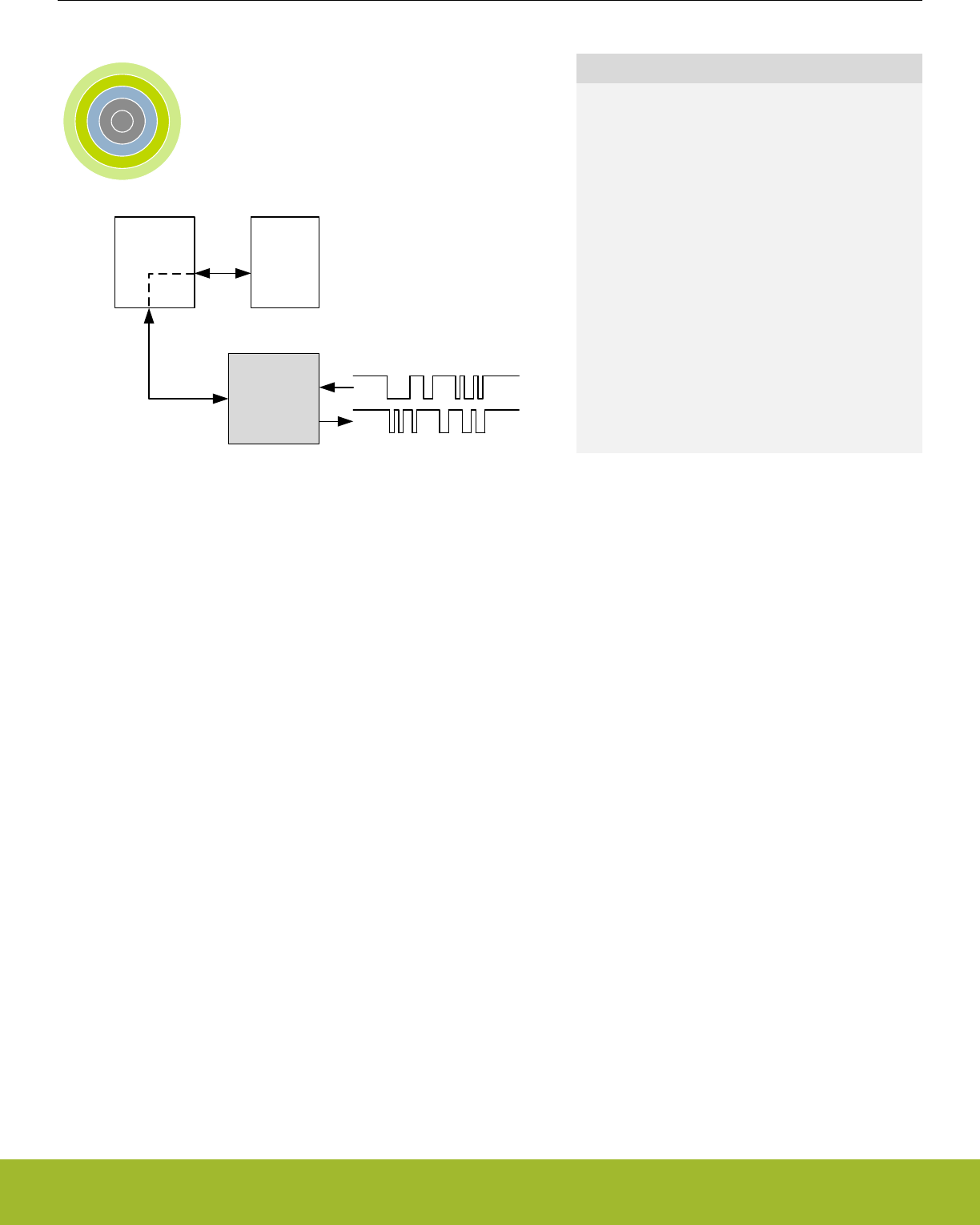
20. LEUART - Low Energy Universal Asynchronous Receiver/Transmitter
0 1 2 3 4
LEUART
RX
TX
DMA
controller
RAM
Quick Facts
What?
The LEUART provides full UART communication us-
ing a low frequency 32.768 kHz clock, and has spe-
cial features for communication without CPU inter-
vention.
Why?
It allows UART communication to be performed in
low energy modes, using only a few µA during active
communication and only 150 nA when waiting for in-
coming data.
How?
A low frequency clock signal allows communication
with less energy. Using DMA, the LEUART can
transmit and receive data with minimal CPU inter-
vention. Special UART-frames can be configured to
help control the data flow, further automating data
transmission.
20.1 Introduction
The unique Low Energy UART (LEUART) is a UART that allows two-way UART communication on a strict power budget. Only a 32.768
kHz clock is needed to allow UART communication up to 9600 baud.
Even when the system is in low energy mode EM2 Deep Sleep (with most core functionality turned off), the LEUART can wait for an
incoming UART frame while having an extremely low energy consumption. When a UART frame is completely received, the CPU can
quickly be woken up. Alternatively, multiple frames can be transferred via the Direct Memory Access (DMA) module into RAM memory
before waking up the CPU.
Received data can optionally be blocked until a configurable start frame is detected. A signal frame can be configured to generate an
interrupt indicating the end of a data transmission. The start frame and signal frame can be used in combination to handle higher level
communication protocols.
Similarly, data can be transmitted in EM2 Deep Sleep either on a frame-by-frame basis with data from the CPU or through use of the
DMA.
The LEUART includes all necessary hardware support to make asynchronous serial communication possible with minimal software
overhead and low energy consumption.
Reference Manual
LEUART - Low Energy Universal Asynchronous Receiver/Transmitter
silabs.com | Smart. Connected. Energy-friendly. Preliminary Rev. 0.5 | 637

20.2 Features
• Low energy asynchronous serial communications
•Full/half duplex communication
• Separate TX / RX enable
• Separate double buffered transmit buffer and receive buffer
• Programmable baud rate, generated as a fractional division of the LFBCLK
• Supports baud rates from 300 baud to 9600 baud
• Can use a high frequency clock source for even higher baud rates
• Configurable number of data bits: 8 or 9 (plus parity bit, if enabled)
• Configurable parity: off, even or odd
• HW parity bit generation and check
• Configurable number of stop bits, 1 or 2
• Capable of sleep-mode wake-up on received frame
• Either wake-up on any received byte or
• Wake up only on specified start and signal frames
• Supports transmission and reception in EM0 Active, EM1 Sleep and EM2 Deep Sleep with
• Full DMA support
• Specified start-frame can start reception automatically
• IrDA modulator (pulse generator, pulse extender)
• Multi-processor mode
• Loopback mode
• Half duplex communication
• Communication debugging
• PRS RX input
Reference Manual
LEUART - Low Energy Universal Asynchronous Receiver/Transmitter
silabs.com | Smart. Connected. Energy-friendly. Preliminary Rev. 0.5 | 638
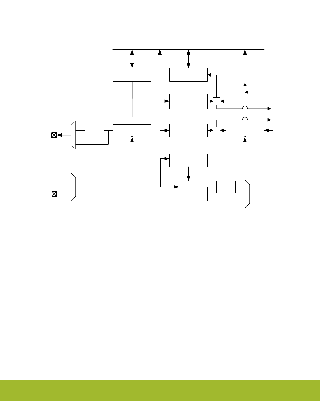
20.3 Functional Description
An overview of the LEUART module is shown in Figure 20.1 LEUART Overview on page 639.
TX Buffer
TX Shift Register
Signal frame interrupt
RX Buffer
RX Shift Register
LEUn_RX
UART Control
and status
Peripheral Bus
TX Baud rate
generator
RX Baud rate
generator
Start frame
(STARTFRAME)
RX Wakeup
SYNC
=
Pulse
extend
Pulse
gen
Signal frame
(SIGFRAME)
=Start frame interrupt
!RXBLOCK
LEUn_TX
Figure 20.1. LEUART Overview
Reference Manual
LEUART - Low Energy Universal Asynchronous Receiver/Transmitter
silabs.com | Smart. Connected. Energy-friendly. Preliminary Rev. 0.5 | 639
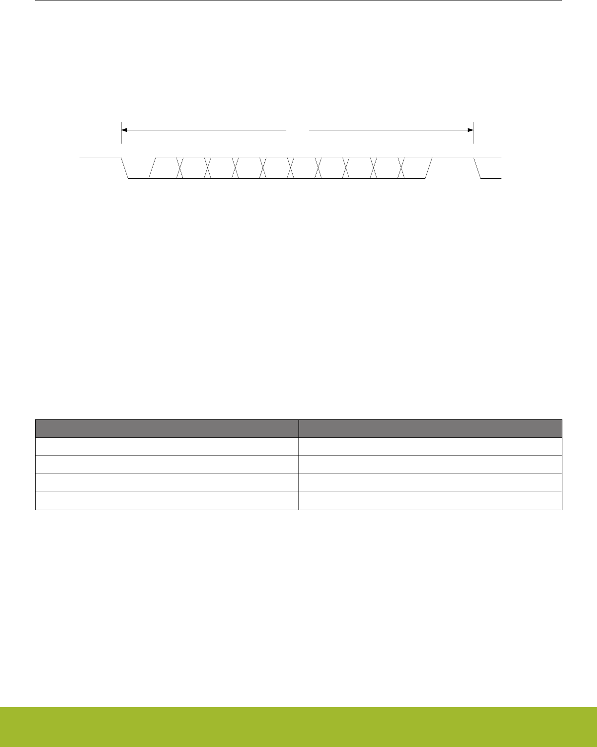
20.3.1 Frame Format
The frame format used by the LEUART consists of a set of data bits in addition to bits for synchronization and optionally a parity bit for
error checking. A frame starts with one start-bit (S), where the line is driven low for one bit-period. This signals the start of a frame, and
is used for synchronization. Following the start bit are 8 or 9 data bits and an optional parity bit. The data is transmitted with the least
significant bit first. Finally, a number of stop-bits, where the line is driven high, end the frame. The frame format is shown in Figure
20.2 LEUART Asynchronous Frame Format on page 640.
S 0 1 2 34 5 6 7 [8] [P] Stop
Start or idleStop or idle
Frame
Figure 20.2. LEUART Asynchronous Frame Format
The number of data bits in a frame is set by DATABITS in LEUARTn_CTRL, and the number of stop-bits is set by STOPBITS in
LEUARTn_CTRL. Whether or not a parity bit should be included, and whether it should be even or odd is defined by PARITY in
LEUARTn_CTRL. For communication to be possible, all parties of an asynchronous transfer must agree on the frame format being
used.
The frame format used by the LEUART can be inverted by setting INV in LEUARTn_CTRL. This affects the entire frame, resulting in a
low idle state, a high start-bit, inverted data and parity bits, and low stop-bits. INV should only be changed while the receiver is disabled.
20.3.1.1 Parity Bit Calculation and Handling
Hardware automatically inserts parity bits into outgoing frames and checks the parity bits of incoming frames. The possible parity
modes are defined in Table 20.1 LEUART Parity Bit on page 640. When even parity is chosen, a parity bit is inserted to make the
number of high bits (data + parity) even. If odd parity is chosen, the parity bit makes the total number of high bits odd. When parity bits
are disabled, which is the default configuration, the parity bit is omitted.
Table 20.1. LEUART Parity Bit
PARITY [1:0] Description
00 No parity (default)
01 Reserved
10 Even parity
11 Odd parity
See 20.3.5.4 Parity Error for more information on parity bit handling.
20.3.2 Clock Source
The LEUART clock source is selected by the LFB bit field the CMU_LFBCLKSEL register. The clock is prescaled by the LEUARTn
bitfield in the CMU_LFBPRESC0 register and enabled by the LEUARTn bit in the CMU_LFBCLKEN0. See Figure 12.2 CMU Overview -
Low Frequency Portion on page 292 for a diagram of the clocking structure.
To use this module, the LE interface clock must be enabled in CMU_HFBUSCLKEN0, in addition to the module clock.
Reference Manual
LEUART - Low Energy Universal Asynchronous Receiver/Transmitter
silabs.com | Smart. Connected. Energy-friendly. Preliminary Rev. 0.5 | 640

20.3.3 Clock Generation
The LEUART clock defines the transmission and reception data rate. The clock generator employs a fractional clock divider to allow
baud rates that are not attainable by integral division of the 32.768 kHz clock that drives the LEUART.
The clock divider used in the LEUART is a 14-bit value, with a 9-bit integral part and a 5-bit fractional part. The baud rate of the
LEUART is given by :
br = fLEUARTn / (1 + LEUARTn_CLKDIV / 256)
Figure 20.3. LEUART Baud Rate Equation
where fLEUARTn is the clock frequency supplied to the LEUART. The value of LEUARTn_CLKDIV thus defines the baud rate of the
LEUART. The integral part of the divider is right-aligned in the upper 24 bits of LEUARTn_CLKDIV and the fractional part is left-aligned
in the lower 8 bits. The divider is thus a 256th of LEUARTn_CLKDIV as seen in the equation.
As an example let us assume fLEUART = 22.5 kHz and the value of DIV in LEUARTn_CLKDIV is 0x0028 (LEUARTn_CLKDIV =
0x00000140). The baud rate = 22.5 kHz / (1 + 0x140 / 256) = 22.5 kHz / 2.25 = 10 kHz.
For a desired baud rate brDESIRED, LEUARTn_CLKDIV can be calculated by using:
LEUARTn_CLKDIV = 256 x (fLEUARTn/brDESIRED - 1)
Figure 20.4. LEUART CLKDIV Equation
It's important to note that this equation results in a 32bit value for the LEUARTn_CLKDIV register but only bits [16:3] are valid and all
others must be 0. For example if we have a 32 kHz clock and whish to achieve a baud rate of 10 kHz the equation above results in a
LEUARTn_CLKDIV value of 0x233. However, the actual value of the register will be 0x230 since bits [2:0] cannot be set. This limits the
best achievable acuracy. In this example the actual baud rate will be 32 kHz / (1+ 0x230 / 255) = 10.039 kHz instead of 32 kHz /
(1+ 0x233 / 255) = 10.002 kHz.
Table 20.2 LEUART Baud Rates on page 641 lists a set of desired baud rates and the closest baud rates reachable by the LEUART
with a 32.768 kHz clock source. It also shows the average baud rate error.
Table 20.2. LEUART Baud Rates
Desired baud rate LEUARTn_CLKDIV LEUARTn_CLKDIV/256 Actual baud rate Error [%]
300 27704 108,21875 300,0217 0.01
600 13728 53,625 599,8719 -0.02
1200 6736 26,3125 1199,744 -0.02
2400 3240 12,65625 2399,487 -0.02
4800 1488 5,8125 4809,982 0.21
9600 616 2,40625 9619,963 0.21
20.3.4 Data Transmission
Data transmission is initiated by writing data to the transmit buffer using one of the methods described in 20.3.4.1 Transmit Buffer Oper-
ation. When the transmit shift register is empty and ready for new data, a frame from the transmit buffer is loaded into the shift register,
and if the transmitter is enabled, transmission begins. When the frame has been transmitted, a new frame is loaded into the shift regis-
ter if available, and transmission continues. If the transmit buffer is empty, the transmitter goes to an idle state, waiting for a new frame
to become available. Transmission is enabled through the command register LEUARTn_CMD by setting TXEN, and disabled by setting
TXDIS. When the transmitter is disabled using TXDIS, any ongoing transmission is aborted, and any frame currently being transmitted
is discarded. When disabled, the TX output goes to an idle state, which by default is a high value. Whether or not the transmitter is
enabled at a given time can be read from TXENS in LEUARTn_STATUS. After a transmission, when there is no more data in the shift
register or transmit buffer, the TXC flag in LEUARTn_STATUS and the TXC interrupt flag in LEUARTn_IF are set, signaling that the
transmitter is idle. The TXC status flag is cleared when a new byte becomes available for transmission, but the TXC interrupt flag must
be cleared by software.
Reference Manual
LEUART - Low Energy Universal Asynchronous Receiver/Transmitter
silabs.com | Smart. Connected. Energy-friendly. Preliminary Rev. 0.5 | 641
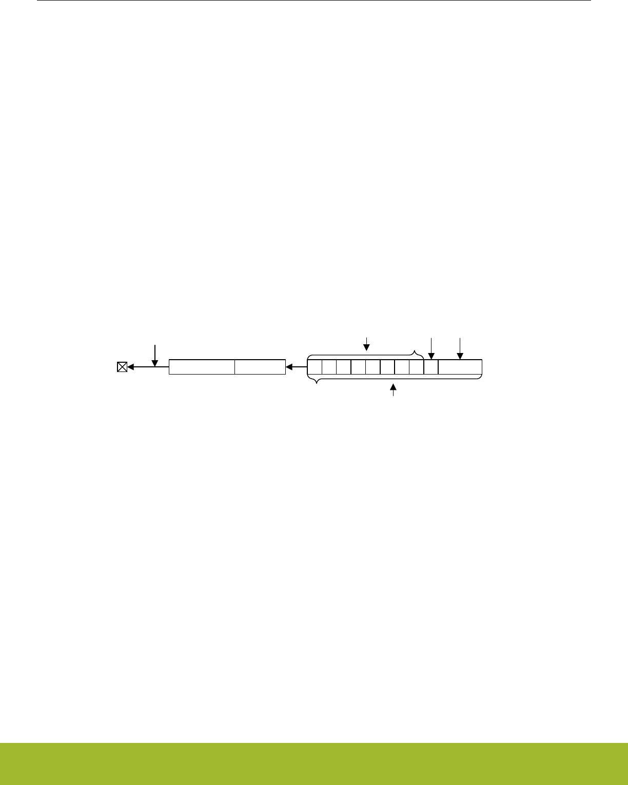
20.3.4.1 Transmit Buffer Operation
A frame can be loaded into the transmit buffer by writing to LEUARTn_TXDATA or LEUARTn_TXDATAX. Using LEUARTn_TXDATA
allows 8 bits to be written to the buffer. If 9 bit frames are used, the 9th bit will in that case be set to the value of BIT8DV in
LEUARTn_CTRL. To set the 9th bit directly and/or use transmission control, LEUARTn_TXDATAX must be used. When writing data to
the transmit buffer using LEUARTn_TXDATAX, the 9th bit written to LEUARTn_TXDATAX overrides the value in BIT8DV, and alone
defines the 9th bit that is transmitted if 9-bit frames are used.
If a write is attempted to the transmit buffer when it is not empty, the TXOF interrupt flag in LEUARTn_IF is set, indicating the overflow.
The data already in the buffer is in that case preserved, and no data is written.
In addition to the interrupt flag TXC in LEUARTn_IF and the status flag TXC in LEUARTn_STATUS which are set when the transmitter
becomes idle, TXBL in LEUARTn_STATUS and the TXBL interrupt flag in LEUARTn_IF are used to indicate the level of the transmit
buffer. Whenever the transmit buffer becomes empty, these flags are set high. Both the TXBL status flag and the TXBL interrupt flag are
cleared automatically when data is written to the transmit buffer.
There is also TXIDLE status in LEUART_STATUS which can be used to detect when the transmit state machine is in the idle state.
The transmit buffer, including the TX shift register can be cleared by setting command bit CLEARTX in LEUARTn_CMD. This will pre-
vent the LEUART from transmitting the data in the buffer and shift register, and will make them available for new data. Any frame cur-
rently being transmitted will not be aborted. Transmission of this frame will be completed. An overview of the operation of the transmitter
is shown in Figure 20.5 LEUART Transmitter Overview on page 642.
LEUn_TX Transmit shift register
TXENS
d0-d8 control d0 d2 d4 d6 d8d7d5d3d1 control
TXDATA
TXDATAX
BIT8DV
Transmit buffer
0
Figure 20.5. LEUART Transmitter Overview
20.3.4.2 Frame Transmission Control
The transmission control bits, which can be written using LEUARTn_TXDATAX, affect the transmission of the written frame. The follow-
ing options are available:
• Generate break: By setting TXBREAK, the output will be held low during the first stop-bit period to generate a framing error. A re-
ceiver that supports break detection detects this state, allowing it to be used e.g. for framing of larger data packets. The line is driven
high for one bit period before the next frame is transmitted so the next start condition can be identified correctly by the recipient.
Continuous breaks lasting longer than an UART frame are thus not supported by the LEUART. GPIO can be used for this. Note that
when AUTOTRI in LEUARTn_CTRL is used, the transmitter is not tristated before the high-bit after the break has been transmitted.
• Disable transmitter after transmission: If TXDISAT is set, the transmitter is disabled after the frame has been fully transmitted.
• Enable receiver after transmission: If RXENAT is set, the receiver is enabled after the frame has been fully transmitted. It is enabled
in time to detect a start-bit directly after the last stop-bit has been transmitted.
The transmission control bits in the LEUART cannot tristate the transmitter. This is performed automatically by hardware if AUTOTRI in
LEUARTn_CTRL is set. See 20.3.7 Half Duplex Communication for more information on half duplex operation.
Reference Manual
LEUART - Low Energy Universal Asynchronous Receiver/Transmitter
silabs.com | Smart. Connected. Energy-friendly. Preliminary Rev. 0.5 | 642
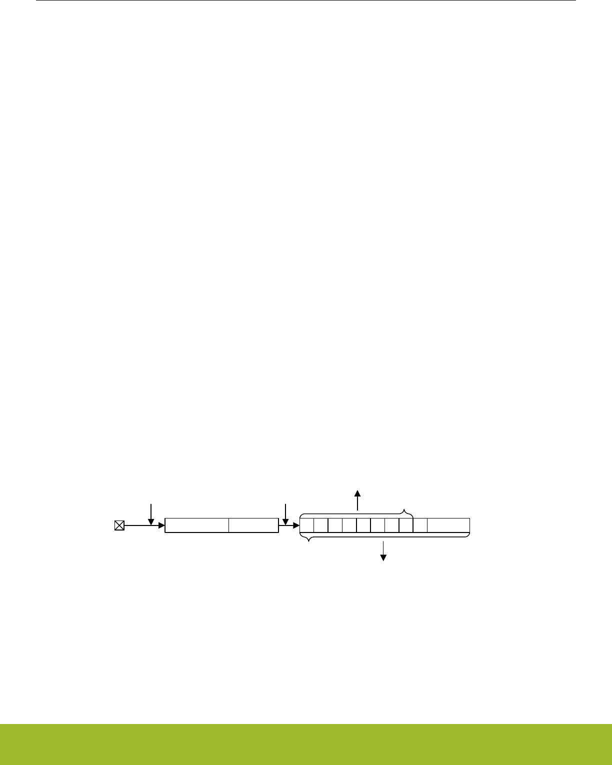
20.3.5 Data Reception
Data reception is enabled by setting RXEN in LEUARTn_CMD. When the receiver is enabled, it actively samples the input looking for a
transition from high to low indicating the start bit of a new frame. When a start bit is found, reception of the new frame begins if the
receive shift register is empty and ready for new data. When the frame has been received, it is pushed into the receive buffer, making
the shift register ready for another frame of data, and the receiver starts looking for another start bit. If the receive buffer is full, the
received frame remains in the shift register until more space in the receive buffer is available.
If an incoming frame is detected while both the receive buffer and the receive shift register are full, the data in the receive shift register
is overwritten, and the RXOF interrupt flag in LEUARTn_IF is set to indicate the buffer overflow.
The receiver can be disabled by setting the command bit RXDIS in LEUARTn_CMD. Any frame currently being received when the re-
ceiver is disabled is discarded. Whether or not the receiver is enabled at a given time can be read out from RXENS in LEUARTn_STA-
TUS.
The receive buffer,can be cleared by setting command bit CLEARRX in LEUARTn_CMD. This will make it avaliable for new data. Any
frame currently being received will not be aborted and will become the first received frame when complete.
20.3.5.1 Receive Buffer Operation
When data becomes available in the receive buffer, the RXDATAV flag in LEUARTn_STATUS and the RXDATAV interrupt flag in
LEUARTn_IF are set. Both the RXDATAV status flag and the RXDATAV interrupt flag are cleared by hardware when data is no longer
available, i.e. when data has been read out of the buffer.
Data can be read from receive buffer using either LEUARTn_RXDATA or LEUARTn_RXDATAX. LEUARTn_RXDATA gives access to
the 8 least significant bits of the received frame, while LEUARTn_RXDATAX must be used to get access to the 9th, most significant bit.
The LEUARTn_RXDATAX register also contains status information regarding the frame.
When a frame is read from the receive buffer using LEUARTn_RXDATA or LEUARTn_RXDATAX, the frame is removed from the buffer,
making room for a new one. If an attempt is done to read more frames from the buffer than what is available, the RXUF interrupt flag in
LEUARTn_IF is set to signal the underflow, and the data read from the buffer is undefined.
Frames can also be read from the receive buffer without removing the data by using LEUARTn_RXDATAXP, which gives access to the
frame in the buffer including control bits. Data read from this register when the receive buffer is empty is undefined. No underflow inter-
rupt is generated by a read using LEUARTn_RXDATAXP, i.e. the RXUF interrupt flag is never set as a result of reading from
LEUARTn_RXDATAXP.
An overview of the operation of the receiver is shown in Figure 20.6 LEUART Receiver Overview on page 643.
LEUn_RX Receive shift register
RXENS !RXBLOCK
d0-d8 status d0 d2 d4 d6 d8d7d5d3d1 status
RXDATA
RXDATAX
(RXDATAXP)
Receive buffer
Figure 20.6. LEUART Receiver Overview
Reference Manual
LEUART - Low Energy Universal Asynchronous Receiver/Transmitter
silabs.com | Smart. Connected. Energy-friendly. Preliminary Rev. 0.5 | 643

20.3.5.2 Blocking Incoming Data
When using hardware frame recognition, as detailed in 20.3.5.6 Programmable Start Frame, 20.3.5.7 Programmable Signal Frame, and
20.3.5.8 Multi-Processor Mode, it is necessary to be able to let the receiver sample incoming frames without passing the frames to
software by loading them into the receive buffer. This is accomplished by blocking incoming data.
Incoming data is blocked as long as RXBLOCK in LEUARTn_STATUS is set. When blocked, frames received by the receiver will not be
loaded into the receive buffer, and software is not notified by the RXDATAV bit in LEUARTn_STATUS or the RXDATAV interrupt flag in
LEUARTn_IF at their arrival. For data to be loaded into the receive buffer, RXBLOCK must be cleared in the instant a frame is fully
received by the receiver. RXBLOCK is set by setting RXBLOCKEN in LEUARTn_CMD and disabled by setting RXBLOCKDIS also in
LEUARTn_CMD. There are two exceptions where data is loaded into the receive buffer even when RXBLOCK is set. The first is when
an address frame is received when in operating in multi-processor mode as shown in 20.3.5.8 Multi-Processor Mode. The other case is
when receiving a start-frame when SFUBRX in LEUARTn_CTRL is set; see 20.3.5.6 Programmable Start Frame
Frames received containing framing or parity errors will not result in the FERR and PERR interrupt flags in LEUARTn_IF being set while
RXBLOCK is set. Hardware recognition is not applied to these erroneous frames, and they are silently discarded.
Note:
If a frame is received while RXBLOCK in LEUARTn_STATUS is cleared, but stays in the receive shift register because the receive buf-
fer is full, the received frame will be loaded into the receive buffer when space becomes available even if RXBLOCK is set at that time.
The overflow interrupt flag RXOF in LEUARTn_IF will be set if a frame in the receive shift register, waiting to be loaded into the receive
buffer is overwritten by an incoming frame even though RXBLOCK is set.
20.3.5.3 Data Sampling
The receiver samples each incoming bit as close as possible to the middle of the bit-period. Except for the start-bit, only a single sam-
ple is taken of each of the incoming bits.
The length of a bit-period is given by 1 + LEUARTn_CLKDIV/256, as a number of 32.768 kHz clock periods. Let the clock cycle where a
start-bit is first detected be given the index 0. The optimal sampling point for each bit in the UART frame is then given by the following
equation:
Sopt(n) = n (1 + LEUARTn_CLKDIV/256) + LEUARTn_CLKDIV/512
Figure 20.7. LEUART Optimal Sampling Point
where n is the bit-index.
Since samples are only done on the positive edges of the 32.768 kHz clock, the actual samples are performed on the closest positive
edge, i.e. the edge given by the following equation:
S(n) = floor(n x (1 + LEUARTn_CLKDIV/256) + LEUARTn_CLKDIV/512)
Figure 20.8. LEUART Actual Sampling Point
The sampling location will thus have jitter according to difference between Sopt and S. The start-bit is found at n=0, then follows the
data bits, any parity bit, and the stop bits.
If the value of the start-bit is found to be high, then the start-bit is discarded, and the receiver waits for a new start-bit.
20.3.5.4 Parity Error
When the parity bit is enabled, a parity check is automatically performed on incoming frames. When a parity error is detected in a
frame, the data parity error bit PERR in the frame is set, as well as the interrupt flag PERR. Frames with parity errors are loaded into
the receive buffer like regular frames.
PERR can be accessed by reading the frame from the receive buffer using the LEUARTn_RXDATAX register.
Reference Manual
LEUART - Low Energy Universal Asynchronous Receiver/Transmitter
silabs.com | Smart. Connected. Energy-friendly. Preliminary Rev. 0.5 | 644

20.3.5.5 Framing Error and Break Detection
A framing error is the result of a received frame where the stop bit was sampled to a value of 0. This can be the result of noise and
baud rate errors, but can also be the result of a break generated by the transmitter on purpose.
When a framing error is detected, the framing error bit FERR in the received frame is set. The interrupt flag FERR in LEUARTn_IF is
also set. Frames with framing errors are loaded into the receive buffer like regular frames.
FERR can be accessed by reading the frame from the receive buffer using the LEUARTn_RXDATAX or LEUARTn_RXDATAXP regis-
ters.
20.3.5.6 Programmable Start Frame
The LEUART can be configured to start receiving data when a special start frame is detected on the input. This can be useful when
operating in low energy modes, allowing other devices to gain the attention of the LEUART by transmitting a given frame.
When SFUBRX in LEUARTn_CTRL is set, an incoming frame matching the frame defined in LEUARTn_STARTFRAME will result in
RXBLOCK in LEUARTn_STATUS being cleared. This can be used to enable reception when a specified start frame is detected. If the
receiver is enabled and blocked, i.e. RXENS and RXBLOCK in LEUARTn_STATUS are set, the receiver will receive all incoming
frames, but unless an incoming frame is a start frame it will be discarded and not loaded into the receive buffer. When a start frame is
detected, the block is cleared, and frames received from that point, including the start frame, are loaded into the receive buffer.
An incoming start frame results in the STARTF interrupt flag in LEUARTn_IF being set, regardless of the value of SFUBRX in
LEUARTn_CTRL. This allows an interrupt to be made when the start frame is detected.
When 8 data-bit frame formats are used, only the 8 least significant bits of LEUARTn_STARTFRAME are compared to incoming
frames. The full length of LEUARTn_STARTFRAME is used when operating with frames consisting of 9 data bits.
Note:
The receiver must be enabled for start frames to be detected. In addition, a start frame with a parity error or framing error is not detec-
ted as a start frame.
20.3.5.7 Programmable Signal Frame
As well as the configurable start frame, a special signal frame can be specified. When a frame matching the frame defined in
LEUARTn_SIGFRAME is detected by the receiver, the SIGF interrupt flag in LEUARTn_IF is set. As for start frame detection, the re-
ceiver must be enabled for signal frames to be detected.
One use of the programmable signal frame is to signal the end of a multi-frame message transmitted to the LEUART. An interrupt will
then be triggered when the packet has been completely received, allowing software to process it. Used in conjunction with the program-
mable start frame and DMA, this makes it possible for the LEUART to automatically begin the reception of a packet on a specified start
frame, load the entire packet into memory, and give an interrupt when reception of a packet has completed. The device can thus wait
for data packets in EM2 Deep Sleep, and only be woken up when a packet has been completely received.
A signal frame with a parity error or framing error is not detected as a signal frame.
Reference Manual
LEUART - Low Energy Universal Asynchronous Receiver/Transmitter
silabs.com | Smart. Connected. Energy-friendly. Preliminary Rev. 0.5 | 645

20.3.5.8 Multi-Processor Mode
To simplify communication between multiple processors and maintain compatibility with the USART, the LEUART supports a multi-pro-
cessor mode. In this mode the 9th data bit in each frame is used to indicate whether the content of the remaining 8 bits is data or an
address.
When multi-processor mode is enabled, an incoming 9-bit frame with the 9th bit equal to the value of MPAB in LEUARTn_CTRL is
identified as an address frame. When an address frame is detected, the MPAF interrupt flag in LEUARTn_IF is set, and the address
frame is loaded into the receive register. This happens regardless of the value of RXBLOCK in LEUARTn_STATUS.
Multi-processor mode is enabled by setting MPM in LEUARTn_CTRL. The mode can be used in buses with multiple slaves, allowing
the slaves to be addressed using the special address frames. An addressed slave, which was previously blocking reception using
RXBLOCK, would then unblock reception, receive a message from the bus master, and then block reception again, waiting for the next
message. See the USART for a more detailed example.
Note:
The programmable start frame functionality can be used for automatic address matching, enabling reception on a correctly configured
incoming frame.
An address frame with a parity error or a framing error is not detected as an address frame. The Start, Signal, and address frames
should not be set to match the same frame since each of these uses separate synchronization to the peripherial clock domain.
20.3.6 Loopback
The LEUART receiver samples LEUn_RX by default, and the transmitter drives LEUn_TX by default. This is not the only configuration
however. When LOOPBK in LEUARTn_CTRL is set, the receiver is connected to the LEUn_TX pin as shown in Figure 20.9 LEUART
Local Loopback on page 646. This is useful for debugging, as the LEUART can receive the data it transmits, but it is also used to
allow the LEUART to read and write to the same pin, which is required for some half duplex communication modes. In this mode, the
LEUn_TX pin must be enabled as an output in the GPIO.
LEUART
RX LEUn_RX
TX LEUn_TX
LOOPBK = 0
µC
LEUART
RX LEUn_RX
TX LEUn_TX
LOOPBK = 1
µC
Figure 20.9. LEUART Local Loopback
20.3.7 Half Duplex Communication
When doing full duplex communication, two data links are provided, making it possible for data to be sent and received at the same
time. In half duplex mode, data is only sent in one direction at a time. There are several possible half duplex setups, as described in the
following sections.
Reference Manual
LEUART - Low Energy Universal Asynchronous Receiver/Transmitter
silabs.com | Smart. Connected. Energy-friendly. Preliminary Rev. 0.5 | 646
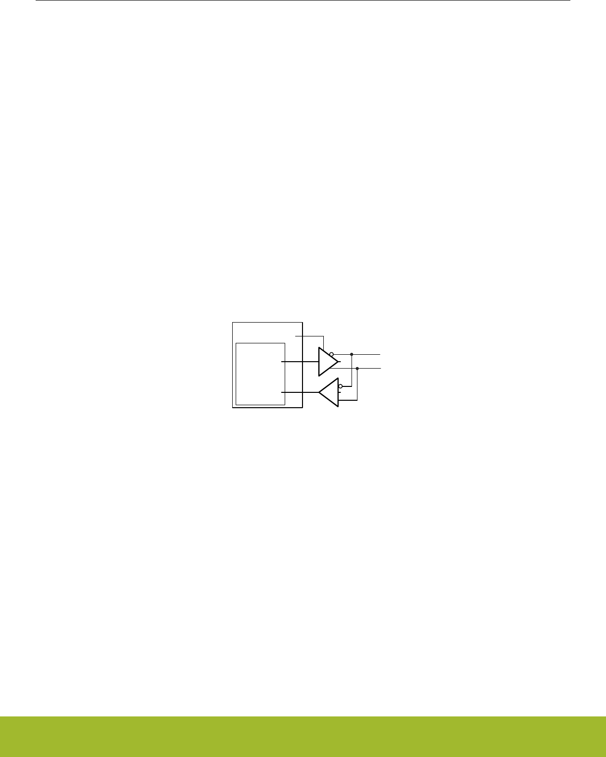
20.3.7.1 Single Data-link
In this setup, the LEUART both receives and transmits data on the same pin. This is enabled by setting LOOPBK in LEUARTn_CTRL,
which connects the receiver to the transmitter output. Because they are both connected to the same line, it is important that the
LEUART transmitter does not drive the line when receiving data, as this would corrupt the data on the line.
When communicating over a single data-link, the transmitter must thus be tristated whenever not transmitting data. If AUTOTRI in
LEUARTn_CTRL is set, the LEUART automatically tristates LEUn_TX whenever the transmitter is inactive. It is then the responsibility
of the software protocol to make sure the transmitter is not transmitting data whenever incoming data is expected.
The transmitter can also be tristated from software by configuring the GPIO pin as an input and disabling the LEUART output on
LEUn_TX.
Note:
Another way to tristate the transmitter is to enable wired-and or wired-or mode in GPIO. For wired-and mode, outputting a 1 will be the
same as tristating the output, and for wired-or mode, outputting a 0 will be the same as tristating the output. This can only be done on
buses with a pull-up or pull-down resistor respectively.
20.3.7.2 Single Data-link with External Driver
Some communication schemes, such as RS-485 rely on an external driver. Here, the driver has an extra input which enables it, and
instead of Tristating the transmitter when receiving data, the external driver must be disabled. The USART has hardware support for
automatically turning the driver on and off. When using the LEUART in such a setup, the driver must be controlled by a GPIO. Figure
20.10 LEUART Half Duplex Communication with External Driver on page 647 shows an example configuration using an external driv-
er.
LEUART
RX
TX
µC GPIO
Figure 20.10. LEUART Half Duplex Communication with External Driver
20.3.7.3 Two Data-links
Some limited devices only support half duplex communication even though two data links are available. In this case software is respon-
sible for making sure data is not transmitted when incoming data is expected.
20.3.8 Transmission Delay
By configuring TXDELAY in LEUARTn_CTRL, the transmitter can be forced to wait a number of bit-periods from when it is ready to
transmit data, to when it actually transmits the data. This delay is only applied to the first frame transmitted after the transmitter has
been idle. When transmitting frames back-to-back the delay is not introduced between the transmitted frames.
This is useful on half duplex buses, because the receiver always returns received frames to software during the first stop-bit. The bus
may still be driven for up to 3 bit periods, depending on the current frame format. Using the transmission delay, a transmission can be
started when a frame is received, and it is possible to make sure that the transmitter does not begin driving the output before the frame
on the bus is completely transmitted.
To route the UART TX and RX signals to a pin first select the desired pins using the RXLOC and TXLOC fields in the LEUARTn_ROU-
TELOC0 register. Then enable the connection using TXPEN and RXPEN in the LEUARTn_ROUTPEN register. See the device data-
sheet for mappings between UART locations (LOC0, LOC1, etc.) and device pins (PA0, PA1, etc.).
Reference Manual
LEUART - Low Energy Universal Asynchronous Receiver/Transmitter
silabs.com | Smart. Connected. Energy-friendly. Preliminary Rev. 0.5 | 647

20.3.9 PRS RX Input
In addition to receiving data on an external pin the LEUART can be configured to receive data directly from a PRS channel by setting
RX_PRS in LEUARTn_INPUT. The PRS channel used can be selected using RX_PRS_SEL in LEUARTn_INPUT. See the PRS chapter
for more details on the PRS block.
For example the output of a comparator could be routed to the LEUART through the PRS to allow for receiving a signal with low peak-
to-peak voltage or a significant DC offset.
20.3.10 DMA Support
The LEUART has full DMA support in energy modes EM0 Active – EM2 Deep Sleep. The DMA controller can write to the transmit buf-
fer using the registers LEUARTn_TXDATA and LEUARTn_TXDATAX, and it can read from receive buffer using the registers
LEUARTn_RXDATA and LEUARTn_RXDATAX. This enables single byte transfers and 9 bit data + control/status bits transfers both to
and from the LEUART. The DMA will start up the HFRCO and run from this when it is waken by the LEUART in EM2. The HFRCO is
disabled once the transaction is done.
A request for the DMA controller to read from the receive buffer can come from one of the following sources:
• Receive buffer full
A write request can come from one of the following sources:
• Transmit buffer and shift register empty. No data to send.
• Transmit buffer empty
In some cases, it may be sensible to temporarily stop DMA access to the LEUART when a parity or framing error has occurred. This is
enabled by setting ERRSDMA in LEUARTn_CTRL. When this bit is set, the DMA controller will not get requests from the receive buffer
if a framing error or parity error is detected in the received byte. The ERRSDMA bit applies only to the RX DMA.
When operating in EM2 Deep Sleep, the DMA controller must be powered up in order to perform the transfer. This is automatically
performed for read operations if RXDMAWU in LEUARTn_CTRL is set and for write operations if TXDMAWU in LEUARTn_CTRL is set.
To make sure the DMA controller still transfers bits to and from the LEUART in low energy modes, these bits must thus be configured
accordingly.
Note:
When RXDMAWU or TXDMAWU is set, the system will not be able to go to EM2 Deep Sleep/EM3 Stop before all related LEUART
DMA requests have been processed. This means that if RXDMAWU is set and the LEUART receives a frame, the system will not be
able to go to EM2 Deep Sleep/EM3 Stop before the frame has been read from the LEUART. In order for the system to go to EM2 during
the last byte transmission, LEUART_CTRL_TXDMAWU must be cleared in the DMA interrupt service routine. This is because TXBL will
be high during that last byte transfer.
Reference Manual
LEUART - Low Energy Universal Asynchronous Receiver/Transmitter
silabs.com | Smart. Connected. Energy-friendly. Preliminary Rev. 0.5 | 648

20.3.11 Pulse Generator/ Pulse Extender
The LEUART has an optional pulse generator for the transmitter output, and a pulse extender on the receiver input. These are enabled
by setting PULSEEN in LEUARTn_PULSECTRL, and with INV in LEUARTn_CTRL set, they will change the output/input format of the
LEUART from NRZ to RZI as shown in Figure 20.11 LEUART - NRZ vs. RZI on page 649.
S 0 1 2 34 5 6 7 PStop
IdleIdle
NRZ
RZI
Figure 20.11. LEUART - NRZ vs. RZI
If PULSEEN in LEUARTn_PULSECTRL is set while INV in LEUARTn_CTRL is cleared, the output waveform will look like RZI shown in
Figure 20.11 LEUART - NRZ vs. RZI on page 649, only inverted.
The width of the pulses from the pulse generator can be configured using PULSEW in LEUARTn_PULSECTRL. The generated pulse
width is PULSEW + 1 cycles of the 32.768 kHz clock, which makes pulse width from 31.25µs to 500µs possible.
Since the incoming signal is only sampled on positive clock edges, the width of the incoming pulses must be at least two 32.768 kHz
clock periods wide for reliable detection by the LEUART receiver. They must also be shorter than half a UART bit period.
At 2400 baud or lower, the pulse generator is able to generate RZI pulses compatible with the IrDA physical layer specification. The
external IrDA device must generate pulses of sufficient length for successful two-way communication.
PULSEFILT in the LEUARTn_PULSECTRL register can be used to extend the minimum receive pulse width from 2 clock periods to 3
clock periods.
20.3.11.1 Interrupts
The interrupts generated by the LEUART are combined into one interrupt vector. If LEUART interrupts are enabled, an interrupt will be
made if one or more of the interrupt flags in LEUARTn_IF and their corresponding bits in LEUART_IEN are set.
20.3.12 Register access
Since this module is a Low Energy Peripheral, and runs off a clock which is asynchronous to the HFCORECLK, special considerations
must be taken when accessing registers. Please refer to 4.3 Access to Low Energy Peripherals (Asynchronous Registers) for a descrip-
tion on how to perform register accesses to Low Energy Peripherals.
The registers LEUARTn_FREEZE and LEUARTn_SYNCBUSY are used for synchronization of this peripheral.
Reference Manual
LEUART - Low Energy Universal Asynchronous Receiver/Transmitter
silabs.com | Smart. Connected. Energy-friendly. Preliminary Rev. 0.5 | 649

20.4 Register Map
The offset register address is relative to the registers base address.
Offset Name Type Description
0x000 LEUARTn_CTRL RW Control Register
0x004 LEUARTn_CMD W1 Command Register
0x008 LEUARTn_STATUS RStatus Register
0x00C LEUARTn_CLKDIV RW Clock Control Register
0x010 LEUARTn_STARTFRAME RW Start Frame Register
0x014 LEUARTn_SIGFRAME RW Signal Frame Register
0x018 LEUARTn_RXDATAX R(a) Receive Buffer Data Extended Register
0x01C LEUARTn_RXDATA R(a) Receive Buffer Data Register
0x020 LEUARTn_RXDATAXP RReceive Buffer Data Extended Peek Register
0x024 LEUARTn_TXDATAX WTransmit Buffer Data Extended Register
0x028 LEUARTn_TXDATA WTransmit Buffer Data Register
0x02C LEUARTn_IF RInterrupt Flag Register
0x030 LEUARTn_IFS W1 Interrupt Flag Set Register
0x034 LEUARTn_IFC (R)W1 Interrupt Flag Clear Register
0x038 LEUARTn_IEN RW Interrupt Enable Register
0x03C LEUARTn_PULSECTRL RW Pulse Control Register
0x040 LEUARTn_FREEZE RW Freeze Register
0x044 LEUARTn_SYNCBUSY RSynchronization Busy Register
0x054 LEUARTn_ROUTEPEN RW I/O Routing Pin Enable Register
0x058 LEUARTn_ROUTELOC0 RW I/O Routing Location Register
0x064 LEUARTn_INPUT RW LEUART Input Register
Reference Manual
LEUART - Low Energy Universal Asynchronous Receiver/Transmitter
silabs.com | Smart. Connected. Energy-friendly. Preliminary Rev. 0.5 | 650

20.5 Register Description
20.5.1 LEUARTn_CTRL - Control Register (Async Reg)
For more information about asynchronous registers please see 4.3 Access to Low Energy Peripherals (Asynchronous Registers).
Offset Bit Position
0x000
31
30
29
28
27
26
25
24
23
22
21
20
19
18
17
16
15
14
13
12
11
10
9
8
7
6
5
4
3
2
1
0
Reset
0x0
0
0
0
0
0
0
0
0
0
0
0x0
0
0
Access
RW
RW
RW
RW
RW
RW
RW
RW
RW
RW
RW
RW
RW
RW
Name
TXDELAY
TXDMAWU
RXDMAWU
BIT8DV
MPAB
MPM
SFUBRX
LOOPBK
ERRSDMA
INV
STOPBITS
PARITY
DATABITS
AUTOTRI
Bit Name Reset Access Description
31:16 Reserved To ensure compatibility with future devices, always write bits to 0. More information in 1.2 Conven-
tions
15:14 TXDELAY 0x0 RW TX Delay Transmission
Configurable delay before new transfers. Frames sent back-to-back are not delayed.
Value Mode Description
0 NONE Frames are transmitted immediately
1 SINGLE Transmission of new frames are delayed by a single bit period
2 DOUBLE Transmission of new frames are delayed by two bit periods
3 TRIPLE Transmission of new frames are delayed by three bit periods
13 TXDMAWU 0 RW TX DMA Wakeup
Set to wake the DMA controller up when in EM2 and space is available in the transmit buffer.
Value Description
0 While in EM2, the DMA controller will not get requests about space be-
ing available in the transmit buffer
1 DMA is available in EM2 for the request about space available in the
transmit buffer
12 RXDMAWU 0 RW RX DMA Wakeup
Set to wake the DMA controller up when in EM2 and data is available in the receive buffer.
Value Description
0 While in EM2, the DMA controller will not get requests about data being
available in the receive buffer
1 DMA is available in EM2 for the request about data in the receive buffer
11 BIT8DV 0 RW Bit 8 Default Value
When 9-bit frames are transmitted, the default value of the 9th bit is given by BIT8DV. If TXDATA is used to write a frame,
then the value of BIT8DV is assigned to the 9th bit of the outgoing frame. If a frame is written with TXDATAX however, the
default value is overridden by the written value.
Reference Manual
LEUART - Low Energy Universal Asynchronous Receiver/Transmitter
silabs.com | Smart. Connected. Energy-friendly. Preliminary Rev. 0.5 | 651

Bit Name Reset Access Description
10 MPAB 0 RW Multi-Processor Address-Bit
Defines the value of the multi-processor address bit. An incoming frame with its 9th bit equal to the value of this bit marks
the frame as a multi-processor address frame.
9 MPM 0 RW Multi-Processor Mode
Set to enable multi-processor mode.
Value Description
0 The 9th bit of incoming frames have no special function
1 An incoming frame with the 9th bit equal to MPAB will be loaded into
the receive buffer regardless of RXBLOCK and will result in the MPAB
interrupt flag being set
8 SFUBRX 0 RW Start-Frame UnBlock RX
Clears RXBLOCK when the start-frame is found in the incoming data. The start-frame is loaded into the receive buffer.
Value Description
0 Detected start-frames have no effect on RXBLOCK
1 When a start-frame is detected, RXBLOCK is cleared and the start-
frame is loaded into the receive buffer
7LOOPBK 0 RW Loopback Enable
Set to connect receiver to LEUn_TX instead of LEUn_RX.
Value Description
0 The receiver is connected to and receives data from LEUn_RX
1 The receiver is connected to and receives data from LEUn_TX
6 ERRSDMA 0 RW Clear RX DMA On Error
When set, RX DMA requests will be cleared on framing and parity errors.
Value Description
0 Framing and parity errors have no effect on DMA requests from the
LEUART
1 RX DMA requests from the LEUART are disabled if a framing error or
parity error occurs.
5 INV 0 RW Invert Input And Output
Set to invert the output on LEUn_TX and input on LEUn_RX.
Value Description
0 A high value on the input/output is 1, and a low value is 0.
1 A low value on the input/output is 1, and a high value is 0.
4 STOPBITS 0 RW Stop-Bit Mode
Determines the number of stop-bits used. Only used when transmitting data. The receiver only verifies that one stop bit is
present.
Value Mode Description
Reference Manual
LEUART - Low Energy Universal Asynchronous Receiver/Transmitter
silabs.com | Smart. Connected. Energy-friendly. Preliminary Rev. 0.5 | 652

Bit Name Reset Access Description
0 ONE One stop-bit is transmitted with every frame
1 TWO Two stop-bits are transmitted with every frame
3:2 PARITY 0x0 RW Parity-Bit Mode
Determines whether parity bits are enabled, and whether even or odd parity should be used.
Value Mode Description
0 NONE Parity bits are not used
2 EVEN Even parity are used. Parity bits are automatically generated and
checked by hardware.
3 ODD Odd parity is used. Parity bits are automatically generated and checked
by hardware.
1 DATABITS 0 RW Data-Bit Mode
This register sets the number of data bits.
Value Mode Description
0 EIGHT Each frame contains 8 data bits
1 NINE Each frame contains 9 data bits
0 AUTOTRI 0 RW Automatic Transmitter Tristate
When set, LEUn_TX is tristated whenever the transmitter is inactive.
Value Description
0 LEUn_TX is held high when the transmitter is inactive. INV inverts the
inactive state.
1 LEUn_TX is tristated when the transmitter is inactive
Reference Manual
LEUART - Low Energy Universal Asynchronous Receiver/Transmitter
silabs.com | Smart. Connected. Energy-friendly. Preliminary Rev. 0.5 | 653

20.5.2 LEUARTn_CMD - Command Register (Async Reg)
For more information about asynchronous registers please see 4.3 Access to Low Energy Peripherals (Asynchronous Registers).
Offset Bit Position
0x004
31
30
29
28
27
26
25
24
23
22
21
20
19
18
17
16
15
14
13
12
11
10
9
8
7
6
5
4
3
2
1
0
Reset
0
0
0
0
0
0
0
0
Access
W1
W1
W1
W1
W1
W1
W1
W1
Name
CLEARRX
CLEARTX
RXBLOCKDIS
RXBLOCKEN
TXDIS
TXEN
RXDIS
RXEN
Bit Name Reset Access Description
31:8 Reserved To ensure compatibility with future devices, always write bits to 0. More information in 1.2 Conven-
tions
7 CLEARRX 0 W1 Clear RX
Set to clear receive buffer and the RX shift register.
6 CLEARTX 0 W1 Clear TX
Set to clear transmit buffer and the TX shift register.
5 RXBLOCKDIS 0 W1 Receiver Block Disable
Set to clear RXBLOCK, resulting in all incoming frames being loaded into the receive buffer.
4 RXBLOCKEN 0 W1 Receiver Block Enable
Set to set RXBLOCK, resulting in all incoming frames being discarded.
3 TXDIS 0 W1 Transmitter Disable
Set to disable transmission.
2 TXEN 0 W1 Transmitter Enable
Set to enable data transmission.
1 RXDIS 0 W1 Receiver Disable
Set to disable data reception. If a frame is under reception when the receiver is disabled, the incoming frame is discarded.
0 RXEN 0 W1 Receiver Enable
Set to activate data reception on LEUn_RX.
Reference Manual
LEUART - Low Energy Universal Asynchronous Receiver/Transmitter
silabs.com | Smart. Connected. Energy-friendly. Preliminary Rev. 0.5 | 654

20.5.3 LEUARTn_STATUS - Status Register
Offset Bit Position
0x008
31
30
29
28
27
26
25
24
23
22
21
20
19
18
17
16
15
14
13
12
11
10
9
8
7
6
5
4
3
2
1
0
Reset
1
0
1
0
0
0
0
Access
R
R
R
R
R
R
R
Name
TXIDLE
RXDATAV
TXBL
TXC
RXBLOCK
TXENS
RXENS
Bit Name Reset Access Description
31:7 Reserved To ensure compatibility with future devices, always write bits to 0. More information in 1.2 Conven-
tions
6 TXIDLE 1 R TX Idle
Set when TX is idle
5 RXDATAV 0 R RX Data Valid
Set when data is available in the receive buffer. Cleared when the receive buffer is empty.
4 TXBL 1 R TX Buffer Level
Indicates the level of the transmit buffer. Set when the transmit buffer is empty, and cleared when it is full.
3 TXC 0 R TX Complete
Set when a transmission has completed and no more data is available in the transmit buffer. Cleared when a new transmis-
sion starts.
2 RXBLOCK 0 R Block Incoming Data
When set, the receiver discards incoming frames. An incoming frame will not be loaded into the receive buffer if this bit is
set at the instant the frame has been completely received.
1 TXENS 0 R Transmitter Enable Status
Set when the transmitter is enabled.
0 RXENS 0 R Receiver Enable Status
Set when the receiver is enabled. The receiver must be enabled for start frames, signal frames, and multi-processor ad-
dress bit detection.
Reference Manual
LEUART - Low Energy Universal Asynchronous Receiver/Transmitter
silabs.com | Smart. Connected. Energy-friendly. Preliminary Rev. 0.5 | 655

20.5.4 LEUARTn_CLKDIV - Clock Control Register (Async Reg)
For more information about asynchronous registers please see 4.3 Access to Low Energy Peripherals (Asynchronous Registers).
Offset Bit Position
0x00C
31
30
29
28
27
26
25
24
23
22
21
20
19
18
17
16
15
14
13
12
11
10
9
8
7
6
5
4
3
2
1
0
Reset
0x0000
Access
RW
Name
DIV
Bit Name Reset Access Description
31:17 Reserved To ensure compatibility with future devices, always write bits to 0. More information in 1.2 Conven-
tions
16:3 DIV 0x0000 RW Fractional Clock Divider
Specifies the fractional clock divider for the LEUART. Bits [7:3] are the fractional part and bits [16:8] are the integer part.
The total divider is ([16:8] + [7:3]/32). To make the math easier the total divider can also be calculated as '([16:8] + [7:0]/
256) where bits [0:2] will always be 0.
2:0 Reserved To ensure compatibility with future devices, always write bits to 0. More information in 1.2 Conven-
tions
20.5.5 LEUARTn_STARTFRAME - Start Frame Register (Async Reg)
For more information about asynchronous registers please see 4.3 Access to Low Energy Peripherals (Asynchronous Registers).
Offset Bit Position
0x010
31
30
29
28
27
26
25
24
23
22
21
20
19
18
17
16
15
14
13
12
11
10
9
8
7
6
5
4
3
2
1
0
Reset
0x000
Access
RW
Name
STARTFRAME
Bit Name Reset Access Description
31:9 Reserved To ensure compatibility with future devices, always write bits to 0. More information in 1.2 Conven-
tions
8:0 STARTFRAME 0x000 RW Start Frame
When a frame matching STARTFRAME is detected by the receiver, STARTF interrupt flag is set, and if SFUBRX is set,
RXBLOCK is cleared. The start-frame is be loaded into the RX buffer.
Reference Manual
LEUART - Low Energy Universal Asynchronous Receiver/Transmitter
silabs.com | Smart. Connected. Energy-friendly. Preliminary Rev. 0.5 | 656

20.5.6 LEUARTn_SIGFRAME - Signal Frame Register (Async Reg)
For more information about asynchronous registers please see 4.3 Access to Low Energy Peripherals (Asynchronous Registers).
Offset Bit Position
0x014
31
30
29
28
27
26
25
24
23
22
21
20
19
18
17
16
15
14
13
12
11
10
9
8
7
6
5
4
3
2
1
0
Reset
0x000
Access
RW
Name
SIGFRAME
Bit Name Reset Access Description
31:9 Reserved To ensure compatibility with future devices, always write bits to 0. More information in 1.2 Conven-
tions
8:0 SIGFRAME 0x000 RW Signal Frame
When a frame matching SIGFRAME is detected by the receiver, SIGF interrupt flag is set.
20.5.7 LEUARTn_RXDATAX - Receive Buffer Data Extended Register (Actionable Reads)
Offset Bit Position
0x018
31
30
29
28
27
26
25
24
23
22
21
20
19
18
17
16
15
14
13
12
11
10
9
8
7
6
5
4
3
2
1
0
Reset
0
0
0x000
Access
R
R
R
Name
FERR
PERR
RXDATA
Bit Name Reset Access Description
31:16 Reserved To ensure compatibility with future devices, always write bits to 0. More information in 1.2 Conven-
tions
15 FERR 0 R Receive Data Framing Error
Set if data in buffer has a framing error. Can be the result of a break condition.
14 PERR 0 R Receive Data Parity Error
Set if data in buffer has a parity error.
13:9 Reserved To ensure compatibility with future devices, always write bits to 0. More information in 1.2 Conven-
tions
8:0 RXDATA 0x000 R RX Data
Use this register to access data read from the LEUART. Buffer is cleared on read access.
Reference Manual
LEUART - Low Energy Universal Asynchronous Receiver/Transmitter
silabs.com | Smart. Connected. Energy-friendly. Preliminary Rev. 0.5 | 657

20.5.8 LEUARTn_RXDATA - Receive Buffer Data Register (Actionable Reads)
Offset Bit Position
0x01C
31
30
29
28
27
26
25
24
23
22
21
20
19
18
17
16
15
14
13
12
11
10
9
8
7
6
5
4
3
2
1
0
Reset
0x00
Access
R
Name
RXDATA
Bit Name Reset Access Description
31:8 Reserved To ensure compatibility with future devices, always write bits to 0. More information in 1.2 Conven-
tions
7:0 RXDATA 0x00 R RX Data
Use this register to access data read from LEUART. Buffer is cleared on read access. Only the 8 LSB can be read using
this register.
20.5.9 LEUARTn_RXDATAXP - Receive Buffer Data Extended Peek Register
Offset Bit Position
0x020
31
30
29
28
27
26
25
24
23
22
21
20
19
18
17
16
15
14
13
12
11
10
9
8
7
6
5
4
3
2
1
0
Reset
0
0
0x000
Access
R
R
R
Name
FERRP
PERRP
RXDATAP
Bit Name Reset Access Description
31:16 Reserved To ensure compatibility with future devices, always write bits to 0. More information in 1.2 Conven-
tions
15 FERRP 0 R Receive Data Framing Error Peek
Set if data in buffer has a framing error. Can be the result of a break condition.
14 PERRP 0 R Receive Data Parity Error Peek
Set if data in buffer has a parity error.
13:9 Reserved To ensure compatibility with future devices, always write bits to 0. More information in 1.2 Conven-
tions
8:0 RXDATAP 0x000 R RX Data Peek
Use this register to access data read from the LEUART.
Reference Manual
LEUART - Low Energy Universal Asynchronous Receiver/Transmitter
silabs.com | Smart. Connected. Energy-friendly. Preliminary Rev. 0.5 | 658

20.5.10 LEUARTn_TXDATAX - Transmit Buffer Data Extended Register (Async Reg)
For more information about asynchronous registers please see 4.3 Access to Low Energy Peripherals (Asynchronous Registers).
Offset Bit Position
0x024
31
30
29
28
27
26
25
24
23
22
21
20
19
18
17
16
15
14
13
12
11
10
9
8
7
6
5
4
3
2
1
0
Reset
0
0
0
0x000
Access
W
W
W
W
Name
RXENAT
TXDISAT
TXBREAK
TXDATA
Bit Name Reset Access Description
31:16 Reserved To ensure compatibility with future devices, always write bits to 0. More information in 1.2 Conven-
tions
15 RXENAT 0 W Enable RX After Transmission
Set to enable reception after transmission.
Value Description
0 The receiver is not enabled after the frame has been transmitted
1 The receiver is enabled (setting RXENS) after the frame has been
transmitted
14 TXDISAT 0 W Disable TX After Transmission
Set to disable transmitter directly after transmission has competed.
Value Description
0 The transmitter is not disabled after the frame has been transmitted
1 The transmitter is disabled (clearing TXENS) after the frame has been
transmitted
13 TXBREAK 0 W Transmit Data As Break
Set to send data as a break. Recipient will see a framing error or a break condition depending on its configuration and the
value of TXDATA.
Value Description
0 The specified number of stop-bits are transmitted
1 Instead of the ordinary stop-bits, 0 is transmitted to generate a break. A
single stop-bit is generated after the break to allow the receiver to de-
tect the start of the next frame
12:9 Reserved To ensure compatibility with future devices, always write bits to 0. More information in 1.2 Conven-
tions
8:0 TXDATA 0x000 W TX Data
Use this register to write data to the LEUART. If the transmitter is enabled, a transfer will be initiated at the first opportunity.
Reference Manual
LEUART - Low Energy Universal Asynchronous Receiver/Transmitter
silabs.com | Smart. Connected. Energy-friendly. Preliminary Rev. 0.5 | 659

20.5.11 LEUARTn_TXDATA - Transmit Buffer Data Register (Async Reg)
For more information about asynchronous registers please see 4.3 Access to Low Energy Peripherals (Asynchronous Registers).
Offset Bit Position
0x028
31
30
29
28
27
26
25
24
23
22
21
20
19
18
17
16
15
14
13
12
11
10
9
8
7
6
5
4
3
2
1
0
Reset
0x00
Access
W
Name
TXDATA
Bit Name Reset Access Description
31:8 Reserved To ensure compatibility with future devices, always write bits to 0. More information in 1.2 Conven-
tions
7:0 TXDATA 0x00 W TX Data
This frame will be added to the transmit buffer. Only 8 LSB can be written using this register. 9th bit and control bits will be
cleared.
Reference Manual
LEUART - Low Energy Universal Asynchronous Receiver/Transmitter
silabs.com | Smart. Connected. Energy-friendly. Preliminary Rev. 0.5 | 660

20.5.12 LEUARTn_IF - Interrupt Flag Register
Offset Bit Position
0x02C
31
30
29
28
27
26
25
24
23
22
21
20
19
18
17
16
15
14
13
12
11
10
9
8
7
6
5
4
3
2
1
0
Reset
0
0
0
0
0
0
0
0
0
1
0
Access
R
R
R
R
R
R
R
R
R
R
R
Name
SIGF
STARTF
MPAF
FERR
PERR
TXOF
RXUF
RXOF
RXDATAV
TXBL
TXC
Bit Name Reset Access Description
31:11 Reserved To ensure compatibility with future devices, always write bits to 0. More information in 1.2 Conven-
tions
10 SIGF 0 R Signal Frame Interrupt Flag
Set when a signal frame is detected. MPA, START, and SIGNAL should not be set to match the same frame since they use
different synchronizers.
9STARTF 0 R Start Frame Interrupt Flag
Set when a start frame is detected. MPA, START, and SIGNAL should not be set to match the same frame since they use
different synchronizers.
8MPAF 0 R Multi-Processor Address Frame Interrupt Flag
Set when a multi-processor address frame is detected. MPA, START, and SIGNAL should not be set to match the same
frame since they use different synchronizers.
7FERR 0 R Framing Error Interrupt Flag
Set when a frame with a framing error is received while RXBLOCK is cleared.
6 PERR 0 R Parity Error Interrupt Flag
Set when a frame with a parity error is received while RXBLOCK is cleared.
5 TXOF 0 R TX Overflow Interrupt Flag
Set when a write is done to the transmit buffer while it is full. The data already in the transmit buffer is preserved.
4 RXUF 0 R RX Underflow Interrupt Flag
Set when trying to read from the receive buffer when it is empty.
3 RXOF 0 R RX Overflow Interrupt Flag
Set when data is incoming while the receive shift register is full. The data previously in shift register is overwritten by the
new data.
2 RXDATAV 0 R RX Data Valid Interrupt Flag
Set when data becomes available in the receive buffer.
1 TXBL 1 R TX Buffer Level Interrupt Flag
Set when space becomes available in the transmit buffer for a new frame.
0 TXC 0 R TX Complete Interrupt Flag
Set after a transmission when both the TX buffer and shift register are empty.
Reference Manual
LEUART - Low Energy Universal Asynchronous Receiver/Transmitter
silabs.com | Smart. Connected. Energy-friendly. Preliminary Rev. 0.5 | 661

20.5.13 LEUARTn_IFS - Interrupt Flag Set Register
Offset Bit Position
0x030
31
30
29
28
27
26
25
24
23
22
21
20
19
18
17
16
15
14
13
12
11
10
9
8
7
6
5
4
3
2
1
0
Reset
0
0
0
0
0
0
0
0
0
Access
W1
W1
W1
W1
W1
W1
W1
W1
W1
Name
SIGF
STARTF
MPAF
FERR
PERR
TXOF
RXUF
RXOF
TXC
Bit Name Reset Access Description
31:11 Reserved To ensure compatibility with future devices, always write bits to 0. More information in 1.2 Conven-
tions
10 SIGF 0 W1 Set SIGF Interrupt Flag
Write 1 to set the SIGF interrupt flag
9 STARTF 0 W1 Set STARTF Interrupt Flag
Write 1 to set the STARTF interrupt flag
8 MPAF 0 W1 Set MPAF Interrupt Flag
Write 1 to set the MPAF interrupt flag
7 FERR 0 W1 Set FERR Interrupt Flag
Write 1 to set the FERR interrupt flag
6 PERR 0 W1 Set PERR Interrupt Flag
Write 1 to set the PERR interrupt flag
5 TXOF 0 W1 Set TXOF Interrupt Flag
Write 1 to set the TXOF interrupt flag
4 RXUF 0 W1 Set RXUF Interrupt Flag
Write 1 to set the RXUF interrupt flag
3 RXOF 0 W1 Set RXOF Interrupt Flag
Write 1 to set the RXOF interrupt flag
2:1 Reserved To ensure compatibility with future devices, always write bits to 0. More information in 1.2 Conven-
tions
0 TXC 0 W1 Set TXC Interrupt Flag
Write 1 to set the TXC interrupt flag
Reference Manual
LEUART - Low Energy Universal Asynchronous Receiver/Transmitter
silabs.com | Smart. Connected. Energy-friendly. Preliminary Rev. 0.5 | 662

20.5.14 LEUARTn_IFC - Interrupt Flag Clear Register
Offset Bit Position
0x034
31
30
29
28
27
26
25
24
23
22
21
20
19
18
17
16
15
14
13
12
11
10
9
8
7
6
5
4
3
2
1
0
Reset
0
0
0
0
0
0
0
0
0
Access
(R)W1
(R)W1
(R)W1
(R)W1
(R)W1
(R)W1
(R)W1
(R)W1
(R)W1
Name
SIGF
STARTF
MPAF
FERR
PERR
TXOF
RXUF
RXOF
TXC
Bit Name Reset Access Description
31:11 Reserved To ensure compatibility with future devices, always write bits to 0. More information in 1.2 Conven-
tions
10 SIGF 0 (R)W1 Clear SIGF Interrupt Flag
Write 1 to clear the SIGF interrupt flag. Reading returns the value of the IF and clears the corresponding interrupt flags
(This feature must be enabled globally in MSC.).
9 STARTF 0 (R)W1 Clear STARTF Interrupt Flag
Write 1 to clear the STARTF interrupt flag. Reading returns the value of the IF and clears the corresponding interrupt flags
(This feature must be enabled globally in MSC.).
8 MPAF 0 (R)W1 Clear MPAF Interrupt Flag
Write 1 to clear the MPAF interrupt flag. Reading returns the value of the IF and clears the corresponding interrupt flags
(This feature must be enabled globally in MSC.).
7 FERR 0 (R)W1 Clear FERR Interrupt Flag
Write 1 to clear the FERR interrupt flag. Reading returns the value of the IF and clears the corresponding interrupt flags
(This feature must be enabled globally in MSC.).
6 PERR 0 (R)W1 Clear PERR Interrupt Flag
Write 1 to clear the PERR interrupt flag. Reading returns the value of the IF and clears the corresponding interrupt flags
(This feature must be enabled globally in MSC.).
5 TXOF 0 (R)W1 Clear TXOF Interrupt Flag
Write 1 to clear the TXOF interrupt flag. Reading returns the value of the IF and clears the corresponding interrupt flags
(This feature must be enabled globally in MSC.).
4 RXUF 0 (R)W1 Clear RXUF Interrupt Flag
Write 1 to clear the RXUF interrupt flag. Reading returns the value of the IF and clears the corresponding interrupt flags
(This feature must be enabled globally in MSC.).
3 RXOF 0 (R)W1 Clear RXOF Interrupt Flag
Write 1 to clear the RXOF interrupt flag. Reading returns the value of the IF and clears the corresponding interrupt flags
(This feature must be enabled globally in MSC.).
2:1 Reserved To ensure compatibility with future devices, always write bits to 0. More information in 1.2 Conven-
tions
0 TXC 0 (R)W1 Clear TXC Interrupt Flag
Write 1 to clear the TXC interrupt flag. Reading returns the value of the IF and clears the corresponding interrupt flags (This
feature must be enabled globally in MSC.).
Reference Manual
LEUART - Low Energy Universal Asynchronous Receiver/Transmitter
silabs.com | Smart. Connected. Energy-friendly. Preliminary Rev. 0.5 | 663

20.5.15 LEUARTn_IEN - Interrupt Enable Register
Offset Bit Position
0x038
31
30
29
28
27
26
25
24
23
22
21
20
19
18
17
16
15
14
13
12
11
10
9
8
7
6
5
4
3
2
1
0
Reset
0
0
0
0
0
0
0
0
0
0
0
Access
RW
RW
RW
RW
RW
RW
RW
RW
RW
RW
RW
Name
SIGF
STARTF
MPAF
FERR
PERR
TXOF
RXUF
RXOF
RXDATAV
TXBL
TXC
Bit Name Reset Access Description
31:11 Reserved To ensure compatibility with future devices, always write bits to 0. More information in 1.2 Conven-
tions
10 SIGF 0 RW SIGF Interrupt Enable
Enable/disable the SIGF interrupt
9 STARTF 0 RW STARTF Interrupt Enable
Enable/disable the STARTF interrupt
8 MPAF 0 RW MPAF Interrupt Enable
Enable/disable the MPAF interrupt
7 FERR 0 RW FERR Interrupt Enable
Enable/disable the FERR interrupt
6 PERR 0 RW PERR Interrupt Enable
Enable/disable the PERR interrupt
5 TXOF 0 RW TXOF Interrupt Enable
Enable/disable the TXOF interrupt
4 RXUF 0 RW RXUF Interrupt Enable
Enable/disable the RXUF interrupt
3 RXOF 0 RW RXOF Interrupt Enable
Enable/disable the RXOF interrupt
2 RXDATAV 0 RW RXDATAV Interrupt Enable
Enable/disable the RXDATAV interrupt
1 TXBL 0 RW TXBL Interrupt Enable
Enable/disable the TXBL interrupt
0 TXC 0 RW TXC Interrupt Enable
Enable/disable the TXC interrupt
Reference Manual
LEUART - Low Energy Universal Asynchronous Receiver/Transmitter
silabs.com | Smart. Connected. Energy-friendly. Preliminary Rev. 0.5 | 664

20.5.16 LEUARTn_PULSECTRL - Pulse Control Register (Async Reg)
For more information about asynchronous registers please see 4.3 Access to Low Energy Peripherals (Asynchronous Registers).
Offset Bit Position
0x03C
31
30
29
28
27
26
25
24
23
22
21
20
19
18
17
16
15
14
13
12
11
10
9
8
7
6
5
4
3
2
1
0
Reset
0
0
0x0
Access
RW
RW
RW
Name
PULSEFILT
PULSEEN
PULSEW
Bit Name Reset Access Description
31:6 Reserved To ensure compatibility with future devices, always write bits to 0. More information in 1.2 Conven-
tions
5 PULSEFILT 0 RW Pulse Filter
Enable a one-cycle pulse filter for pulse extender
Value Description
0 Filter is disabled. Pulses must be at least 2 cycles long for reliable de-
tection.
1 Filter is enabled. Pulses must be at least 3 cycles long for reliable de-
tection.
4 PULSEEN 0 RW Pulse Generator/Extender Enable
Filter LEUART output through pulse generator and the LEUART input through the pulse extender.
3:0 PULSEW 0x0 RW Pulse Width
Configure the pulse width of the pulse generator as a number of 32.768 kHz clock cycles.
Reference Manual
LEUART - Low Energy Universal Asynchronous Receiver/Transmitter
silabs.com | Smart. Connected. Energy-friendly. Preliminary Rev. 0.5 | 665

20.5.17 LEUARTn_FREEZE - Freeze Register
Offset Bit Position
0x040
31
30
29
28
27
26
25
24
23
22
21
20
19
18
17
16
15
14
13
12
11
10
9
8
7
6
5
4
3
2
1
0
Reset
0
Access
RW
Name
REGFREEZE
Bit Name Reset Access Description
31:1 Reserved To ensure compatibility with future devices, always write bits to 0. More information in 1.2 Conven-
tions
0 REGFREEZE 0 RW Register Update Freeze
When set, the update of the LEUART logic from registers is postponed until this bit is cleared. Use this bit to update several
registers simultaneously.
Value Mode Description
0 UPDATE Each write access to a LEUART register is updated into the Low Fre-
quency domain as soon as possible.
1 FREEZE The LEUART is not updated with the new written value.
Reference Manual
LEUART - Low Energy Universal Asynchronous Receiver/Transmitter
silabs.com | Smart. Connected. Energy-friendly. Preliminary Rev. 0.5 | 666

20.5.18 LEUARTn_SYNCBUSY - Synchronization Busy Register
Offset Bit Position
0x044
31
30
29
28
27
26
25
24
23
22
21
20
19
18
17
16
15
14
13
12
11
10
9
8
7
6
5
4
3
2
1
0
Reset
0
0
0
0
0
0
0
0
Access
R
R
R
R
R
R
R
R
Name
PULSECTRL
TXDATA
TXDATAX
SIGFRAME
STARTFRAME
CLKDIV
CMD
CTRL
Bit Name Reset Access Description
31:8 Reserved To ensure compatibility with future devices, always write bits to 0. More information in 1.2 Conven-
tions
7 PULSECTRL 0 R PULSECTRL Register Busy
Set when the value written to PULSECTRL is being synchronized.
6 TXDATA 0 R TXDATA Register Busy
Set when the value written to TXDATA is being synchronized.
5 TXDATAX 0 R TXDATAX Register Busy
Set when the value written to TXDATAX is being synchronized.
4 SIGFRAME 0 R SIGFRAME Register Busy
Set when the value written to SIGFRAME is being synchronized.
3 STARTFRAME 0 R STARTFRAME Register Busy
Set when the value written to STARTFRAME is being synchronized.
2 CLKDIV 0 R CLKDIV Register Busy
Set when the value written to CLKDIV is being synchronized.
1 CMD 0 R CMD Register Busy
Set when the value written to CMD is being synchronized.
0 CTRL 0 R CTRL Register Busy
Set when the value written to CTRL is being synchronized.
Reference Manual
LEUART - Low Energy Universal Asynchronous Receiver/Transmitter
silabs.com | Smart. Connected. Energy-friendly. Preliminary Rev. 0.5 | 667

20.5.19 LEUARTn_ROUTEPEN - I/O Routing Pin Enable Register
Offset Bit Position
0x054
31
30
29
28
27
26
25
24
23
22
21
20
19
18
17
16
15
14
13
12
11
10
9
8
7
6
5
4
3
2
1
0
Reset
0
0
Access
RW
RW
Name
TXPEN
RXPEN
Bit Name Reset Access Description
31:2 Reserved To ensure compatibility with future devices, always write bits to 0. More information in 1.2 Conven-
tions
1 TXPEN 0 RW TX Pin Enable
When set, the TX pin of the LEUART is enabled.
Value Description
0 The LEUn_TX pin is disabled
1 The LEUn_TX pin is enabled
0 RXPEN 0 RW RX Pin Enable
When set, the RX pin of the LEUART is enabled.
Value Description
0 The LEUn_RX pin is disabled
1 The LEUn_RX pin is enabled
Reference Manual
LEUART - Low Energy Universal Asynchronous Receiver/Transmitter
silabs.com | Smart. Connected. Energy-friendly. Preliminary Rev. 0.5 | 668

20.5.20 LEUARTn_ROUTELOC0 - I/O Routing Location Register
Offset Bit Position
0x058
31
30
29
28
27
26
25
24
23
22
21
20
19
18
17
16
15
14
13
12
11
10
9
8
7
6
5
4
3
2
1
0
Reset
0x00
0x00
Access
RW
RW
Name
TXLOC
RXLOC
Bit Name Reset Access Description
31:14 Reserved To ensure compatibility with future devices, always write bits to 0. More information in 1.2 Conven-
tions
13:8 TXLOC 0x00 RW I/O Location
Decides the location of the LEUART TX pin. See the device datasheet for the mapping between location and physical pins.
Value Mode Description
0 LOC0 Location 0
1 LOC1 Location 1
2 LOC2 Location 2
3 LOC3 Location 3
4 LOC4 Location 4
5 LOC5 Location 5
6 LOC6 Location 6
7 LOC7 Location 7
8 LOC8 Location 8
9 LOC9 Location 9
10 LOC10 Location 10
11 LOC11 Location 11
12 LOC12 Location 12
13 LOC13 Location 13
14 LOC14 Location 14
15 LOC15 Location 15
16 LOC16 Location 16
17 LOC17 Location 17
18 LOC18 Location 18
19 LOC19 Location 19
20 LOC20 Location 20
21 LOC21 Location 21
22 LOC22 Location 22
23 LOC23 Location 23
Reference Manual
LEUART - Low Energy Universal Asynchronous Receiver/Transmitter
silabs.com | Smart. Connected. Energy-friendly. Preliminary Rev. 0.5 | 669

Bit Name Reset Access Description
24 LOC24 Location 24
25 LOC25 Location 25
26 LOC26 Location 26
27 LOC27 Location 27
28 LOC28 Location 28
29 LOC29 Location 29
30 LOC30 Location 30
31 LOC31 Location 31
7:6 Reserved To ensure compatibility with future devices, always write bits to 0. More information in 1.2 Conven-
tions
5:0 RXLOC 0x00 RW I/O Location
Decides the location of the LEUART RX pin. See the device datasheet for the mapping between location and physical pins.
Value Mode Description
0 LOC0 Location 0
1 LOC1 Location 1
2 LOC2 Location 2
3 LOC3 Location 3
4 LOC4 Location 4
5 LOC5 Location 5
6 LOC6 Location 6
7 LOC7 Location 7
8 LOC8 Location 8
9 LOC9 Location 9
10 LOC10 Location 10
11 LOC11 Location 11
12 LOC12 Location 12
13 LOC13 Location 13
14 LOC14 Location 14
15 LOC15 Location 15
16 LOC16 Location 16
17 LOC17 Location 17
18 LOC18 Location 18
19 LOC19 Location 19
20 LOC20 Location 20
21 LOC21 Location 21
22 LOC22 Location 22
23 LOC23 Location 23
Reference Manual
LEUART - Low Energy Universal Asynchronous Receiver/Transmitter
silabs.com | Smart. Connected. Energy-friendly. Preliminary Rev. 0.5 | 670

Bit Name Reset Access Description
24 LOC24 Location 24
25 LOC25 Location 25
26 LOC26 Location 26
27 LOC27 Location 27
28 LOC28 Location 28
29 LOC29 Location 29
30 LOC30 Location 30
31 LOC31 Location 31
Reference Manual
LEUART - Low Energy Universal Asynchronous Receiver/Transmitter
silabs.com | Smart. Connected. Energy-friendly. Preliminary Rev. 0.5 | 671

20.5.21 LEUARTn_INPUT - LEUART Input Register
Offset Bit Position
0x064
31
30
29
28
27
26
25
24
23
22
21
20
19
18
17
16
15
14
13
12
11
10
9
8
7
6
5
4
3
2
1
0
Reset
0
0x0
Access
RW
RW
Name
RXPRS
RXPRSSEL
Bit Name Reset Access Description
31:6 Reserved To ensure compatibility with future devices, always write bits to 0. More information in 1.2 Conven-
tions
5 RXPRS 0 RW PRS RX Enable
When set, the PRS channel selected as input to RX.
4 Reserved To ensure compatibility with future devices, always write bits to 0. More information in 1.2 Conven-
tions
3:0 RXPRSSEL 0x0 RW RX PRS Channel Select
Select PRS channel as input to RX.
Value Mode Description
0 PRSCH0 PRS Channel 0 selected
1 PRSCH1 PRS Channel 1 selected
2 PRSCH2 PRS Channel 2 selected
3 PRSCH3 PRS Channel 3 selected
4 PRSCH4 PRS Channel 4 selected
5 PRSCH5 PRS Channel 5 selected
6 PRSCH6 PRS Channel 6 selected
7 PRSCH7 PRS Channel 7 selected
8 PRSCH8 PRS Channel 8 selected
9 PRSCH9 PRS Channel 9 selected
10 PRSCH10 PRS Channel 10 selected
11 PRSCH11 PRS Channel 11 selected
Reference Manual
LEUART - Low Energy Universal Asynchronous Receiver/Transmitter
silabs.com | Smart. Connected. Energy-friendly. Preliminary Rev. 0.5 | 672
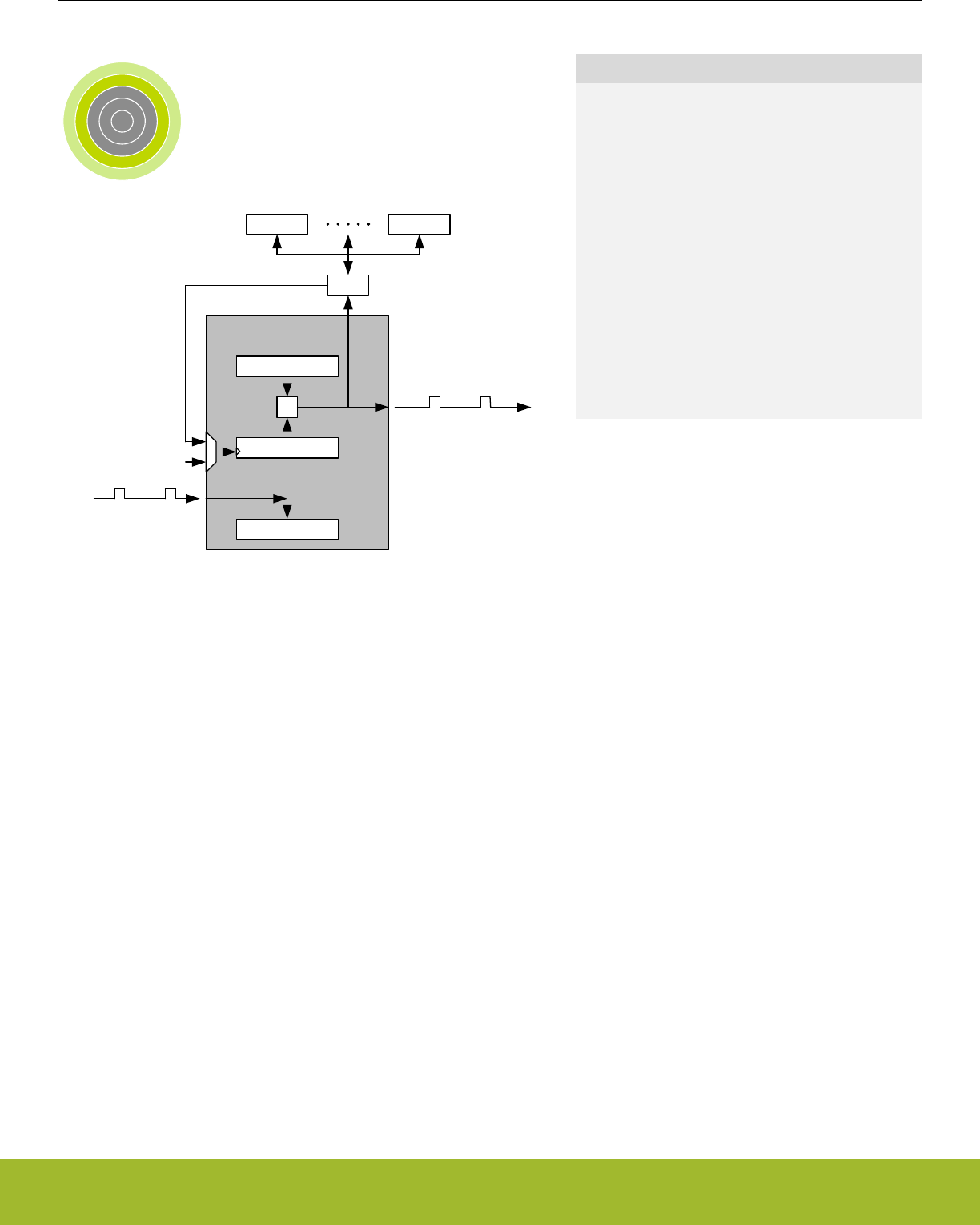
21. TIMER/WTIMER - Timer/Counter
0 1 2 3 4
TIMER
Counter
Capture values
Compare values
=
PRS
ADC
Output compare/PWM
Input capture
USART
Clock
Quick Facts
What?
The TIMER (Timer/Counter) keeps track of timing
and counts events, generates output waveforms,
and triggers timed actions in other peripherals.
Why?
Most applications have activities that need to be
timed accurately with as little CPU intervention and
energy consumption as possible.
How?
The flexible 16/32-bit timer can be configured to pro-
vide PWM waveforms with optional dead-time inser-
tion (e.g. motor control) or work as a frequency gen-
erator. The timer can also count events and control
other peripherals through the PRS, which offloads
the CPU and reduces energy consumption.
21.1 Introduction
The general purpose timer has 3 or 4 compare/capture channels for input capture and compare/Pulse-Width Modulation (PWM) output.
The TIMER and WTIMER peripherals are identical except for the timer width. A TIMER is 16-bits wide and a WTIMER is 32-bits wide.
Some timers also include a Dead-Time Insertion module suitable for motor control applications.
Refer to the device datasheet to determine the capabilities (capture/compare channel count and DTI) of each timer instance.
Reference Manual
TIMER/WTIMER - Timer/Counter
silabs.com | Smart. Connected. Energy-friendly. Preliminary Rev. 0.5 | 673

21.2 Features
• 16/32-bit auto reload up/down counter
• Dedicated 16/32-bit reload register which serves as counter maximum
• 3 or 4 Compare/Capture channels
• Individually configurable as either input capture or output compare/PWM
• Multiple Counter modes
• Count up
• Count down
• Count up/down
• Quadrature Decoder
• Direction and count from external pins
• 2x Count Mode
• Counter control from PRS or external pin
• Start
• Stop
• Reload and start
• Inter-Timer connection
• Allows 32-bit counter mode
• Start/stop synchronization between several timers
• Input Capture
• Period measurement
• Pulse width measurement
• Two capture registers for each capture channel
• Capture on either positive or negative edge
• Capture on both edges
• Optional digital noise filtering on capture inputs
• Output Compare
• Compare output toggle/pulse on compare match
• Immediate update of compare registers
• PWM
• Up-count PWM
• Up/down-count PWM
• Predictable initial PWM output state (configured by SW)
• Buffered compare register to ensure glitch-free update of compare values
• Clock sources
• HFPERCLKTIMERn
• 10-bit Prescaler
• External pin
• Peripheral Reflex System
• Debug mode
• Configurable to either run or stop when processor is stopped (halt/breakpoint)
• Interrupts, PRS output and/or DMA request on:
• Underflow
• Overflow
• Compare/Capture event
• Dead-Time Insertion Unit
• Complementary PWM outputs with programmable dead-time
• Dead-time is specified independently for rising and falling edge
• 10-bit prescaler
• 6-bit time value
• Outputs have configurable polarity
• Outputs can be set inactive individually by software.
Reference Manual
TIMER/WTIMER - Timer/Counter
silabs.com | Smart. Connected. Energy-friendly. Preliminary Rev. 0.5 | 674
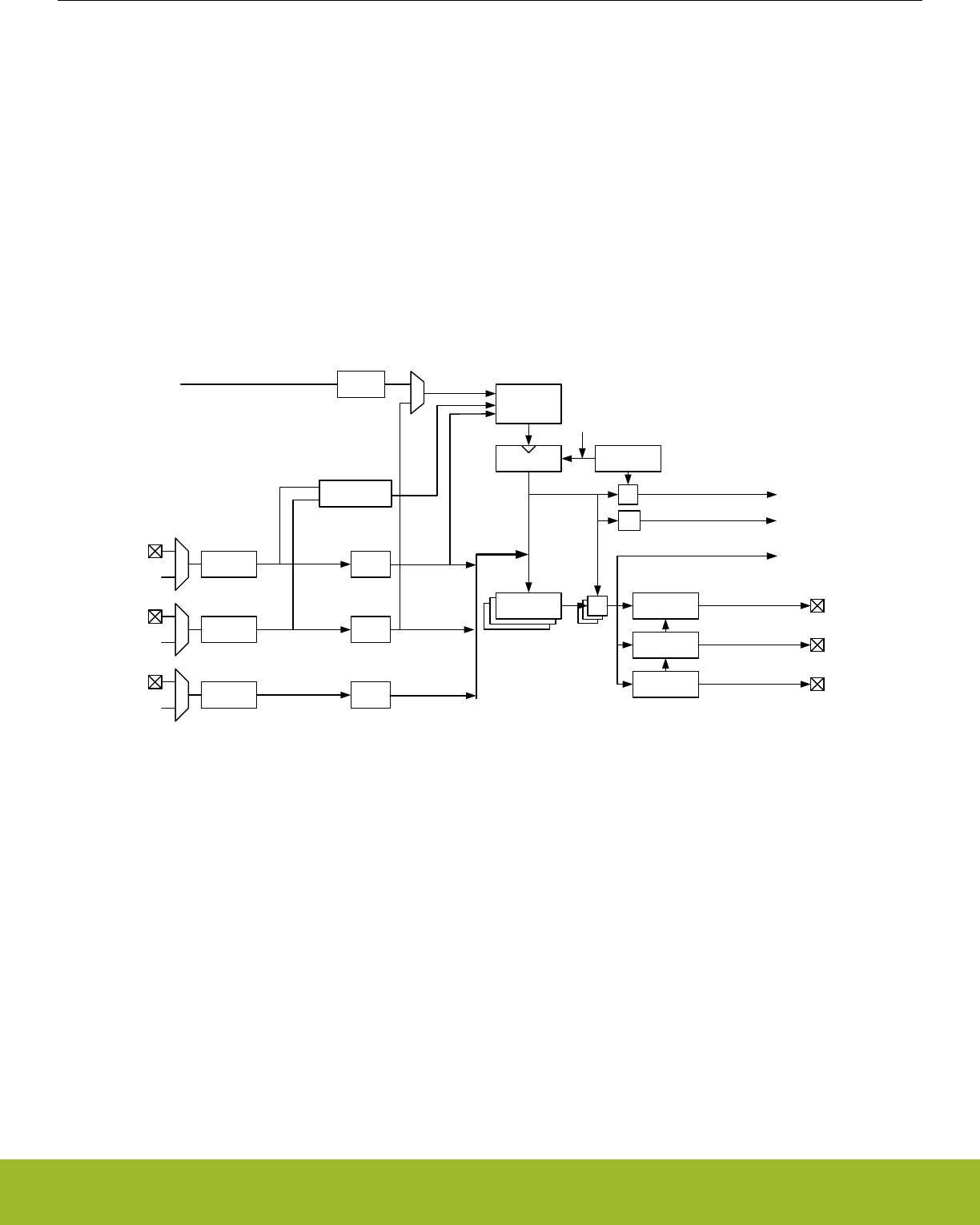
• Configurable action on fault
• Set outputs inactive
•Clear output
• Tristate output
• Individual fault sources
• One or two PRS signals
• Debugger
• Support for automatic restart
• Core lockup
• Configuration lock
21.3 Functional Description
An overview of the TIMER/WTIMER module is shown in Figure 21.1 TIMER/WTIMER Block Overview on page 675 and it consists of
a 16/32 bit up/down counter with 3 Compare/Capture channels connected to pins TIMn_CC0, TIMn_CC1, and TIMn_CC2.
==
Compare and
PWM config
Compare and
PWM config
Compare and
PWM config
=
TnCCR0[15:0
]
TnCCR1[15:0
]
Compare Match x
TIMERn_TOPTIMERn_CNT
TIMERn_CCx
Input Capture
Update
condition
Note: For simplicity, all
TIMERn_CCx registers are
grouped together in the figure,
but they all have individual Input
Capture Registers
=
= 0
CNTCLK
Counter
control
Overflow
Underflow
TIMn_CC0
Input logic Edge
detect
Quadrature
Decoder
Input logic
Input logic
Edge
detect
Edge
detect
PRS inputs
PRS inputs
PRS inputs
Prescaler
HFPERCLKTIMERn
TIMn_CC1
TIMn_CC2
TIMn_CC0
TIMn_CC1
TIMn_CC2
Figure 21.1. TIMER/WTIMER Block Overview
WTIMERs (Wide TIMERs) are 32-bit variants of the TIMER/WTIMER module.
21.3.1 Counter Modes
The timer consists of a counter that can be configured to the following modes:
1. Up-count: Counter counts up until it reaches the value in TIMERn_TOP, where it is reset to 0 before counting up again.
2. Down-count: The counter starts at the value in TIMERn_TOP and counts down. When it reaches 0, it is reloaded with the value in
TIMERn_TOP.
3. Up/Down-count: The counter starts at 0 and counts up. When it reaches the value in TIMERn_TOP, it counts down until it reaches
0 and starts counting up again.
4. Quadrature Decoder: Two input channels where one determines the count direction, while the other pin triggers a clock event.
In addition, to the TIMER/WTIMER modes listed above, the TIMER/WTIMER also supports a 2x Count Mode. In this mode the counter
increments/decrements by 2. The 2x Count Mode intended use is to generate 2x PWM frequency when the Compare/Capture channel
is put in PWM mode. The 2x Count Mode can be enabled by setting the X2CNT bitfield in the TIMERn_CTRL register.
The counter value can be read or written by software at any time by accessing the CNT field in TIMERn_CNT.
Reference Manual
TIMER/WTIMER - Timer/Counter
silabs.com | Smart. Connected. Energy-friendly. Preliminary Rev. 0.5 | 675
21.3.1.1 Events
Overflow is set when the counter value shifts from TIMERn_TOP to the next value when counting up. In up-count mode and Quadrature
Decoder mode the next value is 0. In up/down-count mode, the next value is TIMERn_TOP-1.
Underflow is set when the counter value shifts from 0 to the next value when counting down. In down-count mode and Quadrature De-
coder mode, the next value is TIMERn_TOP. In up/down-count mode the next value is 1.
An update event occurs on overflow in up-count mode and on underflow in down-count or up/down count mode. Additionally, an update
event also occurs on overflow and underflow in Quadrature Decoder Mode. This event is used to time updates of buffered values.
21.3.1.2 Operation
Figure 21.2 TIMER/WTIMER Hardware Timer/Counter Control on page 676 shows the hardware Timer/Counter control. Software can
start or stop the counter by setting the START or STOP bits in TIMERn_CMD. The counter value (CNT in TIMERn_CNT) can always be
written by software to any 16/32-bit value.
It is also possible to control the counter through either an external pin or PRS input. This is done through the input logic for the Com-
pare/Capture Channel 0. The Timer/Counter allows individual actions (start, stop, reload) to be taken for rising and falling input edges.
This is configured in the RISEA and FALLA fields in TIMERn_CTRL. The reload value is 0 in up-count and up/down-count mode and
TOP in down-count mode.
The RUNNING bit in TIMERn_STATUS indicates if the timer is running or not. If the SYNC bit in TIMERn_CTRL is set, the timer is
started/stopped/reloaded (external pin or PRS) when any of the other timers are started/stopped/reloaded.
The DIR bit in TIMERn_STATUS indicates the counting direction of the timer at any given time. The counter value can be read or writ-
ten by software through the CNT field in TIMERn_CNT. In Up/Down-Count mode the count direction will be set to up if the CNT value is
written by software.
Counter
(Controlled by TIMERn_CTRL)
Compare/Capture channel 0
(Controlled by TIMERn_CC0_CTRL)
TIMn_CC0
PRS channels
PRSSEL
INSEL
Filter
FILT
ICEDGE
Input
Capture 0
Counter
RISEA FALLA
Start
Stop
Reload&Start
Figure 21.2. TIMER/WTIMER Hardware Timer/Counter Control
Reference Manual
TIMER/WTIMER - Timer/Counter
silabs.com | Smart. Connected. Energy-friendly. Preliminary Rev. 0.5 | 676
21.3.1.3 Clock Source
The counter can be clocked from several sources, which are all synchronized with the peripheral clock (HFPERCLK). See Figure
21.3 TIMER/WTIMER Clock Selection on page 677.
Counter
(Controlled by TIMERn_CTRL)
Compare/Capture channel 1
(Controlled by TIMERn_CC1_CTRL)
TIMn_CC1
PRS channels
PRSSEL
INSEL
Filter
FILT
ICEDGE
HFPERCLKTIMERn
CLKSEL
Prescaler
PRESC
Input
Capture 1
Counter
Figure 21.3. TIMER/WTIMER Clock Selection
21.3.1.4 Peripheral Clock (HFPERCLK)
The peripheral clock (HFPERCLK) can be used as a source with a configurable prescale factor of 2^PRESC, where PRESC is an inte-
ger between 0 and 10, which is set in PRESC in TIMERn_CTRL. However, if 2x Count Mode is enabled and the Compare/Capture
channels are put in PWM mode, the CC output is updated on both clock edges so prescaling the peripheral clock will produce an incor-
rect result. The prescaler is stopped and reset when the timer is stopped.
21.3.1.5 Compare/ Capture Channel 1 Input
The timer can also be clocked by positive and/or negative edges on the Compare/Capture channel 1 input. This input can either come
from the TIMn_CC1 pin or one of the PRS channels. The input signal must not have a higher frequency than fHFPERCLK/3 when running
from a pin input or a PRS input with FILT enabled in TIMERn_CCx_CTRL. When running from PRS without FILT, the frequency can be
as high as fHFPERCLK. Note that when clocking the timer from the same pulse that triggers a start (through RISEA/FALLA in
TIMERn_CTRL), the starting pulse will not update the Counter Value.
21.3.1.6 Underflow/Overflow from Neighboring Timer
All timers are linked together (see Figure 21.4 TIMER/WTIMER Connections on page 677), allowing timers to count on overflow/
underflow from the lower numbered neighbouring timers to form a 32-bit or 48-bit timer. Note that all timers must be set to same count
direction and less significant timer(s) can only be set to count up or down.
TIMER0TIMER1TIMER2 Overflow Overflow
Underflow Underflow
Figure 21.4. TIMER/WTIMER Connections
21.3.1.7 One-Shot Mode
By default, the counter counts continuously until it is stopped. If the OSMEN bit is set in the TIMERn_CTRL register, however, the coun-
ter is disabled by hardware on the first update event (see 21.3.1.1 Events). Note that when the counter is running with CC1 as clock
source (0b01 in CLKSEL in TIMERn_CTRL) and OSMEN is set, a CC1 capture event will not take place on the update event (CC1
rising edge) that stops the timer.
Reference Manual
TIMER/WTIMER - Timer/Counter
silabs.com | Smart. Connected. Energy-friendly. Preliminary Rev. 0.5 | 677
21.3.1.8 Top Value Buffer
The TIMERn_TOP register can be altered either by writing it directly or by writing to the TIMER_TOPB (buffer) register. When writing to
the buffer register the TIMERn_TOPB register will be written to TIMERn_TOP on the next update event. Buffering ensures that the TOP
value is not set below the actual count value. The TOPBV flag in TIMERn_STATUS indicates whether the TIMERn_TOPB register con-
tains data that has not yet been written to the TIMERn_TOP register (see Figure 21.5 TIMER/WTIMER TOP Value Update Functionality
on page 678).
Note: When writing to TIMERn_TOP register directly, the TIMERn_TOPB register value will be invalidated and the TOPBV flag will be
cleared. This prevents TIMERn_TOP register from being immediately updated by an existing valid TIMERn_TOPB value during the next
update event.
TOP
APB Write (TOPB) TOPB
Load APB
Load APB
TOPBV
Set
Clear
APB Write (TOP)
Update event
Load TOPB
APB Data
Figure 21.5. TIMER/WTIMER TOP Value Update Functionality
Reference Manual
TIMER/WTIMER - Timer/Counter
silabs.com | Smart. Connected. Energy-friendly. Preliminary Rev. 0.5 | 678
21.3.1.9 Quadrature Decoder
Quadrature Decoding mode is used to track motion and determine both rotation direction and position. The Quadrature Decoder uses
two input channels that are 90 degrees out of phase (see Figure 21.6 TIMER/WTIMER Quadrature Encoded Inputs on page 679).
Channel A
Channel B
Forward rotation (Channel A leads Channel B)
90°
Channel A
Channel B
Backward rotation (Channel B leads Channel A)
90°
Figure 21.6. TIMER/WTIMER Quadrature Encoded Inputs
In the timer these inputs are tapped from the Compare/Capture channel 0 (Channel A) and 1 (Channel B) inputs before edge detection.
The Timer/Counter then increments or decrements the counter, based on the phase relation between the two inputs. The Quadrature
Decoder Mode supports two channels, but if a third channel (Z-terminal) is available, this can be connected to an external interrupt and
trigger a counter reset from the interrupt service routine. By connecting a periodic signal from another timer as input capture on
Compare/Capture Channel 2, it is also possible to calculate speed and acceleration.
Note: In Quadrature Decoder mode, overflow and underflow triggers an update event.
Counter
(Controlled by TIMERn_CTRL)
Compare/Capture channel 1
(Controlled by TIMERn_CC1_CTRL)
Compare/Capture channel 0
(Controlled by TIMERn_CC0_CTRL)
TIMn_CC0
PRS channels
PRSSEL
INSEL
Filter
FILT
ICEDGE
Quadrature
Decoder
TIMn_CC1
PRS channels
PRSSEL
INSEL
Filter
FILT
ICEDGE
Input
Capture 0
Input
Capture 1
Counter
Inc
Dec
QDM MODE
Ch B
Ch A
Figure 21.7. TIMER/WTIMER Quadrature Decoder Configuration
Reference Manual
TIMER/WTIMER - Timer/Counter
silabs.com | Smart. Connected. Energy-friendly. Preliminary Rev. 0.5 | 679
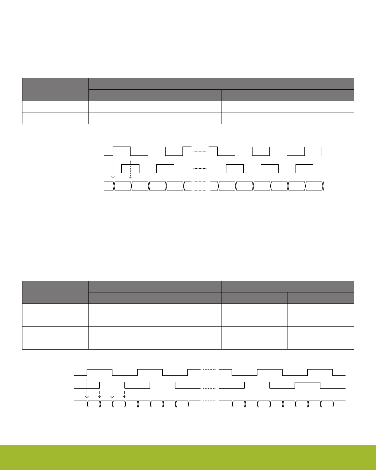
The Quadrature Decoder can be set in either X2 or X4 mode, which is configured in the QDM bit in TIMERn_CTRL. See Figure
21.7 TIMER/WTIMER Quadrature Decoder Configuration on page 679
21.3.1.10 X2 Decoding Mode
In X2 Decoding mode, the counter increments or decrements on every edge of Channel A, see Table 21.1 TIMER/WTIMER Counter
Response in X2 Decoding Mode on page 680 and Figure 21.8 TIMER/WTIMER X2 Decoding Mode on page 680.
Table 21.1. TIMER/WTIMER Counter Response in X2 Decoding Mode
Channel B
Channel A
Rising Falling
0 Increment Decrement
1 Decrement Increment
Channel A
Channel B
CNT 34 5 6 7 834567 28
Figure 21.8. TIMER/WTIMER X2 Decoding Mode
21.3.1.11 X4 Decoding Mode
In X4 Decoding mode, the counter increments or decrements on every edge of Channel A and Channel B, see Figure 21.9 TIMER/
WTIMER X4 Decoding Mode on page 680 and Table 21.2 TIMER/WTIMER Counter Response in X4 Decoding Mode on page 680.
Table 21.2. TIMER/WTIMER Counter Response in X4 Decoding Mode
Opposite Channel Channel A Channel B
Rising Falling Rising Falling
Channel A = 0 Decrement Increment
Channel A = 1 Increment Decrement
Channel B = 0 Increment Decrement
Channel B = 1 Decrement Increment
Channel A
Channel B
34567891011
3 4 5 6 7 8 9 10 11 2
2
CNT
Figure 21.9. TIMER/WTIMER X4 Decoding Mode
Reference Manual
TIMER/WTIMER - Timer/Counter
silabs.com | Smart. Connected. Energy-friendly. Preliminary Rev. 0.5 | 680
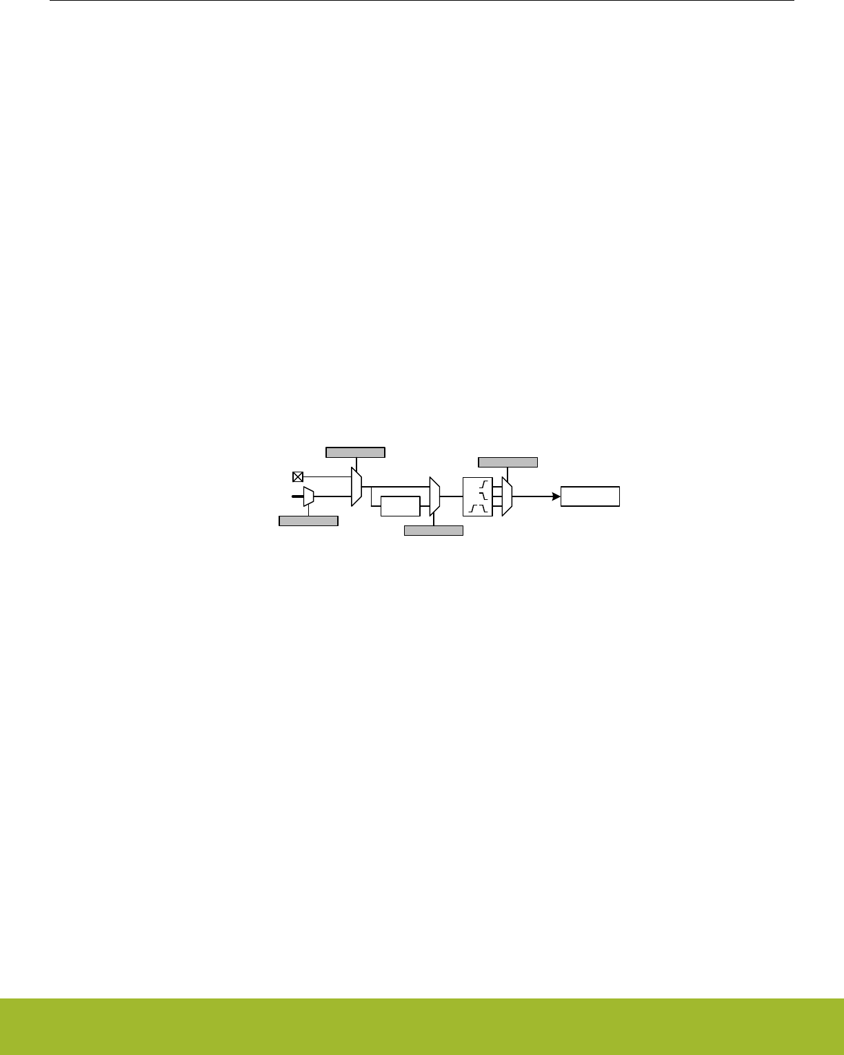
21.3.1.12 TIMER/WTIMER Rotational Position
To calculate a position Figure 21.10 TIMER/WTIMER Rotational Position Equation on page 681 can be used.
pos° = (CNT/X x N) x 360°
Figure 21.10. TIMER/WTIMER Rotational Position Equation
where X = Encoding type and N = Number of pulses per revolution.
21.3.2 Compare/Capture Channels
The timer contains 3 Compare/Capture channels, which can be configured in the following modes:
1. Input Capture
2. Output Compare
3. PWM
21.3.2.1 Input Pin Logic
Each Compare/Capture channel can be configured as an input source for the Capture Unit or as external clock source for the timer (see
Figure 21.11 TIMER/WTIMER Input Pin Logic on page 681). Compare/Capture channels 0 and 1 are the inputs for the Quadrature
Decoder Mode. The input channel can be filtered before it is used, which requires the input to remain stable for 5 cycles in a row before
the input is propagated to the output.
TIMn_CCx
PRS channels
PRSSEL
INSEL
Filter
FILT
ICEDGE
Input
Capture x
Figure 21.11. TIMER/WTIMER Input Pin Logic
21.3.2.2 Compare/Capture Registers
The Compare/Capture channel registers are prefixed with TIMERn_CCx_, where the x stands for the channel number. Since the Com-
pare/Capture channels serve three functions (input capture, compare, PWM), the behavior of the Compare/Capture registers
(TIMERn_CCx_CCV) and buffer registers (TIMERn_CCx_CCVB) change depending on the mode the channel is set in.
Reference Manual
TIMER/WTIMER - Timer/Counter
silabs.com | Smart. Connected. Energy-friendly. Preliminary Rev. 0.5 | 681
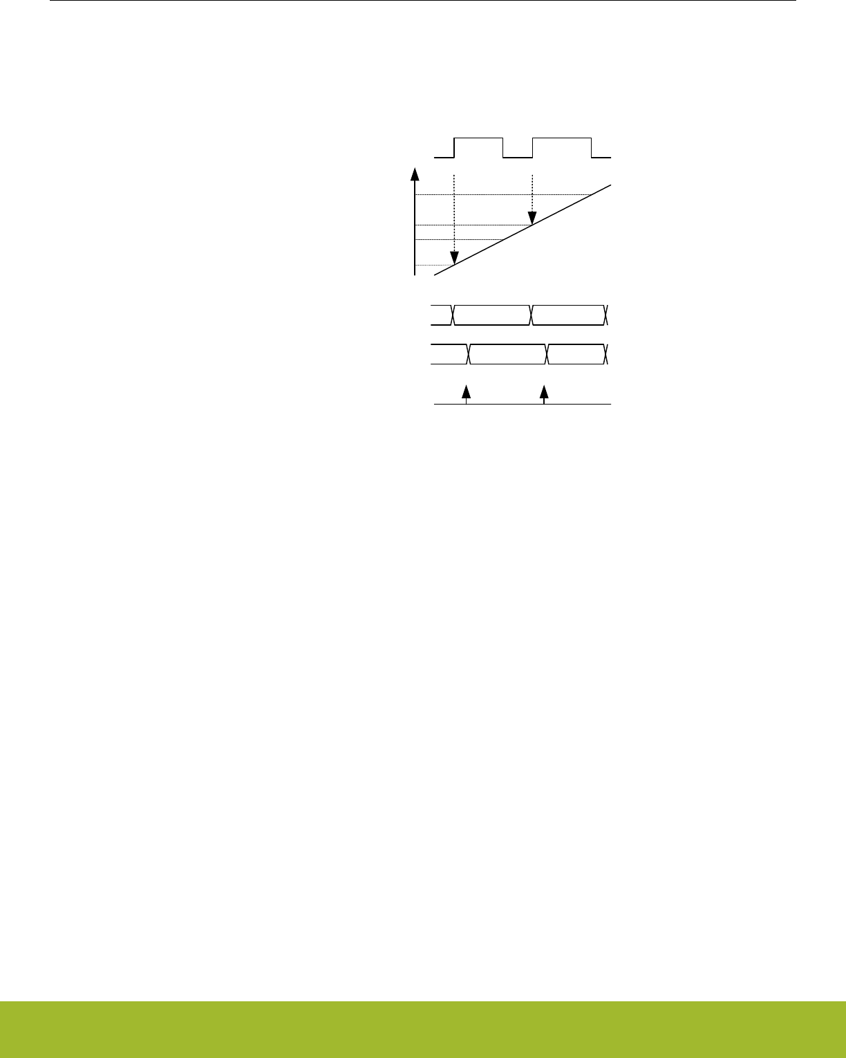
21.3.2.3 Input Capture
In Input Capture Mode, the counter value (TIMERn_CNT) can be captured in the Compare/Capture Register (TIMERn_CCx_CCV) (see
Figure 21.12 TIMER/WTIMER Input Capture on page 682). The CCPOL bits in TIMERn_STATUS indicate the polarity of the edge that
triggered the capture in TIMERn_CCx_CCV.
TIMERn_CCx_CCV
m
n
y
z
TIMERn_CNT
Input
Read TIMERn_CCx_CCV
TIMERn_CCx_CCVB m y
prev. val m y
Figure 21.12. TIMER/WTIMER Input Capture
The Compare/Capture Buffer Register (TIMERn_CCx_CCVB) and the TIMERn_CCx_CCV register form double-buffered capture regis-
ters allowing two subsequent capture events to take place before a read-out is required. The first capture can always be read from
TIMERn_CCx_CCV, and reading this address will load the next capture value into TIMERn_CCx_CCV from TIMERn_CCx_CCVB if it
contains valid data. The CC value can be read without altering the FIFO contents by reading TIMERn_CCx_CCVP.
TIMERn_CCx_CCVB can also be read without altering the FIFO contents. The ICV flag in TIMERn_STATUS indicates if there is a valid
unread capture in TIMERn_CCx_CCV. In this mode, TIMERn_CCx_CCV is read-only.
In the case where a capture is triggered while both TIMERn_CCx_CCV and TIMERn_CCx_CCVB contain unread capture values, the
buffer overflow interrupt flag (ICBOF in TIMERn_IF) will be set. On overflow new capture values will overwrite the value in
TIMERn_CCx_CCVB and the value of TIMERn_CCx_CCV will remain unchanged. TIMERn_CCx_CCV will always contain the oldest
unread value and TIMERn_CCx_CCVB will always contain the newest value.
Note: In input capture mode, the timer will only trigger interrupts when it is running.
Reference Manual
TIMER/WTIMER - Timer/Counter
silabs.com | Smart. Connected. Energy-friendly. Preliminary Rev. 0.5 | 682

21.3.2.4 Period/Pulse-Width Capture
Period and/or pulse-width capture can only be possible with Channel 0 (CC0), because this is the only channel that can start and stop
the timer. This can be done by setting the RISEA field in TIMERn_CTRL to Clear&Start, and select the wanted input from either exter-
nal pin or PRS, see Figure 21.13 TIMER/WTIMER Period and/or Pulse width Capture on page 683. For period capture, the Compare/
Capture Channel should then be set to input capture on a rising edge of the same input signal. To capture the width of a high pulse, the
Compare/Capture Channel should be set to capture on a falling edge of the input signal. To measure the low pulse-width of a signal,
opposite polarities should be chosen.
0
Input
CNT
Clear&Start
Input Capture (frequency capture)
Input Capture (pulse-width capture)
Figure 21.13. TIMER/WTIMER Period and/or Pulse width Capture
Reference Manual
TIMER/WTIMER - Timer/Counter
silabs.com | Smart. Connected. Energy-friendly. Preliminary Rev. 0.5 | 683
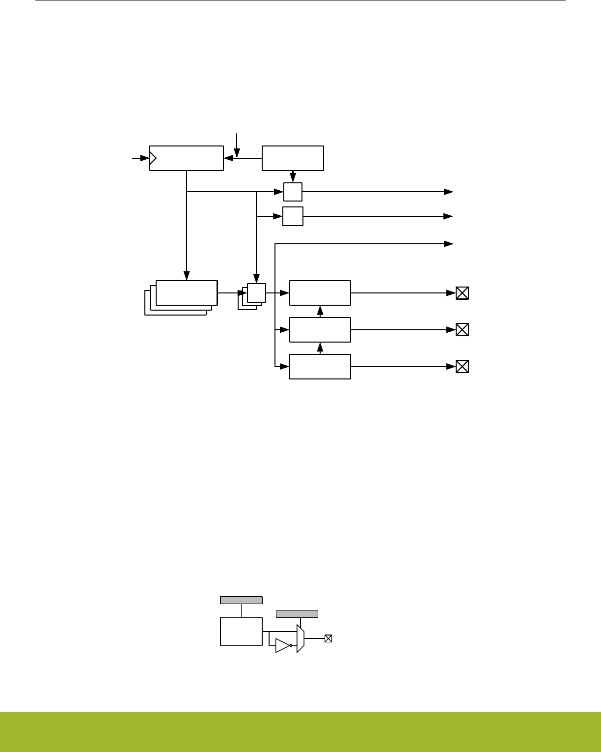
21.3.2.5 Compare
Each Compare/Capture channel contains a comparator which outputs a compare match if the contents of TIMERn_CCx_CCV matches
the counter value, see Figure 21.14 TIMER/WTIMER Block Diagram Showing Comparison Functionality on page 684. In compare
mode, each compare channel can be configured to either set, clear or toggle the output on an event (compare match, overflow or un-
derflow). The output from each channel is represented as an alternative function on the port it is connected to, which needs to be ena-
bled for the CC outputs to propagate to the pins.
TnCCR0[15:0
]
TnCCR1[15:0
]
Underflow
Compare Match x
TIMERn_TOPTIMERn_CNT
TIMERn_CCx
Update
Condition
Note: For simplicity, all
TIMERn_CCx registers are
grouped together in the figure,
but they all have individual
Compare Register and logic
=
= 0
==TIMn_CC0
Compare and
PWM config
Compare and
PWM config
Compare and
PWM config
=
TIMn_CC1
TIMn_CC2
CNTCLK
Overflow
Figure 21.14. TIMER/WTIMER Block Diagram Showing Comparison Functionality
The compare output is delayed by one cycle to allow for full 0% to 100% PWM generation. If occurring in the same cycle, match action
will have priority over overflow or underflow action.
The input selected (through PRSSEL, INSEL and FILTSEL in TIMERn_CCx_CTRL) for the CC channel will also be sampled on com-
pare match and the result is found in the CCPOL bits in TIMERn_STATUS. It is also possible to configure the CCPOL to always track
the inputs by setting ATI in TIMERn_CTRL.
The COIST bit in TIMERn_CCx_CTRL is the initial state of the compare/PWM output. The COIST bit can also be used as an initial
value to the compare outputs on a reload-start when RSSCOIST is set in TIMERn_CTRL. Also the resulting output can be inverted by
setting OUTINV in TIMERn_CCx_CTRL. It is recommended to turn off the CC channel before configuring the output state to avoid any
pulses on the output. The CC channel can be turned off by setting MODE to OFF in TIMER_CCx_CTRL. The following figure shows the
output logic for the TIMER/WTIMER module.
TIMn_CCx
COIST
OUTINV
Output
Compare/
PWM x 0
1
Figure 21.15. TIMER/WTIMER Output Logic
Reference Manual
TIMER/WTIMER - Timer/Counter
silabs.com | Smart. Connected. Energy-friendly. Preliminary Rev. 0.5 | 684
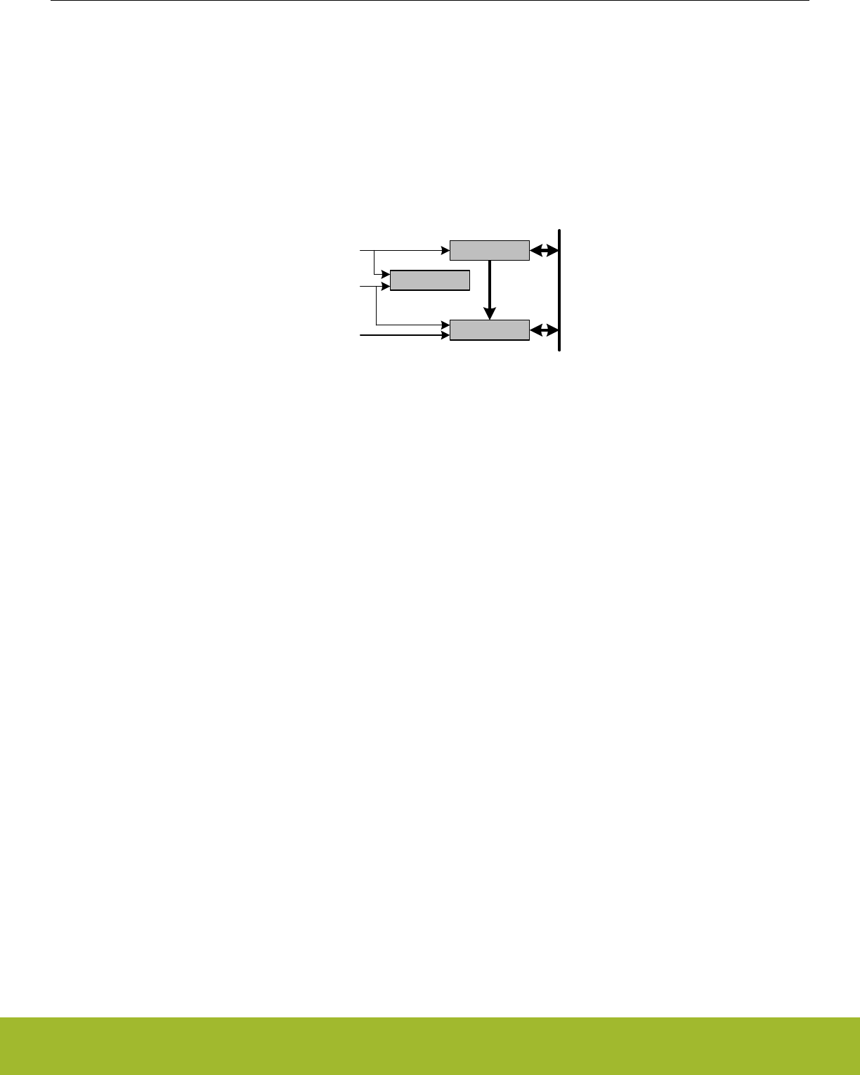
21.3.2.6 Compare Mode Registers
When running in Output Compare or PWM mode, the value in TIMERn_CCx_CCV will be compared against the count value. In Com-
pare mode the output can be configured to toggle, clear or set on compare match, overflow, and underflow through the CMOA, COFOA
and CUFOA fields in TIMERn_CCx_CTRL. TIMERn_CCx_CCV can be accessed directly or through the buffer register
TIMERn_CCx_CCVB, see Figure 21.16 TIMER/WTIMER Output Compare/PWM Buffer Functionality Detail on page 685. When writ-
ing to the buffer register, the value in TIMERn_CCx_CCVB will be written to TIMERn_CCx_CCV on the next update event. This func-
tionality ensures glitch free PWM outputs. The CCVBV flag in TIMERn_STATUS indicates whether the TIMERn_CCx_CCVB register
contains data that has not yet been written to the TIMERn_CCx_CCV register. Note that when writing 0 to TIMERn_CCx_CCVB in up-
down count mode the CCV value is updated when the timer counts from 0 to 1. Thus, the compare match for the next period will not
happen until the timer reaches 0 again on the way down.
CCV
APB Write (CCB) CCVB
Load APB
Load APB
CCVBV
Set
Clear
APB Write (CC)
Update event
Load CCB
APB Data
Figure 21.16. TIMER/WTIMER Output Compare/PWM Buffer Functionality Detail
Reference Manual
TIMER/WTIMER - Timer/Counter
silabs.com | Smart. Connected. Energy-friendly. Preliminary Rev. 0.5 | 685

21.3.2.7 Frequency Generation (FRG)
Frequency generation (see Figure 21.17 TIMER/WTIMER Up-count Frequency Generation on page 686) can be achieved in compare
mode by:
• Setting the counter in up-count mode
• Enabling buffering of the TOP value.
• Setting the CC channels overflow action to toggle
0
TIMERn_TOP
TIMERn_CCx_CCV
Figure 21.17. TIMER/WTIMER Up-count Frequency Generation
The output frequency is given by Figure 21.18 TIMER/WTIMER Up-count Frequency Generation Equation on page 686
fFRG = fHFPERCLK/ ( 2^(PRESC + 1) x (TOP + 1) x 2)
Figure 21.18. TIMER/WTIMER Up-count Frequency Generation Equation
The figure below provides cycle accurate timing and event generation information for frequency generation.
0
TIMERn_TOP =
TIMERn_CCx_CCV
1
2
3
4
TIMERn_CCx
Figure 21.19. TIMER/WTIMER Up-count Frequency Generation Detail
21.3.2.8 Pulse-Width Modulation (PWM)
In PWM mode, TIMERn_CCx_CCV is buffered to avoid glitches in the output. The settings in the Compare Output Action configuration
bits are ignored in PWM mode and PWM generation is only supported for up-count and up/down-count mode.
Reference Manual
TIMER/WTIMER - Timer/Counter
silabs.com | Smart. Connected. Energy-friendly. Preliminary Rev. 0.5 | 686
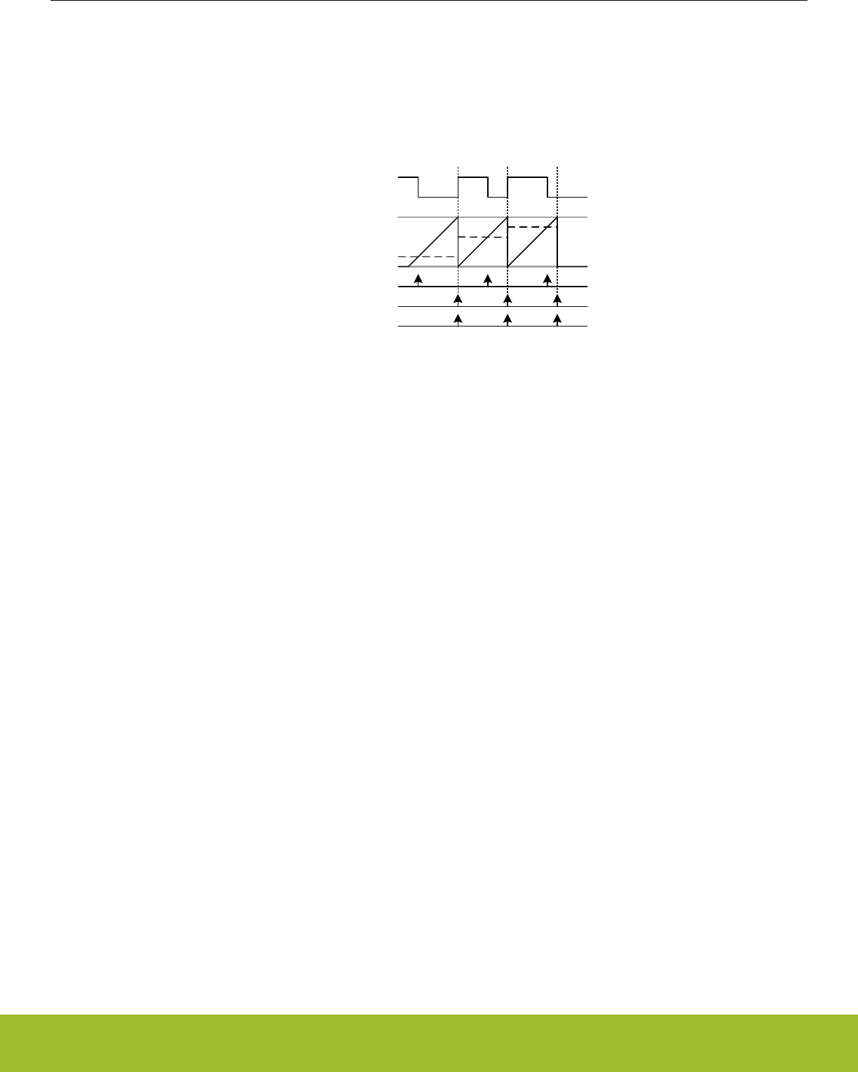
21.3.2.9 Up-count (Single-slope) PWM
If the counter is set to up-count and the Compare/Capture channel is put in PWM mode, single slope PWM output will be generated
(see Figure 21.20 TIMER/WTIMER Up-count PWM Generation on page 687). In up-count mode the PWM period is TOP+1 cycles
and the PWM output will be high for a number of cycles equal to TIMERn_CCx_CCV. This means that a constant high output is ach-
ieved by setting TIMERn_CCx_CCV to TOP+1 or higher. The PWM resolution (in bits) is then given by Figure 21.21 TIMER/WTIMER
Up-count PWM Resolution Equation on page 687.
0
TIMERn_TOP
TIMERn_CCx_CCV
TIMn_CCx
Overflow
Compare match
Buffer update
Figure 21.20. TIMER/WTIMER Up-count PWM Generation
RPWMup = log(TOP+1)/log(2)
Figure 21.21. TIMER/WTIMER Up-count PWM Resolution Equation
The PWM frequency is given by Figure 21.22 TIMER/WTIMER Up-count PWM Frequency Equation on page 687:
fPWMup/down = fHFPERCLK/ ( 2^PRESC x (TOP + 1))
Figure 21.22. TIMER/WTIMER Up-count PWM Frequency Equation
The high duty cycle is given by Figure 21.23 TIMER/WTIMER Up-count Duty Cycle Equation on page 687
DSup = CCVx/(TOP+1)
Figure 21.23. TIMER/WTIMER Up-count Duty Cycle Equation
The figure below provides cycle accurate timing and event generation information for up-count mode.
Reference Manual
TIMER/WTIMER - Timer/Counter
silabs.com | Smart. Connected. Energy-friendly. Preliminary Rev. 0.5 | 687

0
TIMERn_TOP =
TIMERn_CCx_CCV =
TIMn_CCx
Overflow
Compare match
Buffer update
1
2
3
4
TIMERn_CCx
Figure 21.24. TIMER/WTIMER Up-count PWM Generation Detail
Reference Manual
TIMER/WTIMER - Timer/Counter
silabs.com | Smart. Connected. Energy-friendly. Preliminary Rev. 0.5 | 688

21.3.2.10 2x Count Mode (Up-count)
When the timer is set in 2x mode, the TIMER/WTIMER will count up by two. This will in effect make any odd Top value be rounded
down to the closest even number. Similarly, any odd CC value will generate a match on the closest lower even value as shown in
Figure 21.25 TIMER/WTIMER CC out in 2x mode on page 689
2 4 0 2 40
Clock
CC Out
02 4 0 2 40 0
Top = 5
CC = 1
Top = 5
CC = 2
Figure 21.25. TIMER/WTIMER CC out in 2x mode
The PWM resolution is given by Figure 21.26 TIMER/WTIMER 2x PWM Resolution Equation on page 689.
RPWM2xmode = log(TOP/2+1)/log(2)
Figure 21.26. TIMER/WTIMER 2x PWM Resolution Equation
The PWM frequency is given by Figure 21.27 TIMER/WTIMER 2x Mode PWM Frequency Equation( Up-count) on page 689:
fPWM2xmode = fHFPERCLK/ floor(TOP/2)+1
Figure 21.27. TIMER/WTIMER 2x Mode PWM Frequency Equation( Up-count)
The high duty cycle is given by Figure 21.28 TIMER/WTIMER 2x Mode Duty Cycle Equation on page 689
DS2xmode = CCVx/((floor(TOP/2)+1)*2)
Figure 21.28. TIMER/WTIMER 2x Mode Duty Cycle Equation
Reference Manual
TIMER/WTIMER - Timer/Counter
silabs.com | Smart. Connected. Energy-friendly. Preliminary Rev. 0.5 | 689
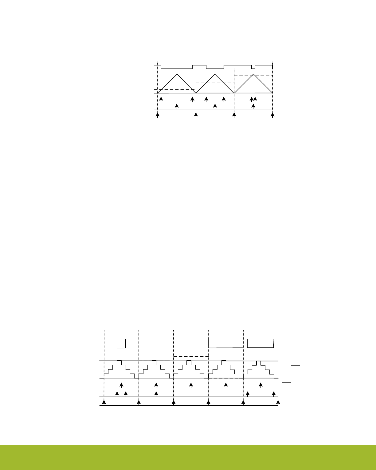
21.3.2.11 Up/Down-count (Dual-slope) PWM
If the counter is set to up-down count and the Compare/Capture channel is put in PWM mode, dual slope PWM output will be generated
by Figure 21.29 TIMER/WTIMER Up/Down-count PWM Generation on page 690.The resolution (in bits) is given by Figure 21.30 TIM-
ER/WTIMER Up/Down-count PWM Resolution Equation on page 690.
0
TIMERn_TOP
TIMERn_CCx_CCV
TIMn_CCx
Overflow
Compare match
Buffer update
Figure 21.29. TIMER/WTIMER Up/Down-count PWM Generation
RPWMup/down = log(TOP+1)/log(2)
Figure 21.30. TIMER/WTIMER Up/Down-count PWM Resolution Equation
The PWM frequency is given by Figure 21.31 TIMER/WTIMER Up/Down-count PWM Frequency Equation on page 690:
fPWMup/down = fHFPERCLK/ ( 2^(PRESC+1) x TOP))
Figure 21.31. TIMER/WTIMER Up/Down-count PWM Frequency Equation
The high duty cycle is given by Figure 21.32 TIMER/WTIMER Up/Down-count Duty Cycle Equation on page 690
DSup/down = CCVx/TOP
Figure 21.32. TIMER/WTIMER Up/Down-count Duty Cycle Equation
The figure below provides cycle accurate timing and event generation information for up-count mode.
TIMERn_TOP =
TIMERn_CCx_CCV =
TIMn_CCx
Overflow
Compare match
Buffer update
1
2
3
4
0
TIMERn_CCx
Figure 21.33. TIMER/WTIMER Up/Down-count PWM Generation
Reference Manual
TIMER/WTIMER - Timer/Counter
silabs.com | Smart. Connected. Energy-friendly. Preliminary Rev. 0.5 | 690

21.3.2.12 2x Count Mode (Up/Down-count)
When the timer is set in 2x mode, the TIMER/WTIMER will count up/down by two. This will in effect make any odd Top value be roun-
ded down to the closest even number. Similarly, any odd CC value will generate a match on the closest lower even value as shown in
Figure 21.34 TIMER/WTIMER CC out in 2x mode on page 691
2 4 2 0 20
Clock
CC Out
42 4 2 0 20 4
Top = 5
CC = 1
Top = 5
CC = 2
Figure 21.34. TIMER/WTIMER CC out in 2x mode
Figure 21.35 TIMER/WTIMER 2x PWM Resolution Equation on page 691.
RPWM2xmode = log(TOP/2+1)/log(2)
Figure 21.35. TIMER/WTIMER 2x PWM Resolution Equation
The PWM frequency is given by Figure 21.36 TIMER/WTIMER 2x Mode PWM Frequency Equation( Up/Down-count) on page 691:
fPWM2xmode = fHFPERCLK/ (floor(TOP/2)*2)
Figure 21.36. TIMER/WTIMER 2x Mode PWM Frequency Equation( Up/Down-count)
The high duty cycle is given by two equations based on the CCVx values.Figure 21.37 TIMER/WTIMER 2x Mode Duty Cycle Equation
for CCVx = 1 or CCVx = even on page 691 and Figure 21.38 TIMER/WTIMER 2x Mode Duty Cycle Equation for all other CCVx = odd
values on page 691
DS2xmode = (CCVx*2)/(floor(TOP/2)*4)
Figure 21.37. TIMER/WTIMER 2x Mode Duty Cycle Equation for CCVx = 1 or CCVx = even
DS2xmode = (CCVx*2 - CCVx)/(floor(TOP/2)*4)
Figure 21.38. TIMER/WTIMER 2x Mode Duty Cycle Equation for all other CCVx = odd values
21.3.2.13 Timer Configuration Lock
To prevent software errors from making changes to the timer configuration, a configuration lock is available similar to DTI configuration
Lock. Writing any value but 0xCE80 to LOCKKEY in TIMERn_LOCK results in TIMERn_CTRL, TIMERn_CMD, TIMERn_TOP,
TIMERn_CNT, TIMERn_CCx_CTRL and TIMERn_CCx_CCV being locked from writing. To unlock the registers, write 0xCE80 to LOCK-
KEY in TIMERn_LOCK. The value of TIMERn_LOCK is 1 when the lock is active, and 0 when the registers are unlocked.
Reference Manual
TIMER/WTIMER - Timer/Counter
silabs.com | Smart. Connected. Energy-friendly. Preliminary Rev. 0.5 | 691
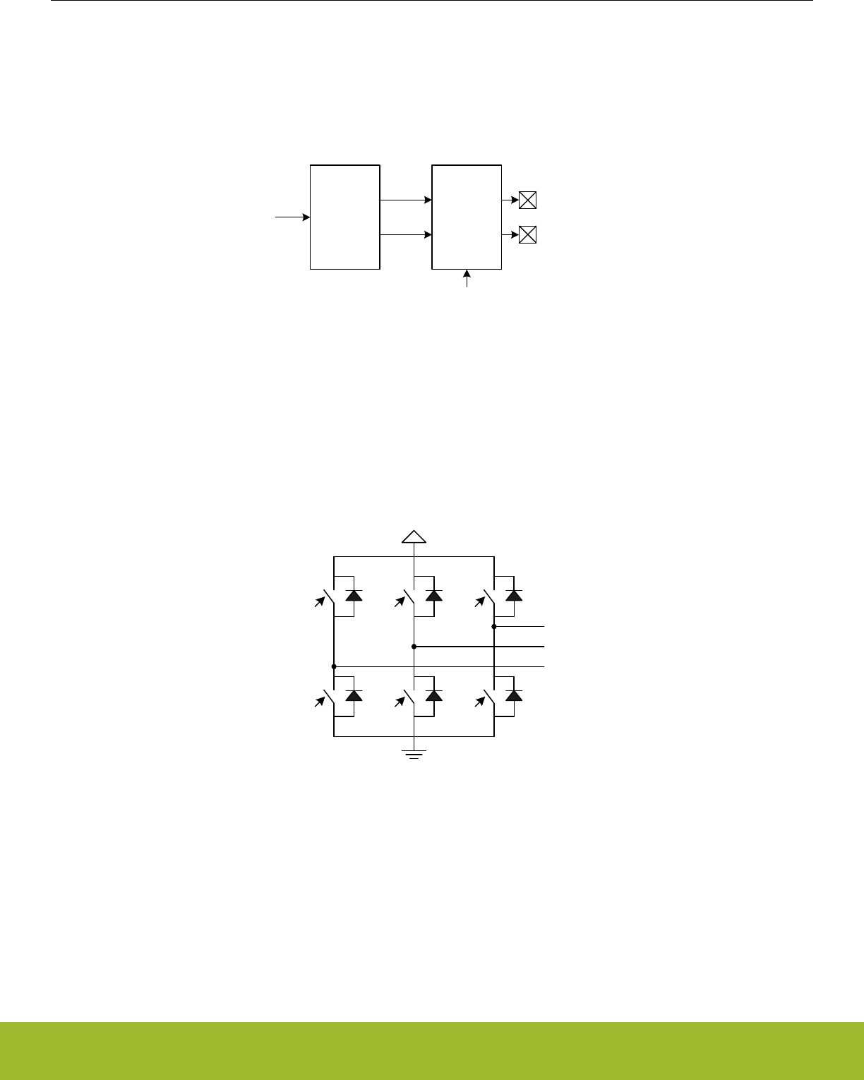
21.3.3 Dead-Time Insertion Unit
Some of the timers include a Dead-Time Insertion module suitable for motor control applications. Refer to the device datasheet to check
if a timer has this feature. The example settings in this section are for TIMER0, but identical settings can be used for other timers with
DTI as well. The Dead-Time Insertion Unit aims to make control of brushless DC (BLDC) motors safer and more efficient by introducing
complementary PWM outputs with dead-time insertion and fault handling, see Figure 21.39 TIMER/WTIMER Dead-Time Insertion Unit
Overview on page 692.
Dead time
insertion
Original PWM (TIM0_CCx_pre) Fault
handling
Primary output (TIM0_CCx)
Complementary output (TIM0_CDTIx)
Fault sources
Figure 21.39. TIMER/WTIMER Dead-Time Insertion Unit Overview
When used for motor control, the PWM outputs TIM0_CC0, TIM0_CC1 and TIM0_CC2 are often connected to the high-side transistors
of a triple half-bridge setup (UH, VH and WH), and the complementary outputs connected to the respective low-side transistors (UL, VL,
WL shown in Figure 21.40 TIMER/WTIMER Triple Half-Bridge on page 692). Transistors used in such a bridge often do not open/
close instantaneously, and using the exact complementary inputs for the high and low side of a half-bridge may result in situations
where both gates are open. This can give unnecessary current-draw and short circuit the power supply. The DTI unit provides dead-
time insertion to deal with this problem.
UH VH WH
WLVLUL
W
V
U
Figure 21.40. TIMER/WTIMER Triple Half-Bridge
For each of the 3 compare-match outputs of TIMER0, an additional complementary output is provided by the DTI unit. These outputs,
named TIM0_CDTI0, TIM0_CDTI1 and TIM0_CDTI2 are provided to make control of e.g. 3-channel BLDC or permanent magnet AC
(PMAC) motors possible using only a single timer, see Figure 21.41 TIMER/WTIMER Overview of Dead-Time Insertion Block for a Sin-
gle PWM channel on page 693.
Reference Manual
TIMER/WTIMER - Timer/Counter
silabs.com | Smart. Connected. Energy-friendly. Preliminary Rev. 0.5 | 692
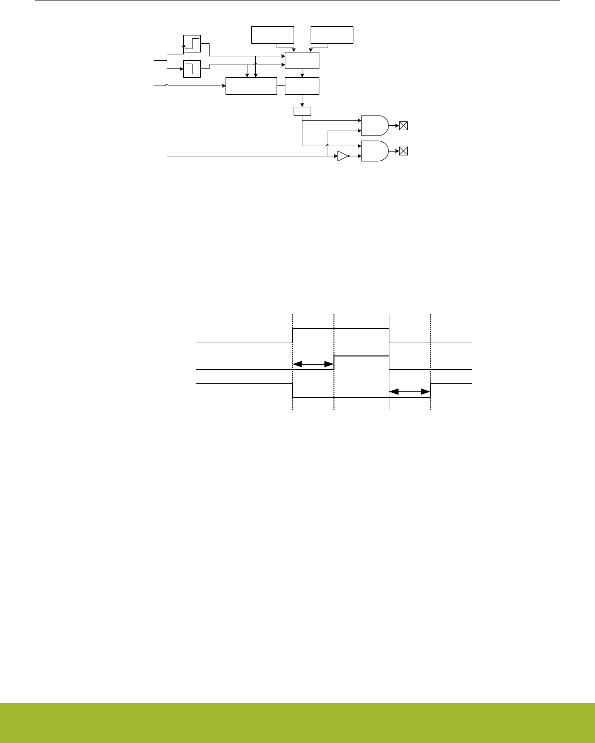
Clock control Counter
Select
DTFALLT DTRISET
=0
Original PWM (TIM0_CCx_pre)
HFPERCLKTIMERn
Primary output (TIM0_CCx)
Complementary Output (TIM0_CDTIx)
Figure 21.41. TIMER/WTIMER Overview of Dead-Time Insertion Block for a Single PWM channel
The DTI unit is enabled by setting DTEN in TIMER0_DTCTRL. In addition to providing the complementary outputs, the DTI unit then
also overrides the compare match outputs from the timer.
The DTI unit gives the rising edges of the PWM outputs and the rising edges of the complementary PWM outputs a configurable time
delay. By doing this, the DTI unit introduces a dead-time where both the primary and complementary outputs in a pair are inactive as
seen in Figure 21.42 TIMER/WTIMER Polarity of Both Signals are Set as Active-High on page 693.
Original PWM
TIM0_CC0
TIM0_CDTI0
dt1
dt2
Figure 21.42. TIMER/WTIMER Polarity of Both Signals are Set as Active-High
Dead-time is specified individually for the rising and falling edge of the original PWM. These values are shared across all the three
PWM channels of the DTI unit. A single prescaler value is provided for the DTI unit, meaning that both the rising and falling edge dead-
times share prescaler value. The prescaler divides the HFPERCLKTIMERn by a configurable factor between 1 and 1024, which is set in
the DTPRESC field in TIMER0_DTTIME. The rising and falling edge dead-times are configured in DTRISET and DTFALLT in TIM-
ER0_DTTIME to any number between 1-64 HFPERCLKTIMER0 cycles.
The DTAR and DTFATS bits in TIMER0_DTCTRL control the DTI output behavior when the timer stops. By default the DTI block stops
when the timer is stopped. Setting the DTAR bit will cause the DTI to output on channel 0 to continue when the timer is stopped. DTAR
effects only channel 0. See 21.3.3.2 PRS Channel as a Source for an example of when this can be used. While in this mode the undivi-
ded HFPERCLK_TIMER0 (DTPRESC=0) is always used regardless of programmed DTPRESC value in TIMER0_DTTIME. This means
that rise and fall dead times are calculated assuming DTPRESC = 0.
When the timer stops DTI outputs are frozen by default, preserving their last state. To allow the outputs to go to a safe state as pro-
grammed in the DTFA field of TIMER0_DTFC register and set the DTFATS bitfield in the TIMER0_DTCTRL reg. Note that when DTAR
is also set, DTAR has priority over DTFATS for DTI channel 0 output.
The following table shows the DTI output when the timer is halted.
Reference Manual
TIMER/WTIMER - Timer/Counter
silabs.com | Smart. Connected. Energy-friendly. Preliminary Rev. 0.5 | 693

Table 21.3. DTI output when timer halted
DTAR DTFATS State
0 0 frozen
0 1 safe
1 0 running
1 1 running
Reference Manual
TIMER/WTIMER - Timer/Counter
silabs.com | Smart. Connected. Energy-friendly. Preliminary Rev. 0.5 | 694

21.3.3.1 Output Polarity
The value of the primary and complementary outputs in a pair will never be set active at the same time by the DTI unit. The polarity of
the outputs can be changed if this is required by the application. The active values of the primary and complementary outputs are set by
the DTIPOL and DTCINV bits in the TIMER0_DTCTRL register. The DTIPOL bit of this register specifies the base polarity. If DTIPOL
=0, then the outputs are active-high, and if DTIPOL = 1 they are active-low. The relative phase of the primary and complementary out-
puts is not changed by DTIPOL, as the polarity of both outputs is changed, see Figure 21.43 TIMER/WTIMER Output Polarities on
page 695.
In some applications, it may be required that the primary outputs are active-high, while the complementary outputs are active-low. This
can be accomplished by manipulating the DTCINV bit of the TIMER0_DTCTRL register, which inverts the polarity of the complementary
outputs relative to the primary outputs. As an example, DTIPOL = 0 and DTCINV = 0 results in outputs with opposite phase and active-
high states. Similarly, DTIPOL = 1 and DTCINV = 1 results in outputs with equal phase and the primary output will be active-high while
the complementary will be active-low.
Original PWM
TIM0_CC0
TIM0_CDTI0
TIM0_CC0
TIM0_CDTI0
TIM0_CC0
TIM0_CDTI0
TIM0_CC0
TIM0_CDTI0
DTIPOL = 0
DTCINV = 0
DTIPOL = 1
DTCINV = 0
DTIPOL = 0
DTCINV = 1
DTIPOL = 1
DTCINV = 1
Figure 21.43. TIMER/WTIMER Output Polarities
Output generation on the individual DTI outputs can be disabled by configuring TIMER0_DTOGEN. When output generation on an out-
put is disabled that output will go to and stay in its inactive state.
21.3.3.2 PRS Channel as a Source
A PRS channel can be used as input to the DTI module instead of the PWM output from the timer for DTI channel 0. Setting DTPRSEN
in TIMER0_DTCTRL will override the source of the first DTI channel, driving TIM0_CC0 and TIM0_CDTI0, with the value on the PRS
channel. The rest of the DTI channels will continue to be driven by the PWM output from the timer. The input PRS channel is chosen by
configuring DTPRSSEL in TIMER0_DTCTRL. Note that the timer must be running even when PRS is used as DTI source. However, if it
is required to keep the DTI channel 0 running even when the timer is stopped, set DTAR in TIMER0_DTCTRL. When this bit is set, it
uses DTPRESC=0 regardless of the value programmed in DTPRESC in TIMER0_DTTIME.
The DTI prescaler, set by DTPRESC in TIMER0_DTTIME determines the accuracy with which the DTI can insert dead-time into a PRS
signal. The maximum dead-time error equals 2DTPRESC clock cycles. With zero prescaling, the inserted dead-times are therefore accu-
rate, but they may be inaccurate for larger prescaler settings.
Reference Manual
TIMER/WTIMER - Timer/Counter
silabs.com | Smart. Connected. Energy-friendly. Preliminary Rev. 0.5 | 695

21.3.3.3 Fault Handling
The fault handling system of the DTI unit allows the outputs of the DTI unit to be put in a well-defined state in case of a fault. This
hardware fault handling system enables a fast reaction to faults, reducing the possibility of damage to the system.
The fault sources which trigger a fault in the DTI module are determined by the bitfields of TIMER0_DTFC register. Any combination of
the available error sources can be selected:
• PRS source 0, determined by DTPRS0FSEL in TIMER0_DTFC
• PRS source 1, determined by DTPRS1FSEL in TIMER0_DTFC
• Debugger
• Core Lockup
One or two PRS channels can be used as an error source. When PRS source 0 is selected as an error source, DTPRS0FSEL deter-
mines which PRS channel is used for this source. DTPRS1FSEL determines which PRS channel is selected as PRS source 1. Please
note that for Core Lockup, the LOCKUPRDIS in RMU_CTRL must be set. Otherwise this will generate a full reset of the chip.
21.3.3.4 Action on Fault
When a fault occurs, the bit representing the fault source is set in TIMER0_DTFAULT register, and the outputs from the DTI unit are set
to a well-defined state. The following options are available, and can be enabled by configuring DTFACT in TIMER0_DTFC:
• Set outputs to inactive level
• Clear outputs
• Tristate outputs
With the first option enabled, the output state in case of a fault depends on the polarity settings for the individual outputs. An output set
to be active high will be set low if a fault is detected, while an output set to be active low will be driven high.
When a fault occurs, the fault source(s) can be read out from TIMER0_DTFAULT register.
Additionally a fault action can also be triggered when the timer stops if DTFATS in TIMER0_DTCTRL is set. This allows the DTI output
to go to safe state programmed in DTFACT in TIMER0_DTFC when timer stops. When DTAR and DTFATS in TIMER0_DTCTRL are
both set, DTI channel 0 keeps running even when the timer stops. This is useful when DTI channel 0 has an input coming from PRS.
21.3.3.5 Exiting Fault State
When a fault is triggered by the PRS system, software intervention is required to re-enable the outputs of the DTI unit. This is done by
manually clearing bits in TIMER0_DTFAULT register. If the fault source as determined by checking TIMER0_DEFAULT is the debugger
alone, the outputs can be automatically restarted when the debugger exits. To enable automatic restart set DTDAS in TIMER0_DCTRL.
When an automatic restart occurs the DTDBGF bit in TIMER0_DTFAULT will be automatically cleared by hardware. If any other bits in
the TIMER0_DTFAULT register are set when the hardware clears DTDBGF the DTI module will not exit the fault state.
21.3.3.6 DTI Configuration Lock
To prevent software errors from making changes to the DTI configuration, a configuration lock is available. Writing any value but
0xCE80 to LOCKKEY in TIMER0_DTLOCK results in TIMER0_DTFC, TIMER0_DTCTRL, TIMER0_DTTIME and TIMER0_ROUTE be-
ing locked from writing. To unlock the registers, write 0xCE80 to LOCKKEY in TIMER0_DTLOCK. The value of TIMER0_DTLOCK is 1
when the lock is active, and 0 when the registers are unlocked.
21.3.4 Debug Mode
When the CPU is halted in debug mode, the timer can be configured to either continue to run or to be frozen. This is configured in
DEBUGRUN in TIMERn_CTRL.
Reference Manual
TIMER/WTIMER - Timer/Counter
silabs.com | Smart. Connected. Energy-friendly. Preliminary Rev. 0.5 | 696

21.3.5 Interrupts, DMA and PRS Output
The timer has 3 different types of output events:
•Counter Underflow
• Counter Overflow
• Compare match or input capture (one per Compare/Capture channel)
Each of the events has its own interrupt flag. Also, there is one interrupt flag for each Compare/Capture channel which is set on buffer
overflow in capture mode. Buffer overflow happens when a new capture pushes an old unread capture out of the TIMERn_CCx_CCV/
TIMERn_CCx_CCVB register pair.
If the interrupt flags are set and the corresponding interrupt enable bits in TIMERn_IEN are set high, the timer will send out an interrupt
request. Each of the events will also lead to a one HFPERCLKTIMERn cycle high pulse on individual PRS outputs. Setting PRSOCNF to
LEVEL in TIMERn_CCx_CTRL will make the compare match PRS output follow the compare match output, instead of outputting one
HFPERCLKTIMERn cycle high pulse. Interrupts are cleared by setting the corresponding bit in the TIMERn_IFC register.
Each of the events will also set a DMA request when they occur. The different DMA requests are cleared when certain acknowledge
conditions are met, see Table 21.4 TIMER/WTIMER DMA Events on page 697. Events which clear the DMA requests do not clear
interrupt flags. Software must still manually clear the interrupt flag if interrupts are in use.
If DMACLRACT is set in TIMERn_CTRL, the DMA request is cleared when the triggered DMA channel is active, without having to ac-
cess any timer registers. This is useful in cases where a timer event is used to trigger a DMA transfer that does not target the CCV or
CCVB register.
Table 21.4. TIMER/WTIMER DMA Events
Event Acknowledge/Clear
Underflow/Overflow Read or write to TIMERn_CNT or TIMERn_TOPB
CC 0 Read or write to TIMERn_CC0_CCV or TIMERn_CC0_CCVB
CC 1 Read or write to TIMERn_CC1_CCV or TIMERn_CC1_CCVB
CC 2 Read or write to TIMERn_CC2_CCV or TIMERn_CC2_CCVB
21.3.6 GPIO Input/Output
The TIMn_CCx inputs/outputs and TIM0_CDTIx outputs are accessible as alternate functions through GPIO. Each pin connection can
be enabled/disabled separately by setting the corresponding CCxPEN or CDTIxPEN bits in TIMERn_ROUTE. The LOCATION bits in
the same register can be used to move all enabled pins to alternate pins. See the device datasheet for the mapping between block
locations (LOC0, LOC1, etc.) and actual device pins (PA0, PA1, etc.).
Reference Manual
TIMER/WTIMER - Timer/Counter
silabs.com | Smart. Connected. Energy-friendly. Preliminary Rev. 0.5 | 697

21.4 Register Map
The offset register address is relative to the registers base address.
Offset Name Type Description
0x000 TIMERn_CTRL RW Control Register
0x004 TIMERn_CMD W1 Command Register
0x008 TIMERn_STATUS RStatus Register
0x00C TIMERn_IF RInterrupt Flag Register
0x010 TIMERn_IFS W1 Interrupt Flag Set Register
0x014 TIMERn_IFC (R)W1 Interrupt Flag Clear Register
0x018 TIMERn_IEN RW Interrupt Enable Register
0x01C TIMERn_TOP RWH Counter Top Value Register
0x020 TIMERn_TOPB RW Counter Top Value Buffer Register
0x024 TIMERn_CNT RWH Counter Value Register
0x02C TIMERn_LOCK RWH TIMER Configuration Lock Register
0x030 TIMERn_ROUTEPEN RW I/O Routing Pin Enable Register
0x034 TIMERn_ROUTELOC0 RW I/O Routing Location Register
0x03C TIMERn_ROUTELOC2 RW I/O Routing Location Register
0x060 TIMERn_CC0_CTRL RW CC Channel Control Register
0x064 TIMERn_CC0_CCV RWH(a) CC Channel Value Register
0x068 TIMERn_CC0_CCVP RCC Channel Value Peek Register
0x06C TIMERn_CC0_CCVB RWH CC Channel Buffer Register
... TIMERn_CCx_CTRL RW CC Channel Control Register
... TIMERn_CCx_CCV RWH(a) CC Channel Value Register
... TIMERn_CCx_CCVP RCC Channel Value Peek Register
... TIMERn_CCx_CCVB RWH CC Channel Buffer Register
0x090 TIMERn_CC3_CTRL RW CC Channel Control Register
0x094 TIMERn_CC3_CCV RWH(a) CC Channel Value Register
0x098 TIMERn_CC3_CCVP RCC Channel Value Peek Register
0x09C TIMERn_CC3_CCVB RWH CC Channel Buffer Register
0x0A0 TIMERn_DTCTRL RW DTI Control Register
0x0A4 TIMERn_DTTIME RW DTI Time Control Register
0x0A8 TIMERn_DTFC RW DTI Fault Configuration Register
0x0AC TIMERn_DTOGEN RW DTI Output Generation Enable Register
0x0B0 TIMERn_DTFAULT RDTI Fault Register
0x0B4 TIMERn_DTFAULTC W1 DTI Fault Clear Register
0x0B8 TIMERn_DTLOCK RWH DTI Configuration Lock Register
Reference Manual
TIMER/WTIMER - Timer/Counter
silabs.com | Smart. Connected. Energy-friendly. Preliminary Rev. 0.5 | 698

21.5 Register Description
21.5.1 TIMERn_CTRL - Control Register
Offset Bit Position
0x000
31
30
29
28
27
26
25
24
23
22
21
20
19
18
17
16
15
14
13
12
11
10
9
8
7
6
5
4
3
2
1
0
Reset
0
0
0x0
0x0
0
0
0x0
0x0
0
0
0
0
0
0x0
Access
RW
RW
RW
RW
RW
RW
RW
RW
RW
RW
RW
RW
RW
RW
Name
RSSCOIST
ATI
PRESC
CLKSEL
DISSYNCOUT
X2CNT
FALLA
RISEA
DMACLRACT
DEBUGRUN
QDM
OSMEN
SYNC
MODE
Bit Name Reset Access Description
31:30 Reserved To ensure compatibility with future devices, always write bits to 0. More information in 1.2 Conven-
tions
29 RSSCOIST 0 RW Reload-Start Sets Compare Output initial State
When set, compare output is set to COIST value at Reload-Start event
28 ATI 0 RW Always Track Inputs
when set, makes CCPOL always track the polarity of the inputs
27:24 PRESC 0x0 RW Prescaler Setting
These bits select the prescaling factor.
Value Mode Description
0 DIV1 The HFPERCLK is undivided
1 DIV2 The HFPERCLK is divided by 2
2 DIV4 The HFPERCLK is divided by 4
3 DIV8 The HFPERCLK is divided by 8
4 DIV16 The HFPERCLK is divided by 16
5 DIV32 The HFPERCLK is divided by 32
6 DIV64 The HFPERCLK is divided by 64
7 DIV128 The HFPERCLK is divided by 128
8 DIV256 The HFPERCLK is divided by 256
9 DIV512 The HFPERCLK is divided by 512
10 DIV1024 The HFPERCLK is divided by 1024
23:18 Reserved To ensure compatibility with future devices, always write bits to 0. More information in 1.2 Conven-
tions
17:16 CLKSEL 0x0 RW Clock Source Select
These bits select the clock source for the timer.
Value Mode Description
0 PRESCHFPERCLK Prescaled HFPERCLK
Reference Manual
TIMER/WTIMER - Timer/Counter
silabs.com | Smart. Connected. Energy-friendly. Preliminary Rev. 0.5 | 699

Bit Name Reset Access Description
1 CC1 Compare/Capture Channel 1 Input
2 TIMEROUF Timer is clocked by underflow(down-count) or overflow(up-count) in the
lower numbered neighbor Timer
15 Reserved To ensure compatibility with future devices, always write bits to 0. More information in 1.2 Conven-
tions
14 DISSYNCOUT 0 RW Disable Timer from Start/Stop/Reload other Synchronized Timers
When this bit is set, the Timer does not start/stop/reload other timer with SYNC bit set
Value Description
0 Timer can start/stop/reload other timers with SYNC bit set
1 Timer cannot start/stop/reload other timers with SYNC bit set
13 X2CNT 0 RW 2x Count Mode
Enable 2x count mode
12 Reserved To ensure compatibility with future devices, always write bits to 0. More information in 1.2 Conven-
tions
11:10 FALLA 0x0 RW Timer Falling Input Edge Action
These bits select the action taken in the counter when a falling edge occurs on the input.
Value Mode Description
0 NONE No action
1 START Start counter without reload
2 STOP Stop counter without reload
3 RELOADSTART Reload and start counter
9:8 RISEA 0x0 RW Timer Rising Input Edge Action
These bits select the action taken in the counter when a rising edge occurs on the input.
Value Mode Description
0 NONE No action
1 START Start counter without reload
2 STOP Stop counter without reload
3 RELOADSTART Reload and start counter
7 DMACLRACT 0 RW DMA Request Clear on Active
When this bit is set, the DMA requests are cleared when the corresponding DMA channel is active. This enables the timer
DMA requests to be cleared without accessing the timer.
6DEBUGRUN 0 RW Debug Mode Run Enable
Set this bit to enable timer to run in debug mode.
Value Description
0 Timer is frozen in debug mode
1 Timer is running in debug mode
Reference Manual
TIMER/WTIMER - Timer/Counter
silabs.com | Smart. Connected. Energy-friendly. Preliminary Rev. 0.5 | 700

Bit Name Reset Access Description
5 QDM 0 RW Quadrature Decoder Mode Selection
This bit sets the mode for the quadrature decoder.
Value Mode Description
0 X2 X2 mode selected
1 X4 X4 mode selected
4 OSMEN 0 RW One-shot Mode Enable
Enable/disable one shot mode.
3 SYNC 0 RW Timer Start/Stop/Reload Synchronization
When this bit is set, the Timer is started/stopped/reloaded by start/stop/reload commands in the other timers
Value Description
0 Timer is not started/stopped/reloaded by other timers
1 Timer is started/stopped/reloaded by other timers
2 Reserved To ensure compatibility with future devices, always write bits to 0. More information in 1.2 Conven-
tions
1:0 MODE 0x0 RW Timer Mode
These bits set the counting mode for the Timer. Note, when Quadrature Decoder Mode is selected (MODE = 'b11), the
CLKSEL is don't care. The Timer is clocked by the Decoder Mode clock output.
Value Mode Description
0 UP Up-count mode
1 DOWN Down-count mode
2 UPDOWN Up/down-count mode
3 QDEC Quadrature decoder mode
Reference Manual
TIMER/WTIMER - Timer/Counter
silabs.com | Smart. Connected. Energy-friendly. Preliminary Rev. 0.5 | 701

21.5.2 TIMERn_CMD - Command Register
Offset Bit Position
0x004
31
30
29
28
27
26
25
24
23
22
21
20
19
18
17
16
15
14
13
12
11
10
9
8
7
6
5
4
3
2
1
0
Reset
0
0
Access
W1
W1
Name
STOP
START
Bit Name Reset Access Description
31:2 Reserved To ensure compatibility with future devices, always write bits to 0. More information in 1.2 Conven-
tions
1 STOP 0 W1 Stop Timer
Set this bit to stop timer
0 START 0 W1 Start Timer
Set this bit to start timer
Reference Manual
TIMER/WTIMER - Timer/Counter
silabs.com | Smart. Connected. Energy-friendly. Preliminary Rev. 0.5 | 702

21.5.3 TIMERn_STATUS - Status Register
Offset Bit Position
0x008
31
30
29
28
27
26
25
24
23
22
21
20
19
18
17
16
15
14
13
12
11
10
9
8
7
6
5
4
3
2
1
0
Reset
0
0
0
0
0
0
0
0
0
0
0
0
0
0
0
Access
R
R
R
R
R
R
R
R
R
R
R
R
R
R
R
Name
CCPOL3
CCPOL2
CCPOL1
CCPOL0
ICV3
ICV2
ICV1
ICV0
CCVBV3
CCVBV2
CCVBV1
CCVBV0
TOPBV
DIR
RUNNING
Bit Name Reset Access Description
31:28 Reserved To ensure compatibility with future devices, always write bits to 0. More information in 1.2 Conven-
tions
27 CCPOL3 0 R CC3 Polarity
In Input Capture mode, this bit indicates the polarity of the edge that triggered capture in TIMERn_CC3_CCV. In
Compare/PWM mode, this bit indicates the polarity of the selected input to CC channel 3. These bits are cleared when
CCMODE is written to 0b00 (Off).
Value Mode Description
0 LOWRISE CC3 polarity low level/rising edge
1 HIGHFALL CC3 polarity high level/falling edge
26 CCPOL2 0 R CC2 Polarity
In Input Capture mode, this bit indicates the polarity of the edge that triggered capture in TIMERn_CC2_CCV. In
Compare/PWM mode, this bit indicates the polarity of the selected input to CC channel 2. These bits are cleared when
CCMODE is written to 0b00 (Off).
Value Mode Description
0 LOWRISE CC2 polarity low level/rising edge
1 HIGHFALL CC2 polarity high level/falling edge
25 CCPOL1 0 R CC1 Polarity
In Input Capture mode, this bit indicates the polarity of the edge that triggered capture in TIMERn_CC1_CCV. In
Compare/PWM mode, this bit indicates the polarity of the selected input to CC channel 1. These bits are cleared when
CCMODE is written to 0b00 (Off).
Value Mode Description
0 LOWRISE CC1 polarity low level/rising edge
1 HIGHFALL CC1 polarity high level/falling edge
24 CCPOL0 0 R CC0 Polarity
In Input Capture mode, this bit indicates the polarity of the edge that triggered capture in TIMERn_CC0_CCV. In
Compare/PWM mode, this bit indicates the polarity of the selected input to CC channel 0. These bits are cleared when
CCMODE is written to 0b00 (Off).
Value Mode Description
0 LOWRISE CC0 polarity low level/rising edge
1 HIGHFALL CC0 polarity high level/falling edge
Reference Manual
TIMER/WTIMER - Timer/Counter
silabs.com | Smart. Connected. Energy-friendly. Preliminary Rev. 0.5 | 703

Bit Name Reset Access Description
23:20 Reserved To ensure compatibility with future devices, always write bits to 0. More information in 1.2 Conven-
tions
19 ICV3 0 R CC3 Input Capture Valid
This bit indicates that TIMERn_CC3_CCV contains a valid capture value. These bits are only used in input capture mode
and are cleared when CCMODE is written to 0b00 (Off).
Value Description
0 TIMERn_CC3_CCV does not contain a valid capture value(FIFO emp-
ty)
1 TIMERn_CC3_CCV contains a valid capture value(FIFO not empty)
18 ICV2 0 R CC2 Input Capture Valid
This bit indicates that TIMERn_CC2_CCV contains a valid capture value. These bits are only used in input capture mode
and are cleared when CCMODE is written to 0b00 (Off).
Value Description
0 TIMERn_CC2_CCV does not contain a valid capture value(FIFO emp-
ty)
1 TIMERn_CC2_CCV contains a valid capture value(FIFO not empty)
17 ICV1 0 R CC1 Input Capture Valid
This bit indicates that TIMERn_CC1_CCV contains a valid capture value. These bits are only used in input capture mode
and are cleared when CCMODE is written to 0b00 (Off).
Value Description
0 TIMERn_CC1_CCV does not contain a valid capture value(FIFO emp-
ty)
1 TIMERn_CC1_CCV contains a valid capture value(FIFO not empty)
16 ICV0 0 R CC0 Input Capture Valid
This bit indicates that TIMERn_CC0_CCV contains a valid capture value. These bits are only used in input capture mode
and are cleared when CCMODE is written to 0b00 (Off).
Value Description
0 TIMERn_CC0_CCV does not contain a valid capture value(FIFO emp-
ty)
1 TIMERn_CC0_CCV contains a valid capture value(FIFO not empty)
15:12 Reserved To ensure compatibility with future devices, always write bits to 0. More information in 1.2 Conven-
tions
11 CCVBV3 0 R CC3 CCVB Valid
This field indicates that the TIMERn_CC3_CCVB registers contain data which have not been written to
TIMERn_CC3_CCV. These bits are only used in output compare/PWM mode and are cleared when CCMODE is written to
0b00 (Off).
Value Description
0 TIMERn_CC3_CCVB does not contain valid data
1 TIMERn_CC3_CCVB contains valid data which will be written to
TIMERn_CC3_CCV on the next update event
Reference Manual
TIMER/WTIMER - Timer/Counter
silabs.com | Smart. Connected. Energy-friendly. Preliminary Rev. 0.5 | 704

Bit Name Reset Access Description
10 CCVBV2 0 R CC2 CCVB Valid
This field indicates that the TIMERn_CC2_CCVB registers contain data which have not been written to
TIMERn_CC2_CCV. These bits are only used in output compare/PWM mode and are cleared when CCMODE is written to
0b00 (Off).
Value Description
0 TIMERn_CC2_CCVB does not contain valid data
1 TIMERn_CC2_CCVB contains valid data which will be written to
TIMERn_CC2_CCV on the next update event
9 CCVBV1 0 R CC1 CCVB Valid
This field indicates that the TIMERn_CC1_CCVB registers contain data which have not been written to
TIMERn_CC1_CCV. These bits are only used in output compare/PWM mode and are cleared when CCMODE is written to
0b00 (Off).
Value Description
0 TIMERn_CC1_CCVB does not contain valid data
1 TIMERn_CC1_CCVB contains valid data which will be written to
TIMERn_CC1_CCV on the next update event
8 CCVBV0 0 R CC0 CCVB Valid
This field indicates that the TIMERn_CC0_CCVB registers contain data which have not been written to
TIMERn_CC0_CCV. These bits are only used in output compare/PWM mode and are cleared when CCMODE is written to
0b00 (Off).
Value Description
0 TIMERn_CC0_CCVB does not contain valid data
1 TIMERn_CC0_CCVB contains valid data which will be written to
TIMERn_CC0_CCV on the next update event
7:3 Reserved To ensure compatibility with future devices, always write bits to 0. More information in 1.2 Conven-
tions
2 TOPBV 0 R TOPB Valid
This indicates that TIMERn_TOPB contains valid data that has not been written to TIMERn_TOP. This bit is also cleared
when TIMERn_TOP is written.
Value Description
0 TIMERn_TOPB does not contain valid data
1 TIMERn_TOPB contains valid data which will be written to
TIMERn_TOP on the next update event
1DIR 0 R Direction
Indicates count direction.
Value Mode Description
0 UP Counting up
1 DOWN Counting down
Reference Manual
TIMER/WTIMER - Timer/Counter
silabs.com | Smart. Connected. Energy-friendly. Preliminary Rev. 0.5 | 705

Bit Name Reset Access Description
0 RUNNING 0 R Running
Indicates if timer is running or not.
21.5.4 TIMERn_IF - Interrupt Flag Register
Offset Bit Position
0x00C
31
30
29
28
27
26
25
24
23
22
21
20
19
18
17
16
15
14
13
12
11
10
9
8
7
6
5
4
3
2
1
0
Reset
0
0
0
0
0
0
0
0
0
0
0
Access
R
R
R
R
R
R
R
R
R
R
R
Name
ICBOF3
ICBOF2
ICBOF1
ICBOF0
CC3
CC2
CC1
CC0
DIRCHG
UF
OF
Bit Name Reset Access Description
31:12 Reserved To ensure compatibility with future devices, always write bits to 0. More information in 1.2 Conven-
tions
11 ICBOF3 0 R CC Channel 3 Input Capture Buffer Overflow Interrupt Flag
This bit indicates that a new capture value has pushed an unread value out of TIMERn_CC3_CCVB.
10 ICBOF2 0 R CC Channel 2 Input Capture Buffer Overflow Interrupt Flag
This bit indicates that a new capture value has pushed an unread value out of TIMERn_CC2_CCVB.
9 ICBOF1 0 R CC Channel 1 Input Capture Buffer Overflow Interrupt Flag
This bit indicates that a new capture value has pushed an unread value out of TIMERn_CC1_CCVB.
8 ICBOF0 0 R CC Channel 0 Input Capture Buffer Overflow Interrupt Flag
This bit indicates that a new capture value has pushed an unread value out of TIMERn_CC0_CCVB.
7 CC3 0 R CC Channel 3 Interrupt Flag
This bit indicates that there has been an interrupt event on Compare/Capture channel 3.
6 CC2 0 R CC Channel 2 Interrupt Flag
This bit indicates that there has been an interrupt event on Compare/Capture channel 2.
5 CC1 0 R CC Channel 1 Interrupt Flag
This bit indicates that there has been an interrupt event on Compare/Capture channel 1.
4 CC0 0 R CC Channel 0 Interrupt Flag
This bit indicates that there has been an interrupt event on Compare/Capture channel 0.
3 Reserved To ensure compatibility with future devices, always write bits to 0. More information in 1.2 Conven-
tions
2 DIRCHG 0 R Direction Change Detect Interrupt Flag
This bit is set when count direction changes. Set only in Quadrature Decoder mode
1 UF 0 R Underflow Interrupt Flag
This bit indicates that there has been an underflow.
0 OF 0 R Overflow Interrupt Flag
This bit indicates that there has been an overflow.
Reference Manual
TIMER/WTIMER - Timer/Counter
silabs.com | Smart. Connected. Energy-friendly. Preliminary Rev. 0.5 | 706

21.5.5 TIMERn_IFS - Interrupt Flag Set Register
Offset Bit Position
0x010
31
30
29
28
27
26
25
24
23
22
21
20
19
18
17
16
15
14
13
12
11
10
9
8
7
6
5
4
3
2
1
0
Reset
0
0
0
0
0
0
0
0
0
0
0
Access
W1
W1
W1
W1
W1
W1
W1
W1
W1
W1
W1
Name
ICBOF3
ICBOF2
ICBOF1
ICBOF0
CC3
CC2
CC1
CC0
DIRCHG
UF
OF
Bit Name Reset Access Description
31:12 Reserved To ensure compatibility with future devices, always write bits to 0. More information in 1.2 Conven-
tions
11 ICBOF3 0 W1 Set ICBOF3 Interrupt Flag
Write 1 to set the ICBOF3 interrupt flag
10 ICBOF2 0 W1 Set ICBOF2 Interrupt Flag
Write 1 to set the ICBOF2 interrupt flag
9 ICBOF1 0 W1 Set ICBOF1 Interrupt Flag
Write 1 to set the ICBOF1 interrupt flag
8 ICBOF0 0 W1 Set ICBOF0 Interrupt Flag
Write 1 to set the ICBOF0 interrupt flag
7 CC3 0 W1 Set CC3 Interrupt Flag
Write 1 to set the CC3 interrupt flag
6 CC2 0 W1 Set CC2 Interrupt Flag
Write 1 to set the CC2 interrupt flag
5 CC1 0 W1 Set CC1 Interrupt Flag
Write 1 to set the CC1 interrupt flag
4 CC0 0 W1 Set CC0 Interrupt Flag
Write 1 to set the CC0 interrupt flag
3 Reserved To ensure compatibility with future devices, always write bits to 0. More information in 1.2 Conven-
tions
2 DIRCHG 0 W1 Set DIRCHG Interrupt Flag
Write 1 to set the DIRCHG interrupt flag
1 UF 0 W1 Set UF Interrupt Flag
Write 1 to set the UF interrupt flag
0 OF 0 W1 Set OF Interrupt Flag
Write 1 to set the OF interrupt flag
Reference Manual
TIMER/WTIMER - Timer/Counter
silabs.com | Smart. Connected. Energy-friendly. Preliminary Rev. 0.5 | 707

21.5.6 TIMERn_IFC - Interrupt Flag Clear Register
Offset Bit Position
0x014
31
30
29
28
27
26
25
24
23
22
21
20
19
18
17
16
15
14
13
12
11
10
9
8
7
6
5
4
3
2
1
0
Reset
0
0
0
0
0
0
0
0
0
0
0
Access
(R)W1
(R)W1
(R)W1
(R)W1
(R)W1
(R)W1
(R)W1
(R)W1
(R)W1
(R)W1
(R)W1
Name
ICBOF3
ICBOF2
ICBOF1
ICBOF0
CC3
CC2
CC1
CC0
DIRCHG
UF
OF
Bit Name Reset Access Description
31:12 Reserved To ensure compatibility with future devices, always write bits to 0. More information in 1.2 Conven-
tions
11 ICBOF3 0 (R)W1 Clear ICBOF3 Interrupt Flag
Write 1 to clear the ICBOF3 interrupt flag. Reading returns the value of the IF and clears the corresponding interrupt flags
(This feature must be enabled globally in MSC.).
10 ICBOF2 0 (R)W1 Clear ICBOF2 Interrupt Flag
Write 1 to clear the ICBOF2 interrupt flag. Reading returns the value of the IF and clears the corresponding interrupt flags
(This feature must be enabled globally in MSC.).
9 ICBOF1 0 (R)W1 Clear ICBOF1 Interrupt Flag
Write 1 to clear the ICBOF1 interrupt flag. Reading returns the value of the IF and clears the corresponding interrupt flags
(This feature must be enabled globally in MSC.).
8 ICBOF0 0 (R)W1 Clear ICBOF0 Interrupt Flag
Write 1 to clear the ICBOF0 interrupt flag. Reading returns the value of the IF and clears the corresponding interrupt flags
(This feature must be enabled globally in MSC.).
7 CC3 0 (R)W1 Clear CC3 Interrupt Flag
Write 1 to clear the CC3 interrupt flag. Reading returns the value of the IF and clears the corresponding interrupt flags (This
feature must be enabled globally in MSC.).
6 CC2 0 (R)W1 Clear CC2 Interrupt Flag
Write 1 to clear the CC2 interrupt flag. Reading returns the value of the IF and clears the corresponding interrupt flags (This
feature must be enabled globally in MSC.).
5 CC1 0 (R)W1 Clear CC1 Interrupt Flag
Write 1 to clear the CC1 interrupt flag. Reading returns the value of the IF and clears the corresponding interrupt flags (This
feature must be enabled globally in MSC.).
4 CC0 0 (R)W1 Clear CC0 Interrupt Flag
Write 1 to clear the CC0 interrupt flag. Reading returns the value of the IF and clears the corresponding interrupt flags (This
feature must be enabled globally in MSC.).
3 Reserved To ensure compatibility with future devices, always write bits to 0. More information in 1.2 Conven-
tions
2 DIRCHG 0 (R)W1 Clear DIRCHG Interrupt Flag
Write 1 to clear the DIRCHG interrupt flag. Reading returns the value of the IF and clears the corresponding interrupt flags
(This feature must be enabled globally in MSC.).
Reference Manual
TIMER/WTIMER - Timer/Counter
silabs.com | Smart. Connected. Energy-friendly. Preliminary Rev. 0.5 | 708

Bit Name Reset Access Description
1 UF 0 (R)W1 Clear UF Interrupt Flag
Write 1 to clear the UF interrupt flag. Reading returns the value of the IF and clears the corresponding interrupt flags (This
feature must be enabled globally in MSC.).
0 OF 0 (R)W1 Clear OF Interrupt Flag
Write 1 to clear the OF interrupt flag. Reading returns the value of the IF and clears the corresponding interrupt flags (This
feature must be enabled globally in MSC.).
Reference Manual
TIMER/WTIMER - Timer/Counter
silabs.com | Smart. Connected. Energy-friendly. Preliminary Rev. 0.5 | 709

21.5.7 TIMERn_IEN - Interrupt Enable Register
Offset Bit Position
0x018
31
30
29
28
27
26
25
24
23
22
21
20
19
18
17
16
15
14
13
12
11
10
9
8
7
6
5
4
3
2
1
0
Reset
0
0
0
0
0
0
0
0
0
0
0
Access
RW
RW
RW
RW
RW
RW
RW
RW
RW
RW
RW
Name
ICBOF3
ICBOF2
ICBOF1
ICBOF0
CC3
CC2
CC1
CC0
DIRCHG
UF
OF
Bit Name Reset Access Description
31:12 Reserved To ensure compatibility with future devices, always write bits to 0. More information in 1.2 Conven-
tions
11 ICBOF3 0 RW ICBOF3 Interrupt Enable
Enable/disable the ICBOF3 interrupt
10 ICBOF2 0 RW ICBOF2 Interrupt Enable
Enable/disable the ICBOF2 interrupt
9 ICBOF1 0 RW ICBOF1 Interrupt Enable
Enable/disable the ICBOF1 interrupt
8 ICBOF0 0 RW ICBOF0 Interrupt Enable
Enable/disable the ICBOF0 interrupt
7 CC3 0 RW CC3 Interrupt Enable
Enable/disable the CC3 interrupt
6 CC2 0 RW CC2 Interrupt Enable
Enable/disable the CC2 interrupt
5 CC1 0 RW CC1 Interrupt Enable
Enable/disable the CC1 interrupt
4 CC0 0 RW CC0 Interrupt Enable
Enable/disable the CC0 interrupt
3 Reserved To ensure compatibility with future devices, always write bits to 0. More information in 1.2 Conven-
tions
2 DIRCHG 0 RW DIRCHG Interrupt Enable
Enable/disable the DIRCHG interrupt
1 UF 0 RW UF Interrupt Enable
Enable/disable the UF interrupt
0 OF 0 RW OF Interrupt Enable
Enable/disable the OF interrupt
Reference Manual
TIMER/WTIMER - Timer/Counter
silabs.com | Smart. Connected. Energy-friendly. Preliminary Rev. 0.5 | 710

21.5.8 TIMERn_TOP - Counter Top Value Register
Offset Bit Position
0x01C
31
30
29
28
27
26
25
24
23
22
21
20
19
18
17
16
15
14
13
12
11
10
9
8
7
6
5
4
3
2
1
0
Reset
0x0000FFFF
Access
RWH
Name
TOP
Bit Name Reset Access Description
31:0 TOP 0x0000FFFF RWH Counter Top Value
These bits hold the TOP value for the counter.
21.5.9 TIMERn_TOPB - Counter Top Value Buffer Register
Offset Bit Position
0x020
31
30
29
28
27
26
25
24
23
22
21
20
19
18
17
16
15
14
13
12
11
10
9
8
7
6
5
4
3
2
1
0
Reset
0x00000000
Access
RW
Name
TOPB
Bit Name Reset Access Description
31:0 TOPB 0x00000000 RW Counter Top Value Buffer
These bits hold the TOP buffer value.
Reference Manual
TIMER/WTIMER - Timer/Counter
silabs.com | Smart. Connected. Energy-friendly. Preliminary Rev. 0.5 | 711

21.5.10 TIMERn_CNT - Counter Value Register
Offset Bit Position
0x024
31
30
29
28
27
26
25
24
23
22
21
20
19
18
17
16
15
14
13
12
11
10
9
8
7
6
5
4
3
2
1
0
Reset
0x00000000
Access
RWH
Name
CNT
Bit Name Reset Access Description
31:0 CNT 0x00000000 RWH Counter Value
These bits hold the counter value.
21.5.11 TIMERn_LOCK - TIMER Configuration Lock Register
Offset Bit Position
0x02C
31
30
29
28
27
26
25
24
23
22
21
20
19
18
17
16
15
14
13
12
11
10
9
8
7
6
5
4
3
2
1
0
Reset
0x0000
Access
RWH
Name
TIMERLOCKKEY
Bit Name Reset Access Description
31:16 Reserved To ensure compatibility with future devices, always write bits to 0. More information in 1.2 Conven-
tions
15:0 TIMERLOCKKEY 0x0000 RWH Timer Lock Key
Write any other value than the unlock code to lock TIMERn_CTRL, TIMERn_CMD, TIMERn_TOP, TIMERn_CNT,
TIMERn_CCx_CTRL and TIMERn_CCx_CCV from editing. Write the unlock code to unlock. When reading the register, bit
0 is set when the lock is enabled.
Mode Value Description
Read Operation
UNLOCKED 0 TIMER registers are unlocked
LOCKED 1 TIMER registers are locked
Write Operation
LOCK 0 Lock TIMER registers
UNLOCK 0xCE80 Unlock TIMER registers
Reference Manual
TIMER/WTIMER - Timer/Counter
silabs.com | Smart. Connected. Energy-friendly. Preliminary Rev. 0.5 | 712

21.5.12 TIMERn_ROUTEPEN - I/O Routing Pin Enable Register
Offset Bit Position
0x030
31
30
29
28
27
26
25
24
23
22
21
20
19
18
17
16
15
14
13
12
11
10
9
8
7
6
5
4
3
2
1
0
Reset
0
0
0
0
0
0
0
Access
RW
RW
RW
RW
RW
RW
RW
Name
CDTI2PEN
CDTI1PEN
CDTI0PEN
CC3PEN
CC2PEN
CC1PEN
CC0PEN
Bit Name Reset Access Description
31:11 Reserved To ensure compatibility with future devices, always write bits to 0. More information in 1.2 Conven-
tions
10 CDTI2PEN 0 RW CC Channel 2 Complementary Dead-Time Insertion Pin Enable
Enable/disable CC channel 2 complementary dead-time insertion output connection to pin.
9 CDTI1PEN 0 RW CC Channel 1 Complementary Dead-Time Insertion Pin Enable
Enable/disable CC channel 1 complementary dead-time insertion output connection to pin.
8 CDTI0PEN 0 RW CC Channel 0 Complementary Dead-Time Insertion Pin Enable
Enable/disable CC channel 0 complementary dead-time insertion output connection to pin.
7:4 Reserved To ensure compatibility with future devices, always write bits to 0. More information in 1.2 Conven-
tions
3 CC3PEN 0 RW CC Channel 3 Pin Enable
Enable/disable CC channel 3 output/input connection to pin.
2 CC2PEN 0 RW CC Channel 2 Pin Enable
Enable/disable CC channel 2 output/input connection to pin.
1 CC1PEN 0 RW CC Channel 1 Pin Enable
Enable/disable CC channel 1 output/input connection to pin.
0 CC0PEN 0 RW CC Channel 0 Pin Enable
Enable/disable CC Channel 0 output/input connection to pin.
Reference Manual
TIMER/WTIMER - Timer/Counter
silabs.com | Smart. Connected. Energy-friendly. Preliminary Rev. 0.5 | 713

21.5.13 TIMERn_ROUTELOC0 - I/O Routing Location Register
Offset Bit Position
0x034
31
30
29
28
27
26
25
24
23
22
21
20
19
18
17
16
15
14
13
12
11
10
9
8
7
6
5
4
3
2
1
0
Reset
0x00
0x00
0x00
0x00
Access
RW
RW
RW
RW
Name
CC3LOC
CC2LOC
CC1LOC
CC0LOC
Bit Name Reset Access Description
31:30 Reserved To ensure compatibility with future devices, always write bits to 0. More information in 1.2 Conven-
tions
29:24 CC3LOC 0x00 RW I/O Location
Decides the location of the CC3 pin.
Value Mode Description
0 LOC0 Location 0
1 LOC1 Location 1
2 LOC2 Location 2
3 LOC3 Location 3
4 LOC4 Location 4
5 LOC5 Location 5
6 LOC6 Location 6
7 LOC7 Location 7
8 LOC8 Location 8
9 LOC9 Location 9
10 LOC10 Location 10
11 LOC11 Location 11
12 LOC12 Location 12
13 LOC13 Location 13
14 LOC14 Location 14
15 LOC15 Location 15
16 LOC16 Location 16
17 LOC17 Location 17
18 LOC18 Location 18
19 LOC19 Location 19
20 LOC20 Location 20
21 LOC21 Location 21
22 LOC22 Location 22
Reference Manual
TIMER/WTIMER - Timer/Counter
silabs.com | Smart. Connected. Energy-friendly. Preliminary Rev. 0.5 | 714

Bit Name Reset Access Description
23 LOC23 Location 23
24 LOC24 Location 24
25 LOC25 Location 25
26 LOC26 Location 26
27 LOC27 Location 27
28 LOC28 Location 28
29 LOC29 Location 29
30 LOC30 Location 30
31 LOC31 Location 31
23:22 Reserved To ensure compatibility with future devices, always write bits to 0. More information in 1.2 Conven-
tions
21:16 CC2LOC 0x00 RW I/O Location
Decides the location of the CC2 pin.
Value Mode Description
0 LOC0 Location 0
1 LOC1 Location 1
2 LOC2 Location 2
3 LOC3 Location 3
4 LOC4 Location 4
5 LOC5 Location 5
6 LOC6 Location 6
7 LOC7 Location 7
8 LOC8 Location 8
9 LOC9 Location 9
10 LOC10 Location 10
11 LOC11 Location 11
12 LOC12 Location 12
13 LOC13 Location 13
14 LOC14 Location 14
15 LOC15 Location 15
16 LOC16 Location 16
17 LOC17 Location 17
18 LOC18 Location 18
19 LOC19 Location 19
20 LOC20 Location 20
21 LOC21 Location 21
22 LOC22 Location 22
Reference Manual
TIMER/WTIMER - Timer/Counter
silabs.com | Smart. Connected. Energy-friendly. Preliminary Rev. 0.5 | 715

Bit Name Reset Access Description
23 LOC23 Location 23
24 LOC24 Location 24
25 LOC25 Location 25
26 LOC26 Location 26
27 LOC27 Location 27
28 LOC28 Location 28
29 LOC29 Location 29
30 LOC30 Location 30
31 LOC31 Location 31
15:14 Reserved To ensure compatibility with future devices, always write bits to 0. More information in 1.2 Conven-
tions
13:8 CC1LOC 0x00 RW I/O Location
Decides the location of the CC1 pin.
Value Mode Description
0 LOC0 Location 0
1 LOC1 Location 1
2 LOC2 Location 2
3 LOC3 Location 3
4 LOC4 Location 4
5 LOC5 Location 5
6 LOC6 Location 6
7 LOC7 Location 7
8 LOC8 Location 8
9 LOC9 Location 9
10 LOC10 Location 10
11 LOC11 Location 11
12 LOC12 Location 12
13 LOC13 Location 13
14 LOC14 Location 14
15 LOC15 Location 15
16 LOC16 Location 16
17 LOC17 Location 17
18 LOC18 Location 18
19 LOC19 Location 19
20 LOC20 Location 20
21 LOC21 Location 21
22 LOC22 Location 22
Reference Manual
TIMER/WTIMER - Timer/Counter
silabs.com | Smart. Connected. Energy-friendly. Preliminary Rev. 0.5 | 716

Bit Name Reset Access Description
23 LOC23 Location 23
24 LOC24 Location 24
25 LOC25 Location 25
26 LOC26 Location 26
27 LOC27 Location 27
28 LOC28 Location 28
29 LOC29 Location 29
30 LOC30 Location 30
31 LOC31 Location 31
7:6 Reserved To ensure compatibility with future devices, always write bits to 0. More information in 1.2 Conven-
tions
5:0 CC0LOC 0x00 RW I/O Location
Decides the location of the CC0 pin.
Value Mode Description
0 LOC0 Location 0
1 LOC1 Location 1
2 LOC2 Location 2
3 LOC3 Location 3
4 LOC4 Location 4
5 LOC5 Location 5
6 LOC6 Location 6
7 LOC7 Location 7
8 LOC8 Location 8
9 LOC9 Location 9
10 LOC10 Location 10
11 LOC11 Location 11
12 LOC12 Location 12
13 LOC13 Location 13
14 LOC14 Location 14
15 LOC15 Location 15
16 LOC16 Location 16
17 LOC17 Location 17
18 LOC18 Location 18
19 LOC19 Location 19
20 LOC20 Location 20
21 LOC21 Location 21
22 LOC22 Location 22
Reference Manual
TIMER/WTIMER - Timer/Counter
silabs.com | Smart. Connected. Energy-friendly. Preliminary Rev. 0.5 | 717

Bit Name Reset Access Description
23 LOC23 Location 23
24 LOC24 Location 24
25 LOC25 Location 25
26 LOC26 Location 26
27 LOC27 Location 27
28 LOC28 Location 28
29 LOC29 Location 29
30 LOC30 Location 30
31 LOC31 Location 31
Reference Manual
TIMER/WTIMER - Timer/Counter
silabs.com | Smart. Connected. Energy-friendly. Preliminary Rev. 0.5 | 718

21.5.14 TIMERn_ROUTELOC2 - I/O Routing Location Register
Offset Bit Position
0x03C
31
30
29
28
27
26
25
24
23
22
21
20
19
18
17
16
15
14
13
12
11
10
9
8
7
6
5
4
3
2
1
0
Reset
0x00
0x00
0x00
Access
RW
RW
RW
Name
CDTI2LOC
CDTI1LOC
CDTI0LOC
Bit Name Reset Access Description
31:22 Reserved To ensure compatibility with future devices, always write bits to 0. More information in 1.2 Conven-
tions
21:16 CDTI2LOC 0x00 RW I/O Location
Decides the location of the CDTI2 pin.
Value Mode Description
0 LOC0 Location 0
1 LOC1 Location 1
2 LOC2 Location 2
3 LOC3 Location 3
4 LOC4 Location 4
5 LOC5 Location 5
6 LOC6 Location 6
7 LOC7 Location 7
8 LOC8 Location 8
9 LOC9 Location 9
10 LOC10 Location 10
11 LOC11 Location 11
12 LOC12 Location 12
13 LOC13 Location 13
14 LOC14 Location 14
15 LOC15 Location 15
16 LOC16 Location 16
17 LOC17 Location 17
18 LOC18 Location 18
19 LOC19 Location 19
20 LOC20 Location 20
21 LOC21 Location 21
22 LOC22 Location 22
Reference Manual
TIMER/WTIMER - Timer/Counter
silabs.com | Smart. Connected. Energy-friendly. Preliminary Rev. 0.5 | 719

Bit Name Reset Access Description
23 LOC23 Location 23
24 LOC24 Location 24
25 LOC25 Location 25
26 LOC26 Location 26
27 LOC27 Location 27
28 LOC28 Location 28
29 LOC29 Location 29
30 LOC30 Location 30
31 LOC31 Location 31
15:14 Reserved To ensure compatibility with future devices, always write bits to 0. More information in 1.2 Conven-
tions
13:8 CDTI1LOC 0x00 RW I/O Location
Decides the location of the CDTI1 pin.
Value Mode Description
0 LOC0 Location 0
1 LOC1 Location 1
2 LOC2 Location 2
3 LOC3 Location 3
4 LOC4 Location 4
5 LOC5 Location 5
6 LOC6 Location 6
7 LOC7 Location 7
8 LOC8 Location 8
9 LOC9 Location 9
10 LOC10 Location 10
11 LOC11 Location 11
12 LOC12 Location 12
13 LOC13 Location 13
14 LOC14 Location 14
15 LOC15 Location 15
16 LOC16 Location 16
17 LOC17 Location 17
18 LOC18 Location 18
19 LOC19 Location 19
20 LOC20 Location 20
21 LOC21 Location 21
22 LOC22 Location 22
Reference Manual
TIMER/WTIMER - Timer/Counter
silabs.com | Smart. Connected. Energy-friendly. Preliminary Rev. 0.5 | 720

Bit Name Reset Access Description
23 LOC23 Location 23
24 LOC24 Location 24
25 LOC25 Location 25
26 LOC26 Location 26
27 LOC27 Location 27
28 LOC28 Location 28
29 LOC29 Location 29
30 LOC30 Location 30
31 LOC31 Location 31
7:6 Reserved To ensure compatibility with future devices, always write bits to 0. More information in 1.2 Conven-
tions
5:0 CDTI0LOC 0x00 RW I/O Location
Decides the location of the CDTI0 pin.
Value Mode Description
0 LOC0 Location 0
1 LOC1 Location 1
2 LOC2 Location 2
3 LOC3 Location 3
4 LOC4 Location 4
5 LOC5 Location 5
6 LOC6 Location 6
7 LOC7 Location 7
8 LOC8 Location 8
9 LOC9 Location 9
10 LOC10 Location 10
11 LOC11 Location 11
12 LOC12 Location 12
13 LOC13 Location 13
14 LOC14 Location 14
15 LOC15 Location 15
16 LOC16 Location 16
17 LOC17 Location 17
18 LOC18 Location 18
19 LOC19 Location 19
20 LOC20 Location 20
21 LOC21 Location 21
22 LOC22 Location 22
Reference Manual
TIMER/WTIMER - Timer/Counter
silabs.com | Smart. Connected. Energy-friendly. Preliminary Rev. 0.5 | 721

Bit Name Reset Access Description
23 LOC23 Location 23
24 LOC24 Location 24
25 LOC25 Location 25
26 LOC26 Location 26
27 LOC27 Location 27
28 LOC28 Location 28
29 LOC29 Location 29
30 LOC30 Location 30
31 LOC31 Location 31
Reference Manual
TIMER/WTIMER - Timer/Counter
silabs.com | Smart. Connected. Energy-friendly. Preliminary Rev. 0.5 | 722

21.5.15 TIMERn_CCx_CTRL - CC Channel Control Register
Offset Bit Position
0x060
31
30
29
28
27
26
25
24
23
22
21
20
19
18
17
16
15
14
13
12
11
10
9
8
7
6
5
4
3
2
1
0
Reset
0
0
0
0x0
0x0
0x0
0x0
0x0
0x0
0
0
0x0
Access
RW
RW
RW
RW
RW
RW
RW
RW
RW
RW
RW
RW
Name
FILT
INSEL
PRSCONF
ICEVCTRL
ICEDGE
PRSSEL
CUFOA
COFOA
CMOA
COIST
OUTINV
MODE
Bit Name Reset Access Description
31 Reserved To ensure compatibility with future devices, always write bits to 0. More information in 1.2 Conven-
tions
30 FILT 0 RW Digital Filter
Enable digital filter.
Value Mode Description
0 DISABLE Digital filter disabled
1 ENABLE Digital filter enabled
29 INSEL 0 RW Input Selection
Select Compare/Capture channel input.
Value Mode Description
0 PIN TIMERnCCx pin is selected
1 PRS PRS input (selected by PRSSEL) is selected
28 PRSCONF 0 RW PRS Configuration
Select PRS pulse or level.
Value Mode Description
0 PULSE Each CC event will generate a one HFPERCLK cycle high pulse
1 LEVEL The PRS channel will follow CC out
27:26 ICEVCTRL 0x0 RW Input Capture Event Control
These bits control when a Compare/Capture PRS output pulse and interrupt flag is set. DMA request however is set on
every capture.
Value Mode Description
0 EVERYEDGE PRS output pulse and interrupt flag set on every capture
1 EVERYSECONDEDGE PRS output pulse and interrupt flag set on every second capture
2 RISING PRS output pulse and interrupt flag set on rising edge only (if ICEDGE
= BOTH)
3 FALLING PRS output pulse and interrupt flag set on falling edge only (if ICEDGE
= BOTH)
Reference Manual
TIMER/WTIMER - Timer/Counter
silabs.com | Smart. Connected. Energy-friendly. Preliminary Rev. 0.5 | 723

Bit Name Reset Access Description
25:24 ICEDGE 0x0 RW Input Capture Edge Select
These bits control which edges the edge detector triggers on. The output is used for input capture and external clock input.
Value Mode Description
0 RISING Rising edges detected
1 FALLING Falling edges detected
2 BOTH Both edges detected
3 NONE No edge detection, signal is left as it is
23:20 Reserved To ensure compatibility with future devices, always write bits to 0. More information in 1.2 Conven-
tions
19:16 PRSSEL 0x0 RW Compare/Capture Channel PRS Input Channel Selection
Select PRS input channel for Compare/Capture channel.
Value Mode Description
0 PRSCH0 PRS Channel 0 selected as input
1 PRSCH1 PRS Channel 1 selected as input
2 PRSCH2 PRS Channel 2 selected as input
3 PRSCH3 PRS Channel 3 selected as input
4 PRSCH4 PRS Channel 4 selected as input
5 PRSCH5 PRS Channel 5 selected as input
6 PRSCH6 PRS Channel 6 selected as input
7 PRSCH7 PRS Channel 7 selected as input
8 PRSCH8 PRS Channel 8 selected as input
9 PRSCH9 PRS Channel 9 selected as input
10 PRSCH10 PRS Channel 10 selected as input
11 PRSCH11 PRS Channel 11 selected as input
15:14 Reserved To ensure compatibility with future devices, always write bits to 0. More information in 1.2 Conven-
tions
13:12 CUFOA 0x0 RW Counter Underflow Output Action
Select output action on counter underflow.
Value Mode Description
0 NONE No action on counter underflow
1 TOGGLE Toggle output on counter underflow
2 CLEAR Clear output on counter underflow
3 SET Set output on counter underflow
11:10 COFOA 0x0 RW Counter Overflow Output Action
Select output action on counter overflow.
Value Mode Description
Reference Manual
TIMER/WTIMER - Timer/Counter
silabs.com | Smart. Connected. Energy-friendly. Preliminary Rev. 0.5 | 724

Bit Name Reset Access Description
0 NONE No action on counter overflow
1 TOGGLE Toggle output on counter overflow
2 CLEAR Clear output on counter overflow
3 SET Set output on counter overflow
9:8 CMOA 0x0 RW Compare Match Output Action
Select output action on compare match.
Value Mode Description
0 NONE No action on compare match
1 TOGGLE Toggle output on compare match
2 CLEAR Clear output on compare match
3 SET Set output on compare match
7:5 Reserved To ensure compatibility with future devices, always write bits to 0. More information in 1.2 Conven-
tions
4 COIST 0 RW Compare Output Initial State
This bit is only used in Output Compare and PWM mode. When this bit is set in Compare or PWM mode, the output is set
high when the counter is disabled. When counting resumes, this value will represent the initial value for the output. If the bit
is cleared, the output will be cleared when the counter is disabled.
3 Reserved To ensure compatibility with future devices, always write bits to 0. More information in 1.2 Conven-
tions
2 OUTINV 0 RW Output Invert
Setting this bit inverts the output from the CC channel (Output compare,PWM).
1:0 MODE 0x0 RW CC Channel Mode
These bits select the mode for Compare/Capture channel.
Value Mode Description
0 OFF Compare/Capture channel turned off
1 INPUTCAPTURE Input capture
2 OUTPUTCOMPARE Output compare
3 PWM Pulse-Width Modulation
Reference Manual
TIMER/WTIMER - Timer/Counter
silabs.com | Smart. Connected. Energy-friendly. Preliminary Rev. 0.5 | 725

21.5.16 TIMERn_CCx_CCV - CC Channel Value Register (Actionable Reads)
Offset Bit Position
0x064
31
30
29
28
27
26
25
24
23
22
21
20
19
18
17
16
15
14
13
12
11
10
9
8
7
6
5
4
3
2
1
0
Reset
0x00000000
Access
RWH
Name
CCV
Bit Name Reset Access Description
31:0 CCV 0x00000000 RWH CC Channel Value
In input capture mode, this field holds the first unread capture value. When reading this register in input capture mode, the
contents of the TIMERn_CCx_CCVB register will be written to TIMERn_CCx_CCV in the next cycle. In compare mode, this
fields holds the compare value.
21.5.17 TIMERn_CCx_CCVP - CC Channel Value Peek Register
Offset Bit Position
0x068
31
30
29
28
27
26
25
24
23
22
21
20
19
18
17
16
15
14
13
12
11
10
9
8
7
6
5
4
3
2
1
0
Reset
0x00000000
Access
R
Name
CCVP
Bit Name Reset Access Description
31:0 CCVP 0x00000000 R CC Channel Value Peek
This field is used to read the CC value without pulling data through the FIFO in capture mode.
Reference Manual
TIMER/WTIMER - Timer/Counter
silabs.com | Smart. Connected. Energy-friendly. Preliminary Rev. 0.5 | 726

21.5.18 TIMERn_CCx_CCVB - CC Channel Buffer Register
Offset Bit Position
0x06C
31
30
29
28
27
26
25
24
23
22
21
20
19
18
17
16
15
14
13
12
11
10
9
8
7
6
5
4
3
2
1
0
Reset
0x00000000
Access
RWH
Name
CCVB
Bit Name Reset Access Description
31:0 CCVB 0x00000000 RWH CC Channel Value Buffer
In Input Capture mode, this field holds the last capture value if the TIMERn_CCx_CCV register already contains an earlier
unread capture value. In Output Compare or PWM mode, this field holds the CC buffer value which will be written to
TIMERn_CCx_CCV on an update event if TIMERn_CCx_CCVB contains valid data.
Reference Manual
TIMER/WTIMER - Timer/Counter
silabs.com | Smart. Connected. Energy-friendly. Preliminary Rev. 0.5 | 727

21.5.19 TIMERn_DTCTRL - DTI Control Register
Offset Bit Position
0x0A0
31
30
29
28
27
26
25
24
23
22
21
20
19
18
17
16
15
14
13
12
11
10
9
8
7
6
5
4
3
2
1
0
Reset
0
0
0
0x0
0
0
0
0
Access
RW
RW
RW
RW
RW
RW
RW
RW
Name
DTPRSEN
DTFATS
DTAR
DTPRSSEL
DTCINV
DTIPOL
DTDAS
DTEN
Bit Name Reset Access Description
31:25 Reserved To ensure compatibility with future devices, always write bits to 0. More information in 1.2 Conven-
tions
24 DTPRSEN 0 RW DTI PRS Source Enable
Enable/disable PRS as DTI input.
23:11 Reserved To ensure compatibility with future devices, always write bits to 0. More information in 1.2 Conven-
tions
10 DTFATS 0 RW DTI Fault Action on Timer Stop
When Timer stops, DTI block outputs go to safe state as programmed in DTFA field of TIMERn_DTFC register. However,
when DTAR is also set, DTAR having higher priority allows channel 0 to output the incoming PRS input while the other
channels go to safe state.
9 DTAR 0 RW DTI Always Run
This is used only for DTI channel 0. It Allows DTI channel 0 to keep running even when timer is stopped. This is useful
when its input source is PRS. However, here the undivided HFPERCLK is always used regardless of the programmed val-
ue in DTPRESC.
8Reserved To ensure compatibility with future devices, always write bits to 0. More information in 1.2 Conven-
tions
7:4 DTPRSSEL 0x0 RW DTI PRS Source Channel Select
Selects which PRS channel compare channel 0 will listen to.
Value Mode Description
0 PRSCH0 PRS Channel 0 selected as input
1 PRSCH1 PRS Channel 1 selected as input
2 PRSCH2 PRS Channel 2 selected as input
3 PRSCH3 PRS Channel 3 selected as input
4 PRSCH4 PRS Channel 4 selected as input
5 PRSCH5 PRS Channel 5 selected as input
6 PRSCH6 PRS Channel 6 selected as input
7 PRSCH7 PRS Channel 7 selected as input
8 PRSCH8 PRS Channel 8 selected as input
9 PRSCH9 PRS Channel 9 selected as input
10 PRSCH10 PRS Channel 10 selected as input
11 PRSCH11 PRS Channel 11 selected as input
Reference Manual
TIMER/WTIMER - Timer/Counter
silabs.com | Smart. Connected. Energy-friendly. Preliminary Rev. 0.5 | 728

Bit Name Reset Access Description
3 DTCINV 0 RW DTI Complementary Output Invert.
Set to invert complementary outputs.
2 DTIPOL 0 RW DTI Inactive Polarity
Set inactive polarity for outputs.
1 DTDAS 0 RW DTI Automatic Start-up Functionality
Configure DTI restart on debugger exit.
Value Mode Description
0 NORESTART No DTI restart on debugger exit
1 RESTART DTI restart on debugger exit
0 DTEN 0 RW DTI Enable
Enable/disable DTI.
Reference Manual
TIMER/WTIMER - Timer/Counter
silabs.com | Smart. Connected. Energy-friendly. Preliminary Rev. 0.5 | 729

21.5.20 TIMERn_DTTIME - DTI Time Control Register
Offset Bit Position
0x0A4
31
30
29
28
27
26
25
24
23
22
21
20
19
18
17
16
15
14
13
12
11
10
9
8
7
6
5
4
3
2
1
0
Reset
0x00
0x00
0x0
Access
RW
RW
RW
Name
DTFALLT
DTRISET
DTPRESC
Bit Name Reset Access Description
31:22 Reserved To ensure compatibility with future devices, always write bits to 0. More information in 1.2 Conven-
tions
21:16 DTFALLT 0x00 RW DTI Fall-time
Set time span for the falling edge.
Value Description
DTFALLT Fall time of DTFALLT+1 prescaled HFPERCLK cycles
15:14 Reserved To ensure compatibility with future devices, always write bits to 0. More information in 1.2 Conven-
tions
13:8 DTRISET 0x00 RW DTI Rise-time
Set time span for the rising edge.
Value Description
DTRISET Rise time of DTRISET+1 prescaled HFPERCLK cycles
7:4 Reserved To ensure compatibility with future devices, always write bits to 0. More information in 1.2 Conven-
tions
3:0 DTPRESC 0x0 RW DTI Prescaler Setting
Select prescaler for DTI.
Value Mode Description
0 DIV1 The HFPERCLK is undivided
1 DIV2 The HFPERCLK is divided by 2
2 DIV4 The HFPERCLK is divided by 4
3 DIV8 The HFPERCLK is divided by 8
4 DIV16 The HFPERCLK is divided by 16
5 DIV32 The HFPERCLK is divided by 32
6 DIV64 The HFPERCLK is divided by 64
7 DIV128 The HFPERCLK is divided by 128
8 DIV256 The HFPERCLK is divided by 256
9 DIV512 The HFPERCLK is divided by 512
10 DIV1024 The HFPERCLK is divided by 1024
Reference Manual
TIMER/WTIMER - Timer/Counter
silabs.com | Smart. Connected. Energy-friendly. Preliminary Rev. 0.5 | 730

Bit Name Reset Access Description
Reference Manual
TIMER/WTIMER - Timer/Counter
silabs.com | Smart. Connected. Energy-friendly. Preliminary Rev. 0.5 | 731

21.5.21 TIMERn_DTFC - DTI Fault Configuration Register
Offset Bit Position
0x0A8
31
30
29
28
27
26
25
24
23
22
21
20
19
18
17
16
15
14
13
12
11
10
9
8
7
6
5
4
3
2
1
0
Reset
0
0
0
0
0x0
0x0
0x0
Access
RW
RW
RW
RW
RW
RW
RW
Name
DTLOCKUPFEN
DTDBGFEN
DTPRS1FEN
DTPRS0FEN
DTFA
DTPRS1FSEL
DTPRS0FSEL
Bit Name Reset Access Description
31:28 Reserved To ensure compatibility with future devices, always write bits to 0. More information in 1.2 Conven-
tions
27 DTLOCKUPFEN 0 RW DTI Lockup Fault Enable
Set this bit to 1 to enable core lockup as a fault source
26 DTDBGFEN 0 RW DTI Debugger Fault Enable
Set this bit to 1 to enable debugger as a fault source
25 DTPRS1FEN 0 RW DTI PRS 1 Fault Enable
Set this bit to 1 to enable PRS source 1(PRS channel determined by DTPRS1FSEL) as a fault source
24 DTPRS0FEN 0 RW DTI PRS 0 Fault Enable
Set this bit to 1 to enable PRS source 0(PRS channel determined by DTPRS0FSEL) as a fault source
23:18 Reserved To ensure compatibility with future devices, always write bits to 0. More information in 1.2 Conven-
tions
17:16 DTFA 0x0 RW DTI Fault Action
Select fault action.
Value Mode Description
0 NONE No action on fault
1 INACTIVE Set outputs inactive
2 CLEAR Clear outputs
3 TRISTATE Tristate outputs
15:12 Reserved To ensure compatibility with future devices, always write bits to 0. More information in 1.2 Conven-
tions
11:8 DTPRS1FSEL 0x0 RW DTI PRS Fault Source 1 Select
Select PRS channel for fault source 1.
Value Mode Description
0 PRSCH0 PRS Channel 0 selected as fault source 1
1 PRSCH1 PRS Channel 1 selected as fault source 1
2 PRSCH2 PRS Channel 2 selected as fault source 1
Reference Manual
TIMER/WTIMER - Timer/Counter
silabs.com | Smart. Connected. Energy-friendly. Preliminary Rev. 0.5 | 732

Bit Name Reset Access Description
3 PRSCH3 PRS Channel 3 selected as fault source 1
4 PRSCH4 PRS Channel 4 selected as fault source 1
5 PRSCH5 PRS Channel 5 selected as fault source 1
6 PRSCH6 PRS Channel 6 selected as fault source 1
7 PRSCH7 PRS Channel 7 selected as fault source 1
8 PRSCH8 PRS Channel 8 selected as fault source 1
9 PRSCH9 PRS Channel 9 selected as fault source 1
10 PRSCH10 PRS Channel 10 selected as fault source 1
11 PRSCH11 PRS Channel 11 selected as fault source 1
7:4 Reserved To ensure compatibility with future devices, always write bits to 0. More information in 1.2 Conven-
tions
3:0 DTPRS0FSEL 0x0 RW DTI PRS Fault Source 0 Select
Select PRS channel for fault source 0.
Value Mode Description
0 PRSCH0 PRS Channel 0 selected as fault source 0
1 PRSCH1 PRS Channel 1 selected as fault source 1
2 PRSCH2 PRS Channel 2 selected as fault source 2
3 PRSCH3 PRS Channel 3 selected as fault source 3
4 PRSCH4 PRS Channel 4 selected as fault source 4
5 PRSCH5 PRS Channel 5 selected as fault source 5
6 PRSCH6 PRS Channel 6 selected as fault source 6
7 PRSCH7 PRS Channel 7 selected as fault source 7
8 PRSCH8 PRS Channel 8 selected as fault source 8
9 PRSCH9 PRS Channel 9 selected as fault source 9
10 PRSCH10 PRS Channel 10 selected as fault source 10
11 PRSCH11 PRS Channel 11 selected as fault source 11
Reference Manual
TIMER/WTIMER - Timer/Counter
silabs.com | Smart. Connected. Energy-friendly. Preliminary Rev. 0.5 | 733

21.5.22 TIMERn_DTOGEN - DTI Output Generation Enable Register
Offset Bit Position
0x0AC
31
30
29
28
27
26
25
24
23
22
21
20
19
18
17
16
15
14
13
12
11
10
9
8
7
6
5
4
3
2
1
0
Reset
0
0
0
0
0
0
Access
RW
RW
RW
RW
RW
RW
Name
DTOGCDTI2EN
DTOGCDTI1EN
DTOGCDTI0EN
DTOGCC2EN
DTOGCC1EN
DTOGCC0EN
Bit Name Reset Access Description
31:6 Reserved To ensure compatibility with future devices, always write bits to 0. More information in 1.2 Conven-
tions
5 DTOGCDTI2EN 0 RW DTI CDTI2 Output Generation Enable
This bit enables/disables output generation for the CDTI2 output from the DTI.
4 DTOGCDTI1EN 0 RW DTI CDTI1 Output Generation Enable
This bit enables/disables output generation for the CDTI1 output from the DTI.
3 DTOGCDTI0EN 0 RW DTI CDTI0 Output Generation Enable
This bit enables/disables output generation for the CDTI0 output from the DTI.
2 DTOGCC2EN 0 RW DTI CC2 Output Generation Enable
This bit enables/disables output generation for the CC2 output from the DTI.
1 DTOGCC1EN 0 RW DTI CC1 Output Generation Enable
This bit enables/disables output generation for the CC1 output from the DTI.
0 DTOGCC0EN 0 RW DTI CC0 Output Generation Enable
This bit enables/disables output generation for the CC0 output from the DTI.
Reference Manual
TIMER/WTIMER - Timer/Counter
silabs.com | Smart. Connected. Energy-friendly. Preliminary Rev. 0.5 | 734

21.5.23 TIMERn_DTFAULT - DTI Fault Register
Offset Bit Position
0x0B0
31
30
29
28
27
26
25
24
23
22
21
20
19
18
17
16
15
14
13
12
11
10
9
8
7
6
5
4
3
2
1
0
Reset
0
0
0
0
Access
R
R
R
R
Name
DTLOCKUPF
DTDBGF
DTPRS1F
DTPRS0F
Bit Name Reset Access Description
31:4 Reserved To ensure compatibility with future devices, always write bits to 0. More information in 1.2 Conven-
tions
3 DTLOCKUPF 0 R DTI Lockup Fault
This bit is set to 1 if a core lockup fault has occurred and DTLOCKUPFEN is set to 1. The TIMER0_DTFAULTC register can
be used to clear fault bits.
2 DTDBGF 0 R DTI Debugger Fault
This bit is set to 1 if a debugger fault has occurred and DTDBGFEN is set to 1. The TIMER0_DTFAULTC register can be
used to clear fault bits.
1 DTPRS1F 0 R DTI PRS 1 Fault
This bit is set to 1 if a PRS 1 fault has occurred and DTPRS1FEN is set to 1. The TIMER0_DTFAULTC register can be
used to clear fault bits.
0 DTPRS0F 0 R DTI PRS 0 Fault
This bit is set to 1 if a PRS 0 fault has occurred and DTPRS0FEN is set to 1. The TIMER0_DTFAULTC register can be
used to clear fault bits.
Reference Manual
TIMER/WTIMER - Timer/Counter
silabs.com | Smart. Connected. Energy-friendly. Preliminary Rev. 0.5 | 735

21.5.24 TIMERn_DTFAULTC - DTI Fault Clear Register
Offset Bit Position
0x0B4
31
30
29
28
27
26
25
24
23
22
21
20
19
18
17
16
15
14
13
12
11
10
9
8
7
6
5
4
3
2
1
0
Reset
0
0
0
0
Access
W1
W1
W1
W1
Name
TLOCKUPFC
DTDBGFC
DTPRS1FC
DTPRS0FC
Bit Name Reset Access Description
31:4 Reserved To ensure compatibility with future devices, always write bits to 0. More information in 1.2 Conven-
tions
3 TLOCKUPFC 0 W1 DTI Lockup Fault Clear
Write 1 to this bit to clear core lockup fault.
2 DTDBGFC 0 W1 DTI Debugger Fault Clear
Write 1 to this bit to clear debugger fault.
1 DTPRS1FC 0 W1 DTI PRS1 Fault Clear
Write 1 to this bit to clear PRS 1 fault.
0 DTPRS0FC 0 W1 DTI PRS0 Fault Clear
Write 1 to this bit to clear PRS 0 fault.
Reference Manual
TIMER/WTIMER - Timer/Counter
silabs.com | Smart. Connected. Energy-friendly. Preliminary Rev. 0.5 | 736

21.5.25 TIMERn_DTLOCK - DTI Configuration Lock Register
Offset Bit Position
0x0B8
31
30
29
28
27
26
25
24
23
22
21
20
19
18
17
16
15
14
13
12
11
10
9
8
7
6
5
4
3
2
1
0
Reset
0x0000
Access
RWH
Name
LOCKKEY
Bit Name Reset Access Description
31:16 Reserved To ensure compatibility with future devices, always write bits to 0. More information in 1.2 Conven-
tions
15:0 LOCKKEY 0x0000 RWH DTI Lock Key
Write any other value than the unlock code to lock TIMERn_ROUTE, TIMERn_DTCTRL, TIMERn_DTTIME and
TIMERn_DTFC from editing. Write the unlock code to unlock. When reading the register, bit 0 is set when the lock is ena-
bled.
Mode Value Description
Read Operation
UNLOCKED 0 TIMER DTI registers are unlocked
LOCKED 1 TIMER DTI registers are locked
Write Operation
LOCK 0 Lock TIMER DTI registers
UNLOCK 0xCE80 Unlock TIMER DTI registers
Reference Manual
TIMER/WTIMER - Timer/Counter
silabs.com | Smart. Connected. Energy-friendly. Preliminary Rev. 0.5 | 737
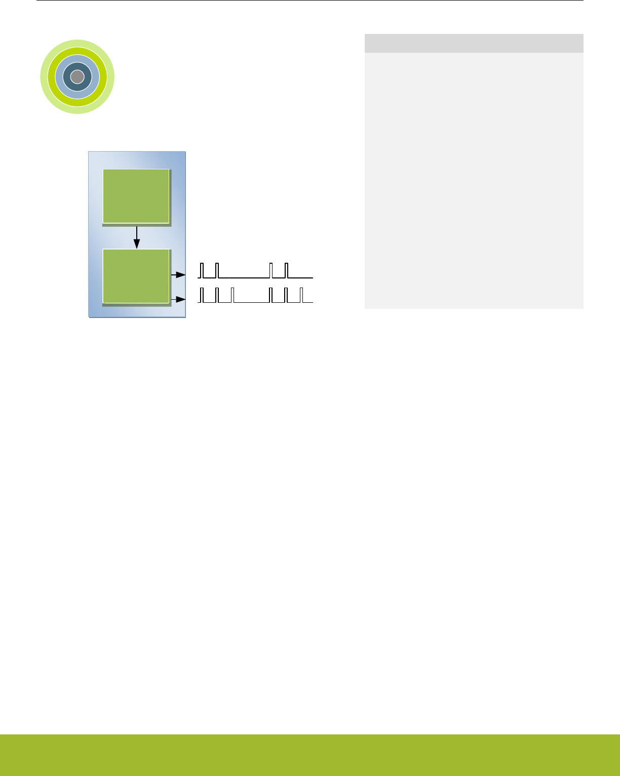
22. LETIMER - Low Energy Timer
0 1 2 3 4
LETIMER
RTC
Quick Facts
What?
The LETIMER is a down-counter that can keep track
of time and output configurable waveforms. Running
on a 32768 Hz clock, the LETIMER is available in
EM0 Active, EM1 Sleep, EM2 Deep Sleep, and EM3
Stop.
Why?
The LETIMER can be used to provide repeatable
waveforms to external components while remaining
in EM2 Deep Sleep. It is well suited for applications
such as metering systems or to provide more com-
pare values than available in the RTC.
How?
With buffered repeat and top value registers, the LE-
TIMER can provide glitch-free waveforms at fre-
quencies up to 16 kHz. It can be coupled with RTC
using PRS, allowing advanced time-keeping and
wake-up functions in EM2 Deep Sleep and EM3
Stop
22.1 Introduction
The unique LETIMERTM, the Low Energy Timer, is a 16-bit timer that is available in energy mode EM0 Active, EM1 Sleep, EM2 Deep
Sleep, and EM3 Stop. Because of this, it can be used for timing and output generation when most of the device is powered down,
allowing simple tasks to be performed while the power consumption of the system is kept at an absolute minimum.
The LETIMER can be used to output a variety of waveforms with minimal software intervention. It can also be connected to the Real
Time Counter (RTC) using PRS, and can be configured to start counting on compare matches from the RTC.
22.2 Features
• 16-bit down count timer
• 2 Compare match registers
• Compare register 0 can be top timer top value
• Compare registers can be double buffered
• Double buffered 8-bit Repeat Register
• Same clock source as the Real Time Counter
• LETIMER can be triggered (started) by an RTC event via PRS or by software
• LETIMER can be started, stopped, and/or cleared by PRS
• 2 output pins can optionally be configured to provide different waveforms on timer underflow:
• Toggle output pin
• Apply a positive pulse (pulse width of one LFACLKLETIMER period)
• PWM
• Interrupt on:
• Compare matches
• Timer underflow
• Repeat done
• Optionally runs during debug
• PRS Output
Reference Manual
LETIMER - Low Energy Timer
silabs.com | Smart. Connected. Energy-friendly. Preliminary Rev. 0.5 | 738
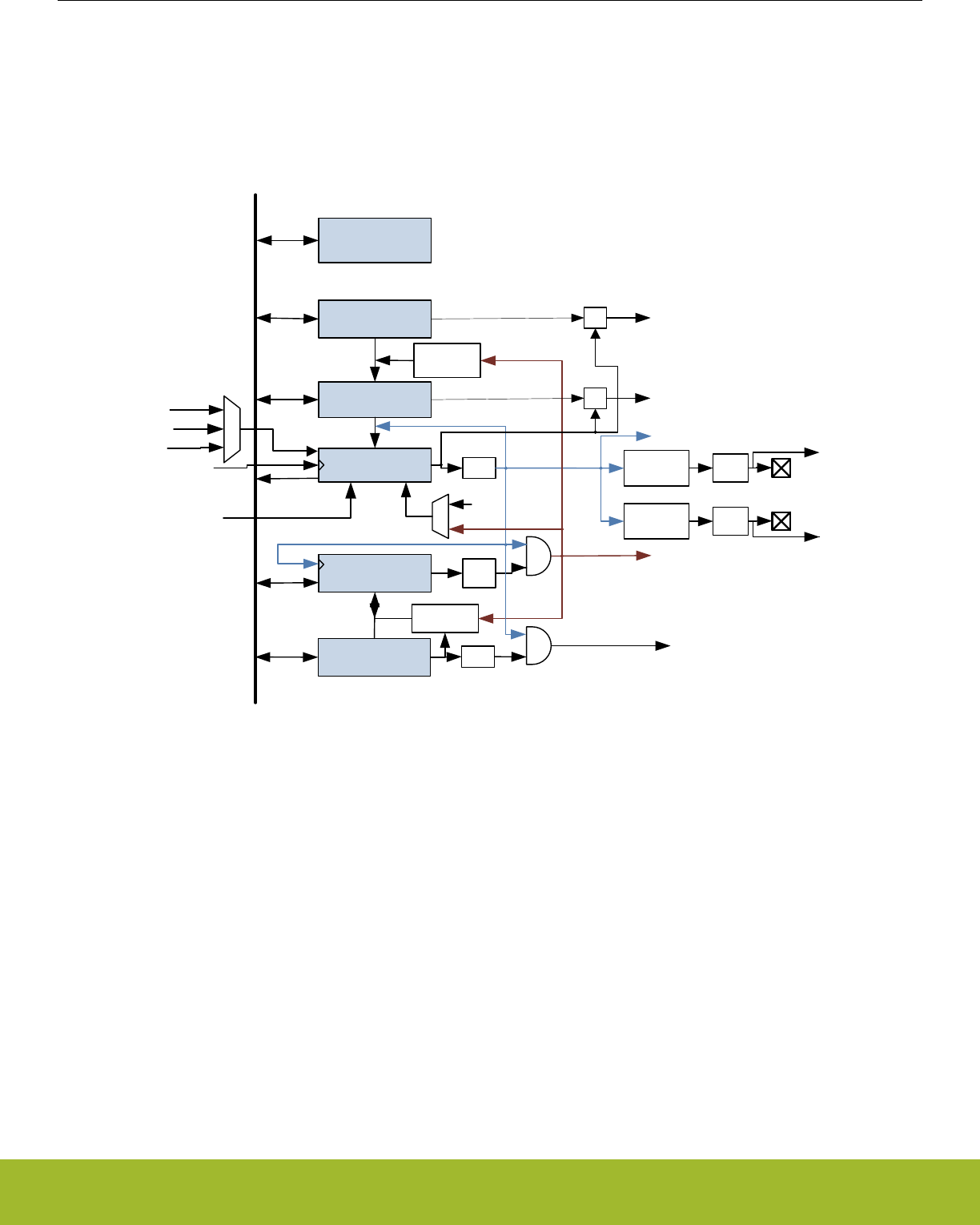
22.3 Functional Description
An overview of the LETIMER module is shown in Figure 22.1 LETIMER Overview on page 739. The LETIMER is a 16-bit down-coun-
ter with two compare registers, LETIMERn_COMP0 and LETIMERn_COMP1. The LETIMERn_COMP0 register can optionally act as a
top value for the counter. The repeat counter LETIMERn_REP0 allows the timer to count a specified number of times before it stops.
Both the LETIMERn_COMP0 and LETIMERn_REP0 registers can be double buffered by the LETIMERn_COMP1 and LETI-
MERn_REP1 registers to allow continuous operation. The timer can generate a single pin output, or two linked outputs.
Peripheral bus
= 0
COMP1
(Top Buffer)
COMP0
(Top)
CNT (Counter)
REP0
(Repeat)
REP1
(Repeat Buffer)
=1
LETIMER Control
and Status
Reload
Update
Update
Stop
PRS event
LFACLKLETIMERn
Start
pin
ctrl LETn_O0
Pulse
Control
Underflow
(UF interrupt flag)
REP0 Zero
(REP0 interrupt flag)
Buffer
Written
Repeat
load logic
pin
ctrl LETn_O1
Pulse
Control
Top load
logic
=1
REP1 Zero
(REP1 interrupt flag)
=
=COMP1 Match
(COMP1 interrupt flag)
COMP0 Match
(COMP0 interrupt flag)
PRS CH1
PRS CH0
RTC event
SW
PRS event
PRS event
Clear
Figure 22.1. LETIMER Overview
22.3.1 Timer
The timer is started by setting command bit START in LETIMERn_CMD, and stopped by setting the STOP command bit in the same
register. RUNNING in LETIMERn_STATUS is set as long as the timer is running. The timer can also be started on external signals,
such as a compare match from the Real Time Counter. If START and STOP are set at the same time, STOP has priority, and the timer
will be stopped.
The timer value can be read using the LETIMERn_CNT register. The value can be written, and it can also be cleared by setting the
CLEAR command bit in LETIMERn_CMD. If the CLEAR and START commands are issued at the same time, the timer will be cleared,
then start counting at the top value.
22.3.2 Compare Registers
The LETIMER has two compare match registers, LETIMERn_COMP0 and LETIMERn_COMP1. Each of these compare registers are
capable of generating an interrupt when the counter value LETIMERn_CNT becomes equal to their value. When LETIMERn_CNT be-
comes equal to the value of LETIMERn_COMP0, the interrupt flag COMP0 in LETIMERn_IF is set, and when LETIMERn_CNT be-
comes equal to the value of LETIMERn_COMP1, the interrupt flag COMP1 in LETIMERn_IF is set.
Reference Manual
LETIMER - Low Energy Timer
silabs.com | Smart. Connected. Energy-friendly. Preliminary Rev. 0.5 | 739

22.3.3 Top Value
If COMP0TOP in LETIMERn_CTRL is set, the value of LETIMERn_COMP0 acts as the top value of the timer, and LETIMERn_COMP0
is loaded into LETIMERn_CNT on timer underflow. If COMP0TOP is cleared to 0, the timer wraps around to 0xFFFF. The underflow
interrupt flag UF in LETIMERn_IF is set when the timer reaches zero.
22.3.3.1 Buffered Top Value
If BUFTOP in LETIMERn_CTRL is set, the value of LETIMERn_COMP0 is buffered by LETIMERn_COMP1. In this mode, the value of
LETIMERn_COMP1 is loaded into LETIMERn_COMP0 every time LETIMERn_REP0 is about to decrement to 0. This can for instance
be used in conjunction with the buffered repeat mode to generate continually changing output waveforms.
Write operations to LETIMERn_COMP0 have priority over buffer loads.
22.3.3.2 Repeat Modes
By default, the timer wraps around to the top value or 0xFFFF on each underflow, and continues counting. The repeat counters can be
used to get more control of the operation of the timer, including defining the number of times the counter should wrap around. Four
different repeat modes are available, see Table 22.1 LETIMER Repeat Modes on page 740.
Table 22.1. LETIMER Repeat Modes
REPMODE Mode Description
0b00 Free-running The timer runs until it is stopped.
0b01 One-shot The timer runs as long as LETI-
MERn_REP0 != 0. LETIMERn_REP0 is de-
cremented at each timer underflow.
0b10 Buffered The timer runs as long as LETI-
MERn_REP0 != 0. LETIMERn_REP0 is de-
cremented on each timer underflow. If LE-
TIMERn_REP1 has been written, it is loa-
ded into LETIMERn_REP0 when LETI-
MERn_REP0 is about to be decremented
to 0.
0b11 Double The timer runs as long as LETI-
MERn_REP0 != 0 or LETIMERn_REP1 !=
0. Both LETIMERn_REP0 and LETI-
MERn_REP1 are decremented at each tim-
er underflow.
The interrupt flags REP0 and REP1 in LETIMERn_IF are set whenever LETIMERn_REP0 or LETIMERn_REP1 are decremented to 0
respectively. REP0 is also set when the value of LETIMERn_REP1 is loaded into LETIMERn_REP0 in buffered mode.
Reference Manual
LETIMER - Low Energy Timer
silabs.com | Smart. Connected. Energy-friendly. Preliminary Rev. 0.5 | 740
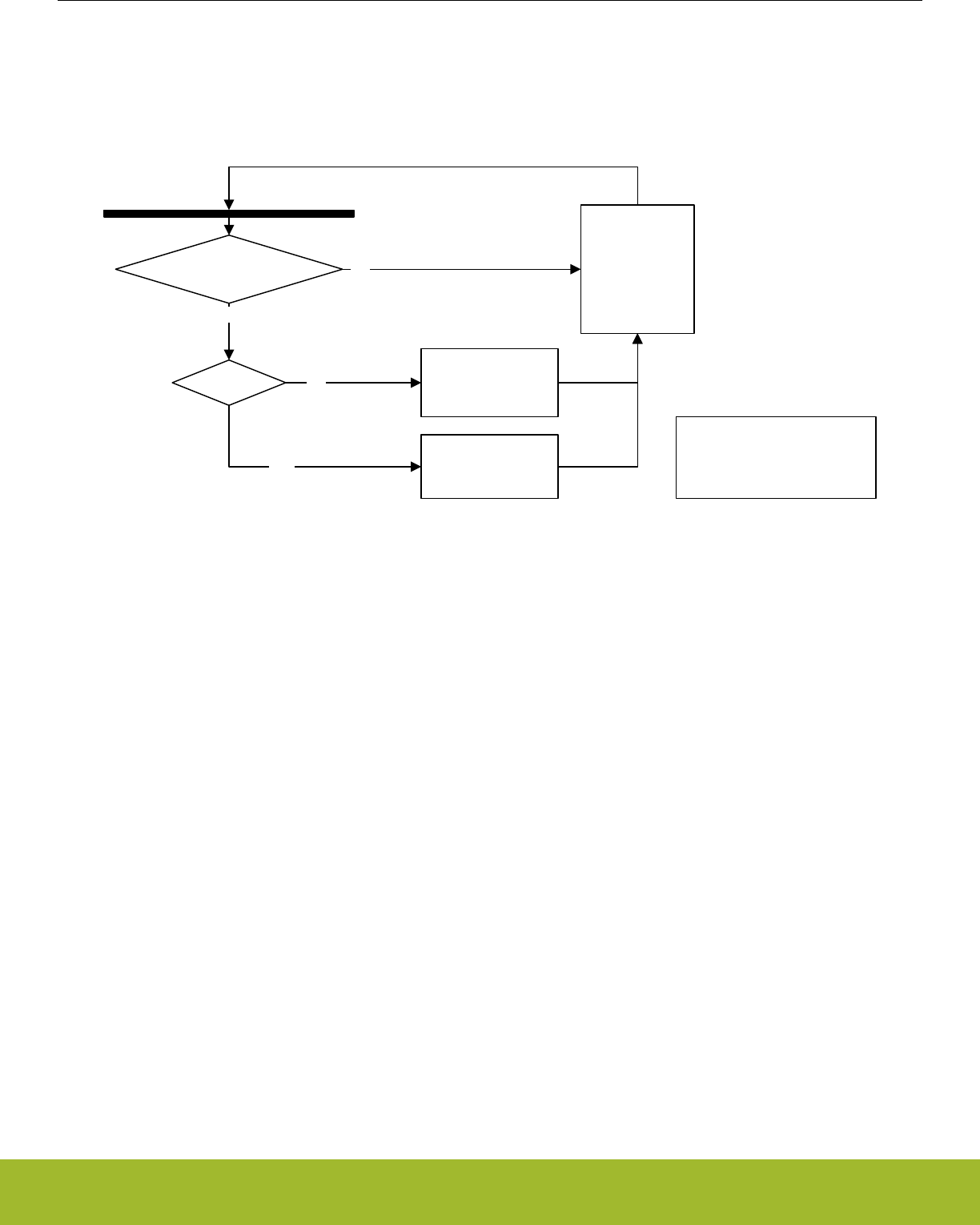
22.3.3.3 Free-Running Mode
In free-running mode, the LETIMER acts as a regular timer and the repeat counter is disabled. When started, the timer runs until it is
stopped using the STOP command bit in LETIMERn_CMD. A state machine for this mode is shown in Figure 22.2 LETIMER State
Machine for Free-running Mode on page 741 .
(RUNNING or START)
and !STOP
YES
NO
CNT == 0 CNT = CNT - 1
NO
YES CNT = TOP*
If (STOP)
RUNNING = 0
Else if (START)
RUNNING = 1
End if
START = 0
STOP = 0
Wait for positive clock edge
If (COMP0TOP)
TOP* = COMP0
Else
TOP* = 0xFFFF
TOP*
Figure 22.2. LETIMER State Machine for Free-running Mode
Note that the CLEAR command bit in LETIMERn_CMD always has priority over other changes to LETIMERn_CNT. When the clear
command is used, LETIMERn_CNT is set to 0 and an underflow event will not be generated when LETIMERn_CNT wraps around to
the top value or 0xFFFF. Since no underflow event is generated, no output action is performed. LETIMERn_REP0, LETIMERn_REP1,
LETIMERn_COMP0 and LETIMERn_COMP1 are also left untouched.
Reference Manual
LETIMER - Low Energy Timer
silabs.com | Smart. Connected. Energy-friendly. Preliminary Rev. 0.5 | 741
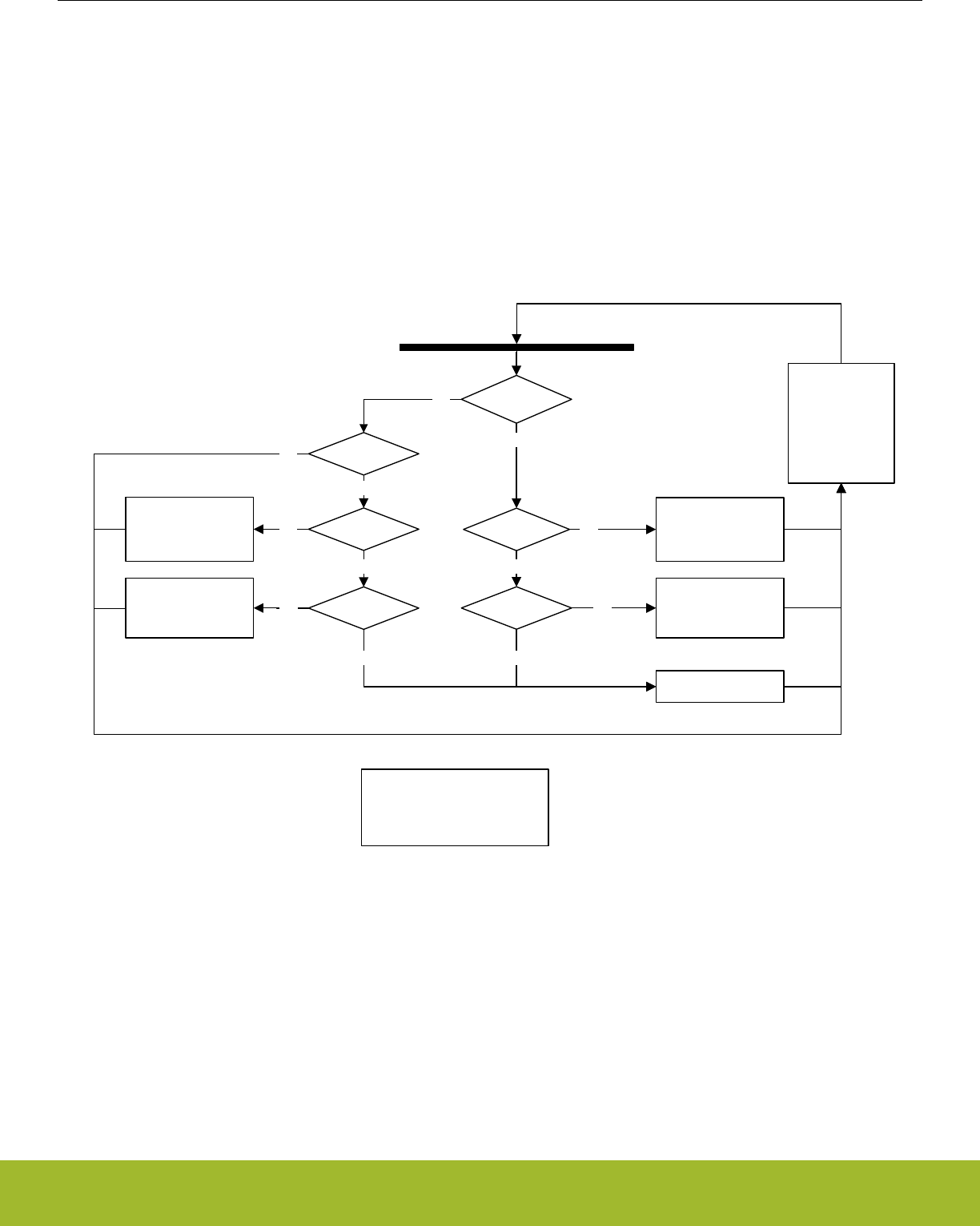
22.3.3.4 One-shot Mode
The one-shot repeat mode is the most basic repeat mode. In this mode, the repeat register LETIMERn_REP0 is decremented every
time the timer underflows, and the timer stops when LETIMERn_REP0 goes from 1 to 0. In this mode, the timer counts down LETI-
MERn_REP0 times, i.e. the timer underflows LETIMERn_REP0 times.
Note:
Note that write operations to LETIMERn_REP0 have priority over the timer decrement event. If LETIMERn_REP0 is assigned a new
value in the same cycle as a timer decrement event occurs, the timer decrement will not occur and the new value is assigned.
LETIMERn_REP0 can be written while the timer is running to allow the timer to run for longer periods at a time without stopping. Figure
22.3 LETIMER One-shot Repeat State Machine on page 742 .
RUNNING
YES
CNT == 0 CNT = CNT - 1
NO
REP0 < 2
YES
NO
STOP = 1
REP0 = 0
CNT = TOP*
If (!START)
REP0 = REP0 - 1
If (STOP)
RUNNING = 0
Else if (START)
RUNNING = 1
End if
START = 0
STOP = 0
Wait for positive clock edge
YES
If (COMP0TOP)
TOP* = COMP0
Else
TOP* = 0xFFFF
TOP*
START
YES
CNT == 0
REP0 == 0
YES
CNT = CNT - 1
CNT = TOP*
NO
NO
YES
NO
NO
Figure 22.3. LETIMER One-shot Repeat State Machine
Reference Manual
LETIMER - Low Energy Timer
silabs.com | Smart. Connected. Energy-friendly. Preliminary Rev. 0.5 | 742
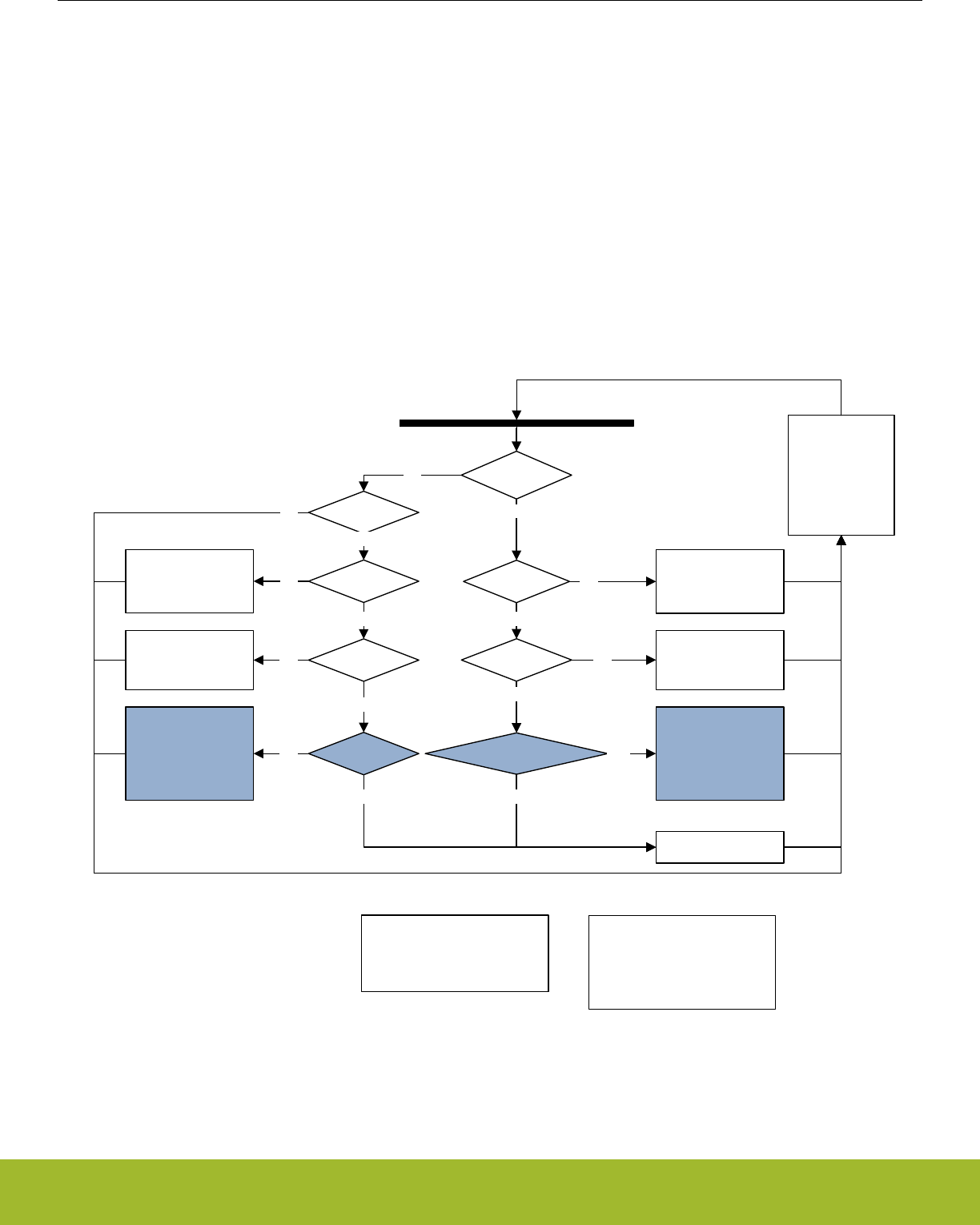
22.3.3.5 Buffered Mode
The Buffered repeat mode allows buffered timer operation. When started, the timer runs LETIMERn_REP0 number of times. If LETI-
MERn_REP1 has been written since the last time it was used and it is nonzero, LETIMERn_REP1 is then loaded into LETI-
MERn_REP0, and counting continues the new number of times. The timer keeps going as long as LETIMERn_REP1 is updated with a
nonzero value before LETIMERn_REP0 is finished counting down. The timer top value (LETIMERn_COMP0) may also optionally be
buffered by setting BUFTOP in LETIMERn_CTRL.
If the timer is started when both LETIMERn_CNT and LETIMERn_REP0 are zero but LETIMERn_REP1 is non-zero, LETIMERn_REP1
is loaded into LETIMERn_REP0, and the counter counts the loaded number of times.
Used in conjunction with a buffered top value, both the top and repeat values of the timer may be buffered, and the timer can for in-
stance be set to run 4 times with period 7 (top value 6), 6 times with period 200, then 3 times with period 50.
A state machine for the buffered repeat mode is shown in Figure 22.4 LETIMER Buffered Repeat State Machine on page 743.
REP1USED shown in the state machine is an internal variable that keeps track of whether the value in LETIMERn_REP1 has been loa-
ded into LETIMERn_REP0 or not. The purpose of this is that a value written to LETIMERn_REP1 should only be counted once.
REP1USED is cleared whenever LETIMERn_REP1 is written.
RUNNING
YES
CNT == 0 CNT = CNT - 1
NO
REP0 < 2
YES
!REP1USED and !REP1 != 0
CNT = TOP**
If (BUFTOP)
COMP0 = COMP1
REP0 = REP1
REP1USED = 1
NO
YES
STOP = 1
REP0 = 0
NO
CNT = TOP*
If (!START)
REP0 = REP0 - 1
If (STOP)
RUNNING = 0
Else if (START)
RUNNING = 1
End if
START = 0
STOP = 0
Wait for positive clock edge
YES
If (!COMP0TOP)
TOP** = 0xFFFF
Else if (BUFTOP)
TOP** = COMP1
Else
TOP** = COMP0
If (COMP0TOP)
TOP* = COMP0
Else
TOP* = 0xFFFF
TOP* TOP**
NO
START
YES
CNT == 0
REP0 == 0
YES
CNT = CNT - 1
CNT = TOP**
If (BUFTOP)
COMP0 = COMP1
REP0 = REP1
REP1USED = 1
CNT = TOP*
NO
NO
YES
REP1 == 0
NO
YES
NO
Figure 22.4. LETIMER Buffered Repeat State Machine
Reference Manual
LETIMER - Low Energy Timer
silabs.com | Smart. Connected. Energy-friendly. Preliminary Rev. 0.5 | 743
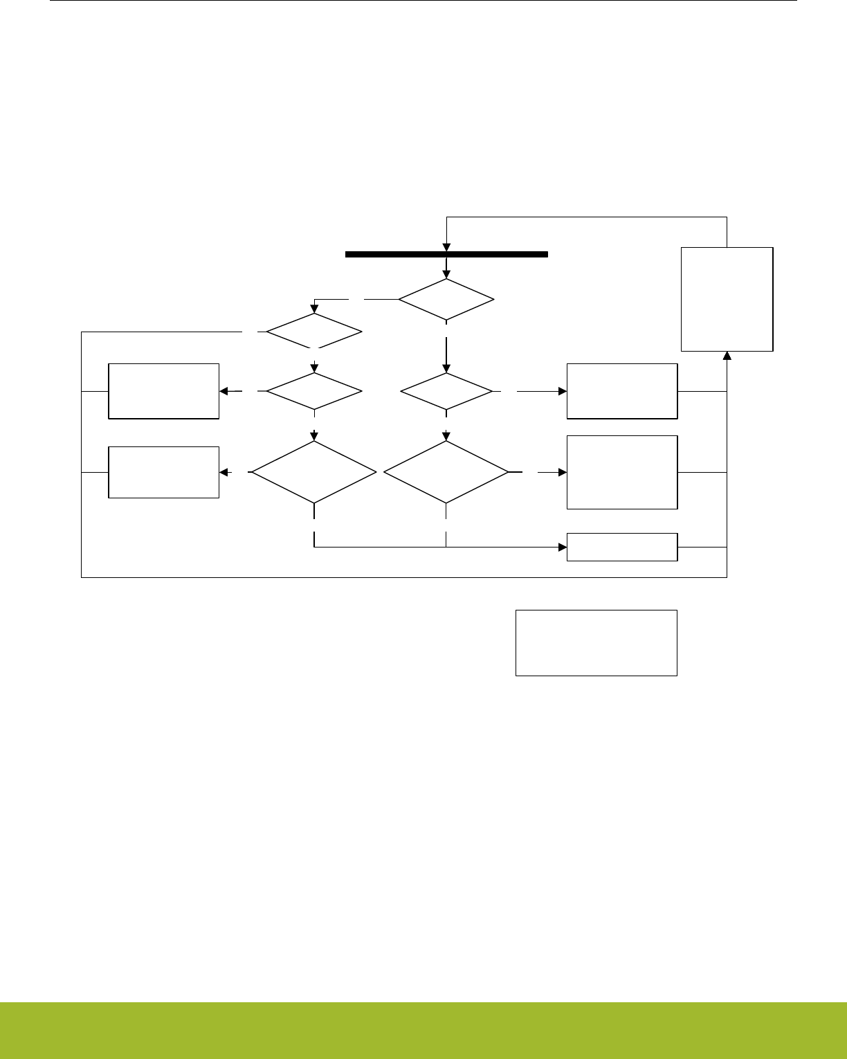
22.3.3.6 Double Mode
The Double repeat mode works much like the one-shot repeat mode. The difference is that, where the one-shot mode counts as long
as LETIMERn_REP0 is larger than 0, the double mode counts as long as either LETIMERn_REP0 or LETIMERn_REP1 is larger than
0. As an example, say LETIMERn_REP0 is 3 and LETIMERn_REP1 is 10 when the timer is started. If no further interaction is done with
the timer, LETIMERn_REP0 will now be decremented 3 times, and LETIMERn_REP1 will be decremented 10 times. The timer counts a
total of 10 times, and LETIMERn_REP0 is 0 after the first three timer underflows and stays at 0. LETIMERn_REP0 and LETI-
MERn_REP1 can be written at any time. After a write to either of these, the timer is guaranteed to underflow at least the written number
of times if the timer is running. Use the Double repeat mode to generate output on both the LETIMER outputs at the same time. The
state machine for this repeat mode can be seen in Figure 22.5 LETIMER Double Repeat State Machine on page 744.
RUNNING
YES
CNT == 0 CNT = CNT - 1
NO
REP0 < 2
And
REP1 < 2
YES
NO
STOP = 1
REP0 = 0
CNT = TOP*
If (REP0 > 0)
REP0 = REP0 - 1
If (REP1 > 0)
REP1 = REP1 - 1
If (STOP)
RUNNING = 0
Else if (START)
RUNNING = 1
End if
START = 0
STOP = 0
Wait for positive clock edge
YES
If (COMP0TOP)
TOP* = COMP0
Else
TOP* = 0xFFFF
TOP*
NO
START
YES
CNT == 0
REP0 == 0
and
REP1 == 0
YES
CNT = CNT - 1
CNT = TOP*
NO
NO
YES
NO
Figure 22.5. LETIMER Double Repeat State Machine
22.3.3.7 Clock Source
The LETIMER clock source and its prescaler value are defined in the Clock Management Unit (CMU). The LFACLKLETIMERn has a fre-
quency given by Figure 22.6 LETIMER Clock Frequency on page 744.
fLFACKL_LETIMERn = 32768/2LETIMERn
Figure 22.6. LETIMER Clock Frequency
where the exponent LETIMERn is a 4 bit value in the CMU_LFAPRESC0 register.
To use this module, the LE interface clock must be enabled in CMU_HFBUSCLKEN0, in addition to the module clock.
Reference Manual
LETIMER - Low Energy Timer
silabs.com | Smart. Connected. Energy-friendly. Preliminary Rev. 0.5 | 744
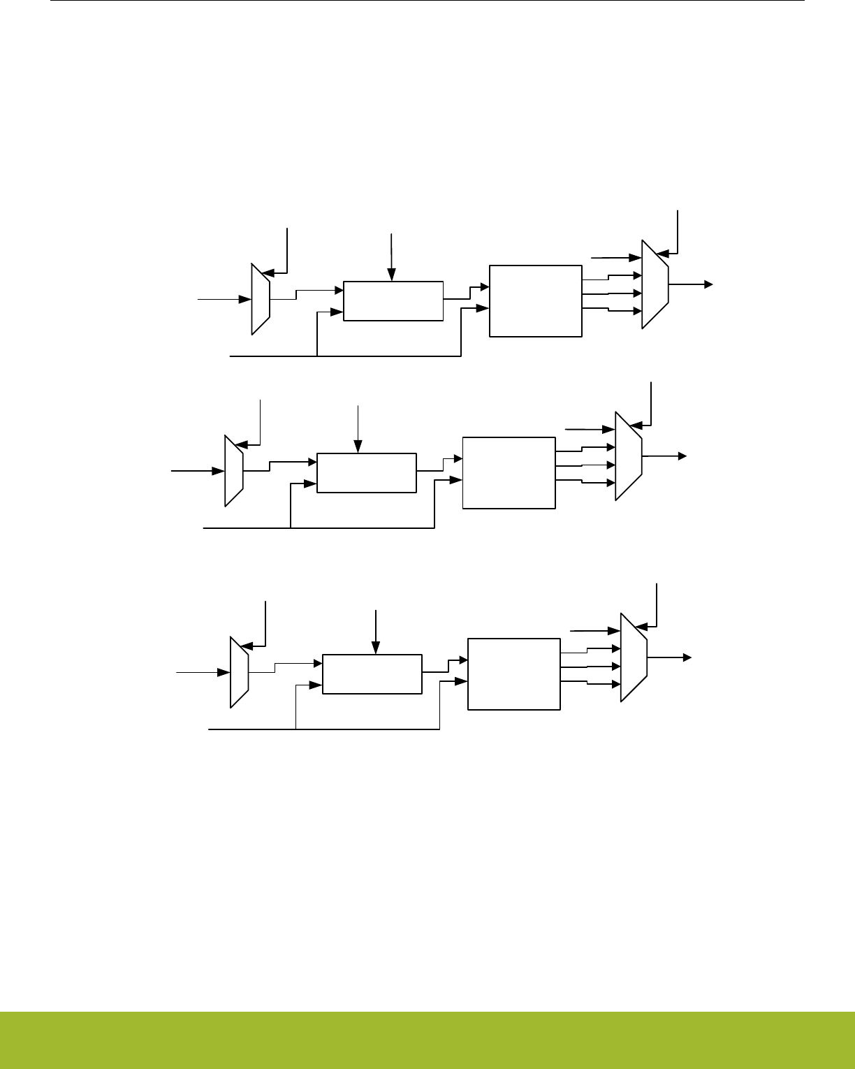
22.3.3.8 PRS Input Triggers
The LETIMER can be configured to start, stop, and/or clear based on PRS inputs. The diagram showing the functions of the PRS input
triggers is shown in Figure 22.7 LETIMER PRS input triggers. on page 745.
There are 12 PRS inputs to the LETIMER. PRSSTARTEN, PRSSTOPEN, and PRSCLEAREN are used to enable starting, stopping,
and/or clearing the LETIMER through the PRS inputs. PRSSTARTSEL, PRSSTOPSEL, and PRSCLEARSEL selects which PRS inputs
are used to start, stop, and/or clear the LETIMER. Finally, PRSSTARTMODE, PRSSTOPMODE, and PRSCLEARMODE select which
edge or edge(s) can trigger the start, stop, and/or clear action.
PRS_IN[11:0]
PRSSTARTSEL
LFACLKLETIMERn
Synchronizer Edge Detect
PRSSTARTMODE
None
Rising
Falling
Both
PRS_START
PRS_IN[11:0]
PRSSTOPSEL
LFACLKLETIMERn
Synchronizer Edge Detect
PRSSTOPMODE
None
Rising
Falling
Both
PRS_STOP
PRS_IN[11:0]
PRSCLEARSEL
LFACLKLETIMERn
Synchronizer Edge Detect
PRSCLEARMODE
None
Rising
Falling
Both
PRS_CLEAR
PRSSTARTEN
PRSSTOPEN
PRSCLEAREN
Figure 22.7. LETIMER PRS input triggers.
22.3.3.9 Debug
If DEBUGRUN in LETIMERn_CTRL is cleared, the LETIMER automatically stops counting when the CPU is halted during a debug ses-
sion, and resumes operation when the CPU continues. Because of synchronization, the LETIMER is halted two clock cycles after the
CPU is halted, and continues running two clock cycles after the CPU continues. RUNNING in LETIMERn_STATUS is not cleared when
the LETIMER stops because of a debug-session.
Set DEBUGRUN in LETIMERn_CTRL to allow the LETIMER to continue counting even when the CPU is halted in debug mode.
Reference Manual
LETIMER - Low Energy Timer
silabs.com | Smart. Connected. Energy-friendly. Preliminary Rev. 0.5 | 745

22.3.4 Underflow Output Action
For each of the repeat registers, an underflow output action can be set. The configured output action is performed every time the coun-
ter underflows while the respective repeat register is nonzero. In PWM mode, the output is similarly only changed on COMP1 match if
the repeat register is nonzero. As an example, the timer will perform 7 output actions if LETIMERn_REP0 is set to 7 when starting the
timer in one-shot mode and leaving it untouched.
The output actions can be set by configuring UFOA0 and UFOA1 in LETIMERn_CTRL. UFOA0 defines the action on output 0, and is
connected to LETIMERn_REP0, while UFOA1 defines the action on output 1 and is connected to LETIMERn_REP1. The possible ac-
tions are defined in Table 22.2 LETIMER Underflow Output Actions on page 746.
Table 22.2. LETIMER Underflow Output Actions
UF0A0/UF0A1 Mode Description
0b00 Idle The output is held at its idle value
0b01 Toggle The output is toggled on LETIMERn_CNT
underflow if LEIMERn_REPx is nonzero
0b10 Pulse The output is held active for one clock cy-
cle on LETIMERn_CNT underflow if LETI-
MERn_REPx is nonzero. It then returns to
its idle value
0b11 PWM The output is set idle on LETIMERn_CNT
underflow and active on compare match
with LETIMERn_COMP1 if LETI-
MERn_REPx is nonzero.
Note:
For the Pulse and PWM modes, the outputs will return to their idle states regardless of the state of the corresponding LETIMERn_REPx
registers. They will only be set active if the LETIMERn_REPx registers are nonzero however.
Note:
For free-running mode, LETIMERn_REP0 != 0 for output generation to be enabled.
The polarity of the outputs can be set individually by configuring OPOL0 and OPOL1 in LETIMERn_CTRL. When these are cleared,
their respective outputs have a low idle value and a high active value. When they are set, the idle value is high, and the active value is
low.
When using the toggle action, the outputs can be driven to their idle values by setting their respective CTO0/CTO1 command bits in
LETIMERn_CTRL. This can be used to put the output in a well-defined state before beginning to generate toggle output, which may be
important in some applications. The command bit can also be used while the timer is running.
Some simple waveforms generated with the different output modes are shown in Figure 22.8 LETIMER Simple Waveforms Output on
page 747. For the example, REPMODE in LETIMERn_CTRL has been cleared, COMP0TOP also in LETIMERn_CTRL has been set
and LETIMERn_COMP0 has been written to 3. As seen in the figure, LETIMERn_COMP0 now decides the length of the signal periods.
For the toggle mode, the period of the output signal is 2(LETIMERn_COMP0 + 1), and for the pulse modes, the periods of the output
signals are LETIMERn_COMP0+1. Note that the pulse outputs are delayed by one period relative to the toggle output. The pulses
come at the end of their periods.
Reference Manual
LETIMER - Low Energy Timer
silabs.com | Smart. Connected. Energy-friendly. Preliminary Rev. 0.5 | 746
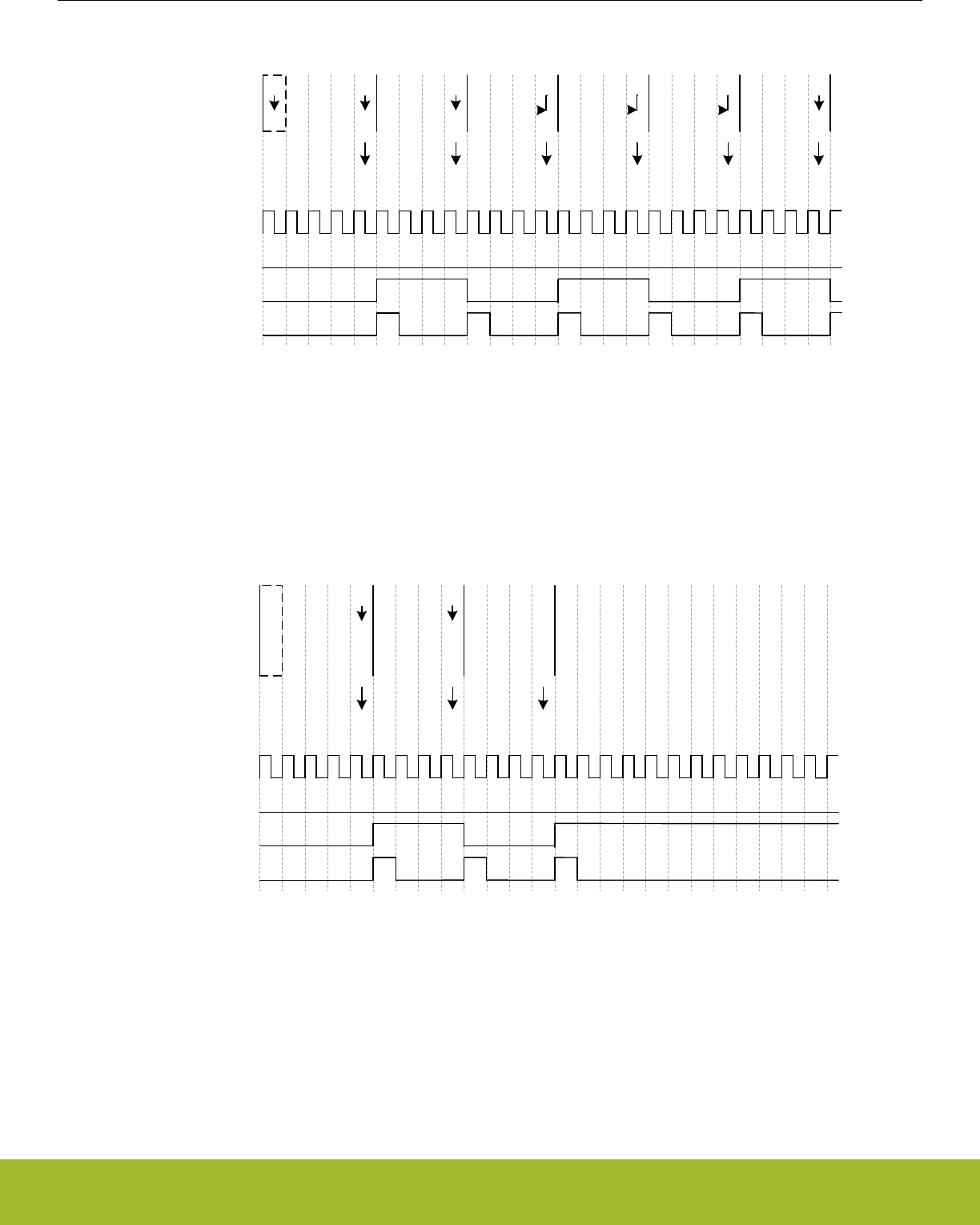
CNT
COMP0 3
3
3
2
3
1
3
0
3
3
3
2
3
1
3
0
3
3
3
2
3
1
3
0
3
3
3
2
3
1
3
0
3
3
3
2
3
1
3
0
3
3
3
2
3
1
Initial configuration
UFIFUFIF UFIF UFIF UFIF
Int. flags set
LFACLKLETIMERn
LETn_O0
UFOA0 = 01
LETn_O0
UFOA0 = 10
LETn_O0
UFOA0 = 00
3
0
UFIF
3
0
Figure 22.8. LETIMER Simple Waveforms Output
For the example in Figure 22.9 LETIMER Repeated Counting on page 747, the One-shot repeat mode has been selected, and LETI-
MERn_REP0 has been written to 3. The resulting behavior is pretty similar to that shown in Figure 6, but in this case, the timer stops
after counting to zero LETIMERn_REP0 times. By using LETIMERn_REP0 the user has full control of the number of pulses/toggles
generated on the output.
CNT
COMP0 3
3
3
2
3
1
3
0
3
3
3
2
3
1
3
0
3
3
3
2
3
1
3
0
Initial configuration
UFIFUFIF UFIF
Int. flags set
LFACLKLETIMERn
LETn_O0
UFOA0 = 01
LETn_O0
UFOA0 = 10
LETn_O0
UFOA0 = 00
REP0 33 3 3 22 2 2 11 1 1
Stop
REP0IF
3
0
0
3
0
0
3
0
0
3
0
0
3
0
0
3
0
0
3
0
0
3
0
0
3
0
0
3
0
0
3
0
0
3
0
0
3
0
3
Figure 22.9. LETIMER Repeated Counting
Using the Double repeat mode, output can be generated on both the LETIMER outputs. Figure 22.10 LETIMER Dual Output on page
748 shows an example of this. UFOA0 and UFOA1 in LETIMERn_CTRL are configured for pulse output and the outputs are config-
ured for low idle polarity. As seen in the figure, the number written to the repeat registers determine the number of pulses generated on
each of the outputs.
Reference Manual
LETIMER - Low Energy Timer
silabs.com | Smart. Connected. Energy-friendly. Preliminary Rev. 0.5 | 747

LETn_O0
LETn_O1
UFOA0 = 10
UFOA1 = 10
REP0 = 2
REP1 = 7
START
REP0 = 3
START
REP0 = 2
REP1 = 3
START
Figure 22.10. LETIMER Dual Output
22.3.5 PRS Output
The LETIMER outputs can be routed out onto the PRS system. LETn_O0 can be routed to PRS channel 0, and LETn_O1 can be rout-
ed to PRS channel 1. Enabling the PRS connection can be done by setting SOURCESEL to LETIMERx and SIGSEL to LETIMERxCHn
in PRS_CHx_CTRL. The PRS register description can be found in 16.5 Register Description
22.3.6 Examples
This section presents a couple of usage examples for the LETIMER.
Reference Manual
LETIMER - Low Energy Timer
silabs.com | Smart. Connected. Energy-friendly. Preliminary Rev. 0.5 | 748
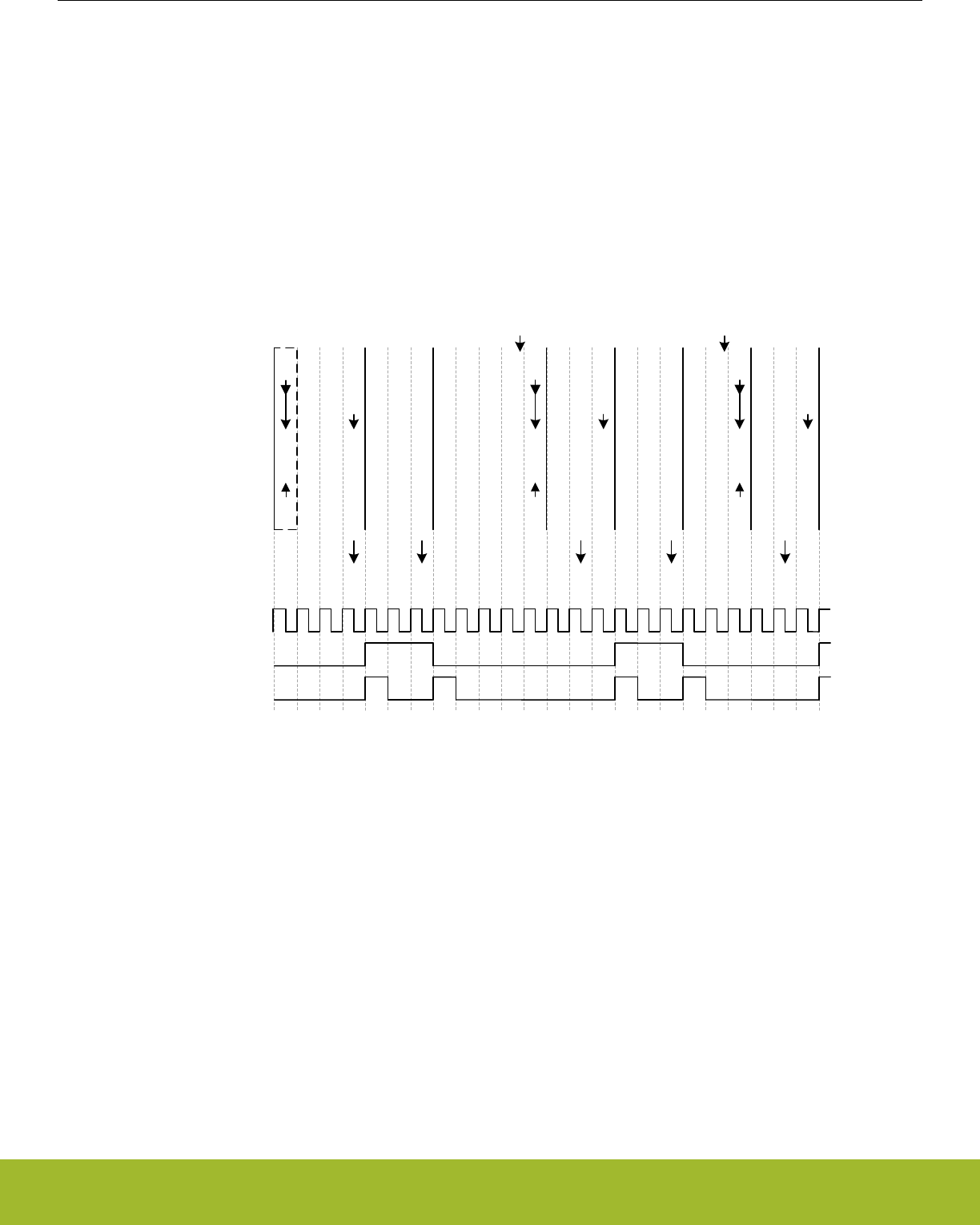
22.3.6.1 Triggered Output Generation
If both LETIMERn_CNT and LETIMERn_REP0 are 0 in buffered mode, and COMP0TOP and BUFTOP in LETIMERn_CTRL are set,
the values of LETIMERn_COMP1 and LETIMERn_REP1 are loaded into LETIMERn_CNT and LETIMERn_REP0 respectively when
the timer is started. If no additional writes to LETIMERn_REP1 are done before the timer stops, LETIMERn_REP1 determines the num-
ber of pulses/toggles generated on the output, and LETIMERn_COMP1 determines the period lengths.
As the RTC can be used via PRS to start the LETIMER, the RTC and LETIMER can thus be combined to generate specific pulse-trains
at given intervals. Software can update LETIMERn_COMP1 and LETIMERn_REP1 to change the number of pulses and pulse-period in
each train, but if changes are not required, software does not have to update the registers between each pulse train.
For the example in Figure 22.11 LETIMER Triggered Operation on page 749, the initial values cause the LETIMER to generate two
pulses with 3 cycle periods, or a single pulse 3 cycles wide every time the LETIMER is started. After the output has been generated, the
LETIMER stops, and is ready to be triggered again.
CNT
TOP0
TOP1
REP0
REP1
2
X
0
0
2
2
2
2
2
2
2
1
2
2
2
0
2
2
2
2
1
2
2
1
1
2
2
0
1
2
2
2
2
2
2
1
2
2
2
0
2
2
2
2
1
2
2
1
1
2
2
0
1
Initial configuration,
REP1 just written
UFIF
REP0IF
UFIF UFIF UFIF
REP0IF
Int. flags set
LFACLKLETIMERn
2u2u2u
Stop
Write
START=1
2
2
0
0
2u
Stop
2
2
2
2
2
2
1
2
2
2
0
2
UFIF
Write
START=1
2
2
0
0
2u
LETn_O0
UFOA0 = 01
LETn_O1
UFOA0 = 10
2u2u2u2u2u2u2u2u2u2u2u2u
2
2
0
0
2u
2
2
0
0
2u
2
2
0
0
2u
2
2
0
0
2u
2
2
0
0
2u
2
2
0
0
2u
Figure 22.11. LETIMER Triggered Operation
Reference Manual
LETIMER - Low Energy Timer
silabs.com | Smart. Connected. Energy-friendly. Preliminary Rev. 0.5 | 749
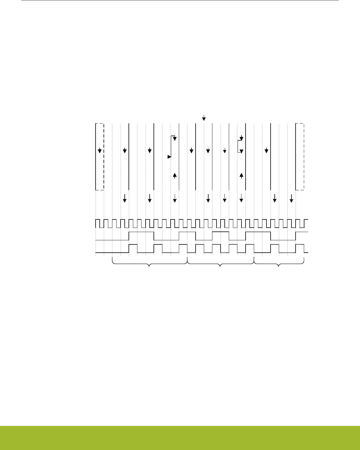
22.3.6.2 Continuous Output Generation
In some scenarios, it might be desired to make LETIMER generate a continuous waveform. Very simple constant waveforms can be
generated without the repeat counter as shown in Figure 22.8 LETIMER Simple Waveforms Output on page 747, but to generate
changing waveforms, using the repeat counter and buffer registers can prove advantageous.
For the example in Figure 22.12 LETIMER Continuous Operation on page 750, the goal is to produce a pulse train consisting of 3
sequences with the following properties:
• 3 pulses with periods of 3 cycles
• 4 pulses with periods of 2 cycles
• 2 pulses with periods of 3 cycles
CNT
COMP0
COMP1
REP0
REP1
1
2
0
3
1
2
2
3
1
2
1
3
1
2
0
3
1
2
2
2
1
2
1
2
1
2
0
2
1
2
2
1
1
2
1
1
1
2
0
1
1
1
1
4
1
1
0
4
1
1
1
3
2
1
0
3
2
1
1
2
2
1
0
2
2
1
1
1
2
1
0
1
2
2
2
2
2
2
1
2
2
2
0
2
2
2
2
1
Initial configuration,
REPB just written
UFIF
REP0IF
UFIF UFIF UFIF UFIF
Int. flags set
Stop,
final values
Write
COMP1 = 2
REP1 = 2
UFIF UFIF UFIF
REP0IF
44 4 4 4u4u4u22 2u2u2u2u
2
2
1
1
2
2
0
1
2u2u
REP0IF
LFACLKLETIMERn
LETn_O0
UFOA0 = 01
LETn_O1
UFOA0 = 10
Pulse Seq. 1 Pulse Seq. 2 Pulse Seq. 3
4 4 4 4 4 4 2 2 2
2
2
0
0
2u
Figure 22.12. LETIMER Continuous Operation
The first two sequences are loaded into the LETIMER before the timer is started.
LETIMERn_COMP0 is set to 2 (cycles – 1), and LETIMERn_REP0 is set to 3 for the first sequence, and the second sequence is loaded
into the buffer registers, i.e. COMP1 is set to 1 and LETIMERn_REP1 is set to 4.
The LETIMER is set to trigger an interrupt when LETIMERn_REP0 is done by setting REP0 in LETIMERn_IEN. This interrupt is a good
place to update the values of the buffers. Last but not least REPMODE in LETIMERn_CTRL is set to buffered mode, and the timer is
started.
In the interrupt routine the buffers are updated with the values for the third sequence. If this had not been done, the timer would have
stopped after the second sequence.
Reference Manual
LETIMER - Low Energy Timer
silabs.com | Smart. Connected. Energy-friendly. Preliminary Rev. 0.5 | 750
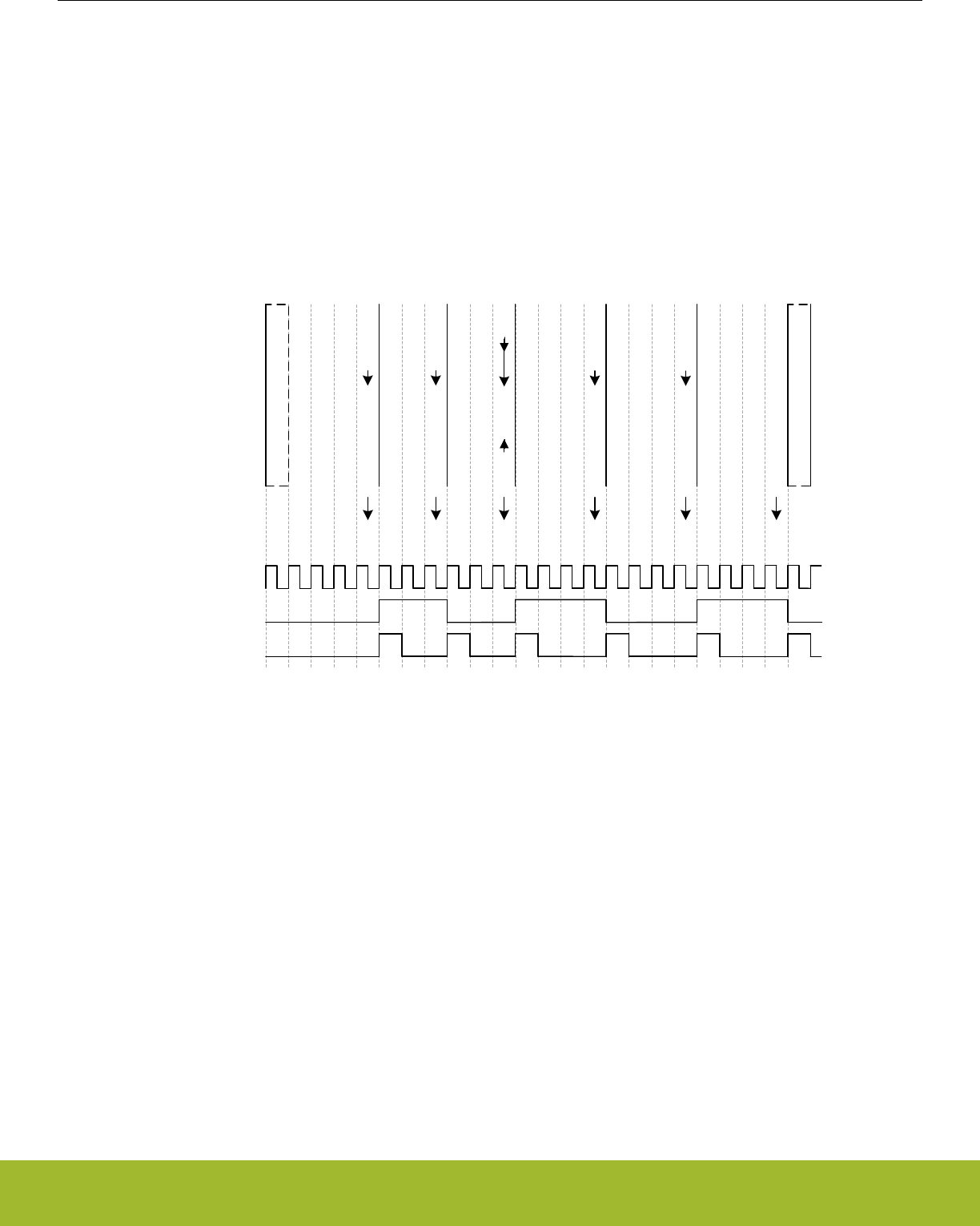
The final result is shown in Figure 22.12 LETIMER Continuous Operation on page 750. The pulse output is grouped to show which
sequence generated which output. Toggle output is also shown in the figure. Note that the toggle output is not aligned with the pulse
outputs.
Note:
Multiple LETIMER cycles are required to write a value to the LETIMER registers. The example in Figure 22.12 LETIMER Continuous
Operation on page 750 assumes that writes are done in advance so they arrive in the LETIMER as described in the figure.
Figure 22.13 LETIMER LETIMERn_CNT Not Initialized to 0 on page 751 shows an example where the LETIMER is started while
LETIMERn_CNT is nonzero. In this case the length of the first repetition is given by the value in LETIMERn_CNT.
CNT
TOP0
TOP1
REP0
REP1
3
2
4
3
3
3
2
3
3
3
2
2
3
3
2
1
3
3
2
0
3
3
2
2
2
3
2
1
2
3
2
0
2
3
2
2
1
3
2
1
1
3
2
0
1
3
3
3
3
3
3
2
3
3
3
1
3
3
3
0
3
3
3
3
2
3
3
2
2
3
3
1
2
3
3
0
2
3
3
3
1
3
3
2
1
3
3
1
1
3
3
0
Initial configuration,
REP1 just written
UFIF
REP0IF
UFIF UFIF UFIF UFIF UFIF
REP0IF
Int. flags set
Stop,
final values
LFACLKLETIMERn
LETn_O0
UFOA0 = 01
LETn_O1
UFOA0 = 10
3 3 3 3 3 3 3 3u3u3u3u3u3u3u
3 3 3 3u3u3u
1
3u
3u
3
3
0
0
3u
Figure 22.13. LETIMER LETIMERn_CNT Not Initialized to 0
22.3.6.3 PWM Output
There are several ways of generating PWM output with the LETIMER, but the most straight-forward way is using the PWM output
mode. This mode is enabled by setting UFOA0 or UFOA1 in LETIMERn_CTRL to 3. In PWM mode, the output is set idle on timer un-
derflow, and active on LETIMERn_COMP1 match, so if for instance COMP0TOP = 1 and OPOL0 = 0 in LETIMERn_CTRL, LETI-
MERn_COMP0 determines the PWM period, and LETIMERn_COMP1 determines the active period.
The PWM period in PWM mode is LETIMERn_COMP0 + 1. There is no special handling of the case where LETIMERn_COMP1 > LE-
TIMERn_COMP0, so if LETIMERn_COMP1 > LETIMERn_COMP0, the PWM output is given by the idle output value. This means that
for OPOLx = 0 in LETIMERn_CTRL, the PWM output will always be 0 for at least one clock cycle, and for OPOLx = 1 LETI-
MERn_CTRL, the PWM output will always be 1 for at least one clock cycle.
To generate a PWM signal using the full PWM range, invert OPOLx when LETIMERn_COMP1 is set to a value larger than LETI-
MERn_COMP0.
22.3.6.4 Interrupts
The interrupts generated by the LETIMER are combined into one interrupt vector. If the interrupt for the LETIMER is enabled, an inter-
rupt will be made if one or more of the interrupt flags in LETIMERn_IF and their corresponding bits in LETIMER_IEN are set.
Reference Manual
LETIMER - Low Energy Timer
silabs.com | Smart. Connected. Energy-friendly. Preliminary Rev. 0.5 | 751

22.3.7 Register access
This module is a Low Energy Peripheral, and supports immediate synchronization. For description regarding immediate synchroniza-
tion, the reader is referred to 4.3.1 Writing.
22.4 Register Map
The offset register address is relative to the registers base address.
Offset Name Type Description
0x000 LETIMERn_CTRL RW Control Register
0x004 LETIMERn_CMD W1 Command Register
0x008 LETIMERn_STATUS RStatus Register
0x00C LETIMERn_CNT RWH Counter Value Register
0x010 LETIMERn_COMP0 RWH Compare Value Register 0
0x014 LETIMERn_COMP1 RW Compare Value Register 1
0x018 LETIMERn_REP0 RWH Repeat Counter Register 0
0x01C LETIMERn_REP1 RWH Repeat Counter Register 1
0x020 LETIMERn_IF RInterrupt Flag Register
0x024 LETIMERn_IFS W1 Interrupt Flag Set Register
0x028 LETIMERn_IFC (R)W1 Interrupt Flag Clear Register
0x02C LETIMERn_IEN RW Interrupt Enable Register
0x034 LETIMERn_SYNCBUSY RSynchronization Busy Register
0x040 LETIMERn_ROUTEPEN RW I/O Routing Pin Enable Register
0x044 LETIMERn_ROUTELOC0 RW I/O Routing Location Register
0x050 LETIMERn_PRSSEL RW PRS Input Select Register
Reference Manual
LETIMER - Low Energy Timer
silabs.com | Smart. Connected. Energy-friendly. Preliminary Rev. 0.5 | 752

22.5 Register Description
22.5.1 LETIMERn_CTRL - Control Register (Async Reg)
For more information about asynchronous registers please see 4.3 Access to Low Energy Peripherals (Asynchronous Registers).
Offset Bit Position
0x000
31
30
29
28
27
26
25
24
23
22
21
20
19
18
17
16
15
14
13
12
11
10
9
8
7
6
5
4
3
2
1
0
Reset
0
0
0
0
0
0x0
0x0
0x0
Access
RW
RW
RW
RW
RW
RW
RW
RW
Name
DEBUGRUN
COMP0TOP
BUFTOP
OPOL1
OPOL0
UFOA1
UFOA0
REPMODE
Bit Name Reset Access Description
31:13 Reserved To ensure compatibility with future devices, always write bits to 0. More information in 1.2 Conven-
tions
12 DEBUGRUN 0 RW Debug Mode Run Enable
Set to keep the LETIMER running in debug mode.
Value Description
0 LETIMER is frozen in debug mode
1 LETIMER is running in debug mode
11:10 Reserved To ensure compatibility with future devices, always write bits to 0. More information in 1.2 Conven-
tions
9 COMP0TOP 0 RW Compare Value 0 Is Top Value
When set, the counter is cleared in the clock cycle after a compare match with compare channel 0.
Value Description
0 The top value of the LETIMER is 65535 (0xFFFF)
1 The top value of the LETIMER is given by COMP0
8 BUFTOP 0 RW Buffered Top
Set to load COMP1 into COMP0 when REP0 reaches 0, allowing a buffered top value.
Value Description
0 COMP0 is only written by software
1 COMP0 is set to COMP1 when REP0 reaches 0
7 OPOL1 0 RW Output 1 Polarity
Defines the idle value of output 1.
6 OPOL0 0 RW Output 0 Polarity
Defines the idle value of output 0.
Reference Manual
LETIMER - Low Energy Timer
silabs.com | Smart. Connected. Energy-friendly. Preliminary Rev. 0.5 | 753

Bit Name Reset Access Description
5:4 UFOA1 0x0 RW Underflow Output Action 1
Defines the action on LETn_O1 on a LETIMER underflow.
Value Mode Description
0 NONE LETn_O1 is held at its idle value as defined by OPOL1
1 TOGGLE LETn_O1 is toggled on CNT underflow
2 PULSE LETn_O1 is held active for one LFACLKLETIMER0 clock cycle on CNT
underflow. The output then returns to its idle value as defined by
OPOL1
3 PWM LETn_O1 is set idle on CNT underflow, and active on compare match
with COMP1
3:2 UFOA0 0x0 RW Underflow Output Action 0
Defines the action on LETn_O0 on a LETIMER underflow.
Value Mode Description
0 NONE LETn_O0 is held at its idle value as defined by OPOL0
1 TOGGLE LETn_O0 is toggled on CNT underflow
2 PULSE LETn_O0 is held active for one LFACLKLETIMER0 clock cycle on CNT
underflow. The output then returns to its idle value as defined by
OPOL0
3 PWM LETn_O0 is set idle on CNT underflow, and active on compare match
with COMP1
1:0 REPMODE 0x0 RW Repeat Mode
Allows the repeat counter to be enabled and disabled.
Value Mode Description
0 FREE When started, the LETIMER counts down until it is stopped by software
1 ONESHOT The counter counts REP0 times. When REP0 reaches zero, the coun-
ter stops
2 BUFFERED The counter counts REP0 times. If REP1 has been written, it is loaded
into REP0 when REP0 reaches zero, otherwise the counter stops
3 DOUBLE Both REP0 and REP1 are decremented when the LETIMER wraps
around. The LETIMER counts until both REP0 and REP1 are zero
Reference Manual
LETIMER - Low Energy Timer
silabs.com | Smart. Connected. Energy-friendly. Preliminary Rev. 0.5 | 754

22.5.2 LETIMERn_CMD - Command Register
Offset Bit Position
0x004
31
30
29
28
27
26
25
24
23
22
21
20
19
18
17
16
15
14
13
12
11
10
9
8
7
6
5
4
3
2
1
0
Reset
0
0
0
0
0
Access
W1
W1
W1
W1
W1
Name
CTO1
CTO0
CLEAR
STOP
START
Bit Name Reset Access Description
31:5 Reserved To ensure compatibility with future devices, always write bits to 0. More information in 1.2 Conven-
tions
4 CTO1 0 W1 Clear Toggle Output 1
Set to drive toggle output 1 to its idle value
3 CTO0 0 W1 Clear Toggle Output 0
Set to drive toggle output 0 to its idle value
2 CLEAR 0 W1 Clear LETIMER
Set to clear LETIMER
1 STOP 0 W1 Stop LETIMER
Set to stop LETIMER
0 START 0 W1 Start LETIMER
Set to start LETIMER
22.5.3 LETIMERn_STATUS - Status Register
Offset Bit Position
0x008
31
30
29
28
27
26
25
24
23
22
21
20
19
18
17
16
15
14
13
12
11
10
9
8
7
6
5
4
3
2
1
0
Reset
0
Access
R
Name
RUNNING
Bit Name Reset Access Description
31:1 Reserved To ensure compatibility with future devices, always write bits to 0. More information in 1.2 Conven-
tions
0 RUNNING 0 R LETIMER Running
Set when LETIMER is running.
Reference Manual
LETIMER - Low Energy Timer
silabs.com | Smart. Connected. Energy-friendly. Preliminary Rev. 0.5 | 755

22.5.4 LETIMERn_CNT - Counter Value Register
Offset Bit Position
0x00C
31
30
29
28
27
26
25
24
23
22
21
20
19
18
17
16
15
14
13
12
11
10
9
8
7
6
5
4
3
2
1
0
Reset
0x0000
Access
RWH
Name
CNT
Bit Name Reset Access Description
31:16 Reserved To ensure compatibility with future devices, always write bits to 0. More information in 1.2 Conven-
tions
15:0 CNT 0x0000 RWH Counter Value
Use to read the current value of the LETIMER.
22.5.5 LETIMERn_COMP0 - Compare Value Register 0 (Async Reg)
For more information about asynchronous registers please see 4.3 Access to Low Energy Peripherals (Asynchronous Registers).
Offset Bit Position
0x010
31
30
29
28
27
26
25
24
23
22
21
20
19
18
17
16
15
14
13
12
11
10
9
8
7
6
5
4
3
2
1
0
Reset
0x0000
Access
RWH
Name
COMP0
Bit Name Reset Access Description
31:16 Reserved To ensure compatibility with future devices, always write bits to 0. More information in 1.2 Conven-
tions
15:0 COMP0 0x0000 RWH Compare Value 0
Compare and optionally top value for LETIMER.
Reference Manual
LETIMER - Low Energy Timer
silabs.com | Smart. Connected. Energy-friendly. Preliminary Rev. 0.5 | 756

22.5.6 LETIMERn_COMP1 - Compare Value Register 1 (Async Reg)
For more information about asynchronous registers please see 4.3 Access to Low Energy Peripherals (Asynchronous Registers).
Offset Bit Position
0x014
31
30
29
28
27
26
25
24
23
22
21
20
19
18
17
16
15
14
13
12
11
10
9
8
7
6
5
4
3
2
1
0
Reset
0x0000
Access
RW
Name
COMP1
Bit Name Reset Access Description
31:16 Reserved To ensure compatibility with future devices, always write bits to 0. More information in 1.2 Conven-
tions
15:0 COMP1 0x0000 RW Compare Value 1
Compare and optionally buffered top value for LETIMER.
22.5.7 LETIMERn_REP0 - Repeat Counter Register 0 (Async Reg)
For more information about asynchronous registers please see 4.3 Access to Low Energy Peripherals (Asynchronous Registers).
Offset Bit Position
0x018
31
30
29
28
27
26
25
24
23
22
21
20
19
18
17
16
15
14
13
12
11
10
9
8
7
6
5
4
3
2
1
0
Reset
0x00
Access
RWH
Name
REP0
Bit Name Reset Access Description
31:8 Reserved To ensure compatibility with future devices, always write bits to 0. More information in 1.2 Conven-
tions
7:0 REP0 0x00 RWH Repeat Counter 0
Optional repeat counter.
Reference Manual
LETIMER - Low Energy Timer
silabs.com | Smart. Connected. Energy-friendly. Preliminary Rev. 0.5 | 757

22.5.8 LETIMERn_REP1 - Repeat Counter Register 1 (Async Reg)
For more information about asynchronous registers please see 4.3 Access to Low Energy Peripherals (Asynchronous Registers).
Offset Bit Position
0x01C
31
30
29
28
27
26
25
24
23
22
21
20
19
18
17
16
15
14
13
12
11
10
9
8
7
6
5
4
3
2
1
0
Reset
0x00
Access
RWH
Name
REP1
Bit Name Reset Access Description
31:8 Reserved To ensure compatibility with future devices, always write bits to 0. More information in 1.2 Conven-
tions
7:0 REP1 0x00 RWH Repeat Counter 1
Optional repeat counter or buffer for REP0.
22.5.9 LETIMERn_IF - Interrupt Flag Register
Offset Bit Position
0x020
31
30
29
28
27
26
25
24
23
22
21
20
19
18
17
16
15
14
13
12
11
10
9
8
7
6
5
4
3
2
1
0
Reset
0
0
0
0
0
Access
R
R
R
R
R
Name
REP1
REP0
UF
COMP1
COMP0
Bit Name Reset Access Description
31:5 Reserved To ensure compatibility with future devices, always write bits to 0. More information in 1.2 Conven-
tions
4 REP1 0 R Repeat Counter 1 Interrupt Flag
Set when repeat counter 1 reaches zero.
3 REP0 0 R Repeat Counter 0 Interrupt Flag
Set when repeat counter 0 reaches zero or when the REP1 interrupt flag is loaded into the REP0 interrupt flag.
2 UF 0 R Underflow Interrupt Flag
Set on LETIMER underflow.
1 COMP1 0 R Compare Match 1 Interrupt Flag
Set when LETIMER reaches the value of COMP1.
0 COMP0 0 R Compare Match 0 Interrupt Flag
Set when LETIMER reaches the value of COMP0.
Reference Manual
LETIMER - Low Energy Timer
silabs.com | Smart. Connected. Energy-friendly. Preliminary Rev. 0.5 | 758

22.5.10 LETIMERn_IFS - Interrupt Flag Set Register
Offset Bit Position
0x024
31
30
29
28
27
26
25
24
23
22
21
20
19
18
17
16
15
14
13
12
11
10
9
8
7
6
5
4
3
2
1
0
Reset
0
0
0
0
0
Access
W1
W1
W1
W1
W1
Name
REP1
REP0
UF
COMP1
COMP0
Bit Name Reset Access Description
31:5 Reserved To ensure compatibility with future devices, always write bits to 0. More information in 1.2 Conven-
tions
4 REP1 0 W1 Set REP1 Interrupt Flag
Write 1 to set the REP1 interrupt flag
3 REP0 0 W1 Set REP0 Interrupt Flag
Write 1 to set the REP0 interrupt flag
2 UF 0 W1 Set UF Interrupt Flag
Write 1 to set the UF interrupt flag
1 COMP1 0 W1 Set COMP1 Interrupt Flag
Write 1 to set the COMP1 interrupt flag
0 COMP0 0 W1 Set COMP0 Interrupt Flag
Write 1 to set the COMP0 interrupt flag
Reference Manual
LETIMER - Low Energy Timer
silabs.com | Smart. Connected. Energy-friendly. Preliminary Rev. 0.5 | 759

22.5.11 LETIMERn_IFC - Interrupt Flag Clear Register
Offset Bit Position
0x028
31
30
29
28
27
26
25
24
23
22
21
20
19
18
17
16
15
14
13
12
11
10
9
8
7
6
5
4
3
2
1
0
Reset
0
0
0
0
0
Access
(R)W1
(R)W1
(R)W1
(R)W1
(R)W1
Name
REP1
REP0
UF
COMP1
COMP0
Bit Name Reset Access Description
31:5 Reserved To ensure compatibility with future devices, always write bits to 0. More information in 1.2 Conven-
tions
4 REP1 0 (R)W1 Clear REP1 Interrupt Flag
Write 1 to clear the REP1 interrupt flag. Reading returns the value of the IF and clears the corresponding interrupt flags
(This feature must be enabled globally in MSC.).
3 REP0 0 (R)W1 Clear REP0 Interrupt Flag
Write 1 to clear the REP0 interrupt flag. Reading returns the value of the IF and clears the corresponding interrupt flags
(This feature must be enabled globally in MSC.).
2 UF 0 (R)W1 Clear UF Interrupt Flag
Write 1 to clear the UF interrupt flag. Reading returns the value of the IF and clears the corresponding interrupt flags (This
feature must be enabled globally in MSC.).
1 COMP1 0 (R)W1 Clear COMP1 Interrupt Flag
Write 1 to clear the COMP1 interrupt flag. Reading returns the value of the IF and clears the corresponding interrupt flags
(This feature must be enabled globally in MSC.).
0 COMP0 0 (R)W1 Clear COMP0 Interrupt Flag
Write 1 to clear the COMP0 interrupt flag. Reading returns the value of the IF and clears the corresponding interrupt flags
(This feature must be enabled globally in MSC.).
Reference Manual
LETIMER - Low Energy Timer
silabs.com | Smart. Connected. Energy-friendly. Preliminary Rev. 0.5 | 760

22.5.12 LETIMERn_IEN - Interrupt Enable Register
Offset Bit Position
0x02C
31
30
29
28
27
26
25
24
23
22
21
20
19
18
17
16
15
14
13
12
11
10
9
8
7
6
5
4
3
2
1
0
Reset
0
0
0
0
0
Access
RW
RW
RW
RW
RW
Name
REP1
REP0
UF
COMP1
COMP0
Bit Name Reset Access Description
31:5 Reserved To ensure compatibility with future devices, always write bits to 0. More information in 1.2 Conven-
tions
4 REP1 0 RW REP1 Interrupt Enable
Enable/disable the REP1 interrupt
3 REP0 0 RW REP0 Interrupt Enable
Enable/disable the REP0 interrupt
2 UF 0 RW UF Interrupt Enable
Enable/disable the UF interrupt
1 COMP1 0 RW COMP1 Interrupt Enable
Enable/disable the COMP1 interrupt
0 COMP0 0 RW COMP0 Interrupt Enable
Enable/disable the COMP0 interrupt
22.5.13 LETIMERn_SYNCBUSY - Synchronization Busy Register
Offset Bit Position
0x034
31
30
29
28
27
26
25
24
23
22
21
20
19
18
17
16
15
14
13
12
11
10
9
8
7
6
5
4
3
2
1
0
Reset
0
Access
R
Name
CMD
Bit Name Reset Access Description
31:2 Reserved To ensure compatibility with future devices, always write bits to 0. More information in 1.2 Conven-
tions
1 CMD 0 R CMD Register Busy
Set when the value written to CMD is being synchronized.
0 Reserved To ensure compatibility with future devices, always write bits to 0. More information in 1.2 Conven-
tions
Reference Manual
LETIMER - Low Energy Timer
silabs.com | Smart. Connected. Energy-friendly. Preliminary Rev. 0.5 | 761

22.5.14 LETIMERn_ROUTEPEN - I/O Routing Pin Enable Register
Offset Bit Position
0x040
31
30
29
28
27
26
25
24
23
22
21
20
19
18
17
16
15
14
13
12
11
10
9
8
7
6
5
4
3
2
1
0
Reset
0
0
Access
RW
RW
Name
OUT1PEN
OUT0PEN
Bit Name Reset Access Description
31:2 Reserved To ensure compatibility with future devices, always write bits to 0. More information in 1.2 Conven-
tions
1 OUT1PEN 0 RW Output 1 Pin Enable
When set, output 1 of the LETIMER is enabled.
Value Description
0 The LETn_O1 pin is disabled
1 The LETn_O1 pin is enabled
0 OUT0PEN 0 RW Output 0 Pin Enable
When set, output 0 of the LETIMER is enabled.
Value Description
0 The LETn_O0 pin is disabled
1 The LETn_O0 pin is enabled
Reference Manual
LETIMER - Low Energy Timer
silabs.com | Smart. Connected. Energy-friendly. Preliminary Rev. 0.5 | 762

22.5.15 LETIMERn_ROUTELOC0 - I/O Routing Location Register
Offset Bit Position
0x044
31
30
29
28
27
26
25
24
23
22
21
20
19
18
17
16
15
14
13
12
11
10
9
8
7
6
5
4
3
2
1
0
Reset
0x00
0x00
Access
RW
RW
Name
OUT1LOC
OUT0LOC
Bit Name Reset Access Description
31:14 Reserved To ensure compatibility with future devices, always write bits to 0. More information in 1.2 Conven-
tions
13:8 OUT1LOC 0x00 RW I/O Location
Decides the location of the LETIMER OUT1 pin.
Value Mode Description
0 LOC0 Location 0
1 LOC1 Location 1
2 LOC2 Location 2
3 LOC3 Location 3
4 LOC4 Location 4
5 LOC5 Location 5
6 LOC6 Location 6
7 LOC7 Location 7
8 LOC8 Location 8
9 LOC9 Location 9
10 LOC10 Location 10
11 LOC11 Location 11
12 LOC12 Location 12
13 LOC13 Location 13
14 LOC14 Location 14
15 LOC15 Location 15
16 LOC16 Location 16
17 LOC17 Location 17
18 LOC18 Location 18
19 LOC19 Location 19
20 LOC20 Location 20
21 LOC21 Location 21
22 LOC22 Location 22
Reference Manual
LETIMER - Low Energy Timer
silabs.com | Smart. Connected. Energy-friendly. Preliminary Rev. 0.5 | 763

Bit Name Reset Access Description
23 LOC23 Location 23
24 LOC24 Location 24
25 LOC25 Location 25
26 LOC26 Location 26
27 LOC27 Location 27
28 LOC28 Location 28
29 LOC29 Location 29
30 LOC30 Location 30
31 LOC31 Location 31
7:6 Reserved To ensure compatibility with future devices, always write bits to 0. More information in 1.2 Conven-
tions
5:0 OUT0LOC 0x00 RW I/O Location
Decides the location of the LETIMER OUT0 pin.
Value Mode Description
0 LOC0 Location 0
1 LOC1 Location 1
2 LOC2 Location 2
3 LOC3 Location 3
4 LOC4 Location 4
5 LOC5 Location 5
6 LOC6 Location 6
7 LOC7 Location 7
8 LOC8 Location 8
9 LOC9 Location 9
10 LOC10 Location 10
11 LOC11 Location 11
12 LOC12 Location 12
13 LOC13 Location 13
14 LOC14 Location 14
15 LOC15 Location 15
16 LOC16 Location 16
17 LOC17 Location 17
18 LOC18 Location 18
19 LOC19 Location 19
20 LOC20 Location 20
21 LOC21 Location 21
22 LOC22 Location 22
Reference Manual
LETIMER - Low Energy Timer
silabs.com | Smart. Connected. Energy-friendly. Preliminary Rev. 0.5 | 764

Bit Name Reset Access Description
23 LOC23 Location 23
24 LOC24 Location 24
25 LOC25 Location 25
26 LOC26 Location 26
27 LOC27 Location 27
28 LOC28 Location 28
29 LOC29 Location 29
30 LOC30 Location 30
31 LOC31 Location 31
Reference Manual
LETIMER - Low Energy Timer
silabs.com | Smart. Connected. Energy-friendly. Preliminary Rev. 0.5 | 765

22.5.16 LETIMERn_PRSSEL - PRS Input Select Register
Offset Bit Position
0x050
31
30
29
28
27
26
25
24
23
22
21
20
19
18
17
16
15
14
13
12
11
10
9
8
7
6
5
4
3
2
1
0
Reset
0x0
0x0
0x0
0x0
0x0
0x0
Access
RW
RW
RW
RW
RW
RW
Name
PRSCLEARMODE
PRSSTOPMODE
PRSSTARTMODE
PRSCLEARSEL
PRSSTOPSEL
PRSSTARTSEL
Bit Name Reset Access Description
31:28 Reserved To ensure compatibility with future devices, always write bits to 0. More information in 1.2 Conven-
tions
27:26 PRSCLEARMODE 0x0 RW PRS Clear Mode
Determines mode for PRS input clear.
Value Mode Description
0 NONE PRS cannot clear the LETIMER
1 RISING Rising edge of selected PRS input can clear the LETIMER
2 FALLING Falling edge of selected PRS input can clear the LETIMER
3 BOTH Both the rising or falling edge of the selected PRS input can clear the
LETIMER
25:24 Reserved To ensure compatibility with future devices, always write bits to 0. More information in 1.2 Conven-
tions
23:22 PRSSTOPMODE 0x0 RW PRS Stop Mode
Determines mode for PRS input stop.
Value Mode Description
0 NONE PRS cannot stop the LETIMER
1 RISING Rising edge of selected PRS input can stop the LETIMER
2 FALLING Falling edge of selected PRS input can stop the LETIMER
3 BOTH Both the rising or falling edge of the selected PRS input can stop the
LETIMER
21:20 Reserved To ensure compatibility with future devices, always write bits to 0. More information in 1.2 Conven-
tions
19:18 PRSSTARTMODE 0x0 RW PRS Start Mode
Determines mode for PRS input start.
Value Mode Description
0 NONE PRS cannot start the LETIMER
1 RISING Rising edge of selected PRS input can start the LETIMER
Reference Manual
LETIMER - Low Energy Timer
silabs.com | Smart. Connected. Energy-friendly. Preliminary Rev. 0.5 | 766

Bit Name Reset Access Description
2 FALLING Falling edge of selected PRS input can start the LETIMER
3 BOTH Both the rising or falling edge of the selected PRS input can start the
LETIMER
17:16 Reserved To ensure compatibility with future devices, always write bits to 0. More information in 1.2 Conven-
tions
15:12 PRSCLEARSEL 0x0 RW PRS Clear Select
Determines which PRS input can clear the LETIMER.
Value Mode Description
0 PRSCH0 PRS Channel 0 selected as input
1 PRSCH1 PRS Channel 1 selected as input
2 PRSCH2 PRS Channel 2 selected as input
3 PRSCH3 PRS Channel 3 selected as input
4 PRSCH4 PRS Channel 4 selected as input
5 PRSCH5 PRS Channel 5 selected as input
6 PRSCH6 PRS Channel 6 selected as input
7 PRSCH7 PRS Channel 7 selected as input
8 PRSCH8 PRS Channel 8 selected as input
9 PRSCH9 PRS Channel 9 selected as input
10 PRSCH10 PRS Channel 10 selected as input
11 PRSCH11 PRS Channel 11 selected as input
11:10 Reserved To ensure compatibility with future devices, always write bits to 0. More information in 1.2 Conven-
tions
9:6 PRSSTOPSEL 0x0 RW PRS Stop Select
Determines which PRS input can stop the LETIMER.
Value Mode Description
0 PRSCH0 PRS Channel 0 selected as input
1 PRSCH1 PRS Channel 1 selected as input
2 PRSCH2 PRS Channel 2 selected as input
3 PRSCH3 PRS Channel 3 selected as input
4 PRSCH4 PRS Channel 4 selected as input
5 PRSCH5 PRS Channel 5 selected as input
6 PRSCH6 PRS Channel 6 selected as input
7 PRSCH7 PRS Channel 7 selected as input
8 PRSCH8 PRS Channel 8 selected as input
9 PRSCH9 PRS Channel 9 selected as input
10 PRSCH10 PRS Channel 10 selected as input
11 PRSCH11 PRS Channel 11 selected as input
Reference Manual
LETIMER - Low Energy Timer
silabs.com | Smart. Connected. Energy-friendly. Preliminary Rev. 0.5 | 767

Bit Name Reset Access Description
5:4 Reserved To ensure compatibility with future devices, always write bits to 0. More information in 1.2 Conven-
tions
3:0 PRSSTARTSEL 0x0 RW PRS Start Select
Determines which PRS input can start the LETIMER.
Value Mode Description
0 PRSCH0 PRS Channel 0 selected as input
1 PRSCH1 PRS Channel 1 selected as input
2 PRSCH2 PRS Channel 2 selected as input
3 PRSCH3 PRS Channel 3 selected as input
4 PRSCH4 PRS Channel 4 selected as input
5 PRSCH5 PRS Channel 5 selected as input
6 PRSCH6 PRS Channel 6 selected as input
7 PRSCH7 PRS Channel 7 selected as input
8 PRSCH8 PRS Channel 8 selected as input
9 PRSCH9 PRS Channel 9 selected as input
10 PRSCH10 PRS Channel 10 selected as input
11 PRSCH11 PRS Channel 11 selected as input
Reference Manual
LETIMER - Low Energy Timer
silabs.com | Smart. Connected. Energy-friendly. Preliminary Rev. 0.5 | 768
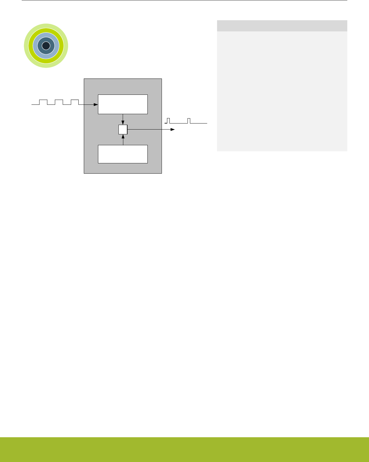
23. CRYOTIMER - Ultra Low Energy Timer/Counter
0 1 2 3 4
CRYOTIMER
Counter
Period
=
Low Frequency
Oscillator
Wakeup Event
Quick Facts
What?
The CRYOTIMER is a timer capable of providing
wakeup events/interrupts after deterministic intervals
in all energy modes, including EM4.
Why?
The CRYOTIMER enables the chip to remain in the
lowest energy modes for long durations, while keep-
ing track of time and being able to wake up at regu-
lar intervals, all with an absolute minimum current
consumption.
How?
Using a counter running on a prescaled Low Fre-
quency Oscillator, the CRYOTIMER can provide pe-
riodic wakeup events with a very wide period range.
23.1 Introduction
The CRYOTIMER is a 32 bit counter which operates on a low frequency oscillator, and is capable of running in all Energy Modes. It can
provide periodic Wakeup events and PRS signals which can be used to wake up peripherals from any energy mode. The CRYOTIMER
provides a very wide range of periods for the interrupts facilitating flexible ultra-low energy operation.
Because of its simplicity, the CRYOTIMER is a lower energy solution for periodically waking up the MCU compared to the RTCC.
23.2 Features
• 32 bit Counter
• Works in all the energy modes
• Only External and Power-On resets reset the CRYOTIMER
• Interrupt/wake up event after deterministic intervals
• PRS Output
• Debug mode
• Configurable to either run or stop when processor is stopped (break)
23.3 Functional Description
Reference Manual
CRYOTIMER - Ultra Low Energy Timer/Counter
silabs.com | Smart. Connected. Energy-friendly. Preliminary Rev. 0.5 | 769

23.3.1 Block Diagram
An overview of the CRYOTIMER is shown in Figure 23.1 CRYOTIMER Block Overview on page 770.
Interrupt/
Wakeup Event
Counter
PRS
Prescaler
PRESC PERIODSEL
Edge
Detector
LFXO
LFRCO
ULFRCO
CRYOCLK
OSCSEL
Figure 23.1. CRYOTIMER Block Overview
Reference Manual
CRYOTIMER - Ultra Low Energy Timer/Counter
silabs.com | Smart. Connected. Energy-friendly. Preliminary Rev. 0.5 | 770

23.3.2 Operation
The desired low frequency oscillator for the CRYOTIMER operation can be selected by using OSCSEL in CRYOTIMER_CTRL. The
selection must be made before enabling the CRYOTIMER, and it must be ensured that the selected oscillator is ready. This can be
checked by observing LFXORDY or LFRCORDY (depending upon the oscillator selection) in CMU_STATUS. Note that the ULFRCO is
always ready.
By default the CRYOTIMER is held in reset. It can be started by setting EN in CRYOTIMER_CTRL. The CRYOTIMER, when running, is
reset by clearing EN.
The timer counts at a frequency determined by PRESC in CRYOTIMER_CTRL. This value should be set before the CRYOTIMER is
enabled. Setting PRESC to 0 gives the maximum resolution, while higher values allow longer periods, see Table 23.1 CRYOTIMER
Resolution vs Maximum Wakeup event/Interrupt period, FCRYOCLK = 32768 Hz on page 771.
The 32-bit Counter provides 32 different options for selecting the duration between the Wakeup events. The selected duration is speci-
fied by CRYOTIMER_PERIODSEL. It should be configured before the CRYOTIMER is enabled.
TWU = (2PRESC x 2PERIODSEL)/fCRYOCLK
Figure 23.2. Duration between the CRYOTIMER Wakeup events in seconds
Table 23.1. CRYOTIMER Resolution vs Maximum Wakeup event/Interrupt period, FCRYOCLK = 32768 Hz
CRYOTIMER_CTRL_PRESC Resolution, 2PRESC/fCRYOCLK Maximum Wakeup event/Interrupt Period
DIV1 30.5 µs 36.4 hours
DIV2 61 µs 72.8 hours
DIV4 122 µs 145.6 hours
DIV8 244 µs 12 days
DIV16 488 µs 24 days
DIV32 977 µs 48 days
DIV64 1.95 ms 97 days
DIV128 3.91 ms 194 days
The 32-bit counter value of the CRYOTIMER can be read using the CRYOTIMER_CNT register.
The PRS output pulses of the CRYOTIMER are 1 CRYOCLK clock cycle wide. However, if the PRESC and PERIODSEL are both set to
0, the width of these pulses will be half CRYOCLK time period.
The CRYOTIMER wakeup events set the flag in the CRYOTIMER_IF. Interrupt on this event can be enabled by using the CRYOTIM-
ER_IEN register.
The CRYOTIMER is always reset by the External Pin and Power-On resets. Additionally, by using EMU_CTRL, it can also be config-
ured to reset by Watchdog, lockup, and system request resets.
Note: The CRYOTIMER configuration bits/registers should only be changed when EN in CRYOTIMER_CTRL is cleared.
23.3.3 Debug Mode
When the CPU is halted in debug mode, the CRYOTIMER can be configured to either continue to run or to be frozen. This is configured
using DEBUGRUN in CRYOTIMER_CTRL.
Reference Manual
CRYOTIMER - Ultra Low Energy Timer/Counter
silabs.com | Smart. Connected. Energy-friendly. Preliminary Rev. 0.5 | 771

23.3.4 Energy Mode availability
The CRYOTIMER is available in all Energy Modes. Wakeup from EM2 Deep Sleep and EM3 Stop to EM0 Active can be performed
using the regular interrupt as discussed in 23.3.2 Operation. To generate wakeup events during EM4 Hibernate/Shutoff, EM4WU in
CRYOTIMER_EM4WUEN must be set to 1. Since the interrupt flag serves as the wakeup source, it must be cleared by software after
exiting a low energy mode. Refer to 11. EMU - Energy Management Unit for details on how to configure the EMU.
23.4 Register Map
The offset register address is relative to the registers base address.
Offset Name Type Description
0x000 CRYOTIMER_CTRL RW Control Register
0x004 CRYOTIMER_PERIODSEL RW Interrupt Duration
0x008 CRYOTIMER_CNT RCounter Value
0x00C CRYOTIMER_EM4WUEN RW Wake Up Enable
0x010 CRYOTIMER_IF RInterrupt Flag Register
0x014 CRYOTIMER_IFS W1 Interrupt Flag Set Register
0x018 CRYOTIMER_IFC (R)W1 Interrupt Flag Clear Register
0x01C CRYOTIMER_IEN RW Interrupt Enable Register
Reference Manual
CRYOTIMER - Ultra Low Energy Timer/Counter
silabs.com | Smart. Connected. Energy-friendly. Preliminary Rev. 0.5 | 772

23.5 Register Description
23.5.1 CRYOTIMER_CTRL - Control Register
Offset Bit Position
0x000
31
30
29
28
27
26
25
24
23
22
21
20
19
18
17
16
15
14
13
12
11
10
9
8
7
6
5
4
3
2
1
0
Reset
0x0
0x0
0
0
Access
RW
RW
RW
RW
Name
PRESC
OSCSEL
DEBUGRUN
EN
Bit Name Reset Access Description
31:8 Reserved To ensure compatibility with future devices, always write bits to 0. More information in 1.2 Conven-
tions
7:5 PRESC 0x0 RW Prescaler Setting
These bits select the prescaling factor.
Value Mode Description
0 DIV1 LF Oscillator frequency undivided
1 DIV2 LF Oscillator frequency divided by 2
2 DIV4 LF Oscillator frequency divided by 4
3 DIV8 LF Oscillator frequency divided by 8
4 DIV16 LF Oscillator frequency divided by 16
5 DIV32 LF Oscillator frequency divided by 32
6 DIV64 LF Oscillator frequency divided by 64
7 DIV128 LF Oscillator frequency divided by 128
4:2 OSCSEL 0x0 RW Select Low frequency oscillator
These bits select the low frequency oscillator for the CRYOTIMER operation. This field should be set after the oscillator to
be selected is ready.
Value Mode Description
0 DISABLED Output is driven low
1 LFRCO Select Low Frequency RC Oscillator
2 LFXO Select Low Frequency Crystal Oscillator
3 ULFRCO Select Ultra Low Frequency RC Oscillator
1 DEBUGRUN 0 RW Debug Mode Run Enable
Set this bit to enable CRYOTIMER to run in debug mode.
0 EN 0 RW Enable CRYOTIMER
Set this bit to start the CRYOTIMER. Clear this bit to reset the CRYOTIMER. This bit should be set after the oscillator to be
selected is ready.
Reference Manual
CRYOTIMER - Ultra Low Energy Timer/Counter
silabs.com | Smart. Connected. Energy-friendly. Preliminary Rev. 0.5 | 773

23.5.2 CRYOTIMER_PERIODSEL - Interrupt Duration
Offset Bit Position
0x004
31
30
29
28
27
26
25
24
23
22
21
20
19
18
17
16
15
14
13
12
11
10
9
8
7
6
5
4
3
2
1
0
Reset
0x20
Access
RW
Name
PERIODSEL
Bit Name Reset Access Description
31:6 Reserved To ensure compatibility with future devices, always write bits to 0. More information in 1.2 Conven-
tions
5:0 PERIODSEL 0x20 RW Interrupts/Wakeup events period setting
Defines the duration between the Interrupts/Wakeup events based on the pre-scaled clock.
Value Description
0 Wakeup event after every Pre-scaled clock cycle.
1 Wakeup event after 2 Pre-scaled clock cycles.
2 Wakeup event after 4 Pre-scaled clock cycles.
3 Wakeup event after 8 Pre-scaled clock cycles.
4 Wakeup event after 16 Pre-scaled clock cycles.
5 Wakeup event after 32 Pre-scaled clock cycles.
6 Wakeup event after 64 Pre-scaled clock cycles.
7 Wakeup event after 128 Pre-scaled clock cycles.
8 Wakeup event after 256 Pre-scaled clock cycles.
9 Wakeup event after 512 Pre-scaled clock cycles.
10 Wakeup event after 1k Pre-scaled clock cycles.
11 Wakeup event after 2k Pre-scaled clock cycles.
12 Wakeup event after 4k Pre-scaled clock cycles.
13 Wakeup event after 8k Pre-scaled clock cycles.
14 Wakeup event after 16k Pre-scaled clock cycles.
15 Wakeup event after 32k Pre-scaled clock cycles.
16 Wakeup event after 64k Pre-scaled clock cycles.
17 Wakeup event after 128k Pre-scaled clock cycles.
18 Wakeup event after 256k Pre-scaled clock cycles.
19 Wakeup event after 512k Pre-scaled clock cycles.
20 Wakeup event after 1M Pre-scaled clock cycles.
21 Wakeup event after 2M Pre-scaled clock cycles.
22 Wakeup event after 4M Pre-scaled clock cycles.
Reference Manual
CRYOTIMER - Ultra Low Energy Timer/Counter
silabs.com | Smart. Connected. Energy-friendly. Preliminary Rev. 0.5 | 774

Bit Name Reset Access Description
23 Wakeup event after 8M Pre-scaled clock cycles.
24 Wakeup event after 16M Pre-scaled clock cycles.
25 Wakeup event after 32M Pre-scaled clock cycles.
26 Wakeup event after 64M Pre-scaled clock cycles.
27 Wakeup event after 128M Pre-scaled clock cycles.
28 Wakeup event after 256M Pre-scaled clock cycles.
29 Wakeup event after 512M Pre-scaled clock cycles.
30 Wakeup event after 1024M Pre-scaled clock cycles.
31 Wakeup event after 2048M Pre-scaled clock cycles.
32 Wakeup event after 4096M Pre-scaled clock cycles.
23.5.3 CRYOTIMER_CNT - Counter Value
Offset Bit Position
0x008
31
30
29
28
27
26
25
24
23
22
21
20
19
18
17
16
15
14
13
12
11
10
9
8
7
6
5
4
3
2
1
0
Reset
0x00000000
Access
R
Name
CNT
Bit Name Reset Access Description
31:0 CNT 0x00000000 R Counter Value
These bits hold the Counter value.
23.5.4 CRYOTIMER_EM4WUEN - Wake Up Enable
Offset Bit Position
0x00C
31
30
29
28
27
26
25
24
23
22
21
20
19
18
17
16
15
14
13
12
11
10
9
8
7
6
5
4
3
2
1
0
Reset
0
Access
RW
Name
EM4WU
Bit Name Reset Access Description
31:1 Reserved To ensure compatibility with future devices, always write bits to 0. More information in 1.2 Conven-
tions
0 EM4WU 0 RW EM4 Wake-up enable
Write 1 to enable wake-up request, write 0 to disable wake-up request.
Reference Manual
CRYOTIMER - Ultra Low Energy Timer/Counter
silabs.com | Smart. Connected. Energy-friendly. Preliminary Rev. 0.5 | 775

23.5.5 CRYOTIMER_IF - Interrupt Flag Register
Offset Bit Position
0x010
31
30
29
28
27
26
25
24
23
22
21
20
19
18
17
16
15
14
13
12
11
10
9
8
7
6
5
4
3
2
1
0
Reset
0
Access
R
Name
PERIOD
Bit Name Reset Access Description
31:1 Reserved To ensure compatibility with future devices, always write bits to 0. More information in 1.2 Conven-
tions
0 PERIOD 0 R Wakeup event/Interrupt
Set when the Wakeup event/Interrupt occurs.
23.5.6 CRYOTIMER_IFS - Interrupt Flag Set Register
Offset Bit Position
0x014
31
30
29
28
27
26
25
24
23
22
21
20
19
18
17
16
15
14
13
12
11
10
9
8
7
6
5
4
3
2
1
0
Reset
0
Access
W1
Name
PERIOD
Bit Name Reset Access Description
31:1 Reserved To ensure compatibility with future devices, always write bits to 0. More information in 1.2 Conven-
tions
0 PERIOD 0 W1 Set PERIOD Interrupt Flag
Write 1 to set the PERIOD interrupt flag
Reference Manual
CRYOTIMER - Ultra Low Energy Timer/Counter
silabs.com | Smart. Connected. Energy-friendly. Preliminary Rev. 0.5 | 776

23.5.7 CRYOTIMER_IFC - Interrupt Flag Clear Register
Offset Bit Position
0x018
31
30
29
28
27
26
25
24
23
22
21
20
19
18
17
16
15
14
13
12
11
10
9
8
7
6
5
4
3
2
1
0
Reset
0
Access
(R)W1
Name
PERIOD
Bit Name Reset Access Description
31:1 Reserved To ensure compatibility with future devices, always write bits to 0. More information in 1.2 Conven-
tions
0 PERIOD 0 (R)W1 Clear PERIOD Interrupt Flag
Write 1 to clear the PERIOD interrupt flag. Reading returns the value of the IF and clears the corresponding interrupt flags
(This feature must be enabled globally in MSC.).
23.5.8 CRYOTIMER_IEN - Interrupt Enable Register
Offset Bit Position
0x01C
31
30
29
28
27
26
25
24
23
22
21
20
19
18
17
16
15
14
13
12
11
10
9
8
7
6
5
4
3
2
1
0
Reset
0
Access
RW
Name
PERIOD
Bit Name Reset Access Description
31:1 Reserved To ensure compatibility with future devices, always write bits to 0. More information in 1.2 Conven-
tions
0 PERIOD 0 RW PERIOD Interrupt Enable
Enable/disable the PERIOD interrupt
Reference Manual
CRYOTIMER - Ultra Low Energy Timer/Counter
silabs.com | Smart. Connected. Energy-friendly. Preliminary Rev. 0.5 | 777

24. VDAC - Digital to Analog Converter
0 1 2 3 4
DAC
...0100010...
...0101110...
Quick Facts
What?
The VDAC is designed for low energy consumption,
but can also provide very good performance. It can
convert digital values to analog signals at up to 500
kilo samples/second with 12-bit accuracy.
Why?
The VDAC can be used to generate accurate analog
signals for sound, sensors and other applications,
using only a limited amount of energy.
How?
The VDAC can generate high-resolution analog sig-
nals while the MCU is operating at low frequencies
and with low total power consumption. Using DMA
and a timer, the VDAC can be used to generate
waveforms without any CPU intervention. The VDAC
is available down to Energy Mode 3.
24.1 Introduction
The Voltage Digital to Analog Converter (VDAC) can convert a digital value to an analog output voltage. The VDAC is fully differential
rail-to-rail, with 12-bit resolution. It has two single ended output buffers which can be combined into one differential output. The VDAC
may be used for a number of different applications such as sensor interfaces or sound output.
Reference Manual
VDAC - Digital to Analog Converter
silabs.com | Smart. Connected. Energy-friendly. Preliminary Rev. 0.5 | 778
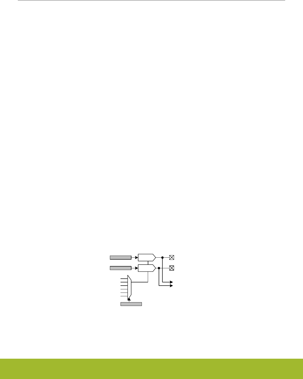
24.2 Features
• 500 ksamples/s operation
•Two single ended output channels
• Can be combined into one differential output
• Integrated prescaler with division factor selectable between 1-128
• Selectable voltage reference
• Internal low noise 2.5V
• Internal low noise 1.25V
• Internal low power 2.5V
• Internal low power 1.25V
• AVDD
• External Pin Reference
• Conversion triggers
• Data write
• PRS input
• Refresh timer
• LESENSE
• Automatic refresh timer
• Selection from 16-64 DAC_CLK cycles
• Individual refresh enable for each channel
• Interrupt generation on buffer empty or finished conversion
• Separate interrupt flags for each channel
• PRS output pulse on finished conversion
• Separate line for each channel
• DMA request on buffer empty
• Separate request for each channel
• Support for offset and gain calibration
• Output to dedicated pins or APORT bus
• Internal connections to ADC and ACMP
• Sine generation mode
• Asynchronous clocking mode
24.3 Functional Description
An overview of the VDAC module is shown in the figure below.
DACn_OUT0
DACn_OUT1
Ch 1
AVDD
1.25 V Low Noise
2.5 V Low Noise
CH0DATA
CH1DATA
ADC / ACMP / APORT
REFSEL
Ch 0
1.25 V
2.5 V
Pin Reference
Figure 24.1. VDAC Overview
Reference Manual
VDAC - Digital to Analog Converter
silabs.com | Smart. Connected. Energy-friendly. Preliminary Rev. 0.5 | 779

24.3.1 Enabling and Disabling a Channel
A VDAC channel is enabled by writing 1 to the CHxEN and disabled by writing 1 to CHxDIS in VDACn_CMD. The channel enabled
status can be read by polling the CHxENS bit in VDACn_STATUS. This bit will go high immediately following a write to CHxEN. After
disabling a channel the CHxENS bit will stay high until the VDAC channel is completely disabled.
Software should configure the VDAC before enabling a channel. Software must not write to any of the following registers while either
CH0ENS or CH1ENS are set:
• VDACn_CTRL
• VDACn_CHxCTRL
• VDACn_OPAxTIMER
A VDAC channel will not begin driving its output before it is enabled and has received a conversion trigger, see 24.3.2.3 Conversion
Trigger. After a channel is enabled it will listen for trigger sources specified in TRIGMODE in VDACn_CHxCTRL. If TRIGMODE is set to
SW, SWPRS or SWREFRESH and a value was written to CHxDATA or COMBDATA before enabling the channel a conversion will start
immediately when the channel is enabled. When disabling a channel any pending triggers are flushed.
24.3.2 Conversions
The VDAC consists of two channels (channel 0 and 1) with separate 12-bit data registers (VDACn_CH0DATA and VDACn_CH1DATA).
These can be used to produce two independent single ended outputs or the channel 0 register can be used to drive both outputs in
differential mode. The VDAC supports two conversion modes: continuous and sample/off.
24.3.2.1 Continuous Mode
In continuous mode the VDAC channels will drive their outputs continuously with the data in the VDACn_CHxDATA registers. A channel
is configured in continuous mode by programming the CONVMODE bitfield in VDACn_CHxCTRL to CONTINUOUS. This mode will
maintain the output voltage and no manual refresh is needed.
In continuous mode the SETTLETIME field in VDACn_OPAxTIMER should be programmed to zero to achive the maximum update rate.
24.3.2.2 Sample/Off Mode
In sample/off mode the VDAC will only drive the output for a limited time per conversion. A channel is configured in sample/off mode by
programming the CONVMODE bitfield in VDACn_CHxCTRL to SAMPLEOFF. How long the channel should drive the output can be
controlled by programming the SETTLETIME field in the VDACn_OPAxTIMER register. The VDAC will drive the output for SETTLE-
TIME fDAC_CLK cycles before tristating the output again (and therefore if SETTLETIME is set to zero, the output will never be driven
when using sample/off mode).
24.3.2.3 Conversion Trigger
Conversions can only be done while a channel is enabled, see 24.3.1 Enabling and Disabling a Channel.
If TRIGMODE is programmed to SW, SWPRS or SWREFRESH a conversion can be started by writing to the VDACn_CHxDATA regis-
ter. The data registers are also mapped to a combined data register, VDACn_COMBDATA, where the data values for both channels can
be written simultaneously. Writing to this register will trigger all enabled channels.
If TRIGMODE is programmed to PRS or SWPRS, a conversion can be started by an incoming pulse on the PRS channel selected in
PRSSEL in VDACn_CHxCTRL. The PRSASYNC bit in VDACn_CHxCTRL determines if the VDAC expects a PRS pulse coming from a
synchronous or asynchronous PRS producer.
If TRIGMODE is programmed to REFRESH or SWREFRESH a conversion will start on an overflow of the internal refresh timer. See
24.3.8 Refresh Timer.
If TRIGMODE is programmed to LESENSE a conversion will start when the LESENSE block sends a request. This setting needs to be
selected whenever the channel is under LESENE control.
24.3.2.4 PRS Triggers
PRS triggers can be used to set a constant sample frequency, for instance by using a TIMER. In order to get a jitter-free sample rate,
set DACCLKMODE to SYNC, set the CH0PRESCRST bit and clear the PRSASYNC bit. Note that this is only possible for channel 0.
The PRSASYNC bit tells whether the VDAC expects a synchronous PRS producer or not. When this bit is cleared, the PRS pulse must
come from a synchronous producer and HFPERCLK must be running (this clock is turned off in EM2 and below). When PRSASYNC is
set, the corresponding PRS channels should also bet configued as asynchronous (see the PRS chapter).
Reference Manual
VDAC - Digital to Analog Converter
silabs.com | Smart. Connected. Energy-friendly. Preliminary Rev. 0.5 | 780

When either DACCLKMODE is set to ASYNC or the PRSASYNC bit is set, the sample frequency cannot be guaranteed to be jitter-free
with respect to the PRS pulses.
The PRS frequency should never be higher than 0.5 MHz (the fastest possible sample rate). In addition the PRS frequency should not
be higher than fHFPERCLK/12 (in synchronous mode). If the PRS frequency is set too high, some PRS pulses will be dropped and the
output can jitter.
24.3.3 Reference Selection
These voltage references are available and are selected by programming the REFSEL field in VDACn_CTRL.
• Internal 1.25 V Low Noise Bandgap Reference
• Internal 2.5 V Low Noise Bandgap Reference
• Internal 1.25 V Low Power Bandgap Reference
• Internal 2.5 V Low Power Bandgap Reference
• AVDD
• External Pin
24.3.4 Warmup Time and Initial Conversion
When a channel is first enabled it needs to warm up. This is performed automatically during the first conversion. The time required to
warm up depends on the programmed DRIVESTRENGTH field in VDACn_OPAx_CTRL. In Table 24.1 VDAC Warmup Time on page
781 the minimum WARMUPTIME field for each drive strength is specified. Software is responsible for programming the correct value
to WARMUPTIME before enabling a channel. If the time is programmed too short, an undefined voltage may be output until the VDAC
settles.
The CHxWARM bits in VDACn_STATUS are set when the warmup period has completed.
A consequence of the warmup period is that in continuous mode, the first conversion might take longer than the following conversions.
In order to make sure all samples have the same timing, perform a dummy conversion to make the VDAC settle to a known voltage
first.
Table 24.1. VDAC Warmup Time
DRIVESTRENGTH WARMUPTIME
0 100 µs
1 85 µs
2 8 µs
3 8 µs
24.3.5 Analog Output
The output selection for each VDAC channel is configured in the VDACn_OPAx_OUT registers. Each VDAC channel has its own main
output pin, VDACn_OUTx, that can be enabled with MAINOUTEN. In addition, several alternate outputs can be selected. These are
enabled by first setting ALTOUTEN and then setting the corresponding bit(s) in ALTOUTPADEN. The VDAC output can also be routed
to APORT by setting APORTOUTEN and configuring the APORTOUTSEL field to select the desired APORT.
The VDAC outputs also have direct internal connections to ADCs and ACMPs. These outputs are always enabled and can be selected
by configuring the input selection for the ADC/ACMP.
In sample/off mode the VDAC will only drive the output for the duration programmed in SETTLETIME (in VDACn_OPAx_TIMER regis-
ter) for each incoming conversion trigger. In continuous mode the VDAC will continue to drive the output until the channel is disabled.
However, note that also in this mode a conversion trigger is needed before the output is enabled. See 24.3.1 Enabling and Disabling a
Channel and 24.3.2.3 Conversion Trigger.
24.3.6 Output Mode
The two VDAC channels can act as two separate single ended channels or be combined into one differential channel. This is selected
through the DIFF bit in VDACn_CTRL.
Reference Manual
VDAC - Digital to Analog Converter
silabs.com | Smart. Connected. Energy-friendly. Preliminary Rev. 0.5 | 781

24.3.6.1 Single Ended Output
When operating in single ended mode, the channel 0 output is on VDACn_OUT0 and the channel 1 output is on VDACn_OUT1. The
output voltage can be calculated using Figure 24.2 VDAC Single Ended Output Voltage on page 782
VOUT = VVDACn_OUTx - VSS= Vref x CHxDATA/4095
Figure 24.2. VDAC Single Ended Output Voltage
where CHxDATA is a 12-bit unsigned integer.
24.3.6.2 Differential Output
When operating in differential mode, both VDAC outputs are used. The differential conversion uses VDACn_CH0DATA as source. The
positive output is on VDACn_OUT1 and the negative output is on VDACn_OUT0. Since the output can be negative, it is expected that
the data is written in 2’s complement form with the MSB of the 12-bit value being the signed bit. The output voltage can be calculated
using Figure 24.3 VDAC Differential Output Voltage on page 782:
VOUT = VVDACn_OUT1 - VVDACn_OUT0= Vref x CH0DATA/2047
Figure 24.3. VDAC Differential Output Voltage
where CH0DATA is a 12-bit signed integer. The common mode voltage is Vref/2.
When using differential mode, the user must make sure that both channels are set up identically. I.e. VDACn_CH0CTRL and
VDACn_CH1CTRL must be programmed to identical values (with the exception that the PRSSEL bitfield is allowed to be programmed
differently for usage together with the OUTENPRS feature). Similarly the user must program VDACn_OPA0TIMER and
VDACn_OPA1TIMER to identical values.
24.3.7 Async Mode
The VDAC is default clocked from HFPERCLK, which is automatically turned off in EM2/3. In order to allow VDAC operation in EM2/3
an internal oscillator can be selected for the VDAC by setting the DACCLKMODE bitfield in VDACn_CTRL to ASYNC. Before entering
EM2/3 software must make sure the channel is enabled first by polling CHxENS in VDACn_STATUS. Entering EM2/3 with an enabled
VDAC channel while DACCLKMODE is set to SYNC is a programming error and will lead to EM23ERRIF getting set to 1.
In asynchronous mode both VDAC channels are not necessarily triggered synchronous to each other and therefore the user should not
assume that e.g. PRS, refresh or VDACn_COMBDATA based conversion triggers are observed by both channels at the same time. In
differential mode both channels will operate in lock step, even while using the asynchronous clocking mode.
24.3.8 Refresh Timer
The VDAC incluces an internal refresh timer. The refresh timer is automatically started if a channel selects either REFRESH or SWRE-
FRESH for TRIGMODE and the channel is enabled. The refresh timer will count the number of fDAC_CLK cycles programmed in RE-
FRESHPERIOD before wrapping and generating a conversion trigger.
24.3.9 Clock Prescaling
The VDAC has an internal clock prescaler, which can divide the input clock by any factor between 1 and 128, by setting the PRESC
field in VDACn_CTRL. The resulting DAC_CLK is used by the converter core and the frequency is given by Figure 24.4 VDAC Clock
Prescaling on page 782 :
fDAC_CLK = fIN_CLK / (PRESC + 1)
Figure 24.4. VDAC Clock Prescaling
where fIN_CLK is the input clock frequency. The fDAC_CLK must be programmed to be at most 1 MHz. When the DACCLKMODE is set to
SYNC, the input clock frequency is fHFPERCLK. When DACCLKMODE is set to ASYNC, an internal 12Mhz oscillator is used. In this
mode it is required that the PRESC field be program to 11 or higher.
Reference Manual
VDAC - Digital to Analog Converter
silabs.com | Smart. Connected. Energy-friendly. Preliminary Rev. 0.5 | 782

The prescaler runs continuously when either of the channels are enabled. When running with a prescaler setting higher than 0, there
will be an unpredictable delay from the time the conversion was triggered to the time the actual conversion takes place. This is because
the conversions are controlled by the prescaled clock and the conversion can arrive at any time during a prescaled clock (DAC_CLK)
period. A second reason for unpredictable delay between a trigger and the associated conversion is that the activity on one channel can
impact whether the VDAC reference is warm or not and therefore it can impact whether warmup is required when using the other chan-
nel. The uncertainty related to the clock prescaler can be addressed by using CH0PRESCRST. If the CH0PRESCRST bit in
VDACn_CTRL is set, the prescaler will be reset every time a conversion is triggered on channel 0. This leads to a predictable latency
between channel 0 trigger and conversion (assuming the warmup sequence is deterministic as well). If channel 0 is used in continuous
mode, the warmup sequence will only apply to its first conversion and software can use the CH0WARM status bit to determine if the
VDAC has warmed up.
24.3.10 High Speed
The VDAC is able to do conversions up to 400 ksamples/s. In order to reach the maximum conversion rate it is recommended to config-
ure the VDAC in the following way:
1. Make fDAC_CLK 1 Mhz
2. Set TRIGMODE to SW
3. Program SETTLETIME in OPAx_TIMER to 0
4. Set up a DMA transfer from a buffer in RAM to CHxDATA
5. Set CONVMODE to CONTINUOUS
24.3.11 Sine Generation Mode
The VDAC contains an automatic sine-generation mode, which is enabled by setting the SINEMODE bit in VDACn_CTRL. In this mode,
the VDAC data is overridden with a conversion data taken from a sine lookup table. The sine signal is controlled by the PRS line selec-
ted by CH0PRSSEL in VDACn_CH0CTRL. When the line is high, a sine wave will be produced. Each period, starting at 0 degrees, is
made up of 16 samples and the frequency is given by Figure 24.5 VDAC Sine Generation on page 783. In case OUTENPRS equals
1, lowering the PRS line selected by CH0PRSSEL will reset the sine output to 0 degrees resulting in a voltage of Vref/2 on the output
channel. In case OUTENPRS equals 0, lowering the PRS line selected by CH0PRSSEL will stop progress of the sine wave at the sam-
ple currently being output (and the sine will therefore not be reset to 0 degrees when raising the PRS line again).
fsine = fHFPERCLK / 32 x (PRESC + 1)
Figure 24.5. VDAC Sine Generation
Sine mode is supported only for the fastest configuration of the VDAC in continuous mode. Therefore the CONVMODE bitfield needs to
be set to CONTINUOUS and the SETTLETIME bitfield in VDACn_OPAxTIMER need to be programmed to zero for the used channel(s)
in order to use sine generation mode. The TRIGMODE bitfield needs to be programmed to PRS for any channel used for sine genera-
tion mode. The other trigger modes are not supported.
The SINE wave will be output on channel 0 and therefore requires that this channel is enabled by writing 1 to CH0EN in the
VDACn_CMD register. If DIFF is set in VDACn_CTRL, the sine wave will be output on both channels, but inverted. Note that when
OUTENPRS in VDACn_CTRL is set, the sine output will be reset to 0 degrees when the PRS line selected by CH1PRSSEL is low.
Reference Manual
VDAC - Digital to Analog Converter
silabs.com | Smart. Connected. Energy-friendly. Preliminary Rev. 0.5 | 783

CH1 PRS
DACn_OUT1
DACn_OUT0
Hi-Z
Hi-Z
CH0 PRS
Vref
0
Vref/2
Vref
0
Vref/2
Figure 24.6. VDAC Sine Mode
24.3.12 Interrupt Flags
The VDAC has several interrupt flags, indicating state transitions and error conditions.
In addition to the VDAC interrupt flags the VDAC registers contain interrupt flags for the OPAMP modules. See The OPAMP chapter for
more information on these flags.
24.3.12.1 Conversion Done
The Conversion Done (CHxCD) interrupt flags are set when a conversion is complete. The flags are set after a channel has driven the
output with the new code for the time programmed in SETTLETIME in VDACn_OPAxTIMER.
24.3.12.2 Buffer Level
The Buffer Level (CHxBL) interrupt flags are set when there is space available in CHxDATA. These flags are initially set, get cleared
when CHxDATA is written and set again when the value is used for a conversion.
24.3.12.3 Overflow/Underflow
If CHxDATA is written to while CHxBL is cleared, the channel overflow flag (CHxOF) will be set. If a new conversion is triggered (e.g. via
PRS) before data is written to CHxDATA (CHxDATA is empty) the channel underflow flag (CHxUF) will be set.
24.3.12.4 EM2/3 Sleep Error
The VDAC can only operate in EM2/3 when DACCLKMODE is set to ASYNC. If EM2 or EM3 is entered while a channel is enabled and
DACCLKMODE is set to SYNC the EM23ERRIF flag will be set.
24.3.13 PRS Outputs
The VDAC has two PRS outputs which will carry a one cycle (HFPERCLK) high pulse when the corresponding channel has finished a
conversion. Only available when DACCLKMODE is set to SYNC.
24.3.14 DMA Request
Each channel sends a DMA request when there is space in the channel's data register (VDACn_CHxDATA). These registers are initially
empty and also become empty every time a conversion is triggered. The request is cleared when VDACn_CHxDATA is written.
24.3.15 LESENSE Trigger Mode
The VDAC can be controlled by LESENSE by programming the TRIGMODE field in VDACn_CHxCTRL to LESENSE. In LESENSE
mode the conversion data can come from either VDACn_CHxDATA registers or LESENSE registers, depending on the LESENSE con-
figuration. The trigger events are also controlled by the LESENSE state machine. See the LESENSE chapter for more information.
Reference Manual
VDAC - Digital to Analog Converter
silabs.com | Smart. Connected. Energy-friendly. Preliminary Rev. 0.5 | 784

24.3.16 Opamps
The VDAC includes a set of highly configurable opamps that can be accessed with the VDAC registers. OPA0 and OPA1 is used for the
output stages of the two VDAC channels, but can be used as standalone opamps if the VDAC channels are not in use. Opamps with
higher numbers are completely standalone. For a detailed description see the OPAMP chapter.
24.3.17 Calibration
The VDAC contains a calibration register, VDACn_CAL, where calibration values for both offset and gain correction can be written. The
required (gain) calibration values depend on the chosen reference and on whether the main or alternative VDAC output is used. The
Device Information page provides the required trim values depending on reference choice and output selection in the DEVIN-
FO_VDACnMAINCAL, DEVINFO_VDACnALTCAL, and DEVINFO_VDACnCH1CAL locations.
The OPAMPs contain a calibration register, VDACn_OPAx_CAL, where calibration values for both offset and gain correction can be
written. The required calibration settings depend on the chosen DRIVESTRENGTH. The required calibration values can be found in the
Device Information pages. For a given OPAMP x, the calibration settings for DRIVESTRENGTH n can be found in DEVINFO_OPAx-
CALn.
24.3.17.1 Channel 1 Calibration
For channel 1, the factory calibration values are only accurate for the main output. When using the alternative outputs or APORT, the
error on the output may be larger than the data sheet values (even when loading values from DEVINFO_VDACn_ALTCAL). To get ac-
curate output from channel 1, either use the main output or perform manual calibration.
24.3.17.2 Manual Calibration
To manually calibrate the VDAC:
1. Enable CH0 and CH1 in their desired modes
2. Set both channel outputs to 80% of full-scale by setting VDACn_CHxDATA = 0xCCC
3. Measure CH0 output and sweep VDACn_CAL.GAINERRTRIM until the smallest calibration error is found
4. Measure CH1 output and sweep VDACn_CAL.GAINERRTRIMCH1 until the smallest calibration error is found
The calibration error is given by
e = abs(Vout/(VREF * 0.8) - 1)
Figure 24.7. Calibration Error
where Vout is the measured voltage at the pin and VREF is the reference voltage.
Note that even if only CH1 is going to be used, the full calibration procedure should be followed. It is permissible to skip CH1 calibration
if only CH0 is used. The following parameters influence the calibration. A change in any of these might require a re-calibration:
• VDACn_CTRL.REFSEL
• VDACn_OPAx_OUT.MAINOUTEN
• VDACn_OPAx_OUT.ALTOUTEN
• VDACn_OPAx_CTRL.DRIVESTRENGTH
24.3.18 Warmup Mode
If the WARMUPMODE field in VDACn_CTRL is set to KEEPINSTANDBY, the VDAC keeps internal bias currents running between con-
versions. It does not reduce the startup time, but it can help reduce noise from the VDAC to other analog peripherals, like the ADC or
ACMP.
Reference Manual
VDAC - Digital to Analog Converter
silabs.com | Smart. Connected. Energy-friendly. Preliminary Rev. 0.5 | 785

24.4 Register Map
The offset register address is relative to the registers base address.
Offset Name Type Description
0x000 VDACn_CTRL RW Control Register
0x004 VDACn_STATUS RStatus Register
0x008 VDACn_CH0CTRL RW Channel 0 Control Register
0x00C VDACn_CH1CTRL RW Channel 1 Control Register
0x010 VDACn_CMD W1 Command Register
0x014 VDACn_IF RInterrupt Flag Register
0x018 VDACn_IFS W1 Interrupt Flag Set Register
0x01C VDACn_IFC (R)W1 Interrupt Flag Clear Register
0x020 VDACn_IEN RW Interrupt Enable Register
0x024 VDACn_CH0DATA RWH Channel 0 Data Register
0x028 VDACn_CH1DATA RWH Channel 1 Data Register
0x02C VDACn_COMBDATA WCombined Data Register
0x030 VDACn_CAL RW Calibration Register
0x0A0 VDACn_OPA0_APORTREQ ROperational Amplifier APORT Request Status Register
0x0A4 VDACn_OPA0_APORTCONFLICT ROperational Amplifier APORT Conflict Status Register
0x0A8 VDACn_OPA0_CTRL RW Operational Amplifier Control Register
0x0AC VDACn_OPA0_TIMER RW Operational Amplifier Timer Control Register
0x0B0 VDACn_OPA0_MUX RW Operational Amplifier Mux Configuration Register
0x0B4 VDACn_OPA0_OUT RW Operational Amplifier Output Configuration Register
0x0B8 VDACn_OPA0_CAL RW Operational Amplifier Calibration Register
0x0C0 VDACn_OPA1_APORTREQ ROperational Amplifier APORT Request Status Register
0x0C4 VDACn_OPA1_APORTCONFLICT ROperational Amplifier APORT Conflict Status Register
0x0C8 VDACn_OPA1_CTRL RW Operational Amplifier Control Register
0x0CC VDACn_OPA1_TIMER RW Operational Amplifier Timer Control Register
0x0D0 VDACn_OPA1_MUX RW Operational Amplifier Mux Configuration Register
0x0D4 VDACn_OPA1_OUT RW Operational Amplifier Output Configuration Register
0x0D8 VDACn_OPA1_CAL RW Operational Amplifier Calibration Register
0x0E0 VDACn_OPA2_APORTREQ ROperational Amplifier APORT Request Status Register
0x0E4 VDACn_OPA2_APORTCONFLICT ROperational Amplifier APORT Conflict Status Register
0x0E8 VDACn_OPA2_CTRL RW Operational Amplifier Control Register
0x0EC VDACn_OPA2_TIMER RW Operational Amplifier Timer Control Register
0x0F0 VDACn_OPA2_MUX RW Operational Amplifier Mux Configuration Register
0x0F4 VDACn_OPA2_OUT RW Operational Amplifier Output Configuration Register
0x0F8 VDACn_OPA2_CAL RW Operational Amplifier Calibration Register
Reference Manual
VDAC - Digital to Analog Converter
silabs.com | Smart. Connected. Energy-friendly. Preliminary Rev. 0.5 | 786

24.5 Register Description
24.5.1 VDACn_CTRL - Control Register
Offset Bit Position
0x000
31
30
29
28
27
26
25
24
23
22
21
20
19
18
17
16
15
14
13
12
11
10
9
8
7
6
5
4
3
2
1
0
Reset
0
0
0x0
0x00
0x0
0
0
0
0
Access
RW
RW
RW
RW
RW
RW
RW
RW
RW
Name
DACCLKMODE
WARMUPMODE
REFRESHPERIOD
PRESC
REFSEL
CH0PRESCRST
OUTENPRS
SINEMODE
DIFF
Bit Name Reset Access Description
31 DACCLKMODE 0 RW Clock Mode
Selects DAC clock source from synchronous or asynchronous - with respect to Peripheral Clock - clock source
Value Mode Description
0 SYNC Uses HFPERCLK to generate DAC_CLK, DAC will run with static set-
tings in EM2 in this mode
1 ASYNC Uses internal VDAC oscillator to generate DAC_CLK. DAC will be
available in EM2
30:29 Reserved To ensure compatibility with future devices, always write bits to 0. More information in 1.2 Conven-
tions
28 WARMUPMODE 0 RW Warm-up Mode
Select Warm-up Mode for DAC
Value Mode Description
0 NORMAL DAC is shut off after each sample off conversion
1 KEEPINSTANDBY DAC is kept in standby mode between sample off conversions
27:26 Reserved To ensure compatibility with future devices, always write bits to 0. More information in 1.2 Conven-
tions
25:24 REFRESHPERIOD 0x0 RW Refresh Period
Select refresh counter period. A channel x will be refreshed with the period set in REFRESHPERIOD if the channel in
VDACn_CHxCTRL has its TRIGMODE set to REFRESH or SWREFRESH.
Value Mode Description
0 8CYCLES All channels with enabled refresh are refreshed every 8 DAC_CLK cy-
cles
1 16CYCLES All channels with enabled refresh are refreshed every 16 DAC_CLK cy-
cles
2 32CYCLES All channels with enabled refresh are refreshed every 32 DAC_CLK cy-
cles
Reference Manual
VDAC - Digital to Analog Converter
silabs.com | Smart. Connected. Energy-friendly. Preliminary Rev. 0.5 | 787

Bit Name Reset Access Description
3 64CYCLES All channels with enabled refresh are refreshed every 64 DAC_CLK cy-
cles
23 Reserved To ensure compatibility with future devices, always write bits to 0. More information in 1.2 Conven-
tions
22:16 PRESC 0x00 RW Prescaler Setting for DAC clock
Selected DAC clock source (as selected by DACCLKMODE) is prescaled by PRESC+1 to generated DAC clock
(DAC_CLK)
Value Description
PRESC Clock division factor of
PRESC+1.
15:11 Reserved To ensure compatibility with future devices, always write bits to 0. More information in 1.2 Conven-
tions
10:8 REFSEL 0x0 RW Reference Selection
Select reference
Value Mode Description
0 1V25LN Internal low noise 1.25 V bandgap reference
1 2V5LN Internal low noise 2.5 V bandgap reference
2 1V25 Internal 1.25 V bandgap reference
3 2V5 Internal 2.5 V bandgap reference
4 VDD AVDD reference
6 EXT External pin reference
7 Reserved To ensure compatibility with future devices, always write bits to 0. More information in 1.2 Conven-
tions
6 CH0PRESCRST 0 RW Channel 0 Start Reset Prescaler
Select if prescaler (determining DAC_CLK rate) is reset on channel 0 start.
Value Description
0 Prescaler not reset on channel 0 start
1 Prescaler reset on channel 0 start
5 OUTENPRS 0 RW PRS Controlled Output Enable
Enable PRS Control of DAC output enable.
Value Description
0 DAC output enable always on
1 DAC output enable controlled by PRS signal selected for CH1
4 SINEMODE 0 RW Sine Mode
Enable/disable sine mode.
Value Description
Reference Manual
VDAC - Digital to Analog Converter
silabs.com | Smart. Connected. Energy-friendly. Preliminary Rev. 0.5 | 788

Bit Name Reset Access Description
0 Sine mode disabled. Sine reset to 0 degrees
1 Sine mode enabled
3:1 Reserved To ensure compatibility with future devices, always write bits to 0. More information in 1.2 Conven-
tions
0 DIFF 0 RW Differential Mode
Select single ended or differential mode.
Value Description
0 Single ended output
1 Differential output
Reference Manual
VDAC - Digital to Analog Converter
silabs.com | Smart. Connected. Energy-friendly. Preliminary Rev. 0.5 | 789

24.5.2 VDACn_STATUS - Status Register
Offset Bit Position
0x004
31
30
29
28
27
26
25
24
23
22
21
20
19
18
17
16
15
14
13
12
11
10
9
8
7
6
5
4
3
2
1
0
Reset
0
0
0
0
0
0
0
0
0
0
0
0
0
0
1
1
0
0
Access
R
R
R
R
R
R
R
R
R
R
R
R
R
R
R
R
R
R
Name
OPA2OUTVALID
OPA1OUTVALID
OPA0OUTVALID
OPA2WARM
OPA1WARM
OPA0WARM
OPA2ENS
OPA1ENS
OPA0ENS
OPA2APORTCONFLICT
OPA1APORTCONFLICT
OPA0APORTCONFLICT
CH1WARM
CH0WARM
CH1BL
CH0BL
CH1ENS
CH0ENS
Bit Name Reset Access Description
31 Reserved To ensure compatibility with future devices, always write bits to 0. More information in 1.2 Conven-
tions
30 OPA2OUTVALID 0 R OPA2 Output Valid Status
OPA2 output is settled externally at the load. In PRS triggered mode this status flag is not used (and remains 0).
29 OPA1OUTVALID 0 R OPA1 Output Valid Status
OPA1 output is settled externally at the load. In PRS triggered mode this status flag is not used (and remains 0).
28 OPA0OUTVALID 0 R OPA0 Output Valid Status
OPA0 output is settled externally at the load. In PRS triggered mode this status flag is not used (and remains 0).
27 Reserved To ensure compatibility with future devices, always write bits to 0. More information in 1.2 Conven-
tions
26 OPA2WARM 0 R OPA2 Warm Status
OPA2 is warm and output is enabled. In PRS triggered mode this status flag is not used (and remains 0).
25 OPA1WARM 0 R OPA1 Warm Status
OPA1 is warm and output is enabled. In PRS triggered mode this status flag is not used (and remains 0).
24 OPA0WARM 0 R OPA0 Warm Status
OPA0 is warm and output is enabled. In PRS triggered mode this status flag is not used (and remains 0).
23 Reserved To ensure compatibility with future devices, always write bits to 0. More information in 1.2 Conven-
tions
22 OPA2ENS 0 R OPA2 Enabled Status
This bit is set when OPA2 is enabled
21 OPA1ENS 0 R OPA1 Enabled Status
This bit is set when OPA1 is enabled
20 OPA0ENS 0 R OPA0 Enabled Status
This bit is set when OPA0 is enabled
19 Reserved To ensure compatibility with future devices, always write bits to 0. More information in 1.2 Conven-
tions
Reference Manual
VDAC - Digital to Analog Converter
silabs.com | Smart. Connected. Energy-friendly. Preliminary Rev. 0.5 | 790

Bit Name Reset Access Description
18 OPA2APORTCON-
FLICT
0 R OPA2 Bus Conflict Output
1 if any of the APORTs being requested by the OPA2 are also being requested by another peripheral.
17 OPA1APORTCON-
FLICT
0 R OPA1 Bus Conflict Output
1 if any of the APORTs being requested by the OPA1 are also being requested by another peripheral.
16 OPA0APORTCON-
FLICT
0 R OPA0 Bus Conflict Output
1 if any of the APORTs being requested by the OPA0 are also being requested by another peripheral.
15:6 Reserved To ensure compatibility with future devices, always write bits to 0. More information in 1.2 Conven-
tions
5 CH1WARM 0 R Channel 1 Warm
This bit is set when channel 1 is warm.
4 CH0WARM 0 R Channel 0 Warm
This bit is set when channel 0 is warm.
3 CH1BL 1 R Channel 1 Buffer Level
This bit is set when there is space for new data in CH1DATA.
2 CH0BL 1 R Channel 0 Buffer Level
This bit is set when there is space for new data in CH0DATA.
1 CH1ENS 0 R Channel 1 Enabled Status
This bit is set when channel 1 is enabled.
0 CH0ENS 0 R Channel 0 Enabled Status
This bit is set when channel 0 is enabled.
Reference Manual
VDAC - Digital to Analog Converter
silabs.com | Smart. Connected. Energy-friendly. Preliminary Rev. 0.5 | 791

24.5.3 VDACn_CH0CTRL - Channel 0 Control Register
Offset Bit Position
0x008
31
30
29
28
27
26
25
24
23
22
21
20
19
18
17
16
15
14
13
12
11
10
9
8
7
6
5
4
3
2
1
0
Reset
0x0
0
0x0
0
Access
RW
RW
RW
RW
Name
PRSSEL
PRSASYNC
TRIGMODE
CONVMODE
Bit Name Reset Access Description
31:16 Reserved To ensure compatibility with future devices, always write bits to 0. More information in 1.2 Conven-
tions
15:12 PRSSEL 0x0 RW Channel 0 PRS Trigger Select
Select Channel 0 PRS input channel.
Value Mode Description
0 PRSCH0 PRS ch 0 triggers a conversion.
1 PRSCH1 PRS ch 1 triggers a conversion.
2 PRSCH2 PRS ch 2 triggers a conversion.
3 PRSCH3 PRS ch 3 triggers a conversion.
4 PRSCH4 PRS ch 4 triggers a conversion.
5 PRSCH5 PRS ch 5 triggers a conversion.
6 PRSCH6 PRS ch 6 triggers a conversion.
7 PRSCH7 PRS ch 7 triggers a conversion.
8 PRSCH8 PRS ch 8 triggers a conversion.
9 PRSCH9 PRS ch 9 triggers a conversion.
10 PRSCH10 PRS ch 10 triggers a conversion.
11 PRSCH11 PRS ch 11 triggers a conversion.
11:9 Reserved To ensure compatibility with future devices, always write bits to 0. More information in 1.2 Conven-
tions
8 PRSASYNC 0 RW Channel 0 PRS Asynchronous Enable
Set this bit to 1 to treat PRS channel as asynchronous
7 Reserved To ensure compatibility with future devices, always write bits to 0. More information in 1.2 Conven-
tions
6:4 TRIGMODE 0x0 RW Channel 0 Trigger Mode
Select Channel 0 conversion trigger.
Value Mode Description
0 SW Channel 0 is triggered by CH0DATA or COMBDATA write
1 PRS Channel 0 is triggered by PRS input
Reference Manual
VDAC - Digital to Analog Converter
silabs.com | Smart. Connected. Energy-friendly. Preliminary Rev. 0.5 | 792

Bit Name Reset Access Description
2 REFRESH Channel 0 is triggered by Refresh timer
3 SWPRS Channel 0 is triggered by CH0DATA/COMBDATA write or PRS input
4 SWREFRESH Channel 0 is triggered by CH0DATA/COMBDATA write or Refresh timer
5 LESENSE Channel 0 is triggered by LESENSE
3:1 Reserved To ensure compatibility with future devices, always write bits to 0. More information in 1.2 Conven-
tions
0 CONVMODE 0 RW Conversion Mode
Configure conversion mode.
Value Mode Description
0 CONTINUOUS DAC channel 0 is set in continuous mode
1 SAMPLEOFF DAC channel 0 is set in sample/off mode
Reference Manual
VDAC - Digital to Analog Converter
silabs.com | Smart. Connected. Energy-friendly. Preliminary Rev. 0.5 | 793

24.5.4 VDACn_CH1CTRL - Channel 1 Control Register
Offset Bit Position
0x00C
31
30
29
28
27
26
25
24
23
22
21
20
19
18
17
16
15
14
13
12
11
10
9
8
7
6
5
4
3
2
1
0
Reset
0x0
0
0x0
0
Access
RW
RW
RW
RW
Name
PRSSEL
PRSASYNC
TRIGMODE
CONVMODE
Bit Name Reset Access Description
31:16 Reserved To ensure compatibility with future devices, always write bits to 0. More information in 1.2 Conven-
tions
15:12 PRSSEL 0x0 RW Channel 1 PRS Trigger Select
Select Channel 1 PRS input channel.
Value Mode Description
0 PRSCH0 PRS ch 0 triggers a conversion.
1 PRSCH1 PRS ch 1 triggers a conversion.
2 PRSCH2 PRS ch 2 triggers a conversion.
3 PRSCH3 PRS ch 3 triggers a conversion.
4 PRSCH4 PRS ch 4 triggers a conversion.
5 PRSCH5 PRS ch 5 triggers a conversion.
6 PRSCH6 PRS ch 6 triggers a conversion.
7 PRSCH7 PRS ch 7 triggers a conversion.
8 PRSCH8 PRS ch 8 triggers a conversion.
9 PRSCH9 PRS ch 9 triggers a conversion.
10 PRSCH10 PRS ch 10 triggers a conversion.
11 PRSCH11 PRS ch 11 triggers a conversion.
11:9 Reserved To ensure compatibility with future devices, always write bits to 0. More information in 1.2 Conven-
tions
8 PRSASYNC 0 RW Channel 1 PRS Asynchronous Enable
Set this bit to 1 to treat PRS channel as asynchronous
7 Reserved To ensure compatibility with future devices, always write bits to 0. More information in 1.2 Conven-
tions
6:4 TRIGMODE 0x0 RW Channel 1 Trigger Mode
Select Channel 1 conversion trigger.
Value Mode Description
0 SW Channel 1 is triggered by CH1DATA or COMBDATA write
1 PRS Channel 1 is triggered by PRS input
Reference Manual
VDAC - Digital to Analog Converter
silabs.com | Smart. Connected. Energy-friendly. Preliminary Rev. 0.5 | 794

Bit Name Reset Access Description
2 REFRESH Channel 1 is triggered by Refresh timer
3 SWPRS Channel 1 is triggered by CH1DATA/COMBDATA write or PRS input
4 SWREFRESH Channel 1 is triggered by CH1DATA/COMBDATA write or Refresh timer
5 LESENSE Channel 1 is triggered by LESENSE
3:1 Reserved To ensure compatibility with future devices, always write bits to 0. More information in 1.2 Conven-
tions
0 CONVMODE 0 RW Conversion Mode
Configure conversion mode.
Value Mode Description
0 CONTINUOUS DAC channel 1 is set in continuous mode
1 SAMPLEOFF DAC channel 1 is set in sample/off mode
Reference Manual
VDAC - Digital to Analog Converter
silabs.com | Smart. Connected. Energy-friendly. Preliminary Rev. 0.5 | 795

24.5.5 VDACn_CMD - Command Register
Offset Bit Position
0x010
31
30
29
28
27
26
25
24
23
22
21
20
19
18
17
16
15
14
13
12
11
10
9
8
7
6
5
4
3
2
1
0
Reset
0
0
0
0
0
0
0
0
0
0
Access
W1
W1
W1
W1
W1
W1
W1
W1
W1
W1
Name
OPA2DIS
OPA2EN
OPA1DIS
OPA1EN
OPA0DIS
OPA0EN
CH1DIS
CH1EN
CH0DIS
CH0EN
Bit Name Reset Access Description
31:22 Reserved To ensure compatibility with future devices, always write bits to 0. More information in 1.2 Conven-
tions
21 OPA2DIS 0 W1 OPA2 Disable
Disables OPA2.
20 OPA2EN 0 W1 OPA2 Enable
Enables OPA2
19 OPA1DIS 0 W1 OPA1 Disable
Disables OPA1.
18 OPA1EN 0 W1 OPA1 Enable
Enables OPA1
17 OPA0DIS 0 W1 OPA0 Disable
Disables OPA0.
16 OPA0EN 0 W1 OPA0 Enable
Enables OPA0
15:4 Reserved To ensure compatibility with future devices, always write bits to 0. More information in 1.2 Conven-
tions
3 CH1DIS 0 W1 DAC Channel 1 Disable
Disables DAC Channel 1
2 CH1EN 0 W1 DAC Channel 1 Enable
Enables DAC Channel 1.
1 CH0DIS 0 W1 DAC Channel 0 Disable
Disables DAC Channel 0.
0 CH0EN 0 W1 DAC Channel 0 Enable
Enables DAC Channel 0
Reference Manual
VDAC - Digital to Analog Converter
silabs.com | Smart. Connected. Energy-friendly. Preliminary Rev. 0.5 | 796

24.5.6 VDACn_IF - Interrupt Flag Register
Offset Bit Position
0x014
31
30
29
28
27
26
25
24
23
22
21
20
19
18
17
16
15
14
13
12
11
10
9
8
7
6
5
4
3
2
1
0
Reset
0
0
0
0
0
0
0
0
0
0
1
1
0
0
0
0
0
0
Access
R
R
R
R
R
R
R
R
R
R
R
R
R
R
R
R
R
R
Name
OPA2OUTVALID
OPA1OUTVALID
OPA0OUTVALID
OPA2PRSTIMEDERR
OPA1PRSTIMEDERR
OPA0PRSTIMEDERR
OPA2APORTCONFLICT
OPA1APORTCONFLICT
OPA0APORTCONFLICT
EM23ERR
CH1BL
CH0BL
CH1UF
CH0UF
CH1OF
CH0OF
CH1CD
CH0CD
Bit Name Reset Access Description
31 Reserved To ensure compatibility with future devices, always write bits to 0. More information in 1.2 Conven-
tions
30 OPA2OUTVALID 0 R OPA3 Output Valid Interrupt Flag
OPA2 output is settled externally at the load
29 OPA1OUTVALID 0 R OPA1 Output Valid Interrupt Flag
OPA1 output is settled externally at the load
28 OPA0OUTVALID 0 R OPA0 Output Valid Interrupt Flag
OPA0 output is settled externally at the load
27:23 Reserved To ensure compatibility with future devices, always write bits to 0. More information in 1.2 Conven-
tions
22 OPA2PRSTIME-
DERR
0 R OPA2 PRS Trigger Mode Error Interrupt Flag
Indicates that in TIMED PRS triggered mode, the negative edge of the PRS pulse came before the OPA output was valid.
21 OPA1PRSTIME-
DERR
0 R OPA1 PRS Trigger Mode Error Interrupt Flag
Indicates that in TIMED PRS triggered mode, the negative edge of the PRS pulse came before the OPA output was valid.
20 OPA0PRSTIME-
DERR
0 R OPA0 PRS Trigger Mode Error Interrupt Flag
Indicates that in TIMED PRS triggered mode, the negative edge of the PRS pulse came before the OPA output was valid.
19 Reserved To ensure compatibility with future devices, always write bits to 0. More information in 1.2 Conven-
tions
18 OPA2APORTCON-
FLICT
0 R OPA2 Bus Conflict Output Interrupt Flag
1 if any of the APORTs being requested by the OPA0 are also being requested by another peripheral.
17 OPA1APORTCON-
FLICT
0 R OPA1 Bus Conflict Output Interrupt Flag
1 if any of the APORTs being requested by the OPA1 are also being requested by another peripheral.
16 OPA0APORTCON-
FLICT
0 R OPA0 Bus Conflict Output Interrupt Flag
1 if any of the APORTs being requested by the OPA0 are also being requested by another peripheral.
Reference Manual
VDAC - Digital to Analog Converter
silabs.com | Smart. Connected. Energy-friendly. Preliminary Rev. 0.5 | 797

Bit Name Reset Access Description
15 EM23ERR 0 R EM2/3 Entry Error Flag
Set when going to EM2/3 while DACCLKMODE equals SYNC and a channel is enabled
14:8 Reserved To ensure compatibility with future devices, always write bits to 0. More information in 1.2 Conven-
tions
7 CH1BL 1 R Channel 1 Buffer Level Interrupt Flag
Indicates space available in CH1DATA.
6 CH0BL 1 R Channel 0 Buffer Level Interrupt Flag
Indicates space available in CH0DATA.
5 CH1UF 0 R Channel 1 Data Underflow Interrupt Flag
Indicates channel 1 data underflow.
4 CH0UF 0 R Channel 0 Data Underflow Interrupt Flag
Indicates channel 0 data underflow.
3 CH1OF 0 R Channel 1 Data Overflow Interrupt Flag
Indicates channel 1 data overflow.
2 CH0OF 0 R Channel 0 Data Overflow Interrupt Flag
Indicates channel 0 data overflow.
1 CH1CD 0 R Channel 1 Conversion Done Interrupt Flag
Indicates channel 1 conversion complete.
0 CH0CD 0 R Channel 0 Conversion Done Interrupt Flag
Indicates channel 0 conversion complete.
Reference Manual
VDAC - Digital to Analog Converter
silabs.com | Smart. Connected. Energy-friendly. Preliminary Rev. 0.5 | 798

24.5.7 VDACn_IFS - Interrupt Flag Set Register
Offset Bit Position
0x018
31
30
29
28
27
26
25
24
23
22
21
20
19
18
17
16
15
14
13
12
11
10
9
8
7
6
5
4
3
2
1
0
Reset
0
0
0
0
0
0
0
0
0
0
0
0
0
0
0
0
Access
W1
W1
W1
W1
W1
W1
W1
W1
W1
W1
W1
W1
W1
W1
W1
W1
Name
OPA2OUTVALID
OPA1OUTVALID
OPA0OUTVALID
OPA2PRSTIMEDERR
OPA1PRSTIMEDERR
OPA0PRSTIMEDERR
OPA2APORTCONFLICT
OPA1APORTCONFLICT
OPA0APORTCONFLICT
EM23ERR
CH1UF
CH0UF
CH1OF
CH0OF
CH1CD
CH0CD
Bit Name Reset Access Description
31 Reserved To ensure compatibility with future devices, always write bits to 0. More information in 1.2 Conven-
tions
30 OPA2OUTVALID 0 W1 Set OPA2OUTVALID Interrupt Flag
Write 1 to set the OPA2OUTVALID interrupt flag
29 OPA1OUTVALID 0 W1 Set OPA1OUTVALID Interrupt Flag
Write 1 to set the OPA1OUTVALID interrupt flag
28 OPA0OUTVALID 0 W1 Set OPA0OUTVALID Interrupt Flag
Write 1 to set the OPA0OUTVALID interrupt flag
27:23 Reserved To ensure compatibility with future devices, always write bits to 0. More information in 1.2 Conven-
tions
22 OPA2PRSTIME-
DERR
0 W1 Set OPA2PRSTIMEDERR Interrupt Flag
Write 1 to set the OPA2PRSTIMEDERR interrupt flag
21 OPA1PRSTIME-
DERR
0 W1 Set OPA1PRSTIMEDERR Interrupt Flag
Write 1 to set the OPA1PRSTIMEDERR interrupt flag
20 OPA0PRSTIME-
DERR
0 W1 Set OPA0PRSTIMEDERR Interrupt Flag
Write 1 to set the OPA0PRSTIMEDERR interrupt flag
19 Reserved To ensure compatibility with future devices, always write bits to 0. More information in 1.2 Conven-
tions
18 OPA2APORTCON-
FLICT
0 W1 Set OPA2APORTCONFLICT Interrupt Flag
Write 1 to set the OPA2APORTCONFLICT interrupt flag
17 OPA1APORTCON-
FLICT
0 W1 Set OPA1APORTCONFLICT Interrupt Flag
Write 1 to set the OPA1APORTCONFLICT interrupt flag
Reference Manual
VDAC - Digital to Analog Converter
silabs.com | Smart. Connected. Energy-friendly. Preliminary Rev. 0.5 | 799

Bit Name Reset Access Description
16 OPA0APORTCON-
FLICT
0 W1 Set OPA0APORTCONFLICT Interrupt Flag
Write 1 to set the OPA0APORTCONFLICT interrupt flag
15 EM23ERR 0 W1 Set EM23ERR Interrupt Flag
Write 1 to set the EM23ERR interrupt flag
14:6 Reserved To ensure compatibility with future devices, always write bits to 0. More information in 1.2 Conven-
tions
5 CH1UF 0 W1 Set CH1UF Interrupt Flag
Write 1 to set the CH1UF interrupt flag
4 CH0UF 0 W1 Set CH0UF Interrupt Flag
Write 1 to set the CH0UF interrupt flag
3 CH1OF 0 W1 Set CH1OF Interrupt Flag
Write 1 to set the CH1OF interrupt flag
2 CH0OF 0 W1 Set CH0OF Interrupt Flag
Write 1 to set the CH0OF interrupt flag
1 CH1CD 0 W1 Set CH1CD Interrupt Flag
Write 1 to set the CH1CD interrupt flag
0 CH0CD 0 W1 Set CH0CD Interrupt Flag
Write 1 to set the CH0CD interrupt flag
Reference Manual
VDAC - Digital to Analog Converter
silabs.com | Smart. Connected. Energy-friendly. Preliminary Rev. 0.5 | 800

24.5.8 VDACn_IFC - Interrupt Flag Clear Register
Offset Bit Position
0x01C
31
30
29
28
27
26
25
24
23
22
21
20
19
18
17
16
15
14
13
12
11
10
9
8
7
6
5
4
3
2
1
0
Reset
0
0
0
0
0
0
0
0
0
0
0
0
0
0
0
0
Access
(R)W1
(R)W1
(R)W1
(R)W1
(R)W1
(R)W1
(R)W1
(R)W1
(R)W1
(R)W1
(R)W1
(R)W1
(R)W1
(R)W1
(R)W1
(R)W1
Name
OPA2OUTVALID
OPA1OUTVALID
OPA0OUTVALID
OPA2PRSTIMEDERR
OPA1PRSTIMEDERR
OPA0PRSTIMEDERR
OPA2APORTCONFLICT
OPA1APORTCONFLICT
OPA0APORTCONFLICT
EM23ERR
CH1UF
CH0UF
CH1OF
CH0OF
CH1CD
CH0CD
Bit Name Reset Access Description
31 Reserved To ensure compatibility with future devices, always write bits to 0. More information in 1.2 Conven-
tions
30 OPA2OUTVALID 0 (R)W1 Clear OPA2OUTVALID Interrupt Flag
Write 1 to clear the OPA2OUTVALID interrupt flag. Reading returns the value of the IF and clears the corresponding inter-
rupt flags (This feature must be enabled globally in MSC.).
29 OPA1OUTVALID 0 (R)W1 Clear OPA1OUTVALID Interrupt Flag
Write 1 to clear the OPA1OUTVALID interrupt flag. Reading returns the value of the IF and clears the corresponding inter-
rupt flags (This feature must be enabled globally in MSC.).
28 OPA0OUTVALID 0 (R)W1 Clear OPA0OUTVALID Interrupt Flag
Write 1 to clear the OPA0OUTVALID interrupt flag. Reading returns the value of the IF and clears the corresponding inter-
rupt flags (This feature must be enabled globally in MSC.).
27:23 Reserved To ensure compatibility with future devices, always write bits to 0. More information in 1.2 Conven-
tions
22 OPA2PRSTIME-
DERR
0 (R)W1 Clear OPA2PRSTIMEDERR Interrupt Flag
Write 1 to clear the OPA2PRSTIMEDERR interrupt flag. Reading returns the value of the IF and clears the corresponding
interrupt flags (This feature must be enabled globally in MSC.).
21 OPA1PRSTIME-
DERR
0 (R)W1 Clear OPA1PRSTIMEDERR Interrupt Flag
Write 1 to clear the OPA1PRSTIMEDERR interrupt flag. Reading returns the value of the IF and clears the corresponding
interrupt flags (This feature must be enabled globally in MSC.).
20 OPA0PRSTIME-
DERR
0 (R)W1 Clear OPA0PRSTIMEDERR Interrupt Flag
Write 1 to clear the OPA0PRSTIMEDERR interrupt flag. Reading returns the value of the IF and clears the corresponding
interrupt flags (This feature must be enabled globally in MSC.).
19 Reserved To ensure compatibility with future devices, always write bits to 0. More information in 1.2 Conven-
tions
18 OPA2APORTCON-
FLICT
0 (R)W1 Clear OPA2APORTCONFLICT Interrupt Flag
Write 1 to clear the OPA2APORTCONFLICT interrupt flag. Reading returns the value of the IF and clears the corresponding
interrupt flags (This feature must be enabled globally in MSC.).
Reference Manual
VDAC - Digital to Analog Converter
silabs.com | Smart. Connected. Energy-friendly. Preliminary Rev. 0.5 | 801

Bit Name Reset Access Description
17 OPA1APORTCON-
FLICT
0 (R)W1 Clear OPA1APORTCONFLICT Interrupt Flag
Write 1 to clear the OPA1APORTCONFLICT interrupt flag. Reading returns the value of the IF and clears the corresponding
interrupt flags (This feature must be enabled globally in MSC.).
16 OPA0APORTCON-
FLICT
0 (R)W1 Clear OPA0APORTCONFLICT Interrupt Flag
Write 1 to clear the OPA0APORTCONFLICT interrupt flag. Reading returns the value of the IF and clears the corresponding
interrupt flags (This feature must be enabled globally in MSC.).
15 EM23ERR 0 (R)W1 Clear EM23ERR Interrupt Flag
Write 1 to clear the EM23ERR interrupt flag. Reading returns the value of the IF and clears the corresponding interrupt
flags (This feature must be enabled globally in MSC.).
14:6 Reserved To ensure compatibility with future devices, always write bits to 0. More information in 1.2 Conven-
tions
5 CH1UF 0 (R)W1 Clear CH1UF Interrupt Flag
Write 1 to clear the CH1UF interrupt flag. Reading returns the value of the IF and clears the corresponding interrupt flags
(This feature must be enabled globally in MSC.).
4 CH0UF 0 (R)W1 Clear CH0UF Interrupt Flag
Write 1 to clear the CH0UF interrupt flag. Reading returns the value of the IF and clears the corresponding interrupt flags
(This feature must be enabled globally in MSC.).
3 CH1OF 0 (R)W1 Clear CH1OF Interrupt Flag
Write 1 to clear the CH1OF interrupt flag. Reading returns the value of the IF and clears the corresponding interrupt flags
(This feature must be enabled globally in MSC.).
2 CH0OF 0 (R)W1 Clear CH0OF Interrupt Flag
Write 1 to clear the CH0OF interrupt flag. Reading returns the value of the IF and clears the corresponding interrupt flags
(This feature must be enabled globally in MSC.).
1 CH1CD 0 (R)W1 Clear CH1CD Interrupt Flag
Write 1 to clear the CH1CD interrupt flag. Reading returns the value of the IF and clears the corresponding interrupt flags
(This feature must be enabled globally in MSC.).
0 CH0CD 0 (R)W1 Clear CH0CD Interrupt Flag
Write 1 to clear the CH0CD interrupt flag. Reading returns the value of the IF and clears the corresponding interrupt flags
(This feature must be enabled globally in MSC.).
Reference Manual
VDAC - Digital to Analog Converter
silabs.com | Smart. Connected. Energy-friendly. Preliminary Rev. 0.5 | 802

24.5.9 VDACn_IEN - Interrupt Enable Register
Offset Bit Position
0x020
31
30
29
28
27
26
25
24
23
22
21
20
19
18
17
16
15
14
13
12
11
10
9
8
7
6
5
4
3
2
1
0
Reset
0
0
0
0
0
0
0
0
0
0
0
0
0
0
0
0
0
0
Access
RW
RW
RW
RW
RW
RW
RW
RW
RW
RW
RW
RW
RW
RW
RW
RW
RW
RW
Name
OPA2OUTVALID
OPA1OUTVALID
OPA0OUTVALID
OPA2PRSTIMEDERR
OPA1PRSTIMEDERR
OPA0PRSTIMEDERR
OPA2APORTCONFLICT
OPA1APORTCONFLICT
OPA0APORTCONFLICT
EM23ERR
CH1BL
CH0BL
CH1UF
CH0UF
CH1OF
CH0OF
CH1CD
CH0CD
Bit Name Reset Access Description
31 Reserved To ensure compatibility with future devices, always write bits to 0. More information in 1.2 Conven-
tions
30 OPA2OUTVALID 0 RW OPA2OUTVALID Interrupt Enable
Enable/disable the OPA2OUTVALID interrupt
29 OPA1OUTVALID 0 RW OPA1OUTVALID Interrupt Enable
Enable/disable the OPA1OUTVALID interrupt
28 OPA0OUTVALID 0 RW OPA0OUTVALID Interrupt Enable
Enable/disable the OPA0OUTVALID interrupt
27:23 Reserved To ensure compatibility with future devices, always write bits to 0. More information in 1.2 Conven-
tions
22 OPA2PRSTIME-
DERR
0 RW OPA2PRSTIMEDERR Interrupt Enable
Enable/disable the OPA2PRSTIMEDERR interrupt
21 OPA1PRSTIME-
DERR
0 RW OPA1PRSTIMEDERR Interrupt Enable
Enable/disable the OPA1PRSTIMEDERR interrupt
20 OPA0PRSTIME-
DERR
0 RW OPA0PRSTIMEDERR Interrupt Enable
Enable/disable the OPA0PRSTIMEDERR interrupt
19 Reserved To ensure compatibility with future devices, always write bits to 0. More information in 1.2 Conven-
tions
18 OPA2APORTCON-
FLICT
0 RW OPA2APORTCONFLICT Interrupt Enable
Enable/disable the OPA2APORTCONFLICT interrupt
17 OPA1APORTCON-
FLICT
0 RW OPA1APORTCONFLICT Interrupt Enable
Enable/disable the OPA1APORTCONFLICT interrupt
Reference Manual
VDAC - Digital to Analog Converter
silabs.com | Smart. Connected. Energy-friendly. Preliminary Rev. 0.5 | 803

Bit Name Reset Access Description
16 OPA0APORTCON-
FLICT
0 RW OPA0APORTCONFLICT Interrupt Enable
Enable/disable the OPA0APORTCONFLICT interrupt
15 EM23ERR 0 RW EM23ERR Interrupt Enable
Enable/disable the EM23ERR interrupt
14:8 Reserved To ensure compatibility with future devices, always write bits to 0. More information in 1.2 Conven-
tions
7 CH1BL 0 RW CH1BL Interrupt Enable
Enable/disable the CH1BL interrupt
6 CH0BL 0 RW CH0BL Interrupt Enable
Enable/disable the CH0BL interrupt
5 CH1UF 0 RW CH1UF Interrupt Enable
Enable/disable the CH1UF interrupt
4 CH0UF 0 RW CH0UF Interrupt Enable
Enable/disable the CH0UF interrupt
3 CH1OF 0 RW CH1OF Interrupt Enable
Enable/disable the CH1OF interrupt
2 CH0OF 0 RW CH0OF Interrupt Enable
Enable/disable the CH0OF interrupt
1 CH1CD 0 RW CH1CD Interrupt Enable
Enable/disable the CH1CD interrupt
0 CH0CD 0 RW CH0CD Interrupt Enable
Enable/disable the CH0CD interrupt
24.5.10 VDACn_CH0DATA - Channel 0 Data Register
Offset Bit Position
0x024
31
30
29
28
27
26
25
24
23
22
21
20
19
18
17
16
15
14
13
12
11
10
9
8
7
6
5
4
3
2
1
0
Reset
0x800
Access
RWH
Name
DATA
Bit Name Reset Access Description
31:12 Reserved To ensure compatibility with future devices, always write bits to 0. More information in 1.2 Conven-
tions
11:0 DATA 0x800 RWH Channel 0 Data
This register contains the value which will be converted by DAC channel 0.
Reference Manual
VDAC - Digital to Analog Converter
silabs.com | Smart. Connected. Energy-friendly. Preliminary Rev. 0.5 | 804

24.5.11 VDACn_CH1DATA - Channel 1 Data Register
Offset Bit Position
0x028
31
30
29
28
27
26
25
24
23
22
21
20
19
18
17
16
15
14
13
12
11
10
9
8
7
6
5
4
3
2
1
0
Reset
0x800
Access
RWH
Name
DATA
Bit Name Reset Access Description
31:12 Reserved To ensure compatibility with future devices, always write bits to 0. More information in 1.2 Conven-
tions
11:0 DATA 0x800 RWH Channel 1 Data
This register contains the value which will be converted by DAC channel 1.
24.5.12 VDACn_COMBDATA - Combined Data Register
Offset Bit Position
0x02C
31
30
29
28
27
26
25
24
23
22
21
20
19
18
17
16
15
14
13
12
11
10
9
8
7
6
5
4
3
2
1
0
Reset
0x800
0x800
Access
W
W
Name
CH1DATA
CH0DATA
Bit Name Reset Access Description
31:28 Reserved To ensure compatibility with future devices, always write bits to 0. More information in 1.2 Conven-
tions
27:16 CH1DATA 0x800 W Channel 1 Data
Data written to this register will be written to DATA in VDACn_CH1DATA.
15:12 Reserved To ensure compatibility with future devices, always write bits to 0. More information in 1.2 Conven-
tions
11:0 CH0DATA 0x800 W Channel 0 Data
Data written to this register will be written to DATA in VDACn_CH0DATA.
Reference Manual
VDAC - Digital to Analog Converter
silabs.com | Smart. Connected. Energy-friendly. Preliminary Rev. 0.5 | 805

24.5.13 VDACn_CAL - Calibration Register
Offset Bit Position
0x030
31
30
29
28
27
26
25
24
23
22
21
20
19
18
17
16
15
14
13
12
11
10
9
8
7
6
5
4
3
2
1
0
Reset
0x8
0x20
0x4
Access
RW
RW
RW
Name
GAINERRTRIMCH1
GAINERRTRIM
OFFSETTRIM
Bit Name Reset Access Description
31:20 Reserved To ensure compatibility with future devices, always write bits to 0. More information in 1.2 Conven-
tions
19:16 GAINERRTRIMCH1 0x8 RW Gain Error Trim Value for CH1
This register contains the fine gain error trim for CH1. Program with Device Information value found in DEVIN-
FO_VDACnCH1CAL depending on chosen reference.
15:14 Reserved To ensure compatibility with future devices, always write bits to 0. More information in 1.2 Conven-
tions
13:8 GAINERRTRIM 0x20 RW Gain Error Trim Value
This register contains the fine gain error trim for CH0 and coarse gain error trim for CH1. Program with Device Information
value found in DEVINFO_VDACnMAINCAL or DEVINFO_VDACnALTCAL depending on chosen reference and choice of
main versus alternative output usage.
7:3 Reserved To ensure compatibility with future devices, always write bits to 0. More information in 1.2 Conven-
tions
2:0 OFFSETTRIM 0x4 RW Input Buffer Offset Calibration Value
This register contains the DAC input buffer offset calibration value. Program with Device Information value found in DDE-
VINFO_VDACnCH1CAL.
Reference Manual
VDAC - Digital to Analog Converter
silabs.com | Smart. Connected. Energy-friendly. Preliminary Rev. 0.5 | 806

24.5.14 VDACn_OPAx_APORTREQ - Operational Amplifier APORT Request Status Register
Offset Bit Position
0x0A0
31
30
29
28
27
26
25
24
23
22
21
20
19
18
17
16
15
14
13
12
11
10
9
8
7
6
5
4
3
2
1
0
Reset
0
0
0
0
0
0
0
0
Access
R
R
R
R
R
R
R
R
Name
APORT4YREQ
APORT4XREQ
APORT3YREQ
APORT3XREQ
APORT2YREQ
APORT2XREQ
APORT1YREQ
APORT1XREQ
Bit Name Reset Access Description
31:10 Reserved To ensure compatibility with future devices, always write bits to 0. More information in 1.2 Conven-
tions
9 APORT4YREQ 0 R 1 if the bus connected to APORT4Y is requested
Reports if the bus connected to APORT4Y is being requested from the APORT
8 APORT4XREQ 0 R 1 if the bus connected to APORT4X is requested
Reports if the bus connected to APORT4X is being requested from the APORT
7 APORT3YREQ 0 R 1 if the bus connected to APORT3Y is requested
Reports if the bus connected to APORT3Y is being requested from the APORT
6 APORT3XREQ 0 R 1 if the bus connected to APORT3X is requested
Reports if the bus connected to APORT3X is being requested from the APORT
5 APORT2YREQ 0 R 1 if the bus connected to APORT2Y is requested
Reports if the bus connected to APORT2Y is being requested from the APORT
4 APORT2XREQ 0 R 1 if the bus connected to APORT2X is requested
Reports if the bus connected to APORT2X is being requested from the APORT
3 APORT1YREQ 0 R 1 if the bus connected to APORT1X is requested
Reports if the bus connected to APORT1X is being requested from the APORT
2 APORT1XREQ 0 R 1 if the bus connected to APORT2X is requested
Reports if the bus connected to APORT2X is being requested from the APORT
1:0 Reserved To ensure compatibility with future devices, always write bits to 0. More information in 1.2 Conven-
tions
Reference Manual
VDAC - Digital to Analog Converter
silabs.com | Smart. Connected. Energy-friendly. Preliminary Rev. 0.5 | 807

24.5.15 VDACn_OPAx_APORTCONFLICT - Operational Amplifier APORT Conflict Status Register
Offset Bit Position
0x0A4
31
30
29
28
27
26
25
24
23
22
21
20
19
18
17
16
15
14
13
12
11
10
9
8
7
6
5
4
3
2
1
0
Reset
0
0
0
0
0
0
0
0
Access
R
R
R
R
R
R
R
R
Name
APORT4YCONFLICT
APORT4XCONFLICT
APORT3YCONFLICT
APORT3XCONFLICT
APORT2YCONFLICT
APORT2XCONFLICT
APORT1YCONFLICT
APORT1XCONFLICT
Bit Name Reset Access Description
31:10 Reserved To ensure compatibility with future devices, always write bits to 0. More information in 1.2 Conven-
tions
9 APORT4YCONFLICT 0 R 1 if the bus connected to APORT4Y is in conflict with another pe-
ripheral
Reports if the bus connected to APORT4Y is is also being requested by another peripheral
8 APORT4XCONFLICT 0 R 1 if the bus connected to APORT4X is in conflict with another pe-
ripheral
Reports if the bus connected to APORT4X is is also being requested by another peripheral
7 APORT3YCONFLICT 0 R 1 if the bus connected to APORT3Y is in conflict with another pe-
ripheral
Reports if the bus connected to APORT3Y is is also being requested by another peripheral
6 APORT3XCONFLICT 0 R 1 if the bus connected to APORT3X is in conflict with another pe-
ripheral
Reports if the bus connected to APORT3X is is also being requested by another peripheral
5 APORT2YCONFLICT 0 R 1 if the bus connected to APORT2Y is in conflict with another pe-
ripheral
Reports if the bus connected to APORT2Y is is also being requested by another peripheral
4 APORT2XCONFLICT 0 R 1 if the bus connected to APORT2X is in conflict with another pe-
ripheral
Reports if the bus connected to APORT2X is is also being requested by another peripheral
3 APORT1YCONFLICT 0 R 1 if the bus connected to APORT1X is in conflict with another pe-
ripheral
Reports if the bus connected to APORT1X is is also being requested by another peripheral
2 APORT1XCONFLICT 0 R 1 if the bus connected to APORT1X is in conflict with another pe-
ripheral
Reports if the bus connected to APORT1X is is also being requested by another peripheral
1:0 Reserved To ensure compatibility with future devices, always write bits to 0. More information in 1.2 Conven-
tions
Reference Manual
VDAC - Digital to Analog Converter
silabs.com | Smart. Connected. Energy-friendly. Preliminary Rev. 0.5 | 808

24.5.16 VDACn_OPAx_CTRL - Operational Amplifier Control Register
Offset Bit Position
0x0A8
31
30
29
28
27
26
25
24
23
22
21
20
19
18
17
16
15
14
13
12
11
10
9
8
7
6
5
4
3
2
1
0
Reset
0
0
0
0x0
0
0
0
1
1
0x2
Access
RW
RW
RW
RW
RW
RW
RW
RW
RW
RW
Name
APORTYMASTERDIS
APORTXMASTERDIS
PRSOUTMODE
PRSSEL
PRSMODE
PRSEN
OUTSCALE
HCMDIS
INCBW
DRIVESTRENGTH
Bit Name Reset Access Description
31:22 Reserved To ensure compatibility with future devices, always write bits to 0. More information in 1.2 Conven-
tions
21 APORTYMASTER-
DIS
0 RW APORT Bus Master Disable
Determines if the OPAx will request the APORT bus Y with POSSEL, NEGSEL or APORTOUTSEL. This bit allows multiple
APORT connected devices to monitor the same APORT bus simultaneously by allowing the OPAx to not master the selec-
ted bus. When 1, the determination is expected to be from another peripheral, and the OPAx only passively looks at the
bus. When 1, the selection of channel for a selected bus is ignored (the bus is not), and is whatever selection the external
device mastering the bus has configured for the APORT bus.
Value Description
0 Bus mastering enabled
1 Bus mastering disabled
20 APORTXMASTER-
DIS
0 RW APORT Bus Master Disable
Determines if the OPAx will request the APORT bus X with POSSEL , NEGSEL or APORTOUTSEL. This bit allows multiple
APORT connected devices to monitor the same APORT bus simultaneously by allowing the OPAx to not master the selec-
ted bus. When 1, the determination is expected to be from another peripheral, and the OPAx only passively looks at the
bus. When 1, the selection of channel for a selected bus is ignored (the bus is not), and is whatever selection the external
device mastering the bus has configured for the APORT bus.
Value Description
0 Bus mastering enabled
1 Bus mastering disabled
19:17 Reserved To ensure compatibility with future devices, always write bits to 0. More information in 1.2 Conven-
tions
16 PRSOUTMODE 0 RW OPAx PRS Output Select.
Selects OPAx Output to PRS.
Value Mode Description
0 WARM Warm status available on PRS. Warm status indicates that opamp is
warm and output is enabled.
Reference Manual
VDAC - Digital to Analog Converter
silabs.com | Smart. Connected. Energy-friendly. Preliminary Rev. 0.5 | 809

Bit Name Reset Access Description
1 OUTVALID Outvalid status available on PRS. Outvalid status indicates that opamp
output is settled externally at the load.
15:14 Reserved To ensure compatibility with future devices, always write bits to 0. More information in 1.2 Conven-
tions
13:10 PRSSEL 0x0 RW OPAx PRS Trigger Select
Select Channel 0 PRS input channel.
Value Mode Description
0 PRSCH0 PRS ch 0 triggers OPA.
1 PRSCH1 PRS ch 1 triggers OPA.
2 PRSCH2 PRS ch 2 triggers OPA.
3 PRSCH3 PRS ch 3 triggers OPA.
4 PRSCH4 PRS ch 4 triggers OPA.
5 PRSCH5 PRS ch 5 triggers OPA.
6 PRSCH6 PRS ch 6 triggers OPA.
7 PRSCH7 PRS ch 7 triggers OPA.
8 PRSCH8 PRS ch 8 triggers OPA.
9 PRSCH9 PRS ch 9 triggers OPA.
10 PRSCH10 PRS ch 10 triggers OPA.
11 PRSCH11 PRS ch 11 triggers OPA.
9 PRSMODE 0 RW OPAx PRS Trigger Mode
PRS trigger mode of OPA.
Value Mode Description
0 PULSED PULSED trigger is considered a regular asynchronous pulse that starts
OPA warmup sequence. The end of warmup sequence is controlled by
timeout settings in OPAxTIMER.
1 TIMED TIMED trigger is considered a pulse long enough to provide OPA
warmup sequence. The end of warmup sequence is controlled by neg-
ative edge of the pulse.
8 PRSEN 0 RW OPAx PRS Trigger Enable
Select OPAx conversion trigger.
Value Description
0 OPAx is triggered by OPAxEN
1 OPAx is triggered by PRS input
7:5 Reserved To ensure compatibility with future devices, always write bits to 0. More information in 1.2 Conven-
tions
4 OUTSCALE 0 RW Scale OPAx output driving strength.
Use this to scale OPAx output driving strength.
Reference Manual
VDAC - Digital to Analog Converter
silabs.com | Smart. Connected. Energy-friendly. Preliminary Rev. 0.5 | 810

Bit Name Reset Access Description
Value Mode Description
0 FULL Select this for full output driving strength.
1 HALF Select this for half output driving strength.
3 HCMDIS 1 RW High Common Mode Disable.
Set to disable high common mode. Disables rail-to-rail on input, while output still remains rail-to-rail. The input voltage to
the opamp while HCM is disabled is restricted between VSS and VDD-1.2V. Setting this bit improves output linearity when
input is low.
2 INCBW 1 RW OPAx unity gain bandwidth scale.
Unity gain bandwidth scale.
Value Description
0 No scaling
1 When set the unity gain bandwidth will be scaled by factor of 2.5. use-
ful to make OPA operate faster for closed-loop gain setting greater than
3x.
1:0 DRIVESTRENGTH 0x2 RW OPAx Operation Mode.
Selects OPAx operation mode.
Value Description
0 Lower accuracy with Low drive strength.
1 Low accuracy with Low drive strength.
2 High accuracy with High drive strength.
3 Higher accuracy with High drive strength.
Reference Manual
VDAC - Digital to Analog Converter
silabs.com | Smart. Connected. Energy-friendly. Preliminary Rev. 0.5 | 811

24.5.17 VDACn_OPAx_TIMER - Operational Amplifier Timer Control Register
Offset Bit Position
0x0AC
31
30
29
28
27
26
25
24
23
22
21
20
19
18
17
16
15
14
13
12
11
10
9
8
7
6
5
4
3
2
1
0
Reset
0x001
0x07
0x00
Access
RW
RW
RW
Name
SETTLETIME
WARMUPTIME
STARTUPDLY
Bit Name Reset Access Description
31:26 Reserved To ensure compatibility with future devices, always write bits to 0. More information in 1.2 Conven-
tions
25:16 SETTLETIME 0x001 RW OPAx Output Settling timeout value.
Number of clock cycles to drive the output
15 Reserved To ensure compatibility with future devices, always write bits to 0. More information in 1.2 Conven-
tions
14:8 WARMUPTIME 0x07 RW OPAx Warmup Time Count Value.
OPAx warmup timeout value
7:6 Reserved To ensure compatibility with future devices, always write bits to 0. More information in 1.2 Conven-
tions
5:0 STARTUPDLY 0x00 RW OPAx Startup delay count value.
OPAx startup delay in us. Used only in PRS sample of mode of stand alone opamp.
Reference Manual
VDAC - Digital to Analog Converter
silabs.com | Smart. Connected. Energy-friendly. Preliminary Rev. 0.5 | 812

24.5.18 VDACn_OPAx_MUX - Operational Amplifier Mux Configuration Register
Offset Bit Position
0x0B0
31
30
29
28
27
26
25
24
23
22
21
20
19
18
17
16
15
14
13
12
11
10
9
8
7
6
5
4
3
2
1
0
Reset
0x0
1
0x6
0xF2
0xF1
Access
RW
RW
RW
RW
RW
Name
RESSEL
GAIN3X
RESINMUX
NEGSEL
POSSEL
Bit Name Reset Access Description
31:27 Reserved To ensure compatibility with future devices, always write bits to 0. More information in 1.2 Conven-
tions
26:24 RESSEL 0x0 RW OPAx Resistor Ladder Select
Configures the resistor ladder tap for OPAx.
Value Mode Resistor Value
0 RES0 R2 = 1/3 x R1
1 RES1 R2 = R1
2 RES2 R2 = 1 2/3 x R1
3 RES3 R2 = 2 1/5 x R1
4 RES4 R2 = 3 x R1
5 RES5 R2 = 4 1/3 x R1
6 RES6 R2 = 7 x R1
7 RES7 R2 = 15 x R1
23:21 Reserved To ensure compatibility with future devices, always write bits to 0. More information in 1.2 Conven-
tions
20 GAIN3X 1 RW OPAx Dedicated 3x gain resistor ladder.
Selects gain of 3x.
Value Description
0 Disables 3x gain ladder.
1 Enables and sets the gain to 3x. If this is set to 1, RESSEL will only be
used externally by other opamps. By default this is set to 1 for dac to
work properly. For stand alone opamp and to configure gain based on
RESSEL value, users need to configure this to 0.
19 Reserved To ensure compatibility with future devices, always write bits to 0. More information in 1.2 Conven-
tions
18:16 RESINMUX 0x6 RW OPAx Resistor Ladder Input Mux
These bits selects the source for the input mux to the resistor ladder
Value Mode Description
0 DISABLE Set for Unity Gain
Reference Manual
VDAC - Digital to Analog Converter
silabs.com | Smart. Connected. Energy-friendly. Preliminary Rev. 0.5 | 813

Bit Name Reset Access Description
1 OPANEXT Set for NEXTOUT(x-1) input
2 NEGPAD NEG pad connected
3 POSPAD POS pad connected
4 COMPAD Neg pad of OPA0 connected. Direct input to support common refer-
ence.
5 CENTER OPA0 and OPA1 Resmux connected to form fully differential instrumen-
tation amplifier.
6 VSS VSS connected
15:8 NEGSEL 0xF2 RW OPAx inverting Input Mux
These bits selects the source for the inverting input on OPAx
Mode Value Description
APORT1YCH1 48 Select APORT1YCH1
APORT1YCH3 49 Select APORT1YCH3
APORT1YCH5 50 Select APORT1YCH5
... ... ........
APORT1YCH31 63 Select APORT1YCH31
APORT2YCH0 80 Select APORT2YCH0
APORT2YCH2 81 Select APORT2YCH2
APORT2YCH4 82 Select APORT2YCH3
... ... ........
APORT2YCH30 95 Select APORT2YCH30
APORT3YCH1 112 Select APORT3YCH1
APORT3YCH3 113 Select APORT3YCH3
APORT3YCH5 114 Select APORT3YCH5
... ... ........
APORT3YCH31 127 Select APORT3YCH31
APORT4YCH0 144 Select APORT4YCH0
APORT4YCH2 145 Select APORT4YCH2
APORT4YCH4 146 Select APORT4YCH4
... ... ........
APORT4YCH30 159 Select APORT4YCH30
DISABLE 240 Input disabled
UG 241 Unity Gain feedback path
OPATAP 242 OPAxTAP as input
NEGPAD 243 Input from NEG PAD
7:0 POSSEL 0xF1 RW OPAx non-inverting Input Mux
These bits selects the source for the non-inverting input on OPAx
Reference Manual
VDAC - Digital to Analog Converter
silabs.com | Smart. Connected. Energy-friendly. Preliminary Rev. 0.5 | 814

Bit Name Reset Access Description
Mode Value Description
APORT1XCH0 32 Select APORT1XCH0
APORT1XCH2 33 Select APORT1XCH2
APORT1XCH4 34 Select APORT1XCH4
... ... ........
APORT1XCH30 47 Select APORT1XCH30
APORT2XCH1 64 Select APORT2XCH1
APORT2XCH3 65 Select APORT2XCH3
APORT2XCH5 66 Select APORT2XCH5
... ... ........
APORT2XCH31 79 Select APORT2XCH30
APORT3XCH0 96 Select APORT3XCH0
APORT3XCH2 97 Select APORT3XCH2
APORT3XCH4 98 Select APORT3XCH4
... ... ........
APORT3XCH30 111 Select APORT3XCH30
APORT4XCH1 128 Select APORT4XCH1
APORT4XCH3 129 Select APORT4XCH3
APORT4XCH5 130 Select APORT4XCH5
... ... ........
APORT4XCH31 143 Select APORT4XCH31
DISABLE 240 Input disabled
DAC 241 DAC as input
POSPAD 242 POS PAD as input
OPANEXT 243 NEXTOUT(x-1) as input. For OPA0 not applicable.
OPATAP 244 OPAxTAP as input. For OPA2 OPA0TAP.
Reference Manual
VDAC - Digital to Analog Converter
silabs.com | Smart. Connected. Energy-friendly. Preliminary Rev. 0.5 | 815

24.5.19 VDACn_OPAx_OUT - Operational Amplifier Output Configuration Register
Offset Bit Position
0x0B4
31
30
29
28
27
26
25
24
23
22
21
20
19
18
17
16
15
14
13
12
11
10
9
8
7
6
5
4
3
2
1
0
Reset
0x00
0x00
0
0
0
1
Access
RW
RW
RW
RW
RW
RW
Name
APORTOUTSEL
ALTOUTPADEN
SHORT
APORTOUTEN
ALTOUTEN
MAINOUTEN
Bit Name Reset Access Description
31:24 Reserved To ensure compatibility with future devices, always write bits to 0. More information in 1.2 Conven-
tions
23:16 APORTOUTSEL 0x00 RW OPAx APORT Output
Select APORT output.
Mode Value Description
APORT1YCH1 48 Select APORT1YCH1
APORT1YCH3 49 Select APORT1YCH3
APORT1YCH5 50 Select APORT1YCH5
... ... ........
APORT1YCH31 63 Select APORT1YCH31
APORT2YCH0 80 Select APORT2YCH0
APORT2YCH2 81 Select APORT2YCH2
APORT2YCH4 82 Select APORT2YCH3
... ... ........
APORT2YCH30 95 Select APORT2YCH30
APORT3YCH1 112 Select APORT3YCH1
APORT3YCH3 113 Select APORT3YCH3
APORT3YCH5 114 Select APORT3YCH5
... ... ........
APORT3YCH31 127 Select APORT3YCH31
APORT4YCH0 144 Select APORT4YCH0
APORT4YCH2 145 Select APORT4YCH2
APORT4YCH4 146 Select APORT4YCH4
... ... ........
APORT4YCH30 159 Select APORT4YCH30
15:9 Reserved To ensure compatibility with future devices, always write bits to 0. More information in 1.2 Conven-
tions
Reference Manual
VDAC - Digital to Analog Converter
silabs.com | Smart. Connected. Energy-friendly. Preliminary Rev. 0.5 | 816

Bit Name Reset Access Description
8:4 ALTOUTPADEN 0x00 RW OPAx Output Enable Value
Set to enable output, clear to disable output
OUT ENABLE VALUE Description
OUT0 xxxx1 Alternate Output 0
OUT1 xxx1x Alternate Output 1
OUT2 xx1xx Alternate Output 2
OUT3 x1xxx Alternate Output 3
OUT4 1xxxx Alternate Output 4
3 SHORT 0 RW OPAx Main and Alternative Output Short
Set this to short circuit main and alternative outputs.
2 APORTOUTEN 0 RW OPAx Aport Output Enable
Set this to enable aport output of OPAx.
1 ALTOUTEN 0 RW OPAx Alternative Output Enable
Set this to enable alternative output of OPAx.
0 MAINOUTEN 1 RW OPAx Main Output Enable
Set this to enable main output of OPAx.
Reference Manual
VDAC - Digital to Analog Converter
silabs.com | Smart. Connected. Energy-friendly. Preliminary Rev. 0.5 | 817

24.5.20 VDACn_OPAx_CAL - Operational Amplifier Calibration Register
Offset Bit Position
0x0B8
31
30
29
28
27
26
25
24
23
22
21
20
19
18
17
16
15
14
13
12
11
10
9
8
7
6
5
4
3
2
1
0
Reset
0x00
0x00
0x0
0x4
0x0
0x7
0x7
Access
RW
RW
RW
RW
RW
RW
RW
Name
OFFSETN
OFFSETP
GM3
GM
CM3
CM2
CM1
Bit Name Reset Access Description
31 Reserved To ensure compatibility with future devices, always write bits to 0. More information in 1.2 Conven-
tions
30:26 OFFSETN 0x00 RW OPAx Inverting Input Offset Configuration Value.
This register contains the offset calibration value for inverting input. Program with value obtained from Device Information
page (DEVINFO_OPAxCALn) depending on OPAMP number and chosen DRIVESTRENGTH.
25 Reserved To ensure compatibility with future devices, always write bits to 0. More information in 1.2 Conven-
tions
24:20 OFFSETP 0x00 RW OPAx Non-Inverting Input Offset Configuration Value.
This register contains the offset calibration value for Non-inverting input offset. Program with value obtained from Device
Information page (DEVINFO_OPAxCALn) depending on OPAMP number and chosen DRIVESTRENGTH.
19 Reserved To ensure compatibility with future devices, always write bits to 0. More information in 1.2 Conven-
tions
18:17 GM3 0x0 RW Gm3 Trim Value
Gm trim code of OPAMP stage 3. Additional trim for OPAMP stage 3. Program with value obtained from Device Information
page (DEVINFO_OPAxCALn) depending on OPAMP number and chosen DRIVESTRENGTH.
16 Reserved To ensure compatibility with future devices, always write bits to 0. More information in 1.2 Conven-
tions
15:13 GM 0x4 RW Gm Trim Value
Gm trim value common to all OPAMP stages to keep the bandwidth insensitive to process variation. Program with value
obtained from Device Information page (DEVINFO_OPAxCALn) depending on OPAMP number and chosen DRIVES-
TRENGTH.
12 Reserved To ensure compatibility with future devices, always write bits to 0. More information in 1.2 Conven-
tions
11:10 CM3 0x0 RW Compensation cap Cm3 trim value
Program with value obtained from Device Information page (DEVINFO_OPAxCALn) depending on OPAMP number and
chosen DRIVESTRENGTH.
9 Reserved To ensure compatibility with future devices, always write bits to 0. More information in 1.2 Conven-
tions
8:5 CM2 0x7 RW Compensation cap Cm2 trim value
Program with value obtained from Device Information page (DEVINFO_OPAxCALn) depending on OPAMP number and
chosen DRIVESTRENGTH.
4 Reserved To ensure compatibility with future devices, always write bits to 0. More information in 1.2 Conven-
tions
Reference Manual
VDAC - Digital to Analog Converter
silabs.com | Smart. Connected. Energy-friendly. Preliminary Rev. 0.5 | 818

Bit Name Reset Access Description
3:0 CM1 0x7 RW Compensation cap Cm1 trim value
Program with value obtained from Device Information page (DEVINFO_OPAxCALn) depending on OPAMP number and
chosen DRIVESTRENGTH.
Reference Manual
VDAC - Digital to Analog Converter
silabs.com | Smart. Connected. Energy-friendly. Preliminary Rev. 0.5 | 819

25. OPAMP - Operational Amplifier
0 1 2 3 4
VIN
-
+
VOUT
Quick Facts
What?
The opamps are low power amplifiers with a high
degree of flexibility targeting a wide variety of stand-
ard opamp application areas. With flexible gain and
interconnection built-in, they can be configured to
support multiple common opamp functions. All pins
are available externally for filter configurations. Each
opamp has a rail-to-rail input and a rail-to-rail output.
Why?
The opamps are included not only to save energy on
a PCB compared to standalone opamps but also to
reduce system cost by replacing external opamps.
How?
Two of the opamps are made available as part of the
VDAC, while the other opamps are standalone. In
addition to popular differential-to-single ended and
differential-to-differential driver modes, an ADC unity
gain buffer mode configuration makes it possible to
isolate kickback noise. The opamps can also be
configured as a multi-step cascaded PGA, and for all
of the built-in modes no external components are
necessary.
25.1 Introduction
The opamps are highly configurable general purpose opamps, suitable for simple filters and buffer applications. The 3 opamps can be
configured to support various operational amplifier functions through a network of muxes with possibilities of selecting ranges of on-chip
non-inverting and inverting gain configurations and selecting between outputs to various destinations. The opamps can also be config-
ured with external feedback in addition to supporting cascade connections between two or three opamps. The opamps are rail-to-rail in
and out. A user selectable mode has been added to optimize linearity, in which case the input voltage to the opamp is restricted to a
range between VSS and VDD-1.2V.
25.2 Features
• 3 individually configurable opamps
• Opamps support rail-to-rail inputs and outputs
• Supports the following functions
• General opamp mode
• Voltage follower unity gain
• Inverting input PGA
• Non-inverting PGA
• Cascaded inverting PGA
• Cascaded non-inverting PGA
• Two opamp differential amplifier
• Three opamp differential amplifier
• Dual buffer ADC driver
• Programmable gain
• Programmable drive strength
• Programmable start delay, warmup and settle time
• Connection to APORT
• Enable / Disable via PRS
Reference Manual
OPAMP - Operational Amplifier
silabs.com | Smart. Connected. Energy-friendly. Preliminary Rev. 0.5 | 820
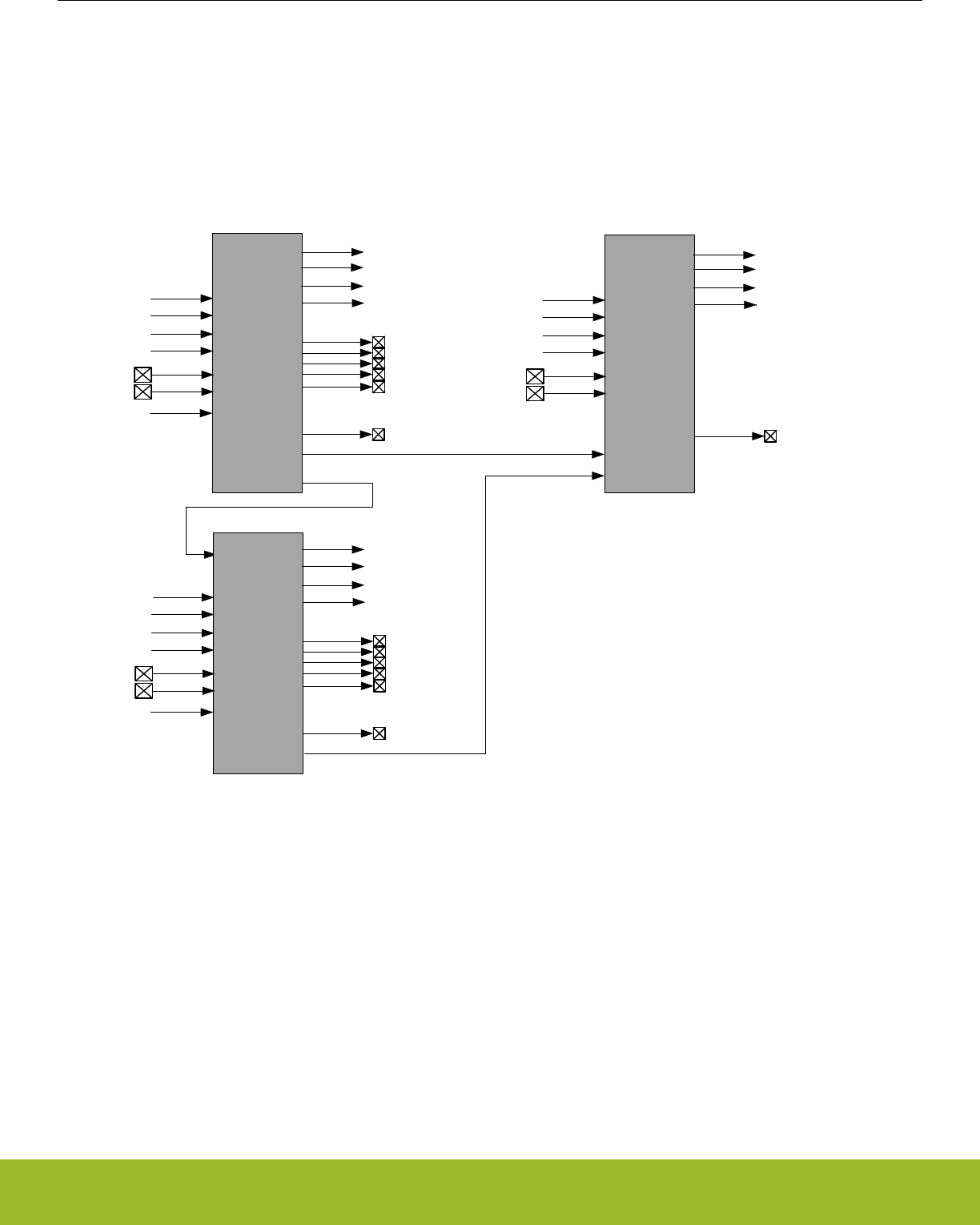
• Output status to PRS
25.3 Functional Description
The 3 opamps can be configured to perform various opamp functions through a network of muxes. An overview of the opamps are
shown in Figure 25.1 OPAMP System Overview on page 821. Two of the 3 opamps are part of the VDAC, while the others are stand-
alone. The outputs of the opamps can be routed to the ADC and ACMP. All 3 opamps can also take input from pins. Since OPA0 and
OPA1 are part of the VDAC, special considerations needs to be taken when both VDAC channel 0/channel 1 and OPA0/OPA1 are
used. For detailed explanation, refer to 25.3.5 Opamp VDAC Combination.
OPA0
OPA0 Main
output
OPA0NEXT
POS0
NEG0
APORT3
APORT4
APORT1
APORT2
DAC_CH0
OPA1 OPA1 Alternative
outputs
OPA1 Main
output
OPA1NEXT
POS1
NEG1
APORT3
APORT4
APORT1
APORT2
DAC_CH1
OPA2
OPA2 Main
output
POS2
NEG2
APORT3
APORT4
APORT1
APORT2
OPA1 APORT
Outputs
OPA0 Alternative
outputs
OPA0 APORT
Outputs OPA2 APORT
Outputs
OPA0TAP
APORT1Y
APORT2Y
APORT3Y
APORT4Y
APORT1Y
APORT2Y
APORT3Y
APORT4Y
APORT1Y
APORT2Y
APORT3Y
APORT4Y
Figure 25.1. OPAMP System Overview
There is a set of input muxes for each opamp, making it possible to select various input sources. A more detailed view of the 3 opamps,
including the mux network is shown in Figure 25.2 OPAMP Overview on page 822. The POSSEL mux connected to the positive input
makes it possible to select a pin, another opamp output, or tap from the resistor network. Similarly, the NEGSEL mux on the negative
input makes it possible to select a pin or a feedback path as its source. The feedback path can be unity gain, 3x gain, or selected from
the resistor network for programmable gain. Each opamp has several outputs, a main output, an alternative output network, APORT
output and a next output. These outputs make it possible to route the output to a pin, another opamp input, the ADC, the ACMP, or into
the feedback path. For details regarding configuring the outputs, see 25.3.1.6 Output Configuration. In addition, there is also a mux to
configure the resistor ladder for connection to VSS, a pin, or another opamp output.
Reference Manual
OPAMP - Operational Amplifier
silabs.com | Smart. Connected. Energy-friendly. Preliminary Rev. 0.5 | 821
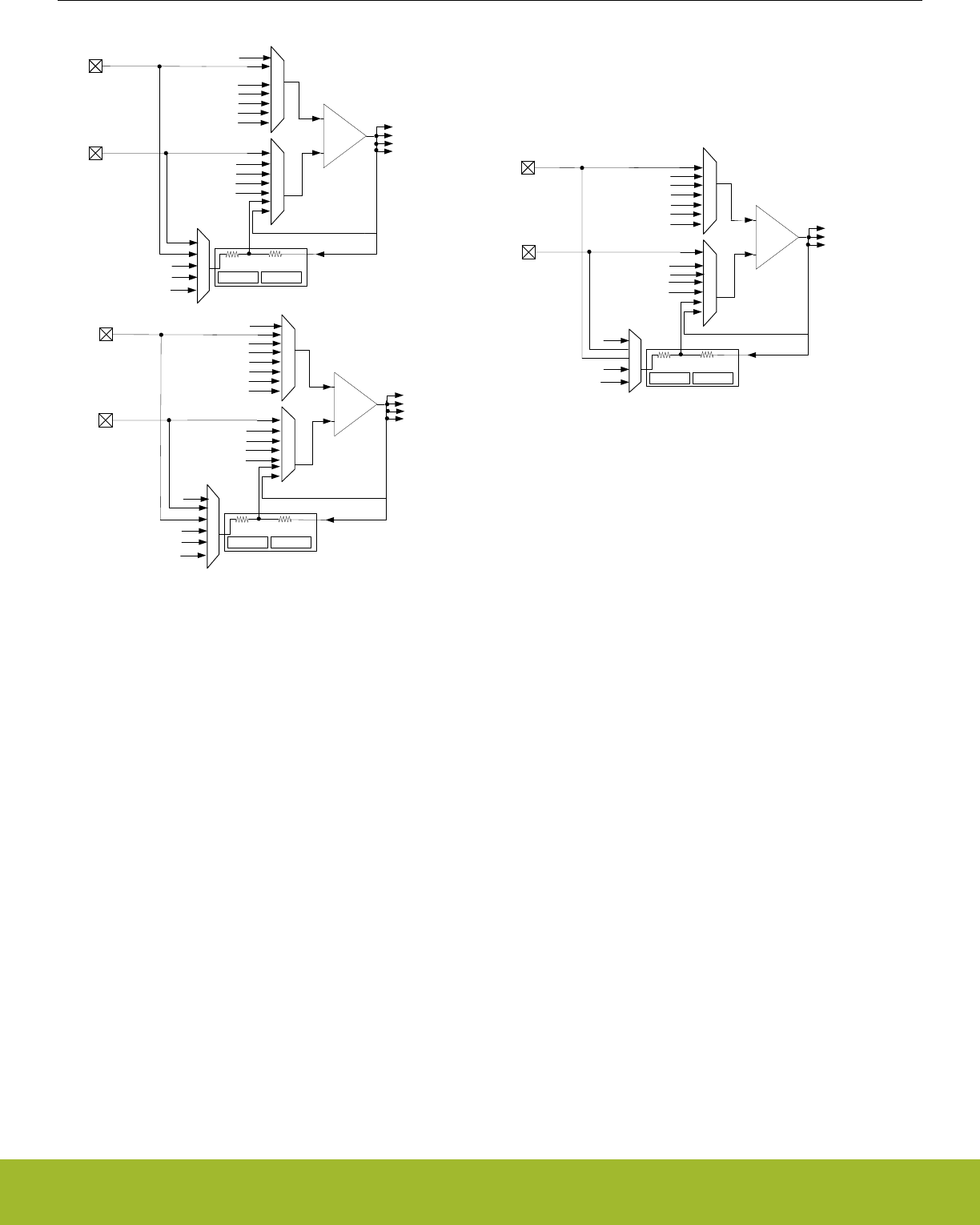
-
+
OPA0TAP
OPA0TAP
VSS
OPA0
POSSEL
NEGSEL
POS0
NEG0
R1 R2
UNITYGAIN
RESINMUX
NEG0
CENTER01
Main output
NEXTOUT0
DAC0CH0
-
+
OPA1TAP
NEXTOUT0
OPA1
POSSEL
NEGSEL
POS1
NEG1
Main output
Alternative output network
NEXTOUT1
DAC0CH1
-
+
OPA0TAP
NEXTOUT1
NEXTOUT1
OPA2
POSSEL
NEGSEL
POS2
NEG2
RESINMUX
Main output
Aport output
Aport output
Aport output
APORT1Y
APORT2Y
APORT3Y
APORT4Y
APORT1X
APORT2X
APORT3X
APORT4X
Alternative output network
Alternative output network
RESSEL GAIN3X
OPA1TAP
VSS R1 R2
UNITYGAIN
RESINMUX
NEG0
CENTER01
RESSEL GAIN3X
NEXTOUT0
OPA2TAP
VSS
R1 R2
NEG0 RESSEL GAIN3X
APORT1X
APORT2X
APORT3X
APORT4X
APORT1X
APORT2X
APORT3X
APORT4X
APORT1Y
APORT2Y
APORT3Y
APORT4Y
APORT1Y
APORT2Y
APORT3Y
APORT4Y
Figure 25.2. OPAMP Overview
25.3.1 Opamp Configuration
Since two of the 3 OPAMPs (OPA0, OPA1) are part of the VDAC, the opamp configuration registers are located in the VDAC.
Each OPAMP can be enabled by setting OPAxEN in VDACn_CMD and can be disabled by setting OPAxDIS in VDACn_CMD. The ena-
bled status of each OPAMP can be read by polling the OPAxENS bit in VDACn_STATUS. OPAxENS goes high immediately after an
OPAxEN is written and goes low when OPAxDIS is written and after OPAMP is completely disabled.
Software must not write to the following registers while OPAxENS set.
• VDACn_OPAx_CTRL
• VDACn_OPAx_TIMER
• VDACn_OPAx_MUX
25.3.1.1 Enable Sources
Opamp can be enabled either with software or PRS. The default source is software. Setting PRSEN to 1 in VDACn_OPAx_CTRL ena-
bles PRS mode. In PRS mode, opamp has two options, which are selectable with PRSMODE in VDACn_OPAx_CTRL. If PRSMODE is
configured to TIMED, opamp is turned on on the positive edge of PRS and stays on until PRS goes low. If PRSMODE is configured to
PULSED, opamp is turned on the positive edge of PRS and stays on based on the timer configurations in VDACn_OPAxTIMER. The
PRS channel is selected by PRSSEL in VDACn_OPAx_CTRL.
25.3.1.2 Warmup Time
When an opamp is enabled some initialization time is required. The warm up period is programmable with WARMUPTIME in
VDACn_OPAx_TIME. The OPAxWARM bit in VDACn_STATUS are set when the warmup period has completed.
The warm up period depends on the selected DRIVESTRENGTH in VDACn_OPAx_CTRL.
Reference Manual
OPAMP - Operational Amplifier
silabs.com | Smart. Connected. Energy-friendly. Preliminary Rev. 0.5 | 822

Table 25.1. OPAMP Warmup Time
DRIVESTRENGTH WARMUPTIME (µs)
0 100
1 85
2 8
3 6
25.3.1.3 Settle Time
After an opamp is enabled and the warmed-up time has elapsed the output settles externally. The settle period is programmable with
SETTLETIME in VDACn_OPAx_TIME. The OPAxOUTVALID bit in VDACn_STATUS is set when the settle period has completed. When
in use by the VDAC the default settling time is used.
The settling period depends on the load at opamp output and DRIVESTRENGTH of the opamp. Table 25.2 OPAMP Settling Time on
page 823 specifies SETTLETIME settings for a load of 1KOhm and 75pF.
Table 25.2. OPAMP Settling Time
DRIVESTRENGTH SETTLETIME (µs)
0 60
1 25
2 3
3 1
25.3.1.4 Startup Delay
Each opamp has an option to delay the warm up period. The startup delay is programmable with STARTDLY in VDACn_OPAx_TIME. If
STARTDLY is programmed to a non-zero value, the opamp is warmed up after STARTDLY+WARMUPTIME, and the output settles after
STARTDLY+WARMUPTIME+SETTLETIME.
25.3.1.5 Input Configuration
The inputs to the opamps are controlled through a set of input muxes. The mux connected to the positive input is configured by the
POSSEL bit-field in the VDACn_OPAx_MUX register. Similarly, the mux connected to the negative input is configured by setting the
NEGSEL bit-field in VDACn_OPAx_MUX. The input into the resistor ladder can be configured by setting the RESINMUX bit-field in
VDACn_OPAx_MUX.
25.3.1.6 Output Configuration
Each opamp has three outputs: the main output, an alternative output network with lower drive strength, and an APORT output with low
drive strength. These three outputs can be configured as shown in Figure 25.3 Opamp Output Stage Overview on page 824. The
main output can be used to drive the main output by setting MAINOUTEN in VDACn_OPAx_OUT. The alternative output can drive the
alternative output network by setting ALTOUTEN in VDACn_OPAx_OUT. The APORT output can drive the APORT selection mux by
setting APORTOUTEN in VDACn_OPAx_OUT.
Reference Manual
OPAMP - Operational Amplifier
silabs.com | Smart. Connected. Energy-friendly. Preliminary Rev. 0.5 | 823
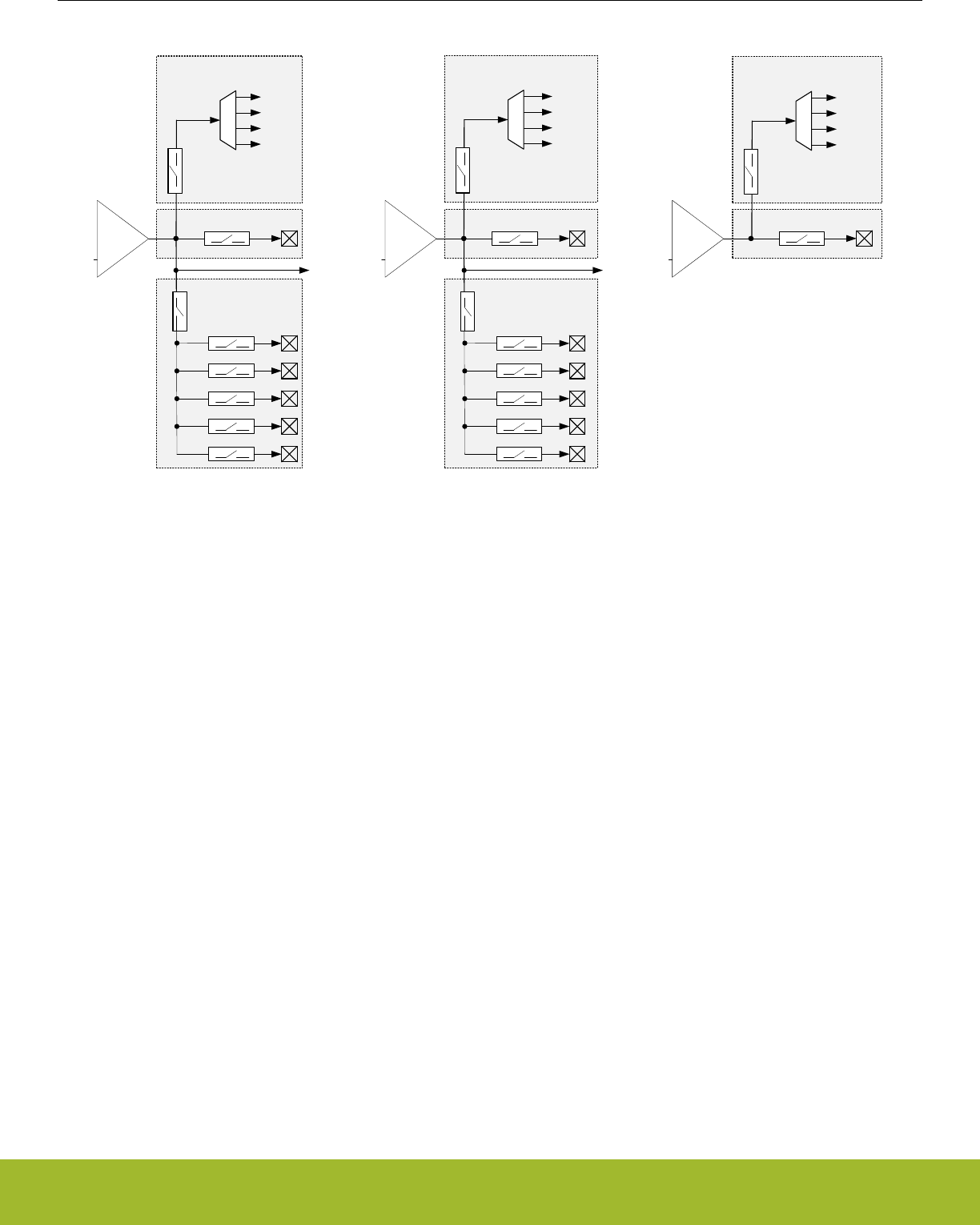
-
+
OPA0
APORT1Y
APORT2Y
APORT Output
NEXTOUT0
Main Output
OUT0
OUT1
OUT2
OUT3
OUT4
MAINOUTEN
ALTOUTEN
-
+
OPA1
NEXTOUT1
Main Output
OUT0
OUT1
OUT2
OUT3
OUT4
MAINOUTEN
ALTOUTEN
-
+
OPA2
Main Output
MAINOUTEN
APORT3Y
APORT4Y
APORTOUTEN
APORTOUTSEL
APORT1Y
APORT2Y
APORT Output
APORT3Y
APORT4Y
APORTOUTEN
APORTOUTSEL
APORT1Y
APORT2Y
APORT Output
APORT3Y
APORT4Y
APORTOUTEN
APORTOUTSEL
Alternative Output
network
Alternative Output
network
Figure 25.3. Opamp Output Stage Overview
The alternative output network consists of connections to pins and a connection to the next opamp. The connections to pins can be
individually enabled by configuring ALTOUTPADEN in te VDACn_OPAx_OUT register. For cascaded opamp configurations, each
opamp has a NEXTOUT connection.
The opamp outputs can also be routed to APORT1Y, APORT2Y, APORT3Y, and APORT4Y. The APORT channel can be selected by
configuring APORTOUTSEL in VDACn_OPAx_OUT.
The opamps are also routed internally to the ADC. OPA0 and OPA1 are routed through the POSMUX of the ADC, and OPA2 routed
through the NEGMUX of the ADC. See 27.3.5 Input Selection in the ADC chapter for information on how to configure the ADC input
mux.
In addition, OPA0 and OPA1 are internally routed to both the POSMUX and NEGMUX of ACMP. See 26.3.4 Input Selection in the
ACMP chapter for information on how to configure the ACMP input mux.
The main and alternate outputs of each opamp can be shorted together by setting the SHORT bit-field in VDACn_OPAx_OUT.
25.3.1.7 Gain Programming
The feedback path of each mux includes a resistor ladder that can be used to select a set of gain values. Gain is configured by the
RESSEL bit-field located in the VDACn_OPAx_MUX register. Gain values are determined by the resistor ladder based on ratio of
R2/R1. It is also possible to bypass the resistor ladder in unity gain mode. In addition, there is also a preconfigured resistor ladder with
3X gain. The 3x gain resistor ladder is enabled by setting GAIN3X in VDACn_OPAx_MUX. By default all opamps are configured in 3x
gain mode. When using RESSEL, GAIN3X should be set to zero.
25.3.1.8 Offset Calibration
Each opamp has a calibration register, VDACn_OPAx_CAL, where calibration values for both offset and gain correction can be written.
The required calibration settings depend on the chosen DRIVESTRENGTH. The default calibration settings stored in
VDACn_OPAx_CAL are for DRIVESTRENGTH=2. If an opamp is being reconfigured, the required calibration settings for DRIVES-
TRENGTH=n can be found in DEVINFO_OPAxCALn. Offsets can be programmed through the OFFSETP and OFFSETN bitfields of
VDACn_OPAx_CAL.
Reference Manual
OPAMP - Operational Amplifier
silabs.com | Smart. Connected. Energy-friendly. Preliminary Rev. 0.5 | 824

25.3.1.9 Disabling of Rail-to-Rail Operation
Each opamp can have its input rail-to-rail stage disabled by setting the HCMDIS in VDACn_OPAx_CTRL. Disabling the rail-to-rail input
stage improves linearity of the opamp, thus improving the total harmonic distortion (THD) at the cost of reduced input signal swing.
25.3.1.10 Unity Gain Bandwidth Scaling
Unity gain bandwidth of an opamp can be scaled setting the INCBW bit in VDACn_OPAx_CTRL. Note that this setting is used only
when closed loop gain is greater than 3X. With this setting is enabled, the opamp is not unity gain stable.
25.3.1.11 Opamp Output Scaling
Opamp output drive strength is scaled by one half when the OUTSCALE bit in VDACn_OPAx_CTRL is set.
25.3.2 Interrupts and PRS Output
Each opamp has an interrupt flag OPAxOUTVALID in VDACn_IF that is set when the output is settled externally at the load. An interrupt
will be requested if the OPAxOUTVALID interrupt flag in VDACn_IF is set and enabled by the OPAxOUTVALID bit in VDACn_IEN.
The OPAxERRPRSMODE interrupt flag in VDACn_IF indicates a protocol error when the opamp is triggered in PRS TIMED mode. This
flag is set if the negative edge of the PRS pulse came before the output to opamp is valid. The interrupt flag is enabled by the OPAx-
ERRPRSMODE bit in VDACn_IEN.
An interrupt can also be requested when an APORT bus conflict occurs if the OPAxAPORTCONFLICT interrupt flag in VDACn_IF is set
and enabled through by the OPAxAPORTCONFLICT bit in VDACn_IEN.
One of two aynchronous PRS outputs can be enabled for each opamp by setting PRSOUTMODE in VDACn_OPAx_CTRL. If PRSOUT-
MODE is WARM, opamp warm-up status is available. If PRSOUTMODE is OUTVALID, opamp output valid status is available.
25.3.3 APORT Request and Conflict Status
The opamps are connected to pins through the APORT system. To help debug over-utilization of APORT resources, the opamps pro-
vide request and conflict status information. The request status of APORT buses is visible through the DACn_OPAx_APORTREQ regis-
ter.
If an APORT bus conflict occurs, it is reported in the DACn_OPAx_APORTCONFLICT register. An APORT conflict occurs if an opamp
requests the same bus at the same time as another analog peripheral. In addition an APORT conflict is reported if any two of NEGSEL,
POSSEL or APORTOUTSEL are configured to request the same APORT bus.
It is possible for the opamps to passively monitor APORT buses without controlling the switches and creating bus conflicts. This can be
done by setting APORTXMASTERDIS or APORTYMASTERDIS in the DACn_OPAx_CTRL register.
25.3.4 Opamp Modes
The opamps can perform several different functions by configuring the internal signal routing between the opamps. The modes availa-
ble are described in the following sections.
25.3.4.1 General Opamp Mode
In this mode, the resistor ladder is isolated from the feedback path, and the input signal routing is defined by POSSEL and NEGSEL in
VDACn_OPAx_MUX. The output signal routing is defined by the setting of VDACn_OPAx_OUT.
Table 25.3. General Opamp Mode Configuration
OPA bit-fields OPA Configuration
OPAx POSSEL POSPADx, APORT[1-4]X
OPAx NEGSEL OPATAP, UG, NEGPADx, APORT[1-4]Y
OPAx RESINMUX NEXTOUT, POSPADx, NEGPADx, VSS
Reference Manual
OPAMP - Operational Amplifier
silabs.com | Smart. Connected. Energy-friendly. Preliminary Rev. 0.5 | 825
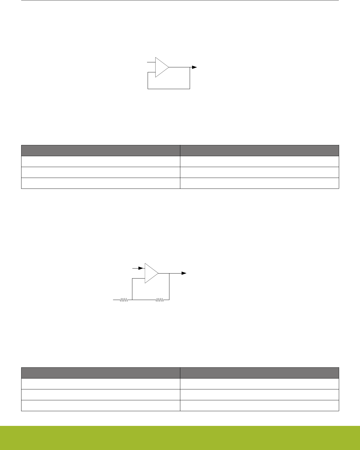
25.3.4.2 Voltage Follower Unity Gain
In this mode, the unity gain feedback path is selected for the negative input by setting the NEGSEL bit-field to UG in the
VDACn_OPAx_MUX register as shown in Figure 25.4 Voltage Follower Unity Gain Overview on page 826. The positive input is selec-
ted by the POSSEL bit-field in VDACn_OPAx_MUX, and the output is configured by VDACn_OPAx_OUT register.
VIN
-
+
VOUT
Figure 25.4. Voltage Follower Unity Gain Overview
Table 25.4. Voltage Follower Unity Gain Configuration
OPA bit-fields OPA Configuration
OPAx POSSEL OPATAP, NEXTOUT, POSPADx, APORT[1-4]X
OPAx NEGSEL UG
OPAx RESINMUX DISABLE
25.3.4.3 Inverting input PGA
Figure 25.5 Inverting input PGA Overview on page 826 shows the inverting input PGA configuration. In this mode, the negative input
is connected to the resistor ladder by setting the NEGSEL bit-field to OPATAP in the VDACn_OPAx_MUX register. This setting provides
a programmable gain on the negative input, which is set by the RESSEL bit-field in VDACn_OPAx_MUX. Signal ground for the positive
input can come from off-chip by setting the POSSEL bit-field to PAD or APORT in VDACn_OPAx_MUX. In addition, the output is config-
ured by VDACn_OPAx_OUT register.
VOUT
VOUT=-(VIN-POS) R2/R1 + POS
R1 R2
POS
-
+
VIN
Figure 25.5. Inverting input PGA Overview
Table 25.5. Inverting input PGA Configuration
OPA bit-fields OPA Configuration
OPAx POSSEL POSPADx, APORT[1-4]X
OPAx NEGSEL OPATAP
OPAx RESINMUX NEXTOUT, NEGPADx, POSPADx
Reference Manual
OPAMP - Operational Amplifier
silabs.com | Smart. Connected. Energy-friendly. Preliminary Rev. 0.5 | 826
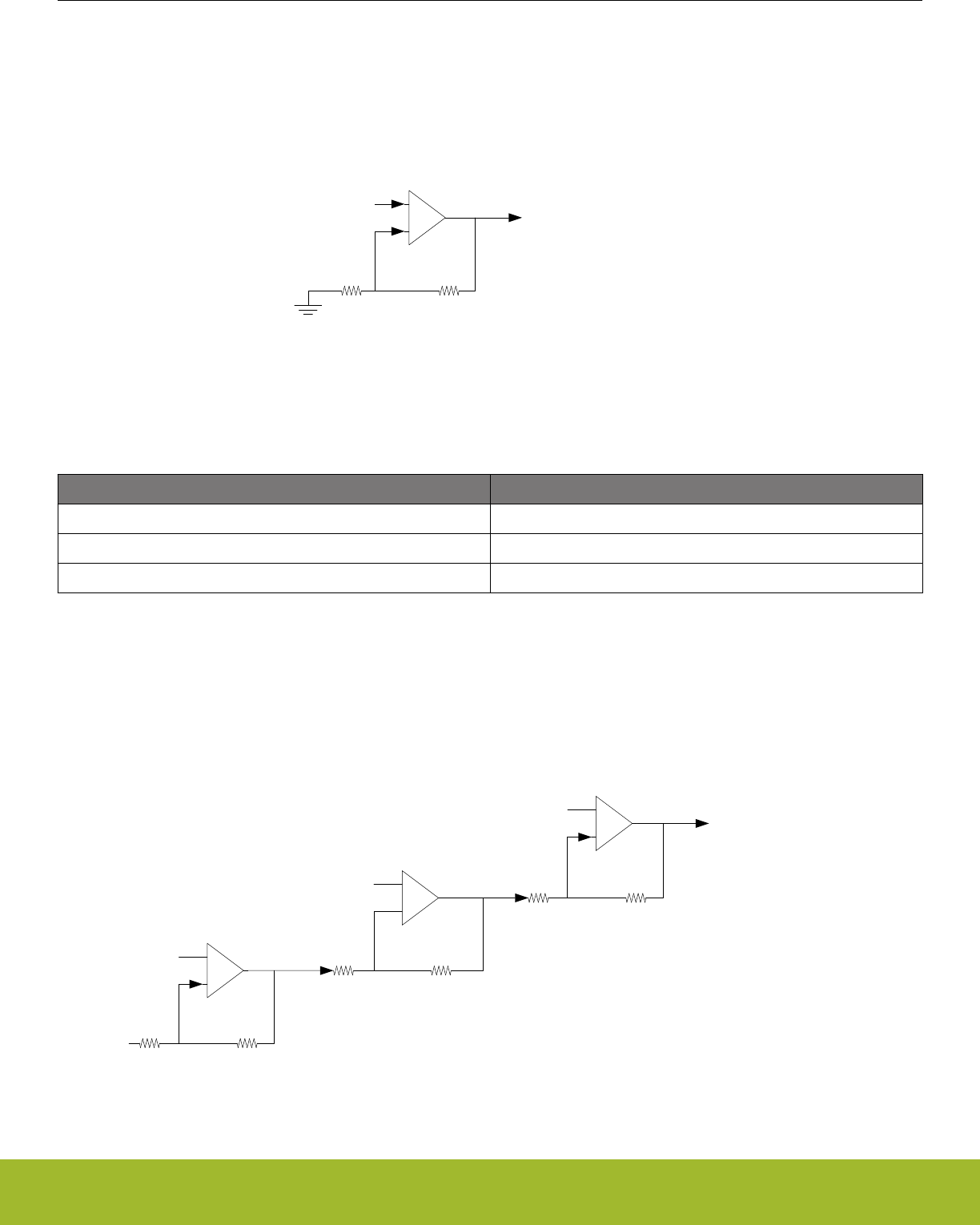
25.3.4.4 Non-inverting PGA
Figure 25.6 Non-inverting PGA Overview on page 827 shows the non-inverting input configuration. In this mode, the negative input is
connected to the resistor ladder by setting the NEGSEL bit-field to OPATAP in VDACn_OPAx_MUX. This setting provides a program-
mable gain on the negative input, which is set by the RESSEL bit-field in VDACn_OPAx_MUX. In addition, the RESINMUX bit-field
must be set to VSS or NEGPAD in VDACn_OPAx_MUX. The positive input is selected by the POSSEL bit-field, and the output is con-
figured by VDACn_OPAx_OUT register.
R1 R2
VIN
-
+
VOUT
VOUT=VIN(1+ R2/R1)
Figure 25.6. Non-inverting PGA Overview
Table 25.6. Non-inverting PGA Configuration
OPA bit-fields OPA Configuration
OPAx POSSEL NEXTOUT, POSPADx, APORT[1-4]X
OPAx NEGSEL OPATAP
OPAx RESINMUX VSS, NEGPAD
25.3.4.5 Cascaded Inverting PGA
This mode enables the opamp signals to be internally configured to cascade two or more opamps in inverting mode as shown in Figure
25.7 Cascaded Inverting PGA Overview on page 827. In both cases, the positive input is connected to signal ground by setting the
POSSEL bit-field to PAD or APORT in VDACn_OPAx_MUX. When cascaded, the negative input is connected to the resistor ladder by
setting the NEGSEL bit-field to OPATAP in VDACn_OPAx_MUX. The input to the resistor ladder is configured by the RESINMUX bit-
field in VDACn_OPAx_MUX.
R1 R2
VIN
-
+
POS0
VOUT1=-(VIN-POS0) x R2/R1 + POS0
VOUT2=-(VOUT1-POS1) x R2/R1 + POS1
VOUT3=-(VOUT2-POS3) x R2/R1 + POS3
R1 R2
-
+
POS1
R1 R2
-
+
POS2
Figure 25.7. Cascaded Inverting PGA Overview
Reference Manual
OPAMP - Operational Amplifier
silabs.com | Smart. Connected. Energy-friendly. Preliminary Rev. 0.5 | 827
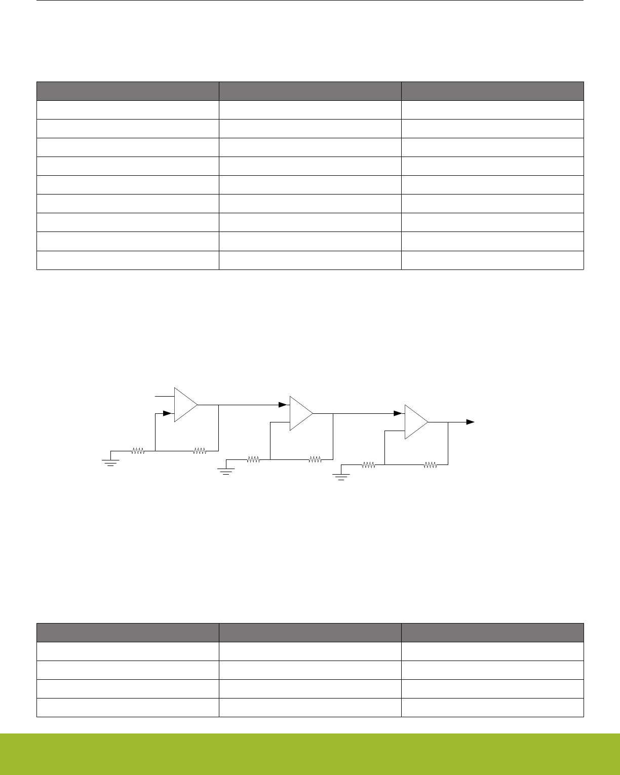
Table 25.7 Cascaded Inverting PGA Configuration on page 828 shows cascaded non-inverting PGA with OPA0,OPA1 and OPA2. The
output from OPA0 is connected to OPA1 to create the second stage by setting the RESINMUX field to OPANEXT in
VDACn_OPA1_MUX. The last stage is created by setting the RESINMUX bit-field to OPANEXT in VDACn_OPA2MUX.
Table 25.7. Cascaded Inverting PGA Configuration
OPA OPA bit-fields OPA Configuration
OPA0 POSSEL POSPAD0, APORT[1-4]X
OPA0 NEGSEL OPATAP
OPA0 RESINMUX NEGPAD0
OPA1 POSSEL POSPAD1, APORT[1-4]X
OPA1 NEGSEL OPATAP
OPA1 RESINMUX OPANEXT
OPA2 POSSEL POSPAD2,APORT[1-4]X
OPA2 NEGSEL OPATAP
OPA2 RESINMUX OPANEXT
25.3.4.6 Cascaded Non-inverting PGA
This mode enables the opamp signals to be internally configured to cascade two or more opamps in non-inverting mode as shown in
Figure 25.8 Cascaded Non-inverting PGA Overview on page 828. The negative input for all opamps will be connected to the resistor
ladder by setting the NEGSEL bit-field to OPATAP. In addition the resistor ladder input must be set to VSS or NEGPADx by configuring
the RESINMUX bit-field in VDACn_OPAx_MUX.
R1 R2
VIN
-
+VOUT1=VIN(1+ R2/R1)
VOUT2=VIN(1+ R2/R1)
VOUT3=VIN(1+ R2/R1)
R1 R2
-
+
R1 R2
-
+
Figure 25.8. Cascaded Non-inverting PGA Overview
Table 25.8 Cascaded Non-inverting PGA Configuration on page 828 shows cascaded non-inverting PGA with OPA0,OPA1 and OPA2.
When cascaded, the positive input on OPA0 is configured by the OPA0 POSSEL bit-field in VDACn_OPA0_MUX. The output from
OPA0 is connected to OPA1 to create the second stage by setting the POSSEL field to OPANEXT in VDACn_OPA1_MUX. The last
stage is created by setting the POSSEL bit-field to OPANEXT in VDACn_OPA2_MUX.
Table 25.8. Cascaded Non-inverting PGA Configuration
OPA OPA bit-fields OPA Configuration
OPA0 POSSEL POSPAD0,APORT[1-4]X
OPA0 NEGSEL OPATAP
OPA0 RESINMUX VSS, NEGPAD0
OPA1 POSSEL OPANEXT
Reference Manual
OPAMP - Operational Amplifier
silabs.com | Smart. Connected. Energy-friendly. Preliminary Rev. 0.5 | 828
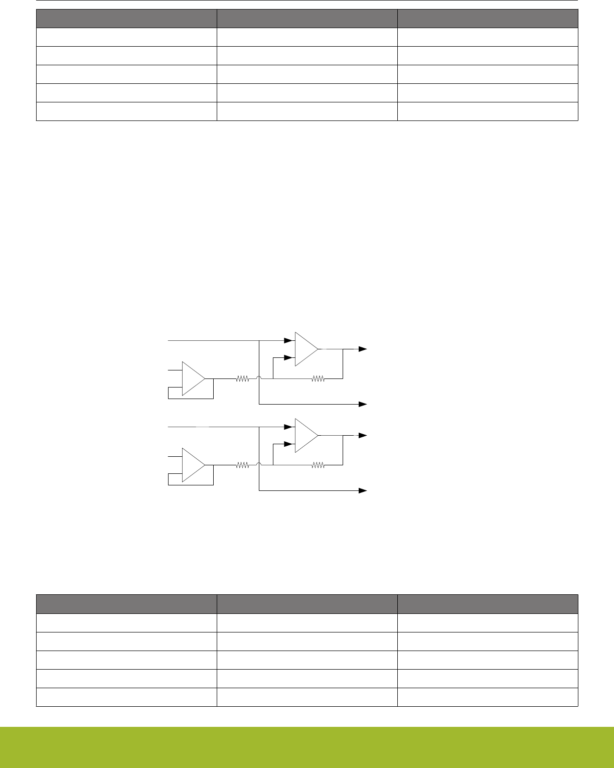
OPA OPA bit-fields OPA Configuration
OPA1 NEGSEL OPATAP
OPA1 RESINMUX VSS, NEGPAD1
OPA2 POSSEL OPANEXT
OPA2 NEGSEL OPATAP
OPA2 RESINMUX VSS, NEGPAD2
25.3.4.7 Two Opamp Differential Amplifier
This mode allows OPA0 and OPA1 or OPA1 and OPA2 to be internally connected to form a two opamp differential amplifier as shown in
Figure 25.9 Two Op-amp Differential Amplifier Overview on page 829. When using OPA0 and OPA1, the positive input of OPA0 can
be connected to any input by setting the POSSEL bit-field in VDACn_OPA0_MUX. The OPA0 feedback path must be configured for
unity gain by setting the NEGSEL bit-field to UG in VDACn_OPA0_MUX. In addition, the OPA0 RESINMUX bit-field must be set to DIS-
ABLED. The OPA0 NEXTOUT output must be connected to OPA1 by setting the RESINMUX bit-field to OPANEXT in
VDAC_n_OPA1_MUX. The positive input onof OPA1 is selected by the POSSELbit-field in VDACn_OPA1_MUX. The OPA1 output is
configured by DACn_OPA1_OUT.
When using OPA1 and OPA2, the positive input of OPA1 can be connected to any input by setting the POSSEL bit-field in
VDACn_OPA1_MUX. The OPA1 feedback path must be configured for unity gain by setting the NEGSEL bit-field to UG in
VDACn_OPA1_MUX. In addition, the OPA1 RESINMUX bit-field must be set to DISABLED. The OPA1 NEXTOUT output must be con-
nected to OPA2 by setting the RESINMUX bit-field to OPANEXT in VDACn_OPA2_MUX. The positive input of OPA2 is selected by the
POSSEL bit-field in VDACn_OPA2_MUX. The OPA2 output is configured by DACn_OPA2_OUT.
R1 R2
V2
-
+
-
+
V1 VDIFF=(V2-V1)R2/R1
OPA0
OPA1
R1 R2
V2
-
+
-
+
V1 VDIFF=(V2-V1)R2/R1
OPA1
OPA2
Figure 25.9. Two Op-amp Differential Amplifier Overview
Table 25.9. OPA0/OPA1 Differential Amplifier Configuration
OPA OPA bit-fields OPA Configuration
OPA0 POSSEL POSPAD0, APORT[1-4]X
OPA0 NEGSEL UG
OPA0 RESINMUX DISABLE
OPA1 POSSEL POSPAD1, APORT[1-4]X
OPA1 NEGSEL OPATAP
Reference Manual
OPAMP - Operational Amplifier
silabs.com | Smart. Connected. Energy-friendly. Preliminary Rev. 0.5 | 829
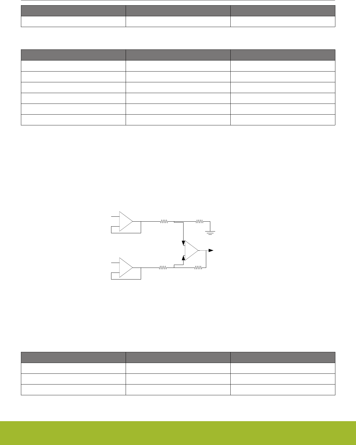
OPA OPA bit-fields OPA Configuration
OPA1 RESINMUX OPANEXT
Table 25.10. OPA1/OPA2 Differential Amplifier Configuration
OPA OPA bit-fields OPA Configuration
OPA1 POSSEL POSPAD1, APORT[1-4]X
OPA1 NEGSEL UG
OPA1 RESINMUX DISABLE
OPA2 POSSEL POSPAD2, APORT[1-4]X
OPA2 NEGSEL OPATAP
OPA2 RESINMUX OPANEXT
25.3.4.8 Three Opamp Differential Amplifier
This mode allows the three opamps to be internally configured to form a three opamp differential amplifier as shown in Figure
25.10 Three Op-amp Differential Amplifier Overview on page 830. For both OPA0 and OPA1, the positive input can be connected to
any input by configuring the OPA0 POSSEL and OPA1 POSSEL bit-fields in VDACn_OPA0_MUX and VDACn_OPA1_MUX, respectiv-
ley. The OPA0 and OPA1 feedback paths must be configured for unity gain by setting the OPA0 NEGSEL and OPA1 NEGSEL bit-fields
to UG in VDACn_OPA0_MUX and VDACn_OPA1_MUX respectivley. In addition the OPA0 RESINMUX and OPA1 RESINMUX bit-fields
must be set to DISABLED. The OPA1 output must be connected to OPA2 by setting RESINMUX to OPANEXT in VDACn_OPA2_MUX
and the OPA2 POSSEL must be set to OPATAP. The OPA2 output is configured by the DACn_OPA2_OUT register.
R1 R2
V2
-
+
VOUT
VOUT=(V2-V1)R2/R1
R1 R2
-
+
-
+
V1
OPA1
OPA0
OPA2
Figure 25.10. Three Op-amp Differential Amplifier Overview
The gain for the Three Opamp Differential Amplifier is determined by the combination of the gain settings of OPA0 and OPA2. Gain
values of 1/3, 1 and 3, are available and programmed as shown in the table below.
Table 25.11. Three Opamp Differential Amplifier Gain Programming
Gain OPA0 RESSEL OPA2 RESSEL
1/3 4 0
111
304
Reference Manual
OPAMP - Operational Amplifier
silabs.com | Smart. Connected. Energy-friendly. Preliminary Rev. 0.5 | 830
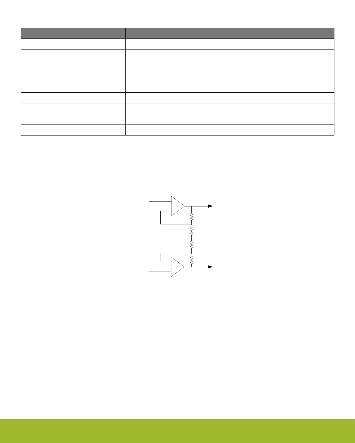
Table 25.12. Three Opamp Differential Amplifier Configuration
OPA OPA bit-fields OPA Configuration
OPA0 POSSEL POSPAD0, APORT[1-4]X
OPA0 NEGSEL UG
OPA0 RESINMUX DISABLE
OPA1 POSSEL POSPAD1, APORT[1-4]X
OPA1 NEGSEL UG
OPA1 RESINMUX DISABLE
OPA2 POSSEL OPATAP
OPA2 NEGSEL OPATAP
OPA2 RESINMUX OPANEXT
25.3.4.9 Instrumentation Amplifier
OPA0 and OPA1 can form a fully differential instrumentation amplifier by setting RESINMUX to CENTER for both opamps in
VDACn_OPA0_MUX and VDACn_OPA1_MUX. Configuring RESINMUX to CENTER makes a connection between resistor ladder of
the opamps as shown in Figure 25.11 Instrumentaion Amplifier Overview on page 831.
R1
R2
-
+VOUT
OPA0
R1
R2
-
+
VOUT
OPA1
V1
V2
Figure 25.11. Instrumentaion Amplifier Overview
25.3.4.10 Common Reference
It is possible to configure all opamps to have a common reference by setting the RESINMUX to COMPAD in VDACn_OPAx_MUX.
When RESINMUX of all opamps is set to COMPAD mode, the NEGPAD input of OPA0 is used.
25.3.4.11 Dual Buffer ADC Driver
It is possible to use any two of the opamps to form a Dual Buffer ADC driver as shown in Figure 25.12 Dual Buffer ADC Driver Overview
on page 832. Both opamps used must be configured in the same way. The positive input is configured by setting the 0PAx POSSEL
to PAD, and the negative input is connected to the resistor ladder by setting NEGSEL to OPATAP in VDACn_OPAx_MUX. The output
from the opamps can be configure to drive pins through the alternative output network or the APORT. The ADC can sample pins that
the opamps are driving through the APORT.
Reference Manual
OPAMP - Operational Amplifier
silabs.com | Smart. Connected. Energy-friendly. Preliminary Rev. 0.5 | 831
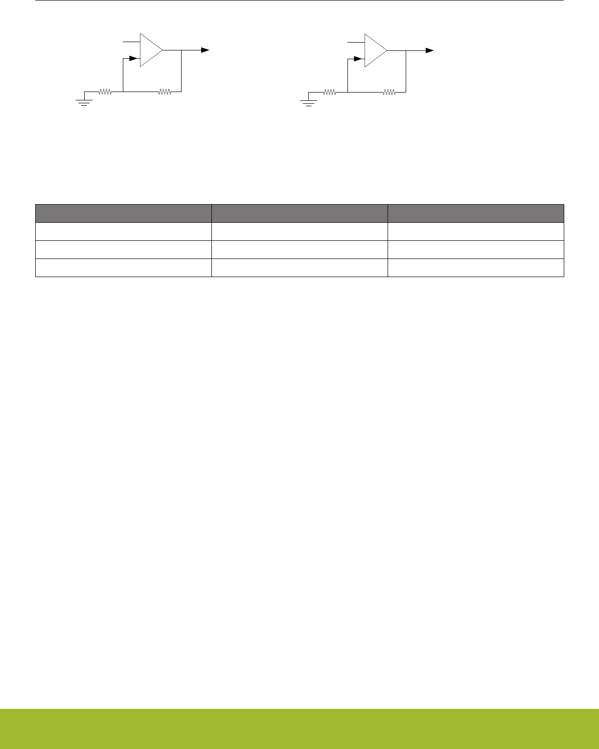
R1 R2
VIP
-
+
VOUTP=VIP(1+ R2/R1)
or
VOUTP = VIP (Unity Gain)
VOUTN=VIN(1+ R2/R1)
or
VOUTN = VIN (Unity Gain)
R1 R2
VIN
-
+
Figure 25.12. Dual Buffer ADC Driver Overview
Table 25.13. Dual Buffer ADC Driver Configuration
OPA OPA bit-fields OPA Configuration
OPAx POSSEL POSPADx, APORT[1-4]X
OPAx NEGSEL OPATAP
OPAx RESINMUX VSS
25.3.5 Opamp VDAC Combination
Since two of the OPAMPs are part of the VDAC, it is not possible to use both VDAC channels and all 3 OPAMPs at the same time. If
both VDAC channels are used, OPA0 and OPA1 can not be used as stand-alone opamp. However, it is possible to use one of the
VDAC channels in combination with OPA0 or OPA1. OPA1 is available when VDAC channel 0 is in use, and OPA0 is available when
VDAC channel 1 is used.
25.4 Register Map
The register map of the opamp can be found in 24.4 Register Map in the VDAC chapter.
25.5 Register Description
The register description of the opamp can be found in 24.5 Register Description in the VDAC chapter.
Reference Manual
OPAMP - Operational Amplifier
silabs.com | Smart. Connected. Energy-friendly. Preliminary Rev. 0.5 | 832
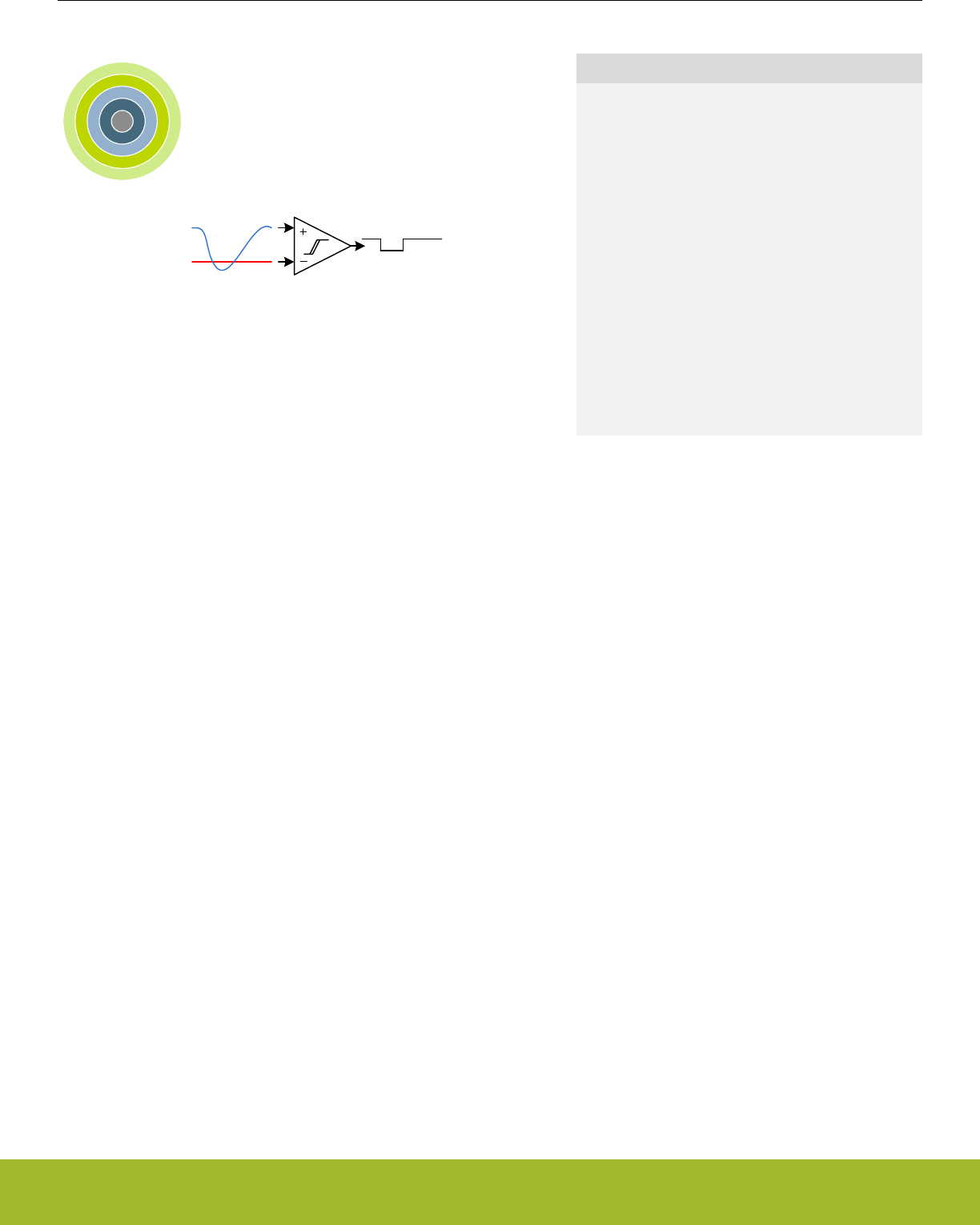
26. ACMP - Analog Comparator
0 1 2 3 4
Quick Facts
What?
The ACMP (Analog Comparator) compares two ana-
log signals and returns a digital value telling which is
greater.
Why?
Applications often do not need to know the exact
value of an analog signal, only if it has passed a cer-
tain threshold. Often the voltage must be monitored
continuously, which requires extremely low power
consumption.
How?
Available down to Energy Mode 3 and using as little
as 100 nA, the ACMP can wake up the system when
input signals pass the threshold. The analog compa-
rator can compare two analog signals or one analog
signal and a highly configurable internal reference.
26.1 Introduction
The Analog Comparator compares the voltage of two analog inputs and outputs a digital signal indicating which input voltage is higher.
Inputs can either be from internal references or from external pins. Response time, and thereby the current consumption, can be config-
ured by altering the current supply to the comparator.
Reference Manual
ACMP - Analog Comparator
silabs.com | Smart. Connected. Energy-friendly. Preliminary Rev. 0.5 | 833

26.2 Features
• Up to 160 selectable external I/O inputs for both positive and negative inputs
•Up to 48 I/O can be used as a dividable reference
• 5 selectable internal inputs
• VDAC channel 0 voltage as a reference
• VDAC channel 1 voltage as a reference
• Dividable Internal 1.25 V bandgap reference voltage
• Dividable Internal 2.5 V bandgap reference voltage
• Dividable VDD reference voltage
• Voltage supply monitoring
• Low power mode for internal V DD and bandgap references
• Selectable hysteresis
• 8 values
• Values can be positive or negative
• Dividable references have scale for both both output values, allowing for even larger hysteresis
• Selectable response time
• Asynchronous interrupt generation on selectable edges
• Rising edge
• Falling edge
• Both edges
• Operational in EM0 Active down to EM3 Stop
• Dedicated capacitive sense mode with up to 8 inputs
• Adjustable internal resistor
• Configurable output when inactive
• Comparator output direct on PRS
• Comparator output on GPIO through alternate functionality
• Output inversion available
Reference Manual
ACMP - Analog Comparator
silabs.com | Smart. Connected. Energy-friendly. Preliminary Rev. 0.5 | 834
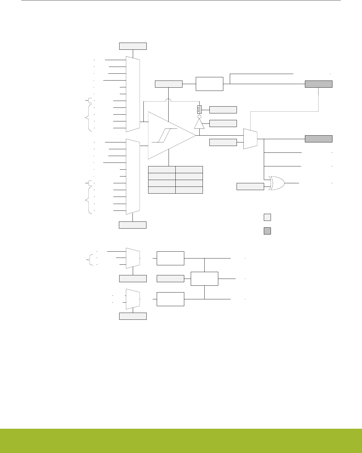
26.3 Functional Description
An overview of the ACMP is shown in Figure 26.1 ACMP Overview on page 835 .
GND
VADIV
VBDIV
APORT1
APORT2
APORT3
APORT4
APORT0
VADIVREFA
REFB
-
+
APORT1
APORT2Y
0
1
1.25V
2.5V
APORT
VLP
VDD Voltage
Divider
Voltage
Divider VBDIV
Sampler VLP
POSSEL
EN Warm-up
Counter ACMPACT
Warmup Interrupt
1
0
INACTVAL
Edge Interrupt
ACMPOUT
GPIOINV Output to GPIO
Output to PRS
VASEL
VBSEL
NEGSEL
VLPSEL
Read/Write Registers
Read Only Registers
VDACOUT0
VDACOUT1
GND
VADIV
VBDIV
APORT1
APORT2
APORT3
APORT4
APORT0
APORT
VLP
VDACOUT0
VDACOUT1
Dedicated
Dedicated
APORT
HYST0
DIVVA0
DIVVB0
HYST1
DIVVA1
DIVVB1
BIASPROG FULLBIAS
CSRESEN
CSRESSEL
Figure 26.1. ACMP Overview
The comparator has two analog inputs: one positive and one negative. When the comparator is active, the output indicates which of the
two input voltages is higher. When the voltage on the positive input is higher than the voltage on the negative input, the digital output is
high and vice versa.
The output of the comparator can be read in the ACMPOUT bit in ACMPn_STATUS. It is possible to switch inputs while the comparator
is enabled, but all other configuration should only be changed while the comparator is disabled.
Reference Manual
ACMP - Analog Comparator
silabs.com | Smart. Connected. Energy-friendly. Preliminary Rev. 0.5 | 835

26.3.1 Warm-up Time
The analog comparator is enabled by setting the EN bit in ACMPn_CTRL. The comparator requires some time to stabilize after it is
enabled. This time period is called the warm-up time. The warm-up period is self-timed and will complete within 5µs after EN is set.
During warm-up and when the comparator is disabled, the output level of the comparator is set to the value of the INACTVAL bit in
ACMPn_CTRL. When the warm-up time is over, the ACMPACT bit in ACMPn_STATUS is set to 1 to indicate that the comparator is
active.
An edge interrupt will be generated if the edge interrupt is enabled and the value set in INACTVAL differs from ACMPOUT when the
comparator transitions from warm-up to active.
Software should wait until the warm-up period is over before entering EM2 or EM3, otherwise no comparator interrupts will be detected.
EM1 can still be entered during warm-up. After the warm-up period is completed, interrupts will be detected in EM2 and EM3.
26.3.2 Response Time
There is a delay from when the input voltage changes polarity to when the output toggles. This delay is called the response time and
can be altered by increasing or decreasing the bias current to the comparator through the BIASPROG and FULLBIAS fields in the
ACMPn_CTRL register. The current and speed of the circuit increase as the values of FULLBIAS and BIASPROG are increased from
their minimum setting of FULLBIAS=0 BIASPROG=0b00000 to the maximum setting FULLBIAS=1 BIASPROG=0b11111 (maximum).
The setting of FULLBIAS has a greater affect on current and speed than the setting of BIASPROG. See the part datasheet for specific
current and response times related to the setting of these fields.
If FULLBIAS is set, to avoid glitches the highest hysteresis level should be used.
Reference Manual
ACMP - Analog Comparator
silabs.com | Smart. Connected. Energy-friendly. Preliminary Rev. 0.5 | 836
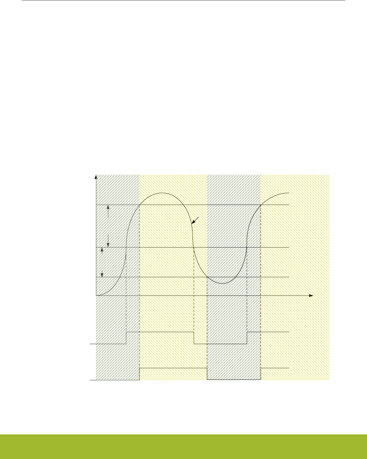
26.3.3 Hysteresis
When the hysteresis level is set to a non-zero value, the digital output will not toggle until the positive input voltage is at a voltage equal
to the hysteresis level above or below the negative input voltage (see Figure 26.3 Hysteresis on page 837 ). This feature can be used
to avoid continual comparator output changes due to noise when the positive and negative inputs are nearly equal by requiring the input
difference to exceed the hysteresis threshold.
In the analog comparator, hysteresis can be configured to 8 different levels. Level 0 is no hysteresis. Hysteresis is configured through
the HYST field in ACMPn_HYSTERESIS0 and ACMPn_HYSTERESIS1 registers. The hysteresis value can be positive or negative.
The comparator will output a 1 if:
POSSEL - NEGSEL > HYST
There are two hysteresis registers, ACMPn_HYSTERESIS0 and ACMPn_HYSTERESIS1, as the ACMP supports asymmetric hystere-
sis. ACMPn_HYSTERESIS0 are the hysteresis values used when the comparator output is 0; ACMPn_HYSTERESIS1 are the values
used when the comparator output is 1. The user must set both registers to the same values if symmetric hysteresis is desired.
Along with the HYST field, the ACMPn_HYSTERESIS0/1 registers include the DIVVA and DIVVB fields. This allows the user to imple-
ment even larger hysteresis when comparing against VADIV or VBDIV, as the reference voltage can vary with the comparator output,
also.
HYSTERESIS0
Active
HYST0
HYST1
Time
Voltage
NEGSEL
NEGSEL + HYST0
NEGSEL + HYST1
HYSTERESIS0
Active
HYSTERESIS1
Active
HYSTERESIS1
Active
POSSEL
CMPOUT without
Hysteresis
CMPOUT with
Hysteresis
Figure 26.3. Hysteresis
Reference Manual
ACMP - Analog Comparator
silabs.com | Smart. Connected. Energy-friendly. Preliminary Rev. 0.5 | 837

26.3.4 Input Selection
The POSSEL and NEGSEL fields in ACMPn_INPUTSEL control the input connections to the positive and negative inputs of the compa-
rator. The user can select external GPIO pins on the chip, or select a number of internal chip voltages. Pins are selected by configuring
channels on APORT buses. Not all selectable channels are available on a given device, as different devices within a family may not
implement or bring out all of the I/O defined for that family. Please refer to datasheet for channel availability and pin mapping.
There are limitations on the POSSEL and NEGSEL connections that can be made. The user cannot select an X-bus for both POSSEL
and NEGSEL simultaneously, nor a Y-bus for both POSSEL and NEGSEL simultaneously. The second limitation is that when using the
feedback resistor only X-bus selections can be made for POSSEL. (The resistor only physically exists on the positive input of the com-
parator).
The user may also select from a number of internal voltages. VADIV and VBDIV are two dividable voltages. VADIV can be VDD divided,
or the user can choose to select inputs from a number of APORT buses. VBDIV consists of two dividable band-gap references of either
1.25V or 2.5V. Each of these voltages have dividers in the ACMPn_HYSTERESIS0/1 registers. The formula for the division of these
voltages is:
VADIV = VA ∙ ( (DIVVA+1) / 64 )
Figure 26.3. VA Voltage Division
VBDIV = VB ∙ ( (DIVVB+1) / 64 )
Figure 26.4. VB Voltage Division
Either VADIV and VBDIV can also be used as an input to a lower power reference: VLP. Which of the two is used is configured via the
VLPSEL field in ACMPn_INPUTSEL. If the user selects VLP as an input source, then VADIV or VBDIV cannot be used as the source
for the other input.
The POSSEL and NEGSEL fields also allow input from the on-chip VDAC channel 0 or VDAC channel 1.
ACMP can be configured to operate with a selected level of accuracy depending on the setting of ACCURACY in ACMPn_CTRL. The
default is low-accuracy mode where ACMP operates with lower accuracy but consumes less current. When higher accuracy is needed
the user can set ACCURACY=1 at the cost of higher current consumption.
Reference Manual
ACMP - Analog Comparator
silabs.com | Smart. Connected. Energy-friendly. Preliminary Rev. 0.5 | 838

26.3.5 Capacitive Sense Mode
The analog comparator includes specialized hardware for capacitive sensing of passive push buttons. Such buttons are traces on the
PCB laid out in a way that creates a parasitic capacitor between the button and the ground node. Because a human finger will have a
small intrinsic capacitance to ground, the capacitance of the button will increase when the button is touched. The capacitance is meas-
ured by including the capacitor in a free-running RC oscillator (see Figure 26.5 Capacitive Sensing Setup on page 840 ). The fre-
quency produced will decrease when the button is touched compared to when it is not touched. By measuring the output frequency with
a timer (via the PRS), the change in capacitance can be detected.
The analog comparator contains a feedback loop including an optional internal resistor. This resistor is enabled by setting the CSRE-
SEN bit in ACMPn_INPUTSEL. The resistance can be set to any of 8 values by configuring the CSRESSEL bits in ACMPn_INPUTSEL.
The source for VADIV is set to VDD by setting field VASEL=0 in ACMPn_INPUTSEL. The oscillation rails are defined by the VADIV
fields in registers ACMPn_HYSTERESIS0/1. The user should select VADIV as the source for NEGSEL, and APORTXCHc for POSSEL
in ACMPn_INPUTSEL. When enabled, the comparator output will oscillate between the rails defined by VADIV in ACMPn_HYSTERE-
SIS0/1.
Reference Manual
ACMP - Analog Comparator
silabs.com | Smart. Connected. Energy-friendly. Preliminary Rev. 0.5 | 839
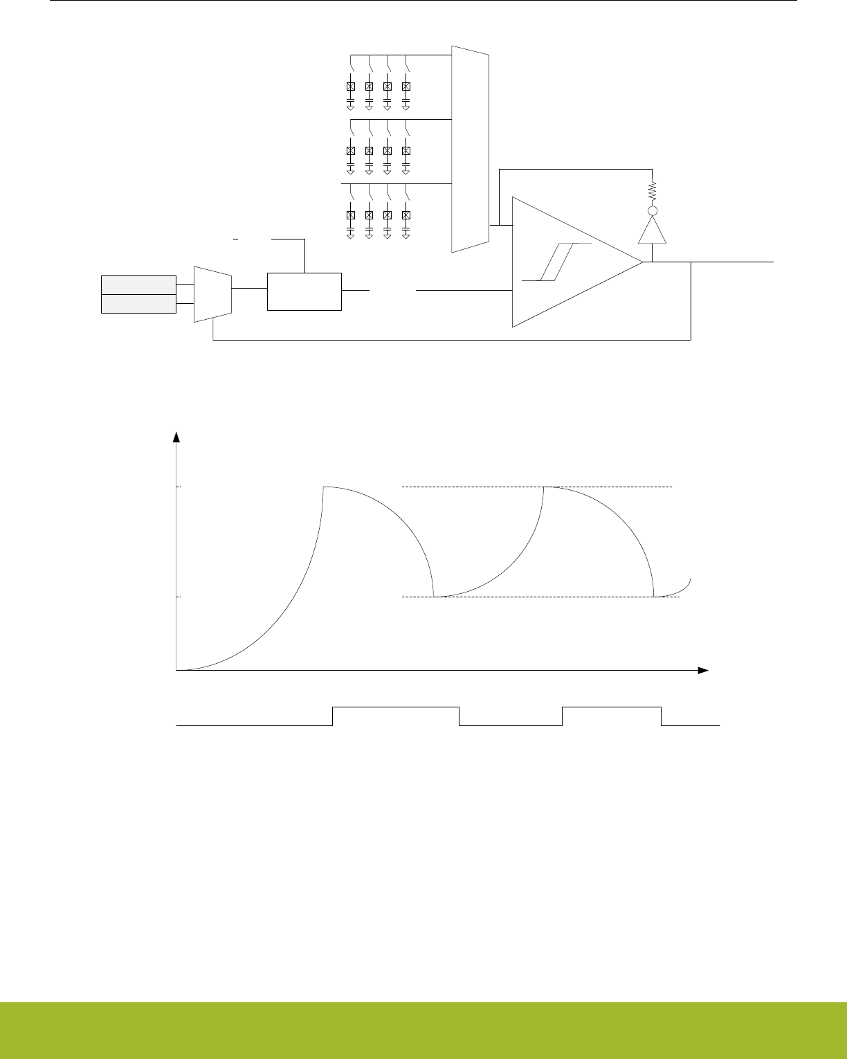
-
+
1
0
VADIV0
VADIV1 VADIV
VDD
Voltage
Divider
ACMPn_HSYTERESIS1.VADIV
ACMPn_HYSTERESIS0.VADIV
time
I/O
voltage
ACMPOUT
Figure 26.5. Capacitive Sensing Setup
Reference Manual
ACMP - Analog Comparator
silabs.com | Smart. Connected. Energy-friendly. Preliminary Rev. 0.5 | 840

26.3.6 Interrupts and PRS Output
The analog comparator includes an edge triggered interrupt flag (EDGE in ACMPn_IF). If either IRISE and/or IFALL in ACMPn_CTRL is
set, the EDGE interrupt flag will be set on rising and/or falling edge of the comparator output respectively. An interrupt request will be
sent if the EDGE interrupt flag in ACMPn_IF is set and enabled through the EDGE bit in ACMPn_IEN. The edge interrupt can also be
used to wake up the device from EM3 Stop-EM1 Sleep.
The analog comparator includes the interrupt flag WARMUP in ACMPn_IF which is set when a warm-up sequence has finished. An
interrupt request will be sent if the WARMUP interrupt flag in ACMPn_IF is set and enabled through the WARMUP bit in ACMPn_IEN.
The analog comparator can also generate an interrupt if a bus conflict occurs. An interrupt request will be sent if the APORTCONFLICT
interrupt flag in ACMPn_IF is set and enabled through the APORTCONFLICT bit in ACMPn_IEN.
The synchronized comparator output is also available as a PRS output signal.
26.3.7 Output to GPIO
The output from the comparator and the capacitive sense output are available as alternate functions to the GPIO pins. Set the ACMP-
PEN bit in ACMPn_ROUTE to enable the output to a pin and the LOCATION bits to select the output location. The GPIO-pin must also
be set as output. The output to the GPIO can be inverted by setting the GPIOINV bit in ACMPn_CTRL.
26.3.8 APORT Conflicts
The analog comparator connects to chip pins through APORT buses. It is possible that another APORT client is using a given APORT
bus. To help debugging over-utilization of APORT resources the ACMP provides a number of status registers. The ACMPn_APOR-
TREQ gives the user visibility into what APORT buses the ACMP is requesting given the setting of registers ACMPn_INPUTSEL and
ACMPn_CTRL. ACMPn_APORTCONFLICT indicates if any of the selections are in conflict, internally or externally.
For example, if the user selects APORT1XCH0 for POSSEL and APORT3XCH1 for NEGSEL, then bits APORT1XCONFLICT and
APORT3XCONFLICT would be 1 in register ACMPn_APORTCONFLICT, as it is illegal for POSSEL and NEGSEL to both select an X-
bus simultaneously.
If the user wishes the ACMP to monitor the same pin as another APORT client within the system, the ACMP can be configured to not
attempt to control the switches on an APORT bus via the fields APORTXMASTERDIS, APORTYMASTERDIS, and APORTVMASTER-
DIS in ACMPn_CTRL. APORTXMASTERDIS and APORTYMASTERDIS control if the X or Y bus selected via POSSEL or NEGESEL is
mastered or not. APORTVMASTERDIS controls if either the X or Y bus selection of VASEL is mastered or not. When bus mastering is
disabled, it is the other APORT client that determines which pin is connected to the APORT bus.
26.3.9 Supply Voltage Monitoring
The ACMP can be used to monitor supply voltages. The ACMP can select which voltage it uses via PWRSEL in ACMPn_CTRL. This
voltage can be selected for VADIV using VASEL=0 in ACMPn_INPUTSEL and divided to a voltage with the band-gap reference range
using DIVVA in registers ACMPn_HYSTERESIS0/1. The band-gap reference voltage can also be scaled via DIVVB in registers
ACMPn_HYSTERESIS0/1 to provide a voltage higher or lower than the scaled VA voltage for comparison.
Reference Manual
ACMP - Analog Comparator
silabs.com | Smart. Connected. Energy-friendly. Preliminary Rev. 0.5 | 841

26.3.10 External override interface
The ACMP can be controlled by an external module, for instance LESENSE. In this mode, the external module will take control of the
positive input mux control signal, which is normally controlled by ACMP_INPUTSEL_POSSEL. Only the APORTs are selectable for the
positive input mux in this mode. Which APORT(s) used is configured in ACMP_EXTIFCTRL_APORTSEL.
ACMP_EXTIFCTRL_APORTSEL also controls the base value for the positive input mux control signal. The external module will be able
to add an offset to this base. The resulting mux configuration can be calculated using Figure 26.6 POSSEL in external override mode
on page 842. The external module controls EXT_OFFSET, while EXT_BASE is controlled by ACMP. See register description of
ACMP_EXTIFCTRL_APORTSEL to see values of EXT_BASE.
POSSEL = EXT_BASE + EXT_OFFSET
Figure 26.6. POSSEL in external override mode
Note: If only one APORT in a pair is used, the external module needs to be programmed to only use the channels that the ACMP has
control of.
The external module is also able to override DIVVA and DIVVB in ACMP_HYSTERESIS0/HYSTERESIS1. This needs to be enabled in
the external module. If the external module does not override DIVVA/DIVVB, the configuration in ACMP_HYSTERESIS0/HYSTERE-
SIS1 will be used.
To enable the external override interface these steps must be performed:
• Configure the parts of the ACMP that will not be overridden, i.e. everything except ACMP_INPUTSEL_POSSEL and possibly
ACMP_HYSTERESIS0/HYSTERESIS1. Make sure ACMP_CTRL_EN is set.
• Configure and enable the external override interface in ACMP_EXTIFCTRL.
• Check for APORT conflicts in ACMP_APORTCONFLICT.
• Wait for ACMP_STATUS_EXTIFACT to go high, indicating that the interface is ready to use.
26.4 Register Map
The offset register address is relative to the registers base address.
Offset Name Type Description
0x000 ACMPn_CTRL RW Control Register
0x004 ACMPn_INPUTSEL RW Input Selection Register
0x008 ACMPn_STATUS RStatus Register
0x00C ACMPn_IF RInterrupt Flag Register
0x010 ACMPn_IFS W1 Interrupt Flag Set Register
0x014 ACMPn_IFC (R)W1 Interrupt Flag Clear Register
0x018 ACMPn_IEN RW Interrupt Enable Register
0x020 ACMPn_APORTREQ RAPORT Request Status Register
0x024 ACMPn_APORTCONFLICT RAPORT Conflict Status Register
0x028 ACMPn_HYSTERESIS0 RW Hysteresis 0 Register
0x02C ACMPn_HYSTERESIS1 RW Hysteresis 1 Register
0x040 ACMPn_ROUTEPEN RW I/O Routing Pine Enable Register
0x044 ACMPn_ROUTELOC0 RW I/O Routing Location Register
0x048 ACMPn_EXTIFCTRL RW External override interface control
Reference Manual
ACMP - Analog Comparator
silabs.com | Smart. Connected. Energy-friendly. Preliminary Rev. 0.5 | 842

26.5 Register Description
26.5.1 ACMPn_CTRL - Control Register
Offset Bit Position
0x000
31
30
29
28
27
26
25
24
23
22
21
20
19
18
17
16
15
14
13
12
11
10
9
8
7
6
5
4
3
2
1
0
Reset
0
0x07
0
0
0x0
0
0x0
0
0
0
0
0
0
Access
RW
RW
RW
RW
RW
RW
RW
RW
RW
RW
RW
RW
RW
Name
FULLBIAS
BIASPROG
IFALL
IRISE
INPUTRANGE
ACCURACY
PWRSEL
APORTVMASTERDIS
APORTYMASTERDIS
APORTXMASTERDIS
GPIOINV
INACTVAL
EN
Bit Name Reset Access Description
31 FULLBIAS 0 RW Full Bias Current
Set this bit to 1 for full bias current. See the datasheet for details.
30 Reserved To ensure compatibility with future devices, always write bits to 0. More information in 1.2 Conven-
tions
29:24 BIASPROG 0x07 RW Bias Configuration
These bits control the bias current level. See the datasheet for details.
23:22 Reserved To ensure compatibility with future devices, always write bits to 0. More information in 1.2 Conven-
tions
21 IFALL 0 RW Falling Edge Interrupt Sense
Set this bit to 1 to set the EDGE interrupt flag on falling edges of comparator output.
Value Mode Description
0 DISABLED Interrupt flag is not set on falling edges
1 ENABLED Interrupt flag is set on falling edges
20 IRISE 0 RW Rising Edge Interrupt Sense
Set this bit to 1 to set the EDGE interrupt flag on rising edges of comparator output.
Value Mode Description
0 DISABLED Interrupt flag is not set on rising edges
1 ENABLED Interrupt flag is set on rising edges
19:18 INPUTRANGE 0x0 RW Input Range
Adjust performance of the comparator for a given input voltage range.
Value Mode Description
0 FULL Setting when the input can be from 0 to VDD.
1 GTVDDDIV2 Setting when the input will always be greater than VDD/2.
Reference Manual
ACMP - Analog Comparator
silabs.com | Smart. Connected. Energy-friendly. Preliminary Rev. 0.5 | 843

Bit Name Reset Access Description
2 LTVDDDIV2 Setting when the input will always be less than VDD/2.
17:16 Reserved To ensure compatibility with future devices, always write bits to 0. More information in 1.2 Conven-
tions
15 ACCURACY 0 RW ACMP accuracy mode
Select between low and high accuracy mode of the comparator. Note, high frequency changes can cause the ACMP per-
formance to degrade. For such uses, such as quickly scanning through multiple channels or setting the ACMP to oscillate
for capacitive sense, this bit should be set to 1.
Value Mode Description
0 LOW ACMP operates in low-accuracy mode but consumes less current.
1 HIGH ACMP operates in high-accuracy mode but consumes more current.
14:12 PWRSEL 0x0 RW Power Select
Selects the power source for the ACMP. NOTE, this field should only be changed when the block is disabled (EN=0).
Value Mode Description
0 AVDD AVDD supply
1 VREGVDD VREGVDD supply
2 IOVDD0 IOVDD/IOVDD0 supply
4 IOVDD1 IOVDD1 supply (if part has two I/O voltages)
11 Reserved To ensure compatibility with future devices, always write bits to 0. More information in 1.2 Conven-
tions
10 APORTVMASTER-
DIS
0 RW APORT Bus Master Disable for Bus selected by VASEL
Determines if the ACMP will request the X or Y APORT bus selected by VASEL. This bit allows multiple APORT connected
devices to monitor the same APORT bus simultaneously by allowing the ACMP to not master the selected bus. When 1,
the determination is expected to be from another peripheral, and the ACMP only passively looks at the bus. When 1, the
selection of channel for a selected bus is ignored (the bus is not), and is whatever selection the external device mastering
the bus has configured for the APORT bus.
Value Description
0 Bus mastering enabled
1 Bus mastering disabled
9 APORTYMASTER-
DIS
0 RW APORT Bus Y Master Disable
Determines if the ACMP will request the APORT Y bus selected by POSSEL or NEGSEL. This bit allows multiple APORT
connected devices to monitor the same APORT bus simultaneously by allowing the ACMP to not master the selected bus.
When 1, the determination is expected to be from another peripheral, and the ACMP only passively looks at the bus. When
1, the selection of channel for a selected bus is ignored (the bus is not), and is whatever selection the external device mas-
tering the bus has configured for the APORT bus.
Value Description
0 Bus mastering enabled
1 Bus mastering disabled
Reference Manual
ACMP - Analog Comparator
silabs.com | Smart. Connected. Energy-friendly. Preliminary Rev. 0.5 | 844

Bit Name Reset Access Description
8 APORTXMASTER-
DIS
0 RW APORT Bus X Master Disable
Determines if the ACMP will request the APORT X bus selected by POSSEL or NEGSEL. This bit allows multiple APORT
connected devices to monitor the same APORT bus simultaneously by allowing the ACMP to not master the selected bus.
When 1, the determination is expected to be from another peripheral, and the ACMP only passively looks at the bus. When
1, the selection of channel for a selected bus is ignored (the bus is not), and is whatever selection the external device mas-
tering the bus has configured for the APORT bus.
Value Description
0 Bus mastering enabled
1 Bus mastering disabled
7:4 Reserved To ensure compatibility with future devices, always write bits to 0. More information in 1.2 Conven-
tions
3 GPIOINV 0 RW Comparator GPIO Output Invert
Set this bit to 1 to invert the comparator alternate function output to GPIO.
Value Mode Description
0 NOTINV The comparator output to GPIO is not inverted
1 INV The comparator output to GPIO is inverted
2 INACTVAL 0 RW Inactive Value
The value of this bit is used as the comparator output when the comparator is inactive.
Value Mode Description
0 LOW The inactive value is 0
1 HIGH The inactive state is 1
1 Reserved To ensure compatibility with future devices, always write bits to 0. More information in 1.2 Conven-
tions
0 EN 0 RW Analog Comparator Enable
Enable/disable analog comparator.
Reference Manual
ACMP - Analog Comparator
silabs.com | Smart. Connected. Energy-friendly. Preliminary Rev. 0.5 | 845

26.5.2 ACMPn_INPUTSEL - Input Selection Register
Offset Bit Position
0x004
31
30
29
28
27
26
25
24
23
22
21
20
19
18
17
16
15
14
13
12
11
10
9
8
7
6
5
4
3
2
1
0
Reset
0x0
0
0
0
0x00
0x00
0x00
Access
RW
RW
RW
RW
RW
RW
RW
Name
CSRESSEL
CSRESEN
VLPSEL
VBSEL
VASEL
NEGSEL
POSSEL
Bit Name Reset Access Description
31 Reserved To ensure compatibility with future devices, always write bits to 0. More information in 1.2 Conven-
tions
30:28 CSRESSEL 0x0 RW Capacitive Sense Mode Internal Resistor Select
These bits select the resistance value for the internal capacitive sense resistor. Resulting actual resistor values are given in
the device datasheets.
Value Mode Description
0 RES0 Internal capacitive sense resistor value 0
1 RES1 Internal capacitive sense resistor value 1
2 RES2 Internal capacitive sense resistor value 2
3 RES3 Internal capacitive sense resistor value 3
4 RES4 Internal capacitive sense resistor value 4
5 RES5 Internal capacitive sense resistor value 5
6 RES6 Internal capacitive sense resistor value 6
7 RES7 Internal capacitive sense resistor value 7
27 Reserved To ensure compatibility with future devices, always write bits to 0. More information in 1.2 Conven-
tions
26 CSRESEN 0 RW Capacitive Sense Mode Internal Resistor Enable
Enable/disable the internal capacitive sense resistor.
25 Reserved To ensure compatibility with future devices, always write bits to 0. More information in 1.2 Conven-
tions
24 VLPSEL 0 RW Low-Power Sampled Voltage Selection
Select the input to the sampled voltage VLP
Value Mode Description
0 VADIV VADIV
1 VBDIV VBDIV
23 Reserved To ensure compatibility with future devices, always write bits to 0. More information in 1.2 Conven-
tions
Reference Manual
ACMP - Analog Comparator
silabs.com | Smart. Connected. Energy-friendly. Preliminary Rev. 0.5 | 846

Bit Name Reset Access Description
22 VBSEL 0 RW VB Selection
Select the input for the VB Divider
Value Mode Description
0 1V25 1.25V
1 2V5 2.50V
21:16 VASEL 0x00 RW VA Selection
Select the input for the VA Divider
Mode Value Description
VDD 0x0 VDD
APORT2YCH0 0x1 APORT2Y Channel 0
APORT2YCH2 0x3 APORT2Y Channel 2
APORT2YCH4 0x5 APORT2Y Channel 4
. . . . . . . . .
APORT2YCH30 0x1f APORT2Y Channel 30
APORT1XCH0 0x20 APORT1X Channel 0
APORT1YCH1 0x21 APORT1Y Channel 1
APORT1XCH2 0x22 APORT1X Channel 2
APORT1YCH3 0x23 APORT1Y Channel 3
APORT1XCH4 0x24 APORT1X Channel 4
APORT1YCH5 0x25 APORT1Y Channel 5
. . . . . . . . .
APORT1XCH30 0x3e APORT1X Channel 30
APORT1YCH31 0x3f APORT1Y Channel 31
15:8 NEGSEL 0x00 RW Negative Input Select
Select negative input.
APORT0XCH0 0x00 Dedicated APORT0X Channel 0
APORT0XCH1 0x01 Dedicated APORT0X Channel 1
APORT0XCH2 0x02 Dedicated APORT0X Channel 2
. . . . . . . . .
APORT0XCH15 0x0f Dedicated APORT0X Channel 15
APORT0YCH0 0x10 Dedicated APORT0Y Channel 0
APORT0YCH1 0x11 Dedicated APORT0Y Channel 1
APORT0YCH2 0x12 Dedicated APORT0Y Channel 2
. . . . . . . . .
APORT0YCH15 0x1f Dedicated APORT0Y Channel 15
Reference Manual
ACMP - Analog Comparator
silabs.com | Smart. Connected. Energy-friendly. Preliminary Rev. 0.5 | 847

Bit Name Reset Access Description
APORT1XCH0 0x20 APORT1X Channel 0
APORT1YCH1 0x21 APORT1Y Channel 1
APORT1XCH2 0x22 APORT1X Channel 2
APORT1YCH3 0x23 APORT1Y Channel 3
APORT1XCH4 0x24 APORT1X Channel 4
APORT1YCH5 0x25 APORT1Y Channel 5
. . . . . . . . .
APORT1XCH30 0x3e APORT1X Channel 30
APORT1YCH31 0x3f APORT1Y Channel 31
APORT2YCH0 0x40 APORT2Y Channel 0
APORT2XCH1 0x41 APORT2X Channel 1
APORT2YCH2 0x42 APORT2Y Channel 2
APORT2XCH3 0x43 APORT2X Channel 3
APORT2YCH4 0x44 APORT2Y Channel 4
APORT2XCH5 0x45 APORT2X Channel 5
. . . . . . . . .
APORT2YCH30 0x5e APORT2Y Channel 30
APORT2XCH31 0x5f APORT2X Channel 31
APORT3XCH0 0x60 APORT3X Channel 0
APORT3YCH1 0x61 APORT3Y Channel 1
APORT3XCH2 0x62 APORT3X Channel 2
APORT3YCH3 0x63 APORT3Y Channel 3
APORT3XCH4 0x64 APORT3X Channel 4
APORT3YCH5 0x65 APORT3Y Channel 5
. . . . . . . . .
APORT3XCH30 0x7e APORT3X Channel 30
APORT3YCH31 0x7f APORT3Y Channel 31
APORT4YCH0 0x80 APORT4Y Channel 0
APORT4XCH1 0x81 APORT4X Channel 1
APORT4YCH2 0x82 APORT4Y Channel 2
APORT4XCH3 0x83 APORT4X Channel 3
APORT4YCH4 0x84 APORT4Y Channel 4
APORT4XCH5 0x85 APORT4X Channel 5
. . . . . . . . .
APORT4YCH30 0x9e APORT4Y Channel 30
APORT4XCH31 0x9f APORT4X Channel 31
DACOUT0 0xf2 DAC Channel 0 Output
Reference Manual
ACMP - Analog Comparator
silabs.com | Smart. Connected. Energy-friendly. Preliminary Rev. 0.5 | 848

Bit Name Reset Access Description
DACOUT1 0xf3 DAC Channel 1 Output
VLP 0xfb Low-Power Sampled Voltage
VBDIV 0xfc Divided VB Voltage
VADIV 0xfd Divided VA Voltage
VDD 0xfe VDD as selected via PWRSEL
VSS 0xff VSS
7:0 POSSEL 0x00 RW Positive Input Select
Select positive input.
APORT0XCH0 0x00 Dedicated APORT0X Channel 0
APORT0XCH1 0x01 Dedicated APORT0X Channel 1
APORT0XCH2 0x02 Dedicated APORT0X Channel 2
. . . . . . . . .
APORT0XCH15 0x0f Dedicated APORT0X Channel 15
APORT0YCH0 0x10 Dedicated APORT0Y Channel 0
APORT0YCH1 0x11 Dedicated APORT0Y Channel 1
APORT0YCH2 0x12 Dedicated APORT0Y Channel 2
. . . . . . . . .
APORT0YCH15 0x1f Dedicated APORT0Y Channel 15
APORT1XCH0 0x20 APORT1X Channel 0
APORT1YCH1 0x21 APORT1Y Channel 1
APORT1XCH2 0x22 APORT1X Channel 2
APORT1YCH3 0x23 APORT1Y Channel 3
APORT1XCH4 0x24 APORT1X Channel 4
APORT1YCH5 0x25 APORT1Y Channel 5
. . . . . . . . .
APORT1XCH30 0x3e APORT1X Channel 30
APORT1YCH31 0x3f APORT1Y Channel 31
APORT2YCH0 0x40 APORT2Y Channel 0
APORT2XCH1 0x41 APORT2X Channel 1
APORT2YCH2 0x42 APORT2Y Channel 2
APORT2XCH3 0x43 APORT2X Channel 3
APORT2YCH4 0x44 APORT2Y Channel 4
APORT2XCH5 0x45 APORT2X Channel 5
. . . . . . . . .
APORT2YCH30 0x5e APORT2Y Channel 30
APORT2XCH31 0x5f APORT2X Channel 31
Reference Manual
ACMP - Analog Comparator
silabs.com | Smart. Connected. Energy-friendly. Preliminary Rev. 0.5 | 849

Bit Name Reset Access Description
APORT3XCH0 0x60 APORT3X Channel 0
APORT3YCH1 0x61 APORT3Y Channel 1
APORT3XCH2 0x62 APORT3X Channel 2
APORT3YCH3 0x63 APORT3Y Channel 3
APORT3XCH4 0x64 APORT3X Channel 4
APORT3YCH5 0x65 APORT3Y Channel 5
. . . . . . . . .
APORT3XCH30 0x7e APORT3X Channel 30
APORT3YCH31 0x7f APORT3Y Channel 31
APORT4YCH0 0x80 APORT4Y Channel 0
APORT4XCH1 0x81 APORT4X Channel 1
APORT4YCH2 0x82 APORT4Y Channel 2
APORT4XCH3 0x83 APORT4X Channel 3
APORT4YCH4 0x84 APORT4Y Channel 4
APORT4XCH5 0x85 APORT4X Channel 5
. . . . . . . . .
APORT4YCH30 0x9e APORT4Y Channel 30
APORT4XCH31 0x9f APORT4X Channel 31
DACOUT0 0xf2 DAC Channel 0 Output
DACOUT1 0xf3 DAC Channel 1 Output
VLP 0xfb Low-Power Sampled Voltage
VBDIV 0xfc Divided VB Voltage
VADIV 0xfd Divided VA Voltage
VDD 0xfe VDD as selected via PWRSEL
VSS 0xff VSS
Reference Manual
ACMP - Analog Comparator
silabs.com | Smart. Connected. Energy-friendly. Preliminary Rev. 0.5 | 850

26.5.3 ACMPn_STATUS - Status Register
Offset Bit Position
0x008
31
30
29
28
27
26
25
24
23
22
21
20
19
18
17
16
15
14
13
12
11
10
9
8
7
6
5
4
3
2
1
0
Reset
0
0
0
0
Access
R
R
R
R
Name
EXTIFACT
APORTCONFLICT
ACMPOUT
ACMPACT
Bit Name Reset Access Description
31:4 Reserved To ensure compatibility with future devices, always write bits to 0. More information in 1.2 Conven-
tions
3 EXTIFACT 0 R External override interface active.
This bit is set when the external override interface is ready to use.
2 APORTCONFLICT 0 R APORT Conflict Output
1 if any of the APORT BUSes being requested by the ACMPn are also being requested by another peripheral
1 ACMPOUT 0 R Analog Comparator Output
Analog comparator output value.
0 ACMPACT 0 R Analog Comparator Active
Analog comparator active status.
Reference Manual
ACMP - Analog Comparator
silabs.com | Smart. Connected. Energy-friendly. Preliminary Rev. 0.5 | 851

26.5.4 ACMPn_IF - Interrupt Flag Register
Offset Bit Position
0x00C
31
30
29
28
27
26
25
24
23
22
21
20
19
18
17
16
15
14
13
12
11
10
9
8
7
6
5
4
3
2
1
0
Reset
0
0
0
Access
R
R
R
Name
APORTCONFLICT
WARMUP
EDGE
Bit Name Reset Access Description
31:3 Reserved To ensure compatibility with future devices, always write bits to 0. More information in 1.2 Conven-
tions
2 APORTCONFLICT 0 R APORT Conflict Interrupt Flag
1 if any of the APORT BUSes being requested by the ACMPn are also being requested by another peripheral
1 WARMUP 0 R Warm-up Interrupt Flag
Indicates that the analog comparator warm-up period is finished.
0 EDGE 0 R Edge Triggered Interrupt Flag
Indicates that there has been a rising or falling edge on the analog comparator output.
26.5.5 ACMPn_IFS - Interrupt Flag Set Register
Offset Bit Position
0x010
31
30
29
28
27
26
25
24
23
22
21
20
19
18
17
16
15
14
13
12
11
10
9
8
7
6
5
4
3
2
1
0
Reset
0
0
0
Access
W1
W1
W1
Name
APORTCONFLICT
WARMUP
EDGE
Bit Name Reset Access Description
31:3 Reserved To ensure compatibility with future devices, always write bits to 0. More information in 1.2 Conven-
tions
2 APORTCONFLICT 0 W1 Set APORTCONFLICT Interrupt Flag
Write 1 to set the APORTCONFLICT interrupt flag
1 WARMUP 0 W1 Set WARMUP Interrupt Flag
Write 1 to set the WARMUP interrupt flag
0 EDGE 0 W1 Set EDGE Interrupt Flag
Write 1 to set the EDGE interrupt flag
Reference Manual
ACMP - Analog Comparator
silabs.com | Smart. Connected. Energy-friendly. Preliminary Rev. 0.5 | 852

26.5.6 ACMPn_IFC - Interrupt Flag Clear Register
Offset Bit Position
0x014
31
30
29
28
27
26
25
24
23
22
21
20
19
18
17
16
15
14
13
12
11
10
9
8
7
6
5
4
3
2
1
0
Reset
0
0
0
Access
(R)W1
(R)W1
(R)W1
Name
APORTCONFLICT
WARMUP
EDGE
Bit Name Reset Access Description
31:3 Reserved To ensure compatibility with future devices, always write bits to 0. More information in 1.2 Conven-
tions
2 APORTCONFLICT 0 (R)W1 Clear APORTCONFLICT Interrupt Flag
Write 1 to clear the APORTCONFLICT interrupt flag. Reading returns the value of the IF and clears the corresponding inter-
rupt flags (This feature must be enabled globally in MSC.).
1 WARMUP 0 (R)W1 Clear WARMUP Interrupt Flag
Write 1 to clear the WARMUP interrupt flag. Reading returns the value of the IF and clears the corresponding interrupt flags
(This feature must be enabled globally in MSC.).
0 EDGE 0 (R)W1 Clear EDGE Interrupt Flag
Write 1 to clear the EDGE interrupt flag. Reading returns the value of the IF and clears the corresponding interrupt flags
(This feature must be enabled globally in MSC.).
Reference Manual
ACMP - Analog Comparator
silabs.com | Smart. Connected. Energy-friendly. Preliminary Rev. 0.5 | 853

26.5.7 ACMPn_IEN - Interrupt Enable Register
Offset Bit Position
0x018
31
30
29
28
27
26
25
24
23
22
21
20
19
18
17
16
15
14
13
12
11
10
9
8
7
6
5
4
3
2
1
0
Reset
0
0
0
Access
RW
RW
RW
Name
APORTCONFLICT
WARMUP
EDGE
Bit Name Reset Access Description
31:3 Reserved To ensure compatibility with future devices, always write bits to 0. More information in 1.2 Conven-
tions
2 APORTCONFLICT 0 RW APORTCONFLICT Interrupt Enable
Enable/disable the APORTCONFLICT interrupt
1 WARMUP 0 RW WARMUP Interrupt Enable
Enable/disable the WARMUP interrupt
0 EDGE 0 RW EDGE Interrupt Enable
Enable/disable the EDGE interrupt
Reference Manual
ACMP - Analog Comparator
silabs.com | Smart. Connected. Energy-friendly. Preliminary Rev. 0.5 | 854

26.5.8 ACMPn_APORTREQ - APORT Request Status Register
Offset Bit Position
0x020
31
30
29
28
27
26
25
24
23
22
21
20
19
18
17
16
15
14
13
12
11
10
9
8
7
6
5
4
3
2
1
0
Reset
0
0
0
0
0
0
0
0
0
0
Access
R
R
R
R
R
R
R
R
R
R
Name
APORT4YREQ
APORT4XREQ
APORT3YREQ
APORT3XREQ
APORT2YREQ
APORT2XREQ
APORT1YREQ
APORT1XREQ
APORT0YREQ
APORT0XREQ
Bit Name Reset Access Description
31:10 Reserved To ensure compatibility with future devices, always write bits to 0. More information in 1.2 Conven-
tions
9 APORT4YREQ 0 R 1 if the bus connected to APORT4Y is requested
Reports if the bus connected to APORT4Y is being requested from the APORT
8 APORT4XREQ 0 R 1 if the bus connected to APORT4X is requested
Reports if the bus connected to APORT4X is being requested from the APORT
7 APORT3YREQ 0 R 1 if the bus connected to APORT3Y is requested
Reports if the bus connected to APORT3Y is being requested from the APORT
6 APORT3XREQ 0 R 1 if the bus connected to APORT3X is requested
Reports if the bus connected to APORT3X is being requested from the APORT
5 APORT2YREQ 0 R 1 if the bus connected to APORT2Y is requested
Reports if the bus connected to APORT2Y is being requested from the APORT
4 APORT2XREQ 0 R 1 if the bus connected to APORT2X is requested
Reports if the bus connected to APORT2X is being requested from the APORT
3 APORT1YREQ 0 R 1 if the bus connected to APORT1X is requested
Reports if the bus connected to APORT1X is being requested from the APORT
2 APORT1XREQ 0 R 1 if the bus connected to APORT2X is requested
Reports if the bus connected to APORT2X is being requested from the APORT
1 APORT0YREQ 0 R 1 if the bus connected to APORT0Y is requested
Reports if the bus connected to APORT0Y is being requested from the APORT
0 APORT0XREQ 0 R 1 if the bus connected to APORT0X is requested
Reports if the bus connected to APORT0X is being requested from the APORT
Reference Manual
ACMP - Analog Comparator
silabs.com | Smart. Connected. Energy-friendly. Preliminary Rev. 0.5 | 855

26.5.9 ACMPn_APORTCONFLICT - APORT Conflict Status Register
Offset Bit Position
0x024
31
30
29
28
27
26
25
24
23
22
21
20
19
18
17
16
15
14
13
12
11
10
9
8
7
6
5
4
3
2
1
0
Reset
0
0
0
0
0
0
0
0
0
0
Access
R
R
R
R
R
R
R
R
R
R
Name
APORT4YCONFLICT
APORT4XCONFLICT
APORT3YCONFLICT
APORT3XCONFLICT
APORT2YCONFLICT
APORT2XCONFLICT
APORT1YCONFLICT
APORT1XCONFLICT
APORT0YCONFLICT
APORT0XCONFLICT
Bit Name Reset Access Description
31:10 Reserved To ensure compatibility with future devices, always write bits to 0. More information in 1.2 Conven-
tions
9 APORT4YCONFLICT 0 R 1 if the bus connected to APORT4Y is in conflict with another pe-
ripheral
Reports if the bus connected to APORT4Y is is also being requested by another peripheral
8 APORT4XCONFLICT 0 R 1 if the bus connected to APORT4X is in conflict with another pe-
ripheral
Reports if the bus connected to APORT4X is is also being requested by another peripheral
7 APORT3YCONFLICT 0 R 1 if the bus connected to APORT3Y is in conflict with another pe-
ripheral
Reports if the bus connected to APORT3Y is is also being requested by another peripheral
6 APORT3XCONFLICT 0 R 1 if the bus connected to APORT3X is in conflict with another pe-
ripheral
Reports if the bus connected to APORT3X is is also being requested by another peripheral
5 APORT2YCONFLICT 0 R 1 if the bus connected to APORT2Y is in conflict with another pe-
ripheral
Reports if the bus connected to APORT2Y is is also being requested by another peripheral
4 APORT2XCONFLICT 0 R 1 if the bus connected to APORT2X is in conflict with another pe-
ripheral
Reports if the bus connected to APORT2X is is also being requested by another peripheral
3 APORT1YCONFLICT 0 R 1 if the bus connected to APORT1X is in conflict with another pe-
ripheral
Reports if the bus connected to APORT1X is is also being requested by another peripheral
2 APORT1XCONFLICT 0 R 1 if the bus connected to APORT1X is in conflict with another pe-
ripheral
Reports if the bus connected to APORT1X is is also being requested by another peripheral
1 APORT0YCONFLICT 0 R 1 if the bus connected to APORT0Y is in conflict with another pe-
ripheral
Reports if the bus connected to APORT0Y is is also being requested by another peripheral
Reference Manual
ACMP - Analog Comparator
silabs.com | Smart. Connected. Energy-friendly. Preliminary Rev. 0.5 | 856

Bit Name Reset Access Description
0 APORT0XCONFLICT 0 R 1 if the bus connected to APORT0X is in conflict with another pe-
ripheral
Reports if the bus connected to APORT0X is is also being requested by another peripheral
Reference Manual
ACMP - Analog Comparator
silabs.com | Smart. Connected. Energy-friendly. Preliminary Rev. 0.5 | 857

26.5.10 ACMPn_HYSTERESIS0 - Hysteresis 0 Register
Offset Bit Position
0x028
31
30
29
28
27
26
25
24
23
22
21
20
19
18
17
16
15
14
13
12
11
10
9
8
7
6
5
4
3
2
1
0
Reset
0x00
0x00
0x0
Access
RW
RW
RW
Name
DIVVB
DIVVA
HYST
Bit Name Reset Access Description
31:30 Reserved To ensure compatibility with future devices, always write bits to 0. More information in 1.2 Conven-
tions
29:24 DIVVB 0x00 RW Divider for VB Voltage when ACMPOUT=0
Divider to scale VB when ACMPOUT=0. VBDIV = VB * (DIVVB+1)/64.
23:22 Reserved To ensure compatibility with future devices, always write bits to 0. More information in 1.2 Conven-
tions
21:16 DIVVA 0x00 RW Divider for VA Voltage when ACMPOUT=0
Divider to scale VA when ACMPOUT=0. VADIV = VA * (DIVVA+1)/64.
15:4 Reserved To ensure compatibility with future devices, always write bits to 0. More information in 1.2 Conven-
tions
3:0 HYST 0x0 RW Hysteresis Select when ACMPOUT=0
Select hysteresis level when comparator output is 0. The hysteresis levels can vary, please see the electrical characteristics
for the device for more information.
Value Mode Description
0 HYST0 No hysteresis
1 HYST1 14 mV hysteresis
2 HYST2 25 mV hysteresis
3 HYST3 30 mV hysteresis
4 HYST4 35 mV hysteresis
5 HYST5 39 mV hysteresis
6 HYST6 42 mV hysteresis
7 HYST7 45 mV hysteresis
8 HYST8 No hysteresis
9 HYST9 -14 mV hysteresis
10 HYST10 -25 mV hysteresis
11 HYST11 -30 mV hysteresis
12 HYST12 -35 mV hysteresis
13 HYST13 -39 mV hysteresis
14 HYST14 -42 mV hysteresis
15 HYST15 -45 mV hysteresis
Reference Manual
ACMP - Analog Comparator
silabs.com | Smart. Connected. Energy-friendly. Preliminary Rev. 0.5 | 858

26.5.11 ACMPn_HYSTERESIS1 - Hysteresis 1 Register
Offset Bit Position
0x02C
31
30
29
28
27
26
25
24
23
22
21
20
19
18
17
16
15
14
13
12
11
10
9
8
7
6
5
4
3
2
1
0
Reset
0x00
0x00
0x0
Access
RW
RW
RW
Name
DIVVB
DIVVA
HYST
Bit Name Reset Access Description
31:30 Reserved To ensure compatibility with future devices, always write bits to 0. More information in 1.2 Conven-
tions
29:24 DIVVB 0x00 RW Divider for VB Voltage when ACMPOUT=1
Divider to scale VB when ACMPOUT=1. VBDIV = VB * (DIVVB+1)/64.
23:22 Reserved To ensure compatibility with future devices, always write bits to 0. More information in 1.2 Conven-
tions
21:16 DIVVA 0x00 RW Divider for VA Voltage when ACMPOUT=1
Divider to scale VA when ACMPOUT=1. VADIV = VA * (DIVVA+1)/64.
15:4 Reserved To ensure compatibility with future devices, always write bits to 0. More information in 1.2 Conven-
tions
3:0 HYST 0x0 RW Hysteresis Select when ACMPOUT=1
Select hysteresis level when comparator output is 1. The hysteresis levels can vary, please see the electrical characteristics
for the device for more information.
Value Mode Description
0 HYST0 No hysteresis
1 HYST1 14 mV hysteresis
2 HYST2 25 mV hysteresis
3 HYST3 30 mV hysteresis
4 HYST4 35 mV hysteresis
5 HYST5 39 mV hysteresis
6 HYST6 42 mV hysteresis
7 HYST7 45 mV hysteresis
8 HYST8 No hysteresis
9 HYST9 -14 mV hysteresis
10 HYST10 -25 mV hysteresis
11 HYST11 -30 mV hysteresis
12 HYST12 -35 mV hysteresis
13 HYST13 -39 mV hysteresis
14 HYST14 -42 mV hysteresis
15 HYST15 -45 mV hysteresis
Reference Manual
ACMP - Analog Comparator
silabs.com | Smart. Connected. Energy-friendly. Preliminary Rev. 0.5 | 859

26.5.12 ACMPn_ROUTEPEN - I/O Routing Pine Enable Register
Offset Bit Position
0x040
31
30
29
28
27
26
25
24
23
22
21
20
19
18
17
16
15
14
13
12
11
10
9
8
7
6
5
4
3
2
1
0
Reset
0
Access
RW
Name
OUTPEN
Bit Name Reset Access Description
31:1 Reserved To ensure compatibility with future devices, always write bits to 0. More information in 1.2 Conven-
tions
0 OUTPEN 0 RW ACMP Output Pin Enable
Enable/disable analog comparator output to pin.
Reference Manual
ACMP - Analog Comparator
silabs.com | Smart. Connected. Energy-friendly. Preliminary Rev. 0.5 | 860

26.5.13 ACMPn_ROUTELOC0 - I/O Routing Location Register
Offset Bit Position
0x044
31
30
29
28
27
26
25
24
23
22
21
20
19
18
17
16
15
14
13
12
11
10
9
8
7
6
5
4
3
2
1
0
Reset
0x00
Access
RW
Name
OUTLOC
Bit Name Reset Access Description
31:6 Reserved To ensure compatibility with future devices, always write bits to 0. More information in 1.2 Conven-
tions
5:0 OUTLOC 0x00 RW I/O Location
Decides the location of the OUT pin.
Value Mode Description
0 LOC0 Location 0
1 LOC1 Location 1
2 LOC2 Location 2
3 LOC3 Location 3
4 LOC4 Location 4
5 LOC5 Location 5
6 LOC6 Location 6
7 LOC7 Location 7
8 LOC8 Location 8
9 LOC9 Location 9
10 LOC10 Location 10
11 LOC11 Location 11
12 LOC12 Location 12
13 LOC13 Location 13
14 LOC14 Location 14
15 LOC15 Location 15
16 LOC16 Location 16
17 LOC17 Location 17
18 LOC18 Location 18
19 LOC19 Location 19
20 LOC20 Location 20
21 LOC21 Location 21
22 LOC22 Location 22
Reference Manual
ACMP - Analog Comparator
silabs.com | Smart. Connected. Energy-friendly. Preliminary Rev. 0.5 | 861

Bit Name Reset Access Description
23 LOC23 Location 23
24 LOC24 Location 24
25 LOC25 Location 25
26 LOC26 Location 26
27 LOC27 Location 27
28 LOC28 Location 28
29 LOC29 Location 29
30 LOC30 Location 30
31 LOC31 Location 31
Reference Manual
ACMP - Analog Comparator
silabs.com | Smart. Connected. Energy-friendly. Preliminary Rev. 0.5 | 862

26.5.14 ACMPn_EXTIFCTRL - External override interface control
Offset Bit Position
0x048
31
30
29
28
27
26
25
24
23
22
21
20
19
18
17
16
15
14
13
12
11
10
9
8
7
6
5
4
3
2
1
0
Reset
0x0
0
Access
RW
RW
Name
APORTSEL
EN
Bit Name Reset Access Description
31:8 Reserved To ensure compatibility with future devices, always write bits to 0. More information in 1.2 Conven-
tions
7:4 APORTSEL 0x0 RW APORT selection for external interface.
Decides which APORT(s) the ACMP will use when controlled by an external module.
Value Mode Description
0 APORT0X APORT0X used. EXT_BASE = ACMP_INPUTSEL_POS-
SEL_APORT0XCH0.
1 APORT0Y APORT0Y used. EXT_BASE = ACMP_INPUTSEL_POS-
SEL_APORT0YCH0.
2 APORT1X APORT1X used. EXT_BASE = ACMP_INPUTSEL_POS-
SEL_APORT1XCH0.
3 APORT1Y APORT1Y used. EXT_BASE = ACMP_INPUTSEL_POS-
SEL_APORT1XCH0.
4 APORT1XY APORT1X/Y used. EXT_BASE = ACMP_INPUTSEL_POS-
SEL_APORT1XCH0.
5 APORT2X APORT2X used. EXT_BASE = ACMP_INPUTSEL_POS-
SEL_APORT2YCH0.
6 APORT2Y APORT2Y used. EXT_BASE = ACMP_INPUTSEL_POS-
SEL_APORT2YCH0.
7 APORT2YX APORT2Y/X used. EXT_BASE = ACMP_INPUTSEL_POS-
SEL_APORT2YCH0.
8 APORT3X APORT3X used. EXT_BASE = ACMP_INPUTSEL_POS-
SEL_APORT3XCH0.
9 APORT3Y APORT3Y used. EXT_BASE = ACMP_INPUTSEL_POS-
SEL_APORT3XCH0.
10 APORT3XY APORT3X/Y used. EXT_BASE = ACMP_INPUTSEL_POS-
SEL_APORT3XCH0.
11 APORT4X APORT4X used. EXT_BASE = ACMP_INPUTSEL_POS-
SEL_APORT4YCH0.
12 APORT4Y APORT4Y used. EXT_BASE = ACMP_INPUTSEL_POS-
SEL_APORT4YCH0.
13 APORT4YX APORT4Y/X used. EXT_BASE = ACMP_INPUTSEL_POS-
SEL_APORT4YCH0.
Reference Manual
ACMP - Analog Comparator
silabs.com | Smart. Connected. Energy-friendly. Preliminary Rev. 0.5 | 863

Bit Name Reset Access Description
3:1 Reserved To ensure compatibility with future devices, always write bits to 0. More information in 1.2 Conven-
tions
0 EN 0 RW Enable external interface.
Set to enable an external module, like LESENSE, to control the ACMP
Reference Manual
ACMP - Analog Comparator
silabs.com | Smart. Connected. Energy-friendly. Preliminary Rev. 0.5 | 864
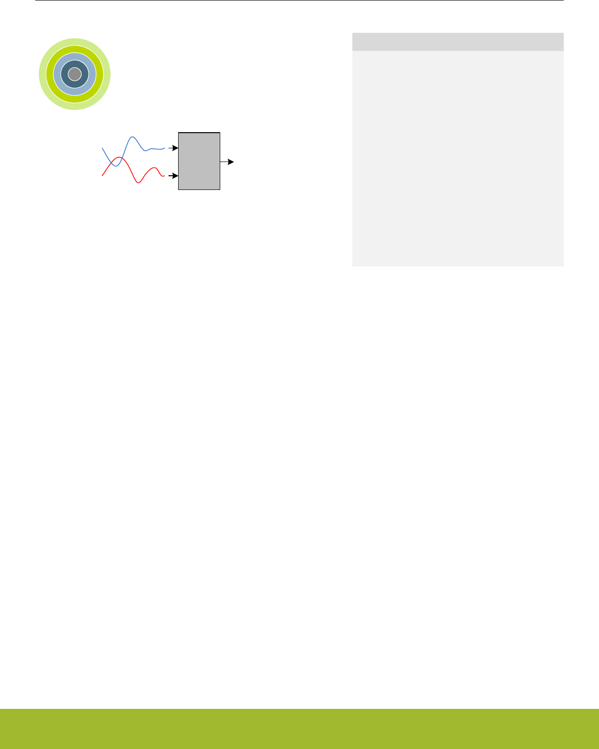
27. ADC - Analog to Digital Converter
0 1 2 3 4
ADC ...0101110...
+
-
Quick Facts
What?
The ADC is used to convert analog signals into a
digital representation and features low-power, auton-
omous operation.
Why?
In many applications there is a need to measure an-
alog signals and record them in a digital representa-
tion, without exhausting the energy source.
How?
A low power ADC samples up to 32 input channels
in a programmable sequence. With the help of PRS
and DMA, the ADC can operate without CPU inter-
vention in EM2 Deep Sleep and EM3 Stop, minimiz-
ing the number of powered up resources. The ADC
can further be duty-cycled to reduce the energy con-
sumption.
27.1 Introduction
The ADC uses a Successive Approximation Register (SAR) architecture, with a resolution of up to 12 bits at up to one million samples
per second (1 Msps). The integrated input multiplexer can select from external I/Os and several internal signals.
Reference Manual
ADC - Analog to Digital Converter
silabs.com | Smart. Connected. Energy-friendly. Preliminary Rev. 0.5 | 865

27.2 Features
• Programmable resolution (6/8/12-bit)
•13 conversion clock cycles for a 12-bit conversion
• Maximum 1 Msps @ 12-bit
• Maximum 1.6 Msps @ 6-bit
• Configurable acquisition time
• Externally controllable conversion start time using PRS in TIMED mode
• Integrated prescaler for conversion clock generation
• Selectable clock division factor from 1 to 128
• Wide conversion clock range: 32 kHz to 16 MHz
• Can be run during EM2 Deep Sleep and EM3 Stop, waking up the system upon various enabled interrupts
• Can be run during EM2 Deep Sleep and EM3 Stop with DMA enabled to pull data from the FIFOs without waking up the system
• Supports up to 144 external input channels and several internal inputs
• Includes temperature sensor and random number generator function
• Left or right adjusted results
• Results in 2’s complement representation
• Differential results sign extended to 32-bits results
• Programmable scan sequence
• Up to 32 configurable samples in scan sequence
• Mask to select which pins are included in the sequence
• Triggered by software or PRS input
• One shot or repetitive mode
• Oversampling available
• Four deep FIFO to store conversion data along with channel ID and option to overwrite old data when full
• Programmable watermark (DVL) to generate SCAN interrupt
• Supports overflow and underflow interrupt generation
• Supports window compare function
• Conversion tailgating support for predictable periodic scans
• Programmable single channel conversion
• Triggered by software or PRS input
• Can be interleaved between two scan sequences
• One shot or repetitive mode
• Oversampling available
• Four deep FIFO to store conversion data with option to overwrite old data when full
• programmable watermark (DVL) to generate SINGLE interrupt
• Supports overflow and underflow interrupt generation
• Supports window compare function
• Hardware oversampling support
• 1st order accumulate and dump filter
• From 2 to 4096 oversampling ratio (OSR)
• Results in 16-bit representation
• Enabled individually for scan sequence and single channel mode
• Common OSR select
• Programmable and preset input full scale (peak-to-peak) range (VFS) with selectable reference sources
• VFS=1.25 V using internal VBGR reference
• VFS=2.5 V using internal VBGR reference
• VFS=AVDD with AVDD as reference source
• VFS=5 V with internal VBGR reference
• Single ended external reference
• Differential external reference
• VFS=2xAVDD with AVDD as reference source
• User-programmable dividers for flexible VFS options from internal, external or supply voltage reference sources
Reference Manual
ADC - Analog to Digital Converter
silabs.com | Smart. Connected. Energy-friendly. Preliminary Rev. 0.5 | 866
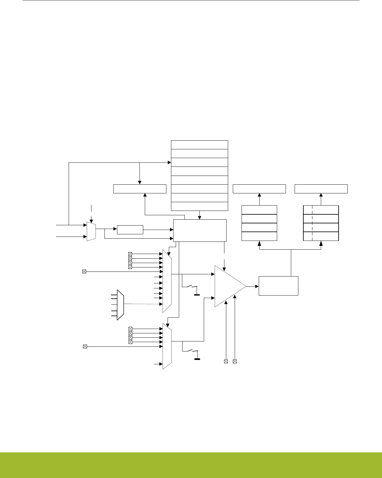
• Support for offset and gain calibration
• Interrupt generation and/or DMA request when
•Programmable number of converted data available in the single FIFO (also generates DMA request)
• Programmable number of converted data available in the scan FIFO (also generates DMA request)
• Single FIFO overflow or underflow
• Scan FIFO overflow or underflow
• Latest Single conversion tripped compare logic
• Latest Scan conversion tripped compare logic
• Analog over-voltage interrupt
• Programming Error interrupt due to APORT Bus Request conflict or NEGSEL programming error
27.3 Functional Description
An overview of the ADC is shown in Figure 27.1 ADC Overview on page 867.
APORT1X
TEMP
VSS
VSS
APORT2X
Sequencer
+
-
Control
ADCn_SINGLEDATA ADCn_SCANDATA
ADCn_SCANCTRLX
ADCn_SINGLECTRL
ADCn_SCANCTRL
Prescaler
ADC_CLK
HFPERCLKADCn
ADCn_SINGLECTRLX
ADCn_STATUS
ADCnCLK
ADCCLKMODE
Oversampling
filter
SINGLESAMPLE
FIFO
SCAN SAMPLE
FIFO
SCAN
INPUTID
ADCn_CMD
ADCn_CTRL
ADCn_CMPTHR
ADCn_BIASPROG
INN_MUX INP_MUX
APORT3X
APORT4X
APORT0X
AVDD
DVDD
DECOUPLE
IOVDD
vdd_mux
APORT1Y
APORT2Y
APORT3Y
APORT4Y
APORT0Y
DAC0OUT0
DAC0OUT1
ADCn_EXTP ADCn_EXTN
Conversion clock
(adc_clk_sar)
ADC_CLK
R5VOUT
IOVDD1
Figure 27.1. ADC Overview
Reference Manual
ADC - Analog to Digital Converter
silabs.com | Smart. Connected. Energy-friendly. Preliminary Rev. 0.5 | 867

27.3.1 Clock Selection
The ADC logic is partitioned into two clock domains: HFPERCLK and ADC_CLK. The HFPERCLK domain contains the register inter-
face logic, APORT request logic and portions of FIFO read logic. The HFPERCLK is the default clock for the ADC peripheral. The rest
of the ADC is clocked by the ADC_CLK domain. The ADC_CLK is chosen by ADCCLKMODE bit in the ADCn_CTRL register.
The ADC_CLK is the main clock for the ADC engine. If the ADCCLKMODE is set to SYNC, the ADC_CLK is equal to the HFPERCLK
and the ADC operates in synchronous mode. If the ADCCLKMODE is set to ASYNC, the ADC_CLK is ASYNCCLK and the ADC oper-
ates in asynchronous mode. This distinction is important to understand as there are additional system restrictions and benefits to run-
ning the ADC in asynchronous mode detailed in 27.3.13 ASYNC ADC_CLK Usage Restrictions and Benefits.
The ADC has an internal clock prescaler, controlled by PRESC bits in ADCn_CTRL, which can divide the ADC_CLK by any factor be-
tween 1 and 128 to generate the conversion clock (adc_clk_sar) for the ADC. This adc_clk_sar is also used to generate acquisition
timing. Note that the maximum clock frequency for adc_clk_sar is 16 MHz. The ADC warmup time is determined by ADC_CLK and not
by adc_clk_sar.
ASYNCCLK is a clock source from the CMU which is considered asynchronous to HFPERCLK. The CMU_ADCCTRL register can be
programmed to request and use ASYNCCLK. It has multiple choices for its source, including AUXHFRCO, HFXO and HFSRCCLK, and
can optionally be inverted. If the chosen source for ASYNCCLK is not active at the time of request, the CMU enables the source oscilla-
tor upon receiving the request, and shuts down the oscillator when the ADC stops requesting the clock. Consult the CMU chapter for
details of how to program the clock sources for the ASYNCCLK and oscillator start-up time details.
Software may choose a clock request generation scheme by programming the ASYNCCLKEN and WARMMODE of the ADCn_CTRL
register. If the ASYNCCLKEN is set to ASNEEDED with WARMMODE set to NORMAL, the ADC requests ASYNCCLK only when a
conversion trigger is activated. The ASYNCCLK request is withdrawn after the conversion is complete. All other options keep the
ASYNCCLK request "ON" until software programs these fields otherwise or changes the ADCCLKMODE to SYNC.
For EM2 Deep Sleep or EM3 Stop operation of the ADC, the ADC_CLK must be configured for AUXHFRCO as this is the only available
option during EM2 Deep Sleep or EM3 Stop. The ADC_CLK source should not be changed as the system enters or exits various ener-
gy modes, otherwise measurement inaccuracies will result.
27.3.2 Conversions
A conversion consists of two phases: acquisition and approximation. The input is sampled in the acquisition phase before it is converted
to digital representation during the approximation phase. The acquisition time can be configured independently for scan sequence and
single channel conversions (see 27.3.3 ADC Modes) by setting AT in ADCn_SINGLECTRL/ADCn_SCANCTRL. The acquisition times
can be set to 1 , 2, 3 or any integer power of 2 from 4 to 256 adc_clk_sar cycles.
Note:
For high impedance sources the acquisition time should be adjusted to allow enough time for the internal sample capacitor to fully
charge. The minimum acquisition time for sampling at 1 Msps and typical input loading is 187.5 ns.
The ADC uses one adc_clk_sar cycle per output bit in the approximation phase plus 1 extra adc_clk_sar cycle.
Tconv= (Tacq+ (N + 1) x Tadc_clk_sar) x OVSRSEL
Where Tacq is the acquisition time set by the AT bit field, N is the resolution (in bits), and OVSRSEL is the oversampling ratio according
to the OVSRSEL field in ADCn_CTRL when oversampling is enabled (see 27.3.8.6 Oversampling).
Figure 27.2. ADC Total Conversion Time Per Output
Bit 11 Bit 10 Bit 9 Bit 8 Bit 7 Bit 6 Bit 5 Bit 4 Bit 3 Bit 2 Bit 1 Bit 0
SINGLEAT/
SCANAT
6-bit value ready 8-bit value ready 12-bit value ready
ADC_CLK
Conversion clock
ADC action
Figure 27.3. ADC Conversion Timing
Reference Manual
ADC - Analog to Digital Converter
silabs.com | Smart. Connected. Energy-friendly. Preliminary Rev. 0.5 | 868

27.3.3 ADC Modes
The ADC contains two programmable modes: single channel mode and scan mode. Both modes have separate configuration registers
and a four-deep FIFO for conversion results. Both modes may be set up to run only once per trigger or to automatically repeat after
each operation. The scan mode has priority over the single channel mode. However by default, if scan sequence is running, a triggered
single channel conversion will be interleaved between two scan samples.
27.3.3.1 Single Channel Mode
Single channel mode can be used to convert a single channel either once per trigger or repetitively. The configuration of single channel
mode is done using the ADCn_SINGLECTRL and ADCn_SINGLECTRLX registers and the result FIFO can be read through the
ADCn_SINGLEDATA register. The DVL field of the ADCn_SINGLECTRLX controls the FIFO watermark crossing which sets the SIN-
GLEDV bit in ADCn_STATUS high and is cleared when the data is read and the number of unread data samples falls below the DVL
threshold. The user can choose to throw out new samples or overwrite the old samples when the FIFO becomes full by programming
the FIFOOFACT field of the ADCn_SINGLECTRLX register. Single channel results can also be read through ADCn_SINGLEDATAP
without popping the FIFO, returning its latest element. The DIFF field in ADCn_SINGLECTRL selects whether differential or single
ended inputs are used and POSSEL and NEGSEL selects the input signal(s). The CMPEN bit in the ADCn_SINGLECTRL register ena-
bles the window compare function, and the latest converted data is compared against values programmed into the ADGT and ADLT
fields of the ADCn_CMPTHR register and generates SINGLECMP interrupts if enabled. The window compare function allows for com-
pare triggering both within (if ADGT less than ADLT) or out of (if ADGT greater than ADLT) window.
27.3.3.2 Scan Mode
Scan mode is used to perform conversions across multiple channels, sweeping a set of selected inputs in a sequence. The configura-
tion of scan mode is done in the ADCn_SCANCTRL and ADCn_SCANCTRLX registers. It has similar controls and data read mecha-
nisms to single channel mode. There are two key differences between single channel mode and scan mode: the input sequence is
programmed differently, and it has additional information in the result to indicate the channel on which the conversion was acquired.
27.3.5 Input Selection explains how the input sequence is chosen. When the scan sequence is triggered, the ADC samples all inputs
that are included in the mask (ADCn_SCANMASK), starting at the lowest pin number. DIFF in ADCn_SCANCTRL selects whether sin-
gle ended or differential inputs are used. The FIFO data is tagged with SCANINPUTID and can be read along with the scan data using
ADCn_SCANDATAX register. The ADCn_SCANDATAXP can be used to read the latest valid entry from the scan FIFO without popping
it. There is also a ADCn_SCANDATA register that contains results without the SCANINPUTID appended.
Reference Manual
ADC - Analog to Digital Converter
silabs.com | Smart. Connected. Energy-friendly. Preliminary Rev. 0.5 | 869

27.3.4 Warm-up Time
After power-on, the ADC requires some time for internal bias currents and references to settle prior to starting a conversion. This time
period is called the warm-up time. Warm-up timing is performed by hardware. Software must program the number of ADC_CLK cycles
required to count at least 1 µs in the TIMEBASE field of the ADCn_CTRL register. TIMEBASE only affects the timing of the warm-up
sequence and is not dependent on adc_clk_sar. When enabling the ADC or changing references between samples, the ADC is auto-
matically warmed up for 5 µs (5 times the period indicated by TIMEBASE).
Normally, the ADC will be warmed up only when samples are requested and is shut off when there are no more samples waiting. How-
ever, if lower latency is needed, configuring the WARMUPMODE field in ADCn_CTRL allows the ADC and/or reference to stay warm
between samples, reducing the warm-up time or eliminating it altogether. Figure 27.4 ADC Analog Power Consumption With Different
WARMUPMODE Settings on page 871 shows the effects on analog power consumption in scenarios using different WARMUPMODE
settings.
The user can program which reference should be kept warm in the CHCONREFWARMIDLE bitfield in the ADCn_CTRL register. By
default the scan mode reference is kept warm. The user can also choose to keep the single channel mode reference warm or to keep
the last used reference warm. If the default setting is kept (scan mode reference is to be kept warm) and if the single-mode reference
setting is different than scan-mode, then single mode conversions will first warmup its reference for 5 µs before a conversion can begin.
Various warmup modes are described here:
• NORMAL: This is the lowest power option for general-purpose use and low sampling rates (below 35 ksps). The ADC and referen-
ces are shut off when there are no samples waiting. The ADC does not consume any power when it is shut down. A 5 µs warmup
time will be initiated prior to every conversion. Figure a in Figure 27.4 ADC Analog Power Consumption With Different WARMUP-
MODE Settings on page 871 shows this mode.
• KEEPINSTANDBY: This mode is suitable for infrequent sampling of lower impedance inputs, and is the lowest power option for sam-
pling rates between about 35 and 125 ksps. It may also be useful for lower sampling rates where latency is important. The reference
selected for scan mode is kept warm, but the ADC is powered down. The ADC will initiate a 1 µs warmup period before a conversion
begins. Because the reference is kept warm, the ADC will consume a small amount of standby current when it is not converting.
Figure b in Figure 27.4 ADC Analog Power Consumption With Different WARMUPMODE Settings on page 871 shows this mode.
• KEEPINSLOWACC: This mode is useful for high-impedance inputs which are sampled infrequently. It is similar to KEEPINSTAND-
BY, but continuously tracks the input, keeping the input multiplexer connected to the APORT bus. This mode consumes little more
power than KEEPINSTANDBY mode (about 2 µA extra) when a conversion is not in progress. This allows the user to avoid pro-
gramming long acquisition time that would otherwise be necessary for high-impedance inputs when ADC wakes up to full power
mode, thereby reducing the total current consumption per conversion.
• KEEPADCWARM: This mode provides the lowest latency and allows for maximum sampling rates. The ADC and reference circuitry
remain powered on even when conversions are not in progress. Figure c in Figure 27.4 ADC Analog Power Consumption With Dif-
ferent WARMUPMODE Settings on page 871 shows this mode. This mode consumes the most power, but as soon as a trigger
event occurs, the acquisition and conversion begin with no warm-up time. Note that if KEEPADCWARM mode is set and HFXO is
selected as the ADC clock source, the HFXO will remain on in EM2.
When KEEPADCWARM is chosen, ADC is termed as being in continuous operation. When any other warmup mode is chosen, ADC is
termed to be in duty-cycled operation.
When entering EM2 Deep Sleep or EM3 Stop, if the ADC is not going to be used, it should be returned to an idle state and WARMUP-
MODE in ADCn_CTRL written to 0. Refer to 27.3.15 ADC Programming Model for more information on placing the ADC in an idle state.
If the ADC is going to be used in these low energy modes, the user can use any of the WARMUPMODE settings, but should be mindful
of the power consumption that comes along with the different mode settings. For EM2 Deep Sleep or EM3 Stop operation, the ADC
clock source must be configured to use AUXHFRCO.
Reference Manual
ADC - Analog to Digital Converter
silabs.com | Smart. Connected. Energy-friendly. Preliminary Rev. 0.5 | 870
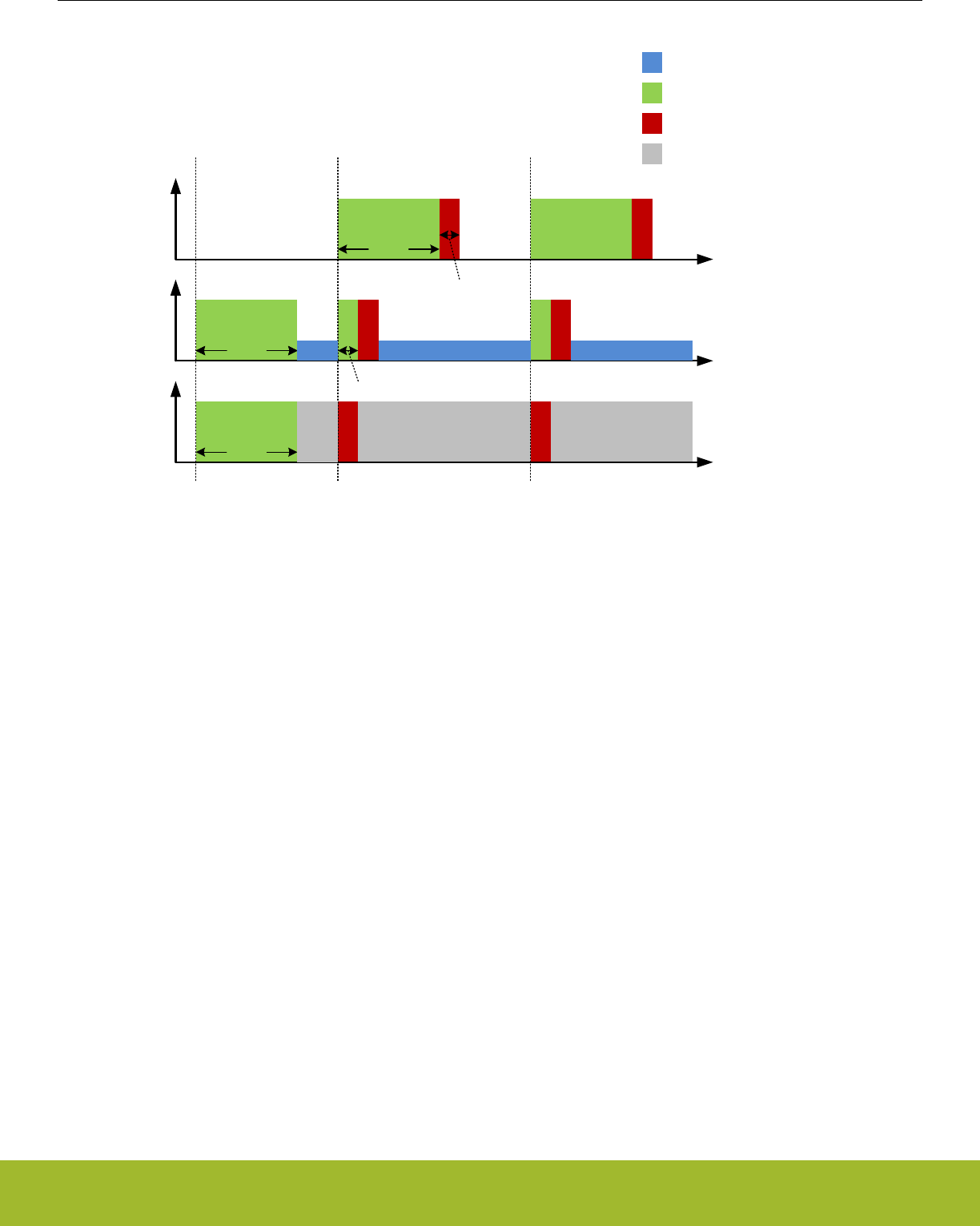
ADC
WARMUPMODE
set Conversion trigger Conversion trigger
Power
Power
Power
Time
Time
ADC warm-up
ADC conversion
ADC standby/ slowacc
5 µs
1 µs
5 µs
5 µs
5 µs
NORMAL
KEEPINSTANDBY/
KEEPINSLOWACC
KEEPADCWARM
Time
a)
b)
c)
1 µs
ADC warmed up
waiting for trigger
Figure 27.4. ADC Analog Power Consumption With Different WARMUPMODE Settings
Note:
When using any warm-up mode other than NORMAL, always switch back to the NORMAL mode before switching to another warm-up
mode.
Reference Manual
ADC - Analog to Digital Converter
silabs.com | Smart. Connected. Energy-friendly. Preliminary Rev. 0.5 | 871
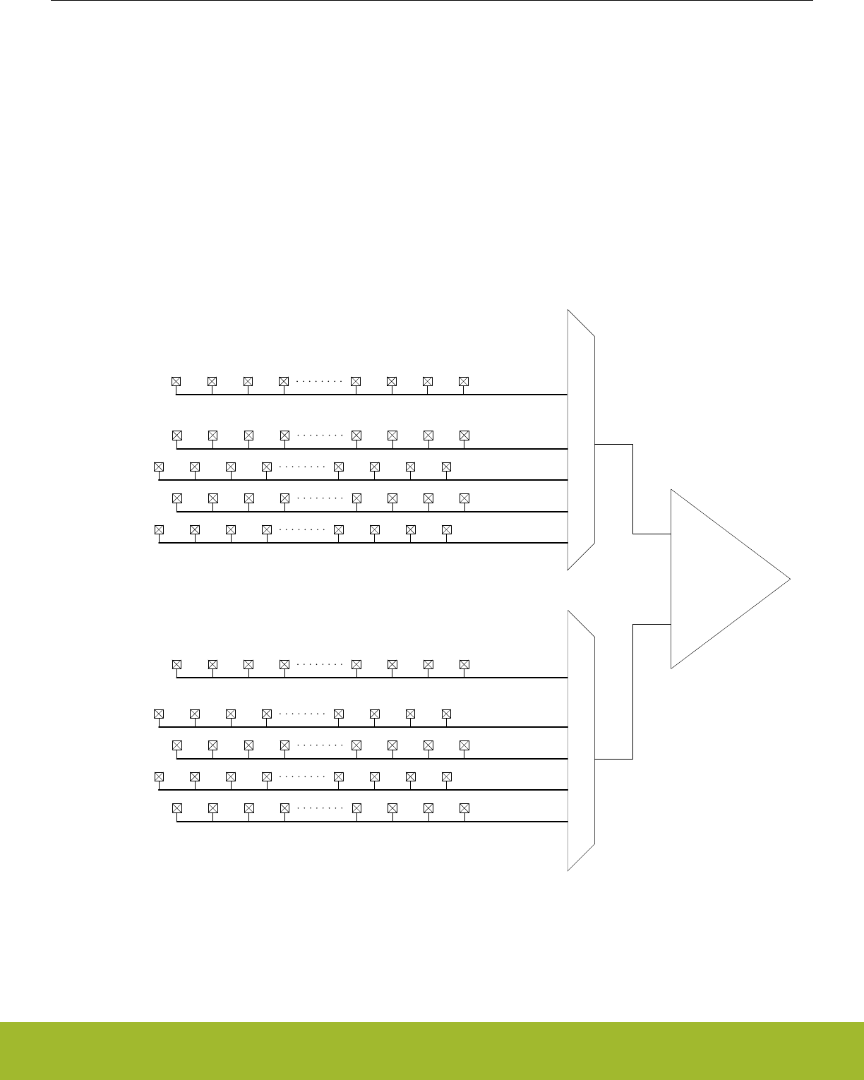
27.3.5 Input Selection
The ADC samples and converts the analog voltage differential at its positive and negative voltage inputs. The input multiplexers of the
ADC can connect these inputs to one of several internal nodes (e.g., temperature sensor) or to external signals via analog ports
(APORT0, APORT1, APORT2, APORT3 or APORT4).
The analog ports APORT1, APORT2, APORT3, and APORT4 connect to external pins via analog buses (BUSAX, BUSAY, BUSBX,
etc.) which are shared among other analog peripherals on the device. APORT1 through APORT4 are each 32 channels wide with con-
nections to two sub-buses: a 16-channel X bus and a 16-channel Y bus. In the ADC module, all X buses connect to the INP_MUX and
all Y buses connect to the INN_MUX as shown in Figure 27.5 APORT connection to the ADC on page 872. Connections to the X and
Y sub-buses alternate channels on the APORT. On APORT1 and APORT3, even-numbered channels connect to the X bus, and odd-
numbered channels connect to the Y bus. On APORT2 and APORT4, even-numbered channels connect to the X bus and odd-num-
bered channels connect to the Y bus. The APORT to BUS mappings may vary from device to device, please refer to the APORT Client
Map on the device datasheet for exact mappings.
Unlike APORT1 through APORT4, APORT0 is not a shared resource. It consists of a 16-channel X bus and a 16-channel Y bus, each
with dedicated I/O pin connections. Note that APORT0 is not available on all device families.
ch0 ch2 ch4 ch6 ch24 ch26 ch28 ch30
ch1 ch3 ch5 ch7 ch25 ch27 ch29 ch31
ch0 ch2 ch4 ch6 ch24 ch26 ch28 ch30
ch1 ch3 ch5 ch7 ch25 ch27 ch29 ch31
ch0 ch2 ch4 ch6 ch24 ch26 ch28 ch30
ch1 ch3 ch5 ch7 ch25 ch27 ch29 ch31
ch0 ch2 ch4 ch6 ch24 ch26 ch28 ch30
ch1 ch3 ch5 ch7 ch25 ch27 ch29 ch31
APORT1X
APORT2X
APORT3X
APORT4X
APORT1Y
APORT2Y
APORT3Y
APORT4Y
+
-
BUSAX
BUSBX
BUSCX
BUSDX
BUSAY
BUSBY
BUSCY
BUSDY
BUSADCnX
ch0 ch1 ch2 ch3 ch15
ch14ch13ch12
BUSADCnY
ch0 ch1 ch2 ch3 ch15
ch14ch13ch12
APORT0X
APORT0Y
INP_MUXINN_MUX
Figure 27.5. APORT connection to the ADC
For differential measurements, one input must be chosen from an X bus and the other from a Y bus. Choosing both inputs from an X
bus or both from a Y bus will generate a PROGERR interrupt (if enabled) of NEGSELCONF type. The PROGERR type can be checked
in the ADCn_STATUS register.
Reference Manual
ADC - Analog to Digital Converter
silabs.com | Smart. Connected. Energy-friendly. Preliminary Rev. 0.5 | 872

The mapping and availability for external I/O connections to ADC0 inputs is shown in device datasheet.
Multiple peripherals may request the same shared system bus (BUSAX, BUSAY, BUSBX, etc.). When this happens, a conflict status is
generated and that bus is kept floating. If this happens with the ADC, the PROGERR field in ADCn_STATUS is set to BUSCONF, and
an interrupt may be generated (if enabled). When connecting dedicated I/Os through APORT0, all inputs are available to APORT0X
and APORT0Y and no bus conflict is possible. Refer to 27.3.5.3 APORT Conflicts for more information on identifying and resolving bus
conflicts.
Note: The internal inputs can only be sampled in single channel, single-ended mode. NEGSEL should be fixed to VSS for these con-
versions.
27.3.5.1 Configuring ADC Inputs in Single Channel Mode
In single channel mode, the ADCn_SINGLECTRL register provides the POSSEL and NEGSEL selection for positive and negative
channel selection of the ADC. The APORT Client Map provides external pin to internal bus channel mapping enumeration for a particu-
lar device. Software can also choose internal nodes for POSSEL.
For single-ended conversions on external (APORT-connected) signals, POSSEL and NEGSEL are fully configurable. However, when
performing conversions on internal signals, NEGSEL must be set to VSS. This NEGSEL reconfigurability feature in single-ended mode
may not be available in all devices. If compatibility with devices that do not support this feature is desired, NEGSEL should be set to
VSS for all single channel single-ended conversions.
Note that in both the POSSEL and NEGSEL fields, it is possible to choose inputs from both X and Y buses, even though X channels
are physically connected to the positive mux (INP_MUX) and Y channels are physically connected to the negative mux (INN_MUX). For
single-ended operation (DIFF = 0), if the positive input is chosen from a Y channel the ADC performs a negative single ended conver-
sion and automatically inverts the result at the end, producing a positive result. For differential conversions (DIFF = 1), if a Y channel is
chosen for the positive input and an X channel is chosen for the negative input, the ADC result will be inverted to produce the correct
polarity.
Refer to device-specific datasheet for specific pin connection options. Note that the same I/O pin may appear in multiple locations.
Reference Manual
ADC - Analog to Digital Converter
silabs.com | Smart. Connected. Energy-friendly. Preliminary Rev. 0.5 | 873
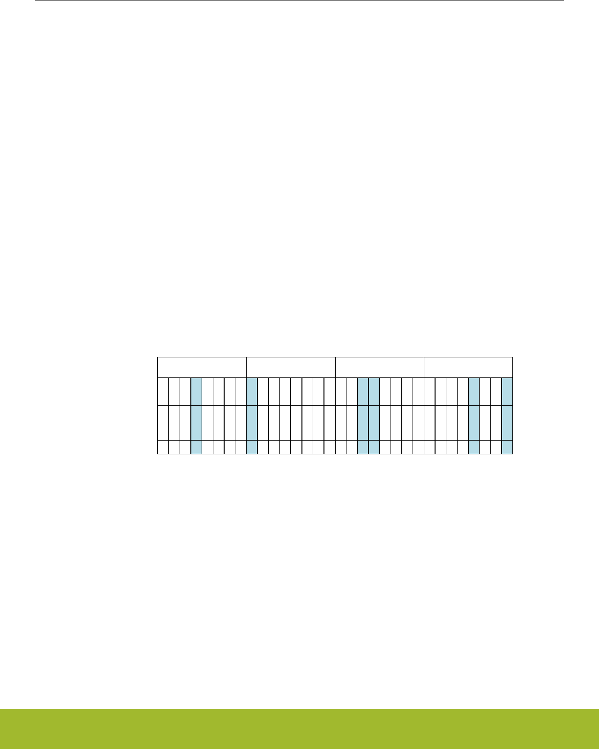
27.3.5.2 Configuring ADC Inputs in Scan Mode
In scan mode, the ADC can sample and convert up to 32 external channels on each conversion trigger. Internal channels are not avail-
able in scan mode. The ADC's scanner logic automatically changes the input mux settings between conversions, eliminating the need
for firmware intervention.
The ADC scanner logic is controlled by a set of 32 logical channels called SCANINPUTIDs. The 32 SCANINPUTIDs are arranged in
four groups of 8 channels each. Each channel group can point to a predefined series of 8 sequential channels on any of the available
APORTs. The ADCn_SCANINPUTSEL register is used to configure which group of physical APORT channels each of the SCANINPU-
TID channel groups map to. For example, selecting APORT1CH16TOCH23 in the INPUT7TO0SEL field selects APORT1CH16 for
SCANINPUTID0, APORT1CH17 for SCANINPUTID1, APORT1CH18 for SCANINPUTID2, and so on.
The four SCANINPUTID groups are fully independent and may be selected from any APORT in any combination. It is possible also to
repeat the same selection in multiple groups. For example, the user may select APORT2CH0TOCH7 for all four of the SCANINPUTID
groups.
In many cases, the user application will not require all 32 channels of the scanner to be converted. Each of the scanner channels may
be individually enabled according to the needs of the system. The ADCn_SCANMASK register is used to enable and disable individual
SCANINPUTIDs. The bits in the ADCnSCANMASK register correspond one-to-one with the SCANINPUTID channel numbers. During a
scan operation, the ADC scanner logic will convert only the enabled SCANINPUTIDs, in order from lowest to highest.
In single-ended mode, all conversions performed by the ADC will be relative to VSS. For any enabled SCANINPUTID, the selected
APORT channel will be connected to the ADC with the opposite ADC input terminal connected to VSS. Note that the channel groups
selected in ADCn_SCANINPUTSEL point to a block of 8 channels on an APORT, which includes both X and Y channels. Depending on
the channels enabled by ADCn_SCANMASK, the ADC may perform conversions on the X or the Y bus associated with that APORT.
Figure 27.6 ADC Single-ended Scan Mode Example on page 874 shows an example of a single-ended scan configuration. In this
example, ADCn_SCANINPUTSEL has been configured to place APORT1CH16TO23 in the first, third, and fourth channel groups.
APORT4CH8TO15 has been placed in the second channel group. ADCn_SCANMASK selects six of these channels for inclusion in the
scan. When an ADC scan is initiated with this configuration, the ADC begins at SCANINPUTID0 and converts each enabled channel in
turn. This scan configuration results in a set of six single-ended ADC conversions: PF0, PF3, PA5, PA5, PF7, and PF4.
SCANINPUTSEL
SCANMASK
APORT1CH16TO23
10010000000011000000000100001000
081624SCANINPUTID 7152331
APORT4CH8TO15APORT1CH16TO23APORT1CH16TO23
PF0
PF1
PF2
PF3
PF4
PF5
PF6
PF7
I/O Pin
PA0
PA1
PA2
PA3
PA4
PA5
none
none
PF0
PF1
PF2
PF3
PF4
PF5
PF6
PF7
PF0
PF1
PF2
PF3
PF4
PF5
PF6
PF7
APORT-Channel
1-16
1-23
1-22
1-21
1-20
1-17
1-18
1-19
1-16
1-23
1-22
1-21
1-20
1-17
1-18
1-19
1-16
1-23
1-22
1-21
1-20
1-17
1-18
1-19
4-8
4-15
4-14
4-13
4-12
4-9
4-10
4-11
Figure 27.6. ADC Single-ended Scan Mode Example
In differential mode, the default operation of the ADC scanner is to perform a differential measurement between the selected APORT
channel and the next channel on that APORT. For example, if the enabled SCANINPUTID points to APORT1CH6, the ADC will perform
a differential conversion between APORT1CH6 and APORT1CH7.
There are two exceptions to this rule, listed in order of precedence:
1. When converting SCANINPUTID15, the differential conversion will be performed between the channel selected by SCANINPU-
TID15 and the channel selected by SCANINPUTID8.
2. When APORTnCH31 is the selected input, the differential conversion will be performed between APORTnCH31 and APORTnCH0.
Figure 27.7 ADC Differential Scan Mode Example on page 875 shows an example of a differential scan configuration. In this example,
ADCn_SCANINPUTSEL has been configured to place APORT1CH16TO23 in the first, third, and fourth channel groups.
APORT4CH8TO15 has been placed in the second channel group. ADCn_SCANMASK selects three channels pairs for inclusion in the
scan. When an ADC scan is initiated with this configuration, the ADC begins at SCANINPUTID0 and converts each enabled channel in
turn. This scan configuration results in a set of three differential ADC conversions: PF0-PF1, PF2-PF3, and PA4-PA5.
Reference Manual
ADC - Analog to Digital Converter
silabs.com | Smart. Connected. Energy-friendly. Preliminary Rev. 0.5 | 874
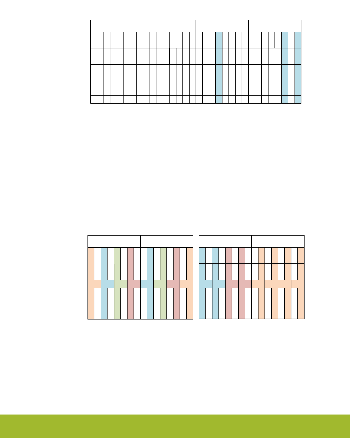
SCANINPUTSEL
SCANMASK
APORT1CH16TO23
10100000000010000000000000000000
081624SCANINPUTID 7152331
APORT4CH8TO15APORT1CH16TO23APORT1CH16TO23
APORT-Channel
(Positive)
APORT-Channel
(Negative)
I/O Differential
1-16
1-23
1-22
1-21
1-20
1-17
1-18
1-19
1-16
1-23
1-22
1-21
1-20
1-17
1-18
1-19
1-16
1-23
1-22
1-21
1-20
1-17
1-18
1-19
4-8
4-15
4-14
4-13
4-12
4-9
4-10
4-11
1-24
1-23
1-22
1-21
1-20
1-17
1-18
1-19
1-24
1-23
1-22
1-21
1-20
1-17
1-18
1-19
1-24
1-23
1-22
1-21
1-20
1-17
1-18
1-19
4-8
4-15
4-14
4-13
4-12
4-9
4-10
4-11
PA0-PA1
PA1-PA2
PA2-PA3
PA3-PA4
PA4-PA5
PA5-none
none
none
PF0-PF1
PF1-PF2
PF2-PF3
PF3-PF4
PF4-PF5
PF5-PF6
PF6-FP7
PF7-none
PF0-PF1
PF1-PF2
PF2-PF3
PF3-PF4
PF4-PF5
PF5-PF6
PF6-FP7
PF7-none
PF0-PF1
PF1-PF2
PF2-PF3
PF3-PF4
PF4-PF5
PF5-PF6
PF6-FP7
PF7-none
Figure 27.7. ADC Differential Scan Mode Example
In certain applications it may be desirable to perform differential conversions on several channels against a common voltage. The
ADCn_SCANNEGSEL register allows eight of the SCANINPUTIDs to re-map the negative terminal of a differential conversion to a
common channel. In the first ADCn_SCANINPUTSEL group, the negative input for SCANINPUT 0, 2, 4, and 6 may be re-mapped to
any of the odd-numbered channels in that group (SCANINPUT 1, 3, 5, or 7). Likewise, in the second ADCn_SCANINPUTSEL group,
the negative input for SCANINPUT 9, 11, 13, and 15 may be re-mapped to any of the even-numbered channels in that group (SCANIN-
PUT 8, 10, 12, or 14).
Figure 27.8 ADC Differential Scan Mode Re-mapping Negative Input Selections on page 875 shows the effects of the ADCn_SCAN-
NEGSEL register on the re-mappable inputs. The left side of the figure shows the default channel mapping, and the right side of the
figure shows how ADCn_SCANNEGSEL can be programmed to map the same negative input on up to four channels.
SCANINPUTSEL
APORT-Channel
(Positive)
APORT-Channel
(Negative)
I/O Differential
SCANNEGSEL
08
SCANINPUTID 715
APORT1CH16TO23
1-16
1-23
1-22
1-21
1-20
1-17
1-18
1-19
1-16
1-23
1-22
1-21
1-20
1-17
1-18
1-19
PF0-PF1
PF1-PF2
PF2-PF3
PF3-PF4
PF4-PF5
PF5-PF6
PF6-PF7
PF7-PF0
1230
APORT1CH16TO23
1-16
1-23
1-22
1-21
1-20
1-17
1-18
1-19
1-24
1-22
1-22
1-21
1-20
1-17
1-18
1-19
PF0-PF1
PF1-PF2
PF2-PF1
PF3-PF4
PF4-PF1
PF5-PF6
PF6-PF1
PF7-none
0123
08 715
APORT1CH16TO23
1-16
1-23
1-22
1-21
1-20
1-17
1-18
1-19
1-22
1-23
1-22
1-21
1-18
1-17
1-18
1-19
PF0-PF1
PF1-PF2
PF2-PF3
PF3-PF2
PF4-PF5
PF5-PF6
PF6-PF7
PF7-PF6
1133
APORT1CH16TO23
1-16
1-23
1-22
1-21
1-20
1-17
1-18
1-19
1-24
1-17
1-22
1-17
1-20
1-17
1-18
1-17
PF0-PF1
PF1-PF2
PF2-PF1
PF3-PF4
PF4-PF1
PF5-PF6
PF6-PF1
PF7-none
0000
Re-mapped using SCANNEGSELDefault SCANNEGSEL Selections
Figure 27.8. ADC Differential Scan Mode Re-mapping Negative Input Selections
Reference Manual
ADC - Analog to Digital Converter
silabs.com | Smart. Connected. Energy-friendly. Preliminary Rev. 0.5 | 875

27.3.5.3 APORT Conflicts
The ADC shares common analog buses connected to its APORTs (1-4) with other analog peripherals (see device-specific datasheet).
As the ADC performs single or scan conversions, it requests the shared buses and sends selections for the control switches to connect
the desired I/O pins. If another analog peripheral requests the same shared bus at the same time, there will be a collision and none of
the peripherals will be granted control of that bus.
To help debug over-utilization of APORT resources, the ADC hardware provides status information in local registers. The ADCn_APOR-
TREQ register gives the user visibility into which APORT(s) the ADC is requesting given the setting of the input selection registers.
ADCn_APORTCONFLICT reports any conflicts that occur. If PROGERR in ADCn_IEN is set, any conflict generates an interrupt. The
PROGERR field in the ADCn_STATUS register indicates whether the programming error happened as a result of an APORT bus con-
flict (BUSCONF) or from a negative-input selection conflict (NEGSELCONF). If the PROGERR interrupt occurred due to a negative se-
lection conflict, then the interrupt can be cleared by software only after correcting the conflict. If a software clear is attempted without
correcting the configuration, the interrupt will be cleared for one clock cycle but then it will trigger again as the invalid configuration still
persists.
Note: The ADC requests shared bus connections as soon as that bus is selected in the input select registers, even if the ADC is not
performing any conversions. This means that by using the APORT request, the ADC will acquire the associated shared analog bus,
preventing other peripherals from using it. The bus will be released only when the input select registers are changed.
It is possible for the ADC to passively monitor shared bus signals without controlling the switches and creating bus conflicts. This can
be done by setting the ADCn_APORTMASTERDIS register. When ADCn_APORTMASTERDIS is used, channel selection defers to the
peripheral acting as the bus master for that shared bus, and no bus conflict will occur. The ADC will connect its input to the shared bus,
but the specific channel will be controlled by the peripheral designated as the bus master.
27.3.6 Reference Selection and Input Range Definition
The full scale voltage (VFS) of the ADC is defined as the full input range, from the lowest possible input voltage to the highest. For
single-ended conversions, the input range on the selected positive input is from 0 to VFS. For differential conversions, the input to the
converter is the difference between the positive and negative input selections. This can range from -VFS/2 to +VFS/2.
VFS for the converter is determined by a combination of the selected voltage reference (VREF) and programmable divider circuits on
the ADC input and voltage reference paths. Users have full control over the VREF and divider selections, offering a very flexible and
wide selection of VFS values. In most applications however, it is not necessary to adjust VFS beyond a set of common pre-defined
choices. For the simplest VFS configuration, refer to 27.3.6.1 Basic Full-Scale Voltage Configuration. If the application requires a VFS
configuration not available in the pre-defined choices, 27.3.6.2 Advanced Full-Scale Voltage Configuration covers additional configura-
tion options.
Reference Manual
ADC - Analog to Digital Converter
silabs.com | Smart. Connected. Energy-friendly. Preliminary Rev. 0.5 | 876

27.3.6.1 Basic Full-Scale Voltage Configuration
Basic configuration of the VFS (full scale voltage) for the converter is done by programming the REF bitfield in ADCn_SINGLECTRL
(for single channel mode) or ADCn_SCANCTRL (for scan mode) to any of the pre-defined options. The list of available pre-defined VFS
options is:
• VFS = 1.25 V using internal VBGR as the reference source
• VFS = 2.5 V using internal VBGR as the reference source
• VFS = AVDD using AVDD as the reference source (AVDD ≤ 3.6 V)
• VFS = 5 V using internal VBGR as the reference source
• VFS = ADCn_EXTP external pin as a single-ended reference source (1.2 V - 3.6 V)
• VFS = ADCn_EXTP - ADCn_EXTN external pins as a differential reference source. ( 1.2 V - 3.6 V difference)
• VFS = 2 x AVDD using AVDD as the reference source (AVDD ≤ 3.6 V)
The maximum and minimum input voltage which the ADC can recognize at any external pin is limited to the supply voltages. If VFS is
configured to be larger than the supply range, the full ADC range will not be available. For example, with a 3.3 V supply and VFS con-
figured to 5 V, the input voltage for single-ended conversions will be limited to 0 to 3.3 V, though the effective VFS is still 5 V.
The ADC uses a chip-level bias circuit to provide bias current for its operation. For highest accuracy when using a VBGR-derived inter-
nal bandgap reference source, GPBIASACC in ADCn_BIASPROG should be cleared to 0. This will allow the ADC to enable high-accu-
racy mode from the bias circuitry during conversions. When AVDD or an external pin reference option is used, software should set
GPBIASACC in ADCn_BIASPROG to 1 to conserve energy. Note that VDAC and DC-DC usage may switch the chip-level bias to high-
accuracy mode (even if ADCn_BIASPROG is set to 1), potentially impacting ADC results. For example, if ADC is doing a conversion
with ADCn_BIASPROG set to 1 and VDAC also starts a conversion using the internal low noise reference, then the chip-level bias cir-
cuit will be automatically switched to high- accuracy mode (potentially corrupting results of the on-going ADC conversion). Similarly,
DC-DC startup automatically switches the chip-level bias circuit to high-accuracy mode for a short time, i.e., if DC-DC startup happens
when ADC is doing a conversion (with ADCn_BIASPROG set to 1), ADC results may get corrupted. DC-DC startup automatically
switches the bias circuit to high-accuracy mode for 25 µs. It is during this time that the ADC conversions with the ADCn_BIASPROG set
to 1 should be avoided.
If the pre-defined VFS options do not suit the particular application, refer to 27.3.6.2 Advanced Full-Scale Voltage Configuration for
more advanced VFS options.
Reference Manual
ADC - Analog to Digital Converter
silabs.com | Smart. Connected. Energy-friendly. Preliminary Rev. 0.5 | 877

27.3.6.2 Advanced Full-Scale Voltage Configuration
For most applications, the pre-defined VFS options described in 27.3.6.1 Basic Full-Scale Voltage Configuration are suitable. Advanced
VFS configurations are also possible by programming the REF bitfield in ADCn_SINGLECTRL or ADCn_SCANCTRL to the CONF op-
tion. Programming the REF bitfield to CONF allows the user to select the specific VREF source and adjust the programmable input and
reference divider options directly.
The general procedure for programming an advanced VFS configuration is as follows:
1. Select the voltage reference source using VREFSEL.
2. Configure VREFATTFIX and VREFATT so that the reference voltage at the ADC is between 0.7 and 1.05 V.
3. Configure VINATT to achieve the desired full-scale voltage.
The VREFSEL field in ADCn_SINGLECTRLX or ADCn_SCANCTRLX selects the voltage reference source. The ADC can choose from
the following voltage reference (VREF) sources:
• VBGR: An internal 0.83 V bandgap reference voltage. This is the most precise internal reference source available.
• VDDXWATT: An attenuated version of the AVDD supply voltage. The attenuation factor is determined by the VREFATTFIX and/or
VREFATT bit fields.
• VREFPWATT: An external reference source applied to the ADCn_EXTP pin, and attenuated by the attenuation factor (determined by
the VREFATTFIX and/or VREFATT bit fields). This is the appropriate choice for external reference inputs greater than 1.05 V.
• VREFP: An external reference source applied to the ADCn_EXTP pin, without any attenuation. This is the appropriate choice for
external reference inputs between 0.7 V and 1.05 V.
• VENTROPY: A very low internal reference voltage (approx. 0.1 V). This option is intended to be used only with the ADC inputs tied
internally to VSS, for generating random noise at the ADC output.
• VREFPNWATT: A differential version of VREFPWATT, with the reference source applied to the ADCn_EXTP and ADCn_EXTN pins
and attenuated. This is the appropriate choice where a differential reference of greater than 1.05 V is required.
• VREFPN: A differential version of VREFP, with the reference source applied to the ADCn_EXTP and ADCn_EXTN pins and no at-
tenuation. This is the appropriate choice where a differential reference of between 0.7 V and 1.05 V is required.
• VBGRLOW: An internal 0.78 V bandgap reference voltage.
The ADC reference voltage should be attenuated to a lower voltage when using AVDD or the external reference source. A simple meth-
od for a wide range of reference sources is to set VREFATTFIX to 1. The VREF attenuation factor (ATTVREF) can then be selected
between 1/3 (when VREFATT is greater than 0), and 1/4 (when VREFATT is equal to 0). For reference sources between 1.2 V and 3.6
V, ATTVREF = 1/3 is the best choice. ATTVREF = 1/4 can be used with references from 1.6 V to 3.8 V, with slight performance degrada-
tion.
Finer granularity on ATTVREF is possible as well, by clearing VREFATTFIX to 0, and setting the VREFATT field. For optimal perform-
ance with VREFATTFIX = 0, the attenuated ADC reference input should be limited to between 0.7 V and 1.05 V. When VREFATTFIX is
cleared to 0, ATTVREF is set according to the equation:
ATTVREF = (VREFATT + 6) / 24 for VREFATT < 13, and (VREFATT - 3) / 12 for VREFATT ≥ 13
Figure 27.9. ATTVREF: VREF Attenuation Factor
The ADC input also includes a programmable attenuator. The VIN attenuator is used to widen the available input range of the ADC
beyond the reference source. The VIN attenuation factor (ATTVIN) is determined by the VINATT field according to the equation:
ATTVIN = VINATT / 12 for VINATT ≥ 3 (settings 0, 1, and 2 are not allowable values for VINATT)
Figure 27.10. ATTVIN: VIN Attenuation Factor
VFS can be calculated by the formula given below for any given VREF source, VREF attenuation, and VIN attenuation:
VFS = 2 ∙ VREF ∙ ATTVREF / ATTVIN
VREF is selected in the VREFSEL bitfield, and
ATTVREF is the VREF attenuation factor, determined by VREFATT or VREFATTFIX
Reference Manual
ADC - Analog to Digital Converter
silabs.com | Smart. Connected. Energy-friendly. Preliminary Rev. 0.5 | 878

ATTVIN is the VIN attenuation factor, determined by VINATT
Figure 27.11. VFS: Full-Scale Input Range
The maximum and minimum input voltage which the ADC can recognize at any external pin is limited to the supply voltages. If VFS is
configured to be larger than the supply range, the full ADC range will not be available. For example, with a 3.3 V supply and VFS con-
figured to 5 V, the input voltage for single-ended conversions will be limited to 0 to 3.3 V, though the effective VFS is still 5 V.
The ADC uses a chip-level bias circuit to provide bias current for its operation. For highest accuracy when using a VBGR-derived inter-
nal bandgap reference source, GPBIASACC in ADCn_BIASPROG should be cleared to 0. This will allow the ADC to enable high-accu-
racy mode from the bias circuitry during conversions. When AVDD or an external pin reference option is used, software should set
GPBIASACC in ADCn_BIASPROG to 1 to conserve energy. Note that VDAC and DC-DC usage may switch the chip-level bias to high-
accuracy mode (even if ADCn_BIASPROG is set to 1), potentially impacting ADC results. For example, if ADC is doing a conversion
with ADCn_BIASPROG set to 1 and VDAC also starts a conversion using the internal low noise reference, then the chip-level bias cir-
cuit will be automatically switched to high- accuracy mode (potentially corrupting results of the on-going ADC conversion). Similarly,
DC-DC startup automatically switches the chip-level bias circuit to high-accuracy mode for a short time, i.e., if DC-DC startup happens
when ADC is doing a conversion (with ADCn_BIASPROG set to 1), ADC results may get corrupted. DC-DC startup automatically
switches the bias circuit to high-accuracy mode for 25 µs. It is during this time that the ADC conversions with the ADCn_BIASPROG set
to 1 should be avoided.
The combination of VREF, ATTVREF and ATTVIN can produce a wide range of full-scale voltage options for the converter. Table
27.1 Advanced VFS Configuration: VREF = AVDD on page 879 shows some example VFS configurations using AVDD as a reference
source.
Table 27.1. Advanced VFS Configuration: VREF = AVDD
AVDD Voltage VREF Attenuation Set-
tings
Reference Voltage at
ADC
VIN Attenuation Set-
tings
VFS
1.85 V VREFATTFIX = 0
VREFATT = 6
ATTVREF = 1/2
0.925 V VINATT = 12
ATTVIN = 1
1.85 V
(+/-0.925 V differential)
3.0 V VREFATTFIX = 0
VREFATT = 2
ATTVREF = 1/3
1.0 V VINATT = 8
ATTVIN = 2/3
3.0 V
(+/-1.5 V differential)
3.0 V VREFATTFIX = 0
VREFATT = 2
ATTVREF = 1/3
1.0 V VINATT = 4
ATTVIN = 1/3
6.0 V
(+/-3.0 V differential)
3.6 V VREFATTFIX = 1
VREFATT = 0
ATTVREF = 1/4
0.9 V VINATT = 6
ATTVIN = 1/2
3.6 V
(+/-1.8 V differential)
Reference Manual
ADC - Analog to Digital Converter
silabs.com | Smart. Connected. Energy-friendly. Preliminary Rev. 0.5 | 879

27.3.7 Programming of Bias Current
The ADC uses a chip-level bias generator to provide bias current for its operation. The ADC's internal bias can be scaled by ADCBIA-
SPROG field of the ADCn_BIASPROG register. At lower conversion speeds, the ADCBIASPROG can be used to lower active power.
Some commonly used settings are given in the ADCBIASPROG register description. For proper operation, the ADC conversion speed
must be scaled accordingly. The scale factor is calculated as:
Bias scale factor = (1- ADCBIASPROG[2:0]/8) / (1+3∙ADCBIASPROG[3])
Figure 27.12. Bias scale factor
The bias programming register also includes the VFAULTCLR bit field. If VREFOF interrupt is enabled and it is triggered, then the user
needs to set this bit in the ISR before clearing the interrupt flag. This bit then needs to be reset after the interrupt flag is cleared in order
to enable the VREFOV flag to trigger on the next VREFOV condition.
The bias current settings should only be changed while the ADC is disabled (i.e. in NORMAL warm-up mode and no conversion in
progress).
27.3.8 Feature Set
The following sections explain different ADC features.
27.3.8.1 Conversion Tailgating
Scan conversions have priority over single channel conversions. This means that if scan and single triggers are received simultaneous-
ly, or even if the scan is received later when ADC is being warmed up for performing a single conversion, the scan conversion will have
priority and will be done before the single conversion. However, a scan trigger will not interrupt in the middle of a single conversion, i.e.,
if the single conversion is in the acquisition or approximation phase, then the scan will have to wait for the single conversion to com-
plete. If a scan sequence is triggered by a timer on a periodic basis, single channel conversion that started just before a scan trigger
can delay the start of the scan sequence, thus causing jitter in sample rate. To solve this, conversion tailgating can be chosen by setting
TAILGATE in ADCn_CTRL. When this bit is set, any triggered single channels will wait for the next scan sequence to finish before acti-
vating (see Figure 27.13 ADC Conversion Tailgating on page 880). The single channel will then follow immediately after the scan
sequence. In this way, the scan sequence will always start immediately when triggered, provided that the period between the scan trig-
gers is big enough to allow the single sample conversion that was triggered to finish before the next scan trigger arrives. Note that if
tailgating is set and a single channel conversion is triggered, it will indefinitely wait for a scan conversion before starting the single chan-
nel conversion.
SINGLESTART
SCANSTART
SCANACT
ADC action
SINGLEACT
Scan Single Scan Single Scan
Figure 27.13. ADC Conversion Tailgating
Reference Manual
ADC - Analog to Digital Converter
silabs.com | Smart. Connected. Energy-friendly. Preliminary Rev. 0.5 | 880

27.3.8.2 Repetitive Mode
Both single channel and scan mode can be run as a one shot conversion or in repetitive mode. The REP bitfield in ADCn_SIN-
GLECTRL/ADCn_SCANCTRL registers can be used to activate the repetitive mode for single and scan respectively. In order to achieve
the maximum sampling rate of 1 Msps, repetitive mode should be used.
It is also possible to have a programmable delay between these repetitive conversions. The REPDELAY bitfield in the ADCn_SIN-
GLECTRLX and ADCn_SCANCTRLX registers can be used to set the delay between two repeated conversions in single channel and
scan mode respectively. For single channel mode when a single conversion in repetitive mode ends, the user programmed REPDELAY
is inserted and then the next single conversion is re triggered after the delay period is over. For scan mode the REPDELAY is inserted
after the entire scan sequence ends. Once the delay period is over, scan mode is internally re triggered. The 27.3.8.1 Conversion Tail-
gating explains how the single channel and scan mode conversions can push each other out of phase. Conversion tailgating can be
chosen in repetitive mode as well in order to ensure that the scan sequence will always start immediately when triggered, provided the
scan REPDELAY chosen is big enough for the single conversion to finish. The status flags SINGLEACT and SCANACT stay high
throughout the repeat mode, i.e., even during the delay period. The flags show that the conversions are either active or pending.
Whether the ADC turns off or stays warmed up between these repeated conversions depends on the WARMUPMODE chosen in the
ADCn_CTRL register. When using single channel mode with repeat mode and REPDELAY enabled, then once the ADC has started
operation (i.e., singleact status flag has gone high) then no new single conversion triggers (software START/ PRS triggers) should be
sent to the ADC until the ADC has stopped converting (i.e., singleact status flag has gone low). The same applies to scan sequence
conversions.
Reference Manual
ADC - Analog to Digital Converter
silabs.com | Smart. Connected. Energy-friendly. Preliminary Rev. 0.5 | 881
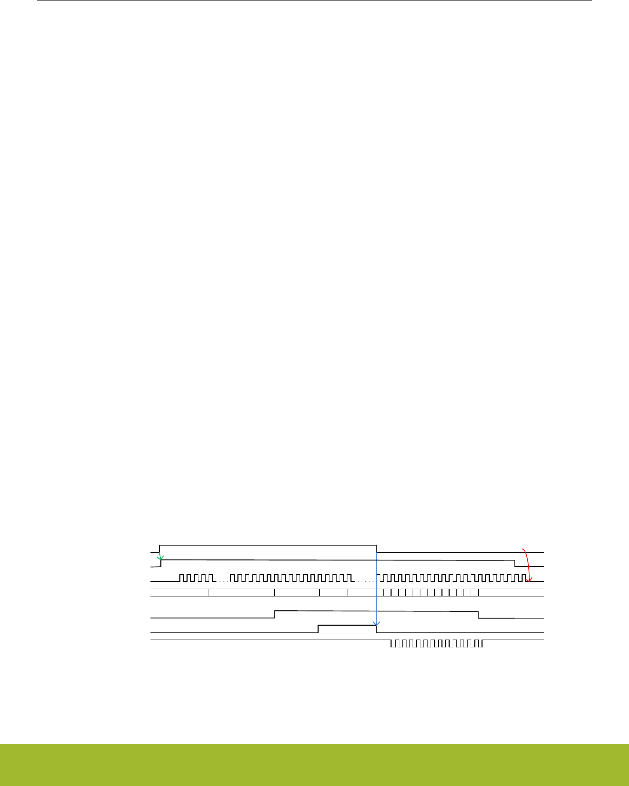
27.3.8.3 Conversion Trigger
The conversion modes can be activated by writing a 1 to the SINGLESTART or SCANSTART bit in the ADCn_CMD register. The con-
versions can be stopped by writing a 1 to the SINGLESTOP or SCANSTOP bit in the ADCn_CMD register. A START command will
have priority over a STOP command. When the ADC is stopped in the middle of a conversion, the result buffer is cleared (the FIFO
contents for any prior conversions are still intact). Every time a STOP command is issued, the user should wait for the corresponding
status flag (SINGLEACT/SCANACT) to go low and then either read all the data in the FIFO or send the corresponding FIFOCLEAR
command. The SINGLEACT and SCANACT bits in ADCn_STATUS are set high when the modes are actively converting or have pend-
ing conversions.
It is also possible to trigger conversions from PRS signals. The PRS is treated as an asynchronous trigger. Setting PRSEN in
ADCn_SINGLECTRL/ADCn_SCANCTRL enables triggering from PRS input. Which PRS channel to listen to is defined by PRSSEL in
ADCn_SINGLECTRLX/ADCn_SCANCTRLX. When PRS trigger is selected, it is still possible to trigger a conversion from software.
Please refer to the PRS chapter for more information on how to set up the PRS channels. When the conversions are triggered using the
ADCn_CMD register, then the SINGLEACT and SCANACT bits in the ADCn_STATUS are set as soon as the START command is writ-
ten to the register. When the conversion is triggered using PRS, it takes some cycles from the time PRS trigger is received until the
SINGLEACT and SCANACT bits are set due to the synchronization requirement. If SINGLEACT is already high then sending a new
START command or a new PRS trigger for a single conversion will not have any impact as ADC already has a single conversion on-
going or a single conversion pending (single conversion can be pending if ADC is busy running a scan sequence). The same rules
apply for SCANACT and SCAN START and PRS triggers. When software issues a SINGLE/SCAN STOP command, it must wait until
SINGLEACT/ SCANACT flag goes low before issuing a new START.
The PRS may trigger the ADC in two possible ways, configured by PRSMODE in ADCn_SINGLECTRLX/ADCn_SCANCTRLX. In
PULSED mode, a PRS pulse triggers the ADC to start the ADC_CLK (if not already enabled), warm up (if not already warm), start the
acquisition period, and perform the conversion. This is identical to issuing a START command from software. In this mode, the input
sampling finishes at the end of the acquisition period (AT).
If the ADC_CLK and the source of the trigger (START command or PRS pulse) are not synchronous, the frequency of the input sam-
pling (FS), will experience a 11/2 to 21/2 ADC_CLK cycle jitter due to synchronization requirements.
To precisely control the sample frequency, the PRSMODE can be set to TIMED mode. In this mode, a long PRS pulse is expected to
trigger the ADC and its negative edge directly finishes input sampling and starts the approximation phase, giving precise sampling fre-
quency management. The restriction is that the PRS pulse has to be long enough to start the ADC_CLK (if not already enabled), and
finish the acquisition period based on the AT field in ADCn_SINGLECTRL/ADCn_SCANCTRL. The PRS pulse needs to be high when
AT event finishes. If it is not high when AT finishes, then it is ignored and input sampling finishes after AT event has ended (a two cycle
latency is added to the conversion in this scenario). In this case, the ADC sets the PRSTIMEDERR interrupt flag.
If the PRS pulse is too long (e.g., FS = 32kHz), the analog ADC start can be delayed to save power. The CONVSTARTDELAY along
with its EN in the ADCn_SINGLECTRLX or ADCn_SCANCTRLx can be programmed to implement a 0 to 8 microseconds delay. The
microsecond tick is counted by TIMEBASE with ADC_CLK similar to warmup case. This saves power as the ADC is not enabled until
the last possible microsecond before the fall edge of the PRS arrives to open the sampling switch and to start the approximation phase.
Figure 27.14 ADC PRS Timed mode with ASNEEDED ADC_CLK request on page 882) shows PRS Timed mode triggering with
CONVSTARTDELAY and ASNEEDED ADC_CLK request. See that power is saved by both delaying the ADC EN and by requesting the
ADC_CLK only during ADC operation. This is especially useful in saving power when running the ADC in EM2 Deep Sleep or EM3 Stop
power mode with low sampling frequency.
ADC_CLK
ADC action
PRS
clkreq_adc_async
CONVSTARTDELAY ADC WARMUP AT DLYBIT12
B12
B0
IDLE IDLE
Analog ADC EN FULL POWER
SHUT DOWN SHUT DOWN
adc_clk_samp
adc_clk_sar
(conversion clock)
0-8 us delay 5 us
delay sampling switch
closing till fall edge of PRS
rise edge starts adc
clock request Adc clock request stops upon
completion of conversion
Figure 27.14. ADC PRS Timed mode with ASNEEDED ADC_CLK request
When a PRS pulse is received, if the ADC_CLK is not running (ASNEEDED mode), then the ADC requests the clock by setting
clkreq_adc_async high. If the chosen clock source (HFXO/ HFSRCCLK/ AUXHFRCO) is already running, then it takes 5 ADC_CLK
cycles after the clock request is asserted for the ADC_CLK to start. HFXO and HFSRCCLK (if chosen as ADC clock source) need to be
Reference Manual
ADC - Analog to Digital Converter
silabs.com | Smart. Connected. Energy-friendly. Preliminary Rev. 0.5 | 882

already running before ADC sends out the clock request. If AUXHFRCO is chosen as the ADC clock source, and it is not already run-
ning, then the CMU automatically turns it on when the ADC sends a clock request. In such a case, it takes (7 ADC_CLK cycles + the
oscillator startup time) for the ADC_CLK to start. The oscillator startup time can be found in the device datasheet.
When triggering repeat mode using PRS and then stopping the triggered mode using STOP command, ensure that the PRS pulse used
to generate the repeat mode has gone low by the time the STOP command is issued. If the PRS pulse continues to stay high after ADC
has stopped the ongoing conversion, then it will be picked as a new trigger to start a new conversion.
Note:
The conversion settings should not be changed while the ADC is running. Doing so may lead to unpredictable behavior.
The adc_clk_sar phase is always reset by a conversion trigger as long as a conversion is not in progress. This gives predictable latency
from the time of the trigger to the time the conversion starts, regardless of when in the trigger occurs.
Software and LESENSE should not trigger conversions if PRS Timed mode is selected and PRSEN is set to 1 in the ADCn_SIN-
GLECTRL/ADCn_SCANCTRL register.
If the PRS Timed mode is being used, the acquisition time (AT) must be set greater than 0.
Scan conversions can be triggered using LESENSE as well. LESENSE only triggers one input conversion at a time (not the whole se-
quence of 32 possible inputs). The input to be converted using LESENSE must be configured by the user in the ADCn_SCANINPUT-
SEL register before triggering the conversion, i.e., one of the 32 inputs chosen in the ADCn_SCANINPUTSEL register must be the one
that is to be converted using LESENSE. The ADCn_SCANMASK is not used for LESENSE triggered conversions. Instead, the user can
select which input should be converted through LESENSE inside the LESENSE settings (LESENSE_CHX). The results of LESENSE
triggered conversions are not loaded in the FIFO/ DATA registers but are instead available in the LESENSE register. Similarly, the
SCAN interrupt flag is not set on completion of a LESENSE triggered conversion (because that flag is set only when the data is written
to the Scan FIFO). When there is a LESENSE triggered conversion going on or pending, the SCANACT status flag is set. The SCAN-
PEND interrupt flag is set when a software/PRS triggered scan goes pending because a LESENSE triggered scan is running
(software/PRS triggered scan will start after the currently running LESENSE scan conversion completes). Similarly, SCANEXTPEND
interrupt flag is set when the LESENSE triggered scan conversion goes pending because a software/PRS triggered scan is running.
LESENSE triggered conversions can be stopped at any time using the SCANSTOP command in the ADCn_CMD register. Note that the
LESENSE triggered conversion cannot trigger the Scan repeat mode.
The DBGHALT bit-field in the ADCn_CTRL register can be used to choose the ADC behavior in debug mode. If this bit is set to 1, then
in debug mode ADC completes the current conversions and then halts. This means that all conversion triggers that were received be-
fore the debug halt occurred will be serviced before the ADC halts. All conversion triggers received after the ADC was halted, will be
serviced when the debug mode is not halted any more. If the repetitive mode is running (in repetitive mode ADC keeps doing conver-
sions until the user sends a software STOP) and a debug mode halt occurs, then the ADC will gracefully complete the current on-going
conversion and then halt. The repetitive mode conversions will restart as soon as the debug mode is not halted any more.
Reference Manual
ADC - Analog to Digital Converter
silabs.com | Smart. Connected. Energy-friendly. Preliminary Rev. 0.5 | 883

27.3.8.4 Output Results
ADC output results are presented in 2’s complement form and the format for single ended and differential conversions are given in
Table 27.2 ADC Single Ended Conversion on page 884 and Table 27.3 ADC Differential Conversion on page 884, respectively. If
differential mode is selected, the results are sign extended up to 32-bits (shown in Table 27.5 ADC Results Representation on page
885).
Table 27.2. ADC Single Ended Conversion
Input Voltage
Output Results
Binary Hex value
4095/4096 ∙ VFS 111111111111 FFF
0.5 ∙ VFS 100000000000 800
1/4096 ∙ VFS 000000000001 001
0 000000000000 000
Table 27.3. ADC Differential Conversion
Input
Output Results
Binary Hex value
2047/4096 ∙ VFS 011111111111 7FF
0.25 ∙ VFS 010000000000 400
1/4096 ∙ VFS 000000000001 001
0 000000000000 000
-1/4096 ∙ VFS 111111111111 FFF
-0.25 ∙ VFS 110000000000 C00
-0.5 ∙ VFS 100000000000 800
27.3.8.5 Resolution
The ADC performs 12-bit conversions by default. However, if full 12-bit resolution is not needed, it is possible to speed up the conver-
sion by selecting a lower resolution (6 or 8 bits). For more information on the accuracy of the ADC, the reader is referred to the electri-
cal characteristics section for the device.
Reference Manual
ADC - Analog to Digital Converter
silabs.com | Smart. Connected. Energy-friendly. Preliminary Rev. 0.5 | 884

27.3.8.6 Oversampling
To achieve higher accuracy, hardware oversampling can be enabled individually for each mode (Set RES in ADCn_SINGLECTRL/
ADCn_SCANCTRL to 0x3). The oversampling rate (OVSRSEL in ADCn_CTRL) can be set to any integer power of 2 from 2 to 4096
and the configuration is shared between the scan and single channel mode (OVSRSEL field in ADCn_CTRL).
With oversampling, each input is sampled at 12-bits of resolution a number of times (given by OVSRSEL), and the results are filtered by
a first order accumulate and dump filter to form the end result. The data presented in the ADCn_SINGLEDATA and ADCn_SCANDATA
registers are the direct contents of the accumulation register (sum of samples). However, if the oversampling ratio is set higher than
16x, the accumulated results are shifted to fit the MSB in bit 15 as shown in Table 27.4 Oversampling Result Shifting and Resolution on
page 885.
Table 27.4. Oversampling Result Shifting and Resolution
Oversampling setting # right shifts Result Resolution # bits
2x 0 13
4x 0 14
8x 0 15
16x 0 16
32x 1 16
64x 2 16
128x 3 16
256x 4 16
512x 5 16
1024x 6 16
2048x 7 16
4096x 8 16
27.3.8.7 Adjustment
By default, all results are right adjusted, with the LSB of the result in bit position 0 (zero). In differential mode the signed bit is extended
up to bit 31, but in single ended mode the bits above the result are read as 0. By setting ADJ in ADCn_SINGLECTRL/
ADCn_SCANCTRL, the results are left adjusted as shown in Table 27.5 ADC Results Representation on page 885. When left adjus-
ted, the MSB is always placed on bit 15 and sign extended to bit 31. All bits below the conversion result are read as 0 (zero).
Table 27.5. ADC Results Representation
Adjustment Resolution Bits
31 ... 16 15 14 13 12 11 10 9 8 7 6 5 4 3 2 1 0
Right
12 11 ... 11 11 11 11 11 11 10 9 8 7 6 5 4 3 2 1 0
8 7 ... 7 7 7 7 7 7 7 7 7 7 6 5 4 3 2 1 0
6 5 ... 5 5 5 5 5 5 5 5 5 5 5 5 4 3 2 1 0
OVS 15 ... 15 15 14 13 12 11 10 9 8 7 6 5 4 3 2 1 0
Left
12 11 ... 11 11 10 9 8 7 6 5 4 3 2 1 0 - - - -
8 7 ... 7 7 6 5 4 3 2 1 0 - - - - - - - -
6 5 ... 5 5 4 3 2 1 0 - - - - - - - - - -
OVS 15 ... 15 15 14 13 12 11 10 9 8 7 6 5 4 3 2 1 0
Reference Manual
ADC - Analog to Digital Converter
silabs.com | Smart. Connected. Energy-friendly. Preliminary Rev. 0.5 | 885

27.3.8.8 Channel Connection
The inputs are connected to the analog ADC at the beginning of the acquisition phase and are disconnected at the end of the acquisi-
tion phase. The time when the APORT switches are closed (for the next input to be converted) can be controlled by the CHCONMODE
bitfield in the ADCn_CTRL register. By default, this field is set to the MAXSETTLE option. For MAXSETTLE, APORT switches are
closed on the next input as soon as the acquisition phase for the current conversion is complete. This means that the APORT switches
are closed approximately 12 adc_clk_sar cycles (assuming 12 bit resolution) before the acquisition phase of the current conversion
starts, giving APORT switches maximum time to settle. The time for which APORT switches should be closed before the acquisition
phase starts, should be the same for all inputs in order to get consistent results. This means that if the ADC is warmed up with CHCON-
REFWARMIDLE set to 0 (scan reference warmed up and the APORT switches for the first scan channel closed) and a single trigger
comes in, the single conversion will have to wait 12 adc_clk_sar cycles before it can start (even if single is using the same reference as
scan). In this case, it might be more suitable to switch to the MAXRESP option in the CHCONMODE bitfield. In MAXRESP, the APORT
switches for the upcoming conversion are closed just before the acquisition phase starts. This gives less settling time to the APORT
switches but removes the extra waiting time before a conversion can start (which could be the case with MAXSETTLE as discussed
above).
27.3.8.9 Temperature Measurement
The ADC includes an internal temperature sensor. This sensor is measured during production test and the temperature readout from
the ADC at production temperature, ADC0CAL3_TEMPREAD1V25, is given in the Device Information (DI) page. The production tem-
perature, CAL_TEMP, is also given in this page. The temperature sensor slope, V_TS_SLOPE (mV/degree Celsius), for the sensor is
found in the data sheet for the device. Using the 1.25V VFS option and 12-bit resolution, the temperature can be calculated according
to the following formula (VFS in the formula is 1250 mV) :
TCELSIUS = CAL_TEMP - (ADC0CAL3_TEMPREAD1V25 - ADC_result) ∙ VFS / (4096∙ V_TS_SLOPE)
Figure 27.15. ADC Temperature Measurement
When reading the temperature sensor, the GPBIASACC bit in ADCn_BIASPROG should be set to 1 to keep the bias in LOWACC
mode. Note that VDAC and DC-DC usage while ADC converts (with ADCn_BIASPROG set to 1) may corrupt ADC results. See section
27.3.6 Reference Selection and Input Range Definition for details.
Note: The minimum acquisition time for the temperature reference is found in the electrical characteristics for the device. If using the
1.25V reference, extra acquisition time is required. In this case the AT field of ADCn_SINGLECTRL or ADCn_SCANCTRL should be
set to a value of 9 or higher.
Note: If the device has more than one ADC, all ADCs may not be equipped with the temperature sensor. Please check the device
datasheet.
27.3.8.10 ADC as a Random Number Generator
The ADC can be used as a random number generator. This is done by:
1. Choose the REF in the ADCn_SINGLECTRL as CONF, setting the VREFSEL in the ADCn_SINGLECTRLX as VENTROPY and
VINATT in the same register to its maximum value of 15.
2. Set DIFF to 1 and RES to 0 in the ADCn_SINGLECTRL register.
3. Trigger a single channel conversion and then read ADCn_SINGLEDATA register when the conversion finishes.
The LSB[2:0] of each sample will be a random number. In this mode, the POSSEL or NEGSEL in ADCn_SINGLECTRL can be connec-
ted to VSS or any other noisy input.
Reference Manual
ADC - Analog to Digital Converter
silabs.com | Smart. Connected. Energy-friendly. Preliminary Rev. 0.5 | 886

27.3.9 Interrupts, PRS Output
The single and scan modes have separate SINGLE and SCAN interrupt flags indicating whether corresponding FIFO contains DVL # of
valid conversion data. Corresponding interrupt enable bit has to be set in ADCn_IEN in order to generate interrupts. For these inter-
rupts, there is no software clear mechanism by writing to ADCn_IFC. The user needs to read enough data from the interrupted FIFO to
ensure it contains less than DVL # of elements. The ADCn_SINGLEFIFOCOUNT/ADCn_SCANFIFOCOUNT can provide number of
valid elements remaining in corresponding FIFO. The FIFO can also be cleared by ADCn_SINGLEFIFOCLEAR/ADCn_SCANFIFO-
CLEAR, but any existing data will be lost by this operation.
In addition to the SINGLE and SCAN interrupt flags, there is separate scan and single channel result overflow interrupt flag which sig-
nals that a result from a scan or single channel FIFO has been overwritten before being read. There is also separate scan and single
channel result underflow interrupt flag which signals that a FIFO read was issued when the FIFO was empty.
There is separate scan and single compare interrupt flag which signals a compare match with latest sample if the CMPEN in
ADCn_SINGLECTRL/ADCn_SCANCTRL is enabled.
ADC has two separate PRS outputs, one for single channel and one for scan sequence. A finished conversion results in a one
ADC_CLK cycle pulse, which is output to the Peripheral Reflex System (PRS). Note that the PRS pulse for scan is generated once after
every channel conversion in the scan sequence.
27.3.10 DMA Request
The ADC has two DMA request lines, SINGLEREQ and SCANREQ, which are set when a single or scan FIFO receives DVL# of sam-
ples. The requests are cleared when the corresponding single or scan result register is read and corresponding FIFO count reaches
lower than DVL. It also has two additional DMA Single request lines, SINGLESREQ and SCANSREQ, that are set when the corre-
sponding FIFO is not empty.
27.3.11 Calibration
The ADC supports offset and gain calibration to correct errors due to process and temperature variations. This must be done individual-
ly for each reference used. For each reference, it needs to be repeated for single-ended, negative single-ended (see 27.3.5 Input Se-
lection for details) and differential measurement. The ADC calibration (ADCn_CAL) register contains register fields for calibrating offset
and gain for both single and scan mode. The gain and offset calibration are done in single channel mode, but the resulting calibration
values can be used for both single and scan mode.
Gain and offset for various references and modes are calibrated during production and the calibration values for these can be found in
the Device Information page. During reset, the gain and offset calibration registers are loaded with the production calibration values for
the 1V25 reference. Others can be loaded as needed or the user can perform calibration on the fly using the particular reference and
mode to be used and write the result in the ADCn_CAL before starting the ADC conversion with them.
27.3.11.1 Offset Calibration
Offset calibration must be performed prior to gain calibration. Follow these steps for the offset calibration in single mode:
1. Select the desired full scale configuration by setting the REF bit field of the ADCn_SINGLECTRL register.
2. Set the AT bit field of the ADCn_SINGLECTRL register to 16CYCLES.
3. Set the POSSEL and NEGSEL of the ADCn_SINGLECTRL register to VSS, and set the DIFF to 1 for enabling differential input if
calibrating for DIFF measurement. During calibration, the ADC samples represent the code coming out of the analog. Thus, since
the input voltage is 0, the expected ADC output is 0b100000000000 in differential mode, 0b000000000000 in single-ended mode
and 0b111111111111 in negative single-ended mode.
4. A binary search is used to find the offset calibration value. Set the CALEN to 1, and OFFSETINVMODE to 1 (if calibrating for nega-
tive single-ended conversion) in the ADCn_CAL register. If user is performing negative single-ended calibration, the SINGLEOFF-
SETINV provides the offset else SINGLEOFFSET bit provides the offset (for both single-ended and differential offset calibration).
Start with 0b0000 (or 0b1111 if doing calibration for differential mode) in SINGLEOFFSET or with 0b1000 in SINGLEOFFSETINV (if
calibrating for negative single-ended conversion). Set the SINGLESTART bit in the ADCn_CMD register to perform a 12-bit conver-
sion and read the ADCn_SINGLEDATA register. The offset is (ADCn_SINGLEDATA - expected ADC output). Calculate this and
write [3:0] of the result into SINGLEOFFSET or SCANOFFSETINV (if doing negative single-ended conversion). The user repeats
till ADCn_SINGLEDATA matches expected ADC output. The ADC has a 8LSB built in negative offset to allow for negative offset
correction. So, with default offset value, which corrects for the negative offset, the converted ADCn_SINGLEDATA would match
expected ADC output if there were no offset. To get better noise immunity, the sampling phase can be repeated with Oversampling
enabled. The result of the binary search is written to the SINGLEOFFSET (or SINGLEOFFSETINV) field of the ADCn_CAL regis-
ter.
Reference Manual
ADC - Analog to Digital Converter
silabs.com | Smart. Connected. Energy-friendly. Preliminary Rev. 0.5 | 887

27.3.11.2 Gain Calibration
Offset calibration must be performed prior to gain calibration. The Gain Calibration is done in the following manner:
1. Select an external ADC channel for single channel conversion (a differential channel can also be used).
2. Apply an external voltage on the selected ADC input channel. This voltage should correspond to the top of the ADC input range for
the selected reference.
3. Set SINGLEGAIN[6:0] to 64 in the ADCn_CAL and measure gain, repeat gain calibration walking the 1 in SINGLEGAIN[6] to SIN-
GLEGAIN[0] till sampled ADCn_SINGLEDATA matches expected value. This is done by setting CALEN in ADCn_CAL set to 1 and
performing single channel, reading in the raw ADC code from the ADCn_SINGLEDATA and comparing it with expected code, i.e.
0b111111111111 for single-ended or differential conversion, and 0b000000000000 for negative single-ended conversion. The target
value is ideally the top of the ADC input range, but it is recommended to use a value a couple of LSBs below in order to avoid
overshooting. The result of the binary search is written to the SINGLEGAIN field of the ADCn_CAL register.
For the VDD reference and external reference, there is no hardware gain calibration. Calibration can be done by software after taking a
sample.
27.3.12 EM2 Deep Sleep or EM3 Stop Operation
The ADC can operate in EM2 Deep Sleep or EM3 Stop mode. For EM2 Deep Sleep or EM3 Stop operation the ADC_CLK must be
selected as AUXHFRCO. The section 27.3.1 Clock Selection describes how to choose AUXHFRCO as the ADC_CLK. The AUXHFR-
CO can be kept on for as long as sample conversion is needed or it can be requested by trigger event and after the conversion is done,
the AUXHFRCO can be shut down. The second option saves power at the expense of the delay to start the AUXHFRCO oscillator. All
the trigger modes are available in EM2 Deep Sleep or EM3 Stop as well.
While in EM2 Deep Sleep or EM3 Stop, the ADC can wake the system to EM0 Active on enabled interrupts. Following interrupts can
wake up the system to EM0 Active:
• SINGLE or SCAN interrupt indicating that the corresponding FIFO has reached the DVL watermark.
• Overflow interrupt (SINGLEOF or SCANOF)
• Underflow interrupt (SINGLEUF or SCANUF), triggered if DMA pops more data than present in the FIFO while the system is asleep
• Compare interrupt (SINGLECMP or SCANCMP)
• Over voltage interrupt (VREFOV)
The ADC can also work with the DMA so that the system does not have to wake up to consume data. This can happen if the SCAN or
SINGLE interrupt is disabled and the SINGLEDMAWU or SCANDMAWU in the ADCn_CTRL is set. The DMA will be triggered by the
ADC when DVL samples become available in the corresponding FIFO. The DMA will then pop all the elements of the corresponding
FIFO and put the system back into the low power state. A system-level wake up will occur upon the DMA done interrupt. Note that other
enabled ADC interrupts can still wake up the system when operating with the DMA. For example, the user can configure the window
compare function to trip when the result reaches a certain threshold while gathering ADC data in EM2 Deep Sleep or EM3 Stop.
The ADC works with the EMU to wake up the system or the DMA. It takes 2 µs from the time the ADC request a wakeup to start of the
peripheral clocks. In this ASYNC mode of ADC_CLK, it takes 6 HFPERCLK cycles to read a single entry from the single or scan FIFO.
So, with a 20MHz HFPERCLK, it takes about 4 µs per DMA wakeup to empty a full FIFO (4 entries). This restricts the sampling rate to
no more than 400 ksps in EM2 Deep Sleep or EM3 Stop in order to avoid FIFO overflows.
The AUXHFRCO power can be reduced by reducing the clock speed, and the user may adjust the ADCBIASPROG field in the
ADCn_BIASPROG register to reduce active power of the ADC during the conversions, thus reducing power even more in EM2 Deep
Sleep/EM3 Stop. Please refer to the data sheet for relevant power consumption numbers.
If the ADC is not to be used in EM2 Deep Sleep or EM3 Stop, then the user should ensure that the ADC is not busy before going to the
low power mode. 27.3.15 ADC Programming Model explains how to ensure the ADC is not busy. If the chip enters EM2 Deep Sleep or
EM3 Stop when ADC is busy without using AUXHFRCO, then the ADC clock will stop but the ADC will stay on, resulting in higher
supply current. If this occurs, the EM23ERR interrupt flag will be set. Software will see this interrupt flag only when the chip wakes up.
Reference Manual
ADC - Analog to Digital Converter
silabs.com | Smart. Connected. Energy-friendly. Preliminary Rev. 0.5 | 888

27.3.13 ASYNC ADC_CLK Usage Restrictions and Benefits
When the ADC_CLK is chosen to come from ASYNCCLK, (ADCCLKMODE is set to ASYNC), the ADC_CLK and the ADC peripheral
clock are considered asynchronous and this adds some restrictions:
• Due to a synchronization delay, accessing the following registers takes extra time (up to additional 7 HFPERCLK cycles):
ADCn_SINGLEDATA, ADCn_SCANDATA, ADCn_SINGLEDATAP, ADCn_SCANDATAP, ADCn_SCANDATAX, ADCn_SCANDA-
TAXP, ADCn_SINGLEFIFOCOUNT, ADCn_SCANFIFOCOUNT, ADCn_SINGLEFIFOCLEAR, ADCn_SCANFIFOCLEAR.
• The safe time to change the ADCn_SINGLECTRL, ADCn_SINGLECTRLX, ADCn_SCANCTRL, ADCn_SCANCTRLx, ADCn_SCA-
NINPUTSEL, ADCn_SCANNEGSEL or ADCn_SCANMASK register is when SINGLEACT/SCANACT in the ADCn_STATUS is 0
with no pending trigger event. The user can enforce this by writing the SINGLESTOP or SCANSTOP in the ADCn_CMD register and
ensuring no trigger event can come before modifying the registers.
• When the ADC needs to run in EM2 Deep Sleep or EM3 Stop, only AUXHFRCO can provide the ADC_CLK to the ADC. Thus the
user needs to set ASYNC mode of ADCCLKMODE and setup the CMU to provide the AUXHFRCO clock as ASYNCCLK.
• If the ADC needs to run on a particular adc_clk_sar frequency to achieve a sample rate and the HFPERCLK is not a proper multiple
for such clock frequency, a higher frequency system clock, HFRCO, can be chosen to be ADC_CLK using ASYNC mode. This al-
lows HFPERCLK to be set to an optimum value from a system view point.
• ASYNC mode can also help with digital noise mitigation as this clock is asynchronous (not balanced) with the system clock. More-
over, the user can use the invert option to invert the source of ASYNCCLK helping in noise mitigation further.
• With ASNEEDED setting for ASYNCCLK request, the ADC_CLK power can be reduced.
27.3.14 Window Compare Function
The ADC supports a window compare function on both the latest single and scan outputs. The compare thresholds, ADGT and ADLT,
are defined in the ADCn_CMPTHR register. These are 16-bit values and their format must match the type of conversion (single-ended
or differential) the user is trying to compare with. For example, a 12-bit differential conversion is sign extended to 16 bits while a 12-bit
single-ended conversion result would get zero padded to 16-bit result before comparing with ADGT and ADLT. If over-sampling is ena-
bled, the conversion result could grow to 16-bits. There is a single set of ADLT and ADGT threshold for both single and scan compare.
The user can however enable single or scan compare logic individually by enabling CMPEN in ADCn_SINGLECTRL or
ADCn_SCANCTRL register.
The user can perform comparison both within or outside of the window defined by the ADGT and ADLT. If the ADLT is greater than
ADGT, the ADC compares if the current sample is within the window. Otherwise, the ADC compares if the current sample is outside of
the window.
Reference Manual
ADC - Analog to Digital Converter
silabs.com | Smart. Connected. Energy-friendly. Preliminary Rev. 0.5 | 889

27.3.15 ADC Programming Model
The ADC configuration registers are considered static and can only be updated when (1) ADC is in SYNC mode and (2) ADC is idle.
ADC is considered busy when it is doing conversions (either the SINGLEACT or SCANACT status flag is high) or when it is warmed up
(one of the following status flags is high: WARM, SINGLEREFWARM, SCANREFWARM). The following registers are considered ADC
configuration registers: CMU_ADCCTRL, ADCn_CTRL, ADCn_SINGLECTRL, ADCn_SINGLECTRLX, ADCn_SCANCTRL,
ADCn_SCANCTRLX, ADCn_SCANINPUTSEL, ADCn_SCANNEGSEL, ADCn_IEN, ADCn_BIASPROG, ADCn_SCANMASK,
ADCn_CAL and ADCn_CMPTHR.
From reset, the ADC is in SYNC mode by default. The user can program the configuration registers as needed. If PRS is to be used,
PRSEN in ADCn_SINGLECTRL/ADCn_SCANCTRL should be set after all other configuration is complete. Once configuration is com-
plete, the ADC is ready to receive triggers. The user must ensure that no LESENSE triggers come in during the time the ADC configu-
ration registers are being updated.
After the ADC has been used to perform conversions, the user must ensure that the ADC is idle before updating the configuration regis-
ters. The first step is to ensure that no new triggers (PRS, LESENSE) are being issued. It can take a few cycles from when a trigger is
received to when SINGELACT/SCANACT flags go high due to synchronization requirement. If it is unclear when the triggers were is-
sued and if those are under synchronization or not, the user should add a small delay before checking the status flags. If the SINGLE-
ACT/SCANACT status flags are high, the corresponding STOP command should be issued and the user should wait until the SINGLE-
ACT/SCANACT flags go low. If the ADC was warmed up, then the WARMUPMODE should be changed to NORMAL and then the user
should wait on WARM, SINGLEREFWARM and SCANREFWARM flags until those go low. Now the ADC is idle.
If both LESENSE scan and PRS/software scan conversions are taking place, then since there are two scans occurring, the SCAN
STOP command needs to be issued twice. The user can check the SCANPENDING status flag. If the flag is set then the user needs to
send out 2 SCAN STOP commands. After sending out the first SCAN STOP, the user needs to wait until the SCANPENDING flag goes
low. Then the second SCAN STOP command should be issued and the user should wait on the SCANACT status flag to go low.
Note:
When switching ADCCLKMODE in the ADCn_CTRL register, use the appropriate sequence below:
• SYNC to ASYNC:
1. Disable ADC interrupts
2. Clear the FIFOs
3. Switch the ADCCLKMODE
• ASYNC TO SYNC:
1. Disable ADC interrupts
2. Switch the ADCCLKMODE
3. Clear the FIFOs
The FIFOs are cleared by writing 1 to the ADCn_SCANFIFOCLEAR and ADCn_SINGLEFIFOCLEAR registers.
When switching from ASYNC to SYNC, ensure that the ASYNC clock is turned off before doing the switch.
Reference Manual
ADC - Analog to Digital Converter
silabs.com | Smart. Connected. Energy-friendly. Preliminary Rev. 0.5 | 890

27.4 Register Map
The offset register address is relative to the registers base address.
Offset Name Type Description
0x000 ADCn_CTRL RW Control Register
0x008 ADCn_CMD W1 Command Register
0x00C ADCn_STATUS RStatus Register
0x010 ADCn_SINGLECTRL RW Single Channel Control Register
0x014 ADCn_SINGLECTRLX RW Single Channel Control Register continued
0x018 ADCn_SCANCTRL RW Scan Control Register
0x01C ADCn_SCANCTRLX RW Scan Control Register continued
0x020 ADCn_SCANMASK RW Scan Sequence Input Mask Register
0x024 ADCn_SCANINPUTSEL RW Input Selection register for Scan mode
0x028 ADCn_SCANNEGSEL RW Negative Input select register for Scan
0x02C ADCn_CMPTHR RW Compare Threshold Register
0x030 ADCn_BIASPROG RW Bias Programming Register for various analog blocks used in ADC op-
eration.
0x034 ADCn_CAL RW Calibration Register
0x038 ADCn_IF RInterrupt Flag Register
0x03C ADCn_IFS W1 Interrupt Flag Set Register
0x040 ADCn_IFC (R)W1 Interrupt Flag Clear Register
0x044 ADCn_IEN RW Interrupt Enable Register
0x048 ADCn_SINGLEDATA R(a) Single Conversion Result Data
0x04C ADCn_SCANDATA R(a) Scan Conversion Result Data
0x050 ADCn_SINGLEDATAP RSingle Conversion Result Data Peek Register
0x054 ADCn_SCANDATAP RScan Sequence Result Data Peek Register
0x068 ADCn_SCANDATAX R(a) Scan Sequence Result Data + Data Source Register
0x06C ADCn_SCANDATAXP RScan Sequence Result Data + Data Source Peek Register
0x07C ADCn_APORTREQ RAPORT Request Status Register
0x080 ADCn_APORTCONFLICT RAPORT Conflict Status Register
0x084 ADCn_SINGLEFIFOCOUNT RSingle FIFO Count Register
0x088 ADCn_SCANFIFOCOUNT RScan FIFO Count Register
0x08C ADCn_SINGLEFIFOCLEAR W1 Single FIFO Clear Register
0x090 ADCn_SCANFIFOCLEAR W1 Scan FIFO Clear Register
0x094 ADCn_APORTMASTERDIS RW APORT Bus Master Disable Register
Reference Manual
ADC - Analog to Digital Converter
silabs.com | Smart. Connected. Energy-friendly. Preliminary Rev. 0.5 | 891

27.5 Register Description
27.5.1 ADCn_CTRL - Control Register
Offset Bit Position
0x000
31
30
29
28
27
26
25
24
23
22
21
20
19
18
17
16
15
14
13
12
11
10
9
8
7
6
5
4
3
2
1
0
Reset
0x0
0
0
0x0
0x1F
0x00
0
0
0
0
0
0x0
Access
RW
RW
RW
RW
RW
RW
RW
RW
RW
RW
RW
RW
Name
CHCONREFWARMIDLE
CHCONMODE
DBGHALT
OVSRSEL
TIMEBASE
PRESC
ADCCLKMODE
ASYNCCLKEN
TAILGATE
SCANDMAWU
SINGLEDMAWU
WARMUPMODE
Bit Name Reset Access Description
31:30 CHCONREFWARMI-
DLE
0x0 RW Channel Connect and Reference Warm Sel when ADC is IDLE
Channel connect and reference warm preference
Value Mode Description
0 PREFSCAN Keep scan reference warm and APORT switches for first scan channel
closed if WARMUPMODE is not NORMAL
1 PREFSINGLE Keep single reference warm and keep APORT switches for single
channel closed if WARMUPMODE is not NORMAL
2 KEEPPREV Keep last used reference warm and keep APORT switches for corre-
sponding channel closed if WARMUPMODE is not NORMAL
29 CHCONMODE 0 RW Channel Connect
Selects Channel Connect Mode
Value Mode Description
0 MAXSETTLE Connect APORT switches for the next input as soon as possible. This
optimizes settling time.
1 MAXRESP Connect APORT switches for the next input at the end of the conver-
sion.
28 DBGHALT 0 RW Debug Mode Halt Enable
Selects ADC behavior during debug mode.
Value Description
0 Continue operation as normal during debug mode.
1 Complete the current conversion and then halt during debug mode.
27:24 OVSRSEL 0x0 RW Oversample Rate Select
Select oversampling rate. Oversampling must be enabled for this setting to take effect.
Reference Manual
ADC - Analog to Digital Converter
silabs.com | Smart. Connected. Energy-friendly. Preliminary Rev. 0.5 | 892

Bit Name Reset Access Description
Value Mode Description
0 X2 2 samples for each conversion result
1 X4 4 samples for each conversion result
2 X8 8 samples for each conversion result
3 X16 16 samples for each conversion result
4 X32 32 samples for each conversion result
5 X64 64 samples for each conversion result
6 X128 128 samples for each conversion result
7 X256 256 samples for each conversion result
8 X512 512 samples for each conversion result
9 X1024 1024 samples for each conversion result
10 X2048 2048 samples for each conversion result
11 X4096 4096 samples for each conversion result
23 Reserved To ensure compatibility with future devices, always write bits to 0. More information in 1.2 Conven-
tions
22:16 TIMEBASE 0x1F RW 1us Time Base
Sets the time base used for the ADC warm up sequence based on ADC_CLK. The TIMEBASE field should be set equal to
produce timing of 1us or greater.
Value Description
TIMEBASE ADC STANDBY/SLOWACC mode warm-up is set to 1 x (TIMEBASE
+ 1) ADC_CLK cycles and NORMAL mode warm-up is set to 5 x
(TIMEBASE + 1) ADC_CLK cycles.
15 Reserved To ensure compatibility with future devices, always write bits to 0. More information in 1.2 Conven-
tions
14:8 PRESC 0x00 RW Prescalar Setting for ADC Sample and Conversion clock
Sets the prescale factor to generate the ADC conversion clock (adc_sar_clk) from ADC_CLK.
Value Description
PRESC Clock prescale factor. ADC_CLK is divided by (PRESC+1) to produce
adc_clk_sar.
7 ADCCLKMODE 0 RW ADC Clock Mode
Selects ADC_CLK source as synchronous or asynchronous - with respect to the Peripheral Clock (HFPERCLK).
Value Mode Description
0 SYNC Synchronous clocking. Uses HFPERCLK to generate ADC_CLK, ADC
will not be available in EM2 in this mode.
1 ASYNC Asynchronous clocking. Uses clk_adc_async coming from CMU to
generate ADC_CLK. ADC might be available in EM2 in this mode if the
CLK_ADC_ASYNC is available in EM2
Reference Manual
ADC - Analog to Digital Converter
silabs.com | Smart. Connected. Energy-friendly. Preliminary Rev. 0.5 | 893

Bit Name Reset Access Description
6 ASYNCCLKEN 0 RW Selects ASYNC CLK enable mode when ADCCLKMODE=1
Write a 1 to keep ASYNC CLK always enabled.
Value Mode Description
0 ASNEEDED ASYNC CLK is enabled only during ADC Conversion.
1 ALWAYSON ASYNC CLK is always enabled.
5 Reserved To ensure compatibility with future devices, always write bits to 0. More information in 1.2 Conven-
tions
4 TAILGATE 0 RW Conversion Tailgating
Enable/disable conversion tailgating. Single channel conversions wait for a scan sequence to finish before starting.
Value Description
0 Scan sequence has priority, but can be delayed by ongoing single
channels.
1 Scan sequence has priority and single channels will only start immedi-
ately after completion of a scan sequence.
3 SCANDMAWU 0 RW SCANFIFO DMA Wakeup
Selects whether to wakeup the DMA controller when in EM2 and DVL is reached in SCANFIFO
Value Description
0 While in EM2, the DMA controller will not get requests about DVL
reached in SCANFIFO
1 DMA is available in EM2 for processing SCANFIFO DVL request
2 SINGLEDMAWU 0 RW SINGLEFIFO DMA Wakeup
Selects whether to wakeup the DMA controller when in EM2 and DVL is reached in SINGLEFIFO
Value Description
0 While in EM2, the DMA controller will not get requests about Data Valid
Level (DVL) reached in SINGLEFIFO
1 DMA is available in EM2 for processing SINGLEFIFO DVL request
1:0 WARMUPMODE 0x0 RW Warm-up Mode
Select Warm-up Mode for ADC
Value Mode Description
0 NORMAL ADC is shut down after each conversion. 5us warmup time is used be-
fore each conversion.
1 KEEPINSTANDBY ADC is kept in standby mode between conversions. 1us warmup time
is used before each conversion.
2 KEEPINSLOWACC ADC is kept in slow acquisition mode between conversions. 1us warm-
up time is used before each conversion.
3 KEEPADCWARM ADC is kept on after conversions, allowing for continuous conversion.
Reference Manual
ADC - Analog to Digital Converter
silabs.com | Smart. Connected. Energy-friendly. Preliminary Rev. 0.5 | 894

27.5.2 ADCn_CMD - Command Register
Offset Bit Position
0x008
31
30
29
28
27
26
25
24
23
22
21
20
19
18
17
16
15
14
13
12
11
10
9
8
7
6
5
4
3
2
1
0
Reset
0
0
0
0
Access
W1
W1
W1
W1
Name
SCANSTOP
SCANSTART
SINGLESTOP
SINGLESTART
Bit Name Reset Access Description
31:4 Reserved To ensure compatibility with future devices, always write bits to 0. More information in 1.2 Conven-
tions
3 SCANSTOP 0 W1 Scan Sequence Stop
Write a 1 to stop scan sequence.
2 SCANSTART 0 W1 Scan Sequence Start
Write a 1 to start scan sequence.
1 SINGLESTOP 0 W1 Single Channel Conversion Stop
Write a 1 to stop single channel conversions.
0 SINGLESTART 0 W1 Single Channel Conversion Start
Write to 1 to start converting in single channel mode.
Reference Manual
ADC - Analog to Digital Converter
silabs.com | Smart. Connected. Energy-friendly. Preliminary Rev. 0.5 | 895

27.5.3 ADCn_STATUS - Status Register
Offset Bit Position
0x00C
31
30
29
28
27
26
25
24
23
22
21
20
19
18
17
16
15
14
13
12
11
10
9
8
7
6
5
4
3
2
1
0
Reset
0
0
0
0x0
0
0
0
0
0
Access
R
R
R
R
R
R
R
R
R
Name
SCANDV
SINGLEDV
WARM
PROGERR
SCANREFWARM
SINGLEREFWARM
SCANPENDING
SCANACT
SINGLEACT
Bit Name Reset Access Description
31:18 Reserved To ensure compatibility with future devices, always write bits to 0. More information in 1.2 Conven-
tions
17 SCANDV 0 R Scan Data Valid
SCANCTRLX_DVL # of scan conversion data results are available in Scan FIFO.
16 SINGLEDV 0 R Single Channel Data Valid
SINGLECTRLX_DVL # of single channel conversion results are available in Single FIFO.
15:13 Reserved To ensure compatibility with future devices, always write bits to 0. More information in 1.2 Conven-
tions
12 WARM 0 R ADC Warmed Up
ADC is warmed up.
11:10 PROGERR 0x0 R Programming Error Status
Programming Error Status
Mode Value Description
BUSCONF x1 APORT reported a BUS Conflict.
NEGSELCONF 1x SINGLECTRL's NEGSEL choice is invalid with respect to POSSEL
choice. Occurs when two X channels or two Y channels are selected.
9 SCANREFWARM 0 R Scan Reference Warmed Up
Reference selected for scan mode is warmed up.
8 SINGLEREFWARM 0 R Single Channel Reference Warmed Up
Reference selected for single channel mode is warmed up.
7:3 Reserved To ensure compatibility with future devices, always write bits to 0. More information in 1.2 Conven-
tions
2 SCANPENDING 0 R Scan Conversion Pending
Indicates that either an external scan (e.g., lesense triggered) or a PRS/software triggered scan has gone pending. SCAN-
PENDIF and SCANEXTPENDIF show which one of two went pending.
1 SCANACT 0 R Scan Conversion Active
Scan sequence is active or has pending conversions.
Reference Manual
ADC - Analog to Digital Converter
silabs.com | Smart. Connected. Energy-friendly. Preliminary Rev. 0.5 | 896

Bit Name Reset Access Description
0 SINGLEACT 0 R Single Channel Conversion Active
Single channel conversion is active or has pending conversions.
Reference Manual
ADC - Analog to Digital Converter
silabs.com | Smart. Connected. Energy-friendly. Preliminary Rev. 0.5 | 897

27.5.4 ADCn_SINGLECTRL - Single Channel Control Register
Offset Bit Position
0x010
31
30
29
28
27
26
25
24
23
22
21
20
19
18
17
16
15
14
13
12
11
10
9
8
7
6
5
4
3
2
1
0
Reset
0
0
0x0
0xFF
0xFF
0x0
0x0
0
0
0
Access
RW
RW
RW
RW
RW
RW
RW
RW
RW
RW
Name
CMPEN
PRSEN
AT
NEGSEL
POSSEL
REF
RES
ADJ
DIFF
REP
Bit Name Reset Access Description
31 CMPEN 0 RW Compare Logic Enable for Single Channel
Enable/disable Compare Logic
Value Description
0 Disable Compare Logic.
1 Enable Compare Logic.
30 Reserved To ensure compatibility with future devices, always write bits to 0. More information in 1.2 Conven-
tions
29 PRSEN 0 RW Single Channel PRS Trigger Enable
Enabled/disable PRS trigger of single channel.
Value Description
0 Single channel is not triggered by PRS input.
1 Single channel is triggered by PRS input selected by PRSSEL.
28 Reserved To ensure compatibility with future devices, always write bits to 0. More information in 1.2 Conven-
tions
27:24 AT 0x0 RW Single Channel Acquisition Time
Select the acquisition time for single channel.
Value Mode Description
0 1CYCLE 1 conversion clock cycle acquisition time for single channel
1 2CYCLES 2 conversion clock cycles acquisition time for single channel
2 3CYCLES 3 conversion clock cycles acquisition time for single channel
3 4CYCLES 4 conversion clock cycles acquisition time for single channel
4 8CYCLES 8 conversion clock cycles acquisition time for single channel
5 16CYCLES 16 conversion clock cycles acquisition time for single channel
6 32CYCLES 32 conversion clock cycles acquisition time for single channel
7 64CYCLES 64 conversion clock cycles acquisition time for single channel
8 128CYCLES 128 conversion clock cycles acquisition time for single channel
9 256CYCLES 256 conversion clock cycles acquisition time for single channel
Reference Manual
ADC - Analog to Digital Converter
silabs.com | Smart. Connected. Energy-friendly. Preliminary Rev. 0.5 | 898

Bit Name Reset Access Description
23:16 NEGSEL 0xFF RW Single Channel Negative Input Selection
Selects the negative input to the ADC for Single Channel Differential mode (in case of singled ended mode, the negative
input is grounded). The user can choose any of the 32 channels of any of the 5 BUSes but must ensure that POSSEL and
NEGSEL are chosen from different resources (X or Y) BUS. In case of an invalid configuration, the ADC will perform a sin-
gle-ended sampling and issue a BUSCONFLICT IRQ.
Mode Value Description
APORT0XCH0 0 Select APORT0XCH0
APORT0XCH1 1 Select APORT0XCH1
... ... ........
APORT0XCH15 15 Select APORT0XCH15
APORT0YCH0 16 Select APORT0YCH0
APORT0YCH1 17 Select APORT0YCH1
APORT0YCH15 31 Select APORT0YCH15
APORT1XCH0 32 Select APORT1XCH0
APORT1YCH1 33 Select APORT1YCH1
... ... ........
APORT1YCH31 63 Select APORT1YCH31
APORT2YCH0 64 Select APORT2YCH0
APORT2XCH1 65 Select APORT2XCH1
... ... ........
APORT2XCH31 95 Select APORT2XCH31
APORT3XCH0 96 Select APORT3XCH0
APORT3YCH1 97 Select APORT3YCH1
... ... ........
APORT3YCH31 127 Select APORT3YCH31
APORT4YCH0 128 Select APORT4YCH0
APORT4XCH1 129 Select APORT4XCH1
... ... ........
APORT4XCH31 159 Select APORT4XCH31
TESTN 245 Reserved for future expansion
VSS 255 VSS
15:8 POSSEL 0xFF RW Single Channel Positive Input Selection
Selects the positive input to the ADC for single channel operation. Software can choose any of the 32 channels of any BUS
as positive input. In DIFF mode POSSEL and NEGSEL need to be chosen from different resources (X or Y). If an X BUS is
connected to POSSEL, only a Y BUS can connect to NEGSEL, and vice-versa. The user can also select some internal
nodes as positive input for single-ended sampling. These internal nodes cannot be sampled differentially.
Mode Value Description
APORT0XCH0 0 Select APORT0XCH0
APORT0XCH1 1 Select APORT0XCH1
Reference Manual
ADC - Analog to Digital Converter
silabs.com | Smart. Connected. Energy-friendly. Preliminary Rev. 0.5 | 899

Bit Name Reset Access Description
... ... ........
APORT0XCH15 15 Select APORT0XCH15
APORT0YCH0 16 Select APORT0YCH0
APORT0YCH1 17 Select APORT0YCH1
APORT0YCH15 31 Select APORT0YCH15
APORT1XCH0 32 Select APORT1XCH0
APORT1YCH1 33 Select APORT1YCH1
... ... ........
APORT1YCH31 63 Select APORT1YCH31
APORT2YCH0 64 Select APORT2YCH0
APORT2XCH1 65 Select APORT2XCH1
... ... ........
APORT2XCH31 95 Select APORT2XCH31
APORT3XCH0 96 Select APORT3XCH0
APORT3YCH1 97 Select APORT3YCH1
... ... ........
APORT3YCH31 127 Select APORT3YCH31
APORT4YCH0 128 Select APORT4YCH0
APORT4XCH1 129 Select APORT4XCH1
... ... ........
APORT4XCH31 159 Select APORT4XCH31
AVDD 224 Select AVDD
BUVDD 225 Select BUVDD
DVDD 226 Select DVDD
PAVDD 227 Reserved for future use
DECOUPLE 228 Select DECOUPLE
IOVDD 229 Select IOVDD
IOVDD1 230 Select IOVDD1. Not Applicable if no IOVDD1 is available.
VSP 231 Reserved for future expansion
OPA2 242 OPA2 output. Not Applicable if no OPA is available.
TEMP 243 Temperature sensor
DAC0OUT0 244 DAC0 output 0. Not Applicable if no DAC is available.
R5VOUT 245 5V sub-system ADC mux output. Not Applicable if no 5V sub-system is
available.
SP1 246 Reserved for future expansion
SP2 247 Reserved for future expansion
DAC0OUT1 248 DAC0 output 1. Not Applicable if no DAC is available.
Reference Manual
ADC - Analog to Digital Converter
silabs.com | Smart. Connected. Energy-friendly. Preliminary Rev. 0.5 | 900

Bit Name Reset Access Description
SUBLSB 249 SUBLSB measurement enabled.
OPA3 250 OPA3 output. Not Applicable if no OPA is available.
VSS 255 VSS
7:5 REF 0x0 RW Single Channel Reference Selection
Select reference to ADC single channel mode.
Value Mode Description
0 1V25 VFS = 1.25V with internal VBGR reference
1 2V5 VFS = 2.5V with internal VBGR reference
2 VDD VFS = AVDD with AVDD as reference source
3 5V VFS = 5V with internal VBGR reference
4 EXTSINGLE Single ended external reference
5 2XEXTDIFF Differential external reference, 2x
6 2XVDD VFS = 2xAVDD with AVDD as the reference source
7 CONF Use SINGLECTRLX to configure reference
4:3 RES 0x0 RW Single Channel Resolution Select
Select single channel conversion resolution.
Value Mode Description
0 12BIT 12-bit resolution.
1 8BIT 8-bit resolution.
2 6BIT 6-bit resolution.
3 OVS Oversampling enabled. Oversampling rate is set in OVSRSEL.
2 ADJ 0 RW Single Channel Result Adjustment
Select single channel result adjustment.
Value Mode Description
0 RIGHT Results are right adjusted.
1 LEFT Results are left adjusted.
1 DIFF 0 RW Single Channel Differential Mode
Select single ended or differential input.
Value Description
0 Single ended input.
1 Differential input.
0 REP 0 RW Single Channel Repetitive Mode
Enable/disable repetitive single channel conversions.
Value Description
Reference Manual
ADC - Analog to Digital Converter
silabs.com | Smart. Connected. Energy-friendly. Preliminary Rev. 0.5 | 901

Bit Name Reset Access Description
0 ADC will perform one conversion per trigger in single channel mode.
1 ADC will repeat conversions in single channel mode continuously until
SINGLESTOP is written.
Reference Manual
ADC - Analog to Digital Converter
silabs.com | Smart. Connected. Energy-friendly. Preliminary Rev. 0.5 | 902

27.5.5 ADCn_SINGLECTRLX - Single Channel Control Register continued
Offset Bit Position
0x014
31
30
29
28
27
26
25
24
23
22
21
20
19
18
17
16
15
14
13
12
11
10
9
8
7
6
5
4
3
2
1
0
Reset
0x0
0
0x00
0x0
0
0
0x0
0x0
0x0
0
0x0
Access
RW
RW
RW
RW
RW
RW
RW
RW
RW
RW
RW
Name
REPDELAY
CONVSTARTDELAYEN
CONVSTARTDELAY
PRSSEL
PRSMODE
FIFOOFACT
DVL
VINATT
VREFATT
VREFATTFIX
VREFSEL
Bit Name Reset Access Description
31:29 REPDELAY 0x0 RW REPDELAY select for SINGLE REP mode
Delay value between two repeated conversions.
Value Mode Description
0 NODELAY No delay
1 4CYCLES 4 conversion clock cycles
2 8CYCLES 8 conversion clock cycles
3 16CYCLES 16 conversion clock cycles
4 32CYCLES 32 conversion clock cycles
5 64CYCLES 64 conversion clock cycles
6 128CYCLES 128 conversion clock cycles
7 256CYCLES 256 conversion clock cycles
28 Reserved To ensure compatibility with future devices, always write bits to 0. More information in 1.2 Conven-
tions
27 CONVSTARTDELAY-
EN
0 RW Enable delaying next conversion start
Delay value for next conversion start event.
Value Description
0 CONVSTARTDELAY is disabled.
1 CONVSTARTDELAY is enabled.
26:22 CONVSTARTDELAY 0x00 RW Delay value for next conversion start if CONVSTARTDELAYEN is
set.
Delay value for next conversion start event in 1us ticks (based on TIMEBASE).
Value Description
DELAY Delay the next conver-
sion start by (CON-
VSTARTDELAY+1) us
Reference Manual
ADC - Analog to Digital Converter
silabs.com | Smart. Connected. Energy-friendly. Preliminary Rev. 0.5 | 903

Bit Name Reset Access Description
21 Reserved To ensure compatibility with future devices, always write bits to 0. More information in 1.2 Conven-
tions
20:17 PRSSEL 0x0 RW Single Channel PRS Trigger Select
Select PRS trigger for single channel.
Value Mode Description
0 PRSCH0 PRS ch 0 triggers single channel
1 PRSCH1 PRS ch 1 triggers single channel
2 PRSCH2 PRS ch 2 triggers single channel
3 PRSCH3 PRS ch 3 triggers single channel
4 PRSCH4 PRS ch 4 triggers single channel
5 PRSCH5 PRS ch 5 triggers single channel
6 PRSCH6 PRS ch 6 triggers single channel
7 PRSCH7 PRS ch 7 triggers single channel
8 PRSCH8 PRS ch 8 triggers single channel
9 PRSCH9 PRS ch 9 triggers single channel
10 PRSCH10 PRS ch 10 triggers single channel
11 PRSCH11 PRS ch 11 triggers single channel
16 PRSMODE 0 RW Single Channel PRS Trigger Mode
PRS trigger mode of single channel.
Value Mode Description
0 PULSED Single channel trigger is considered a regular asynchronous pulse that
starts ADC warm-up, then acquisition/conversion sequence. The
ADC_CLK controls the warmup-time.
1 TIMED Single channel trigger should be a pulse long enough to provide the re-
quired warm-up time for the selected ADC warmup mode. The negative
edge requests sample acquisition. DELAY can be used to delay the
warm-up request if the pulse is too long.
15 Reserved To ensure compatibility with future devices, always write bits to 0. More information in 1.2 Conven-
tions
14 FIFOOFACT 0 RW Single Channel FIFO Overflow Action
Select how FIFO behaves when full
Value Mode Description
0 DISCARD FIFO stops accepting new data if full, triggers SINGLEOF IRQ.
1 OVERWRITE FIFO overwrites old data when full, triggers SINGLEOF IRQ.
13:12 DVL 0x0 RW Single Channel DV Level Select
Select single channel Data Valid level. SINGLE IRQ is set when (DVL+1) number of single channels have been converted
and their results are available in the Single FIFO.
Reference Manual
ADC - Analog to Digital Converter
silabs.com | Smart. Connected. Energy-friendly. Preliminary Rev. 0.5 | 904

Bit Name Reset Access Description
11:8 VINATT 0x0 RW Code for VIN attenuation factor.
Used to set the VIN attenuation factor.
7:4 VREFATT 0x0 RW Code for VREF attenuation factor when VREFSEL is 1, 2 or 5
Used to set VREF attenuation factor.
3 VREFATTFIX 0 RW Enable fixed scaling on VREF
Enables fixed scaling on VREF
Value Description
0 VREFATT setting is used to scale VREF when VREFSEL is 1, 2 or 5.
1 A fixed VREF attenuation is used to cover a large reference source
range. When VREFATT = 0, the scaling factor is 1/4. For non-zero val-
ues of VREFATT, the scaling factor is 1/3.
2:0 VREFSEL 0x0 RW Single Channel Reference Selection
Select reference VREF to ADC single channel mode.
Value Mode Description
0 VBGR Internal 0.83V Bandgap reference
1 VDDXWATT Scaled AVDD: AVDD*(the VREF attenuation factor)
2 VREFPWATT Scaled singled ended external Vref: ADCn_EXTP*(the VREF attenua-
tion factor)
3 VREFP Raw single ended external Vref: ADCn_EXTP
4 VENTROPY Special mode used to generate ENTROPY.
5 VREFPNWATT Scaled differential external Vref from : (ADCn_EXTP-
ADCn_EXTN)*(the VREF attenuation factor)
6 VREFPN Raw differential external Vref from : (ADCn_EXTP-ADCn_EXTN)
7 VBGRLOW Internal Bandgap reference at low setting 0.78V
Reference Manual
ADC - Analog to Digital Converter
silabs.com | Smart. Connected. Energy-friendly. Preliminary Rev. 0.5 | 905

27.5.6 ADCn_SCANCTRL - Scan Control Register
Offset Bit Position
0x018
31
30
29
28
27
26
25
24
23
22
21
20
19
18
17
16
15
14
13
12
11
10
9
8
7
6
5
4
3
2
1
0
Reset
0
0
0x0
0x0
0x0
0
0
0
Access
RW
RW
RW
RW
RW
RW
RW
RW
Name
CMPEN
PRSEN
AT
REF
RES
ADJ
DIFF
REP
Bit Name Reset Access Description
31 CMPEN 0 RW Compare Logic Enable for Scan
Enable/disable Compare Logic
Value Description
0 Disable Compare Logic.
1 Enable Compare Logic.
30 Reserved To ensure compatibility with future devices, always write bits to 0. More information in 1.2 Conven-
tions
29 PRSEN 0 RW Scan Sequence PRS Trigger Enable
Enabled/disable PRS trigger of scan sequence.
Value Description
0 Scan sequence is not triggered by PRS input
1 Scan sequence is triggered by PRS input selected by PRSSEL
28 Reserved To ensure compatibility with future devices, always write bits to 0. More information in 1.2 Conven-
tions
27:24 AT 0x0 RW Scan Acquisition Time
Select the acquisition time for scan.
Value Mode Description
0 1CYCLE 1 conversion clock cycle acquisition time for scan
1 2CYCLES 2 conversion clock cycles acquisition time for scan
2 3CYCLES 3 conversion clock cycles acquisition time for scan
3 4CYCLES 4 conversion clock cycles acquisition time for scan
4 8CYCLES 8 conversion clock cycles acquisition time for scan
5 16CYCLES 16 conversion clock cycles acquisition time for scan
6 32CYCLES 32 conversion clock cycles acquisition time for scan
7 64CYCLES 64 conversion clock cycles acquisition time for scan
8 128CYCLES 128 conversion clock cycles acquisition time for scan
9 256CYCLES 256 conversion clock cycles acquisition time for scan
Reference Manual
ADC - Analog to Digital Converter
silabs.com | Smart. Connected. Energy-friendly. Preliminary Rev. 0.5 | 906

Bit Name Reset Access Description
23:8 Reserved To ensure compatibility with future devices, always write bits to 0. More information in 1.2 Conven-
tions
7:5 REF 0x0 RW Scan Sequence Reference Selection
Select reference to ADC scan sequence.
Value Mode Description
0 1V25 VFS = 1.25V with internal VBGR reference
1 2V5 VFS = 2.5V with internal VBGR reference
2 VDD VFS = AVDD with AVDD as reference source
3 5V VFS = 5V with internal VBGR reference
4 EXTSINGLE Single ended external reference
5 2XEXTDIFF Differential external reference, 2x
6 2XVDD VFS=2xAVDD with AVDD as the reference source
7 CONF Use SCANCTRLX to configure reference
4:3 RES 0x0 RW Scan Sequence Resolution Select
Select scan sequence conversion resolution.
Value Mode Description
0 12BIT 12-bit resolution
1 8BIT 8-bit resolution
2 6BIT 6-bit resolution
3 OVS Oversampling enabled. Oversampling rate is set in OVSRSEL
2 ADJ 0 RW Scan Sequence Result Adjustment
Select scan sequence result adjustment.
Value Mode Description
0 RIGHT Results are right adjusted
1 LEFT Results are left adjusted
1 DIFF 0 RW Scan Sequence Differential Mode
Select single ended or differential input.
Value Description
0 Single ended input
1 Differential input
0 REP 0 RW Scan Sequence Repetitive Mode
Enable/disable repetitive scan sequence.
Value Description
0 Scan conversion mode is deactivated after one sequence.
Reference Manual
ADC - Analog to Digital Converter
silabs.com | Smart. Connected. Energy-friendly. Preliminary Rev. 0.5 | 907

Bit Name Reset Access Description
1 Scan conversion mode repeats continuously until SCANSTOP is writ-
ten.
Reference Manual
ADC - Analog to Digital Converter
silabs.com | Smart. Connected. Energy-friendly. Preliminary Rev. 0.5 | 908

27.5.7 ADCn_SCANCTRLX - Scan Control Register continued
Offset Bit Position
0x01C
31
30
29
28
27
26
25
24
23
22
21
20
19
18
17
16
15
14
13
12
11
10
9
8
7
6
5
4
3
2
1
0
Reset
0x0
0
0x00
0x0
0
0
0x0
0x0
0x0
0
0x0
Access
RW
RW
RW
RW
RW
RW
RW
RW
RW
RW
RW
Name
REPDELAY
CONVSTARTDELAYEN
CONVSTARTDELAY
PRSSEL
PRSMODE
FIFOOFACT
DVL
VINATT
VREFATT
VREFATTFIX
VREFSEL
Bit Name Reset Access Description
31:29 REPDELAY 0x0 RW REPDELAY select for SCAN REP mode
Delay value between two repeated conversions.
Value Mode Description
0 NODELAY No delay
1 4CYCLES 4 conversion clock cycles
2 8CYCLES 8 conversion clock cycles
3 16CYCLES 16 conversion clock cycles
4 32CYCLES 32 conversion clock cycles
5 64CYCLES 64 conversion clock cycles
6 128CYCLES 128 conversion clock cycles
7 256CYCLES 256 conversion clock cycles
28 Reserved To ensure compatibility with future devices, always write bits to 0. More information in 1.2 Conven-
tions
27 CONVSTARTDELAY-
EN
0 RW Enable delaying next conversion start
Delay value for next conversion start event.
Value Description
0 CONVSTARTDELAY is disabled
1 CONVSTARTDELAY is enabled.
26:22 CONVSTARTDELAY 0x00 RW Delay next conversion start if CONVSTARTDELAYEN is set.
Delay value for next conversion start event in 1us ticks (based on TIMEBASE)
Value Description
DELAY Delay the next conver-
sion start by (DELAY+1)
us
Reference Manual
ADC - Analog to Digital Converter
silabs.com | Smart. Connected. Energy-friendly. Preliminary Rev. 0.5 | 909

Bit Name Reset Access Description
21 Reserved To ensure compatibility with future devices, always write bits to 0. More information in 1.2 Conven-
tions
20:17 PRSSEL 0x0 RW Scan Sequence PRS Trigger Select
Select PRS trigger for scan sequence.
Value Mode Description
0 PRSCH0 PRS ch 0 triggers scan sequence
1 PRSCH1 PRS ch 1 triggers scan sequence
2 PRSCH2 PRS ch 2 triggers scan sequence
3 PRSCH3 PRS ch 3 triggers scan sequence
4 PRSCH4 PRS ch 4 triggers scan sequence
5 PRSCH5 PRS ch 5 triggers scan sequence
6 PRSCH6 PRS ch 6 triggers scan sequence
7 PRSCH7 PRS ch 7 triggers scan sequence
8 PRSCH8 PRS ch 8 triggers scan sequence
9 PRSCH9 PRS ch 9 triggers scan sequence
10 PRSCH10 PRS ch 10 triggers scan sequence
11 PRSCH11 PRS ch 11 triggers scan sequence
16 PRSMODE 0 RW Scan PRS Trigger Mode
PRS trigger mode of scan.
Value Mode Description
0 PULSED Scan trigger is considered a regular async pulse that starts ADC warm-
up, then acquisition/conversion sequence. The ADC_CLK controls the
warmup-time.
1 TIMED Scan trigger should be a pulse long enough to provide the required
warm-up time for the selected ADC warmup mode. The negative edge
requests sample acquisition. DELAY can be used to delay the warm-up
request if the pulse is too long.
15 Reserved To ensure compatibility with future devices, always write bits to 0. More information in 1.2 Conven-
tions
14 FIFOOFACT 0 RW Scan FIFO Overflow Action
Select how FIFO behaves when full
Value Mode Description
0 DISCARD FIFO stops accepting new data if full, triggers SCANOF IRQ.
1 OVERWRITE FIFO overwrites old data when full, triggers SCANOF IRQ.
13:12 DVL 0x0 RW Scan DV Level Select
Select Scan Data Valid level. SCAN IRQ is set when (DVL+1) number of scan channels have been converted and their
results are available in the SCAN FIFO.
Reference Manual
ADC - Analog to Digital Converter
silabs.com | Smart. Connected. Energy-friendly. Preliminary Rev. 0.5 | 910

Bit Name Reset Access Description
11:8 VINATT 0x0 RW Code for VIN attenuation factor.
Used to set the VIN attenuation factor.
7:4 VREFATT 0x0 RW Code for VREF attenuation factor when VREFSEL is 1, 2 or 5
Used to set VREF attenuation factor.
3 VREFATTFIX 0 RW Enable fixed scaling on VREF
Enables fixed scaling on VREF
Value Description
0 VREFATT setting is used to scale VREF when VREFSEL is 1, 2 or 5.
1 A fixed VREF attenuation is used to cover a large reference source
range. When VREFATT = 0, the scaling factor is 1/4. For non-zero val-
ues of VREFATT, the scaling factor is 1/3.
2:0 VREFSEL 0x0 RW Scan Channel Reference Selection
Select reference VREF to ADC scan channel mode.
Value Mode Description
0 VBGR Internal 0.83V Bandgap reference
1 VDDXWATT Scaled AVDD: AVDD*(the VREF attenuation factor)
2 VREFPWATT Scaled singled ended external Vref: ADCn_EXTP*(the VREF attenua-
tion factor)
3 VREFP Raw single ended external Vref: ADCn_EXTP
5 VREFPNWATT Scaled differential external Vref from : (ADCn_EXTP-
ADCn_EXTN)*(the VREF attenuation factor)
6 VREFPN Raw differential external Vref from : (ADCn_EXTP-ADCn_EXTN)
7 VBGRLOW Internal Bandgap reference at low setting 0.78V
Reference Manual
ADC - Analog to Digital Converter
silabs.com | Smart. Connected. Energy-friendly. Preliminary Rev. 0.5 | 911

27.5.8 ADCn_SCANMASK - Scan Sequence Input Mask Register
Offset Bit Position
0x020
31
30
29
28
27
26
25
24
23
22
21
20
19
18
17
16
15
14
13
12
11
10
9
8
7
6
5
4
3
2
1
0
Reset
0x00000000
Access
RW
Name
SCANINPUTEN
Bit Name Reset Access Description
31:0 SCANINPUTEN 0x00000000 RW Scan Sequence Input Mask
Set one or more bits in this mask to select which inputs are included in scan sequence in either single ended or differential
mode. This works with SCANINPUTSEL register. The SCANINPUTSEL chooses 32 possible channels for single-ended or
32 pairs of possible channels for differential scanning from BUSes. These chosen channels are referred as ADCn_INPUTx
in the description. Four even inputs from first group of 8 ADCn_INPUTx and four odd inputs from second group of 8
ADCn_INPUTx have programmable NEGSEL, defined in SCANNEGSEL register. If the SCANMASK is set to 0 and scan
conversion is triggered, ADC will do a conversion with garbage results since no inputs were enabled for conversion.
Mode Value Description
DIFF = 0
INPUT0 xxxxxxxxxxxxxxxxxxxxx
xxxxxxxxxx1
ADCn_INPUT0 included in mask
INPUT1 xxxxxxxxxxxxxxxxxxxxx
xxxxxxxxx1x
ADCn_INPUT1 included in mask
INPUT2 xxxxxxxxxxxxxxxxxxxxx
xxxxxxxx1xx
ADCn_INPUT2 included in mask
INPUT3 xxxxxxxxxxxxxxxxxxxxx
xxxxxxx1xxx
ADCn_INPUT3 included in mask
INPUT4 xxxxxxxxxxxxxxxxxxxxx
xxxxxx1xxxx
ADCn_INPUT4 included in mask
INPUT5 xxxxxxxxxxxxxxxxxxxxx
xxxxx1xxxxx
ADCn_INPUT5 included in mask
INPUT6 xxxxxxxxxxxxxxxxxxxxx
xxxx1xxxxxx
ADCn_INPUT6 included in mask
INPUT7 xxxxxxxxxxxxxxxxxxxxx
xxx1xxxxxxx
ADCn_INPUT7 included in mask
... ................ .........................
INPUT31 1xxxxxxxxxxxxxxxxxxxx
xxxxxxxxxx
ADCn_INPUT31 included in mask
DIFF = 1
INPUT0INPUT0NEG-
SEL
xxxxxxxxxxxxxxxxxxxxx
xxxxxxxxxx1
(Positive input: ADCn_INPUT0 Negative input: chosen by IN-
PUT0NEGSEL) included in mask
Reference Manual
ADC - Analog to Digital Converter
silabs.com | Smart. Connected. Energy-friendly. Preliminary Rev. 0.5 | 912

Bit Name Reset Access Description
INPUT1INPUT2 xxxxxxxxxxxxxxxxxxxxx
xxxxxxxxx1x
(Positive input: ADCn_INPUT1 Negative input: ADCn_INPUT2) inclu-
ded in mask
INPUT2INPUT2NEG-
SEL
xxxxxxxxxxxxxxxxxxxxx
xxxxxxxx1xx
(Positive input: ADCn_INPUT2 Negative input: chosen by IN-
PUT2NEGSEL) included in mask
INPUT3INPUT4 xxxxxxxxxxxxxxxxxxxxx
xxxxxxx1xxx
(Positive input: ADCn_INPUT3 Negative input: ADCn_INPUT4) inclu-
ded in mask
INPUT4INPUT4NEG-
SEL
xxxxxxxxxxxxxxxxxxxxx
xxxxxx1xxxx
(Positive input: ADCn_INPUT4 Negative input: chosen by IN-
PUT4NEGSEL) included in mask
INPUT5INPUT6 xxxxxxxxxxxxxxxxxxxxx
xxxxx1xxxxx
(Positive input: ADCn_INPUT5 Negative input: ADCn_INPUT6) inclu-
ded in mask
INPUT6INPUT6NEG-
SEL
xxxxxxxxxxxxxxxxxxxxx
xxxx1xxxxxx
(Positive input: ADCn_INPUT6 Negative input: chosen by IN-
PUT6NEGSEL) included in mask
INPUT7INPUT0 xxxxxxxxxxxxxxxxxxxxx
xxx1xxxxxxx
(Positive input: ADCn_INPUT7 Negative input: ADCn_INPUT8) inclu-
ded in mask
INPUT8INPUT9 xxxxxxxxxxxxxxxxxxxxx
xx1xxxxxxxx
(Positive input: ADCn_INPUT8 Negative input: ADCn_INPUT9) inclu-
ded in mask
INPUT9INPUT9NEG-
SEL
xxxxxxxxxxxxxxxxxxxxx
x1xxxxxxxxx
(Positive input: ADCn_INPUT9 Negative input: chosen by IN-
PUT9NEGSEL) included in mask
INPUT10INPUT11 xxxxxxxxxxxxxxxxxxxxx
1xxxxxxxxxx
(Positive input: ADCn_INPUT10 Negative input: ADCn_INPUT11) in-
cluded in mask
INPUT11IN-
PUT11NEGSEL
xxxxxxxxxxxxxxxxxxxx1
xxxxxxxxxxx
(Positive input: ADCn_INPUT11 Negative input: chosen by IN-
PUT11NEGSEL) included in mask
INPUT12INPUT13 xxxxxxxxxxxxxxxxxxx1x
xxxxxxxxxxx
(Positive input: ADCn_INPUT12 Negative input: ADCn_INPUT13) in-
cluded in mask
INPUT13IN-
PUT13NEGSEL
xxxxxxxxxxxxxxxxxx1xx
xxxxxxxxxxx
(Positive input: ADCn_INPUT13 Negative input: chosen by IN-
PUT13NEGSEL) included in mask
INPUT14INPUT15 xxxxxxxxxxxxxxxxx1xxx
xxxxxxxxxxx
(Positive input: ADCn_INPUT14 Negative input: ADCn_INPUT15) in-
cluded in mask
INPUT15IN-
PUT15NEGSEL
xxxxxxxxxxxxxxxx1xxxx
xxxxxxxxxxx
(Positive input: ADCn_INPUT15 Negative input: chosen by IN-
PUT15NEGSEL) included in mask
INPUT16INPUT17 xxxxxxxxxxxxxxx1xxxxx
xxxxxxxxxxx
(Positive input: ADCn_INPUT16 Negative input: ADCn_INPUT17) in-
cluded in mask
...... ................ ....................................................................
INPUT28INPUT29 xxx1xxxxxxxxxxxxxxxxx
xxxxxxxxxxx
(Positive input: ADCn_INPUT28 Negative input: ADCn_INPUT29) in-
cluded in mask
INPUT29INPUT30 xx1xxxxxxxxxxxxxxxxxx
xxxxxxxxxxx
(Positive input: ADCn_INPUT29 Negative input: ADCn_INPUT30) in-
cluded in mask
INPUT30INPUT31 x1xxxxxxxxxxxxxxxxxxx
xxxxxxxxxxx
(Positive input: ADCn_INPUT30 Negative input: ADCn_INPUT31) in-
cluded in mask
INPUT31INPUT24 1xxxxxxxxxxxxxxxxxxxx
xxxxxxxxxxx
(Positive input: ADCn_INPUT31 Negative input: ADCn_INPUT24) in-
cluded in mask
Reference Manual
ADC - Analog to Digital Converter
silabs.com | Smart. Connected. Energy-friendly. Preliminary Rev. 0.5 | 913

27.5.9 ADCn_SCANINPUTSEL - Input Selection register for Scan mode
Offset Bit Position
0x024
31
30
29
28
27
26
25
24
23
22
21
20
19
18
17
16
15
14
13
12
11
10
9
8
7
6
5
4
3
2
1
0
Reset
0x00
0x00
0x00
0x00
Access
RW
RW
RW
RW
Name
INPUT24TO31SEL
INPUT16TO23SEL
INPUT8TO15SEL
INPUT0TO7SEL
Bit Name Reset Access Description
31:29 Reserved To ensure compatibility with future devices, always write bits to 0. More information in 1.2 Conven-
tions
28:24 INPUT24TO31SEL 0x00 RW Inputs chosen for ADCn_INPUT24-ADCn_INPUT31 as referred in
SCANMASK
Mode Value Description
APORT0CH0TO7 0 Select APORT0's CH0-CH7 as ADCn_INPUT24-ADCn_INPUT31
APORT0CH8TO15 1 Select APORT0's CH8-CH15 as ADCn_INPUT24-ADCn_INPUT31
APORT1CH0TO7 4 Select APORT1's CH0-CH7 as ADCn_INPUT24-ADCn_INPUT31
APORT1CH8TO15 5 Select APORT1's CH8-CH15 as ADCn_INPUT24-ADCn_INPUT31
APORT1CH16TO23 6 Select APORT1's CH16-CH23 as ADCn_INPUT24-ADCn_INPUT31
APORT1CH24TO31 7 Select APORT1's CH24-CH31 as ADCn_INPUT24-ADCn_INPUT31
APORT2CH0TO7 8 Select APORT2's CH0-CH7 as ADCn_INPUT24-ADCn_INPUT31
... . ........
APORT3CH0TO7 12 Select APORT3's CH0-CH7 as ADCn_INPUT24-ADCn_INPUT31
... . ........
APORT4CH0TO7 16 Select APORT4's CH0-CH7 as ADCn_INPUT24-ADCn_INPUT31
... . ........
23:21 Reserved To ensure compatibility with future devices, always write bits to 0. More information in 1.2 Conven-
tions
20:16 INPUT16TO23SEL 0x00 RW Inputs chosen for ADCn_INPUT16-ADCn_INPUT23 as referred in
SCANMASK
Mode Value Description
APORT0CH0TO7 0 Select APORT0's CH0-CH7 as ADCn_INPUT16-ADCn_INPUT23
APORT0CH8TO15 1 Select APORT0's CH8-CH15 as ADCn_INPUT16-ADCn_INPUT23
APORT1CH0TO7 4 Select APORT1's CH0-CH7 as ADCn_INPUT16-ADCn_INPUT23
Reference Manual
ADC - Analog to Digital Converter
silabs.com | Smart. Connected. Energy-friendly. Preliminary Rev. 0.5 | 914

Bit Name Reset Access Description
APORT1CH8TO15 5 Select APORT1's CH8-CH15 as ADCn_INPUT16-ADCn_INPUT23
APORT1CH16TO23 6 Select APORT1's CH16-CH23 as ADCn_INPUT16-ADCn_INPUT23
APORT1CH24TO31 7 Select APORT1's CH24-CH31 as ADCn_INPUT16-ADCn_INPUT23
APORT2CH0TO7 8 Select APORT2's CH0-CH7 as ADCn_INPUT16-ADCn_INPUT23
... . ........
APORT3CH0TO7 12 Select APORT3's CH0-CH7 as ADCn_INPUT16-ADCn_INPUT23
... . ........
APORT4CH0TO7 16 Select APORT4's CH0-CH7 as ADCn_INPUT16-ADCn_INPUT23
... . ........
15:13 Reserved To ensure compatibility with future devices, always write bits to 0. More information in 1.2 Conven-
tions
12:8 INPUT8TO15SEL 0x00 RW Inputs chosen for ADCn_INPUT8-ADCn_INPUT15 as referred in
SCANMASK
Mode Value Description
APORT0CH0TO7 0 Select APORT0's CH0-CH7 as ADCn_INPUT8-ADCn_INPUT15
APORT0CH8TO15 1 Select APORT0's CH8-CH15 as ADCn_INPUT8-ADCn_INPUT15
APORT1CH0TO7 4 Select APORT1's CH0-CH7 as ADCn_INPUT8-ADCn_INPUT15
APORT1CH8TO15 5 Select APORT1's CH8-CH15 as ADCn_INPUT8-ADCn_INPUT15
APORT1CH16TO23 6 Select APORT1's CH16-CH23 as ADCn_INPUT8-ADCn_INPUT15
APORT1CH24TO31 7 Select APORT1's CH24-CH31 as ADCn_INPUT8-ADCn_INPUT15
APORT2CH0TO7 8 Select APORT2's CH0-CH7 as ADCn_INPUT8-ADCn_INPUT15
... . ........
APORT3CH0TO7 12 Select APORT3's CH0-CH7 as ADCn_INPUT8-ADCn_INPUT15
... . ........
APORT4CH0TO7 16 Select APORT4's CH0-CH7 as ADCn_INPUT8-ADCn_INPUT15
... . ........
7:5 Reserved To ensure compatibility with future devices, always write bits to 0. More information in 1.2 Conven-
tions
4:0 INPUT0TO7SEL 0x00 RW Inputs chosen for ADCn_INPUT7-ADCn_INPUT0 as referred in
SCANMASK
Mode Value Description
APORT0CH0TO7 0 Select APORT0's CH0-CH7 as ADCn_INPUT0-ADCn_INPUT7
APORT0CH8TO15 1 Select APORT0's CH8-CH15 as ADCn_INPUT0-ADCn_INPUT7
APORT1CH0TO7 4 Select APORT1's CH0-CH7 as ADCn_INPUT0-ADCn_INPUT7
APORT1CH8TO15 5 Select APORT1's CH8-CH15 as ADCn_INPUT0-ADCn_INPUT7
APORT1CH16TO23 6 Select APORT1's CH16-CH23 as ADCn_INPUT0-ADCn_INPUT7
Reference Manual
ADC - Analog to Digital Converter
silabs.com | Smart. Connected. Energy-friendly. Preliminary Rev. 0.5 | 915

Bit Name Reset Access Description
APORT1CH24TO31 7 Select APORT1's CH24-CH31 as ADCn_INPUT0-ADCn_INPUT7
APORT2CH0TO7 8 Select APORT2's CH0-CH7 as ADCn_INPUT0-ADCn_INPUT7
... . ........
APORT3CH0TO7 12 Select APORT3's CH0-CH7 as ADCn_INPUT0-ADCn_INPUT7
... . ........
APORT4CH0TO7 16 Select APORT4's CH0-CH7 as ADCn_INPUT0-ADCn_INPUT7
... . ........
Reference Manual
ADC - Analog to Digital Converter
silabs.com | Smart. Connected. Energy-friendly. Preliminary Rev. 0.5 | 916

27.5.10 ADCn_SCANNEGSEL - Negative Input select register for Scan
Offset Bit Position
0x028
31
30
29
28
27
26
25
24
23
22
21
20
19
18
17
16
15
14
13
12
11
10
9
8
7
6
5
4
3
2
1
0
Reset
0x0
0x3
0x2
0x1
0x3
0x2
0x1
0x0
Access
RW
RW
RW
RW
RW
RW
RW
RW
Name
INPUT15NEGSEL
INPUT13NEGSEL
INPUT11NEGSEL
INPUT9NEGSEL
INPUT6NEGSEL
INPUT4NEGSEL
INPUT2NEGSEL
INPUT0NEGSEL
Bit Name Reset Access Description
31:16 Reserved To ensure compatibility with future devices, always write bits to 0. More information in 1.2 Conven-
tions
15:14 INPUT15NEGSEL 0x0 RW Negative Input select Register for ADCn_INPUT15 in Differential
Scan mode
Selects negative channel
Value Mode Description
0 INPUT8 Selects ADCn_INPUT8 as negative channel input
1 INPUT10 Selects ADCn_INPUT10 as negative channel input
2 INPUT12 Selects ADCn_INPUT12 as negative channel input
3 INPUT14 Selects ADCn_INPUT14 as negative channel input
13:12 INPUT13NEGSEL 0x3 RW Negative Input select Register for ADCn_INPUT13 in Differential
Scan mode
Selects negative channel
Value Mode Description
0 INPUT8 Selects ADCn_INPUT8 as negative channel input
1 INPUT10 Selects ADCn_INPUT10 as negative channel input
2 INPUT12 Selects ADCn_INPUT12 as negative channel input
3 INPUT14 Selects ADCn_INPUT14 as negative channel input
11:10 INPUT11NEGSEL 0x2 RW Negative Input select Register for ADCn_INPUT11 in Differential
Scan mode
Selects negative channel
Value Mode Description
0 INPUT8 Selects ADCn_INPUT8 as negative channel input
1 INPUT10 Selects ADCn_INPUT10 as negative channel input
2 INPUT12 Selects ADCn_INPUT12 as negative channel input
3 INPUT14 Selects ADCn_INPUT14 as negative channel input
Reference Manual
ADC - Analog to Digital Converter
silabs.com | Smart. Connected. Energy-friendly. Preliminary Rev. 0.5 | 917

Bit Name Reset Access Description
9:8 INPUT9NEGSEL 0x1 RW Negative Input select Register for ADCn_INPUT9 in Differential
Scan mode
Selects negative channel
Value Mode Description
0 INPUT8 Selects ADCn_INPUT8 as negative channel input
1 INPUT10 Selects ADCn_INPUT10 as negative channel input
2 INPUT12 Selects ADCn_INPUT12 as negative channel input
3 INPUT14 Selects ADCn_INPUT14 as negative channel input
7:6 INPUT6NEGSEL 0x3 RW Negative Input select Register for ADCn_INPUT1 in Differential
Scan mode
Selects negative channel
Value Mode Description
0 INPUT1 Selects ADCn_INPUT1 as negative channel input
1 INPUT3 Selects ADCn_INPUT3 as negative channel input
2 INPUT5 Selects ADCn_INPUT5 as negative channel input
3 INPUT7 Selects ADCn_INPUT7 as negative channel input
5:4 INPUT4NEGSEL 0x2 RW Negative Input select Register for ADCn_INPUT4 in Differential
Scan mode
Selects negative channel
Value Mode Description
0 INPUT1 Selects ADCn_INPUT1 as negative channel input
1 INPUT3 Selects ADCn_INPUT3 as negative channel input
2 INPUT5 Selects ADCn_INPUT5 as negative channel input
3 INPUT7 Selects ADCn_INPUT7 as negative channel input
3:2 INPUT2NEGSEL 0x1 RW Negative Input select Register for ADCn_INPUT2 in Differential
Scan mode
Selects negative channel
Value Mode Description
0 INPUT1 Selects ADCn_INPUT1 as negative channel input
1 INPUT3 Selects ADCn_INPUT3 as negative channel input
2 INPUT5 Selects ADCn_INPUT5 as negative channel input
3 INPUT7 Selects ADCn_INPUT7 as negative channel input
1:0 INPUT0NEGSEL 0x0 RW Negative Input select Register for ADCn_INPUT0 in Differential
Scan mode
Selects negative channel
Value Mode Description
Reference Manual
ADC - Analog to Digital Converter
silabs.com | Smart. Connected. Energy-friendly. Preliminary Rev. 0.5 | 918

Bit Name Reset Access Description
0 INPUT1 Selects ADCn_INPUT1 as negative channel input
1 INPUT3 Selects ADCn_INPUT3 as negative channel input
2 INPUT5 Selects ADCn_INPUT5 as negative channel input
3 INPUT7 Selects ADCn_INPUT7 as negative channel input
27.5.11 ADCn_CMPTHR - Compare Threshold Register
Offset Bit Position
0x02C
31
30
29
28
27
26
25
24
23
22
21
20
19
18
17
16
15
14
13
12
11
10
9
8
7
6
5
4
3
2
1
0
Reset
0x0000
0x0000
Access
RW
RW
Name
ADGT
ADLT
Bit Name Reset Access Description
31:16 ADGT 0x0000 RW Greater Than Compare Threshold
Compare threshold value for greater-than comparison. Must match the conversion data representation chosen.
15:0 ADLT 0x0000 RW Less Than Compare Threshold
Compare threshold value for less-than comparison. Must match the conversion data representation chosen.
Reference Manual
ADC - Analog to Digital Converter
silabs.com | Smart. Connected. Energy-friendly. Preliminary Rev. 0.5 | 919

27.5.12 ADCn_BIASPROG - Bias Programming Register for various analog blocks used in ADC operation.
Offset Bit Position
0x030
31
30
29
28
27
26
25
24
23
22
21
20
19
18
17
16
15
14
13
12
11
10
9
8
7
6
5
4
3
2
1
0
Reset
0
0
0x0
Access
RW
RW
RW
Name
GPBIASACC
VFAULTCLR
ADCBIASPROG
Bit Name Reset Access Description
31:17 Reserved To ensure compatibility with future devices, always write bits to 0. More information in 1.2 Conven-
tions
16 GPBIASACC 0 RW Accuracy setting for the system bias during ADC operation
Select bias accuracy mode for ADC operation.
Value Mode Description
0 HIGHACC High accuracy setting. Use when configured for an internal VBGR ref-
erence source.
1 LOWACC Low accuracy setting. Can be used for all references other than VBGR
to conserve energy.
15:13 Reserved To ensure compatibility with future devices, always write bits to 0. More information in 1.2 Conven-
tions
12 VFAULTCLR 0 RW Clear VREFOF flag
Use this bit to request clearing of the VREFOF flag. If VREFOF irq is enabled and is triggered, the user must set this bit in
the ISR to clear VREFOF. The user needs to reset this bit to enable VREFOF to trigger further IRQs upon VREF overflow
conditions.
11:4 Reserved To ensure compatibility with future devices, always write bits to 0. More information in 1.2 Conven-
tions
3:0 ADCBIASPROG 0x0 RW Bias Programming Value of analog ADC block
These bits are used to adjust the bias current in ADC analog block.
Value Mode Description
0 NORMAL Normal power (use for 1Msps operation)
4 SCALE2 Scaling bias to 1/2
8 SCALE4 Scaling bias to 1/4
12 SCALE8 Scaling bias to 1/8
14 SCALE16 Scaling bias to 1/16
15 SCALE32 Scaling bias to 1/32
Reference Manual
ADC - Analog to Digital Converter
silabs.com | Smart. Connected. Energy-friendly. Preliminary Rev. 0.5 | 920

27.5.13 ADCn_CAL - Calibration Register
Offset Bit Position
0x034
31
30
29
28
27
26
25
24
23
22
21
20
19
18
17
16
15
14
13
12
11
10
9
8
7
6
5
4
3
2
1
0
Reset
0
0x40
0x7
0x8
0
0x40
0x7
0x8
Access
RW
RW
RW
RW
RW
RW
RW
RW
Name
CALEN
SCANGAIN
SCANOFFSETINV
SCANOFFSET
OFFSETINVMODE
SINGLEGAIN
SINGLEOFFSETINV
SINGLEOFFSET
Bit Name Reset Access Description
31 CALEN 0 RW Calibration mode is enabled
When enabled, the adc performs conversion and sends raw data to the ADC fifos. This can also be used to debug the adc
data conversion
30:24 SCANGAIN 0x40 RW Scan Mode Gain Calibration Value
This register contains the gain calibration value used with scan conversions. This field is set to the production gain calibra-
tion value for the 1V25 internal reference during reset, hence the reset value might differ from device to device. The field is
unsigned. Higher values lead to higher ADC results.
23:20 SCANOFFSETINV 0x7 RW Scan Mode Offset Calibration Value for negative single-ended
mode
This register contains the offset calibration value used with scan conversions for negative single-ended mode. This field is
set to the production offset calibration value for the 1V25 internal reference during reset, hence the reset value might differ
from device to device. The field is encoded as a signed 2's complement number. Higher values lead to lower ADC results.
19:16 SCANOFFSET 0x8 RW Scan Mode Offset Calibration Value for differential or positive sin-
gle-ended mode
This register contains the offset calibration value used with scan conversions for differential or positive single-ended mode.
This field is set to the production offset calibration value for the 1V25 internal reference during reset, hence the reset value
might differ from device to device. The field is encoded as a signed 2's complement number. Higher values lead to lower
ADC results.
15 OFFSETINVMODE 0 RW Negative single-ended offset calibration is enabled
When enabled, along with CALEN bit, the ADC performs negative singled ended conversion. When not enabled, if CALEN
is set, DIFF bit of SINGLECTRL register decides whether to do positive single-ended or differential conversion.
14:8 SINGLEGAIN 0x40 RW Single Mode Gain Calibration Value
This register contains the gain calibration value used with single conversions. This field is set to the production gain calibra-
tion value for the 1V25 internal reference during reset, hence the reset value might differ from device to device. The field is
unsigned. Higher values lead to higher ADC results.
7:4 SINGLEOFFSETINV 0x7 RW Single Mode Offset Calibration Value for negative single-ended
mode
This register contains the offset calibration value used with single conversions for negative single-ended mode. This field is
set to the production offset calibration value for the 1V25 internal reference during reset, hence the reset value might differ
from device to device. The field is encoded as a signed 2's complement number. Higher values lead to lower ADC results.
Reference Manual
ADC - Analog to Digital Converter
silabs.com | Smart. Connected. Energy-friendly. Preliminary Rev. 0.5 | 921

Bit Name Reset Access Description
3:0 SINGLEOFFSET 0x8 RW Single Mode Offset Calibration Value for differential or positive
single-ended mode
This register contains the offset calibration value used with single conversions for differential or positive single-ended mode.
This field is set to the production offset calibration value for the 1V25 internal reference during reset, hence the reset value
might differ from device to device. The field is encoded as a signed 2's complement number. Higher values lead to lower
ADC results.
Reference Manual
ADC - Analog to Digital Converter
silabs.com | Smart. Connected. Energy-friendly. Preliminary Rev. 0.5 | 922

27.5.14 ADCn_IF - Interrupt Flag Register
Offset Bit Position
0x038
31
30
29
28
27
26
25
24
23
22
21
20
19
18
17
16
15
14
13
12
11
10
9
8
7
6
5
4
3
2
1
0
Reset
0
0
0
0
0
0
0
0
0
0
0
0
0
0
Access
R
R
R
R
R
R
R
R
R
R
R
R
R
R
Name
EM23ERR
PRSTIMEDERR
SCANPEND
SCANEXTPEND
PROGERR
VREFOV
SCANCMP
SINGLECMP
SCANUF
SINGLEUF
SCANOF
SINGLEOF
SCAN
SINGLE
Bit Name Reset Access Description
31:30 Reserved To ensure compatibility with future devices, always write bits to 0. More information in 1.2 Conven-
tions
29 EM23ERR 0 R EM23 Entry Error Flag
Indicates that an incorrect clock was selected as ADC_CLK when going into EM23 resulting in an incorrect conversion.
28 PRSTIMEDERR 0 R PRS Timed Mode Error Flag
Indicates that in PRS timed mode, a PRS negative edge arrived before the AT event and it was ignored.
27 SCANPEND 0 R Scan Trigger Pending Flag
Indicates that an external scan (e.g., LESENSE triggered) is running and PRS/software triggered scan has gone pending.
26 SCANEXTPEND 0 R External Scan Trigger Pending Flag
Indicates that a PRS/software triggered scan is running and the external scan (e.g., LESENSE triggered) has gone pend-
ing.
25 PROGERR 0 R Programming Error Interrupt Flag
Indicates that a programming error has occurred. Read the STATUS register for cause.
24 VREFOV 0 R VREF Over Voltage Interrupt Flag
Indicates that attenuated vref is greater than 1.3V when this bit is set. The ADC stops converting and disconnects the refer-
ence when this happens to protect the internal low-voltage circuits.
23:18 Reserved To ensure compatibility with future devices, always write bits to 0. More information in 1.2 Conven-
tions
17 SCANCMP 0 R Scan Result Compare Match Interrupt Flag
Indicates scan result compare matched the window conditions when this bit is set.
16 SINGLECMP 0 R Single Result Compare Match Interrupt Flag
Indicates single result compare matched the window conditions when this bit is set.
15:12 Reserved To ensure compatibility with future devices, always write bits to 0. More information in 1.2 Conven-
tions
11 SCANUF 0 R Scan FIFO Underflow Interrupt Flag
Indicates scan result FIFO underflow when this bit is set. An underflow occurs if the FIFO is read and there is no data avail-
able.
10 SINGLEUF 0 R Single FIFO Underflow Interrupt Flag
Indicates single result FIFO underflow when this bit is set. An underflow occurs if the FIFO is read and there is no data
available.
Reference Manual
ADC - Analog to Digital Converter
silabs.com | Smart. Connected. Energy-friendly. Preliminary Rev. 0.5 | 923

Bit Name Reset Access Description
9 SCANOF 0 R Scan FIFO Overflow Interrupt Flag
Indicates scan result FIFO overflow when this bit is set. An overflow occurs if there is not room in the FIFO to store a new
result.
8 SINGLEOF 0 R Single FIFO Overflow Interrupt Flag
Indicates single result FIFO overflow when this bit is set. An overflow occurs if there is not room in the FIFO to store a new
result.
7:2 Reserved To ensure compatibility with future devices, always write bits to 0. More information in 1.2 Conven-
tions
1 SCAN 0 R Scan Conversion Complete Interrupt Flag
Indicates (DVL+1) number of scan channel results are available in the Scan FIFO.
0 SINGLE 0 R Single Conversion Complete Interrupt Flag
Indicates (DVL+1) number of single channel results are available in the Single FIFO.
Reference Manual
ADC - Analog to Digital Converter
silabs.com | Smart. Connected. Energy-friendly. Preliminary Rev. 0.5 | 924

27.5.15 ADCn_IFS - Interrupt Flag Set Register
Offset Bit Position
0x03C
31
30
29
28
27
26
25
24
23
22
21
20
19
18
17
16
15
14
13
12
11
10
9
8
7
6
5
4
3
2
1
0
Reset
0
0
0
0
0
0
0
0
0
0
0
0
Access
W1
W1
W1
W1
W1
W1
W1
W1
W1
W1
W1
W1
Name
EM23ERR
PRSTIMEDERR
SCANPEND
SCANEXTPEND
PROGERR
VREFOV
SCANCMP
SINGLECMP
SCANUF
SINGLEUF
SCANOF
SINGLEOF
Bit Name Reset Access Description
31:30 Reserved To ensure compatibility with future devices, always write bits to 0. More information in 1.2 Conven-
tions
29 EM23ERR 0 W1 Set EM23ERR Interrupt Flag
Write 1 to set the EM23ERR interrupt flag
28 PRSTIMEDERR 0 W1 Set PRSTIMEDERR Interrupt Flag
Write 1 to set the PRSTIMEDERR interrupt flag
27 SCANPEND 0 W1 Set SCANPEND Interrupt Flag
Write 1 to set the SCANPEND interrupt flag
26 SCANEXTPEND 0 W1 Set SCANEXTPEND Interrupt Flag
Write 1 to set the SCANEXTPEND interrupt flag
25 PROGERR 0 W1 Set PROGERR Interrupt Flag
Write 1 to set the PROGERR interrupt flag
24 VREFOV 0 W1 Set VREFOV Interrupt Flag
Write 1 to set the VREFOV interrupt flag
23:18 Reserved To ensure compatibility with future devices, always write bits to 0. More information in 1.2 Conven-
tions
17 SCANCMP 0 W1 Set SCANCMP Interrupt Flag
Write 1 to set the SCANCMP interrupt flag
16 SINGLECMP 0 W1 Set SINGLECMP Interrupt Flag
Write 1 to set the SINGLECMP interrupt flag
15:12 Reserved To ensure compatibility with future devices, always write bits to 0. More information in 1.2 Conven-
tions
11 SCANUF 0 W1 Set SCANUF Interrupt Flag
Write 1 to set the SCANUF interrupt flag
10 SINGLEUF 0 W1 Set SINGLEUF Interrupt Flag
Write 1 to set the SINGLEUF interrupt flag
9 SCANOF 0 W1 Set SCANOF Interrupt Flag
Write 1 to set the SCANOF interrupt flag
Reference Manual
ADC - Analog to Digital Converter
silabs.com | Smart. Connected. Energy-friendly. Preliminary Rev. 0.5 | 925

Bit Name Reset Access Description
8 SINGLEOF 0 W1 Set SINGLEOF Interrupt Flag
Write 1 to set the SINGLEOF interrupt flag
7:0 Reserved To ensure compatibility with future devices, always write bits to 0. More information in 1.2 Conven-
tions
Reference Manual
ADC - Analog to Digital Converter
silabs.com | Smart. Connected. Energy-friendly. Preliminary Rev. 0.5 | 926

27.5.16 ADCn_IFC - Interrupt Flag Clear Register
Offset Bit Position
0x040
31
30
29
28
27
26
25
24
23
22
21
20
19
18
17
16
15
14
13
12
11
10
9
8
7
6
5
4
3
2
1
0
Reset
0
0
0
0
0
0
0
0
0
0
0
0
Access
(R)W1
(R)W1
(R)W1
(R)W1
(R)W1
(R)W1
(R)W1
(R)W1
(R)W1
(R)W1
(R)W1
(R)W1
Name
EM23ERR
PRSTIMEDERR
SCANPEND
SCANEXTPEND
PROGERR
VREFOV
SCANCMP
SINGLECMP
SCANUF
SINGLEUF
SCANOF
SINGLEOF
Bit Name Reset Access Description
31:30 Reserved To ensure compatibility with future devices, always write bits to 0. More information in 1.2 Conven-
tions
29 EM23ERR 0 (R)W1 Clear EM23ERR Interrupt Flag
Write 1 to clear the EM23ERR interrupt flag. Reading returns the value of the IF and clears the corresponding interrupt
flags (This feature must be enabled globally in MSC.).
28 PRSTIMEDERR 0 (R)W1 Clear PRSTIMEDERR Interrupt Flag
Write 1 to clear the PRSTIMEDERR interrupt flag. Reading returns the value of the IF and clears the corresponding inter-
rupt flags (This feature must be enabled globally in MSC.).
27 SCANPEND 0 (R)W1 Clear SCANPEND Interrupt Flag
Write 1 to clear the SCANPEND interrupt flag. Reading returns the value of the IF and clears the corresponding interrupt
flags (This feature must be enabled globally in MSC.).
26 SCANEXTPEND 0 (R)W1 Clear SCANEXTPEND Interrupt Flag
Write 1 to clear the SCANEXTPEND interrupt flag. Reading returns the value of the IF and clears the corresponding inter-
rupt flags (This feature must be enabled globally in MSC.).
25 PROGERR 0 (R)W1 Clear PROGERR Interrupt Flag
Write 1 to clear the PROGERR interrupt flag. Reading returns the value of the IF and clears the corresponding interrupt
flags (This feature must be enabled globally in MSC.).
24 VREFOV 0 (R)W1 Clear VREFOV Interrupt Flag
Write 1 to clear the VREFOV interrupt flag. Reading returns the value of the IF and clears the corresponding interrupt flags
(This feature must be enabled globally in MSC.).
23:18 Reserved To ensure compatibility with future devices, always write bits to 0. More information in 1.2 Conven-
tions
17 SCANCMP 0 (R)W1 Clear SCANCMP Interrupt Flag
Write 1 to clear the SCANCMP interrupt flag. Reading returns the value of the IF and clears the corresponding interrupt
flags (This feature must be enabled globally in MSC.).
16 SINGLECMP 0 (R)W1 Clear SINGLECMP Interrupt Flag
Write 1 to clear the SINGLECMP interrupt flag. Reading returns the value of the IF and clears the corresponding interrupt
flags (This feature must be enabled globally in MSC.).
15:12 Reserved To ensure compatibility with future devices, always write bits to 0. More information in 1.2 Conven-
tions
Reference Manual
ADC - Analog to Digital Converter
silabs.com | Smart. Connected. Energy-friendly. Preliminary Rev. 0.5 | 927

Bit Name Reset Access Description
11 SCANUF 0 (R)W1 Clear SCANUF Interrupt Flag
Write 1 to clear the SCANUF interrupt flag. Reading returns the value of the IF and clears the corresponding interrupt flags
(This feature must be enabled globally in MSC.).
10 SINGLEUF 0 (R)W1 Clear SINGLEUF Interrupt Flag
Write 1 to clear the SINGLEUF interrupt flag. Reading returns the value of the IF and clears the corresponding interrupt
flags (This feature must be enabled globally in MSC.).
9 SCANOF 0 (R)W1 Clear SCANOF Interrupt Flag
Write 1 to clear the SCANOF interrupt flag. Reading returns the value of the IF and clears the corresponding interrupt flags
(This feature must be enabled globally in MSC.).
8 SINGLEOF 0 (R)W1 Clear SINGLEOF Interrupt Flag
Write 1 to clear the SINGLEOF interrupt flag. Reading returns the value of the IF and clears the corresponding interrupt
flags (This feature must be enabled globally in MSC.).
7:0 Reserved To ensure compatibility with future devices, always write bits to 0. More information in 1.2 Conven-
tions
Reference Manual
ADC - Analog to Digital Converter
silabs.com | Smart. Connected. Energy-friendly. Preliminary Rev. 0.5 | 928

27.5.17 ADCn_IEN - Interrupt Enable Register
Offset Bit Position
0x044
31
30
29
28
27
26
25
24
23
22
21
20
19
18
17
16
15
14
13
12
11
10
9
8
7
6
5
4
3
2
1
0
Reset
0
0
0
0
0
0
0
0
0
0
0
0
0
0
Access
RW
RW
RW
RW
RW
RW
RW
RW
RW
RW
RW
RW
RW
RW
Name
EM23ERR
PRSTIMEDERR
SCANPEND
SCANEXTPEND
PROGERR
VREFOV
SCANCMP
SINGLECMP
SCANUF
SINGLEUF
SCANOF
SINGLEOF
SCAN
SINGLE
Bit Name Reset Access Description
31:30 Reserved To ensure compatibility with future devices, always write bits to 0. More information in 1.2 Conven-
tions
29 EM23ERR 0 RW EM23ERR Interrupt Enable
Enable/disable the EM23ERR interrupt
28 PRSTIMEDERR 0 RW PRSTIMEDERR Interrupt Enable
Enable/disable the PRSTIMEDERR interrupt
27 SCANPEND 0 RW SCANPEND Interrupt Enable
Enable/disable the SCANPEND interrupt
26 SCANEXTPEND 0 RW SCANEXTPEND Interrupt Enable
Enable/disable the SCANEXTPEND interrupt
25 PROGERR 0 RW PROGERR Interrupt Enable
Enable/disable the PROGERR interrupt
24 VREFOV 0 RW VREFOV Interrupt Enable
Enable/disable the VREFOV interrupt
23:18 Reserved To ensure compatibility with future devices, always write bits to 0. More information in 1.2 Conven-
tions
17 SCANCMP 0 RW SCANCMP Interrupt Enable
Enable/disable the SCANCMP interrupt
16 SINGLECMP 0 RW SINGLECMP Interrupt Enable
Enable/disable the SINGLECMP interrupt
15:12 Reserved To ensure compatibility with future devices, always write bits to 0. More information in 1.2 Conven-
tions
11 SCANUF 0 RW SCANUF Interrupt Enable
Enable/disable the SCANUF interrupt
10 SINGLEUF 0 RW SINGLEUF Interrupt Enable
Enable/disable the SINGLEUF interrupt
9 SCANOF 0 RW SCANOF Interrupt Enable
Enable/disable the SCANOF interrupt
Reference Manual
ADC - Analog to Digital Converter
silabs.com | Smart. Connected. Energy-friendly. Preliminary Rev. 0.5 | 929

Bit Name Reset Access Description
8 SINGLEOF 0 RW SINGLEOF Interrupt Enable
Enable/disable the SINGLEOF interrupt
7:2 Reserved To ensure compatibility with future devices, always write bits to 0. More information in 1.2 Conven-
tions
1 SCAN 0 RW SCAN Interrupt Enable
Enable/disable the SCAN interrupt
0 SINGLE 0 RW SINGLE Interrupt Enable
Enable/disable the SINGLE interrupt
27.5.18 ADCn_SINGLEDATA - Single Conversion Result Data (Actionable Reads)
Offset Bit Position
0x048
31
30
29
28
27
26
25
24
23
22
21
20
19
18
17
16
15
14
13
12
11
10
9
8
7
6
5
4
3
2
1
0
Reset
0x00000000
Access
R
Name
DATA
Bit Name Reset Access Description
31:0 DATA 0x00000000 R Single Conversion Result Data
This register holds the results from the last single channel mode conversion. Reading this field pops one entry from the
SINGLE FIFO.
27.5.19 ADCn_SCANDATA - Scan Conversion Result Data (Actionable Reads)
Offset Bit Position
0x04C
31
30
29
28
27
26
25
24
23
22
21
20
19
18
17
16
15
14
13
12
11
10
9
8
7
6
5
4
3
2
1
0
Reset
0x00000000
Access
R
Name
DATA
Bit Name Reset Access Description
31:0 DATA 0x00000000 R Scan Conversion Result Data
The register holds the results from the last scan mode conversion. Reading this field pops one entry from the SCAN FIFO.
Reference Manual
ADC - Analog to Digital Converter
silabs.com | Smart. Connected. Energy-friendly. Preliminary Rev. 0.5 | 930

27.5.20 ADCn_SINGLEDATAP - Single Conversion Result Data Peek Register
Offset Bit Position
0x050
31
30
29
28
27
26
25
24
23
22
21
20
19
18
17
16
15
14
13
12
11
10
9
8
7
6
5
4
3
2
1
0
Reset
0x00000000
Access
R
Name
DATAP
Bit Name Reset Access Description
31:0 DATAP 0x00000000 R Single Conversion Result Data Peek
The register holds the results from the last single channel mode conversion. Reading this field will not pop an entry from the
SINGLE FIFO.
27.5.21 ADCn_SCANDATAP - Scan Sequence Result Data Peek Register
Offset Bit Position
0x054
31
30
29
28
27
26
25
24
23
22
21
20
19
18
17
16
15
14
13
12
11
10
9
8
7
6
5
4
3
2
1
0
Reset
0x00000000
Access
R
Name
DATAP
Bit Name Reset Access Description
31:0 DATAP 0x00000000 R Scan Conversion Result Data Peek
The register holds the results from the last scan mode conversion. Reading this field will not pop an entry from the SCAN
FIFO.
Reference Manual
ADC - Analog to Digital Converter
silabs.com | Smart. Connected. Energy-friendly. Preliminary Rev. 0.5 | 931

27.5.22 ADCn_SCANDATAX - Scan Sequence Result Data + Data Source Register (Actionable Reads)
Offset Bit Position
0x068
31
30
29
28
27
26
25
24
23
22
21
20
19
18
17
16
15
14
13
12
11
10
9
8
7
6
5
4
3
2
1
0
Reset
0x00
0x0000
Access
R
R
Name
SCANINPUTID
DATA
Bit Name Reset Access Description
31:21 Reserved To ensure compatibility with future devices, always write bits to 0. More information in 1.2 Conven-
tions
20:16 SCANINPUTID 0x00 R Scan Conversion Input ID
Indicates from which input the results in SCANDATA originated. Reading this field pops one entry from the SCAN FIFO.
15:0 DATA 0x0000 R Scan Conversion Result Data
Holds the results from the last scan conversion. Reading this field pops one entry from the SCAN FIFO.
27.5.23 ADCn_SCANDATAXP - Scan Sequence Result Data + Data Source Peek Register
Offset Bit Position
0x06C
31
30
29
28
27
26
25
24
23
22
21
20
19
18
17
16
15
14
13
12
11
10
9
8
7
6
5
4
3
2
1
0
Reset
0x00
0x0000
Access
R
R
Name
SCANINPUTIDPEEK
DATAP
Bit Name Reset Access Description
31:21 Reserved To ensure compatibility with future devices, always write bits to 0. More information in 1.2 Conven-
tions
20:16 SCANINPUTIDPEEK 0x00 R Scan Conversion Data Source Peek
Indicates from which input channel the results in SCANDATA originated. Reading this field does not pop any entry from the
SCAN FIFO.
15:0 DATAP 0x0000 R Scan Conversion Result Data Peek
The register holds the results from the last scan conversion. Reading this field does not pop any entry from the SCAN
FIFO.
Reference Manual
ADC - Analog to Digital Converter
silabs.com | Smart. Connected. Energy-friendly. Preliminary Rev. 0.5 | 932

27.5.24 ADCn_APORTREQ - APORT Request Status Register
Offset Bit Position
0x07C
31
30
29
28
27
26
25
24
23
22
21
20
19
18
17
16
15
14
13
12
11
10
9
8
7
6
5
4
3
2
1
0
Reset
0
0
0
0
0
0
0
0
0
0
Access
R
R
R
R
R
R
R
R
R
R
Name
APORT4YREQ
APORT4XREQ
APORT3YREQ
APORT3XREQ
APORT2YREQ
APORT2XREQ
APORT1YREQ
APORT1XREQ
APORT0YREQ
APORT0XREQ
Bit Name Reset Access Description
31:10 Reserved To ensure compatibility with future devices, always write bits to 0. More information in 1.2 Conven-
tions
9 APORT4YREQ 0 R 1 if the bus connected to APORT4Y is requested
Reports if the bus connected to APORT4Y is being requested from the APORT
8 APORT4XREQ 0 R 1 if the bus connected to APORT4X is requested
Reports if the bus connected to APORT4X is being requested from the APORT
7 APORT3YREQ 0 R 1 if the bus connected to APORT3Y is requested
Reports if the bus connected to APORT3Y is being requested from the APORT
6 APORT3XREQ 0 R 1 if the bus connected to APORT3X is requested
Reports if the bus connected to APORT3X is being requested from the APORT
5 APORT2YREQ 0 R 1 if the bus connected to APORT2Y is requested
Reports if the bus connected to APORT2Y is being requested from the APORT
4 APORT2XREQ 0 R 1 if the bus connected to APORT2X is requested
Reports if the bus connected to APORT2X is being requested from the APORT
3 APORT1YREQ 0 R 1 if the bus connected to APORT1Y is requested
Reports if the bus connected to APORT1Y is being requested from the APORT
2 APORT1XREQ 0 R 1 if the bus connected to APORT1X is requested
Reports if the bus connected to APORT1X is being requested from the APORT
1 APORT0YREQ 0 R 1 if the bus connected to APORT0Y is requested
Reports if the bus connected to APORT0Y is being requested from the APORT
0 APORT0XREQ 0 R 1 if the bus connected to APORT0X is requested
Reports if the bus connected to APORT0X is being requested from the APORT
Reference Manual
ADC - Analog to Digital Converter
silabs.com | Smart. Connected. Energy-friendly. Preliminary Rev. 0.5 | 933

27.5.25 ADCn_APORTCONFLICT - APORT Conflict Status Register
Offset Bit Position
0x080
31
30
29
28
27
26
25
24
23
22
21
20
19
18
17
16
15
14
13
12
11
10
9
8
7
6
5
4
3
2
1
0
Reset
0
0
0
0
0
0
0
0
0
0
Access
R
R
R
R
R
R
R
R
R
R
Name
APORT4YCONFLICT
APORT4XCONFLICT
APORT3YCONFLICT
APORT3XCONFLICT
APORT2YCONFLICT
APORT2XCONFLICT
APORT1YCONFLICT
APORT1XCONFLICT
APORT0YCONFLICT
APORT0XCONFLICT
Bit Name Reset Access Description
31:10 Reserved To ensure compatibility with future devices, always write bits to 0. More information in 1.2 Conven-
tions
9 APORT4YCONFLICT 0 R 1 if the bus connected to APORT4Y is in conflict with another pe-
ripheral
Reports if the bus connected to APORT4Y is is also being requested by another peripheral
8 APORT4XCONFLICT 0 R 1 if the bus connected to APORT4X is in conflict with another pe-
ripheral
Reports if the bus connected to APORT4X is is also being requested by another peripheral
7 APORT3YCONFLICT 0 R 1 if the bus connected to APORT3Y is in conflict with another pe-
ripheral
Reports if the bus connected to APORT3Y is is also being requested by another peripheral
6 APORT3XCONFLICT 0 R 1 if the bus connected to APORT3X is in conflict with another pe-
ripheral
Reports if the bus connected to APORT3X is is also being requested by another peripheral
5 APORT2YCONFLICT 0 R 1 if the bus connected to APORT2Y is in conflict with another pe-
ripheral
Reports if the bus connected to APORT2Y is is also being requested by another peripheral
4 APORT2XCONFLICT 0 R 1 if the bus connected to APORT2X is in conflict with another pe-
ripheral
Reports if the bus connected to APORT2X is is also being requested by another peripheral
3 APORT1YCONFLICT 0 R 1 if the bus connected to APORT1Y is in conflict with another pe-
ripheral
Reports if the bus connected to APORT1Y is is also being requested by another peripheral
2 APORT1XCONFLICT 0 R 1 if the bus connected to APORT1X is in conflict with another pe-
ripheral
Reports if the bus connected to APORT1X is is also being requested by another peripheral
1 APORT0YCONFLICT 0 R 1 if the bus connected to APORT0Y is in conflict with another pe-
ripheral
Reports if the bus connected to APORT0Y is is also being requested by another peripheral
Reference Manual
ADC - Analog to Digital Converter
silabs.com | Smart. Connected. Energy-friendly. Preliminary Rev. 0.5 | 934

Bit Name Reset Access Description
0 APORT0XCONFLICT 0 R 1 if the bus connected to APORT0X is in conflict with another pe-
ripheral
Reports if the bus connected to APORT0X is is also being requested by another peripheral
27.5.26 ADCn_SINGLEFIFOCOUNT - Single FIFO Count Register
Offset Bit Position
0x084
31
30
29
28
27
26
25
24
23
22
21
20
19
18
17
16
15
14
13
12
11
10
9
8
7
6
5
4
3
2
1
0
Reset
0x0
Access
R
Name
SINGLEDC
Bit Name Reset Access Description
31:3 Reserved To ensure compatibility with future devices, always write bits to 0. More information in 1.2 Conven-
tions
2:0 SINGLEDC 0x0 R Single Data count
Number of unread data available in Single FIFO.
27.5.27 ADCn_SCANFIFOCOUNT - Scan FIFO Count Register
Offset Bit Position
0x088
31
30
29
28
27
26
25
24
23
22
21
20
19
18
17
16
15
14
13
12
11
10
9
8
7
6
5
4
3
2
1
0
Reset
0x0
Access
R
Name
SCANDC
Bit Name Reset Access Description
31:3 Reserved To ensure compatibility with future devices, always write bits to 0. More information in 1.2 Conven-
tions
2:0 SCANDC 0x0 R Scan Data count
Number of unread data available in Scan FIFO.
Reference Manual
ADC - Analog to Digital Converter
silabs.com | Smart. Connected. Energy-friendly. Preliminary Rev. 0.5 | 935

27.5.28 ADCn_SINGLEFIFOCLEAR - Single FIFO Clear Register
Offset Bit Position
0x08C
31
30
29
28
27
26
25
24
23
22
21
20
19
18
17
16
15
14
13
12
11
10
9
8
7
6
5
4
3
2
1
0
Reset
0
Access
W1
Name
SINGLEFIFOCLEAR
Bit Name Reset Access Description
31:1 Reserved To ensure compatibility with future devices, always write bits to 0. More information in 1.2 Conven-
tions
0 SINGLEFIFOCLEAR 0 W1 Clear Single FIFO content
Write a 1 to clear Single FIFO content.
27.5.29 ADCn_SCANFIFOCLEAR - Scan FIFO Clear Register
Offset Bit Position
0x090
31
30
29
28
27
26
25
24
23
22
21
20
19
18
17
16
15
14
13
12
11
10
9
8
7
6
5
4
3
2
1
0
Reset
0
Access
W1
Name
SCANFIFOCLEAR
Bit Name Reset Access Description
31:1 Reserved To ensure compatibility with future devices, always write bits to 0. More information in 1.2 Conven-
tions
0 SCANFIFOCLEAR 0 W1 Clear Scan FIFO content
Write a 1 to clear Scan FIFO content.
Reference Manual
ADC - Analog to Digital Converter
silabs.com | Smart. Connected. Energy-friendly. Preliminary Rev. 0.5 | 936

27.5.30 ADCn_APORTMASTERDIS - APORT Bus Master Disable Register
Offset Bit Position
0x094
31
30
29
28
27
26
25
24
23
22
21
20
19
18
17
16
15
14
13
12
11
10
9
8
7
6
5
4
3
2
1
0
Reset
0
0
0
0
0
0
0
0
Access
RW
RW
RW
RW
RW
RW
RW
RW
Name
APORT4YMASTERDIS
APORT4XMASTERDIS
APORT3YMASTERDIS
APORT3XMASTERDIS
APORT2YMASTERDIS
APORT2XMASTERDIS
APORT1YMASTERDIS
APORT1XMASTERDIS
Bit Name Reset Access Description
31:10 Reserved To ensure compatibility with future devices, always write bits to 0. More information in 1.2 Conven-
tions
9 APORT4YMASTER-
DIS
0 RW APORT4Y Master Disable
Determines if the ADC will request this APORT bus (if selected by POSSEL or NEGSEL or SCANINPUTSEL). When 1,
ADC only passively monitors the APORT bus and the selection of the channel for the selected bus is ignored. The channel
selection is done by the device that masters the APORT bus. This bit allows multiple APORT connected devices to monitor
the same APORT bus simultaneously.
Value Description
0 APORT mastering enabled
1 APORT mastering disabled
8 APORT4XMASTER-
DIS
0 RW APORT4X Master Disable
Determines if the ADC will request this APORT bus (if selected by POSSEL or NEGSEL or SCANINPUTSEL). When 1,
ADC only passively monitors the APORT bus and the selection of the channel for the selected bus is ignored. The channel
selection is done by the device that masters the APORT bus. This bit allows multiple APORT connected devices to monitor
the same APORT bus simultaneously.
Value Description
0 APORT mastering enabled
1 APORT mastering disabled
7 APORT3YMASTER-
DIS
0 RW APORT3Y Master Disable
Determines if the ADC will request this APORT bus (if selected by POSSEL or NEGSEL or SCANINPUTSEL). When 1,
ADC only passively monitors the APORT bus and the selection of the channel for the selected bus is ignored. The channel
selection is done by the device that masters the APORT bus. This bit allows multiple APORT connected devices to monitor
the same APORT bus simultaneously.
Value Description
0 APORT mastering enabled
1 APORT mastering disabled
Reference Manual
ADC - Analog to Digital Converter
silabs.com | Smart. Connected. Energy-friendly. Preliminary Rev. 0.5 | 937

Bit Name Reset Access Description
6 APORT3XMASTER-
DIS
0 RW APORT3X Master Disable
Determines if the ADC will request this APORT bus (if selected by POSSEL or NEGSEL or SCANINPUTSEL). When 1,
ADC only passively monitors the APORT bus and the selection of the channel for the selected bus is ignored. The channel
selection is done by the device that masters the APORT bus. This bit allows multiple APORT connected devices to monitor
the same APORT bus simultaneously.
Value Description
0 APORT mastering enabled
1 APORT mastering disabled
5 APORT2YMASTER-
DIS
0 RW APORT2Y Master Disable
Determines if the ADC will request this APORT bus (if selected by POSSEL or NEGSEL or SCANINPUTSEL). When 1,
ADC only passively monitors the APORT bus and the selection of the channel for the selected bus is ignored. The channel
selection is done by the device that masters the APORT bus. This bit allows multiple APORT connected devices to monitor
the same APORT bus simultaneously.
Value Description
0 APORT mastering enabled
1 APORT mastering disabled
4 APORT2XMASTER-
DIS
0 RW APORT2X Master Disable
Determines if the ADC will request this APORT bus (if selected by POSSEL or NEGSEL or SCANINPUTSEL). When 1,
ADC only passively monitors the APORT bus and the selection of the channel for the selected bus is ignored. The channel
selection is done by the device that masters the APORT bus. This bit allows multiple APORT connected devices to monitor
the same APORT bus simultaneously.
Value Description
0 APORT mastering enabled
1 APORT mastering disabled
3 APORT1YMASTER-
DIS
0 RW APORT1Y Master Disable
Determines if the ADC will request this APORT bus (if selected by POSSEL or NEGSEL or SCANINPUTSEL). When 1,
ADC only passively monitors the APORT bus and the selection of the channel for the selected bus is ignored. The channel
selection is done by the device that masters the APORT bus. This bit allows multiple APORT connected devices to monitor
the same APORT bus simultaneously.
Value Description
0 APORT mastering enabled
1 APORT mastering disabled
2 APORT1XMASTER-
DIS
0 RW APORT1X Master Disable
Determines if the ADC will request this APORT bus (if selected by POSSEL or NEGSEL or SCANINPUTSEL). When 1,
ADC only passively monitors the APORT bus and the selection of the channel for the selected bus is ignored. The channel
selection is done by the device that masters the APORT bus. This bit allows multiple APORT connected devices to monitor
the same APORT bus simultaneously.
Value Description
Reference Manual
ADC - Analog to Digital Converter
silabs.com | Smart. Connected. Energy-friendly. Preliminary Rev. 0.5 | 938

Bit Name Reset Access Description
0 APORT mastering enabled
1 APORT mastering disabled
1:0 Reserved To ensure compatibility with future devices, always write bits to 0. More information in 1.2 Conven-
tions
Reference Manual
ADC - Analog to Digital Converter
silabs.com | Smart. Connected. Energy-friendly. Preliminary Rev. 0.5 | 939
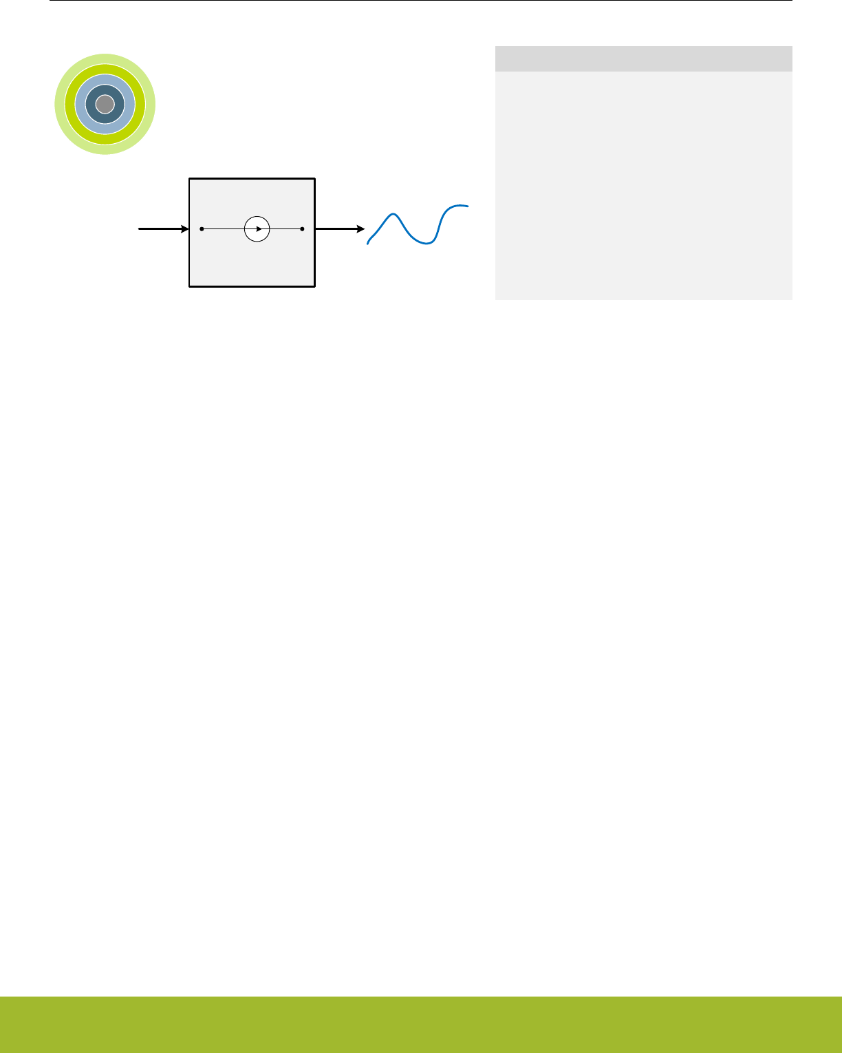
28. IDAC - Current Digital to Analog Converter
0 1 2 3 4
...1100101...
I
IDAC
Quick Facts
What?
The IDAC can sink or source a configurable con-
stant current.
Why?
The IDAC can be used to bias external circuits or (in
conjunction with the ADC) measure capacitance by
injecting a controlled current into a component.
How?
In addition to providing a constant current, the IDAC
can be switched on and off with a PRS signal all the
way down to EM3.
28.1 Introduction
The current digital to analog converter (IDAC) can source or sink a configurable constant current from APORT and/or main pad (OUT-
PAD). The current is configurable with several ranges of various step sizes.
28.2 Features
• Can source and sink current
• Programmable constant output current
• Selectable current range between 0.05 µA and 64 µA
• Each range is linearly programmable in 32 steps
• Support for current calibration
• Support for manual and PRS triggered output enable
• Available in EM0-EM3
Reference Manual
IDAC - Current Digital to Analog Converter
silabs.com | Smart. Connected. Energy-friendly. Preliminary Rev. 0.5 | 940
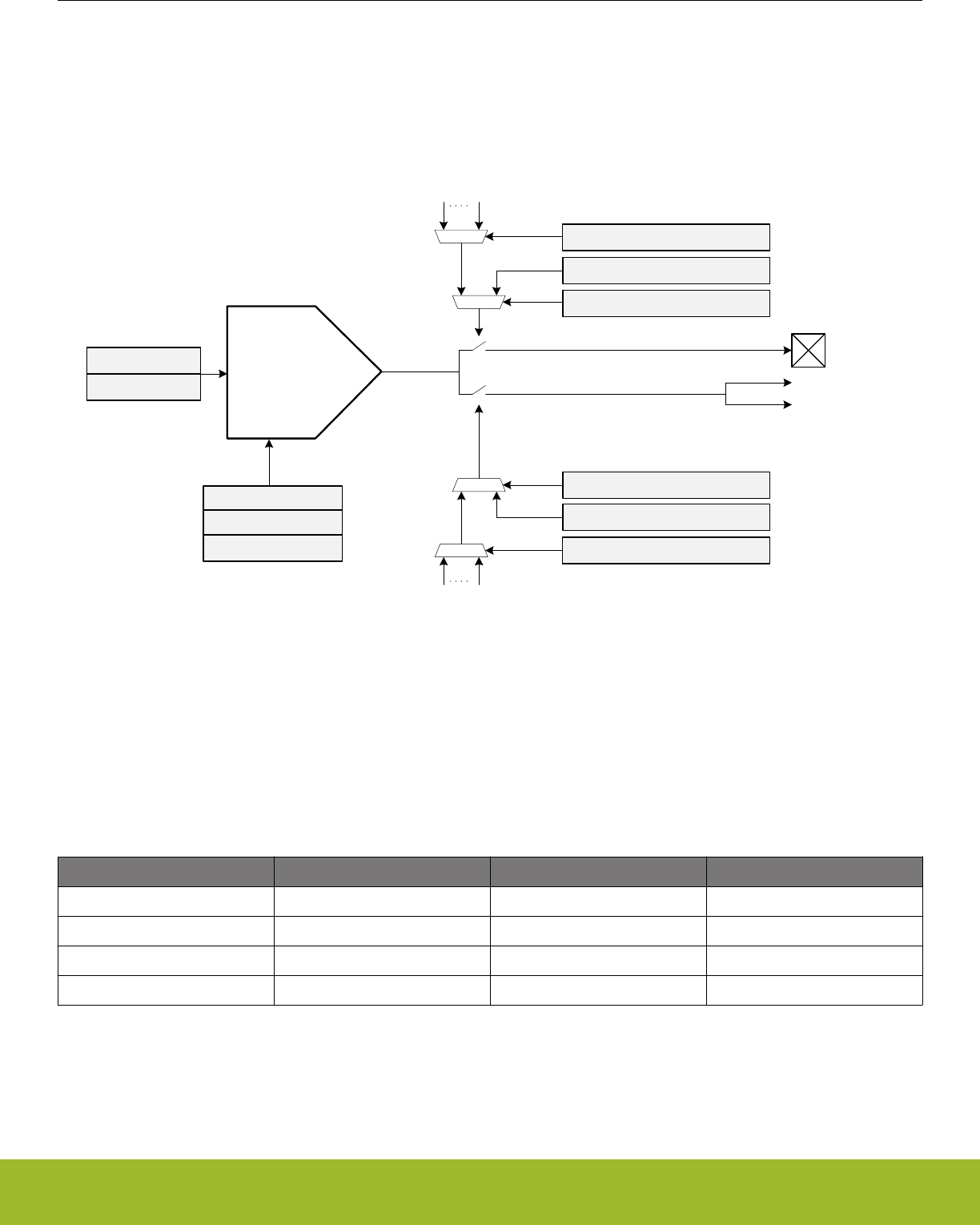
28.3 Functional Description
An overview of the IDAC module is shown in Figure 28.1 IDAC Overview on page 941. The IDAC is designed to source or sink a
programmable current which can be controlled by setting the range and the step in the RANGESEL and STEPSEL bitfields in
IDAC_CURRPROG register. The IDAC output enable can be controlled by software or PRS. The IDAC is enabled by setting EN in
IDAC_CTRL.
IDAC
OUTPAD
RANGESEL
STEPSEL
EN
CURSINK
Internal
output
PRSSEL
MINOUTTRANS
APORTOUTENPRS
APORTOUTEN
PRSCH0 PRSCHn
MAINOUTEN
PRSCH0 PRSCHn
PRSSEL
MAINOUTENPRS
APORT1Y
APORT1X
Figure 28.1. IDAC Overview
28.3.1 Current Programming
The four different current ranges can be selected by configuring the RANGESEL bitfield in IDAC_CURRPROG. The current output in
each range is linearly programmable in 32 steps, and is controlled by the STEPSEL bitfield in IDAC_CURRPROG. These current rang-
es and their step sizes are shown in Table 28.1 Range Selection on page 941.
Table 28.1. Range Selection
Range Select Range Value [µA] Step Size [nA] Step Counts
0 0.05 - 1.6 50 32
1 1.6 - 4.7 100 32
2 0.5 - 16 500 32
3 2 - 64 2000 32
28.3.2 IDAC Enable and Warm-up
The IDAC is enabled by setting the EN bit in IDAC_CTRL. When this bit is set, the IDAC must stabilize before its output current is
stable.
It is important to wait until the IDAC is warmed up, or until any current programming is complete and the output current is stabilized,
before entering EM1, EM2, or EM3.
Reference Manual
IDAC - Current Digital to Analog Converter
silabs.com | Smart. Connected. Energy-friendly. Preliminary Rev. 0.5 | 941

28.3.3 Output Control
The IDAC output enable is controlled separately for APORT and main pad. If APORTOUTENPRS/MAINOUTENPRS is set, output ena-
ble is controlled by PRS, else it is controlled by software via APORTOUTEN/MAINOUTEN.
28.3.4 APORT Configuration
The IDAC APORT outputs can be routed to pins through the APORT system. The pins are selected by requesting an APORT channel
in APORTOUTSEL in IDAC_CTRL. For mapping between APORT channel and physical pin, please refer to datasheet. The IDAC can
be in either master or slave mode when connecting to the APORT. By default the IDAC is in master mode. To enable slave mode, set
APORTMASTERDIS in IDAC_CTRL. As IDAC is only capable of driving an APORT channel, only master mode is meaningful for IDAC.
If the IDAC is in master mode, and another module is currently driving the requested channel, the APORTCONFLICT bitfield in
IDAC_STATUS will be set together with APORT1XCONFLICT or APORT1YCONFLICT in IDAC_APORTCONFLICT. The APORTCON-
FLICT can also be configured to trigger an interrupt, see 28.3.5 Interrupts for details.
28.3.5 Interrupts
The APORTCONFLICT interrupt flag in the IDAC_IF register indicates that a conflict has occurred when requesting a channel from the
APORT. The APORTCONFLICT interrupt can be enabled by setting the APORTCONFLICT bit in IDAC_IEN, or cleared by setting the
APORTCONFLICT bit in IDAC_IFC.
28.3.6 Minimizing Output Transition
If the internal output of the IDAC differs from the voltage at the output pin, enabling the output can cause an unwanted transition. To
minimize this transition, it is possible to charge or discharge the internal output node before enabling the output to the pin. Setting MIN-
OUTTRANS in IDAC_CTRL when the IDAC is sourcing current connects the internal node to GND. Alternatively, setting MINOUT-
TRANS when the IDAC is sinking current connects the internal output node to VDD. Setting APORTOUTEN/MAINOUTEN when MIN-
OUTTRANS is set will halt the charge/discharge until either APORTOUTEN/MAINOUTEN is cleared or MINOUTTRANS is cleared.
28.3.7 Duty Cycle Configuration
The references for the IDAC can be duty-cycled, meaning that it can source current at very low overhead current consumption at the
cost of response time and accuracy. By default duty-cycling is enabled in EM2 and EM3 and disabled in EM0 and EM1. Setting
EM2DUTYCYCLEDIS in IDAC_DUTYCONFIG will disable duty cycling in EM2 and EM3. Note that sinking current can not be done with
duty-cycled references so measures needs to be taken to always disable duty-cycling while sinking current.
28.3.8 Calibration
The IDAC can be calibrated to accurately compensate for process, supply voltage and temperature variations. During the production
test, the middle step of each range is calibrated at room temperature. The TUNING bitfield in the IDAC_CAL register can be used to do
further calibration of each step with an external resistor connected to IDAC_OUT. The calibrated tuning value for each band can be
read from the Device Information (DI) page.
Reference Manual
IDAC - Current Digital to Analog Converter
silabs.com | Smart. Connected. Energy-friendly. Preliminary Rev. 0.5 | 942
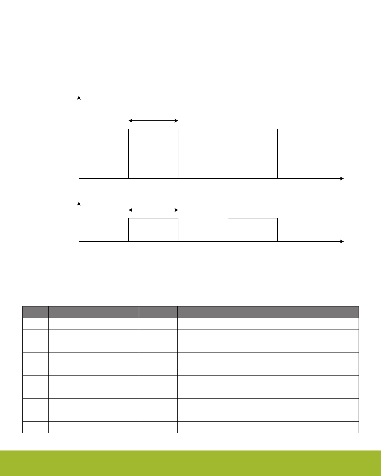
28.3.9 PRS Triggered Charge Injection
The amount of charge sourced or sunk by the IDAC can be controlled by the PRS (e.g., using a timer as producer) via the output
switch. Figure 28.2 IDAC Charge Injection Example on page 943 shows a case where the IDAC is configured to periodically supply
charge using the PRS. The amount of charge injected is proportional to the the period the IDAC is on. The total charge injected is the
current multiplied by the time the output switch is enabled.
The PRS system is enabled by setting APORTOUTENPRS/MAINOUTENPRS in IDAC_CTRL, and the PRS channel is selected by
PRSSEL in IDAC_CTRL. To generate the periodic control signal, the TIMER module can be used, by configuring for example a CC
channel to compare match with a configurable level.
I
T
OFF
ON
T
PRS input
Figure 28.2. IDAC Charge Injection Example
28.4 Register Map
The offset register address is relative to the registers base address.
Offset Name Type Description
0x000 IDAC_CTRL RW Control Register
0x004 IDAC_CURPROG RW Current Programming Register
0x00C IDAC_DUTYCONFIG RW Duty Cycle Configuration Register
0x018 IDAC_STATUS RStatus Register
0x020 IDAC_IF RInterrupt Flag Register
0x024 IDAC_IFS W1 Interrupt Flag Set Register
0x028 IDAC_IFC (R)W1 Interrupt Flag Clear Register
0x02C IDAC_IEN RW Interrupt Enable Register
0x034 IDAC_APORTREQ RAPORT Request Status Register
0x038 IDAC_APORTCONFLICT RAPORT Request Status Register
Reference Manual
IDAC - Current Digital to Analog Converter
silabs.com | Smart. Connected. Energy-friendly. Preliminary Rev. 0.5 | 943

28.5 Register Description
28.5.1 IDAC_CTRL - Control Register
Offset Bit Position
0x000
31
30
29
28
27
26
25
24
23
22
21
20
19
18
17
16
15
14
13
12
11
10
9
8
7
6
5
4
3
2
1
0
Reset
0x0
0
0
0
0
0
0
0x00
0
0
0
0
Access
RW
RW
RW
RW
RW
RW
RW
RW
RW
RW
RW
RW
Name
PRSSEL
MAINOUTENPRS
MAINOUTEN
APORTOUTENPRS
APORTMASTERDIS
EM2DELAY
PWRSEL
APORTOUTSEL
APORTOUTEN
MINOUTTRANS
CURSINK
EN
Bit Name Reset Access Description
31:24 Reserved To ensure compatibility with future devices, always write bits to 0. More information in 1.2 Conven-
tions
23:20 PRSSEL 0x0 RW IDAC Output Enable PRS channel Select
Selects which PRS channel to use to enable output.
Value Mode Description
0 PRSCH0 PRS Channel 0 selected.
1 PRSCH1 PRS Channel 1 selected.
2 PRSCH2 PRS Channel 2 selected.
3 PRSCH3 PRS Channel 3 selected.
4 PRSCH4 PRS Channel 4 selected.
5 PRSCH5 PRS Channel 5 selected.
6 PRSCH6 PRS Channel 6 selected.
7 PRSCH7 PRS Channel 7 selected.
8 PRSCH8 PRS Channel 8 selected.
9 PRSCH9 PRS Channel 9 selected.
10 PRSCH10 PRS Channel 10 selected.
11 PRSCH11 PRS Channel 11 selected.
19 MAINOUTENPRS 0 RW PRS Controlled Main Pad Output Enable
Enable PRS Control of IDAC Main Pad output enable.
Value Description
0 Main pad output enable controlled by IDAC_MAINOUTEN.
1 Main pad output enable controlled by PRS input selected by PRSSEL.
18 MAINOUTEN 0 RW Output Enable
Set to enable IDAC main output to pad if MAINOUTENPRS is not set.
Reference Manual
IDAC - Current Digital to Analog Converter
silabs.com | Smart. Connected. Energy-friendly. Preliminary Rev. 0.5 | 944

Bit Name Reset Access Description
17 Reserved To ensure compatibility with future devices, always write bits to 0. More information in 1.2 Conven-
tions
16 APORTOUTENPRS 0 RW PRS Controlled APORT Output Enable
Enable PRS Control of the IDAC APORT output enable.
Value Description
0 APORT output enable controlled by IDAC_APORTOUTEN.
1 APORT output enable controlled by PRS channel selected by
PRSSEL.
15 Reserved To ensure compatibility with future devices, always write bits to 0. More information in 1.2 Conven-
tions
14 APORTMASTERDIS 0 RW APORT Bus Master Disable
Determines if the IDAC will request the APORT bus selected by APORTOUTSEL. This bit allows multiple APORT connec-
ted devices to monitor the same APORT bus simultaneously by allowing the IDAC to not master the selected bus. When 1,
the determination is expected to be from another peripheral, and the IDAC only passively looks at the bus. When 1, the
selection of channel for a selected bus is ignored (the bus is not), and will be whatever selection the external device mas-
tering the bus has configured for the APORT bus.
Value Description
0 Bus mastering enabled
1 Bus mastering disabled
13 EM2DELAY 0 RW EM2 Delay
Delays EM2 entry until the IDAC output is stable
12 PWRSEL 0 RW Power Select
Selects the power source for the IDAC
Value Mode Description
0 ANA AVDD
1 IO IOVDD
11:4 APORTOUTSEL 0x00 RW APORT Output Select
Select output mode.
APORT1XCH0 0x20 APORT1X Channel 0
APORT1YCH1 0x21 APORT1Y Channel 1
APORT1XCH2 0x22 APORT1X Channel 2
APORT1YCH3 0x23 APORT1Y Channel 3
APORT1XCH4 0x24 APORT1X Channel 4
APORT1YCH5 0x25 APORT1Y Channel 5
. . . . . . . . .
APORT1XCH30 0x3e APORT1X Channel 30
APORT1YCH31 0x3f APORT1Y Channel 31
Reference Manual
IDAC - Current Digital to Analog Converter
silabs.com | Smart. Connected. Energy-friendly. Preliminary Rev. 0.5 | 945

Bit Name Reset Access Description
3 APORTOUTEN 0 RW APORT Output Enable
Set to enable the IDAC output to APORT if APORTOUTENPRS is not set.
2 MINOUTTRANS 0 RW Minimum Output Transition Enable
Set to enable minimum output transition mode for the IDAC.
1 CURSINK 0 RW Current Sink Enable
Set to enable the IDAC as a current sink. By default, the IDAC sources current.
0 EN 0 RW Current DAC Enable
Set to enable the IDAC.
28.5.2 IDAC_CURPROG - Current Programming Register
Offset Bit Position
0x004
31
30
29
28
27
26
25
24
23
22
21
20
19
18
17
16
15
14
13
12
11
10
9
8
7
6
5
4
3
2
1
0
Reset
0x9B
0x00
0x0
Access
RW
RW
RW
Name
TUNING
STEPSEL
RANGESEL
Bit Name Reset Access Description
31:24 Reserved To ensure compatibility with future devices, always write bits to 0. More information in 1.2 Conven-
tions
23:16 TUNING 0x9B RW Tune the current to given accuracy
In production test. the middle step (16) of each range is calibrated and can be read from the Device Information (DI) page.
15:13 Reserved To ensure compatibility with future devices, always write bits to 0. More information in 1.2 Conven-
tions
12:8 STEPSEL 0x00 RW Current Step Size Select
Select the step within each range. The size of each step depends on the RANGESEL setting. RANGESEL settings of 0, 1,
2, and 3 correspond to step sizes of 50 nA, 100 nA, 500 nA, and 2000 nA, respectively. See step details.
7:2 Reserved To ensure compatibility with future devices, always write bits to 0. More information in 1.2 Conven-
tions
1:0 RANGESEL 0x0 RW Current Range Select
Selects current range of the output.
Value Mode Description
0 RANGE0 Current range set to 0 - 1.6 uA.
1 RANGE1 Current range set to 1.6 - 4.7 uA.
2 RANGE2 Current range set to 0.5 - 16 uA.
3 RANGE3 Current range set to 2 - 64 uA.
Reference Manual
IDAC - Current Digital to Analog Converter
silabs.com | Smart. Connected. Energy-friendly. Preliminary Rev. 0.5 | 946

28.5.3 IDAC_DUTYCONFIG - Duty Cycle Configuration Register
Offset Bit Position
0x00C
31
30
29
28
27
26
25
24
23
22
21
20
19
18
17
16
15
14
13
12
11
10
9
8
7
6
5
4
3
2
1
0
Reset
0
Access
RW
Name
EM2DUTYCYCLEDIS
Bit Name Reset Access Description
31:2 Reserved To ensure compatibility with future devices, always write bits to 0. More information in 1.2 Conven-
tions
1 EM2DUTYCYCLE-
DIS
0 RW Duty Cycle Enable.
Set to disable duty cycling in EM2.
0 Reserved To ensure compatibility with future devices, always write bits to 0. More information in 1.2 Conven-
tions
28.5.4 IDAC_STATUS - Status Register
Offset Bit Position
0x018
31
30
29
28
27
26
25
24
23
22
21
20
19
18
17
16
15
14
13
12
11
10
9
8
7
6
5
4
3
2
1
0
Reset
0
Access
R
Name
APORTCONFLICT
Bit Name Reset Access Description
31:2 Reserved To ensure compatibility with future devices, always write bits to 0. More information in 1.2 Conven-
tions
1 APORTCONFLICT 0 R APORT Conflict Output
1 if any of the APORT BUSes being requested by the IDAC are also being requested by another peripheral
0 Reserved To ensure compatibility with future devices, always write bits to 0. More information in 1.2 Conven-
tions
Reference Manual
IDAC - Current Digital to Analog Converter
silabs.com | Smart. Connected. Energy-friendly. Preliminary Rev. 0.5 | 947

28.5.5 IDAC_IF - Interrupt Flag Register
Offset Bit Position
0x020
31
30
29
28
27
26
25
24
23
22
21
20
19
18
17
16
15
14
13
12
11
10
9
8
7
6
5
4
3
2
1
0
Reset
0
Access
R
Name
APORTCONFLICT
Bit Name Reset Access Description
31:2 Reserved To ensure compatibility with future devices, always write bits to 0. More information in 1.2 Conven-
tions
1 APORTCONFLICT 0 R APORT Conflict Interrupt Flag
1 if any of the APORT BUSes being requested by the IDAC are also being requested by another peripheral
0 Reserved To ensure compatibility with future devices, always write bits to 0. More information in 1.2 Conven-
tions
28.5.6 IDAC_IFS - Interrupt Flag Set Register
Offset Bit Position
0x024
31
30
29
28
27
26
25
24
23
22
21
20
19
18
17
16
15
14
13
12
11
10
9
8
7
6
5
4
3
2
1
0
Reset
0
Access
W1
Name
APORTCONFLICT
Bit Name Reset Access Description
31:2 Reserved To ensure compatibility with future devices, always write bits to 0. More information in 1.2 Conven-
tions
1 APORTCONFLICT 0 W1 Set APORTCONFLICT Interrupt Flag
Write 1 to set the APORTCONFLICT interrupt flag
0 Reserved To ensure compatibility with future devices, always write bits to 0. More information in 1.2 Conven-
tions
Reference Manual
IDAC - Current Digital to Analog Converter
silabs.com | Smart. Connected. Energy-friendly. Preliminary Rev. 0.5 | 948

28.5.7 IDAC_IFC - Interrupt Flag Clear Register
Offset Bit Position
0x028
31
30
29
28
27
26
25
24
23
22
21
20
19
18
17
16
15
14
13
12
11
10
9
8
7
6
5
4
3
2
1
0
Reset
0
Access
(R)W1
Name
APORTCONFLICT
Bit Name Reset Access Description
31:2 Reserved To ensure compatibility with future devices, always write bits to 0. More information in 1.2 Conven-
tions
1 APORTCONFLICT 0 (R)W1 Clear APORTCONFLICT Interrupt Flag
Write 1 to clear the APORTCONFLICT interrupt flag. Reading returns the value of the IF and clears the corresponding inter-
rupt flags (This feature must be enabled globally in MSC.).
0 Reserved To ensure compatibility with future devices, always write bits to 0. More information in 1.2 Conven-
tions
28.5.8 IDAC_IEN - Interrupt Enable Register
Offset Bit Position
0x02C
31
30
29
28
27
26
25
24
23
22
21
20
19
18
17
16
15
14
13
12
11
10
9
8
7
6
5
4
3
2
1
0
Reset
0
Access
RW
Name
APORTCONFLICT
Bit Name Reset Access Description
31:2 Reserved To ensure compatibility with future devices, always write bits to 0. More information in 1.2 Conven-
tions
1 APORTCONFLICT 0 RW APORTCONFLICT Interrupt Enable
Enable/disable the APORTCONFLICT interrupt
0 Reserved To ensure compatibility with future devices, always write bits to 0. More information in 1.2 Conven-
tions
Reference Manual
IDAC - Current Digital to Analog Converter
silabs.com | Smart. Connected. Energy-friendly. Preliminary Rev. 0.5 | 949

28.5.9 IDAC_APORTREQ - APORT Request Status Register
Offset Bit Position
0x034
31
30
29
28
27
26
25
24
23
22
21
20
19
18
17
16
15
14
13
12
11
10
9
8
7
6
5
4
3
2
1
0
Reset
0
0
Access
R
R
Name
APORT1YREQ
APORT1XREQ
Bit Name Reset Access Description
31:4 Reserved To ensure compatibility with future devices, always write bits to 0. More information in 1.2 Conven-
tions
3 APORT1YREQ 0 R 1 if the bus connected to APORT1Y is requested
Reports if the bus connected to APORT1Y is being requested by the APORT
2 APORT1XREQ 0 R 1 if the APORT bus connected to APORT1X is requested
Reports if the bus connected to APORT1X is being requested by the APORT
1:0 Reserved To ensure compatibility with future devices, always write bits to 0. More information in 1.2 Conven-
tions
28.5.10 IDAC_APORTCONFLICT - APORT Request Status Register
Offset Bit Position
0x038
31
30
29
28
27
26
25
24
23
22
21
20
19
18
17
16
15
14
13
12
11
10
9
8
7
6
5
4
3
2
1
0
Reset
0
0
Access
R
R
Name
APORT1YCONFLICT
APORT1XCONFLICT
Bit Name Reset Access Description
31:4 Reserved To ensure compatibility with future devices, always write bits to 0. More information in 1.2 Conven-
tions
3 APORT1YCONFLICT 0 R 1 if the bus connected to APORT1Y is in conflict with another pe-
ripheral
Reports if the bus connected to APORT1Y is is also being requested by another peripheral
2 APORT1XCONFLICT 0 R 1 if the bus connected to APORT1X is in conflict with another pe-
ripheral
Reports if the bus connected to APORT1X is is also being requested by another peripheral
1:0 Reserved To ensure compatibility with future devices, always write bits to 0. More information in 1.2 Conven-
tions
Reference Manual
IDAC - Current Digital to Analog Converter
silabs.com | Smart. Connected. Energy-friendly. Preliminary Rev. 0.5 | 950
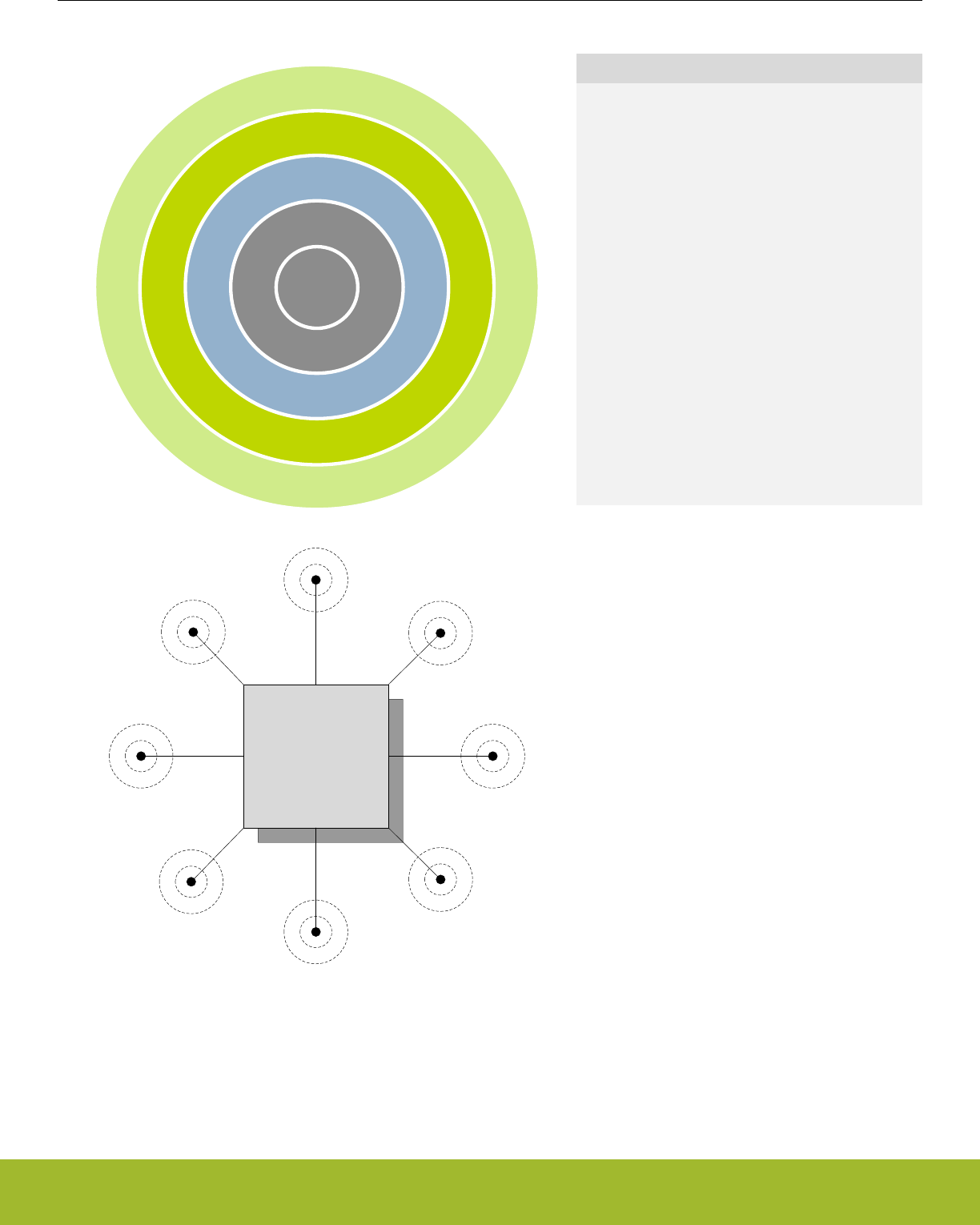
29. LESENSE - Low Energy Sensor Interface
0 1 2 3 4
Gecko
ZZZZZ
Quick Facts
What?
LESENSE is a low energy sensor interface capable
of autonomously collecting and processing data from
multiple sensors even when in EM2. Flexible config-
uration makes LESENSE a versatile sensor inter-
face compatible with a wide range of sensors and
measurement schemes.
Why?
Capability to autonomously monitor sensors allows
the EFR32xG13 Wireless Gecko to reside in a low
energy mode for long periods of time while keeping
track of sensor status and sensor events.
How?
LESENSE is highly configurable and is capable of
collecting data from a wide range of sensor types.
Once the data is collected, the programmable state
machine, LESENSE decoder, is capable of process-
ing sensor data without CPU intervention. A large re-
sult buffer allows the chip to remain in EM2 for long
periods of time while autonomously collecting data.
Reference Manual
LESENSE - Low Energy Sensor Interface
silabs.com | Smart. Connected. Energy-friendly. Preliminary Rev. 0.5 | 951

29.1 Introduction
LESENSE is a low energy sensor interface utilizing on-chip peripherals to perform measurement of a configurable set of sensors. The
sensor measurements results can be processed by the LESENSE decoder, a configurable state machine with up to 32 states. The re-
sults can also be stored in a result buffer to be collected by the CPU or DMA for further processing.
LESENSE operates from EM0 down to EM2, and can wake up the CPU on configurable events.
29.2 Features
• Up to 16 sensors
• Autonomous sensor monitoring in EM0, EM1, and EM2
• Highly configurable decoding of sensor results
• Interrupt on sensor events
• Configurable enable signals to external sensors
• Circular buffer for storage of up to 16 sensor results
• Multiple evaluation modes minimize the need for software interaction
• Supports ADC sampling and evaluation
• Support for multiple sensor types
• LC sensors
• Capacitive sensing
• General analog sensors
Reference Manual
LESENSE - Low Energy Sensor Interface
silabs.com | Smart. Connected. Energy-friendly. Preliminary Rev. 0.5 | 952
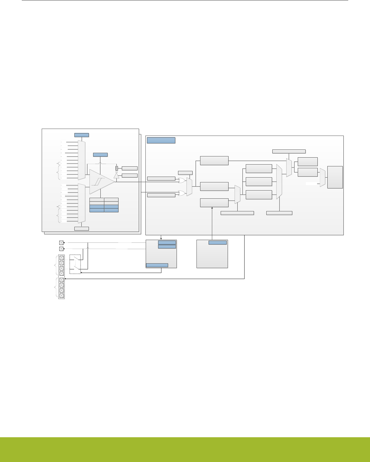
29.3 Functional description
The LESENSE module is capable of controlling on-chip peripherals in order to perform monitoring of different sensors with little or no
CPU intervention. LESENSE uses the analog comparators (ACMP) or the ADC for measurement of sensor signals. LESENSE can also
control the VDAC to generate accurate reference voltages. Figure 29.1 LESENSE block diagram on page 953 shows an overview of
the LESENSE module.
The LESENSE module consists of a sequencer, an evaluation block, a decoder, and a RAM block:
• The sequencer handles interaction with other peripherals and controls timing of sensor measurements. It also includes a counter
that can be used to count pulses on the ACMP output.
• The evaluation block is used to process the data collected by the sequencer.
• To autonomously analyze sensor results, the LESENSE decoder provides the ability to define a finite state machine with up to 32
states, as well as define programmable actions upon state transitions. This allows the decoder to implement a wide range of decod-
ing schemes, such as quadrature decoding.
• A RAM block is used for storage of configuration and measurement results. This allows LESENSE to have a relatively large result
buffer enabling the chip to remain in a low energy mode for long periods of time while collecting sensor data.
DAC0 ADC0
LESENSE
ACMP1
ACMP0
Register bitfields
overridden by LESENSE
CH0
CH1
DAC0_CH0
DAC0_CH1
GND
VADIV
VBDIV
BUS1
BUS2
BUS3
BUS4
BUS0
-
+
APORT
VLP
POSSEL
EN
NEGSEL
DAC0
DAC1
GND
VADIV
VBDIV
BUS1
BUS2
BUS3
BUS4
BUS0
APORT
VLP
DAC0
DAC1
Dedicated
Dedicated
HYST0
DIVVA0
DIVVB0
HYST1
DIVVA1
DIVVB1
BIASPROG FULLBIAS
CSRESEN
CSRESSEL
PERCTRL_ACMP0INV
CURCH[3]
Saturating counter
ACMP sample register
ADC sample register
CH_INTERACT_SAMPLE
PERCTRL_ACMP1INV Threshold compare
Sliding window
Step Detect
CH_EVAL_MODE
LESENSE
DECODER
SCANRES
SENSORSTATE
PRS input
SCANMASK
CHnDATA
CHnCTRL_EN
LES_CHn
LES_ALTEXn
OPAnOUT_PEN
CH_INTERACT_SAMPLE
Figure 29.1. LESENSE block diagram
Reference Manual
LESENSE - Low Energy Sensor Interface
silabs.com | Smart. Connected. Energy-friendly. Preliminary Rev. 0.5 | 953

29.3.1 Channel Configuration
LESENSE has 16 individually configurable channels, each with its own set of configuration registers. Channel configuration is split into
three registers; CHx_TIMING, CHx_INTERACT, and CHx_EVAL. Individual timing for each sensor is configured in CHx_TIMING, sen-
sor interaction is configured in CHx_INTERACT, and configurations regarding evaluation of the measurements are done in CHx_EVAL.
For improved readability, CHx_CONF will be used to refer to the channel configuration registers (CHx_TIMING, CHx_INTERACT, and
CHx_EVAL) throughout this chapter.
By default, the channel configuration registers are directly mapped to the channel number. Configuring SCANCONF in CTRL makes it
possible to alter this mapping.
Configuring SCANCONF to INVMAP will make channels 0-7 use the channel configuration registers for channels 8-15, and vice versa.
This feature allows an application to quickly and easily switch the configuration set for the channels.
Setting SCANCONF to TOGGLE will make channel x alternate between using CHX_CONF and CHX+8_CONF. The configuration used
is decided by the state of the corresponding bit in SCANRES. For instance, if channel 3 is performing a scan and bit 3 in SCANRES is
set, CH11_CONF will be used. Channels 8 through 15 will toggle between CHX_CONF and CHX-8_CONF. This mode provides an easy
way to implement hysteresis on channel events, as threshold values can be changed depending on the sensor status.
Setting SCANCONF to DECDEF will make the state of the decoder define which scan configuration to be used. If the decoder state is
at index 16 or higher, channel x will use CHX+8_CONF, otherwise it will use CHX_CONF. Similarly, channels 8 through 15 will use
CHX_CONF when the decoder state index is less than 8 and CHX-8_CONF when the decoder state index is higher than 7. Allowing the
decoder state to define which configuration to use enables easy implementation of hysteresis, for example, as different threshold values
can be used for the same channel depending on the state of the application. Table 29.1 LESENSE scan configuration selection on page
954 summarizes how channel configuration is selected for different settings of SCANCONF.
Table 29.1. LESENSE scan configuration selection
LESENSE
channel x
SCANCONF
DIRMAP INVMAP TOGGLE DECDEF
SCANRES[n] = 0 SCANRES[n] = 1 DECSTATE < 16 DECSTATE >= 16
0 <= x < 8 CHx_CONF CHx+8_CONF CHx_CONF CHx+8_CONF CHx_CONF CHx+8_CONF
8 <= x < 16 CHx_CONF CHx-8_CONF CHx_CONF CHx-8_CONF CHx_CONF CHx-8_CONF
Channels are enabled in the CHEN register, where bit x enables channel x. During a scan, all enabled channels are measured, starting
with the lowest indexed channel. Figure 29.3 Scan sequence on page 955 illustrates a scan sequence with channels 3, 5, and 9 ena-
bled.
Reference Manual
LESENSE - Low Energy Sensor Interface
silabs.com | Smart. Connected. Energy-friendly. Preliminary Rev. 0.5 | 954

29.3.2 Scan Sequence
LESENSE runs on LFACLKLESENSE, which is a prescaled version of LFACLK. The prescaling factor for LFACLKLESENSE is selected in
the CMU, available prescaling factors are:
• DIV1: LFACLKLESENSE = LFACLK/1
• DIV2: LFACLKLESENSE = LFACLK/2
• DIV4: LFACLKLESENSE = LFACLK/4
• DIV8: LFACLKLESENSE = LFACLK/8
All enabled channels are scanned each scan period. How a new scan is started is configured in the SCANMODE bit field in CTRL. If set
to PERIODIC, the scan frequency is generated using a counter which is clocked by LFACLKLESENSE. This counter has its own prescal-
er. This prescaling factor is configured in PCPRESC in TIMCTRL. A new scan sequence is started each time the counter reaches the
top value, PCTOP. The scan frequency is calculated using Figure 29.2 Scan frequency on page 955. If SCANMODE is set to ONE-
SHOT, a single scan will be made when START in CMD is set. To start a new scan on a PRS event, set SCANMODE to PRS and
configure PRS channel in PRSSEL. The PRS start signal needs to be active for at least one LFACLKLESENSE cycle to make sure LE-
SENSE is able to register it.
Fscan = LFACLKLESENSE/((1 + PCTOP)*2PCPRESC)
Figure 29.2. Scan frequency
It is possible to interleave additional sensor measurements in between the periodic scans. Issuing a start command when LESENSE is
idle will immediately start a new scan, without disrupting the frequency of the periodic scans. If the period counter overflows during the
interleaved scan, the periodically scheduled scan will start immediately after the interleaved scan completes.
CH3 CH5 CH9 CH3 CH5 CH9
START START
Scan period
Figure 29.3. Scan sequence
Reference Manual
LESENSE - Low Energy Sensor Interface
silabs.com | Smart. Connected. Energy-friendly. Preliminary Rev. 0.5 | 955
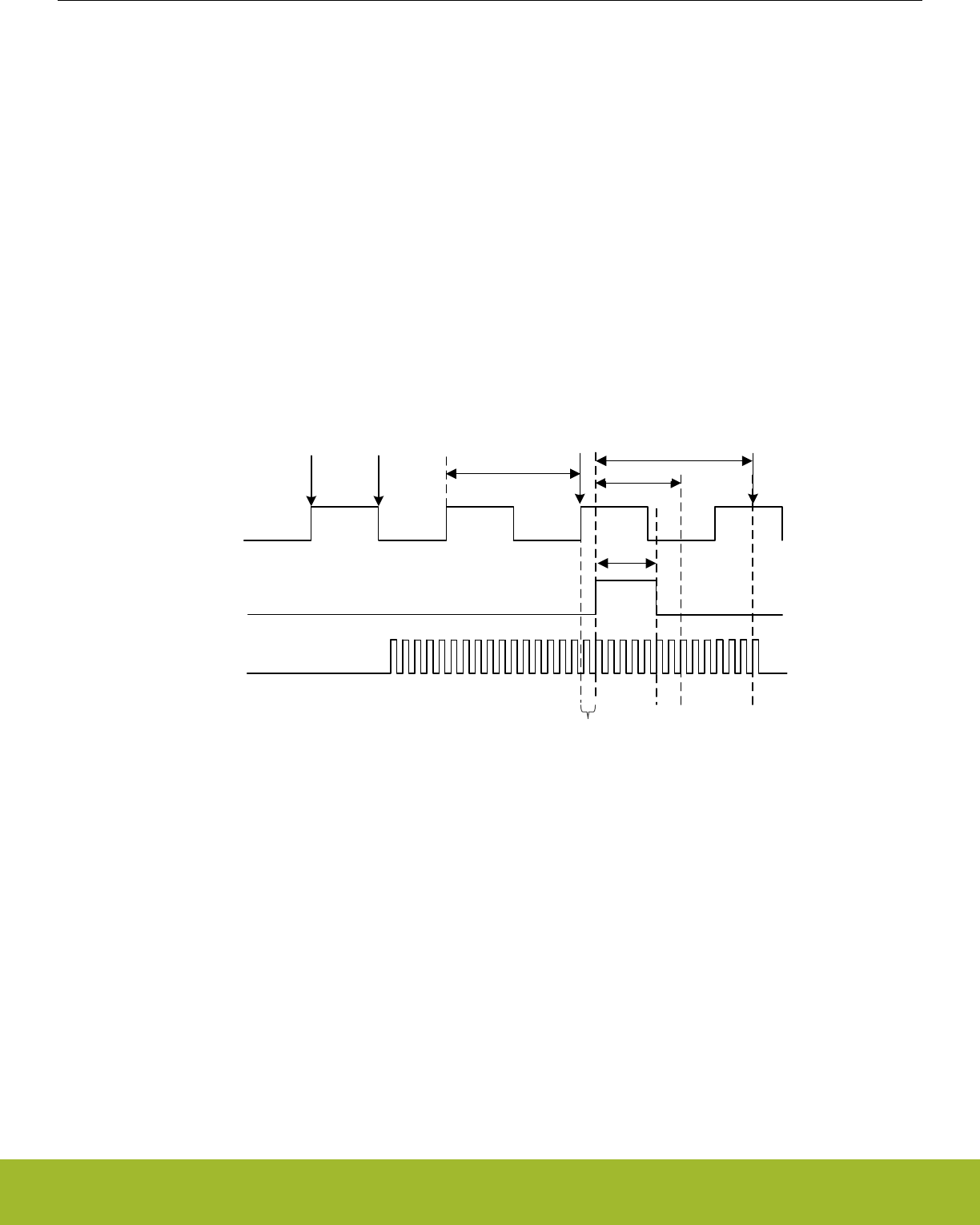
29.3.3 Sensor Timing
For each channel in the scan sequence, the LESENSE interface goes through three phases: idle, excite, and measure. The durations
of the excite and measure phases are configured in the CHx_TIMING registers. The excite phase duration can be configured to be
either a number of AUXHFRCO cycles or a number of LFACLKLESENSE cycles, depending on which one is selected by the EXCLK bit in
the CHx_INTERACT register. LESENSE includes two timers: A low frequency timer, running on LFACLKLESENSE, and a high frequency
timer, running on AUXHFRCO. The low frequency or high frequency timers can be prescaled by configuring LFPRESC or AUXPRESC,
respectively, in the TIMCTRL register. The duration of the measure phase is programmed via MEASUREDLY and SAMPLEDLY in the
CHx_TIMING registers. The output of the ACMP will be ignored for MEASUREDLY EXCLK cycles after start of the sensor measure-
ment. Sampling of the sensor will happen after SAMPLEDLY LFACLKLESENSE, or AUXHFRCO cycles, depending on the configuration
of the SAMPLECLK in the CHx_INTERACT register. The configurable measure- and sample delays enables LESENSE to easily define
exact time windows for sensor measurements. A start delay can be inserted before sensor measurement begin by configuring
STARTDLY in TIMCTRL. This delay can be used to ensure that the VDAC conversion is done and voltages have stabilized before the
sensor measurement begins. The AUXHFRCO startup can be delayed until the system enters the excite phase, by configuring AUX-
STARTUP in TIMCTRL to ONDEMAND. This will reduce the time the AUXHFRCO is enabled and reduce power consumption, with the
tradeoff that that the starting point for high frequency timing will also be delayed the same amount as the AUXHFRCO startup time.
Figure 29.4 Timing diagram, AUXHFRCO based timing on page 956 depicts a sensor sequence with AUXHFRCO based timing (EX-
TIME=5, MEASUREDLY=7, SAMPLEDLY=13), while Figure 29.5 Timing diagram, LFACLK based timing on page 957 depicts a se-
quence with LFACLKLESENSE based timing (EXTIME=1, MEASUREDLY=1, SAMPLEDLY=2).
EXCITE
SAMPLE
LFACLKLESENSE
Idle phase Excite phase Idle phase
SAMPLEDLY
Measure phase
START
AUXHFRCO
INIT
STARTDLY
MEASUREDLY
DAC refresh start
Synchronization
delay
EXTIME
Figure 29.4. Timing diagram, AUXHFRCO based timing
Reference Manual
LESENSE - Low Energy Sensor Interface
silabs.com | Smart. Connected. Energy-friendly. Preliminary Rev. 0.5 | 956
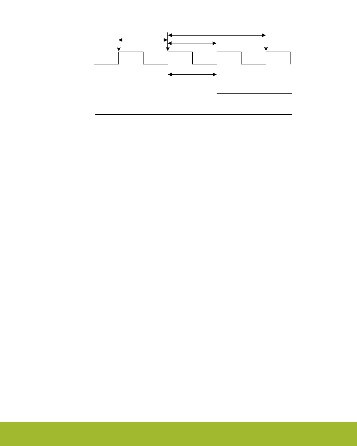
EXCITE
SAMPLE
LFACLKLESENSE
Idle phase Excite phase Idle phase
SAMPLEDLY
Measure phase
START
AUXHFRCO
INIT
STARTDLY
MEASUREDLY
EXTIME
Figure 29.5. Timing diagram, LFACLK based timing
Reference Manual
LESENSE - Low Energy Sensor Interface
silabs.com | Smart. Connected. Energy-friendly. Preliminary Rev. 0.5 | 957

29.3.4 Sensor Interaction
Many sensor types require some type of excitation in order to work. The LESENSE module can generate a variety of sensor stimuli,
both on the same pin as the measurement is to be made on, as well as alternative pins.
By default, excitation is performed on the pin associated with the channel (i.e., excitation and sensor measurement is performed on the
same pin). The mode of the pin during the excitation phase is configured by the EXMODE bitfield in CHx_INTERACT. The available
modes during the excite phase are:
• DISABLED: The pin is disabled.
• HIGH: The pin is driven high.
• LOW: The pin is driven low.
• DACOUT: The pin is connected to the output of a VDAC channel.
Note:
Excitation with VDAC output is only available on some channels. Refer to 29.3.9 VDAC Interface for details.
If the VDAC is in opamp-mode, setting EXMODE to DACOUT will result in excitation with output from the opamp.
LESENSE is able to perform sensor excitation on a pin other than the one being measured. When ALTEX in CHx_INTERACT is set,
the excitation will occur on the alternative excite pin associated with the given channel. By default, the alternative excite pins are map-
ped to the LES_ALTEX pins, but they can also be mapped to LESENSE CHX+8 mod 16. Mapping of the alternative excite pins is config-
ured in ALTEXMAP in the CTRL register. Table 29.2 LESENSE excitation pin mapping on page 958 summarizes the mapping of exci-
tation pins for different configurations.
Table 29.2. LESENSE excitation pin mapping
LESENSE channel
ALTEX = 0 ALTEX = 1
ALTEXMAP = CH ALTEXMAP = ALTEX
0 LES_CH0 LES_CH8 LES_ALTEX0
1 LES_CH1 LES_CH9 LES_ALTEX1
2 LES_CH2 LES_CH10 LES_ALTEX2
3 LES_CH3 LES_CH11 LES_ALTEX3
4 LES_CH4 LES_CH12 LES_ALTEX4
5 LES_CH5 LES_CH13 LES_ALTEX5
6 LES_CH6 LES_CH14 LES_ALTEX6
7 LES_CH7 LES_CH15 LES_ALTEX7
8 LES_CH8 LES_CH0 LES_ALTEX0
9 LES_CH9 LES_CH1 LES_ALTEX1
10 LES_CH10 LES_CH2 LES_ALTEX2
11 LES_CH11 LES_CH3 LES_ALTEX3
12 LES_CH12 LES_CH4 LES_ALTEX4
13 LES_CH13 LES_CH5 LES_ALTEX5
14 LES_CH14 LES_CH6 LES_ALTEX6
15 LES_CH15 LES_CH7 LES_ALTEX7
Figure 29.6 Pin sequencing on page 959 illustrates the sequencing of the pin associated with the active channel and its alternative
excite pin.
Reference Manual
LESENSE - Low Energy Sensor Interface
silabs.com | Smart. Connected. Energy-friendly. Preliminary Rev. 0.5 | 958
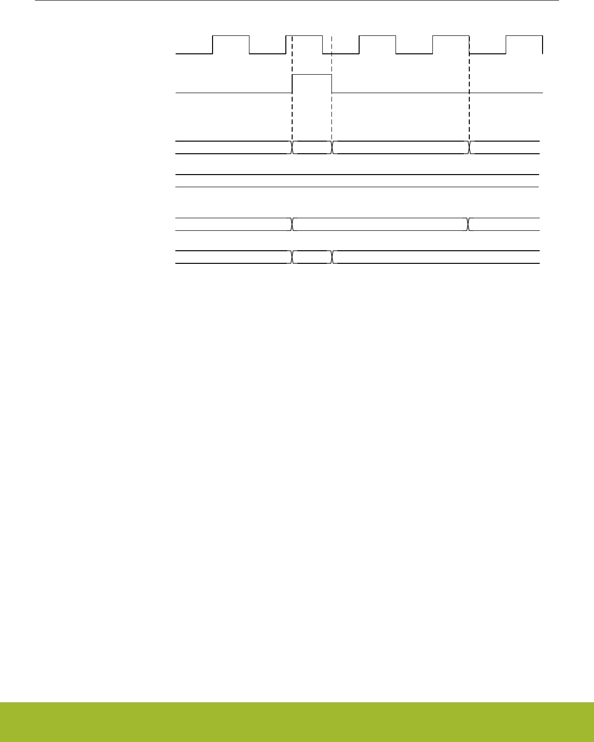
EXCITE
LFACLKLESENSE
Idle phase Excite phase Idle phase
Measure phase
IDLECONF EXMODE Z IDLECONF
Channel pin
IDLECONF
Alternate excite pin
IDLECONF EXMODE IDLECONF
Alternate excite pin
IDLECONF Z IDLECONF
Channel pin
ALTEX=1
ALTEX=0
Figure 29.6. Pin sequencing
The LES_ALTEXn pins have the ability to excite regardless of what channel is active. Setting AEXn in ALTEXCONF will make LES_AL-
TEXn excite for all channels using alternative excitation (i.e., ALTEX in CHx_INTERACT is set).
Note:
When exciting on the pin associated with the active channel, the pin will go through a tri-stated phase before returning to the idle config-
uration. This will not happen on pins used as alternative excitation pins.
The pin configuration for the idle phase can be configured individually for each LESENSE channel and alternative excite pin in the
IDLECONF and ALTEXCONF registers. The modes available are the same as the modes available in the excitation phase. In the
measure phase, the pin mode on the active channel is always disabled (analog input).
To allow the LESENSE mode to control a GPIO pin, the pin must be enabled in the ROUTEPEN register and configured as push-pull.
The IDLECONF configuration should not be altered while the pin enable for a given pin is set in ROUTEPEN.
29.3.5 Sensor Sampling
During the measurement phase, LESENSE can sample data from sensors using either the ADC or ACMP. This is configured in
CHx_INTERACT_SAMPLE. If the ACMP is used, LESENSE can evaluate the ACMP output at a single point in time (CHx_INTER-
ACT_SAMPLE = ACMP), or count pulses on the ACMP output (CHx_INTERACT_SAMPLE = ACMPCOUNT) for a programmable peri-
od of time.
LESENSE includes the ability to sample both analog comparators simultaneously, effectively cutting the time spent on sensor interac-
tion in some applications in half. Setting DUALSAMPLE in CTRL enables this mode. In dual sample mode, channels X and X+8 are
paired, meaning they will be sampled at the same time. DUALSAMPLE mode only works when CHx_INTERACT_SAMPLE is set to
ACMP.
If the ADC is used, LESENSE will initiate ADC conversions and fetch the ADC data for further evaluation. If the ADC is configured in
differential mode, CHx_INTERACT_SAMPLE must be set to ADCDIFF. In this mode, the output from the ADC and the threshold used
for comparison are given in two's complement notation.
See sections29.3.12 ADC Interface and 29.3.10 ACMP Interface for more details on the LESENSE interface to the ADC and ACMPs.
The sampled data from ADC or ACMP will be referred to as sensor data in the remainder of this manual.
Reference Manual
LESENSE - Low Energy Sensor Interface
silabs.com | Smart. Connected. Energy-friendly. Preliminary Rev. 0.5 | 959
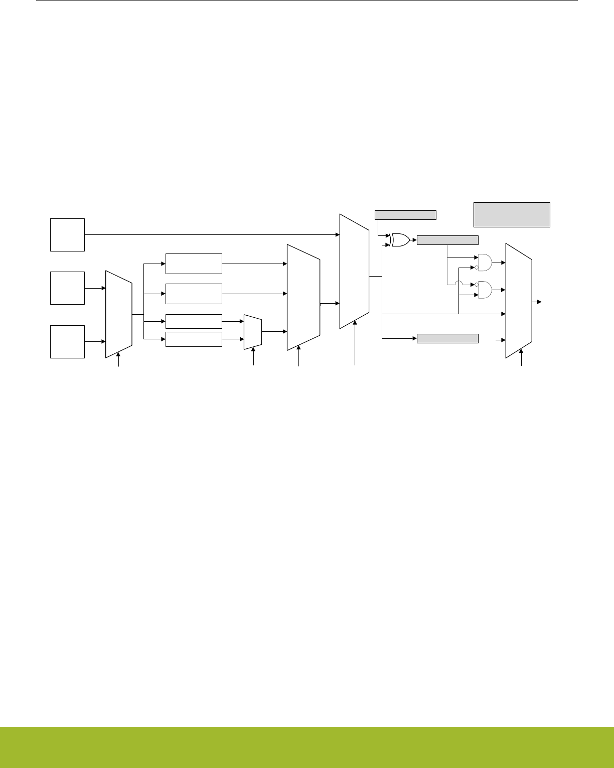
29.3.6 Sensor Evaluation
When a measurement phase is completed, the sensor data is evaluated by the evaluation block. If the sensor data is taken from ACMP
sample in a single point in time (CHx_INTERACT_SAMPLE = ACMP), the evaluation is limited to determining if the sensor data is 0 or
1. For the other sample modes, there are three ways to do sensor evaluation; threshold comparison, sliding window, or step detection.
Evaluation mode is configured in CHx_EVAL_MODE.
If the evaluation of sensor data evaluates to true, the corresponding bit in the result register (SCANRES) is set. By configuring SETIF in
CHx_INTERACT, interrupt flags can also be set on SCANRES events. Figure 29.7 Scan result and interrupt generation on page 960
illustrates how the sensor data or ACMP sample is used for evaluation and interrupt generation.
Note:
For initialization purposes, SCANRES can be written by software. SCANRES should not be written while LESENSE is running (i.e., the
RUNNING bit in LESENSE_STATUS is high).
ACMP
sample
LESENSE
counter
ACMP
COUNTER,
ADC,
ADCDIFF
CHx_EVAL_SCANRESINV
>= COMPTHRES
< COMPTHRES
GE
LESS
CHx_EVAL_COMP CHx_INTERACT_SAMPLE
NONE
LEVEL
POSEDGE
NEGEDGE
CHx_INTERACT_SETIF
0
Set
interrupt
flag
SCANRES[x]
SENSORSTATE*
THRES
SLIDINGWIN
CHx_EVAL_MODE
STEPDET
ADC data
COUNTER
ADC,
ADCDIFF
CHx_INTERACT_SAMPLE
Window state
STEP_UP/
STEP_DOWN
*In STEPDET mode, both step
direction and step/no step is stored
in SENSORSTATE
Figure 29.7. Scan result and interrupt generation
The results from sensor data evaluation can be fed into the decoder through the SENSORSTATE register. In DUALSAMPLE mode,
results from both the sampled ACMPs will be stored in both SCANRES and SENSORSTATE.
29.3.6.1 Threshold comparison
In threshold comparison mode, the sensor data is compared to a threshold configured in CHx_EVAL_COMPTHRES. There are two
modes of threshold comparison: 'less than' and 'greater than or equal'. Threshold comparison mode is configured in CHx_EVAL_COMP.
Reference Manual
LESENSE - Low Energy Sensor Interface
silabs.com | Smart. Connected. Energy-friendly. Preliminary Rev. 0.5 | 960
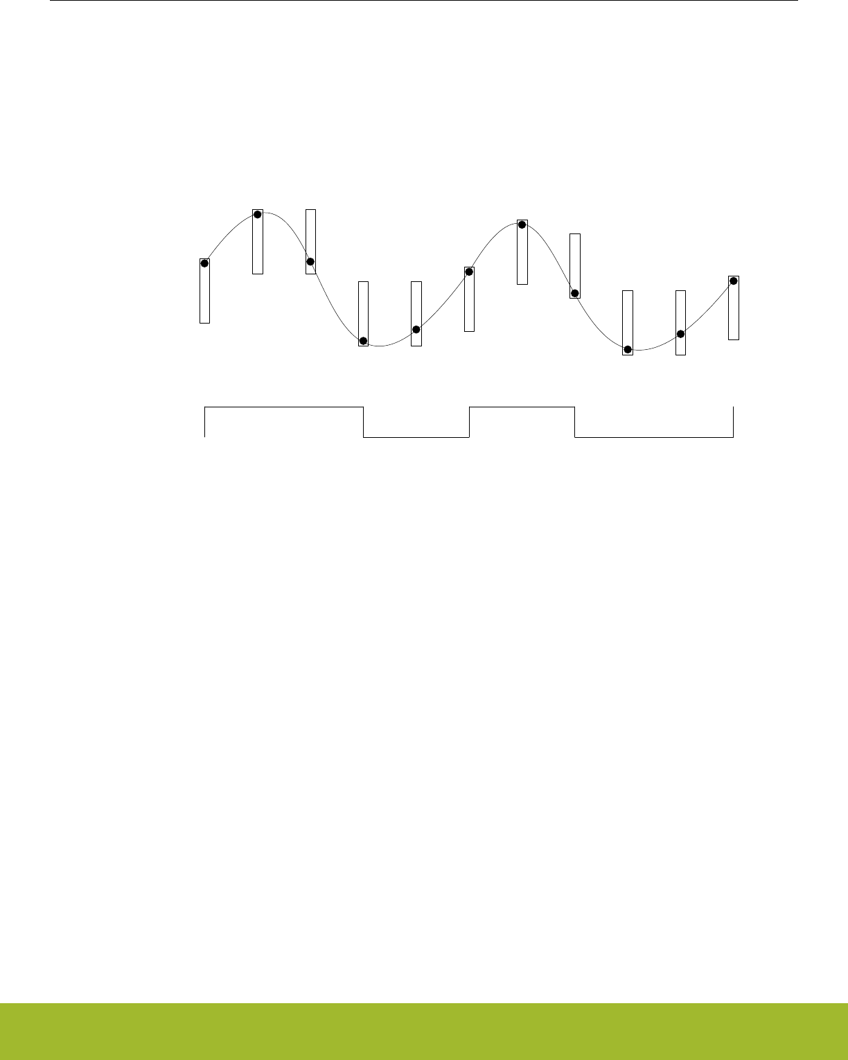
29.3.6.2 Sliding window
In sliding window mode, the sensor data is compared against the upper and lower limits of a window range. The window is defined by a
base, given by CHx_EVAL_COMPTHRES, and a size configured in EVALCTRL_WINSIZE. The window size is constant and the same
for all LESENSE channels, while the base is specific to each channel and will be updated by LESENSE when the sensor data is outside
the current window range. If the sensor data is within the window range, the sensor evaluation will remain the same as it was for the
previous measurement. If the sensor data is below the window range, the measurement will be evaluated to false. If the sensor data is
above the window range, the measurement will be evaluated to true. In both cases, the window base in CHx_EVAL_COMPTHRES will
be updated to reflect the new window range. Figure 29.8 Sliding window on page 961 shows how the sliding window evaluation mode
can be used to implement a system with two self calibrating thresholds.
SCANRES
Sensor data
Figure 29.8. Sliding window
29.3.6.3 Step detection
Step detection is used to detect steps in the sensor data compared to sensor data from the previous measurement. The size of the step
is configured in EVALCTRL_WINSIZE. In this mode, step up and step down are evaluated as described in Figure 29.9 Step detection
on page 961:
STEP_UP = SENSORDATAi >= SENSORDATAi-1 + EVALCTRL_WINSIZE
STEP_DOWN = SENSORDATAi < SENSORDATAi-1 - EVALCTRL_WINSIZE
Figure 29.9. Step detection
If either a step up or a step down is detected, the SCANRES bit for the active channel will be set. In addition, the STEPDIR bit for the
channel will be updated to indicate if a step up or a step down was detected. STEPDIR = 1 indicates a step up. In this mode, previous
sensor data is stored in CHx_EVAL_COMPTHRES.
Reference Manual
LESENSE - Low Energy Sensor Interface
silabs.com | Smart. Connected. Energy-friendly. Preliminary Rev. 0.5 | 961
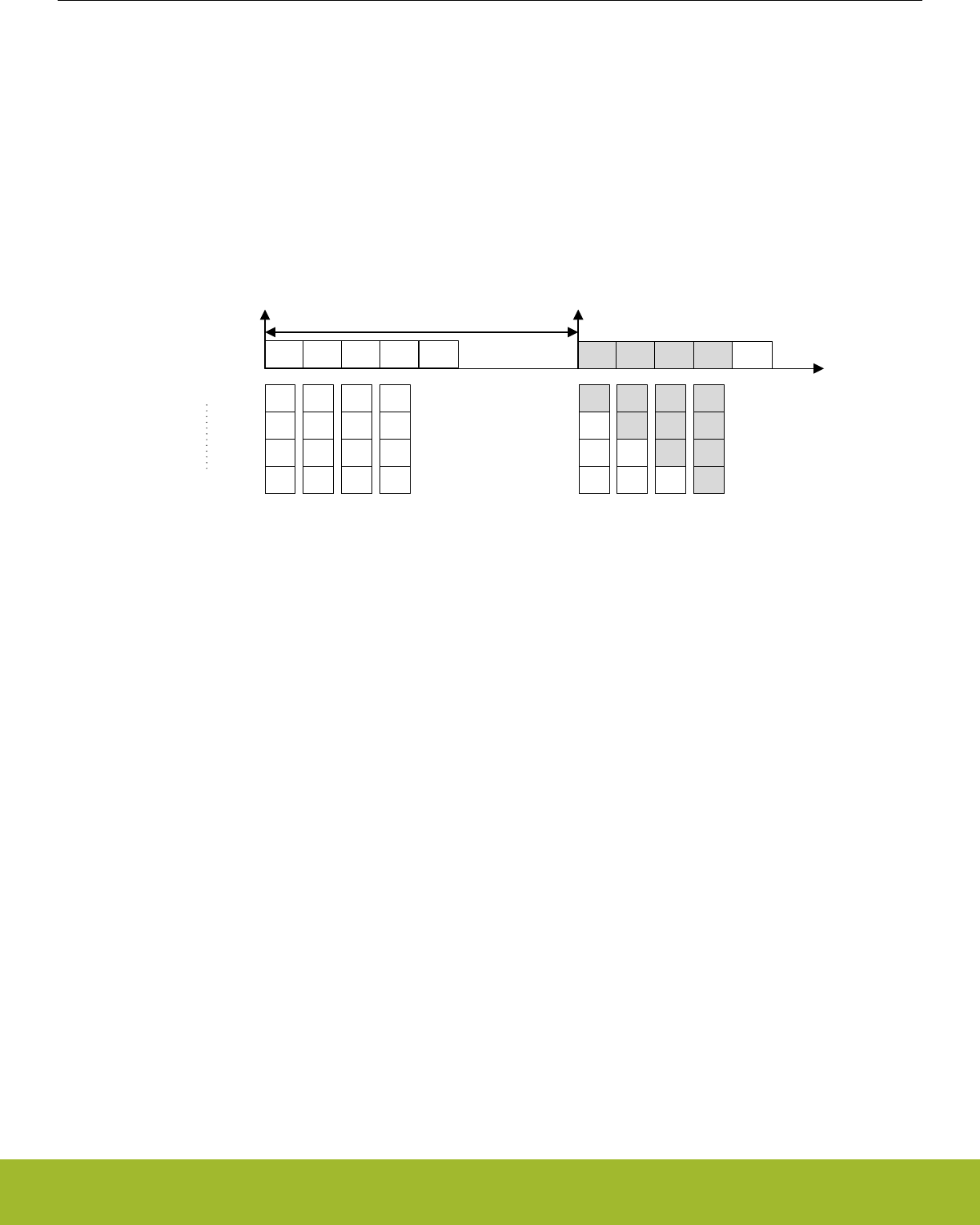
29.3.7 Decoder
Many applications, such as quadrature decoding, require some sort of processing of the sensor readings. In quadrature decoding, the
sensors repeatedly pass through a set of states which correspond to the position of the sensors. This sequence, and many other de-
coding schemes, can be described as a finite state machine. To support this type of decoding without CPU intervention, the LESENSE
module includes a highly configurable decoder capable of decoding input from up to four sensors. The decoder is implemented as a
programmable state machine with up to 32 states. When doing a sensor scan, the results from the sensors are placed in the decoder
input register, SENSORSTATE, if DECODE in CHx_INTERACT is set. The resulting position after a scan is illustrated in Figure
29.10 Sensor scan and decode sequence on page 962, where the bottom blocks show how the SENSORSTATE register is filled. If
step detection is enabled, the step direction is placed in SENSORSTATE in the position after the sensor result. When the scan se-
quence is complete, the decoder evaluates the state of the sensors chosen for decoding, as depicted in Figure 29.10 Sensor scan and
decode sequence on page 962.
CH0 CH1
START START
Scan period
DecodeCH2 CH3 CH0 CH1 DecodeCH2 CH3
CH0
result
-
-
-
CH0
result
CH1
result
-
-
CH0
result
CH1
result
CH2
result
-
CH0
result
CH1
result
CH2
result
CH3
result
SENSORSTATE[0]
SENSORSTATE[3]
CH0
result
CH1
result
CH2
result
CH3
result
CH0
result
CH1
result
CH2
result
CH3
result
CH0
result
CH1
result
CH2
result
CH3
result
CH0
result
CH1
result
CH2
result
CH3
result
Figure 29.10. Sensor scan and decode sequence
Upon a state transition, LESENSE can generate a pulse on one or more of the decoder PRS channels. Which PRS channel to generate
a pulse on is configured in the PRSACT bit field. If PRSCNT in DECCTRL is set, count signals will be generated on decoder PRS chan-
nels 0 and 1 according to the PRSACT configuration. In this mode, channel 0 will pulse each time a count event occurs, while channel 1
indicates the count direction (1 being up and 0 being down). The count direction will be kept at its previous state in between count
events. The EFR32xG13 Wireless Gecko pulse counter may be used to keep track of events based on these PRS outputs.
If SETIF is set, the DECODER interrupt flag will be set when the transition occurs. If INTMAP in DECCTRL and SETIF is set, a transi-
tion from state x or x+16 will set the CHx interrupt flag in addition to the DECODER flag.
Setting CHAIN in STx_TCONFA enables the decoder to evaluate more than two possible transitions for each state. If none of the transi-
tions defined in STx_TCONFA or STx_TCONFB match, the decoder will jump to the next descriptor pair and evaluate the transitions
defined there. The decoder uses two LFACLKLESENSE cycles for each descriptor pair to be evaluated. If ERRCHK in CTRL is set, the
decoder will check that the sensor state has not changed if none of the defined transitions match. The DECERR interrupt flag will be set
if none of the transitions match and the sensor state has changed. Figure 29.11 Decoder state transition evaluation on page 963
illustrates state transitions. The "Generate PRS signals and set interrupt flag" blocks will perform actions according to the configuration
in STx_TCONFA and STx_TCONFB.
Note:
If only one transition from a state is used, STx_TCONFA and STx_TCONFB should be configured equally.
Reference Manual
LESENSE - Low Energy Sensor Interface
silabs.com | Smart. Connected. Energy-friendly. Preliminary Rev. 0.5 | 962
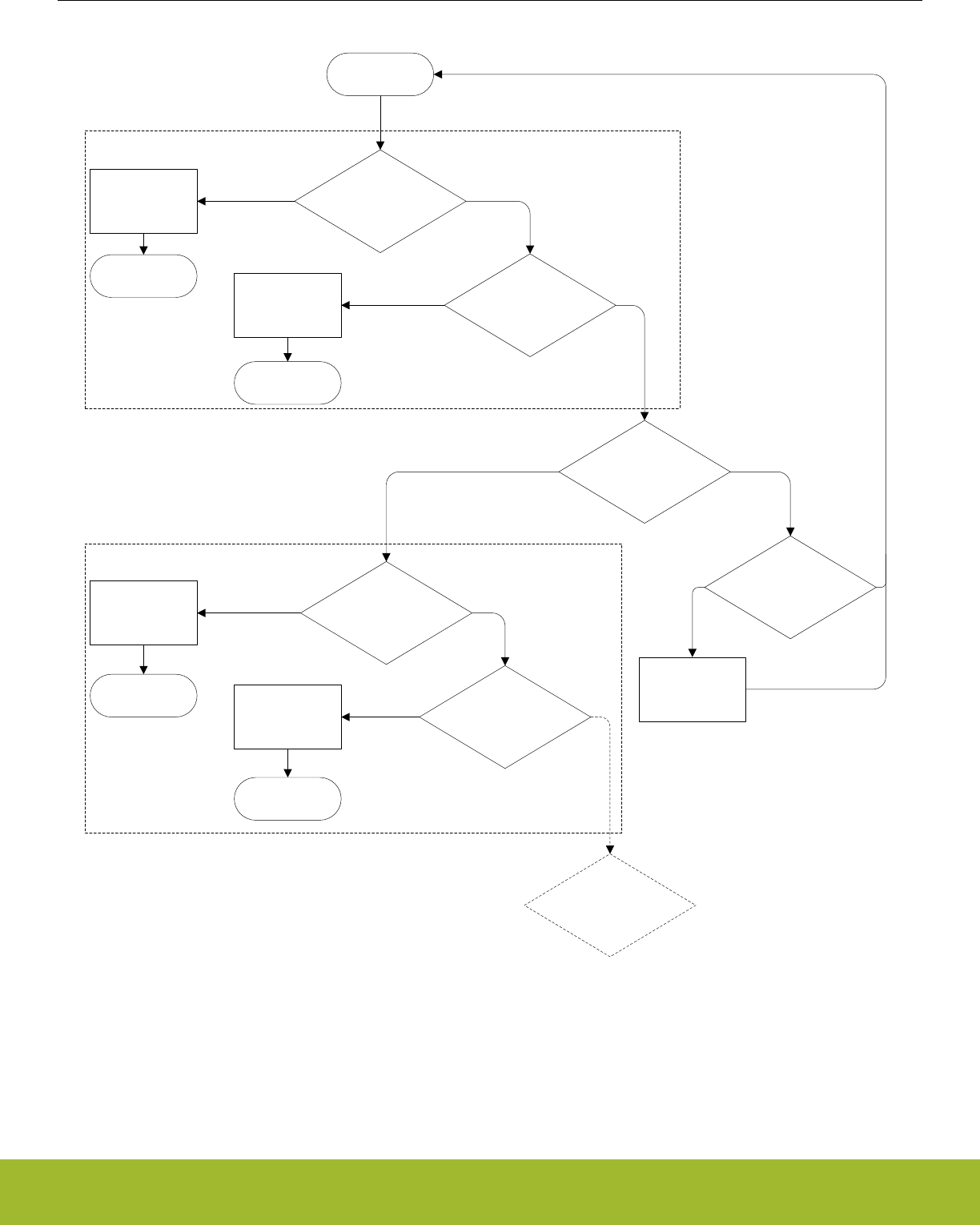
STi+1_TCONF
STi_TCONF
STATEi
NEXTSTATEAi
NEXTSTATEBi
NEXTSTATEAi+1
NEXTSTATEBi+1
Generate PRS
signals and set
interrupt flag
Generate PRS
signals and set
interrupt flag
Generate PRS
signals and set
interrupt flag
Generate PRS
signals and set
interrupt flag
Set DECERR
interrupt flag
SENSORSTATE & ~MASKAi =
COMPAi & ~MASKAi
Y N
SENSORSTATE & ~MASKBi =
COMPBi & ~MASKBi
Y N
CHAINi = 1
Y N
SENSORSTATE & ~MASKAi+1 =
COMPAi+1 & ~MASKAi+1
Y N
SENSORSTATE & ~MASKBi+1 =
COMPBi+1 & ~MASKBi+1
Y N
SENSORSTATE changed &&
ERRCHK=1
Y N
CHAINi+1 = 1
Y N
Figure 29.11. Decoder state transition evaluation
The DECODER has a PRS output named DECCMP. This output can be used to indicate which state, or subset of states, the decoder is
currently in. This PRS output is enabled by setting DECCMPEN in PRSCTRL, and configured through DECCMPMASK and DECCMPV-
AL in PRSCTRL. The value of this PRS output is given by Figure 29.12 DECCMP PRS output on page 964,
Reference Manual
LESENSE - Low Energy Sensor Interface
silabs.com | Smart. Connected. Energy-friendly. Preliminary Rev. 0.5 | 963
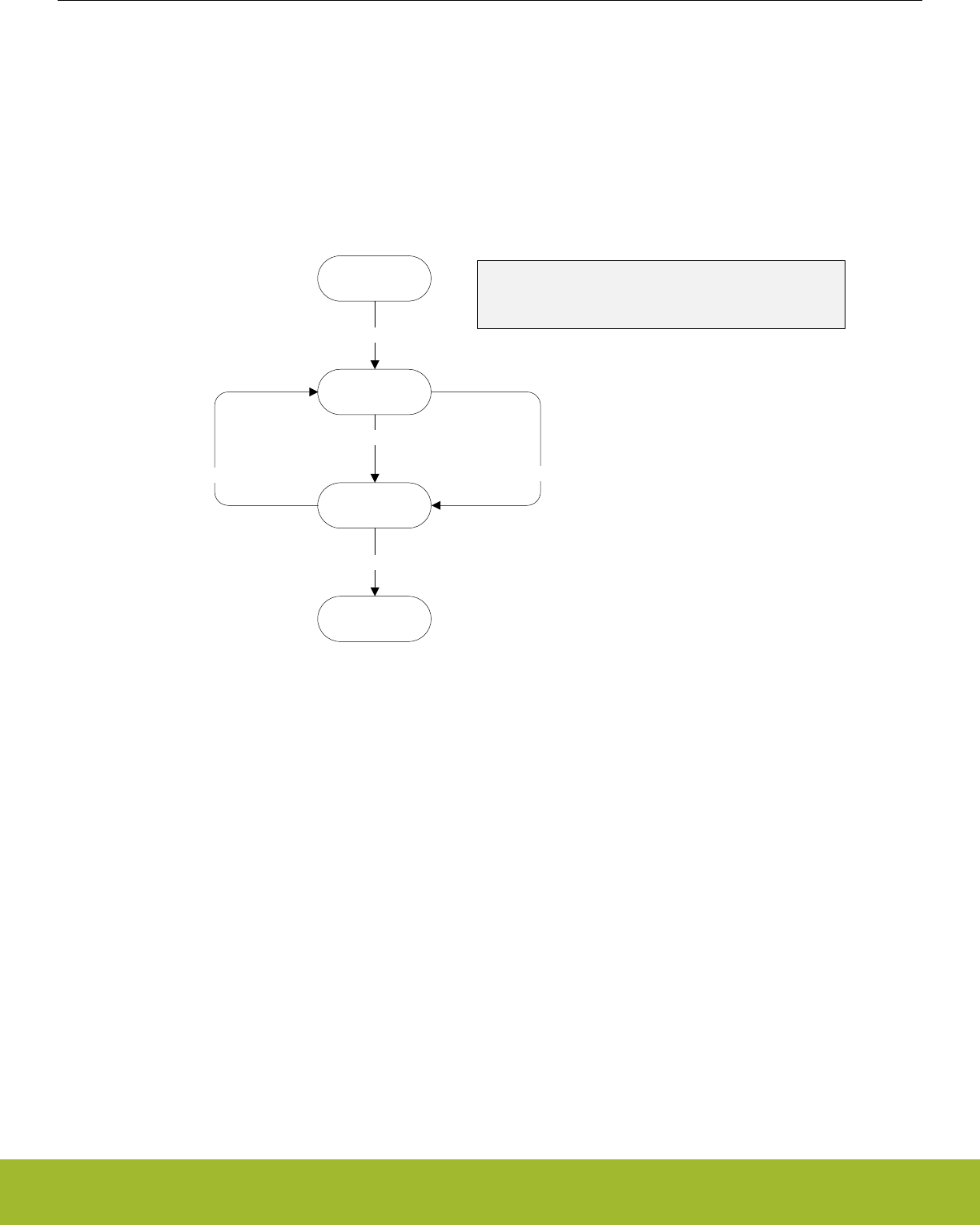
PRS_DECCMP = (DECSTATE & ~DECCMPMASK) == (DECCMPVAL & ~DECCMPMASK)
Figure 29.12. DECCMP PRS output
To prevent unnecessary interrupt requests or PRS outputs when the decoder toggles back and forth between two states, a hysteresis
option is available. The hysteresis function is triggered if a type A transition is preceded by a type B transition, and vice versa. A type A
transition is defined in STx_TCONFA, and a type B transition is defined in STx_TCONFB. When descriptor chaining is used, a jump to
another descriptor will cancel out the hysteresis effect. Figure 29.13 Decoder hysteresis on page 964 illustrates how the hysteresis
triggers upon state transitions.
State 0
State 1
1: B transition, no hysteresis
State 2
2: A transition, hysteresis
State 3
5: A transition, no hysteresis
3: B transition, hysteresis 4: A transition, hysteresis
A transition: Transition defined in TCONFA
B transition: Transition defined in TCONFB
Figure 29.13. Decoder hysteresis
• When HYSTPRSx is set, PRS signal x is suppressed when the hysteresis triggers.
• When HYSTIRQ is set, interrupt requests are suppressed when the hysteresis triggers.
Note:
The decoder error interrupt flag, DECERR, is not affected by the hysteresis.
Reference Manual
LESENSE - Low Energy Sensor Interface
silabs.com | Smart. Connected. Energy-friendly. Preliminary Rev. 0.5 | 964
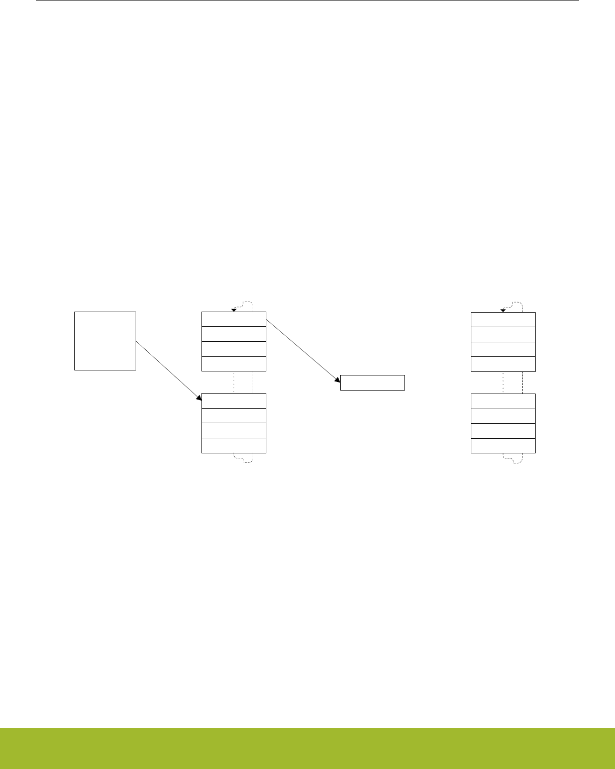
29.3.8 Measurement Results
Part of the LESENSE RAM is treated as a circular buffer for storage of up to 16 sensor measurements results. Each time LESENSE
writes data to the result buffer, the result write pointer (PTR_WR) is incremented. Each time a new result is read through the BUFDATA
register, the result read pointer (PTR_RD) is incremented. The read pointer will not be incremented if there is no valid, unread data in
the result buffer. By default LESENSE will not write additional data to a full result buffer until the data is read by software or DMA. Set-
ting BUFOW in CTRL enables LESENSE to write to the result buffer even if it is full. In this mode, the result read pointer will follow the
write pointer if the buffer is full. The result of this is that data read from the result read register (BUFDATA) will be the oldest unread
result. The location pointers are available in PTR.
The result buffer has three flags in the STATUS register: BUFDATAV, BUFHALFFULL, and BUFFULL. The flags indicate when new data
is available, when the buffer is half full, and when it is full, respectively.
The result buffer also has three interrupt flags in the IR register: BUFDATAV, BUFLEVEL, and BUFOF. BUFDATAV is set when data is
available in the buffer. BUFLEVEL is set when the buffer is either full or half-full, depending on the configuration of BUFIDL in CTRL.
BUFOF is set if the result buffer overflows.
During a scan, the state of each sensor is stored in SCANRES. If a sensor triggers, a 1 is stored in SCANRES, else a 0 is stored in
SCANRES. Whether or not a sensor is said to be triggered depends of the configuration for the given channel. See 29.3.6 Sensor Eval-
uation for details. If STRSAMPLE in CHx_EVAL is set, the sensor data for each channel will be stored in the LESENSE result buffer. If
STRSCANRES in CTRL is set, the result vector, SCANRES, will also be stored in the result buffer. This will be stored after each scan
and will be interleaved with the counter values. The contents of the result buffer can be read from BUFDATA or from BUF[x]_DATA.
When reading from BUF[x]_DATA, neither the result read pointer or the status flags BUFDATAV, BUFHALFFULL, or BUFFULL will be
updated. When reading through the BUFDATA register, the oldest unread result will be read.
BUF0_DATA
BUF1_DATA
BUF2_DATA
BUF3_DATA
BUF12_DATA
BUF13_DATA
BUF14_DATA
BUF15_DATA
BUFDATA
PTR_RD
LESENSE
PTR_WR
CH3 result
CH5 result
CH9 result
SCANRES
CH3 result
CH5 result
CH9 result
SCANRES
Figure 29.14. Circular result buffer
Figure 29.14 Circular result buffer on page 965 illustrates how the result buffer would be filled when channels 3,5, and 9 are enabled
and have STRSAMPLE in CHx_EVAL set, in addition to STRSCANRES in CTRL. The measurement result from the three channels will
be sequentially written during the scan, while SCANRES is written to the result buffer upon scan completion.
Reference Manual
LESENSE - Low Energy Sensor Interface
silabs.com | Smart. Connected. Energy-friendly. Preliminary Rev. 0.5 | 965

29.3.9 VDAC Interface
LESENSE is able to drive the VDAC for generation of accurate reference voltages. This is enabled by setting DACCHxEN in
PERCTRL. The refresh rate of the VDAC channels can be configured in DACCONVTRIG in PERCTRL. If DACCONVTRIG is set to
CHANNELSTART, the VDAC channels are refreshed prior to each sensor measurement, as depicted in Figure 29.4 Timing diagram,
AUXHFRCO based timing on page 956. If DACCONVTRIG is set to SCANSTART, the VDAC channels are refreshed prior to each
scan. The conversion data is either taken from the data registers in the EFR32xG13 Wireless Gecko VDAC interface (VDAC0_CH0DA-
TA and VDAC0_CH1DATA) or from the THRES bitfield in the CHx_INTERACT register for the active LESENSE channel. VDAC data
used is configured in DACCHxDATA in PERCTRL.
Bias configuration, calibration and reference selection is done in the EFR32xG13 Wireless Gecko VDAC module and LESENSE will not
override these configurations.
LESENSE has the possibility to control switches that connect the VDAC alternate outputs. This allows LESENSE to excite sensors with
output from the VDAC channels, this is done by setting CHx_INTERACT_EXMODE to DACOUT. The LESENSE channels can also be
connected to the VDAC output when the given channel is idle, this is done by setting IDLECONF_CHx to DAC.
Note: Only LESENSE channels 4, 5, 7, 10, 12, 13 have the possibility to excite using the VDAC alternate outputs, or connect to the
VDAC alternate outputs during the idle phase.
The VDAC may be chosen as reference to the analog comparators for accurate reference generation. If the VDAC is configured in con-
tinuous mode this does not require any external components. If sample/off mode is used, an external capacitor is needed to maintain
the voltage between samples. To configure the VDAC to use this external capacitor, connect the capacitor to the VDAC pin for the given
channel and set SHORT in VDAC_OPAx_OUT.
Note:
The VDAC mode should not be altered while DACACTIVE in STATUS is set
29.3.10 ACMP Interface
The analog comparators (ACMPs) are used to measure the sensors, and have to be configured according to the application in order for
LESENSE to work properly. Depending on the configuration in the ACMP0MODE and ACMP1MODE bit-fields in PERCTRL, LESENSE
will take control of the positive input mux and the voltage dividers (DIVVA, DIVVB) for ACMP0 and ACMP1. The remaining configuration
of the analog comparators is done in the ACMP register interface.
If ACMPxMODE in PERCTRL is set to MUX, LESENSE will take control of the positive input mux of the ACMP, through the external
override interface, described in the ACMP chapter. The offset given by LESENSE, EXT_OFFSET, depends on whether one or two
ACMPs are controlled by LESENSE. If only one ACMP is used, EXT_POSSEL will have the same value as the active channel. If both
ACMP0 and ACMP1 are used, LESENSE channel 0-7 will use ACMP0 with EXT_OFFSET 0-7, and LESENSE channel 8-15 will use
ACMP1 with EXT_OFFSET 0-7.
If ACMPxMODE in PERCTRL is set to MUXTHRES, LESENSE will also take control of the voltage dividers in the ACMP, DIVVA and
DIVVB. The thresholds used are individual to each channel and is configured using the 6 LSBs of CHx_INTERACT_THRES. By default,
ACMP_HYSTERESIS0_DIVVX and ACMP_HYSTERESIS1_DIVVX will be given the same value, the 6 LSBs of CHx_INTER-
ACT_THRES. To allow different values for ACMP_HYSTERESIS0_DIVVX and ACMP_HYSTERESIS1_DIVVX, ACMPxHYSTEN in
PERCTRL needs to be set. This allows the hysteresis feature in the ACMP to be utilized. ACMP_HYSTERESIS0_DIVVX will get the
value programmed in CHx_INTERACT_THRES[5:0], while ACMP_HYSTERESIS1_DIVVX will get the value programmed in CHx_IN-
TERACT_THRES[11:6].
29.3.11 ACMP and VDAC Duty Cycling
By default, the analog comparators and the VDAC are shut down between LESENSE scans to save energy. If this is not desired, WAR-
MUPMODE in PERCTRL can be configured to prevent them from being shut down.
Both the VDAC and analog comparators rely on a bias module for correct operation. This bias module has a low power mode which
consumes less energy at the cost of reduced accuracy. BIASMODE in BIASCTRL configures how the bias module is controlled by
LESENSE. When set to DUTYCYCLE, LESENSE will set the bias module in high accuracy mode whenever LESENSE is active, and
keep it in the low power mode otherwise. When BIASMODE is set to HIGHACC, the high accuracy mode is always selected. When set
to DONTTOUCH, LESENSE will not control the bias module.
Reference Manual
LESENSE - Low Energy Sensor Interface
silabs.com | Smart. Connected. Energy-friendly. Preliminary Rev. 0.5 | 966

29.3.12 ADC Interface
The LESENSE module can be configured to trigger ADC conversions and use data from the ADC to evaluate sensor status. In order to
do this, the scan mode of the ADC has to be configured. When the sample delay configured in CHx_TIMING_SAMPLEDLY has
expired, LESENSE will initiate an ADC sample. The active LESENSE channel determines which ADC channel to be sampled, where
LESENSE channel X corresponds to ADC scan channel X.
29.3.13 DMA Requests
LESENSE issues a DMA request when the result buffer is either full or half full, depending on the configuration of BUFIDL in CTRL. The
request is cleared when the buffer level drops below the threshold defined in BUFIDL. A single DMA request is also set whenever there
is unread data in the buffer. DMAWU in CTRL configures at which buffer level LESENSE should wake-up the DMA when in EM2.
Note:
The DMA controller should always fetch data from the BUFDATA register.
29.3.14 PRS Output
LESENSE is an asynchronous PRS producer and has twenty PRS outputs. The decoder has four outputs and in addition, all bits in the
SCANRES register are available as PRS outputs. For further information on the decoder PRS output, refer to 29.3.7 Decoder.
29.3.15 RAM
LESENSE includes a RAM block used for storage of configuration and results. Registers mapped to the RAM include: STx_TCONFA,
STx_TCONFB, BUFx_DATA, BUFDATA, CHx_TIMING, CHx_INTERACT, and CHx_EVAL. These registers have unknown value out of
reset and have to be initialized before use.
Note:
Read-modify-write operations on uninitialized RAM register produces undefined values.
29.3.16 Application Examples
Reference Manual
LESENSE - Low Energy Sensor Interface
silabs.com | Smart. Connected. Energy-friendly. Preliminary Rev. 0.5 | 967
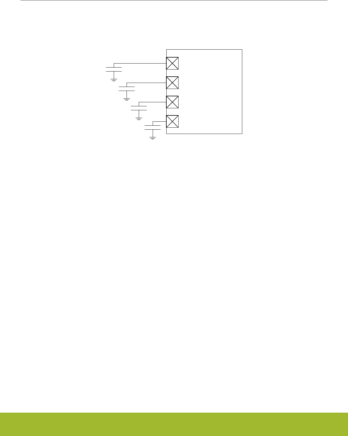
29.3.16.1 Capacitive Sense
Figure 29.15 Capacitive sense setup on page 968 illustrates how the EFR32xG13 Wireless Gecko can be configured to monitor four
capacitive buttons.
ACMP0_CH0
ACMP0_CH1
ACMP0_CH2
ACMP0_CH3
Figure 29.15. Capacitive sense setup
The following steps show how to configure LESENSE to scan through the four buttons 100 times per second, issuing an interrupt if one
of them is pressed.
1. Assuming LFACLKLESENSE is 32kHz, set PCPRESC to 3 and PCTOP to 39 in CTRL. This will set the LESENSE scan frequency to
100Hz.
2. Enable channels 0 through 3 in CHEN and set IDLECONF for these channels to DISABLED. In capacitive sense mode, the GPIO
should always be disabled (i.e., analog input).
3. Configure the ACMP to operate in CAPSENSE mode (refer to the ACMP chapter for more details).
4. Configure the following bit fields in CHx_CONF, for channels 0 through 3:
a. Set EXTIME to 0. No excitation is needed in this mode.
b. Set SAMPLE to ACMPCOUNT and COMP to LESS. This makes LESENSE interpret a sensor as active if the frequency on a
channel drops below the threshold (i.e., the button is pressed).
c. Set SAMPLEDLY to an appropriate value - each sensor will be measured for SAMPLEDLY/FLFACLK_LESENSE seconds. MEAS-
UREDLY should be set to 0
5. Set CTRTHRESHOLD to an appropriate value. An interrupt will be issued if the counter value for a sensor is below this threshold
after the measurement phase.
6. Enable interrupts on channels 0 through 3.
7. Start scan sequence by writing a 1 to START in CMD.
In a capacitive sense application, it might be required to calibrate the threshold values on a periodic basis, for example to compensate
for humidity and other physical variations. LESENSE is able to store up to 16 counter values from a configurable number of channels,
making it possible to collect sample data while in EM2. When calibration is to be performed, the CPU only has to be woken up for a
short period of time as the data to be processed already lies in the result registers. To enable storing of the count value for a channel,
set STRSAMPLE in the CHx_INTERACT register.
Reference Manual
LESENSE - Low Energy Sensor Interface
silabs.com | Smart. Connected. Energy-friendly. Preliminary Rev. 0.5 | 968
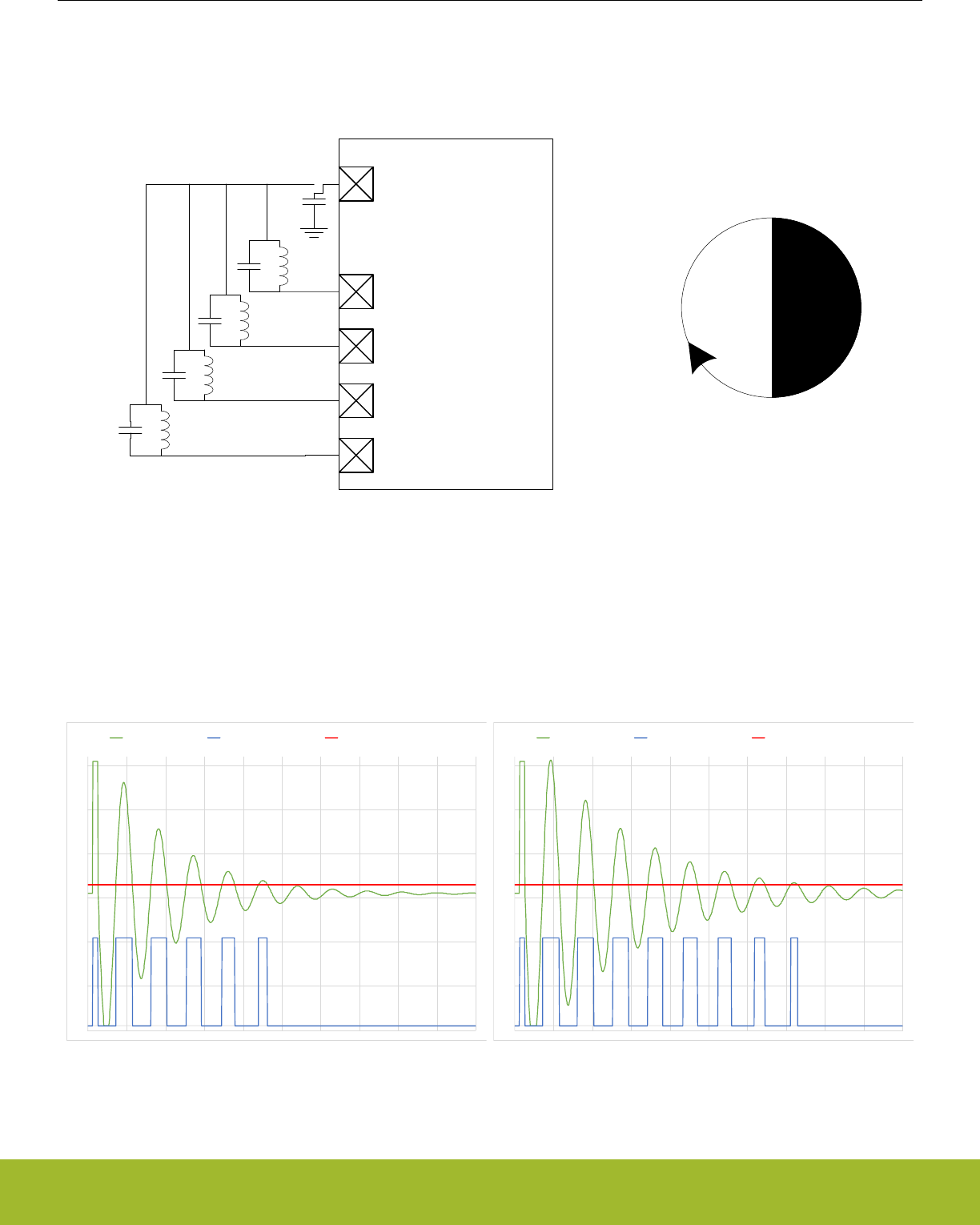
29.3.16.2 LC sensor
Figure 29.16 LC sensor setup on page 969 below illustrates how the EFR32xG13 Wireless Gecko can be set up to monitor four LC
sensors.
ACMP0_CH0
ACMP0_CH1
ACMP0_CH2
DAC0_OUT0
X
XX
X
ACMP0_CH3
Figure 29.16. LC sensor setup
LESENSE can be used to excite and measure the damping factor in LC sensor oscillations. To measure the damping factor, the ACMP
can be used to generate a high output each time the sensor voltage exceeds a certain level. These pulses are counted using an asyn-
chronous counter and compared with the threshold in COMPTHRES in the CHx_EVAL register. If the number of pulses exceeds the
threshold level, the sensor is said to be active, otherwise it is inactive. Figure 29.17 LC sensor oscillations on page 969 illustrates how
the output pulses from the ACMP correspond to damping of the oscillations. The results from sensor evaluation can automatically be
fed into the decoder in order to keep track of rotations.
-0,05
0,45
0,95
1,45
1,95
2,45
2,95
0 10 20 30 40 50 60 70 80 90 100
LC sensor ACMP output ACMP threshold
-0,05
0,45
0,95
1,45
1,95
2,45
2,95
0 10 20 30 40 50 60 70 80 90 100
LC sensor ACMP output ACMP threshold
Figure 29.17. LC sensor oscillations
The following steps show how to configure LESENSE to scan through the four LC sensors 100 times per second.
Reference Manual
LESENSE - Low Energy Sensor Interface
silabs.com | Smart. Connected. Energy-friendly. Preliminary Rev. 0.5 | 969

1. Assuming LFACLKLESENSE is 32kHz, set PCPRESC to 3 and PCTOP to 39 in CTRL. This will set the LESENSE scan frequency to
100Hz.
2. Enable the VDAC and configure it to produce a voltage of Vdd/2.
3. Enable channels 0 through 3 in CHEN. Set IDLECONF for the active channels to DACOUT. The channel pins should be connected
to the VDAC output (effectively shorting the LC sensor) in the idle phase to damp the oscillations.
4. Configure the ACMP to use scaled Vdd as negative input, refer to ACMP chapter for details.
5. Enable and configure PCNT and asynchronous PRS.
6. Configure the GPIOs used as PUSHPULL.
7. Configure the following bit fields in CHx_CONF, for channels 0 through 3:
a. Set EXCLK to AUXHFRCO. AUXHFRCO is needed to achieve short excitation time.
b. Set EXTIME to an appropriate value. Excitation will last for EXTIME/FAUXHFRCO seconds.
c. Set EXMODE to HIGH. The LC sensors are excited by pulling the excitation pin high.
d. Set SAMPLE to ACMPCOUNT and COMP to LESS. Status of each sensor is evaluated based on the number of pulses gener-
ated by the ACMP. If they are less than the threshold value, the sensor is said to be active.
e. Set SAMPLEDLY to an appropriate value, each sensor will be measured for SAMPLEDLY/FLFACLK_LESENSE seconds.
8. Set CTRTHRESHOLD to an appropriate value. If the sensor is active, the counter value after the measurement phase should be
less than the threshold. If it is inactive, the counter value should be greater than the threshold.
9. Start scan sequence by writing a 1 to START in CMD.
Note:
Exciting the LC sensor by pulling the excitation pin high allows the ESD protection in the pads to clamp any voltage swings below the
ground voltage, giving a consistent starting point for the oscillations.
Reference Manual
LESENSE - Low Energy Sensor Interface
silabs.com | Smart. Connected. Energy-friendly. Preliminary Rev. 0.5 | 970

29.3.16.3 LESENSE Decoder 1
The example below illustrates how the LESENSE module can be used for decoding using three sensors
0 1 2 3
7 6 5 4
001
000
011
001
010
011
110
111
111
101
101
100
010 110
000 100
xxx
State Index Sensor value
Figure 29.18. FSM example 1
Figure 29.18 FSM example 1 on page 971, configure the following LESENSE registers:
1. Configure the channels to be used, be sure to set DECODE in CHx_EVAL.
2. Set PRSCNT to enable generation of count waveforms on PRS. Also configure a PCNT to listen to the PRS channels and count
accordingly.
3. Configure the following in STx_TCONFA and STx_TCONFB:
a. Set MASK = 0b1000 in STx_TCONFA and STx_TCONFB for all used states. This enables three sensors to be evaluated by
the decoder.
b. Configure the remaining bit fields in STx_TCONFA and STx_TCONFB as described in Table 29.3 LESENSE decoder configu-
ration on page 971.
Table 29.3. LESENSE decoder configuration
Register TCON-
FA_NEXT-
STATE
TCON-
FA_COMP
TCONFA_PRSACT TCONFB_NEX
TSTATE
TCONFB_COM
P
TCONFB_PRSAC
T
ST0 1 0b001 UP 7 0b100 DOWN
ST1 2 0b011 UP 0 0b000 DOWN
ST2 3 0b010 UP 1 0b001 DOWN
ST3 4 0b110 UP 2 0b011 DOWN
ST4 5 0b111 UP 3 0b010 DOWN
ST5 6 0b101 UP 4 0b110 DOWN
ST6 7 0b100 UP 5 0b111 DOWN
ST7 0 0b000 UP 6 0b101 DOWN
4. To initialize the decoder, run one scan, and read the present sensor status from SENSORSTATE. Then write the index of this state
to DECSTATE.
5. Write to START in CMD to start scanning of sensors and decoding.
Reference Manual
LESENSE - Low Energy Sensor Interface
silabs.com | Smart. Connected. Energy-friendly. Preliminary Rev. 0.5 | 971

29.3.16.4 LESENSE Decoder 2
The example below illustrates how the LESENSE decoder can be used to implement the state machine seen in Figure 29.19 FSM ex-
ample 2 on page 972.
0
2
4
6
8
0010
0000
0001
0000
0001
0011
0011
0010 1XXX
1XXX
1XXX
1XXX
State Index Sensor value
Figure 29.19. FSM example 2
1. Configure STx_TCONFA and STx_TCONFB as described in Table 29.4 LESENSE decoder configuration on page 972.
Table 29.4. LESENSE decoder configuration
Register NEXTSTATE COMP MASK CHAIN
ST0_TCONFA 8 0b1000 0b0111 1
ST0_TCONFB 2 0b0001 0b1000 -
ST1_TCONFA 6 0b0010 0b1000 0
ST1_TCONFB 6 0b0010 0b1000 -
ST2_TCONFA 8 0b1000 0b0111 1
ST2_TCONFB 4 0b0011 0b1000 -
ST3_TCONFA 0 0b0000 0b1000 0
ST3_TCONFB 0 0b0000 0b1000 -
ST4_TCONFA 8 0b1000 0b0111 1
ST4_TCONFB 6 0b0010 0b1000 -
ST5_TCONFA 2 0b0001 0b1000 0
ST5_TCONFB 2 0b0001 0b1000 -
ST6_TCONFA 8 0b1000 0b0111 1
ST6_TCONFB 0 0b0000 0b1000 -
ST7_TCONFA 4 0b0011 0b1000 0
ST7_TCONFB 4 0b0011 0b1000 -
2. To initialize the decoder, run one scan, and read the present sensor status from SENSORSTATE. Then write the index of this state
to DECSTATE.
3. Write to START in CMD to start scanning of sensors and decoding.
Reference Manual
LESENSE - Low Energy Sensor Interface
silabs.com | Smart. Connected. Energy-friendly. Preliminary Rev. 0.5 | 972

29.4 Register Map
The offset register address is relative to the registers base address.
Offset Name Type Description
0x000 LESENSE_CTRL RW Control Register
0x004 LESENSE_TIMCTRL RW Timing Control Register
0x008 LESENSE_PERCTRL RW Peripheral Control Register
0x00C LESENSE_DECCTRL RW Decoder control Register
0x010 LESENSE_BIASCTRL RW Bias Control Register
0x014 LESENSE_EVALCTRL RW LESENSE evaluation control
0x018 LESENSE_PRSCTRL RW PRS control register
0x01C LESENSE_CMD W1 Command Register
0x020 LESENSE_CHEN RW Channel enable Register
0x024 LESENSE_SCANRES RWH Scan result register
0x028 LESENSE_STATUS RStatus Register
0x02C LESENSE_PTR RResult buffer pointers
0x030 LESENSE_BUFDATA R(a) Result buffer data register
0x034 LESENSE_CURCH RCurrent channel index
0x038 LESENSE_DECSTATE RWH Current decoder state
0x03C LESENSE_SENSORSTATE RWH Decoder input register
0x040 LESENSE_IDLECONF RW GPIO Idle phase configuration
0x044 LESENSE_ALTEXCONF RW Alternative excite pin configuration
0x050 LESENSE_IF RInterrupt Flag Register
0x054 LESENSE_IFS W1 Interrupt Flag Set Register
0x058 LESENSE_IFC (R)W1 Interrupt Flag Clear Register
0x05C LESENSE_IEN RW Interrupt Enable Register
0x060 LESENSE_SYNCBUSY RSynchronization Busy Register
0x064 LESENSE_ROUTEPEN RW I/O Routing Register
0x100 LESENSE_ST0_TCONFA RW State transition configuration A
0x104 LESENSE_ST0_TCONFB RW State transition configuration B
... LESENSE_STx_TCONFA RW State transition configuration A
... LESENSE_STx_TCONFB RW State transition configuration B
0x1F8 LESENSE_ST31_TCONFA RW State transition configuration A
0x1FC LESENSE_ST31_TCONFB RW State transition configuration B
0x200 LESENSE_BUF0_DATA RWH Scan results
... LESENSE_BUFx_DATA RWH Scan results
0x23C LESENSE_BUF15_DATA RWH Scan results
0x240 LESENSE_CH0_TIMING RW Scan configuration
0x244 LESENSE_CH0_INTERACT RW Scan configuration
Reference Manual
LESENSE - Low Energy Sensor Interface
silabs.com | Smart. Connected. Energy-friendly. Preliminary Rev. 0.5 | 973

Offset Name Type Description
0x248 LESENSE_CH0_EVAL RWH Scan configuration
... LESENSE_CHx_TIMING RW Scan configuration
... LESENSE_CHx_INTERACT RW Scan configuration
... LESENSE_CHx_EVAL RWH Scan configuration
0x330 LESENSE_CH15_TIMING RW Scan configuration
0x334 LESENSE_CH15_INTERACT RW Scan configuration
0x338 LESENSE_CH15_EVAL RWH Scan configuration
Reference Manual
LESENSE - Low Energy Sensor Interface
silabs.com | Smart. Connected. Energy-friendly. Preliminary Rev. 0.5 | 974

29.5 Register Description
29.5.1 LESENSE_CTRL - Control Register (Async Reg)
For more information about asynchronous registers please see 4.3 Access to Low Energy Peripherals (Asynchronous Registers).
Offset Bit Position
0x000
31
30
29
28
27
26
25
24
23
22
21
20
19
18
17
16
15
14
13
12
11
10
9
8
7
6
5
4
3
2
1
0
Reset
0
0x0
0
0
0
0
0
0x0
0x0
0x0
Access
RW
RW
RW
RW
RW
RW
RW
RW
RW
RW
Name
DEBUGRUN
DMAWU
BUFIDL
STRSCANRES
BUFOW
DUALSAMPLE
ALTEXMAP
SCANCONF
PRSSEL
SCANMODE
Bit Name Reset Access Description
31:23 Reserved To ensure compatibility with future devices, always write bits to 0. More information in 1.2 Conven-
tions
22 DEBUGRUN 0 RW Debug Mode Run Enable
Set to keep LESENSE running in debug mode.
Value Description
0 LESENSE can not start new scans in debug mode
1 LESENSE can start new scans in debug mode
21:20 DMAWU 0x0 RW DMA wake-up from EM2
Set buffer threshold for waking up the DMA controller when the system is in EM2
Value Mode Description
0 DISABLE No DMA wake-up from EM2
1 BUFDATAV DMA wake-up from EM2 when data is valid in the result buffer
2 BUFLEVEL DMA wake-up from EM2 when the result buffer is full/half-full depend-
ing on BUFIDL configuration
19 BUFIDL 0 RW Result buffer interrupt and DMA trigger level
Set buffer threshold for DMA requests and interrupt generation
Value Mode Description
0 HALFFULL DMA and interrupt flags set when result buffer is half-full
1 FULL DMA and interrupt flags set when result buffer is full
18 Reserved To ensure compatibility with future devices, always write bits to 0. More information in 1.2 Conven-
tions
17 STRSCANRES 0 RW Enable storing of SCANRES
When set, SCANRES will be stored in the result buffer after each scan
Reference Manual
LESENSE - Low Energy Sensor Interface
silabs.com | Smart. Connected. Energy-friendly. Preliminary Rev. 0.5 | 975

Bit Name Reset Access Description
16 BUFOW 0 RW Result buffer overwrite
If set, LESENSE will always write to the result buffer, even if it is full
15:14 Reserved To ensure compatibility with future devices, always write bits to 0. More information in 1.2 Conven-
tions
13 DUALSAMPLE 0 RW Enable dual sample mode
When set, both ACMPs will be sampled simultaneously.
12 Reserved To ensure compatibility with future devices, always write bits to 0. More information in 1.2 Conven-
tions
11 ALTEXMAP 0 RW Alternative excitation map
This bit is used to configure which pins alternate excitation is mapped to.
Value Mode Description
0 ALTEX Alternative excitation is mapped to the LES_ALTEX pins.
1 CH Alternative excitation is mapped to the pin of LESENSE channel (X+8
mod 16), X being the active channel.
10:9 Reserved To ensure compatibility with future devices, always write bits to 0. More information in 1.2 Conven-
tions
8:7 SCANCONF 0x0 RW Select scan configuration
These bits control which CHx_CONF registers to be used.
Value Mode Description
0 DIRMAP The channel configuration register registers used are directly mapped
to the channel number.
1 INVMAP The channel configuration register registers used are CHX+8_CONF for
channels 0-7 and CHX-8_CONF for channels 8-15.
2 TOGGLE The channel configuration register registers used toggles between
CHX_CONF and CHX+8_CONF when channel x triggers
3 DECDEF The decoder state defines the CONF registers to be used.
6 Reserved To ensure compatibility with future devices, always write bits to 0. More information in 1.2 Conven-
tions
5:2 PRSSEL 0x0 RW Scan start PRS select
Select PRS source for scan start if SCANMODE is set to PRS.
Value Mode Description
0 PRSCH0 PRS Channel 0 selected as input
1 PRSCH1 PRS Channel 1 selected as input
2 PRSCH2 PRS Channel 2 selected as input
3 PRSCH3 PRS Channel 3 selected as input
4 PRSCH4 PRS Channel 4 selected as input
5 PRSCH5 PRS Channel 5 selected as input
6 PRSCH6 PRS Channel 6 selected as input
7 PRSCH7 PRS Channel 7 selected as input
Reference Manual
LESENSE - Low Energy Sensor Interface
silabs.com | Smart. Connected. Energy-friendly. Preliminary Rev. 0.5 | 976

Bit Name Reset Access Description
8 PRSCH8 PRS Channel 8 selected as input
9 PRSCH9 PRS Channel 9 selected as input
10 PRSCH10 PRS Channel 10 selected as input
11 PRSCH11 PRS Channel 11 selected as input
1:0 SCANMODE 0x0 RW Configure scan mode
These bits control how the scan frequency is decided
Value Mode Description
0 PERIODIC A new scan is started each time the period counter overflows
1 ONESHOT A single scan is performed when START in CMD is set
2 PRS Pulse on PRS channel
Reference Manual
LESENSE - Low Energy Sensor Interface
silabs.com | Smart. Connected. Energy-friendly. Preliminary Rev. 0.5 | 977

29.5.2 LESENSE_TIMCTRL - Timing Control Register (Async Reg)
For more information about asynchronous registers please see 4.3 Access to Low Energy Peripherals (Asynchronous Registers).
Offset Bit Position
0x004
31
30
29
28
27
26
25
24
23
22
21
20
19
18
17
16
15
14
13
12
11
10
9
8
7
6
5
4
3
2
1
0
Reset
0
0x0
0x00
0x0
0x0
0x0
Access
RW
RW
RW
RW
RW
RW
Name
AUXSTARTUP
STARTDLY
PCTOP
PCPRESC
LFPRESC
AUXPRESC
Bit Name Reset Access Description
31:29 Reserved To ensure compatibility with future devices, always write bits to 0. More information in 1.2 Conven-
tions
28 AUXSTARTUP 0 RW AUXHFRCO startup configuration
This bit can be set to ONDEMAND to delay startup of the AUXHFRCO when high frequency timer is used
Value Mode Description
0 PREDEMAND AUXHFRCO is started half a clock cycle before it's needed
1 ONDEMAND AUXHFRCO is started at the time it is needed
27:24 Reserved To ensure compatibility with future devices, always write bits to 0. More information in 1.2 Conven-
tions
23:22 STARTDLY 0x0 RW Start delay configuration
Delay sensor interaction STARTDELAY LFACLKLESENSE cycles for each channel
21:20 Reserved To ensure compatibility with future devices, always write bits to 0. More information in 1.2 Conven-
tions
19:12 PCTOP 0x00 RW Period counter top value
These bits contain the top value for the period counter.
11 Reserved To ensure compatibility with future devices, always write bits to 0. More information in 1.2 Conven-
tions
10:8 PCPRESC 0x0 RW Period counter prescaling
This bitfield is used to divide the clock to the period counter
Value Mode Description
0 DIV1 The period counter clock frequency is LFACLKLESENSE/1
1 DIV2 The period counter clock frequency is LFACLKLESENSE/2
2 DIV4 The period counter clock frequency is LFACLKLESENSE/4
3 DIV8 The period counter clock frequency is LFACLKLESENSE/8
4 DIV16 The period counter clock frequency is LFACLKLESENSE/16
5 DIV32 The period counter clock frequency is LFACLKLESENSE/32
Reference Manual
LESENSE - Low Energy Sensor Interface
silabs.com | Smart. Connected. Energy-friendly. Preliminary Rev. 0.5 | 978

Bit Name Reset Access Description
6 DIV64 The period counter clock frequency is LFACLKLESENSE/64
7 DIV128 The period counter clock frequency is LFACLKLESENSE/128
7 Reserved To ensure compatibility with future devices, always write bits to 0. More information in 1.2 Conven-
tions
6:4 LFPRESC 0x0 RW Prescaling factor for low frequency timer
This bitfield is used to divide the clock to the low frequency timer
Value Mode Description
0 DIV1 Low frequency timer is clocked with LFACLKLESENSE/1
1 DIV2 Low frequency timer is clocked with LFACLKLESENSE/2
2 DIV4 Low frequency timer is clocked with LFACLKLESENSE/4
3 DIV8 Low frequency timer is clocked with LFACLKLESENSE/8
4 DIV16 Low frequency timer is clocked with LFACLKLESENSE/16
5 DIV32 Low frequency timer is clocked with LFACLKLESENSE/32
6 DIV64 Low frequency timer is clocked with LFACLKLESENSE/64
7 DIV128 Low frequency timer is clocked with LFACLKLESENSE/128
3:2 Reserved To ensure compatibility with future devices, always write bits to 0. More information in 1.2 Conven-
tions
1:0 AUXPRESC 0x0 RW Prescaling factor for high frequency timer
This bitfield is used to divide the clock to the high frequency timer
Value Mode Description
0 DIV1 High frequency timer is clocked with AUXHFRCO/1
1 DIV2 High frequency timer is clocked with AUXHFRCO/2
2 DIV4 High frequency timer is clocked with AUXHFRCO/4
3 DIV8 High frequency timer is clocked with AUXHFRCO/8
Reference Manual
LESENSE - Low Energy Sensor Interface
silabs.com | Smart. Connected. Energy-friendly. Preliminary Rev. 0.5 | 979

29.5.3 LESENSE_PERCTRL - Peripheral Control Register (Async Reg)
For more information about asynchronous registers please see 4.3 Access to Low Energy Peripherals (Asynchronous Registers).
Offset Bit Position
0x008
31
30
29
28
27
26
25
24
23
22
21
20
19
18
17
16
15
14
13
12
11
10
9
8
7
6
5
4
3
2
1
0
Reset
0x0
0
0
0
0
0x0
0x0
0
0
0
0
0
0
Access
RW
RW
RW
RW
RW
RW
RW
RW
RW
RW
RW
RW
RW
Name
WARMUPMODE
ACMP1HYSTEN
ACMP0HYSTEN
ACMP1INV
ACMP0INV
ACMP1MODE
ACMP0MODE
DACCONVTRIG
DACSTARTUP
DACCH1DATA
DACCH0DATA
DACCH1EN
DACCH0EN
Bit Name Reset Access Description
31:30 Reserved To ensure compatibility with future devices, always write bits to 0. More information in 1.2 Conven-
tions
29:28 WARMUPMODE 0x0 RW ACMP and VDAC duty cycle mode
This bitfield is used to configure how the VDAC and ACMP are duty cycled when LESENSE is controlling them
Value Mode Description
0 NORMAL The analog comparators and VDAC are shut down when LESENSE is
idle
1 KEEPACMPWARM The analog comparators are kept powered up when LESENSE is idle
2 KEEPDACWARM The VDAC is kept powered up when LESENSE is idle
3 KEEPACMPDACWARM The analog comparators and VDAC are kept powered up when LE-
SENSE is idle
27 ACMP1HYSTEN 0 RW ACMP1 hysteresis enable
Set to control ACMP1_HYSTERESIS0_DIVVX and ACMP1_HYSTERESIS1_DIVVX separately.
26 ACMP0HYSTEN 0 RW ACMP0 hysteresis enable
Set to control ACMP0_HYSTERESIS0_DIVVX and ACMP0_HYSTERESIS1_DIVVX separately.
25 ACMP1INV 0 RW Invert analog comparator 1 output
This bit can be set to invert the output coming from ACMP1
24 ACMP0INV 0 RW Invert analog comparator 0 output
This bit can be set to invert the output coming from ACMP0
23:22 ACMP1MODE 0x0 RW ACMP1 mode
Configure how LESENSE controls ACMP1
Value Mode Description
0 DISABLE LESENSE does not control ACMP1
1 MUX LESENSE controls the input mux (POSSEL) of ACMP1
2 MUXTHRES LESENSE controls the input mux and the threshold value (VDDLEVEL)
of ACMP1
Reference Manual
LESENSE - Low Energy Sensor Interface
silabs.com | Smart. Connected. Energy-friendly. Preliminary Rev. 0.5 | 980

Bit Name Reset Access Description
21:20 ACMP0MODE 0x0 RW ACMP0 mode
Configure how LESENSE controls ACMP0
Value Mode Description
0 DISABLE LESENSE does not control ACMP0
1 MUX LESENSE controls the input mux (POSSEL) of ACMP0
2 MUXTHRES LESENSE controls the input mux (POSSEL) and the threshold value
(VDDLEVEL) of ACMP0
19:9 Reserved To ensure compatibility with future devices, always write bits to 0. More information in 1.2 Conven-
tions
8 DACCONVTRIG 0 RW VDAC conversion trigger configuration
This bit is used to configure how frequently a VDAC conversion is triggered
Value Mode Description
0 CHANNELSTART VDAC is enabled before every LESENSE channel measurement.
1 SCANSTART VDAC is only enabled once per scan.
7 Reserved To ensure compatibility with future devices, always write bits to 0. More information in 1.2 Conven-
tions
6 DACSTARTUP 0 RW VDAC startup configuration
This bit is used to configure the duration between the VDAC conversion trigger and the sensor interaction
Value Mode Description
0 FULLCYCLE VDAC is started a full LFACLKLESENSE cycle before sensor interaction
starts.
1 HALFCYCLE VDAC is started half a LFACLKLESENSE cycle before sensor interaction
starts.
5:4 Reserved To ensure compatibility with future devices, always write bits to 0. More information in 1.2 Conven-
tions
3 DACCH1DATA 0 RW VDAC CH1 data selection.
This bit decides if the data used for VDAC conversion is taken from the VDAC interface or from LESENSE
Value Mode Description
0 DACDATA VDAC data is defined by CH1DATA in the VDAC interface.
1 THRES VDAC data is defined by THRES in CHx_INTERACT.
2 DACCH0DATA 0 RW VDAC CH0 data selection.
This bit decides if the data used for VDAC conversion is taken from the VDAC interface or from LESENSE
Value Mode Description
0 DACDATA VDAC data is defined by CH0DATA in the VDAC interface.
1 THRES VDAC data is defined by THRES in CHx_INTERACT.
Reference Manual
LESENSE - Low Energy Sensor Interface
silabs.com | Smart. Connected. Energy-friendly. Preliminary Rev. 0.5 | 981

Bit Name Reset Access Description
1 DACCH1EN 0 RW VDAC CH1 enable.
Enable LESENSE control of VDAC0 CH1
0 DACCH0EN 0 RW VDAC CH0 enable.
Enable LESENSE control of VDAC0 CH0
Reference Manual
LESENSE - Low Energy Sensor Interface
silabs.com | Smart. Connected. Energy-friendly. Preliminary Rev. 0.5 | 982

29.5.4 LESENSE_DECCTRL - Decoder control Register (Async Reg)
For more information about asynchronous registers please see 4.3 Access to Low Energy Peripherals (Asynchronous Registers).
Offset Bit Position
0x00C
31
30
29
28
27
26
25
24
23
22
21
20
19
18
17
16
15
14
13
12
11
10
9
8
7
6
5
4
3
2
1
0
Reset
0x0
0x0
0x0
0x0
0
0
0
0
0
0
0
0
0
Access
RW
RW
RW
RW
RW
RW
RW
RW
RW
RW
RW
RW
RW
Name
PRSSEL3
PRSSEL2
PRSSEL1
PRSSEL0
INPUT
PRSCNT
HYSTIRQ
HYSTPRS2
HYSTPRS1
HYSTPRS0
INTMAP
ERRCHK
DISABLE
Bit Name Reset Access Description
31:29 Reserved To ensure compatibility with future devices, always write bits to 0. More information in 1.2 Conven-
tions
28:25 PRSSEL3 0x0 RW LESENSE decoder PRS input 3 configuration
Select PRS input for bit 3 of the LESENSE decoder
Value Mode Description
0 PRSCH0 PRS Channel 0 selected as input
1 PRSCH1 PRS Channel 1 selected as input
2 PRSCH2 PRS Channel 2 selected as input
3 PRSCH3 PRS Channel 3 selected as input
4 PRSCH4 PRS Channel 4 selected as input
5 PRSCH5 PRS Channel 5 selected as input
6 PRSCH6 PRS Channel 6 selected as input
7 PRSCH7 PRS Channel 7 selected as input
8 PRSCH8 PRS Channel 8 selected as input
9 PRSCH9 PRS Channel 9 selected as input
10 PRSCH10 PRS Channel 10 selected as input
11 PRSCH11 PRS Channel 11 selected as input
24 Reserved To ensure compatibility with future devices, always write bits to 0. More information in 1.2 Conven-
tions
23:20 PRSSEL2 0x0 RW LESENSE decoder PRS input 2 configuration
Select PRS input for bit 2 of the LESENSE decoder
Value Mode Description
0 PRSCH0 PRS Channel 0 selected as input
1 PRSCH1 PRS Channel 1 selected as input
2 PRSCH2 PRS Channel 2 selected as input
3 PRSCH3 PRS Channel 3 selected as input
4 PRSCH4 PRS Channel 4 selected as input
Reference Manual
LESENSE - Low Energy Sensor Interface
silabs.com | Smart. Connected. Energy-friendly. Preliminary Rev. 0.5 | 983

Bit Name Reset Access Description
5 PRSCH5 PRS Channel 5 selected as input
6 PRSCH6 PRS Channel 6 selected as input
7 PRSCH7 PRS Channel 7 selected as input
8 PRSCH8 PRS Channel 8 selected as input
9 PRSCH9 PRS Channel 9 selected as input
10 PRSCH10 PRS Channel 10 selected as input
11 PRSCH11 PRS Channel 11 selected as input
19 Reserved To ensure compatibility with future devices, always write bits to 0. More information in 1.2 Conven-
tions
18:15 PRSSEL1 0x0 RW LESENSE decoder PRS input 1 configuration
Select PRS input for the bit 1 of the LESENSE decoder
Value Mode Description
0 PRSCH0 PRS Channel 0 selected as input
1 PRSCH1 PRS Channel 1 selected as input
2 PRSCH2 PRS Channel 2 selected as input
3 PRSCH3 PRS Channel 3 selected as input
4 PRSCH4 PRS Channel 4 selected as input
5 PRSCH5 PRS Channel 5 selected as input
6 PRSCH6 PRS Channel 6 selected as input
7 PRSCH7 PRS Channel 7 selected as input
8 PRSCH8 PRS Channel 8 selected as input
9 PRSCH9 PRS Channel 9 selected as input
10 PRSCH10 PRS Channel 10 selected as input
11 PRSCH11 PRS Channel 11 selected as input
14 Reserved To ensure compatibility with future devices, always write bits to 0. More information in 1.2 Conven-
tions
13:10 PRSSEL0 0x0 RW LESENSE decoder PRS input 0 configuration
Select PRS input for the bit 0 of the LESENSE decoder
Value Mode Description
0 PRSCH0 PRS Channel 0 selected as input
1 PRSCH1 PRS Channel 1 selected as input
2 PRSCH2 PRS Channel 2 selected as input
3 PRSCH3 PRS Channel 3 selected as input
4 PRSCH4 PRS Channel 4 selected as input
5 PRSCH5 PRS Channel 5 selected as input
6 PRSCH6 PRS Channel 6 selected as input
7 PRSCH7 PRS Channel 7 selected as input
Reference Manual
LESENSE - Low Energy Sensor Interface
silabs.com | Smart. Connected. Energy-friendly. Preliminary Rev. 0.5 | 984

Bit Name Reset Access Description
8 PRSCH8 PRS Channel 8 selected as input
9 PRSCH9 PRS Channel 9 selected as input
10 PRSCH10 PRS Channel 10 selected as input
11 PRSCH11 PRS Channel 11 selected as input
9 Reserved To ensure compatibility with future devices, always write bits to 0. More information in 1.2 Conven-
tions
8 INPUT 0 RW LESENSE decoder input configuration
Select input to the LESENSE decoder
Value Mode Description
0 SENSORSTATE The SENSORSTATE register is used as input to the decoder.
1 PRS PRS channels are used as input to the decoder.
7 PRSCNT 0 RW Enable count mode on decoder PRS channels 0 and 1
When set, decoder PRS0 and PRS1 will be used to produce output which can be used by a PCNT to count up or down.
6 HYSTIRQ 0 RW Enable decoder hysteresis on interrupt requests
When set, hysteresis is enabled in the decoder, suppressing interrupt requests.
5 HYSTPRS2 0 RW Enable decoder hysteresis on PRS2 output
When set, hysteresis is enabled in the decoder, suppressing changes on PRS channel 2
4 HYSTPRS1 0 RW Enable decoder hysteresis on PRS1 output
When set, hysteresis is enabled in the decoder, suppressing changes on PRS channel 1
3 HYSTPRS0 0 RW Enable decoder hysteresis on PRS0 output
When set, hysteresis is enabled in the decoder, suppressing changes on PRS channel 0
2 INTMAP 0 RW Enable decoder to channel interrupt mapping
When set, a transition from state x in the decoder will set interrupt flag CH[x mod 16]
1 ERRCHK 0 RW Enable check of current state
When set, the decoder checks the current state in addition to the states defined in TCONF
0 DISABLE 0 RW Disable the decoder
When set, the decoder is disabled. When disabled the decoder will keep its current state
Reference Manual
LESENSE - Low Energy Sensor Interface
silabs.com | Smart. Connected. Energy-friendly. Preliminary Rev. 0.5 | 985

29.5.5 LESENSE_BIASCTRL - Bias Control Register (Async Reg)
For more information about asynchronous registers please see 4.3 Access to Low Energy Peripherals (Asynchronous Registers).
Offset Bit Position
0x010
31
30
29
28
27
26
25
24
23
22
21
20
19
18
17
16
15
14
13
12
11
10
9
8
7
6
5
4
3
2
1
0
Reset
0x0
Access
RW
Name
BIASMODE
Bit Name Reset Access Description
31:2 Reserved To ensure compatibility with future devices, always write bits to 0. More information in 1.2 Conven-
tions
1:0 BIASMODE 0x0 RW Select bias mode
This bitfield is used to configure how LESENSE interacts with the bias module
Value Mode Description
0 DONTTOUCH Bias module is controlled by the EMU and is not affected by LESENSE
1 DUTYCYCLE Bias module duty cycled between low power and high accuracy mode
2 HIGHACC Bias module always in high accuracy mode
29.5.6 LESENSE_EVALCTRL - LESENSE evaluation control (Async Reg)
For more information about asynchronous registers please see 4.3 Access to Low Energy Peripherals (Asynchronous Registers).
Offset Bit Position
0x014
31
30
29
28
27
26
25
24
23
22
21
20
19
18
17
16
15
14
13
12
11
10
9
8
7
6
5
4
3
2
1
0
Reset
0x0000
Access
RW
Name
WINSIZE
Bit Name Reset Access Description
31:16 Reserved To ensure compatibility with future devices, always write bits to 0. More information in 1.2 Conven-
tions
15:0 WINSIZE 0x0000 RW Sliding window and step detection size
In sliding window mode, this bitfield configures the window size. In step detection mode, this bitfield is used to configure the
threshold for step detection
Reference Manual
LESENSE - Low Energy Sensor Interface
silabs.com | Smart. Connected. Energy-friendly. Preliminary Rev. 0.5 | 986

29.5.7 LESENSE_PRSCTRL - PRS control register (Async Reg)
For more information about asynchronous registers please see 4.3 Access to Low Energy Peripherals (Asynchronous Registers).
Offset Bit Position
0x018
31
30
29
28
27
26
25
24
23
22
21
20
19
18
17
16
15
14
13
12
11
10
9
8
7
6
5
4
3
2
1
0
Reset
0
0x00
0x00
Access
RW
RW
RW
Name
DECCMPEN
DECCMPMASK
DECCMPVAL
Bit Name Reset Access Description
31:17 Reserved To ensure compatibility with future devices, always write bits to 0. More information in 1.2 Conven-
tions
16 DECCMPEN 0 RW Enable PRS output DECCMP
Enables decoder state compare match PRS output
15:13 Reserved To ensure compatibility with future devices, always write bits to 0. More information in 1.2 Conven-
tions
12:8 DECCMPMASK 0x00 RW Decoder state compare value mask
Masks COMPVAL and DECSTATE for comparison
7:5 Reserved To ensure compatibility with future devices, always write bits to 0. More information in 1.2 Conven-
tions
4:0 DECCMPVAL 0x00 RW Decoder state compare value
Triggers PRS output when equal to DECSTATE
Reference Manual
LESENSE - Low Energy Sensor Interface
silabs.com | Smart. Connected. Energy-friendly. Preliminary Rev. 0.5 | 987

29.5.8 LESENSE_CMD - Command Register
Offset Bit Position
0x01C
31
30
29
28
27
26
25
24
23
22
21
20
19
18
17
16
15
14
13
12
11
10
9
8
7
6
5
4
3
2
1
0
Reset
0
0
0
0
Access
W1
W1
W1
W1
Name
CLEARBUF
DECODE
STOP
START
Bit Name Reset Access Description
31:4 Reserved To ensure compatibility with future devices, always write bits to 0. More information in 1.2 Conven-
tions
3 CLEARBUF 0 W1 Clear result buffer
Set this bit to reset the read and write pointers of the result buffer.
2 DECODE 0 W1 Start decoder
Set this bit to start the LESENSE decoder.
1 STOP 0 W1 Stop scanning of sensors
Set this bit to stop LESENSE. If issued during a scan, the command will take effect after scan completion.
0 START 0 W1 Start scanning of sensors.
Set this bit to start LESENSE.
29.5.9 LESENSE_CHEN - Channel enable Register (Async Reg)
For more information about asynchronous registers please see 4.3 Access to Low Energy Peripherals (Asynchronous Registers).
Offset Bit Position
0x020
31
30
29
28
27
26
25
24
23
22
21
20
19
18
17
16
15
14
13
12
11
10
9
8
7
6
5
4
3
2
1
0
Reset
0x0000
Access
RW
Name
CHEN
Bit Name Reset Access Description
31:16 Reserved To ensure compatibility with future devices, always write bits to 0. More information in 1.2 Conven-
tions
15:0 CHEN 0x0000 RW Enable scan channel
Set bit X to enable channel X
Reference Manual
LESENSE - Low Energy Sensor Interface
silabs.com | Smart. Connected. Energy-friendly. Preliminary Rev. 0.5 | 988

29.5.10 LESENSE_SCANRES - Scan result register (Async Reg)
For more information about asynchronous registers please see 4.3 Access to Low Energy Peripherals (Asynchronous Registers).
Offset Bit Position
0x024
31
30
29
28
27
26
25
24
23
22
21
20
19
18
17
16
15
14
13
12
11
10
9
8
7
6
5
4
3
2
1
0
Reset
0x0000
0x0000
Access
RWH
RWH
Name
STEPDIR
SCANRES
Bit Name Reset Access Description
31:16 STEPDIR 0x0000 RWH Direction of previous step detection
In step detection mode, bit X will be set if a step up was detected on channel X
15:0 SCANRES 0x0000 RWH Scan results
Bit X will be set depending on channel X evaluation
Reference Manual
LESENSE - Low Energy Sensor Interface
silabs.com | Smart. Connected. Energy-friendly. Preliminary Rev. 0.5 | 989

29.5.11 LESENSE_STATUS - Status Register (Async Reg)
For more information about asynchronous registers please see 4.3 Access to Low Energy Peripherals (Asynchronous Registers).
Offset Bit Position
0x028
31
30
29
28
27
26
25
24
23
22
21
20
19
18
17
16
15
14
13
12
11
10
9
8
7
6
5
4
3
2
1
0
Reset
0
0
0
0
0
0
Access
R
R
R
R
R
R
Name
DACACTIVE
SCANACTIVE
RUNNING
BUFFULL
BUFHALFFULL
BUFDATAV
Bit Name Reset Access Description
31:6 Reserved To ensure compatibility with future devices, always write bits to 0. More information in 1.2 Conven-
tions
5 DACACTIVE 0 R LESENSE VDAC interface is active
LESENSE is currently using the VDAC.
4 SCANACTIVE 0 R LESENSE scan active
LESENSE is currently interfacing to sensors.
3 RUNNING 0 R LESENSE periodic counter running
LESENSE is running in periodic mode.
2 BUFFULL 0 R Result buffer full
Set when the result buffer is full
1 BUFHALFFULL 0 R Result buffer half full
Set when the result buffer is half full
0 BUFDATAV 0 R Result data valid
Set when data is available in the result buffer. Cleared when the buffer is empty.
Reference Manual
LESENSE - Low Energy Sensor Interface
silabs.com | Smart. Connected. Energy-friendly. Preliminary Rev. 0.5 | 990

29.5.12 LESENSE_PTR - Result buffer pointers (Async Reg)
For more information about asynchronous registers please see 4.3 Access to Low Energy Peripherals (Asynchronous Registers).
Offset Bit Position
0x02C
31
30
29
28
27
26
25
24
23
22
21
20
19
18
17
16
15
14
13
12
11
10
9
8
7
6
5
4
3
2
1
0
Reset
0x0
0x0
Access
R
R
Name
WR
RD
Bit Name Reset Access Description
31:8 Reserved To ensure compatibility with future devices, always write bits to 0. More information in 1.2 Conven-
tions
7:4 WR 0x0 R Result buffer write pointer.
These bits show the next index in the result buffer to be written to. Incremented when LESENSE writes to result buffer
3:0 RD 0x0 R Result buffer read pointer.
These bits show the index of the oldest unread data in the result buffer. Incremented on read from BUFDATA.
29.5.13 LESENSE_BUFDATA - Result buffer data register (Async Reg) (Actionable Reads)
For more information about asynchronous registers please see 4.3 Access to Low Energy Peripherals (Asynchronous Registers).
Offset Bit Position
0x030
31
30
29
28
27
26
25
24
23
22
21
20
19
18
17
16
15
14
13
12
11
10
9
8
7
6
5
4
3
2
1
0
Reset
0xX
0xXXXX
Access
R
R
Name
BUFDATASRC
BUFDATA
Bit Name Reset Access Description
31:20 Reserved To ensure compatibility with future devices, always write bits to 0. More information in 1.2 Conven-
tions
19:16 BUFDATASRC 0xX R Result data source
This bitfield contains the channel index for the sensor result in BUFDATA.
15:0 BUFDATA 0xXXXX R Result data
This register can be used to read the oldest unread data from the result buffer.
Reference Manual
LESENSE - Low Energy Sensor Interface
silabs.com | Smart. Connected. Energy-friendly. Preliminary Rev. 0.5 | 991

29.5.14 LESENSE_CURCH - Current channel index (Async Reg)
For more information about asynchronous registers please see 4.3 Access to Low Energy Peripherals (Asynchronous Registers).
Offset Bit Position
0x034
31
30
29
28
27
26
25
24
23
22
21
20
19
18
17
16
15
14
13
12
11
10
9
8
7
6
5
4
3
2
1
0
Reset
0x0
Access
R
Name
CURCH
Bit Name Reset Access Description
31:4 Reserved To ensure compatibility with future devices, always write bits to 0. More information in 1.2 Conven-
tions
3:0 CURCH 0x0 R Current channel index
Shows the index of the current channel
29.5.15 LESENSE_DECSTATE - Current decoder state (Async Reg)
For more information about asynchronous registers please see 4.3 Access to Low Energy Peripherals (Asynchronous Registers).
Offset Bit Position
0x038
31
30
29
28
27
26
25
24
23
22
21
20
19
18
17
16
15
14
13
12
11
10
9
8
7
6
5
4
3
2
1
0
Reset
0x00
Access
RWH
Name
DECSTATE
Bit Name Reset Access Description
31:5 Reserved To ensure compatibility with future devices, always write bits to 0. More information in 1.2 Conven-
tions
4:0 DECSTATE 0x00 RWH Current decoder state
Shows the current decoder state
Reference Manual
LESENSE - Low Energy Sensor Interface
silabs.com | Smart. Connected. Energy-friendly. Preliminary Rev. 0.5 | 992

29.5.16 LESENSE_SENSORSTATE - Decoder input register (Async Reg)
For more information about asynchronous registers please see 4.3 Access to Low Energy Peripherals (Asynchronous Registers).
Offset Bit Position
0x03C
31
30
29
28
27
26
25
24
23
22
21
20
19
18
17
16
15
14
13
12
11
10
9
8
7
6
5
4
3
2
1
0
Reset
0x0
Access
RWH
Name
SENSORSTATE
Bit Name Reset Access Description
31:4 Reserved To ensure compatibility with future devices, always write bits to 0. More information in 1.2 Conven-
tions
3:0 SENSORSTATE 0x0 RWH Decoder input register
Shows the status of sensors chosen as input to the decoder
Reference Manual
LESENSE - Low Energy Sensor Interface
silabs.com | Smart. Connected. Energy-friendly. Preliminary Rev. 0.5 | 993

29.5.17 LESENSE_IDLECONF - GPIO Idle phase configuration (Async Reg)
For more information about asynchronous registers please see 4.3 Access to Low Energy Peripherals (Asynchronous Registers).
Offset Bit Position
0x040
31
30
29
28
27
26
25
24
23
22
21
20
19
18
17
16
15
14
13
12
11
10
9
8
7
6
5
4
3
2
1
0
Reset
0x0
0x0
0x0
0x0
0x0
0x0
0x0
0x0
0x0
0x0
0x0
0x0
0x0
0x0
0x0
0x0
Access
RW
RW
RW
RW
RW
RW
RW
RW
RW
RW
RW
RW
RW
RW
RW
RW
Name
CH15
CH14
CH13
CH12
CH11
CH10
CH9
CH8
CH7
CH6
CH5
CH4
CH3
CH2
CH1
CH0
Bit Name Reset Access Description
31:30 CH15 0x0 RW Channel 15 idle phase configuration
This bitfield determines how the channel is configured during the idle phase
Value Mode Description
0 DISABLE CH15 output is disabled in idle phase
1 HIGH CH15 output is high in idle phase
2 LOW CH15 output is low in idle phase
3 DAC CH15 output is connected to VDAC output in idle phase. Note that this
mode is only available on channels 4, 5, 7, 10, 12, 13
29:28 CH14 0x0 RW Channel 14 idle phase configuration
This bitfield determines how the channel is configured during the idle phase
Value Mode Description
0 DISABLE CH14 output is disabled in idle phase
1 HIGH CH14 output is high in idle phase
2 LOW CH14 output is low in idle phase
3 DAC CH14 output is connected to VDAC output in idle phase. Note that this
mode is only available on channels 4, 5, 7, 10, 12, 13
27:26 CH13 0x0 RW Channel 13 idle phase configuration
This bitfield determines how the channel is configured during the idle phase
Value Mode Description
0 DISABLE CH13 output is disabled in idle phase
1 HIGH CH13 output is high in idle phase
2 LOW CH13 output is low in idle phase
3 DAC CH13 output is connected to VDAC output in idle phase. Note that this
mode is only available on channels 4, 5, 7, 10, 12, 13
25:24 CH12 0x0 RW Channel 12 idle phase configuration
This bitfield determines how the channel is configured during the idle phase
Value Mode Description
Reference Manual
LESENSE - Low Energy Sensor Interface
silabs.com | Smart. Connected. Energy-friendly. Preliminary Rev. 0.5 | 994

Bit Name Reset Access Description
0 DISABLE CH12 output is disabled in idle phase
1 HIGH CH12 output is high in idle phase
2 LOW CH12 output is low in idle phase
3 DAC CH12 output is connected to VDAC output in idle phase. Note that this
mode is only available on channels 4, 5, 7, 10, 12, 13
23:22 CH11 0x0 RW Channel 11 idle phase configuration
This bitfield determines how the channel is configured during the idle phase
Value Mode Description
0 DISABLE CH11 output is disabled in idle phase
1 HIGH CH11 output is high in idle phase
2 LOW CH11 output is low in idle phase
3 DAC CH11 output is connected to VDAC output in idle phase. Note that this
mode is only available on channels 4, 5, 7, 10, 12, 13
21:20 CH10 0x0 RW Channel 10 idle phase configuration
This bitfield determines how the channel is configured during the idle phase
Value Mode Description
0 DISABLE CH10 output is disabled in idle phase
1 HIGH CH10 output is high in idle phase
2 LOW CH10 output is low in idle phase
3 DAC CH10 output is connected to VDAC output in idle phase. Note that this
mode is only available on channels 4, 5, 7, 10, 12, 13
19:18 CH9 0x0 RW Channel 9 idle phase configuration
This bitfield determines how the channel is configured during the idle phase
Value Mode Description
0 DISABLE CH9 output is disabled in idle phase
1 HIGH CH9 output is high in idle phase
2 LOW CH9 output is low in idle phase
3 DAC CH9 output is connected to VDAC output in idle phase. Note that this
mode is only available on channels 4, 5, 7, 10, 12, 13
17:16 CH8 0x0 RW Channel 8 idle phase configuration
This bitfield determines how the channel is configured during the idle phase
Value Mode Description
0 DISABLE CH8 output is disabled in idle phase
1 HIGH CH8 output is high in idle phase
2 LOW CH8 output is low in idle phase
3 DAC CH8 output is connected to VDAC output in idle phase. Note that this
mode is only available on channels 4, 5, 7, 10, 12, 13
Reference Manual
LESENSE - Low Energy Sensor Interface
silabs.com | Smart. Connected. Energy-friendly. Preliminary Rev. 0.5 | 995

Bit Name Reset Access Description
15:14 CH7 0x0 RW Channel 7 idle phase configuration
This bitfield determines how the channel is configured during the idle phase
Value Mode Description
0 DISABLE CH7 output is disabled in idle phase
1 HIGH CH7 output is high in idle phase
2 LOW CH7 output is low in idle phase
3 DAC CH7 output is connected to VDAC output in idle phase. Note that this
mode is only available on channels 4, 5, 7, 10, 12, 13
13:12 CH6 0x0 RW Channel 6 idle phase configuration
This bitfield determines how the channel is configured during the idle phase
Value Mode Description
0 DISABLE CH6 output is disabled in idle phase
1 HIGH CH6 output is high in idle phase
2 LOW CH6 output is low in idle phase
3 DAC CH6 output is connected to VDAC output in idle phase. Note that this
mode is only available on channels 4, 5, 7, 10, 12, 13
11:10 CH5 0x0 RW Channel 5 idle phase configuration
This bitfield determines how the channel is configured during the idle phase
Value Mode Description
0 DISABLE CH5 output is disabled in idle phase
1 HIGH CH5 output is high in idle phase
2 LOW CH5 output is low in idle phase
3 DAC CH5 output is connected to VDAC output in idle phase. Note that this
mode is only available on channels 4, 5, 7, 10, 12, 13
9:8 CH4 0x0 RW Channel 4 idle phase configuration
This bitfield determines how the channel is configured during the idle phase
Value Mode Description
0 DISABLE CH4 output is disabled in idle phase
1 HIGH CH4 output is high in idle phase
2 LOW CH4 output is low in idle phase
3 DAC CH4 output is connected to VDAC output in idle phase. Note that this
mode is only available on channels 4, 5, 7, 10, 12, 13
7:6 CH3 0x0 RW Channel 3 idle phase configuration
This bitfield determines how the channel is configured during the idle phase
Value Mode Description
0 DISABLE CH3 output is disabled in idle phase
Reference Manual
LESENSE - Low Energy Sensor Interface
silabs.com | Smart. Connected. Energy-friendly. Preliminary Rev. 0.5 | 996

Bit Name Reset Access Description
1 HIGH CH3 output is high in idle phase
2 LOW CH3 output is low in idle phase
3 DAC CH3 output is connected to VDAC output in idle phase. Note that this
mode is only available on channels 4, 5, 7, 10, 12, 13
5:4 CH2 0x0 RW Channel 2 idle phase configuration
This bitfield determines how the channel is configured during the idle phase
Value Mode Description
0 DISABLE CH2 output is disabled in idle phase
1 HIGH CH2 output is high in idle phase
2 LOW CH2 output is low in idle phase
3 DAC CH2 output is connected to VDAC output in idle phase. Note that this
mode is only available on channels 4, 5, 7, 10, 12, 13
3:2 CH1 0x0 RW Channel 1 idle phase configuration
This bitfield determines how the channel is configured during the idle phase
Value Mode Description
0 DISABLE CH1 output is disabled in idle phase
1 HIGH CH1 output is high in idle phase
2 LOW CH1 output is low in idle phase
3 DAC CH1 output is connected to VDAC output in idle phase. Note that this
mode is only available on channels 4, 5, 7, 10, 12, 13
1:0 CH0 0x0 RW Channel 0 idle phase configuration
This bitfield determines how the channel is configured during the idle phase
Value Mode Description
0 DISABLE CH0 output is disabled in idle phase
1 HIGH CH0 output is high in idle phase
2 LOW CH0 output is low in idle phase
3 DAC CH0 output is connected to VDAC output in idle phase. Note that this
mode is only available on channels 4, 5, 7, 10, 12, 13
Reference Manual
LESENSE - Low Energy Sensor Interface
silabs.com | Smart. Connected. Energy-friendly. Preliminary Rev. 0.5 | 997

29.5.18 LESENSE_ALTEXCONF - Alternative excite pin configuration (Async Reg)
For more information about asynchronous registers please see 4.3 Access to Low Energy Peripherals (Asynchronous Registers).
Offset Bit Position
0x044
31
30
29
28
27
26
25
24
23
22
21
20
19
18
17
16
15
14
13
12
11
10
9
8
7
6
5
4
3
2
1
0
Reset
0
0
0
0
0
0
0
0
0x0
0x0
0x0
0x0
0x0
0x0
0x0
0x0
Access
RW
RW
RW
RW
RW
RW
RW
RW
RW
RW
RW
RW
RW
RW
RW
RW
Name
AEX7
AEX6
AEX5
AEX4
AEX3
AEX2
AEX1
AEX0
IDLECONF7
IDLECONF6
IDLECONF5
IDLECONF4
IDLECONF3
IDLECONF2
IDLECONF1
IDLECONF0
Bit Name Reset Access Description
31:24 Reserved To ensure compatibility with future devices, always write bits to 0. More information in 1.2 Conven-
tions
23 AEX7 0 RW ALTEX7 always excite enable
Set this bit to excite ALTEX7 regardless of what channel is active
22 AEX6 0 RW ALTEX6 always excite enable
Set this bit to excite ALTEX6 regardless of what channel is active
21 AEX5 0 RW ALTEX5 always excite enable
Set this bit to excite ALTEX5 regardless of what channel is active
20 AEX4 0 RW ALTEX4 always excite enable
Set this bit to excite ALTEX4 regardless of what channel is active
19 AEX3 0 RW ALTEX3 always excite enable
Set this bit to excite ALTEX3 regardless of what channel is active
18 AEX2 0 RW ALTEX2 always excite enable
Set this bit to excite ALTEX2 regardless of what channel is active
17 AEX1 0 RW ALTEX1 always excite enable
Set this bit to excite ALTEX1 regardless of what channel is active
16 AEX0 0 RW ALTEX0 always excite enable
Set this bit to excite ALTEX0 regardless of what channel is active
15:14 IDLECONF7 0x0 RW ALTEX7 idle phase configuration
This bitfield determines how the alternate excite pin is configured during the idle phase
Value Mode Description
0 DISABLE ALTEX7 output is disabled in idle phase
1 HIGH ALTEX7 output is high in idle phase
2 LOW ALTEX7 output is low in idle phase
13:12 IDLECONF6 0x0 RW ALTEX6 idle phase configuration
This bitfield determines how the alternate excite pin is configured during the idle phase
Reference Manual
LESENSE - Low Energy Sensor Interface
silabs.com | Smart. Connected. Energy-friendly. Preliminary Rev. 0.5 | 998

Bit Name Reset Access Description
Value Mode Description
0 DISABLE ALTEX6 output is disabled in idle phase
1 HIGH ALTEX6 output is high in idle phase
2 LOW ALTEX6 output is low in idle phase
11:10 IDLECONF5 0x0 RW ALTEX5 idle phase configuration
This bitfield determines how the alternate excite pin is configured during the idle phase
Value Mode Description
0 DISABLE ALTEX5 output is disabled in idle phase
1 HIGH ALTEX5 output is high in idle phase
2 LOW ALTEX5 output is low in idle phase
9:8 IDLECONF4 0x0 RW ALTEX4 idle phase configuration
This bitfield determines how the alternate excite pin is configured during the idle phase
Value Mode Description
0 DISABLE ALTEX4 output is disabled in idle phase
1 HIGH ALTEX4 output is high in idle phase
2 LOW ALTEX4 output is low in idle phase
7:6 IDLECONF3 0x0 RW ALTEX3 idle phase configuration
This bitfield determines how the alternate excite pin is configured during the idle phase
Value Mode Description
0 DISABLE ALTEX3 output is disabled in idle phase
1 HIGH ALTEX3 output is high in idle phase
2 LOW ALTEX3 output is low in idle phase
5:4 IDLECONF2 0x0 RW ALTEX2 idle phase configuration
This bitfield determines how the alternate excite pin is configured during the idle phase
Value Mode Description
0 DISABLE ALTEX2 output is disabled in idle phase
1 HIGH ALTEX2 output is high in idle phase
2 LOW ALTEX2 output is low in idle phase
3:2 IDLECONF1 0x0 RW ALTEX1 idle phase configuration
This bitfield determines how the alternate excite pin is configured during the idle phase
Value Mode Description
0 DISABLE ALTEX1 output is disabled in idle phase
1 HIGH ALTEX1 output is high in idle phase
2 LOW ALTEX1 output is low in idle phase
Reference Manual
LESENSE - Low Energy Sensor Interface
silabs.com | Smart. Connected. Energy-friendly. Preliminary Rev. 0.5 | 999

Bit Name Reset Access Description
1:0 IDLECONF0 0x0 RW ALTEX0 idle phase configuration
This bitfield determines how the alternate excite pin is configured during the idle phase
Value Mode Description
0 DISABLE ALTEX0 output is disabled in idle phase
1 HIGH ALTEX0 output is high in idle phase
2 LOW ALTEX0 output is low in idle phase
Reference Manual
LESENSE - Low Energy Sensor Interface
silabs.com | Smart. Connected. Energy-friendly. Preliminary Rev. 0.5 | 1000

29.5.19 LESENSE_IF - Interrupt Flag Register
Offset Bit Position
0x050
31
30
29
28
27
26
25
24
23
22
21
20
19
18
17
16
15
14
13
12
11
10
9
8
7
6
5
4
3
2
1
0
Reset
0
0
0
0
0
0
0
0
0
0
0
0
0
0
0
0
0
0
0
0
0
0
0
Access
R
R
R
R
R
R
R
R
R
R
R
R
R
R
R
R
R
R
R
R
R
R
R
Name
CNTOF
BUFOF
BUFLEVEL
BUFDATAV
DECERR
DEC
SCANCOMPLETE
CH15
CH14
CH13
CH12
CH11
CH10
CH9
CH8
CH7
CH6
CH5
CH4
CH3
CH2
CH1
CH0
Bit Name Reset Access Description
31:23 Reserved To ensure compatibility with future devices, always write bits to 0. More information in 1.2 Conven-
tions
22 CNTOF 0 R CNTOF interrupt flag
Set when the LESENSE counter overflows.
21 BUFOF 0 R BUFOF interrupt flag
Set when the result buffer overflows
20 BUFLEVEL 0 R BUFLEVEL interrupt flag
Set when the data buffer is full.
19 BUFDATAV 0 R BUFDATAV interrupt flag
Set when data is available in the result buffer.
18 DECERR 0 R DECERR interrupt flag
Set when the decoder detects an error
17 DEC 0 R DEC interrupt flag
Set when the decoder has issued an interrupt request
16 SCANCOMPLETE 0 R SCANCOMPLETE interrupt flag
Set when a scan sequence is completed
15 CH15 0 R CH15 interrupt flag
Set when channel 15 triggers
14 CH14 0 R CH14 interrupt flag
Set when channel 14 triggers
13 CH13 0 R CH13 interrupt flag
Set when channel 13 triggers
12 CH12 0 R CH12 interrupt flag
Set when channel 12 triggers
11 CH11 0 R CH11 interrupt flag
Set when channel 11 triggers
10 CH10 0 R CH10 interrupt flag
Set when channel 10 triggers
Reference Manual
LESENSE - Low Energy Sensor Interface
silabs.com | Smart. Connected. Energy-friendly. Preliminary Rev. 0.5 | 1001

Bit Name Reset Access Description
9 CH9 0 R CH9 interrupt flag
Set when channel 9 triggers
8 CH8 0 R CH8 interrupt flag
Set when channel 8 triggers
7 CH7 0 R CH7 interrupt flag
Set when channel 7 triggers
6 CH6 0 R CH6 interrupt flag
Set when channel 6 triggers
5 CH5 0 R CH5 interrupt flag
Set when channel 5 triggers
4 CH4 0 R CH4 interrupt flag
Set when channel 4 triggers
3 CH3 0 R CH3 interrupt flag
Set when channel 3 triggers
2 CH2 0 R CH2 interrupt flag
Set when channel 2 triggers
1 CH1 0 R CH1 interrupt flag
Set when channel 1 triggers
0 CH0 0 R CH0 interrupt flag
Set when channel 0 triggers
Reference Manual
LESENSE - Low Energy Sensor Interface
silabs.com | Smart. Connected. Energy-friendly. Preliminary Rev. 0.5 | 1002

29.5.20 LESENSE_IFS - Interrupt Flag Set Register
Offset Bit Position
0x054
31
30
29
28
27
26
25
24
23
22
21
20
19
18
17
16
15
14
13
12
11
10
9
8
7
6
5
4
3
2
1
0
Reset
0
0
0
0
0
0
0
0
0
0
0
0
0
0
0
0
0
0
0
0
0
0
0
Access
W1
W1
W1
W1
W1
W1
W1
W1
W1
W1
W1
W1
W1
W1
W1
W1
W1
W1
W1
W1
W1
W1
W1
Name
CNTOF
BUFOF
BUFLEVEL
BUFDATAV
DECERR
DEC
SCANCOMPLETE
CH15
CH14
CH13
CH12
CH11
CH10
CH9
CH8
CH7
CH6
CH5
CH4
CH3
CH2
CH1
CH0
Bit Name Reset Access Description
31:23 Reserved To ensure compatibility with future devices, always write bits to 0. More information in 1.2 Conven-
tions
22 CNTOF 0 W1 Set CNTOF Interrupt Flag
Write 1 to set the CNTOF interrupt flag
21 BUFOF 0 W1 Set BUFOF Interrupt Flag
Write 1 to set the BUFOF interrupt flag
20 BUFLEVEL 0 W1 Set BUFLEVEL Interrupt Flag
Write 1 to set the BUFLEVEL interrupt flag
19 BUFDATAV 0 W1 Set BUFDATAV Interrupt Flag
Write 1 to set the BUFDATAV interrupt flag
18 DECERR 0 W1 Set DECERR Interrupt Flag
Write 1 to set the DECERR interrupt flag
17 DEC 0 W1 Set DEC Interrupt Flag
Write 1 to set the DEC interrupt flag
16 SCANCOMPLETE 0 W1 Set SCANCOMPLETE Interrupt Flag
Write 1 to set the SCANCOMPLETE interrupt flag
15 CH15 0 W1 Set CH15 Interrupt Flag
Write 1 to set the CH15 interrupt flag
14 CH14 0 W1 Set CH14 Interrupt Flag
Write 1 to set the CH14 interrupt flag
13 CH13 0 W1 Set CH13 Interrupt Flag
Write 1 to set the CH13 interrupt flag
12 CH12 0 W1 Set CH12 Interrupt Flag
Write 1 to set the CH12 interrupt flag
11 CH11 0 W1 Set CH11 Interrupt Flag
Write 1 to set the CH11 interrupt flag
Reference Manual
LESENSE - Low Energy Sensor Interface
silabs.com | Smart. Connected. Energy-friendly. Preliminary Rev. 0.5 | 1003

Bit Name Reset Access Description
10 CH10 0 W1 Set CH10 Interrupt Flag
Write 1 to set the CH10 interrupt flag
9 CH9 0 W1 Set CH9 Interrupt Flag
Write 1 to set the CH9 interrupt flag
8 CH8 0 W1 Set CH8 Interrupt Flag
Write 1 to set the CH8 interrupt flag
7 CH7 0 W1 Set CH7 Interrupt Flag
Write 1 to set the CH7 interrupt flag
6 CH6 0 W1 Set CH6 Interrupt Flag
Write 1 to set the CH6 interrupt flag
5 CH5 0 W1 Set CH5 Interrupt Flag
Write 1 to set the CH5 interrupt flag
4 CH4 0 W1 Set CH4 Interrupt Flag
Write 1 to set the CH4 interrupt flag
3 CH3 0 W1 Set CH3 Interrupt Flag
Write 1 to set the CH3 interrupt flag
2 CH2 0 W1 Set CH2 Interrupt Flag
Write 1 to set the CH2 interrupt flag
1 CH1 0 W1 Set CH1 Interrupt Flag
Write 1 to set the CH1 interrupt flag
0 CH0 0 W1 Set CH0 Interrupt Flag
Write 1 to set the CH0 interrupt flag
Reference Manual
LESENSE - Low Energy Sensor Interface
silabs.com | Smart. Connected. Energy-friendly. Preliminary Rev. 0.5 | 1004

29.5.21 LESENSE_IFC - Interrupt Flag Clear Register
Offset Bit Position
0x058
31
30
29
28
27
26
25
24
23
22
21
20
19
18
17
16
15
14
13
12
11
10
9
8
7
6
5
4
3
2
1
0
Reset
0
0
0
0
0
0
0
0
0
0
0
0
0
0
0
0
0
0
0
0
0
0
0
Access
(R)W1
(R)W1
(R)W1
(R)W1
(R)W1
(R)W1
(R)W1
(R)W1
(R)W1
(R)W1
(R)W1
(R)W1
(R)W1
(R)W1
(R)W1
(R)W1
(R)W1
(R)W1
(R)W1
(R)W1
(R)W1
(R)W1
(R)W1
Name
CNTOF
BUFOF
BUFLEVEL
BUFDATAV
DECERR
DEC
SCANCOMPLETE
CH15
CH14
CH13
CH12
CH11
CH10
CH9
CH8
CH7
CH6
CH5
CH4
CH3
CH2
CH1
CH0
Bit Name Reset Access Description
31:23 Reserved To ensure compatibility with future devices, always write bits to 0. More information in 1.2 Conven-
tions
22 CNTOF 0 (R)W1 Clear CNTOF Interrupt Flag
Write 1 to clear the CNTOF interrupt flag. Reading returns the value of the IF and clears the corresponding interrupt flags
(This feature must be enabled globally in MSC.).
21 BUFOF 0 (R)W1 Clear BUFOF Interrupt Flag
Write 1 to clear the BUFOF interrupt flag. Reading returns the value of the IF and clears the corresponding interrupt flags
(This feature must be enabled globally in MSC.).
20 BUFLEVEL 0 (R)W1 Clear BUFLEVEL Interrupt Flag
Write 1 to clear the BUFLEVEL interrupt flag. Reading returns the value of the IF and clears the corresponding interrupt
flags (This feature must be enabled globally in MSC.).
19 BUFDATAV 0 (R)W1 Clear BUFDATAV Interrupt Flag
Write 1 to clear the BUFDATAV interrupt flag. Reading returns the value of the IF and clears the corresponding interrupt
flags (This feature must be enabled globally in MSC.).
18 DECERR 0 (R)W1 Clear DECERR Interrupt Flag
Write 1 to clear the DECERR interrupt flag. Reading returns the value of the IF and clears the corresponding interrupt flags
(This feature must be enabled globally in MSC.).
17 DEC 0 (R)W1 Clear DEC Interrupt Flag
Write 1 to clear the DEC interrupt flag. Reading returns the value of the IF and clears the corresponding interrupt flags (This
feature must be enabled globally in MSC.).
16 SCANCOMPLETE 0 (R)W1 Clear SCANCOMPLETE Interrupt Flag
Write 1 to clear the SCANCOMPLETE interrupt flag. Reading returns the value of the IF and clears the corresponding inter-
rupt flags (This feature must be enabled globally in MSC.).
15 CH15 0 (R)W1 Clear CH15 Interrupt Flag
Write 1 to clear the CH15 interrupt flag. Reading returns the value of the IF and clears the corresponding interrupt flags
(This feature must be enabled globally in MSC.).
14 CH14 0 (R)W1 Clear CH14 Interrupt Flag
Write 1 to clear the CH14 interrupt flag. Reading returns the value of the IF and clears the corresponding interrupt flags
(This feature must be enabled globally in MSC.).
Reference Manual
LESENSE - Low Energy Sensor Interface
silabs.com | Smart. Connected. Energy-friendly. Preliminary Rev. 0.5 | 1005

Bit Name Reset Access Description
13 CH13 0 (R)W1 Clear CH13 Interrupt Flag
Write 1 to clear the CH13 interrupt flag. Reading returns the value of the IF and clears the corresponding interrupt flags
(This feature must be enabled globally in MSC.).
12 CH12 0 (R)W1 Clear CH12 Interrupt Flag
Write 1 to clear the CH12 interrupt flag. Reading returns the value of the IF and clears the corresponding interrupt flags
(This feature must be enabled globally in MSC.).
11 CH11 0 (R)W1 Clear CH11 Interrupt Flag
Write 1 to clear the CH11 interrupt flag. Reading returns the value of the IF and clears the corresponding interrupt flags
(This feature must be enabled globally in MSC.).
10 CH10 0 (R)W1 Clear CH10 Interrupt Flag
Write 1 to clear the CH10 interrupt flag. Reading returns the value of the IF and clears the corresponding interrupt flags
(This feature must be enabled globally in MSC.).
9 CH9 0 (R)W1 Clear CH9 Interrupt Flag
Write 1 to clear the CH9 interrupt flag. Reading returns the value of the IF and clears the corresponding interrupt flags (This
feature must be enabled globally in MSC.).
8 CH8 0 (R)W1 Clear CH8 Interrupt Flag
Write 1 to clear the CH8 interrupt flag. Reading returns the value of the IF and clears the corresponding interrupt flags (This
feature must be enabled globally in MSC.).
7 CH7 0 (R)W1 Clear CH7 Interrupt Flag
Write 1 to clear the CH7 interrupt flag. Reading returns the value of the IF and clears the corresponding interrupt flags (This
feature must be enabled globally in MSC.).
6 CH6 0 (R)W1 Clear CH6 Interrupt Flag
Write 1 to clear the CH6 interrupt flag. Reading returns the value of the IF and clears the corresponding interrupt flags (This
feature must be enabled globally in MSC.).
5 CH5 0 (R)W1 Clear CH5 Interrupt Flag
Write 1 to clear the CH5 interrupt flag. Reading returns the value of the IF and clears the corresponding interrupt flags (This
feature must be enabled globally in MSC.).
4 CH4 0 (R)W1 Clear CH4 Interrupt Flag
Write 1 to clear the CH4 interrupt flag. Reading returns the value of the IF and clears the corresponding interrupt flags (This
feature must be enabled globally in MSC.).
3 CH3 0 (R)W1 Clear CH3 Interrupt Flag
Write 1 to clear the CH3 interrupt flag. Reading returns the value of the IF and clears the corresponding interrupt flags (This
feature must be enabled globally in MSC.).
2 CH2 0 (R)W1 Clear CH2 Interrupt Flag
Write 1 to clear the CH2 interrupt flag. Reading returns the value of the IF and clears the corresponding interrupt flags (This
feature must be enabled globally in MSC.).
1 CH1 0 (R)W1 Clear CH1 Interrupt Flag
Write 1 to clear the CH1 interrupt flag. Reading returns the value of the IF and clears the corresponding interrupt flags (This
feature must be enabled globally in MSC.).
0 CH0 0 (R)W1 Clear CH0 Interrupt Flag
Write 1 to clear the CH0 interrupt flag. Reading returns the value of the IF and clears the corresponding interrupt flags (This
feature must be enabled globally in MSC.).
Reference Manual
LESENSE - Low Energy Sensor Interface
silabs.com | Smart. Connected. Energy-friendly. Preliminary Rev. 0.5 | 1006

29.5.22 LESENSE_IEN - Interrupt Enable Register
Offset Bit Position
0x05C
31
30
29
28
27
26
25
24
23
22
21
20
19
18
17
16
15
14
13
12
11
10
9
8
7
6
5
4
3
2
1
0
Reset
0
0
0
0
0
0
0
0
0
0
0
0
0
0
0
0
0
0
0
0
0
0
0
Access
RW
RW
RW
RW
RW
RW
RW
RW
RW
RW
RW
RW
RW
RW
RW
RW
RW
RW
RW
RW
RW
RW
RW
Name
CNTOF
BUFOF
BUFLEVEL
BUFDATAV
DECERR
DEC
SCANCOMPLETE
CH15
CH14
CH13
CH12
CH11
CH10
CH9
CH8
CH7
CH6
CH5
CH4
CH3
CH2
CH1
CH0
Bit Name Reset Access Description
31:23 Reserved To ensure compatibility with future devices, always write bits to 0. More information in 1.2 Conven-
tions
22 CNTOF 0 RW CNTOF Interrupt Enable
Enable/disable the CNTOF interrupt
21 BUFOF 0 RW BUFOF Interrupt Enable
Enable/disable the BUFOF interrupt
20 BUFLEVEL 0 RW BUFLEVEL Interrupt Enable
Enable/disable the BUFLEVEL interrupt
19 BUFDATAV 0 RW BUFDATAV Interrupt Enable
Enable/disable the BUFDATAV interrupt
18 DECERR 0 RW DECERR Interrupt Enable
Enable/disable the DECERR interrupt
17 DEC 0 RW DEC Interrupt Enable
Enable/disable the DEC interrupt
16 SCANCOMPLETE 0 RW SCANCOMPLETE Interrupt Enable
Enable/disable the SCANCOMPLETE interrupt
15 CH15 0 RW CH15 Interrupt Enable
Enable/disable the CH15 interrupt
14 CH14 0 RW CH14 Interrupt Enable
Enable/disable the CH14 interrupt
13 CH13 0 RW CH13 Interrupt Enable
Enable/disable the CH13 interrupt
12 CH12 0 RW CH12 Interrupt Enable
Enable/disable the CH12 interrupt
11 CH11 0 RW CH11 Interrupt Enable
Enable/disable the CH11 interrupt
Reference Manual
LESENSE - Low Energy Sensor Interface
silabs.com | Smart. Connected. Energy-friendly. Preliminary Rev. 0.5 | 1007

Bit Name Reset Access Description
10 CH10 0 RW CH10 Interrupt Enable
Enable/disable the CH10 interrupt
9 CH9 0 RW CH9 Interrupt Enable
Enable/disable the CH9 interrupt
8 CH8 0 RW CH8 Interrupt Enable
Enable/disable the CH8 interrupt
7 CH7 0 RW CH7 Interrupt Enable
Enable/disable the CH7 interrupt
6 CH6 0 RW CH6 Interrupt Enable
Enable/disable the CH6 interrupt
5 CH5 0 RW CH5 Interrupt Enable
Enable/disable the CH5 interrupt
4 CH4 0 RW CH4 Interrupt Enable
Enable/disable the CH4 interrupt
3 CH3 0 RW CH3 Interrupt Enable
Enable/disable the CH3 interrupt
2 CH2 0 RW CH2 Interrupt Enable
Enable/disable the CH2 interrupt
1 CH1 0 RW CH1 Interrupt Enable
Enable/disable the CH1 interrupt
0 CH0 0 RW CH0 Interrupt Enable
Enable/disable the CH0 interrupt
29.5.23 LESENSE_SYNCBUSY - Synchronization Busy Register
Offset Bit Position
0x060
31
30
29
28
27
26
25
24
23
22
21
20
19
18
17
16
15
14
13
12
11
10
9
8
7
6
5
4
3
2
1
0
Reset
0
Access
R
Name
CMD
Bit Name Reset Access Description
31:8 Reserved To ensure compatibility with future devices, always write bits to 0. More information in 1.2 Conven-
tions
7 CMD 0 R CMD Register Busy
Set when the value written to CMD is being synchronized.
6:0 Reserved To ensure compatibility with future devices, always write bits to 0. More information in 1.2 Conven-
tions
Reference Manual
LESENSE - Low Energy Sensor Interface
silabs.com | Smart. Connected. Energy-friendly. Preliminary Rev. 0.5 | 1008

29.5.24 LESENSE_ROUTEPEN - I/O Routing Register (Async Reg)
For more information about asynchronous registers please see 4.3 Access to Low Energy Peripherals (Asynchronous Registers).
Offset Bit Position
0x064
31
30
29
28
27
26
25
24
23
22
21
20
19
18
17
16
15
14
13
12
11
10
9
8
7
6
5
4
3
2
1
0
Reset
0
0
0
0
0
0
0
0
0
0
0
0
0
0
0
0
0
0
0
0
0
0
0
0
Access
RW
RW
RW
RW
RW
RW
RW
RW
RW
RW
RW
RW
RW
RW
RW
RW
RW
RW
RW
RW
RW
RW
RW
RW
Name
ALTEX7PEN
ALTEX6PEN
ALTEX5PEN
ALTEX4PEN
ALTEX3PEN
ALTEX2PEN
ALTEX1PEN
ALTEX0PEN
CH15PEN
CH14PEN
CH13PEN
CH12PEN
CH11PEN
CH10PEN
CH9PEN
CH8PEN
CH7PEN
CH6PEN
CH5PEN
CH4PEN
CH3PEN
CH2PEN
CH1PEN
CH0PEN
Bit Name Reset Access Description
31:24 Reserved To ensure compatibility with future devices, always write bits to 0. More information in 1.2 Conven-
tions
23 ALTEX7PEN 0 RW ALTEX7 Pin Enable
Set this bit to enable LESENSE ALTEX7 pin
22 ALTEX6PEN 0 RW ALTEX6 Pin Enable
Set this bit to enable LESENSE ALTEX6 pin
21 ALTEX5PEN 0 RW ALTEX5 Pin Enable
Set this bit to enable LESENSE ALTEX5 pin
20 ALTEX4PEN 0 RW ALTEX4 Pin Enable
Set this bit to enable LESENSE ALTEX4 pin
19 ALTEX3PEN 0 RW ALTEX3 Pin Enable
Set this bit to enable LESENSE ALTEX3 pin
18 ALTEX2PEN 0 RW ALTEX2 Pin Enable
Set this bit to enable LESENSE ALTEX2 pin
17 ALTEX1PEN 0 RW ALTEX1 Pin Enable
Set this bit to enable LESENSE ALTEX1 pin
16 ALTEX0PEN 0 RW ALTEX0 Pin Enable
Set this bit to enable LESENSE ALTEX0 pin
15 CH15PEN 0 RW CH15 Pin Enable
Set this bit to enable LESENSE CH15 pin
14 CH14PEN 0 RW CH14 Pin Enable
Set this bit to enable LESENSE CH14 pin
13 CH13PEN 0 RW CH13 Pin Enable
Set this bit to enable LESENSE CH13 pin
12 CH12PEN 0 RW CH12 Pin Enable
Set this bit to enable LESENSE CH12 pin
11 CH11PEN 0 RW CH11 Pin Enable
Set this bit to enable LESENSE CH11 pin
Reference Manual
LESENSE - Low Energy Sensor Interface
silabs.com | Smart. Connected. Energy-friendly. Preliminary Rev. 0.5 | 1009

Bit Name Reset Access Description
10 CH10PEN 0 RW CH10 Pin Enable
Set this bit to enable LESENSE CH10 pin
9 CH9PEN 0 RW CH9 Pin Enable
Set this bit to enable LESENSE CH9 pin
8 CH8PEN 0 RW CH8 Pin Enable
Set this bit to enable LESENSE CH8 pin
7 CH7PEN 0 RW CH7 Pin Enable
Set this bit to enable LESENSE CH7 pin
6 CH6PEN 0 RW CH6 Pin Enable
Set this bit to enable LESENSE CH6 pin
5 CH5PEN 0 RW CH5 Pin Enable
Set this bit to enable LESENSE CH5 pin
4 CH4PEN 0 RW CH4 Pin Enable
Set this bit to enable LESENSE CH4 pin
3 CH3PEN 0 RW CH3 Pin Enable
Set this bit to enable LESENSE CH3 pin
2 CH2PEN 0 RW CH2 Pin Enable
Set this bit to enable LESENSE CH2 pin
1 CH1PEN 0 RW CH1 Pin Enable
Set this bit to enable LESENSE CH1 pin
0 CH0PEN 0 RW CH0 Pin Enable
Set this bit to enable LESENSE CH0 pin
Reference Manual
LESENSE - Low Energy Sensor Interface
silabs.com | Smart. Connected. Energy-friendly. Preliminary Rev. 0.5 | 1010

29.5.25 LESENSE_STx_TCONFA - State transition configuration A (Async Reg)
For more information about asynchronous registers please see 4.3 Access to Low Energy Peripherals (Asynchronous Registers).
Offset Bit Position
0x100
31
30
29
28
27
26
25
24
23
22
21
20
19
18
17
16
15
14
13
12
11
10
9
8
7
6
5
4
3
2
1
0
Reset
0xX
X
X
0xXX
0xX
0xX
Access
RW
RW
RW
RW
RW
RW
Name
PRSACT
SETIF
CHAIN
NEXTSTATE
MASK
COMP
Bit Name Reset Access Description
31:19 Reserved To ensure compatibility with future devices, always write bits to 0. More information in 1.2 Conven-
tions
18:16 PRSACT 0xX RW Configure transition action
Configure which action to perform when sensor state equals COMP
DECCTRL_PRSCNT
= 0
Mode Value Description
NONE 0 No PRS pulses generated
PRS0 1 Generate pulse on LESPRS0
PRS1 2 Generate pulse on LESPRS1
PRS01 3 Generate pulse on LESPRS0 and LESPRS1
PRS2 4 Generate pulse on LESPRS2
PRS02 5 Generate pulse on LESPRS0 and LESPRS2
PRS12 6 Generate pulse on LESPRS1 and LESPRS2
PRS012 7 Generate pulse on LESPRS0, LESPRS1 and LESPRS2
DECCTRL_PRSCNT
= 1
NONE 0 Do not count
UP 1 Count up
DOWN 2 Count down
PRS2 4 Generate pulse on LESPRS2
UPANDPRS2 5 Count up and generate pulse on LESPRS2.
DOWNANDPRS2 6 Count down and generate pulse on LESPRS2.
15 SETIF X RW Set interrupt flag enable
Set interrupt flag when sensor state equals COMP
14 CHAIN X RW Enable state descriptor chaining
When set, descriptor in the next location will also be evaluated
Reference Manual
LESENSE - Low Energy Sensor Interface
silabs.com | Smart. Connected. Energy-friendly. Preliminary Rev. 0.5 | 1011

Bit Name Reset Access Description
13 Reserved To ensure compatibility with future devices, always write bits to 0. More information in 1.2 Conven-
tions
12:8 NEXTSTATE 0xXX RW Next state index
Index of next state to be entered if the sensor state equals COMP
7:4 MASK 0xX RW Sensor mask
Set bit X to exclude sensor X from evaluation.
3:0 COMP 0xX RW Sensor compare value
State transition is triggered when sensor state equals COMP
Reference Manual
LESENSE - Low Energy Sensor Interface
silabs.com | Smart. Connected. Energy-friendly. Preliminary Rev. 0.5 | 1012

29.5.26 LESENSE_STx_TCONFB - State transition configuration B (Async Reg)
For more information about asynchronous registers please see 4.3 Access to Low Energy Peripherals (Asynchronous Registers).
Offset Bit Position
0x104
31
30
29
28
27
26
25
24
23
22
21
20
19
18
17
16
15
14
13
12
11
10
9
8
7
6
5
4
3
2
1
0
Reset
0xX
X
0xXX
0xX
0xX
Access
RW
RW
RW
RW
RW
Name
PRSACT
SETIF
NEXTSTATE
MASK
COMP
Bit Name Reset Access Description
31:19 Reserved To ensure compatibility with future devices, always write bits to 0. More information in 1.2 Conven-
tions
18:16 PRSACT 0xX RW Configure transition action
Configure which action to perform when sensor state equals COMP
DECCTRL_PRSCNT
= 0
Mode Value Description
NONE 0 No PRS pulses generated
PRS0 1 Generate pulse on PRS0
PRS1 2 Generate pulse on PRS1
PRS01 3 Generate pulse on PRS0 and PRS1
PRS2 4 Generate pulse on PRS2
PRS02 5 Generate pulse on PRS0 and PRS2
PRS12 6 Generate pulse on PRS1 and PRS2
PRS012 7 Generate pulse on PRS0, PRS1 and PRS2
DECCTRL_PRSCNT
= 1
NONE 0 Do not count
UP 1 Count up
DOWN 2 Count down
PRS2 4 Generate pulse on PRS2
UPANDPRS2 5 Count up and generate pulse on PRS2.
DOWNANDPRS2 6 Count down and generate pulse on PRS2.
15 SETIF X RW Set interrupt flag
Set interrupt flag when sensor state equals COMP
14:13 Reserved To ensure compatibility with future devices, always write bits to 0. More information in 1.2 Conven-
tions
Reference Manual
LESENSE - Low Energy Sensor Interface
silabs.com | Smart. Connected. Energy-friendly. Preliminary Rev. 0.5 | 1013

Bit Name Reset Access Description
12:8 NEXTSTATE 0xXX RW Next state index
Index of next state to be entered if the sensor state equals COMP
7:4 MASK 0xX RW Sensor mask
Set bit X to exclude sensor X from evaluation.
3:0 COMP 0xX RW Sensor compare value
State transition is triggered when sensor state equals COMP
29.5.27 LESENSE_BUFx_DATA - Scan results (Async Reg)
For more information about asynchronous registers please see 4.3 Access to Low Energy Peripherals (Asynchronous Registers).
Offset Bit Position
0x200
31
30
29
28
27
26
25
24
23
22
21
20
19
18
17
16
15
14
13
12
11
10
9
8
7
6
5
4
3
2
1
0
Reset
0xX
0xXXXX
Access
R
RWH
Name
DATASRC
DATA
Bit Name Reset Access Description
31:20 Reserved To ensure compatibility with future devices, always write bits to 0. More information in 1.2 Conven-
tions
19:16 DATASRC 0xX R Result data source
This bitfield contains the channel index for the sensor result in DATA.
15:0 DATA 0xXXXX RWH Scan result buffer
This bitfield contains the sensor result.
Reference Manual
LESENSE - Low Energy Sensor Interface
silabs.com | Smart. Connected. Energy-friendly. Preliminary Rev. 0.5 | 1014

29.5.28 LESENSE_CHx_TIMING - Scan configuration (Async Reg)
For more information about asynchronous registers please see 4.3 Access to Low Energy Peripherals (Asynchronous Registers).
Offset Bit Position
0x240
31
30
29
28
27
26
25
24
23
22
21
20
19
18
17
16
15
14
13
12
11
10
9
8
7
6
5
4
3
2
1
0
Reset
0xXXX
0xXX
0xXX
Access
RW
RW
RW
Name
MEASUREDLY
SAMPLEDLY
EXTIME
Bit Name Reset Access Description
31:24 Reserved To ensure compatibility with future devices, always write bits to 0. More information in 1.2 Conven-
tions
23:14 MEASUREDLY 0xXXX RW Set measure delay
Configure measure delay. Sensor measuring is delayed for MEASUREDLY EXCLK cycles.
13:6 SAMPLEDLY 0xXX RW Set sample delay
Configure sample delay. Sampling will occur after SAMPLEDLY SAMPLECLK cycles.
5:0 EXTIME 0xXX RW Set excitation time
Configure excitation time. Excitation will last EXTIME EXCLK cycles.
Reference Manual
LESENSE - Low Energy Sensor Interface
silabs.com | Smart. Connected. Energy-friendly. Preliminary Rev. 0.5 | 1015

29.5.29 LESENSE_CHx_INTERACT - Scan configuration (Async Reg)
For more information about asynchronous registers please see 4.3 Access to Low Energy Peripherals (Asynchronous Registers).
Offset Bit Position
0x244
31
30
29
28
27
26
25
24
23
22
21
20
19
18
17
16
15
14
13
12
11
10
9
8
7
6
5
4
3
2
1
0
Reset
X
X
X
0xX
0xX
0xX
0xXXX
Access
RW
RW
RW
RW
RW
RW
RW
Name
ALTEX
SAMPLECLK
EXCLK
EXMODE
SETIF
SAMPLE
THRES
Bit Name Reset Access Description
31:22 Reserved To ensure compatibility with future devices, always write bits to 0. More information in 1.2 Conven-
tions
21 ALTEX X RW Use alternative excite pin
If set, alternative excite pin will be used for excitation
20 SAMPLECLK X RW Select clock used for timing of sample delay
This bit is used to configure which clock is used for timing of SAMPLEDLY
Value Mode Description
0 LFACLK LFACLK will be used for timing
1 AUXHFRCO AUXHFRCO will be used for timing
19 EXCLK X RW Select clock used for excitation timing
This bit is used to configure which clock is used for timing of EXTIME and MEASUREDLY
Value Mode Description
0 LFACLK LFACLK will be used for timing
1 AUXHFRCO AUXHFRCO will be used for timing
18:17 EXMODE 0xX RW Set GPIO mode
GPIO mode for the excitation phase of the scan sequence. Note that DACOUT is only available on channels 4, 5, 7, 10, 12,
13
Value Mode Description
0 DISABLE Disabled
1 HIGH Push Pull, GPIO is driven high
2 LOW Push Pull, GPIO is driven low
3 DACOUT VDAC output
16:14 SETIF 0xX RW Enable interrupt generation
Select interrupt generation mode for CHx interrupt flag.
Value Mode Description
Reference Manual
LESENSE - Low Energy Sensor Interface
silabs.com | Smart. Connected. Energy-friendly. Preliminary Rev. 0.5 | 1016

Bit Name Reset Access Description
0 NONE No interrupt is generated
1 LEVEL Set interrupt flag if the sensor triggers.
2 POSEDGE Set interrupt flag on positive edge of the sensor state
3 NEGEDGE Set interrupt flag on negative edge of the sensor state
4 BOTHEDGES Set interrupt flag on both edges of the sensor state
13:12 SAMPLE 0xX RW Select sample mode
Select measurement to be used for evaluation
Value Mode Description
0 ACMPCOUNT Counter output will be used in evaluation
1 ACMP ACMP output will be used in evaluation
2 ADC ADC output will be used in evaluation
3 ADCDIFF Differential ADC output will be used in evaluation
11:0 THRES 0xXXX RW ACMP threshold or VDAC data
Set threshold used for ACMP, or data used in VDAC conversion.
Reference Manual
LESENSE - Low Energy Sensor Interface
silabs.com | Smart. Connected. Energy-friendly. Preliminary Rev. 0.5 | 1017

29.5.30 LESENSE_CHx_EVAL - Scan configuration (Async Reg)
For more information about asynchronous registers please see 4.3 Access to Low Energy Peripherals (Asynchronous Registers).
Offset Bit Position
0x248
31
30
29
28
27
26
25
24
23
22
21
20
19
18
17
16
15
14
13
12
11
10
9
8
7
6
5
4
3
2
1
0
Reset
0xX
X
0xX
X
X
0xXXXX
Access
RW
RW
RW
RW
RW
RWH
Name
MODE
SCANRESINV
STRSAMPLE
DECODE
COMP
COMPTHRES
Bit Name Reset Access Description
31:23 Reserved To ensure compatibility with future devices, always write bits to 0. More information in 1.2 Conven-
tions
22:21 MODE 0xX RW Configure evaluation mode
Select which evaluation mode to be used on the measurement result
Value Mode Description
0 THRES Threshold comparison is used to evaluate sensor result
1 SLIDINGWIN Sliding window is used to evaluate sensor result
2 STEPDET Step detection is used to evaluate sensor result
20 SCANRESINV X RW Enable inversion of result
If set, the bit stored in SCANRES will be inverted.
19:18 STRSAMPLE 0xX RW Enable storing of sensor sample in result buffer
If set, the sensor sample value will be stored and available in the result buffer
Value Mode Description
0 DISABLE Nothing will be stored in the result buffer.
1 DATA The sensor sample data will be stored in the result buffer.
2 DATASRC The data source (i.e., the channel) will be stored alongside the sensor
sample data.
17 DECODE X RW Send result to decoder
If set, the result from this channel will be shifted into the decoder register.
16 COMP X RW Select mode for threshold comparison
Set compare mode
CH_INTER-
ACT_SAMPLE !=
ACMP
Mode Value Description
Reference Manual
LESENSE - Low Energy Sensor Interface
silabs.com | Smart. Connected. Energy-friendly. Preliminary Rev. 0.5 | 1018

Bit Name Reset Access Description
LESS 0 Comparison evaluates to 1 if sensor data is less than COMPTHRES.
GE 1 Comparison evaluates to 1 if sensor data is greater than, or equal to
COMPTHRES.
CH_INTER-
ACT_SAMPLE =
ACMP
LESS 0 Comparison evaluates to 1 if the ACMP output is 0.
GE 1 Comparison evaluates to 1 if the ACMP output is 1.
15:0 COMPTHRES 0xXXXX RWH Decision threshold for sensor data
In threshold comparison mode, this bitfield is used to configure threshold used for comparison. In step detection mode, this
bitfield is written by LESENSE, and contains the value from previous sensor measurement. In sliding window mode, this
bitfield is written by LESENSE, and contains the window base for the given channel.
Reference Manual
LESENSE - Low Energy Sensor Interface
silabs.com | Smart. Connected. Energy-friendly. Preliminary Rev. 0.5 | 1019

30. GPCRC - General Purpose Cyclic Redundancy Check
0 1 2 3 4
Quick Facts
What?
The GPCRC is an error-detecting module commonly
used in digital networks and storage systems to de-
tect accidental changes to data.
Why?
The GPCRC module can detect errors in data, giv-
ing a higher system reliability and robustness.
How?
Blocks of data entering GPCRC module can have a
short checksum, based on the remainder of a poly-
nomial division of their contents; on retrieval the cal-
culation is repeated, and corrective action can be
taken against presumed data corruption if the check
values do not match.
30.1 Introduction
The GPCRC module is a slave peripheral that implements a Cyclic Redundancy Check (CRC) function. It supports both 32-bit and 16-
bit polynomials. The supported 32-bit polynomial is 0x04C11DB7(IEEE 802.3), while the 16-bit polynomial can be programmed to any
value, depending on the needs of the application. Common 16-bit polynomials are 0x1021 (CCITT-16), 0x3D65 (IEC16-MBus), and
0x8005 (zigbee, 802.15.4, and USB).
30.2 Features
• Programmable 16-bit polynomial, fixed 32-bit polynomial
• Byte-level bit reversal for the CRC input
• Byte-order reorientation for the CRC input
• Word or half-word bit reversal of the CRC result
• Ability to configure and seed an operation in a single register write
• Single-cycle CRC computation for 32-, 16-, or 8-bit blocks
• DMA operation
Reference Manual
GPCRC - General Purpose Cyclic Redundancy Check
silabs.com | Smart. Connected. Energy-friendly. Preliminary Rev. 0.5 | 1020
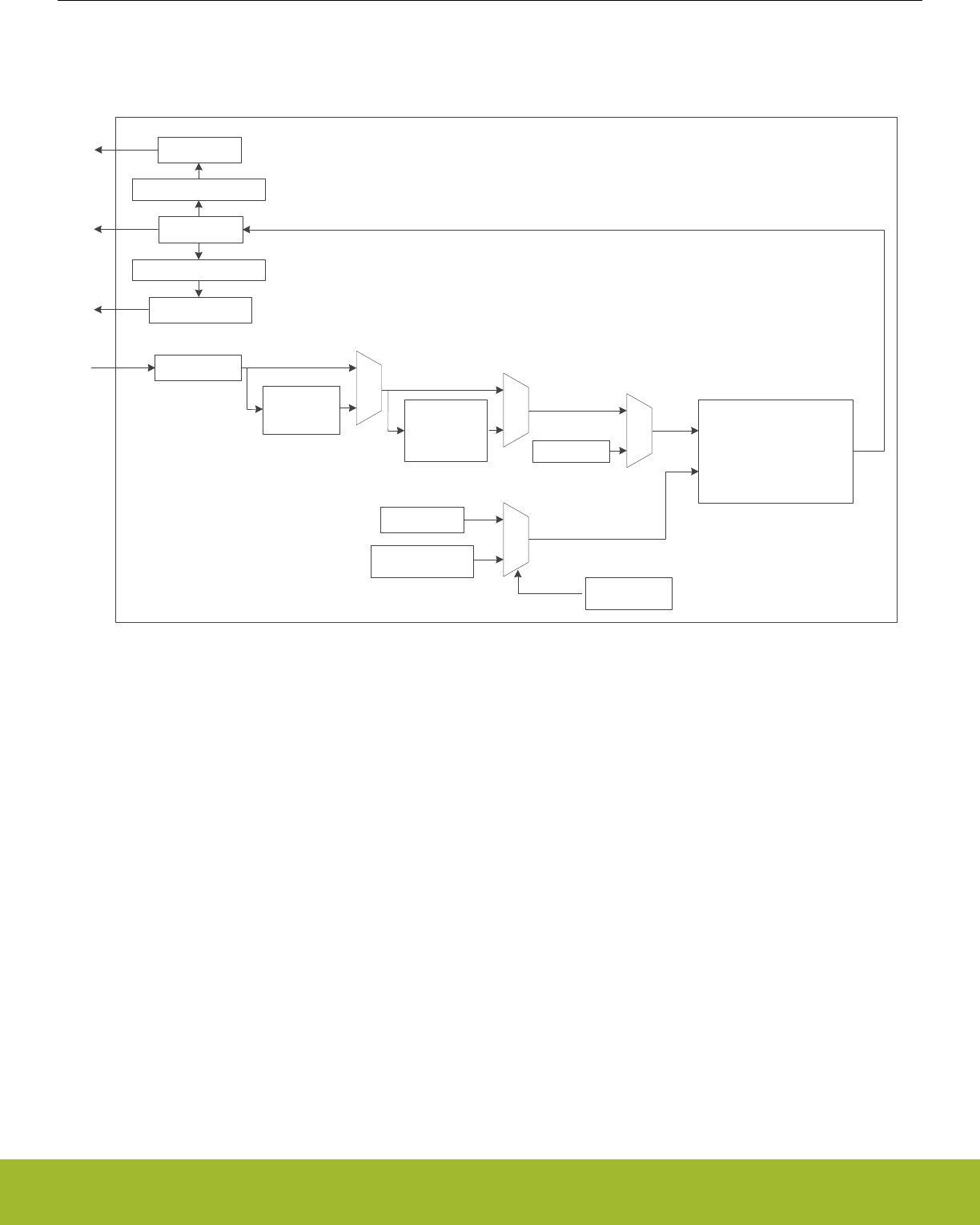
30.3 Functional Description
An overview of the GPCRC module is shown in Figure 30.1 GPCRC Overview on page 1021.
GPCRC Module
DATAREV
INPUTDATA
byte
reorder byte-level
bit
reversal Hardware CRC
Calculation Unit
Seed
bit reversal
POLY
0x04C11DB7
16-bit Programmable
32-bit Fixed Polynomial
Selection
DATA
byte reversal
DATABYTEREV
Figure 30.1. GPCRC Overview
Reference Manual
GPCRC - General Purpose Cyclic Redundancy Check
silabs.com | Smart. Connected. Energy-friendly. Preliminary Rev. 0.5 | 1021

30.3.1 Polynomial Specification
POLYSEL in GPCRC_CTRL selects between 32-bit and 16-bit polynomial functions. When a 32-bit polynomial is selected, the fixed
IEEE 802.3 polynomial(0x04C11DB7) is used. When a 16-bit polynomial is selected, any valid polynomial can be defined by the user in
GPCRC_POLY.
A valid 16-bit CRC polynomial must have an x^16 term and an x^0 term. Theoretically, a 16-bit polynomial has 17 terms total. The con-
vention used is to omit the x^16 term. The polynomial should be written in reversed (little endian) bit order. The most significant bit
corresponds to the lowest order term. Thus, the most significant bit in CRC_POLY represents the x^0 term, and the least significant bit
in CRC_POLY represents the x^15 term. The highest significant bit of CRC_POLY should always set to 1.The polynomial representa-
tion for the CRC-16-CCIT polynomial x^16 + x^12 + x^5 + 1, or 0x8408 in reversed order, is shown in Figure 30.2 Polynomial Repre-
sentation on page 1022.
15 14 13 12 11 10 9 8
POLY
76543210
1000010000001000
x16
x12+
x5+
1+
1
CRC-16-CCITT Normal: 0x1021 Reversed: 0x8408
Figure 30.2. Polynomial Representation
30.3.2 Input and Output Specification
The CRC input data can be written to the GPCRC_INPUTDATA, GPCRC_INPUTDATAHWORD or GPCRC_INPUTDATABYTE register
via the APB bus based on different data size. If BYTEMODE in GPCRC_CTRL is set, only the least significant byte of the data word will
be used for the CRC calculation no matter which input register is written. There are also three output registers for different ordering.
Reading from GPCRC_DATA will get the result based on the polynomial in reversed order, while reading from GPCRC_DATAREV will
get the result based on the polynomial in normal order. The CRC calculation needs one clock cycle, reading from GPCRC_DATA,
GPCRC_DATAREV or GPCRC_DATABYTEREV register or writting to GPCRC_CMD register is halted while the calculation is in pro-
gress.
30.3.3 Initialization
The CRC can be pre-loaded or re-initialized by first writing a 32-bit programmable init value to INIT in GPCRC_INIT and then setting
INIT in GPCRC_CMD. It can also be re-initialized automatically when read from DATA, DATAREV or DATABYTEREV provided that AU-
TOINIT in GPCRC_CTRL is set, the CRC would be re-initialized with the stored init value.
30.3.4 DMA Usage
A DMA channel may be used to transfer data into the CRC engine. All bytes and half-word writes must be word-aligned. The recom-
mended DMA usage model is to use the DMA to transfer all avaliable words of data and use software writes to capture any remaining
bytes.
Reference Manual
GPCRC - General Purpose Cyclic Redundancy Check
silabs.com | Smart. Connected. Energy-friendly. Preliminary Rev. 0.5 | 1022
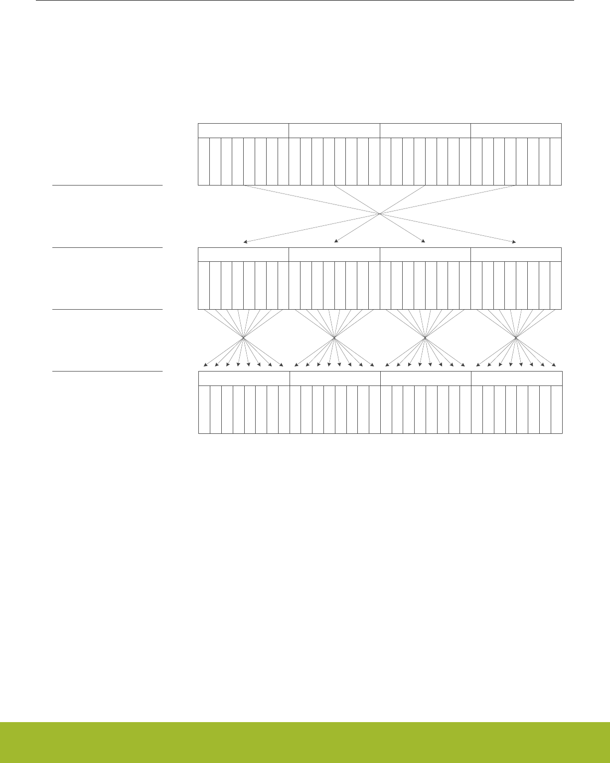
30.3.5 Byte-Level Bit Reversal and Byte Reordering
The byte-level bit reversal and byte reordering operations occur before the data is used in the CRC calculation. Byte reordering can
occur on words or half words. The hardware ignores the BYTEREVERSE field with any byte writes or operations with byte mode ena-
bled (BYTEMODE = 1), but the bit reversal settings (BITREVERSE) are still applied to the byte. 32-bit little endian MSB-first data can
be treated like 32-bit little endian LSB-first data, as shown in Figure 30.3 Data Ordering Example - 32-bit MSB -first to LSB-first on page
1023. In this example, 32-bit data is written to GPCRC_INPUTDATA, BYTEREVERSE is set for byte ordering, and BITREVERSE is set
for byte-level bit reversal.
bit 7
bit 5
bit 4
bit 6
bit 2
bit 0
bit 3
bit 1
Byte 2
bit 7
bit 5
bit 4
bit 6
bit 2
bit 0
bit 3
bit 1
Byte 1Byte 0
bit 7
bit 5
bit 4
bit 6
bit 2
bit 0
bit 3
bit 1
Byte 0
bit 7
bit 5
bit 4
bit 6
bit 2
bit 0
bit 3
bit 1
bit 7
bit 5
bit 4
bit 6
bit 2
bit 0
bit 3
bit 1
Byte 1
bit 7
bit 5
bit 4
bit 6
bit 2
bit 0
bit 3
bit 1
Byte 2
bit 7
bit 5
bit 4
bit 6
bit 2
bit 0
bit 3
bit 1
Byte 3
bit 7
bit 5
bit 4
bit 6
bit 2
bit 0
bit 3
bit 1
Byte 3
bit 0
bit 2
bit 3
bit 1
bit 5
bit 7
bit 4
bit 6
Byte 2
bit 0
bit 2
bit 3
bit 1
bit 5
bit 7
bit 4
bit 6
Byte 0
bit 0
bit 2
bit 3
bit 1
bit 5
bit 7
bit 4
bit 6
Byte 1
bit 0
bit 2
bit 3
bit 1
bit 5
bit 7
bit 4
bit 6
Byte 3
Input data is big endian, MSB-
first
BYTEREVERSE = 1
BITREVERSE = 1
Data is now little endian, LSB-
first for CRC calculation
Figure 30.3. Data Ordering Example - 32-bit MSB -first to LSB-first
When handling 16-bit data, the byte reordering function only swap the two lowest bytes and clear the two highest bytes, as shown in
Figure 30.4 Data Ordering Example - 16-bit MSB -first to LSB-first on page 1024. In this example, 16-bit data is written to GPCRC_IN-
PUTDATAHWORD, BYTEREVERSE is set for byte ordering, and BITREVERSE is set for byte-level bit reversal.
Reference Manual
GPCRC - General Purpose Cyclic Redundancy Check
silabs.com | Smart. Connected. Energy-friendly. Preliminary Rev. 0.5 | 1023
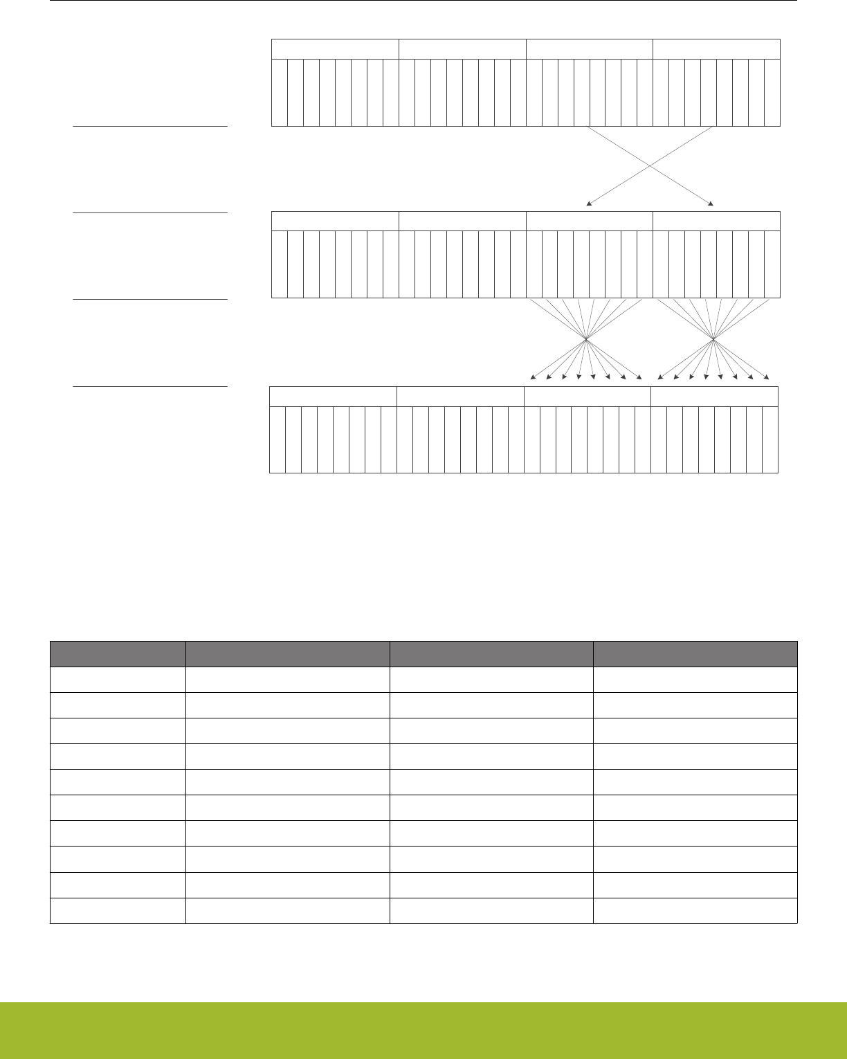
bit 7
bit 5
bit 4
bit 6
bit 2
bit 0
bit 3
bit 1
Byte 2
bit 7
bit 5
bit 4
bit 6
bit 2
bit 0
bit 3
bit 1
Byte 0
bit 7
bit 5
bit 4
bit 6
bit 2
bit 0
bit 3
bit 1
Byte 1
0
0
0
0
0
0
0
0
0
0
0
0
0
0
0
0
bit 7
bit 5
bit 4
bit 6
bit 2
bit 0
bit 3
bit 1
Byte 0
bit 7
bit 5
bit 4
bit 6
bit 2
bit 0
bit 3
bit 1
Byte 1
bit 0
bit 2
bit 3
bit 1
bit 5
bit 7
bit 4
bit 6
Byte 0
bit 0
bit 2
bit 3
bit 1
bit 5
bit 7
bit 4
bit 6
Byte 1
Input data is big endian, MSB-
first
BYTEREVERSE = 1
BITREVERSE = 1
Data is now 16-bit little
endian, LSB-first for CRC
calculation
bit 7
bit 5
bit 4
bit 6
bit 2
bit 0
bit 3
bit 1
Byte 3
8'h00 8'h00
0
0
0
0
0
0
0
0
0
0
0
0
0
0
0
0
8'h00 8'h00
Figure 30.4. Data Ordering Example - 16-bit MSB -first to LSB-first
Assuming a word input byte order of B3 B2 B1 B0, the values used in the CRC calculation for the various settings of the byte-level bit
reversal and byte reordering are shown in Table 30.1 Byte-Level Bit Reversal and Byte Reordering Results (B3 B2 B1 B0 Input Order)
on page 1024.
Table 30.1. Byte-Level Bit Reversal and Byte Reordering Results (B3 B2 B1 B0 Input Order)
Input Width(bits) BYTEREVERSE Setting BITREVERSE Setting Input to CRC calculation
32 0 0 B3 B2 B1 B0
32 1 1 'B0 'B1 'B2 'B3
32 1 0 B0 B1 B2 B3
32 0 1 'B3 'B2 'B1 'B0
16 0 0 XX XX B1 B0
16 1 1 XX XX 'B0 'B1
16 1 0 XX XX B0 B1
16 0 1 XX XX 'B1 'B0
8 - 0 XX XX XX XX B0
8 - 1 XX XX XX XX 'B0
Reference Manual
GPCRC - General Purpose Cyclic Redundancy Check
silabs.com | Smart. Connected. Energy-friendly. Preliminary Rev. 0.5 | 1024

Input Width(bits) BYTEREVERSE Setting BITREVERSE Setting Input to CRC calculation
Notes:
1. X indicates a "don't care".
2. Bn is the byte field within the word.
3. 'Bn is the bit-reversed byte field within the word.
30.4 Register Map
The offset register address is relative to the registers base address.
Offset Name Type Description
0x000 GPCRC_CTRL RW Control Register
0x004 GPCRC_CMD W1 Command Register
0x008 GPCRC_INIT RWH CRC Init Value
0x00C GPCRC_POLY RW CRC Polynomial Value
0x010 GPCRC_INPUTDATA WInput 32-bit Data Register
0x014 GPCRC_INPUTDATAHWORD WInput 16-bit Data Register
0x018 GPCRC_INPUTDATABYTE WInput 8-bit Data Register
0x01C GPCRC_DATA RCRC Data Register
0x020 GPCRC_DATAREV RCRC Data Reverse Register
0x024 GPCRC_DATABYTEREV RCRC Data Byte Reverse Register
Reference Manual
GPCRC - General Purpose Cyclic Redundancy Check
silabs.com | Smart. Connected. Energy-friendly. Preliminary Rev. 0.5 | 1025

30.5 Register Description
30.5.1 GPCRC_CTRL - Control Register
Offset Bit Position
0x000
31
30
29
28
27
26
25
24
23
22
21
20
19
18
17
16
15
14
13
12
11
10
9
8
7
6
5
4
3
2
1
0
Reset
0
0
0
0
0
0
Access
RW
RW
RW
RW
RW
RW
Name
AUTOINIT
BYTEREVERSE
BITREVERSE
BYTEMODE
POLYSEL
EN
Bit Name Reset Access Description
31:14 Reserved To ensure compatibility with future devices, always write bits to 0. More information in 1.2 Conven-
tions
13 AUTOINIT 0 RW Auto Init Enable
Enables auto init by re-seeding the CRC result based on the value in INIT after reading of DATA, DATAREV or DATABY-
TEREV.
12:11 Reserved To ensure compatibility with future devices, always write bits to 0. More information in 1.2 Conven-
tions
10 BYTEREVERSE 0 RW Byte Reverse Mode
Allows byte level reverse of bytes B3, B2, B1, B0 within the 32-bit data word
Value Mode Description
0 NORMAL No reverse: B3, B2, B1, B0
1 REVERSED Reverse byte order. For 32-bit: B0, B1, B2, B3; For 16-bit: 0, 0, B0, B1
9 BITREVERSE 0 RW Byte-level Bit Reverse Enable
Reverses bits within each byte of the 32-bit data word
Value Mode Description
0 NORMAL No reverse
1 REVERSED Reverse bit order in each byte
8 BYTEMODE 0 RW Byte Mode Enable
Treats all writes as bytes. Only the least significant byte of the data-word will be used for CRC calculation for all writes
7:5 Reserved To ensure compatibility with future devices, always write bits to 0. More information in 1.2 Conven-
tions
4 POLYSEL 0 RW Polynomial Select
Selects 16-bit CRC programmable polynomial or 32-bit CRC fixed polynomial
Value Mode Description
0 CRC32 CRC-32 (0x04C11DB7) polynomial selected
1 16 16-bit CRC programmable polynomial selected
Reference Manual
GPCRC - General Purpose Cyclic Redundancy Check
silabs.com | Smart. Connected. Energy-friendly. Preliminary Rev. 0.5 | 1026

Bit Name Reset Access Description
3:1 Reserved To ensure compatibility with future devices, always write bits to 0. More information in 1.2 Conven-
tions
0 EN 0 RW CRC Functionality Enable
Enables CRC functionality.
Value Mode Description
0 DISABLE Disable CRC function. Reordering function is available, only BITRE-
VERSE and BYTEREVERSE bits are configurable in this mode
1 ENABLE Writes to inputdata registers result in CRC operations
30.5.2 GPCRC_CMD - Command Register
Offset Bit Position
0x004
31
30
29
28
27
26
25
24
23
22
21
20
19
18
17
16
15
14
13
12
11
10
9
8
7
6
5
4
3
2
1
0
Reset
0
Access
W1
Name
INIT
Bit Name Reset Access Description
31:1 Reserved To ensure compatibility with future devices, always write bits to 0. More information in 1.2 Conven-
tions
0 INIT 0 W1 Initialization Enable
Writing 1 to this bit initialize the CRC by writing the INIT value in CRC_INIT to CRC_DATA.
30.5.3 GPCRC_INIT - CRC Init Value
Offset Bit Position
0x008
31
30
29
28
27
26
25
24
23
22
21
20
19
18
17
16
15
14
13
12
11
10
9
8
7
6
5
4
3
2
1
0
Reset
0x00000000
Access
RWH
Name
INIT
Bit Name Reset Access Description
31:0 INIT 0x00000000 RWH CRC Initialization Value
This value is loaded into CRC_DATA upon issuing the INIT command in CRC_CMD
Reference Manual
GPCRC - General Purpose Cyclic Redundancy Check
silabs.com | Smart. Connected. Energy-friendly. Preliminary Rev. 0.5 | 1027

30.5.4 GPCRC_POLY - CRC Polynomial Value
Offset Bit Position
0x00C
31
30
29
28
27
26
25
24
23
22
21
20
19
18
17
16
15
14
13
12
11
10
9
8
7
6
5
4
3
2
1
0
Reset
0x0000
Access
RW
Name
POLY
Bit Name Reset Access Description
31:16 Reserved To ensure compatibility with future devices, always write bits to 0. More information in 1.2 Conven-
tions
15:0 POLY 0x0000 RW CRC Polynomial Value
This value defines 16-bit POLY, which is used as the polynomial during the 16-bit CRC calculation. The polynomial is de-
fined in reversed representation, meaning that the lowest degree term is in the highest bit position of POLY. Additionally, the
highest degree term in the polynomial is implicit. Further examples of the CRC configuration can be found in the documen-
tation.
30.5.5 GPCRC_INPUTDATA - Input 32-bit Data Register
Offset Bit Position
0x010
31
30
29
28
27
26
25
24
23
22
21
20
19
18
17
16
15
14
13
12
11
10
9
8
7
6
5
4
3
2
1
0
Reset
0x00000000
Access
W
Name
INPUTDATA
Bit Name Reset Access Description
31:0 INPUTDATA 0x00000000 W Input Data for 32-bit
CRC Input 32-bit Data can be written to this register. Each time this register is written, the CRC value is updated.
Reference Manual
GPCRC - General Purpose Cyclic Redundancy Check
silabs.com | Smart. Connected. Energy-friendly. Preliminary Rev. 0.5 | 1028

30.5.6 GPCRC_INPUTDATAHWORD - Input 16-bit Data Register
Offset Bit Position
0x014
31
30
29
28
27
26
25
24
23
22
21
20
19
18
17
16
15
14
13
12
11
10
9
8
7
6
5
4
3
2
1
0
Reset
0x0000
Access
W
Name
INPUTDATAHWORD
Bit Name Reset Access Description
31:16 Reserved To ensure compatibility with future devices, always write bits to 0. More information in 1.2 Conven-
tions
15:0 INPUTDATAHWORD 0x0000 W Input Data for 16-bit
CRC Input 16-bit Data can be written to this register. Each time this register is written, the CRC value is updated.
30.5.7 GPCRC_INPUTDATABYTE - Input 8-bit Data Register
Offset Bit Position
0x018
31
30
29
28
27
26
25
24
23
22
21
20
19
18
17
16
15
14
13
12
11
10
9
8
7
6
5
4
3
2
1
0
Reset
0x00
Access
W
Name
INPUTDATABYTE
Bit Name Reset Access Description
31:8 Reserved To ensure compatibility with future devices, always write bits to 0. More information in 1.2 Conven-
tions
7:0 INPUTDATABYTE 0x00 W Input Data for 8-bit
CRC Input 8-bit Data can be written to this register. Each time this register is written, the CRC value is updated.
Reference Manual
GPCRC - General Purpose Cyclic Redundancy Check
silabs.com | Smart. Connected. Energy-friendly. Preliminary Rev. 0.5 | 1029

30.5.8 GPCRC_DATA - CRC Data Register
Offset Bit Position
0x01C
31
30
29
28
27
26
25
24
23
22
21
20
19
18
17
16
15
14
13
12
11
10
9
8
7
6
5
4
3
2
1
0
Reset
0x00000000
Access
R
Name
DATA
Bit Name Reset Access Description
31:0 DATA 0x00000000 R CRC Data Register
CRC Data Register, read only. The CRC data register may still be indirectly written from software, by writing the INIT regis-
ter and then issue an INITIALIZE command.
30.5.9 GPCRC_DATAREV - CRC Data Reverse Register
Offset Bit Position
0x020
31
30
29
28
27
26
25
24
23
22
21
20
19
18
17
16
15
14
13
12
11
10
9
8
7
6
5
4
3
2
1
0
Reset
0x00000000
Access
R
Name
DATAREV
Bit Name Reset Access Description
31:0 DATAREV 0x00000000 R Data Reverse Value
Bit reversed version of CRC Data register. When a 32-bit CRC polynomial is selected, the reversal occurs on the entire 32-
bit word. When a 16-bit CRC polynomial is selected, the bits [15:0] are reversed.
Reference Manual
GPCRC - General Purpose Cyclic Redundancy Check
silabs.com | Smart. Connected. Energy-friendly. Preliminary Rev. 0.5 | 1030

30.5.10 GPCRC_DATABYTEREV - CRC Data Byte Reverse Register
Offset Bit Position
0x024
31
30
29
28
27
26
25
24
23
22
21
20
19
18
17
16
15
14
13
12
11
10
9
8
7
6
5
4
3
2
1
0
Reset
0x00000000
Access
R
Name
DATABYTEREV
Bit Name Reset Access Description
31:0 DATABYTEREV 0x00000000 R Data Byte Reverse Value
Byte reversed version of CRC Data register. When a 32-bit CRC polynomial is selected, the bytes are swizzled to {B0, B1,
B2, B3}. When a 16-bit CRC polynomial is selected, the bytes are swizzled to {0, 0, B0, B1}.
Reference Manual
GPCRC - General Purpose Cyclic Redundancy Check
silabs.com | Smart. Connected. Energy-friendly. Preliminary Rev. 0.5 | 1031

31. TRNG - True Random Number Generator
0 1 2 3 4
Quick Facts
What?
The TRNG module is a non-deterministic random
number generator based on a full hardware solution.
Why?
Secure cryptography commonly relies on randomly-
generated numbers for key generation. Software sol-
utions for random number generation do not usually
produce results with enough entropy to satisfy exist-
ing standards. Dedicated hardware can provide suit-
able entropy in an energy-efficient, non-intrusive
manner, while also relieving software burden.
How?
Ring oscillators and sampling logic combine to pro-
duce non-deterministic random numbers.
31.1 Introduction
The TRNG module is a non-deterministic random number generator based on a full hardware solution. The TRNG output passes the
NIST 800-22 and AIS31 test suites.
31.2 Features
• Simple bus interface to access random numbers, control, and status registers
• 64 x 32-bit FIFO for random number access
• Interrupt sources from different FIFO, error, and noise alarm events
• Passes NIST 800-22 and AIS31
• Ready for NIST 800-90B
• Health tests compliant to NIST 800-90B and AIS31
Reference Manual
TRNG - True Random Number Generator
silabs.com | Smart. Connected. Energy-friendly. Preliminary Rev. 0.5 | 1032
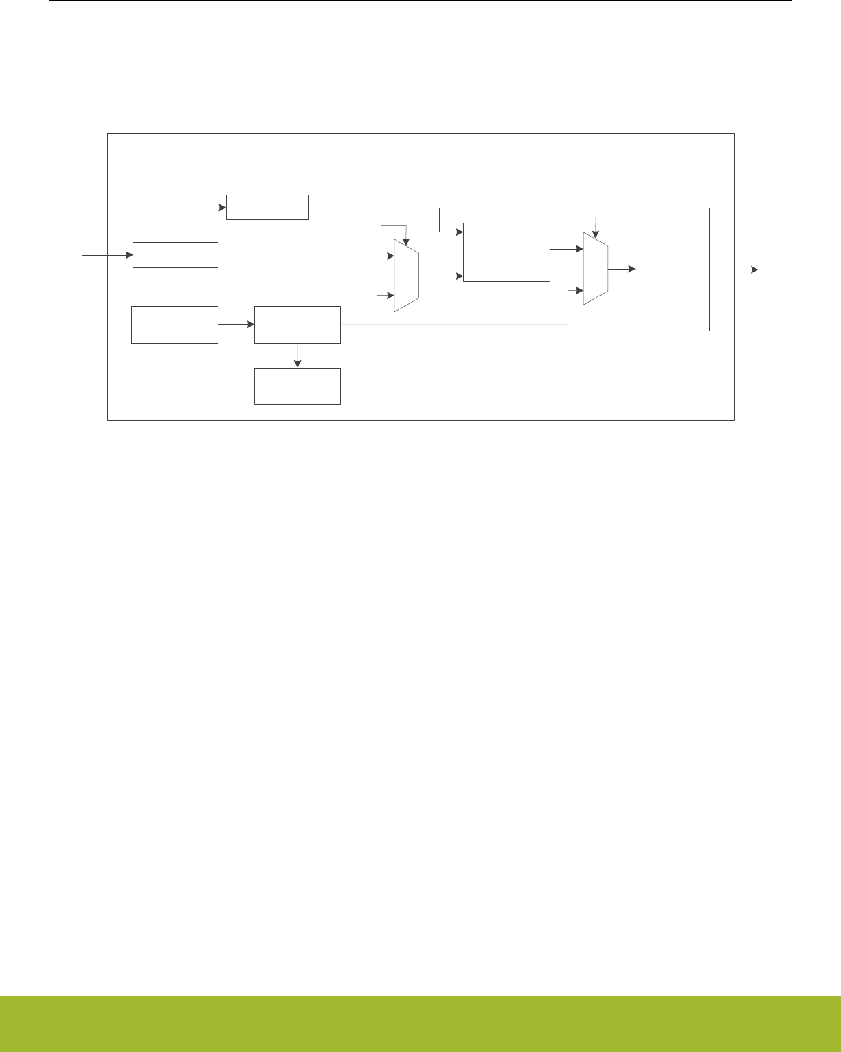
31.3 Functional Description
Software drivers provided by Silicon Labs offer a simple API interface to the TRNG module. It is highly recommended to use the provi-
ded software librariesto access the TRNG module. An overview of the TRNG module is shown in Figure 31.1 TRNG Overview on page
1033.
TRNG Module
KEY
128-bit
Entropy Source
Conditioning
Function
TESTDATA 64 x 32-bit
FIFO
Startup and
Online Tests
TESTEN
CONDBYPASS
Interrupts and
Alarms
Figure 31.1. TRNG Overview
31.3.1 Built-In Tests
The TRNG module includes several built-in tests to detect issues with the noise source, ensure entropy, and meet cryptography stand-
ards.The Repetition Count Test and Adaptive Proportion Test with window sizes of 64 and 4096 bits described in section 6.5.1.2 of
NIST-800-90B (http://csrc.nist.gov/publications/drafts/800-90/draft-sp800-90b.pdf) are implemented in hardware and run continuously
on the data. All three tests have corresponding interrupt flags that can optionally be used to generate a system interrupt.
The AIS31 Online Test described in section 5.5.3 of https://www.bsi.bund.de/SharedDocs/Downloads/DE/BSI/Zertifizierung/Interpreta-
tionen/AIS_31_Functionality_classes_for_random_number_generators_e.pdf is also implemented in hardware, and runs continuously
on the data. Both the preliminary noise alarm and the noise alarm are optionally available as interrupt sources from the TRNG module.
If a noise alarm occurs, the TRNG will be shut down, and must be reset with a software reset.
Additionally, the NIST-800-90B and AIS31 startup tests may be optionally enabled or disabled by software. The NIST-800-90B startup
test is enabled if the CONTROL_BYPNIST bit is cleared to 0. The AIS31 startup test is likewise enabled when CONTROL_BYPAIS31 is
cleared to 0. If either the NIST-800-90B or AIS31 startup tests are enabled, no data will be written to the output FIFO until the startup
requirements for these tests pass.
31.3.2 FIFO Interface
The TRNG module includes a 64-word output FIFO to hold the output data as it becomes available. The number of 32-bit words availa-
ble in the FIFO may be checked at any time by reading the FIFOLEVEL register. When the FIFO is completely filled, the TRNG will be
shut down, the STATUS_FULLIF flag will be set, and no further data will be written to the FIFO until the FIFO has been flushed. Data
may be read from the FIFO one word (32-bits) at a time via the FIFO register. The STATUS_FULLIF flag is cleared upon reading the
FIFOLEVEL register.
Reference Manual
TRNG - True Random Number Generator
silabs.com | Smart. Connected. Energy-friendly. Preliminary Rev. 0.5 | 1033

31.3.3 Data Format - Byte Ordering
All cryptographic data is handled following the big-endian format (AES standard). The first byte (lowest address) of the data is the Most
Significant Byte (MSB). However, the bus interfaces on the core use little endian format for internal byte ordering within a 32-bit word.
The Least Significant Byte (LSB) within a word is stored at the lowest address.
For example, a 128-bit block 0x00112233445566778899AABBCCDDEEFF is read from the FIFO in the following order:
Word 1 = 0x33221100
Word 2 = 0x77665544
Word 3 = 0xBBAA9988
Word 4 = 0xFFDDEECC
This is important to note when checking the conditioning function for validity. The KEY registers also follow this standard, with KEY0
holding the MSB of a 128-bit value and KEY3 holding the LSB.
31.3.4 TRNG Usage
It is highly recommended to use the software libraries provided by Silicon Labs to access the TRNG module. The information in the
following sections are reference for users who choose to write their own low-level software drivers.
Reference Manual
TRNG - True Random Number Generator
silabs.com | Smart. Connected. Energy-friendly. Preliminary Rev. 0.5 | 1034

31.3.4.1 Checking the Conditioning Function
The conditioning function receives 512 bits from the entropy source and generates 128 bits of output. The conditioning function can be
tested by writing a known key and known data into the block with test mode enabled, then validating against the expected output. The
sequence of operations to test the conditioning function is as follows:
1. Apply a software reset by setting CONTROL_SOFTRESET to 1, then clearing it to 0.
2. Configure the CONTROL register. Important configuration options include:
• Enable test mode by setting CONTROL_TESTEN to 1.
• Ensure the conditioning function is used by clearning CONTROL_CONDBYPASS to 0.
3. Write the key into registers KEY0, KEY1, KEY2, and KEY3.
4. Write the 512 bits of known data to TESTDATA 32 bits at a time, polling for STATUS_TESTDATABUSY = 0 after each write.
5. Read the 128-bit result from the FIFO 32 bits at a time.
Table 31.1 Known-Answer Test for Conditioning Function on page 1035 shows an example with a given key, known data input, and
expected output (taken from section F.2.1 in http://csrc.nist.gov/publications/nistpubs/800-38a/sp800-38a.pdf).
Table 31.1. Known-Answer Test for Conditioning Function
128-bit Format 32-bit Bus Format
Key 0x2B7E151628AED2A6ABF7158809CF4F3C 0x16157E2B
0xA6D2AE28
0x8815F7AB
0x3C4FCF09
Input 0x6BC0BCE12A459991E134741A7F9E1925
0xAE2D8A571E03AC9C9EB76FAC45AF8E51
0x30C81C46A35CE411E5FBC1191A0A52EF
0xF69F2445DF4F9B17AD2B417BE66C3710
0xE1BCC06B
0x9199452A
0x1A7434E1
0x25199E7F
0x578A2DAE
0x9CAC031E
0xAC6FB79E
0x518EAF45
0x461CC830
0x11E45CA3
0x19C1FBE5
0xEF520A1A
0x45249FF6
0x179B4FDF
0x7B412BAD
0x10376CE6
Expected output 0x3FF1CAA1681FAC09120ECA307586E1A7 0xA1CAF13F
0x09AC1F68
0x30CA0E12
0xA7E18675
Reference Manual
TRNG - True Random Number Generator
silabs.com | Smart. Connected. Energy-friendly. Preliminary Rev. 0.5 | 1035

31.3.4.2 Checking the Entropy Source
The entropy source may be checked using the three built in test sources: repetition count, 64-sample adaptive proportion, and 4096-
sample adaptive proportion. The entropy source may be tested using the following sequence:
1. Apply a software reset by setting CONTROL_SOFTRESET to 1, then clearing it to 0.
2. Configure the CONTROL register. Important configuration options include:
• Disable test mode by clearing CONTROL_TESTEN to 0.
• Bypass the conditioning function by setting CONTROL_CONDBYPASS to 1.
• Enable the TRNG by setting CONTROL_ENABLE to 1.
3. Check the FIFOLEVEL register to monitor the amount of generated random numbers or wait for the STATUS_FULLIF flag to set,
indicating the FIFO is full. Note that STATUS_FULLIF may be configured to generate an interrupt if desired.
4. When FIFOLEVEL has reached the expected value or when STATUS_FULLIF is set, read the random numbers using the FIFO
register. Those values can be discarded.
5. Continue reading and discarding the random data until at least 4097 x 2 bits (257 x 32-bit words) have been read. This ensures
that enough time has passed for the longest test to run.
6. Check the STATUS register for error flags.
31.3.4.3 Programming a Random Key
1. Check the FIFOLEVEL register to monitor the amount of generated random numbers or wait for the STATUS_FULLIF flag to set,
indicating the FIFO is full. Note that STATUS_FULLIF may be configured to generate an interrupt if desired.
2. When FIFOLEVEL has reached the expected value or when STATUS_FULLIF is set, read the random numbers using the FIFO
register.
3. Use four 32-bit random values to program a random key to the KEY0, KEY1, KEY2, and KEY3 registers.
4. Apply a software reset by setting CONTROL_SOFTRESET to 1, then clearing it to 0. This will flush the FIFO data.
31.3.4.4 Reading Samples
1. Check the FIFOLEVEL register to monitor the amount of generated random numbers or wait for the STATUS_FULLIF flag to set,
indicating the FIFO is full. Note that STATUS_FULLIF may be configured to generate an interrupt if desired.
2. When FIFOLEVEL has reached the expected value or when STATUS_FULLIF is set, read the random numbers using the FIFO
register.
31.4 Register Map
The offset register address is relative to the registers base address.
Offset Name Type Description
0x000 TRNGn_CONTROL RW Main Control Register
0x004 TRNGn_FIFOLEVEL R(a) FIFO Level Register
0x00C TRNGn_FIFODEPTH RFIFO Depth Register
0x010 TRNGn_KEY0 RW Key Register 0
0x014 TRNGn_KEY1 RW Key Register 1
0x018 TRNGn_KEY2 RW Key Register 2
0x01C TRNGn_KEY3 RW Key Register 3
0x020 TRNGn_TESTDATA RW Test Data Register
0x030 TRNGn_STATUS RWH Status Register
0x034 TRNGn_INITWAITVAL RW Initial Wait Counter
0x100 TRNGn_FIFO R(a) FIFO Data
Reference Manual
TRNG - True Random Number Generator
silabs.com | Smart. Connected. Energy-friendly. Preliminary Rev. 0.5 | 1036

31.5 Register Description
31.5.1 TRNGn_CONTROL - Main Control Register
Offset Bit Position
0x000
31
30
29
28
27
26
25
24
23
22
21
20
19
18
17
16
15
14
13
12
11
10
9
8
7
6
5
4
3
2
1
0
Reset
0
0
0
0
0
0
0
0
0
0
0
0
0
Access
RW
RW
RW
RW
RW
RW
RW
RW
RW
RW
RW
RW
RW
Name
BYPAIS31
BYPNIST
FORCERUN
ALMIEN
PREIEN
SOFTRESET
FULLIEN
APT4096IEN
APT64IEN
REPCOUNTIEN
CONDBYPASS
TESTEN
ENABLE
Bit Name Reset Access Description
31:14 Reserved To ensure compatibility with future devices, always write bits to 0. More information in 1.2 Conven-
tions
13 BYPAIS31 0 RW AIS31 Start-up Test Bypass.
Bypass for AIS31 startup test.
Value Mode Description
0 NORMAL AIS31 startup test is applied. No data will be written to the FIFO until
the test passes.
1 BYPASS AIS31 startup test is bypassed.
12 BYPNIST 0 RW NIST Start-up Test Bypass.
Bypass for NIST-800-90B startup test.
Value Mode Description
0 NORMAL NIST-800-90B startup test is applied. No data will be written to the
FIFO until the test passes.
1 BYPASS NIST-800-90B startup test is bypassed.
11 FORCERUN 0 RW Oscillator Force Run
Set this bit to force oscillators to run even when FIFO is full.
Value Mode Description
0 NORMAL Oscillators will shut down when FIFO is full
1 RUN Oscillators will continue to run even after FIFO is full
10 ALMIEN 0 RW Interrupt enable for AIS31 noise alarm
Enable/disable AIS31 noise alarm interrupt.
9 PREIEN 0 RW Interrupt enable for AIS31 preliminary noise alarm
Enable/disable AIS31 preliminary noise alarm interrupt.
8 SOFTRESET 0 RW Software Reset
Set to reset the module. This bit is not cleared automatically.
Reference Manual
TRNG - True Random Number Generator
silabs.com | Smart. Connected. Energy-friendly. Preliminary Rev. 0.5 | 1037

Bit Name Reset Access Description
Value Mode Description
0 NORMAL Module not in reset
1 RESET The continuous test, the conditioning function and the FIFO are reset
7 FULLIEN 0 RW Interrupt enable for FIFO full
Enable/Disable FIFO full interrupt.
6 APT4096IEN 0 RW Interrupt enable for Adaptive Proportion Test failure (4096-sample
window)
Enable/Disable 4096-sample Adaptive Proportion test failure interrupt.
5 APT64IEN 0 RW Interrupt enable for Adaptive Proportion Test failure (64-sample
window)
Enable/Disable 64-sample Adaptive Proportion test failure interrupt.
4 REPCOUNTIEN 0 RW Interrupt enable for Repetition Count Test failure
Enable/Disable Repetition Count Test failure interrupt.
3 CONDBYPASS 0 RW Conditioning Bypass
Enables bypassing of the conditioning function (to observe entropy source directly).
Value Mode Description
0 NORMAL The conditionig function is used
1 BYPASS The conditioning function is bypassed
2 TESTEN 0 RW Test Enable
Selects the input for the conditioning function and continuous tests.
Value Mode Description
0 NOISE Non-determinsitc random number generation
1 TESTDATA Pseudo-random number generation
1 Reserved To ensure compatibility with future devices, always write bits to 0. More information in 1.2 Conven-
tions
0 ENABLE 0 RW TRNG Module Enable
Enable the TRNG. The module will generate random numbers unless the FIFO is full.
Value Mode Description
0 DISABLED Module disabled
1 ENABLED Module enabled
Reference Manual
TRNG - True Random Number Generator
silabs.com | Smart. Connected. Energy-friendly. Preliminary Rev. 0.5 | 1038

31.5.2 TRNGn_FIFOLEVEL - FIFO Level Register (Actionable Reads)
Offset Bit Position
0x004
31
30
29
28
27
26
25
24
23
22
21
20
19
18
17
16
15
14
13
12
11
10
9
8
7
6
5
4
3
2
1
0
Reset
0x00000000
Access
R
Name
VALUE
Bit Name Reset Access Description
31:0 VALUE 0x00000000 R FIFO Level
Number of 32-bit words of random data available in the FIFO. The STATUS_FULLIF flag is cleared when FIFOLEVEL is
read.
31.5.3 TRNGn_FIFODEPTH - FIFO Depth Register
Offset Bit Position
0x00C
31
30
29
28
27
26
25
24
23
22
21
20
19
18
17
16
15
14
13
12
11
10
9
8
7
6
5
4
3
2
1
0
Reset
0x00000040
Access
R
Name
VALUE
Bit Name Reset Access Description
31:0 VALUE 0x00000040 R FIFO Depth.
Maximum number of 32-bit words that can be stored in the FIFO.
Reference Manual
TRNG - True Random Number Generator
silabs.com | Smart. Connected. Energy-friendly. Preliminary Rev. 0.5 | 1039

31.5.4 TRNGn_KEY0 - Key Register 0
Offset Bit Position
0x010
31
30
29
28
27
26
25
24
23
22
21
20
19
18
17
16
15
14
13
12
11
10
9
8
7
6
5
4
3
2
1
0
Reset
0x00000000
Access
RW
Name
VALUE
Bit Name Reset Access Description
31:0 VALUE 0x00000000 RW Key 0
AES Key 32-bit sub-word 0 (MSB).
31.5.5 TRNGn_KEY1 - Key Register 1
Offset Bit Position
0x014
31
30
29
28
27
26
25
24
23
22
21
20
19
18
17
16
15
14
13
12
11
10
9
8
7
6
5
4
3
2
1
0
Reset
0x00000000
Access
RW
Name
VALUE
Bit Name Reset Access Description
31:0 VALUE 0x00000000 RW Key 1
AES Key 32-bit sub-word 1.
Reference Manual
TRNG - True Random Number Generator
silabs.com | Smart. Connected. Energy-friendly. Preliminary Rev. 0.5 | 1040

31.5.6 TRNGn_KEY2 - Key Register 2
Offset Bit Position
0x018
31
30
29
28
27
26
25
24
23
22
21
20
19
18
17
16
15
14
13
12
11
10
9
8
7
6
5
4
3
2
1
0
Reset
0x00000000
Access
RW
Name
VALUE
Bit Name Reset Access Description
31:0 VALUE 0x00000000 RW Key 2
AES Key 32-bit sub-word 2.
31.5.7 TRNGn_KEY3 - Key Register 3
Offset Bit Position
0x01C
31
30
29
28
27
26
25
24
23
22
21
20
19
18
17
16
15
14
13
12
11
10
9
8
7
6
5
4
3
2
1
0
Reset
0x00000000
Access
RW
Name
VALUE
Bit Name Reset Access Description
31:0 VALUE 0x00000000 RW Key 3
AES Key 32-bit sub-word 3 (LSB).
Reference Manual
TRNG - True Random Number Generator
silabs.com | Smart. Connected. Energy-friendly. Preliminary Rev. 0.5 | 1041

31.5.8 TRNGn_TESTDATA - Test Data Register
Offset Bit Position
0x020
31
30
29
28
27
26
25
24
23
22
21
20
19
18
17
16
15
14
13
12
11
10
9
8
7
6
5
4
3
2
1
0
Reset
0x00000000
Access
RW
Name
VALUE
Bit Name Reset Access Description
31:0 VALUE 0x00000000 RW Test data input to conditioning function or to the continuous tests
Each word written to this register represents 32 bits of input data for the selected test in test mode (CONTROL_TESTEN =
1). TESTDATABUSY in the STATUS register will be set to 1 each time data is written, and will clear to 0 when the next data
word can be written. Writes to this register are ignored if the TESTEN bit in the CONTROL register is 0.
Reference Manual
TRNG - True Random Number Generator
silabs.com | Smart. Connected. Energy-friendly. Preliminary Rev. 0.5 | 1042

31.5.9 TRNGn_STATUS - Status Register
Offset Bit Position
0x030
31
30
29
28
27
26
25
24
23
22
21
20
19
18
17
16
15
14
13
12
11
10
9
8
7
6
5
4
3
2
1
0
Reset
0
0
0
0
0
0
0
Access
R
RWH
R
R
R
R
R
Name
ALMIF
PREIF
FULLIF
APT4096IF
APT64IF
REPCOUNTIF
TESTDATABUSY
Bit Name Reset Access Description
31:10 Reserved To ensure compatibility with future devices, always write bits to 0. More information in 1.2 Conven-
tions
9 ALMIF 0 R AIS31 Noise Alarm interrupt status
Set when a noise alarm is detected in the AIS31 online test.
8 PREIF 0 RWH AIS31 Preliminary Noise Alarm interrupt status
Set when a preliminary noise alarm is detected in the AIS31 online test.
7 FULLIF 0 R FIFO full interrupt status
Set when the FIFO is full. The STATUS_FULLIF flag is cleared by reading FIFOLEVEL.
6 APT4096IF 0 R Adaptive Proportion test failure (4096-sample window) interrupt
status
Set when an Adaptive Proportion test (4096-sample window) failure occurs.
5 APT64IF 0 R Adaptive Proportion test failure (64-sample window) interrupt sta-
tus
Set when an Adaptive Proportion test (64-sample window) failure occurs.
4 REPCOUNTIF 0 R Repetition Count Test interrupt status
Set when a Repetition Count Test failure occurs.
3:1 Reserved To ensure compatibility with future devices, always write bits to 0. More information in 1.2 Conven-
tions
0 TESTDATABUSY 0 R Test Data Busy
Indicates that data written to TESTDATA is being processed.
Value Mode Description
0 IDLE TESTDATA write is finished processing or no test in progress.
1 BUSY TESTDATA write is still being processed.
Reference Manual
TRNG - True Random Number Generator
silabs.com | Smart. Connected. Energy-friendly. Preliminary Rev. 0.5 | 1043

31.5.10 TRNGn_INITWAITVAL - Initial Wait Counter
Offset Bit Position
0x034
31
30
29
28
27
26
25
24
23
22
21
20
19
18
17
16
15
14
13
12
11
10
9
8
7
6
5
4
3
2
1
0
Reset
0xFF
Access
RW
Name
VALUE
Bit Name Reset Access Description
31:8 Reserved To ensure compatibility with future devices, always write bits to 0. More information in 1.2 Conven-
tions
7:0 VALUE 0xFF RW Wait counter value
Number of clock cycles to wait before sampling data from the noise source.
31.5.11 TRNGn_FIFO - FIFO Data (Actionable Reads)
Offset Bit Position
0x100
31
30
29
28
27
26
25
24
23
22
21
20
19
18
17
16
15
14
13
12
11
10
9
8
7
6
5
4
3
2
1
0
Reset
0x00000000
Access
R
Name
VALUE
Bit Name Reset Access Description
31:0 VALUE 0x00000000 R FIFO Read Data
Data may be read from the FIFO 32 bits at a time using this register.
Reference Manual
TRNG - True Random Number Generator
silabs.com | Smart. Connected. Energy-friendly. Preliminary Rev. 0.5 | 1044
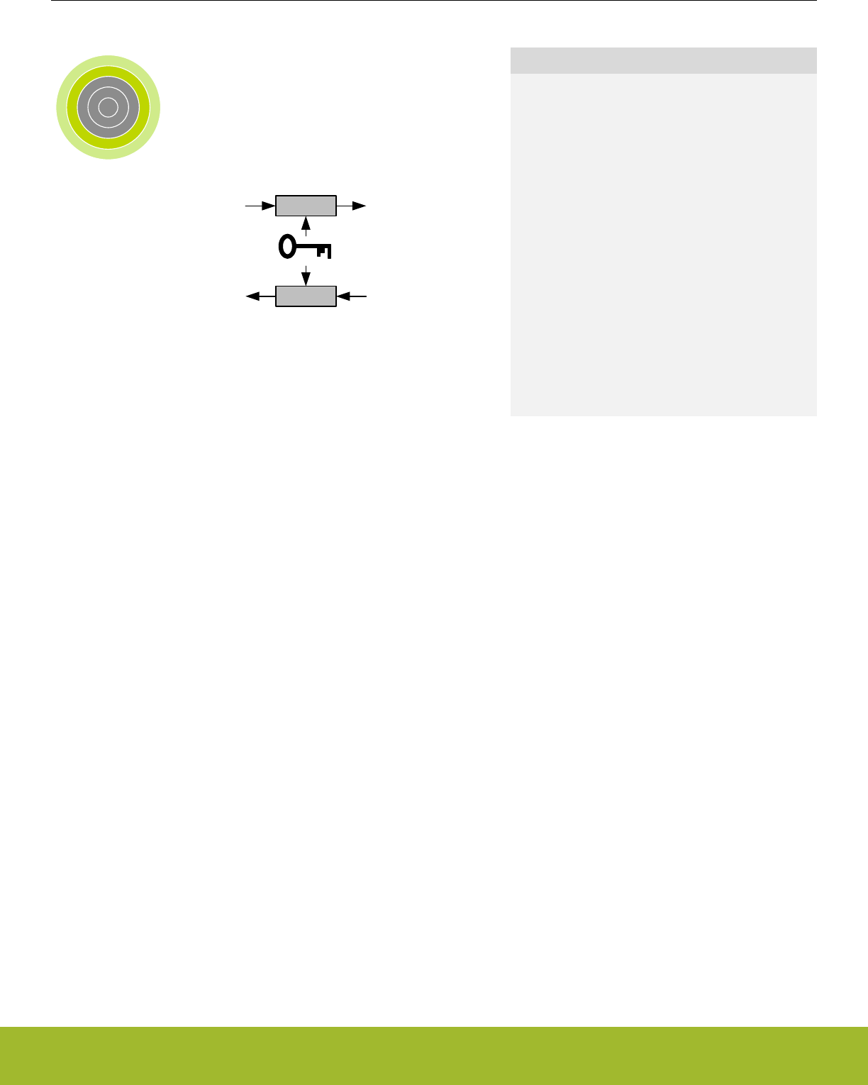
32. CRYPTO - Crypto Accelerator
0 1 2 3 4
How are you? AES &G#%5
!T4/#2I am fine AES
Quick Facts
What?
A fast and energy efficient autonomous hardware
accelerator for AES encryption and decryption with
128- or 256-bit keys, ECC over prime and binary
Galois finite fields, SHA-1, SHA-224 and SHA-256.
Why?
Efficient cryptography with little or no CPU interven-
tion helps to meet the speed and energy demands of
the application. Hardware implementations are gen-
erally more secure against side-channel attacks than
software implementations.
How?
Programmable sequences of instructions on big
numbers allow fast processing with little CPU inter-
vention. Furthermore, CRYPTO is linked to the Buf-
fer Controller (BUFC), thus enabling fast and effi-
cient autonomous cipher operations on data buffer
content.
32.1 Introduction
The CRYPTO module allows efficient acceleration of common cryptographic operations and allows these to be used efficiently with a
low CPU load. Operations performed by CRYPTO can be set up as a sequence of instructions on a set of 128-bit, 256-bit or 512-bit
registers to implement or accelerate Elliptic Curve Cryptography (ECC), SHA-1, SHA-224, SHA-256, and various block cipher modes
based on the Advanced Encryption Standard, also known as AES (FIPS-197).
CRYPTO is capable of autonomously fetching data, performing cipher operations and storing data across multiple blocks. When the
source data is not a multiple of 16 bytes (128 bits), Zero-padding can be included in the last block. Block operations such as Counter
Mode (CTR), Electronic Code Book (ECB), Cipher Block Chaining (CBC), Cipher Feedback (CFB) and Output Feedback (OFB) are
easily implemented. Block Cipher modes of operation such as Electronic Code Book (ECB), Counter Mode (CTR), Cipher Block Chain-
ing (CBC), CBC-MAC (CBC Message Authentication Code), CCM (Counter with CBC-MAC) and GCM (Galois Counter mode) are easi-
ly implemented.
CRYPTO is delivered with an extensive software library in Simplicity Studio that implements all major cryptographic algorithms, includ-
ing but not limited to AES, SHA-1, SHA-2, ECC, and legacy algorithms DES, 3DES, MD4, MD5 and RC4. The implementation acceler-
ates the algorithms using CRYPTO when possible.
Reference Manual
CRYPTO - Crypto Accelerator
silabs.com | Smart. Connected. Energy-friendly. Preliminary Rev. 0.5 | 1045

32.2 Features
• Efficient AES core
• Encryption/decryption using 128-bit key (54 clock cycles) or 256-bit key (75 clock cycles)
• Key buffer
• Supports autonomous cipher block modes (e.g. ECB, CTR, CBC, PCBC, CFB, CBC-MAC, GMAC, CCM, CCM* and GCM)
across multiple blocks
• Accelerated SHA-1, SHA-224 and SHA-256
• Accelerated Elliptic Curve Cryptography (ECC)
• Binary and Prime fields
• Supports NIST recommended curves: P-192, P-224, P-256, K-163, K-233, B-163, and B-233
• Galois/Counter Mode (GCM)
• ALU operations on GCM GF(2^128) field
• Flexible 256-bit ALU and sequencer
• 5 general purpose 256-bit registers
• Supports ADD, SUB, MUL, shift, XOR, etc.
• Up to 20 instructions can be chained to implement various block cipher modes
• Efficient operation
• Automatic data loading and storing from registers (through BUFC, the buffer controller)
• DMA request signals for data read and write
• Optional XOR Data write
• Interrupt on finished operations
• Extensive software support
• Extensive software library in Simplicity Studio
• Implements all major cryptographic algorithms: AES, SHA-1, SHA-2, and ECC
• Implements legacy algorithms: DES, 3DES, MD4, MD5, and RC4
• Hardware accelerated when possible
32.3 Usage and Programming Interface
Many security systems fail due to mistakes in the implementation. Therefore implementations should be left to experts in cryptographic
algorithms.
To solve this, the module is supported by an hardened cryptography software library and API delivered through Silicon Labs' Simplicity
Studio. The software API is a frontend for performing all supported cryptographic operations both for radio-protocols and applications,
and must be used to receive prompt support.
Reference Manual
CRYPTO - Crypto Accelerator
silabs.com | Smart. Connected. Energy-friendly. Preliminary Rev. 0.5 | 1046
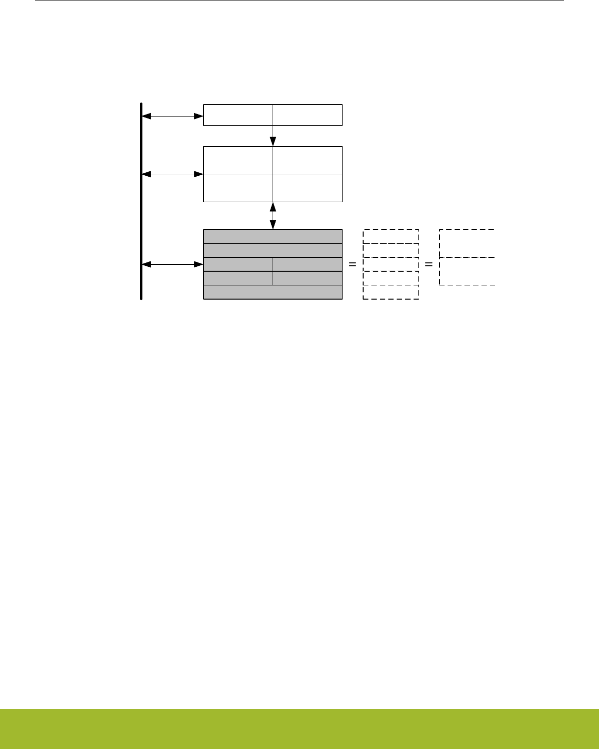
32.4 Functional Description
A block diagram of the CRYPTO module is shown in Figure 32.1 CRYPTO Overview on page 1047.
ALU
SHA
AES
DATA
TRANSFER
Sequencer
DATA1[127:0] DATA0[127:0]
DATA3[127:0] DATA2[127:0]
KEYBUF[255:0]
KEY[255:0]
DDATA0[255:0]
AHB bus
Control
DDATA4[255:0]
DDATA1[255:0]
DDATA0[255:0]
DDATA2[255:0]
DDATA3[255:0]
QDATA0[511:0]
QDATA1[511:0]
Figure 32.1. CRYPTO Overview
Reference Manual
CRYPTO - Crypto Accelerator
silabs.com | Smart. Connected. Energy-friendly. Preliminary Rev. 0.5 | 1047

32.4.1 Data and Key Registers
The CRYPTO module contains five 256-bit registers. Accelerators are implemented through instructions operating on these registers,
either by copying data between registers and external components like the BUFC or through DMA, or by executing instructions on the
registers.
Depending on the instruction, the registers can be accessed as 128-bit, 256-bit or 512-bit registers. The registers can also be accessed
through different interface registers to achieve different results.
When writing to and reading from the CRYPTO_DATAx, CRYPTO_KEY, CRYPTO_KEYBUF, CRYPTO_DDATAx and CRYPTO_QDA-
TAx registers, the least significant part is accessed first and the most significant part last, see Figure 32.2 CRYPTO Data and Key Reg-
ister Operation on page 1049. The same is the case for the XOR and byte-access registers for DATA0 and DATA1. It is important to
note that some of the 256-bit registers are composed of the 128-bit registers, and both the 512-bit registers are composed of the 256-bit
registers.
Note: From here on, the 128, 256 and 512-bit registers are named DATAx, DDATAx, QDATAx, etc, And the access-points to these reg-
isters are named CRYPTO_DATAx, CRYPTO_DDATAx, CRYPTO_QDATAx, etc.
DATA0 can be accessed through CRYPTO_DATA0 (32-bit), CRYPTO_DATA0XOR (32-bit), CRYPTO_DATA0BYTE (8-bit) and CRYP-
TO_DATA0XORBYTE (8-bit). Direct access to bytes 12 - 15 is available through CRYPTO_DATA0BYTE12-15 (8-bit). The DATA0XOR
(in CRYPTO_DATA0XOR) is used for XOR'ing a value with the current value in DATA0. This is used in a large variety of block cipher
modes. All of these registers operate on DATA0.
DATA1 can be accessed through CRYPTO_DATA1 (32-bit) and CRYPTO_DATA1BYTE (8-bit).
The remaining data registers have regular 32-bit access through their respective registers. Note that all data registers require a full read
or write to be fully accessed. This means that the 128-bit registers need four 32-bit reads/writes, the 256-bit registers need 8 reads/
writes and the 512-bit registers need 16 reads/writes. For a read, if all read accesses are not done, the register will end up as a shifted
version of the original value.
Note: For byte-wise data accesses (DDATAxBYTE, DATAxBYTE, etc.), all reads and writes must be performed in groups of 4, due to
internal buffering and shifting of 32 bits at a time. Accessing a number of bytes that is not a multiple of four can cause data incoherency
in all of the data registers.
The KEY and KEYBUF registers are 256 bit wide when AES256 is set in CRYPTO_CTRL. Else they are 128 bit wide. When used as a
part of DDATAx and QDATAx, they are always 256 bit wide.
The registers DDATA0BIG and QDATA1BIG produce byte-swapped versions of DDATA0 and QDATA1 respectively. These may be used
when a computation requires byte-swapping. An example of this is SHA computation, where data needs to be changed to big endian
before CRYPTO can work with it. Little endian data is then loaded in through QDATA1BIG and the resulting little endian hash can be
read out from DDATA0BIG, see 32.4.5 SHA.
Except for KEYBUF, the contents of all data registers are lost when going to EM2.
Reference Manual
CRYPTO - Crypto Accelerator
silabs.com | Smart. Connected. Energy-friendly. Preliminary Rev. 0.5 | 1048
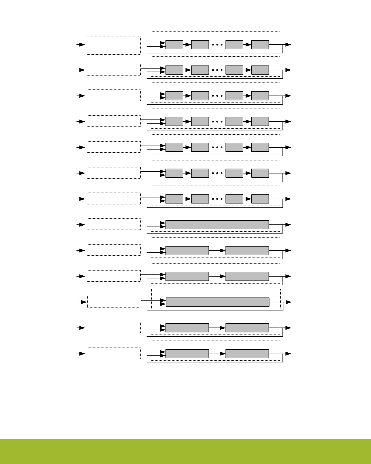
MSBWrite data Read data
DATA1 (128 bit)
LSB
CRYPTO_DATA1
CRYPTO_DATA1BYTE
Write data CRYPTO_DATA2
Write data CRYPTO_DATA3
MSB Read data
DATA2 (128 bit)
LSB
MSB Read data
DATA3 (128 bit)
LSB
MSBWrite data Read data
DATA0 (128 bit)
LSB
CRYPTO_DATA0
CRYPTO_DATA0XOR
CRYPTO_DATA0BYTE
CRYPTO_DATA0XORBYTE
Write data CRYPTO_KEY
Write data CRYPTO_KEYBUF
MSB Read data
KEY (128 bit / 256 bit)
LSB
MSB Read data
KEYBUF (128 bit / 256 bit)
LSB
Shift on write and read
Write data CRYPTO_DDATA0 MSB Read data
DDATA0 (256 bit)
LSB
Write data CRYPTO_DDATA2 DATA1 Read data
DDATA2 (256 bit)
DATA0
CRYPTO_DDATA3 DATA3 Read data
DDATA3 (256 bit)
DATA2Write data
Write data CRYPTO_DDATA1 KEY Read data
DDATA1 (256 bit)
Write data CRYPTO_DDATA4 KEYBUF Read data
DDATA4 (256 bit)
Write data CRYPTO_QDATA0 DDATA1 Read data
QDATA0 (512 bit)
DDATA0
CRYPTO_QDATA1 DDATA3 Read data
QDATA1 (512 bit)
DDATA2Write data
Figure 32.2. CRYPTO Data and Key Register Operation
32.4.1.1 DATA0 Zero
DATA0ZERO in CRYPTO_DSTATUS contains status flags indicating if any 32-bit blocks within DATA0 is 0. E.g. if DATA0[95:64] is
equal to 0x00000000, ZERO64TO95 is set.
Reference Manual
CRYPTO - Crypto Accelerator
silabs.com | Smart. Connected. Energy-friendly. Preliminary Rev. 0.5 | 1049

32.4.1.2 DDATA0 and DDATA1 Quick Observation
DDATA0LSBS in CRYPTO_DSTATUS shows the 4 least significant bits in DDATA0. DDATA0MSBS in CRYPTO_DSTATUS shows the 4
most significant bits of DDATA0, while DDATA1MSB in CRYPTO_DSTATUS shows the msb of DDATA1. These observation bitfields are
useful for determining the sign of the value in the data registers without having to read out the full register data register values
The 4 bits observed by DDATA0MSBS will change depending on RESULTWIDTH in CRYPTO_WAC. When using 260-bit results, DDA-
TA0MSBS shows bits 259-256, when using 256-bit results, it is bits 255-252, and for 128-bit results, bits 127-124 can be observed.
When RESULTWIDTH is 260 bits, the 4 most significant bits, e.g. bits 259-256 are also available in CRYPTO_DDATA0BYTE32, where
they can also be written. Using this register is the only way of inputting the upper 4 bits of a 260-bit number to CRYPTO.
32.4.1.3 Result Width
RESULTWIDTH in CRYPTO_WAC determines the width of the operation when performing arithmetic/shift instructions with CRYPTO.
Using less wide results will reduce the current consumption of the CRYPTO module. The higher-order bits that are beyond the selected
result width are ignored in the computation of arithmetic/shift operations, however, these higher-order bits will be undefined in the result
of such instructions.
When RESULTWIDTH=260BIT, all DDATA registers effectively become 260 bits wide, so that the upper 4 bits are not lost when trans-
ferring data from DDATA0 to the other DDATA registers. Likewise, the arithmetic/shift instructions shall consider the full 260-bit values
of DDATA0-DDATA4 when used as operation inputs. Note that DDATA0 is the only 260-bit register of which MSBs can be observed/
written. The upper 4 bits are observed through DDATA0MSBS in CRYPTO_DSTATUS or through CRYPTO_DDATA0BYTE32. For all
DDATAx registers, the extra MSBs are cleared when DDATAx is written. Furthermore, for a particular x, a write to DDATAx or any of its
aliased registers will cause DDATAx MSBs to be cleared. Note, writing to KEY/KEYBUF will only clear MSBs of DDATA1/DDATA4 when
AES256 mode is set. Likewise, writing to DATA0/DATA2 will not clear DDATA2/DDATA3 MSBs.
Since the DATA0-DATA3 registers are always 128-bit, all bit positions greater than 128 are interpreted as 0 when RESULTWIDTH is
greater than 128 bits. However, the assignment instructions DATAxTODDATAy will not zero-out the upper 128 bits of the DDATAy tar-
get. Instead, those upper words become undefined after such operations.
32.4.2 Instructions and Execution
The CRYPTO module implements a set of instructions in order to load and manipulate data effectively. These instructions are grouped
into four types:
• ALU instructions - arithmetic and logical bitwise operations
• Transfer instructions - moving data between registers and external peripherals like DMA and the BUFC
• Conditional instructions - conditionally execute instructions based on context
• Special instructions - various crypto and support instructions
A single instruction can be executed by writing INSTR in CRYPTO_CMD. This will execute the instruction, and the interface of CRYP-
TO will be locked until the execution has completed. Multiple commands can safely be issued after each other by the CPU as long as
NOBUSYSTALL in CRYPTO_CTRL is not set. If CRYPTO gets a new command or a data access request while busy it will then stall the
bus, and execute the new command as soon as it is done with the previous one. Note, there are some exceptions to this rule. For
example, see 32.4.8 DMA.
Stalling of the bus can be disabled by setting NOBUSYSTALL in CRYPTO_CTRL, however manipulating (reading or writing) registers
while running an instruction will result in undefined behaviour. Additionally, if NOBUSYSTALL=0 and a new command or data access
request is made while the CRYPTO is simultaneously performing a data transfer instruction, it is possible for system lockup due to bus
stalling loops. The safest approach is to always check if an instruction is running by looking at INSTRRUNNING in CRYPTO_STATUS.
Note that this automatic stalling feature does not apply to automated CRYPTO instruction sequences (described next), since there may
be cycle delays between individual instructions for which bus accesses are not prevented. For sequences, always check the SEQRUN-
NING status bit or the SEQDONE interrupt flag to ensure the sequence is finished before attempting CRYPTO register accesses.
Reference Manual
CRYPTO - Crypto Accelerator
silabs.com | Smart. Connected. Energy-friendly. Preliminary Rev. 0.5 | 1050

32.4.2.1 Sequences
For executing a set of instructions, it is more efficient to load them into the CRYPTO module and run them as a sequence. This is done
by writing the instructions into CRYPTO_SEQ0-CRYPTO_SEQ4, and marking the end of the instruction sequence with either an END
or an EXEC instruction. The END simply means end-of-instructions, while writing EXEC means end-of-instructions and execute imme-
diately.
The five registers allow up to 20 instructions to be loaded. To start execution, either end the instructions with an EXEC instruction, or set
SEQSTART in CRYPTO_CMD. CRYPTO will then execute the instructions, starting in CRYPTO_SEQ0, and ending at the first END
instruction. SEQRUNNING in CRYPTO_STATUS is set while the sequence is running, and the interrupt flag SEQDONE in CRYPTO_IF
will be set when the sequence has completed.
A sequence can be stopped by issuing the SEQSTOP command in the CRYPTO_CMD register. This command also clears the state of
ongoing CRYPTO instructions including DMA and BUFC access. Check SEQRUNNING in CRYPTO_STATUS after issuing the SEQ-
STOP command flag to make sure any ongoing sequence/transfer has completed before accessing data registers again.
Reference Manual
CRYPTO - Crypto Accelerator
silabs.com | Smart. Connected. Energy-friendly. Preliminary Rev. 0.5 | 1051

32.4.2.2 Available Instructions
The available ALU instructions are listed in Table 32.1 ALU Instructions on page 1052, data transfer instructions are listed in Table
32.2 Transfer Instructions on page 1053, conditional instructions are listed in Table 32.3 Conditional Instructions on page 1054 and
special instructions are listed in Table 32.4 Special Instructions on page 1054. The tables explains the side-effects of the instructions
and shows which registers are affected. For instructions involving BUFC, the BUFC Buffers are defined by READBUFSEL and WRITE-
BUFSEL in CRYPTO_CTRL for BUFC reads and writes respectively. V0 and V1 in the instructions descriptions can be any of the DDA-
TAx registers and a selection of the DATAx registers. They can be selected using the SELDDATAxDDATAy, SELDATAxDDATAy, SELD-
DATAxDATAy and SELDATAxDATAy instructions. The first register in the instruction will be selected for V0, and the second for V1. This
configuration stays even when the sequence is complete, and can also be set up front. The currently selected V0 and V1 can be read
V0 and V1 in CRYPTO_CSTATUS.
Table 32.1. ALU Instructions
Instruction Description Constraints/Notes
ADD DDATA0 = V0 + V1 If V0 != DDATA0, then V1 != DDATA0
ADDO DDATA0 = V0 + V1 Carry is only set, not cleared.
If V0 != DDATA0, then V1 != DDATA0
ADDC DDATA0 = V0 + V1 + carry If V0 != DDATA0, then V1 != DDATA0
ADDIC DDATA0 = V0 + V1 + carry << 128 If V0 != DDATA0, then V1 != DDATA0.
If resultwidth is 128b, then carry is undefined
MADD DDATA0 = (V0 + V1) mod P If V0 != DDATA0, then V1 != DDATA0
MADD32 DDATA0[i] = V0[i] + V1[i].
Word-wise addition
carry is not modified.
If V0 != DDATA0, then V1 != DDATA0
SUB DDATA0 = V0 - V1 V1 != DDATA0.
If V1 is 128b and resultwidth > 128b,
then upper 128b are unknown
SUBC DDATA0 = V0 - V1 - carry V1 != DDATA0.
If V1 is 128b and resultwidth > 128b,
then upper 128b are unknown
MSUB DDATA0 = (V0 - V1) mod P V1 != DDATA0.
If V1 is 128b and resultwidth > 128b,
then upper 128b are unknown
MUL DDATA0 = DDATA1 * V1.
See 32.4.2.3 MULx Details
V1 != DDATA0,DDATA1
MULC DDATA0 = DDATA1 * V1 + (DDATA0 << MULWIDTH).
See 32.4.2.3 MULx Details
V1 != DDATA0,DDATA1
MMUL DDATA0 = (DDATA1 * V1) mod P V1 != DDATA0,DDATA1
MULO DDATA0 = DDATA1 * V1.
See 32.4.2.3 MULx Details
V1 != DDATA0,DDATA1. Carry is only set, not cleared
SHL DDATA0 = V0 << 1 If V0 is 128b and resultwidth is 260b, then upper 4b are un-
known
SHLC DDATA0 = V0 << 1 | carry If V0 is 128b and resultwidth is 260b, then upper 4b are un-
known
SHLB DDATA0 = V0 << 1 | V0[resultwidth-1] If V0 is 128b and resultwidth is 260b, then upper 4b are un-
known
SHL1 DDATA0 = V0 << 1 | 1 If V0 is 128b and resultwidth is 260b, then upper 4b are un-
known
SHR DDATA0 = V0 >> 1
SHRC DDATA0 = V0 >> 1 | carry << resultwidth-1
Reference Manual
CRYPTO - Crypto Accelerator
silabs.com | Smart. Connected. Energy-friendly. Preliminary Rev. 0.5 | 1052

Instruction Description Constraints/Notes
SHRB DDATA0 = V0 >> 1 | V0[0] << resultwidth-1
SHR1 DDATA0 = V0 >> 1 | 1 << resultwidth-1
SHRA DDATA0 = V0 >> 1 | V0[resultwidth-1] << result-
width-1
CLR DDATA0 = 0
XOR DDATA0 = V0 ^ V1 If V0 != DDATA0, then V1 != DDATA0
INV DDATA0 = ~V0
CSET CARRY = 1
CCLR CARRY = 0
BBSWAP128 DDATA0[127:0] = bbswap(V0[127:0]) See 32.4.2.5 BBSWAP128 Instruction
INC DDATA0 = DDATA0 + 1
DEC DDATA0 = DDATA0 - 1
Table 32.2. Transfer Instructions
Instruction Operation Constraints/Notes
DATAxTOBUF BUFC = DATAx x = 0,1. BUFC buffer defined by WRITEBUFSEL
DATAxXORBUF BUFC = BUFC ^ DATAx x = 0,1. BUFC buffer defined by WRITEBUFSEL
BUFTODATAx DATAx = BUFC x = 0,1. BUFC buffer defined by READBUFSEL
BUFTODATA0XOR DATA0 = DATA0 ^ BUFC BUFC buffer defined by READBUFSEL
DATATODMA0 DMA = DATAX, DMA request DMA0RD DATAX = DATA0, DDATA0, DDATA0BIG, QDATA0
as defined by DMA0RSEL
DMA0TODATA DATAX = DMA, DMA request DATA0WR DATAX = DATA0, DDATA0, DDATA0BIG, QDATA0
DMA0TODATAXOR DATA0 = DATA0 ^ DMA, DMA request DATA0XORWR
DATATODMA1 DMA = DATAX, DMA request DMA1RD DATAX = DATA1, DDATA1, QDATA1, QDATA1BIG
as defined by DMA1RSEL
DMA1TODATA DATAX = DMA, DMA request DATA0WR DATAX = DATA1, DDATA1, QDATA1, QDATA1BIG
DATAxTODATAy DATAy = DATAx
DATAxTODATA0XOR DATA0 = DATA0 ^ DATAx If resultwidth is 128b, then carry is undefined
DATAxTODATA0XOR-
LEN
DATA0 = DATA0 ^ (DATAx & (2**LENGTH-1)) LENGTH is LENGTHA or LENGTHB depending on
active part of sequence. If resultwidth is 128b, then
carry is undefined
DDATAxTODDATAy DDATAy = DDATAx
DDATAxHTODATA1 DATA1 = DDATAx[255:128] Bits DDATA2[259:256] become undefined
DDATAxLTODATAy DATAy = DDATAx[127:0]
SELDDATAxDDATAy Use DDATAx as V0, DDATAy as V1 x = 0,1,2,3,4; y = 0,1,2,3,4
SELDATAxDDATAy Use DATAx as V0, DDATAy as V1 x = 0,1,2; y = 0,1,2,3,4
SELDDATAxDATAy Use DDATAx as V0, DATAy as V1 x = 0,1,2,3,4; y = 0,1
SELDATAxDATAy Use DATAx as V0, DATAy as V1 x = 0,1,2; y = 0,1
Reference Manual
CRYPTO - Crypto Accelerator
silabs.com | Smart. Connected. Energy-friendly. Preliminary Rev. 0.5 | 1053

Table 32.3. Conditional Instructions
Instruction Operation Constraints
EXECIFA Execute following instructions if in part A of sequence
EXECIFB Execute following instructions if in part B of sequence
EXECIFNLAST Execute following instructions if not in last iteration of sequence
EXECIFLAST Execute following instructions if in last iteration of sequence
EXECIFCARRY Execute following instructions if carry bit is set
EXECIFNCARRY Execute following instructions if carry bit not is set
EXECALWAYS Always execute following instructions
Table 32.4. Special Instructions
Instruction Operation
END Ends execution.
EXEC When written to CRYPTO_SEQx register, automatically triggers execution of all instruction up to this point.
AESENC DATA0 = AESENC(DATA0)
AESDEC DATA0 = AESDEC(DATA0)
SHA DDATA0 = SHA(Q1)
DATA1INC DATA1 = inc(DATA1).
See 32.4.2.4 DATA1INC and DATA1INCCLR Instructions
DATA1INCCLR DATA1 = clearinc(DATA1).
See 32.4.2.4 DATA1INC and DATA1INCCLR Instructions
32.4.2.3 MULx Details
For the MULx instructions (not MMUL), MULWIDTH in CRYPTO_WAC specifies the width of operands DDATA1 (and sometimes V1).
This is useful in order to optimize performance because multiplications take the same number of cycles as the bits in the operands plus
a couple of cycles for setup.
As with the other ALU instructions, RESULTWIDTH limits the width of the final result of the MULx and MMUL instructions.
32.4.2.4 DATA1INC and DATA1INCCLR Instructions
DATA1INC and DATA1INCCLR operate on the 1, 2, 3 or 4 most significant bytes in DATA1, depending on INCWIDTH in CRYP-
TO_CTRL. DATA1INC increments these bytes in big endian, while DATA1INCCLR clears the bytes.
32.4.2.5 BBSWAP128 Instruction
The BBSWAP128 instruction copies the contents of the V0 operand to DDATA0 while swapping the bits of the lower 16 bytes. The
operand is not changed. This operation is required for GCM. See 32.4.7 GCM and GMAC
Reference Manual
CRYPTO - Crypto Accelerator
silabs.com | Smart. Connected. Energy-friendly. Preliminary Rev. 0.5 | 1054

32.4.2.6 Carry
The carry output from most instructions can be observed through the CARRY bit in CRYPTO_DSTATUS. Shift-instructions set CARRY
to the value that is shifted out of the register, addition and multiplication set it on register overflow, and subtraction sets it on borrow, e.g.
underflow.
In addition to generating carry information, some instructions also use the current value of CARRY. ADDC, SUBC, SHLC and SHRC all
use carry to generate the result. For all of these instructions, carry allows a program to chain instructions together to operate on bigger
numbers than allowed by CRYPTO. For example, by chaining first an ADD, and then an ADDC which uses the carry from the ADD
operation, two 512-bit numbers can be added. By chaining more instructions, even larger numbers can be manipulated.
Other uses of CARRY include observation. To check if a register is 0, one can subtract 1 using the DEC instruction, and check if goes
negative by checking the CARRY bit. CARRY can be set manually and in CRYPTO programs using the CSET and CCLR instructions,
which set and clear the CARRY bit.
The MULC instruction does not use CARRY like the other carry instructions (i.e., instructions ending in 'C' such as 'ADDC'), but rather
preserves the old contents of the multiplication register.
32.4.3 Repeated Sequence
To maximize efficiency, it is desirable to be able to run a set of instructions over multiple blocks of data autonomously. To repeat a se-
quence over a larger set of data, set LENGTHA in CRYPTO_SEQCTRL to the number of bytes in the set, and BLOCKSIZE to the size
of the blocks in the set. The sequence will then be repeated N times, where N is LENGTHA / BLOCKSIZE if LENGTHA is a multiple of
BLOCKSIZE, or ceiling( LENGTHA / BLOCKSIZE ) if not. In the latter case, data written by DMA or received from BUFC will be zero-
padded up to BLOCKSIZE if it is written to a register which has a size equal to BLOCKSIZE. One notable exception is when LENGTHA
is 0. In this case the sequence will still execute once, but the block transfer instructions will not execute.
Note: If DMAxRSEL in CRYPTO_CTRL selects a register that is smaller than the specified blocksize, DATATODMAx/DMAxTODATA
instructions will not use the full blocksize, but will only transfer enough data to empty/fill the register once. For example, if BLOCKSIZE
is set to 64B and DMA0RSEL=DDATA0, the instruction DATATODMA0 will only read 32B instead of 64B. The processing of
LENGTHA/B will continue as if all 64B had been transferred.
A repeated sequence can also be made do slightly different operations on different parts of the data set. A sequence can be divided
into two parts; part A, and part B. By configuring LENGTHA in CRYPTO_SEQCTRL to the length of part A, and LENGTHB in CRYP-
TO_SEQCTRLB to the length of part B, CRYPTO will first run iterations over part A, knowing it is A, and then part B, knowing it is part
B. By using the conditional instructions listed in Table 32.3 Conditional Instructions on page 1054, a program can execute different in-
structions depending on whether it is in part A or part B.
Reference Manual
CRYPTO - Crypto Accelerator
silabs.com | Smart. Connected. Energy-friendly. Preliminary Rev. 0.5 | 1055
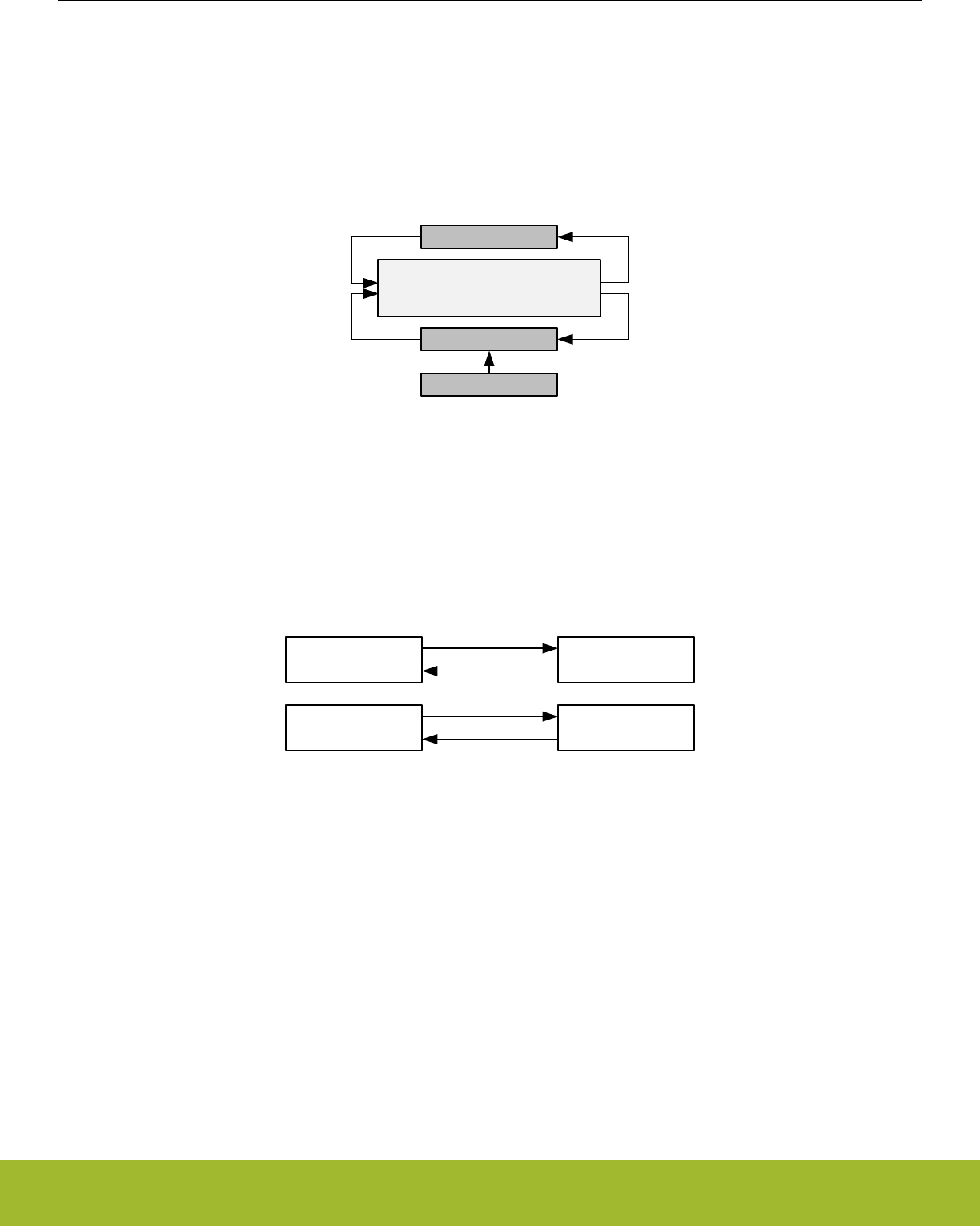
32.4.4 AES
The AES core operates on data in the 128-bit register DATA0 using the either a 128-bit or 256-bit key from the KEY register. The key
width is specified by AES256 in CRYPTO_CTRL. AES operations are implemented as the AESENC and AESDEC instructions, for AES
encryption and AES decryption respectively. An overview of the AES functionality is shown in Figure 32.3 CRYPTO AES Overview on
page 1056.
AES encryption and decryption enables various block cipher modes like ECB, CTR, CBC, PCBC, CFB, OFB, CBC-MAC, GMAC, CCM,
CCM*, and GCM.
DATA0[127:0]
AES
KEY[255:0]
KEYBUF[255:0]
Figure 32.3. CRYPTO AES Overview
The input data before encryption is called the PlainText and output from the encryption is called CipherText. For encryption, the key is
called PlainKey. After encryption, the resulting key in the KEY registers is the CipherKey. This key must be loaded into the KEY regis-
ters prior to the decryption. After one decryption, the resulting key will be the PlainKey. The resulting PlainKey/CipherKey is only de-
pendent on the value in the KEY registers before encryption/decryption. The resulting keys and data are shown in Figure 32.4 CRYPTO
Key and Data Definitions on page 1056.
PlainText CipherText
PlainKey CipherKey
Encryption
Decryption
Encryption
Decryption
Figure 32.4. CRYPTO Key and Data Definitions
The KEY is by default loaded from KEYBUF prior to each AESENC or AESDEC instruction. If the KEY is not to be overwritten, key
buffering should be disabled (KEYBUFDIS in CRYPTO_CTRL). Disabling key buffering also allows the use of key loading through
DMA.
The data and key orientation in the CRYPTO registers are shown in Figure 32.5 CRYPTO Data and Key Orientation as Defined in the
Advanced Encryption Standard on page 1057.
Reference Manual
CRYPTO - Crypto Accelerator
silabs.com | Smart. Connected. Energy-friendly. Preliminary Rev. 0.5 | 1056

DATA3
DATA2
DATA1
DATA0
KEY4
KEY5
KEY6
KEY7
DATA KEY/KEYBUF
[7:0]
[15:8]
[23:16]
[31:24]
a0a4
a1a5
a2a6
a8a12
a9a13
a10 a14
a11 a15
a3a7
Byte order in word
S0,0 S0,1
S1,0 S1,1
S2,0 S2,1
S0,2 S0,3
S1,2 S1,3
S2,2 S2,3
S3,2 S3,3
S3,0 S3,1
KEY0
KEY1
KEY2
KEY3
a16 a20
a17 a21
a18 a22
a24 a28
a25 a29
a26 a30
a27 a31
a19 a23
Figure 32.5. CRYPTO Data and Key Orientation as Defined in the Advanced Encryption Standard
Reference Manual
CRYPTO - Crypto Accelerator
silabs.com | Smart. Connected. Energy-friendly. Preliminary Rev. 0.5 | 1057

32.4.5 SHA
The CRYPTO SHA instruction implements SHA-1 with a 160-bit digest or SHA-2 with a 224-bit digest (SHA-224) or 256-bit digest
(SHA-256). Depending on SHAMODE in CRYPTO_CTRL, SHA-1, SHA-224 or SHA-256 will be run on the data in QDATA1, and the
result will be put on DDATA0. The contents in QDATA1 will be destroyed in the process.
To run SHA on a dataset, it must first be pre-processed by appending a bit '1' to the message, then padding the data with '0' bits until
the message length in bits modulo 512 is 448. Then append the length of the message before pre-processing as a 64-bit big-endian
integer. This pre-processing is known as MD-strengthening, and must be done by software before processing with the CRYPTO mod-
ule.
The pre-processed data can now be run through the CRYPTO module. Begin by writing the values listed in Table 32.5 SHA Init Values
on page 1058 to CRYPTO_DDATA1 from top to bottom, then execute the instructions listed in Table 32.6 SHA Preparations on page
1058.
Table 32.5. SHA Init Values
SHA-1 SHA-224 SHA-256
0x67452301 0xC1059ED8 0x6A09E667
0xEFCDAB89 0x367CD507 0xBB67AE85
0x98BADCFE 0x3070DD17 0x3C6EF372
0x10325476 0xF70E5939 0xA54FF53A
0xC3D2E1F0 0xFFC00B31 0x510E527F
0x00000000 0x68581511 0x9B05688C
0x00000000 0x64F98FA7 0x1F83D9AB
0x00000000 0xBEFA4FA4 0x5BE0CD19
Table 32.6. SHA Preparations
STEP ACTION Description
STEP0 DDATA1TODDATA0 Copy init data to DDATA0
STEP1 SELDDATA0DDATA1 Select DDATA0 and DDATA1 as operands for SHA instruction
Then, for each 512-bit block, write the block to CRYPTO_QDATA1BIG, execute the instructions listed in Table 32.7 SHA for 512-bit
Block on page 1058.
Table 32.7. SHA for 512-bit Block
STEP ACTION Description
STEP0 SHA Perform SHA operation on data in QDATA1
STEP1 MADD32 Accumulate with previous data in DDATA1
STEP2 DDATA0TODDATA1 Copy hash to DDATA1
After the last iteration, the resulting hash can be read out from CRYPTO_DDATA0BIG.
32.4.6 ECC
The CRYPTO module implements support for Elliptic Curve Cryptography through the modular instructions MADD, MMUL and MSUB,
which perform modular addition, multiplication and subtraction respectively. The instructions can operate on a set of both prime fields
GF(p) and binary fields GF(2^m).
The type of modular arithmetic used and the modulus for the modular operations are specified by MODOP and MODULUS in CRYP-
TO_WAC respectively. Changing these in the middle of an operation leads to undefined behaviour.
Reference Manual
CRYPTO - Crypto Accelerator
silabs.com | Smart. Connected. Energy-friendly. Preliminary Rev. 0.5 | 1058

32.4.7 GCM and GMAC
CRYPTO implements support for Galois/Counter Mode (GCM), and also Galois Message Authentication Code (GMAC), by providing
AES instructions and allowing multiplication on the field GF(2^128) defined by the polynomial x^128 + x^7 + x^2 + x + 1.
Note: BBSWAP128 needs to be applied to both operands and the result of the MMUL instruction when using it for GCM and GMAC
Efficient sequencer programs can be set up to perform GCM authentication and encryption/decryption on data from either BUFC, DMA,
or CPU. To achieve a single-pass solution, LENGTHA in CRYPTO_SEQCTRL is set to the length of the authentication part, and
LENGTHB is set to the length of the rest of the message. Conditional instructions can then be used to make sure the two parts of the
message are processed correctly. A similar approach is used to implement CCM.
32.4.8 DMA
The CRYPTO module has 5 DMA request signals (see Table 32.8 DMA Signals on page 1059) split over 2 internal DMA channels:
DMA0 and DMA1. These DMA channels are not associated with channel 0 and 1 of the system DMA, and any system DMA channel
can serve any of the 5 DMA requests. See the DMA chapter for information on how to configure the system DMA.
The DMA signals are set through the use of DMA oriented instructions, and cleared by reading or writing the respective CRYPTO data
registers.
Table 32.8. DMA Signals
Name Set on Cleared on
DMA0WR Instruction DMA0TODATA, and DMA0TODATAXOR if
COMBDMA0WEREQ in CRYPTO_CTRL is set
Full CRYPTO_DATA0, CRYPTO_DDATA0, CRYP-
TO_DDATA0BIG or CRYPTO_QDATA0 write, or CRYP-
TO_DDATA0XOR if COMBDMA0WEDMAREQ in
CRYPTO_CTRL is set
DMA0XORWR Instruction DMA0TODATAXOR Full CRYPTO_DATA0XOR write
DMA0RD Instructions DATATODMA0 Full CRYPTO_DATA0, CRYPTO_DDATA0, CRYP-
TO_DDATA0BIG or CRYPTO_QDATA0 read, depending
on DMA0MODE in CRYPTO_CTRL
DMA1WR Instructions DMA1TODATA Full CRYPTO_DATA1, CRYPTO_DDATA1, CRYP-
TO_QDATA1 or CRYPTO_QDATA1BIG write
DMA1RD Instructions DATATODMA1 Full CRYPTO_DATA1, CRYPTO_DDATA1, CRYP-
TO_QDATA1 or CRYPTO_QDATA1BIG read, depending
on DMA1MODE in CRYPTO_CTRL
Note: DMAxRSEL in CRYPTO_CTRL has to be set to the data registers that are to be read using the respective DMA channels on a
DATATODMAx instruction. As an important note, DMAxRSEL in CRYPTO_CTRL selects what is read from any of the selectable read
registers during an ongoing DATATODMAx transfer .
When a DMA oriented CRYPTO instruction is used (either through a STEP in a Sequence or through CRYPTO_CMD), the correspond-
ing DMA signal is set. The instruction is complete when the entire source/destination is read/written (e.g. if DMA0TODATA is used, the
operation is complete when a total of 128 valid bits have been written through the CRYPTO_DATA0 register). DMAACTIVE in CRYP-
TO_STATUS is set while CRYPTO is working on a DMA-related instruction, e.g. waiting for the DMA to read or write data to CRYPTO
(see 32.4.8.1 DMA Initial Bytes Skip).
Normally, when a sequence or instruction is executed, access to most CRYPTO registers will stall the CPU or DMA that is trying to
access CRYPTO until the operation is done, preventing accesses to CRYPTO that could potentially interfere with an operation. During
DMA operations, all non-DMA registers are writeable and readable, but progress through the DMA operation will only be tracked with
the registers targeted by the DMA operation (i.e., if the DMA operation is supposed to transfer 3 words to DATA0, the DMA can first
choose to transfer data to e.g. DATA3, and then fulfill the transfer to DATA0).
Because the bus interface to CRYPTO is normally locked outside of DMA transfers, a wrongly set up DMA transfer (e.g., transferring
one byte too many) may lock up the interface.. One way to assist in debugging such issues can be setting NOBUSYSTALL in CRYP-
TO_CTRL. This will prevent any stall on CRYPTO register accesses during sequences and instructions. Use this option with care, as
modifying a register that is being used by CRYPTO can lead to undefined behavior.
Reference Manual
CRYPTO - Crypto Accelerator
silabs.com | Smart. Connected. Energy-friendly. Preliminary Rev. 0.5 | 1059

32.4.8.1 DMA Initial Bytes Skip
The DMA must be configured to use 32-bit transfer size. This normally would imply that the source data must be aligned to a 4 byte
address boundary. However, it is possible to skip the initial bytes (1 to 3) when using DMA to write to DATA0 or DATA1 through a
CRYPTO instruction operation. The number of bytes to skip are set in DMA0SKIP and DMA1SKIP in CRYPTO_SEQCTRL. This implies
that if DMA0SKIP is set to another value than 0, the initial DMA access will require 5 DMA transfers, even though only 4x32-bit is re-
quired.
Note: Any valid unused bytes from a previous DMA write will be used before new DMA data is requested. This data is invalidated by
using STOP in CRYPTO_CMD.
32.4.8.2 DMA Unaligned Read/Write
Except for DATA0 and DATA1, which can be loaded bytewise using the CRYPTO_DATA0BYTE, CRYPTO_DATA0XORBYTE and
CRYPTO_DATA1BYTE registers, the CRYPTO data registers are loaded 32-bits at a time. Special care must be taken when using the
DMA and the data buffer is not aligned to a 32-bit address, because the DMA does not directly support 32-bit unaligned accesses.
As an example, let an in-memory 16-byte data buffer start at address 4*N + M and end at the byte before. 4*N + 16 + M, where M is
between 0 and 3 inclusive. With an M=0, we have fully aligned accesses, and everything is fine. For M>0 however, the access is un-
aligned. If M=1, that means that the first 32-bit aligned word of the memory buffer contains 1 byte before the buffer, and 3 bytes of the
buffer. Similarly, the last 32-bit aligned word of the memory buffer contains the last byte of the buffer, and three bytes after the buffer.
When doing an unaligned read, we want to only pass the 16 bytes of the buffer to the CRYPTO module. Not the N bytes before in the
32-bit aligned word, and not the 4-N words at the end. To achieve this, set DxDMAREADMODE in CRYPTO_CTRL to either UN-
ALIGNEDFULL or UNALIGNEDLENLIMIT, and set DATAxDMASKIP in CRYPTO_SEQCTRL equal to N. When reading in data using a
DMA-oriented instruction to DATAx, DDATAx or QDATAx, the read will now only contain the 16 bytes, and not the N bytes before or 4-N
words after. Note that in this case, the DMA has to be set up to transfer 5 32-bit words instead of the effective 4.
Being able to read unaligned data does not solve all cases however. If data is to be written back to the buffer after passing through
CRYPTO, e.g. when doing an in-place encryption or decryption, it is very undesirable to actually modify the N bytes before and 4-N
bytes after the buffer. This is solved using the UAR-suffixed registers in CRYPTO when reading data out from the CRYPTO module,
e.g. CRYPTO_DATA0UAR, CRYPTO_DATA1UAR, CRYPTO_DDATA0UAR,CRYPTO_DDATA1UAR, CRYPTO_QDATA0UAR, etc.
When an unaligned buffer is written to a CRYPTO buffer, CRYPTO stores the N first bytes and the 4-N last bytes internally. When read-
ing out from an UAR register, these bytes are placed back into the data if DATAxDMAPRES is set in CRYPTO_SEQCTRL.
Note that the latter case only works if the first N and the last 4-N bytes are not changed while CRYPTO works on the data. Internally
CRYPTO has 2 buffers for the bytes before and after. The first one is connected to read/write of the DATA0, DDATA0 and QDATA0
registers, and the second is connected to the DATA1, DDATA1 and QDATA1 registers.
If DMAxRMODE in CRYPTO_CTRL is set to FULL or UNALIGNEDFULL and the corresponding DMAxPRES in CRYPTO_SEQCTRL is
set, then a whole number of data buffers have to be written by the DMA. In all other cases, it is enough to write the number of 32-bit
words to pass all LENGTH bits to the target CRYPTO buffer.
Reference Manual
CRYPTO - Crypto Accelerator
silabs.com | Smart. Connected. Energy-friendly. Preliminary Rev. 0.5 | 1060
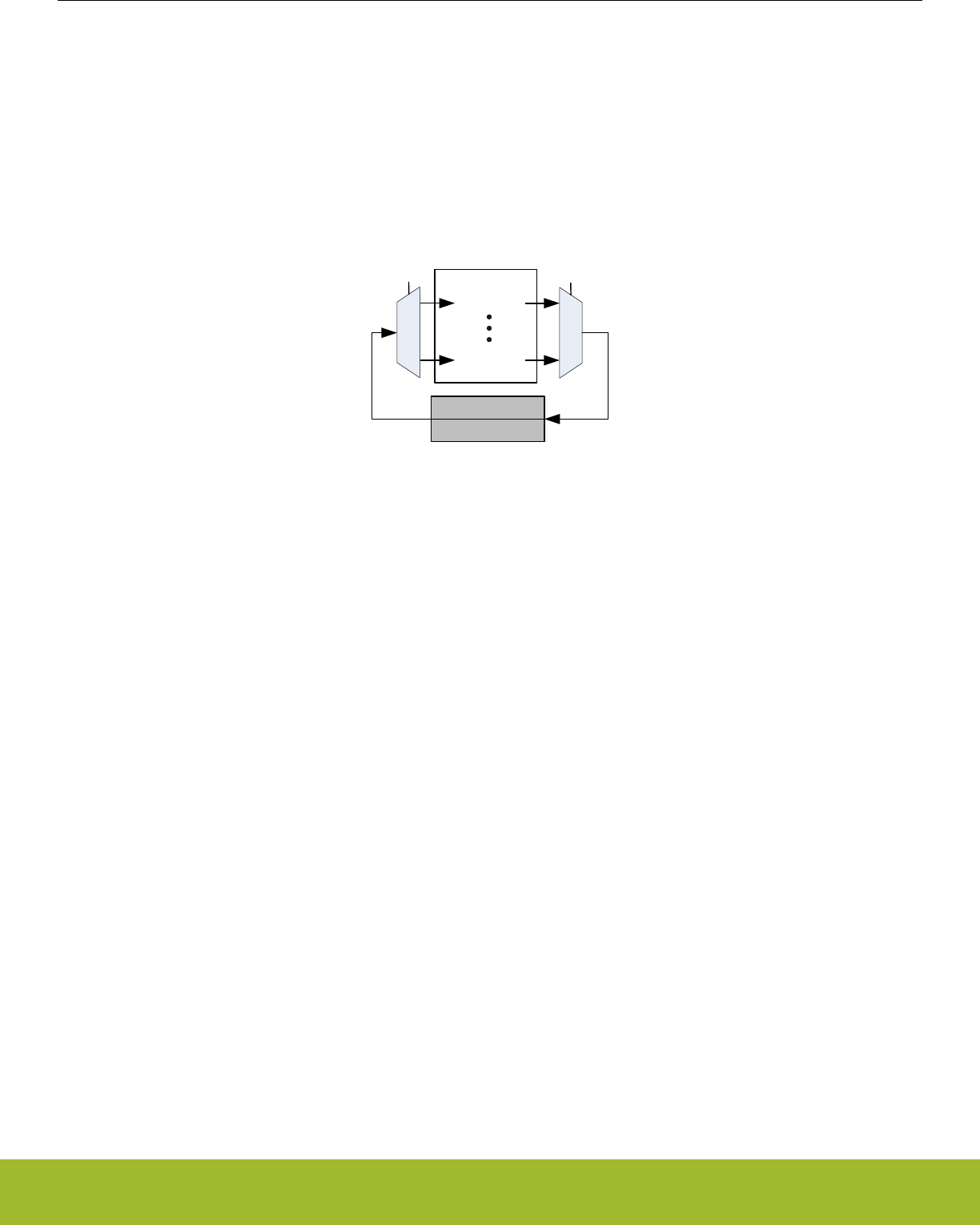
32.4.9 BUFC Data Transfer
To allow automatic encryption/decryption or other operations on radio data, CRYPTO has instructions for moving data from and to
BUFC, the Buffer Controller. Both DATA0 and DATA1 can be loaded with data from the buffer selected by READBUFSEL (CRYP-
TO_CTRL register) as shown in Figure 32.6 CRYPTO BUFC Data Transfer on page 1061. Similarly, the content of DATA0 and DATA1
can be written to the buffer selected by WRITEBUFSEL (also in the CRYPTO_CTRL register).
READBUFSEL
BUFFER0
BUFC
WRITEBUFSEL
BUFFER0
DATA1[127:0]
DATA0[127:0]
Figure 32.6. CRYPTO BUFC Data Transfer
When reading from CRYPTO to the BUFC, the number of bytes read are determined by the DMAxRMODE configuration in CRYP-
TO_CTRL. If it is set to either LENLIMIT or LENLIMITBYTE, only the number of bytes given by LENGTH in CRYPTO_SEQCTRL are
transferred. Else the full width of the last buffer is also written, e.g. a full number of 16-byte buffers are written to the BUFC.
Note:
The buffer selected by READBUFSEL and WRITEBUFSEL in the CRYPTO_CTRL registers must be appropriately configured in the
BUFC module prior to using instructions involving BUFC.
All BUFC reads start at the current BUFC read pointer, and move the pointer according to the number of bytes read. BUFC writes nor-
mally also work in the same way, starting at the current BUFC write pointer, and moving it the right number of positions. For BUFC XOR
writes, software has the option to change this by setting either of DATAxTOBUFXOROW in CRYPTO_CTRL. With this bit set, the BUFC
write pointer will be reset to the start of the previous write before writing to the BUFC. Using this feature, BUFC data can be written with
using the DATAxTOBUFC instructions, and then XOR'ed with another set of data using the DATAxTOBUFCXOR instruction.
BUFACTIVE in CRYPTO_STATUS is set while CRYPTO is reading or writing from/to the BUFC.
Reference Manual
CRYPTO - Crypto Accelerator
silabs.com | Smart. Connected. Energy-friendly. Preliminary Rev. 0.5 | 1061

32.4.10 Debugging
There are multiple ways of debugging CRYPTO sequences. The most straight-forward way is to write individual instructions to INSTR in
CRYPTO_CMD. An instruction can be written, and data can be read out and examined before running another instruction.
Running individual instructions to debug a program falls short when working with repeated sequences. In these cases, a sequence is
run multiple times over a set of data. This cannot be directly replicated with individual instructions
To debug a sequence, set HALT in CRYPTO_SEQCTRL. When set, CRYPTO requires software or the debugger to step it through each
instruction in the sequence. To step through the sequence, set SEQSTEP in CRYPTO_CMD. This will execute the current instruction,
and make CRYPTO ready to execute the next one.
When stepping through a sequence, the current instruction index can be read from SEQIP in CRYPTO_CSTATUS. SEQSKIP, also in
CRYPTO_CSTATUS tells whether the next instruction will be executed or not, based on previous conditionals in the program. SEQ-
PART in CRYPTO_CSTATUS shows whether CRYPTO is currently in part A or B of a sequence. Even with NOBUSYSTALL in CRYP-
TO_CTRL cleared, read and write accesses to CRYPTO will be allowed when CRYPTO is waiting to be stepped. This is to allow data
registers to be inspected during debugging.
Note: The data registers in CRYPTO (those marked read-actionable) require shifting of data in order to return the result. For this rea-
son, reading these registers will have no effect and will return unknown values during normal debugger read accesses (see
7.3.7 Debugger reads of actionable registers).
32.4.11 Example: Cipher Block Chaining (CBC)
In the following the setup and operation of CBC is explained and illustrated. The example can easily be adjusted to perform other cipher
block modes.
Reference Manual
CRYPTO - Crypto Accelerator
silabs.com | Smart. Connected. Energy-friendly. Preliminary Rev. 0.5 | 1062
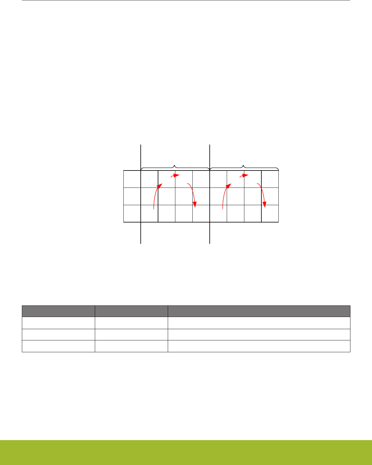
32.4.11.1 CBC Encryption
In CBC encryption, the cipher input is the PlainText XOR'ed with the previous cipher output (an initialization vector IV is used during the
first block). This mode is easily implemented using the CRYPTO instruction sequence BUFTODATA0XOR, AESENC then DATA0TO-
BUF. The BUFTODATA0XOR reads data from the buffer set by READBUFSEL and XOR's it with the content in DATA0. Then the cipher
operation is performed and subsequently the DATA0TOBUF writes the content of DATA0 to the buffer set by WRITEBUFSEL (normally
the same as READBUFSEL).
Prior to the operation, the initialization vector IV and key must be loaded to DATA0 and KEYBUF, respectively. Additionally, the total
number of bytes to be included in the repeated sequence must be set in LENGTHA in CRYPTO_SEQCTRL. Finally, the buffers selec-
ted by READBUFSEL and WRITEBUFSEL must be configured correctly in the BUFC. The sequence is started by issuing the SEQ-
START command in CRYPTO_CMD.
In Figure 32.7 CBC Encryption Operation on page 1063 the CBC encryption is illustrated and in Table 32.9 CBC Encryption Steps on
page 1063 each step in the loop is explained.
Loop 0
DATA0
DATA1
BUF
a8a12
a13
a10 a14
S0,1
P0
S0,2 S0,3
S1,3
S2,3
a24 a28
a25 a29
a26 a30
CBC Encryption
P0
XOR
IV
C0
C0
a0a4
a1a5
a2a6
X
P1
C1
C1
P1
XOR
C0
Loop 1
IV
Init
1 2 3 1 2 3
Steps Steps
Figure 32.7. CBC Encryption Operation
Table 32.9. CBC Encryption Steps
STEP ACTION Description
STEP0 BUFTODATA0XOR Move data (PlainText, Pi) from buffer to DATA0 using XOR write.
STEP1 CIPHER The AES Cipher Core operates on DATA0
STEP2 DATA0TOBUF The cipher output Ci is written to the buffer.
Reference Manual
CRYPTO - Crypto Accelerator
silabs.com | Smart. Connected. Energy-friendly. Preliminary Rev. 0.5 | 1063
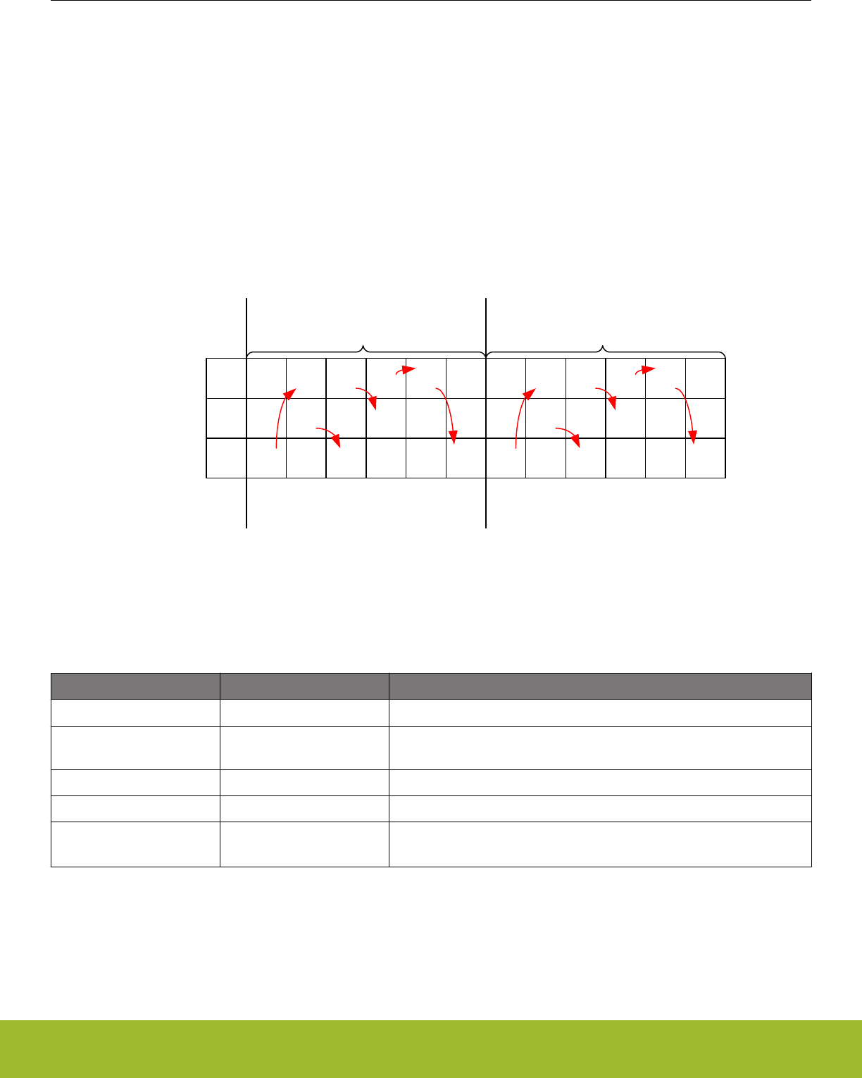
32.4.11.2 CBC Decryption
In CBC decryption, CipherText (Ci) is used as input to the Cipher Core. The output from the Cipher Core is XOR'ed with the CipherText
from the previous block Ci-1 to form the PlainText Pi (an initialization vector IV is used as Ci-1 during the first block).
Because each block requires both Ci-1 and Ci, decryption is somewhat more complex than encryption. Nevertheless, CBC decryption
can be performed in as a repeated sequence by having Ci-1 from the previous block stored in DATA1 and then writing it to buffer without
updating the write pointer (using the DATA1TOBUF instruction). Then the cipher output is XOR'ed with Ci-1 in the buffer by using the
DATA0TOBUFXOR instruction.
In Figure 32.8 CBC Decryption Operation on page 1064 the CBC decryption is illustrated and in Table 32.10 CBC Decryption Steps on
page 1064 each step in the loop is explained.
Loop 0
DATA0
DATA1
BUF
a0a4
a1a5
a2a6
a8a12
a13
a10 a14
S0,1
C0
S0,2 S0,3
S1,3
S2,3
a16 a20
a17
a18
a24 a28
a25 a29
a26 a30
CBC Decryption
C0
IV
C0
E(C0)
E(C0)
XOR
IV
a0a4
a1a5
a2a6
X
C1
S0,2 S0,3
S2,3
E(C1)
E(C1)
XOR
C0
E(C0)
C1
C0
C1
C0
Loop 1
IV
Init
1 2 3 4 5 1 2 3 4 5
Steps Steps
Figure 32.8. CBC Decryption Operation
Table 32.10. CBC Decryption Steps
STEP ACTION Description
STEP0 BUFTODATA0 Moves data (CipherText, Ci) from buffer to DATA0
STEP1 DATA1TOBUF DATA1 (CipherText, Ci-1) is moved to buffer. BUFC Write pointer is not in-
cremented!
STEP2 DATA0TODATA1 Value of DATA0 is copied to DATA1.
STEP3 CIPHER Operation The AES Cipher Core operates on DATA0
STEP4 DATA0TOBUFXOR The cipher output is XOR'ed with Ci-1 (placed in the buffer at Step 2) to
form the PlainText, Pi.
Reference Manual
CRYPTO - Crypto Accelerator
silabs.com | Smart. Connected. Energy-friendly. Preliminary Rev. 0.5 | 1064

32.5 Register Map
The offset register address is relative to the registers base address.
Offset Name Type Description
0x000 CRYPTO_CTRL RW Control Register
0x004 CRYPTO_WAC RW Wide Arithmetic Configuration
0x008 CRYPTO_CMD WCommand Register
0x010 CRYPTO_STATUS RStatus Register
0x014 CRYPTO_DSTATUS RData Status Register
0x018 CRYPTO_CSTATUS RControl Status Register
0x020 CRYPTO_KEY RWH(nB)(a) KEY Register Access
0x024 CRYPTO_KEYBUF RWH(nB)(a) KEY Buffer Register Access
0x030 CRYPTO_SEQCTRL RWH Sequence Control
0x034 CRYPTO_SEQCTRLB RWH Sequence Control B
0x040 CRYPTO_IF RAES Interrupt Flags
0x044 CRYPTO_IFS W1 Interrupt Flag Set Register
0x048 CRYPTO_IFC (R)W1 Interrupt Flag Clear Register
0x04C CRYPTO_IEN RW Interrupt Enable Register
0x050 CRYPTO_SEQ0 RW Sequence register 0
0x054 CRYPTO_SEQ1 RW Sequence Register 1
0x058 CRYPTO_SEQ2 RW Sequence Register 2
0x05C CRYPTO_SEQ3 RW Sequence Register 3
0x060 CRYPTO_SEQ4 RW Sequence Register 4
0x080 CRYPTO_DATA0 RWH(nB)(a) DATA0 Register Access
0x084 CRYPTO_DATA1 RWH(nB)(a) DATA1 Register Access
0x088 CRYPTO_DATA2 RWH(nB)(a) DATA2 Register Access
0x08C CRYPTO_DATA3 RWH(nB)(a) DATA3 Register Access
0x0A0 CRYPTO_DATA0XOR RWH(nB)(a) DATA0XOR Register Access
0x0B0 CRYPTO_DATA0BYTE RWH(nB)(a) DATA0 Register Byte Access
0x0B4 CRYPTO_DATA1BYTE RWH(nB)(a) DATA1 Register Byte Access
0x0BC CRYPTO_DATA0XORBYTE RWH(nB)(a) DATA0 Register Byte XOR Access
0x0C0 CRYPTO_DATA0BYTE12 RWH(nB) DATA0 Register Byte 12 Access
0x0C4 CRYPTO_DATA0BYTE13 RWH(nB) DATA0 Register Byte 13 Access
0x0C8 CRYPTO_DATA0BYTE14 RWH(nB) DATA0 Register Byte 14 Access
0x0CC CRYPTO_DATA0BYTE15 RWH(nB) DATA0 Register Byte 15 Access
0x100 CRYPTO_DDATA0 RWH(nB)(a) DDATA0 Register Access
0x104 CRYPTO_DDATA1 RWH(nB)(a) DDATA1 Register Access
0x108 CRYPTO_DDATA2 RWH(nB)(a) DDATA2 Register Access
0x10C CRYPTO_DDATA3 RWH(nB)(a) DDATA3 Register Access
Reference Manual
CRYPTO - Crypto Accelerator
silabs.com | Smart. Connected. Energy-friendly. Preliminary Rev. 0.5 | 1065

Offset Name Type Description
0x110 CRYPTO_DDATA4 RWH(nB)(a) DDATA4 Register Access
0x130 CRYPTO_DDATA0BIG RWH(nB)(a) DDATA0 Register Big Endian Access
0x140 CRYPTO_DDATA0BYTE RWH(nB)(a) DDATA0 Register Byte Access
0x144 CRYPTO_DDATA1BYTE RWH(nB)(a) DDATA1 Register Byte Access
0x148 CRYPTO_DDATA0BYTE32 RWH(nB) DDATA0 Register Byte 32 access.
0x180 CRYPTO_QDATA0 RWH(nB)(a) QDATA0 Register Access
0x184 CRYPTO_QDATA1 RWH(nB)(a) QDATA1 Register Access
0x1A4 CRYPTO_QDATA1BIG RWH(nB)(a) QDATA1 Register Big Endian Access
0x1C0 CRYPTO_QDATA0BYTE RWH(nB)(a) QDATA0 Register Byte Access
0x1C4 CRYPTO_QDATA1BYTE RWH(nB)(a) QDATA1 Register Byte Access
Reference Manual
CRYPTO - Crypto Accelerator
silabs.com | Smart. Connected. Energy-friendly. Preliminary Rev. 0.5 | 1066

32.6 Register Description
32.6.1 CRYPTO_CTRL - Control Register
Offset Bit Position
0x000
31
30
29
28
27
26
25
24
23
22
21
20
19
18
17
16
15
14
13
12
11
10
9
8
7
6
5
4
3
2
1
0
Reset
0
0x0
0x0
0x0
0x0
0x0
0
0
0
0
Access
RW
RW
RW
RW
RW
RW
RW
RW
RW
RW
Name
COMBDMA0WEREQ
DMA1RSEL
DMA1MODE
DMA0RSEL
DMA0MODE
INCWIDTH
NOBUSYSTALL
SHA
KEYBUFDIS
AES
Bit Name Reset Access Description
31 COMBDMA0WEREQ 0 RW Combined Data0 Write DMA Request
When cleared, the DATA0WR and DATA0XORWR operate independently. When set, DATA0XORWR requests are also giv-
en through DATA0WR
30 Reserved To ensure compatibility with future devices, always write bits to 0. More information in 1.2 Conven-
tions
29:28 DMA1RSEL 0x0 RW DATA0 DMA Unaligned Read Register Select
Specifies which read register is used for DMA1RD DMA requests (see related notes in 32.4.8 DMA and 32.4.3 Repeated
Sequence)
Value Mode Description
0 DATA1
1 DDATA1
2 QDATA1
3 QDATA1BIG
27:26 Reserved To ensure compatibility with future devices, always write bits to 0. More information in 1.2 Conven-
tions
25:24 DMA1MODE 0x0 RW DMA1 Read Mode
This field determines how data is read when using DMA
Value Mode Description
0 FULL Target register is fully read/written during every DMA transaction
1 LENLIMIT Length Limited. When the current length, i.e. LENGTHA or LENGTHB
indicates that there are less bytes available than the register size, only
length + 1 bytes + necessary zero padding is read. Zero padding is au-
tomatically added when writing.
2 FULLBYTE Target register is fully read/written during every DMA transaction. Byte-
wise DMA.
Reference Manual
CRYPTO - Crypto Accelerator
silabs.com | Smart. Connected. Energy-friendly. Preliminary Rev. 0.5 | 1067

Bit Name Reset Access Description
3 LENLIMITBYTE Length Limited. When the current length, i.e. LENGTHA or LENGTHB
indicates that there are less bytes available than the register size, only
length + 1 bytes + necessary zero padding is read. Bytewise DMA.
Zero padding is automatically added when writing.
23:22 Reserved To ensure compatibility with future devices, always write bits to 0. More information in 1.2 Conven-
tions
21:20 DMA0RSEL 0x0 RW DMA0 Read Register Select
Specifies which read register is used for DMA0RD DMA requests (see related notes in 32.4.8 DMA and 32.4.3 Repeated
Sequence)
Value Mode Description
0 DATA0
1 DDATA0
2 DDATA0BIG
3 QDATA0
19:18 Reserved To ensure compatibility with future devices, always write bits to 0. More information in 1.2 Conven-
tions
17:16 DMA0MODE 0x0 RW DMA0 Read Mode
This field determines how data is read when using DMA.
Value Mode Description
0 FULL Target register is fully read/written during every DMA transaction
1 LENLIMIT Length Limited. When the current length, i.e. LENGTHA or LENGTHB
indicates that there are less bytes available than the register size, only
length + necessary zero padding is read. Zero padding is automatically
added when writing.
2 FULLBYTE Target register is fully read/written during every DMA transaction. Byte-
wise DMA.
3 LENLIMITBYTE Length Limited. When the current length, i.e. LENGTHA or LENGTHB
indicates that there are less bytes available than the register size, only
length + necessary zero padding is read. Bytewise DMA. Zero padding
is automatically added when writing.
15:14 INCWIDTH 0x0 RW Increment Width
This field determines the number of bytes used for the increment function in data1.
Value Mode Description
0 INCWIDTH1 Byte 15 in DATA1 is used for the increment function.
1 INCWIDTH2 Bytes 14 and 15 in DATA1 are used for the increment function.
2 INCWIDTH3 Bytes 13 to 15 in DATA1 are used for the increment function.
3 INCWIDTH4 Bytes 12 to 15 in DATA1 are used for the increment function.
13:11 Reserved To ensure compatibility with future devices, always write bits to 0. More information in 1.2 Conven-
tions
10 NOBUSYSTALL 0 RW No Stalling of Bus When Busy
When set, bus accesses will not be stalled on access during an operation
Reference Manual
CRYPTO - Crypto Accelerator
silabs.com | Smart. Connected. Energy-friendly. Preliminary Rev. 0.5 | 1068

Bit Name Reset Access Description
9:3 Reserved To ensure compatibility with future devices, always write bits to 0. More information in 1.2 Conven-
tions
2 SHA 0 RW SHA Mode
Select SHA-1 or SHA-2 mode.
Value Mode Description
0 SHA1 SHA-1 mode
1 SHA2 SHA-2 mode (SHA-224 or SHA-256)
1 KEYBUFDIS 0 RW Key Buffer Disable
Set to Disable key buffering.
0 AES 0 RW AES Mode
Select AES mode
Value Mode Description
0 AES128 AES-128 mode
1 AES256 AES-256 mode
Reference Manual
CRYPTO - Crypto Accelerator
silabs.com | Smart. Connected. Energy-friendly. Preliminary Rev. 0.5 | 1069

32.6.2 CRYPTO_WAC - Wide Arithmetic Configuration
Offset Bit Position
0x004
31
30
29
28
27
26
25
24
23
22
21
20
19
18
17
16
15
14
13
12
11
10
9
8
7
6
5
4
3
2
1
0
Reset
0x0
0x0
0
0x0
Access
RW
RW
RW
RW
Name
RESULTWIDTH
MULWIDTH
MODOP
MODULUS
Bit Name Reset Access Description
31:12 Reserved To ensure compatibility with future devices, always write bits to 0. More information in 1.2 Conven-
tions
11:10 RESULTWIDTH 0x0 RW Result Width
Result-size for non-modulus instructions
Value Mode Description
0 256BIT Results have 256 bits
1 128BIT Results have 128 bits
2 260BIT Results have 260 bits. Upper bits of result can be read through DDA-
TA0MSBS in CRYPTO_STATUS
9:8 MULWIDTH 0x0 RW Multiply Width
Number of bits to multiply on non-modulus multiply instruction
Value Mode Description
0 MUL256 Multiply 256 bits
1 MUL128 Multiply 128 bits
2 MULMOD Same number of bits as specified by MODULUS
7:5 Reserved To ensure compatibility with future devices, always write bits to 0. More information in 1.2 Conven-
tions
4 MODOP 0 RW Modular Operation Field Type
Field type used for modular operations
Value Mode Description
0 BINARY Modular operations use XOR as required by certain algorithms
1 REGULAR Modular operations use normal modular arithmetic, not XOR
3:0 MODULUS 0x0 RW Modular Operation Modulus
Modulus used for modular operations
Value Mode Description
0 BIN256 Generic modulus. p = 2^256
Reference Manual
CRYPTO - Crypto Accelerator
silabs.com | Smart. Connected. Energy-friendly. Preliminary Rev. 0.5 | 1070

Bit Name Reset Access Description
1 BIN128 Generic modulus. p = 2^128
2 ECCBIN233P Modulus for B-233 and K-233 ECC curves. p(t) = t^233 + t^74 + 1
3 ECCBIN163P Modulus for B-163 and K-163 ECC curves. p(t) = t^163 + t^7 + t^6 +
t^3 + 1
4 GCMBIN128 Modulus for GCM. P(t) = t^128 + t^7 + t^2 + t + 1
5 ECCPRIME256P Modulus for P-256 ECC curve. p = 2^256 - 2^224 + 2^192 + 2^96 - 1
6 ECCPRIME224P Modulus for P-224 ECC curve. p = 2^224 - 2^96 - 1
7 ECCPRIME192P Modulus for P-192 ECC curve. p = 2^192 - 2^64 - 1
8 ECCBIN233N P modulus for B-233 ECC curve
9 ECCBIN233KN P modulus for K-233 ECC curve
10 ECCBIN163N P modulus for B-163 ECC curve
11 ECCBIN163KN P modulus for K-163 ECC curve
12 ECCPRIME256N P modulus for P-256 ECC curve
13 ECCPRIME224N P modulus for P-224 ECC curve
14 ECCPRIME192N P modulus for P-192 ECC curve
Reference Manual
CRYPTO - Crypto Accelerator
silabs.com | Smart. Connected. Energy-friendly. Preliminary Rev. 0.5 | 1071

32.6.3 CRYPTO_CMD - Command Register
Offset Bit Position
0x008
31
30
29
28
27
26
25
24
23
22
21
20
19
18
17
16
15
14
13
12
11
10
9
8
7
6
5
4
3
2
1
0
Reset
0
0
0
0x00
Access
W1
W1
W1
W
Name
SEQSTEP
SEQSTOP
SEQSTART
INSTR
Bit Name Reset Access Description
31:12 Reserved To ensure compatibility with future devices, always write bits to 0. More information in 1.2 Conven-
tions
11 SEQSTEP 0 W1 Sequence Step
When in a halted sequence, executes the current instruction and moves to the next
10 SEQSTOP 0 W1 Sequence Stop
Set to stop encryption/decryption regardless of it being a single or a SEQUENCE.
9 SEQSTART 0 W1 Encryption/Decryption SEQUENCE Start
Set to start encryption/decryption SEQUENCE.
8 Reserved To ensure compatibility with future devices, always write bits to 0. More information in 1.2 Conven-
tions
7:0 INSTR 0x00 W Execute Instruction
Write to this field to perform any of the instructions described below. Illegal values are ignored. See 32.4.2.2 Available In-
structions for details and requirements of each instruction
Value Mode Description
0 END End of program
1 EXEC Start executing instructions up to this point, which also marks end of
program
3 DATA1INC See detailed instruction listing
4 DATA1INCCLR See detailed instruction listing
5 AESENC AES Encryption
6 AESDEC AES Decryption
7 SHA SHA
8 ADD Add
9 ADDC Add with carry
12 MADD Modular addition
13 MADD32 Word-wise addition
16 SUB Subtract
17 SUBC Subtract with carry
20 MSUB Modular subtraction
Reference Manual
CRYPTO - Crypto Accelerator
silabs.com | Smart. Connected. Energy-friendly. Preliminary Rev. 0.5 | 1072

Bit Name Reset Access Description
24 MUL Multiply
25 MULC See detailed instruction listing
28 MMUL Modular multiplication
29 MULO See detailed instruction listing
32 SHL Shift left
33 SHLC Shift left with carry (Rotate left)
34 SHLB See detailed instruction listing
35 SHL1 See detailed instruction listing
36 SHR Shift right
37 SHRC Shift right with carry (Rotate right)
38 SHRB See detailed instruction listing
39 SHR1 See detailed instruction listing
40 ADDO See detailed instruction listing
41 ADDIC See detailed instruction listing
48 CLR Clear DDATA0
49 XOR XOR
50 INV Invert operand
52 CSET Carry set
53 CCLR Carry clear
54 BBSWAP128 See detailed instruction listing
56 INC Increment DDATA0
57 DEC Decrement DDATA0
62 SHRA Arithmetic shift right
64 DATA0TODATA0 DATA0 = DATA0
65 DATA0TODATA0XOR DATA0 = DATA0 ^ DATA0
66 DATA0TODATA0XOR-
LEN
DATA0[len-1:0] = DATA0[len-1:0] ^ DATA0[len-1:0]
68 DATA0TODATA1 DATA1 = DATA0
69 DATA0TODATA2 DATA2 = DATA0
70 DATA0TODATA3 DATA3 = DATA0
72 DATA1TODATA0 DATA0 = DATA1
73 DATA1TODATA0XOR DATA0 = DATA0 ^ DATA1
74 DATA1TODATA0XOR-
LEN
DATA0[len-1:0] = DATA0[len-1:0] ^ DATA1[len-1:0]
77 DATA1TODATA2 DATA2 = DATA1
78 DATA1TODATA3 DATA3 = DATA1
80 DATA2TODATA0 DATA0 = DATA2
81 DATA2TODATA0XOR DATA0 = DATA0 ^ DATA2
Reference Manual
CRYPTO - Crypto Accelerator
silabs.com | Smart. Connected. Energy-friendly. Preliminary Rev. 0.5 | 1073

Bit Name Reset Access Description
82 DATA2TODATA0XOR-
LEN
DATA0[len-1:0] = DATA0[len-1:0] ^ DATA2[len-1:0]
84 DATA2TODATA1 DATA1 = DATA2
86 DATA2TODATA3 DATA3 = DATA2
88 DATA3TODATA0 DATA0 = DATA3
89 DATA3TODATA0XOR DATA0 = DATA0 ^ DATA3
90 DATA3TODATA0XOR-
LEN
DATA0[len-1:0] = DATA0[len-1:0] ^ DATA3[len-1:0]
92 DATA3TODATA1 DATA1 = DATA3
93 DATA3TODATA2 DATA2 = DATA3
99 DATATODMA0 See detailed instruction listing
100 DATA0TOBUF See detailed instruction listing
101 DATA0TOBUFXOR See detailed instruction listing
107 DATATODMA1 See detailed instruction listing
108 DATA1TOBUF See detailed instruction listing
109 DATA1TOBUFXOR See detailed instruction listing
112 DMA0TODATA See detailed instruction listing
113 DMA0TODATAXOR See detailed instruction listing
114 DMA1TODATA See detailed instruction listing
120 BUFTODATA0 See detailed instruction listing
121 BUFTODATA0XOR See detailed instruction listing
122 BUFTODATA1 See detailed instruction listing
129 DDATA0TODDATA1 DDATA1 = DDATA0
130 DDATA0TODDATA2 DDATA2 = DDATA0
131 DDATA0TODDATA3 DDATA3 = DDATA0
132 DDATA0TODDATA4 DDATA4 = DDATA0
133 DDATA0LTODATA0 DATA0 = DDATA0[127:0]
134 DDATA0HTODATA1 DATA1 = DDATA0[255:128]
135 DDATA0LTODATA2 DATA2 = DDATA0[127:0]
136 DDATA1TODDATA0 DDATA0 = DDATA1
138 DDATA1TODDATA2 DDATA2 = DDATA1
139 DDATA1TODDATA3 DDATA3 = DDATA1
140 DDATA1TODDATA4 DDATA4 = DDATA1
141 DDATA1LTODATA0 DATA0 = DDATA1[127:0]
142 DDATA1HTODATA1 DATA1 = DDATA1[255:128]
143 DDATA1LTODATA2 DATA2 = DDATA1[127:0]
144 DDATA2TODDATA0 DDATA0 = DDATA2
145 DDATA2TODDATA1 DDATA1 = DDATA2
Reference Manual
CRYPTO - Crypto Accelerator
silabs.com | Smart. Connected. Energy-friendly. Preliminary Rev. 0.5 | 1074

Bit Name Reset Access Description
147 DDATA2TODDATA3 DDATA3 = DDATA2
148 DDATA2TODDATA4 DDATA4 = DDATA2
151 DDATA2LTODATA2 DATA2 = DDATA2[127:0]
152 DDATA3TODDATA0 DDATA0 = DDATA3
153 DDATA3TODDATA1 DDATA1 = DDATA3
154 DDATA3TODDATA2 DDATA2 = DDATA3
156 DDATA3TODDATA4 DDATA4 = DDATA3
157 DDATA3LTODATA0 DATA0 = DDATA3[127:0]
158 DDATA3HTODATA1 DATA1 = DDATA3[255:128]
160 DDATA4TODDATA0 DDATA0 = DDATA4
161 DDATA4TODDATA1 DDATA1 = DDATA4
162 DDATA4TODDATA2 DDATA2 = DDATA4
163 DDATA4TODDATA3 DDATA3 = DDATA4
165 DDATA4LTODATA0 DATA0 = DDATA4[127:0]
166 DDATA4HTODATA1 DATA1 = DDATA4[255:128]
167 DDATA4LTODATA2 DATA2 = DDATA4[127:0]
168 DATA0TODDATA0 DDATA0 = DATA0
169 DATA0TODDATA1 DDATA1 = DATA0
176 DATA1TODDATA0 DDATA0 = DATA1
177 DATA1TODDATA1 DDATA1 = DATA1
184 DATA2TODDATA0 DDATA0 = DATA2
185 DATA2TODDATA1 DDATA1 = DATA2
186 DATA2TODDATA2 DDATA2 = DATA2
192 SELDDATA0DDATA0 Use DDATA0 as V0, DDATA0 as V1
193 SELDDATA1DDATA0 Use DDATA1 as V0, DDATA0 as V1
194 SELDDATA2DDATA0 Use DDATA2 as V0, DDATA0 as V1
195 SELDDATA3DDATA0 Use DDATA3 as V0, DDATA0 as V1
196 SELDDATA4DDATA0 Use DDATA4 as V0, DDATA0 as V1
197 SELDATA0DDATA0 Use DATA0 as V0, DDATA0 as V1
198 SELDATA1DDATA0 Use DATA1 as V0, DDATA1 as V1
199 SELDATA2DDATA0 Use DATA2 as V0, DDATA2 as V1
200 SELDDATA0DDATA1 Use DDATA0 as V0, DDATA1 as V1
201 SELDDATA1DDATA1 Use DDATA1 as V0, DDATA1 as V1
202 SELDDATA2DDATA1 Use DDATA2 as V0, DDATA1 as V1
203 SELDDATA3DDATA1 Use DDATA3 as V0, DDATA1 as V1
204 SELDDATA4DDATA1 Use DDATA4 as V0, DDATA1 as V1
205 SELDATA0DDATA1 Use DATA0 as V0, DDATA0 as V1
Reference Manual
CRYPTO - Crypto Accelerator
silabs.com | Smart. Connected. Energy-friendly. Preliminary Rev. 0.5 | 1075

Bit Name Reset Access Description
206 SELDATA1DDATA1 Use DATA1 as V0, DDATA1 as V1
207 SELDATA2DDATA1 Use DATA2 as V0, DDATA2 as V1
208 SELDDATA0DDATA2 Use DDATA0 as V0, DDATA2 as V1
209 SELDDATA1DDATA2 Use DDATA1 as V0, DDATA2 as V1
210 SELDDATA2DDATA2 Use DDATA2 as V0, DDATA2 as V1
211 SELDDATA3DDATA2 Use DDATA3 as V0, DDATA2 as V1
212 SELDDATA4DDATA2 Use DDATA4 as V0, DDATA2 as V1
213 SELDATA0DDATA2 Use DATA0 as V0, DDATA0 as V1
214 SELDATA1DDATA2 Use DATA1 as V0, DDATA1 as V1
215 SELDATA2DDATA2 Use DATA2 as V0, DDATA2 as V1
216 SELDDATA0DDATA3 Use DDATA0 as V0, DDATA3 as V1
217 SELDDATA1DDATA3 Use DDATA1 as V0, DDATA3 as V1
218 SELDDATA2DDATA3 Use DDATA2 as V0, DDATA3 as V1
219 SELDDATA3DDATA3 Use DDATA3 as V0, DDATA3 as V1
220 SELDDATA4DDATA3 Use DDATA4 as V0, DDATA3 as V1
221 SELDATA0DDATA3 Use DATA0 as V0, DDATA0 as V1
222 SELDATA1DDATA3 Use DATA1 as V0, DDATA1 as V1
223 SELDATA2DDATA3 Use DATA2 as V0, DDATA2 as V1
224 SELDDATA0DDATA4 Use DDATA0 as V0, DDATA4 as V1
225 SELDDATA1DDATA4 Use DDATA1 as V0, DDATA4 as V1
226 SELDDATA2DDATA4 Use DDATA2 as V0, DDATA4 as V1
227 SELDDATA3DDATA4 Use DDATA3 as V0, DDATA4 as V1
228 SELDDATA4DDATA4 Use DDATA4 as V0, DDATA4 as V1
229 SELDATA0DDATA4 Use DATA0 as V0, DDATA4 as V1
230 SELDATA1DDATA4 Use DATA1 as V0, DDATA4 as V1
231 SELDATA2DDATA4 Use DATA2 as V0, DDATA4 as V1
232 SELDDATA0DATA0 Use DDATA0 as V0, DATA0 as V1
233 SELDDATA1DATA0 Use DDATA1 as V0, DATA0 as V1
234 SELDDATA2DATA0 Use DDATA2 as V0, DATA0 as V1
235 SELDDATA3DATA0 Use DDATA3 as V0, DATA0 as V1
236 SELDDATA4DATA0 Use DDATA4 as V0, DATA0 as V1
237 SELDATA0DATA0 Use DATA0 as V0, DATA0 as V1
238 SELDATA1DATA0 Use DATA1 as V0, DATA0 as V1
239 SELDATA2DATA0 Use DATA2 as V0, DATA0 as V1
240 SELDDATA0DATA1 Use DDATA0 as V0, DATA1 as V1
241 SELDDATA1DATA1 Use DDATA1 as V0, DATA1 as V1
242 SELDDATA2DATA1 Use DDATA2 as V0, DATA1 as V1
Reference Manual
CRYPTO - Crypto Accelerator
silabs.com | Smart. Connected. Energy-friendly. Preliminary Rev. 0.5 | 1076

Bit Name Reset Access Description
243 SELDDATA3DATA1 Use DDATA3 as V0, DATA1 as V1
244 SELDDATA4DATA1 Use DDATA4 as V0, DATA1 as V1
245 SELDATA0DATA1 Use DATA0 as V0, DATA1 as V1
246 SELDATA1DATA1 Use DATA1 as V0, DATA1 as V1
247 SELDATA2DATA1 Use DATA2 as V0, DATA1 as V1
248 EXECIFA Run following if in A sequence
249 EXECIFB Run following if in B sequence
250 EXECIFNLAST Run following if in last iteration of combined A and B sequence
251 EXECIFLAST Run following if in last iteration of combined A and B sequence
252 EXECIFCARRY Run following if CARRY bit is set
253 EXECIFNCARRY Run following if CARRY bit is not set
254 EXECALWAYS Resume execution
32.6.4 CRYPTO_STATUS - Status Register
Offset Bit Position
0x010
31
30
29
28
27
26
25
24
23
22
21
20
19
18
17
16
15
14
13
12
11
10
9
8
7
6
5
4
3
2
1
0
Reset
0
0
0
Access
R
R
R
Name
DMAACTIVE
INSTRRUNNING
SEQRUNNING
Bit Name Reset Access Description
31:3 Reserved To ensure compatibility with future devices, always write bits to 0. More information in 1.2 Conven-
tions
2 DMAACTIVE 0 R DMA Action is active
This bit indicates that the AES module is waiting for a DMA transfer to complete.
1 INSTRRUNNING 0 R Action is active
This bit indicates that the AES module busy executing an instruction. The origin of the instruction is either through CRYP-
TO_CMD or due to a running SEQUENCE.
0SEQRUNNING 0 R AES SEQUENCE Running
This bit indicates that the AES module is running an encryption/decryption SEQUENCE.
Reference Manual
CRYPTO - Crypto Accelerator
silabs.com | Smart. Connected. Energy-friendly. Preliminary Rev. 0.5 | 1077

32.6.5 CRYPTO_DSTATUS - Data Status Register
Offset Bit Position
0x014
31
30
29
28
27
26
25
24
23
22
21
20
19
18
17
16
15
14
13
12
11
10
9
8
7
6
5
4
3
2
1
0
Reset
0
X
0xX
0xX
0xX
Access
R
R
R
R
R
Name
CARRY
DDATA1MSB
DDATA0MSBS
DDATA0LSBS
DATA0ZERO
Bit Name Reset Access Description
31:25 Reserved To ensure compatibility with future devices, always write bits to 0. More information in 1.2 Conven-
tions
24 CARRY 0 R Carry From Arithmetic Operation
Set on carry from arithmetic operations
23:21 Reserved To ensure compatibility with future devices, always write bits to 0. More information in 1.2 Conven-
tions
20 DDATA1MSB X R MSB in DDATA1
Allows read of 255 in DDATA1. Does not depend on RESULTWIDTH in CRYPTO_WAC
19:16 DDATA0MSBS 0xX R MSB in DDATA0
Allows read of 4 MSBs in DDATA0. The bits depend on RESULTWIDTH in CRYPTO_WAC
15:12 Reserved To ensure compatibility with future devices, always write bits to 0. More information in 1.2 Conven-
tions
11:8 DDATA0LSBS 0xX R LSBs in DDATA0
Allows read of 4 LSBs in DDATA0
7:4 Reserved To ensure compatibility with future devices, always write bits to 0. More information in 1.2 Conven-
tions
3:0 DATA0ZERO 0xX R Data 0 Zero
This field contains flags indicating if any 32 bit part of DATA0 is 0.
Value Mode Description
1 ZERO0TO31 In DATA0 bits 0 to 31 are all zero.
2 ZERO32TO63 In DATA0 bits 32 to 63 are all zero.
4 ZERO64TO95 In DATA0 bits 64 to 95 are all zero.
8 ZERO96TO127 In DATA0 bits 96 to 127 are all zero.
Reference Manual
CRYPTO - Crypto Accelerator
silabs.com | Smart. Connected. Energy-friendly. Preliminary Rev. 0.5 | 1078

32.6.6 CRYPTO_CSTATUS - Control Status Register
Offset Bit Position
0x018
31
30
29
28
27
26
25
24
23
22
21
20
19
18
17
16
15
14
13
12
11
10
9
8
7
6
5
4
3
2
1
0
Reset
0x00
0
0
0x2
0x1
Access
R
R
R
R
R
Name
SEQIP
SEQSKIP
SEQPART
V1
V0
Bit Name Reset Access Description
31:25 Reserved To ensure compatibility with future devices, always write bits to 0. More information in 1.2 Conven-
tions
24:20 SEQIP 0x00 R Sequence Next Instruction Pointer
Next sequence instruction when in halted sequence
19:18 Reserved To ensure compatibility with future devices, always write bits to 0. More information in 1.2 Conven-
tions
17 SEQSKIP 0 R Sequence Skip Next Instruction
When in halted sequence, tells whether next instruction will be skipped
16 SEQPART 0 R Sequence Part
Shows whether currently in part A or B of a sequence
Value Mode Description
0 SEQA
1 SEQB
15:11 Reserved To ensure compatibility with future devices, always write bits to 0. More information in 1.2 Conven-
tions
10:8 V1 0x2 R Selected ALU Operand 1
Selectable operand for arithmetic operations
Value Mode Description
0 DDATA0
1 DDATA1
2 DDATA2
3 DDATA3
4 DDATA4
5 DATA0
6 DATA1
7 DATA2
7:3 Reserved To ensure compatibility with future devices, always write bits to 0. More information in 1.2 Conven-
tions
Reference Manual
CRYPTO - Crypto Accelerator
silabs.com | Smart. Connected. Energy-friendly. Preliminary Rev. 0.5 | 1079

Bit Name Reset Access Description
2:0 V0 0x1 R Selected ALU Operand 0
Selectable operand for arithmetic operations
Value Mode Description
0 DDATA0
1 DDATA1
2 DDATA2
3 DDATA3
4 DDATA4
5 DATA0
6 DATA1
7 DATA2
32.6.7 CRYPTO_KEY - KEY Register Access (No Bit Access) (Actionable Reads)
Offset Bit Position
0x020
31
30
29
28
27
26
25
24
23
22
21
20
19
18
17
16
15
14
13
12
11
10
9
8
7
6
5
4
3
2
1
0
Reset
0xXXXXXXXX
Access
RWH
Name
KEY
Bit Name Reset Access Description
31:0 KEY 0xXXXXXXX
X
RWH Key Access
Access the KEY. 4x32bits (8x32bits if AES256 in CRYPTO_CTRL is set) read/write accesses are required to fully read/write
KEY.
Reference Manual
CRYPTO - Crypto Accelerator
silabs.com | Smart. Connected. Energy-friendly. Preliminary Rev. 0.5 | 1080

32.6.8 CRYPTO_KEYBUF - KEY Buffer Register Access (No Bit Access) (Actionable Reads)
Offset Bit Position
0x024
31
30
29
28
27
26
25
24
23
22
21
20
19
18
17
16
15
14
13
12
11
10
9
8
7
6
5
4
3
2
1
0
Reset
0xXXXXXXXX
Access
RWH
Name
KEYBUF
Bit Name Reset Access Description
31:0 KEYBUF 0xXXXXXXX
X
RWH Key Buffer Access
Access to KEYBUF. 4x32bits (8x32bits if AES256 in CRYPTO_CTRL is set) read/write accesses are required to fully read/
write KEYBUF
Reference Manual
CRYPTO - Crypto Accelerator
silabs.com | Smart. Connected. Energy-friendly. Preliminary Rev. 0.5 | 1081

32.6.9 CRYPTO_SEQCTRL - Sequence Control
Offset Bit Position
0x030
31
30
29
28
27
26
25
24
23
22
21
20
19
18
17
16
15
14
13
12
11
10
9
8
7
6
5
4
3
2
1
0
Reset
0
0
0
0x0
0x0
0x0
0x0000
Access
RW
RW
RW
RWH
RWH
RW
RWH
Name
HALT
DMA1PRESA
DMA0PRESA
DMA1SKIP
DMA0SKIP
BLOCKSIZE
LENGTHA
Bit Name Reset Access Description
31 HALT 0 RW Halt Sequence
Allows stepping through CRYPTO instructions in the sequence for debugging.
30 Reserved To ensure compatibility with future devices, always write bits to 0. More information in 1.2 Conven-
tions
29 DMA1PRESA 0 RW DMA1 Preserve A
Set to write skipped bytes back on next DMA1WR triggered write. Use this together with DMA1SKIP to enable in-place con-
versions with CRYPTO
28 DMA0PRESA 0 RW DMA0 Preserve A
Set to write skipped bytes back on next DMA0WR triggered write. Use this together with DMA0SKIP to enable in-place con-
versions with CRYPTO
27:26 DMA1SKIP 0x0 RWH DMA1 Skip
Set to number of bytes to exclude from data received by next DMA1RD insruction
25:24 DMA0SKIP 0x0 RWH DMA0 Skip
Set to number of bytes to exclude from data received by next DMA0RD insruction
23:22 Reserved To ensure compatibility with future devices, always write bits to 0. More information in 1.2 Conven-
tions
21:20 BLOCKSIZE 0x0 RW Size of data blocks
Defines the width of blocks processed in each iteration of a sequence running on a dataset (see related note in
32.4.3 Repeated Sequence)
Value Mode Description
0 16BYTES A block is 16 bytes long
1 32BYTES A block is 32 bytes long
2 64BYTES A block is 64 bytes long
19:14 Reserved To ensure compatibility with future devices, always write bits to 0. More information in 1.2 Conven-
tions
13:0 LENGTHA 0x0000 RWH Buffer length A in bytes
This field sets the number of bytes to be handled during the repeated sequence. Set it to the exact number of bytes. If the
number is not a multiple of BLOCKSIZE, the last data block is zero-padded. Format is unsigned integer.
Reference Manual
CRYPTO - Crypto Accelerator
silabs.com | Smart. Connected. Energy-friendly. Preliminary Rev. 0.5 | 1082

32.6.10 CRYPTO_SEQCTRLB - Sequence Control B
Offset Bit Position
0x034
31
30
29
28
27
26
25
24
23
22
21
20
19
18
17
16
15
14
13
12
11
10
9
8
7
6
5
4
3
2
1
0
Reset
0
0
0x0000
Access
RW
RW
RWH
Name
DMA1PRESB
DMA0PRESB
LENGTHB
Bit Name Reset Access Description
31:30 Reserved To ensure compatibility with future devices, always write bits to 0. More information in 1.2 Conven-
tions
29 DMA1PRESB 0 RW DMA1 Preserve B
For unaligned sequences, set this bit along with DMA1PRESA for in-place conversions where all data is written out from
CRYPTO again. If only the second part of a data-set is written, enable only this to preserve the data read in during part A
28 DMA0PRESB 0 RW DMA0 Preserve B
For unaligned sequences, set this bit along with DMA0PRESA for in-place conversions where all data is written out from
CRYPTO again. If only the second part of a data-set is written, enable only this to preserve the data read in during part A
27:14 Reserved To ensure compatibility with future devices, always write bits to 0. More information in 1.2 Conven-
tions
13:0 LENGTHB 0x0000 RWH Buffer length B in bytes
Sets the number of bytes to be handled in a second iteration over a programmed sequence.
Reference Manual
CRYPTO - Crypto Accelerator
silabs.com | Smart. Connected. Energy-friendly. Preliminary Rev. 0.5 | 1083

32.6.11 CRYPTO_IF - AES Interrupt Flags
Offset Bit Position
0x040
31
30
29
28
27
26
25
24
23
22
21
20
19
18
17
16
15
14
13
12
11
10
9
8
7
6
5
4
3
2
1
0
Reset
0
0
0
0
Access
R
R
R
R
Name
BUFUF
BUFOF
SEQDONE
INSTRDONE
Bit Name Reset Access Description
31:4 Reserved To ensure compatibility with future devices, always write bits to 0. More information in 1.2 Conven-
tions
3 BUFUF 0 R Buffer Underflow
Set if the buffer READBUFFER experiences an underflow when attempting a read.
2 BUFOF 0 R Buffer Overflow
Set if the buffer WRITEBUFFER experiences an overflow when attempting a write.
1 SEQDONE 0 R Sequence Done
Set when an instruction sequence has completed
0 INSTRDONE 0 R Instruction done
Set when an instruction has completed
Reference Manual
CRYPTO - Crypto Accelerator
silabs.com | Smart. Connected. Energy-friendly. Preliminary Rev. 0.5 | 1084

32.6.12 CRYPTO_IFS - Interrupt Flag Set Register
Offset Bit Position
0x044
31
30
29
28
27
26
25
24
23
22
21
20
19
18
17
16
15
14
13
12
11
10
9
8
7
6
5
4
3
2
1
0
Reset
0
0
0
0
Access
W1
W1
W1
W1
Name
BUFUF
BUFOF
SEQDONE
INSTRDONE
Bit Name Reset Access Description
31:4 Reserved To ensure compatibility with future devices, always write bits to 0. More information in 1.2 Conven-
tions
3 BUFUF 0 W1 Set BUFUF Interrupt Flag
Write 1 to set the BUFUF interrupt flag
2 BUFOF 0 W1 Set BUFOF Interrupt Flag
Write 1 to set the BUFOF interrupt flag
1 SEQDONE 0 W1 Set SEQDONE Interrupt Flag
Write 1 to set the SEQDONE interrupt flag
0 INSTRDONE 0 W1 Set INSTRDONE Interrupt Flag
Write 1 to set the INSTRDONE interrupt flag
Reference Manual
CRYPTO - Crypto Accelerator
silabs.com | Smart. Connected. Energy-friendly. Preliminary Rev. 0.5 | 1085

32.6.13 CRYPTO_IFC - Interrupt Flag Clear Register
Offset Bit Position
0x048
31
30
29
28
27
26
25
24
23
22
21
20
19
18
17
16
15
14
13
12
11
10
9
8
7
6
5
4
3
2
1
0
Reset
0
0
0
0
Access
(R)W1
(R)W1
(R)W1
(R)W1
Name
BUFUF
BUFOF
SEQDONE
INSTRDONE
Bit Name Reset Access Description
31:4 Reserved To ensure compatibility with future devices, always write bits to 0. More information in 1.2 Conven-
tions
3 BUFUF 0 (R)W1 Clear BUFUF Interrupt Flag
Write 1 to clear the BUFUF interrupt flag. Reading returns the value of the IF and clears the corresponding interrupt flags
(This feature must be enabled globally in MSC.).
2 BUFOF 0 (R)W1 Clear BUFOF Interrupt Flag
Write 1 to clear the BUFOF interrupt flag. Reading returns the value of the IF and clears the corresponding interrupt flags
(This feature must be enabled globally in MSC.).
1 SEQDONE 0 (R)W1 Clear SEQDONE Interrupt Flag
Write 1 to clear the SEQDONE interrupt flag. Reading returns the value of the IF and clears the corresponding interrupt
flags (This feature must be enabled globally in MSC.).
0 INSTRDONE 0 (R)W1 Clear INSTRDONE Interrupt Flag
Write 1 to clear the INSTRDONE interrupt flag. Reading returns the value of the IF and clears the corresponding interrupt
flags (This feature must be enabled globally in MSC.).
Reference Manual
CRYPTO - Crypto Accelerator
silabs.com | Smart. Connected. Energy-friendly. Preliminary Rev. 0.5 | 1086

32.6.14 CRYPTO_IEN - Interrupt Enable Register
Offset Bit Position
0x04C
31
30
29
28
27
26
25
24
23
22
21
20
19
18
17
16
15
14
13
12
11
10
9
8
7
6
5
4
3
2
1
0
Reset
0
0
0
0
Access
RW
RW
RW
RW
Name
BUFUF
BUFOF
SEQDONE
INSTRDONE
Bit Name Reset Access Description
31:4 Reserved To ensure compatibility with future devices, always write bits to 0. More information in 1.2 Conven-
tions
3 BUFUF 0 RW BUFUF Interrupt Enable
Enable/disable the BUFUF interrupt
2 BUFOF 0 RW BUFOF Interrupt Enable
Enable/disable the BUFOF interrupt
1 SEQDONE 0 RW SEQDONE Interrupt Enable
Enable/disable the SEQDONE interrupt
0 INSTRDONE 0 RW INSTRDONE Interrupt Enable
Enable/disable the INSTRDONE interrupt
32.6.15 CRYPTO_SEQ0 - Sequence register 0
Offset Bit Position
0x050
31
30
29
28
27
26
25
24
23
22
21
20
19
18
17
16
15
14
13
12
11
10
9
8
7
6
5
4
3
2
1
0
Reset
0x00
0x00
0x00
0x00
Access
RW
RW
RW
RW
Name
INSTR3
INSTR2
INSTR1
INSTR0
Bit Name Reset Access Description
31:24 INSTR3 0x00 RW Sequence Instruction 3
Sequence instruction. See INSTR in CRYPTO_CMD for a possible values.
23:16 INSTR2 0x00 RW Sequence Instruction 2
Sequence instruction. See INSTR in CRYPTO_CMD for a possible values.
15:8 INSTR1 0x00 RW Sequence Instruction 1
Sequence instruction. See INSTR in CRYPTO_CMD for a possible values.
7:0 INSTR0 0x00 RW Sequence Instruction 0
Sequence instruction. See INSTR in CRYPTO_CMD for a possible values.
Reference Manual
CRYPTO - Crypto Accelerator
silabs.com | Smart. Connected. Energy-friendly. Preliminary Rev. 0.5 | 1087

32.6.16 CRYPTO_SEQ1 - Sequence Register 1
Offset Bit Position
0x054
31
30
29
28
27
26
25
24
23
22
21
20
19
18
17
16
15
14
13
12
11
10
9
8
7
6
5
4
3
2
1
0
Reset
0x00
0x00
0x00
0x00
Access
RW
RW
RW
RW
Name
INSTR7
INSTR6
INSTR5
INSTR4
Bit Name Reset Access Description
31:24 INSTR7 0x00 RW Sequence Instruction 7
Sequence instruction. See INSTR in CRYPTO_CMD for a possible values.
23:16 INSTR6 0x00 RW Sequence Instruction 6
Sequence instruction. See INSTR in CRYPTO_CMD for a possible values.
15:8 INSTR5 0x00 RW Sequence Instruction 5
Sequence instruction. See INSTR in CRYPTO_CMD for a possible values.
7:0 INSTR4 0x00 RW Sequence Instruction 4
Sequence instruction. See INSTR in CRYPTO_CMD for a possible values.
32.6.17 CRYPTO_SEQ2 - Sequence Register 2
Offset Bit Position
0x058
31
30
29
28
27
26
25
24
23
22
21
20
19
18
17
16
15
14
13
12
11
10
9
8
7
6
5
4
3
2
1
0
Reset
0x00
0x00
0x00
0x00
Access
RW
RW
RW
RW
Name
INSTR11
INSTR10
INSTR9
INSTR8
Bit Name Reset Access Description
31:24 INSTR11 0x00 RW Sequence Instruction 11
Sequence instruction. See INSTR in CRYPTO_CMD for a possible values.
23:16 INSTR10 0x00 RW Sequence Instruction 10
Sequence instruction. See INSTR in CRYPTO_CMD for a possible values.
15:8 INSTR9 0x00 RW Sequence Instruction 9
Sequence instruction. See INSTR in CRYPTO_CMD for a possible values.
7:0 INSTR8 0x00 RW Sequence Instruction 8
Sequence instruction. See INSTR in CRYPTO_CMD for a possible values.
Reference Manual
CRYPTO - Crypto Accelerator
silabs.com | Smart. Connected. Energy-friendly. Preliminary Rev. 0.5 | 1088

32.6.18 CRYPTO_SEQ3 - Sequence Register 3
Offset Bit Position
0x05C
31
30
29
28
27
26
25
24
23
22
21
20
19
18
17
16
15
14
13
12
11
10
9
8
7
6
5
4
3
2
1
0
Reset
0x00
0x00
0x00
0x00
Access
RW
RW
RW
RW
Name
INSTR15
INSTR14
INSTR13
INSTR12
Bit Name Reset Access Description
31:24 INSTR15 0x00 RW Sequence Instruction 15
Sequence instruction. See INSTR in CRYPTO_CMD for a possible values.
23:16 INSTR14 0x00 RW Sequence Instruction 14
Sequence instruction. See INSTR in CRYPTO_CMD for a possible values.
15:8 INSTR13 0x00 RW Sequence Instruction 13
Sequence instruction. See INSTR in CRYPTO_CMD for a possible values.
7:0 INSTR12 0x00 RW Sequence Instruction 12
Sequence instruction. See INSTR in CRYPTO_CMD for a possible values.
32.6.19 CRYPTO_SEQ4 - Sequence Register 4
Offset Bit Position
0x060
31
30
29
28
27
26
25
24
23
22
21
20
19
18
17
16
15
14
13
12
11
10
9
8
7
6
5
4
3
2
1
0
Reset
0x00
0x00
0x00
0x00
Access
RW
RW
RW
RW
Name
INSTR19
INSTR18
INSTR17
INSTR16
Bit Name Reset Access Description
31:24 INSTR19 0x00 RW Sequence Instruction 19
Sequence instruction. See INSTR in CRYPTO_CMD for a possible values.
23:16 INSTR18 0x00 RW Sequence Instruction 18
Sequence instruction. See INSTR in CRYPTO_CMD for a possible values.
15:8 INSTR17 0x00 RW Sequence Instruction 17
Sequence instruction. See INSTR in CRYPTO_CMD for a possible values.
7:0 INSTR16 0x00 RW Sequence Instruction 16
Sequence instruction. See INSTR in CRYPTO_CMD for a possible values.
Reference Manual
CRYPTO - Crypto Accelerator
silabs.com | Smart. Connected. Energy-friendly. Preliminary Rev. 0.5 | 1089

32.6.20 CRYPTO_DATA0 - DATA0 Register Access (No Bit Access) (Actionable Reads)
Offset Bit Position
0x080
31
30
29
28
27
26
25
24
23
22
21
20
19
18
17
16
15
14
13
12
11
10
9
8
7
6
5
4
3
2
1
0
Reset
0xXXXXXXXX
Access
RWH
Name
DATA0
Bit Name Reset Access Description
31:0 DATA0 0xXXXXXXX
X
RWH Data 0 Access
Access to DATA0. 4x32bits read/write accesses are required to fully read/write DATA0
32.6.21 CRYPTO_DATA1 - DATA1 Register Access (No Bit Access) (Actionable Reads)
Offset Bit Position
0x084
31
30
29
28
27
26
25
24
23
22
21
20
19
18
17
16
15
14
13
12
11
10
9
8
7
6
5
4
3
2
1
0
Reset
0xXXXXXXXX
Access
RWH
Name
DATA1
Bit Name Reset Access Description
31:0 DATA1 0xXXXXXXX
X
RWH Data 1 Access
Access to DATA1. 4x32bits read/write accesses are required to fully read/write DATA1
Reference Manual
CRYPTO - Crypto Accelerator
silabs.com | Smart. Connected. Energy-friendly. Preliminary Rev. 0.5 | 1090

32.6.22 CRYPTO_DATA2 - DATA2 Register Access (No Bit Access) (Actionable Reads)
Offset Bit Position
0x088
31
30
29
28
27
26
25
24
23
22
21
20
19
18
17
16
15
14
13
12
11
10
9
8
7
6
5
4
3
2
1
0
Reset
0xXXXXXXXX
Access
RWH
Name
DATA2
Bit Name Reset Access Description
31:0 DATA2 0xXXXXXXX
X
RWH Data 2 Access
Access to DATA2. 4x32bits read/write accesses are required to fully read/write DATA2.
32.6.23 CRYPTO_DATA3 - DATA3 Register Access (No Bit Access) (Actionable Reads)
Offset Bit Position
0x08C
31
30
29
28
27
26
25
24
23
22
21
20
19
18
17
16
15
14
13
12
11
10
9
8
7
6
5
4
3
2
1
0
Reset
0xXXXXXXXX
Access
RWH
Name
DATA3
Bit Name Reset Access Description
31:0 DATA3 0xXXXXXXX
X
RWH Data 3 Access
Access to DATA3. 4x32bits read/write accesses are required to fully read/write DATA3.
Reference Manual
CRYPTO - Crypto Accelerator
silabs.com | Smart. Connected. Energy-friendly. Preliminary Rev. 0.5 | 1091

32.6.24 CRYPTO_DATA0XOR - DATA0XOR Register Access (No Bit Access) (Actionable Reads)
Offset Bit Position
0x0A0
31
30
29
28
27
26
25
24
23
22
21
20
19
18
17
16
15
14
13
12
11
10
9
8
7
6
5
4
3
2
1
0
Reset
0xXXXXXXXX
Access
RWH
Name
DATA0XOR
Bit Name Reset Access Description
31:0 DATA0XOR 0xXXXXXXX
X
RWH XOR Data 0 Access
Any value written to this register will be XOR'ed with the value of DATA0. The result is stored in DATA0. Reads return DA-
TA0 directly. 4x32bits read/write accesses are required to perform a full XOR write to DATA0
32.6.25 CRYPTO_DATA0BYTE - DATA0 Register Byte Access (No Bit Access) (Actionable Reads)
Offset Bit Position
0x0B0
31
30
29
28
27
26
25
24
23
22
21
20
19
18
17
16
15
14
13
12
11
10
9
8
7
6
5
4
3
2
1
0
Reset
0xXX
Access
RWH
Name
DATA0BYTE
Bit Name Reset Access Description
31:8 Reserved To ensure compatibility with future devices, always write bits to 0. More information in 1.2 Conven-
tions
7:0 DATA0BYTE 0xXX RWH Data 0 Byte Access
Access to DATA0. 16x8bits read/write accesses are required to fully read/write DATA0. Accesses must be performed in
multiples of 4, or data incoherency may occur
Reference Manual
CRYPTO - Crypto Accelerator
silabs.com | Smart. Connected. Energy-friendly. Preliminary Rev. 0.5 | 1092

32.6.26 CRYPTO_DATA1BYTE - DATA1 Register Byte Access (No Bit Access) (Actionable Reads)
Offset Bit Position
0x0B4
31
30
29
28
27
26
25
24
23
22
21
20
19
18
17
16
15
14
13
12
11
10
9
8
7
6
5
4
3
2
1
0
Reset
0xXX
Access
RWH
Name
DATA1BYTE
Bit Name Reset Access Description
31:8 Reserved To ensure compatibility with future devices, always write bits to 0. More information in 1.2 Conven-
tions
7:0 DATA1BYTE 0xXX RWH Data 1 Byte Access
Access to DATA1. 16x8bits read/write accesses are required to fully read/write DATA1. Accesses must be performed in
multiples of 4, or data incoherency may occur
32.6.27 CRYPTO_DATA0XORBYTE - DATA0 Register Byte XOR Access (No Bit Access) (Actionable Reads)
Offset Bit Position
0x0BC
31
30
29
28
27
26
25
24
23
22
21
20
19
18
17
16
15
14
13
12
11
10
9
8
7
6
5
4
3
2
1
0
Reset
0xXX
Access
RWH
Name
DATA0XORBYTE
Bit Name Reset Access Description
31:8 Reserved To ensure compatibility with future devices, always write bits to 0. More information in 1.2 Conven-
tions
7:0 DATA0XORBYTE 0xXX RWH Data 0 XOR Byte Access
Access to DATA0. 16x8bits read/write accesses are required to fully read/write DATA0. Written data is XOR'ed with the al-
ready present data in DATA0. Accesses must be performed in multiples of 4, or data incoherency may occur
Reference Manual
CRYPTO - Crypto Accelerator
silabs.com | Smart. Connected. Energy-friendly. Preliminary Rev. 0.5 | 1093

32.6.28 CRYPTO_DATA0BYTE12 - DATA0 Register Byte 12 Access (No Bit Access)
Offset Bit Position
0x0C0
31
30
29
28
27
26
25
24
23
22
21
20
19
18
17
16
15
14
13
12
11
10
9
8
7
6
5
4
3
2
1
0
Reset
0xXX
Access
RWH
Name
DATA0BYTE12
Bit Name Reset Access Description
31:8 Reserved To ensure compatibility with future devices, always write bits to 0. More information in 1.2 Conven-
tions
7:0 DATA0BYTE12 0xXX RWH Data 0 Byte 12 Access
Access to DATA0 byte 12.
32.6.29 CRYPTO_DATA0BYTE13 - DATA0 Register Byte 13 Access (No Bit Access)
Offset Bit Position
0x0C4
31
30
29
28
27
26
25
24
23
22
21
20
19
18
17
16
15
14
13
12
11
10
9
8
7
6
5
4
3
2
1
0
Reset
0xXX
Access
RWH
Name
DATA0BYTE13
Bit Name Reset Access Description
31:8 Reserved To ensure compatibility with future devices, always write bits to 0. More information in 1.2 Conven-
tions
7:0 DATA0BYTE13 0xXX RWH Data 0 Byte 13 Access
Access to DATA0 byte 13.
Reference Manual
CRYPTO - Crypto Accelerator
silabs.com | Smart. Connected. Energy-friendly. Preliminary Rev. 0.5 | 1094

32.6.30 CRYPTO_DATA0BYTE14 - DATA0 Register Byte 14 Access (No Bit Access)
Offset Bit Position
0x0C8
31
30
29
28
27
26
25
24
23
22
21
20
19
18
17
16
15
14
13
12
11
10
9
8
7
6
5
4
3
2
1
0
Reset
0xXX
Access
RWH
Name
DATA0BYTE14
Bit Name Reset Access Description
31:8 Reserved To ensure compatibility with future devices, always write bits to 0. More information in 1.2 Conven-
tions
7:0 DATA0BYTE14 0xXX RWH Data 0 Byte 14 Access
Access to DATA0 byte 14.
32.6.31 CRYPTO_DATA0BYTE15 - DATA0 Register Byte 15 Access (No Bit Access)
Offset Bit Position
0x0CC
31
30
29
28
27
26
25
24
23
22
21
20
19
18
17
16
15
14
13
12
11
10
9
8
7
6
5
4
3
2
1
0
Reset
0xXX
Access
RWH
Name
DATA0BYTE15
Bit Name Reset Access Description
31:8 Reserved To ensure compatibility with future devices, always write bits to 0. More information in 1.2 Conven-
tions
7:0 DATA0BYTE15 0xXX RWH Data 0 Byte 15 Access
Access to DATA0 byte 15.
Reference Manual
CRYPTO - Crypto Accelerator
silabs.com | Smart. Connected. Energy-friendly. Preliminary Rev. 0.5 | 1095

32.6.32 CRYPTO_DDATA0 - DDATA0 Register Access (No Bit Access) (Actionable Reads)
Offset Bit Position
0x100
31
30
29
28
27
26
25
24
23
22
21
20
19
18
17
16
15
14
13
12
11
10
9
8
7
6
5
4
3
2
1
0
Reset
0xXXXXXXXX
Access
RWH
Name
DDATA0
Bit Name Reset Access Description
31:0 DDATA0 0xXXXXXXX
X
RWH Double Data 0 Access
Access to DDATA0. 8x32bits read/write accesses are required to fully read/write DDATA0.
32.6.33 CRYPTO_DDATA1 - DDATA1 Register Access (No Bit Access) (Actionable Reads)
Offset Bit Position
0x104
31
30
29
28
27
26
25
24
23
22
21
20
19
18
17
16
15
14
13
12
11
10
9
8
7
6
5
4
3
2
1
0
Reset
0xXXXXXXXX
Access
RWH
Name
DDATA1
Bit Name Reset Access Description
31:0 DDATA1 0xXXXXXXX
X
RWH Double Data 0 Access
Access to DDATA1, which is equal to the full width of KEY regardless of AES256 in CRYPTO_CTRL. 8x32bits read/write
accesses are required to fully read/write DDATA1.
Reference Manual
CRYPTO - Crypto Accelerator
silabs.com | Smart. Connected. Energy-friendly. Preliminary Rev. 0.5 | 1096

32.6.34 CRYPTO_DDATA2 - DDATA2 Register Access (No Bit Access) (Actionable Reads)
Offset Bit Position
0x108
31
30
29
28
27
26
25
24
23
22
21
20
19
18
17
16
15
14
13
12
11
10
9
8
7
6
5
4
3
2
1
0
Reset
0xXXXXXXXX
Access
RWH
Name
DDATA2
Bit Name Reset Access Description
31:0 DDATA2 0xXXXXXXX
X
RWH Double Data 0 Access
Access to DDATA2, which consists of {DATA1, DATA0}. 8x32bits read/write accesses are required to fully read/write DDA-
TA2.
32.6.35 CRYPTO_DDATA3 - DDATA3 Register Access (No Bit Access) (Actionable Reads)
Offset Bit Position
0x10C
31
30
29
28
27
26
25
24
23
22
21
20
19
18
17
16
15
14
13
12
11
10
9
8
7
6
5
4
3
2
1
0
Reset
0xXXXXXXXX
Access
RWH
Name
DDATA3
Bit Name Reset Access Description
31:0 DDATA3 0xXXXXXXX
X
RWH Double Data 0 Access
Access to DDATA3, which consists of {DATA3, DATA2}. 8x32bits read/write accesses are required to fully read/write DDA-
TA3.
Reference Manual
CRYPTO - Crypto Accelerator
silabs.com | Smart. Connected. Energy-friendly. Preliminary Rev. 0.5 | 1097

32.6.36 CRYPTO_DDATA4 - DDATA4 Register Access (No Bit Access) (Actionable Reads)
Offset Bit Position
0x110
31
30
29
28
27
26
25
24
23
22
21
20
19
18
17
16
15
14
13
12
11
10
9
8
7
6
5
4
3
2
1
0
Reset
0xXXXXXXXX
Access
RWH
Name
DDATA4
Bit Name Reset Access Description
31:0 DDATA4 0xXXXXXXX
X
RWH Double Data 0 Access
Access to DDATA4, which is equal to the full width of KEYBUF regardless of AES256 in CRYPTO_CTRL. 8x32bits read/
write accesses are required to fully read/write DDATA4.
32.6.37 CRYPTO_DDATA0BIG - DDATA0 Register Big Endian Access (No Bit Access) (Actionable Reads)
Offset Bit Position
0x130
31
30
29
28
27
26
25
24
23
22
21
20
19
18
17
16
15
14
13
12
11
10
9
8
7
6
5
4
3
2
1
0
Reset
0xXXXXXXXX
Access
RWH
Name
DDATA0BIG
Bit Name Reset Access Description
31:0 DDATA0BIG 0xXXXXXXX
X
RWH Double Data 0 Big Endian Access
Big endian access to DDATA0. 8x32bits read/write accesses are required to fully read/write DDATA0.
Reference Manual
CRYPTO - Crypto Accelerator
silabs.com | Smart. Connected. Energy-friendly. Preliminary Rev. 0.5 | 1098

32.6.38 CRYPTO_DDATA0BYTE - DDATA0 Register Byte Access (No Bit Access) (Actionable Reads)
Offset Bit Position
0x140
31
30
29
28
27
26
25
24
23
22
21
20
19
18
17
16
15
14
13
12
11
10
9
8
7
6
5
4
3
2
1
0
Reset
0xXX
Access
RWH
Name
DDATA0BYTE
Bit Name Reset Access Description
31:8 Reserved To ensure compatibility with future devices, always write bits to 0. More information in 1.2 Conven-
tions
7:0 DDATA0BYTE 0xXX RWH Ddata 0 Byte Access
Access to DDATA0. 32x8bits read/write accesses are required to fully read/write DDATA0. Accesses must be performed in
multiples of 4, or data incoherency may occur
32.6.39 CRYPTO_DDATA1BYTE - DDATA1 Register Byte Access (No Bit Access) (Actionable Reads)
Offset Bit Position
0x144
31
30
29
28
27
26
25
24
23
22
21
20
19
18
17
16
15
14
13
12
11
10
9
8
7
6
5
4
3
2
1
0
Reset
0xXX
Access
RWH
Name
DDATA1BYTE
Bit Name Reset Access Description
31:8 Reserved To ensure compatibility with future devices, always write bits to 0. More information in 1.2 Conven-
tions
7:0 DDATA1BYTE 0xXX RWH Ddata 1 Byte Access
Access to DDATA1. 32x8bits read/write accesses are required to fully read/write DDATA1. Accesses must be performed in
multiples of 4, or data incoherency may occur
Reference Manual
CRYPTO - Crypto Accelerator
silabs.com | Smart. Connected. Energy-friendly. Preliminary Rev. 0.5 | 1099

32.6.40 CRYPTO_DDATA0BYTE32 - DDATA0 Register Byte 32 access. (No Bit Access)
Offset Bit Position
0x148
31
30
29
28
27
26
25
24
23
22
21
20
19
18
17
16
15
14
13
12
11
10
9
8
7
6
5
4
3
2
1
0
Reset
0xX
Access
RWH
Name
DDATA0BYTE32
Bit Name Reset Access Description
31:4 Reserved To ensure compatibility with future devices, always write bits to 0. More information in 1.2 Conven-
tions
3:0 DDATA0BYTE32 0xX RWH Ddata 0 Byte 32 Access
Access to DDATA0 byte 32. This is used when RESULTWIDTH in CRYPTO_WAC is set to 260BIT.
32.6.41 CRYPTO_QDATA0 - QDATA0 Register Access (No Bit Access) (Actionable Reads)
Offset Bit Position
0x180
31
30
29
28
27
26
25
24
23
22
21
20
19
18
17
16
15
14
13
12
11
10
9
8
7
6
5
4
3
2
1
0
Reset
0xXXXXXXXX
Access
RWH
Name
QDATA0
Bit Name Reset Access Description
31:0 QDATA0 0xXXXXXXX
X
RWH Quad Data 0 Access
Access to QDATA0, which is equal to {DDATA1, DDATA0}. 16x32bits read/write accesses are required to fully read/write
QDATA0.
Reference Manual
CRYPTO - Crypto Accelerator
silabs.com | Smart. Connected. Energy-friendly. Preliminary Rev. 0.5 | 1100

32.6.42 CRYPTO_QDATA1 - QDATA1 Register Access (No Bit Access) (Actionable Reads)
Offset Bit Position
0x184
31
30
29
28
27
26
25
24
23
22
21
20
19
18
17
16
15
14
13
12
11
10
9
8
7
6
5
4
3
2
1
0
Reset
0xXXXXXXXX
Access
RWH
Name
QDATA1
Bit Name Reset Access Description
31:0 QDATA1 0xXXXXXXX
X
RWH Quad Data 1 Access
Access to QDATA1, which is equal to {DATA3, DATA2, DATA1, DATA0} and {DDATA3, DDATA2}. 16x32bits read/write ac-
cesses are required to fully read/write QDATA1.
32.6.43 CRYPTO_QDATA1BIG - QDATA1 Register Big Endian Access (No Bit Access) (Actionable Reads)
Offset Bit Position
0x1A4
31
30
29
28
27
26
25
24
23
22
21
20
19
18
17
16
15
14
13
12
11
10
9
8
7
6
5
4
3
2
1
0
Reset
0xXXXXXXXX
Access
RWH
Name
QDATA1BIG
Bit Name Reset Access Description
31:0 QDATA1BIG 0xXXXXXXX
X
RWH Quad Data 1 Big Endian Access
Big endian access to QDATA1, which is equal to {DATA3, DATA2, DATA1, DATA0} and {DDATA3, DDATA2}. 16x32bits
read/write accesses are required to fully read/write QDATA1.
Reference Manual
CRYPTO - Crypto Accelerator
silabs.com | Smart. Connected. Energy-friendly. Preliminary Rev. 0.5 | 1101

32.6.44 CRYPTO_QDATA0BYTE - QDATA0 Register Byte Access (No Bit Access) (Actionable Reads)
Offset Bit Position
0x1C0
31
30
29
28
27
26
25
24
23
22
21
20
19
18
17
16
15
14
13
12
11
10
9
8
7
6
5
4
3
2
1
0
Reset
0xXX
Access
RWH
Name
QDATA0BYTE
Bit Name Reset Access Description
31:8 Reserved To ensure compatibility with future devices, always write bits to 0. More information in 1.2 Conven-
tions
7:0 QDATA0BYTE 0xXX RWH Qdata 0 Byte Access
Access to QDATA0. 64x8bits read/write accesses are required to fully read/write QDATA0. Accesses must be performed in
multiples of 4, or data incoherency may occur
32.6.45 CRYPTO_QDATA1BYTE - QDATA1 Register Byte Access (No Bit Access) (Actionable Reads)
Offset Bit Position
0x1C4
31
30
29
28
27
26
25
24
23
22
21
20
19
18
17
16
15
14
13
12
11
10
9
8
7
6
5
4
3
2
1
0
Reset
0xXX
Access
RWH
Name
QDATA1BYTE
Bit Name Reset Access Description
31:8 Reserved To ensure compatibility with future devices, always write bits to 0. More information in 1.2 Conven-
tions
7:0 QDATA1BYTE 0xXX RWH Qdata 1 Byte Access
Access to QDATA1. 64x8bits read/write accesses are required to fully read/write QDATA1. Accesses must be performed in
multiples of 4, or data incoherency may occur
Reference Manual
CRYPTO - Crypto Accelerator
silabs.com | Smart. Connected. Energy-friendly. Preliminary Rev. 0.5 | 1102
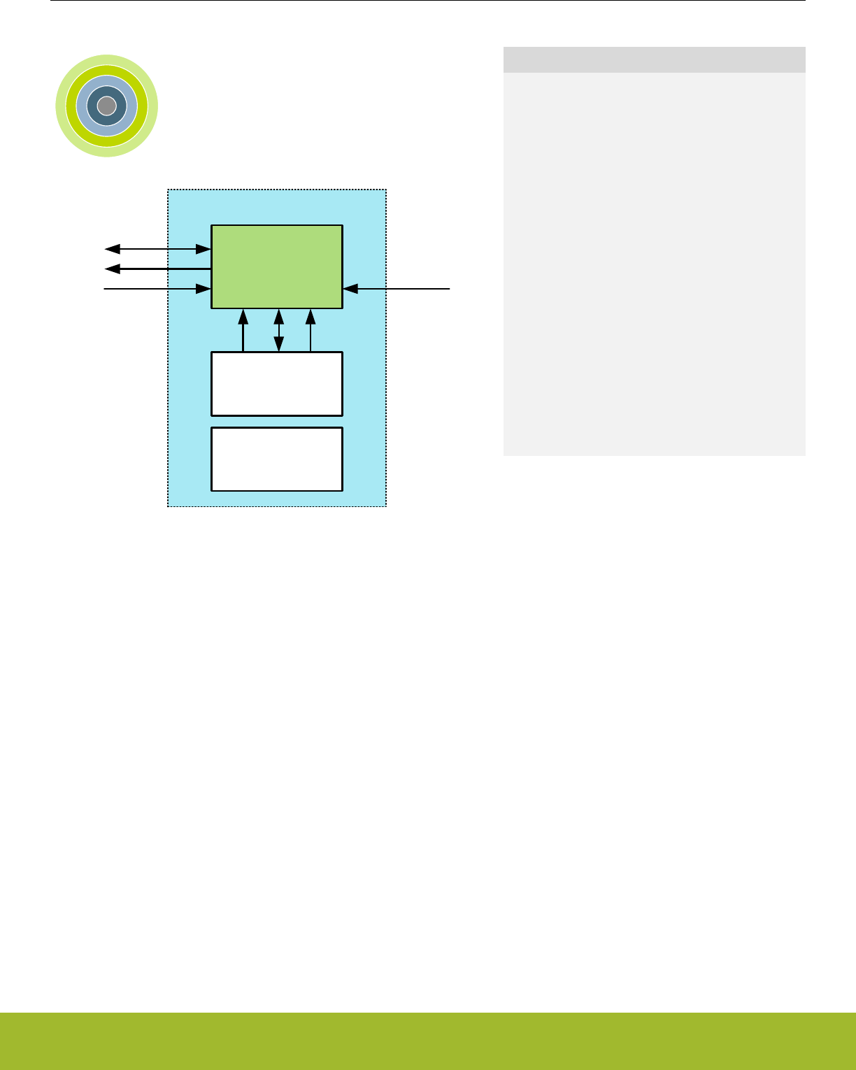
33. GPIO - General Purpose Input/Output
0 1 2 3 4
GPIO
Peripherals
ARM
Cortex-M
Quick Facts
What?
The General Purpose Input/Output (GPIO) is used
for pin configuration, direct pin manipulation and
sensing, as well as routing for peripheral pin connec-
tions.
Why?
Easy to use and highly configurable input/output
pins are important to fit many communication proto-
cols as well as minimizing software control over-
head. Flexible routing of peripheral functions helps
to ease PCB layout.
How?
Each pin on the device can be individually config-
ured as either an input or an output with several dif-
ferent drive modes. Also, individual bit manipulation
registers minimizes control overhead. Peripheral
connections to pins can be routed to several differ-
ent locations, thus solving congestion issues that
may arise with multiple functions on the same pin.
Fully asynchronous interrupts can also be generated
from any pin.
33.1 Introduction
In the EFR32xG13 Wireless Gecko devices the General Purpose Input/Output (GPIO) pins are organized into ports with up to 16 pins
each. These GPIO pins can individually be configured as either an output or input. More advanced configurations like open-drain, open-
source, and glitch filtering can be configured for each individual GPIO pin. The GPIO pins can also be overridden by peripheral pin
connections, like Timer PWM outputs or USART communication, which can be routed to several locations on the device. The GPIO
supports up to 16 asynchronous external pin interrupts, which enable interrupts from any pin on the device. Also, the input value of a
pin can be routed through the Peripheral Reflex System to other peripherals.
Note:
To use the GPIO, the GPIO clock must first be enabled in CMU_HFBUSCLKEN0. Setting this bit enables the HFBUSCLK for the GPIO.
Reference Manual
GPIO - General Purpose Input/Output
silabs.com | Smart. Connected. Energy-friendly. Preliminary Rev. 0.5 | 1103

33.2 Features
• Individual configuration for each pin
•Tristate (reset state)
• Push-pull
• Open-drain
• Pull-up resistor
• Pull-down resistor
• Drive strength
• 1 mA
• 10 mA
• Slewrate
• Over Voltage Tolerance
• EM4 IO pin retention
• Output enable
• Output value
• Pull enable
• Pull direction
• Over Voltage Tolerance
• EM4 wake-up on selected GPIO pins
• Glitch suppression input filter
• Alternate functions (e.g. peripheral outputs and inputs)
• Routed to several locations on the device
• Pin connections can be enabled individually
• Output data can be overridden by peripheral
• Output enable can be overridden by peripheral
• Toggle register for output data
• Dedicated data input register (read-only)
• Interrupts
• 2 Interrupt lines using either levels or edges
• EM4 wake-up pins are selectable for level interrupts
• All GPIO pins are selectable for edge interrupts
• Separate enable, status, set and clear registers
• Asynchronous sensing
• Rising, falling or both edges
• High or low level detection
• Wake up from EM0 Active-EM3 Stop
• Peripheral Reflex System producer
• All GPIO pins are selectable
• Configuration lock functionality to avoid accidental changes
Reference Manual
GPIO - General Purpose Input/Output
silabs.com | Smart. Connected. Energy-friendly. Preliminary Rev. 0.5 | 1104
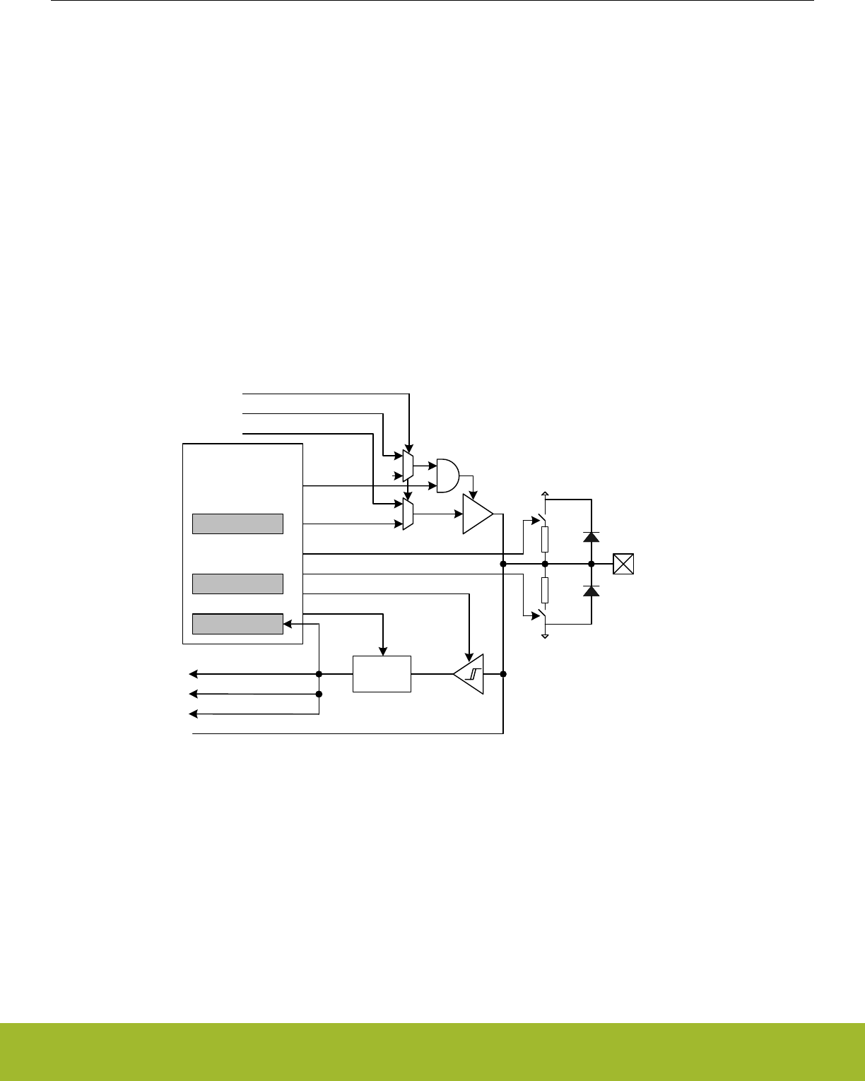
33.3 Functional Description
An overview of the GPIO module is shown in Figure 33.1 Pin Configuration on page 1105. The GPIO pins are grouped into 16-pin
ports. Each individual GPIO pin is called Pxn where x indicates the port (A, B, C ...) and n indicates the pin number (0,1,....,15). Fewer
than 16 bits may be available on some ports, depending on the total number of I/O pins on the package. After a reset, both input and
output are disabled for all pins on the device, except for the Serial Wire Debug pins.
To use a pin, the Mode Register (GPIO_Px_MODEL/GPIO_Px_MODEH) must be configured for the pin to make it an input or output.
These registers can also do more advanced configuration, which is covered in 33.3.1 Pin Configuration. When the port is configured as
an input or an output, the Data In Register (GPIO_Px_DIN) can be used to read the level of each pin in the port (bit n in the register is
connected to pin n on the port). When configured as an output, the value of the Data Out Register (GPIO_Px_DOUT) will be driven to
the pin.
The DOUT value can be changed in 4 different ways:
• Writing to the GPIO_Px_DOUT register
• Writing the BITSET address of the GPIO_Px_DOUT register sets the DOUT bits
• Writing the BITCLEAR address of the GPIO_Px_DOUT register clears the DOUT bits
• Writing the GPIO_Px_DOUTTGL register toggles the corresponding DOUT bits
Reading the GPIO_Px_DOUT register will return its contents. Reading the GPIO_Px_DOUTTGL register will return 0.
GPIO
VSS
MODEn[3:0]
DOUT
Analog connections
VDD
Output enable
Input enable
Interrupt input
Alternate function override
Alternate function input
Alternate function output enable
Alternate function data out
Data out
DIN
Pull-down enable
Pull-up enable
Output enable
Output value
1
Glitch
suppression
filter
Filter enable
PRS
ESD diode
ESD diode
Figure 33.1. Pin Configuration
Reference Manual
GPIO - General Purpose Input/Output
silabs.com | Smart. Connected. Energy-friendly. Preliminary Rev. 0.5 | 1105

33.3.1 Pin Configuration
In addition to setting the pins as either outputs or inputs, the GPIO_Px_MODEL and GPIO_Px_MODEH registers can be used for more
advanced configurations. GPIO_Px_MODEL contains 8 bit fields named MODEn (n=0,1,..7) which control pins 0-7, while
GPIO_Px_MODEH contains 8 bit fields named MODEn (n=8,9,..15) which control pins 8-15. In some modes GPIO_Px_DOUT is also
used for extra configurations like pull-up/down and glitch suppression filter enable. Table 33.1 Pin Configuration on page 1106 shows
the available configurations.
Table 33.1. Pin Configuration
MODEn Input Output DOUT Pull-
down
Pull-
up
Alt Port
Ctrl
Input
Filter
Description
DISABLED Disabled Disabled 0 Input disabled
1 On Input disabled with pull-up
INPUT Enabled
if not
DINDIS
0 Input enabled
1 On Input enabled with filter
INPUTPULL 0 On Input enabled with pull-
down
1 On Input enabled with pull-up
INPUTPULLFILTER 0 On On Input enabled with pull-
down and filter
1 On On Input enabled with pull-up
and filter
PUSHPULL Push-
pull
x Push-pull
PUSHPULLALT x On Push-pull with alternate
port control values
WIREDOR Open
Source
(Wired-
OR)
x Open-source
WIREDORPULLDOWN x On Open-source with pull-
down
WIREDAND Open
Drain
(Wired-
AND)
x Open-drain
WIREDANDFILTER x On Open-drain with filter
WIREDANDPULLUP x On Open-drain with pull-up
WIREDANDPULLUPFILTER x On On Open-drain with pull-up
and filter
WIREDANDALT x On Open-drain with alternate
port control values
WIREDANDALTFILTER x On On Open-drain with alternate
port control values and fil-
ter
WIREDANDALTPULLUP x On On Open-drain with alternate
port control values and
pull-up
WIREDANDALTPULLUPFILTER x On On On Open-drain with alternate
port control values, pull-up
and filter
MODEn determines which mode the pin is in at a given time. Setting MODEn to DISABLED disables the pin, reducing power consump-
tion to a minimum. When the output driver, input driver and Over Voltage Tolerance is disabled, the pin can be used as a connection for
an analog module. An input is enabled by setting MODEn to any value other than DISABLED while DINDIS for the given port is cleared.
Reference Manual
GPIO - General Purpose Input/Output
silabs.com | Smart. Connected. Energy-friendly. Preliminary Rev. 0.5 | 1106
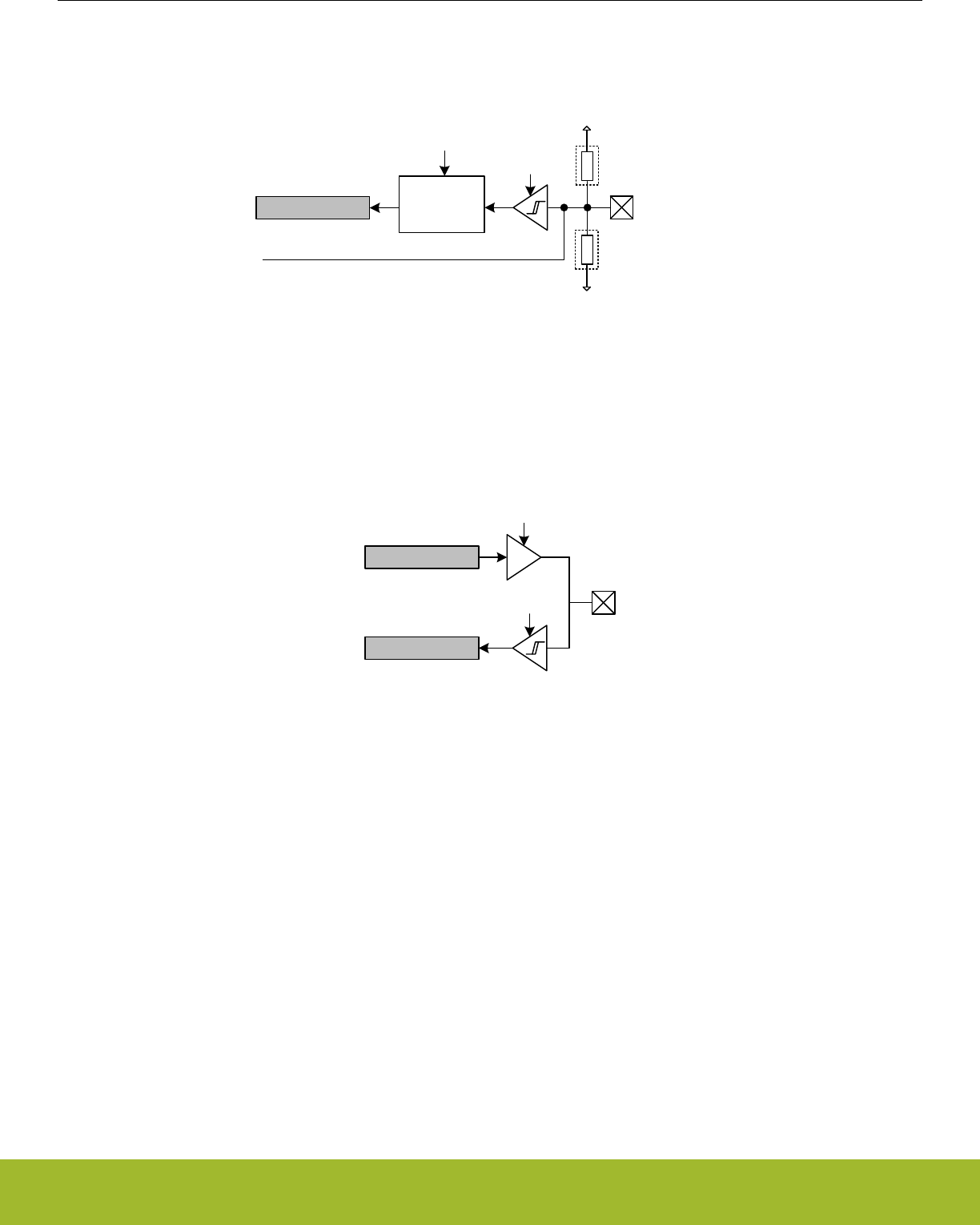
Set DINDIS to disable the input of a gpio port. The pull-up, pull-down and glitch filter function can optionally be applied to the input, see
Figure 33.2 Tristated Output with Optional Pull-up or Pull-down on page 1107.
VDD
DIN
Optional
pull-up
VSS
Optional
pull-down
Input enable
Analog connections
Glitch
suppression
filter
Filter enable
Figure 33.2. Tristated Output with Optional Pull-up or Pull-down
When MODEn is PUSHPULL or PUSHPULLALT, the pin operates in push-pull mode. In this mode, the pin can have alternate port con-
trol values and can be driven either high or low, dependent on the value of GPIO_Px_DOUT. The push-pull configuration is shown in
Figure 33.3 Push-Pull Configuration on page 1107.
Input Enable
DOUT
DIN
Output Enable
Figure 33.3. Push-Pull Configuration
When MODEn is WIREDOR or WIREDORPULLDOWN, the pin operates in open-source mode (with a pull-down resistor for WIRE-
DORPULLDOWN). When driving a high value in open-source mode, the pull-down is disconnected to save power.
When the mode is prefixed with WIREDAND, the pin operates in open-drain mode as shown in Figure 33.4 Open-drain on page 1108.
In open-drain mode, the pin can have an input filter, a pull-up, alternate port control values or any combination of these. When driving a
low value in open-drain mode, the pull-up is disconnected to save power.
Reference Manual
GPIO - General Purpose Input/Output
silabs.com | Smart. Connected. Energy-friendly. Preliminary Rev. 0.5 | 1107

VSS
DOUT
VDD
DIN
Optional
pull-up
Glitch
suppression
filter
Filter enable
Figure 33.4. Open-drain
33.3.1.1 Over Voltage Tolerance
Over voltage capability is available for most pins. If available, it allows the pin to be used at either the minimum of VDDIO + 2V and
5.5V (for 5V tolerant pads) or the minimum of VDDIO + 2V and 3.8V (for non-5V tolerant pads). The datasheet specifies which pins can
be used as 5V tolerant pins. Default over voltage is enabled for each pin supporting that feature. Over voltage tolerance (OVT) can be
disabled on a per pin basis. The over voltage tolerance feature applied to the selected pins is configured in the GPIO_Px_OVTDIS
register. Disabling the over voltage tolerance for a pin will provide less distortion on that pin, which is useful when the pin is used as
analog input.
Note:
The VDAC (and OPAMPs) can drive outputs above VDDIO and therefore the involved pads typically require OVT to be be enabled.
33.3.1.2 Alternate Port Control
The Alternate Port Control allows for additional flexibilty of port level settings. A user may setup two different port configurations (normal
and alternate modes) and select which is applied on a pin by pin bases. For example you may configure half of port A to use the low
drive strength setting (normal mode) while the other half uses high drive strength (alternate mode).
Alternate port control is enabled when MODEn is set to any of the ALT enumerated modes (ie. PUSHPULLALT). When MODEn is an
alternate mode, the pin uses the alternate port control values specified in the DINDISALT,SLEWRATEALT, and DRIVESTRENGTHALT
fields in GPIO_Px_CTRL. In all other modes, the port control values are used from the DINDIS,SLEWRATE, and DRIVESTRENGTH
fields in GPIO_Px_CTRL.
33.3.1.3 Drive Strength
The drive strength can be applied to pins on a port-by-port basis. The drive strength applied to pins configured using normal MODEn
settings can be controlled using the DRIVESTRENGTH field in GPIO_Px_CTRL. The drive strength applied to pins configured using
alternate MODEn settings can be controlled using the DRIVESTRENGTHALT field.
33.3.1.4 Slewrate
The slewrate can be applied to pins on a port-by-port basis. The slewrate applied to pins configured using normal MODEn settings can
be controlled using the SLEWRATE fields in GPIO_Px_CTRL. The slewrate applied to pins configured using the alternate MODEn set-
tings can be controlled using the SLEWRATEALT field.
33.3.1.5 Input Disable
The pin inputs can be disabled on a port-by-port basis. The input of pins configured using the normal MODEn settings can be disabled
by setting DINDIS in GPIO_Px_CTRL. The input of pins configured using the alternate MODEn settings can be disabled by setting DIN-
DISALT.
Reference Manual
GPIO - General Purpose Input/Output
silabs.com | Smart. Connected. Energy-friendly. Preliminary Rev. 0.5 | 1108
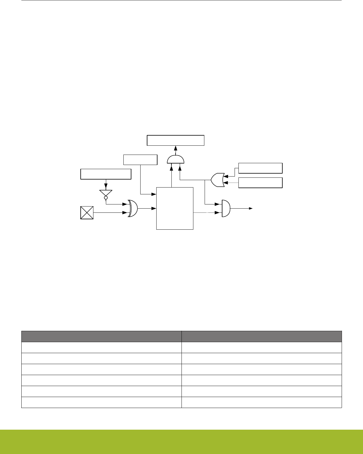
33.3.1.6 Configuration Lock
GPIO_Px_MODEL, GPIO_Px_MODEH, GPIO_Px_CTRL, GPIO_Px_PINLOCKN, GPIO_Px_OVTDIS, GPIO_EXTIPSELL, GPIO_EX-
TIPSELH, GPIO_EXTIPINSELL, GPIO_EXTIPINSELH, GPIO_INSENSE, GPIO_ROUTEPEN, and GPIO_ROUTELOC0 can be locked
by writing any value other than 0xA534 to GPIO_LOCK. Writing the value 0xA534 to the GPIOx_LOCK register unlocks the configura-
tion registers.
In addition to configuration lock, GPIO_Px_MODEL, GPIO_Px_MODEH, GPIO_Px_DOUT, GPIO_Px_DOUTTGL, and GPIO_Px_OVT-
DIS can be locked individually for each pin by clearing the corresponding bit in GPIO_Px_PINLOCKN. When a bit in the GPIO_Px_PIN-
LOCKN register is cleared, it will stay cleared until reset.
33.3.2 EM4 Wake-up
It is possible to trigger a wake-up from EM4 using any of the selectable EM4WU GPIO pins. The wake-up request can be triggered
through the pins by enabling the corresponding bit in the GPIO_EM4WUEN register. When EM4 wake-up is enabled for the pin, the
input filter is enabled during EM4. This is done to avoid false wake-up caused by glitches. In addition, the polarity of the EM4 wake-up
request can be selected using the GPIO_EXTILEVEL register.
GPIO_EXTILEVEL
Wake-up Logic
GPIO_EM4WUEN
GPIO_IF
Wake-up request
GPIO_IFC
GPIO_IEN
Figure 33.5. EM4 Wake-up Logic
The pins used for EM4 wake-up must be configured as inputs with glitch filters using the GPIO_Px_MODEL/GPIO_Px_MODEH regis-
ter. If the input is disabled and the wakeup polarity is low, a false wakeup will occur when entering EM4. If the input is enabled, the
glitch filtered is disabled, and the polarity is set low, a glitch will occur when going into EM4 that will cause an immediate wake-up.
Before going down to EM4, it is important to clear the wake-up logic by setting the GPIO_IFC bit, which clears the wake-up logic, in-
cluding the GPIO_IF register. It is possible to determine which pin caused the EM4WU by reading the GPIO_IF register. The mapping
between EM4WU pins and the bit indexes in the GPIO_EM4WUEN, GPIO_EXTILEVEL, GPIO_IFC, GPIO_IFS, GPIO_IEN, and
GPIO_IF registers is as follows:
Table 33.2. EM4WU Register Bit Index to EM4WU pin Mapping
EM4WU Register Bit Indexes EM4WU Pin
16 GPIO_EM4WU0
17 GPIO_EM4WU1
18 GPIO_EM4WU2
19 GPIO_EM4WU3
... ...
31 GPIO_EM4WU15
Note: Please see the device datasheet for actual pin location
Reference Manual
GPIO - General Purpose Input/Output
silabs.com | Smart. Connected. Energy-friendly. Preliminary Rev. 0.5 | 1109

33.3.3 EM4 Retention
By default GPIO pins revert back to their reset state when EM4 is entered. The GPIO pins can be configured to retain the settings for
output enable, output value, pull enable, pull direction and over voltage tolerance while in EM4.
EM4 GPIO retention is controlled with the EM4IORETMODE field in the EMU_EM4CTRL register. Setting EM4IORETMODE to
EM4EXIT will cause retention to persist while in EM4 and reset the GPIO's during wakeup. Setting EM4IORETMODE to SWUNLATCH
will cause the retention to persist until the EM4UNLATCH bit is written by software. When using SWUNLATCH the GPIO register values
are sill reset on wakup. In order to ensure that the GPIO state does not change sofware must re-write the GPIO registers before setting
EM4UNLATCH and ending EM4 GPIO retention. See the EMU chapter for additional documentation on it's registers and the EM4UN-
LATCH bit.
33.3.4 Alternate Functions
Alternate functions are connections to pins from peripherals, i.e. Timers, USARTs, etc.. These peripherals contain route registers,
where the pin connections are enabled. In addition, the route registers contain a location bit field that configures which pin an output of
that peripheral will be connected to if enabled. After connecting a peripheral, the pin configuration stays as set in GPIO_Px_MODEL,
GPIO_Px_MODEH and GPIO_Px_DOUT registers. For example, the pin configuration must be set to output enable in GPIO_Px_MOD-
EL or GPIO_Px_MODEH for a peripheral to be able to use the pin as an output.
It is not recommended to select two or more peripherals as output on the same pin. The reader is referred to the pin map section of the
device datasheet for more information on the possible locations of each alternate function.
33.3.4.1 Analog Connections
When using the GPIO pin for analog functionality, it is recommended to disable the over voltage tolerance by setting the corresponding
pin in the GPIO_Px_OVTDIS register and setting the MODEn in GPIO_Px_MODEL or GPIO_Px_MODEH equal to DISABLE to disable
the input sense, output driver and pull resistors.
33.3.4.2 Debug Connections
33.3.4.2.1 Serial Wire Debug Connection
The SW Debug Port is routed as an alternate function and the SWDIO and SWCLK pin connections are enabled by default with internal
pull up and pull down resistors, respectively. It is possible to disable these pin connections (and disable the pull resistors) by setting the
SWDIOTMSPEN and SWCLKTCKPEN bits in GPIO_ROUTEPEN to 0.
The Serial Wire Viewer pin, SWV, can be enabled by setting the SWVPEN bit in GPIO_ROUTEPEN. This bit can also be routed to
alternate locations by configuring the SWVLOC bitfield in GPIO_ROUTELOC0.
33.3.4.2.2 JTAG Debug Connection
The JTAG Debug Port is routed as an alternate function and the TMS, TCK, TDO, and TDI pin connections are enabled by default with
internal pull up, pull down, no pull, and pull up resistors, respectively. It is possible to disable these pin connections (and disable the pull
resistors) by setting the SWDIOTMSPEN, SWCLKTCKPEN, TDOPEN, and TDIPEN bits in GPIO_ROUTEPEN to 0.
33.3.4.2.3 Disabling Debug Connections
When the debug pins are disabled, the device can no longer be accessed by a debugger. A reset will set the debug pins back to their
enabled default state. The GPIO_ROUTEPEN register can only be updated when the debugger is disconnected from the system. Any
attempts to modify GPIO_ROUTEPEN when the debugger is connected will not occur. If you do disable the debug pins, make sure you
have at least a 3 second timeout at the start of your program code before you disable the debug pins. This way the debugger will have
time to connect to the the device after a reset and before the pins are disabled.
33.3.4.2.4 ETM Trace Connections
There are five trace pins available on the device. One trace clock which can be enabled by setting the ETMTCLKPEN bitfield in
GPIO_ROUTEPEN. The four data pins can be enabled individually by setting ETMTD0PEN, ETMTD1PEN, ETMTD2PEN and
ETMTD3PEN respectively in GPIO_ROUTEPEN. It is possible to choose which pins the trace data will be exported to. The lowest trace
bit will be routed to the first enabled trace pin. For example, if the ETM data port size is 2 bits and TD0 and TD3 are enabled, will make
bit 0 be routed to TD0 while bit 1 will be routed to TD3.
Both the TCLK and all the TD pins can also be routed to alternate locations by configuring the ETMLOC bitfield in GPIO_ROUTELOC0.
Reference Manual
GPIO - General Purpose Input/Output
silabs.com | Smart. Connected. Energy-friendly. Preliminary Rev. 0.5 | 1110
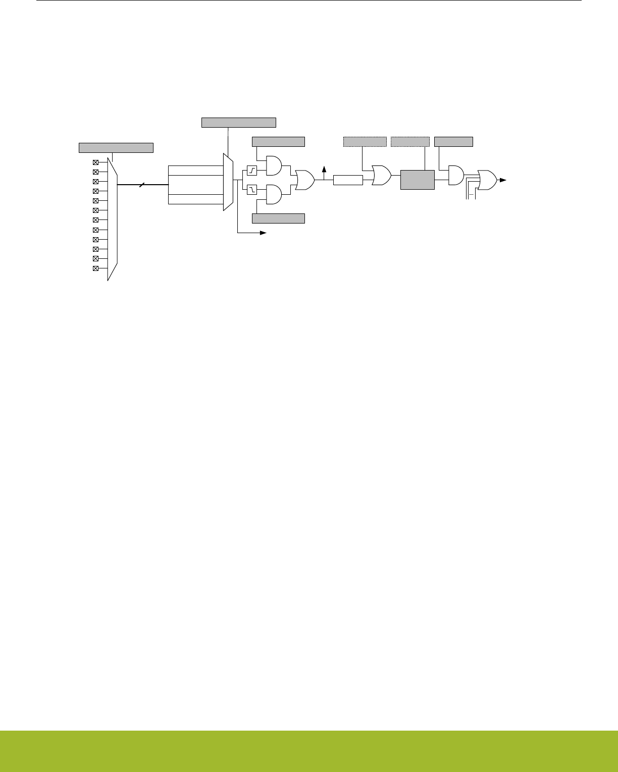
33.3.5 Interrupt Generation
33.3.5.1 Edge Interrupt Generation
The GPIO can generate an interrupt from any edge of the input of any GPIO pin on the device. The edge interrupts have asynchronous
sense capability, enabling wake-up from energy modes as low as EM3 Stop, see Figure 33.6 Pin n Interrupt Generation on page 1111.
IRQ_GPIO_EVEN/
IRQ_GPIO_ODD
PA[p+3:p]
EXTIRISE[n] IEN[n]
EXTIPSEL[n]
PB[p+3:p]
PC[p+3:p]
PD[p+3:p]
PE[p+3:p]
IF[n]
set clear
IFS[n] IFC[n]
wakeup
PF[p+3:p]
EXTIFALL[n]
PRS
Odd/even inputs
Synch
EXTIPINSEL[n]
4
PG[p+3:p]
PH[p+3:p]
PI[p+3:p]
PJ[p+3:p]
PK[p+3:p]
PL[p+3:p]
p = 4 * int( n / 4 )
Figure 33.6. Pin n Interrupt Generation
External pin interrupts can be represented in the form of EXTI[index], where index is the external interrupt number. For example, the
EXTI7 interrupt has an index of 7. All pins within a group of four (0-3,4-7,8-11,12-15) from all ports are grouped together to trigger one
interrupt. The group of pins available to trigger an interrupt is determined by the interrupt index and calculated as int(index/4). For ex-
ample the first 4 interrupts (EXTI0 - EXTI3) are triggered by pins in the first group (Px[3:0]) and the second 4 interrupts (EXTI4-EXTI7)
are triggered by pins in the second group (Px[7:4]).
The EXTIPSELn bits in GPIO_EXTIPSELL or GPIO_EXTIPSELH select which PORT in the group will trigger the interrupt. The EXTI-
PINSELn bits in GPIO_EXTIPINSELL or GPIO_EXTIPINSELH will determine which pin inside the selected group will trigger the inter-
rupt.
For example if EXTIPSEL11 = PORTB and EXTPINSEL11 = 0 then PB8 will be used for EXTI11. EXTI11 uses the third group (11/4 = 2)
so the list of possible pins is Px[11:8]. The setting of EXTIPSEL11 further narrows the selection to PB[11:8]. Finally EXTPINSEL11 se-
lects the first pin in that group which is PB8.
The GPIO_EXTIRISE[n] and GPIO_EXTIFALL[n] registers enable sensing of rising and falling edges. By setting the EXT[n] bit in
GPIO_IEN, a high interrupt flag n, will trigger one of two interrupt lines. The even interrupt line is triggered by any enabled even num-
bered interrupt flag index, while the odd interrupt line is triggered by odd flag indexes. The interrupt flags can be set and cleared by
software when writing the GPIO_IFS and GPIO_IFC registers. Since the external interrupts are asynchronous, they are sensitive to
noise. To increase noise tolerance, the MODEL and MODEH fields in the GPIO_Px_MODEL and GPIO_Px_MODEH registers, respec-
tively, should be set to include glitch filtering for pins that have external interrupts enabled.
Reference Manual
GPIO - General Purpose Input/Output
silabs.com | Smart. Connected. Energy-friendly. Preliminary Rev. 0.5 | 1111

33.3.5.2 Level Interrupt Generation
GPIO can generate a level interrupt using the input of any GPIO EM4 wake-up pins on the device. The interrupts have asynchronous
sense capability, enabling wake-up from energy modes as low as EM4.
In order to enable the level interrupt, set the EM4WU field in the GPIO_IEN register and the EM4WUn field in the GPIO_EXTILEVEL
register. Upon a level interrupt occuring, the corresponding EM4WU index in the GPIO_IF register will be set along with the odd or even
interrupt line depending on the index inside of GPIO_IF, see Figure 33.7 Level Interrupt Example on page 1112 The wake-up granulalr-
ity of the level interrupts is based on the settings of the EM4WU field in the GPIO_IEN register and the EM4WUEN field in the
GPIO_EM4WUEN register, see Table 33.3 Level Interrupt Energy Mode Wakeup on page 1112
Table 33.3. Level Interrupt Energy Mode Wakeup
GPIO_IEN GPIO_EM4WUEN Energy Mode Wakeup
0 0 No Interrupt
0 1 EM4H,EM4S
1 0 EM1,EM2,EM3,EM4H,EM4S
1 1 EM1,EM2,EM3,EM4H,EM4S
By setting the EM4WU8 in GPIO_EXTILEVEL and EM4WU[8] in GPIO_IEN, the interrupt flag EM4WU[8] in GPIO_IF will be triggered
by a high level on pin EM4WU8 and a interrupt request will be sent on IRQ_GPIO_EVEN.
Figure 33.7. Level Interrupt Example
33.3.6 Output to PRS
All pins within a group of four(0-3,4-7,8-11,12-15) from all ports are grouped together to form one PRS producer which outputs to the
PRS. The pin from which the output should be taken is selected in the same fashion as the edge interrupts.
PRS output is not affected by the interrupt edge detection logic or gated by the IEN bits. See Figure 33.6 Pin n Interrupt Generation on
page 1111 for an illustration of where the PRS output signal is generated.
33.3.7 Synchronization
To avoid metastability in synchronous logic connected to the pins, all inputs are synchronized with double flip-flops. The flip-flops for the
input data run on the HFBUSCLK. Consequently, when a pin changes state, the change will have propagated to GPIO_Px_DIN after
two 2 HFBUSCLK cycles. Synchronization (also running on the HFBUSCLK) is also added for interrupt input. To save power when the
external interrupts or level interrupts are not used, the synchronization flip-flops for these can be turned off by clearing INT or
EM4WU,respectively, in GPIO_INSENSE register.
Reference Manual
GPIO - General Purpose Input/Output
silabs.com | Smart. Connected. Energy-friendly. Preliminary Rev. 0.5 | 1112

33.4 Register Map
The offset register address is relative to the registers base address.
Offset Name Type Description
0x000 GPIO_PA_CTRL RW Port Control Register
0x004 GPIO_PA_MODEL RW Port Pin Mode Low Register
0x008 GPIO_PA_MODEH RW Port Pin Mode High Register
0x00C GPIO_PA_DOUT RW Port Data Out Register
0x018 GPIO_PA_DOUTTGL W1 Port Data Out Toggle Register
0x01C GPIO_PA_DIN RPort Data In Register
0x020 GPIO_PA_PINLOCKN RW Port Unlocked Pins Register
0x028 GPIO_PA_OVTDIS RW Over Voltage Disable for all modes
... GPIO_Px_CTRL RW Port Control Register
... GPIO_Px_MODEL RW Port Pin Mode Low Register
... GPIO_Px_MODEH RW Port Pin Mode High Register
... GPIO_Px_DOUT RW Port Data Out Register
... GPIO_Px_DOUTTGL W1 Port Data Out Toggle Register
... GPIO_Px_DIN RPort Data In Register
... GPIO_Px_PINLOCKN RW Port Unlocked Pins Register
... GPIO_Px_OVTDIS RW Over Voltage Disable for all modes
0x210 GPIO_PL_CTRL RW Port Control Register
0x214 GPIO_PL_MODEL RW Port Pin Mode Low Register
0x218 GPIO_PL_MODEH RW Port Pin Mode High Register
0x21C GPIO_PL_DOUT RW Port Data Out Register
0x228 GPIO_PL_DOUTTGL W1 Port Data Out Toggle Register
0x22C GPIO_PL_DIN RPort Data In Register
0x230 GPIO_PL_PINLOCKN RW Port Unlocked Pins Register
0x238 GPIO_PL_OVTDIS RW Over Voltage Disable for all modes
0x400 GPIO_EXTIPSELL RW External Interrupt Port Select Low Register
0x404 GPIO_EXTIPSELH RW External Interrupt Port Select High Register
0x408 GPIO_EXTIPINSELL RW External Interrupt Pin Select Low Register
0x40C GPIO_EXTIPINSELH RW External Interrupt Pin Select High Register
0x410 GPIO_EXTIRISE RW External Interrupt Rising Edge Trigger Register
0x414 GPIO_EXTIFALL RW External Interrupt Falling Edge Trigger Register
0x418 GPIO_EXTILEVEL RW External Interrupt Level Register
0x41C GPIO_IF RInterrupt Flag Register
0x420 GPIO_IFS W1 Interrupt Flag Set Register
0x424 GPIO_IFC (R)W1 Interrupt Flag Clear Register
0x428 GPIO_IEN RW Interrupt Enable Register
Reference Manual
GPIO - General Purpose Input/Output
silabs.com | Smart. Connected. Energy-friendly. Preliminary Rev. 0.5 | 1113

Offset Name Type Description
0x42C GPIO_EM4WUEN RW EM4 wake up Enable Register
0x440 GPIO_ROUTEPEN RW I/O Routing Pin Enable Register
0x444 GPIO_ROUTELOC0 RW I/O Routing Location Register
0x448 GPIO_ROUTELOC1 RW I/O Routing Location Register 1
0x450 GPIO_INSENSE RW Input Sense Register
0x454 GPIO_LOCK RWH Configuration Lock Register
Reference Manual
GPIO - General Purpose Input/Output
silabs.com | Smart. Connected. Energy-friendly. Preliminary Rev. 0.5 | 1114

33.5 Register Description
33.5.1 GPIO_Px_CTRL - Port Control Register
Offset Bit Position
0x000
31
30
29
28
27
26
25
24
23
22
21
20
19
18
17
16
15
14
13
12
11
10
9
8
7
6
5
4
3
2
1
0
Reset
0
0x5
0
0
0x5
0
Access
RW
RW
RW
RW
RW
RW
Name
DINDISALT
SLEWRATEALT
DRIVESTRENGTHALT
DINDIS
SLEWRATE
DRIVESTRENGTH
Bit Name Reset Access Description
31:29 Reserved To ensure compatibility with future devices, always write bits to 0. More information in 1.2 Conven-
tions
28 DINDISALT 0 RW Alternate Data In Disable
Data input disable for port pins using alternate modes.
27:23 Reserved To ensure compatibility with future devices, always write bits to 0. More information in 1.2 Conven-
tions
22:20 SLEWRATEALT 0x5 RW Alternate slewrate limit for port
Slewrate limit for port pins using alternate modes. Higher values represent faster slewrates.
19:17 Reserved To ensure compatibility with future devices, always write bits to 0. More information in 1.2 Conven-
tions
16 DRIVESTRENGTH-
ALT
0 RWAlternate drive strength for port
Drive strength setting for port pins using alternate drive strength.
Value Mode Description
0 STRONG 10 mA drive current
1 WEAK 1 mA drive current
15:13 Reserved To ensure compatibility with future devices, always write bits to 0. More information in 1.2 Conven-
tions
12 DINDIS 0 RW Data In Disable
Data input disable for port pins not using alternate modes.
11:7 Reserved To ensure compatibility with future devices, always write bits to 0. More information in 1.2 Conven-
tions
6:4 SLEWRATE 0x5 RW Slewrate limit for port
Slewrate limit for port pins not using alternate modes. Higher values represent faster slewrates.
3:1 Reserved To ensure compatibility with future devices, always write bits to 0. More information in 1.2 Conven-
tions
Reference Manual
GPIO - General Purpose Input/Output
silabs.com | Smart. Connected. Energy-friendly. Preliminary Rev. 0.5 | 1115

Bit Name Reset Access Description
0 DRIVESTRENGTH 0 RW Drive strength for port
Drive strength setting for port pins not using alternate modes.
Value Mode Description
0 STRONG 10 mA drive current
1 WEAK 1 mA drive current
Reference Manual
GPIO - General Purpose Input/Output
silabs.com | Smart. Connected. Energy-friendly. Preliminary Rev. 0.5 | 1116

33.5.2 GPIO_Px_MODEL - Port Pin Mode Low Register
Offset Bit Position
0x004
31
30
29
28
27
26
25
24
23
22
21
20
19
18
17
16
15
14
13
12
11
10
9
8
7
6
5
4
3
2
1
0
Reset
0x0
0x0
0x0
0x0
0x0
0x0
0x0
0x0
Access
RW
RW
RW
RW
RW
RW
RW
RW
Name
MODE7
MODE6
MODE5
MODE4
MODE3
MODE2
MODE1
MODE0
Bit Name Reset Access Description
31:28 MODE7 0x0 RW Pin 7 Mode
Configure mode for pin 7.
Value Mode Description
0 DISABLED Input disabled. Pullup if DOUT is set.
1 INPUT Input enabled. Filter if DOUT is set
2 INPUTPULL Input enabled. DOUT determines pull direction
3 INPUTPULLFILTER Input enabled with filter. DOUT determines pull direction
4 PUSHPULL Push-pull output
5 PUSHPULLALT Push-pull using alternate control
6 WIREDOR Wired-or output
7 WIREDORPULLDOWN Wired-or output with pull-down
8 WIREDAND Open-drain output
9 WIREDANDFILTER Open-drain output with filter
10 WIREDANDPULLUP Open-drain output with pullup
11 WIREDANDPULLUP-
FILTER
Open-drain output with filter and pullup
12 WIREDANDALT Open-drain output using alternate control
13 WIREDANDALTFILTER Open-drain output using alternate control with filter
14 WIREDANDALTPULL-
UP
Open-drain output using alternate control with pullup
15 WIREDANDALTPUL-
LUPFILTER
Open-drain output using alternate control with filter and pullup
27:24 MODE6 0x0 RW Pin 6 Mode
Configure mode for pin 6.
Value Mode Description
0 DISABLED Input disabled. Pullup if DOUT is set.
1 INPUT Input enabled. Filter if DOUT is set
2 INPUTPULL Input enabled. DOUT determines pull direction
3 INPUTPULLFILTER Input enabled with filter. DOUT determines pull direction
Reference Manual
GPIO - General Purpose Input/Output
silabs.com | Smart. Connected. Energy-friendly. Preliminary Rev. 0.5 | 1117

Bit Name Reset Access Description
4 PUSHPULL Push-pull output
5 PUSHPULLALT Push-pull using alternate control
6 WIREDOR Wired-or output
7 WIREDORPULLDOWN Wired-or output with pull-down
8 WIREDAND Open-drain output
9 WIREDANDFILTER Open-drain output with filter
10 WIREDANDPULLUP Open-drain output with pullup
11 WIREDANDPULLUP-
FILTER
Open-drain output with filter and pullup
12 WIREDANDALT Open-drain output using alternate control
13 WIREDANDALTFILTER Open-drain output using alternate control with filter
14 WIREDANDALTPULL-
UP
Open-drain output using alternate control with pullup
15 WIREDANDALTPUL-
LUPFILTER
Open-drain output using alternate control with filter and pullup
23:20 MODE5 0x0 RW Pin 5 Mode
Configure mode for pin 5.
Value Mode Description
0 DISABLED Input disabled. Pullup if DOUT is set.
1 INPUT Input enabled. Filter if DOUT is set
2 INPUTPULL Input enabled. DOUT determines pull direction
3 INPUTPULLFILTER Input enabled with filter. DOUT determines pull direction
4 PUSHPULL Push-pull output
5 PUSHPULLALT Push-pull using alternate control
6 WIREDOR Wired-or output
7 WIREDORPULLDOWN Wired-or output with pull-down
8 WIREDAND Open-drain output
9 WIREDANDFILTER Open-drain output with filter
10 WIREDANDPULLUP Open-drain output with pullup
11 WIREDANDPULLUP-
FILTER
Open-drain output with filter and pullup
12 WIREDANDALT Open-drain output using alternate control
13 WIREDANDALTFILTER Open-drain output using alternate control with filter
14 WIREDANDALTPULL-
UP
Open-drain output using alternate control with pullup
15 WIREDANDALTPUL-
LUPFILTER
Open-drain output using alternate control with filter and pullup
Reference Manual
GPIO - General Purpose Input/Output
silabs.com | Smart. Connected. Energy-friendly. Preliminary Rev. 0.5 | 1118

Bit Name Reset Access Description
19:16 MODE4 0x0 RW Pin 4 Mode
Configure mode for pin 4.
Value Mode Description
0 DISABLED Input disabled. Pullup if DOUT is set.
1 INPUT Input enabled. Filter if DOUT is set
2 INPUTPULL Input enabled. DOUT determines pull direction
3 INPUTPULLFILTER Input enabled with filter. DOUT determines pull direction
4 PUSHPULL Push-pull output
5 PUSHPULLALT Push-pull using alternate control
6 WIREDOR Wired-or output
7 WIREDORPULLDOWN Wired-or output with pull-down
8 WIREDAND Open-drain output
9 WIREDANDFILTER Open-drain output with filter
10 WIREDANDPULLUP Open-drain output with pullup
11 WIREDANDPULLUP-
FILTER
Open-drain output with filter and pullup
12 WIREDANDALT Open-drain output using alternate control
13 WIREDANDALTFILTER Open-drain output using alternate control with filter
14 WIREDANDALTPULL-
UP
Open-drain output using alternate control with pullup
15 WIREDANDALTPUL-
LUPFILTER
Open-drain output using alternate control with filter and pullup
15:12 MODE3 0x0 RW Pin 3 Mode
Configure mode for pin 3.
Value Mode Description
0 DISABLED Input disabled. Pullup if DOUT is set.
1 INPUT Input enabled. Filter if DOUT is set
2 INPUTPULL Input enabled. DOUT determines pull direction
3 INPUTPULLFILTER Input enabled with filter. DOUT determines pull direction
4 PUSHPULL Push-pull output
5 PUSHPULLALT Push-pull using alternate control
6 WIREDOR Wired-or output
7 WIREDORPULLDOWN Wired-or output with pull-down
8 WIREDAND Open-drain output
9 WIREDANDFILTER Open-drain output with filter
10 WIREDANDPULLUP Open-drain output with pullup
11 WIREDANDPULLUP-
FILTER
Open-drain output with filter and pullup
Reference Manual
GPIO - General Purpose Input/Output
silabs.com | Smart. Connected. Energy-friendly. Preliminary Rev. 0.5 | 1119

Bit Name Reset Access Description
12 WIREDANDALT Open-drain output using alternate control
13 WIREDANDALTFILTER Open-drain output using alternate control with filter
14 WIREDANDALTPULL-
UP
Open-drain output using alternate control with pullup
15 WIREDANDALTPUL-
LUPFILTER
Open-drain output using alternate control with filter and pullup
11:8 MODE2 0x0 RW Pin 2 Mode
Configure mode for pin 2.
Value Mode Description
0 DISABLED Input disabled. Pullup if DOUT is set.
1 INPUT Input enabled. Filter if DOUT is set
2 INPUTPULL Input enabled. DOUT determines pull direction
3 INPUTPULLFILTER Input enabled with filter. DOUT determines pull direction
4 PUSHPULL Push-pull output
5 PUSHPULLALT Push-pull using alternate control
6 WIREDOR Wired-or output
7 WIREDORPULLDOWN Wired-or output with pull-down
8 WIREDAND Open-drain output
9 WIREDANDFILTER Open-drain output with filter
10 WIREDANDPULLUP Open-drain output with pullup
11 WIREDANDPULLUP-
FILTER
Open-drain output with filter and pullup
12 WIREDANDALT Open-drain output using alternate control
13 WIREDANDALTFILTER Open-drain output using alternate control with filter
14 WIREDANDALTPULL-
UP
Open-drain output using alternate control with pullup
15 WIREDANDALTPUL-
LUPFILTER
Open-drain output using alternate control with filter and pullup
7:4 MODE1 0x0 RW Pin 1 Mode
Configure mode for pin 1.
Value Mode Description
0 DISABLED Input disabled. Pullup if DOUT is set.
1 INPUT Input enabled. Filter if DOUT is set
2 INPUTPULL Input enabled. DOUT determines pull direction
3 INPUTPULLFILTER Input enabled with filter. DOUT determines pull direction
4 PUSHPULL Push-pull output
5 PUSHPULLALT Push-pull using alternate control
6 WIREDOR Wired-or output
Reference Manual
GPIO - General Purpose Input/Output
silabs.com | Smart. Connected. Energy-friendly. Preliminary Rev. 0.5 | 1120

Bit Name Reset Access Description
7 WIREDORPULLDOWN Wired-or output with pull-down
8 WIREDAND Open-drain output
9 WIREDANDFILTER Open-drain output with filter
10 WIREDANDPULLUP Open-drain output with pullup
11 WIREDANDPULLUP-
FILTER
Open-drain output with filter and pullup
12 WIREDANDALT Open-drain output using alternate control
13 WIREDANDALTFILTER Open-drain output using alternate control with filter
14 WIREDANDALTPULL-
UP
Open-drain output using alternate control with pullup
15 WIREDANDALTPUL-
LUPFILTER
Open-drain output using alternate control with filter and pullup
3:0 MODE0 0x0 RW Pin 0 Mode
Configure mode for pin 0.
Value Mode Description
0 DISABLED Input disabled. Pullup if DOUT is set.
1 INPUT Input enabled. Filter if DOUT is set
2 INPUTPULL Input enabled. DOUT determines pull direction
3 INPUTPULLFILTER Input enabled with filter. DOUT determines pull direction
4 PUSHPULL Push-pull output
5 PUSHPULLALT Push-pull using alternate control
6 WIREDOR Wired-or output
7 WIREDORPULLDOWN Wired-or output with pull-down
8 WIREDAND Open-drain output
9 WIREDANDFILTER Open-drain output with filter
10 WIREDANDPULLUP Open-drain output with pullup
11 WIREDANDPULLUP-
FILTER
Open-drain output with filter and pullup
12 WIREDANDALT Open-drain output using alternate control
13 WIREDANDALTFILTER Open-drain output using alternate control with filter
14 WIREDANDALTPULL-
UP
Open-drain output using alternate control with pullup
15 WIREDANDALTPUL-
LUPFILTER
Open-drain output using alternate control with filter and pullup
Reference Manual
GPIO - General Purpose Input/Output
silabs.com | Smart. Connected. Energy-friendly. Preliminary Rev. 0.5 | 1121

33.5.3 GPIO_Px_MODEH - Port Pin Mode High Register
Offset Bit Position
0x008
31
30
29
28
27
26
25
24
23
22
21
20
19
18
17
16
15
14
13
12
11
10
9
8
7
6
5
4
3
2
1
0
Reset
0x0
0x0
0x0
0x0
0x0
0x0
0x0
0x0
Access
RW
RW
RW
RW
RW
RW
RW
RW
Name
MODE15
MODE14
MODE13
MODE12
MODE11
MODE10
MODE9
MODE8
Bit Name Reset Access Description
31:28 MODE15 0x0 RW Pin 15 Mode
Configure mode for pin 15.
Value Mode Description
0 DISABLED Input disabled. Pullup if DOUT is set.
1 INPUT Input enabled. Filter if DOUT is set
2 INPUTPULL Input enabled. DOUT determines pull direction
3 INPUTPULLFILTER Input enabled with filter. DOUT determines pull direction
4 PUSHPULL Push-pull output
5 PUSHPULLALT Push-pull using alternate control
6 WIREDOR Wired-or output
7 WIREDORPULLDOWN Wired-or output with pull-down
8 WIREDAND Open-drain output
9 WIREDANDFILTER Open-drain output with filter
10 WIREDANDPULLUP Open-drain output with pullup
11 WIREDANDPULLUP-
FILTER
Open-drain output with filter and pullup
12 WIREDANDALT Open-drain output using alternate control
13 WIREDANDALTFILTER Open-drain output using alternate control with filter
14 WIREDANDALTPULL-
UP
Open-drain output using alternate control with pullup
15 WIREDANDALTPUL-
LUPFILTER
Open-drain output using alternate control with filter and pullup
27:24 MODE14 0x0 RW Pin 14 Mode
Configure mode for pin 14.
Value Mode Description
0 DISABLED Input disabled. Pullup if DOUT is set.
1 INPUT Input enabled. Filter if DOUT is set
2 INPUTPULL Input enabled. DOUT determines pull direction
3 INPUTPULLFILTER Input enabled with filter. DOUT determines pull direction
Reference Manual
GPIO - General Purpose Input/Output
silabs.com | Smart. Connected. Energy-friendly. Preliminary Rev. 0.5 | 1122

Bit Name Reset Access Description
4 PUSHPULL Push-pull output
5 PUSHPULLALT Push-pull using alternate control
6 WIREDOR Wired-or output
7 WIREDORPULLDOWN Wired-or output with pull-down
8 WIREDAND Open-drain output
9 WIREDANDFILTER Open-drain output with filter
10 WIREDANDPULLUP Open-drain output with pullup
11 WIREDANDPULLUP-
FILTER
Open-drain output with filter and pullup
12 WIREDANDALT Open-drain output using alternate control
13 WIREDANDALTFILTER Open-drain output using alternate control with filter
14 WIREDANDALTPULL-
UP
Open-drain output using alternate control with pullup
15 WIREDANDALTPUL-
LUPFILTER
Open-drain output using alternate control with filter and pullup
23:20 MODE13 0x0 RW Pin 13 Mode
Configure mode for pin 13.
Value Mode Description
0 DISABLED Input disabled. Pullup if DOUT is set.
1 INPUT Input enabled. Filter if DOUT is set
2 INPUTPULL Input enabled. DOUT determines pull direction
3 INPUTPULLFILTER Input enabled with filter. DOUT determines pull direction
4 PUSHPULL Push-pull output
5 PUSHPULLALT Push-pull using alternate control
6 WIREDOR Wired-or output
7 WIREDORPULLDOWN Wired-or output with pull-down
8 WIREDAND Open-drain output
9 WIREDANDFILTER Open-drain output with filter
10 WIREDANDPULLUP Open-drain output with pullup
11 WIREDANDPULLUP-
FILTER
Open-drain output with filter and pullup
12 WIREDANDALT Open-drain output using alternate control
13 WIREDANDALTFILTER Open-drain output using alternate control with filter
14 WIREDANDALTPULL-
UP
Open-drain output using alternate control with pullup
15 WIREDANDALTPUL-
LUPFILTER
Open-drain output using alternate control with filter and pullup
Reference Manual
GPIO - General Purpose Input/Output
silabs.com | Smart. Connected. Energy-friendly. Preliminary Rev. 0.5 | 1123

Bit Name Reset Access Description
19:16 MODE12 0x0 RW Pin 12 Mode
Configure mode for pin 12.
Value Mode Description
0 DISABLED Input disabled. Pullup if DOUT is set.
1 INPUT Input enabled. Filter if DOUT is set
2 INPUTPULL Input enabled. DOUT determines pull direction
3 INPUTPULLFILTER Input enabled with filter. DOUT determines pull direction
4 PUSHPULL Push-pull output
5 PUSHPULLALT Push-pull using alternate control
6 WIREDOR Wired-or output
7 WIREDORPULLDOWN Wired-or output with pull-down
8 WIREDAND Open-drain output
9 WIREDANDFILTER Open-drain output with filter
10 WIREDANDPULLUP Open-drain output with pullup
11 WIREDANDPULLUP-
FILTER
Open-drain output with filter and pullup
12 WIREDANDALT Open-drain output using alternate control
13 WIREDANDALTFILTER Open-drain output using alternate control with filter
14 WIREDANDALTPULL-
UP
Open-drain output using alternate control with pullup
15 WIREDANDALTPUL-
LUPFILTER
Open-drain output using alternate control with filter and pullup
15:12 MODE11 0x0 RW Pin 11 Mode
Configure mode for pin 11.
Value Mode Description
0 DISABLED Input disabled. Pullup if DOUT is set.
1 INPUT Input enabled. Filter if DOUT is set
2 INPUTPULL Input enabled. DOUT determines pull direction
3 INPUTPULLFILTER Input enabled with filter. DOUT determines pull direction
4 PUSHPULL Push-pull output
5 PUSHPULLALT Push-pull using alternate control
6 WIREDOR Wired-or output
7 WIREDORPULLDOWN Wired-or output with pull-down
8 WIREDAND Open-drain output
9 WIREDANDFILTER Open-drain output with filter
10 WIREDANDPULLUP Open-drain output with pullup
11 WIREDANDPULLUP-
FILTER
Open-drain output with filter and pullup
Reference Manual
GPIO - General Purpose Input/Output
silabs.com | Smart. Connected. Energy-friendly. Preliminary Rev. 0.5 | 1124

Bit Name Reset Access Description
12 WIREDANDALT Open-drain output using alternate control
13 WIREDANDALTFILTER Open-drain output using alternate control with filter
14 WIREDANDALTPULL-
UP
Open-drain output using alternate control with pullup
15 WIREDANDALTPUL-
LUPFILTER
Open-drain output using alternate control with filter and pullup
11:8 MODE10 0x0 RW Pin 10 Mode
Configure mode for pin 10.
Value Mode Description
0 DISABLED Input disabled. Pullup if DOUT is set.
1 INPUT Input enabled. Filter if DOUT is set
2 INPUTPULL Input enabled. DOUT determines pull direction
3 INPUTPULLFILTER Input enabled with filter. DOUT determines pull direction
4 PUSHPULL Push-pull output
5 PUSHPULLALT Push-pull using alternate control
6 WIREDOR Wired-or output
7 WIREDORPULLDOWN Wired-or output with pull-down
8 WIREDAND Open-drain output
9 WIREDANDFILTER Open-drain output with filter
10 WIREDANDPULLUP Open-drain output with pullup
11 WIREDANDPULLUP-
FILTER
Open-drain output with filter and pullup
12 WIREDANDALT Open-drain output using alternate control
13 WIREDANDALTFILTER Open-drain output using alternate control with filter
14 WIREDANDALTPULL-
UP
Open-drain output using alternate control with pullup
15 WIREDANDALTPUL-
LUPFILTER
Open-drain output using alternate control with filter and pullup
7:4 MODE9 0x0 RW Pin 9 Mode
Configure mode for pin 9.
Value Mode Description
0 DISABLED Input disabled. Pullup if DOUT is set.
1 INPUT Input enabled. Filter if DOUT is set
2 INPUTPULL Input enabled. DOUT determines pull direction
3 INPUTPULLFILTER Input enabled with filter. DOUT determines pull direction
4 PUSHPULL Push-pull output
5 PUSHPULLALT Push-pull using alternate control
6 WIREDOR Wired-or output
Reference Manual
GPIO - General Purpose Input/Output
silabs.com | Smart. Connected. Energy-friendly. Preliminary Rev. 0.5 | 1125

Bit Name Reset Access Description
7 WIREDORPULLDOWN Wired-or output with pull-down
8 WIREDAND Open-drain output
9 WIREDANDFILTER Open-drain output with filter
10 WIREDANDPULLUP Open-drain output with pullup
11 WIREDANDPULLUP-
FILTER
Open-drain output with filter and pullup
12 WIREDANDALT Open-drain output using alternate control
13 WIREDANDALTFILTER Open-drain output using alternate control with filter
14 WIREDANDALTPULL-
UP
Open-drain output using alternate control with pullup
15 WIREDANDALTPUL-
LUPFILTER
Open-drain output using alternate control with filter and pullup
3:0 MODE8 0x0 RW Pin 8 Mode
Configure mode for pin 8.
Value Mode Description
0 DISABLED Input disabled. Pullup if DOUT is set.
1 INPUT Input enabled. Filter if DOUT is set
2 INPUTPULL Input enabled. DOUT determines pull direction
3 INPUTPULLFILTER Input enabled with filter. DOUT determines pull direction
4 PUSHPULL Push-pull output
5 PUSHPULLALT Push-pull using alternate control
6 WIREDOR Wired-or output
7 WIREDORPULLDOWN Wired-or output with pull-down
8 WIREDAND Open-drain output
9 WIREDANDFILTER Open-drain output with filter
10 WIREDANDPULLUP Open-drain output with pullup
11 WIREDANDPULLUP-
FILTER
Open-drain output with filter and pullup
12 WIREDANDALT Open-drain output using alternate control
13 WIREDANDALTFILTER Open-drain output using alternate control with filter
14 WIREDANDALTPULL-
UP
Open-drain output using alternate control with pullup
15 WIREDANDALTPUL-
LUPFILTER
Open-drain output using alternate control with filter and pullup
Reference Manual
GPIO - General Purpose Input/Output
silabs.com | Smart. Connected. Energy-friendly. Preliminary Rev. 0.5 | 1126

33.5.4 GPIO_Px_DOUT - Port Data Out Register
Offset Bit Position
0x00C
31
30
29
28
27
26
25
24
23
22
21
20
19
18
17
16
15
14
13
12
11
10
9
8
7
6
5
4
3
2
1
0
Reset
0x0000
Access
RW
Name
DOUT
Bit Name Reset Access Description
31:16 Reserved To ensure compatibility with future devices, always write bits to 0. More information in 1.2 Conven-
tions
15:0 DOUT 0x0000 RW Data Out
Data output on pin.
33.5.5 GPIO_Px_DOUTTGL - Port Data Out Toggle Register
Offset Bit Position
0x018
31
30
29
28
27
26
25
24
23
22
21
20
19
18
17
16
15
14
13
12
11
10
9
8
7
6
5
4
3
2
1
0
Reset
0x0000
Access
W1
Name
DOUTTGL
Bit Name Reset Access Description
31:16 Reserved To ensure compatibility with future devices, always write bits to 0. More information in 1.2 Conven-
tions
15:0 DOUTTGL 0x0000 W1 Data Out Toggle
Write bits to 1 to toggle corresponding bits in GPIO_Px_DOUT. Bits written to 0 will have no effect.
Reference Manual
GPIO - General Purpose Input/Output
silabs.com | Smart. Connected. Energy-friendly. Preliminary Rev. 0.5 | 1127

33.5.6 GPIO_Px_DIN - Port Data In Register
Offset Bit Position
0x01C
31
30
29
28
27
26
25
24
23
22
21
20
19
18
17
16
15
14
13
12
11
10
9
8
7
6
5
4
3
2
1
0
Reset
0x0000
Access
R
Name
DIN
Bit Name Reset Access Description
31:16 Reserved To ensure compatibility with future devices, always write bits to 0. More information in 1.2 Conven-
tions
15:0 DIN 0x0000 R Data In
Port data input.
33.5.7 GPIO_Px_PINLOCKN - Port Unlocked Pins Register
Offset Bit Position
0x020
31
30
29
28
27
26
25
24
23
22
21
20
19
18
17
16
15
14
13
12
11
10
9
8
7
6
5
4
3
2
1
0
Reset
0xFFFF
Access
RW
Name
PINLOCKN
Bit Name Reset Access Description
31:16 Reserved To ensure compatibility with future devices, always write bits to 0. More information in 1.2 Conven-
tions
15:0 PINLOCKN 0xFFFF RW Unlocked Pins
Shows unlocked pins in the port. To lock pin n, clear bit n. The pin is then locked until reset.
Reference Manual
GPIO - General Purpose Input/Output
silabs.com | Smart. Connected. Energy-friendly. Preliminary Rev. 0.5 | 1128

33.5.8 GPIO_Px_OVTDIS - Over Voltage Disable for all modes
Offset Bit Position
0x028
31
30
29
28
27
26
25
24
23
22
21
20
19
18
17
16
15
14
13
12
11
10
9
8
7
6
5
4
3
2
1
0
Reset
0x0000
Access
RW
Name
OVTDIS
Bit Name Reset Access Description
31:16 Reserved To ensure compatibility with future devices, always write bits to 0. More information in 1.2 Conven-
tions
15:0 OVTDIS 0x0000 RW Disable Over Voltage capability
Disabling the Over Voltage capability will provide less distortion on analog inputs.
Reference Manual
GPIO - General Purpose Input/Output
silabs.com | Smart. Connected. Energy-friendly. Preliminary Rev. 0.5 | 1129

33.5.9 GPIO_EXTIPSELL - External Interrupt Port Select Low Register
Offset Bit Position
0x400
31
30
29
28
27
26
25
24
23
22
21
20
19
18
17
16
15
14
13
12
11
10
9
8
7
6
5
4
3
2
1
0
Reset
0x0
0x0
0x0
0x0
0x0
0x0
0x0
0x0
Access
RW
RW
RW
RW
RW
RW
RW
RW
Name
EXTIPSEL7
EXTIPSEL6
EXTIPSEL5
EXTIPSEL4
EXTIPSEL3
EXTIPSEL2
EXTIPSEL1
EXTIPSEL0
Bit Name Reset Access Description
31:28 EXTIPSEL7 0x0 RW External Interrupt 7 Port Select
Select input port for external interrupt 7.
Value Mode Description
0 PORTA Port A group selected for external interrupt 7
1 PORTB Port B group selected for external interrupt 7
2 PORTC Port C group selected for external interrupt 7
3 PORTD Port D group selected for external interrupt 7
5 PORTF Port F group selected for external interrupt 7
27:24 EXTIPSEL6 0x0 RW External Interrupt 6 Port Select
Select input port for external interrupt 6.
Value Mode Description
0 PORTA Port A group selected for external interrupt 6
1 PORTB Port B group selected for external interrupt 6
2 PORTC Port C group selected for external interrupt 6
3 PORTD Port D group selected for external interrupt 6
5 PORTF Port F group selected for external interrupt 6
23:20 EXTIPSEL5 0x0 RW External Interrupt 5 Port Select
Select input port for external interrupt 5.
Value Mode Description
0 PORTA Port A group selected for external interrupt 5
1 PORTB Port B group selected for external interrupt 5
2 PORTC Port C group selected for external interrupt 5
3 PORTD Port D group selected for external interrupt 5
5 PORTF Port F group selected for external interrupt 5
19:16 EXTIPSEL4 0x0 RW External Interrupt 4 Port Select
Select input port for external interrupt 4.
Reference Manual
GPIO - General Purpose Input/Output
silabs.com | Smart. Connected. Energy-friendly. Preliminary Rev. 0.5 | 1130

Bit Name Reset Access Description
Value Mode Description
0 PORTA Port A group selected for external interrupt 4
1 PORTB Port B group selected for external interrupt 4
2 PORTC Port C group selected for external interrupt 4
3 PORTD Port D group selected for external interrupt 4
5 PORTF Port F group selected for external interrupt 4
15:12 EXTIPSEL3 0x0 RW External Interrupt 3 Port Select
Select input port for external interrupt 3.
Value Mode Description
0 PORTA Port A group selected for external interrupt 3
1 PORTB Port B group selected for external interrupt 3
2 PORTC Port C group selected for external interrupt 3
3 PORTD Port D group selected for external interrupt 3
5 PORTF Port F group selected for external interrupt 3
11:8 EXTIPSEL2 0x0 RW External Interrupt 2 Port Select
Select input port for external interrupt 2.
Value Mode Description
0 PORTA Port A group selected for external interrupt 2
1 PORTB Port B group selected for external interrupt 2
2 PORTC Port C group selected for external interrupt 2
3 PORTD Port D group selected for external interrupt 2
5 PORTF Port F group selected for external interrupt 2
7:4 EXTIPSEL1 0x0 RW External Interrupt 1 Port Select
Select input port for external interrupt 1.
Value Mode Description
0 PORTA Port A group selected for external interrupt 1
1 PORTB Port B group selected for external interrupt 1
2 PORTC Port C group selected for external interrupt 1
3 PORTD Port D group selected for external interrupt 1
5 PORTF Port F group selected for external interrupt 1
3:0 EXTIPSEL0 0x0 RW External Interrupt 0 Port Select
Select input port for external interrupt 0.
Value Mode Description
0 PORTA Port A group selected for external interrupt 0
1 PORTB Port B group selected for external interrupt 0
Reference Manual
GPIO - General Purpose Input/Output
silabs.com | Smart. Connected. Energy-friendly. Preliminary Rev. 0.5 | 1131

Bit Name Reset Access Description
2 PORTC Port C group selected for external interrupt 0
3 PORTD Port D group selected for external interrupt 0
5 PORTF Port F group selected for external interrupt 0
Reference Manual
GPIO - General Purpose Input/Output
silabs.com | Smart. Connected. Energy-friendly. Preliminary Rev. 0.5 | 1132

33.5.10 GPIO_EXTIPSELH - External Interrupt Port Select High Register
Offset Bit Position
0x404
31
30
29
28
27
26
25
24
23
22
21
20
19
18
17
16
15
14
13
12
11
10
9
8
7
6
5
4
3
2
1
0
Reset
0x0
0x0
0x0
0x0
0x0
0x0
0x0
0x0
Access
RW
RW
RW
RW
RW
RW
RW
RW
Name
EXTIPSEL15
EXTIPSEL14
EXTIPSEL13
EXTIPSEL12
EXTIPSEL11
EXTIPSEL10
EXTIPSEL9
EXTIPSEL8
Bit Name Reset Access Description
31:28 EXTIPSEL15 0x0 RW External Interrupt 15 Port Select
Select input port for external interrupt 15.
Value Mode Description
0 PORTA Port A group selected for external interrupt 15
1 PORTB Port B group selected for external interrupt 15
2 PORTC Port C group selected for external interrupt 15
3 PORTD Port D group selected for external interrupt 15
5 PORTF Port F group selected for external interrupt 15
27:24 EXTIPSEL14 0x0 RW External Interrupt 14 Port Select
Select input port for external interrupt 14.
Value Mode Description
0 PORTA Port A group selected for external interrupt 14
1 PORTB Port B group selected for external interrupt 14
2 PORTC Port C group selected for external interrupt 14
3 PORTD Port D group selected for external interrupt 14
5 PORTF Port F group selected for external interrupt 14
23:20 EXTIPSEL13 0x0 RW External Interrupt 13 Port Select
Select input port for external interrupt 13.
Value Mode Description
0 PORTA Port A group selected for external interrupt 13
1 PORTB Port B group selected for external interrupt 13
2 PORTC Port C group selected for external interrupt 13
3 PORTD Port D group selected for external interrupt 13
5 PORTF Port F group selected for external interrupt 13
19:16 EXTIPSEL12 0x0 RW External Interrupt 12 Port Select
Select input port for external interrupt 12.
Reference Manual
GPIO - General Purpose Input/Output
silabs.com | Smart. Connected. Energy-friendly. Preliminary Rev. 0.5 | 1133

Bit Name Reset Access Description
Value Mode Description
0 PORTA Port A group selected for external interrupt 12
1 PORTB Port B group selected for external interrupt 12
2 PORTC Port C group selected for external interrupt 12
3 PORTD Port D group selected for external interrupt 12
5 PORTF Port F group selected for external interrupt 12
15:12 EXTIPSEL11 0x0 RW External Interrupt 11 Port Select
Select input port for external interrupt 11.
Value Mode Description
0 PORTA Port A group selected for external interrupt 11
1 PORTB Port B group selected for external interrupt 11
2 PORTC Port C group selected for external interrupt 11
3 PORTD Port D group selected for external interrupt 11
5 PORTF Port F group selected for external interrupt 11
11:8 EXTIPSEL10 0x0 RW External Interrupt 10 Port Select
Select input port for external interrupt 10.
Value Mode Description
0 PORTA Port A group selected for external interrupt 10
1 PORTB Port B group selected for external interrupt 10
2 PORTC Port C group selected for external interrupt 10
3 PORTD Port D group selected for external interrupt 10
5 PORTF Port F group selected for external interrupt 10
7:4 EXTIPSEL9 0x0 RW External Interrupt 9 Port Select
Select input port for external interrupt 9.
Value Mode Description
0 PORTA Port A group selected for external interrupt 9
1 PORTB Port B group selected for external interrupt 9
2 PORTC Port C group selected for external interrupt 9
3 PORTD Port D group selected for external interrupt 9
5 PORTF Port F group selected for external interrupt 9
3:0 EXTIPSEL8 0x0 RW External Interrupt 8 Port Select
Select input port for external interrupt 8.
Value Mode Description
0 PORTA Port A group selected for external interrupt 8
1 PORTB Port B group selected for external interrupt 8
Reference Manual
GPIO - General Purpose Input/Output
silabs.com | Smart. Connected. Energy-friendly. Preliminary Rev. 0.5 | 1134

Bit Name Reset Access Description
2 PORTC Port C group selected for external interrupt 8
3 PORTD Port D group selected for external interrupt 8
5 PORTF Port F group selected for external interrupt 8
Reference Manual
GPIO - General Purpose Input/Output
silabs.com | Smart. Connected. Energy-friendly. Preliminary Rev. 0.5 | 1135

33.5.11 GPIO_EXTIPINSELL - External Interrupt Pin Select Low Register
Offset Bit Position
0x408
31
30
29
28
27
26
25
24
23
22
21
20
19
18
17
16
15
14
13
12
11
10
9
8
7
6
5
4
3
2
1
0
Reset
0x3
0x2
0x1
0x0
0x3
0x2
0x1
0x0
Access
RW
RW
RW
RW
RW
RW
RW
RW
Name
EXTIPINSEL7
EXTIPINSEL6
EXTIPINSEL5
EXTIPINSEL4
EXTIPINSEL3
EXTIPINSEL2
EXTIPINSEL1
EXTIPINSEL0
Bit Name Reset Access Description
31:30 Reserved To ensure compatibility with future devices, always write bits to 0. More information in 1.2 Conven-
tions
29:28 EXTIPINSEL7 0x3 RW External Interrupt 7 Pin Select
Select the pin for external interrupt 7.
Value Mode Description
0 PIN4 Pin 4
1 PIN5 Pin 5
2 PIN6 Pin 6
3 PIN7 Pin 7
27:26 Reserved To ensure compatibility with future devices, always write bits to 0. More information in 1.2 Conven-
tions
25:24 EXTIPINSEL6 0x2 RW External Interrupt 6 Pin Select
Select the pin for external interrupt 6.
Value Mode Description
0 PIN4 Pin 4
1 PIN5 Pin 5
2 PIN6 Pin 6
3 PIN7 Pin 7
23:22 Reserved To ensure compatibility with future devices, always write bits to 0. More information in 1.2 Conven-
tions
21:20 EXTIPINSEL5 0x1 RW External Interrupt 5 Pin Select
Select the pin for external interrupt 5.
Value Mode Description
0 PIN4 Pin 4
1 PIN5 Pin 5
2 PIN6 Pin 6
3 PIN7 Pin 7
Reference Manual
GPIO - General Purpose Input/Output
silabs.com | Smart. Connected. Energy-friendly. Preliminary Rev. 0.5 | 1136

Bit Name Reset Access Description
19:18 Reserved To ensure compatibility with future devices, always write bits to 0. More information in 1.2 Conven-
tions
17:16 EXTIPINSEL4 0x0 RW External Interrupt 4 Pin Select
Select the pin for external interrupt 4.
Value Mode Description
0 PIN4 Pin 4
1 PIN5 Pin 5
2 PIN6 Pin 6
3 PIN7 Pin 7
15:14 Reserved To ensure compatibility with future devices, always write bits to 0. More information in 1.2 Conven-
tions
13:12 EXTIPINSEL3 0x3 RW External Interrupt 3 Pin Select
Select the pin for external interrupt 3.
Value Mode Description
0 PIN0 Pin 0
1 PIN1 Pin 1
2 PIN2 Pin 2
3 PIN3 Pin 3
11:10 Reserved To ensure compatibility with future devices, always write bits to 0. More information in 1.2 Conven-
tions
9:8 EXTIPINSEL2 0x2 RW External Interrupt 2 Pin Select
Select the pin for external interrupt 2.
Value Mode Description
0 PIN0 Pin 0
1 PIN1 Pin 1
2 PIN2 Pin 2
3 PIN3 Pin 3
7:6 Reserved To ensure compatibility with future devices, always write bits to 0. More information in 1.2 Conven-
tions
5:4 EXTIPINSEL1 0x1 RW External Interrupt 1 Pin Select
Select the pin for external interrupt 1.
Value Mode Description
0 PIN0 Pin 0
1 PIN1 Pin 1
2 PIN2 Pin 2
3 PIN3 Pin 3
Reference Manual
GPIO - General Purpose Input/Output
silabs.com | Smart. Connected. Energy-friendly. Preliminary Rev. 0.5 | 1137

Bit Name Reset Access Description
3:2 Reserved To ensure compatibility with future devices, always write bits to 0. More information in 1.2 Conven-
tions
1:0 EXTIPINSEL0 0x0 RW External Interrupt 0 Pin Select
Select the pin for external interrupt 0.
Value Mode Description
0 PIN0 Pin 0
1 PIN1 Pin 1
2 PIN2 Pin 2
3 PIN3 Pin 3
Reference Manual
GPIO - General Purpose Input/Output
silabs.com | Smart. Connected. Energy-friendly. Preliminary Rev. 0.5 | 1138

33.5.12 GPIO_EXTIPINSELH - External Interrupt Pin Select High Register
Offset Bit Position
0x40C
31
30
29
28
27
26
25
24
23
22
21
20
19
18
17
16
15
14
13
12
11
10
9
8
7
6
5
4
3
2
1
0
Reset
0x3
0x2
0x1
0x0
0x3
0x2
0x1
0x0
Access
RW
RW
RW
RW
RW
RW
RW
RW
Name
EXTIPINSEL15
EXTIPINSEL14
EXTIPINSEL13
EXTIPINSEL12
EXTIPINSEL11
EXTIPINSEL10
EXTIPINSEL9
EXTIPINSEL8
Bit Name Reset Access Description
31:30 Reserved To ensure compatibility with future devices, always write bits to 0. More information in 1.2 Conven-
tions
29:28 EXTIPINSEL15 0x3 RW External Interrupt 15 Pin Select
Select the pin for external interrupt 15.
Value Mode Description
0 PIN12 Pin 12
1 PIN13 Pin 13
2 PIN14 Pin 14
3 PIN15 Pin 15
27:26 Reserved To ensure compatibility with future devices, always write bits to 0. More information in 1.2 Conven-
tions
25:24 EXTIPINSEL14 0x2 RW External Interrupt 14 Pin Select
Select the pin for external interrupt 14.
Value Mode Description
0 PIN12 Pin 12
1 PIN13 Pin 13
2 PIN14 Pin 14
3 PIN15 Pin 15
23:22 Reserved To ensure compatibility with future devices, always write bits to 0. More information in 1.2 Conven-
tions
21:20 EXTIPINSEL13 0x1 RW External Interrupt 13 Pin Select
Select the pin for external interrupt 13.
Value Mode Description
0 PIN12 Pin 12
1 PIN13 Pin 13
2 PIN14 Pin 14
3 PIN15 Pin 15
Reference Manual
GPIO - General Purpose Input/Output
silabs.com | Smart. Connected. Energy-friendly. Preliminary Rev. 0.5 | 1139

Bit Name Reset Access Description
19:18 Reserved To ensure compatibility with future devices, always write bits to 0. More information in 1.2 Conven-
tions
17:16 EXTIPINSEL12 0x0 RW External Interrupt 12 Pin Select
Select the pin for external interrupt 12.
Value Mode Description
0 PIN12 Pin 12
1 PIN13 Pin 13
2 PIN14 Pin 14
3 PIN15 Pin 15
15:14 Reserved To ensure compatibility with future devices, always write bits to 0. More information in 1.2 Conven-
tions
13:12 EXTIPINSEL11 0x3 RW External Interrupt 11 Pin Select
Select the pin for external interrupt 11.
Value Mode Description
0 PIN8 Pin 8
1 PIN9 Pin 9
2 PIN10 Pin 10
3 PIN11 Pin 11
11:10 Reserved To ensure compatibility with future devices, always write bits to 0. More information in 1.2 Conven-
tions
9:8 EXTIPINSEL10 0x2 RW External Interrupt 10 Pin Select
Select the pin for external interrupt 10.
Value Mode Description
0 PIN8 Pin 8
1 PIN9 Pin 9
2 PIN10 Pin 10
3 PIN11 Pin 11
7:6 Reserved To ensure compatibility with future devices, always write bits to 0. More information in 1.2 Conven-
tions
5:4 EXTIPINSEL9 0x1 RW External Interrupt 9 Pin Select
Select the pin for external interrupt 9.
Value Mode Description
0 PIN8 Pin 8
1 PIN9 Pin 9
2 PIN10 Pin 10
3 PIN11 Pin 11
Reference Manual
GPIO - General Purpose Input/Output
silabs.com | Smart. Connected. Energy-friendly. Preliminary Rev. 0.5 | 1140

Bit Name Reset Access Description
3:2 Reserved To ensure compatibility with future devices, always write bits to 0. More information in 1.2 Conven-
tions
1:0 EXTIPINSEL8 0x0 RW External Interrupt 8 Pin Select
Select the pin for external interrupt 8.
Value Mode Description
0 PIN8 Pin 8
1 PIN9 Pin 9
2 PIN10 Pin 10
3 PIN11 Pin 11
33.5.13 GPIO_EXTIRISE - External Interrupt Rising Edge Trigger Register
Offset Bit Position
0x410
31
30
29
28
27
26
25
24
23
22
21
20
19
18
17
16
15
14
13
12
11
10
9
8
7
6
5
4
3
2
1
0
Reset
0x0000
Access
RW
Name
EXTIRISE
Bit Name Reset Access Description
31:16 Reserved To ensure compatibility with future devices, always write bits to 0. More information in 1.2 Conven-
tions
15:0 EXTIRISE 0x0000 RW External Interrupt n Rising Edge Trigger Enable
Set bit n to enable triggering of external interrupt n on rising edge.
Value Description
EXTIRISE[n] = 0 Rising edge trigger disa-
bled
EXTIRISE[n] = 1 Rising edge trigger ena-
bled
Reference Manual
GPIO - General Purpose Input/Output
silabs.com | Smart. Connected. Energy-friendly. Preliminary Rev. 0.5 | 1141

33.5.14 GPIO_EXTIFALL - External Interrupt Falling Edge Trigger Register
Offset Bit Position
0x414
31
30
29
28
27
26
25
24
23
22
21
20
19
18
17
16
15
14
13
12
11
10
9
8
7
6
5
4
3
2
1
0
Reset
0x0000
Access
RW
Name
EXTIFALL
Bit Name Reset Access Description
31:16 Reserved To ensure compatibility with future devices, always write bits to 0. More information in 1.2 Conven-
tions
15:0 EXTIFALL 0x0000 RW External Interrupt n Falling Edge Trigger Enable
Set bit n to enable triggering of external interrupt n on falling edge.
Value Description
EXTIFALL[n] = 0 Falling edge trigger dis-
abled
EXTIFALL[n] = 1 Falling edge trigger ena-
bled
Reference Manual
GPIO - General Purpose Input/Output
silabs.com | Smart. Connected. Energy-friendly. Preliminary Rev. 0.5 | 1142

33.5.15 GPIO_EXTILEVEL - External Interrupt Level Register
Offset Bit Position
0x418
31
30
29
28
27
26
25
24
23
22
21
20
19
18
17
16
15
14
13
12
11
10
9
8
7
6
5
4
3
2
1
0
Reset
0
0
0
0
0
0
Access
RW
RW
RW
RW
RW
RW
Name
EM4WU12
EM4WU9
EM4WU8
EM4WU4
EM4WU1
EM4WU0
Bit Name Reset Access Description
31:29 Reserved To ensure compatibility with future devices, always write bits to 0. More information in 1.2 Conven-
tions
28 EM4WU12 0 RW EM4 Wake Up Level for EM4WU12 Pin
27:26 Reserved To ensure compatibility with future devices, always write bits to 0. More information in 1.2 Conven-
tions
25 EM4WU9 0 RW EM4 Wake Up Level for EM4WU9 Pin
24 EM4WU8 0 RW EM4 Wake Up Level for EM4WU8 Pin
23:21 Reserved To ensure compatibility with future devices, always write bits to 0. More information in 1.2 Conven-
tions
20 EM4WU4 0 RW EM4 Wake Up Level for EM4WU4 Pin
19:18 Reserved To ensure compatibility with future devices, always write bits to 0. More information in 1.2 Conven-
tions
17 EM4WU1 0 RW EM4 Wake Up Level for EM4WU1 Pin
16 EM4WU0 0 RW EM4 Wake Up Level for EM4WU0 Pin
15:0 Reserved To ensure compatibility with future devices, always write bits to 0. More information in 1.2 Conven-
tions
Reference Manual
GPIO - General Purpose Input/Output
silabs.com | Smart. Connected. Energy-friendly. Preliminary Rev. 0.5 | 1143

33.5.16 GPIO_IF - Interrupt Flag Register
Offset Bit Position
0x41C
31
30
29
28
27
26
25
24
23
22
21
20
19
18
17
16
15
14
13
12
11
10
9
8
7
6
5
4
3
2
1
0
Reset
0x0000
0x0000
Access
R
R
Name
EM4WU
EXT
Bit Name Reset Access Description
31:16 EM4WU 0x0000 R EM4 wake up Pin Interrupt Flag
EM4 wake up Pin Interrupt flag.
Value Description
0 Interrupt flag cleared
1 Interrupt flag set
15:0 EXT 0x0000 R External Pin Interrupt Flag
Pin n external interrupt flag.
Value Description
0 External interrupt flag
cleared
1 External interrupt flag
set
33.5.17 GPIO_IFS - Interrupt Flag Set Register
Offset Bit Position
0x420
31
30
29
28
27
26
25
24
23
22
21
20
19
18
17
16
15
14
13
12
11
10
9
8
7
6
5
4
3
2
1
0
Reset
0x0000
0x0000
Access
W1
W1
Name
EM4WU
EXT
Bit Name Reset Access Description
31:16 EM4WU 0x0000 W1 Set EM4WU Interrupt Flag
Write 1 to set the EM4WU interrupt flag
15:0 EXT 0x0000 W1 Set EXT Interrupt Flag
Write 1 to set the EXT interrupt flag
Reference Manual
GPIO - General Purpose Input/Output
silabs.com | Smart. Connected. Energy-friendly. Preliminary Rev. 0.5 | 1144

33.5.18 GPIO_IFC - Interrupt Flag Clear Register
Offset Bit Position
0x424
31
30
29
28
27
26
25
24
23
22
21
20
19
18
17
16
15
14
13
12
11
10
9
8
7
6
5
4
3
2
1
0
Reset
0x0000
0x0000
Access
(R)W1
(R)W1
Name
EM4WU
EXT
Bit Name Reset Access Description
31:16 EM4WU 0x0000 (R)W1 Clear EM4WU Interrupt Flag
Write 1 to clear the EM4WU interrupt flag. Reading returns the value of the IF and clears the corresponding interrupt flags
(This feature must be enabled globally in MSC.).
15:0 EXT 0x0000 (R)W1 Clear EXT Interrupt Flag
Write 1 to clear the EXT interrupt flag. Reading returns the value of the IF and clears the corresponding interrupt flags (This
feature must be enabled globally in MSC.).
33.5.19 GPIO_IEN - Interrupt Enable Register
Offset Bit Position
0x428
31
30
29
28
27
26
25
24
23
22
21
20
19
18
17
16
15
14
13
12
11
10
9
8
7
6
5
4
3
2
1
0
Reset
0x0000
0x0000
Access
RW
RW
Name
EM4WU
EXT
Bit Name Reset Access Description
31:16 EM4WU 0x0000 RW EM4WU Interrupt Enable
Enable/disable the EM4WU interrupt
15:0 EXT 0x0000 RW EXT Interrupt Enable
Enable/disable the EXT interrupt
Reference Manual
GPIO - General Purpose Input/Output
silabs.com | Smart. Connected. Energy-friendly. Preliminary Rev. 0.5 | 1145

33.5.20 GPIO_EM4WUEN - EM4 wake up Enable Register
Offset Bit Position
0x42C
31
30
29
28
27
26
25
24
23
22
21
20
19
18
17
16
15
14
13
12
11
10
9
8
7
6
5
4
3
2
1
0
Reset
0x0000
Access
RW
Name
EM4WUEN
Bit Name Reset Access Description
31:16 EM4WUEN 0x0000 RW EM4 wake up enable
Write 1 to enable EM4 wake up request, write 0 to disable EM4 wake up request.
Value Description
0 Disable EM4 wake up on pin
1 Enable EM4 wake up on pin
15:0 Reserved To ensure compatibility with future devices, always write bits to 0. More information in 1.2 Conven-
tions
Reference Manual
GPIO - General Purpose Input/Output
silabs.com | Smart. Connected. Energy-friendly. Preliminary Rev. 0.5 | 1146

33.5.21 GPIO_ROUTEPEN - I/O Routing Pin Enable Register
Offset Bit Position
0x440
31
30
29
28
27
26
25
24
23
22
21
20
19
18
17
16
15
14
13
12
11
10
9
8
7
6
5
4
3
2
1
0
Reset
0
0
0
0
0
0
1
1
1
1
Access
RW
RW
RW
RW
RW
RW
RW
RW
RW
RW
Name
ETMTD3PEN
ETMTD2PEN
ETMTD1PEN
ETMTD0PEN
ETMTCLKPEN
SWVPEN
TDIPEN
TDOPEN
SWDIOTMSPEN
SWCLKTCKPEN
Bit Name Reset Access Description
31:21 Reserved To ensure compatibility with future devices, always write bits to 0. More information in 1.2 Conven-
tions
20 ETMTD3PEN 0 RW ETM Trace Data Pin Enable
Enable ETM Trace Data Output 3 connection to pin.
19 ETMTD2PEN 0 RW ETM Trace Data Pin Enable
Enable ETM Trace Data Output 2 connection to pin.
18 ETMTD1PEN 0 RW ETM Trace Data Pin Enable
Enable ETM Trace Data Output 1 connection to pin.
17 ETMTD0PEN 0 RW ETM Trace Data Pin Enable
Enable ETM Trace Data Output 0 connection to pin.
16 ETMTCLKPEN 0 RW ETM Trace Clock Pin Enable
Enable ETM Trace Clock Output connection to pin.
15:5 Reserved To ensure compatibility with future devices, always write bits to 0. More information in 1.2 Conven-
tions
4 SWVPEN 0 RW Serial Wire Viewer Output Pin Enable
Enable Serial Wire Viewer connection to pin.
3 TDIPEN 1 RW JTAG Test Debug Input Pin Enable
Enable JTAG TDI connection to pin.
2 TDOPEN 1 RW JTAG Test Debug Output Pin Enable
Enable JTAG TDO connection to pin.
1 SWDIOTMSPEN 1 RW Serial Wire Data and JTAG Test Mode Select Pin Enable
Enable Serial Wire Data and JTAG Test Mode Select connection to pin. WARNING: When this pin is disabled, the device
can no longer be accessed by a debugger. A reset will set the pin back to a default state as enabled. If you disable this pin,
make sure you have at least a 3 second timeout at the start of you program code before you disable the pin. This way, the
debugger will have time to halt the device after a reset before the pin is disabled.
0 SWCLKTCKPEN 1 RW Serial Wire Clock and JTAG Test Clock Pin Enable
Enable Serial Wire and JTAG Clock connection to pin. WARNING: When this pin is disabled, the device can no longer be
accessed by a debugger. A reset will set the pin back to a default state as enabled. If you disable this pin, make sure you
have at least a 3 second timeout at the start of you program code before you disable the pin. This way, the debugger will
have time to halt the device after a reset before the pin is disabled.
Reference Manual
GPIO - General Purpose Input/Output
silabs.com | Smart. Connected. Energy-friendly. Preliminary Rev. 0.5 | 1147

33.5.22 GPIO_ROUTELOC0 - I/O Routing Location Register
Offset Bit Position
0x444
31
30
29
28
27
26
25
24
23
22
21
20
19
18
17
16
15
14
13
12
11
10
9
8
7
6
5
4
3
2
1
0
Reset
0x00
Access
RW
Name
SWVLOC
Bit Name Reset Access Description
31:6 Reserved To ensure compatibility with future devices, always write bits to 0. More information in 1.2 Conven-
tions
5:0 SWVLOC 0x00 RW I/O Location
Decides the location of the SWV pins.
Value Mode Description
0 LOC0 Location 0
1 LOC1 Location 1
2 LOC2 Location 2
3 LOC3 Location 3
Reference Manual
GPIO - General Purpose Input/Output
silabs.com | Smart. Connected. Energy-friendly. Preliminary Rev. 0.5 | 1148

33.5.23 GPIO_ROUTELOC1 - I/O Routing Location Register 1
Offset Bit Position
0x448
31
30
29
28
27
26
25
24
23
22
21
20
19
18
17
16
15
14
13
12
11
10
9
8
7
6
5
4
3
2
1
0
Reset
0x00
0x00
0x00
0x00
0x00
Access
RW
RW
RW
RW
RW
Name
ETMTD3LOC
ETMTD2LOC
ETMTD1LOC
ETMTD0LOC
ETMTCLKLOC
Bit Name Reset Access Description
31:26 ETMTD3LOC 0x00 RW I/O Location
Decides the location of ETM TD3
Value Mode Description
0 LOC0 Location 0
1 LOC1 Location 1
2 LOC2 Location 2
3 LOC3 Location 3
25:20 ETMTD2LOC 0x00 RW I/O Location
Decides the location of ETM TD2
Value Mode Description
0 LOC0 Location 0
1 LOC1 Location 1
2 LOC2 Location 2
3 LOC3 Location 3
19:14 ETMTD1LOC 0x00 RW I/O Location
Decides the location of ETM TD1
Value Mode Description
0 LOC0 Location 0
1 LOC1 Location 1
2 LOC2 Location 2
3 LOC3 Location 3
13:8 ETMTD0LOC 0x00 RW I/O Location
Decides the location of ETM TD0
Value Mode Description
0 LOC0 Location 0
Reference Manual
GPIO - General Purpose Input/Output
silabs.com | Smart. Connected. Energy-friendly. Preliminary Rev. 0.5 | 1149

Bit Name Reset Access Description
1 LOC1 Location 1
2 LOC2 Location 2
3 LOC3 Location 3
7:6 Reserved To ensure compatibility with future devices, always write bits to 0. More information in 1.2 Conven-
tions
5:0 ETMTCLKLOC 0x00 RW I/O Location
Decides the location of ETM TCLK
Value Mode Description
0 LOC0 Location 0
1 LOC1 Location 1
2 LOC2 Location 2
3 LOC3 Location 3
33.5.24 GPIO_INSENSE - Input Sense Register
Offset Bit Position
0x450
31
30
29
28
27
26
25
24
23
22
21
20
19
18
17
16
15
14
13
12
11
10
9
8
7
6
5
4
3
2
1
0
Reset
1
1
Access
RW
RW
Name
EM4WU
INT
Bit Name Reset Access Description
31:2 Reserved To ensure compatibility with future devices, always write bits to 0. More information in 1.2 Conven-
tions
1 EM4WU 1 RW EM4WU Interrupt Sense Enable
Set this bit to enable input sensing for EM4WU interrupts.
0 INT 1 RW Interrupt Sense Enable
Set this bit to enable input sensing for interrupts.
Reference Manual
GPIO - General Purpose Input/Output
silabs.com | Smart. Connected. Energy-friendly. Preliminary Rev. 0.5 | 1150

33.5.25 GPIO_LOCK - Configuration Lock Register
Offset Bit Position
0x454
31
30
29
28
27
26
25
24
23
22
21
20
19
18
17
16
15
14
13
12
11
10
9
8
7
6
5
4
3
2
1
0
Reset
0x0000
Access
RWH
Name
LOCKKEY
Bit Name Reset Access Description
31:16 Reserved To ensure compatibility with future devices, always write bits to 0. More information in 1.2 Conven-
tions
15:0 LOCKKEY 0x0000 RWH Configuration Lock Key
Write any other value than the unlock code to lock MODEL, MODEH, CTRL, PINLOCKN, OVTDIS, EXTIPSELL, EXTIP-
SELH, EXTIGSELL, EXTIGSELH,INSENSE, ROUTEPEN, and ROUTELOC0 from editing. Write the unlock code to unlock.
When reading the register, bit 0 is set when the lock is enabled.
Mode Value Description
Read Operation
UNLOCKED 0 GPIO registers are unlocked
LOCKED 1 GPIO registers are locked
Write Operation
LOCK 0 Lock GPIO registers
UNLOCK 0xA534 Unlock GPIO registers
Reference Manual
GPIO - General Purpose Input/Output
silabs.com | Smart. Connected. Energy-friendly. Preliminary Rev. 0.5 | 1151
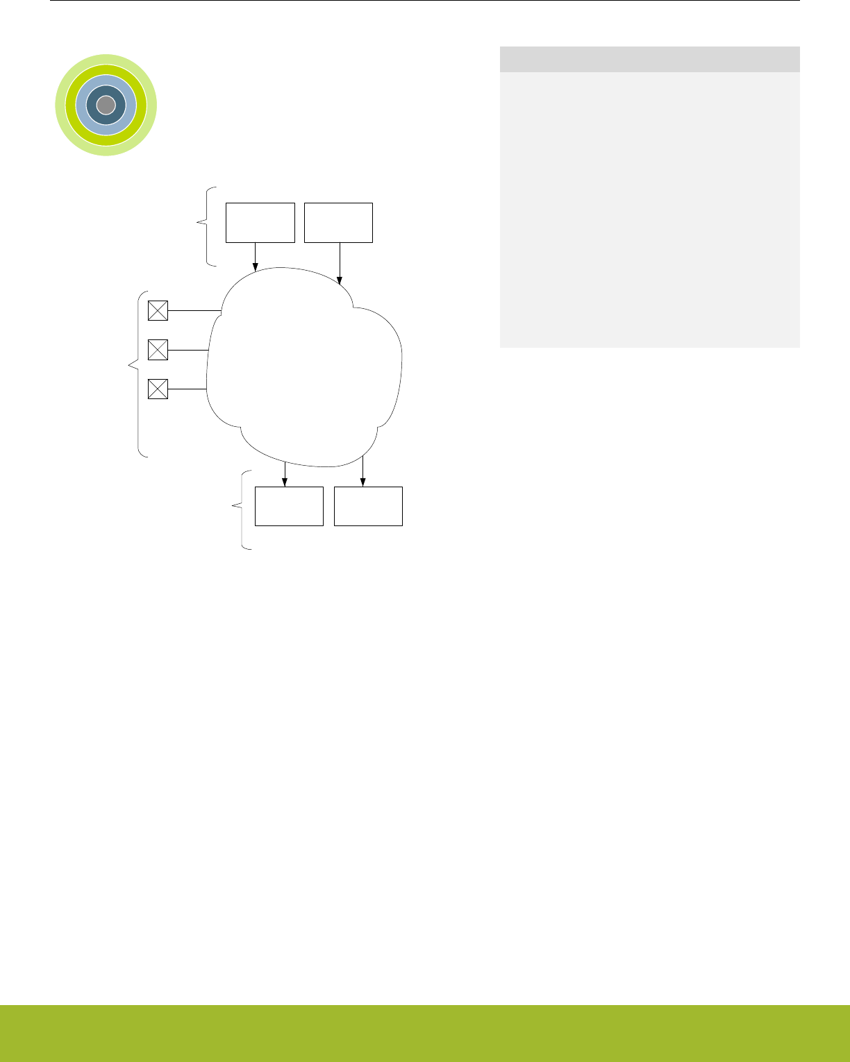
34. APORT - Analog Port
0 1 2 3 4
Pins
. . .
ADC
VDAC IDAC
ACMP . . .
APORT
Producers
Consumers
. . .
Quick Facts
What?
The Analog Port (APORT) is a set of analog buses
which are used to connect I/O pins to analog periph-
eral signals.
Why?
The APORT gives on-chip analog resources access
to a large number of I/O pins, and provides the sys-
tem designer with a high degree of routing flexibility.
How?
An analog peripheral requests a pad by simply con-
figuring its input/output to use a channel on APORT.
That selection becomes an APORT request where
the APORT control switches the pad and the analog
signal onto a common bus.
34.1 Introduction
APORT consists of wires, switches, and control logic needed to route signals between analog peripherals and I/O pins. On-chip clients
can be either producers or consumers. Analog producers are active devices that drive current/voltage into an APORT, such as current
or voltage DACs. Consumers are passive devices that monitor or react to the current/voltage routed to them via the APORT, such as
ADCs or analog comparators (ACMP).
34.2 Features
• Pins are typically mapped to two different APORT buses
• Arbitration and conflict status provided to each APORT client
Reference Manual
APORT - Analog Port
silabs.com | Smart. Connected. Energy-friendly. Preliminary Rev. 0.5 | 1152

34.3 Functional Description
Analog bus (ABUS)
Analog node (ANODE) 0
Analog node (ANODE) 1
Analog node (ANODE) 2
Analog node (ANODE) 3
Switch control
Figure 34.1. Analog Bus (ABUS)
An analog bus (ABUS) consists of analog switches connected to a common wire as shown in Figure 34.1 Analog Bus (ABUS) on page
1153. An APORT consists of multiple ABUSes. Since many clients can operate differentially, buses are grouped by pairs as X and Y. If
a given client uses a single ABUS (e.g. single-ended ADC), X and Y are just labels to differentiate the two buses.
When operating differentially, most APORT clients require that one input be chosen from an X bus and the other from a Y bus. For
example, the ACMP block will not allow both positive and negative inputs to be chosen from X buses.
Reference Manual
APORT - Analog Port
silabs.com | Smart. Connected. Energy-friendly. Preliminary Rev. 0.5 | 1153
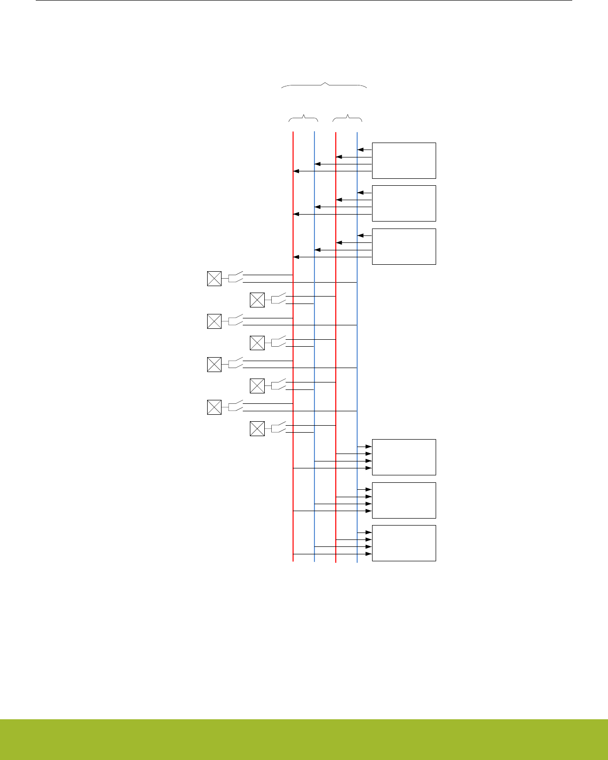
34.3.1 APORT ABUS Naming
X Y
A
Pin 0
Pin 1
X Y
B
Pin 2
Pin 3
Pin 4
Pin 5
Pin 7
Pin 6
BUS
Consumer 0
(e.g. ACMP,
ADC)
Consumer 1
(e.g. ACMP,
ADC)
Consumer 2
(e.g. ACMP,
ADC)
Producer 0
(e.g. VDAC,
IDAC)
Producer 1
(e.g. VDAC,
IDAC)
Producer 2
(e.g. VDAC,
IDAC)
. . .
. . .
. . .
Figure 34.2. Conceptual APORT Structure
APORT ABUSes are prefixed with "BUS" and are grouped in pairs. Each pair is uniquely identified using a letter prefix ("A", "B", "C",
etc.) followed by either a "X" or "Y" to identify the ABUS in the pair. For example, "BUSDX" decodes as: "BUS"=ABUS, "D"=pair,
"X"=bus. Figure 34.2 Conceptual APORT Structure on page 1154 illustrates this organization.
APORT clients are generally described once in this reference manual regardless of its number of instances. For example, the ACMP
client is described once, but the device could contain multiple instances of the ACMP. Because of this, for APORT client descriptions in
Reference Manual
APORT - Analog Port
silabs.com | Smart. Connected. Energy-friendly. Preliminary Rev. 0.5 | 1154
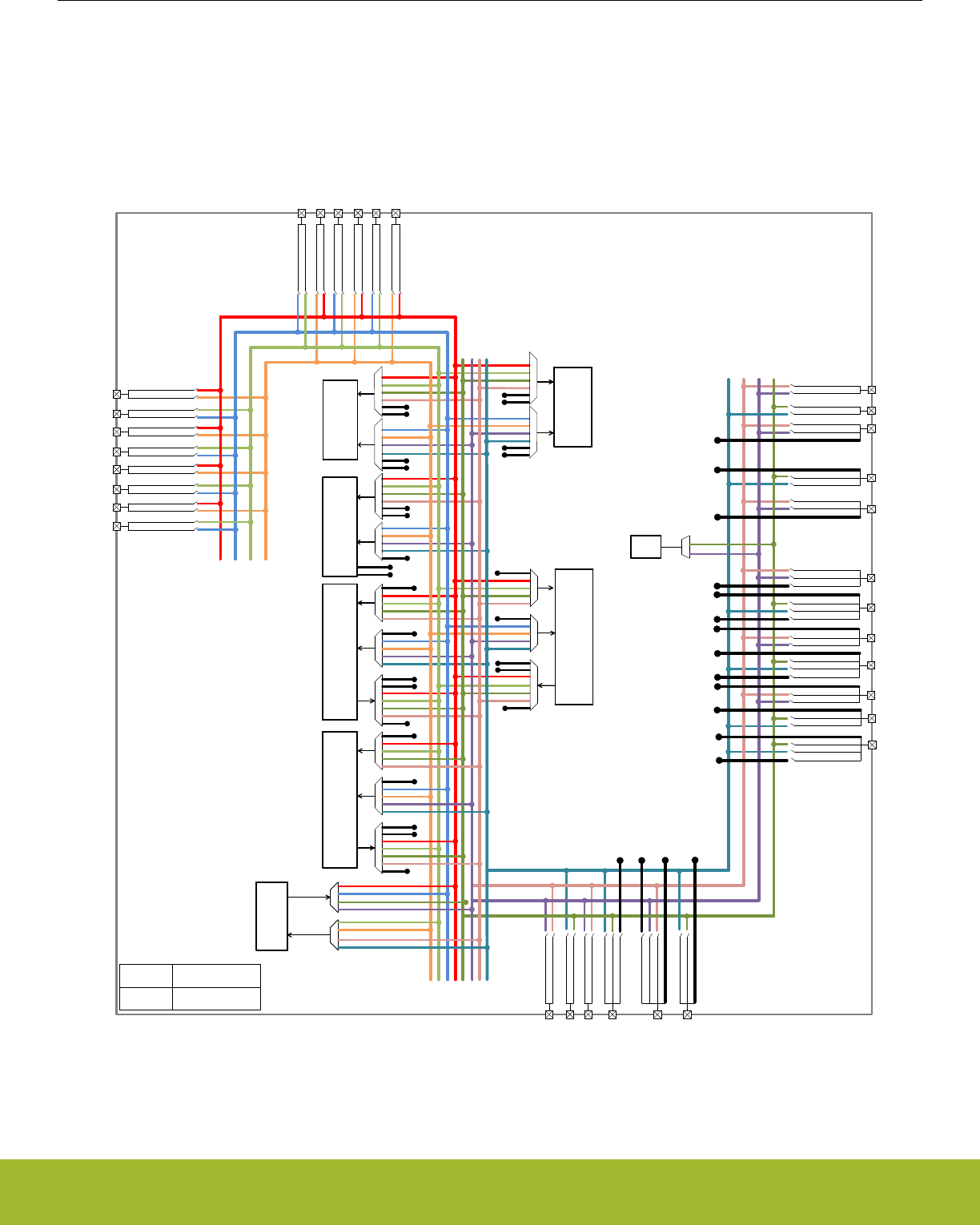
this reference manual, the ABUS connections are generalized with the prefix "APORT" followed by a number (instead of the "BUS"
followed by a letter). It is possible that different instances of an APORT client connect to different ABUSes. For example, ACMP0
APORT1X might connect to the ABUS BUSAX while ACMP1 APORT1X might connect to ABUS BUSCX. Refer to the APORT Client
Map in the device datasheet to map the generalized APORT client bus name to an actual device ABUS. A given ABUS has multiple
switches which need to be identified. The switches on a bus are specified with the ABUS connection ID followed by a channel ID. For
example, channel switch 7 on a given APORT client might be given as APORT1XCH7. Not all APORT channels map to actual GPIO.
Refer to the APORT Client Maps in the device datasheet for APORT to GPIO mapping.
PF0
PF1
PF2
PF3
PF4
PF5
PF6
PF7
PC6
PC7
PC8
PC9
PC10
PC11
PD9
PD10
PD14
PD13
PD12
PD11
PD15
PA0
PA4
PA3
PA2
PA1
PA5
PB14
PB13
PB12
PB11
PB15
AX
AY
BX
BY
CX
CY
DX
DY
IDAC0 1X
1Y
POS
NEG
ACMP0
1Y
2Y
3Y
4Y
POS
NEG
ACMP1
ADC0
EXTP
EXTN
POS
NEG
OPA0
1X
2X
3X
4X
1Y
2Y
3Y
4Y
1X
OPA0_P
OPA0_N
OUT0
OUT0ALT
OUT1
OUT2
OUT3
OUT4
OUT
POS
NEG
OPA1
OUT
1X
2X
3X
4X
1Y
2Y
3Y
4Y
1X
OPA1_P
OPA1_N
OUT1
OUT1ALT
OUT1
OUT2
OUT3
OUT4
ADC_EXTP
ADC_EXTN
OUT0
OUT1
OPA0_N
OPA0_P
OPA1_N
OPA1_P
VDAC0_OUT0ALT
OUT0ALT
VDAC0_OUT0ALT
OUT0ALT
VDAC0_OUT0ALT
OUT0ALT
VDAC0_OUT1ALT
OUT1ALT
VDAC0_OUT1ALT
OUT1ALT
VDAC0_OUT0ALT
OUT1ALT
nX, nY APORTnX, APORTnY
AX, BY, … BUSAX, BUSBY, ...
POS
NEG
OPA2
1X
2X
3X
4X
1Y
2Y
3Y
4Y
1X
OPA2_P
OPA2_N
OUT2
OUT2ALT
OUT1
OUT2
OUT3
OUT4
OUT
CEXT
1X
1Y
3X
3Y
CSEN
CEXT_SENSE
2X
2Y
4X
4Y
OUT2
OPA2_P
OPA2_N
1X
2X
3X
4X
2X
3X
4X
1Y
2Y
3Y
4Y
1X
NEXT1
NEXT0
NEXT1
NEXT0
NEXT1
NEXT0
NEXT1
NEXT0
POS
NEG
1X
2X
3X
4X
1Y
2Y
3Y
4Y
NEXT0
NEXT1
NEXT2
NEXT2
NEXT0
NEXT1
Figure 34.3. Detailed APORT Structure
Reference Manual
APORT - Analog Port
silabs.com | Smart. Connected. Energy-friendly. Preliminary Rev. 0.5 | 1155

Figure 34.3 Detailed APORT Structure on page 1155 shows all the possible routes between different peripherals and different pins via
APORT BUS for the largest package of the EFR32 device family. Note that, in the figure, the BUSxX and BUSxY are annotated as xX
and xY, where x=A,B,C,D and the APORTnX and APORTnY are annotated as nX and nY, where n=1,2,3,4.
For example, the IDAC APORT output 1X can be routed to pin PB14 through BUSCX. The configuration required for this routing is as
follows:
• Set IDAC_CTRL_APORTOUTSEL = APORT1XCH30. This selects the IDAC APORT output 1X and pin PB14.
• Set IDAC_CTRL_APORTOUTEN = 1 and IDAC_CTRL_APORTOUTENPRS = 0. This enables the IDAC to ungate it's output to
BUSCX.
Another example, when ADC is configured to operate in single channel mode for differential inputs (see 27.3.3.1 Single Channel Mode
for how to configure ADC in single channel mode), the positive ADC APORT input 2X and the negative ADC APORT input 2Y can be
routed to pin PC9 and PC10 via BUSBX and BUSBY respectively with the following configuration:
• Set ADCn_SINGLECTRL_POSSEL = APORT2XCH9. This selects the pin PC9 for the positive input to the ADC.
• Set ADCn_SINGLECTRL_NEGSEL = APORT2YCH10. This selects the pin PC10 for the negative input to the ADC.
For smaller packages, not all GPIO pins are available. Please see the Pinout sections of the device datasheet for pin availability on a
specific device.
Reference Manual
APORT - Analog Port
silabs.com | Smart. Connected. Energy-friendly. Preliminary Rev. 0.5 | 1156
34.3.2 Managing ABUSes
The ABUSes of an APORT are shared resources. The user needs to be mindful of this in assigning I/O for different clients throughout
the chip, as it is possible to have conflicts for a given ABUS. Each ABUS has an arbiter responsible for limiting the control over the
ABUS to one and only one client. If multiple clients attempt to control an ABUS, the arbiter allows no client control over the ABUS and
asserts a conflict signal to the clients. The user has the ability to check for such a conflict in each client's status, as well as generate an
interrupt.
Having only one client control an ABUS is not the same as having only one user of an ABUS. It is possible for multiple clients to access
a single ABUS, but requires all but one client to relinquish control of the ABUS. To do this, some clients have bits to disable bus master-
ship which are 0 by default. One example is the APORTXMASTERDIS bit in the ACMPn_CTRL. When set to 1, the client will not assert
control of the APORT X BUS switches, but may still connect to an APORT X BUS that is controlled by another client.
For example, if an IDAC, ADC, and ACMP all want to use the same pin on a particular ABUS the user might set the bus master disable
bit to 1 for the IDAC and ACMP. The ADC is the sole master of the switch configuration on that ABUS, so switches are configured using
the configuration set in the ADC. When IDAC or ACMP channels are chosen on that same bus, the actual pin connection is dictated by
the ADC settings for that bus.
ACMP0
ABUS[0]
ABUS[2]
ABUS[4]
ABUS[6]
ABUS[1]
ABUS[3]
ABUS[5]
ABUS[7]
ACMP1 ADC0
APORT_CONTROL
APORT_REQ =
0000_1111
APORT_REQ =
0011_0000
APORT_REQ =
1000_0000
Figure 34.4. APORT Example 1
Figure 34.4 APORT Example 1 on page 1157 illustrates the sharing of APORT. For illustration purposes, each ABUS is identified by a
numeric index (instead of BUSAX, BUSAY, BUSBX, etc.). Also, the requests from all the APORT clients are packed into a bit-vector
named APORT_REQ to illustrate the request from the APORT Clients (instead of by name such as APORT1XREQ, APORT1YREQ,
APORT2XREQ, etc.). In Figure 34.4 APORT Example 1 on page 1157, ABUS and client are the same color if the client has been gran-
ted the ABUS.
In Figure 34.4 APORT Example 1 on page 1157 ADC0 has requested ABUS[3:0], ACMP1 has requested ABUS[5:4], ACMP0 has re-
quested ABUS[7], and ABUS[6] is unused. No APORT Client has requested the same ABUS as another, so there is no conflict.
Reference Manual
APORT - Analog Port
silabs.com | Smart. Connected. Energy-friendly. Preliminary Rev. 0.5 | 1157
ACMP0
ABUS[0]
ABUS[2]
ABUS[4]
ABUS[6]
ABUS[1]
ABUS[3]
ABUS[5]
ABUS[7]
ACMP1 ADC0
APORT_CONTROL
APORT_REQ =
0000_1111
APORT_REQ =
0011_0000
APORT_REQ =
0001_0000
Figure 34.5. APORT Example 2: Bus Conflict
In Figure 34.5 APORT Example 2: Bus Conflict on page 1158 is a similar example to Figure 34.4 APORT Example 1 on page 1157, but
now both ACMP0 and ACMP1 are requesting ABUS[4]. This is a configuration error, so APORT grants neither client ABUS[4]. The user
must resolve the conflict before ABUS[4] is useable.
ACMP0
ABUS[0]
ABUS[2]
ABUS[4]
ABUS[6]
ABUS[1]
ABUS[3]
ABUS[5]
ABUS[7]
ACMP1 ADC0
APORT_CONTROL
APORT_REQ =
0000_1111
APORT_REQ =
0011_0000
APORT_REQ =
0000_0000
Figure 34.6. APORT Example 3: Sharing an ABUS
Figure 34.6 APORT Example 3: Sharing an ABUS on page 1158 illustrates ABUS sharing. Both ACMPs are configured identically, ex-
cept ACMP0 has its APORTXMASTERDIS bit-field set to 1. There is only one APORT master for ABUS[5:4] in this case, so there is no
conflict.
Reference Manual
APORT - Analog Port
silabs.com | Smart. Connected. Energy-friendly. Preliminary Rev. 0.5 | 1158
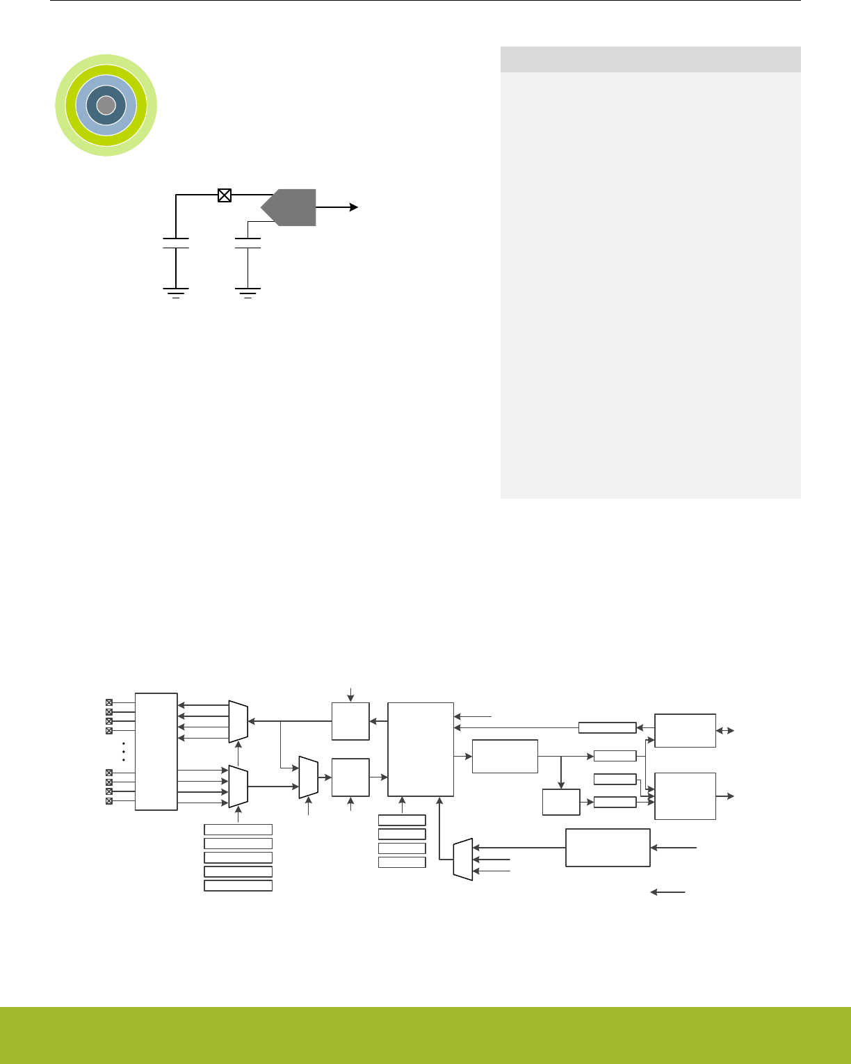
35. CSEN - Capacitive Sense Module
0 1 2 3 4
...0101110...
CSEN
CREF
CEXTERNAL
Quick Facts
What?
The capacitive sense (CSEN) module uses a capac-
itance-to-digital circuit to measure the capacitance of
touch-sensitive switches. The module contains an
advanced capacitance-to-digital converter that can
be configured to take measurements on a single port
pin or scan through a group of up to 64 port pins
connected via the APORT buses. Port pins/channels
can also be shorted together internally to measure
the combined capacitance, lowering the required en-
ergy usage for wake-on-touch applications. Adjusta-
ble maximum capacitance allows for optimal dynam-
ic range, while hardware accumulation and filtering
reduce processor computation time. Interrupts can
be generated when CSEN completes conversions or
when the measured value crosses a threshold.
Why?
The CSEN module is designed to perform extremely
low-power autonomous conversions of capacitive
touch switches.
How?
The CSEN module uses charge timing techniques to
compare external capacitance against internal refer-
ence capacitors.
35.1 Introduction
The capacitive sensing (CSEN) module uses a capacitance-to-digital circuit to determine the capacitance on an input pin. The module
can take measurements from different physical pins using the APORT multiplexer. In addition, the module can measure multiple pins in
sequence using the scan modes, or multiple pins at the same time (bonded together) using the multiple-channel measurement feature.
CSEN is available in EM0, EM1, EM2 and EM3.
Capacitance
to Digital
Converter
w/ SAR and
Delta-Mod
Modes
Gain
APORT2X
APORT2Y
APORT4X
APORT4Y CEXT_SENSE
Driver
CEXT
APORT1X
APORT1Y
APORT3X
APORT3Y
LOCALSENS IREFPROG
IDACIREFS
Accumulate /
Average DATA
APORT
Shared
Bus
Matrix
GPIO
EMA
EMA
Filter
CPTHR
SINGLECTRL
SCANINPUTSEL0
SCANMASK0
SCANINPUTSEL1
SCANMASK1
START (software)
PRS
TIMER
HFPERCLKCSEN
LFBCLKCSEN
CLKCSEN – Self-generated conversion clock
Trigger
Source
to APB Register
Interfaces
Local Timer
w/ prescaler and
auto-reload
CTRL
CMD
ANACTRL
DMCFG
Comparison
& Interrupt
Logic
DMBASELINE DMA
Interface RAM
Interrupts
Figure 35.1. CSEN Overview
Reference Manual
CSEN - Capacitive Sense Module
silabs.com | Smart. Connected. Energy-friendly. Preliminary Rev. 0.5 | 1159

35.2 Features
• Up to 64 Channels, connected via APORT buses.
• Single sample, continuous single sample, single scan and continuous scan modes supported.
• Support for both SAR and Delta Modulation conversions.
• SAR conversions are progammable to resolutions of 10, 12, 14, or 16 bits.
• Delta Modulation conversions support dynamic or fixed gain, and are programmable to resolutions of 10, 12, 14, or 16 bits.
• Supports channel bonding to monitor multiple channels, shorted internally, with a single conversion. The maximum number of chan-
nels to be shorted is limited by the maximum capacitance that can be measured by the analog core.
• Conversions triggered by software, PRS, or dedicated timer running from LFXO, LFRCO, or ULFRCO.
• Hardware accumulation of 1, 2, 4, 8, 16, 32, or 64 samples. The result can be right-shifted to the desired resolution or collected in a
22-bit accumulator for further processing by software.
• Hardware exponential moving average (EMA) filter for candidate touch detection during low power autonomous operation.
• Automatic threshold comparison with programmable polarity.
• Low-frequency noise filter to reject noise sources such as 50/60 Hz.
• DMA interface to collect accumulated samples in on-chip RAM. The DMA interface can also be used to program starting values for
delta-modulation conversions. The DMA interface can run down to EM2.
35.3 Timing
35.3.1 Clocks
The CSEN module takes two external clock sources as input. The register interface is driven by the HFPERCLK source, allowing for
fast access to the control and data for the block. The local timer is driven by the LFBCLK source. The CSEN block also contains an
internal, low-energy conversion clock source (CLKCSEN). Conversions are self-timed and the block only requires external clocks under
certain circumstances.
For register access, HFPERCLKCSEN must be enabled to the CSEN block in the CMU_HFPERCLKEN0 register. When register access
is not required, this clock may be shut down for energy savings.
LFBCLKCSEN is used by the local CSEN timer. It should be enabled to the CSEN block in the CMU_LFBCLKEN0 register any time the
CSEN local timer is used as a conversion trigger.
35.3.2 Conversion Triggers
CSEN conversions can be triggered from one of three different sources, selected by CTRL_STM: a software register write, a PRS
channel, or the local CSEN timer. The selected trigger source begins a conversion cycle. Depending on the selected conversion mode,
one conversion trigger may generate one or many output words from the CSEN module. See 35.6 Converison Modes for more details
on the CSEN output for each mode.
Software Triggered Conversions
When CTRL_STM is set to START, conversions are triggered by software. Software triggering is typically used when operating the
CSEN block in a continuous mode to gather conversions as quickly as the converter allows. Software triggering may also be used in
applications where a single conversion or one scan cycle is needed infrequently and sporadically by different software processes.
When configured for software triggering, a write of the CMD_START bit to logic 1 initiates conversions.
PRS Triggered Conversions
When CTRL_STM is set to PRS, conversions are triggered via a PRS event. PRS triggers are typcally used when it is necessary to
synchronize CSEN conversions with other events in the system. For example, the LETIMER may be used in EM2 to initiate a CSEN
scan operation and other events at the same time. A number of different PRS channels may be configured as the trigger source. The
specific PRS channel to be used as a trigger source is selected in the PRSSEL register.
Reference Manual
CSEN - Capacitive Sense Module
silabs.com | Smart. Connected. Energy-friendly. Preliminary Rev. 0.5 | 1160

CSEN Timer Triggered Conversions
When CTRL_STM is set to TIMER, a local 8-bit CSEN timer is used to trigger conversions. The local timer is typically used in conjunc-
tion with non-continuous conversion modes to provide periodic conversion triggers at slow sampling rates. The local timer is clocked
from LFBCLKCSEN, and configured with the TIMCTRL register. The CSEN timer has a local prescaler (set by the TIMCTRL_PCPRESC
field), which divides the LFBCLKCSEN further. The TIMCTRL_PCTOP field sets the reload value for the CSEN timer. The CSEN timer
counts down for the number of clocks specified in TIMCTRL_PCTOP. When the counter reaches zero, a conversion cycle is triggered
and the timer is reloaded.
35.3.3 Shutdown and Warmup
Many target applications for CSEN require low power operation and infrequent sampling. By default, the converter will power down
when it is not in use to save energy. Upon receiving a conversion trigger, the CSEN block will power on and wait for (3 +
TIMCTRL_WARMPCNT) CLKCSEN clock cycles before starting conversions.
CTRL_WARMUPMODE defines the behavior of the CSEN converter when it is not actively converting. Software may choose to keep
the CSEN block powered on at all times by setting the CTRL_WARMUPMODE bit to logic 1.
35.4 Conversion Types
The CSEN block offers two different types of conversions: SAR, and Delta Modulation.
35.4.1 SAR Conversion Type
SAR (successive approximation register) conversions are self-contained and do not depend on the results of any previous conversions.
SAR conversions will be performed when CTRL_CONVSEL is set to SAR. CTRL_SARCR sets the SAR conversion resolution, and is
selectable between 10, 12, 14, or 16 bits. SAR converisons last for N cycles of CLKCSEN, where N is the selected resolution (i.e. 12-bit
conversions last for 12 CLKCSEN cycles).
Every SAR conversion consists of a set of tests, one for each bit of the converter. The MSB is tested first, followed by all other bits
down to the LSB. Each test narrows the possible value by 1/2 until the final result is determined.
Reference Manual
CSEN - Capacitive Sense Module
silabs.com | Smart. Connected. Energy-friendly. Preliminary Rev. 0.5 | 1161
35.4.2 Delta Modulation Conversion Type
Delta modulation (DM) conversions provide significant noise, response time, and energy consumption improvements over SAR conver-
sions. A DM conversion inherently takes longer than a SAR conversion to arrive at one result. However, it is much less susceptible to
noise events in the system. Whereas a large number of SAR conversions may need to be averaged to produce a desired noise resolu-
tion, the same noise resolution can be achieved with few DM conversions. However, DM conversions require more specific knowledge
of the underlying conversion process to implement effectively. Silicon Laboratories software libraries use delta modulation for the best
possible performance. It is recommended to use the provided libraries in most applcations. The information provided in this section is
intended as a reference for CSEN module driver development.
Delta modulation conversions are performed when CTRL_CONVSEL is set to DM. DMCFG_DMCR sets the DM conversion resolution,
and is selectable between 10, 12, 14, or 16 bits. The selected resolution does not have an impact on conversion timing.
A delta modulated conversion begins with a test against a provided initial value, known as the baseline. If the comparison is high (the
external capacitor is larger than the initial value), the comparison value is increased by a specified amount (the delta). If the comparison
is low, the comparison value is decreased by the delta. The cycle then repeats, testing against the new value. Each subsequent test
brings the test value closer to the external capacitance value, until the desired number of tests have been performed and an output
result is produced. The converter may be configured to use a fixed delta value, or to reduce the value by a factor of two at specific
intervals.
The DM state machine is configured using different fields in the DMCFG register. The DMG field sets the initial delta step to be used,
between 0 and 255 codes at the selected resolution (specified by DMCFG_CRMODE). The DMCFG_DMR field specifies how many
tests in a row are to be performed using each delta step. The converter will perform (4 x DMCFG_DMR) tests at each delta step for
DMCFG_DMR > 0. For DMCFG_DMR = 0, the converter will perform 64 tests at each delta step. The number of tests performed at
each delta step is referred to here as a "cycle". The DMCFG_DMCR field specifies how many cycles the state machine will take to
produce one conversion output. For DMCFG_DMCR = 0, the number of cycles will be 16. If the DMCFG_DMGRDIS bit is cleared to 0,
the delta step will be halved after each cycle. If DMCFG_DMGRDIS is set to 1, all cycles will use a fixed delta step value. Each test
performed by the converter requires one CLKCSEN, and so a full DM conversion requires number_of_cycles x tests_per_cycle clocks of
CLKCSEN. Figure 35.2 Delta modulation conversion with gain reduction (DMCFG_DMGDIS = 0) on page 1162 and Figure 35.3 Delta
modulation conversion with fixed delta step (DMCFG_DMGDIS = 1) on page 1163 show how delta modulation conversions are per-
formed with and without gain reduction.
External Cap
Actual Value
Initial Value
(from DMBASELINE)
+4
+4
+4
+4
+2
+2
+2
-2
+1 +1 +1
-1
4 samples with
DMG = 4
4 samples with
DMG = 2
4 samples with
DMG = 1
Conversion lasts 12 samples total with DMCR = 3, DMR = 1
= 3 cycles (DMCR) of 4 samples each (DMR x 4)
Final Value
(to DATA)
Figure 35.2. Delta modulation conversion with gain reduction (DMCFG_DMGDIS = 0)
Reference Manual
CSEN - Capacitive Sense Module
silabs.com | Smart. Connected. Energy-friendly. Preliminary Rev. 0.5 | 1162
External Cap
Actual Value
Initial Value
(from DMBASELINE)
+4
+4
+4
+4
4 samples with
DMG = 4
4 samples with
DMG = 4
4 samples with
DMG = 4
Conversion lasts 12 samples total with DMCR = 3, DMR = 1
= 3 cycles (DMCR) of 4 samples each (DMR x 4)
Final Value
(to DATA)
+4
+4
-4
+4
-4
+4
-4
+4
Figure 35.3. Delta modulation conversion with fixed delta step (DMCFG_DMGDIS = 1)
The initial test value (baseline) for a DM conversion can be written to the DMBASELINE register prior to the start of the conversion.
DMBASELINE contains two fields: BASELINEUP and BASELINEDN. Only the BASELINEUP field is used when chopping is disabled
(CTRL_CHOPEN = 0). If chopping is enabled, software must maintain a second baseline value for the ramp-down phase, and write it to
BASELINEDN.
Reference Manual
CSEN - Capacitive Sense Module
silabs.com | Smart. Connected. Energy-friendly. Preliminary Rev. 0.5 | 1163

35.5 Input Configuration
CSEN channel inputs are routed through the on-chip APORT bus matrix. Each APORT bus is a shared resource among certain analog
peripherals on the device. Some knowledge of how the CSEN block utilizes the APORT buses is necessary to avoid conflicts with other
peripherals.
Each time the CSEN module connects to an external pin to take a conversion, it uses one or two of the shared APORT buses. By
default, the CSEN module charges the external capacitor through one APORT connection on the CEXT line, and senses the voltage at
the capacitor through a different APORT connection on the CEXT_SENSE line. This eliminates any errors introduced by series impe-
dance of the APORT buses, particularly if the external cpacitance is large. To conserve on-chip resources, it is possible to both charge
and sense through the CEXT line, by setting CTRL_LOCALSENS to logic 1.When CTRL_LOCALSENS is set to 1, the CEXT_SENSE
line is not needed and the corresponding bus may be used by other peripherals.
The CSEN module has four APORT buses connected to the CEXT signal and four APORT buses connected to the CEXT_SENSE sig-
nal. The specific buses used for each pin selection depend on the channel, according to Table 35.1 CSEN APORT Bus Connectivity on
page 1164. For example, if APORT1XCH4 (APORT1 channel 4) is selected in SINGLECTRL_SINGLESEL, the CEXT signal will be
connected to the shared BUSAX, channel 4. If CTRL_LOCALSENS is set to DISABLE, then the CEXT_SENSE signal will be connected
to APORT2YCH4, and use the shared bus BUSBY, channel 4.
The same connections apply to scan mode conversions and bonded conversions. For scan mode conversions, the connection through
the bus is only made on one channel at a time, when that channel is being converted in the scan. For bonded connections, all selected
channel connections are made simultaneously.
Table 35.1. CSEN APORT Bus Connectivity
Selected CSEN Channel CEXT Routing CEXT_SENSE Routing
(LOCALSENS = 0)
APORT1, Even Channel APORT1XCHn / BUSAXCHn APORT2YCHn / BUSBYCHn
APORT1, Odd Channel APORT1YCHn / BUSAYCHn APORT2XCHn / BUSBXCHn
APORT3, Even Channel APORT3XCHn / BUSCXCHn APORT4YCHn / BUSDYCHn
APORT3, Odd Channel APORT3YCHn / BUSCYCHn APORT4XCHn / BUSDXCHn
When the CSEN module requests an APORT bus that is already in use by another peripheral, an APORT conflict will occur. The
IF_APORTCONFLICT interrupt flag will be set to 1 (generating an interrupt if enabled), and the APORTCONFLICT register will reflect
the bus(es) where the conflict occurred. Careful channel planning for the system will avoid APORT conflicts in most systems.
Channel selection for the CSEN module depends on the selected conversion mode. More details on how to select specific input pins
are found in 35.6 Converison Modes.
35.6 Converison Modes
The CSEN module supports several conversion modes:
• Single Channel - A conversion trigger starts conversions on a single channel. One output result is produced, then the converter will
halt.
• Scan - A conversion trigger starts a scan sequence, which converts a specified number of channels independently and in sequence.
One output result is produced per channel, then the converter will halt.
• Bonded Channel - A conversion trigger starts conversions on a bonded channel. A bonded channel is several input channels which
are shorted together internally. One output result is produced, then the converter will halt.
• Continuous Single Channel - A conversion trigger starts continuous conversions on a single channel. The single channel conversion
will re-trigger automatically after each output result and repeat until halted.
• Continuous Scan - A conversion trigger starts continuous channel scanning. The scan sequence will re-trigger automatically at the
end of each scan and repeat until halted.
• Continuous Bonded Channel - A conversion trigger starts continuous conversions on a bonded channel. The bonded channel con-
version will re-trigger automatically after each output result and repeat until halted.
The conversion mode is selected by the CTRL_CM and CTRL_MCEN fields. Refer to 35.6.1 Single Channel Conversions, 35.6.2 Scan
Conversions, and 35.6.3 Bonded Channel Conversions for specific information on configuring the CSEN module to the desired conver-
sion mode.
Reference Manual
CSEN - Capacitive Sense Module
silabs.com | Smart. Connected. Energy-friendly. Preliminary Rev. 0.5 | 1164

35.6.1 Single Channel Conversions
CSEN is configured for single channel mode when CTRL_MCEN = DISABLE and CTRL_CM = SGL. For continuous single channel
mode, CTRL_MCEN = DISABLE and CTRL_CM = CONTSGL.
In single channel mode, SINGLECTRL_SINGLESEL specifies the input channel to be converted. Firmware may select any of the pins
connected to the CEXT signal via the APORT. Refer to the Analog Port (APORT) Client Maps section in the product datasheet for map-
ping of the CEXT signal to specific pins.
When a single channel conversion is triggered, the CSEN block will use the configured conversion type (SAR or DM) to convert the
capacitance seen at the selected input pin to a digital value one or more times. The hardware accumulator setting (CTRL_ACU) deter-
mines how many times the input pin will be sampled and accumulated before an output word is produced. The IF_CONV interrupt flag
will be set to 1 by hardware when an output word is available in the DATA register.
Note: The auto-ground feature is typically not used in single channel conversion mode and should be disabled by software. However, if
auto-grounding is enabled, it will ground the unused channels specified by the SCANINPUTSEL0/1 and SCANMASKSEL0/1 registers.
See the channel selection discussion in 35.6.2 Scan Conversionsfor more details.
Reference Manual
CSEN - Capacitive Sense Module
silabs.com | Smart. Connected. Energy-friendly. Preliminary Rev. 0.5 | 1165
35.6.2 Scan Conversions
CSEN is configured for scan mode when CTRL_MCEN = DISABLE and CTRL_CM = SCAN. For continuous scan mode, CTRL_MCEN
= DISABLE and CTRL_CM = CONTSCAN.
In scan mode, the input channels to be converted during the scan are determined by the SCANINPUTSEL0/1 and SCANMASK0/1 reg-
isters. There are 64 available channels in the scanner logic. SCANINPUTSEL0/1 allow software to route CSEN scan channels to
APORT-capable GPIO in groups of 8. SCANMASK0/1 specify which channels on those groups are to be included in the scan.
Note: It is possible to include the same group of 8 in more than one place in the scan sequence. However, for the majority of use ca-
ses, the SCANINPUTSEL0 register should be written to 0x07060504, and SCANINPUTSEL1 should be written to 0x0F0E0D0C. This
will configure the CSEN scan channels to match their order in bonded mode.
Individual channels are included in the scan based on their bit positions in the mask registers, SCANMASK0 and SCANMASK1. A '1' in
the corresponding bit of the mask register will include that channel in the scan. Refer to the Analog Port (APORT) Client Maps section
in the product datasheet for mapping of the CEXT signal to specific pins.
When a scan conversion is triggered, the CSEN block will convert each of the selected channels in turn, starting at channel 0 and work-
ing up to channel 63. If a channel is not configured for scan in the SCANMASK0/1 register (i.e. the bit for that channel is '0'), it will be
skipped.
An example of how the scan logic progresses through channels is shown in Figure 35.4 Scan Mode Sequencing on page 1166. In this
simple example, SCANMASK0 = 0x00000318 and SCANMASK1 = 0x00000006, which selects channels 3, 4, 8, 9, 33, and 34 in turn.
SCANMASK0SCANMASK1
CSEN Input
Channel
0
0
0
1
0
1
2
3
0
1
2
3
1
0
0
0
4
5
6
7
4
5
6
7
1
1
0
0
8
9
10
11
8
9
10
11
0 12
12
SCANMASK
Values
32
33
34
35
60
61
62
63
0
1
1
0
1
2
0
3
0
0
0
0
28
29
30
31
28
29
30
31
0
0
0
0
28
29
30
31
4
27 590
360
270
0 13
13
27
Channel 3
DATA Output
Order
Channel 4
Channel 8
Channel 9
Channel 33
Channel 34
Figure 35.4. Scan Mode Sequencing
An auto-grounding feature is available for scan mode conversions. This feature forces hardware to ground all of the non-active CSEN
channels selected by SCANMASK0/1, to reduce bleed-through from measurements on other CSEN channels. Auto-grounding is ena-
bled by setting the CTRL_AUTOGND bit to logic 1.
Reference Manual
CSEN - Capacitive Sense Module
silabs.com | Smart. Connected. Energy-friendly. Preliminary Rev. 0.5 | 1166

CSEN will use the configured conversion type (SAR or DM) to convert the capacitance seen at each of the selected input pins to a
digital value one or more times. The hardware accumulator setting (CTRL_ACU) determines how many times each input pin will be
sampled and accumulated before an output word is produced. The IF_CONV interrupt flag will be set to 1 by hardware when each out-
put word is available in the DATA register, and the IF_EOS interrupt flag will be set to 1 by hardware at the completion of a scan cycle.
The DMBASELINE register provides the starting point for DM conversions. This starting point will be different for each channel in the
scan, and the DMBASELINE register should be updated accordingly. This is typically done via DMA.
Note: DMA or software must read the output words from the DATA register before completion of the next conversion. New conversions
will over-write the DATA register contents.
35.6.3 Bonded Channel Conversions
CSEN is configured for bonded mode when CTRL_MCEN = ENABLE and CTRL_CM = SGL. For continuous bonded mode,
CTRL_MCEN = ENABLE and CTRL_CM = CONTSGL.
Bonded channel conversions are intended primarily for wake-on-touch applications where minimal power consupmtion is necessary.
Bonded channel conversions operate similar to single channel conversions, except that multiple channels are shorted together and con-
verted as a single capacitance value.
In bonded mode, the channels to be bonded are based on their bit positions in the mask registers SCANMASK0 and SCANMASK1,
according to a fixed location, as shown in Figure 35.5 CSEN Input Configuration in Bonded Mode on page 1167. SCANMASK0 selects
channels from APORT1 and SCANMASK1 selects channels from APORT3. Even-numbered channels are connected through the X
bus, and odd-numbered channels are connected through the Y bus. Channels with a '1' in the corresponding position of SCAN-
MASK0/1 will be shorted together during the conversion and converterd as a single channel. Refer to the Analog Port (APORT) Client
Maps section in the product datasheet for mapping of the CEXT signal to specific pins.
SCANMASK0
SCANMASK1
CSEN Input
Channel
0
1
2
0
1
2
32
33
34
35
60
61
62
63
0
1
2
3
28
29
30
31
4
27 59
36
APORT
Connection
APORT1XCH0
APORT1YCH1
APORT1XCH2
CSEN Input
Channel
APORT
Connection
Shared Bus
Channel
BUSAX channel 0
BUSAY channel 1
BUSAX channel 2
Shared Bus
Channel
3
28
29
30
31
3
28
29
30
31
4
27 27
4
APORT1YCH3
APORT1XCH28
APORT1YCH29
APORT1XCH30
APORT1YCH31
APORT1YCH27
APORT1XCH4
BUSAX channel 3
BUSAX channel 28
BUSAY channel 29
BUSAX channel 30
BUSAY channel 31
BUSAY channel 27
BUSAY channel 4
APORT3XCH0
APORT3YCH1
APORT3XCH2
BUSCX channel 0
BUSCY channel 1
BUSCX channel 2
APORT3YCH3
APORT3XCH28
APORT3YCH29
APORT3XCH30
APORT3YCH31
APORT3YCH27
APORT3XCH4
BUSCX channel 3
BUSCX channel 28
BUSCY channel 29
BUSCX channel 30
BUSCY channel 31
BUSCY channel 27
BUSCY channel 4
Figure 35.5. CSEN Input Configuration in Bonded Mode
When a bonded conversion is triggered, the CSEN block will use the configured conversion type (SAR or DM) to convert the total ca-
pacitance seen at the selected input pins to a digital value one or more times. The hardware accumulator setting (CTRL_ACU) deter-
mines how many times the input pins will be sampled and accumulated before an output word is produced. The IF_CONV interrupt flag
will be set to 1 by hardware when an output word is available in the DATA register.
Note: The auto-ground feature should not be used in bonded conversion mode. Software should clear CTRL_AUTOGND to 0 when
configuring CSEN for bonded conversions.
Reference Manual
CSEN - Capacitive Sense Module
silabs.com | Smart. Connected. Energy-friendly. Preliminary Rev. 0.5 | 1167
35.7 Output Data
Output data from the CSEN module is posted to the DATA register. The data encoding can be affected by several configuration settings.
Figure 35.6 Data encoding for different resolution settings on page 1168 shows the effect that the resolution settings (CTRL_SARCR
for SAR conversions or DMCFG_CRMODE for DM conversions) have on the output word. In this example, only one sample is accumu-
lated. Regardless of the resolution setting, the MSB is always presented in bit position 15.
31 30 29 28 27 26 25 24 23 22 21 20 19 18 17 16 15 14 13 12 11 10 9 8 7 6 5 4 3 2 1 0
CSEN_DATA Register
0 0 0 0 0 0 0 0 0 0 0 0 0 0 0 0 16 bit Data
0 0 0 0 0 0 0 0 0 0 0 0 0 0 0 0 14 bit Data
0 0 0 0 0 0 0 0 0 0 0 0 0 0 0 0 12 bit Data
0 0 0 0 0 0 0 0 0 0 0 0 0 0 0 0 10 bit Data 0 0 0 0 0 0
0 0 0 0
0 0
Figure 35.6. Data encoding for different resolution settings
A hardware accumulator allows the CSEN block to accumulate multiple samples on the same channel for each conversion data word
produced, and automatically right-shift to normalize the data to 16 bits. This is effective as a simple noise filter. The CTRL_ACU field
sets the number of samples to be accumulated from 1, 2, 4, 8, 16, 32, or 64 samples. The right-shift operation can optionally be disa-
bled by setting CTRL_DRSF to 1. Figure 35.7 Data encoding for different accumulator settings on page 1168 shows the effects of the
accumulator, with and without right-shifting on the output data word. In this example, the sample resolution is fixed at 12 bits, but the
same principles apply to any resolution setting.
31 30 29 28 27 26 25 24 23 22 21 20 19 18 17 16 15 14 13 12 11 10 9 8 7 6 5 4 3 2 1 0
CSEN_DATA Register
0000000000000000
0000000000000000
0000000000000000
0000000000000000
0 0 0 0
000
0 0
12 bit Data, ACU = 1 (2 samples), DRSF = 0
12 bit Data, ACU = 2 (4 samples), DRSF = 0
12 bit Data, ACU >= 4 (>= 16 samples), DRSF = 0
12 bit Data, ACU = 0 (1 sample / no accumulation)
000000000000000
00000000000000
0000000000
000
0 0
12 bit Data, ACU = 1 (2 samples), DRSF = 1
12 bit Data, ACU = 2 (4 samples), DRSF = 1
12 bit Data, ACU = 6 (64 samples), DRSF = 1
0
0 0
0 00 0
When DRSF = 0, accumulation extends LSB
When DRSF = 1, accumulation extends MSB
Figure 35.7. Data encoding for different accumulator settings
Reference Manual
CSEN - Capacitive Sense Module
silabs.com | Smart. Connected. Energy-friendly. Preliminary Rev. 0.5 | 1168
When the conversion type is delta modulation (CTRL_CONVSEL = DM) and chopping is enabled (CTRL_CHOPEN = ENABLE), this is
a special case for the output word. In this case, both the "up" and the "down" portions of the conversion must be stored. The DATA
register will hold the "up" portion in the lower 16 bits and the "down" portion in the upper 16 bits as shown in Figure 35.8 Data encoding
for delta modulation with chopping on page 1169.
31 30 29 28 27 26 25 24 23 22 21 20 19 18 17 16 15 14 13 12 11 10 9 8 7 6 5 4 3 2 1 0
CSEN_DATA Register
16 bit “Up” Data
14 bit “Up” Data
12 bit “Up” Data
10 bit “Up” Data 0 0 0 0 0 0
0 0 0 0
0 0
16 bit “Down” Data
14 bit “Down” Data
12 bit “Down” Data
10 bit “Down” Data 0 0 0 0 0 0
0 0 0 0
0 0
Figure 35.8. Data encoding for delta modulation with chopping
35.8 Low Frequency Noise Filter (Chopping)
The CSEN module includes a low-frequency noise filter, which is implemented internally using a chopping mechanism. Chopping is en-
abled by setting CTRL_CHOPEN to ENABLE. In a normal conversion cycle (CTRL_CHOPEN = DISABLE), the charge timing is always
performed on a positive (up) ramp. When chopping is enabled, the converter will alternate between using a positive (up) and negative
(down) ramp for each sample. While the absolute capacitance value contributes the same amount for an up or a down conversion, any
low-frequency offset artifacts due to supply changes will have opposite polarity.Averaging the results of an "up" and a "down" conver-
sion taken back-to-back effectively eliminataes the low-frequency offset differences.
When chopping is used with SAR type converisons, the accumulator performs the necessary averaging in hardware. The accumulator
must be set to average at least two samples when chopping is enabled. Because the accumulator always works on multiples of two
samples, an even number of "up" and "down" samples will be included in the average.
When chopping is used with DM type conversions, user software must maintain both an "up" and "down" portion of the baseline for the
conversion separately. For this reason, the output word will contain both values when using DM conversions. In order to gain the bene-
fits of chopping in DM mode, software should average the "up" and "down" results together.
Reference Manual
CSEN - Capacitive Sense Module
silabs.com | Smart. Connected. Energy-friendly. Preliminary Rev. 0.5 | 1169

35.9 Wake on Threshold and Exponential Moving Average
The CSEN module has the capability to operate in the energy-efficient EM2 or EM3 modes and autonomously wake the system when a
predetermined threshold is crossed, either while doing single channel conversions or bonded channel conversions. This allows a sys-
tem to monitor one or more input channels to implement low-energy "wait-for-touch" features. There are two different comparator
threshold tests available for this purpose:
• Absolute - used to compare data outputs with "less than or equal" or "greater than" tests against a fixed value. This is useful for
applications with short sleep durations, which simply want to wake quickly if a certain condition is met.
• Relative EMA - used to compare data outputs against a moving average window. This is extremely useful for applications with long-
term sleep requirements. The relative comparison allows the CSEN module to adjust for slow changes in capacitance such as those
due to environmental changes (temperature, supply) without waking the system.
The absolute test is used when CTRL_CMPEN = ENABLE and CTRL_EMACMP = DISABLE. In this mode, any output word written to
the DATA register will be compared against the value in the CMPTHR register. The polarity of the comparison is configured with the
CTRL_CMPPOL field. Setting CTRL_CMPPOL to GT means that the comparison will be true if DATA is greater than CMPTHR. Setting
CTRL_CMPPOL to LTE means that the comparison will be true if DATA is less than or equal to CMPTHR. On a true result, the IF_CMP
interrupt flag is set to 1, and any continuous conversion in progress will be halted.
The relative EMA test is used when CTRL_EMACMP = ENABLE. In this mode, the exponential moving average (EMA) value is used to
establish a low-noise average code reading. The EMA is a moving average that is re-calculated on every output data word from the
converter, according to the following equation:
EMA[n] = EMA[n-1] - EMA[n-1]/N + DATA/N,
Figure 35.9. CSEN Exponential Moving AverageCalculation
The EMA register stores the current EMA value. This register may be written by software to quickly establish a new baseline average. N
in the equation above is the sample weighting of the EMA filter, and is controlled with the EMASAMPLE field. Lower values of EMA-
SAMPLE mean less averaging, and quicker response time, while higher EMASAMPLE values will reject more noise at the expense of
response time.
When relative EMA comparisons are enabled, every new sample is compared with a window around the EMA. The lower bound of this
window is EMA - CMPTHR, and the upper bound of the window is EMA + CMPTHR. If the new sample written to DATA falls outside
that window (lower than the lower bound or higher than the upper bound), the CMP interrupt flag is set to 1 and any continuous conver-
sion in progress is halted. Using the EMA comparison, large jumps in the output data word will trip the comparator and wake the sys-
tem, but gradual changes will not trigger false positives. Figure 35.10 Wake on Threshold With Relative EMA on page 1171shows an
example of the EMA moving average filter and window.
Reference Manual
CSEN - Capacitive Sense Module
silabs.com | Smart. Connected. Energy-friendly. Preliminary Rev. 0.5 | 1170
Time
Output Codes
EMA
EMA + CMPTHR
EMA - CMPTHR
DATA Output
Sample crosses window, CMP = 1
Figure 35.10. Wake on Threshold With Relative EMA
35.10 Analog Adjustments
The analog front-end of the CSEN module has some additional controls that may be useful in certain applications.
35.10.1 Current Reference and Gain
The internal current source used for charging the reference capacitor can be adjusted using the ANACTRL_IREFPROG field. This ad-
justs the ratio of the internal reference current source vs. the external drive current source, and thereby adjusts the effective gain of the
converter. The lowest gain setting is when ANACTRL_IREFPROG = 0, and the highest is with ANACTRL_IREFPROG = 7. The differ-
ence between the lowest and highest setting is approximately 10x. High gain gives the best sensitivity and resolution for small capaci-
tors, such as those typically implemented as touch-sensitive PCB features. Lower gain allows for larger capacitor values to be meas-
ured. It can also be useful to lower the gain when performing bonded channel conversions.
35.10.2 Current Drive
The external capacitor is charged with a current-source DAC during conversions. The full scale output of the current DAC can be adjus-
ted using the ANACTRL_IDACIREFS field. When ANACTRL_IDACIREFS is 0, the drive current is at its maximum setting. For
ANACTRL_IDACIREFS settings of 1-7, the drive current is reduced by a factor of ANACTRL_IDACIREFS / 8. For most touch switch
applications, the maximum (default) current drive (ANACTRL_IDACIREFS = 0) should be used. Lower current drive may be useful
when there is additional series impedance between the device pin and the capacitive sensor.
35.10.3 Reset (Discharge) Timing
During a conversion, the external capacitance is charged and discharged multiple times. The amount of time used for the reset (dis-
charge) phase is controlled by the ANACTRL_TRSTPROG field. For most touch sensitive switch applications, the fastest (default) tim-
ing should be used. Extended reset timing may be useful in applications with additional series impedance between the device pin and
the capacitive sensor.
Reference Manual
CSEN - Capacitive Sense Module
silabs.com | Smart. Connected. Energy-friendly. Preliminary Rev. 0.5 | 1171

35.11 DMA Interface
The CSEN module has DMA support for reads of the DATA register and writes to the DMBASELINE register. This enables the CSEN
module to operate autonomously from software, either to free up software cycles during EM0 or to enable lower power operation in
EM1 and EM2.
DMA transfers to and from the CSEN module are enabled by setting the CTRL_DMAEN bit to 1. If the converter is used in SAR mode,
only DMA reads (from the DATA register) are triggered. If the converter is used in delta modulation mode, both DMA reads from the
DATA register and DMA writes to the DMBASELINE register are triggered.
Requests for a DATA register read occur at the end of a conversion cycle any time the CSEN module writes new output information to
the DATA register. DMA may read half words (16 bits) or full words (32 bits) from the DATA register, depending on the specific CSEN
configuration and the needs of the application. The CSEN module does not halt when the DMA read request is posted. It will immedi-
ately begin the next conversion. If the DMA read request is not serviced by the time the next conversion has completed, the IF_DMAOF
flag will be set to indicate an overflow event has occurred.
Requests for a data write to the DMBASELINE register occur only when using delta-modulation type conversions. The write request will
be triggered at the start of a conversion, prior to the first sample comparison. The conversion will not begin until the DMA services this
write request.
Note: If an absolute or EMA threshold interrupt is enabled when using the DMA, software must be aware that the converter will halt
when the interrupt condition occurs. In this case it may be necessary to reconfigure portions of the DMA transfer before resuming con-
versions.
Reference Manual
CSEN - Capacitive Sense Module
silabs.com | Smart. Connected. Energy-friendly. Preliminary Rev. 0.5 | 1172

35.12 Register Map
The offset register address is relative to the registers base address.
Offset Name Type Description
0x000 CSEN_CTRL RW Control
0x004 CSEN_TIMCTRL RW Timing Control
0x008 CSEN_CMD W1 Command
0x00C CSEN_STATUS RStatus
0x010 CSEN_PRSSEL RW PRS Select
0x014 CSEN_DATA RWH Output Data
0x018 CSEN_SCANMASK0 RW Scan Channel Mask 0
0x01C CSEN_SCANINPUTSEL0 RW Scan Input Selection 0
0x020 CSEN_SCANMASK1 RW Scan Channel Mask 1
0x024 CSEN_SCANINPUTSEL1 RW Scan Input Selection 1
0x028 CSEN_APORTREQ RAPORT Request Status
0x02C CSEN_APORTCONFLICT RAPORT Request Conflict
0x030 CSEN_CMPTHR RW Comparator Threshold
0x034 CSEN_EMA RWH Exponential Moving Average
0x038 CSEN_EMACTRL RW Exponential Moving Average Control
0x03C CSEN_SINGLECTRL RW Single Conversion Control
0x040 CSEN_DMBASELINE RW Delta Modulation Baseline
0x044 CSEN_DMCFG RW Delta Modulation Configuration
0x048 CSEN_ANACTRL RW Analog Control
0x054 CSEN_IF RInterrupt Flag
0x058 CSEN_IFS W1 Interrupt Flag Set
0x05C CSEN_IFC (R)W1 Interrupt Flag Clear
0x060 CSEN_IEN RW Interrupt Enable
Reference Manual
CSEN - Capacitive Sense Module
silabs.com | Smart. Connected. Energy-friendly. Preliminary Rev. 0.5 | 1173

35.13 Register Description
35.13.1 CSEN_CTRL - Control
Offset Bit Position
0x000
31
30
29
28
27
26
25
24
23
22
21
20
19
18
17
16
15
14
13
12
11
10
9
8
7
6
5
4
3
2
1
0
Reset
0
0
0
0
0
0
0
0
0
0
0
0x3
0
0x0
0x0
0x0
0
0
Access
RW
RW
RW
RW
RW
RW
RW
RW
RW
RW
RW
RW
RW
RW
RW
RW
RW
RW
Name
CPACCURACY
LOCALSENS
WARMUPMODE
EMACMPEN
MXUC
AUTOGND
CHOPEN
CONVSEL
DMAEN
DRSF
CMPEN
STM
MCEN
ACU
SARCR
CM
CMPPOL
EN
Bit Name Reset Access Description
31:29 Reserved To ensure compatibility with future devices, always write bits to 0. More information in 1.2 Conven-
tions
28 CPACCURACY 0 RW Charge Pump Accuracy
This bit enables a more accurate reference for the APORT supply voltage. For the CSEN module, this bit has no effect on
performance and should be written to 0.
Value Mode Description
0 LO Request Low Accuracy Mode.
1 HI Request High Accuracy Mode.
27 LOCALSENS 0 RW Local Sensing Enable
When cleared to 0, Kelvin sensing will be used. The external capacitor will be charged through the CEXT signal and the
voltage at the pin will be monitored through a different APORT bus on the CEXT_CSEN signal. When this bit is set to 1,
charging and sensing are both performed with the CEXT signal.
26 WARMUPMODE 0 RW Select Warmup mode for CSEN
Use this bit to keep the analog core enabled regardless of the conversion state.
Value Mode Description
0 NORMAL CSEN analog core is shutdown after each operation completes. The
next conversion trigger will incur a delay of (3 + WARMUPCNT) CSEN
clock cycles before the conversion begins.
1 KEEPCSENWARM CSEN remains powered up, allowing continuous conversion
25 EMACMPEN 0 RW Greater and less than comparison using the exponential moving
average (EMA) is enabled.
The comparator flag (CMPIF) will be set if the accumulated result is greater than or equal to EMA+CMPTHR[8:0] or less
than or equal to EMA-CMPTHR[8:0].
24 MXUC 0 RW CSEN Mux Disconnect.
CSEN Mux Disconnect.
Value Mode Description
0 CONN The CSEN mux inputs are connected.
Reference Manual
CSEN - Capacitive Sense Module
silabs.com | Smart. Connected. Energy-friendly. Preliminary Rev. 0.5 | 1174

Bit Name Reset Access Description
1 UNC The CSEN mux inputs unconnected.
23 AUTOGND 0 RW CSEN Automatic Ground Enable
Use this bit to enable automatic grounding of unused channels during scan conversions. For instance, if five channels are
included in a scan, four channels will be grounded while one channel is being converted. This feature should be disabled
when performing bonded conversions (MCE = 1).
Value Mode Description
0 DISABLE Auto grounding is disabled.
1 ENABLE Auto grounding is enabled.
22 CHOPEN 0 RW CSEN Chop Enable
Enables chopping for low-frequency noise filtering. When chopping is enabled, the ACU field must be set to a value greater
than ACC1.
Value Mode Description
0 DISABLE Chopping is disabled.
1 ENABLE Chopping is enabled.
21 CONVSEL 0 RW CSEN Converter Select
This bit selects between SAR conversions and delta modulation conversions.
Value Mode Description
0 SAR The CSEN uses the SAR method for conversions.
1 DM The CSEN uses the delta modulation method for conversions.
20 DMAEN 0 RW CSEN DMA Enable Bit.
Enables DMA transfers. DMA triggers are provided for DATA register reads of SAR and DM conversions. DMA triggers are
also provided for DMBASELINE writes when DM conversions are performed.
Value Mode Description
0 DISABLE CSEN DMA is disabled.
1 ENABLE CSEN DMA is enabled.
19 DRSF 0 RW CSEN Disable Right-Shift
Disables the hardware accumulator right-shift operation.
Value Mode Description
0 DISABLE DATA[15:0] stores the last conversion (accumulated) result.
1 ENABLE DATA[21:0] stores the last conversion (accumulated) result.
18 CMPEN 0 RW CSEN Digital Comparator Enable
This bit enables the digital comparator which compares the accumulated CSEN conversions to the value stored in the
CMPTHR register. When enabled, a comparator event will halt continuous conversions. Note that this bit is only effective
when EMACMPEN = 0.
Value Mode Description
0 DISABLE CSEN comparator is disabled.
Reference Manual
CSEN - Capacitive Sense Module
silabs.com | Smart. Connected. Energy-friendly. Preliminary Rev. 0.5 | 1175

Bit Name Reset Access Description
1 ENABLE CSEN comparator is enabled.
17:16 STM 0x3 RW Start Trigger Select
Selects the start-of-conversion trigger to be used. Depending on the CSEN configuration, a single trigger may result in one
or more conversions across multiple channels.
Value Mode Description
0 PRS PRS Triggering. Conversions are triggered by the PRS channel selec-
ted in PRSSEL.
1 TIMER Timer Triggering. Conversions are triggered by a local CSEN timer re-
load.
2 START Software Triggering. Conversions are triggered by writing a 1 to the
START field of the CMD register.
15 MCEN 0 RW CSEN Multiple Channel Enable.
This field enables bonded-channel conversions, where selected channels are shorted together. Use only with CM = SGL or
CONTSGL.
Value Mode Description
0 DISABLE Multiple channel feature is disabled.
1 ENABLE Selected channels are internally shorted together and the combined
node is converted.
14:12 ACU 0x0 RW CSEN Accumulator Mode Select.
This field configures the hardware accumulator.
Value Mode Description
0 ACC1 Accumulate 1 sample.
1 ACC2 Accumulate 2 sample.
2 ACC4 Accumulate 4 sample.
3 ACC8 Accumulate 8 sample.
4 ACC16 Accumulate 16 sample.
5 ACC32 Accumulate 32 sample.
6 ACC64 Accumulate 64 sample.
11:10 Reserved To ensure compatibility with future devices, always write bits to 0. More information in 1.2 Conven-
tions
9:8 SARCR 0x0 RW SAR Conversion Resolution.
This field selects the resolution of SAR type conversions.
Value Mode Description
0 CLK10 Conversions last 10 internal CSEN clocks and are 10-bits in length.
1 CLK12 Conversions last 12 internal CSEN clocks and are 12-bits in length.
2 CLK14 Conversions last 14 internal CSEN clocks and are 14-bits in length.
3 CLK16 Conversions last 16 internal CSEN clocks and are 16-bits in length.
Reference Manual
CSEN - Capacitive Sense Module
silabs.com | Smart. Connected. Energy-friendly. Preliminary Rev. 0.5 | 1176

Bit Name Reset Access Description
7:6 Reserved To ensure compatibility with future devices, always write bits to 0. More information in 1.2 Conven-
tions
5:4 CM 0x0 RW CSEN Conversion Mode Select.
This field is used to select a conversion method.
Value Mode Description
0 SGL Single Channel Mode: One conversion of a single channel (when MCE
= 0) or set of bonded channels (when MCE = 1) per conversion trigger.
1 SCAN Scan Mode: Scans multiple selected channels once per conversion
trigger.
2 CONTSGL Continuous Single Channel: Continuous conversion of a single channel
(when MCE = 0) or set of bonded channels (when MCE = 1).
3 CONTSCAN Continuous Scan Mode: Continuously scans multiple selected chan-
nels.
3Reserved To ensure compatibility with future devices, always write bits to 0. More information in 1.2 Conven-
tions
2 CMPPOL 0 RW CSEN Digital Comparator Polarity Select
This bit determines the polarity of the digital comparator.
Value Mode Description
0 GT The digital comparator flag (CMPIF) is set if the conversion result is
greater than the threshold.
1 LTE The digital comparator flag (CMPIF) is set if the conversion result is
less than or equal to the threshold.
1 EN 0 RW CSEN Enable
This bit enables the CSEN module. The CSEN module can be configured while disabled and then enabled when conver-
sions are required. Clearing this bit to 0 will cancel any conversions in progress, but does not reset the configuration.
Value Mode Description
0 DISABLE CSEN disabled.
1 ENABLE CSEN enabled and ready to convert. Must be done before the start
trigger.
0Reserved To ensure compatibility with future devices, always write bits to 0. More information in 1.2 Conven-
tions
Reference Manual
CSEN - Capacitive Sense Module
silabs.com | Smart. Connected. Energy-friendly. Preliminary Rev. 0.5 | 1177

35.13.2 CSEN_TIMCTRL - Timing Control
Offset Bit Position
0x004
31
30
29
28
27
26
25
24
23
22
21
20
19
18
17
16
15
14
13
12
11
10
9
8
7
6
5
4
3
2
1
0
Reset
0x0
0x00
0x0
Access
RW
RW
RW
Name
WARMUPCNT
PCTOP
PCPRESC
Bit Name Reset Access Description
31:18 Reserved To ensure compatibility with future devices, always write bits to 0. More information in 1.2 Conven-
tions
17:16 WARMUPCNT 0x0 RW Warmup Period Counter
Configures the warmup time for the converter when WARMUPMODE = NORMAL. The CSEN warmup time is defined as
WARMUPCNT+3 CSEN clocks.
15:8 PCTOP 0x00 RW Period counter top value
This field contains the reload value for the period counter. If CTRL_STM = TIMER, the counter counts down and a start
trigger is generated when the counter reaches zero. The counter is automatically reloaded from this field.
7:3 Reserved To ensure compatibility with future devices, always write bits to 0. More information in 1.2 Conven-
tions
2:0 PCPRESC 0x0 RW Period Counter Prescaler
This field sets the pre-scaler for local CSEN timer clock.
Value Mode Description
0 DIV1 The period counter clock frequency is LFBCLKCSEN/1
1 DIV2 The period counter clock frequency is LFBCLKCSEN/2
2 DIV4 The period counter clock frequency is LFBCLKCSEN/4
3 DIV8 The period counter clock frequency is LFBCLKCSEN/8
4 DIV16 The period counter clock frequency is LFBCLKCSEN/16
5 DIV32 The period counter clock frequency is LFBCLKCSEN/32
6 DIV64 The period counter clock frequency is LFBCLKCSEN/64
7 DIV128 The period counter clock frequency is LFBCLKCSEN/128
Reference Manual
CSEN - Capacitive Sense Module
silabs.com | Smart. Connected. Energy-friendly. Preliminary Rev. 0.5 | 1178

35.13.3 CSEN_CMD - Command
Offset Bit Position
0x008
31
30
29
28
27
26
25
24
23
22
21
20
19
18
17
16
15
14
13
12
11
10
9
8
7
6
5
4
3
2
1
0
Reset
0
Access
W1
Name
START
Bit Name Reset Access Description
31:1 Reserved To ensure compatibility with future devices, always write bits to 0. More information in 1.2 Conven-
tions
0 START 0 W1 Start Software-Triggered Conversions
When CTRL_STM = START, writing a 1 to this bit will trigger CSEN conversions.
35.13.4 CSEN_STATUS - Status
Offset Bit Position
0x00C
31
30
29
28
27
26
25
24
23
22
21
20
19
18
17
16
15
14
13
12
11
10
9
8
7
6
5
4
3
2
1
0
Reset
0
Access
R
Name
CSENBUSY
Bit Name Reset Access Description
31:1 Reserved To ensure compatibility with future devices, always write bits to 0. More information in 1.2 Conven-
tions
0 CSENBUSY 0 R Busy Flag
This bit is set to 1 when a conversion is currently taking place.
Value Mode Description
0 IDLE Conversion is complete or a conversion is not currently in progress.
1 BUSY Conversion is in progress.
Reference Manual
CSEN - Capacitive Sense Module
silabs.com | Smart. Connected. Energy-friendly. Preliminary Rev. 0.5 | 1179

35.13.5 CSEN_PRSSEL - PRS Select
Offset Bit Position
0x010
31
30
29
28
27
26
25
24
23
22
21
20
19
18
17
16
15
14
13
12
11
10
9
8
7
6
5
4
3
2
1
0
Reset
0x0
Access
RW
Name
PRSSEL
Bit Name Reset Access Description
31:4 Reserved To ensure compatibility with future devices, always write bits to 0. More information in 1.2 Conven-
tions
3:0 PRSSEL 0x0 RW PRS Channel Select
Selects the PRS channel to be used as a conversion trigger when CTRL_STM = PRS.
Value Mode Description
0 PRSCH0 PRS Channel 0 selected as the start trigger
1 PRSCH1 PRS Channel 1 selected as the start trigger
2 PRSCH2 PRS Channel 2 selected as the start trigger
3 PRSCH3 PRS Channel 3 selected as the start trigger
4 PRSCH4 PRS Channel 4 selected as the start trigger
5 PRSCH5 PRS Channel 5 selected as the start trigger
6 PRSCH6 PRS Channel 6 selected as the start trigger
7 PRSCH7 PRS Channel 7 selected as the start trigger
8 PRSCH8 PRS Channel 8 selected as the start trigger
9 PRSCH9 PRS Channel 9 selected as the start trigger
10 PRSCH10 PRS Channel 10 selected as the start trigger
11 PRSCH11 PRS Channel 11 selected as the start trigger
Reference Manual
CSEN - Capacitive Sense Module
silabs.com | Smart. Connected. Energy-friendly. Preliminary Rev. 0.5 | 1180

35.13.6 CSEN_DATA - Output Data
Offset Bit Position
0x014
31
30
29
28
27
26
25
24
23
22
21
20
19
18
17
16
15
14
13
12
11
10
9
8
7
6
5
4
3
2
1
0
Reset
0x00000000
Access
RWH
Name
DATA
Bit Name Reset Access Description
31:0 DATA 0x00000000 RWH Output Data
Output data words are written to the DATA register when sampling and accumulation for a channel have completed. Data
encoding depends on the resolution, accumulator settings, and conversion type. See the chapter text for more details on
data output encoding.
35.13.7 CSEN_SCANMASK0 - Scan Channel Mask 0
Offset Bit Position
0x018
31
30
29
28
27
26
25
24
23
22
21
20
19
18
17
16
15
14
13
12
11
10
9
8
7
6
5
4
3
2
1
0
Reset
0x00000000
Access
RW
Name
SCANINPUTEN
Bit Name Reset Access Description
31:0 SCANINPUTEN 0x00000000 RW Scan Channel Mask
Scan channel mask for CSEN channels CSEN_INPUT0 through CSEN_INPUT31. For scan mode conversions, a '1' in any
bit position will include the channel specified by SCANINPUTSEL0 in a scan. For bonded channel conversions, a '1' in any
bit position includes the corresponding channel from APORT1 / BUSA in the bonded conversion. If AUTOGND = ENABLE
the scan mask also determines the pins that will be grounded when inactive, for both scan and single channel conversions.
Reference Manual
CSEN - Capacitive Sense Module
silabs.com | Smart. Connected. Energy-friendly. Preliminary Rev. 0.5 | 1181

35.13.8 CSEN_SCANINPUTSEL0 - Scan Input Selection 0
Offset Bit Position
0x01C
31
30
29
28
27
26
25
24
23
22
21
20
19
18
17
16
15
14
13
12
11
10
9
8
7
6
5
4
3
2
1
0
Reset
0x0
0x0
0x0
0x0
Access
RW
RW
RW
RW
Name
INPUT24TO31SEL
INPUT16TO23SEL
INPUT8TO15SEL
INPUT0TO7SEL
Bit Name Reset Access Description
31:28 Reserved To ensure compatibility with future devices, always write bits to 0. More information in 1.2 Conven-
tions
27:24 INPUT24TO31SEL 0x0 RW CSEN_INPUT24-31 Select
Channels chosen for CSEN_INPUT24-CSEN_INPUT31 as referred in SCANMASK0
Mode Value Description
APORT1CH0TO7 4 Select APORT1 CH0-CH7 as CSEN_INPUT24-CSEN_INPUT31
APORT1CH8TO15 5 Select APORT1 CH8-CH15 as CSEN_INPUT24-CSEN_INPUT31
APORT1CH16TO23 6 Select APORT1 CH16-CH23 as CSEN_INPUT24-CSEN_INPUT31
APORT1CH24TO31 7 Select APORT1 CH24-CH31 as CSEN_INPUT24-CSEN_INPUT31
APORT3CH0TO7 12 Select APORT3 CH0-CH7 as CSEN_INPUT24-CSEN_INPUT31
APORT3CH8TO15 13 Select APORT3 CH8-CH15 as CSEN_INPUT24-CSEN_INPUT31
APORT3CH16TO23 14 Select APORT3 CH16-CH23 as CSEN_INPUT24-CSEN_INPUT31
APORT3CH24TO31 15 Select APORT3 CH24-CH31 as CSEN_INPUT24-CSEN_INPUT31
23:20 Reserved To ensure compatibility with future devices, always write bits to 0. More information in 1.2 Conven-
tions
19:16 INPUT16TO23SEL 0x0 RW CSEN_INPUT16-23 Select
Channels chosen for CSEN_INPUT16-CSEN_INPUT23 as referred in SCANMASK0
Mode Value Description
APORT1CH0TO7 4 Select APORT1 CH0-CH7 as CSEN_INPUT16-CSEN_INPUT23
APORT1CH8TO15 5 Select APORT1 CH8-CH15 as CSEN_INPUT16-CSEN_INPUT23
APORT1CH16TO23 6 Select APORT1 CH16-CH23 as CSEN_INPUT16-CSEN_INPUT23
APORT1CH24TO31 7 Select APORT1 CH24-CH31 as CSEN_INPUT16-CSEN_INPUT23
APORT3CH0TO7 12 Select APORT3 CH0-CH7 as CSEN_INPUT16-CSEN_INPUT23
APORT3CH8TO15 13 Select APORT3 CH8-CH15 as CSEN_INPUT16-CSEN_INPUT23
APORT3CH16TO23 14 Select APORT3 CH16-CH23 as CSEN_INPUT16-CSEN_INPUT23
APORT3CH24TO31 15 Select APORT3 CH24-CH31 as CSEN_INPUT16-CSEN_INPUT23
Reference Manual
CSEN - Capacitive Sense Module
silabs.com | Smart. Connected. Energy-friendly. Preliminary Rev. 0.5 | 1182

Bit Name Reset Access Description
15:12 Reserved To ensure compatibility with future devices, always write bits to 0. More information in 1.2 Conven-
tions
11:8 INPUT8TO15SEL 0x0 RW CSEN_INPUT8-15 Select
Channels chosen for CSEN_INPUT8-CSEN_INPUT15 as referred in SCANMASK0
Mode Value Description
APORT1CH0TO7 4 Select APORT1 CH0-CH7 as CSEN_INPUT8-CSEN_INPUT15
APORT1CH8TO15 5 Select APORT1 CH8-CH15 as CSEN_INPUT8-CSEN_INPUT15
APORT1CH16TO23 6 Select APORT1 CH16-CH23 as CSEN_INPUT8-CSEN_INPUT15
APORT1CH24TO31 7 Select APORT1 CH24-CH31 as CSEN_INPUT8-CSEN_INPUT15
APORT3CH0TO7 12 Select APORT3 CH0-CH7 as CSEN_INPUT8-CSEN_INPUT15
APORT3CH8TO15 13 Select APORT3 CH8-CH15 as CSEN_INPUT8-CSEN_INPUT15
APORT3CH16TO23 14 Select APORT3 CH16-CH23 as CSEN_INPUT8-CSEN_INPUT15
APORT3CH24TO31 15 Select APORT3 CH24-CH31 as CSEN_INPUT8-CSEN_INPUT15
7:4 Reserved To ensure compatibility with future devices, always write bits to 0. More information in 1.2 Conven-
tions
3:0 INPUT0TO7SEL 0x0 RW CSEN_INPUT0-7 Select
Channels chosen for CSEN_INPUT7-CSEN_INPUT0 as referred in SCANMASK0
Mode Value Description
APORT1CH0TO7 4 Select APORT1 CH0-CH7 as CSEN_INPUT0-CSEN_INPUT7
APORT1CH8TO15 5 Select APORT1 CH8-CH15 as CSEN_INPUT0-CSEN_INPUT7
APORT1CH16TO23 6 Select APORT1 CH16-CH23 as CSEN_INPUT0-CSEN_INPUT7
APORT1CH24TO31 7 Select APORT1 CH24-CH31 as CSEN_INPUT0-CSEN_INPUT7
APORT3CH0TO7 12 Select APORT3 CH0-CH7 as CSEN_INPUT0-CSEN_INPUT7
APORT3CH8TO15 13 Select APORT3 CH8-CH15 as CSEN_INPUT0-CSEN_INPUT7
APORT3CH16TO23 14 Select APORT3 CH16-CH23 as CSEN_INPUT0-CSEN_INPUT7
APORT3CH24TO31 15 Select APORT3 CH24-CH31 as CSEN_INPUT0-CSEN_INPUT7
Reference Manual
CSEN - Capacitive Sense Module
silabs.com | Smart. Connected. Energy-friendly. Preliminary Rev. 0.5 | 1183

35.13.9 CSEN_SCANMASK1 - Scan Channel Mask 1
Offset Bit Position
0x020
31
30
29
28
27
26
25
24
23
22
21
20
19
18
17
16
15
14
13
12
11
10
9
8
7
6
5
4
3
2
1
0
Reset
0x00000000
Access
RW
Name
SCANINPUTEN
Bit Name Reset Access Description
31:0 SCANINPUTEN 0x00000000 RW Scan Channel Mask.
Scan channel mask for CSEN channels CSEN_INPUT32 through CSEN_INPUT63. For scan mode conversions, a '1' in
any bit position will include the channel specified by SCANINPUTSEL1 in a scan. For bonded channel conversions, a '1' in
any bit position includes the corresponding channel from APORT3 / BUSC in the bonded conversion. If AUTOGND = ENA-
BLE the scan mask also determines the pins that will be grounded when inactive, for both scan and single channel conver-
sions.
Reference Manual
CSEN - Capacitive Sense Module
silabs.com | Smart. Connected. Energy-friendly. Preliminary Rev. 0.5 | 1184

35.13.10 CSEN_SCANINPUTSEL1 - Scan Input Selection 1
Offset Bit Position
0x024
31
30
29
28
27
26
25
24
23
22
21
20
19
18
17
16
15
14
13
12
11
10
9
8
7
6
5
4
3
2
1
0
Reset
0x0
0x0
0x0
0x0
Access
RW
RW
RW
RW
Name
INPUT56TO63SEL
INPUT48TO55SEL
INPUT40TO47SEL
INPUT32TO39SEL
Bit Name Reset Access Description
31:28 Reserved To ensure compatibility with future devices, always write bits to 0. More information in 1.2 Conven-
tions
27:24 INPUT56TO63SEL 0x0 RW CSEN_INPUT56-63 Select
Channels chosen for CSEN_INPUT56-CSEN_INPUT63 as referred in SCANMASK1
Mode Value Description
APORT1CH0TO7 4 Select APORT1 CH0-CH7 as CSEN_INPUT56-CSEN_INPUT63
APORT1CH8TO15 5 Select APORT1 CH8-CH15 as CSEN_INPUT56-CSEN_INPUT63
APORT1CH16TO23 6 Select APORT1 CH16-CH23 as CSEN_INPUT56-CSEN_INPUT63
APORT1CH24TO31 7 Select APORT1 CH24-CH31 as CSEN_INPUT56-CSEN_INPUT63
APORT3CH0TO7 12 Select APORT3 CH0-CH7 as CSEN_INPUT56-CSEN_INPUT63
APORT3CH8TO15 13 Select APORT3 CH8-CH15 as CSEN_INPUT56-CSEN_INPUT63
APORT3CH16TO23 14 Select APORT3 CH16-CH23 as CSEN_INPUT56-CSEN_INPUT63
APORT3CH24TO31 15 Select APORT3 CH24-CH31 as CSEN_INPUT56-CSEN_INPUT63
23:20 Reserved To ensure compatibility with future devices, always write bits to 0. More information in 1.2 Conven-
tions
19:16 INPUT48TO55SEL 0x0 RW CSEN_INPUT48-55 Select
Channels chosen for CSEN_INPUT48-CSEN_INPUT55 as referred in SCANMASK1
Mode Value Description
APORT1CH0TO7 4 Select APORT1 CH0-CH7 as CSEN_INPUT48-CSEN_INPUT55
APORT1CH8TO15 5 Select APORT1 CH8-CH15 as CSEN_INPUT48-CSEN_INPUT55
APORT1CH16TO23 6 Select APORT1 CH16-CH23 as CSEN_INPUT48-CSEN_INPUT55
APORT1CH24TO31 7 Select APORT1 CH24-CH31 as CSEN_INPUT48-CSEN_INPUT55
APORT3CH0TO7 12 Select APORT3 CH0-CH7 as CSEN_INPUT48-CSEN_INPUT55
APORT3CH8TO15 13 Select APORT3 CH8-CH15 as CSEN_INPUT48-CSEN_INPUT55
APORT3CH16TO23 14 Select APORT3 CH16-CH23 as CSEN_INPUT48-CSEN_INPUT55
APORT3CH24TO31 15 Select APORT3 CH24-CH31 as CSEN_INPUT48-CSEN_INPUT55
Reference Manual
CSEN - Capacitive Sense Module
silabs.com | Smart. Connected. Energy-friendly. Preliminary Rev. 0.5 | 1185

Bit Name Reset Access Description
15:12 Reserved To ensure compatibility with future devices, always write bits to 0. More information in 1.2 Conven-
tions
11:8 INPUT40TO47SEL 0x0 RW CSEN_INPUT40-47 Select
Channels chosen for CSEN_INPUT40-CSEN_INPUT47 as referred in SCANMASK1
Mode Value Description
APORT1CH0TO7 4 Select APORT1 CH0-CH7 as CSEN_INPUT40-CSEN_INPUT47
APORT1CH8TO15 5 Select APORT1 CH8-CH15 as CSEN_INPUT40-CSEN_INPUT47
APORT1CH16TO23 6 Select APORT1 CH16-CH23 as CSEN_INPUT40-CSEN_INPUT47
APORT1CH24TO31 7 Select APORT1 CH24-CH31 as CSEN_INPUT40-CSEN_INPUT47
APORT3CH0TO7 12 Select APORT3 CH0-CH7 as CSEN_INPUT40-CSEN_INPUT47
APORT3CH8TO15 13 Select APORT3 CH8-CH15 as CSEN_INPUT40-CSEN_INPUT47
APORT3CH16TO23 14 Select APORT3 CH16-CH23 as CSEN_INPUT40-CSEN_INPUT47
APORT3CH24TO31 15 Select APORT3 CH24-CH31 as CSEN_INPUT40-CSEN_INPUT47
7:4 Reserved To ensure compatibility with future devices, always write bits to 0. More information in 1.2 Conven-
tions
3:0 INPUT32TO39SEL 0x0 RW CSEN_INPUT32-39 Select
Channels chosen for CSEN_INPUT32-CSEN_INPUT39 as referred in SCANMASK1
Mode Value Description
APORT1CH0TO7 4 Select APORT1 CH0-CH7 as CSEN_INPUT32-CSEN_INPUT39
APORT1CH8TO15 5 Select APORT1 CH8-CH15 as CSEN_INPUT32-CSEN_INPUT39
APORT1CH16TO23 6 Select APORT1 CH16-CH23 as CSEN_INPUT32-CSEN_INPUT39
APORT1CH24TO31 7 Select APORT1 CH24-CH31 as CSEN_INPUT32-CSEN_INPUT39
APORT3CH0TO7 12 Select APORT3 CH0-CH7 as CSEN_INPUT32-CSEN_INPUT39
APORT3CH8TO15 13 Select APORT3 CH8-CH15 as CSEN_INPUT32-CSEN_INPUT39
APORT3CH16TO23 14 Select APORT3 CH16-CH23 as CSEN_INPUT32-CSEN_INPUT39
APORT3CH24TO31 15 Select APORT3 CH24-CH31 as CSEN_INPUT32-CSEN_INPUT39
Reference Manual
CSEN - Capacitive Sense Module
silabs.com | Smart. Connected. Energy-friendly. Preliminary Rev. 0.5 | 1186

35.13.11 CSEN_APORTREQ - APORT Request Status
Offset Bit Position
0x028
31
30
29
28
27
26
25
24
23
22
21
20
19
18
17
16
15
14
13
12
11
10
9
8
7
6
5
4
3
2
1
0
Reset
0
0
0
0
0
0
0
0
Access
R
R
R
R
R
R
R
R
Name
APORT4YREQ
APORT4XREQ
APORT3YREQ
APORT3XREQ
APORT2YREQ
APORT2XREQ
APORT1YREQ
APORT1XREQ
Bit Name Reset Access Description
31:10 Reserved To ensure compatibility with future devices, always write bits to 0. More information in 1.2 Conven-
tions
9 APORT4YREQ 0 R 1 if the bus connected to APORT4Y is requested
Reports if the bus connected to APORT4Y is being requested from the APORT
8 APORT4XREQ 0 R 1 if the bus connected to APORT4X is requested
Reports if the bus connected to APORT4X is being requested from the APORT
7 APORT3YREQ 0 R 1 if the bus connected to APORT3Y is requested
Reports if the bus connected to APORT3Y is being requested from the APORT
6 APORT3XREQ 0 R 1 if the bus connected to APORT3X is requested
Reports if the bus connected to APORT3X is being requested from the APORT
5 APORT2YREQ 0 R 1 if the bus connected to APORT2Y is requested
Reports if the bus connected to APORT2Y is being requested from the APORT
4 APORT2XREQ 0 R 1 if the bus connected to APORT2X is requested
Reports if the bus connected to APORT2X is being requested from the APORT
3 APORT1YREQ 0 R 1 if the bus connected to APORT1X is requested
Reports if the bus connected to APORT1X is being requested from the APORT
2 APORT1XREQ 0 R 1 if the bus connected to APORT2X is requested
Reports if the bus connected to APORT1X is being requested from the APORT
1:0 Reserved To ensure compatibility with future devices, always write bits to 0. More information in 1.2 Conven-
tions
Reference Manual
CSEN - Capacitive Sense Module
silabs.com | Smart. Connected. Energy-friendly. Preliminary Rev. 0.5 | 1187

35.13.12 CSEN_APORTCONFLICT - APORT Request Conflict
Offset Bit Position
0x02C
31
30
29
28
27
26
25
24
23
22
21
20
19
18
17
16
15
14
13
12
11
10
9
8
7
6
5
4
3
2
1
0
Reset
0
0
0
0
0
0
0
0
Access
R
R
R
R
R
R
R
R
Name
APORT4YCONFLICT
APORT4XCONFLICT
APORT3YCONFLICT
APORT3XCONFLICT
APORT2YCONFLICT
APORT2XCONFLICT
APORT1YCONFLICT
APORT1XCONFLICT
Bit Name Reset Access Description
31:10 Reserved To ensure compatibility with future devices, always write bits to 0. More information in 1.2 Conven-
tions
9 APORT4YCONFLICT 0 R 1 if the bus connected to APORT4Y is in conflict with another pe-
ripheral
Reports if the bus connected to APORT4Y is is also being requested by another peripheral
8 APORT4XCONFLICT 0 R 1 if the bus connected to APORT4X is in conflict with another pe-
ripheral
Reports if the bus connected to APORT4X is is also being requested by another peripheral
7 APORT3YCONFLICT 0 R 1 if the bus connected to APORT3Y is in conflict with another pe-
ripheral
Reports if the bus connected to APORT3Y is is also being requested by another peripheral
6 APORT3XCONFLICT 0 R 1 if the bus connected to APORT3X is in conflict with another pe-
ripheral
Reports if the bus connected to APORT3X is is also being requested by another peripheral
5 APORT2YCONFLICT 0 R 1 if the bus connected to APORT2Y is in conflict with another pe-
ripheral
Reports if the bus connected to APORT2Y is is also being requested by another peripheral
4 APORT2XCONFLICT 0 R 1 if the bus connected to APORT2X is in conflict with another pe-
ripheral
Reports if the bus connected to APORT2X is is also being requested by another peripheral
3 APORT1YCONFLICT 0 R 1 if the bus connected to APORT1Y is in conflict with another pe-
ripheral
Reports if the bus connected to APORT1Y is is also being requested by another peripheral
2 APORT1XCONFLICT 0 R 1 if the bus connected to APORT1X is in conflict with another pe-
ripheral
Reports if the bus connected to APORT1X is is also being requested by another peripheral
1:0 Reserved To ensure compatibility with future devices, always write bits to 0. More information in 1.2 Conven-
tions
Reference Manual
CSEN - Capacitive Sense Module
silabs.com | Smart. Connected. Energy-friendly. Preliminary Rev. 0.5 | 1188

35.13.13 CSEN_CMPTHR - Comparator Threshold
Offset Bit Position
0x030
31
30
29
28
27
26
25
24
23
22
21
20
19
18
17
16
15
14
13
12
11
10
9
8
7
6
5
4
3
2
1
0
Reset
0x0000
Access
RW
Name
CMPTHR
Bit Name Reset Access Description
31:16 Reserved To ensure compatibility with future devices, always write bits to 0. More information in 1.2 Conven-
tions
15:0 CMPTHR 0x0000 RW Comparator Threshold.
When CMPEN is set to 1 and EMACMPEN is cleared to 0, a greater than or less than/equal (based on CMPPOL) compari-
son between the DATA register and CMPTHR value. If the desired condition is met, the CMPIF flag will be set. When
EMACMPEN is set to 1, a comparison window is used instead. The DATA register will be compared against EMA +/-
CMPTHR. The CMPIF flag is set any time the conversion result is above (EMA + CMPTHR) or below (EMA - CMPTHR).
35.13.14 CSEN_EMA - Exponential Moving Average
Offset Bit Position
0x034
31
30
29
28
27
26
25
24
23
22
21
20
19
18
17
16
15
14
13
12
11
10
9
8
7
6
5
4
3
2
1
0
Reset
0x000000
Access
RWH
Name
EMA
Bit Name Reset Access Description
31:22 Reserved To ensure compatibility with future devices, always write bits to 0. More information in 1.2 Conven-
tions
21:0 EMA 0x000000 RWH Calculated Exponential Moving Average
This register contains the current exponential moving average. The EMA is updated every time an accumulated sample is
produced, according to the formula: EMA[n] = EMA[n-1] - EMA[n-1]/N + DATA/N, where N is the EMA sample weight selec-
ted by EMASAMPLE. This register can be written to initialize the average.
Reference Manual
CSEN - Capacitive Sense Module
silabs.com | Smart. Connected. Energy-friendly. Preliminary Rev. 0.5 | 1189

35.13.15 CSEN_EMACTRL - Exponential Moving Average Control
Offset Bit Position
0x038
31
30
29
28
27
26
25
24
23
22
21
20
19
18
17
16
15
14
13
12
11
10
9
8
7
6
5
4
3
2
1
0
Reset
0x0
Access
RW
Name
EMASAMPLE
Bit Name Reset Access Description
31:3 Reserved To ensure compatibility with future devices, always write bits to 0. More information in 1.2 Conven-
tions
2:0 EMASAMPLE 0x0 RW EMA Sample Weight
This field specifies the sample weighting (N) for the exponential moving average filter.
Value Mode Description
0 W1 EMA weight (N) is 1.
1 W2 EMA weight (N) is 2.
2 W4 EMA weight (N) is 4.
3 W8 EMA weight (N) is 8.
4 W16 EMA weight (N) is 16.
5 W32 EMA weight (N) is 32.
6 W64 EMA weight (N) is 64.
Reference Manual
CSEN - Capacitive Sense Module
silabs.com | Smart. Connected. Energy-friendly. Preliminary Rev. 0.5 | 1190

35.13.16 CSEN_SINGLECTRL - Single Conversion Control
Offset Bit Position
0x03C
31
30
29
28
27
26
25
24
23
22
21
20
19
18
17
16
15
14
13
12
11
10
9
8
7
6
5
4
3
2
1
0
Reset
0x00
Access
RW
Name
SINGLESEL
Bit Name Reset Access Description
31:11 Reserved To ensure compatibility with future devices, always write bits to 0. More information in 1.2 Conven-
tions
10:4 SINGLESEL 0x00 RW Single Channel Input Select
This field selects the channel to be sampled for single channel conversions.
Mode Value Description
APORT1XCH0 32 Select APORT1XCH0
APORT1YCH1 33 Select APORT1YCH1
... ... ........
APORT3XCH0 96 Select APORT3XCH0
APORT3YCH1 97 Select APORT3YCH1
... ... ........
3:0 Reserved To ensure compatibility with future devices, always write bits to 0. More information in 1.2 Conven-
tions
Reference Manual
CSEN - Capacitive Sense Module
silabs.com | Smart. Connected. Energy-friendly. Preliminary Rev. 0.5 | 1191

35.13.17 CSEN_DMBASELINE - Delta Modulation Baseline
Offset Bit Position
0x040
31
30
29
28
27
26
25
24
23
22
21
20
19
18
17
16
15
14
13
12
11
10
9
8
7
6
5
4
3
2
1
0
Reset
0x0000
0x0000
Access
RW
RW
Name
BASELINEDN
BASELINEUP
Bit Name Reset Access Description
31:16 BASELINEDN 0x0000 RW Delta Modulator Integrator Initial Value
When CHOPEN = ENABLE, this field is used to initialize the ramp-down integrator. Unused if CHOPEN = DISABLE.
15:0 BASELINEUP 0x0000 RW Delta Modulator Integrator Initial Value
This field is used to initialize the integrator. When CHOPEN = ENABLE, this field is used for the ramp-up integrator.
Reference Manual
CSEN - Capacitive Sense Module
silabs.com | Smart. Connected. Energy-friendly. Preliminary Rev. 0.5 | 1192

35.13.18 CSEN_DMCFG - Delta Modulation Configuration
Offset Bit Position
0x044
31
30
29
28
27
26
25
24
23
22
21
20
19
18
17
16
15
14
13
12
11
10
9
8
7
6
5
4
3
2
1
0
Reset
0
0x0
0x0
0x0
0x00
Access
RW
RW
RW
RW
RW
Name
DMGRDIS
CRMODE
DMCR
DMR
DMG
Bit Name Reset Access Description
31:29 Reserved To ensure compatibility with future devices, always write bits to 0. More information in 1.2 Conven-
tions
28 DMGRDIS 0 RW Delta Modulation Gain Step Reduction Disable
If this bit set, the integrator uses a constant gain step for all cycles, given by DMG. Otherwise, at the end of each cycle, the
gain step is divided by two and rounded up (DMG = DMG[7:1] + DMG[0]).
27:22 Reserved To ensure compatibility with future devices, always write bits to 0. More information in 1.2 Conven-
tions
21:20 CRMODE 0x0 RW Delta Modulator Conversion Resolution.
This field selects the resolution for DM conversions.
Value Mode Description
0 DM10 10-bit delta modulator
1 DM12 12-bit delta modulator
2 DM14 14-bit delta modulator
3 DM16 16-bit delta modulator
19:16 DMCR 0x0 RW Delta Modulator Conversion Rate
The DMCR field determines how many cycles the DM converter will use per conversion. For the case of DMCR = 0, the
converter will perform 16 cycles. Each cycle will consist of between 4 and 64 tests as determined by the DMR field.
15:12 Reserved To ensure compatibility with future devices, always write bits to 0. More information in 1.2 Conven-
tions
11:8 DMR 0x0 RW Delta Modulator Gain Reduction Interval
The DMR field determines how many tests are performed and integrated at each gain step setting. For DMR = 0, 64 tests
will be performed per cycle (at the same gain step). For DMR = 1 to 15, (DMR x 4) tests will be performed per cycle.
7:0 DMG 0x00 RW Delta Modulator Gain Step
This field sets the initial gain step size (the "delta") for the delta modulator. This field represents a number of codes at the
resolution selected by CRMODE.
Reference Manual
CSEN - Capacitive Sense Module
silabs.com | Smart. Connected. Energy-friendly. Preliminary Rev. 0.5 | 1193

35.13.19 CSEN_ANACTRL - Analog Control
Offset Bit Position
0x048
31
30
29
28
27
26
25
24
23
22
21
20
19
18
17
16
15
14
13
12
11
10
9
8
7
6
5
4
3
2
1
0
Reset
0x0
0x0
0x7
Access
RW
RW
RW
Name
TRSTPROG
IDACIREFS
IREFPROG
Bit Name Reset Access Description
31:23 Reserved To ensure compatibility with future devices, always write bits to 0. More information in 1.2 Conven-
tions
22:20 TRSTPROG 0x0 RW Reset Timing
This field adjusts the amount of time used to discharge the external capacitor during a conversion. Reset timing is in-
creased for larger values of TRSTPROG.
19:11 Reserved To ensure compatibility with future devices, always write bits to 0. More information in 1.2 Conven-
tions
10:8 IDACIREFS 0x0 RW Current DAC and Reference Current Scale
This field adjusts the currents used in the CSEN block. This directly affects the drive strength to the external capacitor. For
IDACIREFS = 0, the maximum drive strength is used. For IDACIREFS = 1 to 7, the relative drive strength is (IDACIREFS /
8).
7 Reserved To ensure compatibility with future devices, always write bits to 0. More information in 1.2 Conven-
tions
6:4 IREFPROG 0x7 RW Reference Current Control.
This field sets the relative magnitude of the current source that charges the internal reference cap. Lower settings allow for
larger external capacitance, and higher settings allow for more precise measurements on smaller capacitors.
3:0 Reserved To ensure compatibility with future devices, always write bits to 0. More information in 1.2 Conven-
tions
Reference Manual
CSEN - Capacitive Sense Module
silabs.com | Smart. Connected. Energy-friendly. Preliminary Rev. 0.5 | 1194

35.13.20 CSEN_IF - Interrupt Flag
Offset Bit Position
0x054
31
30
29
28
27
26
25
24
23
22
21
20
19
18
17
16
15
14
13
12
11
10
9
8
7
6
5
4
3
2
1
0
Reset
0
0
0
0
0
Access
R
R
R
R
R
Name
APORTCONFLICT
DMAOF
EOS
CONV
CMP
Bit Name Reset Access Description
31:5 Reserved To ensure compatibility with future devices, always write bits to 0. More information in 1.2 Conven-
tions
4 APORTCONFLICT 0 R APORT Conflict Interrupt Flag
1 if any of the BUSes being requested by the CSEN are also being requested by another peripheral
3 DMAOF 0 R DMA Overflow Interrupt Flag.
When DMAEN is 1, this flag will be set to 1 by hardware if DMA does not read the DATA register and a new conversion
completes.
2 EOS 0 R End of Scan Interrupt Flag.
This flag is set to 1 at the end of a scan cycle, after all channels have been converted.
1 CONV 0 R Conversion Done Interrupt Flag
This flag is set to 1 when a data conversion is complete and the result has been posted to DATA.
0 CMP 0 R Digital Comparator Interrupt Flag
This flag is set to 1 when a CSEN comparator event has happened.
Reference Manual
CSEN - Capacitive Sense Module
silabs.com | Smart. Connected. Energy-friendly. Preliminary Rev. 0.5 | 1195

35.13.21 CSEN_IFS - Interrupt Flag Set
Offset Bit Position
0x058
31
30
29
28
27
26
25
24
23
22
21
20
19
18
17
16
15
14
13
12
11
10
9
8
7
6
5
4
3
2
1
0
Reset
0
0
0
0
0
Access
W1
W1
W1
W1
W1
Name
APORTCONFLICT
DMAOF
EOS
CONV
CMP
Bit Name Reset Access Description
31:5 Reserved To ensure compatibility with future devices, always write bits to 0. More information in 1.2 Conven-
tions
4 APORTCONFLICT 0 W1 Set APORTCONFLICT Interrupt Flag
Write 1 to set the APORTCONFLICT interrupt flag
3 DMAOF 0 W1 Set DMAOF Interrupt Flag
Write 1 to set the DMAOF interrupt flag
2 EOS 0 W1 Set EOS Interrupt Flag
Write 1 to set the EOS interrupt flag
1 CONV 0 W1 Set CONV Interrupt Flag
Write 1 to set the CONV interrupt flag
0 CMP 0 W1 Set CMP Interrupt Flag
Write 1 to set the CMP interrupt flag
Reference Manual
CSEN - Capacitive Sense Module
silabs.com | Smart. Connected. Energy-friendly. Preliminary Rev. 0.5 | 1196

35.13.22 CSEN_IFC - Interrupt Flag Clear
Offset Bit Position
0x05C
31
30
29
28
27
26
25
24
23
22
21
20
19
18
17
16
15
14
13
12
11
10
9
8
7
6
5
4
3
2
1
0
Reset
0
0
0
0
0
Access
(R)W1
(R)W1
(R)W1
(R)W1
(R)W1
Name
APORTCONFLICT
DMAOF
EOS
CONV
CMP
Bit Name Reset Access Description
31:5 Reserved To ensure compatibility with future devices, always write bits to 0. More information in 1.2 Conven-
tions
4 APORTCONFLICT 0 (R)W1 Clear APORTCONFLICT Interrupt Flag
Write 1 to clear the APORTCONFLICT interrupt flag. Reading returns the value of the IF and clears the corresponding inter-
rupt flags (This feature must be enabled globally in MSC.).
3 DMAOF 0 (R)W1 Clear DMAOF Interrupt Flag
Write 1 to clear the DMAOF interrupt flag. Reading returns the value of the IF and clears the corresponding interrupt flags
(This feature must be enabled globally in MSC.).
2 EOS 0 (R)W1 Clear EOS Interrupt Flag
Write 1 to clear the EOS interrupt flag. Reading returns the value of the IF and clears the corresponding interrupt flags (This
feature must be enabled globally in MSC.).
1 CONV 0 (R)W1 Clear CONV Interrupt Flag
Write 1 to clear the CONV interrupt flag. Reading returns the value of the IF and clears the corresponding interrupt flags
(This feature must be enabled globally in MSC.).
0 CMP 0 (R)W1 Clear CMP Interrupt Flag
Write 1 to clear the CMP interrupt flag. Reading returns the value of the IF and clears the corresponding interrupt flags
(This feature must be enabled globally in MSC.).
Reference Manual
CSEN - Capacitive Sense Module
silabs.com | Smart. Connected. Energy-friendly. Preliminary Rev. 0.5 | 1197

35.13.23 CSEN_IEN - Interrupt Enable
Offset Bit Position
0x060
31
30
29
28
27
26
25
24
23
22
21
20
19
18
17
16
15
14
13
12
11
10
9
8
7
6
5
4
3
2
1
0
Reset
0
0
0
0
0
Access
RW
RW
RW
RW
RW
Name
APORTCONFLICT
DMAOF
EOS
CONV
CMP
Bit Name Reset Access Description
31:5 Reserved To ensure compatibility with future devices, always write bits to 0. More information in 1.2 Conven-
tions
4 APORTCONFLICT 0 RW APORTCONFLICT Interrupt Enable
Enable/disable the APORTCONFLICT interrupt
3 DMAOF 0 RW DMAOF Interrupt Enable
Enable/disable the DMAOF interrupt
2 EOS 0 RW EOS Interrupt Enable
Enable/disable the EOS interrupt
1 CONV 0 RW CONV Interrupt Enable
Enable/disable the CONV interrupt
0 CMP 0 RW CMP Interrupt Enable
Enable/disable the CMP interrupt
Reference Manual
CSEN - Capacitive Sense Module
silabs.com | Smart. Connected. Energy-friendly. Preliminary Rev. 0.5 | 1198

36. Revision History
36.1 Revision 0.5
May 3rd, 2017
•Section 7.3.1: Clarified default state of debug logic from power-on is JTAG.
• Section 8.x: Added language to clarify that flash erase and write are only supported in high voltage modes (Voltage Scale Level 2).
• Section 12.x: Added PLFRCO to low-frequency clocking diagram, and to discussions of LFnCLKs as needed.
• Table 12.3: Changed maximum frequency condition for WS2 to 20 MHz.
• TRNGn_FIFOLEVEL register: Marked as actionable reads, because the STATUS_FULLIF flag is cleared upon reading this register.
• Figure 34.3: Updated APORT diagram to include internal signal connections between analog peripherals.
• Removed Confidential watermark.
36.2 Revision 0.1
January 17th, 2017
Initial release.
Reference Manual
Revision History
silabs.com | Smart. Connected. Energy-friendly. Preliminary Rev. 0.5 | 1199

Appendix 1. Abbreviations
This section lists abbreviations used in this document.
Table 1.1. Abbreviations
Abbreviation Description
ADC Analog to Digital Converter
AES Advanced Encryption Standard
AFC Automatic Frequency Control
AGC Automatic Gain Control
AHB AMBA Advanced High-performance Bus. AMBA is short for "Advanced Microcontroller Bus Architec-
ture".
APB AMBA Advanced Peripheral Bus. AMBA is short for "Advanced Microcontroller Bus Architecture".
APC Automatic Power Control
ASK Amplitude Shift Keying
BLE Bluetooth Low Energy
BLE-LR Bluetooth Low Energy Long Range
BR Baud Rate
BT Bandwidth Time product
BUFC Buffer Controller
BW Bandwidth
CBC Cipher Block Chaining (AES mode of operation)
CBC-MAC Cipher Block Chaining - Message Authentication Code (AES mode of operation)
CC Compare / Capture
CCA Clear Channel Assessment
CFB Cipher Feedback (AES mode of operation)
CHF Channel Filter
CLK Clock
CM3 ARM Cortex-M3
CM4 ARM Cortex-M4
CMD Command
CMU Clock Management Unit
CRC Cyclic Redundancy Check
CTR Counter mode (AES mode of operation)
CTRL Control
DBG Debug
DC Direct Current
DEC Decimator
DEMOD Demodulator
Reference Manual
Abbreviations
silabs.com | Smart. Connected. Energy-friendly. Preliminary Rev. 0.5 | 1200

Abbreviation Description
DSA Detection of Signal Arrival
DSSS Direct Sequence Spread Spectrum
ECB Electronic Code Book (AES mode of operation)
EFR32 Wireless Gecko
EM Energy Mode
EMU Energy Management Unit
FEC Forward Error Correction
FIR Finite Impulse Response
FRC Frame Controller
FSK Frequency Shift Keying
GFSK Gaussian Frequency Shift Keying
GMSK Gaussian Minimum Shift Keying
GPIO General Purpose Input / Output
HFRCO High Frequency RC Oscillator
HFXO High Frequency Crystal Oscillator
HW Hardware
Hz Hertz
IF Intermediate Frequency
ISR Interrupt Service Routine
LFRCO Low Frequency RC Oscillator
LFXO Low Frequency Crystal Oscillator
LNA Low Noise Amplifier
LO Local Oscillator
MOD Modulator
MODEM Modulator and Demodulator
MSK Minimum Shift Keying
NRZ Non Return to Zero
NVIC Nested Vector Interrupt Controller
OFB Output Feedback Mode (AES mode of operation)
OOK On Off Keying
OQPSK Offset Quadrature Phase Shift Keying
OSR Over-Sampling Ratio
PA Power Amplifier
PD Power Down
PHY Physical Layer
PROTIMER Protocol Timer
PRS Peripheral Reflex System
Reference Manual
Abbreviations
silabs.com | Smart. Connected. Energy-friendly. Preliminary Rev. 0.5 | 1201

Abbreviation Description
PWM Pulse Width Modulation
RAC Radio Controller
RAM Random Access Memory
RF Radio Frequency
RMU Reset Management Unit
RSM Radio State Machine
RSSI Received Signal Strength Indicator
RTC Real Time Counter
RX Receive
SEQ Radio Sequencer
SPI Serial Peripheral Interface
SRC Sample Rate Converter
STIMER Sequencer Timer
SW Software
SYNTH Synthesizer
TX Transmit
WOR Wake On Radio
XTAL Crystal
Reference Manual
Abbreviations
silabs.com | Smart. Connected. Energy-friendly. Preliminary Rev. 0.5 | 1202

http://www.silabs.com
Silicon Laboratories Inc.
400 West Cesar Chavez
Austin, TX 78701
USA
Simplicity Studio
One-click access to MCU and
wireless tools, documentation,
software, source code libraries &
more. Available for Windows,
Mac and Linux!
IoT Portfolio
www.silabs.com/IoT
SW/HW
www.silabs.com/simplicity
Quality
www.silabs.com/quality
Support and Community
community.silabs.com
Disclaimer
Silicon Labs intends to provide customers with the latest, accurate, and in-depth documentation of all peripherals and modules available for system and software implementers using or
intending to use the Silicon Labs products. Characterization data, available modules and peripherals, memory sizes and memory addresses refer to each specific device, and "Typical"
parameters provided can and do vary in different applications. Application examples described herein are for illustrative purposes only. Silicon Labs reserves the right to make changes
without further notice and limitation to product information, specifications, and descriptions herein, and does not give warranties as to the accuracy or completeness of the included
information. Silicon Labs shall have no liability for the consequences of use of the information supplied herein. This document does not imply or express copyright licenses granted
hereunder to design or fabricate any integrated circuits. The products are not designed or authorized to be used within any Life Support System without the specific written consent of
Silicon Labs. A "Life Support System" is any product or system intended to support or sustain life and/or health, which, if it fails, can be reasonably expected to result in significant personal
injury or death. Silicon Labs products are not designed or authorized for military applications. Silicon Labs products shall under no circumstances be used in weapons of mass
destruction including (but not limited to) nuclear, biological or chemical weapons, or missiles capable of delivering such weapons.
Trademark Information
Silicon Laboratories Inc.® , Silicon Laboratories®, Silicon Labs®, SiLabs® and the Silicon Labs logo®, Bluegiga®, Bluegiga Logo®, Clockbuilder®, CMEMS®, DSPLL®, EFM®, EFM32®,
EFR, Ember®, Energy Micro, Energy Micro logo and combinations thereof, "the world’s most energy friendly microcontrollers", Ember®, EZLink®, EZRadio®, EZRadioPRO®,
Gecko®, ISOmodem®, Micrium, Precision32®, ProSLIC®, Simplicity Studio®, SiPHY®, Telegesis, the Telegesis Logo®, USBXpress®, Zentri and others are trademarks or registered
trademarks of Silicon Labs. ARM, CORTEX, Cortex-M3 and THUMB are trademarks or registered trademarks of ARM Holdings. Keil is a registered trademark of ARM Limited. All
other products or brand names mentioned herein are trademarks of their respective holders.
