Course: ECE 124 Digital Circuits And Systems Manual
User Manual:
Open the PDF directly: View PDF ![]() .
.
Page Count: 96
- 2 Introduction and ECE-124 Labs Outline
- 3 Lab 1 – Design Entry Using Altera Quartus-II
- 4 Lab 2 – VHDL - Combinational Circuits PART 1 – Simple ALU Design
- 4.1 Prelab
- 4.2 Lab2 Outline
- 4.3 Lab2 Activities
- 4.3.1 Recall from Lab1:
- 4.3.2 Recalling Some Constructs of a VHDL Design
- 4.3.3 Design Re-use of VHDL – Structural Coding Style
- 4.3.4 Project Setup for Lab2
- 4.3.5 NEW VHDL Component - What is a Seven Segment Decoder?
- 4.3.6 Lab2-Part A – Hunting for “BUGS”
- 4.3.7 NEW VHDL Component - What is a Multiplexer or MUX function?
- 4.3.8 Lab2-Part B – Using the Seven Segment Displays
- 4.3.9 Lab2-Part C- Project Brief for Lab2 Demo
- 4.4 POST- Lab2 Activities
- 4.5 LAB2 SUBMISSION FORM
- 5 LAB3: VHDL for Combinational Circuits PART 2 – Energy Monitor
- 5.1 Prelab
- 5.2 Lab3 Outline
- 5.3 Lab3 Activities
- 5.4 POST - Lab3 Activities
- 5.5 LAB3 SUBMISSION FORM
- 6 LAB4: VHDL for Sequential Circuits – Flip-flops & State-Machines
- 6.1 Prelab
- 6.2 Lab4 Outline
- 6.3 Lab4 Activities
- 6.3.1 Recall from Lab3:
- 6.3.2 Brief Discussion on Sequential Processing
- 6.3.3 New VHDL Component – What is a Flip-Flop?
- 6.3.4 What are VHDL Processes?
- 6.3.5 Initial Project Setup for Lab4
- 6.3.6 Lab4 Part A – Creating Some Simple Flip-Flop Register Designs
- 6.3.7 New VHDL Component – What is a State Machine?
- 6.3.8 Lab4 Part B - Project Brief for Lab4 Demo
- 6.4 POST – Lab4 Activities
- 6.5 LAB4 SUBMISSION FORM

1.1.1.1.1
DEPARTMENT OF ELECTRICAL AND COMPUTER ENGINEERING
ECE-124 LAB MANUAL-S2018
V2.5
Course: ECE-124 Digital Circuits and Systems

ECE-124 Lab Manual – W2018– V2.4 1
University of Waterloo
Contents
2 Introduction and ECE-124 Labs Outline .............................................................................................. 7
2.1 LogicalStep FPGA Board User Peripherals .................................................................................... 8
2.2 Field Programmable Gate Array (FPGA) Technology ................................................................... 9
2.3 FPGA Design Software ................................................................................................................10
2.4 ECE-124 Lab Sessions Outline: ....................................................................................................11
3 Lab 1 – Design Entry Using Altera Quartus-II ....................................................................................12
3.1 Prelab ..........................................................................................................................................12
3.2 Lab1 Outline: ..............................................................................................................................12
3.3 Lab1 Activities .............................................................................................................................13
3.3.1 Starting Your Lab1 Project ...................................................................................................13
3.3.2 Functional Simulations ........................................................................................................23
3.3.3 Compensating for Active-LOW PB inputs ............................................................................27
3.3.4 FPGA Design Compilation and Download............................................................................28
3.3.5 VHDL Design Entry ...............................................................................................................31
3.3.6 Adding Some Automation....................................................................................................34
3.4 POST - Lab1 Activities .................................................................................................................36
3.5 LAB1 SUBMISSION FORM ...........................................................................................................39
4 Lab 2 – VHDL - Combinational Circuits PART 1 – Simple ALU Design ...............................................40
4.1 Prelab ..........................................................................................................................................40
4.2 Lab2 Outline ...............................................................................................................................40
4.3 Lab2 Activities .............................................................................................................................41
4.3.1 Recall from Lab1: .................................................................................................................41
4.3.2 Recalling Some Constructs of a VHDL Design ......................................................................41
4.3.3 Design Re-use of VHDL – Structural Coding Style ................................................................42
4.3.4 Project Setup for Lab2 .........................................................................................................43

ECE-124 Lab Manual – W2018– V2.4 2
University of Waterloo
4.3.5 NEW VHDL Component - What is a Seven Segment Decoder? ...........................................46
4.3.6 Lab2-Part A – Hunting for “BUGS” .......................................................................................48
4.3.7 NEW VHDL Component - What is a Multiplexer or MUX function? ...................................52
4.3.8 Lab2-Part B – Using the Seven Segment Displays ...............................................................53
4.3.9 Lab2-Part C- Project Brief for Lab2 Demo ...........................................................................55
4.4 POST- Lab2 Activities ..................................................................................................................59
4.5 LAB2 SUBMISSION FORM ...........................................................................................................61
5 LAB3: VHDL for Combinational Circuits PART 2 – Energy Monitor ...................................................62
5.1 Prelab ..........................................................................................................................................62
5.2 Lab3 Outline ...............................................................................................................................62
5.3 Lab3 Activities .............................................................................................................................63
5.3.1 Recall from Lab2: .................................................................................................................63
5.3.2 Project Setup for Lab3 .........................................................................................................63
5.3.3 New VHDL Component – What is a Magnitude Comparator? ............................................64
5.3.4 Lab3-Part A – Creating a 4-Bit Magnitude Comparator ......................................................64
5.3.5 Functional Simulation of Magnitude Comparator ...............................................................66
5.3.6 Lab3 Part B. – Project Brief for Lab3 Demo .........................................................................67
5.4 POST - Lab3 Activities .................................................................................................................68
5.5 LAB3 SUBMISSION FORM ...........................................................................................................69
6 LAB4: VHDL for Sequential Circuits – Flip-flops & State-Machines ..................................................70
6.1 Prelab ..........................................................................................................................................70
6.2 Lab4 Outline ...............................................................................................................................70
6.3 Lab4 Activities .............................................................................................................................71
6.3.1 Recall from Lab3: .................................................................................................................71
6.3.2 Brief Discussion on Sequential Processing ..........................................................................71
6.3.3 New VHDL Component – What is a Flip-Flop? ....................................................................72
6.3.4 What are VHDL Processes? ..................................................................................................72
6.3.5 Initial Project Setup for Lab4 ...............................................................................................74
6.3.6 Lab4 Part A – Creating Some Simple Flip-Flop Register Designs .........................................75

ECE-124 Lab Manual – W2018– V2.4 3
University of Waterloo
6.3.7 New VHDL Component – What is a State Machine? ...........................................................81
6.3.8 Lab4 Part B - Project Brief for Lab4 Demo ...........................................................................88
6.4 POST – Lab4 Activities ................................................................................................................93
6.5 LAB4 SUBMISSION FORM ...........................................................................................................94

ECE-124 Lab Manual – W2018– V2.4 4
University of Waterloo
LIST OF FIGURES:
Figure 1 - LogicalStep Board....................................................................................................................... 7
Figure 2 - LogicalStep Block Diagram ......................................................................................................... 8
Figure 3 - Typical FPGA Configuration Memory ......................................................................................... 9
Figure 4 Lab1: Starting Lab1 Project Folder .............................................................................................13
Figure 5 Lab1: FPGA Project Setup ..........................................................................................................13
Figure 6 Lab1: Project Folder After Setup ................................................................................................14
Figure 7 Lab1: TCL Script Invocation ........................................................................................................15
Figure 8 Lab1: TCL File Completed ...........................................................................................................15
Figure 9 Lab1: FPGA PIN PLANNER ..........................................................................................................16
Figure 10 Lab1: Starting Top Level Schematic .........................................................................................17
Figure 11 Lab1: New Schematic Creation for schem_gates Block ..........................................................17
Figure 12 Lab1: Insertion of Library Symbols into schem_gates Schematic............................................18
Figure 13 Lab1: Locating Pins in Symbol Library for schem_gates Block................................................18
Figure 14 Lab1: Insertion of I/O Pins into schem_gates Schematic .......................................................19
Figure 15 Lab1: Look-up Table for Gate Logic Functions ........................................................................19
Figure 16 Lab1: Locating Gates in Symbol Library for schem_gates Block .............................................20
Figure 17 Lab1: Connecting Gates in schem_gates Block .......................................................................20
Figure 18 Lab1: Creating Symbol for schem_gates Block ........................................................................21
Figure 19 Lab1: Top Level Schematic Before Adding Symbols ................................................................21
Figure 20 Lab1: Selecting the schem_gates Symbol for Insertion ...........................................................22
Figure 21 Lab1: Hooking Up Pins to schem_gates Block .........................................................................22
Figure 22 Lab1: Starting a New Simulation ..............................................................................................23
Figure 23 Lab1: Simulation Window ........................................................................................................23
Figure 24 Lab1: Setting Simulation End Time ..........................................................................................24
Figure 25 Lab1: Adding Nodes to Simulator Window ..............................................................................24
Figure 26 Lab1: Calling up Simulator Node Finder ..................................................................................25
Figure 27 Lab1: Listing Pins with Node Finder .........................................................................................25
Figure 28 Lab1: Adding Node Stimulus ....................................................................................................26
Figure 29 Lab1: Adding more Stimulus ....................................................................................................26
Figure 30 Lab1: Simulation Complete ......................................................................................................27
Figure 31 Lab1: Inserting Inverters after PB Key Inputs ..........................................................................28
Figure 32 Lab1: Quartus FPGA Programmer ............................................................................................28
Figure 33 Lab1: Quartus FPGA Programming File Browser .....................................................................29
Figure 34 Lab1: Selecting the FPGA Programming File (.sof)...................................................................29
Figure 35 Lab1: Starting the Quartus FPGA Programming ......................................................................30

ECE-124 Lab Manual – W2018– V2.4 5
University of Waterloo
Figure 36 Lab1: VHDL Example for a Simple AND Gate ...........................................................................31
Figure 37 Lab1: Starting a VHDL Design Entry File ...................................................................................32
Figure 38 Lab1: Initial VHDL_gates File ....................................................................................................32
Figure 39 Lab1: Selecting the VHDL_gates Symbol for Insertion ............................................................33
Figure 40 Lab1: Adding Connections to VHDL_gates...............................................................................33
Figure 41 Lab1: Adding Automation to LogicalStep_Lab1_top Design ...................................................34
Figure 42 Lab 1: Creating a 28 Bit Signal Bus for the Counter Output ....................................................35
Figure 43 Lab1: Using Bits from the Counter Signal Bus .........................................................................35
Figure 44 Lab1: Initial Schematic Version of Polarity Control .................................................................36
Figure 45 Lab1: Initial VHDL File of Polarity Control ................................................................................37
Figure 46 Lab1: Demo Design ..................................................................................................................37
Figure 47 Lab2: Component Structure are Similar to Entity Structures ..................................................42
Figure 48 Lab2: VHDL Example of Using Components for LogicalStep_Lab1_top Design ......................43
Figure 49 Lab2: Project Folder after Setup ..............................................................................................44
Figure 50 Lab2: FPGA Project Setup........................................................................................................44
Figure 51 Lab2: TCL Script Invocation ......................................................................................................45
Figure 52 Lab2: TCL File Completed .........................................................................................................45
Figure 53 Lab2: LogicalStep Board Seven Segment Displays ...................................................................46
Figure 54 Lab2: VHDL file Seven Segment Decoder.................................................................................46
Figure 55 Lab2: Initial VHDL Design of LogicalStep_Lab2_top ................................................................47
Figure 56 Lab2: Adding Nodes for Functional Simulation .......................................................................48
Figure 57 Lab2: Grouping Nodes for Hexadecimal format ......................................................................49
Figure 58 Lab2: Setting the Group Radix .................................................................................................49
Figure 59 Lab2: Group Hex Value Shown in Simulator ............................................................................50
Figure 60 Lab2: Stimulus Counting Increment Setup ..............................................................................51
Figure 61 Lab2: Counting Input Stimulus .................................................................................................51
Figure 62 Lab2: Seven Segment Decoder Reference Operation .............................................................52
Figure 63 Lab2: VHDL 2 to 1 Multiplexer .................................................................................................52
Figure 64 Lab2: Quad Port 4 bit Multiplexer ...........................................................................................53
Figure 65 Lab2: VHDL Code for a Quad-Bit 4 to 1 Multiplexer ................................................................53
Figure 66 Lab2: VHDL Component Declaration for seg7_mux ................................................................54
Figure 67 Lab2: Some Components Used in Lab2 Part B .........................................................................55
Figure 68 Lab2: Part C (Project) Multiplexing for Seven Segment Displays ............................................57
Figure 69 Lab2: Part C (Project) Logic Processor and Multiplexing for LED’s ..........................................57
Figure 70 Lab2: Part C (Project) Four Bit Inputs and Adder Circuit .........................................................58
Figure 71 Lab2: Part C (Project) Sections Integrated ...............................................................................59
Figure 72 Lab2: Project Report Format ....................................................................................................60

ECE-124 Lab Manual – W2018– V2.4 6
University of Waterloo
Figure 73 Lab3: Levels of Comparator Logic ...........................................................................................64
Figure 74 Lab4: D-Type Flip-Flop .............................................................................................................72
Figure 75 Lab4: Adding a Clock Enable To the Flip-Flop ........................................................................73
Figure 76 Lab4: Serial String of Flip-Flops ...............................................................................................74
Figure 77 Lab4: LogicalStep_Lab4_top with Clock Sourcing for FPGA ...................................................75
Figure 78 Lab3: VHDL for a Bidirectional Shift Register ...........................................................................76
Figure 79 Lab4: Inserting Register Nodes for Simulation .......................................................................77
Figure 80 Lab4: Simulation of the Bidirectional Shift Register ...............................................................78
Figure 81: Lab4: Compiler Example of a Unidirectional Shift Register ....................................................78
Figure 82 Lab4: Simple Up/Down Binary Counter .................................................................................79
Figure 83 Lab4: Simulation of Up/Down Binary Counter........................................................................80
Figure 84 Lab4: VHDL Compiler generated Binary Counter (Up direction only) .....................................80
Figure 85 Lab4: Process: Getting a Simple Breakfast ..............................................................................81
Figure 86 Lab4: State Diagram for Simple Breakfast process ..................................................................82
Figure 87 Lab4: Moore State Machine ....................................................................................................83
Figure 88 Lab4: Mealy State Machine .....................................................................................................83
Figure 89 Lab4: Entity Declaration for State Machine Example ..............................................................83
Figure 90 Lab4: State Machine States Defined by a VHDL TYPE Statement ...........................................84
Figure 91 Lab4: Process for the Register Section of State Machine Example .........................................84
Figure 92 Lab4: Transition Section for State Machine Example ..............................................................85
Figure 93 Lab4: Example of Decoder Logic for Moore State Machine ....................................................86
Figure 94 Lab4: Shortened Version of Moore Decoder section ..............................................................86
Figure 95 Lab4: Mealy State Machine Decoder Section with Extra Input and Output Added ................87
Figure 96 Lab4: Robotic Arm Project .......................................................................................................88
Figure 97 Lab4: Lab4 Project Block Diagram............................................................................................90
Table 1 - Lab1: Submission Form .............................................................................................................39
Table 2 - Lab2: Submission Form .............................................................................................................61
Table 3 - Lab3: Submission Form .............................................................................................................69
Table 4 - Lab4: Submission Form .............................................................................................................94
ECE-124 Lab Manual – W2018– V2.4 7
University of Waterloo
2 Introduction and ECE-124 Labs Outline
ECE-124 is an introductory course on Digital Logic Design and Implementation
Each laboratory experiment has several parts:
1. A prelab will include to prepare for the Lab session.
2. A three‐hour lab session which is used to develop your Lab design. Help is available.
3. A final lab report, one day (24‐Hour) after your demo for each lab except for Lab1. You must regard
the guidelines in the lab manual as the final reference. Late lab reports will lose marks of 1 mark per
day.
There is a Late‐Submission Drop Box.
4. Absolutely no food or drink in the laboratories. Do not leave the doors or windows open.
The room will be closed after hours if the rules cannot be followed.
5. Following the Lab Manual is important but please note that:
FURTHER DETAILS FOR THE LAB SESSION FPGA DESIGN WORK IS PROVIDED DURING THE LAB
SESSION. ATTENDANCE IS THEREFORE REQUIRED.
Each workstation in the ECE 124 lab is equipped with:
1. University of Waterloo LogicalStep Board housing an Altera MAX10
Field Programmable Gate Array (FPGA) chip and various peripheral components
2. Altera Quartus‐Prime FPGA Design v15.1 Software
We are going to be briefly covering the
design of the board platform that will
be used to prove the implementation of
the FPGA designs during the course.
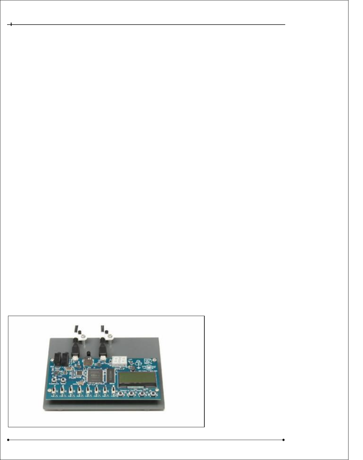
This board platform is the University of
Waterloo - LogicalStep board. Figure 1
is a photo of the U of W LogicalStep
board that will be used for your
experiments in the course.
Figure 1 - LogicalStep Board
ECE-124 Lab Manual – W2018– V2.4 8
University of Waterloo
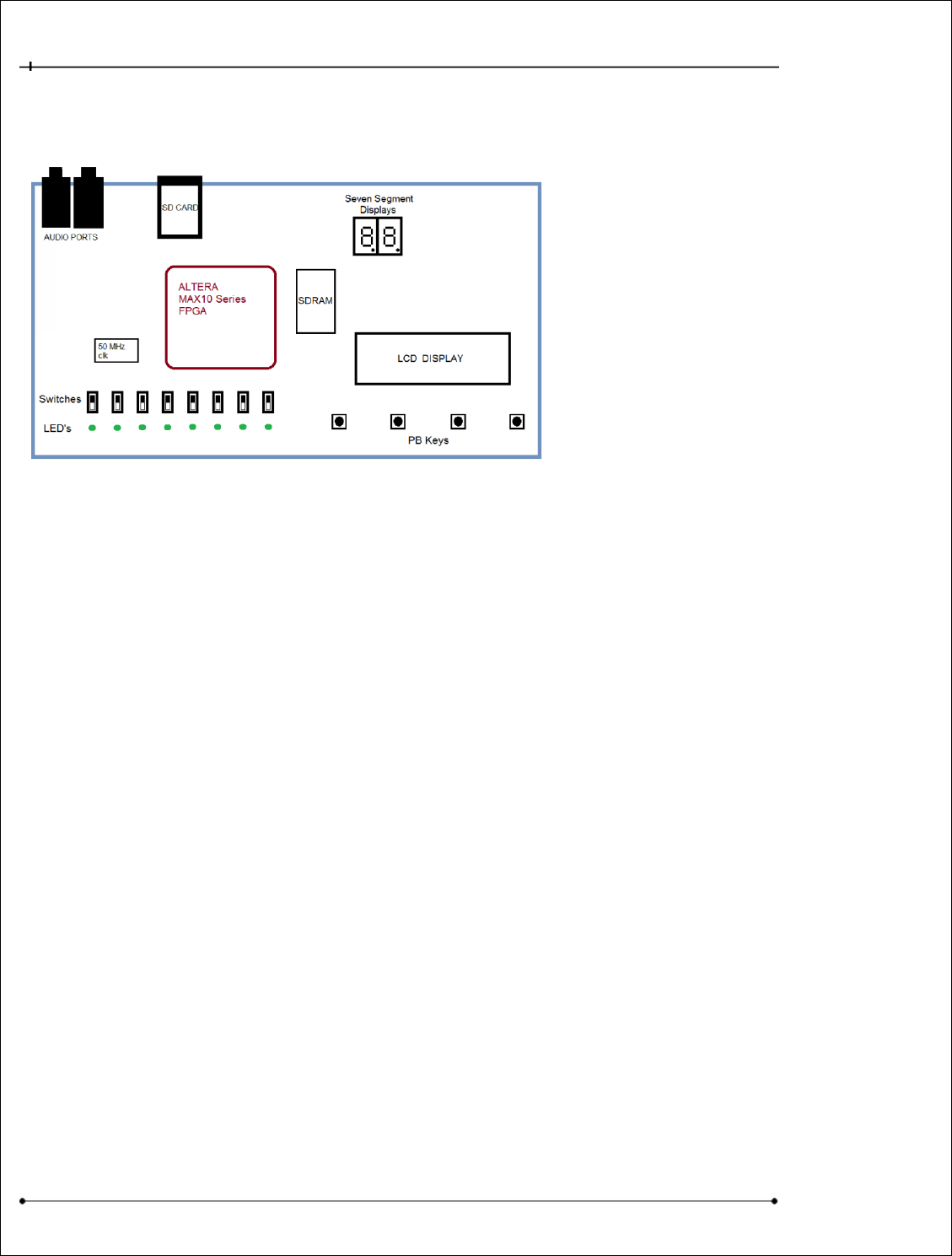
Figure 2 is a sketch of the external FPGA designer resources (peripherals) that can be used for various
FPGA design projects.
Figure 2 - LogicalStep Block Diagram
2.1 LogicalStep FPGA Board User Peripherals
The LogicalStep board is equipped with some peripherals that can be used to create various
applications. These peripherals are things such as a clock source, switches and Push-Button Key
inputs, output LED indicators, SDRAM, SD Card (like a mini-disk) and Audio electronics etc.
For the purposes of the ECE-124 labs course we are only interested in using the clock source, switches
/ push buttons for supplying logic inputs and for outputs we will use the LED’s and the Seven-Segment
Displays.
LEDs are electronic components which can emit light with much greater efficiency than incandescent
lamps. Specific pins on the FPGA are connected on the LogicalStep board to drive these LED’s.
Other LED indicators on the board are the Seven‐Segment displays (so called because it is an
arrangement of 7 bar segments). They are arranged in such a way that the numbers 0 to 9, and letters
A to F, can be displayed. Seven segments is the minimum number which can uniquely display numbers
and that is why they are used for many calculator or electronic displays. To drive these displays a
Seven‐Segment decoder (inside the FPGA) is usually used to converts a 4 bit binary number to a
Seven‐Segment LED pattern so that a person can see a number or letter instead of trying to interpret
the original 4 bit binary number. There are also 8 slide switch inputs and 4 push-button key inputs. A
50 MHz clock is connected to the FPGA to drive logic processing.
ECE-124 Lab Manual – W2018– V2.4 9
University of Waterloo
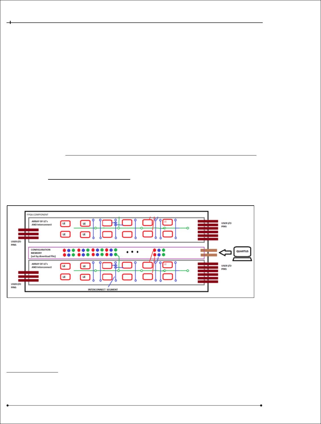
2.2 Field Programmable Gate Array (FPGA) Technology
FPGA technology has been around since the mid 1980’s. It has gradually grown in complexity and
capability and is now a dominant technology used in the workplace. For a typical FPGA there are two
prime components involved within its architecture. These are the Logic Elements (LE’s) and the
interconnect resources. Both of these items are completely configurable after the FPGA device is
powered. The Logic Elements are used to implement gate-level logic and the interconnect section is
used to connect the various LE’s in some arrangement. The design files that are downloaded into the
device are developed on an external software-based design platform (such as Altera Quartus Prime).
When a designer has processed the design in Quartus its download file can be sent into the
appropriate FPGA for use with other technology on a board.
But one might ask ”How does a FPGA download file become functioning hardware?”.
In the sketch shown below all of the logic functions and interconnect that are in an FPGA device are
controlled by configuration memory cells located in the FPGA. These memory cells directly control the
activation or deactivation of switch transistors. These transistors are placed in the FPGA to control
logic lookup-tables (inside the LE blocks) and interconnect path link connections.
Figure 3 - Typical FPGA Configuration Memory
Thus a download file can be used to implement any logic hardware function or functions within the
FPGA. Since the FPGA can be reconfigured, it can implement different hardware functions by simply
having different download files sent to it. The external I/O connections are usually fixed on a board
design however and they must be kept in mind when considering design new FPGA designs. FPGAs
are different than microprocessors or microcontrollers because the designer is able to change the
hardware design of the logic.

ECE-124 Lab Manual – W2018– V2.4 10
University of Waterloo
The FPGA device that is used on the LogicalStep board that you will be using is a current technology
FPGA platform. Although it is one of the smaller FPGA’s offered in the marketplace it can still pack a
lot of functionality into the device’s 8K LE’s and 144 pins. This FPGA offers many other kinds of
internal resources (DSP’, RAM, PLL’s) but are beyond the scope of the Lab course.
2.3 FPGA Design Software
This course will be using the Quartus Prime set of tools to develop the FPGA designs and it is a full
FPGA design software suite from Altera (now Intel). It aids the designer through the different stages of
describing the hardware design and targeting it for a certain Altera FPGA chip. The typical
development process uses the following stages:
• Design Entry:
O Schematic Entry: by connecting blocks of ranging complexity. It can be used to interconnect simple
components such as simple logic gates or to interconnect previously created hardware blocks
O Hardware Description Language: such as VHDL or Verilog (we use VHDL)
• Design Compilation Part 1:
O Analysis and Synthesis: An HDL or schematic file is analyzed and is mapped into a number of logic gate
equivalents and their connections. The synthesized file can be used for functional simulations.
• Circuit Simulation:
o Functional Simulation: This is used to verify the logic functionality of the design before further processing
steps are attempted. Any functional errors are fixed in the design
• Design Compilation Part 2:
O Repeat of Analysis and Synthesis: The proven functional design is synthesized for further processing.
O Place and Route: the synthesized logic is arranged (Placement) for an FPGA device. After the Placement
phase a Routing algorithm determines the best way to connect the logic. The routing details yield timing
information about the “placed and routed” design.
• Timing Analysis:
o This is usually required for higher performance or higher density designs that have been placed and
routed. It gives an accurate indication of how fast the circuit can run and how much timing margin is
available for various operating conditions. Timing errors are fixed in the design.
• Design Compilation Part 3:
O Repeat of Analysis / Synthesis / Placement / Route: The fully implemented design is processed.
O Assembly: a load file is produced so that it can be downloaded to the FPGA chip.
• Programming the FPGA:
o The circuit can be physically tested afterwards by applying inputs and observing the outputs.

ECE-124 Lab Manual – W2018– V2.4 11
University of Waterloo
2.4 ECE-124 Lab Sessions Outline:
Lab Sessions:
1. Session 1: Lab Procedures; Lab1- Design Entry Methods Using Altera Quartus Prime Tools (3 hrs)
2. Session 2: Demo from Lab1; Lab2- VHDL for Combinational Circuits PART 1 (3 hrs) – Simple ALU Design
3. Session 3: Demo from Lab2; Lab3- VHDL for Combinational Circuits PART 2 (3 hrs) – Energy Monitor
4. Session 4: Demo from Lab3; Lab4- VHDL for Sequential Circuits (3 hrs)- Flip-flops/State Machines
5. Session 5: Demo from Lab4; Lab5- Wrap-up of Sequential Circuits (3 hrs) - Robotic Arm Controller
The Lab Stations are made for groups of two. Settle on your lab partner during the first Lab.
NOTE: in the Lab Manual pages there are numerous, highly detailed screen-shots entered. The fine print on those
pictures may be readable by using the ZOOM feature in your document viewer.

ECE-124 Lab Manual – W2018– V2.4 12
University of Waterloo
3 Lab 1 – Design Entry Using Altera Quartus-II
The goal of this lab session is primarily to gain experience with the Altera Quartus Prime FPGA Design
Environment. Lab1 will go through two design entry methods and some simulation steps for design
testing. Later the design will be processed for the programming of an FPGA on the LogicalStep board
to observe how the logic circuit actually works in hardware. Since Lab1 starts so early in the term
relative to the lecture material we will be doing some basic examination of two input gate
functions
3.1 Prelab
No prelab work is necessary for LAB1. However students should familiarize themselves with the
ECE-124 Lab Manual Outline and FPGA technology sections.
3.2 Lab1 Outline:
Attendance will be taken. Your Team partnerships will be settled during LAB1 and Group Numbers will
be assigned for each team.
Lab 1 is composed of the following main categories:
1. Brief introduction to the laboratory, its equipment and the student conduct expected during
Lab sessions.
2. Learning two Design entry methods (Schematic and VHDL) for small digital circuits.
3. Running Synthesis and Simulation processes on the circuits to check that they operate as
expected.
4. Processing the FPGA designs into load files for downloading into the LogicalStep board and
confirming that the hardware implementations function as expected.
5. Modifying the above circuit designs to provide new functionality and then test them.
ECE-124 Lab Manual – W2018– V2.4 13
University of Waterloo
3.3 Lab1 Activities
3.3.1 Starting Your Lab1 Project
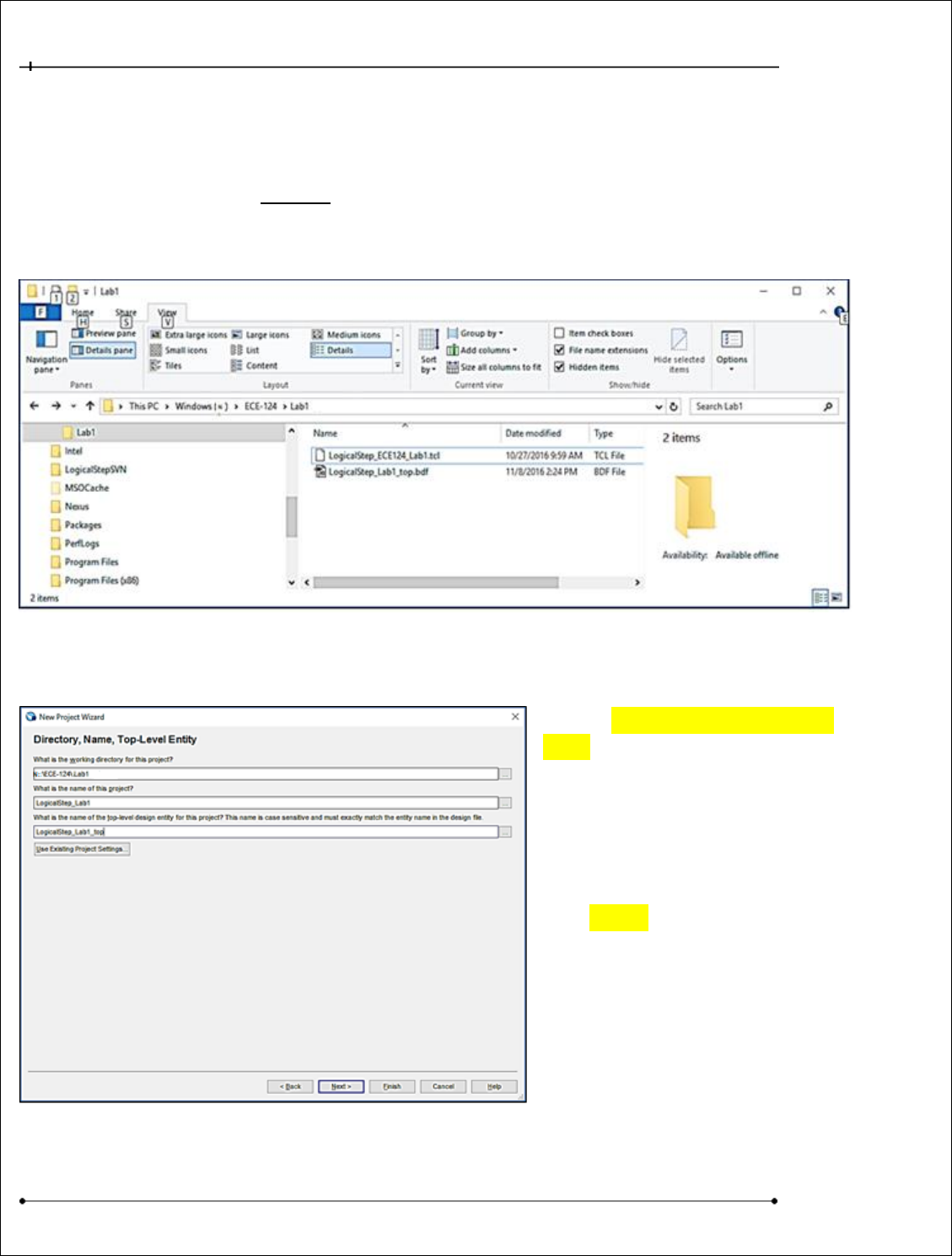
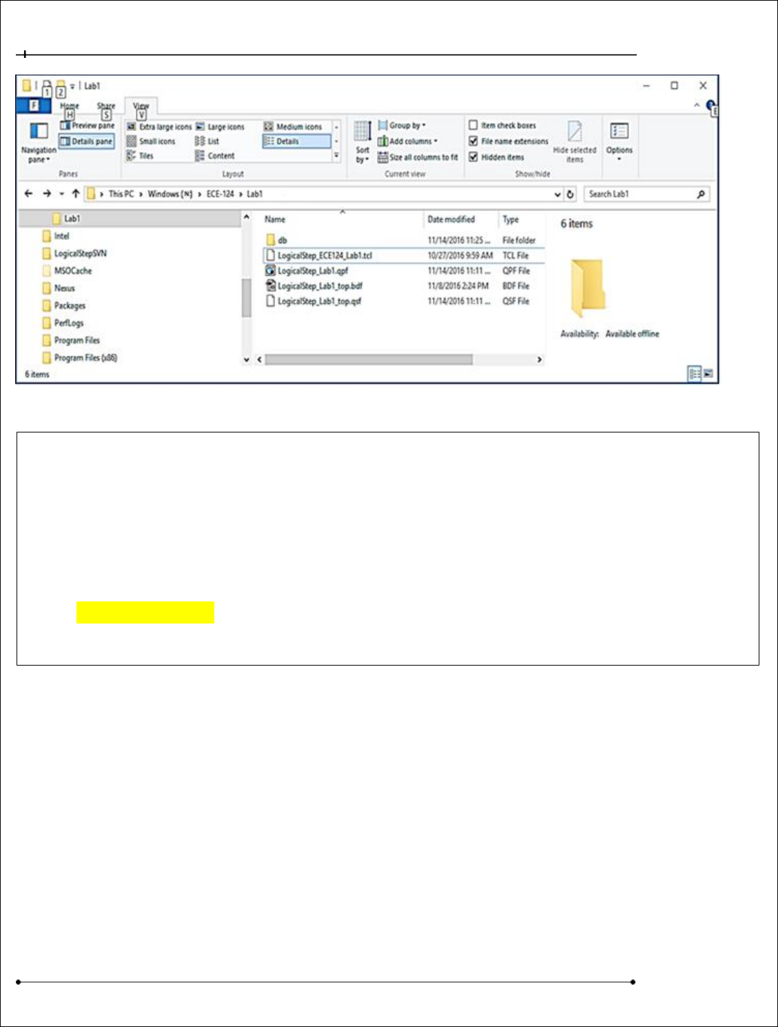
To begin your Lab1 project use the Windows10 File Explorer and browse to somewhere on a team
members file space on the N: drive and create a folder called ECE124. Go to LEARN and download the
Lab1 Zipped folder “Lab1” into the ECE124 folder on the N: drive. Extract the contents into a new Lab1
project folder. The new files are as follows in Figure 4:
Figure 4 Lab1: Starting Lab1 Project Folder
Start up the Altera Quartus Prime platform to begin a new project. Go to the FILE tab.
SELECT FILE>New Project Wizard. Click
NEXT to go to the second slide.
The project parameters will now be
entered as in Figure 5.
Project Folder: N:/ECE-124/Lab1
Project Name: LogicalStep_Lab1
Project Top Level: LogicalStep_Lab1_top
Click FINISH on the Wizard Dialog
Window.
After the setup has completed you should see the following in your project folder as in Figure 6:
Figure 5 Lab1: FPGA Project Setup
ECE-124 Lab Manual – W2018– V2.4 14
University of Waterloo
Figure 6 Lab1: Project Folder After Setup
Next, in Quartus, the TCL script must be run to assign the FPGA device type that is being used for this
lab and then pin assignments for the FPGA that are reserved for the LogicStep FPGA and finally the
project LogicalStep_Lab1 is opened.
Notice in the Project folder the file LogicalStep_Lab1.qpf (Altera Quartus Project File or QPF).
In later FPGA design work you can do one of two procedures to get back into your FPGA project to
run in Quartus for Lab1.
1) You can browse to the Project folder and “double-click on the QPF file. This will launch
Quartus and will load your FPGA design that you saved previously.
2) Alternatively, you can invoke the Quartus Prime v15.1 tools and then go to the
FILE>Open_Project tab and then browse to the QPF file in your project folder and select the
QPF file.
ECE-124 Lab Manual – W2018– V2.4 15
University of Waterloo
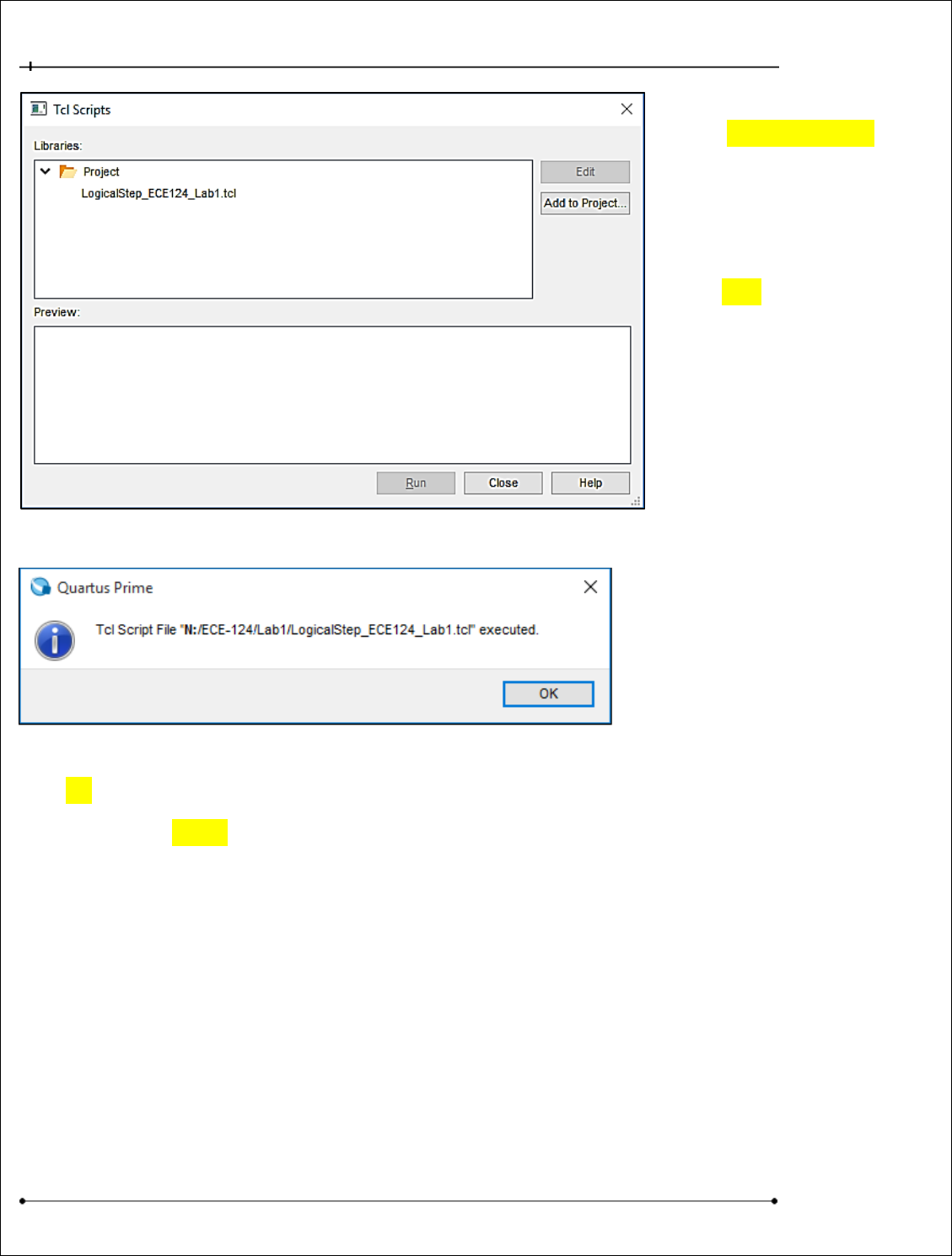
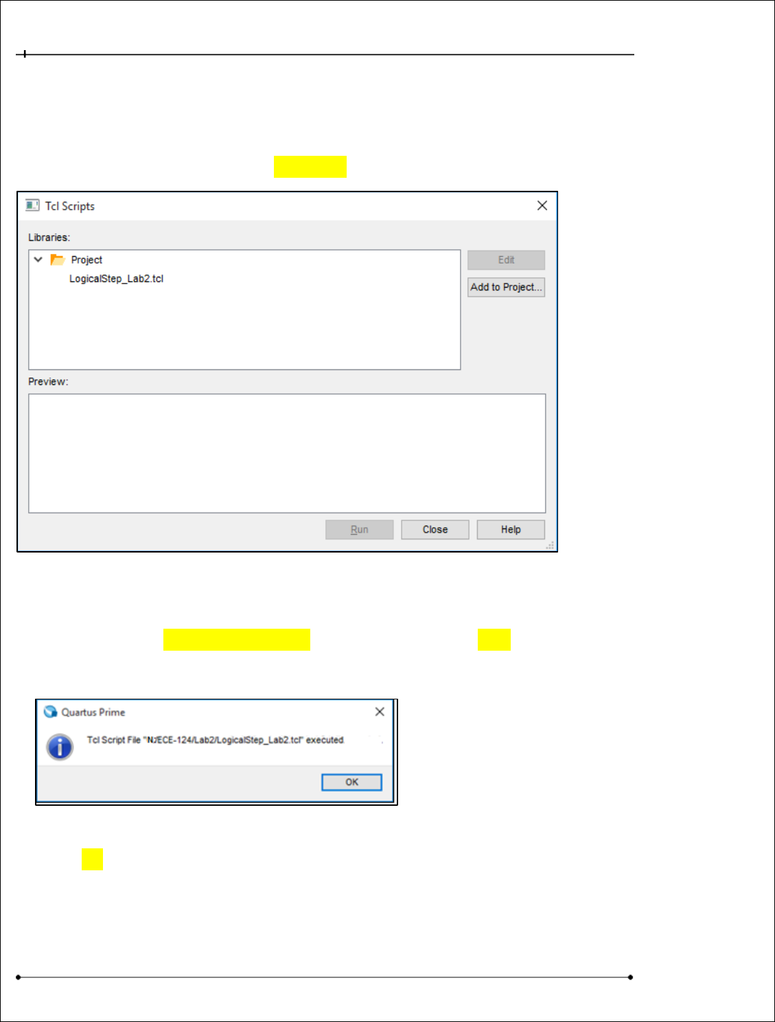
Go to the Tools TAB and
SELECT Tools>Tcl Scripts. The
following dialog box (Figure 7)
should appear:
SELECT the TCL (pronounced
as “tickle”) file and then click
on the RUN button.
Figure 7 Lab1: TCL Script Invocation
The Figure 8 window should appear when it is finished.
Figure 8 Lab1: TCL File Completed
Click OK.
Then SELECT the CLOSE button on the TCL Script Dialog window.
NOTE that this TCL file will NOT have to be run again for the entire Lab1 project since the pin and
FPGA Device assignments are established.
ECE-124 Lab Manual – W2018– V2.4 16
University of Waterloo
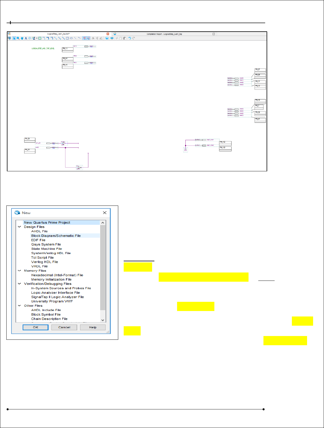
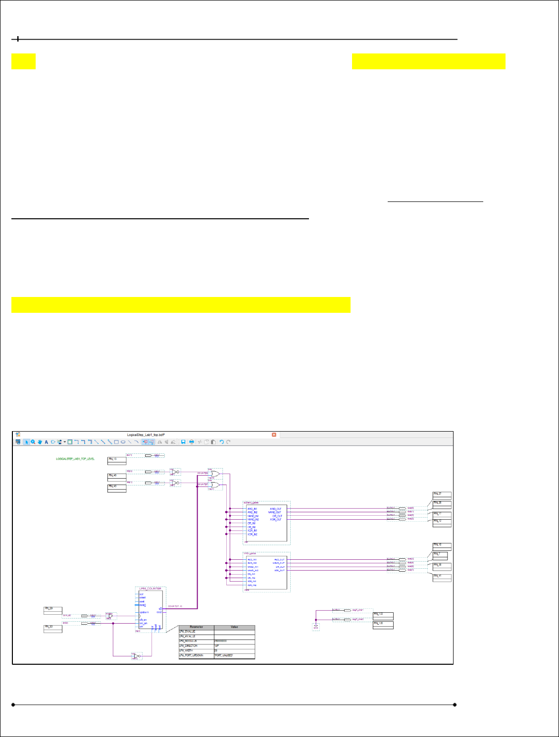
Earlier the top level file for this lab was downloaded from LEARN into the Lab1 project folder. The top
level file is in schematic form (see Figure 10). Schematic entry methods for a simple set of gate-level
functions will be the first part of this lab. Go to FILE Tab and SELECT File>Open and then browse to the
LogicalStep_Lab1_top.bdf file (see Figure 6).
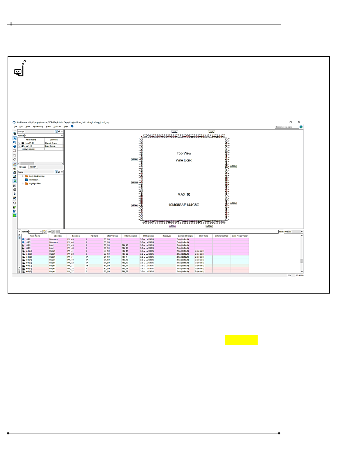
DEEP DIVE :
With the assignments made with the TCL file you can observe the signal pins that are used on
the FPGA by calling up the Pin Planner utility. Go to the ASSIGNMENTS Tab and select the Pin
Planner option. You should see something like the following:
Figure 9 Lab1: FPGA PIN PLANNER
ECE-124 Lab Manual – W2018– V2.4 17
University of Waterloo
Figure 10 Lab1: Starting Top Level Schematic
There are two pins for Push-Button Key Inputs, two pins for Switch inputs, eight pins for LED Outputs
and a pin for a Clock Input provided in the Lab1 design. The
Clock Input will be used later in the lab session.
Now we can start adding some design hierarchy by creating
functional blocks and then installing them at the top level
design later. The first block that will be created will be of a
schematic entry format. Go to the FILE Tab and select
File>New. The dialog box as shown in Figure 11 will open.
SELECT the Block Diagram/Schematic File. A blank schematic
window will then open in Quartus. After it opens save the
schematic file as “schem_gates.bdf” by going to the FILE Tab
and selecting the File>Save As option.
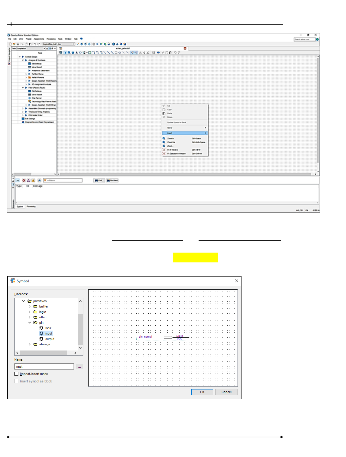
To insert schematic symbols on the schem_gates sheet RIGHT-
CLICK anywhere on the schematic sheet (as in Figure 12) and a
dialog box should appear. SELECT the Insert>Symbol
option.
Figure 11 Lab1: New Schematic Creation for schem_gates Block
ECE-124 Lab Manual – W2018– V2.4 18
University of Waterloo
Figure 12 Lab1: Insertion of Library Symbols into schem_gates Schematic
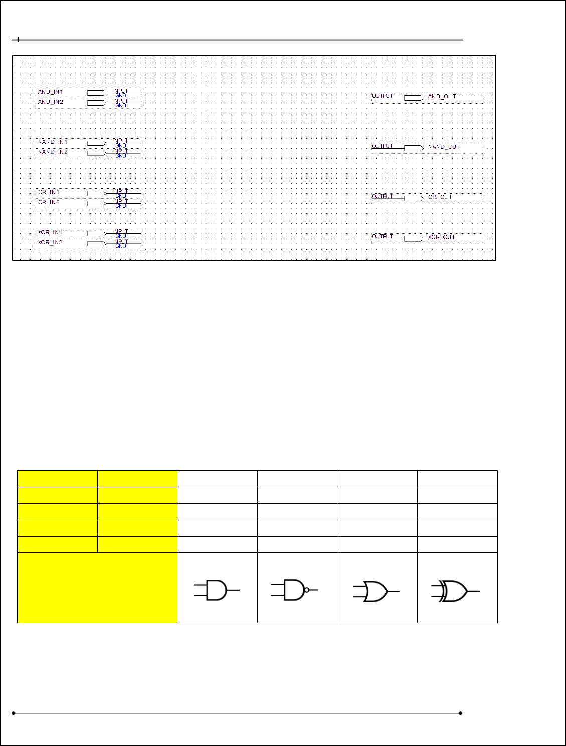
To this schematic we will add INPUT pins on the left and OUTPUT pins on the right (typical for
schematic convention for readability). So within the Symbols Dialog box that will appear browse to
the altera/quartus libraries and then SELECT the Primitives/pin folder. Here you can select the pins
as required and place them on the schematic sheet.
Figure 13 Lab1: Locating Pins in Symbol
Library for schem_gates Block
Add Inputs and Outputs to the schematic sheet as shown below in Figure 14:
ECE-124 Lab Manual – W2018– V2.4 19
University of Waterloo
Figure 14 Lab1: Insertion of I/O Pins into schem_gates Schematic
List of inputs:
AND_IN1, AND_IN2, NAND_IN1, NAND_IN2, OR_IN1, OR_IN2, XOR_IN1, XOR_IN2
List of outputs :
AND_OUT, NAND_OUT, OR_OUT, XOR_OUT
Name each of the pins as in the lists above. (Double-click each pin and modify its Name property).
After placing and naming the pins on the schematic sheet return again to the symbol Libraries for logic
gates in the Primitives/Logic folder.
We will only be using 2 input gates for this lab. Below is a truth table for the gates that are to be
entered. Also notice how in the INPUTS that bit1 changes at half the rate of bit0.
IN 1
IN 0
AND
NAND
OR
XOR
0
0
0
1
0
0
0
1
0
1
1
1
1
0
0
1
1
1
1
1
1
0
1
0
GATE SYMBOL →
Figure 15 Lab1: Look-up Table for Gate Logic Functions
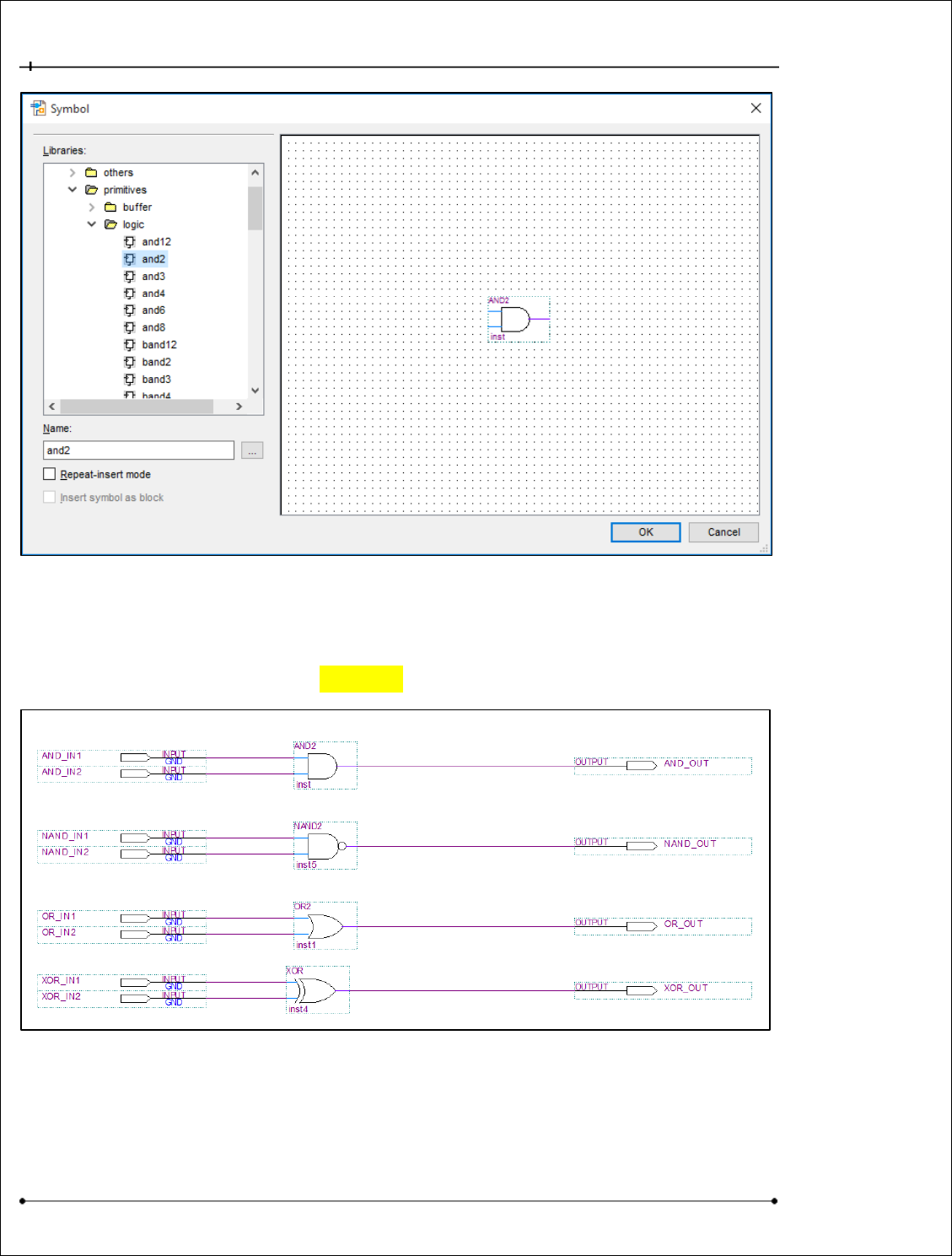
You must locate the basic 2 input gate functions (AND, NAND, OR, XOR) from the altera/quartus
libraries and insert them into this schematic. Below in Figure 16 is an example of the two input AND
gate.
ECE-124 Lab Manual – W2018– V2.4 20
University of Waterloo
Figure 16 Lab1: Locating Gates in Symbol Library for schem_gates Block
Connect the input pins to the gate inputs and the output pins to the gate outputs as shown below in
Figure 17. Use the Orthogonal Node Tool (highlighted below)). After the schematic is drawn save the
file. Go to the FILE Tab and select File>Save.
Figure 17 Lab1: Connecting Gates in schem_gates Block
Now that a schematic design file has been created we must make a symbol for it so that we can add
its symbol to the top level schematic (LogicalStep_Lab1_top). Go to the FILE Tab.
ECE-124 Lab Manual – W2018– V2.4 21
University of Waterloo
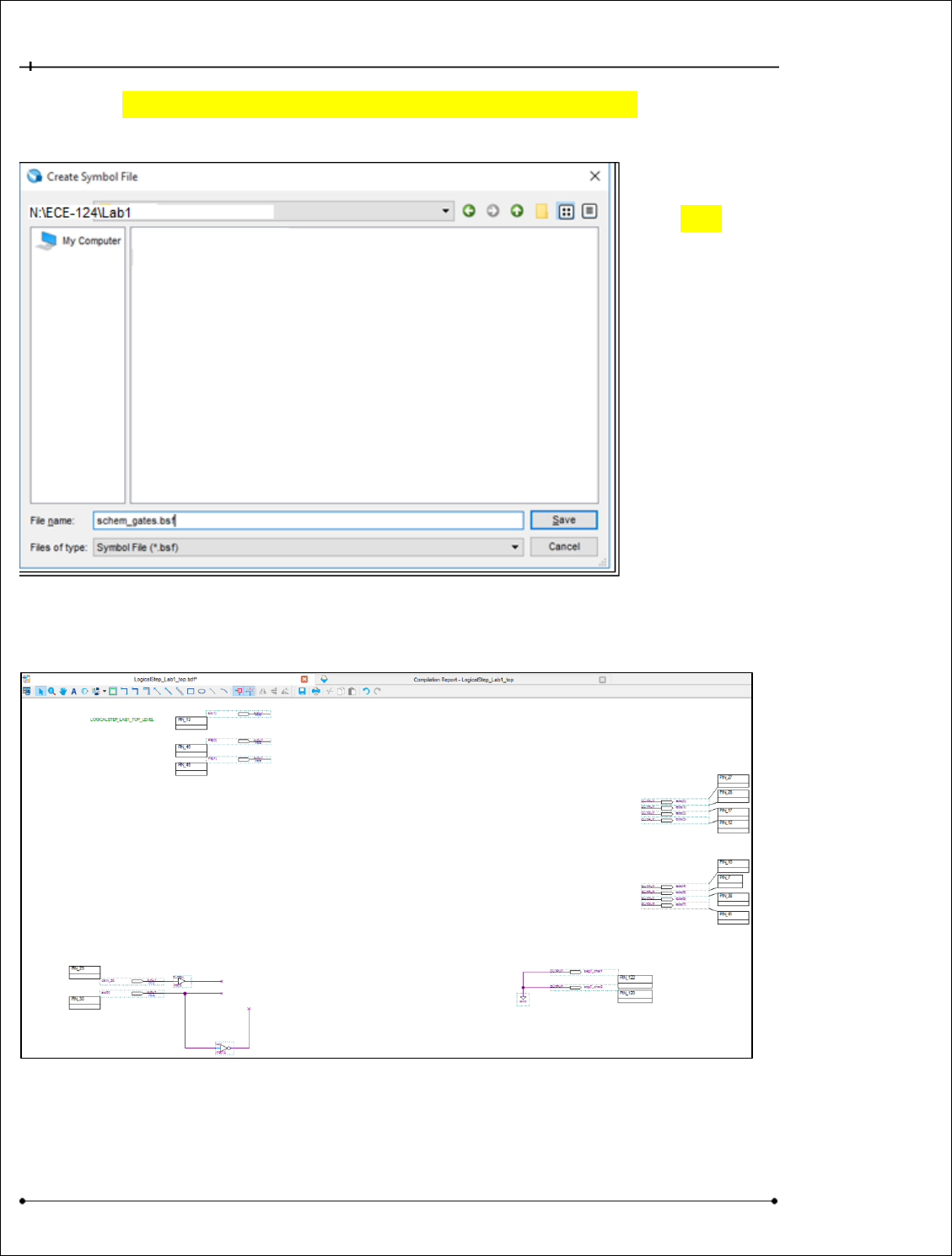
SELECT the File>Create / Update> Create Symbol Files for Current File option. A Window like the one
in Figure 18 appears. The symbol filename option for “schem_gates.bsf” should be visible.
Click Save.
Close the schem_gates design file. Return to the LocialStep_Lab1_top schematic as in Figure 19.
Figure 19 Lab1: Top Level Schematic Before Adding Symbols
Figure 18 Lab1: Creating Symbol for schem_gates Block
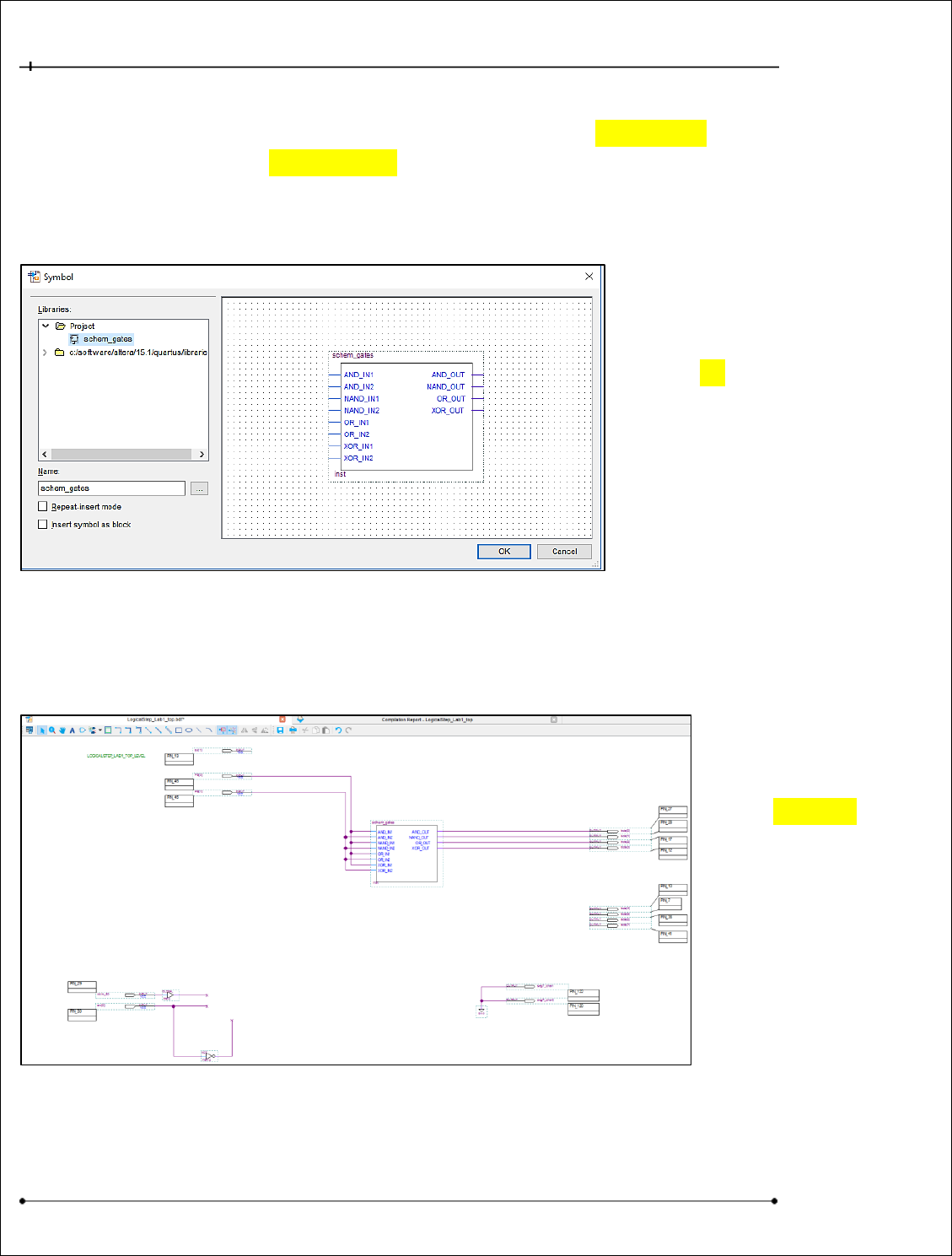
ECE-124 Lab Manual – W2018– V2.4 22
University of Waterloo
On the LogicalStep_Lab1_top schematic design the new schem_gates.bsf symbol (block that was just
created in the previous step) will be inserted. To insert a symbol RIGHT-CLICK anywhere on the top
level schematic. SELECT the Insert>Symbol option.
The Symbol Dialog box appears (see Figure 20). Expand the Project folder and browse to the
schem_gates file.
Figure 20 Lab1: Selecting the schem_gates Symbol
for Insertion
Click the OK Button.
Place the symbol on the schematic.
After it is added to the top level schematic sheet connect its symbol pins to the Push-Button port pins
and to the output pins that drive LED’s on the LogicalStep board. Use the ORTHOGONAL NODE TOOL
as before.
SELECT File>Save to save
the top schematic design
as in Figure 21.
Figure 21 Lab1: Hooking Up Pins to schem_gates Block
Now we are ready to do some functional testing by simulation.
ECE-124 Lab Manual – W2018– V2.4 23
University of Waterloo
3.3.2 Functional Simulations
3.3.2.1 Preparation for Functional Simulation – Analysis and Synthesis
Within Quartus go to the PROCESSING Tab. SELECT Start>Start Analysis and Synthesis” process to
process the design into a gate level logic file for simulation purposes.
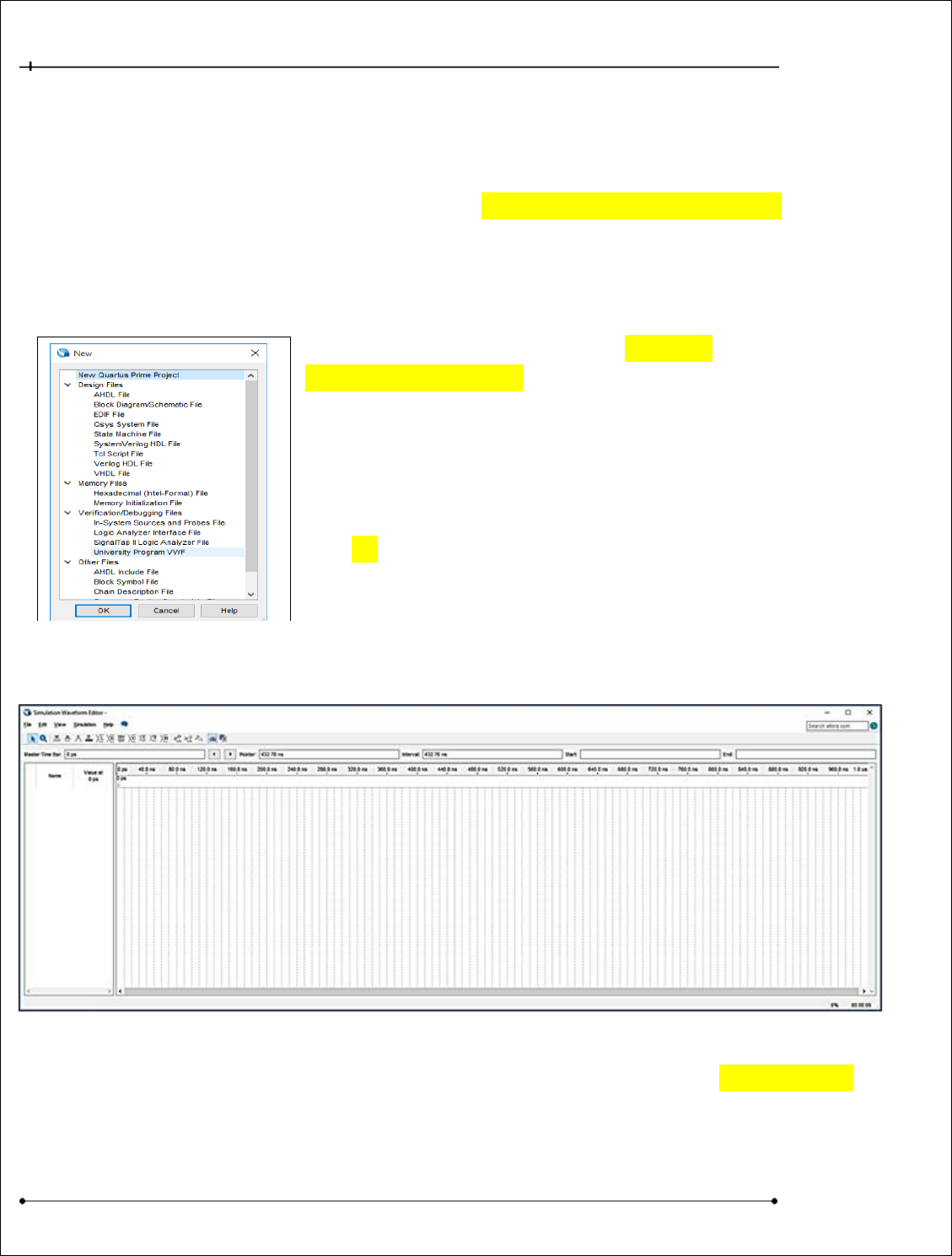
3.3.2.2 Opening a Simulation Window
Now under the FILE Tab SELECT the FILE>New and then SELECT the
University Program VWF utility to open a Functional Simulation
window (see Figure 22). This will be used to illustrate the gate-level
functionality in a visual manner. Nodes (nets) will be inserted from
the design (see below) for control and observation.
Click OK.
A new window will open like the one shown in Figure 23.
Figure 23 Lab1: Simulation Window
Set the Time scale by going to the Simulator Window EDIT Tab and SELECT the Edit >End Time option.
Figure 22 Lab1: Starting a New Simulation
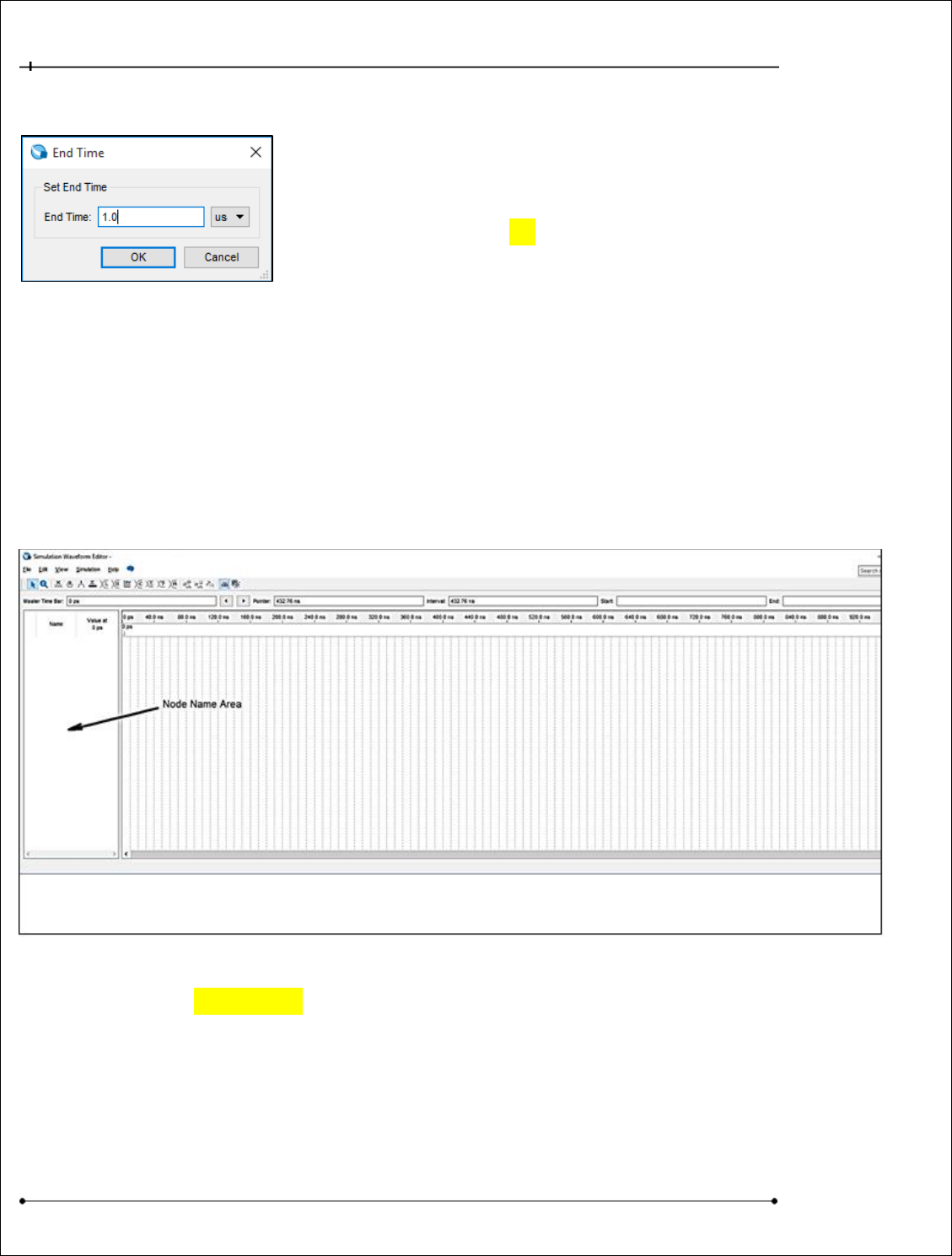
ECE-124 Lab Manual – W2018– V2.4 24
University of Waterloo
Then a window like the one shown in Figure 24 will appear.
Set it to 1 usec. Click the OK button.
3.3.2.3 Adding Nodes to the Simulation Window
For the simulation only the two Push-Button inputs and the first four LED outputs will be inserted into
the simulator.
Figure 25 Lab1: Adding Nodes to Simulator Window
Double-Click the Node NAME area of the Simulator Window and the following Dialog window will
appear as in Figure 26 below:
Figure 24 Lab1: Setting Simulation End Time
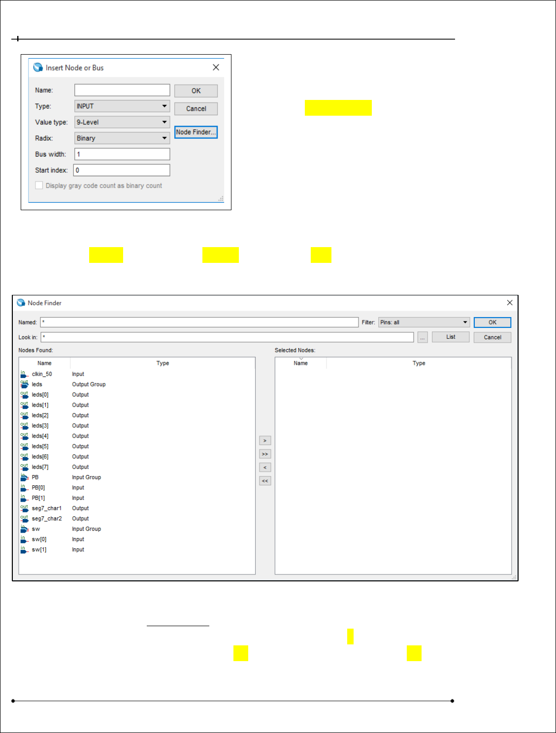
ECE-124 Lab Manual – W2018– V2.4 25
University of Waterloo
Click on the Node Finder Button for faster node
identification and insertion. The Node Finder Dialog Box
will appear. This will allow you to browse the
synthesized design for nodes (nets) to probe for the
Functional Simulation.
With the node FILTER setting set to “Pins all” Click on the LIST button as shown in Figure 27. The list
of pins from the design will appear as shown.
Figure 27 Lab1: Listing Pins with Node Finder
SELECT the following pins in the order specified: PB[0], PB[1], leds[0], leds[1], leds[2], leds[3], leds[4],
leds[5], leds[6], leds[7]. After selection of the group click on the ‘>’ button to copy them to the
Selected Nodes window. Then click on the OK button and again Click on the OK button on the
Node_Finder Dialog Box (Figure 26).
Figure 26 Lab1: Calling up Simulator Node Finder
ECE-124 Lab Manual – W2018– V2.4 26
University of Waterloo
3.3.2.4 Adding Stimulus to the Input Nodes
Figure 28 Lab1: Adding Node Stimulus
To provide the stimulus waveforms to the input pins SELECT input PB [0] in the NAME column and
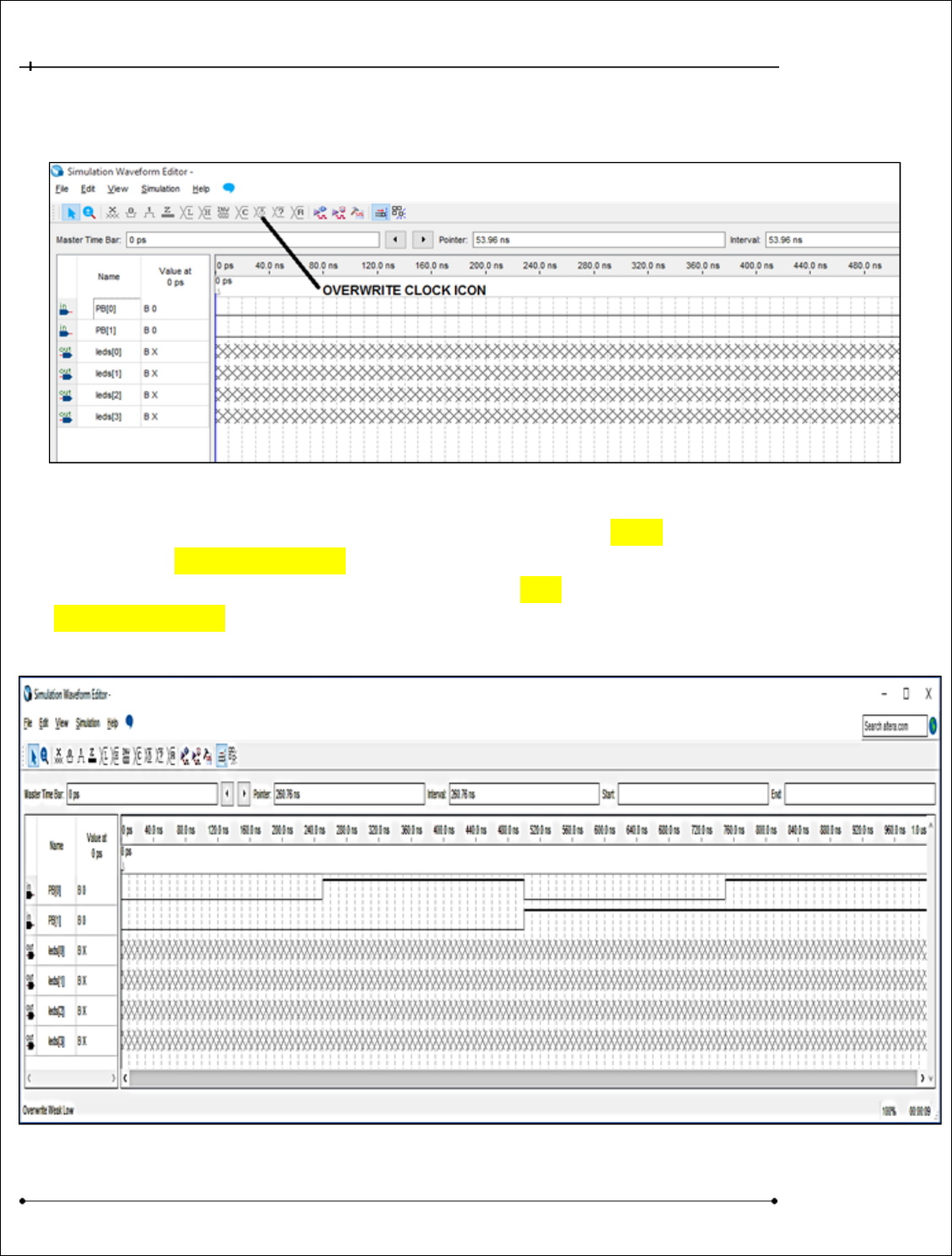
then Click on the OVERWRITE CLOCK button (shown above in Figure 28) and enter a period of 500
nseconds. Then similarly, for the PB[1] input SELECT the PB[1] in the NAME column and then click on
the OVERWRITE CLOCK button (shown above in Figure 29) and enter 1000 nsec for the period value.
These two entries should create waveforms for stimulus as shown in Figure 29.
Figure 29 Lab1: Adding more Stimulus
ECE-124 Lab Manual – W2018– V2.4 27
University of Waterloo
The stimulus is now created. But the outputs are still undefined since the simulation has not yet
been run. Save the Simulation file as waveform.vwf by going to the Simulator window FILE Tab and
SELECT the File>Save option.
3.3.2.5 Running the Functional Simulation
On the Simulator window SIMULATION Tab and SELECT the Simulation>Run Functional Simulation
option. The simulation results should look like the screenshot in Figure 30 when it has completed.
Figure 30 Lab1: Simulation Complete
Recall that the leds[0] pin is connected to the AND_OUT pin of schem_gates in the design. Similarly
leds[1] is connected to NAND_OUT, leds[2] with OR_OUT and leds[3] with XOR_OUT. Confirm that
the simulation waveforms follow the gate truth tables covered earlier.
3.3.3 Compensating for Active-LOW PB inputs
At this point the functional simulation has proven the design functionality. We can now close the
Simulator Windows.
Moving now to a real world operation of the FPGA on the LogicalStep board there will have to be a
small modification added to the schematic to adjust for conditions external to the FPGA. We want the
inputs to the logic blocks to match the logic levels that were defined as in the simulations. On the
LogicalStep board when each PB key is pressed the signal state is ‘0’ for a closed condition. But we
want a logical ‘1’ to arrive at the appropriate schem_gates block input when the PB key is pressed.
ECE-124 Lab Manual – W2018– V2.4 28
University of Waterloo
Therefore we must add inverters to PB[0] and PB[1] pin inputs. The inverters will ensure that this
compensation happens. Go to the altera/quartus libraries again to insert the “not” gate from the
Primitives/logic folder for each of the inverters. Insert and connect them as shown in Figure 31.
Figure 31 Lab1: Inserting Inverters after PB Key Inputs
3.3.4 FPGA Design Compilation and Download
Now the FPGA Compilation process will be executed. Go to the PROCESSING Tab and SELECT the
Processing>Start Compilation option. When the FPGA compilation finishes and if no compilation
errors are found (ignore any warnings) then an FPGA load file can be downloaded into the FPGA.
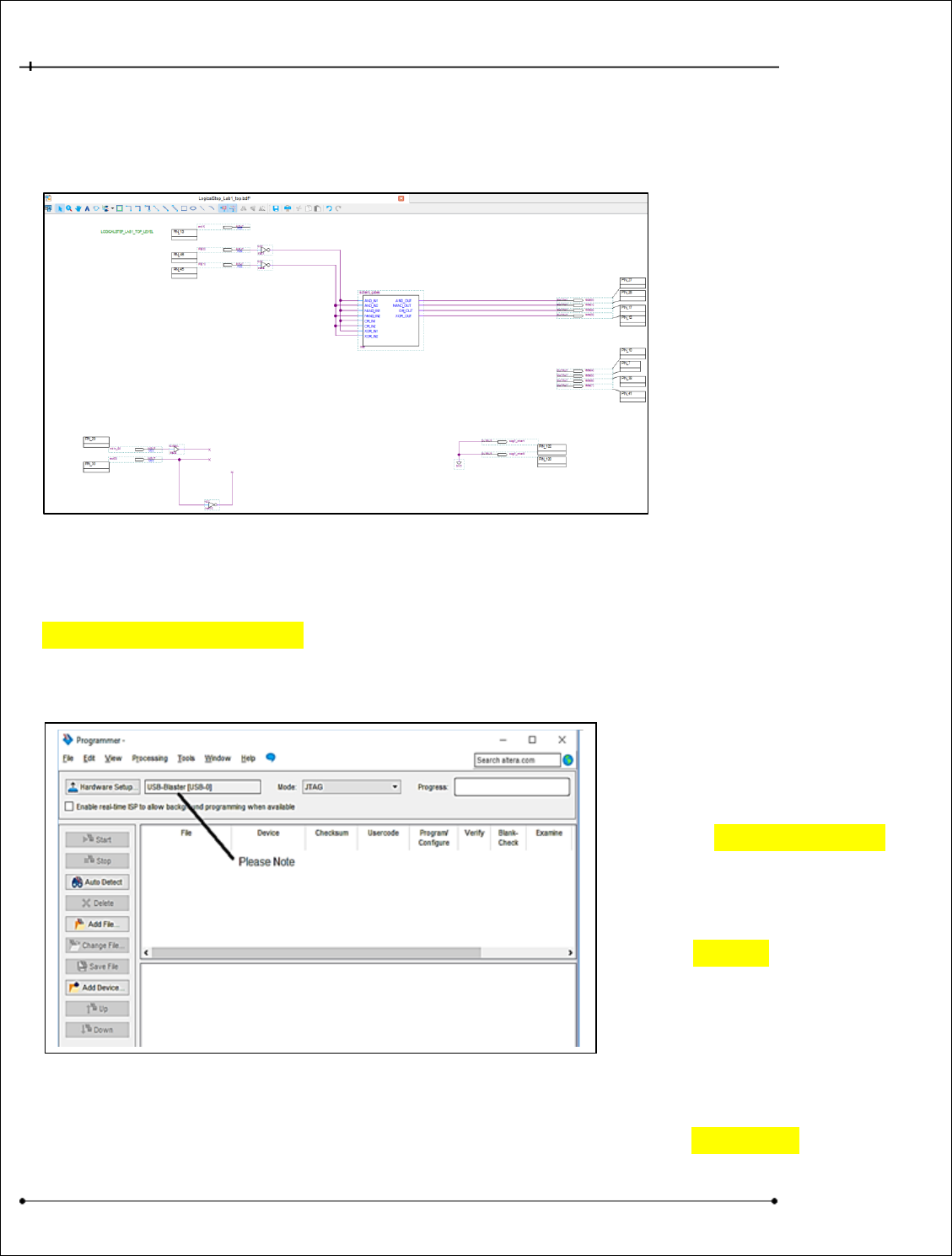
Use the Quartus Programmer
utility to download your design file
into the LogicalStep board FPGA
by going to the TOOLS Tab and
SELECT the Tools>Programmer
option.
A Programmer dialog window will
open as shown in Figure 32.
Click the ADD File button.
NOTE: If the LogicalStep board is
connected the USB Blaster should
be seen beside the Hardware Setup field (Otherwise speak with the Instructor).
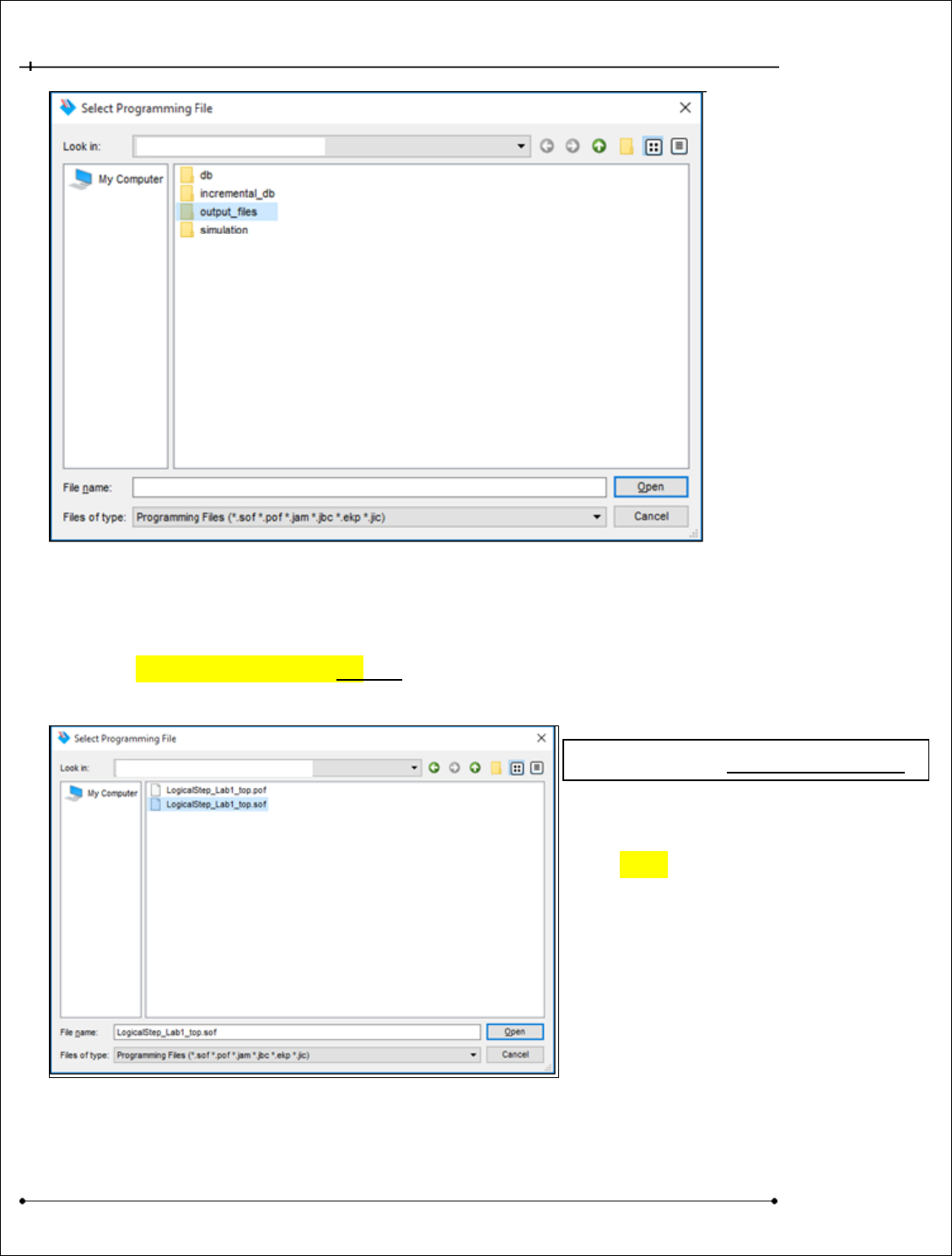
A Select Programming File window will open (Figure 33). Browse to the output_files folder.
Figure 32 Lab1: Quartus FPGA Programmer
ECE-124 Lab Manual – W2018– V2.4 29
University of Waterloo
Figure 33 Lab1: Quartus FPGA Programming File Browser
Select the LogicalStep_Lab1_top.sof file as shown in Figure 34.
Click Open.
Then requested file will then show up
in the Programmer window as shown
below in Figure 35.
WATCH OUT! (NOT the .pof file).
Figure 34 Lab1: Selecting the FPGA Programming File (.sof)
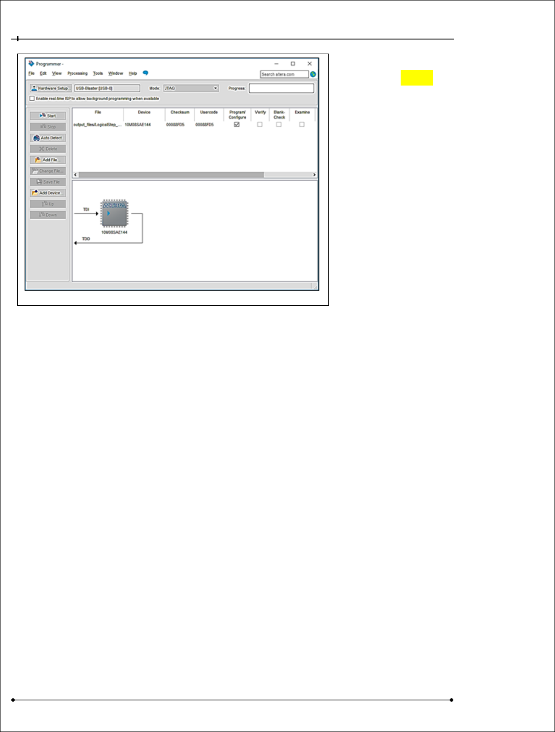
ECE-124 Lab Manual – W2018– V2.4 30
University of Waterloo
Click on the START button (see Figure
35) to begin the FPGA download. The
progress window should indicate
100% after the downloading is
completed.
After downloading you can test your FPGA design by using board-level inputs (PB [1..0] Keys) and
also observing the outputs (LEDs) according to your logic gate truth tables.
Figure 35 Lab1: Starting the Quartus FPGA Programming
ECE-124 Lab Manual – W2018– V2.4 31
University of Waterloo
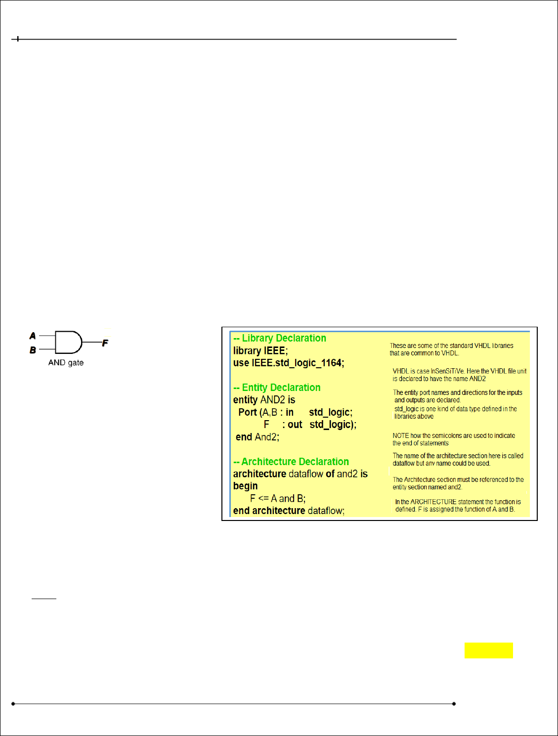
3.3.5 VHDL Design Entry
The main areas that will be covered on VHDL in this course have to do with the parts of the VHDL
design unit (hardware block). For ECE-124 there are just two main areas of focus. These are the
ENTITY and ARCHITECTURE constructs. (Library declarations are also required, as shown in Figure 36
below but just a few variants of these library declarations will be provided to you for use):
1. ENTITY: declares the design unit name and the ports (which are inputs and outputs of the
entity or design unit) associated with it. Each port name, type (input or output) and width
(number of bits) is declared in the entity.
2. ARCHITECTURE: specifies the actual functionality of the entity. Notice that the entity has no
information about how the hardware block uses the inputs or how to produce the outputs ‐
that is the role of the architecture associated with the entity.
Figure 36 is an example of a complete VHDL unit for a two input AND gate:
Within the Architectural construct
there are two styles used to describe
the functionality of a VHDL design
unit. These are:
1. Behavioral: where the relation
between input and output is
declared using logical equations.
2. Structural: where you can use
previously created entities in your
design unit as components. For example if you built an adder unit you can use it as a component in
designing a microprocessor.
For Lab1 we will just be using the Behavioral style.
The VHDL design entry method within Quartus will now be covered. Similar to how we created the
design for the schem_gates block we will now create a VHDL design block.
Returning to the LogicalStep_Lab1_top design in Quartus go to the FILE Tab and Select File>New.
The dialog box shown below in Figure 37 will open:
Figure 36 Lab1: VHDL Example for a Simple AND Gate
ECE-124 Lab Manual – W2018– V2.4 32
University of Waterloo
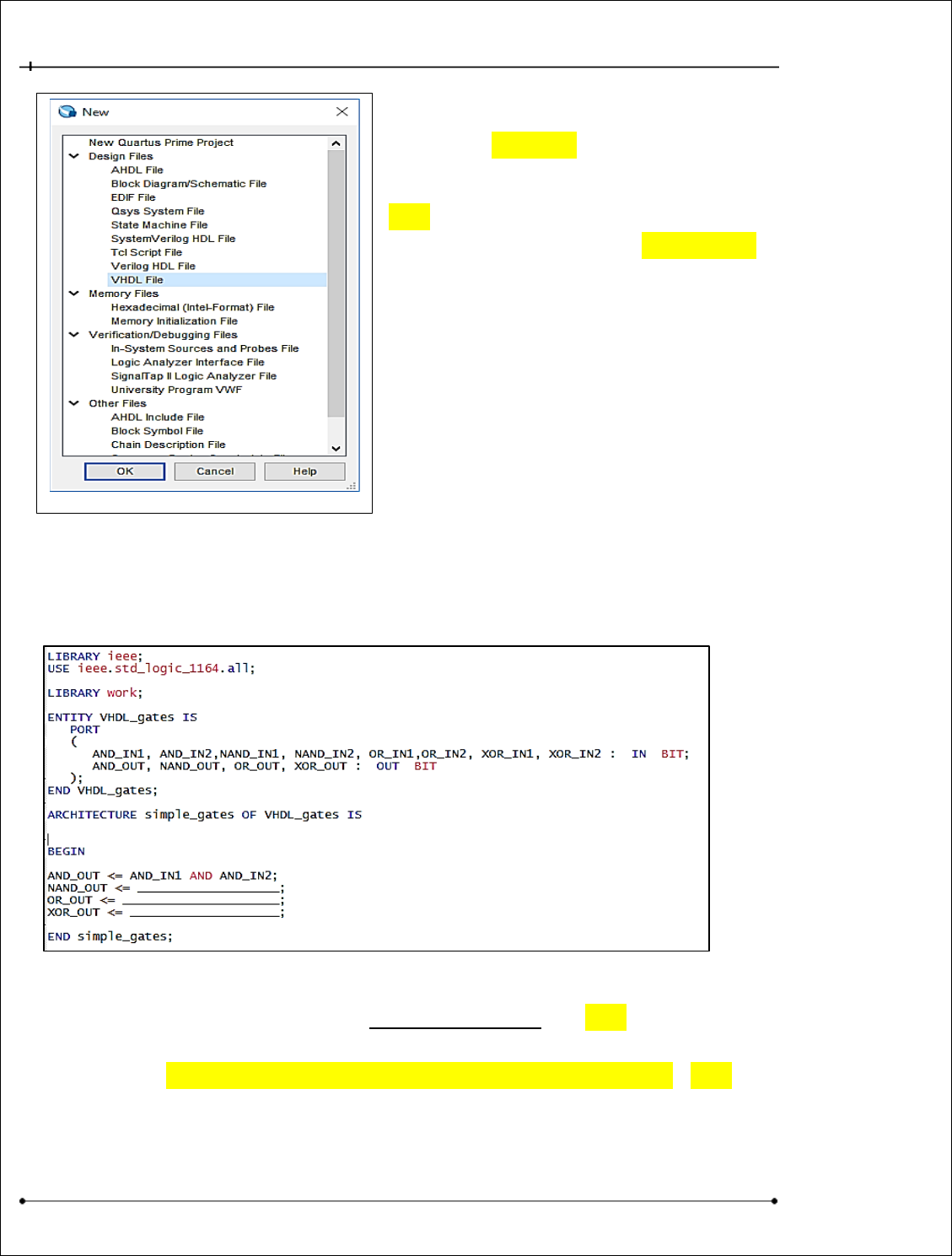
SELECT the VHDL File option. A blank VHDL window will then
open in Quartus.
Save this VHDL file as “VHDL_gates.vhd” by going to the
FILE Tab and SELECTING the File> Save As option.
This VHDL design file is to be an exact functional replica of
the schem_gates circuit that was done earlier (for easier
comparison during the demo) but entered with VHDL
coding.
You must enter the all of the VHDL code shown below in Figure 38 and then fill in the VHDL coding in
the ARCHITECTURE section for the remaining gate function types (same as “schematic_gates”).
Figure 38 Lab1: Initial VHDL_gates File
Save the VHDL file by browsing to your Lab1 project folder and Save the VHDL_gates.vhd file and just
leave the file active (current). Create a schematic block symbol for the VHDL_gates design.file. Do this
as before (using File>Create / Update>Create Symbol files for Current File). Save the VHDL_gates.bsf
symbol.
Figure 37 Lab1: Starting a VHDL Design Entry File
ECE-124 Lab Manual – W2018– V2.4 33
University of Waterloo
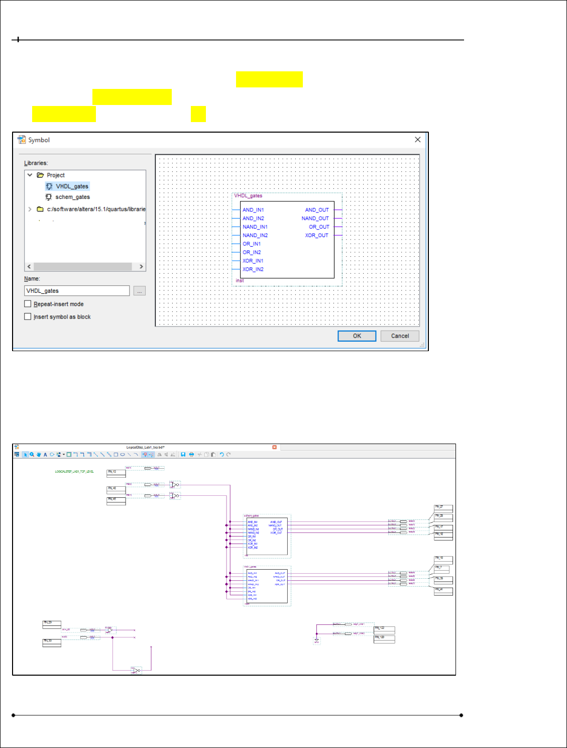
Go back to the top level schematic design to insert (“instantiate”) the new VHDL_gates symbol as in
Figure 39. Recall that to select the symbol RIGHT-CLICK anywhere on the top level schematic again
and SELECT the Insert>Symbol option. Browse to the Project folder in the Symbol Window and Select
the VHDL_gates symbol and Click OK.
Figure 39 Lab1: Selecting the VHDL_gates Symbol for Insertion
Connect the VHDL block input to the same input connections and connect the VHDL block outputs to
the other remaining LogicalStep board LEDs as shown in Figure 40 by using the ORTHOGONAL NODE
TOOL as before.
Figure 40 Lab1: Adding Connections to VHDL_gates
ECE-124 Lab Manual – W2018– V2.4 34
University of Waterloo
Save the design and run a FULL compile of the new FPGA design (Processing>Start Compilation).
Download the new FPGA design into the FPGA with the programmer and then test with the PB[1..0]
keys. Confirm that both the schematic and VHDL implementations work the same by observing the
patterns on the two sets of LED outputs.
3.3.6 Adding Some Automation
As a next step to the LogicalStep_Lab1_top design add an LPM_counter from the library in
(altera/quartus/megafunctions/arithmetic/lpm_counter). The counter will use the clkin_50 input pin
signal to increment. The clock on the LogicalStep board runs at 50 MHz. The counter is being added to
automate the operation of the PB keys and to slow down the logic activity of the schem_gates and
VHDL gates blocks so that you can actually see them switching. The parameters for the counter can be
observed in the diagram below in Figure 41.
Double-Click the LPM_Parameter block and modify its properties.
LPM_MODULUS: 260000000
LPM_DIRECTION: “UP” (include quotes)
LPM_WIDTH: 28
LPM_PORT_UPDOWN: “PORT_UNUSED” (include quotes)
Connect the LPM_Counter clock input (pin with a “I>” on the left side of the symbol) to the GLOBAL
buffer that is used by the CLKIN_50 input pin using the Orthogonal Node Tool as before.
Figure 41 Lab1: Adding Automation to LogicalStep_Lab1_top Design
ECE-124 Lab Manual – W2018– V2.4 35
University of Waterloo
Next connect the counter “cnt_en” inputs to the sw[0] input pin. Also make sure to connect the sw[0]
INVERTER to the counter “aclr” pin. These two connections will turn the counter on and off.
Disconnect the two PB inverter outputs from the schem_gates and VHDL_gates block inputs. Insert
and connect a single, two-input OR gate to each of those inverter outputs. Then connect the OR gate
outputs back to the wires connected to the schem_gates and VHDL_gates block inputs.
Using the Orthogonal
BUS tool (icon is
located beside the
Orthogonal NODE Tool)
connect a bus (a thick
wire) to the
LPM_Counter “q[]”
output (See Figure 42).
Draw it to up close to
the OR gates. Select
this bus and Right-click
to change its
properties. Label this
bus as COUNT[27..0].
Figure 42 Lab 1: Creating a 28 Bit Signal Bus for the Counter Output
Using the Orthogonal
NODE tool draw two
thin wires from the new
bus (COUNT[27..0]) to
the open OR gate inputs
as shown in Figure 43.
Select each of these thin
wires and change their
properties to label them
as COUNT[26] and
COUNT[27] as shown.
Why do you think we
connect to the two
highest COUNT bits from
the counter??
Figure 43 Lab1: Using Bits from the Counter Signal Bus
ECE-124 Lab Manual – W2018– V2.4 36
University of Waterloo
We will NOT be discussing the internal functionality of the counter during this lab. We will only be
using it as a “generic engine” to automate the PB inputs to the design.
Other schematic-based functions can be viewed in the library for your future reference.
So the way this automation should work is:
1) If sw[0] is OFF then the counter does not count and the PB inputs can be used as before.
2) If sw[0] is ON then the counter is enabled and the PB inputs are not required to be manually
operated.
Recompile the design (Processing>Start Compilation) and then download the load file (using
Tools>Programmer) into the FPGA and then confirm the automatic operation of the blocks on the
LogicalStep LEDs.
Again, the VHDL design driven LED’s should match the operation of the schematic design driven LEDs.
3.4 POST - Lab1 Activities
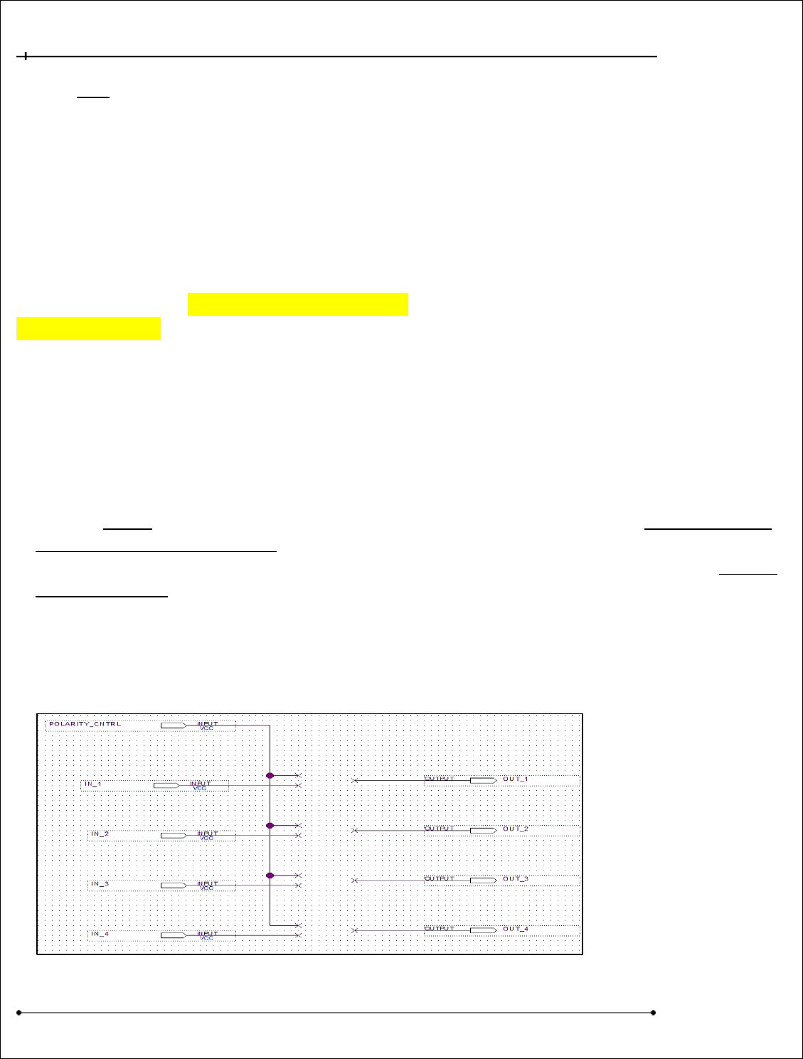
For your DEMO design in the next Lab session you must add another two blocks (one in schematic
form and one VHDL design form) that allows sw[1] to be used as an output polarity change
control on each of the output pins. Further, a new block function must be entered to use a single 2
pin gate per path. (One pin will be connected to the Polarity Control and the second pin will be
connected to the upstream schem_gates or VHDL_gates output).
Hint: Do the schematic one first and create the gate truth tables for various 2 input gates in the
library to determine what kind of 2 input gate to use. The connections are shown below in
Figure 44 but with the gates missing.
Figure 44 Lab1: Initial Schematic Version of Polarity Control
ECE-124 Lab Manual – W2018– V2.4 37
University of Waterloo
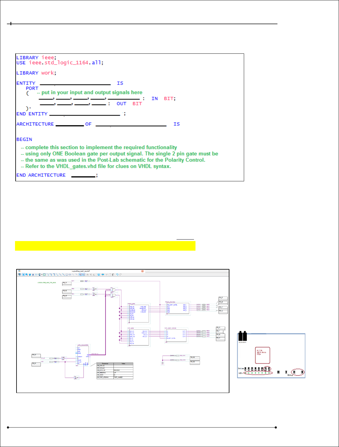
For the VHDL version you may use the following info below in Figure 45:
Figure 45 Lab1: Initial VHDL File of Polarity Control
For the VHDL version make sure that you save that file with the same name as the declared ENTITY
name used.
Create, save and add a schematic block symbol for EACH of your new blocks as before (using
File>Create / Update>Create Symbol files for Current File) and add it to the LogicalStep_Lab1_top
schematic with the required connections mentioned above.
Your final schematic design
will look something like the
following in Figure 46.
Figure 46 Lab1: Demo Design

ECE-124 Lab Manual – W2018– V2.4 38
University of Waterloo
Complete the work for the Lab1 Demo design (ie: get it compiled and tested on the LogicalStep
board) since it will be required at the next lab session in Lab 2. Make sure everything is saved to
project folder (“Lab1”) on your N:drive. Select the FILE>Close Project option.
There will be no typical report for this lab but you will need to answer some basic Lab1 related
questions listed on the Lab1 Submission form during the time of your Lab1 DEMO.
NEXT LAB SESSION: We will get into more challenging logic designing where we learn and build
functions that are used in simple computers today.
ECE-124 Lab Manual – W2018– V2.4 39
University of Waterloo
3.5 LAB1 SUBMISSION FORM
Table 1 - Lab1: Submission Form
ECE-124 Lab-1 Submission Form – Winter 2018
GROUP NUMBER:
Lab1
Demo
Lab1
Quiz
SESSION NUMBER:
Out of 5
Out of 5
I am submitting this report for grading. I certify that this report, including any code, descriptions,
flowcharts as part of the submission were written by the team member(s) below and there has not been
any use of prior academic credit at this university or any other institution. The penalty for plagiarism or
submission without signature(s) will be a grade of zero
NAME: (Print)
UW User ID
(not Student ID)
Signature
Partner A:
Partner B:
LAB1 DESIGN DEMO
Marks Allotted
A
B
With BOTH sw[0], sw[1] OFF and using PB[1..0]
verify AND, NAND, OR, XOR of schem/VHDL gates driven LEDs
1
Verify with sw[1] ON, sw[0] OFF that the LED’s invert when using
the previous step of AND, NAND, OR, XOR
1
With sw[1] OFF and sw[0] ON verify the LED SEQUENCE on
LEDS[3..0] together with LED’s[7..4]: 0010, 1110, 1110, 0101
2
With sw[1] ON and sw[0] ON verify the LED SEQUENCE on
LEDS[3..0] together with LED’s[7..4]: 1101, 0001, 0001, 1010
1
LAB1 DEMO MARK
Out of 5
LAB1 QUIZ
Marks Allotted
A
B
Why were inverters added after the PB[1..0] inputs?
1
Name one typical development process used in an FPGA design.
1
What are the two main components of a VHDL design file?
1
What style of coding was used in the Lab1 VHDL
Architecture section?
1
For your Polarity Control block what kind of gate was used?
1
LAB1 QUIZ MARK
TOTAL
out of 5

ECE-124 Lab Manual – W2018– V2.4 40
University of Waterloo
4 Lab 2 – VHDL - Combinational Circuits PART 1 – Simple ALU Design
The main goal of this lab session is to continue gaining lab experience with using VHDL for
combinational logic design. Some new VHDL components will be introduced along with their
associated data format requirements. There will be some logic errors “planted” into a part of the
provided logic (Seven Segment decoder) that must be discovered during simulations and must be
corrected to meet the Lab2 project requirements. The final design must be demonstrated during the
next Lab Session. A report must be submitted on LEARN within 24 hours after the Lab2 DEMO is
shown.
4.1 Prelab
1. Review the Lab1 processes used for entering, testing and implementing FPGA designs.
2. Review the Lab1 Submission form from LEARN for the Lab2 session.
3. Be ready to have your Lab1 Demo design available for demonstration.
4.2 Lab2 Outline
Attendance will be taken.
The lab starts with a brief review of design entry methods used in Lab1 and some VHDL topics are also
covered. Then the following new topics will be presented:
1 Review of Lab1
2 Recalling Some Constructs of a VHDL Design
3 Design Re-use in VHDL – Structural coding style
4 Project Setup for Lab2
5 New VHDL Component - What is a Hex to Seven Segment Decoder?
6 Lab2 Part A. – Hunting for “Bugs”.
7 New VHDL Component - What is a Multiplexer or MUX function?
8 Lab2 Part B. – Using the Seven Segment Displays
9 Lab2-Part C- Project Brief for Lab2 Demo

ECE-124 Lab Manual – W2018– V2.4 41
University of Waterloo
4.3 Lab2 Activities
4.3.1 Recall from Lab1:
Last time in the lab some basic gate functionality was entered into the FPGA. We briefly explored
some of the tools and utilities available within the Quartus FPGA development environment. The top
level design was schematic based. A subordinate block in schematic form was developed to be added
in the hierarchy. Later the design was “synthesized” into a logical gates representation so that
functional simulations could be completed. A functional simulation STIMULUS was created and saved
to drive the synthesized gate design for simulation. The simulation was run and the results were
compared against the truth tables of the gates implemented.
Having completed a functional verification of the schematic design entry with simulation, a full design
COMPILATION was run so that a download file could be created for loading into the LogicalStep board
FPGA. It was confirmed that by observing the LED patterns that the schematic entry design worked in
actual hardware.
A VHDL design functionally equivalent to the schematic version was created and then added to the
top level of the FPGA design. The larger FPGA design was compiled and downloaded to the FPGA on
the LogicalStep board. It was then confirmed by observing the LED patterns that the VHDL design
section behaved identically to the schematic design version.
Later a type of hardware-bases automation was added to the design so that manual exercising of the
hardware inputs was not required. As a final design step, and to be shown as a DEMO, some output
polarity control was added (one in schematic form, one in VHDL form) so that the output operation
could be run in two different modes based on an external Push-Button Key input.
4.3.2 Recalling Some Constructs of a VHDL Design
The VHDL language uses two main structures to describe a design unit (hardware block):
1 Entity: declares the design unit name and the ports
2 Architecture: implements the actual functionality of the entity.
There are two coding styles used in the VHDL Architecture section:
a) Behavioral: where the relation between input and output is declared using logical equations.
b) Structural: where you can use previously created entities in your design unit as components.
ECE-124 Lab Manual – W2018– V2.4 42
University of Waterloo
4.3.3 Design Re-use of VHDL – Structural Coding Style
Lab1 was very simple in scope and it just used the Behavioral style of VHDL coding. Lab2 will also be
using the second style (Structural). To re-use VHDL units that were created beforehand we use the
Structural style to include those VHDL files in a VHDL design file that is higher in the design hierarchy.
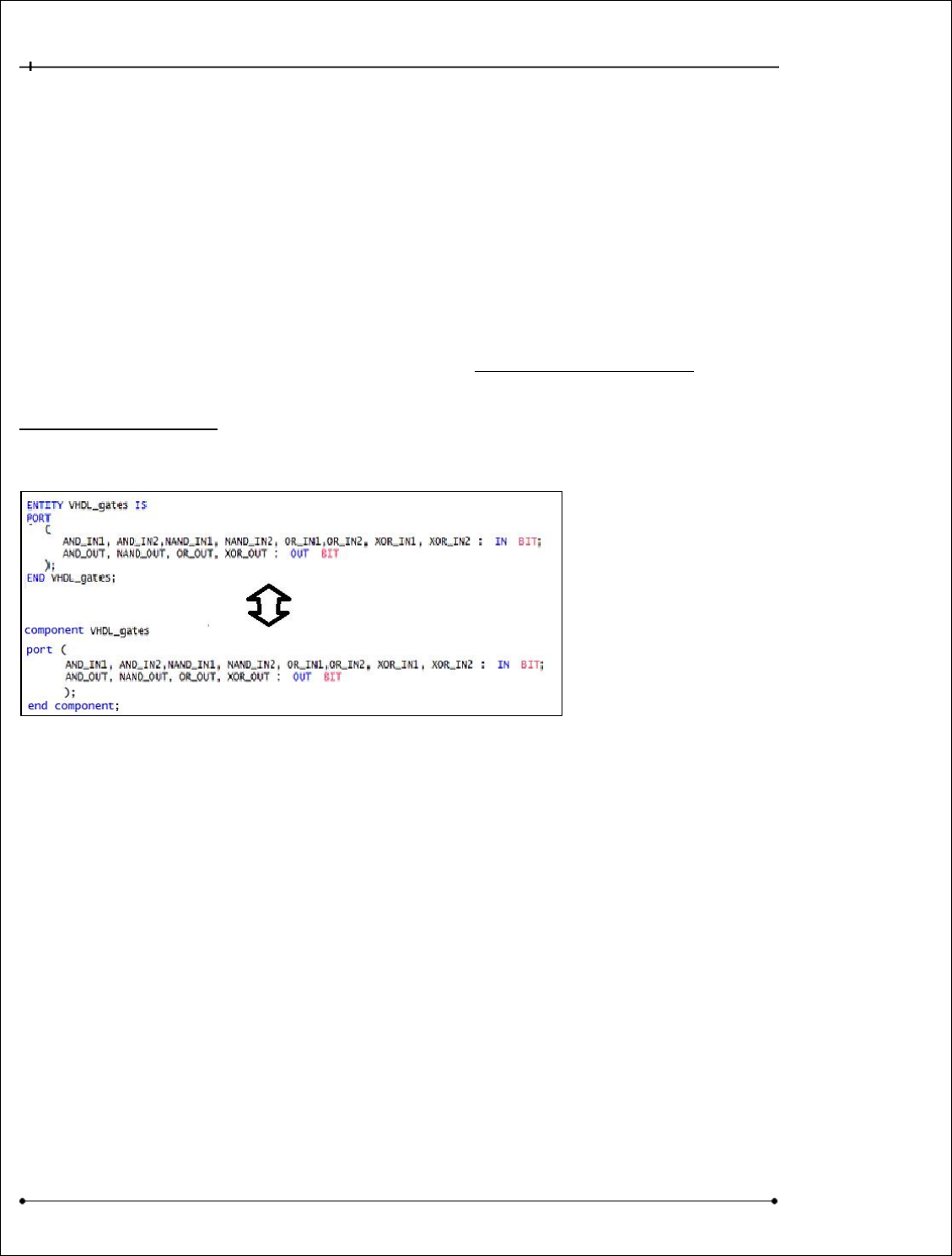
First we have to explain a construct called the Component construct. It looks very much like an Entity
construct (see Figure 47). See some example Entity syntax below for a VHDL file called VHDL_gates
and a companion Component Declaration in another file that could use the VHDL_gates file. They are
very close in syntax. One thing to remember in the Component declarations is that the port names
must match those defined in the Entity declarations of the VHDL file being used. The nets to the
Component instances may require unique names.
Figure 47 Lab2: Component Structure are Similar to Entity Structures
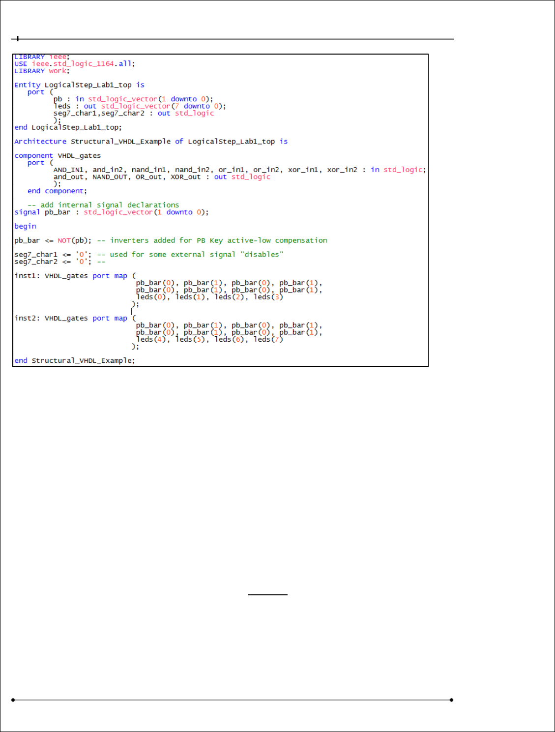
After a Component is declared inside a new VHDL architecture there is still the signal hook-up to its
interfaces to be done. For example if we were to do the LogicalStep_Lab1_top as a purely VHDL file it
could use the previously designed VHDL_gates file as a component. New signal declarations would be
required for the internal VHDL component linking.
The LogicalStep_Lab1_top could look something like that shown in Figure 48 with the Component
INSTANCES added in the bottom section:
Note the “signal” declaration for the pb_bar internal signals.
ECE-124 Lab Manual – W2018– V2.4 43
University of Waterloo
This can be used as a reference for the component instantiation exercises later in this lab session.
The signal hook-up is in the bottom section (between the “begin and end” statements). Notice how
two signals pb_bar(0), pb_bar(1) were added to do the PB key active-low compensation via adding the
inverter function (NOT).
4.3.4 Project Setup for Lab2
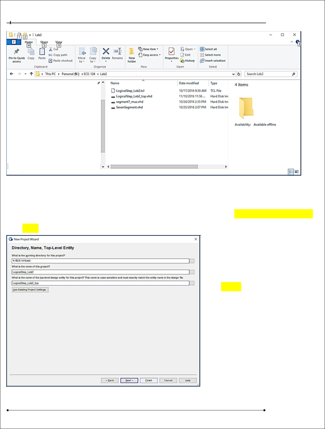
Start the LAB2 like what was done in Lab1 by creating a new project folder on your N: drive. Using the
Windows File Explorer go to your ECE-124 folder directory. Go to LEARN and download the Lab2
Zipped folder “Lab2” into the ECE-124 folder. Extract the contents to create the new Lab2 project
folder. The new files are shown below in Figure 49.
Figure 48 Lab2: VHDL Example of Using Components for LogicalStep_Lab1_top Design
ECE-124 Lab Manual – W2018– V2.4 44
University of Waterloo
Figure 49 Lab2: Project Folder after Setup
Start up the Altera Quartus Prime platform and begin a new project (Using FILE>New Project Wizard).
Click NEXT to go to the second slide.
The project parameters will now be
entered.
Project Folder: N:/ECE-124/Lab2
Project Name: LogicalStep_Lab2
Project Top Level: LogicalStep_Lab2_top
Click FINISH on the New Project
Wizard Dialog Window.
(see Figure 50)
Figure 50 Lab2: FPGA Project Setup
ECE-124 Lab Manual – W2018– V2.4 45
University of Waterloo
Next, in Quartus, the Lab2 TCL script must be run to assign the FPGA device type, the FPGA pin
assignments for the FPGA that are reserved for the LogicalStep FPGA and finally the project
LogicalStep_Lab2 is created and opened.
Go to the Tools tab and SELECT the Tcl Scripts option. The dialog box in Figure 51 should appear:
Figure 51 Lab2: TCL Script Invocation
SELECT the TCL file “LogicalStep_Lab2.tcl” and then click on the RUN button as in Figure 51.
The following in Figure 52 should appear when it is finished.
Figure 52 Lab2: TCL File Completed
Click the OK Button and close the TCL Scripts window.
ECE-124 Lab Manual – W2018– V2.4 46
University of Waterloo
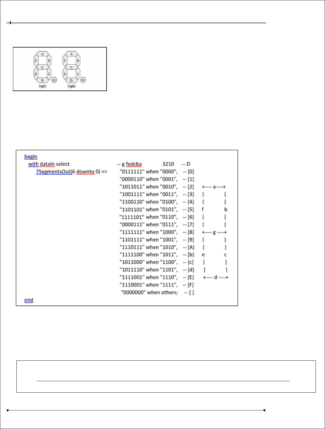
4.3.5 NEW VHDL Component - What is a Seven Segment Decoder?
For the LogicalStep board there are two seven segment displays
available. See Figure 53.
To drive each display with logic we typically use a hex to seven-segment decoder. Hex input values (4
bits) are used to represent hex variable values and the decoder converts the 4-bit hex values (the
3210 columns), to a pattern of 7 bits to drive the seven segments.
An example of this function is shown in Figure 54 below in VHDL format.
Figure 54 Lab2: VHDL file Seven Segment Decoder
Question: For the above example how big of a task do you feel it would be to enter the function
above with just schematic gates??
TAKE-AWAY:
➔A Hardware Description Language (HDL) can be much more efficient in design entry
exercises than the schematic design entry method.
Figure 53 Lab2: LogicalStep Board Seven Segment Displays
ECE-124 Lab Manual – W2018– V2.4 47
University of Waterloo
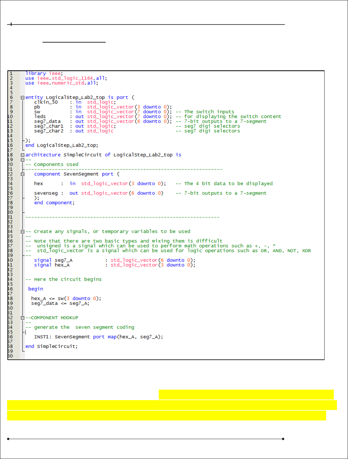
Earlier the top level design file (LogicalStep_Lab2_top.vhd) was downloaded from LEARN into the
Lab2 project folder. This time the top level design file is a VHDL file. Notice in the screen-shot below in
Figure 55 that the pins are declared in the Entity section.
Figure 55 Lab2: Initial VHDL Design of LogicalStep_Lab2_top
In the above example the component for the SevenSegment decoder is already declared for you as
well as two signal busses (hex_A and Seg7_A). Observe (between the “begin” and “end” statements)
how the busses (signal groupings) are connected and how the instantiation of the component is done
in the example above. YOU must add the above VHDL code to your LogicalStep_Lab2_top.vhd file.
ECE-124 Lab Manual – W2018– V2.4 48
University of Waterloo
4.3.6 Lab2-Part A – Hunting for “BUGS”
In the Architecture section instantiate a SevenSegment instance and call it INST1. Then connect the
four switch inputs (sw[3..0] ) to the SevenSegment instance INST1 hex inputs and connect the
seg7_data pins to the SevenSegment instance outputs. Refer to Figure 48 in the “Design Re-use within
VHDL” section in the Lab Manual as an example. Next run an ANALYSIS and SYNTHESIZE compilation
process to allow a functional simulation to be executed. This can be done by going to the Processing
TAB and then selecting “Processing>Start>Analysis and Synthesis” option.
WE WILL NOT BE DOWNLOADING THIS DESIGN DUE TO PIN PROPERTY CONSTRAINTS (pin drive
settings) AT THIS STAGE OF THE LAB.
For this Lab there are “logic errors planted” into a part of the provided SevenSegment.vhd file that
must be discovered during functional simulations and must be corrected to meet the Lab2 project
requirements later. There are three bugs in the SevenSegment.vhd table file.
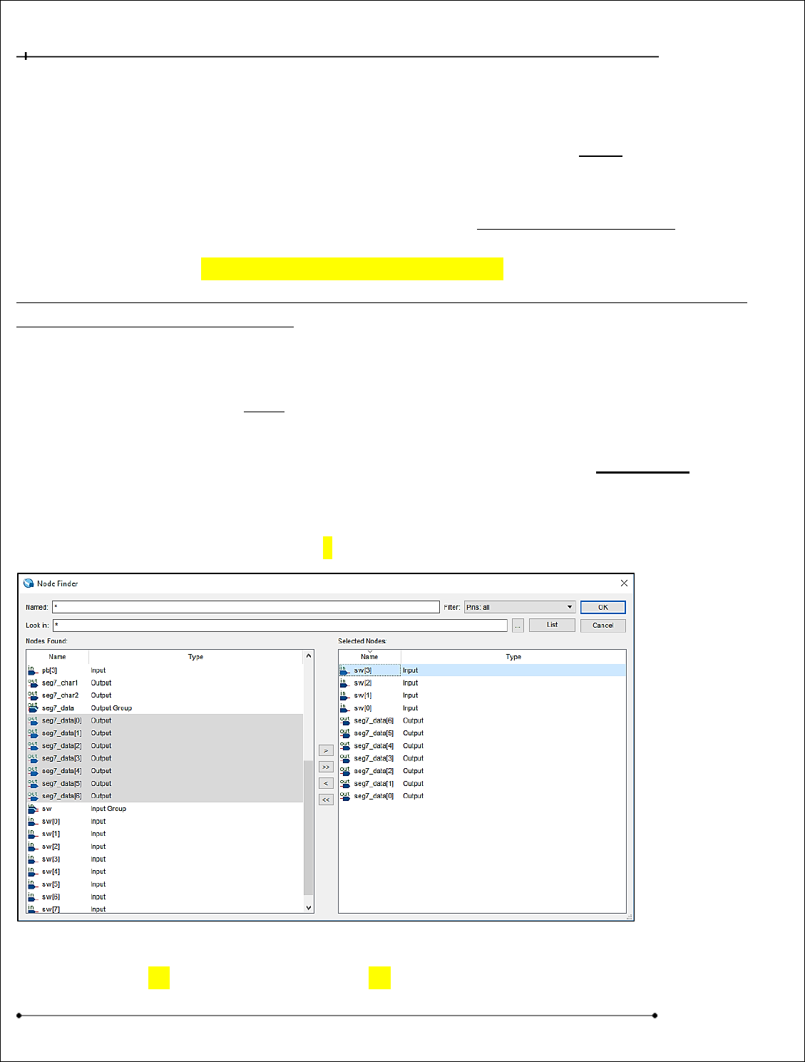
Recall from Lab1 how functional Simulations are set up within Quartus (see section 2.3.2 and Figures
22 to 26). In the Node Finder window in Figure 56 SELECT the following pins in the order specified:
sw[3], sw[2], sw[1], sw[0], seg7_data[6], seg7_data[5], seg7_data[4], seg7_data[3], seg7_data[2],
seg7_data[1], seg7_data[0]
After selection of the group click on the ‘>’ button to copy them to the Selected Nodes window.
Figure 56 Lab2: Adding Nodes for Functional Simulation
Then click on the OK button. Then Click on the OK button on the Node Finder Dialog Box.
ECE-124 Lab Manual – W2018– V2.4 49
University of Waterloo
Within the simulation Window one can
group the individual nodes into “groups”
or “buses”. This can often save
interpretation time of the simulation
results. Start with the sw[3..0] nodes.
SELECT the nodes in the following order
with the Control Key continually pressed:
sw[3], sw[2], sw[1], sw[0].
With all of these signals highlighted
RIGHT-CLICK over the names column and
some options appear.
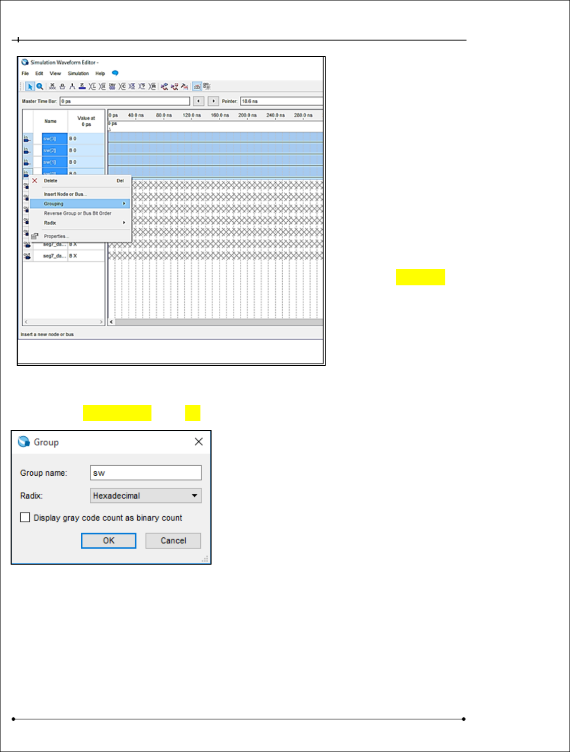
SELECT the Grouping option as in Figure
57.
A new window will appear for the group of nodes as shown in Figure 58. Leave the name “sw” but set
the RADIX to Hexadecimal. Click OK.
Figure 57 Lab2: Grouping Nodes for Hexadecimal format
Figure 58 Lab2: Setting the Group Radix
ECE-124 Lab Manual – W2018– V2.4 50
University of Waterloo
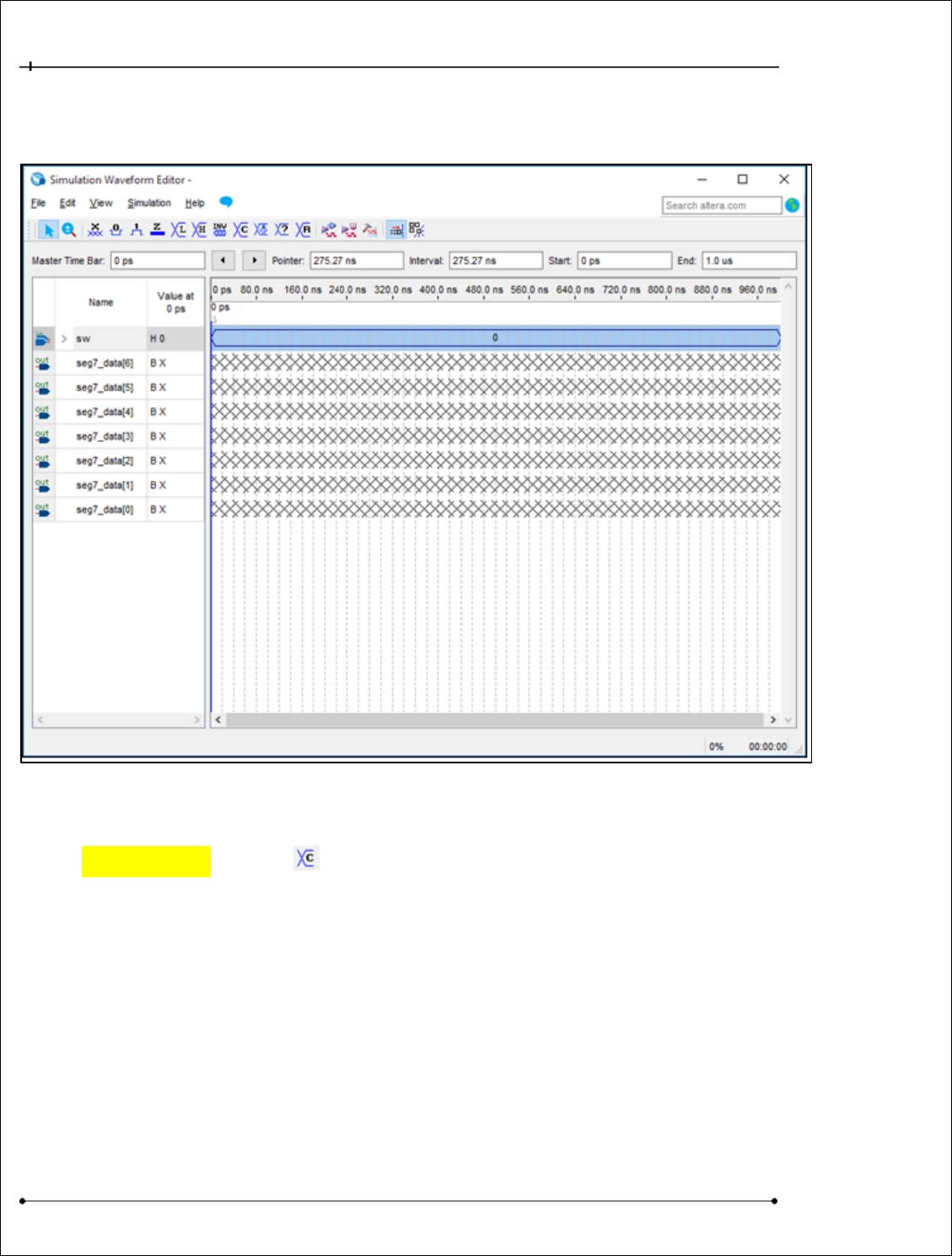
Below in Figure 59 one can now see that the representation of the four sw nodes is replaced with a
single BUS group called sw and its data is represented in Hexadecimal format.
Figure 59 Lab2: Group Hex Value Shown in Simulator
Now we must add some STIMULUS to represent counting in hex. With the sw bus still selected Click
on the COUNT VALUE button ( ). A window like that shown in Figure 60 will appear. Set the
counting to increment by 1 every 50 nsec.
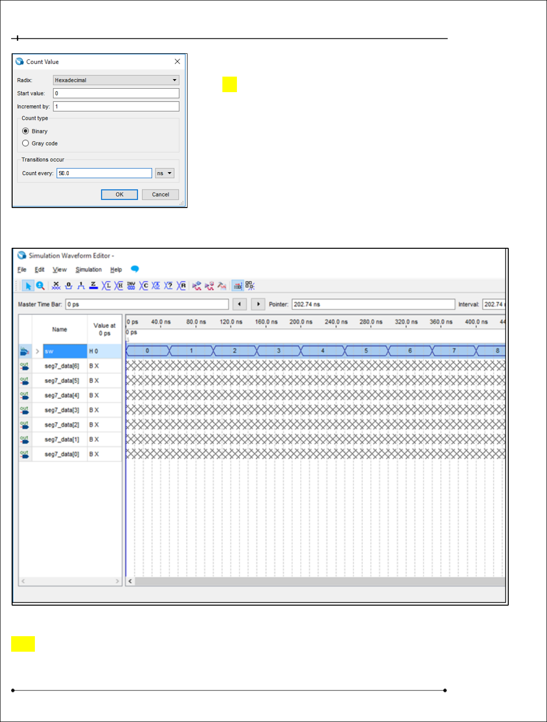
ECE-124 Lab Manual – W2018– V2.4 51
University of Waterloo
Click OK.
Now you should see the stimulus like the screen-shot below Figure 61:
Figure 61 Lab2: Counting Input Stimulus
Save the file as waveform.vwf.
Figure 60 Lab2: Stimulus Counting Increment Setup
ECE-124 Lab Manual – W2018– V2.4 52
University of Waterloo
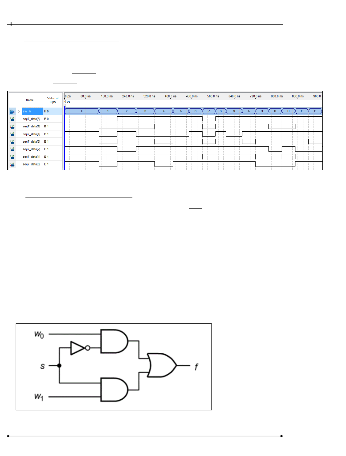
Now run the Functional simulation with the incrementing HEX values (0 – F) of the sw bus. Refer to
the reference simulation in Figure 62. Notice that for each HEX value in Figure 62 that there is a set of
column segment bit values. Compare your simulation results with those in Figure 62. Take note of any
mismatched sets of column segment values per HEX input value in your simulation as compared to
the reference column waveforms shown in Figure 62.
Figure 62 Lab2: Seven Segment Decoder Reference Operation
After noting the simulation differences for the HEX values open the SevenSegment.vhd file (inside
Lab2 project directory) to correct the appropriate set of row segment values. The seg7_data[0] bits
are in the segment “A”, seg7_data[1 ]bits are in the segment “B”, etc. Make the changes and then
save the file in the Lab2 project folder. Then re-synthesize the design and then run the simulation
again to confirm the correct functionality as in Figure 62
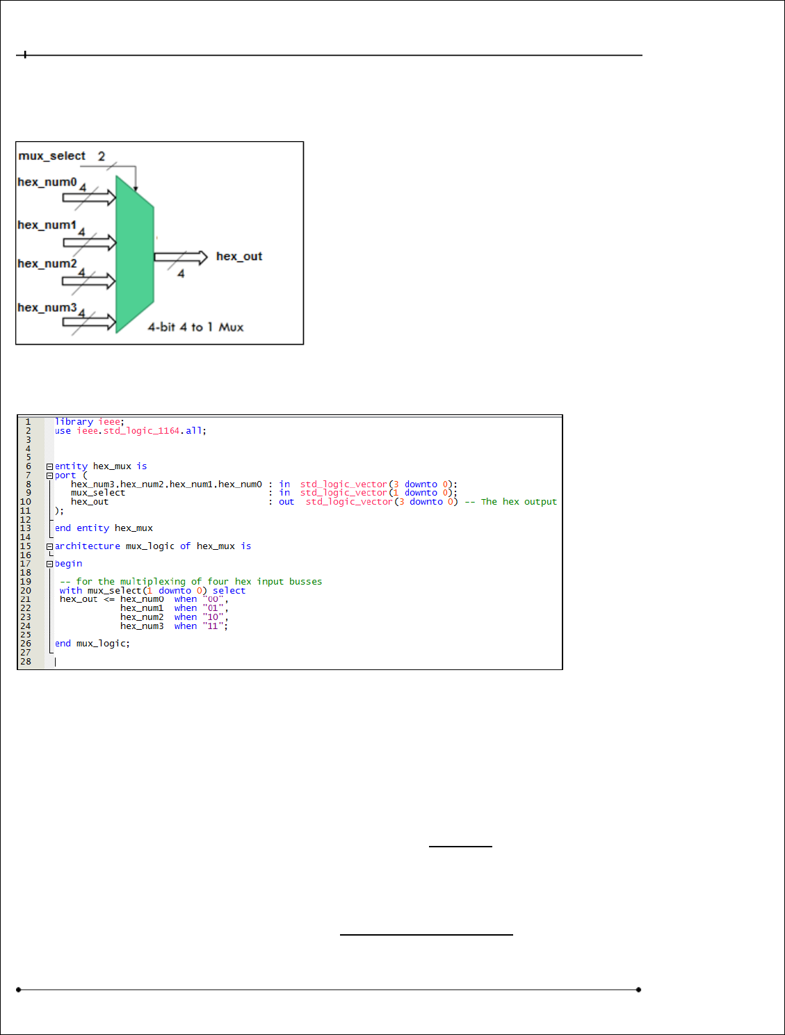
4.3.7 NEW VHDL Component - What is a Multiplexer or MUX function?
Multiplexers are usually used to select different data sources of input to a downstream
function input or process. The selection is controlled by the state of the SELECT control inputs
(see Figure 63).
Multiplexers can be found in a number of input/output ratios (e.g.: 2 to1, 4 to 1, 8 to 1 …)
Figure 63 is a simple 2 to 1
multiplexer or MUX function. Its
output function “f” will pass along
the w0 input value when the
“select” control input “s” is in a
LOW state (or a “0”). But when “s”
is in the HIGH state (or a “1”) the
output function “f” will pass along
the value from the w1 input.
Figure 63 Lab2: VHDL 2 to 1 Multiplexer
ECE-124 Lab Manual – W2018– V2.4 53
University of Waterloo
A graphical representation example of a QUAD-bit 4 to 1 multiplexer is shown below for your
reference in Figure 64. A VHDL companion is shown in Figure 65. All busses are 4 bits wide.
Figure 64 Lab2: Quad Port 4 bit Multiplexer
Figure 65 Lab2: VHDL Code for a Quad-Bit 4 to 1 Multiplexer
4.3.8 Lab2-Part B – Using the Seven Segment Displays
Earlier we debugged the SevenSegment design and we can now use it for new VHDL project
designs. There are two seven segment displays on the LogicalStep board so two SevenSegment
decoders will be required. So there must be a second instance of the SevenSegment decoder
added to the next version of the LogicalStep_Lab2_top design.
Disconnect the SevenSegment decoder outputs (INST1) from the seg7_data pins that were used in
Part A. This can be done by removing the “seg7_data <= seg7_A” line from the
LogicalStep_Lab2_top file (added in Part A).
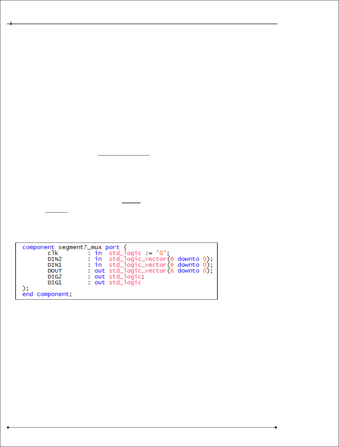
ECE-124 Lab Manual – W2018– V2.4 54
University of Waterloo
Add a second instance of the SevenSegment decoder component and name it as INST2.
For example:
INST2: SevenSegment port map (……);
Now connect the sw[7..4] switch inputs to a new signal bus called hex_B. This signal bus will have
the same width as the hex_A signal bus (4 bits) when declared. Connect the other end of the
hex_B bus to the INST2 SevenSegment decoder set of inputs. The output port of INST2 will connect
to a new signal bus to be declared called seg7_B. This new bus will have the same width as the
seg7_A bus.
The LogicalStep FPGA has just enough pins to access the external peripherals. The FPGA
pin-out has a common external seven-segment bus driving the Digit1 and Digit2 displays. Please
refer again to Figure 53 described earlier for the orientation of Digit1 and Digit2 on the board.
So your FPGA design will need to add a provided seven segment multiplexer function.
A unique (14 input to 7 output) MUX will be added to our design for this purpose on the
LogicalStep board. It’s like having seven 2-to-1 muxes in parallel with a common SELECT input.
This mux cannot be used for other purposes in the FPGA for the LogicalStep board.
Add the VHDL function segment7_mux as a component declaration (Figure 66) to the
LogicalStep_Lab2_top design.
Figure 66 Lab2: VHDL Component Declaration for seg7_mux
Also instantiate the segment7_mux function instance as INST3. For example:
INST3: segment7_mux port map (……);
The internal signal buses (hex_A, hex_B) are connected to the INST1 and INST2 inputs mentioned
earlier. The INST1 and INST2 outputs (seg7_A, seg7_B) must be connected to the INST3 inputs (for
DIN2, DIN1 resp.).There are three other signals to connect to INST3. These are the clk input to the
clkin_50 input pin; the output to the seg7_char1 output pin and the output to the seg7_char2
output pin. These signals are generated internally in the segment7_mux block.
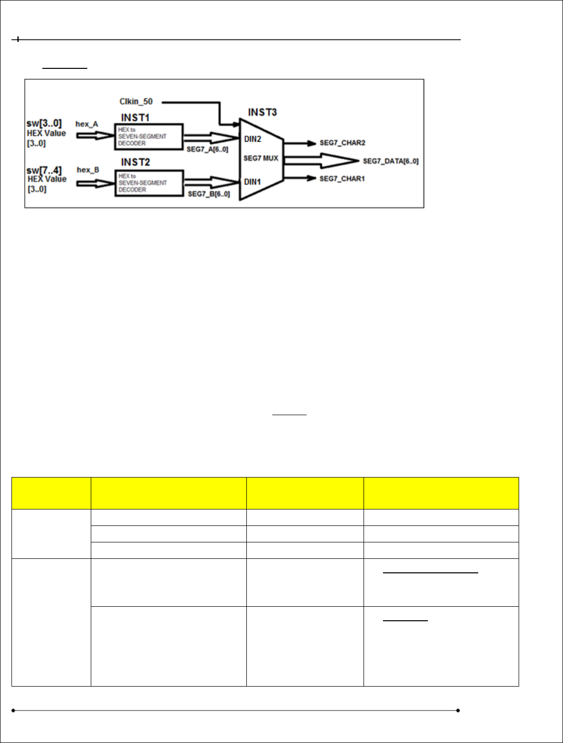
ECE-124 Lab Manual – W2018– V2.4 55
University of Waterloo
An example block diagram for these instance interconnects is shown below in Figure 67:
Figure 67 Lab2: Some Components Used in Lab2 Part B
With the clock input the “mux selector” is generated internally in the block and it is automatically
alternating the selection for the two SevenSegment data input buses. The two outputs (seg7_char1
and seg7_char 2) are sent to the external display to direct the mux output to the appropriate seven
segment display on the LogicalStep board.
Compile the design and download it to the FPGA. The Dual seven-Segment display should follow
the two sets of HEX inputs from the switches.
4.3.9 Lab2-Part C- Project Brief for Lab2 Demo
The next part of the lab will be used to develop a simple ALU with the LogicalStep_Lab2_top design.
An ALU is an Arithmetic Logic Unit which is a fundamental part of computer technology used today.
An ALU is typically enabled by a CPU after an instruction is decoded and the operands are gathered.
The functional requirements for this ALU are described in the following:
SIGNAL
TYPE:
SIGNAL NAME:
ASSIGNED
PORT(s):
Comment
INPUTS
Operand1[3..0]
SW[3..0]
hex_A could be used
Operand2[3..0]
SW[7..4]
hex_B could be used
OPERATOR[3..0]
PB[3..0]
OUTPUTS
LOGICAL RESULT[3..0]
LEDS[3..0],
LEDS[7..4]
Logical operations of
OP1,OP2 on LEDS[3..0],
LEDS[7..4] are off
ARITHMETIC
RESULT[6..0]
SEVENSEG[6..0].
LEDS[7..0]
Addition of OP1, OP2
shown in HEX on Seven
Segment Digit1&Digit2
and in BINARY on the
LEDS[7..0]
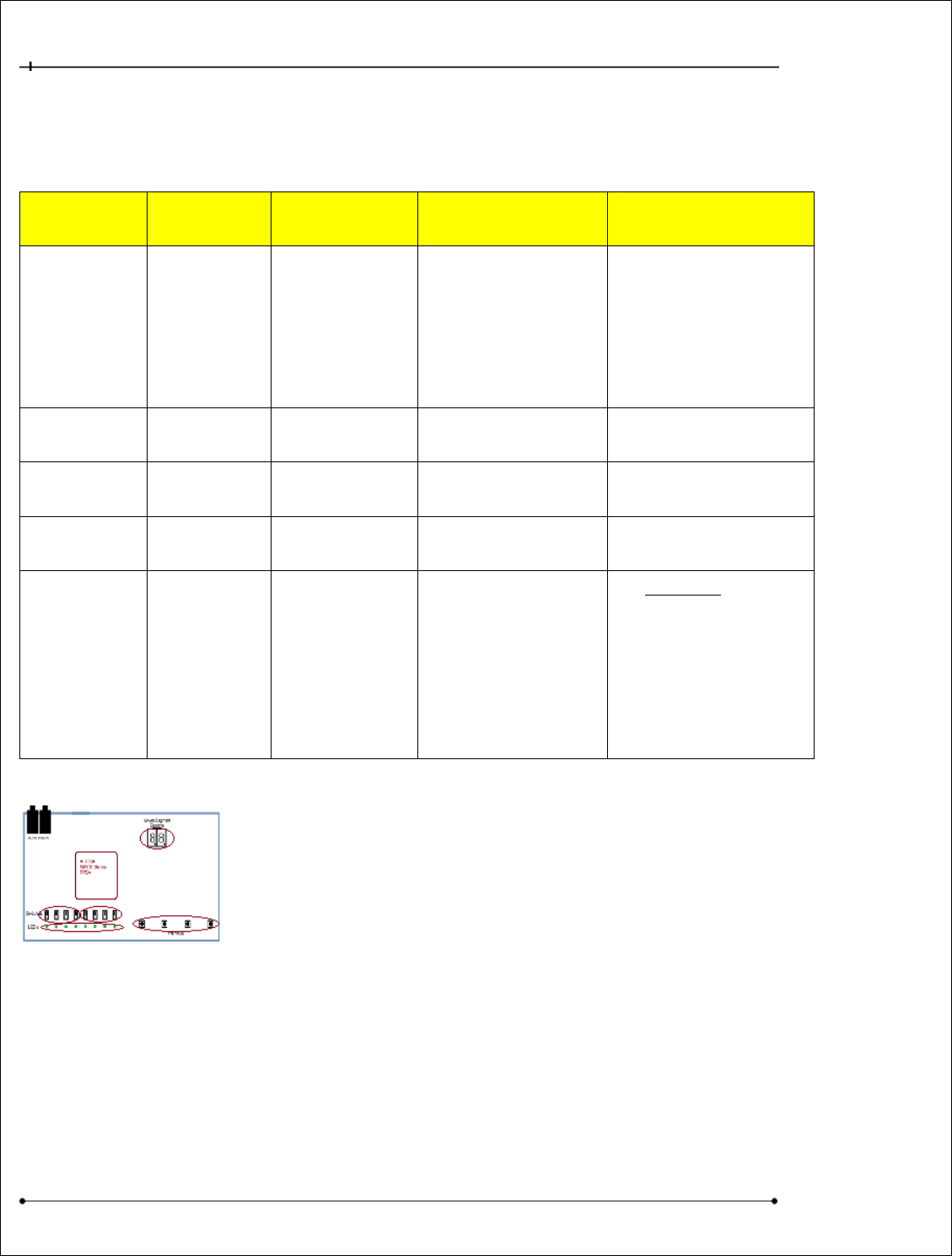
ECE-124 Lab Manual – W2018– V2.4 56
University of Waterloo
The functions are to be directed by the four PB Keys (perhaps use them as mux select lines).
Remember that the PB keys are Active-low so you should either add inverters or modify your VHDL
code to suit.
PB[3..0]
Pins
Inverted
PB[3..0]
OPERATOR
DESCRIPTION
DISPLAY
1111
0000
none
Operands
displayed
On seven-
segment digits
Operand1 on
seg7 display
DIGIT2,
Operand2 on
seg7 display
DIGIT1
1110
0001
AND
Logical AND of
operands
Result on
LEDs[3..0]
1101
0010
OR
Logical OR of
operands
Result on
LEDs[3..0]
1011
0100
XOR
Logical XOR of
operands
Result on
LEDs[3..0]
0111
1000
ADD
Binary ADD of
operands
Addition of OP1,
OP2 shown on
Dual Seven
Segment display
in HEX and in
BINARY on the
LEDS[7..0]
Consider the following guidelines in your design.
1. Break the overall design into sections.
Section 1: The hex to SevenSegment decoder and seg7_mux components from Lab2 part B
may be used. But the SevenSegment Decoders will have different input signals. The 4 bit
inputs will come from two halves of an eight-bit multiplexer output as shown in Figure 68.
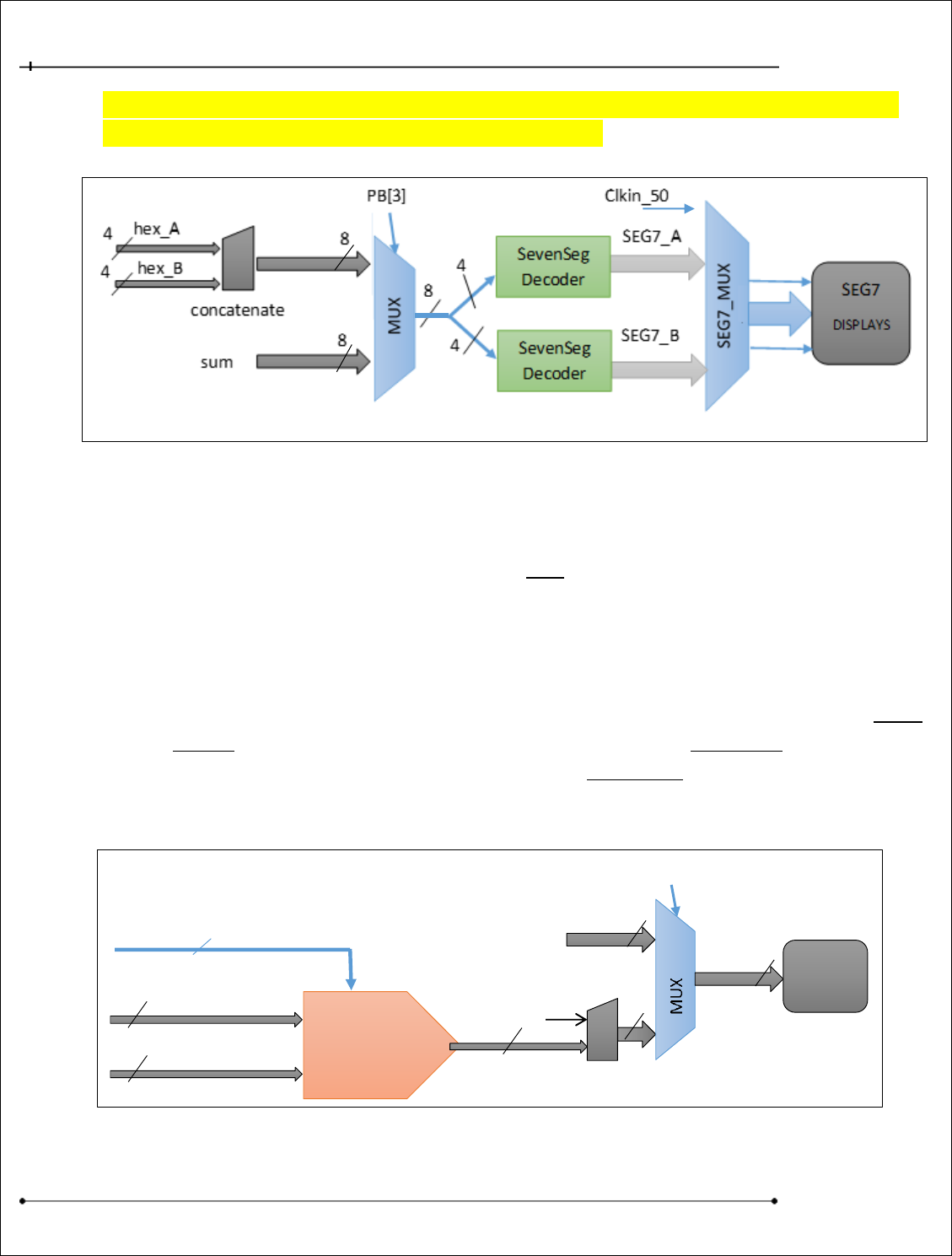
ECE-124 Lab Manual – W2018– V2.4 57
University of Waterloo
Figure 68 Lab2: Part C (Project) Multiplexing for Seven Segment Displays
This output will be multiplexed between the 8 bit SUM (when PB(3) is active) and the two
operands (e.g.: hex_A, hex_B) when PB(3) is NOT active.
When PB(3) is in the OFF state the two operands should be displayed on the two Seven
Segment displays. However when PB(3) is activated then both of the Seven Segment
displays must be used to display the arithmetic sum. Add “signal” declarations as required
for any intermediate connections between VHDL instances. To build a multiplexer you can
use the reference example like that shown in Figure 65 but modified to suit your
connections.
2. Section 2: The ALU logical results (Figure 69) should be displayed on the leds[3..0] but ONLY
when a logical operation is selected from the table above (not for arithmetic). When the
ADDITION mode is selected (related to pb(3)) the leds must show the ARITHMETIC result.
Since the arithmetic result could be bigger than a 4 bit hex value the arithmetic result
should be displayed on leds[7..0] when the ADDITION mode is requested.
sum (std_logic_vector[7 downto 0] )
4
hex_A
4
hex_B
LOGIC
PROCESSOR
4
Logic_func[3 downto 0]
“0000”
8
concatenate
8
8
LEDs
PB[2..0]
PB[3]
Figure 69 Lab2: Part C (Project) Logic Processor and Multiplexing for LED’s
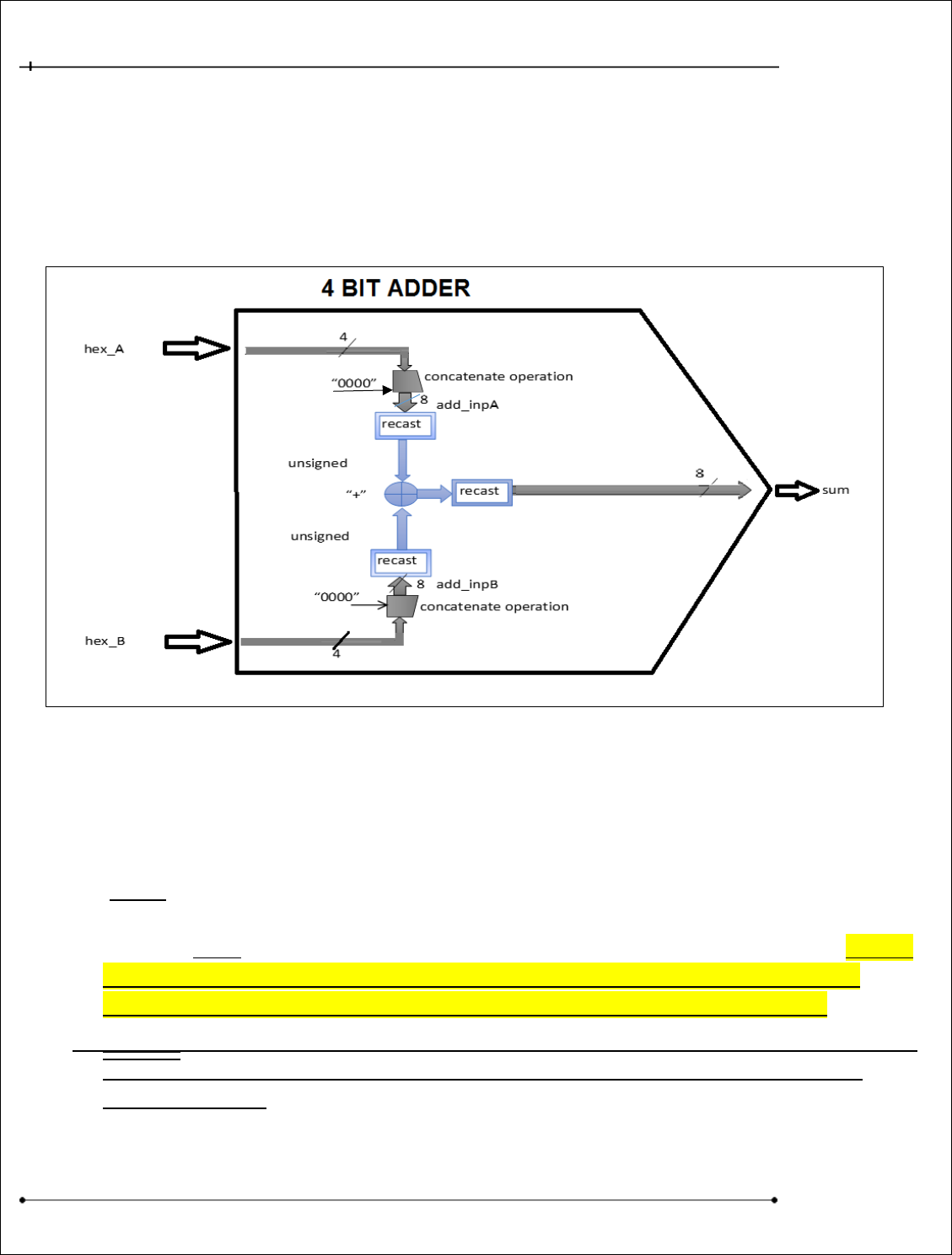
ECE-124 Lab Manual – W2018– V2.4 58
University of Waterloo
3. Section 3: The hardest part to understand for Lab2 Part C will perhaps be the recasting of
the data types of the signals. The logic signals must use the std_logic_vector[..] data type
but they must be recast into the unsigned data type (like an Integer) before they can be
used in any arithmetic operation. When the Arithmetic result is computed the unsigned
variable may be recast back to the std_logic_vector[..] for display on the LEDs or sent to the
SevenSegment decoders etc. See Figure 70.
You may use a VHDL statement like the form below to do the whole add function and signal
recasting (in light blue in Figure 70):
sum (7 downto 0)<= std_logic_vector(unsigned(add_inpA) + unsigned(add_inpB));
(where: sum is declared of type std_logic_vector[7 ..0], add_inpA, add_inpB are ALL
declared to be of type std_logic_vector[7 ..0]. Note then that the add_inpA and add_inpB
buses are 8 bits. But the input hex operands sw[3..0], sw[7..4] are only 4 bits each. Use the
Concatenate operator “&” in VHDL to add your leading zeroes with each of the input
operands (hex_A, hex_B )to modify add_inpA[], add_inpB[] into 8 bit vectors etc.
4. BONUS: If more than ONE PB is pressed at the same time ALL GREEN LED’s should be
activated to show an “ERROR” condition and the two SEVEN-SEGMENT displays
should show “8”.
Figure 70 Lab2: Part C (Project) Four Bit Inputs and Adder Circuit
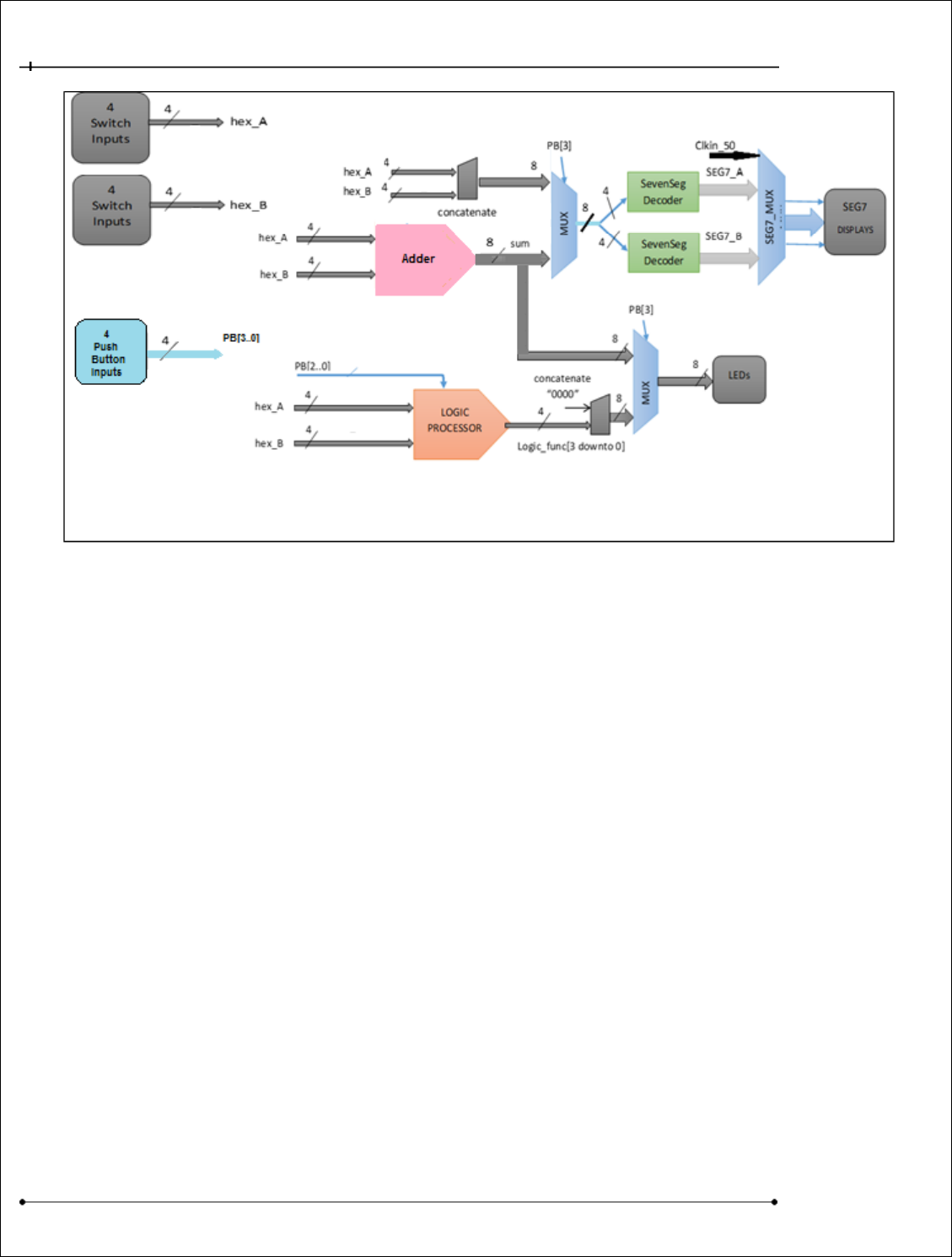
ECE-124 Lab Manual – W2018– V2.4 59
University of Waterloo
Figure 71 Lab2: Part C (Project) Sections Integrated
4.4 POST- Lab2 Activities
1. Complete the work for the Lab2 Demo design since it will be required at the next lab session in
Lab 3.
2. A report on the Lab2 design is due within 24 hours (after your Lab2 Demo).
Submit your completed project report to LEARN ECE-124 Lab2 Reports Dropbox folder. Make sure
that your Session Number and Group Number are included in your report title (see Figure 72) and
filename.
ECE-124 Lab Manual – W2018– V2.4 60
University of Waterloo
Figure 72 Lab2: Project Report Format
NEXT LAB SESSION: You will be designing a Magnitude Comparator (from scratch) that will be used
in the processing in subsequent labs. An Energy Monitor Logic function will be developed in Lab3.
ECE-124 Lab Manual – W2018– V2.4 61
University of Waterloo
4.5 LAB2 SUBMISSION FORM
Table 2 - Lab2: Submission Form
ECE-124 Lab-2 Submission Form – Winter 2018
GROUP NUMBER:
Lab2
Demo:
Lab2
Report
SESSION NUMBER:
Out of
10
Out of
10
I am submitting this report for grading. I certify that this report, including any code, descriptions,
flowcharts as part of the submission were written by the team member(s) below and there has not been
any use of prior academic credit at this university or any other institution. The penalty for plagiarism or
submission without signature(s) will be a grade of zero
NAME: (Print)
UW User ID
(not Student ID)
Signature
Partner A:
Partner B:
LAB2 DESIGN DEMO
Marks Allotted
A
B
Seven Segment Display bugs (quantity 3) corrected ?
1
Operands appear on Digit1 & Digit2 when PB’s are OFF ?
1
Logical Results shown correctly on LEDs[3..0] when PB[2..0] ON ?
1
Arithmetic results shown on Digits and LED’s when PB(3) ON ?
2
LEDs[7..4] OFF when Arithmetic result Less than or Equal to 1111
2
DISCUSSION: Describe how you implemented the VHDL coding.
3
LAB2 DEMO MARK
Total (up to 12)
out of 10
LAB2 DESIGN REPORT (see rubric on LEARN for details)
Marks Allotted
TEAM
Structural VHDL Used in top level VHDL design
2
Sub-block VHDL files with good Coding Style
2
Simulation of Logic functions showing the AND,OR,XOR modes
2
Simulation of Arithmetic functions showing the ADD mode
2
Total Design Logic Elements Used from Compilation Report
2
Delay in Report Submission (-1 per day) x number of days:
LAB2 Report MARK
Out of 10

ECE-124 Lab Manual – W2018– V2.4 62
University of Waterloo
5 LAB3: VHDL for Combinational Circuits PART 2 – Energy Monitor
During this lab a new project for combinational logic will be described and a demo and a lab report
are expected as deliverables. The project for this lab session is another VHDL-based FPGA design for
implementing a simple Energy Monitoring Controller that could be used in a home. The final design
must be demonstrated during the next Lab session. A Lab3 report must be submitted on LEARN within
24 hours after the Lab3 DEMO is completed.
5.1 Prelab
1. Review the Lab2 procedures used for entering, testing and implementing FPGA designs.
2. Review the Lab2 Submission form from LEARN for the Demo during the Lab3 session.
3. Be ready to have your Lab2 Demo design available for demonstration.
5.2 Lab3 Outline
Attendance will be taken.
The following new topics will be presented:
1. Review of Lab2
2. New VHDL Component - What is a Magnitude Comparator?
3. Project Setup for Lab3
4. Lab3 Part A. – Creating a 4 Bit Magnitude Comparator
5. Functional Simulations of a 4-Bit Magnitude Comparator
6. Lab3 Part B. – Project Brief for Lab3 Demo

ECE-124 Lab Manual – W2018– V2.4 63
University of Waterloo
5.3 Lab3 Activities
5.3.1 Recall from Lab2:
During Lab2 we developed some further VHDL knowledge on using the VHDL “Structural” style of
coding. We learned how to re-use VHDL files as components that were developed previously (Seven
Segment Decoder and Multiplexers) and could instantiate a number of copies of these components in
the primary VHDL design file (LogicalStep_Lab2_top). The INSTANCES could be then “wired” together
using declared signals (busses) and port mapping.
We also learned that signal data types could be “re-cast” into new types to allow different kinds of
processing to be accomplished.
5.3.2 Project Setup for Lab3
Start the Lab3 setup like what was done in Labs 1&2 for creating a new project. Using the Windows
File Explorer go to the ECE-124 folder directory. Go to LEARN and download the Zipped folder “Lab3”
into the ECE-124 folder. Extract the zipped folder contents to create your Lab3 project folder and it
should then have the LogicalStep_Lab3_top.vhd, LogicalStep_Lab3.tcl and segment7_mux.vhd files
installed inside it.
Start up the Altera Quartus Prime platform. Begin the new project by using
FILE>New Project Wizard). Enter the new Project parameters:
Project Folder: N:/ECE-124/Lab3
Project Name: LogicalStep_Lab3
Project Top Level: LogicalStep_Lab3_top
Click FINISH on the New Project Wizard Dialog Window.
Copy the sevensegment.vhd file from your Lab2 project folder into your Lab3 Project folder.
Then run the Lab3 TCL script to assign the FPGA device type, pin assignments subordinate VHDL files
for the LogicalStep_Lab3 project.
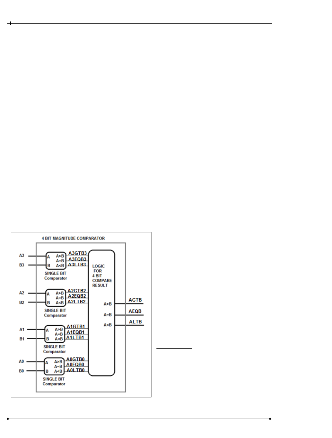
ECE-124 Lab Manual – W2018– V2.4 64
University of Waterloo
5.3.3 New VHDL Component – What is a Magnitude Comparator?
To put it simply - A magnitude comparator accepts two input variables and determines how they
compare with each other. There are three outputs from such a function. These are the input A is
greater than input B; input A is equal to input B; and input A is less than input B.
5.3.4 Lab3-Part A – Creating a 4-Bit Magnitude Comparator
For Lab3 a magnitude comparator is to be designed with GATES using two levels of hierarchy. The
bottom level will just compare the magnitude of two single bits and then pass along its three results
(A>B, A=B, A<B) to the upper level. The upper level will have the lower level declared as a component.
It will also have a group of instances of this component to cover the number of parallel operand bits
being compared. Inside the higher level the instance outputs are connected to a logic network to
determine the overall A>B, A=B, A<B results for the operands A and B.
The logic that is to be built in Lab3 – Part B requires a 4-bit Magnitude Comparator to determine
whether more energy is required for heating or cooling a home.
So….you guessed it… we must make up one for the project. See Figure 73.
Start by creating a Single bit Magnitude Comparator
Truth Table with single bit inputs for A and B. Then
create 3 output columns (one for each of A>B, A=B,
A<B) and then use logical reasoning to determines
which conditions force these outputs to activate.
Create a Single-bit comparator VHDL file
(Compx1.vhd) with the above information in its
design using Boolean equations for the outputs. Then
create a higher-level VHDL file (Compx4.vhd) which
includes the Declaration of the Compx1 as a
component and also 4 instances of the Compx1 in
your Compx4 architecture section.
In the Compx4 VHDL file some arrangement of logic
has to be made to make use of all of the individual
comparisons coming from the instances of Compx1.
Figure 73 Lab3: Levels of Comparator Logic
ECE-124 Lab Manual – W2018– V2.4 65
University of Waterloo
One thing to consider is to start with the highest-order bit in the group of bits being compared. For
example:
If A3 >B3 is TRUE then the lower bits of A2, B2, A1, B1, A0, B0 don’t need to be considered further
for the 4 bit A>B equation. Use the table below (X means “Don’t Care”).
Same thing if B3 > A3 (which is of course the same thing as A3<B3).
However if A3=B3 is TRUE then you have to look to the comparison of the lower bits (A2>B2) and so
on.
Comparison Inputs from 1-Bit Comparators
4-Bit Comparator
Outputs
A3<B3
A3=B3
A3>B3
A2<B2
A2=B2
A2>B2
A1<B1
A1=B1
A1>B1
A0<B0
A0=B0
A0>B0
A<B
A=B
A>B
0
0
1
X
X
X
X
X
X
X
X
X
0
0
1
1
0
0
X
X
X
X
X
X
X
X
X
1
0
0
0
1
0
0
0
1
X
X
X
X
X
X
0
0
1
0
1
0
X
X
X
X
X
X
0
1
0
X
X
X
0
1
0
X
X
X
0
1
0
0
1
0
0
1
0
0
1
0
0
1
0
0
1
0
0
1
0
Your gate-tree design for the 4-bit Comparator (Compx4) will be based on that logical approach. Fill
in the blanks for the inputs and outputs for the 4 bit Comparator function table above. Then write
Boolean equations for the three Comparator outputs inside your Compx4 file based on the inputs.
After the Compx4 design is completed open the LogicalStep_Lab3_top.vhd file and declare the
Compx4 in it as a component and also instantiate 1 instance in the Architecture section in
LogicalStep_Lab3_top.vhd. Connect a 4-bit signal group to the sw[3..0] inputs for input A and a
second 4-bit signal group to sw[7..4] bits for input B. Connect the 3 magnitude comparison outputs
of the Compx4 to the leds[2..0] output pins of LogicalStep_Lab3_top.vhd.
A set of Functional Simulations will be used to prove whether the 4 bit Magnitude Comparator is
designed correctly.

ECE-124 Lab Manual – W2018– V2.4 66
University of Waterloo
5.3.5 Functional Simulation of Magnitude Comparator
5.3.5.1 Adding Nodes to the Simulator
Begin this phase of Lab3 by running a compile to get an Analysis and Synthesis process completed.
Then, as before, open a Functional Simulation window (refer to section 2.3.2 in Lab1) and insert the
nodes of interest
(inputA sw[3..0], input Bsw[7..4], magnitude comparison outputs leds[2..0])
As before, group the individual nets into groups (sometimes called busses or vectors). For example,
if you select the signals one at a time for sw[3], sw[2], sw[1], sw[0] you can group into a hexadecimal
format and also name the group as Input_A. Similarly this can be done for the sw[7], sw[6], sw[5],
sw[4] becoming a hexadecimal formatted Input_B vector.
5.3.5.2 Adding Stimulus to the Inputs
For stimulus of this design it is usually best to make one input vector change relative to a static value
of the other input. Observe the behavior of the A>B, A=B and A<B outputs. You will do the
simulations runs with 4 different stimulus sets.
For example, for simulation 1 set Input_A to a static value of hex 1. Then run the Input_B through all
hex values between hex 0 and hex F. Save that stimulus file and then run that simulation and save it.
For simulation 2 set Input_A to hex 2 and repeat the sequence on Input_B as before. Run the
simulation and save it to a different file.
For simulation 3 set Input_A to hex 5 and repeat the sequence on Input_B. Run the simulation and
save it to a different file.
Finally for simulation 4 set Input_A to hex 8 and repeat the sequence on Input_B. Run the simulation
and save it to a different file.
Save the four stimulus files for your report.
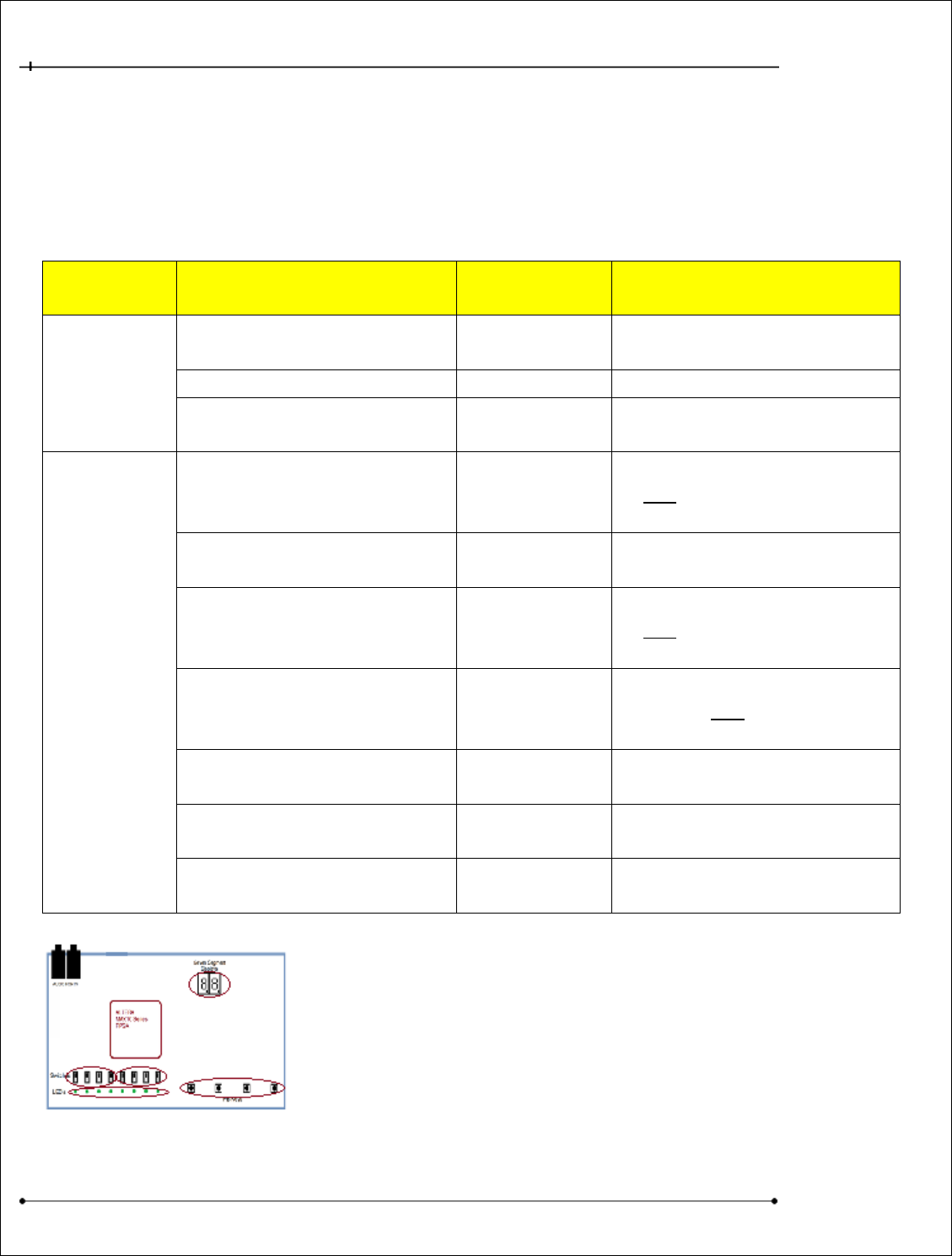
ECE-124 Lab Manual – W2018– V2.4 67
University of Waterloo
5.3.6 Lab3 Part B. – Project Brief for Lab3 Demo
The project for this lab session is another VHDL-based FPGA design for implementing a simple Energy
Monitoring Controller that could be used in a home. The final design must be demonstrated during
the Lab3 DEMO time.
SIGNAL
TYPE:
SIGNAL NAME:
ASSIGNED
PORT(s):
Comment
INPUTS
Current_Temp[3..0]
SW[3..0]
Set somewhere is mid-
range
Desired_Temp[3..0]
SW[7..4]
Various settings
DoorsWindowsOpen[2..0]
PB[2..0]
Fdoor-PB2, window-PB1,
Bdoor-PB0
OUTPUTS
FURNACE_ON
LEDS[0]
ON when BELOW temp
and with all
windows/Doors closed
SYSTEM AT TEMP
LEDS[1]
ON when AT TEMP (even if
Doors/windows are OPEN)
A/C ON
LEDS[2]
ON when ABOVE temp
and with all
windows/Doors closed
BLOWER ON
LEDS[3]
ON when A/C or Furnace
are ON and with all
windows/Doors closed
Door/Window OPEN[2..0]
in alignment with PB[2..0]
LEDS[6..4]
Fdoor-led6,
window-led5, bdoor-led4
Current
Temperature[3..0]
DIGIT 2
Current Temp (HEX)
Desired
Temperature[3..0]
DIGIT 1
Desired Temp (HEX)

ECE-124 Lab Manual – W2018– V2.4 68
University of Waterloo
With the doors and windows CLOSED the Furnace or A/C will be activated whenever there is a
difference detected between the Current and Desired temperature values. When either of these
turn ON the Blower must turn ON also.
The AT_TEMP indicator turns ON when DesiredTemp = Current Temp regardless if any doors or
windows are OPEN
Status indicators must also be illuminated when any door and window OPEN
The Current and Desired values of the temperatures are to be displayed on the two seven-
segment digits.
Use your knowledge from the previous labs to use as components the seven_segment decoders
and multiplexers. You can use your newly developed 4-bit comparator design to control the
Blower and determine whether the A/C or Furnace is to be activated.
5.4 POST - Lab3 Activities
1. Complete the work for the Lab3 Demo design since it will be required at the next lab session in
Lab 4. Different settings of Current Temp and Desired temp monitoring and control must be
demonstrated; Doors/Windows Open detection demonstrated.
2. A report on the Lab3 design is due within 24 hours after your Lab Demo and its content is
outlined in the Lab3 Submission Form.
Submit your completed project report to LEARN ECE-124 Lab3 Reports Dropbox folder. Make sure
that your Session Number and Group Number are included in your report title (see Figure 72 in the
Lab2 section) and filename.
NEXT LAB SESSION: You will be getting into the really cool stuff in digital logic. You will be learning
about storage elements (flip-flops) and state machines that do the logic processing over time
(sequential logic).
BONUS: Implement a Vacation Mode (via PB(3)) that, when pressed, provides an alternate FIXED
setting (Vacation Mode Value set to “0100” in binary inside your VHDL file) instead of the Desired
Temp value. When PB(3) is pressed LED7 is to go ON and the Comparator is forced to compare
the Current Value against the Vacation Mode Value and the Furnace/AC operations should
activate accordingly. Please keep the Vacation Mode Value and its logic separate from your
Comparator design.
ECE-124 Lab Manual – W2018– V2.4 69
University of Waterloo
5.5 LAB3 SUBMISSION FORM
Table 3 - Lab3: Submission Form
ECE-124 Lab-3 Submission Form – Winter 2018
GROUP NUMBER:
Lab3
Demo
Lab3
Report
SESSION NUMBER:
Out of
10
Out of
10
I am submitting this report for grading. I certify that this report, including any code, descriptions,
flowcharts as part of the submission were written by the team member(s) below and there has not been
any use of prior academic credit at this university or any other institution. The penalty for plagiarism or
submission without signature(s) will be a grade of zero
NAME: (Print)
UW User ID (not Student ID)
Signature
Partner A:
Partner B:
LAB3 DESIGN DEMO
Marks Allotted
A
B
Desired Temp (sw[7..4]) is displayed on Digit1?
1
Current Temp (sw[3..0]) is displayed on Digit2?
1
Doors/Windows (PB[2..0]) displayed on LEDs[6..4]?
1
Furnace, Blower, System At Temp, A/C, Blower Indicators LEDs?
1
A/C ON & Blower ON when Current Temp > Desired Temp?
1
Furnace ON & Blower ON when Current Temp < Desired Temp?
1
A/C, Furnace, Blower turn OFF when Doors/Windows Open?
1
DISCUSSION: Comment on your VHDL Implementation?
3
LAB3 DEMO MARK
Total (up to 12)
out of 10
LAB3 DESIGN REPORT (see rubric on LEARN for details)
Marks Allotted
TEAM
All VHDL files (not the sevenseg_decoder or seg7_mux files).
Structural VHDL design must be used at the Top Level.
Comparator must have a Boolean equation per each output.
2
Truth Table for 4-Bit Comparator Design with all entries inserted
2
Part A Simulations of Comparator showing A>B, A=B, A<B
2
RTL View of the Logic design (just of the Top Level)
2
Total Design Logic Elements Used /8064
2
Delay in Report Submission (-1 per day) x number of days:
LAB3 REPORT MARK
Out of 10

ECE-124 Lab Manual – W2018– V2.4 70
University of Waterloo
6 LAB4: VHDL for Sequential Circuits – Flip-flops & State-Machines
Lab4 will be the first one that uses sequential logic. The basic background on the topic of sequential
logic will be briefly covered to suit the lab4 requirements. Design elements from previous labs will
be used for Lab4. Both Moore and Mealy State Machine designs will be new parts for the design
goals for this lab.
6.1 Prelab
1. Review the Lab3 steps used for entering, testing and implementing FPGA designs.
2. Review the Lab3 Submission form from LEARN for the Lab4 session.
3. Be ready to have your Lab3 Demo design available for demonstration.
6.2 Lab4 Outline
Attendance will be taken.
The following new topics will be presented:
1. Review of Lab3
2. Brief Discussion on Sequential Processing
3. New VHDL Component - What is a Flip-Flop?
4. What are VHDL processes?
5. Project Setup for Lab4
6. Creating Some Simple Flip-Flop Register Designs
7. New VHDL Component – What are State Machines?
8. Project Brief for Lab4 Demo

ECE-124 Lab Manual – W2018– V2.4 71
University of Waterloo
6.3 Lab4 Activities
6.3.1 Recall from Lab3:
Last time in the lab we developed a 4-bit Magnitude Comparator. The comparison process was
implemented in two levels. This technique often simplifies the creation phase of a design. This
function was used in an Energy Monitoring Controller to determine current and desired temperature
differences.
6.3.2 Brief Discussion on Sequential Processing
This is the first lab having to do with sequential logic design and this is where some really cool design
work can be accomplished. Sequential logic is used for event-driven processing. You can probably
think of things in life that require a process to complete tasks. These processes usually run in a
sequence.
A trivial example could be something that is done every morning perhaps before getting here for your
lab work:
Process: Getting Simple Breakfast
Step 1: Get bread from cupboard
Step 2: Place bread in toaster
Step 3: Get plate
Step 4: Wait for Toast cycle completion
Step 5: Put Toast on plate
Step 6: Butter the Toast
Step 7: Add Jam
Step 8: Process done…..--> Enjoy.
These tasks must be done in the sequence described for the process to be completed successfully.
In the next section a new logical element will be described that can “hold” the logical value for any
sequential step in a process.
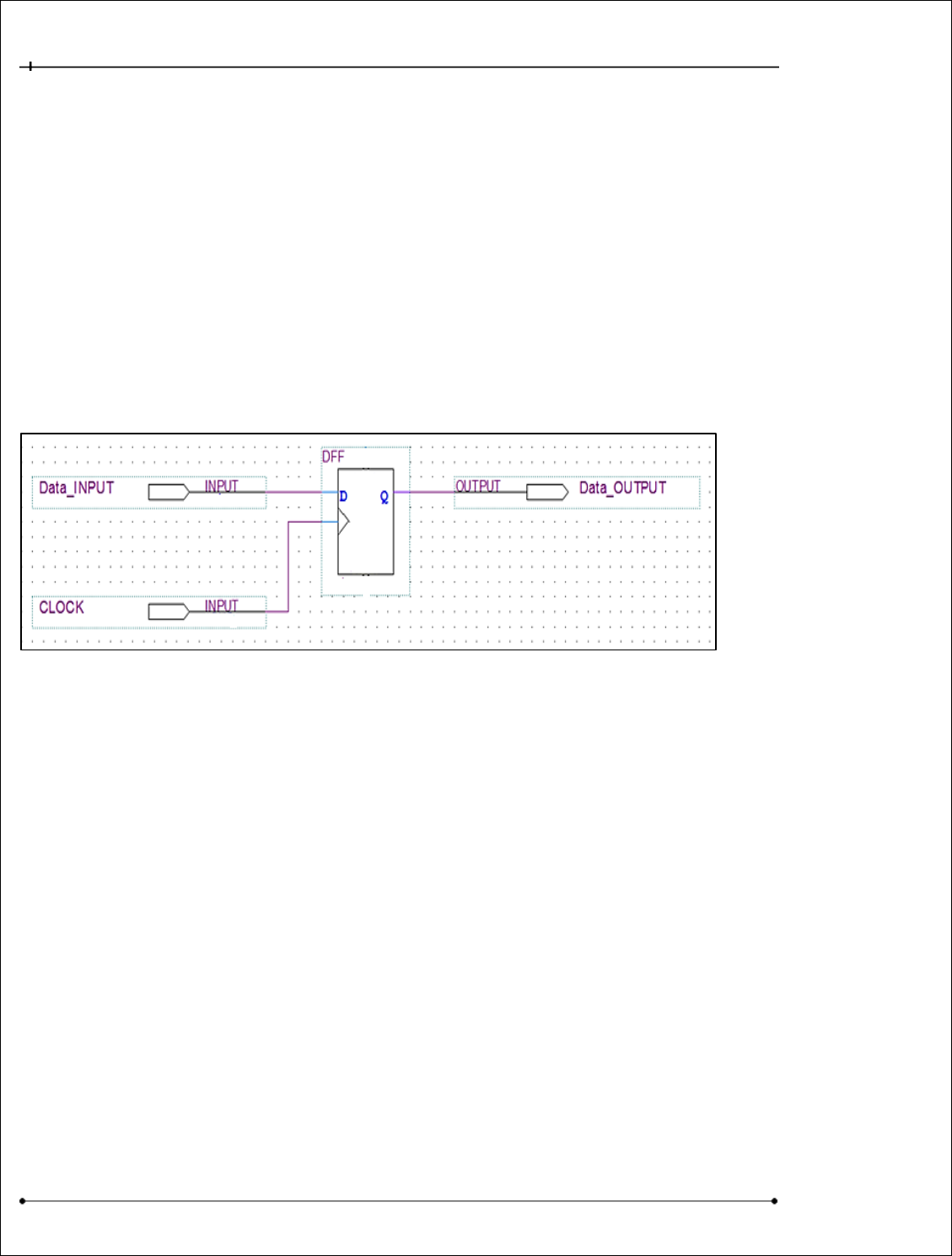
ECE-124 Lab Manual – W2018– V2.4 72
University of Waterloo
6.3.3 New VHDL Component – What is a Flip-Flop?
Well this is not a reference to a type of footwear. Nope.
In digital logic a basic element that is used in sequential logic is the Flip-Flop. This function records a
sample presented at its input and presents a copy of that input value to its output when a clock signal
is received. If there are no further clocks then the Flip-Flop should hold its output value indefinitely
(as long as there is power). Another name, perhaps more professional sounding, for this kind of device
is a Register.
Flip-Flops can come in many flavours (R/S, J/K, T, D) but most casual references to flip-flops are
referring to the D-type variety as shown below in Figure 74:
Figure 74 Lab4: D-Type Flip-Flop
There are usually other inputs to a standard flip flop (such as Asynchronous Preset, Asynchronous
Clear, Clock Enable inputs) but for now let’s just focus on the simpler functions.
Registers can be used in all kinds of higher-order functions such as counters, shift registers, state
machines, accumulators etc. In Lab1 we used a 28-bit counter to automate the Lab1 digital logic. It
would have 28 registered outputs.
6.3.4 What are VHDL Processes?
VHDL Processes are hardware-description constructs that are used to design Sequential Logic.
VHDL Process structures have the following syntax:
Label: process (sensitivity list) is
begin
..
end process;
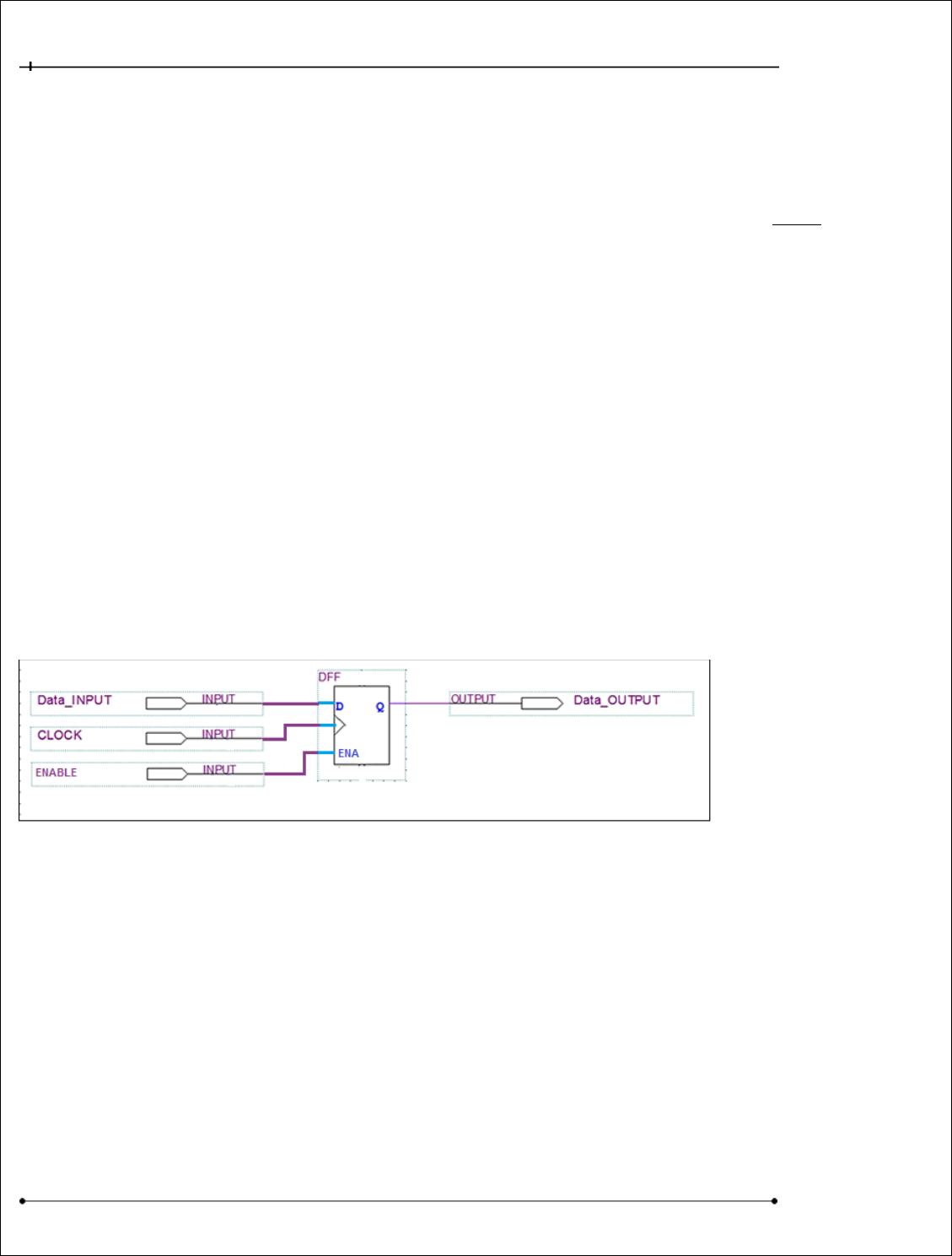
ECE-124 Lab Manual – W2018– V2.4 73
University of Waterloo
The Label can be any convenient value for code readability etc. The <sensitivity list> is the list of
inputs that the process is directed to observe to determine if a process output is to change. Such
inputs might include the “clock” signal for example. For clocks there is usually a kind “filtering” added
within the processing block to constrain process changes to occur on a desired clock EDGE. For
example one could use the “IF (rising_edge (clock)) THEN…” in the construct to evaluate whether any
state machine change will occur but only in association with the rising edge of each clock cycle.
So a Flip-Flop or Register (Figure 74) can be created in VHDL using a PROCESS. See the example below:
process (<clock_signal>) is
begin
if (rising_edge(<clock_signal>)) then
register <= <data>;
end if;
end process;
The Register will accept the “data” value on the rising edge of <clock signal>. When the next clock
rising edge arrives the input <data> is again captured and the previous captured value is
OVERWRITTEN. But what if we want to capture the data and KEEP IT for a while? What do we need to
do since the clock may always be running? For this situation we need to add some new Flip-Flop
functionality. In Figure 75 we add a new capability. This is the Clock Enable or just “ENABLE”.
Figure 75 Lab4: Adding a Clock Enable To the Flip-Flop
This function makes the Flip-Flop update to a new value at the Flip-Flop Data_INPUT when the next
clock edge arrives and only IF the ENABLE is active. If the Enable is OFF during any rising_edge of the
clock signal then the flip-flop implicitly retains its current value (inferred by VHDL).
process (<clock_signal>) is
begin
if (rising_edge(<clock_signal>) then
if (ENABLE) then
register <= <data>;
end if;
end if;
end process;
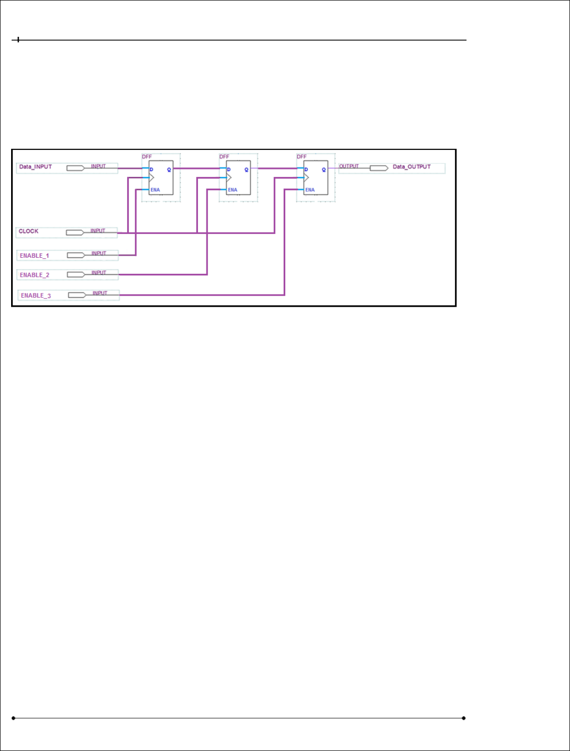
ECE-124 Lab Manual – W2018– V2.4 74
University of Waterloo
The ENABLE can be activated whenever a change is required for a Flip-Flop at the next clock cycle.
Now imagine the case where we want to put a string of these Flip-Flops registers together as shown in
Figure 76. One can see that the separate registers are activated by when the various ENABLE inputs
activate AND with the preceding upstream stage being ACTIVE. The process sequence is DONE when
the last stage (Data_Output) is activated in this example.
Figure 76 Lab4: Serial String of Flip-Flops
6.3.5 Initial Project Setup for Lab4
Start the Lab4 like what was done in earlier Labs. Go to LEARN and download the Lab4 Zipped folder
“Lab4” into the ECE-124 folder on your N: Drive. Extract the contents to create the new Lab4 project
folder and its contents therein.
Start up the Altera Quartus Prime platform and begin a new project with the New Project Wizard.
Enter the new Project parameters:
Project Folder: Lab4
Project Name: LogicalStep_Lab4
Project Top Level: LogicalStep_Lab4_top
Click FINISH on the New Project Wizard Dialog Window.
Run the Lab4 TCL script to assign the FPGA device type and pins for the LogicalStep FPGA.
This part of the lab session will require some of the same components that were used in the previous
lab such as SevenSegment, seg7_mux, Compx4 and Compx1 VHDL files. Copy these VHDL files from
your Lab3 Project folder into your Lab4 Project folder.
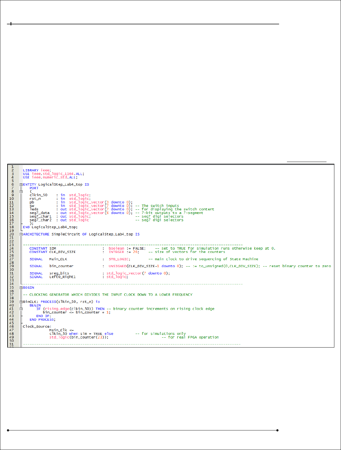
ECE-124 Lab Manual – W2018– V2.4 75
University of Waterloo
6.3.6 Lab4 Part A – Creating Some Simple Flip-Flop Register Designs
In the first part of this lab we will develop a simple bidirectional shift register and an up/down binary
counter. For each of these the total number of register stages used will be eight. The register stages
will also be output to the LED’s.
6.3.6.1 Adding Some Clock Source Flexibility
We want to be able to run this designs in either a physical, real-world scenario (with a download to
the LogicalStep board) OR in a simulation environment. A flexible, high-level control of your design
will select the “clocking source” for these two situations.
Within the new top-level design file (LogicalStep_Lab4_top.vhd) near the beginning of the file VHDL
code (as shown in Figure 77 below) the design uses the 50MHz clock input (clkin_50) and some new
signals are created for flexibility of the clocking network. The first process “BINCLK” is a clock divider.
This process is merely a counter (similar to what was used in Lab1) to slow down the shift register
clock to something where the register changes can be observed by eye. At the high end of the divider
counter outputs is Bit23 and it will output a clock that is 2**24th of the input clock frequency
(50,000,000 Hz). After division Bit23 will change at just under a 4 Hz clock rate. This will be used to
Figure 77 Lab4: LogicalStep_Lab4_top with Clock Sourcing for FPGA
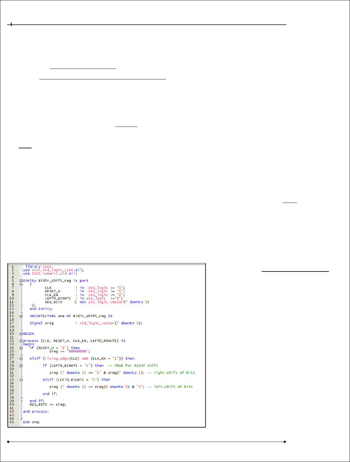
ECE-124 Lab Manual – W2018– V2.4 76
University of Waterloo
drive the signal “Main_Clk” for the physical FPGA download version of the LogicalStep_Lab4_top
design on the LogicalStep_Board for visual reasons.
However for simulation purposes later on you must change the source for Main_Clk to one that is
driven by STIMULUS for the clkin_50 pin directly (otherwise you will be waiting for a LOOONNNGGG
time for each Main_Clk cycle to occur with the 2**24 division of the clock divider output). To make
things easier to switch between FPGA-design versions some flexibility should be added to the design.
In Figure 77 a CONSTANT named “SIM” is ahead of the signal declarations in the Architecture Section
and it can be used to change the source of Main_Clk. The Boolean constant SIM is used as a selector
for a 2-to-1 mux. When SIM is TRUE the Main_Clk signal is driven directly by the Clkin_50 pin as above
for SIMulation. When SIM is set to a FALSE value then the Main_Clk signal is connected to the divider
output Bit23 for use when running your design on the LogicalStep board.
6.3.6.2 Implementing a Bidirectional Shift Register Component
As specified earlier the shift register is to have 8 stages. Across all of the stages only ONE will be active
at a time. This is equivalent to a “ONE-HOT” encoding arrangement of the shift register.
The shift register will be clocked by the Main_Clk clock signal. Recall that registers are implemented
inside VHDL processes. A control signal that should be made “common” to all of the shift register
registers will be the input called Left0_Right1. When Left0_Right1 is at ‘0’ the shift register “shifts
LEFT”. When it is at “1” the shift register “shifts RIGHT”. Enter the VHDL code (lines 1 to 45) in
Figure 78 into a VHDL COMPONENT
design and then declare it and
Instantiate it at the top level.
Connect its outputs to the LEDs, its
LEFT0_RIGHT1 control input to PB(0)
and its CLK_EN to PB(1).
The Shift Register will only change if the
“CLK_EN” (PB(1)) is a ‘1’.
Figure 78 Lab3: VHDL for a Bidirectional Shift Register
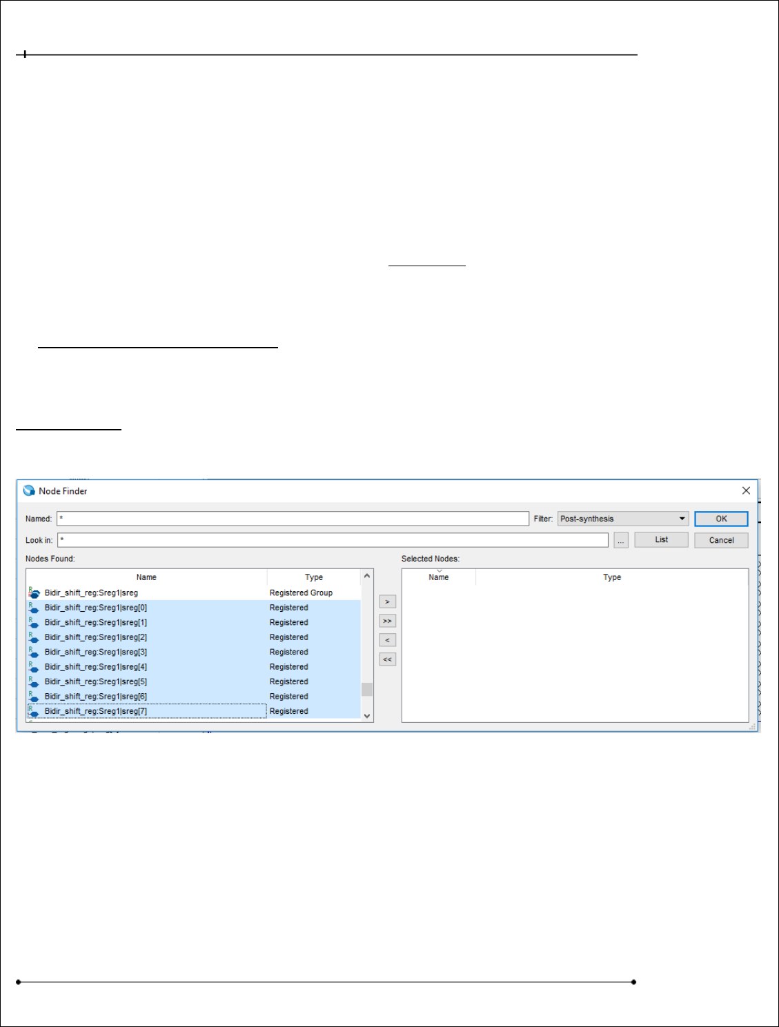
ECE-124 Lab Manual – W2018– V2.4 77
University of Waterloo
6.3.6.3 Functional Simulation of the Bidirectional Shift Register
Up until now the Quartus Simulator has been used to display combinational logic activity using only
the Input and Output pins to control and observe the design. This is a limitation with the Quartus
Simulator for the simulation of Combinational Logic. That is why in earlier labs when it was desired to
view internal signals steps were taken to connect them to the outside pins in the VHDL coding
(eg: Lab2 PartA).
But the Quartus simulator also will display internal REGISTERS and this is the first lab session that
illustrates that kind of access for observation purposes.
Before you recompile the LogicalStep_Lab4_top for simulation change the clock source for Main_Clk
by setting the SIM constant to TRUE. Then do an Analysis & Synthesis type of compile for your design.
Besides adding the Input and Output Pins to the Node List in your Functional simulation you can now
add the internal registers of the shift register. This can be done by changing the NodeFinder Filter to:
Post-Synthesis. Then the register bits of the shift register can be selected.
Refer to Figure 79.
Figure 79 Lab4: Inserting Register Nodes for Simulation
For stimulus do the following:
Set the Clkin_50 to a 20 nsec period.
Set each of the pb(0) and pb(1) inputs to a ‘1’.
Set the rst_n to a ‘1’ (OFF state) for the whole simulation and then just force it to a ‘0’ for, say, the first 50 ns.
Set the rst_n signal return to the ‘1’ state. Halfway in the simulation set the pb(0) to a ‘0’ state.
Sometime after pb(0) is changed try toggling the pb(1) to ‘0’ and then back to a ‘1’.
Your simulation should look something like that shown in Figure 80.
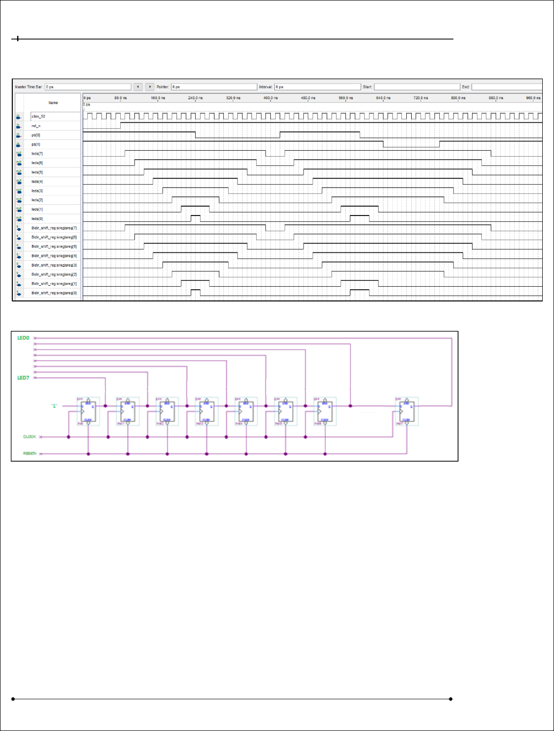
ECE-124 Lab Manual – W2018– V2.4 78
University of Waterloo
Figure 80 Lab4: Simulation of the Bidirectional Shift Register
Figure 81: Lab4: Compiler Example of a Unidirectional Shift Register
For clarity purposes Figure 81 shows what the VHDL compiler creates for a simplified version of the shift
register(unidirectional only). The flip-flops are only influenced by data from its downstream neighbor. There is
no increase in connection complexity as number of shift register stages increases. This design will be
compared to one in the next section.
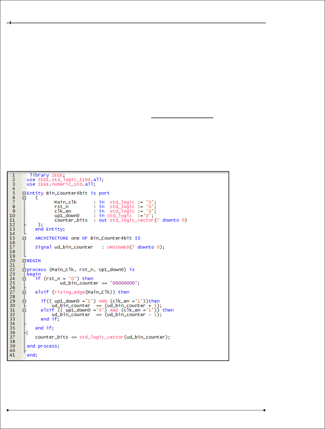
ECE-124 Lab Manual – W2018– V2.4 79
University of Waterloo
6.3.6.4 Implementing a Simple Up/Down Binary Counter Component
You have already used some binary counters in this Lab course. A simple 8 bit up/down binary
counter will now be implemented.
The binary counter will be clocked by the Main_Clk clock signal like what was done for the shift
register example. Recall that registers are implemented inside VHDL processes. A control signal that
should be made “common” to all of the shift register registers will be the input called Up1_Down0.
When up1_down0 is at ‘1’ the counter counts up. When it is at “0” ‘1’ the counter counts down. Enter
the VHDL code (lines 1 to 41) in Figure 82 into a VHDL COMPONENT design and then declare it and
Instantiate it in your LogicalStep_Lab4_top file. At the top level disconnect the LED’s from the shift
Register component and then connect them to the counter component outputs, its Up1_Down0
control input to pb(0) and its clk_en to pb(1).
The Binary Counter will only change if the “clk_en” (pb(1)) is a ‘1’.
Figure 82 Lab4: Simple Up/Down Binary Counter
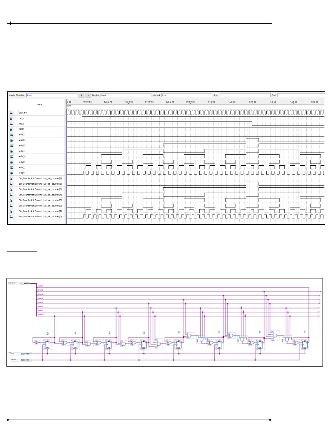
ECE-124 Lab Manual – W2018– V2.4 80
University of Waterloo
6.3.6.5 Functional Simulation of the Up/Down Binary Counter
Similar to what was done for the Bidirectional Shift Register the Up/Down Binary Counter can be
simulated. Using the same setup (SIM set to TRUE, Clkin_50 set to 20 nsec period etc.) run a
simulation of the design. It should be similar to what is shown in Figure 83.
Figure 83 Lab4: Simulation of Up/Down Binary Counter
Side Note: Notice in Figure 83 how each higher-order bit in the binary counter toggles at half of the
rate of the preceding lower-order bit (i.e.: bit 4 changes at half the rate of bit 3 which in turn changes
at half the rate of bit2 and so on).
Figure 84 Lab4: VHDL Compiler generated Binary Counter (Up direction only)
For clarity purposes Figure 84 shows what the VHDL compiler creates for a simplified version of the Binary
Counter where the clock enable and UP/Down logic are not included.

ECE-124 Lab Manual – W2018– V2.4 81
University of Waterloo
Notice how much more logic is required as the design gets towards the higher order bits in the
counter. The logic “FAN-IN” gets greater and greater for the binary counter higher order register bits.
Each of the register outputs from all lower register bits in the chain come toward the higher order
register inputs.
Whereas for the earlier shift register example the logic FAN-IN is maintained to be the same for each
stage (the inputs to a register stage just comes from its immediate neighbor).
Each of these two kinds of register designs has an impact on how fast each of these register designs
can be “clocked”.
Another aspect to examine in this comparison is with the amount required for register logic for the
format choice (encoding format). The 8 bit binary counter has 8 Flip-flops which can represent 2**8
combinations (256 - 8-bit binary values). To implement the equivalent number of combinations in the
shift register it would require 256 serially connected flip-flops.
Some interesting things can be noted from these two design exercises in terms of design trade-offs:
1) Sequential logic encoding format choice can impact the amount of logic required (both
combinational and sequential).
2) Sequential logic encoding format choice can impact the speed of operation.
The focus will now leave the simulation of these simple register designs. These designs will be
revisited later on for the Lab4 Project Demo.
6.3.7 New VHDL Component – What is a State Machine?
Now that the topic of basic register functionality has been introduced a new powerful use for
registers will be covered. Returning to the earlier trivial process for a Simple Breakfast an outline is
shown in Figure 85 and a state diagram is shown in Figure 86..
STATE: OUTPUTS: TRANSITION EVENT TO NEXT
STATE:
State 1: Get bread from cupboard < Got Bread >
State 2: Placing bread in toaster (DROP BREAD IN TOASTER) < Bread in toaster>
State 3: Get plate (START TOASTER) < Got Plate >
State 4: Wait for Toast cycle completion < Toast Pops Up >
State 5: Put Toast on plate (GET TOAST FROM TOASTER) < Toast on Plate >
State 6: Butter the Toast (APPLY BUTTER) < Toast Buttered >
State 7: Add Jam (APPLY JAM) < Jam Added >
State 8: Process done…..--> Enjoy. (DONE) <wait for REPEAT>
Figure 85 Lab4: Process: Getting a Simple Breakfast
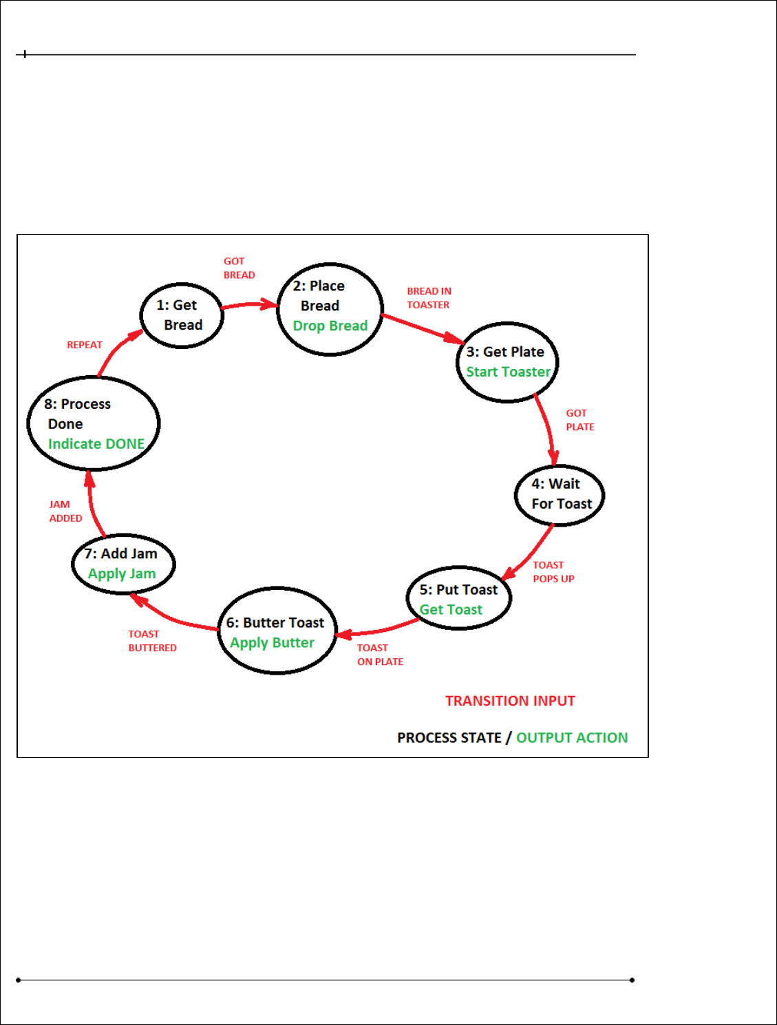
ECE-124 Lab Manual – W2018– V2.4 82
University of Waterloo
Observe the left hand column in Figure 85 that shows the name or “state” steps involved in the
process. In the right-hand column are the transition inputs to the process that would be from sensors
that could signify events such as “Got_Bread, Bread_in_Toaster_and_Started, Got_Plate” etc.
The process outputs could be used to control the mechanics to “Drop Bread in Toaster”, “Start
Toaster”,….”DONE” etc.
Figure 86 Lab4: State Diagram for Simple Breakfast process
To repeat the process above would have to receive an additional input such as a “Repeat” signal. The
above process for some imaginative design engineer could be implemented with a STATE MACHINE
design.
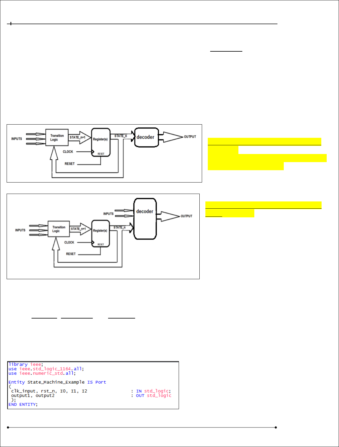
ECE-124 Lab Manual – W2018– V2.4 83
University of Waterloo
In state machine design the conditions that make its process change from its CURRENT state to its
NEXT state are varied. Combinational logic is used to determine if or when those state transitions
should occur. The state changes occur in synchronization with a state machine clock. This is where
registers are involved.
There are just two classes of state machines in sequential logic design. These are the Moore and
Mealy types. To remember the names just think of two engineers sitting at a Thanksgiving table. One
engineer politely says to the other “Would you like some Moore corn?” to which the second engineer
replies “Only if it’s not Mealy”. (Groan!).
MOORE STATE MACHINE
Output is a function of present state ONLY
(Figure 87).
Moore SM’s outputs are only changed when
the state machine is clocked.
MEALY STATE MACHINE
Outputs are functions of present state AND
inputs (Figure 88).
For this lab there will be development of both kinds of state machines (Moore and Mealy). Referring
back to Figures 87 and 88 there are generally just three sections in each state machine design. These
are the Register, Transition and Decoder sections.
Provided for you in the Lab4 download files from Learn is a VHDL file named State_Machine Example.
The Entity section for this file is shown in Figure 89. It consists of a clock input, a reset input, a few
transition control inputs and two outputs to signal when the process is in specific states.
Figure 89 Lab4: Entity Declaration for State Machine Example
Figure 87 Lab4: Moore State Machine
Figure 88 Lab4: Mealy State Machine
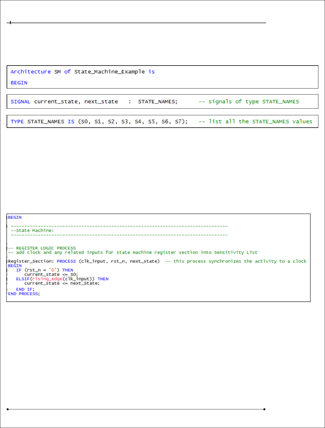
ECE-124 Lab Manual – W2018– V2.4 84
University of Waterloo
Further in the VHDL file (shown in Figure 90) in the Architecture declaration section the details set up
the list of states for a state machine with a TYPE statement named STATE_NAMES. This gives the state
machine the set of state values for its processing.
Figure 90 Lab4: State Machine States Defined by a VHDL TYPE Statement
Then two signals are declared to HOLD two different values of the TYPE STATE_NAMES to keep the
“current” state and “next” state assignments for the state machine.
The Register section uses the state machine clock input, the next_state value input coming from the
Transition Section, and usually some kind of RESET input signal in its Sensitivity List. These are used to
advance the state machine to new states in alignment with a particular clock edge. This first state
machine process is labelled in Figure 91 as “Register_Section”.
Figure 91 Lab4: Process for the Register Section of State Machine Example
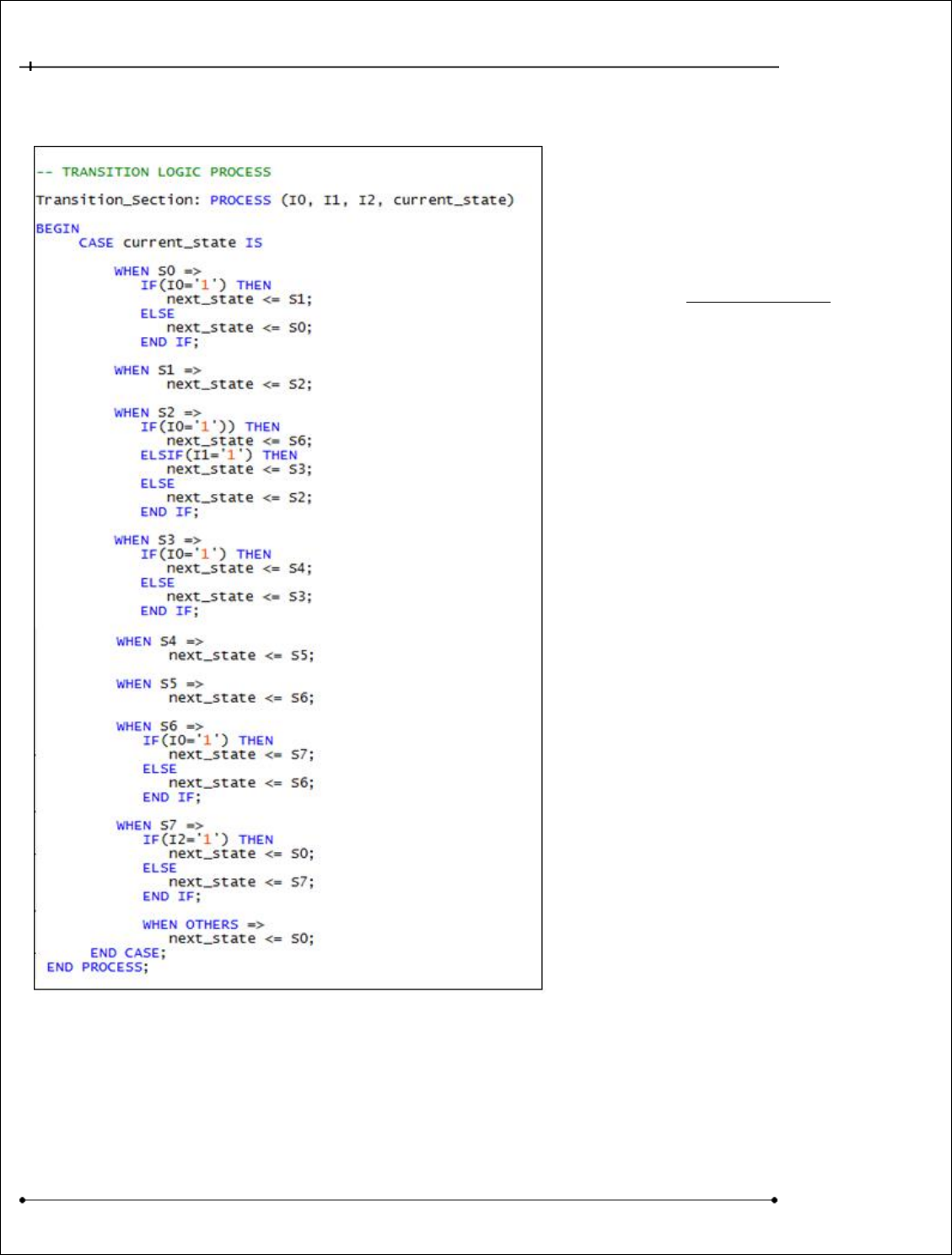
ECE-124 Lab Manual – W2018– V2.4 85
University of Waterloo
The Transition section (to be located in a second Process construct) uses the VHDL “CASE” statement
construct. It uses a number of the State Machine inputs (not the clock or reset) and the CURRENT
state in its Sensitivity List to evaluate
what and when the NEXT state will be
(including “no change”). A typical
example of a CASE statement construct is
shown below in Figure 92 and it is always
implemented within a process. NOTE: All
“constant_expression” options in a VHDL
case statement must be constant and
unique. Also, the case statement entries
must cover all input values of
“expression” to be complete, otherwise
it must include a “when others” clause at
the end.
case <expression> is
when <constant_expression> =>
-- Sequential Statement(s)
when <constant_expression> =>
-- Sequential Statement(s)
when others =>
-- Sequential Statement(s)
end case;
The CASE statement construct can
specify a signal group for the
<expression> and for each possible value
of that signal group is stated in the
<constant expression> fields.
An example of Transition section being
implemented with a CASE statement is
shown in Figure 92 with the process
labelled as “Transition_Section”. It
implements the sequencing control of
the range of state values that were
declared earlier.
Note how specific inputs are observed by the Transition Logic only in specific states and also how
inputs can cause the State Machine to “JUMP” states. For example if an “I0” input signal is active
when the State Machine Example is in State “S2” the State Machine will take a jump in its state
sequence to state “S6”.
Figure 92 Lab4: Transition Section for State Machine Example
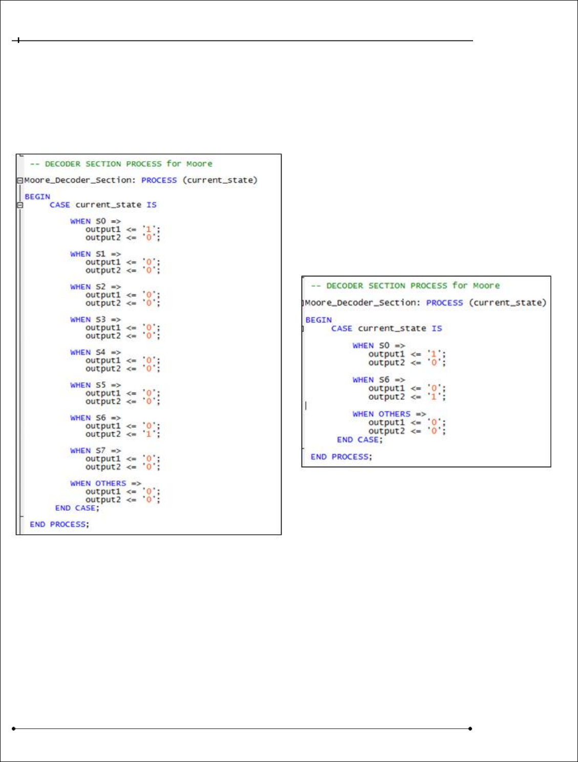
ECE-124 Lab Manual – W2018– V2.4 86
University of Waterloo
The example Decoder section shown in Figure 93 sets the output1 and output2 signals when the state
machine state reaches specific states. The output signal levels must be defined for all current_state
values. Figure 93 would be a Decoder section for a Moore State Machine design since the outputs are
dependent ONLY on the state machine current_state values. Figure 94 shows an abbreviated version.
Figure 93 Lab4: Example of Decoder Logic for Moore State Machine
Figure 94 Lab4: Shortened Version of Moore Decoder section
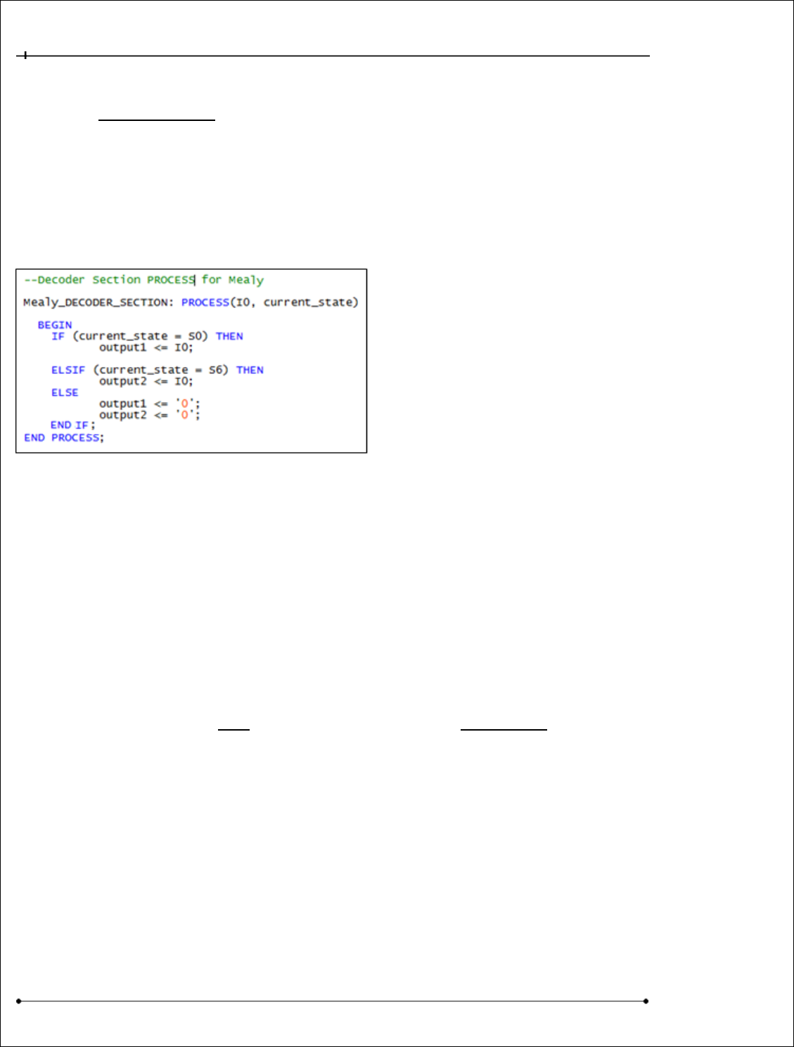
ECE-124 Lab Manual – W2018– V2.4 87
University of Waterloo
For a Mealy State Machine the difference is that the outputs depend on the state value AND inputs.
The inputs may or may not affect a change of the current_state value. In essence the Mealy State
Machine state is like a “gate control”. If we were to convert the previous Moore State Machine into a
Mealy State Machine then the following changes would happen to the Decoder section as shown in
the Mealy Decoder section (Figure 95). Let’s assume that the Transition Logic can remain the same as
in the Moore example earlier.
Figure 95 Lab4: Mealy State Machine Decoder Section with Extra Input and
Output Added
From Figure 95 it can be deduced that output1 and
output2 are combinational outputs driven by the
input I0 but only when the state machine is in state
S0 (for output1) or state S6 (for output2). If required
the outputs can be driven during numerous different
states with the appropriate inputs being considered.
Note that for Mealy State machines, with the outputs being driven by combinational inputs, that the
outputs can suffer from any kind of asynchronous behaviour of the inputs. For example, if I0 is
“intermittent” then output1 and output2 will be “intermittent” as well during the enabling states. This
is the main disadvantage of Mealy machines as compared to Moore machines. The advantage for
Mealy State Machines is that often they can be designed with fewer states than their Moore machine
counterparts. They can also impact the outputs sooner since a state change may not have to occur
first.
Alternatively an example for the Moore machine case, the output1 would be driven by a
current_state value of “S0”only. Outside of the S0 state the direct input connection from “I0” to the
outputs would be moot. The advantage that Moore State Machines over their Mealy State Machine
counterparts is that external inputs are prevented from influencing the State Machine outputs
directly. The State Machine must change “state” first and then the outputs are driven by decoding the
“current_state” value.
It all depends on the requirements of the application.
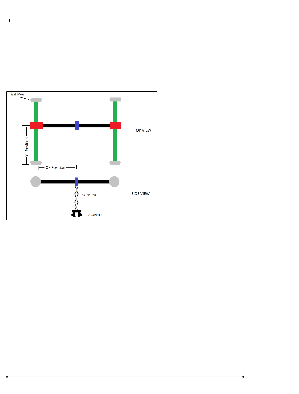
ECE-124 Lab Manual – W2018– V2.4 88
University of Waterloo
6.3.8 Lab4 Part B - Project Brief for Lab4 Demo
The Lab4 Project will encompass all of the components that you have designed earlier this term and in
addition to the components that were developed earlier in this lab session.
You will creating a Robotic Arm Controller or RAC (illustrated in Figure 96 and its Control System in
Figure 97) that could be used for a positioning a robotic arm in 2 dimensions and employing an
extender/grappler.
Figure 96 Lab4: Robotic Arm Project
Your Lab4 project will include the following declared as VHDL COMPONENTS in the
LogicalStep_Lab4_top.vhd file:
1) 4-bit Magnitude Comparator (2 instances)
2) Seven-Segment Decoder (2 instances)
3) Seg7_Mux (1 instance)
4) Bidirectional 4-bit Shift Register (1 instance - changed from 8-bits earlier)
5) Binary 4-bit up/down Counter (2 instances - changed from 8-bits earlier)
6) Mealy State Machine (1 instance) to be used as the X/Y Position Controller
7) Moore State Machine (2 instances) one for Extender and one for Grappler
8) all multiplexers
The above VHDL components are to be declared and used in the LogicalStep_Lab4_top.vhd file ONLY.

ECE-124 Lab Manual – W2018– V2.4 89
University of Waterloo
There will also be some other I/O elements used in the Lab4 project:
1) 8 slide switch inputs:
SW[7:4] – Target X co-ordinate;
SW[3:0] – Target Y co-ordinate
2) 4 Push Buttons:
pb(3) – X Drive Enable;
pb(2) – Y Drive Enable;
pb(1) Extender Toggle (In/Out);
pb(0) Grappler Toggle (Open/Closed);
3) 2 seven segment displays:
Digit1 – Multiplexed between Target X-co-ordinate when pb(3) open and ; X-current position
when pb(3) is pressed;
Digit2 – Multiplexed between Target Y-co-ordinate when pb(2) open; Y-current position when
pb(2) is pressed;
4) 8 LED outputs:
leds[7:4] – Extender position;
leds[3] -- Grappler ON;
leds[2:1] -- for your use;
leds[0] -- System Error;
Figure 97 shows the control system. The Motor Drive electronics are external and will be driven by the
X/Y Comparators. The comparator outputs (EQ, GT, LT) also are connected back into the X/Y Position
Controller (Mealy SM). The Comparator inputs are from the 4 bit Binary Counters and the Slide
Switches.
The slide switches will be used to set the desired X and Y TARGET co-ordinates for the Robotic Arm
Controller (RAC). The hex-coded switches SW[7:4] value will represent the X TARGET co-ordinate and
the hex-coded switches SW[3:0] value will represent the Y TARGET co-ordinate for the RAC.
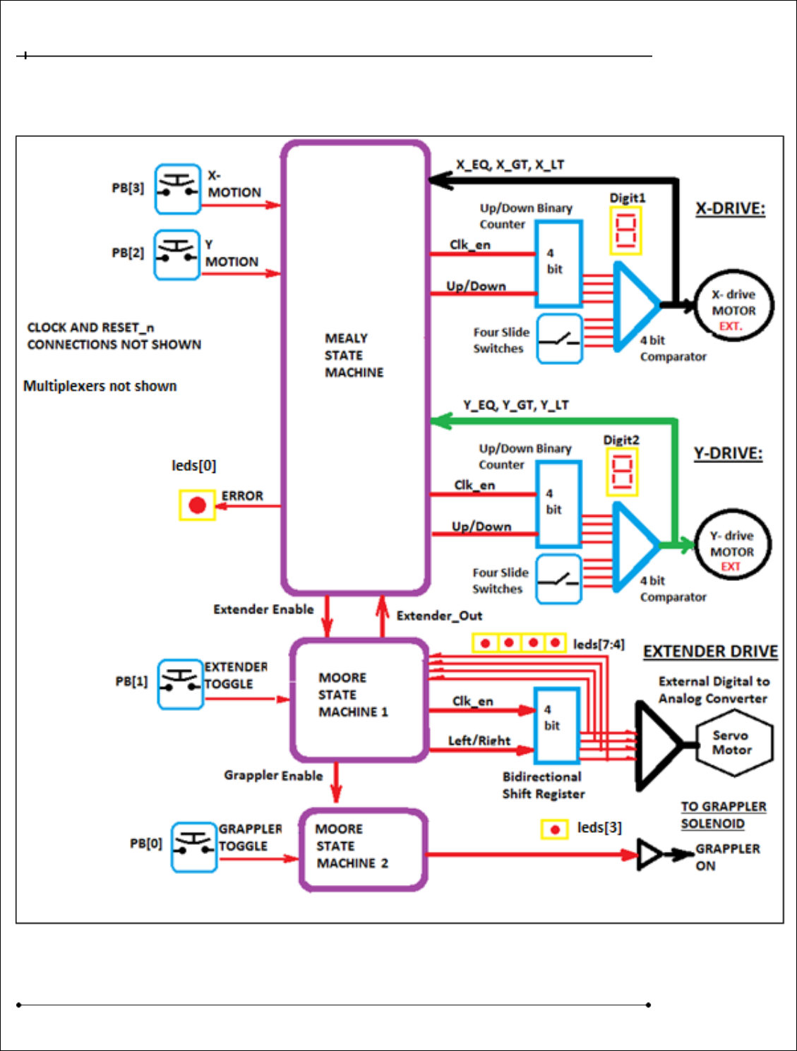
ECE-124 Lab Manual – W2018– V2.4 90
University of Waterloo
The seven-segment displays are multiplexed between the Target and the “in-motion” current X/Y
position of the RAC (X on Digit1 and Y on Digit2).
Figure 97 Lab4: Lab4 Project Block Diagram

ECE-124 Lab Manual – W2018– V2.4 91
University of Waterloo
The RAC will be considered “in X-motion” when PB[3] is pressed and RAC has not yet reached its
TARGET X-location. The RAC will be considered “in Y-motion” when PB[2] is pressed and RAC has not
yet reached its TARGET Y-location. If either pb(3) or pb(2) are not pressed before the Target Position
is reached the appropriate binary counter will just retain its current value. The X-motion and Y-motion
are completely independent operations. They should be able to operate either sequentially or be able
to operate in parallel.
When the RAC reaches its TARGET X/Y co-ordinates the Extender can be enabled for operation. When
“enabled by the X/Y Position Controller the Extender Controller (Moore SM1) may extend the
extender. A single bidirectional shift register is to represent the extender position. It is to be toggled
either ON or OFF by push button pb(1). When activated the extender begins its extension process and
continues until it reaches FULL extension. The extender position sequence is to be displayed on
leds[7:4] as shown below:
Position: leds[7:4]
Retracted: 0000
Extending1: 1000
Extending2: 1100
Extending3: 1110
Fully Extended: 1111
Anytime that the extender is NOT in its retracted position (“0000”) the Moore SM1 status flag
“Extender_Out” must be driven active. Only in the Fully Extended position is the Grappler Controller
(Moore SM2) to be enabled for Open/Close operations.
To Toggle the Open/Closed state of the Grappler the input pb(0) is used. The Grappler “Closed” state
will be displayed on leds[3].
NOTE: If any attempt is made to move the RAC to new Target co-ordinates while the Extender_Out
flag is active the X/Y Position Controller must be PREVENTED from X or Y motion and a System Error
must be indicated on leds[0]. The System Error will also be displayed on BOTH Digit1 and Digit2 by
exhibiting a FLASHING condition. This Error Condition must remain active (locked) until the Extender is
Retracted. When retracted the Moore SM1 Extender_Out flag is turned OFF, the System Error
conditioned is turned off and then X/Y motion may continue.
6.3.8.1 Mealy State Machine Requirements for X/Y Position Control
The Mealy State Machine for the Lab4 Project will consist of 3 primary sections. These will be the
Register, Transition and Decoder sections. The Register section will be clocked by the rising edge of

ECE-124 Lab Manual – W2018– V2.4 92
University of Waterloo
the Main_Clk input. A reset input must also be included to clear the Register section back to its initial
state.
The Transition section will allow the states to change states according to the inputs received from the
Comparators, Push-Button switches pb[3:2] and the Extender Controller.
The Decoder section MUST be of the MEALY form. Outputs should be defaulted to ‘0’ but when
activated to a ‘1’ level the outputs are NOT to be driven by the “current_state” alone but by inputs
during specific current_state values. Hybrid forms of decoding (mix of Moore and Mealy) will be
penalized for Lab4.
6.3.8.2 Moore State Machine 1 and 2 Requirements
The Moore State Machine 1 (Extender Controller) and 2(Grappler Controller) for the Lab4 Project will
each consist of 3 primary sections. These will be the Register, Transition and Decoder sections. Each of
the Register sections will be clocked by the rising edge of the Main_Clk input. A reset input must also
be included to clear the Register sections back to its initial state.
For Moore SM1 the Transition section will allow the states to change states according to the inputs
received from the bidirectional Shift Register, Extender_Enable and the Push-Button pb[1]. For Moore
SM2 the Transition section will allow the states to change states according to the inputs received from
the Grappler_Enable and the Push-Button pb[0].
Each of the Decoder sections MUST be of the MOORE form. Outputs should be defined for each of the
“current_state” values only.
Hybrid forms of decoding (mix of Moore and Mealy) will be penalized for Lab4.
6.3.8.3 Multiplexers
Any Multiplexers used in the design are to be declared and instantiated at the top level to make for
easier readability etc. All functionality will be reviewed and marked.
6.3.8.4 State Diagrams
State diagrams for each state machine can be created by the Quartus tools. Use the Tools>Netlist
Viewers> State Machine Viewer to create them.
ECE-124 Lab Manual – W2018– V2.4 93
University of Waterloo
6.3.8.5 Lab4 Project Input / Output Definitions
6.4 POST – Lab4 Activities
1. Demo’s of the Lab4 designs will be required at the next lab session in Lab 5.
2. A report on the Lab4 design is due within 24 hours after your Lab Demo. Refer to the Lab4
Submission Form for its requirement details.
Submit your completed project report (pdf format) to LEARN ECE-124 Lab4 Reports Dropbox folder
according to your Session and Group Number naming format.
SIGNAL
T Y P E :
SIGNAL NAME:
ASSIGNED
PORT(s):
Comment
Inputs
Main_clk
n/a
Main clock driven by clock source logic
rst_n
rst_n
RESET (Active_LOW)
sw[7..4]
sw[7..4]
Target X- Co-ordinate (in hex)
sw[3..0]
sw[3..0]
Target Y- Co-ordinate (in hex)
pb[3]
pb[3]
X-Motion Enable
pb[2]
pb[2]
Y-Motion Enable
pb[1]
pb[1]
Entender Toggle
pb[0]
pb[0]
Grappler Toggle
Outputs
seg7_data[6..0]
seg7_data[6..0]
Used to display TARGET values for X (on
Digit1 and Y (on Digit2).
seg7_char1,
seg7_char2
seg7_char1,
seg7_char2
Target X/Y seven segment display
control by seg7_mux
leds[7:4]
leds[7:4]
Shows extender position
leds[3]
leds[3]
Shows Grappler activation
leds[2:1]
leds[2:1]
User LEDs.
leds[0]
leds[0]
Shows System Error
ECE-124 Lab Manual – W2018– V2.4 94
University of Waterloo
6.5 LAB4 SUBMISSION FORM
Table 4 - Lab4: Submission Form
ECE-124 Lab-4 Submission Form – Winter 2018
GROUP NUMBER:
Lab4
Demo
Lab4
Report
SESSION NUMBER:
Out of
10
Out of
10
I am submitting this report for grading. I certify that this report, including any code, descriptions,
flowcharts as part of the submission were written by the team member(s) below and there has not
been any use of prior academic credit at this university or any other institution. The penalty for
plagiarism or submission without signature(s) will be a grade of zero
NAME: (Print)
UW User ID
(not Student ID)
Signature
Partner A:
Partner B:
LAB4 DESIGN DEMO
Marks
Allotted
A
B
Target X value on Digit1 (pb3 OFF); Target Y value on Digit2 (pb2 OFF)
1
X-Motion/Y-Motion has changing values on Digit1/Digit2
1
Extender enabled only at Target co-ordinates
1
Extender Position shown on leds[7:4]
1
Grappler enabled only at Fully Extended Extender (Grappler- led[3])
1
System Error when X/Y Motion with Extender not retracted
1
System Error Cleared when Extender is retracted.
1
DISCUSSION: Comment on your VHDL Implementation?
3
LAB4 DEMO MARK
Out of 10
LAB4 DESIGN REPORT (see rubric on LEARN for details)
Marks
Allotted
TEAM
Structural VHDL for Top Level VHDL file (only instances and
connections) – no gates except in instance input fields
2
Simulation of 8bit Shift Register and 8 bit Binary Counter in both
directions
2
State Diagrams of Mealy SM, Moore SM1, MooreSM2 machines
2
Mealy Form for Mealy SM; Moore form for Moore SM1, Sm2
2
Fitter Report on Resources Utilization by Entity (Logic Cells each)
2
Delay in Report Submission (-1 per day) x number of days:
LAB4 REPORT MARK
Out of 10

ECE-124 Lab Manual – W2018– V2.4 95
University of Waterloo
