ELITEGROUP COMPUTER SYSTEMS ED2LN30PA1 DATA CARD User Manual Part 2
ELITEGROUP COMPUTER SYSTEMS CO., LTD DATA CARD Part 2
Contents
- 1. User Manual Part 1
- 2. User Manual Part 2
- 3. User Manual
User Manual Part 2

The following section describes the system architecture of Inter-Processor Communication on
a WWAN M.2 module when connected to a Microsoft Windows® based Host OS Windows®
7, Windows® 8.x.
The software components of a WWAN M.2 module running Windows® 7 and
Windows® 8 are depicted in Figure 12 and Figure 13 respectively.
In the Windows® 7 architecture:
The Windows® 7 driver interfaces with the WWAN M.2 modem using a virtual
terminal connection over CDC-ECM.
A Third party connection manager utilized
Independent Hardware Vendor (IHV) provided MBIM driver
In the Windows® 8 architecture:
Microsoft requirements:
oMBIM interfaces
oUser Mode Driver Framework (UMDF) driver for GNSS, and Firmware
Update, Carrier Switching application.
oRTD3 support
For all Windows platforms:
The WWAN M.2 module is exposed as a composite device
GNSS will be supported through a serial interface
When mobile broadband is disabled, GNSS will still be available.
The mobile network adapter driver will interface to the modem software through the
MBIM interface.
All Intel specific features will be supported through MBIM.
The connection manager provided with Win 8 OS and above will be used. For
Win 7, the IHV provided connection manager is used.
There will be an application layer to hide the differences in the mobile broadband API
between Win 7 and Win 8.
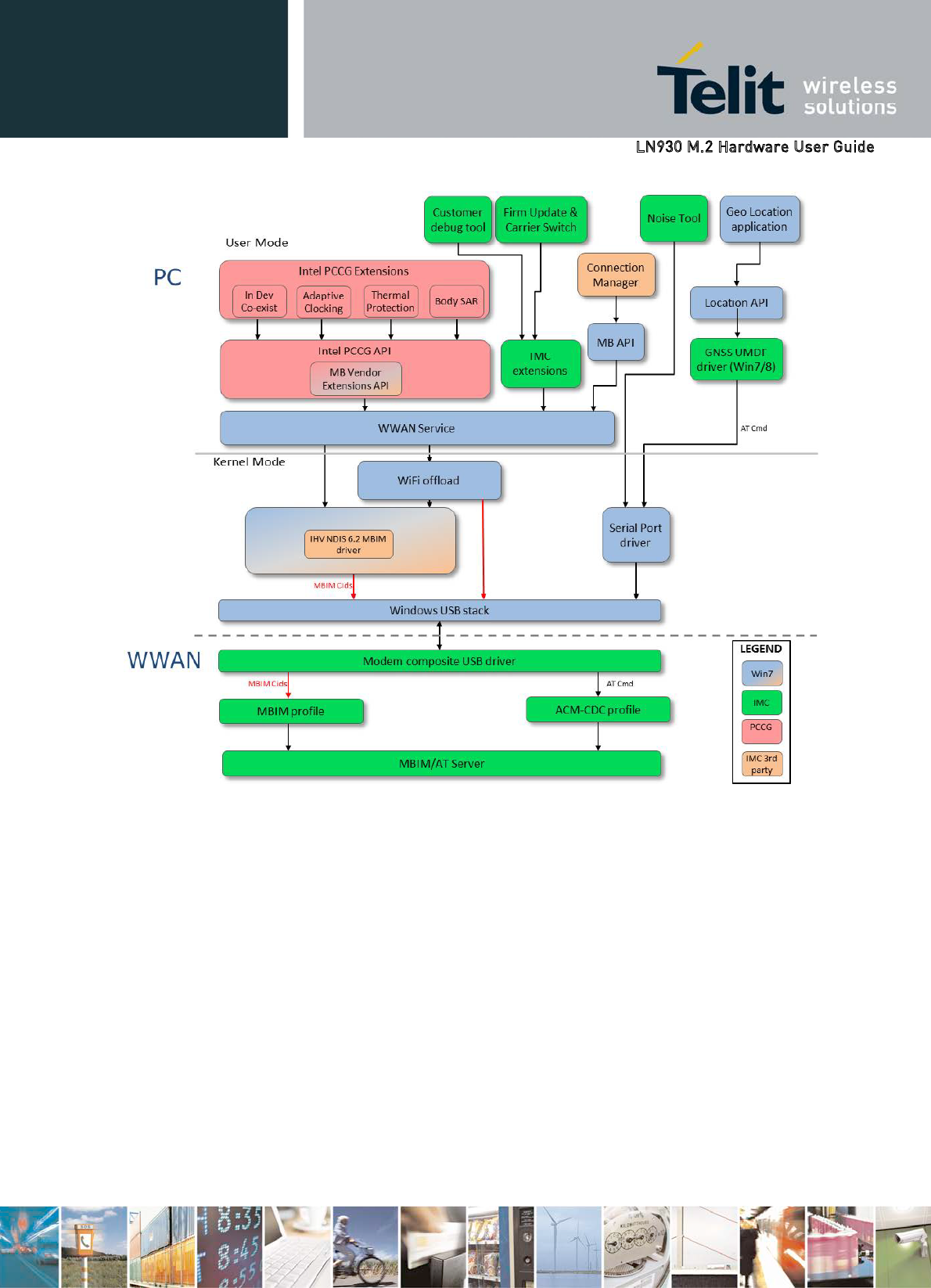
Figure 12 Windows 7 Software Architecture
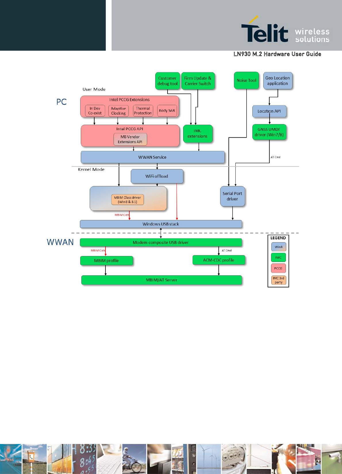
Figure 13 Windows 8 Software Architecture
In order to support both Windows®8 and Windows®7 (for corporate legacy applications),
with a single modem architecture, IMC will provide a kernel level driver implementing the
Mobile Broadband Interface Model. The driver is WHQL certified for Windows®7.
IMC provides a GNSS "User mode" driver to enable GNSS Applications executing on
Windows PC/Tablet to communicate to the GNSS device located on the M.2 module. The
driver communicates to Modem module via AT commands over an ACM-CDC USB
channel.
This is a “user friendly” Windows GUI application enabling the consumer, whose Ultrabook
or tablet is hosting an Intel M.2 module, to update the firmware on WWAN module by
executing a graphical application based on .NET4 framework. The same application runs on
both Windows®7 and Windows®8 environments and its look & feel can be customized if
required.
This same application is used to upgrade the standard image flashed at the factory with one
that better fits the local Carrier. When a new SIM is inserted, the application will detect the
inserted SIM does not match the WWAN device firmware. It will then allow the user to
select and update the WWAN firmware with a suitable image reflecting the local network of
the Carrier.
This is a Windows®8 application allows a M.2 end user to collect debugging information
under guidance of a Customer Support operator. The log file can be sent to a Technical
support center and fed into an analysis tool, such as Intel’s Mobile Analyzer application, to
diagnose potential problems found in the field after module deployment.
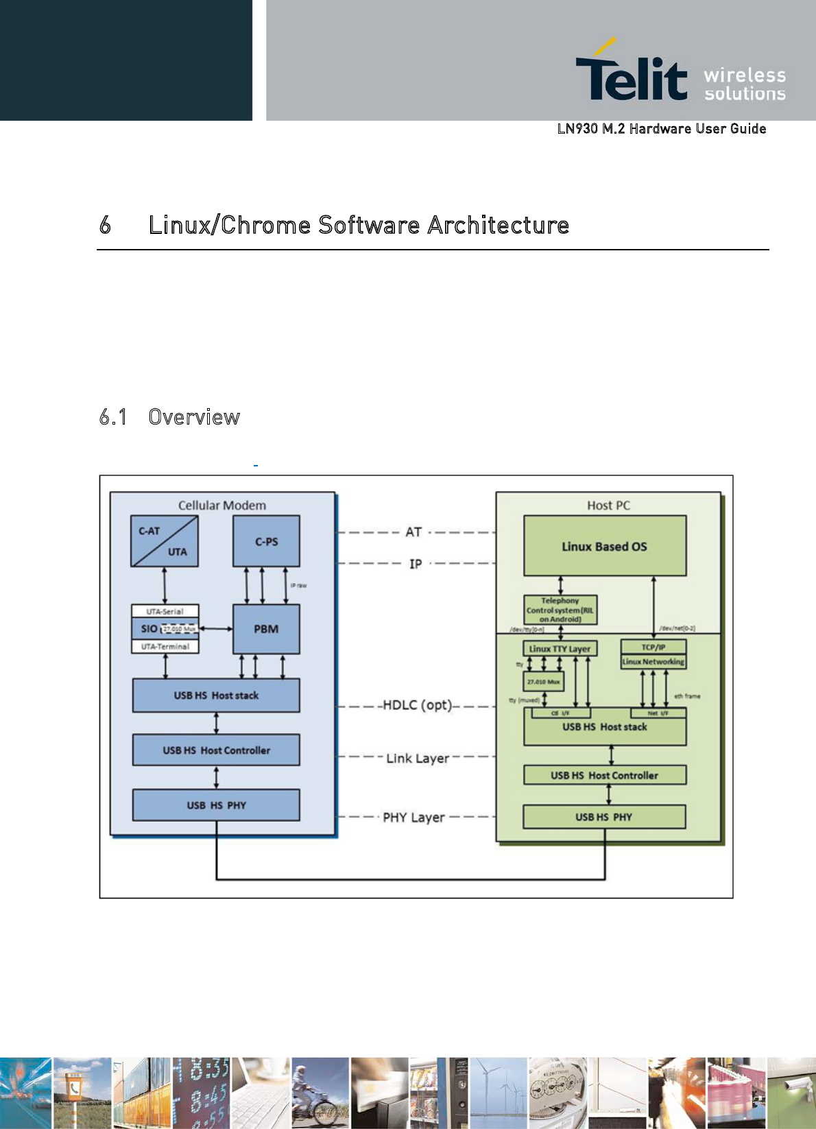
The following section describes the system architecture of Inter-Processor Communication
on a M.2 module when connected to a Linux based Host OS (Android, Chrome, and Ubuntu).
The description is only concerned with the HS-USB port which is the only available
functional interprocessor communications (IPC) interface at run-time and takes into account
only the AT control plane and IP packets data connection. Audio packet exchange is outside
the scope of the current version of M.2.
Figure 14 illustrates the architecture of the IPC and its components.
Figure 14 Linux Software Architecture
The user data is transferred from/to the cellular protocol stack (C-PS) to the IPC via a
centralized memory manager. The centralized memory manager is called packet buffer
manager (PBM). The user data is routed along the data plane as IP packets using several
logical channels. Each logical channel corresponds to a dedicated Packet Data Network
(PDN) connection.
There is no TCP/IP stack on the modem side in the data path from IPC over PBM to
C-PS handling IP address based routing.
The central packet buffer manager (PBM) provides a common packet buffer used between
IPC and PS. No copy operation of data is necessary between cellular PS and IPC. The HS-
USB interface provides a highly efficient data path via DMA with scatter/gather linked-list
processing.
The control plane is using at least one dedicated channel through Serial IO component (S-IO)
to the AT command handler. The interface towards the driver is called Universal Terminal
Adapter (UTA)-Terminal, while the interface towards application is called UTA-Serial
interface. The application in our case is the AT command handler called C-AT. The control
channel is using AT commands. A detailed list of all supported AT commands can be found
in a separate application note.
In the context of an AT command based architecture, a SW multiplexer can be added. The
SW multiplexer of the 3GPP 27.010 protocol provides a number of logical channels (DLC)
which serve as AT terminals on Host PC side. These logical channels are mapped on-top of
one of the control channels of the specific physical IPC interface.
The 3GPP 27.010 multiplexer protocol is a data link protocol (layer-2 of the OSI model)
which uses HDLC-like framing, virtual data channels, and channels’ control procedure. The
protocol is implemented according to 3GPP TS27.010. It allows software applications on the
Host processor to access the USB-HS port on M.2 in a concurrent way by emulating multiple
virtual communication channels. The MUX protocol controls the virtual channels and
conveys user data over the virtual channels.

The USB 2.0 HS stack is used for communication with a PC in device role.
Additional details on the USB interface can be found in Section 3.1, Interprocessor Interface.
The USB feature may be configured by the UTA_USB API. The user may define different
use cases, such as support of different numbers of CDC-ACM or CDC-NCM channels.
Up to 3 CDC-ACM logical channels are available to be used as an interface for the
following functionality:
AT commands
3GPP 27.010 Multiplexer
Tracing
Connection to test framework
The ACM channels are connected via UTA-Terminal to S-IO and from there via UTA-
Serial to the application on modem side.
Up to 4 CDC-NCM functions are available to be used as interface for network
connections servicing for up to four PDN connections.
The NCM channels are connected via the PBM driver interface to PBM and from there via
PBM service interfaces to the PTM component of C-PS.
The default configuration is 3 CDC-ACM channels for control and trace and 4 CDC–
NCM channels for data connections. A specific configuration is set via the AT+XSIO
command. The detailed usage of the default configuration is:
1st ACM channel:: Modem Control Channel, Channel ID: USBCDC/0
2nd ACM channel:: Trace data, Channel ID: USBCDC/1
3rd ACM channel:: free, Channel ID: USBCDC/2
1st - 4th NCM channel: data channel for PDN connection: Channel ID:
USBHS/NCM/0-3
The host computer can set the modem into USB sleep (L1) state (to save battery power)
whenever the link is idle. To return from sleep state the host computer performs
L1Resume. This can also be triggered by the modem using L1-Remote- Wake-up. The
sleep (L1) state is introduced by “USB 2.0 Link Power Management Addendum” and
allows fast state transitions between active and sleep states.
The PC can set the modem into USB suspend state (to save battery power) when no
communication takes place or when the PC is switched into standby mode. The suspend state
also can be triggered by X-GOLD™ Baseband device through a proprietary device initiated
selective suspend mechanism. The wake up is performed by Host Resume. The modem can
wake up the host computer from standby state using Remote Wake-up
The software components of a WWAN M.2 module running the Android operating system is
shown Figure 15.
Android version 15/16 will be supported.
Intel Intrinsic Radio Interface Layer (RIL) will be used and supported via a USB
CDC-ACM driver.
All Intel features will be supported via AT commands.
Advanced Linux Sound Architecture (ALSA) will not be supported on data only
WWAN M.2 modules.
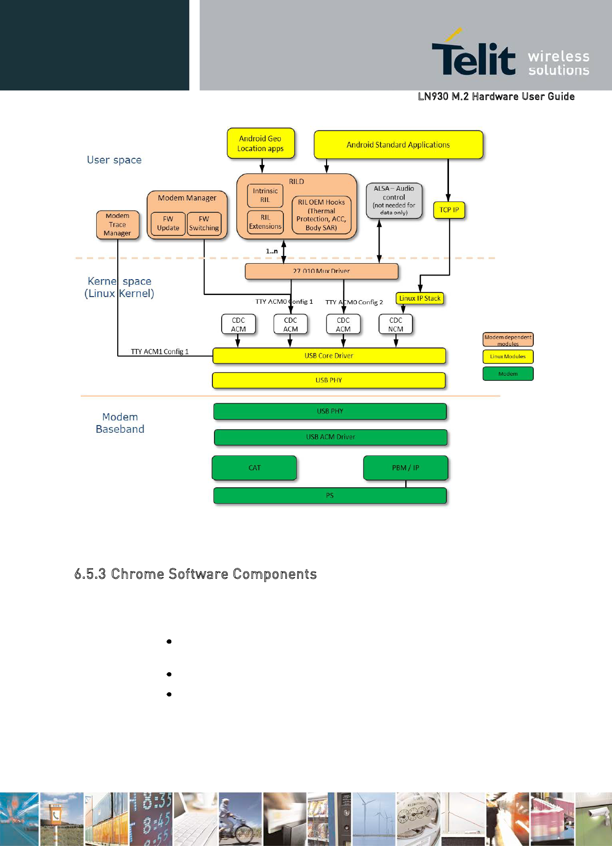
Figure 15 Android Software Architecture
A preliminary view of the software components of a WWAN M.2 module running the
Chrome operating system is shown in Figure 16. The architecture is still in development;
however, it is expected that:
Intel Intrinsic Radio Interface Layer (RIL) will be used and supported via a USB
CDC-MBIM driver.
All Intel features will be supported via MBIM commands.
Advanced Linux Sound Architecture (ALSA) will not be supported on data only
WWAN M.2 modules.
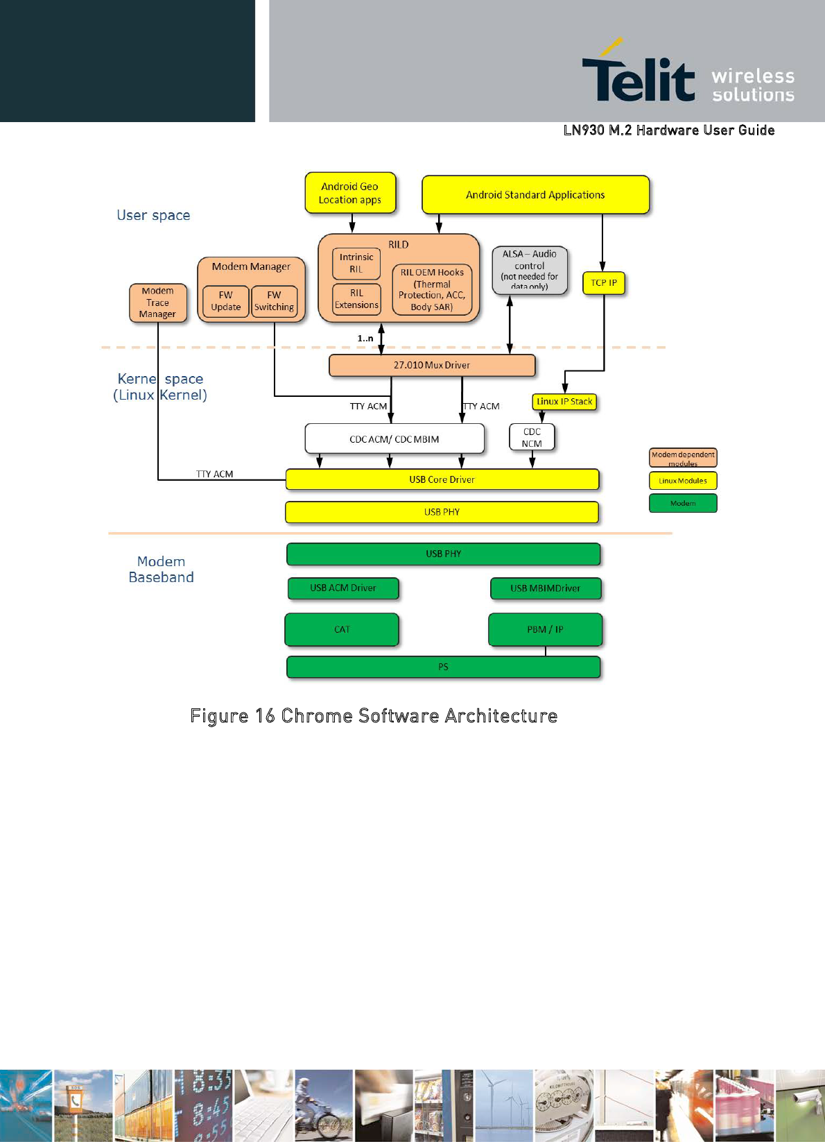
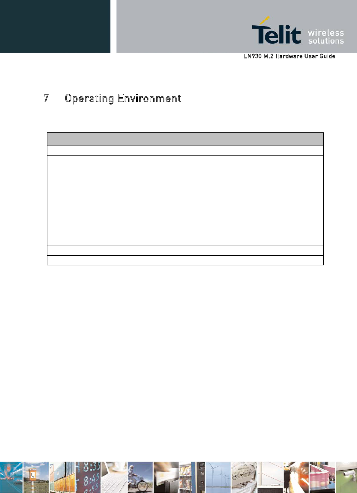
Table 24 Operating Environment
Item Description
Form Factor Card Type 3042
Operating Temperature The module full operating temperature in compliance with 3GPP
specification shall be
-10 °C to +55 °C – Normal
+55 °C to +70 °C – Extreme
Extreme is the surrounding air temperature of the module inside the
platform when the card is fully operating at worst case condition.
We cannot guarantee the RF performance of the device, since
components might operate out of specification. On the RF side we are
using a mechanism called Progressive Power Reduction to limit the
PA output power at high operating temperature.
Storage Temperature -40 °C (minus 40) to +70 °C (plus 70) non-operating.
Humidity <85% humidity, non-condensing
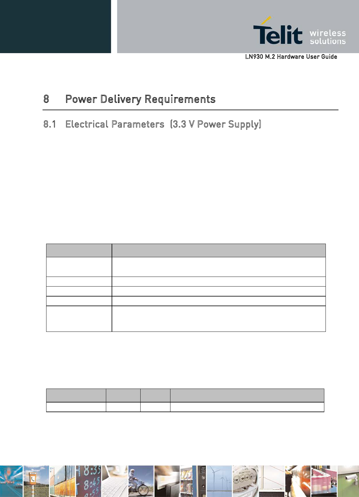
The M.2 modules utilize a single regulated power rail of 3.3 V provided by the host
platform. There is no other VDDIO like pin and the M.2 module is responsible for
generating its own I/O voltage source using the 3.3 V power rail. This
3.3 V voltage rail source on the platform should always be on and available during the
system’s stand-by/suspend state to support the wake event processing on the
communications card.
There are 5 power pins on the host interface, pins 2, 4, 70, 72, and 74.
The requirements of the regulated 3.3 V power supply provided by the host platform are
listed below.
Table 25 M.2 Module Power Delivery Requirements - Ultrabook
Requirement Detailed Description
Supply voltage 3.3 V at the Card connector will be within 5% tolerance on the
motherboard.
Peak Current The host board shall provide 2.5 A peak current.
Average Current Average max current of 1.1 A will be supported.
Max in-rush current Max module in-rush current of 5.1 A will be supported.
Power pin
connections
The power pins specified in WWAN card #’s, 2, 4, 70, 72, 74 will be connected
to 3.3 V supply and WWAN configuration pins 1, 69, and 75 will be connected
to ground.
For Tablet platforms, the 3.3 V regulated power rail can be replaced with a direct VBAT
connection. Key parameters for VBAT in a direct connection configuration are shown in
Table 26.
Table 26 VBAT Power Delivery Requirements – Direct Connections (Tablet)
Power Source Vmin Vmax Cell Type
VBAT 3.135 V* 4.4 V Once cell Li-Ion battery
(*) RF performance cannot be guaranteed below 3.135 V.
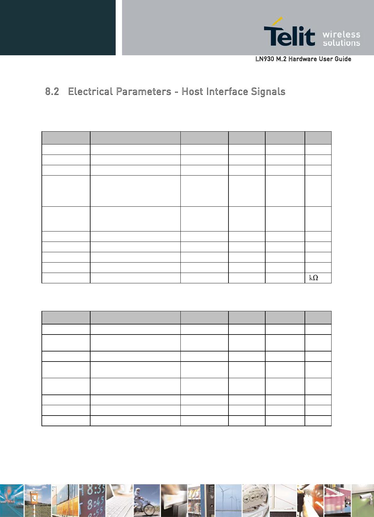
Table 27 DC Specification for 3.3V Logic Signaling
Symbol Parameter Condition Min Max Unit
+3.3V Supply Voltage - 3.135 3.465 V
VIH Input High Voltage - 2.0 3.6 V
VIL Input Low Voltage - -0.5 0.8 V
IOL Output Low Current for
Open-drain Signals
Not applicable to LED# and
DAS/DSS# pins
0.4 V 4 - mA
IOL Output Low Current for
Open-drain Signals
Applies to the LED# pins
0.4 V 9 - mA
IIN Input Leakage Current 0 V to 3.3 V -10 +10 µA
ILKG Output Leakage Current 0 V to 3.3 V -50 +50 µA
CIN Input Pin Capacitance - - 7 pF
COUT Output Pin Capacitance - - 30 pF
RPULL-UP Pull-up Resistance - 9 60
Table 28 DC Specification for 1.8V Logic Signaling
Symbol Parameter Condition Min Max Unit
VDD18 Supply Voltage - 1.7 1.9 V
VIH Input High Voltage - 0.7 *
VDD18
VDD18 +
0.3 V
VIL Input Low Voltage - -0.3 0.3 VDD18 V
VOH Output High Voltage IOH = -1 mA
VDD18 Min VDD18 -
0.45 - V
VOL Output Low Voltage IOL = 1 mA
VDD18 Min - 0.45 V
IIN Input Leakage Current 0 V to VDD18 -10 +10 µA
ILKG Output Leakage Current 0 V to VDD18 -50 +50 µA
CIN Input Pin Capacitance - - 10 pF
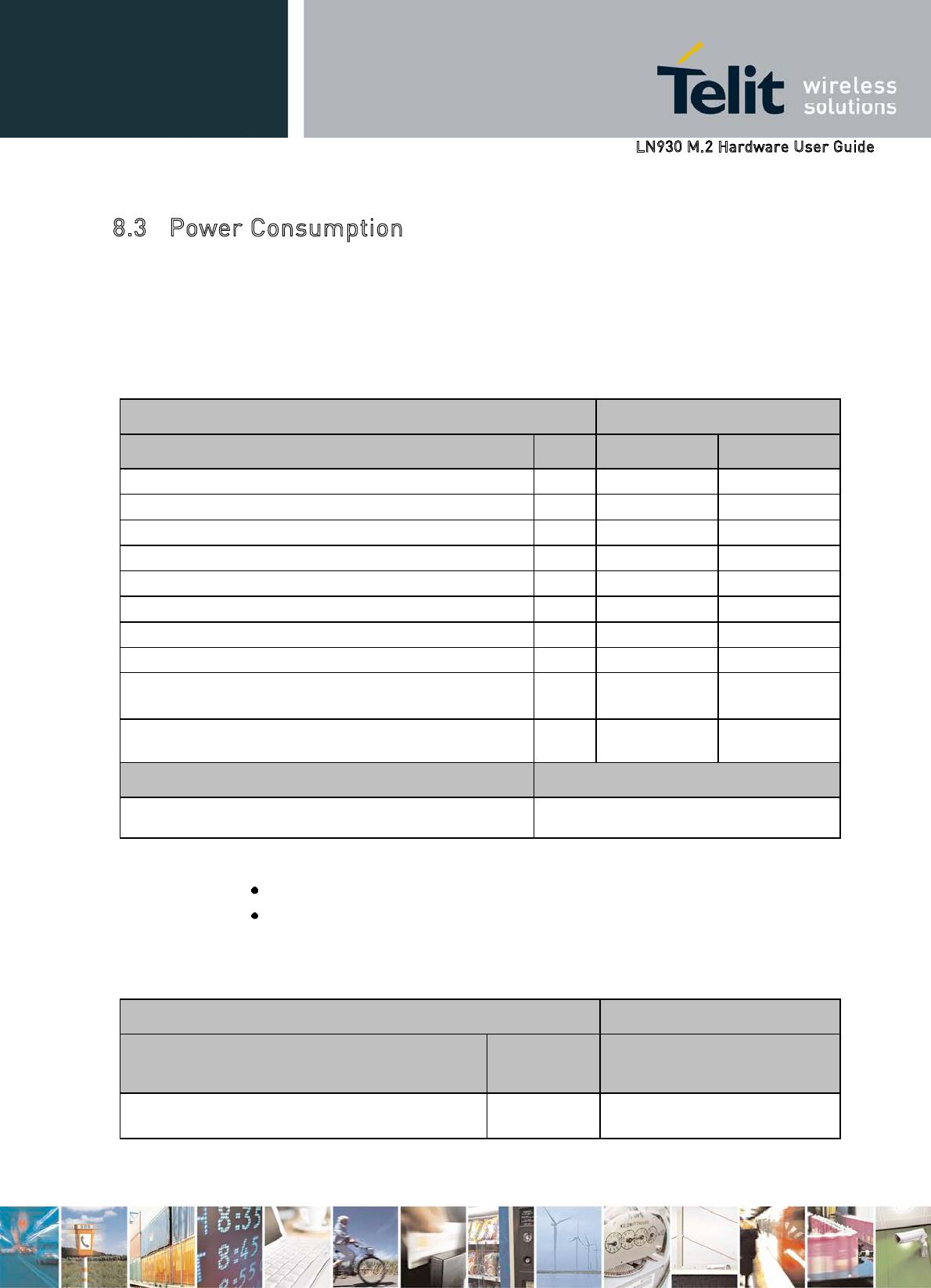
This section lists the power consumption targets.
Typical target values at Vsys = 3.3 V
Table 29 LTE Power Consumption
M.2 Power Consumption (*) Transmit Power
LTE Use Case Band 10 dBm 23 dBm
LTE UTP, Cat. 3, 20 MHz, 100 RB - (APAC SKU only) 1 1195 mW 2195 mW
LTE UTP, Cat. 3, 20 MHz, 100 RB - (APAC SKU only) 3 1175 mW 2356 mW
LTE UTP, Cat. 3, 10 MHz, 50 RB - (APAC SKU only) 8 1000 mW 2201 mW
LTE UTP, Cat. 3, 20 MHz, 100 RB - (APAC SKU only) 9 1175 mW 2244 mW
LTE UTP, Cat. 3, 10 MHz, 50 RB - (APAC SKU only) 11 1073 mW 2155 mW
LTE UTP, Cat. 3, 15 MHz, 75 RB - (APAC SKU only) 18 1122 mW 1911 mW
LTE UTP, Cat. 3, 15 MHz, 75 RB - (APAC SKU only) 19 1112 mw 1874 mW
LTE UTP, Cat. 3, 15 MHz, 75 RB - (APAC SKU only) 21 1208 mW 2270 mW
LTE UTP, Cat. 3, 100 Mbps/50 Mbps, 20 MHz –
(APAC
not included) 7 1068 mW 2531 mW
LTE UTP, Cat. 3, max throughput, 10 MHz –
(APAC not
included) 17 916 mW 2394 mW
LTE Use Case Standby Power
LTE Stand-by current, DRX 1.28 s serv. Cell only 8 mW
(*) Applicable to modules:
LN930
LN930-AP
Table 30 UMTS Power Consumption
M.2 Power Consumption Transmit Power
UMTS Use Case
(DC-HSDAP+ or HSDPA+)
Band 10 dBm
UMTS FTP, Cat. 24, RxDiv
(M.2 DC-HSDPA+)
Band 1 988 mW

UMTS FTP, Cat 14, QAM64
(M.2 DC-HSDPA+)
Band 1 771 mW
UMTS FTP, Cat 14, QAM64
(M.2 HSDPA+)
Band 1 813 mW
Standby Power
UMTS Stand-by current, DRX7, 16NB cells - 6 mW
UMTS Stand-by current, DRX7, 16NB cells (HN930) - 6.6 mW
Table 31 GSM Power Consumption
GSM Use Case Band Transmit Power
2UL, 1DL, PCL10 (*) GPRS 900 475 mW
2UL, 1DL, PCL5 (*) GPRS900 1482 mW
Standby Power
GSM Stand-by, DRX5, 16NB cells - 6 mW
GSM Stand-by, DRX5, 16NB cells (£) - 6.88 mW
(*) Applicable to modules: LN930, LN930-AP, HN930
(£) Applicable to module: HN930 (XMM™ 6260 based)
The M.2 Data Card has shielding and noise filtering in place to ensure that the
WWAN module does not impact the operation of the host system.
The M.2 Data Card must also be able to tolerate platform noise caused by high order clock
harmonics from the host processor and associated support circuitry. It is required that the
noise levels (as measured at the antenna connector) in the operating frequencies of the M.2
Data Card be no greater than 5 dB as compared to the noise floor of the host system.
Wireless subsystems in mobile platforms are affected by platform related noise, even with the
best antenna and chassis design. This noise hampers the wireless radio performance,
sometimes severely. For platforms that incorporate wireless subsystems like WWAN, passing
the wireless operator certification is an important component of platform launch.
One of the key elements of platform noise, commonly referred to as RF interference, is LCD
display panel pixel clock and its harmonics. The pixel clock generates RF that translates
directly into noise picked up by platform wireless radios due to the close proximity of display
electronics and the integrated antennas in the system. Many of the panel vendors allow the
pixel clock to be “tweaked” (i.e. adapt the pixel clock) to shift the harmonics from interfering
with the wireless components in operating radio frequencies.
A radio’s receive performance could be improved by moving any harmonics of the graphics
pixel clock outside of the frequencies used by the wireless modules. This will be
accomplished by shifting the display pixel clock. Shifting the pixel clock is not expected to
affect the graphics quality or its performance. The display panel refresh rate will not be
changed.
To support crosstalk mitigation, the WWAN module provides an event indication to the host
when the channel frequency changes. On the event indication, the host would use the
frequency change information (i.e. Center Frequency, Bandwidth, and any other optional
information) through an API that would facilitate the facilitating the implementation of a
noise mitigation service.
The M.2 Data Card includes a digital thermal sensor in order to monitor the temperature
of the WWAN Card. The firmware will support the extraction of temperature information
from the module and the configuration of auxiliary trip points.
The configuration of the thermal trip points and receipt of thermal data is available
through a WWAN power control API in order for the host to implement a power and
thermal management framework for the system.
The WWAN M.2 module provides support for EAP methods; EAP-SIM, EAP-AKA, and
EAP-AKA’. These methods, which are used on WiFi authentication, require access to
WWAN SIM credentials to connect to WiFi Networks and offload from WWAN.
All necessary AT commends needed for the EAP-SIM functionality are supported. In addition,
all necessary commands need for the PIN entry, change, and lock/unlock are supported.
Through the API, the host can manage Wi-Fi Hotspot connectivity with Operator provisioned
Hotspot SSIDs and/or End-User provided SSIDs and seamlessly offload a data session from a
3G/4G connection to Wi-Fi hotspot connection after successful authentication of the device
and authorization of the end-user subscription using the SIM on the platform.
Transmit power as measure at the WWAN antenna connector
Table 32 Conducted Transmit Power – 2G
Parameter Condition Requirement
Conducted Transmit Power 850 MHz/900 MHz 33 dBm +/- 3 db
1800 MHz/1900 MHz 30 dBm +/- 3 db
2G not supported for APAC SKU
Table 33 Conducted Transmit Power – 3G
HDPA+ / LTE LN930
Parameter Condition Requirement
Conducted Transmit Power1W-CDMA class 3 24 dBm + 1 db /- 3 db
LN930-AP (APAC SKU only)
Parameter Condition Requirement
Conducted Transmit Power1W-CDMA class 3 24 dBm + 1 db /- 3 db
1 Conducted transmit power as measured at the WWAN M.2 RF main antenna connector.
Table 34 Conducted Transmit Power – LTE
HDPA+ / LTE LN930
Parameter Condition Requirement
Conducted Transmit Power1E-UTRA class 3 23 dBm + 0.5/- 1 db
LN930-AP (APAC SKU only)
Parameter Condition Requirement
Conducted Transmit Power1E_UTRA class 3 22.5 dBm + 0.5 /- 1 db
2 Conducted transmit power as measured at the WWAN M.2 RF main antenna connector.
The reference sensitivity power level is the minimum mean power applied to both the WWAN
M.2 antenna ports at which the throughput shall meet or exceed the requirements for the
specified reference measurement channel.
Condition: Calibration voltage = 3.3V, 25C shielded room
Table 35 Rx Sensitivity - GSM
Band Condition Min Rx Sensitivity Limit (dBm)
GSM850 GMSK -110
GSM900 GMSK -109
GSM1800 GMSK -109
GSM1900 GMSK -106
Table 36 Rx Sensitivity - UMTS
HDPA+ / LTE LN930
Band Condition Min Rx Sensitivity Limit (dBm)
1 BER<0.1% -107
2 BER<0.1% -106
4 BER<0.1% -107
5 BER<0.1% -107
8 BER<0.1% -107
LN930-AP (APAC SKU only)
Band Condition Min Rx Sensitivity Limit (dBm)
1 BER<0.1% -106
6 BER<0.1% -106
8 BER<0.1% -103
11 BER<0.1% -106
19 BER<0.1% -106
GSM not supported for LN930-AP
Main and Diversity ports are measured separately. Combining both antenna ports
increases sensitivity by 3 dB. Table 36 Rx Sensitivity – UMTS reflects both ports
combined.
Table 37 Rx Sensitivity - LTE
HDPA+ / LTE LN930
EARFCN
LTE
Band Duplex Modulation Bandwidth
(Hz) Min Rx
Sensitivit
y Limit
(dBm)
Low
Channel Middle
Channel High Channel
1 FDD QPSK 10 -96 50 320 550
2 FDD QPSK 10 -95 650 920 1150
3 FDD QPSK 10 -97 1250 1678 1900
4 FDD QPSK 10 -96 2000 2110 2350
5 FDD QPSK 10 -97 2450 2510 2600
7 FDD QPSK 10 -96 2800 3100 3400
8 FDD QPSK 10 -97 3525 3625 3750
13 FDD QPSK 10 -97 5180 5230 5279
17 FDD QPSK 10 -97 5780 5800 5890
18 FDD QPSK 10 -97 5900 5925 5950
19 FDD QPSK 10 -97 6050 6075 6100
20 FDD QPSK 10 -94 6200 6300 6400
LN930-AP (APAC SKU only)
EARFCN
LTE
Band Duplex Modulation Bandwidth
(Hz) Min Rx
Sensitivit
y Limit
(dBm)
Low
Channel Middle
Channel High Channel
1 FDD QPSK 10 -96 50 320 550
3 FDD QPSK 10 -96 1250 1678 1900
8 FDD QPSK 10 -96 3525 3625 3750
9 FDD QPSK 10 -96 3850 3975 4099
11 FDD QPSK 10 -96 4800 4850 4899
18 FDD QPSK 10 -97 5900 5925 5950
19 FDD QPSK 10 -97 6050 6075 6100
21 FDD QPSK 10 -96 6500 6525 6549
26 FDD QPSK 10 -97 8740 8865 8989
GSM not supported for APAC SKU
Main and Diversity ports are measured separately. Combining both antenna ports
increases sensitivity by 3 dB. Table 36. Rx Sensitivity – UMTS reflects both ports
combined.
Table 37 is a generic view that includes all LTE bands for Rx sensitivity. The APAC
SKU does not include LTE Bands 2, 4, 5, 7, 13, and 17.

The following tables provide antenna guidance for the platform designer.
Table 38 Antenna Recommendation
Parameter Recommendation
Impedance 50 ohm
Antenna Shape
and Radiation
Pattern
Near Omni-directional in the Horizontal plane is preferred
Polarization Predominantly vertical polarization and near Omni-Azimuth pattern are
desired;
H-polarization must not be eliminated ( indoor, diversity)
Input Power 33 dBm typical peak power GSM LB*
30 dBm typical peak power GSM HB*
24 dBm typical average power WCDMA
23 dBm typical average power LTE
*Not included for APAC SKU.
Table 39 Antenna Recommendation - Bandwidth of Main & Diversity Antenna
RF
Band
Center
Frequency
Uplink (UL)
UE Tx
Downlink
(DL) UE Rx
Duplex
Mode
Common
Name
Bandwidth of
Main Antenna
(MHz)
Bandwidth of
Diversity Antenna
(MHz)
001 I (1) 2100 MHz 1920 MHz to
1980 MHz
2110
MHz to
2170 MHz FDD IMT 250 60
002 II (2) 1900 MHz 1850 MHz to
1910 MHz
1930
MHz to
1990 MHz FDD PCS 140 60
003 III (3) 1800 MHz 1710 MHz to
1785 MHz
1805
MHz to
1880 MHz FDD DCS 170 75
004 IV (4) 1700 MHz 1710 MHz to
1755 MHz
2110
MHz to
2155 MHz FDD AWS 445 45
005 V (5) 850 MHz 824 MHz to
849 MHz
869 MHz to
894 MHz FDD CLR 70 25
006 VI (6) 850 MHz 830 MHz to
840 MHz
875 MHz to
885 MHz FDD UMTS 800 55 10
007 VII (7) 2600 MHz 2500 MHz to
2570 MHz
2620
MHz to
2690 MHz FDD IMT-E 190 70
008 VIII
(8) 900 MHz 880 MHz to
915 MHz
925 MHz to
960 MHz FDD GSM 80 35
009 IX (9) 1800 MHz 1749.9
MHz to
1784.9 MHz
1844.9
MHz to
1879.9 MHz FDD UMTS 1800 130 35
010 X (10) 1700 MHz 1710 MHz to
1770 MHz
2110 MHz to
2170 MHz FDD Extended
AWS 460 60
011 XI
(11) 1500 MHz 1427.9 MHz to
1447.9 MHz
1475.9 MHz
to
1495.9 MHz
FDD PDC 68 20
013 XIII
(13) 750 MHz 777 MHz to
787 MHz
746 MHz to
756 MHz FDD
upper SMH
block C 41 10
017 XVII
(17) 700 MHz
704 MHz
to
716 MHz
734 MHz
to
746 MHz
FDD
lower SMH
blocks B/C
(subset of
42 12
RF
Band
Center
Frequency
Uplink (UL)
UE Tx
Downlink
(DL) UE Rx
Duplex
Mode
Common
Name
Bandwidth of
Main Antenna
(MHz)
Bandwidth of
Diversity Antenna
(MHz)
band 12)
018 XVIII
(18) 850 MHz 815 MHz to
830 MHz
860 MHz to
875 MHz FDD
Japan lower
800 60 15
019 XIX
(19) 850 MHz 830 MHz to
845 MHz
875 MHz to
890 MHz FDD
Japan upper
800 60 15
020 XX
(20) 800 MHz 832 MHz to
862 MHz
791 MHz to
821 MHz FDD
EU's Digital
Dividend 71 30
021 XXI
(21) 1500 MHz 1447.9 MHz to
1462.9 MHz
1495.9 MHz
to
1510.9 MHz
FDD PDC 63 15.4
025 XXV
(25) 1900 MHz 1850 MHz to
1915 MHz
1930 MHz to
1995 MHz FDD
Extended
PCS
(superset of
band 2)
145 65
026 XXVI
(26) 850MHz 814 MHz to
849 MHz
859 MHz to
894 MHz FDD ESM+CLR 80 35
027 XXVII
(27) 850MHz 806 MHz to
824 MHz
851 MHz to
869 MHz FDD ESMR 63 18
028 XXVIII
(28) 750MHz
703 MHz to 728
MHz
758 MHz to
803 MHz FDD APAC 700 100 45
GPS
1575.42 MHz
GPS L1 35
GLONASS
1602 MHz GLONASS L1
35
APAC SKU does not include RF Bands 7, 10, 13, 17, 20, 25, 26, 27, 28
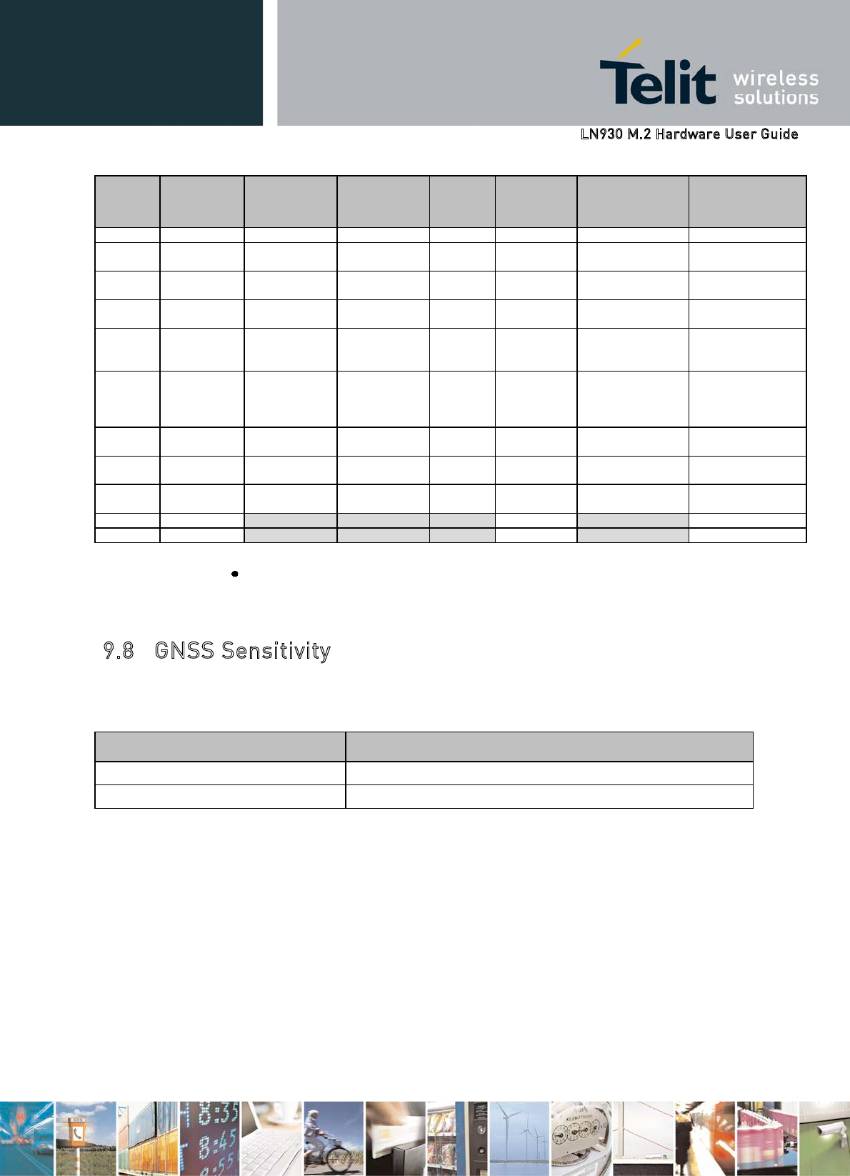
Table 40 GNSS Sensitivity
Parameter Min Limit (dBm)
Cold Start Sensitivity -145
Hot Start Sensitivity -155

M.2 module complies with the following listed test standards:
3GPP TS 31.121 USIM
3GPP TS 31.124USAT
3GPP TS51.010-1, 2G PS & RF & RRM
3GPP TS 51.010-4 2G SIMTK
3GPP TS34.121-1 3G RF & RRM
3GPP TS34.123-1 3G PS
3DPP TS36.124 LTE Radiated Emission
3GPP TS36.521-1 LTE RF
3GPP TS 36.521-3 LTE RRM
3GPP TS36.523-1 LTE PS
ETSI TS 102 230 UICC
OMA ETS SUPL v1.0 LBS SUPL
OMA ETS SUPL v2.0 LBS SUPL
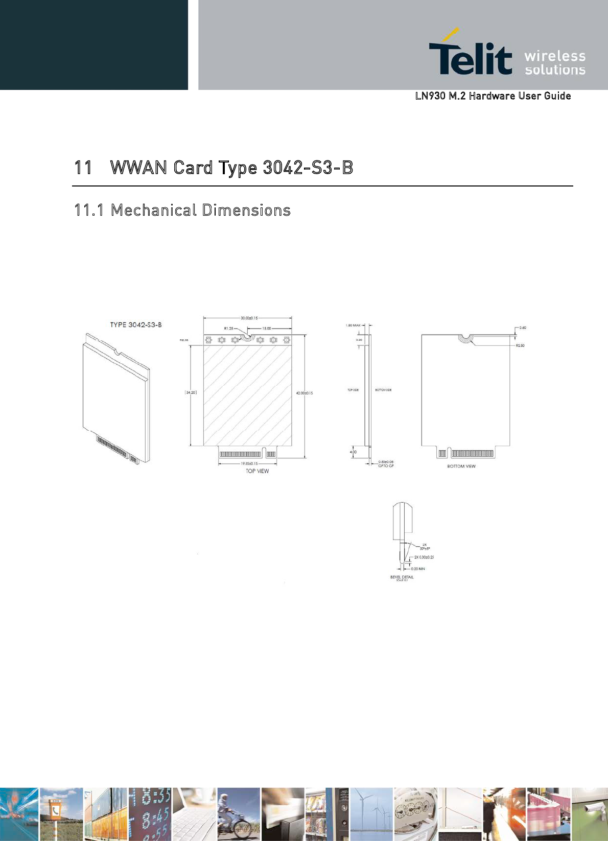
The mechanical dimensions of WWAN Card Type 3042 are shown in Figure 17 and Figure 17.
The WWAN card is 30 mm x 42 mm. The height is 1.5 mm from the top of the PCB to the
top of the outside shield. There are a total of 75 pins; however 8 pins are lost to support the
slot+. All components are mounted on the Top side.
Figure 17 WWAN Card 3042 Mechanical Dimensions
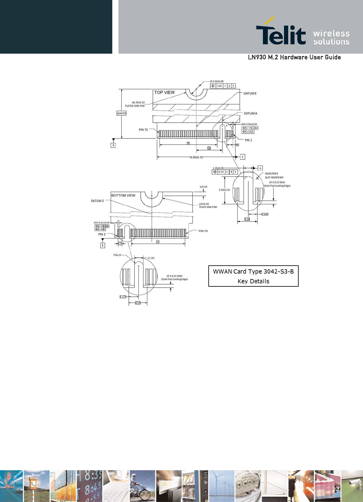
Figure 18 WWAN Card 3042 Slot Key Details
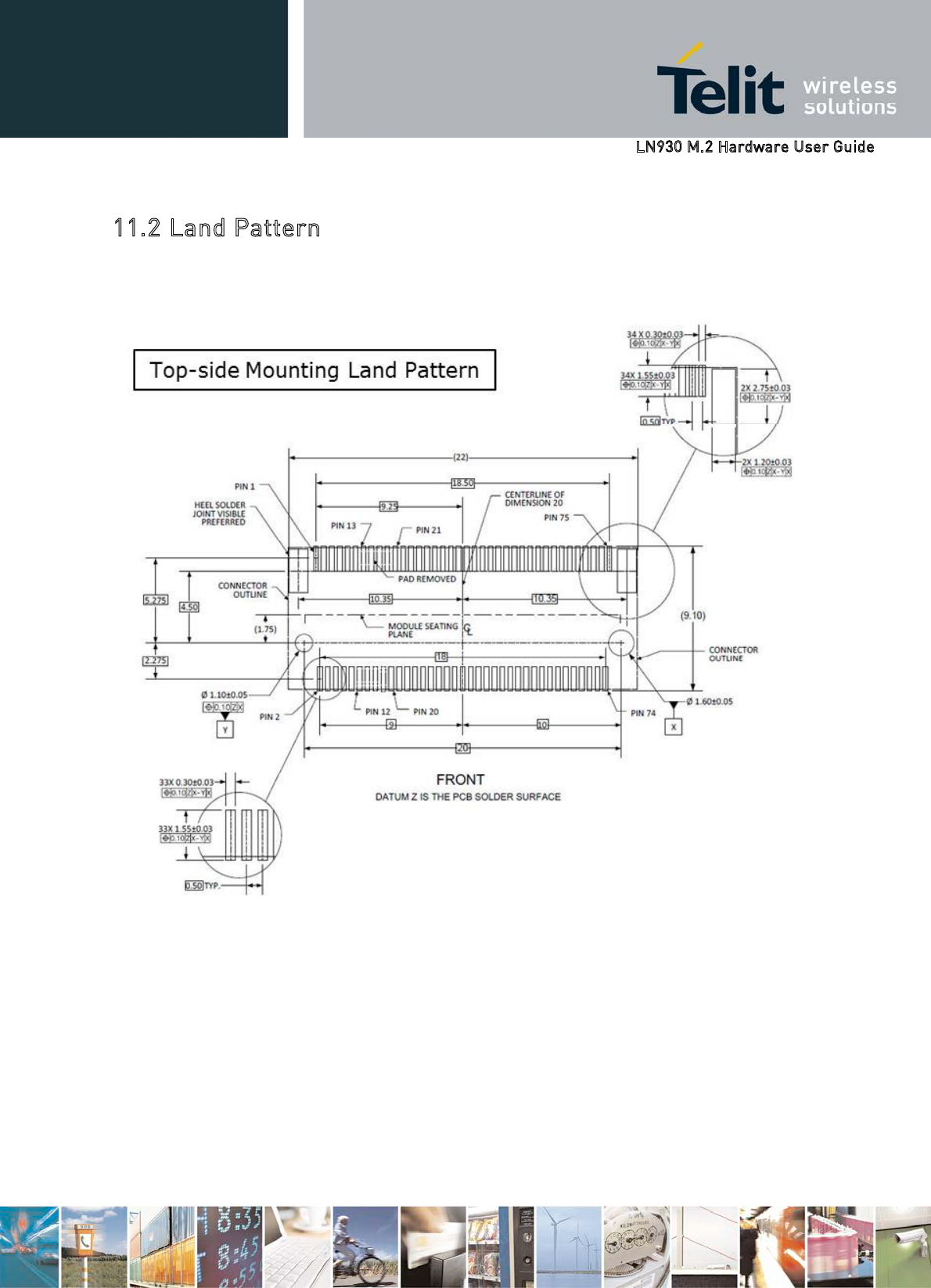
Figure 19 illustrates a typical land pattern for a top-mount connector with the key removed.
Figure 19 WWAN Card Type 3042 Top-Side Mounting Land Pattern
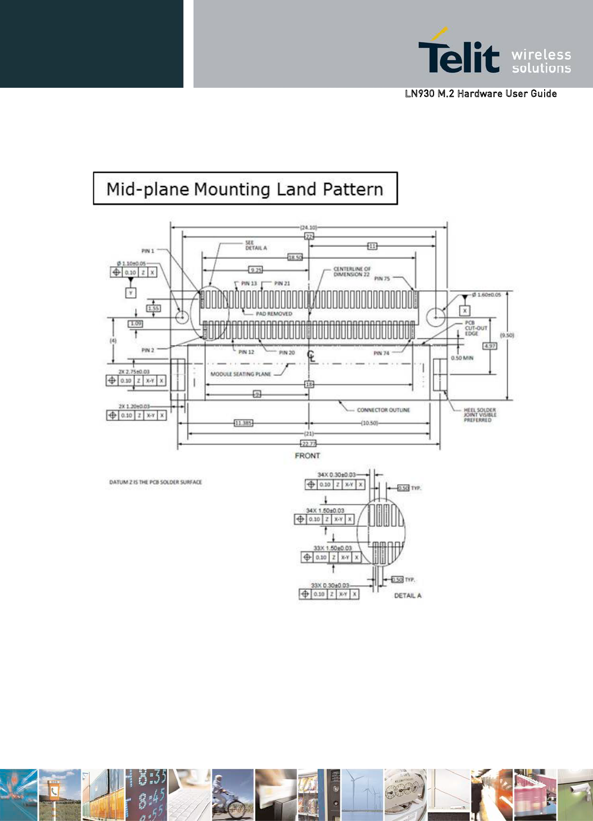
Figure 20 illustrates a typical mid-plane (in-line) land pattern with slot key removed.
Figure 20 WWAN Card 3042 Mid-plane Land Pattern with Slot Key Removed

Figure 21 illustrates the locations for the main Rx/Tx antenna and the Diversity/GPS antenna.
Figure 21 Antenna Connector Location
Table 41 Antenna Connector Assignment
Antenna Interface
0 TBD
1 Diversity/ GPS
2 TBD
3 TBD
4 WWAN Main Tx/Rx
5 TBD
For M.2 Modules positions 1 and 4 are used. The other antenna connectors are not
mounted on the module.
READ CAREFULLY
Be sure the use of this product is allowed in the country and in the environment required. The
use of this product may be dangerous and has to be avoided in the following areas:
Where it can interfere with other electronic devices in environments such as hospitals,
airports, aircrafts, etc.
Where there is risk of explosion such as gasoline stations, oil refineries, etc. It is
responsibility of the user to enforce the country regulation and the specific
environment regulation.
Do not disassemble the product; any mark of tampering will compromise the warranty
validity. We recommend following the instructions of the hardware user guides for a correct
wiring of the product. The product has to be supplied with a stabilized voltage source and the
wiring has to be conforming to the security and fire prevention regulations. The product has to
be handled with care, avoiding any contact with the pins because electrostatic discharges may
damage the product itself. Same cautions have to be taken for the SIM, checking carefully the
instruction for its use. Do not insert or remove the SIM when the product is in power saving
mode.
The system integrator is responsible of the functioning of the final product; therefore, care has
to be taken to the external components of the module, as well as of any project or installation
issue, because the risk of disturbing the GSM network or external devices or having impact
on the security. Should there be any doubt, please refer to the technical documentation and the
regulations in force. Every module has to be equipped with a proper antenna with specific
characteristics. The antenna has
to be installed with care in order to avoid any interference with other electronic devices and
has to guarantee a minimum distance from the body (20 cm). In case of this requirement
cannot be satisfied, the system integrator has to assess the final product against the SAR
regulation.
The European Community provides some Directives for the electronic equipments
introduced on the market. All the relevant information’s are available on the European
Community website:
http://ec.europa.eu/enterprise/sectors/rtte/documents/
The text of the Directive 99/05 regarding telecommunication equipments is available,
while the applicable Directives (Low Voltage and EMC) are available at:
http://ec.europa.eu/enterprise/sectors/electrical/

The following chapters are related to the M.2 module on the EVK carrier board.
The LN930 products portfolio has been evaluated against the essential requirements of the
1999/5/EC Directive.
Bulgarian Telit Communications S.p.A. , 2G/3G module
1999/5/ .
Czech Telit Communications S.p.A. tímto prohlašuje, že tento 2G/3G module
ími
Danish Undertegnede Telit Communications S.p.A. erklærer herved, at følgende udstyr
2G/3G module
overholder de væsentlige krav og øvrige relevante krav i direktiv 1999/5/EF.
Dutch Hierbij verklaart Telit Communications S.p.A.
dat het toestel 2G/3G module in
overeenstemming is met de essentiële eisen en de andere relevante bepalingen van richtlijn
1999/5/EG.
English Hereby, Telit Communications S.p.A., declares that this 2G/3G module is
in compliance with
the essential requirements and other relevant provisions of Directive 1999/5/EC.
Estonian Käesolevaga kinnitab Telit Communications S.p.A. seadme 2G/3G module
vastavust direktiivi
1999/5/EÜ põhinõuetele ja nimetatud direktiivist tulenevatele teistele asjakohastele sätetele.
German
Hiermit erklärt Telit Communications S.p.A., dass sich das Gerät 2G/3G module in
Übereinstimmung mit den grundlegenden Anforderungen und den übrigen einschlägigen
Bestimmungen der Richtlinie 1999/5/EG befindet.
Greek
2G/3G module
Hungarian
Alulírott, Telit Communications S.p.A. nyilatkozom, hogy a 2G/3G module megf
elel a
vonatkozó alapvetõ követelményeknek és az 1999/5/EC irányelv egyéb elõírásainak.
Finnish Telit Communications S.p.A.
vakuuttaa täten että 2G/3G module tyyppinen laite on direktiivin
1999/5/EY oleellisten vaatimusten ja sitä koskevien direktiivin muiden ehtojen mukainen.
French
Par la présente Telit Communications S.p.A. déclare que l'appareil 2G/3G module est conforme
aux exigences essentielles et aux autres dispositions pertinentes de la directive 1999/5/CE.
Icelandic Hér með lýsir Telit Communications S.p.A. yfir því að 2G/3G module
er í samræmi við
grunnkröfur og aðrar kröfur, sem gerðar eru í tilskipun 1999/5/EC
Italian
Con la presente Telit Communications S.p.A. dichiara che questo 2G/3G module è conforme ai
requisiti essenziali ed alle altre disposizioni pertinenti stabilite dalla direttiva 1999/5/CE.
Latvian Ar šo Telit Communications S.p.A. 2G/3G module
.
Lithuanian
Šiuo Telit Communications S.p.A. deklaruoja, kad šis 2G/3G module
atitinka esminius
reikalavimus ir kitas 1999/5/EB Direktyvos nuostatas.
Maltese
Hawnhekk,
Telit Communications S.p.A.
, jiddikjara li dan
2G/3G module
jikkonforma mal
-
-Dirrettiva 1999/5/EC.
Norwegian
Telit Communications S.p.A. erklærer herved at utstyret 2G/3G module
er i samsvar med de
grunnleggende krav og øvrige relevante krav i direktiv 1999/5/EF.
Polish 2G/3G module
jest zgodny z
iami Dyrektywy 1999/5/EC
Portuguese
Telit Communications S.p.A. declara que este 2G/3G module
está conforme com os requisitos
essenciais e outras disposições da Directiva 1999/5/CE.
Slovak Telit Communications S.p.A. týmto vyhlasuje, že 2G/3G module
a základné požiadavky a
všetky príslušné ustanovenia Smernice 1999/5/ES.
Slovenian Telit Communications S.p.A. izjavlja, da je ta 2G/3G modul
v skladu z bistvenimi zahtevami in
Spanish Por medio de la presente Telit Communications S.p.A. declara que el 2G/3G module
cumple con
los requisitos esenciales y cualesquiera otras disposiciones aplicables o exigibles de la Directiva
1999/5/CE.
Swedish Härmed intygar Telit Communications S.p.A. att denna 2G/3G module
står I överensstämmelse
med de väsentliga egenskapskrav och övriga relevanta bestämmelser som framgår av direktiv
1999/5/EG.
In order to satisfy the essential requirements of 1999/5/EC Directive, the LN930 is
compliant with the following standards:
RF spectrum use (R&TTE art. 3.2) EN 300 440-2 V1.4.1
EN 301 511 V9.0.2
EN 301 908-1 V6.2.1
EN 301 908-2 V5.2.1
EN 301 908-13 V5.2.1
EN 300 440-1 V1.6.1
EMC (R&TTE art. 3.1b) EN 301 489-1 V1.9.2
EN 301 489-3 V1.4.1
EN 301 489-7 V1.3.1
EN 301 489-24 V1.5.1
Health & Safety (R&TTE art. 3.1a) EN 60950-1:2006 + A11:2009 + A1:2010 + A12:2011
EN 62311: 2008
The conformity assessment procedure referred to in Article 10 and detailed in Annex IV of
Directive 1999/5/EC has been followed with the involvement of the following Notified
Body:
Thus, the following marking is included in the product:
The full declaration of conformity can be found on the following address:
http://www.telit.com/
There is no restriction for the commercialization in all the countries of the European Union.
Final product integrating this module must be assessed against essential requirements of
the 1999/5/EC (R&TTE) Directive. It should be noted that assessment does not necessarily
lead to testing. Telit Communications S.p.A. recommends carrying out the following
assessments:
RF spectrum use (R&TTE art.
3.2)
It will depend on the antenna used on the final
product.
EMC (R&TTE art. 3.1b) Testing
Health & Safety (R&TTE art.
3.1a)
Testing
Alternately, assessment of the final product against EMC (Art. 3.1b) and Electrical safety
(Art. 3.1a) essential requirements can be done against the essential requirements of the
EMC and the LVD Directives:
Low Voltage Directive 2006/95/EC and product safety
Directive EMC 2004/108/EC for conformity for EMC
This device meets the EU requirements (1999/519/EC) and the International Commission on
Non-Ionizing Radiation Protection (ICNIRP) on the limitation of exposure of the general
public to electromagnetic fields by way of health protection.
To comply with the RF exposure requirements, this module must be installed in a host
platform that is intended to be operated in a minimum of 20 cm separation distance to the user.
In all cases assessment of the final product must be met against the Essential requirements of
the R&TTE Directive Articles 3.1(a) and (b), safety and EMC respectively, as well as any
relevant Article 3.3 requirements.
1. The Dipole antenna (gain: GPRS/EGPRS/WCDMA/LTE: 2dBi) was verified in the
conformity testing, and for compliance the antenna shall not be modified. A separate approval
is required for all other operating configurations, including different antenna configurations.
2. If any other simultaneous transmission radio is installed in the host platform together with
this module, or above restrictions cannot be kept, a separate RF exposure assessment and CE
equipment certification is required.
Telit has not approved any changes or modifications to this device by the user. Any changes
or modifications could void the user’s authority to operate the equipment.
Telit n’approuve aucune modification apportée à l’appareil par l’utilisateur, quelle qu’en soit
la nature. Tout changement ou modification peuvent annuler le droit d’utilisation de
l’appareil par l’utilisateur.
The OEM integrator has to be aware not to provide information to the end user regarding how
to install or remove this RF module in the user’s manual of the end product which integrates
this module. The end user manual shall include all required regulatory information/warning as
show in this manual.
CAN ICES-3(B)/ NMB-3(B)
This device complies with Part 15 of the FCC Rules and Industry Canada licence-exempt
RSS standard(s). Operation is subject to the following two conditions: (1) this device may not
cause interference, and (2) this device must accept any interference, including interference
that may cause undesired operation of the device.
Le présent appareil est conforme aux CNR d'Industrie Canada applicables aux appareils
radio exempts de licence. L'exploitation est autorisée aux deux conditions suivantes : (1)
l'appareil ne doit pas produire de brouillage, et (2) l'utilisateur de l'appareil doit accepter
tout brouillage radioélectrique subi, même si le brouillage est susceptible d'en compromettre
le fonctionnement.
This equipment has been tested and found to comply with the limits for a Class B digital device, pursuant to part
15 of the FCC Rules. These limits are designed to provide reasonable protection against harmful interference in a
residential installation. This equipment generates, uses and can radiate radio frequency energy and, if not installed
and used in accordance with the instructions, may cause harmful interference to radio communications. However,
there is no guarantee that interference will not occur in a particular installation. If this equipment does cause
harmful interference to radio or television reception, which can be determined by turning the equipment off and on,
the user is encouraged to try to correct the interference by one or more of the following measures:
- Reorient or relocate the receiving antenna.
- Increase the separation between the equipment and receiver.
- Connect the equipment into an outlet on a circuit different from that to which the receiver
is connected.
- Consult the dealer or an experienced radio/TV technician for help.
This equipment complies with FCC/IC radiation exposure limits set forth for an uncontrolled
environment. This equipment should be installed and operated with minimum distance 20 cm
between the radiator & your body.
When the module is installed in the host device, the FCC/IC ID label must be visible through a
window on the final device or it must be visible when an access panel, door or cover is easily
re-moved. If not, a second label must be placed on the outside of the final device that contains
the following text: “Contains FCC ID: RI7LN930”, “Contains IC ID: 5131A-LN930”.The
grantee's FCC/IC ID can be used only when all FCC/IC compliance requirements are met.
This device is intended only for OEM integrators under the following conditions:
(1) The antenna must be installed such that 20 cm is maintained between the antenna and users,
(2) The transmitter module may not be co-located with any other transmitter or antenna.
(3) To comply with FCC/IC regulations limiting both maximum RF output power and human
exposure to RF radiation, the maximum antenna gain including cable loss in a mobile exposure
condition must not exceed:
5.0 dBi in Cellular band
3.0 dBi in PCS band
5.5 dBi in AWS band
5.0 dBi in 700 MHz band
5.0 dBi in 2500MHz band
In the event that these conditions cannot be met (for example certain laptop configurations or
co-location with another transmitter), then the FCC/IC authorization is no longer considered
valid and the FCC/IC ID cannot be used on the final product. In these circumstances, the OEM
integrator will be responsible for re-evaluating the end product (including the transmitter) and
obtaining a separate FCC/IC authorization.
Revision Date Changes
0 2013-05-20 First issue
1 2013-07-09 •
Update setting for Pin 21 on the host interface. This signal is not connected.
• Updated pin names of pins 1, 21, 69, and 75 in Table 4 and Table 19 to
simply reflect HW Configuration use.
• Updated Table 24 to indicate configuration pins 1, 69, and 75 are tied to
GND.
• Rename section 3.6 Coexistence Interface to In-Device Coexistence
Interface. Additional information on the Inter-device coexistence support was added.
• Updated section 4.1.3 System Trace Tool Section.
• Updated Figure 5 – RF Engine for WW SKU.
• Add further information USB LPM to USB section
• Added information on Seamless Roaming & Wifi Off-load – SIM_EAP,
SIM-AKA under Other Requirements
• Added information on Antenna Design Guidelines under Other
Requirements.
2 2013-07-29 RF bands updated
3 2013-08-26 Updating on RF bands
Updated section 3.5 and 3.4.5
Updated temp range
4 2013-09-09 HN930-DC product was removed from portfolio
5 2013-09-15 Main & Diversity antenna positions have been swapped.
Updated documentation accordingly, Figure 6 and Figure 10.
Updated WWAN M.2 Mechanical drawings, Figure 14 through Figure 17.
Updated Card_power_ON_OFF description for UltraBook in Table 9.
Updated comments in Table 15 regarding the DPR#/SAR signal.
Updated SIM DTECTED signal to indicate an external pull-up.
Updated Platform Block Diagrams to show DPR# signal is connected to an
EINT pin (not GPIO) on XGOLD.
Identified Audio Signals on host interface in Table 4. Previously these were
simply defined as Reserved.
Updated VBAT requirements in Table 24 and Table 25.
6 2013-11-20 Regulation section was updated
Adding support for UMTS Band 6 to M.2 APAC SKU (see Table 2).
Updated 3G RF Band support for APAC Module, supported bands are 1, 8,
11, and 19. (see Table 2)
Added Measured Values for 2G/3G Rx Sensitivity Table 31 and Table 32.
Update Measured Value and changed header name in Rx Sensitivity LTE
Table 33
Modified supply voltage lower spec for Ultra book in Table 24.
Update Table 4, Table 6, Table 26 voltage levels for USB and SIM pins.
Added LTE conditions and added Table 33.
7 2014-04-10 Added SSIC to ICP interface. Updated RESET signal definition. Updated
Antenna figures.
Updated Conducted Transmit Power requirements, Table 32.
Section 2.2, Table 4
Changed UIM signals pins 30, 32, 34, 36
Replaced dash with underscore in signal names.
Changed supply voltage for Antenna Tuning Signal
(ANTCTL*) from (1.7 V – 2.6 V) to 1.8 V.
Section 3.5, Table 20 changed supply voltage for Antenna Tuning Signals
(ANTCTL*) from (1.7 V – 2.6 V) to 1.8 V.
Section 3.11, Table 25 correction to both no connect pins and key slot pins.
Section 8.2, Table 27
oChanged the max voltage to 3.0 V for WAKE_WWAN# signal
oChanged Typ voltage and max voltage for the Antenna Tuning
Signals to 0/1.8 V and 2.3 V respectfully
Correction in Section 11.3, fixed typo in sentence: For WWAN M.2
Modules, only positions 1 and 4 are used.
Updated table to only indicate minimum RX sensitivity limit.
Updated Section Conducted Transmit Power section.
Added CAT 4: DL 150 Mbps, UL 50 Mbps to APAC LTE in Table 3
Deleted LED Blink Status in Table 14
Updated Table 4 and Table 27
Added Humidity Requirement
Removed Quality & Reliability section since this is a requirement of the
ODM.
Correction to: DPR signal includes pull-up, SSIC N/P pin locations, COEX
pin names.
8 2014-06-24 Added IC Canada certification wording.
Section 3.2.1, SIM Design Recommendations - added new section
Section 3.12, Antenna Interface changed connector of the WWAN antenna
cable to iPEX MHF4 from Hirose W.FLT
Section 7, Table 24. Operating Environment changed description for
Operating Temperature to include extreme temperature +55 °C to +70 °C
and added additional description
Section 8.2, deleted Table 27. Electrical Parameters – Host Interface
Signals and replaced it with:
oTable 27. DC Specification for 3.3 V Logic Signaling
oTable 28. DC Specification for 1.8 V Logic Signaling
Section 8.3, Table 29. LTE Power Consumption
oAdded additional LTE Use Cases for APAC SKU only - Bands
1, 3, 8, 9, 11, 18, 19, and 21
oChanged standby power to 8 mW
Section 9.6, -
oTable 35. Rx Sensitivity – GSM - added note indicating that
GSM is not supported for APAC SKU.
oTable 36. Rx Sensitivity – UMTS– added note indicating that
the minimum limits reflects that the main and diversity ports are
combined.
oTable 37. Rx Sensitivity – LTE – added note indicating that the
8 LTE bands 2, 4, 5, 7, 13, 17, 20, and 26 is not supported for
APAC SKU
Section 9.7, Antenna Recommendations
Table 38. Antenna Recommendation, added note indicating that the
first 2 recommendations for Input Power are not supported for APAC
SKU.
Table 39. Antenna Recommendation - Bandwidth of Main &
Diversity Antenna - added not indicating that the following 9 RF
Bands 007, 010, 013, 017, 020, 025, 026, 027, and 028 are not
supported by the APAC SKU.
9 2014-11-18 Replaced Requirement with Target in Table 32 to Table 37.
Changes to Table 32. Conducted Transmit Power – 2G
Changes to Table 33. Conducted Transmit Power – 3G
Changes to Table 34. Conducted Transmit Power – LTE
Changes to Table 35. Rx Sensitivity – GSM
Changes to Table 36. Rx Sensitivity – UMTS
Changes to Table 37. Rx Sensitivity – LTE
Changes to Table 38. Antenna Recommendation
10 2014-12-21 Added note to Table 3. WWAN M.2 Module – Data Services
SKU. This is only for generic SW and VZW SW, but not for AT&T SW.
Changes to Section 3.2 USIM Interface
Changes to Section 3.2 USIM Interface
List number 2 and 3
Changes to Table 4. WWAN M.2 Host Interface Signals pins 29, 31, 35,
and 37.
Changes to Table 6. USB SSIC - ICP Interface
Changes to Table 33. Conducted Transmit Power – LTE
Changes to Table 4. WWAN M.2 Host Interface Signals pins 29, 31, 35,
37, and 67.
Changes to Table 36. Rx Sensitivity – LTE

Added new table, Table 39. GNSS Sensitivity