ELITEGROUP COMPUTER SYSTEMS ED2LN30PA1 DATA CARD User Manual Part 1
ELITEGROUP COMPUTER SYSTEMS CO., LTD DATA CARD Part 1
UserManual.wiki
>
ELITEGROUP COMPUTER SYSTEMS
>
ED2LN30PA1 User Manual
>
User Manual Part 1
Contents
1.
User Manual Part 1
2.
User Manual Part 2
3.
User Manual
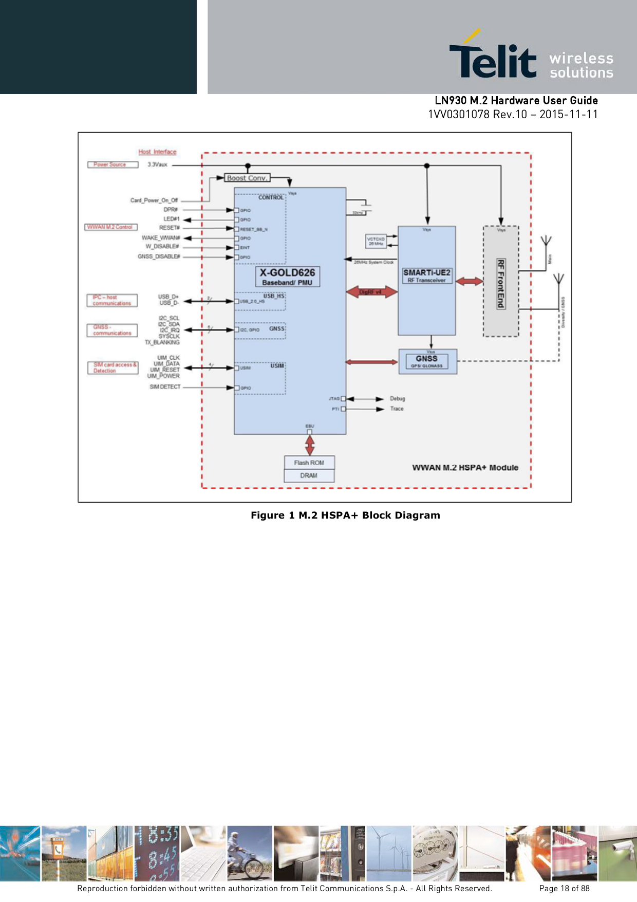
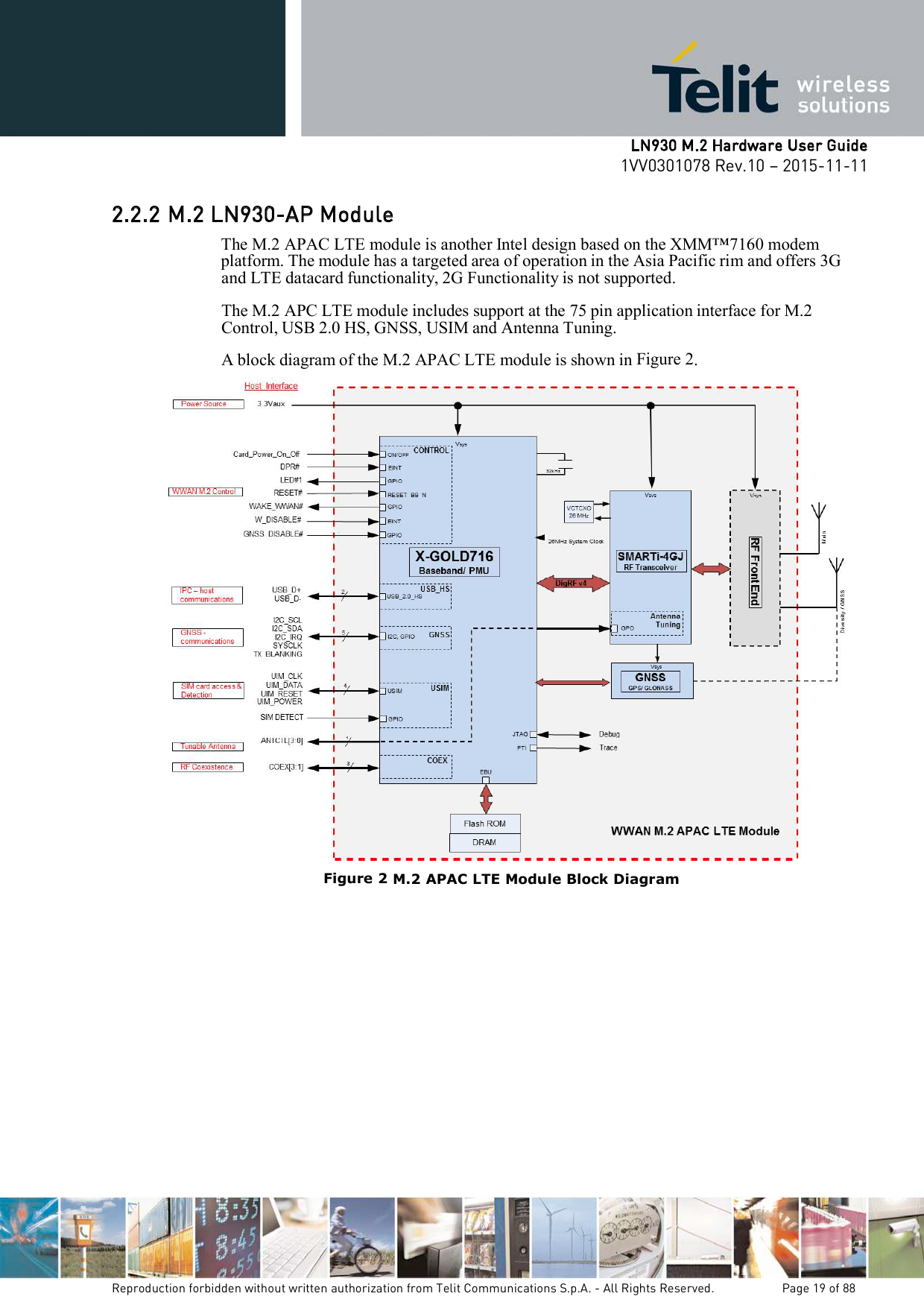
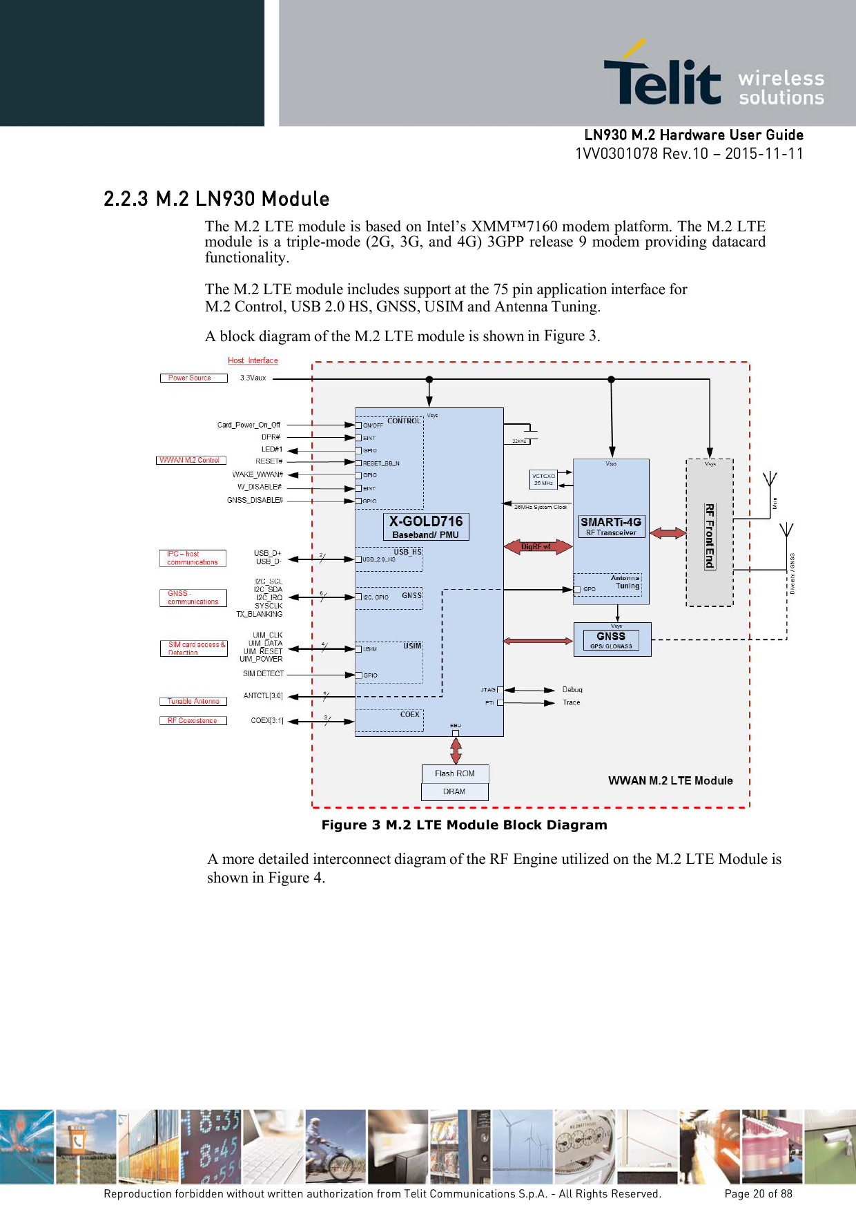
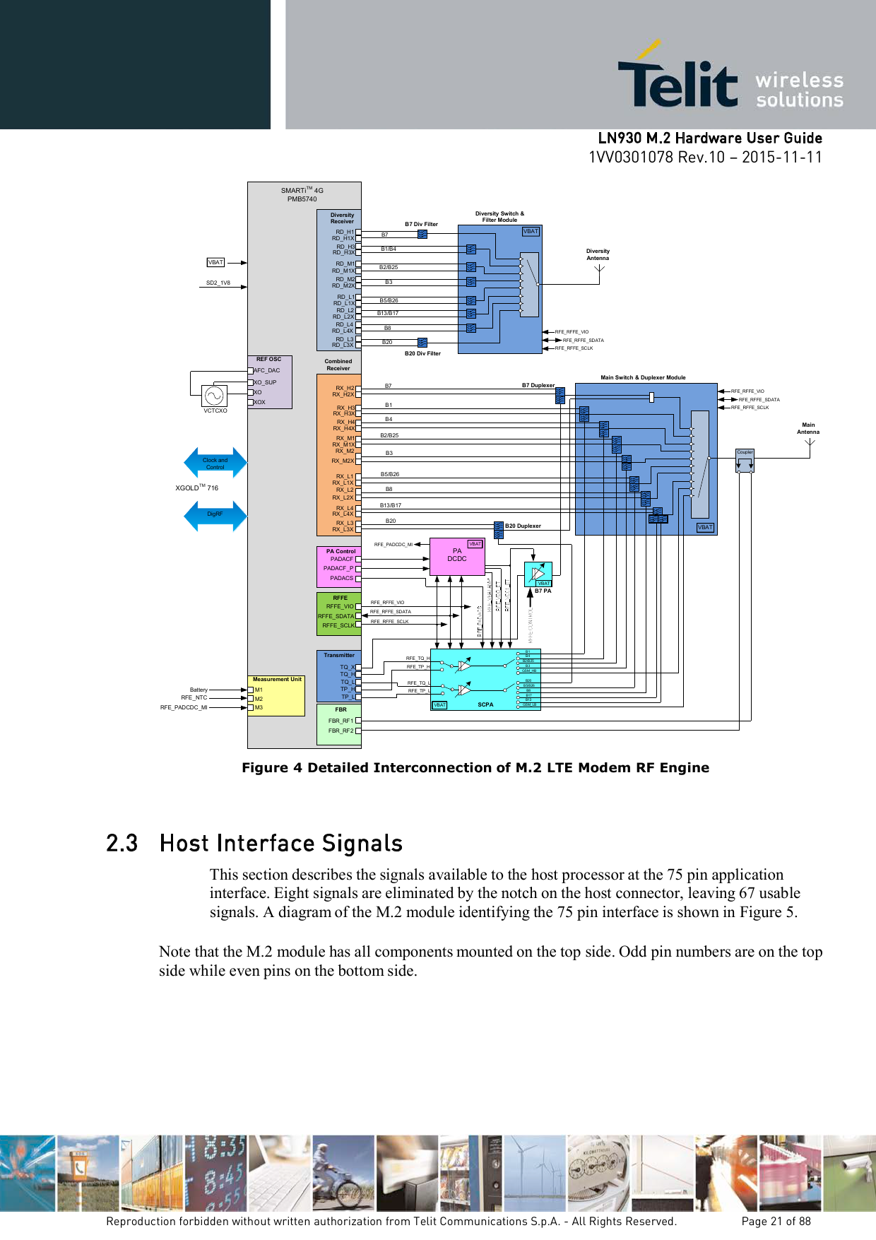
User Manual Part 1
Navigation menu
Upload a User Manual
Namespaces
Wiki Guide
HTML
PDF
Info
Views
User Manual
Discussion / Help
Navigation