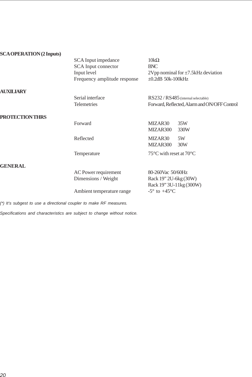
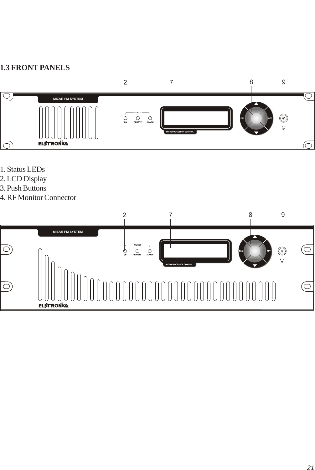
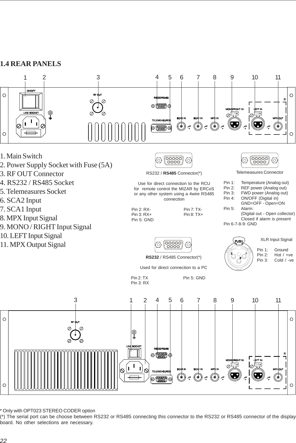
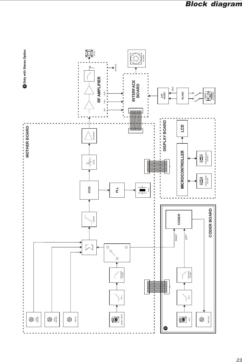
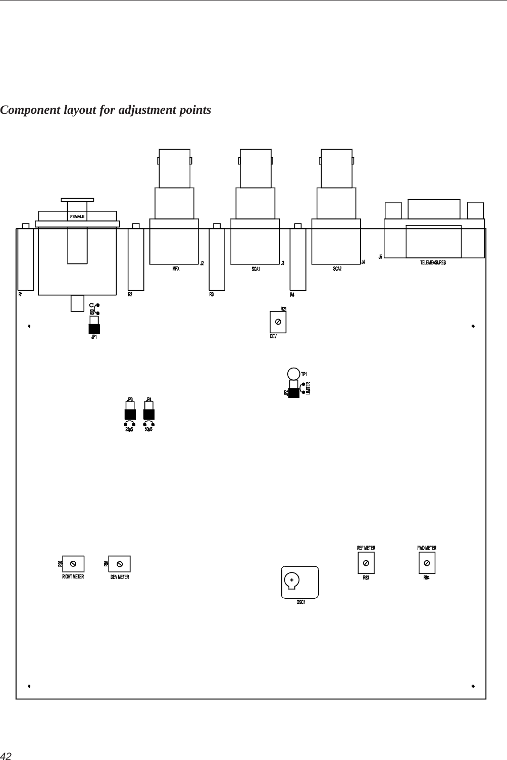
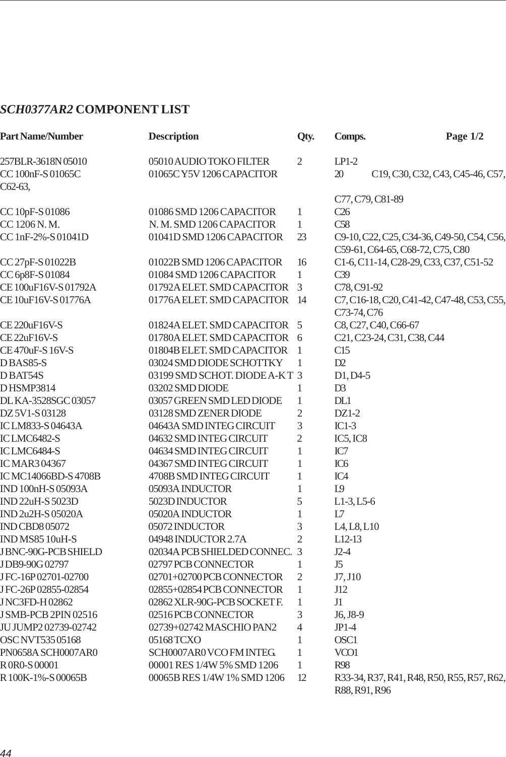
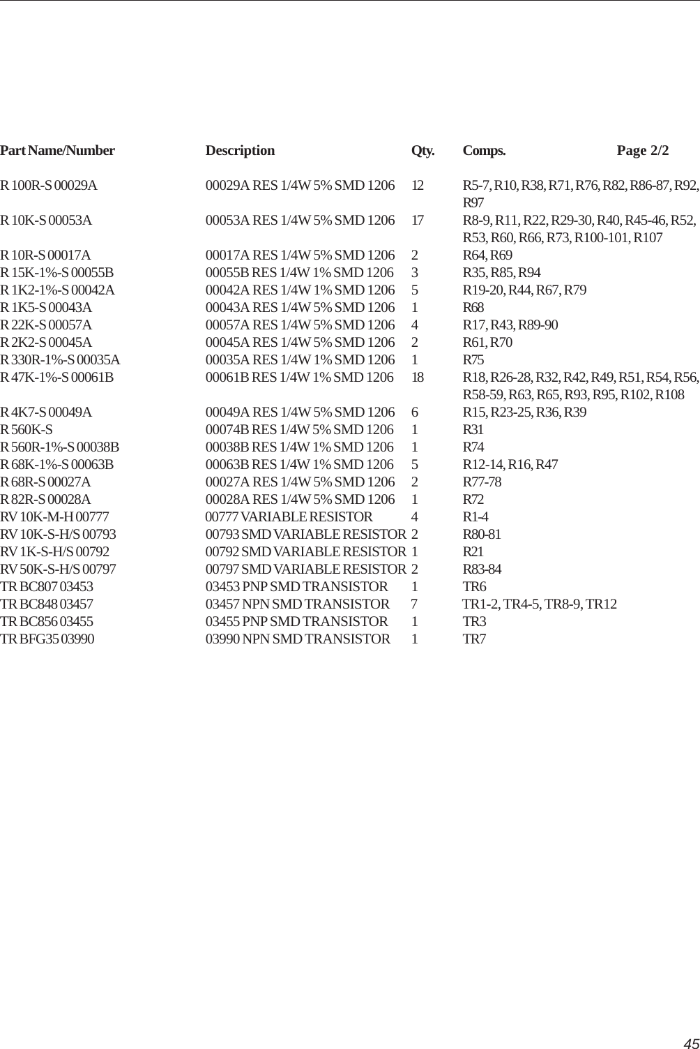
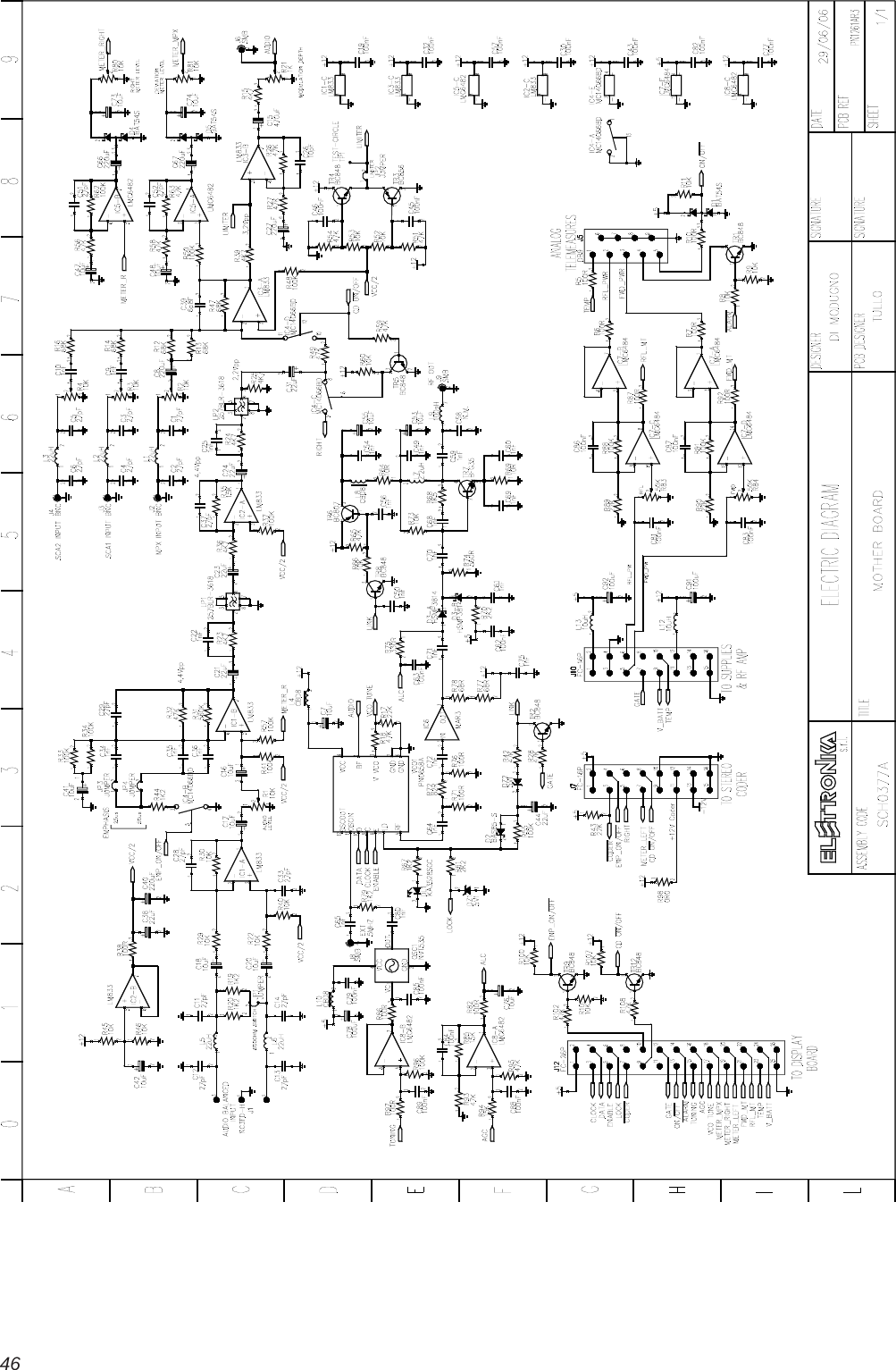
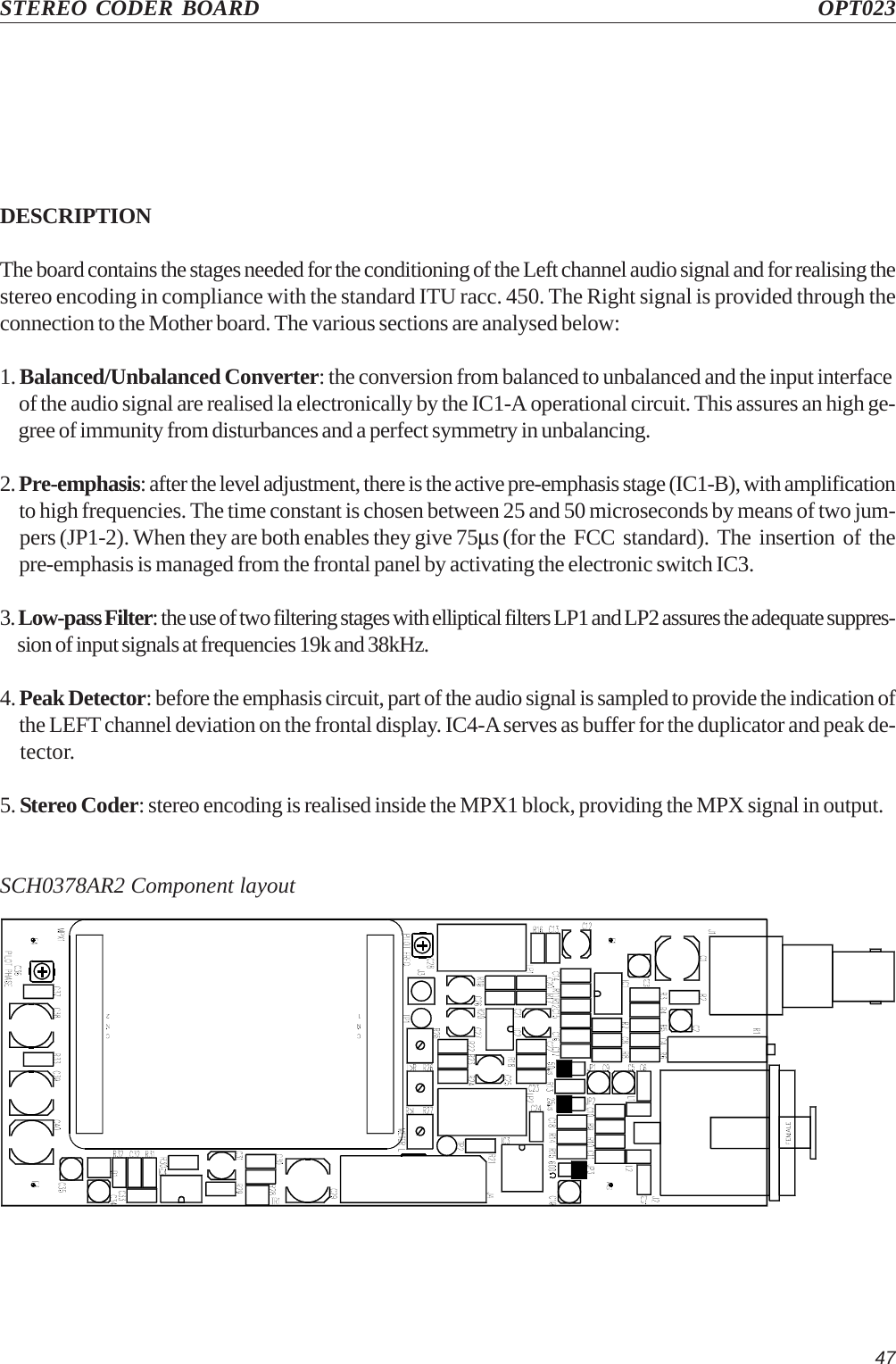
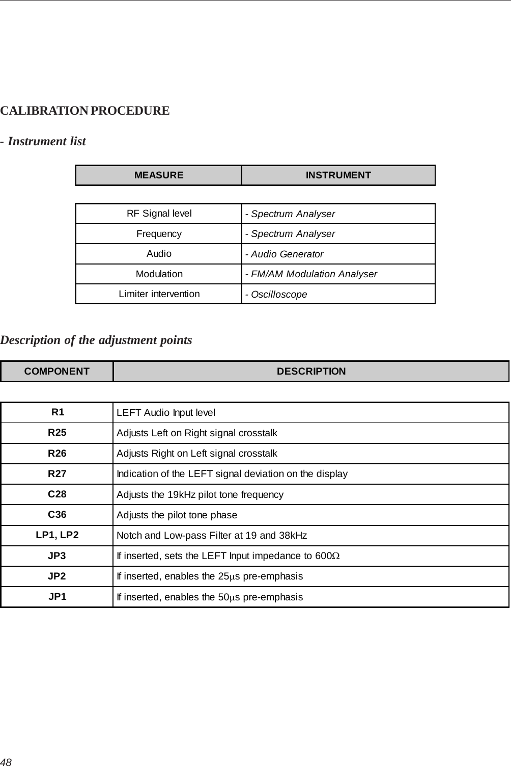
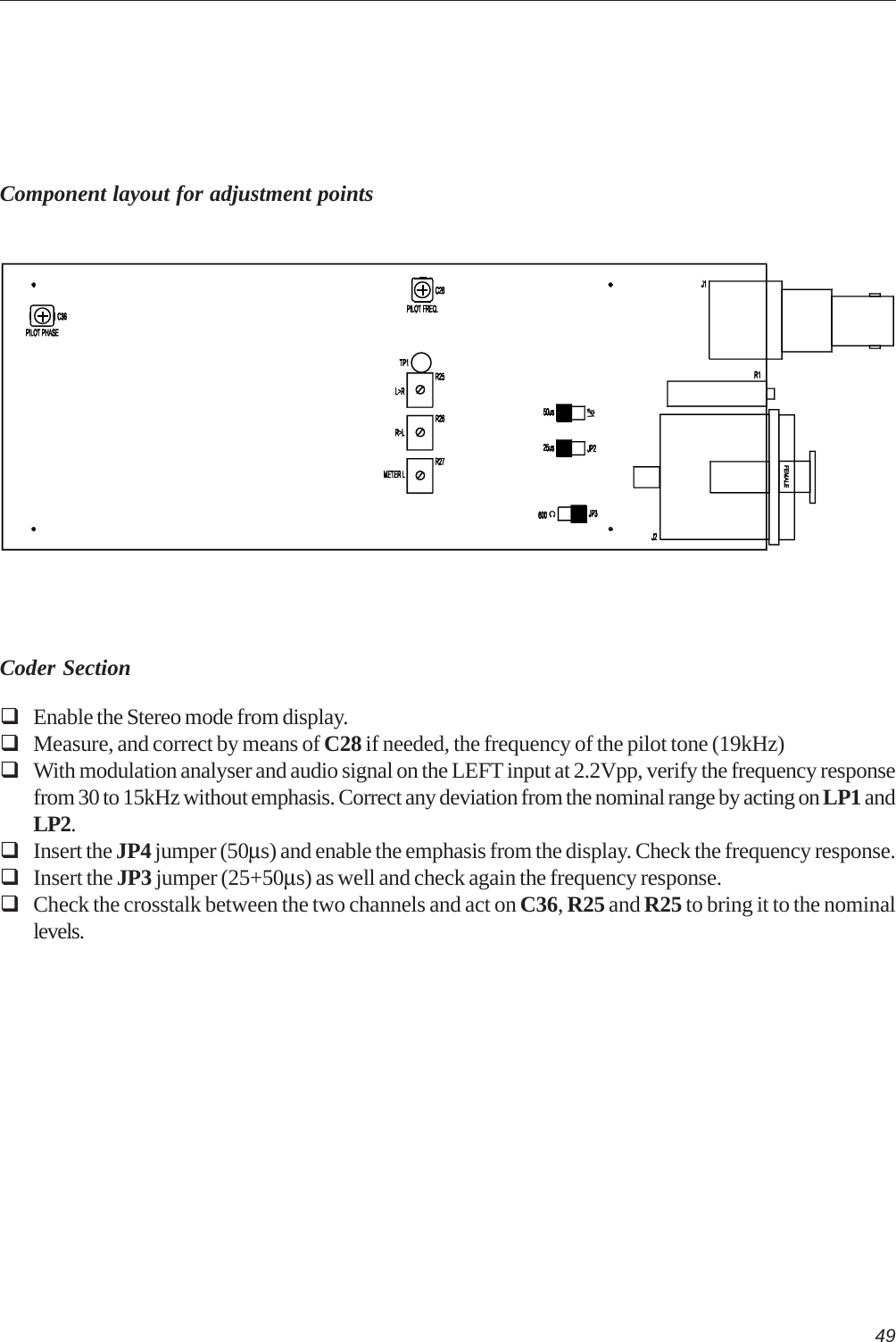
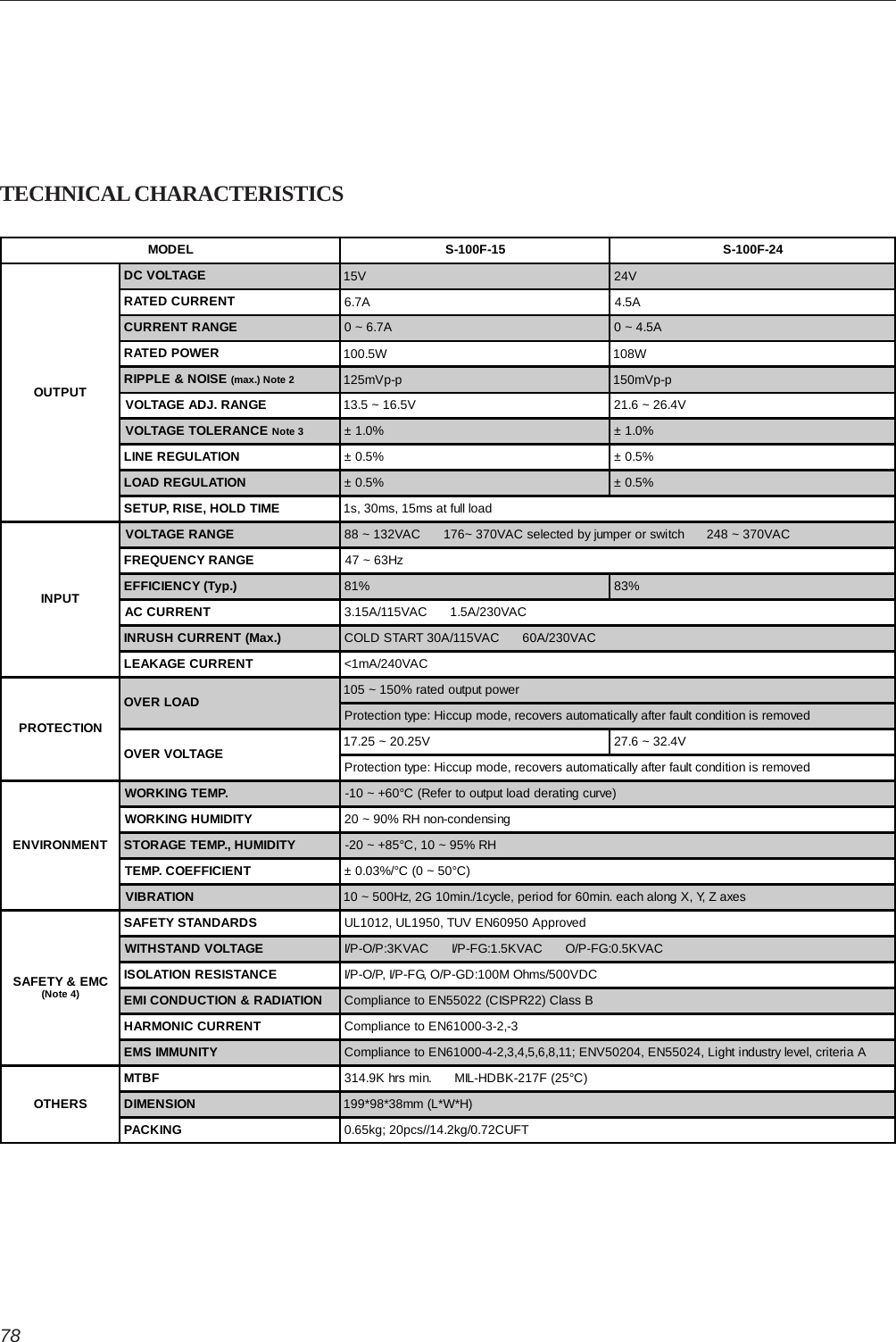
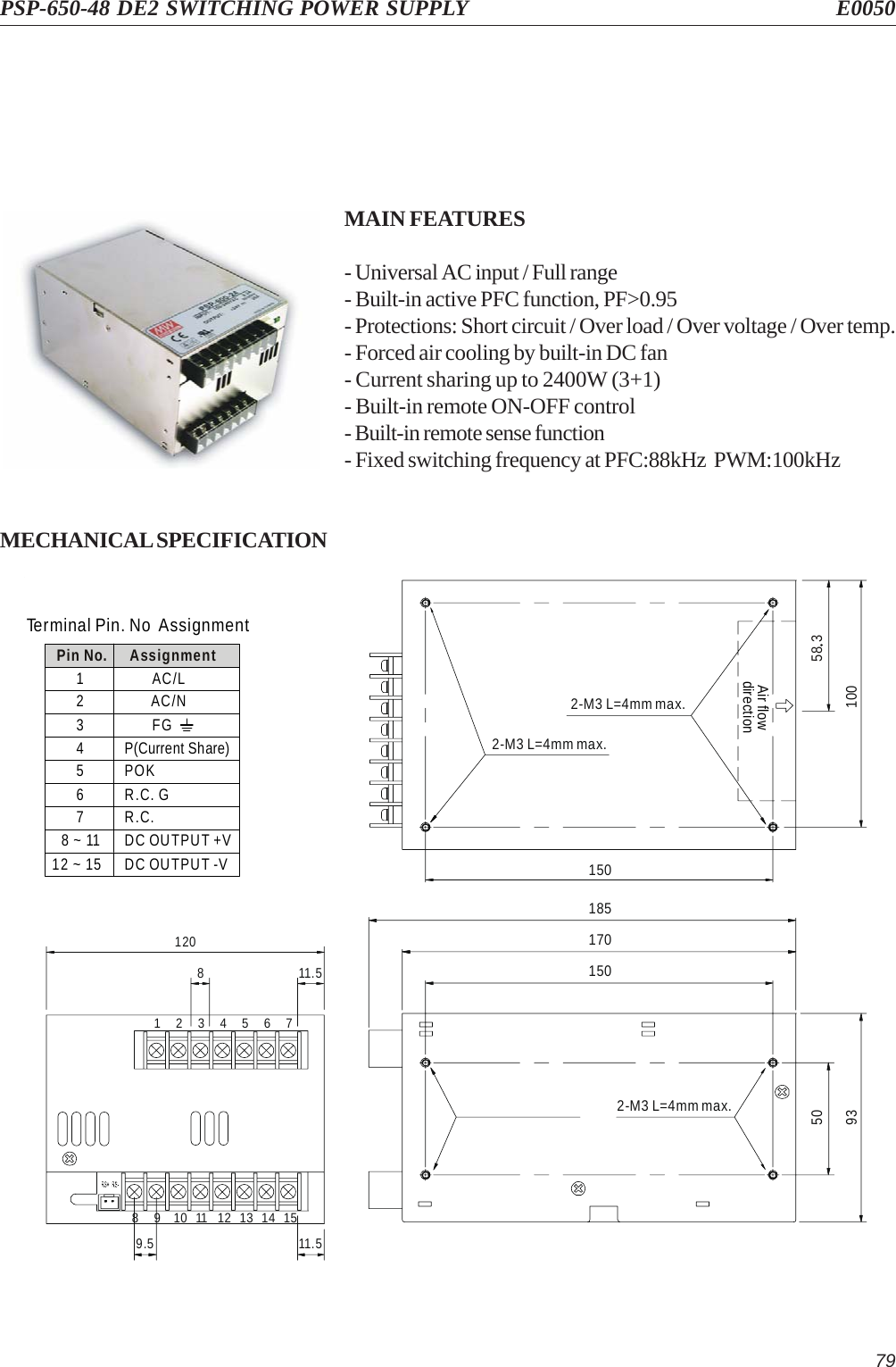
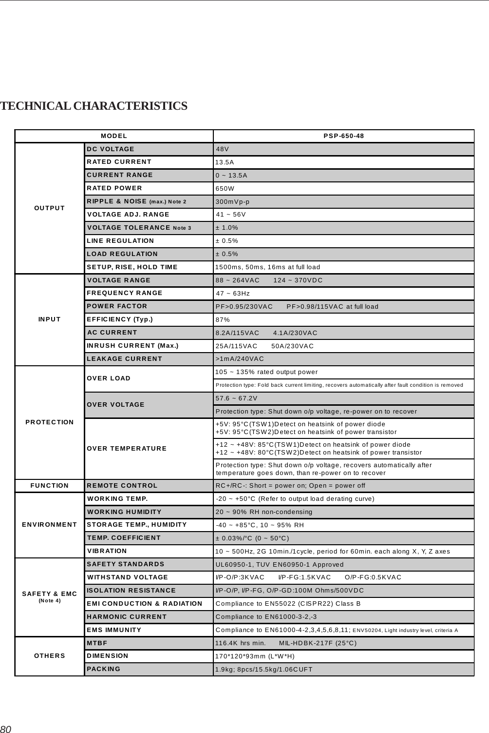
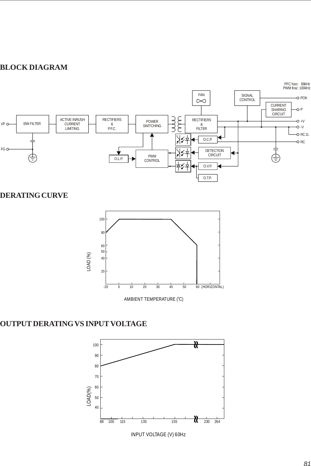
Elettronika S r l MIZAR30 30 Watt FM Broadcast Transmitter User Manual

Elettronika S.r.l. 30 Watt FM Broadcast Transmitter
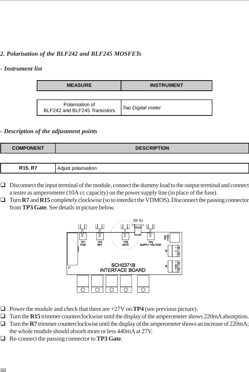
User Manual

MIZARFM Transmitter SystemCODE APF073AAPF074A TITLE MIZAR FM TRANSMITTER REV   1.1 DATE 26/07/07
30W 300WMONO APF073AMIZAR30 APF074AMIZAR300STEREO APF073A+OPT023MIZAR30S APF074A+OPT023MIZAR300SMIZAR Transmitter FamilySS 96   Km 11370027 Palo del Colle (Ba) ITALYTel. +39 (0)80 626755Fax +39 (0)80 629262E-mail: elettronika@elettronika.itWeb site: http://www.elettronika.itRegistration number: IT-17686Registration number: IT-24436POWERAUDIO
Mizar Transmitter Family .................................................................................................. 2Summaries ......................................................................................................................... 3Warning .............................................................................................................................. 7Warranty ............................................................................................................................. 8Introduction ....................................................................................................................... 9Content of the manual ...................................................................................................... 9Treatment of electrical shock ......................................................................................... 11First-aid ......................................................................................................................... 12    Treatment of electrical burns ......................................................................................... 12    Note............................................................................................................................... 12RoHS Normative .............................................................................................................. 13MIZAR FM Transmitter System....................................................................................... 15Section 1 - Information ................................................................................................... 17    1.1 Description .............................................................................................................. 18    1.2 Technical characteristcs .......................................................................................... 19    1.3 Front panels ............................................................................................................21    1.4 Rear panels .............................................................................................................22    Block Diagram ...............................................................................................................23Section 2 - Installation .................................................................................................... 25    2.1 Operating environment............................................................................................ 26    2.2 First installation ....................................................................................................... 26    2.3 Installation of MIZAR Mono with external Stereo Coder.......................................... 27    2.4 Installation of MIZAR Stereo with external RDS Coder ........................................... 27    2.5 MIZAR remote control with Elettronika RCU ........................................................... 28Section 3 - Operation ...................................................................................................... 29    3.1 User interface and software settings ....................................................................... 30    3.2 AGC Implementation ............................................................................................... 32    3.3 Alarms and automatic behaviours ........................................................................... 33    3.4 Status LEDs ............................................................................................................ 33Section 4 - Diagram......................................................................................................... 35    - APF073A MIZAR30 Cable Diagram ............................................................................ 36    - APF074A MIZAR300 Cable Diagram .......................................................................... 37    - APF073A_APF074A MIZAR Component list............................................................... 38    - SCH0377A Mother Board............................................................................................ 39        - Description .............................................................................................................. 39        - SCH0377A Component layout ................................................................................ 40        - Calibration procedure.............................................................................................. 41            - Instrument list...................................................................................................... 41Summaries
            - Description of the adjustment points ................................................................... 41            - Component layout for adjustment points............................................................. 42            - RF Section .......................................................................................................... 43            - Modulation Section.............................................................................................. 43            - Audio Section ...................................................................................................... 43            - General ............................................................................................................... 43        - SCH0377A Component list ..................................................................................... 44        - SCH0377A Electric Diagram ................................................................................... 46    - OPT023 Stereo Coder Board ...................................................................................... 47        - Description .............................................................................................................. 47        - SCH0378A Component layout ................................................................................ 47        - Calibration procedure.............................................................................................. 48            - Instrument list...................................................................................................... 48            - Description of the adjustment points ................................................................... 48            - Component layout for adjustment points............................................................. 49            - Coder Section .....................................................................................................49        - SCH0378A Component list ..................................................................................... 50        - SCH0378A Electric Diagram ................................................................................... 51    - SCH0372A Display Board ........................................................................................... 52        - Description .............................................................................................................. 52        - SCH0372A Top layer Component layout................................................................. 52        - SCH0372A Bottom layer Component layout ........................................................... 52        - SCH0372A Component list ..................................................................................... 53        - SCH0372A Electric Diagram ................................................................................... 54    - MFF0025B 30W FM Amplifier Module ........................................................................ 55        - Description .............................................................................................................. 55        - Technical Characteristics ........................................................................................ 55        - MFF0025B Component list ..................................................................................... 55        - MFF0025B Component layout ................................................................................ 56        - Calibration Procedure ............................................................................................. 56            - Calibration of the Output Filter ............................................................................ 56                - Instrument list.................................................................................................. 56            - Polarisation of the BLF242 and BLF245 MOSFETs............................................ 58                - Instrument list.................................................................................................. 58                - Description of the adjustment points ............................................................... 58        - SCH0382B 30W FM Amplifier Board Component layout ........................................ 59        - SCH0382B Component list ..................................................................................... 60        - SCH0382B Electric Diagram ................................................................................... 61
    - MFF0031A 300W Amplifier Module............................................................................. 63        - Description .............................................................................................................. 63        - Technical Characteristics ........................................................................................ 63        - MFF0031A Component list...................................................................................... 63        - MFF0031A Component layout ................................................................................ 64        - Calibration Procedure ............................................................................................. 65                - Instrument list.................................................................................................. 65                - Output Filter Section ....................................................................................... 65                - Polarisation of the Transistor........................................................................... 65                - Instrument list.................................................................................................. 66                - Description of the adjustment points ............................................................... 67        - SCH0427A 300W FM Amplifier Board Component layout ...................................... 68        - SCH0427A Component list ..................................................................................... 69        - SCH0426A FM Amplifier Interface Board Component layout.................................. 71        - SCH0426A Component list ..................................................................................... 71        - SCH0427A Electric Diagram ................................................................................... 72        - SCH0426A Electric Diagram ................................................................................... 74    - SCH0371B Interface Board......................................................................................... 75        - SCH0371B Interface Board Component layout ...................................................... 75        - SCH0371B Component list ..................................................................................... 75        - SCH0371B Electric Diagram ................................................................................... 76    - E0060 S-100F-24 Switching power supply ................................................................. 77        - Main Features .........................................................................................................77        - Mechanical Specification......................................................................................... 77        - Technical Characteristics ........................................................................................ 78    - E0050 PSP-650-48 DE2 Switching power supply....................................................... 79        - Main Features .........................................................................................................79        - Mechanical Specification......................................................................................... 79        - Technical Characteristics ........................................................................................ 80        - Block Diagram.........................................................................................................81        - Derating Curve ........................................................................................................81        - Output Derating VS Input Voltage ........................................................................... 81        - Control terminal instruction manual......................................................................... 82        - Parallel operation with remote setting ..................................................................... 82        - E0050 Electric Diagram .......................................................................................... 83
7WARNINGThe apparatus described in this manual has been designed and manufactured with devices to safe-guard the users. In any case it is recommended that during any operation of installation, maintenance,miscellaneous interventions and calibrations requiring the apparatus to be switched on,THE USER TAKES ALL THEPRECAUTIONS AGAINST INCIDENTSIt is required to use the proper clothes and protection gloves in order to prevent damages from inci-dental contacts with high-voltage parts.The manufacturer declines every responsibility in case the recommendations above are not followed.IMPORTANTThe component lists attached to the relevant electrical diagrams indicate for each item the reference,the description and the type normally used.The Elettronika S.r.l. though reserves the right to use or supply as spare parts components withequivalent characteristics but of a different type, assuring anyway the optimal work of the apparatusin accordance with the specifications.The enclosed monographs are solely owned by Elettronika S.r.l.The use of anything enclosed in this technical manual without explicit authorization given by ElettronikaS.r.l. will be prosecuted by the law.The data and technical characteristics of the apparatus described in this manual are not compelling forthe manufacturer.The Elettronika S.r.l. reserves the right to make, without previous notice, modifications or updates inorder to improve the quality of the product.The general conditions of supply and sale are described in the contracts.The delivery time are in accordance with the products and quantities ordered.
8Summary of warrantyWe, ELETTRONIKA S.r.l., SS096  Km 113 Z.I.  PALO DEL COLLE (BA) ITALY, warrant to the ORIGINAL PURCHASER of a NEW  product, for aperiod of one (1) year from the date of purchase by the original purchaser (the “warranty period”) that the new ELETTRONIKA product is free of defectsin materials and workmanship and will meet or exceed all advertised specifications for such a product. This warranty does not extend to any subsequentpurchaser or user, and automatically terminates upon sale or other disposition of our product.Items excluded from this ELETTRONIKA warrantyWe are not responsible for product failure caused by misuse, accident, or neglect. This warranty does not extend to any product on which the serialnumber has been defaced, altered, or removed. It does not cover damage to loads or any other products or accessories resulting from ELETTRONIKAproduct failure. It does not cover defects or damage caused by use of unauthorized modificstions, accessories, parts, or service.What we will doWe will remedy any defect, in material or workmanship (except as excluded), in our sole discretion, by repair, replacement, or refund. If a refund iselected, then you must make the defective or malfunctioning component available to us free and clear of all liens or other encumbrances. The refund willbe equal to the actual purchase price, not including interest, insurance, closing costs, and other finance charges less a reasonable depreciation on theproduct from the date of original purchase. Warranty work can only be performed at our authorized service centers or at our factory. Expenses inremedying the defect will be borne by ELETTRONIKA, including one-way surface freight shipping costs within the United States. (Purchaser must bearthe expense of shipping the product between any foreign country and the port of entry in the United States and all taxes, duties, and other custom’s fee(s)for such foreign shipments).How to obtain warranty serviceYou must notify us of your need for warranty service not later than ninety (90) days after the expiration of the warranty period. We will give you anauthorization to return the product for service. All components must be shipped in a factory pack or equivalent which, if needed, mayDesclaimer of consequential and incidental damagesYou are  not entitled to recover from us any consequential or incidental damages resulting from any defect in our product. This includes any damageto another product or products resulting from such a defect.Warranty alterationsNo person has the authority to enlarge, or modify this warranty. The warranty is not extended by the lenght of time for which you are deprived ofthe use of the product. Repairs and replacement parts are provided under the terms of this warranty shall carry only the unexpired portion of thiswarranty.Design changesWe reserve the right to change the design of any product from time to time without notice and with no obligation to make corresponding changes inproducts previously manufactured.Legal remedies of purchaserThere is no warranty which extends beyond the terms hereof. This written warranty is given in lieu of any oral or implied warranties not containedherein. We disclaim all implied warranties, including without limitation any warranties of merchantability or fitness for a particular purpose. No actionto enforce this warranty shall be commenced later than ninety (90) days after expiration of the warranty period.Warranty for electronic tubesThe warranty applied for electronic tubes is the one given by the manufacturer of the tube. In the event that the product shows anomalies within thedeadline of the validity of the warranty given by the manufacturer of the product itself, the buyer will have to return it to the seller with the neededdocuments and the written description of the defect. The seller will ship the broken tube to the manufacturer in order to effect the necessary technicaltests to find out the cause of the anomaly. Meanwhile the buyer of the tube who needs to use, and as such to replace immediately the product, will haveto buy a new one and provide to the relevant payment, further to the issuing by the seller of a regular commercial invoice. After the adequate tests madeby the manufacturer, should the result be positive, that is confirm the defect in manufacturing, the seller will issue a regular credit note in the name ofthe buyer and return the amount paid. Should the result be negative, that is detect a negligence in the installation or use by the buyer, he will have noright against the seller.Warranty
9INTRODUCTIONThe apparatus described in this manual is the latest of this series, offering high performances, remark-able reliability and a wide range of characteristics, it all at a competitive cost.Its is easy to install and use. It only takes to follow the installation procedure as shown in this manual:after having removed all from the package, you only have to follow step by step the description in thevarious sections.Before starting to use the apparatus, remember to:read  carefully  the  general  safety  information contained in this section;follow the  instructions  for  the  installation and set up of the apparatus;read all the remaining  sections  of  this  manual in order to know well the apparatus and learnhow to obtain  the  best  of  its  characteristics.CONTENTS OF THE MANUALThe chapter composing this manual contain all the information concerning the use of the apparatus.For more information refer to ELETTRONIKA S.r.l.This manual is made up of different chapters, each made up of various sections.
10WARNING!The currents and voltages in this equipment are dangerous!Personnel must at all times observe safety regulation!This manual is intended as a general guide for trained and qualified personnel who are aware of thedangers inherent in handling potentially hazaedous electrical and electronic circuits.It is not intended to contain a complete statement of all safety precautions which should be observed bypersonnel in using this or other electronic equipment.The installation, operation, maintenance and service of this equipment involves risks both to personneland equipment, and must be performed only by qualified personnel exercising due care.Elettronika S.r.l. shall not be responsible for injury or damage resulting from improper procedures orfrom the use of improperly trained or inexperienced personnel performing such tasks.During installation and operation of this equipment, local building codes and fire protection standardsmust be observed.WARNING!Always disconnect power before opening covers,doors, enclosures, gates, panels or shields.Always use grounding nsticks and short out highvoltage points before servicing. Never makeinternal adjustments, perform maintenance orservice when alone or when fatigued.Do not remove, short-circuit or tamper with interlock switches on access covers, doors, enclosures,gates, panels or shields.Keep away from live circuits, know your equipment and don’t take chances.WARNING!In case of emergency ensure that power has been disconnected.
11A - AIRWAYIf unconscious, open airway lift up neck, pushforehead back, clear out mouth if necessary,observe for breathing.Treatment of electrical shock1) If victim is not responsive follow the A, B, C’s of basic life support.PLACE VICTIM FLAT ON HIS BACK ON A HARD SURFACEB - BREATHINGIf not breathing, begin artificial breathing. Tilthead, pinch nostrils, make airttght seal, 4 quickfull breaths. Remember mouth to mouth resuscita-tion must be commenced as soon as possible.C - CIRCULATIONCheck carotid pulse. If pulseabsent, begin artificial circulation. Approx. 80sec.: 1 rescuer, 15 compressions, 2 quick breaths.Approx. 60sec.: 2 rescuers, 5 compressions, 1 breath.NOTE: DO NOT INTERRUPT RHYTHMOF COMPRESSIONS WHEN SECOND PERSONIS GIVING BREATH.Call for medical assistance as soon as possible.
122) If victim is responsive:- keep them warm;- keep them as quiet as possible;- loosen their clothing (a reclining position is recommended).FIRST-AIDPersonnel engaged in the installation, operation, maintenance or servicing of this equipment are urgedto become familiar with first-aid theory and practices. The following information is not intended to bea complete first-aid procedure, it is brief and is only to be used as a reference. It is the duty of allpersonnel using the equipment to be prepared to give adequate Emergency First Aid and thereby pre-vent avoidable loss of life.TREATMENT OF ELECTRICAL BURNS1) Extensive burned and broken skin.- Cover area with clean sheet or cloth (cleansed available cloth article);- do not break blisters, remove tissure, remove adhered particles of clothing, or apply any salve orointment;- treat victim for shock as required;- arrange transportation to a hospital as quickly as possible;- if arms or legs are effected keep them elevated.NOTEIf medical help will not be available within an hour and the victim is conscious and not vomiting, givehim a weak solution of salt and soda: 1 level teaspoonful of salt and 1/2 level teaspoonful of bakingsoda to each quart of water (neither hot or cold).Allow victim to sip slowly about 4 ounces (half a glass) over a period of 15 minutes.Discontinue fluid if vomiting occurs (do not give alcohol).2) Less severe burns - (1st & 2nd degree).- Apply cool (not ice cold) compresses using the cleansed available cloth article;- do not break blisters, remove tissue, remove adhered particles of clothing, or apply salve or ointment;- apply clean dry dressing if necessary;- treat victim for shock as required;- arrange transportation to a hospital as qickly as possible;- if arms or legs are affected keep them elevated.
13Further to the directives issued by the European Community, 2002/95/CE, 2002/95/CE and 2003/108/CE, and to the Italian Decree of Law n° 151 dated 25 July 2005, this is to inform the customers of ElettronikaS.r.l. living within the boundaries of the European Community about the following obligations:1) It is forbidden to trash RAEE products (which includes all broadcasting products which are not expresslylabelled as lead-free) along with normal wastes;2) Such devices must be brought to proper centres able to perform the adequate processing in order torecycle their parts where possible and dispose of the raw materials contained therein;3) For equipment purchased from Elettronika after the 13th of August 2005, the gathering, transport, processing,recycle and disposal operations are responsibility of Elettronika who will bear all related expenses;4) For equipment purchased from Elettronika before the 13th of August 2005 , the gathering, transport,processing, recycle and disposal operations are responsibility of Elettronika, who will bear all related expenses,only if you are purchasing from us new equipment in substitution of the disposed one;5) Electric and electronic devices contains lead in soldering, cables, etc. This substance pollutes the environmentand may be accumulated in the organism of plants and mammals. It is dangerous for humans because it mayaffect blood, bone marrow, peripheral and central nervous system and kidneys, causing anaemia,encephalopathies (e.g., convulsions), peripheral neuropathies, cramps of the abdomen and kidney damages.Besides it affects human reproduction and growth.These devices also contain mercury. From the environmental point of view, this substance is highly toxic foraquatic life, and can be accumulated in the organism of fish.Long-term damages to humans can affect the central nervous system and the kidneys, producing irritability,emotional instability, tremors, damages to the mind and the memory, language disorders. It may also irritateand whiten the gums, and its effects may be cumulative. Based on tests on animals, it may affect the humanreproduction or growth.There is also chrome, which may result in irritation of the eyes and respiration system.Cadmium is also present. In humans it may damage lungs, due to repeated or prolonged contact with its dust,and kidneys. It may cause cancer.6) The symbol below marks the devices which cannot be disposed of along with normal wastes, as stated in1) and 2) above.7) The payment of fees is foreseen for the non-allowed disposal of such devices.Communication N°1 -2002/95/CE - RoHS Directive
15FM TRANSMITTER SYSTEMMIZARUser’s manual
17Section 1 - InformationContents:1.1 Description1.2 Technical characteristics1.3 Front Panels1.4 Rear PanelsBlock Diagram
18MIZAR FM SYSTEM1.1 DESCRIPTIONThe MIZAR represents a family of radio transmitters available with 30W and 300W power, completelycontrolled by microprocessor, used for radio transmissions in FM band, both stereo and mono.The high technological content along with the use of surface mounting components allowed the realization ofan apparatus with excellent performances and limited dimensions.The extremely simplified wiring increases the reliability of the whole system and makes testing easier.Among the main characteristics there are:- availability of 30W (2U) and 300W (3U) version with extremely simplified wiring;- repeatability of the performances, guaranteed by the completely mechanized assembling;- good values of distortion and high S/N ratio;- analogic telemetry signals available on DB9;- RS232 (or RS485) connections for remote control;- automatic output power level control;- control of all the functions via 2x16 display;- all the final stages with MOSFET technology;- a stereo coder can be integrated in the cabinet.
191.2 TECHNICAL CHARACTERISTICSRF SECTION Frequency Range / Step 87.5 - 108MHz / 10-50-100kHz (from front panel)87.0 - 108MHz for China, other bands on requestReference Stability ±2.5ppm (0° - 50°C)Nominal Output Power 30W, 300WPower Level 0-100% (from front panel)Output Impedance / Connector 50Ω / N FemaleRF Monitor Level / Connector -40dBc ±3dB / BNC (*)Off lock Attenuation > 60dBAsynchronous AM S/N ratio > 65dBSynchronous AM S/N ratio > 60dBSpurious and Harmonic supp. Meets or exceeds all FCC and CCIR requirementsModulation Capability Meets or exceeds all FCC and CCIR requirementsMPX OPERATION Audio Input Impedance 10kΩAudio Input Connector BNCAudio Input Level 2.2Vpp nominal, +6dB/-12dB adjustable from rear panelFrequency Amplitude Response ±0.2dB  30Hz-100kHzHarmonic Distortion <0.1%  30Hz-100kHz (<0.05% 30Hz-53kHz)S/N Ratio with CCIR unweighted 73dBS/N Ratio with CCIR weighted 73dBMONO OPERATION Audio Input Impedance Balanced 600Ω / 10kΩ (jumper)Audio Input Connector XLRAudio Input Level 2.2Vpp nominal, +6dB/-12dB adjustable from rear panelFrequency Amplitude Response ±0.5dB  30Hz-15kHzHarmonic Distortion <0.05%  30Hz-15kHzPre-emphasis Flat, 50µs, 75µs (ON/OFF from display, 50/75 from jumper)S/N Ratio with CCIR unw. filter 73dBS/N Ratio with CCIR weig. filter 73dBINTERNAL CODER OPERATION (OPT023 Stereo Coder Option)Audio Input Impedance Balanced 600Ω / 10kΩ (jumper)Audio Input Connector XLRAudio Input Level 2.2Vpp nominal, +6dB/-12dB adjustable from rear panelMPX Output Conn. / Impedance BNC / 50ΩMPX Output Level 5.6VppFrequency Amplitude Response ±0.5dB  30Hz-15kHzHarmonic Distortion <0.05%  30Hz-15kHzPre-emphasis Flat, 50µs, 75µs (ON/OFF from display, 50/75 from jumper)Stereo separation > 50dB (typ. 60dB) 30Hz-15kHzS/N Ratio with CCIR unw.filter 70dBS/N Ratio with CCIR weig. filter 70dB
20SCA OPERATION (2 Inputs) SCA Input impedance 10kΩSCA Input connector BNCInput level 2Vpp nominal for ±7.5kHz deviationFrequency amplitude response ±0.2dB  50k-100kHzAUXILIARY Serial interface RS232 / RS485 (internal selectable)Telemetries Forward, Reflected, Alarm and ON/OFF ControlPROTECTION THRS Forward MIZAR30 35WMIZAR300 330WReflected MIZAR30 5WMIZAR300 30WTemperature 75°C with reset at 70°CGENERAL AC Power requirement 80-260Vac  50/60HzDimensions / Weight Rack 19” 2U-6kg (30W)Rack 19” 3U-11kg (300W)Ambient temperature range -5°  to  +45°C(*) It’s subgest to use a directional coupler to make RF measures.Specifications and characteristics are subject to change without notice.
21MIZAR FM SYSTEMSTATUSMIZAR FM SYSTEM1.3 FRONT PANELS821. Status LEDs2. LCD Display3. Push Buttons4. RF Monitor Connector798279
22* Only with OPT023 STEREO CODER option(*) The serial port can be choose between RS232 or RS485 connecting this connector to the RS232 or RS485 connector of the displayboard. No other selections are necessary.1.4 REAR PANELS31. Main Switch2. Power Supply Socket with Fuse (5A)3. RF OUT Connector4. RS232 / RS485 Socket5. Telemeasures Socket6. SCA2 Input7. SCA1 Input8. MPX Input Signal9. MONO / RIGHT Input Signal10. LEFT Input Signal11. MPX Output Signal16254*7 8 9 10 113162547 8 9 10 11*RS232 / RS485 Connector(*)Used for direct connection to a PCPin 2: TX Pin 5: GNDPin 3: RXRS232 / RS485 Connector(*)Use for direct connection to the RCUfor  remote control the MIZAR by ERCoSor any other system using a 4wire RS485connectionPin 2: RX- Pin 7: TX-Pin 3: RX+ Pin 8: TX+Pin 5: GNDTelemeasures ConnectorPin 1: Temperature (Analog out)Pin 2: REF power (Analog out)Pin 3: FWD power (Analog out)Pin 4: ON/OFF (Digital in)GND=OFF - Open=ONPin 5: Alarm:(Digital out - Open collector)Closed if alarm is presentPin 6-7-8-9: GNDXLR Input SignalPin 1: GroundPin 2: Hot / +vePin 3: Cold / -ve
23Block diagramMONO / RIGHTMPX INSCA1SOCKET50 s LOW PASSFILTERLIMITERVCOLEVELPLLSCA2SOCKETLEFT 50 s LOW PASSFILTERCODERMPX O UTLEFTRIGHTRF DRIVERINTERFACEBOARDREF FWD GATEMONITORRF OUTBLOWER27VAC/DCFILTERVACRS232 / RS485SOCKET TELEMEASURESSOCKETTCXOAC SOCKETMOTHER BOARDDISPLAY BOARDCODER BOARD
25Section 2 - InstallationContents:2.1 Operating environment2.2 First installation2.3 Installation of MIZAR Mono with external Stereo Coder2.4 Installation of MIZAR Stereo with external RDS Coder2.5 MIZAR remote control with Elettronika RCU
262.1 OPERATING ENVIRONMENTYou can install the apparatus in a standard component rack or on a suitable surface such as a bench or desk.In any case, the area should be as clean and well-ventilated as possible. Do not locate the transmitter directlyabove a hot piece of equipment. The upper lid can be dismounted to allow an easy internal access. Theequipment is designed with a modular design, that is each circuit is realized inside different modules or boards.All interconnections between modules are made by means of connectable cables which allow an easy andquick maintenance of demaged modules.2.2 FIRST INSTALLATION1. Connect Antenna cable2. Connect AC POWER cord3. Select step and frequency with display interface4. Move power slowly up till nominal power and check the Reflected Power to be low. If Reflected Power     increase check the RF Output connectionsAUDIO INPUT(LEFT only with OPT023)AC POWERTo ANTENNAGNDOnly with OPT023
272.3 INSTALLATION OF MIZAR MONO WITH EXTERNAL STEREO CODER2.4 INSTALLATION OF MIZAR STEREO WITH EXTERNAL RDS CODERRDS CODERMPX OUT + RDS MPX INLEFT RIGHTSTEREO CODERMPX OUT
282.5 MIZAR REMOTE CONTROL WITH ELETTRONIKA RCUIn order to connect MIZAR to RCU the RS232 / RS485 connector must be set to RS485. This choice isdone cabling the rear panel connector to the J1 (RS485) or J2 (RS232) on the Display Board.REMOTE CONTROL UNITPORT n
29Section 3 - OperationsContents:3.1 User interface and Software settings3.2 AGC Implementation3.3 Alarms and automatic behaviours3.4 Status LEDs
303.1 USER INTERFACE AND SOFTWARE SETTINGSWhen the equipment is switched on, the display shows the presentation screen, containing the name of thedevice and the release number of the firmware.The mono/stereo choice is made automatically by MIZAR, detecting the presence of the Stereo CoderBoard (OPT023).At this stage the device restores the last configuration saved of power, frequency and all other parameters.The other menu can be accessed by pressing the UP and DOWN keys.All menus show the name of one or two parameter, which can be the reading of a status (e.g. lock/unlock) ora setting (e.g. Emphasis circuit ON/OFF). In the latter case, the setting may be changed by pressing the RETin the relevant menu. When the RET key is pressed while in a setting menu, the parameter name label startsblinking to show that the setting is being edited and not read.While the label blinks, the user can change the value shown by pressing the UP and DOWN keys. To exit theedit mode of a setting, and confirm any change made, press the RET key. To leave the edit mode withoutconfirming any change, press ESC.Pressing the ESC key while navigating into menu structure, the main menu with the presentation screen isreached.Some parameter can be modified only in a protected mode, this possibility willbe highlighted in the menu list. To enter in the protected mode switch on theMIZAR with both UP and DOWN key pressed. The confirmation of theprotected mode enter will be the display message below and the blinking redalarm led. This will remember that in protected mode all the alarms and protections will be disabled.The existing menu, in the order they can be accessed by pressing the UP key, are briefly described below.This shows the actual level of Forward and Reflected Power. The ForwardPower level can be adjusted.This shows the actual alarm threshold of Forward and Reflected Power. Bothlevels can be adjusted in protected menu.FM Stereo TXSoftware  V2.4FM Mono TXSoftware  V2.4 Fwd 30W········| | | Ref   0W········| | |SETUPALARM DISABLED Fwd Alm 40W Ref Alm   5W
31Temperat.   37°C·········| | | | |This shows the value of temperature of the heat sink.This shows if the PLL generating the output frequency is locked or not.Stereo with coder ON.This shows the frequency deviation of the carrier.This shows the Stereo Coder position. It is possible to choose either ON orOFF position.This shows the Emphasis position. It is possible to choose either ON or OFFposition.This shows the operating frequency of the MIZAR. It is possible to choose afrequency from 87.50 MHz (87.00 for China models) to 108.00 MHz.This shows the frequency step (minimum distance between adjacent channels).It is possible to choose between 10kHz, 50kHz or 100 kHz.This shows the internal AGC enabling status. It is possible to choose eitherEnabled or Disabled.This shows the AGC working status. It can be:- Disabled;- Low Set: AGC stopped because reference power is too low;PLL VCOLockL·········| | | | |R·········| | | | |Stereo CoderOFFEmphasisOFFFrequency100.00 MHzDeviation·······| | | | |Frequency Step100 kHzINTERNAL AGCENABLEDAGC STATUSLock
32Last Alarm (0/5)EmptyModel30W   EKA- Low Read: AGC stopped because power reading is too low;- Lock: AGC goal has been reached;- Max: AGC stopped because of maximum power increasing;- Min: AGC stopped because of  maximum power decreasing;- Pull-up: AGC is increasing power;- Pull-down: AGC is decreasing power.This shows the remote control habilitation. It is possible to choose eitherENABLED or DISABLED position. The TLM Command in the second lineshow the actual value of the static on/off command coming from Telemetriesconnector on the rear panel. If Remote is DISABLED this command will notbe take in account, if ENABLED this will be the operating state of the MIZAR.This show the last occurred alarm. The numbers in the first line are the numberof occurred alarm and the maximum alarm number before the lock out of theMIZAR (five). To reset the lock out press RET and RET again. When analarm occurs the menu is automatically changed to this menu.This menu is available only in protected mode. It is possible to choose theModel of MIZAR FM Transmitter between 30W and 300W, between EKA,China and OIRT frequency bands.   Remote  DISABLED   TLM Command  ON3.2 AGC IMPLEMENTATIONThe AGC goal is to maintain stable the output power. Output power in fact can change due to the increase ofamplifier temperature. Note that when you change the operating frequency the output power change due tothe different gain at different frequency, but this change is not stabilized by this AGC algorithm.The AGC algorithm is based on the acquisition of the optimal output power level, stored when you changeMIZAR output power. To keep the power stable the AGC change the power gain of MIZAR. When the goalpower is achieved the AGC stops until the power moves up or down.The AGC work is stopped immediately (output power remains blocked to that reached in the moment of theAGC stop) when one of this condition occurs:• one of MIZAR alarms is triggered;• input power level is to low;• AGC has change the MIRA output power too much.
333.3 ALARMS AND AUTOMATIC BEHAVIOURSThe apparatus signals a working anomaly when any of the following conditions is met: PLL Unlock Forward Power exceed the threshold Reflected Power exceed the threshold Temperature of the Heat Sink exceed the maximum allowedIn case of failure of any of these parameters, the apparatus automatically mute the output power and changethe menu to the Log menu with the last alarm highlighted. The value of the failed parameter blinks in its menu,in order to highlight the anomalous working condition.3.4 STATUS LEDs ON (Green) Blinking RF Output Power is growing from 0 to nominalLit RF Output Power at nominal value REMOTE (Yellow) Unlit Remote disabledLit Remote enabled ALARM (Red) Blinking Protected mode enteredLit Alarm present
35Section 4 - DiagramContents:- APF073A MIZAR30 Cable diagram- APF074A MIZAR300 Cable Diagram- APF073A_APF074A MIZAR Component list- Modules description
36
37
38Part Name Code Description Qty02035 BNC CONNECTOR FOR RG316 CABLE 102513 90 SMB SOCKET cod. R114186000W 2 (APF073A) 1 (APF074A)02518 SMB SOCKET FOR RG174 CABLE code R114082000W 1 (APF073A) 2 (APF074A)02695 DB9 CONNECTOR FOR IU008059 CABLE 102699 FEMALE 10WIRE CONNECTOR 102700 FEMALE 16WIRE CONNECTOR 202833 AC SOCKET WITH FUSE-HOLDER 1 (APF074A)02841 3 POLES CANON PLUG 102855 FEMALE 26WIRE CONNECOTR 205069 TOROIDAL FILTER 1 (APF074A)05551B 2U HANDLE KIT 2 (APF073A)05552B 3U HANDLE KIT 2 (APF074A)07522 LIGHTED SWITCH 1 (APF073A)07524A BLACK SWITCH 1 (APF074A)07602 BLOWER GRID 1 (APF073A) 2 (APF074A)07613 PAPST BLOWER 1 (APF073A) 2 (APF074A)07918 AC FILTER 1 (APF073A)07924 PVC PROTECTION 1 (APF074A)07925 PVC PROTECTION 107926 PVC PROTECTION 1 (APF073A)08502 RG 316 50Ω CABLE 0.70 (APF073A) 0.90 (APF074A)CON0306 CON0306R0 COVER 1CON0340S CON0340R1S MIZAR30 BOX 1 (APF073A)CON0354R2S CON0354R2 MIZAR300 BOX 1 (APF074A)DET1220 DET1220R1 BLOWER CONVEYER 1 (APF073A)DET1317R0P DET1317R0P MECHANICAL DETAIL 1 (APF074A)DET1361R0P DET1361R0 MECHANICAL DETAIL 1 (APF074A)E0050 PSP-650-48 DE2 SWITHCING POWER SUPPLY 1 (APF074A)E0060 S-100F-24 SWITCHING POWER SUPPLY 1 (APF073A)FUS5A 5A FUSE 2 (APF073A)FUS10B 10A FUSE 2 (APF074A)MFF0025BR0 30W FM AMPLIFIER MODULE 1 (APF073A)MFF0031AR0 300W FM AMPLIFIER MODULE 1 (APF074A)PAN0141 PAN0141R1 FRONT PANEL 1 (APF073A)PAN0153R0P FRONT PANEL 1 (APF074A)SCH0372AR1 DISPLAY BOARD 1SCH0377AR2 MOTHER BOARD 1V0761 BLACK PLASTIC TAP 1V0768 BLACK PLASTIC TAP 1Component list APF073A_APF074A - MIZAR
39MOTHER BOARD SCH0377AR2DESCRIPTIONThe board contains the stages needed to condition the audio MONO or RIGHT signals and modulate infrequency a synthesised oscillator. It provides an output radio frequency signal in the II-VHF band, to drivethe final amplification stage. The various sections are analysed below:1. Balanced/Unbalanced Converter: the conversion from balanced to unbalanced and the input interface     of the audio signal are realised la electronically by the IC1-A operational circuit. This assures an high ge-     gree of immunity from disturbances and a perfect symmetry in unbalancing.2. Pre-emphasis: after the level adjustment, there is the active pre-emphasis stage (IC1-B), with amplification     to high frequencies. The time constant is chosen between 25 and 50 microseconds by means of two jum-     pers (JP3-4). When they are both enables they give 75us (for the FCC standard). The insertion of the pre-     emphasis is managed from the frontal panel by activating the electronic switch IC4.3. Low-pass Filter: the use of two filtering stages with elliptical filters LP1 and LP2 assures the adequate suppres-     sion of input signals at frequencies 19k and 38kHz.4. Additioner: depending on the operating mode selected by the frontal panel (Stereo or Mono) the MONO     signal, after the low-pass filter, is sent to the internal stereo coder (as RIGHT signal) or added to the auxi-     liary inputs (SCA1-2 and MPX) in the stage composed by IC3-A.5. Peak Detector: at the output of the additioner, part of the signal is sampled for the indication of the devia-     tion on the front panel. IC5-A serves as buffer for the duplicator and peak detector. Aside from the peak     detector for the indication of the modulation level, the board also includes a second detector (IC5-B and     D4) used to measure the level of the RIGHT signal.6. Limitation circuit: TR3 and TR4 realise the deviation limitation  circuit  by  cutting  the  audio signal which     exceeds the set voltage threshold on the relevant basis, by means of the resistor network R51-54.7. Oscillator: a frequency synthesis oscillator with PLL generates the radiofrequency carrier which is modulated     in  frequency  in  the  same  circuit.  The  reference frequency is generated by a 5.0MHz TCXO with good     temperature stability.8. RF Driver: after the oscillator there is a PIN diode stage (D3) to check the amplitude of the signal and mo-     dify the output power. The dynamic is greater than 40dB. The monolith amplifier (IC6) serves as buffer in     order to make the load effects on the oscillator circuit irrelevant. Finally, the stage with TR7 amplifies the     signal to the adequate levels for driving the power module. A circuit monitoring the power supply of TR7,     composed by TR6 and TR8, activates to switch the transistor off in case of alarms (such as PLL unlock or     any anomaly detected by the control board).
409. Telemetering: the most important analogue signals – forward and reflectesd power, switch on/off, alarms     and temperature – are buffered and made available on the J5 socket for connecting remote control systems.SCH0377AR2 Component layout
41CALIBRATION PROCEDURE- Instrument listDescription of the adjustment pointsMEASURE INSTRUMENTRF Signal level - Spectrum AnalyserFrequency - Spectrum AnalyserAudio - Audio GeneratorModulation - FM/AM Modulation AnalyserLimiter intervention - OscilloscopeCOMPONENT DESCRIPTIONR1 MONO/RIGHT Audio Input levelR2 MPX Input levelR3 SCA1 Input levelR4 SCA2 Input levelR21 Modulation depth adjustmentR80 Indication of the RIGHT signal deviation on display (only if the stereo option is installed)R81 Indication of the deviation on the displayR83 Indication of the Reflected Power on the displayR84 Indication of the Forward Power on the displayLP1, LP2 Notch and Low-pass Filter at 19 and 38kHzOSC1 RF Signal output frequency calibrationJP1 If inserted, sets the MONO Input impedance to 600ΩJP2 If inserted, enables the deviation limiterJP3 If inserted, enables the 25µs pre-emphasisJP4 If inserted, enables the 50µs pre-emphasis
42Component layout for adjustment points
43RF SectionCheck the lock of the oscillator on the whole operating range (87 - 108MHz).If the synthesised frequency is not correct, try to correct it by means of the capacitive trimmer of theOSC1 reference.Verify the signal-to-noise ration (CCIR) of the oscillator, which should be >73dB on the whole band.Verify the output level by the J9 (RF OUT) connector, higher than 24.5dBm on the whole band.Verify that the final stage is switched off when the PLL of the oscillator unlocks.Modulation SectionDisable the emphasis (from the display).Insert the JP1 jumper (so to have an input impedance of 600Ω).Insert the JP2 jumper to enable the limitation circuit.Provide a 400Hz, 2.2Vpp banalced signal to the MONO input.Adjust R1 in order to have an amplitude of 3.2Vpp on TP1 (on which the oscilloscope is connected).Adjust R21 to obtain a deviation of ±75kHz.Adjust R81 to obtain the indication of the nominal deviation on the display.Double the level of the input signal (4.4Vpp) and check that the modulation increase is no more than 1dB.Audio SectionWith modulation analyser and audio signal on the MONO input at 2.2Vpp, verify the frequency responsefrom 30 to 15kHz without emphasis. Correct any deviation from the nominal range by acting on LP1 andLP2.Insert the JP4 jumper (50µs) and enable the emphasis from the display. Check the frequency response.Insert the JP3 jumper (25+50µs) as well and check again the frequency response.Verify the frequency response of the MPX input from 30 to 100kHz, calibrating R2 for the nominaldeviation with 2.2Vpp signal amplitude.Verify the frequency response of the SCA1 and SCA2 inputs from 50k to 100kHz, calibrating R3 andR4 for the nominal deviation (±7.5kHz) with 2.2Vpp signal amplitude.GeneralVerify the remote switch-off function by short-circuiting pin 5 of J5 to ground.
44SCH0377AR2 COMPONENT LISTPart Name/Number Description Qty. Comps. Page 1/2257BLR-3618N 05010 05010 AUDIO TOKO FILTER 2 LP1-2CC 100nF-S 01065C 01065C Y5V 1206 CAPACITOR 20 C19, C30, C32, C43, C45-46, C57,C62-63, C77, C79, C81-89CC 10pF-S 01086 01086 SMD 1206 CAPACITOR 1 C26CC 1206 N. M. N. M. SMD 1206 CAPACITOR 1 C58CC 1nF-2%-S 01041D 01041D SMD 1206 CAPACITOR 23 C9-10, C22, C25, C34-36, C49-50, C54, C56,C59-61, C64-65, C68-72, C75, C80CC 27pF-S 01022B 01022B SMD 1206 CAPACITOR 16 C1-6, C11-14, C28-29, C33, C37, C51-52CC 6p8F-S 01084 01084 SMD 1206 CAPACITOR 1 C39CE 100uF16V-S 01792A 01792A ELET. SMD CAPACITOR 3 C78, C91-92CE 10uF16V-S 01776A 01776A ELET. SMD CAPACITOR 14 C7, C16-18, C20, C41-42, C47-48, C53, C55,C73-74, C76CE 220uF16V-S 01824A ELET. SMD CAPACITOR 5 C8, C27, C40, C66-67CE 22uF16V-S 01780A ELET. SMD CAPACITOR 6 C21, C23-24, C31, C38, C44CE 470uF-S 16V-S 01804B ELET. SMD CAPACITOR 1 C15D BAS85-S 03024 SMD DIODE SCHOTTKY 1 D2D BAT54S 03199 SMD SCHOT. DIODE A-K T 3 D1, D4-5D HSMP3814 03202 SMD DIODE 1 D3DL KA-3528SGC 03057 03057 GREEN SMD LED DIODE 1 DL1DZ 5V1-S 03128 03128 SMD ZENER DIODE 2 DZ1-2IC LM833-S 04643A 04643A SMD INTEG CIRCUIT 3 IC1-3IC LMC6482-S 04632 SMD INTEG CIRCUIT 2 IC5, IC8IC LMC6484-S 04634 SMD INTEG CIRCUIT 1 IC7IC MAR3 04367 04367 SMD INTEG CIRCUIT 1 IC6IC MC14066BD-S 4708B 4708B SMD INTEG CIRCUIT 1 IC4IND 100nH-S 05093A 05093A INDUCTOR 1 L9IND 22uH-S 5023D 5023D INDUCTOR 5 L1-3, L5-6IND 2u2H-S 05020A 05020A INDUCTOR 1 L7IND CBD8 05072 05072 INDUCTOR 3 L4, L8, L10IND MS85 10uH-S 04948 INDUCTOR 2.7A 2 L12-13J BNC-90G-PCB SHIELD 02034A PCB SHIELDED CONNEC. 3 J2-4J DB9-90G 02797 02797 PCB CONNECTOR 1 J5J FC-16P 02701-02700 02701+02700 PCB CONNECTOR 2 J7, J10J FC-26P 02855-02854 02855+02854 PCB CONNECTOR 1 J12J NC3FD-H 02862 02862 XLR-90G-PCB SOCKET F. 1 J1J SMB-PCB 2PIN 02516 02516 PCB CONNECTOR 3 J6, J8-9JU JUMP2 02739-02742 02739+02742 MASCHIO PAN2 4 JP1-4OSC NVT535 05168 05168 TCXO 1 OSC1PN0658A SCH0007AR0 SCH0007AR0 VCO FM INTEG. 1 VCO1R 0R0-S 00001 00001 RES 1/4W 5% SMD 1206 1 R98R 100K-1%-S 00065B 00065B RES 1/4W 1% SMD 1206 12 R33-34, R37, R41, R48, R50, R55, R57, R62,R88, R91, R96
45Part Name/Number Description Qty. Comps. Page 2/2R 100R-S 00029A 00029A RES 1/4W 5% SMD 1206 12 R5-7, R10, R38, R71, R76, R82, R86-87, R92,R97R 10K-S 00053A 00053A RES 1/4W 5% SMD 1206 17 R8-9, R11, R22, R29-30, R40, R45-46, R52,R53, R60, R66, R73, R100-101, R107R 10R-S 00017A 00017A RES 1/4W 5% SMD 1206 2 R64, R69R 15K-1%-S 00055B 00055B RES 1/4W 1% SMD 1206 3 R35, R85, R94R 1K2-1%-S 00042A 00042A RES 1/4W 1% SMD 1206 5 R19-20, R44, R67, R79R 1K5-S 00043A 00043A RES 1/4W 5% SMD 1206 1 R68R 22K-S 00057A 00057A RES 1/4W 5% SMD 1206 4 R17, R43, R89-90R 2K2-S 00045A 00045A RES 1/4W 5% SMD 1206 2 R61, R70R 330R-1%-S 00035A 00035A RES 1/4W 1% SMD 1206 1 R75R 47K-1%-S 00061B 00061B RES 1/4W 1% SMD 1206 18 R18, R26-28, R32, R42, R49, R51, R54, R56,R58-59, R63, R65, R93, R95, R102, R108R 4K7-S 00049A 00049A RES 1/4W 5% SMD 1206 6 R15, R23-25, R36, R39R 560K-S 00074B RES 1/4W 5% SMD 1206 1 R31R 560R-1%-S 00038B 00038B RES 1/4W 1% SMD 1206 1 R74R 68K-1%-S 00063B 00063B RES 1/4W 1% SMD 1206 5 R12-14, R16, R47R 68R-S 00027A 00027A RES 1/4W 5% SMD 1206 2 R77-78R 82R-S 00028A 00028A RES 1/4W 5% SMD 1206 1 R72RV 10K-M-H 00777 00777 VARIABLE RESISTOR 4 R1-4RV 10K-S-H/S 00793 00793 SMD VARIABLE RESISTOR 2 R80-81RV 1K-S-H/S 00792 00792 SMD VARIABLE RESISTOR 1 R21RV 50K-S-H/S 00797 00797 SMD VARIABLE RESISTOR 2 R83-84TR BC807 03453 03453 PNP SMD TRANSISTOR 1 TR6TR BC848 03457 03457 NPN SMD TRANSISTOR 7 TR1-2, TR4-5, TR8-9, TR12TR BC856 03455 03455 PNP SMD TRANSISTOR 1 TR3TR BFG35 03990 03990 NPN SMD TRANSISTOR 1 TR7
46
47STEREO CODER BOARD OPT023DESCRIPTIONThe board contains the stages needed for the conditioning of the Left channel audio signal and for realising thestereo encoding in compliance with the standard ITU racc. 450. The Right signal is provided through theconnection to the Mother board. The various sections are analysed below:1. Balanced/Unbalanced Converter: the conversion from balanced to unbalanced and the input interface     of the audio signal are realised la electronically by the IC1-A operational circuit. This assures an high ge-     gree of immunity from disturbances and a perfect symmetry in unbalancing.2. Pre-emphasis: after the level adjustment, there is the active pre-emphasis stage (IC1-B), with amplification     to high frequencies. The time constant is chosen between 25 and 50 microseconds by means of two jum-     pers (JP1-2). When they are both enables they give 75µs (for the  FCC  standard).  The  insertion  of  the     pre-emphasis is managed from the frontal panel by activating the electronic switch IC3.3. Low-pass Filter: the use of two filtering stages with elliptical filters LP1 and LP2 assures the adequate suppres-     sion of input signals at frequencies 19k and 38kHz.4. Peak Detector: before the emphasis circuit, part of the audio signal is sampled to provide the indication of     the LEFT channel deviation on the frontal display. IC4-A serves as buffer for the duplicator and peak de-    tector.5. Stereo Coder: stereo encoding is realised inside the MPX1 block, providing the MPX signal in output.SCH0378AR2 Component layout
48CALIBRATION PROCEDURE- Instrument listDescription of the adjustment pointsMEASURE INSTRUMENTRF Signal level - Spectrum AnalyserFrequency - Spectrum AnalyserAudio - Audio GeneratorModulation - FM/AM Modulation AnalyserLimiter intervention - OscilloscopeCOMPONENT DESCRIPTIONR1 LEFT Audio Input levelR25 Adjusts Left on Right signal crosstalkR26 Adjusts Right on Left signal crosstalkR27 Indication of the LEFT signal deviation on the displayC28 Adjusts the 19kHz pilot tone frequencyC36 Adjusts the pilot tone phaseLP1, LP2 Notch and Low-pass Filter at 19 and 38kHzJP3 If inserted, sets the LEFT Input impedance to 600ΩJP2 If inserted, enables the 25µs pre-emphasisJP1 If inserted, enables the 50µs pre-emphasis
49Component layout for adjustment pointsCoder SectionEnable the Stereo mode from display.Measure, and correct by means of C28 if needed, the frequency of the pilot tone (19kHz)With modulation analyser and audio signal on the LEFT input at 2.2Vpp, verify the frequency responsefrom 30 to 15kHz without emphasis. Correct any deviation from the nominal range by acting on LP1 andLP2.Insert the JP4 jumper (50µs) and enable the emphasis from the display. Check the frequency response.Insert the JP3 jumper (25+50µs) as well and check again the frequency response.Check the crosstalk between the two channels and act on C36, R25 and R25 to bring it to the nominallevels.
50SCH0378AR2 COMPONENT LISTPart Name/Number Description Qty. Comps.257BLR-3618N 05010 05010 AUDIO TOKO FILTER 2 LP1-2CC 100nF-S 01065C 01065C Y5V 1206 CAPACITOR 6 C14, C22, C24, C30, C33, C37CC 1nF-2%-S 01041D 01041D SMD 1206 CAPACITOR 5 C13, C16-18, C23CC 27pF-S 01022B 01022B SMD 1206 CAPACITOR 9 C4, C6-8, C10-11, C15, C20, C32CE 10uF16V-S 01776A 01776A ELET. SMD CAPACITOR 7 C2-3, C5, C9, C19, C34-35CE 22uF16V-S 01780A ELET. SMD CAPACITOR 6 C12, C21, C25-27, C31CE 470uF-S 16V-S 01804B ELET. SMD CAPACITOR 5 C1, C29, C38-40CV 4.5-20pF-S 01481 01481 VARIABLE CAPACITOR 1 C28CV 7-50pF-S 01474 01474 VARIABLE CAPACITOR 1 C36D BAT54S 03199 SMD SCHOT. DIODE A-K T 1 D1IC LM833-S 04643A 04643A SMD INTEG CIRCUIT 2 IC1-2IC LMC6482-S 04632 SMD INTEG CIRCUIT 1 IC4IC MC14066BD-S 4708B 4708B SMD INTEG CIRCUIT 1 IC3IND 22uH-S 5023D 5023D INDUCTOR 2 L1-2J BNC-90G-PCB SHIELD 02034A PCB SHIELDED CONNEC. 1 J1J FC-16P 02701-02700 02701+02700 PCB CONNECTOR 1 J4J NC3FD-H 02862 02862 XLR-90G-PCB SOCKET F. 1 J2J SMB-PCB N. M. SMB PCB N. M. 1 J3JU JUMP2 02739-02742 02739+02742 PAN2 MALE 3 JP1-3MPX CTC30-01 04894 STEREO ENCODER 1 MPX1R 100K-1%-S 00065B 00065B RES 1/4W 1% SMD 1206 7 R3-4, R14-15, R20, R23, R31R 10K-S 00053A 00053A RES 1/4W 5% SMD 1206 7 R2, R5-8, R29-30R 15K-1%-S 00055B 00055B RES 1/4W 1% SMD 1206 1 R17R 18K-S 00056B 00056B RES 1/4W 5% SMD 1206 1 R33R 1K2-1%-S 00042A 00042A RES 1/4W 1% SMD 1206 3 R9-10, R13R 47K-1%-S 00061B 00061B RES 1/4W 1% SMD 1206 4 R12, R21-22, R32R 47R-S 00025A 00025A RES 1/4W 5% SMD 1206 1 R28R 4K7-S 00049A 00049A RES 1/4W 5% SMD 1206 4 R16, R18-19, R24R 560K-S 00074B RES 1/4W 5% SMD 1206 1 R11RV 10K-M-H 00777 00777 VARIABLE RESISTOR 1 R1RV 10K-S-H/S 00793 00793 SMD VARIABLE RESISTOR 1 R27RV 50K-S-H/S 00797 00797 SMD VARIABLE RESISTOR 2 R25-26TR BCV47 03465 NPN SMD TRANSISTOR 1 TR1
51
52DISPLAY BOARD SCH0372AR1DESCRIPTIONThe MIZAR display board contains the HMI (human machine interface) of the equipment composed by aalphanumeric 2 rows x 16 columns displayand a keys series, a connector for collecting and sending datastowards the equipment mother-board and its thinking heart made by a Flash microcontroller.The board is able of reading 8 analogic signals coming from mother-board. These are only bufferized on theboard and therefore their conditioning is made on the mother-board.The remaining digital input and output signals are conneted directly to the micro, where is necessary someinterverntion speed, or are multiplexed on shift register where the speed is less important.The board moreover provide the remotability to the equipment by an asyncronous serial, configurable asRS232 or RS485 simply connecting the output connector to one of the two serial connectors present on thedisplay board.SCH0372AR1 Top layer Component layoutSCH0372AR1 Bottom layer Component layout
53SCH0372AR1 COMPONENT LISTPart Name/Number Description Qty. Comps.CC 100nF-S 01065C 01065C Y5V 1206 CAPACITOR 20 C3-5, C7, C12, C14, C16-17, C24-28, C30,C31-35, C37CC 15pF-S 01088 01088 SMD 1206 CAPACITOR 2 C1-2CC 1uF100V-S 01760A 01760A Y5V 1206 50V CAPAC. 7 C8, C11, C13, C15, C18-20CC 220nF-S 1069A 1069A Y5V 1206 CAPACITOR 6 C6, C9-10, C21-23CE 10uF16V-S 01776A 01776A ELET. SMD CAPACITOR 2 C29, C36D 1N4148-S 03002 03002 SMD DIODE 2 D1-2DIS MDLS16268CLVBLDW 03072C DISPLAY 2 X 16 WIDE 1 LCD1DL LEDG5 03060 03060 GREEN LED DIODE 5mm 1 DL3DL LEDR5 03061 03061 RED LED DIODE 5mm 1 DL1DL LEDY5 03054B 03054B YELL. LED DIODE 5mm 1 DL2IC 74HC00-S 4762A 4762A SMD INTEG CIRCUIT 1 IC3IC LMC6482-S 04632 SMD INTEG CIRCUIT 1 IC5IC LMC6484-S 04634 SMD INTEG CIRCUIT 2 IC8-9IC MAX232-S 04804B 04804B SMD INTEG CIRCUIT 1 IC7IC MAX3080-S 04770 04770 SMD INTEG CIRCUIT 1 IC4IC MC14094BD 04718 04718 SMD INTEG CIRCUIT 1 IC1IC MC74HC589 4874 04874 SMD INTEG CIRCUIT 1 IC2IC PIC18F452-S 04807C + 07509C INTEG CIRCUIT 1 IC6IND CBD8 05072 05072 INDUCTOR 1 L1J FC-10P 02697-02699 02697+02699 PCB CONNEC. POL 2 J1-2J FC-26P 02855-02854 02855+02854 PCB CONNEC. POL 1 J5J PAN6 02713-14-15 02713+02714+02715 PCB CONN. 2 J3-4JU JUMP3 02707-02742 02707+02742 MASCHIO PAN3 1 JP1R 100R-S 00029A 00029A RES 1/4W 5% SMD 1206 2 R6-7R 10K-S 00053A 00053A RES 1/4W 5% SMD 1206 4 R9, R16-17, R20R 120R-S 00030A 00030A RES 1/4W 5% SMD 1206 1 R3R 12R-S 00018A 00018A RES 1/4W 5% SMD 1206 1 R18R 1K0-S 00041A 00041A RES 1/4W 5% SMD 1206 1 R19R 470R-S 00037A 00037A RES 1/4W 5% SMD 1206 1 R8R 47K-S 00061A 00061A RES 1/4W 5% SMD 1206 5 R2, R4-5, R11-12R 820R-S 00040A 00040A RES 1/4W 5% SMD 1206 3 R13-15RV 10K-3266X 00807 00807 VARIABLE RESISTOR 1 R1RV 5K-M-V 00783 00783 VARIABLE RESISTOR 1 R10T CLOCHE GREY WITH BLUE CENTER   4 x xxxxxx + 4 x xxxxxx + xxxx 1 T1TR BC817 03454 03454 NPN SMD TRANSISTOR 1 TR1XTAL 20MHz-S CXS00001  QUARTZ 1 XTAL1
54
5530W FM AMPLIFIER MODULE MFF0025BR0DESCRIPTIONThe MFF0025B amplifier module is designed to amplify the FM modulated carriers in the 87-108MHz band,and can provide an output of 30W CW. In order to obtain the desired gain, the amplifier is made up by twogain stages: the pilot stage uses a BLF242 MOSFET, while the final stage uses a BLF245 MOSFET.An input adaptation circuit allows the adaptation of the module to the various driving levels. The output powerregulation is made by controlling the power level of the input signal of the module. The final stage of themodule also has a control terminal allowing to disable the MOSFET immediately, if needed. The output of themodule is completed by a 9th order (4 cell) low-pass filter to attenuate the level of the harmonics of the signal,and by two high-directivity directional couplers needed to sample part of the Forward and Reflected Powerin order to measure their levels. The final is provided with the needed circuits (SCH0371B Interface Board)to read the output Forward and Reflected Power, the heatsink temperature and the voltage supplied.TECHNICAL CHARACTERISTICSFrequency Range 87 - 108MHzOutput Power 30WInput Return Loss >25dBPower Supply +27VRF Input Impedance 50ΩRF Output Impedance 50ΩBias Current BLF242 with Vdd = +27V: 220mABias Current BLF245 with Vdd = +27V: 220mAGain 20dBEfficiency 54%MFF0025BR0 COMPONENT LISTPart Name/Number Description Qty.SCH0382BR0 30W FM AMPLIFIER BOARD 101400 BYPASSING CAPACITOR 101408 BYPASSING CAPACITOR 3DET1304 DET1304R0 30W DISSIPATOR 1DET1276 DET1276R0 AMPLIFIER REAR BAR 1DET1277 DET1277R1 AMPLIFIER INPUT BAR 1DET1239 DET1239R1 AMPLIFIER MODULE COVER 1SCH0371BR0 INTERFACE BOARD 107907 TO220 INSULATOR 207910 TO220 INSULATOR 202515 SMB SCREW cod. R114313000 108502 RG 316 50Ω CABLE 0.1502516 SMB CONNECTOR FOR PCB 102248 17x17 NF FLANGE CONNECTOR 1
56CALIBRATION PROCEDUREThe calibration procedure is mainly made of three step:1. Calibration of the Output Filter2. Polarization of the BLF242 and BLF245 MOSFETS1. Calibration of the Output Filter- Instrument listMEASURE INSTRUMENTCalibration of the Output Filter Network analyser or alternately Spectrumanalyser with tracking generator and SWRBridgeMFF0025BR0 Component layout
57Calibrate the spectrum analyser after setting a 100MHz span centered ad 100MHz (10MHz/div - 5dB/div).Connect the input of the filter to port 1 of the network analyser, connect the output of the filter to a dummyload.Display the reflection coefficient (parameter s11). The calibration consists in acting on the coils (L8, L9,L10, L11) to obtain a curve as the one shown in picture A after closing the module.
58- Description of the adjustment pointsDisconnect the input terminal of the module, connect the dummy load to the output terminal and connecta tester as amperometer (10A cc capacity) on the power supply line (in place of the fuse).Turn R7 and R15 completely clockwise (so to interdict the VDMOS). Disconnect the passing connectorfrom TP3 Gate. See details in picture below.2. Polarisation of the BLF242 and BLF245 MOSFETs- Instrument listCOMPONENT DESCRIPTIONR15, R7 Adjust polarisationMEASURE INSTRUMENTPolarisation ofBLF242 and BLF245 Transistors Two Digital meterPower the module and check that there are +27V on TP4 (see previous picture).Turn the R15 trimmer counterclockwise until the display of the amperometer shows 220mA absorption.Turn the R7 trimmer counterclockwise until the display of the amperometer shows an increase of 220mA;the whole module should absorb more or less 440mA at 27V.Re-connect the passing connector to TP3 Gate.RF IN
59SCH0382BR0 30W FM Amplifier Board Component layout
60SCH0382BR0 COMPONENT LISTPart Name/Number Description Qty. Comps.25Ohm 08523 08523 WHITE TEFLON RF CABLE 0.40 CB1-2CC 100pF-S 01092 01092 SMD 1206 CAPACITOR 5 C2, C7, C9, C11, C15CC 100nF-S 01065C 01065C Y5V 1206 CAPACITOR 5 C3-5, C12-13CC 33pF-S 01023A 01023A SMD 1206 CAPACITOR 1 C10CC 1p2F-S 01081 01081 SMD 1206 CAPACITOR 1 C1CC 1nF-S 01096 01096 SMD 1206 CAPACITOR 6 C19, C21, C23-26CC 39pF-S 1024A 1024A SMD 1206 CAPACITOR 2 C20, C22CC 47nF-S 01061A 01061A SMD 1206 CAPACITOR 3 C16-18CC 6p8F-S 01084 01084 SMD 1206 CAPACITOR 1 C8CE 10uF50V-S 01779A 01779A ELET. SMD CAPACITOR 2 C6, C14CP 100pF-S 01135 01135 CHIP CHB 1 CP5CP 150pF-S 01137 01137 CHIP CHB 1 CP1CP 33pF-S 01127 01127 CHIP CHB 2 CP8, CP12CP 470pF-S 01143 01143 CHIP CHB 4 CP2-4, CP6CP 68pF-S 01131 01131 CHIP CHB 3 CP9-11CP 3p6F-S 01104B 01104B CHIP CHB 1 CP7D 1N4148-S 03002 03002 SMD DIODE 1 D1D HSMS2802 03207 03207 SMD DIODE 2 D2-3DZ 3V9-S 03134 SMD ZENER DIODE 4 DZ1-4IND 6 SP_D4_d0.8mm-S 05043 INDUCTOR 2 L1-2IND 7 SP_D6_d0.8mm-S 07691 COATED WIRE 0.30 L5IND 4 SP_D8_d1.2mm-S 07684 SILVER WIRE 0.80 L8-L11IND CBD8 05072 05072 INDUCTOR 1 L7IND VK200 05013 05013 INDUCTOR 3 L3-4, L6R 10R-S 00017A 00017A RES 1/4W 5% SMD 1206 1 R11R 120R-S 00030A 00030A RES 1/4W 5% SMD 1206 1 R2R 12R-S 00018A 00018A RES 1/4W 5% SMD 1206 1 R12R 1K0-S 00041A 00041A RES 1/4W 5% SMD 1206 2 R6, R14R 1M-S 00077A 00077A RES 1/4W 5% SMD 1206 2 R5, R13R 220R-S 00033A 00033A RES 1/4W 5% SMD 1206 4 R23-26R 22K-S 00057A 00057A RES 1/4W 5% SMD 1206 1 R21R 22R-S 00021A 00021A RES 1/4W 5% SMD 1206 2 R19-20R 47R-S 00025A 00025A RES 1/4W 5% SMD 1206 1 R4R 4K7-S 00049A 00049A RES 1/4W 5% SMD 1206 2 R10, R18R 56K-S 00062A 00062A RES 1/4W 5% SMD 1206 2 R8-9, R16-17R 56R-S 00026A 00026A RES 1/4W 5% SMD 1206 1 R22R 68R-S 00027A 00027A RES 1/4W 5% SMD 1206 2 R1, R3RV 50K-S-H/S 00797 00797 SMD VARIABLE RESISTOR 2 R7, R15TR1 BLF242 04005 TRANSISTOR 1 TR1TR2 BLF245 03985 TRANSISTOR 1 TR2
61
62
63300W FM AMPLIFIER MODULE MFF0031AR0DESCRIPTIONThe Amplifier Module MFF0031A was designed to amplify FM carriers in the 87 - 108MHz band, and isable to provide an output of 300W CW. Besides it is provided with an RF Monitor output with a level of -40dBc ±3dB. In order to obtain the desired gain, the amplifier is made up by two gain stages: the pilot stageuses a MOSFET BLF244, the final stage a MOSFET SD2942. An input adaptation circuit allows to adaptthe module to various driving levels. The adjustment of the output is achieved by controlling the power level ofthe input signal. For both stages of the module there is a control terminal allowing to instantaneously disablethe MOSFETs if needed. The output of the module is completed by an 9th order (4 cells) Low-pass Filter toattenuate the harmonic level of the esable signal, and by two high-directivity directional couplers needed tosample part of the Forward and Reflected Power for measuring their levels.TECHNICAL CHARACTERISTICSFrequency Range 87 - 108MHz RF Output Impedance 50ΩOutput Power 300W Bias Current BLF244 with Vdd = +28V: 300mAInput Return Loss >10dB Bias Current SD2942 with Vdd = +50V: 80mAPower Supply +50V Gain 33dB (with 3dB interstage attenuation)RF Input Impedance 50ΩEfficiency 54%MFF0031AR0 COMPONENT LISTPart Name/Number Description Qty.00135 47Ω 1/2W RESISTOR 100664 LM35DT THERMAL SENSOR 101003 0.5pF CERAMIC CAPACITOR 101092 100pF MULTITURN CHIP 101400 BYPASSING CAPACITOR 101403 BYPASSING CAPACITOR 402209 PANEL MOUNTING N CONNECTOR 102514 PANEL MOUNTING SMB R114553000 204315 LM7805 VOLTAGE REGULATOR 104321 LM7812 VOLTAGE REGULATOR 104340A LM317HVT VOLTAGVE REGULATOR 205742 COVER 107907 TO220 INSULATOR 407910 TO220 INSULATOR 4DET1326R0P DET1326R0 HEAT SINK 1SCA0129R0B SCA0129R0 FM AMPLIFIER BOX 1SCH0371BR0 INTERFACE BOARD 1SCH0426AR0 FM AMPLIFIER INTERFACE BOARD 1SCH0427AR0 300W FM AMPLIFIER BOARD 1
64MFF0031AR0 Component layout
65MEASURE INSTRUMENTCalibration of the Output Filter Network analyser or alternately Spectrumanalyser with tracking generator and SWRBridgeCALIBRATION PROCEDURE- Instrument listOutput Filter SectionCalibrate the Network Analyser after setting a 100MHz span centred on 100MHz (10MHz/div - 5dB/div).Connect the input of the filter to port 1 of the Network Analyser.Connect the output of the filter to a dummy load. Display the Reflection coefficient (parameter s11). Thecalibration consists in acting on the coils (L9, L10, L11, L12) until a curve as below.Polarisation of the TransistorAfter verifying that the power supply is properly connected to the passing capacitor next to the SMBconnector, and before proceeding with the polarisation of the MOSFETs, disconnect the L8 and L13
66Stop powering the module, then proceed with the polarisation of the MOSFETs.- Instrument listcoils on the SCH0427A board. Power the module and check with a Digital Tester that the level of thevoltages on the Interface Boards (SCH0426A and SCH0371B) matches the one shown in table Tab.1and Tab.2 respectively:CONTROL POINTS VOLTAGE MEASUREMENTPIN 3 of IC5PIN 3 of IC6 +50VPIN 2 of IC5 +20VPIN 2 of IC6 +24VPIN 3 of IC4 +12VPIN 3 of IC3 +5VCONTROL POINTS VOLTAGE MEASUREMENTTP1 +50VTP2 +28VTP3 +50VTab.1Tab. 2MEASURE INSTRUMENTPolarisation ofBLF244 and SD2942 Transistors Two Digital meter
67- Description of the adjustment pointsDisconnect the input terminal of the module. Connect the dummy load to the output terminal.Turn R4 and R24 completely clockwise (so to interdict the transistors).Disconnect the passing capacitor from TP3 Gate.Turn the R4 trimmer counterclockwise until the display of the Amperometer shows an absorption of300mA. Stop powering the module.Connect a Tester as Amperometer (10A cc scale) on the power supply line (in place of the L8 coil) andpower the module.Turn the R24 trimmer counterclockwise until the display of the Amperometer shows an absorption of80mA. Stop powering the module.Reconnect the passing capacitor to TP3 Gate.COMPONENT DESCRIPTIONR4, R24 Adjust polarisation
68SCH0427AR0 300W FM Amplifier Board Component layout
69SCH0427AR0 COMPONENT LISTPart Name/Number Description Qty. Comps. Page 1/201081 01081 1.2pF MULT. CHIP CAPAC. 1 C4CC 100pF 01029 01029 100pF CAPACITOR 2 C5, C10CC 150pF 01031 01031 150pF CAPACITOR 1 C1CC 220pF 01033 01033 220pF CAPACITOR 1 C301096 01096 1nF MULT. CHIP CAPAC. 2 C34, C36CC 10nF 01053 01053 10nF 500V CAPACITOR 2 C19, C25CC 47nF 01061 01061 47nF CAPACITOR 2 C12-13CC 100nF 01065 01065 100nF CAPACITOR 3 C6-7, C901073A 01073A 470nF 100V POL. CAPAC. 2 C14, C26CC 39pF 01024 01024 39pF CAPACITOR 2 C33, C3501127 01127 33pF CHIP CAPACITOR 1 C1101779 01779 10uF 63V ELET. CAPAC. 1 C801795B 01795B 100uF 100V ELET. CAPAC. 2 C24, C2701143 01143 470pF CHIP CAPACITOR 8 C15-18, C20-2301206 01206 27pF 500V 10% CAPACIT. 1 C3201210 01210 56pF 500V 10% CAPACIT. 2 C29, C3101211 01211 68pF 500V 10% CAPACIT. 1 C30R 220 00033A 00033A RES SMD 1206 4 R28-31R 1K 00041A 00041A RES SMD 1206 1 R3R 3K 00047A 00047A RES SMD 1206 1 R27R 2.7K 00046A 00046A RES SMD 1206 1 R7R 6.8K 00051A 00051A RES SMD 1206 1 R26R 33K 00059A 00059A RES SMD 1206 2 R5, R22R 100K 00065A 00065A RES SMD 1206 1 R25R 1M 00077A 00077A RES SMD 1206 1 R2R 10 00127 00127 RES 1/2W 3 R8, R20, R23R 18 00130 00130 RES 1/2W 3 R17-19R 22 00131 00131 RES 1/2W 2 R9, R12R 27 00132 00132 RES 1/2W 2 R10-11R 47 00135 00135 RES 1/2W 1 R1R 560 00148 00148 RES 1/2W 4 R13-16R 100K 00661 00661 NTC 100K 5% 1 R21R 100K 00791 00791 MULT. TRIMMER 1 R24R 50K 00797 00797 SMT TRIMMER 1 R405043 05043 6 TURNS 4mm INDUCTOR 2 L3, L605045 05045 15 TURNS 5mm INDUCTOR 1 L405013 05013 VK 200 1 L1305064 05064 FERRITE 2 L7-8C0129 C0129 1.5mmq BLACK CABLE 0.15 L7-805064 05064 FERRITE 1 T108504 08504 50Ω RG58 CABLE 0.10 T1C0171 C0171 WHITE TEFLON CABLE 0.18 T1CAV105 CAV105 25Ω 201mm RG316 CABLE 2 CB1-2
70Part Name/Number Description Qty. Comps. Page 2/2CAV095 CAV095 50Ω 288mm RG303 CABLE 1 CB307684 1.2mm SILVER WIRE 0.70 L6, L9-12PN0666A PRINTED CIRCUIT BOARD 103009 1N4007 DIODE 1 D103203 BAT83 DIODE 2 D2-3R 22K 00057A 00057A RES SMD 1206 1 R603134 ZENER 3.9V DIODE 2 DZ1-201027 01027 68pF CAPACITOR 1 C205042 05042 3 TURNS 4mm INDUCTOR 2 L1-201205 01205 22pF 500V CAPACITOR 1 C2803471 03471 SD2942 TRANSISTOR 1 TR203981 03981 BLF244 TRANSISTOR 1 TR1
71SCH0426AR0 FM Amplifier Interface Board Component layoutSCH0426AR0 COMPONENT LISTPart Name/Number Description Qty. Comps.04340A 04340A LM317HVT LINEAR REG. 2 IC1-201065I 01065I 100nF AVX CAPACITOR 2 C1-201065C 01065C 100nF CAPACITOR 2 C3-4R 0.15 00405 00405 RES SMD 1W 2 R3-4R 4.7K 00049B 00049B RES SMD 1206 1 R1R 220 00033C 00033C RES SMD 1206 1 R201791A 01791A 47uF CAPACITOR 1 C5PN1316AR1B PRINTED CIRCUIT BOARD 1
72
73
74
75SCH0371BR0 Interface Board Component layoutSCH0371BR0 COMPONENT LISTPart Name/Number Description Qty. Comps.CC 100nF-S 01065C 01065C Y5V 1206 CAPACITOR 8 C2, C5, C9-10, C12-13, C15-16CC 100nFAVX 01065A 01065A CERAMIC CAPACITOR 4 C17-18, C20-21CE 100uF100V 01795B ELETT. CAPACITOR 1 C3CE 10uF35V-S 01778A 01778A ELET. SMD CAPACITOR 8 C1, C4, C6-8, C11, C14, C19CNV DC-DC TMR1211 04832B DC DCCONVER. IN 15V 1 CNV1D BAS85-S 03024 SMD DIODE SCHOTTKY 2 D1-2FUSE 2A-PCB 7543 7543 FUSE HOLDER+FUSE 5x2 1 F1IC 7805 04315 04315 VOLTAGE REGULATOR 1 IC3IC 7812 04321 04321 VOLTAGE REGULATOR 1 IC4IC LM317 04340 04340 INTEG CIRCUIT 2 IC5-6IC LM35DT 00664 00664 INTEG CIRCUIT 1 IC2IC LMC6482-S 04632 SMD INTEG CIRCUIT 1  IC1J FC-16P 02701-02700 02701+02700 PCB CONNECTOR 1 J1J SCREWCONN2 02853 02853 PCB SCREW CONNECTOR 2 J2-3JU JUMP2 02739-02742 02739+02742 MALE PAN2 2 JP1-2R 100K-S 00065A 00065A RES 1/4W 5% SMD 1206 2 R4, R10R 100R-S 00029A 00029A RES 1/4W 5% SMD 1206 2 R5, R8R 10K-S 00053A 00053A RES 1/4W 5% SMD 1206 2 R3, R9R 1K0-1%-S 00041B 00041B RES 1/4W 1% SMD 1206 1 R7R 270R-S 00034A 00034A RES 1/4W5% SMD 1206 2 R13, R16R 3K9-1%-S 00048B 00048B RES 1/4W 1% SMD 1206 1 R6R 47K-S 00061A 00061A RES 1/4W 5% SMD 1206 2 R12, R15R 5K6-S 00050A 00050A RES 1/4W 5% SMD 1206 2 R11, R14R 68K-S 00063A 00063A RES 1/4W 5% SMD 1206 1 R2RV 10K-S-H/S 00793 00793 SMD VARIABLE RESISTOR 1 R1TR BC848 03457 03457 NPN SMD TRANSISTOR 2 TR1-2INTERFACE BOARD SCH0371BR0
76
77S-100F-24 SWITCHING POWER SUPPLY E0060MAIN FEATURES- AC Input range selectable by switch- Protections: Short circuit / Over load / Over voltage- Cooling by free air convection- 100% full load burn-in test- Fixed switching frequency at 83kHzMECHANICAL SPECIFICATION3.5919774.57654328.2112019957.5129.58085.53.54-M39896.5 19022 1573.5189.5183-M33.528.538PIN N° ASSIGNMENT PIN N° ASSIGNMENT1AC/L4, 5DC OUTPUT -V2AC/N6, 7DC OUTPUT +V3FGTERMINAL Pin. No Assignment
78TECHNICAL CHARACTERISTICSMODEL S-100F-15 S-100F-24OUTPUTDC VOLTAGE 15V 24VRATED CURRENT 6.7A 4.5ACURRENT RANGE 0 ~ 6.7A 0 ~ 4.5ARATED POWER 100.5W 108WRIPPLE & NOISE (max.) Note 2 125mVp-p 150mVp-pVOLTAGE ADJ. RANGE 13.5 ~ 16.5V 21.6 ~ 26.4VVOLTAGE TOLERANCE Note 3 ± 1.0% ± 1.0%LINE REGULATION ± 0.5% ± 0.5%LOAD REGULATION ± 0.5% ± 0.5%SETUP, RISE, HOLD TIME 1s, 30ms, 15ms at full loadINPUTVOLTAGE RANGE 88 ~ 132VAC      176~ 370VAC selected by jumper or switch      248 ~ 370VACFREQUENCY RANGE 47 ~ 63HzEFFICIENCY (Typ.) 81% 83%AC CURRENT 3.15A/115VAC      1.5A/230VACINRUSH CURRENT (Max.) COLD START 30A/115VAC      60A/230VACLEAKAGE CURRENT <1mA/240VACPROTECTIONOVER LOAD 105 ~ 150% rated output powerProtection type: Hiccup mode, recovers automatically after fault condition is removedOVER VOLTAGE 17.25 ~ 20.25V 27.6 ~ 32.4VProtection type: Hiccup mode, recovers automatically after fault condition is removedENVIRONMENTWORKING TEMP. -10 ~ +60°C (Refer to output load derating curve)WORKING HUMIDITY 20 ~ 90% RH non-condensingSTORAGE TEMP., HUMIDITY -20 ~ +85°C, 10 ~ 95% RHTEMP. COEFFICIENT ± 0.03%/°C (0 ~ 50°C)VIBRATION 10 ~ 500Hz, 2G 10min./1cycle, period for 60min. each along X, Y, Z axesSAFETY & EMC(Note 4)SAFETY STANDARDS UL1012, UL1950, TUV EN60950 ApprovedWITHSTAND VOLTAGE I/P-O/P:3KVAC      I/P-FG:1.5KVAC      O/P-FG:0.5KVACISOLATION RESISTANCE I/P-O/P, I/P-FG, O/P-GD:100M Ohms/500VDCEMI CONDUCTION & RADIATION Compliance to EN55022 (CISPR22) Class BHARMONIC CURRENT Compliance to EN61000-3-2,-3EMS IMMUNITY Compliance to EN61000-4-2,3,4,5,6,8,11; ENV50204, EN55024, Light industry level, criteria AOTHERSMTBF 314.9K hrs min.      MIL-HDBK-217F (25°C)DIMENSION 199*98*38mm (L*W*H)PACKING 0.65kg; 20pcs//14.2kg/0.72CUFT
79PSP-650-48 DE2 SWITCHING POWER SUPPLY E0050MAIN FEATURES- Universal AC input / Full range- Built-in active PFC function, PF>0.95- Protections: Short circuit / Over load / Over voltage / Over temp.- Forced air cooling by built-in DC fan- Current sharing up to 2400W (3+1)- Built-in remote ON-OFF control- Built-in remote sense function- Fixed switching frequency at PFC:88kHz  PWM:100kHzMECHANICAL SPECIFICATIONTerminal Pin. No AssignmentPin No.1345678 ~ 1112 ~ 152AssignmentFGP(Current Share)POKR.C. GR.C.DC OUTPUT +VDC OUTPUT -VAC/NAC/L1701851502-M3 L=4mm max.935015010058 32-M3 L=4mm max.Air flowdirection2-M3 L=4mm max.9.5 11.5811.5120151413121110765432198
80TECHNICAL CHARACTERISTICSMODEL PSP-650-48OUTPUTDC VOLTAGE 48VRATED CURRENT 13.5ACURRENT RANGE 0 ~ 13.5ARATED POWER 650WRIPPLE & NOISE (max.) Note 2 300mVp-pVOLTAGE ADJ. RANGE 41 ~ 56VVOLTAGE TOLERANCE Note 3 ± 1.0%LINE REGULATION ± 0.5%LOAD REGULATION ± 0.5%SETUP, RISE, HOLD TIME 1500ms, 50ms, 16ms at full loadINPUTVOLTAGE RANGE 88 ~ 264VAC      124 ~ 370VDCFREQUENCY RANGE 47 ~ 63HzPOWER FACTOR PF>0.95/230VAC      PF>0.98/115VAC at full loadEFFICIENCY (Typ.) 87%AC CURRENT 8.2A/115VAC      4.1A/230VACINRUSH CURRENT (Max.) 25A/115VAC      50A/230VACLEAKAGE CURRENT >1mA/240VACPROTECTIONOVER LOAD 105 ~ 135% rated output powerProtection type: Fold back current limiting, recovers automatically after fault condition is removedOVER VOLTAGE 57.6 ~ 67.2VProtection type: Shut down o/p voltage, re-power on to recoverOVER TEMPERATURE+5V: 95°C(TSW1)Detect on heatsink of power diode+5V: 95°C(TSW2)Detect on heatsink of power transistor+12 ~ +48V: 85°C(TSW1)Detect on heatsink of power diode+12 ~ +48V: 80°C(TSW2)Detect on heatsink of power transistorProtection type: Shut down o/p voltage, recovers automatically aftertemperature goes down, than re-power on to recoverFUNCTION REMOTE CONTROL RC+/RC-: Short = power on; Open = power offENVIRONMENTWORKING TEMP. -20 ~ +50°C (Refer to output load derating curve)WORKING HUMIDITY 20 ~ 90% RH non-condensingSTORAGE TEMP., HUMID ITY -40 ~ +85°C, 10 ~ 95% RHTEMP. COEFFICIENT ± 0.03%/°C (0 ~ 50°C)VIBRATION 10 ~ 500Hz, 2G 10min./1cycle, period for 60min. each along X, Y, Z axesSAFETY & EMC(Note 4)SAFETY STANDARDS UL60950-1, TUV EN60950-1 ApprovedWITHSTAND VOLTAGE I/P-O/P:3KVAC      I/P-FG:1.5KVAC      O/P-FG:0.5KVACISOLATION RESISTANCE I/P-O/P, I/P-FG, O/P-GD:100M Ohms/500VDCEMI CONDUCTION & RADIATION Compliance to EN55022 (CISPR22) Class BHARMONIC CURRENT Compliance to EN61000-3-2,-3EMS IMMUNITY Compliance to EN61000-4-2,3,4,5,6,8,11; ENV50204, Light industry level, criteria AOTHERSMTBF 116.4K hrs min.      MIL-HDBK-217F (25°C)DIMENSION 170*120*93mm (L*W*H)PACKING 1.9kg; 8pcs/15.5kg/1.06CUFT
81ACTIVE INRUSHCURRENTLIMITINGEMI FILTERI/PFGRECTIFIERS&P.F.C.POWERSWITCHINGO.L.P. PWMCONTROLRECTIFIERS&FILTERO.C.P.O.V.P.O.T.P.DETECTIONCIRCUITFAN SIGNALCONTROLCURRENTSHARINGCIRCUITPFC fosc:   88kHzPWM fosc: 100kHzPOKP+V-VRC.G.RCBLOCK DIAGRAMDERATING CURVEAMBIENT TEMPERATURE ( C)oLOAD (%)-20 0 10 20 30 45 50 60 (HORIZONTAL)2040506080100INPUT VOLTAGE (V) 60Hz11588 100 135 155 230 264901008070605040LOAD(%)OUTPUT DERATING VS INPUT VOLTAGE
82CONTROL TERMINAL INSTRUCTION MANUALPOK SignalPOK Signal is the voltage difference betweenLOAD LOAD LOAD+++---"RCG" and "POK" pin output POK Signal for TTL level signalPSU turn on: 3.3V ~ 5.6VPSU turn off: 0V ~ 1VRemote SensingPower ON: RCG and RC for shortRemote ControlPower OFF: RCG and RC for openLNFGPPOKRCGRC+V +V +V +V -V -V -V -VLNFGPPOKRCGRC+V +V +V +V -V -V -V -VLNFGPPOKRCGRC+V +V +V +V -V -V -V -VPARALLEL OPERATION WITH REMOTE SETTINGPSULOAD+V -V+-P RC- RS+ RS-PSU PSU+-P RC- RS+ RS- +-PRC-RS+RS- +-P RC- RS+ RS-PSU
83
84
85
86

Navigation menu