Elettronika S r l MIZAR30 30 Watt FM Broadcast Transmitter User Manual
Elettronika S.r.l. 30 Watt FM Broadcast Transmitter
User Manual

MIZAR
FM Transmitter System
CODE APF073A
APF074A TITLE MIZAR FM TRANSMITTER REV 1.1 DATE 26/07/07
30W 300W
MONO APF073A
MIZAR30 APF074A
MIZAR300
STEREO APF073A+OPT023
MIZAR30S APF074A+OPT023
MIZAR300S
MIZAR Transmitter Family
SS 96 Km 113
70027 Palo del Colle (Ba) ITALY
Tel. +39 (0)80 626755
Fax +39 (0)80 629262
E-mail: elettronika@elettronika.it
Web site: http://www.elettronika.it
Registration number: IT-17686
Registration number: IT-24436
POWER
AUDIO

Mizar Transmitter Family .................................................................................................. 2
Summaries ......................................................................................................................... 3
Warning .............................................................................................................................. 7
Warranty ............................................................................................................................. 8
Introduction ....................................................................................................................... 9
Content of the manual ...................................................................................................... 9
Treatment of electrical shock ......................................................................................... 11
First-aid ......................................................................................................................... 12
Treatment of electrical burns ......................................................................................... 12
Note............................................................................................................................... 12
RoHS Normative .............................................................................................................. 13
MIZAR FM Transmitter System....................................................................................... 15
Section 1 - Information ................................................................................................... 17
1.1 Description .............................................................................................................. 18
1.2 Technical characteristcs .......................................................................................... 19
1.3 Front panels ............................................................................................................21
1.4 Rear panels .............................................................................................................22
Block Diagram ...............................................................................................................23
Section 2 - Installation .................................................................................................... 25
2.1 Operating environment............................................................................................ 26
2.2 First installation ....................................................................................................... 26
2.3 Installation of MIZAR Mono with external Stereo Coder.......................................... 27
2.4 Installation of MIZAR Stereo with external RDS Coder ........................................... 27
2.5 MIZAR remote control with Elettronika RCU ........................................................... 28
Section 3 - Operation ...................................................................................................... 29
3.1 User interface and software settings ....................................................................... 30
3.2 AGC Implementation ............................................................................................... 32
3.3 Alarms and automatic behaviours ........................................................................... 33
3.4 Status LEDs ............................................................................................................ 33
Section 4 - Diagram......................................................................................................... 35
- APF073A MIZAR30 Cable Diagram ............................................................................ 36
- APF074A MIZAR300 Cable Diagram .......................................................................... 37
- APF073A_APF074A MIZAR Component list............................................................... 38
- SCH0377A Mother Board............................................................................................ 39
- Description .............................................................................................................. 39
- SCH0377A Component layout ................................................................................ 40
- Calibration procedure.............................................................................................. 41
- Instrument list...................................................................................................... 41
Summaries

- Description of the adjustment points ................................................................... 41
- Component layout for adjustment points............................................................. 42
- RF Section .......................................................................................................... 43
- Modulation Section.............................................................................................. 43
- Audio Section ...................................................................................................... 43
- General ............................................................................................................... 43
- SCH0377A Component list ..................................................................................... 44
- SCH0377A Electric Diagram ................................................................................... 46
- OPT023 Stereo Coder Board ...................................................................................... 47
- Description .............................................................................................................. 47
- SCH0378A Component layout ................................................................................ 47
- Calibration procedure.............................................................................................. 48
- Instrument list...................................................................................................... 48
- Description of the adjustment points ................................................................... 48
- Component layout for adjustment points............................................................. 49
- Coder Section .....................................................................................................49
- SCH0378A Component list ..................................................................................... 50
- SCH0378A Electric Diagram ................................................................................... 51
- SCH0372A Display Board ........................................................................................... 52
- Description .............................................................................................................. 52
- SCH0372A Top layer Component layout................................................................. 52
- SCH0372A Bottom layer Component layout ........................................................... 52
- SCH0372A Component list ..................................................................................... 53
- SCH0372A Electric Diagram ................................................................................... 54
- MFF0025B 30W FM Amplifier Module ........................................................................ 55
- Description .............................................................................................................. 55
- Technical Characteristics ........................................................................................ 55
- MFF0025B Component list ..................................................................................... 55
- MFF0025B Component layout ................................................................................ 56
- Calibration Procedure ............................................................................................. 56
- Calibration of the Output Filter ............................................................................ 56
- Instrument list.................................................................................................. 56
- Polarisation of the BLF242 and BLF245 MOSFETs............................................ 58
- Instrument list.................................................................................................. 58
- Description of the adjustment points ............................................................... 58
- SCH0382B 30W FM Amplifier Board Component layout ........................................ 59
- SCH0382B Component list ..................................................................................... 60
- SCH0382B Electric Diagram ................................................................................... 61

- MFF0031A 300W Amplifier Module............................................................................. 63
- Description .............................................................................................................. 63
- Technical Characteristics ........................................................................................ 63
- MFF0031A Component list...................................................................................... 63
- MFF0031A Component layout ................................................................................ 64
- Calibration Procedure ............................................................................................. 65
- Instrument list.................................................................................................. 65
- Output Filter Section ....................................................................................... 65
- Polarisation of the Transistor........................................................................... 65
- Instrument list.................................................................................................. 66
- Description of the adjustment points ............................................................... 67
- SCH0427A 300W FM Amplifier Board Component layout ...................................... 68
- SCH0427A Component list ..................................................................................... 69
- SCH0426A FM Amplifier Interface Board Component layout.................................. 71
- SCH0426A Component list ..................................................................................... 71
- SCH0427A Electric Diagram ................................................................................... 72
- SCH0426A Electric Diagram ................................................................................... 74
- SCH0371B Interface Board......................................................................................... 75
- SCH0371B Interface Board Component layout ...................................................... 75
- SCH0371B Component list ..................................................................................... 75
- SCH0371B Electric Diagram ................................................................................... 76
- E0060 S-100F-24 Switching power supply ................................................................. 77
- Main Features .........................................................................................................77
- Mechanical Specification......................................................................................... 77
- Technical Characteristics ........................................................................................ 78
- E0050 PSP-650-48 DE2 Switching power supply....................................................... 79
- Main Features .........................................................................................................79
- Mechanical Specification......................................................................................... 79
- Technical Characteristics ........................................................................................ 80
- Block Diagram.........................................................................................................81
- Derating Curve ........................................................................................................81
- Output Derating VS Input Voltage ........................................................................... 81
- Control terminal instruction manual......................................................................... 82
- Parallel operation with remote setting ..................................................................... 82
- E0050 Electric Diagram .......................................................................................... 83

7
WARNING
The apparatus described in this manual has been designed and manufactured with devices to safe-
guard the users. In any case it is recommended that during any operation of installation, maintenance,
miscellaneous interventions and calibrations requiring the apparatus to be switched on,
THE USER TAKES ALL THE
PRECAUTIONS AGAINST INCIDENTS
It is required to use the proper clothes and protection gloves in order to prevent damages from inci-
dental contacts with high-voltage parts.
The manufacturer declines every responsibility in case the recommendations above are not followed.
IMPORTANT
The component lists attached to the relevant electrical diagrams indicate for each item the reference,
the description and the type normally used.
The Elettronika S.r.l. though reserves the right to use or supply as spare parts components with
equivalent characteristics but of a different type, assuring anyway the optimal work of the apparatus
in accordance with the specifications.
The enclosed monographs are solely owned by Elettronika S.r.l.
The use of anything enclosed in this technical manual without explicit authorization given by Elettronika
S.r.l. will be prosecuted by the law.
The data and technical characteristics of the apparatus described in this manual are not compelling for
the manufacturer.
The Elettronika S.r.l. reserves the right to make, without previous notice, modifications or updates in
order to improve the quality of the product.
The general conditions of supply and sale are described in the contracts.
The delivery time are in accordance with the products and quantities ordered.

8
Summary of warranty
We, ELETTRONIKA S.r.l., SS096 Km 113 Z.I. PALO DEL COLLE (BA) ITALY, warrant to the ORIGINAL PURCHASER of a NEW product, for a
period of one (1) year from the date of purchase by the original purchaser (the “warranty period”) that the new ELETTRONIKA product is free of defects
in materials and workmanship and will meet or exceed all advertised specifications for such a product. This warranty does not extend to any subsequent
purchaser or user, and automatically terminates upon sale or other disposition of our product.
Items excluded from this ELETTRONIKA warranty
We are not responsible for product failure caused by misuse, accident, or neglect. This warranty does not extend to any product on which the serial
number has been defaced, altered, or removed. It does not cover damage to loads or any other products or accessories resulting from ELETTRONIKA
product failure. It does not cover defects or damage caused by use of unauthorized modificstions, accessories, parts, or service.
What we will do
We will remedy any defect, in material or workmanship (except as excluded), in our sole discretion, by repair, replacement, or refund. If a refund is
elected, then you must make the defective or malfunctioning component available to us free and clear of all liens or other encumbrances. The refund will
be equal to the actual purchase price, not including interest, insurance, closing costs, and other finance charges less a reasonable depreciation on the
product from the date of original purchase. Warranty work can only be performed at our authorized service centers or at our factory. Expenses in
remedying the defect will be borne by ELETTRONIKA, including one-way surface freight shipping costs within the United States. (Purchaser must bear
the expense of shipping the product between any foreign country and the port of entry in the United States and all taxes, duties, and other custom’s fee(s)
for such foreign shipments).
How to obtain warranty service
You must notify us of your need for warranty service not later than ninety (90) days after the expiration of the warranty period. We will give you an
authorization to return the product for service. All components must be shipped in a factory pack or equivalent which, if needed, may
Desclaimer of consequential and incidental damages
You are not entitled to recover from us any consequential or incidental damages resulting from any defect in our product. This includes any damage
to another product or products resulting from such a defect.
Warranty alterations
No person has the authority to enlarge, or modify this warranty. The warranty is not extended by the lenght of time for which you are deprived of
the use of the product. Repairs and replacement parts are provided under the terms of this warranty shall carry only the unexpired portion of this
warranty.
Design changes
We reserve the right to change the design of any product from time to time without notice and with no obligation to make corresponding changes in
products previously manufactured.
Legal remedies of purchaser
There is no warranty which extends beyond the terms hereof. This written warranty is given in lieu of any oral or implied warranties not contained
herein. We disclaim all implied warranties, including without limitation any warranties of merchantability or fitness for a particular purpose. No action
to enforce this warranty shall be commenced later than ninety (90) days after expiration of the warranty period.
Warranty for electronic tubes
The warranty applied for electronic tubes is the one given by the manufacturer of the tube. In the event that the product shows anomalies within the
deadline of the validity of the warranty given by the manufacturer of the product itself, the buyer will have to return it to the seller with the needed
documents and the written description of the defect. The seller will ship the broken tube to the manufacturer in order to effect the necessary technical
tests to find out the cause of the anomaly. Meanwhile the buyer of the tube who needs to use, and as such to replace immediately the product, will have
to buy a new one and provide to the relevant payment, further to the issuing by the seller of a regular commercial invoice. After the adequate tests made
by the manufacturer, should the result be positive, that is confirm the defect in manufacturing, the seller will issue a regular credit note in the name of
the buyer and return the amount paid. Should the result be negative, that is detect a negligence in the installation or use by the buyer, he will have no
right against the seller.
Warranty

9
INTRODUCTION
The apparatus described in this manual is the latest of this series, offering high performances, remark-
able reliability and a wide range of characteristics, it all at a competitive cost.
Its is easy to install and use. It only takes to follow the installation procedure as shown in this manual:
after having removed all from the package, you only have to follow step by step the description in the
various sections.
Before starting to use the apparatus, remember to:
read carefully the general safety information contained in this section;
follow the instructions for the installation and set up of the apparatus;
read all the remaining sections of this manual in order to know well the apparatus and learn
how to obtain the best of its characteristics.
CONTENTS OF THE MANUAL
The chapter composing this manual contain all the information concerning the use of the apparatus.
For more information refer to ELETTRONIKA S.r.l.
This manual is made up of different chapters, each made up of various sections.

10
WARNING!
The currents and voltages in this equipment are dangerous!
Personnel must at all times observe safety regulation!
This manual is intended as a general guide for trained and qualified personnel who are aware of the
dangers inherent in handling potentially hazaedous electrical and electronic circuits.
It is not intended to contain a complete statement of all safety precautions which should be observed by
personnel in using this or other electronic equipment.
The installation, operation, maintenance and service of this equipment involves risks both to personnel
and equipment, and must be performed only by qualified personnel exercising due care.
Elettronika S.r.l. shall not be responsible for injury or damage resulting from improper procedures or
from the use of improperly trained or inexperienced personnel performing such tasks.
During installation and operation of this equipment, local building codes and fire protection standards
must be observed.
WARNING!
Always disconnect power before opening covers,
doors, enclosures, gates, panels or shields.
Always use grounding nsticks and short out high
voltage points before servicing. Never make
internal adjustments, perform maintenance or
service when alone or when fatigued.
Do not remove, short-circuit or tamper with interlock switches on access covers, doors, enclosures,
gates, panels or shields.
Keep away from live circuits, know your equipment and don’t take chances.
WARNING!
In case of emergency ensure that power has been disconnected.

11
A - AIRWAY
If unconscious, open airway lift up neck, push
forehead back, clear out mouth if necessary,
observe for breathing.
Treatment of electrical shock
1) If victim is not responsive follow the A, B, C’s of basic life support.
PLACE VICTIM FLAT ON HIS BACK ON A HARD SURFACE
B - BREATHING
If not breathing, begin artificial breathing. Tilt
head, pinch nostrils, make airttght seal, 4 quick
full breaths. Remember mouth to mouth resuscita-
tion must be commenced as soon as possible.
C - CIRCULATION
Check carotid pulse. If pulse
absent, begin artificial circulation. Approx. 80sec.: 1 rescuer, 15 compressions, 2 quick breaths.
Approx. 60sec.: 2 rescuers, 5 compressions, 1 breath.
NOTE: DO NOT INTERRUPT RHYTHM
OF COMPRESSIONS WHEN SECOND PERSON
IS GIVING BREATH.
Call for medical assistance as soon as possible.

12
2) If victim is responsive:
- keep them warm;
- keep them as quiet as possible;
- loosen their clothing (a reclining position is recommended).
FIRST-AID
Personnel engaged in the installation, operation, maintenance or servicing of this equipment are urged
to become familiar with first-aid theory and practices. The following information is not intended to be
a complete first-aid procedure, it is brief and is only to be used as a reference. It is the duty of all
personnel using the equipment to be prepared to give adequate Emergency First Aid and thereby pre-
vent avoidable loss of life.
TREATMENT OF ELECTRICAL BURNS
1) Extensive burned and broken skin.
- Cover area with clean sheet or cloth (cleansed available cloth article);
- do not break blisters, remove tissure, remove adhered particles of clothing, or apply any salve or
ointment;
- treat victim for shock as required;
- arrange transportation to a hospital as quickly as possible;
- if arms or legs are effected keep them elevated.
NOTE
If medical help will not be available within an hour and the victim is conscious and not vomiting, give
him a weak solution of salt and soda: 1 level teaspoonful of salt and 1/2 level teaspoonful of baking
soda to each quart of water (neither hot or cold).
Allow victim to sip slowly about 4 ounces (half a glass) over a period of 15 minutes.
Discontinue fluid if vomiting occurs (do not give alcohol).
2) Less severe burns - (1st & 2nd degree).
- Apply cool (not ice cold) compresses using the cleansed available cloth article;
- do not break blisters, remove tissue, remove adhered particles of clothing, or apply salve or ointment;
- apply clean dry dressing if necessary;
- treat victim for shock as required;
- arrange transportation to a hospital as qickly as possible;
- if arms or legs are affected keep them elevated.

13
Further to the directives issued by the European Community, 2002/95/CE, 2002/95/CE and 2003/108/
CE, and to the Italian Decree of Law n° 151 dated 25 July 2005, this is to inform the customers of Elettronika
S.r.l. living within the boundaries of the European Community about the following obligations:
1) It is forbidden to trash RAEE products (which includes all broadcasting products which are not expressly
labelled as lead-free) along with normal wastes;
2) Such devices must be brought to proper centres able to perform the adequate processing in order to
recycle their parts where possible and dispose of the raw materials contained therein;
3) For equipment purchased from Elettronika after the 13th of August 2005, the gathering, transport, processing,
recycle and disposal operations are responsibility of Elettronika who will bear all related expenses;
4) For equipment purchased from Elettronika before the 13th of August 2005 , the gathering, transport,
processing, recycle and disposal operations are responsibility of Elettronika, who will bear all related expenses,
only if you are purchasing from us new equipment in substitution of the disposed one;
5) Electric and electronic devices contains lead in soldering, cables, etc. This substance pollutes the environment
and may be accumulated in the organism of plants and mammals. It is dangerous for humans because it may
affect blood, bone marrow, peripheral and central nervous system and kidneys, causing anaemia,
encephalopathies (e.g., convulsions), peripheral neuropathies, cramps of the abdomen and kidney damages.
Besides it affects human reproduction and growth.
These devices also contain mercury. From the environmental point of view, this substance is highly toxic for
aquatic life, and can be accumulated in the organism of fish.
Long-term damages to humans can affect the central nervous system and the kidneys, producing irritability,
emotional instability, tremors, damages to the mind and the memory, language disorders. It may also irritate
and whiten the gums, and its effects may be cumulative. Based on tests on animals, it may affect the human
reproduction or growth.
There is also chrome, which may result in irritation of the eyes and respiration system.
Cadmium is also present. In humans it may damage lungs, due to repeated or prolonged contact with its dust,
and kidneys. It may cause cancer.
6) The symbol below marks the devices which cannot be disposed of along with normal wastes, as stated in
1) and 2) above.
7) The payment of fees is foreseen for the non-allowed disposal of such devices.
Communication N°1 -2002/95/CE - RoHS Directive

15
FM TRANSMITTER SYSTEM
MIZAR
User’s manual

17
Section 1 - Information
Contents:
1.1 Description
1.2 Technical characteristics
1.3 Front Panels
1.4 Rear Panels
Block Diagram
18
MIZAR FM SYSTEM
1.1 DESCRIPTION
The MIZAR represents a family of radio transmitters available with 30W and 300W power, completely
controlled by microprocessor, used for radio transmissions in FM band, both stereo and mono.
The high technological content along with the use of surface mounting components allowed the realization of
an apparatus with excellent performances and limited dimensions.
The extremely simplified wiring increases the reliability of the whole system and makes testing easier.
Among the main characteristics there are:
- availability of 30W (2U) and 300W (3U) version with extremely simplified wiring;
- repeatability of the performances, guaranteed by the completely mechanized assembling;
- good values of distortion and high S/N ratio;
- analogic telemetry signals available on DB9;
- RS232 (or RS485) connections for remote control;
- automatic output power level control;
- control of all the functions via 2x16 display;
- all the final stages with MOSFET technology;
- a stereo coder can be integrated in the cabinet.

19
1.2 TECHNICAL CHARACTERISTICS
RF SECTION Frequency Range / Step 87.5 - 108MHz / 10-50-100kHz (from front panel)
87.0 - 108MHz for China, other bands on request
Reference Stability ±2.5ppm (0° - 50°C)
Nominal Output Power 30W, 300W
Power Level 0-100% (from front panel)
Output Impedance / Connector 50Ω / N Female
RF Monitor Level / Connector -40dBc ±3dB / BNC (*)
Off lock Attenuation > 60dB
Asynchronous AM S/N ratio > 65dB
Synchronous AM S/N ratio > 60dB
Spurious and Harmonic supp. Meets or exceeds all FCC and CCIR requirements
Modulation Capability Meets or exceeds all FCC and CCIR requirements
MPX OPERATION Audio Input Impedance 10kΩ
Audio Input Connector BNC
Audio Input Level 2.2Vpp nominal, +6dB/-12dB adjustable from rear panel
Frequency Amplitude Response ±0.2dB 30Hz-100kHz
Harmonic Distortion <0.1% 30Hz-100kHz (<0.05% 30Hz-53kHz)
S/N Ratio with CCIR unweighted 73dB
S/N Ratio with CCIR weighted 73dB
MONO OPERATION Audio Input Impedance Balanced 600Ω / 10kΩ (jumper)
Audio Input Connector XLR
Audio Input Level 2.2Vpp nominal, +6dB/-12dB adjustable from rear panel
Frequency Amplitude Response ±0.5dB 30Hz-15kHz
Harmonic Distortion <0.05% 30Hz-15kHz
Pre-emphasis Flat, 50µs, 75µs (ON/OFF from display, 50/75 from jumper)
S/N Ratio with CCIR unw. filter 73dB
S/N Ratio with CCIR weig. filter 73dB
INTERNAL CODER OPERATION (OPT023 Stereo Coder Option)
Audio Input Impedance Balanced 600Ω / 10kΩ (jumper)
Audio Input Connector XLR
Audio Input Level 2.2Vpp nominal, +6dB/-12dB adjustable from rear panel
MPX Output Conn. / Impedance BNC / 50Ω
MPX Output Level 5.6Vpp
Frequency Amplitude Response ±0.5dB 30Hz-15kHz
Harmonic Distortion <0.05% 30Hz-15kHz
Pre-emphasis Flat, 50µs, 75µs (ON/OFF from display, 50/75 from jumper)
Stereo separation > 50dB (typ. 60dB) 30Hz-15kHz
S/N Ratio with CCIR unw.filter 70dB
S/N Ratio with CCIR weig. filter 70dB

20
SCA OPERATION (2 Inputs) SCA Input impedance 10kΩ
SCA Input connector BNC
Input level 2Vpp nominal for ±7.5kHz deviation
Frequency amplitude response ±0.2dB 50k-100kHz
AUXILIARY Serial interface RS232 / RS485 (internal selectable)
Telemetries Forward, Reflected, Alarm and ON/OFF Control
PROTECTION THRS Forward MIZAR30 35W
MIZAR300 330W
Reflected MIZAR30 5W
MIZAR300 30W
Temperature 75°C with reset at 70°C
GENERAL AC Power requirement 80-260Vac 50/60Hz
Dimensions / Weight Rack 19” 2U-6kg (30W)
Rack 19” 3U-11kg (300W)
Ambient temperature range -5° to +45°C
(*) It’s subgest to use a directional coupler to make RF measures.
Specifications and characteristics are subject to change without notice.
21
MIZAR FM SYSTEM
STATUS
MIZAR FM SYSTEM
1.3 FRONT PANELS
8
2
1. Status LEDs
2. LCD Display
3. Push Buttons
4. RF Monitor Connector
79
8
279
22
* Only with OPT023 STEREO CODER option
(*) The serial port can be choose between RS232 or RS485 connecting this connector to the RS232 or RS485 connector of the display
board. No other selections are necessary.
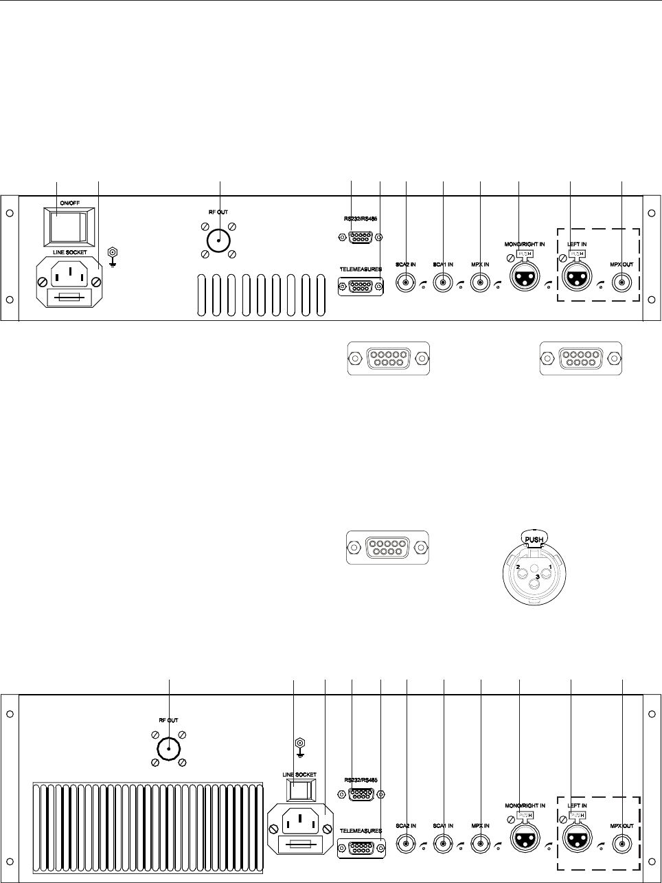
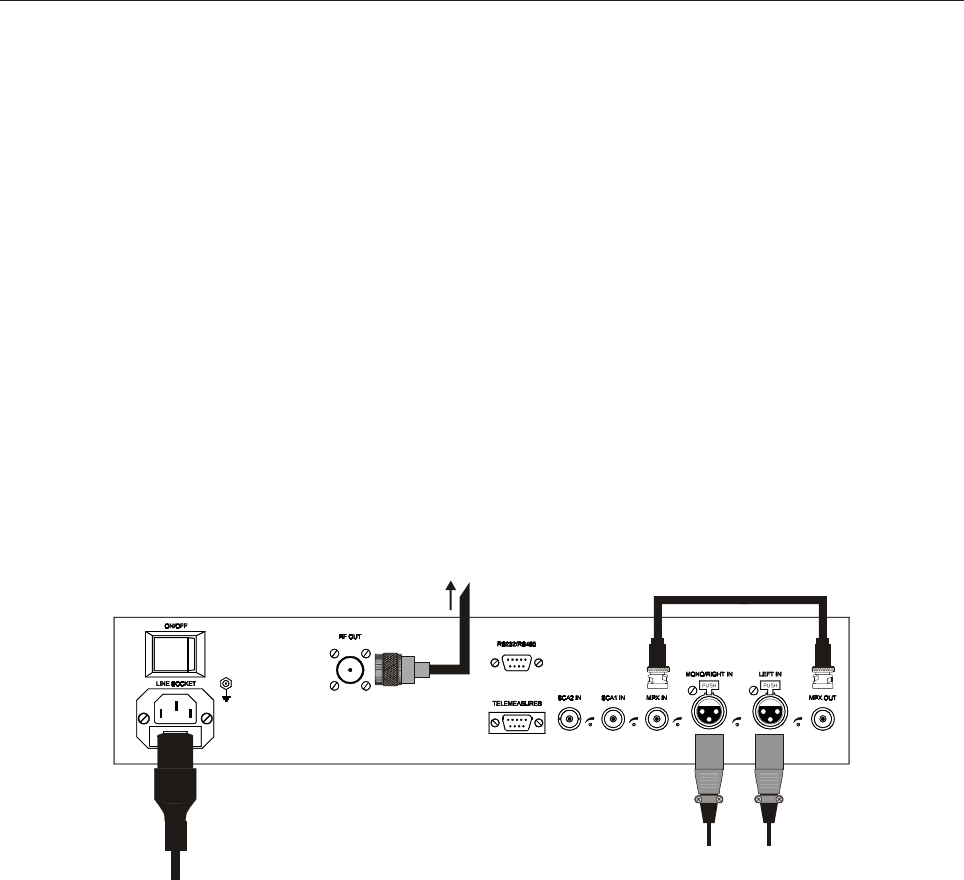
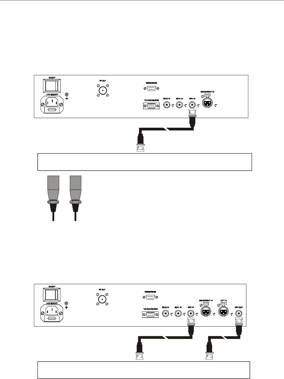
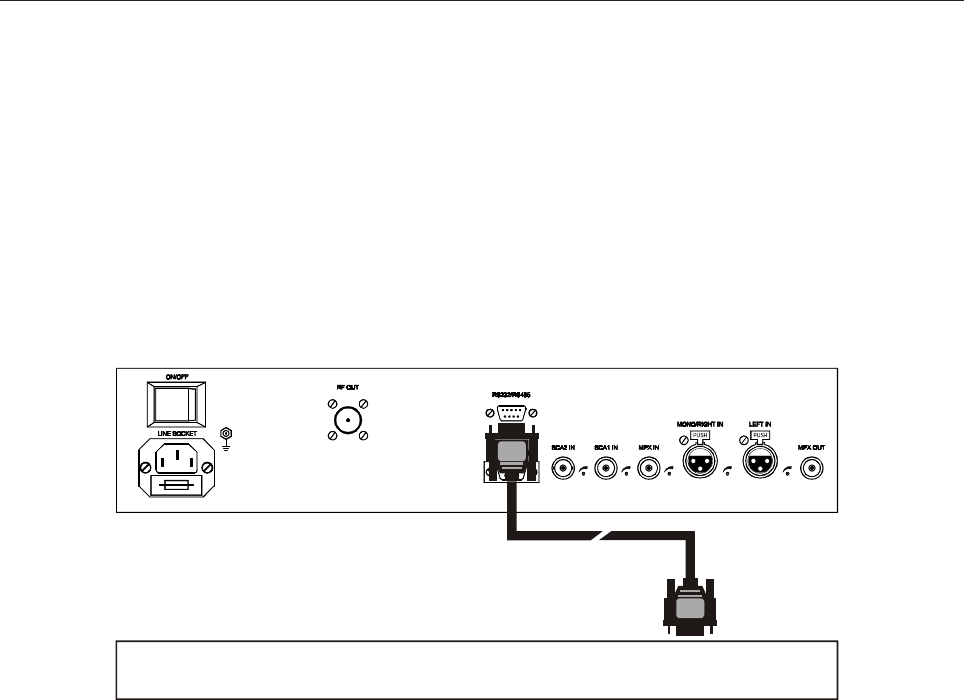
1.4 REAR PANELS
3
1. Main Switch
2. Power Supply Socket with Fuse (5A)
3. RF OUT Connector
4. RS232 / RS485 Socket
5. Telemeasures Socket
6. SCA2 Input
7. SCA1 Input
8. MPX Input Signal
9. MONO / RIGHT Input Signal
10. LEFT Input Signal
11. MPX Output Signal
16
25
4
*
7 8 9 10 11
316
25
47 8 9 10 11
*
RS232 / RS485 Connector(*)
Used for direct connection to a PC
Pin 2: TX Pin 5: GND
Pin 3: RX
RS232 / RS485 Connector(*)
Use for direct connection to the RCU
for remote control the MIZAR by ERCoS
or any other system using a 4wire RS485
connection
Pin 2: RX- Pin 7: TX-
Pin 3: RX+ Pin 8: TX+
Pin 5: GND
Telemeasures Connector
Pin 1: Temperature (Analog out)
Pin 2: REF power (Analog out)
Pin 3: FWD power (Analog out)
Pin 4: ON/OFF (Digital in)
GND=OFF - Open=ON
Pin 5: Alarm:
(Digital out - Open collector)
Closed if alarm is present
Pin 6-7-8-9: GND
XLR Input Signal
Pin 1: Ground
Pin 2: Hot / +ve
Pin 3: Cold / -ve
23
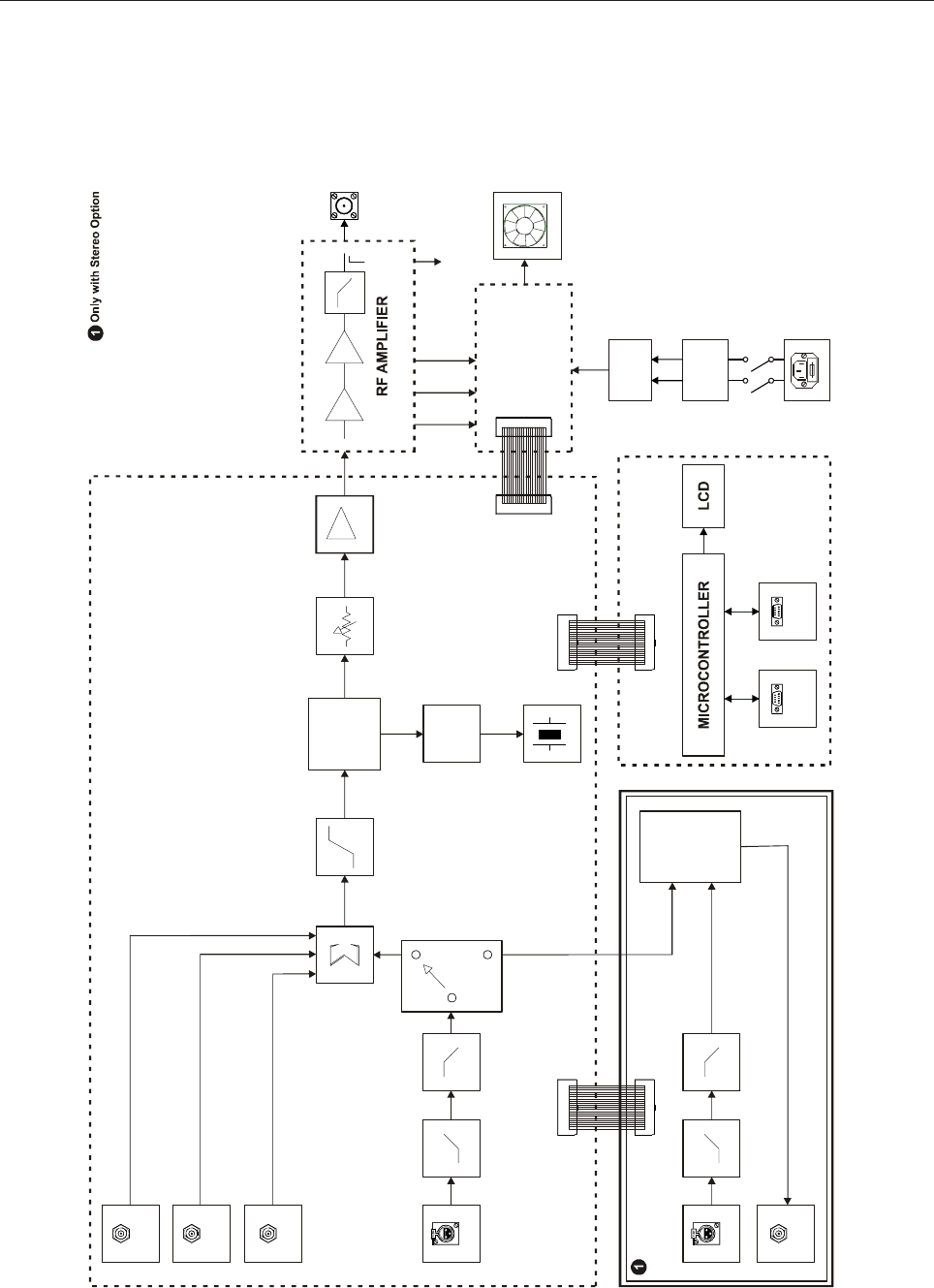
Block diagram
MONO / RIGHT
MPX IN
SCA1
SOCKET
50 s
LOW PASS
FILTER
LIMITER
VCO
LEVEL
PLL
SCA2
SOCKET
LEFT 50 s
LOW PASS
FILTER
CODER
MPX O UT
LEFT
RIGHT
RF DRIVER
INTERFACE
BOARD
REF FWD GATE
MONITOR
RF OUT
BLOWER
27V
AC/DC
FILTER
VAC
RS232 / RS485
SOCKET TELEMEASURES
SOCKET
TCXO
AC SOCKET
MOTHER BOARD
DISPLAY BOARD
CODER BOARD

25
Section 2 - Installation
Contents:
2.1 Operating environment
2.2 First installation
2.3 Installation of MIZAR Mono with external Stereo Coder
2.4 Installation of MIZAR Stereo with external RDS Coder
2.5 MIZAR remote control with Elettronika RCU
26
2.1 OPERATING ENVIRONMENT
You can install the apparatus in a standard component rack or on a suitable surface such as a bench or desk.
In any case, the area should be as clean and well-ventilated as possible. Do not locate the transmitter directly
above a hot piece of equipment. The upper lid can be dismounted to allow an easy internal access. The
equipment is designed with a modular design, that is each circuit is realized inside different modules or boards.
All interconnections between modules are made by means of connectable cables which allow an easy and
quick maintenance of demaged modules.
2.2 FIRST INSTALLATION
1. Connect Antenna cable
2. Connect AC POWER cord
3. Select step and frequency with display interface
4. Move power slowly up till nominal power and check the Reflected Power to be low. If Reflected Power
increase check the RF Output connections
AUDIO INPUT
(LEFT only with OPT023)
AC POWER
To ANTENN
A
GND
Only with OPT023
27
2.3 INSTALLATION OF MIZAR MONO WITH EXTERNAL STEREO CODER
2.4 INSTALLATION OF MIZAR STEREO WITH EXTERNAL RDS CODER
RDS CODER
MPX OUT + RDS MPX IN
LEFT RIGHT
STEREO CODER
MPX OUT
28
2.5 MIZAR REMOTE CONTROL WITH ELETTRONIKA RCU
In order to connect MIZAR to RCU the RS232 / RS485 connector must be set to RS485. This choice is
done cabling the rear panel connector to the J1 (RS485) or J2 (RS232) on the Display Board.
REMOTE CONTROL UNIT
PORT n

29
Section 3 - Operations
Contents:
3.1 User interface and Software settings
3.2 AGC Implementation
3.3 Alarms and automatic behaviours
3.4 Status LEDs

30
3.1 USER INTERFACE AND SOFTWARE SETTINGS
When the equipment is switched on, the display shows the presentation screen, containing the name of the
device and the release number of the firmware.
The mono/stereo choice is made automatically by MIZAR, detecting the presence of the Stereo Coder
Board (OPT023).
At this stage the device restores the last configuration saved of power, frequency and all other parameters.
The other menu can be accessed by pressing the UP and DOWN keys.
All menus show the name of one or two parameter, which can be the reading of a status (e.g. lock/unlock) or
a setting (e.g. Emphasis circuit ON/OFF). In the latter case, the setting may be changed by pressing the RET
in the relevant menu. When the RET key is pressed while in a setting menu, the parameter name label starts
blinking to show that the setting is being edited and not read.
While the label blinks, the user can change the value shown by pressing the UP and DOWN keys. To exit the
edit mode of a setting, and confirm any change made, press the RET key. To leave the edit mode without
confirming any change, press ESC.
Pressing the ESC key while navigating into menu structure, the main menu with the presentation screen is
reached.
Some parameter can be modified only in a protected mode, this possibility will
be highlighted in the menu list. To enter in the protected mode switch on the
MIZAR with both UP and DOWN key pressed. The confirmation of the
protected mode enter will be the display message below and the blinking red
alarm led. This will remember that in protected mode all the alarms and protections will be disabled.
The existing menu, in the order they can be accessed by pressing the UP key, are briefly described below.
This shows the actual level of Forward and Reflected Power. The Forward
Power level can be adjusted.
This shows the actual alarm threshold of Forward and Reflected Power. Both
levels can be adjusted in protected menu.
FM Stereo TX
Software V2.4
FM Mono TX
Software V2.4
Fwd 30W········| | |
Ref 0W········| | |
SETUP
ALARM DISABLED
Fwd Alm 40W
Ref Alm 5W

31
Temperat. 37°C
·········| | | | |
This shows the value of temperature of the heat sink.
This shows if the PLL generating the output frequency is locked or not.
Stereo with coder ON.
This shows the frequency deviation of the carrier.
This shows the Stereo Coder position. It is possible to choose either ON or
OFF position.
This shows the Emphasis position. It is possible to choose either ON or OFF
position.
This shows the operating frequency of the MIZAR. It is possible to choose a
frequency from 87.50 MHz (87.00 for China models) to 108.00 MHz.
This shows the frequency step (minimum distance between adjacent channels).
It is possible to choose between 10kHz, 50kHz or 100 kHz.
This shows the internal AGC enabling status. It is possible to choose either
Enabled or Disabled.
This shows the AGC working status. It can be:
- Disabled;
- Low Set: AGC stopped because reference power is too low;
PLL VCO
Lock
L·········| | | | |
R·········| | | | |
Stereo Coder
OFF
Emphasis
OFF
Frequency
100.00 MHz
Deviation
·······| | | | |
Frequency Step
100 kHz
INTERNAL AGC
ENABLED
AGC STATUS
Lock

32
Last Alarm (0/5)
Empty
Model
30W EKA
- Low Read: AGC stopped because power reading is too low;
- Lock: AGC goal has been reached;
- Max: AGC stopped because of maximum power increasing;
- Min: AGC stopped because of maximum power decreasing;
- Pull-up: AGC is increasing power;
- Pull-down: AGC is decreasing power.
This shows the remote control habilitation. It is possible to choose either
ENABLED or DISABLED position. The TLM Command in the second line
show the actual value of the static on/off command coming from Telemetries
connector on the rear panel. If Remote is DISABLED this command will not
be take in account, if ENABLED this will be the operating state of the MIZAR.
This show the last occurred alarm. The numbers in the first line are the number
of occurred alarm and the maximum alarm number before the lock out of the
MIZAR (five). To reset the lock out press RET and RET again. When an
alarm occurs the menu is automatically changed to this menu.
This menu is available only in protected mode. It is possible to choose the
Model of MIZAR FM Transmitter between 30W and 300W, between EKA,
China and OIRT frequency bands.
Remote DISABLED
TLM Command ON
3.2 AGC IMPLEMENTATION
The AGC goal is to maintain stable the output power. Output power in fact can change due to the increase of
amplifier temperature. Note that when you change the operating frequency the output power change due to
the different gain at different frequency, but this change is not stabilized by this AGC algorithm.
The AGC algorithm is based on the acquisition of the optimal output power level, stored when you change
MIZAR output power. To keep the power stable the AGC change the power gain of MIZAR. When the goal
power is achieved the AGC stops until the power moves up or down.
The AGC work is stopped immediately (output power remains blocked to that reached in the moment of the
AGC stop) when one of this condition occurs:
• one of MIZAR alarms is triggered;
• input power level is to low;
• AGC has change the MIRA output power too much.

33
3.3 ALARMS AND AUTOMATIC BEHAVIOURS
The apparatus signals a working anomaly when any of the following conditions is met:
PLL Unlock
Forward Power exceed the threshold
Reflected Power exceed the threshold
Temperature of the Heat Sink exceed the maximum allowed
In case of failure of any of these parameters, the apparatus automatically mute the output power and change
the menu to the Log menu with the last alarm highlighted. The value of the failed parameter blinks in its menu,
in order to highlight the anomalous working condition.
3.4 STATUS LEDs
ON (Green) Blinking RF Output Power is growing from 0 to nominal
Lit RF Output Power at nominal value
REMOTE (Yellow) Unlit Remote disabled
Lit Remote enabled
ALARM (Red) Blinking Protected mode entered
Lit Alarm present

35
Section 4 - Diagram
Contents:
- APF073A MIZAR30 Cable diagram
- APF074A MIZAR300 Cable Diagram
- APF073A_APF074A MIZAR Component list
- Modules description
36
37

38
Part Name Code Description Qty
02035 BNC CONNECTOR FOR RG316 CABLE 1
02513 90 SMB SOCKET cod. R114186000W 2 (APF073A) 1 (APF074A)
02518 SMB SOCKET FOR RG174 CABLE code R114082000W 1 (APF073A) 2 (APF074A)
02695 DB9 CONNECTOR FOR IU008059 CABLE 1
02699 FEMALE 10WIRE CONNECTOR 1
02700 FEMALE 16WIRE CONNECTOR 2
02833 AC SOCKET WITH FUSE-HOLDER 1 (APF074A)
02841 3 POLES CANON PLUG 1
02855 FEMALE 26WIRE CONNECOTR 2
05069 TOROIDAL FILTER 1 (APF074A)
05551B 2U HANDLE KIT 2 (APF073A)
05552B 3U HANDLE KIT 2 (APF074A)
07522 LIGHTED SWITCH 1 (APF073A)
07524A BLACK SWITCH 1 (APF074A)
07602 BLOWER GRID 1 (APF073A) 2 (APF074A)
07613 PAPST BLOWER 1 (APF073A) 2 (APF074A)
07918 AC FILTER 1 (APF073A)
07924 PVC PROTECTION 1 (APF074A)
07925 PVC PROTECTION 1
07926 PVC PROTECTION 1 (APF073A)
08502 RG 316 50Ω CABLE 0.70 (APF073A) 0.90 (APF074A)
CON0306 CON0306R0 COVER 1
CON0340S CON0340R1S MIZAR30 BOX 1 (APF073A)
CON0354R2S CON0354R2 MIZAR300 BOX 1 (APF074A)
DET1220 DET1220R1 BLOWER CONVEYER 1 (APF073A)
DET1317R0P DET1317R0P MECHANICAL DETAIL 1 (APF074A)
DET1361R0P DET1361R0 MECHANICAL DETAIL 1 (APF074A)
E0050 PSP-650-48 DE2 SWITHCING POWER SUPPLY 1 (APF074A)
E0060 S-100F-24 SWITCHING POWER SUPPLY 1 (APF073A)
FUS5A 5A FUSE 2 (APF073A)
FUS10B 10A FUSE 2 (APF074A)
MFF0025BR0 30W FM AMPLIFIER MODULE 1 (APF073A)
MFF0031AR0 300W FM AMPLIFIER MODULE 1 (APF074A)
PAN0141 PAN0141R1 FRONT PANEL 1 (APF073A)
PAN0153R0P FRONT PANEL 1 (APF074A)
SCH0372AR1 DISPLAY BOARD 1
SCH0377AR2 MOTHER BOARD 1
V0761 BLACK PLASTIC TAP 1
V0768 BLACK PLASTIC TAP 1
Component list APF073A_APF074A - MIZAR

39
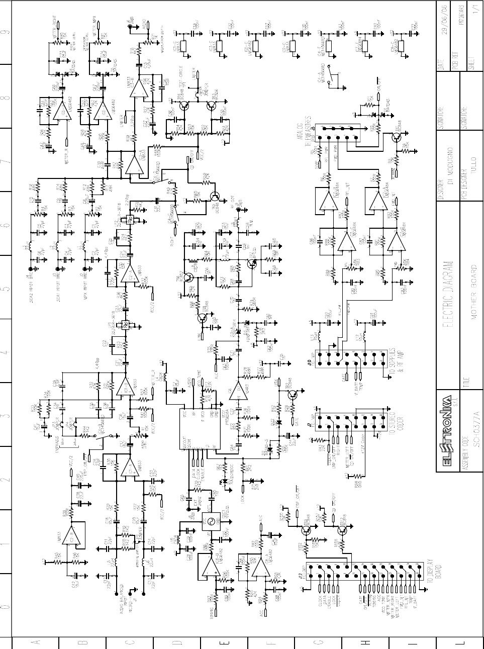
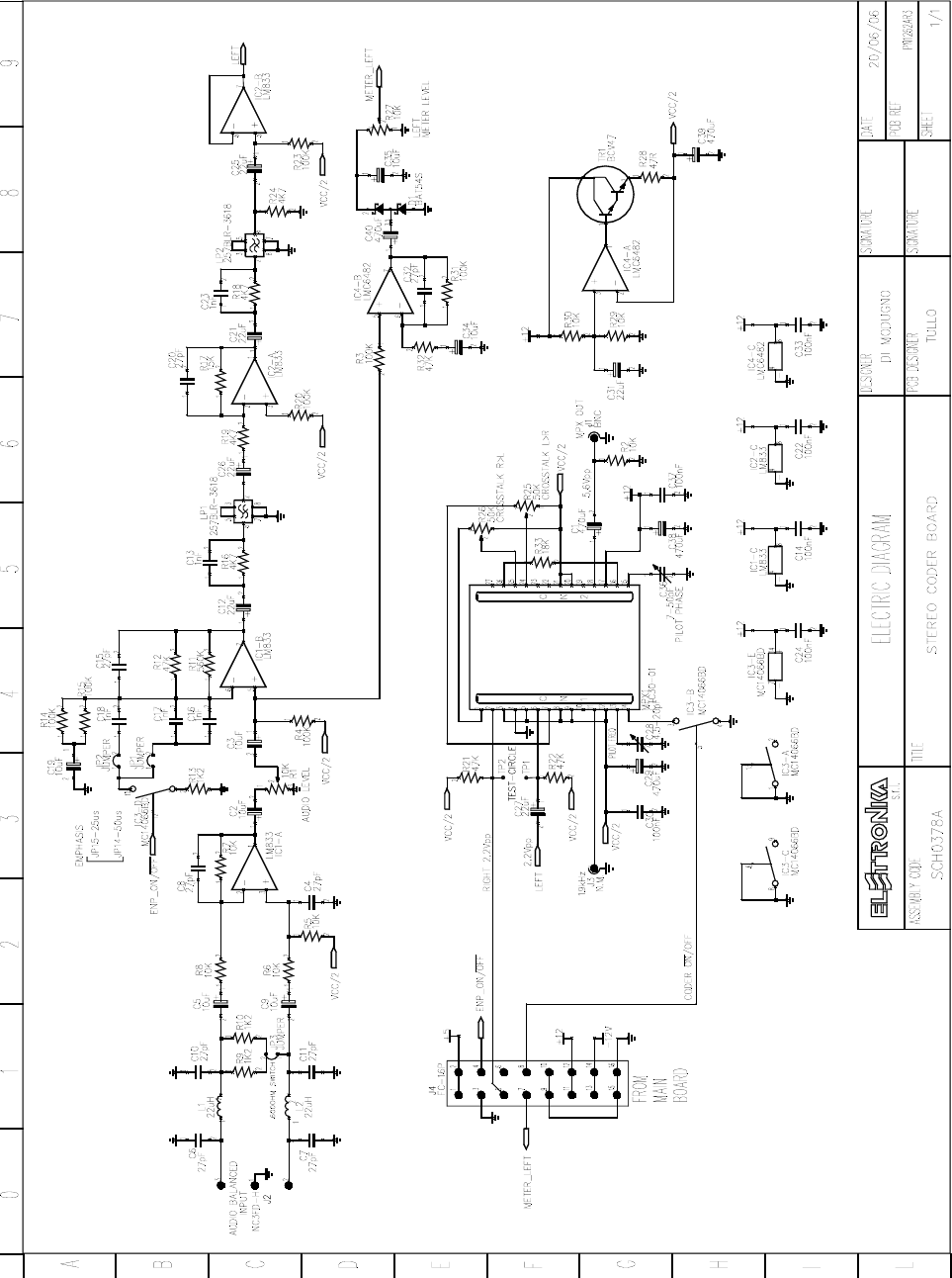
MOTHER BOARD SCH0377AR2
DESCRIPTION
The board contains the stages needed to condition the audio MONO or RIGHT signals and modulate in
frequency a synthesised oscillator. It provides an output radio frequency signal in the II-VHF band, to drive
the final amplification stage. The various sections are analysed below:
1. Balanced/Unbalanced Converter: the conversion from balanced to unbalanced and the input interface
of the audio signal are realised la electronically by the IC1-A operational circuit. This assures an high ge-
gree of immunity from disturbances and a perfect symmetry in unbalancing.
2. Pre-emphasis: after the level adjustment, there is the active pre-emphasis stage (IC1-B), with amplification
to high frequencies. The time constant is chosen between 25 and 50 microseconds by means of two jum-
pers (JP3-4). When they are both enables they give 75us (for the FCC standard). The insertion of the pre-
emphasis is managed from the frontal panel by activating the electronic switch IC4.
3. Low-pass Filter: the use of two filtering stages with elliptical filters LP1 and LP2 assures the adequate suppres-
sion of input signals at frequencies 19k and 38kHz.
4. Additioner: depending on the operating mode selected by the frontal panel (Stereo or Mono) the MONO
signal, after the low-pass filter, is sent to the internal stereo coder (as RIGHT signal) or added to the auxi-
liary inputs (SCA1-2 and MPX) in the stage composed by IC3-A.
5. Peak Detector: at the output of the additioner, part of the signal is sampled for the indication of the devia-
tion on the front panel. IC5-A serves as buffer for the duplicator and peak detector. Aside from the peak
detector for the indication of the modulation level, the board also includes a second detector (IC5-B and
D4) used to measure the level of the RIGHT signal.
6. Limitation circuit: TR3 and TR4 realise the deviation limitation circuit by cutting the audio signal which
exceeds the set voltage threshold on the relevant basis, by means of the resistor network R51-54.
7. Oscillator: a frequency synthesis oscillator with PLL generates the radiofrequency carrier which is modulated
in frequency in the same circuit. The reference frequency is generated by a 5.0MHz TCXO with good
temperature stability.
8. RF Driver: after the oscillator there is a PIN diode stage (D3) to check the amplitude of the signal and mo-
dify the output power. The dynamic is greater than 40dB. The monolith amplifier (IC6) serves as buffer in
order to make the load effects on the oscillator circuit irrelevant. Finally, the stage with TR7 amplifies the
signal to the adequate levels for driving the power module. A circuit monitoring the power supply of TR7,
composed by TR6 and TR8, activates to switch the transistor off in case of alarms (such as PLL unlock or
any anomaly detected by the control board).
40
9. Telemetering: the most important analogue signals – forward and reflectesd power, switch on/off, alarms
and temperature – are buffered and made available on the J5 socket for connecting remote control systems.
SCH0377AR2 Component layout
41
CALIBRATION PROCEDURE
- Instrument list
Description of the adjustment points
MEASURE INSTRUMENT
RF Signal level - Spectrum Analyser
Frequency - Spectrum Analyser
Audio - Audio Generator
Modulation - FM/AM Modulation Analyser
Limiter intervention - Oscilloscope
COMPONENT DESCRIPTION
R1 MONO/RIGHT Audio Input level
R2 MPX Input level
R3 SCA1 Input level
R4 SCA2 Input level
R21 Modulation depth adjustment
R80 Indication of the RIGHT signal deviation on display (only if the stereo option is installed)
R81 Indication of the deviation on the display
R83 Indication of the Reflected Power on the display
R84 Indication of the Forward Power on the display
LP1, LP2 Notch and Low-pass Filter at 19 and 38kHz
OSC1 RF Signal output frequency calibration
JP1 If inserted, sets the MONO Input impedance to 600Ω
JP2 If inserted, enables the deviation limiter
JP3 If inserted, enables the 25µs pre-emphasis
JP4 If inserted, enables the 50µs pre-emphasis
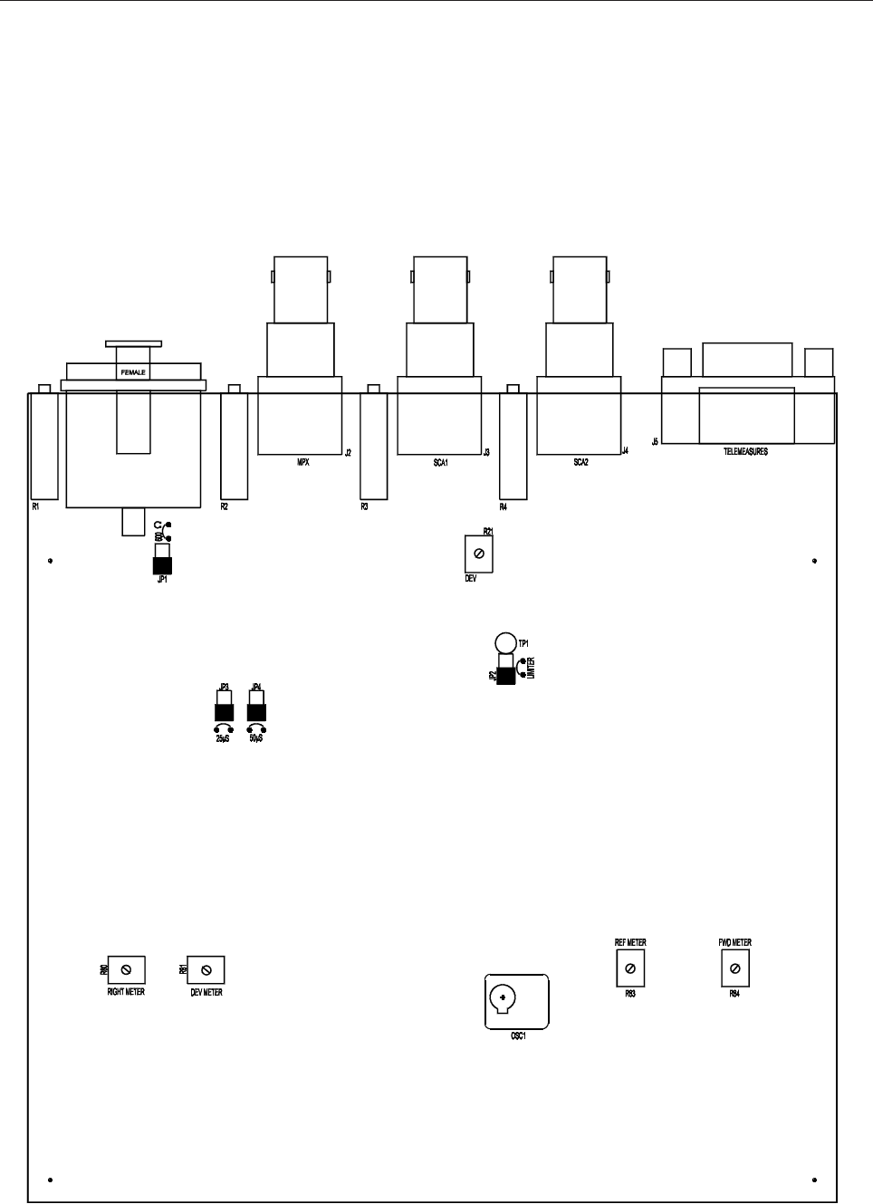
42
Component layout for adjustment points

43
RF Section
Check the lock of the oscillator on the whole operating range (87 - 108MHz).
If the synthesised frequency is not correct, try to correct it by means of the capacitive trimmer of the
OSC1 reference.
Verify the signal-to-noise ration (CCIR) of the oscillator, which should be >73dB on the whole band.
Verify the output level by the J9 (RF OUT) connector, higher than 24.5dBm on the whole band.
Verify that the final stage is switched off when the PLL of the oscillator unlocks.
Modulation Section
Disable the emphasis (from the display).
Insert the JP1 jumper (so to have an input impedance of 600Ω).
Insert the JP2 jumper to enable the limitation circuit.
Provide a 400Hz, 2.2Vpp banalced signal to the MONO input.
Adjust R1 in order to have an amplitude of 3.2Vpp on TP1 (on which the oscilloscope is connected).
Adjust R21 to obtain a deviation of ±75kHz.
Adjust R81 to obtain the indication of the nominal deviation on the display.
Double the level of the input signal (4.4Vpp) and check that the modulation increase is no more than 1dB.
Audio Section
With modulation analyser and audio signal on the MONO input at 2.2Vpp, verify the frequency response
from 30 to 15kHz without emphasis. Correct any deviation from the nominal range by acting on LP1 and
LP2.
Insert the JP4 jumper (50µs) and enable the emphasis from the display. Check the frequency response.
Insert the JP3 jumper (25+50µs) as well and check again the frequency response.
Verify the frequency response of the MPX input from 30 to 100kHz, calibrating R2 for the nominal
deviation with 2.2Vpp signal amplitude.
Verify the frequency response of the SCA1 and SCA2 inputs from 50k to 100kHz, calibrating R3 and
R4 for the nominal deviation (±7.5kHz) with 2.2Vpp signal amplitude.
General
Verify the remote switch-off function by short-circuiting pin 5 of J5 to ground.

44
SCH0377AR2 COMPONENT LIST
Part Name/Number Description Qty. Comps. Page 1/2
257BLR-3618N 05010 05010 AUDIO TOKO FILTER 2 LP1-2
CC 100nF-S 01065C 01065C Y5V 1206 CAPACITOR 20 C19, C30, C32, C43, C45-46, C57,
C62-63, C77, C79, C81-89
CC 10pF-S 01086 01086 SMD 1206 CAPACITOR 1 C26
CC 1206 N. M. N. M. SMD 1206 CAPACITOR 1 C58
CC 1nF-2%-S 01041D 01041D SMD 1206 CAPACITOR 23 C9-10, C22, C25, C34-36, C49-50, C54, C56,
C59-61, C64-65, C68-72, C75, C80
CC 27pF-S 01022B 01022B SMD 1206 CAPACITOR 16 C1-6, C11-14, C28-29, C33, C37, C51-52
CC 6p8F-S 01084 01084 SMD 1206 CAPACITOR 1 C39
CE 100uF16V-S 01792A 01792A ELET. SMD CAPACITOR 3 C78, C91-92
CE 10uF16V-S 01776A 01776A ELET. SMD CAPACITOR 14 C7, C16-18, C20, C41-42, C47-48, C53, C55,
C73-74, C76
CE 220uF16V-S 01824A ELET. SMD CAPACITOR 5 C8, C27, C40, C66-67
CE 22uF16V-S 01780A ELET. SMD CAPACITOR 6 C21, C23-24, C31, C38, C44
CE 470uF-S 16V-S 01804B ELET. SMD CAPACITOR 1 C15
D BAS85-S 03024 SMD DIODE SCHOTTKY 1 D2
D BAT54S 03199 SMD SCHOT. DIODE A-K T 3 D1, D4-5
D HSMP3814 03202 SMD DIODE 1 D3
DL KA-3528SGC 03057 03057 GREEN SMD LED DIODE 1 DL1
DZ 5V1-S 03128 03128 SMD ZENER DIODE 2 DZ1-2
IC LM833-S 04643A 04643A SMD INTEG CIRCUIT 3 IC1-3
IC LMC6482-S 04632 SMD INTEG CIRCUIT 2 IC5, IC8
IC LMC6484-S 04634 SMD INTEG CIRCUIT 1 IC7
IC MAR3 04367 04367 SMD INTEG CIRCUIT 1 IC6
IC MC14066BD-S 4708B 4708B SMD INTEG CIRCUIT 1 IC4
IND 100nH-S 05093A 05093A INDUCTOR 1 L9
IND 22uH-S 5023D 5023D INDUCTOR 5 L1-3, L5-6
IND 2u2H-S 05020A 05020A INDUCTOR 1 L7
IND CBD8 05072 05072 INDUCTOR 3 L4, L8, L10
IND MS85 10uH-S 04948 INDUCTOR 2.7A 2 L12-13
J BNC-90G-PCB SHIELD 02034A PCB SHIELDED CONNEC. 3 J2-4
J DB9-90G 02797 02797 PCB CONNECTOR 1 J5
J FC-16P 02701-02700 02701+02700 PCB CONNECTOR 2 J7, J10
J FC-26P 02855-02854 02855+02854 PCB CONNECTOR 1 J12
J NC3FD-H 02862 02862 XLR-90G-PCB SOCKET F. 1 J1
J SMB-PCB 2PIN 02516 02516 PCB CONNECTOR 3 J6, J8-9
JU JUMP2 02739-02742 02739+02742 MASCHIO PAN2 4 JP1-4
OSC NVT535 05168 05168 TCXO 1 OSC1
PN0658A SCH0007AR0 SCH0007AR0 VCO FM INTEG. 1 VCO1
R 0R0-S 00001 00001 RES 1/4W 5% SMD 1206 1 R98
R 100K-1%-S 00065B 00065B RES 1/4W 1% SMD 1206 12 R33-34, R37, R41, R48, R50, R55, R57, R62,
R88, R91, R96

45
Part Name/Number Description Qty. Comps. Page 2/2
R 100R-S 00029A 00029A RES 1/4W 5% SMD 1206 12 R5-7, R10, R38, R71, R76, R82, R86-87, R92,
R97
R 10K-S 00053A 00053A RES 1/4W 5% SMD 1206 17 R8-9, R11, R22, R29-30, R40, R45-46, R52,
R53, R60, R66, R73, R100-101, R107
R 10R-S 00017A 00017A RES 1/4W 5% SMD 1206 2 R64, R69
R 15K-1%-S 00055B 00055B RES 1/4W 1% SMD 1206 3 R35, R85, R94
R 1K2-1%-S 00042A 00042A RES 1/4W 1% SMD 1206 5 R19-20, R44, R67, R79
R 1K5-S 00043A 00043A RES 1/4W 5% SMD 1206 1 R68
R 22K-S 00057A 00057A RES 1/4W 5% SMD 1206 4 R17, R43, R89-90
R 2K2-S 00045A 00045A RES 1/4W 5% SMD 1206 2 R61, R70
R 330R-1%-S 00035A 00035A RES 1/4W 1% SMD 1206 1 R75
R 47K-1%-S 00061B 00061B RES 1/4W 1% SMD 1206 18 R18, R26-28, R32, R42, R49, R51, R54, R56,
R58-59, R63, R65, R93, R95, R102, R108
R 4K7-S 00049A 00049A RES 1/4W 5% SMD 1206 6 R15, R23-25, R36, R39
R 560K-S 00074B RES 1/4W 5% SMD 1206 1 R31
R 560R-1%-S 00038B 00038B RES 1/4W 1% SMD 1206 1 R74
R 68K-1%-S 00063B 00063B RES 1/4W 1% SMD 1206 5 R12-14, R16, R47
R 68R-S 00027A 00027A RES 1/4W 5% SMD 1206 2 R77-78
R 82R-S 00028A 00028A RES 1/4W 5% SMD 1206 1 R72
RV 10K-M-H 00777 00777 VARIABLE RESISTOR 4 R1-4
RV 10K-S-H/S 00793 00793 SMD VARIABLE RESISTOR 2 R80-81
RV 1K-S-H/S 00792 00792 SMD VARIABLE RESISTOR 1 R21
RV 50K-S-H/S 00797 00797 SMD VARIABLE RESISTOR 2 R83-84
TR BC807 03453 03453 PNP SMD TRANSISTOR 1 TR6
TR BC848 03457 03457 NPN SMD TRANSISTOR 7 TR1-2, TR4-5, TR8-9, TR12
TR BC856 03455 03455 PNP SMD TRANSISTOR 1 TR3
TR BFG35 03990 03990 NPN SMD TRANSISTOR 1 TR7
46

47
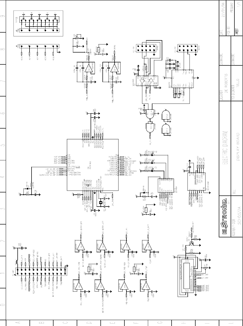
STEREO CODER BOARD OPT023
DESCRIPTION
The board contains the stages needed for the conditioning of the Left channel audio signal and for realising the
stereo encoding in compliance with the standard ITU racc. 450. The Right signal is provided through the
connection to the Mother board. The various sections are analysed below:
1. Balanced/Unbalanced Converter: the conversion from balanced to unbalanced and the input interface
of the audio signal are realised la electronically by the IC1-A operational circuit. This assures an high ge-
gree of immunity from disturbances and a perfect symmetry in unbalancing.
2. Pre-emphasis: after the level adjustment, there is the active pre-emphasis stage (IC1-B), with amplification
to high frequencies. The time constant is chosen between 25 and 50 microseconds by means of two jum-
pers (JP1-2). When they are both enables they give 75µs (for the FCC standard). The insertion of the
pre-emphasis is managed from the frontal panel by activating the electronic switch IC3.
3. Low-pass Filter: the use of two filtering stages with elliptical filters LP1 and LP2 assures the adequate suppres-
sion of input signals at frequencies 19k and 38kHz.
4. Peak Detector: before the emphasis circuit, part of the audio signal is sampled to provide the indication of
the LEFT channel deviation on the frontal display. IC4-A serves as buffer for the duplicator and peak de-
tector.
5. Stereo Coder: stereo encoding is realised inside the MPX1 block, providing the MPX signal in output.
SCH0378AR2 Component layout
48
CALIBRATION PROCEDURE
- Instrument list
Description of the adjustment points
MEASURE INSTRUMENT
RF Signal level - Spectrum Analyser
Frequency - Spectrum Analyser
Audio - Audio Generator
Modulation - FM/AM Modulation Analyser
Limiter intervention - Oscilloscope
COMPONENT DESCRIPTION
R1 LEFT Audio Input level
R25 Adjusts Left on Right signal crosstalk
R26 Adjusts Right on Left signal crosstalk
R27 Indication of the LEFT signal deviation on the display
C28 Adjusts the 19kHz pilot tone frequency
C36 Adjusts the pilot tone phase
LP1, LP2 Notch and Low-pass Filter at 19 and 38kHz
JP3 If inserted, sets the LEFT Input impedance to 600Ω
JP2 If inserted, enables the 25µs pre-emphasis
JP1 If inserted, enables the 50µs pre-emphasis
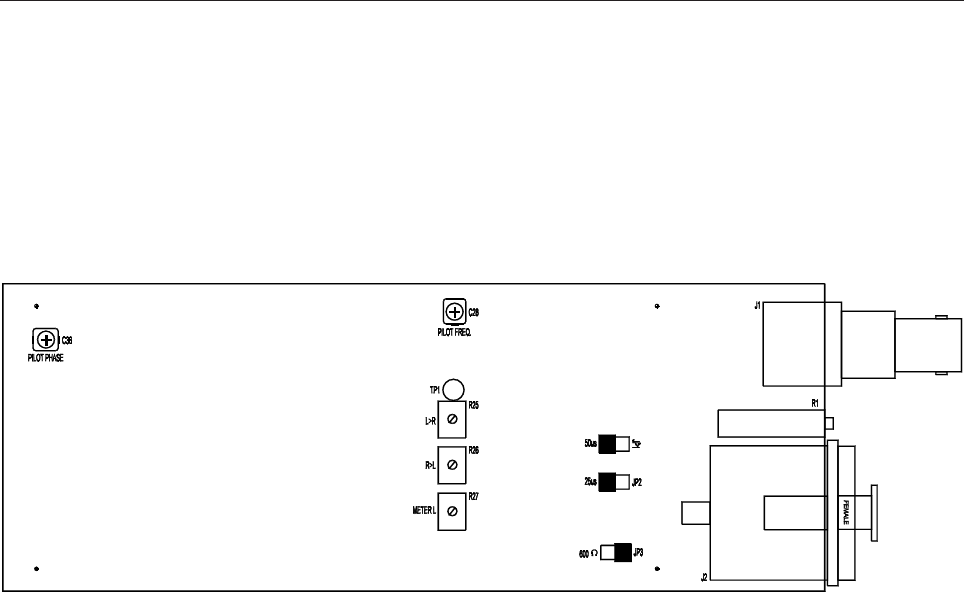
49
Component layout for adjustment points
Coder Section
Enable the Stereo mode from display.
Measure, and correct by means of C28 if needed, the frequency of the pilot tone (19kHz)
With modulation analyser and audio signal on the LEFT input at 2.2Vpp, verify the frequency response
from 30 to 15kHz without emphasis. Correct any deviation from the nominal range by acting on LP1 and
LP2.
Insert the JP4 jumper (50µs) and enable the emphasis from the display. Check the frequency response.
Insert the JP3 jumper (25+50µs) as well and check again the frequency response.
Check the crosstalk between the two channels and act on C36, R25 and R25 to bring it to the nominal
levels.

50
SCH0378AR2 COMPONENT LIST
Part Name/Number Description Qty. Comps.
257BLR-3618N 05010 05010 AUDIO TOKO FILTER 2 LP1-2
CC 100nF-S 01065C 01065C Y5V 1206 CAPACITOR 6 C14, C22, C24, C30, C33, C37
CC 1nF-2%-S 01041D 01041D SMD 1206 CAPACITOR 5 C13, C16-18, C23
CC 27pF-S 01022B 01022B SMD 1206 CAPACITOR 9 C4, C6-8, C10-11, C15, C20, C32
CE 10uF16V-S 01776A 01776A ELET. SMD CAPACITOR 7 C2-3, C5, C9, C19, C34-35
CE 22uF16V-S 01780A ELET. SMD CAPACITOR 6 C12, C21, C25-27, C31
CE 470uF-S 16V-S 01804B ELET. SMD CAPACITOR 5 C1, C29, C38-40
CV 4.5-20pF-S 01481 01481 VARIABLE CAPACITOR 1 C28
CV 7-50pF-S 01474 01474 VARIABLE CAPACITOR 1 C36
D BAT54S 03199 SMD SCHOT. DIODE A-K T 1 D1
IC LM833-S 04643A 04643A SMD INTEG CIRCUIT 2 IC1-2
IC LMC6482-S 04632 SMD INTEG CIRCUIT 1 IC4
IC MC14066BD-S 4708B 4708B SMD INTEG CIRCUIT 1 IC3
IND 22uH-S 5023D 5023D INDUCTOR 2 L1-2
J BNC-90G-PCB SHIELD 02034A PCB SHIELDED CONNEC. 1 J1
J FC-16P 02701-02700 02701+02700 PCB CONNECTOR 1 J4
J NC3FD-H 02862 02862 XLR-90G-PCB SOCKET F. 1 J2
J SMB-PCB N. M. SMB PCB N. M. 1 J3
JU JUMP2 02739-02742 02739+02742 PAN2 MALE 3 JP1-3
MPX CTC30-01 04894 STEREO ENCODER 1 MPX1
R 100K-1%-S 00065B 00065B RES 1/4W 1% SMD 1206 7 R3-4, R14-15, R20, R23, R31
R 10K-S 00053A 00053A RES 1/4W 5% SMD 1206 7 R2, R5-8, R29-30
R 15K-1%-S 00055B 00055B RES 1/4W 1% SMD 1206 1 R17
R 18K-S 00056B 00056B RES 1/4W 5% SMD 1206 1 R33
R 1K2-1%-S 00042A 00042A RES 1/4W 1% SMD 1206 3 R9-10, R13
R 47K-1%-S 00061B 00061B RES 1/4W 1% SMD 1206 4 R12, R21-22, R32
R 47R-S 00025A 00025A RES 1/4W 5% SMD 1206 1 R28
R 4K7-S 00049A 00049A RES 1/4W 5% SMD 1206 4 R16, R18-19, R24
R 560K-S 00074B RES 1/4W 5% SMD 1206 1 R11
RV 10K-M-H 00777 00777 VARIABLE RESISTOR 1 R1
RV 10K-S-H/S 00793 00793 SMD VARIABLE RESISTOR 1 R27
RV 50K-S-H/S 00797 00797 SMD VARIABLE RESISTOR 2 R25-26
TR BCV47 03465 NPN SMD TRANSISTOR 1 TR1
51
52
DISPLAY BOARD SCH0372AR1
DESCRIPTION
The MIZAR display board contains the HMI (human machine interface) of the equipment composed by a
alphanumeric 2 rows x 16 columns displayand a keys series, a connector for collecting and sending datas
towards the equipment mother-board and its thinking heart made by a Flash microcontroller.
The board is able of reading 8 analogic signals coming from mother-board. These are only bufferized on the
board and therefore their conditioning is made on the mother-board.
The remaining digital input and output signals are conneted directly to the micro, where is necessary some
interverntion speed, or are multiplexed on shift register where the speed is less important.
The board moreover provide the remotability to the equipment by an asyncronous serial, configurable as
RS232 or RS485 simply connecting the output connector to one of the two serial connectors present on the
display board.
SCH0372AR1 Top layer Component layout
SCH0372AR1 Bottom layer Component layout

53
SCH0372AR1 COMPONENT LIST
Part Name/Number Description Qty. Comps.
CC 100nF-S 01065C 01065C Y5V 1206 CAPACITOR 20 C3-5, C7, C12, C14, C16-17, C24-28, C30,
C31-35, C37
CC 15pF-S 01088 01088 SMD 1206 CAPACITOR 2 C1-2
CC 1uF100V-S 01760A 01760A Y5V 1206 50V CAPAC. 7 C8, C11, C13, C15, C18-20
CC 220nF-S 1069A 1069A Y5V 1206 CAPACITOR 6 C6, C9-10, C21-23
CE 10uF16V-S 01776A 01776A ELET. SMD CAPACITOR 2 C29, C36
D 1N4148-S 03002 03002 SMD DIODE 2 D1-2
DIS MDLS16268CLVBLDW 03072C DISPLAY 2 X 16 WIDE 1 LCD1
DL LEDG5 03060 03060 GREEN LED DIODE 5mm 1 DL3
DL LEDR5 03061 03061 RED LED DIODE 5mm 1 DL1
DL LEDY5 03054B 03054B YELL. LED DIODE 5mm 1 DL2
IC 74HC00-S 4762A 4762A SMD INTEG CIRCUIT 1 IC3
IC LMC6482-S 04632 SMD INTEG CIRCUIT 1 IC5
IC LMC6484-S 04634 SMD INTEG CIRCUIT 2 IC8-9
IC MAX232-S 04804B 04804B SMD INTEG CIRCUIT 1 IC7
IC MAX3080-S 04770 04770 SMD INTEG CIRCUIT 1 IC4
IC MC14094BD 04718 04718 SMD INTEG CIRCUIT 1 IC1
IC MC74HC589 4874 04874 SMD INTEG CIRCUIT 1 IC2
IC PIC18F452-S 04807C + 07509C INTEG CIRCUIT 1 IC6
IND CBD8 05072 05072 INDUCTOR 1 L1
J FC-10P 02697-02699 02697+02699 PCB CONNEC. POL 2 J1-2
J FC-26P 02855-02854 02855+02854 PCB CONNEC. POL 1 J5
J PAN6 02713-14-15 02713+02714+02715 PCB CONN. 2 J3-4
JU JUMP3 02707-02742 02707+02742 MASCHIO PAN3 1 JP1
R 100R-S 00029A 00029A RES 1/4W 5% SMD 1206 2 R6-7
R 10K-S 00053A 00053A RES 1/4W 5% SMD 1206 4 R9, R16-17, R20
R 120R-S 00030A 00030A RES 1/4W 5% SMD 1206 1 R3
R 12R-S 00018A 00018A RES 1/4W 5% SMD 1206 1 R18
R 1K0-S 00041A 00041A RES 1/4W 5% SMD 1206 1 R19
R 470R-S 00037A 00037A RES 1/4W 5% SMD 1206 1 R8
R 47K-S 00061A 00061A RES 1/4W 5% SMD 1206 5 R2, R4-5, R11-12
R 820R-S 00040A 00040A RES 1/4W 5% SMD 1206 3 R13-15
RV 10K-3266X 00807 00807 VARIABLE RESISTOR 1 R1
RV 5K-M-V 00783 00783 VARIABLE RESISTOR 1 R10
T CLOCHE GREY WITH BLUE CENTER 4 x xxxxxx + 4 x xxxxxx + xxxx 1 T1
TR BC817 03454 03454 NPN SMD TRANSISTOR 1 TR1
XTAL 20MHz-S CXS00001 QUARTZ 1 XTAL1
54

55
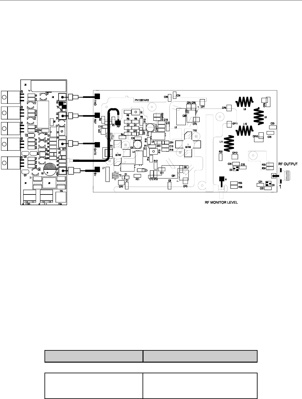
30W FM AMPLIFIER MODULE MFF0025BR0
DESCRIPTION
The MFF0025B amplifier module is designed to amplify the FM modulated carriers in the 87-108MHz band,
and can provide an output of 30W CW. In order to obtain the desired gain, the amplifier is made up by two
gain stages: the pilot stage uses a BLF242 MOSFET, while the final stage uses a BLF245 MOSFET.
An input adaptation circuit allows the adaptation of the module to the various driving levels. The output power
regulation is made by controlling the power level of the input signal of the module. The final stage of the
module also has a control terminal allowing to disable the MOSFET immediately, if needed. The output of the
module is completed by a 9th order (4 cell) low-pass filter to attenuate the level of the harmonics of the signal,
and by two high-directivity directional couplers needed to sample part of the Forward and Reflected Power
in order to measure their levels. The final is provided with the needed circuits (SCH0371B Interface Board)
to read the output Forward and Reflected Power, the heatsink temperature and the voltage supplied.
TECHNICAL CHARACTERISTICS
Frequency Range 87 - 108MHz
Output Power 30W
Input Return Loss >25dB
Power Supply +27V
RF Input Impedance 50Ω
RF Output Impedance 50Ω
Bias Current BLF242 with Vdd = +27V: 220mA
Bias Current BLF245 with Vdd = +27V: 220mA
Gain 20dB
Efficiency 54%
MFF0025BR0 COMPONENT LIST
Part Name/Number Description Qty.
SCH0382BR0 30W FM AMPLIFIER BOARD 1
01400 BYPASSING CAPACITOR 1
01408 BYPASSING CAPACITOR 3
DET1304 DET1304R0 30W DISSIPATOR 1
DET1276 DET1276R0 AMPLIFIER REAR BAR 1
DET1277 DET1277R1 AMPLIFIER INPUT BAR 1
DET1239 DET1239R1 AMPLIFIER MODULE COVER 1
SCH0371BR0 INTERFACE BOARD 1
07907 TO220 INSULATOR 2
07910 TO220 INSULATOR 2
02515 SMB SCREW cod. R114313000 1
08502 RG 316 50Ω CABLE 0.15
02516 SMB CONNECTOR FOR PCB 1
02248 17x17 NF FLANGE CONNECTOR 1
56
CALIBRATION PROCEDURE
The calibration procedure is mainly made of three step:
1. Calibration of the Output Filter
2. Polarization of the BLF242 and BLF245 MOSFETS
1. Calibration of the Output Filter
- Instrument list
MEASURE INSTRUMENT
Calibration of the Output Filter Network analyser or alternately Spectrum
analyser with tracking generator and SWR
Bridge
MFF0025BR0 Component layout
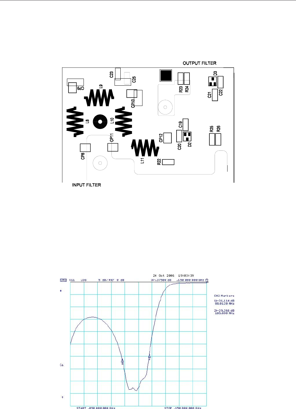
57
Calibrate the spectrum analyser after setting a 100MHz span centered ad 100MHz (10MHz/div - 5dB/
div).
Connect the input of the filter to port 1 of the network analyser, connect the output of the filter to a dummy
load.
Display the reflection coefficient (parameter s11). The calibration consists in acting on the coils (L8, L9,
L10, L11) to obtain a curve as the one shown in picture A after closing the module.
58
- Description of the adjustment points
Disconnect the input terminal of the module, connect the dummy load to the output terminal and connect
a tester as amperometer (10A cc capacity) on the power supply line (in place of the fuse).
Turn R7 and R15 completely clockwise (so to interdict the VDMOS). Disconnect the passing connector
from TP3 Gate. See details in picture below.
2. Polarisation of the BLF242 and BLF245 MOSFETs
- Instrument list
COMPONENT DESCRIPTION
R15, R7 Adjust polarisation
MEASURE INSTRUMENT
Polarisation of
BLF242 and BLF245 Transistors Two Digital meter
Power the module and check that there are +27V on TP4 (see previous picture).
Turn the R15 trimmer counterclockwise until the display of the amperometer shows 220mA absorption.
Turn the R7 trimmer counterclockwise until the display of the amperometer shows an increase of 220mA;
the whole module should absorb more or less 440mA at 27V.
Re-connect the passing connector to TP3 Gate.
RF IN
59
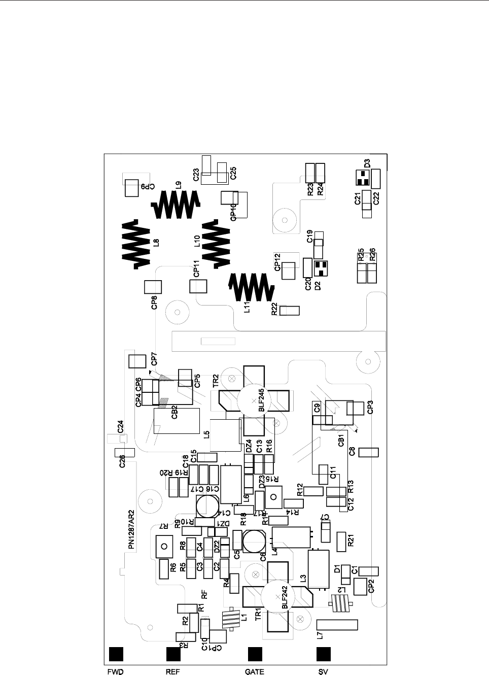
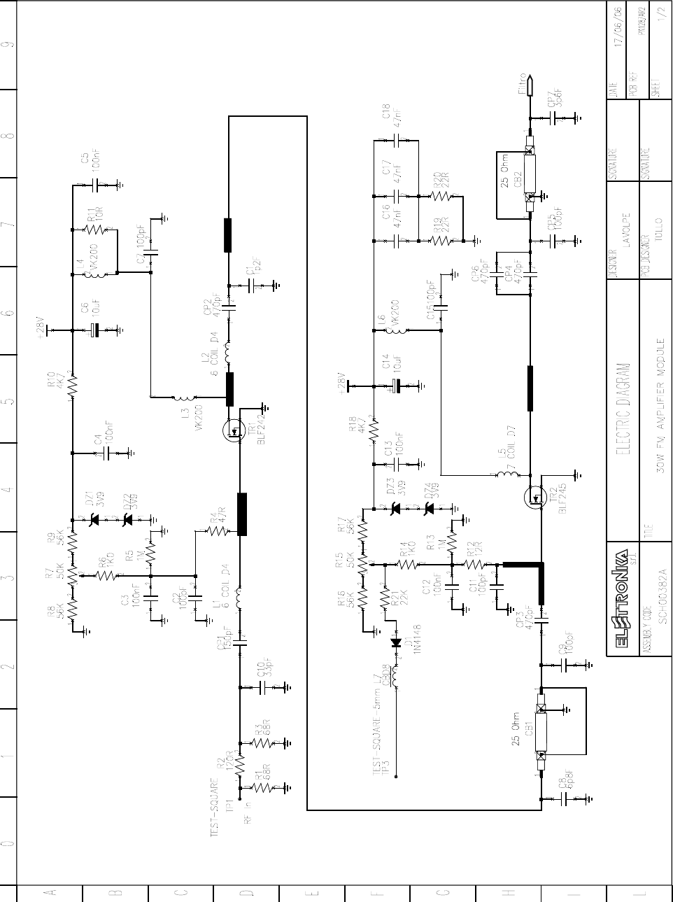
SCH0382BR0 30W FM Amplifier Board Component layout

60
SCH0382BR0 COMPONENT LIST
Part Name/Number Description Qty. Comps.
25Ohm 08523 08523 WHITE TEFLON RF CABLE 0.40 CB1-2
CC 100pF-S 01092 01092 SMD 1206 CAPACITOR 5 C2, C7, C9, C11, C15
CC 100nF-S 01065C 01065C Y5V 1206 CAPACITOR 5 C3-5, C12-13
CC 33pF-S 01023A 01023A SMD 1206 CAPACITOR 1 C10
CC 1p2F-S 01081 01081 SMD 1206 CAPACITOR 1 C1
CC 1nF-S 01096 01096 SMD 1206 CAPACITOR 6 C19, C21, C23-26
CC 39pF-S 1024A 1024A SMD 1206 CAPACITOR 2 C20, C22
CC 47nF-S 01061A 01061A SMD 1206 CAPACITOR 3 C16-18
CC 6p8F-S 01084 01084 SMD 1206 CAPACITOR 1 C8
CE 10uF50V-S 01779A 01779A ELET. SMD CAPACITOR 2 C6, C14
CP 100pF-S 01135 01135 CHIP CHB 1 CP5
CP 150pF-S 01137 01137 CHIP CHB 1 CP1
CP 33pF-S 01127 01127 CHIP CHB 2 CP8, CP12
CP 470pF-S 01143 01143 CHIP CHB 4 CP2-4, CP6
CP 68pF-S 01131 01131 CHIP CHB 3 CP9-11
CP 3p6F-S 01104B 01104B CHIP CHB 1 CP7
D 1N4148-S 03002 03002 SMD DIODE 1 D1
D HSMS2802 03207 03207 SMD DIODE 2 D2-3
DZ 3V9-S 03134 SMD ZENER DIODE 4 DZ1-4
IND 6 SP_D4_d0.8mm-S 05043 INDUCTOR 2 L1-2
IND 7 SP_D6_d0.8mm-S 07691 COATED WIRE 0.30 L5
IND 4 SP_D8_d1.2mm-S 07684 SILVER WIRE 0.80 L8-L11
IND CBD8 05072 05072 INDUCTOR 1 L7
IND VK200 05013 05013 INDUCTOR 3 L3-4, L6
R 10R-S 00017A 00017A RES 1/4W 5% SMD 1206 1 R11
R 120R-S 00030A 00030A RES 1/4W 5% SMD 1206 1 R2
R 12R-S 00018A 00018A RES 1/4W 5% SMD 1206 1 R12
R 1K0-S 00041A 00041A RES 1/4W 5% SMD 1206 2 R6, R14
R 1M-S 00077A 00077A RES 1/4W 5% SMD 1206 2 R5, R13
R 220R-S 00033A 00033A RES 1/4W 5% SMD 1206 4 R23-26
R 22K-S 00057A 00057A RES 1/4W 5% SMD 1206 1 R21
R 22R-S 00021A 00021A RES 1/4W 5% SMD 1206 2 R19-20
R 47R-S 00025A 00025A RES 1/4W 5% SMD 1206 1 R4
R 4K7-S 00049A 00049A RES 1/4W 5% SMD 1206 2 R10, R18
R 56K-S 00062A 00062A RES 1/4W 5% SMD 1206 2 R8-9, R16-17
R 56R-S 00026A 00026A RES 1/4W 5% SMD 1206 1 R22
R 68R-S 00027A 00027A RES 1/4W 5% SMD 1206 2 R1, R3
RV 50K-S-H/S 00797 00797 SMD VARIABLE RESISTOR 2 R7, R15
TR1 BLF242 04005 TRANSISTOR 1 TR1
TR2 BLF245 03985 TRANSISTOR 1 TR2
61
62

63
300W FM AMPLIFIER MODULE MFF0031AR0
DESCRIPTION
The Amplifier Module MFF0031A was designed to amplify FM carriers in the 87 - 108MHz band, and is
able to provide an output of 300W CW. Besides it is provided with an RF Monitor output with a level of -
40dBc ±3dB. In order to obtain the desired gain, the amplifier is made up by two gain stages: the pilot stage
uses a MOSFET BLF244, the final stage a MOSFET SD2942. An input adaptation circuit allows to adapt
the module to various driving levels. The adjustment of the output is achieved by controlling the power level of
the input signal. For both stages of the module there is a control terminal allowing to instantaneously disable
the MOSFETs if needed. The output of the module is completed by an 9th order (4 cells) Low-pass Filter to
attenuate the harmonic level of the esable signal, and by two high-directivity directional couplers needed to
sample part of the Forward and Reflected Power for measuring their levels.
TECHNICAL CHARACTERISTICS
Frequency Range 87 - 108MHz RF Output Impedance 50Ω
Output Power 300W Bias Current BLF244 with Vdd = +28V: 300mA
Input Return Loss >10dB Bias Current SD2942 with Vdd = +50V: 80mA
Power Supply +50V Gain 33dB (with 3dB interstage attenuation)
RF Input Impedance 50ΩEfficiency 54%
MFF0031AR0 COMPONENT LIST
Part Name/Number Description Qty.
00135 47Ω 1/2W RESISTOR 1
00664 LM35DT THERMAL SENSOR 1
01003 0.5pF CERAMIC CAPACITOR 1
01092 100pF MULTITURN CHIP 1
01400 BYPASSING CAPACITOR 1
01403 BYPASSING CAPACITOR 4
02209 PANEL MOUNTING N CONNECTOR 1
02514 PANEL MOUNTING SMB R114553000 2
04315 LM7805 VOLTAGE REGULATOR 1
04321 LM7812 VOLTAGE REGULATOR 1
04340A LM317HVT VOLTAGVE REGULATOR 2
05742 COVER 1
07907 TO220 INSULATOR 4
07910 TO220 INSULATOR 4
DET1326R0P DET1326R0 HEAT SINK 1
SCA0129R0B SCA0129R0 FM AMPLIFIER BOX 1
SCH0371BR0 INTERFACE BOARD 1
SCH0426AR0 FM AMPLIFIER INTERFACE BOARD 1
SCH0427AR0 300W FM AMPLIFIER BOARD 1
64
MFF0031AR0 Component layout
65
MEASURE INSTRUMENT
Calibration of the Output Filter Network analyser or alternately Spectrum
analyser with tracking generator and SWR
Bridge
CALIBRATION PROCEDURE
- Instrument list
Output Filter Section
Calibrate the Network Analyser after setting a 100MHz span centred on 100MHz (10MHz/div - 5dB/div).
Connect the input of the filter to port 1 of the Network Analyser.
Connect the output of the filter to a dummy load. Display the Reflection coefficient (parameter s11). The
calibration consists in acting on the coils (L9, L10, L11, L12) until a curve as below.
Polarisation of the Transistor
After verifying that the power supply is properly connected to the passing capacitor next to the SMB
connector, and before proceeding with the polarisation of the MOSFETs, disconnect the L8 and L13
66
Stop powering the module, then proceed with the polarisation of the MOSFETs.
- Instrument list
coils on the SCH0427A board. Power the module and check with a Digital Tester that the level of the
voltages on the Interface Boards (SCH0426A and SCH0371B) matches the one shown in table Tab.1
and Tab.2 respectively:
CONTROL POINTS VOLTAGE MEASUREMENT
PIN 3 of IC5
PIN 3 of IC6 +50V
PIN 2 of IC5 +20V
PIN 2 of IC6 +24V
PIN 3 of IC4 +12V
PIN 3 of IC3 +5V
CONTROL POINTS VOLTAGE MEASUREMENT
TP1 +50V
TP2 +28V
TP3 +50V
Tab.1
Tab. 2
MEASURE INSTRUMENT
Polarisation of
BLF244 and SD2942 Transistors Two Digital meter

67
- Description of the adjustment points
Disconnect the input terminal of the module. Connect the dummy load to the output terminal.
Turn R4 and R24 completely clockwise (so to interdict the transistors).
Disconnect the passing capacitor from TP3 Gate.
Turn the R4 trimmer counterclockwise until the display of the Amperometer shows an absorption of
300mA. Stop powering the module.
Connect a Tester as Amperometer (10A cc scale) on the power supply line (in place of the L8 coil) and
power the module.
Turn the R24 trimmer counterclockwise until the display of the Amperometer shows an absorption of
80mA. Stop powering the module.
Reconnect the passing capacitor to TP3 Gate.
COMPONENT DESCRIPTION
R4, R24 Adjust polarisation
68
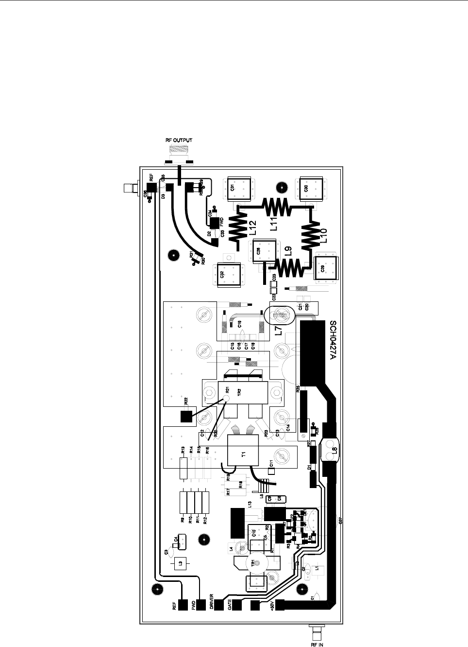
SCH0427AR0 300W FM Amplifier Board Component layout

69
SCH0427AR0 COMPONENT LIST
Part Name/Number Description Qty. Comps. Page 1/2
01081 01081 1.2pF MULT. CHIP CAPAC. 1 C4
CC 100pF 01029 01029 100pF CAPACITOR 2 C5, C10
CC 150pF 01031 01031 150pF CAPACITOR 1 C1
CC 220pF 01033 01033 220pF CAPACITOR 1 C3
01096 01096 1nF MULT. CHIP CAPAC. 2 C34, C36
CC 10nF 01053 01053 10nF 500V CAPACITOR 2 C19, C25
CC 47nF 01061 01061 47nF CAPACITOR 2 C12-13
CC 100nF 01065 01065 100nF CAPACITOR 3 C6-7, C9
01073A 01073A 470nF 100V POL. CAPAC. 2 C14, C26
CC 39pF 01024 01024 39pF CAPACITOR 2 C33, C35
01127 01127 33pF CHIP CAPACITOR 1 C11
01779 01779 10uF 63V ELET. CAPAC. 1 C8
01795B 01795B 100uF 100V ELET. CAPAC. 2 C24, C27
01143 01143 470pF CHIP CAPACITOR 8 C15-18, C20-23
01206 01206 27pF 500V 10% CAPACIT. 1 C32
01210 01210 56pF 500V 10% CAPACIT. 2 C29, C31
01211 01211 68pF 500V 10% CAPACIT. 1 C30
R 220 00033A 00033A RES SMD 1206 4 R28-31
R 1K 00041A 00041A RES SMD 1206 1 R3
R 3K 00047A 00047A RES SMD 1206 1 R27
R 2.7K 00046A 00046A RES SMD 1206 1 R7
R 6.8K 00051A 00051A RES SMD 1206 1 R26
R 33K 00059A 00059A RES SMD 1206 2 R5, R22
R 100K 00065A 00065A RES SMD 1206 1 R25
R 1M 00077A 00077A RES SMD 1206 1 R2
R 10 00127 00127 RES 1/2W 3 R8, R20, R23
R 18 00130 00130 RES 1/2W 3 R17-19
R 22 00131 00131 RES 1/2W 2 R9, R12
R 27 00132 00132 RES 1/2W 2 R10-11
R 47 00135 00135 RES 1/2W 1 R1
R 560 00148 00148 RES 1/2W 4 R13-16
R 100K 00661 00661 NTC 100K 5% 1 R21
R 100K 00791 00791 MULT. TRIMMER 1 R24
R 50K 00797 00797 SMT TRIMMER 1 R4
05043 05043 6 TURNS 4mm INDUCTOR 2 L3, L6
05045 05045 15 TURNS 5mm INDUCTOR 1 L4
05013 05013 VK 200 1 L13
05064 05064 FERRITE 2 L7-8
C0129 C0129 1.5mmq BLACK CABLE 0.15 L7-8
05064 05064 FERRITE 1 T1
08504 08504 50Ω RG58 CABLE 0.10 T1
C0171 C0171 WHITE TEFLON CABLE 0.18 T1
CAV105 CAV105 25Ω 201mm RG316 CABLE 2 CB1-2

70
Part Name/Number Description Qty. Comps. Page 2/2
CAV095 CAV095 50Ω 288mm RG303 CABLE 1 CB3
07684 1.2mm SILVER WIRE 0.70 L6, L9-12
PN0666A PRINTED CIRCUIT BOARD 1
03009 1N4007 DIODE 1 D1
03203 BAT83 DIODE 2 D2-3
R 22K 00057A 00057A RES SMD 1206 1 R6
03134 ZENER 3.9V DIODE 2 DZ1-2
01027 01027 68pF CAPACITOR 1 C2
05042 05042 3 TURNS 4mm INDUCTOR 2 L1-2
01205 01205 22pF 500V CAPACITOR 1 C28
03471 03471 SD2942 TRANSISTOR 1 TR2
03981 03981 BLF244 TRANSISTOR 1 TR1
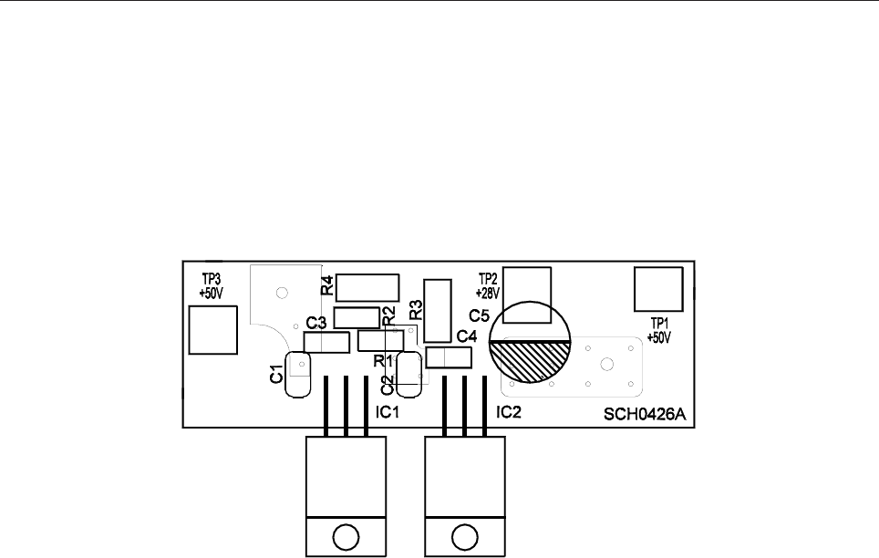
71
SCH0426AR0 FM Amplifier Interface Board Component layout
SCH0426AR0 COMPONENT LIST
Part Name/Number Description Qty. Comps.
04340A 04340A LM317HVT LINEAR REG. 2 IC1-2
01065I 01065I 100nF AVX CAPACITOR 2 C1-2
01065C 01065C 100nF CAPACITOR 2 C3-4
R 0.15 00405 00405 RES SMD 1W 2 R3-4
R 4.7K 00049B 00049B RES SMD 1206 1 R1
R 220 00033C 00033C RES SMD 1206 1 R2
01791A 01791A 47uF CAPACITOR 1 C5
PN1316AR1B PRINTED CIRCUIT BOARD 1
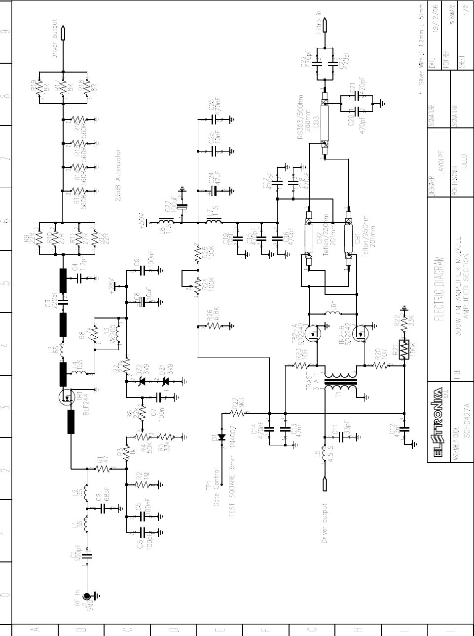
72
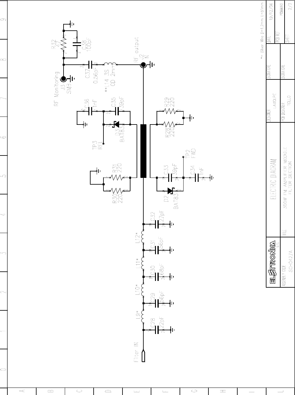
73
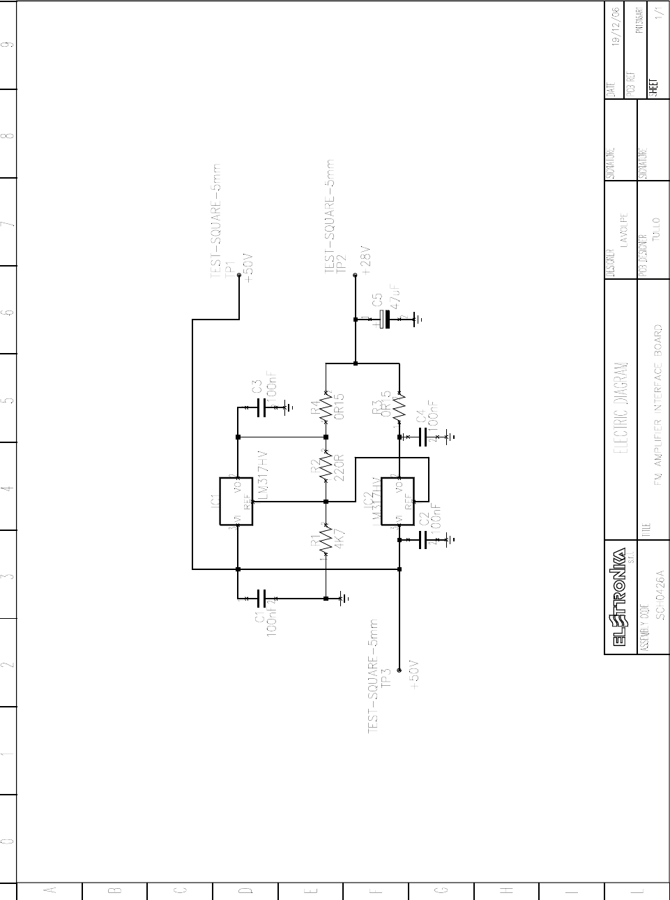
74
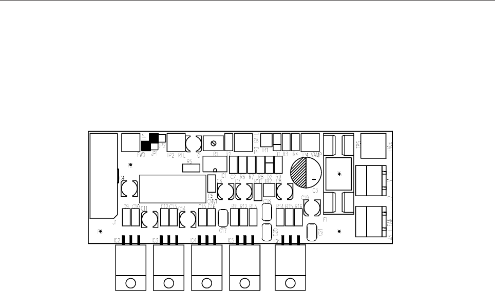
75
SCH0371BR0 Interface Board Component layout
SCH0371BR0 COMPONENT LIST
Part Name/Number Description Qty. Comps.
CC 100nF-S 01065C 01065C Y5V 1206 CAPACITOR 8 C2, C5, C9-10, C12-13, C15-16
CC 100nFAVX 01065A 01065A CERAMIC CAPACITOR 4 C17-18, C20-21
CE 100uF100V 01795B ELETT. CAPACITOR 1 C3
CE 10uF35V-S 01778A 01778A ELET. SMD CAPACITOR 8 C1, C4, C6-8, C11, C14, C19
CNV DC-DC TMR1211 04832B DC DCCONVER. IN 15V 1 CNV1
D BAS85-S 03024 SMD DIODE SCHOTTKY 2 D1-2
FUSE 2A-PCB 7543 7543 FUSE HOLDER+FUSE 5x2 1 F1
IC 7805 04315 04315 VOLTAGE REGULATOR 1 IC3
IC 7812 04321 04321 VOLTAGE REGULATOR 1 IC4
IC LM317 04340 04340 INTEG CIRCUIT 2 IC5-6
IC LM35DT 00664 00664 INTEG CIRCUIT 1 IC2
IC LMC6482-S 04632 SMD INTEG CIRCUIT 1 IC1
J FC-16P 02701-02700 02701+02700 PCB CONNECTOR 1 J1
J SCREWCONN2 02853 02853 PCB SCREW CONNECTOR 2 J2-3
JU JUMP2 02739-02742 02739+02742 MALE PAN2 2 JP1-2
R 100K-S 00065A 00065A RES 1/4W 5% SMD 1206 2 R4, R10
R 100R-S 00029A 00029A RES 1/4W 5% SMD 1206 2 R5, R8
R 10K-S 00053A 00053A RES 1/4W 5% SMD 1206 2 R3, R9
R 1K0-1%-S 00041B 00041B RES 1/4W 1% SMD 1206 1 R7
R 270R-S 00034A 00034A RES 1/4W5% SMD 1206 2 R13, R16
R 3K9-1%-S 00048B 00048B RES 1/4W 1% SMD 1206 1 R6
R 47K-S 00061A 00061A RES 1/4W 5% SMD 1206 2 R12, R15
R 5K6-S 00050A 00050A RES 1/4W 5% SMD 1206 2 R11, R14
R 68K-S 00063A 00063A RES 1/4W 5% SMD 1206 1 R2
RV 10K-S-H/S 00793 00793 SMD VARIABLE RESISTOR 1 R1
TR BC848 03457 03457 NPN SMD TRANSISTOR 2 TR1-2
INTERFACE BOARD SCH0371BR0
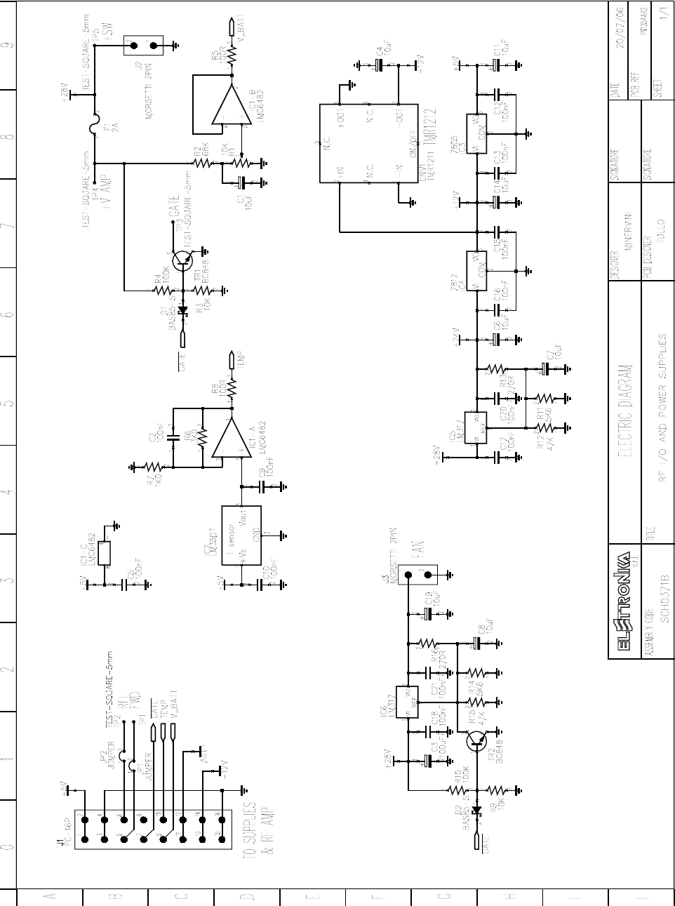
76
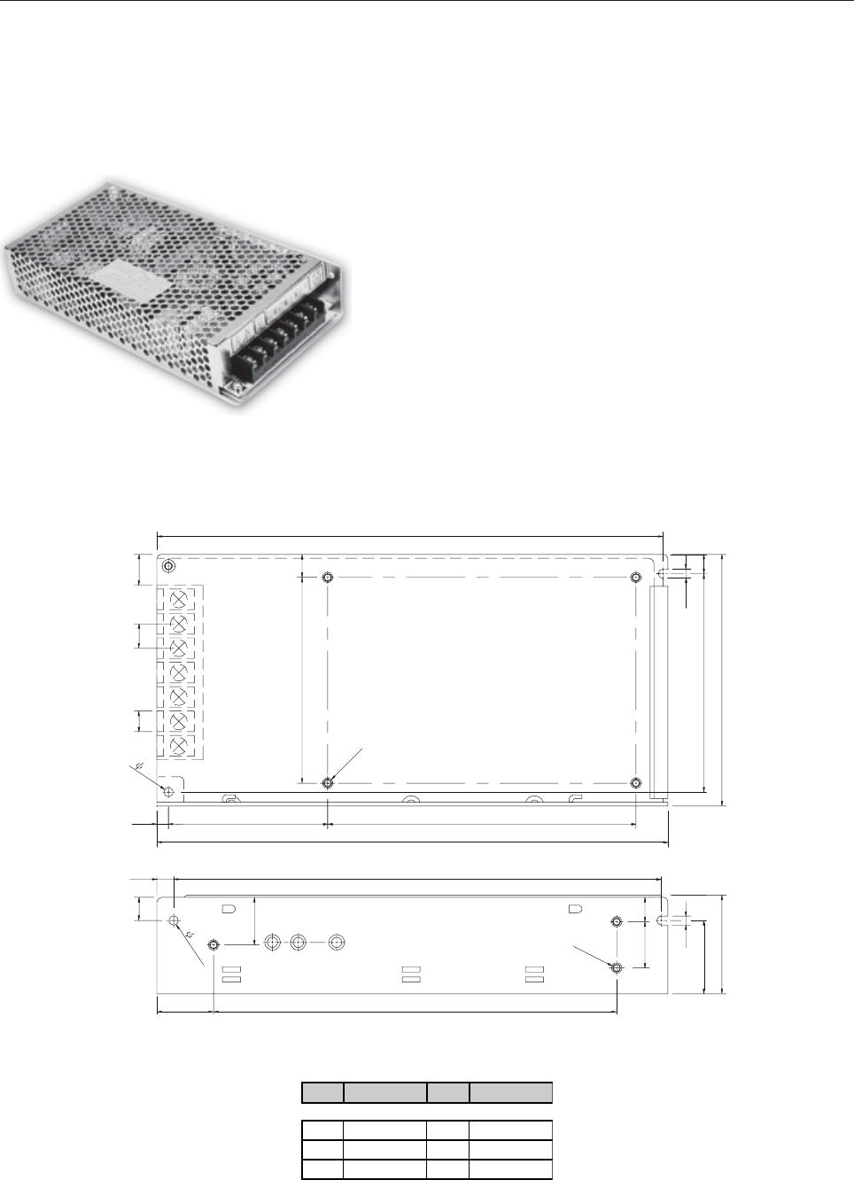
77
S-100F-24 SWITCHING POWER SUPPLY E0060
MAIN FEATURES
- AC Input range selectable by switch
- Protections: Short circuit / Over load / Over voltage
- Cooling by free air convection
- 100% full load burn-in test
- Fixed switching frequency at 83kHz
MECHANICAL SPECIFICATION
3.5
9
197
7
4.5
7
6
5
4
3
2
8.2
1
120
199
57.5
12
9.5
80
85.5
3.5
4-M3
98
9
6.5 190
22 157
3.5
18
9.5
18
3-M3
3.5
28.5
38
PIN N° ASSIGNMENT PIN N° ASSIGNMENT
1AC/L4, 5DC OUTPUT -V
2AC/N6, 7DC OUTPUT +V
3FG
TERMINAL Pin. No Assignment

78
TECHNICAL CHARACTERISTICS
MODEL S-100F-15 S-100F-24
OUTPUT
DC VOLTAGE 15V 24V
RATED CURRENT 6.7A 4.5A
CURRENT RANGE 0 ~ 6.7A 0 ~ 4.5A
RATED POWER 100.5W 108W
RIPPLE & NOISE (max.) Note 2 125mVp-p 150mVp-p
VOLTAGE ADJ. RANGE 13.5 ~ 16.5V 21.6 ~ 26.4V
VOLTAGE TOLERANCE Note 3 ± 1.0% ± 1.0%
LINE REGULATION ± 0.5% ± 0.5%
LOAD REGULATION ± 0.5% ± 0.5%
SETUP, RISE, HOLD TIME 1s, 30ms, 15ms at full load
INPUT
VOLTAGE RANGE 88 ~ 132VAC 176~ 370VAC selected by jumper or switch 248 ~ 370VAC
FREQUENCY RANGE 47 ~ 63Hz
EFFICIENCY (Typ.) 81% 83%
AC CURRENT 3.15A/115VAC 1.5A/230VAC
INRUSH CURRENT (Max.) COLD START 30A/115VAC 60A/230VAC
LEAKAGE CURRENT <1mA/240VAC
PROTECTION
OVER LOAD 105 ~ 150% rated output power
Protection type: Hiccup mode, recovers automatically after fault condition is removed
OVER VOLTAGE 17.25 ~ 20.25V 27.6 ~ 32.4V
Protection type: Hiccup mode, recovers automatically after fault condition is removed
ENVIRONMENT
WORKING TEMP. -10 ~ +60°C (Refer to output load derating curve)
WORKING HUMIDITY 20 ~ 90% RH non-condensing
STORAGE TEMP., HUMIDITY -20 ~ +85°C, 10 ~ 95% RH
TEMP. COEFFICIENT ± 0.03%/°C (0 ~ 50°C)
VIBRATION 10 ~ 500Hz, 2G 10min./1cycle, period for 60min. each along X, Y, Z axes
SAFETY & EMC
(Note 4)
SAFETY STANDARDS UL1012, UL1950, TUV EN60950 Approved
WITHSTAND VOLTAGE I/P-O/P:3KVAC I/P-FG:1.5KVAC O/P-FG:0.5KVAC
ISOLATION RESISTANCE I/P-O/P, I/P-FG, O/P-GD:100M Ohms/500VDC
EMI CONDUCTION & RADIATION Compliance to EN55022 (CISPR22) Class B
HARMONIC CURRENT Compliance to EN61000-3-2,-3
EMS IMMUNITY Compliance to EN61000-4-2,3,4,5,6,8,11; ENV50204, EN55024, Light industry level, criteria A
OTHERS
MTBF 314.9K hrs min. MIL-HDBK-217F (25°C)
DIMENSION 199*98*38mm (L*W*H)
PACKING 0.65kg; 20pcs//14.2kg/0.72CUFT
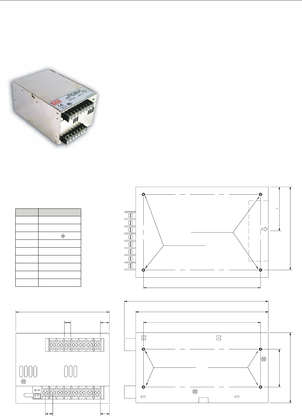
79
PSP-650-48 DE2 SWITCHING POWER SUPPLY E0050
MAIN FEATURES
- Universal AC input / Full range
- Built-in active PFC function, PF>0.95
- Protections: Short circuit / Over load / Over voltage / Over temp.
- Forced air cooling by built-in DC fan
- Current sharing up to 2400W (3+1)
- Built-in remote ON-OFF control
- Built-in remote sense function
- Fixed switching frequency at PFC:88kHz PWM:100kHz
MECHANICAL SPECIFICATION
Terminal Pin. No Assignment
Pin No.
1
3
4
5
6
7
8 ~ 11
12 ~ 15
2
Assignment
FG
P(Current Share)
POK
R.C. G
R.C.
DC OUTPUT +V
DC OUTPUT -V
AC/N
AC/L
170
185
150
2-M3 L=4mm max.
93
50
150
100
58 3
2-M3 L=4mm max.
Air flow
direction
2-M3 L=4mm max.
9.5 11.5
811.5
120
151413121110
76
5
4321
98
80
TECHNICAL CHARACTERISTICS
MODEL PSP-650-48
OUTPUT
DC VOLTAGE 48V
RATED CURRENT 13.5A
CURRENT RANGE 0 ~ 13.5A
RATED POWER 650W
RIPPLE & NOISE (max.) Note 2 300mVp-p
VOLTAGE ADJ. RANGE 41 ~ 56V
VOLTAGE TOLERANCE Note 3 ± 1.0%
LINE REGULATION ± 0.5%
LOAD REGULATION ± 0.5%
SETUP, RISE, HOLD TIME 1500ms, 50ms, 16ms at full load
INPUT
VOLTAGE RANGE 88 ~ 264VAC 124 ~ 370VDC
FREQUENCY RANGE 47 ~ 63Hz
POWER FACTOR PF>0.95/230VAC PF>0.98/115VAC at full load
EFFICIENCY (Typ.) 87%
AC CURRENT 8.2A/115VAC 4.1A/230VAC
INRUSH CURRENT (Max.) 25A/115VAC 50A/230VAC
LEAKAGE CURRENT >1mA/240VAC
PROTECTION
OVER LOAD 105 ~ 135% rated output power
Protection type: Fold back current limiting, recovers automatically after fault condition is removed
OVER VOLTAGE 57.6 ~ 67.2V
Protection type: Shut down o/p voltage, re-power on to recover
OVER TEMPERATURE
+5V: 95°C(TSW1)Detect on heatsink of power diode
+5V: 95°C(TSW2)Detect on heatsink of power transistor
+12 ~ +48V: 85°C(TSW1)Detect on heatsink of power diode
+12 ~ +48V: 80°C(TSW2)Detect on heatsink of power transistor
Protection type: Shut down o/p voltage, recovers automatically after
temperature goes down, than re-power on to recover
FUNCTION REMOTE CONTROL RC+/RC-: Short = power on; Open = power off
ENVIRONMENT
WORKING TEMP. -20 ~ +50°C (Refer to output load derating curve)
WORKING HUMIDITY 20 ~ 90% RH non-condensing
STORAGE TEMP., HUMID ITY -40 ~ +85°C, 10 ~ 95% RH
TEMP. COEFFICIENT ± 0.03%/°C (0 ~ 50°C)
VIBRATION 10 ~ 500Hz, 2G 10min./1cycle, period for 60min. each along X, Y, Z axes
SAFETY & EMC
(Note 4)
SAFETY STANDARDS UL60950-1, TUV EN60950-1 Approved
WITHSTAND VOLTAGE I/P-O/P:3KVAC I/P-FG:1.5KVAC O/P-FG:0.5KVAC
ISOLATION RESISTANCE I/P-O/P, I/P-FG, O/P-GD:100M Ohms/500VDC
EMI CONDUCTION & RADIATION Compliance to EN55022 (CISPR22) Class B
HARMONIC CURRENT Compliance to EN61000-3-2,-3
EMS IMMUNITY Compliance to EN61000-4-2,3,4,5,6,8,11; ENV50204, Light industry level, criteria A
OTHERS
MTBF 116.4K hrs min. MIL-HDBK-217F (25°C)
DIMENSION 170*120*93mm (L*W*H)
PACKING 1.9kg; 8pcs/15.5kg/1.06CUFT
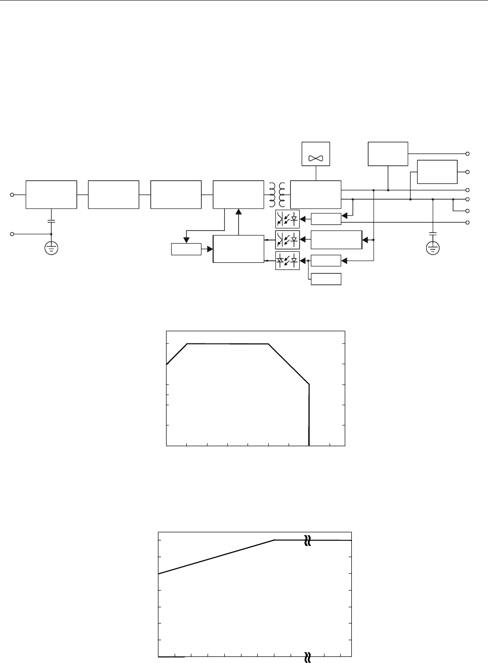
81
ACTIVE INRUSH
CURRENT
LIMITING
EMI FILTER
I/P
FG
RECTIFIERS
&
P.F.C.
POWER
SWITCHING
O.L.P. PWM
CONTROL
RECTIFIERS
&
FILTER
O.C.P.
O.V.P.
O.T.P.
DETECTION
CIRCUIT
FAN SIGNAL
CONTROL
CURRENT
SHARING
CIRCUIT
PFC fosc: 88kHz
PWM fosc: 100kHz
POK
P
+V
-V
RC.G.
RC
BLOCK DIAGRAM
DERATING CURVE
AMBIENT TEMPERATURE ( C)
o
LOAD (
%
)
-20 0 10 20 30 45 50 60 (HORIZONTAL)
20
40
50
60
80
100
INPUT VOLTAGE (V) 60Hz
11588 100 135 155 230 264
90
100
80
70
60
50
40
LOAD(%)
OUTPUT DERATING VS INPUT VOLTAGE
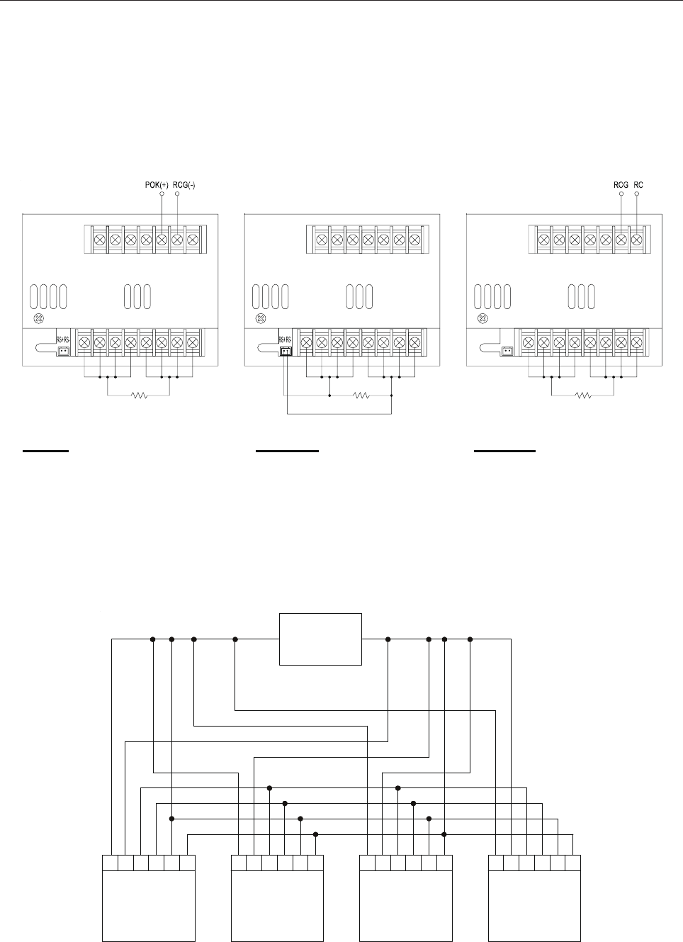
82
CONTROL TERMINAL INSTRUCTION MANUAL
POK Signal
POK Signal is the voltage difference between
LOAD LOAD LOAD
+++---
"RCG" and "POK" pin output POK Signal for TTL level signal
PSU turn on: 3.3V ~ 5.6V
PSU turn off: 0V ~ 1V
Remote Sensing
Power ON: RCG and RC for short
Remote Control
Power OFF: RCG and RC for open
LNFGPPOKRCGRC
+V +V +V +V -V -V -V -V
LNFGPPOKRCGRC
+V +V +V +V -V -V -V -V
LNFGPPOKRCGRC
+V +V +V +V -V -V -V -V
PARALLEL OPERATION WITH REMOTE SETTING
PSU
LOAD
+V -V
+-P RC- RS+ RS-
PSU PSU
+-P RC- RS+ RS- +-PRC-RS+RS- +-P RC- RS+ RS-
PSU
83
84
85
86