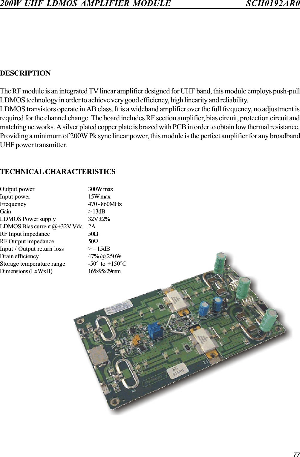
Elettronika S r l TXUP5000 TXUP5000 5 kW Analog TV Transmitter User Manual APT120A AUTV 5000LD Rev0 Date221003 p65
Elettronika S.r.l. TXUP5000 5 kW Analog TV Transmitter APT120A AUTV 5000LD Rev0 Date221003 p65
Contents
- 1. User Manual Part 1
- 2. User Manual Part 2
- 3. User Manual Part 3
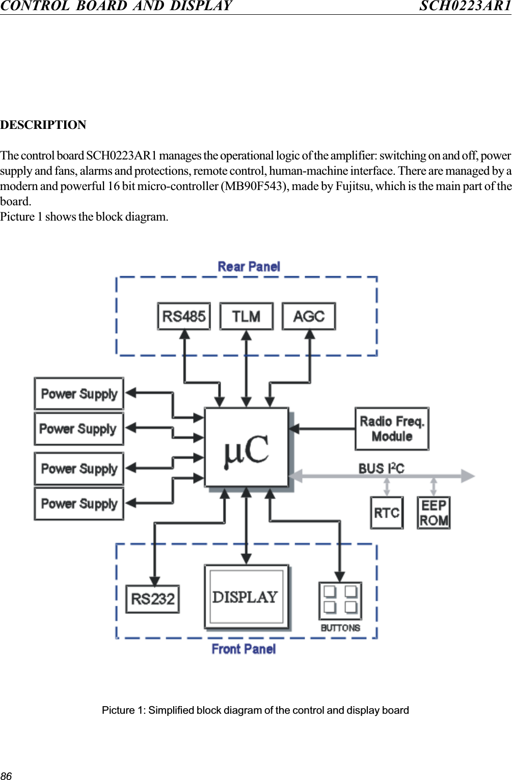
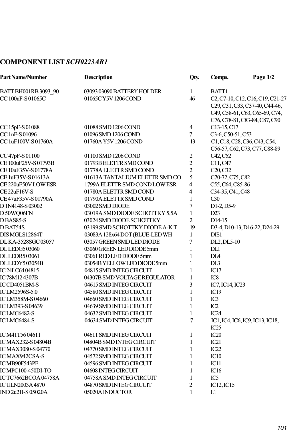
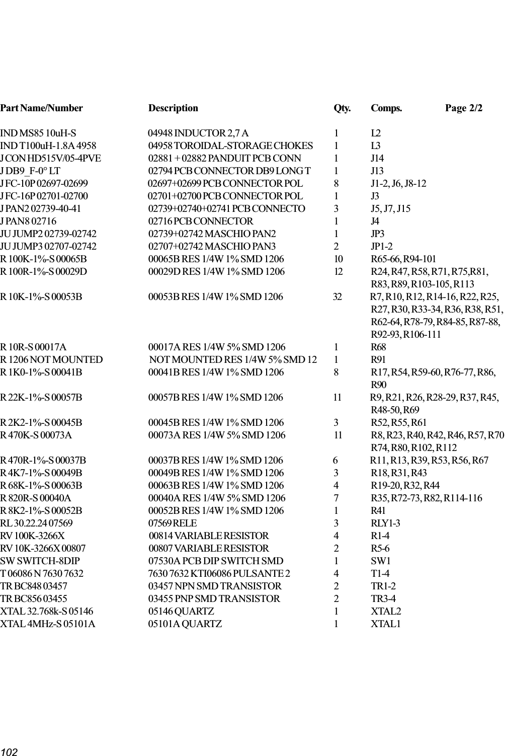
User Manual Part 2