Elettronika S r l TXUP5000 TXUP5000 5 kW Analog TV Transmitter User Manual APT120A AUTV 5000LD Rev0 Date221003 p65
Elettronika S.r.l. TXUP5000 5 kW Analog TV Transmitter APT120A AUTV 5000LD Rev0 Date221003 p65
Contents
- 1. User Manual Part 1
- 2. User Manual Part 2
- 3. User Manual Part 3
User Manual Part 2

49
_______________________________________________________________________________________________
Section 1 - Information
Contents:
1.1 Description
1.2 Technical characteristics
50
1.1 DESCRIPTION
The AUTV/1500LD is an amplifier operating into Band IV-V for common amplification process of the Vision
and Sound carriers.
The amplifier has been designed to offer to the customer high performances, high reliability and greater
simplicity in his operation and maintenance procedures.
The amplifiers modules employ all solid state LDMOS technology in order to obtain high gain, wide-
band performances, very good linearity, reliability and high efficiency.
The equipment design allows the soft degradation (RF power loss) for several transistor faulty: in fact the
output combiner uses RF power resistors for unbalancing power dissipation. The unit is enclosed in a cabinet
for 19- 6U rackmounting.
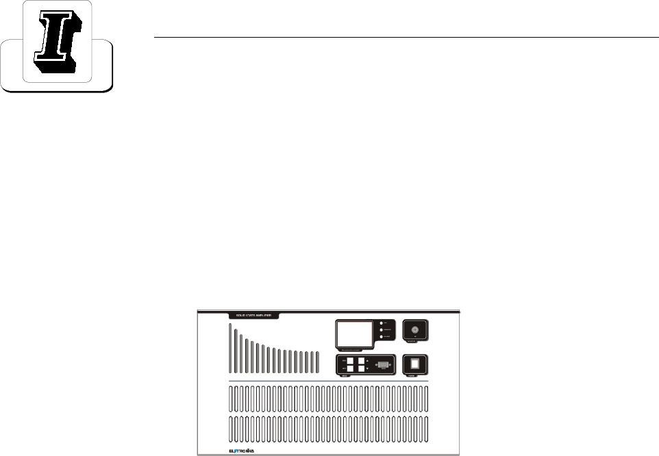
AUTV/1500LD
LDMOS - UHF TV AMPLIFIER

51
1.2 TECHNICAL CHARACTERISTICS
RF
Frequency range 470 - 860MHz
Output power 1300W PEP
Video/Sound power ratio 10/1
Out stage technology Solid State LDMOS
Vision-Sound amplification Common
I.M.D. (-8, -10, -16dB) Better than -54dB
Standards G, K, N
Spurious and harmonics level In compliance with CCIR rec.
RF Output impedance 50W
RF Output connector 7/16
GENERAL
Power supply 230Vac, ±10%, 50/60Hz
400Vac 3P+N (on request)
Power consumption 3400VA at black level
RS232 Socket DB9 Connector (on front panel)
RS485 Socket DB9 Connector (on rear panel)
Telemeasuring socket DB9 Connector (on rear panel)
AGC Socket DB9 Connector (on rear panel)
Power factor > = 0.9
Ambient temperature -5° to +45°C
Relative humidity 20% - 90%
Altitude Up to 2.500 meters
Cooling Forced air
Cabinet Rack 19-6U
Dimensions 760x263x266mm
Weight 70kg
PROTECTION THR.
FWD Power 1500W
REF Power 150W
Unbalacing 350W
Temperature 75°C
IDC 25A
VDC Min 10V - Max 33,5V

52
This page is intentionally blank
53
_______________________________________________________________________________________________
Section 2 - Installation
Contents:
2.1 Operating environment
2.2 Preliminary operations
2.3 Telemeasuring socket connections
2.4 RS232, RS485 and AGC socket connections
2.5 Preventive maintenance
- Front panel
- Rear panel
54
2.1 OPERATING ENVIRONMENT
You can install the apparatus in a standard component rack or on a suitable surface such as a bench or desk.
In any case, the area should be as clean and well-ventilated as possible. Always allow for at least 2 cm of
clearance under the unit for ventilation. If you set the apparatus on a flat surface, install spacers on the bottom
cover plate. If you install the apparatus in a rack, provide adequate clearance above and below. Do not locate
the apparatus directly above a hot piece of equipment.
2.2 PRELIMINARY OPERATIONS
Correct installation of the equipment is important for maximum performance and reliability. Antenna and earth
connections must be installed with the greatest care. The equipment adjustment isnt need, because the unit is
completely adjusted by our technical staff. This is the installation procedure:
1. connect the power supply cable of the exciter to the auxiliary socket on the rear panel of the amplifier;
2. connect the power supply cable of the amplifier to the electric network (230VAC). If there is the Isolator
Transformer, the amplifier is provided with cable and plug;
3. connect the exciter / antenna cables respectively to the RF IN and RF OUT on the rear panel of the
amplifier.
WARNING!!!
FOR ELECTRICAL SAFETY REASONS AND IN ORDER TO KEEP
THE APPARATUS SAFE, THE GROUND TERMINAL OF THE
APPARATUS MUST BE CONNECTED TO THE EXISTING GROUND-
ING SYSTEM AND NOT BY USING THE SHIELD OF THE OUTPUT
COAXIAL CABLE.
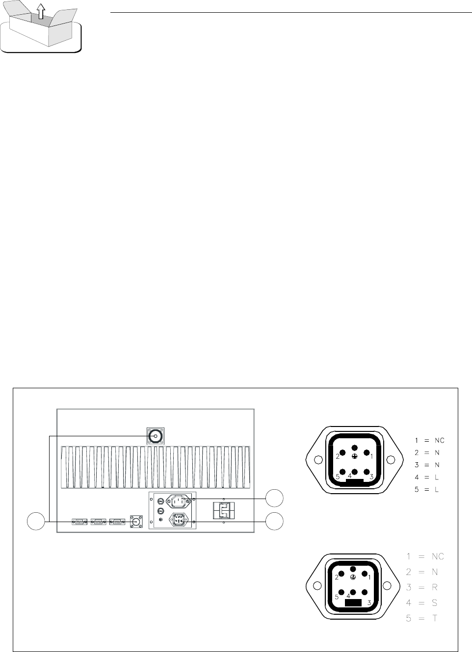
13
2
Three-Phase cabling
Monophase cabling
55
When the apparatus is put within a combined system it is directly connected to the input splitting and output
combining systems.
Before fully powering the apparatus, check that the output connections of the coaxial cable to the antenna
system are working.
In order to this it is possible to check the indication of the reflected power at low power levels. Only if the
SWR indication on the display is 0, the output power can be slowly increased. At maximum output power,
some watts might be shown as reflected power.
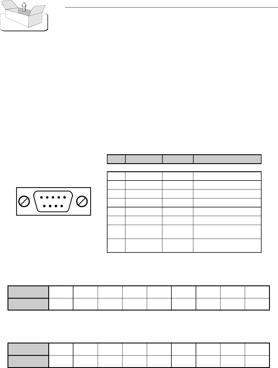
2.3 TELEMEASURING SOCKET CONNECTIONS
DB9 Socket
2.4 RS232, RS485 AND AGC SOCKET CONNECTIONS
PIN N° SIGNAL TYPE IN / OUT FUNCTION
1 Analog Output FWD Power
2 Analog Output REF Power
3 Digital Output Temperature
4 Digital Input Interlock
5GND - -
6 - 7 Digital Output Free contact (closed when alarm)
8 Digital Input 0V = ON
5V = Normal
9 Digital Input 0V = OFF
5V = Normal
PIN 1234 56789
FUNCTIONS -TxDRxD-GND----
RS232 - DB9 Socket
PIN 1234 56789
FUNCTIONS -Rx-Rx+5VGND-Tx-Tx+-
RS485 - DB9 Socket
56
AGC - DB9 Socket
PIN N° SIGNAL TYPE IN / OUT FUNCTION
1GND - -
2 Digital Output 0V = Normal
5V = AGC Alarm
3 Digital Output 0V = Normal
5V = AGC Alarm
8 Analog Output FWD Power
9 Analog Output FWD Power
2.5 PREVENTIVE MAINTENANCE
To ensure maximum performance and minimum repair trouble, we strongly recommend you to follow the
below stated headlines for preventive maintenance:
1. check antenna installation and ground connection at regular intervals;
2. keep your apparatus clean and dry externally: this will ensure continuous functioning of the front panel
controls;
3. if the apparatus has not been used for a long period of time combined with exposure to extreme environ-
mental conditions, open the unit and make a visual inspection.
Remove salt, water or ice with a moist cloth before turning the apparatus on. Check that the cooling fans are
running freely.
4. for general maintenance and top performance, call an authorized service technician to give the apparatus
and the complete antenna/earth connection installation a general check every 12-18 months;
5. check at regular intervals that the air intake located on the front panel is free of dust. If there is visible dust,
remove it by means of a soft brush.
57
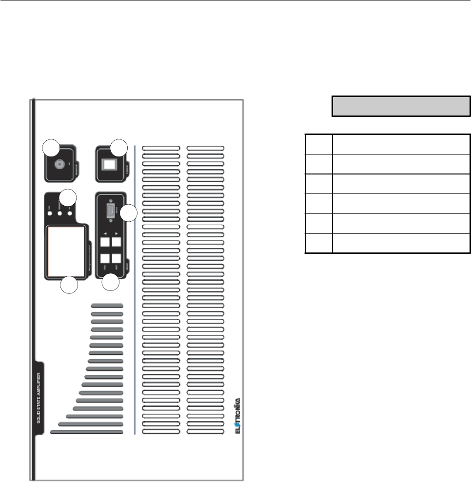
Front panel
1
2
3
4
5
6
DESCRIPTION
1LCD Display
2 Function keys
3 Status LEDs
4 RF Monitor connector
5 Main switch
6 RS232 Socket
58
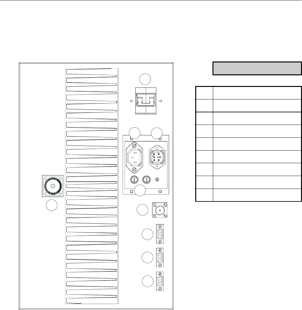
Rear panel
1
2
3
4
56
9
8
7
DESCRIPTION
1 Breaker
2 Power supply socket
3 Auxiliary socket
4Fuse
5 RS485 Socket
6 AGC Socket
7 Telemeasure socket
8 RF Input connector
9 RF Output connector

59
_______________________________________________________________________________________________
Section 3 - Operation
Contents:
3.1 Control board and display description
3.2 Operation
3.3 Display
3.4 Menu
60
3.1 OPERATION
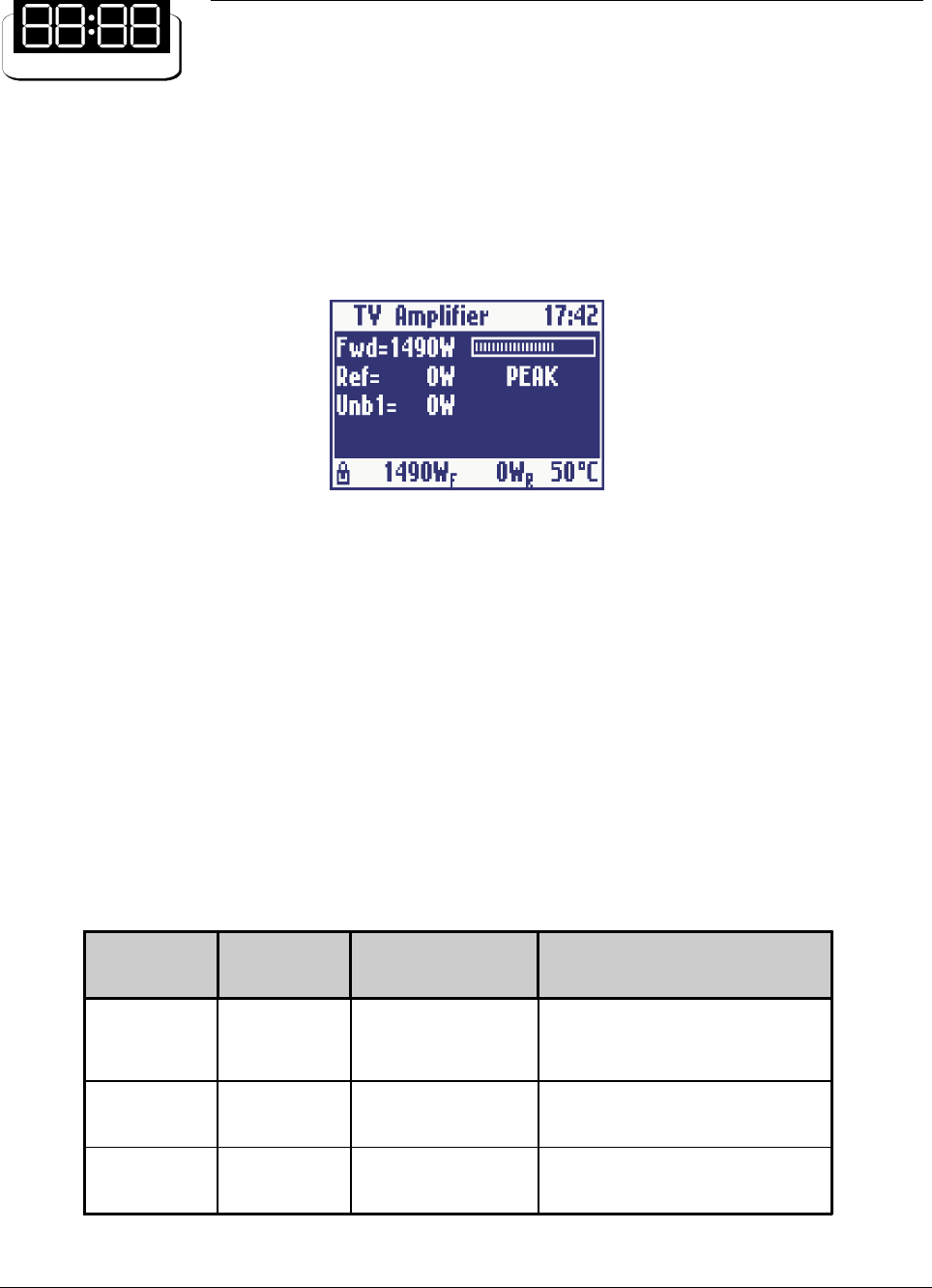
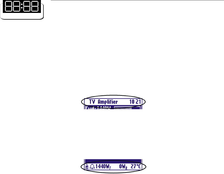
At startup, after intro image, the display shows the main screen, showing the RF powers as in Figure 1:
The user may turn on and off the amplifier by means of the switch on the front panel. The control board turns
on all the power supplies, the exciter, if any, and the cooling fans. While the amplifier is working, the micro-
controller monitors continuously the most important parameters: power supply voltages, absorbed currents,
temperature, forward and reflected power, unbalances, if any. Each signal is associated to a maximum threshold
beyond which the amplifier is immediately put in protection status by turning off one or more power supply,
depending on the failed block. In order to prevent a temporary problem to trigger a definitive protection
status, the failed block is turned on again for up to five times. If it goes beyond the protection threshold for
more than five times, it is declared as FAILED and will no longer be turned on. In this case the amplifier will
have to be turned off manually by means of the switch on the front panel, then turned on again after performing
the needed maintenance. On the front panel there are also three LEDs labelled ON, REMOTE and ALARM.
Their meanings are explained below.
Figure 1: Main screen
LED COLOUR MEANING MEANING WHEN BLINKING
ON Green The amplifier is on
The amplifier has been turned on
locally but it has been turned off by
remote
REMOTE Yellow Remote control is
enabled It ne ve r blinks
ALARM Red Alarm status It never blinks
Table 1: Meanings of the three LEDs on the front panel
1 Screenshots in this manual are indicative and they refers to a TV amplifier, so they can be different from those on your equipment.
61
3.2 DISPLAY
The control board is provided with a modern 128x64 pixels graphic display with blue backlight. Normally it
always shows a title bar (on the top line) and a status bar (on the bottom line).
The title bar, see Figure 2, shows the name of the amplifier (TV Amplifier or FM Amplifier) and the current
time.
Figure 2: Title bar
Figure 3: Status Bar
The status bar indicates the forward and reflected power and the temperature. It also contains two symbols
for the interlock (lock) and a generic alarm (bell).
The bell symbol is displayed in case of alarm. It blinks if there has been an alarm which has ended but has not
yet been seen by the user. It stops blinking once the alarm Log has been checked.
The interlock symbol is displayed only when the check for this alarm is enabled. It may be either a close lock,
see Figure 3, when there is no alarm (close interlock chain) or an open lock in case of alarm (open interlock
chain).
Since the status bar is always on the display, regardless of the displayed screen, the user may monitor at any
moment the most important parameters and the presence of alarms, if any, while moving between different
screens.
3.3 MENU
The user may see or modify locally some configuration parameters of the apparatus by means of the four keys
on the front panel. All screens are made up by hierarchical menus and the user may move between them in a
simple and intuitive way.
To see the main menu its sufficient to press ESC key (see Figure 4).
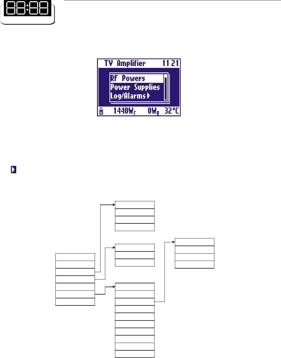
62
Figure 4: Main menu
The display only shows three items, but the whole menu can be scrolled by means of the UP and DOWN
arrow keys. Any item can be chosen by selecting it and pressing the RET key. Menu entries with arrow on the
right open sub-menus when chosen. Thus there is a hierarchical structure as in Figure 5. To go back from
a sub-menu to the previous menu, press the ESC key. If the ESC key is pressed in the main menu, the main
powers screen is accessed.
Figure 5: Hierarchical menu structure
All menu items are described in detail below.
RF Powers
Power Supplies
Log/Alarms >
Working Timer >
Thresholds
Settings >
Exit
View Log/Alarms
Clear Log/Alarms
Log Mode
View Timer
Timer Reset
Exit
RMS/Peak
Date/Time
Display
Frequency
Slave Address
Remote
Interlock
Release
Serial Number
Exit
Backlight
Contrast
Screensaver
Exit
Exit
63
- RF Powers
This is the main screen showing the RF powers of the amplifier: forward power, reflected power, unbalances,
if any. For forward power a level bar is displayed. See example in Figure 1.
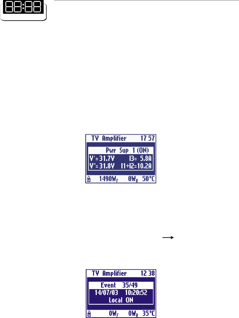
- Power Supply
This screen shows all the signals coming from the power supply. To check a different power supply press the
UP (or DOWN) key to see the next (or previous) one. For each power supply, the two voltages, the two
absorbed currents and the status (ON or OFF) are shown.
Figure 6: Power supply screen
- Log/Alarms
The control board is provided with an external EEPROM and a clock. Any alarm or switching event is saved
into an event log stored inside the EEPROM and associated to the time at which it occurred. The Log/Alarms
sub-menu allows to manage this log.
It is possible to see the events stored in the log by selecting Log/Alarms View Log/Alarms. All events
can be scrolled by pressing the UP and DOWN keys. The event shown in Figure 7 is the turning on of the
amplifier by means of the local switch. Each event is associated to the date and time at which it occurred and
to a description.
Figure 7: Event stored in the log
64
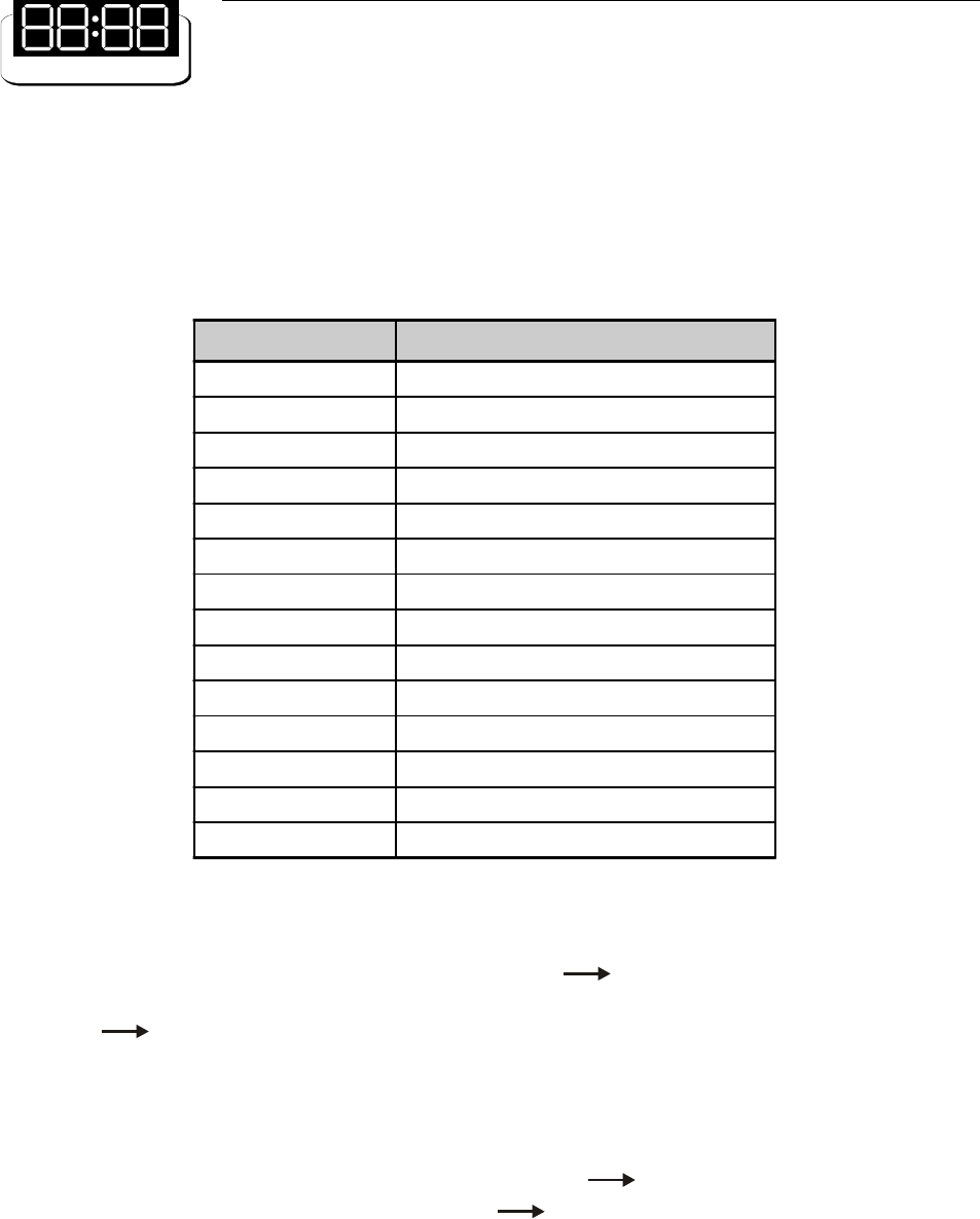
In case of alarm on a parameter, the value of the parameter which caused the alarm is saved into the log. In
case of alarm still existing after five turning-on attempts, the parameter is marked as FAILED. Table 2 is the
list of all the events which can be logged.
Table 2: Events managed and logged by the control board
The log may be completely deleted by selecting Log/Alarms Clear Log/Alarms.
Amplifier can store in the log details about alarms and generic events. You can change this behaviour selecting
Log/Alarms Log/Mode menu item.
- Working Timer
The control board has a working timer which is always enabled while the amplifier is working (i. e. there is at
least one power supply working). The menu entry Working Timer View Timer allows to check the hours
for which the timer has been enabled. Working Timer Timer Reset resets the timer.
- Thresholds
This is a screen showing the alarm threshold of each and all signals monitored by the control board. The list
can be scrolled by means of the UP and DOWN keys.
EVENT DESCRIPTION
Local ON Amplifier turned on by means of the local switch
Local OFF Amplifier turned off by means of the local switch
Remote ON Amplifier turned on remotely
Remote OFF Amplifier turned off remotely
Interlock opened Interlock chain opened
Interlock closed Interlock chain closed
Power Supply ON Power supply on
Fwd Pwr xxxxW Alarm for forward power
Ref Pwr xxxxW Alarm for reflected power
UnbY xxxxW Unbalancing alarm
Pwr Sup x: V1 xx.xV Power supply voltage alarm
I1 xx.xA Power supply current alarm
Pwr Sup x: OVERVOLT Power supply overvoltage alarm
Pwr Sup x: OVERTEMP Power supply overtemperature alarm
65
- RMS/Peak
The control board can monitor both the RMS and peak powers. The menu entry Settings RMS/Peak
allows to choose the power to be displayed and monitored.
- Date/Time
This screen allows to set the current date and time. The setting is changed by pressing the arrow keys, then
pressing the RET key to move to the following setting and eventually save the changes. To go back to the
previous menu and discard any change made, press the ESC key. Figure 8 shows an example of this screen.
Figure 8: Date and time setting screen
- Display
The menu entry Settings Display allows to change some settings of the display, such has back light,
contrast and screensaver. The back light and the contrast are set by means of the UP and DOWN arrow
keys. The changes made are saved by pressing the RET key or discarded pressing the ESC key. Figure 9
shows the contrast screen.
With Settings Display Screensaver you can set an interval time after which display backlight is
turned off. When display backlight is off, press any key to switch it on.
Figure 9: Display contrast setting screen
66
- Frequency (only for some Amplifiers)
The forward and reflected RF power is measured by means of a directional coupler. In order to compensate
for the effect due to the sampling made by the coupler, it is possible to set the frequency by means of the menu
entry Settings Frequency. The setting can be changed by pressing the arrow keys. The changes made
are saved by pressing the RET key or discarded pressing the ESC key. In a TV Amplifier, set the video
carrier frequency.
- Slave Address
The amplifier may be used either in stand-alone mode or as slave of a master within a multiple transmitter. In
the latter case an unique address for each amplifier has to be specified, in order for all of them to communicate
with the master on the same RS485 bus. The menu entry Settings Slave Address allows to choose the
stand-alone mode or set a slave address by means of the UP and DOWN arrow keys. The changes made are
saved by pressing the RET key or discarded pressing the ESC key. This screen is shown in Figure 10.
Figure 10:Slave address setting screen
- Remote
The amplifier may be controlled either locally, by means of the keys and display, or remotely. There are three
possibilities for remote control:
- using a direct serial connection between amplifier RS232 connector and a PC RS232;
- using the remote control device manufactured by Elettronika S.r.l. (RCU), on the RS485 bus;
- using a general-purpose control system connected to telemeasures.
You can enable / disable remote control choosing menu item Settings Remote. When remote control
is enabled, the yellow REMOTE LED on the front panel is lit.
- Interlock
One of the pins of the telemeasure connector, located on the rear panel, is for the interlock alarm. It is an input
line which turns off the amplifier in case of alarm. The interlock check can be enabled or disabled using menu

67
item Settings Interlock. When it is enabled, the status bar shows the lock symbol (see Figure 3),
which is close if the interlock chain is closed (no alarm) or open if it is open (alarm).
- Firmware Release
The menu entry Settings Firmware Release allows to display the firmware version number and the
hardware release of the amplifier.
- Serial Number
The menu entry Settings Serial Number allows to display the serial number of the apparatus.

68
This page is intentionally blank
69
_______________________________________________________________________________________________
Section 4 - Diagram
Contents:
- Cable diagram
- AUTV/1500LD Component layout
- RF Section Block Diagram
- MTF0070BR0 Amplifier module - Component list
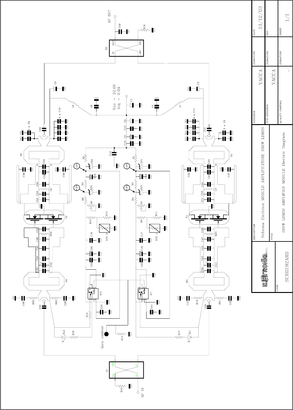
- SCH0192AR0 (200W UHF LDMOS Amplifier module)
- SCH0223AR1 (Control board and display)
- SCH0221AR1 (Amplifier interface)
- SCH0215AR0 (Mains distribution board)
- E0026 (1kW 32Vdc Switching power supply)
70
71
72

73
Part Name Code Description Qty
00001 0W 1206 SMD RESISTOR 2
01041D 1nF 1206 2% SMD CAPACITOR 2
00221B 75W 1206 1% SMD RESISTOR 2
03207 HSMS-2802*L31 DIODE 2
SCH0192AR0 200W UHF LDMOS AMPLIFIER MODULE 9
SCH0221AR0 AMPLIFIER INTERFACE 1
SCH0248AR0 8 WAY WILKINSON 1
SCH0249AR0 4 WAY WILKINSON Dx 1
SCH0250AR0 4 WAY WILKINSON Sx 1
SCH0251AR0 2 WAY WILKINSON 1
SCH0252AR0 1500W UHF INPUT COUPLER 1
PN1091A C.S. PN1091AR3 OUTPUT DIRECTIONAL COUPLER 1
02402 7/16 FEMALE CONNECTOR cod. 0142 1
02512 J01151A0531 SMA SOCKET WITHOUT BAT. 1
01400 2499-003-X5U0-102M FEED-THROUGH CAPACITOR 14
01408 5000PF FEED-THROUGH CAPACITOR 2
DET0726 DET0726R2 SIDE x 1500W UHF AMP. MOD. 2
DET0727 DET0727R1 INTERNAL FRONT SIDE x AMP. MOD. 1
DET0728 DET0728R4 INTERNAL SIDE x AMP. MOD. 2
DET0729 DET0729R2 FRONT SIDE x AMP. MOD. 1
DET0730 DET0730R2 REAR SIDE x AMP. MOD. 1
DET0732 DET0732R1 CONNECTIONS SUPPORT BOARD 1
DET0734 DET0734R0 COVER x AMPLIFIER MODULE P. 2634 1
DET0736 DET0736R5 HEATSINK x AMPLIFIER MODULE 1
DET0807 DET0807R3 SCREEN DIR. COUPLER MODULE 1
DET0810 DET0810R0 PART. x DIRECTIONAL COUPLER 1
DET0811 DET0811R1 COVER x DIRECTIONAL COUPLER 1
DET0812 DET0812R1 TEFLON RING x DIRECTIONAL COUPLER 1
DET0819 DET0819R0 SPESS. x INPUT DIR. COUPLER 1
DET0828 DET0828R0 COVER x AMPLIFIER MODULE P. 2644 1
DET0839 DET0839R2 DIRECTIONAL COUPLER 1
08502 RG316 50W CABLE 3,00
08527 HF-85 ENDIFORM CABLE 0,20
Component list MTF0070BR0 Amplifier module

74
This page is intentionally blank

75
Part Name Code Description Qty
DET0516 DET0516R0 SUPPORTO PRESE ZN 1
E0026 ALIM. SWITCHING 1kW 32VDC mod. PBIT2129 3
V0958 ACCESSORIO GUIDA DIN ELECO E205 2
V0962 MORSETTIERA/GIUNZIONE ELECO E806 1
Z0081B TAV... SUPPORTO INT. MAG. QUADRIPOL. 2
Z0673 TAV. 1199 CHIUS. CONT. PROF. 775 ZN 2
MTF0070BR0 MOD. AMPLIFICATORE 1500W LDMOS UHF 1
02830 PRESA VDE 10A cod. PX675 A63 1
02876 PRESA VOLANTE ILME 16A PENTAPOLARE 3mt 1
02877 SPINA A PANNELLO ILME 16A PENTAPOLARE 1
07524A INTERR. NERI I3910 1
07515 INTER. AUTOM. 4*16A 4.5KA 23902 1
07541 PORTAFUS. 10A PANN. cod. P1820 3
07925 PROTEZIONE IN GOMMA OVC PG 075 1
08500 CAVO RG174 50 Ohm 1,40
FUS1A FUSIBILI 1A 5x20 RITARDATI ST520210 1
FUS5A FUSIBILI 5A 5x20 RITARDATI ST520250 1
PAN0074 PAN0074AR0 PANN. 6U AMPLIFICATORE LDMOS 1
05553B KIT MANIGLIE 5-6U cod. 235.013 2
Z0021 TAV. 635/A TOND. OTT. x INT. MAGNET. 2
07605B VENTOLA D2E097-BI56-48 2
07605A COND. 2uF 2
02228 GE 15145 D/60 NF A VITONE 1
02699 CONNETTORE cod. 534-2301 FEMM. 10 VIE 9
02695 CONNETTORE DB9F x CAVO 525-2810 3
00664 SENSORE TERMICO LM 35DT 1
SCH0223AR1 SCHEDA CONTROLLO AMPLIFICATORI PBOX2003 1
SCH0215AR0 SCHEDA DISTRIBUZIONE RETE 1
CON0178 CON0178R2 POSTERIORE 1500W LDMOS UHF 1
CON0179 CON0179R1 LATERALE 1500W LDMOS UHF 2
FUS3A FUSIB. 3.15A 5x20 RITAR. ST520231 1
02502 J01150A0041 SMA x RG58/c 1
07605F GRIGLIA 09485-2-4039 4
08503 CABLE RG303 50 Ohm 1,20
DET0771 DET0771R0 CANALINA COPERTURA CAVI 1
DET0772 DET0772R0 BARRETTA FISSAGGIO VENTOLE 1
Component list APT117B - AUTV/1500LD

76
This page is intentionally blank
77
200W UHF LDMOS AMPLIFIER MODULE SCH0192AR0
DESCRIPTION
The RF module is an integrated TV linear amplifier designed for UHF band, this module employs push-pull
LDMOS technology in order to achieve very good efficiency, high linearity and reliability.
LDMOS transistors operate in AB class. It is a wideband amplifier over the full frequency, no adjustment is
required for the channel change. The board includes RF section amplifier, bias circuit, protection circuit and
matching networks. A silver plated copper plate is brazed with PCB in order to obtain low thermal resistance.
Providing a minimum of 200W Pk sync linear power, this module is the perfect amplifier for any broadband
UHF power transmitter.
TECHNICAL CHARACTERISTICS
Output power 300W max
Input power 15W max
Frequency 470 - 860MHz
Gain > 13dB
LDMOS Power supply 32V ±2%
LDMOS Bias current @+32V Vdc 2A
RF Input impedance 50W
RF Output impedance 50W
Input / Output return loss > = 15dB
Drain efficiency 47% @ 250W
Storage temperature range -50° to +150°C
Dimensions (LxWxH) 165x95x29mm
78
CALIBRATION PROCEDURE
- Technical characteristics
Power supply voltage 32V (± 2%)
Polarisation current 1.0 cold for each device (2A total), ± 0.1A
Gain for low signal Not less than 13dB in the 470-860MHz band (± 1dB)
Compare to the typical curve eclosed
- Adjustment procedure
Polarisation current calibration 32V stabilised power supply
10A amperometer
Gain curve Network analyser
- Adjustment points description
R7-R8 (Trimmers) Adjust the current absorbed in stand-by (1.0A per device)
Middle frequency 660MHz, span 500MHz, 2dB/div., reference to the arrow
- Curve response graphic
79
- Calibration steps
STEP 1. Close the input and the output of the module by connecting them to a 50WW
WW
W dummy load
and connect the spectrum analyser through a directive sample, in order to look for self-oscillation of the
module, if any (anyway the module has been designed so that it would not self-oscillate even if totally de-
coupled, without any input or output load).
STEP 2. Check the voltages of the polarisation circuits without assembling the transistors first:
connect the 32V power supply to the proper turret by means of a fastening screw, then give power and check
data:
- the stabilised voltage on the zener diodes DZ1 and DZ2 is about 15V compared to the ground;
- the stabilised voltage on the zener diodes DZ3 and DZ4 is about 6.8V compared to the ground;
- the voltage on the pads to which the gates of the LDMOS transistors will be soldered (R23 and R24
resistors side) changes from 0V to a maximum value of about 6V when moving the relevant trimmer (R7-R8).
STEP 3. Check the work of the protections.
- Set both trimmers so that there is a value of about 4.5V on the pads of the gates;
- solder some wire to the pad between the two LEDs, next to the serigraphy of the input hybrid H1;
- in order to check the work of the protections aboard, a power of about 4V has to be supplied to the wire,
for example by touching with it the reophore of C23 or C24 which is not connected to ground; the two red
LEDs will immediately light up and the two RF transistors will be switched off at the same time: the polarisation
current (2A) will decrease to 0 and of course the gain curve displayed by the spectrum analyser will decrease;
- after this it is important to restore the position of the two trimmers for the minimum voltage! Then
disconnect the 32V power supply.
STEP 4. Fastening of the LDMOS transistors: after properly cleaning the plate surface, smear a thin
layer of silicone fat on the lower side of the flange of the MOSFETs, fasten them to the heat sink and solder
the gate first, then the drain. Solder the two 13pF (ATC) chip capacitors and above them the two 1-5pF
Solder a wire

80
capacitive trimmers, between the two pair of gates, as shown by the mounting plan.
STEP5. Connect serially a c.c. amperometer to the power supply, with scale starting from more than 5A
(i.e. 10A).
STEP 6. Power the module and check the MOSFET is not absorbing current; this means that the device
is integral and working correctly.
STEP 7. Slowly turn the R7 trimmer until the MOSFET absorbs 1A, always checking that there are no
self-oscillation; under this conditions it is possible to check by means of a digital tester that the voltage on the
gate is about 5.2-5.4V.
STEP 8. Repeat the previous step for the other section of the module, this time turnign R8 and checking
that the indication of the current on the amperometer increases to 2A total (which includes the current of the
other device left on).
STEP 9. Check the response curve of the module by means of the network analyser.
STEP 10. Check the response curve for low signal with centre 660MHz and span 500MHz, 2dB/div.
STEP 11. The curve should be similar to the one enclosed, with a tolerance of ± 0.5dB. To obtain this, act
on the four trimmers C41-C41a and C42-C42a with the proper calibrator, inorder to flatten the curve as
much as possible, especially at the edged of the band which represents the minimum values.
STEP 12. Finally, check that the current in stand-by does not increase by more than 15÷20%, reaching at
worst 2.3÷2.4A when the heat sink is hot and not ventilated.
Note: when mounting-removing the PALLET on the heat sink, tightly fasten the screw of each all N input and output
connectors. These are mounted with a single 3mm screw and if it is not properly fastened it may be detached from the PCB
by a movement of the connector once it has already been soldered to the path.
81
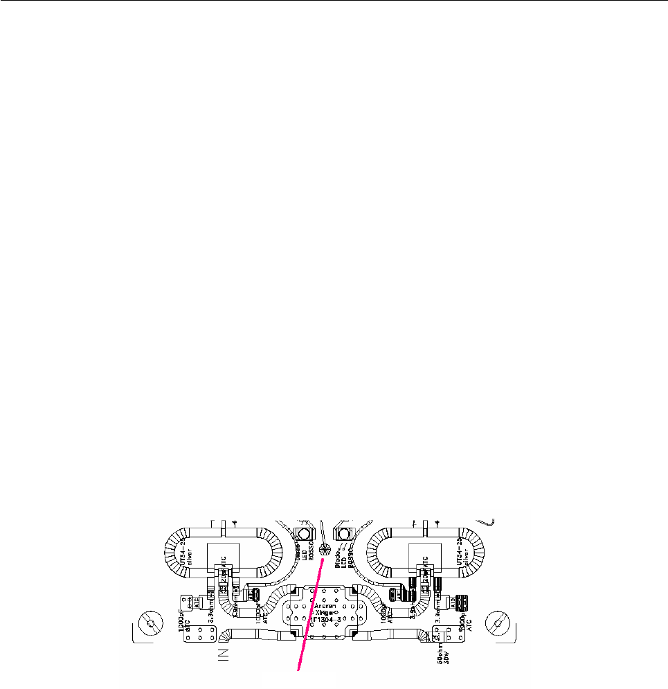
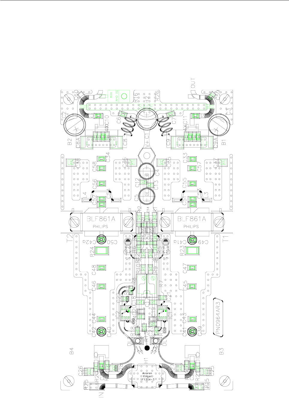
Component layout SCH0192AR0
82

83
COMPONENT LIST SCH0192AR0
REF. DESCRIPTION ELETTRONIKA CODE Page 1/3
R1 2200W 1/4W 1206 SMD RESISTOR 00045A
R2 2200W 1/4W 1206 SMD RESISTOR 00045A
R3 2200W 1/4W 1206 SMD RESISTOR 00045A
R4 2200W 1/4W 1206 SMD RESISTOR 00045A
R5 1200W 1/4W 1206 SMD RESISTOR 00042A
R6 1200W 1/4W 1206 SMD RESISTOR 00042A
R7 50kW MULTITURNS PTH TRIMMER 00800
R8 50kW MULTITURNS PTH TRIMMER 00800
R9 1200W 1/4W 1206 SMD RESISTOR 00042A
R10 1200W 1/4W 1206 SMD RESISTOR 00042A
R11 18kW 1/4W 1206 SMD RESISTOR 00056B
R12 18kW 1/4W 1206 SMD RESISTOR 00056B
R13 680KW 1/4W 1206 SMD RESISTOR 00075A
R14 0W 1/4W 1206 SMD RESISTOR 00001
R15 50W 30W 1512EBX SMD RESISTOR 00416A
R16 50W 60W 00432
R17 4.7kW 1/4W 1206 SMD RESISTOR 00049A
R18 4.7kW 1/4W 1206 SMD RESISTOR 00049A
R19 3.9W 1/4W 1206 SMD RESISTOR 00012A
R20 3.9W 1/4W 1206 SMD RESISTOR 00012A
R21 3.9W 1/4W 1206 SMD RESISTOR 00012A
R22 3.9W 1/4W 1206 SMD RESISTOR 00012A
R23 1000W 1W 2512 SMD RESISTOR 00396
R24 1000W 1W 2512 SMD RESISTOR 00396
*R25 = R15 (da montare se si inverte lingresso)
*R26 = R26 (da montare se si inverte luscita)
C1 470uF 50V PTH ELECTROLYTIC CAPACITOR 01807B
C2 470uF 50V PTH ELECTROLYTIC CAPACITOR 01807B
C3 470uF 50V PTH ELECTROLYTIC CAPACITOR 01807B
C4 100uF 50V PTH ELECTROLYTIC CAPACITOR 01795
C5 100uF 50V PTH ELECTROLYTIC CAPACITOR 01795
C6 1nF ATC 100B CAPACITOR OR EQUIVALENT 01145
C7 1nF ATC 100B CAPACITOR OR EQUIVALENT 01145
C8 x 2 2 x 100nF ATC CAPACITOR OR EQUIVALENT 01065H
C9 x 2 2 x 100nF ATC CAPACITOR OR EQUIVALENT 01065H
C10 x 4 4 x 100pF ATC 100B CAPACITOR OR EQUIVALENT 01135
C11 x 4 4 x 100pF ATC 100B CAPACITOR OR EQUIVALENT 01135
C12 100nF 1210 SMD CAPACITOR 1065G
C13 100nF 1210 SMD CAPACITOR 1065G
C14 100nF 1210 SMD CAPACITOR 1065G
C15 1uF 35V SMD TANTALIUM CAPACITOR 01613A
C16 1uF 35V SMD TANTALIUM CAPACITOR 01613A
C17 100nF 1210 SMD CAPACITOR 1065G

84
REF. DESCRIPTION ELETTRONIKA CODE Page 2/3
C18 100nF 1210 SMD CAPACITOR 1065G
C19 10uF 16V SMD TANTALIUM CAPACITOR 01626A
C20 10uF 16V SMD TANTALIUM CAPACITOR 01626A
C21 100nF 1210 SMD CAPACITOR 1065G
C22 100nF 1210 SMD CAPACITOR 1065G
C23 100nF 1210 SMD CAPACITOR 1065G
C24 100nF 1210 SMD CAPACITOR 1065G
C25 1nF ATC 100B CAPACITOR OR EQUIVALENT 01145
C26 1nF ATC 100B CAPACITOR OR EQUIVALENT 01145
C27 1nF ATC 100B CAPACITOR OR EQUIVALENT 01145
C28 1nF ATC 100B CAPACITOR OR EQUIVALENT 01145
C29 20pF ATC 100B CAPACITOR OR EQUIVALENT 01123
C30 20pF ATC 100B CAPACITOR OR EQUIVALENT 01123
C31 20pF ATC 100B CAPACITOR OR EQUIVALENT 01123
C32 20pF ATC 100B CAPACITOR OR EQUIVALENT 01123
C33 1.3pF ATC 100B CAPACITOR OR EQUIVALENT 01104
C34 1.3pF ATC 100B CAPACITOR OR EQUIVALENT 01104
C35 470pF ATC 100B CAPACITOR OR EQUIVALENT 01143
C36 470pF ATC 100B CAPACITOR OR EQUIVALENT 01143
C37 470pF ATC 100B CAPACITOR OR EQUIVALENT 01143
C38 470pF ATC 100B CAPACITOR OR EQUIVALENT 01143
C39 4.7pF ATC 100B CAPACITOR OR EQUIVALENT 01108
C40 4.7pF ATC 100B CAPACITOR OR EQUIVALENT 01108
C41 x 2 2 x 1¸5pF JOHANSON SMD TRIMMER 1485
C42 x 2 2 x 1¸5pF JOHANSON SMD TRIMMER 1485
C43 3.6pF ATC 100B CAPACITOR OR EQUIVALENT 01104B
C44 3.6pF ATC 100B CAPACITOR OR EQUIVALENT 01104B
C45 6.8pF ATC 100B CAPACITOR OR EQUIVALENT 01111
C46 6.8pF ATC 100B CAPACITOR OR EQUIVALENT 01111
C47 6.8pF ATC 100B CAPACITOR OR EQUIVALENT 01111
C48 6.8pF ATC 100B CAPACITOR OR EQUIVALENT 01111
C49 13pF ATC 100B CAPACITOR OR EQUIVALENT 01119A
C50 13pF ATC 100B CAPACITOR OR EQUIVALENT 01119A
C51 8.2pF ATC 100B CAPACITOR OR EQUIVALENT 01113
C52 8.2pF ATC 100B CAPACITOR OR EQUIVALENT 01113
C53 8.2pF ATC 100B CAPACITOR OR EQUIVALENT 01113
C54 8.2pF ATC 100B CAPACITOR OR EQUIVALENT 01113
C55 10pF ATC 100B CAPACITOR OR EQUIVALENT 01117
C56 10pF ATC 100B CAPACITOR OR EQUIVALENT 01117
C57 4.7pF ATC 100B CAPACITOR OR EQUIVALENT 01108
C58 4.7pF ATC 100B CAPACITOR OR EQUIVALENT 01108
C59 0.3pF ATC 100B CAPACITOR OR EQUIVALENT 01160
T1 BLF861A RF LDMOS POWER TRANSISTOR 04034
T2 BLF861A RF LDMOS POWER TRANSISTOR 04034
B1 COAX 2:1 BALUN 08491

85
REF. DESCRIPTION ELETTRONIKA CODE Page 3/3
B2 COAX 2:1 BALUN 08491
B3 COAX 4:1 BALUN 08492
B4 COAX 4:1 BALUN 08492
L1 4 TURNS SILV. COP. WIRE 1.2mm WOUND ON OD 5mm 07684
L2 4 TURNS SILV. COP. WIRE 1.2mm WOUND ON OD 5mm 07684
L3 ½ TURN COIL
L4 ½ TURN COIL
H1 HYBRID COUPLER 3dB 90° ANAREN 05368
H2 HYBRID COUPLER 3dB 90° SAGE 05369
NTC1 NTC 100KW PTH 00661
NTC2 NTC 100KW PTH 00661
IC1 DG419DY 04583
IC2 DG419DY 04583
DZ1 15V SMD ZENER DIODE 03135
DZ2 15V SMD ZENER DIODE 03135
DZ3 6.8V SMD ZENER DIODE 03137
DZ4 6.8V SMD ZENER DIODE 03137
DL1 SMD LED DIODE - RED - 03056
DL2 SMD LED DIODE - RED - 03056
PN964AR3 PCB 0643K
Torretta 3x10 f/f V0774
Imballo velapack 200x125x50 09983
86
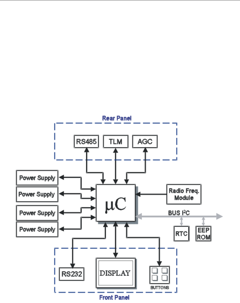
Picture 1: Simplified block diagram of the control and display board
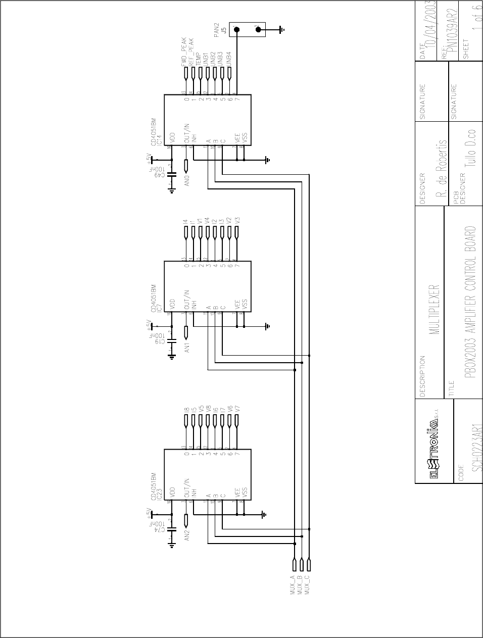
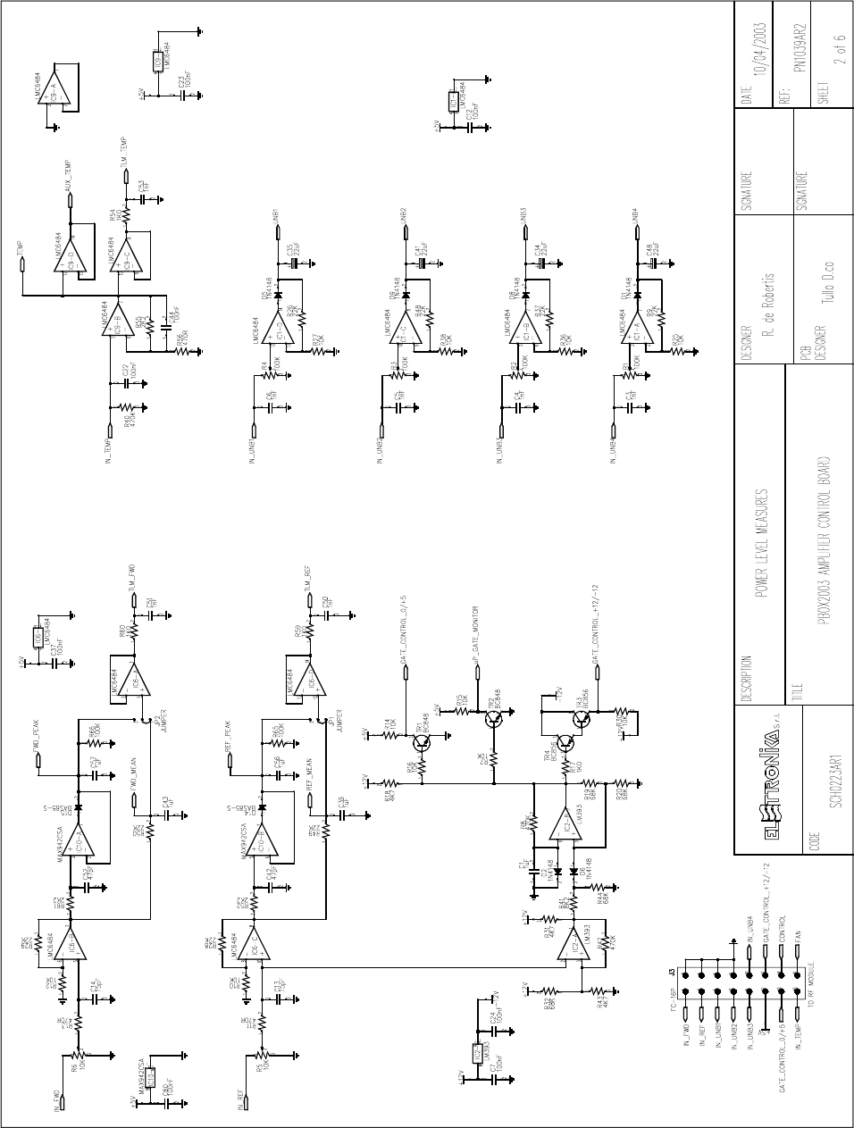
CONTROL BOARD AND DISPLAY SCH0223AR1
DESCRIPTION
The control board SCH0223AR1 manages the operational logic of the amplifier: switching on and off, power
supply and fans, alarms and protections, remote control, human-machine interface. There are managed by a
modern and powerful 16 bit micro-controller (MB90F543), made by Fujitsu, which is the main part of the
board.
Picture 1 shows the block diagram.
87
It can be seen that the micro-controller is the heart of the control system, to which the various peripherals
(power supply, serial ports, telemeasure socket, AGC port, RF amplifier module, ROM, clock, display and
keys) are interfaced.
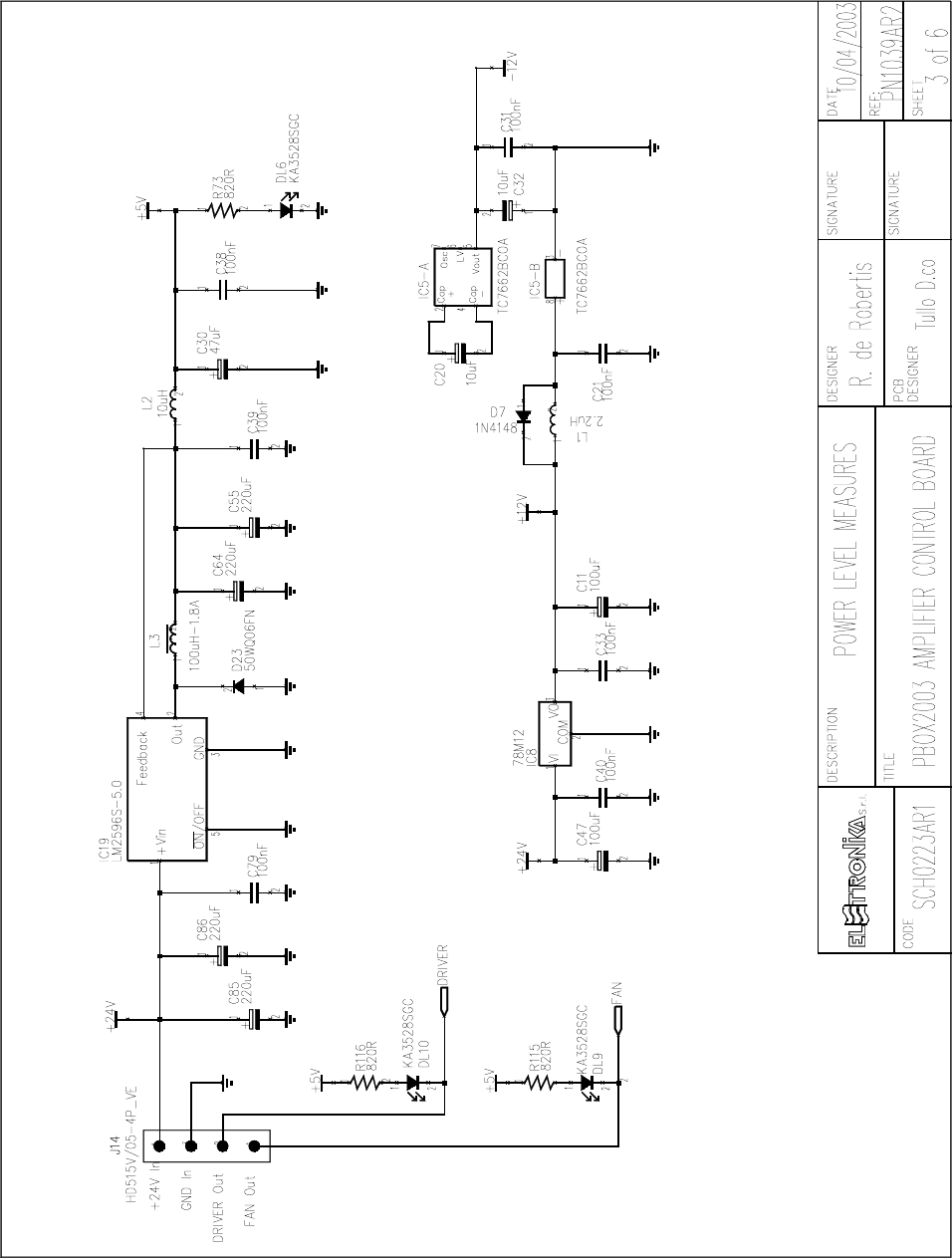
- Power Supply
The board is powered with a continuous +24V voltage from which the +5V voltage powering the most of the
chips (micro-controller, operational amplifiers, display, etc.) is derived by means of a switching converter (see
IC19). A +12Vdc voltage is obtained from it as well, by means of a linear conversion provided by the
integrated circuit IC8. From this, a -12Vdc voltage is obtained by means of the integrated circuit IC5. The
-12V voltage is also used to adjust the contrast of the display.
- Connectors
On the board SCH0223AR1 there are several connectors used as interfaces for the peripherals of the apparatus
and the ports for external communication.
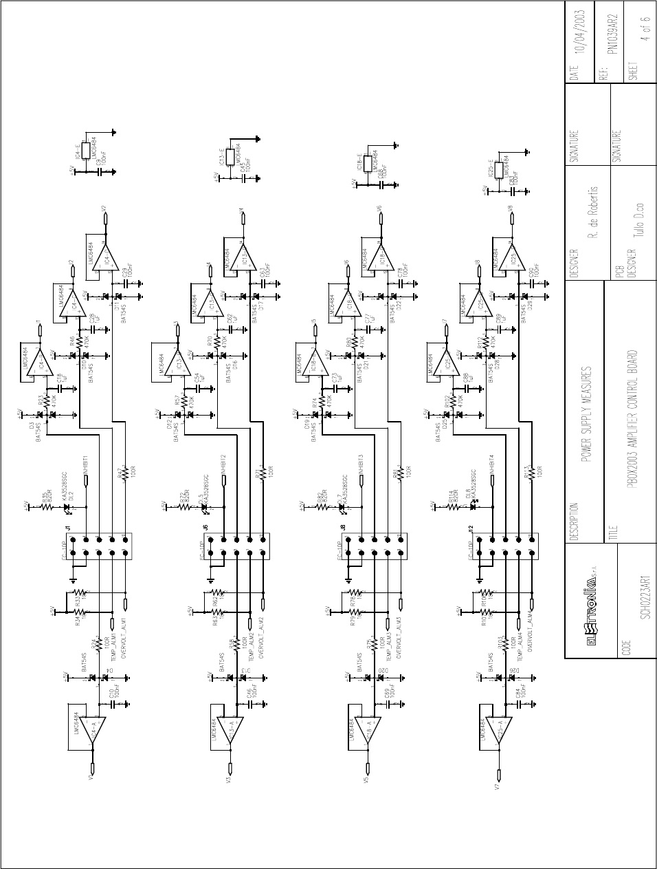
POWER SUPPLY
The connectors J1, J6, J8 e J12 are connected to the power supply powering the RF amplifier modules. The
number of power supply used changes depending on the amplifier, up to four power supply. They are connected
in the order shown in Table 1 below. Remaining connectors, if any, are left unused.
Table 1: Interface connectors for the power supply
Through this connection, each power supply provides the two levels of voltage and current acquired by the
micro-controller by means of an internal ADC. Besides the connectors allow the control board to turn on or
off the individual power supply (for instance when an alarm occurs). The used power supply are protected
CONNECTOR POWER SUPPLY N°
J1 1
J6 2
J8 3
J12 4
88
agaimst voltage surges or temperature increases. If one of these events occurs, the power supply is switched
off and the event is signalled to the micro-controller through the connection with the control board.
RF AMPLIFICATION
The J3 connector interfaces the control board with the RF amplification section. Through this connector the
micro-controller acquires the sample of forward and reflected power, unbalancing (if any), and temperature
of the critic amplification area. It also allows to inhibit the transistors in case of reflected power alarm, by
means of a totally hardware, thus extremely fast protection.
Depending on the apparatus, this connector may also allow to enable or disable the cooling fans of the critic
area.
RS485
The J11 connector (10 pin socket) is directly wired to a DB9 female connector placed on the rear panel of the
apparatus. This communication bus allows to connect the amplifier to the control (Amplifier Control) module
of a high-power transmitter composed by several individual amplifiers. In this case, each amplifier and the
Amplifier Control are connected to the same 4-wires RS485 bus and each of them as a unique address
(which can be set by means of the keys and the display) for correct communication.
In case of single (stand-alone) amplifier, the RS485 connector can be used for connection to the Remote
Control Unit (RCU) made by Elettronika S.r.l. This unit allows to monitor and control the remote transmitter
from any site provided with PSTN or GSM1 phone connection.
Table 2 shows the wiring between the J11 connector on the board and the DB9 female connector on the rear
panel, along with the description of the lines.
1 For more details about the control system contact the distributor or the manufacturer.
PIN N°
ON DB9
PIN N°
ON J11 DESCRIPTION
11 Not used
23 Rx-
35 Rx+
47 +5V
59 GND
62 Not used
74 Tx-
86 Tx+
98 Not used
Table 2: Description of the RS485 connector
89
TELEMEASURES
The J9 telemeasure connector (10 pins socket) is directly wired on a DB9 female connector placed on the
rear panel. There are input and output digital lines (TTL level) and analog output lines on this connector, which
are used to monitor and control the amplifier by means of a general-purpose remote control system.
The correspondende between the pins of the J9 connector on the board and the DB9 female connector on the
rear panel, as well as the meaning of the various lines, is shown in table 3 below (the directions refers to the
position of the micro-controller on the board).
PIN N°
ON DB9
PIN N°
ON J9 TYPE DIRECTION DESCRIPTION
1 1 Analog Output Forward power
2 3 Analog Output Reflected power
3 5 Analog Output Temperature
4 7 Digital Input
Interlock:
0V = Interlock Alarm
5V = Normal
59 - -Ground
6-7 2-4 Digital Output Free Contact
(closed when amplifier is in alarm)
8 6 Digital Input Turning-on control
(usually high, active when low)
9 8 Digital Input Turning-off control
(usually high, active when low)
Table 3: Description of the telemeasures connector
The input stage of the digital controls has an internal pull-up towards the 5V power supply voltage. To use this
lines it only takes setting a switch to close to earth, when closed, the relevant control (turning on or off) is
enabled and the switch may be switched open again (impulse controls).
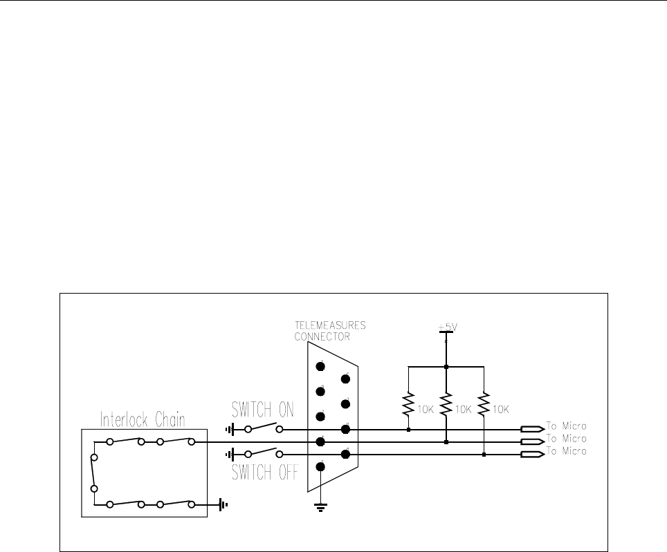
The interlock pin may be used as protection so that the amplifier is switched off the digital input level is low. It
is possible to use several serially connected switches to make an interlock chain. Usually all switches are
closed and the interlock level is low, thus the amplifier is on. If even only one of the switches is opened, the
(*)
(*)
(*) You can select by means of two jumpers on the board (JP1 and JP2) RMS or peak power. If there are two jumpers on pins 1 and 2 of
JP1 and JP2 connector, RMS power is selected. Otherwise, if there are two jumpers on pins 2 and 3 of the same connectors, peak power
is selected.
90
Picture 2: Usage of the digital input signals of the telemeasures connector
AGC / EXCITER
The connector called J10, as the telemeasures connector and the RS485 bus, is wired to a DB9 female
connector placed on the rear panel of the amplifier. This connectors allow the implementation of an automatic
gain control between an exciter and the amplifier. A voltage signal related to the forward output power
supplied by the amplifier is provided through two pins of the AGC connector. Connecting one of these to the
relevant input pin of the exciter, this can pursuit a given voltage level, so that the output power is always
constant. In order to avoid that, in case of an alarm decreasing the forward power, the exciter strongly
increases the output level due to the AGC, thus damaging the amplification stages, the connector is provided
with two digital output lines called AGC Alarm. Under alarm conditions, this lines are brought by the micro-
controller at a low level, so that the exciter can stop the AGC.
Table 4 shows the connection between the J10 connector on the board and the DB9 connector on the rear
panel, along with the description of each pin (the direction of the pin is referred to the position of the micro-
controller on the board).
level of the interlock signal becomes high (this line has a pull-up towards the +5V power supply voltage as
well) and the protection for interlock alarm is activated for the amplifier, which is switched off. Note that in
case the interlock protection is not used, the pin 4 of the DB9 telemeasure connector and the earth pin (pin 5)
must be short circuited. Otherwise it is possible to disable the monitoring of the interlock chain from menu (see
user manual).
Picure 2 shows a usage for the digital input signals to turn on and off the amplifier and for the interlock alarm.
91
Table 4: Description of the AGC connector
RS232
The DB9 female connector on the front panel is an external communication RS232 serial port, through which
a PC can be connected directly to the amplifier in order to perform operations such as the remote control (by
means of an adequate software2) and the update of the microcontroller firmware.
The used communication protocol is asynchronous, at a 19200bps speed, 1 start bit, 8 data bits, 1 stop bit,
no parity. No hardware flow is used. The connector is DCE type and the pin used are shown in Table 5.
PIN N° ON DB9 123456789
DESCRIPTION -TxDRxD-GND----
MISCELLANEOUS
The J2 (called AUX), J4, J5 and J17 connectors are not used and are there only for future updates. The SW1
dip-switches are partially used for the configuration of the correct mode for the micro-controller. The other
switches are not used. It is important that the position of the dip-switches is left unchanged, because changing
it may set a wrong mode for the micro-controller, affecting the work of the whole amplifier.
2 For more information about this application contact the distributor of the manufacturer.
PIN N°
ON DB9
PIN N°
ON J10 TYPE DIRECTION DESCRIPTION
11- -Ground
23DigitalOutput
AGC Alarm
0V = Alarm
5V = Normal
35DigitalOutput
AGC Alarm
0V = Alarm
5V = Normal
47- -Not used
59 - -Not used
62 - -Not used
7 4 - - Nout used
8 6 Analog Output Forward power
9 8 Analog Output Forward power
Table 5: Description of the RS232 connector
92
FIRMWARE UPDATE
The micro-controller MB90F543 is provided with a built-in Flash memory containing the firmware. The
firmware can be updated to later versions without removing the apparatus from the rack and/or replacing the
chip.
To upgrade it, connect a PC to the RS232 socket on the front panel of the apparatus by means of a cable
DB9 male - DB9 female (pin-to-pin).
Launch on the PC the EKAFlash application, select the serial port in use of the PC and choose the update file
by pressing the ... key and click on Download button.
Eventually, turn off the amplifier from the main switch and then turn it on again. The upgrade of the firmware
begins on the EKAFlash window. Picture 3 shows this window while a firmware is being updated.
Picture 3: The EKAFlash window while updating a firmware
93
94
95
96
97
98
99
100

101
COMPONENT LIST SCH0223AR1
Part Name/Number Description Qty. Comps. Page 1/2
BATT BH001RB 3093_90 03093 03090 BATTERY HOLDER 1 BATT1
CC 100nF-S 01065C 01065C Y5V 1206 COND 46 C2, C7-10, C12, C16, C19, C21-27
C29, C31, C33, C37-40, C44-46,
C49, C58-61, C63, C65-69, C74,
C76, C78-81, C83-84, C87, C90
CC 15pF-S 01088 01088 SMD 1206 COND 4 C13-15, C17
CC 1nF-S 01096 01096 SMD 1206 COND 7 C3-6, C50-51, C53
CC 1uF100V-S 01760A 01760A Y5V 1206 COND 13 C1, C18, C28, C36, C43, C54,
C56-57, C62, C73, C77, C88-89
CC 47pF-S 01100 01100 SMD 1206 COND 2 C42, C52
CE 100uF25V-S 01793B 01793B ELETTR SMD COND 2 C11, C47
CE 10uF35V-S 01778A 01778A ELETTR SMD COND 2 C20, C32
CE 1uF35V-S 01613A 01613A TANTALIUM ELETTR SMD CO 5 C70-72, C75, C82
CE 220uF50V LOW ESR 1799A ELETTR SMD COND LOW ESR 4 C55, C64, C85-86
CE 22uF16V-S 01780A ELETTR SMD COND 4 C34-35, C41, C48
CE 47uF35V-S 01790A 01790A ELETTR SMD COND 1 C30
D 1N4148-S 03002 03002 SMD DIODE 7 D1-2, D5-9
D 50WQ06FN 03019A SMD DIODE SCHOTTKY 5,5A 1 D23
D BAS85-S 03024 SMD DIODE SCHOTTKY 2 D14-15
D BAT54S 03199 SMD SCHOTTKY DIODE A-K T 19 D3-4, D10-13, D16-22, D24-29
DIS MGLS12864T 03083A 128x64 DOT (BLUE-LED WH 1 DIS1
DL KA-3528SGC 03057 03057 GREEN SMD LED DIODE 7 DL2, DL5-10
DL LEDG5 03060 03060 GREEN LED DIODE 5mm 1 DL1
DL LEDR5 03061 03061 RED LED DIODE 5mm 1 DL4
DL LEDY5 03054B 03054B YELLOW LED DIODE 5mm 1 DL3
IC 24LC64 04815 04815 SMD INTEG CIRCUIT 1 IC17
IC 78M12 4307B 04307B SMD VOLTAGE REGULATOR 1 IC8
IC CD4051BM-S 04615 SMD INTEG CIRCUIT 3 IC7, IC14, IC23
IC LM2596S-5.0 04580 SMD INTEG CIRCUIT 1 IC19
IC LM358M-S 04660 04660 SMD INTEG CIRCUIT 1 IC3
IC LM393-S 04639 04639 SMD INTEG CIRCUIT 1 IC2
IC LMC6482-S 04632 SMD INTEG CIRCUIT 1 IC24
IC LMC6484-S 04634 SMD INTEG CIRCUIT 7 IC1, IC4, IC6, IC9, IC13, IC18,
IC25
IC M41T56 04611 04611 SMD INTEG CIRCUIT 1 IC20
IC MAX232-S 04804B 04804B SMD INTEG CIRCUIT 1 IC21
IC MAX3080-S 04770 04770 SMD INTEG CIRCUIT 1 IC22
IC MAX942CSA-S 04572 SMD INTEG CIRCUIT 1 IC10
IC MB90F543PF 04596 SMD INTEG CIRCUIT 1 IC11
IC MPC100-450DI-TO 04608 INTEG CIRCUIT 1 IC16
IC TC7662BCOA 04758A 04758A SMD INTEG CIRCUIT 1 IC5
IC ULN2003A 4870 04870 SMD INTEG CIRCUIT 2 IC12, IC15
IND 2u2H-S 05020A 05020A INDUCTOR 1 L1

102
Part Name/Number Description Qty. Comps. Page 2/2
IND MS85 10uH-S 04948 INDUCTOR 2,7 A 1 L2
IND T100uH-1.8A 4958 04958 TOROIDAL-STORAGE CHOKES 1 L3
J CON HD515V/05-4PVE 02881 + 02882 PANDUIT PCB CONN 1 J14
J DB9_F-0° LT 02794 PCB CONNECTOR DB9 LONG T 1 J13
J FC-10P 02697-02699 02697+02699 PCB CONNECTOR POL 8 J1-2, J6, J8-12
J FC-16P 02701-02700 02701+02700 PCB CONNECTOR POL 1 J3
J PAN2 02739-40-41 02739+02740+02741 PCB CONNECTO 3 J5, J7, J15
J PAN8 02716 02716 PCB CONNECTOR 1 J4
JU JUMP2 02739-02742 02739+02742 MASCHIO PAN2 1 JP3
JU JUMP3 02707-02742 02707+02742 MASCHIO PAN3 2 JP1-2
R 100K-1%-S 00065B 00065B RES 1/4W 1% SMD 1206 10 R65-66, R94-101
R 100R-1%-S 00029D 00029D RES 1/4W 1% SMD 1206 12 R24, R47, R58, R71, R75,R81,
R83, R89, R103-105, R113
R 10K-1%-S 00053B 00053B RES 1/4W 1% SMD 1206 32 R7, R10, R12, R14-16, R22, R25,
R27, R30, R33-34, R36, R38, R51,
R62-64, R78-79, R84-85, R87-88,
R92-93, R106-111
R 10R-S 00017A 00017A RES 1/4W 5% SMD 1206 1 R68
R 1206 NOT MOUNTED NOT MOUNTED RES 1/4W 5% SMD 12 1 R91
R 1K0-1%-S 00041B 00041B RES 1/4W 1% SMD 1206 8 R17, R54, R59-60, R76-77, R86,
R90
R 22K-1%-S 00057B 00057B RES 1/4W 1% SMD 1206 11 R9, R21, R26, R28-29, R37, R45,
R48-50, R69
R 2K2-1%-S 00045B 00045B RES 1/4W 1% SMD 1206 3 R52, R55, R61
R 470K-S 00073A 00073A RES 1/4W 5% SMD 1206 11 R8, R23, R40, R42, R46, R57, R70
R74, R80, R102, R112
R 470R-1%-S 00037B 00037B RES 1/4W 1% SMD 1206 6 R11, R13, R39, R53, R56, R67
R 4K7-1%-S 00049B 00049B RES 1/4W 1% SMD 1206 3 R18, R31, R43
R 68K-1%-S 00063B 00063B RES 1/4W 1% SMD 1206 4 R19-20, R32, R44
R 820R-S 00040A 00040A RES 1/4W 5% SMD 1206 7 R35, R72-73, R82, R114-116
R 8K2-1%-S 00052B 00052B RES 1/4W 1% SMD 1206 1 R41
RL 30.22.24 07569 07569 RELE 3 RLY1-3
RV 100K-3266X 00814 VARIABLE RESISTOR 4 R1-4
RV 10K-3266X 00807 00807 VARIABLE RESISTOR 2 R5-6
SW SWITCH-8DIP 07530A PCB DIP SWITCH SMD 1 SW1
T 06086 N 7630 7632 7630 7632 KTI06086 PULSANTE 2 4 T1-4
TR BC848 03457 03457 NPN SMD TRANSISTOR 2 TR1-2
TR BC856 03455 03455 PNP SMD TRANSISTOR 2 TR3-4
XTAL 32.768k-S 05146 05146 QUARTZ 1 XTAL2
XTAL 4MHz-S 05101A 05101A QUARTZ 1 XTAL1