FEIBIT ELECTRONIC TECHNOLOGY FZB57A5PF FZB57A5+Module User Manual FZB57A5 specification
SHENZHEN FEIBIT ELECTRONIC TECHNOLOGY Co., LTD FZB57A5+Module FZB57A5 specification
user manual
FZB57A3+
IEEE 802.15.4 ZigBee Module
page 1 of 12
FCC ID:2AE8BFZB57A5PF
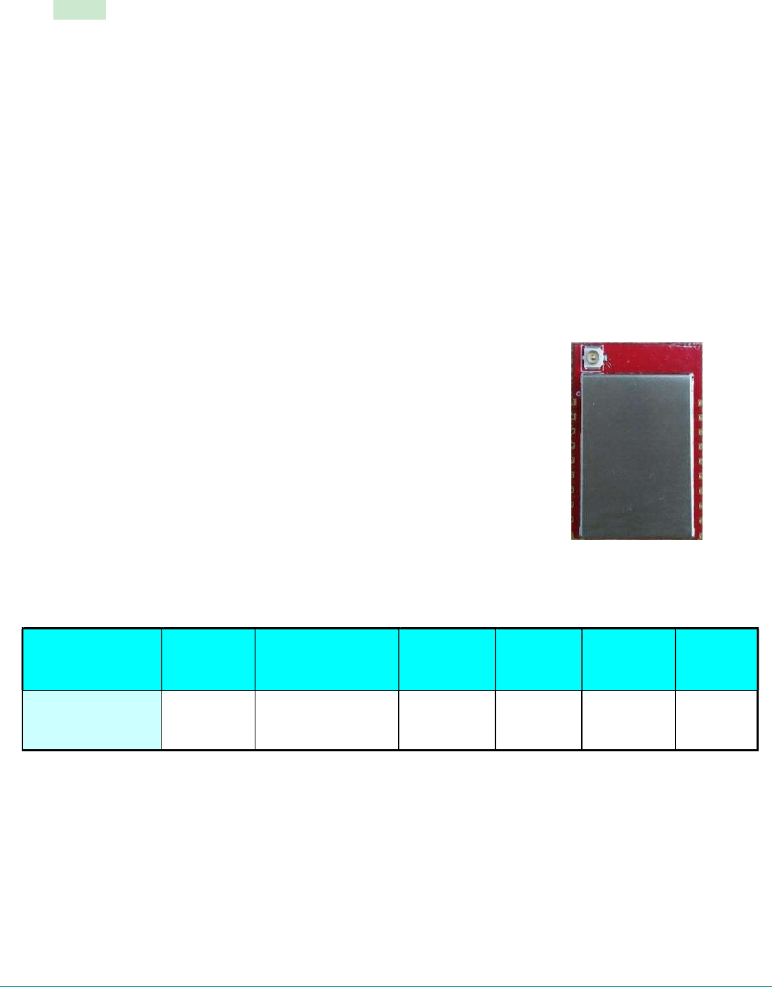
FZB57A5+
2.4 GHz IEEE 802.15.4 ZigBeeModule
characteristicsFeatures:
ReservingSystem
IEEE Std. 802.15.4
Is the Chip Solution
TI CC2530F256RHAR
Band
2.4G
Size
18mm*27.1mm*2.3mm
Model Overview:
1.Briefdescription:
ZigBee module FZB57A5+ is based on TI CC2530F256RHAR, complied with IEEE, complied, and it is also known
as "
The ZigBee module FZB57A5+ is a TI based CC2530F256RHAR development that supports the 2.4GHz IEEE
802.15.4 label
Quasi - maximum support for 250kbps rate wireless network connections.
Model
Installa
tion
method
Support
standard
rate(MAX)
Band
Antenna
interfac
e
Remarks
FZB57A5+ SMT IEEE 802.15.4 250kbps 2.4 GHz IPEX 3.3V
power
supply
FZB57A3+
IEEE 802.15.4 ZigBee Module
page 2 of 12
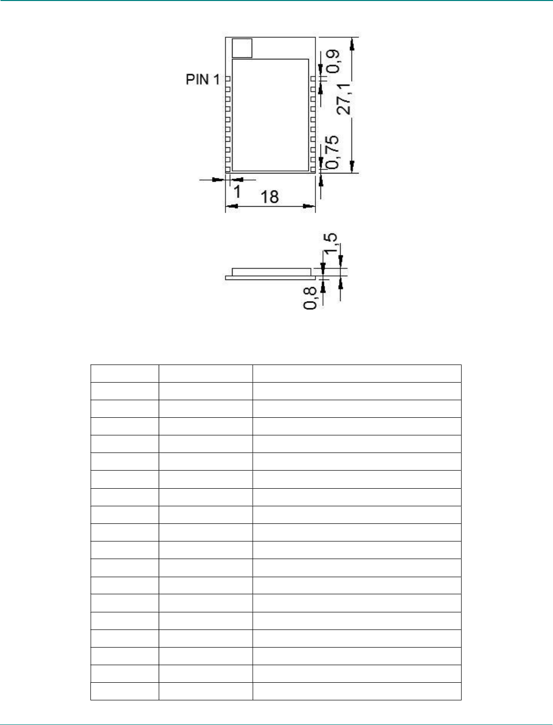
2.PackageoutlineandMounting:(View direction: confront)
NOTE1:General tolerance ±0.2mm unless otherwise stated
3.PinDefinition:
Pin#
Name
Description
1
GND
Ground connection
2
VCC
3.3V Main Voltage Source Input
3
P2_2
Digital I/O Port 2.2/JTAG DC
4
P2_1
Digital I/O Port 2.1/JTAG DD
5
P2_0
Digital I/O Port 2.0
6
P1_7
Digital I/O Port 1.7
7
P1_6
Digital I/O Port 1.6
8
P1_5
Digital I/O Port 1.5
9
P1_3
Digital I/O Port 1.3
10
P1_2
Digital I/O Port 1.2
11
P1_4
Digital I/O Port 1.4
12
P0_6
Digital I/O Port 0.6
13
P0_5
Digital I/O Port 0.5/UART RTS
14
P0_4
Digital I/O Port 0.4/UART CTS
15
P0_3
Digital I/O Port 0.3/UART TXD
16
P0_2
Digital I/O Port 0.2/UART RXD
17
P0_1
Digital I/O Port 0.1
18
P0_0
Digital
I/O Port 0.0
FZB57A3+
IEEE 802.15.4 ZigBee Module
page 3 of 12
19
RST
Reset
20
GND
Ground connection
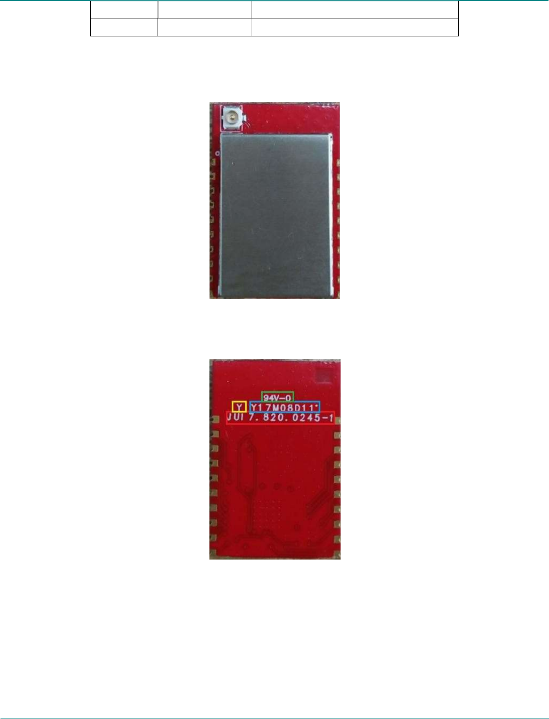
1. ProductPicture:
TOP VIEW
BOTTOM VIEW
Silk screen Description:
1. the character in the red box is PCB figure number.
2. the character in the yellow box is the PCB supplier control character.
3. the character in the blue box is the PCB batch number.
4. the character in the green frame is PCB flame retardant grade.
FZB57A3+
IEEE 802.15.4 ZigBee Module
page 4 of 12
2.
key materials:
Serial
number
Key name Model Specification /
material
Producer Remarks
1 Integrated
circuit
CC2530F256RHAR
VQFN
TI
2 Integrated
circuit
CC2592RGVR
PVQFN
TI
3
PCB JUB7.820.0245-2
FR-4,4LAY
The founding of the UK
Sunlord
4
crystal
oscillator
E3SB32E00000BE
32M Hosonic
5
crystal
oscillator
ETST00327000JE
32.768KHz Hosonic
3. GeneralRequirements:
No.
Feature Description
6-1
Operation Voltage 3.3±0.3V
6-2
TX Current Consumption <150mA
6-3
Operation Temperature -20°C ~ +60°C
6-4
Antenna Type no antenna
6-5
CPU Type 8051
6-6
Storage Temperature -40°C ~ +85°C
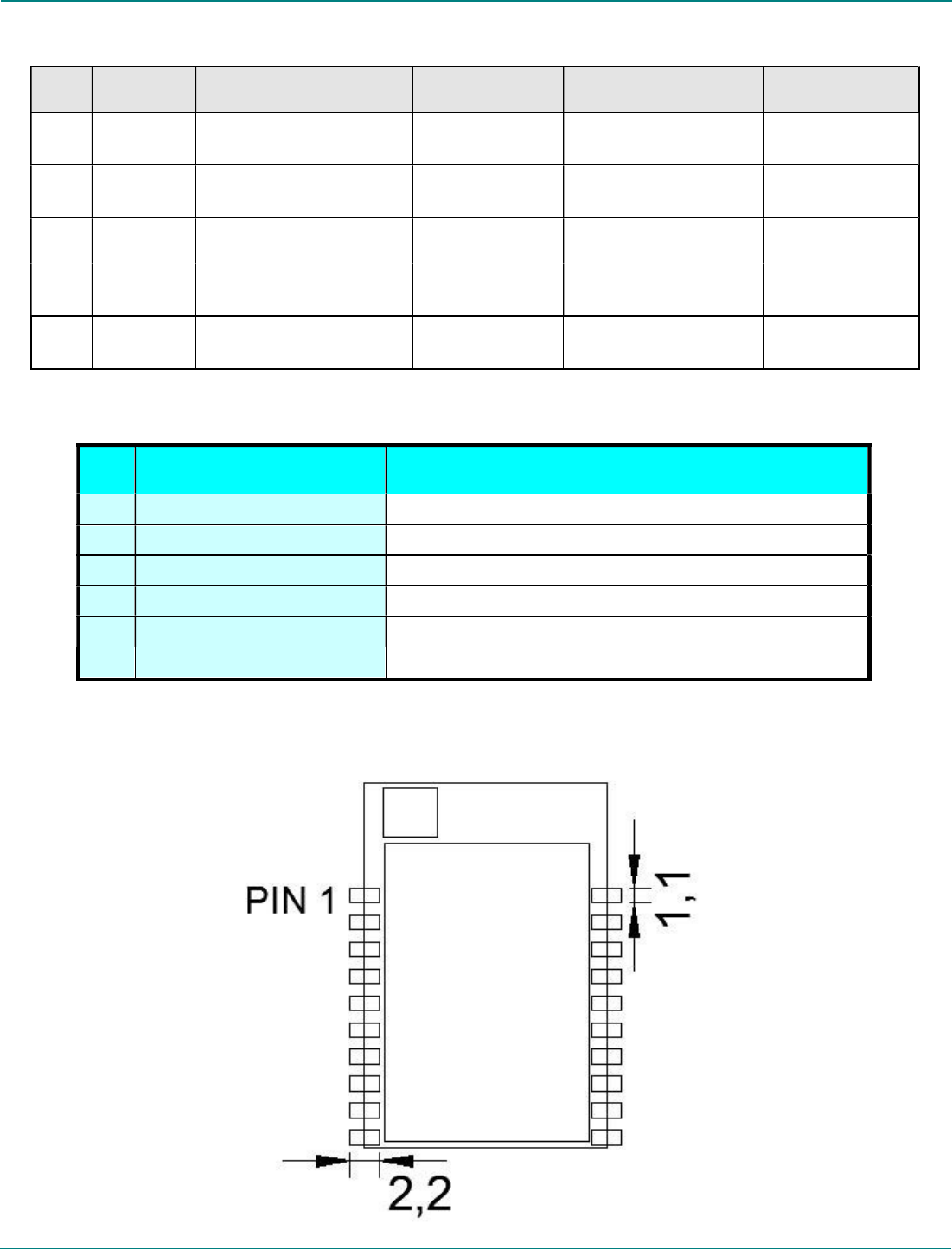
4. SMTSolder plate recommendation:
page 5 of 12
ZB-T530-RSF1
IEEE 802.15.4 ZigBee Module
5. ElectricalCharacteristics:
Items Contents
Specification IEEE802.15.4
Frequency 2400~2483.5MHz
Channel CH10 to CH26
Data rate 250kbps/MAX
Min. Typ. Max. Unit Remark
TX Characteristics
1. Power Levels(Calibrated)
1) 21.1dBm Mode 18 19.5 21 dBm
2) 19.7dBm Mode 17 18 19.5
3) 11.8dBm Mode
9
10 11.5
2. Spectrum Mask @ target power
/
0% 5.12%
3 Constellation Error(EVM)@ target power 0% 10% 35%
4. Frequency Error -40 -10 40 ppm
RX Characteristics Min. Typ. Max. Unit
5 Minimum Input Level Sensitivity(each chain)
/
-100 -85 dBm
6 Maximum Input Level
/
/
-20 dBm
6. TestSoftwareRequirements:
Mfg. software tool version is SmartRFProgr_1.12.7 or later.
The version of the manufacturing software tool isSmartRFProgr_1.12.7 Or subsequent version。
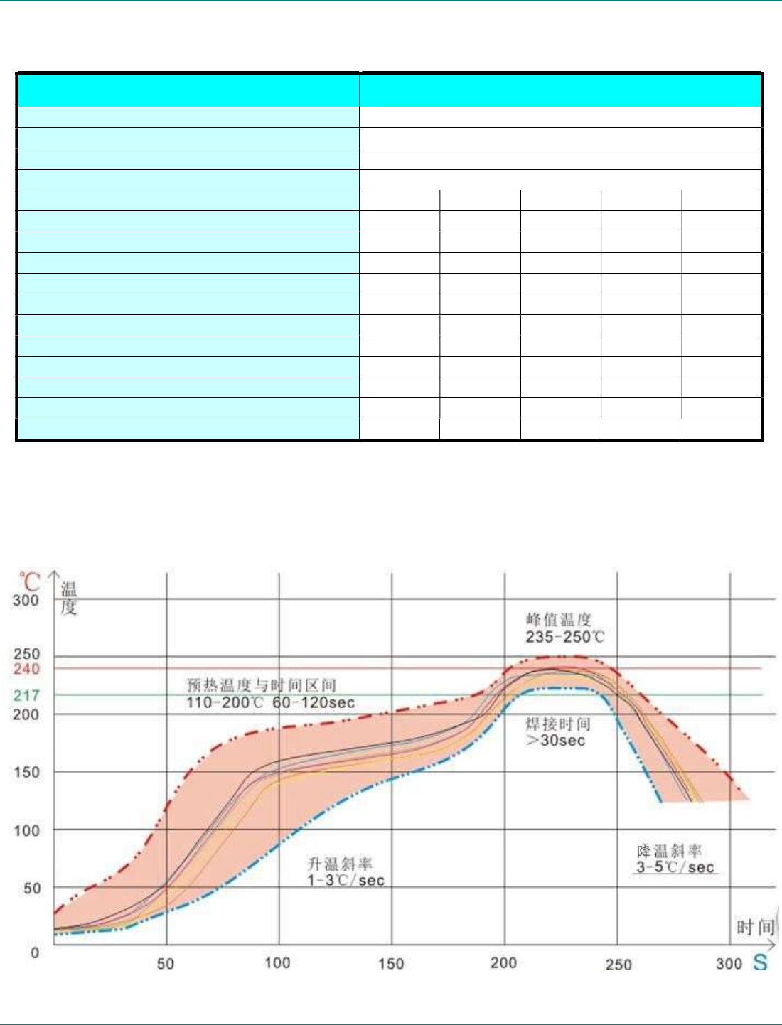
7. RefelowStandardCondition:

page 6 of 12
ZB-T530-RSF1
IEEE 802.15.4 ZigBee Module
Heating area: temperature: <150 C, time: 60~90 seconds, the slope control at 1~3 C between /S. Preheating
constant temperature area: temperature: 150 ~ 200 c, time: 60-120 seconds, the slope is between 0.3-0.8.
Reflow zone: peak temperature 235 C ~250 C (suggested peak temperature < 245 C), time 30-70 seconds.
Cooling area: temperature: 217 C ~170 C, the slope at 3~5 /S.
Solder is tin silver copper alloy lead-free solder / Sn&Ag&Cu Lead-free solder (SAC305)。
8. Mechanical, EnvironmentalandReliabilityTests:
Test Items Test Conditions Qty
Criteria Condition
4-1
Drop test
The packed samples within
100Kg can be tested
Drop height:
Face Side: 800/600/450mm
Edge line: 600/450/350mm
Drop time: 1 each Face and
edge.
1xBox
After drop test, the outer box and inner box will
not been broken by appearance visual
inspection.
4-2
Vibration test
X-Y-Z direction, first
Frequency changing from
10Hz to 30Hz to 10Hz
,amplitude 0.75mm, 5 times
vibrations, then frequency
Changing from 30Hz to 55
Hz to 30 Hz, amplitude
0.15mm, 5 time vibration.
3
After test, the Appearance, Power EVM and
Frequency error shall be satisfied with the
specification.
4-3
Impact test
Impact acceleration:
50m/sec2;
Impact duration: 16ms;
Impact times: 1000.
3
After test, the Appearance, Power EVM and
Frequency error shall be satisfied with the
specification.
4-4
Soldering ability
test
Soldering temperature:
235±5℃
Soldering duration:
2±0.5S
3
1.
After soldering, the soldered area must be
covered by a smooth bright solder layer, some
deficiencies such as a small amount of the
pinhole, not wetting are allowed, but the
deficiencies can not be in the same place;
2.
At least 90% of soldered area shall becovered
continuously by the solderingmaterial.
4-5
Humidity test
Leave samples in 40±3℃,
93% RH @ 96 hours
3
Leave samples in standard test condition for 2
hours then test, the Appearance, Power, EVM
and Frequency error functional parameter shall
be satisfied with the test specification.
4-6
High temperature
load life test
Thermostat cabinet
temperature: 55±5℃
Applied voltage:
110% rated voltage
Working duration: 200 hour
(Supply Voltage Cycle
23h power on, 1h power off)
60
After test, leave samples in standard condition
for 1 hour and test, Power, EVM and Frequency
error shall be satisfied with the testspecification.
4-7
High temperature
load test
Temperature: 55±5℃
Samples work for 16 hours
3
After test, the
Appearance, Power, EVM and
Frequency error shall be Satisfied with the test
specification.

ZB-T530-RSF1
IEEE 802.15.4 ZigBee Module
page 10 of 12
4-8
Low temperature
storage test
Leave the samples in
-25±3℃@24 hours
3
Leave samples in standard test condition for 2
hours then test, the
Appearance, Power, EVM
and Frequency error shall be satisfied with the
test specification.
4-9
Low temperature
load test
Leave samples in
-15±3℃@ 2 hours,
samples’ function
shall be normal, the let
samples work for 1 hour
3
After test,
leave the samples in standard
condition and tested the Appearance, Power,
EVM and Frequency error shall be satisfied with
the test specification.
4-10
Temperature circle
test
One cycle duration
-10±3℃ @3H
40±3℃ @3H
Total cycle: 10x
3
After test,
leave the samples in standard
condition and tested Power EVM and Frequency
error shall be qualified and all the characters
shall be satisfied with the test specification.
4-11
Continuous
TP test
Twice cycle duration
-10±3℃@4H
+60±3℃@4H,
+25@2H@2H
3
During test, There will not been appeared signal
disconnection or interruption between DUT and
AP.
4-12
ESD
Discharge voltage: 2kV
C: 150pF
Discharge resistance:330Ω
Positive10 times
1 time for each second
3
The products can recoverable smoothly after
ESD test.
ZB-T530-RSF1
IEEE 802.15.4 ZigBee Module
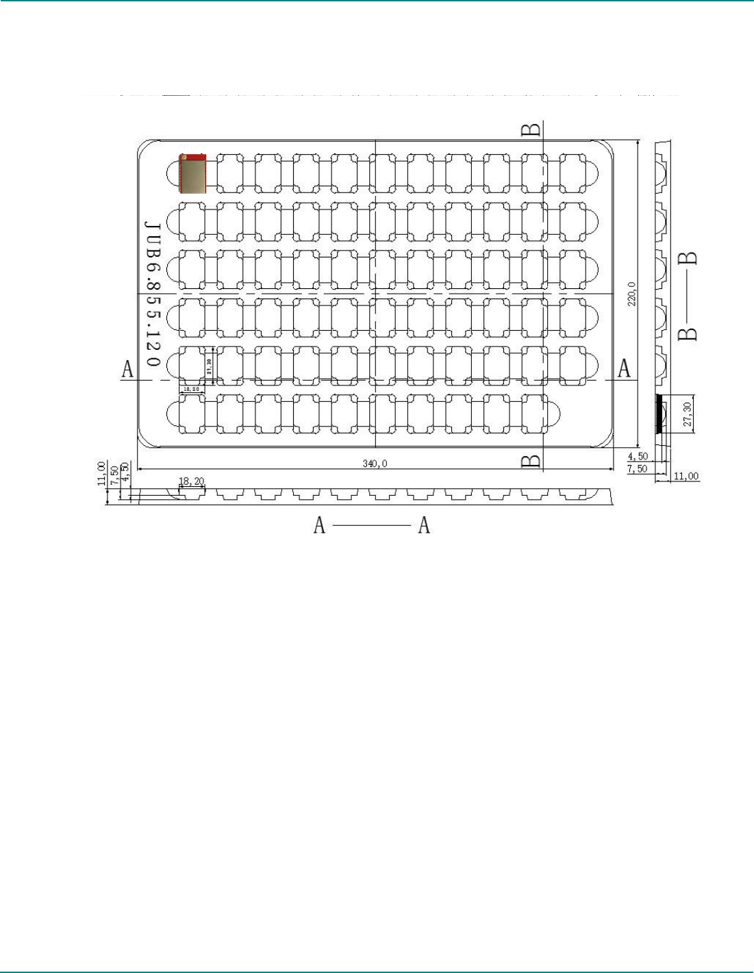
13. Packaging requirements:
(1) the size of the tray and the setting direction of the module, such as the following.
Feeral Communication Commission (FCC) Radiation Exposure Statement
This device complies with part 15 of the FCC rules. Operation is subject to the following two conditions:
(1)this device may not cause harmful interference, and
(2)this device must accept any interference received, including interference that may cause undesired operation.
NOTE: The manufacturer is not responsible for any radio or TV interference caused by unauthorized modifications or
changes to this equipment. Such modifications or changes could void the user’s authority to operate the equipment.
NOTE: This equipment has been tested and found to comply with the limits for a Class B digital device, pursuant to part
15 of the FCC Rules. These limits are designed to provide reasonable protection against harmful interference in a
residential installation. This equipment generates uses and can radiate radio frequency energy and, if not installed and
used in accordance with the instructions, may cause harmful interference to radio communications. However, there is no
guarantee that interference will not occur in a particular installation. If this equipment does cause harmful interference to
radio or television reception, which can be determined by turning the equipment off and on, the user is encouraged to try
to correct the interference by one or more of the following measures:
Reorien‐t or relocate the receiving antenna.
Increase the separation between the equipment and receiver.‐
Connect the equipment into an outlet on a circuit different from that to which the receiver is connected.‐
Consult the dealer or an experienced radio/TV ‐technician for help.
Federal Communication Commission (FCC) Radiation Exposure Statement
When using the module, maintain a distance of 20cm from the body to ensure compliance with RF exposure
requirements.

ZB-T530-RSF1
IEEE 802.15.4 ZigBee Module
A certified modular has the option to use a permanently affixed label, or an electronic label. For a perman
ently affixed label, the module must be labelled with an FCC ID:2AE8BFZB57A5PF. The OEM manual
must provide clear instructions explaining to the OEM the labelling requirements, options and OEM user
manual instructions that are required For a host using a this FCC certified modular with a standard fixed
label, if (1) the module’s FCC ID is notvisible when installed in the host, or (2) if the host is marketed so
that end users do not have straightforward commonly used methods for access to remove the module so
that the FCC ID of the module is visible; then an additional permanent label referring to the enclosed
module:
“Contains Transmitter Module FCC ID: 2AE8BFZB57A5PF or “Contains FCC ID:2AE8BFZB57A5PF ”
must be used. The host OEM user manual must also contain clear instructions on how end users can find
and/or access the module and the FCC ID.
Host product is required to comply with all applicable FCC equipment authorizations regulations,
requirements and equipment functions not associated with the transmitter module portion. compliance
must be demonstrated to regulations for other transmitter components within the host product; to require
ments for unintentional radiators (Part 15B). To ensure compliance with all nontransmitter functions the
host manufacturer is responsible for ensuring compliance with the module(s) installed and fully operationa
l. If a host was previously authorized as an unintentional radiator under the Declaration of Conformity
procedure without a transmitter certified module and a module is added, the host manufacturer is respons
ible for ensuring that the after the module is installed and operational the host continues to be compliant
with the Part 15B unintentional radiator requirements. Since this may depend on the details of how the
module is integrated with the host, we suggest the host device to recertify part 15B to ensure complete
compliance with FCC requirement: Part 2 Subpart J Equipment Authorization Procedures , KDB784748
D01 v07, and KDB 997198 about importation of radio frequency devices into the United States.