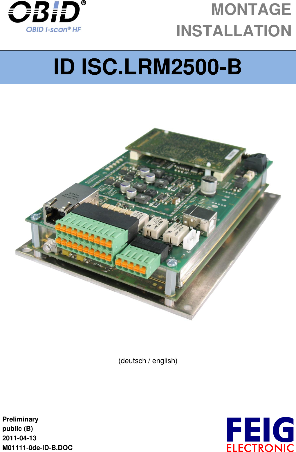
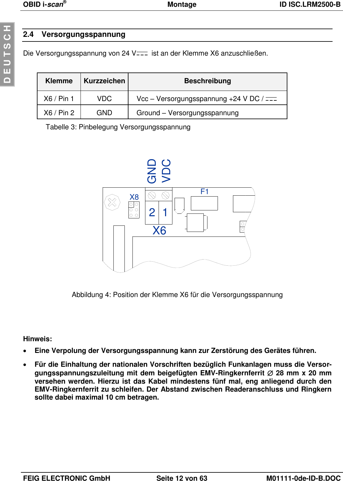
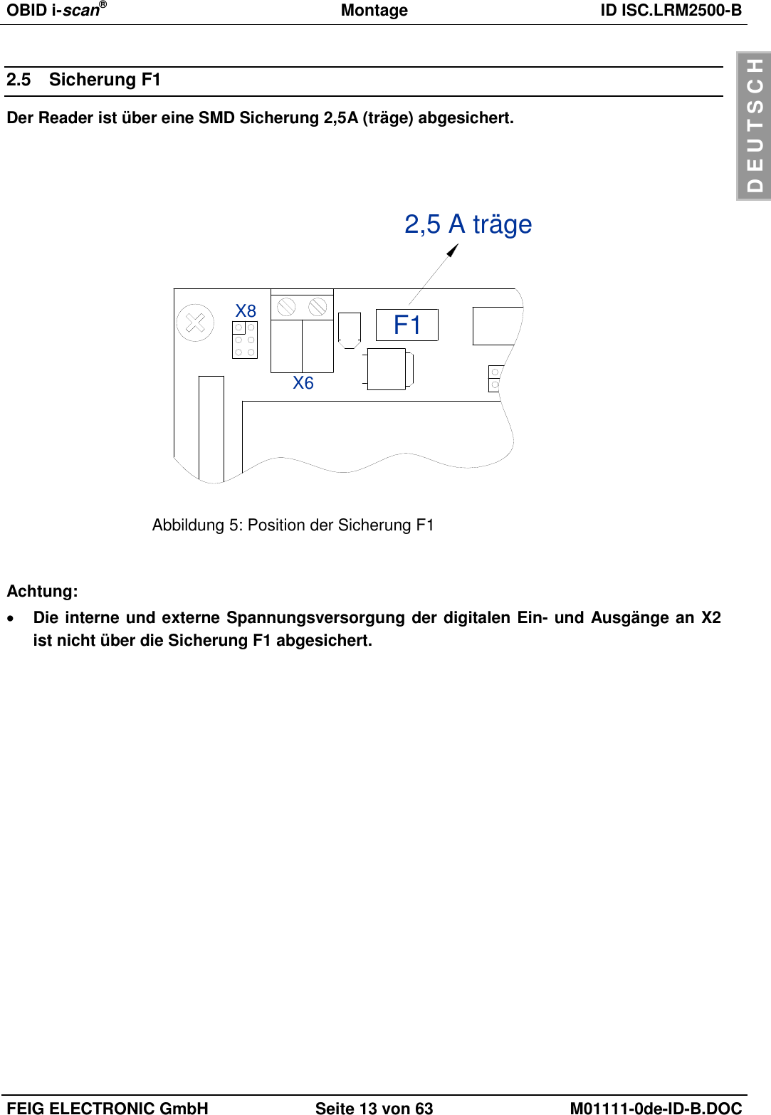
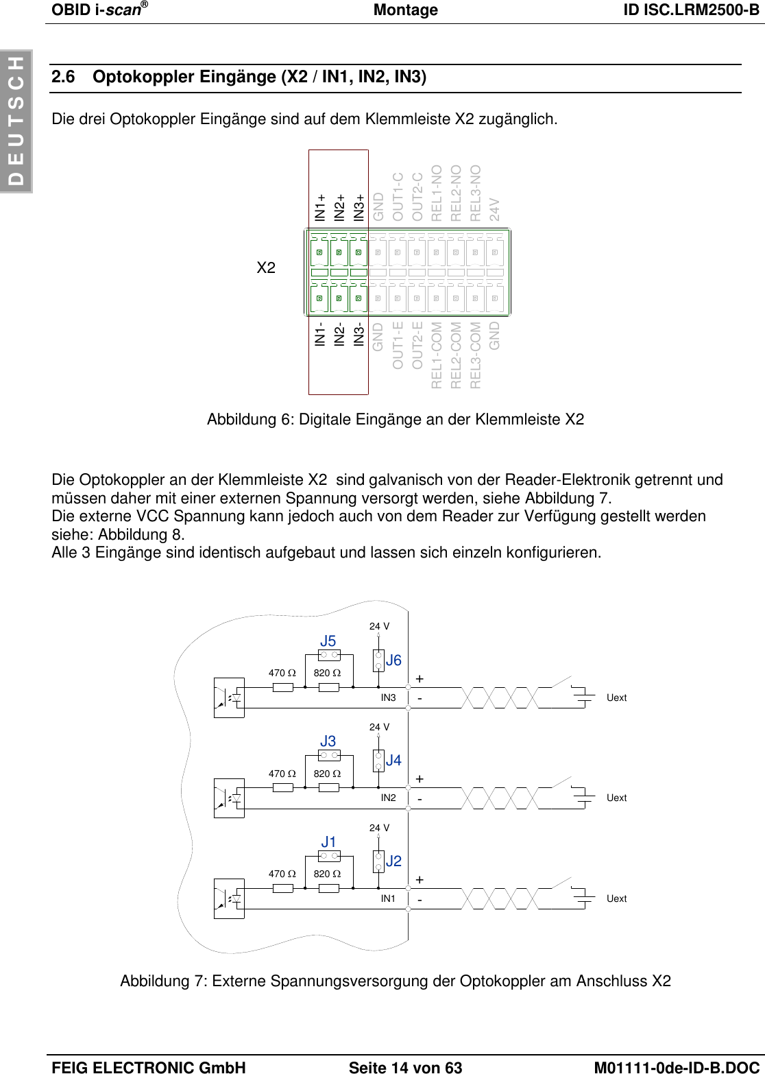
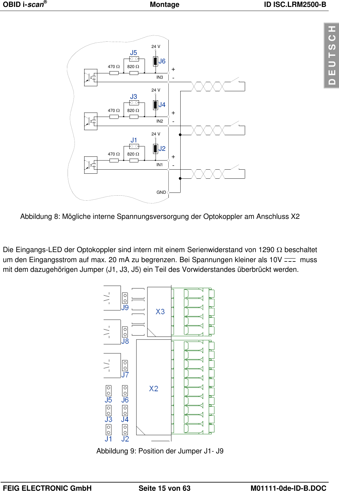
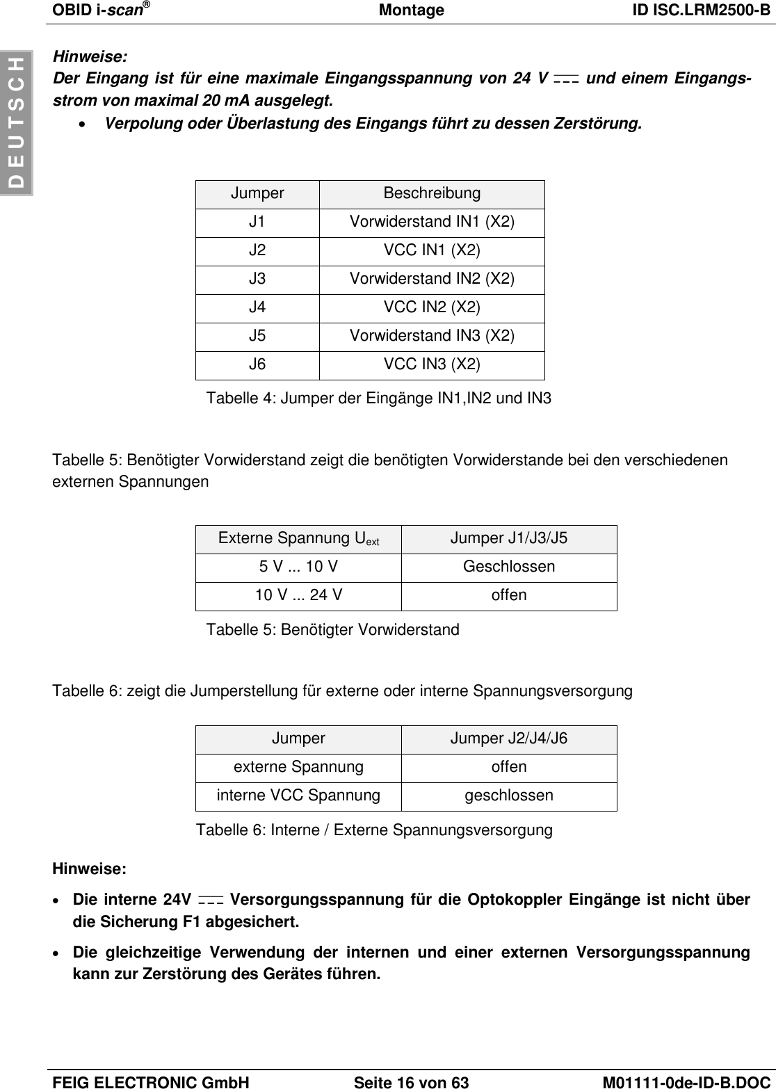
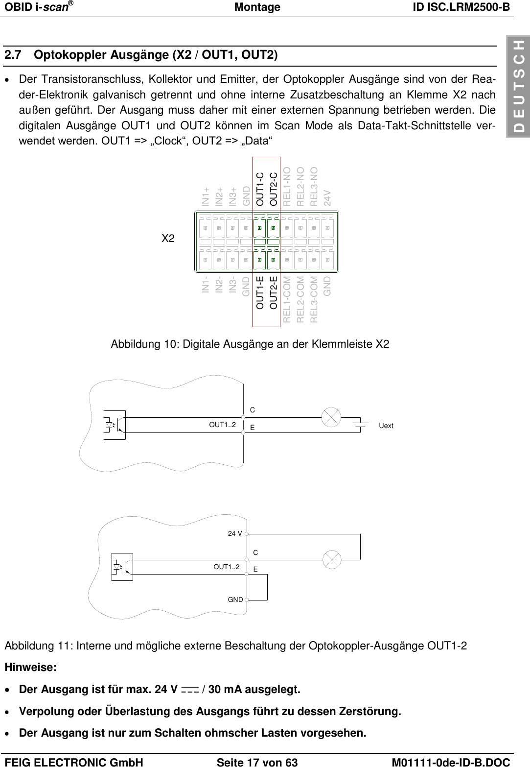
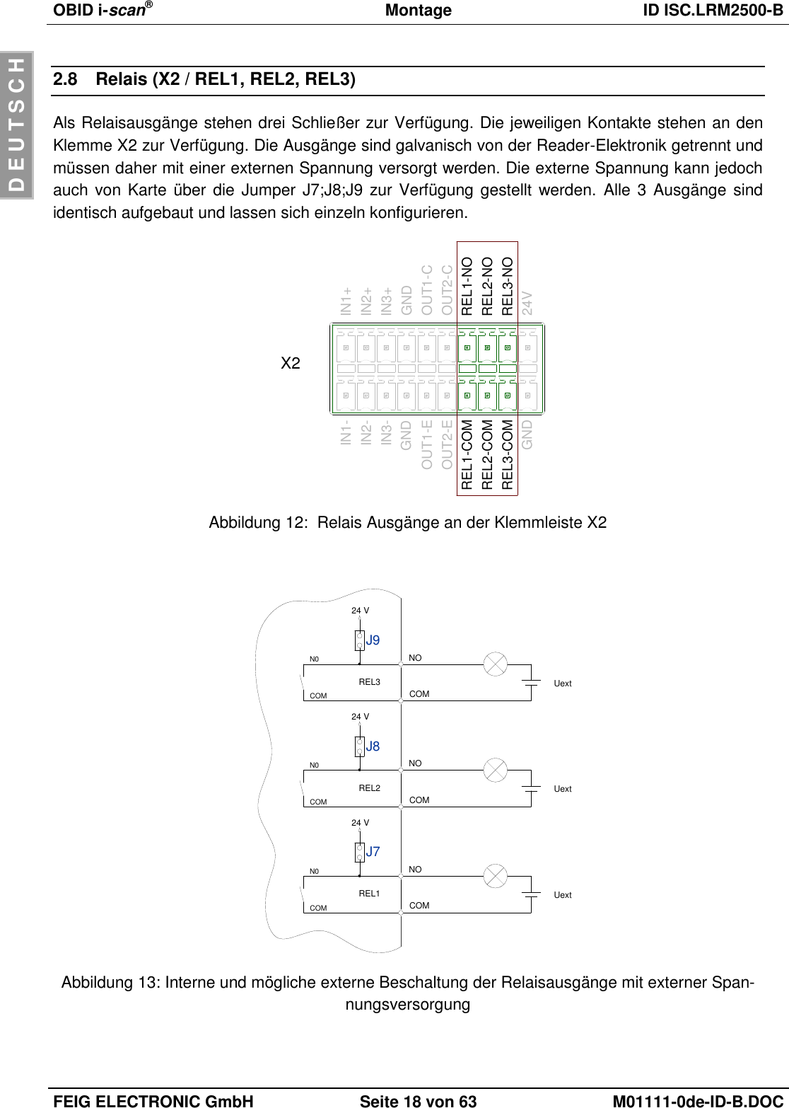
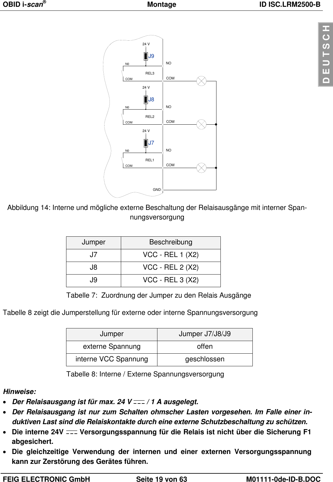
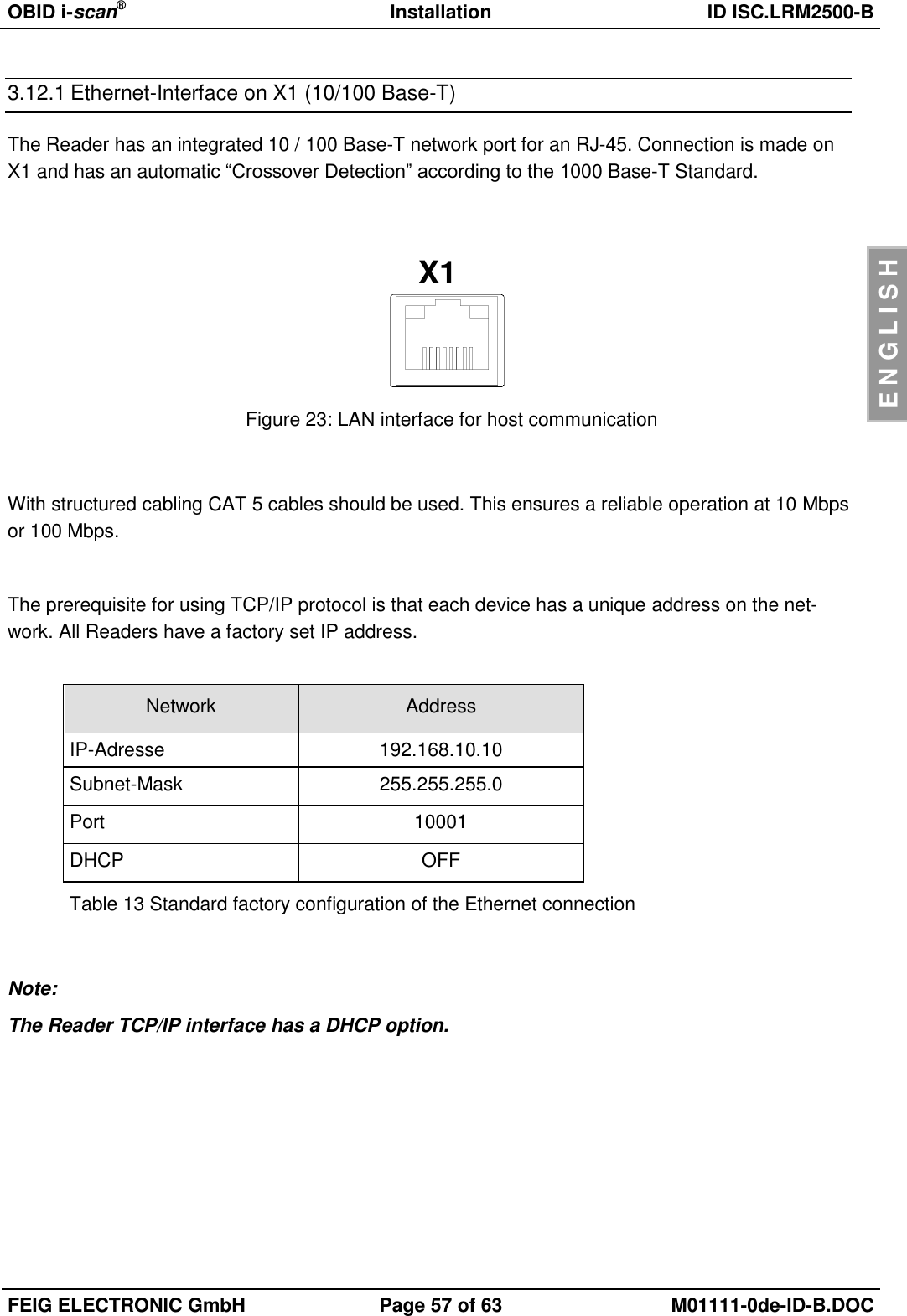
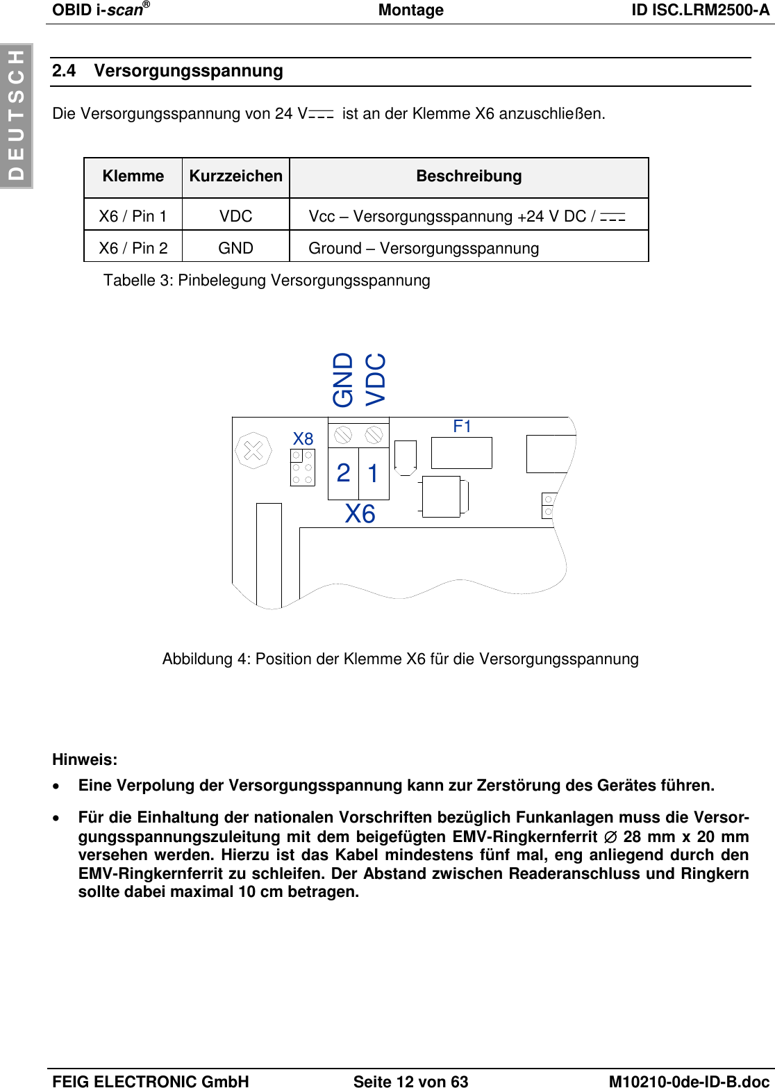
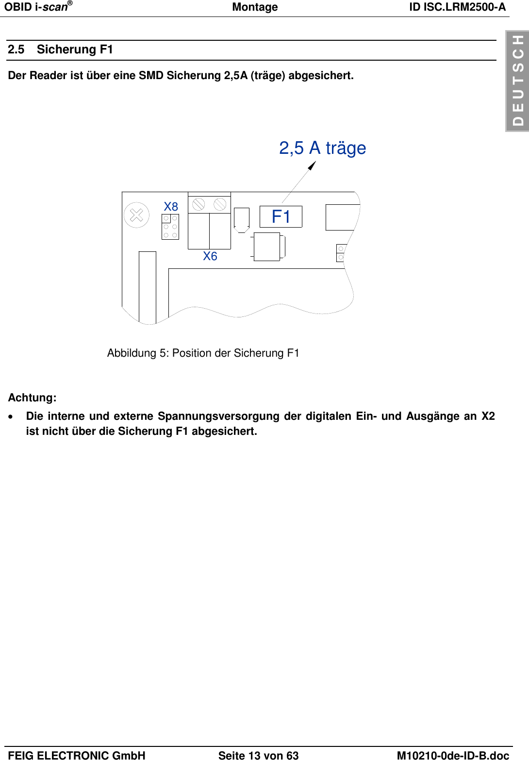
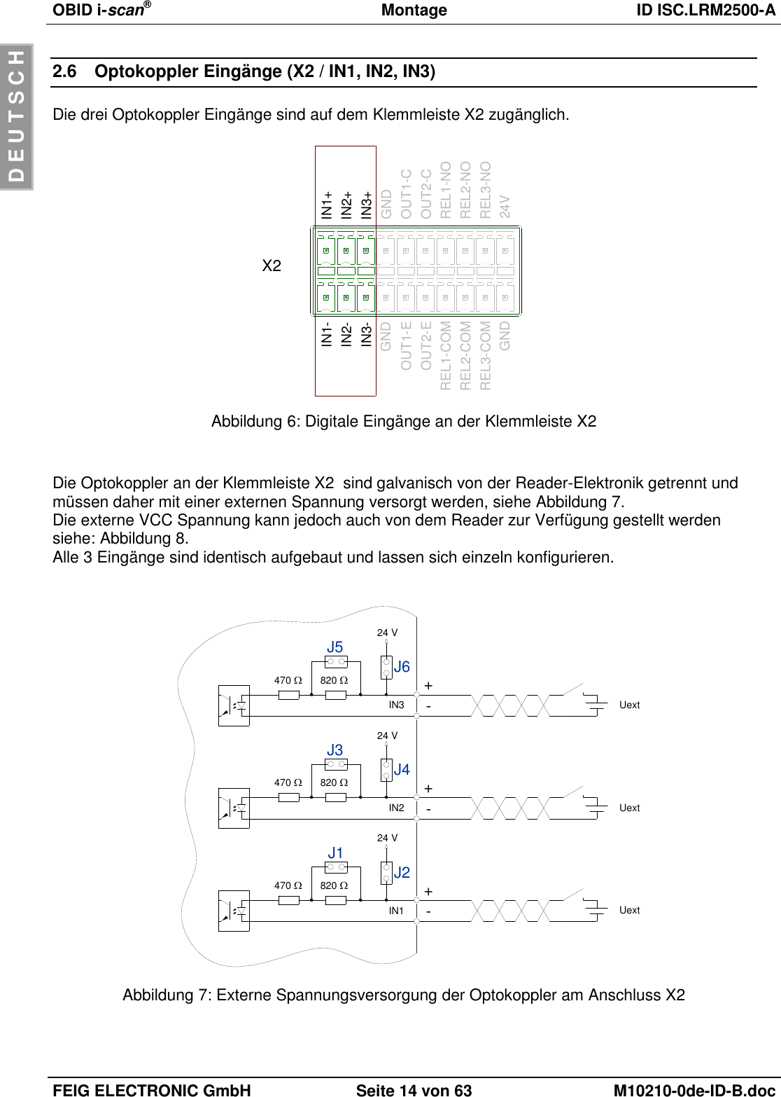
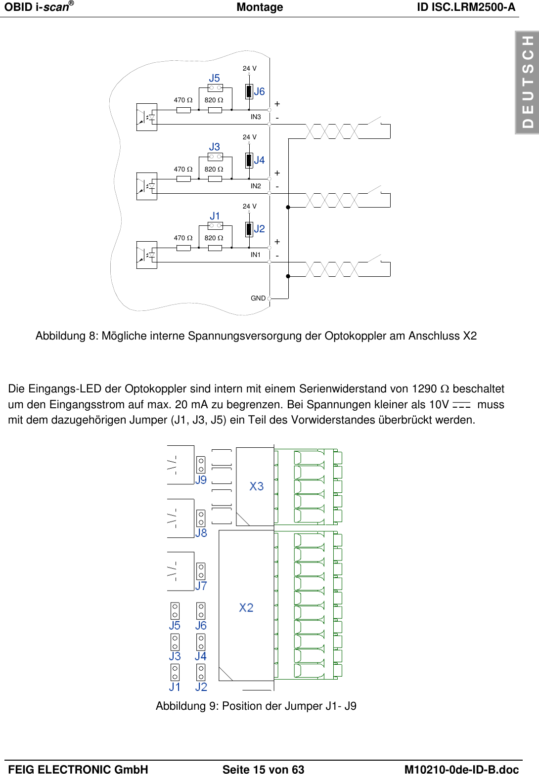
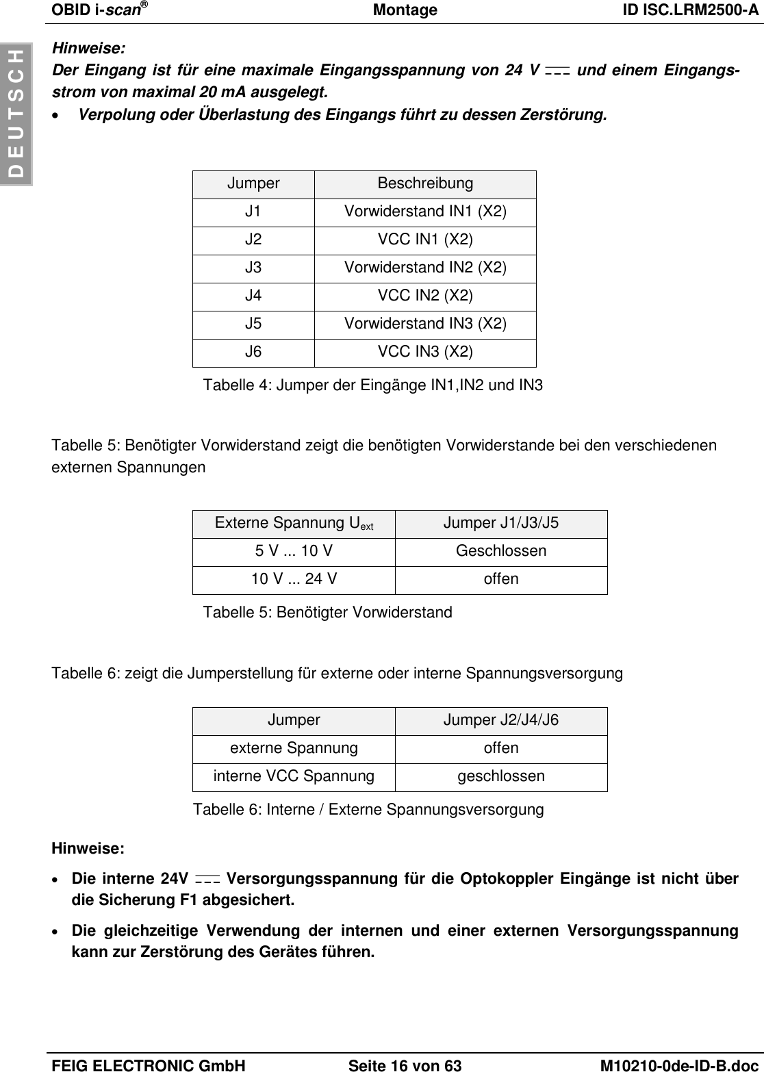
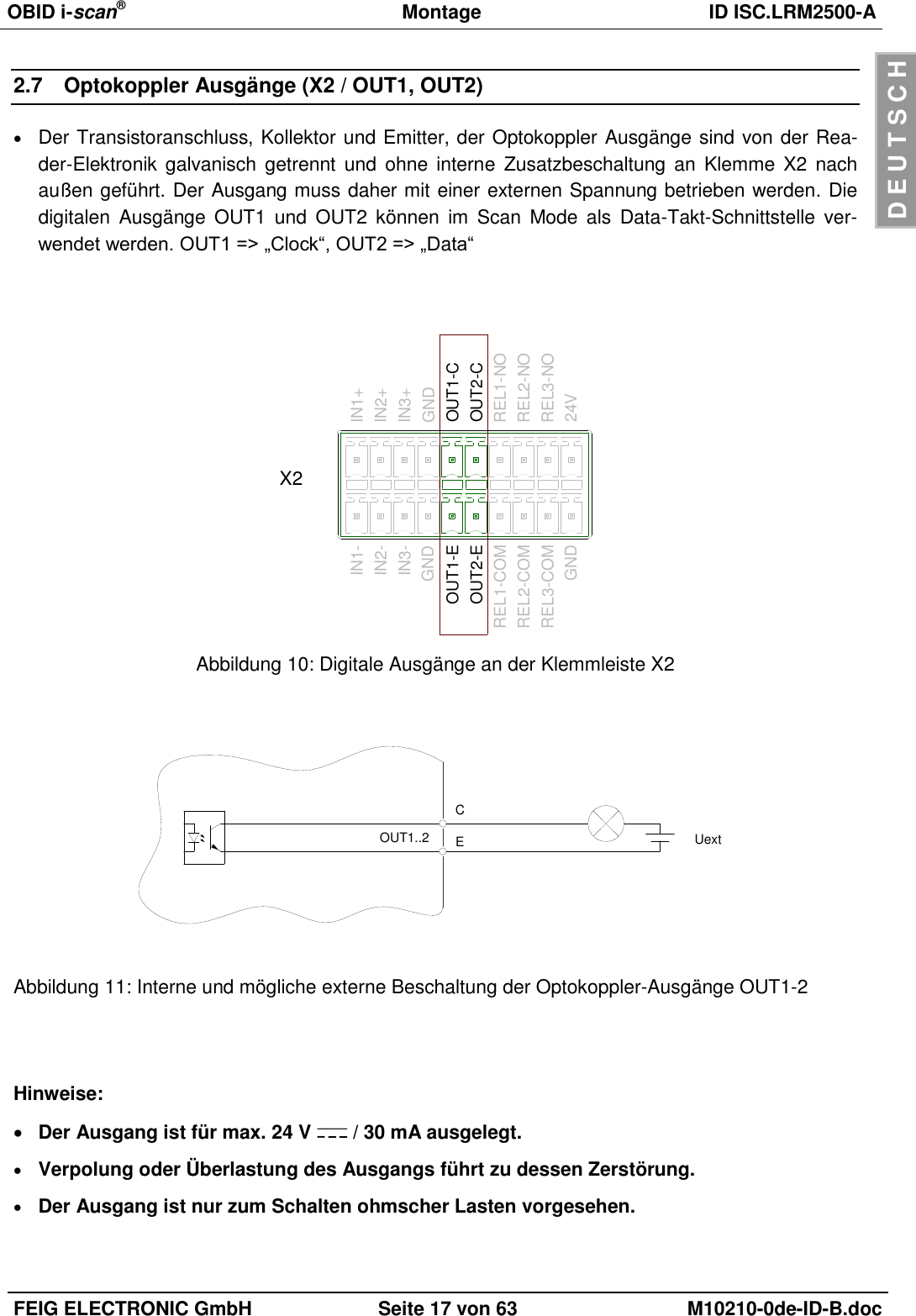
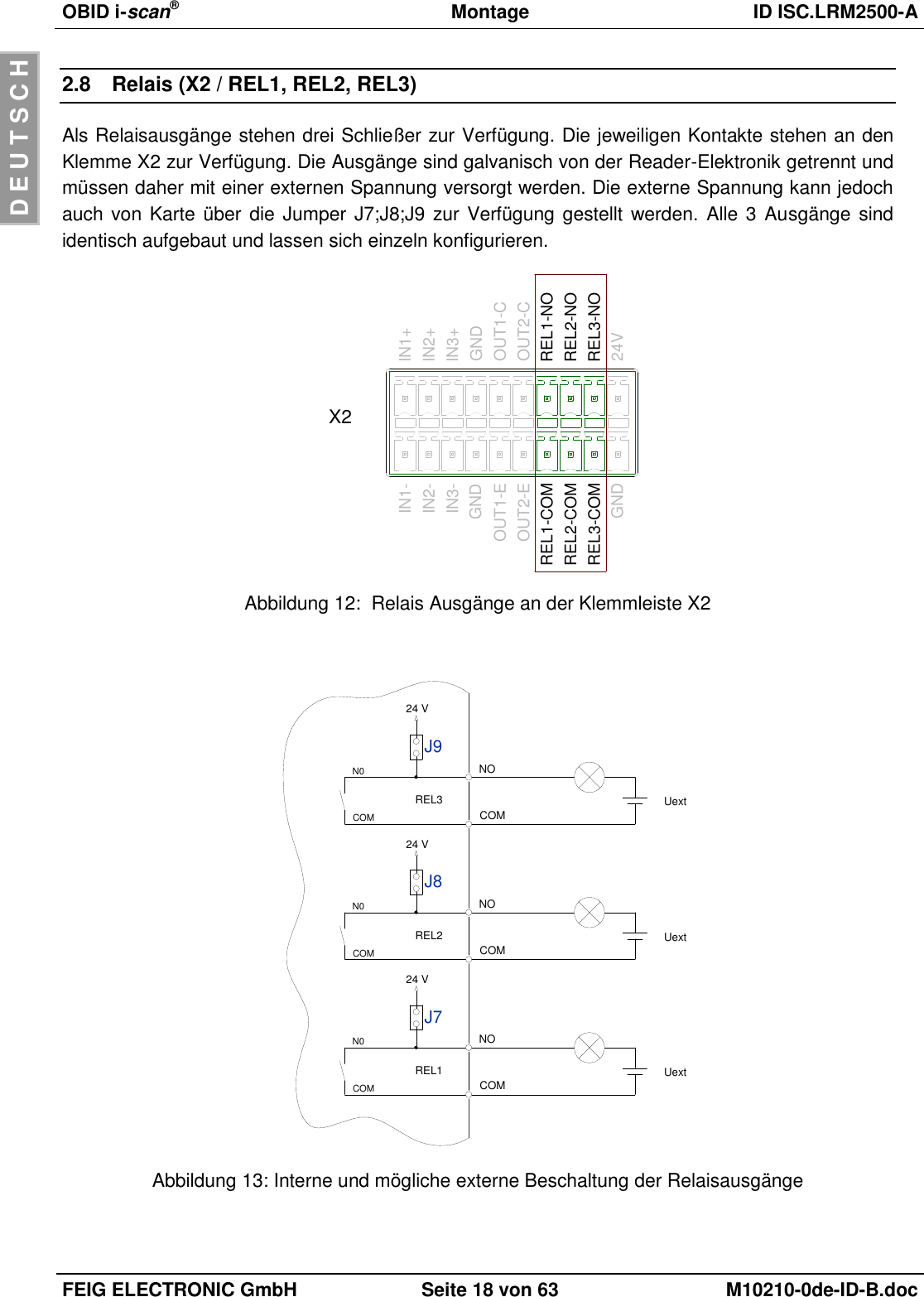
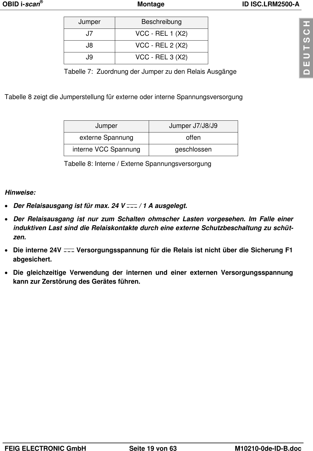
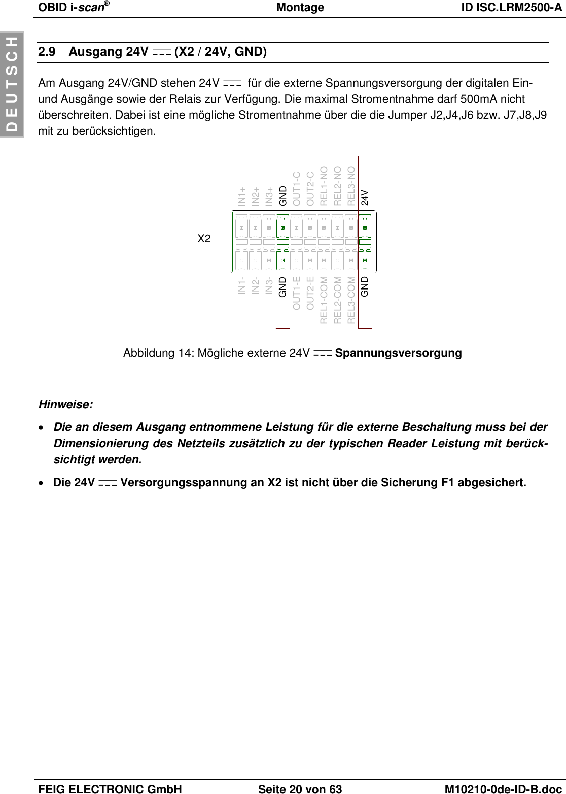
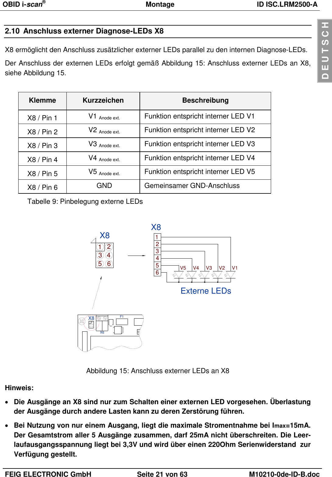
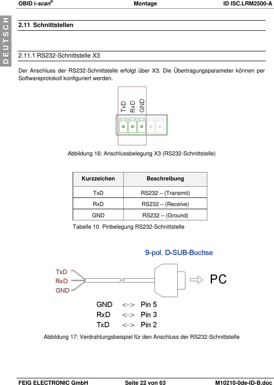
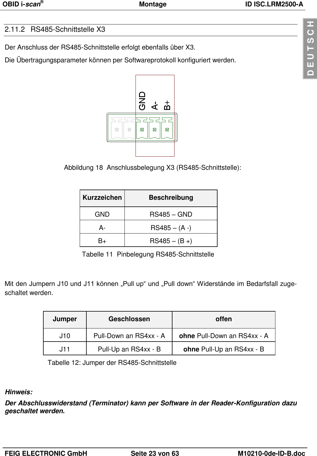
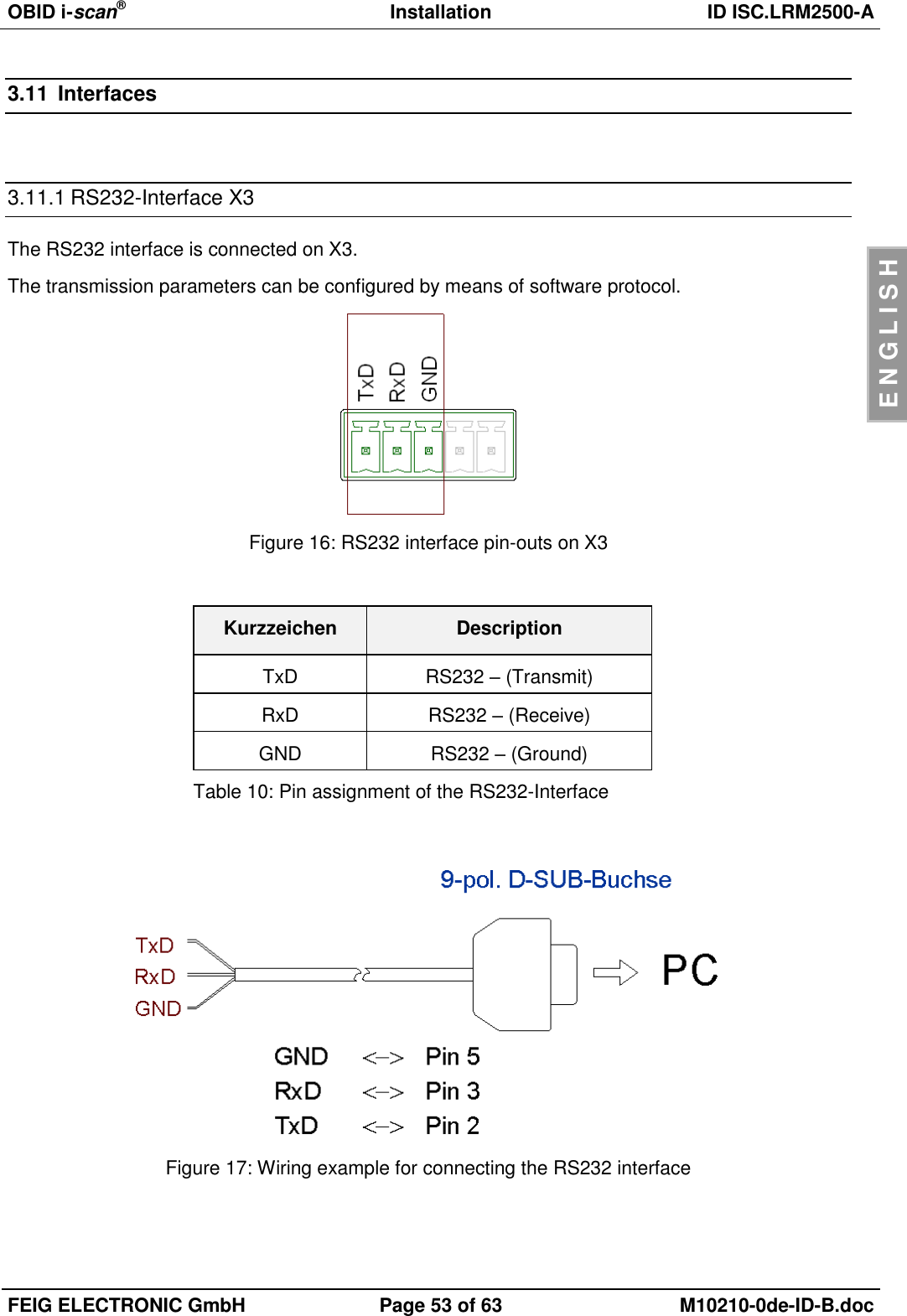
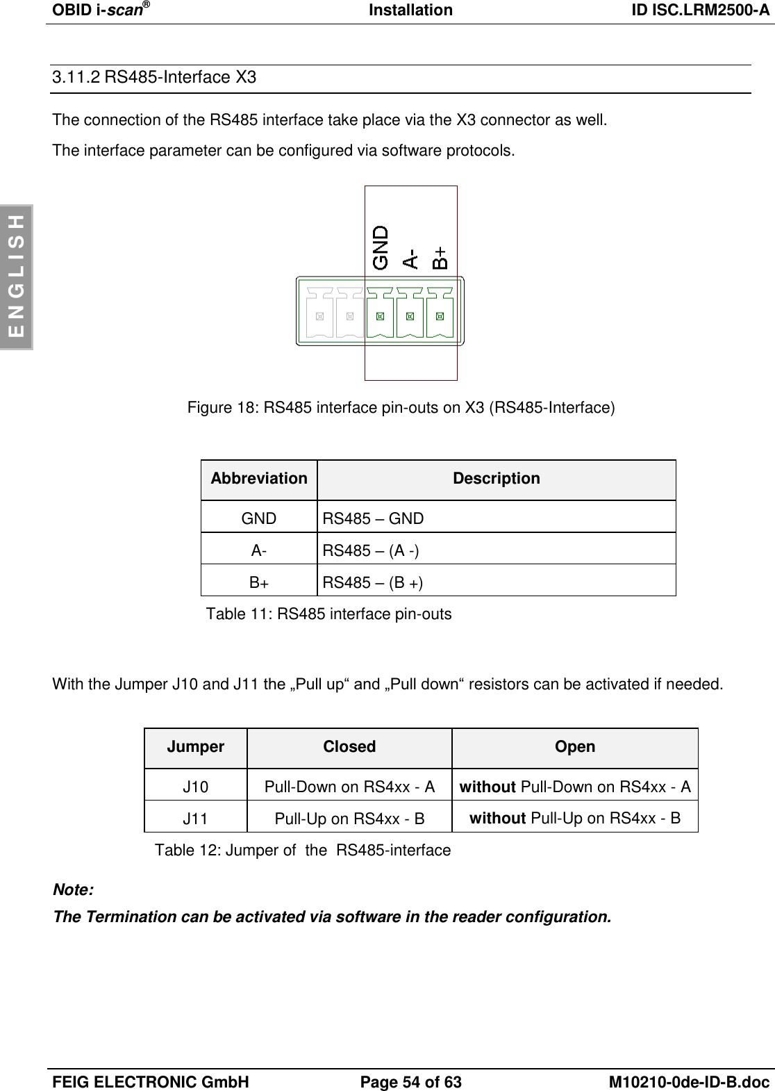
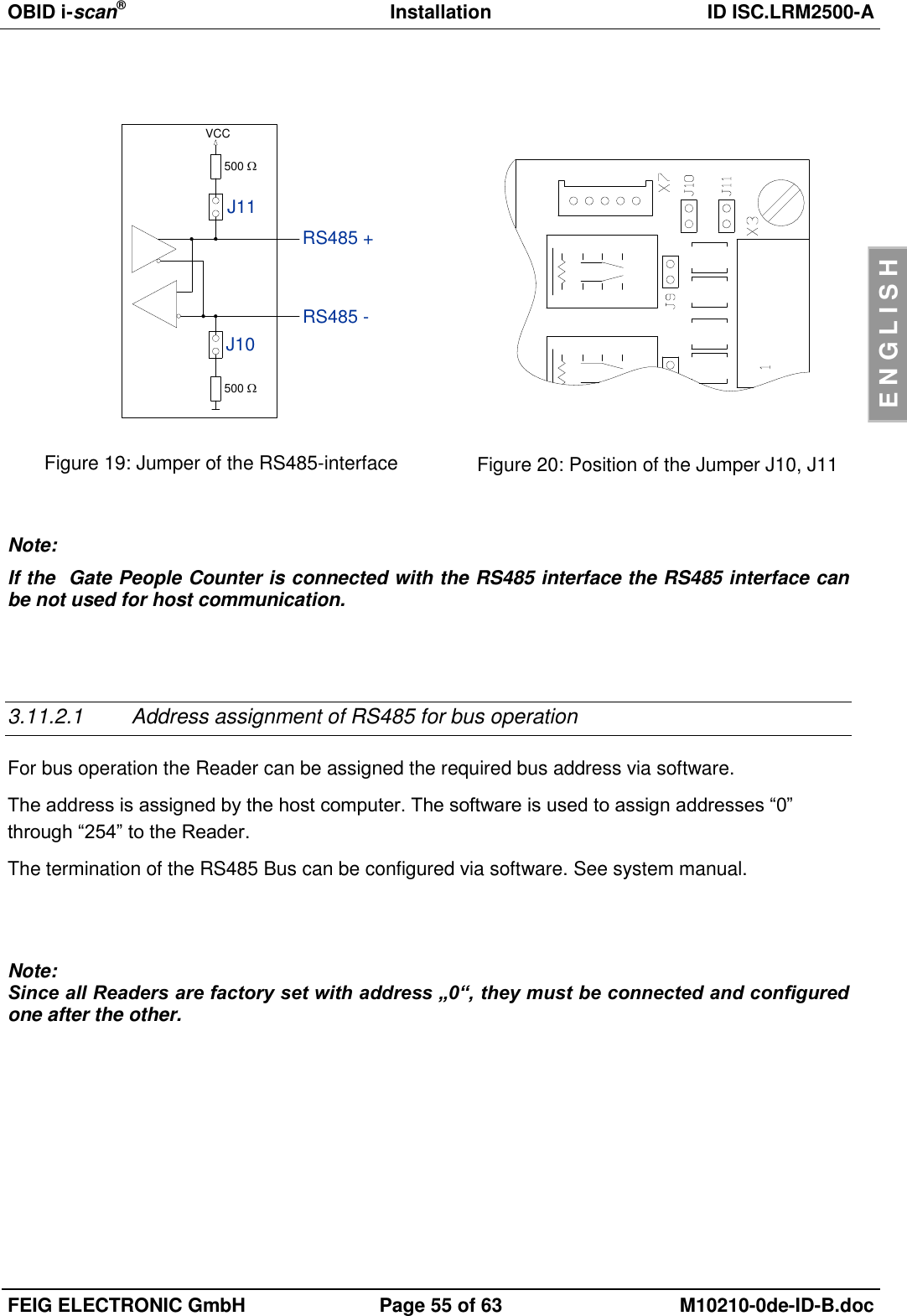
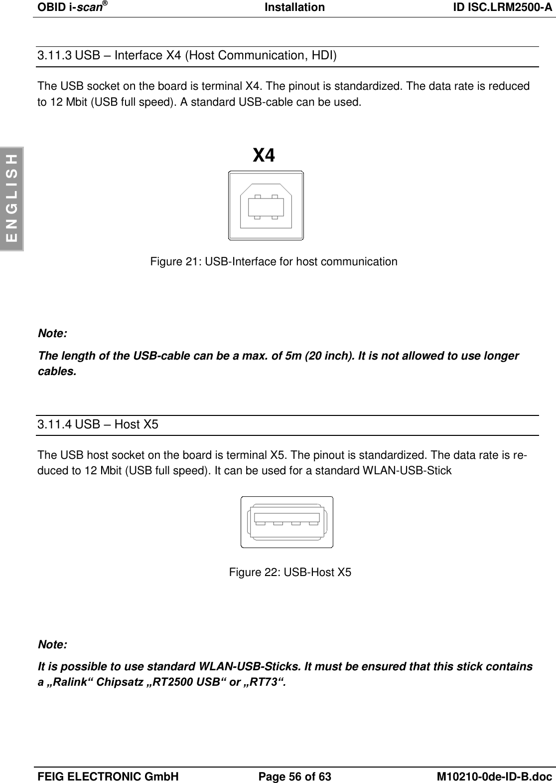
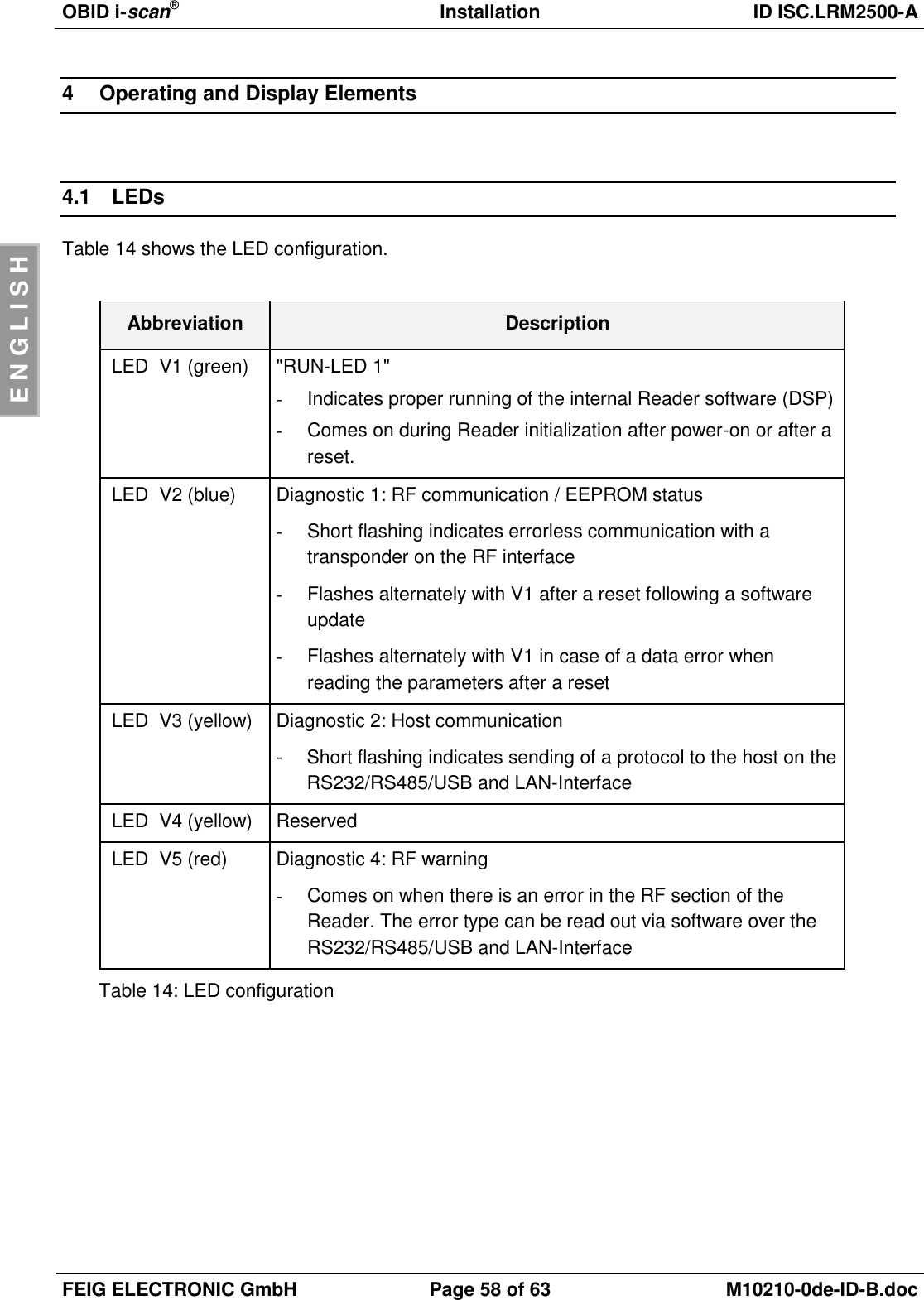
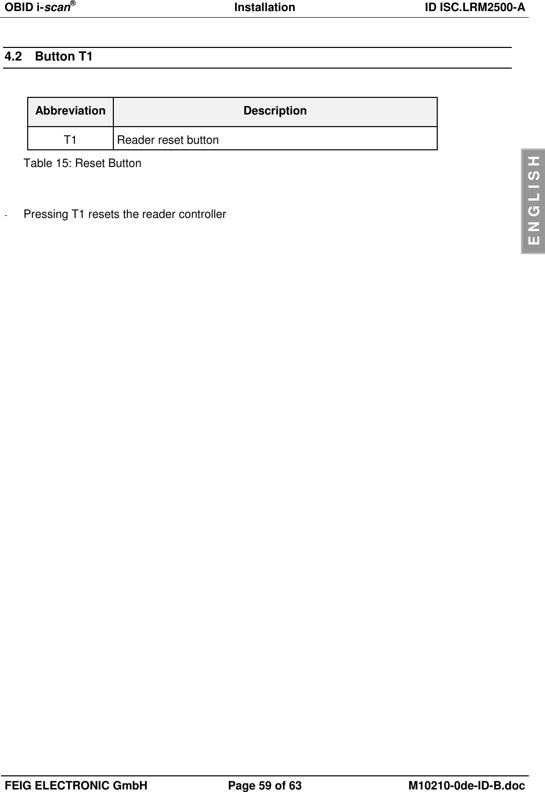
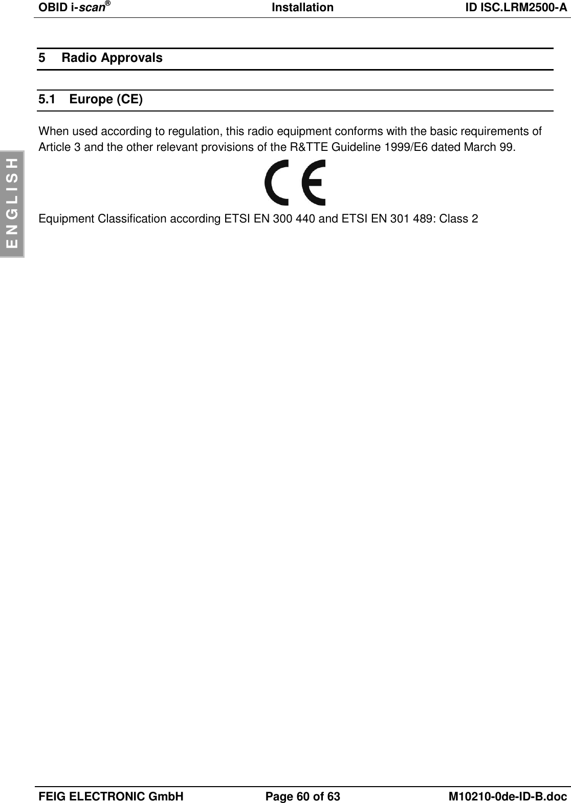
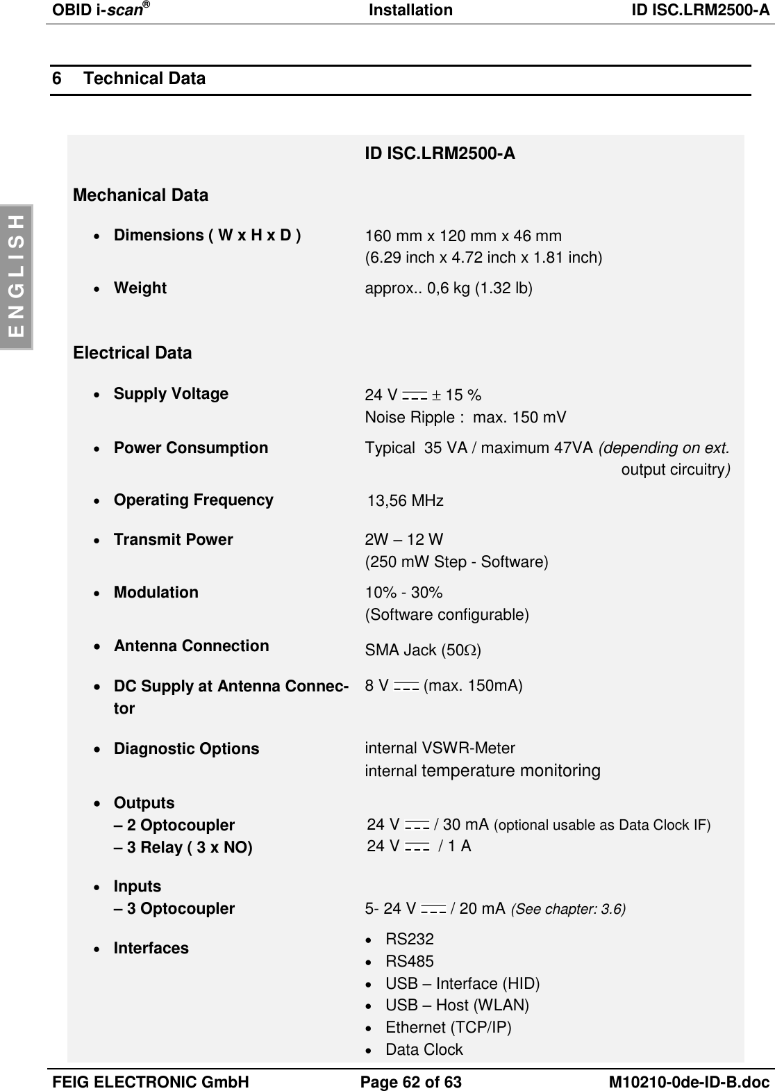
Feig Electronic LRM2500 RFID Reader User Manual
Feig Electronic GmbH RFID Reader
UserManual.wiki
>
Feig Electronic
>
LRM2500 User Manual
>
User Manual
Contents
1.
User Manual
2.
User Manual II
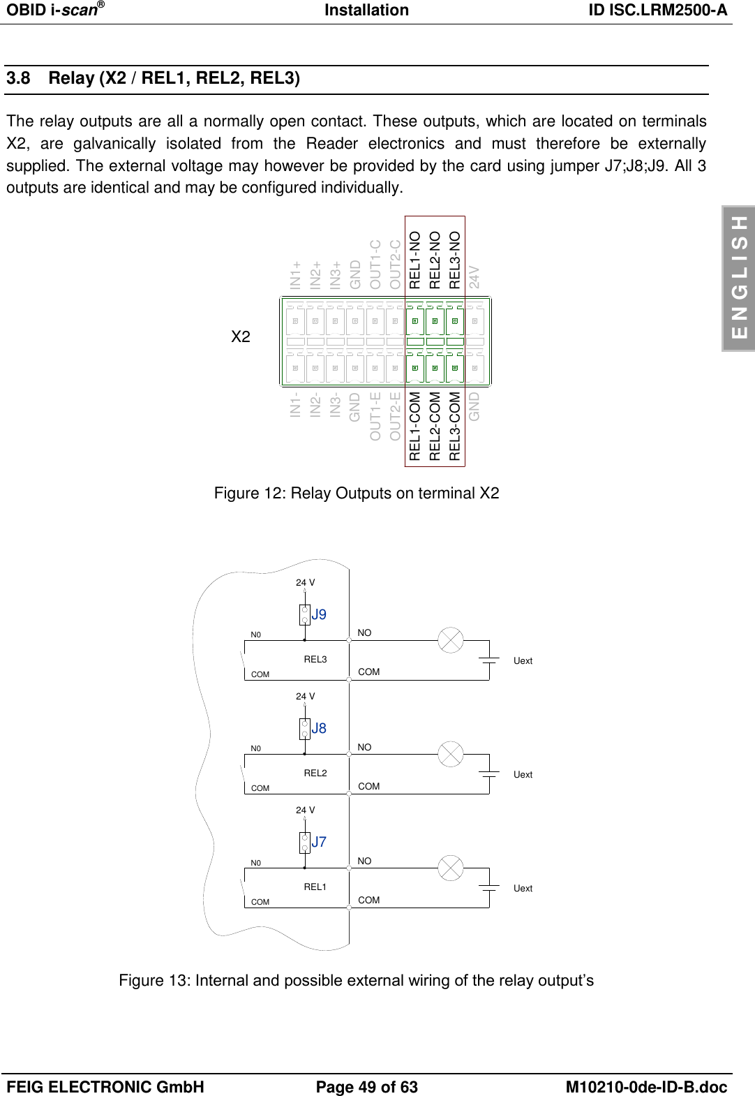
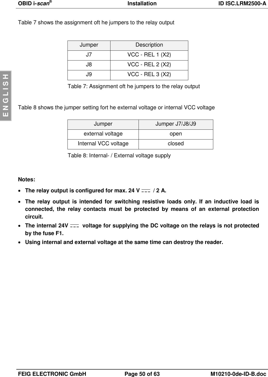
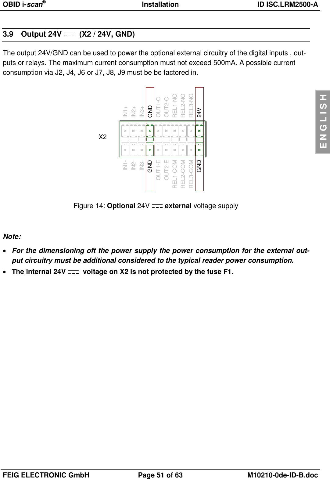
3.
Users Manual
User Manual
Navigation menu
Upload a User Manual
Namespaces
Wiki Guide
HTML
PDF
Info
Views
User Manual
Discussion / Help
Navigation