Feig Electronic LRM2500 RFID Reader User Manual
Feig Electronic GmbH RFID Reader
Contents
- 1. User Manual
- 2. User Manual II
- 3. Users Manual
User Manual

State: 2010-03-01 Vers. no.: 1.10
m. dudde hochfrequenz-technik Rottland 5a D-51429 Bergisch Gladbach/ Germany Tel. +49 2207-96890 Fax +49 2207 968920
Annex no. 5
Functional Description /
User Manual
MONTAGE
INSTALLATION
Preliminary
public (B)
2011-04-13
M01111-0de-ID-B.DOC
ID ISC.LRM2500-B
(deutsch / english)


OBID i-scan®
Montage
ID ISC.LRM2500-B
FEIG ELECTRONIC GmbH
Seite 3 von 63
M01111-0de-ID-B.DOC
D E U T S C H
Hinweis
Copyright 2011 by
FEIG ELECTRONIC GmbH
Lange Straße 4
D-35781 Weilburg-Waldhausen
Tel.: +49 6471 3109-0
http://www.feig.de
Alle früheren Ausgaben verlieren mit dieser Ausgabe ihre Gültigkeit.
Die Angaben in diesem Dokument können ohne vorherige Ankündigung geändert werden.
Weitergabe sowie Vervielfältigung dieses Dokuments, Verwertung und Mitteilung ihres Inhalts sind nicht
gestattet, soweit nicht ausdrücklich zugestanden. Zuwiderhandlung verpflichtet zu Schadenersatz. Alle
Rechte für den Fall der Patenterteilung oder Gebrauchsmuster-Eintragung vorbehalten.
Die Zusammenstellung der Informationen in diesem Dokument erfolgt nach bestem Wissen und Gewissen.
FEIG ELECTRONIC GmbH übernimmt keine Gewährleistung für die Richtigkeit und Vollständigkeit der An-
gaben in diesem Dokument. Insbesondere kann FEIG ELECTRONIC GmbH nicht für Folgeschäden auf
Grund fehlerhafter oder unvollständiger Angaben haftbar gemacht werden. Da sich Fehler, trotz aller Bemü-
hungen nie vollständig vermeiden lassen, sind wir für Hinweise jederzeit dankbar.
Die in diesem Dokument gemachten Installationsempfehlungen gehen von günstigsten Rahmenbedingun-
gen aus. FEIG ELECTRONIC GmbH übernimmt weder Gewähr für die einwandfreie Funktion in system-
fremden Umgebungen, noch für die Funktion eines Gesamtsystems, welches die in diesem Dokument be-
schriebenen Geräte enthält.
FEIG ELECTRONIC weist ausdrücklich darauf hin, dass die in diesem Dokument beschriebenen Geräte
nicht für den Einsatz mit oder in medizinischen Geräten oder für Geräte für lebenserhaltende Maßnahmen
konzipiert sind, bei denen ein Fehler eine Gefahr für menschliches Leben oder für die gesundheitliche Un-
versehrtheit zur Folge haben kann. Der Applikationsdesigner ist dafür verantwortlich geeignete Maßnahmen
zu ergreifen um Gefahren, Schäden oder Verletzungen zu vermeiden.
FEIG ELECTRONIC GmbH übernimmt keine Gewährleistung dafür, dass die in diesem Dokument enthal-
tenden Informationen frei von fremden Schutzrechten sind. FEIG ELECTRONIC GmbH erteilt mit diesem
Dokument keine Lizenzen auf eigene oder fremde Patente oder andere Schutzrechte.
OBID® und OBID i-scan® ist ein eingetragenes Warenzeichen der FEIG ELECTRONIC GmbH
my-d® ist ein eingetragenes Warenzeichen der Infineon Technologies AG
I-CODE® und mifare® ist ein eingetragenes Warenzeichen der Philips Electronics N.V.
Tag-it ist ein Warenzeichen der Texas Instruments Incorporated

OBID i-scan®
Montage
ID ISC.LRM2500-B
FEIG ELECTRONIC GmbH
Seite 4 von 63
M01111-0de-ID-B.DOC
D E U T S C H
Inhalt
Sicherheits- und Warnhinweise - vor Inbetriebnahme unbedingt lesen 6
1 Leistungsmerkmale der Readerfamilie ID ISC.LRM2500 7
1.1 Leistungsmerkmale .................................................................................................... 7
1.2 Verfügbare Readervarianten ...................................................................................... 7
2 Montage und Anschluss 8
2.1 Montage ....................................................................................................................... 8
2.2 Anschlussklemmen .................................................................................................. 10
2.3 Antennenanschluss .................................................................................................. 11
2.4 Versorgungsspannung ............................................................................................. 12
2.5 Sicherung F1 ............................................................................................................. 13
2.6 Optokoppler Eingänge (X2 / IN1, IN2, IN3) .............................................................. 14
2.7 Optokoppler Ausgänge (X2 / OUT1, OUT2) ............................................................. 17
2.8 Relais (X2 / REL1, REL2, REL3) ............................................................................... 18
2.9 Ausgang 24V (X2 / 24V, GND) ............................................................................ 20
2.10 Anschluss externer Diagnose-LEDs X8 .................................................................. 21
2.11 Schnittstellen ............................................................................................................ 22
2.11.1 RS232-Schnittstelle X3 .......................................................................................... 22
2.11.2 RS485-Schnittstelle X3 .......................................................................................... 23
2.12 USB – Schnittstelle X4 (Host Kommunikation) ....................................................... 25
2.12.1 Ethernet-Schnittstelle an X1 (10/100 Base-T) ........................................................ 26
3 Bedien- und Anzeigeelemente 27
3.1 LEDs .......................................................................................................................... 27
3.2 Taster T1.................................................................................................................... 28
4 Funkzulassungen 29

OBID i-scan®
Montage
ID ISC.LRM2500-B
FEIG ELECTRONIC GmbH
Seite 5 von 63
M01111-0de-ID-B.DOC
D E U T S C H
4.1 Europa (CE) ............................................................................................................... 29
4.2 USA (FCC) und Kanada (IC) ..................................................................................... 30
5 Technische Daten 31

OBID i-scan®
Montage
ID ISC.LRM2500-B
FEIG ELECTRONIC GmbH
Seite 6 von 63
M01111-0de-ID-B.DOC
D E U T S C H
Sicherheits- und Warnhinweise - vor Inbetriebnahme unbedingt lesen
Das Gerät darf nur für den vom Hersteller vorgesehenen Zweck verwendet werden.
Die Bedienungsanleitung ist zugriffsfähig aufzubewahren und jedem Benutzer auszuhändigen.
Unzulässige Veränderungen und die Verwendung von Ersatzteilen und Zusatzeinrichtungen,
die nicht vom Hersteller des Gerätes verkauft oder empfohlen werden, können Brände, elektri-
sche Schläge und Verletzungen verursachen. Solche Maßnahmen führen daher zu einem
Ausschluss der Haftung und der Hersteller übernimmt keine Gewährleistung.
Für das Gerät gelten die Gewährleistungsbestimmungen des Herstellers in der zum Zeitpunkt
des Kaufs gültigen Fassung. Für eine ungeeignete, falsche manuelle oder automatische Ein-
stellung von Parametern für ein Gerät bzw. ungeeignete Verwendung eines Gerätes wird keine
Haftung übernommen.
Reparaturen dürfen nur vom Hersteller durchgeführt werden.
Anschluss-, Inbetriebnahme-, Wartungs-, und sonstige Arbeiten am Gerät dürfen nur von Elekt-
rofachkräften mit einschlägiger Ausbildung erfolgen.
Alle Arbeiten am Gerät und dessen Aufstellung müssen in Übereinstimmung mit den nationa-
len elektrischen Bestimmungen und den örtlichen Vorschriften durchgeführt werden.
Beim Arbeiten an dem Gerät müssen die jeweils gültigen Sicherheitsvorschriften beachtet wer-
den.
Vor Berührung der Platinen ist stets die Spannungsversorgung abzuschalten und durch Nach-
messen sicherzustellen, dass das Gerät spannungslos ist. Das Verlöschen einer Betriebsan-
zeige ist kein Indikator dafür, dass das Gerät vom Netz getrennt und spannungslos ist.
Besonderer Hinweis für Träger von Herzschrittmachern:
Obwohl dieses Gerät die zulässigen Grenzwerte für elektromagnetische Felder nicht über-
schreitet, sollten Sie einen Mindestabstand von 25 cm zwischen der angeschlossenen Antenne
und Ihrem Herzschrittmacher einhalten und sich nicht für längere Zeit in unmittelbarer Nähe
des Geräts bzw. der Antenne aufhalten.

OBID i-scan®
Montage
ID ISC.LRM2500-B
FEIG ELECTRONIC GmbH
Seite 7 von 63
M01111-0de-ID-B.DOC
D E U T S C H
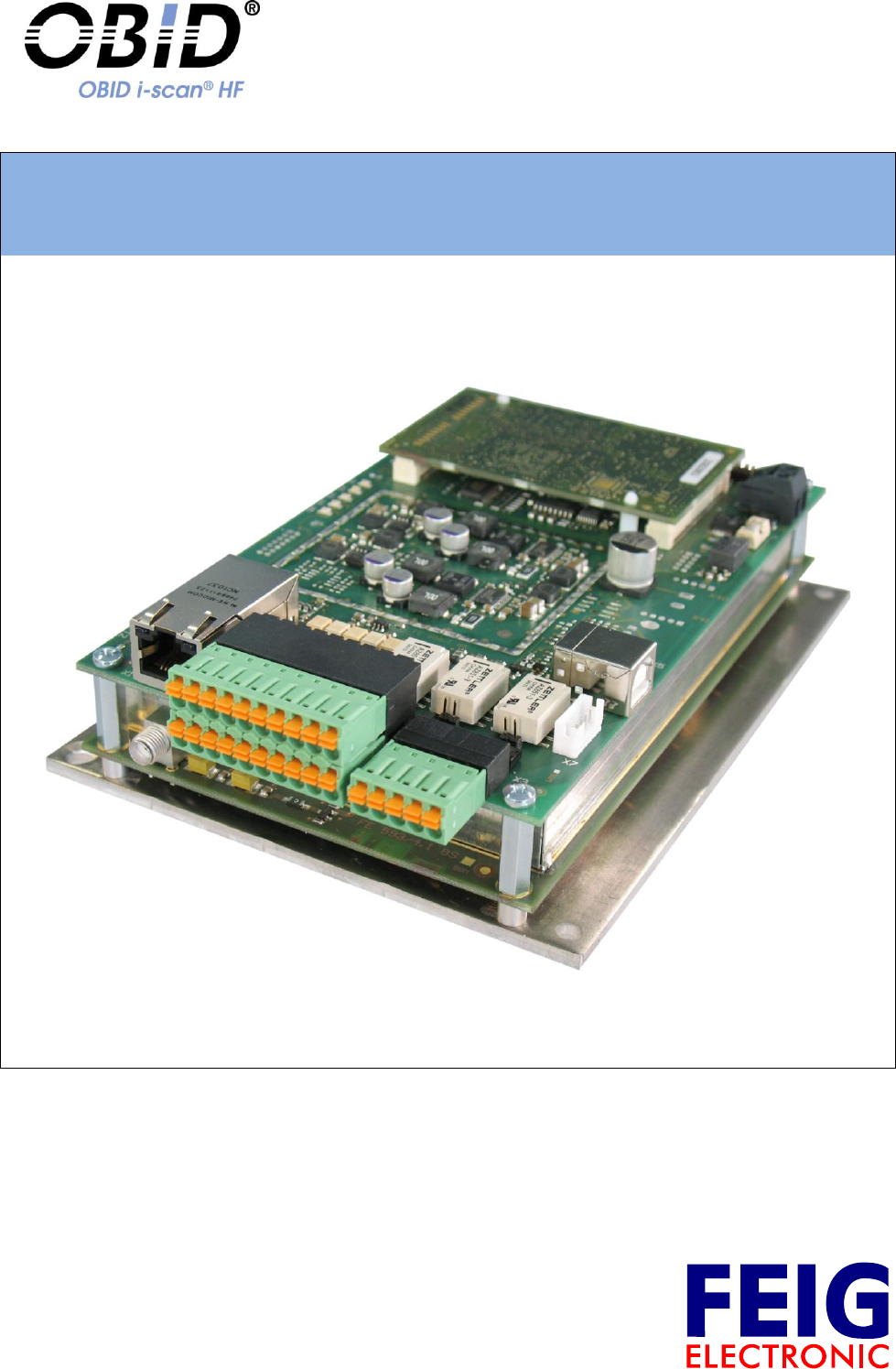
1 Leistungsmerkmale der Readerfamilie ID ISC.LRM2500
1.1 Leistungsmerkmale
Der Reader ist für das Lesen von passiven Datenträgern, sogenannten „Smart Labels“, mit einer
Betriebsfrequenz von 13,56 MHz entwickelt. Zum Betrieb ist es notwendig eine geeignete externe
Antenne an dem Anschluss „ANT1“ anzuschließen.
1.2 Verfügbare Readervarianten
Folgende Readervarianten sind z.Z. verfügbar:
Reader
Beschreibung
ID ISC.LRM2500-B
Modulvariante mit RS232/485- / USB- / LAN-Interface
Tabelle 1: Verfügbare Readervarianten
OBID i-scan®
Montage
ID ISC.LRM2500-B
FEIG ELECTRONIC GmbH
Seite 8 von 63
M01111-0de-ID-B.DOC
D E U T S C H
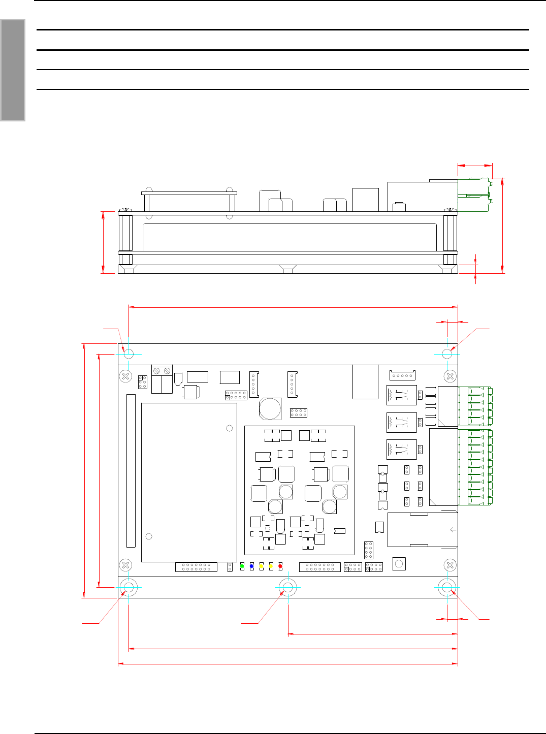
2 Montage und Anschluss
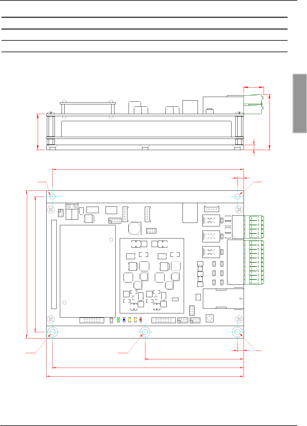
2.1 Montage
Das Reader-Modul ist für die Montage auf einem Kühlkörper konzipiert. Für die Befestigung befin-
det sich in den vier Ecken der Trägerplatte jeweils eine Bohrung mit dem 4,5 mm (siehe Abbil-
dung 1)
29
T1
X1
J2
J4
J1
J3
J6
J7
J5
X2
V4
V3
V2V1 V5
45
X8
X6
F1
J8
J9 X3
X4
X7
16,3
4
120
110
ø 4,5 mm*
160
155
80
ø 4,5 mm* ø 4,5 mm*
5
ø 4,5 mm
155
GND
VDC
ø 4,5 mm
5
Abbildung 1 Maßzeichnung des Reader-Moduls ID ISC.LRM2500 mit Montageplatte

OBID i-scan®
Montage
ID ISC.LRM2500-B
FEIG ELECTRONIC GmbH
Seite 9 von 63
M01111-0de-ID-B.DOC
D E U T S C H
Für die Ausnutzung der vollen Leistungsfähigkeit des Reader-Moduls sollte der verwendete Kühl-
körper einen Wärmewiderstand RThK von maximal 1,0 K/W besitzen. Bei der Montage des Reader-
Moduls auf den Kühlkörper ist auf einen möglichst geringen Wärmeübergangswiderstand zwischen
Trägerplatte und Kühlkörper zu achten. Die Verwendung von Wärmeleitpaste wird empfohlen.
Bei korrekt abgestimmter Antenne und ausreichender Luftkonvektion entlang der Montageplatte
kann der ID ISC.LRM2500 auch ohne zusätzlichen Kühlkörper bis zu einer Leistung von 2 W be-
trieben werden. Hierbei ist jedoch zu beachten, dass eine Verstimmung der Antenne zu einer zu-
sätzlichen Erwärmung des Readers führt. In diesem Falle regelt der Reader seine Ausgangsleis-
tung zurück bis die obere Grenztemperatur seiner Endstufe wieder unterschritten wird.
OBID i-scan®
Montage
ID ISC.LRM2500-B
FEIG ELECTRONIC GmbH
Seite 10 von 63
M01111-0de-ID-B.DOC
D E U T S C H
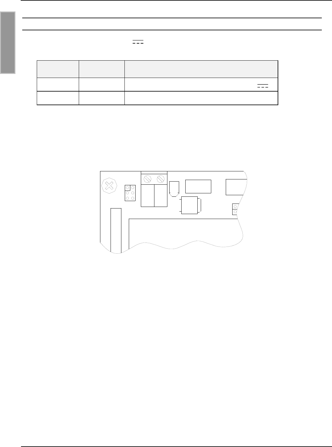
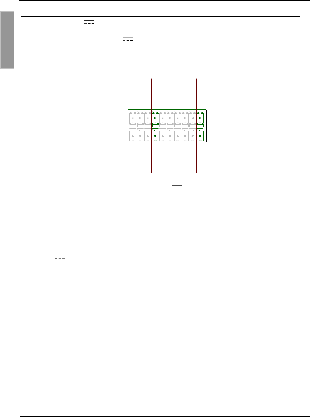
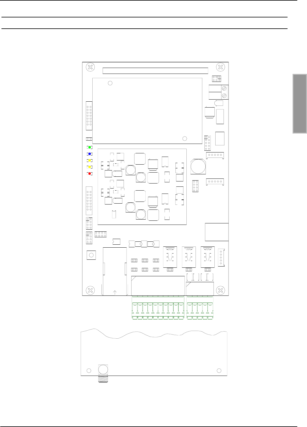
2.2 Anschlussklemmen
Abbildung 2 zeigt die Anschlussklemmen und Bedienelemente des ID ISC.LRM2500.
X8
X6
F1
J8
J9 X3
X4
X7
T1
X1
J2
J4
J1
J3
J6
J7
J5
X2
ANT1
V4
V3
V2V1 V5
Abbildung 2 Anschlussklemmen des Readers
OBID i-scan®
Montage
ID ISC.LRM2500-B
FEIG ELECTRONIC GmbH
Seite 11 von 63
M01111-0de-ID-B.DOC
D E U T S C H
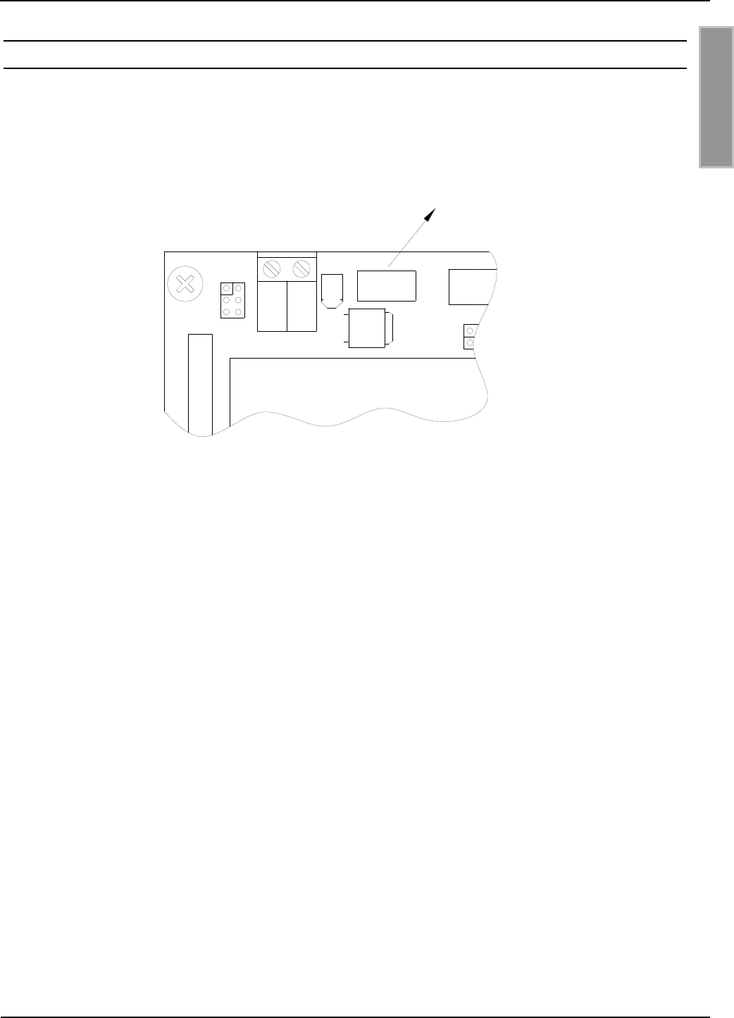
2.3 Antennenanschluss
Zum Anschluss der Antenne an den ID ISC.LRM2500 befindet sich auf der unteren Leiterplatte die
SMA-Buchse "ANT1".
Aktive externe Funktionseinheiten (z.B. ID ISC.DAT) können zusätzlich über den Antennenan-
schluss mit 8 V versorgt werden. Diese kann per Software Konfiguration aktiviert werden.
Die maximale Stromaufnahme darf dabei 150mA nicht überschreiten. Diese Leistung muss zusätz-
lich zur Gesamtleistungsaufnahme des Readers mit berücksichtigt werden.
Das maximale Anzugsdrehmoment der SMA-Buchse beträgt 0,45 Nm.
Achtung:
Höhere Anzugsdrehmomente führen zur Zerstörung der Buchse.
Klemme
Beschreibung
ANT1
Anschluss der externen Antenne
(Eingangsimpedanz 50)
Tabelle 2: Anschluss der externen Antenne
Hinweise:
Das Stehwellenverhältnis VSWR der Antenne sollte den Wert 1,3 nicht überschreiten.
Für das Erreichen optimaler Lesereichweiten müssen die Koaxialkabel zwischen Reader
und Antenne definierte Längen haben. Für alle Antennen von der Firma FEIG
ELECTRONIC GmbH und für alle Antennen welche mit den Abgleichplatinen (z.B. ID
ISC.DAT, ID ISC.MAT-B und ID ISC.MAT-S) von FEIG ELECTRONIC GmbH aufgebaut
sind ist die optimale Länge des Koaxialkabels 1,35 m (Artikel Nr. 1654.004.00.00, Be-
zeichnung ID ISC.ANT.C-B). Siehe auch Montageanleitung Power Splitter ID ISC.ANT.PS-
B und ID ISC.ANT.MUX.
Die optimale Betriebsgüte der Antenne sollte im Bereich QB = 10...30 liegen. Zur Ermitt-
lung der Betriebsgüte muss die Antenne mit einer 50-Quelle, z.B. einem Network Ana-
lyzer oder einem Frequenzgenerator, versorgt werden.
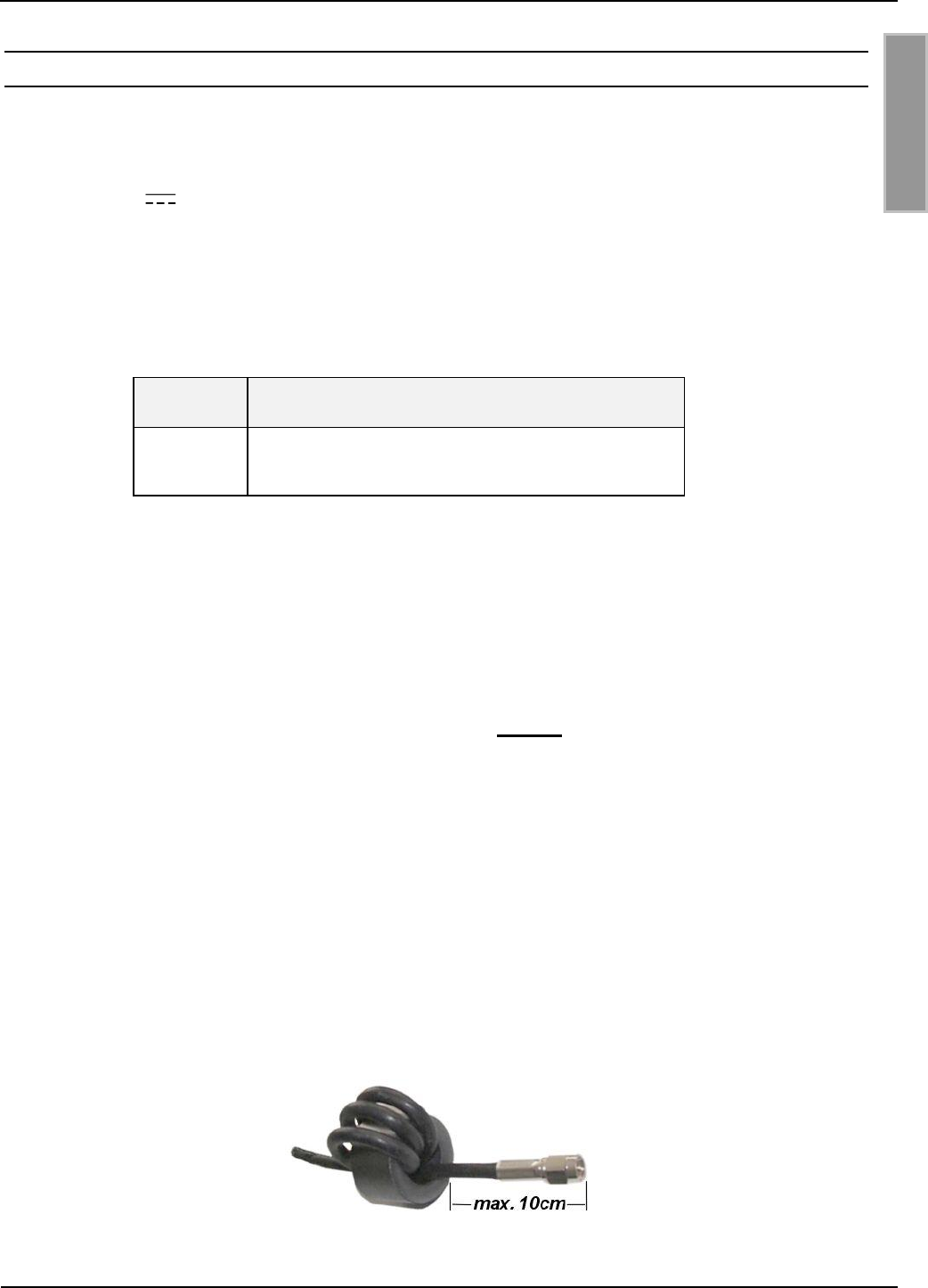
Zur Vermeidung extern eingekoppelter Störungen muss die Antennenzuleitung dem bei-
gefügten EMV-Ringkernferrit 28 mm x 20 mm versehen werden. Hierzu ist die Anten-
nenzuleitung mindestens vier mal, eng anliegend durch den EMV-Ringkernferrit zu füh-
ren. Der Abstand zwischen Readeranschluss ANT1 und Ringkern sollte dabei maximal
10 cm betragen (siehe Abbildung 3).
Beim Anschluss der Antenne ist darauf zu achten, dass diese die zulässigen Grenzwerte
der nationalen Vorschriften bezüglich Funkanlagen nicht überschreitet.
Abbildung 3 Antennenkabel mit EMV-Ringkernferrit
OBID i-scan®
Montage
ID ISC.LRM2500-B
FEIG ELECTRONIC GmbH
Seite 12 von 63
M01111-0de-ID-B.DOC
D E U T S C H
2.4 Versorgungsspannung
Die Versorgungsspannung von 24 V ist an der Klemme X6 anzuschließen.
Klemme
Kurzzeichen
Beschreibung
X6 / Pin 1
VDC
Vcc – Versorgungsspannung +24 V DC /
X6 / Pin 2
GND
Ground – Versorgungsspannung
Tabelle 3: Pinbelegung Versorgungsspannung
GND
VDC
X8
X6
F1
1
2
Abbildung 4: Position der Klemme X6 für die Versorgungsspannung
Hinweis:
Eine Verpolung der Versorgungsspannung kann zur Zerstörung des Gerätes führen.
Für die Einhaltung der nationalen Vorschriften bezüglich Funkanlagen muss die Versor-
gungsspannungszuleitung mit dem beigefügten EMV-Ringkernferrit 28 mm x 20 mm
versehen werden. Hierzu ist das Kabel mindestens fünf mal, eng anliegend durch den
EMV-Ringkernferrit zu schleifen. Der Abstand zwischen Readeranschluss und Ringkern
sollte dabei maximal 10 cm betragen.
OBID i-scan®
Montage
ID ISC.LRM2500-B
FEIG ELECTRONIC GmbH
Seite 13 von 63
M01111-0de-ID-B.DOC
D E U T S C H
2.5 Sicherung F1
Der Reader ist über eine SMD Sicherung 2,5A (träge) abgesichert.
Achtung:
Die interne und externe Spannungsversorgung der digitalen Ein- und Ausgänge an X2
ist nicht über die Sicherung F1 abgesichert.
X8
X6
F1
2,5 A träge
Abbildung 5: Position der Sicherung F1
OBID i-scan®
Montage
ID ISC.LRM2500-B
FEIG ELECTRONIC GmbH
Seite 14 von 63
M01111-0de-ID-B.DOC
D E U T S C H
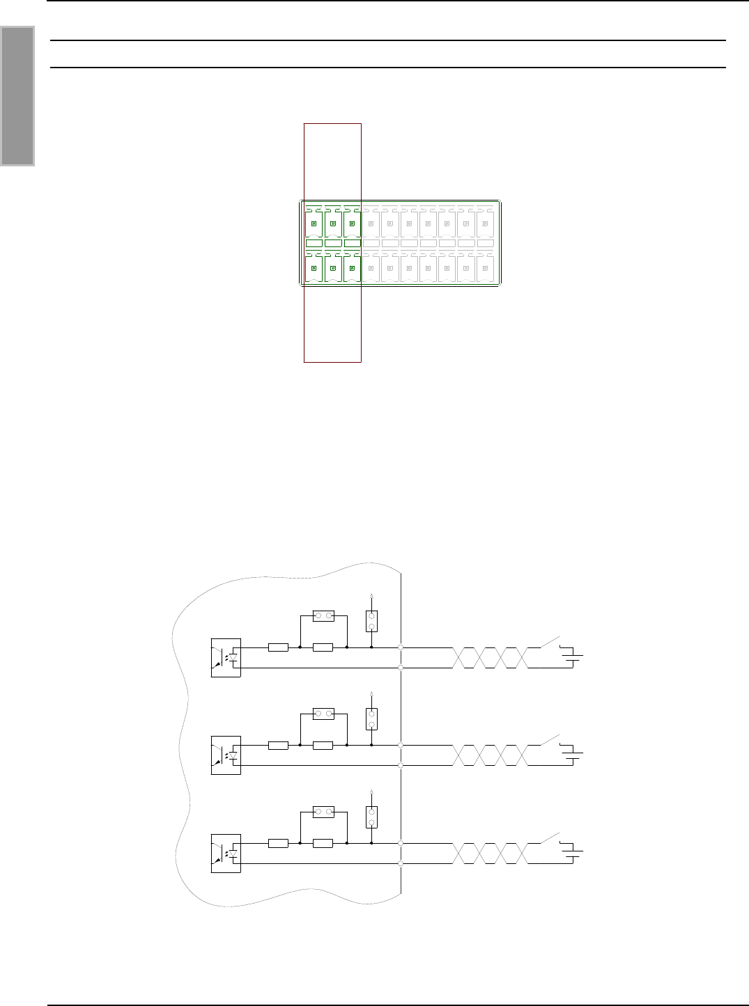
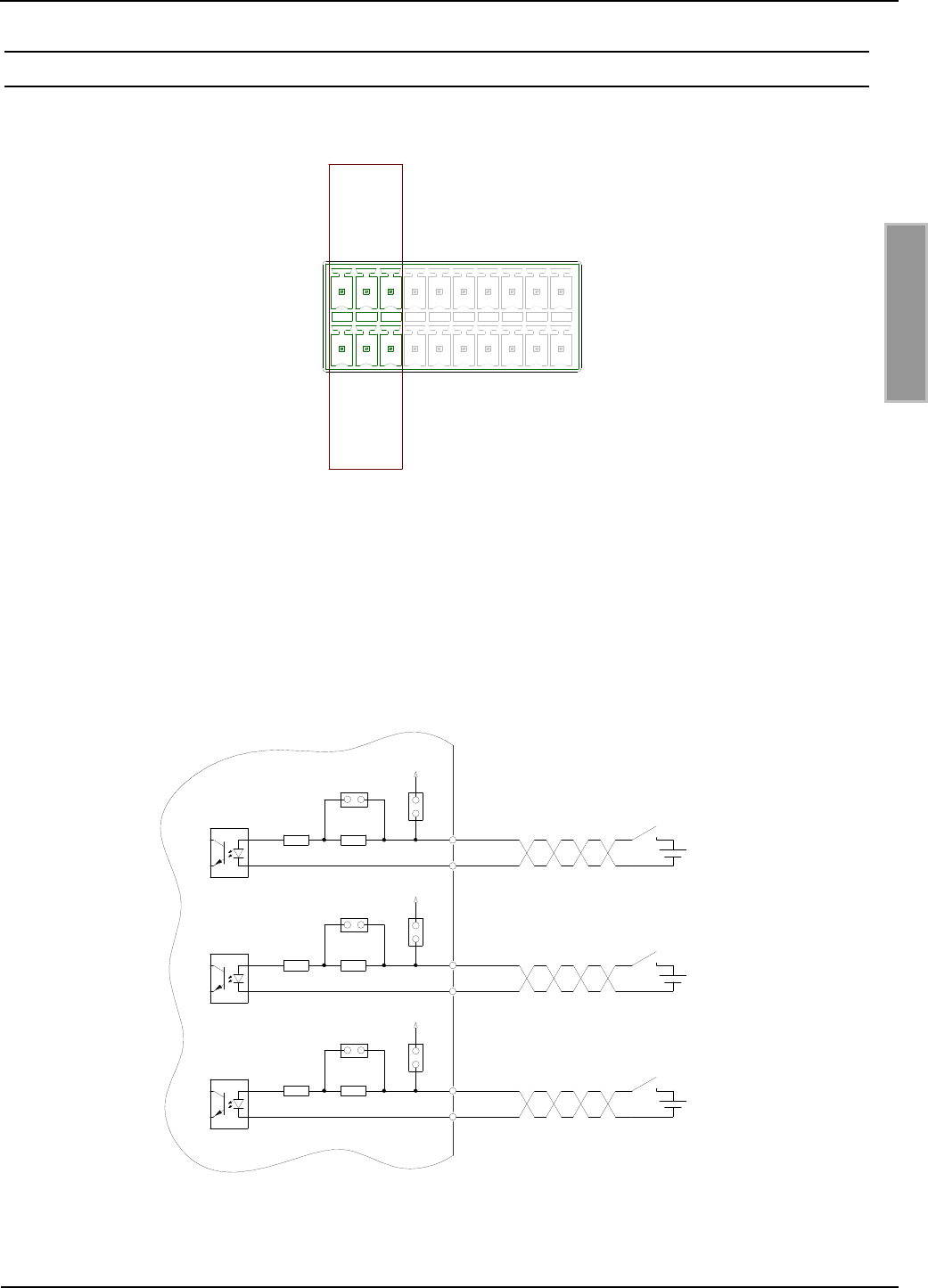
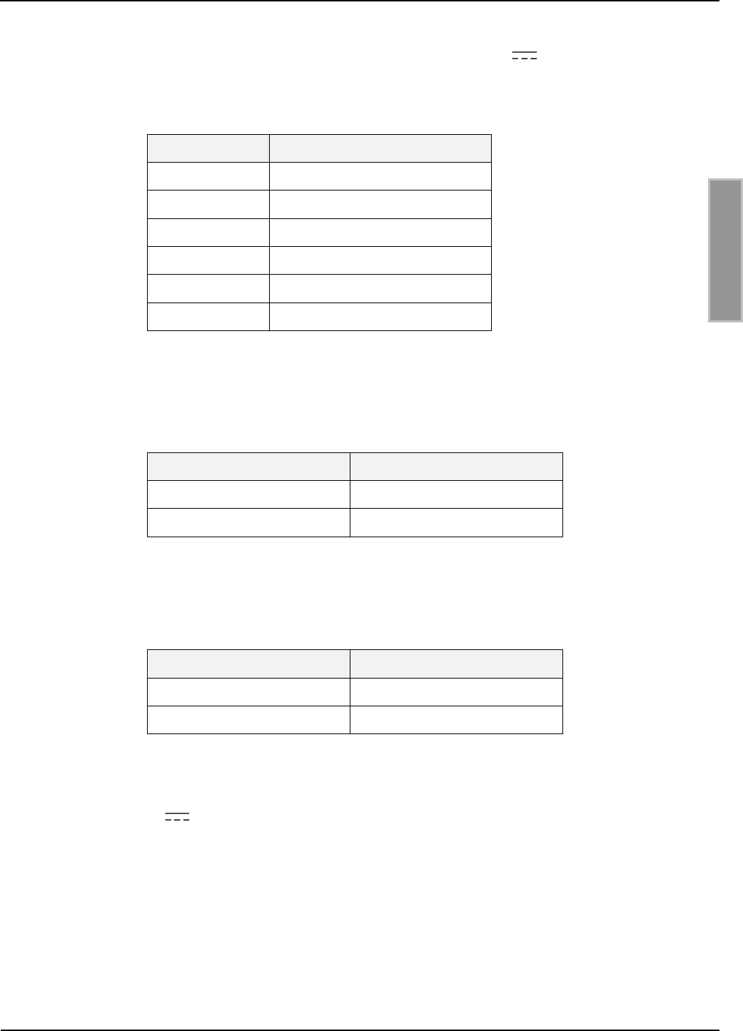
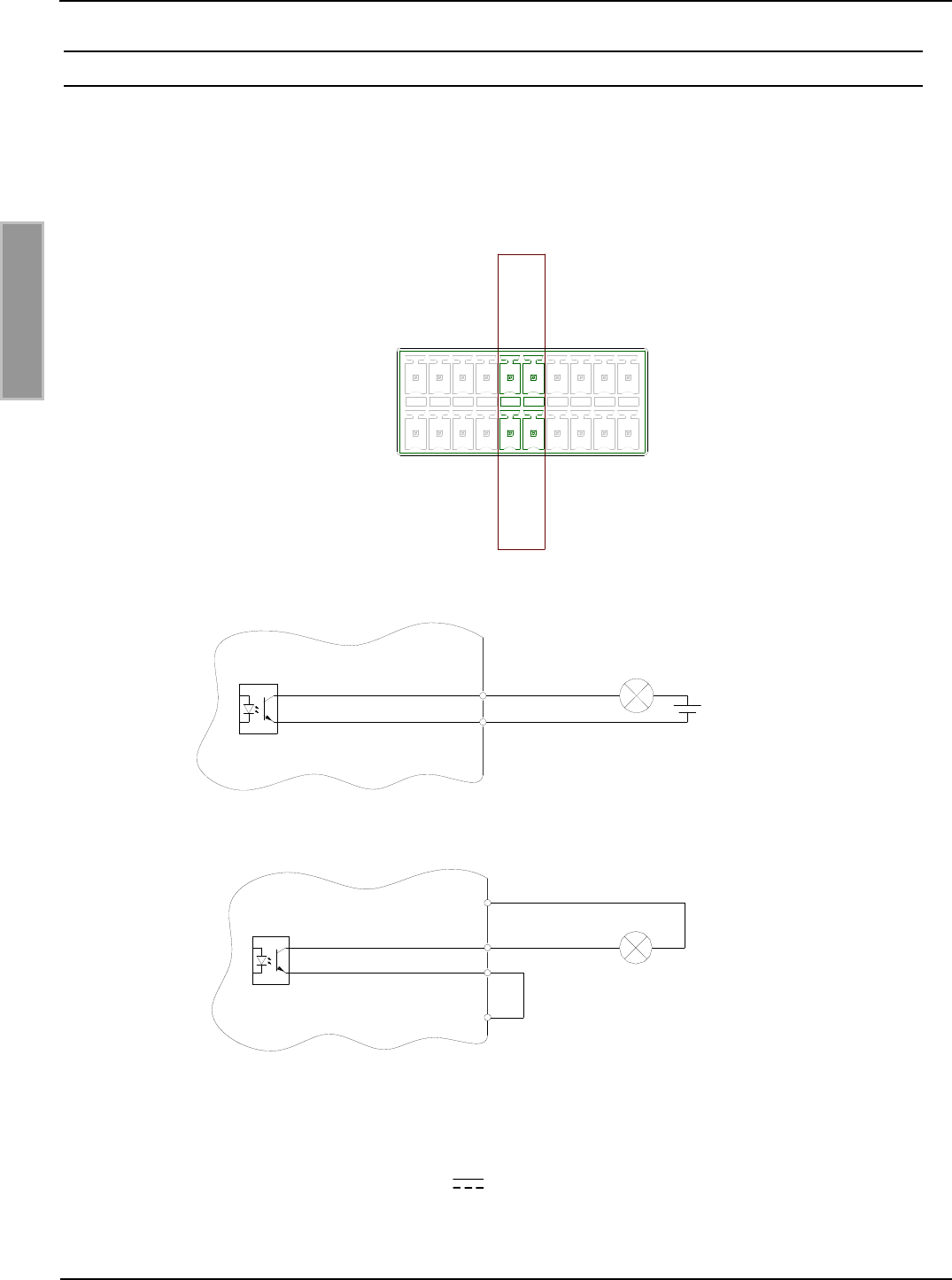
2.6 Optokoppler Eingänge (X2 / IN1, IN2, IN3)
Die drei Optokoppler Eingänge sind auf dem Klemmleiste X2 zugänglich.
X2
IN1-
REL3-COM
REL2-COM
REL1-COM
GND
IN3-
IN2-
GND
OUT2-E
IN1+
OUT1-C
GND
IN3+
IN2+
OUT2-C
REL3-NO
REL2-NO
REL1-NO
24V
OUT1-E
Abbildung 6: Digitale Eingänge an der Klemmleiste X2
Die Optokoppler an der Klemmleiste X2 sind galvanisch von der Reader-Elektronik getrennt und
müssen daher mit einer externen Spannung versorgt werden, siehe Abbildung 7.
Die externe VCC Spannung kann jedoch auch von dem Reader zur Verfügung gestellt werden
siehe: Abbildung 8.
Alle 3 Eingänge sind identisch aufgebaut und lassen sich einzeln konfigurieren.
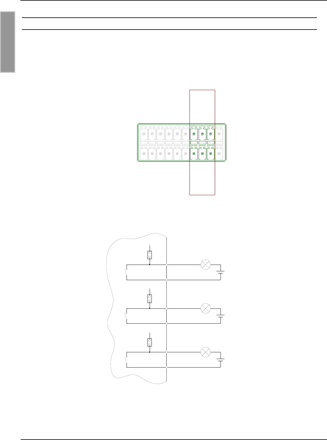
470 +
IN1 -Uext
820 J2
J1 24 V
470 +
IN2 -Uext
820 J4
J3 24 V
470 +
IN3 -Uext
820 J6
J5 24 V
Abbildung 7: Externe Spannungsversorgung der Optokoppler am Anschluss X2
OBID i-scan®
Montage
ID ISC.LRM2500-B
FEIG ELECTRONIC GmbH
Seite 15 von 63
M01111-0de-ID-B.DOC
D E U T S C H
470 +
IN1 -
820 J2
J1 24 V
470 +
IN2 -
820 J4
J3 24 V
470 +
IN3 -
820 J6
J5 24 V
GND
Abbildung 8: Mögliche interne Spannungsversorgung der Optokoppler am Anschluss X2
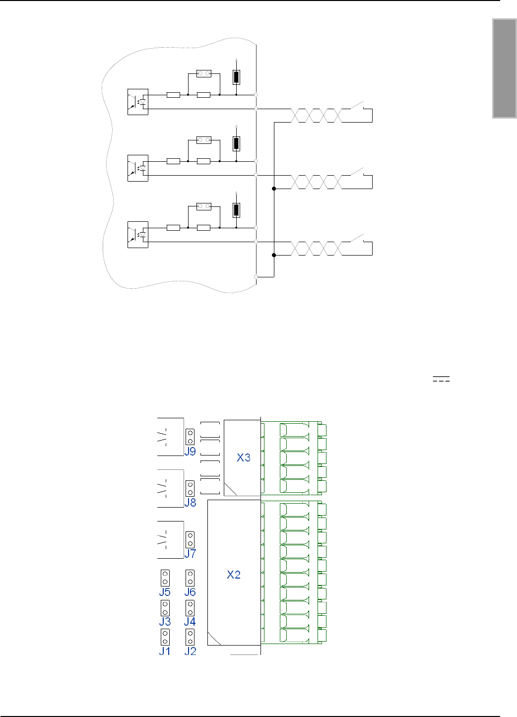
Die Eingangs-LED der Optokoppler sind intern mit einem Serienwiderstand von 1290 beschaltet
um den Eingangsstrom auf max. 20 mA zu begrenzen. Bei Spannungen kleiner als 10V muss
mit dem dazugehörigen Jumper (J1, J3, J5) ein Teil des Vorwiderstandes überbrückt werden.
Abbildung 9: Position der Jumper J1- J9

OBID i-scan®
Montage
ID ISC.LRM2500-B
FEIG ELECTRONIC GmbH
Seite 16 von 63
M01111-0de-ID-B.DOC
D E U T S C H
Hinweise:
Der Eingang ist für eine maximale Eingangsspannung von 24 V und einem Eingangs-
strom von maximal 20 mA ausgelegt.
Verpolung oder Überlastung des Eingangs führt zu dessen Zerstörung.
Jumper
Beschreibung
J1
Vorwiderstand IN1 (X2)
J2
VCC IN1 (X2)
J3
Vorwiderstand IN2 (X2)
J4
VCC IN2 (X2)
J5
Vorwiderstand IN3 (X2)
J6
VCC IN3 (X2)
Tabelle 4: Jumper der Eingänge IN1,IN2 und IN3
Tabelle 5: Benötigter Vorwiderstand zeigt die benötigten Vorwiderstande bei den verschiedenen
externen Spannungen
Externe Spannung Uext
Jumper J1/J3/J5
5 V ... 10 V
Geschlossen
10 V ... 24 V
offen
Tabelle 5: Benötigter Vorwiderstand
Tabelle 6: zeigt die Jumperstellung für externe oder interne Spannungsversorgung
Jumper
Jumper J2/J4/J6
externe Spannung
offen
interne VCC Spannung
geschlossen
Tabelle 6: Interne / Externe Spannungsversorgung
Hinweise:
Die interne 24V Versorgungsspannung für die Optokoppler Eingänge ist nicht über
die Sicherung F1 abgesichert.
Die gleichzeitige Verwendung der internen und einer externen Versorgungsspannung
kann zur Zerstörung des Gerätes führen.
OBID i-scan®
Montage
ID ISC.LRM2500-B
FEIG ELECTRONIC GmbH
Seite 17 von 63
M01111-0de-ID-B.DOC
D E U T S C H
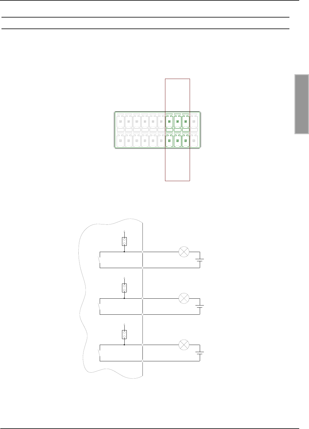
2.7 Optokoppler Ausgänge (X2 / OUT1, OUT2)
Der Transistoranschluss, Kollektor und Emitter, der Optokoppler Ausgänge sind von der Rea-
der-Elektronik galvanisch getrennt und ohne interne Zusatzbeschaltung an Klemme X2 nach
außen geführt. Der Ausgang muss daher mit einer externen Spannung betrieben werden. Die
digitalen Ausgänge OUT1 und OUT2 können im Scan Mode als Data-Takt-Schnittstelle ver-
wendet werden. OUT1 => „Clock“, OUT2 => „Data“
OUT1-E
IN1-
REL3-COM
REL2-COM
REL1-COM
GND
IN3-
IN2-
GND
OUT2-E
IN1+
OUT1-C
GND
IN3+
IN2+
OUT2-C
REL3-NO
REL2-NO
REL1-NO
24V
X2
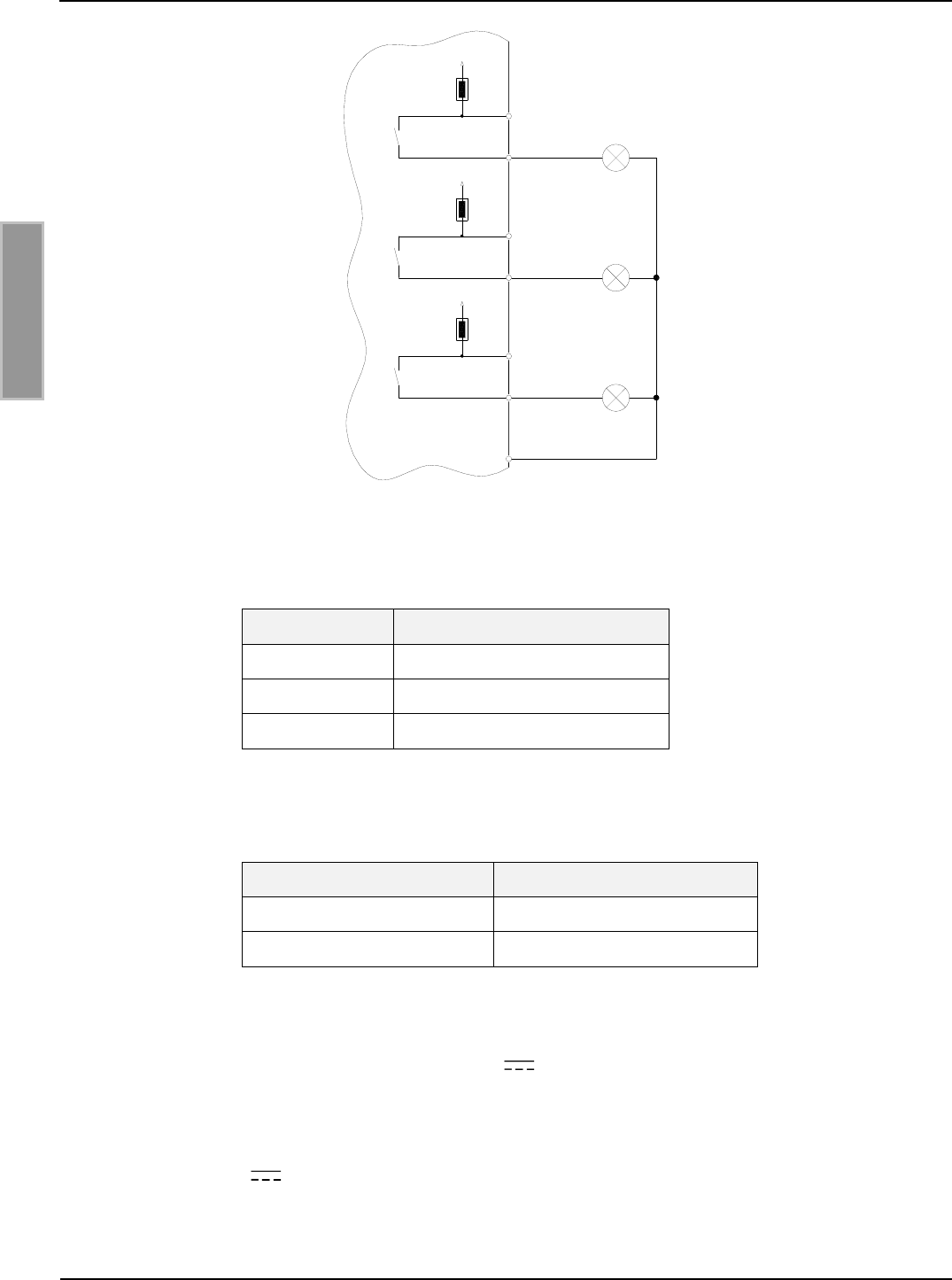
Abbildung 10: Digitale Ausgänge an der Klemmleiste X2
OUT1..2 E
C
Uext
OUT1..2 E
C
24 V
GND
Abbildung 11: Interne und mögliche externe Beschaltung der Optokoppler-Ausgänge OUT1-2
Hinweise:
Der Ausgang ist für max. 24 V / 30 mA ausgelegt.
Verpolung oder Überlastung des Ausgangs führt zu dessen Zerstörung.
Der Ausgang ist nur zum Schalten ohmscher Lasten vorgesehen.
OBID i-scan®
Montage
ID ISC.LRM2500-B
FEIG ELECTRONIC GmbH
Seite 18 von 63
M01111-0de-ID-B.DOC
D E U T S C H
2.8 Relais (X2 / REL1, REL2, REL3)
Als Relaisausgänge stehen drei Schließer zur Verfügung. Die jeweiligen Kontakte stehen an den
Klemme X2 zur Verfügung. Die Ausgänge sind galvanisch von der Reader-Elektronik getrennt und
müssen daher mit einer externen Spannung versorgt werden. Die externe Spannung kann jedoch
auch von Karte über die Jumper J7;J8;J9 zur Verfügung gestellt werden. Alle 3 Ausgänge sind
identisch aufgebaut und lassen sich einzeln konfigurieren.
IN1-
REL3-COM
REL2-COM
REL1-COM
GND
IN3-
IN2-
GND
OUT2-E
IN1+
OUT1-C
GND
IN3+
IN2+
OUT2-C
REL3-NO
REL2-NO
REL1-NO
24V
OUT1-E
X2
Abbildung 12: Relais Ausgänge an der Klemmleiste X2
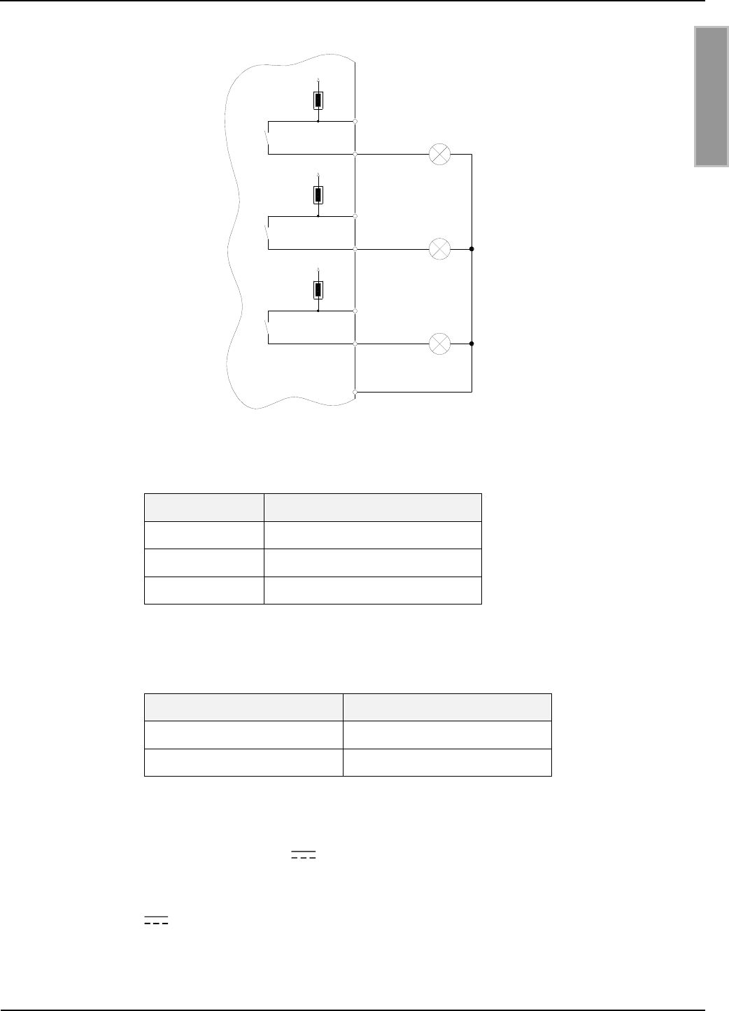
REL1
COM
N0 NO
COM
Uext
J7
24 V
REL2
COM
N0 NO
COM
Uext
J8
24 V
REL3
COM
N0 NO
COM
Uext
J9
24 V
Abbildung 13: Interne und mögliche externe Beschaltung der Relaisausgänge mit externer Span-
nungsversorgung
OBID i-scan®
Montage
ID ISC.LRM2500-B
FEIG ELECTRONIC GmbH
Seite 19 von 63
M01111-0de-ID-B.DOC
D E U T S C H
REL1
COM
N0 NO
COM
J7
24 V
REL2
COM
N0 NO
COM
J8
24 V
REL3
COM
N0 NO
COM
J9
24 V
GND
Abbildung 14: Interne und mögliche externe Beschaltung der Relaisausgänge mit interner Span-
nungsversorgung
Jumper
Beschreibung
J7
VCC - REL 1 (X2)
J8
VCC - REL 2 (X2)
J9
VCC - REL 3 (X2)
Tabelle 7: Zuordnung der Jumper zu den Relais Ausgänge
Tabelle 8 zeigt die Jumperstellung für externe oder interne Spannungsversorgung
Jumper
Jumper J7/J8/J9
externe Spannung
offen
interne VCC Spannung
geschlossen
Tabelle 8: Interne / Externe Spannungsversorgung
Hinweise:
Der Relaisausgang ist für max. 24 V / 1 A ausgelegt.
Der Relaisausgang ist nur zum Schalten ohmscher Lasten vorgesehen. Im Falle einer in-
duktiven Last sind die Relaiskontakte durch eine externe Schutzbeschaltung zu schützen.
Die interne 24V Versorgungsspannung für die Relais ist nicht über die Sicherung F1
abgesichert.
Die gleichzeitige Verwendung der internen und einer externen Versorgungsspannung
kann zur Zerstörung des Gerätes führen.
OBID i-scan®
Montage
ID ISC.LRM2500-B
FEIG ELECTRONIC GmbH
Seite 20 von 63
M01111-0de-ID-B.DOC
D E U T S C H
2.9 Ausgang 24V (X2 / 24V, GND)
Am Ausgang 24V/GND stehen 24V für die externe Spannungsversorgung der digitalen Ein-
und Ausgänge sowie der Relais zur Verfügung. Die maximal Stromentnahme darf 500mA nicht
überschreiten. Dabei ist eine mögliche Stromentnahme über die die Jumper J2,J4,J6 bzw. J7,J8,J9
mit zu berücksichtigen.
X2
IN1-
REL3-COM
REL2-COM
REL1-COM
GND
IN3-
IN2-
GND
OUT2-E
IN1+
OUT1-C
GND
IN3+
IN2+
OUT2-C
REL3-NO
REL2-NO
REL1-NO
24V
OUT1-E
Abbildung 15: Mögliche externe 24V Spannungsversorgung
Hinweise:
Die an diesem Ausgang entnommene Leistung für die externe Beschaltung muss bei der
Dimensionierung des Netzteils zusätzlich zu der typischen Reader Leistung mit berück-
sichtigt werden.
Die 24V Versorgungsspannung an X2 ist nicht über die Sicherung F1 abgesichert.
OBID i-scan®
Montage
ID ISC.LRM2500-B
FEIG ELECTRONIC GmbH
Seite 21 von 63
M01111-0de-ID-B.DOC
D E U T S C H
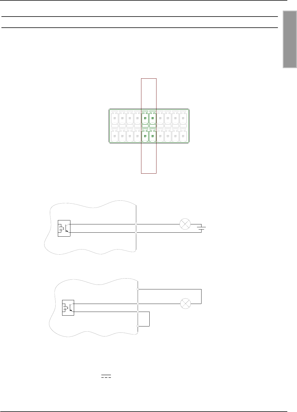
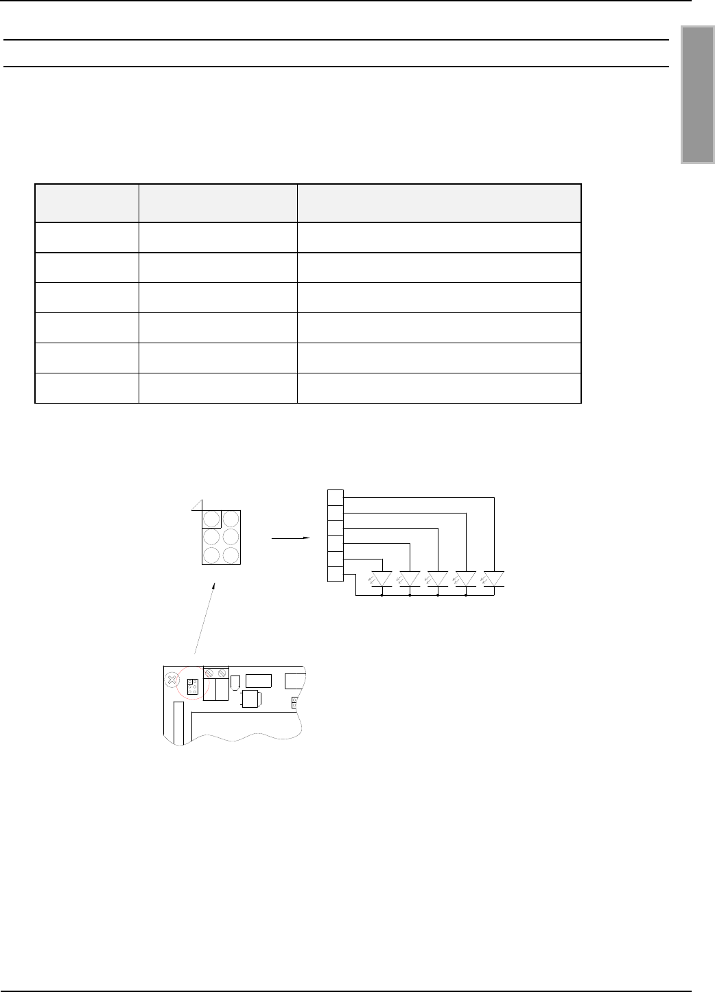
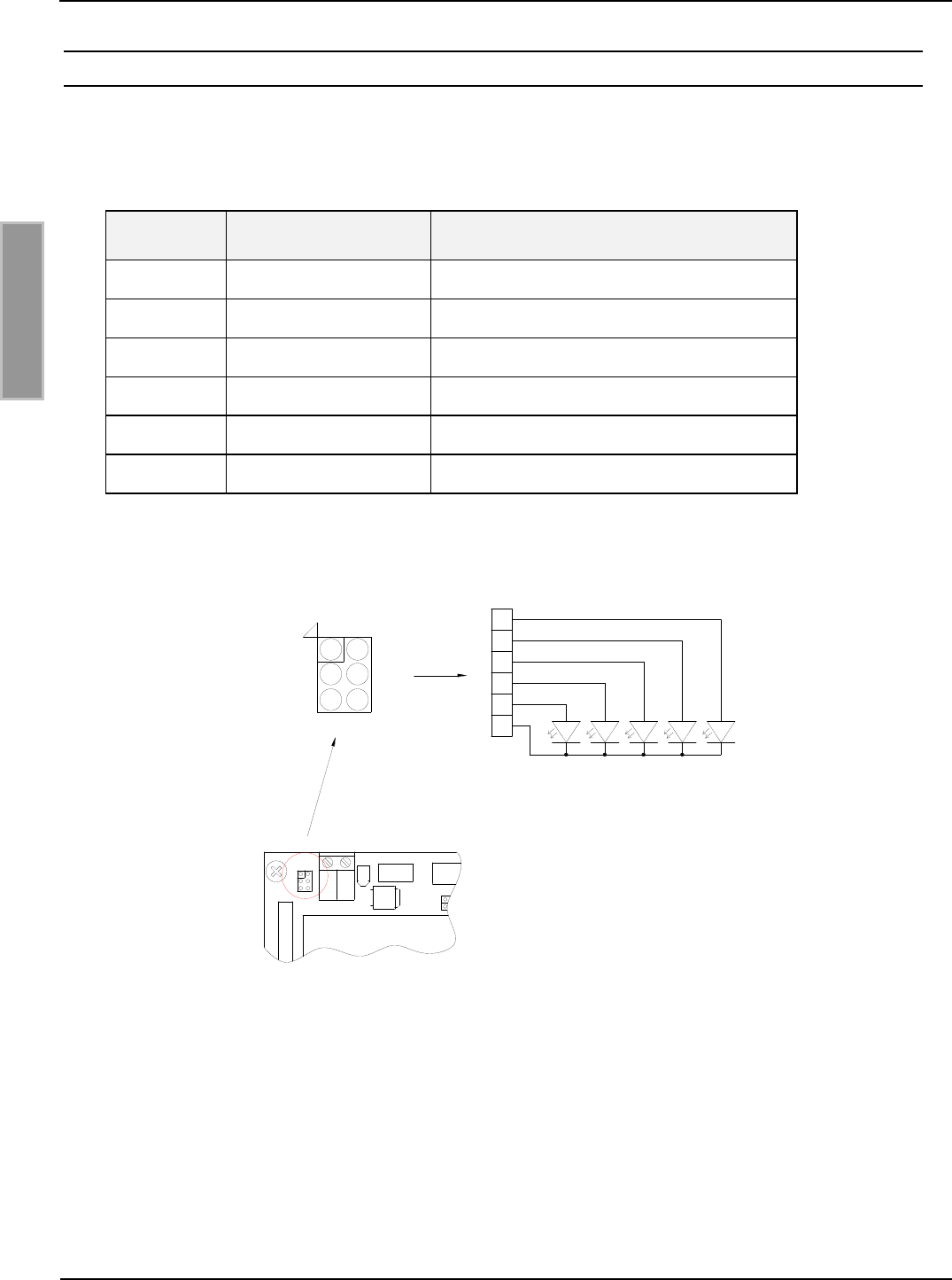
2.10 Anschluss externer Diagnose-LEDs X8
X8 ermöglicht den Anschluss zusätzlicher externer LEDs parallel zu den internen Diagnose-LEDs.
Der Anschluss der externen LEDs erfolgt gemäß Abbildung 16: Anschluss externer LEDs an X8,
siehe Abbildung 16.
Klemme
Kurzzeichen
Beschreibung
X8 / Pin 1
V1 Anode ext.
Funktion entspricht interner LED V1
X8 / Pin 2
V2 Anode ext.
Funktion entspricht interner LED V2
X8 / Pin 3
V3 Anode ext.
Funktion entspricht interner LED V3
X8 / Pin 4
V4 Anode ext.
Funktion entspricht interner LED V4
X8 / Pin 5
V5 Anode ext.
Funktion entspricht interner LED V5
X8 / Pin 6
GND
Gemeinsamer GND-Anschluss
Tabelle 9: Pinbelegung externe LEDs
5
3
12
4
6
6
2
3
4
5V5 V4
Externe LEDs
X8
V2V3 V1
X8 1
X8
X6
F1
Abbildung 16: Anschluss externer LEDs an X8
Hinweis:
Die Ausgänge an X8 sind nur zum Schalten einer externen LED vorgesehen. Überlastung
der Ausgänge durch andere Lasten kann zu deren Zerstörung führen.
Bei Nutzung von nur einem Ausgang, liegt die maximale Stromentnahme bei Imax=15mA.
Der Gesamtstrom aller 5 Ausgänge zusammen, darf 25mA nicht überschreiten. Die Leer-
laufausgangsspannung liegt bei 3,3V und wird über einen 220Ohm Serienwiderstand zur
Verfügung gestellt.
OBID i-scan®
Montage
ID ISC.LRM2500-B
FEIG ELECTRONIC GmbH
Seite 22 von 63
M01111-0de-ID-B.DOC
D E U T S C H
2.11 Schnittstellen
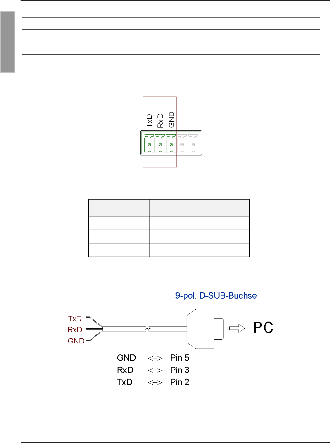
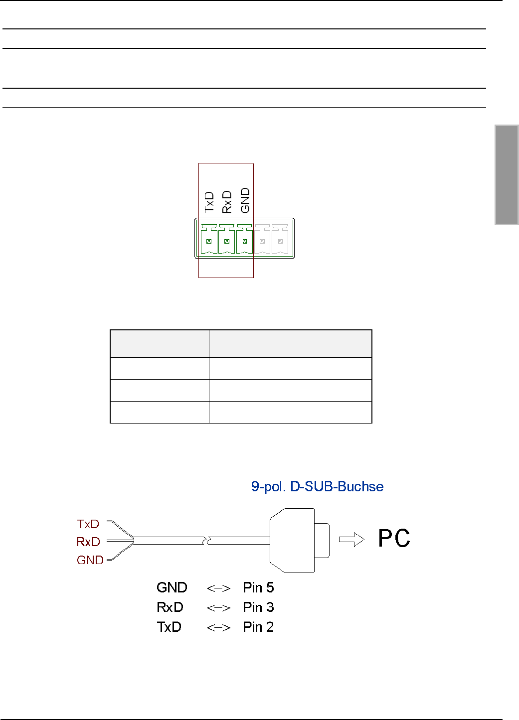
2.11.1 RS232-Schnittstelle X3
Der Anschluss der RS232-Schnittstelle erfolgt über X3. Die Übertragungsparameter können per
Softwareprotokoll konfiguriert werden.
Abbildung 17: Anschlussbelegung X3 (RS232-Schnittstelle)
Kurzzeichen
Beschreibung
TxD
RS232 – (Transmit)
RxD
RS232 – (Receive)
GND
RS232 – (Ground)
Tabelle 10 Belegung RS232-Schnittstelle
Abbildung 18: Verdrahtungsbeispiel für den Anschluss der RS232-Schnittstelle
OBID i-scan®
Montage
ID ISC.LRM2500-B
FEIG ELECTRONIC GmbH
Seite 23 von 63
M01111-0de-ID-B.DOC
D E U T S C H
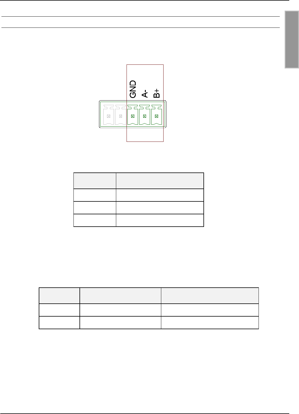
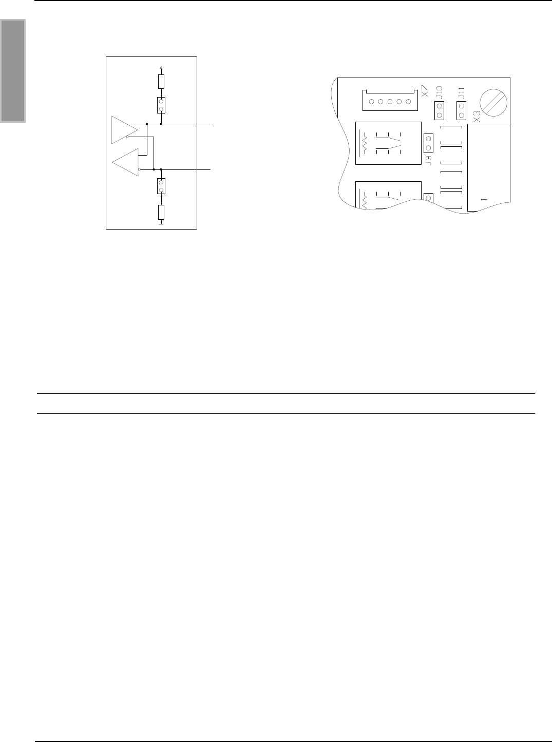
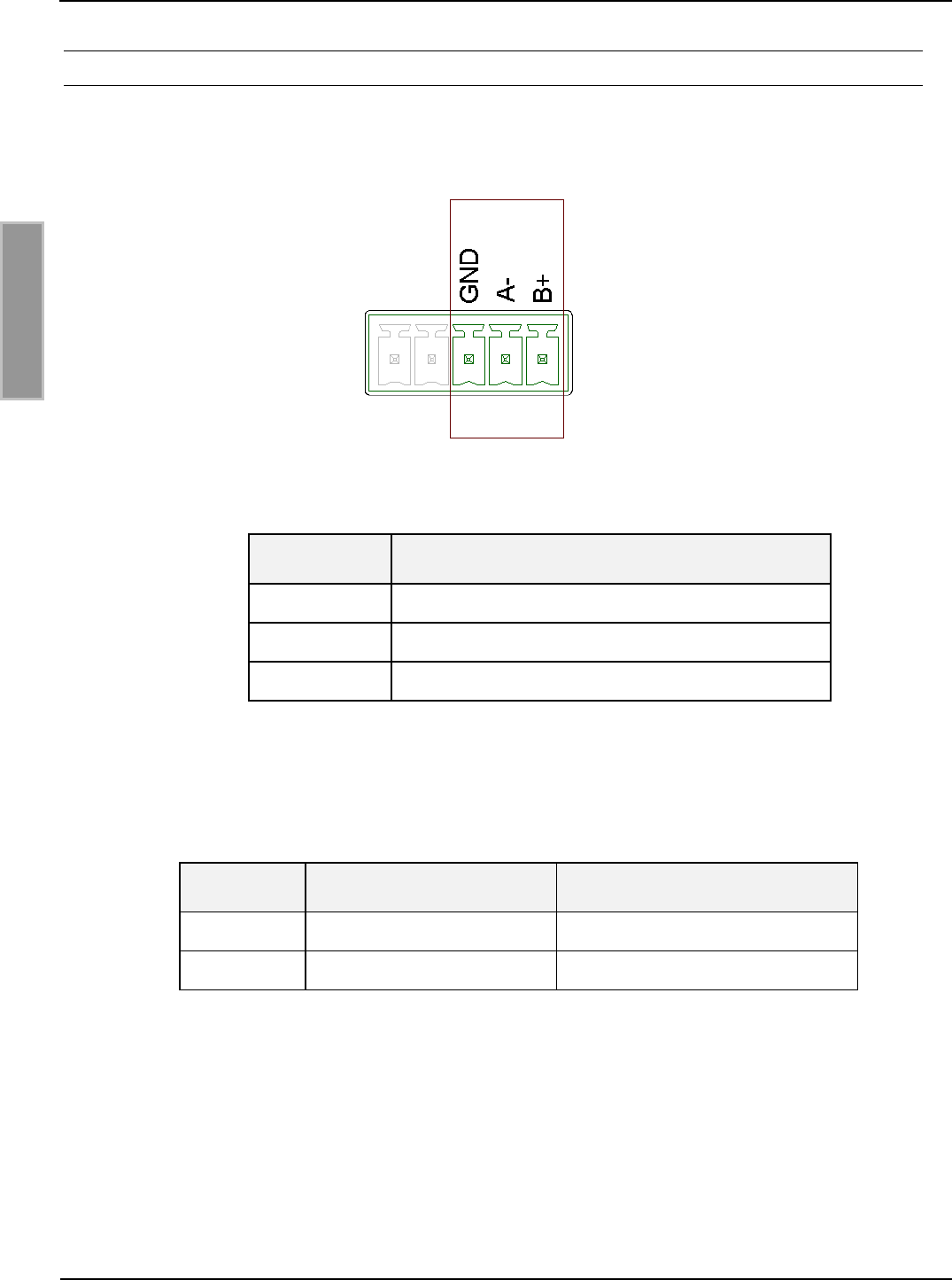
2.11.2 RS485-Schnittstelle X3
Der Anschluss der RS485-Schnittstelle erfolgt ebenfalls über X3.
Die Übertragungsparameter können per Softwareprotokoll konfiguriert werden.
Kurzzeichen
Beschreibung
GND
RS485 – GND
A-
RS485 – (A -)
B+
RS485 – (B +)
Tabelle 11 Pinbelegung RS485-Schnittstelle
Mit den Jumpern J10 und J11 können „Pull up“ und „Pull down“ Widerstände im Bedarfsfall zuge-
schaltet werden.
Jumper
Geschlossen
offen
J10
Pull-Down an RS4xx - A
ohne Pull-Down an RS4xx - A
J11
Pull-Up an RS4xx - B
ohne Pull-Up an RS4xx - B
Tabelle 12: Jumper der RS485-Schnittstelle
Hinweis:
Der Abschlusswiderstand (Terminator) kann per Software in der Reader-Konfiguration dazu
geschaltet werden.
Abbildung 19 Anschlussbelegung X3 (RS485-Schnittstelle):
OBID i-scan®
Montage
ID ISC.LRM2500-B
FEIG ELECTRONIC GmbH
Seite 24 von 63
M01111-0de-ID-B.DOC
D E U T S C H
J11
VCC
J10
500
500
RS485 +
RS485 -
Abbildung 20: Jumper der RS485-Schnittstelle
Abbildung 21: Position der Jumper J10, J11
Hinweis:
Wird ein Gate People Counter an der RS485 Schnittstelle betrieben steht die RS485 Schnitt-
stelle nicht mehr für die Host Kommunikation zur Verfügung.
2.11.2.1 Adresseinstellung RS485 für Busbetrieb
Für den Busbetrieb bietet der Reader die Möglichkeit, die benötigte Busadresse per Software zu
vergeben.
Die Adressvergabe erfolgt über den Host-Rechner. Mit Hilfe der Software können dem Reader die
Adressen "0" bis "254" zugewiesen werden.
Eine evtl. notwendige Terminierung des RS485 Bus kann ebenfalls per Software konfiguriert wer-
den. Siehe Systemhandbuch.
Hinweis:
Da alle Reader werksseitig die Adresse 0 eingestellt haben, müssen sie nacheinander ange-
schlossen und konfiguriert werden.

OBID i-scan®
Montage
ID ISC.LRM2500-B
FEIG ELECTRONIC GmbH
Seite 25 von 63
M01111-0de-ID-B.DOC
D E U T S C H
2.12 USB – Schnittstelle X4 (Host Kommunikation)
Der Anschluss der USB-Schnittstelle erfolgt über Buchse X4. Die Belegung ist genormt. Die Daten-
rate des Readers ist auf 12 Mbit beschränkt (USB Full Speed). Es kann ein Standard-USB-Kabel
verwendet werden.
Hinweis:
Die maximale Länge des USB-Kabels darf 5 m betragen. Längere Kabel sind nicht erlaubt.
Abbildung 22: USB-Schnittstelle für Host Kommunikation
X4
OBID i-scan®
Montage
ID ISC.LRM2500-B
FEIG ELECTRONIC GmbH
Seite 26 von 63
M01111-0de-ID-B.DOC
D E U T S C H
2.12.1 Ethernet-Schnittstelle an X1 (10/100 Base-T)
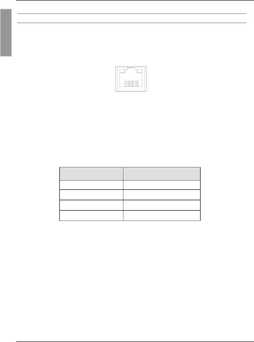
Der Reader verfügt über eine integrierte 10/100 Base-T Netzwerkschnittstelle mit Standard RJ-45-
Anschluss. Der Anschluss erfolgt über X1 und hat eine automatische „Crossover Detection“ ent-
sprechend dem 1000 Base-T Standard.
Bei einer strukturierten Verkabelung sollten mindestens Kabel der Kategorie CAT5 verwendet wer-
den. Dies garantiert einen problemlosen Betrieb bei 10 Mbps oder 100 Mbps.
Voraussetzung für den Einsatz des TCP/IP-Protokolls ist, dass jedes Gerät am Netzwerk über eine
eigene IP-Adresse verfügt. Alle Reader verfügen über eine werksseitig voreingestellte IP-Adresse.
Netzwerk
Adresse
IP-Adresse
192.168.10.10
Subnet-Mask
255.255.255.0
Port
10001
DHCP
AUS
Tabelle 13: Werkskonfiguration der Ethernet-Schnittstelle
Hinweis:
Der Reader verfügt über eine DHCP-fähige TCP/IP Schnittstelle, die werkseitig ausgeschal-
tet ist.
X1
Abbildung 23: LAN Schnittstelle für Host Kommunikation

OBID i-scan®
Montage
ID ISC.LRM2500-B
FEIG ELECTRONIC GmbH
Seite 27 von 63
M01111-0de-ID-B.DOC
D E U T S C H
3 Bedien- und Anzeigeelemente
3.1 LEDs
Tabelle 1 zeigt die Konfiguration der LEDs.
Kurzzeichen
Beschreibung
LED V1 (grün)
"RUN-LED 1"
- Signalisiert den ordnungsgemäßen Ablauf der
internen Reader-Software (DSP)
- Leuchtet während der Reader-Initialisierung nach dem Ein-
schalten bzw. nach einem Reset.
LED V2 (blau)
Diagnose 1: RF-Kommunikation / EEPROM-Status
- Signalisiert durch ein kurzes Blinken die fehlerfreie Kommuni-
kation mit einem Transponder auf der RF-Schnittstelle
- Blinkt abwechselnd mit V1 nach dem Reset im Anschluss an
ein Software-Update
- Blinkt abwechselnd mit V1 falls nach einem Reset ein Daten-
fehler beim Lesen der Parameter auftrat
LED V3 (gelb)
Diagnose 2: Host-Kommunikation
- Signalisiert durch ein kurzes Blinken das Senden eines Proto-
kolls an den Host auf der RS232/RS485/USB/LAN-Schnittstelle
LED V4 (gelb)
Reserviert
LED V5 (rot)
Diagnose 4: RF-Warnung
- Leuchtet bei einem Fehler im RF-Teil des Readers. Der Feh-
lertyp kann per Software über die RS232/RS485/USB/LAN-
Schnittstelle ausgelesen werden
Tabelle 14: Konfiguration der LEDs

OBID i-scan®
Montage
ID ISC.LRM2500-B
FEIG ELECTRONIC GmbH
Seite 28 von 63
M01111-0de-ID-B.DOC
D E U T S C H
3.2 Taster T1
Kurzzeichen
Beschreibung
T1
Reader Reset-Taste
Tabelle 15: Reset-Taste
- Durch betätigen von T1 wird am Reader ein CPU-Reset durchgeführt

OBID i-scan®
Montage
ID ISC.LRM2500-B
FEIG ELECTRONIC GmbH
Seite 29 von 63
M01111-0de-ID-B.DOC
D E U T S C H
4 Funkzulassungen
4.1 Europa (CE)
Die Funkanlage entspricht, bei bestimmungsgemäßer Verwendung den grundlegenden Anforde-
rungen des Artikels 3 und den übrigen einschlägigen Bestimmungen der R&TTE Richtlinie
1999/5/EG vom März 99.
Equipment Classification gemäß ETSI EN 300 440 und ETSI EN 301 489: Class 2

OBID i-scan®
Montage
ID ISC.LRM2500-B
FEIG ELECTRONIC GmbH
Seite 30 von 63
M01111-0de-ID-B.DOC
D E U T S C H
4.2 USA (FCC) und Kanada (IC)
Product name:
ID ISC.LRM2500-B
Reader name:
ID ISC.LRM2500-B
FCC ID:
IC:
PJMLRM2500
6633A-LRM2500
Notice for USA and
Canada
This device complies with Part 15 of the FCC Rules and with
RSS-210 of Industry Canada.
Operation is subject to the following two conditions.
(1) this device may not cause harmful interference, and
(2) this device must accept any interference received,
including interference that may cause undesired operation.
Unauthorized modifications may void the authority granted under
Federal communications Commission Rules permitting the operation
of this device.
This equipment has been tested and found to comply with the limits for
a Class A digital device, pursuant to Part 15 of the FCC Rules. These
limits are designed to provide reasonable protection against harmful
interference when the equipment is operated in a commercial
environment. This equipment generates, uses, and can radiate radio
frequency energy and, if not installed and used in accordance with the
instruction manual, may cause harmful interference to radio
communications. Operation of this equipment in a residential area is
likely to cause harmful interference in which case the user will be
required to correct the interference at his own expense.
Le présent appareil est conforme aux CNR d'Industrie Canada appli-
cables aux appareils radio exempts de licence. L'exploitation est auto-
risée aux deux conditions suivantes :
(1) l'appareil ne doit pas produire de brouillage, et
(2) l'utilisateur de l'appareil doit accepter tout brouillage radioélectrique
subi, même si le brouillage est susceptible d'en compromettre le fonc-
tionnement.
Warning: Changes or modification made to this equipment not expressly approved by
FEIG ELECTRONIC GmbH may void the FCC authorization to operate this equipment.

OBID i-scan®
Montage
ID ISC.LRM2500-B
FEIG ELECTRONIC GmbH
Seite 31 von 63
M01111-0de-ID-B.DOC
D E U T S C H
5 Technische Daten
ID ISC.LRM2500-B
Mechanische Daten
Abmessungen ( B x H x T )
160 mm x 120 mm x 46 mm
Gewicht
ca. 0,6 kg
Elektrische Daten
Spannungsversorgung
24 V 15 %
Noise Ripple : max. 150 mV
Leistungsaufnahme
Typisch 35 VA / maximal 47VA (je nach ext.
Beschaltung)
Betriebsfrequenz
13,56 MHz
Sendeleistung
2 W – 12 W
(per Software in 250 mW Schritten einstellbar)
Modulationsgrad
10% - 30%
(per Software einstellbar)
Antennenanschluss
SMA Buchse (50)
Gleichspannung auf
der Antennenleitung
8 V (max. 150mA)
Diagnoseoptionen
internes VSWR-Meter
interne Temperaturüberwachung
Ausgänge:
– 2 Optokoppler
– 3 Relais ( 3 x Schließer)
24 V / 30 mA (Optional nutzbar als Data Clock IF)
24 V / 1 A
Eingänge
– 3 Optokoppler
5-24 V / 20 mA (siehe Kapitel 2.6)
Schnittstellen
- RS232
- RS485
- USB
- Ethernet (TCP/IP)
- Data Clock

OBID i-scan®
Montage
ID ISC.LRM2500-B
FEIG ELECTRONIC GmbH
Seite 32 von 63
M01111-0de-ID-B.DOC
D E U T S C H
Protokoll Modi
- FEIG ISO HOST
- BRM (Datenfilterung und Datenpufferung)
- Scan Mode
- Notification Mode
Unterstützte Transponder
ISO15693, ISO18000-3 MODE 1
(EM HF ISO Chips, Fujitsu HF ISO Chips,
KSW Sensor Chips, IDS Sensor Chips
Infineon my-d, NXP I-Code, STM ISO Chips,
TI Tag-it)
NXP I Code 1
Signalgeber, optisch
5 LEDs zur Diagnose des Betriebszustandes
Umgebungsbedingungen
Temperaturbereich
– Betrieb
– Lagerung
-20°C bis +55°C
-25°C bis +85°C
Luftfeuchtigkeit
5% - 80%, nicht kondensierend
Vibration
EN60068-2-6
10 Hz bis 150 Hz : 0,075 mm / 1 g
Schock
EN60068-2-27
Beschleunigung : 30 g
Zulassung
Zulassung Funk
– Europa
– USA
EN 300 330
FCC 47 CFR Part 15
EMV
EN 301 489
Sicherheit
– Elektrische Sicherheit
– Human Exposure
EN 60950
EN 50364

OBID i-scan®
Installation
ID ISC.LRM2500-B
FEIG ELECTRONIC GmbH
Page 34 of 63
M01111-0de-ID-B.DOC
E N G L I S H
Note
Copyright 2011 by
FEIG ELECTRONIC GmbH
Lange Strasse 4
D-35781 Weilburg-Waldhausen
Tel.: +49 6471 3109-0
http://www.feig.de
With the edition of this document, all previous editions become void. Indications made in this manual may be
changed without previous notice.
Copying of this document, and giving it to others and the use or communication of the contents thereof are
forbidden without express authority. Offenders are liable to the payment of damages. All rights are reserved
in the event of the grant of a patent or the registration of a utility model or design.
Composition of the information in this document has been done to the best of our knowledge. FEIG
ELECTRONIC GmbH does not guarantee the correctness and completeness of the details given in this
manual and may not be held liable for damages ensuing from incorrect or incomplete information. Since,
despite all our efforts, errors may not be completely avoided, we are always grateful for your useful tips.
The instructions given in this manual are based on advantageous boundary conditions. FEIG ELECTRONIC
GmbH does not give any guarantee promise for perfect function in cross environments.
FEIG call explicit attention that devices which are subject of this document are not designed with compo-
nents and testing methods for a level of reliability suitable for use in or in connection with surgical implants or
as critical components in any life support systems whose failure to perform can reasonably be expected to
cause significant injury to a human. To avoid damage, injury, or death, the user or application designer must
take reasonably prudent steps to protect against system failures.
FEIG ELECTRONIC GmbH assumes no responsibility for the use of any information contained in this docu-
ment and makes no representation that they free of patent infringement. FEIG ELECTRONIC GmbH does
not convey any license under its patent rights nor the rights of others.
OBID® and OBID i-scan® are registered trademarks of FEIG ELECTRONIC GmbH.
my-d® is a registered trademark of Infineon Technologies AG
I-CODE® is a registered trademark of Philips Electronics N.V.
Tag-itTM is a registered trademark of Texas Instruments Incorporated.

OBID i-scan®
Installation
ID ISC.LRM2500-B
FEIG ELECTRONIC GmbH
Page 35 of 63
M01111-0de-ID-B.DOC
E N G L I S H
Content
1 Safety Instructions / Warning - Read before start-up ! 37
2 Performance Features of Reader Family ID ISC.LRM2500 38
2.1 Performance Features .............................................................................................. 38
2.2 Available Reader Types ............................................................................................ 38
3 Installation and mounting 39
3.1 Mounting ................................................................................................................... 39
3.2 Terminals ................................................................................................................... 41
3.3 Antenna connection ................................................................................................. 42
3.4 Supply voltage .......................................................................................................... 43
3.5 Fuse F1 ...................................................................................................................... 44
3.6 X2: Optokoppler Inputs (X2 / IN1, IN2, IN3) ............................................................. 45
3.7 Optocoupler outputs (X2 / OUT1, OUT2) ................................................................. 48
3.8 Relay (X2 / REL1, REL2, REL3) ................................................................................ 49
3.9 Output 24V (X2 / 24V, GND) .............................................................................. 51
3.10 X8: External diagnostic LED connections .............................................................. 52
3.11 Interfaces ................................................................................................................... 53
3.11.1 RS232-Interface X3 ................................................................................................ 53
3.11.2 RS485-Interface X3 ................................................................................................ 54
3.12 USB – Interface X4 (Host Communication) ............................................................. 56
3.12.1 Ethernet-Interface on X1 (10/100 Base-T) .............................................................. 57
4 Operating and Display Elements 58
4.1 LEDs .......................................................................................................................... 58
4.2 Button T1 ................................................................................................................... 59
5 Radio Approvals 60

OBID i-scan®
Installation
ID ISC.LRM2500-B
FEIG ELECTRONIC GmbH
Page 36 of 63
M01111-0de-ID-B.DOC
E N G L I S H
5.1 Europe (CE) ............................................................................................................... 60
5.2 USA (FCC) and Canada (IC) ..................................................................................... 61
6 Technical Data 62

OBID i-scan®
Installation
ID ISC.LRM2500-B
FEIG ELECTRONIC GmbH
Page 37 of 63
M01111-0de-ID-B.DOC
E N G L I S H
1 Safety Instructions / Warning - Read before start-up !
The device may only be used for the purpose intended by the manufacturer.
The operation manual should be kept readily available at all times for each user.
Unauthorized changes and the use of spare parts and additional devices which have not been
sold or recommended by the manufacturer may cause fire, electric shocks or injuries. Such
unauthorized measures shall exclude the manufacturer from any liability.
The liability-prescriptions of the manufacturer in the issue valid at the time of purchase are valid
for the device. The manufacturer shall not be held legally responsible for inaccuracies, errors,
or omissions in the manual or automatically set parameters for a device or for an incorrect
application of a device.
Repairs may only be undertaken by the manufacturer.
Installation, operation, and maintenance procedures should only be carried out by qualified
personnel.
Use of the device and its installation must be in accordance with national legal requirements
and local electrical codes .
When working on devices the valid safety regulations must be observed.
Before touching the device, the power supply must always be interrupted. Make sure that the
device is without voltage by measuring. The fading of an operation control (LED) is no indicator
for an interrupted power supply or the device being out of voltage!
Special advice for wearers of cardiac pacemakers:
Although this device doesn't exceed the valid limits for electromagnetic fields you should keep
a minimum distance of 25 cm between the device and your cardiac pacemaker and not stay in
the immediate proximity of the device’s antenna for any length of time.

OBID i-scan®
Installation
ID ISC.LRM2500-B
FEIG ELECTRONIC GmbH
Page 38 of 63
M01111-0de-ID-B.DOC
E N G L I S H
2 Performance Features of Reader Family ID ISC.LRM2500
2.1 Performance Features
The Reader has been developed for reading passive data carriers, so-called „Smart Labels“, using
an operating frequency of 13.56 MHz. For the operation it is necessary to connect a appropriate
external antenna to the connector ANT1.
2.2 Available Reader Types
The following Reader type’s are currently available:
Reader type
Description
ID ISC.LRM2500-B
Device version with RS232/485- / USB- / LAN-Interface
Table 1: Available Reader types
OBID i-scan®
Installation
ID ISC.LRM2500-B
FEIG ELECTRONIC GmbH
Page 39 of 63
M01111-0de-ID-B.DOC
E N G L I S H
3 Installation and mounting
3.1 Mounting
The Reader Module is designed for installation on a heat sink. Mounting is accomplished using the
4.5 mm holes located in each corner of the base plate (see: Figure 1).
29
T1
X1
J2
J4
J1
J3
J6
J7
J5
X2
V4
V3
V2V1 V5
45
X8
X6
F1
J8
J9 X3
X4
X7
16,3
4
120
110
ø 4,5 mm*
160
155
80
ø 4,5 mm* ø 4,5 mm*
5
ø 4,5 mm
155
GND
VDC
ø 4,5 mm
5
Figure 1: Scale drawing oft he Reader module with mounting plate

OBID i-scan®
Installation
ID ISC.LRM2500-B
FEIG ELECTRONIC GmbH
Page 40 of 63
M01111-0de-ID-B.DOC
E N G L I S H
To fully exploit the performance of the Reader Module, the heat sink should have a thermal resis-
tance RThK of max. 1 K/W. When attaching the Reader Module to the heat sink you should strive for
a little heat transfer resistance between the base plate and the heat sink as possible. The use of
heat sink compound is recommended.
If the antenna is properly tuned and there is sufficient air convection along the mounting plate, the
ID ISC.LRM2000 can be operated without an additional heat sink at up to 2W of power. Note here
however that detuning of the antenna can result in additional heating of the Reader. In such cases
the Reader regulates its output power down until the upper temperature limit of its final stage fallen
down again.

OBID i-scan®
Installation
ID ISC.LRM2500-B
FEIG ELECTRONIC GmbH
Page 42 of 63
M01111-0de-ID-B.DOC
E N G L I S H
3.3 Antenna connection
The SMA socket „ANT1“ is located on the lower circuit board for connecting the antenna to the ID
ISC.LRM2500.
Active external function units (e.g. ID ISC.DAT) can also be supplied with 8 V through the an-
tenna terminal. The maximum current draw is then not allowed to exceed 150mA. This additional
power consumption must be considered for the total reader power consumption.
The maximum tightening torque for the SMA socket is 0.45 Nm (4.0 lbf in).
Attention:
Exceeding the tightening torque will destroy the socket.
Terminal
Description
ANT1
For connecting the antenna
Table 2: Antenna jack
The standing wave ratio VSWR for the antenna should not exceed a value of 1,3.
For reaching optimal read ranges the coaxial cables between readers and antenna must
have defined lengths. For all antennas of the company FEIG ELECTRONICS GmbH and
for all antennas which with the tuning boards (e.g. ID ISC.DAT, ID ISC.MAT b and ID
ISC.MAT s) of FEIG ELECTRONICS GmbH is made the optimal length of the coaxial ca-
ble is 1.35 m (Article No. 1654.004.00.00, Name ID ISC.ANT.C-B). See also Mounting
Manual Power Splitter ID ISC.ANT.PS-B and ID ISC.ANT.MUX.
The optimum operating Q factor of the antenna should be in a range of Qoper = 10...30. To
determine the operating Q the antenna must be supplied with a 50 Ohm source such as
a network analyzer or frequency generator.
To prevent external coupled noise, the antenna cable must be fitted with the included
EMC ferrite ring core 28 mm x 20 mm. The antenna line must be wound around the
ring core for at least 4 turns. The distance between the Reader termination and the ring
core should be maximum 10 cm (see Figure 3).
When connecting an antenna, ensure that it does not exceed the permissible limits pre-
scribed by the national regulations for radio frequency devices.
Figure 3: Antenna line with EMC ring cores

OBID i-scan®
Installation
ID ISC.LRM2500-B
FEIG ELECTRONIC GmbH
Page 43 of 63
M01111-0de-ID-B.DOC
E N G L I S H
3.4 Supply voltage
The supply voltage of 24 V is connected to Terminal X6.
Terminal
Abbreviation
Description
X6 / Pin 1
VDC
Vcc – supply voltage + 24 V
X6 / Pin 2
GND
Ground – supply voltage
Table 3: Pin-outs for supply voltage on X6
GND
VDC
X8
X6
F1
1
2
Figure 4: Position oft he connector X6 for the power supply
Note:
Reversing the supply voltage polarity may destroy the device.
To meet national requirements for radio frequency devices the power supply line must
be fitted with one of the supplied EMC ring cores 28 mm x 20 mm. The power supply
line must be wound around the ring core for at least 5 turns. The distance between the
Reader termination and the ring core should be maximum 10 cm.

OBID i-scan®
Installation
ID ISC.LRM2500-B
FEIG ELECTRONIC GmbH
Page 44 of 63
M01111-0de-ID-B.DOC
E N G L I S H
3.5 Fuse F1
The reader have been protected with a SMD fuse 2,5A (time-lag).
Attention!:
The 24V voltage for supplying the internal and external DC voltage on X2 for the dig-
ital inputs and outputs is not protected by the fuse F1.
Figure 5: Position oft he fuse F1
X8
X6
F1
2,5 A time-lag
OBID i-scan®
Installation
ID ISC.LRM2500-B
FEIG ELECTRONIC GmbH
Page 45 of 63
M01111-0de-ID-B.DOC
E N G L I S H
3.6 X2: Optokoppler Inputs (X2 / IN1, IN2, IN3)
The three optocouplers inputs are available on Terminal X2.
X2
IN1-
REL3-COM
REL2-COM
REL1-COM
GND
IN3-
IN2-
GND
OUT2-E
IN1+
OUT1-C
GND
IN3+
IN2+
OUT2-C
REL3-NO
REL2-NO
REL1-NO
24V
OUT1-E
Figure 6: Optocoupler pin-outs on terminal X2
The optocoupler on terminal strips X2 are galvanically isolated from the Reader electronics and
must therefore be powered externally, see Figure 7. The external VCC voltage may however be
provided by the reader, see Figure 8.
All 3 inputs are identical and may therefore be configured individually.
470 +
IN1 -Uext
820 J2
J1 24 V
470 +
IN2 -Uext
820 J4
J3 24 V
470 +
IN3 -Uext
820 J6
J5 24 V
Figure 7: External power supply for the optocouplers

OBID i-scan®
Installation
ID ISC.LRM2500-B
FEIG ELECTRONIC GmbH
Page 46 of 63
M01111-0de-ID-B.DOC
E N G L I S H
470 +
IN1 -
820 J2
J1 24 V
470 +
IN2 -
820 J4
J3 24 V
470 +
IN3 -
820 J6
J5 24 V
GND
Figure 8: Possible internal power supply for the optocouplers
The input LED for the optocouplers are internally connected to a series resistor of 1290 and are
limited to an input current of max. 20mA. For voltages of less than 10V a part of the series
resistance must be jumpered (J1, J3, J5) accordingly.
Figure 9: Position oft he Jumper J1- J9
OBID i-scan®
Installation
ID ISC.LRM2500-B
FEIG ELECTRONIC GmbH
Page 47 of 63
M01111-0de-ID-B.DOC
E N G L I S H
Note:
The input is configured for a maximum input voltage of 24 V and an input current
of maximum 20mA.
Reversing the polarity or overloading the input will destroy it.
Jumper
Description
J1
Series resistance IN1 (X2)
J2
VCC IN1 (X2)
J3
Series resistance IN2 (X2)
J4
VCC IN2 (X2)
J5
Series resistance IN3 (X2)
J6
VCC IN3 (X2)
Table 4: Jumpers for inputs IN1,IN2 and IN3
Table 5 shows the required external series resistances for the various external voltages
External voltage Uext
Jumper J1/J3/J5
5 V ... 10 V
ON
10 V ... 24 V
OFF
Table 5: Required external series resistance
Table 6 shows the jumper setting for external or internal supply voltage
Jumper
Jumper J2/J4/J6
external voltage
OFF
internal VCC voltage
ON
Table 6: Internal / External supply voltage
Note:
The internal 24V voltage for supplying the DC voltage on the digital inputs is not
protected by the fuse F1.
Using internal and external voltage at the same time can destroy the reader.
OBID i-scan®
Installation
ID ISC.LRM2500-B
FEIG ELECTRONIC GmbH
Page 48 of 63
M01111-0de-ID-B.DOC
E N G L I S H
3.7 Optocoupler outputs (X2 / OUT1, OUT2)
The transistor connections, collector and emitter, of the optocoupler outputs are galvanically
isolated from the Reader electronics and are carried to the outside without any internal ancillary
circuitry on Terminal X2. The output must therefore be powered by an external power supply.
The digital outputs OUT1 and OUT2 can be used fort the data clock interface. OUT1 => „Clock“,
OUT2 => „Data“
OUT1-E
IN1-
REL3-COM
REL2-COM
REL1-COM
GND
IN3-
IN2-
GND
OUT2-E
IN1+
OUT1-C
GND
IN3+
IN2+
OUT2-C
REL3-NO
REL2-NO
REL1-NO
24V
X2
Figure 10: Digital Output’s on terminal X2
OUT1..2 E
C
Uext
OUT1..2 E
C
24 V
GND
Figure 11: Internal and possible external wiring of the digital output OUT1-2
Note:
The output is configured for max. 24 V / 30 mA.
Polarity reversal or overload on the output will destroy it.
The output is intended for switching resistive loads only.
OBID i-scan®
Installation
ID ISC.LRM2500-B
FEIG ELECTRONIC GmbH
Page 49 of 63
M01111-0de-ID-B.DOC
E N G L I S H
3.8 Relay (X2 / REL1, REL2, REL3)
The relay outputs are all a normally open contact. These outputs, which are located on terminals
X2, are galvanically isolated from the Reader electronics and must therefore be externally
supplied. The external voltage may however be provided by the card using jumper J7;J8;J9. All 3
outputs are identical and may be configured individually.
IN1-
REL3-COM
REL2-COM
REL1-COM
GND
IN3-
IN2-
GND
OUT2-E
IN1+
OUT1-C
GND
IN3+
IN2+
OUT2-C
REL3-NO
REL2-NO
REL1-NO
24V
OUT1-E
X2
Figure 12: Relay Outputs on terminal X2
REL1
COM
N0 NO
COM
Uext
J7
24 V
REL2
COM
N0 NO
COM
Uext
J8
24 V
REL3
COM
N0 NO
COM
Uext
J9
24 V
Figure 13: Internal and possible external wiring of the relay output’s with external voltage
OBID i-scan®
Installation
ID ISC.LRM2500-B
FEIG ELECTRONIC GmbH
Page 50 of 63
M01111-0de-ID-B.DOC
E N G L I S H
REL1
COM
N0 NO
COM
J7
24 V
REL2
COM
N0 NO
COM
J8
24 V
REL3
COM
N0 NO
COM
J9
24 V
GND
Figure 14: Internal and possible external wiring of the relay output’s with internal voltage
Table 7 shows the assignment oft he jumpers to the relay output
Jumper
Description
J7
VCC - REL 1 (X2)
J8
VCC - REL 2 (X2)
J9
VCC - REL 3 (X2)
Table 7: Assignment oft he jumpers to the relay output
Table 8 shows the jumper setting fort he external voltage or internal VCC voltage
Jumper
Jumper J7/J8/J9
external voltage
open
Internal VCC voltage
closed
Table 8: Internal- / External voltage supply
Notes:
The relay output is configured for max. 24 V / 2 A.
The relay output is intended for switching resistive loads only. If an inductive load is
connected, the relay contacts must be protected by means of an external protection
circuit.
The internal 24V voltage for supplying the DC voltage on the relays is not protected
by the fuse F1.
Using internal and external voltage at the same time can destroy the reader.

OBID i-scan®
Installation
ID ISC.LRM2500-B
FEIG ELECTRONIC GmbH
Page 51 of 63
M01111-0de-ID-B.DOC
E N G L I S H
3.9 Output 24V (X2 / 24V, GND)
The output 24V/GND can be used to power the optional external circuitry of the digital inputs , out-
puts or relays. The maximum current consumption must not exceed 500mA. A possible current
consumption via J2, J4, J6 or J7, J8, J9 must be be factored in.
X2
IN1-
REL3-COM
REL2-COM
REL1-COM
GND
IN3-
IN2-
GND
OUT2-E
IN1+
OUT1-C
GND
IN3+
IN2+
OUT2-C
REL3-NO
REL2-NO
REL1-NO
24V
OUT1-E
Figure 15: Optional 24V external voltage supply
Note:
For the dimensioning oft the power supply the power consumption for the external out-
put circuitry must be additional considered to the typical reader power consumption.
The internal 24V voltage on X2 is not protected by the fuse F1.
OBID i-scan®
Installation
ID ISC.LRM2500-B
FEIG ELECTRONIC GmbH
Page 52 of 63
M01111-0de-ID-B.DOC
E N G L I S H
3.10 X8: External diagnostic LED connections
X8 allows for connection of additional external LEDs in parallel with the internal diagnostic LEDs.
The external LEDs are connected as shown in Figure 16
Terminal
Abbreviation
Description
X8 / Pin 1
V1 Anode ext.
Function same as internal LED V1
X8 / Pin 2
V2 Anode ext.
Function same as internal LED V2
X8 / Pin 3
V3 Anode ext.
Function same as internal LED V3
X8 / Pin 4
V4 Anode ext.
Function same as internal LED V4
X8 / Pin 5
V5 Anode ext.
Function same as internal LED V5
X8 / Pin 6
GND
Common GND
Table 9: External LEDs pin-outs
external LEDs
X8 1
5
3
12
4
6
6
2
3
4
5V5 V4
X8
V2V3 V1
X8
X6
F1
Figure 16: Connecting external LEDs to X8
Note:
The outputs on X8 are intended for switching an external LED only. Overloading the
outputs with other loads may destroy them.
If only one output is used the maximum current consumption is Imax=15mA. The total
current consumption of all 5 outputs together should not increase 25mA. The off-load
output voltage is 3,3V and is supplied via a 220Ohm series resistor.
OBID i-scan®
Installation
ID ISC.LRM2500-B
FEIG ELECTRONIC GmbH
Page 53 of 63
M01111-0de-ID-B.DOC
E N G L I S H
3.11 Interfaces
3.11.1 RS232-Interface X3
The RS232 interface is connected on X3.
The transmission parameters can be configured by means of software protocol.
Figure 17: RS232 interface pin-outs on X3
Kurzzeichen
Description
TxD
RS232 – (Transmit)
RxD
RS232 – (Receive)
GND
RS232 – (Ground)
Table 10: Pin assignment of the RS232-Interface
Figure 18: Wiring example for connecting the RS232 interface
OBID i-scan®
Installation
ID ISC.LRM2500-B
FEIG ELECTRONIC GmbH
Page 54 of 63
M01111-0de-ID-B.DOC
E N G L I S H
3.11.2 RS485-Interface X3
The connection of the RS485 interface take place via the X3 connector as well.
The interface parameter can be configured via software protocols.
Abbreviation
Description
GND
RS485 – GND
A-
RS485 – (A -)
B+
RS485 – (B +)
Table 11: RS485 interface pin-outs
With the Jumper J10 and J11 the „Pull up“ and „Pull down“ resistors can be activated if needed.
Jumper
Closed
Open
J10
Pull-Down on RS4xx - A
without Pull-Down on RS4xx - A
J11
Pull-Up on RS4xx - B
without Pull-Up on RS4xx - B
Table 12: Jumper of the RS485-interface
Note:
The Termination can be activated via software in the reader configuration.
Figure 19: RS485 interface pin-outs on X3 (RS485-Interface)

OBID i-scan®
Installation
ID ISC.LRM2500-B
FEIG ELECTRONIC GmbH
Page 55 of 63
M01111-0de-ID-B.DOC
E N G L I S H
J11
VCC
J10
500
500
RS485 +
RS485 -
Figure 20: Jumper of the RS485-interface
Figure 21: Position of the Jumper J10, J11
Note:
If the Gate People Counter is connected with the RS485 interface the RS485 interface can
be not used for host communication.
3.11.2.1 Address assignment of RS485 for bus operation
For bus operation the Reader can be assigned the required bus address via software.
The address is assigned by the host computer. The software is used to assign addresses “0”
through “254” to the Reader.
The termination of the RS485 Bus can be configured via software. See system manual.
Note:
Since all Readers are factory set with address „0“, they must be connected and configured
one after the other.

OBID i-scan®
Installation
ID ISC.LRM2500-B
FEIG ELECTRONIC GmbH
Page 56 of 63
M01111-0de-ID-B.DOC
E N G L I S H
3.12 USB – Interface X4 (Host Communication)
The USB socket on the board is terminal X4. The pinout is standardized. The data rate is reduced
to 12 Mbit (USB full speed). A standard USB-cable can be used.
Note:
The length of the USB-cable can be a max. of 5m (20 inch). It is not allowed to use longer
cables.
X4
Figure 22: USB-Interface for host communication

OBID i-scan®
Installation
ID ISC.LRM2500-B
FEIG ELECTRONIC GmbH
Page 57 of 63
M01111-0de-ID-B.DOC
E N G L I S H
3.12.1 Ethernet-Interface on X1 (10/100 Base-T)
The Reader has an integrated 10 / 100 Base-T network port for an RJ-45. Connection is made on
X1 and has an automatic “Crossover Detection” according to the 1000 Base-T Standard.
With structured cabling CAT 5 cables should be used. This ensures a reliable operation at 10 Mbps
or 100 Mbps.
The prerequisite for using TCP/IP protocol is that each device has a unique address on the net-
work. All Readers have a factory set IP address.
Network
Address
IP-Adresse
192.168.10.10
Subnet-Mask
255.255.255.0
Port
10001
DHCP
OFF
Table 13 Standard factory configuration of the Ethernet connection
Note:
The Reader TCP/IP interface has a DHCP option.
X1
Figure 23: LAN interface for host communication

OBID i-scan®
Installation
ID ISC.LRM2500-B
FEIG ELECTRONIC GmbH
Page 58 of 63
M01111-0de-ID-B.DOC
E N G L I S H
4 Operating and Display Elements
4.1 LEDs
Table 14 shows the LED configuration.
Abbreviation
Description
LED V1 (green)
"RUN-LED 1"
- Indicates proper running of the internal Reader software (DSP)
- Comes on during Reader initialization after power-on or after a
reset.
LED V2 (blue)
Diagnostic 1: RF communication / EEPROM status
- Short flashing indicates errorless communication with a
transponder on the RF interface
- Flashes alternately with V1 after a reset following a software
update
- Flashes alternately with V1 in case of a data error when
reading the parameters after a reset
LED V3 (yellow)
Diagnostic 2: Host communication
- Short flashing indicates sending of a protocol to the host on the
RS232/RS485/USB and LAN-Interface
LED V4 (yellow)
Reserved
LED V5 (red)
Diagnostic 4: RF warning
- Comes on when there is an error in the RF section of the
Reader. The error type can be read out via software over the
RS232/RS485/USB and LAN-Interface
Table 14: LED configuration

OBID i-scan®
Installation
ID ISC.LRM2500-B
FEIG ELECTRONIC GmbH
Page 59 of 63
M01111-0de-ID-B.DOC
E N G L I S H
4.2 Button T1
Abbreviation
Description
T1
Reader reset button
Table 15: Reset Button
- Pressing T1 resets the reader controller

OBID i-scan®
Installation
ID ISC.LRM2500-B
FEIG ELECTRONIC GmbH
Page 60 of 63
M01111-0de-ID-B.DOC
E N G L I S H
5 Radio Approvals
5.1 Europe (CE)
When used according to regulation, this radio equipment conforms with the basic requirements of
Article 3 and the other relevant provisions of the R&TTE Guideline 1999/E6 dated March 99.
Equipment Classification according ETSI EN 300 440 and ETSI EN 301 489: Class 2

OBID i-scan®
Installation
ID ISC.LRM2500-B
FEIG ELECTRONIC GmbH
Page 61 of 63
M01111-0de-ID-B.DOC
E N G L I S H
5.2 USA (FCC) and Canada (IC)
Product name:
ID ISC.LRM2500-B
Reader name:
ID ISC.LRM2500-B
FCC ID:
IC:
PJMLRM2500
6633A-LRM2500
Notice for USA and
Canada
This device complies with Part 15 of the FCC Rules and with
RSS-210 of Industry Canada.
Operation is subject to the following two conditions.
(1) this device may not cause harmful interference, and
(2) this device must accept any interference received,
including interference that may cause undesired operation.
Unauthorized modifications may void the authority granted under
Federal communications Commission Rules permitting the operation
of this device.
This equipment has been tested and found to comply with the limits for
a Class A digital device, pursuant to Part 15 of the FCC Rules. These
limits are designed to provide reasonable protection against harmful
interference when the equipment is operated in a commercial
environment. This equipment generates, uses, and can radiate radio
frequency energy and, if not installed and used in accordance with the
instruction manual, may cause harmful interference to radio
communications. Operation of this equipment in a residential area is
likely to cause harmful interference in which case the user will be
required to correct the interference at his own expense.
Le présent appareil est conforme aux CNR d'Industrie Canada appli-
cables aux appareils radio exempts de licence. L'exploitation est auto-
risée aux deux conditions suivantes :
(1) l'appareil ne doit pas produire de brouillage, et
(2) l'utilisateur de l'appareil doit accepter tout brouillage radioélectrique
subi, même si le brouillage est susceptible d'en compromettre le fonc-
tionnement.
Warning: Changes or modification made to this equipment not expressly approved by
FEIG ELECTRONIC GmbH may void the FCC authorization to operate this equipment.

OBID i-scan®
Installation
ID ISC.LRM2500-B
FEIG ELECTRONIC GmbH
Page 62 of 63
M01111-0de-ID-B.DOC
E N G L I S H
6 Technical Data
ID ISC.LRM2500-B
Mechanical Data
Dimensions ( W x H x D )
160 mm x 120 mm x 46 mm
(6.29 inch x 4.72 inch x 1.81 inch)
Weight
approx.. 0,6 kg (1.32 lb)
Electrical Data
Supply Voltage
24 V 15 %
Noise Ripple : max. 150 mV
Power Consumption
Typical 35 VA / maximum 47VA (depending on ext.
output circuitry)
Operating Frequency
13,56 MHz
Transmit Power
2W – 12 W
(250 mW Step - Software)
Modulation
10% - 30%
(Software configurable)
Antenna Connection
SMA Jack (50)
DC Supply at Antenna Connec-
tor
8 V (max. 150mA)
Diagnostic Options
internal VSWR-Meter
internal temperature monitoring
Outputs
– 2 Optocoupler
– 3 Relay ( 3 x NO)
24 V / 30 mA (optional usable as Data Clock IF)
24 V / 1 A
Inputs
– 3 Optocoupler
5- 24 V / 20 mA (See chapter: 3.6)

OBID i-scan®
Installation
ID ISC.LRM2500-B
FEIG ELECTRONIC GmbH
Page 63 of 63
M01111-0de-ID-B.DOC
E N G L I S H
Interfaces
- RS232
- RS485
- USB
- Ethernet (TCP/IP)
- Data Clock
Protocol Modes
- FEIG ISO HOST
- BRM (Data Filtering and Data Buffering
- Scan Mode
- Notification Mode
Supported Transponders
ISO15693, ISO18000-3 MODE 1
(EM HF ISO Chips, Fujitsu HF ISO Chips,
KSW Sensor Chips, IDS Sensor Chips,
Infineon my-d, NXP I-Code, STM ISO Chips,
TI Tag-it)
NXP I Code 1
Optical Indicators
5 LEDs for Operating Status Diagnostics
Ambient
Temperature Range
– Operating
– Storage
-20°C to +55°C (-4°F to +131°F)
-25°C to +85°C (-13°F to +185°F)
Humidity
5% - 80%, no condensation
Vibration
EN 60068-2-6
10 Hz to 150 Hz : 0,075 mm / 1 g
Shock
EN 60068-2-27
Acceleration : 30 g
Applicable Standards
RF Approval
– Europe
– USA
EN 300 330
FCC 47 CFR Part 15
EMC
EN 301 489
Safety
– Low Voltage Directive
– Human Exposure
EN 60950
EN 50364
MONTAGE
INSTALLATION
Preliminary
public (B)
2011-04-13
M10210-0de-ID-B.doc
ID ISC.LRM2500-A
(deutsch / english)


OBID i-scan®
Montage
ID ISC.LRM2500-A
FEIG ELECTRONIC GmbH
Seite 3 von 63
M10210-0de-ID-B.doc
D E U T S C H
Hinweis
Copyright 2011 by
FEIG ELECTRONIC GmbH
Lange Straße 4
D-35781 Weilburg-Waldhausen
Tel.: +49 6471 3109-0
http://www.feig.de
Alle früheren Ausgaben verlieren mit dieser Ausgabe ihre Gültigkeit.
Die Angaben in diesem Dokument können ohne vorherige Ankündigung geändert werden.
Weitergabe sowie Vervielfältigung dieses Dokuments, Verwertung und Mitteilung ihres Inhalts sind nicht
gestattet, soweit nicht ausdrücklich zugestanden. Zuwiderhandlung verpflichtet zu Schadenersatz. Alle
Rechte für den Fall der Patenterteilung oder Gebrauchsmuster-Eintragung vorbehalten.
Die Zusammenstellung der Informationen in diesem Dokument erfolgt nach bestem Wissen und Gewissen.
FEIG ELECTRONIC GmbH übernimmt keine Gewährleistung für die Richtigkeit und Vollständigkeit der An-
gaben in diesem Dokument. Insbesondere kann FEIG ELECTRONIC GmbH nicht für Folgeschäden auf
Grund fehlerhafter oder unvollständiger Angaben haftbar gemacht werden. Da sich Fehler, trotz aller Bemü-
hungen nie vollständig vermeiden lassen, sind wir für Hinweise jederzeit dankbar.
Die in diesem Dokument gemachten Installationsempfehlungen gehen von günstigsten Rahmenbedingun-
gen aus. FEIG ELECTRONIC GmbH übernimmt weder Gewähr für die einwandfreie Funktion in system-
fremden Umgebungen, noch für die Funktion eines Gesamtsystems, welches die in diesem Dokument be-
schriebenen Geräte enthält.
FEIG ELECTRONIC weist ausdrücklich darauf hin, dass die in diesem Dokument beschriebenen Geräte
nicht für den Einsatz mit oder in medizinischen Geräten oder für Geräte für lebenserhaltende Maßnahmen
konzipiert sind, bei denen ein Fehler eine Gefahr für menschliches Leben oder für die gesundheitliche Un-
versehrtheit zur Folge haben kann. Der Applikationsdesigner ist dafür verantwortlich geeignete Maßnahmen
zu ergreifen um Gefahren, Schäden oder Verletzungen zu vermeiden.
FEIG ELECTRONIC GmbH übernimmt keine Gewährleistung dafür, dass die in diesem Dokument enthal-
tenden Informationen frei von fremden Schutzrechten sind. FEIG ELECTRONIC GmbH erteilt mit diesem
Dokument keine Lizenzen auf eigene oder fremde Patente oder andere Schutzrechte.
OBID® und OBID i-scan® ist ein eingetragenes Warenzeichen der FEIG ELECTRONIC GmbH
my-d® ist ein eingetragenes Warenzeichen der Infineon Technologies AG
I-CODE® und mifare® ist ein eingetragenes Warenzeichen der Philips Electronics N.V.
Tag-it ist ein Warenzeichen der Texas Instruments Incorporated

OBID i-scan®
Montage
ID ISC.LRM2500-A
FEIG ELECTRONIC GmbH
Seite 4 von 63
M10210-0de-ID-B.doc
D E U T S C H
Inhalt
Sicherheits- und Warnhinweise - vor Inbetriebnahme unbedingt lesen 6
1 Leistungsmerkmale der Readerfamilie ID ISC.LRM2500 7
1.1 Leistungsmerkmale .................................................................................................... 7
1.2 Verfügbare Readervarianten ...................................................................................... 7
2 Montage und Anschluss 8
2.1 Montage ....................................................................................................................... 8
2.2 Anschlussklemmen .................................................................................................. 10
2.3 Antennenanschluss .................................................................................................. 11
2.4 Versorgungsspannung ............................................................................................. 12
2.5 Sicherung F1 ............................................................................................................. 13
2.6 Optokoppler Eingänge (X2 / IN1, IN2, IN3) .............................................................. 14
2.7 Optokoppler Ausgänge (X2 / OUT1, OUT2) ............................................................. 17
2.8 Relais (X2 / REL1, REL2, REL3) ............................................................................... 18
2.9 Ausgang 24V (X2 / 24V, GND) ............................................................................ 20
2.10 Anschluss externer Diagnose-LEDs X8 .................................................................. 21
2.11 Schnittstellen ............................................................................................................ 22
2.11.1 RS232-Schnittstelle X3 .......................................................................................... 22
2.11.2 RS485-Schnittstelle X3 .......................................................................................... 23
2.11.3 USB – Schnittstelle X4 (Host Kommunikation, HDI) ............................................... 25
2.11.4 USB – Host X5 ....................................................................................................... 25
2.11.5 Ethernet-Schnittstelle an X1 (10/100 Base-T) ........................................................ 26
3 Bedien- und Anzeigeelemente 27
3.1 LEDs .......................................................................................................................... 27
3.2 Taster T1.................................................................................................................... 28

OBID i-scan®
Montage
ID ISC.LRM2500-A
FEIG ELECTRONIC GmbH
Seite 5 von 63
M10210-0de-ID-B.doc
D E U T S C H
4 Funkzulassungen 29
4.1 Europa (CE) ............................................................................................................... 29
4.2 USA (FCC) und Kanada (IC) ..................................................................................... 30
5 Technische Daten 31

OBID i-scan®
Montage
ID ISC.LRM2500-A
FEIG ELECTRONIC GmbH
Seite 6 von 63
M10210-0de-ID-B.doc
D E U T S C H
Sicherheits- und Warnhinweise - vor Inbetriebnahme unbedingt lesen
Das Gerät darf nur für den vom Hersteller vorgesehenen Zweck verwendet werden.
Die Bedienungsanleitung ist zugriffsfähig aufzubewahren und jedem Benutzer auszuhändigen.
Unzulässige Veränderungen und die Verwendung von Ersatzteilen und Zusatzeinrichtungen,
die nicht vom Hersteller des Gerätes verkauft oder empfohlen werden, können Brände, elektri-
sche Schläge und Verletzungen verursachen. Solche Maßnahmen führen daher zu einem
Ausschluss der Haftung und der Hersteller übernimmt keine Gewährleistung.
Für das Gerät gelten die Gewährleistungsbestimmungen des Herstellers in der zum Zeitpunkt
des Kaufs gültigen Fassung. Für eine ungeeignete, falsche manuelle oder automatische Ein-
stellung von Parametern für ein Gerät bzw. ungeeignete Verwendung eines Gerätes wird keine
Haftung übernommen.
Reparaturen dürfen nur vom Hersteller durchgeführt werden.
Anschluss-, Inbetriebnahme-, Wartungs-, und sonstige Arbeiten am Gerät dürfen nur von Elekt-
rofachkräften mit einschlägiger Ausbildung erfolgen.
Alle Arbeiten am Gerät und dessen Aufstellung müssen in Übereinstimmung mit den nationa-
len elektrischen Bestimmungen und den örtlichen Vorschriften durchgeführt werden.
Beim Arbeiten an dem Gerät müssen die jeweils gültigen Sicherheitsvorschriften beachtet wer-
den.
Vor Berührung der Platinen ist stets die Spannungsversorgung abzuschalten und durch Nach-
messen sicherzustellen, dass das Gerät spannungslos ist. Das Verlöschen einer Betriebsan-
zeige ist kein Indikator dafür, dass das Gerät vom Netz getrennt und spannungslos ist.
Besonderer Hinweis für Träger von Herzschrittmachern:
Obwohl dieses Gerät die zulässigen Grenzwerte für elektromagnetische Felder nicht über-
schreitet, sollten Sie einen Mindestabstand von 25 cm zwischen der angeschlossenen Antenne
und Ihrem Herzschrittmacher einhalten und sich nicht für längere Zeit in unmittelbarer Nähe
des Geräts bzw. der Antenne aufhalten.

OBID i-scan®
Montage
ID ISC.LRM2500-A
FEIG ELECTRONIC GmbH
Seite 7 von 63
M10210-0de-ID-B.doc
D E U T S C H
1 Leistungsmerkmale der Readerfamilie ID ISC.LRM2500
1.1 Leistungsmerkmale
Der Reader ist für das Lesen von passiven Datenträgern, sogenannten „Smart Labels“, mit einer
Betriebsfrequenz von 13,56 MHz entwickelt. Zum Betrieb ist es notwendig eine geeignete externe
Antenne an dem Anschluss „ANT1“ anzuschließen.
1.2 Verfügbare Readervarianten
Folgende Readervarianten sind z.Z. verfügbar:
Reader
Beschreibung
ID ISC.LRM2500-A
Modulvariante mit RS232/485- / USB- / LAN-Interface, USB-
Host und Embedded Linux
ID ISC.LRM2500-B
Modulvariante mit RS232/485- / USB- / LAN-Interface
Tabelle 1: Verfügbare Readervarianten
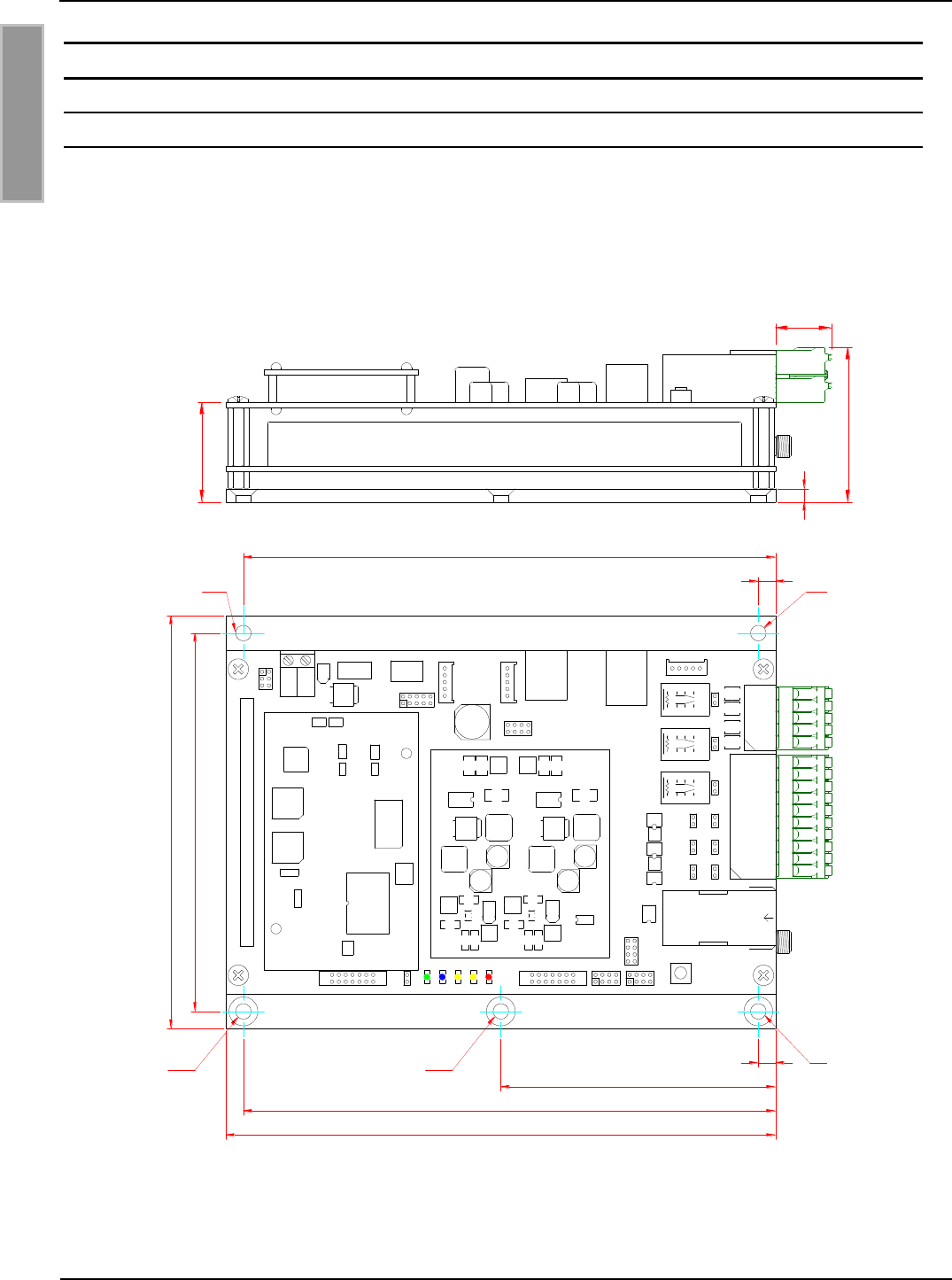
OBID i-scan®
Montage
ID ISC.LRM2500-A
FEIG ELECTRONIC GmbH
Seite 8 von 63
M10210-0de-ID-B.doc
D E U T S C H
2 Montage und Anschluss
2.1 Montage
Das Reader-Modul ist für die Montage auf einem Kühlkörper konzipiert. Für die Befestigung befin-
det sich in den vier Ecken der Trägerplatte jeweils eine Bohrung mit dem 4,5 mm (siehe Fehler!
Verweisquelle konnte nicht gefunden werden.)
120
110
ø 4,5 mm*
160
155
80
ø 4,5 mm* ø 4,5 mm*
5
ø 4,5 mm
V4
V3
V2V1 V5
X8
X6
F1
J8
J9 X3
X4
X7
29
45
16,3
155
GND
VDC
ø 4,5 mm
5
4
X5
T1
X1
J2
J4
J1
J3
J6
J7
J5
X2
Abbildung 1 Maßzeichnung des Reader-Moduls ID ISC.LRM2500-A mit Montageplatte

OBID i-scan®
Montage
ID ISC.LRM2500-A
FEIG ELECTRONIC GmbH
Seite 9 von 63
M10210-0de-ID-B.doc
D E U T S C H
Für die Ausnutzung der vollen Leistungsfähigkeit des Reader-Moduls sollte der verwendete Kühl-
körper einen Wärmewiderstand RThK von maximal 1,0 K/W besitzen. Bei der Montage des Reader-
Moduls auf den Kühlkörper ist auf einen möglichst geringen Wärmeübergangswiderstand zwischen
Trägerplatte und Kühlkörper zu achten. Die Verwendung von Wärmeleitpaste wird empfohlen.
Bei korrekt abgestimmter Antenne und ausreichender Luftkonvektion entlang der Montageplatte
kann der ID ISC.LRM2500 auch ohne zusätzlichen Kühlkörper bis zu einer Leistung von 2 W be-
trieben werden. Hierbei ist jedoch zu beachten, dass eine Verstimmung der Antenne zu einer zu-
sätzlichen Erwärmung des Readers führt. In diesem Falle regelt der Reader seine Ausgangsleis-
tung zurück bis die obere Grenztemperatur seiner Endstufe wieder unterschritten wird.
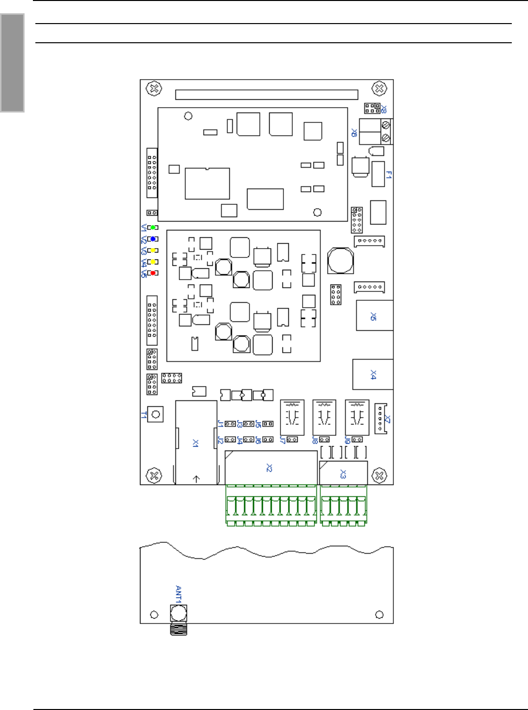
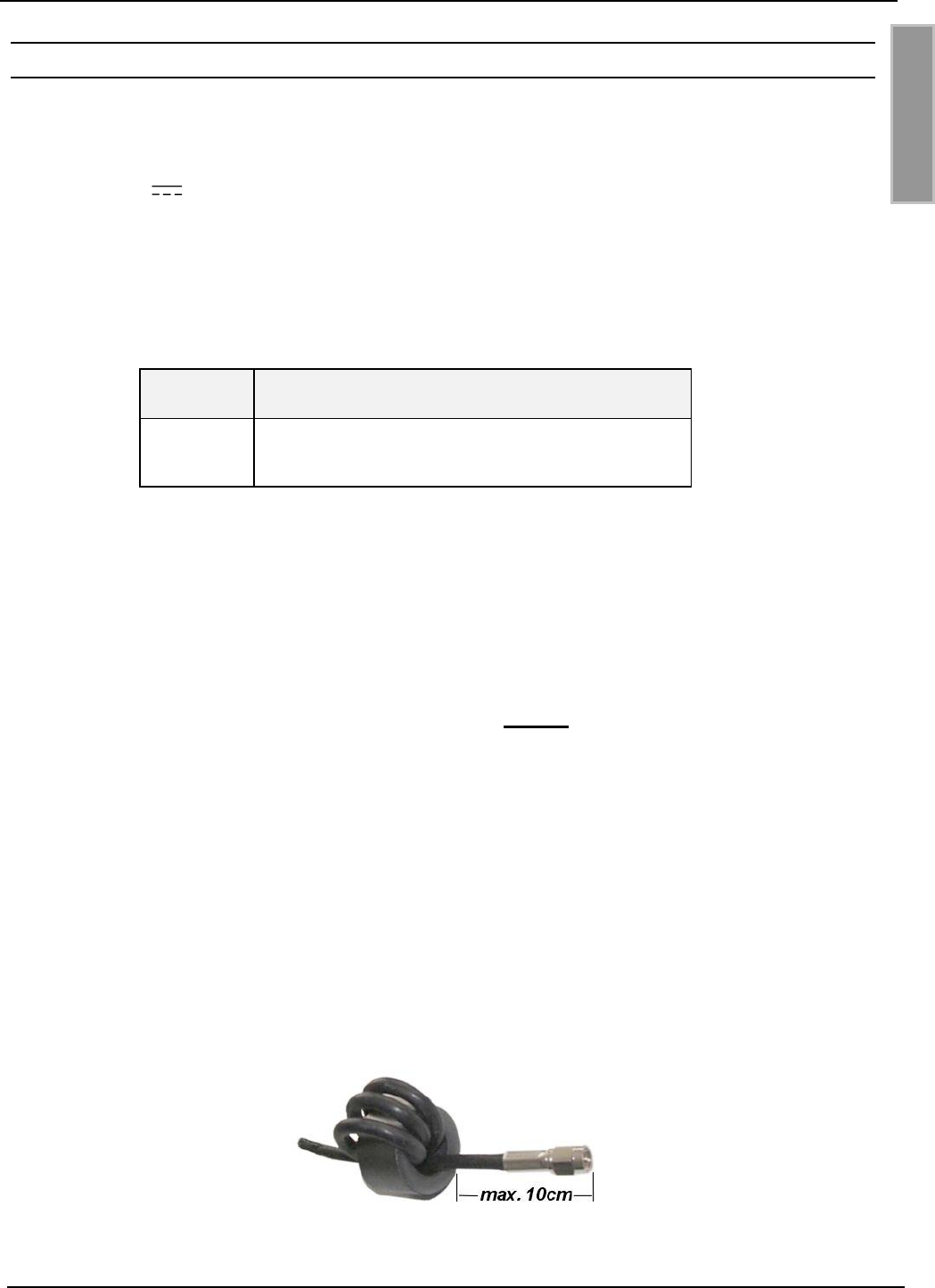
OBID i-scan®
Montage
ID ISC.LRM2500-A
FEIG ELECTRONIC GmbH
Seite 11 von 63
M10210-0de-ID-B.doc
D E U T S C H
2.3 Antennenanschluss
Zum Anschluss der Antenne an den ID ISC.LRM2500 befindet sich auf der unteren Leiterplatte die
SMA-Buchse "ANT1".
Aktive externe Funktionseinheiten (z.B. ID ISC.DAT) können zusätzlich über den Antennenan-
schluss mit 8 V versorgt werden. Diese kann per Software Konfiguration aktiviert werden.
Die maximale Stromaufnahme darf dabei 150mA nicht überschreiten. Diese Leistung muss zusätz-
lich zur Gesamtleistungsaufnahme des Readers mit berücksichtigt werden.
Das maximale Anzugsdrehmoment der SMA-Buchse beträgt 0,45 Nm.
Achtung:
Höhere Anzugsdrehmomente führen zur Zerstörung der Buchse.
Klemme
Beschreibung
ANT1
Anschluss der externen Antenne
(Eingangsimpedanz 50)
Tabelle 2: Anschluss der externen Antenne
Hinweise:
Das Stehwellenverhältnis VSWR der Antenne sollte den Wert 1,3 nicht überschreiten.
Für das Erreichen optimaler Lesereichweiten müssen die Koaxialkabel zwischen Reader
und Antenne definierte Längen haben. Für alle Antennen von der Firma FEIG
ELECTRONIC GmbH und für alle Antennen welche mit den Abgleichplatinen (z.B. ID
ISC.DAT, ID ISC.MAT-B und ID ISC.MAT-S) von FEIG ELECTRONIC GmbH aufgebaut
sind ist die optimale Länge des Koaxialkabels 1,35 m (Artikel Nr. 1654.004.00.00, Be-
zeichnung ID ISC.ANT.C-B). Siehe auch Montageanleitung Power Splitter ID ISC.ANT.PS-
B und ID ISC.ANT.MUX.
Die optimale Betriebsgüte der Antenne sollte im Bereich QB = 10...30 liegen. Zur Ermitt-
lung der Betriebsgüte muss die Antenne mit einer 50-Quelle, z.B. einem Network Ana-
lyzer oder einem Frequenzgenerator, versorgt werden.
Zur Vermeidung extern eingekoppelter Störungen muss die Antennenzuleitung dem bei-
gefügten EMV-Ringkernferrit 28 mm x 20 mm versehen werden. Hierzu ist die Anten-
nenzuleitung mindestens vier mal, eng anliegend durch den EMV-Ringkernferrit zu füh-
ren. Der Abstand zwischen Readeranschluss ANT1 und Ringkern sollte dabei maximal
10 cm betragen (siehe Abbildung 3).
Beim Anschluss der Antenne ist darauf zu achten, dass diese die zulässigen Grenzwerte
der nationalen Vorschriften bezüglich Funkanlagen nicht überschreitet.
Abbildung 3 Antennenkabel mit EMV-Ringkernferrit
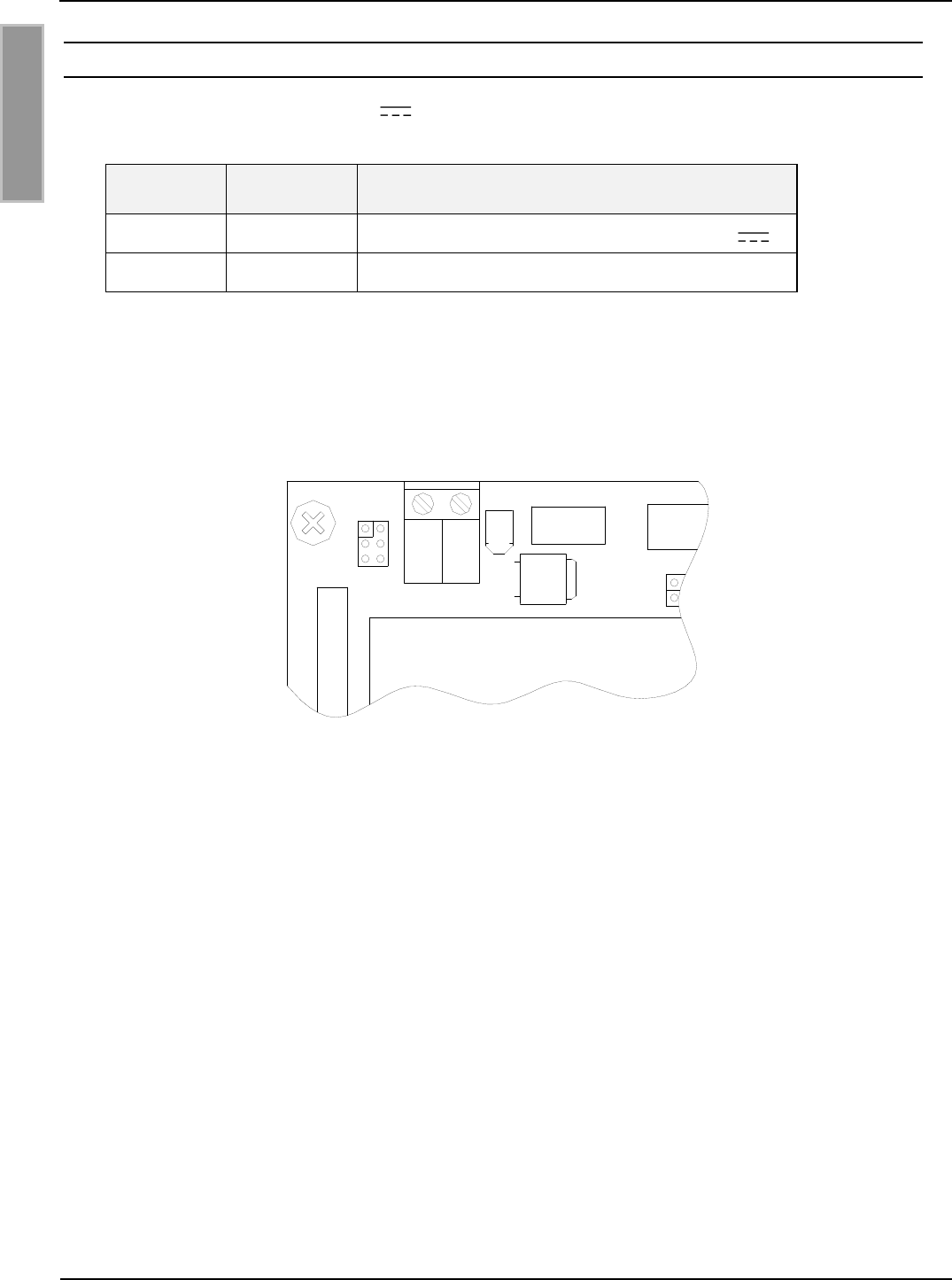
OBID i-scan®
Montage
ID ISC.LRM2500-A
FEIG ELECTRONIC GmbH
Seite 12 von 63
M10210-0de-ID-B.doc
D E U T S C H
2.4 Versorgungsspannung
Die Versorgungsspannung von 24 V ist an der Klemme X6 anzuschließen.
Klemme
Kurzzeichen
Beschreibung
X6 / Pin 1
VDC
Vcc – Versorgungsspannung +24 V DC /
X6 / Pin 2
GND
Ground – Versorgungsspannung
Tabelle 3: Pinbelegung Versorgungsspannung
GND
VDC
X8
X6
F1
1
2
Abbildung 4: Position der Klemme X6 für die Versorgungsspannung
Hinweis:
Eine Verpolung der Versorgungsspannung kann zur Zerstörung des Gerätes führen.
Für die Einhaltung der nationalen Vorschriften bezüglich Funkanlagen muss die Versor-
gungsspannungszuleitung mit dem beigefügten EMV-Ringkernferrit 28 mm x 20 mm
versehen werden. Hierzu ist das Kabel mindestens fünf mal, eng anliegend durch den
EMV-Ringkernferrit zu schleifen. Der Abstand zwischen Readeranschluss und Ringkern
sollte dabei maximal 10 cm betragen.
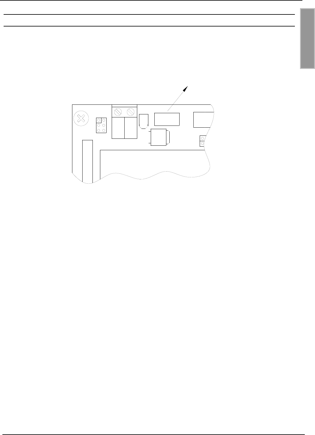
OBID i-scan®
Montage
ID ISC.LRM2500-A
FEIG ELECTRONIC GmbH
Seite 13 von 63
M10210-0de-ID-B.doc
D E U T S C H
2.5 Sicherung F1
Der Reader ist über eine SMD Sicherung 2,5A (träge) abgesichert.
Achtung:
Die interne und externe Spannungsversorgung der digitalen Ein- und Ausgänge an X2
ist nicht über die Sicherung F1 abgesichert.
X8
X6
F1
2,5 A träge
Abbildung 5: Position der Sicherung F1
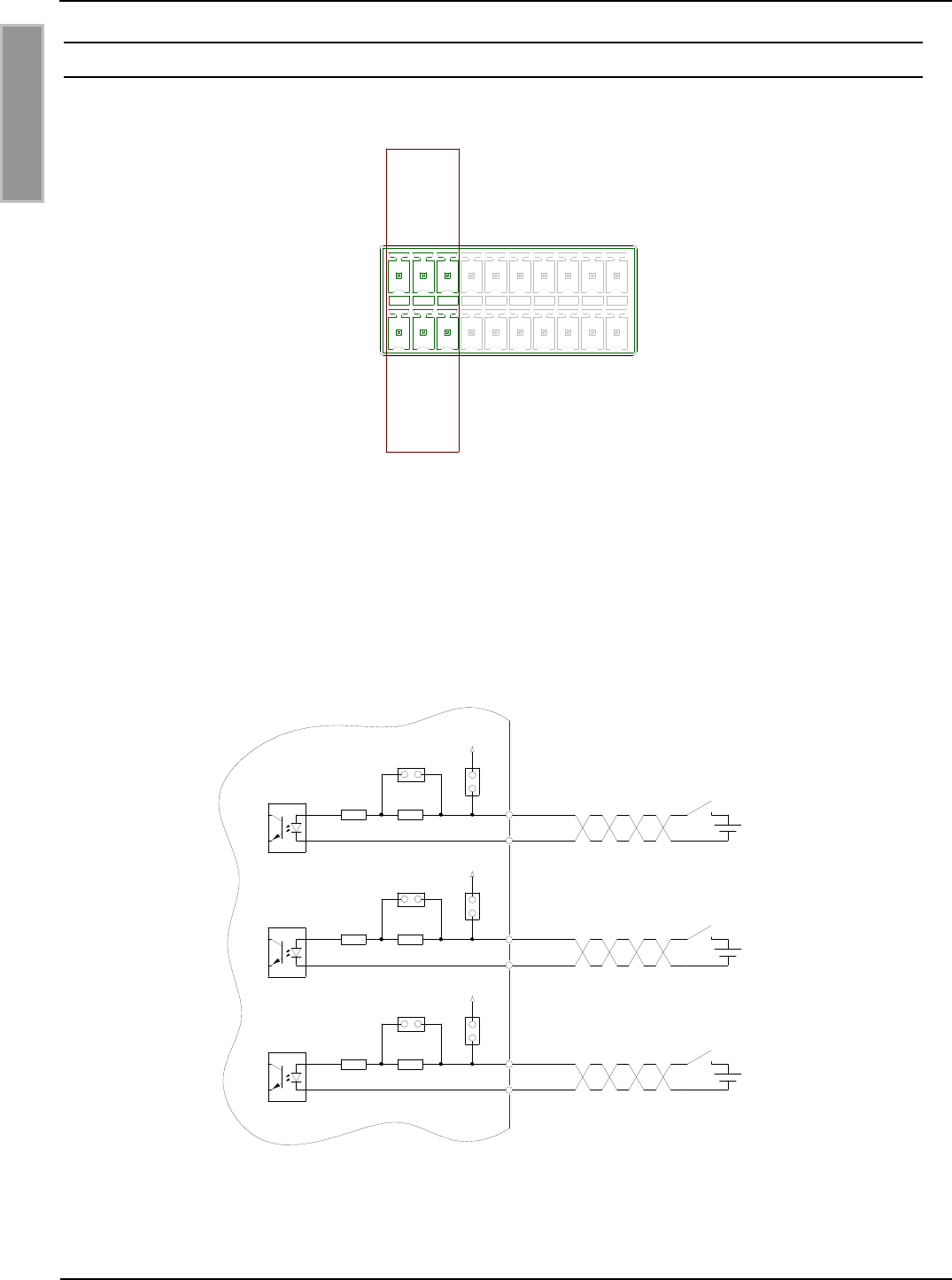
OBID i-scan®
Montage
ID ISC.LRM2500-A
FEIG ELECTRONIC GmbH
Seite 14 von 63
M10210-0de-ID-B.doc
D E U T S C H
2.6 Optokoppler Eingänge (X2 / IN1, IN2, IN3)
Die drei Optokoppler Eingänge sind auf dem Klemmleiste X2 zugänglich.
X2
IN1-
REL3-COM
REL2-COM
REL1-COM
GND
IN3-
IN2-
GND
OUT2-E
IN1+
OUT1-C
GND
IN3+
IN2+
OUT2-C
REL3-NO
REL2-NO
REL1-NO
24V
OUT1-E
Abbildung 6: Digitale Eingänge an der Klemmleiste X2
Die Optokoppler an der Klemmleiste X2 sind galvanisch von der Reader-Elektronik getrennt und
müssen daher mit einer externen Spannung versorgt werden, siehe Abbildung 7.
Die externe VCC Spannung kann jedoch auch von dem Reader zur Verfügung gestellt werden
siehe: Abbildung 8.
Alle 3 Eingänge sind identisch aufgebaut und lassen sich einzeln konfigurieren.
470 +
IN1 -Uext
820 J2
J1 24 V
470 +
IN2 -Uext
820 J4
J3 24 V
470 +
IN3 -Uext
820 J6
J5 24 V
Abbildung 7: Externe Spannungsversorgung der Optokoppler am Anschluss X2
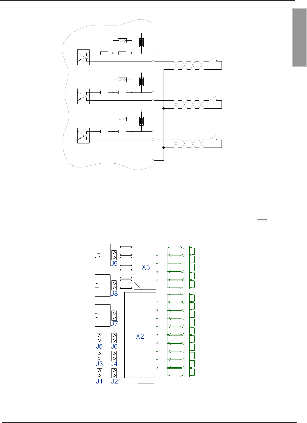
OBID i-scan®
Montage
ID ISC.LRM2500-A
FEIG ELECTRONIC GmbH
Seite 15 von 63
M10210-0de-ID-B.doc
D E U T S C H
470 +
IN1 -
820 J2
J1 24 V
470 +
IN2 -
820 J4
J3 24 V
470 +
IN3 -
820 J6
J5 24 V
GND
Abbildung 8: Mögliche interne Spannungsversorgung der Optokoppler am Anschluss X2
Die Eingangs-LED der Optokoppler sind intern mit einem Serienwiderstand von 1290 beschaltet
um den Eingangsstrom auf max. 20 mA zu begrenzen. Bei Spannungen kleiner als 10V muss
mit dem dazugehörigen Jumper (J1, J3, J5) ein Teil des Vorwiderstandes überbrückt werden.
Abbildung 9: Position der Jumper J1- J9
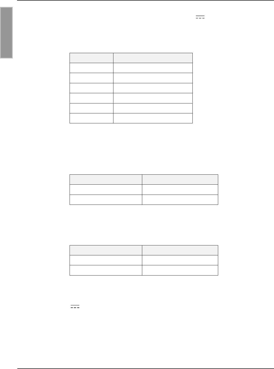
OBID i-scan®
Montage
ID ISC.LRM2500-A
FEIG ELECTRONIC GmbH
Seite 16 von 63
M10210-0de-ID-B.doc
D E U T S C H
Hinweise:
Der Eingang ist für eine maximale Eingangsspannung von 24 V und einem Eingangs-
strom von maximal 20 mA ausgelegt.
Verpolung oder Überlastung des Eingangs führt zu dessen Zerstörung.
Jumper
Beschreibung
J1
Vorwiderstand IN1 (X2)
J2
VCC IN1 (X2)
J3
Vorwiderstand IN2 (X2)
J4
VCC IN2 (X2)
J5
Vorwiderstand IN3 (X2)
J6
VCC IN3 (X2)
Tabelle 4: Jumper der Eingänge IN1,IN2 und IN3
Tabelle 5: Benötigter Vorwiderstand zeigt die benötigten Vorwiderstande bei den verschiedenen
externen Spannungen
Externe Spannung Uext
Jumper J1/J3/J5
5 V ... 10 V
Geschlossen
10 V ... 24 V
offen
Tabelle 5: Benötigter Vorwiderstand
Tabelle 6: zeigt die Jumperstellung für externe oder interne Spannungsversorgung
Jumper
Jumper J2/J4/J6
externe Spannung
offen
interne VCC Spannung
geschlossen
Tabelle 6: Interne / Externe Spannungsversorgung
Hinweise:
Die interne 24V Versorgungsspannung für die Optokoppler Eingänge ist nicht über
die Sicherung F1 abgesichert.
Die gleichzeitige Verwendung der internen und einer externen Versorgungsspannung
kann zur Zerstörung des Gerätes führen.
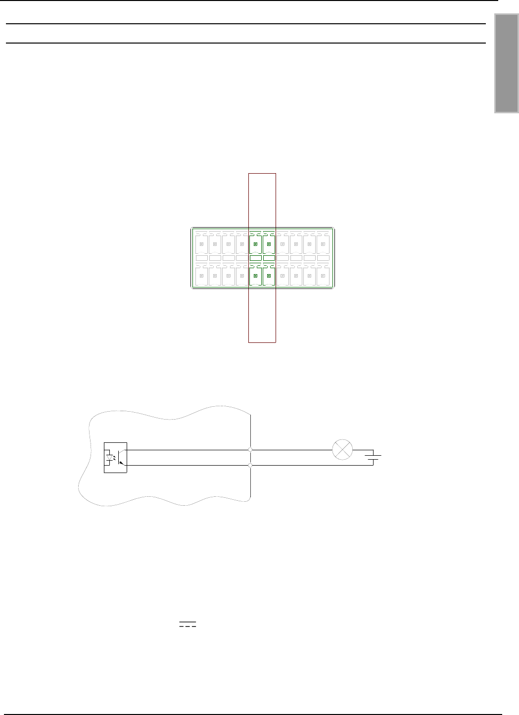
OBID i-scan®
Montage
ID ISC.LRM2500-A
FEIG ELECTRONIC GmbH
Seite 17 von 63
M10210-0de-ID-B.doc
D E U T S C H
2.7 Optokoppler Ausgänge (X2 / OUT1, OUT2)
Der Transistoranschluss, Kollektor und Emitter, der Optokoppler Ausgänge sind von der Rea-
der-Elektronik galvanisch getrennt und ohne interne Zusatzbeschaltung an Klemme X2 nach
außen geführt. Der Ausgang muss daher mit einer externen Spannung betrieben werden. Die
digitalen Ausgänge OUT1 und OUT2 können im Scan Mode als Data-Takt-Schnittstelle ver-
wendet werden. OUT1 => „Clock“, OUT2 => „Data“
OUT1-E
IN1-
REL3-COM
REL2-COM
REL1-COM
GND
IN3-
IN2-
GND
OUT2-E
IN1+
OUT1-C
GND
IN3+
IN2+
OUT2-C
REL3-NO
REL2-NO
REL1-NO
24V
X2
Abbildung 10: Digitale Ausgänge an der Klemmleiste X2
OUT1..2 E
C
Uext
Abbildung 11: Interne und mögliche externe Beschaltung der Optokoppler-Ausgänge OUT1-2
Hinweise:
Der Ausgang ist für max. 24 V / 30 mA ausgelegt.
Verpolung oder Überlastung des Ausgangs führt zu dessen Zerstörung.
Der Ausgang ist nur zum Schalten ohmscher Lasten vorgesehen.
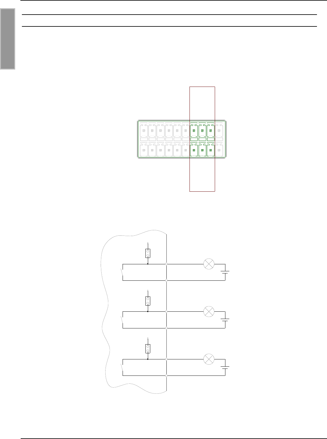
OBID i-scan®
Montage
ID ISC.LRM2500-A
FEIG ELECTRONIC GmbH
Seite 18 von 63
M10210-0de-ID-B.doc
D E U T S C H
2.8 Relais (X2 / REL1, REL2, REL3)
Als Relaisausgänge stehen drei Schließer zur Verfügung. Die jeweiligen Kontakte stehen an den
Klemme X2 zur Verfügung. Die Ausgänge sind galvanisch von der Reader-Elektronik getrennt und
müssen daher mit einer externen Spannung versorgt werden. Die externe Spannung kann jedoch
auch von Karte über die Jumper J7;J8;J9 zur Verfügung gestellt werden. Alle 3 Ausgänge sind
identisch aufgebaut und lassen sich einzeln konfigurieren.
IN1-
REL3-COM
REL2-COM
REL1-COM
GND
IN3-
IN2-
GND
OUT2-E
IN1+
OUT1-C
GND
IN3+
IN2+
OUT2-C
REL3-NO
REL2-NO
REL1-NO
24V
OUT1-E
X2
Abbildung 12: Relais Ausgänge an der Klemmleiste X2
REL1
COM
N0 NO
COM
Uext
J7
24 V
REL2
COM
N0 NO
COM
Uext
J8
24 V
REL3
COM
N0 NO
COM
Uext
J9
24 V
Abbildung 13: Interne und mögliche externe Beschaltung der Relaisausgänge

OBID i-scan®
Montage
ID ISC.LRM2500-A
FEIG ELECTRONIC GmbH
Seite 19 von 63
M10210-0de-ID-B.doc
D E U T S C H
Jumper
Beschreibung
J7
VCC - REL 1 (X2)
J8
VCC - REL 2 (X2)
J9
VCC - REL 3 (X2)
Tabelle 7: Zuordnung der Jumper zu den Relais Ausgänge
Tabelle 8 zeigt die Jumperstellung für externe oder interne Spannungsversorgung
Jumper
Jumper J7/J8/J9
externe Spannung
offen
interne VCC Spannung
geschlossen
Tabelle 8: Interne / Externe Spannungsversorgung
Hinweise:
Der Relaisausgang ist für max. 24 V / 1 A ausgelegt.
Der Relaisausgang ist nur zum Schalten ohmscher Lasten vorgesehen. Im Falle einer
induktiven Last sind die Relaiskontakte durch eine externe Schutzbeschaltung zu schüt-
zen.
Die interne 24V Versorgungsspannung für die Relais ist nicht über die Sicherung F1
abgesichert.
Die gleichzeitige Verwendung der internen und einer externen Versorgungsspannung
kann zur Zerstörung des Gerätes führen.
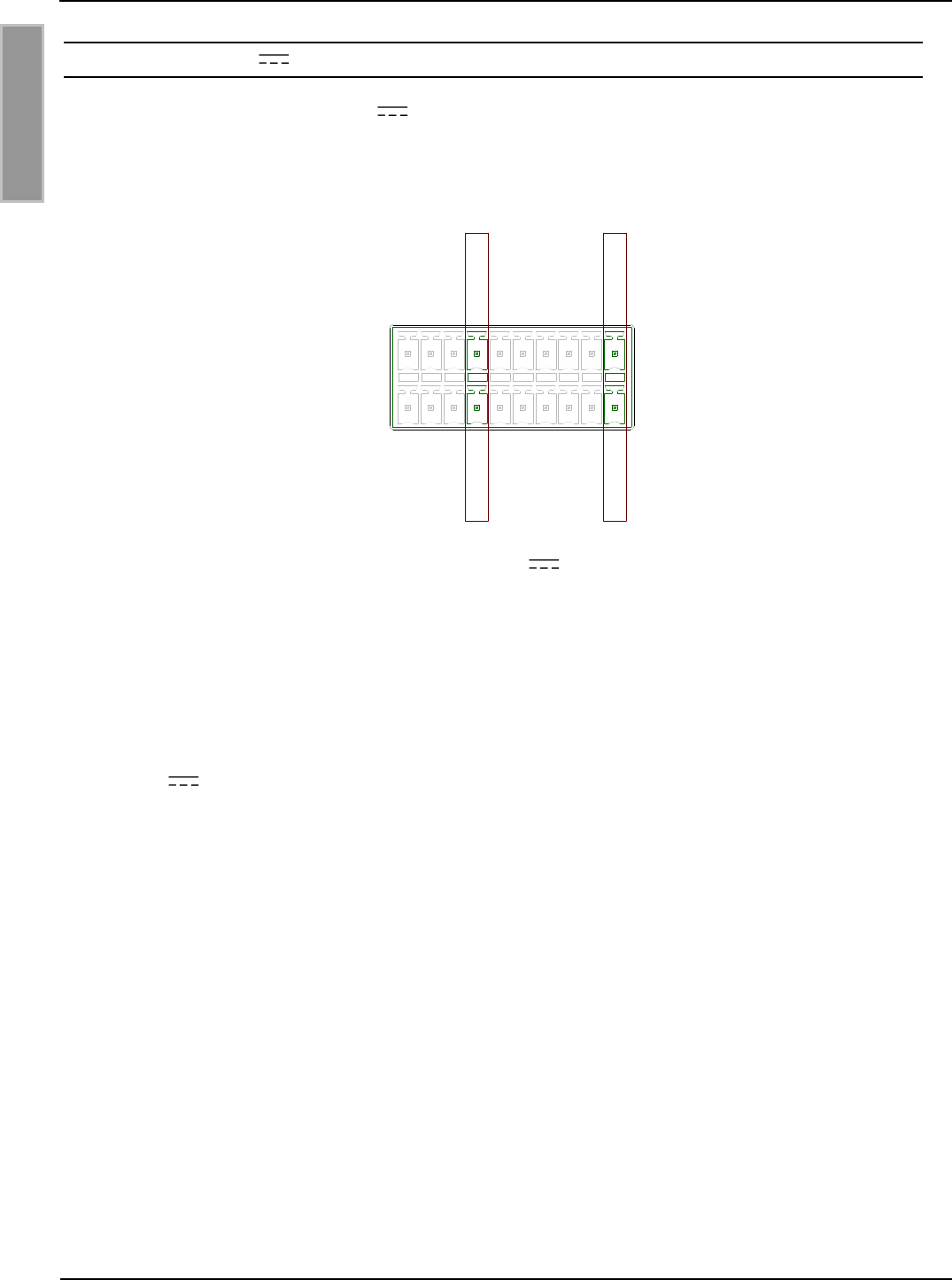
OBID i-scan®
Montage
ID ISC.LRM2500-A
FEIG ELECTRONIC GmbH
Seite 20 von 63
M10210-0de-ID-B.doc
D E U T S C H
2.9 Ausgang 24V (X2 / 24V, GND)
Am Ausgang 24V/GND stehen 24V für die externe Spannungsversorgung der digitalen Ein-
und Ausgänge sowie der Relais zur Verfügung. Die maximal Stromentnahme darf 500mA nicht
überschreiten. Dabei ist eine mögliche Stromentnahme über die die Jumper J2,J4,J6 bzw. J7,J8,J9
mit zu berücksichtigen.
X2
IN1-
REL3-COM
REL2-COM
REL1-COM
GND
IN3-
IN2-
GND
OUT2-E
IN1+
OUT1-C
GND
IN3+
IN2+
OUT2-C
REL3-NO
REL2-NO
REL1-NO
24V
OUT1-E
Abbildung 14: Mögliche externe 24V Spannungsversorgung
Hinweise:
Die an diesem Ausgang entnommene Leistung für die externe Beschaltung muss bei der
Dimensionierung des Netzteils zusätzlich zu der typischen Reader Leistung mit berück-
sichtigt werden.
Die 24V Versorgungsspannung an X2 ist nicht über die Sicherung F1 abgesichert.
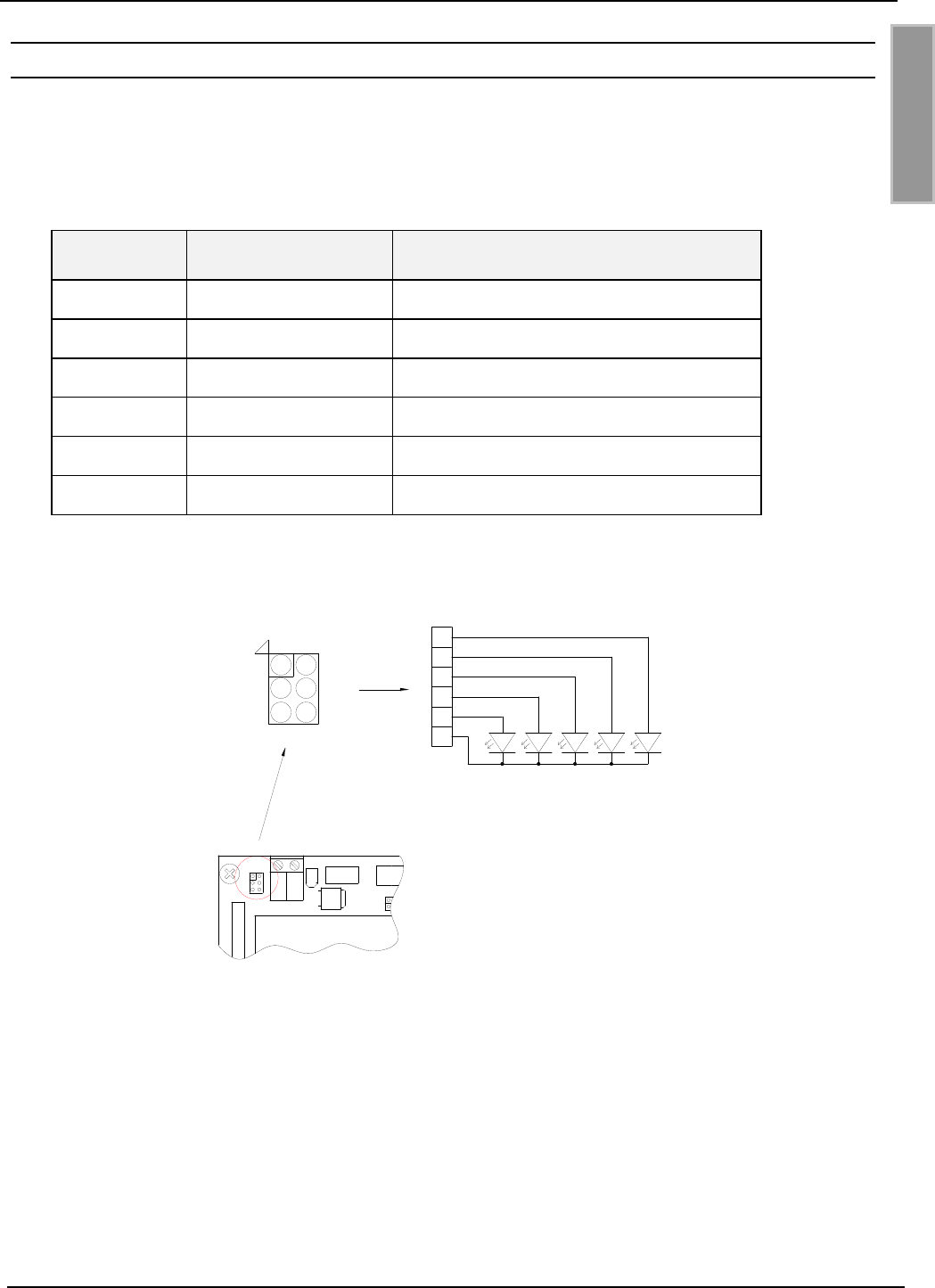
OBID i-scan®
Montage
ID ISC.LRM2500-A
FEIG ELECTRONIC GmbH
Seite 21 von 63
M10210-0de-ID-B.doc
D E U T S C H
2.10 Anschluss externer Diagnose-LEDs X8
X8 ermöglicht den Anschluss zusätzlicher externer LEDs parallel zu den internen Diagnose-LEDs.
Der Anschluss der externen LEDs erfolgt gemäß Abbildung 15: Anschluss externer LEDs an X8,
siehe Abbildung 15.
Klemme
Kurzzeichen
Beschreibung
X8 / Pin 1
V1 Anode ext.
Funktion entspricht interner LED V1
X8 / Pin 2
V2 Anode ext.
Funktion entspricht interner LED V2
X8 / Pin 3
V3 Anode ext.
Funktion entspricht interner LED V3
X8 / Pin 4
V4 Anode ext.
Funktion entspricht interner LED V4
X8 / Pin 5
V5 Anode ext.
Funktion entspricht interner LED V5
X8 / Pin 6
GND
Gemeinsamer GND-Anschluss
Tabelle 9: Pinbelegung externe LEDs
5
3
12
4
6
6
2
3
4
5V5 V4
Externe LEDs
X8
V2V3 V1
X8 1
X8
X6
F1
Abbildung 15: Anschluss externer LEDs an X8
Hinweis:
Die Ausgänge an X8 sind nur zum Schalten einer externen LED vorgesehen. Überlastung
der Ausgänge durch andere Lasten kann zu deren Zerstörung führen.
Bei Nutzung von nur einem Ausgang, liegt die maximale Stromentnahme bei Imax=15mA.
Der Gesamtstrom aller 5 Ausgänge zusammen, darf 25mA nicht überschreiten. Die Leer-
laufausgangsspannung liegt bei 3,3V und wird über einen 220Ohm Serienwiderstand zur
Verfügung gestellt.
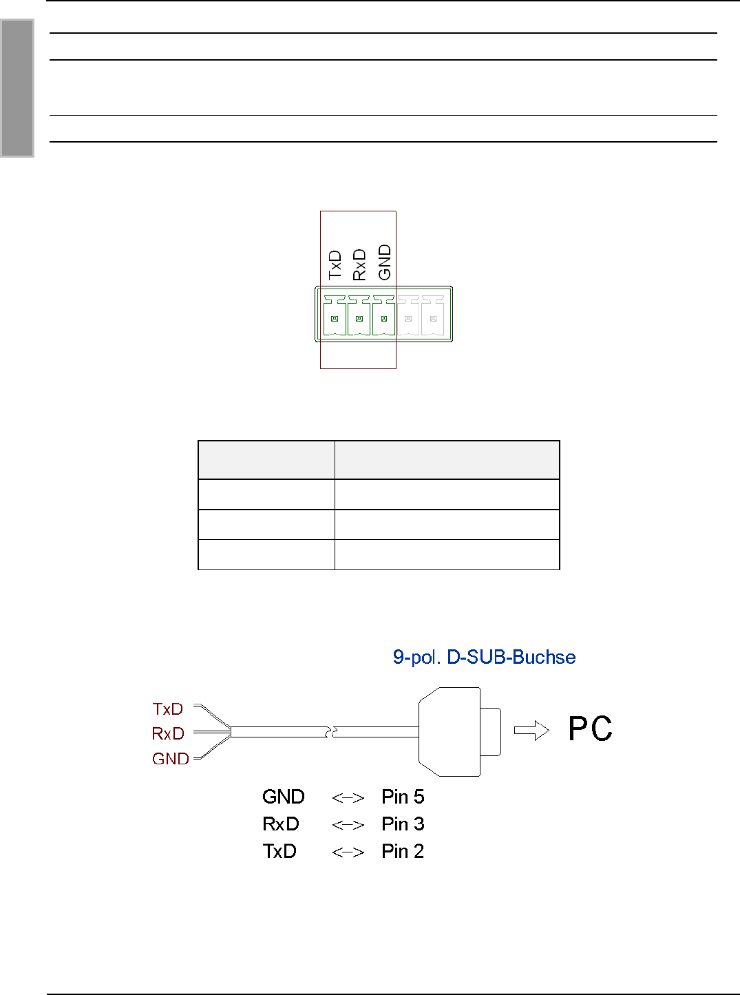
OBID i-scan®
Montage
ID ISC.LRM2500-A
FEIG ELECTRONIC GmbH
Seite 22 von 63
M10210-0de-ID-B.doc
D E U T S C H
2.11 Schnittstellen
2.11.1 RS232-Schnittstelle X3
Der Anschluss der RS232-Schnittstelle erfolgt über X3. Die Übertragungsparameter können per
Softwareprotokoll konfiguriert werden.
Abbildung 16: Anschlussbelegung X3 (RS232-Schnittstelle)
Kurzzeichen
Beschreibung
TxD
RS232 – (Transmit)
RxD
RS232 – (Receive)
GND
RS232 – (Ground)
Tabelle 10 Pinbelegung RS232-Schnittstelle
Abbildung 17: Verdrahtungsbeispiel für den Anschluss der RS232-Schnittstelle
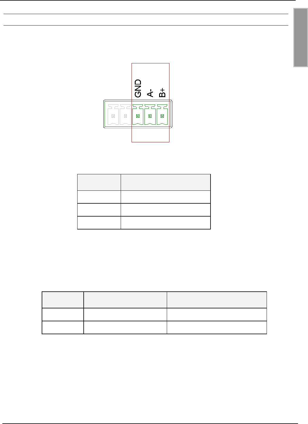
OBID i-scan®
Montage
ID ISC.LRM2500-A
FEIG ELECTRONIC GmbH
Seite 23 von 63
M10210-0de-ID-B.doc
D E U T S C H
2.11.2 RS485-Schnittstelle X3
Der Anschluss der RS485-Schnittstelle erfolgt ebenfalls über X3.
Die Übertragungsparameter können per Softwareprotokoll konfiguriert werden.
Kurzzeichen
Beschreibung
GND
RS485 – GND
A-
RS485 – (A -)
B+
RS485 – (B +)
Tabelle 11 Pinbelegung RS485-Schnittstelle
Mit den Jumpern J10 und J11 können „Pull up“ und „Pull down“ Widerstände im Bedarfsfall zuge-
schaltet werden.
Jumper
Geschlossen
offen
J10
Pull-Down an RS4xx - A
ohne Pull-Down an RS4xx - A
J11
Pull-Up an RS4xx - B
ohne Pull-Up an RS4xx - B
Tabelle 12: Jumper der RS485-Schnittstelle
Hinweis:
Der Abschlusswiderstand (Terminator) kann per Software in der Reader-Konfiguration dazu
geschaltet werden.
Abbildung 18 Anschlussbelegung X3 (RS485-Schnittstelle):

OBID i-scan®
Montage
ID ISC.LRM2500-A
FEIG ELECTRONIC GmbH
Seite 24 von 63
M10210-0de-ID-B.doc
D E U T S C H
J11
VCC
J10
500
500
RS485 +
RS485 -
Abbildung 19: Jumper der RS485-Schnittstelle
Abbildung 20: Position der Jumper J10, J11
Hinweis:
Wird ein Gate People Counter an der RS485 Schnittstelle betrieben steht die RS485 Schnitt-
stelle nicht mehr für die Host Kommunikation zur Verfügung.
2.11.2.1 Adresseinstellung RS485 für Busbetrieb
Für den Busbetrieb bietet der Reader die Möglichkeit, die benötigte Busadresse per Software zu
vergeben.
Die Adressvergabe erfolgt über den Host-Rechner. Mit Hilfe der Software können dem Reader die
Adressen "0" bis "254" zugewiesen werden.
Eine evtl. notwendige Terminierung des RS485 Bus kann ebenfalls per Software konfiguriert wer-
den. Siehe Systemhandbuch.
Hinweis:
Da alle Reader werksseitig die Adresse 0 eingestellt haben, müssen sie nacheinander ange-
schlossen und konfiguriert werden.

OBID i-scan®
Montage
ID ISC.LRM2500-A
FEIG ELECTRONIC GmbH
Seite 25 von 63
M10210-0de-ID-B.doc
D E U T S C H
2.11.3 USB – Schnittstelle X4 (Host Kommunikation, HDI)
Der Anschluss der USB-Schnittstelle erfolgt über Buchse X4. Die Belegung ist genormt. Die Daten-
rate des Readers ist auf 12 Mbit beschränkt (USB Full Speed). Es kann ein Standard-USB-Kabel
verwendet werden.
Hinweis:
Die maximale Länge des USB-Kabels darf 5 m betragen. Längere Kabel sind nicht erlaubt.
2.11.4 USB – Host X5
Der Anschluss der USB-Host erfolgt über Buchse X5. Die Belegung ist genormt. Die Datenrate des
Readers ist auf 12 Mbit beschränkt (USB Full Speed). Der USB Anschluss kann für ein Standard
WLAN-Stick genutzt werden.
Hinweis:
Es können handelübliche WLAN Sticks eingesetzt werden, die über einen „Ralink“ Chip-
satz „RT2500 USB“ oder „RT73“ verfügen.
Abbildung 21: USB-Schnittstelle für Host Kommunikation
X4
Abbildung 22: USB-Host X5

OBID i-scan®
Montage
ID ISC.LRM2500-A
FEIG ELECTRONIC GmbH
Seite 26 von 63
M10210-0de-ID-B.doc
D E U T S C H
2.11.5 Ethernet-Schnittstelle an X1 (10/100 Base-T)
Der Reader verfügt über eine integrierte 10/100 Base-T Netzwerkschnittstelle mit Standard RJ-45-
Anschluss. Der Anschluss erfolgt über X1 und hat eine automatische „Crossover Detection“ ent-
sprechend dem 1000 Base-T Standard.
Bei einer strukturierten Verkabelung sollten mindestens Kabel der Kategorie CAT5 verwendet wer-
den. Dies garantiert einen problemlosen Betrieb bei 10 Mbps oder 100 Mbps.
Voraussetzung für den Einsatz des TCP/IP-Protokolls ist, dass jedes Gerät am Netzwerk über eine
eigene IP-Adresse verfügt. Alle Reader verfügen über eine werksseitig voreingestellte IP-Adresse.
Netzwerk
Adresse
IP-Adresse
192.168.10.10
Subnet-Mask
255.255.255.0
Port
10001
DHCP
AUS
Tabelle 13: Werkskonfiguration der Ethernet-Schnittstelle
Hinweis:
Der Reader verfügt über eine DHCP-fähige TCP/IP Schnittstelle, die werkseitig ausgeschal-
tet ist.
X1
Abbildung 23: LAN Schnittstelle für Host Kommunikation

OBID i-scan®
Montage
ID ISC.LRM2500-A
FEIG ELECTRONIC GmbH
Seite 27 von 63
M10210-0de-ID-B.doc
D E U T S C H
3 Bedien- und Anzeigeelemente
3.1 LEDs
Tabelle 1 zeigt die Konfiguration der LEDs.
Kurzzeichen
Beschreibung
LED V1 (grün)
"RUN-LED 1"
- Signalisiert den ordnungsgemäßen Ablauf der
internen Reader-Software (DSP)
- Leuchtet während der Reader-Initialisierung nach dem Ein-
schalten bzw. nach einem Reset.
LED V2 (blau)
Diagnose 1: RF-Kommunikation / EEPROM-Status
- Signalisiert durch ein kurzes Blinken die fehlerfreie Kommuni-
kation mit einem Transponder auf der RF-Schnittstelle
- Blinkt abwechselnd mit V1 nach dem Reset im Anschluss an
ein Software-Update
- Blinkt abwechselnd mit V1 falls nach einem Reset ein Daten-
fehler beim Lesen der Parameter auftrat
LED V3 (gelb)
Diagnose 2: Host-Kommunikation
- Signalisiert durch ein kurzes Blinken das Senden eines Proto-
kolls an den Host auf der RS232/RS485/USB/LAN-Schnittstelle
LED V4 (gelb)
Reserviert
LED V5 (rot)
Diagnose 4: RF-Warnung
- Leuchtet bei einem Fehler im RF-Teil des Readers. Der Feh-
lertyp kann per Software über die RS232/RS485/USB/LAN-
Schnittstelle ausgelesen werden
Tabelle 14: Konfiguration der LEDs

OBID i-scan®
Montage
ID ISC.LRM2500-A
FEIG ELECTRONIC GmbH
Seite 28 von 63
M10210-0de-ID-B.doc
D E U T S C H
3.2 Taster T1
Kurzzeichen
Beschreibung
T1
Reader Reset-Taste
Tabelle 15: Reset-Taste
- Durch betätigen von T1 wird am Reader ein CPU-Reset durchgeführt

OBID i-scan®
Montage
ID ISC.LRM2500-A
FEIG ELECTRONIC GmbH
Seite 29 von 63
M10210-0de-ID-B.doc
D E U T S C H
4 Funkzulassungen
4.1 Europa (CE)
Die Funkanlage entspricht, bei bestimmungsgemäßer Verwendung den grundlegenden Anforde-
rungen des Artikels 3 und den übrigen einschlägigen Bestimmungen der R&TTE Richtlinie
1999/5/EG vom März 99.
Equipment Classification gemäß ETSI EN 300 440 und ETSI EN 301 489: Class 2

OBID i-scan®
Montage
ID ISC.LRM2500-A
FEIG ELECTRONIC GmbH
Seite 30 von 63
M10210-0de-ID-B.doc
D E U T S C H
4.2 USA (FCC) und Kanada (IC)
Product name:
ID ISC.LRM2500-A
Reader name:
ID ISC.LRM2500-A
FCC ID:
IC:
PJMLRM2500
6633A-LRM2500
Notice for USA and
Canada
This device complies with Part 15 of the FCC Rules and with
RSS-210 of Industry Canada.
Operation is subject to the following two conditions.
(1) this device may not cause harmful interference, and
(2) this device must accept any interference received,
including interference that may cause undesired operation.
Unauthorized modifications may void the authority granted under
Federal communications Commission Rules permitting the operation
of this device.
This equipment has been tested and found to comply with the limits for
a Class A digital device, pursuant to Part 15 of the FCC Rules. These
limits are designed to provide reasonable protection against harmful
interference when the equipment is operated in a commercial
environment. This equipment generates, uses, and can radiate radio
frequency energy and, if not installed and used in accordance with the
instruction manual, may cause harmful interference to radio
communications. Operation of this equipment in a residential area is
likely to cause harmful interference in which case the user will be
required to correct the interference at his own expense.
Le présent appareil est conforme aux CNR d'Industrie Canada appli-
cables aux appareils radio exempts de licence. L'exploitation est auto-
risée aux deux conditions suivantes :
(1) l'appareil ne doit pas produire de brouillage, et
(2) l'utilisateur de l'appareil doit accepter tout brouillage radioélectrique
subi, même si le brouillage est susceptible d'en compromettre le fonc-
tionnement.
Warning: Changes or modification made to this equipment not expressly approved by
FEIG ELECTRONIC GmbH may void the FCC authorization to operate this equipment.

OBID i-scan®
Montage
ID ISC.LRM2500-A
FEIG ELECTRONIC GmbH
Seite 31 von 63
M10210-0de-ID-B.doc
D E U T S C H
5 Technische Daten
ID ISC.LRM2500-A
Mechanische Daten
Abmessungen ( B x H x T )
160 mm x 120 mm x 46 mm
Gewicht
ca. 0,6 kg
Elektrische Daten
Spannungsversorgung
24 V 15 %
Noise Ripple : max. 150 mV
Leistungsaufnahme
Typisch 35 VA / maximal 47VA (je nach ext.
Beschaltung)
Betriebsfrequenz
13,56 MHz
Sendeleistung
2 W – 12 W
(per Software in 250 mW Schritten einstellbar)
Modulationsgrad
10% - 30%
(per Software einstellbar)
Antennenanschluss
SMA Buchse (50)
Gleichspannung auf
der Antennenleitung
8 V (max. 150mA)
Diagnoseoptionen
internes VSWR-Meter
interne Temperaturüberwachung
Ausgänge:
– 2 Optokoppler
– 3 Relais ( 3 x Schließer)
24 V / 30 mA (Optional nutzbar als Data Clock IF)
24 V / 1 A
Eingänge
– 3 Optokoppler
5-24 V / 20 mA (siehe Kapitel 2.6)
Schnittstellen
RS232
RS485
USB – Interface (HID)
USB – Host (WLAN)
Ethernet (TCP/IP)
Data Clock

OBID i-scan®
Montage
ID ISC.LRM2500-A
FEIG ELECTRONIC GmbH
Seite 32 von 63
M10210-0de-ID-B.doc
D E U T S C H
Protokoll Modi
FEIG ISO HOST
BRM (Datenfilterung und Datenpufferung)
Scan Mode
Notification Mode
Unterstützte Transponder
ISO15693, ISO18000-3-A
(EM HF ISO Chips, Fujitsu HF ISO Chips, KSW
Sensor Chips, Infineon my-d, NXP I-Code, STM
ISO Chips, TI Tag-it)
NXP I Code 1
Signalgeber, optisch
5 LEDs zur Diagnose des Betriebszustandes
Umgebungsbedingungen
Temperaturbereich
– Betrieb
– Lagerung
-20°C bis +55°C
-25°C bis +85°C
Luftfeuchtigkeit
5% - 80%, nicht kondensierend
Vibration
EN60068-2-6
10 Hz bis 150 Hz : 0,075 mm / 1 g
Schock
EN60068-2-27
Beschleunigung : 30 g
Zulassung
Zulassung Funk
– Europa
– USA
- Canada
EN 300 330
FCC 47 CFR Part 15
RSS 210
EMV
EN 301 489
Sicherheit
– Elektrische Sicherheit
– Human Exposure
EN 60950
EN 50364

OBID i-scan®
Installation
ID ISC.LRM2500-A
FEIG ELECTRONIC GmbH
Page 34 of 63
M10210-0de-ID-B.doc
E N G L I S H
Note
Copyright 2011 by
FEIG ELECTRONIC GmbH
Lange Strasse 4
D-35781 Weilburg-Waldhausen
Tel.: +49 6471 3109-0
http://www.feig.de
With the edition of this document, all previous editions become void. Indications made in this manual may be
changed without previous notice.
Copying of this document, and giving it to others and the use or communication of the contents thereof are
forbidden without express authority. Offenders are liable to the payment of damages. All rights are reserved
in the event of the grant of a patent or the registration of a utility model or design.
Composition of the information in this document has been done to the best of our knowledge. FEIG
ELECTRONIC GmbH does not guarantee the correctness and completeness of the details given in this
manual and may not be held liable for damages ensuing from incorrect or incomplete information. Since,
despite all our efforts, errors may not be completely avoided, we are always grateful for your useful tips.
The instructions given in this manual are based on advantageous boundary conditions. FEIG ELECTRONIC
GmbH does not give any guarantee promise for perfect function in cross environments.
FEIG call explicit attention that devices which are subject of this document are not designed with compo-
nents and testing methods for a level of reliability suitable for use in or in connection with surgical implants or
as critical components in any life support systems whose failure to perform can reasonably be expected to
cause significant injury to a human. To avoid damage, injury, or death, the user or application designer must
take reasonably prudent steps to protect against system failures.
FEIG ELECTRONIC GmbH assumes no responsibility for the use of any information contained in this docu-
ment and makes no representation that they free of patent infringement. FEIG ELECTRONIC GmbH does
not convey any license under its patent rights nor the rights of others.
OBID® and OBID i-scan® are registered trademarks of FEIG ELECTRONIC GmbH.
my-d® is a registered trademark of Infineon Technologies AG
I-CODE® is a registered trademark of Philips Electronics N.V.
Tag-itTM is a registered trademark of Texas Instruments Incorporated.

OBID i-scan®
Installation
ID ISC.LRM2500-A
FEIG ELECTRONIC GmbH
Page 35 of 63
M10210-0de-ID-B.doc
E N G L I S H
Content
1 Safety Instructions / Warning - Read before start-up ! 37
2 Performance Features of Reader Family ID ISC.LRM2500 38
2.1 Performance Features .............................................................................................. 38
2.2 Available Reader Types ............................................................................................ 38
3 Installation and mounting 39
3.1 Mounting ................................................................................................................... 39
3.2 Terminals ................................................................................................................... 41
3.3 Antenna connection ................................................................................................. 42
3.4 Supply voltage .......................................................................................................... 43
3.5 Fuse F1 ...................................................................................................................... 44
3.6 X2: Optokoppler Inputs (X2 / IN1, IN2, IN3) ............................................................. 45
3.7 Optocoupler outputs (X2 / OUT1, OUT2) ................................................................. 48
3.8 Relay (X2 / REL1, REL2, REL3) ................................................................................ 49
3.9 Output 24V (X2 / 24V, GND) .............................................................................. 51
3.10 X8: External diagnostic LED connections .............................................................. 52
3.11 Interfaces ................................................................................................................... 53
3.11.1 RS232-Interface X3 ................................................................................................ 53
3.11.2 RS485-Interface X3 ................................................................................................ 54
3.11.3 USB – Interface X4 (Host Communication, HDI) .................................................... 56
3.11.4 USB – Host X5 ....................................................................................................... 56
3.11.5 Ethernet-Interface on X1 (10/100 Base-T) .............................................................. 57
4 Operating and Display Elements 58
4.1 LEDs .......................................................................................................................... 58
4.2 Button T1 ................................................................................................................... 59

OBID i-scan®
Installation
ID ISC.LRM2500-A
FEIG ELECTRONIC GmbH
Page 36 of 63
M10210-0de-ID-B.doc
E N G L I S H
5 Radio Approvals 60
5.1 Europe (CE) ............................................................................................................... 60
5.2 USA (FCC) and Canada (IC) ..................................................................................... 61
6 Technical Data 62

OBID i-scan®
Installation
ID ISC.LRM2500-A
FEIG ELECTRONIC GmbH
Page 37 of 63
M10210-0de-ID-B.doc
E N G L I S H
1 Safety Instructions / Warning - Read before start-up !
The device may only be used for the purpose intended by the manufacturer.
The operation manual should be kept readily available at all times for each user.
Unauthorized changes and the use of spare parts and additional devices which have not been
sold or recommended by the manufacturer may cause fire, electric shocks or injuries. Such
unauthorized measures shall exclude the manufacturer from any liability.
The liability-prescriptions of the manufacturer in the issue valid at the time of purchase are valid
for the device. The manufacturer shall not be held legally responsible for inaccuracies, errors,
or omissions in the manual or automatically set parameters for a device or for an incorrect
application of a device.
Repairs may only be undertaken by the manufacturer.
Installation, operation, and maintenance procedures should only be carried out by qualified
personnel.
Use of the device and its installation must be in accordance with national legal requirements
and local electrical codes .
When working on devices the valid safety regulations must be observed.
Before touching the device, the power supply must always be interrupted. Make sure that the
device is without voltage by measuring. The fading of an operation control (LED) is no indicator
for an interrupted power supply or the device being out of voltage!
Special advice for wearers of cardiac pacemakers:
Although this device doesn't exceed the valid limits for electromagnetic fields you should keep
a minimum distance of 25 cm between the device and your cardiac pacemaker and not stay in
the immediate proximity of the device’s antenna for any length of time.

OBID i-scan®
Installation
ID ISC.LRM2500-A
FEIG ELECTRONIC GmbH
Page 38 of 63
M10210-0de-ID-B.doc
E N G L I S H
2 Performance Features of Reader Family ID ISC.LRM2500
2.1 Performance Features
The Reader has been developed for reading passive data carriers, so-called „Smart Labels“, using
an operating frequency of 13.56 MHz. For the operation it is necessary to connect a appropriate
external antenna to the connector ANT1.
2.2 Available Reader Types
The following Reader type’s are currently available:
Reader type
Description
ID ISC.LRM2500-A
Module version with RS232/485- / USB- / LAN-Interface, USB-
Host und Embedded Linux
ID ISC.LRM2500-B
Module version with RS232/485- / USB- / LAN-Interface
Table 1: Available Reader types
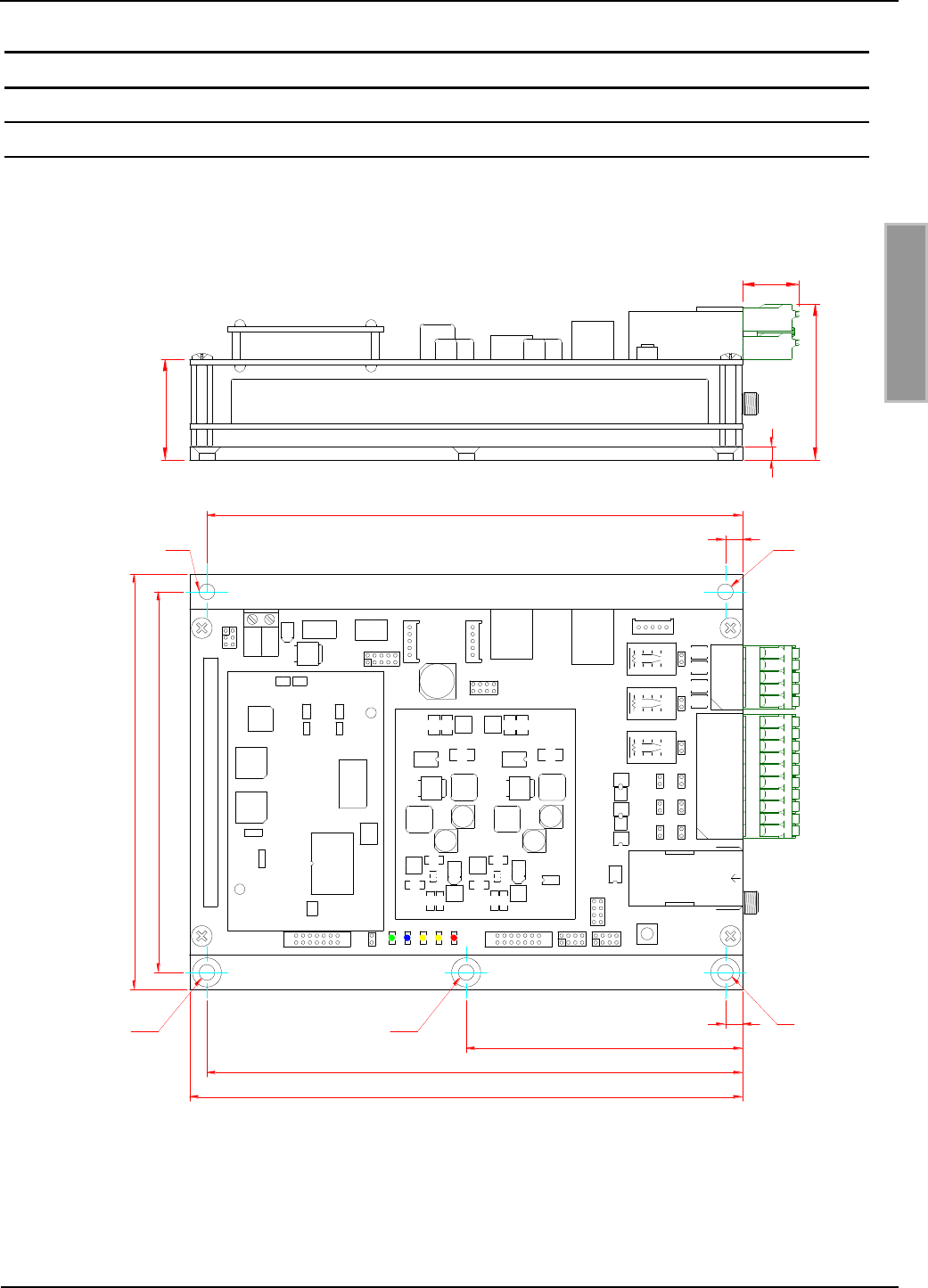
OBID i-scan®
Installation
ID ISC.LRM2500-A
FEIG ELECTRONIC GmbH
Page 39 of 63
M10210-0de-ID-B.doc
E N G L I S H
3 Installation and mounting
3.1 Mounting
The Reader Module is designed for installation on a heat sink. Mounting is accomplished using the
4.5 mm holes located in each corner of the base plate (see: Figure 1).
120
110
ø 4,5 mm*
160
155
80
ø 4,5 mm* ø 4,5 mm*
5
ø 4,5 mm
V4
V3
V2V1 V5
X8
X6
F1
J8
J9 X3
X4
X7
29
45
16,3
155
GND
VDC
ø 4,5 mm
5
4
X5
T1
X1
J2
J4
J1
J3
J6
J7
J5
X2
Figure 1: Scale drawing oft he Reader module with mounting plate

OBID i-scan®
Installation
ID ISC.LRM2500-A
FEIG ELECTRONIC GmbH
Page 40 of 63
M10210-0de-ID-B.doc
E N G L I S H
To fully exploit the performance of the Reader Module, the heat sink should have a thermal resis-
tance RThK of max. 1 K/W. When attaching the Reader Module to the heat sink you should strive for
a little heat transfer resistance between the base plate and the heat sink as possible. The use of
heat sink compound is recommended.
If the antenna is properly tuned and there is sufficient air convection along the mounting plate, the
ID ISC.LRM2000 can be operated without an additional heat sink at up to 2W of power. Note here
however that detuning of the antenna can result in additional heating of the Reader. In such cases
the Reader regulates its output power down until the upper temperature limit of its final stage fallen
down again.
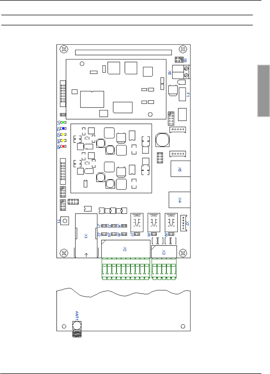
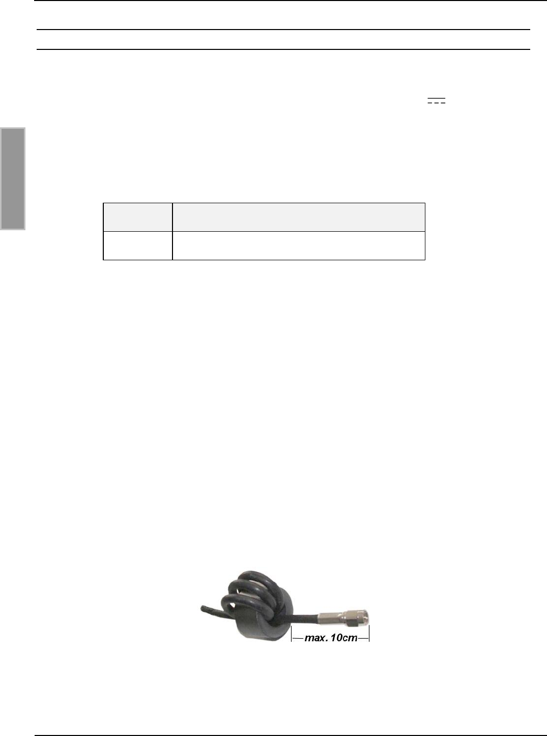
OBID i-scan®
Installation
ID ISC.LRM2500-A
FEIG ELECTRONIC GmbH
Page 42 of 63
M10210-0de-ID-B.doc
E N G L I S H
3.3 Antenna connection
The SMA socket „ANT1“ is located on the lower circuit board for connecting the antenna to the ID
ISC.LRM2500.
Active external function units (e.g. ID ISC.DAT) can also be supplied with 8 V through the an-
tenna terminal. The maximum current draw is then not allowed to exceed 150mA. This additional
power consumption must be considered for the total reader power consumption.
The maximum tightening torque for the SMA socket is 0.45 Nm (4.0 lbf in).
Attention:
Exceeding the tightening torque will destroy the socket.
Terminal
Description
ANT1
For connecting the antenna
Table 2: Antenna jack
The standing wave ratio VSWR for the antenna should not exceed a value of 1,3.
For reaching optimal read ranges the coaxial cables between readers and antenna must
have defined lengths. For all antennas of the company FEIG ELECTRONICS GmbH and
for all antennas which with the tuning boards (e.g. ID ISC.DAT, ID ISC.MAT b and ID
ISC.MAT s) of FEIG ELECTRONICS GmbH is made the optimal length of the coaxial ca-
ble is 1.35 m (Article No. 1654.004.00.00, Name ID ISC.ANT.C-B). See also Mounting
Manual Power Splitter ID ISC.ANT.PS-B and ID ISC.ANT.MUX.
The optimum operating Q factor of the antenna should be in a range of Qoper = 10...30. To
determine the operating Q the antenna must be supplied with a 50 Ohm source such as
a network analyzer or frequency generator.
To prevent external coupled noise, the antenna cable must be fitted with the included
EMC ferrite ring core 28 mm x 20 mm. The antenna line must be wound around the
ring core for at least 4 turns. The distance between the Reader termination and the ring
core should be maximum 10 cm (see Figure 3).
When connecting an antenna, ensure that it does not exceed the permissible limits pre-
scribed by the national regulations for radio frequency devices.
Figure 3: Antenna line with EMC ring cores
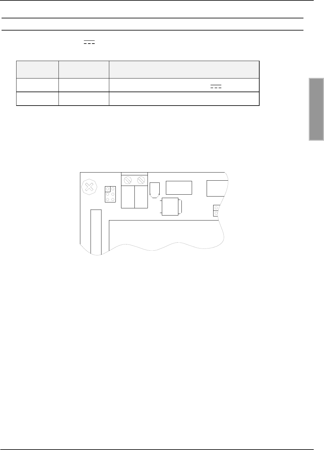
OBID i-scan®
Installation
ID ISC.LRM2500-A
FEIG ELECTRONIC GmbH
Page 43 of 63
M10210-0de-ID-B.doc
E N G L I S H
3.4 Supply voltage
The supply voltage of 24 V is connected to Terminal X6.
Terminal
Abbreviation
Description
X6 / Pin 1
VDC
Vcc – supply voltage + 24 V
X6 / Pin 2
GND
Ground – supply voltage
Table 3: Pin-outs for supply voltage on X6
GND
VDC
X8
X6
F1
1
2
Figure 4: Position oft he connector X6 for the power supply
Note:
Reversing the supply voltage polarity may destroy the device.
To meet national requirements for radio frequency devices the power supply line must
be fitted with one of the supplied EMC ring cores 28 mm x 20 mm. The power supply
line must be wound around the ring core for at least 5 turns. The distance between the
Reader termination and the ring core should be maximum 10 cm.
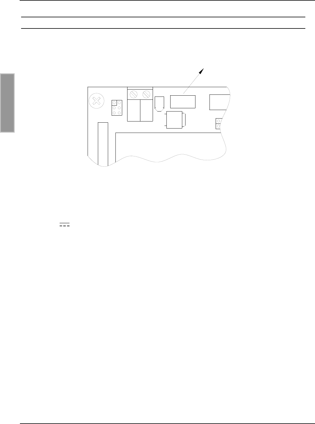
OBID i-scan®
Installation
ID ISC.LRM2500-A
FEIG ELECTRONIC GmbH
Page 44 of 63
M10210-0de-ID-B.doc
E N G L I S H
3.5 Fuse F1
The reader have been protected with a SMD fuse 2,5A (time-lag).
Attention!:
The 24V voltage for supplying the internal and external DC voltage on X2 for the dig-
ital inputs and outputs is not protected by the fuse F1.
Figure 5: Position oft he fuse F1
X8
X6
F1
2,5 A time-lag

OBID i-scan®
Installation
ID ISC.LRM2500-A
FEIG ELECTRONIC GmbH
Page 45 of 63
M10210-0de-ID-B.doc
E N G L I S H
3.6 X2: Optokoppler Inputs (X2 / IN1, IN2, IN3)
The three optocouplers inputs are available on Terminal X2.
X2
IN1-
REL3-COM
REL2-COM
REL1-COM
GND
IN3-
IN2-
GND
OUT2-E
IN1+
OUT1-C
GND
IN3+
IN2+
OUT2-C
REL3-NO
REL2-NO
REL1-NO
24V
OUT1-E
Figure 6: Optocoupler pin-outs on terminal X2
The optocoupler on terminal strips X2 are galvanically isolated from the Reader electronics and
must therefore be powered externally, see Figure 7. The external VCC voltage may however be
provided by the reader, see Figure 8.
All 3 inputs are identical and may therefore be configured individually.
470 +
IN1 -Uext
820 J2
J1 24 V
470 +
IN2 -Uext
820 J4
J3 24 V
470 +
IN3 -Uext
820 J6
J5 24 V
Figure 7: External power supply for the optocouplers
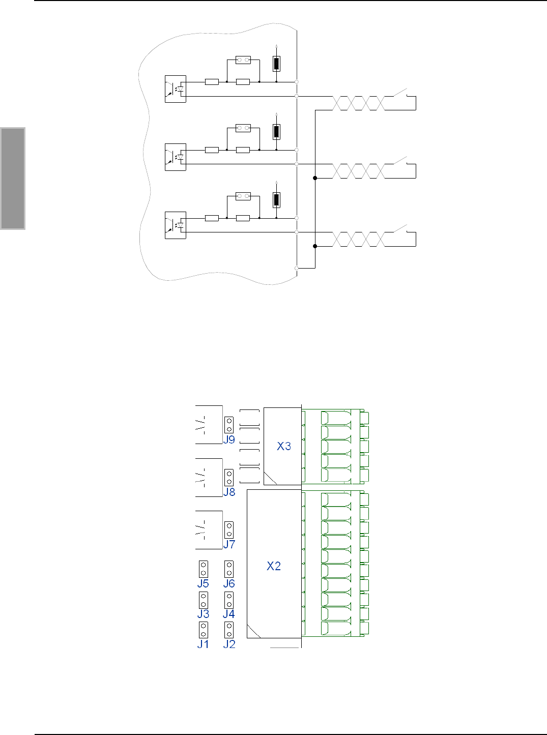
OBID i-scan®
Installation
ID ISC.LRM2500-A
FEIG ELECTRONIC GmbH
Page 46 of 63
M10210-0de-ID-B.doc
E N G L I S H
470 +
IN1 -
820 J2
J1 24 V
470 +
IN2 -
820 J4
J3 24 V
470 +
IN3 -
820 J6
J5 24 V
GND
Figure 8: Possible internal power supply for the optocouplers
The input LED for the optocouplers are internally connected to a series resistor of 1290 and are
limited to an input current of max. 20mA. For voltages of less than 10V a part of the series
resistance must be jumpered (J1, J3, J5) accordingly.
Figure 9: Position oft he Jumper J1- J9

OBID i-scan®
Installation
ID ISC.LRM2500-A
FEIG ELECTRONIC GmbH
Page 47 of 63
M10210-0de-ID-B.doc
E N G L I S H
Note:
The input is configured for a maximum input voltage of 24 V and an input current of
maximum 20mA.
Reversing the polarity or overloading the input will destroy it.
Jumper
Description
J1
Series resistance IN1 (X2)
J2
VCC IN1 (X2)
J3
Series resistance IN2 (X2)
J4
VCC IN2 (X2)
J5
Series resistance IN3 (X2)
J6
VCC IN3 (X2)
Table 4: Jumpers for inputs IN1,IN2 and IN3
Table 5 shows the required external series resistances for the various external voltages
External voltage Uext
Jumper J1/J3/J5
5 V ... 10 V
ON
10 V ... 24 V
OFF
Table 5: Required external series resistance
Table 6 shows the jumper setting for external or internal supply voltage
Jumper
Jumper J2/J4/J6
external voltage
OFF
internal VCC voltage
ON
Table 6: Internal / External supply voltage
Note:
The internal 24V voltage for supplying the DC voltage on the digital inputs is not
protected by the fuse F1.
Using internal and external voltage at the same time can destroy the reader.
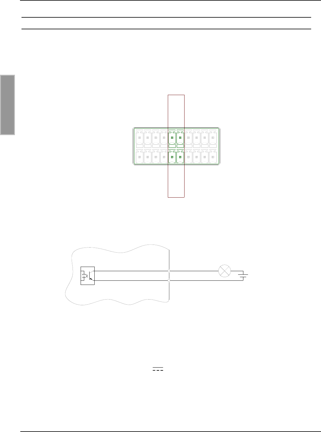
OBID i-scan®
Installation
ID ISC.LRM2500-A
FEIG ELECTRONIC GmbH
Page 48 of 63
M10210-0de-ID-B.doc
E N G L I S H
3.7 Optocoupler outputs (X2 / OUT1, OUT2)
The transistor connections, collector and emitter, of the optocoupler outputs are galvanically
isolated from the Reader electronics and are carried to the outside without any internal ancillary
circuitry on Terminal X2. The output must therefore be powered by an external power supply.
The digital outputs OUT1 and OUT2 can be used fort the data clock interface. OUT1 => „Clock“,
OUT2 => „Data“
OUT1-E
IN1-
REL3-COM
REL2-COM
REL1-COM
GND
IN3-
IN2-
GND
OUT2-E
IN1+
OUT1-C
GND
IN3+
IN2+
OUT2-C
REL3-NO
REL2-NO
REL1-NO
24V
X2
Figure 10: Digital Output’s on terminal X2
OUT1..2 E
C
Uext
Figure 11: Internal and possible external wiring of the digital output OUT1-2
Note:
The output is configured for max. 24 V / 30 mA.
Polarity reversal or overload on the output will destroy it.
The output is intended for switching resistive loads only.

OBID i-scan®
Installation
ID ISC.LRM2500-A
FEIG ELECTRONIC GmbH
Page 49 of 63
M10210-0de-ID-B.doc
E N G L I S H
3.8 Relay (X2 / REL1, REL2, REL3)
The relay outputs are all a normally open contact. These outputs, which are located on terminals
X2, are galvanically isolated from the Reader electronics and must therefore be externally
supplied. The external voltage may however be provided by the card using jumper J7;J8;J9. All 3
outputs are identical and may be configured individually.
IN1-
REL3-COM
REL2-COM
REL1-COM
GND
IN3-
IN2-
GND
OUT2-E
IN1+
OUT1-C
GND
IN3+
IN2+
OUT2-C
REL3-NO
REL2-NO
REL1-NO
24V
OUT1-E
X2
Figure 12: Relay Outputs on terminal X2
REL1
COM
N0 NO
COM
Uext
J7
24 V
REL2
COM
N0 NO
COM
Uext
J8
24 V
REL3
COM
N0 NO
COM
Uext
J9
24 V
Figure 13: Internal and possible external wiring of the relay output’s
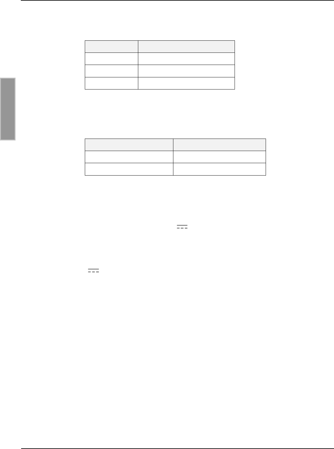
OBID i-scan®
Installation
ID ISC.LRM2500-A
FEIG ELECTRONIC GmbH
Page 50 of 63
M10210-0de-ID-B.doc
E N G L I S H
Table 7 shows the assignment oft he jumpers to the relay output
Jumper
Description
J7
VCC - REL 1 (X2)
J8
VCC - REL 2 (X2)
J9
VCC - REL 3 (X2)
Table 7: Assignment oft he jumpers to the relay output
Table 8 shows the jumper setting fort he external voltage or internal VCC voltage
Jumper
Jumper J7/J8/J9
external voltage
open
Internal VCC voltage
closed
Table 8: Internal- / External voltage supply
Notes:
The relay output is configured for max. 24 V / 2 A.
The relay output is intended for switching resistive loads only. If an inductive load is
connected, the relay contacts must be protected by means of an external protection
circuit.
The internal 24V voltage for supplying the DC voltage on the relays is not protected
by the fuse F1.
Using internal and external voltage at the same time can destroy the reader.
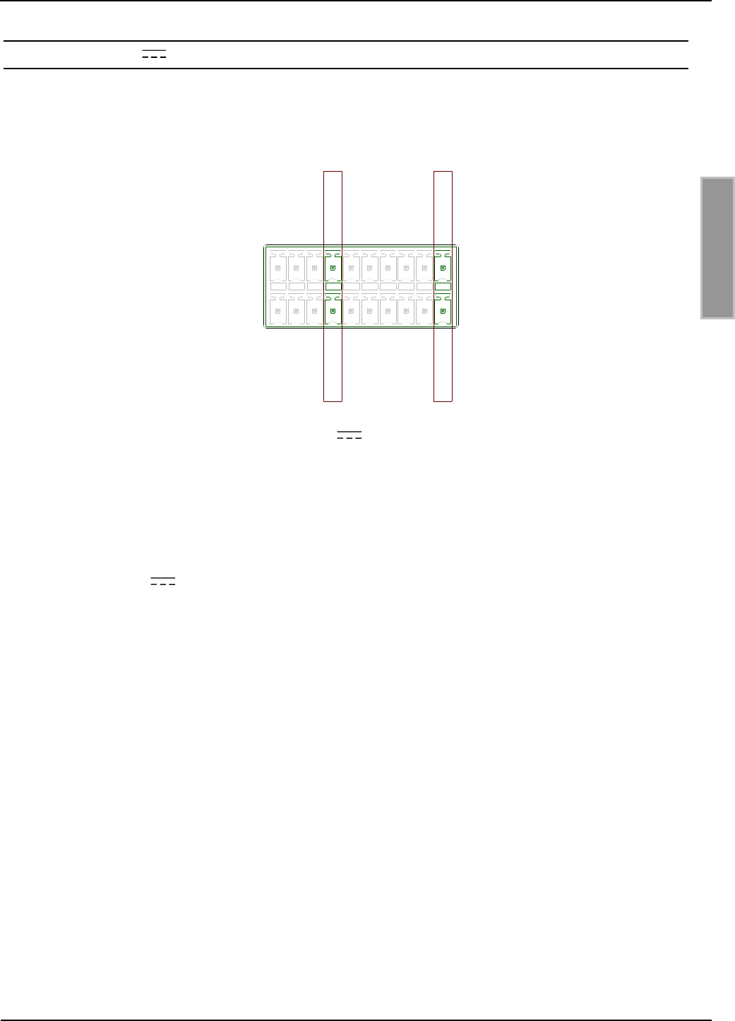
OBID i-scan®
Installation
ID ISC.LRM2500-A
FEIG ELECTRONIC GmbH
Page 51 of 63
M10210-0de-ID-B.doc
E N G L I S H
3.9 Output 24V (X2 / 24V, GND)
The output 24V/GND can be used to power the optional external circuitry of the digital inputs , out-
puts or relays. The maximum current consumption must not exceed 500mA. A possible current
consumption via J2, J4, J6 or J7, J8, J9 must be be factored in.
X2
IN1-
REL3-COM
REL2-COM
REL1-COM
GND
IN3-
IN2-
GND
OUT2-E
IN1+
OUT1-C
GND
IN3+
IN2+
OUT2-C
REL3-NO
REL2-NO
REL1-NO
24V
OUT1-E
Figure 14: Optional 24V external voltage supply
Note:
For the dimensioning oft the power supply the power consumption for the external out-
put circuitry must be additional considered to the typical reader power consumption.
The internal 24V voltage on X2 is not protected by the fuse F1.

OBID i-scan®
Installation
ID ISC.LRM2500-A
FEIG ELECTRONIC GmbH
Page 52 of 63
M10210-0de-ID-B.doc
E N G L I S H
3.10 X8: External diagnostic LED connections
X8 allows for connection of additional external LEDs in parallel with the internal diagnostic LEDs.
The external LEDs are connected as shown in Figure 15
Terminal
Abbreviation
Description
X8 / Pin 1
V1 Anode ext.
Function same as internal LED V1
X8 / Pin 2
V2 Anode ext.
Function same as internal LED V2
X8 / Pin 3
V3 Anode ext.
Function same as internal LED V3
X8 / Pin 4
V4 Anode ext.
Function same as internal LED V4
X8 / Pin 5
V5 Anode ext.
Function same as internal LED V5
X8 / Pin 6
GND
Common GND
Table 9: External LEDs pin-outs
external LEDs
X8 1
5
3
12
4
6
6
2
3
4
5V5 V4
X8
V2V3 V1
X8
X6
F1
Figure 15: Connecting external LEDs to X8
Note:
The outputs on X8 are intended for switching an external LED only. Overloading the
outputs with other loads may destroy them.
If only one output is used the maximum current consumption is Imax=15mA. The total
current consumption of all 5 outputs together should not increase 25mA. The off-load
output voltage is 3,3V and is supplied via a 220Ohm series resistor.

OBID i-scan®
Installation
ID ISC.LRM2500-A
FEIG ELECTRONIC GmbH
Page 53 of 63
M10210-0de-ID-B.doc
E N G L I S H
3.11 Interfaces
3.11.1 RS232-Interface X3
The RS232 interface is connected on X3.
The transmission parameters can be configured by means of software protocol.
Figure 16: RS232 interface pin-outs on X3
Kurzzeichen
Description
TxD
RS232 – (Transmit)
RxD
RS232 – (Receive)
GND
RS232 – (Ground)
Table 10: Pin assignment of the RS232-Interface
Figure 17: Wiring example for connecting the RS232 interface

OBID i-scan®
Installation
ID ISC.LRM2500-A
FEIG ELECTRONIC GmbH
Page 54 of 63
M10210-0de-ID-B.doc
E N G L I S H
3.11.2 RS485-Interface X3
The connection of the RS485 interface take place via the X3 connector as well.
The interface parameter can be configured via software protocols.
Abbreviation
Description
GND
RS485 – GND
A-
RS485 – (A -)
B+
RS485 – (B +)
Table 11: RS485 interface pin-outs
With the Jumper J10 and J11 the „Pull up“ and „Pull down“ resistors can be activated if needed.
Jumper
Closed
Open
J10
Pull-Down on RS4xx - A
without Pull-Down on RS4xx - A
J11
Pull-Up on RS4xx - B
without Pull-Up on RS4xx - B
Table 12: Jumper of the RS485-interface
Note:
The Termination can be activated via software in the reader configuration.
Figure 18: RS485 interface pin-outs on X3 (RS485-Interface)
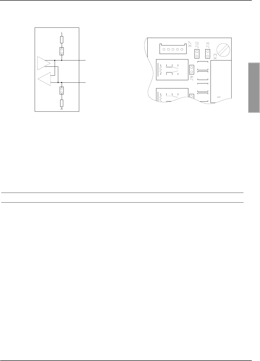
OBID i-scan®
Installation
ID ISC.LRM2500-A
FEIG ELECTRONIC GmbH
Page 55 of 63
M10210-0de-ID-B.doc
E N G L I S H
J11
VCC
J10
500
500
RS485 +
RS485 -
Figure 19: Jumper of the RS485-interface
Figure 20: Position of the Jumper J10, J11
Note:
If the Gate People Counter is connected with the RS485 interface the RS485 interface can
be not used for host communication.
3.11.2.1 Address assignment of RS485 for bus operation
For bus operation the Reader can be assigned the required bus address via software.
The address is assigned by the host computer. The software is used to assign addresses “0”
through “254” to the Reader.
The termination of the RS485 Bus can be configured via software. See system manual.
Note:
Since all Readers are factory set with address „0“, they must be connected and configured
one after the other.

OBID i-scan®
Installation
ID ISC.LRM2500-A
FEIG ELECTRONIC GmbH
Page 56 of 63
M10210-0de-ID-B.doc
E N G L I S H
3.11.3 USB – Interface X4 (Host Communication, HDI)
The USB socket on the board is terminal X4. The pinout is standardized. The data rate is reduced
to 12 Mbit (USB full speed). A standard USB-cable can be used.
Note:
The length of the USB-cable can be a max. of 5m (20 inch). It is not allowed to use longer
cables.
3.11.4 USB – Host X5
The USB host socket on the board is terminal X5. The pinout is standardized. The data rate is re-
duced to 12 Mbit (USB full speed). It can be used for a standard WLAN-USB-Stick
Note:
It is possible to use standard WLAN-USB-Sticks. It must be ensured that this stick contains
a „Ralink“ Chipsatz „RT2500 USB“ or „RT73“.
X4
Figure 21: USB-Interface for host communication
Figure 22: USB-Host X5
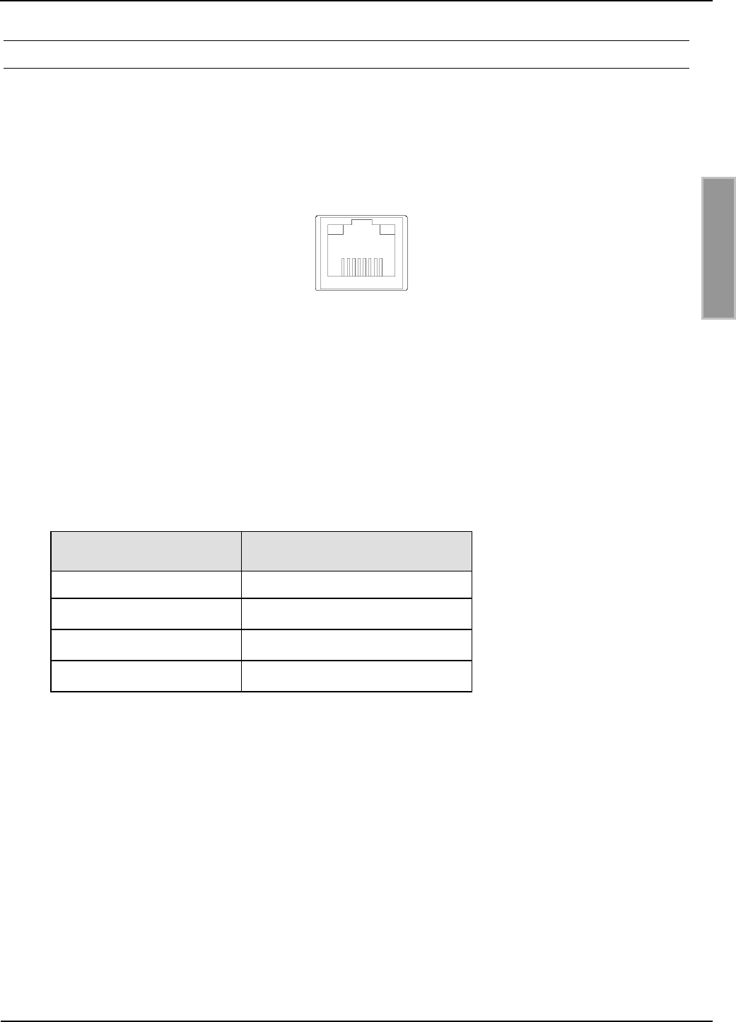
OBID i-scan®
Installation
ID ISC.LRM2500-A
FEIG ELECTRONIC GmbH
Page 57 of 63
M10210-0de-ID-B.doc
E N G L I S H
3.11.5 Ethernet-Interface on X1 (10/100 Base-T)
The Reader has an integrated 10 / 100 Base-T network port for an RJ-45. Connection is made on
X1 and has an automatic “Crossover Detection” according to the 1000 Base-T Standard.
With structured cabling CAT 5 cables should be used. This ensures a reliable operation at 10 Mbps
or 100 Mbps.
The prerequisite for using TCP/IP protocol is that each device has a unique address on the net-
work. All Readers have a factory set IP address.
Network
Address
IP-Adresse
192.168.10.10
Subnet-Mask
255.255.255.0
Port
10001
DHCP
OFF
Table 13 Standard factory configuration of the Ethernet connection
Note:
The Reader TCP/IP interface has a DHCP option.
X1
Figure 23: LAN interface for host communication

OBID i-scan®
Installation
ID ISC.LRM2500-A
FEIG ELECTRONIC GmbH
Page 58 of 63
M10210-0de-ID-B.doc
E N G L I S H
4 Operating and Display Elements
4.1 LEDs
Table 14 shows the LED configuration.
Abbreviation
Description
LED V1 (green)
"RUN-LED 1"
- Indicates proper running of the internal Reader software (DSP)
- Comes on during Reader initialization after power-on or after a
reset.
LED V2 (blue)
Diagnostic 1: RF communication / EEPROM status
- Short flashing indicates errorless communication with a
transponder on the RF interface
- Flashes alternately with V1 after a reset following a software
update
- Flashes alternately with V1 in case of a data error when
reading the parameters after a reset
LED V3 (yellow)
Diagnostic 2: Host communication
- Short flashing indicates sending of a protocol to the host on the
RS232/RS485/USB and LAN-Interface
LED V4 (yellow)
Reserved
LED V5 (red)
Diagnostic 4: RF warning
- Comes on when there is an error in the RF section of the
Reader. The error type can be read out via software over the
RS232/RS485/USB and LAN-Interface
Table 14: LED configuration

OBID i-scan®
Installation
ID ISC.LRM2500-A
FEIG ELECTRONIC GmbH
Page 59 of 63
M10210-0de-ID-B.doc
E N G L I S H
4.2 Button T1
Abbreviation
Description
T1
Reader reset button
Table 15: Reset Button
- Pressing T1 resets the reader controller

OBID i-scan®
Installation
ID ISC.LRM2500-A
FEIG ELECTRONIC GmbH
Page 60 of 63
M10210-0de-ID-B.doc
E N G L I S H
5 Radio Approvals
5.1 Europe (CE)
When used according to regulation, this radio equipment conforms with the basic requirements of
Article 3 and the other relevant provisions of the R&TTE Guideline 1999/E6 dated March 99.
Equipment Classification according ETSI EN 300 440 and ETSI EN 301 489: Class 2

OBID i-scan®
Installation
ID ISC.LRM2500-A
FEIG ELECTRONIC GmbH
Page 61 of 63
M10210-0de-ID-B.doc
E N G L I S H
5.2 USA (FCC) and Canada (IC)
Product name:
ID ISC.LRM2500-A
Reader name:
ID ISC.LRM2500-A
FCC ID:
IC:
PJMLRM2500
6633A-LRM2500
Notice for USA and
Canada
This device complies with Part 15 of the FCC Rules and with
RSS-210 of Industry Canada.
Operation is subject to the following two conditions.
(1) this device may not cause harmful interference, and
(2) this device must accept any interference received,
including interference that may cause undesired operation.
Unauthorized modifications may void the authority granted under
Federal communications Commission Rules permitting the operation
of this device.
This equipment has been tested and found to comply with the limits for
a Class A digital device, pursuant to Part 15 of the FCC Rules. These
limits are designed to provide reasonable protection against harmful
interference when the equipment is operated in a commercial
environment. This equipment generates, uses, and can radiate radio
frequency energy and, if not installed and used in accordance with the
instruction manual, may cause harmful interference to radio
communications. Operation of this equipment in a residential area is
likely to cause harmful interference in which case the user will be
required to correct the interference at his own expense.
Le présent appareil est conforme aux CNR d'Industrie Canada appli-
cables aux appareils radio exempts de licence. L'exploitation est auto-
risée aux deux conditions suivantes :
(1) l'appareil ne doit pas produire de brouillage, et
(2) l'utilisateur de l'appareil doit accepter tout brouillage radioélectrique
subi, même si le brouillage est susceptible d'en compromettre le fonc-
tionnement.
Warning: Changes or modification made to this equipment not expressly approved by
FEIG ELECTRONIC GmbH may void the FCC authorization to operate this equipment.

OBID i-scan®
Installation
ID ISC.LRM2500-A
FEIG ELECTRONIC GmbH
Page 62 of 63
M10210-0de-ID-B.doc
E N G L I S H
6 Technical Data
ID ISC.LRM2500-A
Mechanical Data
Dimensions ( W x H x D )
160 mm x 120 mm x 46 mm
(6.29 inch x 4.72 inch x 1.81 inch)
Weight
approx.. 0,6 kg (1.32 lb)
Electrical Data
Supply Voltage
24 V 15 %
Noise Ripple : max. 150 mV
Power Consumption
Typical 35 VA / maximum 47VA (depending on ext.
output circuitry)
Operating Frequency
13,56 MHz
Transmit Power
2W – 12 W
(250 mW Step - Software)
Modulation
10% - 30%
(Software configurable)
Antenna Connection
SMA Jack (50)
DC Supply at Antenna Connec-
tor
8 V (max. 150mA)
Diagnostic Options
internal VSWR-Meter
internal temperature monitoring
Outputs
– 2 Optocoupler
– 3 Relay ( 3 x NO)
24 V / 30 mA (optional usable as Data Clock IF)
24 V / 1 A
Inputs
– 3 Optocoupler
5- 24 V / 20 mA (See chapter: 3.6)
Interfaces
RS232
RS485
USB – Interface (HID)
USB – Host (WLAN)
Ethernet (TCP/IP)
Data Clock

OBID i-scan®
Installation
ID ISC.LRM2500-A
FEIG ELECTRONIC GmbH
Page 63 of 63
M10210-0de-ID-B.doc
E N G L I S H
Protocol Modes
FEIG ISO HOST
BRM (Data Filtering and Data Buffering
Scan Mode
Notification Mode
Supported Transponder
ISO15693, ISO18000-3-A
(EM HF ISO Chips, Fujitsu HF ISO Chips, KSW
Sensor Chips, Infineon my-d, NXP I-Code, STM
ISO Chips, TI Tag-it)
NXP I Code 1
Optical Indicators
5 LEDs for Operating Status Diagnostics
Ambient
Temperature Range
– Operating
– Storage
-20°C to +55°C (-4°F to +131°F)
-25°C to +85°C (-13°F to +185°F)
Humidity
5% - 80%, no condensation
Vibration
EN 60068-2-6
10 Hz to 150 Hz : 0,075 mm / 1 g
Shock
EN 60068-2-27
Acceleration : 30 g
Applicable Standards
RF Approval
– Europe
– USA
- Canada
EN 300 330
FCC 47 CFR Part 15
RSS-210
EMC
EN 301 489
Safety
– Low Voltage Directive
– Human Exposure
EN 60950
EN 50364