Fibocom Wireless H330 UMTS/HSPA + MODULE User Manual USERS MANUAL
Fibocom Wireless Inc. UMTS/HSPA + MODULE USERS MANUAL
UserManual.wiki
>
Fibocom Wireless
>
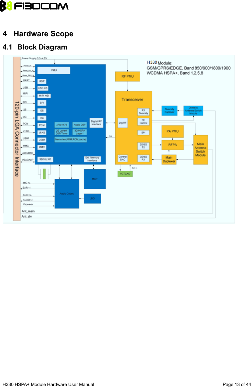
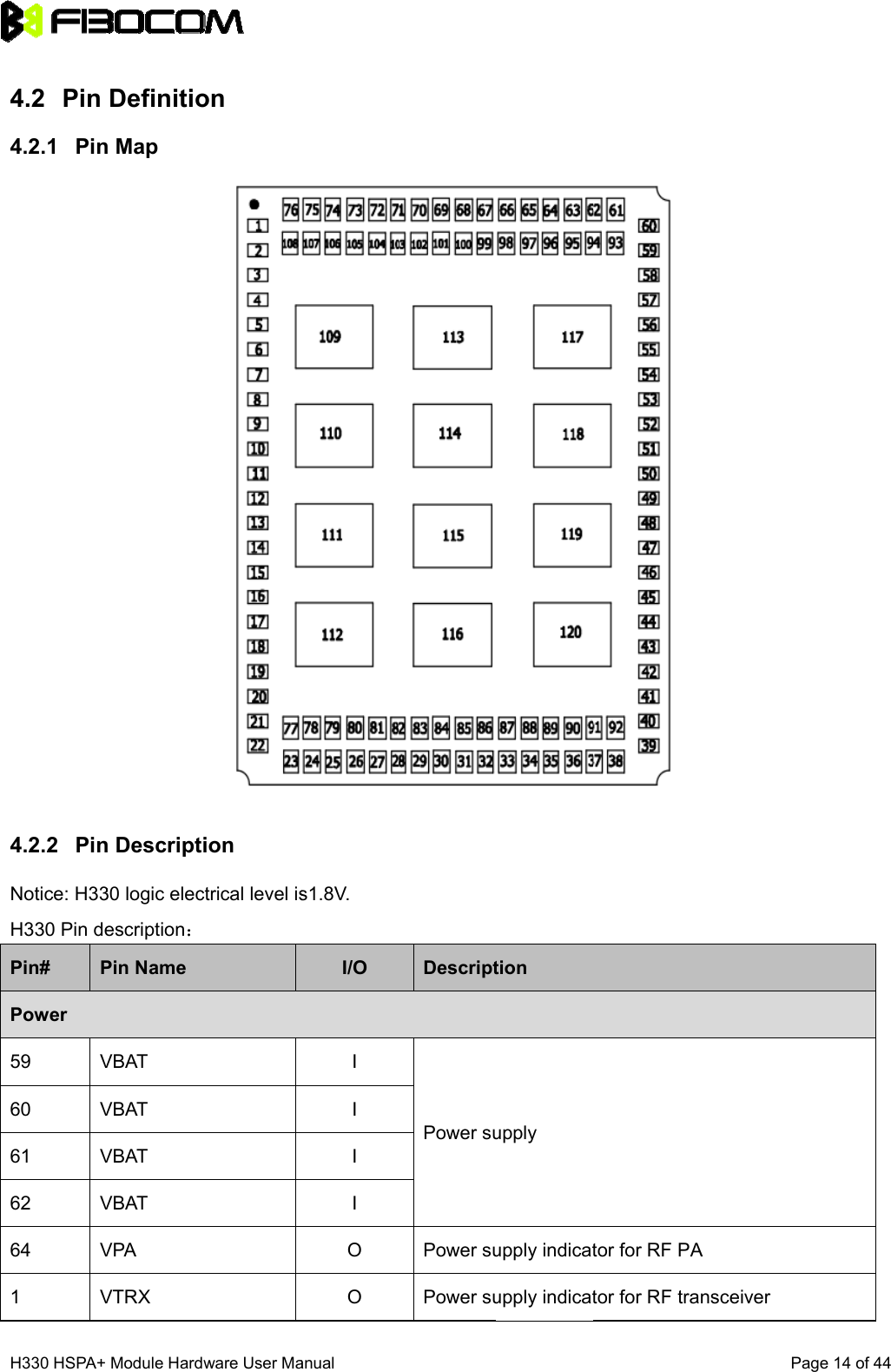
H330 User Manual
USERS MANUAL
Navigation menu
Upload a User Manual
Namespaces
Wiki Guide
HTML
PDF
Info
Views
User Manual
Discussion / Help
Navigation